
2760QM - Processor INTEL - Free user manual and instructions
Find the device manual for free 2760QM INTEL in PDF.
| Product Type | Processor |
| Brand | Intel |
| Model | Core i7-2760QM |
| Architecture | Sandy Bridge |
| Socket | rPGA988B (Socket G2) |
| Number of Cores | 4 |
| Number of Threads | 8 (Hyper-Threading) |
| Base Frequency | 2.4 GHz |
| Max Turbo Boost Frequency | 3.5 GHz |
| L3 Cache | 6 MB |
| Integrated Memory Controller | Yes, dual-channel DDR3 |
| Memory Support | DDR3-1066/1333/1600 |
| TDP (Thermal Design Power) | 45 W |
| Lithography | 32 nm |
| Instruction Set | Intel 64, SSE4.2, AVX |
| Supported Technologies | Hyper-Threading, Turbo Boost 2.0, Intel VT-x, Intel VT-d, Execute Disable Bit |
| PCI Express | Version 2.0, 16 lanes |
| Maximum Operating Temperature | 100 °C |
| Recommended Cooling | Active fan compatible with socket G2 |
| Power Supply | Through the motherboard (no direct power connector) |
Frequently Asked Questions - 2760QM INTEL
User questions about 2760QM INTEL
0 question about this device. Answer the ones you know or ask your own.
Ask a new question about this device
Download the instructions for your Processor in PDF format for free! Find your manual 2760QM - INTEL and take your electronic device back in hand. On this page are published all the documents necessary for the use of your device. 2760QM by INTEL.
USER MANUAL 2760QM INTEL
Intel® Core™ i7 Processor Family for the LGA-2011 Socket
Datasheet, Volume 2
Supporting Desktop Intel® Core™ i7-3960X Extreme Edition Processor for the LGA-2011 Socket
Supporting Desktop Intel ^® Core ^TM i7-3000K and i7-3000 Processor Series for the LGA-2011 Socket
This is volume 2 of 2.
November 2011
INFORMATION IN THIS DOCUMENT IS PROVIDED IN CONNECTION WITH INTEL® PRODUCTS. NO LICENSE, EXPRESS OR IMPLIED, BY ESTOPPEL OR OTHERWISE, TO ANY INTELLECTUAL PROPERTY RIGHTS IS GRANTED BY THIS DOCUMENT. EXCEPT AS PROVIDED IN INTEL'S TERMS AND CONDITIONS OF SALE FOR SUCH PRODUCTS, INTEL ASSUMES NO LIABILITY WHATSOEVER, AND INTEL DISCLAIMS ANY EXPRESS OR IMPLIED WARRANTY, RELATING TO SALE AND/OR USE OF INTEL PRODUCTS INCLUDING LIABILITY OR WARRANTIES RELATING TO FITNESS FOR A PARTICULAR PURPOSE, MERCHANTABILITY, OR INFRINGEMENT OF ANY PATENT, COPYRIGHT OR OTHER INTELLECTUAL PROPERTY RIGHT. Intel products are not intended for use in medical, life saving, life sustaining, critical control or safety systems, or in nuclear facility applications.
Intel may make changes to specifications and product descriptions at any time, without notice.
Designers must not rely on the absence or characteristics of any features or instructions marked "reserved" or "undefined." Intel reserves these for future definition and shall have no responsibility whatsoever for conflicts or incompatibilities arising from future changes to them. The information here is subject to change without notice. Do not finalize a design with this information.
The products described in this document may contain design defects or errors known as errata which may cause the product to deviate from published specifications. Current characterized errata are available on request.
This document contains information on products in the design phase of development. The information here is subject to change without notice. Do not finalize a design with this information.
Contact your local Intel sales office or your distributor to obtain the latest specifications and before placing your product order.
Hyper-Threading Technology requires a computer system with a processor supporting HT Technology and an HT Technology enabled chipset, BIOS and operating system. Performance will vary depending on the specific hardware and software you use. For more information including details on which processors support HT Technology, see
http://www.intel.com/products/ht/hyperthreading_more.htm.
Enhanced Intel SpeedStep® Technology - See the Processor Spec Finder or contact your Intel representative for more information.
Enabling Execute Disable Bit functionality requires a PC with a processor with Execute Disable Bit capability and a supporting operating system. Check with your PC manufacturer on whether your system delivers Execute Disable Bit functionality.
Intel® Virtualization Technology requires a computer system with an enabled Intel® processor, BIOS, virtual machine monitor (VMM) and, for some uses, certain computer system software enabled for it. Functionality, performance or other benefits will vary depending on hardware and software configurations and may require a BIOS update. Software applications may not be compatible with all operating systems. Please check with your application vendor.
Intel® Turbo Boost Technology requires a PC with a processor with Intel Turbo Boost Technology capability. Intel Turbo Boost Technology performance varies depending on hardware, software and overall system configuration. Check with your PC manufacturer on whether your system delivers Intel Turbo Boost Technology. For more information, see http://www.intel.com/technology/turboboost/.
Intel® Active Management Technology requires the platform to have an Intel® AMT-enabled chipset, network hardware and software, connection with a power source and a network connection.
64-bit computing on Intel architecture requires a computer system with a processor, chipset, BIOS, operating system, device drivers and applications enabled for Intel ^® 64 architecture. Performance will vary depending on your hardware and software configurations. Consult with your system vendor for more information.
Intel processor numbers are not a measure of performance. Processor numbers differentiate features within each processor family, not across different processor families. See http://www.intel.com/products/processor_number for details.
I^2C is a two-wire communications bus/protocol developed by Philips. SMBus is a subset of the I^2C bus/protocol and was developed by Intel. Implementations of the I^2C bus/protocol may require licenses from various entities, including Philips Electronics N.V. and North American Philips Corporation.
Intel, Enhanced Intel SpeedStep Technology, Intel Core, and the Intel logo are trademarks of Intel Corporation in the U.S. and other countries.
* Other names and brands may be claimed as the property of others.
Copyright © 2011, Intel Corporation. All rights reserved.
Contents
1 Introduction....25
1.1 Document Terminology 25
1.2 Related Documents 27
1.3 Register Terminology.... 28
2 Configuration Process and Registers 31
2.1 Platform Configuration Structure 31
2.1.1 Processor IIO Devices (CPUBUSNO (0)) 31
2.1.2 Processor Uncore Devices (CPUBUSN0 (1)) 33
2.2 Configuration Register Rules 34
2.2.1 CSR Access 34
2.2.2 PCI Bus Number 34
2.2.3 Uncore Bus Number 34
2.3 Configuration Mechanisms 35
2.3.1 Standard PCI Express* Configuration Mechanism.... 35
2.4 Device Mapping.... 35
3 Processor Integrated I/O (IIO) Configuration Registers 37
3.1 Processor IIO Devices (PCI Bus CPUBUSNO (0)) 37
3.2 PCI Configuration Space Registers (CSRs) 37
3.2.1 Unimplemented Devices/Functions and Registers.... 37
3.2.2 PCI Bus Number.... 37
3.2.3 IIO PCI Express* Configuration Space Registers 40
3.2.4 Standard PCI Configuration Space (Type 0/1
Common Configuration Space).... 47
3.2.4.1 VID—Vendor Identification Register 47
3.2.4.2 DID—Device Identification Register 47
3.2.4.3 PCICMD—PCI Command Register 48
3.2.4.4 PCISTS—PCI Status Register 49
3.2.4.5 RID—Revision Identification Register 51
3.2.4.6 CCR—Class Code Register 51
3.2.4.7 CLSR—Cacheline Size Register 51
3.2.4.8 PLAT—Primary Latency Timer Register.... 52
3.2.4.9 HDR—Header Type Register 52
3.2.4.10 HDR—Header Type Register 52
3.2.4.11 BIST—Built-In Self Test Register....53
3.2.4.12 PBUS—Primary Bus Number Register 53
3.2.4.13 SECBUS—Secondary Bus Number Register.... 53
3.2.4.14 SUBBUS—Subordinate Bus Number Register 53
3.2.4.15 IOBAS—I/O Base Register 54
3.2.4.16 IOLIM—I/O Limit Register 54
3.2.4.17 SECSTS—Secondary Status Register 55
3.2.4.18 MBAS—Memory Base Register 56
3.2.4.19 MLIM—Memory Limit Register 56
3.2.4.20 PBAS—Prefetchable Memory Base Register.... 57
3.2.4.21 PLIM—Prefetchable Memory Limit Register 57
3.2.4.22 PBASU—Prefetchable Memory Base (Upper 32 bits) Register...... 57
3.2.4.23 PLIMU—Prefetchable Memory Limit (Upper 32 bits) Register ..... 58
3.2.4.24 SVID—Subsystem Vendor ID Register.... 58
3.2.4.25 SDID—Subsystem Identity 59
3.2.4.26 CAPPTR—Capability Pointer 59
3.2.4.27 CAPPTR—Capability Pointer 59
3.2.4.28 INTL—Interrupt Line Register 59
3.2.4.29 INTPIN—Interrupt Pin Register 60
3.2.4.30 BCTRL—Bridge Control Register 60
3.2.4.31 SCAPID—Subsystem Capability Identity Register....61
3.2.4.32 SNXTPTR—Subsystem ID Next Pointer Register....62
3.2.4.33 DMIRCBAR—DMI Root Complex Register Block Base Address Register 62
3.2.4.34 MSICAPID—MSI Capability ID Register 62
3.2.4.35 MSINXTPTR—MSI Next Pointer Register....63
3.2.4.36 MSIMSGCTL—MSI Control Register 63
3.2.4.37 MSIMSGCTL—MSI Control Register 64
3.2.4.38 MSGADR—MSI Address Register....65
3.2.4.39 MSGDAT—MSI Data Register 65
3.2.4.40 MSIMSK—MSI Mask Bit Register....65
3.2.4.41 MSIPENDING—MSI Pending Bit Register 66
3.2.4.42 PXPCAPID—PCI Express* Capability Identity Register....66
3.2.4.43 PXPNXTPTR—PCI Express* Next Pointer Register....66
3.2.4.44 PXPCAP—PCI Express* Capabilities Register....67
3.2.4.45 DEVCAP—PCI Express* Device Capabilities Register 68
3.2.4.46 DEVCTRL—PCI Express* Device Control Register 69
3.2.4.47 DEVSTS—PCI Express* Device Status Register....71
3.2.4.48 LNKCAP—PCI Express* Link Capabilities Register....72
3.2.4.49 LNKCON—PCI Express* Link Control Register....73
3.2.4.50 LNKSTS—PCI Express* Link Status Register....75
3.2.4.51 SLTCAP—PCI Express* Slot Capabilities Register 76
3.2.4.52 SLTCON—PCI Express* Slot Control Register....78
3.2.4.53 SLTSTS—PCI Express* Slot Status Register 80
3.2.4.54 ROOTCON—PCI Express* Root Control Register....81
3.2.4.55 ROOTCAP—PCI Express* Root Capabilities Register....83
3.2.4.56 ROOTSTS—PCI Express* Root Status Register....84
3.2.4.57 DEVCAP2—PCI Express* Device Capabilities 2 Register ....84
3.2.4.58 DEVCTRL2—PCI Express* Device Control Register 2....85
3.2.4.59 LNKCAP2—PCI Express* Link Capabilities 2 Register 86
3.2.4.60 LNKCON2—PCI Express* Link Control 2 Register ....87
3.2.4.61 LNKSTS2—PCI Express* Link Status Register 2 ....88
3.2.4.62 PMCAP—Power Management Capabilities Register 89
3.2.4.63 PMCSR—Power Management Control and Status Register....90
3.2.4.64 XPREUT_HDR_EXT—REUT PCIe* Header Extended Register .....91
3.2.4.65 XPREUT_HDR_CAP—REUT Header Capability Register....91
3.2.4.66 XPREUT_HDR_LEF—REUT Header Leaf Capability Register .....92
3.2.4.67 ACSCAPHDR—Access Control Services Extended Capability Header Register 9
3.2.4.68 ACSCAP—Access Control Services Capability Register....93
3.2.4.69 ACSCTRL—Access Control Services Control Register....94
3.2.4.70 APICBASE—APIC Base Register 94
3.2.4.71 APICLIMIT—APIC Limit Register 95
3.2.4.72 VSECHDR—PCI Express* Enhanced Capability Header Register – DMI2 Mode....95
3.2.4.73 VSHDR—Vendor Specific Header Register – DMI2 Mode....95
3.2.4.74 ERRAPHDR—PCI Express* Enhanced Capability Header Register - Root Ports....96
3.2.4.75 UNCERRSTS—Uncorrectable Error Status Register 96
3.2.4.76 UNCERRMSK—Uncorrectable Error Mask Register....97
3.2.4.77 UNCERRSEV—Uncorrectable Error Severity Register....97
3.2.4.78 CORERRSTS—Correctable Error Status Register....98
3.2.4.79 CORERRMSK—Correctable Error Mask Register 98
3.2.4.80 ERRCAP—Advanced Error Capabilities and Control Register .....99
3.2.4.81 HDRLOG[0:3]—Header Log 0-3 Register 99
3.2.4.82 RPERRCMD—Root Port Error Command Register 100
3.2.4.83 RPERRSTS—Root Port Error Status Register 100
3.2.4.84 ERRSID—Error Source Identification Register 101
3.2.4.85 PERFCTRLSTS—Performance Control and Status Register.....102
3.2.4.86 MISCCTRLSTS—Miscellaneous Control and Status Register.....103
3.2.4.87 PCIE_IOU_BIF_CTRL—PCIe* Port Bifurcation Control Register - DMI2 Port/PCIe* 107
3.2.4.88 DMICTRL—DMI Control Register 107
3.2.4.89 PCIE IOU BIF CTRL—PCIe* Port Bifurcation Control Register..... 108
3.2.4.90 PXP2CAP—Secondary PCI Express* Extended Capability Header Register....109
3.2.4.91 LNKCON3—Link Control 3 Register 109
3.2.5 PCI Express* and DMI2 Error Registers 110
3.2.5.1 ERRINJCAP—PCI Express* Error Injection Capability Register...... 110
3.2.5.2 ERRINJHDR—PCI Express* Error Injection Capability Header Register.... 110
3.2.5.3 ERRINJCON—PCI Express* Error Injection Control Register ..... 111
3.2.5.4 CTOCTRL—Completion Timeout Control Register 111
3.2.5.5 XPCORERRSTS—XP Correctable Error Status Register 112
3.2.5.6 XPCORERRMSK—XP Correctable Error Mask Register 112
3.2.5.7 XPUNCERRSTS—XP Uncorrectable Error Status Register.... 113
3.2.5.8 XPUNCERRMSK—XP Uncorrectable Error Mask Register 113
3.2.5.9 XPUNCERRSEV—XP Uncorrectable Error Severity Register 114
3.2.5.10 XPUNCERRPTR—XP Uncorrectable Error Pointer Register 114
3.2.5.11 UNCEDMASK—Uncorrectable Error Detect Status Mask Register .... 115
3.2.5.12 COREDMASK—Correctable Error Detect Status Mask Register ..... 115
3.2.5.13 RPEDMASK—Root Port Error Detect Status Mask Register..... 116
3.2.5.14 XPUNCEDMASK—XP Uncorrectable Error Detect Mask Register ..... 116
3.2.5.15 XPCOREDMASK—XP Correctable Error Detect Mask Register ..... 117
3.2.5.16 XPGLBERRSTS—XP Global Error Status Register.... 117
3.2.5.17 XPGLBERRPTR—XP Global Error Pointer Register 118
3.2.5.18 LNERRSTS—Lane Error Status Register.... 118
3.2.5.19 LER_CAP—Live Error Recovery Capability Register 119
3.2.5.20 LER_HDR—Live Error Recovery Capability Header Register 119
3.2.5.21 LER_CTRLSTS—Live Error Recovery Control and Status Register ... 119
3.2.5.22 LER_UNCERRMSK—Live Error Recovery Uncorrectable Error Mask Register.... 120
3.2.5.23 LER_XPUNCERRMSK—Live Error Recovery XP Uncorrectable Error Mask Register....120
3.2.5.24 LER_RPERRMSK—Live Error Recovery Root Port Error Mask Register....121
3.2.6 PCI Express* Lane Equalization Registers 121
3.2.6.1 LN[0:3]EQ—Lane 0 through Lane 3 Equalization Control Register....121
3.2.6.2 LN[4:7]EQ—Lane 4 through Lane 7 Equalization Control Register .. 122
3.2.6.3 LN[8:15]EQ—Lane 8 though Lane 15 Equalization Control Register 124
3.2.7 PCI Express* and DMI2 Perfmon 125
3.2.7.1 XPPMDL[0:1]—XP PM Data Low Bits Register.... 125
3.2.7.2 XPPMCL[0:1]—XP PM Compare Low Bits Register 125
3.2.7.3 XPPMDH—XP PM Data High Bits Register.... 126
3.2.7.4 XPPMCH—XP PM Compare High Bits Register 126
3.2.7.5 XPPMR[0:1]—XP PM Response Control Register.... 127
3.2.7.6 XPPMEVL[0:1]—XP PM Events Low Register.... 130
3.2.7.7 XPPMEVH[0:1]—XP PM Events High Register 132
3.2.7.8 XPPMER[0:1]—XP PM Resource Events Register 133
3.2.8 DMI Root Complex Register Block (RCRB).... 134
3.2.8.1 DMIVC0RCAP—DMI VC0 Resource Capability Register 135
3.2.8.2 DMIVC0RCTL—DMI VC0 Resource Control Register.... 135
3.2.8.3 DMIVC0RSTS—DMI VC0 Resource Status Register.... 136
3.2.8.4 DMIVC1RCAP—DMI VC1 Resource Capability Register 136
3.2.8.5 DMI VC1 RCTL—DMI VC1 Resource Control Register.... 137
3.2.8.6 DMI VC1RSTS—DMI VC1 Resource Status Register.... 138
3.2.8.7 DMIVCPRCAP—DMI VCP Resource Capability Register 138
3.2.8.8 DMI VCPRCTL—DMI VCP Resource Control Register 139
3.2.8.9 DMI VCPRSTS—DMI VCP Resource Status Register.... 140
3.2.8.10 DMI VCMRCAP—DMI VCM Resource Capability Register 140
3.2.8.11 DMI VCMRCTL—DMI VCM Resource Control Register.... 141
3.2.8.12 DMI VCMRSTS—DMI VCM Resource Status Register.... 141
3.2.8.13 DMI RCLDECH—DMI Root Complex Link Declaration Register ..... 142
3.2.8.14 DMIESD—DMI Element self Description Register....142
3.2.8.15 DMILED—DMI Link Entry Description Register 142
3.2.8.16 DMILBA0—DMI Link Address Register 143
3.2.8.17 DMIVC1CdtThrottle—DMI VC1 Credit Throttle Register 143
3.2.8.18 DMI VCpCdtThrottle—DMI VCp Credit Throttle Register....143
3.2.8.19 DMIVCmCdtThrottle—DMI VCm Credit Throttle Register....144
3.3 Integrated I/O Core Registers....145
3.3.1 Configuration Register Maps (Device 5, Function: 0, 2 and 4) .....145
3.3.2 PCI Configuration Space Registers Common to Device 5....155
3.3.2.1 VID—Vendor Identification Register 155
3.3.2.2 DID—Device Identification Register....155
3.3.2.3 PCICMD—PCI Command Register 155
3.3.2.4 PCISTS—PCI Status Register....156
3.3.2.5 RID—Revision Identification Register 157
3.3.2.6 CCR—Class Code Register 157
3.3.2.7 CLSR—Cacheline Size Register 157
3.3.2.8 HDR—Header Type Register....158
3.3.2.9 SVID—Subsystem Vendor ID Register 158
3.3.2.10 SID—Subsystem Device ID Register 158
3.3.2.11 CAPPTR—Capability Pointer Register 159
3.3.2.12 INTL—Interrupt Line Register....159
3.3.2.13 INTPIN—Interrupt Pin Register....159
3.3.2.14 PXPCAPID—PCI Express* Capability Identity Register....159
3.3.2.15 PXPNXTPTR—PCI Express* Next Pointer Register....160
3.3.2.16 PXPCAP—PCI Express* Capabilities Register....160
3.3.3 Intel ^ VT-d, Address Mapping, System Management, Coherent Interface, Misc Registers ....160
3.3.3.1 HDRTYPECTRL—PCI Header Type Control Register 160
3.3.3.2 MMCFG—MMCFG Address Range Register 161
3.3.3.3 TSEG—TSeg Address Range Register 161
3.3.3.4 GENPROTRANGE1_BASE—Generic Protected Memory Range 1 Base Address Register ....161
3.3.3.5 GENPROTRANGE1_LIMIT—Generic Protected Memory Range 1 Limit Address Register ....162
3.3.3.6 GENPROTRANGE2_BASE—Generic Protected Memory Range 2 Base Address Register ....162
3.3.3.7 GENPROTRANGE2_LIMIT—Generic Protected Memory Range 2 Limit Address Register....163
3.3.3.8 TOLM—Top of Low Memory Register 163
3.3.3.9 TOHM—Top of High Memory Register 163
3.3.3.10 NCMEM_BASE—NCMEM Base Register....164
3.3.3.11 NCMEM_LIMIT—NCMEM Limit Register 164
3.3.3.12 MENCMEM_BASE—Intel ^® Management Engine (Intel ^® ME) Non-coherent Memory Base Address Register....164
3.3.3.13 MENCMEM_LIMIT—Intel® ME Non-coherent Memory Limit Address Register 16:
3.3.3.14 CPUBUSNO—CPU Internal Bus Numbers Register....165
3.3.3.15 LMMIOL—Local MMIO Low Base Register 166
3.3.3.16 LMMIOH_BASE—Local MMIO High Base Register....166
3.3.3.17 LMMIOH_LIMIT—Local MMIO High Base Register 167
3.3.3.18 GENPROTRANGE0_BASE—Generic Protected Memory Range 0 Base Address Register ....167
3.3.3.19 GENPROTRANGE0_LIMIT—Generic Protected Memory Range 0 Limit Address Register ....168
3.3.3.20 CIPCTRL—Coherent Interface Protocol Control Register 168
3.3.3.21 CIPSTS—Coherent Interface Protocol Status Register 170
3.3.3.22 CIPDCASAD—Coherent Interface Protocol DCA Source Address Decode Register....170
3.3.3.23 CIPINTRC—Coherent Interface Protocol Interrupt Control Register .171
3.3.3.24 CIPINTRS—Coherent interface Protocol Interrupt Status Register...172
3.3.3.25 VTBAR—Base Address Register for Intel® VT-d Registers......173
3.3.3.26 VTGENCTRL—Intel® VT-d General Control Register.... 173
3.3.3.27 VTISOCHCTRL—Intel® VT-d Isoch Related Control Register ..... 174
3.3.3.28 VTGENCTRL2—Intel® VT-d General Control 2 Register 175
3.3.3.29 IOTLBPARTITION—IOTLB Partitioning Control Register.... 176
3.3.3.30 VTUNCERRSTS—Uncorrectable Error Status Register 176
3.3.3.31 VTUNCERRMSK—Intel® VT Uncorrectable Error Mask Register...... 177
3.3.3.32 VTUNCERRSEV—Intel® VT Uncorrectable Error Severity Register... 177
3.3.3.33 VTUNCERRPTR—Intel® VT Uncorrectable Error Pointer Register..... 178
3.3.3.34 IIOMISCCTRL—IIO MISC Control Register 178
3.3.3.35 IRP_MISC_DFX0—Coherent Interface Miscellaneous DFx 0 Register....182
3.3.3.36 IRP_MISC_DFX1—Coherent Interface Miscellaneous DFx 1 Register....183
3.3.3.37 IRPODELS—Coherent Interface 0 Debug Event Lane Select Register .... 184
3.3.3.38 IRP1DELS—Coherent Interface 1 Debug Event Lane Select Register 184
3.3.3.39 IRP0DBGRING[0:1]—Coherent Interface 0 Debug Ring 0 Register . 185
3.3.3.40 IRP1DBGRING[0:1]—Coherent Interface 1 Debug Ring 0 Register . 185
3.3.3.41 IRP0DBGRING1—Coherent Interface 0 Debug Ring 1 Register..... 185
3.3.3.42 IRP1DBGRING1—Coherent Interface 1 Debug Ring 1 Register..... 185
3.3.3.43 IRP0RNG—Coherent Interface 0 Cluster Debug Ring Control Register....186
3.3.3.44 IRP1RNG—Coherent Interface 1 Cluster Debug Ring Control Register.... 188
3.3.3.45 IRPEGCREDITS—R2PCIe Egress Credits Register 190
3.3.4 Global System Control and Error Registers.... 191
3.3.4.1 IRPPERRSV—IRP Protocol Error Severity Register 191
3.3.4.2 IIOERRSV—IIO Core Error Severity Register.... 192
3.3.4.3 MIERRSV—Miscellaneous Error Severity Register.... 192
3.3.4.4 PCIERRSV—PCIe* Error Severity Map Register.... 193
3.3.4.5 SYSMAP—System Error Event Map Register.... 193
3.3.4.6 VIRAL—Viral Alert Register.... 194
3.3.4.7 ERRPINCTL—Error Pin Control Register 194
3.3.4.8 ERRPINST—Error Pin Status Register.... 195
3.3.4.9 ERRPINDAT—Error Pin Data Register 195
3.3.4.10 VPPCTL—VPP Control Register 196
3.3.4.11 VPPSTS—VPP Status Register 196
3.3.4.12 GNERRST—Global Non-Fatal Error Status Register.... 197
3.3.4.13 GFERRST—Global Fatal Error Status Register.... 198
3.3.4.14 GERRCTL—Global Error Control Register 199
3.3.4.15 GSYSST—Global System Event Status Register 200
3.3.4.16 GSYSCTL—Global System Event Control Register 200
3.3.4.17 GFFERRST—Global Fatal FERR Status Register 200
3.3.4.18 GFNERRST—Global Fatal NERR Status Register 201
3.3.4.19 GNFERRST—Global Non-Fatal FERR Status Register.... 201
3.3.4.20 GNNERRST—Global Non-Fatal NERR Status Register.... 201
3.3.5 Local Error Registers.... 202
3.3.5.1 IRPP0ERRST—IRP Protocol Error Status Register 202
3.3.5.2 IRPP0ERRCTL—IRP Protocol Error Control Register 202
3.3.5.3 IRPP0FFERRST—IRP Protocol Fatal FERR Status Register.... 203
3.3.5.4 IRPP0FNERRST—IRP Protocol Fatal NERR Status Register 204
3.3.5.5 IRPP0FFERRHD[0:3]—IRP Protocol Fatal FERR Header Log 0 Register....204
3.3.5.6 IRPP0NFERRST—IRP Protocol Non-Fatal FERR Status Register..... 205
3.3.5.7 IRPP0NNERRST—IRP Protocol Non-Fatal NERR Status Register..... 205
3.3.5.8 IRPPONFERRHD[0:3]—IRP Protocol Non-Fatal FERR Header Log 0 Register....206
3.3.5.9 IRPP0ERRCNTSEL—IRP Protocol Error Counter Select Register ..... 206
3.3.5.10 IRPP0ERRCNT—IRP Protocol Error Counter Register....206
3.3.5.11 IRPP1ERRST—IRP Protocol Error Status Register 207
3.3.5.12 IRPP1ERRCTL—IRP Protocol Error Control Register....208
3.3.5.13 IRPP1FFERRST—IRP Protocol Fatal FERR Status Register .....209
3.3.5.14 IRPP1FNERRST—IRP Protocol Fatal NERR Status Register 209
3.3.5.15 IRPP1FFERRHD[0:3]—IRP Protocol Fatal FERR Header Log 0 Register ....210
3.3.5.16 IRPP1NFERRST—IRP Protocol Non-Fatal FERR Status Register .....210
3.3.5.17 IRPP1NNERRST—IRP Protocol Non-Fatal NERR Status Register .....211
3.3.5.18 IRPP1NFERRHD[0:3]—IRP Protocol Non-Fatal FERR Header Log 0 Register 211
3.3.5.19 IRPP1ERRCNTSEL—IRP Protocol Error Counter Select Register.....211
3.3.5.20 IRPP1ERRCNT—IRP Protocol Error Counter Register 212
3.3.5.21 IIOERRST—IIO Core Error Status Register 212
3.3.5.22 IIOERRCTL—IIO Core Error Control Register 212
3.3.5.23 IIOFFERRST—IIO Core Fatal FERR Status Register....213
3.3.5.24 IIOFFERRHD[0:3]—IIO Core Fatal FERR Header Register .....213
3.3.5.25 IIOFNERRST—IIO Core Fatal NERR Status Register 213
3.3.5.26 IIONFERRST—IIO Core Non-Fatal FERR Status Register....213
3.3.5.27 II ONFERRHD[0:3]—IIO Core Non-Fatal FERR Header Register .....214
3.3.5.28 IIONNERRST—IIO Core Non-Fatal NERR Status Register....214
3.3.5.29 IIOERRCNTSEL—IIO Core Error Counter Selection Register .....214
3.3.5.30 IIOERRCNT—IIO Core Error Counter Register....215
3.3.5.31 MIERRST—Miscellaneous Error Status Register 215
3.3.5.32 MIERRCTL—Miscellaneous Error Control Register 215
3.3.5.33 MIFFERRST—Miscellaneous Fatal First Error Status Register .....216
3.3.5.34 MIFFERRHDR_[0:3]—Miscellaneous Fatal First Error Header 0 Log Register 216
3.3.5.35 MIFNERRST—Miscellaneous Fatal Next Error Status Register .....216
3.3.5.36 MINFERRST—Miscellaneous Non-Fatal First Error Status Register ...216
3.3.5.37 MINFERRHDR_[0:3]—Miscellaneous Non-Fatal First Error Header 0 Log Register....217
3.3.5.38 MINNERRST—Miscellaneous Non-Fatal Next Error Status Register ..217
3.3.5.39 MIERRCNTSEL—Miscellaneous Error Count Select Register .....217
3.3.5.40 MIERRCNT—Miscellaneous Error Counter Register....217
3.3.6 IOxAPIC PCI Configuration Space....218
3.3.6.1 MBAR—IOxAPIC Base Address Register 218
3.3.6.2 SVID—Subsystem Vendor ID Register 218
3.3.6.3 SDID—Subsystem Device ID Register 218
3.3.6.4 INTL—Interrupt Line Register....219
3.3.6.5 INTPIN—Interrupt Pin Register - Others 219
3.3.6.6 ABAR—I/OxAPIC Alternate BAR Register....219
3.3.6.7 PMCAP—Power Management Capabilities Register....220
3.3.6.8 PMCSR—Power Management Control and Status Register......220
3.3.6.9 RDINDEX—Alternate Index to read Indirect I/OxAPIC Register.....221
3.3.6.10 RDWINDOW—Alternate Window to read Indirect I/OxAPIC Register 221
3.3.6.11 IOAPICTETPC—IOxAPIC Table Entry Target Programmable Control Register....222
3.3.6.12 IOADSELS0—IOxAPIC DSELS Register 0....222
3.3.6.13 IOADSELS1—IOxAPIC DSELS Register 1....223
3.3.6.14 IOUTSRC0—IO Interrupt Source Register 0....223
3.3.6.15 IOINTSRC1—IO Interrupt Source Register 1....224
3.3.6.16 IOREMINTCNT—Remote IO Interrupt Count Register.....224
3.3.6.17 IOREMGPECNT—Remote IO GPE Count Register 225
3.3.6.18 IOXAPICPARERRINJCTL—IOxAPIC Parity Error Injection Control Register....225
3.3.6.19 FAUXGV—FauxGV Register 225
3.3.7 I/OxAPIC Memory Mapped Registers 226
3.3.7.1 INDEX—Index Register 228
3.3.7.2 WNDW—Window Register....228
3.3.7.3 PAR—Pin Assertion Register....228
3.3.7.4 EOI Register....229
3.3.7.5 APICID Register 229
3.3.7.6 VER—Version Register 229
3.3.7.7 ARBID—Arbitration ID Register 230
3.3.7.8 BCFG—Boot Configuration Register 230
3.3.7.9 RTL[0:23]—Redirection Table Low DWord Register 231
3.3.7.10 RTH[0:23]—Redirection Table High DWord Register 232
3.3.8 Intel ^ VT-d Memory Mapped Register 233
3.3.8.1 VTD0_VERSION—Version Number Register.... 239
3.3.8.2 VTD0_CAP—Intel ^® VT-d Capabilities Register 239
3.3.8.3 VTD0 EXT CAP—Extended Intel ^ VT-d Capability Register..... 240
3.3.8.4 VTD0_GLBCMD—Global Command Register 241
3.3.8.5 VTD0_GLBSTS—Global Status Register 243
3.3.8.6 VTD0_ROOTENTRYADD—Root Entry Table Address Register ..... 244
3.3.8.7 VTD0_CTXCMD—Context Command Register 244
3.3.8.8 VTD0_FLTSTS—Fault Status Register 246
3.3.8.9 VTD0_FLTEVTCTRL—Fault Event Control Register....247
3.3.8.10 VTD0_FLTEVTDATA—Fault Event Data Register.... 247
3.3.8.11 VTD0_FLTEVTADDR—Fault Event Address Register.... 248
3.3.8.12 VTD0_PMEN—Protected Memory Enable Register.... 248
3.3.8.13 VTD0_PROT_LOW_MEM_BASE—Protected Memory Low Base Register....24
3.3.8.14 VTD0_PROT_LOW_MEM_LIMIT—Protected Memory Low Limit Register....24
3.3.8.15 VTD0_PROT_HIGH_MEM_BASE—Protected Memory High Base Register....24
3.3.8.16 VTD0_PROT_HIGH_MEM_LIMIT—Protected Memory High Limit Register 24
3.3.8.17 VTD0_INV_QUEUE_HEAD—Invalidation Queue Header
Pointer Register....25
3.3.8.18 VTD0_INV_QUEUE_TAIL—Invalidation Queue Tail
Pointer Register....25
3.3.8.19 VTD0_INV_QUEUE_ADD—Invalidation Queue Address Register ..... 250
3.3.8.20 VTD0_INV_COMP_STATUS—Invalidation Completion Status Register.... 25
3.3.8.21 VTD0_INV_COMP_EVT_CTL—Invalidation Completion Event Control Register.... 25
3.3.8.22 VTD0_INV_COMP_EVT_DATA—Invalidation Completion Event Data Register 252
3.3.8.23 VTD0_INV_COMP_EVT_ADDR—Invalidation Completion Event Address Register.... 252
3.3.8.24 VTD0_INTR_REMAP_TABLE_BASE—Interrupt Remapping Table Base Address Register.... 252
3.3.8.25 VTD0_FLTREC0_GPA—Fault Record Register 253
3.3.8.26 VTD0_FLTREC0_SRC—Fault Record Register 253
3.3.8.27 VTD0_FLTREC1_GPA—Fault Record Register 253
3.3.8.28 VTD0_FLTREC1_SRC—Fault Record Register 254
3.3.8.29 VTD0_FLTREC2_GPA—Fault Record Register.... 254
3.3.8.30 VTD0_FLTREC2_SRC—Fault Record Register 255
3.3.8.31 VTD0_FLTREC3_GPA—Fault Record Register.... 255
3.3.8.32 VTD0_FLTREC3_SRC—Fault Record Register 256
3.3.8.33 VTD0_FLTREC4_GPA—Fault Record Register 256
3.3.8.34 VTD0_FLTREC4_SRC—Fault Record Register 257
3.3.8.35 VTD0_FLTREC5_GPA—Fault Record Register 257
3.3.8.36 VTD0_FLTREC5_SRC—Fault Record Register 258
3.3.8.37 VTD0_FLTREC6_GPA—Fault Record Register 258
3.3.8.38 VTD0_FLTREC6_SRC—Fault Record Register 259
3.3.8.39 VTD0_FLTREC7_GPA—Fault Record Register 259
3.3.8.40 VTD0_FLTREC7_SRC—Fault Record Register 260
3.3.8.41 VTD0_INVADDRREG—Invalidate Address Register....260
3.3.8.42 VTD0_IOTLBINV—IOTLB Invalidate Register 261
3.3.8.43 VTD1_VERSION—Version Number Register 262
3.3.8.44 VTD1_CAP—Intel® VT-d Capabilities Register 262
3.3.8.45 VTD1 EXT CAP—Extended Intel ^® VT-d Capability Register .....263
3.3.8.46 VTD1_GLBCMD—Global Command Register....264
3.3.8.47 VTD1_GLBSTS—Global Status Register....266
3.3.8.48 VTD1_ROOTENTRYADD—Root Entry Table Address Register .....266
3.3.8.49 VTD1_CTXCMD—Context Command Register 267
3.3.8.50 VTD1_FLTSTS—Fault Status Register 268
3.3.8.51 VTD1 FLTEVTCTRL—Fault Event Control Register 269
3.3.8.52 VTD1_FLTEVTDATA—Fault Event Data Register 269
3.3.8.53 VTD1_FLTEVTADDR—Fault Event Address Register 270
3.3.8.54 VTD1_PMEN—Protected Memory Enable Register....270
3.3.8.55 VTD1_PROT_LOW_MEM_BASE—Protected Memory Low Base Register 270
3.3.8.56 VTD1_PROT_LOW_MEM_LIMIT—Protected Memory Low Limit Register 271
3.3.8.57 VTD1_PROT_HIGH_MEM_BASE—Protected Memory High Base Register 271
3.3.8.58 VTD1_PROT_HIGH_MEM_LIMIT—Protected Memory High Limit Register 271
3.3.8.59 VTD1_INV_QUEUE_HEAD—Invalidation Queue Header
Pointer Register 272
3.3.8.60 VTD1_INV_QUEUE_TAIL—Invalidation Queue Tail
Pointer Register 272
3.3.8.61 VTD1_INV_QUEUE_ADD—Invalidation Queue Address Register 272
3.3.8.62 VTD1_INV_COMP_STATUS—Invalidation Completion Status Register 273
3.3.8.63 VTD1_INV_COMP_EVT_CTL—Invalidation Completion Event Control Register....273
3.3.8.64 VTD1_INV_COMP_EVT_DATA—Invalidation Completion Event Data Register....273
3.3.8.65 VTD1_INV_COMP_EVT_ADDR—Invalidation Completion Event Address Register 274
3.3.8.66 VTD1_INTR_REMAP_TABLE_BASE—Interrupt Remapping Table Base Address Register 274
3.3.8.67 VTD1 FLTREC0 GPA—Fault Record Register 274
3.3.8.68 VTD1_FLTREC0_SRC—Fault Record Register 275
3.3.8.69 VTD1_INVADDRREG—Invalidate Address Register 275
3.3.8.70 VTD1_IOTLBINV—IOTLB Invalidate Register 276
4 Processor Uncore Configuration Registers 277
4.1 PCI Standard Registers....277
4.1.1 VID—Vendor Identification Register....277
4.1.2 DID—Device Identification Register 277
4.1.3 PCICMD—PCI Command Register....278
4.1.4 PCISTS—PCI Status Register....279
4.1.5 RID—Revision Identification Register 280
4.1.6 CCR—Class Code Register....280
4.1.7 CLSR—Cacheline Size Register....280
4.1.8 PLAT—Primary Latency Timer Register....280
4.1.9 HDR—Header Type Register 281
4.1.10 BIST—Built-In Self Test Register....281
4.1.11 SVID—Subsystem Vendor ID Register 281
4.1.12 SDID—Subsystem Device ID Register 281
4.1.13 CAPPTR—Capability Pointer Register....282
4.1.14 INTL—Interrupt Line Register 282
4.1.15 INTPIN—Interrupt Pin Register 282
4.1.16 MINGNT—Minimum Grant Register 282
4.1.17 MAXLAT—Maximum Latency Register 282
4.2 Integrated Memory Controller Configuration Registers 283
4.2.1 Processor Registers....283
4.2.2 CSR Register Maps 283
4.2.3 CBO unicast CSRs 301
4.2.3.1 RTID_Config_Pool01_Size—Ring Global Configuration Register..... 301
4.2.3.2 RTID_Config_Pool23_Size—Ring Global Configuration Register..... 301
4.2.3.3 RTID_Config_Pool45_Size—Ring Global Configuration Register..... 302
4.2.3.4 RTID_Config_Pool67_Size—Ring Global Configuration Register..... 302
4.2.3.5 VNA Credit Config—VNA Credit Configuration Register 303
4.2.3.6 PipeRspFunc—Pipe Response Function Register.... 303
4.2.3.7 PipeDbgBusSel—Pipe Debug Bus Select Register 30
4.2.3.8 SadDbgMm2 Register 30
4.2.3.9 Cbsads_Unicast_Cfg_Spare Register.... 304
4.2.3.10 CBO_GDXC_PKT_CNTRL—CBO GDXC Packet Control Register ..... 30
4.2.3.11 RTID_Config_Pool01_Base—Ring Global Configuration Register..... 30
4.2.3.12 RTID_Config_Pool23_Base—Ring Global Configuration Register..... 30
4.2.3.13 RTID_Config_Pool45_Base—Ring Global Configuration Register..... 30
4.2.3.14 RTID_Config_Pool67_Base—Ring Global Configuration Register..... 30
4.2.3.15 RTID_Pool_Config—Ring Global Configuration Register.... 31
4.2.3.16 RTID_Config_Pool01_Base_Shadow—Ring Global Configuration Shadow Register 3
4.2.3.17 RTID_Config_Pool23_Base_Shadow—Ring Global Configuration Shadow Register 312
4.2.3.18 RTID_Config_Pool45_Base_Shadow—Ring Global Configuration Shadow Register 313
4.2.3.19 RTID_Config_Pool67_Base_Shadow—Ring Global Configuration Shadow Register 314
4.2.3.20 RTID_Pool_Config_Shadow—Ring Global Configuration Shadow Register 315
4.2.4 System Address Decoder Registers (CBO) 316
4.2.4.1 PAM0123—CBO SAD PAM Register 316
4.2.4.2 PAM456—CBO SAD PAM Register 31
4.2.4.3 SMRAMC—System Management RAM Control Register 319
4.2.4.4 MESEG_BASE—Manageability Engine Base Address Register ..... 3
4.2.4.5 MESEG LIMIT—Manageability Engine Limit Address Register ..... 32
4.2.4.6 DRAM RULE[0:9]—DRAM Rule 0 Register 32
4.2.4.7 INTERLEAVE_LIST[0:9]—DRAM Interleave List 0 Register ...... 32
4.2.4.8 DRAM_RULE_1—DRAM Rule 1 Register 32
4.2.4.9 INTERLEAVE_LIST_1—DRAM Interleave List 1 Register 32
4.2.4.10 DRAM_RULE_2—DRAM Rule 2 Register 3
4.2.4.11 INTERLEAVE_LIST_2—DRAM Interleave List 2 Register ...... 3
4.2.4.12 DRAM_RULE_3—DRAM Rule 3 Register 3
4.2.4.13 INTERLEAVE LIST 3—DRAM Interleave List 3 Register ...... 3
4.2.4.14 DRAM_RULE_4—DRAM Rule 4 Register 3
4.2.4.15 INTERLEAVE LIST 4—DRAM Interleave List 4 Register ...... 3
4.2.4.16 DRAM_RULE_5—DRAM Rule 5 Register 3
4.2.4.17 INTERLEAVE LIST 5—DRAM Interleave List 5 Register ...... 3
4.2.4.18 DRAM RULE 6—DRAM Rule 6 Register 3
4.2.4.19 INTERLEAVE LIST 6—DRAM Interleave List 6 Register ...... 3
4.2.4.20 DRAM_RULE_7—DRAM Rule 7 Register 3
4.2.4.21 INTERLEAVE_LIST_7—DRAM Interleave List 7 Register ...... 3
4.2.4.22 DRAM_RULE_8—DRAM Rule 8 Register 3
4.2.4.23 INTERLEAVE_LIST_8—DRAM Interleave List 8 Register ...... 3
4.2.4.24 DRAM_RULE_9—DRAM Rule 9 Register 3
4.2.4.25 INTERLEAVE LIST 9—DRAM Interleave List 9 Register ...... 3
4.2.5 Caching Agent Broadcast Registers (CBo) 331
4.2.5.1 Cbo ISOC Config—Cbo Isochrony Configuration Register...... 331
4.2.5.2 Cbo_Coh_Config—Cbo Coherency Configuration Register.... 33
4.2.5.3 TOLM—Top of Low Memory Register.... 332
4.2.5.4 TOHM—Top of High Memory Register 332
4.2.5.5 MMIO_RULE[0:7]—MMIO Rule 0 Register 33
4.2.5.6 MMCFG_Rule—MMCFG Rule for Interleave Decoder Register ..... 334
4.2.5.7 IOPORT_Target_LIST—IO Target List Register 33
4.2.5.8 MMCFG Target LIST—MMCFG Target List Register 335
4.2.5.9 MMIO_Target_LIST—MMIO Target List Register....335
4.2.5.10 IOAPIC_Target_LIST—IOAPIC Target List Register....336
4.2.5.11 SAD_Target—SAD Target List 336
4.2.5.12 SAD_Control—SAD Control Register....337
4.2.6 Integrated Memory Controller Target Address Registers 337
4.2.6.1 PXPCAP—PCI Express* Capability Register....337
4.2.6.2 MCMTR—MC Memory Technology Register 338
4.2.6.3 TADWAYNESS_[0:11]—TAD Range Wayness, Limit and Target Register 339
4.2.6.4 MCMTR2—MC Memory Technology Register 2....339
4.2.6.5 MC_INIT_STATE_G—Initialization State for Boot, Training and IOSAV Register....340
4.2.6.6 RCOMP_TIMER—RCOMP Wait Timer Register....341
4.2.7 Integrated Memory Controller MemHot Registers 342
4.2.7.1 MH MAINCNTL—MEMHOT Main Control Register....342
4.2.7.2 MH_SENSE_500NS_CFG—MEMHOT Sense and 500 ns Config Register ....343
4.2.7.3 MH_DTYCYC_MIN_ASRT_CNTR[0:1]—MEMHOT Duty Cycle Period and Min Assertion Counter Register....343
4.2.7.4 MH_IO_500NS_CNTR—MEMHOT Input Output and 500ns Counter Register....344
4.2.7.5 MH_CHN_ASTN—MEMHOT Domain Channel Association Register ...345
4.2.7.6 MH TEMP STAT—MEMHOT Temperature Status Register....346
4.2.7.7 MH_EXT_STAT Register....347
4.2.8 Integrated Memory Controller SMBus Registers....347
4.2.8.1 SMB_STAT[0:1]—SMBus Status Register 347
4.2.8.2 SMBCMD[0:1]—SMBus Command Register....349
4.2.8.3 SMBCntl_[0:1]—SMBus Control Register 350
4.2.8.4 SMB_TSOD_POLL_RATE_CNTR_[0:1]—SMBus Clock Period Counter Register....351
4.2.8.5 SMB STAT 1—SMBus Status Register....352
4.2.8.6 SMBCMD_1—SMBus Command Register 353
4.2.8.7 SMBCntl_1—SMBus Control Register....354
4.2.8.8 SMB_TSOD_POLL_RATE_CNTR_1—SMBus Clock Period Counter Register....355
4.2.8.9 SMB_PERIOD_CFG—SMBus Clock Period Config Register 356
4.2.8.10 SMB_PERIOD_CNTR—SMBus Clock Period Counter Register .....356
4.2.8.11 SMB_TSOD_POLL_RATE—SMBus TSOD POLL RATE Register......356
4.2.9 Integrated Memory Controller DIMM Memory Technology Type Registers.....357
4.2.9.1 PXPCAP—PCI Express* Capability Register 357
4.2.9.2 DIMMMTR_[0:2]—DIMM Memory Technology Register....358
4.2.10 Integrated Memory Controller Memory Target Address Decoder Registers.....359
4.2.10.1 TADCHNILVOFFSET_[0:11]—TAD Range Channel Interleave i OFFSET Register 359
4.2.11 Integrated Memory Controller Channel Rank Registers....360
4.2.11.1 RIRWAYNESSLIMIT_[0:4]—RIR Range Wayness and Limit Register 360
4.2.11.2 RIRILV0OFFSET_[0:4]—RIR Range Rank Interleave 0 OFFSET Register ....360
4.2.11.3 RIRILV1OFFSET_[0:4]—RIR Range Rank Interleave 1 OFFSET Register 361
4.2.11.4 RIRILV2OFFSET_[0:4]—RIR Range Rank Interleave 2 OFFSET Register 361
4.2.11.5 RIRILV3OFFSET_[0:4]—RIR Range Rank Interleave 3 OFFSET Register 362
4.2.11.6 RIRILV4OFFSET_[0:4]—RIR Range Rank Interleave 4 OFFSET Register ....362
4.2.11.7 RIRILV5OFFSET_[0:4]—RIR Range Rank Interleave 5 OFFSET Register ....362
4.2.11.8 RIRILV6OFFSET_[0:4]—RIR Range Rank Interleave 6 OFFSET Register....363
4.2.11.9 RIRILV7OFFSET_[0:4]—RIR Range Rank Interleave 7 OFFSET Register....363
4.2.11.10 RIRILV0OFFSET_1—RIR Range Rank Interleave 0 OFFSET Register....364
4.2.11.11 RIRILV1OFFSET_1—RIR Range Rank Interleave 1 OFFSET Register.... 364
4.2.11.12 RIRILV2OFFSET_1—RIR Range Rank Interleave 2 OFFSET Register.... 365
4.2.11.13 RIRILV3OFFSET_1—RIR Range Rank Interleave 3 OFFSET Register.... 365
4.2.11.14 RIRILV4OFFSET_1—RIR Range Rank Interleave 4 OFFSET Register.... 366
4.2.11.15 RIRILV5OFFSET_1—RIR Range Rank Interleave 5 OFFSET Register.... 366
4.2.11.16 RIRILV6OFFSET_1—RIR Range Rank Interleave 6 OFFSET Register.... 367
4.2.11.17 RIRILV7OFFSET_1—RIR Range Rank Interleave 7 OFFSET Register.... 367
4.2.11.18 RIRILV0OFFSET_2—RIR Range Rank Interleave 0 OFFSET Register.... 368
4.2.11.19 RIRILV1OFFSET_2—RIR Range Rank Interleave 1 OFFSET Register....368
4.2.11.20 RIRILV2OFFSET_2—RIR Range Rank Interleave 2 OFFSET Register.... 369
4.2.11.21 RIRILV3OFFSET_2—RIR Range Rank Interleave 3 OFFSET Register.... 369
4.2.11.22 RIRILV4OFFSET_2—RIR Range Rank Interleave 4 OFFSET Register.... 370
4.2.11.23 RIRILV5OFFSET_2—RIR Range Rank Interleave 5 OFFSET Register.... 370
4.2.11.24 RIRILV6OFFSET_2—RIR Range Rank Interleave 6 OFFSET Register.... 371
4.2.11.25 RIRILV7OFFSET_2—RIR Range Rank Interleave 7 OFFSET Register.... 371
4.2.11.26 RIRILV0OFFSET_3—RIR Range Rank Interleave 0 OFFSET Register.... 372
4.2.11.27 RIRILV1OFFSET_3—RIR Range Rank Interleave 1 OFFSET Register.... 372
4.2.11.28 RIRILV2OFFSET_3—RIR Range Rank Interleave 2 OFFSET Register.... 373
4.2.11.29 RIRILV3OFFSET_3—RIR Range Rank Interleave 3 OFFSET Register.... 373
4.2.11.30 RIRILV4OFFSET_3—RIR Range Rank Interleave 4 OFFSET Register.... 374
4.2.11.31 RIRILV5OFFSET_3—RIR Range Rank Interleave 5 OFFSET Register.... 374
4.2.11.32 RIRILV6OFFSET_3—RIR Range Rank Interleave 6 OFFSET Register.... 375
4.2.11.33 RIRILV7OFFSET_3—RIR Range Rank Interleave 7 OFFSET Register.... 375
4.2.11.34 RIRILV0OFFSET_4—RIR Range Rank Interleave 0 OFFSET Register.... 376
4.2.11.35 RIRILV1OFFSET_4—RIR Range Rank Interleave 1 OFFSET Register.... 376
4.2.11.36 RIRILV2OFFSET_4—RIR Range Rank Interleave 2 OFFSET Register.... 377
4.2.11.37 RIRILV3OFFSET_4—RIR Range Rank Interleave 3 OFFSET Register.... 377
4.2.11.38 RIRILV4OFFSET_4—RIR Range Rank Interleave 4 OFFSET Register.... 378
4.2.11.39 RIRILV5OFFSET_4—RIR Range Rank Interleave 5 OFFSET Register ....378
4.2.11.40 RIRILV6OFFSET_4—RIR Range Rank Interleave 6 OFFSET Register 379
4.2.11.41 RIRILV7OFFSET_4—RIR Range Rank Interleave 7 OFFSET Register 379
4.2.12 Integrated Memory Controller Error Injection Registers....380
4.2.12.1 PXPENHCAP—PCI Express* Capability Register ....380
4.2.12.2 RIRWAYNESSLIMIT_[0:4]—RIR Range Wayness and Limit Register 380
4.2.12.3 RIRILV0OFFSET_[0:4]—RIR Range Rank Interleave 0 OFFSET Register 381
4.2.12.4 RIRILV1OFFSET_[0:4]—RIR Range Rank Interleave 1 OFFSET Register ....381
4.2.12.5 RIRILV2OFFSET_[0:4]—RIR Range Rank Interleave 2 OFFSET Register ....382
4.2.12.6 RIRILV3OFFSET_[0:4]—RIR Range Rank Interleave 3 OFFSET Register ....382
4.2.12.7 RIRILV4OFFSET_[0:4]—RIR Range Rank Interleave 4 OFFSET Register ....383
4.2.12.8 RIRILV5OFFSET_[0:4]—RIR Range Rank Interleave 5 OFFSET Register ....383
4.2.12.9 RIRILV6OFFSET_[0:4]—RIR Range Rank Interleave 6 OFFSET Register ....384
4.2.12.10 RIRILV7OFFSET_[0:4]—RIR Range Rank Interleave 7 OFFSET Register ....384
4.2.12.11 RIRILV0OFFSET_1—RIR Range Rank Interleave 0 OFFSET Register ....385
4.2.12.12 RIRILV1OFFSET_1—RIR Range Rank Interleave 1 OFFSET Register 385
4.2.12.13 RIRILV2OFFSET_1—RIR Range Rank Interleave 2 OFFSET Register ....386
4.2.12.14 RIRILV3OFFSET_1—RIR Range Rank Interleave 3 OFFSET Register ....386
4.2.12.15 RIRILV4OFFSET_1—RIR Range Rank Interleave 4 OFFSET Register 387
4.2.12.16 RIRILV5OFFSET_1—RIR Range Rank Interleave 5 OFFSET Register ....387
4.2.12.17 RIRILV6OFFSET_1—RIR Range Rank Interleave 6 OFFSET Register ....388
4.2.12.18 RIRILV7OFFSET_1—RIR Range Rank Interleave 7 OFFSET Register ....388
4.2.12.19 RIRILV0OFFSET_2—RIR Range Rank Interleave 0 OFFSET Register ....389
4.2.12.20 RIRILV1OFFSET_2—RIR Range Rank Interleave 1 OFFSET Register ....389
4.2.12.21 RIRILV2OFFSET_2—RIR Range Rank Interleave 2 OFFSET Register ....390
4.2.12.22 RIRILV3OFFSET_2—RIR Range Rank Interleave 3 OFFSET Register ....390
4.2.12.23 RIRILV4OFFSET_2—RIR Range Rank Interleave 4 OFFSET Register ....391
4.2.12.24 RIRILV5OFFSET_2—RIR Range Rank Interleave 5 OFFSET Register ....391
4.2.12.25 RIRILV6OFFSET_2—RIR Range Rank Interleave 6 OFFSET Register 392
4.2.12.26 RIRILV7OFFSET_2—RIR Range Rank Interleave 7 OFFSET Register 393
4.2.12.27 RIRILV0OFFSET_3—RIR Range Rank Interleave 0 OFFSET Register 393
4.2.12.28 RIRILV1OFFSET_3—RIR Range Rank Interleave 1 OFFSET Register ....394
4.2.12.29 RIRILV2OFFSET_3—RIR Range Rank Interleave 2 OFFSET Register.... 394
4.2.12.30 RIRILV3OFFSET_3—RIR Range Rank Interleave 3 OFFSET Register.... 395
4.2.12.31 RIRILV4OFFSET_3—RIR Range Rank Interleave 4 OFFSET Register.... 395
4.2.12.32 RIRILV5OFFSET_3—RIR Range Rank Interleave 5 OFFSET Register.... 396
4.2.12.33 RIRILV6OFFSET_3—RIR Range Rank Interleave 6 OFFSET Register.... 396
4.2.12.34 RIRILV7OFFSET_3—RIR Range Rank Interleave 7 OFFSET Register.... 397
4.2.12.35 RIRILV0OFFSET_4—RIR Range Rank Interleave 0 OFFSET Register.... 397
4.2.12.36 RIRILV1OFFSET_4—RIR Range Rank Interleave 1 OFFSET Register.... 398
4.2.12.37 RIRILV2OFFSET_4—RIR Range Rank Interleave 2 OFFSET Register.... 398
4.2.12.38 RIRILV3OFFSET_4—RIR Range Rank Interleave 3 OFFSET Register.... 399
4.2.12.39 RIRILV4OFFSET_4—RIR Range Rank Interleave 4 OFFSET Register.... 399
4.2.12.40 RIRILV5OFFSET_4—RIR Range Rank Interleave 5 OFFSET Register.... 400
4.2.12.41 RIRILV6OFFSET_4—RIR Range Rank Interleave 6 OFFSET Register.... 400
4.2.12.42 RIRILV7OFFSET_4—RIR Range Rank Interleave 7 OFFSET Register.... 401
4.2.12.43RSP_FUNC_ADDR_MATCH_LO Register 401
4.2.12.44RSP_FUNC_ADDR_MATCH_HI Register 402
4.2.12.45RSP_FUNC_ADDR_MASK_LO Register.... 402
4.2.12.46RSP_FUNC_ADDR_MASK_HI Register 403
4.2.13 Integrated Memory Controller Thermal Control Registers 403
4.2.13.1 PXPCAP—PCI Express* Capability Register 403
4.2.13.2 ET_CFG—Electrical Throttling Configuration Register.... 404
4.2.13.3 CHN_TEMP_CFG—Channel TEMP Configuration Register 405
4.2.13.4 CHN_TEMP_STAT—Channel TEMP Status Register 405
4.2.13.5 DIMM_TEMP_OEM[0:2]—DIMM TEMP Configuration Register ..... 406
4.2.13.6 DIMM_TEMP_TH[0:2]—DIMM TEMP Configuration Register ..... 407
4.2.13.7 DIMM_TEMP_THRT_LMT_[0:2]—DIMM TEMP Configuration Register 408
4.2.13.8 DIMM_TEMP_EV_OFST_[0:2]—DIMM TEMP Configuration Register 409
4.2.13.9 DIMMTEMPSTAT_[0:2]—DIMM TEMP Status Register 410
4.2.13.10PM_CMD_PWR_[0:2]—Electrical Power and Thermal Throttling Command Power Register.... 411
4.2.13.11 ET_DIMM_AVG_SUM[0:2]—Electrical Throttling Energy Accumulator Register 412
4.2.13.12ET_DIMM_TH[0:2]—Electrical Throttling Energy Threshold Register 412
4.2.13.13THRT_PWR_DIMM[0:2]—THRT_PWR_DIMM_0 Register 413
4.2.13.14PM_PDWN—PM_CKE_OFF_Control_Register.... 413
4.2.13.15MC_TERM_RNK_MSK—MC Termination Rank Mask Register ..... 415
4.2.13.16PM_SREF—PM Self-Refresh Control Register 415
4.2.13.17PM_DLL—PM DLL Config Register 416
4.2.13.18ET_CH_AVG—Electrical Throttling Energy Averager Register ..... 417
4.2.13.19ET_CH_SUM—Electrical Throttling Energy Accumulator Register .... 417
4.2.13.20ET_CH_TH—Electrical Throttling Energy Threshold.... 417
4.2.14 Integrated Memory Controller DIMM Channels Timing Registers 418
4.2.14.1 TCDBP—Timing Constraints DDR3 Bin Parameter Register 418
4.2.14.2 TCRAP—Timing Constraints DDR3 Regular Access Parameter Register....419
4.2.14.3 TCRWP—Timing Constraints DDR3 Read Write Parameter Register....420
4.2.14.4 TCOTHP—Timing Constraints DDR3 Other Timing Parameter Register....422
4.2.14.5 TCRFP—Timing Constraints DDR3 Refresh Parameter Register .....423
4.2.14.6 TCRFTP—Timing Constraints Refresh Timing Parameter Register....423
4.2.14.7 TCSRFTP—Timing Constraints Self-Refresh Timing Parameter Register....424
4.2.14.8 TCMR2SHADOW—Timing Constraints MR2 Shadow Timing Parameter Register....424
4.2.14.9 TCZQCAL—Timing Constraints ZQ Calibration Timing Parameter Register....425
4.2.14.10TCSTAGGER_REF Register 426
4.2.14.11TCMR0SHADOW—MR0 Shadow Register....426
4.2.14.12RPQAGE Register 427
4.2.14.13IDLETIME—Page Policy and Timing Parameter Register......427
4.2.14.14RDIMMTIMINGCNTL—RDIMM Timing Parameter Register 428
4.2.14.15RDIMMTIMINGCNTL2 Register 429
4.2.14.16TCMRS—DDR3 MRS Timing Register 429
4.2.14.17RD ODT TBL0—Read ODT Lookup Table 0 Register....429
4.2.14.18RD_ODT_TBL1—Read ODT Lookup Table 1 Register....430
4.2.14.19RD_ODT_TBL2—Read ODT Lookup Table 2 Register....431
4.2.14.20WR_ODT_TBL0—Write ODT Lookup Table 0 Register....432
4.2.14.21WR_ODT_TBL1—Write ODT Lookup Table 1 Register....433
4.2.14.22WR ODT TBL2—Write ODT Lookup Table 2 Register....434
4.2.14.23MC INIT STAT C Register 434
4.2.14.24RSP FUNC MCCTRL ERR INJ Register....435
4.2.14.25PWMM STARV CNTR PRESCALER Register....435
4.2.14.26WDBWM—WDB Watermarks Register....436
4.2.14.27WDAR_MODE Register 436
4.2.14.28SPARING Register 437
4.2.15 Integrated Memory Controller DDR3 Training Registers....437
4.2.15.1 IOSAV_SPEC_CMD_ADDR_[0:3]—IOSAV Special Command ADDR Seq 0 Register ....437
4.2.15.2 IOSAV_CH_ADDR_UPDT_[0:3]—IOSAV Channel Address Update Seq 0 Register ....438
4.2.15.3 IOSAV_CH_ADDR_LFSR_[0:3]—IOSAV Channel Address LFSR Seq 0 Register ....439
4.2.15.4 IOSAV_CH_SPCL_CMD_CTRL_[0:3]—IOSAV Channel Special Command Control Seq 0 Register ....439
4.2.15.5 IOSAV_CH_SUBSEQ_CTRL_[0:3]—IOSAV Channel Sub-Sequence Control Seq 0 Register ....440
4.2.15.6 IOSAV_CH_SEQ_CTRL—IOSAV Channel Sequence Control Register....441
4.2.15.7 IOSAV_CH_STAT—IOSAV Channel Status Register....442
4.2.15.8 IOSAV_CH_DATA_CNTL—IOSAV Channel Data Control Register....443
4.2.15.9 IOSAV_CH_DATA_CYC_MSK—IOSAV Channel Data Cycle Mask Register....443
4.2.16 Integrated Memory Controller Error Registers....444
4.2.16.1 ROUNDTRIP0—Round-Trip Latency Register....444
4.2.16.2 ROUNDTRIP1—Round-Trip Latency 1 Register 444
4.2.16.3 IOLATENCY0—IO Latency Register....445
4.2.16.4 IOLATENCY1—IO Latency 1 Register 445
4.2.16.5 WDBPRELOADREG0—WDB Data Load Register 0....446
4.2.16.6 WDBPRELOADREG1—WDB Data Load Register 1....446
4.2.16.7 WDBPRELOADCTRL—WDB Preload Control Register....447
4.2.16.8 CORRERRCNT_0—Corrected Error Count Register 448
4.2.16.9 CORRERRCNT_1—Corrected Error Count Register 449
4.2.16.10CORRERRCNT 2—Corrected Error Count Register.... 449
4.2.16.11CORRERRCNT_3—Corrected Error Count Register.... 450
4.2.16.12CORRERRTHRSHLD_0—Corrected Error Threshold Register...... 450
4.2.16.13CORRERRTHRSHLD 1—Corrected Error Threshold Register...... 451
4.2.16.14CORRERRTHRSHLD 2—Corrected Error Threshold Register...... 451
4.2.16.15CORRERRTHRSHLD_3—Corrected Error Threshold Register..... 451
4.2.16.16CORRERRORSTATUS—Corrected Error Status Register 452
4.2.16.17LEAKY_BKT_2ND_CNTR_REG_Register 453
4.2.16.18 DEVTAG_CNTRL[0:7]—Device Tagging Control for Logical Rank 0 Register.... 454
4.2.16.19IOSAV_CH_B0_B3_BW_SERR Register 455
4.2.16.20|OSAV_CH_B4_B7_BW_SERR Register.... 455
4.2.16.21IOSAV CH B8 BW SERR Register 456
4.2.16.22|OSAV_CH_B0_B3_BW_MASK Register.... 456
4.2.16.23|OSAV_CH_B4_B7_BW_MASK_Register.... 457
4.2.16.24IOSAV_CH_B8_BW_MASK Register 457
4.2.16.25|OSAV_DQ_LFSR[0:2] Register 458
4.2.16.26IOSAV_DQ_LFSRSEED[0:2] Register 458
4.2.16.27IOSAV_DQ_LFSR1 Register 459
4.2.16.28IOSAV_DQ_LFSRSEED1 Register 459
4.2.16.29IOSAV_DQ_LFSR2 Register 460
4.2.16.30IOSAV_DQ_LFSRSEED2_Register 460
4.2.16.31MCSCRAMBLECONFIG—Data Scrambler Configuration Register ..... 461
4.2.16.32MCSCRAMBLE_SEED_SEL_Register 461
4.2.16.33RSP_FUNC_CRC_ERR_INJ_DEV0_XOR_MSK_Register.... 462
4.2.16.34RSP FUNC CRC ERR INJ DEV1 XOR MSK Register.... 462
4.2.16.35RSP FUNC CRC ERR INJ EXTRA Register 463
4.2.16.36x4modesel—MDCP X4 Mode Select Register 464
4.3 Processor Home Agent Registers 465
4.3.1 CSR Register Maps 465
4.3.2 Processor Home Agent Register 466
4.3.2.1 TMBAR—Thermal Memory Mapped Register Range Base..... 466
4.3.2.2 TAD[0:11]—Target Address Decode DRAM Rule Register...... 466
4.3.2.3 HaCrdtCnt—Home Agent Credit Counter Register 467
4.3.2.4 HtBase—Home Track Base Selection Register 470
4.3.2.5 HABGFTune—HA BGF Tuning Register 471
4.4 Power Control Unit (PCU) Registers 472
4.4.1 CSR Register Maps 472
4.4.2 PCU0 Registers 476
4.4.2.1 MEM_TRML_ESTIMATION_CONFIG—Memory Thermal Estimation Configuration Register 476
4.4.2.2 MEM_TRML_ESTIMATION_CONFIG2—Memory Thermal Estimation Configuration 2 Register....477
4.4.2.3 MEM_TRML_TEMPERATURE_REPORT Register 477
4.4.2.4 MEM_ACCUMULATED_BW_CH[0:3]— MEM_ACCUMULATED_BW_CH_0_Register.... 478
4.4.2.5 PRIP_NRG_STTS—Primary Plane Energy Status Register 478
4.4.2.6 PACKAGE POWER SKU—Package Power SKU Register.... 478
4.4.2.7 PACKAGE POWER SKU UNIT—Package Power SKU Unit Register.. 479
4.4.2.8 PACKAGE ENERGY_STATUS—Package Energy Status Register ..... 479
4.4.2.9 PLATFORM_ID—Platform ID Register 480
4.4.2.10 PLATFORM_INFO—Platform Information Register 480
4.4.2.11 PP0_Any_Thread_Activity—PP0_Any_Thread_Activity Register ..... 481
4.4.2.12 PP0_Efficient_Cycles—Power Plane 0 Efficient Cycles Register ..... 481
4.4.2.13 PP0_Thread_Activity—Power Plane 0 Thread Activity Register ..... 481
4.4.2.14 Package_Temperature Register 482
4.4.2.15 PP0_temperature Register 482
4.4.2.16 PCU_REFERENCE_CLOCK—PCU Reference Clock Register 482
4.4.2.17 P_STATE_LIMITS—P-State Limits Register 483
4.4.2.18 TEMPERATURE_TARGET—Temperature Target Register 484
4.4.2.19 TURBO_POWER_LIMIT—Turbo Power Limit Register.... 484
4.4.2.20 PRIP_TURBO_PWR_LIM—Primary Plane Turbo Power Limitation Register 486
4.4.2.21 PRIMARY_PLANE_CURRENT_CONFIG_CONTROL—Primary Plane Current Configuration Control Register....487
4.4.3 PCU1 Registers....488
4.4.3.1 SSKPD—Sticky Scratchpad Data Register....488
4.4.3.2 C2C3TT—C2 to C3 Transition Timer Register....488
4.4.3.3 PCIE_ILTR_OVRD—PCI Express* Latency Tolerance Requirement (LTR) Override Register....489
4.4.3.4 BIOS_MAILBOX_DATA—BIOS Mailbox Data Register 490
4.4.3.5 BIOS_MAILBOX_INTERFACE—BIOS Mailbox Interface Register .....490
4.4.3.6 BIOS RESET CPL—BIOS Reset Complete Register....491
4.4.3.7 MC BIOS REQ—MC BIOS REQ Register 493
4.4.3.8 CSR DESIRED CORES—Desired Cores Register....493
4.4.3.9 SAPMCTL—System Agent Power Management Control Register.....494
4.4.3.10 M_COMP—Memory COMP Control Register 496
4.4.3.11 SAPMTIMERS—System Agent Power Management Timers Register .496
4.4.3.12 RINGTIMERS—RING Timers Register....497
4.4.3.13 BANDTIMERS—PLL Self Banding Timers Register 497
4.4.4 PCU2 Registers....498
4.4.4.1 CPU BUS NUMBER—CPU Bus Number Register....498
4.4.4.2 SA TÉMPÉRATURE—SA Temperature Register....498
4.4.4.3 DYNAMIC_PERF_POWER_CTL_Register 498
4.4.4.4 GLOBAL PKG C'S CONTROL Register 499
4.4.4.5 GLOBAL NID MAP REGISTER 0 Register....500
4.4.4.6 PKG CST ENTRY CRITERIA MASK Register 501
4.4.4.7 PRIMARY PLANE RAPL PERF STATUS Register....501
4.4.4.8 PACKAGE RAPL PERF STATUS Register....502
4.4.4.9 DRAM POWER INFO Register 502
4.4.4.10 DRAM ENERGY STATUS Register....503
4.4.4.11 DRAM_ENERGY_STATUS_CH[0:3]—DRAM Energy Status CHO Register ....503
4.4.4.12 DRAM_PLANE_POWER_LIMIT—DRAM Plane Power Limit Register ...504
4.4.4.13 DRAM_RAPL_PERF_STATUS—DRAM RAPL Perf Status Register.....504
4.4.4.14 PERF_P_LIMIT_CONTROL Register....505
4.4.4.15 IO BANDWIDTH P LIMIT CONTROL Register 506
4.4.4.16 MCA_ERR_SRC_LOG—MCA Error Source Log Register ....507
4.4.4.17 SAPMTIMERS3—System Agent Power Management Timers3 Register....507
4.4.4.18 THERMTRIP CONFIG—ThermTrip Configuration Register....508
4.4.4.19 PERFMON_PCODE_FILTER—Perfmon Pcode Filter Register....508
4.4.5 PCU3 Registers....509
4.4.5.1 DEVHIDE[0:7]—Function 0 Device Hide Register ....509
4.4.5.2 CAP_HDR Register....509
4.4.5.3 CAPID0 Register....510
4.4.5.4 CAPID1 Register....511
4.4.5.5 CAPID2 Register....513
4.4.5.6 CAPID3 Register....514
4.4.5.7 CAPID4 Register....515
4.4.5.8 FLEX_RATIO—Flexible Ratio Register....516
4.4.5.9 RESOLVED CORES MASK—Resolved Cores Mask Register .....516
4.4.5.10 PWR_LIMIT_MISC_INFO Register 516
4.5 Processor Utility Box (UBOX) Registers ....517
4.5.1 CSR Group....517
4.5.2 Processor Utility Box (UBOX) Registers 519
4.5.2.1 CPUNODEID—Node ID Configuration Register 519
4.5.2.2 CPUEnable—CPU Enable Register....519
4.5.2.3 IntControl—Interrupt Control Register....520
4.5.2.4 LockControl—Lock Control Register....521
4.5.2.5 GIDNIDMAP—Node ID Mapping Register....521
4.5.2.6 CoreCount—Number of Cores Register 522
4.5.2.7 UBOXErrSts—Error Status Register 522
4.5.2.8 EVENTS_DEBUG Register.... 523
4.5.3 ScratchPad and Semaphore Registers 523
4.5.3.1 BIOSScratchpad[0:7]—BIOS Scratchpad 0 Register.... 523
4.5.3.2 BIOSNonStickyScratchpad[0:15]—BIOS NonSticky Scratchpad 0 Register 523
4.5.3.3 LocalSemaphore[0:1]—Local Semaphore 0 Register 524
4.5.3.4 System Semaphore[0:1]—System Semaphore 0 Register.... 525
4.5.3.5 DEVHIDE[0:7]—Device Hide 0 Register.... 526
4.5.3.6 CPUBUSNO—CPU Bus Number Register.... 526
4.5.3.7 SMICtrl—SMI Control Register 526
4.5.3.8 ABORTDEBUG1—Abort Debug Register 527
4.5.3.9 ABORTDEBUG2—Abort Debug Register 527
4.6 Performance Monitoring (PMON) Registers 528
4.6.1 CSR Register Maps 528
4.6.2 Processor Performance Monitor Registers....529
4.6.2.1 PmonCtr[0:4]—PMON Counter 529
4.6.2.2 PmonDbgCntResetVal—Perfmon Counter 4 Reset Value Register....529
4.6.2.3 PmonCntr_Fixed—Fixed Counter Register.... 529
4.6.2.4 PmonCntrCfg[0:4]—Performance Counter Control Register ..... 530
4.6.2.5 PmonUnitCtrl—Performance Unit Control Register.... 531
4.6.2.6 PmonUnitStatus—Performance Unit Status Register.... 532
4.6.2.7 HaPerfmonAddrMatch0—
Home Agent Perfmon Address Match Register 0 .... 533
4.6.2.8 HaPerfmonAddrMatch1—
Home Agent Perfmon Address Match Register 1 .... 533
4.6.2.9 HaPerfmonOpcodeMatch—HA Performance Opcode Match Register 533
4.6.2.10 HAPmonDbgCtrl—HA Perfmon Debug Control Register 534
4.6.2.11 HAPmonDbgCntResetVal—Perfmon Counter 4 Reset Value Register....534
4.7 R2PCIe Routing Table and Ring Credits 535
4.7.1 R2PCIe Routing Register Map.... 535
4.7.1.1 IIO BW COUNTER—IIO Bandwidth Counter Register.... 536
4.7.1.2 R2PGNCTRL—R2PCIe General Control Register.... 536
4.7.1.3 R2PINGERRLOG0 Register 536
4.7.1.4 R2PINGERRMSK0 Register.... 537
4.7.1.5 R2PINGDBG Register 537
4.7.1.6 R2PEGRDBG Register 538
4.7.1.7 R2PDEBUG—R2PCIe Debug Register.... 538
4.7.1.8 R2EGRERRLOG Register 539
4.7.1.9 R2EGRERRMSK Register 540
4.7.1.10 R2PCIE DBG BUS CONTROL Register 54
4.7.1.11 R2PCIE_DBG_BUS_MATCH_Register 541
4.7.1.12 R2PCIE_DBG_BUS_MASK Register 541
4.7.1.13 R2PCIE_ASC_CNTR Register.... 541
4.7.1.14 R2PCIE_ASC_LDVAL Register 542
4.7.1.15 R2PCIE_ASC_CONTROL Register 542
4.7.1.16 R2PCIE GLB RSP CNTRL Register 542
4.7.1.17 R2PCIE LCL RESP CNTRL Register 542
4.8 MISC Registers 543
4.8.1 DDRIOTrainingModeA[0:1]—DDRIOTrainingMode Register 543
4.8.2 DDRIOTrainingResult1A[0:1]—
DDRIOTrainingResult1 Register 544
4.8.3 DDRIOTrainingResult2A[0:1]—
DDRIOTrainingResult2 Register 544
4.8.4 DDRIOBuffCfgA[0:1]—DDRIOBuffCfg Register 545
4.8.5 DDRIOTXRXBotRank0A[0:1]—
DDRIOTXRXBotRank0 Register.... 546
4.8.6 DDRIORXTopRank0A[0:1]—DDRIORXTopRank0 Register 547
intel®
4.8.7 DDRIOTXTopRank0A[0:1]—DDRIOTXTopRank0 Register 547
4.8.8 DDRIOCtIPICode0A[0:1]—DDRIOCtIPICode0 Register 548
4.8.9 DDRIOCtIPICode1A[0:1]—DDRIOCtIPICode1 Register 549
4.8.10 DDRIOLogicDelayA[0:1]—DDRIOLogicDelay Register....550
4.8.11 DDRIOCtIRankCnfgA[0:1]—DDRIOCtIRankCnfg Register....550
4.8.12 DDRIOCmdPICodeA[0:1]—DDRIOCmdPICode Register....551
4.8.13 DDRIOCKRankUsedA[0:1]—DDRIOCKRankUsed Register 552
4.8.14 DDRIOCKpCode0A[0:1]—DDRIOCKpCode0 Register 553
4.8.15 DDRIOCKpCode1A[0:1]—DDRIOCKpCode1 Register 554
4.8.16 DDRIOCKLogicDelayA[0:1]—DDRIOCKLogicDelay Register....555
4.8.17 DDRIOCompOvrOfst2A[0:1]— DDRIOCompOvrOfst2 Register....555
4.8.18 DDRIOCompOVR5A[0:1] Register 556
4.8.19 DDRIOCompCfgSPDA[0:1] Register....557
4.8.20 QPIREUT_PM_R0—REUT Power Management Register 0 ....558
4.8.21 TXALIGN_EN Register....560
4.8.22 TXEQ_LVL0_0 Register 561
4.8.23 TXEQ_LVL0_1 Register 561
4.8.24 TXEQ_LVL1_0 Register 561
4.8.25 TXEQ_LVL1_1 Register 562
4.8.26 TXEQ_LVL2_0 Register 562
4.8.27 TXEQ_LVL2_1 Register 562
4.8.28 TXEQ_LVL3_0 Register 563
4.8.29 FWDC_LCPKAMP_CFG Register 563
Figures
2-1 Processor Integrated I/O Device Map....31
2-2 Processor Uncore Devices Map....33
3-1 DMI2 Port (Device 0) and PCI Express* Root Ports Type 1 Configuration Space......38
3-2 Device 1/Functions 0–1 (Root Ports) – Device 2/Function 0–3 (Root Port Mode) and Devices 3/Functions 0–3 (Root Ports) Type 1 Configuration Space ....39
3-3 Base Address of Intel VT-d Remap Engines233
Tables
1-1 Processor Terminology 25
1-2 Processor Documents....27
1-3 Register Attributes Definitions 28
2-1 Functions Specifically Handled by the Processor 35
3-1 (DMI2 Mode) Legacy Configuration Map - Device 0 Function 0 - Offset 00h-0FCh....40
3-2 (DMI2) Extended Configuration Map - Device 0/Function 0 - Offset 100h-1FCh....41
3-3 (DMI2) Mode Extended Configuration Map - Device 0/Function 0 - Offset 200h-2FCh....42
3-4 Device 1/Functions 0-1 (PCIe* Root Ports), Devices 2/Functions 0-3 (PCIe* Root Ports), and Device 3/Function 0-3 (PCIe* Root Ports) Legacy Configuration Map....43
3-5 Device 1/Functions 0-1 (PCIe* Root Ports), Devices 2/Functions 0-3 (PCIe* Root Ports), Device 3/Function 0-3 (PCIe* Root Ports) Extended Configuration Map - Offset 100h-1FFh ....44
3-6 Device 1/Functions 0-1 (PCIe* Root Ports), Devices 2/Functions 0-3 (PCIe* Root Ports), and Device 3/Function 0-3 (PCIe* Root Ports) Extended Configuration Map - Offset 200h-2FCh ....45
3-7 Device 0/Function 0 DMI2 mode), Devices 2/Functions 0 (PCIe* Root Port), and Device 3/Function 0 (PCIe* Root Port) Extended Configuration Map - Offset 400h-4FCh .... 46
3-8 DMI2 RCRB Registers.... 134
3-9 Intel ^ VT, Address Map, System Management, Miscellaneous Registers (Device 5, Function 0) – Offset 000h-0FFh .... 145
3-10 Intel ^ VT-d, Address Map, System Management, Miscellaneous Registers (Device 5, Function 0) – Offset 100h-1FFh ..... 146
3-11 Intel ^ VT-d, Address Map, System Management, Miscellaneous Registers (Device 5, Function 0) - Offset 200h-2FFh 147
3-12 Intel ^ VT-d, Address Map, System Management, Miscellaneous Registers (Device 5, Function 0) – Offset 800h–8FFh ..... 148
3-13 IIO Control/Status and Global Error Register Map - Device 5, Function 2 - Offset 0h-FFh.... 149
3-14 IIO Control/Status and Global Error Register Map - Device 5, Function 2 - Offset 100h-1FFh.... 150
3-15 IIO Local Error Map - Device 5, Function 2 - Offset 200h-2FFh.... 151
3-16 IIO Local Error Map - Device 5, Function 2 - Offset 300h-3FFh.... 152
3-17 I/OxAPIC PCI Configuration Space Map - Device 5/Function 4 - Offset 00h-FFh 153
3-18 I/OxAPIC PCI Configuration Space Map - Device 5/Function 4 - Offset 200h-2FFh.... 154
3-19 I/OxAPIC Direct Memory Mapped Registers.... 226
3-20 I/OxAPIC Indexed Registers (Redirection Table Entries) - WINDOW 0 - Register Map Table.... 227
3-21 Intel ^® VT-d Memory Mapped Registers - 00h-FFh (VTD0) ...... 234
3-22 Intel ^® VT-d Memory Mapped Registers - 100h-1FCh (VTD0) ...... 235
3-23 Intel ^® VT-d Memory Mapped Registers - 200h-2FCh (VTD0), 1200h-12FCh (VTD1) 236
3-24 Intel ^® VT-d Memory Mapped Registers - 1000h-11FCh (VTD1).... 237
3-25 Intel ^® VT-d Memory Mapped Registers - 1100h-11FCh (VTD1).... 238
4-1 Unicast CSR's(CBo) : Device 12–13, Function 0–3, Offset 00h–FCh ...... 283
4-2 System Address Decoder (CBo) : Device 12, Function 6, Offset 00h-FCh ...... 284
4-3 Caching agent broadcast registers(CBo) : Device 12, Function 7, Offset 00h-FCh.... 285
4-4 Caching agent broadcast registers(CBo): Device 13, Function 6, Offset 00h-FCh....286
4-5 Memory Controller Target Address Decoder Registers: Device 15, Function 0, Offset 00h-FCh 287
4-6 Memory Controller MemHot and SMBus Registers: Bus N, Device 15, Function 0, Offset 100h-1FCh....288
4-7 Memory Controller RAS Registers: Bus N, Device 15, Function 1, Offset 00h-FCh....289
4-8 Memory Controller RAS Registers: Bus N, Device 15, Function 1, Offset 100h-1FCh 290
4-9 Memory Controller DIMM Timing and Interleave Registers: Bus N, Device 15, Function 2-5 Offset 00h-FCh 291
4-10 Memory Controller Channel Rank Registers: Bus N, Device 15, Function 2–5 Offset 100h–1FCh .... 292
4-11 Memory Controller Channel 2 Thermal Control Registers: Bus N, Device 16, Function 0, Offset 00h-FCh Memory Controller Channel 3 Thermal Control Registers: Bus N, Device 16, Function 1, Offset 00h-FCh Memory Controller Channel 0 Thermal Control Registers: Bus N, Device 16,
Function 4, Offset 00h–FCh
Memory Controller Channel 1 Thermal Control Registers: Bus N, Device 16, Function 5, Offset 00h–FCh....293
4-12 Memory Controller Channel 2 Thermal Control Registers: Bus N, Device 16, Function 0, Offset 100h-1FCh
Memory Controller Channel 3 Thermal Control Registers: Bus N, Device 16, Function 1, Offset 100h-1FCh
Memory Controller Channel 0 Thermal Control Registers: Bus N, Device 16, Function 4, Offset 100h-1FCh
Memory Controller Channel 1 Thermal Control Registers: Bus N, Device 16, Function 5, Offset 100h-1FCh ....294
4-13 Memory Controller Channel 2 DIMM Timing Registers: Bus N, Device 16, Function 0, Offset 200h-2FCh
Memory Controller Channel 3 DIMM Timing Registers: Bus N, Device 16, Function 1, Offset 200h-2FCh
Memory Controller Channel 0 DIMM Timing Registers: Bus N, Device 16, Function 4, Offset 200h-2FCh
Memory Controller Channel 1 DIMM Timing Registers: Bus N, Device 16, Function 5, Offset 200h-2FCh ....295
4-14 Memory Controller Channel 2 DIMM Timing Registers: Bus N, Device 16, Function 0, Offset 300h-3FCh
Memory Controller Channel 3 DIMM Timing Registers: Bus N, Device 16, Function 1, Offset 300h-3FCh
Memory Controller Channel 0 DIMM Timing Registers: Bus N, Device 16, Function 4, Offset 300h-3FCh
Memory Controller Channel 1 DIMM Timing Registers: Bus N, Device 16, Function 5, Offset 300h-3FCh ....296
4-15 Memory Controller Channel 2 DIMM Training Registers: Bus N, Device 16, Function 0, Offset 400h–4FCh
Memory Controller Channel 3 DIMM Training Registers: Bus N, Device 16, Function 1, Offset 400h-4FCh
Memory Controller Channel 0 DIMM Training Registers: Bus N, Device 16, Function 4, Offset 400h-4FCh
Memory Controller Channel 1 DIMM Training Registers: Bus N, Device 16, Function 5, Offset 400h-4FCh ....297
4-16 Memory Controller Channel 2 Error Registers: Bus N, Device 16, Function 2, Offset 00h-FCh
Memory Controller Channel 3 Error Registers: Bus N, Device 16, Function 3, Offset 00h-FCh
Memory Controller Channel 0 Error Registers: Bus N, Device 16, Function 6, Offset 00h-FCh
Memory Controller Channel 1 Error Registers: Bus N, Device 16, Function 7, Offset 00h-FC 298
4-17 Memory Controller Channel 2 Error Registers: Bus N, Device 16, Function 2, Offset 100h-1FCh
Memory Controller Channel 3 Error Registers: Bus N, Device 16, Function 3, Offset 100h-1FCh
Memory Controller Channel 0 Error Registers: Bus N, Device 16, Function 6, Offset 100h-1FCh
Memory Controller Channel 1 Error Registers: Bus N, Device 16, Function 7, Offset 100h-1FCh....299
4-18 Memory Controller Channel 2 Error Registers: Bus N, Device 16, Function 2, Offset 200h-2FCh
Memory Controller Channel 3 Error Registers: Bus N, Device 16, Function 3, Offset 200h-2FCh
Memory Controller Channel 0 Error Registers: Bus N, Device 16, Function 6,
Offset 200h-2FCh
Memory Controller Channel 1 Error Registers: Bus N, Device 16, Function 7, Offset 200h-2FCh 300
4-19 Processor Home Agent Registers Device: 14, Function: 0)....465
4-20 PCU0 Register Map: Device: 10 Function: 000h-104h 472
4-21 PCU1 Register Map: Device: 10 Function: 1 473
4-22 PCU2 Register Map Table: Device: 10 Function: 2.... 474
4-23 PCU2 Register Map Table: Device: 10 Function: 3.... 475
4-24 Processor Utility BOX Registers Device 11, Function 0 517
4-25 Scratchpad and Semaphore Registers (Device 11, Function 3)....518
4-26 Ring2PCIe Perfmon Registers (Device 19, Function 1 - Home Agent Perfmon Registers Device 14, Function 1 - Memory Controller Perfmon Registers Device 16, Function 0,1,4,5.... 528
4-27 R2PCIe Register Map (Device 19, Function 0)....535
| Revision Number | Description Date | |
| 001 • Initial release November 2011 | ||
| 002 • Updated to clarify references to PCI Express* November 2011 | ||
1 Introduction
This document is Volume 2 of the datasheet for the Intel ^® Core ^™ i7 processor family for the LGA-2011 socket. The complete datasheet consists of two volumes. This document provides register information. Volume 1 provides DC electrical specifications, land and signal definitions, interface functional descriptions, power management descriptions, and additional feature information pertinent to the implementation and operation of the processor on its platform.
The Intel ^® Core ^™ i7 processor family for the LGA-2011 socket are multi-core processors, based on 32-nm process technology. The processor is optimized for performance with the power efficiencies of a low-power microarchitecture. Processor features vary by SKU and include up to 20 MB of shared cache, and an integrated memory controller. The processors support all the existing Streaming SIMD Extensions 2 (SSE2), Streaming SIMD Extensions 3 (SSE3), and Streaming SIMD Extensions 4 (SSE4). The processor supports several Advanced Technologies – Execute Disable Bit, Intel ^® 64 Technology, Enhanced Intel SpeedStep ^® Technology, Intel ^® Virtualization Technology (Intel ^® VT), and Intel ^® Hyper-Threading Technology (Intel ^® HT Technology).
The processor contains one or more PCI devices within a single physical component. The configuration registers for these devices are mapped as devices residing on the PCI Bus assigned for the processor socket. This document describes these configuration space registers or device-specific control and status registers (CSRs) only. This document does NOT include Model Specific Registers (MSRs).
The processor implements several key technologies:
- Four channel Integrated Memory Controller supporting DDR3
- Integrated I/O with up to 40 lanes for PCI Express* capable of up to 8.0 GT/s speeds.
Note: Throughout this document, Intel ^ Core ^TM i7 processor family for the LGA-2011 socket may be referred to as "processor".
1.1 Document Terminology
A ‘#’ symbol after a signal name refers to an active low signal, indicating a signal is in the active state when driven to a low level. For example, when RESET# is low, a reset has been requested.
Table 1-1. Processor Terminology (Sheet 1 of 3)
| Term Description | |
| DDR3 | Third generation Double Data Rate SDRAM memory technology that is the successor to DDR2 SDRAM |
| DMA Direct Memory Access | |
| DMI2 Direct Media Interface | 2 |
| DTS Digital Thermal Sensor | |
| Enhanced Intel SpeedStep® Technology | Allows the operating system to reduce power consumption when performance is not needed. |
Table 1-1. Processor Terminology (Sheet 2 of 3)
| Term | Description |
| Execute Disable Bit | The Execute Disable bit allows memory to be marked as executable or non-executable, when combined with a supporting operating system. If code attempts to run in non-executable memory the processor raises an error to the operating system. This feature can prevent some classes of viruses or worms that exploit buffer overrun vulnerabilities and can thus help improve the overall security of the system. See the Intel® 64 and IA-32 Architectures Software Developer's Manuals for more detailed information. |
| Functional Operation | Refers to the normal operating conditions in which all processor specifications, including DC, AC, system bus, signal quality, mechanical, and thermal, are satisfied. |
| Home Agent (HA) | Responsible for memory transaction through the Ring and handles incoming/outgoing memory transactions |
| Integrated Heat Spreader (IHS) | A component of the processor package used to enhance the thermal performance of the package. Component thermal solutions interface with the processor at the IHS surface. |
| Integrated Memory Controller (IMC) | The Memory Controller is integrated on the processor die. |
| Intel® 64 Technology 64-bit | memory extensions to the IA-32 architecture. |
| Intel® Turbo Boost Technology | Intel® Turbo Boost Technology is a way to automatically run the processor core faster than the marked frequency if the part is operating under power, temperature, and current specifications limits of the Thermal Design Power (TDP). This results in increased performance of both single and multi-threaded applications. |
| Intel® Virtualization Technology (Intel® VT) | Processor virtualization which when used in conjunction with Virtual Machine Monitor software enables multiple, robust independent software environments inside a single platform. |
| Intel® VT-d | Intel® Virtualization Technology (Intel® VT) for Directed I/O. Intel VT-d is a hardware assist, under system software (Virtual Machine Manager or OS) control, for enabling I/O device virtualization. Intel VT-d also brings robust security by providing protection from errant DMAs by using DMA remapping, a key feature of Intel VT-d. |
| IOV I/O Virtualization | |
| Jitter | Any timing variation of a transition edge or edges from the defined Unit Interval (UI). |
| LGA2011 Socket | The 2011-land FC-LGA package mates with the system board through this surface mount, 2011-contact socket. |
| NCTF | Non-Critical to Function: NCTF locations are typically redundant ground or non-critical reserved, so the loss of the solder joint continuity at end of life conditions will not affect the overall product functionality. |
| NTB Non-Transparent Bridge | |
| PCH | Platform Controller Hub. The next generation chipset with centralized platform capabilities including the main I/O interfaces along with display connectivity, audio features, power management, manageability, security and storage features. |
| PCU Power Control Unit. | |
| PECI Platform Environment | Control Interface |
| Processor The 64-bit, single | core or multi-core component (package) |
| Processor Core | The term "processor core" refers to Si die itself which can contain multiple execution cores. Each execution core has an instruction cache, data cache, and 256-KB L2 cache. All execution cores share the L3 cache. |
| Rank | A unit of DRAM corresponding four to eight devices in parallel. These devices are usually, but not always, mounted on a single side of a DDR3 DIMM. |
| Ring Processor interconnect | between the different Uncore modules |
| RP Indicate Root Port for PCI | Express |
| SCI System Control Interrupt. | Used in ACPI protocol. |
Table 1-1. Processor Terminology (Sheet 3 of 3)
| Term Description | |
| SMBus | System Management Bus. A two-wire interface through which simple system and power management related devices can communicate with the rest of the system. It is based on the principals of the operation of the I^2C two-wire serial bus from Philips Semiconductor. |
| SSE Intel | ^ Streaming SIMD Extensions (Intel ^ SSE) |
| Storage Conditions | A non-operational state. The processor may be installed in a platform, in a tray, or loose. Processors may be sealed in packaging or exposed to free air. Under these conditions, processor landings should not be connected to any supply voltages, have any I/Os biased or receive any clocks. Upon exposure to "free air" (that is, unsealed packaging or a device removed from packaging material) the processor must be handled in accordance with moisture sensitivity labeling (MSL) as indicated on the packaging material. |
| TAC Thermal Averaging Constant | |
| TDP Thermal Design Power | |
| Uncore The portion of the processor comprising the shared cache, IMC, and IIO. | |
| Unit Interval | Signaling convention that is binary and unidirectional. In this binary signaling, one bit is sent for every edge of the forwarded clock, whether it be a rising edge or a falling edge. If a number of edges are collected at instances t_1, t_2, t_n, ..., t_k then the UI at instance "n" is defined as: UI_n = t_n - t_n-1 |
| UR Unsupported Requests | |
| Vcc | Processor core power supply |
| Vss | Processor ground |
| x1 Refers to a Link or Port with one Physical Lane | |
| x16 Refers to a Link or Port with sixteen Physical Lanes | |
| x4 Refers to a Link or Port with four Physical Lanes | |
| x8 Refers to a Link or Port with eight Physical Lanes | |
1.2 Related Documents
Refer to the following documents for additional information.
Table 1-2. Processor Documents (Sheet 1 of 2)
| Document | Document Number/ Location |
| Intel® CoreTM i7 Processor Family for the LGA-2011 Socket Datasheet, Volume 1 | 326196 |
| Desktop Intel® CoreTM i7 Processor Family for the LGA-2011 Thermal Mechanical Specification and Design Guide | 326199 |
| Intel® CoreTM i7 Processor Family for the LGA-2011 Socket Specification Update | 326198 |
| Intel® X79 Express Chipset Datasheet | 326200 |
| Intel® X79 Express Chipset Thermal Mechanical Specifications and Design Guide | 326202 |
| Advanced Configuration and Power Interface Specification 3.0 | http://www.acpi.info |
| PCI Local Bus Specification http://www.pcisig.com/ | specifications |
| PCI Express® Base Specification http://www.pcisig.com | |
| DDR3 SDRAM Specification | http://www.jedec.org |
Table 1-2. Processor Documents (Sheet 2 of 2)
| Document | Document Number/ Location |
| Intel® 64 and IA-32 Architectures Software Developer's ManualsVolume 1: Basic ArchitectureVolume 2A: Instruction Set Reference, A-MVolume 2B: Instruction Set Reference, N-ZVolume 3A: System Programming GuideVolume 3B: System Programming GuideIntel® 64 and IA-32 Architectures Optimization Reference Manual | http://www.intel.com/products/processor/manuals/index.htm |
| Intel® Virtualization Technology Specification for Directed I/O Architecture Specification | http://download.intel.com/technology/computing/vptech/Intel(r)_VT_for_Direct_IO.pdf |
1.3 Register Terminology
The bits in configuration register descriptions will have an assigned attribute from Table 1-3. Bits without a Sticky attribute are set to their default value by a hard reset.
Note: Table 1-3 is a comprehensive list of all possible attributes and included for completeness.
Table 1-3. Register Attributes Definitions (Sheet 1 of 2)
| Attr Description | |
| RO | Read Only: These bits can only be read by software, writes have no effect. The value of the bits is determined by the hardware only. |
| RW | Read / Write: These bits can be read and written by software. |
| RC | Read Clear Variant : These bits can be read by software, and the act of reading them automatically clears them. HW is responsible for writing these bits, and therefore the -V modifier is implied. |
| W1S | Write 1 to Set : Writing a 1 to these bits will set them to 1. Writing 0 will have no effect. Reading will return indeterminate values and read ports are not requited on the register. These are not supported by critter, and today is only allowed in the Cbo. |
| WO | Write Only: These bits can only be written by microcode, reads return indeterminate values. Microcode that wants to ensure this bit was written must read wherever the side-effect takes place. |
| RW-O | Read / Write Once: These bits can be read by software. After reset, these bits can only be written by software once, after which the bits becomes ‘Read Only’. |
| RW-L | Read / Write Lock: These bits can be read and written by software. Hardware can make these bits ‘Read Only’ using a separate configuration bit or other logic. |
| RW1C | Read / Write 1 to Clear: These bits can be read and cleared by software. Writing a ‘1’ to a bit clears it, while writing a ‘0’ to a bit has no effect. |
| ROS | RO Sticky: These bits can only be read by software, writes have no effect. The value of the bits is determined by the hardware only. These bits are only re-initialized to their default value by a PWRGOOD reset. |
| RW1S | Read, Write 1 to Set: These bits can be read. Writing a 1 to a given bit will set it to 1. Writing a 0 to a given bit will have no effect. It is not possible for software to set a bit to “0”. The 1->0 transition can only be performed by hardware. These registers are implicitly -V. |
| RWS | R / W Sticky: These bits can be read and written by software. These bits are only re-initialized to their default value by a PWRGOOD reset. |
| RW1CS | R / W1C Sticky: These bits can be read and cleared by software. Writing a ‘1’ to a bit clears it, while writing a ‘0’ to a bit has no effect. These bits are only re-initialized to their default value by a PWRGOOD reset. |
Table 1-3. Register Attributes Definitions (Sheet 2 of 2)
| Attr Description | |
| RW-LB | Read/ Write Lock Bypass : Similar to RWL, these bits can be read and written by software. HW can make these bits "Read Only" using a separate configuration bit or other logic. However, RW-LB is a special case where the locking is controlled by the lock-bypass capability that is controlled by the lock-bypass enable bits. Each lock-bypass enable bit enables a set of config request sources that can bypass the lock. The requests sourced from the corresponding bypass enable bits will be lock-bypassed (that is, RW) while requests sourced from other sources are under lock control (RO). The lock bit and bypass enable bit are generally defined with RWO attributes. Sticky can be used with this attribute (RW-SWB). These bits are only reinitialized to their default values after PWRGOOD. Note that the lock bits may not be sticky, and it is important that they are written to after reset to ensure that software will not be able to change their values after a reset. |
| RO-FW | Read Only Forced Write :These bits are read only from the perspective of the cores. However, Pcode is able to write to these registers. |
| RWS-O | If a register is both sticky and "once" then the sticky value applies to both the register value and the "once" characteristic. Only a PWRGOOD reset will reset both the value and the "once" so that the register can be written to again. |
| RW-V | These bits may be modified by hardware. Software cannot expect the values to stay unchanged. This is similar to "volatile" in software land. |
| RWS-L | If a register is both sticky and locked, then the sticky behavior only applies to the value. The sticky behavior of the lock is determined by the register that controls the lock. |
| RV | Reserved: These bits are reserved for future expansion and their value must not be modified by software. When writing these bits, software must preserve the value read. The bits are read-only must return 0 when read. |
2 Configuration Process and Registers
2.1 Platform Configuration Structure
The DMI2 physically connects the processor and the PCH. From a configuration standpoint, the DMI2 is a logical extension of PCI Bus 0. DMI2 and the internal devices in the processor IIO and PCH logically constitute PCI Bus 0 to configuration software. As a result, all devices internal to the processor and the PCH appear to be on PCI Bus 0.
2.1.1 Processor IIO Devices (CPUBUSNO (0))
The processor IIO contains 10 PCI devices within a single, physical component. The configuration registers for the devices are mapped as devices residing on PCI Bus "CPUBUSNO(0)" where CPUBUSNO(0) is programmable by BIOS.
Figure 2-1. Processor Integrated I/O Device Map
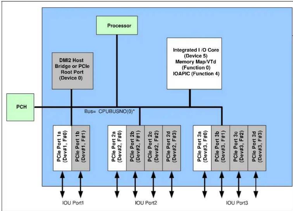
flowchart
graph TD
    A["PCH"] --> B["PCIe Port 1a (Dev#1, F#0)"]
    A --> C["PCIe Port 1b (Dev#1, F#1)"]
    A --> D["PCIe Port 2a (Dev#2, F#0)"]
    A --> E["PCIe Port 2b (Dev#2, F#1)"]
    A --> F["PCIe Port 2c (Dev#2, F#2)"]
    A --> G["PCIe Port 2d (Dev#2, F#3)"]
    A --> H["PCIe Port 3a (Dev#3, F#0)"]
    A --> I["PCIe Port 3b (Dev#3, F#1)"]
    A --> J["PCIe Port 3c (Dev#3, F#2)"]
    A --> K["PCIe Port 3d (Dev#3, F#3)"]
    B --> L["DMI2 Host Bridge or PCIe Root Port (Device 0)"]
    C --> L
    D --> M["Integrated I/O Core (Device 5) Memory Map/VTd (Function 0) IOAPIC (Function 4)"]
    E --> M
    F --> M
    G --> M
    H --> M
    I --> M
    J --> M
    K --> M
    L --> N["IOU Port1"]
    M --> O["IOU Port2"]
    N --> P["IOU Port3"]
    O --> P
    Q["Processor"] --> R["Bus= CPUBUSNO(0)*"]
- Device 0: DMI2 Root Port. Logically this appears as a PCI device residing on PCI Bus 0. Device 0 contains the standard PCI header registers, extended PCI configuration registers and DMI2 device specific configuration registers.
- Device 1: PCI Express Root Port 1a and 1b. Logically this appears as a "virtual" PCI-to-PCI bridge residing on PCI Bus 0 and is compliant with the PCI Express Local Bus Specification Revision 3.0. Device 1 contains the standard PCI Express/PCI configuration registers including PCI Express Memory Address Mapping registers. It
also contains the extended PCI Express configuration space that include PCI Express error status/control registers and Isochronous and Virtual Channel controls.
- Device 2: PCI Express Root Port 2a, 2b, 2c and 2d. Logically this appears as a "virtual" PCI-to-PCI bridge residing on PCI bus 0 and is compliant with PCI Express Specification Revision 3.0. Device 2 contains the standard PCI Express/PCI configuration registers including PCI Express Memory Address Mapping registers. It also contains the extended PCI Express configuration space that include PCI Express Link status/control registers and Isochronous and Virtual Channel controls.
- Device 3: PCI Express Root Port 3a, 3b, 3c and 3d. Logically this appears as a "virtual" PCI-to-PCI bridge residing on PCI Bus 0 and is compliant with PCI Express Local Bus Specification Revision 3.0. Device 3 contains the standard PCI Express/PCI configuration registers including PCI Express Memory Address Mapping registers. It also contains the extended PCI Express configuration space that include PCI Express error status/control registers and Isochronous and Virtual Channel controls.
- Device 5: Integrated I/O Core. This device contains the Standard PCI registers for each of its functions. This device implements three functions; Function 0 contains Address Mapping, Intel® Virtualization Technology (Intel® VT) for Directed I/O (Intel® VT-d) related registers and other system management registers. Function 4 contains System Control/Status registers and miscellaneous control/status registers on power management and throttling.
2.1.2 Processor Uncore Devices (CPUBUSN0 (1))
The configuration registers for these devices are mapped as devices residing on the PCI bus assigned for the processor socket.
Figure 2-2. Processor Uncore Devices Map
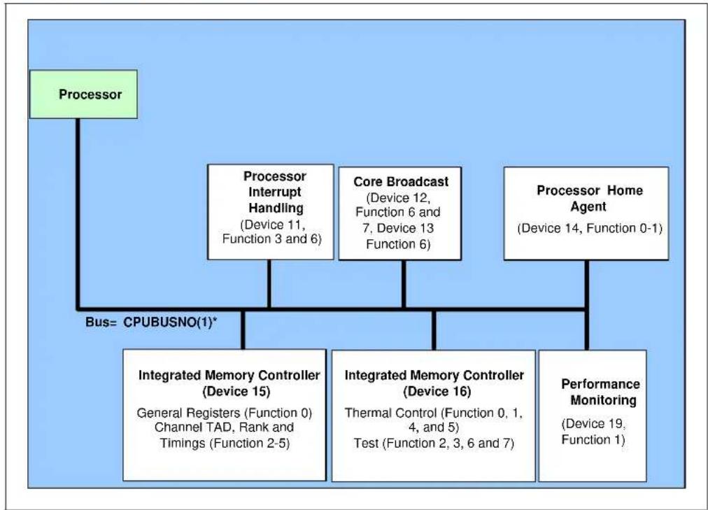
flowchart
graph TD
    A["Processor"] --> B["Processor Interrupt Handling\n(Device 11, Function 3 and 6)"]
    A --> C["Core Broadcast\n(Device 12, Function 6 and 7, Device 13 Function 6)"]
    A --> D["Processor Home Agent\n(Device 14, Function 0-1)"]
    B --> E["Integrated Memory Controller\n(Device 15)\nGeneral Registers (Function 0)\nChannel TAD, Rank and Timings (Function 2-5)"]
    C --> F["Integrated Memory Controller\n(Device 16)\nThermal Control (Function 0, 1, 4, and 5)\nTest (Function 2, 3, 6 and 7)"]
    D --> G["Performance Monitoring\n(Device 19, Function 1)"]
    E --> H["Bus= CPUBUSNO(1)*"]
    F --> H
    G --> H
- Device 10: Processor Power Control Unit. Device 10, Function 0-3 contains the configurable PCU registers and resides at DID of 3CC0h-3CD0h.
- Device 11: Processor Interrupt Event Handling. Device 11, Function 3 contains the Semaphore and Scratchpad configuration registers. Device 11, Function 0 contains the processor Interrupt control registers.
- Device 12: Processor Core Broadcast. Device 12, Function 0-3 contains the Unicast configuration registers, Function 6 contains the Caching agent broadcast configuration registers for the Memory Controller. Function 7 contains the System Address Decode registers.
- Device 13: Processor Core Broadcast. Device 13, Function 0-3 contain the Unicast registers, Function 6 contains the Caching agent broadcast configuration registers for the Memory Controller.
- Device 14: Processor Home Agent. Device 14, Function 0 contains the processor Home Agent Target Address configuration registers for the Memory Controller. Device 14, Function 1 contains processor Home Agent performance monitoring registers.
- Device 15: Integrated Memory Controller. Device 15, Function 0 contains the general and MemHot registers for the Integrated Memory Controller and resides at DID of 3CA8h. Device 15, Function 2-5 contains the Target Address Decode, Channels Rank and Memory Timing Registers which resides at DID of 3CAAh to 3CADh.
• Device 16: Integrated Memory Controller Channel 0, 1, 2 and 3. Device 16, Function 0, 1, 4 and 5 contains the Thermal control registers for Integrated Memory Controller. Channel 0 resides at DID of 3CB4h. Channel 1 resides at DID of 3CB5h. Channel 2 resides at DID of 3CB0h. Channel 3 resides at DID of 3CB1h. Device 16, Function 2, 3, 6 and 7 contains the test registers for the Integrated Memory Controller.
- Device 19: Processor performance monitoring and Ring. Device 19, Function 1 contains the processor Ring to PCI Express performance monitoring registers and resides a DID of 3C43h.
2.2 Configuration Register Rules
Types of registers:
- PCI Configuration Space Registers (CSRs)
- CSRs are chipset specific registers that are located at PCI defined address space.
2.2.1 CSR Access
Configuration space registers are accessed using the configuration transaction mechanism defined in the PCI specification and this uses the bus:device:function number concept to address a specific device's configuration space. Accesses to PCI configuration registers is achieved using NcCfgRd/Wr transactions on the Ring.
All configuration register accesses are accessed over Message Channel through the UBox but might come from a variety of different sources:
- Local cores
• P E C I o r J T A G
This unit supports PCI configuration space access as defined in the PCI Express Base Specification, Revision 3.0. Configuration registers can be read or written in Byte, WORD (16-bit), or DWord (32-bit) quantities. Accesses larger than a DWord to PCI Express configuration space will result in unexpected behavior. All multi-byte numeric fields use "little-endian" ordering (that is, lower addresses contain the least significant parts of the field).
2.2.2 PCI Bus Number
In the tables shown for IIO devices (0–7), the PCI Bus numbers are all marked as "Bus 0". The specific bus number for all PCIe* devices in the processor is specified in the CPUBUSNO register "CPUBUSNO—CPU Internal Bus Numbers Register" on page 165 which exists in the I/O module's configuration space.
2.2.3 Uncore Bus Number
In the tables shown for Uncore devices (8 - 19), the PCI Bus numbers are all marked as "bus 1". The specific bus number for all PCIe devices in the processor is specified in the CPUBUSNO register found at "CPUBUSNO—CPU Internal Bus Numbers Register" on page 165.
2.3 Configuration Mechanisms
The processor is the originator of configuration cycles. Internal to the processor, transactions received through both of the below configuration mechanisms are translated to the same format.
2.3.1 Standard PCI Express\* Configuration Mechanism
The following is the mechanism for translating processor I/O bus cycles to configuration cycles.
The PCI specification defines a slot based "configuration space" that allows each device to contain up to eight functions, with each function containing up to 256, 8-bit configuration registers. The PCI specification defines two bus cycles to access the PCI configuration space—Configuration Read and Configuration Write. Memory and I/O spaces are supported directly by the processor. Configuration space is supported by a mapping mechanism implemented within the processor.
2.4 Device Mapping
Each component in the processor is uniquely identified by a PCI bus address consisting of Bus Number, Device Number and Function Number. Device configuration is based on the PCI Type 0 configuration conventions. All processor registers appear on the PCI bus assigned for the processor socket.
Table 2-1. Functions Specifically Handled by the Processor (Sheet 1 of 2)
| Register Group DID Device Function Comment | ||||
| DMI2 3C00h 0 0 x4 Link from Processor to PCH | ||||
| PCI Express Root Port 1 | 3C02h,3C03h | 1 0-1 | x8 or x4 max link width | |
| PCI Express Root Port 2 | 3C04h,3C05h,3C06h,3C07h | 2 0-3 | x16, x8 or x4 max link width | |
| PCI Express Root Port 3 | 3C08h,3C09h,3COAh,3C0Bh | 3 0-3 | x16, x8 or x4 max link width | |
| Core | 3C28h 5 0 | Address Map, VTd_Misc, System Management | ||
| Core | 3C2Ah | 5 2 RAS, Control | Status and Global Errors | |
| Core | 3C2Ch | 5 4 I/O APIC | ||
| Core | 3C40h 5 6 IIO Switch and IRP Perfmon | |||
| PCU | 3CC0h,3CC1h,3CC2h3CD0h | 10 | 0-3 | Power Control Unit |
| UBOX | 3CE0h | 11 0 Scratchpad and Semaphores | ||
| UBOX | 3CE3h | 11 3 Scratchpad and Semaphores | ||
| Caching Agent (CBo) | 3CE8h,3CEAh,3CECh,3CEEh | 12 | 0-3 | Unicast Registers |
Table 2-1. Functions Specifically Handled by the Processor (Sheet 2 of 2)
| Register Group | DID | Device | Function | Comment |
| Caching Agent (CBo) | 3CE9h,3CEBh,3CEDh,3CEFh | 13 0-3 | Unicast Registers | |
| Caching Agent (CBo) 3CF4h 12 | 6 System Address Decoder | |||
| Caching Agent (CBo) 3CF6h 12 | 7 System Address Decoder | |||
| Caching Agent (CBo) 3CF5h 13 | 6 Broadcast Registers | |||
| Home Agent (HA) | 3CA0h,3C46h | 14 0-1 | Processor Home Agent | |
| Integrated Memory Controller | 3CA8h 15 0 | Target Address / Thermal Registers | ||
| Integrated Memory Controller | 3CAAh,3CABh,3CACh,3CADh,3CAEh | 15 2-6 | Channel Target Address Decoder Registers | |
| Integrated Memory Controller | 3CB2h,3CB3h,3CB6h,3CB7h | 16 2, 3 ,6, 7 Channel 0 -3 ERROR Registers | ||
| Integrated Memory Controller | 3CB0h,3CB1h,3CB4h,3CB5h | 16 0, | 1, 4, 5 Channel 0 -3 Thermal Control | |
| Integrated Memory Controller | 3CB8h 17 0 | DDRIO | ||
| R2PCIe 3CE4h 19 0 R2PCIE | ||||
| R2PCIe 3C43h 19 1 PCI Express | Ring performance monitoring | |||
3 Processor Integrated I/O (IIO) Configuration Registers
3.1 Processor IIO Devices (PCI Bus CPUBUSNO (0))
The processor IIO contains 10 PCI devices within a single, physical component. The configuration registers for the devices are mapped as devices residing on PCI Bus "CPUBUSNO(0)" where CPUBUSNO(0) is programmable by BIOS.
3.2 PCI Configuration Space Registers (CSRs)
This section covers registers which reside in legacy PCIe configuration space. Comments at the top of the table indicate what devices/functions the description applies to. Exceptions that apply to specific functions are noted in the individual bit descriptions.
3.2.1 Unimplemented Devices/ Functions and Registers
Configuration reads to unimplemented functions and devices will return all ones emulating a master abort response. Note that there is no asynchronous error reporting that happens when a configuration read master aborts. Configuration writes to unimplemented functions and devices will return a normal response.
Software should not attempt or rely on reads or writes to unimplemented registers or register bits. Unimplemented registers should return 00h bytes. Writes to unimplemented registers are ignored. For configuration writes to these register (require a completion), the completion is returned with a normal completion status (not master-aborted).
3.2.2 PCI Bus Number
In the following tables, the PCI Bus numbers are all marked as "bus 0". The specific bus number for all PCIe devices in the processor is specified in the CPUBUSNO register found at Section 3.3.3.14, "CPUBUSNO—CPU Internal Bus Numbers Register" on page 165.
Figure 3-1. DMI2 Port (Device 0) and PCI Express* Root Ports Type 1 Configuration Space
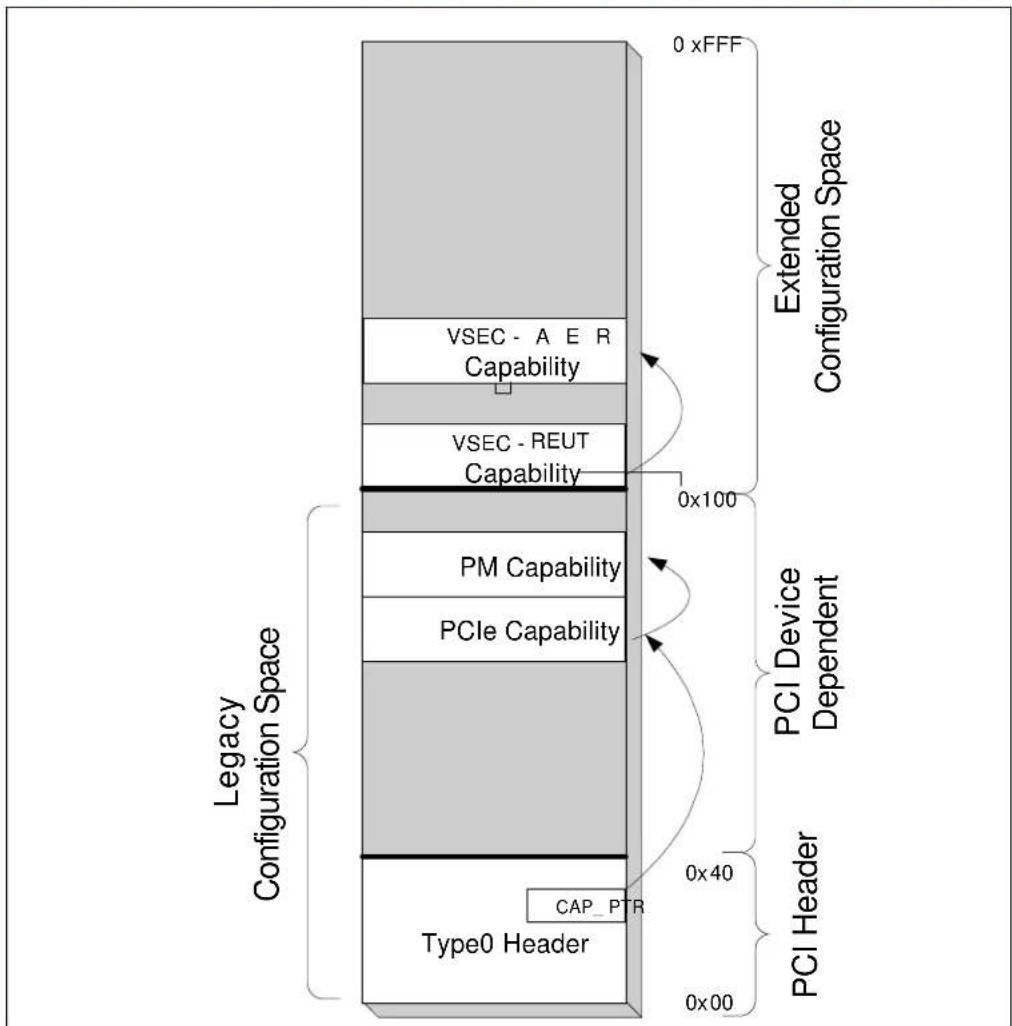
Note: VSEC stands for Vendor Specific Extended Capability. In DMI2 mode, AER appears as a vendor specific extended capability.
Figure 3-2. Device 1/ Functions 0–1 (Root Ports) – Device 2/ Function 0–3 (Root Port Mode) and Devices 3/ Functions 0–3 (Root Ports) Type 1 Configuration Space
Figure 3-2 illustrates how each PCI Express/DMI2 port's configuration space appears to software. Each PCI Express configuration space has three regions:
- Standard PCI Header: This region is the standard PCI-to-PCI bridge header providing legacy OS compatibility and resource management.
- PCI Device Dependent Region: This region is also part of standard PCI configuration space and contains basic PCI capability structures and other port specific registers. For the processor, the supported capabilities are:
— SVID/SDID Capability
— Message Signalled Interrupts
— Power Management
— PCI Express Capability
- PCI Express Extended Configuration Space: This space is an enhancement beyond standard PCI and only accessible with PCI Express aware software.
3.2.3 IIO PCI Express\* Configuration Space Registers
Table 3-1. (DMI2 Mode) Legacy Configuration Map - Device 0 Function 0 - Offset 00h-0FCh
| DID VID 0h 80h | |||||||||
| PCISTS PCICMD 4h | 84h | ||||||||
| CCR RID 8h | 88h | ||||||||
| BIST HDR | PLAT CLSR Ch | 8Ch | |||||||
| 10h | PXPCAP | PXPNXTPTR | PXPCAPID | 90h | |||||
| 14h | DEVCAP | 94h | |||||||
| 18h | 98h | ||||||||
| 1Ch | 9Ch | ||||||||
| 20h | A0h | ||||||||
| 24h | A4h | ||||||||
| 28h | A8h | ||||||||
| SDID | SVID | 2Ch | ACh | ||||||
| 30h | B0h | ||||||||
| CAPPTR | 34h | DEVCAP2 | B4h | ||||||
| 38h | B8h | ||||||||
| INTPIN | INTL | 3Ch | LNKCAP2 | BCh | |||||
| 40h | C0h | ||||||||
| 44h | C4h | ||||||||
| 48h | C8h | ||||||||
| 4Ch | CCh | ||||||||
| DMIRCBAR | 50h | D0h | |||||||
| 54h | D4h | ||||||||
| 58h | D8h | ||||||||
| 5Ch | DCh | ||||||||
| 60h | PMCAP | E0h | |||||||
| 64h | PMCSR | E4h | |||||||
| 68h | E8h | ||||||||
| 6Ch | ECh | ||||||||
| 70h | DEVSTS | DEVCTRL | DEVSTS | ||||||
| 74h | |||||||||
| 78h | DEVCTRL2 | ||||||||
| 7Ch | |||||||||
Table 3-2. (DMI2) Extended Configuration Map - Device 0/ Function 0 - Offset 100h-1FCh
| XPREUT_HDR_EXT 100h | PERFCTRLSTS | 180h | ||
| XPREUT_HDR_CAP 104h 184h | ||||
| XPREUT_HDR_LEF 108h | MISCCTRLSTS | 188h | ||
| 10Ch 18Ch | ||||
| 110h PCIE_IOU_BIF_CTRL 190h | ||||
| 114h 194h | ||||
| 118h 198h | ||||
| 11Ch 19Ch | ||||
| 120h | DMICTRL | 1A0h | ||
| 124h 1A4h | ||||
| 128h DMISTS 1A8h | ||||
| 12Ch 1ACh | ||||
| 130h LNKSTS LNKCON 1B0h | ||||
| 134h 1B4h | ||||
| 138h 1B8h | ||||
| 13Ch 1BCh | ||||
| APICLIMIT APICBASE 140h LNKSTS2 | LNKCON2 1C0h | |||
| VSECHDR | 144h | 1C4h | ||
| VSHDR | 148h | 1C8h | ||
| UNCERRSTS | 14Ch | 1CCh | ||
| UNCERRMSK | 150h | ERRINJCAP | 1D0h | |
| UNCERRSEV | 154h | ERRINJHDR | 1D4h | |
| CORERRSTS | 158h | ERRINJCON | 1D8h | |
| CORERRMSK | 15Ch | 1DCh | ||
| ERRCAP 160h | CTOCTRL 1E0h | |||
| HDRLOG0 | 164h | 1E4h | ||
| HDRLOG1 | 168h | 1E8h | ||
| HDRLOG2 | 16Ch | 1ECh | ||
| HDRLOG3 | 170h | 1F0h | ||
| RPERRCMD | 174h | 1F4h | ||
| RPERRSTS | 178h | 1F8h | ||
| ERRSID 17Ch | 1FCh | |||
Table 3-3. (DMI2) Mode Extended Configuration Map - Device 0/ Function 0 - Offset 200h-2FCh
| XPCORERRSTS 200h LER_CAP 280h | ||||
| XPCORERRMSK 204h LER_HDR 284h | ||||
| XPUNCERRSTS 208h LER_CTRLSTS | 288h | |||
| XPUNCERRMSK 20Ch LER_UNCERRMSK 28Ch | ||||
| XPUNCERRSEV 210h LER_XPUNCERRMSK 290h | ||||
| XPUNCERR PTR | 214h LER_RPERMSK 294h | |||
| UNCEDMASK | 218h | |||
| COREDMASK | 21Ch | |||
| RPEDMASK | 220h | |||
| XPUNCEDMASK | 224h | |||
| XPCOREDMASK | 228h | |||
| 22Ch | ||||
| XPGLBERRPTR | XPGLBERRSTS | 230h | ||
| 234h | ||||
| 238h | ||||
| 23Ch | ||||
| 240h | ||||
| 244h | ||||
| 248h | ||||
| 24Ch | ||||
| 250h | ||||
| 254h | ||||
| 258h | ||||
| 25Ch | ||||
| 260h | ||||
| 264h | ||||
| 268h | ||||
| 26Ch | ||||
| 270h XPPMDFXMAT0 2F0h | ||||
| 274h | ||||
| 278h | ||||
| 27Ch | ||||
Table 3-4. Device 1/ Functions 0-1 (PCIe* Root Ports), Devices 2/ Functions 0-3 (PCIe* Root Ports), and Device 3/ Function 0-3 (PCIe* Root Ports) Legacy Configuration Map
| DID VID 0h 80h | |||||||||
| PCISTS PCICMD 4h 84h | |||||||||
| CCR RID 8h 88h | |||||||||
| BIST HDR | PLAT CLSR Ch | 8Ch | |||||||
| 10h | PXPCAP PXPNXTPTR | PXPCAPID 90h | |||||||
| 14h | DEVCAP | 94h | |||||||
| SUBBUS | SECBUS | PBUS | 18h | DEVSTS | DEVCTRL | 98h | |||
| SECSTS | IOLIM | IOBAS | 1Ch | LNKCAP | 9Ch | ||||
| MLIM | MBAS | 20h | LNKSTS | LNKCON | A0h | ||||
| PLIM | PBAS | 24h | SLTCAP | A4h | |||||
| PBASU | 28h | SLTSTS | SLTCON | A8h | |||||
| PLIMU | 2Ch | ROOTCAP | ROOTCON | ACh | |||||
| 30h | ROOTSTS | B0h | |||||||
| CAPPTR | 34h | DEVCAP2 | B4h | ||||||
| 38h | DEVCTRL2 | B8h | |||||||
| BCTRL | INTPIN | INTL | 3Ch | LNKCAP2 | BCh | ||||
| SNXTPTR | SCAPID | 40h | LNKSTS2 | LNKCON2 | C0h | ||||
| SDID | SVID | 44h | C4h | ||||||
| 48h | C8h | ||||||||
| 4Ch | CCh | ||||||||
| DMIRCBAR^1 | 50h | D0h | |||||||
| 54h | D4h | ||||||||
| 58h | D8h | ||||||||
| 5Ch | DCh | ||||||||
| MSIMSGCTL | MSINXTPTR | MSICAPID | 60h | PMCAP | E0h | ||||
| MSGADR | 64h | PMCSR | E4h | ||||||
| MSGDAT | 68h | E8h | |||||||
| MSIMSK | 6Ch | ECh | |||||||
| MSIPENDING | 70h | F0h | |||||||
| 74h | F4h | ||||||||
| 78h | F8h | ||||||||
| 7Ch | FCh | ||||||||
Notes:
1. DMIRCBAR - Device 0 Only
Table 3-5. Device 1/ Functions 0-1 (PCIe* Root Ports), Devices 2/ Functions 0-3 (PCIe* Root Ports), Device 3/ Function 0-3 (PCIe* Root Ports) Extended Configuration Map - Offset 100h-1FFh
| XPREUT_HDR_EXT 100h PERFCTRLSTS 180h | |||||
| XPREUT_HDR_CAP 104h 184h | |||||
| XPREUT_HDR_LEF 108h MISCCTRLSTS 188h | 8Ch | ||||
| 10Ch | |||||
| ACSCAPHDR 110h | PCIE_IOU_BIF_CTRL 190h | ||||
| ACSCTRL ACSCAP 114h | 194h | ||||
| 118h 198h | |||||
| 11Ch 19Ch | |||||
| 120h 1A0h | |||||
| 124h 1A4h | |||||
| 128h 1A8h | |||||
| 12Ch 1ACh | |||||
| 130h 1B0h | |||||
| 134h 1B4h | |||||
| 138h 1B8h | |||||
| 13Ch 1BCh | |||||
| APICLIMIT APICBASE 140h 1C0h | |||||
| 144h 1C4h | |||||
| ERRCAPHDR 148h 1C8h | |||||
| UNCERRSTS 14Ch 1CCh | |||||
| UNCERRMSK | 150h | ERRINJCAP | 1D0h | ||
| UNCERRSEV 154h | ERRINJHDR 1D4h | ||||
| CORERRSTS | 158h | ERRINJCON | 1D8h | ||
| CORERRMSK | 15Ch | 1DCh | |||
| ERRCAP | 160h | CTOCTRL | 1E0h | ||
| HDRLOG0 | 164h | E8h | 1E4h | ||
| HDRLOG1 | 168h | ||||
| HDRLOG2 | 16Ch 1ECh | ||||
| HDRLOG3 | 170h | 1F0h | |||
| RPERRCMD | 174h | 1F4h | |||
| RPERRSTS | 178h | 1F8h | |||
| ERRSID | 17Ch 1FCh | ||||
Table 3-6. Device 1/ Functions 0-1 (PCIe* Root Ports), Devices 2/ Functions 0-3 (PCIe* Root Ports), and Device 3/ Function 0-3 (PCIe* Root Ports) Extended Configuration Map - Offset 200h-2FCh
| XPCORERRSTS 200h LER_CAP 280h | ||||
| XPCORERRMSK 204h LER_HDR 284h | ||||
| XPUNCERRSTS 208h LER_CTRLSTS 288h | ||||
| XPUNCERRMSK 20Ch LER_UNCERRMSK 28Ch | ||||
| XPUNCERRSEV 210h LER_XPUNCERRMSK 290h | ||||
| XPUNCERR PTR | 214h | LER_RPERMSK | 294h | |
| UNCEDMASK | 218h | 298h | ||
| COREDMASK | 21Ch | 29Ch | ||
| RPEDMASK | 220h | 2A0h | ||
| XPUNCEDMASK 224h | 2A4h | |||
| XPCOREDMASK 228h | 2A8h | |||
| 22Ch | 2ACh | |||
| XPGLBERRPTR | XPGLBERRSTS | 230h | 2B0h | |
| 234h | 2B4h | |||
| 238h | 2B8h | |||
| 23Ch | 2BCh | |||
| 240h | 2C0h | |||
| 244h | 2C4h | |||
| 248h | 2C8h | |||
| 24Ch | 2CCh | |||
| PXP2CAP^4 | 250h | 2D0h | ||
| LNKCON3^4 | 254h | 2D4h | ||
| LNERRSTS^4 | 258h | 2D8h | ||
| LN1EQ^4 | LN0EQ^4 | 25Ch | 2DCh | |
| LN3EQ^4 | LN2EQ^4 | 260h | 2E0h | |
| LN5EQ^5 | LN4EQ^5 | 264h | 2E4h | |
| LN7EQ^5 | LN6EQ^5 | 268h | 2E8h | |
| LN9EQ^3 | LN8EQ^3 | 26Ch | 2ECh | |
| LN11EQ^3 | LN10EQ^3 | 270h | XPPMDFXMAT0^1 | 2F0h |
| LN13EQ^3 | LN12EQ^3 | 274h | XPPMDFXMAT1^2 | 2F4h |
| LN15EQ^3 | LN14EQ^3 | 278h | XPPMDFXMSK0^3 | 2F8h |
| 27Ch | XPPMDFXMSK1^3 | 2FCh | ||
Note:
1. Applicable to Device 0,2,3/Function 0.
2. Applicable to Device 2/Function 0.
3. Applicable to Device 2,3/Function 0.
4. Applicable to Device 1-3.
5. Applicable to Device 1/Function 0 and Device 2,3/Function 0,2.
Table 3-7. Device 0/ Function 0 DMI2 mode), Devices 2/ Functions 0 (PCIe* Root Port), and Device 3/ Function 0 (PCIe* Root Port) Extended Configuration Map - Offset 400h-4FCh
| 400h XPPMDL0 480h | |||
| 404h XPPMDL1 484h | |||
| 408h XPPMCL0 488h | |||
| 40Ch XPPMCL1 48Ch | |||
| 410h XPPMCH XPPMDH 490h | |||
| 414h XPPMR0 494h | |||
| 418h XPPMR1 498h | |||
| 41Ch XPPMEVL0 49Ch | |||
| 420h XPPMEVL1 4A0h | |||
| 424h XPPMEVH0 4A4h | |||
| 428h XPPMEVH1 4A8h | |||
| 42Ch XPPMER0 4ACh | |||
| 430h XPPMER1 4B0h | |||
| 434h | 4B4h | ||
| 438h 4B8h | |||
| 43Ch 4BCh | |||
| 440h 4C0h | |||
| 444h 4C4h | |||
| 448h 4C8h | |||
| 44Ch 4CCh | |||
| 450h 4D0h | |||
| 454h 4D4h | |||
| 458h 4D8h | |||
| 45Ch 4DCh | |||
| 460h 4E0h | |||
| 464h 4E4h | |||
| 468h 4E8h | |||
| 46Ch 4ECh | |||
| 470h | 4F0h | ||
| 474h | 4F4h | ||
| 478h | 4F8h | ||
| 47Ch 4FCh | |||
3.2.4 Standard PCI Configuration Space (Type 0/1 Common Configuration Space)
This section covers registers in the 0h to 3Fh region that are common to all the devices 0–3. Comments at the top of the table indicate what devices/functions the description applies to. Exceptions that apply to specific functions are noted in the individual bit descriptions.
3.2.4.1 VID—Vendor Identification Register
| Register: VIDBus: 0 Device: 0 Function: 0 Offset: 00hBus: 0 Device: 1 Function: 0-1 Offset: 00hBus: 0 Device: 2 Function: 0-3 Offset: 00hBus: 0 Device: 3 Function: 0-3 Offset: 00h | |||
| Bit Attr | Reset Value | Description | |
| 15:0 PO 8086h | Vendor Identification NumberThe value is assigned by PCI-SIG to Intel. | ||
3.2.4.2 DID—Device Identification Register
| DIDBus: 0 Device: 0 Function: 0 Offset: 00hBus: 0 Device: 1 Function: 0-1 Offset: 00hBus: 0 Device: 2 Function: 0-3 Offset: 00hBus: 0 Device: 3 Function: 0-3 Offset: 00h | |||
| Bit Attr | Reset Value | Description | |
| 15:0 RO | Device Identification NumberDevice IDs for PCI Express root ports are as follows:3C00h = Device 0 in DMI mode3C02h = Port 1a3C03h = Port 1b3C04h = Port 2a3C05h = Port 2b3C06h = Port 2c3C07h = Port 2d3C08h = Port 3a in PCIe mode3C09h = Port 3b3C0Ah = Port 3c3C0Bh = Port 3dThe value is assigned by Intel to each product. | ||
3.2.4.3 PCI CMD—PCI Command Register
| PCI CMDBus: 0 Device: 0 Function: 0 Offset: 04hBus: 0 Device: 1 Function: 0-1 Offset: 04hBus: 0 Device: 2 Function: 0-3 Offset: 04hBus: 0 Device: 3 Function: 0-3 Offset: 04h | |||
| Bit Attr | Reset Value | Description | |
| 15:11 RV 0h Reserved | |||
| 10 RW 0b | INTxDisable: Interrupt DisableThis bit controls the ability of the PCI Express port to generate INTx messages. This bit does not affect the ability of the processor to route interrupt messages received at the PCI Express port. However, this bit controls the generation of legacy interrupts to the DMI for PCI Express errors detected internally in this port (for example, Malformed TLP, CRC error, completion time out, and so forth) or when receiving RP error messages or interrupts due to HP/PM events generated in legacy mode within the processor.1 = Legacy Interrupt mode is disabled0 = Legacy Interrupt mode is enabled | ||
| 9 | RO | 0b | Fast Back-to-Back EnableNot applicable to PCI Express must be hardwired to 0. |
| 8 | RO | 0b | SERR EnableFor PCI Express/DMI ports, this field enables notifying the internal core error logic of occurrence of an uncorrectable error (fatal or non-fatal) at the port. The internal core error logic of IIO then decides if/how to escalate the error further (pins/message, and so forth). This bit also controls the propagation of PCI Express ERR_FATAL and ERR_NONFATAL messages received from the port to the internal IIO core error logic.1 = Fatal and Non-fatal error generation and Fatal and Non-fatal error message forwarding is enabled0 = Fatal and Non-fatal error generation and Fatal and Non-fatal error message forwarding is disabledRefer to PCI Express Base Specification, Revision 3.0 for details of how this bit is used in conjunction with other control bits in the Root Control register for forwarding errors detected on the PCI Express interface to the system core error logic. |
| 7 | RO | 0b | IDSEL Stepping/ Wait Cycle ControlNot applicable to PCI Express must be hardwired to 0. |
| 6 | RW | 0b | Parity Error ResponseFor PCI Express/DMI ports, IIO ignores this bit and always does ECC/parity checking and signaling for data/address of transactions both to and from IIO. This bit though affects the setting of bit 8 in the PCISTS register (see bit 8 in Section 3.2.4.4, "PCISTS—PCI Status Register"). |
| 5 | RO | 0b | VGA palette snoop EnableNot applicable to PCI Express; must be hardwired to 0. |
| 4 | RO | 0b | Memory Write and Invalidate EnableNot applicable to PCI Express; must be hardwired to 0. |
| 3 | RO | 0b | Special Cycle EnableNot applicable to PCI Express; must be hardwired to 0. |
| 2 | RW | 0b | Bus Master Enable1 = PCIe NTB will forward Memory Requests that it receives on its primary internal interface to its secondary external link interface.0 = PCIe NTB will not forward Memory Requests that it receives on its primary internal interface. Memory requests received on the primary internal interface will be returned to requester as an Unsupported Requests UR.Requests other than Memory Requests are not controlled by this bit.Reset Value value of this bit is 0b. |
| 1 | R | W | Memory Space Enable1 = Enables a PCI Express port's memory range registers to be decoded as valid target addresses for transactions from secondary side.0 = Disables a PCI Express port's memory range registers (including the Configuration Registers range registers) to be decoded as valid target addresses for transactions from secondary side. All memory accesses received from secondary side are UR'ed. |
| 0 | R | O | I/O Space EnableThis bit controls a device's response to I/O Space accesses. When this bit is 0, it disables the device response. When this bit is 1, it allows the device to respond to I/O space accesses.The state after RST# is 0. NTB does not support I/O space accesses. Hardwired to 0. |
3.2.4.4 PCI STS—PCI Status Register
| PCI STSBus: 0 Device: 0 Function: 0 Offset: 06hBus: 0 Device: 1 Function: 0-1 Offset: 06hBus: 0 Device: 2 Function: 0-3 Offset: 06hBus: 0 Device: 3 Function: 0-3 Offset: 06h | |||
| Bit Attr | Reset Value | Description | |
| 15 RW1C 0b | Detected Parity ErrorThis bit is set by a root port when it receives a packet on the primary side with an uncorrectable data error (including a packet with poison bit set) or an uncorrectable address/control parity error. The setting of this bit is regardless of the Parity Error Response bit (PERRE) in the PCICMD register. | ||
| 14 RW1C 0b | Signaled System Error1 = The root port reported fatal/non-fatal (and not correctable) errors it detected on its PCI Express interface to the IIO core error logic (which might eventually escalate the error through the ERR[2:0] pins or message to processor core or message to PCH). The SERRE bit in the PCICMD register must be set for a device to report the error in the IIO core error logic.Software clears this bit by writing a 1 to it. This bit is also set (when SERR enable bit is set) when a FATAL/NON-FATAL message is forwarded to the IIO core error logic. IIO internal core errors (like parity error in the internal queues) are not reported using this bit.0 = The root port did not report a fatal/non-fatal error. | ||
| 13 RW1C 0b | Received Master AbortThis bit is set when a root port experiences a master abort condition on a transaction it mastered on the primary interface (uncore internal bus).Note that certain errors might be detected right at the PCI Express interface and those transactions might not propagate to the primary interface before the error is detected (for example, accesses to memory above TOCM in cases where the PCIe interface logic itself might have visibility into TOCM). Such errors do not cause this bit to be set, and are reported using the PCI Express interface error bits (secondary status register).Conditions that cause bit 13 to be set, include:Device receives a completion on the primary interface (internal bus of uncore) with Unsupported Request or master abort completion Status. This includes UR status received on the primary side of a PCI Express port on peer-to-peer completions also. | ||
| Bit | Attr | Reset Value | Description |
| 12 RW1C 0b | Received Target AbortThis bit is set when a device experiences a completer abort condition on a transaction it mastered on the primary interface (uncore internal bus). Certain errors might be detected right at the PCI Express interface and those transactions might not propagate to the primary interface before the error is detected (for example, accesses to memory above VTBAR). Such errors do not cause this bit to be set, and are reported using the PCI Express interface error bits (secondary status register).Conditions that cause bit 12 to be set, include:Device receives a completion on the primary interface (internal bus of uncore) with completer abort completion Status. This includes CA status received on the primary side of a PCI Express port on peer-to-peer completions also. | ||
| 11 RW1C 0b | Signaled Target AbortThis bit is set when a root port signals a completer abort completion status on the primary side (internal bus of uncore). This condition includes a PCI Express port forwarding a completer abort status received on a completion from the secondary. | ||
| 10:9 RO 0h | DEVSEL# TimingNot applicable to PCI Express. Hardwired to 0. | ||
| 8 | R W 1 | Master Data Parity ErrorThis bit is set by a root port if the Parity Error Response bit in the PCI Command register is set and it either receives a completion with poisoned data from the primary side or it forwards a packet with data (including MSI writes) to the primary side with poison. | |
| 7 | R O | Fast Back-to-BackNot applicable to PCI Express. Hardwired to 0. | |
| 6 | R O | 0 b Reserved | |
| 5 | R O | PCI Bus 66 MHz CapableNot applicable to PCI Express. Hardwired to 0. | |
| 4 | R O | Capabilities ListThis bit indicates the presence of a capabilities list structure. | |
| 3 | R O - | INTx StatusThis read-only bit reflects the state of the interrupt in the PCI Express Root Port. Only when the Interrupt Disable bit in the command register is a 0 and this Interrupt Status bit is a 1, will this device generate INTx interrupt. Setting the Interrupt Disable bit to a 1 has no effect on the state of this bit. This bit does not get set for interrupts forwarded to the root port from downstream devices in the hierarchy. When MSI are enabled, Interrupt status should not be set.The intx status bit should be de-asserted when all the relevant events (RAS errors/HP/link change status/PM) internal to the port using legacy interrupts are cleared by software. | |
| 2:0 RV 0h Reserved | |||
3.2.4.5 RID—Revision Identification Register
| RIDBus: 0 Device: 0 Function: 0 Offset: 08hBus: 0 Device: 1 Function: 0-1 Offset: 08hBus: 0 Device: 2 Function: 0-3 Offset: 08hBus: 0 Device: 3 Function: 0-3 Offset: 08h | |||
| Bit Attr | Reset Value | Description | |
| 7:0 RO 00h | Revision IdentificationReflects the Uncore Revision ID after reset.Reflects the Compatibility Revision ID after BIOS writes 69h to any RID register in any processor function.Implementation Note: Read and write requests from the host to any RID register in any processor function are re-directed to the IIO cluster. Accesses to the CCR field are also redirected due to DWord alignment. It is possible that JTAG accesses are direct; thus, will not always be redirected. | ||
3.2.4.6 CCR—Class Code Register
| CCRBus: 0 Device: 0 Function: 0 Offset: 09hBus: 0 Device: 1 Function: 0-1 Offset: 09hBus: 0 Device: 2 Function: 0-3 Offset: 09hBus: 0 Device: 3 Function: 0-3 Offset: 09h | |||
| Bit Attr | Reset Value | Description | |
| 23:16 RO 06h | Base ClassFor Root ports (including the root port mode operation of DMI and NTB ports), this field is hardwired to 06h indicating it is a Bridge Device. | ||
| 15:8 RO 04h | Sub-ClassFor Root ports, this field defaults to 04h indicating PCI-PCI bridge. This register changes to the sub-class of 00h to indicate Host Bridge, when bit 0 in the MISCCTRLSTS register is set. | ||
| 7:0 RO 00h | Register-Level Programming InterfaceThis field is hardwired to 00h for PCI Express ports. | ||
3.2.4.7 CLSR—Cacheline Size Register
| CLSRBus: 0 Device: 0 Function: 0 Offset: 0ChBus: 0 Device: 1 Function: 0-1 Offset: 0ChBus: 0 Device: 2 Function: 0-3 Offset: 0ChBus: 0 Device: 3 Function: 0-3 Offset: 0Ch | |||
| Bit Attr | Reset Value | Description | |
| 7:0 | RW 0h | Cacheline SizeThis register is set as RW for compatibility reasons only. Cacheline size for the processor is always 64B. IIO hardware ignores this setting. | |
3.2.4.8 PLAT—Primary Latency Timer Register
| PLATBus: 0 Device: 0 Function: 0 Offset: 0DhBus: 0 Device: 1 Function: 0-1 Offset: 0DhBus: 0 Device: 2 Function: 0-3 Offset: 0DhBus: 0 Device: 3 Function: 0-3 Offset: 0Dh | |||
| Bit Attr | Reset Value | Description | |
| 7:0 RO 0h | Primary Latency TimerNot applicable to PCI Express. Hardwired to 00h. | ||
3.2.4.9 HDR—Header Type Register
| HDRBus: 0 Device: 0 Function: 0 Offset: 0Eh | |||
| Bit Attr | Reset Value | Description | |
| 7 | R | O | Multi-function DeviceThis bit defaults to 0 for Device 0. |
| 6:0 RO-V 00h | Configuration LayoutThis field identifies the format of the configuration header layout.In DMI mode, default is 00h indicating a conventional type 00h PCI header. | ||
3.2.4.10 HDR—Header Type Register
| HDRBus: 0 Device: 1 Function: 0-1 Offset: 0EhBus: 0 Device: 2 Function: 0-3 Offset: 0EhBus: 0 Device: 3 Function: 0-3 Offset: 0Eh | |||
| Bit Attr | Reset Value | Description | |
| 7 | RO-V | Multi-function DeviceThis bit defaults to 1 for Devices 1-3 since these are multi-function devices.BIOS can individually control the value of this bit in Function 0 of these devices, based on the HDRTYPCTRL register. BIOS will write to that register to change this held to 0 in Function 0 of these devices if it exposes only Function 0 in the device to OS.Note: In product SKUs where only Function 0 of the device is exposed to any software (BIOS/OS), BIOS would still have to set the control bits mentioned above to set the bit in this register to be compliant per PCI rules. | |
| 6:0 RO | 01h | Configuration LayoutThis field identifies the format of the configuration header layout. It is Type1 for all PCI Express root ports. The default is 01h indicating a PCI to PCI Bridge. | |
3.2.4.11 BIST—Built-In Self Test Register
| BISTBus: 0 Device: 0 Function: 0 Offset: 0FhBus: 0 Device: 1 Function: 0-1 Offset: 0FhBus: 0 Device: 2 Function: 0-3 Offset: 0FhBus: 0 Device: 3 Function: 0-3 Offset: 0Fh | |||
| Bit Attr | Reset Value | Description | |
| 7:0 RO 0h | BIST TestsNot supported. Hardwired to 00h. | ||
3.2.4.12 PBUS—Primary Bus Number Register
| PBUSBus: 0 Device: 1 Function: 0-1 Offset: 18hBus: 0 Device: 2 Function: 0-3 Offset: 18hBus: 0 Device: 3 Function: 0-3 Offset: 18h | |||
| Bit Attr | Reset Value | Description | |
| 7:0 RW 00h | Primary Bus NumberConfiguration software programs this field with the number of the bus on the primary side of the bridge. This register has to be kept consistent with the Internal Bus Number 0 in the CPUBUSNO01 register. BIOS (and OS if internal bus number gets moved) must program this register to the correct value since IIO hardware would depend on this register for inbound configuration cycle decode purposes. | ||
3.2.4.13 SECBUS—Secondary Bus Number Register
| SECBUSBus: 0 Device: 1 Function: 0-1 Offset: 19hBus: 0 Device: 2 Function: 0-3 Offset: 19hBus: 0 Device: 3 Function: 0-3 Offset: 19h | |||
| Bit Attr | Reset Value | Description | |
| 7:0 RW 00h | Secondary Bus NumberThis field is programmed by configuration software to assign a bus number to the secondary bus of the virtual PCI-to-PCI bridge. IIO uses this register to either forward a configuration transaction as a Type 1 or Type 0 to PCI Express. | ||
3.2.4.14 SUBBUS—Subordinate Bus Number Register
| SUBBUSBus: 0 Device: 0 Function: 0 Offset: 1Ah (PCI e MODE)Bus: 0 Device: 1 Function: 0-1 Offset: 1AhBus: 0 Device: 2 Function: 0-3 Offset: 1AhBus: 0 Device: 3 Function: 0-3 Offset: 1Ah | |||
| Bit Attr | Reset Value | Description | |
| 7:0 RW 00h | Subordinate Bus NumberThis register is programmed by configuration software with the number of the highest subordinate bus that is behind the PCI Express port. Any transaction that falls between the secondary and subordinate bus number (both inclusive) of an Express port is forwarded to the express port. | ||
3.2.4.15 IOBAS—I / O Base Register
| IOBASBus: 0 Device: 0 Function: 0 Offset: 1Ch (PCI e MODE)Bus: 0 Device: 1 Function: 0-1 Offset: 1ChBus: 0 Device: 2 Function: 0-3 Offset: 1ChBus: 0 Device: 3 Function: 0-3 Offset: 1Ch | |||
| Bit Attr | Reset Value | Description | |
| 7:4 RW Fh | I/ O Base AddressThis field corresponds to A[15:12] of the I/O base address of the PCI Express port. See also the IOLIM register description. | ||
| 3:2 RW-L 3h | More I/ O Base AddressWhen EN1K is set in the Section 3.3.4, "Global System Control and Error Registers" on page 191 register, these bits become RW and allow for 1K granularity of I/O addressing; otherwise, these are RO. | ||
| 1:0 RO 0h | I/ O Address capabilityI/O supports only 16 bit addressing. | ||
3.2.4.16 IOLIM—I/O Limit Register
| IOLIMBus: 0 Device: 0 Function: 0 Offset: 1Dh (PCIe MODE)Bus: 0 Device: 1 Function: 0-1 Offset: 1DhBus: 0 Device: 2 Function: 0-3 Offset: 1DhBus: 0 Device: 3 Function: 0-3 Offset: 1Dh | |||
| Bit Attr | Reset Value | Description | |
| 7:4 RW 0h | I/ O Address LimitThis field corresponds to A[15:12] of the I/O limit address of the PCI Express port.The I/O Base and I/O Limit registers define an address range that is used by the PCI Express port to determine when to forward I/O transactions from one interface to the other using the following formula:IO_BASE ≤ A[15:12] ≤ IO_LIMITThe bottom of the defined I/O address range will be aligned to a 4 KB boundary (1 KB if EN1K bit is set. Refer to Section 3.3.4, "Global System Control and Error Registers" on page 191 for definition of EN1K bit) while the top of the region specified by IO_LIMIT will be one less than a 4 KB (1 KB if EN1K bit is set) multiple.Notes:1. Setting the I/O limit less than I/O base disables the I/O range altogether.2. In general the I/O base and limit registers will not be programmed by software without clearing the IOSE bit first. | ||
| 3:2 RW-L 0h | More I/ O Address LimitWhen EN1K is set in Section 3.3.4, "Global System Control and Error Registers" register, these bits become RW and allow for 1K granularity of I/O addressing, otherwise these are RO. | ||
| 1:0 RO 0h | I/ O Address Limit CapabilityIIO only supports 16 bit addressing. | ||
3.2.4.17 SECSTS—Secondary Status Register
| SECSTSBus: 0 Device: 0 Function: 0 Offset: 1Eh (PCIe MODE)Bus: 0 Device: 1 Function: 0-1 Offset: 1EhBus: 0 Device: 2 Function: 0-3 Offset: 1EhBus: 0 Device: 3 Function: 0-3 Offset: 1Eh | |||
| Bit Attr | Reset Value | Description | |
| 15 RW1C 0b | Detected Parity ErrorThis bit is set by the root port when it receives a poisoned TLP in the PCI Express port. This bit is set regardless of the state the Parity Error Response Enable bit in the Bridge Control register. | ||
| 14 RW1C 0b | Received System ErrorThis bit is set by the root port when it receives a ERR_FATAL or ERR_NONFATAL message from PCI Express. This does not include the virtual ERR* messages that are internally generated from the root port when it detects an error on its own. | ||
| 13 RW1C 0b | Received Master Abort StatusThis bit is set when the root port receives a Completion with Unsupported Request Completion Status or when the root port master aborts a Type 0 configuration packet that has a non-zero device number. | ||
| 12 RW1C 0b | Received Target Abort StatusThis bit is set when the root port receives a Completion with Completer Abort Status. | ||
| 11 RW1C 0b | Signaled Target AbortThis bit is set when the root port sends a completion packet with a Completer Abort Status (including peer-to-peer completions that are forwarded from one port to another). | ||
| 10:9 RO 00b | DEVSEL# TimingNot applicable to PCI Express. Hardwired to 0. | ||
| 8 | RW1C | 0b | Master Data Parity ErrorThis bit is set by the root port on the secondary side (PCI Express link) if the Parity Error Response Enable bit (PERRE) is set in Bridge Control register and either of the following two conditions occurs:The PCI Express port receives a Completion from PCI Express marked poisoned.The PCI Express port poisons an outgoing packet with data.If the Parity Error Response Enable bit in Bridge Control Register is cleared, this bit is never set. |
| 7 | RO | 0b | Fast Back-to-Back Transactions CapableNot applicable to PCI Express. Hardwired to 0. |
| 6 | RV | 0h | Reserved |
| 5 | RO | 0b | PCI bus 66 MHz capabilityNot applicable to PCI Express. Hardwired to 0. |
| 4:0 | RV | 0h | Reserved |
3.2.4.18 MBAS—Memory Base Register
| MBASBus: 0 Device: 0 Function: 0 Offset: 20h (PCI e* MODE)Bus: 0 Device: 1 Function: 0-1 Offset: 20hBus: 0 Device: 2 Function: 0-3 Offset: 20hBus: 0 Device: 3 Function: 0-3 Offset: 20h | |||
| Bit Attr | Reset Value | Description | |
| 15:4 RW FFFh | Memory Base AddressThis bit corresponds to A[31:20] of the 32-bit memory window's base address of the PCI Express port. See also the MLIM register description. | ||
| 3:0 RV 0h Reserved | |||
3.2.4.19 MLIM—Memory Limit Register
| MLIMBus: 0 Device: 0 Function: 0 Offset: 22h (PCIe* MODE)Bus: 0 Device: 1 Function: 0-1 Offset: 22hBus: 0 Device: 2 Function: 0-3 Offset: 22hBus: 0 Device: 3 Function: 0-3 Offset: 22h | |||
| Bit Attr | Reset Value | Description | |
| 15:4 RW 000h | Memory Limit AddressThis field corresponds to A[31:20] of the 32-bit memory window's limit address that corresponds to the upper limit of the range of memory accesses that will be passed by the PCI Express bridge.The Memory Base and Memory Limit registers define a memory mapped I/O non-prefetchable address range (32-bit addresses) and the IIO directs accesses in this range to the PCI Express port based on the following formula:MEMORY_BASE ≤ A[31:20] ≤ MEMORY_LIMITThe upper 12 bits of both the Memory Base and Memory Limit registers are read/write and correspond to the upper 12 address bits – A[31:20] of 32-bit addresses. Thus, the bottom of the defined memory address range will be aligned to a 1 MB boundary and the top of the defined memory address range will be one less than a 1 MB boundary. Refer to the Address Map (PCH Platform Architecture Specification) for further details on decoding.Notes:1. Setting the memory limit less than memory base disables the 32-bit memory range altogether.2. In general the memory base and limit registers will not be programmed by software without clearing the MSE bit first. | ||
| 3:0 RV 0h Reserved | |||
3.2.4.20 PBAS—Prefetchable Memory Base Register
| PBASBus: 0 Device: 0 Function: 0 Offset: 24h (PCIe* MODE)Bus: 0 Device: 1 Function: 0-1 Offset: 24hBus: 0 Device: 2 Function: 0-3 Offset: 24hBus: 0 Device: 3 Function: 0-3 Offset: 24h | |||
| Bit Attr | Reset Value | Description | |
| 15:4 FW FFFh | Prefetchable Memory Base AddressThis field corresponds to A[31:20] of the prefetchable memory address range's base address of the PCI Express port. See also the PLIMU register description. | ||
| 3:0 RO 1h | Prefetchable Memory Base Address CapabilityIIO sets this bit to 01h to indicate 64-bit capability. | ||
3.2.4.21 PLIM—Prefetchable Memory Limit Register
| PLIMBus: 0 Device: 0 Function: 0 Offset: 26h (PCIe* MODE)Bus: 0 Device: 1 Function: 0-1 Offset: 26hBus: 0 Device: 2 Function: 0-3 Offset: 26hBus: 0 Device: 3 Function: 0-3 Offset: 26h | |||
| Bit Attr | Reset Value | Description | |
| 15:4 RW 000h | Prefetchable Memory Limit AddressThis field corresponds to A[31:20] of the prefetchable memory address range's limit address of the PCI Express port. See also the PLIMU register description. | ||
| 3:0 RO 1h | Prefetchable Memory Limit Address CapabilityIIO sets this field to 01h to indicate 64-bit capability. | ||
3.2.4.22 PBASU—Prefetchable Memory Base (Upper 32 bits) Register
| PBASUBus: 0 Device: 0 Function: 0 Offset: 28h (PCIe* MODE)Bus: 0 Device: 1 Function: 0-1 Offset: 28hBus: 0 Device: 2 Function: 0-3 Offset: 28hBus: 0 Device: 3 Function: 0-3 Offset: 28h | |||
| Bit Attr | Reset Value | Description | |
| 31:0 RW FFFFFFFh | Prefetchable Upper 32-bit Memory Base AddressThis field corresponds to A[63:32] of the prefetchable memory address range's base address of the PCI Express port. See the PLIMU register description. | ||
3.2.4.23 PLIMU—Prefetchable Memory Limit (Upper 32 bits) Register
| PLIMUBus: 0 Device: 0 Function: 0 Offset: 2Ch (PCI e* MODE)Bus: 0 Device: 1 Function: 0-1 Offset: 2ChBus: 0 Device: 2 Function: 0-3 Offset: 2ChBus: 0 Device: 3 Function: 0-3 Offset: 2Ch | |||
| Bit Attr | Reset Value | Description | |
| 31:0 RW | 00000000h | Prefetchable Upper 32-bit Memory Limit AddressThis field corresponds to A[63:32] of the prefetchable memory address range's limit address of the PCI Express port. The Prefetchable Memory Base and Memory Limit registers define a memory mapped I/O prefetchable address range (64-bit addresses) that is used by the PCI Express bridge to determine when to forward memory transactions based on the following formula: PREFETCH_MEMORY_BASE_UPPER::PREFETCH_MEMORY_BASE ≤ A[63:20] ≤ PREFETCH_MEMORY_LIMIT_UPPER::PREFETCH_MEMORY_LIMITThe upper 12 bits of both the Prefetchable Memory Base and Memory Limit registers are read/write and correspond to the upper 12 address bits, A[31:20] of 32-bit addresses. The bottom of the defined memory address range will be aligned to a 1 MB boundary and the top of the defined memory address range will be one less than a 1 MB boundary.The bottom 4 bits of both the Prefetchable Memory Base and Prefetchable Memory Limit registers are read-only, contain the same value, and encode whether or not the bridge supports 64-bit addresses.If these four bits have the value 0h, the bridge supports only 32 bit addresses.If these four bits have the value 1h, the bridge supports 64-bit addresses and the Prefetchable Base Upper 32 Bits and Prefetchable Limit Upper 32 Bits registers hold the rest of the 64-bit prefetchable base and limit addresses respectively.Notes:1. Setting the prefetchable memory limit less than prefetchable memory base disables the 64-bit prefetchable memory range altogether.2. In general the memory base and limit registers will not be programmed by software without clearing the MSE bit first. | |
3.2.4.24 SVID—Subsystem Vendor ID Register
| SVIDBus: 0 Device: 0 Function: 0 Offset: 2Ch ( DMI2 MODE)Bus: 0 Device: 0 Function: 0 Offset: 44h ( PCIe* MODE)Bus: 0 Device: 1 Function: 0-1 Offset: 44hBus: 0 Device: 2 Function: 0-3 Offset: 44hBus: 0 Device: 3 Function: 0-3 Offset: 44h | |||
| Bit Attr | Reset Value | Description | |
| 15:0 RW-O 8086h | Subsystem Vendor IDAssigned by PCI-SIG for the subsystem vendor. This defaults to 8086 but can be changed by BIOS. | ||
3.2.4.25 SDID—Subsystem Identity
| SDIDBus: 0 Device: 0 Function: 0 Offset: 2Eh( DMI2 MODE)Bus: 0 Device: 0 Function: 0 Offset: 46h( PCIe* MODE)Bus: 0 Device: 1 Function: 0-1 Offset: 46hBus: 0 Device: 2 Function: 0-3 Offset: 46hBus: 0 Device: 3 Function: 0-3 Offset: 46h | |||
| Bit Attr | Reset Value | Description | |
| 15:0 FW-O 00h | Subsystem Device IDAssigned by the subsystem vendor to uniquely identify the subsystem | ||
3.2.4.26 CAPPTR—Capability Pointer
| CAPPTRBus: 0 Device: 0 Function: 0 Offset: 34h | |||
| Bit Attr | Reset Value | Description | |
| 7:0 RO 90h | Capability PointerThis field points to the first capability structure for the device.In DMI mode it points to the PCIe capability.In PCIe mode it points to the SVID/SDID capability. | ||
3.2.4.27 CAPPTR—Capability Pointer
| CAPPTRBus: 0 Device: 1 Function: 0-1 Offset: 34hBus: 0 Device: 2 Function: 0-3 Offset: 34hBus: 0 Device: 3 Function: 0-3 Offset: 34h | |||
| Bit Attr | Reset Value | Description | |
| 7:0 RO 40h | Capability PointerThis field points to the first capability structure for the device which is the SVID/SDID capability. | ||
3.2.4.28 INTL—Interrupt Line Register
| INTLBus: 0 Device: 0 Function: 0 Offset: 3ChBus: 0 Device: 1 Function: 0-1 Offset: 3ChBus: 0 Device: 2 Function: 0-3 Offset: 3ChBus: 0 Device: 3 Function: 0-3 Offset: 3Ch | |||
| Bit Attr | Reset Value | Description | |
| 7:0 RW | 00h | Interrupt LineThis is RW only for compatibility reasons. IIO hardware does not use it for any reason. | |
3.2.4.29 INTPIN—Interrupt Pin Register
| INTPINBus: 0 Device: 0 Function: 0 Offset: 3DhBus: 0 Device: 1 Function: 0-1 Offset: 3DhBus: 0 Device: 2 Function: 0-3 Offset: 3DhBus: 0 Device: 3 Function: 0-3 Offset: 3Dh | |||
| Bit Attr | Reset Value | Description | |
| 7:0 RW-O 01h | Interrupt PinThe only allowed values in this register are 00h and 01h.BIOS will leave the register at its default value unless it chooses to fully defeature INTx generation from a root port. For the latter scenario, BIOS will write a value of 00h before the OS takes control. The OS, when it reads this register to be 00h, understands that the root port does not generate any INTx interrupt. This helps simplify some of the BIOS ACPI tables relating to interrupts when INTx interrupt generation from a root port is not enabled in the platform.When BIOS writes a value of 00h in this register, that in itself does not disable INTx generation in hardware. Disabling INTx generation in hardware has to be achieved through the INTx Disable bit in the “PCICMD—PCI Command Register” register.IIO hardware does not use this bit for anything.For DMI mode operation, it is not applicable, since Device 0 does not generate any INTx interrupts on its own while in DMI mode. | ||
3.2.4.30 BCTRL—Bridge Control Register
| BCTRLBus: 0 Device: 0 Function: 0 Offset: 3Eh (PCIe* MODE)Bus: 0 Device: 1 Function: 0-1 Offset: 3EhBus: 0 Device: 2 Function: 0-3 Offset: 3EhBus: 0 Device: 3 Function: 0-3 Offset: 3Eh | |||
| Bit Attr | Reset Value | Description | |
| 15:12 RV 0h Reserved | |||
| 11 RO 0b | Discard Timer SERR StatusNot applicable to PCI Express. This bit is hardwired to 0. | ||
| 10 RO 0b | Discard Timer StatusNot applicable to PCI Express. This bit is hardwired to 0. | ||
| 9 | RO | 0b | Secondary Discard TimerNot applicable to PCI Express. This bit is hardwired to 0. |
| 8 | RO | 0b | Primary Discard TimerNot applicable to PCI Express. This bit is hardwired to 0. |
| 7 | RO | 0b | Fast Back-to-Back EnableNot applicable to PCI Express. This bit is hardwired to 0. |
| 6 | RW | 0b | Secondary Bus Reset1 = Setting this bit triggers a hot reset on the link for the corresponding PCI Express port and the PCI Express hierarchy domain subordinate to the port. This sends the LTSSM into the Training (or Link) Control Reset state, which necessarily implies a reset to the downstream device and all subordinate devices. The transaction layer corresponding to the port will be emptied by virtue of the link going down when this bit is set. This means that in the outbound direction, all posted transactions are dropped and non-posted transactions are sent a UR response. In the inbound direction, completions for inbound NP requests are dropped when they arrive. Inbound posted writes are retired normally. Note also that a secondary bus reset will not reset the virtual PCI-to-PCI bridge configuration registers of the targeted PCI Express port.0 = No reset happens on the PCI Express port. |
| Bit | Attr | Reset Value | Description |
| 5 | R | O | Master Abort ModeNot applicable to PCI Express. This bit is hardwired to 0. |
| 4 | R | W | VGA 16-bit DecodeThis bit enables the virtual PCI-to-PCI bridge to provide 16-bit decoding of VGA I/O address precluding the decoding of alias addresses every 1 KB.0 = Execute 10-bit address decodes on VGA I/O accesses.1 = Execute 16-bit address decodes on VGA I/O accesses.Notes:1. This bit only has meaning if bit 3 of this register is also set to 1, enabling VGA I/O decoding and forwarding by the bridge.2. Refer to PCI-PCI Bridge Specification Revision 1.2 for further details of this bit behavior. |
| 3 | R | W | VGA EnableThis bit controls the routing of processor-initiated transactions targeting VGA compatible I/O and memory address ranges. This bit must only be set for one peer-to-peer port in the entire system.Note: When Device 3 Function 0 is in NTB mode, then the Device 3 Function 0 version of this bit must be left at default value. VGA compatible devices are not supported on the secondary side of the NTB. |
| 2 | R | W | ISA EnableThis bit modifies the response by the root port to an I/O access issued by the core that targets ISA I/O addresses. This applies only to I/O addresses that are enabled by the IOBASE and IOLIM registers.1 = The root port will not forward to PCI Express any I/O transactions addressing the last 768 bytes in each 1 KB block even if the addresses are within the range defined by the IOBASE and IOLIM registers.0 = All addresses defined by the IOBASE and IOLIM for core issued I/O transactions will be mapped to PCI Express. |
| 1 | R | W | SERR Response EnableThis bit controls forwarding of ERR_COR, ERR_NONFATAL and ERR_FATAL messages from the PCI Express port to the primary side.1 = Enables forwarding of ERR_COR, ERR_NONFATAL and ERR_FATAL messages.0 = Disables forwarding of ERR_COR, ERR_NONFATAL and ERR_FATALRefer to PCI Express Base Specification, Revision 3.0 for details of the myriad control bits that control error reporting in IIO. |
| 0 | R | W | Parity Error Response EnableThis only effect this bit has is on the setting of bit 8 in the SECSTS register. |
3.2.4.31 SCAPID—Subsystem Capability Identity Register
| SCAPIDBus: 0 Device: 0 Function: 0 Offset: 40h (PCIe* MODE)Bus: 0 Device: 1 Function: 0-1 Offset: 40hBus: 0 Device: 2 Function: 0-3 Offset: 40hBus: 0 Device: 3 Function: 0-3 Offset: 40h | |||
| Bit | Attr | Reset Value | Description |
| 7:0 | RO | 0Dh | Capability IDAssigned by PCI-SIG for subsystem capability ID |
3.2.4.32 SNXTPTR—Subsystem ID Next Pointer Register
| SNXTPTRBus: 0 Device: 0 Function: 0 Offset: 41h (PCIe* MODE)Bus: 0 Device: 1 Function: 0-1 Offset: 41hBus: 0 Device: 2 Function: 0-3 Offset: 41hBus: 0 Device: 3 Function: 0-3 Offset: 41h | |||
| Bit Attr | Reset Value | Description | |
| 7:0 RO 60h | Next PtrThis field is set to 60h for the next capability list (MSI capability structure) in the chain. | ||
3.2.4.33 DMIRCBAR—DMI Root Complex Register Block Base Address Register
| DMI RCBARBus: 0 Device: 0 Function: 0 Offset: 50h | |||
| Bit Attr | Reset Value | Description | |
| 31:12 RW-LB 00000h | DMI Base AddressThis field corresponds to bits 32:12 of the base address DMI Root Complex register space. BIOS will program this register resulting in a base address for a 4 KB block of contiguous memory address space. This register ensures that a naturally aligned 4KB space is allocated within the first 64 GB of addressable memory space. System Software uses this base address to program the DMI Root Complex register set.This register is kept around on Device 0 even if that port is operating as PCIe port, to provide flexibility of using the VCs in PCIe mode as well. | ||
| 11:1 RV 0h Reserved | |||
| 0 | RW-LB | 0b | DMI RCBAR Enable0 = DMIRCBAR is disabled and does not claim any memory1 = DMIRCBAR memory mapped accesses are claimed and decodedNotes:1. Accesses to registers pointed to by the DMIRCBAR using the message channel or JTAG mini-port are not gated by this enable bit; that is, accesses to these registers are honored regardless of the setting of this bit.2. BIOS sets this bit only when it wishes to update the registers in the DMIRCBAR. It must clear this bit when it has finished changing values. |
3.2.4.34 MSI CAPID—MSI Capability ID Register
| MSI CAPI DBus: 0 Device: 0 Function: 0 Offset: 60h (PCIe* MODE)Bus: 0 Device: 1 Function: 0-1 Offset: 60hBus: 0 Device: 2 Function: 0-3 Offset: 60hBus: 0 Device: 3 Function: 0-3 Offset: 60h | |||
| Bit Attr | Reset Value | Description | |
| 7:0 RO 05h | Capability IDAssigned by PCI-SIG for MSI (root ports). | ||
3.2.4.35 MSI NXTPTR—MSI Next Pointer Register
| MSINXTPTRBus: 0 Device: 0 Function: 0 Offset: 61h (PCIe* MODE)Bus: 0 Device: 1 Function: 0-1 Offset: 61hBus: 0 Device: 2 Function: 0-3 Offset: 61hBus: 0 Device: 3 Function: 0-3 Offset: 61h | |||
| Bit Attr | Reset Value | Description | |
| 7:0 RW-O 90h | Next PtrThis field is set to 90h for the next capability list (PCI Express capability structure) in the chain.0_3_0_Port3_NTB: Attr: RW-O; Reset Value: 80h | ||
3.2.4.36 MSI MSGCTL—MSI Control Register
| MSI MSGCTLBus: 0 Device: 0 Function: 0 Offset: 62h (PCIe* MODE)Bus: 0 Device: 1 Function: 0-1 Offset: 62hBus: 0 Device: 2 Function: 0-3 Offset: 62hBus: 0 Device: 3 Function: 1-3 Offset: 62h | |||
| Bit Attr | Reset Value | Description | |
| 15:9 RV 0h Reserved | |||
| 8 | R | O | Per-vector masking capableThis bit indicates that PCI Express ports support MSI per-vector masking. |
| 7 | R | O | Bus 64-bit Address CapableThis field is hard wired to 0h since the message addresses are only 32-bit addresses (fore example, FEEx_xxxxh). |
| 6:4 | RW | 000b | Multiple Message EnableApplicable only to PCI Express ports. Software writes to this field to indicate the number of allocated messages, which is aligned to a power of two. When MSI is enabled, the software will allocate at least one message to the device. A value of 000 indicates 1 message. Any value greater than or equal to 001 indicates a message of 2.See MSIDR for discussion on how the interrupts are distributed among the various sources of interrupts based on the number of messages allocated by software for the PCI Express ports. |
| 3:1 | RO | 001b | Multiple Message CapableThe processor Express ports support two messages for all their internal events. |
| 0 | RW | MSI EnableSoftware sets this bit to select INTx style interrupt or MSI interrupt for root port generated interrupts.0 = INTx interrupt mechanism is used for root port interrupts, provided the override bits in Section 3.2.4.86, “MISCCTRLSTS—Miscellaneous Control and Status Register” on page 103) allow it.1 = MSI interrupt mechanism is used for root port interrupts, provided the override bits in MISCCTRLSTS allow it.Bits 4:2 and bit 2 MISCCTRLSTS can disable both MSI and INTx interrupt from being generated on root port interrupt events. | |
3.2.4.37 MSI MSGCTL—MSI Control Register
| MSI MSGCTLBus: 0 Device: 3 Function: 0 Offset: 62h | |||
| Bit Attr | Reset Value | Description | |
| 15:9 RV 0h Reserved | |||
| 8 | R | O | Per-vector Masking CapableThis bit indicates that PCI Express ports support MSI per-vector masking. |
| 7 | R | O | Bus 64-bit Address CapableA PCI Express Endpoint must support the 64-bit Message Address version of the MSI Capability structure1 = Function is capable of sending 64-bit message address0 = Function is not capable of sending 64-bit message address. |
| 6:4 RW 000b | Multiple Message EnableApplicable only to PCI Express ports. Software writes to this field to indicate the number of allocated messages, which are aligned to a power of two. When MSI is enabled, the software will allocate at least one message to the device. A value of 000 indicates 1 message.000 = 1001 = 2010 = 4011 = 8100 = 16101 = 32110 = Reserved111 = Reserved | ||
| 3:1 RO 001b | Multiple Message CapableIOH's PCI Express port supports 16 messages for all internal events.000 = 1001 = 2010 = 4011 = 8100 = 16101 = 32110 = Reserved111 = Reserved | ||
| 0 | RW | MSI EnableThe software sets this bit to select platform-specific interrupts or transmit MSI messages.0 = Disables MSI from being generated.0b= Enables the PCI Express port to use MSI messages for RAS, provided bit 4 in MISCCTRLSTS is clear and also enables the Express port to use MSI messages for PM and HP events at the root port provided these individual events are not enabled for ACPI handling.Note: Software must disable INTx and MSI-X for this device when using MSI. | |
3.2.4.38 MSGADR—MSI Address Register
The MSI Address Register (MSIAR) contains the system specific address information to route MSI interrupts from the root ports and is broken into its constituent fields.
| MSGADRBus: 0 Device: 0 Function: 0 Offset: 64h (PCIe* MODE)Bus: 0 Device: 1 Function: 0-1 Offset: 64hBus: 0 Device: 2 Function: 0-3 Offset: 64hBus: 0 Device: 3 Function: 0-3 Offset: 64h | |||
| Bit Attr | Reset Value | Description | |
| 31:20 RW 000h | Address MSBThis field specifies the 12 most significant bits of the 32-bit MSI address. This field is RW for compatibility reasons only. | ||
| 19:2 RW 00000h | Address IDThe definition of this field depends on whether interrupt remapping is enabled or disabled. | ||
| 1:0 RV 0h Reserved | |||
3.2.4.39 MSGDAT—MSI Data Register
| MSGDATBus: 0 Device: 0 Function: 0 Offset: 68h (PCIe* MODE)Bus: 0 Device: 1 Function: 0-1 Offset: 68hBus: 0 Device: 2 Function: 0-3 Offset: 68hBus: 0 Device: 3 Function: 0-3 Offset: 68h | |||
| Bit Attr | Reset Value | Description | |
| 31:16 RV 0000h Reserved | |||
| 15:0 RW 0000h | DataThe definition of this field depends on whether interrupt remapping is enabled or disabled. | ||
3.2.4.40 MSI MSK—MSI Mask Bit Register
| MSIMSKBus: 0 Device: 0 Function: 0 Offset: 6Ch (PCIe* MODE)Bus: 0 Device: 1 Function: 0-1 Offset: 6ChBus: 0 Device: 2 Function: 0-3 Offset: 6ChBus: 0 Device: 3 Function: 0-3 Offset: 6Ch | |||
| Bit Attr | Reset Value | Description | |
| 31:2 RV 0h Reserved | |||
| 1:0 | RW | 0h | Mask BitsRelevant only when MSI is enabled and used for interrupts generated by the root port. For each Mask bit that is set, the PCI Express port is prohibited from sending the associated message. When only one message is allocated to the root port by software, only mask bit 0 is relevant and used by hardware. |
3.2.4.41 MSI PENDING—MSI Pending Bit Register
| MSI PENDINGBus: 0 Device: 0 Function: 0 Offset: 70h (PCIe* MODE)Bus: 0 Device: 1 Function: 0-1 Offset: 70hBus: 0 Device: 2 Function: 0-3 Offset: 70hBus: 0 Device: 3 Function: 0-3 Offset: 70h | |||
| Bit Attr | Reset Value | Description | |
| 31:2 RV 0h Reserved | |||
| 1:0 RO-V 0h | Pending BitsThis field is relevant only when MSI is enabled and used for interrupts generated by the root port. When MSI is not enabled or used by the root port, this register always reads a value 0. For each Pending bit that is set, the PCI Express port has a pending associated message. When only one message is allocated to the root port by software, only pending bit 0 is set/cleared by hardware and pending bit 1 always reads 0.Hardware sets this bit when it has an interrupt pending to be sent. This bit remains set till either the interrupt is sent by hardware or the status bits associated with the interrupt condition are cleared by software. | ||
3.2.4.42 PXPCAPID—PCI Express\* Capability Identity Register
| PXPCAPIDBus: 0 Device: 0 Function: 0 Offset: 90hBus: 0 Device: 1 Function: 0-1 Offset: 90hBus: 0 Device: 2 Function: 0-3 Offset: 90hBus: 0 Device: 3 Function: 0-3 Offset: 90h | |||
| Bit Attr | Reset Value | Description | |
| 7:0 RO 10h | Capability IDThis field provides the PCI Express capability ID assigned by PCI-SIG. | ||
3.2.4.43 PXPNXTPTR—PCI Express\* Next Pointer Register
| PXPNXTPTRBus: 0 Device: 0 Function: 0 Offset: 91hBus: 0 Device: 1 Function: 0-1 Offset: 91hBus: 0 Device: 2 Function: 0-3 Offset: 91hBus: 0 Device: 3 Function: 0-3 Offset: 91h | |||
| Bit Attr | Reset Value | Description | |
| 7:0 RO E0h | Next PtrThis field is set to the PCI PM capability. | ||
3.2.4.44 PXPCAP—PCI Express\* Capabilities Register
| PXPCAPBus: 0 Device: 0 Function: 0 Offset: 92hBus: 0 Device: 1 Function: 0-1 Offset: 92hBus: 0 Device: 2 Function: 0-3 Offset: 92hBus: 0 Device: 3 Function: 0-3 Offset: 92h 2 | |||
| Bit Attr | Reset Value | Description | |
| 15:14 RV 0h Reserved | |||
| 13:9 RO 00h | Interrupt Message NumberThis field applies to root ports. This field indicates the interrupt message number that is generated for PM/HP/BW-change events. When there are more than one MSI interrupt Number allocated for the root port MSI interrupts, this register field is required to contain the offset between the base Message Data and the MSI Message that is generated when there are PM/HP/BW-change interrupts. IIO assigns the first vector for PM/HP/BW-change events and so this field is set to 0. | ||
| 8 R W - | Slot ImplementedThis bit applies only to the root ports.1 = Indicates that the PCI Express link associated with the port is connected to a slot.0 = Indicates no slot is connected to this port.Notes:This register bit is of type "write once" and is set by BIOS. | ||
| 7:4 RO | 4h | Device/ Port TypeThis field identifies the type of device. It is set to 0100 for all the Express ports. | |
| 3:0 RW-O | 2h | Capability VersionThis field identifies the version of the PCI Express capability structure, which is 2h as of now. This register field is left as RW-O to cover any unknowns with PCIe 3.0. | |
3.2.4.45 DEVCAP—PCI Express\* Device Capabilities Register
| DEVCAPBus: 0 Device: 0 Function: 0 Offset: 94hBus: 0 Device: 1 Function: 0-1 Offset: 94hBus: 0 Device: 2 Function: 0-3 Offset: 94hBus: 0 Device: 3 Function: 0-3 Offset: 94h | |||
| Bit Attr | Reset Value | Description | |
| 31:28 RV 0h Reserved | |||
| 27:26 RO 0h | Captured Slot Power Limit ScaleDoes not apply to root ports or integrated devices. | ||
| 25:18 RO 00h | Captured Slot Power Limit ValueDoes not apply to root ports or integrated devices. | ||
| 17:16 RV 0h Reserved | |||
| 15 RO 1b | Role Based Error ReportingProcessor is 1.1 compliant and so supports this feature. | ||
| 14 RO 0b | Power Indicator Present on DeviceDoes not apply to root ports or integrated devices. | ||
| 13 RO 0b | Attention Indicator PresentDoes not apply to root ports or integrated devices. | ||
| 12 RO 0b | Attention Button PresentDoes not apply to root ports or integrated devices. | ||
| 11:9 RO 00b | Endpoint L1 Acceptable LatencyDoes not apply to RC. | ||
| 8:6 RO | 000b | Endpoint L0s Acceptable LatencyDoes not apply to RC. | |
| 5 RO | 0b | Extended Tag Field SupportedNot supported. | |
| 4:3 RO 0h | Phantom Functions SupportedIIO does not support phantom functions. | ||
| 2:0 RO 0h | Max Payload Size SupportedMax payload is 128B on the DMI/PCIe port corresponding to Port 0. | ||
3.2.4.46 DEVCTRL—PCI Express\* Device Control Register
| DEVCTRLBus: 0 Device: 0 Function: 0 Offset: F0h (DMI2 MODE)Bus: 0 Device: 0 Function: 0 Offset: 98h (PCIe* MODE)Bus: 0 Device: 1 Function: 0-1 Offset: 98hBus: 0 Device: 2 Function: 0-3 Offset: 98hBus: 0 Device: 3 Function: 0-3 Offset: 98h | |||
| Bit Attr | Reset Value | Description | |
| 15 RV 0h Reserved | |||
| 14:12 RO 000b | Max_Read_Request_SizePCI Express/DMI ports in the processor do not generate requests greater than 64B and this field is RO. | ||
| 11 RO 0b | Enable No SnoopNot applicable to DMI or PCIe root ports since they never set the 'No Snoop' bit for transactions they originate (not forwarded from peer) to PCI Express/DMI. This bit has no impact on forwarding of NoSnoop attribute on peer requests. | ||
| 10 RO 0b | Auxiliary Power Management EnableNot applicable to Processor | ||
| 9 RO | 0b | Phantom Functions EnableNot applicable to IIO since it never uses phantom functions as a requester. | |
| 8 RO | 0h | Extended Tag Field EnableNot applicable since IIO it never generates any requests on its own that uses tags 7:5. Note though that on peer to peer writes, IIO forwards the tag field along without modification and tag fields 7:5 could be set and that is not impacted by this bit. | |
| 7:5 RW | 000b | Max Payload SizeThis field is set by configuration software for the maximum TLP payload size for the PCI Express port. As a receiver, the IIO must handle TLPs as large as the set value. As a requester (That is, for requests where IIO's own RequesterID is used), it must not generate TLPs exceeding the set value. Permissible values that can be programmed are indicated by the Max_Payload_Size_Supported in the Device Capabilities register.000 = =128B max payload size001 = 256B max payload sizeothers = alias to 128BIIO can receive packets equal to the size set by this field.IIO generate read completions as large as the value set by this field.IIO generates memory writes of max 64B. | |
| 4 RO | 0b | Enable Relaxed OrderingNot applicable to root/DMI ports since they never set relaxed ordering bit as a requester (this does not include tx forwarded from peer devices). This bit has no impact on forwarding of relaxed ordering attribute on peer requests. | |
| 3 RW | 0b | Unsupported Request Reporting EnableThis bit controls the reporting of unsupported requests that IIO itself detects on requests its receives from a PCI Express/DMI port.0 = Reporting of unsupported requests is disabled1 = Reporting of unsupported requests is enabled.Refer to PCI Express Base Specification, Revision 3.0 for complete details of how this bit is used in conjunction with other bits to UR errors. | |
| 2 RW | 0b | Fatal Error Reporting EnableThis bit controls the reporting of fatal errors that IIO detects on the PCI Express/DMI interface.0 = Reporting of Fatal error detected by device is disabled1 = Reporting of Fatal error detected by device is enabledRefer to PCI Express Base Specification, Revision 3.0 for complete details of how this bit is used in conjunction with other bits to report errors.This bit is not used to control the reporting of other internal component uncorrectable fatal errors (at the port unit) in any way. | |
| Bit Attr | Reset Value | Description | |
| 1 | R | W | Non Fatal Error Reporting EnableThis bit controls the reporting of non-fatal errors that IIO detects on the PCI Express/DMI interface.0 = Reporting of Non Fatal error detected by device is disabled1 = Reporting of Non Fatal error detected by device is enabledRefer to PCI Express Base Specification, Revision 3.0 for complete details of how this bit is used in conjunction with other bits to report errors.This bit is not used to control the reporting of other internal component uncorrectable non-fatal errors (at the port unit) in any way. |
| 0 | R | W | Correctable Error Reporting EnableThis bit controls the reporting of correctable errors that IIO detects on the PCI Express/DMI interface.0 = Reporting of link Correctable error detected by the port is disabled1 = Reporting of link Correctable error detected by port is enabledRefer to PCI Express Base Specification, Revision 3.0 for complete details of how this bit is used in conjunction with other bits to report errors.This bit is not used to control the reporting of other internal component correctable errors (at the port unit) in any way. |
3.2.4.47 DEVSTS—PCI Express\* Device Status Register
| DEVSTSBus: 0 Device: 0 Function: 0 Offset: F2h (DMI 2 MODE)Bus: 0 Device: 0 Function: 0 Offset: 9Ah (PCIe* MODE)Bus: 0 Device: 1 Function: 0-1 Offset: 9AhBus: 0 Device: 2 Function: 0-3 Offset: 9AhBus: 0 Device: 3 Function: 0-3 Offset: 9Ah | |||
| Bit Attr | Reset Value | Description | |
| 15:6 RV Oh Reserved | |||
| 5 | R O | Transactions PendingDoes not apply to Root/DMI ports, that is, bit hardwired to 0 for these devices. | |
| 4 | R O | AUX Power DetectedDoes not apply to the processor | |
| 3 | R W 1 | Unsupported Request DetectedThis bit indicates that the root port or DMI port detected an Unsupported Request.Errors are logged in this register regardless of whether error reporting is enabledor not in the Device Control Register.1 = Unsupported Request detected at the device/port. These unsupportedrequests are NP requests inbound that the root port or DMI port received andC it detected them as unsupported requests (for example, address decodingfailures that the root port detected on a packet, receiving inbound lock reads,BME bit is clear and so forth).0 = No unsupported request detected by the root or DMI portNote: This bit is not set on peer-to-peer completions with UR status that areforwarded by the root port or DMI port to the PCIe/DMI link. | |
| 2 | R W 1 | Fatal Error DetectedThis bit indicates that a fatal (uncorrectable) error is detected by the root or DMIport. Errors are logged in this register regardless of whether error reporting isenabled or not in the Device Control register.1 = Fatal errors detected0 = No Fatal errors detected | |
| 1 | R W 1 | Non Fatal Error DetectedThis bit gets set if a non-fatal uncorrectable error is detected by the root or DMIport. Errors are logged in this register regardless of whether error reporting isenabled or not in the Device Control register.1 = Non Fatal errors detected0 = No non-Fatal Errors detected | |
| 0 | R W 1 | Correctable Error DetectedThis bit gets set if a correctable error is detected by the root or DMI port. Errorsare logged in this register regardless of whether error reporting is enabled or notin the PCI Express Device Control register.1 = Correctable errors detected0 = No correctable errors detected | |
3.2.4.48 LNKCAP—PCI Express\* Link Capabilities Register
The Link Capabilities register identifies the PCI Express specific link capabilities. The link capabilities register needs some default values setup by the local host.
| LNKCAPBus: 0 Device: 0 Function: 0 Offset: 9Ch (PCI e* MODE)Bus: 0 Device: 1 Function: 0-1 Offset: 9ChBus: 0 Device: 2 Function: 0-3 Offset: 9ChBus: 0 Device: 3 Function: 0-3 Offset: 9Ch | |||
| Bit Attr | Reset Value | Description | |
| 31:24 RW-O 0h | Port NumberThis field indicates the PCI Express port number for the link and is initialized by software/ BIOS. IIO hardware does nothing with this bit. | ||
| 23:22 RV 0h Reserved | |||
| 21 RO 1b | Link Bandwidth Notification CapabilityA value of 1b indicates support for the Link Bandwidth Notification status and interrupt mechanisms. | ||
| 20 RO 1b | Data Link Layer Link Active Reporting CapableIIO supports reporting status of the data link layer so software knows when it can enumerate a device on the link or otherwise know the status of the link. | ||
| 19 RO 1b | Surprise Down Error Reporting CapableIIO supports reporting a surprise down error condition. | ||
| 18 RO 0b | Clock Power ManagementDoes not apply to the processor | ||
| 17:15 RW-O 010b | L1 Exit LatencyThis field indicates the L1 exit latency for the given PCI Express port. It indicates the length of time this port requires to complete transition from L1 to L0.000 = Less than 1 us001 = 1 us to less than 2 us010 = 2 us to less than 4 us011 = 4 us to less than 8 us100 = 8 us to less than 16 us101 = 16 us to less than 32 us110 = 32 us to 64 us111 = More than 64 usThis register is made writable once by BIOS so that the value is settable based on experiments post-si. | ||
| 14:12 RW-O 011b | L0s Exit LatencyThis field indicates the L0s exit latency (that is, L0s to L0) for the PCI Express port.000 = Less than 64 ns001 = 64 ns to less than 128 ns010 = 128 ns to less than 256 ns011 = 256 ns to less than 512 ns100 = 512 ns to less than 1 us101 = 1 to less than 2 us110 = 2 to 4 us111 = More than 4 usThis register is made writable once by BIOS so that the value is settable based on experiments post-si. | ||
| 11:10 RW-O 11b | Active State Link PM SupportThis field indicates the level of active state power management supported on the given PCI Express port.00 = Disabled01 = L0s Entry Supported10 = Reserved11 = L0s and L1 Supported | ||
| 9:4 RW-O 4h | Maximum Link WidthThis field indicates the maximum width of the given PCI Express Link attached to the port.000001 = x1000010 = x2000100 = x4001000 = x8010000 = x16Others = ReservedThis is left as a RW-O register for BIOS to update based on the platform usage of the links. | ||
| 3:0 RW-O 0010b | Maximum Link SpeedThis field indicates the maximum link speed of this Port.0001 = 2.5 Gbps0010 = 5 Gbps0011 = 8 Gbps (Port 0 does not support this speed)Others = ReservedProcessor supports a maximum of 5 Gbps for the DMI port. | ||
3.2.4.49 LNKCON—PCI Express\* Link Control Register
The PCI Express Link Control register controls the PCI Express Link specific parameters. The link control register needs some default values setup by the local host.
| LNKCONBus: 0 Device: 0 Function: 0 Offset: 1B0h (DMI2 MODE)Bus: 0 Device: 0 Function: 0 Offset: A0h (PCIe* MODE)Bus: 0 Device: 1 Function: 0-1 Offset: A0hBus: 0 Device: 2 Function: 0-3 Offset: A0hBus: 0 Device: 3 Function: 0-3 Offset: A0h | |||
| Bit Attr | Reset Value | Description | |
| 15:12 RV 0h Reserved | |||
| 11 | RW | 0b | Link Autonomous Bandwidth Interrupt EnableFor root ports, when set to 1b, this bit enables the generation of an interrupt to indicate that the Link Autonomous Bandwidth Status bit has been set. For DMI mode on Device 0, interrupt is not supported and hence this bit is not useful.Expectation is that BIOS will set bit 27 in Section 3.2.4.86,"MISCCTRLSTS—Miscellaneous Control and Status Register" on page 103 to notify the system of autonomous bandwidth change event on that port. |
| 10 | RW | 0b | Link Bandwidth Management Interrupt EnableFor root ports, when set to 1b, this bit enables the generation of an interrupt to indicate that the Link Bandwidth Management Status bit has been set. For DMI mode on Device 0, interrupt is not supported and hence this bit is not useful.Expectation is that BIOS will set bit 27 inSection 3.2.4.86,"MISCCTRLSTS—Miscellaneous Control and Status Register" on page 103 to notify the system of autonomous bandwidth change event on that port. |
| 9 | RW | 0b | Hardware Autonomous Width DisableWhen Set, this bit disables hardware from changing the Link width for reasons other than attempting to correct unreliable Link operation by reducing Link width.IIO does not, by itself, change width for any reason other than reliability. So this bit only disables such a width change as initiated by the device on the other end of the link. |
| Bit | Attr | Reset Value | Description |
| 8 | R | O | Enable Clock Power ManagementNot Applicable to processor |
| 7 | R | W | Extended SynchThis bit when set, forces the transmission of additional ordered sets when exiting L0s and when in recovery. See PCI Express Base Specification, Revision 3.0 for details. |
| 6 | R W | - | Common Clock ConfigurationSoftware sets this bit to indicate that this component and the component at the opposite end of the Link are operating with a common clock source. A value of 0b indicates that this component and the component at the opposite end of the Link are operating with separate reference clock sources. Reset Value of this bit is 0b.Components use this common clock configuration information to report the correct L0s and L1 Exit Latencies in the NFTS.The values used come from these registers depending on the value of this bit:0 = Use NFTS values from CLSPHYCTL31 = Use NFTS values from CLSPHYCTL4 |
| 5 | W | O | Retrain LinkA write of 1 to this bit initiates link retraining in the given PCI Express/DMI port by directing the LTSSM to the recovery state if the current state is [L0, L0s or L1]. If the current state is anything other than L0, L0s, L1, then a write to this bit does nothing. This bit always returns 0 when read. It is permitted to write 1b to this bit while simultaneously writing modified values to other fields in this register. If the LTSSM is not already in Recovery or Configuration, the resulting Link training must use the modified values. If the LTSSM is already in Recovery or Configuration, the modified values are not required to affect the Link training that is already in progress. |
| 4 | R | W | Link DisableThis field controls whether the link associated with the PCI Express/DMI port is enabled or disabled. When this bit is a 1, a previously configured link would return to the 'disabled' state as defined in the PCI Express Base Specification, Revision 3.0. When this bit is clear, an LTSSM in the 'disabled' state goes back to the detect state.0 = Enables the link associated with the PCI Express port1 = Disables the link associated with the PCI Express port |
| 3 | R | O | Read Completion BoundarySet to zero to indicate IIO could return read completions at 64B boundaries |
| 2 | R | V | 0 h Reserved |
| 1:0 RW-V 00b | Active State Link PM ControlWhen 01b or 11b, L0s on transmitter is enabled; otherwise, it is disabled. 10 and 11 enables L1 ASPM. | ||
3.2.4.50 LNKSTS—PCI Express\* Link Status Register
The PCI Express Link Status register provides information on the status of the PCI Express Link such as negotiated width, training, and so forth. The link status register needs some default values setup by the local host.
| LNKSTSBus: 0 Device: 0 Function: 0 Offset: 1B2h (DMI2 MODE)Bus: 0 Device: 0 Function: 0 Offset: A2h (PCIe* MODE)Bus: 0 Device: 1 Function: 0-1 Offset: A2hBus: 0 Device: 2 Function: 0-3 Offset: A2hBus: 0 Device: 3 Function: 0-3 Offset: A2h | |||
| Bit Attr | Reset Value | Description | |
| 15 RW1C 0b | Link Autonomous Bandwidth StatusThis bit is set to 1b by hardware to indicate that hardware has autonomously changed link speed or width, without the port transitioning through DL_Down status for reasons other than to attempt to correct unreliable link operation. IIO does not, on its own, change speed or width autonomously for non-reliability reasons. IIO only sets this bit when it receives a width or speed change indication from downstream component that is not for link reliability reasons. | ||
| 14 RW1C 0b | Link Bandwidth Management StatusThis bit is set to 1b by hardware to indicate that either of the following has occurred without the port transitioning through DL_Down status:A link retraining initiated by a write of 1b to the Retrain Link bit has completedHardware has autonomously changed link speed or width to attempt to correct unreliable link operationNote: IIO also sets this bit when it receives a width or speed change indication from downstream component that is for link reliability reasons. | ||
| 13 RO-V 0b | Data Link Layer Link ActiveSet to 1b when the Data Link Control and Management State Machine is in the DL_Active state; 0b otherwise. When this bit is 0b, the transaction layer associated with the link will abort all transactions that would otherwise be routed to that link. | ||
| 12 RW-O 1b | Slot Clock ConfigurationThis bit indicates whether the processor receives clock from the same xtal that also provides clock to the device on the other end of the link.1 = Indicates that same xtal provides clocks to the processor and the slot or device on other end of the link0 = Indicates that different xtals provide clocks to the processor and the slot or device on other end of the linkIn general, this field is expected to be set to 1b by BIOS based on board clock routing, except probably in some NTB usage models. This bit has to be set to 1b on DMI mode operation on Device 0. | ||
| 11 RO-V 0b | Link TrainingThis field indicates the status of an ongoing link training session in the PCI Express port0 = LTSSM has exited the recovery/configuration state.1 = LTSSM is in recovery/configuration state or the Retrain Link was set but training has not yet begun.The IIO hardware clears this bit once LTSSM has exited the recovery/configuration state. Refer to PCI Express Base Specification, Revision 3.0 for details of which states within the LTSSM would set this bit and which states would clear this bit. | ||
| 10 | RO | 0b | Reserved |
| 9:4 RO-V3:0 RO-V 1h | 00h | Negotiated Link WidthThis field indicates the negotiated width of the given PCI Express link after training is completed. Only x1, x2, x4, x8, and x16 link width negotiations are possible in the processor for Device 1-2 and only x1, x2 and x4 on Device 0. A value of 01h in this field corresponds to a link width of x1, 02h indicates a link width of x2, and so on, with a value of 10h for a link width of x16.The value in this field is reserved and could show any value when the link is not up. Software determines if the link is up or not by reading bit 13 of this register.Current Link SpeedThis field indicates the negotiated Link speed of the given PCI Express Link.0001 = 2.5 Gbps0010 = 5 Gbps0011 = 8 Gbps (Port 0 does not support this speed)Others = ReservedThe value in this field is not defined when the link is not up. Software determines if the link is up or not by reading bit 13 of this register. | |
3.2.4.51 SLTCAP—PCI Express\* Slot Capabilities Register
The Slot Capabilities register identifies the PCI Express specific slot capabilities.
| SLTCAPBus: 0 Device: 0 Function: 0 Offset: A4h (PCIe* MODE)Bus: 0 Device: 1 Function: 0-1 Offset: A4hBus: 0 Device: 2 Function: 0-3 Offset: A4hBus: 0 Device: 3 Function: 0-3 Offset: A4h | |||
| Bit Attr | Reset Value | Description | |
| 31:19 RW-O 0h | Physical Slot NumberThis field indicates the physical slot number of the slot connected to the PCI Express port and is initialized by BIOS. | ||
| 18 RO 0b | Command Complete Not CapableProcessor is capable of command complete interrupt. | ||
| 17 RW-O 0b | Electromechanical Interlock PresentThis bit, when set, indicates that an Electromechanical Interlock is implemented on the chassis for this slot and that lock is controlled by bit 11 in Slot Control register. This field is initialized by BIOS based on the system architecture.BIOS Note: This capability is not set if the Electromechanical Interlock control is connected to main slot power control.This is expected to be used only for Express Module hot-pluggable slots. | ||
| 16:15 RW-O 0b | Slot Power Limit ScaleThis field specifies the scale used for the Slot Power Limit Value and is initialized by BIOS. IIO uses this field when it sends a Set_Slot_Power_Limit message on PCI Express. Range of Values:00 = 1.0x01 = 0.1x10 = 0.01x11 = 0.001xWrites to this register trigger a Set_Slot_Power_Limit message to be sent. | ||
| 14:7 RW-O 00h | Slot Power Limit ValueThis field specifies the upper limit on power supplied by slot in conjunction with the Slot Power Limit Scale value defined previously Power limit (in Watts) = SPLS x SPLV.This field is initialized by BIOS. IIO uses this field when it sends a Set_Slot_Power_Limit message on PCI Express.Writes to this register trigger a Set_Slot_Power_Limit message to be sent.Design Note: IIO sends the Set_Slot_Power_Limit message on the link at first link up condition (except on the DMI link operating in DMI mode) without regards to whether this register and the Slot Power Limit Scale register are programmed yet by BIOS. | ||
| 6 | R W | - | Hot-plug CapableThis field defines hot-plug support capabilities for the PCI Express port.1 = indicates that this slot is not capable of supporting hot-plug operations.0 = indicates that this slot is capable of supporting hot-plug operationsThis bit is programmed by BIOS based on the system design. This bit must be programmed by BIOS to be consistent with the VPP enable bit for the port. |
| 5 | R W | - | Hot-plug SurpriseThis field indicates that a device in this slot may be removed from the system without prior notification. This field is initialized by BIOS.0 = indicates that hot-plug surprise is not supported1 = indicates that hot-plug surprise is supportedGenerally this bit is not expected to be set because the only know usage case for this is the ExpressCard OFF. But that is not really expected usage in Processor context. But this bit is present regardless to allow a usage if it arises.This bit is used by IIO hardware to determine if a transition from DL_active to DL_Inactive is to be treated as a surprise down error or not. If a port is associated with a hot-pluggable slot and the hot-plug surprise bit is set, then any transition to DL_Inactive is not considered an error. Refer to PCI Express Base Specification, Revision 3.0 for further details. |
| 4 | R W | - | Power Indicator PresentThis bit indicates that a Power Indicator is implemented for this slot and is electrically controlled by the chassis.0 = indicates that a Power Indicator that is electrically controlled by the chassis is O not present0 b1 = indicates that Power Indicator that is electrically controlled by the chassis is presentBIOS programs this field with a 1 for CEM/Express Module FFs, if the slot is hot-plug capable. |
| 3 | R W | - | Attention Indicator PresentThis bit indicates that an Attention Indicator is implemented for this slot and is electrically controlled by the chassis0 = indicates that an Attention Indicator that is electrically controlled by the O chassis is not present1 = indicates that an Attention Indicator that is electrically controlled by the chassis is presentBIOS programs this field with a 1 for CEM/Express Module FFs, if the slot is hot-plug capable. |
| 2 | R W | - | MRL Sensor PresentThis bit indicates that an MRL Sensor is implemented on the chassis for this slot.0 = indicates that an MRL Sensor is not present10 indicates that an MRL Sensor is presentBIOS programs this field with a 0 for Express Module FF always. If CEM slot is hot-plug capable, BIOS programs this field with either 0 or 1 depending on system design. |
| 1 | R W | - | Power Controller PresentThis bit indicates that a software controllable power controller is implemented on the chassis for this slot.00 indicates that a software controllable power controller is not present1 = indicates that a software controllable power controller is presentBIOS programs this field with a 1 for CEM/Express Module FFs, if the slot is hot-plug capable. |
| SLTCAPBus: 0 Device: 0 Function: 0 Offset: A4h (PCIe+ MODE)Bus: 0 Device: 1 Function: 0-1 Offset: A4hBus: 0 Device: 2 Function: 0-3 Offset: A4hBus: 0 Device: 3 Function: 0-3 Offset: A4h | |||
| Bit Attr | Reset Value | Description | |
| 0 | R W | - | Attention Button PresentThis bit indicates that the Attention Button event signal is routed (from slot or on-board in the chassis) to the IIO's hot-plug controller.0 Θ indicates that an Attention Button signal is routed to IIO1 = indicates that an Attention Button is not routed to IIOBIOS programs this field with a 1 for CEM/Express Module FFs, if the slot is hot-plug capable. |
3.2.4.52 SLTCON—PCI Express\* Slot Control Register
Any write to this register will set the Command Completed bit in the SLTSTS register, ONLY if the VPP enable bit for the port is set. If the port's VPP enable bit is set (that is, hot-plug for that slot is enabled), then the required actions on VPP are completed before the Command Completed bit is set in the SLTSTS register. If the VPP enable bit for the port is clear, then the write simply updates this register (see individual bit definitions for details) but the Command Completed bit in the SLTSTS register is not set.
| SLTCONBus: 0 Device: 0 Function: 0 Offset: A8h (PCIe* MODE)Bus: 0 Device: 1 Function: 0-1 Offset: A8hBus: 0 Device: 2 Function: 0-3 Offset: A8hBus: 0 Device: 3 Function: 0-3 Offset: A8h | |||
| Bit Attr | Reset Value | Description | |
| 15:13 | RV | 0h | Reserved |
| 12 | RWS | 0b | Data Link Layer State Changed EnableWhen set to 1, this field enables software notification when Data Link Layer Link Active bit in the "LNKSTS—PCI Express" Link Status Register" on page 75 register changes state |
| 11 | RW | 0b | Electromechanical Interlock ControlWhen software writes either a 1 to this bit, IIO pulses the EMIL pin. Write of 0 has no effect. This bit always returns a 0 when read. If electromechanical lock is not implemented, then either a write of 1 or 0 to this register has no effect. |
| 10 | RWS | 1b | Power Controller ControlIf a power controller is implemented, when writes to this field will set the power state of the slot per the defined encodings. Reads of this field must reflect the value from the latest write, even if the bcorresponding hot-plug command is not executed yet at the VPP, unless software issues a write without waiting for the previous command to complete in which case the read value is undefined.0 = Power On1 = Power OffNote: If the link experiences an unexpected DL_Down condition that is not the result of a Hot Plug removal, the Processor follows the PCI Express specification for logging Surprise Link Down. Software is required to set SLTCON[10] to 0 (Power On) in all devices that do not connect to a slot that supports Hot-Plug to enable logging of this error in that device.For devices connected to slots supporting Hot-Plug operations, SLTCON[10] usage to control PWREN# assertion is as described elsewhere. |
| 9:8 RW 3h | Power Indicator ControlIf a Power Indicator is implemented, writes to this field will set the Power Indicator to the written state. Reads of this field must reflect the value from the latest write, even if the corresponding hot-plug command is not executed yet at the VPP, unless software issues a write without waiting for the previous command to complete in which case the read value is undefined.00 = Reserved.01 = On10 = Blink (IIO drives 1 Hz square wave for Chassis mounted LEDs)11 = OffIIO does not generated the Power_Indicator_On/Off/Blink messages on PCI Express when this field is written to by software. | ||
| 7:6 RW 3h | Attention Indicator ControlIf an Attention Indicator is implemented, writes to this field will set the Attention Indicator to the written state. Reads of this field reflect the value from the latest write, even if the corresponding hot-plug command is not executed yet at the VPP, unless software issues a write without waiting for the previous command to complete in which case the read value is undefined.00 = Reserved.01 = On10 = Blink (Processor drives 1 Hz square wave)11 = OffIIO does not generated the Attention_Indicator_On/Off/Blink messages on PCI Express when this field is written to by software. | ||
| 5 | R | W | Hot-plug Interrupt EnableWhen set to 1b, this bit enables generation of Hot-Plug interrupt.0 = Disables interrupt generation on Hot-plug events1 = Enables interrupt generation on Hot-plug events |
| 4 | R | W | Command Completed Interrupt EnableThis field enables software notification (Interrupt - MSI/INTx or WAKE) when a command is completed by the hot-plug controller connected to the PCI Express port0 = Disables hot-plug interrupts on a command completion by a hot-plug Controller1 = Enables hot-plug interrupts on a command completion by a hot-plug Controller |
| 3 | R | W | Presence Detect Changed EnableThis bit enables the generation of hot-plug interrupts or wake messages using a presence detect changed event.0 = Disables generation of hot-plug interrupts or wake messages when a presence detect changed event happens.1 = Enables generation of hot-plug interrupts or wake messages when a presence detect changed event happens. |
| 2 | R | W | MRL Sensor Changed EnableThis bit enables the generation of hot-plug interrupts or wake messages using a MRL Sensor changed event.0 = Disables generation of hot-plug interrupts or wake messages when an MRL Sensor changed event happens.1 = Enables generation of hot-plug interrupts or wake messages when an MRL Sensor changed event happens. |
| SLTCONBus: 0 Device: 0 Function: 0 Offset: A8h (PCIe+ MODE)Bus: 0 Device: 1 Function: 0-1 Offset: A8hBus: 0 Device: 2 Function: 0-3 Offset: A8hBus: 0 Device: 3 Function: 0-3 Offset: A8h | |||
| Bit Attr | Reset Value | Description | |
| 1 | R | W | Power Fault Detected EnableThis bit enables the generation of hot-plug interrupts or wake messages using a power fault event.0 = Disables generation of hot-plug interrupts or wake messages when a power fault event happens.1 = Enables generation of hot-plug interrupts or wake messages when a power fault event happens. |
| 0 | R | W | Attention Button Pressed EnableThis bit enables the generation of hot-plug interrupts or wake messages using an attention button pressed event.0 = Disables generation of hot-plug interrupts or wake messages when the attention button is pressed.1 = Enables generation of hot-plug interrupts or wake messages when the attention button is pressed. |
3.2.4.53 SLTSTS—PCI Express\* Slot Status Register
The PCI Express Slot Status register defines important status information for operations such as hot-plug and Power Management.
| SLTSTSBus: 0 Device: 0 Function: 0 Offset: AAh (PCIe* MODE)Bus: 0 Device: 1 Function: 0-1 Offset: AAhBus: 0 Device: 2 Function: 0-3 Offset: AAhBus: 0 Device: 3 Function: 0-3 Offset: AAh | |||
| Bit Attr | Reset Value | Description | |
| 15:9 RV 0h Reserved | |||
| 8 | R W 1 | Data Link Layer State ChangedThis bit is set (if it is not already set) when the state of the Data Link Layer Link Active bit in the Link Status register changes. Software must read Data Link Layer Active field to determine the link state before initiating configuration cycles to the hot-plugged device. | |
| 7 | RO | Electromechanical Latch StatusWhen read, this register returns the current state of the Electromechanical Interlock (the EMILS pin), which has the defined encodings as:0 = Electromechanical Interlock Disengaged1 = Electromechanical Interlock Engaged | |
| 6 | RO | Presence Detect StateFor ports with slots (where the Slot Implemented bit of the PCI Express Capabilities Registers is 1b), this field is the logical OR of the Presence Detect status determined using an in-band mechanism and sideband Present Detect pins. Refer to how PCI Express Base Specification, Revision 3.0 for how the inband presence detect mechanism works (certain states in the LTSSM constitute 'card present' and others do not).0b= Card/Module slot empty1 = Card/module Present in slot (powered or unpowered)For ports with no slots, IIO hardwires this bit to 1b.Note: The operating system could get confused when it sees an empty PCI Express root port, that is, 'no slots + no presence', since this is now disallowed in the specification. Thus, BIOS must hide all unused root ports devices in IIO configuration space, using the DEVHIDE register. | |
| 5 | R | O | MRL Sensor StateThis bit reports the status of an MRL sensor if it is implemented.0 = MRL Closed1 = MRL Open. |
| 4 | R W | 1 | Command CompletedThis bit is set by IIO when the hot-plug command has completed and the hot-plug controller is ready to accept a subsequent command. It is subsequently cleared by software after the field has been read and processed. This bit provides no assurance that the action corresponding to the command is complete. Any write to 'PCI Express Slot Control Register (SLTCON)' (regardless of the port is capable or enabled for hot-plug) is considered a 'hot-plug' command.If the port is not hot-plug capable or hot-plug enabled, then the hot-plug command does not trigger any action on the VPP port but the command is still completed using this bit. |
| 3 | R W | 1 | Presence Detect ChangedThis bit is set by IIO when the value reported in bit 6 is changes. It is subsequently cleared by software after the field has been read and processed. |
| 2 | R W | 1 | MRL Sensor ChangedThis bit is set if the value reported in bit 5 changes. It is subsequently cleared by software after the field has been read and processed. |
| 1 | R W | 1 | Power Fault DetectedThis bit is set by IIO when a power fault event is detected by the power controller (which is reported using the VPP bit stream). It is subsequently cleared by software after the field has been read and processed. |
| 0 | R W | 1 | Attention Button PressedThis bit is set by IIO when the attention button is pressed. It is subsequently cleared by software after the field has been read and processed.IIO silently discards the Attention_Button_Pressed message if received from PCI Express link without updating this bit. |
3.2.4.54 ROOTCON—PCI Express\* Root Control Register
| ROOTCONBus: 0 Device: 0 Function: 0 Offset: AChBus: 0 Device: 1 Function: 0-1 Offset: AChBus: 0 Device: 2 Function: 0-3 Offset: AChBus: 0 Device: 3 Function: 0-3 Offset: ACh | |||
| Bit Attr | Reset Value | Description | |
| 15:5 FV 0h | Reserved | ||
| 4 | RW | CRS software visibility EnableThis bit, when set, enables the Root Port to return Configuration Request Retry Status (CRS) Completion Status to software. If this bit is 0, retry status cannot be returned to software. | |
| 3 | RW | PME Interrupt EnableThis field controls the generation of MSI interrupts/INTx interrupts for PME messages.1 = Enables interrupt generation upon receipt of a PME message0 = Disables interrupt generation for PME messages | |
| 2 | R | W | System Error on Fatal Error EnableThis field enables notifying the internal IIO core error logic of occurrence of an uncorrectable fatal error at the port or below its hierarchy. The internal core error logic of IIO then decides if/how to escalate the error further (pins/message etc).1 = Indicates that an internal IIO core error logic notification should be generated if a fatal error (ERR_FATAL) is reported by any of the devices in the hierarchy associated with and including this port.0 = No internal IIO core error logic notification should be generated on a fatal error (ERR_FATAL) reported by any of the devices in the hierarchy associated with and including this port.Generation of system notification on a PCI Express fatal error is orthogonal to generation of an MSI/INTx interrupt for the same error. Both a system error and MSI/INTx can be generated on a fatal error or software can chose one of the two.Refer to PCI Express Base Specification, Revision 3.0 for details of how this bit is used in conjunction with other error control bits to generate core logic notification of error events in a PCI Express port.Since this register is defined only in PCIe mode for Device 0, this bit will read a 0 in DMI mode. Thus, to enable core error logic notification on DMI mode fatal errors, BIOS must set bit 35 of “MISCCTRLSTS—Miscellaneous Control and Status Register” on page 103 to a 1 (to override this bit) on Device 0 in DMI mode. |
| 1 | R | W | System Error on Non-Fatal Error EnableThis field enables notifying the internal IIO core error logic of occurrence of an uncorrectable non-fatal error at the port or below its hierarchy. The internal IIO core error logic then decides if/how to escalate the error further (pins/message etc).1 = Indicates that a internal IIO core error logic notification should be generated if a non-fatal error (ERR_NONFATAL) is reported by any of the devices in the hierarchy associated with and including this port.0 = No internal core error logic notification should be generated on a non-fatal error (ERR_NONFATAL) reported by any of the devices in the hierarchy associated with and including this port.Generation of system notification on a PCI Express non-fatal error is orthogonal to generation of an MSI/INTx interrupt for the same error. Both a system error and MSI/INTx can be generated on a non-fatal error or software can chose one of the two.Refer to PCI Express Base Specification, Revision 3.0 for details of how this bit is used in conjunction with other error control bits to generate core logic notification of error events in a PCI Express port.Since this register is defined only in PCIe mode for Device# 0, this bit will read a 0 in DMI mode. So, to enable core error logic notification on DMI mode non-fatal errors, BIOS must set bit 34 of “MISCCTRLSTS—Miscellaneous Control and Status Register” on page 103 to a 1 (to override this bit) on Device# 0 in DMI mode. |
| 0 | R | W | System Error on Correctable Error EnableThis field controls notifying the internal IIO core error logic of the occurrence of a correctable error in the device or below its hierarchy. The internal core error logic of IIO then decides if/how to escalate the error further (pins/message, and so on).1 = Indicates that an internal core error logic notification should be generated if a correctable error (ERR_COR) is reported by any of the devices in the hierarchy associated with and including this port.0 = No internal core error logic notification should be generated on a correctable error (ERR_COR) reported by any of the devices in the hierarchy associated with and including this port.Generation of system notification on a PCI Express correctable error is orthogonal to generation of an MSI/INTx interrupt for the same error. Both a system error and MSI/INTx can be generated on a correctable error or software can chose one of the two.Refer to PCI Express Base Specification, Revision 3.0 for details of how this bit is used in conjunction with other error control bits to generate core logic notification of error events in a PCI Express port.Since this register is defined only in PCIe mode for Device# 0, this bit will read a 0 in DMI mode. So, to enable core error logic notification on DMI mode correctable errors, BIOS must set bit 33 of “MISCCTRLSTS—Miscellaneous Control and Status Register” on page 103 to a 1 (to override this bit) on Device# 0 in DMI mode. |
3.2.4.55 ROOTCAP—PCI Express\* Root Capabilities Register
| ROOTCAPBus: 0 Device: 0 Function: 0 Offset: AEh (PCIe* MODE)Bus: 0 Device: 1 Function: 0-1 Offset: AEhBus: 0 Device: 2 Function: 0-3 Offset: AEhBus: 0 Device: 3 Function: 0-3 Offset: AEh | |||
| Bit Attr | Reset Value | Description | |
| 15:1 RV 0h Reserved | |||
| 0 | RO | CRS Software VisibilityThis bit, when set, indicates that the Root Port is capable of returningConfiguration Request Retry Status (CRS) Completion Status to software.Processor supports this capability. | |
3.2.4.56 ROOTSTS—PCI Express\* Root Status Register
| ROOTSTSBus: 0 Device: 0 Function: 0 Offset: B0h (PCIe* MODE)Bus: 0 Device: 1 Function: 0-1 Offset: B0hBus: 0 Device: 2 Function: 0-3 Offset: B0hBus: 0 Device: 3 Function: 0-3 Offset: B0h | |||
| Bit Attr | Reset Value | Description | |
| 31:18 RV 0h Reserved | |||
| 17 RO-V 0b | PME PendingThis field indicates that another PME is pending when the PME Status bit is set.When the PME Status bit is cleared by software, the pending PME is delivered byhardware by setting the PME Status bit again and updating the Requestor IDappropriately. The PME pending bit is cleared by hardware if no more PMEs arepending. | ||
| 16 RW1C 0b | PME StatusThis field indicates a PM_PME message (either from the link or internally fromwithin that root port) was received at the port.1 = PME was asserted by a requester as indicated by the PME Requester ID fieldThis bit is cleared by software by writing a 1. The root port itself could be thesource of a PME event when a hot-plug event is observed when the port is inD3hot state. | ||
| 15:0 | RO-V | 0000h | PME Requester IDThis field indicates the PCI requester ID of the last PME requestor. If the root portitself was the source of the (virtual) PME message, then a RequesterID ofCPUBUSNO0 :DevNo:FunctionNo is logged in this field. |
3.2.4.57 DEVCAP2—PCI Express\* Device Capabilities 2 Register
| DEVCAP2Bus: 0 Device: 0 Function: 0 Offset: B4hBus: 0 Device: 1 Function: 0-1 Offset: B4hBus: 0 Device: 2 Function: 0-3 Offset: B4hBus: 0 Device: 3 Function: 0-3 Offset: B4h | |||
| Bit Attr | Reset Value | Description | |
| 31:14 RV 0h Reserved | |||
| 13:12 RW-O 01b | TPH Completer SupportedThis field indicates the support for TLP Processing Hints. Processor does not support the extended TPH header.00 = TPH and Extended TPH Completer not supported.01 = TPH Completer supported; Extended TPH Completer not supported.10 = Reserved.11 = Both TPH and Extended TPH Completer supported. | ||
| 11 RW-O 0b | LTR Mechanism SupportedA value of 1b indicates support for the optional Latency Tolerance Reporting (LTR) mechanism capability. | ||
| 10 RO | 0b | No RO-enabled PR-PR PassingIf this bit is Set, the routing element never carries out the passing permitted by PCIe ordering rule entry A2b that is associated with the Relaxed Ordering Attribute field being Set.This bit applies only for Switches and RCs that support peer to peer traffic between Root Ports. This bit applies only to Posted Requests being forwarded through the Switch or RC and does not apply to traffic originating or terminating within the Switch or RC itself. All Ports on a Switch or RC must report the same value for this bit. For all other functions, this bit must be 0b. | |
| 9 | R W - | AtomicOp CAS Completer 128-bit Operand SupportedUnsupported | |
| 8 | R W - | AtomicOp Completer 64-bit Operand SupportedUnsupported | |
| 7 | R W - | AtomicOp Completer 32-bit Operand SupportedUnsupported | |
| 6 | R O | AtomicOp Routing Supportedpeer-to-peer routing of AtomicOp is not supported | |
| 5 | R W - | Alternative RID InterpretationCapableThis bit is set to 1b indicating Root Port supports this capability. | |
| 4 | R O | Completion Timeout Disable SupportedIIO supports disabling completion timeout | |
| 3:0 RO Eh | Completion Timeout Values SupportedThis field indicates device support for the optional Completion Timeout program-mability mechanism. This mechanism allows system software to modify the Completion Timeout range. Bits are one-hot encoded and set according to the table below to show timeout value ranges supported. A device that supports the optional capability of Completion Timeout Programmability must set at least two bits. Four time values ranges are defined:Range A = 50 us to 10 msRange B = 10 ms to 250 msRange C = 250 ms to 4 sRange D = 4 s to 64 sBits are set according to table below to show timeout value ranges supported.0000b = Completions Timeout programming not supported – values is fixed by implementation in the range 50 us to 50 ms.0001b = Range A0010b = Range B0011b = Range A & B0110b = Range B & C0111b = Range A, B, & C1110b = Range B, CD1111b = Range A, B, C & DAll other values are reserved.IIO supports timeout values up to 10 ms–64 s. | ||
3.2.4.58 DEVCTRL2—PCI Express\* Device Control Register 2
| DEVCTRL2Bus: 0 Device: 0 Function: 0 Offset: F8h (DMI2 MODE)Bus: 0 Device: 0 Function: 0 Offset: B8h (PCIe* MODE)Bus: 0 Device: 1 Function: 0-1 Offset: B8hBus: 0 Device: 2 Function: 0-3 Offset: B8hBus: 0 Device: 3 Function: 0-3 Offset: B8h | |||
| Bit Attr | Reset Value | Description | |
| 15:6 RV | 0 h Reserved | ||
| 5 | R | O | Alternative RID InterpretationEnableThis bitApplies only to root ports. When set to 1b, ARI is enabled for the Root Port. For Device 0 in DMI mode, this bit is ignored. |
| 4 | R | W | Completion Timeout Disable1 = Disables the Completion Timeout mechanism for all NP tx that IIO issues on the PCIe/DMI link.0 = Completion timeout is enabled.Software can change this field while there is active traffic in the root/DMI port. |
| 3:0 RW 0h | Completion Timeout Value on NP Tx that IIO issues on PCIe/ DMIIn Devices that support Completion Timeout programmability, this field allows system software to modify the Completion Timeout range. The following encodings and corresponding timeout ranges are defined:0000b = 10 ms to 50 ms0001b = Reserved (IIO aliases to 0000b)0010b = Reserved (IIO aliases to 0000b)0101b = 16 ms to 55 ms0110b = 65 ms to 210 ms1001b = 260 ms to 900 ms1010b = 1 s to 3.5 s1101b = 4 s to 13 s1110b = 17 s to 64 sWhen software selects 17 s to 64 s range, “CTOCTRL—Completion Timeout Control Register” on page 111 further controls the timeout value within that range. For all other ranges selected by the operating system, the timeout value within that range is fixed in IIO hardware.Software can change this field while there is active traffic in the root port.This value will also be used to control PME_TO_ACK Timeout. That is, this field sets the timeout value for receiving a PME_TO_ACK message after a PME_TURN_OFF message has been transmitted. The PME_TO_ACK Timeout has meaning only if bit 6 of “MISCCTRLSTS—Miscellaneous Control and Status Register” on page 103 register is set to a 1b. | ||
3.2.4.59 LNKCAP2—PCI Express\* Link Capabilities 2 Register
| LNKCAP2Bus: 0 Device: 0 Function: 0 Offset: BChBus: 0 Device: 1 Function: 0-1 Offset: BChBus: 0 Device: 2 Function: 0-3 Offset: BChBus: 0 Device: 3 Function: 0-3 Offset: BCh | |||
| Bit Attr | Reset Value | Description | |
| 31:8 RV 0h Reserved | |||
| 7:1 | RO-V | 3h | Supported Link Speeds VectorThis field indicates the supported Link speed(s) of the associated Port. For each bit, a value of 1b indicates that the corresponding Link speed is supported; otherwise, the Link speed is not supported.Bit definitions are:Bit 1 = 2.5 GT/s set in processorBit 2 = 5.0 GT/s set in processorBit 3 = 8.0 GT/s set in processor unless PCIe 3.0 is disabled in that partBits 7:4 = ReservedThe processor supports all speeds, unless PCIe 3.0 is disabled in that part, then only Gen1 and Gen2 are supported. |
| 0 | RV | 0h | Reserved |
3.2.4.60 LNKCON2—PCI Express\* Link Control 2 Register
| LNKCON2Bus: 0 Device: 0 Function: 0 Offset: 1C0h (DMI 2 MODE)Bus: 0 Device: 0 Function: 0 Offset: C0h (PCIe* MODE)Bus: 0 Device: 1 Function: 0-1 Offset: C0hBus: 0 Device: 2 Function: 0-3 Offset: C0hBus: 0 Device: 3 Function: 0-3 Offset: C0h | |||
| Bit Attr | Reset Value | Description | |
| 15:13 RO 0b Reserved | |||
| 12 RWS 0b | Compliance De-emphasisThis bit sets the de-emphasis level in Polling.Compliance state if the entry occurred due to the Enter Compliance bit being 1b.1 = -3.5 dB0 = -6 dB | ||
| 11 RWS 0b | Compliance SOSWhen set to 1b, the LTSSM is required to send SKP Ordered Sets periodically in between the (modified) compliance patterns. | ||
| 10 RWS 0b | Enter Modified ComplianceWhen this bit is set to 1b, the device transmits Modified Compliance Pattern if the LTSSM enters Polling.Compliance substate. | ||
| 9:7 | RWS-V | 000b | Transmit MarginThis field controls the value of the nondeemphasized voltage level at the Transmitter pins. |
| 6 | RW-O | 0b | Selectable De-emphasisWhen the Link is operating at 5.0 GT/s speed, this bit selects the level of de-emphasis for an Upstream component.Encodings:1 = -3.5 dB0 = -6 dBWhen the Link is operating at 2.5 GT/s speed, the setting of this bit has no effect. |
| 5 | RWS | 0b | Hardware Autonomous Speed DisableWhen set, this bit disables hardware from changing the Link speed for device specific reasons other than attempting to correct unreliable Link operation by reducing Link speed. |
| 4 | RWS-V | 0b | Enter ComplianceSoftware is permitted to force a link to enter Compliance mode at the speed indicated in the Target Link Speed field by setting this bit to 1b in both components on a link and then initiating a hot reset on the link. |
| 3:0 | RWS-V 2h | Target Link SpeedThis field sets an upper limit on link operational speed by restricting the values advertised by the upstream component in its training sequences. Defined encodings are:0001b = 2.5 Gb/s Target Link Speed0010b = 5 Gb/s Target Link SpeedAll other encodings are reserved.If a value is written to this field that does not correspond to a speed included in the Supported Link Speeds field, IIO will default to Gen1 speed.This field is also used to set the target compliance mode speed when software is using the Enter Compliance bit to force a link into compliance mode. | |
3.2.4.61 LNKSTS2—PCI Express\* Link Status Register 2
| LNKSTS2Bus: 0 Device: 0 Function: 0 Offset: 1C2h (DMI2 MODE)Bus: 0 Device: 0 Function: 0 Offset: C2h (PCIe* MODE)Bus: 0 Device: 1 Function: 0-1 Offset: C2hBus: 0 Device: 2 Function: 0-3 Offset: C2hBus: 0 Device: 3 Function: 0-3 Offset: C2h | |||
| Bit Attr | Reset Value | Description | |
| 15:6 RV 0h Reserved | |||
| 5 | R W 1 | Link Equalization RequestThis bit is set by hardware to request Link equalization process to be performed on the link. | |
| 4 | R O - | Equalization Phase 3 SuccessfulWhen set to 1b, this indicates that Phase 3 of the Transmitter Equalization procedure has successfully completed. | |
| 3 | R O - | Equalization Phase 2 SuccessfulWhen set to 1b, this indicates that Phase 2 of the Transmitter Equalization procedure has successfully completed. | |
| 2 | R O - | Equalization Phase 1 SuccessfulWhen set to 1b, this indicates that Phase 1 of the Transmitter Equalization procedure has successfully completed. | |
| 1 | R O - | Equalization CompleteWhen set to 1b, this indicates that the Transmitter Equalization procedure has completed. | |
| 0 | R O - | Current De-emphasis LevelWhen operating at Gen2 speed, this reports the current de-emphasis level. This field is Unused for Gen1 speeds1b = -3.5 dB0b = -6 dB | |
3.2.4.62 PMCAP—Power Management Capabilities Register
The PM Capabilities Register defines the capability ID, next pointer, and other power management related support. The following PM registers/capabilities are added for software compliance.
| PMCAPBus: 0 Device: 0 Function: 0 Offset: E0hBus: 0 Device: 1 Function: 0-1 Offset: E0hBus: 0 Device: 2 Function: 0-3 Offset: E0hBus: 0 Device: 3 Function: 0-3 Offset: E0h (RP_ONLY) | |||
| Bit Attr | Reset Value | Description | |
| 31:27 RO 0h | PME SupportIndicates the PM states within which the function is capable of sending a PME message. NTB secondary side does not forward PME messages.Bit 31 = D3coldBit 30 = D3hotBit 29 = D2Bit 28 = D1Bit 27 = D0 | ||
| 26 RO 0b | D2 SupportIIO does not support power management state D2. | ||
| 25 RO 0b | D1 SupportIIO does not support power management state D1. | ||
| 24:22 RO 000b | AUX CurrentDevice does not support auxiliary current | ||
| 21 RO 0b | Device Specific InitializationDevice initialization is not required | ||
| 20 RV 0h Reserved | |||
| 19 RO 0b | PME ClockThis field is hardwired to 0h as it does not apply to PCI Express. | ||
| 18:16 RO 011b | VersionThis field is set to 3h (PM 1.2 compliant) as version number for all PCI Express ports. | ||
| 15:8 RO 00h | Next Capability PointerThis is the last capability in the chain and hence set to 0. | ||
| 7:0 RO | 01h | Capability IDProvides the PM capability ID assigned by PCI-SIG. | |
3.2.4.63 PMCSR—Power Management Control and Status Register
This register provides status and control information for PM events in the PCI Express port of the IIO.
| PMCSRBus: 0 Device: 0 Function: 0 Offset: E4hBus: 0 Device: 1 Function: 0-1 Offset: E4hBus: 0 Device: 2 Function: 0-3 Offset: E4hBus: 0 Device: 3 Function: 0-3 Offset: E4h | |||
| Bit Attr | Reset Value | Description | |
| 31:24 RO 00h | DataNot relevant for IIO | ||
| 23 RO 0h | Bus Power/ Clock Control EnableThis field is hardwired to 0h as it does not apply to PCI Express. | ||
| 22 RO 0h | B2/ B3 SupportThis field is hardwired to 0h as it does not apply to PCI Express. | ||
| 21:16 RV 0h Reserved | |||
| 15 RO 0h | PME StatusApplies only to RPs. This bit is hard-wired to read-only 0, since this function does not support PME# generation from any power state.This PME Status is a sticky bit. This bit is set, independent of the PMEEN bit defined below, on an enabled PCI Express hotplug event provided the RP was in D3hot state. Software clears this bit by writing a 1 when it has been completed. Refer to PCI Express Base Specification, Revision 3.0 for further details on wake event generation at a RP | ||
| 14:13 RO 0h | Data ScaleNot relevant for IIO | ||
| 12:9 RO 0h | Data SelectNot relevant for IIO | ||
| 8 RO | 0h | PME EnableApplies only to RPs.0 = Disable ability to send PME messages when an event occurs1 = Enables ability to send PME messages when an event occurs | |
| 7:4 RV 0h Reserved | |||
| 3 RW-O | 1b | Indicates IIO does not reset its registers when it transitions from D3hot to D0 | |
| 2 RV | 0h | Reserved | |
| 1:0 RW | 0h | Power StateThis 2-bit field is used to determine the current power state of the function and to set a new power state as well.00 = D001 = D1 (not supported by IIO)10 = D2 (not supported by IIO)11 = D3_hotIf Software tries to write 01 or 10 to this field, the power state does not change from the existing power state (which is either D0 or D3hot) and nor do these bits 1:0 change value.All devices will respond to only Type 0 configuration transactions when in D3hot state (RP will not forward Type 1 accesses to the downstream link) and will not respond to memory/I0 transactions (that is, D3hot state is equivalent to MSE/ IOSE bits being clear) as target and will not generate any memory/I0/ configuration transactions as initiator on the primary bus (messages are still allowed to pass through). | |
3.2.4.64 XPREUT\_HDR\_EXT—REUT PCIe\* Header Extended Register
| XPREFUT_HDR_EXTBus: 0 Device: 0 Function: 0 Offset: 100hBus: 0 Device: 1 Function: 0-1 Offset: 100Bus: 0 Device: 2 Function: 0-3 Offset: 100Bus: 0 Device: 3 Function: 0-3 Offset: 100 | |||
| Bit Attr | Reset Value | Description | |
| 31:20 RO 110h | PcieNextPtrNext Capability Pointer This field contains the offset to the next PCI capability structure or 00h if no other items exist in the linked list of capabilities.In DMI Mode, it points to the Vendor Specific Error Capability.In PCIe Mode, it points to the ACS Capability. | ||
| 19:16 RO 1h | PcieCapVersion: Capability VersionThis field is a PCI-SIG defined version number that indicates the nature and format of the extended capability. This indicates the version of the REUT Capability. | ||
| 15:0 RO Bh | PcieCapID: PCIe Extended CapIDThis field has the value 0Bh to identify the CAP_ID assigned by the PCI SIG indicating a vendor specific capability. | ||
3.2.4.65 XPREUT\_HDR\_CAP—REUT Header Capability Register
| XPREFUT_HDR_CAPBus: 0 Device: 0 Function: 0 Offset: 104hBus: 0 Device: 1 Function: 0-1 Offset: 104hBus: 0 Device: 2 Function: 0-3 Offset: 104hBus: 0 Device: 3 Function: 0-3 Offset: 104h | |||
| Bit Attr | Reset Value | Description | |
| 31:20 RO Ch | VSECLength: VSEC LengthThis field defines the length of the REUT 'capability body'. The size of the leaf body is 12 bytes including the _EXT, _CAP and _LEF registers. | ||
| 19:16 RO 0h | VSECI DRev: REUT VSECI D RevThis field is defined as the version number that indicates the nature and format of the VSEC structure. Software must qualify the Vendor ID before interpreting this field. | ||
| 15:0 RO 0002h | VSECI D: REUT Engine VSECI DThis field is a Intel-defined ID number that indicates the nature and format of the VSEC structure. Software must qualify the Vendor ID before interpreting this field.Notes:A value of '00h' is reservedA value of '01h' is the ID Council defined for REUT engines.A value of '02h' is specified for the REUT 'leaf' capability structure which resides in each link which in supported by a REUT engine. | ||
3.2.4.66 XPREUT\_HDR\_LEF—REUT Header Leaf Capability Register
| XPREFUT_HDR_LEFBus: 0 Device: 0 Function: 0 Offset: 108hBus: 0 Device: 1 Function: 0-1 Offset: 108hBus: 0 Device: 2 Function: 0-3 Offset: 108hBus: 0 Device: 3 Function: 0-3 Offset: 108h | |||
| Bit Attr | Reset Value | Description | |
| 31:16 RV 0h Reserved | |||
| 15:8 RO 30h | LeafReutDevNumThis field identifies the PCI Device/Function # where the REUT engine associated with this link resides.Device6 = 00110b & function0 = 000b = 30h | ||
| 7:0 RO 2h | LeafReutEnglDThis field identifies the REUT engine associated with the link (same as the REUT ID). | ||
3.2.4.67 ACSCAPHDR—Access Control Services Extended Capability Header Register
| ACSCAPHDRBus: 0 Device: 0 Function: 0 Offset: 110h(PCIe* MODE)Bus: 0 Device: 1 Function: 0-1 Offset: 110hBus: 0 Device: 2 Function: 0-3 Offset: 110hBus: 0 Device: 3 Function: 0-3 Offset: 110h | |||
| Bit Attr | Reset Value | Description | |
| 31:20 RO 1 | 48h | Next Capability OffsetThis field points to the next Capability in extended configuration space.In PCIe Mode, it points to the Advanced Error Capability. | |
| 19:16 RO | 1h | Capability VersionSet to 1h for this version of the PCI Express logic | |
| 15:0 RO 000Dh | PCI Express Extended CAP IDAssigned for Access Control Services capability by PCISIG. | ||
3.2.4.68 ACSCAP—Access Control Services Capability Register
| ACSCAPBus: 0 Device: 0 Function: 0 Offset: 114h (PCIe* MODE)Bus: 0 Device: 1 Function: 0-1 Offset: 114hBus: 0 Device: 2 Function: 0-3 Offset: 114hBus: 0 Device: 3 Function: 0-3 Offset: 114h | |||
| Bit Attr | Reset Value | Description | |
| 15:8 RO 0h | Egress Control Vector SizeNot Applicable for IIO | ||
| 7 | R | V | 0 h Reserved |
| 6 | RO | ACS Direct Translated P2PApplies only to root ports Indicates that the component does not implement ACS Direct Translated peer-to-peer. | |
| 5 | R | O | ACS P2P Egress ControlAppliesonly to boot ports Indicates that the component does not implement ACS peer-to-peer Egress Control. |
| 4 | R | O | ACS Upstream ForwardingAppliesonly to boot ports Indicates that the component implements ACS Upstream Forwarding. |
| 3 | R | O | ACS P2P Completion RedirectAppliesonly to boot ports Indicates that the component implements ACS peer-to-peer Completion Redirect. |
| 2 | R | O | ACS P2P Request RedirectAppliesonly to boot ports Indicates that the component implements ACS peer-to-peer Request Redirect. |
| 1 | R | O | ACS Translation BlockingAppliesonly to boot ports Indicates that the component implements ACS Translation Blocking. |
| 0 | R | O | ACS Source ValidationAppliesonly to boot ports Indicates that the component implements ACS Source Validation. |
3.2.4.69 ACSCTRL—Access Control Services Control Register
| ACSCTRLBus: 0 Device: 0 Function: 0 Offset: 116h (PCIe* MODE)Bus: 0 Device: 1 Function: 0-1 Offset: 116hBus: 0 Device: 2 Function: 0-3 Offset: 116hBus: 0 Device: 3 Function: 0-3 Offset: 116h | |||
| Bit Attr | Reset Value | Description | |
| 15:7 RV 0h Reserved | |||
| 6 | R | O | ACS Direct Translated P2P EnableApplies only to boot ports This is hardwired to 0b as the component does not implement ACS Direct Translated peer-to-peer. |
| 5 | R | O | ACS P2P Egress Control EnableApplies only to boot ports. The component does not implement ACS peer-to-peer Egress Control and hence this bit should not be used by software. |
| 4 | RW | ACS Upstream Forwarding EnableApplies only to root ports. When this bit is set, transactions arriving from a root port that target the same port back down, will be forwarded. Normally such traffic would be aborted.Other than this, the bit has no other impact on IIO hardware. | |
| 3 | RW | ACS P2P Completion Redirect EnableApplies only to root ports. Determines when the component redirects peer-to-peer Completions upstream; applicable only to Read Completions whose Relaxed Ordering Attribute is clear. | |
| 2 | RW | ACS P2P Request Redirect EnableApplies only to root ports. When this bit is set, transactions arriving from a root port that target the same port back down, will be forwarded. Normally such traffic would be aborted.Other than this, the bit has no other impact on IIO hardware. | |
| 1 | RW | ACS Translation Blocking EnableApplies only to root ports. When set, the component blocks all upstream Memory Requests whose Address Translation (AT) field is not set to the default value. | |
| 0 | RW | ACS Source Validation EnableApplies only to root ports. When set, the component validates the Bus Number from the Requester ID of upstream Requests against the secondary / subordinate Bus Numbers. | |
3.2.4.70 API CBASE—APIC Base Register
| APICBASEBus: 0 Device: 0 Function: 0 Offset: 140hBus: 0 Device: 1 Function: 0-1 Offset: 140hBus: 0 Device: 2 Function: 0-3 Offset: 140hBus: 0 Device: 3 Function: 0-3 Offset: 140h | |||
| Bit Attr | Reset Value | Description | |
| 15:12 | RV 0h | Reserved | |
| 11:1 | RW | 000h | Bits 19:9 of the APIC base Applies only to root ports.Bits 31:20 are assumed to be FECh. Bits 8:0 are a don't care for address decode.Address decoding to the APIC range is done as:APICBASE.ADDR[31:8] ≤ A[31:8] ≤ APICLIMIT.ADDR[31:8].Outbound accesses to the APIC range are claimed by the root port and forwarded to PCIe, if bit 0 is set, even if the MSE bit of the root port is clear or the root port itself is in D3hot state. |
| 0 | RW | APIC Range EnableOnEnables the decode of the APIC window | |
3.2.4.71 APICLIMIT—APIC Limit Register
| APICLIMITBus: 0 Device: 0 Function: 0 Offset: 142hBus: 0 Device: 1 Function: 0-1 Offset: 142hBus: 0 Device: 2 Function: 0-3 Offset: 142hBus: 0 Device: 3 Function: 0-3 Offset: 142h | |||
| Bit Attr | Reset Value | Description | |
| 15:12 RV 0h Reserved | |||
| 11:1 RW 000h | Bits 19:9 of the APIC limitApplies only to root ports.Bits 31:20 are assumed to be FECh. Bits 8:0 are a don't care for address decode.Address decoding to the APIC range is done as:APICBASE.ADDR[31:8] ≤ A[31:8] ≤ APICLIMIT.ADDR[31:8].Outbound accesses to the APIC range are claimed by the root port and forwarded to PCIe, if the range is enabled, even if the MSE bit of the root port is clear or the root port itself is in D3hot state. | ||
| 0 | RV | 0h | Reserved |
3.2.4.72 VSECHDR—PCI Express\* Enhanced Capability Header Register - DMI 2 Mode
| VSECHDRBus: 0 Device: 0 Function: 0 Offset: 144h | |||
| Bit Attr | Reset Value | Description | |
| 31:20 RO 1 | D0h | Next Capability OffsetThis field points to the next Capability in extended configuration space or is 0 if it is that last capability. | |
| 19:16 RO 1h | Capability VersionSet to 1h for this version of the PCI Express logic | ||
| 15:0 RO | 000Bh | PCI Express Extended CAP IDAssigned for Vendor Specific Capability | |
3.2.4.73 VSHDR—Vendor Specific Header Register – DMI 2 Mode
| VSHDRBus: 0 Device: 0 Function: 0 Offset: 148h | |||
| Bit Attr | Reset Value | Description | |
| 31:20 | RO | 3Ch | VSEC LengthThis field points to the next Capability in extended configuration space which is the ACS capability at 150h. |
| 19:16 | RO 1h | VSEC VersionSet to 1h for this version of the PCI Express logic | |
| 15:0 | RO | 4h | VSEC IDIdentifies Intel Vendor Specific Capability for AER on DMI |
3.2.4.74 ERRCAPHDR—PCI Express\* Enhanced Capability Header Register – Root Ports
| ERRCAPHDRBus: 0 Device: 0 Function: 0 Offset: 148h (PCIe* MODE)Bus: 0 Device: 1 Function: 0-1 Offset: 148hBus: 0 Device: 2 Function: 0-3 Offset: 148hBus: 0 Device: 3 Function: 0-3 Offset: 148h | |||
| Bit Attr | Reset Value | Description | |
| 31:20 RO 1D0h | Next Capability OffsetThis field points to the next Capability in extended configuration space or is 0 if it is that last capability. | ||
| 19:16 RO 1h | Capability VersionSet to 1h for this version of the PCI Express logic | ||
| 15:0 RO 0001h | PCI Express Extended CAP IDAssigned for advanced error reporting | ||
3.2.4.75 UNCERRSTS—Uncorrectable Error Status Register
This register identifies uncorrectable errors detected for PCI Express/DMI port
| UNCERRSTSBus: 0 Device: 0 Function: 0 Offset: 14ChBus: 0 Device: 1 Function: 0-1 Offset: 14ChBus: 0 Device: 2 Function: 0-3 Offset: 14ChBus: 0 Device: 3 Function: 0-3 Offset: 14Ch | |||
| Bit Attr | Reset Value | Description | |
| 31:22 RV | 0h Reserved | ||
| 21 | RW1CS 0b ACS Violation Status | ||
| 20 | RW1CS 0b Received an Unsupported Request | ||
| 19 | RV | 0h Reserved | |
| 18 | RW1CS 0b Malformed TLP Status | ||
| 17 | RW1CS 0b Receiver Buffer Overflow Status | ||
| 16 | RW1CS 0b Unexpected Completion Status | ||
| 15 | RW1CS 0b Completer Abort Status | ||
| 14 | RW1CS 0b Completion Time-out Status | ||
| 13 | RW1CS 0b Flow Control Protocol Error Status | ||
| 12 | RW1CS 0b Poisoned TLP Status | ||
| 11:6 RV | 0h Reserved | ||
| 5 | RW1CS | 0b | Surprise Down Error StatusNote: For non hot-plug removals, this will be logged only when SLTCON[10] is set to 0. |
| 4 | RW1CS | 0b | Data Link Protocol Error Status |
| 3:0 RV | 0h Reserved | ||
3.2.4.76 UNCERRMSK—Uncorrectable Error Mask Register
This register masks uncorrectable errors from being signaled.
| UNCERRMSKBus: 0 Device: 0 Function: 0 Offset: 150hBus: 0 Device: 1 Function: 0-1 Offset: 150hBus: 0 Device: 2 Function: 0-3 Offset: 150hBus: 0 Device: 3 Function: 0-3 Offset: 150h | |||
| Bit Attr | Reset Value | Description | |
| 31:22 RV 0h Reserved | |||
| 21 RWS 0b ACS Violation Mask | |||
| 20 RWS 0b Unsupported Request Error Mask | |||
| 19 RV 0h Reserved | |||
| 18 RWS 0b Malformed TLP Mask | |||
| 17 RWS 0b Receiver Buffer Overflow Mask | |||
| 16 RWS 0b Unexpected Completion Mask | |||
| 15 RWS 0b Completer Abort Mask | |||
| 14 RWS 0b Completion Time-out Mask | |||
| 13 RWS 0b Flow Control Protocol Error Mask | |||
| 12 RWS 0b Poisoned TLP Mask | |||
| 11:6 RV 0h Reserved | |||
| 5 | RWS | 0b | Surprise Down Error Mask |
| 4 | RWS | 0b | Data Link Layer Protocol Error Mask |
| 3:0 | RV 0h | Reserved | |
3.2.4.77 UNCERRSEV—Uncorrectable Error Severity Register
This register indicates the severity of the uncorrectable errors
| UNCERRSEVBus: 0 Device: 0 Function: 0 Offset: 154hBus: 0 Device: 1 Function: 0-1 Offset: 154hBus: 0 Device: 2 Function: 0-3 Offset: 154hBus: 0 Device: 3 Function: 0-3 Offset: 154h | |||
| Bit Attr | Reset Value | Description | |
| 31:22 RV 0h Reserved | |||
| 21 RWS 0b ACS Violation Severity | |||
| 20 RWS 0b Unsupported Request Error Severity | |||
| 19 RV 0h Reserved | |||
| 18 RWS 1b Malformed TLP Severity | |||
| 17 RWS 1b Receiver Buffer Overflow Severity | |||
| 16 RWS 0b Unexpected Completion Severity | |||
| 15 RWS 0b Completer Abort Severity | |||
| 14 RWS 0b Completion Time-out Severity | |||
| 13 RWS 1b Flow Control Protocol Error Severity | |||
| 12 RWS 0b Poisoned TLP Severity | |||
| 11:6 RV 0h Reserved | |||
| 5 | RWS | 1b | Surprise Down Error Severity |
| 4 | RWS | 1b | Data Link Protocol Error Severity |
| 3:0 | RV 0h Reserved | ||
3.2.4.78 CORERRSTS—Correctable Error Status Register
This register identifies the status of the correctable errors that have been detected by the PCI Express port
| CORERRSTSBus: 0 Device: 0 Function: 0 Offset: 158hBus: 0 Device: 1 Function: 0-1 Offset: 158hBus: 0 Device: 2 Function: 0-3 Offset: 158hBus: 0 Device: 3 Function: 0-3 Offset: 158h | |||||
| Bit Attr | Reset Value | Description | |||
| 31:14 RV 0h Reserved | |||||
| 13 RW1CS 0b Advisory Non-fatal Error Status | |||||
| 12 RW1CS 0b Replay Timer Time-out Status | |||||
| 11:9 RV 0h Reserved | |||||
| 8 R W | 1 | C S | 0 | b | Replay_Num Rollover Status |
| 7 R W | 1 | C S | 0 | b | Bad DLLP Status |
| 6 R W | 1 | C S | 0 | b | Bad TLP Status |
| 5:1 RV 0h Reserved | |||||
| 0 R W | 1 | C S | 0 | b | Receiver Error Status |
3.2.4.79 CORERRMSK—Correctable Error Mask Register
This register masks correctable errors from being signaled.
| CORERRMSKBus: 0 Device: 0 Function: 0 Offset: 15ChBus: 0 Device: 1 Function: 0-1 Offset: 15ChBus: 0 Device: 2 Function: 0-3 Offset: 15ChBus: 0 Device: 3 Function: 0-3 Offset: 15Ch | |||
| Bit Attr | Reset Value | Description | |
| 31:14 RV 0h Reserved | |||
| 13 | RWS | 1b | Advisory Non-fatal Error Mask |
| 12 | RWS | 0b | Replay Timer Time-out Mask |
| 11:9 RV 0h Reserved | |||
| 8 | RWS | 0b | Replay_Num Rollover Mask |
| 7 | RWS | 0b | Bad DLLP Mask |
| 6 | RWS | 0b | Bad TLP Mask |
| 5:1 | RV 0h Reserved | ||
| 0 | RWS | 0b | Receiver Error Mask |
3.2.4.80 ERRCAP—Advanced Error Capabilities and Control Register
| ERRCAPBus: 0 Device: 0 Function: 0 Offset: 160hBus: 0 Device: 1 Function: 0-1 Offset: 160hBus: 0 Device: 2 Function: 0-3 Offset: 160hBus: 0 Device: 3 Function: 0-3 Offset: 160h | |||
| Bit Attr | Reset Value | Description | |
| 31:9 RV 0h Reserved | |||
| 8 | R | O | ECRC Check EnableNot Applicable to IIO |
| 7 | R | O | ECRC Check CapableNot Applicable to IIO |
| 6 | R | O | ECRC Generation EnableNot Applicable to IIO |
| 5 | R | O | ECRC Generation CapableNot Applicable to IIO |
| 4:0 ROS-V 0h | First error pointerThe First Error Pointer is a read-only register that identifies the bit position of the first unmasked error reported in the Uncorrectable Error register. In case of two errors happening at the same time, fatal error gets precedence over non-fatal, in terms of being reported as first error. This field is rearmed to capture new errors when the status bit indicated by this field is cleared by software. | ||
3.2.4.81 HDRLOG[0:3]—Header Log 0-3 Register
This register contains the header log when the first error occurs. Headers of the subsequent errors are not logged.
| HDRLOG[0:3]Bus: 0 Device: 0 Function: 0 Offset: 164h, 168h, 16Ch, 170hBus: 0 Device: 1 Function: 0-1 Offset: 164h, 168h, 16Ch, 170hBus: 0 Device: 2 Function: 0-3 Offset: 164h, 168h, 16Ch, 170hBus: 0 Device: 3 Function: 0-3 Offset: 164h, 168h, 16Ch, 170h | |||
| Bit Attr | Reset Value | Description | |
| 31:0 | ROS-V | 00000000h | Log of Header DWord 0Logs the first DWord of the header on an error condition |
3.2.4.82 RPERRCMD—Root Port Error Command Register
This register controls behavior upon detection of errors.
| RPERRCMDBus: 0 Device: 0 Function: 0 Offset: 174hBus: 0 Device: 1 Function: 0-1 Offset: 174hBus: 0 Device: 2 Function: 0-3 Offset: 174hBus: 0 Device: 3 Function: 0-3 Offset: 174h | |||
| Bit Attr | Reset Value | Description | |
| 31:3 RV 0h Reserved | |||
| 2 | RW | 0b | FATAL Error Reporting EnableApplies to root ports only Enable MSI/INTx interrupt on fatal errors when set. |
| 1 | RW | 0b | Non-FATAL Error Reporting EnableApplies to root ports only Enable interrupt on a non-fatal error when set. |
| 0 | RW | 0b | Correctable Error Reporting EnableApplies to root ports only Enable interrupt on correctable errors when set. |
3.2.4.83 RPERRSTS—Root Port Error Status Register
The Root Error Status register reports status of error Messages (ERR_COR), ERR_NONFATAL, and ERR_FATAL) received by the Root Complex in IIO, and errors detected by the Root Port itself (which are treated conceptually as if the Root Port had sent an error Message to itself). The ERR_NONFATAL and ERR_FATAL Messages are grouped together as uncorrectable. Each correctable and uncorrectable (Non-fatal and Fatal) error source has a first error bit and a next error bit associated with it respectively. When an error is received by a Root Complex, the respective first error bit is set and the Requestor ID is logged in the Error Source Identification register. A set individual error status bit indicates that a particular error category occurred; software may clear an error status by writing a 1 to the respective bit. If software does not clear the first reported error before another error Message is received of the same category (correctable or uncorrectable), the corresponding next error status bit will be set but the Requestor ID of the subsequent error Message is discarded. The next error status bits may be cleared by software by writing a 1 to the respective bit as well.
| RPERRSTSBus: 0 Device: 0 Function: 0 Offset: 178hBus: 0 Device: 1 Function: 0-1 Offset: 178hBus: 0 Device: 2 Function: 0-3 Offset: 178hBus: 0 Device: 3 Function: 0-3 Offset: 178h | |||
| Bit Attr | Reset Value | Description | |
| 31:27 RO 0h | Advanced Error Interrupt Message NumberAdvanced Error Interrupt Message Number offset between base message data an the MSI message if assigned more than one message number. IIO hardware automatically updates this register to 1h if the number of messages allocated to the root port is 2. | ||
| 26:7 RO | 0h Reserved | ||
| 6 RW1CS | 0b | Fatal Error Messages ReceivedSet when one or more Fatal Uncorrectable error Messages have been received. | |
| 5 RW1CS | 0b | Non-Fatal Error Messages ReceivedSet when one or more Non-Fatal Uncorrectable error Messages have been received. | |
| 4 | R W | 1 | First Uncorrectable FatalSet when bit 2 is set (from being clear) and the message causing bit 2 to be set is an ERR FATAL message. |
| 3 | R W | 1 | Multiple Error Fatal/ Nonfatal ReceivedSet when either a fatal or a non-fatal error message is received and Error Fatal/ Nonfatal Received is already set, that is, log from the 2nd Fatal or No fatal error message onwards |
| 2 | R W | 1 | Error Fatal/ Nonfatal ReceivedSet when either a fatal or a non-fatal error message is received and this bit is already not set; that is, log the first error message. When this bit is set, bit 3 could be either set or clear. |
| 1 | R W | 1 | Multiple Correctable Error ReceivedSet when either a correctable error message is received and Correctable Error Received bit is already set; that is, log from the 2nd Correctable error message onwards. |
| 0 | R W | 1 | Correctable Error ReceivedSet when a correctable error message is received and this bit is already not set; that is, log the first error message. |
3.2.4.84 ERRSID—Error Source Identification Register
| ERRSIDBus: 0 Device: 0 Function: 0 Offset: 17ChBus: 0 Device: 1 Function: 0-1 Offset: 17ChBus: 0 Device: 2 Function: 0-3 Offset: 17ChBus: 0 Device: 3 Function: 0-3 Offset: 17Ch | |||
| Bit Attr | Reset Value | Description | |
| 31:16 ROS-V 0h | Fatal Non Fatal Error Source IDRequestor ID of the source when an Fatal or Non Fatal error message is received and the Error Fatal/Nonfatal Received bit is not already set; that is, log ID of the first Fatal or Non Fatal error message. When the root port itself is the cause of the received message (virtual message), then a Source ID of CPUBUSNO0:DevNo:0 is logged into this register. | ||
| 15:0 ROS-V 0h | Correctable Error Source IDRequestor ID of the source when a correctable error message is received and the Correctable Error Received bit is not already set; that is, log ID of the first correctable error message. When the root port itself is the cause of the received message (virtual message), then a Source ID of CPUBUSNO0:DevNo:0 is logged into this register. | ||
3.2.4.85 PERFCTRLSTS—Performance Control and Status Register
| PERFCTRLSTSBus: 0 Device: 0 Function: 0 Offset: 180hBus: 0 Device: 1 Function: 0-1 Offset: 180hBus: 0 Device: 2 Function: 0-3 Offset: 180hBus: 0 Device: 3 Function: 0-3 Offset: 180h | |||
| Bit Attr | Reset Value | Description | |
| 63:42 RV 0h Reserved | |||
| 41 RW 0b | TLP Processing Hint DisableWhen set, writes or reads with TPH=1, will be treated as if TPH=0. | ||
| 40 RW 0b | DCA Requester ID OverrideWhen this bit is set, Requester ID match for DCA writes is bypassed. All writes from the port are treated as DCA writes and the tag field will convey if DCA is enabled or not and the target information. | ||
| 39:36 RV 0h Reserved | |||
| 35 RW 0b Max read request completion combining size | |||
| 34:21 RV 0h Reserved | |||
| 20:16 RW | 18h | Outstanding Requests for Gen1 | |
| 15:14 RV 0h Reserved | |||
| 13:8 RW | 30h | Outstanding Requests for Gen2 | |
| 7 RW | 0b | Use Allocating Flows for 'Normal Writes' on VC0 and VCP1 = Use allocating flows for the writes that meet the following criteria.0 = Use non-allocating flows for writes that meet the following criteria.(TPH=0 OR TPHDIS=1 OR (TPH=1 AND Tag=0 AND CIPCTRL[28]=1)) AND(NS=0 OR NoSnoopOpWrEn=0) ANDNon-DCA WriteNotes:1. VC1/VCm traffic is not impacted by this bit in Device 02. When allocating flows are used for the above write types, IIO does not send a Prefetch Hint message.3. Current recommendation for BIOS is to just leave this bit at default of 1b for all but DMI port. For DMI port when operating in DMI mode, this bit must be left at default value and when operating in PCIe mode, this bit should be set by BIOS.4. There is a coupling between the usage of this bit and bits 2 and 3.5. TPHDIS is bit 0 of this register6. NoSnoopOpWrEn is bit 3 of this register | |
| 4 RW | 1b | Read Stream Interleave Size | |
| 3 RW | 0b | Enable No-Snoop Optimization on VC0 writes and VCP writesThis applies to writes with the following conditions:NS=1 AND (TPH=0 OR TPHDIS=1)1 = Inbound writes to memory with above conditions will be treated as non-coherent (no snoops) writes on Intel QPI0 = Inbound writes to memory with above conditions will be treated as allocating or non-allocating writes, depending on bit 4 in this register.Notes:1. If TPH=1 and TPHDIS=0, then NS is ignored and this bit is ignored2. VC1/VCm writes are not controlled by this bit since they are always non-snoop and can be no other way.3. Current recommendation for BIOS is to just leave this bit at default of 0b. | |
| 2 | R | W | Enable No-Snoop Optimization on VC0 reads and VCP readsThis applies to reads with the following conditions:NS=1 AND (TPH=0 OR TPHDIS=1)1 = When the condition is true for a given inbound read request to memory, it will be treated as non-coherent (no snoops) reads on Intel QPI.0 = When the condition is true for a given inbound read request to memory, it will be treated as normal snooped reads from PCIe (which trigger a PCI RdCurrent or DRd.UC on IDI).Notes:1. If TPH=1 and TPHDIS=0 then NS is ignored and this bit is ignored2. VC1 and VCM reads are not controlled by this bit and those reads are always non-snoop.3. Current recommendation for BIOS is to just leave this bit at default of 0b. |
| 1 | R | W | 0 b Disable reads bypassing other reads |
| 0 | R | W | 1 b Read Stream Policy |
3.2.4.86 MISCCTRLSTS—Miscellaneous Control and Status Register
| MISCCTRLSTSBus: 0 Device: 0 Function: 0 Offset: 188hBus: 0 Device: 1 Function: 0-1 Offset: 188hBus: 0 Device: 2 Function: 0-3 Offset: 188hBus: 0 Device: 3 Function: 0-3 Offset: 188h | |||
| Bit Attr | Reset Value | Description | |
| 63:52 | RV | 0h | Reserved |
| 51 | RW | 1b | VCM Arbitrated in VC1 |
| 50 | RW | 0b | No VCM Throttle in Quiesce |
| 49 | RW1CS | 0b | Locked read timed outIndicates that a locked read request incurred a completion time-out on PCI Express/DMI |
| 48 | RW1C | 0b | Received PME_TO_ACKIndicates that IIO received a PME turn off ack packet or it timed out waiting for the packet |
| 47:42 | RV | 0h | Reserved |
| 41 | RW | 0b | Override SocketID in Completion IDFor TPH/DCA requests, the Completer ID can be returned with SocketID when this bit is set. |
| 40:39 | RV | 0h | Reserved |
| 38 | RW | 0b | 'Problematic Port' for Lock FlowsThis bit is set by BIOS when it knows that this port is connected to a device that creates Posted-Posted dependency on its In-Out queues.Briefly, this bit is set on a link if:This link is connected to a processor RP or processor NTB port on the other side of the linkIIO lock flows depend on the setting of this bit to treat this port in a special way during the flows. If BIOS is setting up the lock flow to be in the 'Intel QPI compatible' mode, then this bit must be set to 0.Note: An inbound MSI request can block the posted channel until EOI's are posted to all outbound queues enabled to receive EOI. Because of this, this bit cannot be set unless EOIFD is also set. |
| 37 RW 0b | Disable MCTP Broadcast to this linkWhen set, this bit will prevent a broadcast MCTP message (w/ Routing Type of 'Broadcast from RC') from being sent to this link. This bit is provided as a general chicken bit in case there are devices that barf when they receive this message or for the case where peer-to-peer posted traffic is to be specifically prohibited to this port to avoid deadlocks, like can happen if this port is the 'problematic' port. | ||
| 36 RWS 0b | Form-FactorIndicates what form-factor a particular root port controls0 = CEM1 = Express ModuleThis bit is used to interpret bit 6 in the VPP serial stream for the port as either MRL# (CEM) input or EMLSTS# (Express Module) input. | ||
| 35 RW 0b | Override System Error on PCIe Fatal Error EnableWhen set, fatal errors on PCI Express (that have been successfully propagated to the primary interface of the port) are sent to the IIO core error logic (for further escalation) regardless of the setting of the equivalent bit in the ROOTCTRL register. When clear, the fatal errors are only propagated to the IIO core error logic if the equivalent bit in ROOTCTRL register is set.For Device 0 in DMI mode and Device 3/Function 0, unless this bit is set, DMI/NTB link related fatal errors will never be notified to system software. | ||
| 34 RW 0b | Override System Error on PCIe Non-fatal Error EnableWhen set, non-fatal errors on PCI Express (that have been successfully propagated to the primary interface of the port) are sent to the IIO core error logic (for further escalation) regardless of the setting of the equivalent bit in the ROOTCTRL register. When clear, the non-fatal errors are only propagated to the IIO core error logic if the equivalent bit in ROOTCTRL register is set.For Device 0 in DMI mode and Device 3/Function 0, unless this bit is set, DMI/NTB link related non-fatal errors will never be notified to system software. | ||
| 33 RW 0b | Override System Error on PCIe Correctable Error EnableWhen set, correctable errors on PCI Express (that have been successfully propagated to the primary interface of the port) are sent to the IIO core error logic (for further escalation) regardless of the setting of the equivalent bit in the ROOTCTRL register. When clear, the correctable errors are only propagated to the IIO core error logic if the equivalent bit in ROOTCTRL register is set.For Device 0 in DMI mode and Device 3/Function 0, unless this bit is set, DMI/NTB link related correctable errors will never be notified to system software. | ||
| 32 RW 0b | ACPI PME Interrupt EnableWhen set, Assert/Deassert_PMEGPE messages are enabled to be generated when ACPI mode is enabled for handling PME messages from PCI Express. See Power Management Chapter for more details of this bit's usage.When this bit is cleared (from a 1), a Deassert_PMEGPE message is scheduled on behalf of the root port if an Assert_PMEGPE message was sent last from the root port.When NTB is enabled on Device 3/Function 0, this bit is meaningless because PME messages are not expected to be received on the NTB link. | ||
| 31 RW 0b | Disable L0s on transmitterWhen set, IIO never puts its tx in L0s state, even if OS enables it using the Link Control register. | ||
| 29 RW 1b | cfg_to_enDisables/enables config timeouts, independently of other timeouts. | ||
| 28 RW 0b | to_disDisables timeouts completely. | ||
| Bit | Attr | Reset Value | Description |
| 27 RWS 0b | System Interrupt Only on Link BW/ Management StatusThis bit, when set, will disable generating MSI and Intx interrupts on link bandwidth (speed and/or width) and management changes, even if MSI or INTx is enabled (that is, will disable generating MSI or INTx when LNKSTS bits 15 and 14 are set). Whether or not this condition results in a system event like SMI/PMI/CPEI is dependent on whether this event masked or not in the XPCORERRMSK register.When Device 3 is operation in NTB mode, this bit still applies and BIOS needs to do the needful if it wants to enable/disable these events from generating MSI/INTx interrupts from the NTB device. | ||
| 26 RW 0b | EOI Forwarding Disable - Disable EOI broadcast to this PCIe link1 = EOI message will not be broadcast down this PCIe link.0 = The port is a valid target for EOI broadcast.BIOS must set this bit on a port if it is connected to another processor NTB or root port on other end of the link. | ||
| 25 RO 0b | Peer-to-peer Memory Write DisableWhen set, peer-to-peer memory writes are master aborted; otherwise, they are allowed to progress per the peer-to-peer decoding rules.This has not be implemented and so is read-only. | ||
| 24 RW 0b | Peer-to-peer Memory Read DisableWhen set, peer-to-peer memory reads are master aborted; otherwise, they are allowed to progress per the peer-to-peer decoding rules. | ||
| 23 RW 0b | Phold DisableApplies only to Device 0. When set, the IIO responds with Unsupported request on receiving assert_phold message from PCH and results in generating a fatal error. | ||
| 22 RWS 0b check_cpl_tc | |||
| 21 RW-O 0b | Force Outbound TC to ZeroForces the TC field to zero for outbound requests.1 = TC is forced to zero on all outbound transactions regardless of the source TC value0 = TC is not alteredNote:In DMI mode, TC is always forced to zero and this bit has no effect. | ||
| 20 RW 1b | Malformed TLP 32b address in 64b header EnableWhen set, this bit enables reporting a Malformed packet when the TLP is a 32 bit address in a 4DW header. PCI Express forbids using 4DW header sizes when the address is less than 4 GB, but some cards may use the 4DW header anyway. In these cases, the upper 32 bits of address are all 0. | ||
| 19 RV 0h Reserved | |||
| 18 RWS 0b | Disable Read Completion CombiningWhen set, all completions are returned without combining. Completions are naturally broken on cacheline boundaries, so all completions will be 64B or less. | ||
| 17 RO 0b Force Data Parity Error | |||
| 16 RO 0b Force EP Bit Error | |||
| 15 RWS 0b dis_hdr_storage | |||
| 14 RWS 0b allow_one_np_os | |||
| 13 RWS 0b tlp_on_any_lane | |||
| 12 RWS 1b disable_ob_parity_check | |||
| 11 RWS 1b | allow_1nonvc1_after_10vc1sAllow a non-VC1 request from DMI to go after every ten VC1 request (to prevent starvation of non-VC1).Notes:This bit has no effect if the port is in PCI Express mode. | ||
| 10 RV 0h Reserved | |||
| 9 | R | W S | dispdspollingDisables gen2 if timeout happens in polling.cfg. |
| 8:7 RW 0b PME2ACKTOCTRL | |||
| 6 | R | W | Enable timeout for receiving PME_TO_ACKWhen set, IIO enables the timeout to receiving the PME_TO_ACK |
| 5 | R W - | Send PME_TURN_OFF messageWhen this bit is set to 1b IIO sends a PME_TURN_OFF message to the PCIe link.Hardware clears this bit when the message has been sent on the link. | |
| 4 | R | W | Enable System Error only for AERApplies only to root ports. For Device 0 in DMI mode, this bit is to be left at default value always. When this bit is set, the PCI Express errors do not trigger an MSI or Intx interrupt, regardless of the whether MSI or INTx is enabled or not. Whether or not BCI Express errors result in a system event like NMI/SMI/PMI/CPEI is dependent on whether the appropriate system error or override system error enable bits are set or not.When this bit is clear, PCI Express errors are reported using MSI or INTx and/or NMI/SMI/MCA/CPEI.. . |
| 3 | RW | Enable ACPI_mode_for_HotplugThis bit applies only to root ports. For Device 0 in DMI mode, this bit is to be left at the Reset Value always. When this bit is set, all Hot Plug events from the PCI Express port are handled using _HPGPE messages to the PCH and no MSI/INTx messages are ever generated for Hot Plug events (regardless of whether MSI or INTx is enabled at the root port or not) at the root port.When this bit is clear, _HPGPE message generation on behalf of root port Hot Plug events is disabled and OS can chose to generate MSI or INTx interrupt for Hot Plug events, by setting the MSI enable bit in the Section 3.3.5.22, "MSICTRL: MSI Control" on page 188 in root ports. This bit does not apply to the DMI ports. Refer to PCI Express Base Specification, Revision 2.0 and Chapter 10, 'PCI Express Hot Plug Interrupts,' for details of MSI and GPE message generation for hot plug events. Clearing this bit (from being 1) schedules a Deassert_HPGPE event on behalf of the root port, provided there was any previous Assert_HPGPE message that was sent without an associated Deassert message. Note that this bit applies to Device 3/Fn#0 in NTB mode as well and BIOS needs to set it up appropriately in that mode. | |
| 2 | R | W | Enable ACPI_mode_for_PMThis bit applies only to root ports. For Dev#0 in DMI mode, this bit is to be left at default value always. When this bit is set, all PM events at the PCI Express port are handled via _PMEGPE messages to the ICH, and no MSI interrupts are ever generated for PM events at the root port (regardless of whether MSI in the Section 3.3.5.22, " : MSI Control" on page 188 is enabled at the root port or not). When clear, _PMEGPE message generation for PM events is disabled and OS can chose to generate MSI interrupts for delivering PM events by setting the MSI enable bit in root ports. This bit does not apply to the DMI ports. Refer to PCI Express Base Specification, Revision 2.0 and Chapter 19, 'Power Management,' for details of MSI and GPE Clearing this bit (from being 1) schedules a Deassert_PMEGPE event on behalf of the root port, provided there was any previous Assert_PMEGPE message that was sent without an associated Deassert message. Note that this bit applies to Dev#3/Fn#0 in NTB mode as well and BIOS needs to set it up appropriately in that mode. |
| 1 | R W - | O o b Enable Inbound Configuration Requests | |
3.2.4.87 PCIe\_IOU\_BIF\_CTRL—PCIe\* Port Bifurcation Control Register - DMI2 Port/PCIe\*
| PCI E_I OU_BIF_CTRLBus: 0 Device: 0 Function: 0 Offset: 190h | |||
| Bit Attr | Reset Value | Description | |
| 15:4 RV 0h Reserved | |||
| 3 | W | O | IOU Start BifurcationWhen software writes a 1 to this bit, IIO starts the port 0 bifurcation process. After writing to this bit, software can poll the Data Link Layer link active bit in the LNKSTS register to determine if a port is up and running. Once a port bifurcation has been initiated by writing a 1 to this bit, software cannot initiate any more write-10to this bit (write of 0 is ok).Note: This bit can be written to a 1 in the same write that changes values for bits 2:0 in this register and in that case, the new value from the write to bits 2:0 take effect.This bit always reads a 0b. |
| 2:0 RO 000b | I OU Bifurcation ControlTo select a IOU bifurcation, software sets this field and then either1. sets bit 3 in this register to initiate training OR2. resets the entire processor and on exit from that reset.The processor will bifurcate the ports per the setting in this field. In Port 0, it is hardwired to never bifurcate.000 = x4others = Reserved | ||
3.2.4.88 DMI CTRL—DMI Control Register
| DMI CTRBus: N Device: 0 Function: 0 CFG Mode: ParentOffset: 1A0 | |||
| Bit Attr | Reset Value | Description | |
| 63:2 FO | 00000000000000000000h | Reserved | |
| 1 | RW | Auto Complete PM Message HandshakeThis bit, if set, enables the DMI port to automatically complete PM message handshakes by generating an Ack_Sx or Rst_Warn_Ack message down DMI for the following DMI messages received:Go_S0Go_S1_RWGo_S1_TempGo_S1_FinalGo_S3Go_S4Go_S5Rst_Warn | |
| 0 | RW | Abort Inbound RequestsSetting this bit causes IIO to abort all inbound requests on the DMI port. This will be used during specific power state and reset transitions to prevent requests from PCH. This bit does not apply in PCI Express mode.Inbound posted requests will be dropped and inbound non-posted requests will be completed with Unsupported Request completion. Completions flowing inbound (from outbound requests) will not be dropped, but will be forwarded normally. This bit will not affect S-state auto-completion, if it is enabled. | |
3.2.4.89 PCIe\_IOU\_BIF\_CTRL—PCIe\* Port Bifurcation Control Register
| PCI E_I OU_BIF_CTRLBus: 0 Device: 1 Function: 0 Offset: 190hBus: 0 Device: 2 Function: 0 Offset: 190hBus: 0 Device: 3 Function: 0 Offset: 190h | |||
| Bit Attr | Reset Value | Description | |
| 15:4 RV 0h Reserved | |||
| 3 | W | O | Port Start BifurcationWhen software writes a 1 to this bit, IIO starts the port 0 bifurcation process.After writing to this bit, software can poll the Data Link Layer link active bit in the LNKSTS register to determine if a port is up and running. Once a port bifurcation has been initiated by writing a 1 to this bit, software cannot initiate any more write-1 to this bit (write of 0 is ok).Note: That this bit can be written to a 1 in the same write that changes values for bits 2:0 in this register and in that case, the new value from the write to bits 2:0 take effect.This bit always reads a 0b. |
| 2:0 RWS | Port Bifurcation ControlTo select a Port bifurcation, software sets this field and then either1. sets bit 3 in this register to initiate training OR2. resets the entire Processor and on exit from that reset,Processor will bifurcate the ports per the setting in this field.For Device 1 Function 0:000 = x4x4 (operate lanes 7:4 as x4, 3:0 as x4)001 = x8others = ReservedFor Device 2 Function 0:000 = x4x4x4x4 (operate lanes 15:12 as x4, 11:8 as x4, 7:4 as x4 and 3:0 as x4)001 = x4x4x8 (operate lanes 15:12 as x4, 11:8 as x4 and 7:0 as x8)010 = x8x4x4 (operate lanes 15:8 as x8, 7:4 as x4 and 3:0 as x4)011 = x8x8 (operate lanes 15:8 as x8, 7:0 as x8)100 = x16others: ReservedDevice :1 Function :0 CFG: Attr: RWS Reset Value: 001bDevice :2 Function :0 CFG: Attr: RWS Reset Value: 100bDevice :3 Function :0 CFG: Attr: RWS Reset Value: 100b | ||
3.2.4.90 PXP2CAP—Secondary PCI Express\* Extended Capability Header Register
| PXP2CAPBus: 0 Device: 1 Function: 0-1 Offset: 250hBus: 0 Device: 2 Function: 0-3 Offset: 250hBus: 0 Device: 3 Function: 0-3 Offset: 250h | |||
| Bit Attr | Reset Value | Description | |
| 31:20 RO 280h | Next Capability OffsetThis field contains the offset to the next PCI Express Extended Capability structure or 000h if no other items exist in the linked list of capabilities. | ||
| 19:16 RO 2h | Capability VersionThis field is a PCI-SIG defined version number that indicates the version of the Capability structure present. Must be 1h for this version of the specification. | ||
| 15:0 PWO 0000h | PCI Express Extended Capability IDThis field is a PCI SIG defined ID number that indicates the nature and format of the Extended Capability. PCI Express Extended Capability ID for the Secondary PCI Express Extended Capability is 0019h.Note: BIOS is required to write 0019h. | ||
3.2.4.91 LNKCON3—Link Control 3 Register
| LNKCON3Bus: 0 Device: 1 Function: 0-1 Offset: 254hBus: 0 Device: 2 Function: 0-3 Offset: 254hBus: 0 Device: 3 Function: 0-3 Offset: 254h | |||
| Bit Attr | Reset Value | Description | |
| 31:2 FV 0h Reserved | |||
| 1 | R | W | Link Equalization Request Interrupt EnableWhen Set, this bit enables the generation of interrupt to indicate that the Link Equalization Request bit has been set. |
| 0 | R | W | Perform EqualizationWhen this register is 1b and a 1b is written to the `Link Retrain' register with `Target Link Speed' set to 8 GT/s, the Upstream component must perform Transmitter Equalization. |
3.2.5 PCI Express\* and DMI2 Error Registers
The architecture model for error logging and escalation of internal errors is similar to that of PCI Express AER, except that these internal errors never trigger an MSI and are always reported to the system software. Mask bits mask the reporting of an error and severity bit controls escalation to either fatal or non-fatal error to the internal core error logic. Internal errors detected in the PCI Express cluster are not dependent on any other control bits for error escalation other than the mask bit defined in these registers. All these registers are sticky.
3.2.5.1 ERRINJCAP—PCI Express\* Error Injection Capability Register
Defines a vendor specific capability for WHEA error injection.
| ERRI NJCAPBus: 0 Device: 0 Function: 0 Offset: 1D0hBus: 0 Device: 1 Function: 0 -1 Offset: 1D0hBus: 0 Device: 2 Function: 0 -3 Offset: 1D0hBus: 0 Device: 3 Function: 0-3 Offset: 1D0h | |||
| Bit Attr | Reset Value | Description | |
| 31:20 RO 280h | Next Capability OffsetThis field points to the next capability or 0 if there isn't a next capability. | ||
| 19:16 RO 1h | Capability VersionSet to 2h for this version of the PCI Express specification | ||
| 15:0 RO 000Bh | PCI Express Extended Capability IDVendor Defined Capability | ||
3.2.5.2 ERRINJHDR—PCI Express\* Error Injection Capability Header Register
| ERRINJHDRBus: 0 Device: 0 Function: 0 Offset: 1D4hBus: 0 Device: 1 Function: 0 -1 Offset: 1D4hBus: 0 Device: 2 Function: 0 -3 Offset: 1D4hBus: 0 Device: 3 Function: 0-3 Offset: 1D4h | |||
| Bit Attr | Reset Value | Description | |
| 31:20 RO 00Ah | Vendor Specific Capability LengthIndicates the length of the capability structure, including header bytes. | ||
| 19:16 RO 1h | Vendor Specific Capability RevisionSet to 1h for this version of the WHEA Error Injection logic. | ||
| 15:0 RO 0003h | Vendor Specific IDAssigned for WHEA Error Injection | ||
3.2.5.3 ERRINJCON—PCI Express\* Error Injection Control Register
| ERRINJCONBus: 0 Device: 0 Function: 0 Offset: 1D8hBus: 0 Device: 1 Function: 0 -1 Offset: 1D8hBus: 0 Device: 2 Function: 0 -3 Offset: 1D8hBus: 0 Device: 3 Function: 0-3 Offset: 1D8h | |||
| Bit Attr | Reset Value | Description | |
| 15:3 RV 0h Reserved | |||
| 2 | R | W | Cause a Completion Timeout ErrorWhen this bit is written to transition from 0 to 1, one and only one error assertion pulse is produced on the error source signal for the given port. This error will appear equivalent to an actual error assertion because this event is OR'd into the existing error reporting structure. To log another error, this bit must be cleared first, before setting again. Leaving this bit in a 1 state does not produce a persistent error condition.Notes:This bit is used for an uncorrectable error testThis bit must be cleared by software before creating another event.This bit is disabled by bit 0 of this register |
| 1 | R | W | Cause a Receiver ErrorWhen this bit is written to transition from 0 to 1, one and only one error assertion pulse is produced on the error source signal for the given port. This error will appear equivalent to an actual error assertion because this event is OR'd into the existing error reporting structure. To log another error, this bit must be cleared first, before setting again. Leaving this bit in a 1 state does not produce a persistent error condition.Notes:This bit is used for an correctable error testThis bit must be cleared by software before creating another event.This bit is disabled by bit 0 of this register |
| 0 | RW | - | Error Injection DisableThis bit disables the use of the PCIe error injection bits.O bNotes:This is a write once bit. |
3.2.5.4 CTOCTRL—Completion Timeout Control Register
| CTOCTRLBus: 0 Device: 0 Function: 0 Offset: 1E0hBus: 0 Device: 1 Function: 0-1 Offset: 1E0hBus: 0 Device: 2 Function: 0-3 Offset: 1E0hBus: 0 Device: 3 Function: 0-3 Offset: 1E0h | |||
| Bit Attr | Reset Value | Description | |
| 31:10 | RV 0h Reserved | ||
| 9:8 | RW | 00b | XP-to-PCIe timeout select within 17 s to 64 s rangeWhen OS selects a timeout range of 17s to 64s for XP (that affect NP tx issued to the PCIe/DMI) using the root port's DEVCTRL2 register, this field selects the sub-range within that larger range, for additional controllability.00 = 17s-30s01 = 31s-45s10 = 46s-64s11 = Reserved |
| 7:0 | RV 0h | Reserved | |
3.2.5.5 XPCORERRSTS—XP Correctable Error Status Register
The contents of the next set of registers – XPCORERRSTS, XPCORERRMSK, XPUNCERRSTS, XPUNCERRMSK, XPUNCERRSEV, XPUNCERRPTR – to be defined by the design team based on microarchitecture. The architecture model for error logging and escalation of internal errors is similar to that of PCI Express AER, except that these internal errors never trigger an MSI and are always reported to the system software. Mask bits mask the reporting of an error and severity bit controls escalation to either fatal or non-fatal error to the internal core error logic. Internal errors detected in the PCI Express cluster are not dependent on any other control bits for error escalation other than the mask bit defined in these registers. All these registers are sticky.
| XPCORERRSTSBus: 0 Device: 0 Function: 0 Offset: 200hBus: 0 Device: 1 Function: 0 -1 Offset: 200hBus: 0 Device: 2 Function: 0 -3 Offset: 200hBus: 0 Device: 3 Function: 0-3 Offset: 200h | |||
| Bit Attr | Reset Value | Description | |
| 31:1 RV 0h Reserved | |||
| 0 | R W | 1 | PCI link bandwidth changed statusThis bit is set when the logical OR of LNKSTS[15] and LNKSTS[14] goes from 0 to 1. |
3.2.5.6 XPCORERRMSK—XP Correctable Error Mask Register
| XPCORERRMSKBus: 0 Device: 0 Function: 0 Offset: 204hBus: 0 Device: 1 Function: 0 -1 Offset: 204hBus: 0 Device: 2 Function: 0 -3 Offset: 204hBus: 0 Device: 3 Function: 0-3 Offset: 204h | |||
| Bit Attr | Reset Value | Description | |
| 31:1 RV 0h Reserved | |||
| 0 | RWS | PCI link bandwidth Changed maskOkasks the BW change event from being propagated to the IIO core error logic as a correctable error | |
3.2.5.7 XPUNCERRSTS—XP Uncorrectable Error Status Register
| XPUNCERRSTSBus: 0 Device: 0 Function: 0 Offset: 208hBus: 0 Device: 1 Function: 0 -1 Offset: 208hBus: 0 Device: 2 Function: 0 -3 Offset: 208hBus: 0 Device: 3 Function: 0-3 Offset: 208h | ||||
| Bit Attr | Reset Value | Description | ||
| 31:10 RV Oh Reserved | ||||
| 9 R W | 1 | Outbound Poisoned DataSet when outbound poisoned data (from Intel QPI or peer, write or read completion) is received by this port | ||
| 8 R W | 1 | C S 0 b | Received MSI writes greater than a DWord data | |
| 7 R W | 1 | C S 0 b | Unused7 | |
| 6 R W | 1 | C S 0 b | Received PCIe completion with UR status | |
| 5 R W | 1 | C S 0 b | Received PCIe completion with CA status | |
| 4 R W | 1 | C S 0 b | Sent completion with Unsupported Request | |
| 3 R W | 1 | C S 0 b | Sent completion with Completer Abort | |
| 2 R W | 1 | C S 0 b | Unused2 | |
| 1 R W | 1 | C S 0 b | Outbound Switch FIFO data parity error detected | |
| 0 R W | 1 | C S 0 b | Unused0 | |
3.2.5.8 XPUNCERRMSK—XP Uncorrectable Error Mask Register
| XPUNCERRMSKBus: 0 Device: 0 Function: 0 Offset: 20ChBus: 0 Device: 1 Function: 0 -1 Offset: 20ChBus: 0 Device: 2 Function: 0 -3 Offset: 20ChBus: 0 Device: 3 Function: 0-3 Offset: 20Ch | |||
| Bit Attr | Reset Value | Description | |
| 31:10 RV 0h Reserved | |||
| 9 | R W S | Outbound Poisoned Data MaskMasks signaling of stop and scream condition to the core error logic. | |
| 8 | R W S | 0 b Received MSI writes greater than a DWord data mas | |
| 7 | R W S | 0 b Unused7 | |
| 6 | R W S | 0 b Received PCIe completion with UR status mask | |
| 5 | R W S | 0 b Received PCIe completion with CA status mask | |
| 4 | RWS 0b | Sent completion with Unsupported Request mask | |
| 3 | R W S | 0 b Sent completion with Completer Abort mask | |
| 2 | R W S | 0 b Unused2 | |
| 1 | RWS 0b | Outbound Switch FIFO data parity error detected mask | |
| 0 | R W S | 0 b Unused0 | |
3.2.5.9 XPUNCERRSEV—XP Uncorrectable Error Severity Register
| XPUNCERRSEVBus: 0 Device: 0 Function: 0 Offset: 210hBus: 0 Device: 1 Function: 0 -1 Offset: 210hBus: 0 Device: 2 Function: 0 -3 Offset: 210hBus: 0 Device: 3 Function: 0-3 Offset: 210h | |||||
| Bit Attr | Reset Value | Description | |||
| 31:10 RV 0h Reserved | |||||
| 9 | R | W S | 0 | b | Outbound Poisoned Data Severity |
| 8 | R | W S | 0 | b | Received MSI writes greater than a DWord data severity |
| 7 | R | W S | 0 | b | Unused7 |
| 6 | R | W S | 0 | b | Received PCIe completion with UR status severity |
| 5 | R | W S | 0 | b | Received PCIe completion with CA status severity |
| 4 | R | W S | 0 | b | Sent completion with Unsupported Request severity |
| 3 | R | W S | 0 | b | Sent completion with Completer Abort severity |
| 2 | R | W S | 0 | b | Unused2 |
| 1 | R | W S | 1 | b | Outbound Switch FIFO data parity error detected severity |
| 0 | R | W S | 0 | b | Unused0 |
3.2.5.10 XPUNCERRPTR—XP Uncorrectable Error Pointer Register
| XPUNCERRPTRBus: 0 Device: 0 Function: 0 Offset: 214hBus: 0 Device: 1 Function: 0 -1 Offset: 214hBus: 0 Device: 2 Function: 0-3 Offset: 214hBus: 0 Device: 3 Function: 0-3 Offset: 214h | |||
| Bit Attr | Reset Value | Description | |
| 7:5 | RV 0h | Reserved | |
| 4:0 | ROS-V | 0h | XP Uncorrectable First Error PointerThis field points to which of the unmasked uncorrectable errors happened first.This field is only valid when the corresponding error is unmasked and the status bit is set and this field is rearmed to load again when the status bit indicated to by this pointer is cleared by software from 1 to 0.Value of 0h corresponds to bit 0 in XPUNCERRSTS register, value of 1h corresponds to bit 1 etc. |
3.2.5.11 UNCEDMASK—Uncorrectable Error Detect Status Mask Register
This register masks PCIe link related uncorrectable errors from causing the associated AER status bit to be set.
| UNCEDMASKBus: 0 Device: 0 Function: 0 Offset: 218hBus: 0 Device: 1 Function: 0 -1 Offset: 218hBus: 0 Device: 2 Function: 0 -3 Offset: 218hBus: 0 Device: 3 Function: 0-3 Offset: 218h | |||
| Bit Attr | Reset Value | Description | |
| 31:22 RV 0h Reserved | |||
| 21 RWS 0b ACS Violation Detect Mask | |||
| 20 RWS 0b Received an Unsupported Request Detect Mask | |||
| 19 RV 0h Reserved | |||
| 18 RWS 0b Malformed TLP Detect Mask | |||
| 17 RWS 0b Receiver Buffer Overflow Detect Mask | |||
| 16 RWS 0b Unexpected Completion Detect Mask | |||
| 15 RWS 0b Completer Abort Detect Mask | |||
| 14 RWS 0b Completion Time-out Detect Mask | |||
| 13 RWS 0b Flow Control Protocol Error Detect Mask | |||
| 12 RWS 0b Poisoned TLP Detect Mask | |||
| 11:6 RV 0h Reserved | |||
| 5 | R W S | 0 b Surprise Down Error Detect Mask | |
| 4 | R W S | 0 b Data Link Layer Protocol Error Detect Mask | |
| 3:0 | RV 0h Reserved | ||
3.2.5.12 COREDMASK—Correctable Error Detect Status Mask Register
This register masks PCIe link related correctable errors from causing the associated status bit in AER status register to be set.
| COREDMASKBus: 0 Device: 0 Function: 0 Offset: 1D0hBus: 0 Device: 1 Function: 0 -1 Offset: 21ChBus: 0 Device: 2 Function: 0-3 Offset: 21ChBus: 0 Device: 3 Function: 0-3 Offset: 21Ch | |||
| Bit Attr | Reset Value | Description | |
| 31:14 RV 0h Reserved | |||
| 13 RWS 0b Advisory Non-fatal Error Detect Mask | |||
| 12 RWS 0b Replay Timer Time-out Detect Mask | |||
| 11:9 RV 0h Reserved | |||
| 8 | R W S | 0 b | Replay_Num Rollover Detect Mask |
| 7 | R W S | 0 b | Bad DLLP Detect Mask |
| 6 | R W S | 0 b | Bad TLP Detect Mask |
| 5:1 | RV 0h Reserved | ||
| 0 | R W S | 0 b | Receiver Error Detect Mask |
3.2.5.13 RPEDMASK—Root Port Error Detect Status Mask Register
This register masks the associated error messages (received from PCIe link and NOT the virtual ones generated internally), from causing the associated status bits in AER to be set
| RPEDMASKBus: 0 Device: 0 Function: 0 Offset: 220hBus: 0 Device: 1 Function: 0 -1 Offset: 220hBus: 0 Device: 2 Function: 0 -3 Offset: 220hBus: 0 Device: 3 Function: 0-3 Offset: 220h | ||||
| Bit Attr | Reset Value | Description | ||
| 31:3 R V 0h Reserved | ||||
| 2 | R W S | 0 b | Fatal error Detected Status mask | |
| 1 | R W S | 0 b | Non-fatal error detected Status mask | |
| 0 | R W S | 0 b | Correctable error detected status mask | |
3.2.5.14 XPUNCEDMASK—XP Uncorrectable Error Detect Mask Register
This register masks other uncorrectable errors from causing the associated XPUNCERRSTS status bit to be set.
| XPUNCEDMASKBus: 0 Device: 0 Function: 0 Offset: 224hBus: 0 Device: 1 Function: 0 -1 Offset: 224hBus: 0 Device: 2 Function: 0 -3 Offset: 224hBus: 0 Device: 3 Function: 0-3 Offset: 224h | |||||
| Bit Attr | Reset Value | Description | |||
| 31:10 RV 0h Reserved | |||||
| 9 | R | W | S | 0 | b Outbound Poisoned Data Detect Mask |
| 8 | R | W | S | 0 | b Received MSI writes greater than a DWord data Detect Mask |
| 7 | R | W | S | 0 | b Unused7 |
| 6 | R | W | S | 0 | b Received PCIe completion with UR Detect Mask |
| 5 | R | W | S | 0 | b Received PCIe completion with CA Detect Mask |
| 4 | R | W | S | 0 | b Sent completion with Unsupported Request Detect Mask |
| 3 | R | W | S | 0 | b Sent completion with Completer Abort Detect Mask |
| 2 | R | W | S | 0 | b Unused2 |
| 1 | R | W | S | 0 | b Outbound Switch FIFO data parity error Detect Mask |
| 0 | R | W | S | 0 | b Unused0 |
3.2.5.15 XPCOREDMASK—XP Correctable Error Detect Mask Register
This register masks other correctable errors from causing the associated XPCORERRSTS status bit to be set.
| XPCOREDMASKBus: 0 Device: 0 Function: 0 Offset: 228hBus: 0 Device: 1 Function: 0 -1 Offset: 228hBus: 0 Device: 2 Function: 0 -3 Offset: 228hBus: 0 Device: 3 Function: 0-3 Offset: 228h | |||
| Bit Attr | Reset Value | Description | |
| 31:1 FV 0h Reserved | |||
| 0 | R W S | 0 b | PCI link bandwidth changed Detect Mask |
3.2.5.16 XPGLBERRSTS—XP Global Error Status Register
This register captures a concise summary of the error logging in AER registers so that sideband system management software can view the errors independent of the main OS that might be controlling the AER errors.
| XPGLBERRSTSBus: 0 Device: 0 Function: 0 Offset: 230hBus: 0 Device: 1 Function: 0 -1 Offset: 230hBus: 0 Device: 2 Function: 0 -3 Offset: 230hBus: 0 Device: 3 Function: 0-3 Offset: 230h | |||
| Bit Attr | Reset Value | Description | |
| 15:3 RV 0h Reserved | |||
| 2 | R W | 1 | PCIe AER Correctable ErrorA PCIe correctable error (ERR_COR message received from externally or through a virtual ERR_COR message generated internally) was detected anew. Note that if that error was masked in the PCIe AER, it is not reported in this field. Software clears this bit by writing a 1 and at that stage, only 'subsequent' PCIe unmasked correctable errors will set this bit.Conceptually, per the flow of PCI Express Base Specification 2.0 defined Error message control, this bit is set by the ERR_COR message that is enabled to cause a System Error notification. |
| 1 | R W | 1 | PCIe AER Non-fatal ErrorA PCIe non-fatal error (ERR_NONFATAL message received from externally or through a virtual ERR_NONFATAL message generated internally) was detected anew.Note that if that error was masked in the PCIe AER, it is not reported in this field. Software clears this bit by writing a 1 and at that stage only 'subsequent' PCIe unmasked non-fatal errors will set this bit again. |
| 0 | R W | 1 | PCIe AER Fatal ErrorA PCIe fatal error (ERR_FATAL message received from externally or through a virtual ERR_FATAL message generated internally) was detected anew. Note that if that error was masked in the PCIe AER, it is not reported in this field. Software clears this bit by writing a 1 and at that stage, only 'subsequent' PCIe unmasked fatal errors will set this bit. |
3.2.5.17 XPGLBERRPTR—XP Global Error Pointer Register
Check that the perfmon registers are per "cluster"
| XPGLBERRPTRBus: 0 Device: 0 Function: 0 Offset: 232hBus: 0 Device: 1 Function: 0 -1 Offset: 232hBus: 0 Device: 2 Function: 0 -3 Offset: 232hBus: 0 Device: 3 Function: 0-3 Offset: 232h | |||
| Bit Attr | Reset Value | Description | |
| 15:3 RV 0h Reserved | |||
| 2:0 ROS-V 0b | XP Cluster Global First Error PointerThis field points to which of the 3 errors indicated in the XPGLBERRSTS register happened first. This field is only valid when the corresponding status bit is set and this field is rearmed to load again when the status bit indicated to by this pointer is cleared by software from 1 to 0.Value of 0h corresponds to bit 0 in XPGLBERRSTS register, value of 1h corresponds to bit 1, and so forth. | ||
3.2.5.18 LNERRSTS—Lane Error Status Register
| LNERRSTSBus: 0 Device: 1 Function: 0 -1 Offset: 258hBus: 0 Device: 2 Function: 0 -3 Offset: 258hBus: 0 Device: 3 Function: 0-3 Offset: 258h | |||
| Bit Attr | Reset Value | Description | |
| 31:16 RV 0h Reserved | |||
| 15:0 RW1CS | 0000h | Lane Error StatusA value of 1b in any bit indicates if the corresponding PCIe Express Lane detected lane based error.bit 0 Lane 0 Error Detectedbit 1 Lane 1 Error Detectedbit 2 Lane 2 Error Detectedbit 3 Lane 3 Error Detectedbit 4 Lane 4 Error Detected (not used when the link is bifurcated as x4)bit 5 Lane 5 Error Detected (not used when the link is bifurcated as x4)bit 6 Lane 6 Error Detected (not used when the link is bifurcated as x4)bit 7 Lane 7 Error Detected (not used when the link is bifurcated as x4)bit 8 Lane 8 Error Detected (not used when the link is bifurcated as x4 or x8)bit 9 Lane 9 Error Detected (not used when the link is bifurcated as x4 or x8)bit 10 Lane 10 Error Detected (not used when the link is bifurcated as x4 or x8)bit 11 Lane 11 Error Detected (not used when the link is bifurcated as x4 or x8)bit 12 Lane 12 Error Detected (not used when the link is bifurcated as x4 or x8)bit 13 Lane 13 Error Detected (not used when the link is bifurcated as x4 or x8)bit 14 Lane 14 Error Detected (not used when the link is bifurcated as x4 or x8)bit 15 Lane 15 Error Detected (not used when the link is bifurcated as x4 or x8) | |
3.2.5.19 LER\_CAP—Live Error Recovery Capability Register
Live error recovery is not supported in the processor.
| LER_CAPBus: 0 Device: 0 Function: 0 Offset: 280hBus: 0 Device: 1 Function: 0-1 Offset: 280Bus: 0 Device: 2 Function: 0-3 Offset: 280Bus: 0 Device: 3 Function: 0-3 Offset: 280 | |||
| Bit Attr | Reset Value | Description | |
| 31:20 | RO 000h Next Capability Offset | ||
| 19:16 | RO 1h Capability Version | ||
| 15:0 | O 000Bh | PCI Express Extended Capability IDVendor Specific Capability | |
3.2.5.20 LER\_HDR—Live Error Recovery Capability Header Register
| LER_HDRBus: 0 Device: 0 Function: 0 Offset: 284hBus: 0 Device: 1 Function: 0-1 Offset: 284Bus: 0 Device: 2 Function: 0-3 Offset: 284Bus: 0 Device: 3 Function: 0-3 Offset: 284 | |||
| Bit Attr | Reset Value | Description | |
| 31:20 RO 018h VSEC Length | |||
| 19:16 RO 2h VSEC Revision ID | |||
| 15:0 RO 0004h | Vendor Specific IDRepresents the Live Error Recovery capability | ||
3.2.5.21 LER\_CTRLSTS—Live Error Recovery Control and Status Register
| LER_CTRLSTSBus: 0 Device: 0 Function: 0 Offset: 288hBus: 0 Device: 1 Function: 0-1 Offset: 288Bus: 0 Device: 2 Function: 0-3 Offset: 288Bus: 0 Device: 3 Function: 0-3 Offset: 288 | |||
| Bit Attr | Reset Value | Description | |
| 31 RW1CS | 0b | Live Error Recovery StatusIndicates that an error was detected that caused the PCIe port to go into a live error recovery (LER) mode. While in LER mode, the link goes into a LinkDown state and all outbound transactions are aborted (including packets that may have caused the error).This bit remains set until all the associated unmasked status bits are cleared.Once this status becomes cleared by clearing the error condition, the link will retrain into LinkUp state and outbound transactions will no longer be aborted.A link that is forced into a LinkDown state due to LER does not trigger a "surprise LinkDown" error in the UNCERRSTS register. | |
| 30:1 RV | 0h Reserved | ||
| 0 | RWS | 0b | Live Error Recovery EnableWhen set, as long as the LER_SS Status bit in this register is set, the associated root port will go into LER mode. When clear, the root port can never go into LER mode. |
3.2.5.22 LER\_UNCERRMSK—Live Error Recovery Uncorrectable Error Mask Register
This register masks uncorrectable errors from being signaled as LER events.
| LER_UNCERRMSKBus: 0 Device: 0 Function: 0 Offset: 28ChBus: 0 Device: 1 Function: 0-1 Offset: 28CBus: 0 Device: 2 Function: 0-3 Offset: 28CBus: 0 Device: 3 Function: 0-3 Offset: 28C | |||
| Bit Attr | Reset Value | Description | |
| 31:22 RV 0h Reserved | |||
| 21 RWS 0b ACS Violation Mask | |||
| 20 RWS 0b Unsupported Request Error Mask | |||
| 19 RV 0h Reserved | |||
| 18 RWS 0b Malformed TLP Mask | |||
| 17 RWS 0b Receiver Buffer Overflow Mask | |||
| 16 RWS 0b Unexpected Completion Mask | |||
| 15 RWS 0b Completer Abort Mask | |||
| 14 RWS 0b Completion Time-out Mask | |||
| 13 RWS 0b Flow Control Protocol Error Mask | |||
| 12 RWS 0b Poisoned TLP Mask | |||
| 11:6 RV 0h Reserved | |||
| 5 | R W S | 0 b Surprise Down Error Mask | |
| 4 | R W S | 0 b Data Link Layer Protocol Error Mask | |
| 3:0 | RV 0h Reserved | ||
3.2.5.23 LER\_XPUNCERRMSK—Live Error Recovery XP Uncorrectable Error Mask Register
| LER_XPUNCERRMSKBus: 0 Device: 0 Function: 0 Offset: 290Bus: 0 Device: 1 Function: 0-1 Offset: 290Bus: 0 Device: 2 Function: 0-3 Offset: 290Bus: 0 Device: 3 Function: 0-3 Offset: 290 | |||
| Bit Attr | Reset Value | Description | |
| 31:10 RV 0h Reserved | |||
| 9 | R W S | Outbound Poisoned Data MaskMasks signaling of stop and scream condition to the core error logic | |
| 8:7 | RV 0h Reserved | ||
| 6 | RWS 0b | Received PCIe completion with Unsupported Request status mask | |
| 5 | RWS 0b | Received PCIe completion with Completer Abort status mask | |
| 4 | R W S | 0 b Sent completion with Unsupported Request mask | |
| 3 | R W S | 0 b Sent completion with Completer Abort mask | |
| 2:0 | RV 0h Reserved | ||
3.2.5.24 LER\_RPERRMSK—Live Error Recovery Root Port Error Mask Register
| LER_RPERRMSKBus: 0 Device: 0 Function: 0 Offset: 294Bus: 0 Device: 1 Function: 0-1 Offset: 294Bus: 0 Device: 2 Function: 0-3 Offset: 294Bus: 0 Device: 3 Function: 0-3 Offset: 294 | |||
| Bit Attr | Reset Value | Description | |
| 31:7 RV 0h Reserved | |||
| 6 | R W S | Fatal Error Messages Received MaskMasks LER response to Fatal Error Messages received | |
| 5 | R W S | Non-Fatal Error Messages Received MaskMasks LER response to Non-Fatal Error Messages received. | |
| 4:0 RV 0h Reserved | |||
3.2.6 PCI Express\* Lane Equalization Registers
3.2.6.1 LN[0:3]EQ—Lane 0 through Lane 3 Equalization Control Register
| LN[0:3]EQBus: 0 Device: 1 Function: 0-1 Offset: 25Ch, 25Eh, 260h, 262hBus: 0 Device: 2 Function: 0-3 Offset: 25Ch, 25Eh, 260h, 262hBus: 0 Device: 3 Function: 0-3 Offset: 25Ch, 25Eh, 260h, 262h | |||
| Bit Attr | Reset Value | Description | |
| 15 | RV 0h | Reserved | |
| 14:12 | RW1C | 0000h | Downstream Component Receiver Preset HintReceiver Preset Hint for Downstream Component with the following encoding. The Upstream component must pass on this value in the EQ TS2'es.000b = -6 dB001b = -7 dB010b = -8 dB011b = -9 dB100b = -10 dB101b = -11 dB110b = -12 dB111b = ReservedFor a Downstream Component, this field reflects the latest Receiver Preset value requested from the Upstream Component on Lane 0. The default value is 111b. |
| 11 | RV 0h | Reserved | |
| 10:8 | RW-O | 2h | Downstream Component Transmitter PresetTransmitter Preset for Downstream Component with the following encoding. The Upstream component must pass on this value in the EQ TS2'es.000b = -6 dB for de-emphasis, 0 dB for preshoot001b = -3.5 dB for de-emphasis, 0 dB for preshoot010b = -6 dB for de-emphasis, -3.5 dB for preshoot011b = -3.5 dB for de-emphasis, -3.5 dB for preshoot100b = -0 dB for de-emphasis, 0 dB for preshoot101b = -0 dB for de-emphasis, -3.5 dB for preshootothers = reservedFor a Downstream Component, this field reflects the latest Transmitter Preset requested from the Upstream Component on Lane 0. The default value is 111b. |
| Bit | Attr | Reset Value | Description |
| 7 | R | V | 0 h Reserved |
| 6:4 RO 7h Upstream Component Receiver Preset HintReceiver Preset Hint for Upstream Component. The upstream component uses this hint for receiver equalization. The Root Ports are upstream components. The encodings are defined below.000b = -6 dB001b = -7 dB010b = -8 dB011b = -9 dB100b = -10 dB101b = -11 dB110b = -12 dB111b = reserved | |||
| 3 | R | V | 0 h Reserved |
| 2:0 RW-O 2h Upstream Component Transmitter PresetTransmitter Preset for an Upstream Component. The Root Ports are upstream components. The encodings are defined below.000b = -6 dB for de-emphasis, 0 dB for preshoot001b = -3.5 dB for de-emphasis, 0 dB for preshoot010b = -6 dB for de-emphasis, -3.5 dB for preshoot011b = -3.5 dB for de-emphasis, -3.5 dB for preshoot100b = -0 dB for de-emphasis, 0 dB for preshoot101b = -0 dB for de-emphasis, -3.5 dB for preshootothers = reserved | |||
3.2.6.2 LN[4:7]EQ—Lane 4 through Lane 7 Equalization Control Register
This register is unused when the link is configured at x4 in the bifurcation register.
| LN[4:7]EQBus: 0 Device: 1 Function: 0 Offset: 264h, 266h, 268h, 26AhBus: 0 Device: 2 Function: 0, 2 Offset: 264h, 266h, 268h, 26AhBus: 0 Device: 3 Function: 0, 2 Offset: 264h, 266h, 268h, 26Ah | |||
| Bit | Attr | Reset Value | Description |
| 15 | RV | 0h Reserved | |
| 14:12 | RW-O 2h | Downstream Component Receiver Preset HintReceiver Preset Hint for Downstream Component with the following encoding. The Upstream component must pass on this value in the EQ TS2'es.000b = -6 dB001b = -7 dB010b = -8 dB011b = -9 dB100b = -10 dB101b = -11 dB110b = -12 dB111b = ReservedFor a Downstream Component, this field reflects the latest Receiver Preset value requested from the Upstream Component on Lane 0. The default value is 111b. | |
| 11 | RV | 0h Reserved | |
| Bit Attr | Reset Value | Description | |
| 10:8 RW-O 2h | Downstream Component Transmitter PresetTransmitter Preset for Downstream Component with the following encoding. The Upstream component must pass on this value in the EQ TS2'es.000b = -6 dB for de-emphasis, 0 dB for preshoot001b = -3.5 dB for de-emphasis, 0 dB for preshoot010b = -6 dB for de-emphasis, -3.5 dB for preshoot011b = -3.5 dB for de-emphasis, -3.5 dB for preshoot100b = -0 dB for de-emphasis, 0 dB for preshoot101b = -0 dB for de-emphasis, -3.5 dB for preshootothers = reservedFor a Downstream Component, this field reflects the latest Transmitter Preset requested from the Upstream Component on Lane 0. The default value is 111b. | ||
| 7 | R | V | 0 h Reserved |
| 6:4 RO 7h | Upstream Component Receiver Preset HintReceiver Preset Hint for Upstream Component. The upstream component uses this hint for receiver equalization. The Root Ports are upstream components. The encodings are defined below.000b = -6 dB001b = -7 dB010b = -8 dB011b = -9 dB100b = -10 dB101b = -11 dB110b = -12 dB111b = reserved | ||
| 3 | R | V | 0 h Reserved |
| 2:0 RW-O 2h | Upstream Component Transmitter PresetTransmitter Preset for an Upstream Component. The Root Ports are upstream components. The encodings are defined below.000b = -6 dB for de-emphasis, 0 dB for preshoot001b = -3.5 dB for de-emphasis, 0 dB for preshoot010b = -6 dB for de-emphasis, -3.5 dB for preshoot011b = -3.5 dB for de-emphasis, -3.5 dB for preshoot100b = -0 dB for de-emphasis, 10 dB for preshoot101b = -0 dB for de-emphasis, -3.5 dB for preshootothers = reserved | ||
3.2.6.3 LN[8:15]EQ—Lane 8 though Lane 15 Equalization Control Register
This register is unused when the link is configured at x4 or x8 in the bifurcation register.
| LN[8:15]EQBus: 0 Device: 2 Function: 0 Offset: 26Ch, 26Eh, 270h, 272h, 274h, 276h, 278h, 278hBus: 0 Device: 3 Function: 0 Offset: 26Ch, 26Eh, 270h, 272h, 274h, 276h, 278h, 278h | |||
| Bit Attr | Reset Value | Description | |
| 15 RV 0h Reserved | |||
| 14:12 RW-O 2h | Downstream Component Receiver Preset HintReceiver Preset Hint for Downstream Component with the following encoding. The Upstream component must pass on this value in the EQ TS2'es.000b = -6 dB001b = -7 dB010b = -8 dB011b = -9 dB100b = -10 dB101b = -11 dB110b = -12 dB111b = ReservedFor a Downstream Component, this field reflects the latest Receiver Preset value requested from the Upstream Component on Lane 0. The default value is 111b. | ||
| 11 RV 0h Reserved | |||
| 10:8 RW-O 2h | Downstream Component Transmitter PresetTransmitter Preset for Downstream Component with the following encoding. The Upstream component must pass on this value in the EQ TS2'es.000b = -6 dB for de-emphasis, 0 dB for preshoot001b = -3.5 dB for de-emphasis, 0 dB for preshoot010b = -6 dB for de-emphasis, -3.5 dB for preshoot011b = -3.5 dB for de-emphasis, -3.5 dB for preshoot100b = -0 dB for de-emphasis, 0 dB for preshoot101b = -0 dB for de-emphasis, -3.5 dB for preshootothers = reservedFor a Downstream Component, this field reflects the latest Transmitter Preset requested from the Upstream Component on Lane 0. The default value is 111b. | ||
| 7 | RV | 0h | Reserved |
| 6:4 RO 7h | Upstream Component Receiver Preset HintReceiver Preset Hint for Upstream Component. The upstream component uses this hint for receiver equalization. The Root Ports are upstream components. The encodings are defined below.000b = -6 dB001b = -7 dB010b = -8 dB011b = -9 dB100b = -10 dB101b = -11 dB110b = -12 dB111b = reserved | ||
| 3 | RV | 0h | Reserved |
| 2:0 RW-O 2h | Upstream Component Transmitter PresetTransmitter Preset for an Upstream Component. The Root Ports are upstream components. The encodings are defined below.000b = -6 dB for de-emphasis, 0 dB for preshoot001b = -3.5 dB for de-emphasis, 0 dB for preshoot010b = -6 dB for de-emphasis, -3.5 dB for preshoot011b = -3.5 dB for de-emphasis, -3.5 dB for preshoot100b = -0 dB for de-emphasis, 0 dB for preshoot101b = -0 dB for de-emphasis, -3.5 dB for preshootothers = reserved | ||
3.2.7 PCI Express\* and DMI2 Perfmon
3.2.7.1 XPPMDL[0:1]—XP PM Data Low Bits Register
This is the performance monitor counter. This counter is reset at the beginning of a sample period unless pre-loaded with a sample value. Therefore, the counter can cause an early overflow condition with values loaded into the register.
| XPPMDL[0:1]Bus: 0 Device: 0 Function: 0 Offset: 480, 484Bus: 0 Device: 2 Function: 0 Offset: 480, 484Bus: 0 Device: 3 Function: 0 Offset: 480, 484 | |||
| Bit Attr | Reset Value | Description | |
| 31:0 | RW-V | 0h | PM data counter low valueLow order bits [31:0] for PM data counter[1:0]. |
3.2.7.2 XPPMCL[0:1]—XP PM Compare Low Bits Register
The value of PMD is compared to the value of PMC. If PMD is greater than PMC, this status is reflected in the PERFCON register and/or on the GE[3:0] (TBD) as selected in the Event Status Output field of the PMR register.
| XPPMCL[0:1]Bus: 0 Device: 0 Function: 0 Offset: 488, 48CBus: 0 Device: 2 Function: 0 Offset: 488, 48CBus: 0 Device: 3 Function: 0 Offset: 488, 48C | |||
| Bit Attr | Reset Value | Description | |
| 31:0 | RW | FFFFFFFh | PM compare low valueLow order bits [31:0] for PM compare register [1:0]. |
3.2.7.3 XPPMDH—XP PM Data High Bits Register
This register contains the high nibbles from each of the PMD 36-bit counter register.
| XPPMDHBus: 0 Device: 0 Function: 0 Offset: 490Bus: 0 Device: 2 Function: 0 Offset: 490Bus: 0 Device: 3 Function: 0 Offset: 490 | |||
| Bit Attr | Reset Value | Description | |
| 15:12 RV 0h Reserved | |||
| 11:8 RW-V 0h | High Nibble PEX Counter1 valueHigh order bits [35:32] of the 36-bit PM Data1 register. | ||
| 7:4 RV 0h Reserved | |||
| 3:0 RW-V 0h | High Nibble PEX Counter0 valueHigh order bits [35:32] of the 36-bit PM Data0 register. | ||
3.2.7.4 XPPMCH—XP PM Compare High Bits Register
This register contains the high nibbles from each of the PMC 36-bit compare registers.
| XPPMCHBus: 0 Device: 0 Function: 0 Offset: 492Bus: 0 Device: 2 Function: 0 Offset: 492Bus: 0 Device: 3 Function: 0 Offset: 492 | |||
| Bit Attr | Reset Value | Description | |
| 15:12 RV 0h Reserved | |||
| 11:8 RW Fh | High Nibble PEX Compare1 valueHigh order bits [35:32] of the 36-bit PM Compare1 register. | ||
| 7:4 RV 0h Reserved | |||
| 3:0 RW Fh | High Nibble PEX Compare0 valueHigh order bits [35:32] of the 36-bit PM Compare0 register. | ||
3.2.7.5 XPPMR[0:1]—XP PM Response Control Register
The PMR register controls operation of its associated counter, and provides overflow or max compare status information.
| XPPMR[0:1]Bus: 0 Device: 0 Function: 0 Offset: 494, 498Bus: 0 Device: 2 Function: 0 Offset: 494, 498Bus: 0 Device: 3 Function: 0 Offset: 494, 498 | |||
| Bit Attr | Reset Value | Description | |
| 31 RV 0h Reserved | |||
| 30 RW 0b | Not greater than comparison0 = PMC will compare a greater than function. When clear the perfmon status will assert when the PMD is greater than the PMC.1 = PMC will compare with NOT (greater than) function. When set the perfmon status will assert when the PMD is less than or equal to the PMC. | ||
| 29 RW 0b | Force PMD counter to add zero to inputThis feature is used with the queue measurement bus. When this bit is set the value on the queue measurement bus is added to zero so the result in PMD will always reflect the value from the queue measurement bus.0 = Do not add zero. Normal PerfMon operation.1 = Add zero with input queue bus. | ||
| 28 RW 0b | Latched Count Enable Select0 = Normal PM operation. Use CENS as count enable.1 = Use Latched count enable from queue empty events | ||
| 27 RW 0b | Reset Pulse EnableSetting this bit will select a pulsed version of the reset signal source in the reset block.0 = Normal reset signaling1 = Select a pulsed reset from the reset signal sources. | ||
| 26:24 RV 0h Reserved | |||
| 20:19 RW 0h | Event Group SelectionSelects which event register to use for performance monitoring.00 = Bus events (XPMEVL,H register) and also Resource Utilizations (XP_PMER Registers) when all XP_PMEH and XP_PMEL Registers are set to '0'. That is, when monitoring PMER events, all PMEV events are to be deselected; when monitoring PMEV events, all PMER events are to be deselected.01 = Reserved10 = Queue measurement (in the XPPMER register).Note: To enable FIFO queue histogramming write bit field CNTMD = '11' and select queues in the XPPMER register.11 = Reserved | ||
| 18:17 RW 0b | Count Event SelectSelects the condition for incrementing the performance monitor counter.00 = Event source selected by PMEV{L,H}01 = Partner event status (max compare or overflow)10 = All clocks when enabled11 = Reserved | ||
| 16 RW 0b | Event Polarity InvertThis bit inverts the polarity of the conditioned event signal.0 = No inversion1 = Invert the polarity of the conditioned event signal | ||
| Bit | Attr | Reset Value | Description |
| 15:14 RW 00b | Count ModeThis field sets how the events will be counted.00 = Count clocks when event is logic high. Counting is level sensitive, whenever the event is logic 1 the counter is enabled to count.01 = Count rising edge events. Active low signals should be inverted with EVPOLINV for correct measurements.10 = Latch event and count clocks continuously. After the event is asserted, latch this state and count clocks continuously. The latched state of this condition is cleared by xxxPMRx.CNTRST bit, or PERFCON.GBRST, or GE[3:0].11 = Enable FIFO (push/pop) queue histogram measurement.This mode will enable histogram measurements on PM0. This mode enable logic to perform the function listed in the table below. The measurement cycle will not begin until the Qempty signal is asserted. Refer to xref.FIFO queue histogram tableFI FOn_Push FI FOn_POP PMD Adder control0 0 A d d1 0 Add queue bus value*0 1 Sub queue bus value*1 1 A d dThe latched condition of the Qempty signal cannot be cleared by PMR.CLREVLAT.A new measurement cycle requires clearing all counters and the latched value by asserting either PMRx.CNTRST or PERFCON.GBRST. | ||
| 13:11 RW 000b | Counter enable sourceThese bits identify which input enables the counter. Reset Value disables counting.000 = Disabled001 = Local Count Enabled (LCEN). This bit is always a logic 1.010 = Partner counter's event status (max compare or overflow)011 = Reserved100 = GE[0], from the Global Debug Event Block101 = GE[1], from the Global Debug Event Block110 = GE[2], from the Global Debug Event Block111 = GE[3], from the Global Debug Event BlockNote: Address/Header MatchOut signal must align with PMEVL,H events for this to be effective. | ||
| 10:8 RW 000b | Reset Event SelectCounter and event status will reset and counting will continue.000 = No reset condition001 = Partner's event status: When the partner counter causes an event status condition to be activated, either by a counter overflow or max comparison, then this counter will reset and continue counting.010 = Partners PME register event: When the partner counter detects a match condition which meets its selected PME register qualifications, then this counter will reset and continue counting.011 = This PM counter's status output.100 = GE[0], from the Global Debug Event Block.101 = GE[1], from the Global Debug Event Block.110 = GE[2], from the Global Debug Event Block.111 = GE[3], from the Global Debug Event Block. | ||
| Bit Attr | Reset Value | Description | |
| 7:6 RW 00b | Compare ModeThis field defines how the PMC (compare) register is to be used.00 = compare mode disabled (PMC register not used)01 = max compare only: The PMC register value is compared with the counter value. If the counter value is greater then the Compare Status (CMPSTAT) will be set.10 = max compare with update of PMC at end of sample: The PMC register value is compared with the counter value, and if the counter value is greater, the PMC register is updated with the counter value. Note, the Compare Status field is not affected in this mode.11 = Reserved | ||
| 5 | R | W | PM Status Signal Output 0 = Level output from status/overflow signals.1 = Pulsed output from status/overflow signals. |
| 4:3 RW 00b | PerfMon Trigger OutputThis field selects what the signal is communicated to the chip's event logic structure.00 = No cluster trigger output from PerfMons or header match.01 = PM Status.10 = PM Event Detection.11 = Reserved | ||
| 2 | RW 1 | Compare StatusThis status bit captures a count compare event. The Compare Status field can be programmed to allow this bit to be driven to Global Event (GE[3:0]) signals which will then distribute the event to the debug logic.0 -Cno event b1 = count compare – PMD counter greater than PMC register when in compare mode.This bit remains set once an event is reported even though the original condition is no longer valid. Writing a logic 1 clears the bit. | |
| 1 | RW 1 | Overflow Status BitThis status bit captures the overflow event from the PMD counter. This bit remains set once an event is reported even though the original condition is no longer valid. Writing a logic 1 clears the bit. | |
| 0 | R | W | Counter ResetSetting this bit resets the PMD counter, the associated adder storage register and the count mode state latch (see bits CNTMD) to the default state. It does not change the state of this PMR register, the event selections, or the value in the compare register.Note: This bit must be cleared by software, otherwise the counters remain in reset. There is also a reset bit in the PERFCON register which clears all PM registers including the PMR. |
3.2.7.6 XPPMEVL[0:1]—XP PM Events Low Register
Selections in this register correspond to fields within the PCIe header. Each field selection is logically combined according to the match equation. The qualifications for fields in this register are listed below. It should be noted that the bit selections are generic for packet and for either inbound or outbound direction. Because of this, there will be bit fields that do not make sense. For these packet matching situations the user should select "Either" which acts as a don't care for the match equation.
PCIe PerfMon Match Equation
PMEV Match = ((IO_Cfg_Write_event + IO_Cfg_Read_event + Mem_Write_event + Mem_Read_event + Trusted_write_event + Trusted_read_event + General_event) & INOUTBND) + GESEL
IO_Cfg_Write_event = (REQCMP[0] & CMPR[1] & RDWR[1] & DATALEN & (TTYP[2] + (TTYP[1] & CFGTYP)))
IO_Cfg_Read_event = (REQCMP[0] & CMPR[1] & RDWR[0] & DATALEN & (TTYP[2] + (FMTTYP[1] & CFGTYP)))
Mem_Write_event = (REQCMP[0] & CMPR[0] & RDWR[1] & DATALEN & TTYP[3] & LOCK & EXTADDR & SNATTR)
Note: An outbound memory write does not have a snoop attribute as an inbound memory write has. So the user should set SNATTR="11" for outbound memory write transaction event counting.
Mem_Read_event = (REQCMP[0] & CMPR[1] & RDWR[0] & DATALEN & ((TTYP[3] & LOCK & EXTADDR & SNATTR) + TTYP[2] + (TTYP[1] & CFGTYP)))
Note: For outbound memory reads, there is no concept of issuing a snoop cycle. The user should select SNATTR="11" for either snoop attribute.
Msg_event = (TTYP[0] & DND)
(INOUTBND[0] & (MatchEq) + (IOBND[1] & (MatchEq)
Setting both bits in INOUTBND is acceptable however the performance data gathered will not be accurate since once one header can be counted at a time.
| XPPMEVL[0:1]Bus: 0 Device: 0 Function: 0 Offset: 49C, 4A0Bus: 0 Device: 2 Function: 0 Offset: 49C, 4A0Bus: 0 Device: 3 Function: 0 Offset: 49C, 4A0 | |||
| Bit Attr | Reset Value | Description | |
| 31:30 RW 0b | Data or no data attributex1 = Request/completion/message with data1x = Request/completion/message packet without data | ||
| 29:28 RW 0bBit Attr | Snoop Attributex1 = No snoop required1x = Snoop required11 = EitherReset ValueDescription | ||
| 27:26 | RW 0b | Request or Completion Packet Selectionx1 = Request packet1x = Completion packet11 = Either | |
| 25:24 | RW 0b | Read or Write Selectionx1 = Read1x = Write11 = Either | |
| 23:22 | RW 0b | Completion Requiredx1 = No completion required1x = Completion required11 = Either | |
| 21:20 | RW 0b | Lock Attribute Selectionx1 = No lock1x = Lock11 = Either | |
| 19:18 | RW 0b | Extended Addressing Headerx1 = 32b addressing1x = 64b addressing11 = Either | |
| 17:16 | RW 0b | Configuration Typex1 = Type01x = Type 111 = Either | |
| 15:11 | RW 0h | Transaction Type Encoding1_xxxx = Trustedx_1xxx: Memoryx_x1xx: IOx_xx1x: Configurationx_xxx1: Messages1_1111: Any transaction type | |
| 10:4 | RW 0h | Data Length1xx_xxxx = (129 to 256 bytes)x1x_xxxx = (65 to 128 bytes)xx1_xxxx = (33 to 64 bytes)xxx_1xxx = (17 to 32 bytes)xxx_x1xx = (9 to 16 bytes)xxx_xx1x = (0 to 8 bytes)xxx_xxx1 = 0 bytes, used for a special zero length encoded packets111_1111 = Any Data length | |
| 3:0 | RW 0b | Completion Status.1xxx = Completer abortx1xx = Configuration request retry status (only used for inbound completions)xx1x = Unsupported requestxxx1 = Successful completion1111 = Any statusThe completion feature is not supported. This field should not be used by software(reserved): write 0 always, read return random. | |
3.2.7.7 XPPMEVH[0:1]—XP PM Events High Register
Selections in this register correspond to fields within the PEX packet header. Each field selection is ANDed with all other fields in this register including the XPPMEVL except for the Global Event signals. These signals are OR'ed with any event in the XPPMEVL and enables for debug operations requiring the accumulation of specific debug signals. The qualifications for fields in this register are as follows.
| XPPMEVH[0:1]Bus: 0 Device: 0 Function: 0 Offset: 4A4, 4A8Bus: 0 Device: 2 Function: 0 Offset: 4A4, 4A8Bus: 0 Device: 3 Function: 0 Offset: 4A4, 4A8 | |||
| Bit Attr | Reset Value | Description | |
| 31:8 RV 0h Reserved | |||
| 7:2 RW 0h | Global Event SelectionSelects which GE[3:0] is used for event counting. This field is OR'd with other fields in this register. The GEs cannot be qualified with other PerfMon signals.If more than 1 GE is selected then the resultant event is the OR between each GE.However, properly counting Global Event based on design, XP PM Response Control Register bit 13:11 CENS must be set to choose GE[3:0] and also bit 18:17 CNTEVSEL must be set to 2'b10. 1x\_xxxx = GE[5] x1\_xxxx = GE[4] xx\_1xxx = GE[3] xx\_x1xx = GE[2] xx\_xx1x = GE[1] xx\_xxx1 = GE[0] | ||
| 1:0 RW 00b | Inbound or Outbound SelectionSelects which path to count transactions. 1x = Outbound x1 = Inbound (from PCI bus) 11 = Either | ||
3.2.7.8 XPPMER[0:1]—XP PM Resource Events Register
This register is used to select queuing structures for measurement. Use of this event register is mutually exclusive with the XPPMEV{L,H} registers. The Event Register Select field in the PMR register must select this register for to enable monitoring operations of the queues.
| XPPMER[0:1]Bus: 0 Device: 0 Function: 0 Offset: 4AC, 4B0Bus: 0 Device: 2 Function: 0 Offset: 4AC, 4B0Bus: 0 Device: 3 Function: 0 Offset: 4AC, 4B0 | |||
| Bit Attr | Reset Value | Description | |
| 31:21 RV 0h Reserved | |||
| 20:17 RW 0b | XP Resource AssignmentThis selects which PCI Express links are being monitored.A logic 1 selects that PCIe link for monitoring.1000 = Select NA / PXP6 / PXP10 (depending on device number) for monitoring.0100 = Select PXP2 / PXP5 / PXP9 (depending on device number) for monitoring.0010 = Select PXP1 / PXP4 / PXP8 (depending on device number) for monitoring.0001 = Select PXP / PXP3 / PXP7 (depending on device number) for monitoring. | ||
| 16:13 RW 0b | Link Send UtilizationThis level signal that is active when the link could send a packet or an idle. The choices are a logic idle flit, a link layer packet, or a transaction layer packet. The user can count the number of clocks that the link is not active by inverting this signal in the event conditioning logic (PMR.EVPOLINV = 1). The selection listed combines all the links for clarity. If the user is operating on XP3 then the bit field selects Links[6:3] only.0000 = No event selected1000 = Link 6 (xp3), link 10 (xp7), reserved, reserved0100 = Link 5 (xp3), link 9 (xp7), reserved, reserved0010 = Link 4 (xp3), link 8 (xp7), port 2 (xp0), reserved0001 = Link 3 (xp3), link 7 (xp7), link 1 (xp0), link 0 (xp0 -DMI) | ||
| 12:11 RV 0h Reserved | |||
| 10:8 FO 0b | ReservedBits 10:8 is defined as PSHPOPQSEL[2:0] :PSHPOPQSEL: Push/Pop Queue Select (TBD)0000 = No queue selected0001 = TBD0010-1111 = Reserved | ||
| 7:6 RW 0h flow cntrclass | |||
| 5:0 RW 0h | QBUSSEL: Queue Measurement Bus Select:This field selects a queue to monitor. These queues are connected the QueueMeasBus that is derived from the difference in the write and read pointers.000000 = No queues selected---010001 = xp0, xp3, xp7 - Inbound data payload010010 = xp1, xp4, xp8 - Inbound data payload010100 = xp2, xp5, xp9 - Inbound data payload011000 = NA, xp6, xp10 - Inbound data payload100001 = xp0, xp3, xp7 - Outbound data payload100010 = xp1, xp4, xp8 - Outbound data payload100100 = xp2, xp5, xp9 - Outbound data payload101000 = NA, xp6, xp10 - Outbound data payloadothers = reservedNA = not applicable. | ||
3.2.8 DMI Root Complex Register Block (RCRB)
This block is mapped into memory space, using register DMIRCBAR [Device 0:Function 0, offset 50h].
Table 3-8. DMI2 RCRB Registers
| DMIVC0RCAP 10h 90h | ||||
| DMIVC0RCTL 14h | 94h | |||
| DMIVC0RSTS | 18h 98h | |||
| DMIVC1RCAP 1Ch | 9Ch | |||
| DMIVC1RCTL 20h | A0h | |||
| DMIVC1RSTS | 24h A4h | |||
| DMIVCPRCAP 28h | A8h | |||
| DMIVCPRCTL 2Ch | ACh | |||
| DMIVCPRSTS | 30h B0h | |||
| DMIVCMRCAP 34h | B4h | |||
| DMIVCMRCTL 38h | B8h | |||
| DMIVCMRSTS | 3Ch ECh | |||
| DMIRCLDECH 40h | C0h | |||
| DMIESD 44h | C4h | |||
| 48h C8h | ||||
| 4Ch CCh | ||||
| DMILED 50h | D0h | |||
| 54h D4h | ||||
| DMILBA0 58h | D8h | |||
| 5Ch DCh | ||||
| DMIVC1CdtThrottle 60h | E0h | |||
| DMIVCpCdtThrottle 64h | E4h | |||
| DMIVCmCdtThrottle 68h | E8h | |||
| 6Ch ECh | ||||
| 70h | F0h | |||
| 74h | F4h | |||
| 78h | F8h | |||
| 7Ch FCh | ||||
| 80h | 100h | |||
| 84h | 104h | |||
| 88h | 108h | |||
| 8Ch | 10Ch | |||
3.2.8.1 DMI VC0RCAP—DMI VC0 Resource Capability Register
| DMI VC0RCAPBus: 0 Device: 0 Function: 0 MMIO BAR: DMI RCBAROffset: 10 | |||
| Bit Attr | Reset Value | Description | |
| 31:16 RO 0000h | Max Time Slots | ||
| 15 RO 0h | Reject Snoop Transactions0 = Transactions with or without the No Snoop bit set within the TLP header are allowed on this VC.1 = Any transaction without the No Snoop bit set within the TLP header will be rejected as an Unsupported Request. | ||
| 14:0 RV 0h Reserved | |||
3.2.8.2 DMI VC0 RCTL—DMI VC0 Resource Control Register
Controls the resources associated with PCI Express Virtual Channel 0.
| DMI VC0RCTLBus: 0 Device: 0 Function: 0 MMIO BAR: DMI RCBAROffset: 14 | |||
| Bit | Attr | Reset Value | Description |
| 31 | RO | 1b | Virtual Channel 0 EnableFor VC0, this is hardwired to 1 and read only as VC0 can never be disabled. |
| 30:27 RV | 0h Reserved | ||
| 26:24 RD | 0h | Virtual Channel 0 IDAssigns a VC ID to the VC resource. For VC0, this is hardwired to 0 and read only. | |
| 23:8 | RV | 0h Reserved | |
| 7 | RO | 0b | Traffic Class 7/ Virtual Channel 0 MapTraffic Class 7 is always routed to VCm. |
| 6:1 RW-LB 3Fh | Traffic Class / Virtual Channel 0 MapIndicates the TCs (Traffic Classes) that are mapped to the VC resource. Bit locations within this field correspond to TC values. For example, when bit 6 is set in this field, TC6 is mapped to this VC resource. When more than one bit in this field is set, it indicates that multiple TCs are mapped to the VC resource. In order to remove one or more TCs from the TC/VC Map of an enabled VC, software must ensure that no new or outstanding transactions with the TC labels are targeted at the given Link. | ||
| 0 | RO | 1b | Traffic Class 0 / Virtual Channel 0 MapTraffic Class 0 is always routed to VC0. |
3.2.8.3 DMI VC0RSTS—DMI VC0 Resource Status Register
Reports the Virtual Channel specific status.
| DMI VCORSTSBus: 0 Device: 0 Function: 0 MMIO BAR: DMI RCBAROffset: 1A | |||
| Bit Attr | Reset Value | Description | |
| 15:2 RV 0h Reserved | |||
| 1 | R O - | Virtual Channel 0 Negotiation Pending0 = The VC negotiation is complete.1 = The VC resource is still in the process of negotiation (initialization or disabling).This bit indicates the status of the process of Flow Control initialization. It is set by default on Reset, as well as whenever the corresponding Virtual Channel is Disabled or the Link is in the DL_Down state.It is cleared when the link successfully exits the FC_INIT2 state.BIOS Requirement: Before using a Virtual Channel, software must check whether the VC Negotiation Pending fields for that Virtual Channel are cleared in both Components on a Link. | |
| 0 | R V | 0 h Reserved | |
3.2.8.4 DMI VC1RCAP—DMI VC1 Resource Capability Register
| DMI VC1RCAPBus: 0 Device: 0 Function: 0 MMIO BAR: DMI RCBAROffset: 1C | |||
| Bit Attr | Reset Value | Description | |
| 31:16 RV 0h Reserved | |||
| 15 | RO | 1b | Reject Snoop Transactions0 = Transactions with or without the No Snoop bit set within the TLP header are allowed on this VC.1 = Any transaction without the No Snoop bit set within the TLP header will be rejected as an Unsupported Request. |
| 14:0 RV 0h Reserved | |||
3.2.8.5 DMI VC1 RCTL—DMI VC1 Resource Control Register
Controls the resources associated with PCI Express* Virtual Channel 1.
| DMI VC1RCTLBus: 0 Device: 0 Function: 0 MMIO BAR: DMI RCBAROffset: 20 | |||
| Bit Attr | Reset Value | Description | |
| 31 RW-LB 0b | Virtual Channel 1 Enable0 = Virtual Channel is disabled.1 = Virtual Channel is enabled. See exceptions below.Software must use the VC Negotiation Pending bit to check whether the VC negotiation is complete. When VC Negotiation Pending bit is cleared, a 1 read from this VC Enable bit indicates that the VC is enabled (Flow Control Initialization is completed for the PCI Express port). A 0 read from this bit indicates that the Virtual Channel is currently disabled.BIOS Requirement:1. To enable a Virtual Channel, the VC Enable bits for that Virtual Channel must be set in both Components on a Link.2. To disable a Virtual Channel, the VC Enable bits for that Virtual Channel must be cleared in both Components on a Link.3. Software must ensure that no traffic is using a Virtual Channel at the time it is disabled.4. Software must fully disable a Virtual Channel in both Components on a Link before re-enabling the Virtual Channel. | ||
| 30:27 RV 0h Reserved | |||
| 26:24 RW-LB | 001b | Virtual Channel 1 IDAssigns a VC ID to the VC resource. Assigned value must be non-zero. This field can not be modified when the VC is already enabled. | |
| 23:8 RV 0h Reserved | |||
| 7 RO | 0b | Traffic Class 7/ Virtual Channel 1 MapTraffic Class 7 is always routed to VCm. | |
| 6:1 RW-LB | 00h | Traffic Class / Virtual Channel 1 MapIndicates the TCs (Traffic Classes) that are mapped to the VC resource. Bit locations within this field correspond to TC values. For example, when bit 6 is set in this field, TC6 is mapped to this VC resource. When more than one bit in this field is set, it indicates that multiple TCs are mapped to the VC resource. To remove one or more TCs from the TC/VC Map of an enabled VC, software must ensure that no new or outstanding transactions with the TC labels are targeted at the given Link. | |
| 0 RO | 0b | Traffic Class 0 / Virtual Channel 0 MapTraffic Class 0 is always routed to VC0. | |
3.2.8.6 DMI VC1 RSTS—DMI VC1 Resource Status Register
Reports the Virtual Channel specific status.
| DMI VC1 RSTSBus: N Device: 0 Function: 0 MMIO BAR: DMIRCBAROffset: 26 | |||
| Bit Attr | Reset Value | Description | |
| 15:2 RV 0h Reserved | |||
| 1 | R O - | Virtual Channel 1 Negotiation Pending0 = The VC negotiation is complete.1 = The VC resource is still in the process of negotiation (initialization or disabling).This bit indicates the status of the process of Flow Control initialization. It is set by default on Reset, as well as whenever the corresponding Virtual Channel is Disabled or the Link is in the DL_Down state.It is cleared when the link successfully exits the FC_INIT2 state.BIOS Requirement: Before using a Virtual Channel, software must check whether the VC Negotiation Pending fields for that Virtual Channel are cleared in both Components on a Link. | |
| 0 | R V | 0 h Reserved | |
3.2.8.7 DMI VCPRCAP—DMI VCP Resource Capability Register
| DMI VCPRCAPBus: 0 Device: 0 Function: 0 MMIO BAR: DMIRCBAROffset: 28 | |||
| Bit Attr | Reset Value | Description | |
| 31:16 | RV 0h | Reserved | |
| 15 | RO | 0b | Reject Snoop Transactions0 = Transactions with or without the No Snoop bit set within the TLP header are allowed on this VC.1 = Any transaction without the No Snoop bit set within the TLP header will be rejected as an Unsupported Request. |
| 14:0 RV 0h Reserved | |||
3.2.8.8 DMI VCPRCTL—DMI VCP Resource Control Register
Controls the resources associated with the DMI Private Channel (VCp).
| DMI VCPRCTLBus: 0 Device: 0 Function: 0 MMIO BAR: DMI RCBAROffset: 2C | |||
| Bit Attr | Reset Value | Description | |
| 31 RW-LB 0b | Virtual Channel Private Enable0 = Virtual Channel is disabled.1 = Virtual Channel is enabled. See exceptions below.Software must use the VC Negotiation Pending bit to check whether the VC negotiation is complete. When VC Negotiation Pending bit is cleared, a 1 read from this VC Enable bit indicates that the VC is enabled (Flow Control Initialization is completed for the PCI Express port). A 0 read from this bit indicates that the Virtual Channel is currently disabled.BIOS Requirement:1. To enable a Virtual Channel, the VC Enable bits for that Virtual Channel must be set in both Components on a Link.2. To disable a Virtual Channel, the VC Enable bits for that Virtual Channel must be cleared in both Components on a Link.3. Software must ensure that no traffic is using a Virtual Channel at the time it is disabled.4. Software must fully disable a Virtual Channel in both Components on a Link before re-enabling the Virtual Channel. | ||
| 30:27 RV 0h Reserved | |||
| 26:24 RW-LB | 010b | Virtual Channel Private IDAssigns a VC ID to the VC resource. This field can not be modified when the VC is already enabled. No private VCs are precluded by hardware and private VC handling is implemented the same way as non-private VC handling. | |
| 23:8 RV 0h Reserved | |||
| 7 RO | 0b | Traffic Class 7/ Virtual Channel 0 MapTraffic Class 7 is always routed to VCm. | |
| 6:1 RW-LB | 00h | Traffic Class / Virtual Channel private MapIndicates the TCs (Traffic Classes) that are mapped to the VC resource. Bit locations within this field correspond to TC values. For example, when bit 6 is set in this field, TC6 is mapped to this VC resource. When more than one bit in this field is set, it indicates that multiple TCs are mapped to the VC resource. To remove one or more TCs from the TC/VC Map of an enabled VC, software must ensure that no new or outstanding transactions with the TC labels are targeted at the given Link. | |
| 0 RO | 0b | Traffic Class 0 / Virtual Channel Private MapTraffic Class 0 is always routed to VC0. | |
3.2.8.9 DMI VCPRSTS—DMI VCP Resource Status Register
Reports the Virtual Channel specific status.
| DMI VCPRSTSBus: N Device: 0 Function: 0 MMIO BAR: DMIRCBAROffset: 32 | |||
| Bit Attr | Reset Value | Description | |
| 15:2 RV 0h Reserved | |||
| 1 | R O - | Virtual Channel Private Negotiation Pending0 = The VC negotiation is complete.1 = The VC resource is still in the process of negotiation (initialization or disabling).This bit indicates the status of the process of Flow Control initialization. It is set by default on Reset, as well as whenever the corresponding Virtual Channel is Disabled or the Link is in the DL_Down state.It is cleared when the link successfully exits the FC_INIT2 state.BIOS Requirement: Before using a Virtual Channel, software must check whether the VC Negotiation Pending fields for that Virtual Channel are cleared in both Components on a Link. | |
| 0 | R V | 0 h Reserved | |
3.2.8.10 DMI VCMRCAP—DMI VCM Resource Capability Register
| DMI VCMRCAPBus: 0 Device: 0 Function: 0 MMIO BAR: DMI RCBAROffset: 34 | |||
| Bit Attr | Reset Value | Description | |
| 31:16 | RV 0h Reserved | ||
| 15 | RO | 1b | Reject Snoop Transactions0 = Transactions with or without the No Snoop bit set within the TLP header are allowed on this VC.1 = Any transaction without the No Snoop bit set within the TLP header will be rejected as an Unsupported Request. |
| 14:0 RV 0h Reserved | |||
3.2.8.11 DMI VCMRCTL—DMI VCM Resource Control Register
Controls the resources associated with PCI Express Virtual Channel 0.
| DMI VCMRCTLBus: 0 Device: 0 Function: 0 MMIO BAR: DMI RCBAROffset: 38 | |||
| Bit Attr | Reset Value | Description | |
| 31 RW-LB 0b | Virtual Channel M Enable0 = Virtual Channel is disabled.1 = Virtual Channel is enabled. See exceptions below.Software must use the VC Negotiation Pending bit to check whether the VC negotiation is complete. When VC Negotiation Pending bit is cleared, a 1 read from this VC Enable bit indicates that the VC is enabled (Flow Control Initialization is completed for the PCI Express port). A 0 read from this bit indicates that the Virtual Channel is currently disabled.BIOS Requirement:1. To enable a Virtual Channel, the VC Enable bits for that Virtual Channel must be set in both Components on a Link.2. To disable a Virtual Channel, the VC Enable bits for that Virtual Channel must be cleared in both Components on a Link.3. Software must ensure that no traffic is using a Virtual Channel at the time it is disabled.4. Software must fully disable a Virtual Channel in both Components on a Link before re-enabling the Virtual Channel. | ||
| 30:27 RV 0h Reserved | |||
| 26:24 RW-LB | 000b | VCm ID | |
| 23:8 RV 0h Reserved | |||
| 7 | RO | 1b | Traffic Class 7/ Virtual Channel 0 MapTraffic Class 7 is always routed to VCM. |
| 6:1 | RO | 0h | Traffic Class / Virtual Channel M MapNo other traffic class is mapped to VCM |
| 0 | RO | 0b | Traffic Class 0 Virtual Channel Map |
3.2.8.12 DMI VCMRSTS—DMI VCM Resource Status Register
Reports the Virtual Channel specific status.
| DMI VCMRSTSBus: N Device: 0 Function: 0 MMIO BAR: DMI RCBAROffset: 3E | |||
| Bit Attr | Reset Value | Description | |
| 15:2 RV 0h Reserved | |||
| 1 | RO-V | 1b | Virtual Channel 0 Negotiation Pending0 = The VC negotiation is complete.1 = The VC resource is still in the process of negotiation (initialization or disabling).This bit indicates the status of the process of Flow Control initialization. It is set by default on Reset, as well as whenever the corresponding Virtual Channel is Disabled or the Link is in the DL_Down state.It is cleared when the link successfully exits the FC_INIT2 state.BIOS Requirement: Before using a Virtual Channel, software must check whether the VC Negotiation Pending fields for that Virtual Channel are cleared in both Components on a Link. |
| 0 | RV | 0h | Reserved |
3.2.8.13 DMI RCLDECH—DMI Root Complex Link Declaration Register
This register only has meaning if placed in the configuration space.
| DMI RCLDECHBus: 0 Device: 0 Function: 0 MMIO BAR: DMIRCBAROffset: 40 | |||
| Bit Attr | Reset Value | Description | |
| 31:20 RO 080h | Pointer to | Next Capability | |
| 19:16 RO 1h | Capability VersionIndicates capability structure version | ||
| 15:0 RO 0005h | Extended Capability IDIndicates Root Complex Link Declaration capability structure. | ||
3.2.8.14 DMI ESD—DMI Element self Description Register
| DMI ESDBus: 0 Device: 0 Function: 0 MMIO BAR: DMI RCBAROffset: 44 | |||
| Bit Attr | Reset Value | Description | |
| 31:24 RO 01h Port Number | |||
| 23:16 RW-O 00h Component ID | |||
| 15:8 RO 01h Number of Link Entries | |||
| 7:4 RV | 0h Reserved | ||
| 3:0 RO 2h | Element TypeIndicates Internal Root Complex Link for DMI port | ||
3.2.8.15 DMI LED—DMI Link Entry Description Register
| DMI LEDBus: 0 Device: 0 Function: 0 MMIO BAR: DMI RCBAROffset: 50 | |||
| Bit Attr | Reset Value | Description | |
| 31:24 | RW-O 00h Target | Port Number | |
| 23:16 | RW-O 00h Target | Component ID | |
| 15:2 RV 00h Reserved | |||
| 1 | RO | 0b | Link Type0 = Link Points to Memory Mapped Space1 = Link Points to Configuration Space |
| 0 | RW-O | 0b | Link Valid |
3.2.8.16 DMI LBA0—DMI Link Address Register
| DMI LBA0Bus: 0 Device: 0 Function: 0 MMIO BAR: DMI RCBAROffset: 58 | |||
| Bit Attr | Reset Value | Description | |
| 31:12 RW-O 00000h Link Address | |||
| 11:0 RV 0h Reserved | |||
3.2.8.17 DMI VC1 CdtThrottle—DMI VC1 Credit Throttle Register
| DMI VC1 CdtThrottleBus: 0 Device: 0 Function: 0 MMIO BAR: DMI RCBAROffset: 60 | |||
| Bit Attr | Reset Value | Description | |
| 31:24 | RWS 00h | Posted Request Data VC1 Credit WithholdNumber of VC1 Posted Data credits to withhold from being reported or used. | |
| 23:22 | RV 0h Reserved | ||
| 21:16 | RWS 00h | Posted Request Header VC1 Credit WithholdNumber of VC1 Posted Request credits to withhold from being reported or used. | |
| 15:8 | RWS 00h | Non-Posted Request Data VC1 Credit WithholdNumber of VC1 Non-Posted Data credits to withhold from being reported or used. | |
| 7:6 | RV 0h Reserved | ||
| 5:0 | RWS 00h | Non-Posted Request Header VC1 Credit WithholdNumber of VC1 Non-Posted Request credits to withhold from being reported or used. | |
3.2.8.18 DMI VCpCdtThrottle—DMI VCp Credit Throttle Register
| DMI VCpCdtThrottleBus: 0 Device: 0 Function: 0 MMIO BAR: DMI RCBAROffset: 64 | |||
| Bit Attr | Reset Value | Description | |
| 31:24 | RWS 00h | Posted Request Data VCP Credit WithholdNumber of VCP Posted Data credits to withhold from being reported or used. | |
| 23:22 | RV 0h Reserved | ||
| 21:16 | RWS 00h | Posted Request Header VCP Credit WithholdNumber of VCP Posted Request credits to withhold from being reported or used. | |
| 15:8 | RWS 00h | Non-Posted Request Data VCP Credit WithholdNumber of VCP Non-Posted Data credits to withhold from being reported or used. | |
| 7:6 | RV 0h | Reserved | |
| 5:0 | RWS 00h | Non-Posted Request Header VCP Credit WithholdNumber of VCP Non-Posted Request credits to withhold from being reported or used. | |
3.2.8.19 DMI VCm CdtThrottle—DMI VCm Credit Throttle Register
| DMI VCm Cdt ThrottleBus: 0 Device: 0 Function: 0 MMIO BAR: DMI RCBAROffset: 68 | |||
| Bit Attr | Reset Value | Description | |
| 31:24 | RWS 00h | Posted Request Data VCm Credit WithholdNumber of VCm Posted Data credits to withhold from being reported or used. | |
| 23:22 | RV 0h Reserved | ||
| 21:16 | RWS 00h | Posted Request Header VCm Credit WithholdNumber of VCm Posted Request credits to withhold from being reported or used. | |
| 15:8 | RWS 00h | Non-Posted Request Data VCm Credit WithholdNumber of VCm Non-Posted Data credits to withhold from being reported or used. | |
| 7:6 | RV 0h Reserved | ||
| 5:0 | RWS 00h | Non-Posted Request Header VCm Credit WithholdNumber of VCm Non-Posted Request credits to withhold from being reported or used. | |
3.3 Integrated I/O Core Registers
This section describes the standard PCI configuration registers and device specific Configuration Registers related to below:
- Intel VT-d, address mapping, system management and Miscellaneous Registers - Device 5, Function 0
• IIO control/status and Global Error Registers- Device 5, Function 2
• IOxAPIC Registers- Device 5, Function 4
3.3.1 Configuration Register Maps (Device 5, Function: 0, 2 and 4)
Table 3-9. Intel ^ VT, Address Map, System Management, Miscellaneous Registers (Device 5, Function 0) - Offset 000h-0FFh
| DID VID 00h HDRTYPECTRL 80h | ||||||
| PCISTS PCICMD 04h MMCFG 84h | ||||||
| CCR RID 08h | 88h | |||||
| HDR | CLSR | 0Ch | 8Ch | |||
| 10h | 90h | |||||
| 14h | 94h | |||||
| 18h | 98h | |||||
| 1Ch | 9Ch | |||||
| 20h | A0h | |||||
| 24h | A4h | |||||
| 28h | TSEG | A8h | ||||
| SDID | SVID | 2Ch | ACh | |||
| 30h | GENPROTRANGE1_BASE | B0h | ||||
| CAPPTR^1 | 34h | B4h | ||||
| 38h | GENPROTRANGE1_LIMIT | B8h | ||||
| INTPIN | INTL | 3Ch | BCh | |||
| 40h | GENPROTRANGE2_BASE | C0h | ||||
| PXPCAP | PXPNXTPTR | PXPCAPID | 44h | C4h | ||
| PCIe-Reserved | 48h | GENPROTRANGE2_LIMIT | C8h | |||
| 4Ch | CCh | |||||
| 50h | TOLM | D0h | ||||
| 54h | TOHM | D4h | ||||
| 58h | D8h | |||||
| 5Ch | DCh | |||||
| 60h | NCMEM_BASE | E0h | ||||
| 64h | E4h | |||||
| 68h NCMEM_LIMIT E8h | ||||||
| 6Ch | ECh | |||||
| 70h | MENCMEM_BASE | F0h | ||||
| 74h | F4h | |||||
| 78h | MENCMEM_LIMIT | F8h | ||||
| 7Ch | FCh | |||||
Notes:
1. CAPPTR points to the first capability block
Table 3-10. Intel ^ VT-d, Address Map, System Management, Miscellaneous Registers (Device 5, Function 0) – Offset 100h-1FFh
| 100h | VTBAR 180h | |||
| 104h | VTGENCTRL 184h | |||
| CPUBUSNO 108h VTISOCHCTRL 188h | ||||
| LMMIOL 10Ch VTGENCTRL2 18Ch | ||||
| LMMIOH_BASE | 110h | 190h | ||
| 114h | OTLBPARTITION 194h | |||
| LMMIOH_LIMIT | 118h | 198h | ||
| 11Ch | 19Ch | |||
| GENPROTRANGEO_BASE | 120h | 1A0h | ||
| 124h | 1A4h | |||
| GENPROTRANGEO_LIMIT | 128h | VTUNCERRSTS 1A8h | ||
| 12Ch | VTUNCERRMSK 1ACh | |||
| 130h | VTUNCERRSEV 1B0h | |||
| 134h | VTUNCERRPTR | 1B4h | ||
| 138h | 1B8h | |||
| 13Ch | 1BCh | |||
| CIPCTRL | 140h | IIOMISCCTRL | 1C0h | |
| CIPSTS | 144h | 1C4h | ||
| CIPDCASAD 148h | 1C8h | |||
| CIPINTRC | 14Ch | 1CCh | ||
| 150h | 1D0h | |||
| CIPINTRS | 154h | 1D4h | ||
| 158h | 1D8h | |||
| 15Ch | 1DCh | |||
| 160h | 1E0h | |||
| 164h | 1E4h | |||
| 168h | 1E8h | |||
| 16Ch | 1ECh | |||
| 170h | 1F0h | |||
| 174h | 1F4h | |||
| 178h | 1F8h | |||
| 17Ch | 1FCh | |||
Table 3-11. Intel ^ VT-d, Address Map, System Management, Miscellaneous Registers (Device 5, Function 0) - Offset 200h-2FFh
| 200h 280h | ||
| 204h 284h | ||
| 208h 288h | ||
| 20Ch 28Ch | ||
| 210h LTDPR 290h | ||
| 214h 294h | ||
| 218h 298h | ||
| 21Ch 29Ch | ||
| 220h 2A0h | ||
| 224h 2A4h | ||
| 228h 2A8h | ||
| 22Ch 2ACh | ||
| 230h 2B0h | ||
| 234h 2B4h | ||
| 238h 2B8h | ||
| 23Ch 2BCh | ||
| 240h 2C0h | ||
| 244h 2C4h | ||
| 248h 2C8h | ||
| 24Ch 2CCh | ||
| 250h 2D0h | ||
| 254h 2D4h | ||
| 258h 2D8h | ||
| 25Ch 2DCh | ||
| 260h 2E0h | ||
| 264h 2E4h | ||
| 268h 2E8h | ||
| 26Ch 2ECh | ||
| 270h 2F0h | ||
| 274h 2F4h | ||
| 278h 2F8h | ||
| 27Ch 2FCh |
Table 3-12. Intel ^ VT-d, Address Map, System Management, Miscellaneous Registers (Device 5, Function 0) – Offset 800h–8FFh
| IRP_MISC_DFX0 800h 880h | ||||||
| IRP_MISC_DFX1 804h | 884h | |||||
| IRP0DELS | 808h | 888h | ||||
| 80Ch | 88Ch | |||||
| IRP1DELS | 810h | 890h | ||||
| 814h | 894h | |||||
| IRP0DBGRING0 | 818h | 898h | ||||
| 81Ch | 89Ch | |||||
| IRP1DBGRING0 | 820h | 8A0h | ||||
| 824h | 8A4h | |||||
| IRPSPARER EGS | IRP1DBGRI NG1 | IRP0DBGRI NG1 | 828h | 8A8h | ||
| 82Ch 8ACh | ||||||
| IRP0RNG 830h | 8B0h | |||||
| IRP1RNG 834h | 8B4h | |||||
| 838h 8B8h | ||||||
| 83Ch 8BCh | ||||||
| IRPEGCREDITS | 840h | 8C0h | ||||
| 844h | 8C4h | |||||
| 848h 8C8h | ||||||
| 84Ch 8CCh | ||||||
| 850h 8D0h | ||||||
| 854h 8D4h | ||||||
| 858h 8D8h | ||||||
| 85Ch 8DCh | ||||||
| 860h 8E0h | ||||||
| 864h 8E4h | ||||||
| 868h 8E8h | ||||||
| 86Ch 8ECh | ||||||
| 870h 8F0h | ||||||
| 874h 8F4h | ||||||
| 878h 8F8h | ||||||
| 87Ch 8FCh | ||||||
Table 3-13. IIO Control/ Status and Global Error Register Map – Device 5, Function 2 – Offset 0h–FFh
| DID VID 0h | IRPPERRSV | |||||
| PCISTS PCICMD 04h | ||||||
| CCR RID 08h | ||||||
| HDR CLSR 0Ch IIOERRSV | ||||||
| 10h MI ERRSV | ||||||
| 14h PCI ERRSV | ||||||
| 18h | ||||||
| 1Ch SYSMAP | ||||||
| 20h VIRAL | ||||||
| 24h ERRPINCTL | ||||||
| 28h ERRPINST | ||||||
| SDID | SVID | 2Ch | ERRPINDAT | |||
| 30h | VPPCTL | |||||
| 34h | ||||||
| 38h | VPPSTS | |||||
| 3Ch | ||||||
| 40h | ||||||
| 44h | ||||||
| 48h | ||||||
| 4Ch | ||||||
| 50h | ||||||
| 54h | ||||||
| 58h | ||||||
| 5Ch | ||||||
| 60h | ||||||
| 64h | ||||||
| 68h | ||||||
| 6Ch | ||||||
| 70h | ||||||
| 74h | ||||||
| 78h | ||||||
| 7Ch | ||||||
Notes:
1. CAPPTR points to the first capability block.
Table 3-14. IIO Control/ Status and Global Error Register Map - Device 5, Function 2 - Offset 100h-1FFh
| RESERVED PCIe Header space 100h 180h | ||
| 104h 184h | ||
| 108h 188h | ||
| 10Ch 18Ch | ||
| 110h 190h | ||
| 114h 194h | ||
| 118h 198h | ||
| 11Ch 19Ch | ||
| 120h 1A0h | ||
| 124h 1A4h | ||
| 128h 1A8h | ||
| 12Ch 1ACh | ||
| 130h 1B0h | ||
| 134h 1B4h | ||
| 138h 1B8h | ||
| 13Ch 1BCh | ||
| 140h GNERRST | ||
| 144h GFERRST | ||
| 148h GERRCTL | ||
| 14Ch GSYSST | ||
| 150h GSYSCTL | ||
| 154h | ||
| 158h | ||
| 15Ch GFFERRST | ||
| 160h | ||
| 164h | ||
| 168h GFNERRST | ||
| 16Ch GNFERRST | ||
| 170h | ||
| 174h | ||
| 178h GNNERRST | ||
| 17Ch | ||
Table 3-15. IIO Local Error Map - Device 5, Function 2 - Offset 200h-2FFh
| 200h 280h204h 284h208h 288h20Ch 28Ch210h 290h214h 294h218h 298h21Ch 29Ch220h 2A0h224h 2A4h228h 2A8h22Ch 2ACh | ||
| IRPP0ERRST 230h IRPP1ERRST 2B0h | ||
| IRPP0ERRCTL 234h IRPP1ERRCTL 2B4h | ||
| IRPP0FFERRST 238h IRPP1FFERRST 2B8h | ||
| IRPP0FNERRST 23Ch IRPP1FNERRST 2BCh | ||
| IRPP0FFERRHD0 240h IRPP1FFERRHD0 2C0h | ||
| IRPP0FFERRHD1 244h IRPP1FFERRHD1 2C4h | ||
| IRPP0FFERRHD2 248h IRPP1FFERRHD2 2C8h | ||
| IRPP0FFERRHD3 24Ch IRPP1FFERRHD3 | 2CCh | |
| IRPP0NFERRST 250h | IRPP1NFERRST 2D0h | |
| IRPP0NNERRST | 254h IRPP1NNERRST 2D4h | |
| IRPP0NFERRHD0 | 258h | IRPP1NFERRHD0 |
| IRPP0NFERRHD1 | 25Ch IRPP1NFERRHD1 2DCh | |
| IRPP0NFERRHD2 | 260h | IRPP1NFERRHD2 |
| IRPP0NFERRHD3 | 264h | IRPP1NFERRHD3 |
| IRPP0ERRCNTSEL | 268h | IRPP1ERRCNTSEL |
| IRPP0ERRCNT | 26Ch IRPP1ERRCNT 2ECh | |
| 270h 2F0h | ||
| 274h 2F4h | ||
| 278h 2F8h | ||
| 27Ch 2FCh |
Table 3-16. IIO Local Error Map - Device 5, Function 2 - Offset 300h-3FFh
| IIOERRST 300h MIERRST 380h | |||
| IIOERRCTL 304h MIERRCTL 384h | |||
| IIOFFERRST 308h MIFFERRST 388h | |||
| IIOFFERRHD0 30Ch MIFFERRHDR_0 38Ch | |||
| IIOFFERRHD1 310h MIFFERRHDR_1 390h | |||
| IIOFFERRHD2 314h MIFFERRHDR_2 394h | |||
| IIOFFERRHD3 318h MIFFERRHDR_3 398h | |||
| IIOFNERRST 31Ch MIFNERRST 39Ch | |||
| IIONFERRST 320h MINFERRST 3A0h | |||
| IIONFERRHD0 324h MINFERRHDR_0 | 3A4h | ||
| IIONFERRHD1 328h MINFERRHDR_1 | 3A8h | ||
| IIONFERRHD2 32Ch MINFERRHDR_2 | 3ACh | ||
| IIONFERRHD3 330h MINFERRHDR_3 | 3B0h | ||
| IIONNERRST | 334h | MINNERRST | 3B4h |
| 338h | 3B8h | ||
| IIOERRCNTSEL | 33Ch | MIERRCNTSEL | 3BCh |
| IIOERRCNT | 340h | MIERRCNT | 3C0h |
| 344h | 3C4h | ||
| 348h | 3C8h | ||
| 34Ch | 3CCh | ||
| 350h | 3D0h | ||
| 354h | 3D4h | ||
| 358h | 3D8h | ||
| 35Ch | 3DCh | ||
| 360h | 3E0h | ||
| 364h | 3E4h | ||
| 368h | 3E8h | ||
| 36Ch | 3ECh | ||
| 370h | 3F0h | ||
| 374h | 3F4h | ||
| 378h | 3F8h | ||
| 37Ch | 3FCh |
Table 3-17. I/ OxAPIC PCI Configuration Space Map - Device 5/ Function 4 - Offset 00h-FFh
| DID VID 0h RDINDEX 80h | |||||||
| PCISTS PCICMD 4h | 84h | ||||||
| CCR RID 8h | 88h | ||||||
| HDR CLSR Ch 8Ch | |||||||
| MBAR 10h RDWINDOW 90h | |||||||
| 14h | 94h | ||||||
| 18h | 98h | ||||||
| 1Ch | 9Ch | ||||||
| 20h IOAPICTETPC A0h | |||||||
| 24h | A4h | ||||||
| 28h | A8h | ||||||
| SDID | SVID | 2Ch | ACh | ||||
| 30h | B0h | ||||||
| CAPPTR | 34h | B4h | |||||
| 38h | B8h | ||||||
| INTPIN INTL | 3Ch | BCh | |||||
| ABAR | 40h | C0h | |||||
| PXPCAP | 44h | C4h | |||||
| 48h | C8h | ||||||
| 4Ch | CCh | ||||||
| 50h | D0h | ||||||
| 54h | D4h | ||||||
| 58h | D8h | ||||||
| 5Ch | DCh | ||||||
| 60h | E0h | ||||||
| 64h | E4h | ||||||
| 68h | E8h | ||||||
| PMCAP | 6Ch | ECh | |||||
| PMCSR | 70h | F0h | |||||
| 74h | F4h | ||||||
| 78h | F8h | ||||||
| 7Ch | FCh | ||||||
Table 3-18. I/ OxAPIC PCI Configuration Space Map - Device 5/ Function 4 - Offset 200h-2FFh
| 200h 280h | ||
| 204h 284h | ||
| 208h IOADSELS0 288h | ||
| 20Ch IOADSELS1 28Ch | ||
| 210h 290h | ||
| 214h 294h | ||
| 218h 298h | ||
| 21Ch 29Ch | ||
| 220h IOINTSRC0 2A0h | ||
| 224h IOINTSRC1 2A4h | ||
| 228h IOREMINTCNT 2A8h | ||
| 22Ch IOREMGPECNT 2ACh | ||
| 230h 2B0h | ||
| 234h 2B4h | ||
| 238h 2B8h | ||
| 23Ch 2BCh | ||
| 240h IOXAPICPARERRINJCTL 2C0h | ||
| 244h FAUXGV 2C4h | ||
| 248h 2C8h | ||
| 24Ch 2CCh | ||
| 250h 2D0h | ||
| 254h 2D4h | ||
| 258h 2D8h | ||
| 25Ch | 2DCh | |
| 260h 2E0h | ||
| 264h 2E4h | ||
| 268h 2E8h | ||
| 26Ch 2ECh | ||
| 270h 2F0h | ||
| 274h 2F4h | ||
| 278h 2F8h | ||
| 27Ch 2FCh |
3.3.2 PCI Configuration Space Registers Common to Device 5
3.3.2.1 VID—Vendor Identification Register
| VIDBus: 0 Device: 5 Function: 0,2,4, Offset: 00h | |||
| Bit Attr | Reset Value | Description | |
| 15:0 PO 8086h | Vendor Identification NumberThe value is assigned by PCI-SIG to Intel. | ||
3.3.2.2 DID—Device Identification Register
| DIDBus: 0 Device: 5 Function: 0,2,4 Offset: 02h | |||
| Bit Attr | Reset Value | Description | |
| 15:0 FO 3C28h | Device Identification NumberDevice ID values vary from function to function. Bits 15:8 are equal to 3Ch for the processor. The following list is a breakdown of the function groups.3C00h-3C1Fh : PCI Express and DMI ports3C20h-3C3Fh : IO Features (APIC, VT)3CA0h-3CBFh : Home Agent/Memory Controller3CC0h-3CDFh : Power Management3CE0h-3CFFh : Cbo/Ring | ||
3.3.2.3 PCI CMD—PCI Command Register
This register defines the PCI 3.0 compatible command register values applicable to PCI Express space.
| PCI CMDBus: 0 Device: 5 Function: 0,2,4 Offset: 04h | |||
| Bit Attr | Reset Value | Description | |
| 15:11 RV 0h Reserved | |||
| 10 | RO | 0b | INTx DisableNot applicable for these devices |
| 9 | RO | 0b | Fast Back-to-Back EnableNot applicable to PCI Express and is hardwired to 0 |
| 8 | RO | 0b | SERR EnableThis bit has no impact on error reporting from these devices |
| 7 | RO | 0b | IDSEL Stepping/ Wait Cycle ControlNot applicable to internal devices. Hardwired to 0. |
| 6 | RO | 0b | Parity Error ResponseThis bit has no impact on error reporting from these devices |
| 5 | RO | 0b | VGA palette snoop EnableNot applicable to internal devices. Hardwired to 0. |
| 4 | RO | 0b | Memory Write and Invalidate EnableNot applicable to internal devices. Hardwired to 0. |
| 3 | R | O | Special Cycle EnableNot applicable. Hardwired to 0. |
| 2 | R | O | Bus Master EnableHardwired to 0 since these devices don't generate any transactions |
| 1 | R | O | Memory Space EnableHardwired to 0 since these devices don't decode any memory BARs |
| 0 | R | O | IO Space EnableHardwired to 0 since these devices don't decode any IO BARs |
3.3.2.4 PCI STS—PCI Status Register
The PCI Status register is a 16-bit status register that typically reports the occurrence of various events associated with the primary side of the "virtual" PCI Express device. Since these devices are host bridge devices, the only field that has meaning is "Capabilities List."
| PCI STSBus: 0 Device: 5 Function: 0,2,4 Offset: 06h | |||
| Bit Attr | Reset Value | Description | |
| 15 RO 0b | Detected Parity ErrorThis bit is set when the device receives a packet on the primary side with an uncorrectable data error (including a packet with poison bit set) or an uncorrectable address/control parity error. The setting of this bit is regardless of the Parity Error Response bit (PERRE) in the PCICMD register. R2PCIe will never set this bit. | ||
| 14 RO 0b | Signaled System ErrorHardwired to 0 | ||
| 13 RO 0b | Received Master AbortHardwired to 0 | ||
| 12 RO 0b | Received Target AbortHardwired to 0 | ||
| 11 RO 0b | Signaled Target AbortHardwired to 0 | ||
| 10:9 RO 0h | DEVSEL# TimingNot applicable to PCI Express. Hardwired to 0. | ||
| 8 | R | O | Master Data Parity ErrorHardwired to 0b |
| 7 | R | O | Fast Back-to-BackNot applicable to PCI Express. Hardwired to 0. |
| 6 | RV | 0h | Reserved |
| 5 | R | O | pci bus 66 MHz capableNot applicable to PCI Express. Hardwired to 0. |
| 4 | R | O | Capabilities ListThis bit indicates the presence of a capabilities list structure |
| 3 | R | O | INTx StatusHardwired to 0b |
| 2:0 | RV | 0h | Reserved |
3.3.2.5 RID—Revision Identification Register
This register contains the revision number of the Integrated I/O.
| RIDBus: 0 Device: 5 Function: 0,2,4 Offset: 08h | |||
| Bit Attr | Reset Value | Description | |
| 7:0 RO 00h | Revision_IDReflects the Uncore Revision ID after reset.Reflects the Compatibility Revision ID after BIOS writes 69h to any RID register in any processor function.Implementation Note: Read and write requests from the host to any RID register in any processor Intel QPI function are re-directed to the IIO cluster. Accesses to the CCR field are also redirected due to DWord alignment. It is possible that JTAG accesses are direct, so will not always be redirected. | ||
3.3.2.6 CCR—Class Code Register
This register contains the Class Code for the device.
| CCRBus: 0 Device: 5 Function: 0,2,4 Offset: 09h | |||
| Bit Attr | Reset Value | Description | |
| 23:16 RO 08h | Base ClassFor almost all IIO device/functions this field is hardwired to 06h, indicating it is a 'Bridge Device'. Non-bridge generic devices use a value of 08h, indicating it is a 'Generic System Peripheral'. | ||
| 15:8 RO 80h | Sub-ClassFor almost all IIO device/functions, this field defaults to 00h indicating host bridge.Non-bridge devices use a value of 80h. | ||
| 7:0 RO 00h | Register-Level Programming InterfaceSet to 00h for all non-APIC devices. | ||
3.3.2.7 CLSR—Cacheline Size Register
| CLSRBus: 0 Device: 5 Function: 0,2,4 Offset: 0Ch | |||
| Bit Attr | Reset Value | Description | |
| 7:0 | RW 0h | Cacheline SizeThis register is set as RW for compatibility reasons only. Cacheline size for the processor is always 64B. | |
3.3.2.8 HDR—Header Type Register
This register identifies the header layout of the configuration space.
| HDRBus: 0 Device: 5 Function: 0,2,4 Offset: 0Eh | |||
| Bit Attr | Reset Value | Description | |
| 7 | R | O | Multi-function DeviceThis bit defaults to 1b since all these devices are multi-function For Devive 4, 6, 7, BIOS can individually control the value of this bit in function 0 of these devices, based on HDRTYPECTRL register. BIOS will set these control bits to change this field to 0 in function# 0 of these devices, if it exposes only function 0 in the device to OS. |
| 6:0 RO 00h | Configuration LayoutThis field identifies the format of the configuration header layout. It is Type 0 for all these devices. The default is 00h, indicating a 'endpoint device'. | ||
| 7 | R | O | Multi-function DeviceThis bit defaults to 1b since all these devices are multi-function. For Device 4, 6, 7, BIOS can individually control the value of this bit in function# 0 of these devices, based on HDRTYPECTRL register. BIOS will set these control bits to change this field to 0 in function 0 of these devices, if it exposes only function 0 in the device to OS. |
3.3.2.9 SVID—Subsystem Vendor ID Register
| SVIDBus: 0 Device: 5 Function: 0, 2,4 Offset: 2Ch | |||
| Bit Attr | Reset Value | Description | |
| 15:0 | RW-O | 8086h | Subsystem Vendor Identification NumberThe default value specifies Intel but can be set to any value once after reset. |
3.3.2.10 SID—Subsystem Device ID Register
| SCI DBus: 0 Device: 5 Function: 0,2,4 Offset: 2 Eh | |||
| Bit Attr | Reset Value | Description | |
| 15:0 | RW-O 00h | Subsystem Device Identification NumberAssigned by the subsystem vendor to uniquely identify the subsystem | |
3.3.2.11 CAPPTR—Capability Pointer Register
The CAPPTR provides the offset to the location of the first device capability in the capability list.
| CAPPTRBus: 0 Device: 5 Function: 0,2,4 Offset: 34h | |||
| Bit Attr Reset | Value Description | ||
| 7:0 RO | Dev 5, F 0,2= 40hDev 5, F4= 44h | Capability PointerPoints to the first capability structure for the device which is the PCIe capability. | |
3.3.2.12 INTL—Interrupt Line Register
The Interrupt Line register is used to communicate interrupt line routing information between initialization code and the device driver.
| INTLBus: 0 Device: 5 Function: 0,2 Offset: 3Ch | |||
| Bit Attr | Reset Value | Description | |
| 7:0 RO 00h | Interrupt LineNot applicable for these devices | ||
3.3.2.13 INTPIN—Interrupt Pin Register
| INTPINBus: 0 Device: 5 Function: 0,2 Offset: 3Dh | |||
| Bit Attr | Reset Value | Description | |
| 7:0 RO 00h | Interrupt PinNot applicable since these devices do not generate any interrupt on their own | ||
3.3.2.14 PXPCAPID—PCI Express\* Capability Identity Register
The PCI Express Capability List register enumerates the PCI Express Capability structure in the PCI 3.0 configuration space.
| PXPCAPIDBus: 0 Device: 5 Function: 0, 2 Offset: 40h | |||
| Bit Attr | Reset Value | Description | |
| 7:0 RO 10h | Capability IDThis field provides the PCI Express capability ID assigned by PCI-SIG. | ||
3.3.2.15 PXPNXTPTR—PCI Express\* Next Pointer Register
The PCI Express Capability List register enumerates the PCI Express Capability structure in the PCI 3.0 configuration space.
| PXPNXTPTRBus: 0 Device: 5 Function: 0,2 Offset: 41h | |||
| Bit Attr | Reset Value | Description | |
| 7:0 RO E0h | Next PtrThis field is set to the PCI PM capability. | ||
3.3.2.16 PXPCAP—PCI Express\* Capabilities Register
The PCI Express Capability List register enumerates the PCI Express Capability structure in the PCI 3.0 configuration space.
| PXPCAPBus: 0 Device: 5 Function: 0, 2,4 Offset: 42h | |||
| Bit Attr | Reset Value | Description | |
| 15:14 RV 0h Reserved | |||
| 13:9 | RO | 00h | Interrupt Message Number. Not applicable |
| 8 | RO | 0b | Slot Implemented. Not applicable |
| 7:4 | RO 1001b | Device/ Port TypeThis field identifies the type of device. It is set to for the DMA to indicate root complex integrated endpoint device. | |
| 3:0 | RO | 2h | Capability VersionThis field identifies the version of the PCI Express capability structure. Set to 2h for PCI Express and DMA devices for compliance with the extended base registers. |
3.3.3 Intel ^ VT-d, Address Mapping, System Management, Coherent Interface, Misc Registers
3.3.3.1 HDRTYPECTRL—PCI Header Type Control Register
| HDRTYPECTRLBus: 0 Device: 5 Function: 0 Offset: 80 | |||
| Bit Attr | Reset Value | Description | |
| 31:3 RV | 0h Reserved | ||
| 2:0 RW | 000b | Set Header Type to Single Function (clear MFD bit)When set, function# 0 with in the indicated device shows a value of 0 for bit 7 of the HDR register, indicating a single function device. BIOS sets this bit, when only function# 0 is visible within the device, either because SKU reasons or BIOS has hidden all functions but function# 0 within the device using the DEVHIDE register.Bit 0 is for Device 1Bit 1 is for Device 2Bit 3 is for Device 3Currently this is defined only for devices 1, 2 and 3 because in other devices it is expected that at least 2 functions are visible to the operating system or the entire device is hidden. | |
3.3.3.2 MMCFG—MMCFG Address Range Register
| MMCFGBus: 0 Device: 5 Function: 0 Offset: 84 | |||
| Bit Attr | Reset Value | Description | |
| 63:58 | RW-LB 00h | MMCFG Limit AddressThis field indicates the limit address which is aligned to a 64 MB boundary. Any access that decodes to be between MMCFG.BASE < Addr < MMCFG.LIMIT targets the MMCFG region and is aborted by IIO. Setting the MMCFG.BASE greater than MMCFG.LIMIT disables this region. | |
| 57:32 | RV 0h Reserved | ||
| 31:26 | RW-LB 3FH | MMCFG Base AddressIndicates the base address which is aligned to a 64 MB boundary. | |
| 25:0 | RV 0h Reserved | ||
3.3.3.3 TSEG—TSeg Address Range Register
| TSEGBus: 0 Device: 5 Function: 0 Offset: A8 | |||
| Bit Attr | Reset Value | Description | |
| 63:52 | RW-LB 000h | TSeg Limit AddressThis field indicates the limit address which is aligned to a 1 MB boundary. Bits 31:20 corresponds to A[31:20] address bits.Any access to falls within TSEG.BASE ≤ Addr ≤ TSEG.LIMIT is considered to target the TSEG region and IIO aborts it. Setting the TSEG.BASE greater than the limit disables this region. | |
| 51:32 | RV | 0h Reserved | |
| 31:20 | RW-LB FE0h | TSeg Base AddressIndicates the base address which is aligned to a 1MB boundary. Bits 31:20 corresponds to A[31:20] address bits. | |
| 19:0 RV | 0h Reserved | ||
3.3.3.4 GENPROTRANGE1\_BASE—Generic Protected Memory Range 1 Base Address Register
| GENPROTRANGE1_BASEBus: 0 Device: 5 Function: 0 Offset: B0 | |||
| Bit Attr | Reset Value | Description | |
| 63:51 | RV 0h Reserved | ||
| 50:16 | RW-LB | 7FFFFFFFh | Base addressThis field indicates bits 50:16 of the generic memory address range that needs to be protected from inbound DMA accesses. The protected memory range can be anywhere in the memory space addressable by the processor. Addresses that fall in this range; that is, GenProtRange.Base[63:16] ≤ Address [63:16] ≤ GenProtRange.Limit [63:16]) are completer aborted by IIO.Setting the Protected range base address greater than the limit address disables the protected memory region. Note that this range is orthogonal to Intel VT-d specification defined protected address range.Since this register provides for a generic range, it can be used to protect any system DRAM region or MMIO region from DMA accesses. But the expected usage for this range is to abort all PCIe accesses to the PCI-Segments region. |
| 15:0 R | V 0h Reserved | ||
3.3.3.5 GENPROTRANGE1\_LIMIT—Generic Protected Memory Range 1 Limit Address Register
| GENPROTRANGE1_LIMITBus: 0 Device: 5 Function: 0 Offset: B8 | |||
| Bit Attr | Reset Value | Description | |
| 63:51 RV 0h Reserved | |||
| 50:16 RW-LB | 000000000h | Limit addressThis field indicates bits 50:16 of the generic memory address range that needs to be protected from inbound DMA accesses. The protected memory range can be anywhere in the memory space addressable by the processor. Addresses that fall in this range; that is, GenProtRange.Base[63:16] < Address [63:16] < GenProtRange.Limit [63:16]) are completer aborted by IIO.Setting the Protected range base address greater than the limit address disables the protected memory region.This range is orthogonal to Intel VT-d specification defined protected address range. This register is programmed once at boot time and does not change after that, including any quiesce flows. Since this register provides for a generic range, it can be used to protect any system DRAM region from DMA accesses. The expected usage for this range is to abort all PCIe accesses to the PCI-Segments region. | |
| 15:0 RV 0h Reserved | |||
3.3.3.6 GENPROTRANGE2\_BASE—Generic Protected Memory Range 2 Base Address Register
| GENPROTRANGE2_BASEBus: 0 Device: 5 Function: 0 Offset: C0 | |||
| Bit Attr | Reset Value | Description | |
| 63:51 RV 0h Reserved | |||
| 50:16 RW-LB | 7FFFFFFFh | Base addressThis field indicates bits 50:16 of the generic memory address range that needs to be protected from inbound DMA accesses. The protected memory range can be anywhere in the memory space addressable by the processor. Addresses that fall in this range; that is, GenProtRange.Base[63:16] ≤ Address [63:16] ≤ GenProtRange.Limit [63:16]) are completer aborted by IIO.Setting the Protected range base address greater than the limit address disables the protected memory region.This range is orthogonal to Intel VT-d Specification defined protected address range. This register is programmed once at boot time and does not change after that, including any quiesce flows.This region is expected to be used to protect against PAM region accesses inbound, but could also be used for other purposes, if needed. | |
| 15:0 RV 0h Reserved | |||
3.3.3.7 GENPROTRANGE2\_LIMIT—Generic Protected Memory Range 2 Limit Address Register
| GENPROTRANGE2_LIMITBus: 0 Device: 5 Function: 0 Offset: C8 | |||
| Bit Attr | Reset Value | Description | |
| 63:51 | RV 0h Reserved | ||
| 50:16 | RW-LB | 000000000h | Limit addressThis field indicates bits 50:16 of the generic memory address range that needs to be protected from inbound DMA accesses. The protected memory range can be anywhere in the memory space addressable by the processor. Addresses that fall in this range; that is, GenProtRange.Base[63:16] < Address [63:16] < GenProtRange.Limit [63:16] are completer aborted by IIO.Setting the Protected range base address greater than the limit address disables the protected memory region. This range is orthogonal to Intel VT-d specification defined protected address range. This register is programmed once at boot time and does not change after that, including any quiesce flows.This region is expected to be used to protect against PAM region accesses inbound, but could also be used for other purposes, if needed. |
| 15:0 | RV 0h Reserved | ||
3.3.3.8 TOLM—Top of Low Memory Register
| TOLMBus: 0 Device: 5 Function: 0 Offset: D0 | |||
| Bit Attr | Reset Value | Description | |
| 31:26 | RW-LB 00h | TOLM addressThis field indicates the top of low DRAM memory which is aligned to a 64 MB boundary. A 32-bit transaction that satisfies '0 ≤ Address[31:26] ≤ TOLM[31:26]' is a transaction towards main memory. | |
| 25:0 P | V 0h Reserved | ||
3.3.3.9 TOHM—Top of High Memory Register
| TOHMBus: 0 Device: 5 Function: 0 Offset: D4 | |||
| Bit Attr | Reset Value | Description | |
| 63:26 RW-LB | 0000000000h | TOHM addressThis field indicates the limit of an aligned 64 MB granular region that decodes >4 GB addresses towards system DRAM memory. A 64-bit transaction that satisfies '4G ≤ A[63:26] ≤ TOHM[63:26]' is a transaction towards main memory.This register is programmed once at boot time and does not change after that, including during quiesce flows. | |
| 25:0 P V 0h Reserved | |||
3.3.3.10 NCMEM\_BASE—NCMEM Base Register
| NCMEM_BASEBus: 0 Device: 5 Function: 0 Offset: E0 | |||
| Bit Attr | Reset Value | Description | |
| 63:26 | RW-LB | 3FFFFFFFFFh | Non Coherent memory base addressThis field describes the base address of a 64 MB aligned DRAM memory region on Intel QPI that is non-coherent. Address bits 63:26 of an inbound address if it satisfies 'NcMem.Base[63:26] ≤ A[63:26] ≤ NcMem.Limit[63:26]' is considered to be towards the non-coherent Intel QPI memory region. This means that IIO cannot ever use 'allocating' write commands for accesses to this region, over IDI. This, in effect., means that DCA/TH writes cannot ever target this address region.The range indicated by the Non-coherent memory base and limit registers does not necessarily fall within the low DRAM or high DRAM memory regions as described using the corresponding base and limit registers.Usage Model for this range is ROL. Accesses to this range default to NSWr and NSRd accesses on Intel QPI. But accesses to this range will use non-allocating reads and writes, when enabled.This register is programmed once at boot time and does not change after that, including any quiesce flows. |
| 25:0 | RV 0h Reserved | ||
3.3.3.11 NCMEM\_LIMIT—NCMEM Limit Register
| NCMEM_LIMITBus: 0 Device: 5 Function: 0 Offset: E8 | |||
| Bit Attr | Reset Value | Description | |
| 63:26 RW-LB | 0000000000h | Non Coherent memory limit addressDescribes the limit address of a 64 MB aligned DRAM memory region on Intel QPI that is non-coherent. Address bits 63:26 of an inbound address if it satisfies 'NcMem.Base[63:26] ≤ A[63:26] ≤ NcMem.Limit[63:26]' is considered to be towards the non-coherent Intel QPI memory region. This means that IIO cannot ever use 'allocating' write commands for accesses to this region, over IDI. This in effect means that DCA/TH writes cannot ever target this address region.The range indicated by the Non-coherent memory base and limit registers does not necessarily fall within the low DRAM or high DRAM memory regions as described using the corresponding base and limit registers.This register is programmed once at boot time and does not change after that, including any quiesce flows. | |
| 25:0 RV 0h Reserved | |||
3.3.3.12 MENCMEM\_BASE—Intel® Management Engine (Intel® ME) Non-coherent Memory Base Address Register
| MENCMEM_BASEBus: 0 Device: 5 Function: 0 Offset: F0 | |||
| Bit Attr | Reset Value | Description | |
| 63:19 RW-LB | 1FFFFFFFFFFFh | Intel Management Engine (Intel ME) UMA Base AddressIndicates the base address which is aligned to a 1MB boundary. Bits 63:19 corresponds to A[63:19] address bits. | |
| 18:0 RV 0h Reserved | |||
3.3.3.13 MENCMEM\_LIMIT—Intel ^ ME Non-coherent Memory Limit Address Register
| MENCMEM_LIMITBus: 0 Device: 5 Function: 0 Offset: F8 | |||
| Bit Attr | Reset Value | Description | |
| 63:19 RW-LB | 000000000000h | Intel ME UMA Limit AddressThis field indicates the limit address which is aligned to a 1 MB boundary. Bits [63:19] corresponds to A[63:19] address bits. Any address that falls within MENCMEMBASE ≤ Addr ≤ MENCMELIMIT range is considered to target the UMA range. Setting the MCNCMEMBASE greater than the MCNCMEMLIMIT disables this range.The range indicated by this register must fall within the low DRAM or high DRAM memory regions as described using the corresponding base and limit registers. | |
| 18:0 RV 0h Reserved | |||
3.3.3.14 CPUBUSNO—CPU Internal Bus Numbers Register
| CPUBUSNOBus: 0 Device: 5 Function: 0 Offset: 108 | |||
| Bit Attr | Reset Value | Description | |
| 31:17 | RV 0h Reserved | ||
| 16 RW-LB 0h | Valid1 = IIO claims PCI config accesses from ring if:— Bus # matches the value in bits 7:0 of this register and Device # ≥ 16 OR— Bus # does not match either the value in bits 7:0 or 15:8 of this register0 = IIO does not claim PCI config accesses from ring | ||
| 15:8 | RW-LB 00h | Internal bus number 1 of CPU UncoreThis field indicates the internal bus # of the rest of uncore. All devices are claimed by UBOX on behalf of this component. Devices that do not exist within this component on this bus number are master aborted by the UBOX. | |
| 7:0 | RW-LB 00h | Internal bus number 0 of CPU UncoreThis field indicates the internal bus # of IIO and also PCH. Configuration requests that target Devices 16-31 on this bus number must be forwarded to the PCH by the IIO. Devices 0–15 on this bus number are claimed by the UBOX to send to IIO internal registers. UBOX master aborts devices 8-15 automatically, since these devices do not exist. | |
3.3.3.15 LMMI OL—Local MMIO Low Base Register
| LMMIOLBus: 0 Device: 5 Function: 0 Offset: 10C | |||
| Bit Attr | Reset Value | Description | |
| 31:24 | RW-LB 00h | Local MMIO Low Limit AddressThis field corresponds to A[31:24] of MMIOL limit. An inbound memory address that satisfies 'local MMIOL base[15:8] ≤ A[31:24] ≤ local MMIOL limit[15:8]' is treated as a local peer-to-peer transaction that does not cross the coherent interface.Notes:1. Setting LMMIOL.BASE greater than LMMIOL.LIMIT disables local MMIOL peer-to-peer.2. This register is programmed once at boot time and does not change after that, including any quiesce flows. | |
| 23:16 | RV 0h Reserved | ||
| 15:8 | RW-LB 00h | Local MMIO Low Base AddressThis field corresponds to A[31:24] of MMIOL base address. An inbound memory address that satisfies 'local MMIOL base[15:8] ≤ A[31:24] ≤ local MMIOL limit[15:8]' is treated as a local peer-to-peer transaction that do not cross coherent interface.Notes:1. Setting LMMIOL.BASE greater than LMMIOL.LIMIT disables local MMIOL peer-to-peer.2. This register is programmed once at boot time and does not change after that, including any quiesce flows. | |
| 7:0 | RV 0h | Reserved | |
3.3.3.16 LMMIOH\_BASE—Local MMIO High Base Register
| LMMIOH_BASEBus: N Device: 5 Function: 0 Offset: 110 | |||
| Bit Attr | Reset Value | Description | |
| 63:51 RV 0h Reserved | |||
| 50:26 RW-LB | 000000 0h | Local MMIOH Base AddressThis field corresponds to A[50:26] of MMIOH base. An inbound memory address that satisfies local MMIOH base [50:26] ≤ A[63:26] ≤ local MMIOH limit [50:26] is treated as a local peer-to-peer transaction that does not cross the coherent interface.Notes:1. Setting LMMIOH.BASE greater than LMMIOH.LIMIT disables local MMIOH peer-to-peer.2. This register is programmed once at boot time and does not change after that, including any quiesce flows. | |
| 25:0 RV 0h Reserved | |||
3.3.3.17 LMMIOH\_LIMIT—Local MMIO High Base Register
| LMMIOH_LIMITBus: N Device: 5 Function: 0 Offset: 118 | |||
| Bit Attr | Reset Value | Description | |
| 63:51 | RV 0h Reserved | ||
| 50:26 | RW-LB | 000000 0h | Local MMIOH Limit AddressThis field corresponds to A[50:26] of MMIOH limit. An inbound memory address that satisfies local MMIOH base [50:26] ≤ A[63:26] ≤ local MMIOH limit [50:26] is treated as local a peer-to-peer transactions that does not cross the coherent interface.Notes:1. Setting LMMIOH.BASE greater than LMMIOH.LIMIT disables local MMIOH peer-to-peer.2. This register is programmed once at boot time and does not change after that, including any quiesce flows. |
| 25:0 | RV 0h Reserved | ||
3.3.3.18 GENPROTRANGE0\_BASE—Generic Protected Memory Range 0 Base Address Register
| GENPROTRANGE0_BASEBus: 0 Device: 5 Function: 0 Offset: 120 | |||
| Bit Attr | Reset Value | Description | |
| 63:51 | RV 0h Reserved | ||
| 50:16 | RW-LB | 7FFFFFFFh | Base addressThis field indicates bits 50:16 of generic memory address range that needs to be protected from inbound DMA accesses. The protected memory range can be anywhere in the memory space addressable by the processor. Addresses that fall in this range; that is, GenProtRange.Base[63:16] ≤ Address [63:16] ≤ GenProtRange.Limit [63:16]) are completer aborted by IIO.Setting the Protected range base address greater than the limit address disables the protected memory region. Note that this range is orthogonal to Intel VT-d specification defined protected address range.Since this register provides for a generic range, it can be used to protect any system DRAM region or MMIO region from DMA accesses. But the expected usage for this range is to abort all PCIe accesses to the PCI-Segments region. |
| 15:0 | RV 0h Reserved | ||
3.3.3.19 GENPROTRANGE0\_LIMIT—Generic Protected Memory Range 0 Limit Address Register
| GENPROTRANGE0_LIMITBus: 0 Device: 5 Function: 0 Offset: 128 | |||
| Bit Attr | Reset Value | Description | |
| 63:51 RV 0h Reserved | |||
| 50:16 RW-LB | 000000000h | Limit AddressThis field indicates bits 50:16 of generic memory address range that needs to be protected from inbound DMA accesses. The protected memory range can be anywhere in the memory space addressable by the processor. Addresses that fall in this range; that is, GenProtRange.Base[63:16] < Address [63:16] < GenProtRange.Limit [63:16]) are completer aborted by IIO.Setting the Protected range base address greater than the limit address disables the protected memory region.This range is orthogonal to Intel VT-d specification defined protected address range. This register is programmed once at boot time and does not change after that, including any quiesce flows. Since this register provides for a generic range, it can be used to protect any system DRAM region from DMA accesses. The expected usage for this range is to abort all PCIe accesses to the PCI-Segments region. | |
| 15:0 RV 0h Reserved | |||
3.3.3.20 CIPCTRL—Coherent Interface Protocol Control Register
| CIPCTRLBus: 0 Device: 5 Function: 0 Offset: 140 | |||
| Bit Attr | Reset Value | Description | |
| 31 RW 0b | Flush Currently Pending Writes to DRAM from Write CacheWhenever this bit is written to 1 (regardless what the current value of this bit is), IRP block first clears bit 0 in CIPSTS register and takes a snapshot of the currently pending write transactions to DRAM in Write Cache, wait for them to complete fully (that is, deallocate the corresponding Write Cache/RRB entry) and then set bit 0 in CIPSTS register. | ||
| 30:29 RV 0h Reserved | |||
| 28 RW 0b | Disable WriteUpdate FlowWhen set, the PCIWriteUpdate command is never issued on IDI and the writes that triggered this flow would be treated as 'normal' writes and the rules corresponding to the 'normal writes' apply. | ||
| 27:16 RV 0h Reserved | |||
| 15 RW 1b Read Merge Enable | |||
| 14:12 | RW 0h | Socket IDThis is the BIOS programmed field that indicates the 'SocketID' of this particular socket. 'SocketID' is the unique value that each socket in the system gets for DCA/DIO target determination. Normally this value is the same as the APICID[7:5] of the cores in the socket, but it can be other values as well, if system topology were to not allow that straight mapping.IIO uses strapped NodeID to compare against the target NodeID determined by using the target SocketID value as a lookup into the CIPDCASAD register. If there is a match, then a PCIDCAHint is not sent (since the data is already located in the same LLC).This register is not used for this comparison. It is not used by hardware at all. | |
| 11:9 RW 0h | RRB Size (Write Cache Size)Specifies the number of entries used in each half of the write cache. The default is to use all entries.000 = 64 each side (128 total)001 = 56 each side (112 total)010 = 48 each side (96 total)011 = 40 each side (80 total)100 = 32 each side (64 total)101 = 24 each side (48 total)110 = 16 each side (32 total)111 = 8 each side (16 total)Used to limit performance for tuning purposes.This size includes both isoch and non-isoch traffic. | ||
| 8:6 RW 001b | Number of RTIDs for VCp000 = 0001 = 1010 = 2011 = 3100 = 4Others = ReservedLimits the number of RTIDs used for VCp isoch. An equal number of RRB entries are also reserved for VCp isoch. BIOS programs a value into this register based on SKU. | ||
| 5:3 RW 000b | Number of RTIDs for VC1000 = 0001 = 1010 = 2011 = 3100 = 4Others = ReservedLimits the number of RTIDs used for VC1 isoch. An equal number of RRB entries are also reserved for VC1 isoch. BIOS programs a value into this register based on SKU. | ||
| 2 | R | W | Extended RTID Mode EnableWhen this bit is set, NDR responses that IIO sends back on AK ring to Ubox or Cbox and DRS responses it sends back on BL ring to Ubox or Cbox (and not to Intel QPI), IIO copies DNID[2] on to the RHNID[2] field. |
| 1 | R | W | Disable write combiningCauses all writes to send a WB request as soon as M-state is acquired.0 = Enable b2b Write Combining for writes from same port1 = Disable b2b Write Combining for writes from same port |
| 0 | R | W | PCI RdCurrent/ DRd.UC mode selectOn Inbound Coherent Reads selection of RdCur or DRd is done based on this configuration bb.0 = PCI RdCurrent1 = DRd.UC |
3.3.3.21 CIPSTS—Coherent Interface Protocol Status Register
| CIPSTSBus: 0 Device: 5 Function: 0 Offset: 144 | |||
| Bit Attr | Reset Value | Description | |
| 31:3 RV 0h Reserved | |||
| 2 | R | O | RRB non-phold_arb EmptyThis indicates that there are no pending requests in the RRB with the exception of ProcLock/Unlock* messages to the lock arbiter.0 = Pending RRB requests1 = RRB Empty except for any pending Proclock*/UnlockThis is a live bit and hence can toggle clock by clock. This is provided mostly as a debug visibility feature. |
| 1 | R | O | RRB EmptyThis indicates that there are no pending requests in the RRB.0 = Pending RRB requests1 = RRB EmptyThis is a live bit and hence can toggle clock by clock. This is provided mostly as a debug visibility feature. |
| 0 | R | O | Flush Currently Pending Writes from Write Cache StatusThis bit gets cleared whenever bit 31 in CPICTRL is written to 1 by software and gets set by hardware when the pending writes in the Write Cache (at the time bit 31 in CIPCTRL is written to 1 by software) complete; that is, the Write Cache/RRB entry is deallocated for all those writes. |
3.3.3.22 CIPDCASAD—Coherent Interface Protocol DCA Source Address Decode Register
| CI PDCASADBus: 0 Device: 5 Function: 0 Offset: 148 | |||
| Bit Attr | Reset Value | Description | |
| 31:29 | RW 000b | DCA Lookup Table Entry 7For a TPH/ DCA request, this field specifies the target NodeID[2:0] when the inverted Tag[2:0] is 7. | |
| 28:26 | RW 000b | DCA Lookup Table Entry 6For a TPH/ DCA request, this field specifies the target NodeID[2:0] when the inverted Tag[2:0] is 6. | |
| 25:23 | RW 000b | DCA Lookup Table Entry 5For a TPH/ DCA request, this field specifies the target NodeID[2:0] when the inverted Tag[2:0] is 5. | |
| 22:20 | RW 000b | DCA Lookup Table Entry 4For a TPH/ DCA request, this field specifies the target NodeID[2:0] when the inverted Tag[2:0] is 4. | |
| 19:17 | RW 000b | DCA Lookup Table Entry 3For a TPH/ DCA request, this field specifies the target NodeID[2:0] when the inverted Tag[2:0] is 3. | |
| 16:14 | RW 000b | DCA Lookup Table Entry 2For a TPH/ DCA request, this field specifies the target NodeID[2:0] when the inverted Tag[2:0] is 2. | |
| 13:11 | RW 000b | DCA Lookup Table Entry 1For a TPH/ DCA request, this field specifies the target NodeID[2:0] when the inverted Tag[2:0] is 1. | |
| Bit | Attr | Reset Value | Description |
| 10:8 R | W 000b | DCA Lookup Table Entry 0For a TPH/DCA request, this field specifies the target NodeID[2:0] when the inverted Tag[2:0] is 0. | |
| 7:1 RV | Oh Reserved | ||
| 0 | R | W | Enable TPH/ DCAWhen disabled, PrefetchHint will not be sent on the coherent interface.0 = Disable TPH/DCA Prefetch Hints1 = Enable TPH/DCA Prefetch HintsNotes: This table is programmed by BIOS and this bit is set when the table is valid |
3.3.3.23 CIPINTRC—Coherent Interface Protocol Interrupt Control Register
| CI P I NTRCBus: 0 Device: 5 Function: 0 Offset: 14C | |||
| Bit | Attr | Reset Value | Description |
| 63:45 | RV 0h | Reserved | |
| 44 | RW | 1b A20M Detect | |
| 43 | RW | 1b INTR Detect | |
| 42 | RW | 0b SMI Detect | |
| 41 | RW | 0b INIT Detect | |
| 40 | RW | 0b NMI Detect | |
| 39:38 | RV 0h | Reserved | |
| 37 | RW | 0b FERR Invert | |
| 36 | RW | 1b A20M Invert | |
| 35 | RW | 0b INTR Invert | |
| 34 | RW | 0b SMI Invert | |
| 33 | RW | 0b Init Invert | |
| 32 | RW | 0b NMI Invert | |
| 31:26 | RV 0h | Reserved | |
| 25 | RW | 0b | Disable INTx Route to PCH |
| 24 | RW | 0b Route NMI to MCA | |
| 23:21 | RV 0h | Reserved | |
| 20 | RW | 0b A20M Mask | |
| 19 | RV 0h | Reserved | |
| 18 | RW | 0b SMI / MSI Enable | |
| 17 | RW | 0b Init MSI Enable | |
| 16 | RW | 0b NMI MSI Enable | |
| 15:14 | RV 0h | Reserved | |
| 13 RW-L | b | FERR MaskNote: Locked by RSPLCK | |
| 12 | RW | 1b A20M Mask | |
| 11 RW 1b INTR Mask | |||
| 10 RW 1b SMI Mask | |||
| 9 | R | W | 1 b Init Mask |
| 8 | R | W | 1 b NMI Mask |
| 7 | R W - | IA32 or IPF0 bNote: Locked by RSPLCK | |
| 6:2 RV 0h Reserved | |||
| 1 | R | W | 0 b Interrupt Logical Mode |
| 0 | R W - | Cluster Check Sampling Mode0 bNote: Locked by RSPLCK | |
3.3.3.24 CI P I NTRS—Coherent interface Protocol Interrupt Status Register
This register is to be polled by BIOS to determine if internal pending system interrupts are drained out of IIO.
| CI P I NTRSBus: 0 Device: 5 Function: 0 Offset: 154 | |||
| Bit | Attr | Reset Value | Description |
| 31 | RW1CS 0b | Externally generated VLWSignaledThis is set when IIO forwards a VLW from PCH that had the SMI bit asserted. | |
| 30 | RW1CS 0b | Externally generated VLWSignaledThis is set when IIO forwards a VLW from PCH that had the NMI bit asserted. | |
| 29:8 | RV 0h | Reserved | |
| 7 | RO-V | 0b | MCA RAS Event Pending |
| 6 | RO-V | 0b | NMI RAS Event Pending |
| 5 | RO-V | 0b | SMI RAS Event Pending |
| 4 | RO-V | 0b | INTR Event Pending |
| 3 | RO-V | 0b | A20M Event Pending |
| 2 | RO-V | 0b | INIT Event Pending |
| 1 | RO-V | 0b | NMI Event Pending |
| 0 | RO | -V | VLW message pending(either generated internally or externally) |
3.3.3.25 VTBAR—Base Address Register for Intel ^® VT-d Registers
| VTBARBus: 0 Device: 5 Function: 0 Offset: 180 | |||
| Bit Attr | Reset Value | Description | |
| 31:13 RW-LB 00000h | Intel VT-d Base AddressThis field provides an aligned 8K base address for IIO registers relating to Intel VT-d. All inbound accesses to this region are completer aborted by the IIO. | ||
| 12:1 RV 0h Reserved | |||
| 0 | R W | - | Intel VT-d Base Address EnableAccesses to registers pointed to by VTBAR are accessible using message channel or JTAG mini-port, irrespective of the setting of this enable bit. That is, even if this bit is clear, read/write to Intel VT-d registers are completed normally (writes update Registers and reads return the value of the register) for accesses from message channel or JTAG mini-port.This bit is RW-LB (that is, lock is determined based on the 'trusted' bit in message channel) when VTGENCTRL[15] is set, else it is RO. |
3.3.3.26 VTGENCTRL—Intel ® VT-d General Control Register
| VTGENCTRLBus: 0 Device: 5 Function: 0 Offset: 184 | |||
| Bit Attr | Reset Value | Description | |
| 15 | RW-O | 0b | Lock Intel VT-dWhen this bit is 0, the VTBAR[0]is RW-LB else it is RO. |
| 14:8 RV 0h Reserved | |||
| 7:4 | RW-LB | 0011b | Isoch/ Non-Isoch HPA_LIMITRepresents the host processor addressing limit0000 = 2^36 (that is, bits 35:0)0001 = 2^37 (that is, bits 36:0)...1010 = 2^46 (that is, bits 45:0)When Intel VT-d translation is enabled on an Intel VT-d engine (isoch or non-isoch), all host addresses (during page walks) that go beyond the limit specified in this register will be aborted by IIO. Pass-through and 'translated' ATS accesses carry the host-address directly in the access and are subject to this check as well. |
| 3:0 | RW-LB | 8h | Isoch/ Non-Isoch GPA_LIMITRepresents the guest virtual addressing limit for the non-Isoch Intel VT-d engine.0000 = 2^40 (That is, bits 39:0)0001 = 2^41 (That is, bits 40:0)...0111 = 2^47 1000 = 2^48 Others = ReservedWhen Intel VT-d translation is enabled, all incoming guest addresses from PCI Express, associated with the non-isoch Intel VT-d engine, that go beyond the limit specified in this register will be aborted by IIO and a UR response returned. This register is not used when translation is not enabled. Note that 'translated' and 'pass-through' addresses are in the 'host-addressing' domain and NOT 'guest-addressing' domain and hence GPA_LIMIT checking on those accesses are bypassed and instead HPA_LIMIT checking applies. |
3.3.3.27 VTI SOCHCTRL—Intel ® VT-d I soch Related Control Register
| VTI SOCHCTRLBus: 0 Device: 5 Function: 0 Offset: 188 | |||
| Bit Attr | Reset Value | Description | |
| 31:9 RV 0h Reserved | |||
| 8 | R W | - | Intel High Definition Audio traffic to use Vcp channel1 = all Vcp traffic uses the Intel High Definition Audio optimizations in Intel VT-d pagewalk request.0 = non-Intel High Definition Audio Vcp traffic uses VC0 channel for Intel VT-d pagewalk request.This bit should be set whenever Intel High Definition Audio traffic is sharing Vcp with non-Intel High Definition Audio rather than running on VC1 to avoid and non-Intel High Definition Audio to Intel High Definition Audio dependencies that can crop up when Intel High Definition Audio traffic is also on Vcp.When this bit is cleared, VC0 can block non-Intel High Definition Audio Vcp traffic.If Intel High Definition Audio traffic is running on Vcp, then Vcp traffic can block Intel High Definition Audio. Therefore, VC0 can block Intel High Definition Audio traffic.Intel High Definition Audio traffic will always use the optimizations regardless of the value of this bit. This bit makes it is possible to allow non-Intel High Definition Audio Vcp to also use the Intel High Definition Audio optimizations. |
| 7:5 RW-LB 0h | L3 Dedicated Resource for ISOCHNumber of Isoch L3 entries reserved for Intel High Definition Audio and non-Intel High Definition Audio Vcp.USB Vcp would use these reserved entries only when Isoch engine is enabled and USB VCP is set to take High priority switch path.000 = 16 entries when Isoch engine is enabled.001 = 1 entry010 = 2 entries011 = 4 entries100 = 8 entries101 = 16 entriesOthers = Reserved | ||
| 4:2 RW-LB 0h | Number of Isoch L1 entries for Intel High Definition Audio when Isoch Intel VT-d Engine Is Enabled000 = 16 entries (when ISOCH is enabled only)001 = 1 entry010 = 2 entries011 = 4 entries100 = 8 entries101 = 16 entriesOthers = Reserved | ||
| 1 | R | V | 0 h Reserved |
| 0 | R W | - | Steer Intel High Definition Audio to non-Intel High Definition Audio Intel VT-d EngineWhen this bit is set, it causes Intel High Definition Audio traffic to use the Non-Isoch Intel VT-d engine |
3.3.3.28 VTGENCTRL2—Intel ^® VT-d General Control 2 Register
| VTGENCTRL2Bus: 0 Device: 5 Function: 0 Offset: 18C | |||
| Bit Attr | Reset Value | Description | |
| 31:12 RV 0h Reserved | |||
| 11 RW-L 0b | LRU Count ControlThis bit controls what increments the LRU counter that is used to degrade the LRU bits in the IOTLB, L1/L2, and L3 caches.1 = Count Cycles (same as TB)0 = Count Requests | ||
| 10:7 FW-LB 7h | LRU TimerThis bit controls the rate at which the LRU buckets should degrade.If in "Request" mode (LRUCTRL = 0), then LRU will be degraded after 16 * N requests where N is the value of this field.If we are in "Cycles" mode (CRUCTRL = 1), then LRU will be degraded after 256 * N cycles where N is the value of this field.The default value of 7h (along with LRUCTRL=0) will provide a default behavior of decreasing the LRU buckets every 112 requests. | ||
| 6:5 RW-LB | 01b | Prefetch ControlQueued invalidation, interrupt table read, context table reads and root table reads NEVER have prefetch/snarf/reuse capability. This is a general rule. Beyond that the Prefetch Control bits control additional behavior as shown below.00 = Prefetch/snarf/reuse is turned off, that is, IRP cluster never reuses the Intel VT-d read data01 = Prefetch/snarf/reuse is enabled for all leaf/non-leaf Intel VT-d page walk reads.10 = Prefetch/snarf/reuse is enabled only on leaf (not non-leaf) Intel VT-d page walks reads with CC.ALH bit set11 = Prefetch/snarf/reuse is enabled on ALL leaf (not non-leaf) Intel VT-d page walks reads regardless of the setting of the CC.ALH bit | |
| 4 | RV | 0h | Reserved |
| 3 | RW-LB | 0b | Do Not use U bit in leaf entry for leaf eviction policy on untranslated DMA requests (AT=00b) |
| 2 | RW-LB | 0b | Mark non-leaf entries on translation requests with AT=01 for early eviction |
| 1 | RW-LB | 0b | Do Not mark leaf entries with U=0 on translation requests with AT=01 for early eviction |
| 0 | RV | 0h | Reserved |
3.3.3.29 I OTLBPARTITION—I OTLB Partitioning Control Register
| IOTLBPARTITIONBus: 0 Device: 5 Function: 0 Offset: 194 | |||
| Bit Attr | Reset Value | Description | |
| 31:29 | RV 0h Reserved | ||
| 28:27 | RW 00b Range Selection for DMI[20:22] | ||
| 26:25 | RW 00b Range Selection for IOU24 upper X2 link | ||
| 24:23 | RW 00b Range Selection for IOU23 upper X2 link | ||
| 22:15 | RV 0h Reserved | ||
| 14:13 | RW 00b Range Selection for Intel ME | ||
| 12:11 | RW 00b Range Selection for CB | ||
| 10:9 | RW 00b Range Selection for INTR | ||
| 8:1 RV 0h Reserved | |||
| 0 | RW-LB 0b | IOTLB Partitioning Enable0 = Disabled1 = Enabled | |
3.3.3.30 VTUNCERRSTS—Uncorrectable Error Status Register
| VTUNCERRSTSBus: 0 Device: 5 Function: 0 Offset: 1A8 | |||
| Bit Attr | Reset Value | Description | |
| 31 | RW1CS 0b | Intel VT-d Specification Defined ErrorsThis bit is set when an Intel VT-d specification defined error has been detected (and logged in the Intel VT-d fault registers) | |
| 30:9 RV 0h Reserved | |||
| 8 | RW1CS | 0b | Protected memory region space violated status |
| 7 | RW1CS | 0b | Illegal request to FEEhIllegal request to FEEh; GPA/HPA limit error status |
| 6 | RW1CS | 0b | Unsuccessful status received in the coherent Interface read completion status |
| 5 | RW1CS | 0b | TLB1 parity error status |
| 4 | RW1CS | 0b | TLB0 parity error status |
| 3 | RW1CS | 0b | Data parity error while doing a L3 lookup status |
| 2 | RW1CS | 0b | Data parity error while doing a L2 lookup status |
| 1 | RW1CS | 0b | Data parity error while doing a L1 lookup status |
| 0 | RW1CS | 0b | Data parity error while doing a context cache look up status |
3.3.3.31 VTUNCERRMSK—Intel ^® VT Uncorrectable Error Mask Register
| VTUNCERRMSKBus: 0 Device: 5 Function: 0 Offset: 1AC | |||
| Bit Attr | Reset Value | Description | |
| 31 RWS 0b Mask reporting Intel VT-d defined errors to IIO core logic | |||
| 30:9 RV 0h Reserved | |||
| 8 | R W S | 0 b | Protected memory region space violated mask |
| 7 | R W S | Illegal request to FEEh MaskIllegal request to FEEh, GPA/HPA limit error mask | |
| 6 | R W S | Unsuccessful status received in the coherent interface read completion mask | |
| 5 | R W S | 0 b | TLB1 Parity Error Mask |
| 4 | R W S | 0 b | TLB0 Parity Error Mask |
| 3 | R W S | 0 b | Data Parity Error while doing a L3 lookup mask |
| 2 | R W S | 0 b | Data Parity Error while doing a L2 lookup mask |
| 1 | R W S | 0 b | Data Parity Error while doing a L1 lookup mask |
| 0 | R W S | 0 b | Data Parity Error while doing a context cache look |
3.3.3.32 VTUNCERRSEV—Intel ^® VT Uncorrectable Error Severity Register
| VTUNCERRSEVBus: 0 Device: 5 Function: 0 Offset: 1B0 | |||
| Bit Attr | Reset Value | Description | |
| 31 RWS 0b | VT-d Specification Defined Error SeverityWhen set, this bit escalates reporting of Intel VT-d specification defined errors, as FATAL errors. When clear, those errors are escalated as Nonfatal errors. | ||
| 30:9 RV 0h Reserved | |||
| 8 | R W S | 1 b | Protected memory region space violated severity |
| 7 | R W S | Illegal Request to FEEh SeverityIllegal request to FEEh, GPA/HPA limit error severity | |
| 6 | R W S | Unsuccessful status received in the coherent Interface read completion severity | |
| 5 | R W S | 1 b | TLB1 Parity Error Severity |
| 4 | R W S | 1 b | TLB0 Parity Error Severity |
| 3 | R W S | 1 b | Data Parity Error while doing a L3 lookup severity |
| 2 | R W S | 1 b | Data Parity Error while doing a L2 lookup severity |
| 1 | R W S | 1 b | Data Parity Error while doing a L1 lookup severity |
| 0 | R W S | 1 b | Data Parity Error while doing a context cache look |
3.3.3.33 VTUNCERRPTR—Intel ^® VT Uncorrectable Error Pointer Register
| VTUNCERRPTRBus: 0 Device: 5 Function: 0 Offset: 1B4 | |||
| Bit Attr | Reset Value | Description | |
| 7:5 RV 0h Reserved | |||
| 4:0 ROS-V 00h | Intel VT Uncorrectable First Error PointerThis field points to which of the unmasked uncorrectable errors happened first.This field is only valid when the corresponding error is unmasked and the status bit is set and this field is rearmed to load again when the status bit indicated to by this pointer is cleared by software from 1 to 0.A value of 0h corresponds to bit 0 in VTUNCERRSTS register, a value of 1h corresponds to bit 1, and so forth. | ||
3.3.3.34 IIOMISCCTRL—IIO MISC Control Register
| I I O M I S C C T R LBus: 0 Device: 5 Function: 0 Offset: 1C0 | |||
| Bit Attr | Reset Value | Description | |
| 63:42 RV 0h Reserved | |||
| 41 RW 0b | Enable Poison Message Specification BehaviorIn the processor, a received poison packet is treated as a Fatal error if its severity bit is set, but treated as correctable if the severity bit is cleared (and logged in both the UNCERRSTS register and the Advisory Non-Fatal Error bit in the CORERRSTS register).In the processor, a POISFEN bit forces the poison error to be logged as an Advisory Non-Fatal error. When this bit is set, the poison severity bit can force Fatal behavior regardless of POISFEN. Generally however, MCA needs to have priority over AER drivers, so this bit default is 0. The PCIe specification requires this bit to be 0.When this bit is clear:sev pfen Error0 0 non-fatal0 1 correctable1 0 fatal1 1 correctableWhen this bit is set:sev pfen Error0 0 non-fatal0 1 correctable1 0 fatal1 1 fatal | ||
| 40 | RV 0h Reserved | ||
| 39 RW 0b | Disable New APIC OrderingWhen this bit is set, behavior returns to the original behavior. | ||
| 38 | RWS-O 0b | UNIPHY Enable Power Down | |
| 37 RW 0b | Poison Forwarding EnableThis bit enables poisoned data received inbound (either inbound posted data or completions for outbound reads that have poisoned data) to be forwarded to the destination (DRAM or Cache or PCIe Peer).0 = Poison indication is not forwarded with the data(this may result in silent corruption if AER poison reporting is disabled).1 = Poison indication is forwarded with the data(this may result in a conflict with MCA poison reporting if AER poison reporting is enabled) | ||
| Bit | Attr | Reset Value | Description |
| 36:35 | RV 0h Reserved | ||
| 34:32 | RWS 000b | Show the PCI Express Port identifier in Intel QPI packetsA Port Identifier that identifies which PCI Express port a transaction comes from will be placed in the AD Ring TNID[2:0] field of the request packet, when enabled. This field is normally used for DCAHint and is not used for normal demand read.Since there are up to 11 specific ports, then Port ID is encoded in 4 bits. Only three bits can be selected to be sent in TNID as follows: 100 = TNID[2:0] = PortID[3:1] 011 = TNID[2:0] = PortID[3:2, 0] 010 = TNID[2:0] = PortID[3, 1:0] 001 = TNID[2:0] = PortID[2:0] 000 = IIO will not send Port ID information in the TNID[2:0] fieldThe PortIDs are mapped as follows: 0 = Device 0 Function 0 DMI/PCIe port 0 (IOU2) 1 = Device 1 Function 0 Port 1a (x4 or x8) (IOU2) 2 = Device 1 Function 1 Port 1b (x4) (IOU2) 3 = Device 2 Function 0 Port 2a (x4, x8, or x16) (IOU0) 4 = Device 2 Function 1 Port 2b (x4) (IOU0) 5 = Device 2 Function 2 Port 2c (x4 or x8) (IOU0) 6 = Device 2 Function 3 Port 2d (x4) (IOU0) 7 = Device 3 Function 0 Port 3a (x4, x8, or x16) 8 = Device 3 Function 1 Port 3b (x4) (IOU1) 9 = Device 3 Function 2 Port 3c (x4 or x8) (IOU1) 10 = Device 3 Function 3 Port 3d (x4) (IOU1) 11 = CB 12 = VT Note:The TNID[2:0] value will be copied to the TORID[4:0] by CBo, if the packet is to be sent to the Intel QPI port. | |
| 31 RV 0h Reserved | |||
| 30 | RW | 1b | Treat last write in descriptor SpeciallyTreat CB DMA writes with NS=RO=1 & NS is enabled in CB DMA & 'last write in descriptor', as-if NS=1 and RO=0 write. |
| 29 | RW | 0b | Disable local P2P memory writesWhen set, local peer-to-peer memory writes are aborted by IIO . |
| 28 | RW | 0b | Disable local P2P ReadsWhen set, local peer-to-peer memory reads are aborted by IIO and a UR response returned |
| 27 | RW | 0b | Disable Remote P2P memory writesWhen set, remote peer-to-peer memory writes are aborted by IIO. |
| 26 | RW | 0b | Disable Remote P2P ReadsWhen set, remote peer-to-peer memory reads are aborted by IIO and a UR response returned. |
| 25 | RWS 1b | Use Allocating Flows for CB DMAWhen set, use Allocating Flows for non-DCA writes from CB DMA. This bit does not affect DCA requests when DCA requests are enabled (bit 21 of this register). A DCA request is identified as matching the DCA requestor ID and having a Tag of non-zero. All DCA requests are always allocating, unless they are disabled, or unless all allocating flows are disabled (bit 24). If all allocating flows are disabled, then DCA requests are also disabled.BIOS is to leave this bit at default of 1b for all but DMI port. | |
| 24 RW 0b | Disable all allocating flowsWhen this bit is set, IIO will no more issue any new inbound IDI command that can allocate into LLC. Instead, all the writes will use one of the non-allocating commands - PCIWiL/PCIWiLF/PCINSWr/PCINSWrF. This is provided primarily for PSMI where a mode is needed to not allocate into the LLC. Software should set this bit only when no requests are being actively issued on IDI. So either a lock/quiesce flow should be employed before this bit is set/cleared or it should be set up before DMA is enabled in system. | ||
| 23 RV 0h Reserved | |||
| 22 RW 0b Disable RO on | writes from CB DMA | ||
| 21 RW 0b | Disable DCA from CB DMA1 = DCA is disabled from CB DMA engine and the write are treated as normal non-DCA writes | ||
| 20 RW 0b | Switch Arbitration Weight for CB DMA1 = CB DMA arbitration weight is treated equivalent to a x16 PCIe port.0 = It is equivalent to a x8 PCIe port. | ||
| 19 RW 0b | RVGAENRemote VGA Enable Enables VGA accesses to be sent to remote node.1 = Accesses to the VGA region (A_0000h to B_FFFFh) will be forwarded to the CBo where it will determine the node ID where the VGA region resides. It will then be forwarded to the given remote node.0 = VGA accesses will be forwarded to the local PCIe port that has its VGAEN set. If none have their VGAEN set, then the request will be forwarded to the local DMI port, if operating in DMI mode. If it is not operating in DMI mode, then the request will be aborted. | ||
| 18 RW 1b | Disable inbound RO for VC0/ VCP writesWhen enabled, this mode will treat all inbound write traffic as RO=0 for VC0. This affects all PCI Express ports and the DMI port.0 = Ordering of inbound transactions is based on RO bit for VC01 = RO bit is treated as '0' for all inbound VC0 trafficThis impacts only the NS write traffic because for snooped traffic RO bit is ignored by hardware. When this bit is set, the NS write (if enabled) BW is going to be generally bad.This bit does not impact VC1 and VCM writes. | ||
| 17:16 RW 01b | VC1 Write OrderingThis mode is used to control VC1 write traffic from DMI (Intel High Definition Audio).00 = Reserved01 = Serialize writes on CSI issuing one at a time10 = Pipeline writes on CSI except for writes with Tag value of 21h which are issued only after prior writes have all completed and reached global observability11 = Pipeline writes on CSI based on RO bit. That is, if RO=1, pipeline a write on Intel QPI without waiting for prior write to have reached global observability. If RO=0, then it needs to wait till prior writes have all reached global observability. | ||
| 15 RW 0b | DMI VC1 Intel VT-d fetch OrderingThis mode is to allow VC1 Intel VT-d conflicts with outstanding VC0 Intel VT-d reads on IDI to be pipelined. This can occur when Intel VT-d tables are shared between Intel High Definition Audio (VC1) and other devices. To ensure QoS the Intel VT-d reads from VC1 need to be issued in parallel with non-Isoc accesses to the same cacheline.0 = Serialize all IDI address conflicts to DRAM1 = Pipeline Intel VT-d reads from VC1 with address conflict on IDINote: A maximum of 1 VC1 Intel VT-d read and 1 non-VC1 Intel VT-d read to the same address can be outstanding on IDI. | ||
| 14 RW 0b | Pipeline Non-Snooped Writes on the Coherent InterfaceWhen this bit is set, it allows inbound non-snooped writes to pipeline at the coherent interface; issuing the writes before previous writes are completed in the coherent domain. | ||
| 13 RW 0b | VC1 Reads Bypass VC1 Writes0 = VC1 Reads push VC1 writes1 = VC1 Reads are allowed to bypass VC1 writes | ||
| 12 RW 0b | Lock Thawing ModeThis mode controls how inbound queues in the south agents (PCIe, DMI) thaw when they are target of a locked read. See xref for details on when this should be used and on the restrictions in its use.0 = Thaw only posted requests1 = Thaw posted and non-posted requests.If the lock target is also a 'problematic' port (as indicated by bit TBD in MISCCTRLSTS register), then this becomes meaningless because both posted and non-posted requests are thawed. | ||
| 11 RV 0h Reserved | |||
| 10 RW 0b | Legacy PortSockets where the NodeID=0 are generally identified as having the legacy DMI port. But there is still a possibility that another socket also has a NodeID=0. The system is configured by software to route legacy transactions to the correct socket. However, inbound legacy messages received on a PCIe port of a socket with NodeID=0 that is not the true legacy port need to be routed to a remote socket that is the true legacy port.For a local NodeID is zero, this bit is used to determine if inbound messages should be routed to a DMI port on a remote socket with NodeID=0, or if the messages should be sent to the local DMI port, since the local NodeID is also 0. If the local NodeID is not zero, then this bit is ignored.0 = indicates this socket has the true DMI legacy port, send legacy transactions to local DMI port1 = indicates this is a non-legacy socket, send legacy transactions to the Coherent InterfaceNotes:1. This bit does not affect routing for non-message transactions. It only affects inbound messages that need to be routed to the true legacy port.2. This bit is NOT used for any outbound address decode/routing purposes.Outbound traffic that is subtractively decoded will always be forwarded to local DMI port, if one exists, or it will be aborted.3. The default value of this field is based on the NodeID and FWAGENT_DMIMODE straps.4. Software can only change this bit after reset during early boot phase, but must guarantee there is no traffic flowing through the system, except for the write that changes this bit. | ||
| 9 | R | W | Intel High Definition Audio traffic to use VCP channelThis bit indicates whether Isoch Intel High Definition Audio traffic from PCH will use the VCP channel or the VC1 channel. It is used to optimized isoch traffic flow.0 = Isoch IntelHigh Definition Audio traffic optimized for VC1 - only VC1 traffic will use the low latency paths1 = Isoch Intel High Definition Audio traffic optimized for VCP - VC1 and VCP will use the low latency paths |
| 8 | R | W | 0 b TOCM field is validEnables the TOCM field. |
3.3.3.35 IRP\_MISC\_DFX0—Coherent Interface Miscellaneous DFx 0 Register
| IRP_MISC_DFX0Bus: 0 Device: 5 Function: 0 Offset: 800 | |||
| Bit Attr | Reset Value | Description | |
| 31 RW-L 0b | Disable Prefetch Ack Bypass PathA bypass path for the pf_ack reduces latency by 3 cycles. This bit disables the bypass.Note: Locked by DBGBUSLCK | ||
| 30 RW-L 0b | Enable Parity Error CheckingEnables Parity Error Checking in the IRP on the data received from the IIO switchNote: Locked by DBGBUSLCK | ||
| 29 RW-L 0b | Force No-Snoop on VC1 and VCMThis bit forces no snp on vc1 vcm transactions. This bit needs to be used in conjunction with fast path disable for vc1 vcm transactions, otherwise switch will receive an additional prh_doneNote: Locked by DBGBUSLCK | ||
| 28 RW-L 1b | Dump Prefetch with ConflictsThis bit is a performance optimization. If there is a wr pf that is followed by a conflicting transaction, this just sends a fake pf_ack without sending it to CBONote: Locked by DBGBUSLCK | ||
| 27 RW-L 1b | Use Latest Read PrefetchThis bit is a performance optimization. If a rd pf 1, rd pf 2, rd f 1, rd f 2 is sent, then the data from rd pf 2 is used for rd f 1. This is ok since the data being sent is an even later version than what is ok.Note: Locked by DBGBUSLCK | ||
| 26 RW-L 0b | Disregard SNUM while mergingThis bit merges non back to back writes. This might cause deadlock. It needs to be used with flush transactions on timeout knob.Note: Locked by DBGBUSLCK | ||
| 25 RW-L 0b | Disregard Posted OrderingWrites are sent in any random order. This might cause deadlock. It needs to be used with aging timer rollover.Note: Locked by DBGBUSLCK | ||
| 24 RW-L 1b | Disregard Intel VT-d Reuse HintThis bit disregards the reuse hint from Intel VT-d. Results are in a fetch to CBO every time.Note: Locked by DBGBUSLCK | ||
| 23:22 RW-L 00b | Ageing Timer Rollover0h = Disabled1h = 32 us2h = 128 us3h = 512 usThere is an error of abt +100%. The numbers maybe moved around a little to facilitate pre-si validationNote: Locked by DBGBUSLCK | ||
| 21:15 RW-L 03h | Threshold to flush reusable linesThe number of free lines left before some of the older Intel VT-d reuse lines are flushedNote: Locked by DBGBUSLCK | ||
| 14 RW-L 0b | Repeat Dumped PrefetchThis bit is a performance optimization. if ownership is lost due to a tickle, it is reissued independent of the switch coming back without a fetch from switch.Note: Locked by DBGBUSLCK | ||
| Bit Attr | Reset Value | Description | |
| 13:9 R W-L 09h | Minimum Free Conflict Queue EntriesThe number of free conflict entries at which the non-isoc transactions are throttled. There are a total of 32 entries to begin with.Note: Locked by DBGBUSLCK | ||
| 8 | R W - | Check IO Config FormatDoes some format checking (address alignment) for io and cfg transactions.Note: Locked by DBGBUSLCK | |
| 7 | R W - | Check LT Read FormatDoes some format checking for lt transactions.Note: Locked by DBGBUSLCK | |
| 6 | R W - | Use Isoch Overflow QueueUse a different queue between switch and IRP for isoc transaction.Note: Locked by DBGBUSLCK | |
| 5 | R W - | Enable spiIsoch Intel VT RequestsIssue an isoc Intel VT transaction irrespective of whether another trans to the same address is pending or not.Note: Locked by DBGBUSLCK | |
| 4:1 RW-L 4h | Minimum FreeIsoch HQ EntryNote: Locked by DBGBUSLCK | ||
| 0 | R V | 0 h Reserved | |
3.3.3.36 IRP\_MISC\_DFX1—Coherent Interface Miscellaneous DFx 1 Register
| IRP_MISC_DFX1Bus: 0 Device: 5 Function: 0 Offset: 804 | |||
| Bit Attr | Reset Value | Description | |
| 31:14 | RV | 0h Reserved | |
| 13 | RW-L | 0b | Use BGF Credit for BGF Empty |
| 12 | RV | 0h | Reserved |
| 11:10 | RW-L 00b | Config Retry Timeout0h = 32 us1h = 256 ms2h = 4 sec3h = 64 secHas a +100% timeout errorNote: Locked by DBGBUSLCK | |
| 9:8 RW-L 00b | Debug Field SelectNote: Locked by DBGBUSLCK | ||
| 7:2 RW-L 0h | Debug Entry Number SelectNote: Locked by DBGBUSLCK | ||
| 1 | R W - | Auto Debug Signal Enableputs out cache entry related info on a round robin basisNote: Locked by DBGBUSLCK | |
| 0 | R W - | Debug Signal EnableEnables reading addressCAM in unused cycles.Note: Locked by DBGBUSLCK | |
3.3.3.37 IRPODELS—Coherent Interface 0 Debug Event Lane Select Register
| IRPODELSBus: 0 Device: 5 Function: 0 Offset: 808 | |||
| Bit Attr | Reset Value | Description | |
| 63:36 RV 0h Reserved | |||
| 35:32 RW-L 0h | Debug Event Set Lane Select 8Note: Locked by DBGBUSLCK | ||
| 31:28 RW-L 0h | Debug Event Set Lane Select 7Note: Locked by DBGBUSLCK | ||
| 27:24 RW-L 0h | Debug Event Set Lane Select 6Note: Locked by DBGBUSLCK | ||
| 23:20 RW-L 0h | Debug Event Set Lane Select 5Note: Locked by DBGBUSLCK | ||
| 19:16 RW-L 0h | Debug Event Set Lane Select 4Note: Locked by DBGBUSLCK | ||
| 15:12 RW-L 0h | Debug Event Set Lane Select 3Note: Locked by DBGBUSLCK | ||
| 11:8 RW-L 0h | Debug Event Set Lane Select 2Note: Locked by DBGBUSLCK | ||
| 7:4 RW-L 0h | Debug Event Set Lane Select 1Note: Locked by DBGBUSLCK | ||
| 3:0 RW-L 0h | Debug Event Set Lane Select 0Note: Locked by DBGBUSLCK | ||
3.3.3.38 IRP1DELS—Coherent Interface 1 Debug Event Lane Select Register
| IRP1DELSBus: 0 Device: 5 Function: 0 Offset: 810 | |||
| Bit Attr | Reset Value | Description | |
| 63:36 RV 0h Reserved | |||
| 35:32 RW-L 0h | Debug Event Set Lane Select 8Note: Locked by DBGBUSLCK | ||
| 31:28 RW-L 0h | Debug Event Set Lane Select 7Note: Locked by DBGBUSLCK | ||
| 27:24 RW-L 0h | Debug Event Set Lane Select 6Note: Locked by DBGBUSLCK | ||
| 23:20 RW-L 0h | Debug Event Set Lane Select 5Note: Locked by DBGBUSLCK | ||
| 19:16 RW-L 0h | Debug Event Set Lane Select 4Note: Locked by DBGBUSLCK | ||
| 15:12 RW-L 0h | Debug Event Set Lane Select 3Note: Locked by DBGBUSLCK | ||
| 11:8 RW-L 0h | Debug Event Set Lane Select 2Note: Locked by DBGBUSLCK | ||
| 7:4 RW-L 0h | Debug Event Set Lane Select 1Note: Locked by DBGBUSLCK | ||
| 3:0 RW-L 0h | Debug Event Set Lane Select 0Note: Locked by DBGBUSLCK | ||
3.3.3.39 IRP0DBGRING[0:1]—Coherent Interface 0 Debug Ring 0 Register
| IRP0DBGRI NG[0:1]Bus: 0 Device: 5 Function: 0 Offset: 818 | |||
| Bit Attr | Reset Value | Description | |
| 63:0 RO | 00000000000000000000h | Debug Ring Signal | |
3.3.3.40 IRP1DBGRING[0:1]—Coherent Interface 1 Debug Ring 0 Register
| IRP1DBGRI NG[0:1]Bus: 0 Device: 5 Function: 0 Offset: 820 | |||
| Bit Attr | Reset Value | Description | |
| 63:0 FO | 00000000000000000000h | Debug Ring Signal | |
3.3.3.41 IRP0DBGRING1—Coherent Interface 0 Debug Ring 1 Register
| IRP0DBGRI NG1Bus: 0 Device: 5 Function: 0 Offset: 828 | |||
| Bit Attr | Reset Value | Description | |
| 7:0 RO 00h Debug Ring Signal [71:64] | |||
3.3.3.42 IRP1DBGRING1—Coherent Interface 1 Debug Ring 1 Register
| IRP1DBGRI NG1Bus: 0 Device: 5 Function: 0 Offset: 829 | |||
| Bit Attr | Reset Value | Description | |
| 7:0 RO 00h Debug Ring | Signal [71:64] | ||
3.3.3.43 IRPORNG—Coherent Interface 0 Cluster Debug Ring Control Register
| IRPORNGBus: 0 Device: 5 Function: 0 Offset: 830 | |||
| Bit Attr | Reset Value | Description | |
| 31 RWS-L 0b | Select TriggerThis bit selects the cluster trigger output signals (ClusterTrigOut[1:0]) from this cluster and places them onto the two LSBs of the lane selected by primary lane (bits 30:27).Note: Locked by DBGBUSLCK | ||
| 30:27 RWS-L 0000b | Primary Lane Selection for placement of a triggerThis field selects the lane this cluster will use to place the designated trigger enabled by bit 31. When cluster trigger out is enabled by bit 31, the lane selected with bits 30:27 will display the CTO triggers on its two LSB bits - Only if this cluster supports CTO outputs.Note: Locked by DBGBUSLCK | ||
| 26:24 RWS-L 000b | Debug ring source lane 8 selectThis field selects the source of data to be driven to the next cluster on lane 8.000 = Select ring contents from previous cluster onto debug ring001 = Select cluster outgoing data onto debug ring010 = Select cluster incoming data onto debug ring011 = Select debug bus lane 8 onto debug ring111 = Select debug bus lane 3 onto debug ringOthers = ReservedNote: Locked by DBGBUSLCK | ||
| 23:21 RWS-L 000b | Debug ring source lane 7 selectThis field selects the source of data to be driven to the next cluster on lane 7.000 = Select ring contents from previous cluster onto debug ring001 = Select cluster outgoing data onto debug ring010 = Select cluster incoming data onto debug ring011 = Select debug bus lane 7 onto debug ring111 = Select debug bus lane 2 onto debug ringOthers = ReservedNote: Locked by DBGBUSLCK | ||
| 20:18 RWS-L 000b | Debug ring source lane 6 selectThis field selects the source of data to be driven to the next cluster on lane 6.000 = Select ring contents from previous cluster onto debug ring001 = Select cluster outgoing data onto debug ring010 = Select cluster incoming data onto debug ring011 = Select debug bus lane 6 onto debug ring111 = Select debug bus lane 1 onto debug ringOthers = ReservedNote: Locked by DBGBUSLCK | ||
| 17:15 RWS-L 000bBit Attr | Debug ring source lane 5 selectThis field selects the source of data to be driven to the next cluster on lane 5.000 = Select ring contents from previous cluster onto debug ring001 = Select cluster outgoing data onto debug ring010 = Select cluster incoming data onto debug ring011 = Select debug bus lane 5 onto debug ring111 = Select debug bus lane 0 onto debug ringOthers = ReservedNote: Locked by DBGBUSLCKReset ValueDescription | ||
| 14:12 | RWS-L 000b | Debug ring source lane 4 selectThis field selects the source of data to be driven to the next cluster on lane 4.000 = Select ring contents from previous cluster onto debug ring001 = Select cluster outgoing data onto debug ring010 = Select cluster incoming data onto debug ring011 = Select debug bus lane 4 onto debug ring111 = Select debug bus lane 8 onto debug ringOthers = ReservedNote: Locked by DBGBUSLCK | |
| 11:9 | RWS-L 000b | Debug ring source lane 3 selectThis field selects the source of data to be driven to the next cluster on lane 3.000 = Select ring contents from previous cluster onto debug ring001 = Select cluster outgoing data onto debug ring010 = Select cluster incoming data onto debug ring011 = Select debug bus lane 3 onto debug ring111 = Select debug bus lane 7 onto debug ringOthers = ReservedNote: Locked by DBGBUSLCK | |
| 8:6 | RWS-L 000b | Debug ring source lane 2 selectThis field selects the source of data to be driven to the next cluster on lane 2.000 = Select ring contents from previous cluster onto debug ring001 = Select cluster outgoing data onto debug ring010 = Select cluster incoming data onto debug ring011 = Select debug bus lane 2 onto debug ring111 = Select debug bus lane 6 onto debug ringOthers = ReservedNote: Locked by DBGBUSLCK | |
| 5:3 | RWS-L 000b | Debug ring source lane 1 selectThis field selects the source of data to be driven to the next cluster on lane 1.000 = Select ring contents from previous cluster onto debug ring001 = Select cluster outgoing data onto debug ring010 = Select cluster incoming data onto debug ring011 = Select debug bus lane 1 onto debug ring111 = Select debug bus lane 5 onto debug ringOthers = ReservedNote: Locked by DBGBUSLCK | |
| 2:0 | RWS-L 000b | Debug ring source lane 0 selectThis field selects the source of data to be driven to the next cluster on lane 0.000 = Select ring contents from previous cluster onto debug ring001 = Select cluster outgoing data onto debug ring010 = Select cluster incoming data onto debug ring011 = Select debug bus lane 0 onto debug ring111 = Select debug bus lane 4 onto debug ringOthers = ReservedNote: Locked by DBGBUSLCK | |
3.3.3.44 IRP1RNG—Coherent Interface 1 Cluster Debug Ring Control Register
| IRP1RNGBus: 0 Device: 5 Function: 0 Offset: 834 | |||
| Bit Attr | Reset Value | Description | |
| 31 RWS-L 0b | Select TriggerThis bit selects the cluster trigger output signals (ClusterTrigOut[1:0]) from this cluster and places them onto the two LSBs of the lane selected by primary lane (bits 30:27).Note: Locked by DBGBUSLCK | ||
| 30:27 RWS-L 0000b | Primary Lane Selection for Placement of a TriggerThis field selects the lane this cluster will use to place the designated trigger enabled by bit 31. When cluster trigger out is enabled by bit 31, then the lane selected with bits 30:27 will display the CTO triggers on it's two LSB bits - Only if this cluster supports CTO outputs.Note: Locked by DBGBUSLCK | ||
| 26:24 RWS-L 000b | DebugRring Source lane 8 SelectThis field selects the source of data to be driven to the next cluster on lane 8.000 = Select ring contents from previous cluster onto debug ring001 = Select cluster outgoing data onto debug ring010 = Select cluster incoming data onto debug ring011 = Select debug bus lane 8 onto debug ring111 = Select debug bus lane 3 onto debug ringOthers = ReservedNote: Locked by DBGBUSLCK | ||
| 23:21 RWS-L 000b | Debug ring source lane 7 selectThis field selects the source of data to be driven to the next cluster on lane 7.000 = Select ring contents from previous cluster onto debug ring001 = Select cluster outgoing data onto debug ring010 = Select cluster incoming data onto debug ring011 = Select debug bus lane 7 onto debug ring111 = Select debug bus lane 2 onto debug ringOthers = ReservedNote: Locked by DBGBUSLCK | ||
| 20:18 RWS-L 000b | Debug ring source lane 6 selectThis field selects the source of data to be driven to the next cluster on lane 6.000 = Select ring contents from previous cluster onto debug ring001 = Select cluster outgoing data onto debug ring010 = Select cluster incoming data onto debug ring011 = Select debug bus lane 6 onto debug ring111 = Select debug bus lane 1 onto debug ringOthers = ReservedNote: Locked by DBGBUSLCK | ||
| 17:15 RWS-L 000bBit Attr | Debug ring source lane 5 selectThis field selects the source of data to be driven to the next cluster on lane 5.000 = Select ring contents from previous cluster onto debug ring001 = Select cluster outgoing data onto debug ring010 = Select cluster incoming data onto debug ring011 = Select debug bus lane 5 onto debug ring111 = Select debug bus lane 0 onto debug ringOthers = ReservedNote: Locked by DBGBUSLCKReset ValueDescription | ||
| 14:12 | RWS-L 000b | Debug ring source lane 4 selectThis field selects the source of data to be driven to the next cluster on lane 4.000 = Select ring contents from previous cluster onto debug ring001 = Select cluster outgoing data onto debug ring010 = Select cluster incoming data onto debug ring011 = Select debug bus lane 4 onto debug ring111 = Select debug bus lane 8 onto debug ringOthers = ReservedNote: Locked by DBGBUSLCK | |
| 11:9 | RWS-L 000b | Debug ring source lane 3 selectThis field selects the source of data to be driven to the next cluster on lane 3.000 = Select ring contents from previous cluster onto debug ring001 = Select cluster outgoing data onto debug ring010 = Select cluster incoming data onto debug ring011 = Select debug bus lane 3 onto debug ring111 = Select debug bus lane 7 onto debug ringOthers = ReservedNote: Locked by DBGBUSLCK | |
| 8:6 | RWS-L 000b | Debug ring source lane 2 selectThis field selects the source of data to be driven to the next cluster on lane 2.000 = Select ring contents from previous cluster onto debug ring001 = Select cluster outgoing data onto debug ring010 = Select cluster incoming data onto debug ring011 = Select debug bus lane 2 onto debug ring111 = Select debug bus lane 6 onto debug ringOthers = ReservedNote: Locked by DBGBUSLCK | |
| 5:3 | RWS-L 000b | Debug ring source lane 1 selectThis field selects the source of data to be driven to the next cluster on lane 1.000 = Select ring contents from previous cluster onto debug ring001 = Select cluster outgoing data onto debug ring010 = Select cluster incoming data onto debug ring011 = Select debug bus lane 1 onto debug ring111 = Select debug bus lane 5 onto debug ringOthers = ReservedNote: Locked by DBGBUSLCK | |
| 2:0 | RWS-L 000b | Debug ring source lane 0 selectThis field selects the source of data to be driven to the next cluster on lane 0.000 = Select ring contents from previous cluster onto debug ring001 = Select cluster outgoing data onto debug ring010 = Select cluster incoming data onto debug ring011 = Select debug bus lane 0 onto debug ring111 = Select debug bus lane 4 onto debug ringOthers = ReservedNote: Locked by DBGBUSLCK | |
3.3.3.45 IRPEGCREDITS—R2PCI e Egress Credits Register
This register specifies the Credits used by IRP when transmitting messages to various destinations on various rings. BIOS should leave this register at default unless noted otherwise in the individual bit descriptions. These registers are made CSR only for the scenario that this might be needed for testing purposes.
| IRPEGCREDITSBus: 0 Device: 5 Function: 0 Offset: 840 | |||
| Bit Attr | Reset Value | Description | |
| 63:34 | RV 0h Reserved | ||
| 33:30 | RW-L 8h | FIFO CreditsThe IRP has a FIFO on the inbound path feeding the R2PCIe. This is only a staging FIFO to assist in the flow of inbound traffic. This field specifies the number of FIFO entries to use in this IRP staging FIFO. | |
| 29:28 | RW-L 1h | IIO to UBox NCB/ NCS CreditsThis field specifies the number of credits allocated for IIO to UBox NCB and NCS combined. Uses entries in R2PCIe BL Pool B. | |
| 27:24 | RW-L 8h | IIO IDI CreditsSpecifies the credits used for:I2U data for VC0I2U data VC1/VCmI 2 U d a t a V CpDR S t o C BoxThese use R2PCIe BL Pool A entries. | |
| 23:22 | RW-L 1h BL Egress | - DRS to Intel QPI Credits | |
| 21:20 | RW-L 1h | AD Egress - IIO VC1 CreditsThis field specifies the credits used for VC1 and VCm combined. Uses R2PCIe AD Pool A credits. | |
| 19:18 | RW-L 1h AD Egress | - IIO VCp Credits | |
| 17:14 | RW-L 9h AD Egress | - IIO VC0 Write Credits | |
| 13:10 | RW-L Bh | AD Egress - IIO VC0 Read CreditsThese are the total credits allocated for read requests for VC0. There are three transaction types that can use this pool:Non-posted read requests (used for remote peer-to-peer)A credit from this pool will be used to send these.Posted read requests (used for read requests to HA, either local or remote)A credit from this pool will be used to send these.A credit from the vc0_rd_p0_cdt_threshold pool will be used.NDR to Intel QPI requestsA credit from the qpi_ndr_cdt_threshold will be used.If more than one credit is used, then a credit will be used from this pool too.The total number of credits reserved for all three types is 12, regardless of how these registers are programmed. | |
| 9:6 RW-L 7h | AD Egress - IIO VC0 Non-Posted Read CreditsThis field represents how many of the vc0_rd_cdt_threshold credits may be used for non-posted reads (remote peer-to-peer).Posted read requests (used for read requests to HA, either local or remote)A credit from this pool will be used to send these.A credit from the vc0_rd_cdt_threshold pool will be used. | ||
| 5:3 RW-L 7h II O to CBox | NDR Credits | ||
| 2:0 RW-L 4h | AD Egress - IIO NDR to Intel QPI CreditsThese are the total credits allocated for NDR packets.NDR to Intel QPI requestsIf more than one credit is used, a credit from the vc0_rd_cdt_threshold pool will be used.A credit from this pool will be used.The first credit out of this pool is not shared with vc0_rd_cdt_threshold, but all additional credits are shared from that pool. | ||
3.3.4 Global System Control and Error Registers
3.3.4.1 IRPPERRSV—IRP Protocol Error Severity Register
| IRPPERRSVBus: 0 Device: 5 Function: 2 Offset: 80 | |||
| Bit Attr | Reset Value | Description | |
| 63:30 | RV 0h Reserved | ||
| 29:28 | RWS 10b | Protocol Parity Error (DB)00 = Error Severity Level 0 (Correctable)01 = Error Severity Level 1 (Recoverable)10 = Error Severity Level 2 (Fatal)11 = Reserved | |
| 27:26 | RWS 10b | Protocol Queue/ Table Overflow or Underflow (DA)00 = Error Severity Level 0 (Correctable)01 = Error Severity Level 1 (Recoverable)10 = Error Severity Level 2 (Fatal)11 = Reserved | |
| 25:22 | RV 0h Reserved | ||
| 21:20 | RWS 10b | Protocol Layer Received Unexpected Response/ Completion (D7)00 = Error Severity Level 0 (Correctable)01 = Error Severity Level 1 (Recoverable)10 = Error Severity Level 2 (Fatal)11 = Reserved | |
| 19:10 | RV 0h Reserved | ||
| 9:8 RWS 01b | CSR access crossing 32-bit boundary (C3)00 = Error Severity Level 0 (Correctable)01 = Error Severity Level 1 (Recoverable)10 = Error Severity Level 2 (Fatal)11 = Reserved | ||
| 7:6 RWS 01b | Write Cache Un-correctable ECC (C2)00 = Error Severity Level 0 (Correctable)01 = Error Severity Level 1 (Recoverable)10 = Error Severity Level 2 (Fatal)11 = Reserved | ||
| 5:4 RWS 01b | Protocol Layer Received Poisoned Packet (C1)00 = Error Severity Level 0 (Correctable)01 = Error Severity Level 1 (Recoverable)10 = Error Severity Level 2 (Fatal)11 = Reserved | ||
| 3:2 RWS 00b Write Cache Correctable ECC (B4)00 = Error Severity Level 0 (Correctable)01 = Error Severity Level 1 (Recoverable)10 = Error Severity Level 2 (Fatal)11 = Reserved | |||
| 1:0 RV 0h Reserved | |||
3.3.4.2 IIOERRSV—IIO Core Error Severity Register
This register associates the detected IIO internal core errors to an error severity level. An individual error is reported with the corresponding severity in this register. Software can program the error severity to one of the three severities supported by IIO. This register is sticky and can only be reset by PWRGOOD.
| IIOERRSVBus: 0 Device: 5 Function: 2 Offset: 8C | |||
| Bit Attr | Reset Value | Description | |
| 31:14 RV 0h Reserved | |||
| 13:12 RWS 01b | Overflow/ Underflow Error Severity00 = Error Severity Level 0 (Correctable)01 = Error Severity Level 1 (Recoverable)10 = Error Severity Level 2 (Fatal)11 = Reserved | ||
| 11:10 RWS 01b | Completer Abort Error Severity00 = Error Severity Level 0 (Correctable)01 = Error Severity Level 1 (Recoverable)10 = Error Severity Level 2 (Fatal)11 = Reserved | ||
| 9:8 RWS 01b | Master Abort Error Severity00 = Error Severity Level 0 (Correctable)01 = Error Severity Level 1 (Recoverable)10 = Error Severity Level 2 (Fatal)11 = Reserved | ||
| 7:0 RV 0h Reserved | |||
3.3.4.3 MI ERRSV—Miscellaneous Error Severity Register
| MI ERRSVBus: 0 Device: 5 Function: 2 Offset: 90 | |||
| Bit Attr | Reset Value | Description | |
| 31:10 RV 0h Reserved | |||
| 9:8 RWS 00b DFx Injection Error | |||
| 7:6 RWS 00b VPP port Error Status Severity | |||
| 5:4 RWS 00b JTAG TAP Status Severity | |||
| 3:2 RWS 00b | SMBus Port Status SeverityThere is no SMBus; thus, this field is unused. | ||
| 1:0 RWS 00b Config Register par Severity | |||
3.3.4.4 PCI ERRSV—PCIe\* Error Severity Map Register
This register allows remapping of the PCIe errors to the IIO error severity.
| PCI ERRSVBus: 0 Device: 5 Function: 2 Offset: 94 | |||
| Bit Attr | Reset Value | Description | |
| 31:6 RV 0h Reserved | |||
| 5:4 RWS 10b | PCIe Fatal Error Severity Map10 = Map this PCIe error type to Error Severity 201 = Map this PCIe error type to Error Severity 100 = Map this PCIe error type to Error Severity 0 | ||
| 3:2 RWS 01b | PCIe Non-Fatal Error Severity Map10 = Map this PCIe error type to Error Severity 201 = Map this PCIe error type to Error Severity 100 = Map this PCIe error type to Error Severity 0 | ||
| 1:0 RWS 00b | PCIe Correctable Error Severity Map10 = Map this PCIe error type to Error Severity 201 = Map this PCIe error type to Error Severity 100 = Map this PCIe error type to Error Severity 0 | ||
3.3.4.5 SYSMAP—System Error Event Map Register
This register maps the error severity detected by the IIO to on of the system events. When an error is detected by the IIO, its corresponding error severity determines which system event to generate according to this register.
| SYSMAPBus: 0 Device: 5 Function: 2 Offset: 9C | |||
| Bit Attr | Reset Value | Description | |
| 31:11 RV 0h Reserved | |||
| 10:8 RWS 101b | Severity 2 Error Map101 = Generate CPEI010 = Generate NMI001 = Generate SMI/PMI000 = No inband messageOthers = Reserved | ||
| 7 RV 0h | Reserved | ||
| 6:4 RWS 010b | Severity 1 Error Map101 = Generate CPEI010 = Generate NMI001 = Generate SMI/PMI000 = No inband messageOthers = Reserved | ||
| 3 RV 0h | Reserved | ||
| 2:0 RWS 010b | Severity 0 Error Map101 = Generate CPEI010 = Generate NMI001 = Generate SMI/PMI000 = No inband messageOthers = Reserved | ||
3.3.4.6 VIRAL—Viral Alert Register
This register provides the option to generate viral alert upon the detection of fatal error. Viral is not officially supported in the processor but am still leaving it in here because IVB might need it.
| VIRALBus: 0 Device: 5 Function: 2 Offset: A0 | |||
| Bit Attr | Reset Value | Description | |
| 31:3 RV 0h Reserved | |||
| 2 | R W S | Fatal Viral Alert EnableThis bit enables viral alert for Fatal Error.0 = Disable Viral Alert for error severity 2.1 = IIO goes viral when error severity 2 is set in the system event status register.Notes:1. Recommendation is for BIOS to leave this bit at 0 always.2. This is unsupported in the processor | |
| 1:0 | RV 0h Reserved | ||
3.3.4.7 ERRPINCTL—Error Pin Control Register
This register provides the option to configure an error pin to either as a special purpose error pin that is asserted based on the detected error severity, or as a general purpose output that is asserted based on the value in the ERRPINDAT. The assertion of the error pins can also be completely disabled by this register.
| ERRPINCTLBus: 0 Device: 5 Function: 2 Offset: A4 | |||
| Bit Attr | Reset Value | Description | |
| 31:6 RV 0h Reserved | |||
| 5:4 | RW | 00b | Error[2] Pin Assertion Control11 = Reserved10 = Assert Error Pin when error severity 2 is set in the system event status reg.01 = Assert and Deassert Error pin according to error pin data register.00 = Disable Error pin assertion |
| 3:2 | RW | 00b | Error[1] Pin Assertion Control11 = Reserved10 = Assert Error Pin when error severity 1 is set in the system event status reg.01 = Assert and Deassert Error pin according to error pin data register.00 = Disable Error pin assertion |
| 1:0 | RW | 00b | Error[0] Pin Assertion Control11 = Reserved10 = Assert Error Pin when error severity 0 is set in the system event status reg.01 = Assert and Deassert Error pin according to error pin data register.00 = Disable Error pin assertion |
3.3.4.8 ERRPINST—Error Pin Status Register
This register reflects the state of the error pin assertion. The status bit of the corresponding error pin is set upon the deassertion to assertion transition of the error pin. This bit is cleared by the software with writing 1 to the corresponding bit.
| ERRPINSTBus: 0 Device: 5 Function: 2 Offset: A8 | |||
| Bit Attr | Reset Value | Description | |
| 31:3 R V 0h Reserved | |||
| 2 | R W | 1 | Error[2] Pin StatusThis bit is set upon the transition of deassertion to assertion of the Error pin. Software write 1 to clear the status. |
| 1 | R W | 1 | Error[1] Pin StatusThis bit is set upon the transition of deassertion to assertion of the Error pin. Software write 1 to clear the status. |
| 0 | R W | 1 | Error[0] Pin StatusThis bit is set upon the transition of deassertion to assertion of the Error pin. Software write 1 to clear the status. |
3.3.4.9 ERRPINDAT—Error Pin Data Register
This register provides the data value when the error pin is configured as a general purpose output.
| ERRPINDATBus: 0 Device: 5 Function: 2 Offset: AC | |||
| Bit Attr | Reset Value | Description | |
| 31:3 RV 0h Reserved | |||
| 2 | R W | - | Error[2] Pin DataThis bit acts as the general purpose output for the Error[2] pin. Software sets/clears this bit to assert/deassert Error[2] pin. This bit applies only whenERRPINCTL[5:4]=0; otherwise it is reserved.0 = Deassert Error[2] pin1 = Assert Error[2] pin |
| 1 | R W | - | Error[1] Pin DataThis bit acts as the general purpose output for the Error[1] pin. Software sets/clears this bit to assert/deassert Error[1] pin. This bit applies only whenERRPINCTL[3:2]=0; otherwise it is reserved.0 = Deassert Error[1] pin1 = Assert Error[1] pin |
| 0 | R W | - | Error[0] Pin DataThis bit acts as the general purpose output for the Error[0] pin. Software sets/clears this bit to assert/deassert Error[0] pin. This bit applies only whenERRPINCTL[1:0]=0; otherwise it is reserved.0 = Deassert Error[0] pin1 = Assert Error[0] pin |
3.3.4.10 VPPCTL—VPP Control Register
This register defines the control/command for PCA9555.
| VPPCTLBus: 0 Device: 5 Function: 2 Offset: B0 | |||
| Bit Attr | Reset Value | Description | |
| 63:56 RV 0h Reserved | |||
| 55 RWS 0b | VPP Reset Mode0 = Power good reset will reset the VPP state machines and hard reset will cause the VPP state machine to terminate at the next 'logical' VPP stream boundary and then reset the VPP state machines1 = Both power good and hard reset will reset the VPP state machines | ||
| 54:44 RWS 000h | VPP EnableWhen set, the VPP function for the corresponding root port is enabled.Enable Root Port[54] Port 3d[53] Port 3c[52] Port 3b[51] Port 3a[50] Port 2d[49] Port 2c[48] Port 2b[47] Port 2a[46] Port 1b[45] Port 1a[44] Port 0 (PCIe mode only) | ||
| 43:0 | RWS | 00000000000h | VPP AddressThis field assigns the VPP address of the device on the VPP interface and assigns the port address for the ports within the VPP device. There are more address bits than root ports so assignment must be spread across VPP ports.Port Addr Root Port[43] [42:40] Port 3d[39] [38:36] Port 3c[35] [34:32] Port 3b[31] [30:28] Port 3a[27] [27:24] Port 2d[23] [22:20] Port 2c[19] [18:16] Port 2b[15] [14:12] Port 2a[11] [10:8] Port 1b[7] [6:4] Port 1a[3] [2:0] Port 0 (PCIe mode only) |
3.3.4.11 VPPSTS—VPP Status Register
This register defines the status from PCA9555.
| VPPSTSBus: 0 Device: 5 Function: 2 Offset: B8 | |||
| Bit Attr | Reset Value | Description | |
| 31:1 RV 0h Reserved | |||
| 0 RW1CS 00b | VPP ErrorVPP Port error happened; that is, an unexpected STOP of NACK was seen on the VPP port. | ||
3.3.4.12 GNERRST—Global Non-Fatal Error Status Register
This register indicates the non-fatal error reported to the IIO global error logic. An individual error status bit that is set indicates that a particular local interface has detected an error.
| GNERRSTBus: 0 Device: 5 Function: 2 Offset: 1C0 | |||
| Bit Attr | Reset Value | Description | |
| 31:26 RV 0h Reserved | |||
| 25 RW1CS 0b V Td Error Status | |||
| 24 RW1CS 0b Miscellaneous | ous Error Status | ||
| 23 RW1CS 0b | IIO Core Error StatusThis bit indicates that IIO core has detected an error. | ||
| 22 RW1CS 0b | DMA Error StatusThis bit indicates that IIO has detected an error in its DMA engine. | ||
| 21 RV 0h Reserved | |||
| 20 RW1CS 0b | DMI Error StatusThis bit indicates that IIO DMI port 0 has detected an error. | ||
| 19:16 RV 0h Reserved | |||
| 15:5 RW1CS | 000h | PCIe Error StatusAssociated PCIe logical port has detected an error.Bit 5 = Port 0Bit 6 = Port 1aBit 7 = Port 1bBit 8 = Port 2aBit 9 = Port 2bBit 10 = Port 2cBit 11 = Port 2dBit 12 = Port 3aBit 13 = Port 3bBit 14 = Port 3cBit 15 = Port 3d | |
| 4:2 RV 0h Reserved | |||
| 1 RW1CS | 0b | IRP1 Coherent Interface Error | |
| 0 RW1CS | 0b | IRP0 Coherent Interface Error | |
3.3.4.13 GFERRST—Global Fatal Error Status Register
This register indicates the fatal error reported to the IIO global error logic. An individual error status bit that is set indicates that a particular local interface has detected an error.
| GFERRSTBus: 0 Device: 5 Function: 2 Offset: 1C4 | |||
| Bit Attr | Reset Value | Description | |
| 31:26 | RV 0h Reserved | ||
| 25 RW1CS 0b | Intel VT-d Error StatusThis register indicates the fatal error reported to the Intel VT-d error logic. An individual error status bit that is set indicates that a particular local interface has detected an error. | ||
| 24 RV 0h Reserved | |||
| 23 RW1CS 0b | IIO Core Error StatusThis bit indicates that IIO core has detected an error. | ||
| 22 RW1CS 0b | DMA Error StatusThis bit indicates that IIO has detected an error in its DMA engine. | ||
| 21 RV 0h Reserved | |||
| 20 RW1CS 0b | DMI Error StatusThis bit indicates that IIO DMI port 0 has detected an error. | ||
| 19:16 | RV 0h Reserved | ||
| 15:5 RW1CS | 000h | PCIe Error StatusAssociated PCIe logical port has detected an error.Bit 5 = Port 0Bit 6 = Port 1aBit 7 = Port 1bBit 8 = Port 2aBit 9 = Port 2bBit 10 = Port 2cBit 11 = Port 2dBit 12 = Port 3aBit 13 = Port 3bBit 14 = Port 3cBit 15 = Port 3d | |
| 4:2 | RV 0h | Reserved | |
| 1 | RW1CS | 0b | IRP1 Coherent Interface Error |
| 0 | RW1CS | 0b | IRP0 Coherent Interface Error |
3.3.4.14 GERRCTL—Global Error Control Register
This register controls/masks the reporting of errors detected by the IIO local interfaces. An individual error control bit that is set masks error reporting of the particular local interface; software may set or clear the control bit. This register is sticky and can only be reset by PWRGOOD. Note that bit fields in this register can become reserved depending on the port configuration. For example, if the PCIe port is configured as 2X8 ports, then only the corresponding PCIe X8 bit fields are valid; other bits are unused and reserved. Global error control register masks errors reported from the local interface to the global register. If the an error reporting is disabled in this register, all errors from the corresponding local interface will not set any of the global error status bits.
| GERRCTLBus: 0 Device: 5 Function: 2 Offset: 1C8 | |||
| Bit Attr | Reset Value | Description | |
| 31:26 | RV 0h Reserved | ||
| 25 RW | 0b VTd | Error Mask | |
| 24 RW | 0b Miscellaneous | Error Mask | |
| 23 RW | 0b | IIO Core Error EnableThis bit enables/masks the error detected in the IIO Core. | |
| 22 RW | 0b | DMA Error EnableThis bit enables/masks the error detected in the DMA . | |
| 21 RV | 0h Reserved | ||
| 20 RW | 0b | DMI Error EnableThis bit enables/masks the error detected in the DMI[0] Port. | |
| 19:16 | RV 0h Reserved | ||
| 15:5 RW | 000h | PCIe Error MaskMasks the error detected with the associated PCIe port.Bit 5 = Port 0Bit 6 = Port 1aBit 7 = Port 1bBit 8 = Port 2aBit 9 = Port 2bBit 10 = Port 2cBit 11 = Port 2dBit 12 = Port 3aBit 13 = Port 3bBit 14 = Port 3cBit 15 = Port 3d | |
| 4:2 | RV 0h | Reserved | |
| 1 | RW | 0b | IRP1 Error Mask |
| 0 | RW | 0b | IRP0 Error MaskWhen set, disables logging of this error |
3.3.4.15 GSYSST—Global System Event Status Register
This register indicates the error severity signaled by the IIO global error logic. Setting of an individual error status bit indicates that the corresponding error severity has been detected by the IIO.
| GSYSSTBus: 0 Device: 5 Function: 2 Offset: 1CC | |||
| Bit Attr | Reset Value | Description | |
| 31:5 RV 0h Reserved | |||
| 4 | R O | S | Severity Error 4 Thermal TripThermal Trip Error (not used in the processor) |
| 3 | R O | S | Severity 3 Thermal AlertThermal Alert Error (not used in the processor) |
| 2 | R O | S | Severity 2 Error StatusWhen set, IIO has detected an error of error severity 2 |
| 1 | R O | S | Severity 1 Error StatusWhen set, IIO has detected an error of error severity 1 |
| 0 | R O | S | Severity 0 Error StatusWhen set, IIO has detected an error of error severity 0 |
3.3.4.16 GSYSCTL—Global System Event Control Register
The system event control register controls/masks the reporting the errors indicated by the system event status register. When cleared, the error severity does not cause the generation of the system event. When set, detection of the error severity generates system event(s) according to system event map register (SYSMAP).
| GSYSCTLBus: 0 Device: 5 Function: 2 Offset: 1D0 | |||
| Bit Attr | Reset Value | Description | |
| 31:5 RV 0h Reserved | |||
| 4 | R | W | Severity 4 Enable Thermal TripThermal Trip Enable (not used in the processor) |
| 3 | R | W | Severity 3 Enable Thermal AlertThermal Alert Enable (not used in the processor) |
| 2 | R | W | 0 b Severity 2 Error Enable |
| 1 | R | W | 0 b Severity 1 Error Enable |
| 0 | R | W | 0 b Severity 0 Error Enable |
3.3.4.17 GFFERRST—Global Fatal FERR Status Register
| GFFERRSTBus: 0 Device: 5 Function: 2 Offset: 1DC | |||
| Bit Attr | Reset Value | Description | |
| 31:27 | RV 0h | Reserved | |
| 26:0 | ROS-V | 0000000h | Global Error Status LogThis field logs the global error status register content when the first fatal error is reported. This has the same format as the global error status register (GFERRST). |
3.3.4.18 GFNERRST—Global Fatal NERR Status Register
| GFNERRSTBus: 0 Device: 5 Function: 2 Offset: 1E8 | |||
| Bit Attr | Reset Value | Description | |
| 31:27 RV 0h Reserved | |||
| 26:0 ROS-V | 000000 0h | Global Error Status LogThis filed logs the global error status register content when the next fatal error is reported. This has the same format as the global error status register (GFERRST). | |
3.3.4.19 GNFERRST—Global Non-Fatal FERR Status Register
| GNFERRSTBus: 0 Device: 5 Function: 2 Offset: 1EC | |||
| Bit Attr | Reset Value | Description | |
| 31:27 RV 0h Reserved | |||
| 26:0 ROS-V | 000000 0h | Global Error Status LogThis filed logs the global error status register content when the first non-fatal error is reported. This has the same format as the global error status register (GNERRST). | |
3.3.4.20 GNNERRST—Global Non-Fatal NERR Status Register
| GNNERRSTBus: 0 Device: 5 Function: 2 Offset: 1F8 | |||
| Bit Attr | Reset Value | Description | |
| 31:27 RV 0h Reserved | |||
| 26:0 ROS-V | 000000 0h | Global Error Status LogThis filed logs the global error status register content when the subsequent non-fatal error is reported. This has the same format as the global error status register (GNERRST). | |
3.3.5 Local Error Registers
3.3.5.1 IRPP0ERRST—IRP Protocol Error Status Register
This register indicates the error detected by the Coherent Interface.
| IRPP0ERRSTBus: 0 Device: 5 Function: 2 Offset: 230 | |||
| Bit Attr | Reset Value | Description | |
| 31:15 RV 0h Reserved | |||
| 14 RW1CS 0b | Protocol Parity Error (DB)This bit was originally used for detecting parity error on coherent interface;however, no parity checks exist. Thus, this bit logs parity errors on data from the IIO switch on the inbound path. | ||
| 13 RW1CS 0b Protocol Queue/ Table Overflow or Underflow (DA) | |||
| 12:11 RV 0h Reserved | |||
| 10 RW1CS 0b | Protocol Layer Received Unexpected Response/ Completion (D7)A completion has been received from the Coherent Interface that was unexpected. | ||
| 9:5 RV 0h Reserved | |||
| 4 RW1CS | 0b | CSR access crossing 32-bit boundary (C3) | |
| 3 RW1CS | 0b | Write Cache Un-correctable ECC (C2)A double bit ECC error was detected within the Write Cache. | |
| 2 RW1CS | 0b | Protocol Layer Received Poisoned Packet (C1)A poisoned packet has been received from the Coherent Interface. | |
| 1 RW1CS | 0b | Write Cache Correctable ECC (B4)A single bit ECC error was detected and corrected within the Write Cache. | |
| 0 RV | 0h | Reserved | |
3.3.5.2 IRPP0ERRCTL—IRP Protocol Error Control Register
This register enables the error status bit setting for a Coherent Interface detected error. Setting of the bit enables the setting of the corresponding error status bit in IRPPERRST register. If the bit is cleared, the corresponding error status will not be set.
| IRPP0ERRCTLBus: 0 Device: 5 Function: 2 Offset: 234 | |||
| Bit Attr | Reset Value | Description | |
| 31:15 RV 0h Reserved | |||
| 14 | RWS | 0b | Protocol Parity Error (DB)0 = Disable error status logging for this error1 = Enable Error status logging for this error |
| 13 | RWS | 0b | Protocol Queue/ Table Overflow or Underflow (DA)0 = Disable error status logging for this error1 = Enable Error status logging for this error |
| 12:11 RV 0h Reserved | |||
| 10 | RWS | 0b | Protocol Layer Received Unexpected Response/ Completion (D7)0 = Disable error status logging for this error1 = Enable Error status logging for this error |
| 9:5 RV 0h Reserved | |||
| 4 | R | W S | CSR Access Crossing 32-bit Boundary (C3)0 = Disable Error status logging for this error1 = Enable Error status logging for this error |
| 3 | R | W S | Write Cache Un-correctable ECC (C2)0 = Disable Error status logging for this error1 = Enable Error status logging for this error |
| 2 | R | W S | Protocol Layer Received Poisoned Packet (C1)0 = Disable Error status logging for this error1 = Enable Error status logging for this error |
| 1 | R | W S | Write Cache Correctable ECC (B4)0 = Disable Error status logging for this error1 = Enable Error status logging for this error |
| 0 | R | V | 0 h Reserved |
3.3.5.3 IRPP0FFERRST—IRP Protocol Fatal FERR Status Register
The error status log indicates which error is causing the report of the first fatal error event.
| IRPPOFFERRSTBus: 0 Device: 5 Function: 2 Offset: 238 | |||
| Bit Attr | Reset Value | Description | |
| 31:15 RV 0h Reserved | |||
| 14 ROS-V | 0b | Protocol Parity Error (DB)This bit was originally used for detecting parity error on coherent interface;however, no parity checks exist. Thus, this bit logs parity errors on data from the IIO switch on the inbound path. | |
| 13 ROS-V | 0b | Protocol Queue/ Table Overflow or Underflow (DA) | |
| 12:11 RV 0h Reserved | |||
| 10 ROS-V | 0b | Protocol Layer Received Unexpected Response/ Completion (D7)A completion has been received from the Coherent Interface that was unexpected. | |
| 9:5 RV 0h Reserved | |||
| 4 ROS-V | 0b | CSR Access Crossing 32-bit Boundary (C3) | |
| 3 ROS-V | 0b | Write Cache Un-correctable ECC (C2)A double bit ECC error was detected within the Write Cache. | |
| 2 ROS-V | 0b | Protocol Layer Received Poisoned Packet (C1)A poisoned packet has been received from the Coherent Interface. | |
| 1 ROS-V | 0b | Write Cache Correctable ECC (B4)A single bit ECC error was detected and corrected within the Write Cache. | |
| 0 R | V | 0 h Reserved | |
3.3.5.4 IRPP0FNERRST—IRP Protocol Fatal NERR Status Register
The error status log indicates which error is causing the report of the next fatal error event (any event that is not the first).
| IRPP0FNERRSTBus: 0 Device: 5 Function: 2 Offset: 23C | |||
| Bit Attr | Reset Value | Description | |
| 31:15 RV 0h Reserved | |||
| 14 ROS-V 0b | Protocol Parity Error (DB)This bit was originally used for detecting parity error on coherent interface;however, no parity checks exist. Thus, this logs parity errors on data from the IIO switch on the inbound path. | ||
| 13 ROS-V 0b Protocol Queue/ Table Overflow or Underflow (DA) | |||
| 12:11 RV 0h Reserved | |||
| 10 ROS-V 0b | Protocol Layer Received Unexpected Response/ Completion (D7)A completion has been received from the Coherent Interface that was unexpected. | ||
| 9:5 RV 0h Reserved | |||
| 4 | R O S | - V 0 b CSR Access Crossing 32-bit Boundary (C3) | |
| 3 | R O S | Write Cache Un-correctable ECC (C2)A double bit ECC error was detected within the Write Cache. | |
| 2 | R O S | Protocol Layer Received Poisoned Packet (C1)A poisoned packet has been received from the Coherent Interface. | |
| 1 | R O S | Write Cache Correctable ECC (B4)A single bit ECC error was detected and corrected within the Write Cache. | |
| 0 | RV 0h | Reserved | |
3.3.5.5 IRPP0FFERRHD[0:3]—IRP Protocol Fatal FERR Header Log 0 Register
| IRPPOFFERRHD[0:3]Bus: 0 Device: 5 Function: 2 Offset: 240, 244, 248, 24C | |||
| Bit Attr | Reset Value | Description | |
| 31:0 | ROS-V | 00000000h | Log of Header DWord 0Logs the first DWord of the header on an error condition |
3.3.5.6 IRPP0NFERRST—IRP Protocol Non-Fatal FERR Status Register
The error status log indicates which error is causing the report of the first non-fatal error event.
| IRPPONFERRSTBus: 0 Device: 5 Function: 2 Offset: 250 | |||
| Bit Attr | Reset Value | Description | |
| 31:15 RV 0h Reserved | |||
| 14 ROS-V 0b | Protocol Parity Error (DB)This bit was originally used for detecting parity error on coherent interface;however, no parity checks exist. Thus, this bit logs parity errors on data from the IIO switch on the inbound path. | ||
| 13 ROS-V 0b Protocol Queue/ Table Overflow or Underflow (DA) | |||
| 12:11 RV 0h Reserved | |||
| 10 ROS-V 0b | Protocol Layer Received Unexpected Response/ Completion (D7)A completion has been received from the Coherent Interface that was unexpected. | ||
| 9:5 RV 0h Reserved | |||
| 4 R O S | - V 0 b CSR access crossing 32-bit boundary (C3) | ||
| 3 R O S | Write Cache Un-correctable ECC (C2)A double bit ECC error was detected within the Write Cache. | ||
| 2 R O S | Protocol Layer Received Poisoned Packet (C1)A poisoned packet has been received from the Coherent Interface. | ||
| 1 R O S | Write Cache Correctable ECC (B4)A single bit ECC error was detected and corrected within the Write Cache. | ||
| 0 RV 0h | Reserved | ||
3.3.5.7 IRPP0NNERRST—IRP Protocol Non-Fatal NERR Status Register
The error status log indicates which error is causing the report of the next non-fatal error event (any event that is not the first).
| IRPP0NNERRSTBus: 0 Device: 5 Function: 2 Offset: 254 | |||
| Bit Attr | Reset Value | Description | |
| 31:15 RV 0h Reserved | |||
| 14 ROS-V 0b | Protocol Parity Error (DB)This bit was originally used for detecting parity error on coherent interface;however, no parity checks exist. Thus, this bit logs parity errors on data from the IIO switch on the inbound path. | ||
| 13 ROS-V 0b Protocol Queue/ Table Overflow or Underflow (DA) | |||
| 12:11 RV 0h Reserved | |||
| 10 ROS-V 0b | Protocol Layer Received Unexpected Response/ Completion (D7)A completion has been received from the Coherent Interface that was unexpected. | ||
| 9:5 RV 0h Reserved | |||
| 4 R O S | - V 0 b CSR Access Crossing 32-bit Boundary (C3) | ||
| 3 R O S | Write Cache Un-correctable ECC (C2)A double bit ECC error was detected within the Write Cache. | ||
| 2 R O S | Protocol Layer Received Poisoned Packet (C1)A poisoned packet has been received from the Coherent Interface. | ||
| 1 | R O | S | Write Cache Correctable ECC (B4)A single bit ECC error was detected and corrected within the Write Cache. |
| 0 | R | V | 0 h Reserved |
3.3.5.8 IRPP0NFERRHD[0:3]—IRP Protocol Non-Fatal FERR Header Log 0 Register
| IRPP0NFERRHD[0:3]Bus: 0 Device: 5 Function: 2 Offset: 258, 25C, 260, 264 | |||
| Bit Attr | Reset Value | Description | |
| 31:0 ROS-V | 00000000h | Log of Header DWord 0Logs the first DWord of the header on an error condition | |
3.3.5.9 IRPP0ERRCNTSEL—IRP Protocol Error Counter Select Register
| IRPP0ERRCNTSELBus: 0 Device: 5 Function: 2 Offset: 268 | |||
| Bit Attr | Reset Value | Description | |
| 31:19 RV 0h | Reserved | ||
| 18:0 RW | 00000h | Select Error Events for CountingSee IRPP0ERRST for per bit description of each error. Each bit in this field has the following behavior:0 = Do not select this error type for error counting1 = Select this error type for error counting | |
3.3.5.10 IRPP0ERRCNT—IRP Protocol Error Counter Register
| IRPP0ERRCNTBus: 0 Device: 5 Function: 2 Offset: 26C | |||
| Bit Attr | Reset Value | Description | |
| 31:8 RV 0h | Reserved | ||
| 7 | RW1CS | 0b | ERROVF: Error Accumulator Overflow0 = No overflow occurred1 = Error overflow. The error count may not be valid. |
| 6:0 | RW1CS | 00h | Error Accumulator (Counter)This counter accumulates errors that occur when the associated error type is selected in the ERRCNTSEL register.Notes:1. This register is cleared by writing 7Fh.2. Maximum counter available is 127d (7Fh) |
3.3.5.11 IRPP1ERRST—IRP Protocol Error Status Register
This register indicates the error detected by the Coherent Interface.
| IRPP1ERRSTBus: 0 Device: 5 Function: 2 Offset: 2B0 | |||
| Bit Attr | Reset Value | Description | |
| 31:15 RV 0h Reserved | |||
| 14 RW1CS 0b | Protocol Parity Error (DB)This bit was originally used for detecting parity error on coherent interface;however, no parity checks exist. Thus, this bit logs parity errors on data from the IIO switch on the inbound path. | ||
| 13 RW1CS 0b Protocol Queue/ Table Overflow or Underflow (DA) | |||
| 12:11 RV 0h Reserved | |||
| 10 RW1CS 0b | Protocol Layer Received Unexpected Response/ Completion (D7)A completion has been received from the Coherent Interface that was unexpected. | ||
| 9:5 RV 0h Reserved | |||
| 4 RW1CS | 0b | CSR Access Crossing 32-bit Boundary (C3) | |
| 3 R W | 1 | Write Cache Un-correctable ECC (C2)A double bit ECC error was detected within the Write Cache. | |
| 2 R W | 1 | Protocol Layer Received Poisoned Packet (C1)A poisoned packet has been received from the Coherent Interface. | |
| 1 R W | 1 | Write Cache Correctable ECC (B4)A single bit ECC error was detected and corrected within the Write Cache. | |
| 0 RV | 0h | Reserved | |
3.3.5.12 IRPP1ERRCTL—IRP Protocol Error Control Register
This register enables the error status bit setting for a Coherent Interface detected error. Setting of the bit enables the setting of the corresponding error status bit in IRPPERRST register. If the bit is cleared, the corresponding error status will not be set.
| IRPP1ERRCTLBus: 0 Device: 5 Function: 2 Offset: 2B4 | |||
| Bit Attr | Reset Value | Description | |
| 31:15 RV 0h Reserved | |||
| 14 RWS 0b | Protocol Parity Error (DB)0 = Disable error status logging for this error1 = Enable Error status logging for this error | ||
| 13 RWS 0b | Protocol Queue/ Table Overflow or Underflow (DA)0 = Disable error status logging for this error1 = Enable Error status logging for this error | ||
| 12:11 RV 0h Reserved | |||
| 10 RWS 0b | Protocol Layer Received Unexpected Response/ Completion (D7)0 = Disable error status logging for this error1 = Enable Error status logging for this error | ||
| 9:5 RV 0h Reserved | |||
| 4 | RWS | 0b | CSR Access Crossing 32-bit Boundary (C3)0 = Disable error status logging for this error1 = Enable Error status logging for this error |
| 3 | RWS | 0b | Write Cache Un-correctable ECC (C2)0 = Disable error status logging for this error1 = Enable Error status logging for this error |
| 2 | RWS | 0b | Protocol Layer Received Poisoned Packet (C1)0 = Disable error status logging for this error1 = Enable Error status logging for this error |
| 1 | RWS | 0b | Write Cache Correctable ECC (B4)0 = Disable error status logging for this error1 = Enable Error status logging for this error |
| 0 | RV | 0h | Reserved |
3.3.5.13 IRPP1FFERRST—IRP Protocol Fatal FERR Status Register
The error status log indicates which error is causing the report of the first fatal error event.
| IRPP1FFERRSTBus: 0 Device: 5 Function: 2 Offset: 2B8 | |||
| Bit Attr | Reset Value | Description | |
| 31:15 RV 0h Reserved | |||
| 14 ROS-V 0b | Protocol Parity Error (DB)This bit was Originally used for detecting parity error on coherent interface;however, no parity checks exist. Thus, this bit logs parity errors on data from the IIO switch on the inbound path. | ||
| 13 ROS-V 0b Protocol Queue/ Table Overflow or Underflow (DA) | |||
| 12:11 RV 0h Reserved | |||
| 10 ROS-V 0b | Protocol Layer Received Unexpected Response/ Completion (D7)A completion has been received from the Coherent Interface that was unexpected. | ||
| 9:5 RV 0h Reserved | |||
| 4 R O S | - V 0 b CSR Access Crossing 32-bit Boundary (C3) | ||
| 3 R O S | Write Cache Un-correctable ECC (C2)A double bit ECC error was detected within the Write Cache. | ||
| 2 R O S | Protocol Layer Received Poisoned Packet (C1)A poisoned packet has been received from the Coherent Interface. | ||
| 1 R O S | Write Cache Correctable ECC (B4)A single bit ECC error was detected and corrected within the Write Cache. | ||
| 0 RV 0h | Reserved | ||
3.3.5.14 IRPP1FNERRST—IRP Protocol Fatal NERR Status Register
The error status log indicates which error is causing the report of the next fatal error event (any event that is not the first).
| IRPP1FNERRSTBus: 0 Device: 5 Function: 2 Offset: 2BC | |||
| Bit Attr | Reset Value | Description | |
| 31:15 RV 0h Reserved | |||
| 14 ROS-V 0b | Protocol Parity Error (DB)This bit was originally used for detecting parity error on coherent interface;however, no parity checks exist. Thus, this bit logs parity errors on data from the IIO switch on the inbound path. | ||
| 13 ROS-V 0b Protocol Queue/ Table Overflow or Underflow (DA) | |||
| 12:11 RV 0h Reserved | |||
| 10 ROS-V 0b | Protocol Layer Received Unexpected Response/ Completion (D7)A completion has been received from the Coherent Interface that was unexpected. | ||
| 9:5 RV 0h Reserved | |||
| 4 R O S | - V 0 b CSR Access Crossing 32-bit Boundary (C3) | ||
| 3 R O S | Write Cache Un-correctable ECC (C2)A double bit ECC error was detected within the Write Cache. | ||
| 2 R O S | Protocol Layer Received Poisoned Packet (C1)A poisoned packet has been received from the Coherent Interface. | ||
| 1 | R O S | Write Cache Correctable ECC (B4)A single bit ECC error was detected and corrected within the Write Cache. | |
| 0 | R V | 0 h Reserved | |
3.3.5.15 IRPP1FFERRHD[0:3]—IRP Protocol Fatal FERR Header Log 0 Register
| IRPP1FFERRHD[0:3]Bus: 0 Device: 5 Function: 2 Offset: 2C0, 2C4, 2C8, 2CC | |||
| Bit Attr | Reset Value | Description | |
| 31:0 ROS-V | 00000000h | Log of Header DWord 0Logs the first DWord of the header on an error condition | |
3.3.5.16 IRPP1NFERRST—IRP Protocol Non-Fatal FERR Status Register
The error status log indicates which error is causing the report of the first non-fatal error event.
| IRPP1NFERRSTBus: 0 Device: 5 Function: 2 Offset: 2D0 | |||
| Bit Attr | Reset Value | Description | |
| 31:15 RV 0h Reserved | |||
| 14 ROS-V | 0b | Protocol Parity Error (DB)This bit was originally used for detecting parity error on coherent interface:however, no parity checks exist. Thus, this bit logs parity errors on data from the IIO switch on the inbound path. | |
| 13 ROS-V | 0b | Protocol Queue/ Table Overflow or Underflow (DA) | |
| 12:11 RV 0h Reserved | |||
| 10 ROS-V | 0b | Protocol Layer Received Unexpected Response/ Completion (D7)A completion has been received from the Coherent Interface that was unexpected. | |
| 9:5 RV 0h Reserved | |||
| 4 R O S | - V 0 b CSR Access Crossing 32-bit Boundary (C3) | ||
| 3 R O S | Write Cache Un-correctable ECC (C2)A double bit ECC error was detected within the Write Cache. | ||
| 2 R O S | Protocol Layer Received Poisoned Packet (C1)A poisoned packet has been received from the Coherent Interface. | ||
| 1 R O S | Write Cache Correctable ECC (B4)A single bit ECC error was detected and corrected within the Write Cache. | ||
| 0 R V | 0 h Reserved | ||
3.3.5.17 IRPP1NNERRST—IRP Protocol Non-Fatal NERR Status Register
The error status log indicates which error is causing the report of the next non-fatal error event (any event that is not the first).
| IRPP1NNERRSTBus: 0 Device: 5 Function: 2 Offset: 2D4 | |||
| Bit Attr | Reset Value | Description | |
| 31:15 RV 0h Reserved | |||
| 14 ROS-V 0b | Protocol Parity Error (DB)This bit was originally used for detecting parity error on coherent interface:however, no parity checks exist. Thus, this bit logs parity errors on data from the IIO switch on the inbound path. | ||
| 13 ROS-V 0b Protocol Queue/ Table Overflow or Underflow (DA) | |||
| 12:11 RV 0h Reserved | |||
| 10 ROS-V 0b | Protocol Layer Received Unexpected Response/ Completion (D7)A completion has been received from the Coherent Interface that was unexpected. | ||
| 9:5 RV 0h Reserved | |||
| 4 R O S | - V 0 b CSR Access Crossing 32-bit Boundary (C3) | ||
| 3 R O S | Write Cache Un-correctable ECC (C2)A double bit ECC error was detected within the Write Cache. | ||
| 2 R O S | Protocol Layer Received Poisoned Packet (C1)A poisoned packet has been received from the Coherent Interface. | ||
| 1 R O S | Write Cache Correctable ECC (B4)A single bit ECC error was detected and corrected within the Write Cache. | ||
| 0 RV 0h | Reserved | ||
3.3.5.18 IRPP1NFERRHD[0:3]—IRP Protocol Non-Fatal FERR Header Log 0 Register
| IRPP1NFERRHD[0:3]Bus: 0 Device: 5 Function: 2 Offset: 2D8, 2DC, 2E0, 2E4 | |||
| Bit Attr | Reset Value | Description | |
| 31:0 | ROS-V | 00000000h | Log of Header DWord 0Logs the first DWord of the header on an error condition |
3.3.5.19 IRPP1ERRCNTSEL—IRP Protocol Error Counter Select Register
| IRPP1ERRCNTSELBus: 0 Device: 5 Function: 2 Offset: 2E8 | |||
| Bit Attr | Reset Value | Description | |
| 31:19 | RV 0h Reserved | ||
| 18:0 | RW 00000h | Select Error Events for CountingSee IRPP0ERRST for per bit description of each error. Each bit in this field has the following behavior:0 = Do not select this error type for error counting1 = Select this error type for error counting | |
3.3.5.20 IRPP1ERRCNT—IRP Protocol Error Counter Register
| IRPP1ERRCNTBus: 0 Device: 5 Function: 2 Offset: 2EC | |||
| Bit Attr | Reset Value | Description | |
| 31:8 RV 0h Reserved | |||
| 7 | R W | 1 | Error Accumulator Overflow = NS overflow occurred1 = Error overflow. The error count may not be valid. |
| 6:0 RW1CS 00h | Error Accumulator (Counter)This counter accumulates errors that occur when the associated error type is selected in the ERRCNTSEL register.Notes:1. This register is cleared by writing 7Fh.2. Maximum counter available is 127d (7Fh) | ||
3.3.5.21 IIOERRST—IIO Core Error Status Register
This register indicates the IIO internal core errors detected by the IIO error logic. An individual error status bit that is set indicates that a particular error occurred; software may clear an error status by writing a 1 to the respective bit. This register is sticky and can only be reset by PWRGOOD. Clearing of the IIO** ERRST is done by clearing the corresponding IIOERRST bits.
| IIOERRSTBus: 0 Device: 5 Function: 2 Offset: 300 | ||||||
| Bit Attr | Reset Value | Description | ||||
| 31:7 RV 0h Reserved | ||||||
| 6 | R W | 1 | C S | 0 | b | Overflow/ Underflow Error Status (C6) |
| 5 | R W | 1 | C S | 0 | b | Completer Abort Error Status (C5) |
| 4 | R W | 1 | C S | 0 | b | Master Abort Error Status (C4) |
| 3:0 | RV 0h | Reserved | ||||
3.3.5.22 IIOERRCTL—IIO Core Error Control Register
This register controls the reporting of IIO internal core errors detected by the IIO error logic. An individual error control bit that is cleared masks reporting of that a particular error; software may set or clear the respective bit. This register is sticky and can only be reset by PWRGOOD.
| 11OERRCTLBus: 0 Device: 5 Function: 2 Offset: 304 | |||
| Bit Attr | Reset Value | Description | |
| 31:7 RV 0h Reserved | |||
| 6 | RWS | 0b | Overflow/ Underflow Error Enable (C6) |
| 5 | RWS | 0b | Completer Abort Error Enable (C5) |
| 4 | RWS | 0b | Master Abort Error Enable (C4) |
| 3:0 | RV 0h Reserved | ||
3.3.5.23 IIOFFERRST—IIO Core Fatal FERR Status Register
| II OFFERRSTBus: 0 Device: 5 Function: 2 Offset: 308 | |||
| Bit Attr | Reset Value | Description | |
| 31:7 FV 0h Reserved | |||
| 6:0 ROS-V 00h | IIO Core Error Status LogThe error status log indicates which error is causing the report of the first error event. The encoding indicates the corresponding bit position of the error in the error status register. | ||
3.3.5.24 IIOFFERRHD[0:3]—IIO Core Fatal FERR Header Register
Header log stores the IIO data path header information of the associated IIO core error.
The header indicates where the error is originating from and the address of the cycle.
| IIOFFERRHD[0:3]Bus: 0 Device: 5 Function: 2 Offset: 30C, 310, 314, 318 | |||
| Bit Attr | Reset Value | Description | |
| 31:0 FOS-V | 00000000h | Log of Header DWord 0Logs the first DWord of the header on an error condition | |
3.3.5.25 IIOFNERRST—IIO Core Fatal NERR Status Register
| IIOFNERRSTBus: 0 Device: 5 Function: 2 Offset: 31C | |||
| Bit Attr | Reset Value | Description | |
| 31:7 FV 0h Reserved | |||
| 6:0 ROS-V 00h | IIO Core Error Status LogThe error status log indicates which error is causing the report of the first error event. The encoding indicates the corresponding bit position of the error in the error status register. | ||
3.3.5.26 IIONFERRST—IIO Core Non-Fatal FERR Status Register
| IIONFERRSTBus: 0 Device: 5 Function: 2 Offset: 320 | |||
| Bit Attr | Reset Value | Description | |
| 31:7 PV 0h Reserved | |||
| 6:0 ROS-V 00h | IIO Core Error Status LogThe error status log indicates which error is causing the report of the first error event. The encoding indicates the corresponding bit position of the error in the error status register. | ||
3.3.5.27 IIONFERRHD[0:3]—IIO Core Non-Fatal FERR Header Register
Header log stores the IIO data path header information of the associated IIO core error. The header indicates where the error is originating from and the address of the cycle.
| I I ONFERRHD[0:3]Bus: 0 Device: 5 Function: 2 Offset: 324, 328, 32C, 330 | |||
| Bit Attr | Reset Value | Description | |
| 31:0 ROS-V | 00000000h | Log of Header DWord 0Logs the first DWord of the header on an error condition | |
3.3.5.28 II ONNERRST—II O Core Non-Fatal NERR Status Register
| I I ONNERRSTBus: 0 Device: 5 Function: 2 Offset: 334 | |||
| Bit Attr | Reset Value | Description | |
| 31:7 RV 0h Reserved | |||
| 6:0 ROS-V 00h | IIO Core Error Status LogThe error status log indicates which error is causing the report of the next error event. The encoding indicates the corresponding bit position of the error in the error status register. | ||
3.3.5.29 IIOERRCNTSEL—IIO Core Error Counter Selection Register
| 11OERRCNTSELBus: 0 Device: 5 Function: 2 Offset: 33C | ||||
| Bit Attr | Reset Value | Description | ||
| 31:7 RV 0h Reserved | ||||
| 6 | R | W | 0 b | Overflow/ Underflow Error Count Select |
| 5 | R | W | 0 b | Completer Abort Error Select |
| 4 | R | W | 0 b | Master Abort Error Select |
| 3:0 | RV 0h Reserved | |||
3.3.5.30 IIOERRCNT—IIO Core Error Counter Register
| IIOERRCNTBus: 0 Device: 5 Function: 2 Offset: 340 | |||
| Bit Attr | Reset Value | Description | |
| 31:8 FV 0h Reserved | |||
| 7 | R W | 1 | Error Accumulator Overflow = NS overflow occurred1 = Error overflow. The error count may not be valid. |
| 6:0 RW1CS 00h | Error AccumulatorThis counter accumulates errors that occur when the associated error type is selected in the ERRCNTSEL register.Notes:1. This register is cleared by writing 7Fh.2. Maximum counter available is 127d (7Fh). | ||
3.3.5.31 MI ERRST—Miscellaneous Error Status Register
| MI ERRSTBus: 0 Device: 5 Function: 2 Offset: 380 | |||
| Bit Attr | Reset Value | Description | |
| 31:5 RV Oh Reserved | |||
| 4 | R W | 1 | C S 0 b DFx Injected Error |
| 3 | R W | 1 | C S 0 b VPP Error Status |
| 2 | R W | 1 | C S 0 b JTAG Tap Port Status |
| 1 | R W | 1 | SMBus Port Status (not used)This bit will never be set since there is no longer an SMBus slave device. |
| 0 | R W | 1 | C S 0 b Config Register Parity Error |
3.3.5.32 MI ERRCTL—Miscellaneous Error Control Register
| MI ERRCTLBus: 0 Device: 5 Function: 2 Offset: 384 | |||
| Bit Attr | Reset Value | Description | |
| 31:5 RV 0h Reserved | |||
| 4 | RWS | 0b | DFx Injected Error Enable |
| 3 | RWS | 0b | VPP Error Status Enable |
| 2 | RWS | 0b | JTAG Tap Port Status Enable |
| 1 | RWS | SMBus Port Status EnableThis bit has no effect. | |
| 0 | RWS | 0b | Config Register Parity Error Enable |
3.3.5.33 MI FFERRST—Miscellaneous Fatal First Error Status Register
| MI FFERRSTBus: 0 Device: 5 Function: 2 Offset: 388 | |||
| Bit Attr | Reset Value | Description | |
| 31:11 RV 0h Reserved | |||
| 10:0 ROS-V 000h Miscellaneous Error Status Log | |||
3.3.5.34 MIFFERRHDR\_[0:3]—Miscellaneous Fatal First Error Header 0 Log Register
| MI FFERRHDR_[0:3]Bus: 0 Device: 5 Function: 2 Offset: 38C, 390, 394, 398 | |||
| Bit Attr | Reset Value | Description | |
| 31:0 ROS-V | 000000 00h | Header | |
3.3.5.35 MI FNERRST—Miscellaneous Fatal Next Error Status Register
| MI FNERRSTBus: 0 Device: 5 Function: 2 Offset: 39C | |||
| Bit Attr | Reset Value | Description | |
| 31:11 RV 0h Reserved | |||
| 10:0 ROS-V 000h Miscellaneous Error Status Log | |||
3.3.5.36 MINFERRST—Miscellaneous Non-Fatal First Error Status Register
| MINFERRSTBus: 0 Device: 5 Function: 2 Offset: 3A0 | |||
| Bit Attr | Reset Value | Description | |
| 31:11 RV 0h Reserved | |||
| 10:0 ROS-V 000n | Miscellaneous Error Status Log | ||
3.3.5.37 MINFERRHDR\_[0:3]—Miscellaneous Non-Fatal First Error Header 0 Log Register
| MINFERRHDR_[0:3]Bus: 0 Device: 5 Function: 2 Offset: 3A4, 3A8, 3AC, 3B0 | |||
| Bit Attr | Reset Value | Description | |
| 31:0 FOS-V | 00000000h | Header | |
3.3.5.38 MINNERRST—Miscellaneous Non-Fatal Next Error Status Register
| MINNERRSTBus: 0 Device: 5 Function: 2 Offset: 3B4 | |||
| Bit Attr | Reset Value | Description | |
| 31:11 RV 0h Reserved | |||
| 10:0 ROS-V 000 h Miscellaneous Error Status Log | |||
3.3.5.39 MIERRCNTSEL—Miscellaneous Error Count Select Register
| MI ERRCNTSELBus: 0 Device: 5 Function: 2 Offset: 3BC | |||
| Bit Attr | Reset Value | Description | |
| 31:5 FV 0h Reserved | |||
| 4 | RW | 0b | DFx Injected Error Count Select |
| 3 | RW | 0b | VPP Error Status Count Select |
| 2 | RW | 0b | JTAG Tap Port Status Count Select |
| 1 | R | W | SMBus Port Status Count SelectThis bit has no effect. |
| 0 | RW | 0b | Config Register Parity Error Count Select |
3.3.5.40 MI ERRCNT—Miscellaneous Error Counter Register
| MI ERRCNTBus: 0 Device: 5 Function: 2 Offset: 3C0 | |||
| Bit Attr | Reset Value | Description | |
| 31:8 FV 0h Reserved | |||
| 7 | RW1CS | 0b | Error Accumulator Overflow0 = No overflow occurred1 = Error overflow.The error count may not be valid. |
| 6:0 | RW1CS 00h | 00h | Error AccumulatorThis counter accumulates errors that occur when the associated error type is selected in the ERRCNTSEL register.Notes:1. This register is cleared by writing 7Fh.2. Maximum counter available is 127d (7Fh). |
3.3.6 IOxAPIC PCI Configuration Space
This section covers the I/OxAPIC related registers
3.3.6.1 MBAR—IOxAPIC Base Address Register
| MBARBus: 0 Device: 5 Function: 4 Offset: 10 | |||
| Bit Attr | Reset Value | Description | |
| 31:12 RW 0h | BARThis marks the 4 KB aligned 32-bit base address for memory-mapped registers of I/OxAPICNote: Any accesses using message channel or JTAG mini port to registers pointed to by the MBAR address, are not gated by MSE bit (in PCICMD register) being set; that is, even if MSE bit is a 0, message channel accesses to the registers pointed to by MBAR address are allowed/completed normally. | ||
| 11:4 RO 0h Reserved | |||
| 3 | R | O | PrefetchableThe IOxAPIC registers are not prefetchable. |
| 2:1 | RO | 00b | TypeThe IOAPIC registers can only be placed below 4G system address space. |
| 0 | R | O | Memory SpaceThis Base Address Register indicates memory space. |
3.3.6.2 SVID—Subsystem Vendor ID Register
| SVIDBus: 0 Device: 5 Function: 4 Offset: 2C | |||
| Bit Attr | Reset Value | Description | |
| 15:0 | RW-O | 8086h | Subsystem Vendor Identification Number.The default value specifies Intel but can be set to any value once after reset. |
3.3.6.3 SDID—Subsystem Device ID Register
| SDIDBus: 0 Device: 5 Function: 4 Offset: 2E | |||
| Bit Attr | Reset Value | Description | |
| 15:0 | RW-O | 0000h | Subsystem Device Identification NumberAssigned by the subsystem vendor to uniquely identify the subsystem |
3.3.6.4 INTL—Interrupt Line Register
| INTLBus: 0 Device: 5 Function: 4 Offset: 3C | |||
| Bit Attr | Reset Value | Description | |
| 7:0 RO 00h | Interrupt LineNot applicable for these devices | ||
3.3.6.5 INTPIN—Interrupt Pin Register - Others
| INTPINBus: 0 Device: 5 Function: 4 Offset: 3D | |||
| Bit Attr | Reset Value | Description | |
| 7:0 RO 00h | Interrupt PinNot applicable since these devices do not generate any interrupt on their own | ||
3.3.6.6 ABAR—I / OxAPIC Alternate BAR Register
| ABARBus: 0 Device: 5 Function: 4 Offset: 40 | |||
| Bit Attr | Reset Value | Description | |
| 15 RW 0b | ABAR EnableWhen set, the range FECX_YZ00 to FECX_YZFF is enabled as an alternate access method to the IOxAPIC registers and these addresses are claimed by the IIO's internal I/OxAPIC, regardless of the setting the MSE bit in the I/OxAPIC configuration space. Bits 'XYZ' are defined below.Note:Any accesses using message channel or JTAG mini port to registers pointed to by the ABAR address, are not gated by this bit being set. That is, even if this bit is a 0, message channel accesses to the registers pointed to by ABAR address are allowed/completed normally. | ||
| 14:12 | RO 0h Reserved | ||
| 11:8 RW 0h | Base Address [19:16] (XBAD)These bits determine the high order bits of the I/O APIC address map. When a memory address is recognized by the IIO which matches FECX_YZ00-to-FECX_YZFF, the IIO will respond to the cycle and access the internal I/O APIC. | ||
| 7:4 | RW 0h | Base Address [15:12] (YBAD)These bits determine the low order bits of the I/O APIC address map. When a memory address is recognized by the IIO which matches FECX_YZ00-to-FECX_YZFF, the IIO will respond to the cycle and access the internal I/O APIC. | |
| 3:0 | RW 0h | Base Address [11:8] (ZBAD)These bits determine the low order bits of the I/O APIC address map. When a memory address is recognized by the IIO which matches FECX_YZ00-to-FECX_YZFF, the IIO will respond to the cycle and access the internal I/O APIC. | |
3.3.6.7 PMCAP—Power Management Capabilities Register
| PMCAPBus: 0 Device: 5 Function: 4 Offset: 6C | |||
| Bit Attr | Reset Value | Description | |
| 31:27 RO 0h | PME SupportBits 31, 30, and 27 must be set to 1 for PCI-PCI bridge structures representing ports on root complexes. | ||
| 26 RO 0b | D2 SupportI/OxAPIC does not support power management state D2. | ||
| 25 RO 0b | D1 SupportI/OxAPIC does not support power management state D1. | ||
| 24:22 RO 0h AUX Current | |||
| 21 RO 0b Device Specific Initialization | |||
| 20 RV 0h Reserved | |||
| 19 RO 0b | PME ClockThis field is hardwired to 0h as it does not apply to PCI Express. | ||
| 18:16 RW-O 011b | VersionThis field is set to 3h (PM 1.2 compliant) as version number. The bits are RW-O to make the version 2h incase legacy operating systems have any issues. | ||
| 15:8 RO 00h | Next Capability PointerThis is the last capability in the chain and hence set to 0. | ||
| 7:0 RO | 01h | Capability IDThis field provides the PM capability ID assigned by PCI-SIG. | |
3.3.6.8 PMCSR—Power Management Control and Status Register
| PMCSRBus: 0 Device: 5 Function: 4 Offset: 70 | |||
| Bit Attr | Reset Value | Description | |
| 31:24 | RO 0h | DataNot relevant for I/OxAPIC | |
| 23 RO 0h | Bus Power/ Clock Control EnableNot relevant for I/OxAPIC | ||
| 22 RO 0h | B2/ B3 SupportNot relevant for I/OxAPIC | ||
| 21:16 | RV 0h | Reserved | |
| 15 RO 0h | PME StatusNot relevant for I/OxAPIC | ||
| 14:13 | RO 0h | Data ScaleNot relevant for I/OxAPIC | |
| 12:9 | RO 0h | Data SelectNot relevant for I/OxAPIC | |
| 8 | RO | 0h | PME EnableNot relevant for I/OxAPIC |
| 7:4 | RV 0h | Reserved | |
| Bit | Attr | Reset Value | Description |
| 3 | R | O | No Soft ResetThis bit indicates I/OxAPIC does not reset its registers when transitioning from D3hot to D0. |
| 2 | R | V | 0 h Reserved |
| 1:0 RW-V 0h | Power StateThis 2-bit field is used to determine the current power state of the function and to set a new power state as well.00 = D001 = D1 (not supported by IOAPIC)10 = D2 (not supported by IOAPIC)11 = D3_hotIf Software tries to write 01 or 10 to this field, the power state does not change from the existing power state (which is either D0 or D3hot), nor do these bits 1:0 change value.When in D3hot state, I/OxAPIC willrespond to only Type 0 configuration transactions targeted at the device's configuration space, when in D3hot statewill not respond to memory (That is, D3hot state is equivalent to MSE) accesses to MBAR region.Note: ABAR region access still go through in D3hot state, if it enabled.will not generate any MSI writes | ||
3.3.6.9 RDINDEX—Alternate Index to read Indirect I/OxAPIC Register
| RDINDEXBus: 0 Device: 5 Function: 4 Offset: 80 | |||
| Bit | Attr | Reset Value | Description |
| 7:0 | RW 0h | IndexWhen PECI/JTAG wants to read the indirect RTE registers of I/OxAPIC, this register is used to point to the index of the indirect register, as defined in the I/OxAPIC indirect memory space. Software writes to this register and then does a read of the RDWINDOW register to read the contents at that index.Note: Hardware does not preclude software from accessing this register over the coherent interface, but that is not what this register is defined for. | |
3.3.6.10 RDWINDOW—Alternate Window to read Indirect I/OxAPIC Register
| RDWINDOWBus: 0 Device: 5 Function: 4 Offset: 90 | |||
| Bit | Attr | Reset Value | Description |
| 31:0 | RO | 0h | WindowWhen SMBUS/JTAG reads this register, the data contained in the indirect register pointed to by the RDINDEX register is returned on the read. |
3.3.6.11 IOAPI CTETPC—IOxAPIC Table Entry Target Programmable Control Register
| IOAPI CTETPCBus: 0 Device: 5 Function: 4 Offset: A0 | |||
| Bit Attr | Reset Value | Description | |
| 31:17 RV 0h Reserved | |||
| 16 RW 0b | CB DMA Channel 0 IntA Interrupt Assignment0 = src/int is connected to IOAPIC table entry 71 = src/int is connected to IOAPIC table entry 23 | ||
| 15:13 RV 0h Reserved | |||
| 12 RW 0b | NTB Interrupt Assignment0 = src/int is connected to IOAPIC table entry 161 = src/int is connected to IOAPIC table entry 23 | ||
| 11 RV 0h Reserved | |||
| 10 RW 0b | Port 3c IntB Interrupt Assignment0 = src/int is connected to IOAPIC table entry 211 = src/int is connected to IOAPIC table entry 19 | ||
| 9 | R | V | 0 h Reserved |
| 8 | RW | 0b | Port 3a IntB Interrupt Assignment0 = src/int is connected to IOAPIC table entry 201 = src/int is connected to IOAPIC table entry 17 |
| 7 | R | V | 0 h Reserved |
| 6 | RW | 0b | Port 2c IntB Interrupt Assignment0 = src/int is connected to IOAPIC table entry 131 = src/int is connected to IOAPIC table entry 11 |
| 5 | R | V | 0 h Reserved |
| 4 | RW | 0b | Port 2a IntB Interrupt Assignment0 = src/int is connected to IOAPIC table entry 121 = src/int is connected to IOAPIC table entry 9 |
| 3:1 | RV 0h Reserved | ||
| 0 | RW | 0b | Port 0 IntB Interrupt Assignment0 = src/int is connected to IOAPIC table entry 11 = src/int is connected to IOAPIC table entry 3 |
3.3.6.12 IOADSELS0—IOxAPIC DSELS Register 0
| I OADSELS0Bus: 0 Device: 5 Function: 4 Offset: 288 | |||
| Bit Attr | Reset Value | Description | |
| 31:29 RV 0h Reserved | |||
| 28 | RWS 0b SW2IPC | AER Negative Edge Mask | |
| 27 | RWS 0b SW2IPC | AER Event Select | |
| 26:0 | RWS 0h gttcfg2SI | I pcl OADels0[26:0] | |
3.3.6.13 IOADSELS1—IOxAPIC DSELS Register 1
| I OADSELS1Bus: 0 Device: 5 Function: 4 Offset: 28C | |||
| Bit Attr | Reset Value | Description | |
| 31:18 RV 0h Reserved | |||
| 17:0 R W S 0h gtt cfg2SI pcl OADels1[17:0] | |||
3.3.6.14 I O I NTSRC0—I O Interrupt Source Register 0
| IOINTSRC0Bus: 0 Device: 5 Function: 4 Offset: 2A0 | |||
| Bit Attr | Reset Value | Description | |
| 31:0 FW-V | 00000000h | Interrupt Source 0Bit Interrupt Source | |
| 31 INTD Port 3b | |||
| 30 INTC Port 3b | |||
| 29 INTB Port 3b | |||
| 28 INTA Port 3b | |||
| 27 INTD Port 3a | |||
| 26 INTC Port 3a | |||
| 25 INTB Port 3a | |||
| 24 INTA Port 3a | |||
| 23 INTD Port 1b | |||
| 22 INTC Port 1b | |||
| 21 INTB Port 1b | |||
| 20 INTA Port 1b | |||
| 19 INTD Port 1a | |||
| 18 INTC Port 1a | |||
| 17 INTB Port 1a | |||
| 16 INTA Port 1a | |||
| 15 INTD Port 2d | |||
| 14 INTC Port 2d | |||
| 13 INTB Port 2d | |||
| 12 INTA Port 2d | |||
| 11 INTD Port 2c | |||
| 10 INTC Port 2c | |||
| 9 INTB Port 2c | |||
| 8 INTA Port 2c | |||
| 7 INTD Port 2b | |||
| 6 INTC Port 2b | |||
| 5 INTB Port 2b | |||
| 4 INTA Port 2b | |||
| 3 INTD Port 2a | |||
| 2 INTC Port 2a | |||
| 1 INTB Port 2a | |||
| 0 INTA Port 2a | |||
3.3.6.15 I O I NTSRC1—I O Interrupt Source Register 1
| IOINTSRC1Bus: 0 Device: 5 Function: 4 Offset: 2A4 | |||
| Bit Attr | Reset Value | Description | |
| 31:21 RV 0h Reserved | |||
| 20:0 RW-V 000000h | Interrupt Source 1Bit Interrupt Source20 INTA Root Port Core19 INTB ME KT18 INTC ME IDE-R17 INTD ME HECI16 INTA ME HECI15 INTD CB DMA14 INTC CB DMA13 INTB CB DMA12 INTA CB DMA11 INTD Port 0/DMI10 INTC Port 0/DMI9 INTB Port 0/DMI8 INTA Port 0/DMI7 INTD Port 3d6 INTC Port 3d5 INTB Port 3d4 INTA Port 3d3 INTD Port 3c2 INTC Port 3c1 INTB Port 3c0 INTA Port 3c | ||
3.3.6.16 IOREMINTCNT—Remote IO Interrupt Count Register
| IOREMINTCNTBus: 0 Device: 5 Function: 4 Offset: 2A8 | |||
| Bit | Attr | Reset Value | Description |
| 31:24 RW | 0h | REM_INT_D_CNTNumber of remote interrupts D received | |
| 23:16 RW | 0h | REM_INT_C_CNTNumber of remote interrupts C received | |
| 15:8 RW | 0h | REM_INT_B_CNTNumber of remote interrupts B received | |
| 7:0 RW | 0h | REM_INT_A_CNTNumber of remote interrupts A received | |
3.3.6.17 IOREMGPECNT—Remote IO GPE Count Register
| IOREMGPECNTBus: 0 Device: 5 Function: 4 Offset: 2AC | |||
| Bit Attr | Reset Value | Description | |
| 31:24 RV 0h Reserved | |||
| 23:16 RW 0h | REM_HPGPE_CNTNumber of remote HPGPEs received | ||
| 15:8 RW 0h | REM_PMGPE_CNTNumber of remote PMGPEs received | ||
| 7:0 RW 0h | REM_GPE_CNTNumber of remote GPEs received | ||
3.3.6.18 I OXAPICPARERRINJCTL—IOxAPIC Parity Error Injection Control Register
| IOXAPICPARERRINJCTLBus: 0 Device: 5 Function: 4 Offset: 2C0 | |||
| Bit Attr | Reset Value | Description | |
| 31 RWS 0b EI E | |||
| 30 RWS 0b EI RFS | |||
| 29:26 RV 0h Reserved | |||
| 25:24 RWS 0b BFS[1:0] | |||
| 23:22 RV 0h Reserved | |||
| 21:18 RWS 0b Unused [3:0] | |||
| 17:4 RV 0h Reserved | |||
| 3:0 RWS 0b PF[3:0] | |||
3.3.6.19 FAUXGV—FauxGV Register
| FAUXGVBus: 0 Device: 5 Function: 4 Offset: 2C4 | |||
| Bit Attr | Reset Value | Description | |
| 31:1 RV 0h Reserved | |||
| 0 | RWS-L | 0b | Faux GV Enable |
3.3.7 I/ OxAPIC Memory Mapped Registers
I/OxAPIC has a direct memory mapped space. An index/data register pair is located within the directed memory mapped region and is used to access the redirection table entries. provides the direct memory mapped registers of the I/OxAPIC. The offsets shown in the table are from the base address in either ABAR or MBAR or both. Accesses to addresses beyond 40h return all 0s.
Only addresses up to offset FFh can be accessed using the ABAR register; whereas offsets up to FFFh can be accessed using MBAR. Only aligned DWord reads and write are allowed towards the I/OxAPIC memory space. Any other accesses will result in an error.
Table 3-19. I/ OxAPIC Direct Memory Mapped Registers
| INDX 0h | ||
| 4h | ||
| 8h | ||
| Ch | ||
| WNDW 10h | ||
| 14h | ||
| 18h | ||
| 1Ch | ||
| PAR 20h | ||
| 24h | ||
| 28h | ||
| 2Ch | ||
| 30h | ||
| 34h | ||
| 38h | ||
| 3Ch | ||
| EOI 40h | ||
| 44h | ||
| 48h | ||
| 4Ch | ||
| 50h | ||
| 54h | ||
| 58h | ||
| 5Ch | ||
| 60h | ||
| 64h | ||
Table 3-20. I/ OxAPIC Indexed Registers (Redirection Table Entries) - WINDOW 0 - Register Map Table
| BCFG ARBID VER APICID 0h 80h | ||||||
| 4h 84h | ||||||
| 8h 88h | ||||||
| Ch 8Ch | ||||||
| RTH1 RTL1 | RTH0 RTL0 10h 90h | |||||
| RTH3 RTL3 | RTH2 RTL2 14h 94h | |||||
| RTH5 RTL5 | RTH4 RTL4 18h 98h | |||||
| RTH7 RTL7 | RTH6 RTL6 1Ch 9Ch | |||||
| RTH9 RTL9 | RTH8 RTL8 20h A0h | |||||
| RTH11 RTL11 | RTH10 RTL10 | 24h | A4h | |||
| RTH13 RTL13 | RTH12 RTL12 | 28h | A8h | |||
| RTH15 RTL15 | RTH14 RTL14 | 2Ch | ||||
| RTH17 RTL17 | RTH16 RTL16 | 30h | B0h | |||
| RTH19 RTL19 | RTH18 RTL18 | 34h | B4h | |||
| RTH21 RTL21 | RTH20 RTL20 | 38h | B8h | |||
| RTH23 RTL23 | RTH22 RTL22 | 3Ch | ||||
| 40h C0h | ||||||
| 44h C4h | ||||||
| 48h C8h | ||||||
| 4Ch | CCh | |||||
| 50h | D0h | |||||
| 54h | D4h | |||||
| 58h | D8h | |||||
| 5Ch | DCh | |||||
| 60h E0h | ||||||
| 64h E4h | ||||||
| 68h E8h | ||||||
| 6Ch | ECh | |||||
| 70h F0h | ||||||
| 74h F4h | ||||||
| 78h F8h | ||||||
| 7Ch FCh | ||||||
3.3.7.1 INDEX—Index Register
The Index Register will select which indirect register appears in the window register to be manipulated by software. Software will program this register to select the desired APIC internal register.
| INDXBus: 0 Device: 5 Function: 4 MMIO BAR: MBAROffset: 0 | |||
| Bit Attr | Reset Value | Description | |
| 7:0 RW-L 00h | IndexIndirect register to access.Note: Locked in D3hot state. | ||
3.3.7.2 WNDW—Window Register
| WNDWBus: 0 Device: 5 Function: 4 MMIO BAR: MBAROffset: 10 | |||
| Bit Attr | Reset Value | Description | |
| 31:0 RW-LV | 00000000h | DataData to be written to the indirect register on writes, and location of read data from the indirect register on reads.Note: Locked in D3hot state. | |
3.3.7.3 PAR—Pin Assertion Register
| PARBus: 0 Device: 5 Function: 4 MMIO BAR: MBAROffset: 20 | |||
| Bit Attr | Reset Value | Description | |
| 7:0 RO 0h | Pin AssertionIIO does not allow writes to the PAR to cause MSI interrupts. | ||
3.3.7.4 EOI Register
| EOIBus: 0 Device: 5 Function: 4 MMIO BAR: MBAROffset: 40 | |||
| Bit Attr | Reset Value | Description | |
| 7:0 RW-L 00h | EOIThe EOI register is present to provide a mechanism to efficiently convert level interrupts to edge triggered MSI interrupts. When a write is issued to this register, the I/O(x)APIC will check the lower 8 bits written to this register, and compare it with the vector field for each entry in the I/O Redirection Table. When a match is found, the Remote_IRR bit for that I/O Redirection Entry will be cleared. If multiple I/O Redirection entries, for any reason, assign the same vector, each of those entries will have the Remote_IRR bit reset to 0. This will cause the corresponding I/OxAPIC entries to resample their level interrupt inputs and if they are still asserted, cause more MSI interrupt(s) (if unmasked) which will again set the Remote_IRR bit.Note:Locked in D3hot state | ||
3.3.7.5 APICID Register
This register uniquely identifies an APIC in the system. This register is not used by operating systems anymore and is still implemented in hardware because of FUD.
| APICIDBus: 0 Device: 5 Function: 4 MMIO BAR: WINDOW_0Offset: 0 | |||
| Bit Attr | Reset Value | Description | |
| 27:24 RW 0b | APICIDAllows for up to 16 unique APIC IDs in the system. | ||
| 23:0 RV 0h Reserved | |||
| 7:28 RV 0h Reserved | |||
3.3.7.6 VER—Version Register
This register uniquely identifies an APIC in the system. This register is not used by operating systems anymore and is still implemented in hardware because of FUD.
| VERBus: 0 Device: 5 Function: 4 MMIO BAR: WINDOW_0Offset: 1 | |||
| Bit Attr | Reset Value | Description | |
| 23:16 | RO 17h | Maximum Redirection EntriesThis is the entry number of the highest entry in the redirection table. It is equal to the number of interrupt inputs minus one. This field is hardwired to 17h to indicate 24 interrupts. | |
| 15 | RO | 0b | IRQ Assertion Register SupportedThis bit is set to 0 to indicate that this version of the I/OxAPIC does not implement the IRQ Assertion register and does not allow PCI devices to write to it to cause interrupts. |
| 14:8 R | V 0h Reserved | ||
| 7:0 | RO 20 h | VersionThis identifies the implementation version. This field is hardwired to 20h indicate this is an I/OxAPIC. | |
| 7:24 R | V 0h Reserved | ||
3.3.7.7 ARBID—Arbitration ID Register
This is a legacy register carried over from days of serial bus interrupt delivery. This register has no meaning in IIO. It just tracks the APICID register for compatibility reasons.
| ARBI DBus: 0 Device: 5 Function: 4 MMIO BAR: WINDOW_0Offset: 2 | |||
| Bit Attr | Reset Value | Description | |
| 27:24 RO 0b | Arbitration IDJust tracks the APICID register. | ||
| 23:0 RV 0h Reserved | |||
| 7:28 RV 0h Reserved | |||
3.3.7.8 BCFG—Boot Configuration Register
| BCFGBus: 0 Device: 5 Function: 4 MMIO BAR: WINDOW_0Offset: 3 | |||
| Bit Attr | Reset Value | Description | |
| 7:1 RV 0h Reserved | |||
| 0 | R | W | Boot ConfigurationThis bit is default = 1 to indicate FSB delivery mode. A value of 0 has no effect. Its left as RW for software compatibility reasons. |
3.3.7.9 RTL[0:23]—Redirection Table Low DWORD Register
The information in this register along with Redirection Table High DWord register is used to construct the MSI interrupt. There is one of these pairs of registers for every interrupt. The first interrupt has the redirection registers at offset 10h. The second interrupt at 12h, third at 14h, etc. until the final interrupt (interrupt 23) at 3Eh.
| RTL[0:23]Bus: 0 Device: 5 Function: 4 MMIO BAR: WINDOW_0Offset: 10 | |||
| Bit Attr | Reset Value | Description | |
| 17 RW 0b | Disable FlushingThis bit has no meaning in IIO. This bit is RW for software compatibility reasons only | ||
| 16 RW 1b | MaskWhen cleared, an edge assertion or level (depending on bit 15 in this register) on the corresponding interrupt input results in delivery of an MSI interrupt using the contents of the corresponding redirection table high/low entry. When set, an edge or level on the corresponding interrupt input does not cause MSI Interrupts and no MSI interrupts are held pending as well (that is, if an edge interrupt asserted when the mask bit is set, no MSI interrupt is sent and the hardware does not remember the event to cause an MSI later when the mask is cleared). When set, assertion/deassertion of the corresponding interrupt input causes Assert/Deassert_INTx messages to be sent to the legacy ICH, provided the 'Disable PCI INTx Routing to ICH' bit is clear. If the latter is set, Assert/Deassert_INTx messages are not sent to the legacy ICH.When mask bit goes from 1 to 0 for an entry and the entry is programmed for level input, the input is sampled and if asserted, an MSI is sent. Also, if an Assert_INTx message was previously sent to the legacy ICH/internal-coalescing logic on behalf of the entry, when the mask bit is clear, then a Deassert_INTx event is scheduled on behalf of the entry (whether this event results in a Deassert_INTx message to the legacy ICH depends on whether there were other outstanding Deassert_INTx messages from other sources). When the mask bit goes from 0 to 1, and the corresponding interrupt input is already asserted, an Assert_INTx event is scheduled on behalf of the entry. Note though that if the interrupt is deasserted when the bit transitions from 0 to 1, a Deassert_INTx is not scheduled on behalf of the entry. | ||
| 15 RW 0b | Trigger ModeThis field indicates the type of signal on the interrupt input that triggers an interrupt.0 = Indicates edge sensitive1 = Indicates level sensitive. | ||
| 14 RO 0b | Remote IRRThis bit is used for level triggered interrupts; its meaning is undefined for edge triggered interrupts. For level triggered interrupts, this bit is set when an MSI interrupt has been issued by the I/OxAPIC into the system fabric (noting that if BME bit is clear or when the mask bit is set, no new MSI interrupts cannot be generated and this bit cannot transition from 0 to 1 in those conditions). It is reset (if set) when an EOI message is received from a local APIC with the appropriate vector number, at which time the level interrupt input corresponding to the entry is resampled causing one more MSI interrupt (if other enable bits are set) and causing this bit to be set again. | ||
| 13 RW 0b | Interrupt Input Pin Polarity0 = Active high1 = Active lowStrictly, speaking this bit has no meaning in IIO since the Assert/Deassert_INTx messages are level in-sensitive. But the core I/OxAPIC logic that is reused from PXH might be built to use this bit to determine the correct polarity. Most operating systems today support only active low interrupt inputs for PCI devices. Given that, the OS is expected to program a 1 into this register and so the 'internal' virtual wire signals in the IIO need to be active low (that is, 0= asserted and 1= deasserted). | ||
| Bit Attr | Reset Value | Description | |
| 12 RO 0b | Delivery StatusWhen trigger mode is set to level and the entry is unmasked, this bit indicates the state of the level interrupt. That is, 1b if interrupt is asserted; else 0b. When the trigger mode is set to level but the entry is masked, this bit is always 0b. This bit is always 0b when trigger mode is set to edge. | ||
| 11 RW 0b | Destination Mode0 - Physical1 - Logical | ||
| 10:8 RW 0b | Delivery ModeThis field specifies how the APICs listed in the destination field should act upon reception of the interrupt. Certain Delivery modes will only operate as intended when used in conjunction with a specific trigger mode. The encodings are:000 = Fixed: Trigger mode can be edge or level. Examine TM bit to determine.001 = Lowest Priority: Trigger mode can be edge or level. Examine TM bit to determine.010 = SMI/PMI: Trigger mode is always edge and TM bit is ignored.011 = Reserved100 = NMI. Trigger mode is always edge and TM bit is ignored.101 = INIT. Trigger mode is always edge and TM bit is ignored.110 = Reserved111 = ExtINT. Trigger mode is always edge and TM bit is ignored. | ||
| 7:0 RW 0h | VectorThis field contains the interrupt vector for this interrupt | ||
| 7:18 RV 0h Reserved | |||
3.3.7.10 RTH[0:23]—Redirection Table High DWord Register
| RTH[0:23]Bus: 0 Device: 5 Function: 4 MMIO BAR: WINDOW_0Offset: 11 | |||
| Bit Attr | Reset Value | Description | |
| 31:24 | RW | 00h | Destination IDThey are bits [19:12] of the MSI address. |
| 23:16 | RW | 00h | Extended Destination IDThese bits become bits [11:4] of the MSI address. |
| 15:0 RV 0h Reserved | |||
| 7:32 RV 0h Reserved | |||
3.3.8 Intel ® VT-d Memory Mapped Register
Intel VT-d registers are all addressed using aligned DWord or aligned QWord accesses. Any combination of bits is allowed within a DWord or QWord access. The Intel VT-d remap engine registers corresponding to the non-Isochronous port represented by Device 0, occupy the first 4 K of offset starting from the base address defined by VTBAR register. The Intel VT-d Isochronous remap engine registers occupies the second 4 K of offset starting from the base address.
Figure 3-3. Base Address of Intel VT-d Remap Engines
Table 3-21. Intel ^ VT-d Memory Mapped Registers - 00h-FFh (VTD0)
| VTD0_VERSION 0h | VTD0_INV_QUEUE_HEAD | 80h | |
| 4h 84h | |||
| VTD0_CAP | 8h | VTD0_INV_QUEUE_TAIL | 88h |
| Ch 8Ch | |||
| VTD0_EXT_CAP | 10h | VTD0_INV_QUEUE_ADD | 90h |
| 14h 94h | |||
| VTD0_GLBCMD 18h | 98h | ||
| VTD0_GLBSTS 1Ch VTD0_INV_COMP_STATUS 9Ch | |||
| VTD0_ROOTENTRYADD | 20h | VTD0_INV_COMP_EVT_CTL A0h | |
| 24h | VTD0_INV_COMP_EVT_DATA A4h | ||
| VTD0_CTXCMD | 28h | VTD0_INV_COMP_EVT_ADDR | A8h |
| 2Ch ACh | |||
| 30h B0h | |||
| VTD0_FLTSTS 34h | B4h | ||
| VTD0_FLTEVTCTRL 38h | VTD0_INTR_REMAP_TABLE_BASE | B8h | |
| VTD0_FLTEVTDATA | 3Ch BCh | ||
| VTD0_FLTEVTADDR | 40h | C0h | |
| 44h | C4h | ||
| 48h C8h | |||
| 4Ch CCh | |||
| 50h D0h | |||
| 54h D4h | |||
| 58h D8h | |||
| 5Ch | DCh | ||
| 60h E0h | |||
| VTD0_PMEN | 64h | E4h | |
| VTD0_PROT_LOW_MEM_BASE | 68h | E8h | |
| VTD0_PROT_LOW_MEM_LIMIT | 6Ch | ECh | |
| VTD0_PROT_HIGH_MEM_BASE | 70h | F0h | |
| 74h | F4h | ||
| VTD0_PROT_HIGH_MEM_LIMIT | 78h | F8h | |
| 7Ch | FCh | ||
Table 3-22. Intel ^ VT-d Memory Mapped Registers - 100h-1FCh (VTD0)
| VTD0_FLTREC0_GPA | 100h | 180h | |
| 104h 184h | |||
| VTD0_FLTREC0_SRC | 108h 188h | ||
| 10Ch 18Ch | |||
| VTD0_FLTREC1_GPA | 110h 190h | ||
| 114h 194h | |||
| VTD0_FLTREC1_SRC | 118h 198h | ||
| 11Ch 19Ch | |||
| VTD0_FLTREC2_GPA | 120h 1A0h | ||
| 124h 1A4h | |||
| VTD0_FLTREC2_SRC | 128h 1A8h | ||
| 12Ch 1ACh | |||
| VTD0_FLTREC3_GPA | 130h 1B0h | ||
| 134h 1B4h | |||
| VTD0_FLTREC3_SRC | 138h 1B8h | ||
| 13Ch 1BCh | |||
| VTD0_FLTREC4_GPA | 140h 1C0h | ||
| 144h 1C4h | |||
| VTD0_FLTREC4_SRC | 148h 1C8h | ||
| 14Ch 1CCh | |||
| VTD0_FLTREC5_GPA | 150h 1D0h | ||
| 154h 1D4h | |||
| VTD0_FLTREC5_SRC | 158h 1D8h | ||
| 15Ch 1DCh | |||
| VTD0_FLTREC6_GPA | 160h 1E0h | ||
| 164h 1E4h | |||
| VTD0_FLTREC6_SRC | 168h 1E8h | ||
| 16Ch 1ECh | |||
| VTD0_FLTREC7_GPA | 170h 1F0h | ||
| 174h 1F4h | |||
| VTD0_FLTREC7_SRC | 178h 1F8h | ||
| 17Ch 1FCh |
Table 3-23. Intel ^ VT-d Memory Mapped Registers - 200h-2FCh (VTD0), 1200h-12FCh (VTD1)
| VTD0_INVADDRREG | 200h | 280h | |
| 204h 284h | |||
| VTD0_IOTLBINV | 208h 288h | ||
| 20Ch 28Ch | |||
| 210h 290h | |||
| 214h 294h | |||
| 218h 298h | |||
| 21Ch 29Ch | |||
| 220h 2A0h | |||
| 224h 2A4h | |||
| 228h 2A8h | |||
| 22Ch 2ACh | |||
| 230h 2B0h | |||
| 234h 2B4h | |||
| 238h 2B8h | |||
| 23Ch 2BCh | |||
| 240h 2C0h | |||
| 244h 2C4h | |||
| 248h 2C8h | |||
| 24Ch 2CCh | |||
| 250h 2D0h | |||
| 254h 2D4h | |||
| 258h 2D8h | |||
| 25Ch 2DCh | |||
| 260h 2E0h | |||
| 264h 2E4h | |||
| 268h 2E8h | |||
| 26Ch 2ECh | |||
| 270h 2F0h | |||
| 274h 2F4h | |||
| 278h 2F8h | |||
| 27Ch 2FCh |
Table 3-24. Intel ^ VT-d Memory Mapped Registers - 1000h-11FCh (VTD1)
| VTD1_VERSION 1000h | VTD1_INV_QUEUE_HEAD | 1080h | |
| 1004h 1084h | |||
| VTD1_CAP | 1008h | VTD1_INV_QUEUE_TAIL | 1088h |
| 100Ch 108Ch | |||
| VTD1_EXT_CAP | 1010h | VTD1_INV_QUEUE_ADD | 1090h |
| 1014h 1094h | |||
| VTD1_GLBCMD 1018h | 1098h | ||
| VTD1_GLBSTS 101Ch VTD1_INV_COMP_STATUS 109Ch | |||
| VTD1_ROOTENTRYADD | 1020h VTD1_INV_COMP_EVT_CTL 10A0h | ||
| 1024h VTD1_INV_COMP_EVT_DATA 10A4h | |||
| VTD1_CTXCMD | 1028h | VTD1_INV_COMP_EVT_ADDR | 10A8h |
| 102Ch 10ACh | |||
| 1030h 10B0h | |||
| VTD1_FLTSTS 1034h | 10B4h | ||
| VTD1_FLTEVTCTRL 1038h | VTD1_INTR_REMAP_TABLE_BASE | 10B8h | |
| VTD1_FLTEVTDATA 103Ch 10BCh | |||
| VTD1_FLTEVTADDR | 1040h | 10C0h | |
| 1044h | 10C4h | ||
| 1048h 10C8h | |||
| 104Ch 10CCh | |||
| 1050h 10D0h | |||
| 1054h 10D4h | |||
| 1058h 10D8h | |||
| 105Ch 10DCh | |||
| 1060h 10E0h | |||
| VTD1_PMEN | 1064h | 10E4h | |
| VTD1_PROT_LOW_MEM_BASE | 1068h | 10E8h | |
| VTD1_PROT_LOW_MEM_LIMIT | 106Ch | 10ECh | |
| VTD1_PROT_HIGH_MEM_BASE | 1070h | 10F0h | |
| 1074h | 10F4h | ||
| VTD1_PROT_HIGH_MEM_LIMIT | 1078h | 10F8h | |
| 107Ch | 10FCh | ||
Table 3-25. Intel ^ VT-d Memory Mapped Registers - 1100h-11FCh (VTD1)
| VTD1_FLTREC0_GPA | 1100h | 1180h | |
| 1104h | 1184h | ||
| VTD1_FLTREC0_SRC | 1108h | 1188h | |
| 110Ch | 118Ch | ||
| 1110h 190h | |||
| 1114h 194h | |||
| 1118h 198h | |||
| 111Ch 19Ch | |||
| 1120h 1A0h | |||
| 1124h 1A4h | |||
| 1128h 1A8h | |||
| 112Ch 1ACh | |||
| 1130h 1B0h | |||
| 1134h 1B4h | |||
| 1138h 1B8h | |||
| 113Ch 1BCh | |||
| 1140h 1C0h | |||
| 1144h 1C4h | |||
| 1148h 1C8h | |||
| 114Ch 1CCh | |||
| 1150h 1D0h | |||
| 1154h 1D4h | |||
| 1158h 1D8h | |||
| 115Ch 1DCh | |||
| 1160h 1E0h | |||
| 1164h 1E4h | |||
| 1168h 1E8h | |||
| 116Ch 1ECh | |||
| 1170h 1F0h | |||
| 1174h 1F4h | |||
| 1178h 1F8h | |||
| 117Ch 1FCh |
3.3.8.1 VTD0\_VERSION—Version Number Register
| VTD0_VERSIONBus: 0 Device: 5 Function: 0 MMIO BAR: VTBAROffset: 0h | |||
| Bit Attr | Reset Value | Description | |
| 31:8 RV 0h Reserved | |||
| 7:4 RO 1h Major Revision | |||
| 3:0 RO 0h Minor Revision | |||
3.3.8.2 VTD0\_CAP—Intel ® VT-d Capabilities Register
| VTD0_CAPBus: 0 Device: 5 Function: 0 MMIO BAR: VTBAROffset: 8h | |||
| Bit Attr | Reset Value | Description | |
| 63:56 | RV 0h Reserved | ||
| 55 RO | 1b | DMA Read DrainingThe processor supports hardware based draining | |
| 54 RO | 1b | DMA Write DrainingThe processor supports hardware based write draining | |
| 53:48 | RO 12h | MAMVThe processor support MAMV value of 12h (up to 1G super pages). | |
| 47:40 | RO 07h | Number of Fault Recording RegistersThe processor supports 8 fault recording registers | |
| 39 RO | 1b | Page Selective InvalidationSupported in IIO | |
| 38 RV | 0h Reserved | ||
| 37:34 | RWO 3h | Super Page Support2 MB, 1G supported. | |
| 33:24 | RO 10h | Fault Recording Register OffsetFault registers are at offset 100h | |
| 23 | RW-O 0b | ISOCHRemapping Engine has ISOCH Support.Note: This bit used to be for "Spatial Separation". This is no longer the case. | |
| 22 RWO | 1b | ZLRZLR: Zero-length DMA requests to write-only pages supported. | |
| 21:16 | RO 2Fh | MGAWThis register is set by the processor-based on the setting of the GPA LIMIT register. The value is the same for both the Intel High Definition Audio and non-Intel High Definition Audio engines. This is because the translation for Intel High Definition Audio has been extended to be 4-level (instead of 3). | |
| 15:13 | RV 0h Reserved | ||
| 12:8 | RO 04h | SAGAWSupports 4-level walk on both Intel High Definition Audio and non-Intel High Definition Audio engines. | |
| 7 | R | O | CMThe processor does not cache invalid pages.This bit should always be set to 0 on hardware. It can be set to 1 when doing software virtualization of Intel VT-d. |
| 6 | R | O | PHMR SupportThe processor supports protected high memory range. |
| 5 | R | O | PLMR SupportThe processor supports protected low memory range. |
| 4 | R | O | RWBFNot applicable for the processor. |
| 3 | R | O | Advanced Fault LoggingThe processor does not support advanced fault logging. |
| 2:0 RO 010b | Number of Domains SupportedThe processor supports 256 domains with 8 bit domain ID. | ||
3.3.8.3 VTD0\_EXT\_CAP—Extended Intel ® VT-d Capability Register
| VTD0_EXT_CAPBus: 0 Device: 5 Function: 0 MMIO BAR: VTBAROffset: 10h | |||
| Bit Attr | Reset Value | Description | |
| 63:24 RV 0h Reserved | |||
| 23:20 RO Fh | Maximum Handle Mask ValueIIO supports all 16 bits of handle being masked.Note: IIO always performs global interrupt entry invalidation on any interrupt cache invalidation command and hardware never really looks at the mask value. | ||
| 19:18 RV 0h Reserved | |||
| 17:8 RO | 20h | Invalidation Unit OffsetIIO has the invalidation registers at offset 200h. | |
| 7 RWO | Snoop Control0 = Hardware does not support 1-setting of the SNP field in the page-table 1b entries.1 = Hardware supports the 1-setting of the SNP field in the page-table entries.IIO supports snoop override only for the non-isoch Intel VT-d engine. | ||
| 6 RW-O | Pass throughIIO supports pass through. This bit is RW-O for defeaturing in case of post-si bugs. | ||
| 5 R | O | Caching HintsIIIO supports caching hints | |
| 4 R | O | IA32 Extended Interrupt ModeIIO supports the extended interrupt mode | |
| 3 RWO | Interrupt Remapping SupportIIO supports this | ||
| 2 RW-O | Device TLB SupportIIO supports ATS for the non-isoch Intel VT-d engine. This bit is RW-O for non-isoch engine in case we might have to defeature ATS post-si. | ||
| 1 | R W O | Queued Invalidation SupportIIO supports this | |
| 0 | R W - | Coherency SupportBIOS can write to this bit to indicate to hardware to either snoop or not-snoop the DNA/Interrupt table structures in memory (root/context/pd/pt/irt). Note that this bit is expected to be always set to 0 for the Intel High Definition Audio Intel VT-d engine and programmability is only provided for that engine for debug reasons. | |
3.3.8.4 VTD0\_GLBCMD—Global Command Register
| VTD0_GLBCMDBus: 0 Device: 5 Function: 0 MMIO BAR: VTBAROffset: 18h | |||
| Bit Attr | Reset Value | Description | |
| 31 RW 0b | Translation EnableSoftware writes to this field to request hardware to enable/disable DMA-remapping hardware.0 = Disable DMA-remapping hardware1 = Enable DMA-remapping hardwareHardware reports the status of the translation enable operation through the TES field in the Global Status register. Before enabling (or re-enabling) DMA-remapping hardware through this field, software must:Setup the DMA-remapping structures in memoryFlush the write buffers (through WBF field), if write buffer flushing is reported as required.Set the root-entry table pointer in hardware (through SRTP field).Perform global invalidation of the context-cache and global invalidation of IOTLBIf advanced fault logging supported, setup fault log pointer (through SFL field) and enable advanced fault logging (through EAFL field).There may be active DMA requests in the platform when software updates this field. Hardware must enable or disable remapping logic only at deterministic transaction boundaries, so that any in-flight transaction is either subject to remapping or not at all. | ||
| 30 RW 0b | Set Root Table PointerSoftware sets this field to set/update the root-entry table pointer used by hardware. The root-entry table pointer is specified through the Root-entry Table Address register. Hardware reports the status of the root table pointer set operation through the RTPS field in the Global Status register. The root table pointer set operation must be performed before enabling or re-enabling (after disabling) DMA remapping hardware.After a root table pointer set operation, software must globally invalidate the context cache followed by global invalidate of IOTLB. This is required to ensure hardware uses only the remapping structures referenced by the new root table pointer, and not any stale cached entries. While DMA-remapping hardware is active, software may update the root table pointer through this field. However, to ensure valid in-flight DMA requests are deterministically remapped, software must ensure that the structures referenced by the new root table pointer are programmed to provide the same remapping results as the structures referenced by the previous root table pointer.Clearing this bit has no effect. | ||
| 29 | RO | 0b | Set Fault Log PointerNot Applicable to the processor |
| 28 | RO | 0b | Enable Advanced Fault LoggingNot Applicable to the processor |
| 27 RO 0b | Write Buffer FlushNot Applicable to the processor | ||
| 26 RW 0b | Queued Invalidation EnableSoftware writes to this field to enable queued invalidations.0 = Disable queued invalidations. In this case, invalidations must be performed through the Context Command and IOTLB Invalidation Unit registers.1 = Enable use of queued invalidations. Once enabled, all invalidations must be submitted through the invalidation queue and the invalidation registers cannot be used till the translation has been disabled. The invalidation queue address register must be initialized before enabling queued invalidations. Also software must make sure that all invalidations submitted prior using the register interface are all completed before enabling the queued invalidation interface.Hardware reports the status of queued invalidation enable operation through QIES field in the Global Status register. Value returned on read of this field is undefined. | ||
| 25 RW 0b | Interrupt Remapping Enable0 = Disable Interrupt Remapping Hardware1 = Enable Interrupt Remapping HardwareHardware reports the status of the interrupt-remap enable operation through the IRES field in the Global Status register.Before enabling (or re-enabling) Interrupt-remapping hardware through this field, software must: Setup the interrupt-remapping structures in memorySet the Interrupt Remap table pointer in hardware (through IRTP field).Perform global invalidation of IOTLBThere may be active interrupt requests in the platform when software updates this field. Hardware must enable or disable remapping logic only at deterministic transaction boundaries, so that any in-flight interrupts are either subject to remapping or not at all. IIO must drain any in-flight translated DMA read/write, MSI interrupt requests queued within the root complex before completing the translation enable command and reflecting the status of the command through the IRES field in the GSTS_REG. Value returned on read of this field is undefined. | ||
| 24 RW 0b | Set Interrupt Remap Table PointerSoftware sets this field to set/update the interrupt remapping table pointer used by hardware. The interrupt remapping table pointer is specified through the Interrupt Remapping Table Address register.Hardware reports the status of the interrupt remapping table pointer set operation through the IRTPS field in the Global Status register.The interrupt remap table pointer set operation must be performed before enabling or re-enabling (after disabling) interrupt remapping hardware through the IRE field.After an interrupt remap table pointer set operation, software must globally invalidate the interrupt entry cache. This is required to ensure hardware uses only the interrupt remapping entries referenced by the new interrupt remap table pointer, and not any stale cached entries.While interrupt remapping is active, software may update the interrupt remapping table pointer through this field. However, to ensure valid in-flight interrupt requests are deterministically remapped, software must ensure that the structures referenced by the new interrupt remap table pointer are programmed to provide the same remapping results as the structures referenced by the previous interrupt remap table pointer. Clearing this bit has no effect. IIO hardware internally clears this field before the 'set' operation requested by software has take effect. | ||
| 23 RW 0b | Compatibility Format InterruptSoftware writes to this field to enable or disable Compatibility Format interrupts on Intel 64 platforms. The value in this field is effective only when interrupt-remapping is enabled and Legacy Interrupt Mode is active.0 = Block Compatibility format interrupts.1 = Process Compatibility format interrupts as pass-through (bypass interrupt remapping).Hardware reports the status of updating this field through the CFIS field in the Global Status register.This field is not implemented on Itanium® platforms. | ||
| 22:0 RV 0h Reserved | |||
3.3.8.5 VTD0\_GLBSTS—Global Status Register
| VTD0_GLBSTSBus: 0 Device: 5 Function: 0 MMIO BAR: VTBAROffset: 1Ch | |||
| Bit Attr | Reset Value | Description | |
| 31 RO 0b | Translation Enable StatusWhen set, this bit indicates that translation hardware is enabled and when clear indicates the translation hardware is not enabled. | ||
| 30 RO 0b | Set Root Table Pointer StatusThis field indicates the status of the root- table pointer in hardware. This field is cleared by hardware when software sets the SRTP field in the Global Command register. This field is set by hardware when hardware finishes the set root-table pointer operation (by performing an implicit global invalidation of the context-cache and IOTLB, and setting/updating the root-table pointer in hardware with the value provided in the Root-Entry Table Address register). | ||
| 29 RO 0b | Set Fault Log Pointer StatusNot applicable to the processor | ||
| 28 RO 0b | Advanced Fault Logging StatusNot applicable to the processor | ||
| 27 RO 0b | Write Buffer Flush StatusNot applicable to the processor | ||
| 26 RO 0b | Queued Invalidation Interface StatusIIO sets this bit once it has completed the software command to enable the queued invalidation interface. Until then, this bit is 0. | ||
| 25 RO 0b | Interrupt Remapping Enable StatusOH sets this bit once it has completed the software command to enable the interrupt remapping interface. Until then, this bit is 0. | ||
| 24 RO 0b | Interrupt Remapping Table Pointer StatusThis field indicates the status of the interrupt remapping table pointer in hardware. This field is cleared by hardware when software sets the SIRTP field in the Global Command register. This field is set by hardware when hardware completes the set interrupt remap table pointer operation using the value provided in the Interrupt Remapping Table Address register. | ||
| 23 RO 0b | Compatibility Format Interrupt StatusThe value reported in this field is applicable only when interrupt-remapping is enabled and Legacy interrupt mode is active.0 = Compatibility format interrupts are blocked.1 = Compatibility format interrupts are processed as pass-through (bypassing interrupt remapping). | ||
| Bit Attr | Reset Value | Description | |
| 22:0 RV 0h Reserved | |||
3.3.8.6 VTD0\_ROOTENTRYADD—Root Entry Table Address Register
| VTD0_ROOTENTRYADDBus: 0 Device: 5 Function: 0 MMIO BAR: VTBAROffset: 20h | |||
| Bit Attr | Reset Value | Description | |
| 63:12 RW 0h | Root Entry Table Base Address4K aligned base address for the root entry table. The processor does not use bits 63:43 and checks for them to be 0. Software specifies the base address of the root-entry table through this register, and enables it in hardware through the SRTP field in the Global Command register. Reads of this register returns a value that was last programmed to it. | ||
| 11:0 RV 0h Reserved | |||
3.3.8.7 VTD0\_CTXCMD—Context Command Register
| VTD0_CTXCMDBus: 0 Device: 5 Function: 0 MMIO BAR: VTBAROffset: 28h | |||
| Bit Attr | Reset Value | Description | |
| 63 RW 0b | Invalidate Context Entry CacheSoftware requests invalidation of context-cache by setting this field. Software must also set the requested invalidation granularity by programming the CIRG field. Software must read back and check the ICC field to be clear to confirm the invalidation is complete. Software must not update this register when this field is set. Hardware clears the ICC field to indicate the invalidation request is complete. Hardware also indicates the granularity at which the invalidation operation was performed through the CAIG field. Software must not submit another invalidation request through this register while the ICC field is set. Software must submit a context cache invalidation request through this field only when there are no invalidation requests pending at this DMA-remapping hardware unit. Since information from the context-cache may be used by hardware to tag IOTLB entries, software must perform domain-selective (or global) invalidation of IOTLB after the context cache invalidation has completed. | ||
| Bit | Attr | Reset Value | Description |
| 62:61 | RW 0b | Context Invalidation Request GranularityWhen requesting hardware to invalidate the context-entry cache (by setting the ICC field), software writes the requested invalidation granularity through this field. Following are the encodings for the 2-bit IRG field.00 = Reserved. Hardware ignores the invalidation request and reports invalidation complete by clearing the ICC field and reporting 00 in the CAIG field.01 = Global Invalidation request. The processor supports this.10 = Domain-selective invalidation request. The target domain-id must be specified in the DID field. The processor supports this.11 = Device-selective invalidation request. The target SID must be specified in the SID field, and the domain-id (programmed in the context-entry for this device) must be provided in the DID field. The processor aliases the hardware behavior for this command to the 'Domain-selective invalidation request'.Hardware indicates completion of the invalidation request by clearing the ICC field. At this time, hardware also indicates the granularity at which the actual invalidation was performed through the CAIG field. | |
| 60:59 | RO 0b | Context Actual Invalidation GranularityHardware reports the granularity at which an invalidation request was processed through the CAIG field at the time of reporting invalidation completion (by clearing the ICC field). The following are the encoding for the 2-bit CAIG field.00 = Reserved. This is the value on reset.01 = Global Invalidation performed. The processor sets this in response to a global invalidation request.10 = Domain-selective invalidation performed using the domain-id that was specified by software in the DID field. The processor set this in response to a domain-selective or device-selective invalidation request.11 = Device-selective invalidation. The processor never sets this encoding. | |
| 58:34 | RV 0h Reserved | ||
| 33:32 | RW 00b | Function MaskUsed by the processor when performing device selective invalidation. | |
| 31:16 | RW 0h | Source IDUsed by the processor when performing device selective context cache invalidation. | |
| 15:0 | RW 0h | Domain IDIndicates the id of the domain whose context-entries needs to be selectively invalidated. Software needs to program this for both domain and device selective invalidates. The processor ignores bits 15:8 since it supports only a 8 bit Domain ID. | |
3.3.8.8 VTD0\_FLTSTS—Fault Status Register
| VTD0_FLTSTSBus: 0 Device: 5 Function: 0 MMIO BAR: VTBAROffset: 34h | |||
| Bit Attr | Reset Value | Description | |
| 31:16 RV 0h Reserved | |||
| 15:8 ROS-V 0h | Fault Record IndexThis field is valid only when the Primary Fault Pending field is set. This field indicates the index (from base) of the fault recording register to which the first pending fault was recorded when the Primary Fault pending field was set by hardware. | ||
| 7 | R | V | 0 h Reserved |
| 6 | RW1CS | 0b | Invalidation Timeout ErrorHardware detected a Device-IOTLB invalidation completion time-out. At this time, a fault event may be generated based on the programming of the Fault Event Control register. |
| 5 | RW1CS | 0b | Invalidation Completion ErrorHardware received an unexpected or invalid Device-IOTLB invalidation completion. At this time, a fault event is generated based on the programming of the Fault Event Control register. |
| 4 | RW1CS | 0b | Invalidation Queue ErrorHardware detected an error associated with the invalidation queue. For example, hardware detected an erroneous or un-supported Invalidation Descriptor in the Invalidation Queue. At this time, a fault event is generated based on the programming of the Fault Event Control register. |
| 3:2 | RV 0h Reserved | ||
| 1 | ROS-V | 0b | Primary Fault PendingThis field indicates if there are one or more pending faults logged in the fault recording registers. Hardware computes this field as the logical OR of Fault (F) fields across all the fault recording registers of this DMA-remap hardware unit.0 = No pending faults in any of the fault recording registers1 = One or more fault recording registers has pending faults. The fault recording index field is updated by hardware whenever this field is set by hardware. Also, depending on the programming of fault event control register, a fault event is generated when hardware sets this field. |
| 0 | RW1CS | 0b | Primary Fault OverflowHardware sets this bit to indicate overflow of fault recording registers |
3.3.8.9 VTD0\_FLTEVTCTRL—Fault Event Control Register
| VTD0_FLTEVTCTRLBus: 0 Device: 5 Function: 0 MMIO BAR: VTBAROffset: 38h | |||
| Bit Attr | Reset Value | Description | |
| 31 RW 1b | Interrupt Message Mask1 = Hardware is prohibited from issuing interrupt message requests.0 = Software has cleared this bit to indicate interrupt service is available. When a faulting condition is detected, hardware may issue an interrupt request (using the fault event data and fault event address register values) depending on the state of the interrupt mask and interrupt pending bits. | ||
| 30 RO 0b | Interrupt PendingHardware sets the IP field whenever it detects an interrupt condition. The interrupt condition is defined as when an interrupt condition occurs when hardware records a fault through one of the Fault Recording registers and sets the PPF field in Fault Status register. - Hardware detected error associated with the Invalidation Queue, setting the IQE field in the Fault Status register.Hardware detected invalidation completion timeout error, setting the ICT field in the Fault Status register.If any of the above status fields in the Fault Status register was already set at the time of setting any of these fields, it is not treated as a new interrupt condition.The IP field is kept set by hardware while the interrupt message is held pending. The interrupt message could be held pending due to interrupt mask (IM field) being set, or due to other transient hardware conditions.The IP field is cleared by hardware as soon as the interrupt message pending condition is serviced. This could be due to eitherHardware issuing the interrupt message due to either change in the transient hardware condition that caused interrupt message to be held pending or due to software clearing the IM field.Software servicing all the pending interrupt status fields in the Fault Status register.PPF field is cleared by hardware when it detects all the Fault Recording registers have Fault (F) field clear.Other status fields in the Fault Status register is cleared by software writing back the value read from the respective fields. | ||
| 29:0 RV 0h Reserved | |||
3.3.8.10 VTD0\_FLTEVTDATA—Fault Event Data Register
| VTD0_FLTEVTDATABus: 0 Device: 5 Function: 0 MMIO BAR: VTBAROffset: 3Ch | |||
| Bit Attr | Reset Value | Description | |
| 31:16 | RV | 0h | Reserved |
| 15:0 R W 0h | Interrupt | Data | |
3.3.8.11 VTD0\_FLTEVTADDR—Fault Event Address Register
| VTD0_FLTEVTADDRBus: 0 Device: 5 Function: 0 MMIO BAR: VTBAROffset: 40h | |||
| Bit Attr | Reset Value | Description | |
| 63:2 RW | 000000000000000000000h | Interrupt AddressThe interrupt address is interpreted as the address of any other interrupt from a PCI Express port. | |
| 1:0 RV 0h Reserved | |||
3.3.8.12 VTD0\_PMEN—Protected Memory Enable Register
| VTD0_PMENBus: 0 Device: 5 Function: 0 MMIO BAR: VTBAROffset: 64h | |||
| Bit Attr | Reset Value | Description | |
| 31 RW-LB 0b | Enable Protected MemoryEnable Protected Memory PROT_LOW_BASE/LIMIT and PROT_HIGH_BASE/LIMIT memory regions.Software can use the protected low/high address ranges to protect both the DMA remapping tables and the interrupt remapping tables. There is no separate set of registers provided for each. | ||
| 30:1 RV 0h Reserved | |||
| 0 | R | O | Protected Region StatusThis bitUs set by the processor when it has completed enabling the protected memory region per the rules stated in the Intel VT-d specification. |
3.3.8.13 VTD0\_PROT\_LOW\_MEM\_BASE—Protected Memory Low Base Register
| VTD0_PROT_LOW_MEM_BASEBus: 0 Device: 5 Function: 0 MMIO BAR: VTBAROffset: 68h | |||
| Bit Attr | Reset Value | Description | |
| 31:21 | RW-LB | 000h | Low protected DRAM region base16 MB aligned base address of the low protected DRAM regionIntel VT-d engine generated reads/writes (page walk, interrupt queue, invalidation queue read, invalidation status) are allowed toward this region; but no DMA accesses (non-translated DMA or ATS translated DMA or pass through DMA; that is, no DMA access of any kind) from any device is allowed toward this region (regardless of whether TE is 0 or 1), when enabled. |
| 20:0 RV 0h Reserved | |||
3.3.8.14 VTD0\_PROT\_LOW\_MEM\_LIMIT—Protected Memory Low Limit Register
| VTD0_PROT_LOW_MEM_LIMITBus: 0 Device: 5 Function: 0 MMIO BAR: VTBAROffset: 6Ch | |||
| Bit Attr | Reset Value | Description | |
| 31:21 RW-LB 000h | Low protected DRAM region16 MB aligned limit address of the low protected DRAM regionIntel VT-d engine generated reads/writes (page walk, interrupt queue, invalidation queue read, invalidation status) are allowed toward this region; but no DMA accesses (non-translated DMA or ATS translated DMA or pass through DMA; that is, no DMA access of any kind) from any device is allowed toward this region (regardless of whether TE is 0 or 1), when enabled. | ||
| 20:0 RV 0h Reserved | |||
3.3.8.15 VTD0\_PROT\_HIGH\_MEM\_BASE—Protected Memory High Base Register
| VTD0_PROT_HIGH_MEM_BASEBus: 0 Device: 5 Function: 0 MMIO BAR: VTBAROffset: 70h | |||
| Bit Attr | Reset Value | Description | |
| 63:21 RW-LB | 00000000000h | High protected DRAM region16 MB aligned base address of the high protected DRAM regionIntel VT-d engine generated reads/writes (page walk, interrupt queue, invalidation queue read, invalidation status) are allowed toward this region; but no DMA accesses (non-translated DMA or ATS translated DMA or pass through DMA; that is, no DMA access of any kind) from any device is allowed toward this region (regardless of whether TE is 0 or 1), when enabled. | |
| 20:0 FV 0h Reserved | |||
3.3.8.16 VTD0\_PROT\_HIGH\_MEM\_LIMIT—Protected Memory High Limit Register
| VTD0_PROT_HIGH_MEM_LIMITBus: 0 Device: 5 Function: 0 MMIO BAR: VTBAROffset: 78h | |||
| Bit Attr | Reset Value | Description | |
| 63:21 RW-LB | 00000000000h | High protected DRAM region16 MB aligned limit address of the high protected DRAM regionIntel VT-d engine generated reads/writes (page walk, interrupt queue, invalidationqueue read, invalidation status) are allowed toward this region; but no DMAaccesses (non-translated DMA or ATS translated DMA or pass through DMA; thatis, no DMA access of any kind) from any device is allowed toward this region(regardless of whether TE is 0 or 1), when enabled. | |
| 20:0 RV 0h Reserved | |||
3.3.8.17 VTD0\_INV\_QUEUE\_HEAD—Invalidation Queue Header Pointer Register
| VTD0_INV_QUEUE_HEADBus: 0 Device: 5 Function: 0 MMIO BAR: VTBAROffset: 80h | |||
| Bit Attr | Reset Value | Description | |
| 63:19 RV 0h Reserved | |||
| 18:4 PO-V 0000h | Queue HeadThis field specifies the offset (128-bit aligned) to the invalidation queue for the command that will be fetched next by hardware. This field is incremented after the command has been fetched successfully and has been verified to be a valid/ supported command. | ||
| 3:0 RV 0h Reserved | |||
3.3.8.18 VTD0\_INV\_QUEUE\_TAIL—Invalidation Queue Tail Pointer Register
| VTD0_INV_QUEUE_TAILBus: 0 Device: 5 Function: 0 MMIO BAR: VTBAROffset: 88h | |||
| Bit Attr | Reset Value | Description | |
| 63:19 RV 0h Reserved | |||
| 18:4 RW 0000h | Queue TailThis field specifies the offset (128-bit aligned) to the invalidation queue for the command that will be written next by software. | ||
| 3:0 RV 0h Reserved | |||
3.3.8.19 VTD0\_INV\_QUEUE\_ADD—Invalidation Queue Address Register
| VTD0_INV_QUEUE_ADDBus: 0 Device: 5 Function: 0 MMIO BAR: VTBAROffset: 90h | |||
| Bit Attr | Reset Value | Description | |
| 63:12 | RW | 0000000000000000h | Invalidation Request Queue Base AddressThis field points to the base of size-aligned invalidation request queue. |
| 11:3 RV 0h Reserved | |||
| 2:0 | RW | 0h | Queue SizeThis field specifies the length of the invalidation request queue. The number of entries in the invalidation queue is defined as 2^^(X + 8) , where X is the value programmed in this field. |
3.3.8.20 VTD0\_INV\_COMP\_STATUS—Invalidation Completion Status Register
| VTD0_INV_COMP_STATUSBus: 0 Device: 5 Function: 0 MMIO BAR: VTBAROffset: 9Ch | |||
| Bit Attr | Reset Value | Description | |
| 31:1 FV 0h Reserved | |||
| 0 | R W | 1 | Invalidation Wait Descriptor CompleteThis field indicates completion of Invalidation Wait Descriptor with Interrupt Flag (IF) field set. Hardware clears this field when it is executing a wait descriptor with IF field set and sets this bit when the descriptor is complete. |
3.3.8.21 VTD0\_INV\_COMP\_EVT\_CTL—Invalidation Completion Event Control Register
| VTD0_INV_COMP_EVT_CTLBus: 0 Device: 5 Function: 0 MMIO BAR: VTBAROffset: A0h | |||
| Bit Attr | Reset Value | Description | |
| 31 RW 1b | Interrupt Mask0 = No masking of interrupt. When a invalidation event condition is detected,hardware issues an interrupt message (using the Invalidation Event Data &Invalidation Event Address register values).1 = This is the value on reset. Software may mask interrupt message generationby setting this field. Hardware is prohibited from sending the interruptmessage when this field is set. | ||
| 30 | RO | 0b | Interrupt PendingHardware sets the IP field when it detects an interrupt condition. Interruptcondition is defined as:— An Invalidation Wait Descriptor with Interrupt Flag (IF) field setcompleted, setting the IWC field in the Fault Status register.If the IWC field in the Invalidation Event Status register was already set at thetime of setting this field, it is not treated as a new interrupt condition. The IPfield is kept set by hardware while the interrupt message is held pending. Theinterrupt message could be held pending due to interrupt mask (IM field)being set, or due to other transient hardware conditions.The IP field is cleared by hardware as soon as the interrupt message pendingcondition is serviced. This could be due to either:Hardware issuing the interrupt message due to either change in the transienthardware condition that caused interrupt message to be held pending or dueto software clearing the IM field.Software servicing the IWC field in the Fault Status register. |
| 29:0 FV 0h Reserved | |||
3.3.8.22 VTD0\_INV\_COMP\_EVT\_DATA—Invalidation Completion Event Data Register
| VTD0_INV_COMP_EVT_DATABus: 0 Device: 5 Function: 0 MMIO BAR: VTBAROffset: A4h | |||
| Bit Attr | Reset Value | Description | |
| 31:16 RV 0h Reserved | |||
| 15:0 RW 0h Interrupt Data | |||
3.3.8.23 VTD0\_INV\_COMP\_EVT\_ADDR—Invalidation Completion Event Address Register
| VTD0_INV_COMP_EVT_ADDRBus: 0 Device: 5 Function: 0 MMIO BAR: VTBAROffset: A8h | |||
| Bit Attr | Reset Value | Description | |
| 63:2 RW 0h Interrupt Address | |||
| 1:0 RW 0h Reserved | |||
3.3.8.24 VTD0\_INTR\_REMAP\_TABLE\_BASE—Interrupt Remapping Table Base Address Register
| VTD0_INTR_REMAP_TABLE_BASEBus: 0 Device: 5 Function: 0 MMIO BAR: VTBAROffset: B8h | |||
| Bit Attr | Reset Value | Description | |
| 63:12 RW 0h | Intr Remap BaseThis field points to the base of page-aligned interrupt remapping table. If the Interrupt Remapping Table is larger than 4 KB in size, it must be size-aligned. Reads of this field return the value that was last programmed to it. | ||
| 11 RW-LB | 0b | IA32 Extended Interrupt Enable0 = IA32 system is operating in legacy IA32 interrupt mode. Hardware interprets only 8-bit APICID in the Interrupt Remapping Table entries.1 = IA32 system is operating in extended IA32 interrupt mode. Hardware interprets 32-bit APICID in the Interrupt Remapping Table entries. | |
| 10:4 RV 0h Reserved | |||
| 3:0 | RW 0b | SizeThis field specifies the size of the interrupt remapping table. The number of entries in the interrupt remapping table is 2^^(X+1) , where X is the value programmed in this field. | |
3.3.8.25 VTD0\_FLTREC0\_GPA—Fault Record Register
| VTD0_FLTREC0_GPABus: 0 Device: 5 Function: 0 MMIO BAR: VTBAROffset: 100h | |||
| Bit Attr | Reset Value | Description | |
| 63:12 | ROS-V 0h | GPA4k aligned GPA for the faulting transaction. Valid only when F field is set | |
| 11:0 R | V 0h Reserved | ||
3.3.8.26 VTD0\_FLTREC0\_SRC—Fault Record Register
| VTD0_FLTRECO_SRCBus: 0 Device: 5 Function: 0 MMIO BAR: VTBAROffset: 108h | |||
| Bit Attr | Reset Value | Description | |
| 63 RW1CS 0b | FaultHardware sets this field to indicate a fault is logged in this fault recording register.The F field is set by hardware after the details of the fault is recorded in the PADDR, SID, FR and T fields.When this field is set, hardware may collapse additional faults from the same requestor (SID).Software writes the value read from this field to clear it. | ||
| 62 ROS-V 0b | TypeType of the first faulted DMA request0 = DMA write1 = DMA read requestThis field is only valid when Fault (F) bit is set. | ||
| 61:60 ROS-V | 00b | Address TypeThis field captures the AT field from the faulted DMA request. This field is valid only when the F field is set. | |
| 59:40 RV 0h | Reserved | ||
| 39:32 ROS-V | 00h | Fault ReasonThis field provies the Reason for the first translation fault. See Intel VT-d specification for details. This field is only valid when Fault bit is set. | |
| 31:16 RV 0h | Reserved | ||
| 15:0 ROS-V | 0000h | Source IdentifierRequester ID of the DMA request that faulted. Valid only when F bit is set | |
3.3.8.27 VTD0\_FLTREC1\_GPA—Fault Record Register
| VTD0_FLTREC1_GPABus: 0 Device: 5 Function: 0 MMIO BAR: VTBAROffset: 110h | |||
| Bit Attr | Reset Value | Description | |
| 63:12 | ROS-V 0h | GPA4k aligned GPA for the faulting transaction. Valid only when F field is set | |
| 11:0 R | V 0h Reserved | ||
3.3.8.28 VTD0\_FLTREC1\_SRC—Fault Record Register
| VTD0_FLTREC1_SRCBus: 0 Device: 5 Function: 0 MMIO BAR: VTBAROffset: 118h | |||
| Bit Attr | Reset Value | Description | |
| 63 RW1CS 0b | FaultHardware sets this field to indicate a fault is logged in this fault recording register.The F field is set by hardware after the details of the fault is recorded in the PADDR, SID, FR and T fields.When this field is set, hardware may collapse additional faults from the same requestor (SID).Software writes the value read from this field to clear it. | ||
| 62 ROS-V 0b | TypeType of the first faulted DMA request.0 = DMA write1 = DMA read requestThis field is only valid when Fault (F) bit is set. | ||
| 61:60 ROS-V 00b | Address TypeThis field captures the AT field from the faulted DMA request. This field is valid only when the F field is set. | ||
| 59:40 RV | 0h Reserved | ||
| 39:32 ROS-V 00h | Fault ReasonThis field provides the Reason for the first translation fault. See Intel VT-d specification for details. This field is only valid when Fault bit is set. | ||
| 31:16 RV | 0h Reserved | ||
| 15:0 ROS-V | 0000h | Source IdentifierRequester ID of the DMA request that faulted. Valid only when F bit is set | |
3.3.8.29 VTD0\_FLTREC2\_GPA—Fault Record Register
| VTD0_FLTREC2_GPABus: 0 Device: 5 Function: 0 MMIO BAR: VTBAROffset: 120h | |||
| Bit Attr | Reset Value | Description | |
| 63:12 ROS-V 0h | GPA4k aligned GPA for the faulting transaction. Valid only when F field is set | ||
| 11:0 RV 0h Reserved | |||
3.3.8.30 VTD0\_FLTREC2\_SRC—Fault Record Register
| VTD0_FLTREC2_SRCBus: 0 Device: 5 Function: 0 MMIO BAR: VTBAROffset: 128h | |||
| Bit Attr | Reset Value | Description | |
| 63 RW1CS 0b | FaultHardware sets this field to indicate a fault is logged in this fault recording register.The F field is set by hardware after the details of the fault is recorded in the PADDR, SID, FR and T fields.When this field is set, hardware may collapse additional faults from the same requestor (SID).Software writes the value read from this field to clear it. | ||
| 62 ROS-V 0b | TypeType of the first faulted DMA request.0 = DMA write1 = DMA read requestThis field is only valid when Fault (F) bit is set. | ||
| 61:60 ROS-V 00b | Address TypeThis field captures the AT field from the faulted DMA request. This field is valid only when the F field is set. | ||
| 59:40 RV | Oh Reserved | ||
| 39:32 ROS-V 00h | Fault ReasonThis field provides the Reason for the first translation fault. See Intel VT-d specification for details. This field is only valid when Fault bit is set. | ||
| 31:16 RV | Oh Reserved | ||
| 15:0 ROS-V | 0000h | Source IdentifierRequester ID of the DMA request that faulted. Valid only when F bit is set | |
3.3.8.31 VTD0\_FLTREC3\_GPA—Fault Record Register
| VTD0_FLTREC3_GPABus: 0 Device: 5 Function: 0 MMIO BAR: VTBAROffset: 130h | |||
| Bit Attr | Reset Value | Description | |
| 63:12 ROS-V 0h | GPA4k aligned GPA for the faulting transaction. Valid only when F field is set | ||
| 11:0 RV 0h Reserved | |||
3.3.8.32 VTD0\_FLTREC3\_SRC—Fault Record Register
| VTD0_FLTREC3_SRCBus: 0 Device: 5 Function: 0 MMIO BAR: VTBAROffset: 138h | |||
| Bit Attr | Reset Value | Description | |
| 63 RW1CS 0b | FaultHardware sets this field to indicate a fault is logged in this fault recording register.The F field is set by hardware after the details of the fault is recorded in the PADDR, SID, FR and T fields.When this field is set, hardware may collapse additional faults from the same requestor (SID).Software writes the value read from this field to clear it. | ||
| 62 ROS-V 0b | TypeType of the first faulted DMA request.0 = DMA write1 = DMA read requestThis field is only valid when Fault (F) bit is set. | ||
| 61:60 ROS-V 00b | Address TypeThis field captures the AT field from the faulted DMA request. This field is valid only when the F field is set. | ||
| 59:40 RV | 0h Reserved | ||
| 39:32 ROS-V 00h | Fault ReasonThis field provides the Reason for the first translation fault. See Intel VT-d specification for details. This field is only valid when Fault bit is set. | ||
| 31:16 RV | 0h Reserved | ||
| 15:0 ROS-V | 0000h | Source IdentifierRequester ID of the DMA request that faulted. Valid only when F bit is set | |
3.3.8.33 VTD0\_FLTREC4\_GPA—Fault Record Register
| VTD0_FLTREC4_GPABus: 0 Device: 5 Function: 0 MMIO BAR: VTBAROffset: 140h | |||
| Bit Attr | Reset Value | Description | |
| 63:12 ROS-V 0h | GPA4k aligned GPA for the faulting transaction. Valid only when F field is set | ||
| 11:0 RV 0h Reserved | |||
3.3.8.34 VTD0\_FLTREC4\_SRC—Fault Record Register
| VTD0_FLTREC4_SRCBus: 0 Device: 5 Function: 0 MMIO BAR: VTBAROffset: 148h | |||
| Bit Attr | Reset Value | Description | |
| 63 RW1CS 0b | FaultHardware sets this field to indicate a fault is logged in this fault recording register.The F field is set by hardware after the details of the fault is recorded in the PADDR, SID, FR and T fields.When this field is set, hardware may collapse additional faults from the same requestor (SID).Software writes the value read from this field to clear it. | ||
| 62 ROS-V 0b | TypeType of the first faulted DMA request.0 = DMA write1 = DMA read requestThis field is only valid when Fault (F) bit is set. | ||
| 61:60 ROS-V 00b | Address TypeThis field captures the AT field from the faulted DMA request. This field is valid only when the F field is set. | ||
| 59:40 RV | Oh Reserved | ||
| 39:32 ROS-V 00h | Fault ReasonThis field provides the Reason for the first translation fault. See Intel VT-d specification for details. This field is only valid when Fault bit is set. | ||
| 31:16 RV | Oh Reserved | ||
| 15:0 ROS-V | 0000h | Source IdentifierRequester ID of the DMA request that faulted. Valid only when F bit is set | |
3.3.8.35 VTD0\_FLTREC5\_GPA—Fault Record Register
| VTD0_FLTREC5_GPABus: 0 Device: 5 Function: 0 MMIO BAR: VTBAROffset: 150h | |||
| Bit Attr | Reset Value | Description | |
| 63:12 ROS-V 0h | GPA4k aligned GPA for the faulting transaction. Valid only when F field is set | ||
| 11:0 RV 0h Reserved | |||
3.3.8.36 VTD0\_FLTREC5\_SRC—Fault Record Register
| VTD0_FLTREC5_SRCBus: 0 Device: 5 Function: 0 MMIO BAR: VTBAROffset: 158h | |||
| Bit Attr | Reset Value | Description | |
| 63 RW1CS 0b | FaultHardware sets this field to indicate a fault is logged in this fault recording register.The F field is set by hardware after the details of the fault is recorded in the PADDR, SID, FR and T fields.When this field is set, hardware may collapse additional faults from the same requestor (SID).Software writes the value read from this field to clear it. | ||
| 62 ROS-V 0b | TypeType of the first faulted DMA request.0 = DMA write1 = DMA read requestThis field is only valid when Fault (F) bit is set. | ||
| 61:60 ROS-V 00b | Address TypeThis field captures the AT field from the faulted DMA request. This field is valid only when the F field is set. | ||
| 59:40 RV | Oh Reserved | ||
| 39:32 ROS-V 00h | Fault ReasonThis field provides the Reason for the first translation fault. See Intel VT-d specification for details. This field is only valid when Fault bit is set. | ||
| 31:16 RV | Oh Reserved | ||
| 15:0 ROS-V | 0000h | Source IdentifierRequester ID of the DMA request that faulted. Valid only when F bit is set | |
3.3.8.37 VTD0\_FLTREC6\_GPA—Fault Record Register
| VTD0_FLTREC6_GPABus: 0 Device: 5 Function: 0 MMIO BAR: VTBAROffset: 160h | |||
| Bit Attr | Reset Value | Description | |
| 63:12 ROS-V 0h | GPA4k aligned GPA for the faulting transaction. Valid only when F field is set | ||
| 11:0 RV 0h Reserved | |||
3.3.8.38 VTD0\_FLTREC6\_SRC—Fault Record Register
| VTD0_FLTREC6_SRCBus: 0 Device: 5 Function: 0 MMIO BAR: VTBAROffset: 168h | |||
| Bit Attr | Reset Value | Description | |
| 63 RW1CS 0b | FaultHardware sets this field to indicate a fault is logged in this fault recording register.The F field is set by hardware after the details of the fault is recorded in the PADDR, SID, FR and T fields.When this field is set, hardware may collapse additional faults from the same requestor (SID).Software writes the value read from this field to clear it. | ||
| 62 ROS-V 0b | TypeType of the first faulted DMA request.0 = DMA write1 = DMA read requestThis field is only valid when Fault (F) bit is set. | ||
| 61:60 ROS-V 00b | Address TypeThis field captures the AT field from the faulted DMA request. This field is valid only when the F field is set. | ||
| 59:40 RV | Oh Reserved | ||
| 39:32 ROS-V 00h | Fault ReasonThis field provides the Reason for the first translation fault. See Intel VT-d specification for details. This field is only valid when Fault bit is set. | ||
| 31:16 RV | Oh Reserved | ||
| 15:0 ROS-V | 0000h | Source IdentifierRequester ID of the DMA request that faulted. Valid only when F bit is set | |
3.3.8.39 VTD0\_FLTREC7\_GPA—Fault Record Register
| VTD0_FLTREC7_GPABus: 0 Device: 5 Function: 0 MMIO BAR: VTBAROffset: 170h | |||
| Bit Attr | Reset Value | Description | |
| 63:12 ROS-V 0h | GPA4k aligned GPA for the faulting transaction. Valid only when F field is set | ||
| 11:0 RV 0h Reserved | |||
3.3.8.40 VTD0\_FLTREC7\_SRC—Fault Record Register
| VTD0_FLTREC7_SRCBus: 0 Device: 5 Function: 0 MMIO BAR: VTBAROffset: 178h | |||
| Bit Attr | Reset Value | Description | |
| 63 RW1CS 0b | FaultHardware sets this field to indicate a fault is logged in this fault recording register.The F field is set by hardware after the details of the fault is recorded in the PADDR, SID, FR and T fields.When this field is set, hardware may collapse additional faults from the same requestor (SID).Software writes the value read from this field to clear it. | ||
| 62 ROS-V 0b | TypeType of the first faulted DMA request.0 = DMA write1 = DMA read requestThis field is only valid when Fault (F) bit is set. | ||
| 61:60 ROS-V 00b | Address TypeThis field captures the AT field from the faulted DMA request. This field is valid only when the F field is set. | ||
| 59:40 RV | Oh Reserved | ||
| 39:32 ROS-V 00h | Fault ReasonThis field provides the Reason for the first translation fault. See Intel VT-d specification for details. This field is only valid when Fault bit is set. | ||
| 31:16 RV | Oh Reserved | ||
| 15:0 ROS-V | 0000h | Source IdentifierRequester ID of the DMA request that faulted. Valid only when F bit is set | |
3.3.8.41 VTD0\_INVADDRREG—Invalidate Address Register
| VTD0_INVADDRREGBus: 0 Device: 5 Function: 0 MMIO BAR: VTBAROffset: 200h | |||
| Bit Attr | Reset Value | Description | |
| 63:12 | RW | 0000000000000000h | addrTo request a page-specific invalidation request to hardware, software must first write the corresponding guest physical address to this register, and then issue a page-specific invalidate command through the IOTLB_REG. |
| 11:7 RV | 0h Reserved | ||
| 6 | RW | 0b | ihThe field provides hint to hardware to preserve or flush the respective non-leaf page-table entries that may be cached in hardware.0 = Software may have modified both leaf and non-leaf page-table entries corresponding to mappings specified in the ADDR and AM fields. On a page-selective invalidation request, IIO must flush both the cached leaf and nonleaf page-table entries corresponding to mappings specified by ADDR and AM fields. IIO performs a domain-level invalidation on non-leaf entries and page-selective-domain-level invalidation at the leaf level.1 = Software has not modified any non-leaf page-table entries corresponding to mappings specified in the ADDR and AM fields. On a page-selective invalidation request, IIO preserves the cached non-leaf page-table entries corresponding to mappings specified by ADDR and AM fields and performs only a page-selective invalidation at the leaf level. |
| 5:0 | RW | 0h | amIIO supports values of 0–9. All other values result in undefined results. |
3.3.8.42 VTD0\_I OTLBINV-I OTLB Invalidate Register
| VTD0_IOTLBINVBus: 0 Device: 5 Function: 0 MMIO BAR: VTBAROffset: 208h | |||
| Bit Attr | Reset Value | Description | |
| 63 RW 0b | Invalidate IOTLB cacheSoftware requests IOTLB invalidation by setting this field. Software must also set the requested invalidation granularity by programming the IIRG field. Hardware clears the IVT field to indicate the invalidation request is complete. Hardware also indicates the granularity at which the invalidation operation was performed through the IAIG field. Software must read back and check the IVT field to be clear to confirm the invalidation is complete.When IVT field is set, software must not update the contents of this register (and Invalidate Address register, if it is being used), nor submit new IOTLB invalidation requests. | ||
| 62 RV 0h Reserved | |||
| 61:60 RW 00b | IOTLB Invalidation Request GranularityWhen requesting hardware to invalidate the I/OTLB (by setting the IVT field), software writes the requested invalidation granularity through this IIRG field.Following are the encoding for the 2-bit IIRG field.00 = Reserved. Hardware ignores the invalidation request and reports invalidation complete by clearing the IVT field and reporting 00 in the AIG field.01 = Global Invalidation request. The processor supports this.10 = Domain-selective invalidation request. The target domain-id must be specified in the DID field. The processor supports this11 = Page-selective invalidation request. The target address, mask and invalidation hint must be specified in the Invalidate Address register, the domain-id must be provided in the DID field. The processor supports this. | ||
| 59 RV 0h Reserved | |||
| 58:57 RO | 00b | IOTLB Actual Invalidation GranularityHardware reports the granularity at which an invalidation request was proceed through the AIG field at the time of reporting invalidation completion (by clearing the IVT field).The following are the encoding for the 2-bit IAIG field.00 = Reserved. This indicates hardware detected an incorrect invalidation request and ignored the request. Examples of incorrect invalidation requests include detecting an unsupported address mask value in Invalidate Address register for page-selective invalidation requests or an unsupported/undefined encoding in IIRG.01 = Global Invalidation performed. The processor sets this in response to a global IOTLB invalidation request.10 = Domain-selective invalidation performed using the domain-id that was specified by software in the DID field. The processor sets this in response to a domain selective IOTLB invalidation request.11 = Processor sets this in response to a page selective invalidation request. | |
| 56:50 RV 0h Reserved | |||
| 49 RW 0b | drProcessor uses this to drain or not drain reads on an invalidation request. | ||
| 48 RW 0b | dwProcessor uses this to drain or not drain writes on an invalidation request. | ||
| 47:32 RW 0000h | didDomain to be invalidated and is programmed by software for both page and domain selective invalidation requests. Processor ignores the bits 47:40 since it supports only an 8 bit Domain ID. | ||
| 31:0 RV 0h Reserved | |||
3.3.8.43 VTD1\_VERSION—Version Number Register
| VTD1_VERSIONBus: 0 Device: 5 Function: 0 MMIO BAR: VTBAROffset: 1000h | |||
| Bit Attr | Reset Value | Description | |
| 31:8 RV 0h Reserved | |||
| 7:4 RO 1h Major Revision | |||
| 3:0 RO 0h Minor Revision | |||
3.3.8.44 VTD1\_CAP—Intel ® VT-d Capabilities Register
| VTD1_CAPBus: 0 Device: 5 Function: 0 MMIO BAR: VTBAROffset: 1008h | |||
| Bit Attr | Reset Value | Description | |
| 63:56 RV 0h Reserved | |||
| 55 RO 1b | DMA Read DrainingProcessor supports hardware based draining | ||
| 54 RO 1b | DMA Write DrainingProcessor supports hardware based write draining | ||
| 53:48 RO 12h | MAMVProcessor support MAMV value of 12h (up to 1G super pages). | ||
| 47:40 RO 00h | Number of Fault Recording RegistersProcessor supports 1 fault recording register on the Intel High Definition Audio engine. | ||
| 39 RO 1b | Page Selective InvalidationSupported in IIO | ||
| 38 RV 0h Reserved | |||
| 37:34 | RWO 3h | Super Page Support2 MB, 1G super pages supported | |
| 33:24 RO 10h | Fault Recording Register OffsetFault registers are at offset 100h | ||
| 23 | RW-O 1b | ISOCHRemapping Engine has ISOCH Support.Note: This bit used to be for "Spatial Separation". This is no longer the case. | |
| 22 RWO 1b | ZLRZero-length DMA requests to write-only pages supported. | ||
| 21:16 RO 2Fh | MGAWThis register is set by processor based on the setting of the GPA_LIMIT register.The value is the same for both the Intel High Definition Audio and non-Intel High Definition Audio engines . This is because the translation for Intel High Definition Audio has been extended to be 4-level (instead of 3). | ||
| 15:13 RV 0h Reserved | |||
| 12:8 RO 04h | SAGAWSupports 4-level walks on both Intel High Definition Audio and non-Intel High Definition Audio Intel VT-d engines. | ||
| 7 | RO | 0b | CMProcessor does not cache invalid pages |
| 6 | R | O | PHMR SupportProcessor supports protected high memory range |
| 5 | R | O | PLMR SupportProcessor supports protected low memory range |
| 4 | R | O | RWBFNot applicable for the processor |
| 3 | R | O | Advanced Fault LoggingProcessor does not support advanced fault logging |
| 2:0 RO 010b | Number of Domains SupportedProcessor supports 256 domains with 8 bit domain ID | ||
3.3.8.45 VTD1\_EXT\_CAP—Extended Intel ^® VT-d Capability Register
| VTD1_EXT_CAPBus: 0 Device: 5 Function: 0 MMIO BAR: VTBAROffset: 1010h | |||
| Bit Attr | Reset Value | Description | |
| 63:24 | RV 0h Reserved | ||
| 23:20 | RO Fh | Maximum Handle Mask ValueIIO supports all 16 bits of handle being masked. Note IIO always performs global interrupt entry invalidation on any interrupt cache invalidation command and hardware never really looks at the mask value. | |
| 19:18 | RV 0h Reserved | ||
| 17:8 PO 20h | Invalidation Unit OffsetIIO has the invalidation registers at offset 200h | ||
| 7 | RWO | Snoop Control0 = Hardware does not support 1-setting of the SNP field in the page-table 0b entries.1 = Hardware supports the 1-setting of the SNP field in the page-table entries.IIO supports snoop override only for the non-isoch Intel VT-d engine | |
| 6 | RW-O | Pass throughIIO supports pass through. This bit is RW-O for defeaturing in case of post-si bugs. | |
| 5 | R | O | Caching HintsbIIO supports caching hints |
| 4 | R | O | IA32 Extended Interrupt ModeIIO supports the extended interrupt mode |
| 3 | RWO | Interrupt Remapping SupportIIO supports this | |
| 2 | R | O | Device TLB supportIIO supports ATS for the non-isoch Intel VT-d engine. This bit is RW-O for non-isoch engine in case we might have to defeature ATS post-si. |
| 1 | RWO | Queued Invalidation supportIIO supports this | |
| 0 | RW-O | Coherency SupportBIOS can write to this bit to indicate to hardware to either snoop or not-snoop the DMA/Interrupt table structures in memory (root/context/pd/pt/irt). This bit is expected to be always set to 0 for the Intel High Definition Audio Intel VT-d engine and programmability is only provided for that engine for debug reasons. | |
3.3.8.46 VTD1\_GLBCMD—Global Command Register
| VTD1_GLBCMDBus: 0 Device: 5 Function: 0 MMIO BAR: VTBAROffset: 1018h | |||
| Bit Attr | Reset Value | Description | |
| 31 RW 0b | Translation EnableSoftware writes to this field to request hardware to enable/disable DMA-remapping hardware.0 = Disable DMA-remapping hardware1 = Enable DMA-remapping hardwareHardware reports the status of the translation enable operation through the TES field in the Global Status register. Before enabling (or re-enabling) DMA-remapping hardware through this field, software must:Setup the DMA-remapping structures in memoryFlush the write buffers (through WBF field), if write buffer flushing is reported as required.Set the root-entry table pointer in hardware (through SRTP field).Perform global invalidation of the context-cache and global invalidation of IOTLBIf advanced fault logging supported, setup fault log pointer (through SFL field) and enable advanced fault logging (through EAFL field).There may be active DMA requests in the platform when software updates this field. Hardware must enable or disable remapping logic only at deterministic transaction boundaries, so that any in-flight transaction is either subject to remapping or not at all. | ||
| 30 RW 0b | Set Root Table PointerSoftware sets this field to set/update the root-entry table pointer used by hardware. The root-entry table pointer is specified through the Root-entry Table Address register. Hardware reports the status of the root table pointer set operation through the RTPS field in the Global Status register. The root table pointer set operation must be performed before enabling or re-enabling (after disabling) DMA remapping hardware.After a root table pointer set operation, software must globally invalidate the context cache followed by global invalidate of IOTLB. This is required to ensure hardware uses only the remapping structures referenced by the new root table pointer, and not any stale cached entries. While DMA-remapping hardware is active, software may update the root table pointer through this field. However, to ensure valid in-flight DMA requests are deterministically remapped, software must ensure that the structures referenced by the new root table pointer are programmed to provide the same remapping results as the structures referenced by the previous root table pointer.Clearing this bit has no effect. | ||
| 29 RO 0b | Set Fault Log PointerNot applicable to the processor | ||
| 28 RO 0b | Enable Advanced Fault LoggingNot applicable to the processor | ||
| 27 RO 0b | Write Buffer FlushNot applicable to the processor | ||
| 26 RW 0b | Queued Invalidation EnableSoftware writes to this field to enable queued invalidations.0 = Disable queued invalidations. In this case, invalidations must be performed through the Context Command and IOTLB Invalidation Unit registers.1 = Enable use of queued invalidations. Once enabled, all invalidations must be submitted through the invalidation queue and the invalidation registers cannot be used till the translation has been disabled. The invalidation queue address register must be initialized before enabling queued invalidations. Also software must make sure that all invalidations submitted prior using the register interface are all completed before enabling the queued invalidation interface.Hardware reports the status of queued invalidation enable operation through QIES field in the Global Status register. Value returned on read of this field is undefined. | ||
| 25 RW 0b | Interrupt Remapping Enable0 = Disable Interrupt Remapping Hardware1 = Enable Interrupt Remapping HardwareHardware reports the status of the interrupt-remap enable operation through the IRES field in the Global Status register.Before enabling (or re-enabling) Interrupt-remapping hardware through this field, software must: Setup the interrupt-remapping structures in memorySet the Interrupt Remap table pointer in hardware (through IRTP field).Perform global invalidation of IOTLBThere may be active interrupt requests in the platform when software updates this field. Hardware must enable or disable remapping logic only at deterministic transaction boundaries, so that any in-flight interrupts are either subject to remapping or not at all. IIO must drain any in-flight translated DMA read/write, MSI interrupt requests queued within the root complex before completing the translation enable command and reflecting the status of the command through the IRES field in the GSTS_REG. Value returned on read of this field is undefined. | ||
| 24 RW 0b | Set Interrupt Remap Table PointerSoftware sets this field to set/update the interrupt remapping table pointer used by hardware. The interrupt remapping table pointer is specified through the Interrupt Remapping Table Address register.Hardware reports the status of the interrupt remapping table pointer set operation through the IRTPS field in the Global Status register.The interrupt remap table pointer set operation must be performed before enabling or re-enabling (after disabling) interrupt remapping hardware through the IRE field.After an interrupt remap table pointer set operation, software must globally invalidate the interrupt entry cache. This is required to ensure hardware uses only the interrupt remapping entries referenced by the new interrupt remap table pointer, and not any stale cached entries.While interrupt remapping is active, software may update the interrupt remapping table pointer through this field. However, to ensure valid in-flight interrupt requests are deterministically remapped, software must ensure that the structures referenced by the new interrupt remap table pointer are programmed to provide the same remapping results as the structures referenced by the previous interrupt remap table pointer. Clearing this bit has no effect. IIO hardware internally clears this field before the 'set' operation requested by software has take effect. | ||
| 23 RW 0b | Compatibility Format InterruptSoftware writes to this field to enable or disable Compatibility Format interrupts on Intel/E64 platforms. The value in this field is effective only when interrupt-remapping is enabled and Legacy Interrupt mode is active.0 = Block Compatibility format interrupts.1 = Process Compatibility format interrupts as pass-through (bypass interrupt emapping).Hardware reports the status of updating this field through the CFIS field in the Global Status register.This field is not implemented on Itanium platforms. | ||
| 22:0 FV 0h Reserved | |||
3.3.8.47 VTD1\_GLBSTS—Global Status Register
| VTD1_GLBSTSBus: 0 Device: 5 Function: 0 MMIO BAR: VTBAROffset: 101Ch | |||
| Bit Attr | Reset Value | Description | |
| 31 RO 0b | Translation Enable StatusWhen set, indicates that translation hardware is enabled and when clear indicates the translation hardware is not enabled. | ||
| 30 RO 0b | Set Root Table Pointer StatusThis field indicates the status of the root- table pointer in hardware. This field is cleared by hardware when software sets the SRTP field in the Global Command register. This field is set by hardware when hardware finishes the set root-table pointer operation (by performing an implicit global invalidation of the context-cache and IOTLB, and setting/updating the root-table pointer in hardware with the value provided in the Root-Entry Table Address register). | ||
| 29 RO 0b | Set Fault Log Pointer StatusNot applicable to the processor | ||
| 28 RO 0b | Advanced Fault Logging StatusNot applicable to the processor | ||
| 27 RO 0b | Write Buffer Flush StatusNot applicable to the processor | ||
| 26 RO 0b | Queued Invalidation Interface StatusIIO sets this bit once it has completed the software command to enable the queued invalidation interface. Till then this bit is 0. | ||
| 25 RO 0b | Interrupt Remapping Enable StatusOH sets this bit once it has completed the software command to enable the interrupt remapping interface. Till then this bit is 0. | ||
| 24 RO 0b | Interrupt Remapping Table Pointer StatusThis field indicates the status of the interrupt remapping table pointer in hardware. This field is cleared by hardware when software sets the SIRTP field in the Global Command register. This field is set by hardware when hardware completes the set interrupt remap table pointer operation using the value provided in the Interrupt Remapping Table Address register. | ||
| 23 RO 0b | Compatibility Format Interrupt StatusThe value reported in this field is applicable only when interrupt-remapping is enabled and Legacy interrupt mode is active.0 = Compatibility format interrupts are blocked.1 = Compatibility format interrupts are processed as pass-through (bypassing interrupt remapping). | ||
| 22:0 RV 0h Reserved | |||
3.3.8.48 VTD1\_ROOTENTRYADD—Root Entry Table Address Register
| VTD1_ROOTENTRYADDBus: 0 Device: 5 Function: 0 MMIO BAR: VTBAROffset: 1020h | |||
| Bit Attr | Reset Value | Description | |
| 63:12 RW | 0h | Root Entry Table Base Address4K aligned base address for the root entry table. The processor does not use bits 63:43 and checks for them to be 0. Software specifies the base address of the root-entry table through this register, and enables it in hardware through the SRTP field in the Global Command register. Reads of this register returns value that was last programmed to it. | |
| 11:0 RV 0h Reserved | |||
3.3.8.49 VTD1\_CTXCMD—Context Command Register
| VTD1_CTXCMDBus: 0 Device: 5 Function: 0 MMIO BAR: VTBAROffset: 1028 | |||
| Bit Attr | Reset Value | Description | |
| 63 RW 0b | Invalidate Context Entry CacheSoftware requests invalidation of context-cache by setting this field. Software must also set the requested invalidation granularity by programming the CIRG field. Software must read back and check the ICC field to be clear to confirm the invalidation is complete. Software must not update this register when this field is set. Hardware clears the ICC field to indicate the invalidation request is complete. Hardware also indicates the granularity at which the invalidation operation was performed through the CAIG field. Software must not submit another invalidation request through this register while the ICC field is set. Software must submit a context cache invalidation request through this field only when there are no invalidation requests pending at this DMA-remapping hardware unit. Since information from the context-cache may be used by hardware to tag IOTLB entries, software must perform domain-selective (or global) invalidation of IOTLB after the context cache invalidation has completed. | ||
| 62:61 RW 0b | Context Invalidation Request GranularityWhen requesting hardware to invalidate the context-entry cache (by setting the ICC field), software writes the requested invalidation granularity through this field. Following are the encoding for the 2-bit IRG field.00 = Reserved. Hardware ignores the invalidation request and reports invalidation complete by clearing the ICC field and reporting 00 in the CAIG field.01 = Global Invalidation request. The processor supports this.10 = Domain-selective invalidation request. The target domain-id must be specified in the DID field. The processor supports this.11 = Device-selective invalidation request. The target SID must be specified in the SID field, and the domain-id (programmed in the context-entry for this device) must be provided in the DID field. The processor aliases the hardware behavior for this command to the 'Domain-selective invalidation request'.Hardware indicates completion of the invalidation request by clearing the ICC field. At this time, hardware also indicates the granularity at which the actual invalidation was performed through the CAIG field. | ||
| 60:59 RO 0b | Context Actual Invalidation GranularityHardware reports the granularity at which an invalidation request was processed through the CAIG field at the time of reporting invalidation completion (by clearing the ICC field). The following are the encoding for the 2-bit CAIG field.00 = Reserved. This is the value on reset.01 = Global Invalidation performed. The processor sets this in response to a global invalidation request.10 = Domain-selective invalidation performed using the domain-id that was specified by software in the DID field. The processor set this in response to a domain-selective or device-selective invalidation request.11 = Device-selective invalidation. The processor never sets this encoding. | ||
| 58:34 RV | 0h Reserved | ||
| 33:32 RW | 00b | fmUsed by the processor when performing device selective invalidation. | |
| 31:16 RW 0h | Source IDUsed by the processor when performing device selective context cache invalidation. | ||
| 15:0 RW 0h | Domain IDIndicates the id of the domain whose context-entries needs to be selectively invalidated. S/W needs to program this for both domain and device selective invalidates. The processor ignores bits 15:8 since it supports only a 8 bit Domain ID. | ||
3.3.8.50 VTD1\_FLTSTS—Fault Status Register
| VTD1_FLTSTSBus: 0 Device: 5 Function: 0 MMIO BAR: VTBAROffset: 1034h | |||
| Bit Attr | Reset Value | Description | |
| 31:16 RV 0h Reserved | |||
| 15:8 ROS-V 0h | Fault Record IndexThis field is valid only when the Primary Fault Pending field is set. This field indicates the index (from base) of the fault recording register to which the first pending fault was recorded when the Primary Fault pending field was set by hardware. | ||
| 7 | R | V | 0 h Reserved |
| 6 | RW1CS | 0b | Invalidation Timeout ErrorHardware detected a Device-IOTLB invalidation completion time-out. At this time, a fault event may be generated based on the programming of the Fault Event Control register. |
| 5 | RW1CS | 0b | Invalidation Completion ErrorHardware received an unexpected or invalid Device-IOTLB invalidation completion. At this time, a fault event is generated based on the programming of the Fault Event Control register. |
| 4 | RW1CS | 0b | Invalidation Queue ErrorHardware detected an error associated with the invalidation queue. For example, hardware detected an erroneous or un-supported Invalidation Descriptor in the Invalidation Queue. At this time, a fault event is generated based on the programming of the Fault Event Control register. |
| 3:2 | RV 0h Reserved | ||
| 1 | ROS-V | 0b | Primary Fault PendingThis field indicates if there are one or more pending faults logged in the fault recording registers. Hardware computes this field as the logical OR of Fault (F) fields across all the fault recording registers of this DMA-remap hardware unit.0 = No pending faults in any of the fault recording registers1 = One or more fault recording registers has pending faults. The fault recording index field is updated by hardware whenever this field is set by hardware. Also, depending on the programming of fault event control register, a fault event is generated when hardware sets this field. |
| 0 | RW1CS | 0b | Primary Fault OverflowHardware sets this bit to indicate overflow of fault recording registers |
3.3.8.51 VTD1\_FLTEVTCTRL—Fault Event Control Register
| VTD1_FLTEVTCTRLBus: 0 Device: 5 Function: 0 MMIO BAR: VTBAROffset: 1038h | |||
| Bit Attr | Reset Value | Description | |
| 31 RW 1b | Interrupt Message Mask0 = Hardware is prohibited from issuing interrupt message requests.1 = Software has cleared this bit to indicate interrupt service is available. When a faulting condition is detected, hardware may issue a interrupt request (using the fault event data and fault event address register values) depending on the state of the interrupt mask and interrupt pending bits. | ||
| 30 RO 0b | Interrupt PendingHardware sets the IP field whenever it detects an interrupt condition. Interrupt condition is defined as when an interrupt condition occurs when hardware records a fault through one of the Fault Recording registers and sets the PPF field in Fault Status register. - Hardware detected error associated with the Invalidation Queue, setting the IQE field in the Fault Status register.Hardware detected invalidation completion timeout error, setting the ICT field in the Fault Status register.If any of the above status fields in the Fault Status register was already set at the time of setting any of these fields, it is not treated as a new interrupt condition.The IP field is kept set by hardware while the interrupt message is held pending. The interrupt message could be held pending due to interrupt mask (IM field) being set, or due to other transient hardware conditions.The IP field is cleared by hardware as soon as the interrupt message pending condition is serviced. This could be due to eitherHardware issuing the interrupt message due to either change in the transient hardware condition that caused interrupt message to be held pending or due to software clearing the IM field.Software servicing all the pending interrupt status fields in the Fault Status register.PPF field is cleared by hardware when it detects all the Fault Recording registers have Fault (F) field clear.Other status fields in the Fault Status register is cleared by software writing back the value read from the respective fields. | ||
| 29:0 RV 0h Reserved | |||
3.3.8.52 VTD1\_FLTEVTDATA—Fault Event Data Register
| VTD1_FLTEVTDATABus: 0 Device: 5 Function: 0 MMIO BAR: VTBAROffset: 103Ch | |||
| Bit Attr | Reset Value | Description | |
| 31:16 | RV | 0h | Reserved |
| 15:0 R W 0h | Interrupt | Data | |
3.3.8.53 VTD1\_FLTEVTADDR—Fault Event Address Register
| VTD1_FLTEVTADDRBus: 0 Device: 5 Function: 0 MMIO BAR: VTBAROffset: 1040h | |||
| Bit Attr | Reset Value | Description | |
| 63:2 RW | 000000000000000000000h | Interrupt AddressThe interrupt address is interpreted as the address of any other interrupt from a PCI Express port. | |
| 1:0 RV 0h Reserved | |||
3.3.8.54 VTD1\_PMEN—Protected Memory Enable Register
| VTD1_PMENBus: 0 Device: 5 Function: 0 MMIO BAR: VTBAROffset: 1064h | |||
| Bit Attr | Reset Value | Description | |
| 31 RW-LB 0b | Enable Protected MemoryEnable Protected Memory PROT_LOW_BASE/LIMIT and PROT_HIGH_BASE/LIMIT memory regions.Software can use the protected low/high address ranges to protect both the DMA remapping tables and the interrupt remapping tables. There is no separate set of registers provided for each. | ||
| 30:1 RV 0h Reserved | |||
| 0 | R | O | Protected Region StatusThis bitUs set by the processor whenever it has completed enabling the protected memory region per the rules stated in the Intel VT-d Specification. |
3.3.8.55 VTD1\_PROT\_LOW\_MEM\_BASE—Protected Memory Low Base Register
| VTD1_PROT_LOW_MEM_BASEBus: 0 Device: 5 Function: 0 MMIO BAR: VTBAROffset: 1068h | |||
| Bit Attr | Reset Value | Description | |
| 31:21 | RW-LB | 000h | Low protected DRAM region base16 MB aligned base address of the low protected DRAM regionIntel VT-d engine generated reads/writes (page walk, interrupt queue, invalidation queue read, invalidation status) are allowed toward this region; but no DMA accesses (non-translated DMA or ATS translated DMA or pass through DMA; that is, no DMA access of any kind) from any device is allowed toward this region (regardless of whether TE is 0 or 1), when enabled. |
| 20:0 RV 0h Reserved | |||
3.3.8.56 VTD1\_PROT\_LOW\_MEM\_LIMIT—Protected Memory Low Limit Register
| VTD1_PROT_LOW_MEM_LIMITBus: 0 Device: 5 Function: 0 MMIO BAR: VTBAROffset: 106Ch | |||
| Bit Attr | Reset Value | Description | |
| 31:21 RW-LB 000h | Low protected DRAM region16 MB aligned limit address of the low protected DRAM regionIntel VT-d engine generated reads/writes (page walk, interrupt queue, invalidation queue read, invalidation status) are allowed toward this region; but no DMA accesses (non-translated DMA or ATS translated DMA or pass through DMA; that is no DMA access of any kind) from any device is allowed toward this region (regardless of whether TE is 0 or 1), when enabled. | ||
| 20:0 RV 0h Reserved | |||
3.3.8.57 VTD1\_PROT\_HIGH\_MEM\_BASE—Protected Memory High Base Register
| VTD1_PROT_HIGH_MEM_BASEBus: 0 Device: 5 Function: 0 MMIO BAR: VTBAROffset: 1070h | |||
| Bit Attr | Reset Value | Description | |
| 63:21 RW-LB | 00000000000h | High protected DRAM region16 MB aligned base address of the high protected DRAM regionIntel VT-d engine generated reads/writes (page walk, interrupt queue, invalidation queue read, invalidation status) are allowed toward this region; but no DMA accesses (non-translated DMA or ATS translated DMA or pass through DMA; that is, no DMA access of any kind) from any device is allowed toward this region (regardless of whether TE is 0 or 1), when enabled. | |
| 20:0 F V 0h Reserved | |||
3.3.8.58 VTD1\_PROT\_HIGH\_MEM\_LIMIT—Protected Memory High Limit Register
| VTD1_PROT_HIGH_MEM_LIMITBus: 0 Device: 5 Function: 0 MMIO BAR: VTBAROffset: 1078h | |||
| Bit Attr | Reset Value | Description | |
| 63:21 RW-LB | 00000000000h | High protected DRAM region16 MB aligned limit address of the high protected DRAM regionIntel VT-d engine generated reads/writes (page walk, interrupt queue, invalidation queue read, invalidation status) are allowed toward this region; but no DMA accesses (non-translated DMA or ATS translated DMA or pass through DMA; that is, no DMA access of any kind) from any device is allowed toward thisregion (regardless of whether TE is 0 or 1), when enabled. | |
| 20:0 RV 0h Reserved | |||
3.3.8.59 VTD1\_INV\_QUEUE\_HEAD—Invalidation Queue Header Pointer Register
| VTD1_INV_QUEUE_HEADBus: 0 Device: 5 Function: 0 MMIO BAR: VTBAROffset: 1080h | |||
| Bit Attr | Reset Value | Description | |
| 63:19 RV 0h Reserved | |||
| 18:4 PO-V 0000h | Queue HeadThis field specifies the offset (128-bit aligned) to the invalidation queue for the command that will be fetched next by hardware. This field is incremented after the command has been fetched successfully and has been verified to be a valid/ supported command. | ||
| 3:0 RV 0h Reserved | |||
3.3.8.60 VTD1\_INV\_QUEUE\_TAIL—Invalidation Queue Tail Pointer Register
| VTD1_INV_QUEUE_TAILBus: 0 Device: 5 Function: 0 MMIO BAR: VTBAROffset: 1088h | |||
| Bit Attr | Reset Value | Description | |
| 63:19 RV 0h Reserved | |||
| 18:4 RW 0h | Queue TailThis field specifies the offset (128-bit aligned) to the invalidation queue for the command that will be written next by software. | ||
| 3:0 RV 0h Reserved | |||
3.3.8.61 VTD1\_INV\_QUEUE\_ADD—Invalidation Queue Address Register
| VTD1_INV_QUEUE_ADDBus: 0 Device: 5 Function: 0 MMIO BAR: VTBAROffset: 1090h | |||
| Bit Attr | Reset Value | Description | |
| 63:12 | RW | 00000000000000000h | Invalidation Request Queue Base AddressThis field points to the base of size-aligned invalidation request queue. |
| 11:3 RV 0h Reserved | |||
| 2:0 | RW 0h | Queue SizeThis field specifies the length of the invalidation request queue. The number of entries in the invalidation queue is defined as 2^^(X + 8) , where X is the value programmed in this field. | |
3.3.8.62 VTD1\_INV\_COMP\_STATUS—Invalidation Completion Status Register
| VTD1_INV_COMP_STATUSBus: 0 Device: 5 Function: 0 MMIO BAR: VTBAROffset: 109Ch | |||
| Bit Attr | Reset Value | Description | |
| 31:1 FV 0h Reserved | |||
| 0 | R W | 1 | Invalidation Wait Descriptor CompleteThis field indicates completion of Invalidation Wait Descriptor with Interrupt Flag (IF) field set. Hardware clears this field whenever it is executing a wait descriptor with IF field set and sets this bit when the descriptor is complete. |
3.3.8.63 VTD1\_INV\_COMP\_EVT\_CTL—Invalidation Completion Event Control Register
| VTD1_INV_COMP_EVT_CTLBus: 0 Device: 5 Function: 0 MMIO BAR: VTBAROffset: 10A0h | |||
| Bit Attr | Reset Value | Description | |
| 31 RW 1b | Interrupt Mask0 = No masking of interrupt. When a invalidation event condition is detected,hardware issues an interrupt message (using the Invalidation Event Data &Invalidation Event Address register values).1 = This is the value on reset. Software may mask interrupt message generationby setting this field. Hardware is prohibited from sending the interruptmessage when this field is set. | ||
| 30 | RO | 0b | Interrupt PendingHardware sets the IP field whenever it detects an interrupt condition. Interruptcondition is defined as:- An Invalidation Wait Descriptor with Interrupt Flag (IF)field set completed, setting the IWC field in the Fault Status register.If the IWC field in the Invalidation Event Status register was already set at thetime of setting this field, it is not treated as a new interrupt condition. The IPfield is kept set by hardware while the interrupt message is held pending. Theinterrupt message could be held pending due to interrupt mask (IM field)being set, or due to other transient hardware conditions.The IP field is cleared by hardware as soon as the interrupt message pendingcondition is serviced. This could be due to either:Hardware issuing the interrupt message due to either change in the transienthardware condition that caused interrupt message to be held pending or dueto software clearing the IM field.Software servicing the IWC field in the Fault Status register. |
| 29:0 F | V 0h Reserved | ||
3.3.8.64 VTD1\_INV\_COMP\_EVT\_DATA—Invalidation Completion Event Data Register
| VTD1_INV_COMP_EVT_DATABus: 0 Device: 5 Function: 0 MMIO BAR: VTBAROffset: 10A4h | |||
| Bit Attr | Reset Value | Description | |
| 31:16 | RV 0h | Reserved | |
| 15:0 RW 0h Interrupt Data | |||
3.3.8.65 VTD1\_INV\_COMP\_EVT\_ADDR—Invalidation Completion Event Address Register
| VTD1_INV_COMP_EVT_ADDRBus: 0 Device: 5 Function: 0 MMIO BAR: VTBAROffset: 10A8h | |||
| Bit Attr | Reset Value | Description | |
| 63:2 RW 0h Interrupt Address | |||
| 1:0 RV 0h Reserved | |||
3.3.8.66 VTD1\_INTR\_REMAP\_TABLE\_BASE—Interrupt Remapping Table Base Address Register
| VTD1_INTR_REMAP_TABLE_BASEBus: 0 Device: 5 Function: 0 MMIO BAR: VTBAROffset: 10B8h | |||
| Bit Attr | Reset Value | Description | |
| 63:12 RW 0h | Intr Remap BaseThis field points to the base of page-aligned interrupt remapping table. If the Interrupt Remapping Table is larger than 4 KB in size, it must be size-aligned. Reads of this field returns value that was last programmed to it. | ||
| 11 RW-LB 0b | IA-32 Extended Interrupt Enable0 = IA-32 system is operating in legacy IA32 interrupt mode. Hardware interprets only 8-bit APICID in the Interrupt Remapping Table entries.1 = IA-32 system is operating in extended IA-32 interrupt mode. Hardware interprets 32-bit APICID in the Interrupt Remapping Table entries. | ||
| 10:4 RV 0h Reserved | |||
| 3:0 | RW 0b | SizeThis field specifies the size of the interrupt remapping table. The number of entries in the interrupt remapping table is 2^^(X+1) , where X is the value programmed in this field. | |
3.3.8.67 VTD1\_FLTREC0\_GPA—Fault Record Register
| VTD1_FLTRECO_GPABus: 0 Device: 5 Function: 0 MMIO BAR: VTBAROffset: 1100h | |||
| Bit Attr | Reset Value | Description | |
| 63:12 | ROS-V 0h | GPA4k aligned GPA for the faulting transaction. Valid only when F field is set | |
| 11:0 FV 0h Reserved | |||
3.3.8.68 VTD1\_FLTREC0\_SRC—Fault Record Register
| VTD1_FLTRECO_SRCBus: 0 Device: 5 Function: 0 MMIO BAR: VTBAROffset: 1108h | |||
| Bit Attr | Reset Value | Description | |
| 63 RW1CS 0b | FaultHardware sets this field to indicate a fault is logged in this fault recording register.The F field is set by hardware after the details of the fault is recorded in the PADDR, SID, FR and T fields.When this field is set, hardware may collapse additional faults from the same requestor (SID).Software writes the value read from this field to clear it. | ||
| 62 ROS-V 0b | TypeType of the first faulted DMA request0 = DMA write1 = DMA read requestThis field is only valid when Fault (F) bit is set. | ||
| 61:60 ROS-V 00b | Address TypeThis field captures the AT field from the faulted DMA request. This field is valid only when the F field is set. | ||
| 59:40 RV | 0h Reserved | ||
| 39:32 ROS-V 00h | Fault ReasonThis field indicates the Reason for the first translation fault. See Intel VT-d specification for details.This field is only valid when Fault bit is set. | ||
| 31:16 RV | 0h Reserved | ||
| 15:0 ROS-V | 0000h | Source IdentifierRequester ID of the DMA request that faulted. Valid only when F bit is set | |
3.3.8.69 VTD1\_INVADDRREG—Invalidate Address Register
| VTD1_INVADDRREGBus: 0 Device: 5 Function: 0 MMIO BAR: VTBAROffset: 1200h | |||
| Bit Attr | Reset Value | Description | |
| 63:12 | RW | 0000000000000000h | addrTo request a page-specific invalidation request to hardware, software must first write the corresponding guest physical address to this register, and then issue a page-specific invalidate command through the IOTLB_REG. |
| 11:7 RV | 0h Reserved | ||
| 6 | RW | 0b | ihThe field provides hint to hardware to preserve or flush the respective non-leaf page-table entries that may be cached in hardware.0 = Software may have modified both leaf and non-leaf page-table entries corresponding to mappings specified in the ADDR and AM fields. On a page-selective invalidation request, IIO must flush both the cached leaf and nonleaf page-table entries corresponding to mappings specified by ADDR and AM fields. IIO performs a domain-level invalidation on non-leaf entries and page-selective-domain-level invalidation at the leaf level1 = Software has not modified any non-leaf page-table entries corresponding to mappings specified in the ADDR and AM fields. On a page-selective invalidation request, IIO preserves the cached non-leaf page-table entries corresponding to mappings specified by ADDR and AM fields and performs only a page-selective invalidation at the leaf level |
| 5:0 | RW | 0h | amIIO supports values of 0–9. All other values result in undefined results. |
3.3.8.70 VTD1\_I OTLBI NV—I OTLB Invalidate Register
| VTD1_IOTLBINVBus: 0 Device: 5 Function: 0 MMIO BAR: VTBAROffset: 1208 | |||
| Bit Attr | Reset Value | Description | |
| 63 RW 0b | Invalidate IOTLB cacheSoftware requests IOTLB invalidation by setting this field. Software must also set the requested invalidation granularity by programming the IIRG field.Hardware clears the IVT field to indicate the invalidation request is complete. Hardware also indicates the granularity at which the invalidation operation was performed through the IAIG field. Software must read back and check the IVT field to be clear to confirm the invalidation is complete.When IVT field is set, software must not update the contents of this register (and Invalidate Address register, if it is being used), nor submit new IOTLB invalidation requests. | ||
| 62 RV 0h Reserved | |||
| 61:60 RW 00b | IOTLB Invalidation Request GranularityWhen requesting hardware to invalidate the I/OTLB (by setting the IVT field), software writes the requested invalidation granularity through this IIRG field.Following are the encodings for the 2-bit IIRG field.00 = Reserved. Hardware ignores the invalidation request and reports invalidation complete by clearing the IVT field and reporting 00 in the AIG field.01 = Global Invalidation request. The processor supports this.10 = Domain-selective invalidation request. The target domain-id must be specified in the DID field. The processor supports this11 = Page-selective invalidation request. The target address, mask and invalidation hint must be specified in the Invalidate Address register, the domain-id must be provided in the DID field. The processor supports this. | ||
| 59 RV 0h Reserved | |||
| 58:57 RO 00b | IOTLB Actual Invalidation GranularityHardware reports the granularity at which an invalidation request was proceed through the AIG field at the time of reporting invalidation completion (by clearing the IVT field). The following are the encodings for the 2-bit IAIG field.00 = Reserved. This indicates hardware detected an incorrect invalidation request and ignored the request. Examples of incorrect invalidation requests include detecting an unsupported address mask value in Invalidate Address register for page-selective invalidation requests or an unsupported/undefined encoding in IIRG.01 = Global Invalidation performed. The processor sets this in response to a global IOTLB invalidation request.10 = Domain-selective invalidation performed using the domain-id that was specified by software in the DID field. The processor sets this in response to a domain selective IOTLB invalidation request.11 = The processor sets this in response to a page selective invalidation request. | ||
| 56:50 RV 0h Reserved | |||
| 49 RW 0b | drThe processor uses this to drain or not drain reads on an invalidation request. | ||
| 48 RW 0b | dwThe processor uses this to drain or not drain writes on an invalidation request. | ||
| 47:32 RW 0000h | didDomain to be invalidated and is programmed by software for both page and domain selective invalidation requests. The processor ignores the bits 47:40 since it supports only an 8 bit Domain ID. | ||
| 31:0 RV 0h Reserved | |||
4 Processor Uncore Configuration Registers
This chapter also contains the Integrated Memory Controller Registers for all 4 Channels and the Power Control Unit (PCU) registers.
4.1 PCI Standard Registers
These registers appear in every function for every uncore device and can be accessed using the provided offset.
4.1.1 VID—Vendor Identification Register
| VIDOffset: 0h | |||
| Bit Attr | Reset Value | Description | |
| 15:0 FO 8086h | Vendor Identification NumberThe value is assigned by PCI-SIG to Intel. | ||
4.1.2 DID—Device Identification Register
| DIDOffset: 2h | |||
| Bit Attr | Reset Value | Description | |
| 15:0 RO | Device Identification NumberDevice ID values vary from function to function. Bits 15:8 are equal to 3Ch for the processor. The following list is a breakdown of the function groups.3C00h-3C1h PCI Express and DMI ports3C20h-3C3Fh : IO Features (APIC, VT)3CA0h-3CBFh : Home Agent/Memory Controller3CC0h-3CDFh : Power Management3CE0h-3CFFh : Cbo/Ring1_8_0_CFG: Attr: RO Reset Value: 3C80h1_9_0_CFG: Attr: RO Reset Value: 3C90h | ||
4.1.3 PCI CMD—PCI Command Register
| PCI CMDOffset: 4h | |||
| Bit Attr | Reset Value | Description | |
| 15:11 RV 0h Reserved | |||
| 10 RO 0b | INTx DisableNot applicable for these devices | ||
| 9 | R | O | Fast Back-to-Back EnableNot applicable to PCI Express and is hardwired to 0 |
| 8 | R | O | SERR EnableThis bit has no impact on error reporting from these devices |
| 7 | R | O | IDSEL Stepping/ Wait Cycle ControlNot applicable to internal devices. Hardwired to 0. |
| 6 | R | O | Parity Error ResponseThis bit has no impact on error reporting from these devices |
| 5 | R | O | VGA palette snoop EnableNot applicable to internal devices. Hardwired to 0. |
| 4 | R | O | Memory Write and Invalidate EnableNot applicable to internal devices. Hardwired to 0. |
| 3 | R | O | Special Cycle EnableNot applicable. Hardwired to 0. |
| 2 | R | O | Bus Master EnableHardwired to 0 since these devices do not generate any transactions |
| 1 | R | O | Memory Space EnableHardwired to 0 since these devices do not decode any memory BARs |
| 0 | R | O | IO Space EnableHardwired to 0 since these devices do not decode any IO BARs |
4.1.4 PCI STS—PCI Status Register
| PCI STSOffset: 6h | |||
| Bit Attr | Reset Value | Description | |
| 15 RO | 0b | Detected Parity ErrorThis bit is set when the device receives a packet on the primary side with an uncorrectable data error (including a packet with poison bit set) or an uncorrectable address/control parity error. The setting of this bit is regardless of the Parity Error Response bit (PERRE) in the PCI CMD register. R2PCIe will never set this bit. | |
| 14 RO | 0b | Signaled System ErrorHardwired to 0 | |
| 13 RO | 0b | Received Master AbortHardwired to 0 | |
| 12 RO | 0b | Received Target AbortHardwired to 0 | |
| 11 RO | 0b | Signaled Target AbortHardwired to 0 | |
| 10:9 RO | 0h | DEVSEL# TimingNot applicable to PCI Express. Hardwired to 0. | |
| 8 | R | O | Master Data Parity ErrorHardwired to 0 |
| 7 | R | O | Fast Back-to-BackNot applicable to PCI Express. Hardwired to 0. |
| 6 | R | O | 0 b Reserved |
| 5 | R | O | 66MHz capableNot applicable to PCI Express. Hardwired to 0. |
| 4 | R | O | Capabilities ListThis bit indicates the presence of a capabilities list structure |
| 3 | R | O | INTx StatusHardwired to 0 b |
| 2:0 RV | 0h Reserved | ||
4.1.5 RID—Revision Identification Register
| RIDOffset: 8h | |||
| Bit Attr | Reset Value | Description | |
| 7:0 RO 00h | Revision_IDReflects the Uncore Revision ID after reset.Reflects the Compatibility Revision ID after BIOS writes 69h to any RID register in any processor function.Implementation Note: Read and write requests from the host to any RID register in any processor function are re-directed to the IIO cluster. Accesses to the CCR field are also redirected due to DWord alignment. It is possible that JTAG accesses are direct, so will not always be redirected. | ||
4.1.6 CCR—Class Code Register
| CCROffset: 9h | |||
| Bit Attr | Reset Value | Description | |
| 23:16 RO 08h Base Class | Generic Device | ||
| 15:8 RO 80h Sub-Class | Generic Device | ||
| 7:0 RO 00h Register-Level | Set to 00h for all non-APIC devices. | ||
4.1.7 CLSR—Cacheline Size Register
| CLSROffset: Ch | |||
| Bit Attr | Reset Value | Description | |
| 7:0 RW 0h | Cacheline SizeThis register is set as RW for compatibility reasons only. Cacheline size for processor is always 64B. | ||
4.1.8 PLAT—Primary Latency Timer Register
| PLATOffset: Dh | |||
| Bit Attr | Reset Value | Description | |
| 7:0 RO 0h | Primary Latency TimerNot applicable to PCI Express. Hardwired to 00h. | ||
4.1.9 HDR—Header Type Register
| HDROffset: Eh | |||
| Bit Attr | Reset Value | Description | |
| 7 | R | O | Multi-function DeviceThis bit defaults to 1b since all these devices are multi-function |
| 6:0 RO 00h | Configuration LayoutThis field identifies the format of the configuration header layout. It is Type 0 for all these devices. The default is 00h, indicating a 'endpoint device'. | ||
4.1.10 BIST—Built-In Self Test Register
| BISTOffset: Fh | |||
| Bit Attr | Reset Value | Description | |
| 7:0 RO 0h | BIST TestsNot supported. Hardwired to 00h | ||
4.1.11 SVID—Subsystem Vendor ID Register
| SVIDOffset: 2Ch | |||
| Bit Attr | Reset Value | Description | |
| 15:0 F | W-O 8086h | Subsystem Vendor Identification Number.The default value specifies Intel but can be set to any value once after reset. | |
4.1.12 SDID—Subsystem Device ID Register
| SDIDOffset: 2Eh | |||
| Bit Attr | Reset Value | Description | |
| 15:0 R W-O 00h | Subsystem Device Identification NumberAssigned by the subsystem vendor to uniquely identify the subsystem | ||
4.1.13 CAPPTR—Capability Pointer Register
| CAPPTROffset: 34h | |||
| Bit Attr | Reset Value | Description | |
| 7:0 RO 00h | Capability PointerPoints to the first capability structure for the device which is the PCIe capability. | ||
4.1.14 INTL—Interrupt Line Register
| INTLOffset: 3Ch | |||
| Bit Attr | Reset Value | Description | |
| 7:0 RO 00h | Interrupt LineNot applicable for these devices | ||
4.1.15 INTPIN—Interrupt Pin Register
| INTPINOffset: 3Dh | |||
| Bit Attr | Reset Value | Description | |
| 7:0 RO 00h | Interrupt PinNot applicable since these devices do not generate any interrupt on their own | ||
4.1.16 MINGNT—Minimum Grant Register
| Offset: 3Eh | |||
| Bit Attr | Reset Value | Description | |
| 7:0 RO 00h | Minimum Grant ValueThis register does not apply to PCI Express. It is hard-coded to '00'h. | ||
4.1.17 MAXLAT—Maximum Latency Register
| Offset: 3Fh | |||
| Bit Attr | Reset Value | Description | |
| 7:0 RO 00h | Maximum Latency ValueThis register does not apply to PCI Express. It is hard-coded to '00'h. | ||
4.2 Integrated Memory Controller Configuration Registers
The Integrated Memory Controller unit contains four controllers. Up to four channels can be operated independently. The DRAM controllers share a common address decode. Configuration registers may be per channel or common.
4.2.1 Processor Registers
All Integrated Memory Controller registers listed below are specific to the processor.
4.2.2 CSR Register Maps
The following register maps are for Memory Controller control logic registers:
Table 4-1. Unicast CSR's(CBo) : Device 12-13, Function 0-3, Offset 00h-FCh
| DID VID 0h CBO_GDXC_PKT_CNTRL 80h | ||||||
| PCISTS PCICMD 4h | 84h | |||||
| CCR RID 8h | 88h | |||||
| BIST HDR | PLAT CLSR | Ch | 8Ch | |||
| 10h | 90h | |||||
| 14h | 94h | |||||
| 18h | 98h | |||||
| 1Ch | 9Ch | |||||
| 20h | RTID_Config_Pool01_Base | A0h | ||||
| 24h | RTID_Config_Pool23_Base | A4h | ||||
| 28h | RTID_Config_Pool45_Base | A8h | ||||
| SDID | SVID | 2Ch | RTID_Config_Pool67_Base | ACh | ||
| 30h | RTID_Pool_Config | B0h | ||||
| CAPPTR | 34h | |||||
| 38h | ||||||
| MAXLAT | MINGNT | INTPIN | INTL | 3Ch | BCh | |
| RTID_Config_Pool01_Size | 40h | RTID_Config_Pool01_Base_Shadow | C0h | |||
| RTID_Config_Pool23_Size | 44h | RTID_Config_Pool23_Base_Shadow | C4h | |||
| RTID_Config_Pool45_Size | 48h | RTID_Config_Pool45_Base_Shadow | C8h | |||
| RTID_Config_Pool67_Size | 4Ch | RTID_Config_Pool67_Base_Shadow | CCh | |||
| 50h | RTID_Pool_Config_Shadow | D0h | ||||
| VNA_Credit_Config | 54h | D4h | ||||
| PipeRspFunc | 58h | D8h | ||||
| PipeDbgBusSel | 5Ch | DCh | ||||
| 60h | E0h | |||||
| 64h | E4h | |||||
| 68h | E8h | |||||
| SadDbgMm2 | 6Ch | ECh | ||||
| Cbsads_Unicast_Cfg_Spare | 70h | F0h | ||||
| 74h | F4h | |||||
| 78h | F8h | |||||
| 7Ch | FCh | |||||
Table 4-2. System Address Decoder (CBo) : Device 12, Function 6, Offset 00h-FCh
| DID VID 0h DRAM_RULE 80h | ||||||
| PCISTS PCICMD 4h INTERLEAVE_LIST 84h | ||||||
| CCR RID 8h DRAM_RULE_1 88h | ||||||
| BIST | HDR | PLAT | CLSR | Ch | INTERLEAVE_LIST_1 | 8Ch |
| 10h DRAM_RULE_2 90h | ||||||
| 14h | INTERLEAVE_LIST_2 | 94h | ||||
| 18h DRAM_RULE_3 98h | ||||||
| 1Ch | INTERLEAVE_LIST_3 | 9Ch | ||||
| 20h DRAM_RULE_4 A0h | ||||||
| 24h | INTERLEAVE_LIST_4 | A4h | ||||
| 28h DRAM_RULE_5 A8h | ||||||
| SDID | SVID | 2Ch | INTERLEAVE_LIST_5 | ACh | ||
| 30h DRAM_RULE_6 B0h | ||||||
| 34h | INTERLEAVE_LIST_6 | B4h | ||||
| 38h DRAM_RULE_7 B8h | ||||||
| MAXLAT | MINGNT | INTPIN | INTL | 3Ch | INTERLEAVE_LIST_7 | BCh |
| PAM0123 | 40h DRAM_RULE_8 C0h | |||||
| PAM456 | 44h | INTERLEAVE_LIST_8 | C4h | |||
| 48h DRAM_RULE_9 C8h | ||||||
| SMRAMC | 4Ch | INTERLEAVE_LIST_9 | CCh | |||
| 50h | D0h | |||||
| 54h | D4h | |||||
| 58h | D8h | |||||
| 5Ch | DCh | |||||
| 60h | E0h | |||||
| 64h | E4h | |||||
| 68h | E8h | |||||
| 6Ch | ECh | |||||
| MESEG_BASE | 70h | F0h | ||||
| 74h | F4h | |||||
| MESEG_LIMIT | 78h | F8h | ||||
| 7Ch | FCh | |||||
Table 4-3. Caching agent broadcast registers(CBo) : Device 12, Function 7, Offset 00h-FCh
| DID VID 0h TOLM 80h | ||||||
| PCISTS PCICMD 4h TOHM 84h | ||||||
| CCR RID 8h | 88h | |||||
| BIST HDR PLAT CLSR Ch | 8Ch | |||||
| 10h | 90h | |||||
| 14h | 94h | |||||
| 18h | 98h | |||||
| 1Ch | 9Ch | |||||
| 20h | A0h | |||||
| 24h | A4h | |||||
| 28h | A8h | |||||
| SDID | SVID | 2Ch | ACh | |||
| 30h | B0h | |||||
| CAPPTR | 34h | B4h | ||||
| 38h | B8h | |||||
| MAXLAT | MINGNT | INTPIN | INTL | 3Ch | BCh | |
| 40h | C0h | |||||
| Cbo_ISOC_Config | 44h | C4h | ||||
| 48h | C8h | |||||
| 4Ch | CCh | |||||
| Cbo_Coh_Config | 50h | D0h | ||||
| 54h | D4h | |||||
| 58h | D8h | |||||
| 5Ch | DCh | |||||
| 60h | E0h | |||||
| 64h | E4h | |||||
| 68h | E8h | |||||
| 6Ch | ECh | |||||
| 70h | F0h | |||||
| 74h | F4h | |||||
| 78h | F8h | |||||
| 7Ch | FCh | |||||
Table 4-4. Caching agent broadcast registers(CBo): Device 13, Function 6, Offset 00h-FCh
| DID VID 0h | MMIO_RULE | 80h | ||||
| PCISTS PCICMD 4h 84h | ||||||
| CCR RID 8h | MMIO_RULE_1 | 88h | ||||
| BIST HDR PLAT CLSR Ch 8Ch | ||||||
| 10h | MMIO_RULE_2 | 90h | ||||
| 14h 94h | ||||||
| 18h | MMIO_RULE_3 | 98h | ||||
| 1Ch | 9Ch | |||||
| 20h | MMIO_RULE_4 | A0h | ||||
| 24h | A4h | |||||
| 28h | MMIO_RULE_5 | A8h | ||||
| SDID | SVID | 2Ch | ACh | |||
| 30h | MMIO_RULE_6 | B0h | ||||
| CAPPTR | B4h | |||||
| 34h | ||||||
| 38h | MMIO_RULE_7 | B8h | ||||
| MAXLAT | MINGNT | INTPIN | INTL | 3Ch | BCh | |
| 40h | MMCFG_Rule | C0h | ||||
| 44h | C4h | |||||
| 48h | C8h | |||||
| 4Ch | CCh | |||||
| 50h | D0h | |||||
| 54h | D4h | |||||
| 58h | D8h | |||||
| 5Ch | DCh | |||||
| 60h | IOPORT_Target_LIST | E0h | ||||
| 64h | MMCFG_Target_LIST | E4h | ||||
| 68h | MMIO_Target_LIST | E8h | ||||
| 6Ch | IOAPIC_Target_LIST | ECh | ||||
| 70h | SAD_Target | F0h | ||||
| 74h | SAD_Control | F4h | ||||
| 78h F8h | ||||||
| 7Ch | FCh | |||||
Table 4-5. Memory Controller Target Address Decoder Registers: Device 15, Function 0, Offset 00h–FCh
| DID VID 0h TADWAYNESS_0 80h | ||||||
| PCISTS PCICMD 4h TADWAYNESS_1 84h | ||||||
| CCR RID 8h TADWAYNESS_2 88h | ||||||
| BIST HDR PLAT CLSR Ch TADWAYNESS_3 8Ch | ||||||
| 10h TADWAYNESS_4 90h | ||||||
| 14h TADWAYNESS_5 94h | ||||||
| 18h TADWAYNESS_6 98h | ||||||
| 1Ch TADWAYNESS_7 9Ch | ||||||
| 20h TADWAYNESS_8 A0h | ||||||
| 24h TADWAYNESS_9 A4h | ||||||
| 28h | TADWAYNESS_10 | A8h | ||||
| SDID | SVID | 2Ch | TADWAYNESS_11 | ACh | ||
| 30h | MCMTR2 | B0h | ||||
| CAPPTR | MC_INIT_STATE_G | B4h | ||||
| 38h | B8h | |||||
| MAXLAT | MINGNT | INTPIN | INTL | 3Ch | BCh | |
| PXPCAP | 40h | RCOMP_TIMER C0h | ||||
| 44h | C4h | |||||
| 48h | C8h | |||||
| 4Ch | CCh | |||||
| 50h | D0h | |||||
| 54h | D4h | |||||
| 58h | D8h | |||||
| 5Ch | DCh | |||||
| 60h | E0h | |||||
| 64h | E4h | |||||
| 68h | E8h | |||||
| 6Ch | ECh | |||||
| 70h | F0h | |||||
| 74h | F4h | |||||
| 78h | F8h | |||||
| MCMTR | 7Ch | FCh | ||||
Table 4-6. Memory Controller MemHot and SMBus Registers: Bus N, Device 15, Function 0, Offset 100h-1FCh
| 100h SMB_STAT_0 180h | |||
| MH_MAINCNTL 104h SMBCMD_0 184h | |||
| 108h SMBCntI_0 188h | |||
| MH_SENSE_500NS_CFG 10Ch SMB_TSOD_POLL_RATE_CNTR_0 18Ch | |||
| MH_DTYCYC_MIN_ASRT_CNTR_0 110h SMB_STAT_1 190h | |||
| MH_DTYCYC_MIN_ASRT_CNTR_1 114h SMBCMD_1 194h | |||
| MH_IO_500NS_CNTR 118h SMBCntI_1 198h | |||
| MH_CHN_ASTN 11Ch SMB_TSOD_POLL_RATE_CNTR_1 19Ch | |||
| MH_TEMP_STAT | 120h | SMB_PERIOD_CFG | 1A0h |
| MH_EXT_STAT | 124h | SMB_PERIOD_CNTR | 1A4h |
| 128h | SMB_TSOD_POLL_RATE | 1A8h | |
| 12Ch | 1ACh | ||
| 130h | 1B0h | ||
| 134h | 1B4h | ||
| 138h | 1B8h | ||
| 13Ch | 1BCh | ||
| 140h | 1C0h | ||
| 144h | 1C4h | ||
| 148h | 1C8h | ||
| 14Ch | 1CCh | ||
| 150h | 1D0h | ||
| 154h | 1D4h | ||
| 158h | 1D8h | ||
| 15Ch | 1DCh | ||
| 160h | 1E0h | ||
| 164h | 1E4h | ||
| 168h | 1E8h | ||
| 16Ch | 1ECh | ||
| 170h | 1F0h | ||
| 174h | 1F4h | ||
| 178h | 1F8h | ||
| 17Ch | 1FCh | ||
Table 4-7. Memory Controller RAS Registers: Bus N, Device 15, Function 1, Offset 00h-FCh
| DID VID 0h SPA READDRESSLO 80h | ||||||
| PCISTS PCICMD 4h | 84h | |||||
| CCR RID 8h | 88h | |||||
| BIST HDR PLAT CLSR Ch | 8Ch | |||||
| 10h 90h | ||||||
| 14h SSRSTATUS 94h | ||||||
| 18h | SCRUBADDRESSLO | 98h | ||||
| 1Ch SCRUBADDRESSHI 9Ch | ||||||
| 20h | SCRUBCTL | A0h | ||||
| 24h A4h | ||||||
| 28h | SPAREINTERVAL | A8h | ||||
| SDID | SVID | 2Ch | RASENABLES | ACh | ||
| 30h B0h | ||||||
| CAPPTR | 34h B4h | |||||
| 38h | LEAKY_BUCKET_CFG | B8h | ||||
| MAXLAT | MINGNT | INTPIN | INTL | 3Ch | BCh | |
| PXPCAP | 40h | LEAKY_BUCKET_CNTR_LO | C0h | |||
| 44h | LEAKY_BUCKET_CNTR_HI | C4h | ||||
| 48h C8h | ||||||
| 4Ch | CCh | |||||
| 50h | MTCTL | D0h | ||||
| 54h | MAXMTR | D4h | ||||
| 58h | MTLFSR | D8h | ||||
| 5Ch | MTLFSRSEED | DCh | ||||
| 60h E0h | ||||||
| 64h E4h | ||||||
| 68h E8h | ||||||
| 6Ch | ECh | |||||
| 70h F0h | ||||||
| 74h F4h | ||||||
| 78h F8h | ||||||
| 7Ch | FCh | |||||
Table 4-8. Memory Controller RAS Registers: Bus N, Device 15, Function 1, Offset 100h-1FCh
| 100h 180h | ||
| 104h 184h | ||
| 108h 188h | ||
| 10Ch 18Ch | ||
| 110h 190h | ||
| 114h McASCControl 194h | ||
| 118h 198h | ||
| 11Ch 19Ch | ||
| 120h 1A0h | ||
| 124h 1A4h | ||
| 128h 1A8h | ||
| 12Ch 1ACh | ||
| 130h 1B0h | ||
| 134h 1B4h | ||
| 138h 1B8h | ||
| 13Ch 1BCh | ||
| 140h 1C0h | ||
| 144h 1C4h | ||
| 148h 1C8h | ||
| 14Ch 1CCh | ||
| 150h 1D0h | ||
| 154h 1D4h | ||
| 158h 1D8h | ||
| 15Ch 1DCh | ||
| 160h 1E0h | ||
| 164h 1E4h | ||
| 168h 1E8h | ||
| 16Ch 1ECh | ||
| 170h 1F0h | ||
| 174h 1F4h | ||
| 178h 1F8h | ||
| 17Ch 1FCh |
Table 4-9. Memory Controller DIMM Timing and Interleave Registers: Bus N, Device 15, Function 2-5 Offset 00h-FCh
| DID VID 0h DIM MMTR_0 80h | ||||||
| PCISTS PCICMD 4 h DIMMMTR_1 84h | ||||||
| CCR RID 8h DIMMMTR_2 88h | ||||||
| BIST HDR PLAT CLSR Ch | 8Ch | |||||
| 10h TADCHNILVOFFSET_0 90h | ||||||
| 14h TADCHNILVOFFSET_1 94h | ||||||
| 18h TADCHNILVOFFSET_2 98h | ||||||
| 1Ch TADCHNILVOFFSET_3 9Ch | ||||||
| 20h TADCHNILVOFFSET_4 A0h | ||||||
| 24h TADCHNILVOFFSET_5 A4h | ||||||
| 28h TADCHNILVOFFSET_6 A8h | ||||||
| SDID | SVID | 2Ch | TADCHNILVOFFSET_7 | ACh | ||
| 30h TADCHNILVOFFSET_8 B0h | ||||||
| 34h TADCHNILVOFFSET_9 B4h | ||||||
| 38h | TADCHNILVOFFSET_10 | B8h | ||||
| MAXLAT | MINGNT | INTPIN | INTL | 3Ch | TADCHNILVOFFSET_11 | BCh |
| PXPCAP | 40h | C0h | ||||
| 44h | C4h | |||||
| 48h | C8h | |||||
| 4Ch | CCh | |||||
| 50h | D0h | |||||
| 54h | D4h | |||||
| 58h | D8h | |||||
| 5Ch | DCh | |||||
| 60h | E0h | |||||
| 64h | E4h | |||||
| 68h | E8h | |||||
| 6Ch | ECh | |||||
| 70h | F0h | |||||
| 74h | F4h | |||||
| 78h | F8h | |||||
| 7Ch | FCh | |||||
Table 4-10. Memory Controller Channel Rank Registers: Bus N, Device 15, Function 2-5 Offset 100h-1FCh
| PXPENHCAP 100h RIRILV0OFFSET_3 180h | |||
| 104h RIRILV1OFFSET_3 184h | |||
| RIRWAYNESSLIMIT_0 108h RIRILV2OFFSET_3 188h | |||
| RIRWAYNESSLIMIT_1 10Ch RIRILV3OFFSET_3 18Ch | |||
| RIRWAYNESSLIMIT_2 110h RIRILV4OFFSET_3 190h | |||
| RIRWAYNESSLIMIT_3 114h RIRILV5OFFSET_3 194h | |||
| RIRWAYNESSLIMIT_4 118h RIRILV6OFFSET_3 198h | |||
| 11Ch RIRILV7OFFSET_3 19Ch | |||
| RIRILV0OFFSET_0 120h RIRILV0OFFSET_4 1A0h | |||
| RIRILV1OFFSET_0 124h RIRILV1OFFSET_4 1A4h | |||
| RIRILV2OFFSET_0 128h RIRILV2OFFSET_4 1A8h | |||
| RIRILV3OFFSET_0 12Ch RIRILV3OFFSET_4 1ACh | |||
| RIRILV4OFFSET_0 130h RIRILV4OFFSET_4 1B0h | |||
| RIRILV5OFFSET_0 134h RIRILV5OFFSET_4 1B4h | |||
| RIRILV6OFFSET_0 138h RIRILV6OFFSET_4 1B8h | |||
| RIRILV7OFFSET_0 13Ch RIRILV7OFFSET_4 1BCh | |||
| RIRILV0OFFSET_1 140h RSP_FUNC_ADDR_MATCH_LO 1C0h | |||
| RIRILV1OFFSET_1 144h RSP_FUNC_ADDR_MATCH_HI 1C4h | |||
| RIRILV2OFFSET_1 148h RSP_FUNC_ADDR_MASK_LO 1C8h | |||
| RIRILV3OFFSET_1 14Ch RSP_FUNC_ADDR_MASK_HI 1CCh | |||
| RIRILV4OFFSET_1 150h | 1D0h | ||
| RIRILV5OFFSET_1 154h | 1D4h | ||
| RIRILV6OFFSET_1 158h | 1D8h | ||
| RIRILV7OFFSET_1 15Ch | 1DCh | ||
| RIRILV0OFFSET_2 160h | 1E0h | ||
| RIRILV1OFFSET_2 164h | 1E4h | ||
| RIRILV2OFFSET_2 168h | 1E8h | ||
| RIRILV3OFFSET_2 16Ch | 1ECh | ||
| RIRILV4OFFSET_2 170h | 1F0h | ||
| RIRILV5OFFSET_2 174h | 1F4h | ||
| RIRILV6OFFSET_2 178h | 1F8h | ||
| RIRILV7OFFSET_2 17Ch | 1FCh | ||
The following register maps are for memory controller control logic registers:
Table 4-11. Memory Controller Channel 2 Thermal Control Registers: Bus N, Device 16, Function 0, Offset 00h–FCh Memory Controller Channel 3 Thermal Control Registers: Bus N, Device 16, Function 1, Offset 00h–FCh Memory Controller Channel 0 Thermal Control Registers: Bus N, Device 16, Function 4, Offset 00h–FCh Memory Controller Channel 1 Thermal Control Registers: Bus N, Device 16, Function 5, Offset 00h–FCh
| DID VID 0h 80h | ||||||
| PCISTS PCICMD 4h | 84h | |||||
| CCR RID 8h | 88h | |||||
| BIST HDR | PLAT CLSR Ch | 8Ch | ||||
| 10h 90h | ||||||
| 14h 94h | ||||||
| 18h 98h | ||||||
| 1Ch 9Ch | ||||||
| 20h | PmonCntr_0 | A0h | ||||
| 24h A4h | ||||||
| 28h | PmonCntr_1 | A8h | ||||
| SDID | SVID | 2Ch ACh | ||||
| 30h | PmonCntr_2 | B0h | ||||
| CAPPTR | 34h B4h | |||||
| 38h | PmonCntr_3 | B8h | ||||
| MAXLAT | MINGNT | INTPIN | INTL | 3Ch | BCh | |
| PXPCAP | 40h | PmonCntr_4 | C0h | |||
| 44h C4h | ||||||
| 48h | PmonDbgCntResetVal | C8h | ||||
| 4Ch CCh | ||||||
| 50h | PmonCntr_Fixed | D0h | ||||
| 54h D4h | ||||||
| 58h | PmonCntrCfg_0 | D8h | ||||
| 5Ch | PmonCntrCfg_1 | DCh | ||||
| 60h | PmonCntrCfg_2 | E0h | ||||
| 64h | PmonCntrCfg_3 | E4h | ||||
| 68h | PmonCntrCfg_4 | E8h | ||||
| 6Ch | PmonDbgCtrl | ECh | ||||
| 70h F0h | ||||||
| 74h | PmonUnitCtrl | F4h | ||||
| 78h | PmonUnitStatus | F8h | ||||
| 7Ch FCh | ||||||
Table 4-12. Memory Controller Channel 2 Thermal Control Registers: Bus N, Device 16, Function 0, Offset 100h–1FCh Memory Controller Channel 3 Thermal Control Registers: Bus N, Device 16, Function 1, Offset 100h–1FCh Memory Controller Channel 0 Thermal Control Registers: Bus N, Device 16, Function 4, Offset 100h–1FCh Memory Controller Channel 1 Thermal Control Registers: Bus N, Device 16, Function 5, Offset 100h–1FCh
| 100h ET_DIMM_TH_0 180h | ||||
| ET_CFG 104h ET_DIMM_TH_1 184h | ||||
| CHN_TEMP_CFG 108h ET_DIMM_TH_2 188h | ||||
| CHN_TEMP_STAT 10Ch | 18Ch | |||
| DIMM_TEMP_OEM_0 110h THRT_PWR_DIMM_1 190h | ||||
| DIMM_TEMP_OEM_1 114h | THRT_PWR_DIMM_0 190h | 198h | ||
| DIMM_TEMP_OEM_2 118h | ||||
| 11Ch 19Ch | ||||
| DIMM_TEMP_TH_0 120h | 1A0h | |||
| DIMM_TEMP_TH_1 124h | 1A4h | |||
| DIMM_TEMP_TH_2 128h | 1A8h | |||
| 12Ch 1ACh | ||||
| DIMM_TEMP_THRT_LMT_0 130h | 1B0h | |||
| DIMM_TEMP_THRT_LMT_1 134h | 1B4h | |||
| DIMM_TEMP_THRT_LMT_2 138h | 1B8h | |||
| 13Ch 1BCh | ||||
| DIMM_TEMP_EV_OFST_0 | 140h | 1C0h | ||
| DIMM_TEMP_EV_OFST_1 | 144h | 1C4h | ||
| DIMM_TEMP_EV_OFST_2 | 148h | 1C8h | ||
| 14Ch 1CCh | ||||
| DIMMTEMPSTAT_0 | 150h | PM_PDWN | 1D0h | |
| DIMMTEMPSTAT_1 | 154h | MC_TERM_RNK_MSK | 1D4h | |
| DIMMTEMPSTAT_2 | 158h | PM_SREF | 1D8h | |
| 15Ch | PM_DLL | 1DCh | ||
| PM_CMD_PWR_0 | 160h | 1E0h | ||
| PM_CMD_PWR_1 | 164h | 1E4h | ||
| PM_CMD_PWR_2 | 168h | 1E8h | ||
| 16Ch 1ECh | ||||
| ET_DIMM_AVG_SUM_0 | 170h | 1F0h | ||
| ET_DIMM_AVG_SUM_1 | 174h | ET_CH_AVG | 1F4h | |
| ET_DIMM_AVG_SUM_2 | 178h | ET_CH_SUM | 1F8h | |
| 17Ch | ET_CH_TH | 1FCh | ||
Table 4-13. Memory Controller Channel 2 DIMM Timing Registers: Bus N, Device 16, Function 0, Offset 200h-2FCh Memory Controller Channel 3 DIMM Timing Registers: Bus N, Device 16, Function 1, Offset 200h-2FCh Memory Controller Channel 0 DIMM Timing Registers: Bus N, Device 16, Function 4, Offset 200h-2FCh Memory Controller Channel 1 DIMM Timing Registers: Bus N, Device 16, Function 5, Offset 200h-2FCh
| TCDBP 200h MC_INIT_STAT_C 280h | |||
| TCRAP 204h | A8h | 284h | |
| TCRWP 208h | 288h | ||
| TCOTHP 20Ch | 28Ch | ||
| TCRFP 210h | 290h | ||
| TCRFTP 214h | 294h | ||
| TCSRFTP 218h | 298h | ||
| TCMR2SHADOW 21Ch | 29Ch | ||
| TCZQCAL 220h | 2A0h | ||
| TCSTAGGER_REF 224h | 2A4h | ||
| 228h 2B0h | |||
| TCMROSHADOW 22Ch | 2ACh | ||
| 230h 2C8h | |||
| RPQAGE | 234h | 2B4h | |
| IDLETIME | 238h | 2B8h | |
| RDIMMTIMINGCNTL | 23Ch | 2BCh | |
| RDIMMTIMINGCNTL2 | 240h | 2C0h | |
| TCMRS | 244h | 2C4h | |
| 248h 2C8h | |||
| 24Ch | 2CCh | ||
| 250h | 2D0h | ||
| 254h | 2D4h | ||
| 258h | 2D8h | ||
| 25Ch | 2DCh | ||
| RD_ODT_TBL0 | 260h | 2E0h | |
| RD_ODT_TBL1 | 264h | 2E4h | |
| RD_ODT_TBL2 | 268h | 2E8h | |
| 26Ch | 2ECh | ||
| WR_ODT_TBL0 | 270h | 2F0h | |
| WR_ODT_TBL1 | 274h | 2F4h | |
| WR_ODT_TBL2 | 278h | 2F8h | |
| 27Ch 2FCh |
Table 4-14. Memory Controller Channel 2 DIMM Timing Registers: Bus N, Device 16, Function 0, Offset 300h–3FCh Memory Controller Channel 3 DIMM Timing Registers: Bus N, Device 16, Function 1, Offset 300h–3FCh Memory Controller Channel 0 DIMM Timing Registers: Bus N, Device 16, Function 4, Offset 300h–3FCh Memory Controller Channel 1 DIMM Timing Registers: Bus N, Device 16, Function 5, Offset 300h–3FCh
| RSP_FUNC_MCCTRL_ERR_INJ 300h 380h | |||
| PWMM_STARV_CNTR_PRESCALER 304h | 384h | ||
| WDBWM 308h | 388h | ||
| WDAR_MODE 30Ch | 38Ch | ||
| 310h 390h | |||
| 314h 394h | |||
| 318h 398h | |||
| 31Ch 39Ch | |||
| 320h 3A0h | |||
| 324h 3A4h | |||
| 328h 3A8h | |||
| 32Ch 3ACh | |||
| 330h 3B0h | |||
| 334h 3B4h | |||
| SPARING 338h | 3B8h | ||
| 33Ch 3BCh | |||
| 340h 3C0h | |||
| 344h 3C4h | |||
| 348h 3C8h | |||
| 34Ch 3CCh | |||
| 350h 3D0h | |||
| 354h 3D4h | |||
| 358h 3D8h | |||
| 35Ch 3DCh | |||
| 360h 3E0h | |||
| 364h 3E4h | |||
| 368h 3E8h | |||
| 36Ch 3ECh | |||
| 370h 3F0h | |||
| 374h 3F4h | |||
| 378h 3F8h | |||
| 37Ch 3FCh |
Table 4-15. Memory Controller Channel 2 DIMM Training Registers: Bus N, Device 16, Function 0, Offset 400h-4FCh Memory Controller Channel 3 DIMM Training Registers: Bus N, Device 16, Function 1, Offset 400h-4FCh Memory Controller Channel 0 DIMM Training Registers: Bus N, Device 16, Function 4, Offset 400h-4FCh Memory Controller Channel 1 DIMM Training Registers: Bus N, Device 16, Function 5, Offset 400h-4FCh
| IOSAV_SPEC_CMD_ADDR_0 400h 480h | |||
| IOSAV_SPEC_CMD_ADDR_1 404h | 484h | ||
| IOSAV_SPEC_CMD_ADDR_2 408h | 488h | ||
| IOSAV_SPEC_CMD_ADDR_3 40Ch | 48Ch | ||
| IOSAV_CH_ADDR_UPDT_0 410h | 490h | ||
| IOSAV_CH_ADDR_UPDT_1 414h | 494h | ||
| IOSAV_CH_ADDR_UPDT_2 418h | 498h | ||
| IOSAV_CH_ADDR_UPDT_3 41Ch | 49Ch | ||
| IOSAV_CH_ADDR_LFSR_0 420h | 4A0h | ||
| IOSAV_CH_ADDR_LFSR_1 424h | 4A4h | ||
| IOSAV_CH_ADDR_LFSR_2 428h | 4A8h | ||
| IOSAV_CH_ADDR_LFSR_3 42Ch | 4ACh | ||
| IOSAV_CH_SPCL_CMD_CTRL_0 430h | 4B0h | ||
| IOSAV_CH_SPCL_CMD_CTRL_1 434h | 4B4h | ||
| IOSAV_CH_SPCL_CMD_CTRL_2 438h | 4B8h | ||
| IOSAV_CH_SPCL_CMD_CTRL_3 43Ch | 4BCh | ||
| IOSAV_CH_SUBSEQ_CTRL_0 440h | 4C0h | ||
| IOSAV_CH_SUBSEQ_CTRL_1 444h | 4C4h | ||
| IOSAV_CH_SUBSEQ_CTRL_2 448h | 4C8h | ||
| IOSAV_CH_SUBSEQ_CTRL_3 44Ch | 4CCh | ||
| IOSAV_CH_SEQ_CTRL 450h | 4D0h | ||
| IOSAV_CH_STAT 454h | 4D4h | ||
| 458h 4D8h | |||
| IOSAV_CH_DATA_CNTL 45Ch | 4DCh | ||
| IOSAV_CH_DATA_CYC_MSK 460h | 4E0h | ||
| 464h 4E4h | |||
| 468h 4E8h | |||
| 46Ch 4ECh | |||
| 470h | 4F0h | ||
| 474h | 4F4h | ||
| 478h | 4F8h | ||
| 47Ch 4FCh | |||
Table 4-16. Memory Controller Channel 2 Error Registers: Bus N, Device 16, Function 2, Offset 00h-FCh Memory Controller Channel 3 Error Registers: Bus N, Device 16, Function 3, Offset 00h-FCh Memory Controller Channel 0 Error Registers: Bus N, Device 16, Function 6, Offset 00h-FCh Memory Controller Channel 1 Error Registers: Bus N, Device 16, Function 7, Offset 00h-FC
| DID VID 0h ROUNDTRIP0 80h | ||||||
| PCISTS PCICMD 4h ROUNDTRIP1 84h | ||||||
| CCR RID 8h | 88h | |||||
| BIST HDR PLAT CLSR Ch IOLATENCY0 | 8Ch | |||||
| 10h | IOLATENCY1 | 90h | ||||
| 14h | 94h | |||||
| 18h | WDBPRELOADREG0 | 98h | ||||
| 1Ch | WDBPRELOADREG1 | 9Ch | ||||
| 20h | WDBPRELOADCTRL | A0h | ||||
| 24h | A4h | |||||
| 28h | A8h | |||||
| SDID | SVID | 2Ch | ACh | |||
| 30h | B0h | |||||
| CAPPTR | 34h | B4h | ||||
| 38h | B8h | |||||
| MAXLAT | MINGNT | INTPIN | INTL | 3Ch | BCh | |
| PXPCAP | 40h | C0h | ||||
| 44h | C4h | |||||
| 48h | C8h | |||||
| 4Ch | CCh | |||||
| 50h | D0h | |||||
| 54h | D4h | |||||
| 58h | D8h | |||||
| 5Ch | DCh | |||||
| 60h | E0h | |||||
| 64h | E4h | |||||
| 68h | E8h | |||||
| 6Ch | ECh | |||||
| 70h | F0h | |||||
| 74h | F4h | |||||
| 78h | F8h | |||||
| 7Ch | FCh | |||||
Table 4-17. Memory Controller Channel 2 Error Registers: Bus N, Device 16, Function 2, Offset 100h-1FCh Memory Controller Channel 3 Error Registers: Bus N, Device 16, Function 3, Offset 100h-1FCh Memory Controller Channel 0 Error Registers: Bus N, Device 16, Function 6, Offset 100h-1FCh Memory Controller Channel 1 Error Registers: Bus N, Device 16, Function 7, Offset 100h-1FCh
| 100h 1 | 80h | |||||
| CORRERRCNT_0 104h | 184h | |||||
| CORRERRCNT_1 108h | 188h | |||||
| CORRERRCNT_2 10Ch | 18Ch | |||||
| CORRERRCNT_3 110h | 190h | |||||
| 114h 1 | 94h | |||||
| 118h 1 | 98h | |||||
| CORRERRTHRSHLD_0 11Ch | 19Ch | |||||
| CORRERRTHRSHLD_1 120h IOSAV_CH_ | B0_B3_BW_SERR 1A0h | |||||
| CORRERRTHRSHLD_2 124h IOSAV_CH_ | B4_B7_BW_SERR 1A4h | |||||
| CORRERRTHRSHLD_3 128h IOSAV_CH_ | B8_BW_SERR 1A8h | |||||
| 12Ch 1 | ACh | |||||
| 130h IOSAV_CH_B0_B3_BW_MASK 1B0h | ||||||
| CORRERRORSTATUS 134h IOSAV_CH_ | B4_B7_BW_MASK 1B4h | |||||
| LEAKY_BKT_2ND_CNTR_REG | 138h IOSAV_CH_B8_BW_MASK 1B8h | |||||
| 13Ch 1 | BCh | |||||
| DEVTAG_CNTL_3 | DEVTAG_CNTL_2 | DEVTAG_CNTL_1 | DEVTAG_CNTL_0 | 140h | IOSAV_DQ_LFSR0 | 1C0h |
| DEVTAG_CNTL_7 | DEVTAG_CNTL_6 | DEVTAG_CNTL_5 | DEVTAG_CNTL_4 | 144h | IOSAV_DQ_LFSRSEED0 | 1C4h |
| 148h | IOSAV_DQ_LFSR1 | 1C8h | ||||
| 14Ch | IOSAV_DQ_LFSRSEED1 | 1CCh | ||||
| 150h | IOSAV_DQ_LFSR2 | 1D0h | ||||
| 154h | IOSAV_DQ_LFSRSEED2 | 1D4h | ||||
| 158h 1 | D8h | |||||
| 15Ch | 1DCh | |||||
| 160h MCSCRAMBLECONFIG 1E0h | ||||||
| 164h MCSCRAMBLE_SEED_SEL 1E4h | ||||||
| 168h 1 | E8h | |||||
| 16Ch 1 | ECh | |||||
| 170h 1 | F0h | |||||
| 174h 1 | F4h | |||||
| 178h 1 | F8h | |||||
| 17Ch 1 | FCh | |||||
Table 4-18. Memory Controller Channel 2 Error Registers: Bus N, Device 16, Function 2, Offset 200h-2FCh Memory Controller Channel 3 Error Registers: Bus N, Device 16, Function 3, Offset 200h-2FCh Memory Controller Channel 0 Error Registers: Bus N, Device 16, Function 6, Offset 200h-2FCh Memory Controller Channel 1 Error Registers: Bus N, Device 16, Function 7, Offset 200h-2FCh
| RSP_FUNC_CRC_ERR_INJ_DEV0_XOR_MSK 200h 280h | |||
| RSP_FUNC_CRC_ERR_INJ_DEV1_XOR_MSK 204h | 284h | ||
| RSP_FUNC_CRC_ERR_INJ_EXTRA 208h | 288h | ||
| 20Ch 28Ch | |||
| 210h 290h | |||
| 214h 294h | |||
| 218h 298h | |||
| 21Ch 29Ch | |||
| 220h 2A0h | |||
| 224h 2A4h | |||
| 228h 2A8h | |||
| 22Ch 2ACh | |||
| 230h 2B0h | |||
| 234h 2B4h | |||
| 238h 2B8h | |||
| 23Ch 2BCh | |||
| 240h 2C0h | |||
| 244h 2C4h | |||
| 248h 2C8h | |||
| 24Ch 2CCh | |||
| 250h 2D0h | |||
| 254h 2D4h | |||
| 258h 2D8h | |||
| 25Ch 2DCh | |||
| 260h 2E0h | |||
| 264h 2E4h | |||
| x4modesel 268h | 2E8h | ||
| 26Ch 2ECh | |||
| 270h 2F0h | |||
| 274h 2F4h | |||
| 278h 2F8h | |||
| RSP_FUNC_CRC_ERR_INJ_DEV0_XOR_MSK 200h | 280h |
4.2.3 CBO unicast CSRs
4.2.3.1 RTID\_Config\_Pool01\_Size—Ring Global Configuration Register
This control register contains the RTID pool information for Cbo
| RTID_Config_Pool01_SizeBus: 1 Device: 12 Function: 0 CFG Mode: ParentOffset: 40hBus: 1 Device: 12 Function: 0 Offset: 40hBus: 1 Device: 12 Function: 1 Offset: 40hBus: 1 Device: 12 Function: 2 Offset: 40hBus: 1 Device: 12 Function: 3 Offset: 40hBus: 1 Device: 13 Function: 0 Offset: 40hBus: 1 Device: 13 Function: 1 Offset: 40hBus: 1 Device: 13 Function: 2 Offset: 40hBus: 1 Device: 13 Function: 3 Offset: 40h | |||
| Bit Attr | Reset Value | Description | |
| 31:26 | RV 0h Reserved | ||
| 25:22 | RWS 0010b | Pool1_SizeTotal number of enabled RTIDs in the Pool (of 8) | |
| 21:10 | RV 0h Reserved | ||
| 9:6 RWS 0010b | Pool0_SizeTotal number of enabled RTIDs in the Pool (of 8) | ||
| 5:0 RV 0h Reserved | |||
4.2.3.2 RTID\_Config\_Pool23\_Size—Ring Global Configuration Register
This control register contains the RTID pool information for Cbo.
| RTID_Config_Pool23_SizeBus: 1 Device: 12 Function: 0 CFG Mode: ParentOffset: 44hBus: 1 Device: 12 Function: 0 Offset: 44hBus: 1 Device: 12 Function: 1 Offset: 44hBus: 1 Device: 12 Function: 2 Offset: 44hBus: 1 Device: 12 Function: 3 Offset: 44hBus: 1 Device: 13 Function: 0 Offset: 44hBus: 1 Device: 13 Function: 1 Offset: 44hBus: 1 Device: 13 Function: 2 Offset: 44hBus: 1 Device: 13 Function: 3 Offset: 44h | |||
| Bit Attr | Reset Value | Description | |
| 31:26 | RV 0h Reserved | ||
| 25:22 | RWS 0010b | Pool3_SizeTotal number of enabled RTIDs in the Pool (of 8) | |
| 21:10 | RV 0h Reserved | ||
| 9:6 R | WS 0010b | Pool2_SizeTotal number of enabled RTIDs in the Pool (of 8) | |
| 5:0 RV 0h Reserved | |||
4.2.3.3 RTID\_Config\_Pool45\_Size—Ring Global Configuration Register
This control register contains the RTID pool information for Cbo.
| RTID_Config_Pool45_SizeBus: 1 Device: 12 Function: 0 CFG Mode: ParentOffset: 48hBus: 1 Device: 12 Function: 0 Offset: 48hBus: 1 Device: 12 Function: 1 Offset: 48hBus: 1 Device: 12 Function: 2 Offset: 48hBus: 1 Device: 12 Function: 3 Offset: 48hBus: 1 Device: 13 Function: 0 Offset: 48hBus: 1 Device: 13 Function: 1 Offset: 48hBus: 1 Device: 13 Function: 2 Offset: 48hBus: 1 Device: 13 Function: 3 Offset: 48h | |||
| Bit Attr | Reset Value | Description | |
| 31:26 RV 0h Reserved | |||
| 25:22 RWS 0010b | Pool5_SizeTotal number of enabled RTIDs in the Pool (of 8) | ||
| 21:10 RV 0h Reserved | |||
| 9:6 RWS 0010b | Pool4_SizeTotal number of enabled RTIDs in the Pool (of 8) | ||
| 5:0 RV 0h Reserved | |||
4.2.3.4 RTID\_Config\_Pool67\_Size—Ring Global Configuration Register
This control register contain the RTID pool information for Cbo.
| RTID_Config_Pool67_SizeBus: 1 Device: 12 Function: 0 CFG Mode: ParentOffset: 4ChBus: 1 Device: 12 Function: 0 Offset: 4ChBus: 1 Device: 12 Function: 1 Offset: 4ChBus: 1 Device: 12 Function: 2 Offset: 4ChBus: 1 Device: 12 Function: 3 Offset: 4ChBus: 1 Device: 13 Function: 0 Offset: 4ChBus: 1 Device: 13 Function: 1 Offset: 4ChBus: 1 Device: 13 Function: 2 Offset: 4ChBus: 1 Device: 13 Function: 3 Offset: 4Ch | |||
| Bit Attr | Reset Value | Description | |
| 31:26 RV 0h Reserved | |||
| 25:22 RWS 0010b | Pool7_SizeTotal number of enabled RTIDs in the Pool (of 8) | ||
| 21:10 RV 0h Reserved | |||
| 9:6 RWS 0010b | Pool6_SizeTotal number of enabled RTIDs in the Pool (of 8) | ||
| 5:0 RV 0h Reserved | |||
4.2.3.5 VNA\_Credit\_Config—VNA Credit Configuration Register
Register related to VNA Credit Configuration
| VNA_Credit_ConfigBus: 1 Device: 12 Function: 0 CFG Mode: ParentOffset: 54hBus: 1 Device: 12 Function: 0 Offset: 54hBus: 1 Device: 12 Function: 1 Offset: 54hBus: 1 Device: 12 Function: 2 Offset: 54hBus: 1 Device: 12 Function: 3 Offset: 54hBus: 1 Device: 13 Function: 0 Offset: 54hBus: 1 Device: 13 Function: 1 Offset: 54hBus: 1 Device: 13 Function: 2 Offset: 54hBus: 1 Device: 13 Function: 3 Offset: 54h | |||
| Bit Attr | Reset Value | Description | |
| 31 RWS 0b | Cbo Coherency ConfigurationDisable ISOC VN credit reservation | ||
| 30 RWS 0b VNA Credit Change | |||
| 29:15 RV 0h Reserved | |||
| 14:12 RWS 010b | BL_VNA_R2PCI EBL VNA credit count for R2PCIE (processor note, the VNA credit count toward R2PCIE can't exceed 3, so the maximum value should be 3 or less) | ||
| 11:9 RWS 001b | BL_VNA_R3QPI 1BL VNA credit count for R3QPI1 | ||
| 8:6 | RWS 001b | BL_VNA_R3QPI 0BL VNA credit count for R3QPI0 | |
| 5:3 | RWS 001b | AD_VNA_R3QPI 1AD VNA credit count for R3QPI1 | |
| 2:0 | RWS 001b | AD_VNA_R3QPI 0AD VNA credit count for R3QPI0 | |
4.2.3.6 PipeRspFunc—Pipe Response Function Register
Pipe Response Function
| PipeRspFuncBus: 1 Device: 12 Function: 0 CFG Mode: ParentOffset: 58hBus: 1 Device: 12 Function: 0 Offset: 58hBus: 1 Device: 12 Function: 1 Offset: 58hBus: 1 Device: 12 Function: 2 Offset: 58hBus: 1 Device: 12 Function: 3 Offset: 58hBus: 1 Device: 13 Function: 0 Offset: 58hBus: 1 Device: 13 Function: 1 Offset: 58hBus: 1 Device: 13 Function: 2 Offset: 58hBus: 1 Device: 13 Function: 3 Offset: 58h | |||
| Bit Attr | Reset Value | Description | |
| 31:17 RV 0h Reserved | |||
| 16:13 RWS 0000 p Trigger Selection | |||
| 12 RWS 0b Force Reject | |||
| 11:2 F WSS 000h | Error I Injection Mask | ||
| 1 | RWS | 0b | Error Injection State Enable |
| 0 | RWS | 0b | ErrInjCVEn |
4.2.3.7 PipeDbgBusSel—Pipe Debug Bus Select Register
Pipe Debug Bus Select
| PipeDbgBusSelBus: 1 Device: 12 Function: 0 CFG Mode: ParentOffset: 5ChBus: 1 Device: 12 Function: 0 Offset: 5ChBus: 1 Device: 12 Function: 1 Offset: 5ChBus: 1 Device: 12 Function: 2 Offset: 5ChBus: 1 Device: 12 Function: 3 Offset: 5ChBus: 1 Device: 13 Function: 0 Offset: 5ChBus: 1 Device: 13 Function: 1 Offset: 5ChBus: 1 Device: 13 Function: 2 Offset: 5ChBus: 1 Device: 13 Function: 3 Offset: 5Ch | |||
| Bit Attr | Reset Value | Description | |
| 31:20 RV 0h Reserved | |||
| 19 RWS 0b DbgBusEventPS | |||
| 18:15 RWS 0000b DbgBusEventPSSelect | |||
| 14:12 RWS 000b DbgBusEventGSSelect | |||
| 11:0 RWS 000h DbBusPSPreSel | |||
4.2.3.8 SadDbgMm2 Register
| SadDbgMm2Bus: 1 Device: 12 Function: 0 CFG Mode: ParentOffset: 6ChBus: 1 Device: 12 Function: 0 Offset: 6ChBus: 1 Device: 12 Function: 1 Offset: 6ChBus: 1 Device: 12 Function: 2 Offset: 6ChBus: 1 Device: 12 Function: 3 Offset: 6ChBus: 1 Device: 13 Function: 0 Offset: 6ChBus: 1 Device: 13 Function: 1 Offset: 6ChBus: 1 Device: 13 Function: 2 Offset: 6ChBus: 1 Device: 13 Function: 3 Offset: 6Ch | |||
| Bit Attr | Reset Value | Description | |
| 31 RWS 0b Valid | |||
| 30:21 RV 0h Reserved | |||
4.2.3.9 Cbsads\_Unicast\_Cfg\_Spare Register
| Cbsads_Unicast_Cfg_SpareBus: 1 Device: 12 Function: 0 CFG Mode: ParentOffset: 70hBus: 1 Device: 12 Function: 0 Offset: 70hBus: 1 Device: 12 Function: 1 Offset: 70hBus: 1 Device: 12 Function: 2 Offset: 70hBus: 1 Device: 12 Function: 3 Offset: 70hBus: 1 Device: 13 Function: 0 Offset: 70hBus: 1 Device: 13 Function: 1 Offset: 70hBus: 1 Device: 13 Function: 2 Offset: 70hBus: 1 Device: 13 Function: 3 Offset: 70h | |||
| Bit Attr | Reset Value | Description | |
| 31:0 | RWS | 00000000h | reserved |
4.2.3.10 CBO\_GDXC\_PKT\_CNTRL—CBO GDXC Packet Control Register
This register is controlled by lock bit GDXCLCK in XXX register. The register may be readable with the lock bit set but no writes will take effect unless the lock bit is set to 0.
| CBO_GDXC_PKT_CNTRLBus: 1 Device: 12 Function: 0 CFG Mode: ParentOffset: 80hBus: 1 Device: 12 Function: 0 Offset: 80hBus: 1 Device: 12 Function: 1 Offset: 80hBus: 1 Device: 12 Function: 2 Offset: 80hBus: 1 Device: 12 Function: 3 Offset: 80hBus: 1 Device: 13 Function: 0 Offset: 80hBus: 1 Device: 13 Function: 1 Offset: 80hBus: 1 Device: 13 Function: 2 Offset: 80hBus: 1 Device: 13 Function: 3 Offset: 80h | |||
| Bit Attr | Reset Value | Description | |
| 31:16 | RV 0h Reserved | ||
| 7 | R V | 0 h Reserved | |
| 6 | R W S | CBo Dog Bus Seq Match DisableCBo Dog Bus Seq Match Disable | |
| 5 | R W S | CBo GDXC Spare Control Bit # 2Spare bit for CBo GDXC Packet control | |
| 4 | R W S | CBo GDXC Spare Control Bit # 1Spare bit for CBo GDXC Packet control | |
| 3 | R W S | CBo GDXC the Processor Time StampWhen asserted, the time stamp mechanism used with IDI messages is switched tothe Intel® CoreTM i7 processor family for the LGA-2011 socket approach. Themessage format is not otherwise affected. | |
| 2 | R W S | CBo GDXC PMA IDI Message EnableThe IDI-like message issued from the PMA (generally associated with certainpower management events) is enabled by this bit. When not asserted, the CBoMCI arbiter will not receive any PMA IDI message valid signal. | |
| 1 | R W S | GDXC Time Stamp NOP Message EnableGDXC esynci and e super synci events result in a construction of a NOP with theappropriate Time Stamp value. When this bit not asserted, the CBo MCI arbiterwill not receive any NOP message valid signal (effectively dropping this message). | |
4.2.3.11 RTID\_Config\_Pool01\_Base—Ring Global Configuration Register
This control register contain the RTID pool information for Cbo.
| RTID_Config_Pool01_BaseBus: 1 Device: 12 Function: 0 CFG Mode: ParentOffset: A0hBus: 1 Device: 12 Function: 0 Offset: A0hBus: 1 Device: 12 Function: 1 Offset: A0hBus: 1 Device: 12 Function: 2 Offset: A0hBus: 1 Device: 12 Function: 3 Offset: A0hBus: 1 Device: 13 Function: 0 Offset: A0hBus: 1 Device: 13 Function: 1 Offset: A0hBus: 1 Device: 13 Function: 2 Offset: A0hBus: 1 Device: 13 Function: 3 Offset: A0h | |||
| Bit Attr | Reset Value | Description | |
| 31:26 RV 0h Reserved | |||
| 25 RW-V 0h | Pool1_ExtendedModeTo indicate that this pool is in use for RTID extension feature. | ||
| 24:22 RV 0h Reserved | |||
| 21:16 RW-V 00h | Pool1_Base_RTIDStarting RTID number for Pool0 | ||
| 15:10 RV 0h Reserved | |||
| 9 R W - | Pool0_ExtendedModeV To indicate that this pool is in use for RTID extension feature. | ||
| 8:6 RV 0h Reserved | |||
| 5:0 RW-V 00h | Pool0_Base_RTIDStarting RTID number for Pool0 | ||
4.2.3.12 RTID\_Config\_Pool23\_Base—Ring Global Configuration Register
This control register contains the RTID pool information for Cbo.
| RTID_Config_Pool23_BaseBus: 1 Device: 12 Function: 0 CFG Mode: ParentOffset: A4hBus: 1 Device: 12 Function: 0 Offset: A4hBus: 1 Device: 12 Function: 1 Offset: A4hBus: 1 Device: 12 Function: 2 Offset: A4hBus: 1 Device: 12 Function: 3 Offset: A4hBus: 1 Device: 13 Function: 0 Offset: A4hBus: 1 Device: 13 Function: 1 Offset: A4hBus: 1 Device: 13 Function: 2 Offset: A4hBus: 1 Device: 13 Function: 3 Offset: A4h | |||
| Bit Attr | Reset Value | Description | |
| 31:26 RV 0h Reserved | |||
| 25 RW-V 0h | Pool3_ExtendedModeTo indicate that this pool is in use for RTID extension feature. | ||
| 24:22 RV 0h Reserved | |||
| 21:16 RW-V 00h | Pool3_Base_RTIDStarting RTID number for Pool0 | ||
| 15:10 RV 0h Reserved | |||
| 9 RW-V | 0h | Pool2_ExtendedModeTo indicate that this pool is in use for RTID extension feature. | |
| 8:6 RV 0h Reserved | |||
| 5:0 RW-V 00h | Pool2_Base_RTIDStarting RTID number for Pool0 | ||
4.2.3.13 RTID\_Config\_Pool45\_Base—Ring Global Configuration Register
This control register contain the RTID pool information for Cbo.
| RTID_Config_Pool45_BaseBus: 1 Device: 12 Function: 0 CFG Mode: ParentOffset: A8hBus: 1 Device: 12 Function: 0 Offset: A8hBus: 1 Device: 12 Function: 1 Offset: A8hBus: 1 Device: 12 Function: 2 Offset: A8hBus: 1 Device: 12 Function: 3 Offset: A8hBus: 1 Device: 13 Function: 0 Offset: A8hBus: 1 Device: 13 Function: 1 Offset: A8hBus: 1 Device: 13 Function: 2 Offset: A8hBus: 1 Device: 13 Function: 3 Offset: A8h | |||
| Bit Attr | Reset Value | Description | |
| 31:26 RV 0h Reserved | |||
| 25 RW-V 0h | Pool5_ExtendedModeTo indicate that this pool is in use for RTID extension feature. | ||
| 24:22 RV 0h Reserved | |||
| 21:16 RW-V 00h | Pool5_Base_RTIDStarting RTID number for Pool0 | ||
| 15:10 RV 0h Reserved | |||
| 9 R W - | Pool4_ExtendedModeTo indicate that this pool is in use for RTID extension feature. | ||
| 8:6 RV 0h Reserved | |||
| 5:0 RW-V 00h | Pool4_Base_RTIDStarting RTID number for Pool0 | ||
4.2.3.14 RTID\_Config\_Pool67\_Base—Ring Global Configuration Register
This control register contains the RTID pool information for Cbo.
| RTID_Config_Pool67_BaseBus: 1 Device: 12 Function: 0 CFG Mode: ParentOffset: AChBus: 1 Device: 12 Function: 0 Offset: AChBus: 1 Device: 12 Function: 1 Offset: AChBus: 1 Device: 12 Function: 2 Offset: AChBus: 1 Device: 12 Function: 3 Offset: AChBus: 1 Device: 13 Function: 0 Offset: AChBus: 1 Device: 13 Function: 1 Offset: AChBus: 1 Device: 13 Function: 2 Offset: AChBus: 1 Device: 13 Function: 3 Offset: ACh | |||
| Bit Attr | Reset Value | Description | |
| 31:26 RV 0h Reserved | |||
| 25 RW-V 0h | Pool7_ExtendedModeTo indicate that this pool is in use for RTID extension feature. | ||
| 24:22 RV 0h Reserved | |||
| 21:16 RW-V 00h | Pool7_Base_RTIDStarting RTID number for Pool0 | ||
| 15:10 RV 0h Reserved | |||
| 9 RW-V | 0h | Pool6_ExtendedModeTo indicate that this pool is in use for RTID extension feature. | |
| 8:6 RV 0h Reserved | |||
| 5:0 RW-V 00h | Pool6_Base_RTIDStarting RTID number for Pool0 | ||
4.2.3.15 RTID\_Pool\_Config—Ring Global Configuration Register
This control register contain the RTID pool information for Cbo.
| RTID_Pool_ConfigBus: 1 Device: 12 Function: 0 CFG Mode: ParentOffset: B0hBus: 1 Device: 12 Function: 0 Offset: B0hBus: 1 Device: 12 Function: 1 Offset: B0hBus: 1 Device: 12 Function: 2 Offset: B0hBus: 1 Device: 12 Function: 3 Offset: B0hBus: 1 Device: 13 Function: 0 Offset: B0hBus: 1 Device: 13 Function: 1 Offset: B0hBus: 1 Device: 13 Function: 2 Offset: B0hBus: 1 Device: 13 Function: 3 Offset: B0h | |||
| Bit Attr | Reset Value | Description | |
| 31:23 RV 0h Reserved | |||
| 22:17 RW-V 00h | Victim RTIDRTID Base for Victim RTID | ||
| 16:11 RW-V 00h | CriticalRTIDRTID Base for Critical priority RTID (VC1) | ||
| 10:5 RW-V 00h | HighRTIDRTID Base for High priority RTID (VCP) | ||
| 4 R W - | Frcl SMQRTIDForce all WBs to use only the shared RTID for Eviction | ||
| 3 R W - | FrcSharedRTIDOnlyForce transaction waiting for Shared RTID NOT to use General RTID | ||
| 2 R W - | ExtendedRTIDEnEnable Extended RTID Mode | ||
| 1:0 RW-V 0h | RTIDPoolSel00 = Use NodeID[2:0] (SinglePool)01 = Use NodeID [1:0], (DoublePool10)10 = Use NodeID[2:1], (DoublePool21)11 = Use NodeID[2], NodeID[0] (DoublePool20) | ||
4.2.3.16 RTID\_Config\_Pool01\_Base\_Shadow—Ring Global Configuration Shadow Register
This control register contains the RTID pool information for Cbo.
| RTID_Config_Pool01_Base_ShadowBus: 1 Device: 12 Function: 0 CFG Mode: ParentOffset: C0hBus: 1 Device: 12 Function: 0 Offset: C0hBus: 1 Device: 12 Function: 1 Offset: C0hBus: 1 Device: 12 Function: 2 Offset: C0hBus: 1 Device: 12 Function: 3 Offset: C0hBus: 1 Device: 13 Function: 0 Offset: C0hBus: 1 Device: 13 Function: 1 Offset: C0hBus: 1 Device: 13 Function: 2 Offset: C0hBus: 1 Device: 13 Function: 3 Offset: C0h | |||
| Bit Attr | Reset Value | Description | |
| 31:26 | RV 0h Reserved | ||
| 25 RWS-V 0h | Pool1_ExtendedModeTo indicate that this pool is in use for RTID extension feature. | ||
| 24:22 | RV 0h Reserved | ||
| 21:16 | RWS-V 00h | Pool1_Base_RTIDStarting RTID number for Pool0 | |
| 15:10 | RV 0h Reserved | ||
| 9 | R W S | Pool0_ExtendedModeTo indicate that this pool is in use for RTID extension feature. | |
| 8:6 | RV 0h Reserved | ||
| 5:0 | RWS-V 00h | Pool0_Base_RTIDStarting RTID number for Pool0 | |
4.2.3.17 RTID\_Config\_Pool23\_Base\_Shadow—Ring Global Configuration Shadow Register
This control register contain the RTID pool information for Cbo.
| RTID_Config_Pool23_Base_ShadowBus: 1 Device: 12 Function: 0 CFG Mode: ParentOffset: C4hBus: 1 Device: 12 Function: 0 Offset: C4hBus: 1 Device: 12 Function: 1 Offset: C4hBus: 1 Device: 12 Function: 2 Offset: C4hBus: 1 Device: 12 Function: 3 Offset: C4hBus: 1 Device: 13 Function: 0 Offset: C4hBus: 1 Device: 13 Function: 1 Offset: C4hBus: 1 Device: 13 Function: 2 Offset: C4hBus: 1 Device: 13 Function: 3 Offset: C4h | |||
| Bit Attr | Reset Value | Description | |
| 31:26 RV 0h Reserved | |||
| 25 RWS-V 0h | Pool3_ExtendedModeTo indicate that this pool is in use for RTID extension feature. | ||
| 24:22 RV 0h Reserved | |||
| 21:16 RWS-V 00h | Pool3_Base_RTIDStarting RTID number for Pool0 | ||
| 15:10 RV 0h Reserved | |||
| 9 R W S | Pool2_ExtendedModeTo indicate that this pool is in use for RTID extension feature. | ||
| 8:6 RV 0h Reserved | |||
| 5:0 | RWS-V 00h | Pool2_Base_RTIDStarting RTID number for Pool0 | |
4.2.3.18 RTID\_Config\_Pool45\_Base\_Shadow—Ring Global Configuration Shadow Register
This control register contains the RTID pool information for Cbo.
| RTID_Config_Pool45_Base_ShadowBus: 1 Device: 12 Function: 0 CFG Mode: ParentOffset: C8hBus: 1 Device: 12 Function: 0 Offset: C8hBus: 1 Device: 12 Function: 1 Offset: C8hBus: 1 Device: 12 Function: 2 Offset: C8hBus: 1 Device: 12 Function: 3 Offset: C8hBus: 1 Device: 13 Function: 0 Offset: C8hBus: 1 Device: 13 Function: 1 Offset: C8hBus: 1 Device: 13 Function: 2 Offset: C8hBus: 1 Device: 13 Function: 3 Offset: C8h | |||
| Bit Attr | Reset Value | Description | |
| 31:26 RV 0h Reserved | |||
| 25 RWS-V 0h | Pool5_ExtendedModeTo indicate that this pool is in use for RTID extension feature. | ||
| 24:22 RV 0h Reserved | |||
| 21:16 RWS-V 00h | Pool5_Base_RTIDStarting RTID number for Pool0 | ||
| 15:10 RV 0h Reserved | |||
| 9 RW S | Pool4_ExtendedModeTo indicate that this pool is in use for RTID extension feature. | ||
| 8:6 RV 0h Reserved | |||
| 5:0 RWS-V 00h | Pool4_Base_RTIDStarting RTID number for Pool0 | ||
4.2.3.19 RTID\_Config\_Pool67\_Base\_Shadow—Ring Global Configuration Shadow Register
This control register contain the RTID pool information for Cbo.
| RTID_Config_Pool67_Base_ShadowBus: 1 Device: 12 Function: 0 CFG Mode: ParentOffset: CChBus: 1 Device: 12 Function: 0 Offset: CChBus: 1 Device: 12 Function: 1 Offset: CChBus: 1 Device: 12 Function: 2 Offset: CChBus: 1 Device: 12 Function: 3 Offset: CChBus: 1 Device: 13 Function: 0 Offset: CChBus: 1 Device: 13 Function: 1 Offset: CChBus: 1 Device: 13 Function: 2 Offset: CChBus: 1 Device: 13 Function: 3 Offset: CCh | |||
| Bit Attr | Reset Value | Description | |
| 31:26 RV 0h Reserved | |||
| 25 RWS-V 0h | Pool7_ExtendedModeTo indicate that this pool is in use for RTID extension feature. | ||
| 24:22 RV 0h Reserved | |||
| 21:16 RWS-V 00h | Pool7_Base_RTIDStarting RTID number for Pool0 | ||
| 15:10 RV 0h Reserved | |||
| 9 R W S | Pool6_ExtendedModeTo indicate that this pool is in use for RTID extension feature. | ||
| 8:6 RV 0h Reserved | |||
| 5:0 | RWS-V 00h | Pool6_Base_RTIDStarting RTID number for Pool0 | |
4.2.3.20 RTID\_Pool\_Config\_Shadow—Ring Global Configuration Shadow Register
This control register contains the RTID pool information for Cbo.
| RTID_Pool_Config_ShadowBus: 1 Device: 12 Function: 0 CFG Mode: ParentOffset: D0hBus: 1 Device: 12 Function: 0 Offset: D0hBus: 1 Device: 12 Function: 1 Offset: D0hBus: 1 Device: 12 Function: 2 Offset: D0hBus: 1 Device: 12 Function: 3 Offset: D0hBus: 1 Device: 13 Function: 0 Offset: D0hBus: 1 Device: 13 Function: 1 Offset: D0hBus: 1 Device: 13 Function: 2 Offset: D0hBus: 1 Device: 13 Function: 3 Offset: D0h | |||
| Bit Attr | Reset Value | Description | |
| 31:23 | RV 0h Reserved | ||
| 22:17 | RWS 00h | Victim RTIDRTID Base for Victim RTID | |
| 16:11 | RWS 00h | CriticalRTIDRTID Base for Critical priority RTID (VC1) | |
| 10:5 | RWS 00h | HighRTIDRTID Base for High priority RTID (VCP) | |
| 4 | R | W S | FrcI SMQRTIDForce all WBS to use only the shared RTID for Eviction |
| 3 | R | W S | FrcSharedRTIDOnlyForce transaction waiting for Shared RTID NOT to use General RTID |
| 2 | R | W S | ExtendedRTIDEnEnable Extended RTID Mode |
| 1:0 | RWS | 0h | RTIDPoolSel00 = Use NodeID[2:0] (SinglePool)01 = Use NodeID [1:0], (DoublePool10)10 = Use NodeID[2:1], (DoublePool21)11 = Use NodeID[2], NodeID[0] (DoublePool20) |
4.2.4 System Address Decoder Registers (CBO)
4.2.4.1 PAM0123—CBO SAD PAM Register
| PAM0123Bus: 1 Device: 12 Function: 6 Offset: 40h | |||
| Bit Attr | Reset Value | Description | |
| 31:30 | RV 0h Reserved | ||
| 29:28 | RW 0h | PAM3_HI ENABLE: 0D4000h-0D7FFFh Attribute (HI ENABLE)This field controls the steering of read and write cycles that address the BIOS area from 0D4000h to 0D7FFFh.00 = DRAM Disabled: All accesses are directed to DMI.01 = Read Only: All reads are sent to DRAM. All writes are forwarded to DMI.10 = Write Only: All writes are send to DRAM. Reads are serviced by DMI.11 = Normal DRAM Operation: All reads and writes are serviced by DRAM. | |
| 27:26 | RV 0h Reserved | ||
| 25:24 | RW 0h | PAM3_LO ENABLE: 0D0000h-0D3FFFh Attribute (LO ENABLE)This field controls the steering of read and write cycles that address the BIOS area from 0D0000h to 0D3FFFh.00 = DRAM Disabled: All accesses are directed to DMI.01 = Read Only: All reads are sent to DRAM. All writes are forwarded to DMI.10 = Write Only: All writes are send to DRAM. Reads are serviced by DMI.11 = Normal DRAM Operation: All reads and writes are serviced by DRAM. | |
| 23:22 | RV 0h Reserved | ||
| 21:20 | RW 0h | PAM2_HI ENABLE: 0CC000h-0CFFFFh Attribute (HI ENABLE)This field controls the steering of read and write cycles that address the BIOS area from 0CC000h to 0CFFFFh.00 = DRAM Disabled: All accesses are directed to DMI.01 = Read Only: All reads are sent to DRAM. All writes are forwarded to DMI.10 = Write Only: All writes are send to DRAM. Reads are serviced by DMI.11 = Normal DRAM Operation: All reads and writes are serviced by DRAM. | |
| 19:18 | RV 0h Reserved | ||
| 17:16 | RW 0h | PAM2_LO ENABLE: 0C8000h-0CBFFFh Attribute (LO ENABLE)This field controls the steering of read and write cycles that address the BIOS area from 0C8000h to 0CBFFFh.00 = DRAM Disabled: All accesses are directed to DMI.01 = Read Only: All reads are sent to DRAM. All writes are forwarded to DMI.10 = Write Only: All writes are send to DRAM. Reads are serviced by DMI.11 = Normal DRAM Operation: All reads and writes are serviced by DRAM. | |
| 15:14 | RV 0h Reserved | ||
| 13:12 | RW 0h | PAM1_HI ENABLE: 0C4000h-0C7FFFh Attribute (HI ENABLE)This field controls the steering of read and write cycles that address the BIOS area from 0C4000h to 0C7FFFh.00 = DRAM Disabled: All accesses are directed to DMI.01 = Read Only: All reads are sent to DRAM. All writes are forwarded to DMI.10 = Write Only: All writes are send to DRAM. Reads are serviced by DMI.11 = Normal DRAM Operation: All reads and writes are serviced by DRAM. | |
| 11:10 | RV 0h Reserved | ||
| Bit Attr | Reset Value | Description | |
| 9:8 RW 0h | PAM1_LOENABLE: 0C0000h-0C3FFFh Attribute (LOENABLE)This field controls the steering of read and write cycles that address the BIOS area from 0C0000h to 0C3FFFh.00 = DRAM Disabled: All accesses are directed to DMI.01 = Read Only: All reads are sent to DRAM. All writes are forwarded to DMI.10 = Write Only: All writes are send to DRAM. Reads are serviced by DMI.11 = Normal DRAM Operation: All reads and writes are serviced by DRAM. | ||
| 7:6 RV 0h Reserved | |||
| 5:4 RW-LB 0h | PAM0_HI ENABLE: 0F0000h-0FFFFh Attribute (HI ENABLE)This field controls the steering of read and write cycles that address the BIOS area from 0F0000h to 0FFFFh.00 = DRAM Disabled: All accesses are directed to DMI.01 = Read Only: All reads are sent to DRAM. All writes are forwarded to DMI.10 = Write Only: All writes are send to DRAM. Reads are serviced by DMI.11 = Normal DRAM Operation: All reads and writes are serviced by DRAM. | ||
| 3:0 RV 0h Reserved | |||
4.2.4.2 PAM456—CBO SAD PAM Register
| PAM456Bus: 1 Device: 12 Function: 6 Offset: 44h | |||
| Bit Attr | Reset Value | Description | |
| 31:22 | RV 0h Reserved | ||
| 21:20 | RW 0h | PAM6_HI ENABLE: 0EC000h-0EFFFFh Attribute (HI ENABLE)This field controls the steering of read and write cycles that address the BIOS area from 0EC000h to 0EFFFFh.00 = DRAM Disabled: All accesses are directed to DMI.01 = Read Only: All reads are sent to DRAM. All writes are forwarded to DMI.10 = Write Only: All writes are send to DRAM. Reads are serviced by DMI.11 = Normal DRAM Operation: All reads and writes are serviced by DRAM. | |
| 19:18 | RV 0h Reserved | ||
| 17:16 | RW 0h | PAM6_LOENABLE: 0E8000h-0EBFFFh Attribute (LOENABLE)This field controls the steering of read and write cycles that address the BIOS area from 0E8000h to 0EBFFFh.00 = DRAM Disabled: All accesses are directed to DMI.01 = Read Only: All reads are sent to DRAM. All writes are forwarded to DMI.10 = Write Only: All writes are send to DRAM. Reads are serviced by DMI.11 = Normal DRAM Operation: All reads and writes are serviced by DRAM. | |
| 15:14 | RV 0h Reserved | ||
| 13:12 | RW 0h | PAM5_HI ENABLE: 0E4000h-0E7FFFh Attribute (HI ENABLE)This field controls the steering of read and write cycles that address the BIOS area from 0E4000h to 0E7FFFh.00 = DRAM Disabled: All accesses are directed to DMI.01 = Read Only: All reads are sent to DRAM. All writes are forwarded to DMI.10 = Write Only: All writes are send to DRAM. Reads are serviced by DMI.11 = Normal DRAM Operation: All reads and writes are serviced by DRAM. | |
| 11:10 | RV 0h Reserved | ||
| 9:8 RW 0h | PAM5_LOENABLE: 0E0000h-0E3FFFh Attribute (LOENABLE)This field controls the steering of read and write cycles that address the BIOS area from 0E0000h to 0E3FFFh.00 = DRAM Disabled: All accesses are directed to DMI.01 = Read Only: All reads are sent to DRAM. All writes are forwarded to DMI.10 = Write Only: All writes are send to DRAM. Reads are serviced by DMI.11 = Normal DRAM Operation: All reads and writes are serviced by DRAM. | ||
| 7:6 RV 0h Reserved | |||
| 5:4 RW 0h | PAM4_HI ENABLE: 0DC000h-0DFFFFh Attribute (HI ENABLE)This field controls the steering of read and write cycles that address the BIOS area from 0DC000h to 0DFFFFh.00 = DRAM Disabled: All accesses are directed to DMI.01 = Read Only: All reads are sent to DRAM. All writes are forwarded to DMI.10 = Write Only: All writes are send to DRAM. Reads are serviced by DMI.11 = Normal DRAM Operation: All reads and writes are serviced by DRAM. | ||
| 3:2 RV 0h Reserved | |||
| 1:0 RW 0h | PAM4_LOENABLE: 0D8000h-0DBFFFh Attribute (LOENABLE)This field controls the steering of read and write cycles that address the BIOS area from 0D8000h to 0DBFFFh.00 = DRAM Disabled: All accesses are directed to DMI.01 = Read Only: All reads are sent to DRAM. All writes are forwarded to DMI.10 = Write Only: All writes are send to DRAM. Reads are serviced by DMI.11 = Normal DRAM Operation: All reads and writes are serviced by DRAM. | ||
4.2.4.3 SMRAMC—System Management RAM Control Register
| SMRAMCBus: 1 Device: 12 Function: 6 Offset: 4Ch | |||
| Bit Attr | Reset Value | Description | |
| 31:7 FV 0h Reserved | |||
| 6 | R W | - | D_OPEN: SMM Space Open (D_OPEN)When D_OPEN=1 and D_LCK=0, the SMM space DRAM is made visible even when SMM decode is not active.bThis is intended to help BIOS initialize SMM space.Software should ensure that D_OPEN=1 and D_CLS=1 are note set at the same time. |
| 5 | R W | - | D_CLS: SMM Space Closed (D_CLS)When D_CLS = 1 SMM space DRAM is not accessible to data references, even if SMM decode is active. Code references may still access SMM space DRAM. This will allow SMM software to reference through SMM space to update the display even when SMM is mapped over the VGA range. Software should ensure that D_OPEN=1 and D_CLS=1 are not set at the same time. |
| 4 | R W | - | D_LCKProcessor note: The following described the original intention of D_LCK. In the processor ES1, D_LCK set to 1 will make DRAM RULEs and INTERLEAVE LIST read only. However, the plan is to fix this in ES2 where D_LCK will effectively have no effect to any other registers.<Stale D_LCK information, does not apply to the processor>SMM Space Locked (D_LCK): When D_LCK is set to 1 then D_OPEN is reset to 0 and D_LCK, D_OPEN, C_BASE_SEG, G_SMRAPE, PCIEXBAR, (DRAM RULEs and INTERLEAVE_LISTs) become read only. D_LCK can be set to 1 using a normal configuration space write but can only be cleared by a Reset. The combination of D_LCK and D_OPEN provide convenience with security. The BIOS can use the D_OPEN function to initialize SMM space and then use D_LCK to 'lock down' SMM space in the future so that no application software (or BIOS itself) can violate the integrity of SMM space, even if the program has knowledge of the D_OPEN function. |
| 3 | R W | - | G_SMRAM: Global SMRAM Enable (G_SMRAME)If set to a 1, then Compatible SMRAM functions are enabled, providing 128 KB of DRAM Accessible at the A0000h address while in SMM (ADSB with SMM decode).To enable Extended SMRAM function this bit has to be set to 1. Once D_LCK is set, this bit becomes read only. |
| 2:0 RO 010b | C_BASE_SEG: Compatible SMM Space Base Segment (C_BASE_SEG)This field indicates the location of SMM space. SMM DRAM is not remapped. It is simply made visible if the conditions are right to access SMM space; otherwise, the access is forwarded to HI. Only SMM space between A0000h and BFFFFh is supported so this field is hardwired to 010. | ||
4.2.4.4 MESEG\_BASE—Manageability Engine Base Address Register
| MESEG_BASEBus: 1 Device: 12 Function: 6 Offset: 70h | |||
| Bit Attr | Reset Value | Description | |
| 63:46 RV 0h Reserved | |||
| 45:19 RW-LB | 000000 0h | MEBASEThis field corresponds to A[45:19] of the base address memory range that is allocated to the ME. | |
| 18:0 RV 0h Reserved | |||
4.2.4.5 MESEG\_LIMIT—Manageability Engine Limit Address Register
| MESEG_LIMITBus: 1 Device: 12 Function: 6 Offset: 78h | |||
| Bit Attr | Reset Value | Description | |
| 63:46 RV 0h Reserved | |||
| 45:19 RW-LB | 0000000h | MELI MIThis field corresponds to A[45:19] of the limit address memory range that is allocated to the ME. Minimum granularity is 1 MB for this region. | |
| 18:12 RV 0h Reserved | |||
| 11 RW-LB 0h | ENThis bit indicates whether the ME Stolen Memory range is enabled or not. When enabled, all IA access to this range must be aborted. | ||
| 10 RW-LB 0h | MELCKThis field indicates whether all bits in the MESEG_BASE and MESEG_MASK registers are locked. When locked, updates to any field for these registers must be dropped. | ||
| 9:0 RV 0h Reserved | |||
4.2.4.6 DRAM\_RULE[0:9]—DRAM Rule 0 Register
| DRAM_RULE[0:9]Bus: 1 Device: 12 Function: 6 Offset: 80h | |||
| Bit Attr | Reset Value | Description | |
| 31:26 RV 0h Reserved | |||
| 25:6 RW-LB 00000h | LimitThis field correspond to Addr[45:26] of the DRAM rule top limit address. Must be strictly greater then previous rule, even if this rule is disabled, unless this rule and all following rules are disabled. Lower limit is the previous rule (or 0 if this is the first rule) | ||
| 5:4 RV 0h Reserved | |||
| 3:2 RW-LB 00b | Attribute for the DRAM Rule00 = DRAM01 = MMCFG10 = NXM (not POR for the processor) | ||
| 1 | RW-LB | 0h | Interleave_ModeDRAM rule interleave mode. If a dram_rule hits a 3 bit number is used to index into the corresponding interleave_list to determine which package the DRAM belongs to. This mode selects how that number is computed.1 = Address bits {8,7,6}.0 = Address bits {8,7,6} XORed with {18,17,16}. |
| 0 | RW-LB | 0h | RULE_ENABLEEnable for this DRAM rule. |
4.2.4.7 INTERLEAVE\_LIST[0:9]—DRAM Interleave List 0 Register
| INTERLEAVE_LIST[0:9]Bus: 1 Device: 12 Function: 6 Offset: 84h | |||
| Bit Attr | Reset Value | Description | |
| 31:30 | RV 0h Reserved | ||
| 29:27 | RW-LB | 0h | Package7NodeID of the Interleave List target. |
| 26:24 | RW-LB | 0h | Package6NodeID of the Interleave List target. |
| 23:22 | RV 0h Reserved | ||
| 21:19 | RW-LB | 0h | Package5NodeID of the Interleave List target. |
| 18:16 | RW-LB | 0h | Package4NodeID of the Interleave List target. |
| 15:14 | RV 0h Reserved | ||
| 13:11 | RW-LB | 0h | Package3NodeID of the Interleave List target. |
| 10:8 | RW-LB | 0h | Package2NodeID of the Interleave List target. |
| 7:6 | RV 0h Reserved | ||
| 5:3 | RW-LB | 0h | Package1NodeID of the Interleave List target. |
| 2:0 | RW-LB | 0h | Package0NodeID of the Interleave List target. |
4.2.4.8 DRAM\_RULE\_1—DRAM Rule 1 Register
| DRAM_RULE_1Bus: 1 Device: 12 Function: 6 Offset: 88h | |||
| Bit Attr | Reset Value | Description | |
| 31:26 RV 0h Reserved | |||
| 25:6 RW-LB 00000h | LimitThis field correspond to Addr[45:26] of the DRAM rule top limit address. Must be strictly greater then previous rule, even if this rule is disabled, unless this rule and all following rules are disabled. Lower limit is the previous rule (or 0 if this is the first rule) | ||
| 5:4 RV 0h Reserved | |||
| 3:2 RW-LB 00b | attribute for DRAM rule00 = DRAM01 = MMCFG10 = NXM (not POR for the processor) | ||
| 1 | RW-LB | 0h | Interleave_ModeDRAM rule interleave mode. If a dram_rule hits a 3 bit number is used to index into the corresponding interleave_list to determine which package the DRAM belongs to. This mode selects how that number is computed.1 = 1: Address bits {8,7,6}.0 = 0: Address bits {8,7,6} XORed with {18,17,16}. |
| 0 | RW-LB | 0h | RULE_ENABLEEnable for this DRAM rule. |
4.2.4.9 INTERLEAVE\_LIST\_1—DRAM Interleave List 1 Register
| INTERLEAVE_LIST_1Bus: 1 Device: 12 Function: 6 Offset: 8Ch | |||
| Bit Attr | Reset Value | Description | |
| 31:30 | RV 0h Reserved | ||
| 29:27 | RW-LB | 0h | Package7NodeID of the Interleave List target. |
| 26:24 | RW-LB | 0h | Package6NodeID of the Interleave List target. |
| 23:22 | RV 0h Reserved | ||
| 21:19 | RW-LB | 0h | Package5NodeID of the Interleave List target. |
| 18:16 | RW-LB | 0h | Package4NodeID of the Interleave List target. |
| 15:14 | RV 0h Reserved | ||
| 13:11 | RW-LB | 0h | Package3NodeID of the Interleave List target. |
| 10:8 | RW-LB | 0h | Package2NodeID of the Interleave List target. |
| 7:6 | RV 0h Reserved | ||
| 5:3 | RW-LB | 0h | Package1NodeID of the Interleave List target. |
| 2:0 | RW-LB | 0h | Package0NodeID of the Interleave List target. |
4.2.4.10 DRAM\_RULE\_2—DRAM Rule 2 Register
| DRAM_RULE_2Bus: 1 Device: 12 Function: 6 Offset: 90h | |||
| Bit Attr | Reset Value | Description | |
| 31:26 RV 0h Reserved | |||
| 25:6 RW-LB 000 | 00h | LimitThis correspond to Addr[45:26] of the DRAM rule top limit address. Must be strictly greater then previous rule, even if this rule is disabled, unless this rule and all following rules are disabled. Lower limit is the previous rule (or 0 if this is the first rule) | |
| 5:4 RV 0h Reserved | |||
| 3:2 RW-LB | 00b | Attribute for DRAM rule00 = DRAM01 = MMCFG10 = NXM (not POR for the processor) | |
| 1 | RW-LB | 0h | Interleave_ModeDRAM rule interleave mode. If a dram_rule hits a 3 bit number is used to index into the corresponding interleave_list to determine which package the DRAM belongs to. This mode selects how that number is computed.1 = Address bits {8,7,6}.0 = Address bits {8,7,6} XORed with {18,17,16}. |
| 0 | RW-LB | 0h | RULE_ENABLEEnable for this DRAM rule. |
4.2.4.11 INTERLEAVE\_LIST\_2—DRAM Interleave List 2 Register
| INTERLEAVE_LIST_2Bus: 1 Device: 12 Function: 6 Offset: 94h | |||
| Bit Attr | Reset Value | Description | |
| 31:30 | RV 0h Reserved | ||
| 29:27 | RW-LB | 0h | Package7NodeID of the Interleave List target. |
| 26:24 | RW-LB | 0h | Package6NodeID of the Interleave List target. |
| 23:22 | RV 0h Reserved | ||
| 21:19 | RW-LB | 0h | Package5NodeID of the Interleave List target. |
| 18:16 | RW-LB | 0h | Package4NodeID of the Interleave List target. |
| 15:14 | RV 0h Reserved | ||
| 13:11 | RW-LB | 0h | Package3NodeID of the Interleave List target. |
| 10:8 | RW-LB | 0h | Package2NodeID of the Interleave List target. |
| 7:6 | RV 0h Reserved | ||
| 5:3 | RW-LB | 0h | Package1NodeID of the Interleave List target. |
| 2:0 | RW-LB | 0h | Package0NodeID of the Interleave List target. |
4.2.4.12 DRAM\_RULE\_3—DRAM Rule 3 Register
| DRAM_RULE_3Bus: 1 Device: 12 Function: 6 Offset: 98h | |||
| Bit Attr | Reset Value | Description | |
| 31:26 RV 0h Reserved | |||
| 25:6 RW-LB 00000h | LimitThis field correspond to Addr[45:26] of the DRAM rule top limit address. Must be strictly greater then previous rule, even if this rule is disabled, unless this rule and all following rules are disabled. Lower limit is the previous rule (or 0 if this is the first rule) | ||
| 5:4 RV 0h Reserved | |||
| 3:2 RW-LB 00b | Attribute for DRAM rule00 - DRAM, 01 - MMCFG , 10 - NXM (not POR for the processor) | ||
| 1 | RW-LB | 0h | Interleave_ModeDRAM rule interleave mode. If a dram_rule hits a 3 bit number is used to index into the corresponding interleave_list to determine which package the DRAM belongs to. This mode selects how that number is computed.1 = Address bits {8,7,6}.0 = Address bits {8,7,6} XORed with {18,17,16}. |
| 0 | RW-LB | 0h | RULE_ENABLEEnable for this DRAM rule. |
4.2.4.13 INTERLEAVE\_LIST\_3—DRAM Interleave List 3 Register
| INTERLEAVE_LIST_3Bus: 1 Device: 12 Function: 6 Offset: 9Ch | |||
| Bit Attr | Reset Value | Description | |
| 31:30 | RV 0h Reserved | ||
| 29:27 | RW-LB | 0h | Package7NodeID of the Interleave List target. |
| 26:24 | RW-LB | 0h | Package6NodeID of the Interleave List target. |
| 23:22 | RV 0h Reserved | ||
| 21:19 | RW-LB | 0h | Package5NodeID of the Interleave List target. |
| 18:16 | RW-LB | 0h | Package4NodeID of the Interleave List target. |
| 15:14 | RV 0h Reserved | ||
| 13:11 | RW-LB | 0h | Package3NodeID of the Interleave List target. |
| 10:8 | RW-LB | 0h | Package2NodeID of the Interleave List target. |
| 7:6 | RV 0h Reserved | ||
| 5:3 | RW-LB | 0h | Package1NodeID of the Interleave List target. |
| 2:0 | RW-LB | 0h | Package0NodeID of the Interleave List target. |
4.2.4.14 DRAM\_RULE\_4—DRAM Rule 4 Register
| DRAM_RULE_4Bus: 1 Device: 12 Function: 6 Offset: A0h | |||
| Bit Attr | Reset Value | Description | |
| 31:26 RV 0h Reserved | |||
| 25:6 RW-LB 000 | 00h | LimitThis field correspond to Addr[45:26] of the DRAM rule top limit address. Must be strictly greater then previous rule, even if this rule is disabled, unless this rule and all following rules are disabled. Lower limit is the previous rule (or 0 if this is the first rule) | |
| 5:4 RV 0h Reserved | |||
| 3:2 RW-LB | 00b | Attribute for DRAM rule00 = DRAM01 = MMCFG10 = NXM (not POR for the processor) | |
| 1 | RW-LB | 0h | Interleave_ModeDRAM rule interleave mode. If a dram_rule hits a 3 bit number is used to index into the corresponding interleave_list to determine which package the DRAM belongs to. This mode selects how that number is computed.1 = Address bits {8,7,6}.0 = Address bits {8,7,6} XORed with {18,17,16}. |
| 0 | RW-LB | 0h | RULE_ENABLEEnable for this DRAM rule. |
4.2.4.15 INTERLEAVE\_LIST\_4—DRAM Interleave List 4 Register
| INTERLEAVE_LIST_4Bus: 1 Device: 12 Function: 6 Offset: A4h | |||
| Bit Attr | Reset Value | Description | |
| 31:30 | RV 0h Reserved | ||
| 29:27 | RW-LB | 0h | Package7NodeID of the Interleave List target. |
| 26:24 | RW-LB | 0h | Package6NodeID of the Interleave List target. |
| 23:22 | RV 0h Reserved | ||
| 21:19 | RW-LB | 0h | Package5NodeID of the Interleave List target. |
| 18:16 | RW-LB | 0h | Package4NodeID of the Interleave List target. |
| 15:14 | RV 0h Reserved | ||
| 13:11 | RW-LB | 0h | Package3NodeID of the Interleave List target. |
| 10:8 | RW-LB | 0h | Package2NodeID of the Interleave List target. |
| 7:6 | RV 0h Reserved | ||
| 5:3 | RW-LB | 0h | Package1NodeID of the Interleave List target. |
| 2:0 | RW-LB | 0h | Package0NodeID of the Interleave List target. |
4.2.4.16 DRAM\_RULE\_5—DRAM Rule 5 Register
| DRAM_RULE_5Bus: 1 Device: 12 Function: 6 Offset: A8h | |||
| Bit Attr | Reset Value | Description | |
| 31:26 RV 0h Reserved | |||
| 25:6 RW-LB 00000h | LimitThis field correspond to Addr[45:26] of the DRAM rule top limit address. Must be strictly greater then previous rule, even if this rule is disabled, unless this rule and all following rules are disabled. Lower limit is the previous rule (or 0 if this is the first rule) | ||
| 5:4 RV 0h Reserved | |||
| 3:2 RW-LB 00b | Attribute for DRAM rule00 = DRAM01 = MMCFG10 = NXM (not POR for the processor) | ||
| 1 | RW-LB | 0h | Interleave_ModeDRAM rule interleave mode. If a dram_rule hits a 3 bit number is used to index into the corresponding interleave_list to determine which package the DRAM belongs to. This mode selects how that number is computed.1 = Address bits {8,7,6}.0 = Address bits {8,7,6} XORed with {18,17,16}. |
| 0 | RW-LB | 0h | RULE_ENABLEEnable for this DRAM rule. |
4.2.4.17 INTERLEAVE\_LIST\_5—DRAM Interleave List 5 Register
| INTERLEAVE_LIST_5Bus: 1 Device: 12 Function: 6 Offset: ACh | |||
| Bit Attr | Reset Value | Description | |
| 31:30 | RV 0h Reserved | ||
| 29:27 | RW-LB | 0h | Package7NodeID of the Interleave List target. |
| 26:24 | RW-LB | 0h | Package6NodeID of the Interleave List target. |
| 23:22 | RV 0h Reserved | ||
| 21:19 | RW-LB | 0h | Package5NodeID of the Interleave List target. |
| 18:16 | RW-LB | 0h | Package4NodeID of the Interleave List target. |
| 15:14 | RV 0h Reserved | ||
| 13:11 | RW-LB | 0h | Package3NodeID of the Interleave List target. |
| 10:8 | RW-LB | 0h | Package2NodeID of the Interleave List target. |
| 7:6 | RV 0h Reserved | ||
| 5:3 | RW-LB | 0h | Package1NodeID of the Interleave List target. |
| 2:0 | RW-LB | 0h | Package0NodeID of the Interleave List target. |
4.2.4.18 DRAM\_RULE\_6—DRAM Rule 6 Register
| DRAM_RULE_6Bus: 1 Device: 12 Function: 6 Offset: B0h | |||
| Bit Attr | Reset Value | Description | |
| 31:26 RV 0h Reserved | |||
| 25:6 RW-LB 000 | 00h | LimitThis correspond to Addr[45:26] of the DRAM rule top limit address. Must be strictly greater then previous rule, even if this rule is disabled, unless this rule and all following rules are disabled. Lower limit is the previous rule (or 0 if this is the first rule) | |
| 5:4 RV 0h Reserved | |||
| 3:2 RW-LB | 00b | Attribute for DRAM rule00 = DRAM01 = MMCFG10 = NXM (not POR for the processor) | |
| 1 | RW-LB | 0h | Interleave_ModeDRAM rule interleave mode. If a dram_rule hits a 3 bit number is used to index into the corresponding interleave_list to determine which package the DRAM belongs to. This mode selects how that number is computed.1 = Address bits {8,7,6}.0 = Address bits {8,7,6} XORed with {18,17,16}. |
| 0 | RW-LB | 0h | RULE_ENABLEEnable for this DRAM rule. |
4.2.4.19 INTERLEAVE\_LIST\_6—DRAM Interleave List 6 Register
| INTERLEAVE_LIST_6Bus: 1 Device: 12 Function: 6 Offset: B4h | |||
| Bit Attr | Reset Value | Description | |
| 31:30 | RV 0h Reserved | ||
| 29:27 | RW-LB | 0h | Package7NodeID of the Interleave List target. |
| 26:24 | RW-LB | 0h | Package6NodeID of the Interleave List target. |
| 23:22 | RV 0h Reserved | ||
| 21:19 | RW-LB | 0h | Package5NodeID of the Interleave List target. |
| 18:16 | RW-LB | 0h | Package4NodeID of the Interleave List target. |
| 15:14 | RV 0h Reserved | ||
| 13:11 | RW-LB | 0h | Package3NodeID of the Interleave List target. |
| 10:8 | RW-LB | 0h | Package2NodeID of the Interleave List target. |
| 7:6 | RV 0h Reserved | ||
| 5:3 | RW-LB | 0h | Package1NodeID of the Interleave List target. |
| 2:0 | RW-LB | 0h | Package0NodeID of the Interleave List target. |
4.2.4.20 DRAM\_RULE\_7—DRAM Rule 7 Register
| DRAM_RULE_7Bus: 1 Device: 12 Function: 6 Offset: B8h | |||
| Bit Attr | Reset Value | Description | |
| 31:26 RV 0h Reserved | |||
| 25:6 RW-LB 00000h | LimitThis field correspond to Addr[45:26] of the DRAM rule top limit address. Must be strictly greater then previous rule, even if this rule is disabled, unless this rule and all following rules are disabled. Lower limit is the previous rule (or 0 if this is the first rule) | ||
| 5:4 RV 0h Reserved | |||
| 3:2 RW-LB 00b | Attribute for DRAM rule00 = DRAM01 = MMCFG10 = NXM (not POR for the processor) | ||
| 1 | RW-LB | 0h | Interleave_ModeDRAM rule interleave mode. If a dram_rule hits a 3 bit number is used to index into the corresponding interleave_list to determine which package the DRAM belongs to. This mode selects how that number is computed.1 = Address bits {8,7,6}.0 = Address bits {8,7,6} XORed with {18,17,16}. |
| 0 | RW-LB | 0h | RULE_ENABLEEnable for this DRAM rule. |
4.2.4.21 INTERLEAVE\_LIST\_7—DRAM Interleave List 7 Register
| INTERLEAVE_LIST_7Bus: 1 Device: 12 Function: 6 Offset: BCh | |||
| Bit Attr | Reset Value | Description | |
| 31:30 | RV 0h Reserved | ||
| 29:27 | RW-LB | 0h | Package7NodeID of the Interleave List target. |
| 26:24 | RW-LB | 0h | Package6NodeID of the Interleave List target. |
| 23:22 | RV 0h Reserved | ||
| 21:19 | RW-LB | 0h | Package5NodeID of the Interleave List target. |
| 18:16 | RW-LB | 0h | Package4NodeID of the Interleave List target. |
| 15:14 | RV 0h Reserved | ||
| 13:11 | RW-LB | 0h | Package3NodeID of the Interleave List target. |
| 10:8 | RW-LB | 0h | Package2NodeID of the Interleave List target. |
| 7:6 | RV 0h Reserved | ||
| 5:3 | RW-LB | 0h | Package1NodeID of the Interleave List target. |
| 2:0 | RW-LB | 0h | Package0NodeID of the Interleave List target. |
4.2.4.22 DRAM\_RULE\_8—DRAM Rule 8 Register
| DRAM_RULE_8Bus: 1 Device: 12 Function: 6 Offset: C0h | |||
| Bit Attr | Reset Value | Description | |
| 31:26 RV 0h Reserved | |||
| 25:6 RW-LB 000 | 00h | LimitThis field correspond to Addr[45:26] of the DRAM rule top limit address. Must be strictly greater then previous rule, even if this rule is disabled, unless this rule and all following rules are disabled. Lower limit is the previous rule (or 0 if this is the first rule) | |
| 5:4 RV 0h Reserved | |||
| 3:2 RW-LB | 00b | Attribute for DRAM rule00 = DRAM01 = MMCFG10 = NXM (not POR for the processor) | |
| 1 | RW-LB | 0h | Interleave_ModeDRAM rule interleave mode. If a dram_rule hits a 3 bit number is used to index into the corresponding interleave_list to determine which package the DRAM belongs to. This mode selects how that number is computed.1 = Address bits {8,7,6}.0 = Address bits {8,7,6} XORed with {18,17,16}. |
| 0 | RW-LB | 0h | RULE_ENABLEEnable for this DRAM rule. |
4.2.4.23 INTERLEAVE\_LIST\_8—DRAM Interleave List 8 Register
| INTERLEAVE_LIST_8Bus: 1 Device: 12 Function: 6 Offset: C4h | |||
| Bit Attr | Reset Value | Description | |
| 31:30 | RV 0h Reserved | ||
| 29:27 | RW-LB | 0h | Package7NodeID of the Interleave List target. |
| 26:24 | RW-LB | 0h | Package6NodeID of the Interleave List target. |
| 23:22 | RV 0h Reserved | ||
| 21:19 | RW-LB | 0h | Package5NodeID of the Interleave List target. |
| 18:16 | RW-LB | 0h | Package4NodeID of the Interleave List target. |
| 15:14 | RV 0h Reserved | ||
| 13:11 | RW-LB | 0h | Package3NodeID of the Interleave List target. |
| 10:8 | RW-LB | 0h | Package2NodeID of the Interleave List target. |
| 7:6 | RV 0h Reserved | ||
| 5:3 | RW-LB | 0h | Package1NodeID of the Interleave List target. |
| 2:0 | RW-LB | 0h | Package0NodeID of the Interleave List target. |
4.2.4.24 DRAM\_RULE\_9—DRAM Rule 9 Register
| DRAM_RULE_9Bus: 1 Device: 12 Function: 6 Offset: C8h | |||
| Bit Attr | Reset Value | Description | |
| 31:26 RV 0h Reserved | |||
| 25:6 RW-LB 00000h | LimitThis field correspond to Addr[45:26] of the DRAM rule top limit address. Must be strictly greater then previous rule, even if this rule is disabled, unless this rule and all following rules are disabled. Lower limit is the previous rule (or 0 if this is the first rule) | ||
| 5:4 RV 0h Reserved | |||
| 3:2 RW-LB 00b | Attribute for DRAM rule00 = DRAM01 = MMCFG10 = NXM (not POR for the processor) | ||
| 1 | RW-LB | 0h | Interleave_ModeDRAM rule interleave mode. If a dram_rule hits a 3 bit number is used to index into the corresponding interleave_list to determine which package the DRAM belongs to. This mode selects how that number is computed.1 = Address bits {8,7,6}.0 = Address bits {8,7,6} XORed with {18,17,16}. |
| 0 | RW-LB | 0h | RULE_ENABLEEnable for this DRAM rule. |
4.2.4.25 INTERLEAVE\_LIST\_9—DRAM Interleave List 9 Register
| INTERLEAVE_LIST_9Bus: 1 Device: 12 Function: 6 Offset: CCh | |||
| Bit Attr | Reset Value | Description | |
| 31:30 | RV 0h Reserved | ||
| 29:27 | RW-LB | 0h | Package7NodeID of the Interleave List target. |
| 26:24 | RW-LB | 0h | Package6NodeID of the Interleave List target. |
| 23:22 | RV 0h Reserved | ||
| 21:19 | RW-LB | 0h | Package5NodeID of the Interleave List target. |
| 18:16 | RW-LB | 0h | Package4NodeID of the Interleave List target. |
| 15:14 | RV 0h Reserved | ||
| 13:11 | RW-LB | 0h | Package3NodeID of the Interleave List target. |
| 10:8 | RW-LB | 0h | Package2NodeID of the Interleave List target. |
| 7:6 | RV 0h Reserved | ||
| 5:3 | RW-LB | 0h | Package1NodeID of the Interleave List target. |
| 2:0 | RW-LB | 0h | Package0NodeID of the Interleave List target. |
4.2.5 Caching Agent Broadcast Registers (CBo)
4.2.5.1 Cbo\_ISOC\_Config—Cbo Isochrony Configuration Register
| Cbo_I SOC_ConfigBus: 1 Device: 12 Function: 7 Offset: 44h | |||
| Bit Attr | Reset Value | Description | |
| 31:1 RV 0h Reserved | |||
| 0 | R | W | Isoc_EnableEnable@SOC mode. This will be used for TOR pipeline to reserve TOR entries for ISOC. |
4.2.5.2 Cbo\_Coh\_Config—Cbo Coherency Configuration Register
| Cbo_Coh_ConfigBus: 1 Device: 12 Function: 7 Offset: 50h | ||||
| Bit Attr | Reset Value | Description | ||
| 31:24 RV 0h Reserved | ||||
| 23 RW 0b | Disable ISOC RTID ReservationDisable ISOC RTID Reservation | |||
| 22 RV 0h Reserved | ||||
| 21 RW 0b | Disable ISOC Egress ReservationDisable ISOC Egress Reservation | |||
| 20 RW 0b | Disable ISOC TOR ReservationDisable TOR ISOC reservation | |||
| 19 RW 1b | Enable LLC miss messageEnable LLC Miss message | |||
| 18 RW 1b | Enable IIO BL ring Credit schemeEnable IIO BL ring Credit scheme | |||
| 17 RW 1b | EarlyRTI DReleaseRelease RTID early for IIO transactions | |||
| 16 RW 1h | BiasFwdLocalHomeRspFwdIWB when HOME!=Requestor (BiasFwd must be enabled). | |||
| 15 RW 1h | BiasFwdDoubleDataRspFwdIWB when HOME!=Local (BiasFwd must be enabled) | |||
| 14 RW 0h Reserved | ||||
| 13 RW 1b | WaitforDataCmpWait for Data+Cmp before sending through Cpipe. if 0h, will do it separately. | |||
| 12 RW 0h | BiasFwdEnable RspFwdIWB mode, BiasFwdDoubleData & BiasFwdLocalHome are used for further qualifications. Table below shows the qualifications and behaviors:BiasFwd BiasFwdDoubleData BiasFwdLocalHome Behaviour for SnpData/ Code with LLC=MOriginal behaviour. No C2C.Implicit writeback to HA Fwd only when Home!=Requestor AND Home!=Local Fwd only when Home!=Requestor Fwd only when Home!=Local Fwd for all cases | |||
| 0 x x | ||||
| 1 0 0 | ||||
| 1 0 1 | ||||
| 1 1 0 | ||||
| 1 1 1 | ||||
| Cbo_Coh_ConfigBus: 1 Device: 12 Function: 7 Offset: 50h | |||
| Bit Attr | Reset Value | Description | |
| 11 RW 0h | DowngradeFtoSDowngrade all F state to S state | ||
| 10 RW 0h | Mtol BiasUse Mtol policy as opposed to MtoS policy | ||
| 9 | R | V | 0 h Reserved |
| 8 | R | W | DrdGOSonEMEnable GOS on E/M state for DRD |
| 7 | R | W | DPSrcSnoopEnable DP Early Snoop optimization |
| 6:1 RV 0h Reserved | |||
| 0 | R | W | EGOEnable Cbo Early GO mode |
4.2.5.3 TOLM—Top of Low Memory Register
| TOLMBus: 1 Device: 12 Function: 7 Offset: 80h | |||
| Bit Attr | Reset Value | Description | |
| 31:4 RV 0h Reserved | |||
| 3:0 | RW-LB | 1h | Top of low memoryThis register contains bits 31 to 28 of an address one byte above the maximum DRAM memory below 4G that is usable by the operating system. |
4.2.5.4 TOHM—Top of High Memory Register
| TOHMBus: 1 Device: 12 Function: 7 Offset: 84h | |||
| Bit Attr | Reset Value | Description | |
| 31:21 | RV 0h | Reserved | |
| 20:0 | RW-LB | 007FFFh | Top of High MemoryThis register contains bits 45:25 of an address one byte above the maximum DRAM memory; above 4 GB that is usable by the operating system. |
4.2.5.5 MMIO\_RULE[0:7]—MMIO Rule 0 Register
| MMIO_RULE[0:7]Bus:N Device:13 Function:6 Offset:80h,88h,90h,98h,A0h,A8h,B0h,B8h | |||
| Bit Altr | Reset Value | Description | |
| 63:46 | RV 0h | Reserved | |
| Bit Attr | Reset Value | Description | |
| 45:26 | RW-LB 00000h | Limit addressThis field correspond to Addr[45:26] of the MMIO rule top limit address. Both base and limit must match to declare a match to this MMIO rule. | |
| 25:21 | RV 0h Reserved | ||
| 20:1 F | W-LB 00000h | Base addressThis field correspond to Addr[45:26] of the MMIO rule base address. Both base and limit must match to declare a match to this MMIO rule. The granularity of MMIO rule is 64 MB. | |
| 0 | R W - | RULE_ENABLEEnable for this MMIO rule. | |
4.2.5.6 MMCFG\_Rule—MMCFG Rule for Interleave Decoder Register
| MMCFG_RuleBus: N Device: 13 Function: 6 Offset: C0h | |||
| Bit Attr | Reset Value | Description | |
| 63:46 RV 0h Reserved | |||
| 45:20 RW-LB | 000000 0h | Base addressThis field correspond to Addr[45:20] of the MMCFG rule base address. The granularity of MMCFG rule is 64 MB. This interleave decoder can be used for higher segments of the MMCFG and is not restricted to Segment 0 of MMCFG.Check MMCFG_TargetList for Interleaved target list used by this decoder. | |
| 19:3 RV 0h Reserved | |||
| 2:1 RW-LB 00b | LengthThis field documents the maximum bus number supported by the interleave decoder.MaxBusNumber is a 3-bit field that represents an exponential number 2^(n)-1 . If the 3-bits are zero, then n=8; else n=value. That is, 255, 1, 3, 7, 15, 31, 63, 127.Processor only support the following configuration:2'b10 : MaxBusNumber = 63 (that is, 64 MB MMCFG range)2'b01 : MaxBusNumber = 127 (that is, 128 MB MMCFG range)2'b00 : MaxBusNumber = 256 (that is, 256 MB MMCFG range)Minimum granularity of MMCFG range is 64 MB. | ||
| 0 | RW-LB | 0h | RULE_ENABLEEnable for this MMCFG interleave decoder. |
4.2.5.7 IOPORT\_Target\_LIST—IO Target List Register
| IOPORT_Target_LISTBus: N Device: 13 Function: 6 Offset: E0h | |||
| Bit Attr | Reset Value | Description | |
| 31:24 | RV 0h Reserved | ||
| 23:21 | RW-LB | 0h | Package7NodeID of the IOAPIC target. |
| 20:18 | RW-LB | 0h | Package6NodeID of the IOAPIC target. |
| 17:15 | RW-LB | 0h | Package5NodeID of the IOAPIC target. |
| 14:12 | RW-LB | 0h | Package4NodeID of the IOAPIC target. |
| 11:9 | RW-LB | 0h | Package3NodeID of the IOAPIC target. |
| 8:6 RW-LB | 0h | Package2NodeID of the IOAPIC target. | |
| 5:3 RW-LB | 0h | Package1NodeID of the IOAPIC target. | |
| 2:0 RW-LB | 0h | Package0NodeID of the IOAPIC target. | |
4.2.5.8 MMCFG\_Target\_LIST—MMCFG Target List Register
| MMCFG_Target_LISTBus: N Device: 13 Function: 6 Offset: E4 | |||
| Bit Attr | Reset Value | Description | |
| 31:24 RV 0h Reserved | |||
| 23:21 RW-LB 0h | Package7NodeID of the MMCFG target. | ||
| 20:18 RW-LB 0h | Package6NodeID of the MMCFG target. | ||
| 17:15 RW-LB 0h | Package5NodeID of the MMCFG target. | ||
| 14:12 RW-LB 0h | Package4NodeID of the MMCFG target. | ||
| 11:9 RW-LB 0h | Package3NodeID of the MMCFG target. | ||
| 8:6 RW-LB 0h | Package2NodeID of the MMCFG target. | ||
| 5:3 RW-LB 0h | Package1NodeID of the MMCFG target. | ||
| 2:0 RW-LB 0h | Package0NodeID of the MMCFG target. | ||
4.2.5.9 MMIO\_Target\_LIST—MMIO Target List Register
| MMIO_Target_LISTBus: N Device: 13 Function: 6 Offset: E8h | |||
| Bit Attr | Reset Value | Description | |
| 31:24 RV 0h Reserved | |||
| 23:21 RW-LB 0h | Package7NodeID of the MMIO target. | ||
| 20:18 RW-LB 0h | Package6NodeID of the MMIO target. | ||
| 17:15 RW-LB 0h | Package5NodeID of the MMIO target. | ||
| 14:12 RW-LB 0h | Package4NodeID of the MMIO target. | ||
| 11:9 RW-LB 0h | Package3NodeID of the MMIO target. | ||
| 8:6 RW-LB 0h | Package2NodeID of the MMIO target. | ||
| 5:3 RW-LB 0h | Package1NodeID of the MMIO target. | ||
| 2:0 RW-LB 0h | Package0NodeID of the MMIO target. | ||
4.2.5.10 IOAPIC\_Target\_LIST—IOAPIC Target List Register
| IOAPIC_Target_LISTBus: N Device: 13 Function: 6 Offset: ECh | |||
| Bit Attr | Reset Value | Description | |
| 31:24 RV 0h Reserved | |||
| 23:21 RW-LB 0h | Package7NodeID of the IOAPIC target. | ||
| 20:18 RW-LB 0h | Package6NodeID of the IOAPIC target. | ||
| 17:15 RW-LB 0h | Package5NodeID of the IOAPIC target. | ||
| 14:12 RW-LB 0h | Package4NodeID of the IOAPIC target. | ||
| 11:9 RW-LB 0h | Package3NodeID of the IOAPIC target. | ||
| 8:6 RW-LB 0h | Package2NodeID of the IOAPIC target. | ||
| 5:3 RW-LB 0h | Package1NodeID of the IOAPIC target. | ||
| 2:0 RW-LB 0h | Package0NodeID of the IOAPIC target. | ||
4.2.5.11 SAD\_Target—SAD Target List
| SAD_TargetBus: N Device: 13 Function: 6 Offset: F0h | |||
| Bit Attr | Reset Value | Description | |
| 31:16 RV 0h Reserved | |||
| 12 RW-LB 0b Enable SourceID Feature | |||
| 11:9 RW-LB 000b | SourceID SourceID of the Socket. Programmable by BIOS. By default, the value should be part of the APICID that represent the socket. | ||
| 8:6 RW-LB 0h | VGA_TargetTarget NodeID of the VGA Target | ||
| 5:3 RW-LB 0h | Legacy_PCH_TargetTarget NodeID of the Legacy PCH Target | ||
| 2:0 RW-LB 0h | Flash_TargetTarget NodeID of the Flash Target | ||
4.2.5.12 SAD\_Control—SAD Control Register
| SAD_ControlBus: N Device: 13 Function: 6 Offset: F4h | |||
| Bit Attr | Reset Value | Description | |
| 31:3 RV 0h Reserved | |||
| 2:0 RW-L 0h | Local_NodeIDNodeID of the local Socket. | ||
4.2.6 Integrated Memory Controller Target Address Registers
This section describes the PCI/PCIe registers that are present in this unit. It covers registers from offset 40h to FFh for PCI configuration space or 80h to FFFh for PCIe configuration space.
The following Memory Controller Main Registers are part of the address decode functions.
4.2.6.1 PXPCAP—PCI Express\* Capability Register
| PXPCAPBus: 1 Device: 15 Function: 0 Offset: 40h | |||
| Bit Attr | Reset Value | Description | |
| 31:30 | RV 0h Reserved | ||
| 29:25 | RO 00h | Interrupt Message NumberNot applicable for this device | |
| 24 RO | 0b | Slot ImplementedNot applicable for integrated endpoints | |
| 23:20 | RO 9h | Device/ Port TypeDevice type is Root Complex Integrated Endpoint | |
| 19:16 | RO 1h | Capability VersionPCI Express Capability is Compliant with Version 1.0 of the PCI Express Specification.Note: This capability structure is not compliant with Versions beyond 1.0, since they require additional capability registers to be reserved. The only purpose for this capability structure is to make enhanced configuration space available.Minimizing the size of this structure is accomplished by reporting version 1.0 compliancy and reporting that this is an integrated root port device. As such, only three DWords of configuration space are required for this structure. | |
| 15:8 | RO 00h | Next Capability PointerPointer to the next capability. Set to 0 to indicate there are no more capability structures. | |
| 7:0 | RO 10h | Capability IDProvides the PCI Express capability ID assigned by PCI-SIG. | |
4.2.6.2 MCMTR—MC Memory Technology Register
| MCMTRBus: 1 Device: 15 Function: 0 Offset: 7Ch | |||
| Bit Attr | Reset Value | Description | |
| 31:10 RV 0h Reserved | |||
| 8 | R W | - | NORMAL = IOBAV mode 0 b1 = Normal Mode |
| 7:4 RV 0h Reserved | |||
| 3 | R W | - | DIR_ENNote: This bit will only work if the SKU is enabled for this feature.Changing this bit will require BIOS to re-initialize the memory. |
| 2 | R W | - | ECC_EN: ECC Enable _0 h Note: This bit will only work if the SKU is enabled for this feature |
| 1 | R W | - | LS_ENUse lodR-step channel mode if set; otherwise, independent channel mode.Note: This bit will only work if the SKU is enabled for this feature |
| 0 | R W | - | CLOSE_PG _0 h Use close page address mapping if set; otherwise, open page. |
4.2.6.3 TADWAYNESS\_[0:11]—TAD Range Wayness, Limit and Target Register
There are total of 12 TAD ranges (N+P+1= number of TAD ranges; P= how many times channel interleave changes within the SAD ranges.).
| TADWAYNESS[0:11]Bus: 1 Device: 15 Function: 0 Offset: 80h, 84h, 88h, 8Ch, 90h, 94h, 98h,9ChBus: 1 Device: 15 Function: 0 Offset: A0h, A4h, A8h, ACh | |||
| Bit Attr | Reset Value | Description | |
| 31:12 RW-LB 000 | 00h | TAD_LIMITHighest address of the range in system address space, 64 MB granularity; that is,TADRANGLIMIT[45:26]. | |
| 11:10 RW-LB 0h | TAD_SKT_WAYsocket interleave wayness00 = 1 way,01 = 2 way,10 = 4 way,11 = 8 way. | ||
| 9:8 RW-LB 0h | TAD_CH_WAY: Channel Interleave Wayness00 = interleave across 1 channel01 = interleave across 2 channels10 = interleave across 3 channels11 = interleave across 4 channelsNote: This parameter effectively tells iMC how much to divide the system addressby when adjusting for the channel interleave. Since both channels in a pair storeevery line of data, divide by 1 when interleaving across one pair and 2 wheninterleaving across two pairs. For HA, it tells how may channels to distribute theread requests across. When interleaving across 1 pair, distribute the reads to twochannels; when interleaving across 2 pairs, distribute the reads across 4 pairs.Writes always go to both channels in the pair when the read target is eitherchannel. | ||
| 7:6 RW-LB 0h | TAD_CH_TGT3Target channel for channel interleave 3 (used for 4-way TAD interleaving).This register is used in the iMC only for reverse address translation for loggingspare/patrol errors, converting a rank address back to a system address. | ||
| 5:4 RW-LB 0h | TAD_CH_TGT2Target channel for channel interleave 2 (used for 3/4-way TAD interleaving). | ||
| 3:2 RW-LB 0h | TAD_CH_TGT1Target channel for channel interleave 1 (used for 2/3/4-way TAD interleaving). | ||
| 1:0 RW-LB 0h | TAD_CH_TGT0Target channel for channel interleave 0 (used for 1/2/3/4-way TAD interleaving). | ||
4.2.6.4 MCMTR2—MC Memory Technology Register 2
MC Memory Technology Register 2
| MCMTR2Bus: 1 Device: 15 Function: 0 Offset: B0h | |||
| Bit Attr | Reset Value | Description | |
| 31:4 RV 0h Reserved | |||
| 3:0 | RW-L | 0h | MONROE_CHN_FORCE_SR: Monroe Technology software channel force SRcontrol.When set, the corresponding channel is ignoring the ForceSRExit. A new transaction arrive at this channel will still cause the SR exit. |
4.2.6.5 MC\_INIT\_STATE\_G—Initialization State for Boot, Training and IOSAV Register
This register defines the high-level behavior in IOSAV mode. It defines the DDR reset pin value, DCLK enable, refresh enable IOSAV synchronization features and bits indicating the MRC status
This register is lock by uCR LT_IOSAV_MEMINIT_DIS
| MC_INIT_STATE_GBus: 1 Device: 15 Function: 0 Offset: B4h | |||
| Bit Attr | Reset Value | Description | |
| 31:13 | RV 0h Reserved | ||
| 12:9 | RWS-L 0h | cs_oe_enPer channel CS output enable override | |
| 8 | R W | S | MC is in SRThis bit indicates if it is safe to keep the MC in SR during MC-reset. If it is clear when reset occurs, it means that the reset is without warning and the DDR-reset should be asserted. If set when reset occurs, it indicates that DDR is already in SR and it can keep it this way. This bit can also indicate MRC if reset without warning has occurred, and if it has, cold-reset flow should be selected. |
| 7 | RW-L | 0b | MRC_DONEThis bit indicates the PCU that the MRC is done, MC is in normal mode, ready to serve, and PCU may begin power-control operations.MRC should set this bit when MRC is done, but it doesn't need to wait until training results are saved in BIOS flas.h |
| 5 | RW-L | 1b | DDRIO Reset (internal logic): DDR IO reset (also known as TrainReset in RTL)To reset the I/O this bit has to be set for 20 DCLKs and then cleared. Setting this bit will reset the DDRIO receive FIFO registers only.It is required in some of the training steps |
| 4 | RW-L | 1b | IOSAV sequence channel syncThis bit is used to sync the IOSAV operation in four channels. It is expected that BIOS clear the bit after IOSAV test. Clearing the bit during test may lead to unknown behavior. By setting it four channels get the enable together |
| 3 | RW-L | 0b | Refresh EnableIf cold reset, this bit should be set by BIOS after:1. Initializing the refresh timing parameters2. Running DDR through reset and init sequenceIf warm reset or S3 exit, this bit should be set immediately after SR exit |
| 2 | RW-L | 0b | DCLK Enable (for all channels)DCLK Enable (for all channels) |
| 1 | RW-L | 1b | DDR_RESETDDR reset for all DIMMs from all channels within this socket. No IMC/DDRIO logic is reset by asserting this register.This bit is negative logic! That is, writing 0 to induce a reset and write 1 for not reset. |
4.2.6.6 RCOMP\_TIMER—RCOMP Wait Timer Register
Defines the time from IO starting to run RCOMP evaluation until RCOMP results are definitely ready. This counter is added in order to keep determinism of the process if operated in different modes
The register also indicates that first RCOMP has been done - required by BIOS
| RCOMP_TIMERBus: 1 Device: 15 Function: 0 Offset: C0h | |||
| Bit Attr | Reset Value | Description | |
| 31 RW 0b | rcomp_in_progressrcomp in progress status bit | ||
| 30:22 RV 0h Reserved | |||
| 21 RW 0b | ignore_mdll_locked_bitIgnore DDRIO MDLL lock status during rcomp when set | ||
| 20 RW 0b | no_mdll_fsm_overrideDo not force DDRIO MDLL on during rcomp when set | ||
| 19:17 RV 0h Reserved | |||
| 16 RW-LV 0b | First RCOMP has been done in DDRIOThis is a status bit that indicates the first RCOMP has been completed. It is cleared on reset, and set by MC hardware when the first RCOMP is completed. BIOS should wait until this bit is set before executing any DDR commandLocked by the inverted output of MCMAIN.PSMI_QSC_CNTL.FORCERW | ||
| 15:0 RW 044Ch | COUNTDCLK cycle count that MC needs to wait from the point it has triggered RCOMP evaluation until it can trigger the load to registers | ||
4.2.7 Integrated Memory Controller MemHot Registers
These registers Control for the Integrated Memory Controller thermal throttle logic for each channel.
4.2.7.1 MH\_MA INCNTL—MEMHOT Main Control Register
| MH_MA INCNTLBus: 1 Device: 15 Function: 0 Offset: 104h | |||
| Bit Attr | Reset Value | Description | |
| 31:19 RV 0h Reserved | |||
| 18 RW 0h | MHOT_EXT_SMI_ENGenerate SMI event when either MEMHOT[1:0]# is externally asserted. | ||
| 17 RW 0h | MHOT_SMI_ENGenerate SMI during internal MEMHOT# event assertion | ||
| 16 RW 0b | Enabling external MEM_HOT sensing logicExternally asserted MEM_HOTsense control enable bit.When set, the MEM_HOT sense logic is enabled. | ||
| 15 RW 1b | Enabling mem_hot output generation logicMEM_HOT output generation logic enable control.When 0, the MEM_HOT output generation logic is disabled (that is, MEM_HOT[1:0]# outputs are in de-asserted state) no assertion regardless of the memory temperature. Sensing of externally asserted MEM_HOT[1:0]# is not affected by this bit. iMC will always reset the MH1_DIMM_VAL and MH0_DIMM_VAL bits in the next DCLK so there is no impact to the PCODE update to the MH_TEMP_STAT registers.When 1, the MEM_HOT output generation logic is enabled. | ||
4.2.7.2 MH\_SENSE\_500NS\_CFG—MEMHOT Sense and 500 ns Config Register
| MH_SENSE_500NS_CFGBus: 1 Device: 15 Function: 0 Offset: 10Ch | |||
| Bit Attr | Reset Value | Description | |
| 31:26 | RV 0h Reserved | ||
| 25:16 | RW 0C8h | MH_SENSE_PERIODMEMHOT Input Sense Period in number of CNTR_500_NANOSEC. BIOS calculates the number of CNTR_500_NANOSEC for 50 usec/100 usec/200 usec/400 usec. | |
| 15:13 | RW 2h | MH_IN_SENSE_ASSERTMEMHOT Input Sense Assertion Time in number of CNTR_500_NANOSEC. BIOS calculates the number of CNFG_500_NANOSEC for 1 usec/2 usec input_sense duration.Here is MH_IN_SENSE_ASSERT ranges:0 or 1 = Reserved2-7 = 1 usec - 3.5 usec sense assertion time in 500 nsec increment | |
| 12:10 | RV 0h Reserved | ||
| 9:0 RWS 190h | CNFG_500_NANOSEC500 ns equivalent in DCLK. BIOS calculates the number of DCLK to be equivalent to 500 nanoseconds. This value is loaded into CNTR_500_NANOSEC when it is decremented to zero. For pre-Si validation, minimum 2 can be set to speed up the simulation.The following are the recommended CNFG_500_NANOSEC values based from each DCLK frequency:DCLK=400 MHz, CNFG_500_NANOSEC = 0C8hDCLK=533 MHz, CNFG_500_NANOSEC = 10AhDCLK=667 MHz, CNFG_500_NANOSEC = 14DhDCLK=800 MHz, CNFG_500_NANOSEC = 190hDCLK=933 MHz, CNFG_500_NANOSEC = 1D2h | ||
4.2.7.3 MH\_DTYCYC\_MIN\_ASRT\_CNTR\_[0:1]—MEMHOT Duty Cycle Period and Min Assertion Counter Register
| MH_DTYCYC_MIN_ASRT_CNTR_[0:1]Bus: 1 Device: 15 Function: 0 Offset: 110h, 114h | |||
| Bit Attr | Reset Value | Description | |
| 31:20 | RO-V | 0h | MH_MIN_ASRTN_CNTRMEM_HOT[1:0]# Minimum Assertion Time Current Count in number of CNTR_500_NANOSEC (decrement by 1 every CNTR_500_NANOSEC). When the counter is zero, the counter is remain at zero and it is only loaded with MH_MIN_ASRTN when MH_DUTY_CYC_PRD_CNTR is reloaded. |
| 19:0 | RW-LV | 00000h | MH_DUTY_CYC_PRD_CNTRMEM_HOT[1:0]# DUTY Cycle Period Current Count in number of CNTR_500_NANOSEC (decrement by 1 every CNTR_500_NANOSEC). When the counter is zero, the next cycle is loaded with MH_DUTY_CYC_PRD. PMSI pause (at quiencense) and resume (at wipe) |
4.2.7.4 MH\_IO\_500NS\_CNTR—MEMHOT Input Output and 500ns Counter Register
| MH_IO_500NS_CNTRBus: 1 Device: 15 Function: 0 Offset: 118h | |||
| Bit Attr | Reset Value | Description | |
| 31:22 RW-LV 000h | MH1_IO_CNTRMEM_HOT[1:0]# Input Output Counter in number of CNTR_500_NANOSEC. When MH0_IO_CNTR is zero, the counter is loaded with MH_SENSE_PERIOD in the next CNTR_500_NANOSEC. When count is greater than MH_IN_SENSE_ASSERT, the MEM_HOT[1]# output driver may be turned on if the corresponding MEM_HOT# event is asserted. The receiver is turned off during this time. When count is equal or less than MH_IN_SENSE_ASSERT, MEM_HOT[1:0]#, output is disabled and receiver is turned on. Hardware will decrement this counter by 1 every time CNTR_500_NANOSEC is decremented to zero. When the counter is zero, the next CNFG_500_NANOSEC count is loaded with MH_IN_SENSE_ASSERT. This counter is subject to PMSI pause (at quiencense) and resume (at wipe). | ||
| 21:12 RW-LV 000h | MH0_IO_CNTRMEM_HOT[1:0]# Input Output Counter in number of CNTR_500_NANOSEC. When MH_IO_CNTR is zero, the counter is loaded with MH_SENSE_PERIOD in the next CNTR_500_NANOSEC. When count is greater than MH_IN_SENSE_ASSERT, the MEM_HOT[1:0]# output driver may be turn on if the corresponding MEM_HOT# event is asserted. The receiver is turned off during this time. When count is equal or less than MH_IN_SENSE_ASSERT, MEM_HOT[1:0]# output is disabled and receiver is turned on. BIOS calculates the number of CNTR_500_NANOSEC (hardware will decrement this register by 1 every CNTR_500_NANOSEC). When the counter is zero, the next CNTR_500_NANOSEC count is loaded with MH_IN_SENSE_ASSERT. This counter is subject to PMSI pause (at quiencense) and resume (at wipe). | ||
| 11:10 RV 0h Reserved | |||
| 9:0 RW-LV 000h | CNTR_500_NANOSEC500 ns base counters used for the MEM_HOT counters and the SMBus counters. BIOS calculates the number of DCLK to be equivalent to 500 nanoseconds. CNTR_500_NANOSEC (hardware will decrement this register by 1 every CNTR_500_NANOSEC). When the counter is zero, the next CNTR_500_NANOSEC count is loaded with CNFG_500_NANOSEC. This counter is subject to PMSI pause (at quiencense) and resume (at wipe). | ||
4.2.7.5 MH\_CHN\_ASTN—MEMHOT Domain Channel Association Register
| MH_CHN_ASTNBus: 1 Device: 15 Function: 0 Offset: 11Ch | |||
| Bit Attr | Reset Value | Description | |
| 31:24 | RV 0h Reserved | ||
| 23:20 | RO Bh | MH1_2ND_CHN_ASTNMemHot[1]# 2nd Channel Association bit 23 is valid bit.Note: Valid bit means the association is valid and it does not imply the channel is populated.bit 22-20 = 2nd channel ID within this MEMHOT domain.Note: This register is hardcoded in design. It is read-accessible by firmware. Design must make sure this register is not removed by downstream tools. | |
| 19:16 | RO Ah | MH1_1ST_CHN_ASTNMemHot[1]# 1st Channel Association bit 19 is valid bit.Note: Valid bit means the association is valid and it does not implies the channel is populated.bit 18-16 = 1st channel ID within this MEMHOT domainNote: This register is hardcoded in design. It is read-accessible by firmware. Design must make sure this register is not removed by downstream tools. | |
| 15:8 | RV 0h Reserved | ||
| 7:4 RO 9h | MH0_2ND_CHN_ASTNMemHot[0]# 2nd Channel Association bit 7 is valid bit.Note: Valid bit means the association is valid and it does not implies the channel is populated.bit 6-4 = 2nd channel ID within this MEMHOT domainNote: This register is hardcoded in design. It is read-accessible by firmware. Design must make sure this register is not removed by downstream tools. | ||
| 3:0 RO 8h | MH0_1ST_CHN_ASTNMemHot[0]# 1st Channel Association bit 3 is valid bit.Note: Valid bit means the association is valid and it does not implies the channel is populated or exist.bit 2-0 = 1st channel ID within this MEMHOT domainNote: This register is hardcoded in design. It is read-accessible by firmware. Design must make sure this register is not removed by downstream tools. | ||
4.2.7.6 MH\_TEMP\_STAT—MEMHOT Temperature Status Register
| MH_TEMP_STATBus: 1 Device: 15 Function: 0 Offset: 120h | |||
| Bit Attr | Reset Value | Description | |
| 31 RW-V 0h | MH1_DIMM_VALValid if set. PCODE searches the hottest DIMM temperature and writes the hottest temperature and the corresponding Hottest DIMM CID/ID and sets the valid bit. MEMHOT hardware logic processes the corresponding MEMHOT data when there is a MEMHOT event. Upon processing, the valid bit is reset. PCODE can write over an existing valid temperature since a valid temperature may not occur during a MEMHOT event. If PCODE setting the valid bit occurs at the same cycle that the MEMHOT logic processing and tries to clear, the PCODE set will dominate since it is a new temperature is updated while processing logic tries to clear an existing temperature. | ||
| 30:28 RW 0h | MH1_DIMM_CIDHottest DIMM Channel ID for MEM_HOT[1]#. PCODE searches the hottest DIMM temperature and writes the hottest temperature and the corresponding Hottest DIMM CID/ID. | ||
| 27:24 RW 0h | MH1_DIMM_IDHottest DIMM ID for MEM_HOT[1]#. PCODE searches the hottest DIMM temperature and writes the hottest temperature and the corresponding Hottest DIMM CID/ID. | ||
| 23:16 RW 00h | MH1_TEMPHottest DIMM Sensor Reading for MEM_HOT[1]#. This reading represents the temperature of the hottest DIMM. PCODE searches the hottest DIMM temperature and writes the hottest temperature and the corresponding Hottest DIMM CID/ID.Note:iMC hardware loads this value into the MEM_HOT duty cycle generator counter since PCode may update this field at different rate/time. This field ranges from 0 to 127; that is, the most significant bit is always zero. | ||
| 15 RW-V 0h | MH0_DIMM_VALValid if set. PCODE searches the hottest DIMM temperature and writes the hottest temperature and the corresponding Hottest DIMM CID/ID and sets the valid bit. MEMHOT hardware logic processes the corresponding MEMHOT data when there is a MEMHOT event. Upon processing, the valid bit is reset. PCODE can write over an existing valid temperature since a valid temperature may not occur during a MEMHOT event. If PCODE setting the valid bit occurs at that the same cycle that the MEMHOT logic processing and tries to clear, the PCODE set will dominate since it is a new temperature updated while processing logic tries to clear an existing temperature. | ||
| 14:12 RW 0h | MH0_DIMM_CIDHottest DIMM Channel ID for MEM_HOT[0]#. PCODE searches the hottest DIMM temperature and writes the hottest temperature and the corresponding Hottest DIMM CID/ID. | ||
| 11:8 RW 0h | MH0_DIMM_IDHottest DIMM ID for MEM_HOT[0]#. PCODE searches the hottest DIMM temperature and writes the hottest temperature and the corresponding Hottest DIMM CID/ID. | ||
| 7:0 RW 00h | MH0_TEMPHottest DIMM Sensor Reading for MEM_HOT[0]#. This reading represents the temperature of the hottest DIMM. PCODE searches the hottest DIMM temperature and writes the hottest temperature and the corresponding Hottest DIMM CID/ID.Note:iMC hardware loads this value into the MEM_HOT duty cycle generator counter since PCode may update this field at different rate/time. This field ranges from 0 to 127; that is, the most significant bit is always zero. | ||
4.2.7.7 MH\_EXT\_STAT Register
Capture externally asserted MEM_HOT[1:0]# assertion detection.
| MH_EXT_STATBus: 1 Device: 15 Function: 0 Offset: 124h | |||
| Bit Attr | Reset Value | Description | |
| 31:2 FV 0h Reserved | |||
| 1 | R W 1 | MH_EXT_STAT_1MEM_HOT[1]# assertion status at this sense period.Set if MEM_HOT[1]# is asserted externally for this sense period. This running status bit will automatically update with the next sensed value in the next MEM_HOT input sense phase. | |
| 0 | R W 1 | MH_EXT_STAT_0MEM_HOT[0]# assertion status at this sense period.Set if MEM_HOT[0]# is asserted externally for this sense period. This running status bit will automatically update with the next sensed value in the next MEM_HOT input sense phase. | |
4.2.8 Integrated Memory Controller SMBus Registers
4.2.8.1 SMB\_STAT\_[0:1]—SMBus Status Register
This register provides the interface to the SMBus/I ^2 C (SCL and SDA signals) that is used to access the Serial Presence Detect EEPROM or Thermal Sensor on DIMM (TSOD) that defines the technology, configuration, and speed of the DIMM's controlled by iMC.
| SMB_STAT_[0:1]Bus: 1 Device: 15 Function: 0 Offset: 180h | |||
| Bit Attr | Reset Value | Description | |
| 31 RO-V 0h | SMB_RDORead Data ValidThis bit is set by iMC when the Data field of this register receives read data from the SPD/TSOD after completion of an SMBus read command. It is cleared by iMC when a subsequent SMBus read command is issued. | ||
| 30 RO-V 0h | SMB_WODWrite Operation DoneThis bit is set by iMC when a SMBus Write command has been completed on the SMBus. It is cleared by iMC when a subsequent SMBus Write command is issued. | ||
| 29 RW-V | 0h | SMB_SBESMBus ErrorThis bit is set by iMC if an SMBus transaction (including the TSOD polling or message channel initiated SMBus access) that does not complete successfully (non-Ack has been received from slave at expected Ack slot of the transfer). If a slave device is asserting clock stretching, IMC does not have logic to detect this condition to set the SBE bit directly; however, the SMBus master will detect the error at the corresponding transaction's expected ACK slot.Note: Once the SMBUS_SBE bit is set, iMC stops issuing hardware-initiated TSOD polling SMBus transactions until the SMB_SBE is cleared. iMC will not increment the SMB_STAT_x.TSOD_SA until the SMB_SBE is cleared. Manual SMBus command interface is not affected; that is, new command issue will clear the SMB_SBE | |
| Bit | Attr | Reset Value | Description |
| 28 ROS-V 0h | SMB_BUSY: SMBus Busy stateThis bit is set by IMC while an SMBus/I^2C command (including TSOD command issued from IMC hardware) is executing. Any transaction that is completed normally or gracefully will clear this bit automatically. By setting the SMB_SOFT_RST will also clear this bit.This register bit is sticky across reset; thus, any surprise reset during pending SMBus operation will sustain the bit assertion across surprised warm-reset. The BIOS reset handler can read this bit before issuing any SMBus transaction to determine whether a slave device may need special care to force the slave to idle state (such as, using clock override toggling (SMB_CKOVRD) and/or using induced time-out by asserting SMB_CKOVRD for 25-35 ms). | ||
| 27 RV 0h Reserved | |||
| 26:24 RO-V 111b | Last Issued TSOD Slave AddressThis field captures the last issued TSOD slave address. Following is the slave address and the DDR CHN and DIMM slot mapping:Slave Address: 0 -- Channel: Even Chn; Slot #: 0Slave Address: 1 -- Channel: Even Chn; Slot #: 1Slave Address: 2 -- Channel: Even Chn; Slot #: 2Slave Address: 3 -- Channel: Even Chn; Slot #: 3 (reserved for future use)Slave Address: 4 -- Channel: Odd Chn; Slot #: 0Slave Address: 5 -- Channel: Odd Chn; Slot #: 1Slave Address: 6 -- Channel: Odd Chn; Slot #: 2Slave Address: 7 -- Channel: Odd Chn; Slot #: 3 (reserved for future use)Since this field only captures the TSOD polling slave address, during SMB error handling, software should check the hung SMB_TSOD_POLL_EN state before disabling the SMB_TSOD_POLL_EN in order to qualify whether this field is valid. | ||
| 23:16 RV 0h Reserved | |||
| 15:0 RO-V 0000h | SMB_RDATARead DataHolds data read from SMBus Read commands.Since TSOD/EEPROM are I^2C devices and the byte order is MSByte first in a word read, reading of I^2C using word read should return SMB_RDATA[15:8]=I2C_MSB and SMB_RDATA[7:0]=I2C_LSB. If the reading of I^2C using byte read, the SMB_RDATA[15:8]=donit care; SMB_RDATA[7:0]=read_byte.If we have a SMB slave connected on the bus, reading of the SMBus slave using word read should return SMB_RDATA[15:8]=SMB_LSB and SMB_RDATA[7:0]=SMB_MSB.If the software is not sure whether the target is I^2C or SMBus slave, use byte access. | ||
4.2.8.2 SMBCMD\_[0:1]—SMBus Command Register
A write to this register initiates a DIMM EEPROM access through the SMBus/I ^2 C*.
| SMBCMD_[0:1]Bus: 1 Device: 15 Function: 0 Offset: 184h | |||
| Bit Attr | Reset Value | Description | |
| 31 RW-V 0b | SMB_CMD_TRIGGER: CMD TriggerAfter setting this bit to 1, the SMBus master will issue the SMBus command using the other fields written in SMBCMD_[0:1] and SMBCntl_[0:1].Note: The '-V' in the attribute implies the hardware will reset this bit when the SMBus command is being started. | ||
| 30 RWS 0b | SMB_PNTR_SEL: Pointer SelectionSMBus/I2C present pointer based access enable when set; otherwise, use random access protocol. Hardware based TSOD polling will also use this bit to enable the pointer word read.Important Note: The processor hardware based TSOD polling can be configured with pointer based access. If software manually issues a SMBus transaction to other address (that is, changing the pointer in the slave device), it is software's responsibility to restore the pointer in each TSOD before returning to hardware based TSOD polling while keeping the SMB_PNTR_SEL=1. | ||
| 29 RWS 0b | SMB_WORD_ACCESS: Word accessSMBus/I2C word (2B) access when set; otherwise, it is a byte access. | ||
| 28 RWS 0b | SMB_WRT_PNTRBit[28:27] = 00: SMBus ReadBit[28:27] = 01: SMBus WriteBit[28:27] = 10: illegal combinationBit[28:27] = 11: Write to pointer register SMBus/I2C pointer update (byte). Bit 30, and 29 are ignored.Note: SMBCntl_[0:1][26] will NOT disable WrtPntr update command. | ||
| 27 RWS 0b | SMB_WRT_CMD0 = Read command1 = Write command | ||
| 26:24 RWS 000b | SMB_SA: Slave AddressThis field identifies the DIMM SPD/TSOD to be accessed. | ||
| 23:16 RWS 00h | SMB_BA: Bus Txn AddressThis field identifies the bus transaction address to be accessed.Note: In WORD access, 23:16 specifies 2B access address. In Byte access, 23:16 specified 1B access address. | ||
| 15:0 | RWS | 0000h | SMB_WDATA: Write DataHolds data to be written by SPDW commands.Since TSOD/EEPROM are I2C devices and the byte order is MSByte first in a word write, writing of I2C using word write should use SMB_WDATA[15:8]=I2C_MSB and SMB_WDATA[7:0]=I2C_LSB. If writing of I2C using byte write, the SMB_WDATA[15:8]=donit care; SMB_WDATA[7:0]=write_byte.If we have a SMB slave connected on the bus, writing of the SMBus slave using word write should use SMB_WDATA[15:8]=SMB_LSB and SMB_WDATA[7:0]=SMB_MSB.It is software responsibility to figure out the byte order of the slave access. |
4.2.8.3 SMBCntl\_[0:1]—SMBus Control Register
| SMBCntl_[0:1]Bus: 1 Device: 15 Function: 0 Offset: 188h | |||
| Bit Attr | Reset Value | Description | |
| 31:28 RWS 1010b | SMB_DTI: Device Type IdentifierThis field specifies the device type identifier. Only devices with this device-type will respond to commands.0011 = Specifies TSOD.1010 = Specifies EEPROMs.0110 = Specifies a write-protect operation for an EEPROM.Other identifiers can be specified to target non-EEPROM devices on the SMBus.Note: IMC based hardware TSOD polling uses hardcoded DTI. Changing this field has no effect on the hardware based TSOD polling. | ||
| 27 RWS-V 1h | SMB_CKOVRD: Clock Override0 = Clock signal is driven low, overriding writing a '1' to CMD.1 = Clock signal is released high, allowing normal operation of CMD.Toggling this bit can be used to 'budge' the port out of a 'stuck' state.Software can write this bit to 0 and the SMB_SOFT_RST to 1 to force hung SMBus controller and the SMB slaves to idle state without using power good reset or warm reset.Note: software need to set the SMB_CKOVRD back to 1 after 35 ms in order to force slave devices to time-out in case there is any pending transaction. The corresponding SMB_STAT_x.SMB_SBE error status bit may be set if there was such pending transaction time-out (non-graceful termination). If the pending transaction was a write operation, the slave device content may be corrupted by this clock override operation. A subsequent SMB command will automatically clear the SMB_SBE.Note: IMC added SMBus time-out control timer in ES2. When the time-out control timer expires, the SMB_CKOVRD# will "de-assert"; that is, return to 1 value and clear the SMB_SBE=0. | ||
| 26 RW-O 0h | SMB_DIS_WRT: Disable SMBus WriteWriting a 0 to this bit enables CMD to be set to 1; Writing a 1 to force CMD bit to be always 0; that is, disabling SMBus write. This bit can only be written 0/1 once to enable SMB write disable feature. SMBus Read is not affected. The I^2C Write Pointer Update Command is not affected Important Note to BIOS: Since BIOS is the source to update SMBCNTL_x register initially after reset, it is important to determine whether the SMBus can have write capability before writing any upper bits (bit 24:31) using byte-enable config write (or writing any bit within this register using 32b config write) within the SMBCNTL register. | ||
| 25:24 RV | 0h Reserved | ||
| 20:11 RV | 0h Reserved | ||
| 10 | RW 0h | SMB_SOFT_RSTSMBus software reset strobe to graceful terminate pending transaction (after ACK) and keep the SMB from issuing any transaction until this bit is cleared. If slave device is hung, software can write this bit to 1 and the SMB_CKOVRD to 0 (for more than 35 ms) to force hung the SMB slaves to time-out and put it in idle state without using power good reset or warm reset.Note: Software needs to set the SMB_CKOVRD back to 1 after 35 ms in order to force slave devices to time-out in case there is any pending transaction. The corresponding SMB_STAT_x.SMB_SBE error status bit may be set if there was such pending transaction time-out (non-graceful termination). If the pending transaction was a write operation, the slave device content may be corrupted by this clock override operation. A subsequent SMB command will automatically cleared the SMB_SBE. | |
| 9 | RV | 0h | Reserved |
| Bit Attr | Reset Value | Description | |
| 8 | R W | - | SMB_TSOD_POLL_EN: TSOD Polling Enable0 = Disable TSOD polling and enable SPDCMD accesses.1 = Disable SPDCMD access and enable TSOD polling.It is important to make sure no pending SMBus transaction and the TSOD polling must be disabled (and pending TSOD polling must be drained) before changing the TSODPOLLEN. |
| 7:0 RW-LB 00h | TSOD_PRESENT for the lower and upper channelsDIMM slot mask to indicate whether the DIMM is equipped with TSOD sensor.Bit 7: must be programmed to zero. Upper channel slot #3 is not supportedBit 6: TSOD PRESENT at upper channel (ch 1 or ch 3) slot #2Bit 5: TSOD PRESENT at upper channel (ch 1 or ch 3) slot #1Bit 4: TSOD PRESENT at upper channel (ch 1 or ch 3) slot #0Bit 3: must be programmed to zero. Lower channel slot #3 is not supportedBit 2: TSOD PRESENT at lower channel (ch 0 or ch 2) slot #2Bit 1: TSOD PRESENT at lower channel (ch 0 or ch 2) slot #1Bit 0: TSOD PRESENT at lower channel (ch 0 or ch 2) slot #0 | ||
4.2.8.4 SMB\_TSOD\_POLL\_RATE\_CNTR\_[0:1]—SMBus Clock Period Counter Register
| SMB_TSOD_POLL_RATE_CNTR_[0:1]Bus: 1 Device: 15 Function: 0 Offset: 18Ch | |||
| Bit Attr | Reset Value | Description | |
| 31:18 RV 0h | Reserved | ||
| 17:0 RW-LV | 00000h | SMB_TSOD_POLL_RATE_CNTR: TSOD Poll Rate CounterWhen counter is decremented to zero – reset to zero or written to zero –SMB_TSOD_POLL_RATE value is loaded into this counter and appear the updatedvalue in the next DCLK. | |
4.2.8.5 SMB\_STAT\_1—SMBus Status Register
This register provides the interface to the SMBus/I ^2 C (SCL and SDA signals) that is used to access the Serial Presence Detect EEPROM or Thermal Sensor on DIMM (TSOD) that defines the technology, configuration, and speed of the DIMMs controlled by iMC.
| SMB_STAT_1Bus: 1 Device: 15 Function: 0 Offset: 190h | |||
| Bit Attr | Reset Value | Description | |
| 31 RO-V 0h | SMB_RDO: Read Data ValidThis bit is set by iMC when the Data field of this register receives read data from the SPD/TSOD after completion of an SMBus read command. It is cleared by iMC when a subsequent SMBus read command is issued. | ||
| 30 RO-V 0h | SMB_WOD: Write Operation DoneThis bit is set by iMC when a SMBus Write command has been completed on the SMBus. It is cleared by iMC when a subsequent SMBus Write command is issued. | ||
| 29 RO-V 0h | SMB_SBE: SMBus ErrorThis bit is set by iMC if an SMBus transaction (including the TSOD polling or message channel initiated SMBus access) that does not complete successfully (non-Ack has been received from slave at expected Ack slot of the transfer). If a slave device is asserting clock stretching, IMC does not have logic to detect this condition to set the SBE bit directly; however, the SMBus master will detect the error at the corresponding transaction's expected ACK slot.This bit is cleared by iMC when an SMBus read/write command is issued or by setting the SMBSoftRst. | ||
| 28 ROS-V 0h | SMB_BUSY: SMBus Busy stateThis bit is set by iMC while an SMBus/I^2C command (including TSOD command issued from IMC hardware) is executing. Any transaction that is completed normally or gracefully will clear this bit automatically. By setting the SMB_SOFT_RST will also clear this bit.This register bit is sticky across reset so any surprise reset during pending SMBus operation will sustain the bit assertion across surprised warm-reset. BIOS reset handler can read this bit before issuing any SMBus transaction to determine whether a slave device may need special care to force the slave to idle state (such as, using clock override toggling (SMB_CKOVRD) and/or using induced time-out by asserting SMB_CKOVRD for 25-35ms). | ||
| 27 RV 0h Reserved | |||
| 26:24 RO-V | 111b | Last Issued TSOD Slave AddressThis field captures the last issued TSOD slave address. Here is the slave address and the DDR CHN and DIMM slot mapping:Slave Address: 0 -- Channel: Even Chn; Slot #: 0Slave Address: 1 -- Channel: Even Chn; Slot #: 1Slave Address: 2 -- Channel: Even Chn; Slot #: 2Slave Address: 3 -- Channel: Even Chn; Slot #: 3 (reserved for future use)Slave Address: 4 -- Channel: Odd Chn; Slot #: 0Slave Address: 5 -- Channel: Odd Chn; Slot #: 1Slave Address: 6 -- Channel: Odd Chn; Slot #: 2Slave Address: 7 -- Channel: Odd Chn; Slot #: 3 (reserved for future use)Since this field only captures the TSOD polling slave address. During SMB error handling, software should check the hung SMB_TSOD_POLL_EN state before disabling the SMB_TSOD_POLL_EN in order to qualify whether this field is valid. | |
| 23:16 | RV 0h Reserved | ||
| 15:0 RO-V 0000h | SMB_RDATA: Read DataHolds data read from SMBus Read commands.Since TSOD/EEPROM are I^2C devices and the byte order is MSByte first in a word read, reading of I^2C using word read should return SMB_RDATA[15:8]=I2C_MSB and SMB_RDATA[7:0]=I2C_LSB. If reading of I^2C using byte read, the SMB_RDATA[15:8]=donit care; SMB_RDATA[7:0]=read_byte.If we have a SMB slave connected on the bus, reading of the SMBus slave using word read should return SMB_RDATA[15:8]=SMB_LSB and SMB_RDATA[7:0]=SMB_MSB.If the software is not sure whether the target is I^2C or SMBus slave, use byte access. | ||
4.2.8.6 SMBCMD\_1—SMBus Command Register
A write to this register initiates a DIMM EEPROM access through the SMBus/I ^2 C.
| SMBCMD_1Bus: 1 Device: 15 Function: 0 Offset: 194h | |||
| Bit Attr | Reset Value | Description | |
| 31 RW-V 0b | SMB_CMD_TRIGGER: CMD TriggerAfter setting this bit to 1, the SMBus master will issue the SMBus command using the other fields written in SMBCMD_[0:1] and SMBCntl_[0:1].Note: the "-V" in the attribute implies the hardware will reset this bit when the SMBus command is being started. | ||
| 30 RWS 0b | SMB_PNTR_SEL: Pointer SelectionSMBus/I2C present pointer based access enable when set; otherwise, use random access protocol, Hardware based TSOD polling will also use this bit to enable the pointer word read.Important Note: The processor hardware based TSOD polling can be configured with pointer based access. If software manually issue SMBus transaction to an other address (that is, changing the pointer in the slave device), it is software's responsibility to restore the pointer in each TSOD before returning to hardware based TSOD polling while keeping the SMB_PNTR_SEL=1. | ||
| 29 RWS 0b | SMB_WORD_ACCESS: Word AccessSMBus/I2C word (2B) access when set; otherwise, it is a byte access. | ||
| 28 RWS 0b | SMB_WRT_PNTRBit[28:27] = 00: SMBus ReadBit[28:27] = 01: SMBus WriteBit[28:27] = 10: illegal combinationBit[28:27] = 11: Write to pointer register SMBus/I2C pointer update (byte). bit 30, and 29 are ignored.Note: SMBCntl_[0:1][26] will NOT disable WrtPntr update command. | ||
| 27 RWS 0b | SMB_WRT_CMD0 = Read command1 = Write command | ||
| 26:24 | RWS | 000b | SMB_SA: Slave AddressThis field identifies the DIMM SPD/TSOD to be accessed. |
| 23:16 | RWS | 00h | SMB_BA: Bus Txn AddressThis field identifies the bus transaction address to be accessed.Note: in WORD access, 23:16 specify 2B access address. In Byte access, 23:16 specify 1B access address. |
| 15:0 RWS 0000h | SMB_WDATA: Write DataHolds data to be written by SPDW commands.Since TSOD/EEPROM are I^2C devices and the byte order is MSByte first in a word write, writing of I^2C using word write should use SMB_WDATA[15:8]=I2C_MSB and SMB_WDATA[7:0]=I2C_LSB. If writing of I^2C using byte write, the SMB_WDATA[15:8]=donit care; SMB_WDATA[7:0]=write_byte.If we have a SMB slave connected on the bus, writing of the SMBus slave using word write should use SMB_WDATA[15:8]=SMB_LSB and SMB_WDATA[7:0]=SMB_MSB.It is software responsibility to figure out the byte order of the slave access. | ||
4.2.8.7 SMBCntl\_1—SMBus Control Register
| SMBCntl_1Bus: 1 Device: 15 Function: 0 Offset: 198h | |||
| Bit Attr | Reset Value | Description | |
| 31:28 | RWS 1010b | SMB_DTI: Device Type IdentifierThis field specifies the device type identifier. Only devices with this device-type will respond to commands.0011 = Specifies TSOD.1010 = Specifies EEPROMs.0110 = Specifies a write-protect operation for an EEPROM.Other identifiers can be specified to target non-EEPROM devices on the SMBus.Note: IMC based hardware TSOD polling uses hardcoded DTI. Changing this field has no effect on the hardware based TSOD polling. | |
| 27 RWS 1h | SMB_CKOVRD: Clock Override0 = Clock signal is driven low, overriding writing a '1' to CMD.1 = Clock signal is released high, allowing normal operation of CMD.Toggling this bit can be used to 'budge' the port out of a 'stuck' state.Software can write this bit to 0 and the SMB_SOFT_RST to 1 to force hung SMBus controller and the SMB slaves to idle state without using power good reset or warm reset.Note: software need to set the SMB_CKOVRD back to 1 after 35 ms in order to force slave devices to time-out in case there is any pending transaction. The corresponding SMB_STAT_x.SMB_SBE error status bit may be set if there was such pending transaction time-out (non-graceful termination). If the pending transaction was a write operation, the slave device content may be corrupted by this clock override operation. A subsequent SMB command will automatically cleared the SMB_SBE. | ||
| 26 RW-O | 0h | SMB_DIS_WRT: Disable SMBus WriteWriting a 0 to this bit enables CMD to be set to 1; Writing a 1 to force CMD bit to be always 0; that is, disabling SMBus write. This bit can only be written 0/1 once to enable SMB write disable feature. SMBus Read is not affected. I^2C Write Pointer Update Command is not affected.Important Note to BIOS: Since BIOS is the source to update SMBCNTL_x register initially after reset, it is important to determine whether the SMBus can have write capability before writing any upper bits (bit 24:31) using byte-enable config write (or writing any bit within this register using 32b config write) within the SMBCNTL register. | |
| 25:11 | RV | 0h Reserved | |
| Bit | Attr | Reset Value | Description |
| 10 RW 0h | SMB_SOFT_RSTSMBus software reset strobe to graceful terminate pending transaction (after ACK) and keep the SMB from issuing any transaction until this bit is cleared. If slave device is hung, software can write this bit to 1 and the SMB_CKOVRD to 0 (for more than 35ms) to force hung the SMB slaves to time-out and put it in idle state without using power good reset or warm reset.Note:software need to set the SMB_CKOVRD back to 1 after 35 ms in order to force slave devices to time-out in case there is any pending transaction. The corresponding SMB_STAT_x.SMB_SBE error status bit may be set if there was such pending transaction time-out (non-graceful termination). If the pending transaction was a write operation, the slave device content may be corrupted by this clock override operation. A subsequent SMB command will automatically cleared the SMB_SBE. | ||
| 9 | R | V | 0 h Reserved |
| 8 | R W | - | SMB_TSOD_POLL_EN: TSOD Ppolling Enable0 = Disable TSOD polling and enable SPDCMD accesses.1 = Disable SPDCMD access and enable TSOD polling.It is important to make sure no pending SMBus transaction and the TSOD polling must be disabled (and pending TSOD polling must be drained) before changing the TSODPOLLEN. |
| 7:0 RW-LB 00h | TSOD_PRESENT for the lower and upper channelsDIMM slot mask to indicate whether the DIMM is equipped with TSOD sensor.Bit 7: must be programmed to zero. Upper channel slot #3 is not supportedBit 6: TSOD PRESENT at upper channel (ch 1 or ch 3) slot #2Bit 5: TSOD PRESENT at upper channel (ch 1 or ch 3) slot #1Bit 4: TSOD PRESENT at upper channel (ch 1 or ch 3) slot #0Bit 3: must be programmed to zero. Lower channel slot #3 is not supportedBit 2: TSOD PRESENT at lower channel (ch 0 or ch 2) slot #2Bit 1: TSOD PRESENT at lower channel (ch 0 or ch 2) slot #1Bit 0: TSOD PRESENT at lower channel (ch 0 or ch 2) slot #0 | ||
4.2.8.8 SMB\_TSOD\_POLL\_RATE\_CNTR\_1—SMBus Clock Period Counter Register
| SMB_TSOD_POLL_RATE_CNTR_1Bus: 1 Device: 15 Function: 0 Offset: 19Ch | |||
| Bit | Attr | Reset Value | Description |
| 31:18 | RV | 0h | Reserved |
| 17:0 | RW-LV | 00000h | SMB_TSOD_POLL_RATE_CNTR: TSOD Poll Rate CounterWhen counter is decremented to zero - reset to zero or written to zero -SMB_TSOD_POLL_RATE value is loaded into this counter and appear the updated value in the next DCLK. |
4.2.8.9 SMB\_PERIOD\_CFG—SMBus Clock Period Config Register
| SMB_PERIOD_CFGBus: 1 Device: 15 Function: 0 Offset: 1A0h | |||
| Bit Attr | Reset Value | Description | |
| 15:0 RWS 0FA0h | SMB_CLK_PRDThis field specifies both SMBus Clock in number of DCLK.Note: To generate a 50% duty cycle SCL, half of the SMB_CLK_PRD is used to generate SCL high. SCL must stay low for at least another half of the SMB_CLK_PRD before pulling high. It is recommend to program an even value in this field since the hardware is simply doing a right shift for the divided by 2 operation.Note: The 100KHz SMB_CLK_PRD default value is calculated based on 800MT/s (400MHz) DCLK. | ||
4.2.8.10 SMB\_PERIOD\_CNTR—SMBus Clock Period Counter Register
| SMB_PERIOD_CNTRBus: 1 Device: 15 Function: 0 Offset: 1A4h | |||
| Bit Attr | Reset Value | Description | |
| 31:16 RO-V 0000h | SMB1_CLK_PRD_CNTRSMBus #1 Clock Period Counter for Ch 23This field is the current SMBus Clock Period Counter Value. | ||
| 15:0 RO-V 0000h | SMB0_CLK_PRD_CNTRSMBus #0 Clock Period Counter for Ch 01This field is the current SMBus Clock Period Counter Value. | ||
4.2.8.11 SMB\_TSOD\_POLL\_RATE—SMBus TSOD POLL RATE Register
| SMB_TSOD_POLL_RATEBus: 1 Device: 15 Function: 0 Offset: 1A8h | |||
| Bit Attr | Reset Value | Description | |
| 31:18 RV 0h Reserved | |||
| 17:0 RWS 3E800h | SMB_TSOD_POLL_RATETSOD poll rate configuration between consecutive TSOD accesses to the TSOD devices on the same SMBus segment. This field specifies the TSOD poll rate in number of 500 ns per CNFG_500_NANOSEC register field definition. | ||
4.2.9 Integrated Memory Controller DIMM Memory Technology Type Registers
4.2.9.1 PXPCAP—PCI Express\* Capability Register
| PXPCAPBus: 1 Device: 15 Function: 2 Offset: 40hBus: 1 Device: 15 Function: 3 Offset: 40hBus: 1 Device: 15 Function: 4 Offset: 40hBus: 1 Device: 15 Function: 5 Offset: 40h | |||
| Bit Attr | Reset Value | Description | |
| 31:30 RV 0h Reserved | |||
| 29:25 RO 00h | Interrupt Message NumberNot applicable for this device | ||
| 24 RO 0b | Slot ImplementedNot applicable for integrated endpoints | ||
| 23:20 RO 9h | Device/ Port TypeDevice type is Root Complex Integrated Endpoint | ||
| 19:16 RO 1h | Capability VersionPCI Express Capability is Compliant with Version 1.0 of the PCI Express Specification.Note: This capability structure is not compliant with Versions beyond 1.0, since they require additional capability registers to be reserved. The only purpose for this capability structure is to make enhanced configuration space available.Minimizing the size of this structure is accomplished by reporting version 1.0 compliancy and reporting that this is an integrated root port device. As such, only three DWords of configuration space are required for this structure. | ||
| 15:8 RO 00h | Next Capability PointerPointer to the next capability. Set to 0 to indicate there are no more capability structures. | ||
| 7:0 RO 10h | Capability IDProvides the PCI Express capability ID assigned by PCI-SIG. | ||
4.2.9.2 DIMMMTR\_[0:2]—DIMM Memory Technology Register
| DIMMMTR_[0:2]Bus: 1 Device: 15 Function: 2 Offset: 80h, 84h, 88hBus: 1 Device: 15 Function: 3 Offset: 80h, 84h, 88hBus: 1 Device: 15 Function: 4 Offset: 80h, 84h, 88hBus: 1 Device: 15 Function: 5 Offset: 80h, 84h, 88h | |||
| Bit Attr | Reset Value | Description | |
| 31:20 RV 0h Reserved | |||
| 19:16 RW-LB 0h | RANK_DISABLE ControlRANK Disable Control to disable patrol, refresh, and ZQCAL operation. This bit setting must be set consistently with TERM_RNK_MSK; that is, both corresponding bits cannot be set at the same time. Thus, a disabled rank must not be selected for the termination rank.RANK_DISABLE[3]; that is, bit 19: rank 3 disable.Note: DIMMMTR_2.RANK_DISABLE[3] is don't care since DIMM 2 must not be quad-rank.RANK_DISABLE[2]; that is, bit 18: rank 2 disable.Note: DIMMMTR_2.RANK_DISABLE[2] is don't care since DIMM 2 must not be quad-rank.RANK_DISABLE[1]; that is, bit 17: rank 1 disableRANK_DISABLE[0]; that is, bit 16: rank 0 disableWhen set, no patrol or refresh will be perform on this rank. ODT termination is not affected by this bit. | ||
| 15 RV 0h Reserved | |||
| 14 RW-LB 0h | DIMM_POPDIMM populated if set; otherwise, unpopulated. | ||
| 13:12 RW-LB 0h | RANK_CNT00 = SR01 = DR10 = QR11 = reserved | ||
| 11:9 RV 0h Reserved | |||
| 4:2 RW-LB 0h | RA_WIDTH000 = reserved (the processor does not support 512Mb DDR3)001 = 13 bits010 = 14 bits011 = 15 bits100 = 16 bits101 = 17 bits110 = 18 bits111 = reserved | ||
| 1:0 RW-LB 0h | CA_WIDTH00 = 10 bits01 = 11 bits10 = 12 bits11 = reserved | ||
4.2.10 Integrated Memory Controller Memory Target Address Decoder Registers
4.2.10.1 TADCHNILVOFFSET\_[0:11]—TAD Range Channel Interleave i OFFSET Register
| TADCHNI LVOFFSET_[0:11]Bus: 1 Device: 15 Function: 2 Offset: 90h, 94h, 98h, 9Ch, A0h, A4h, A8h, AChBus: 1 Device: 15 Function: 2 Offset: B0h, B4h, B8h, BChBus: 1 Device: 15 Function: 3 Offset: 90h, 94h, 98h, 9Ch, A0h, A4h, A8h, AChBus: 1 Device: 15 Function: 3 Offset: B0h, B4h, B8h, BChBus: 1 Device: 15 Function: 4 Offset: 90h, 94h, 98h, 9Ch, A0h, A4h, A8h, AChBus: 1 Device: 15 Function: 4 Offset: B0h, B4h, B8h, BChBus: 1 Device: 15 Function: 5 Offset: 90h, 94h, 98h, 9Ch, A0h, A4h, A8h, AChBus: 1 Device: 15 Function: 5 Offset: B0h, B4h, B8h, BCh | |||
| Bit Attr | Reset Value | Description | |
| 31:30 RV 0h Reserved | |||
| 29:28 RW-LB 0h | CHN_IDX_OFFSET: Reverse Address Translation Channel Index OffsetBIOS programs this field by calculating:(TAD[N].BASE / TAD[N].TAD_SKT_WAY) % TAD[N].TAD_CH_WAYwhere % is the modulo function.CHN_IDX_OFFSET can have a value of 0, 1, or 2.In this equation, the BASE is the lowest address in the TAD range. TheTAD_SKT_WAY is 1, 2, 4, or 8, and TAD_CH_WAY is 1, 2, 3, or 4. CHN_IDX_OFFSETwill always end up being zero if TAD_CH_WAY is not equal to 3. If TAD_CH_WAY is 3,CHN_IDX_OFFSET can be 0, 1, or 2. | ||
| 27:26 RV 0h Reserved | |||
| 25:6 RW-LB 0h | TAD_OFFSETChannel interleave 0 offset; that is, CHANNELOFFSET[45:26] == channel interleave i offset, 64 MB granularity . | ||
| 5:0 RV 0h Reserved | |||
4.2.11 Integrated Memory Controller Channel Rank Registers
There are a total of 6 RIR ranges (represents how many rank interleave ranges supported to cover DIMM configuration).
4.2.11.1 RIRWAYNESSLIMIT\_[0:4]—RIR Range Wayness and Limit Register
| RI RWAYNESSLIMIT_[0:4]Bus: 1 Device: 15 Function: 2 Offset: 108h, 10Ch, 110h, 114h, 118hBus: 1 Device: 15 Function: 3 Offset: 108h, 10Ch, 110h, 114h, 118hBus: 1 Device: 15 Function: 4 Offset: 108h, 10Ch, 110h, 114h, 118hBus: 1 Device: 15 Function: 5 Offset: 108h, 10Ch, 110h, 114h, 118h | |||
| Bit Attr | Reset Value | Description | |
| 31 RW 0b | RI R_VALRange Valid when set; otherwise, invalid | ||
| 30 RV 0h Reserved | |||
| 29:28 RW 0h | RI R_WAYrank interleave wayness00 = 1 way,01 = 2 way,10 = 4 way,11 = 8 way. | ||
| 27:11 RV 0h Reserved | |||
| 10:1 | RW 0h | RI R_LIMITRIR[5:0].LIMIT[38:29] == highest address of the range in channel address space,384 GB in lock-step/192 GB in independent channel, 512 MB granularity. M= How many rank interleave ranges supported to cover customer DIMM configuration. In the processor M=6. | |
| 0 | RV | 0h | Reserved |
4.2.11.2 RIRILV0OFFSET\_[0:4]—RIR Range Rank Interleave 0 OFFSET Register
| RI RILV0OFFSET_[0:4]Bus: 1 Device: 15 Function: 2 Offset: 120hBus: 1 Device: 15 Function: 3 Offset: 120hBus: 1 Device: 15 Function: 4 Offset: 120hBus: 1 Device: 15 Function: 5 Offset: 120h | |||
| Bit Attr | Reset Value | Description | |
| 31:20 RV 0h Reserved | |||
| 19:16 RW 0h | RI R_RNK_TGT0Target rank ID for rank interleave 0 (used for 1/2/4/8-way RIR interleaving). | ||
| 15 RV 0h Reserved | |||
| 14:2 RW 0h | RI R_OFFSET0RIR[5:0].RANKOFFSET0[38:26] == rank interleave 0 offset, 64 MB granularity(the processor minimum rank size is 512 MB. 512 MB/8 interleave = 64 MB per 8-way interleave.) | ||
| 1:0 RV 0h Reserved | |||
4.2.11.3 RIRILV1OFFSET\_[0:4]—RIR Range Rank Interleave 1 OFFSET Register
| RI RILV1 OFFSET [0:4]Bus: 1 Device: 15 Function: 2 Offset: 124hBus: 1 Device: 15 Function: 3 Offset: 124hBus: 1 Device: 15 Function: 4 Offset: 124hBus: 1 Device: 15 Function: 5 Offset: 124h | |||
| Bit Attr | Reset Value | Description | |
| 31:20 | RV 0h Reserved | ||
| 19:16 | RW 0h | RIR_RNK_TGT1Target rank ID for rank interleave 1 (used for 1/2/4/8-way RIR interleaving). | |
| 15 RV 0h Reserved | |||
| 14:2 RW 0h | RI R_OFFSET1RIR[5:0].RANKOFFSET1[38:26] == rank interleave 1 offset, 64 MB granularity(the processor minimum rank size is 512 MB. 512 MB/8 interleave = 64 MB per 8-way Interleave.) | ||
| 1:0 | RV 0h Reserved | ||
4.2.11.4 RIRILV2OFFSET\_[0:4]—RIR Range Rank Interleave 2 OFFSET Register
| RI RILV2OFFSET_[0:4]Bus: 1 Device: 15 Function: 2 Offset: 128hBus: 1 Device: 15 Function: 3 Offset: 128hBus: 1 Device: 15 Function: 4 Offset: 128hBus: 1 Device: 15 Function: 5 Offset: 128h | |||
| Bit Attr | Reset Value | Description | |
| 31:20 | RV 0h Reserved | ||
| 19:16 | RW 0h | RIR_RNK_TGT2Target rank ID for rank interleave 2 (used for 1/2/4/8-way RIR interleaving). | |
| 15 RV 0h Reserved | |||
| 14:2 RW 0h | RI R_OFFSET2RIR[5:0].RANKOFFSET2[38:26] == rank interleave 2 offset, 64 MB granularity(the processor minimum rank size is 512 MB. 512 MB/8 interleave = 64 MB per 8-way interleave.) | ||
| 1:0 | RV 0h Reserved | ||
4.2.11.5 RIRILV3OFFSET\_[0:4]—RIR Range Rank Interleave 3 OFFSET Register
| RIRILV3OFFSET_[0:4]Bus: 1 Device: 15 Function: 2 Offset: 12ChBus: 1 Device: 15 Function: 3 Offset: 12ChBus: 1 Device: 15 Function: 4 Offset: 12ChBus: 1 Device: 15 Function: 5 Offset: 12Ch | |||
| Bit Attr | Reset Value | Description | |
| 31:20 RV 0h Reserved | |||
| 19:16 RW 0h | RI R_RNK_TGT3Target rank ID for rank interleave 3 (used for 1/2/4/8-way RIR interleaving). | ||
| 15 RV 0h Reserved | |||
| 14:2 RW 0h | RI R_OFFSET3RIR[5:0].RANKOFFSET3[38:26] == rank interleave 3 offset, 64 MB granularity (processor minimum rank size is 512 MB. 512 MB/8 interleave = 64 MB per 8-way interleave.) | ||
| 1:0 | RV 0h Reserved | ||
4.2.11.6 RIRILV4OFFSET\_[0:4]—RIR Range Rank Interleave 4 OFFSET Register
| RI RILV4OFFSET_[0:4]Bus: 1 Device: 15 Function: 2 Offset: 130hBus: 1 Device: 15 Function: 3 Offset: 130hBus: 1 Device: 15 Function: 4 Offset: 130hBus: 1 Device: 15 Function: 5 Offset: 130h | |||
| Bit Attr | Reset Value | Description | |
| 31:20 RV 0h Reserved | |||
| 19:16 RW 0h | RI R_RNK_TGT4Target rank ID for rank interleave 4 (used for 1/2/4/8-way RIR interleaving). | ||
| 15 RV 0h Reserved | |||
| 14:2 RW 0h | RI R_OFFSET4RIR[5:0].RANKOFFSET4[38:26] == rank interleave 4 offset, 64 MB granularity (processor minimum rank size is 512 MB. 512 MB/8 interleave = 64 MB per 8-way interleave.) | ||
| 1:0 | RV 0h Reserved | ||
4.2.11.7 RIRILV5OFFSET\_[0:4]—RIR Range Rank Interleave 5 OFFSET Register
| RIRILV5OFFSET_[0:4]Bus: 1 Device: 15 Function: 2 Offset: 134hBus: 1 Device: 15 Function: 3 Offset: 134hBus: 1 Device: 15 Function: 4 Offset: 134hBus: 1 Device: 15 Function: 5 Offset: 134h | |||
| Bit Attr | Reset Value | Description | |
| 31:20 RV 0h Reserved | |||
| 19:16 RW 0h | RI R_RNK_TGT5Target rank ID for rank interleave 5 (used for 1/2/4/8-way RIR interleaving). | ||
| 15 RV 0h Reserved | |||
| 14:2 RW 0h | RI R_OFFSET5RIR[5:0].RANKOFFSET5[38:26] == rank interleave 5 offset, 64 MB granularity (processor minimum rank size is 512 MB. 512 MB/8 interleave = 64 MB per 8-way interleave.) | ||
| 1:0 RV 0h Reserved | |||
4.2.11.8 RIRILV6OFFSET\_[0:4]—RIR Range Rank Interleave 6 OFFSET Register
| RI RILV6OFFSET_[0:4]Bus: 1 Device: 15 Function: 2 Offset: 138hBus: 1 Device: 15 Function: 3 Offset: 138hBus: 1 Device: 15 Function: 4 Offset: 138hBus: 1 Device: 15 Function: 5 Offset: 138h | |||
| Bit Attr | Reset Value | Description | |
| 31:20 RV 0h Reserved | |||
| 19:16 RW 0h | RI R_RNK_TGT6Target rank ID for rank interleave 6 (used for 1/2/4/8-way RIR interleaving). | ||
| 15 RV 0h Reserved | |||
| 14:2 RW 0h | RI R_OFFSET6RIR[5:0].RANKOFFSET6[38:26] == rank interleave 6 offset, 64 MB granularity (processor minimum rank size is 512 MB. 512 MB/8 interleave = 64 MB per 8-way interleave.) | ||
| 1:0 RV 0h Reserved | |||
4.2.11.9 RIRILV7OFFSET\_[0:4]—RIR Range Rank Interleave 7 OFFSET Register
| RI RILV7OFFSET [0:4]Bus: 1 Device: 15 Function: 2 Offset: 13ChBus: 1 Device: 15 Function: 3 Offset: 13ChBus: 1 Device: 15 Function: 4 Offset: 13ChBus: 1 Device: 15 Function: 5 Offset: 13Ch | |||
| Bit Attr | Reset Value | Description | |
| 31:20 RV 0h Reserved | |||
| 19:16 RW 0h | RIR_RNK_TGT7Target rank ID for rank interleave 7 (used for 1/2/4/8-way RIR interleaving). | ||
| 15 RV 0h Reserved | |||
| 14:2 RW 0h | RI R_OFFSET7RIR[5:0].RANKOFFSET7[38:26] == rank interleave 0 offset, 64 MB granularity (processor minimum rank size is 512 MB. 512 MB/8 interleave = 64 MB per 8-way interleave.) | ||
| 1:0 RV 0h Reserved | |||
4.2.11.10 RIRILV0OFFSET\_1—RI R Range Rank Interleave 0 OFFSET Register
| RI RILV0OFFSET_1Bus: 1 Device: 15 Function: 2 Offset: 140hBus: 1 Device: 15 Function: 3 Offset: 140hBus: 1 Device: 15 Function: 4 Offset: 140hBus: 1 Device: 15 Function: 5 Offset: 140h | |||
| Bit Attr | Reset Value | Description | |
| 31:20 RV 0h Reserved | |||
| 19:16 RW 0h | RI R_RNK_TGT0Target rank ID for rank interleave 0 (used for 1/2/4/8-way RIR interleaving). | ||
| 15 RV 0h Reserved | |||
| 14:2 RW 0h | RI R_OFFSET0RIR[5:0].RANKOFFSET0[38:26] == rank interleave 0 offset, 64 MB granularity (processor minimum rank size is 512 MB. 512 MB/8 interleave = 64 MB per 8-way interleave.) | ||
| 1:0 RV 0h Reserved | |||
4.2.11.11 RIRILV1OFFSET\_1—RIR Range Rank Interleave 1 OFFSET Register
| RIRILV1OFFSET_1Bus: 1 Device: 15 Function: 2 Offset: 144hBus: 1 Device: 15 Function: 3 Offset: 144hBus: 1 Device: 15 Function: 4 Offset: 144hBus: 1 Device: 15 Function: 5 Offset: 144h | |||
| Bit Attr | Reset Value | Description | |
| 31:20 RV 0h Reserved | |||
| 19:16 RW 0h | RI R_RNK_TGT1Target rank ID for rank interleave 1 (used for 1/2/4/8-way RIR interleaving). | ||
| 15 RV 0h Reserved | |||
| 14:2 RW 0h | RI R_OFFSET1RIR[5:0].RANKOFFSET1[38:26] == rank interleave 1 offset, 64 MB granularity (processor minimum rank size is 512 MB. 512 MB/8 interleave = 64 MB per 8-way interleave.) | ||
| 1:0 RV 0h Reserved | |||
4.2.11.12 RIRILV2OFFSET\_1—RI R Range Rank Interleave 2 OFFSET Register
| RI RILV2OFFSET_1Bus: 1 Device: 15 Function: 2 Offset: 148hBus: 1 Device: 15 Function: 3 Offset: 148hBus: 1 Device: 15 Function: 4 Offset: 148hBus: 1 Device: 15 Function: 5 Offset: 148h | |||
| Bit Attr | Reset Value | Description | |
| 31:20 RV 0h Reserved | |||
| 19:16 RW 0h | RI R_RNK_TGT2Target rank ID for rank interleave 2 (used for 1/2/4/8-way RIR interleaving). | ||
| 15 RV 0h Reserved | |||
| 14:2 RW 0h | RI R_OFFSET2RIR[5:0].RANKOFFSET2[38:26] == rank interleave 2 offset, 64 MB granularity (processor minimum rank size is 512 MB. 512 MB/8 interleave = 64 MB per 8-way interleave.) | ||
| 1:0 | RV 0h Reserved | ||
4.2.11.13 RIRILV3OFFSET\_1—RIR Range Rank Interleave 3 OFFSET Register
| RI RILV3OFFSET_1Bus: 1 Device: 15 Function: 2 Offset: 14ChBus: 1 Device: 15 Function: 3 Offset: 14ChBus: 1 Device: 15 Function: 4 Offset: 14ChBus: 1 Device: 15 Function: 5 Offset: 14Ch | |||
| Bit Attr | Reset Value | Description | |
| 31:20 RV 0h Reserved | |||
| 19:16 RW 0h | RIR_RNK_TGT3Target rank ID for rank interleave 3 (used for 1/2/4/8-way RIR interleaving). | ||
| 15 RV 0h Reserved | |||
| 14:2 RW 0h | RIR_OFFSET3RIR[5:0].RANKOFFSET3[38:26] == rank interleave 3 offset, 64 MB granularity (processor minimum rank size is 512 MB. 512 MB/8 interleave = 64 MB per 8-way interleave.) | ||
| 1:0 | RV 0h Reserved | ||
4.2.11.14 RIRILV4OFFSET\_1—RI R Range Rank Interleave 4 OFFSET Register
| RI RILV4OFFSET_1Bus: 1 Device: 15 Function: 2 Offset: 150hBus: 1 Device: 15 Function: 3 Offset: 150hBus: 1 Device: 15 Function: 4 Offset: 150hBus: 1 Device: 15 Function: 5 Offset: 150h | |||
| Bit Attr | Reset Value | Description | |
| 31:20 RV 0h Reserved | |||
| 19:16 RW 0h | RI R_RNK_TGT4Target rank ID for rank interleave 4 (used for 1/2/4/8-way RIR interleaving). | ||
| 15 RV 0h Reserved | |||
| 14:2 RW 0h | RI R_OFFSET4RIR[5:0].RANKOFFSET4[38:26] == rank interleave 4 offset, 64 MB granularity (processor minimum rank size is 512 MB. 512 MB/8 interleave = 64 MB per 8-way interleave.) | ||
| 1:0 RV 0h Reserved | |||
4.2.11.15 RIRILV5OFFSET\_1—RIR Range Rank Interleave 5 OFFSET Register
| RI RILV5OFFSET_1Bus: 1 Device: 15 Function: 2 Offset: 154hBus: 1 Device: 15 Function: 3 Offset: 154hBus: 1 Device: 15 Function: 4 Offset: 154hBus: 1 Device: 15 Function: 5 Offset: 154h | |||
| Bit Attr | Reset Value | Description | |
| 31:20 RV 0h Reserved | |||
| 19:16 RW 0h | RI R_RNK_TGT5Target rank ID for rank interleave 5 (used for 1/2/4/8-way RIR interleaving). | ||
| 15 RV 0h Reserved | |||
| 14:2 RW 0h | RI R_OFFSET5RIR[5:0].RANKOFFSET5[38:26] == rank interleave 5 offset, 64 MB granularity (processor minimum rank size is 512 MB. 512 MB/8 interleave = 64 MB per 8-way interleave.) | ||
| 1:0 RV 0h Reserved | |||
4.2.11.16 RIRILV6OFFSET\_1—RI R Range Rank Interleave 6 OFFSET Register
| RI RILV6OFFSET_1Bus: 1 Device: 15 Function: 2 Offset: 158hBus: 1 Device: 15 Function: 3 Offset: 158hBus: 1 Device: 15 Function: 4 Offset: 158hBus: 1 Device: 15 Function: 5 Offset: 158h | |||
| Bit Attr | Reset Value | Description | |
| 31:20 RV 0h Reserved | |||
| 19:16 RW 0h | RI R_RNK_TGT6Target rank ID for rank interleave 6 (used for 1/2/4/8-way RIR interleaving). | ||
| 15 RV 0h Reserved | |||
| 14:2 RW 0h | RI R_OFFSET6RIR[5:0].RANKOFFSET6[38:26] == rank interleave 6 offset, 64 MB granularity (processor minimum rank size is 512 MB. 512 MB/8 interleave = 64 MB per 8-way interleave.) | ||
| 1:0 | RV 0h Reserved | ||
4.2.11.17 RIRILV7OFFSET\_1—RI R Range Rank Interleave 7 OFFSET Register
| RI RILV7OFFSET_1Bus: 1 Device: 15 Function: 2 Offset: 15ChBus: 1 Device: 15 Function: 3 Offset: 15ChBus: 1 Device: 15 Function: 4 Offset: 15ChBus: 1 Device: 15 Function: 5 Offset: 15Ch | |||
| Bit Attr | Reset Value | Description | |
| 31:20 RV 0h Reserved | |||
| 19:16 RW 0h | RI R_RNK_TGT7Target rank ID for rank interleave 7 (used for 1/2/4/8-way RIR interleaving). | ||
| 15 RV 0h Reserved | |||
| 14:2 PW 0h | RI R_OFFSET7RIR[5:0].RANKOFFSET7[38:26] == rank interleave 0 offset, 64 MB granularity (processor minimum rank size is 512 MB. 512 MB/8 interleave = 64 MB per 8-way interleave.) | ||
| 1:0 | RV 0h Reserved | ||
4.2.11.18 RIRILV0OFFSET\_2—RIR Range Rank Interleave 0 OFFSET Register
| RIRILV0OFFSET_2Bus: 1 Device: 15 Function: 2 Offset: 160hBus: 1 Device: 15 Function: 3 Offset: 160hBus: 1 Device: 15 Function: 4 Offset: 160hBus: 1 Device: 15 Function: 5 Offset: 160h | |||
| Bit Attr | Reset Value | Description | |
| 31:20 RV 0h Reserved | |||
| 19:16 RW 0h | RI R_RNK_TGT0Target rank ID for rank interleave 0 (used for 1/2/4/8-way RIR interleaving). | ||
| 15 RV 0h Reserved | |||
| 14:2 RW 0h | RI R_OFFSET0RIR[5:0].RANKOFFSET0[38:26] == rank interleave 0 offset, 64 MB granularity (processor minimum rank size is 512 MB. 512 MB/8 interleave = 64 MB per 8-way interleave.) | ||
| 1:0 RV 0h Reserved | |||
4.2.11.19 RIRILV1OFFSET\_2—RIR Range Rank Interleave 1 OFFSET Register
| RI RILV1OFFSET_2Bus: 1 Device: 15 Function: 2 Offset: 164hBus: 1 Device: 15 Function: 3 Offset: 164hBus: 1 Device: 15 Function: 4 Offset: 164hBus: 1 Device: 15 Function: 5 Offset: 164h | |||
| Bit Attr | Reset Value | Description | |
| 31:20 RV 0h Reserved | |||
| 19:16 RW 0h | RI R_RNK_TGT1Target rank ID for rank interleave 1 (used for 1/2/4/8-way RIR interleaving). | ||
| 15 RV 0h Reserved | |||
| 14:2 RW 0h | RI R_OFFSET1RIR[5:0].RANKOFFSET1[38:26] == rank interleave 1 offset, 64 MB granularity (processor minimum rank size is 512 MB. 512 MB/8 interleave = 64 MB per 8-way interleave.) | ||
| 1:0 RV 0h Reserved | |||
4.2.11.20 RIRILV2OFFSET\_2—RIR Range Rank Interleave 2 OFFSET Register
| RI RILV2OFFSET_2Bus: 1 Device: 15 Function: 2 Offset: 168hBus: 1 Device: 15 Function: 3 Offset: 168hBus: 1 Device: 15 Function: 4 Offset: 168hBus: 1 Device: 15 Function: 5 Offset: 168h | |||
| Bit Attr | Reset Value | Description | |
| 31:20 RV 0h Reserved | |||
| 19:16 RW 0h | RI R_RNK_TGT2Target rank ID for rank interleave 2 (used for 1/2/4/8-way RIR interleaving). | ||
| 15 RV 0h Reserved | |||
| 14:2 RW 0h | RI R_OFFSET2RIR[5:0].RANKOFFSET2[38:26] == rank interleave 2 offset, 64 MB granularity (processor minimum rank size is 512 MB. 512 MB/8 interleave = 64 MB per 8-way interleave.) | ||
| 1:0 | RV 0h Reserved | ||
4.2.11.21 RIRILV3OFFSET\_2—RI R Range Rank Interleave 3 OFFSET Register
| RI RILV3OFFSET_2Bus: 1 Device: 15 Function: 2 Offset: 16ChBus: 1 Device: 15 Function: 3 Offset: 16ChBus: 1 Device: 15 Function: 4 Offset: 16ChBus: 1 Device: 15 Function: 5 Offset: 16Ch | |||
| Bit Attr | Reset Value | Description | |
| 31:20 RV 0h Reserved | |||
| 19:16 RW 0h | RI R_RNK_TGT3Target rank ID for rank interleave 3 (used for 1/2/4/8-way RIR interleaving). | ||
| 15 RV 0h Reserved | |||
| 14:2 PW 0h | RI R_OFFSET3RIR[5:0].RANKOFFSET3[38:26] == rank interleave 3 offset, 64 MB granularity (processor minimum rank size is 512 MB. 512 MB/8 interleave = 64 MB per 8-way interleave.) | ||
| 1:0 | RV 0h Reserved | ||
4.2.11.22 RIRILV4OFFSET\_2—RIR Range Rank Interleave 4 OFFSET Register
| RIRILV4OFFSET_2Bus: 1 Device: 15 Function: 2 Offset: 170hBus: 1 Device: 15 Function: 3 Offset: 170hBus: 1 Device: 15 Function: 4 Offset: 170hBus: 1 Device: 15 Function: 5 Offset: 170h | |||
| Bit Attr | Reset Value | Description | |
| 31:20 RV 0h Reserved | |||
| 19:16 RW 0h | RI R_RNK_TGT4Target rank ID for rank interleave 4 (used for 1/2/4/8-way RIR interleaving). | ||
| 15 RV 0h Reserved | |||
| 14:2 RW 0h | RI R_OFFSET4RIR[5:0].RANKOFFSET4[38:26] == rank interleave 4 offset, 64 MB granularity (processor minimum rank size is 512 MB. 512 MB/8 interleave = 64 MB per 8-way interleave.) | ||
| 1:0 RV 0h Reserved | |||
4.2.11.23 RIRILV5OFFSET\_2—RIR Range Rank Interleave 5 OFFSET Register
| RI RILV5OFFSET_2Bus: 1 Device: 15 Function: 2 Offset: 174hBus: 1 Device: 15 Function: 3 Offset: 174hBus: 1 Device: 15 Function: 4 Offset: 174hBus: 1 Device: 15 Function: 5 Offset: 174h | |||
| Bit Attr | Reset Value | Description | |
| 31:20 RV 0h Reserved | |||
| 19:16 RW 0h | RI R_RNK_TGT5Target rank ID for rank interleave 5 (used for 1/2/4/8-way RIR interleaving). | ||
| 15 RV 0h Reserved | |||
| 14:2 RW 0h | RI R_OFFSET5RIR[5:0].RANKOFFSET5[38:26] == rank interleave 5 offset, 64 MB granularity (processor minimum rank size is 512 MB. 512 MB/8 interleave = 64 MB per 8-way interleave.) | ||
| 1:0 RV 0h Reserved | |||
4.2.11.24 RIRILV6OFFSET\_2—RIR Range Rank Interleave 6 OFFSET Register
| RI RILV6OFFSET_2Bus: 1 Device: 15 Function: 2 Offset: 178hBus: 1 Device: 15 Function: 3 Offset: 178hBus: 1 Device: 15 Function: 4 Offset: 178hBus: 1 Device: 15 Function: 5 Offset: 178h | |||
| Bit Attr | Reset Value | Description | |
| 31:20 RV 0h Reserved | |||
| 19:16 RW 0h | RI R_RNK_TGT6Target rank ID for rank interleave 6 (used for 1/2/4/8-way RIR interleaving). | ||
| 15 RV 0h Reserved | |||
| 14:2 RW 0h | RI R_OFFSET6RIR[5:0].RANKOFFSET6[38:26] == rank interleave 6 offset, 64 MB granularity (processor minimum rank size is 512 MB. 512 MB/8 interleave = 64 MB per 8-way interleave.) | ||
| 1:0 | RV 0h Reserved | ||
4.2.11.25 RIRILV7OFFSET\_2—RI R Range Rank Interleave 7 OFFSET Register
| RI RILV7OFFSET_2Bus: 1 Device: 15 Function: 2 Offset: 17ChBus: 1 Device: 15 Function: 3 Offset: 17ChBus: 1 Device: 15 Function: 4 Offset: 17ChBus: 1 Device: 15 Function: 5 Offset: 17Ch | |||
| Bit Attr | Reset Value | Description | |
| 31:20 RV 0h Reserved | |||
| 19:16 RW 0h | RI R_RNK_TGT7Target rank ID for rank interleave 7 (used for 1/2/4/8-way RIR interleaving). | ||
| 15 RV 0h Reserved | |||
| 14:2 PW 0h | RI R_OFFSET7RIR[5:0].RANKOFFSET7[38:26] == rank interleave 0 offset, 64 MB granularity (processor minimum rank size is 512 MB. 512 MB/8 interleave = 64 MB per 8-way interleave.) | ||
| 1:0 | RV 0h Reserved | ||
4.2.11.26 RIRILV0OFFSET\_3—RI R Range Rank Interleave 0 OFFSET Register
| RIRILV0OFFSET_3Bus: 1 Device: 15 Function: 2 Offset: 180hBus: 1 Device: 15 Function: 3 Offset: 180hBus: 1 Device: 15 Function: 4 Offset: 180hBus: 1 Device: 15 Function: 5 Offset: 180h | |||
| Bit Attr | Reset Value | Description | |
| 31:20 RV 0h Reserved | |||
| 19:16 RW 0h | RI R_RNK_TGT0Target rank ID for rank interleave 0 (used for 1/2/4/8-way RIR interleaving). | ||
| 15 RV 0h Reserved | |||
| 14:2 RW 0h | RI R_OFFSET0RIR[5:0].RANKOFFSET0[38:26] == rank interleave 0 offset, 64 MB granularity (processor minimum rank size is 512 MB. 512 MB/8 interleave = 64 MB per 8-way interleave.) | ||
| 1:0 RV 0h Reserved | |||
4.2.11.27 RIRILV1OFFSET\_3—RIR Range Rank Interleave 1 OFFSET Register
| RI RILV1OFFSET_3Bus: 1 Device: 15 Function: 2 Offset: 184hBus: 1 Device: 15 Function: 3 Offset: 184hBus: 1 Device: 15 Function: 4 Offset: 184hBus: 1 Device: 15 Function: 5 Offset: 184h | |||
| Bit Attr | Reset Value | Description | |
| 31:20 RV 0h Reserved | |||
| 19:16 RW 0h | RI R_RNK_TGT1Target rank ID for rank interleave 1 (used for 1/2/4/8-way RIR interleaving). | ||
| 15 RV 0h Reserved | |||
| 14:2 RW 0h | RI R_OFFSET1RIR[5:0].RANKOFFSET1[38:26] == rank interleave 1 offset, 64 MB granularity (processor minimum rank size is 512 MB. 512 MB/8 interleave = 64 MB per 8-way interleave.) | ||
| 1:0 RV 0h Reserved | |||
4.2.11.28 RIRILV2OFFSET\_3—RI R Range Rank Interleave 2 OFFSET Register
| RI RILV2OFFSET_3Bus: 1 Device: 15 Function: 2 Offset: 188hBus: 1 Device: 15 Function: 3 Offset: 188hBus: 1 Device: 15 Function: 4 Offset: 188hBus: 1 Device: 15 Function: 5 Offset: 188h | |||
| Bit Attr | Reset Value | Description | |
| 31:20 RV 0h Reserved | |||
| 19:16 RW 0h | RI R_RNK_TGT2Target rank ID for rank interleave 2 (used for 1/2/4/8-way RIR interleaving). | ||
| 15 RV 0h Reserved | |||
| 14:2 RW 0h | RI R_OFFSET2RIR[5:0].RANKOFFSET2[38:26] == rank interleave 2 offset, 64 MB granularity (processor minimum rank size is 512 MB. 512 MB/8 interleave = 64 MB per 8-way interleave.) | ||
| 1:0 | RV 0h Reserved | ||
4.2.11.29 RIRILV3OFFSET\_3—RI R Range Rank Interleave 3 OFFSET Register
| RI RILV3OFFSET_3Bus: 1 Device: 15 Function: 2 Offset: 18ChBus: 1 Device: 15 Function: 3 Offset: 18ChBus: 1 Device: 15 Function: 4 Offset: 18ChBus: 1 Device: 15 Function: 5 Offset: 18Ch | |||
| Bit Attr | Reset Value | Description | |
| 31:20 RV 0h Reserved | |||
| 19:16 RW 0h | RI R_RNK_TGT3Target rank ID for rank interleave 3 (used for 1/2/4/8-way RIR interleaving). | ||
| 15 RV 0h Reserved | |||
| 14:2 PW 0h | RI R_OFFSET3RIR[5:0].RANKOFFSET3[38:26] == rank interleave 3 offset, 64 MB granularity (processor minimum rank size is 512 MB. 512 MB/8 interleave = 64 MB per 8-way interleave.) | ||
| 1:0 | RV 0h Reserved | ||
4.2.11.30 RIRILV4OFFSET\_3—RI R Range Rank Interleave 4 OFFSET Register
| RIRILV4OFFSET_3Bus: 1 Device: 15 Function: 2 Offset: 190hBus: 1 Device: 15 Function: 3 Offset: 190hBus: 1 Device: 15 Function: 4 Offset: 190hBus: 1 Device: 15 Function: 5 Offset: 190h | |||
| Bit Attr | Reset Value | Description | |
| 31:20 RV 0h Reserved | |||
| 19:16 RW 0h | RI R_RNK_TGT4Target rank ID for rank interleave 4 (used for 1/2/4/8-way RIR interleaving). | ||
| 15 RV 0h Reserved | |||
| 14:2 RW 0h | RI R_OFFSET4RIR[5:0].RANKOFFSET4[38:26] == rank interleave 4 offset, 64 MB granularity (processor minimum rank size is 512 MB. 512 MB/8 interleave = 64 MB per 8-way interleave.) | ||
| 1:0 RV 0h Reserved | |||
4.2.11.31 RIRILV5OFFSET\_3—RI R Range Rank Interleave 5 OFFSET Register
| RI RILV5OFFSET_3Bus: 1 Device: 15 Function: 2 Offset: 194hBus: 1 Device: 15 Function: 3 Offset: 194hBus: 1 Device: 15 Function: 4 Offset: 194hBus: 1 Device: 15 Function: 5 Offset: 194h | |||
| Bit Attr | Reset Value | Description | |
| 31:20 RV 0h Reserved | |||
| 19:16 RW 0h | RI R_RNK_TGT5Target rank ID for rank interleave 5 (used for 1/2/4/8-way RIR interleaving). | ||
| 15 RV 0h Reserved | |||
| 14:2 RW 0h | RI R_OFFSET5RIR[5:0].RANKOFFSET5[38:26] == rank interleave 5 offset, 64 MB granularity (processor minimum rank size is 512 MB. 512 MB/8 interleave = 64 MB per 8-way interleave.) | ||
| 1:0 RV 0h Reserved | |||
4.2.11.32 RIRILV6OFFSET\_3—RI R Range Rank Interleave 6 OFFSET Register
| RI RILV6OFFSET_3Bus: 1 Device: 15 Function: 2 Offset: 198hBus: 1 Device: 15 Function: 3 Offset: 198hBus: 1 Device: 15 Function: 4 Offset: 198hBus: 1 Device: 15 Function: 5 Offset: 198h | |||
| Bit Attr | Reset Value | Description | |
| 31:20 RV 0h Reserved | |||
| 19:16 RW 0h | RI R_RNK_TGT6Target rank ID for rank interleave 6 (used for 1/2/4/8-way RIR interleaving). | ||
| 15 RV 0h Reserved | |||
| 14:2 RW 0h | RI R_OFFSET6RIR[5:0].RANKOFFSET6[38:26] == rank interleave 6 offset, 64 MB granularity (processor minimum rank size is 512 MB. 512 MB/8 interleave = 64 MB per 8-way interleave.) | ||
| 1:0 | RV 0h Reserved | ||
4.2.11.33 RIRILV7OFFSET\_3—RI R Range Rank Interleave 7 OFFSET Register
| RI RILV7OFFSET_3Bus: 1 Device: 15 Function: 2 Offset: 19ChBus: 1 Device: 15 Function: 3 Offset: 19ChBus: 1 Device: 15 Function: 4 Offset: 19ChBus: 1 Device: 15 Function: 5 Offset: 19Ch | |||
| Bit Attr | Reset Value | Description | |
| 31:20 RV 0h Reserved | |||
| 19:16 RW 0h | RI R_RNK_TGT7Target rank ID for rank interleave 7 (used for 1/2/4/8-way RIR interleaving). | ||
| 15 RV 0h Reserved | |||
| 14:2 PW 0h | RI R_OFFSET7RIR[5:0].RANKOFFSET7[38:26] == rank interleave 0 offset, 64 MB granularity (processor minimum rank size is 512 MB. 512 MB/8 interleave = 64 MB per 8-way interleave.) | ||
| 1:0 | RV 0h Reserved | ||
4.2.11.34 RIRILV0OFFSET\_4—RIR Range Rank Interleave 0 OFFSET Register
| RIRILV0OFFSET_4Bus: 1 Device: 15 Function: 2 Offset: 1A0hBus: 1 Device: 15 Function: 3 Offset: 1A0hBus: 1 Device: 15 Function: 4 Offset: 1A0hBus: 1 Device: 15 Function: 5 Offset: 1A0h | |||
| Bit Attr | Reset Value | Description | |
| 31:20 RV 0h Reserved | |||
| 19:16 RW 0h | RI R_RNK_TGT0Target rank ID for rank interleave 0 (used for 1/2/4/8-way RIR interleaving). | ||
| 15 RV 0h Reserved | |||
| 14:2 RW 0h | RI R_OFFSET0RIR[5:0].RANKOFFSET0[38:26] == rank interleave 0 offset, 64 MB granularity (processor minimum rank size is 512 MB. 512 MB/8 interleave = 64 MB per 8-way interleave.) | ||
| 1:0 RV 0h Reserved | |||
4.2.11.35 RIRILV1OFFSET\_4—RI R Range Rank Interleave 1 OFFSET Register
| RI RILV1OFFSET_4Bus: 1 Device: 15 Function: 2 Offset: 1A4hBus: 1 Device: 15 Function: 3 Offset: 1A4hBus: 1 Device: 15 Function: 4 Offset: 1A4hBus: 1 Device: 15 Function: 5 Offset: 1A4h | |||
| Bit Attr | Reset Value | Description | |
| 31:20 RV 0h Reserved | |||
| 19:16 RW 0h | RI R_RNK_TGT1Target rank ID for rank interleave 1 (used for 1/2/4/8-way RIR interleaving). | ||
| 15 RV 0h Reserved | |||
| 14:2 RW 0h | RI R_OFFSET1RIR[5:0].RANKOFFSET1[38:26] == rank interleave 1 offset, 64 MB granularity (processor minimum rank size is 512 MB. 512 MB/8 interleave = 64 MB per 8-way interleave.) | ||
| 1:0 RV 0h Reserved | |||
4.2.11.36 RIRILV2OFFSET\_4—RI R Range Rank Interleave 2 OFFSET Register
| RI RILV2OFFSET_4Bus: 1 Device: 15 Function: 2 Offset: 1A8hBus: 1 Device: 15 Function: 3 Offset: 1A8hBus: 1 Device: 15 Function: 4 Offset: 1A8hBus: 1 Device: 15 Function: 5 Offset: 1A8h | |||
| Bit Attr | Reset Value | Description | |
| 31:20 RV 0h Reserved | |||
| 19:16 RW 0h | RI R_RNK_TGT2Target rank ID for rank interleave 2 (used for 1/2/4/8-way RIR interleaving). | ||
| 15 RV 0h Reserved | |||
| 14:2 RW 0h | RI R_OFFSET2RIR[5:0].RANKOFFSET2[38:26] == rank interleave 2 offset, 64 MB granularity (processor minimum rank size is 512 MB. 512 MB/8 interleave = 64 MB per 8-way interleave.) | ||
| 1:0 | RV 0h Reserved | ||
4.2.11.37 RIRILV3OFFSET\_4—RI R Range Rank Interleave 3 OFFSET Register
| RI RILV3OFFSET_4Bus: 1 Device: 15 Function: 2 Offset: 1AChBus: 1 Device: 15 Function: 3 Offset: 1AChBus: 1 Device: 15 Function: 4 Offset: 1AChBus: 1 Device: 15 Function: 5 Offset: 1ACh | |||
| Bit Attr | Reset Value | Description | |
| 31:20 RV 0h Reserved | |||
| 19:16 RW 0h | RIR_RNK_TGT3Target rank ID for rank interleave 3 (used for 1/2/4/8-way RIR interleaving). | ||
| 15 RV 0h Reserved | |||
| 14:2 RW 0h | RIR_OFFSET3RIR[5:0].RANKOFFSET3[38:26] == rank interleave 3 offset, 64 MB granularity (processor minimum rank size is 512 MB. 512 MB/8 interleave = 64 MB per 8-way interleave.) | ||
| 1:0 | RV 0h Reserved | ||
4.2.11.38 RIRILV4OFFSET\_4—RI R Range Rank Interleave 4 OFFSET Register
| RIRILV4OFFSET_4Bus: 1 Device: 15 Function: 2 Offset: 1B0hBus: 1 Device: 15 Function: 3 Offset: 1B0hBus: 1 Device: 15 Function: 4 Offset: 1B0hBus: 1 Device: 15 Function: 5 Offset: 1B0h | |||
| Bit Attr | Reset Value | Description | |
| 31:20 RV 0h Reserved | |||
| 19:16 RW 0h | RI R_RNK_TGT4Target rank ID for rank interleave 4 (used for 1/2/4/8-way RIR interleaving). | ||
| 15 RV 0h Reserved | |||
| 14:2 RW 0h | RI R_OFFSET4RIR[5:0].RANKOFFSET4[38:26] == rank interleave 4 offset, 64 MB granularity (processor minimum rank size is 512 MB. 512 MB/8 interleave = 64 MB per 8-way interleave.) | ||
| 1:0 RV 0h Reserved | |||
4.2.11.39 RIRILV5OFFSET\_4—RI R Range Rank Interleave 5 OFFSET Register
| RI RILV5OFFSET_4Bus: 1 Device: 15 Function: 2 Offset: 1B4hBus: 1 Device: 15 Function: 3 Offset: 1B4hBus: 1 Device: 15 Function: 4 Offset: 1B4hBus: 1 Device: 15 Function: 5 Offset: 1B4h | |||
| Bit Attr | Reset Value | Description | |
| 31:20 RV 0h Reserved | |||
| 19:16 RW 0h | RI R_RNK_TGT5Target rank ID for rank interleave 5 (used for 1/2/4/8-way RIR interleaving). | ||
| 15 RV 0h Reserved | |||
| 14:2 RW 0h | RI R_OFFSET5RIR[5:0].RANKOFFSET5[38:26] == rank interleave 5 offset, 64 MB granularity (processor minimum rank size is 512 MB. 512 MB/8 interleave = 64 MB per 8-way interleave.) | ||
| 1:0 RV 0h Reserved | |||
4.2.11.40 RIRILV6OFFSET\_4—RIR Range Rank Interleave 6 OFFSET Register
| RI RILV6OFFSET_4Bus: 1 Device: 15 Function: 2 Offset: 1B8hBus: 1 Device: 15 Function: 3 Offset: 1B8hBus: 1 Device: 15 Function: 4 Offset: 1B8hBus: 1 Device: 15 Function: 5 Offset: 1B8h | |||
| Bit Attr | Reset Value | Description | |
| 31:20 RV 0h Reserved | |||
| 19:16 RW 0h | RI R_RNK_TGT6Target rank ID for rank interleave 6 (used for 1/2/4/8-way RIR interleaving). | ||
| 15 RV 0h Reserved | |||
| 14:2 RW 0h | RI R_OFFSET6RIR[5:0].RANKOFFSET6[38:26] == rank interleave 6 offset, 64 MB granularity (processor minimum rank size is 512 MB. 512 MB/8 interleave = 64 MB per 8-way interleave.) | ||
| 1:0 | RV 0h Reserved | ||
4.2.11.41 RIRILV7OFFSET\_4—RI R Range Rank Interleave 7 OFFSET Register
| RI RILV7OFFSET_4Bus: 1 Device: 15 Function: 2 Offset: 1BChBus: 1 Device: 15 Function: 3 Offset: 1BChBus: 1 Device: 15 Function: 4 Offset: 1BChBus: 1 Device: 15 Function: 5 Offset: 1BCh | |||
| Bit Attr | Reset Value | Description | |
| 31:20 RV 0h Reserved | |||
| 19:16 RW 0h | RI R_RNK_TGT7Target rank ID for rank interleave 7 (used for 1/2/4/8-way RIR interleaving). | ||
| 15 RV 0h Reserved | |||
| 14:2 RW 0h | RI R_OFFSET7RIR[5:0].RANKOFFSET7[38:26] == rank interleave 0 offset, 64 MB granularity (processor minimum rank size is 512 MB. 512 MB/8 interleave = 64 MB per 8-way interleave.) | ||
| 1:0 | RV 0h Reserved | ||
4.2.12 Integrated Memory Controller Error Injection Registers
Complete address match (Addr[45:3]) and mask is supported for all Home Agent writes. Error injection does not use the response logic triggers and uses the match mask logic output to determine which writes need to get error injection. Users can program up to two x4 device masks (8-bits per chunk - 64 bits per cacheline).
4.2.12.1 PXPENHCAP—PCI Express\* Capability Register
This field points to the next Capability in extended configuration space.
| PXPENHCAPBus: 1 Device: 15 Function: 2 Offset: 100hBus: 1 Device: 15 Function: 3 Offset: 100hBus: 1 Device: 15 Function: 4 Offset: 100hBus: 1 Device: 15 Function: 5 Offset: 100h | |||
| Bit Attr | Reset Value | Description | |
| 31:20 RO 000h N | ext Capability Offset | ||
4.2.12.2 RIRWAYNESSLIMIT\_[0:4]—RIR Range Wayness and Limit Register
There are total of 5 RIR ranges (represents how many rank interleave ranges supported to cover customer DIMM configuration.).
| RI RWAYNESSLIMIT_[0:4]Bus: 1 Device: 15 Function: 2 Offset: 108h, 10Ch, 110h, 114h, 118hBus: 1 Device: 15 Function: 3 Offset: 108h, 10Ch, 110h, 114h, 118Bus: 1 Device: 15 Function: 4 Offset: 108h, 10Ch, 110h, 114h, 118hBus: 1 Device: 15 Function: 5 Offset: 108h, 10Ch, 110h, 114h, 118h | |||
| Bit Attr | Reset Value | Description | |
| 31 RW-LB 0b | RI R_VALRange Valid when set; otherwise, invalid | ||
| 30 RV 0h Reserved | |||
| 29:28 | RW-LB 0h | RI R_WAYrank interleave wayness00 = 1 way01 = 2 way10 = 4 way11 = 8 way | |
| 27:11 | RV 0h Reserved | ||
| 10:1 | RW-LB 0h | RI R_LIMITRIR[5:0].LIMIT[38:29] == highest address of the range in channel address space, 192 GB in independent channel, 512 MB granularity. M= How many rank interleave ranges supported to cover customer DIMM configuration. In the processor M=6. | |
| 0 | RV | Reserved | |
4.2.12.3 RIRILV0OFFSET\_[0:4]—RIR Range Rank Interleave 0 OFFSET Register
| RI RILV0OFFSET_[0:4]Bus: 1 Device: 15 Function: 2 Offset: 120hBus: 1 Device: 15 Function: 3 Offset: 120hBus: 1 Device: 15 Function: 4 Offset: 120hBus: 1 Device: 15 Function: 5 Offset: 120h | |||
| Bit Attr | Reset Value | Description | |
| 31:20 | RV 0h Reserved | ||
| 19:16 | RW-LB 0h | RIR_RNK_TGT0Target rank ID for rank interleave 0 (used for 1/2/4/8-way RIR interleaving). | |
| 15 RV 0h Reserved | |||
| 14:2 FW-LB 0h | RI R_OFFSET0RIR[5:0].RANKOFFSET0[38:26] == rank interleave 0 offset, 64 MB granularity (processor's minimum rank size is 512 MB. 512 MB/8 interleave = 64 MB per 8-way interleave.) | ||
| 1:0 | RV 0h Reserved | ||
4.2.12.4 RIRILV1OFFSET\_[0:4]—RIR Range Rank Interleave 1 OFFSET Register
| RI RILV1OFFSET_[0:4]Bus: 1 Device: 15 Function: 2 Offset: 124hBus: 1 Device: 15 Function: 3 Offset: 124hBus: 1 Device: 15 Function: 4 Offset: 124hBus: 1 Device: 15 Function: 5 Offset: 124h | |||
| Bit Attr | Reset Value | Description | |
| 31:20 RV 0h Reserved | |||
| 19:16 RW-LB 0h | RIR_RNK_TGT1Target rank ID for rank interleave 1 (used for 1/2/4/8-way RIR interleaving). | ||
| 15 RV 0h Reserved | |||
| 14:2 RW-LB 0h | RIR_OFFSET1RIR[5:0].RANKOFFSET1[38:26] == rank interleave 1 offset, 64 MB granularity (processor's minimum rank size is 512 MB. 512 MB/8 interleave = 64 MB per 8-way interleave.) | ||
| 1:0 RV 0h | Reserved | ||
4.2.12.5 RIRILV2OFFSET\_[0:4]—RIR Range Rank Interleave 2 OFFSET Register
| RI RILV2OFFSET_[0:4]Bus: 1 Device: 15 Function: 2 Offset: 128hBus: 1 Device: 15 Function: 3 Offset: 128hBus: 1 Device: 15 Function: 4 Offset: 128hBus: 1 Device: 15 Function: 5 Offset: 128h | |||
| Bit Attr | Reset Value | Description | |
| 31:20 RV 0h Reserved | |||
| 19:16 RW-LB 0h | RI R_RNK_TGT2Target rank ID for rank interleave 2 (used for 1/2/4/8-way RIR interleaving). | ||
| 15 RV 0h Reserved | |||
| 14:2 RW-LB 0h | RI R_OFFSET2RIR[5:0].RANKOFFSET2[38:26] == rank interleave 2 offset, 64 MB granularity (processor's minimum rank size is 512 MB. 512 MB/8 interleave = 64 MB per 8-way interleave.) | ||
| 1:0 | RV 0h Reserved | ||
4.2.12.6 RIRILV3OFFSET\_[0:4]—RIR Range Rank Interleave 3 OFFSET Register
| RI RILV3OFFSET_[0:4]Bus: 1 Device: 15 Function: 2 Offset: 12ChBus: 1 Device: 15 Function: 3 Offset: 12ChBus: 1 Device: 15 Function: 4 Offset: 12ChBus: 1 Device: 15 Function: 5 Offset: 12Ch | |||
| Bit Attr | Reset Value | Description | |
| 31:20 RV 0h Reserved | |||
| 19:16 RW-LB 0h | RI R_RNK_TGT3Target rank ID for rank interleave 3 (used for 1/2/4/8-way RIR interleaving). | ||
| 15 RV 0h Reserved | |||
| 14:2 RW-LB 0h | RI R_OFFSET3RIR[5:0].RANKOFFSET3[38:26] == rank interleave 3 offset, 64 MB granularity (processor's minimum rank size is 512 MB. 512 MB/8 interleave = 64 MB per 8-way interleave.) | ||
| 1:0 RV 0h | Reserved | ||
4.2.12.7 RIRILV4OFFSET\_[0:4]—RIR Range Rank Interleave 4 OFFSET Register
| RI RILV4OFFSET_[0:4]Bus: 1 Device: 15 Function: 2 Offset: 130hBus: 1 Device: 15 Function: 3 Offset: 130hBus: 1 Device: 15 Function: 4 Offset: 130hBus: 1 Device: 15 Function: 5 Offset: 130h | |||
| Bit Attr | Reset Value | Description | |
| 31:20 | RV 0h Reserved | ||
| 19:16 | RW-LB 0h | RIR_RNK_TGT4Target rank ID for rank interleave 4 (used for 1/2/4/8-way RIR interleaving). | |
| 15 RV 0h Reserved | |||
| 14:2 FW-LB 0h | RI R_OFFSET4RIR[5:0].RANKOFFSET4[38:26] == rank interleave 4 offset, 64 MB granularity (processor's minimum rank size is 512 MB. 512 MB/8 interleave = 64 MB per 8-way interleave.) | ||
| 1:0 | RV 0h Reserved | ||
4.2.12.8 RIRILV5OFFSET\_[0:4]—RIR Range Rank Interleave 5 OFFSET Register
| RI RILV5OFFSET_[0:4]Bus: 1 Device: 15 Function: 2 Offset: 134hBus: 1 Device: 15 Function: 3 Offset: 134hBus: 1 Device: 15 Function: 4 Offset: 134hBus: 1 Device: 15 Function: 5 Offset: 134h | |||
| Bit Attr | Reset Value | Description | |
| 31:20 RV 0h Reserved | |||
| 19:16 RW-LB 0h | RIR_RNK_TGT5Target rank ID for rank interleave 5 (used for 1/2/4/8-way RIR interleaving). | ||
| 15 RV 0h Reserved | |||
| 14:2 RW-LB 0h | RIR_OFFSET5RIR[5:0].RANKOFFSET5[38:26] == rank interleave 5 offset, 64 MB granularity (processor's minimum rank size is 512 MB. 512 MB/8 interleave = 64 MB per 8-way interleave.) | ||
| 1:0 RV 0h | Reserved | ||
4.2.12.9 RIRILV6OFFSET\_[0:4]—RIR Range Rank Interleave 6 OFFSET Register
| RI RILV6OFFSET_[0:4]Bus: 1 Device: 15 Function: 2 Offset: 138hBus: 1 Device: 15 Function: 3 Offset: 138hBus: 1 Device: 15 Function: 4 Offset: 138hBus: 1 Device: 15 Function: 5 Offset: 138h | |||
| Bit Attr | Reset Value | Description | |
| 31:20 RV 0h Reserved | |||
| 19:16 RW-LB 0h | RI R_RNK_TGT6Target rank ID for rank interleave 6 (used for 1/2/4/8-way RIR interleaving). | ||
| 15 RV 0h Reserved | |||
| 14:2 RW-LB 0h | RI R_OFFSET6RIR[5:0].RANKOFFSET6[38:26] == rank interleave 6 offset, 64 MB granularity (processor's minimum rank size is 512 MB. 512 MB/8 interleave = 64 MB per 8-way interleave.) | ||
| 1:0 RV 0h | Reserved | ||
4.2.12.10 RIRILV7OFFSET\_[0:4]—RIR Range Rank Interleave 7 OFFSET Register
| RI RILV7OFFSET_[0:4]Bus: 1 Device: 15 Function: 2 Offset: 13ChBus: 1 Device: 15 Function: 3 Offset: 13ChBus: 1 Device: 15 Function: 4 Offset: 13ChBus: 1 Device: 15 Function: 5 Offset: 13Ch | |||
| Bit Attr | Reset Value | Description | |
| 31:20 RV 0h Reserved | |||
| 19:16 RW-LB 0h | RI R_RNK_TGT7Target rank ID for rank interleave 7 (used for 1/2/4/8-way RIR interleaving). | ||
| 15 RV 0h Reserved | |||
| 14:2 | RW-LB 0h | RI R_OFFSET7RIR[5:0].RANKOFFSET7[38:26] == rank interleave 0 offset, 64 MB granularity (processor's minimum rank size is 512 MB. 512 MB/8 interleave = 64 MB per 8-way interleave.) | |
| 1:0 | RV 0h Reserved | ||
4.2.12.11 RIRILV0OFFSET\_1—RI R Range Rank Interleave 0 OFFSET Register
| RI RILV0OFFSET_1Bus: 1 Device: 15 Function: 2 Offset: 140hBus: 1 Device: 15 Function: 3 Offset: 13ChBus: 1 Device: 15 Function: 4 Offset: 13ChBus: 1 Device: 15 Function: 5 Offset: 13Ch | |||
| Bit Attr | Reset Value | Description | |
| 31:20 | RV 0h Reserved | ||
| 19:16 | RW-LB 0h | RIR_RNK_TGT0Target rank ID for rank interleave 0 (used for 1/2/4/8-way RIR interleaving). | |
| 15 RV 0h Reserved | |||
| 14:2 FW-LB 0h | RI R_OFFSET0RIR[5:0].RANKOFFSET0[38:26] == rank interleave 0 offset, 64 MB granularity (processor's minimum rank size is 512 MB. 512 MB/8 interleave = 64 MB per 8-way interleave.) | ||
| 1:0 | RV 0h Reserved | ||
4.2.12.12 RIRILV1OFFSET\_1—RIR Range Rank Interleave 1 OFFSET Register
| RI RILV1OFFSET_1Bus: 1 Device: 15 Function: 2 Offset: 144hBus: 1 Device: 15 Function: 3 Offset: 144hBus: 1 Device: 15 Function: 4 Offset: 144hBus: 1 Device: 15 Function: 5 Offset: 144h | |||
| Bit Attr | Reset Value | Description | |
| 31:20 RV 0h Reserved | |||
| 19:16 RW-LB 0h | RIR_RNK_TGT1Target rank ID for rank interleave 1 (used for 1/2/4/8-way RIR interleaving). | ||
| 15 RV 0h Reserved | |||
| 14:2 RW-LB 0h | RIR_OFFSET1RIR[5:0].RANKOFFSET1[38:26] == rank interleave 1 offset, 64 MB granularity (processor's minimum rank size is 512 MB. 512 MB/8 interleave = 64 MB per 8-way interleave.) | ||
| 1:0 RV 0h | Reserved | ||
4.2.12.13 RIRILV2OFFSET\_1—RI R Range Rank Interleave 2 OFFSET Register
| RI RILV2OFFSET_1Bus: 1 Device: 15 Function: 2 Offset: 148hBus: 1 Device: 15 Function: 3 Offset: 148hBus: 1 Device: 15 Function: 4 Offset: 148hBus: 1 Device: 15 Function: 5 Offset: 148h | |||
| Bit Attr | Reset Value | Description | |
| 31:20 RV 0h Reserved | |||
| 19:16 RW-LB 0h | RI R_RNK_TGT2Target rank ID for rank interleave 2 (used for 1/2/4/8-way RIR interleaving). | ||
| 15 RV 0h Reserved | |||
| 14:2 RW-LB 0h | RI R_OFFSET2RIR[5:0].RANKOFFSET2[38:26] == rank interleave 2 offset, 64 MB granularity (processor's minimum rank size is 512 MB. 512 MB/8 interleave = 64 MB per 8-way interleave. | ||
| 1:0 | RV 0h Reserved | ||
4.2.12.14 RIRILV3OFFSET\_1—RIR Range Rank Interleave 3 OFFSET Register
| RI RILV3OFFSET_1Bus: 1 Device: 15 Function: 2 Offset: 14ChBus: 1 Device: 15 Function: 3 Offset: 14ChBus: 1 Device: 15 Function: 4 Offset: 14ChBus: 1 Device: 15 Function: 5 Offset: 14Ch | |||
| Bit Attr | Reset Value | Description | |
| 31:20 RV 0h Reserved | |||
| 19:16 RW-LB 0h | RI R_RNK_TGT3Target rank ID for rank interleave 3 (used for 1/2/4/8-way RIR interleaving). | ||
| 15 RV 0h Reserved | |||
| 14:2 RW-LB 0h | RI R_OFFSET3RIR[5:0].RANKOFFSET3[38:26] == rank interleave 3 offset, 64 MB granularity (processor's minimum rank size is 512 MB. 512 MB/8 interleave = 64 MB per 8-way interleave.) | ||
| 1:0 RV 0h | Reserved | ||
4.2.12.15 RIRILV4OFFSET\_1—RI R Range Rank Interleave 4 OFFSET Register
| RI RILV4OFFSET_1Bus: 1 Device: 15 Function: 2 Offset: 150hBus: 1 Device: 15 Function: 3 Offset: 150hBus: 1 Device: 15 Function: 4 Offset: 150hBus: 1 Device: 15 Function: 5 Offset: 150h | |||
| Bit Attr | Reset Value | Description | |
| 31:20 | RV 0h Reserved | ||
| 19:16 | RW-LB 0h | RIR_RNK_TGT4Target rank ID for rank interleave 4 (used for 1/2/4/8-way RIR interleaving). | |
| 15 RV 0h Reserved | |||
| 14:2 F | W-LB 0h | RIR_OFFSET4RIR[5:0].RANKOFFSET4[38:26] == rank interleave 4 offset, 64 MB granularity (processor's minimum rank size is 512 MB. 512 MB/8 interleave = 64 MB per 8-way interleave.) | |
| 1:0 | RV 0h | Reserved | |
4.2.12.16 RIRILV5OFFSET\_1—RIR Range Rank Interleave 5 OFFSET Register
| RI RILV5OFFSET_1Bus: 1 Device: 15 Function: 2 Offset: 154hBus: 1 Device: 15 Function: 3 Offset: 154hBus: 1 Device: 15 Function: 4 Offset: 154hBus: 1 Device: 15 Function: 5 Offset: 154h | |||
| Bit Attr | Reset Value | Description | |
| 31:20 RV 0h Reserved | |||
| 19:16 RW-LB 0h | RIR_RNK_TGT5Target rank ID for rank interleave 5 (used for 1/2/4/8-way RIR interleaving). | ||
| 15 RV 0h Reserved | |||
| 14:2 RW-LB 0h | RIR_OFFSET5RIR[5:0].RANKOFFSET5[38:26] == rank interleave 5 offset, 64 MB granularity (processor's minimum rank size is 512 MB. 512 MB/8 interleave = 64 MB per 8-way interleave.) | ||
| 1:0 RV 0h | Reserved | ||
4.2.12.17 RIRILV6OFFSET\_1—RI R Range Rank Interleave 6 OFFSET Register
| RI RILV6OFFSET_1Bus: 1 Device: 15 Function: 2 Offset: 158hBus: 1 Device: 15 Function: 3 Offset: 158hBus: 1 Device: 15 Function: 4 Offset: 158hBus: 1 Device: 15 Function: 5 Offset: 158h | |||
| Bit Attr | Reset Value | Description | |
| 31:20 RV 0h Reserved | |||
| 19:16 RW-LB 0h | RI R_RNK_TGT6Target rank ID for rank interleave 6 (used for 1/2/4/8-way RIR interleaving). | ||
| 15 RV 0h Reserved | |||
| 14:2 RW-LB 0h | RI R_OFFSET6RIR[5:0].RANKOFFSET6[38:26] == rank interleave 6 offset, 64 MB granularity (processor's minimum rank size is 512 MB. 512 MB/8 interleave = 64 MB per 8-way interleave.) | ||
| 1:0 | RV 0h Reserved | ||
4.2.12.18 RIRILV7OFFSET\_1—RIR Range Rank Interleave 7 OFFSET Register
| RI RILV7OFFSET_1Bus: 1 Device: 15 Function: 2 Offset: 15ChBus: 1 Device: 15 Function: 3 Offset: 15ChBus: 1 Device: 15 Function: 4 Offset: 15ChBus: 1 Device: 15 Function: 5 Offset: 15Ch | |||
| Bit Attr | Reset Value | Description | |
| 31:20 RV 0h Reserved | |||
| 19:16 RW-LB 0h | RI R_RNK_TGT7Target rank ID for rank interleave 7 (used for 1/2/4/8-way RIR interleaving). | ||
| 15 RV 0h Reserved | |||
| 14:2 RW-LB 0h | RI R_OFFSET7RIR[5:0].RANKOFFSET7[38:26] == rank interleave 0 offset, 64 MB granularity (processor's minimum rank size is 512 MB. 512 MB/8 interleave = 64 MB per 8-way interleave.) | ||
| 1:0 RV 0h | Reserved | ||
4.2.12.19 RIRILV0OFFSET\_2—RIR Range Rank Interleave 0 OFFSET Register
| RI RILV0OFFSET_2Bus: 1 Device: 15 Function: 2 Offset: 160hBus: 1 Device: 15 Function: 3 Offset: 15ChBus: 1 Device: 15 Function: 4 Offset: 15ChBus: 1 Device: 15 Function: 5 Offset: 15Ch | |||
| Bit Attr | Reset Value | Description | |
| 31:20 | RV 0h Reserved | ||
| 19:16 | RW-LB 0h | RIR_RNK_TGT0Target rank ID for rank interleave 0 (used for 1/2/4/8-way RIR interleaving). | |
| 15 RV 0h Reserved | |||
| 14:2 FW-LB 0h | RI R_OFFSET0RIR[5:0].RANKOFFSET0[38:26] == rank interleave 0 offset, 64 MB granularity (processor's minimum rank size is 512 MB. 512 MB/8 interleave = 64 MB per 8-way interleave.) | ||
| 1:0 | RV 0h Reserved | ||
4.2.12.20 RIRILV1OFFSET\_2—RIR Range Rank Interleave 1 OFFSET Register
| RI RILV1OFFSET_2Bus: 1 Device: 15 Function: 2 Offset: 164hBus: 1 Device: 15 Function: 3 Offset: 164hBus: 1 Device: 15 Function: 4 Offset: 164hBus: 1 Device: 15 Function: 5 Offset: 164h | |||
| Bit Attr | Reset Value | Description | |
| 31:20 | RV 0h Reserved | ||
| 19:16 | RW-LB 0h | RIR_RNK_TGT1Target rank ID for rank interleave 1 (used for 1/2/4/8-way RIR interleaving). | |
| 15 RV 0h Reserved | |||
| 14:2 RW-LB 0h | RI R_OFFSET1RIR[5:0].RANKOFFSET1[38:26] == rank interleave 1 offset, 64 MB granularity (processor's minimum rank size is 512 MB. 512 MB/8 interleave = 64 MB per 8-way interleave.) | ||
| 1:0 | RV 0h Reserved | ||
4.2.12.21 RIRILV2OFFSET\_2—RIR Range Rank Interleave 2 OFFSET Register
| RI RILV2OFFSET_2Bus: 1 Device: 15 Function: 2 Offset: 168hBus: 1 Device: 15 Function: 3 Offset: 168hBus: 1 Device: 15 Function: 4 Offset: 168hBus: 1 Device: 15 Function: 5 Offset: 168h | |||
| Bit Attr | Reset Value | Description | |
| 31:20 RV 0h Reserved | |||
| 19:16 RW-LB 0h | RI R_RNK_TGT2Target rank ID for rank interleave 2 (used for 1/2/4/8-way RIR interleaving). | ||
| 15 RV 0h Reserved | |||
| 14:2 RW-LB 0h | RI R_OFFSET2RIR[5:0].RANKOFFSET2[38:26] == rank interleave 2 offset, 64 MB granularity (processor's minimum rank size is 512 MB. 512 MB/8 interleave = 64 MB per 8-way interleave.) | ||
| 1:0 | RV 0h Reserved | ||
4.2.12.22 RIRILV3OFFSET\_2—RIR Range Rank Interleave 3 OFFSET Register
| RI RILV3OFFSET_2Bus: 1 Device: 15 Function: 2 Offset: 16ChBus: 1 Device: 15 Function: 3 Offset: 16ChBus: 1 Device: 15 Function: 4 Offset: 16ChBus: 1 Device: 15 Function: 5 Offset: 16Ch | |||
| Bit Attr | Reset Value | Description | |
| 31:20 RV 0h Reserved | |||
| 19:16 RW-LB 0h | RI R_RNK_TGT3Target rank ID for rank interleave 3 (used for 1/2/4/8-way RIR interleaving). | ||
| 15 RV 0h Reserved | |||
| 14:2 RW-LB 0h | RI R_OFFSET3RIR[5:0].RANKOFFSET3[38:26] == rank interleave 3 offset, 64 MB granularity (processor's minimum rank size is 512 MB. 512 MB/8 interleave = 64 MB per 8-way interleave.) | ||
| 1:0 | RV 0h Reserved | ||
4.2.12.23 RIRILV4OFFSET\_2—RIR Range Rank Interleave 4 OFFSET Register
| RI RILV4OFFSET_2Bus: 1 Device: 15 Function: 2 Offset: 170hBus: 1 Device: 15 Function: 3 Offset: 170hBus: 1 Device: 15 Function: 4 Offset: 170hBus: 1 Device: 15 Function: 5 Offset: 170h | |||
| Bit Attr | Reset Value | Description | |
| 31:20 | RV 0h Reserved | ||
| 19:16 | RW-LB 0h | RIR_RNK_TGT4Target rank ID for rank interleave 4 (used for 1/2/4/8-way RIR interleaving). | |
| 15 RV 0h Reserved | |||
| 14:2 FW-LB 0h | RI R_OFFSET4RIR[5:0].RANKOFFSET4[38:26] == rank interleave 4 offset, 64 MB granularity (processor's minimum rank size is 512 MB. 512 MB/8 interleave = 64 MB per 8-way interleave.) | ||
| 1:0 | RV 0h Reserved | ||
4.2.12.24 RIRILV5OFFSET\_2—RIR Range Rank Interleave 5 OFFSET Register
| RI RILV5OFFSET_2Bus: 1 Device: 15 Function: 2 Offset: 174hBus: 1 Device: 15 Function: 3 Offset: 174hBus: 1 Device: 15 Function: 4 Offset: 174hBus: 1 Device: 15 Function: 5 Offset: 174h | |||
| Bit Attr | Reset Value | Description | |
| 31:20 RV 0h Reserved | |||
| 19:16 RW-LB 0h | RIR_RNK_TGT5Target rank ID for rank interleave 5 (used for 1/2/4/8-way RIR interleaving). | ||
| 15 RV 0h Reserved | |||
| 14:2 RW-LB 0h | RIR_OFFSET5RIR[5:0].RANKOFFSET5[38:26] == rank interleave 5 offset, 64 MB granularity (processor's minimum rank size is 512 MB. 512 MB/8 interleave = 64 MB per 8-way interleave.) | ||
| 1:0 RV 0h | Reserved | ||
4.2.12.25 RIRILV6OFFSET\_2—RIR Range Rank Interleave 6 OFFSET Register
| RI RILV6OFFSET_2Bus: 1 Device: 15 Function: 2 Offset: 178hBus: 1 Device: 15 Function: 3 Offset: 178hBus: 1 Device: 15 Function: 4 Offset: 178hBus: 1 Device: 15 Function: 5 Offset: 178h | |||
| Bit Attr | Reset Value | Description | |
| 31:20 RV 0h Reserved | |||
| 19:16 RW-LB 0h | RI R_RNK_TGT6Target rank ID for rank interleave 6 (used for 1/2/4/8-way RIR interleaving). | ||
| 15 RV 0h Reserved | |||
| 14:2 RW-LB 0h | RI R_OFFSET6RIR[5:0].RANKOFFSET6[38:26] == rank interleave 6 offset, 64 MB granularity (processor's minimum rank size is 512 MB. 512 MB/8 interleave = 64 MB per 8-way interleave.) | ||
| 1:0 | RV 0h Reserved | ||
4.2.12.26 RIRILV7OFFSET\_2—RIR Range Rank Interleave 7 OFFSET Register
| RI RILV7OFFSET_2Bus: 1 Device: 15 Function: 2 Offset: 17ChBus: 1 Device: 15 Function: 3 Offset: 17ChBus: 1 Device: 15 Function: 4 Offset: 17ChBus: 1 Device: 15 Function: 5 Offset: 17Ch | |||
| Bit Attr | Reset Value | Description | |
| 31:20 | RV 0h Reserved | ||
| 19:16 | RW-LB 0h | RIR_RNK_TGT7Target rank ID for rank interleave 7 (used for 1/2/4/8-way RIR interleaving). | |
| 15 RV 0h Reserved | |||
| 14:2 FW-LB 0h | RI R_OFFSET7RIR[5:0].RANKOFFSET7[38:26] == rank interleave 0 offset, 64 MB granularity (processor's minimum rank size is 512 MB. 512 MB/8 interleave = 64 MB per 8-way interleave.) | ||
| 1:0 | RV 0h Reserved | ||
4.2.12.27 RIRILV0OFFSET\_3—RIR Range Rank Interleave 0 OFFSET Register
| RI RILV0OFFSET_3Bus: 1 Device: 15 Function: 2 Offset: 180hBus: 1 Device: 15 Function: 3 Offset: 17ChBus: 1 Device: 15 Function: 4 Offset: 17ChBus: 1 Device: 15 Function: 5 Offset: 17Ch | |||
| Bit Attr | Reset Value | Description | |
| 31:20 | RV 0h Reserved | ||
| 19:16 | RW-LB 0h | RIR_RNK_TGT0Target rank ID for rank interleave 0 (used for 1/2/4/8-way RIR interleaving). | |
| 15 RV 0h Reserved | |||
| 14:2 RW-LB 0h | RI R_OFFSET0RIR[5:0].RANKOFFSET0[38:26] == rank interleave 0 offset, 64 MB granularity (processor's minimum rank size is 512 MB. 512 MB/8 interleave = 64 MB per 8-way interleave.) | ||
| 1:0 | RV 0h Reserved | ||
4.2.12.28 RIRILV1OFFSET\_3—RIR Range Rank Interleave 1 OFFSET Register
| RI RILV1OFFSET_3Bus: 1 Device: 15 Function: 2 Offset: 184hBus: 1 Device: 15 Function: 3 Offset: 184hBus: 1 Device: 15 Function: 4 Offset: 184hBus: 1 Device: 15 Function: 5 Offset: 184h | |||
| Bit Attr | Reset Value | Description | |
| 31:20 RV 0h Reserved | |||
| 19:16 RW-LB 0h | RI R_RNK_TGT1Target rank ID for rank interleave 1 (used for 1/2/4/8-way RIR interleaving). | ||
| 15 RV 0h Reserved | |||
| 14:2 RW-LB 0h | RI R_OFFSET1RIR[5:0].RANKOFFSET1[38:26] == rank interleave 1 offset, 64 MB granularity (processor's minimum rank size is 512 MB. 512 MB/8 interleave = 64 MB per 8-way interleave.) | ||
| 1:0 | RV 0h Reserved | ||
4.2.12.29 RIRILV2OFFSET\_3—RIR Range Rank Interleave 2 OFFSET Register
| RI RILV2OFFSET_3Bus: 1 Device: 15 Function: 2 Offset: 188hBus: 1 Device: 15 Function: 3 Offset: 188hBus: 1 Device: 15 Function: 4 Offset: 188hBus: 1 Device: 15 Function: 5 Offset: 188h | |||
| Bit Attr | Reset Value | Description | |
| 31:20 RV 0h Reserved | |||
| 19:16 RW-LB 0h | RI R_RNK_TGT2Target rank ID for rank interleave 2 (used for 1/2/4/8-way RIR interleaving). | ||
| 15 RV 0h Reserved | |||
| 14:2 RW-LB 0h | RI R_OFFSET2RIR[5:0].RANKOFFSET2[38:26] == rank interleave 2 offset, 64 MB granularity (processor's minimum rank size is 512 MB. 512 MB/8 interleave = 64 MB per 8-way interleave.) | ||
| 1:0 RV 0h | Reserved | ||
4.2.12.30 RIRILV3OFFSET\_3—RI R Range Rank Interleave 3 OFFSET Register
| RI RILV3OFFSET_3Bus: 1 Device: 15 Function: 2 Offset: 18ChBus: 1 Device: 15 Function: 3 Offset: 18ChBus: 1 Device: 15 Function: 4 Offset: 18ChBus: 1 Device: 15 Function: 5 Offset: 18Ch | |||
| Bit Attr | Reset Value | Description | |
| 31:20 | RV 0h Reserved | ||
| 19:16 | RW-LB 0h | RIR_RNK_TGT3Target rank ID for rank interleave 3 (used for 1/2/4/8-way RIR interleaving). | |
| 15 RV 0h Reserved | |||
| 14:2 F | W-LB 0h | RI R_OFFSET3RIR[5:0].RANKOFFSET3[38:26] == rank interleave 3 offset, 64 MB granularity (processor's minimum rank size is 512 MB. 512 MB/8 interleave = 64 MB per 8-way interleave.) | |
| 1:0 | RV 0h | Reserved | |
4.2.12.31 RIRILV4OFFSET\_3—RIR Range Rank Interleave 4 OFFSET Register
| RI RILV4OFFSET_3Bus: 1 Device: 15 Function: 2 Offset: 190hBus: 1 Device: 15 Function: 3 Offset: 190hBus: 1 Device: 15 Function: 4 Offset: 190hBus: 1 Device: 15 Function: 5 Offset: 190h | |||
| Bit Attr | Reset Value | Description | |
| 31:20 RV 0h Reserved | |||
| 19:16 RW-LB 0h | RIR_RNK_TGT4Target rank ID for rank interleave 4 (used for 1/2/4/8-way RIR interleaving). | ||
| 15 RV 0h Reserved | |||
| 14:2 RW-LB 0h | RIR_OFFSET4RIR[5:0].RANKOFFSET4[38:26] == rank interleave 4 offset, 64 MB granularity (processor's minimum rank size is 512 MB. 512 MB/8 interleave = 64 MB per 8-way interleave.) | ||
| 1:0 RV 0h | Reserved | ||
4.2.12.32 RIRILV5OFFSET\_3—RIR Range Rank Interleave 5 OFFSET Register
| RI RILV5OFFSET_3Bus: 1 Device: 15 Function: 2 Offset: 194hBus: 1 Device: 15 Function: 3 Offset: 194hBus: 1 Device: 15 Function: 4 Offset: 194hBus: 1 Device: 15 Function: 5 Offset: 194h | |||
| Bit Attr | Reset Value | Description | |
| 31:20 RV 0h Reserved | |||
| 19:16 RW-LB 0h | RI R_RNK_TGT5Target rank ID for rank interleave 5 (used for 1/2/4/8-way RIR interleaving). | ||
| 15 RV 0h Reserved | |||
| 14:2 RW-LB 0h | RI R_OFFSET5RIR[5:0].RANKOFFSET5[38:26] == rank interleave 5 offset, 64 MB granularity (processor's minimum rank size is 512 MB. 512 MB/8 interleave = 64 MB per 8-way interleave.) | ||
| 1:0 | RV 0h Reserved | ||
4.2.12.33 RIRILV6OFFSET\_3—RIR Range Rank Interleave 6 OFFSET Register
| RI RILV6OFFSET_3Bus: 1 Device: 15 Function: 2 Offset: 198hBus: 1 Device: 15 Function: 3 Offset: 198hBus: 1 Device: 15 Function: 4 Offset: 198hBus: 1 Device: 15 Function: 5 Offset: 198h | |||
| Bit Attr | Reset Value | Description | |
| 31:20 RV 0h Reserved | |||
| 19:16 RW-LB 0h | RI R_RNK_TGT6Target rank ID for rank interleave 6 (used for 1/2/4/8-way RIR interleaving). | ||
| 15 RV 0h Reserved | |||
| 14:2 RW-LB 0h | RI R_OFFSET6RIR[5:0].RANKOFFSET6[38:26] == rank interleave 6 offset, 64 MB granularity (processor's minimum rank size is 512 MB. 512 MB/8 interleave = 64 MB per 8-way interleave.) | ||
| 1:0 | RV 0h Reserved | ||
4.2.12.34 RIRILV7OFFSET\_3—RI R Range Rank Interleave 7 OFFSET Register
| RI RILV7OFFSET_3Bus: 1 Device: 15 Function: 2 Offset: 19ChBus: 1 Device: 15 Function: 3 Offset: 19ChBus: 1 Device: 15 Function: 4 Offset: 19ChBus: 1 Device: 15 Function: 5 Offset: 19Ch | |||
| Bit Attr | Reset Value | Description | |
| 31:20 | RV 0h Reserved | ||
| 19:16 | RW-LB 0h | RIR_RNK_TGT7Target rank ID for rank interleave 7 (used for 1/2/4/8-way RIR interleaving). | |
| 15 RV 0h Reserved | |||
| 14:2 F | W-LB 0h | RI R_OFFSET7RIR[5:0].RANKOFFSET7[38:26] == rank interleave 0 offset, 64 MB granularity (processor's minimum rank size is 512 MB. 512 MB/8 interleave = 64 MB per 8-way interleave.) | |
| 1:0 | RV 0h | Reserved | |
4.2.12.35 RIRILV0OFFSET\_4—RIR Range Rank Interleave 0 OFFSET Register
| RI RILV0OFFSET_4Bus: 1 Device: 15 Function: 2 Offset: 1A0hBus: 1 Device: 15 Function: 3 Offset: 19ChBus: 1 Device: 15 Function: 4 Offset: 19ChBus: 1 Device: 15 Function: 5 Offset: 19Ch | |||
| Bit Attr | Reset Value | Description | |
| 31:20 | RV 0h Reserved | ||
| 19:16 | RW-LB 0h | RIR_RNK_TGT0Target rank ID for rank interleave 0 (used for 1/2/4/8-way RIR interleaving). | |
| 15 RV 0h Reserved | |||
| 14:2 RW-LB 0h | RI R_OFFSET0RIR[5:0].RANKOFFSET0[38:26] == rank interleave 0 offset, 64 MB granularity (processor's minimum rank size is 512 MB. 512 MB/8 interleave = 64 MB per 8-way interleave.) | ||
| 1:0 | RV 0h Reserved | ||
4.2.12.36 RIRILV1OFFSET\_4—RIR Range Rank Interleave 1 OFFSET Register
| RI RILV1OFFSET_4Bus: 1 Device: 15 Function: 2 Offset: 1A4hBus: 1 Device: 15 Function: 3 Offset: 1A4hBus: 1 Device: 15 Function: 4 Offset: 1A4hBus: 1 Device: 15 Function: 5 Offset: 1A4h | |||
| Bit Attr | Reset Value | Description | |
| 31:20 RV 0h Reserved | |||
| 19:16 RW-LB 0h | RI R_RNK_TGT1Target rank ID for rank interleave 1 (used for 1/2/4/8-way RIR interleaving). | ||
| 15 RV 0h Reserved | |||
| 14:2 RW-LB 0h | RI R_OFFSET1RIR[5:0].RANKOFFSET1[38:26] == rank interleave 1 offset, 64 MB granularity (processor's minimum rank size is 512 MB. 512 MB/8 interleave = 64 MB per 8-way interleave.) | ||
| 1:0 | RV 0h Reserved | ||
4.2.12.37 RIRILV2OFFSET\_4—RIR Range Rank Interleave 2 OFFSET Register
| RI RILV2OFFSET_4Bus: 1 Device: 15 Function: 2 Offset: 1A8hBus: 1 Device: 15 Function: 3 Offset: 1A8hBus: 1 Device: 15 Function: 4 Offset: 1A8hBus: 1 Device: 15 Function: 5 Offset: 1A8h | |||
| Bit Attr | Reset Value | Description | |
| 31:20 RV 0h Reserved | |||
| 19:16 RW-LB 0h | RI R_RNK_TGT2Target rank ID for rank interleave 2 (used for 1/2/4/8-way RIR interleaving). | ||
| 15 RV 0h Reserved | |||
| 14:2 RW-LB 0h | RI R_OFFSET2RIR[5:0].RANKOFFSET2[38:26] == rank interleave 2 offset, 64 MB granularity (processor's minimum rank size is 512 MB. 512 MB/8 interleave = 64 MB per 8-way interleave.) | ||
| 1:0 RV 0h | Reserved | ||
4.2.12.38 RIRILV3OFFSET\_4—RI R Range Rank Interleave 3 OFFSET Register
| RI RILV3OFFSET_4Bus: 1 Device: 15 Function: 2 Offset: 1AChBus: 1 Device: 15 Function: 3 Offset: 1AChBus: 1 Device: 15 Function: 4 Offset: 1AChBus: 1 Device: 15 Function: 5 Offset: 1ACh | |||
| Bit Attr | Reset Value | Description | |
| 31:20 | RV 0h Reserved | ||
| 19:16 | RW-LB 0h | RIR_RNK_TGT3Target rank ID for rank interleave 3 (used for 1/2/4/8-way RIR interleaving). | |
| 15 RV 0h Reserved | |||
| 14:2 F | W-LB 0h | RI R_OFFSET3RIR[5:0].RANKOFFSET3[38:26] == rank interleave 3 offset, 64 MB granularity (processor's minimum rank size is 512 MB. 512 MB/8 interleave = 64 MB per 8-way interleave.) | |
| 1:0 | RV 0h | Reserved | |
4.2.12.39 RIRILV4OFFSET\_4—RIR Range Rank Interleave 4 OFFSET Register
| RI RILV4OFFSET_4Bus: 1 Device: 15 Function: 2 Offset: 1B0hBus: 1 Device: 15 Function: 3 Offset: 1B0hBus: 1 Device: 15 Function: 4 Offset: 1B0hBus: 1 Device: 15 Function: 5 Offset: 1B0h | |||
| Bit Attr | Reset Value | Description | |
| 31:20 RV 0h Reserved | |||
| 19:16 RW-LB 0h | RIR_RNK_TGT4Target rank ID for rank interleave 4 (used for 1/2/4/8-way RIR interleaving). | ||
| 15 RV 0h Reserved | |||
| 14:2 RW-LB 0h | RIR_OFFSET4RIR[5:0].RANKOFFSET4[38:26] == rank interleave 4 offset, 64 MB granularity (processor's minimum rank size is 512 MB. 512 MB/8 interleave = 64 MB per 8-way interleave.) | ||
| 1:0 RV 0h | Reserved | ||
4.2.12.40 RIRILV5OFFSET\_4—RIR Range Rank Interleave 5 OFFSET Register
| RI RILV5OFFSET_4Bus: 1 Device: 15 Function: 2 Offset: 1B4hBus: 1 Device: 15 Function: 3 Offset: 1B4hBus: 1 Device: 15 Function: 4 Offset: 1B4hBus: 1 Device: 15 Function: 5 Offset: 1B4h | |||
| Bit Attr | Reset Value | Description | |
| 31:20 RV 0h Reserved | |||
| 19:16 RW-LB 0h | RI R_RNK_TGT5Target rank ID for rank interleave 5 (used for 1/2/4/8-way RIR interleaving). | ||
| 15 RV 0h Reserved | |||
| 14:2 RW-LB 0h | RI R_OFFSET5RIR[5:0].RANKOFFSET5[38:26] == rank interleave 5 offset, 64 MB granularity (processor's minimum rank size is 512 MB. 512 MB/8 interleave = 64 MB per 8-way interleave.) | ||
| 1:0 | RV 0h Reserved | ||
4.2.12.41 RIRILV6OFFSET\_4—RIR Range Rank Interleave 6 OFFSET Register
| RI RILV6OFFSET_4Bus: 1 Device: 15 Function: 2 Offset: 1B8hBus: 1 Device: 15 Function: 3 Offset: 1B8hBus: 1 Device: 15 Function: 4 Offset: 1B8hBus: 1 Device: 15 Function: 5 Offset: 1B8h | |||
| Bit Attr | Reset Value | Description | |
| 31:20 RV 0h Reserved | |||
| 19:16 RW-LB 0h | RI R_RNK_TGT6Target rank ID for rank interleave 6 (used for 1/2/4/8-way RIR interleaving). | ||
| 15 RV 0h Reserved | |||
| 14:2 RW-LB 0h | RI R_OFFSET6RIR[5:0].RANKOFFSET6[38:26] == rank interleave 6 offset, 64 MB granularity (processor's minimum rank size is 512 MB. 512 MB/8 interleave = 64 MB per 8-way interleave.) | ||
| 1:0 RV 0h | Reserved | ||
4.2.12.42 RIRILV7OFFSET\_4—RIR Range Rank Interleave 7 OFFSET Register
| RI RILV7OFFSET_4Bus: 1 Device: 15 Function: 2 Offset: 1BChBus: 1 Device: 15 Function: 3 Offset: 1BChBus: 1 Device: 15 Function: 4 Offset: 1BChBus: 1 Device: 15 Function: 5 Offset: 1BCh | |||
| Bit Attr | Reset Value | Description | |
| 31:20 | RV 0h Reserved | ||
| 19:16 | RW-LB 0h | RIR_RNK_TGT7Target rank ID for rank interleave 7 (used for 1/2/4/8-way RIR interleaving). | |
| 15 RV | 0h Reserved | ||
| 14:2 | RW-LB 0h | RI R_OFFSET7RIR[5:0].RANKOFFSET7[38:26] == rank interleave 0 offset, 64 MB granularity (processor's minimum rank size is 512 MB. 512 MB/8 interleave = 64 MB per 8-way interleave.) | |
| 1:0 | RV 0h | Reserved | |
4.2.12.43 RSP\_FUNC\_ADDR\_MATCH\_LO Register
Complete address match (Addr[45:3]) and mask is supported for all HA writes. Instead of using DFx global response logic triggers, the error injection logic uses the address match mask logic output to determine which memory writes need to get error injection. Users can program up to two x4 device masks (8-bits per chunk - 64 bits per cacheline).
| RSP_FUNC_ADDR_MATCH_LOBus: 1 Device: 15 Function: 2 Offset: 1C0hBus: 1 Device: 15 Function: 3 Offset: 1C0hBus: 1 Device: 15 Function: 4 Offset: 1C0hBus: 1 Device: 15 Function: 5 Offset: 1C0h | |||
| Bit Attr | Reset Value | Description | |
| 31:0 | RWS | 00000000h | ADDR_MATCH_LOWERAddr Match Lower: 32-bits (Match Addr[34:3]) |
4.2.12.44 RSP\_FUNC\_ADDR\_MATCH\_HI Register
Complete address match (Addr[45:3]) and mask is supported for all HA writes. Instead of using DFx global response logic triggers, the error injection logic uses the address match mask logic output to determine which memory writes need to get error injection. Users can program up to two x4 device masks (8-bits per chunk - 64 bits per cacheline).
| RSP_FUNC_ADDR_MATCH_HIBus: 1 Device: 15 Function: 2 Offset: 1C4hBus: 1 Device: 15 Function: 3 Offset: 1C4hBus: 1 Device: 15 Function: 4 Offset: 1C4hBus: 1 Device: 15 Function: 5 Offset: 1C4h | |||
| Bit Attr | Reset Value | Description | |
| 31:24 RV 0h Reserved | |||
| 15:12 RV 0h Reserved | |||
| 11 RWS-LV 0b | RSP_FUNC | C_ADDR_MATCH_ENEnabling the Address Match Response Function when set. The enable bit is self cleared after match and the lock is driven from the AND output of EPMCMAIN_DFX_LCK_CNTL.RSPLCK (uCR) AND MC_ERR_INJ_LCK.MC_ERR_INJ_LCK (MSR) registers. | |
| 10:0 RWS 000h | ADDR_MATCH | HIGHERAddr Match Higher : 11-Bits (Match Addr[45:35]) | |
4.2.12.45 RSP\_FUNC\_ADDR\_MASK\_LO Register
Complete address match (Addr[45:3]) and mask is supported for all HA writes. Error injection does not use the response logic triggers and uses the match mask logic output to determine which writes need to get error injection. Users can program up to two x4 device masks (8-bits per chunk - 64 bits per cacheline).
The address match function is gated by EPMCMAIN_DFX_LCK_CNTL.RSPLCK (uCR) AND
MC_ERR_INJ_LCK.MC_ERR_INJ_LCK (MSR) registers; that is, match operation occurs only when either locks are cleared.
| RSP_FUNC_ADDR_MASK_LOBus: 1 Device: 15 Function: 2 Offset: 1C8hBus: 1 Device: 15 Function: 3 Offset: 1C8hBus: 1 Device: 15 Function: 4 Offset: 1C8hBus: 1 Device: 15 Function: 5 Offset: 1C8h | |||
| Bit Attr | Reset Value | Description | |
| 31:0 RWS | 00000000h | ADDR_MASK_LOWERAddress Mask to deselect (when set) the corresponding Addr[34:3] for the address match. | |
4.2.12.46 RSP\_FUNC\_ADDR\_MASK\_HI Register
Complete address match (Addr[45:3]) and mask is supported for all HA writes. Error injection does not use the response logic triggers and uses the match mask logic output to determine which writes need to get error injection. Users can program up to two x4 device masks (8-bits per chunk - 64 bits per cacheline).
The address match function is gated by EPMCMAIN_DFX_LCK_CNTL.RSPLCK (uCR) AND MC_ERR_INJ_LCK.MC_ERR_INJ_LCK (MSR) registers; that is, match operation occurs only when either locks are cleared.
| RSP_FUNC_ADDR_MASK_HIBus: 1 Device: 15 Function: 2 Offset: 1CChBus: 1 Device: 15 Function: 3 Offset: 1CChBus: 1 Device: 15 Function: 4 Offset: 1CChBus: 1 Device: 15 Function: 5 Offset: 1CCh | |||
| Bit Attr | Reset Value | Description | |
| 31:24 | RV 0h Reserved | ||
| 15:11 | RV 0h Reserved | ||
| 10:0 F | WS 000h | ADDR_MASK_HIGHERAddress Mask to deselect (when set) the corresponding Addr[45:35] for the address match. | |
4.2.13 Integrated Memory Controller Thermal Control Registers
4.2.13.1 PXPCAP—PCI Express\* Capability Register
| PXPCAPBus: 1 Device: 16 Function: 0 Offset: 40hBus: 1 Device: 16 Function: 1 Offset: 40hBus: 1 Device: 16 Function: 4 Offset: 40hBus: 1 Device: 16 Function: 5 Offset: 40h | |||
| Bit Attr | Reset Value | Description | |
| 31:30 | RV 0h Reserved | ||
| 29:25 | RO 00h | Interrupt Message NumberNot applicable for this device | |
| 24 RO | 0b | Slot ImplementedNot applicable for integrated endpoints | |
| 23:20 | RO 9h | Device/ Port TypeDevice type is Root Complex Integrated Endpoint | |
| 19:16 | RO 1h | Capability VersionPCI Express Capability is Compliant with Version 1.0 of the PCI Express specification.Note: This capability structure is not compliant with Versions beyond 1.0, since they require additional capability registers to be reserved. The only purpose for this capability structure is to make enhanced configuration space available.Minimizing the size of this structure is accomplished by reporting version 1.0 compliancy and reporting that this is an integrated root port device. As such, only three DWords of configuration space are required for this structure. | |
| 15:8 | RO 00h | Next Capability PointerPointer to the next capability. Set to 0 to indicate there are no more capability structures. | |
| 7:0 | RO 10h | Capability IDProvides the PCI Express capability ID assigned by PCI-SIG. | |
4.2.13.2 ET\_CFG—Electrical Throttling Configuration Register
| ET_CFGBus: 1 Device: 16 Function: 0 Offset: 104hBus: 1 Device: 16 Function: 1 Offset: 104hBus: 1 Device: 16 Function: 4 Offset: 104hBus: 1 Device: 16 Function: 5 Offset: 104h | |||
| Bit Attr | Reset Value | Description | |
| 31:16 RV 0h Reserved | |||
| 15 RW 0h ET_EN: Electrical Throttling Enable | |||
| 14:10 RV 0h Reserved | |||
| 9:8 RW 1h | ET_DIV: Energy Equation Divider Control00 = divider=2 (the energy counter is right shift by 1 bit)01 = divider=4 (the energy counter is right shift by 2 bit)10 = divider=8 (the energy counter is right shift by 3 bit)11 = divider=16 (the energy counter is right shift by 4 bit) | ||
| 7:0 RW 00h | ET_SMPL_PRD: Energy Calculation Sample Period (in number of DCLK)This value is loaded onto the corresponding ETSAMPLEPERIOD count-down counter. The counter is reload with the ETSAMPLEPERIOD count after it counted zero.When ET_EN is zero (disable electrical throttling), ET_SMPL_PRD should be set to zero to avoid the corresponding SMI ET quicense ack bit (CH_FRZE_ET_CNTR_ACK) never asserted.Recommended setting when ET_EN is enabled:DCLK Setting400 MHz 33h533 MHz 44h667 MHz 55h800 MHz 66h933 MHz 77hHowever, the setting is subject to change per platform power delivery recommendation. | ||
4.2.13.3 CHN\_TEMP\_CFG—Channel TEMP Configuration Register
| CHN_TEMP_CFGBus: 1 Device: 16 Function: 0 Offset: 108hBus: 1 Device: 16 Function: 1 Offset: 108hBus: 1 Device: 16 Function: 4 Offset: 108hBus: 1 Device: 16 Function: 5 Offset: 108h | |||
| Bit Attr | Reset Value | Description | |
| 31 RW 1h OLTT_EN: OLTT Temperature Tracking Enable | |||
| 30 RV 0h Reserved | |||
| 29 RW 0h | CLTT_OR_PCODE_TEMP_MUX_SELThe TEMP_STAT byte update multiplexer select control to direct the source to update DIMMTEMPSTAT_[0:3][7:0]:0 = Corresponding to the DIMM TEMP_STAT byte from PCODE_TEMP_OUTPUT.1 = TSOD temperature reading from CLTT logic. | ||
| 28 | RW-O | 1b | CLTT_DEBUG_DISABLE_LOCK: lock bit of DIMMTEMPSTAT_[0:3][7:0]Set this lock bit to disable configuration write to DIMMTEMPSTAT_[0:3][7:0].When this bit is clear, system debug/test software can update the DIMMTEMPSTAT_[0:3][7:0] to verify various temperature scenerios. |
| 27 RW 1b Enables thermal bandwidth throttling limit | |||
| 26:24 | RV 0h | Reserved | |
| 23:16 | RW | 00h | THRT_EXTMaximum number of throttled transactions to be issued during BWLIMITTF due to externally asserted MEMHOT#. |
| 15 RW 0b | THRT_ALLOW_ISOCHWhen this bit is zero, MC will lower CKE during Thermal Throttling, and ISOCH is blocked. When this bit is one, MC will NOT lower CKE during Thermal Throttling, and ISOCH will be allowed base on bandwidth throttling setting. However, setting this bit would mean more power consumption due to CKE is asserted during thermal or power throttling.This bit can be updated dynamically in independent channel configuration only. | ||
| 14:11 | RV 0h | Reserved | |
| 10:0 FW 3FFh | BW_LIMIT_TFBW Throttle Window Size in DCLK | ||
4.2.13.4 CHN\_TEMP\_STAT—Channel TEMP Status Register
| CHN_TEMP_STATBus: 1 Device: 16 Function: 0 Offset: 10ChBus: 1 Device: 16 Function: 1 Offset: 10ChBus: 1 Device: 16 Function: 4 Offset: 10ChBus: 1 Device: 16 Function: 5 Offset: 10Ch | |||
| Bit Attr | Reset Value | Description | |
| 31:3 RV 0h Reserved | |||
| 2 | RW1C | 0b | Event Asserted on DIMM ID 2 |
| 1 | RW1C | 0b | Event Asserted on DIMM ID 1 |
| 0 | RW1C | 0b | Event Asserted on DIMM ID 0 |
4.2.13.5 DIMM\_TEMP\_OEM\_[0:2]—DIMM TEMP Configuration Register
| DIMM_TEMP_OEM_[0:2]Bus: 1 Device: 16 Function: 0 Offset: 110, 114, 118hBus: 1 Device: 16 Function: 1 Offset: 110, 114, 118hBus: 1 Device: 16 Function: 4 Offset: 110, 114, 118hBus: 1 Device: 16 Function: 5 Offset: 110, 114, 118h | |||
| Bit Attr | Reset Value | Description | |
| 31:27 RV 0h Reserved | |||
| 26:24 RW 0h | TEMP_OEM_HI_HYST: Positive going Threshold Hysteresis ValueThis value is subtracted from TEMPOEMHI to determine the point where the asserted status for that threshold will clear. Set to 00h if sensor does not support positive-going threshold hysteresis | ||
| 23:19 RV 0h Reserved | |||
| 18:16 RW 0h | TEMP_OEM_LO_HYST: Negative going Threshold Hysteresis ValueThis value is added to TEMPOEMLO to determine the point where the asserted status for that threshold will clear. Set to 00h if sensor does not support negative-going threshold hysteresis. | ||
| 15:8 RW 50h | TEMP_OEM_HI: Upper Threshold ValueTCase threshold at which to Initiate System Interrupt (SMI or MEMHOT#) at a + going rate.Note: The default value is listed in decimal.valid range: 32-127 °C.Others = Reserved. | ||
| 7:0 RW 4Bh | TEMP_OEM_LO: Lower Threshold ValueTCase threshold at which to Initiate System Interrupt (SMI or MEMHOT#) at a - going rate.Note: The default value is listed in decimal.valid range: 32 - 127 °C.Others = Reserved. | ||
4.2.13.6 DIMM\_TEMP\_TH\_[0:2]—DIMM TEMP Configuration Register
| DIMM_TEMP_TH_[0:2]Bus: 1 Device: 16 Function: 0 Offset: 120, 124, 128hBus: 1 Device: 16 Function: 1 Offset: 120, 124, 128hBus: 1 Device: 16 Function: 4 Offset: 120, 124, 128hBus: 1 Device: 16 Function: 5 Offset: 120, 124, 128h | |||
| Bit Attr | Reset Value | Description | |
| 31:27 RV 0h Reserved | |||
| 26:24 RW 0h | TEMP_THRT_HYST: Positive going Threshold Hysteresis ValueSet to 00h if sensor does not support positive-going threshold hysteresis. This value is subtracted from TEMP_THRT_XX to determine the point where the asserted status for that threshold will clear. | ||
| 23:16 RW 5Fh | TEMP_HITCase threshold at which to Initiate THRTCRIT and assert THERMTRIP# valid range: 32-127 °C.Note: The default value is listed in decimal.FF = DisabledOthers = ReservedTEMP_HI should be programmed so it is greater than TEMP_MID | ||
| 15:8 PW 5Ah | TEMP_MIDTCase threshold at which to Initiate THRTHI and assert valid range: 32-127 °C.Note: The default value is listed in decimal.FF = DisabledOthers = ReservedTEMP_MID should be programmed so it is less than TEMP_HI | ||
| 7:0 RW 55h | TEMP_LOTCase threshold at which to Initiate 2x refresh and/or THRTMID and initiate Interrupt (MEMHOT#).Note: The default value is listed in decimal.valid range: 32-127 °C.FF = DisabledOthers = ReservedTEMP_LO should be programmed so it is less than TEMP_MID | ||
4.2.13.7 DIMM\_TEMP\_THRT\_LMT[0:2]—DIMM TEMP
Configuration Register
All three THRT_CRIT, THRT_HI and THRT_MID are per DIMM BW limit; that is, all activities (ACT, READ, WRITE) from all ranks within a DIMM are tracked together in one DIMM activity counter.
| DIMM_TEMP_THRT_LMT_[0:2]Bus: 1 Device: 16 Function: 0 Offset: 130, 134, 138hBus: 1 Device: 16 Function: 1 Offset: 130, 134, 138hBus: 1 Device: 16 Function: 4 Offset: 130, 134, 138hBus: 1 Device: 16 Function: 5 Offset: 130, 134, 138h | |||
| Bit Attr | Reset Value | Description | |
| 31:24 RV 0h Reserved | |||
| 23:16 RW 00h | THRT_CRITMaximum number of throttled transactions (ACT, READ, WRITE) to be issued during BWLIMITTF. | ||
| 15:8 RW 0Fh | THRT_HIMaximum number of throttled transactions (ACT, READ, WRITE) to be issued during BWLIMITTF. | ||
| 7:0 RW FFh | THRT_MIDMaximum number of throttled transactions (ACT, READ, WRITE) to be issued during BWLIMITTF. | ||
4.2.13.8 DIMM\_TEMP\_EV\_OFST[0:2]—DIMM TEMP
Configuration Register
| DIMM_TEMP_EV_OFST_[0:2]Bus: 1 Device: 16 Function: 0 Offset: 140h, 144h, 148hBus: 1 Device: 16 Function: 1 Offset: 140h, 144h, 148hBus: 1 Device: 16 Function: 4 Offset: 140h, 144h, 148hBus: 1 Device: 16 Function: 5 Offset: 140h, 144h, 148h | |||
| Bit Attr | Reset Value | Description | |
| 31:24 RO 00h | TEMP_AVG_INTRVLTemperature data is averaged over this period. At the end of averaging period (ms), averaging process starts again. 1h-FFh = Averaging data is read using TEMPDIMM STATUSREGISTER (Byte 1/2) as well as used for generating hysteresis based interrupts.00 = Instantaneous Data (non-averaged) is read using TEMPDIMM STATUSREGISTER (Byte 1/2) as well as used for generating hysteresis based interrupts.Note:The processor does not support temperature averaging. | ||
| 23:15 RV 0h Reserved | |||
| 14 RW 0b | Initiate THRTMID on TEMPLOInitiate THRTMID on TEMPLO | ||
| 13 RW 1b | Initiate 2X refresh on TEMPLODIMM with extended temperature range capability will need double refresh rate in order to avoid data lost when DIMM temperature is above 85 °C, but below 95 °C.Warning: If the 2x refresh is disable with extended temperature range DIMM configuration, system cooling and power thermal throttling scheme must ensure the DIMM temperature will not exceed 85 °C. | ||
| 12 RW 0b | Assert MEMHOT Event on TEMPHIAssert MEMHOT# Event on TEMPHI | ||
| 11 RW 0b | Assert MEMHOT Event on TEMPMIDAssert MEMHOT# Event on TEMPMID | ||
| 10 RW 0b | Assert MEMHOT Event on TEMPLOAssert MEMHOT# Event on TEMPLO | ||
| 9 | RW | 0b | Assert MEMHOT Event on TEMPOEMHIAssert MEMHOT# Event on TEMPOEMHI |
| 8 | RW | 0b | Assert MEMHOT Event on TEMPOEMLOAssert MEMHOT# Event on TEMPOEMLO |
| 7:4 | RV 0h Reserved | ||
| 3:0 | RW 0h | DIMM_TEMP_OFFSETBit 3:0 = Temperature Offset field | |
4.2.13.9 DIMMTEMPSTAT\_[0:2]—DIMM TEMP Status Register
| DIMMTEMPSTAT_[0:2]Bus: 1 Device: 16 Function: 0 Offset: 150h, 154h, 158hBus: 1 Device: 16 Function: 1 Offset: 150h, 154h, 158hBus: 1 Device: 16 Function: 4 Offset: 150h, 154h, 158hBus: 1 Device: 16 Function: 5 Offset: 150h, 154h, 158h | |||
| Bit Attr | Reset Value | Description | |
| 31:29 RV 0h Reserved | |||
| 28 RW1C 0b | Event Asserted on TEMPHI going HIGHIt is assumed that each of the event assertion is going to trigger Configurable interrupt (Either MEMHOT# only or both SMI and MEMHOT#) defined in bit 30 of iCHN_TEMP_CFGi | ||
| 27 RW1C 0b | Event Asserted on TEMPMID going HighIt is assumed that each of the event assertion is going to trigger Configurable interrupt (Either MEMHOT# only or both SMI and MEMHOT#) defined in bit 30 of iCHN_TEMP_CFGi | ||
| 26 RW1C 0b | Event Asserted on TEMPLO Going HighIt is assumed that each of the event assertion is going to trigger Configurable interrupt (Either MEMHOT# only or both SMI and MEMHOT#) defined in bit 30 of iCHN_TEMP_CFGi | ||
| 25 RW1C 0b | Event Asserted on TEMPOEMLO Going LowIt is assumed that each of the event assertion is going to trigger Configurable interrupt (Either MEMHOT# only or both SMI and MEMHOT#) defined in bit 30 of iCHN_TEMP_CFGi | ||
| 24 RW1C 0b | Event Asserted on TEMPOEMHI Going HighIt is assumed that each of the event assertion is going to trigger Configurable interrupt (Either MEMHOT# only or both SMI and MEMHOT#) defined in bit 30 of iCHN_TEMP_CFGi | ||
| 23:8 RV 0h Reserved | |||
| 7:0 RW-LV 55h | DIMM_TEMPCurrent DIMM Temperature for thermal throttlingLock byCLTT_DEBUG_DISABLE_LOCKWhen the CLTT_DEBUG_DISABLE_LOCK is cleared (unlocked), debug software can write to this byte to test various temperature scenarios.When the CLTT_DEBUG_DISABLE_LOCK is set, this field becomes read-only; that is, configuration write to this byte is aborted. This byte is updated from internal logic from a 2:1 Multiplexing, which can be selected from either CLTT temperature or from the corresponding uCR temperature registers output(PCODE_TEMP_OUTPUT) updated from pcode. The mux select is controlled byCLTT_OR_PCODE_TEMP_MUX_SEL defined in CHN_TEMP_CFG register.Valid range from 0 to 127 (that is, 0 °C to +127 °C). Any negative value read from TSOD is forced to 0. TSOD decimal point value is also truncated to integer value.The default value is changed to 85 °C to avoid missing refresh during S3 resume or during warm-reset flow after the DIMM is exiting self-refresh. The correct temperature may not be fetched from TSOD yet but the DIMM temperature may be still high and need to be refreshed at 2x rate. | ||
4.2.13.10 PM\_CMD\_PWR\_[0:2]—Electrical Power and Thermal Throttling Command Power Register
| PM_CMD_PWR_[0:2]Bus: 1 Device: 16 Function: 0 Offset: 160h, 164h, 168hBus: 1 Device: 16 Function: 1 Offset: 160h, 164h, 168hBus: 1 Device: 16 Function: 4 Offset: 160h, 164h, 168hBus: 1 Device: 16 Function: 5 Offset: 160h, 164h, 168h | |||
| Bit Attr | Reset Value | Description | |
| 31:27 RW 10h | ODT termination power weightThis field defines the number of DCLK of ODT-assertion to increase the OLTT and ET energy counters (that is, corresponding PMSUMPCCXRY, ET_DIMMSUM and ET_CH_SUM) by 16. Hardware provides internal ODT counters (two per DIMM slot) to track each ODT. When the internal count decrement to zero, the corresponding OLTT and ET energy counters are incremented by 16 and the internal ODT counter is loaded with the content of this register field.Possible Valid Range of the register field: 1–31. Others = Reserved.Due to the energy accumulator width limitation, an additional programming limitation is imposed – this field must be programmed equal to or greater than 4 DCLKs.Programming below 4 is not validated and may jeopardize missing thermal event or proper electrical/power throttling during certain corner cases due to energy accumulator over-flow. | ||
| 26:22 RW 10h | ACTIVE_IDLE_DIMMThis field defines the number of DCLK of CKE-assertion to increase the OLTT and ET energy counters (that is, corresponding PMSUMPCCXRY, ET_DIMMSUM and ET_CH_SUM) by 4. Hardware provides internal CKE counters (two per DIMM slot) to track each CKE. When the internal count decrement to zero, the corresponding OLTT and ET energy counters are increment by 4 and the internal CKE counter is loaded with the content of this register field.Valid Range of the register field : 1–31. Others = Reserved.Due to the energy accumulator width limitation, an additional programming limitation is imposed – this field must be programmed equal to or greater than 4 DCLKsProgramming below 4 is not validated and may jeopardize missing thermal event or proper electrical/power throttling during certain corner cases due to energy accumulator over-flow. | ||
| 21:14 RW 00h | PWRREF_DIMMPower contribution of 1x REF or SRE command. The 8b refresh weight defined here is actually being multiplied by 8 (shift left by 3 bits) before being accumulated in the electrical throttling and OLTT counters. | ||
| 13:8 RW 0h | PWRACT_DIMMPower contribution of ACT command in both OLTT and ET energy counters. | ||
| 7:4 RW 0h | PWRCASW_DIMMPower contribution of CAS WR/WRS4 command in both OLTT and ET energy counters. | ||
| 3:0 RW 0h | PWRCASR_DIMMPower contribution of CAS RD/RDS4 command in both OLTT and ET energy counters. | ||
4.2.13.11 ET\_DIMM\_AVG\_SUM\_[0:2]—Electrical Throttling Energy Accumulator Register
| ET_DIMM_AVG_SUM_[0:2]Bus: 1 Device: 16 Function: 0 Offset: 170h, 174h, 178hBus: 1 Device: 16 Function: 1 Offset: 170h, 174h, 178hBus: 1 Device: 16 Function: 4 Offset: 170h, 174h, 178hBus: 1 Device: 16 Function: 5 Offset: 170h, 174h, 178h | |||
| Bit Attr | Reset Value | Description | |
| 31:16 RW-V 0000h | ET_DIMM_AVGDIMM Average EnergyAvg(i) = Sum(i)/ET_DIV+Avg(i-1)-Avg(i-1)/ET_DIV | ||
| 15:0 RW-V 0000h | ET_DIMM_SUM: DIMM Energy Current Sum CounterWhen the ET_SAMPLE_PERIOD counter is counting to zero, the current sum (that is, sum(i)) is used in the above Avg(i) calculation. The ET_DIMM_SUM is reset in the next DCLK. This counter is sized to be sufficient for all scenarios and should not overlap within valid ET_SAMPLE_PERIOD range. | ||
4.2.13.12 ET\_DIMM\_TH\_[0:2]—Electrical Throttling Energy Threshold Register
| ET_DIMM_TH_[0:2]Bus: 1 Device: 16 Function: 0 Offset: 180h, 184h, 188hBus: 1 Device: 16 Function: 1 Offset: 180h, 184h, 188hBus: 1 Device: 16 Function: 4 Offset: 180h, 184h, 188hBus: 1 Device: 16 Function: 5 Offset: 180h, 184h, 188h | |||
| Bit Attr | Reset Value | Description | |
| 31:16 RW FFFFh | ET_DIMM_HI_THAssert electrical throttling when ET_DIMM_AVG is greater than ET_DIMM_HI_TH.Note:Pcode may dynamically change and restore the programmed threshold. Updating the threshold should take effect in the next DCLK. | ||
| 15:0 RW FFFFh | ET_DIMM_LO_THDeassert electrical throttling when ET_DIMM_AVG is less than or equal to ET_DIMM_LO_TH.Note:Pcode may dynamically change and restore the programmed threshold. Updating the threshold should take effect in the next DCLK. | ||
4.2.13.13 THRT\_PWR\_DIMM\_[0:2]—THRT\_PWR\_DIMM\_0 Register
bit[10:0]: Max number of transactions (ACT, READ, WRITE) to be allowed during the 1 usec throttling time frame per power throttling.
| THRT_PWR_DIMM_[0:2]Bus: 1 Device: 16 Function: 0 Offset: 190h, 192h, 194hBus: 1 Device: 16 Function: 1 Offset: 190h, 192h, 194hBus: 1 Device: 16 Function: 4 Offset: 190h, 192h, 194hBus: 1 Device: 16 Function: 5 Offset: 190h, 192h, 194h | |||
| Bit Attr | Reset Value | Description | |
| 15 RW 1b | THRT_PWR_EN1 = Enable the power throttling for the DIMM. | ||
| 14:12 RV 0h Reserved | |||
| 11:0 RW FFFh | Power Throttling ControlThis field indicates the maximum number of transactions (ACT, READ, WRITE) to be allowed (per DIMM) during the 1 usec throttling time frame per power throttling.PCODE can update this register dynamically. | ||
4.2.13.14 PM\_PDWN—PM\_CKE\_OFF\_Control\_Register
| PM_PDWNBus: 1 Device: 16 Function: 0 Offset: 1D0hBus: 1 Device: 16 Function: 1 Offset: 1D0hBus: 1 Device: 16 Function: 4 Offset: 1D0hBus: 1 Device: 16 Function: 5 Offset: 1D0h | |||
| Bit Attr | Reset Value | Description | |
| 31:30 RV 0h Reserved | |||
| 29:28 RW | 01b | PDWN_RDIMM_RC9_A4_A3Bit 29 = Driven on DA4 during the RC9 control word access. Reserved in non-LR-DIMM. In LR-DIMM, for LR-DIMM, DA4=1 for DQ clocking disable in CKE power down.Bit 28 = Driven on DA3 during the RC9 control word access. For non-LR-DIMM, when set (default), register is in weak drive mode; otherwise, the register is in float mode. | |
| 27 RW 0b | CKE output tri-state control during self-refresh0 = CKE is not tri-stated during SR. UDIMM must have this bit set to 0.1 = CKE is tri-stated during register clock off power down self-refresh.This bit must set to zero if it is not doing register clock off power down self-refresh. | ||
| 26:25 RW 00b | Power Down Clock Modes for UDIMMThe field defines how CK and CK# are turned off during SR:00 = CK_ON Mode: This mode defines the CK to be continue to be driven during self-refresh.01 = CK_TRI-STATE_AFTER_PULL_LOW_MODE: after tCKEoff timing delay from SRE CKE de-assertion, iMC waits for tCKoff before dropping CK-ALIGN and CK# -ALIGN (internal signal to DDRIO) to low. The CK-ALIGN and CK# -ALIGN control the CK/CK# clock outputs directly. iMC waits for tCKEv before de-asserting CKOutputEnable to DDRIO; that is, tri-stating CK, CK#.Note: DDRIO will have additional 5 QCLK delay of the CK/CK# tri-state.Note: CKE signal tri-state is under separate control. All other drivers (except DDR_RESET#) will be tri-stated.10 = CK_PULL_LOW_MODE: after tCKEoff timing delay from SRE CKE de-assertion, iMC waits for tCKoff before dropping CK-ALIGN and CK# -ALIGN (internal signal to DDRIO) to LOW throughout the self-refresh. CKE tri-state is under separate configuration control. All other signals (except DDR_RESET#) are tri-stated after tCKEv delay.11 = CK_PULL_HIGH_MODE: after tCKEoff timing delay from SRE CKE de-assertion, iMC waits for tCKoff before pulling both CK-ALIGN and CK# -ALIGN (internal signal to DDRIO) to HIGH throughout the self-refresh. CKE tri-state is under separate configuration control. All other signals (except DDR_RESET#) are tri-stated after tCKEv delay. | ||
| 24 RW 0b | Enable IBT_OFF Register Power Down ModeEnable IBT_OFF Register Power Down Mode when set; otherwise, IBT_ON is enabled. | ||
| 23:17 RV 0h Reserved | |||
| 16 RW 0b | CKE Slow Exit (DLL-OFF) Mode0 = Fast Exit; that is, DLL-ON1 = Slow Exit; that is, DLL-OFF, PDWN_MODE_PPD (Bit 15) must be set if setting this bit. MR0 for all non-termination ranks need to be set as PPD slow, where MR0 for all termination ranks need to be set as PPD fast. IMC hardware will dynamically update the MR0.A12 of the termination ranks upon entering/exiting channel-level PPD-S.This bit is set by BIOS during boot and it is unchanged after boot. | ||
| 15 RW 0b | CKE Precharge Power Down Mode Enable0 = PPD is disabled1 = PPD is enabledFor Independent channel mode, this register field can be updated dynamically. | ||
| 14 RW 0b | CKE Active Power Down Mode Enable0 = APD is disabled1 = APD is enabledFor Independent channel mode, this register field can be updated dynamically. | ||
| 13:8 RV 0h Reserved | |||
| 7:0 RW 80h | PDWN_IDLE_CNTRThis field defines the rank idle period that causes power-down entrance. The number of idle cycles are based from command CS assertion. It is important to program this parameter to be greater than roundtrip latency parameter in order to avoid the CKE de-assertion sooner than data return.For Independent channel mode, this register field can be updated dynamically. | ||
4.2.13.15 MC\_TERM\_RNK\_MSK—MC Termination Rank Mask Register
| MC_TERM_RNK_MSKBus: 1 Device: 16 Function: 0 Offset: 1D4hBus: 1 Device: 16 Function: 1 Offset: 1D4hBus: 1 Device: 16 Function: 4 Offset: 1D4hBus: 1 Device: 16 Function: 5 Offset: 1D4h | |||
| Bit Attr | Reset Value | Description | |
| 31:16 RW 01FFh | ch_ppds_idle_timerPPDS idle counter after all rank's rank idle counters (PDWN_IDEL_CNTR) have been expired. | ||
| 15:10 RV 0h Reserved | |||
| 9:0 RW 111h | TERM_RNK_MSKPhysical Rank Mask to select which rank is used in the termination rank. BIOS programs the PHYSICAL rank select for the termination rank from each DIMM. It is important to note that this is the PHYSICAL CS# mapping instead of the LOGICAL rank mapping.Recommended Programming Method: Deciding and selecting the termination rank on each populated DIMM. For simplicity, BIOS can always select rank 0 of each populated DIMM as the termination rank unless rank 0 is marked as bad rank.Note: BIOS may also optionally enable rank interleaving to separate the termination ranks and non-termination ranks so OS can map more frequently used address ranges into the RIR with termination ranks while mapping less frequently used address ranges into RIR with non-termination ranks. This mapping enables a better power optimization to exploit our PPD-S capability.BIOS must also keep RD_ODT_TBL0-2 and WR_ODT_TBL0-2 consistent. Refer to those registers for further details.This field CAN NOT be set as all zeros for populated channel. Minimum one termination rank per DIMM. It has match rank occupancy for the ranks set as 1. | ||
4.2.13.16 PM\_SREF—PM Self-Refresh Control Register
| PM_SREFBus: 1 Device: 16 Function: 0 Offset: 1D8hBus: 1 Device: 16 Function: 1 Offset: 1D8hBus: 1 Device: 16 Function: 4 Offset: 1D8hBus: 1 Device: 16 Function: 5 Offset: 1D8h | |||
| Bit Attr | Reset Value | Description | |
| 31:29 | RV 0h Reserved | ||
| 23:21 | RV 0h Reserved | ||
| 20 | RW | 0h | SREF_ENEnable or disable opportunistic self-refresh mechanism. |
| 19:0 | RW | FFFFFFh | SREF_IDLE_CNTRThis field defines the rank idle period that causes self-refresh entrance. This value is used when the 'SREFenable' field is set. It defines the # of idle cycles after the command issue; that there should not be any transaction in order to enter self-refresh. It is programmable 1 to 1M-1 dynamically. In DCLK=800 MHz it determines time of up to 1.3 ms. FFFFHe is a reserved value and should not be used in normal operation.The minimum setting needs to allow for a refresh, a zqcal, a retry read, and a handful of cycles for the HA to issue a demand scrub write:TCZQCAL.T_ZQCS + TCRFTP.T RFC + 100 decimal. In reality, the idle counter should be much larger to avoid unnecessary SRE+ SRX overhead.For Independent channel mode, this register field can be updated dynamically. |
4.2.13.17 PM\_DLL—PM DLL Config Register
This register controls the master and slave DLL of the MC I/O.
The slave DLL, if configured to disable, is disabled when all ranks are in power-down. The master DLL, if configured to disable, is disabled when self-refresh.
Both slave DLL and master DLL have wake-up time. Slave DLL disable has wake-up time of \~50 ns, and master DLL wake-up time is \~500 ns. BIOS must programm with the delay in DCLK cycles during power configuration or during the frequency change flow. If the MDLL_sd_en or SDLL_sd_en is programmed to 0, this means that the corresponding mode is disabled.
If IO channel disable option is disabled and master DLL is enabled, this means that in power-down the slave IO channel disable remains active; but in self refresh both IO channel disable and master DLL are shut-down.
Note:
This register will be updated by BIOS only after reset. PCODE will sample this register at the end of Phase 4. After this the register is assumed to remain unchanged.
| PM_DLLBus: 1 Device: 16 Function: 0 Offset: 1DChBus: 1 Device: 16 Function: 1 Offset: 1DChBus: 1 Device: 16 Function: 4 Offset: 1DChBus: 1 Device: 16 Function: 5 Offset: 1DCh | |||
| Bit Attr | Reset Value | Description | |
| 31:19 RV 0h Reserved | |||
| 17:16 RW 00b | MDLL_SDEN: Master DLL Shut-down Enable00 = no DLL shut-downExample - in 1.6 GHz, if DLL lock is 3 us(==2400 DCLK cycles), the DLL_W_timer should be set to 1888 DCLK cycles. In practice after DLL wakes-up, it will count 1888 DCLK cycles until SR is exit, and another tXSDLL (typically 512 DCLK cycles) until the first data command is issued.01 or 1X = Shut-down all MDLLs – command/control and data. | ||
| 11:0 RW FFFh | MDLL_WTIMER: Master DLL Wake Up Timer(delay in DCLK)Per DDRIO design input:The MDLL lock time after the DLL Enable is issued, the lock time is about 100 ns at 1600 MHz and 200 ns at 800 MHz. It should be guardbanded to 500 ns. Thus, if the wake up time from when the DLL enable is issued is counted, the wake up time is 500 ns.This field is defaulted to 533 MHz DCLK initial boot setting. BIOS need to reprogram this register according to ~500 ns equivalent target speed. The recommended setting for each DCLK speed is as follows:DCLK (MHz) Setting400 0C8h533 10Bh667 14Eh800 190h933 1D3h1067 258h | ||
4.2.13.18 ET\_CH\_AVG—Electrical Throttling Energy Averager Register
| ET_CH_AVGBus: 1 Device: 16 Function: 0 Offset: 1F4hBus: 1 Device: 16 Function: 1 Offset: 1F4hBus: 1 Device: 16 Function: 4 Offset: 1F4hBus: 1 Device: 16 Function: 5 Offset: 1F4h | |||
| Bit Attr | Reset Value | Description | |
| 31:18 RV 0h Reserved | |||
| 17:0 RW-V 00000h | ET_CH_AVGChannel Average EnergyAvg(i)=Sum(i)/ET_DIV+ Avg(i-1) - Avg(i-1)/ET_DIV | ||
4.2.13.19 ET\_CH\_SUM—Electrical Throttling Energy Accumulator Register
| ET_CH_SUMBus: 1 Device: 16 Function: 0 Offset: 1F8hBus: 1 Device: 16 Function: 1 Offset: 1F8hBus: 1 Device: 16 Function: 4 Offset: 1F8hBus: 1 Device: 16 Function: 5 Offset: 1F8h | |||
| Bit Attr | Reset Value | Description | |
| 31:18 | RV 0h Reserved | ||
| 17:0 | RW-V 00000h | ET_CH_SUM: Channel Energy Current Sum CounterWhen the ET_SAMPLE_PERIOD counter is counting zero, the current sum (that is, sum(i)) is used in the above Avg(i) calculation), the ET_CH_SUM is reset in the next DCLK. The ET_CH_SUM is sized to be sufficient for worst case scenarios to avoid overflowing within valid ET_SAMPLE_PERIOD range. | |
4.2.13.20 ET\_CH\_TH—Electrical Throttling Energy Threshold
| ET_CH_THBus: 1 Device: 16 Function: 0 Offset: 1FChBus: 1 Device: 16 Function: 1 Offset: 1FChBus: 1 Device: 16 Function: 4 Offset: 1FChBus: 1 Device: 16 Function: 5 Offset: 1FCh | |||
| Bit Attr | Reset Value | Description | |
| 31:16 RW FFFFh | ET_CH_HI_THThe 16b ET_CH_HI_TH field is actually the high order 16b of the 18b threshold value; that is, ET_CH_HI_TH[17:2]. 00b bits are the two least significant bits of the 18b threshold.Channel energy high threshold.Assert electrical throttling when ET_CH_AVG[17:0] is greater than ET_CH_HI_TH[17:0].Note: Firmware may dynamically change and restore the programmed threshold. Updating the threshold should take effect in the next DCLK. | ||
| 15:0 RW FFFFh | ET_CH_LO_THThe 16b ET_CH_LO_TH field is actually the high order 16b of the 18b threshold value; that is, ET_CH_LO_TH[17:2]. 00b bits are the two least significant bits of the 18b threshold.Channel energy low threshold.de-assert electrical throttling when ET_CH_AVG[17:0] is less than or equal to ET_CH_LO_TH[17:0].Note: Firmware may dynamically change and restore the programmed threshold. Updating the threshold should take effect in the next DCLK. | ||
4.2.14 Integrated Memory Controller DIMM Channels Timing Registers
4.2.14.1 TCDBP—Timing Constraints DDR3 Bin Parameter Register
Note: T_AL register field has been removed in this release due to design complexity. Throughout this document, T_AL has a constant zero value.
| TCDBPBus: 1 Device: 16 Function: 0 Offset: 200hBus: 1 Device: 16 Function: 1 Offset: 200hBus: 1 Device: 16 Function: 4 Offset: 200hBus: 1 Device: 16 Function: 5 Offset: 200h | |||
| Bit Attr | Reset Value | Description | |
| 31:27 RV 0h Reserved | |||
| 26 RW 0b | cmd_oe_csCommand/Address output enable follows CS output enable. Cmd_oe_on overrides cmd ow_cs | ||
| 25 RW 0b | cmd_oe_onCommand/Address output enable always on. | ||
| 24:19 RW 1Ch | T_RASACT to PRE command period (must be at least 10, and at most 40) | ||
| 18:14 RW 07h | T_CWLCAS Write Latency (must be at least 5)Note: tWL= tAL+ tCWLProgramming Limitation: tCL - tWL can not be more than 4 DCLK cycles | ||
| 13:9 RW 0Ah | T_CLCAS Latency (must be at least 5)Note: RL= tAL+ tCL.Programming Limitation: tCL - tWL can not be more than 4 DCLK cycles. | ||
| 8:5 RW Ah | T_RPPRE command period (must be at least 5) | ||
| 4:0 RW 0Ah | T_RCDACT to internal read or write delay time in DCLK (must be at least 5)Programming Limitation: T_RCD must be smaller than T_RAS | ||
4.2.14.2 TCRAP—Timing Constraints DDR3 Regular Access Parameter Register
| TCRAPBus: 1 Device: 16 Function: 0 Offset: 204hBus: 1 Device: 16 Function: 1 Offset: 204hBus: 1 Device: 16 Function: 4 Offset: 204hBus: 1 Device: 16 Function: 5 Offset: 204h | |||
| Bit Attr | Reset Value | Description | |
| 31:30 RW 0h | CMD_STRETCHThis field defines the number of cycles the command is stretched.00 = 1N operation01 = Reserved10 = 2N operation11 = 3N operation | ||
| 28:24 RW Ch | T_WRWRITE recovery time (must be at least 15 ns equivalent) | ||
| 23:22 RV 0h Reserved | |||
| 21:16 RW 20h | T_FAWFour activate window (must be at least 4*tRRD and at most 63) | ||
| 15:12 RW 6h | T_WTRDCLK delay from start of internal write transaction to internal read command(must be at least the larger value of 4 DCLK or 7.5 ns)IMC's Write to Read Same Rank (T_WRSR) is automatically calculated based from TCDBP.T_CWL + 4 + T_WTR. | ||
| 11:8 RW 3h | T_CKECKE minimum pulse width (must be at least the larger value of 3 DCLK or 5 ns) | ||
| 7:4 RW Ah | T_RTPInternal READ Command to PRECHARGE Command delay, (must be at least the larger value of 4 DCLK or 7.5 ns) | ||
| 3 RV | 0h | Reserved | |
| 2:0 RW 5h | T_RRDACTIVE to ACTIVE command period, (must be at least the larger value of 4 DCLK or 6 ns) | ||
4.2.14.3 TCRWP—Timing Constraints DDR3 Read Write Parameter Register
| TCRW PBus: 1 Device: 16 Function: 0 Offset: 208hBus: 1 Device: 16 Function: 1 Offset: 208hBus: 1 Device: 16 Function: 4 Offset: 208hBus: 1 Device: 16 Function: 5 Offset: 208h | |||
| Bit Attr | Reset Value | Description | |
| 31:30 RV 0h Reserved | |||
| 29:27 RW 0h | T_CCDBack to back CAS to CAS (that is, READ to READ or WRITE to WRITE) from same rank separation parameter. The actual JEDEC CAS to CAS command separation is (T_CCD + 4) DCLKs measured between the clock assertion edges of the two corresponding asserted command CS#. | ||
| 26:24 RW 2h Reserved | |||
| 23:21 RW 2h | T_WRDDBack to back WRITE to READ from different DIMM separation parameter. The actual WRITE to READ command separation is:TCDBP.T_CWL - TCDBP.T_CL + T_WRDD + 6 DCLKsThis is measured between the clock assertion edges of the two corresponding asserted command CS#. | ||
| 20:18 RW 2h | T_WRDRBack to back WRITE to READ from different RANK separation parameter. The actual WRITE to READ command separation is:TCDBP.T_CWL - TCDBP.T_CL + T_WRDR + 6 DCLKsThis is measured between the clock assertion edges of the two corresponding asserted command CS#. | ||
| 17:15 RW 2h Reserved | |||
| 14:12 RW 2h Reserved | |||
| 11:9 RW 2h | T_WWDDBack to back WRITE to WRITE from different DIMM separation parameter. The actual WRITE to WRITE command separation is:T_WWDD + 5 DCLKsThis is measured between the clock assertion edges of the two corresponding asserted command CS#.Note: te minimum setting of the field must meet the DDRIO requirement for WRITE to WRITE turnaround time to be at least 6 DClk at the DDRIO pin.The maximum design range from the above calculation is 15. | ||
| 8:6 RW 2h | T_WWDRBack to back WRITE to WRITE from different RANK separation parameter. The actual WRITE to WRITE command separation is:T_WWDR + 5 DCLKsThis is measured between the clock assertion edges of the two corresponding asserted command CS#.Note: The minimum setting of the field must meet the DDRIO requirement for WRITE to WRITE turnaround time to be at least 6 DClk at the DDRIO pin.The maximum design range from the above calculation is 15. | ||
| 5:3 RW 2h | T_RRDDBack to back READ to READ from different DIMM separation parameter. The actual READ to READ command separation is:T_RRDD + 5 DCLKsThis is measured between the clock assertion edges of the two corresponding asserted command CS#.Note: The minimum setting of the field must meet the DDRIO requirement for READ to READ turnaround time to be at least 5 DClk at the DDRIO pin.The maximum design range from the above calculation is 31. | ||
| 2:0 RW 2h | T_RRDRBack to back READ to READ from different RANK separation parameter. The actual READ to READ command separation is:T_RRDR + 5 DCLKsThis is measured between the clock assertion edges of the two corresponding asserted command CS#.Note:The minimum setting of the field must meet the DDRIO requirement for READ to READ turnaround time to be at least 5 DClk at the DDRIO pin.The maximum design range from the above calculation is 31. | ||
4.2.14.4 TCOTHP—Timing Constraints DDR3 Other Timing Parameter Register
| TCOTHPBus: 1 Device: 16 Function: 0 Offset: 20ChBus: 1 Device: 16 Function: 1 Offset: 20ChBus: 1 Device: 16 Function: 4 Offset: 20ChBus: 1 Device: 16 Function: 5 Offset: 20Ch | |||
| Bit Attr | Reset Value | Description | |
| 31:28 RW 6h | t_cs_oeDelay in Dclks to disable CS output after all CKE pins are low. | ||
| 27:24 RW 6h | t_odt_oeDelay in Dclks to disable ODT output after all CKE pins are low and either in self-refresh or in IBTOff mode. | ||
| 23:20 RW 2h | t_rwsrBack to back READ to WRITE from same rank separation parameter. The actual READ to WRITE command separation targeting same rank is:TCDBP.T_CL - TCDBP.T_CWL + T_RWSR + 6 DCLKsThis is measured between the clock assertion edges of the two corresponding asserted command CS#.The maximum design range from the above calculation is 23. | ||
| 19:16 RW 2h | t_rwddBack to back READ to WRITE from different DIMM separation parameter. The actual READ to WRITE command separation is:TCDBP.T_CL - TCDBP.T_CWL + T_RWDD + 6 DCLKsThis is measured between the clock assertion edges of the two corresponding asserted command CS#.The maximum design range from the above calculation is 23. | ||
| 15:12 RW 2h | t_rwdrBack to back READ to WRITE from different RANK separation parameter. The actual READ to WRITE command separation is:TCDBP.T_CL - TCDBP.T_CWL + T_RWDR + 6 DCLKsThis is measured between the clock assertion edges of the two corresponding asserted command CS#.The maximum design range from the above calculation is 23. | ||
| 11 RW 0b | shift_odt_earlyNew in ES2:This shifts the ODT waveform one cycle early relative to the timing set up in the ODT_TBL2 register, when in 2N or 3N mode. This bit has no effect in 1N mode. | ||
| 10:8 RW 0h | T_CWL_ADJThis register defines additional WR data delay per channel in order to overcome the WR-flyby issue. The total CAS write latency that the DDR sees is the sum of T_CWL and the T_CWL_ADJ.000 = no added latency (default)001 = 1 Dclk of added latency010 = 2 Dclk of added latency011 = 3 Dclk of added latency1xx = Reduced latency by 1 Dclk. Not supported at tCWL=5 | ||
| 7:5 RW 3h | T_XPExit Power Down with DLL on to any valid command; Exit Precharge Power Down with DLL frozen to commands not requiring a locked DLL. | ||
| 4:0 RW Ah | T_XPDLLExit Precharge Power Down with DLL frozen to commands requiring a locked DLL. | ||
4.2.14.5 TCRFP—Timing Constraints DDR3 Refresh Parameter Register
| TCRFPBus: 1 Device: 16 Function: 0 Offset: 210hBus: 1 Device: 16 Function: 1 Offset: 210hBus: 1 Device: 16 Function: 4 Offset: 210hBus: 1 Device: 16 Function: 5 Offset: 210h | |||
| Bit Attr | Reset Value | Description | |
| 31:16 RV 0h Reserved | |||
| 15:12 RW 9h | REF_PANIC_WMtREFI count level in which the refresh priority is panic (default is 9)It is recommended to set the panic WM at least to 9, in order to utilize the maximum no-refresh period possible | ||
| 11:8 RW 8h | REF_HI_WMtREFI count level that turns the refresh priority to high (default is 8) | ||
| 7:0 RW 3Fh | OREFNIRank idle period that defines an opportunity for refresh, in DCLK cycles | ||
4.2.14.6 TCRFTP—Timing Constraints Refresh Timing Parameter Register
| TCRFTPBus: 1 Device: 16 Function: 0 Offset: 214hBus: 1 Device: 16 Function: 1 Offset: 214hBus: 1 Device: 16 Function: 4 Offset: 214hBus: 1 Device: 16 Function: 5 Offset: 214h | |||
| Blt Attr | Reset Value | Description | |
| 31:25 RW 9h | T_REFIX9This field indicates the minimum period between 9*T_REFI and tRAS maximum (normally 70 us) in 1024*DCLK cycles. The default value will need to reduce 100 DCLK cycles - uncertainty on timing of panic refresh. | ||
| 24:15 RW 080h | T_RFTime of refresh from beginning of refresh until next ACT or refresh is allowed (in DCLK cycles)The recommended T_RFC for 2Gb DDR3 are:0800 MT/s = 040h1067 MT/s = 056h1333 MT/s = 06Bh1600 MT/s = 080h1867 MT/s = 096h | ||
| 14:0 RW 062Ch | T_REFIDefines the average period between refreshes in DCLK cycles. This register defines the 15b tREFI counter limit.The recommended T_REFI[14:0] setting for 7.8 usec:0800 MT/s = 0C30h1067 MT/s = 1040h1333 MT/s = 1450h1600 MT/s = 1860h1867 MT/s = 1C70h | ||
4.2.14.7 TCSRFTP—Timing Constraints Self-Refresh Timing Parameter Register
| TCSRFTPBus: 1 Device: 16 Function: 0 Offset: 218hBus: 1 Device: 16 Function: 1 Offset: 218hBus: 1 Device: 16 Function: 4 Offset: 218hBus: 1 Device: 16 Function: 5 Offset: 218h | |||
| Bit Attr | Reset Value | Description | |
| 31:27 RW ch | T_MODMode Register Set command update delay. | ||
| 26 RV 0h Reserved | |||
| 25:16 RW 100h | T_ZQOPERNormal operation Full calibration time | ||
| 15:12 RW Bh | T_XSOFFSETtXS = T RFC + 10 ns. Setup of T_XSOFFSET is number of cycles for 10 ns. Range is between 3 and 11 DCLK cycles | ||
| 11:0 RW 100h | T_XSDLLExit Self Refresh to commands requiring a locked DLL in the range of 128 to 4095 DCLK cycles | ||
4.2.14.8 TCMR2SHADOW—Timing Constraints MR2 Shadow Timing Parameter Register
| TCMR2SHADOWBus: 1 Device: 16 Function: 0 Offset: 21ChBus: 1 Device: 16 Function: 1 Offset: 21ChBus: 1 Device: 16 Function: 4 Offset: 21ChBus: 1 Device: 16 Function: 5 Offset: 21Ch | |||
| Bit Attr | Reset Value | Description | |
| 31:27 | RV 0h | Reserved | |
| 26:24 | RW-LV | 000b | ADDR_BIT_SWIZZLEEach bit is set in case of the corresponding 2-rank UDIMM requires address mirroring/swizzling. It indicates that some of the address bits are swizzled for rank 1 (or rank 3), and this has to be considered in MRS command. The address swizzling bits:A3 and A4A5 and A6A7 and A8BA0 and BA1Bit 24 refers to DIMM 0Bit 25 refers to DIMM 1Bit 26 refers to DIMM 2 |
| 23:16 RW | 02h | MR2_SHDW_A15TO8Copy of MR2 A[15:8] shadow.Bit 23-19: zero, copy of MR2 A[15:11], reserved for future JEDEC useBit 18-17: Rtt_WR; that is, copy of MR2 A[10:9]Bit 16: zero, copy of MR2 A[8], reserved for future JEDEC use | |
| 15 RV 0h Reserved | |||
| 14:12 RW 000b | MR2_SHDW_A7_SRTCopy of MR2 A[7] shadow that defines per DIMM availability of SRT mode – set if extended temperature range and ASR is not supported; otherwise, cleared.Bit 14: DIMM 2Bit 13: DIMM 1Bit 12: DIMM 0 | ||
| 11 RV 0h Reserved | |||
| 10:8 RW 000b | MR2_SHDW_A6_ASRCopy of MR2 A[6] shadow which defines per DIMM availability of ASR mode – set if Auto Self-Refresh (ASR) is supported; otherwise, cleared.Bit 10: DIMM 2Bit 9: DIMM 1Bit 8: DIMM 0 | ||
| 7:6 RV 0h Reserved | |||
| 5:0 RW 18h | MR2_SHDW_A5TO0Copy of MR2 A[5:0] shadow | ||
4.2.14.9 TCZQCAL—Timing Constraints ZQ Calibration Timing Parameter Register
| TCZQCALBus: 1 Device: 16 Function: 0 Offset: 220hBus: 1 Device: 16 Function: 1 Offset: 220hBus: 1 Device: 16 Function: 4 Offset: 220hBus: 1 Device: 16 Function: 5 Offset: 220h | |||
| Bit Attr | Reset Value | Description | |
| 31:16 | RV 0h | Reserved | |
| 15:8 RW 40h | T_ZQCStZQCS in DCLK cycles (32 to 255, default is 64) | ||
| 7:0 RW 80h | ZQCSPERIODTime between ZQ-FSM initiated ZQCS operations in tREFI* 128 (2 to 255, default is 128).Note: ZQCx is issued at SRX. | ||
4.2.14.10 TCSTAGGER\_REF Register
This register provides the tRFC like timing constraint parameter except it is a timing constraint applicable to REF-REF separation between different ranks on a channel.
Note: This register value only becomes effective after MCMNT_UCR_CHKN_BIT.STAGGER_REF_EN is set.
| TCSTAGGER_REFBus: 1 Device: 16 Function: 0 Offset: 224hBus: 1 Device: 16 Function: 1 Offset: 224hBus: 1 Device: 16 Function: 4 Offset: 224hBus: 1 Device: 16 Function: 5 Offset: 224h | |||
| Bit Attr | Reset Value | Description | |
| 31:10 RV 0h Reserved | |||
| 9:0 RW 080h | T_STAGGER_REFtRFC like timing constraint parameter except it is a timing constraint applicable to REF-REF separation between different ranks on a channel.It is recommended to set T_STAGGER_REF equal or less than the TRFC parameter which is defined as:0800 MT/s = 040h1067 MT/s = 056h1333 MT/s = 06Bh1600 MT/s = 080h1867 MT/s = 096h | ||
4.2.14.11 TCMR0SHADOW—MR0 Shadow Register
MR0 Shadow Register
| TCMR0SHADOWBus: 1 Device: 16 Function: 0 Offset: 22ChBus: 1 Device: 16 Function: 1 Offset: 22ChBus: 1 Device: 16 Function: 4 Offset: 22ChBus: 1 Device: 16 Function: 5 Offset: 22Ch | |||
| Bit Attr | Reset Value | Description | |
| 31:12 RV 0h Reserved | |||
| 11:0 RW 000h | MR0_SHADOWBIOS programs this field for MR0 register A11:A0 for all DIMMs in this channel.iMC hardware is dynamically issuing MRS to MR0 to control the fast and slow exit PPD (MRS MR0 A12). Other address bits (A[11:0]) is defined by this register field.A15:A13 are always zero. | ||
4.2.14.12 RPQAGE Register
This register allows the Read of Pending Queue Age Counters.
| RPQAGEBus: 1 Device: 16 Function: 0 Offset: 234hBus: 1 Device: 16 Function: 1 Offset: 234hBus: 1 Device: 16 Function: 4 Offset: 234hBus: 1 Device: 16 Function: 5 Offset: 234h | |||
| Bit Attr | Reset Value | Description | |
| 31:26 | RV 0h Reserved | ||
| 25:16 | RW 000h | I OCountThe name is misleading. Instead, it is RPQ Age Counter for the Medium and Low priority (VC0) non-isoch transactions issued from HA. The counter is increased by one every time there is a CAS command sent. When the RPQ Age Counter is equal to this configured field value, the non-isoch transaction is aged to the next priority level. BIOS must set this field to non-zero value before setting the MCMTR.NORMAL=1. Recommended settings: 100h but subject to revision based from post-silicon application specific performance tuning. | |
| 15:10 | RV 0h Reserved | ||
| 9:0 RW 000h | CPUGTCountThe name is misleading. Instead, it is RPQ Age Counter for the High priority (VCP) transactions and Critical priority (VC1) isoch transactions issued from HA. The counter is increased by one every time there's a CAS command sent. When the RPQ Age Counter is equal to this configured field value, the isoch transaction is aged to the next priority level. BIOS must set this field to non-zero value before setting the MCMTR.NORMAL=1. Recommended settings: 40h but subject to revision based from post-silicon application specific performance tuning. | ||
4.2.14.13 IDLETIME—Page Policy and Timing Parameter Register
At a high level, the goal of any page closing policy is to trade off some Premature Page Closes (PPCs) in order to avoid more Overdue Page Closes (OPCs). In other words, avoid costly Page Misses and turn them into Page Empties at the expense of occasionally missing a Page Hit and instead getting a Page Empty. The processor scheme achieves this by tracking the number of PPCs and OPCs over a certain configurable window (of requests). It then compares the two values to configurable thresholds, and adjusts the amount of time before closing pages accordingly.
| IDLETIMEBus: 1 Device: 16 Function: 0 Offset: 238hBus: 1 Device: 16 Function: 1 Offset: 238hBus: 1 Device: 16 Function: 4 Offset: 238hBus: 1 Device: 16 Function: 5 Offset: 238h | |||
| Bit Attr | Reset Value | Description | |
| 31:29 RV 0h Reserved | |||
| 28 RW 1b | ADAPT_PG_CLSEThis register is programmed in conjunction with MCMTR.CLOSE_PG to enable three different modes:MCMTR.CLOSE_PG ADAPT_PG_CLSE Mode0 0 Open Page Mode0 1 Adaptive Open Mode1 0 Closed Page Mode1 1 IllegalWhen ADAPT_PG_CLSE=0, the page close idle timer gets set with IDLE_PAGE_RST_VAL times 4. | ||
| 27:21 RW 06h | OPC_TH: Overdue Page Close (OPC) ThresholdIf the number of OPCs in a given window is larger than this threshold, The RV is decreased. | ||
| 20:14 RW 06h | PPC_TH: Premature Page Close (PPC) ThresholdIf the number of PPCs in a given window is larger than this threshold, The RV is increased. | ||
| 13:6 RW 40h | WIN_SIZE: Window Size (WS)The number of requests tracked before making a decision to adapt the RV. | ||
| 5:0 RW 08h | IDLE_PAGE_RST_VAL: Idle Counter Reset Value (RV)This is the value that effectively adapts. It determines what value the various ICs are set to whenever they are reset. It therefore controls the number of cycles before an automatic page close is triggered for an entire channel. | ||
4.2.14.14 RDIMMTIMINGCNTL—RDIMM Timing Parameter Register
| RDIMMTIMINGCNTLBus: 1 Device: 16 Function: 0 Offset: 23ChBus: 1 Device: 16 Function: 1 Offset: 23ChBus: 1 Device: 16 Function: 4 Offset: 23ChBus: 1 Device: 16 Function: 5 Offset: 23Ch | |||
| Bit Attr | Reset Value | Description | |
| 31:29 RV 0h Reserved | |||
| 28:16 RW 12C0h | T_STABThis field provides the stabilizing time in number of DCLK; that is, the DCLK must be stable for T_STAB before any access to the device take place.Note: zero value in T_STAB is reserved and it is important to AVOID programming a zero value in the T_STAB.Recommended settings:FREQ T_STAB for RDIMM (including tCKSRX value)0800 0960h+ 5h= 0965h1067 0C80h+ 5h= 0c85h1333 0FA0h+ 7h= 0FA7h1600 12C0h+ 8h= 12C8h1867 15E0h+ Ah= 15EAh2133 1900h+ Bh= 190BhFREQ T_STAB for UDIMM (that is, tCKSRX value)0800 5h1067 5h1333 7h1600 8h1867 Ah2133 Bh | ||
| 15:4 RV 0h Reserved | |||
| 3:0 RW 8h | T_MRDCommand word to command word programming delay in DCLK | ||
4.2.14.15 RDIMMTIMINGCNTL2 Register
| RDIMMTIMINGCNTL2Bus: 1 Device: 16 Function: 0 Offset: 240hBus: 1 Device: 16 Function: 1 Offset: 240hBus: 1 Device: 16 Function: 4 Offset: 240hBus: 1 Device: 16 Function: 5 Offset: 240h | |||
| Bit Attr | Reset Value | Description | |
| 31:8 RV 0h Reserved | |||
| 3:0 RW 5h | T_CKOFFThis field provides the tCKOFF timing parameter.The number of tCK required for both DCKE0 and DCKE1 to remain LOW before both CK/CK# are driven Low.Minimum setting is 2. | ||
4.2.14.16 TCMRS—DDR3 MRS Timing Register
| TCMRSBus: 1 Device: 16 Function: 0 Offset: 244hBus: 1 Device: 16 Function: 1 Offset: 244hBus: 1 Device: 16 Function: 4 Offset: 244hBus: 1 Device: 16 Function: 5 Offset: 244h | |||
| Bit Attr | Reset Value | Description | |
| 31:4 RV 0h Reserved | |||
| 3:0 RW 8h | TMRD_DDR3This field provides the DDR3 tMRD timing parameter. MRS to MRS minimum delay in number of DCLK. | ||
4.2.14.17 RD\_ODT\_TBL0—Read ODT Lookup Table 0 Register
One entry for each physical rank on each channel. Each entry defines which ODT signals are asserted when accessing that rank. The register also includes ODT timing control.
The recommended BIOS settings to keep the MC_TERM_RNK_MSK consistent are:
- Set Read ODT mapping – read ODT specifies all ODT pins assertion for a read targeting at this rank. Clear read target DIMM's termination rank bit. The non-target DIMM's termination rank bits must be set. All non-termination rank in the ODT mapping table must be cleared.
| RD_ODT_TBL0Bus: 1 Device: 16 Function: 0 Offset: 260hBus: 1 Device: 16 Function: 1 Offset: 260hBus: 1 Device: 16 Function: 4 Offset: 260hBus: 1 Device: 16 Function: 5 Offset: 260h | |||
| Bit Attr | Reset Value | Description | |
| 31:30 | RV 0h Reserved | ||
| 29:24 | RW 0h | RD_ODT_RANK3Rank 3 Read ODT pins | |
| 23:22 | RV 0h Reserved | ||
| 21:16 | RW 0h | RD_ODT_RANK2Rank 2 Read ODT pins | |
| 15:14 | RV 0h Reserved | ||
| 13:8 RW 0h | RD_ODT_RANK1Rank 1 Read ODT pins | ||
| 7:6 RV 0h Reserved | |||
| 5:0 RW 0h | RD_ODT_RANK0Rank 0 Read ODT pins | ||
4.2.14.18 RD\_ODT\_TBL1—Read ODT Lookup Table 1 Register
One entry for each physical rank on each channel. Each entry defines which ODT signals are asserted when accessing that rank. This register also includes ODT timing control.
The recommended BIOS settings to keep the MC_TERM_RNK_MSK consistent are:
- Set Read ODT mapping – read ODT specifies all ODT pins assertion for a read targeting at this rank. Gear read target DIMM's termination rank bit. The non-target DIMM's termination rank bits must be set. All non-termination rank in the ODT mapping table must be cleared.
| RD_ODT_TBL1Bus: 1 Device: 16 Function: 0 Offset: 264hBus: 1 Device: 16 Function: 1 Offset: 264hBus: 1 Device: 16 Function: 4 Offset: 264hBus: 1 Device: 16 Function: 5 Offset: 264h | |||
| Bit Attr | Reset Value | Description | |
| 31:30 RV 0h Reserved | |||
| 29:24 RW 0h | RD_ODT_RANK7Rank 7 Read ODT pins | ||
| 23:22 RV 0h Reserved | |||
| 21:16 RW 0h | RD_ODT_RANK6Rank 6 Read ODT pins | ||
| 15:14 RV 0h Reserved | |||
| 13:8 RW 0h | RD_ODT_RANK5Rank 5 Read ODT pins | ||
| 7:6 RV 0h Reserved | |||
| 5:0 RW 0h | RD_ODT_RANK4Rank 4 Read ODT pins | ||
4.2.14.19 RD\_ODT\_TBL2—Read ODT Lookup Table 2 Register
One entry for each physical rank on each channel. Each entry defines which ODT signals are asserted when accessing that rank. This register also includes ODT timing control.
The recommended BIOS settings to keep the MC_TERM_RNK_MSK consistent are:
- Set Read ODT mapping – read ODT specifies all ODT pins assertion for a read targeting at this rank. Please clear read target DIMM's termination rank bit. The non-target DIMM's termination rank bits must be set. All non-termination rank in the ODT mapping table must be cleared.
| RD_ODT_TBL2Bus: 1 Device: 16 Function: 0 Offset: 268hBus: 1 Device: 16 Function: 1 Offset: 268hBus: 1 Device: 16 Function: 4 Offset: 268hBus: 1 Device: 16 Function: 5 Offset: 268h | |||
| Bit Attr | Reset Value | Description | |
| 31:22 RV 0h Reserved | |||
| 21:20 RW 00b | ExtraTrailingODTExtra Trailing ODT cycles | ||
| 19:18 RV 0h Reserved | |||
| 17:16 RW 00b | ExtraLeadingODTExtra Leading ODT cycles | ||
| 15:14 RV 0h Reserved | |||
| 13:8 RW 0h | Reserved | RD_ODT_RANK9Rank 9 Read ODT pins | |
| 7:6 RV 0h | |||
| 5:0 RW | 0h | RD_ODT_RANK8Rank 8 Read ODT pins | |
4.2.14.20 WR\_ODT\_TBL0—Write ODT Lookup Table 0 Register
One entry for each physical rank on each channel. Each entry defines which ODT signals are asserted when accessing that rank. This register also includes ODT timing control.
The recommended BIOS settings to keep the MC_TERM_RNK_MSK consistent are:
- Set Write ODT mapping - write ODT specified all ODT pins assertion for a write targeting at this rank. All DIMM's termination rank must have the ODT mask asserted. All non-termination rank in the ODT mapping table must be cleared.
| WR_ODT_TBLOBus: 1 Device: 16 Function: 0 Offset: 270hBus: 1 Device: 16 Function: 1 Offset: 270hBus: 1 Device: 16 Function: 4 Offset: 270hBus: 1 Device: 16 Function: 5 Offset: 270h | |||
| Bit Attr | Reset Value | Description | |
| 31:30 RV 0h Reserved | |||
| 29:24 RW 0h | WR_ODT_RANK3Rank 3 Write ODT | ||
| 23:22 RV 0h Reserved | |||
| 21:16 RW 0h | WR_ODT_RANK2Rank 2 Write ODT | ||
| 15:14 RV 0h Reserved | |||
| 13:8 RW 0h | WR_ODT_RANK1Rank 1 Write ODT | ||
| 7:6 RV 0h Reserved | |||
| 5:0 RW 0h | WR_ODT_RANK0Rank 0 Write ODT | ||
4.2.14.21 WR\_ODT\_TBL1—Write ODT Lookup Table 1 Register
One entry for each physical rank on each channel. Each entry defines which ODT signals are asserted when accessing that rank. This register also includes ODT timing control.
The recommended BIOS settings to keep the MC_TERM_RNK_MSK consistent are:
- Set Write ODT mapping – write ODT specified all ODT pins assertion for a write targeting at this rank. All DIMM's termination rank must have the ODT mask asserted. All non-termination rank in the ODT mapping table must be cleared
| WR_ODT_TBL1Bus: 1 Device: 16 Function: 0 Offset: 274hBus: 1 Device: 16 Function: 1 Offset: 274hBus: 1 Device: 16 Function: 4 Offset: 274hBus: 1 Device: 16 Function: 5 Offset: 274h | |||
| Bit Attr | Reset Value | Description | |
| 31:30 | RV 0h Reserved | ||
| 29:24 | RW 0h | WR_ODT_RANK7Rank 7 Write ODT | |
| 23:22 | RV 0h Reserved | ||
| 21:16 | RW 0h | WR_ODT_RANK6Rank 6 Write ODT | |
| 15:14 | RV 0h Reserved | ||
| 13:8 | RW 0h | WR_ODT_RANK5Rank 5 Write ODT | |
| 7:6 | RV 0h Reserved | ||
| 5:0 | RW 0h | WR_ODT_RANK4Rank 4 Write ODT | |
4.2.14.22 WR\_ODT\_TBL2—Write ODT Lookup Table 2 Register
One entry for each physical rank on each channel. Each entry defines which ODT signals are asserted when accessing that rank. This register also includes ODT timing control.
The recommended BIOS settings to keep the MC_TERM_RNK_MSK consistent are:
- Set Write ODT mapping – write ODT specified all ODT pins assertion for a write targeting at this rank. All DIMM's termination rank must have the ODT mask asserted. All non-termination rank in the ODT mapping table must be cleared
| WR_ODT_TBL2Bus: 1 Device: 16 Function: 0 Offset: 278hBus: 1 Device: 16 Function: 1 Offset: 278hBus: 1 Device: 16 Function: 4 Offset: 278hBus: 1 Device: 16 Function: 5 Offset: 278h | |||
| Bit Attr | Reset Value | Description | |
| 31:22 RV 0h Reserved | |||
| 21:20 RW 00b | EXTRA_TRAILING_ODTExtra Trailing ODT cycles | ||
| 19:18 RV 0h Reserved | |||
| 17:16 RW 00b | EXTRA_LEADING_ODTExtra Leading ODT cycles | ||
| 15:14 RV 0h Reserved | |||
| 13:8 RW 0h | WR_ODT_RANK9Rank 9 Write ODT | ||
| 7:6 RV 0h Reserved | |||
| 5:0 RW 0h | WR_ODT_RANK8Rank 8 Write ODT | ||
4.2.14.23 MC\_INIT\_STAT\_C Register
State register per channel. Sets control signals static values. Power-up default is state 0h set by global reset.
BIOS should leave this register default to zero since the processor has Read/Write ODT table logic to control ODT dynamically during IOSAV or NORMAL modes.
| MC_INIT_STAT_CBus: 1 Device: 16 Function: 0 Offset: 280hBus: 1 Device: 16 Function: 1 Offset: 280hBus: 1 Device: 16 Function: 4 Offset: 280hBus: 1 Device: 16 Function: 5 Offset: 280h | |||
| Bit Attr | Reset Value | Description | |
| 31:14 RV 0h Reserved | |||
| 7:6 RV 0h Reserved | |||
| 5:0 RW-L | Oh | CKE ON OVERRIDE1 = The bit overrides and asserts the corresponding CKE[5:0] output signal during IOSAV mode.0 = CKE pin is controlled by the IMC IOSAV logic. | |
4.2.14.24 RSP\_FUNC\_MCCTRL\_ERR\_INJ Register
Error Injection Response Function
This register is locked by EPMCMAIN_DFX_LCK_CNTL.RSPLCK (uCR) AND MC_ERR_INJ_LCK.MC_ERR_INJ_LCK (MSR).
The referenced Used Trigger-0/Use Trigger-1/Use Trigger-2 are being mapped as the followings:
- 01 - Use Trigger-0 from MCGLBRSPCNTL.GIbRsp0
• 10 - Use Trigger-1 from MCGLBRSPCNTL.GIbRsp1
• 11 - Use Trigger-2 from MCGLBRSPCNTL.GIbRsp2
| RSP_FUNC_MCCTRL_ERR_INJBus: 1 Device: 16 Function: 0 Offset: 300hBus: 1 Device: 16 Function: 1 Offset: 300hBus: 1 Device: 16 Function: 4 Offset: 300hBus: 1 Device: 16 Function: 5 Offset: 300h | |||
| Bit Attr | Reset Value | Description | |
| 31:16 RV 0h Reserved | |||
| 15:14 RWS-L 00b | RD_RETRY_INJ_SELRead Retry Error Injection Selection:00 = Do not Inject,01 = Use Trigger-0,10 = Use Trigger-1,11 = Use Trigger-2 | ||
| 7:4 RV 0h Reserved | |||
4.2.14.25 PWMM\_STARV\_CNTR\_PRESCALER Register
This register is the Partial Write Starvation Counter Pre-scaler
| PWMM_STARV_CNTR_PRESCALERBus: 1 Device: 16 Function: 0 Offset: 304hBus: 1 Device: 16 Function: 1 Offset: 304hBus: 1 Device: 16 Function: 4 Offset: 304hBus: 1 Device: 16 Function: 5 Offset: 304h | |||
| Bit Attr | Reset Value | Description | |
| 31 | RW | 0b | dis_wim_exit_blockDisable scheduler blocking when exiting write isoch mode |
| 30 | RW | 0b | wmm_exit_in_wimAllow write major mode exit while in write isoch mode |
| 29:24 | RW | 1Dh | WPQ I soch WMWhen WDB level reaches this WM, the MC is in Isoch mode.Value must be greater than WMM_ENTER and between (RPQ size + 5) and 29. |
4.2.14.26 WDBWM—WDB Watermarks Register
This register configures the WMM behavior – watermarks and the starvation counter.
Setup rules that must be kept are:
- 1 ≤WMM_EXIT < WMM_ENTER - 1
- W M M _ E N T E R < W P Q _ I S
- RPQ_SIZE + 5 ≤ WPQ_IS
- WPQ_IS max value is 29
| WDBWMBus: 1 Device: 16 Function: 0 Offset: 308hBus: 1 Device: 16 Function: 1 Offset: 308hBus: 1 Device: 16 Function: 4 Offset: 308hBus: 1 Device: 16 Function: 5 Offset: 308h | |||
| Bit Attr | Reset Value | Description | |
| 31:16 RW 0020h | STARVE_CNTThis count is used for the starvation switch. If after the WMM transaction count reaches the value in this field and WDB did not go under WMMExit WM, MC returns to RMM for the same number of DCLK and returns back to WMM. | ||
| 15:8 RW 15h | WMM_EXITWhen channel is in WMM, when WDB level gets to this level the MC goes back to RMM.The value must be between 1 and (WMM_Enter - 1). Initial value is 22 | ||
| 7:0 RW 19h | WMM_ENTERWhen WDB reaches the level defined by this pointer, channel goes into WMM, The value must be between 2 and (WPQ_IS - 1). | ||
4.2.14.27 WDAR\_MODE Register
This is the Write Data Always Response Mode register
Lock by EPMCCTRL_DFX_LCK_CNTL.WDAR_LCK
| WDAR_MODEBus: 1 Device: 16 Function: 0 Offset: 30ChBus: 1 Device: 16 Function: 1 Offset: 30ChBus: 1 Device: 16 Function: 4 Offset: 30ChBus: 1 Device: 16 Function: 5 Offset: 30Ch | |||
| Bit Attr | Reset Value | Description | |
| 31:1 RV 0h Reserved | |||
| 0 | RW-L | 0b | WdarMode0 = Not enabled1 = Enabled |
4.2.14.28 SPARING Register
This is the Sparing Credit register
| SPARINGBus: 1 Device: 16 Function: 0 Offset: 338hBus: 1 Device: 16 Function: 1 Offset: 338hBus: 1 Device: 16 Function: 4 Offset: 338hBus: 1 Device: 16 Function: 5 Offset: 338h | |||
| Bit Attr | Reset Value | Description | |
| 31:14 RV 0h Reserved | |||
| 13:8 RW 05h | WRFI FOHWMThis field provides the maximum number of merged write isoch transactions allowed in a channel. When this level is exceeded, write credits will not be returned. A value of 0 disables this feature and allows any number of merged write isoch transactions, which can lead to unexpected behavior. | ||
| 7:6 RV 0h Reserved | |||
| 5:0 RW 00h | SpareCrdtsThis field provides the number of WPQ credits to withhold from HA while sparing is in progress. | ||
4.2.15 Integrated Memory Controller DDR3 Training Registers
4.2.15.1 IOSAV\_SPEC\_CMD\_ADDR\_[0:3]—IOSAV Special Command ADDR Seq 0 Register
The RW-L field is locked by either NORMAL bit in MCMTR register or by IOSAV_DISABLE bit in LT_IOSAV_MEMINIT_DIS register.
| IOSAV_SPEC_CMD_ADDR_[0:3]Bus: 1 Device: 16 Function: 0 Offset: 400h, 404h, 408h, 40ChBus: 1 Device: 16 Function: 1 Offset: 400h, 404h, 408h, 40ChBus: 1 Device: 16 Function: 4 Offset: 400h, 404h, 408h, 40ChBus: 1 Device: 16 Function: 5 Offset: 400h, 404h, 408h, 40Ch | |||
| Bit Attr | Reset Value | Description | |
| 31:28 RV 0h Reserved | |||
| 27:24 RW-L 0h | TGT_RANKPhysical Rank CS Select at the target DIMM Slot; that is, CS[9:0]#. | ||
| 23:21 RW-L | 000b | Bank: Bank Address | |
| 20:18 RW-L | 000b | ROW_ADR_WIDTHFor different DDR chip size, this field defines how many ADDR bits are relevant:0h = 10 bits (9:0) - Only in this mode AP bit in IOSAV_ch#_<ssq>_special_command_CTL is valid1h = 18 bits (17:0) (reserved for HDRL-2)2h = 12 bits (11:0)3h = 13 bits (12:0)4h = 14 bits (13:0)5h = 15 bits (14:0)6h = 16 bits (15:0)7h = 17 bits (16:0) (reserved for HDRL-2) | |
| 17:0 RW-L | 00000h | ROW_COL_ADR: Row Column Address | |
4.2.15.2 IOSAV\_CH\_ADDR\_UPDT\_[0:3]—IOSAV Channel Address Update Seq 0 Register
Need to accommodate slot increment
The RW-L field is locked by either NORMAL bit in MCMTR register or by IOSAV_DISABLE bit in LT_IOSAV_MEMINIT_DIS register.
| IOSAV_CH_ADDR_UPDT_[0:3]Bus: 1 Device: 16 Function: 0 Offset: 410h, 414h, 418h, 41ChBus: 1 Device: 16 Function: 1 Offset: 410h, 414h, 418h, 41ChBus: 1 Device: 16 Function: 4 Offset: 410h, 414h, 418h, 41ChBus: 1 Device: 16 Function: 5 Offset: 410h, 414h, 418h, 41Ch | |||
| Bit Attr | Reset Value | Description | |
| 31:18 RV 0h Reserved | |||
| 17:16 RW-L 00b | Deselect Cycles ControlThis field defines the behavior of LFSR on the deselect cycles (cycles in which no sub-seq command is issued)0h = No change – last issued command is driven with no change1h = LFSR is XORing with address & command (not including CS), but not updating2h = LFSR is XORing with address & command (not including CS), and updating | ||
| 15:12 RW-L | 0h | UPDT_RATEThis field defines once every how many command issues the address is updated.The programmed value should be the (required-rate - 1). For example, in order to get an update every second command issue, the programmed value should be 1.If the programmed value is zero, address is updated every command issue. | |
| 11:10 RW-L 00b | LFSR_UPDT: LFSR UpdateThis field defines the LFSR function as following00 = No LFSR function10 = LFSR function on bits [Address wrap : 0]11 = LFSR function on bits [Address wrap : 3] | ||
| 9:5 RW-L | 0h | ADR_WRAP_LFSR_MSKThis field defines the bit range of the address may be updated. Bit range is [(Address wrap) : 0] | |
| 4:0 RW-L | 0h | ADR_INC: Address IncrementThe address field is incremented by this field every time there is an address update.Bit 0 = Increment RAS / CAS address by 1Bit 1 = Increment RAS / CAS address by 8Bit 2 = Increment bank select by 1Bits 4:3 = Increment rank select by 1, 2 or 3 (two bits)Except for bits 0 & 1, any bit combination may be applied. For example, by setting bits 0 and 2, the address and bank select are incremented every time the address is updatedNote:The address that is incremented is the concatenation of rank # (encoded), bank # and row/column relevant address bits. ExampleRank (CS) = 0b0010 (rank # 1 is selected)Bank = 0b101 (bank 5)# of row bits = 14Row address = 2BCDh == 0b 10 1011 1100 1101This case address is 0b 01 101 10101111001101 (rank, bank row) == 36BCDh | |
4.2.15.3 IOSAV\_CH\_ADDR\_LFSR\_[0:3]—IOSAV Channel Address LFSR Seq 0 Register
The RW-L field is locked by either NORMAL bit in MCMTR register or by IOSAV_DISABLE bit in LT_IOSAV_MEMINIT_DIS register.
| IOSAV_CH_ADDR_LFSR_[0:3]Bus:1 Device:16 Function:0 Offset:420h, 424h, 428h, 42ChBus:1 Device:16 Function:1 Offset:420h, 424h, 428h, 42ChBus:1 Device:16 Function:4 Offset:420h, 424h, 428h, 42ChBus:1 Device:16 Function:5 Offset:420h, 424h, 428h, 42Ch | |||
| Bit Attr | Reset Value | Description | |
| 31:24 RV 0h Reserved | |||
| 23:0 RW-L 000000h | LFSR:23-bit LFSR FieldThis keeps the LFSR current value of the sequence. It is written into the LFSR when sub-sequence is loaded and loaded from LFSR when the sub-sequence is done. | ||
4.2.15.4 IOSAV\_CH\_SPCL\_CMD\_CTRL\_[0:3]—IOSAV Channel Special Command Control Seq 0 Register
The RW-L field is locked by either NORMAL bit in MCMTR register or by IOSAV_DISABLE bit in LT_IOSAV_MEMINIT_DIS register.
| IOSAV_CH_SPCL_CMD_CTRL_[0:3]Bus: 1 Device: 16 Function: 0 Offset: 430h, 434h, 438h, 43ChBus: 1 Device: 16 Function: 1 Offset: 430h, 434h, 438h, 43ChBus: 1 Device: 16 Function: 4 Offset: 430h, 434h, 438h, 43ChBus: 1 Device: 16 Function: 5 Offset: 430h, 434h, 438h, 43Ch | |||
| Bit Attr | Reset Value | Description | |
| 31:30 RV 0h | Reserved | ||
| 29 RW-L 0b | APAuto PrechargeAddress bit 10 as Auto Precharged (when 10 address bits are relevant) | ||
| 28:18 RW-L 000h | CS_CTLControl the CS signal00XX_XXXX_XXXX: all CS' are X01XX_XXXX_XXXX: !((decode of IOSAV_ch# ___special_command_ADDRRank (CS) field) | !X (bitwise OR)Example: CS_ctl == 0x403, and IOSAV_ch# ___special_command_ADDRRank (CS) ==1h, CS pins shall be 2h (bits 0, 2 & 3 are asserted, bit 1 is de-asserted, all active low) | ||
| 17:10 RW-L | 00h | ODT: On Die TerminationODT[7] = reserved for future useODT[6] = reserved for future useODT[5] = D2 ODT1ODT[4] = D2 ODT0ODT[3] = D1 ODT1ODT[2] = D1 ODT0ODT[1] = D0 ODT1ODT[0] = D0 ODT0 | |
| 9:4 RW-L 0h | CKE: Clock EnablesCKE[5] = D2 CKE1CKE[4] = D2 CKE0CKE[3] = D1 CKE1CKE[2] = D1 CKE0CKE[1] = D0 CKE1CKE[0] = D0 CKE0 | ||
| 3 | R | V | 0 h Reserved |
| 2 | R | W - | WE_NN: WE# ControlA value zero means asserted. |
| 1 | R | W - | CAS_NN: CAS# ControlA value zero means asserted. |
| 0 | R | W - | RAS_NN: RAS# ControlAvalue zero means asserted. |
4.2.15.5 IOSAV\_CH\_SUBSEQ\_CTRL\_[0:3]—IOSAV Channel Sub-Sequence Control Seq 0 Register
The RW-L field is locked by either NORMAL bit in MCMTR register or by IOSAV_DISABLE bit in LT_IOSAV_MEMINIT_DIS register.
| IOSAV_CH_SUBSEQ_CTRL_[0:3]Bus: 1 Device: 16 Function: 0 Offset: 440h, 444h, 448h, 44ChBus: 1 Device: 16 Function: 1 Offset: 440h, 444h, 448h, 44ChBus: 1 Device: 16 Function: 4 Offset: 440h, 444h, 448h, 44ChBus: 1 Device: 16 Function: 5 Offset: 440h, 444h, 448h, 44Ch | |||
| Bit Attr | Reset Value | Description | |
| 31:22 RV 0h Reserved | |||
| 21:20 RW-L | 00b | DIR00 = Non-data command01 = RD10 = WR11 = RD&WR | |
| 19:16 RW-L 4h | GAPThis field defines the number of DCLK cycles (GAP+1) between issuing commands within the sub-sequence (minimum setting GAP=3 for minimum actual gap time of 4). | ||
| 15:8 RW-L | 04h | WAITThis field defines the number of DCLK cycles (WAIT+1) between completion of this sub-sequence and beginning the next sub-sequence (minimum setting WAIT=3 for minimum wait time of 4). | |
| 7:0 RW-L 00h | REPEATHow many times this command is repeated in single execution of the sub-sequence. The value FFh stands for infinity. | ||
4.2.15.6 IOSAV\_CH\_SEQ\_CTRL—IOSAV Channel Sequence Control Register
The RW-L field is locked by either NORMAL bit in MCMTR register or by IOSAV_DISABLE bit in LT_IOSAV_MEMINIT_DIS register.
| IOSAV_CH_SEQ_CTRLBus:1 Device:16 Function:0 Offset:450hBus:1 Device:16 Function:1 Offset:450hBus:1 Device:16 Function:4 Offset:450hBus:1 Device:16 Function:5 Offset:450h | |||
| Bit Attr | Reset Value | Description | |
| 31:25 RV 0h Reserved | |||
| 24 RW-L 0b | en_inf_subseqEnable infinite subsequence repeat. | ||
| 23 RW-L 0b | ref_dur_waitEnable refresh during the sequence wait period when set. | ||
| 22 RW-L 0b | ALLOW_REFwhen this bit is set, refresh is not blocked during sequence execution.Note: This bit cannot be set with 'keep_refresh_disabled' bit on the same sequence or during previous sequence.The purpose of the bit is to allow using sequence machine as timer without affecting DDR. | ||
| 21 RV 0h Reserved | |||
| 20 RW-L 0b | KEEP_REF DISif this bit is set, the refresh remains disabled until the next sequence is programmed and begins to execute. In this case it is users responsibility to complete all sequences (until the last which is programmed with this bit cleared) within the 9*T_REFI period. | ||
| 19:18 RW-L 0h | LOOP_LEN0h = One subsequence1h = Two subsequences2h = Three subsequences3h = Four subsequences | ||
| 17 RW-L 0h | STOP_ON_ERRIf this bit is set, the sequence shall stop on the first error that occurs in the sequence. The point that the error is detected is delayed to the command issue; thus, several commands are issued after the command that caused the error was issued. | ||
| 16:8 RW-LV | 004h | WAITThis field is the number of cycles to wait at the end of each sequence-iteration. Purpose of this wait (contrary to the wait at the end of the last sub-sequence) is to allow maintenance operations in infinite loops. If this field is zero, no maintenance operations are allowed. If the field is non-zero, RCOMP, refresh and ZQCx may occur. During the first 16 (TBD) cycles of this wait period, refresh is enabled. On the next 16 (TBD) cycles, RCOMP is allowed. ZQCx, if required, shall occur at the end of the refresh. In the cases of wait >0 (maintenance is allowed) it is recommended not to have each sequence-iteration longer than T_REFI (including the wait period). The wait value must be larger than T_RFC + T_ZQCS + 32-DCLK. | |
| 7:0 RW-LV | 01h | REPEATThis field is the number of iterations. This field is updated in run-time. Sequence starts running as soon as this field is non-zero. The field is decremented every time that a full sequence iteration is completed, and when zero, the sequence is done. If field is set to FFh, infinite repeat is executed; that is, no decrement is done, and sequence is executed until aborted by writing 0 into the repeat field. | |
4.2.15.7 IOSAV\_CH\_STAT—IOSAV Channel Status Register
This register is cleared when writing to the REPEAT field of IOSAV_CH_SEQ_CTRL.
| IOSAV_CH_STATBus: 1 Device: 16 Function: 0 Offset: 454hBus: 1 Device: 16 Function: 1 Offset: 454hBus: 1 Device: 16 Function: 4 Offset: 454hBus: 1 Device: 16 Function: 5 Offset: 454h | |||
| Bit Attr | Reset Value | Description | |
| 31:8 RV 0h Reserved | |||
| 7 | R O - | DONE_AND_REF_DRAINEDThis bit is cleared with the Idle-done bit when a new sequence is written. It is set when the sequence is completed and the refresh counter is drained. For example, if during the sequence the T_REFI counter has accumulated to 6, then this bit remains clear until 6 refreshes have been executed after sequence (assuming no additional T_REFI increment has occurred during this time). | |
| 6 | R O - | V 0 b RCOMP failure | |
| 5 | R V | 0 h Reserved | |
| 4 | R O - | REF_FAILUREThis bit is set when a sequence was stopped by a panic refresh, and cleared when a new sequence is loaded (repeat is rewritten). | |
| 3 | R O - | STOP_ERRORThis bit is set when a sequence was stopped by error, and cleared when a new sequence is loaded (repeat is rewritten). | |
| 2 | R O - | IDLE_DONEThis bit is set when execution is completed and cleared when a new sequence is loaded (repeat is rewritten). | |
| 1 | R O - | RUNThis bit is set when execution of the sequence begins and cleared when execution ends. | |
| 0 | R O - | IDLE_READYThis bit is set when a sequence is programmed (Repeat counter is non-zero) but sequence execution did not start because start conditions are not fulfilled. It is cleared when run has begun. | |
4.2.15.8 IOSAV\_CH\_DATA\_CNTL—IOSAV Channel Data Control Register
This register controls the data flow. This register is read & write, but it is should not be written while a sequence is active (doing this shall cause unpredictable results). The RW-L field is locked by either NORMAL bit in MCMTR register or by IOSAV_DISABLE bit in LT_IOSAV_MEMINIT_DIS register.
| IOSAV_CH_DATA_CNTLBus: 1 Device: 16 Function: 0 Offset: 45ChBus: 1 Device: 16 Function: 1 Offset: 45ChBus: 1 Device: 16 Function: 4 Offset: 45ChBus: 1 Device: 16 Function: 5 Offset: 45Ch | |||
| Bit Attr | Reset Value | Description | |
| 31 RW-L 0b | DQ_LFSR_EN1 = Data pattern is LFSR based0 = Data pattern is from WDB | ||
| 30:25 RV 0h Reserved | |||
| 23:16 RW-L | 00h | CMPPThis pointer is used for reading from WDB data that is used for comparison on read transactions. | |
| 15:8 RW-L | 00h | WRPThis pointer is used for reading from WDB data that is used for write transactions. | |
| 7:0 RW-L | 00h | PAT_LENThis field defines the length of the pattern in WDB in CL (8 * data transfers).Actual pattern length is PAT_LEN + 1. PAT_LEN=n-1 means WDB entries 0 to n-1 are used for the IOSAV data pattern with pattern length of n. The effective range of the PAT_LEN is {0..31}. A value greater than 31 is equivalent to truncated bit 4:0 value; that is, modulo of 32. | |
4.2.15.9 IOSAV\_CH\_DATA\_CYC\_MSK—IOSAV Channel Data Cycle Mask Register
This register controls the data flow. This register is read & write, but it is should not be written while a sequence is active (doing this shall cause unpredictable results). The RW-L field is locked by either the NORMAL bit in the MCMTR register or by IOSAV_DISABLE bit in LT_IOSAV_MEMINIT_DIS register.
| IOSAV_CH_DATA_CYC_MSKBus: 1 Device: 16 Function: 0 Offset: 460hBus: 1 Device: 16 Function: 1 Offset: 460hBus: 1 Device: 16 Function: 4 Offset: 460hBus: 1 Device: 16 Function: 5 Offset: 460h | |||
| Bit Attr | Reset Value | Description | |
| 31:11 RV 0h Reserved | |||
| 10:8 RW-L | 000b | MODEDefines time-masking mode:0h = No masking - check every cycle1h = Mask all but one vector2h = Mask all odd vectors, check all even vectors3h = Mask all even vectors, check all odd vectorsThe RW-L field is locked by either NORMAL bit in MCMTR register or by IOSAV_DISABLE bit in LT_IOSAV_MEMINIT_DIS register. | |
| 7:0 RW-L | 00h | ROW_ENABLEThis field defines the vector that is enabled if Mode is 'Mask all but one vector. | |
4.2.16 Integrated Memory Controller Error Registers
4.2.16.1 ROUNDTRIP0—Round-Trip Latency Register
| ROUNDTRIP0Bus: 1 Device: 16 Function: 2 Offset: 80hBus: 1 Device: 16 Function: 3 Offset: 80hBus: 1 Device: 16 Function: 6 Offset: 80hBus: 1 Device: 16 Function: 7 Offset: 80h | |||
| Bit Attr | Reset Value | Description | |
| 31:30 RV 0h Reserved | |||
| 29:24 RW 0Bh | RT_RANK3Rank 3 round trip latency in QCLK | ||
| 23:22 RV 0h Reserved | |||
| 21:16 RW 0Bh | RT_RANK2Rank 2 round trip latency in QCLK | ||
| 15:14 RV 0h Reserved | |||
| 13:8 RW 0Bh | RT_RANK1Rank 1 round trip latency in QCLK | ||
| 7:6 RV 0h Reserved | |||
| 5:0 RW 0Bh | RT_RANK0Rank 0 round trip latency in QCLK; 56h maximum configurable value. | ||
4.2.16.2 ROUNDTRIP1—Round-Trip Latency 1 Register
| ROUNDTRIP1Bus: 1 Device: 16 Function: 2 Offset: 84hBus: 1 Device: 16 Function: 3 Offset: 84hBus: 1 Device: 16 Function: 6 Offset: 84hBus: 1 Device: 16 Function: 7 Offset: 84h | |||
| Bit Attr | Reset Value | Description | |
| 31:30 | RV | 0h Reserved | |
| 29:24 | RW | 0Bh | RT_RANK7Rank 7 round trip latency in QCLK |
| 23:22 | RV | 0h Reserved | |
| 21:16 | RW | 0Bh | RT_RANK6Rank 6 round trip latency in QCLK |
| 15:14 | RV | 0h Reserved | |
| 13:8 RW | 0Bh | RT_RANK5Rank 5 round trip latency in QCLK | |
| 7:6 | RV | 0h Reserved | |
| 5:0 | RW | 0Bh | RT_RANK4Rank 4 round trip latency in QCLK |
4.2.16.3 IOLATENCY0—IO Latency Register
| IOLATENCY0Bus: 1 Device: 16 Function: 2 Offset: 8ChBus: 1 Device: 16 Function: 3 Offset: 8ChBus: 1 Device: 16 Function: 6 Offset: 8ChBus: 1 Device: 16 Function: 7 Offset: 8Ch | |||
| Bit Attr | Reset Value | Description | |
| 31:28 RW 0h | IO_LAT_RANK7Rank 7 IO latency in QCLK | ||
| 27:24 RW 0h | IO_LAT_RANK6Rank 6 IO latency in QCLK | ||
| 23:20 RW 0h | IO_LAT_RANK5Rank 5 IO latency in QCLK | ||
| 19:16 RW 0h | IO_LAT_RANK4Rank 4 IO latency in QCLK | ||
| 15:12 RW 0h | IO_LAT_RANK3Rank 3 IO latency in QCLK | ||
| 11:8 RW 0h | IO_LAT_RANK2Rank 2 IO latency in QCLK | ||
| 7:4 RW 0h | IO_LAT_RANK1Rank 1 IO latency in QCLK | ||
| 3:0 RW 0h | IO_LAT_RANK0Rank 0 IO latency in QCLK | ||
4.2.16.4 IOLATENCY1—IO Latency 1 Register
| IOLATENCY1Bus: 1 Device: 16 Function: 2 Offset: 90hBus: 1 Device: 16 Function: 3 Offset: 90hBus: 1 Device: 16 Function: 6 Offset: 90hBus: 1 Device: 16 Function: 7 Offset: 90h | |||
| Bit Attr | Reset Value | Description | |
| 31:6 RV 0h Reserved | |||
| 5:0 RW 0h IOLAT_IOCOMP | |||
4.2.16.5 WDBPRELOADREG0—WDB Data Load Register 0
| WDB Data Load Register 0Bus: 1 Device: 16 Function: 2 Offset: 98hBus: 1 Device: 16 Function: 3 Offset: 98hBus: 1 Device: 16 Function: 6 Offset: 98hBus: 1 Device: 16 Function: 7 Offset: 98h | |||
| Bit Attr | Reset Value | Description | |
| 31:24 RW-LB 00h | XFER4 | 4th transfer on a byte of the DDR Bus. | |
| 23:16 RW-LB 00h | XFER3 | 3rd transfer on a byte of the DDR Bus. | |
| 15:8 RW-LB 00h | XFER2 | 2nd transfer on a byte of the DDR Bus. | |
| 7:0 RW-LB 00h | XFER1 | 1st transfer on a byte of the DDR Bus. | |
4.2.16.6 WDBPRELOADREG1—WDB Data Load Register 1
| WDBPRELOADREG1Bus: 1 Device: 16 Function: 2 Offset: 9ChBus: 1 Device: 16 Function: 3 Offset: 9ChBus: 1 Device: 16 Function: 6 Offset: 9ChBus: 1 Device: 16 Function: 7 Offset: 9Ch | |||
| Bit Attr | Reset Value | Description | |
| 31:24 RW-LB 00h | XFER88th transfer on a byte of the DDR Bus. | ||
| 23:16 RW-LB 00h | XFER77th transfer on a byte of the DDR Bus. | ||
| 15:8 RW-LB 00h | XFER66th transfer on a byte of the DDR Bus. | ||
| 7:0 RW-LB 00h | XFER55th transfer on a byte of the DDR Bus. | ||
4.2.16.7 WDBPRELOADCTRL—WDB Preload Control Register
The following is an example to program this register. If you want to load entry 0 with a 01010101... Pattern on each DQ bit, the registers would be programmed as follows:
• WDBPRELOADREG0[31:0] = 32'hFF00_FF00
• WDBPRELOADREG1[31:0] = 32'hFF00_FF00
- WDBPRELOADCTRL[31:0] = 32'h8000_FFFF
To clear entry 31:
- WDBPRELOADREG0[31:0] = 32'h0000_0000
- WDBPRELOADREG1[31:0] = 32'h0000_0000
- WDBPRELOADCTRL[31:0] = 32'h801F_FFFF
If you want to load entry 31 such that only DQ0 will toggle with a 01010101.. Pattern:
• WDBPRELOADREG0[31:0] = 32'h0100_0100
- WDBPRELOADREG1[31:0] = 32'h0100_0100
- WDBPRELOADCTRL[31:0] = 32'h801F_0101
| WDBPRELOADERCTRLBus: 1 Device: 16 Function: 2 Offset: A0hBus: 1 Device: 16 Function: 3 Offset: A0hBus: 1 Device: 16 Function: 6 Offset: A0hBus: 1 Device: 16 Function: 7 Offset: A0h | |||
| Bit Attr | Reset Value | Description | |
| 31 RW-LBV 0b | STARTLOADStart to load data into WDB when set. Hardware will clear when load completes. | ||
| 30:21 RV 0h Reserved | |||
| 20:16 | RW-LB 00h | WDB_ENTRY_NUMWDB entry number to write data into. | |
| 15:8 | RW-LB 00h | BYTEEN_2468XFERByte Enables for each byte of the DDR bus on 2nd, 4th, 6th and 8th transfers. | |
| 7:0 | RW-LB 00h | BYTEEN_1357XFERByte Enables for each byte of the DDR bus on 1st, 3rd, 5th, and 7th transfers. | |
4.2.16.8 CORRERRCNT\_0—Corrected Error Count Register
This register has per Rank corrected error counters.
| CORRERRCNT_0Bus: 1 Device: 16 Function: 2 Offset: 104hBus: 1 Device: 16 Function: 3 Offset: 104hBus: 1 Device: 16 Function: 6 Offset: 104hBus: 1 Device: 16 Function: 7 Offset: 104h | |||
| Bit Attr | Reset Value | Description | |
| 31 RW1CS 0b | RANK 1 OVERFLOWThe corrected error count for this rank has been overflowed. Once set, it can only be cleared using a write from BIOS. | ||
| 30:16 RWS-V 0000h | RANK 1 CORRECTABLE ERROR COUNTThe corrected error count for this rank. Hardware automatically clear this field when the corresponding OVERFLOW_x bit is changing from 0 to 1.This counter increments in number of cacheline accesses – not by codewords. On a read access, if either of the codewords or both codewords have a corrected error, this counter increments by 1.Register: DEVTAG_CNTL<Rank>, Field FAILDEVICE: This field is updated once per cacheline access not by codeword. On a read access, the device is logged as follows:Corr_Err_On_CodeWord_0 Corr_Err_On_CoreWord_1 Device LoggedYes No Corrected Device from CodeWord0No Yes Corrected Device from CodeWord1Yes Yes Corrected Device from CodeWord0 | ||
| 15 RW1CS 0b | RANK 0 OVERFLOWThe corrected error count for this rank has been overflowed. Once set it can only be cleared using a write from BIOS. | ||
| 14:0 RWS-V 0000h | RANK 0 CORRECTABLE ERROR COUNTThe corrected error count for this rank. Hardware automatically clear this field when the corresponding OVERFLOW_x bit is changing from 0 to 1.This counter increments in number of cacheline accesses – not by codewords. On a read access, if either of the codewords or both codewords have a corrected error, this counter increments by 1.Register: DEVTAG_CNTL<Rank>, Field FAILDEVICE: This field is updated once per cacheline accessnot by codeword. On a read access, the device is logged as follows:Corr_Err_On_CodeWord_0 Corr_Err_On_CoreWord_1 Device LoggedYes No Corrected Device from CodeWord0No Yes Corrected Device from CodeWord1Yes yes Corrected Device from CodeWord0 | ||
4.2.16.9 CORRERRCNT\_1—Corrected Error Count Register
This register has per Rank corrected error counters.
| CORRERRCNT_1Bus: 1 Device: 16 Function: 2 Offset: 108hBus: 1 Device: 16 Function: 3 Offset: 108hBus: 1 Device: 16 Function: 6 Offset: 108hBus: 1 Device: 16 Function: 7 Offset: 108h | |||
| Bit Attr | Reset Value | Description | |
| 31 RW1CS 0b | RANK 3 OVERFLOWThe corrected error count has crested over the limit for this rank. Once set it can only be cleared using a write from BIOS. | ||
| 30:16 RWS-V 0000h | RANK 3 COR_ERR_CNTThe corrected error count for this rank. | ||
| 15 RW1CS 0b | RANK 2 OVERFLOWThe corrected error count has crested over the limit for this rank. Once set, it can only be cleared using a write from BIOS. | ||
| 14:0 RWS-V 0000h | RANK 2 COR_ERR_CNTThe corrected error count for this rank. | ||
4.2.16.10 CORRERRCNT\_2—Corrected Error Count Register
This register has per Rank corrected error counters.
| CORRERRCNT_2Bus: 1 Device: 16 Function: 2 Offset: 10ChBus: 1 Device: 16 Function: 3 Offset: 10ChBus: 1 Device: 16 Function: 6 Offset: 10ChBus: 1 Device: 16 Function: 7 Offset: 10Ch | |||
| Bit Attr | Reset Value | Description | |
| 31 RW1CS 0b | RANK 5 OVERFLOWThe corrected error count has crested over the limit for this rank. Once set, it can only be cleared using a write from BIOS. | ||
| 30:16 RWS-V 0000h | RANK 5 COR_ERR_CNTThe corrected error count for this rank. | ||
| 15 RW1CS 0b | RANK 4 OVERFLOWThe corrected error count has crested over the limit for this rank. Once set, it can only be cleared using a write from BIOS. | ||
| 14:0 FWS-V 0000h | RANK 4 COR_ERR_CNTThe corrected error count for this rank. | ||
4.2.16.11 CORRERRCNT\_3—Corrected Error Count Register
This register has per Rank corrected error counters.
| CORRERRCNT_3Bus: 1 Device: 16 Function: 2 Offset: 110hBus: 1 Device: 16 Function: 3 Offset: 110hBus: 1 Device: 16 Function: 6 Offset: 110hBus: 1 Device: 16 Function: 7 Offset: 110h | |||
| Bit Attr | Reset Value | Description | |
| 31 RW1CS 0b | RANK 7 OVERFLOWThe corrected error count for this rank. | ||
| 30:16 RWS-V 0000h | RANK 7 COR_ERR_CNT_7The corrected error count for this rank. | ||
| 15 RW1CS 0b | RANK 6 OVERFLOWThe corrected error count has crested over the limit for this rank. Once set, it can only be cleared using a write from BIOS. | ||
| 14:0 RWS-V 0000h | RANK 6 COR_ERR_CNTThe corrected error count for this rank. | ||
4.2.16.12 CORRERRTHRSHLD\_0—Corrected Error Threshold Register
This register holds the per rank corrected error thresholding value.
| CORRERRTHRSHLD_0Bus: 1 Device: 16 Function: 2 Offset: 11ChBus: 1 Device: 16 Function: 3 Offset: 11ChBus: 1 Device: 16 Function: 6 Offset: 11ChBus: 1 Device: 16 Function: 7 Offset: 11Ch | |||
| Bit Attr | Reset Value | Description | |
| 31 RV 0h Reserved | |||
| 30:16 | RW | 7FFFh | RANK 1 COR_ERR_THThe corrected error threshold for this rank that will be compared to the per rank corrected error counter. |
| 15 RV 0h Reserved | |||
| 14:0 | RW | 7FFFh | RANK 0 COR_ERR_THThe corrected error threshold for this rank that will be compared to the per rank corrected error counter. |
4.2.16.13 CORRERRTHRSHLD\_1—Corrected Error Threshold Register
This register holds the per rank corrected error thresholding value.
| CORRERRTHRSHLD_1Bus: 1 Device: 16 Function: 2 Offset: 120hBus: 1 Device: 16 Function: 3 Offset: 120hBus: 1 Device: 16 Function: 6 Offset: 120hBus: 1 Device: 16 Function: 7 Offset: 120h | |||
| Bit Attr | Reset Value | Description | |
| 31 RV 0h Reserved | |||
| 30:16 RW 7FFFh | RANK 3 COR_ERR_THThe corrected error threshold for this rank that will be compared to the per rank corrected error counter. | ||
| 15 RV 0h Reserved | |||
| 14:0 RW 7FFFh | RANK 2 COR_ERR_THThe corrected error threshold for this rank that will be compared to the per rank corrected error counter. | ||
4.2.16.14 CORRERRTHRSHLD\_2—Corrected Error Threshold Register
This register holds the per rank corrected error thresholding value.
| CORRERRTHRSHLD_2Bus: 1 Device: 16 Function: 2 Offset: 124hBus: 1 Device: 16 Function: 3 Offset: 124hBus: 1 Device: 16 Function: 6 Offset: 124hBus: 1 Device: 16 Function: 7 Offset: 124h | |||
| Bit Attr | Reset Value | Description | |
| 31 RV | 0h Reserved | ||
| 30:16 | RW 7FFFh | RANK 5 COR_ERR_THThe corrected error threshold for this rank that will be compared to the per rankcorrected error counter. | |
| 15 RV | 0h Reserved | ||
4.2.16.15 CORRERRTHRSHLD\_3—Corrected Error Threshold Register
This register holds the per rank corrected error thresholding value.
| CORRERRTHRSHLD_3Bus: 1 Device: 16 Function: 2 Offset: 128hBus: 1 Device: 16 Function: 3 Offset: 128hBus: 1 Device: 16 Function: 6 Offset: 128hBus: 1 Device: 16 Function: 7 Offset: 128h | |||
| Bit Attr | Reset Value | Description | |
| 31 RV 0h Reserved | |||
| 30:16 RW 7FFFh | RANK 7 COR_ERR_THThe corrected error threshold for this rank that will be compared to the per rank corrected error counter. | ||
| 15 RV 0h Reserved | |||
| 14:0 RW 7FFFh | RANK 6 COR_ERR_THThe corrected error threshold for this rank that will be compared to the per rank corrected error counter. | ||
4.2.16.16 CORRERRORSTATUS—Corrected Error Status Register
This register holds per rank corrected error status. These bits are reset by BIOS.
| CORRERRORSTATUSBus: 1 Device: 16 Function: 2 Offset: 134hBus: 1 Device: 16 Function: 3 Offset: 134hBus: 1 Device: 16 Function: 6 Offset: 134hBus: 1 Device: 16 Function: 7 Offset: 134h | |||
| Bit Attr | Reset Value | Description | |
| 31:8 RV 0h Reserved | |||
| 7:0 RW1C 00h | ERR_OVERFLOW_STATThis 8-bit field is the per rank error over-threshold status bits. The organization is as follows:Bit 0 = Rank 0Bit 1 = Rank 1Bit 2 = Rank 2Bit 3 = Rank 3Bit 4 = Rank 4Bit 5 = Rank 5Bit 6 = Rank 6Bit 7 = Rank 7Note:The field tracks which rank has reached or exceeded the corresponding CORRERRTHRSHLD threshold settings. | ||
4.2.16.17 LEAKY\_BKT\_2ND\_CNTR\_REG Register
| LEAKY_BKT_2ND_CNTR_REGBus: 1 Device: 16 Function: 2 Offset: 138hBus: 1 Device: 16 Function: 6 Offset: 138h | |||
| Bit Attr | Reset Value | Description | |
| 31:16 RW 0000h | LEAKY_BKT_2ND_CNTR_LIMITSecondary Leaky Bucket Counter Limit (2b per DIMM). This register defines the secondary leaky bucket counter limit for all 8 logical ranks within channel. The counter logic will generate the secondary LEAK pulse to decrement the rank's correctable error counter by 1 when the corresponding rank leaky bucket rank counter roll over at the predefined counter limit. The counter increment at the primary leak pulse from the LEAKY_BUCKET_CNTR_LO and LEAKY_BUCKET_CNTR_HI logic.Bit[31:30] = Rank 7 Secondary Leaky Bucket Counter LimitBit[29:28] = Rank 6 Secondary Leaky Bucket Counter LimitBit[27:26] = Rank 5 Secondary Leaky Bucket Counter LimitBit[25:24] = Rank 4 Secondary Leaky Bucket Counter LimitBit[23:22] = Rank 3 Secondary Leaky Bucket Counter LimitBit[21:20] = Rank 2 Secondary Leaky Bucket Counter LimitBit[19:18] = Rank 1 Secondary Leaky Bucket Counter LimitBit[17:16] = Rank 0 Secondary Leaky Bucket Counter Limit0h = LEAK pulse is generated one DCLK after the counter roll over at 3.1h = LEAK pulse is generated one DCLK after the primary LEAK pulse is asserted.2h = LEAK pulse is generated one DCLK after the counter roll over at 1.3h = LEAK pulse is generated one DCLK after the counter roll over at 2. | ||
| 15:0 RW-V 0000h | LEAKY_BKT_2ND_CNTRPer rank secondary leaky bucket counter (2b per rank)bit 15:14 = Rank 7 secondary leaky bucket counterbit 13:12 = Rank 6 secondary leaky bucket counterbit 11:10 = Rank 5 secondary leaky bucket counterbit 9:8 = Rank 4 secondary leaky bucket counterbit 7:6 = Rank 3 secondary leaky bucket counterbit 5:4 = Rank 2 secondary leaky bucket counterbit 3:2 = Rank 1 secondary leaky bucket counterbit 1:0 = Rank 0 secondary leaky bucket counter | ||
4.2.16.18 DEVTAG\_CNTRL[0:7]—Device Tagging Control for Logical Rank 0 Register
Usage model – When the number of correctable errors (CORRERRCNT_x) from a particular rank exceeds the corresponding threshold (CORRERRTHRSHLD_y), hardware will generate a SMI interrupt and log (and preserve) the failing device in the FailDevice field. SMM software will read the failing device on the particular rank. Software then sets the EN bit to enable substitution of the failing device/rank with the parity from the rest of the devices inline.
For independent channel configuration, each rank can tag once. Up to 8 ranks can be tagged.
There is no hardware logic to report incorrect programming error. Unpredictable error and/or silent data corruption will be the consequence of such programming error.
If the rank-sparing is enabled, it is recommend to prioritize the rank-sparing before triggering the device tagging due to the nature of the device tagging would drop the correction capability and any subsequent ECC error from this rank would cause uncorrectable error.
| Device Tagging Control CSR for Logical Rank 0Bus: 1 Device: 16 Function: 2 Offset: 140h - 147hBus: 1 Device: 16 Function: 3 Offset: 140h - 147hBus: 1 Device: 16 Function: 6 Offset: 140h - 147hBus: 1 Device: 16 Function: 7 Offset: 140h - 147h | |||
| Bit Attr | Reset Value | Description | |
| 7 | R W | S | Device Tagging Enable for this rankOnce the bit is set, the parity device of the rank is used for the replacement device content. After tagging, the rank will no longer have the "correction" capability. ECC error "detection" capability will not degrade after setting this bit. Must never be enable prior to using IOSAV. |
| 6:5 RV 0h Reserved | |||
| 4:0 RWS-V 1Fh | Fail Device ID for this rankWhen the corresponding rank's CORRESRRCNT is greater than its CORERRTHRESHLD, the hardware will capture the fail device ID of the rank in the FailDevice field. Subsequent correctable error will not change this field until the field is cleared. Valid Range is 0-17 to indicate which x4 device (independent channel) had failed. If the value is equal or greater than 24, the field indicates no device failure had occurred on this rank. | ||
4.2.16.19 IOSAV\_CH\_B0\_B3\_BW\_SERR Register
When an error occurs on one of the data pins, the corresponding bit in this register is set. Bits may be cleared by implicit write. At the end of a sequence (or few sequences ran one after the other without clearing the register), every bit that was set means that there was at least one error in the corresponding bit in the sequence. Every clear bit means that there were no errors in the whole sequence
| IOSAV_CH_B0_B3_BW_SERRBus: 1 Device: 16 Function: 2 Offset: 1A0hBus: 1 Device: 16 Function: 3 Offset: 1A0hBus: 1 Device: 16 Function: 6 Offset: 1A0hBus: 1 Device: 16 Function: 7 Offset: 1A0h | |||
| Bit Attr | Reset Value | Description | |
| 31:24 | RW1CS 00h | B3_BW_SERRORBit-wise error | |
| 23:16 | RW1CS 00h | B2_BW_SERRORBit-wise error | |
| 15:8 | RW1CS 00h | B1_BW_SERRORBit-wise error | |
| 7:0 | RW1CS 00h | B0_BW_SERRORBit-wise error | |
4.2.16.20 IOSAV\_CH\_B4\_B7\_BW\_SERR Register
When an error occurs on one of the data pins, the corresponding bit in this register is set. Bits may be cleared by implicit write. At the end of a sequence (or few sequences ran one after the other without clearing the register), every bit that was set means that there was at least one error in the corresponding bit in the sequence. Every clear bit means that there were no errors in the whole sequence
| IOSAV_CH_B4_B7_BW_SERRBus: 1 Device: 16 Function: 2 Offset: 1A4hBus: 1 Device: 16 Function: 6 Offset: 1A4hBus: 1 Device: 16 Function: 3 Offset: 1A4hBus: 1 Device: 16 Function: 7 Offset: 1A4h | |||
| Bit Attr | Reset Value | Description | |
| 31:24 RW1CS 00h | B7_BW_SERRORBit-wise error | ||
| 23:16 RW1CS 00h | B6_BW_SERRORBit-wise error | ||
| 15:8 RW1CS 00h | B5_BW_SERRORBit-wise error | ||
| 7:0 RW1CS 00h | B4_BW_SERRORBit-wise error | ||
4.2.16.21 IOSAV\_CH\_B8\_BW\_SERR Register
When an error occurs on one of the data pins, the corresponding bit in this register is set. Bits may be cleared by implicit write. At the end of a sequence (or few sequences ran one after the other without clearing the register), every bit that was set means that there was at least one error in the corresponding bit in the sequence. Every clear bit means that there were no errors in the whole sequence
| IOSAV_CH_B8_BW_SERRBus: 1 Device: 16 Function: 2 Offset: 1A8hBus: 1 Device: 16 Function: 6 Offset: 1A8hBus: 1 Device: 16 Function: 3 Offset: 1A8hBus: 1 Device: 16 Function: 7 Offset: 1A8h | |||
| Bit Attr | Reset Value | Description | |
| 31:8 RV 0h Reserved | |||
| 7:0 RW1CS 00h | B8_BW_SERRORBit-wise error | ||
4.2.16.22 IOSAV\_CH\_B0\_B3\_BW\_MASK Register
IOSAV bit-wise compare mask registers – Each bit, if set, blocks the corresponding data bit compare.
| IOSAV_CH_B0_B3_BW_MASKBus: 1 Device: 16 Function: 2 Offset: 1B0hBus: 1 Device: 16 Function: 6 Offset: 1A8hBus: 1 Device: 16 Function: 3 Offset: 1B0hBus: 1 Device: 16 Function: 7 Offset: 1A8h | |||
| Bit Attr | Reset Value | Description | |
| 31:24 | See Description | See Description | B3_BW_MASKBit-wise compare mask1_16_2_CFG: Attr: RWS Reset Value: FFh1_16_6_CFG: Attr: RV Reset Value: 0h |
| 23:16 | See Description | See Description | B2_BW_MASKBit-wise compare mask1_16_2_CFG: Attr: RWS Reset Value: FFh1_16_6_CFG: Attr: RW1CS Reset Value: 00h |
| 15:8 | RWS FFh | B1_BW_MASKBit-wise compare mask | |
| 7:0 | RWS FFh | B0_BW_MASKBit-wise compare mask | |
4.2.16.23 IOSAV\_CH\_B4\_B7\_BW\_MASK Register
IOSAV bit-wise compare mask registers – Each bit, if set, blocks the corresponding data bit compare.
| IOSAV_CH_B4_B7_BW_MASKBus: 1 Device: 16 Function: 2 Offset: 1B4hBus: 1 Device: 16 Function: 6 Offset: 1B4hBus: 1 Device: 16 Function: 2 Offset: 1B4hBus: 1 Device: 16 Function: 6 Offset: 1B4h | |||
| Bit Attr | Reset Value | Description | |
| 31:24 | RWS FFh | B7_BW_MASKBit-wise compare mask | |
| 23:16 | RWS FFh | B6_BW_MASKBit-wise compare mask | |
| 15:8 | RWS FFh | B5_BW_MASKBit-wise compare mask | |
| 7:0 | RWS FFh | B4_BW_MASKBit-wise compare mask | |
4.2.16.24 IOSAV\_CH\_B8\_BW\_MASK Register
IOSAV bit-wise compare mask registers – Each bit, if set, blocks the corresponding data bit compare
| IOSAV_CH_B8_BW_MASKBus: 1 Device: 16 Function: 2 Offset: 1B8hBus: 1 Device: 16 Function: 6 Offset: 1B8hBus: 1 Device: 16 Function: 3 Offset: 1B8hBus: 1 Device: 16 Function: 7 Offset: 1B8h | |||
| Bit Attr | Reset Value | Description | |
| 31:8 RV 0h Reserved | |||
| 7:0 RWS FFh | B8_BW_MASKBit-wise compare mask | ||
4.2.16.25 IOSAV\_DQ\_LFSR[0:2] Register
| IOSAV_DQ_LFSR[0:2]Bus: 1 Device: 16 Function: 2 Offset: 1C0hBus: 1 Device: 16 Function: 6 Offset: 1C0hBus: 1 Device: 16 Function: 3 Offset: 1C0hBus: 1 Device: 16 Function: 7 Offset: 1C0h | |||
| Bit Attr | Reset Value | Description | |
| 31:27 RW 00h | NUMBITSNumber of bits in the LFSR – maximum is 29 decimal. | ||
| 26:0 RW | 0000000h | FBVECLFSR XOR feedback tap points mask position. LFSR Example:MTLFSR.NUMBITS = 0x5 5 flop Isfr, with feedback taken Ifsr[4] outputMTLFSR.FBVEC = 0x9 Feedback tap points at X^3 and X^0Generating function: G(X) = X^5 + X^3 + 1Physical implementation![INTEL 2760QM - IOSAV\_DQ\_LFSR[0:2] Register - 1](/content/2026/02/353163/images/b1f59a62d9803de7a1f517a63839adad8d05cf334da281ee0fbf15616e72900a.jpg) | |
4.2.16.26 IOSAV\_DQ\_LFSRSEED[0:2] Register
| IOSAV_DQ_LFSRSEED[0:2]Bus: 1 Device: 16 Function: 2 Offset: 1C4Bus: 1 Device: 16 Function: 6 Offset: 1C4Bus: 1 Device: 16 Function: 3 Offset: 1C4Bus: 1 Device: 16 Function: 7 Offset: 1C4 | |||
| Bit Attr | Reset Value | Description | |
| 31:27 RV 0h Reserved | |||
| 26:0 RW | 000000 0h | SEEDStart value for LFSR address sequence. | |
4.2.16.27 IOSAV\_DQ\_LFSR1 Register
| IOSAV_DQ_LFSR1Bus: 1 Device: 16 Function: 2 Offset: 1C8hBus: 1 Device: 16 Function: 6 Offset: 1C8hBus: 1 Device: 16 Function: 3 Offset: 1C8hBus: 1 Device: 16 Function: 7 Offset: 1C8h | |||
| Bit Attr | Reset Value | Description | |
| 31:27 RW 0h | NUMBITSNumber of bits in the LFSR – maximum is 29 decimal. | ||
| 26:0 RW | 000000 0h | FBVECLFSR XOR feedback tap points mask position.LFSR Example:MTLFSR.NUMBITS = 0x5 5 flop Isfr, with feedback taken Ifsr[4] outputMTLFSR.FBVEC = 0x9 Feedback tap points at X^3 and X^0Generating function: G(X) = X^5 + X^3 + 1Physical implementation | |
4.2.16.28 IOSAV\_DQ\_LFSRSEED1 Register
| IOSAV_DQ_LFSRSEED1Bus: 1 Device: 16 Function: 2 Offset: 1CChBus: 1 Device: 16 Function: 6 Offset: 1CChBus: 1 Device: 16 Function: 3 Offset: 1CChBus: 1 Device: 16 Function: 7 Offset: 1CCh | |||
| Bit Attr | Reset Value | Description | |
| 31:27 RV 0h Reserved | |||
| 26:0 RW 0h | SEEDStart value for LFSR address sequence. | ||
4.2.16.29 IOSAV\_DQ\_LFSR2 Register
| IOSAV_DQ_LFSR2Bus: 1 Device: 16 Function: 2 Offset: 1D0hBus: 1 Device: 16 Function: 6 Offset: 1D0hBus: 1 Device: 16 Function: 3 Offset: 1D0hBus: 1 Device: 16 Function: 7 Offset: 1D0h | |||
| Bit Attr | Reset Value | Description | |
| 31:27 RW 0h | NUMBITSNumber of bits in the LFSR – maximum is 29 decimal. | ||
| 26:0 RW | 0000000h | FBVECLFSR XOR feedback tap points mask position.LFSR Example:MTLFSR.NUMBITS = 0x5 5 flop Isfr, with feedback taken Ifsr[4] outputMTLFSR.FBVEC = 0x9 Feedback tap points at X^3 and X^0Generating function: G(X) = X^5 + X^3 + 1Physical implementation | |
4.2.16.30 IOSAV\_DQ\_LFSRSEED2 Register
| IOSAV_DQ_LFSRSEED2Bus: 1 Device: 16 Function: 2 Offset: 1D4hBus: 1 Device: 16 Function: 6 Offset: 1D4hBus: 1 Device: 16 Function: 3 Offset: 1D4hBus: 1 Device: 16 Function: 7 Offset: 1D4h | |||
| Bit Attr | Reset Value | Description | |
| 31:27 RV 0h Reserved | |||
| 26:0 RW 0h | SEEDStart value for LFSR address sequence. | ||
4.2.16.31 MCSCRAMBLECONFIG—Data Scrambler Configuration Register
This register is used to scramble and unscramble the MC to DDR Pad data using the DDR command address and the scramble seed. All the fields CH_ENABLE, TX_ENABLE and RX_ENABLE must be set to 1 to enable scrambling, and must be cleared to disable scrambling. This register can only be changed in IOSAV mode before any accesses to memory.
TX_ENABLE: "Hooked up to Receive De-scramble in the design – setting this bit causes MC Rx data from the DDR pads to be descrambled. This bit is locked during normal (non-IOSAV) mode".
RX_ENABLE: "Hooked up to Transmit De-scramble in the design – setting this bit causes MC Tx data to the DDR pads to be scrambled. This bit is locked during normal (non-IOSAV) mode".
| MCSCRAMBLECONFIGBus: 1 Device: 16 Function: 2 Offset: 1E0hBus: 1 Device: 16 Function: 6 Offset: 1E0hBus: 1 Device: 16 Function: 3 Offset: 1E0hBus: 1 Device: 16 Function: 7 Offset: 1E0h | |||
| Bit Attr | Reset Value | Description | |
| 31:4 FV 0h Reserved | |||
| 3 | R W | S | SEED_LOCK: Seed LockLock bit for the seed update.1b = lock0b = unlock |
| 2 | R W | S | CH_ENABLE: Channel EnableThis bit is locked during NORMAL (non-IOSAV) mode. |
| 1 | R W | S | TX_ENABLE"Hooked up to Receive De-scramble in the design – setting this bit causes MC Rx data from the DDR pads to be descrambled. This bit is locked during normal (non-IOSAV) mode". |
| 0 | R W | S | RX_ENABLE"Hooked up to Transmit De-scramble in the design – setting this bit causes MC Tx data to the DDR pads to be scrambled. This bit is locked during normal (non-IOSAV) mode". |
4.2.16.32 MCSCRAMBLE\_SEED\_SEL Register
This register is locked by SEED_LOCK bit in MCSCRAMBLECONFIG register.
| MCSCRAMBLE_SEED_SELBus: 1 Device: 16 Function: 2 Offset: 1E4hBus: 1 Device: 16 Function: 6 Offset: 1E4hBus: 1 Device: 16 Function: 3 Offset: 1E4hBus: 1 Device: 16 Function: 7 Offset: 1E4h | |||
| Bit Attr | Reset Value | Description | |
| 31:16 | RWS-L | 0000h | Upper Scrambling Seed SelectReordering the upper srambling seed select control. |
| 15:0 | RWS-L | 0000h | Lower Scrambling Seed SelectReordering the lower srambling seed select control. |
4.2.16.33 RSP\_FUNC\_CRC\_ERR\_INJ\_DEV0\_XOR\_MSK Register
Error Injection Response Function on Address Match Write Data Error Injection. Associating registers: RSP_FUNC_ADDR_MATCH_LO&HI, RSP_FUNC_ADDR_MATCH_LO&HI, RSP_FUNC_CRC_ERR_INJ_EXTRA.CRC_ERR_INJ_DEV0_5_BITS and CRC_ERR_INJ_DEV1_5_BITS
| RSP_FUNC_CRC_ERR_INJ_DEV0_XOR_MSKBus: 1 Device: 16 Function: 2 Offset: 200hBus: 1 Device: 16 Function: 6 Offset: 200hBus: 1 Device: 16 Function: 3 Offset: 200hBus: 1 Device: 16 Function: 7 Offset: 200h | |||
| Bit Attr | Reset Value | Description | |
| 31:0 RW | 00000000h | DEV0_XOR_MSKDevice 0 data inversion mask for error injection. Eight 4-bit values specify which bits of the nibble are inverted on each data cycle of a BL8 write. Bits 3:0 correspond to the first data cycle. | |
4.2.16.34 RSP\_FUNC\_CRC\_ERR\_INJ\_DEV1\_XOR\_MSK Register
Error Injection Response Function on Address Match Write Data Error Injection. Associating registers: RSP_FUNC_ADDR_MATCH_LO&HI, RSP_FUNC_ADDR_MATCH_LO&HI, RSP_FUNC_CRC_ERR_INJ_EXTRA.CRC_ERR_INJ_DEV0_5_BITS and CRC_ERR_INJ_DEV1_5_BITS
| RSP_FUNC_CRC_ERR_INJ_DEV1_XOR_MSKBus: 1 Device: 16 Function: 2 Offset: 204hBus: 1 Device: 16 Function: 6 Offset: 204hBus: 1 Device: 16 Function: 3 Offset: 204hBus: 1 Device: 16 Function: 7 Offset: 204h | |||
| Bit Attr | Reset Value | Description | |
| 31:0 RW-LB | 00000000h | DEV1_XOR_MSKDevice 1 data inversion mask for error injection. Eight 4-bit values specify which bits of the nibble are inverted on each data cycle of a BL8 write. Bits 3:0 correspond to the first data cycle. | |
4.2.16.35 RSP\_FUNC\_CRC\_ERR\_INJ\_EXTRA Register
This register is provides the Error Injection Response Function.
| RSP_FUNC_CRC_ERR_INJ_EXTRABus: 1 Device: 16 Function: 2 Offset: 208hBus: 1 Device: 16 Function: 6 Offset: 208hBus: 1 Device: 16 Function: 3 Offset: 208hBus: 1 Device: 16 Function: 7 Offset: 208h | |||
| Bit Attr | Reset Value | Description | |
| 31:26 RV 0h Reserved | |||
| 23:18 RV 0h Reserved | |||
| 15:13 RV 0h Reserved | |||
| 12:8 RW-LB 0h | CRC_ERR_INJ_DEV1_5_BITSError Injection Response Function on Address Match Write Data Error Injection.Associating registers:RSP_FUNC_ADDR_MATCH_LO&HI, RSP_FUNC_ADDR_MATCH_LO&HI,RSP_FUNC_CRC_ERR_INJ_DEV0_XOR_MSK andRSP_FUNC_CRC_ERR_INJ_DEV1_XOR_MSKSelects nibble of data bus for device 1 error injection.0h = selects DQ[3:0]1h = selects DQ[7:4]17h = selects ECC[7:4]etc...18h-31h = Reserved | ||
| 7:5 RV 0h Reserved | |||
| 4:0 RW-LB 0h | CRC_ERR_INJ_DEV0_5_BITSError Injection Response Function on Address Match Write Data Error Injection.Associating registers:RSP_FUNC_ADDR_MATCH_LO&HI, RSP_FUNC_ADDR_MATCH_LO&HI,RSP_FUNC_CRC_ERR_INJ_DEV0_XOR_MSK andRSP_FUNC_CRC_ERR_INJ_DEV1_XOR_MSKSelects nibble of data bus for error injection.0h = selects DQ[3:0]1h = selects DQ[7:4]17h = selects ECC[7:4]etc...18h-31h = Reserved | ||
4.2.16.36 x4modesel—MDCP X4 Mode Select Register
| x4 modeselBus: 1 Device: 16 Function: 2 Offset: 268hBus: 1 Device: 16 Function: 3 Offset: 268hBus: 1 Device: 16 Function: 6 Offset: 268hBus: 1 Device: 16 Function: 7 Offset: 268h | |||
| Bit Attr | Reset Value | Description | |
| 31:3 RV 0h Reserved | |||
| 2 | R | W | DIMM2_MODEControls the DDRIO x4 (if set) / x8 (if cleared) DIMM2 DQS select. |
| 1 | R | W | DIMM1_MODEControls the DDRIO x4 (if set) / x8 (if cleared) DIMM1 DQS select. |
| 0 | R | W | DIMM0_MODEControls the DDRIO x4 (if set) / x8 (if cleared) DIMM0 DQS select. |
4.3 Processor Home Agent Registers
4.3.1 CSR Register Maps
The following register maps are for Home Agent registers
Table 4-19. Processor Home Agent Registers Device: 14, Function: 0)
| DID VID 0h 80h | ||||||
| PCISTS PCICMD 4h | 84h | |||||
| CC RID 8h | 88h | |||||
| BIST HDR | MLT CLS Ch | 8Ch | ||||
| TMBAR | 10h | 90h | ||||
| 14h | 94h | |||||
| 18h | 98h | |||||
| 1Ch | 9Ch | |||||
| 20h | HABGFTune | A0h | ||||
| 24h | A4h | |||||
| 28h | A8h | |||||
| SID | SVID | 2Ch | ACh | |||
| 30h | B0h | |||||
| CAPPOINT | 34h | B4h | ||||
| 38h | B8h | |||||
| MAXLAT | MINGNT | INTRPIN | INTRLINE | 3Ch | BCh | |
| TAD0 | 40h | C0h | ||||
| TAD1 | 44h | C4h | ||||
| TAD2 | 48h | C8h | ||||
| TAD3 | 4Ch | CCh | ||||
| TAD4 | 50h | D0h | ||||
| TAD5 | 54h | D4h | ||||
| TAD6 | 58h | D8h | ||||
| TAD7 | 5Ch | DCh | ||||
| TAD8 | 60h | E0h | ||||
| TAD9 | 64h | E4h | ||||
| TAD10 | 68h | E8h | ||||
| TAD11 | 6Ch | ECh | ||||
| HaCrdtCnt 70h | F0h | |||||
| HtBase | 74h | F4h | ||||
| McCrdtThrld | 78h | F8h | ||||
| 7Ch | FCh | |||||
4.3.2 Processor Home Agent Register
The Home agent is responsible for memory transactions and interacts with the processor's ring and handles incoming and outgoing transactions.
4.3.2.1 TMBAR—Thermal Memory Mapped Register Range Base
This is the base address for the Thermal Controller Memory Mapped space. There is no physical memory within this 32 KB window that can be addressed. The 32 KB reserved by this register does not alias to any PCI 2.2 compliant memory mapped space.
All TMBAR space maps the access to this memory space towards MCHBAR space. For details of this BAR, refer to the MCHBAR specifications.
| TMBARBus: 1 Device: 14 Function: 0 Offset: 10h | |||
| Bit Attr | Reset Value | Description | |
| 63:39 RV 0h Reserved | |||
| 38:15 RO 000000 | h | Thermal Memory Map Base AddressThis field corresponds to bits 31:15 of the base address TMBAR address space.BIOS programs this register resulting in a base address for a 32 KB block of contiguous memory address space. This register ensures that a naturally aligned 32 KB space is allocated within total addressable memory space. | |
| 14:0 RV 0h Reserved | |||
4.3.2.2 TAD[0:11]—Target Address Decode DRAM Rule Register
| TAD[0:11]Bus: 1 Device: 14 Function: 0 Offset: 40h, 44h, 48h, 4Ch, 50h, 54h, 58h, 5ChBus: 1 Device: 14 Function: 0 Offset: 60h, 64h, 68h, 6Ch | |||
| Bit Attr | Reset Value | Description | |
| 31:12 | RWS-LB 00000h | TAD LimitThis field defines the memory region limit. It contains the physical address bit range [45:26].0 ≤ physical address [45:26] ≤ TAD[0].Limit , when N=0TAD[N-1].limit+1 ≤ physical address [45:26] ≤ TAD[N].Limit; when N=1 to 11Note: i-LBi means uBox message ConfigRegWr can write to this register. However ComfigWrLtLock can not write to this register. | |
| 11:10 | RWS-LB | 00b | Number of Socket WaysThis field defines the number of sockets interleave in the system.00 = 1 way01 = 2 ways10 = 4 ways11 = 8 waysReset Value value: 0 = 1 socket in the system |
| 9:8 RWS-LB 00b | Number of Channel WaysThis field defines the number of memory channels interleave within a socket.Non-mirrored Configuration (default configuration)00 = 1 way of memory channel01 = 2 ways of memory channel interleaving10 = 3 ways of memory channel interleaving11 = 4 ways of memory channel interleavingReset Value value: 00b = no memory channel interleaving | ||
| 7:6 RWS-LB 00b | TAD_CHANNEL_TARGETTAD_CHANNEL_TARGET (channel[3].id)Non-mirrored Configuration: Channel interleave 3 (used for 4-way TAD interleaving). | ||
| 5:4 RWS-LB 00b | TAD_CHANNEL_TARGETTAD_CHANNEL_TARGET (channel[2].id)Non-mirrored Configuration: Channel interleave 2 (used for 3/4-way TAD interleaving). | ||
| 3:2 RWS-LB 00b | TAD_CHANNEL_TARGETTAD_CHANNEL_TARGET (channel[1].id)Non-mirrored Configuration: Channel interleave 1 (used for 2/3/4-way TAD interleaving). | ||
| 1:0 RWS-LB 00b | TAD_CHANNEL_TARGETTAD_CHANNEL_TARGET (channel[0].id):Non-mirrored Configuration: Channel interleave 0 (used for 1/2/3/4-way TAD interleaving). | ||
4.3.2.3 HaCrdtCnt—Home Agent Credit Counter Register
These registers are used for HA credit initialization and also for DFX debug. They can be accessed by the BIOS and uCode. This is special CSR register that required the initialization process following certain rules.
| HaCrdtCntBus: 1 Device: 14 Function: 0 Offset: 70h | |||
| Bit Attr | Reset Value | Description | |
| 31:18 RV 0h Reserved | |||
| 17 RW 0b | Shared Credit enableWhen this bit is set, HA allows scheduler to shared credits between the global credit counter to the local credit counters. To ensure the deterministic value of the credits for HA at the initialization, it must be prior for HA to service any ring request.1 = Allows to share credits between the global counter and local counter0 = Does not allow share the credits between the global counter and local counter | ||
| 16 RW 0b | Shared Credit ReleaseWhen set, prevents schedulers from speculatively allocating shared credits in the local credit counter. This causes the idle state of the local credit counter to be zero.When cleared, shared credits are pre-allocated to both schedulers' local counters, allowing lower latency.1 = Do not schedule from speculative allocating shared credit at local credit counter;0 = Allows speculative pre-allocate the local credit counters from shared credit counter to reduce the latency | ||
| 15 RW-V 0b | Scheduler 1 read enableWhen set, read the credit counters from scheduler 1 and place the values in Main Counter and Performance. Then the register resets this bit to 0. This ensures the credit counter at the deterministic value at idle state for certain transitions.1 = Read credit counters from scheduler 10 = Do not read credit from the scheduler 1. A 0 is default value at reset and immediately follows reading out all credits (or after its was set). | ||
| 14 RW-V 0b | Scheduler 0 read enableWhen set, read the credit counters from scheduler 0 and place the values in Main Counter and Performance. Then the register resets this bit to 0. This is insures the credit counter at the deterministic value at idle state for certain transition.1 = Read credit counters from scheduler 10 = Do not read credit from the scheduler 1. A 0 is default value at the reset and immediately follows reading out all credits (or after its was set) | ||
| 13 RW-V 0b | Write EnableWhen set, write the credit counters in the both schedulers using the value from Main Count. Software must ensure that credits are in idle state (all credit returned) when writing the credit count. For shared credits, only the global count is written. Software must ensure that Local Credit counter is zero when doing the write by setting sharedCreditRis prior to doing the write.1 = Write to schedulers by using main credit count value0 = Do not write to scheduler counts | ||
| Bit Attr | Reset Value | Description | |
| 12:8 RW 0h | Type of Credit to Be AccessedThe HA has two schedulers. Each scheduler uses its own credit pool. The credit type 0-15 decimal are private credit types. The credit type 16-31 decimal are shared credit types.Private Credits0-3 (00000b-00011b): Write pull buffer credits per MC channel (default 6 each channel)4-7 (00100b-00111b): Partial write pull credits for MC channel (default 3 each channel)8 (01000b): BL egress credits (default 4 each direction)9 (01001b): AK egress credits (default 8 each direction)10 (01010b): AD egress credits (default 6 each direction). This does not include dedicated SNP and NDR credits.11-15 (01011b-01111b): Reserved (RSVD)Shared Credits16-19 (10000b-10011b): Shared MC read credits per MC channel (default 22 each channel)20-23 (10100b-10111b): Shared MC write credits per MC channel (default 32 each channel)24 (11000b): Shared QPI0 BL VNA credits (default 3 and will be initialized by BIOS based on the processor credit table value.credits, non-legacy socket 9 credits =5 normal+4 isoc)25 (11001b): Shared QPI1 BL VNA credits (default 3 and will be initialized by BIOS based on the processor credit table value)26 (11010b): Shared QPI0 AD VNA credits for NDR and SNP (default 4 and will be initialized by BIOS based on the processor credit table value.)27 (11011b): Shared QPI1 AD VNA credits for NDR and SNP (default 4 and will be initialized by BIOS based on the processor credit table value.)28-31 (11101b-11111b): Reserved (RSVD) | ||
| 7:6 RW-V 00b | Prefetch CounterThis field does not apply to private credits. For shared credits, this is the local counter. It only applies to the credit reads. | ||
| 5:0 RW-V 00h | Main CounterFor shared credits, this is the global counter. For private credits, this is the only credit counter. | ||
4.3.2.4 HtBase—Home Track Base Selection Register
Each node has 4 bits mapping to the assigned HT segment starting address. There are 8 segments for each HT bank and total 16 segments. Each segment has 8 trackers. Two segments construct a sector. Each sector has 16 trackers.
| HtBaseBus: 1 Device: 14 Function: 0 Offset: 74h | |||
| Bit Attr | Reset Value | Description | |
| 31:28 | RW 0000b | NID7 HT BaseNID7 HT Base (Nid7HtBase): This field defines the HTID mapping.The base identifies the first entry of HTID allocated for this Node ID. The HTID entry address of node 7 is statically allocated at NID7HtBase. | |
| 27:24 | RW 0000b | NID6 HT BaseNID6 HT Base (Nid6HtBase): This field defines the HTID mapping.The base identifies the first entry of HTID allocated for this Node ID. The HTID entry address of node 6 is statically allocated at NID6HtBase. | |
| 23:20 | RW 0000b | NID5 HT BaseNID5 HT Base (Nid5HtBase): This field defines the HTID mapping.The base identifies the first entry of HTID allocated for this Node ID. The HTID entry address of node 5 is statically allocated at NID5HtBase. | |
| 19:16 | RW 0000b | NID4 HT BaseNID4 HT Base (Nid4HtBase): This field defines the HTID mapping.The base identifies the first entry of HTID allocated for this Node ID. The HTID entry address of node 4 is statically allocated at NID0HtBase. | |
| 15:12 | RW 0000b | NID3 HT BaseNID3 HT Base (Nid3HtBase): This field defines the HTID mapping.The base identifies the first entry of HTID allocated for this Node ID. The HTID entry address of node 3 is statically allocated at NID0HtBase. | |
| 11:8 | RW 0000b | NID2 HT BaseNID2 HT Base (Nid2HtBase): This field defines the HTID mapping.The base identifies the first entry of HTID allocated for this Node ID. The HTID entry address of node 2 is statically allocated at NID2HtBase. | |
| 7:4 | RW 0000b | NID1 HT BaseNID1 HT Base (Nid1HtBase): This field defines the HTID mapping.The base identifies the first entry of HTID allocated for this Node ID. The HTID entry address of node 1 is statically allocated at NID1HtBase. | |
| 3:0 | RW 0000b | NID0 HT BaseNID0 HT Base (Nid0HtBase): This field defines the HTID mapping.The base identifies the first entry of HTID allocated for this Node ID. The HTID entry address of node 0 is statically allocated at NID0HtBase. | |
4.3.2.5 HABGFTune—HA BGF Tuning Register
The flow accommodates BGF sync pulse frequencies of 100 MHz, 50 MHz, 33 MHz, and 25 MHz. However, the MC frequency is likely to be a multiple of 33 MHz. The ratio would have to be programmed with respect to a 33 MHz sync pulse, and the RatioType set to use the pcode-programmed ratio exactly.
| HABGFTuneBus: 1 Device: 14 Function: 0 Offset: A0h | |||
| Bit Attr | Reset Value | Description | |
| 31 RV | 0b Reserved | ||
| 30 RWS-LV 0b | Uratio Match Event StatusThis bit records the Uratio match event occurs for debug and performance tuning observation.1 = Uratio match event occurs0 = Uratio does not match | ||
| 29:21 | RW-L | 0h | BGF Bubble Generator Initial ValueTune bubble generator initial value for update debug and data bubble generator. It overrides the default initial value when Uratio matches.It contains ratio signal bits of initial value of BGF bubble generator counter value. It is U clock bubble generator value to communicate to Dclock domain (under U>D condition). The initial counter value is set up by pCode. The width of the signals must be properly to handle the arithmetic requirement. |
| 20:12 | RW-L | 0h | Command Bubble Generator Initial ValueTune Command BGF bubble generator initial value. Overrides default initial value when Uratio matches. |
| 11:9 | RW-L 000b | Uclock vs. Dclock Separation Pointer DistanceThis field is used for the value of UD separation pointer distance. Tune U to D pointer distance and overrides parameter from PCU when Uratio matches. | |
| 8:1 | RW-L | 0h | Uclock to Bgf Sync Pulse Frequency RatioThis is Uclock to 33 MHz BGF sync pulse frequency ratio. Uclock ratio at which tuning parameters take effect. |
| 0 | RW-L | 0b | Bgf OverrideWhen set, this bit forces BgfRun to remain high when PMA deasserts BGF run. It overrides the PMA BGFrun signal |
4.4 Power Control Unit (PCU) Registers
4.4.1 CSR Register Maps
The following register maps are for Power Control Unit registers
Table 4-20. PCU0 Register Map: Device: 10 Function: 000h–104h
| DID VID 0h 80h | ||||||
| PCISTS PCICMD 4h | PACKAGE_POWER_SKU | 84h | ||||
| CCR RID 8h 88h | ||||||
| BIST HDR PLAT CLSR Ch | PACKAGE POWER_SKU_UNIT 8Ch | |||||
| 10h | PACKAGE_ENERGY_STATUS | 90h | ||||
| 14h | 94h | |||||
| 18h | 98h | |||||
| 1Ch | 9Ch | |||||
| 20h | PLATFORM_ID | A0h | ||||
| 24h | A4h | |||||
| 28h | PLATFORM_INFO | A8h | ||||
| SDID | SVID | 2Ch | ACh | |||
| 30h | B0h | |||||
| CAPPTR | PP0_Any_Thread_Activity | B4h | ||||
| 38h | PP0_Efficient_Cycles | B8h | ||||
| MAXLAT | MINGNT | INTPIN | INTL | 3Ch | PP0_Thread_Activity | BCh |
| 40h | C0h | |||||
| 44h | C4h | |||||
| 48h | Package_Temperature | C8h | ||||
| MEM_TRML_ESTIMATION_CONFIG | 4Ch | PP0_temperature | CCh | |||
| MEM_TRML_ESTIMATION_CONFIG2 | 50h | D0h | ||||
| 54h | PCU_REFERENCE_CLOCK | D4h | ||||
| 58h | P_STATE_LIMITS | D8h | ||||
| 5Ch | DCh | |||||
| MEM_TRML_TEMPERATURE_REPORT | 60h | E0h | ||||
| MEM_ACCUMULATED_BW_CH_0 | 64h | TEMPERATURE_TARGET | E4h | |||
| MEM_ACCUMULATED_BW_CH_1 | 68h | TURBO_POWER_LIMIT | E8h | |||
| MEM_ACCUMULATED_BW_CH_2 | 6Ch | ECh | ||||
| MEM_ACCUMULATED_BW_CH_3 | 70h | PRIP_TURBO_PWR_LIM | F0h | |||
| 74h | F4h | |||||
| 78h | PRIMARY_PLANE_CURRENT_CONFIG_CONTROL | F8h | ||||
| PRIP_NRG_STTS | 7Ch | FCh | ||||
| DID VID 0h | 80h | |||||
Table 4-21. PCU1 Register Map: Device: 10 Function: 1
| DID VID 0h 80h | ||||||
| PCISTS PCICMD 4h | 84h | |||||
| CCR RID 8h | 88h | |||||
| BIST HDR PLAT CLSR Ch BIOS_MAILBOX_DATA 8Ch | ||||||
| 10h BIOS_MAILBOX_INTERFACE 90h | ||||||
| 14h | BIOS_RESET_CPL | 94h | ||||
| 18h | MC_BIOS_REQ | 98h | ||||
| 1Ch | 9Ch | |||||
| 20h | A0h | |||||
| 24h | CSR_DESIRED_CORES | A4h | ||||
| 28h | A8h | |||||
| SDID | SVID | 2Ch | ACh | |||
| 30h | SAPMCTL | B0h | ||||
| CAPPTR | 34h | |||||
| 38h | M_COMP | B8h | ||||
| MAXLAT | MINGNT | INTPIN | INTL | 3Ch | BCh | |
| 40h | SAPMTIMERS | C0h | ||||
| 44h | RINGTIMERS | C4h | ||||
| 48h | BANDTIMERS | C8h | ||||
| 4Ch | CCh | |||||
| 50h | D0h | |||||
| 54h | D4h | |||||
| 58h | D8h | |||||
| 5Ch | DCh | |||||
| 60h | E0h | |||||
| 64h | E4h | |||||
| 68h | E8h | |||||
| SSKPD | 6Ch | ECh | ||||
| 70h | F0h | |||||
| C2C3TT | 74h | F4h | ||||
| PCIE_ILTR_OVRD | 78h | F8h | ||||
| 7Ch | FCh | |||||
Table 4-22. PCU2 Register Map Table: Device: 10 Function: 2
| DID VID 0h | PRIMARY_PLANE_RAPL_PERF_STATUS | 80h | ||||
| PCISTS PCICMD 4h 84h | ||||||
| CCR RID 8h | PACKAGE_RAPL_PERF_STATUS | 88h | ||||
| BIST HDR PLAT CLSR Ch 8Ch | ||||||
| 10h | DRAM_POWER_INFO | 90h | ||||
| 14h 94h | ||||||
| 18h 98h | ||||||
| 1Ch | 9Ch | |||||
| 20h | DRAM_ENERGY_STATUS | A0h | ||||
| 24h | A4h | |||||
| 28h | DRAM_ENERGY_STATUS_CH0 | A8h | ||||
| SDID | SVID | 2Ch | ACh | |||
| 30h | DRAM_ENERGY_STATUS_CH1 | B0h | ||||
| CAPPTR | B4h | |||||
| 34h | ||||||
| 38h | DRAM_ENERGY_STATUS_CH2 | B8h | ||||
| MAXLAT | MINGNT | INTPIN | INTL | 3Ch | BCh | |
| CPU_BUS_NUMBER | 40h | DRAM_ENERGY_STATUS_CH3 | C0h | |||
| SA_TEMPERATURE | 44h | C4h | ||||
| 48h | DRAM_PLANE_POWER_LIMIT | C8h | ||||
| 4Ch | CCh | |||||
| BANDTIMERS2 | 50h | D0h | ||||
| 54h | D4h | |||||
| 58h | DRAM_RAPL_PERF_STATUS | D8h | ||||
| 5Ch | DCh | |||||
| 60h E0h | ||||||
| DYNAMIC_PERF_POWER_CTL | 64h | PERF_P_LIMIT_CONTROL | E4h | |||
| 68h | IO_BANDWIDTH_P_LIMIT_CONTROL | E8h | ||||
| GLOBAL_PKG_C_S_CONTROL_REGISTER | 6Ch | MCA_ERR_SRC_LOG | ECh | |||
| GLOBAL_NID_MAP_REGISTER_0 | 70h | SAPMTIMERS2 F0h | ||||
| 74h | SAPMTIMERS3 F4h | |||||
| 78h | THERMTRIP_CONFIG | F8h | ||||
| PKG_CST_ENTRY_CRITICAL_MASK | 7Ch | PERFMON_PCODE_FILTER | FCh | |||
Table 4-23. PCU2 Register Map Table: Device: 10 Function: 3
| DID VID 0h CAP | HDR 80h | |||||
| PCISTS PCICMD 4h CAPID0 84h | ||||||
| CCR RID 8h CAPID1 88h | ||||||
| BIST HDR PLAT CLSR Ch | CAPID2 | 8Ch | ||||
| 10h CAPID3 90h | ||||||
| 14h CAPID4 94h | ||||||
| 18h | 98h | |||||
| 1Ch | 9Ch | |||||
| 20h | FLEX_RATIO | A0h | ||||
| 24h | A4h | |||||
| 28h | A8h | |||||
| SDID | SVID | 2Ch | ACh | |||
| 30h | RESOLVED_CORES_MASK | B0h | ||||
| 34h | B4h | |||||
| 38h | B8h | |||||
| MAXLAT | MINGNT | INTPIN | INTL | 3Ch | BCh | |
| DEVHIDE0 | 40h | C0h | ||||
| DEVHIDE1 | 44h | C4h | ||||
| DEVHIDE2 | 48h | C8h | ||||
| DEVHIDE3 | 4Ch | CCh | ||||
| DEVHIDE4 | 50h | D0h | ||||
| DEVHIDE5 | 54h | D4h | ||||
| DEVHIDE6 | 58h | D8h | ||||
| DEVHIDE7 | 5Ch | DCh | ||||
| 60h | E0h | |||||
| 64h | E4h | |||||
| 68h | E8h | |||||
| 6Ch | ECh | |||||
| 70h | PCU_LT_CTRL | F0h | ||||
| 74h | ||||||
| 78h | PWR_LIMIT_MISC_INFO | F8h | ||||
| 7Ch | FCh | |||||
4.4.2 PCU0 Registers
4.4.2.1 MEM\_TRML\_ESTIMATION\_CONFIG—Memory Thermal Estimation Configuration Register
This register contains configuration regarding DDR temperature calculations that are done by PCODE.
For the BW estimation mode, the following formula is used:
Temperature = T(n) + AMBIENT
where: T(n) = T(n-1) - (1 - Alpha)^ T(n-1) + Theta^ BW
This register is read byPCODE only during Reset Phase 4.
| MEM_TRML_ESTIMATION_CONFIGBus: 1 Device: 10 Function: 0 Offset: 4Ch | |||
| Bit Attr | Reset Value | Description | |
| 31:22 RW 001h | DDR Thermal Resistance (Theta)The thermal resistance serves as a multiplier for the translation of the memory BW to temperature. The units are given in 1 / power(2,44).Was power(2,48).Thermal Resistance: Defines the thermal resistance. The thermal resistance serves as a multiplier for the translation of the memory BW to temperature. | ||
| 21:12 RW 3FFh | DDR Temperature Decay FactorThis factor is relevant only for BW based temperature estimation. It is equal to "1 minus alpha".The value of the decay factor (1 - alpha) is determined by DDR_TEMP_DECAY_FACTOR / power(2,25) per 1 mSec.Temperature decay factor: Defines the decay factor per 1 mSec for the BW estimation modes (see FW temperature calculation). Relevant for BW based temperature estimation (options 4 and 5). The value is decay_factor/2^16 per 1 mSec. | ||
| 11:4 RW 3Ch | Ambient TemperatureThe Ambient temperature in units of 1 degree (C). This is relevant for BW-based temperature estimation mode only (option 4).Reset Value is 3Ch (60C) | ||
| 3 | R | V | 0 h Reserved |
| 2 | RW | 1b | Disable IMCDisable IMC |
| 1 | RW | 1b | Disable Bandwidth EstimationBW estimation disable |
| 0 | RW | 1b | Disable PECI ControlDisable PECI control |
4.4.2.2 MEM\_TRML\_ESTIMATION\_CONFIG2—Memory Thermal Estimation Configuration 2 Register
This register is used in addition to MEM_TRML_ESTIMATION_CONFIG and will be used to set the power constant of the DDR.
This register is read by PCODE only during Reset Phase 4.
| MEM_TRML_ESTIMATION_CONFIG2Bus: 1 Device: 10 Function: 0 Offset: 50h | |||
| Bit Attr | Reset Value | Description | |
| 31:10 RV 0h Reserved | |||
| 9:0 RW 000h | DDR Rank Static PowerThe static power of each rank.This is in format of 3.7 bits in units of W(or in units of 1 W /2^7) | ||
4.4.2.3 MEM\_TRML\_TEMPERATURE\_REPORT Register
This register is used to report the thermal status of the memory.
The channel max temperature field is used to report the maximal temperature of all ranks.
| MEM_TRML_TEMPERATURE_REPORTBus: 1 Device: 10 Function: 0 Offset: 60h | |||
| Bit Attr | Reset Value | Description | |
| 31:24 | RO-V | 00h | Channel 3 Maximum TemperatureTemperature in Degrees (C). |
| 23:16 | RO-V | 00h | Channel 2 Maximum TemperatureTemperature in Degrees (C). |
| 15:8 | RO-V | 00h | Channel 1 Maximum TemperatureTemperature in Degrees (C). |
| 7:0 RO-V | 00h | Channel 0 Maximum TemperatureTemperature in Degrees (C). | |
4.4.2.4 MEM\_ACCUMULATED\_BW\_CH\_[0:3]—MEM\_ACCUMULATED\_BW\_CH\_0 Register
This register contains a measurement proportional to the weighted DRAM BW for the channel (including all ranks). The weights are configured in the memory controller channel register PM_CMD_PWR.
| MEM_ACCUMULATED_BW_CH_[0:3]Bus: 1 Device: 10 Function: 0 Offset: 64h, 68h, 6Ch, 70h | |||
| Bit Attr | Reset Value | Description | |
| 31:0 PO-V | 00000000h | DataThe weighted BW value is calculated by the memory controller based on the following formula:Num_Precharge * PM_CMD_PWR[PWR_RAS_PRE] +Num_Reads * PM_CMD_PWR[PWR_CAS_R] +Num_Writes * PM_CMD_PWR[PWR_CAS_W] | |
4.4.2.5 PRIP\_NRG\_STTS—Primary Plane Energy Status Register
This register reports total energy consumed. The counter will wrap around and continue counting when it reaches its limit.
The energy status is reported in units which are defined in PACKAGE_POWER_SKU_UNIT_MSR[ENERGY_UNIT].
Software will read this value and subtract the difference from last value read. The value of this register is updated every 1 mSec.
| PRIP_NRG_STTSBus: 1 Device: 10 Function: 0 Offset: 7Ch | |||
| Bit Attr | Reset Value | Description | |
| 31:0 RO-V | 00000000h | Total Energy ConsumedEnergy Value | |
4.4.2.6 PACKAGE\_POWER\_SKU—Package Power SKU Register
Defines allowed SKU power and timing parameters. PCODE will update the contents of this register.
| PACKAGE_POWER_SKUBus: 1 Device: 10 Function: 0 Offset: 84h | |||
| Bit Attr | Reset Value | Description | |
| 63:55 RV 0h Reserved | |||
| 54:48 RO-V 18h | Maximal Time WindowThe maximal time window allowed for the SKU. Higher values will be clamped to this value.The timing interval window is Floating Point number given by power(2, PKG_MAX_WIN).The unit of measurement is defined in PACKAGE_POWER_SKU_UNIT_MSR[TIME_UNIT]. | ||
| 47 RV 0h Reserved | |||
| Bit Attr | Reset Value | Description | |
| 46:32 | RO-V 0258h | Maximal Package PowerThe maximal package power setting allowed for the SKU. Higher values will be clamped to this value. The maximum setting is typical (not guaranteed). | |
| 31 RV | 0h Reserved | ||
| 30:16 | RO-V 0078h | Minimal Package PowerThe minimal package power setting allowed for the SKU. Lower values will be clamped to this value. The minimum setting is typical (not guaranteed). | |
| 15 RV | 0h Reserved | ||
| 14:0 | O-V 0118h | TDP Package PowerThe TDP package power setting allowed for the SKU. The TDP setting is typical (not ensured). | |
4.4.2.7 PACKAGE\_POWER\_SKU\_UNIT—Package Power SKU Unit Register
This register defines units for calculating SKU power and timing parameters. PCODE will update the contents of this register.
| PACKAGE_POWER_SKU_UNITBus: 1 Device: 10 Function: 0 Offset: 8Ch | |||
| Bit Attr | Reset Value | Description | |
| 31:20 | RV 0h Reserved | ||
| 19:16 | RO-V | Ah | Time UnitTime Units used for power control registers.The actual unit value is calculated by 1 s / Power(2,TIME_UNIT).The default value of Ah corresponds to 976 usec. |
| 15:13 | RV 0h Reserved | ||
| 12:8 | RO-V | 10h | Energy UnitsEnergy Units used for power control registers.The actual unit value is calculated by 1 J / Power(2,ENERGY_UNIT).The default value of 10h corresponds to 15.3 uJ. |
| 7:4 | RV 0h Reserved | ||
| 3:0 RO-V | 3h | Power UnitsPower Units used for power control registers.The actual unit value is calculated by 1 W / Power(2,PWR_UNIT).The default value of 0011b corresponds to 1/8 W. | |
4.4.2.8 PACKAGE\_ENERGY\_STATUS—Package Energy Status Register
Package energy consumed by the entire processor (including IA and uncore). The counter will wrap around and continue counting when it reaches its limit.
| PACKAGE_ENERGY_STATUSBus: 1 Device: 10 Function: 0 Offset: 90 | |||
| Bit Attr | Reset Value | Description | |
| 31:0 FQ-V | 00000000h | Energy ValueEnergy Value | |
4.4.2.9 PLATFORM\_ID—Platform ID Register
Used for selecting which patch to use.
| PLATFORM_IDBus: 1 Device: 10 Function: 0 Offset: A0h | |||
| Bit Attr | Reset Value | Description | |
| 63:53 RV 0h Reserved | |||
| 52:50 RO-V 000b | Platform IDThis field contains information concerning the intended platform for the processor. | ||
| 49:0 RV 0h Reserved | |||
4.4.2.10 PLATFORM\_INFO—Platform Information Register
This register contains information about platform's frequency capabilities.
| PLATFORM_INFOBus: 1 Device: 10 Function: 0 Offset: A8h | |||
| Bit Attr | Reset Value | Description | |
| 63:48 | RV 0h Reserved | ||
| 47:40 | RO-V 00h | Maximum Efficiency RatioMaximum Efficiency Ratio. | |
| 39:31 | RV 0h Reserved | ||
| 30 RO-V | 1b | Programmable TJ Offset EnableProgrammable TJ Offset Enable.0 = Programming Not Allowed1 = Programming Allowed | |
| 29 RO-V | 1b | Programming TDP Limits EnableProgrammable TDP Limits for Turbo Mode.0 = Programming Not Allowed1 = Programming Allowed | |
| 28 RO-V | 1b | Programming Turbo RatiosProgrammable Turbo Ratios per number of Active Cores0 = Programming Not Allowed1 = Programming Allowed | |
| 27 RO-V | 0b | Sample PartEncoding Description0 = Production Part1 = Sample Part | |
| 26 RO-V | 0b | DCU 16K Mode Support0 = Indicates that the part does not support the 16K DCU mode.1 = Indicates that the part supports 16K DCU mode. | |
| 25:17 | RV 0h Reserved | ||
| 16 RO-V | 1b | SMM Save CapabilityCapability of x87 instruction/data pointers save/restore in SMM always supported. | |
| 15:8 | RO-V 00h | Maximum Non Turbo Limit Ratio | |
| 7:0 | RV 0h | Reserved | |
4.4.2.11 PP0\_Any\_Thread\_Activity—PP0\_Any\_Thread\_Activity Register
This register will count the BCLK cycles in which at least one of the IA cores was active.
This is a 32 bit accumulation done by PCU hardware. Values exceeding 32b will wrap around.
| PP0_Any_Thread_ActivityBus: 1 Device: 10 Function: 0 Offset: B4h | |||
| Bit Attr | Reset Value | Description | |
| 31:0 F0-V | 00000000h | DATANumber of Cycles | |
4.4.2.12 PP0\_Efficient\_Cycles—Power Plane 0 Efficient Cycles Register
This register will store a value equal to the product of the number of BCLK cycles in which at least one of the IA cores was active and the efficiency score calculated by the PCODE. The efficiency score is a number between 0 and 1 that indicates the IA's efficiency.
This is a 32 bit accumulation done by P-code to this register out of the PUSH-BUS. Values exceeding 32b will wrap around.
This value is used in conjunction with PP0_ANY_THREAD_ACTIVITY to generate statistics for software.
| PP0_Efficient_CyclesBus: 1 Device: 10 Function: 0 Offset: B8h | |||
| Bit Attr | Reset Value | Description | |
| 31:0 RO-V | 00000000h | DATANumber of Cycles | |
4.4.2.13 PP0\_Thread\_Activity—Power Plane 0 Thread Activity Register
This register will store a value equal to the product of the number of BCLK cycles and the number of IA threads that are running. This is a 32-bit accumulation done by PCU haredware. Values exceeding 32b will wrap around.
This value is used in conjunction with PP0_ANY_THREAD_ACTIVITY to generate statistics for SW.
| PP0_Thread_ActivityBus: 1 Device: 10 Function: 0 Offset: BCh | |||
| Bit Attr | Reset Value | Description | |
| 31:0 PO-V | 00000000h | DATANumber of Cycles | |
4.4.2.14 Package\_Temperature Register
Package temperature in degrees (C).
| Package_TemperatureBus: 1 Device: 10 Function: 0 Offset: C8h | |||
| Bit Attr | Reset Value | Description | |
| 31:8 RV 0h Reserved | |||
| 7:0 RO-V 00h | TemperaturePackage temperature in degrees C. | ||
4.4.2.15 PP0\_temperature Register
This register provides the PP0 temperature in degrees C.
| PP0_temperatureBus: 1 Device: 10 Function: 0 Offset: CCh | |||
| Bit Attr | Reset Value | Description | |
| 31:8 RV 0h Reserved | |||
| 7:0 RO-V 00h | TemperaturePP0 temperature in degrees C. | ||
4.4.2.16 PCU\_REFERENCE\_CLOCK—PCU Reference Clock Register
This register will count BCLK cycles. Values exceeding 32b will wrap around. This value is used for energy and power calculations.
| PCU_REFERENCE_CLOCKBus: N Device: 10 Function: 0 Offset: D4h | |||
| Bit Attr | Reset Value | Description | |
| 31:0 RO-V | 00000000h | TIME_VAL :Time ValueNumber of Cycles | |
4.4.2.17 P\_STATE\_LIMITS—P-State Limits Register
This register allows software to limit the maximum frequency allowed during run-time. PCODE will sample this register in slow loop. Functionality added in B-step.
| P_STATE_LIMITSBus: 1 Device: 10 Function: 0 Offset: D8h | |||
| Bit Attr | Reset Value | Description | |
| 31 RW-KL 0b | LockThis bit will lock all settings in this register. | ||
| 30:16 RV 0h Reserved | |||
| 15:8 RW-L 00h | P-State OffsetHardware P-State control on the relative offset from P1. The offset field determines the number of bins to drop P1 (dynamically). | ||
| 7:0 RW-L FFh | P-State LimitationThis field indicates the maximum frequency limit allowed during run-time. | ||
4.4.2.18 TEMPERATURE\_TARGET—Temperature Target Register
This Legacy register holds temperature related constants for platform use.
| TEMPERATURE_TARGETBus: 1 Device: 10 Function: 0 Offset: E4h | |||
| Bit Attr | Reset Value | Description | |
| 31:28 RV 0h Reserved | |||
| 27:24 RO-V 0h | TJ Max TCC OffsetTemperature offset in degrees (C) from the TJ Max. Used for throttling temperature.Will not impact temperature reading. If offset is allowed and set, the throttle will occur and reported at lower than Tj_max | ||
| 23:16 RO-V 00h | Thermal Monitor Reference TemperatureThis field indicates the maximum junction temperature, also referred to as the throttle temperature, TCC activation temperature or prochot temperature. This is the temperature at which the Thermal Monitor is activated. | ||
| 15:8 RO-V 00h | Fan Temperature target offsetFan Temperature target offset (also known as T-Control).This field indicates the relative offset from the Thermal Monitor Trip Temperature at which fans should be engaged. | ||
| 7:0 RV 0h Reserved | |||
4.4.2.19 TURBO\_POWER\_LIMIT—Turbo Power Limit Register
| TURBO_POWER_LIMITBus: 1 Device: 10 Function: 0 Offset: E8h | |||
| Bit Attr | Reset Value | Description | |
| 63 | RW-KL | 0b | Package Power Limit LockWhen set, all settings in this register are locked and are treated as Read Only.This bit will typically set by BIOS during boot time or resume from Sx. |
| 62:56 | RV 0h Reserved | ||
| 55:49 | RW-L | 00h | Package Power Limit 2 Time Windowx = PKG_PWR_LIM_2_TIME[55:54]y = PKG_PWR_LIM_2_TIME[53:49]The timing interval window is Floating Point number given by 1.x * power(2,y).The unit of measurement is defined inPACKAGE_POWER_SKU_UNIT_MSR[TIME_UNIT].The maximal time window is bounded byPACKAGE_POWER_SKU_MSR[PKG_MAX_WIN].The minimum time window is 1 unit of measurement (as defined above). |
| 48 RW-L 0b | Package Clamping Limitation 2Package Clamping limitation #2 - Allow going below P1.0 = PBM is limited between P1 and P0.1 = PBM can go below P1. | ||
| 47 RW-L 0b | Package Power Limit 2 EnableThis bit enables/disables PKG_PWR_LIM_2.0 = Package Power Limit 2 is Disabled1 = Package Power Limit 2 is Enabled | ||
| Bit | Attr | Reset Value | Description |
| 46:32 | RW-L 0000h | Package Power Limit 2This field indicates the power limitation #2.The unit of measurement is defined inPACKAGE_POWER_SKU_UNIT_MSR[PWR_UNIT]. | |
| 31:24 | RV 0h Reserved | ||
| 23:17 | RW-L 00h | Package Power Limit 1 Time Windowx = PKG_PWR_LIM_1_TIME[23:22]y = PKG_PWR_LIM_1_TIME[21:17]The timing interval window is Floating Point number given by 1.x * power(2,y).The unit of measurement is defined inPACKAGE_POWER_SKU_UNIT_MSR[TIME_UNIT].The maximal time window is bounded byPACKAGE_POWER_SKU_MSR[PKG_MAX_WIN]. The minimum time window is 1 unit of measurement (as defined above). | |
| 16 RW-L 0b | Package Clamping Limitation 1Package Clamping limitation #1 - Allow going below P1.0 = PBM is limited between P1 and P0.1 = PBM can go below P1. | ||
| 15 RW-L 0b | Package Power Limit 1 EnablePackage Power Limit 1 is always enabled | ||
| 14:0 RW-L 0000h | Package power limit 1This field indicates the power limitation #1.The unit of measurement is defined inPACKAGE_POWER_SKU_UNIT_MSR[PWR_UNIT]. | ||
4.4.2.20 PRIP\_TURBO\_PWR\_LIM—Primary Plane Turbo Power Limitation Register
This register is used by BIOS/OS/Integrated Graphics Driver/CPM Driver to limit the power budget of the Primary Power Plane.
The overall package turbo power limitation is controlled by PKG_TURBO_POWER_LIMIT.
| PRIP_TURBO_PWR_LIMBus: 1 Device: 10 Function: 0 Offset: F0h | |||
| Bit Attr | Reset Value | Description | |
| 31 RW-KL 0b | Primary Plane Power Limit LockWhen set, all settings in this register are locked and are treated as Read Only. | ||
| 30:24 RV 0h Reserved | |||
| 23:17 RW-L 00h | Control Time Windowsx = CTRL_TIME_WIN[23:22]y = CTRL_TIME_WIN[21:17]The timing interval window is Floating Point number given by 1.x * power(2,y).The unit of measurement is defined inPACKAGE_POWER_SKU_UNIT_MSR[TIME_UNIT].The maximal time window is bounded byPACKAGE_POWER_SKU_MSR[PKG_MAX_WIN]. The minimum time window is zero. | ||
| 16 RW-L 0b | Power plane clamping limitation over TDP settingPower plane Clamping limitation over TDP setting | ||
| 15 RW-L 0b | Power Limitation Control EnableThis bit must be set in order to limit the power of the IA cores power plane.0 = IA cores power plane power limitation is disabled1 = IA cores power plane power limitation is enabled | ||
| 14:0 | RW-L | 0000h | IA Cores Power Plane Power LimitationThis is the power limitation on the IA cores power plane.The unit of measurement is defined inPACKAGE_POWER_SKU_UNIT_MSR[PWR_UNIT]. |
4.4.2.21 PRIMARY\_PLANE\_CURRENT\_CONFIG\_CONTROL—Primary Plane Current Configuration Control Register
Limitation on the maximum current consumption of the primary power plane. PCODE will read this value during Reset Phase 4. On each slow loop, PCODE will calculate the maximum current possible and send the appropriate PS Code according to the thresholds in this register.
The following algorithm is used for this Power Plane:
If Package-C3 or deeper ---> PSI3_CODE, else
If Current ≤ PSI3_THRESHOLD ---> PSI3_CODE, else
If Current ≤ PSI2_THRESHOLD ---> PSI2_CODE, else
If Current ≤ PSI1_THRESHOLD ---> PSI1_CODE, else
---> Hard code to 000b (all phases).
Note: PSI codes are as VR sees them:
000 - All Phases, 001 - 2 Phases, 010 - 1 Phase, 011 - Async
Note: Thresholds are in Amps, not differential, and must be sorted.
Note: For PSI3_CODE, must assume worst-case Pkg-C3 conditions.
| PRIMARY_PLANE_CURRENT_CONFIG_CONTROLBus: 1 Device: 10 Function: 0 Offset: F8h | |||
| Bit Attr | Reset Value | Description | |
| 63:62 | RO-V 00b | Reserved | |
| 61:59 | RO-V 011b | PSI 3 Code | |
| 58:52 | RO-V 01h | PSI 3 Threshold | |
| 51:49 | RO-V 010b | PSI 2 Code | |
| 48:42 | RO-V 05h | PSI 2 Threshold | |
| 41:39 | RO-V 001b | PSI 1 Code | |
| 38:32 | RO-V 14h | PSI 1 Threshold | |
| 31 RO-V 0b | Lock IndicationThis bit will lock the CURRENT_LIMIT settings in this register and will also lock this setting. This means that once set to 1b, the CURRENT_LIMIT setting and this bit become Read Only until the next Warm Reset. | ||
| 30:13 | RV | 0h | Reserved |
| 12:0 | RO-V | 0438h | Current LimitationCurrent limitation in 1/8 A increments. This field is locked by PRIMARY_PLANE_CURRENT_CONFIG_CONTROL[LOCK]. When the LOCK bit is set to 1b, this field becomes Read Only.The default value of 438h corresponds to 135A. |
4.4.3 PCU1 Registers
4.4.3.1 SSKPD—Sticky Scratchpad Data Register
This register holds 64 writable bits with no functionality behind them. It is for the convenience of BIOS and graphics drivers.
| SSKPDBus: 1 Device: 10 Function: 1 Offset: 6Ch | |||
| Bit Attr | Reset Value | Description | |
| 63:0 FWS | 00000000000000000000h | Scratchpad Data4 WORDs of data storage. | |
4.4.3.2 C2C3TT—C2 to C3 Transition Timer Register
Processor Usage – This register is being repurposed for the processor. Pcode will read the value from this register and load it into a firmware timer. The timer is armed when exiting PC3, and a status bit is set when the timer expires. The status bit serves as a gate for entering PC3.
BIOS can update this value during run-time.
Unit for this register is usec. So we have a range of 0-4095 us.
Processor usage – This register contains the initial snoop timer (pop-down) value. BIOS can update this value during run-time.
PCODE will sample this register at slow loop. If the value has changed since the previous sample and in addition there is no valid Hysteresis parameter (HYS) from a previous PM_DMD or PM_RSP message, then PCODE will configure IMPH_CR_SNP_RELOAD[LIM] with this value.
| C2C3TTBus: 1 Device: 10 Function: 1 Offset: 74h | |||
| Bit Attr | Reset Value | Description | |
| 31:12 RV 0h Reserved | |||
| 11:0 RW 32h | Pop Down Initialization ValueValue in micro-seconds. | ||
4.4.3.3 PCIe\_ILTR\_OVRD—PCI Express\* Latency Tolerance Requirement (LTR) Override Register
This register includes parameters that PCODE will use to override information received from PCI Express using LTR messages.
PCODE will sample this register at slow loop.
| PCI E_1LTR_OVRDBus: 1 Device: 10 Function: 1 Offset: 78h | |||
| Bit Attr | Reset Value | Description | |
| 31 RW | 0b | Snoop Latency ValidWhen this bit is set to 0b, PCODE will ignore the Snoop Latency override value. | |
| 30 RW | 0b | Force Snoop Latency Override1 = PCODE will choose the snoop latency requirement from this register, regardless of the LTR messages that are received by any of the PCI Express controllers.0 = PCODE will choose the snoop latency requirement as the minimum value taken between this register and each of the LTR messages that were received by the PCI Express controllers with the Requirement bit set to 1b. | |
| 29 RV | 0h Reserved | ||
| 28:26 RW | 000b | Snoop Latency MultiplierThis field indicates the scale that the SXL value is multiplied by to yield a time value.000b = Value times 1ns001b = Value times 32ns010b = Value times 1,024ns011b = Value times 32,768ns100b = Value times 1,048,576ns101b = Value times 33,554,432nsOther = Not Permitted | |
| 25:16 RW | 000h | Snoop Latency ValueLatency requirement for Snoop requests. This value is multiplied by the SXL_MULTIPLIER field to yield a time value, yielding an expressible range from 1ns to 34,326,183,936 ns.Setting this field and the SXL_MULTIPLIER to all 0s indicates that the device will be impacted by any delay and that the best possible service is requested. | |
| 15 RW | 0b | Non-Snoop Latency ValidWhen this bit is set to 0b, PCODE will ignore the Non-Snoop Latency override value. | |
| 14 RW | 0b | Force Non-Snoop Latency Override1 = PCODE will choose the non-snoop latency requirement from this register, regardless of the LTR messages that are received by any of the PCI Express controllers.0 = PCODE will choose the non-snoop latency requirement as the minimum value taken between this register and each of the LTR messages that were received by the PCI Express controllers with the Requirement bit set to 1b. | |
| 13 RV | 0h Reserved | ||
| 12:10 RW | 000b | Non-Snoop Latency MultiplierThis field indicates the scale that the NSTL value is multiplied by to yield a time value.000b = Value times 1ns001b = Value times 32ns010b = Value times 1,024ns011b = Value times 32,768ns100b = Value times 1,048,576ns101b = Value times 33,554,432nsOther =Not Permitted | |
| PCIE_ILTR_OVRDBus: 1 Device: 10 Function: 1 Offset: 78h | |||
| Bit Attr | Reset Value | Description | |
| 9:0 RW 000h | Non-Snoop Latency ValueLatency requirement for Non-Snoop requests. This value is multiplied by the MULTIPLIER field to yield a time value, yielding an expressible range from 1ns to 34,326.183,936 ns.Setting this field and the MULTIPLIER to all 0s indicates that the device will be impacted by any delay and that the best possible service is requested. | ||
4.4.3.4 BIOS\_MAILBOX\_DATA—BIOS Mailbox Data Register
This is the Data register for the BIOS-to-PCODE mailbox. This mailbox is implemented as a means for accessing statistics and implementing PCODE patches.
This register is used in conjunction with BIOS_MAILBOX_INTERFACE.
| BIOS_MAILBOX_DATABus: 1 Device: 10 Function: 1 Offset: 8Ch | |||
| Bit Attr | Reset Value | Description | |
| 31:0 RW-V | 00000000h | DataThis field contains the data associated with specific commands. | |
4.4.3.5 BIOS\_MAILBOX\_INTERFACE—BIOS Mailbox Interface Register
This is the Control and Status register for the BIOS-to-PCODE mailbox. This mailbox is implemented as a means for accessing statistics and implementing PCODE patches.
This register is used in conjunction with BIOS_MAILBOX_DATA.
| BIOS_MAILBOX_INTERFACEBus: 1 Device: 10 Function: 1 Offset: 90h | |||
| Bit Attr | Reset Value | Description | |
| 31 RW1S 0b | Run/ Busy IndicatorSoftware may write to the two mailbox registers only when RUN_BUSY is cleared (0b). Setting RUN_BUSY to 1b will create a Fast Path event. After setting this bit, SW will poll this bit until it is cleared.PCODE will clear RUN_BUSY after updating the mailbox registers with the result and error code. | ||
| 30:29 RV 0h Reserved | |||
| 28:8 RW-V | 000000 h | Address RangeThis field contains the address associated with specific commands. | |
| 7:0 RW-V 00h | Command / Error CodeThis field contains the SW request command or the PCODE response code, depending on the setting of RUN_BUSY.Command Encodings01h = MAILBOX_BIOS_CMD_READ_PCS02h = MAILBOX_BIOS_CMD_WRITE_PCSError Code Encodings00h = MAILBOX_BIOS_ERROR_NONE01h = MAILBOX_BIOS_ERROR_INVALID_COMMAND | ||
4.4.3.6 BIOS\_RESET\_CPL—BIOS Reset Complete Register
This register is used as interface between BIOS and Pcode Bits in first Byte are written by BIOS and read by Pcode Bits in second Byte are written by Pcode and read by BIOS Expected sequence:
BIOS sets RST_CPL -> Pcode sets PCODE_INIT_DONE -> BIOS sets RST_DRAM_CPL
BIOS should also clear the AutoAck bit, DMICTRL.AUTO_COMPLETE_PM only after ensuring that the PCODE_INIT_DONE bit has been set to 1 by Pcode
| BIOS_RESET_CPLBus: 1 Device: 10 Function: 1 Offset: 94h | |||
| Bit Attr | Reset Value | Description | |
| 31:24 RO-FW 00h | Reserved for PcodeUsed to Facilitate handshake between Pcode and BIOSNote: Attribute is RO-FW | ||
| 23:16 RW1S 00h | Reserved for BIOSUsed to Facilitate handshake between BIOS and PcodeNote: the Attribute is RW1S | ||
| 15 RO-FW 0b | Pcode Init Done 7Used to Facilitate handshake between Pcode and BIOS | ||
| 14 RO-FW 0b | Pcode Init Done 6Used to Facilitate handshake between Pcode and BIOS | ||
| 13 RO-FW 0b | Pcode Init Done 5Used to Facilitate handshake between Pcode and BIOS | ||
| 12 RO-FW 0b | Pcode Init Done 4Used to Facilitate handshake between Pcode and BIOS | ||
| 11 RO-FW 0b | Pcode Init Done 3Used to Facilitate handshake between Pcode and BIOSAck for Bit 3 | ||
| 10 RO-FW 0b | Pcode Init Done 2Used to Facilitate handshake between Pcode and BIOSAck for Bit 2 | ||
| 9 R O | - | Pcode Init Done 1Used W Facilitate handshake between Pcode and BIOSAck for Bit 1 | |
| 8 R O | - | Pcode Init DoneAck for Bit 0This bit is used by Pcode to indicate to BIOS that Pcode has completed sampling of the CSRs that BIOS configured and that Pcode is now ready to accept any multi-socket power management transactions.This bit cannot be set before the RESET_CPL bit is set by BIOS.BIOS must first set the RESET CPL bit and then poll on this bit, wait for it to be 1 before doing anything else - this is a blocking wait. | |
| 7 R W | 1 | Reset CPL 7Used to Facilitate handshake between BIOS and Pcode | |
| 6 R W | 1 | Reset CPL 6Used to Facilitate handshake between BIOS and Pcode | |
| 5 R W | 1 | Reset CPL 5Used to Facilitate handshake between BIOS and Pcode | |
| 4 | R W 1 | Memory Calibration DoneUsed to Facilitate handshake between BIOS and PcodeMemory Calibration Done - DRAM power meter coeffs are now ready for sampling;DRAM PWR Mtr runs only with OLTT up until this bit is set. Once this bit is set,DRAM PWR MTR can start using the DRAM weights.Usage:This bit is used by BIOS to indicate to Pcode that it has completed running theDRAM characterization workloads and has programmed the weights in PcodeMemory using the BIOS to Pcode Mailbox.When this bit is set by BIOS, Pcode will "lock" out the commands in theBIOS2PCODE mailbox which were left available for BIOS to complete the DRAMcharacterization.Expectation is that Pcode will sample this bit every slow loop and when it detects itto be 1, mailbox will be locked out completely and DRAM PBM and Power meterfeatures will become available.Note: If this bit is not set to 1, DRAM PBM and power meter features will notwork. | |
| 3 | R W 1 | PM Configuration CompleteUsed to Facilitate handshake between BIOS and PcodePower-management configuration complete - all the configuration for EDP, PBM,etc is complete. Following this point, a limited number of BIOS-to-Pcode mailboxcommands are still allowed. | |
| 2 | R W 1 | Periodic RCOMP StartUsed to Facilitate handshake between BIOS and PcodePeriodic RCOMP Start - Pcode starts issuing periodic RCOMPs from this pointforward | |
| 1 | R W 1 | PkgS NID Config CompleteUsed to Facilitate handshake between BIOS and PcodeNode ID Configuration is Complete - allows pcode to get ready to receive a ResetWarn; No power mgmt features running at all till this point.If EXPECT_CPU_ONLY_RESET command was issued previously, then Pcode willexecute the CPU-Only reset when it sees RST_CPL_1 set | |
| 0 | R W 1 | BIOS Initialization CompleteTraditional BIOS Done - Pcode samples all PM related registers at this time; Nopower Mgmt features before this point except Reset Warn; No Ratio change canhappen before this bit is set.This bit is set by BIOS to indicate to the processor Power management functionthat it has completed to set up all PM relevant configuration and allow processorPower management function to digest the configuration data and start active PMoperation.It is expected that this bit will be set just before BIOS transfer of control to theOS.0 = Not ready1 = BIOS PM configuration completeThis is kept for backward-compatibility with A-step. If BIOS sets this bit, Pcodeinterprets it as if RST_CPL_4: RST_CPL_1 (bits 4:1) are all set. In other words,this bit supersedes all other bits. Pcode will ack this bit by settingPCODE_INIT_DONE_4:PCODE_INIT_DONE (bits 12:8). | |
4.4.3.7 MC\_BIOS\_REQ—MC\_BIOS\_REQ Register
This register allows BIOS to request Memory Controller clock frequency.
| MC_BIOS_REQBus: 1 Device: 10 Function: 1 Offset: 98h | |||
| Bit Attr | Reset Value | Description | |
| 31:6 RV 0b Reserved | |||
| 5:0 RWS 00h | Request DataThese 6 bits are the data for the request.The only possible request type is MC frequency request.The encoding of this field is indicating the Dclk multiplier:Binary Dec Dclk Equation Dclk freq. Qclk Freq.'000000b 0d ---- MC PLL - shutdown ....'001000b 8d 8*66.66 MHz 533.33 MHz 1067.66 MHz'001010b 10d 10*66.66 MHz 666.667 MHz 1333.33 MHz'001100b 12d 12*66.66 MHz 800 MHz 1600 MHz'001110b 14d 14*66.66 MHz 933.33 MHz 1866.67 MHz'010000b 16d 16*66.66 MHz 1066.67 MHz 2133.33 MHz... | ||
4.4.3.8 CSR\_DESIRED\_CORES—Desired Cores Register
This register defines the number of cores/threads BIOS wants to exist on the next reset. A processor reset must be used for this register to take effect. Programming this register to a value higher than the product has cores should not be done.
This register is reset only by PWRGOOD.
| CSR_DESI RED_CORESBus: 1 Device: 10 Function: 1 Offset: A4h | |||
| Bit Attr | Reset Value | Description | |
| 31 | RWS-KL | 0b | LockOnce written to a 1, changes to this register cannot be done. Cleared only by a power-on reset . |
| 30 | RWS-L | 0b | SMT DisableDisable simultaneous multithreading in all cores if this bit is set to 1. |
| 29:16 | RV | 0h Reserved | |
| 15:0 | RWS-L | 0000h | Cores Off MaskBIOS will set this bit to request that the matching core should not be activated coming out of reset.The default value of this registers means that all cores are enabled.Restrictions: At least one core needs to be left active. Otherwise, FW will ignore the setting altogether. |
4.4.3.9 SAPMCTL—System Agent Power Management Control Register
PCODE will sample this register at the end of Phase 4.
| SAPMCTLBus: 1 Device: 10 Function: 1 Offset: B0h | |||
| Bit Attr | Reset Value | Description | |
| 31 RW-KL 0b | Lock IndicationWhen set to 1b this bit locks various PM registers. | ||
| 30 RW-L 0b | SetVID Decay DisableThis bit is used by BIOS to disable SETVID Decay to enable use of VR12 designs that do not support decay function.0 = Enable Decay (Reset Value)1 = Disable Decay | ||
| 29 RW-L 1b | QPI_LOS_PLL_SEN_ENABLEThis bit is used by BIOS to disable Intel QPI L0S link state from playing any role in TurnPLL On/Srexit equation in ptpc_sapm.vs.1 = Enable QPI_L0s in TurnPLL On/Srexit equations.(Reset Value)0 = Disable QPI_L0s in TurnPLL On/Srexit equations | ||
| 28 RW-L 1b | QPI_L0_PLL_SEN_ENABLEThis bit is used by BIOS to disable Intel QPI L0 link state from playing any role in TurnPLL On/Srexit equation in ptpc_sapm.vs.1 = Enable QPI_L0 in TurnPLL On/Srexit equations.(Reset Value)0 = Disable QPI_L0 in TurnPLL On/Srexit equations | ||
| 27 RW-L 1b | IIO_LOS_PLL_SEN_ENABLEThis bit is used by BIOS to disable IIO L0S link state from playing any role in TurnPLL On/Srexit equation in ptpc_sapm.vs.1 = Enable IIO_LOS in TurnPLL On/Srexit equations.(Reset Value)0 = Disable IIO_LOS in TurnPLL On/Srexit equations | ||
| 26 RW-L 1b | IIO_L0_PLL_SEN_ENABLEThis bit is used by BIOS to disable IIO L0 link state from playing any role in TurnPLL On/Srexit equation in ptpc_sapm.vs.1 = Enable IIO_L0 in TurnPLL On/Srexit equations.(Reset Value)0 = Disable IIO_L0 in TurnPLL On/Srexit equations | ||
| 25:16 RV 0h Reserved | |||
| 15 RW-L 0b | Memory DLL On When Display Engine is ActiveForce memory master DLL on when the Display Engine is active. This includes cases where memory is not accessed.This bit has to be set only if there are issues with the memory DLL wakeup based on the Self Refresh exit indication from Display Engine.0 = Display Engine wakes up memory DLL using the Self Refresh exit indication only1 = Force Memory DLL on when the Display Engine is active | ||
| 14 RW-L 0b | Memory PLL On When Display Engine is ActiveForce Memory PLLs (MCPLL and GDPLL) on when the Display Engine is active. This includes cases where memory is not accessed.This bit has to be set only if there are issues with the Memory PLL wakeup based on the Self Refresh exit indication from Display Engine.0 = Display Engine wakes up Memory PLLs using the Self Refresh exit indication only1 = Force Memory PLLs on when the Display Engine is active | ||
| 13 RW-L 1b | Ungate System Agent Clock When Memory PLL is OnWhen this bit is set to 1b, FCLK will never be gated when the memory controller PLL is ON. Otherwise, FCLK gating policies are not affected by the locking of the memory controller PLLs. | ||
| Bit Attr | Reset Value | Description | |
| 12 RW-L 1b | Non-Snoop Wakeup Triggers Self Refresh ExitWhen this bit is set to 1b, a Non-Snoop wakeup signal from PCH sideband indication will cause the PCU to force the MC to exit from Self-Refresh. Otherwise, the Non-Snoop indication will not affect the Self Refresh exit policy. | ||
| 11 RW-L 0b | Ungate System Agent Clock on Self Refresh ExitThe Display Engine can indicate to the PCU that it wants the Memory Controller to exit self-refresh.When this bit is set to 1b, this request from the Display Engine will cause FCLK to be ungated. Otherwise, this request from the Display Engine has no effect on FCLK gating. | ||
| 10 RW-L 0b | Memory DLL Shutdown SensitivityThis bit indicates when the Memory Master DLL may be shutdown based on link active power states.0 = Memory DLL may be shut down in L1 and deeper sleep states.1 = Memory DLL may be shut down in L0s and deeper sleep states. | ||
| 9 | R W - | Memory PLL Shutdown SensitivityThis bit indicates when the Memory PLLs (MCPLL and GDPLL) may be shutdown based on link active power states.0 = Memory PLLs may be shut down in L1 and deeper sleep states.1 = Memory PLLs may be shut down in L0s and deeper sleep states. | |
| 8 | R W - | System Agent Clock Gating SensitivityThis bit indicates when the System Agent clock gating is possible based on link active power states.0 =LSystem Agent clockgating is allowed in L1 and deeper sleep states.1 = System Agent clock gating is allowed in L0s and deeper sleep states.Note: This bit is redundant, since L0s can never allow Fclk gating, since PPLL is on. | |
| 7:4 RV 0h Reserved | |||
| 3 | R W - | Intel QPI PLL Shutdown EnableThis bit is used to enable shutting down the Intel QPI PLL.0 = PLL shutdown is not allowed1 = PLL shutdown is allowed | |
| 2 | R W - | PCIe PLL Shutdown EnableThis bit is used to enable shutting down the PCIe/DMI PLL.0 = PLL shutdown is not allowed1 = PLL shutdown is allowed | |
| 1 | R W - | Memory PLLs Shutdown EnableThis bit is used to enable shutting down the Memory Controller PLLs (MCPLL and GDPLL). 1 b0 = PLL shutdown is not allowed1 = PLL shutdown is allowed | |
| 0 | R W - | System Agent Clock Gating EnableThis bit is used to enable or disable the System Agent Clock Gating (FCLK).0 = SA Clock Gating is Not Allowed1 = SA Clock Gating is Allowed | |
4.4.3.10 M\_COMP—Memory COMP Control Register
| M_COMPBus: 1 Device: 10 Function: 1 Offset: B8h | |||
| Bit Attr | Reset Value | Description | |
| 31:9 RV 0h Reserved | |||
| 8 | R W 1 | Force COMP CycleWriting 1 to this field triggers a COMP cycle. HW will reset this bit when the COMP cycle ends. | |
| 7:5 RV 0h Reserved | |||
| 4:1 RW-L Dh | Periodic COMP IntervalThis field indicates the period of RCOMP. The time is indicated by power(2,COMP_INTERVAL) * 10.24 usec.The default value of Dh corresponds to ~84 ms. | ||
| 0 | R W - | COMP DisableDisable periodic COMP cycles0 = Enabled1 = Disabled | |
4.4.3.11 SAPMTIMERS—System Agent Power Management Timers Register
SAPM timers in 10 ns (100 MHz) units.
PCODE will sample this register at the end of Phase 4.
| SAPMTIMERSBus: 1 Device: 10 Function: 1 Offset: C0h | |||
| Bit Attr | Reset Value | Description | |
| 31:16 | RW-L | 00FAh | Memory PLL TimerThis field is used to generate a deterministic memory PLL lock signal. The value should allow SFR lock + PLL lock (without PLL banding time) + DQ clock compensation.SFR lock = 5 usPLL lock = 2.5 us (150 cycles for phase acquisition + 64 cycles lock timer)D/Qclk compensation = 1.05 us (550 Dclk for DDR1067)There is a strong relationship between this register value and 1. The latencies the PCU negotiate with the IO devices,2. The display engine watermark values set by the graphics driverThe value is defined in granularity of BCLK (10ns). The default value of FAh corresponds to 2.5 uSec.PCODE assumes this field aligns with the similar field inBANDTIMERS_1_10_1_CFG - c |
| 15:8 RV 0h Reserved | |||
4.4.3.12 RINGTIMERS—RING Timers Register
RING Timers in 10n s granularity.
| RINGTIMERSBus: 1 Device: 10 Function: 1 Offset: C4h | |||
| Bit Attr | Reset Value | Description | |
| 31:22 | RW-L 200h | RCLK PLL SFR TimerThis field is used to generate a deterministic time for SFR (5 uSec).The value is defined in BCLK granularity (10 ns units). The default value of 200h corresponds to 5.12 uSec. | |
| 21:10 | RW-L 76Ch | RCLK PLL Reset TimerThis field is used to generate a deterministic RCLK PLL lock signal for Reset. The value should account for PLL lock (with banding time):PLL Lock = 2.5 uSec (150 cycles for phase acquisition + 64 cycles lock timer)Self Banding = 14 uSecThe value is defined in BCLK granularity (10ns units). The default value of 76Ch corresponds to 19 uSec. | |
4.4.3.13 BANDTIMERS—PLL Self Banding Timers Register
MPLL and PPLL time to complete the self-banding process.
The units are in 10 ns (100 MHz) granularity.
| BANDTIMERSBus: 1 Device: 10 Function: 1 Offset: C8h | |||
| Bit Attr | Reset Value | Description | |
| 31:16 | RW-L 0640h | Memory PLL Banding TimerThe time it takes for the PLL to find the best band. This time is taken into account on the first PLL lock (reset) and in any PLL lock if PCU_MISC_ENABLE[LNPLLfastLockDisable] is set to 1b.The HVM hander may program this timer to a low value to shorten the test time. The default value corresponds to 16 us. | |
| 15:0 | RW-L 2FA8h | PCIe and DMI PLL Banding TimerThe time it takes for the PLL to find the best band. This time is taken into account on the first PLL lock (reset) and in any PLL lock if PCU_MISC_ENABLE[LCPPLLfastLockDisable] is set to 1b.The HVM hander may program this timer to a low value to shorten the test time. The default value corresponds to 122 us. | |
4.4.4 PCU2 Registers
4.4.4.1 CPU\_BUS\_NUMBER—CPU Bus Number Register
This register is used by BIOS to write the Bus number for the socket. Pcode will use these values to determine whether PECI accesses are local or downstream.
| CPU_BUS_NUMBERBus: 1 Device: 10 Function: 2 Offset: 40h | |||
| Bit Attr | Reset Value | Description | |
| 31 RW-LB 0b | ValidThisw field indicates whether the bus numbers have been initialized or not | ||
| 30:16 RV 0h Reserved | |||
| 15:8 RW-LB | 00h | Bus Number 1Bus number for non-IIO entities on the local socket | |
4.4.4.2 SA\_TEMPERATURE—SA Temperature Register
SA temperature in degrees (C). This field is updated by FW.
| SA_TEMPERATUREBus: 1 Device: 10 Function: 2 Offset: 44h | |||
| Bit Attr | Reset Value | Description | |
| 31:8 RV 0h Reserved | |||
| 7:0 RO-V 00h | TemperaturePP0 temperature in degrees C. | ||
4.4.4.3 DYNAMIC\_PERF\_POWER\_CTL Register
This register effectively governs all major power saving engines and hueristics on the die.
| DYNAMIC_PERF_POWER_CTLBus: 1 Device: 10 Function: 2 Offset: 64h | |||
| Bit Attr | Reset Value | Description | |
| 31:30 RW-V 00b | Reserved | ||
| 29:26 RW-V 0000b | EEP_L_OverrideThis indicates a EEP L override. Value 0-15 | ||
| 25 RW-V | 0b | EEP_L_Override_Enable0 = Disable over ride1 = Enable over ride | |
| 24 RW-V | 0b | I-Turbo Override Enable0 = Disable override1 = Enable override | |
| 23 RW-V | 0b | CST Demotion Override Enable0 = Disable override1 = Enable override | |
| Bit | Attr | Reset Value | Description |
| 22 RW-V 0b | Turbo Demotion Override Enable0 = Disable override1 = Enable override | ||
| 21 RW-V 0b Reserved | |||
| 20 RW-V 0b | Uncore_Perf_PLimit_Override_Enable0 = Disable over ride1 = Enable over ride | ||
| 19:16 RW-V 0b Reserved | |||
| 15 RW-V 0b | IO_BW_PLimit_Override_Enable0 = Disable over ride1 = Enable over ride | ||
| 14:11 RV 0h Reserved | |||
| 10 RW-V 0b | IMC_APM_Override_Enable0 = Disable over ride1 = Enable over ride | ||
| 9:6 RV 0h Reserved | |||
| 5 | R W - | IOM_APM_Override_Enable0 →/Disable over ride b1 = Enable over ride | |
| 4:1 RV 0h Reserved | |||
| 0 | R W - | QPI_APM_Override_Enable0 →/Disable over ride b1 = Enable over ride | |
4.4.4.4 GLOBAL\_PKG\_C\_S\_CONTROL Register
This register is in the PCU CR space. It contains information pertinent to the master slave IPC protocol and global enable/disable for PK CST and SST. Expectation is that BIOS will write this register during the Reset/Init flow.
| GLOBAL_PKG_C_S_CONTROL_REGISTERBus: 1 Device: 10 Function: 2 Offset: 6Ch | |||
| Bit | Attr | Reset Value | Description |
| 31:15 | RW 00 | 000h Reserved | |
| 14:12 | RW | 000b | Master_NIDMaster socket NID. Can also be determined from the Socket0 entry in the NID MAP register. |
| 11 | RW 0b | Reserved | |
| 10:8 RW 00 | 00 | 0b | My_NIDNID of this socket. |
| 7:3 | RW 0h | Reserved | |
| 2 | RW | Am_I_Master0this bit is set, socket is master. Master socket will be the leady socket. BIOS will set this bit in the legacy socket. | |
| 1:0 | RW 0b | Reserved | |
4.4.4.5 GLOBAL\_NID\_MAP\_REGISTER\_0 Register
This reister is in the PCU CR space. It contains NID information for all the sockets in the platform. BIOS should map the Master socket NID to the Socket0 entry. Expectation is that BIOS will write this register during the Reset/Init flow.
| GLOBAL_NID_MAP_REGISTER_0Bus: 1 Device: 10 Function: 2 Offset: 70h | |||
| Bit Attr | Reset Value | Description | |
| 31:28 RW 0000b | Skt_ValidValid bits indicating whether NID has been programmed by BIOS. If bit is 0 after the CST/SST ready bit is set, then it implies that the socket is not populated. | ||
| 27:16 RW 000h | ReservedReserved | ||
| 15 RW 0b | ReservedReserved for Skt3 NID[3] | ||
| 14:12 RW 000b | Skt3_NIDSocket3 NID | ||
| 11 RW 0b | ReservedReserved for Skt2 NID[3] | ||
| 10:8 RW 000b | Skt2_NIDSocket2 NID | ||
| 7 R | W | ReservedReserved for Skt1 NID[3] | |
| 6:4 RW 000b | Skt1_NIDSocket1_NID | ||
| 3 R | W | ReservedReserved for Skt0 NID[3] | |
| 2:0 RW 000b | Skt0_NIDSocket0 NID | ||
4.4.4.6 PKG\_CST\_ENTRY\_CRITERIA\_MASK Register
This register is used to configure which events will be used as a gate for PC3 entry. Expectation is that IOS will write this register based on the system config and devices in the system.
It is expected that disabled Intel QPI/PCIe links must report L1.
| PKG_CST_ENTRY_CRITERIA_MASKBus: 1 Device: 10 Function: 2 Offset: 7Ch | |||
| Bit Attr | Reset Value | Description | |
| 31:29 | RW 000b | Reserved | |
| 28 RW | 1b | DRAM_in_SRWhen set to 1, DRAM must be in SR. | |
| 27:26 | RW 00b | Reserved | |
| 25 RW | 1b | QPI_1_in_L1When set to 1, QPI_1 is required to be in L1. | |
| 24 RW | 1b | QPI_0_in_L1When set to 1, QPI_0 must be in L1 | |
| 23 RW | 0b | QPI_1_in_L0sWhen set to 1, QPI_1 must be in L0s or L1. | |
| 22 RW | 0b | QPI_0_in_L0sWhen set to 1, QPI_0 must be in L0s or L1. | |
| 21:11 | RW 000h | PCIe_in_L1MSB = PCIe10, LSB=PCIe0. | |
| 10:0 | RW 000h | PCIe_in_L0sMSB = PCIe_10, LSB = PCIe_0. | |
4.4.4.7 PRIMARY\_PLANE\_RAPL\_PERF\_STATUS Register
This register is used by Pcode to report QOS and Power limit violations in the Platform PBM.
Dual mapped as PCU IOREG
| PRIMARY_PLANE_RAPL_PERF_STATUSBus: 1 Device: 10 Function: 2 Offset: 80h | |||
| Bit Attr | Reset Value | Description | |
| 63:32 | RV | 0h | Reserved |
| 31:0 | RO-V | 00000000h | Power Limit Throttle CounterThis field reports the number of times the Power limiting algorithm had to clip the power limit due to hitting the lowest power state available.Accumulated PRIMARY_PLANE throttled time |
4.4.4.8 PACKAGE\_RAPL\_PERF\_STATUS Register
This register is used by Pcode to report Package Power limit violations in the Platform PBM.
| PACKAGE_RAPL_PERF_STATUSBus: 1 Device: 10 Function: 2 Offset: 88h | |||
| Bit Attr | Reset Value | Description | |
| 63:32 RV 0h Reserved | |||
| 31:0 PO-V | 000000 00h | Power Limit Throttle CounterThis field reports the number of times the Power limiting algorithm had to clip the power limit due to hitting the lowest power state available.Accumulated PACKAGE throttled time | |
4.4.4.9 DRAM\_POWER\_INFO Register
This register defines allowed DRAM power and timing parameters.
PCODE will update the contents of this register.
| DRAM_POWER_INFOBus: 1 Device: 10 Function: 2 Offset: 90h | |||
| Bit Attr | Reset Value | Description | |
| 63 RW-KL 0b | LockLock bit to lock the Register. | ||
| 62:55 RV 0h Reserved | |||
| 54:48 | RW-L 28h | Maximal Time WindowThe maximal time window allowed for the DRAM. Higher values will be clamped to this value.x = PKG_MAX_WIN[54:53]y = PKG_MAX_WIN[52:48]The timing interval window is Floating Point number given by 1.x * power(2,y).The unit of measurement is defined in DRAM_POWER_INFO_UNIT_MSR[TIME_UNIT]. | |
| 47 | RV 0h Reserved | ||
| 46:32 | RW-L | 0258h | Maximal Package PowerThe maximal power setting allowed for DRAM. Higher values will be clamped to this value. The maximum setting is typical (not guaranteed).The units for this value are defined in DRAM_POWER_INFO_UNIT_MSR[PWR_UNIT]. |
| 31 | RV 0h Reserved | ||
| 30:16 | RW-L | 0078h | Minimal DRAM PowerThe minimal power setting allowed for DRAM. Lower values will be clamped to this value. The minimum setting is typical (not guaranteed).The units for this value are defined in DRAM_POWER_INFO_UNIT_MSR[PWR_UNIT]. |
| 15 | RV 0h Reserved | ||
| 14:0 RW-L 0118h | Spec DRAM PowerThe specification power allowed for DRAM. The TDP setting is typical (not guaranteed).The units for this value are defined in DRAM_POWER_INFO_UNIT_MSR[PWR_UNIT]. | ||
4.4.4.10 DRAM\_ENERGY\_STATUS Register
DRAM energy consumed by all the DIMMS in all the Channels. The counter will wrap around and continue counting when it reaches its limit.
The energy status is reported in units which are defined in DRAM_POWER_INFO_UNIT_MSR[ENERGY_UNIT].
The data is updated by PCODE and is Read Only for all SW.
| DRAM_ENERGY_STATUSBus: 1 Device: 10 Function: 2 Offset: A0h | |||
| Bit Attr | Reset Value | Description | |
| 63:32 RV 0h Reserved | |||
| 31:0 FO-V | 000000 00h | Energy Value | |
4.4.4.11 DRAM\_ENERGY\_STATUS\_CH[0:3]—DRAM Energy Status CH0 Register
DRAM energy consumed by all the DIMMS in Channel0. The counter will wrap around and continue counting when it reaches its limit.
The energy status is reported in units which are defined in DRAM_POWER_INFO_UNIT_MSR[ENERGY_UNIT].
The data is updated by PCODE and is Read Only for all SW.
| DRAM_ENERGY_STATUS_CH[0:3]Bus: 1 Device: 10 Function: 2 Offset: A8h, B0h, B8h, C0h | |||
| Bit Attr | Reset Value | Description | |
| 63:32 RV 0h Reserved | |||
| 31:0 FO-V | 000000 00h | Energy Value | |
4.4.4.12 DRAM\_PLANE\_POWER\_LIMIT—DRAM Plane Power Limit Register
This register is used by BIOS/OS/Integrated Graphics Driver/CPM Driver to limit the power budget of DRAM Plane.
The overall package turbo power limitation is controlled by DRAM_PLANE_POWER_LIMIT.
| DRAM_PLANE_POWER_LIMITBus: 1 Device: 10 Function: 2 Offset: C8h | |||
| Bit Attr | Reset Value | Description | |
| 63:32 RV 0h Reserved | |||
| 31 RW-KL 0b | Primary Plane Power Limit LockWhen this bit is set, all settings in this register are locked and are treated as Read Only. | ||
| 30:24 RV 0h Reserved | |||
| 23:17 RW-L 00h | Control Time Windowsx = CTRL_TIME_WIN[23:22]y = CTRL_TIME_WIN[21:17]The timing interval window is Floating Point number given by 1.x * power(2,y).The unit of measurement is defined inPACKAGE_POWER_SKU_UNIT_MSR[TIME_UNIT].The maximal time window is bounded byPACKAGE_POWER_SKU_MSR[PKG_MAX_WIN]. The minimum time window is 1 unit of measurement (as defined above). | ||
| 16 RO | 0b | RESERVEDReserved | |
| 15 RW-L 0b | Power Limitation Control EnableThis bit must be set in order to limit the power of the DRAM power plane.0 = DRAM power plane power limitation is disabled1 = DRAM power plane power limitation is enabled | ||
| 14:0 RW-L | 0000h | DRAM Power Plane Power LimitationThis is the power limitation on the IA cores power plane.The unit of measurement is defined inDRAM_POWER_INFO_UNIT_MSR[PWR_UNIT]. | |
4.4.4.13 DRAM\_RAPL\_PERF\_STATUS—DRAM RAPL Perf Status Register
This register is used by Pcode to report DRAM Plane Power limit violations in the Platform PBM.
Dual mapped as PCU IOREG
| DRAM_RAPL_PERF_STATUSBus: 1 Device: 10 Function: 2 Offset: D8h | |||
| Bit Attr | Reset Value | Description | |
| 63:16 RV 0h Reserved | |||
| 15:0 RO-V | 0000h | Power Limit Violation CounterThis field reports the number of times the Power limiting algorithm had to clip the power limit due to hitting the lowest power state available. | |
4.4.4.14 PERF\_P\_LIMIT\_CONTROL Register
This register is BIOS configurable. Dual mapping will prevent additional fast path events or polling needs from PCODE. Hardware does not use the CSR input, it is primarily used by PCODE. Note that PERF_P_LIMIT_CLIP must be nominally configured to guaranteed frequency + 1, if turbo related actions are needed in slave sockets.
| PERF_P_LIMIT_CONTROLBus: 1 Device: 10 Function: 2 Offset: E4h | |||
| Bit Attr | Reset Value | Description | |
| 31:19 | RO-V 0FA0h | I-Turbo Wait PeriodTime period in ms to wait before granting Turbo, from the time the first Turbo is requested.Reset Value = 4 seconds. | |
| 18:13 | RW-V 0h | Perf_P_Limit_ThresholdThreshold values | |
| 12 RO-V 0b | I-Turbo EnableEnable bit for I-Turbo Feature. | ||
| 11:6 RW-V 0h | Perf_P_Limit_ClipClip values to be used for Clip/ Threshold Mode | ||
| 5 | RW-V | 0b | Disable_PERF_P_InputDisable input from Perf-P limit into the I-Turbo algorithm. |
| 4:3 | RW-V | 00b | Reserved |
| 2:1 | RW-V | 00b | Resolution_modeResolution mode determines the algorithm used in master.00 = Maximum p-state01 = Max clip = Max valued clip to Perf_P_Limit_Clip10 = Threshold = If any value exceeds threshold, force output Perf_P_Limit_Clip11 = Average = Average P-State |
| 0 | RW-V | 0b | Perf_P_Limit_EnEnable bit for enabling Performance P-Limit function, |
4.4.4.15 IO\_BANDWIDTH\_P\_LIMIT\_CONTROL Register
This register provides various controls.
| IO_BANDWIDTH_P_LIMIT_CONTROLBus: 1 Device: 10 Function: 2 Offset: E8h | |||
| Bit Attr | Reset Value | Description | |
| 31 RW-V 0b | Override EnableIO_BW_PLIMIT Override Bit:0 = Disable1 = Enable | ||
| 30 RW-V 0b Reserved | |||
| 29:27 RW-V 000b | Intel QPI Threshold 2 | ||
| 26:24 RW-V 000b | Intel QPI Floor 2 | ||
| 23:21 RW-V 000b | Intel QPI Threshold 1 | ||
| 20:18 RW-V 000b | Intel QPI Floor 1 | ||
| 17:15 RW-V 011b | IO threshold 3 | ||
| 14:12 RW-V 000b | IO Floor 3 | ||
| 11:9 RW-V 101b | IO Threshold 2 | ||
| 8:6 RW-V 010b | IO Floor 2 | ||
| 5:3 RW-V 110b | IO THRESHOLD 1 | ||
| 2:0 RW-V 100b | IO Floor 1 | ||
4.4.4.16 MCA\_ERR\_SRC\_LOG—MCA Error Source Log Register
MCSourceLog is used by the PCU to log the error sources. This register is initialized to zeroes during reset. The PCU will set the relevant bits when the condition they represent appears. The PCU never clears the registers-the UBox or off-die entities should clear them when they are consumed, unless their processing involves taking down the platform.
| MCA_ERR_SRC_LOGBus: 1 Device: 10 Function: 2 Offset: ECh | |||
| Bit Attr | Reset Value | Description | |
| 31 RWS-V 0b | CATERRExternal error: The package asserted CATERR# (for any reason).It is or (bit 30, bit 29); functions as a Valid bit for the other two package conditions. It has no effect when a local core is associated with the error. | ||
| 30 RWS-V 0b | IERRExternal error: The package asserted IERR. | ||
| 29 RWS-V 0b | MCERRExternal error: The package asserted MCERR. | ||
| 28:8 RV 0h Reserved | |||
| 7:0 RWS-V | 00h | Core MaskBit i is on if core i asserted an error. | |
4.4.4.17 SAPMTIMERS3—System Agent Power Management Timers3 Register
SAPM timers in 10 ns (100 MHz) units.
PCODE will sample this register at the end of Phase 4.
PPLL_TIMER field moved from SAPMTIMERS_1_10_1_CFG since width needed was 16 bits
Swapped PPLL_TIMER and PPLL_Short_timer so that it matches SAPMTIMERS2_1_10_2_CFG
| SAPMTIMERS3Bus: 1 Device: 10 Function: 2 Offset: F4h | |||
| Bit Attr | Reset Value | Description | |
| 31:16 | RW-L | 0400h | PCIe PLL Short timerShort wait from before going to PLL OFF state.Set to 0 if want to bypass timerThe value is defined in Bclks (10ns units), 100h = 2.56 us |
4.4.4.18 THERMTRIP\_CONFIG—ThermTrip Configuration Register
This register is used to configure whether the Thermtrip signal only carries the processor Trip information, or does it carry the Mem trip information as well. The register will be used by HW to enable ORing of the memtrip info into the thermtrip OR tree.
| THERMTRIP_CONFIGBus: 1 Device: 10 Function: 2 Offset: F8h | |||
| Bit Attr | Reset Value | Description | |
| 31:4 RV 0h Reserved | |||
| 0 | R | W | Enable MEM Trip1 = PCU will OR in the MEMtrip information into the ThermTrip OR Tree0 = PCU will ignore the MEMtrip information and ThermTrip will just have the processor indication.Expect BIOS to Enable this in Phase 4. |
4.4.4.19 PERFMON\_PCODE\_FILTER—Perfmon Pcode Filter Register
This register has three mappings depending on the type of Perfmon Events that are being counted.
This register is read by Pcode and communicates the Masking information from the BIOS/SW to Pcode.
| PERFMON_PCODE_FILTERBus: 1 Device: 10 Function: 2 Offset: FCh | |||
| Bit Attr | Reset Value | Description | |
| 31:0 RW-V | FFFFFFFh | FilterPcode makes the decision on how to interpret the 32-bit fieldInterpretation 2:15:0 – ThreadIDInterpretation 1:7:0 – CoreIDInterpretation 0:31:24 – Voltage/Frequency Range 323:16 – Voltage/Frequency Range 215:8 – Voltage/Frequency Range 17:0 – Voltage/Frequency Range 0 | |
4.4.5 PCU3 Registers
4.4.5.1 DEVHIDE[0:7]—Function 0 Device Hide Register
This register is used by BIOS to hide functions in devices.
| DEVHIDE[0:7]Bus: 1 Device: 10 Function: 3 Offset: 40h, 44h, 48h, 4Ch, 50h, 54h, 58h,5Ch | |||
| Bit Attr | Reset Value | Description | |
| 31:0 RW-LB | 00000000h | Disable FunctionA bit set in this register implies that the appropriate device function is not enabled. For instance, if bit 5 is set in DEVHIDE4, then it means that in device 5, function 4 is disabled. | |
4.4.5.2 CAP\_HDR Register
This register is a Capability Header. It enumerates the CAPID registers available, and points to the next CAP_PTR.
| CAP_HDRBus: 1 Device: 10 Function: 3 Offset: 80h | |||
| Bit Attr | Reset Value | Description | |
| 31:28 | RV 0h Reserved | ||
| 27:24 | RO-FW 1h | CAPID_VersionThis field has the value 0001b to identify the first revision of the CAPID register definition. | |
| 23:16 | RO-FW 18h | CAPID_LengthThis field indicates the structure length including the header in bytes. | |
| 15:8 | RO-FW 00h | Next_Cap_PtrThis field is hardwired to 00h indicating the end of the capabilities linked list. | |
| 7:0 | RO-FW 09h | CAP_IDThis field has the value 1001b to identify the CAP_ID assigned by the PCI SIG for vendor dependent capability pointers. | |
4.4.5.3 CAPID0 Register
This register is a processor Capability Register used to expose to BIOS for SKU differentiation.
| CAPID0Bus: 1 Device: 10 Function: 3 Offset: 84h | |||
| Bit Attr | Reset Value | Description | |
| 31 RO-FW 0b | PCLMULQ_DISDisable PCLMULQ instructions | ||
| 30 RO-FW 0b | DCU_MODE0 = Normal1 = 16K 1/2 size ECC mode | ||
| 29 RO-FW 0b | PECI_ENEnable PECI to the processor | ||
| 28 RO-FW 0b | ART_DIS SparDisable support for Always Running APIC Timer.Disable the ART (Always Running APIC Timer) function in the APIC (enable legacy timer) | ||
| 27 RO-FW 0b | SLC64_DIS Disable Segment-Limit Checking 64-Bit Mode - Segment limit checks also in long mode (currently only supported in compatibility mode) | ||
| 26 RO-FW 0b | GSSE256_DIS Disable all GSSE instructions and Disables setting GSSE XFeatureEnabledMask[GSSE] bit. | ||
| 25 RO-FW 0b | XSAVEOPT_DIS Disable XSAVEOPT. | ||
| 24 RO-FW 0b | XSAVE_DIS Disable the following instructions: XSAVE, XSAVEOPT, XRSTOR, XSETBV, and XGETBV. | ||
| 23 RO-FW 0b | AES_DIS Disable AES | ||
| 22 RO-FW 0b | TSC_DEADLINE_DIS APIC timer last tick relative mode: Disable support for TSC Deadline | ||
| 21 RO-FW 0b Reserved | |||
| 20 RO-FW 0b Reserved | |||
| 19 RO-FW 0b Reserved | |||
| 18 RO-FW 0b | SMX_DIS Disable SMX | ||
| 17 RO-FW 0b | VMX_DIS Disable VMX | ||
| 16 RO-FW 0b | CORECONF_RES12Core configuration reserved bit 12 | ||
| 15 RO-FW 0b | VT_X3_EN Enable Intel VT-x3 | ||
| 14 RO-FW 0b | VT_REAL_MODEIntel VT Real mode | ||
| 13 RO-FW 0b | VT_CPAUSE_EN Enable CPAUSE - conditional PAUSE loop exiting; New VMX control to allow exit on PAUSE loop that are longer than a specified Window | ||
| Bit Attr | Reset Value | Description | |
| 12 RO-FW 0b | HT_DISDisable multi threading | ||
| 11:9 RO-FW 000b | LLC_WAY_EN: Enable LLC waysValue Cache Size'000 0.5 M (4 lower ways)'001 1 M (8 lower ways)'010 1.5 M (12 lower ways)'011 2 M (16 lower ways)'100 2.5M (20 lower ways) | ||
| 8 | R O | - | PRG_TDP_LIM_ENAllows usage of TURBO_POWER_LIMIT MSRs |
| 7:5 RO-FW 000b | CACHESZ: Minimal LLC size/ ways.Can be upgraded through SSKU up to LLC_WAYS_EN.Value LLC Size per slice (Enabled ways per slice)'000 0.5 M (4 lower ways)'001 1 M (8 lower ways)'010 1.5 M (12 lower ways)'011 2 M (16 lower ways)'100 2.5M (20 lower ways) | ||
| 4 | R O | - | PKGTYPPackage Type 0 b |
| 3 | R O | - | DE_SKTR_EP4SSocket R, Efficient performance four socket configuration |
| 2 | R O | - | DE_SKTR_EP2SSocket R, Efficient performance two socket configuration |
| 1 | R O | - | DE_SKTB2_ENSocket B2, EN2 (entry level 2) package configuration |
| 0 | R O | - | DE_SKTB2_UPSocket B2, EN1 (entry level 1) package configuration |
4.4.5.4 CAPID1 Register
This register is a processor Capability Register used to expose to BIOS for SKU differentiation.
| CAPID1Bus: 1 Device: 10 Function: 3 Offset: 88h | |||
| Bit Attr | Reset Value | Description | |
| 31 RO-FW 0b | DIS_MEM_MIRRORDisable memory channel mirroring mode. | ||
| 30 RO-FW 0b | Reserved | ||
| 29:26 | RO-FW 000b | DMFCThis field controls which values may be written to the Memory Frequency Select field 6:4 of the Clocking Configuration registers (MCHBAR Offset C00h). Any attempt to write an unsupported value will be ignored.[3:3] = If set, over-clocking is supported and bits [2:0] are ignored.[2:0] = Maximum allowed memory frequency.3b111 - up to DDR-1066 (4 x 266)3b110 - up to DDR-1333 (5 x 266)3b101 - up to DDR-1600 (6 x 266)3b100 - up to DDR-1866 (7 x 266)3b011 - up to DDR-2133 (8 x 266) -- reserved, not supported3b010 - up to DDR-2400 (9 x 266) -- reserved, not supported3b001 - up to DDR-2666 (10 x 266) -- reserved, not supported3b000 - up to DDR-2933 (11 x 266) -- reserved, not supported | |
| 25:23 | RO-FW 000b | MEM_PA_SIZEPhysical address size supported in the core low two bits (Assuming uncore is 44 by default)000 = 46010 = 44101 = 36110 = 40111 = 39reserved | |
| 22:17 | RO-FW 0h | SSKU_P0_RATIOMax turbo Freq down ratio for soft bin | |
| 16:11 | RO-FW 0h | SSKU_P1_RATIOGuaranteed Freq ratio for soft bin | |
| 10 RO-FW 0b | SSKU_ENEnable Soft SKU feature | ||
| 9 | R O | QOS_DISDisable Quality of Service | |
| 8 | R O | CDD0 = Device enabled.1 = Device disabled.uCode - GP# on WRMSR TURBO_POWER_CURRENT_LIMIT (TDC and TDP limits) | |
| 7 | R O | X2APIC_ENEnable Extended APIC support.When set it enables the support of x2APIC (Extended APIC) in the core and unCore. | |
| 6 | R O | CPU_HOT_ADD_ENIntel Trusted Execution Technology for Servers - ENABLE CPU HOT ADD | |
| 5 | R O | PWRBITS_DISD = Power features activated during reset1 = Power features (especially clock gating) are not activated | |
| 4 | R O | GV3_DISDisabW GV3. Does not allow for the writing of the IA32_PERF_CONTROL register in order to change ratios | |
| 3:2 RO-FW 00b | PPPEPPPE_ENABLE | ||
| 1 | R O | CORE_RAS_ENEnable Data Poisoning, MCA recovery | |
| 0 | R O | DCA_ENDCA Enable 0 b | |
4.4.5.5 CAPID2 Register
This register is a processor Capability Register used to expose to BIOS for SKU differentiation.
| CAPI D2Bus: 1 Device: 10 Function: 3 Offset: 8Ch | |||
| Bit Attr | Reset Value | Description | |
| 31:30 RO-FW 00b | QPI_SPARE | ||
| 29:25 RO-FW 0h | QPI_ALLOWED_CFCLK_RATIO_DISAllowed CFCLK ratio is 12, 11, 10, 9, 8 (default), 7; one bit is allocated for each supported ratio except 8, the default ratio. Intel QPI transfer rate = 8 * CFCLK. Bits are organized as r12_r11_r10_r9_r7 format. 0/1 --> ratio supported/not_supported. Reset Value ratio of 8 is always supported; hence cannot be disabled. Ex:00000 ==> Supported ratio: 12, 11, 10, 9, 8 (default), 7; ratio not supported:none00001 ==> Supported ratio: 12, 11, 10, 9, 8 (default); ratio not supported: 7......11111 ==> Supported ratio: 8 (default); ratio not supported: 12, 11, 10, 9, 7 | ||
| 24 RO-FW 0b | QPI_LINK1_DISWhen set Intel QPI link 1 will be disabled. | ||
| 23 RO-FW 0b | QPI_LINK0_DISWhen set Intel QPI link 0 will be disabled. | ||
| 22:20 RO-FW 00b | PCI E_SPARE | ||
| 19 RO-FW 0b | PCI E_DISNTBDisable NTB support | ||
| 18 RO-FW 0b | PCI E_DISROLDisable Raid-on-load | ||
| 17 RO-FW 0b | PCI E_DISLTSXDisable LTSX | ||
| 16 RO-FW 0b | Reserved | ||
| 15 RO-FW 0b | PCI E_DISPCI EG3Disable PCIe Gen 3 | ||
| 14 RO-FW 0b | PCI E_DISDMADisable DMA engine and supporting functionality | ||
| 13 RO-FW 0b | PCI E_DISDMIDisable DMI interface | ||
| 12:3 RO-FW 0h | PCI E_DISXPDEVDisable specific PCIe port (example: 2x20 (EP), 1x20(EN2), 2x20 (EN1) speed supported here) | ||
| 2:1 RO-FW 0b | PCI E_DISx16Disable the PCIe x16 ports (limit to x8's only) | ||
| 0 RO-FW | 0b | PCI E_DISWSDisable WS features such as graphics cards in PCIe gen 2 slots | |
4.4.5.6 CAPID3 Register
This register is a processor Capability Register used to expose to BIOS for SKU differentiation.
| CAPID3Bus: 1 Device: 10 Function: 3 Offset: 90h | |||
| Bit Attr | Reset Value | Description | |
| 31:30 | RO-FW 00b | MC_SPARE | |
| 29:24 | RO-FW 0h | MC2GD: MC2GDBit[5:4]Tx Pulse Width Control Bit[1:0].00 = Reset Value01 = Short11 = Long10 = ReservedMC2GDBit3 = DLL VRM: Increase Resistance in the VRM Feedback loopMC2GDBit2 = DLL VRM: Increase Amp Current in the VRM Feedback loopMC2GDBit1 = DLL Startup Time setting. 1 = 16cycles, 0 = 32cyclesMC2GDBit0 = 1.35V DDR3L LVDDR disableDownload from PCU may change the default value after reset de-assertion. | |
| 23 | RO-FW 0b | DISABLE MONROE TECHNOLOGYMonroe Technology Disable | |
| 22 | RO-FW 0b | DISABLE_SMBUS_WRT: RAID-On-LOAD Disable ControlSMBUS write capability disable control. When set, SMBus write is disabled. | |
| 21 | RO-FW 0b | DISABLE_ROL_OR_ADRWhen set, memory ignores ADR event. | |
| 20 | RO-FW 0b | DISABLE_EXTENDED_ADDR_DIMM: Extended Addressing DIMM Disable ControlWhen set, DIMM with extended addressing (MA[17/16] is forced to be zero when driving MA[17:16]. The default value may change after reset de-assertion. | |
| 19 | RO-FW 0b | DISABLE_EXTENDED_LATENCY_DIMM: Extended Latency DIMM Disable CcontrolWhen set, DIMM with extended latency is forced to CAS to be less than or equal to 14. The default value may change after reset de-assertion. | |
| 18 | RO-FW 0b | DISABLE_PATROL_SCRUB: Patrol Scrub Disable ControlWhen set, rank patrol scrub is disabled. The default value may change after reset de-assertion. | |
| 17 | RO-FW 0b | DISABLE_SPARING: Sparing Disable ControlWhen set, rank sparing is disabled. The default value may change after reset de-assertion. | |
| 16 | RO-FW 0b | DISABLE_LOCKSTEP: LOCKSTEP Disable ControlWhen set, channel lockstep operation is disabled by forcing independent channel mode. The default value may change after reset de-assertion. | |
| 15 | RO-FW 0b | DISABLE_CLTT: CLTT Disable ControlWhen set, CLTT support is disabled by disabling TSOD polling. The default value may change after reset de-assertion. | |
| 14 | RO-FW 0b | DISABLE_UDIMM: UDIMM Disable ControlWhen set, UDIMM support is disabled by disabling address bit swizzling. The default value may change after reset de-assertion. | |
| 13 | RO-FW 0b | DISABLE_RDIMM: RDIMM Disable ControlWhen set, RDIMM support is disabled by disabling the RDIMM control word access. In addition, the upper 5 bits of the 13b T_STAB register will be treated as zeros: that is, the T_STAB can only have max of 255 DCLK delay after clock-stopped power down mode which is in sufficient for normal RDIMM clock stabilization; hence, users will not be able to support self-refresh with clock off mode (S3, pkg C6) if the RDIMM disable is one. The default value may change after reset de-assertion. | |
| Bit Attr | Reset Value | Description | |
| 12 RO-FW 0b | DISABLE_3N: Fused 3N Disable ControlWhen set, 3N mode under normal/IOSAV operation (excluding MRS) is disabled.The default value may change after reset de-assertion. | ||
| 11 RO-FW 0b | DISABLE_DIRDIR disable control. When set, directory is disabled. | ||
| 10 RO-FW 0b | DISABLE_ECC: ECC Disable ControlWhen set, ECC is disabled. | ||
| 9 | R O | - | DISABLE_QR_DIMM: QR DIMM Disable ControlWhen set, CS signals for QR-DIMM in slot 0-1 is disabled. Note: some CS may Have Multiplexed with address signal to support extended addressing. The CS signal disabling is only applicable to CS not the being multiplexed with address.The default value may change after reset de-assertion. |
| 8 | R O | - | DISABLE_4GBIT_DDR3: 4Gb Disable ControlWhen set, the address decode to the corresponding 4Gb mapping is disabled.Note: LR-DIMM's logical device density is also limited to 4Gb when this fuse is set.The default value may change after reset de-assertion. |
| 7 | R O | - | DISABLE_8GBIT_DDR3: 8Gb or Higher Disable ControlWhen Set, the address decode to the corresponding 8Gb or higher mapping is disabled. The default value may change after reset de-assertion. |
| 6 | R | V | 0 h Reserved |
| 5 | R O | - | DISABLE_3_DPC: 3 DPC Disable ControlWhen set, CS signals for DIMM slot 2 are disabled.Note: Some CS may have multiplexed with address signal to support extended addressing. The CS signal disabling is only applicable to CS not the being multiplexed with address.The default value may change after reset de-assertion. |
| 4 | R O | - | DISABLE_2_DPC: 2 DPC Disable ControlWhen set, CS signals for DIMM slot 1-2 (that is, slots 0 is not disabled) are disabled.Note: Some CS may have multiplexed with address signal to support extended addressing. The CS signal disabling is only applicable to CS not the being multiplexed with address.The default value may change after reset de-assertion. |
| 3:0 RO-FW 0h | CHN_DISABLE: Channel Disable ControlWhen set, the corresponding channel is disabled. The default value may change after reset de-assertion. | ||
4.4.5.7 CAPID4 Register
This register is a Capability Register used to expose enable/disable Fuses to BIOS for SKU differentiation.
| CAPID4Bus: 1 Device: 10 Function: 3 Offset: 94h | |||
| Bit Attr | Reset Value | Description | |
| 31:0 F0-FW | 00000000h | Reserved | |
4.4.5.8 FLEX\_RATIO—Flexible Ratio Register
This 'flexible boot' register is written by BIOS in order to modify the maximum non-turbo ratio on the next reset.
| FLEX_RATIOBus: 1 Device: 10 Function: 3 Offset: A0h | |||
| Bit Attr | Reset Value | Description | |
| 63:17 RV 0h Reserved | |||
| 16 RWS 0b | Flex EnableFlex Ratio Enabled | ||
| 15:8 RWS 00h | Flex RatioDesired Flex ratio. | ||
| 7:0 | RWS 00h | Over Clocking Extra VoltageExtra voltage to be used for Over Clocking. The voltage is defined in units of 1/256 Volts. | |
4.4.5.9 RESOLVED\_CORES\_MASK—Resolved Cores Mask Register
| RESOLVED CORES MASKBus: 1 Device: 10 Function: 3 Offset: B0h | |||
| Bit Attr | Reset Value | Description | |
| 31:25 RV 0h Reserved | |||
| 24 RO-V 0b | SMT Capability0 = 1 thread1 = 2 threads | ||
| 23:16 RO-V | 0h | Fused Core MaskVector of fused enabled IA cores in the package. | |
| 15:10 RV 0h Reserved | |||
| 9:8 RO-V 00b | Thread MaskThread Mask indicates which threads are enabled in the core. The LSB is the enable bit for Thread 0, whereas the MSB is the enable bit for Thread 1. | ||
| 7:0 RO-V 00h | Core MaskThe resolved IA core mask contains the functional and non-defeatured IA cores.The mask is indexed by logical ID. It is normally contiguous, unless BIOS defeature is activated on a particular core.Ucode will read this mask in order to decide on BSP and APIC IDs. | ||
4.4.5.10 PWR\_LIMIT\_MISC\_INFO Register
| PWR_LIMIT_MISC_INFOBus: N Device: 10 Function: 3 Offset: F8h | |||
| Bit Attr | Reset Value | Description | |
| 31:22 RV 0h Reserved | |||
| 21:15 RO-FW 0h | Minimal PBM Window SizeMinimal Time window | ||
| 14:0 RO-FW | 0000h | Socket Power at PNSkt power at Pn | |
4.5 Processor Utility Box (UBOX) Registers
The Utility Box is the piece of the processor logic that deals with the non mainstream flows in the system. This includes transactions like the register accesses, interrupt flows, lock flows and events. In addition, the Utility Box houses co-ordination for the performance architecture, and also houses scratchpad and semaphore registers
4.5.1 CSR Group
This section apply to the processor performance Utility Box Semaphore and Scratchpad registers
Table 4-24. Processor Utility BOX Registers Device 11, Function 0
| DID VID 0h 80h | ||||||
| PCISTS PCICMD 4h | 84h | |||||
| CCR RID 8h | 88h | |||||
| BIST HDR | PLAT CLSR Ch | 8Ch | ||||
| 10h 90h | ||||||
| 14h 94h | ||||||
| 18h 98h | ||||||
| 1Ch | 9Ch | |||||
| 20h | EVENTS_DEBUG | A0h | ||||
| 24h A4h | ||||||
| 28h A8h | ||||||
| SDID | SVID | 2Ch | ACh | |||
| 30h E0h | ||||||
| CAPPTR | 34h B4h | |||||
| 38h E8h | ||||||
| MAXLAT | MINGNT | INTPIN | INTL | 3Ch | BCh | |
| CPUNODEID | 40h | C0h | ||||
| CPUEnable | 44h | C4h | ||||
| IntControl | 48h | C8h | ||||
| 4Ch | CCh | |||||
| LockControl 50h | D0h | |||||
| GIDNIDMAP | 54h | D4h | ||||
| 58h | D8h | |||||
| 5Ch | DCh | |||||
| CoreCount | 60h | E0h | ||||
| UBOXErrSts | 64h | E4h | ||||
| 68h E8h | ||||||
| 6Ch | ECh | |||||
| 70h F0h | ||||||
| 74h F4h | ||||||
| 78h F8h | ||||||
| 7Ch | FCh | |||||
Table 4-25. Scratchpad and Semaphore Registers (Device 11, Function 3)
| DID VID 0h BIOSNonStickyScratchpad8 80h | ||||||
| PCISTS PCICMD 4h BIOSNonStickyScratchpad9 | 84h | |||||
| CCR RID 8h BIOSNonStickyScratchpad10 88h | ||||||
| BIST HDR PLAT CLSR Ch BIOSNonStickyScratchpad11 8Ch | ||||||
| 10h B | IOSNonStickyScratchpad12 90h | |||||
| 14h B | IOSNonStickyScratchpad13 94h | |||||
| 18h B | IOSNonStickyScratchpad14 98h | |||||
| 1Ch B | IOSNonStickyScratchpad15 9Ch | |||||
| 20h | LocalSemaphore0 | A0h | ||||
| 24h | LocalSemaphore1 | A4h | ||||
| 28h | SystemSemaphore0 | A8h | ||||
| SDID | SVID | 2Ch | SystemSemaphore1 | ACh | ||
| 30h | DEVHIDE0 | B0h | ||||
| CAPPTR | 34h | DEVHIDE1 | ||||
| 38h | DEVHIDE2 | B8h | ||||
| MAXLAT | MINGNT | INTPIN | INTL | 3Ch | DEVHIDE3 | BCh |
| BIOSScratchpad0 | 40h | DEVHIDE4 | C0h | |||
| BIOSScratchpad1 | 44h | DEVHIDE5 | C4h | |||
| BIOSScratchpad2 | 48h | DEVHIDE6 | C8h | |||
| BIOSScratchpad3 | 4Ch | DEVHIDE7 | CCh | |||
| BIOSScratchpad4 | 50h C | PUBUSNO D0h | ||||
| BIOSScratchpad5 | 54h | D4h | ||||
| BIOSScratchpad6 | 58h | SMICtrl | D8h | |||
| BIOSScratchpad7 | 5Ch | DCh | ||||
| BIOSNonStickyScratchpad0 60h | ABORTDEBUG1 E0h | |||||
| BIOSNonStickyScratchpad1 64h | ABORTDEBUG2 E4h | |||||
| BIOSNonStickyScratchpad2 68h | E8h | |||||
| BIOSNonStickyScratchpad3 6Ch | ECh | |||||
| BIOSNonStickyScratchpad4 70h | F0h | |||||
| BIOSNonStickyScratchpad5 74h | F4h | |||||
| BIOSNonStickyScratchpad6 78h | F8h | |||||
| BIOSNonStickyScratchpad7 7Ch | FCh | |||||
4.5.2 Processor Utility Box (UBOX) Registers
4.5.2.1 CPUNODEID—Node ID Configuration Register
This is the Node ID Configuration Register
| CPUNODEIDBus: 1 Device: 11 Function: 0 Offset: 40h | |||
| Bit Attr | Reset Value | Description | |
| 31:16 RV 0h Reserved | |||
| 15:13 RW-LB 000b | Node Controller Node IdNode ID of the Node Controller. Set by the BIOS. | ||
| 12:10 RW-LB 000b | NodeID of the legacy socketNodeID of the legacy socket | ||
| 9:8 RV 0h Reserved | |||
| 7:5 RW-LB 000b | NodeId of the lock masterNodeId of the lock master | ||
| 4:3 RV 0h Reserved | |||
| 2:0 RW-LB 000b | NodeId of the local registerNode Id of the local Socket | ||
4.5.2.2 CPUEnable—CPU Enable Register
This register indicates which processor is enabled
| CPUEnableBus: 1 Device: 11 Function: 0 Offset: 44h | |||
| Bit Attr | Reset Value | Description | |
| 31 | RW-LB | 0b | ValidValid bit to indicate that the register has been initialized. |
| 30:8 RV 0h Reserved | |||
| 7:0 RW-LB | 00h | Node ID enable registerBit mask to indicate which node_id is enabled. | |
4.5.2.3 IntControl—Interrupt Control Register
Interrupt Configuration Register
| IntControlBus: 1 Device: 11 Function: 0 Offset: 48h | |||
| Bit Attr | Reset Value | Description | |
| 31:19 RV 0h Reserved | |||
| 18 RW-LB 0b | IA32 Logical Flat or Cluster Mode Override Enable0 = IA32 Logical Flat or Cluster Mode bit is locked as Read only bit.1 = IA32 Logical Flat or Cluster Mode bit may be written by SW, values written by xTPR update are ignored.For one time override of the IA32 Logical Flat or Cluster Mode value, return this bit to its default state after the bit is changed. Leaving this bit as 1 will prevent automatic update of the filter. | ||
| 17 RW-LBV 0b | IA32 Logical Flat or Cluster ModeSet by BIOS to indicate if the OS is running logical flat or logical cluster mode.This bit can also be updated by IntPrioUpd messages.This bit reflects the setup of the filter at any given time.0 = Flat1 = Cluster | ||
| 16 RW-LB 0b | Cluster Check Sampling Mode0 = Disable checking for Logical_APICID[31:0] being non-zero when sampling flat/ cluster mode bit in the IntPrioUpd message as part of setting bit 1 in this register1 = Enable the above checking | ||
| 15:11 RV 0h Reserved | |||
| 10:8 RW-LB | 000b | Vecor Based Hashe Mode ControlThis field indicates the hash mode control for the interrupt control.Select the hush function for the Vector based Hash Mode interrupt redirection control :000 = Select bits 7:4/5:4 for vector cluster/flat algorithm001 = Select bits 6:3/4:3010 = Select bits 4:1/2:1011 = Select bits 3:0/1:0other = Reserved | |
| 7 RV | 0h | Reserved | |
| 6:4 RW-LB | 000b | Redirection Mode Select for Logical InterruptsSelects the redirection mode used for MSI interrupts with lowest-priority delivery mode. The following schemes are used :000 = Fixed Priority - select the first enabled APIC in the cluster.001 = Redirect last vector selected (applicable only in extended mode)010 = Hash Vector - select the first enabled APIC in round robin manner starting form the hash of the vector number.default: Fixed Priority | |
| 3:2 RV 0h Reserved | |||
| 1 RW-LB | 0b | Force to X2 APIC ModeWrite:1 = Forces the system to move into X2APIC Mode.0 = No affectFunctional only if X2APIC mode is enabled using bit[0] of the same register. | |
| 0 RW-LB | 0b | Extended APIC EnableSet this bit if you would like extended XAPIC configuration to be used.0b1 -> X2APIC is enabled in the system0b0 -> X2APIC is disabled in the systemThis is just a defeature bit and does not enable X2APIC mode. | |
4.5.2.4 LockControl—Lock Control Register
| LockControlBus: 1 Device: 11 Function: 0 Offset: 50h | |||
| Bit Attr | Reset Value | Description | |
| 31:5 PV 0h Reserved | |||
| 4 | R | W | Compatibility ModeEnable Compatibility Mode |
| 3:1 RW 001b | Delay Between tTo LocksThis may be used to prevent starvation on frequent Lock usage.000 = 0h001 = 200h (1.2 us)010 = 1000h (10 us)011 = 2000h (20 us)100 = 4000h (40 us)101 = 8000h (80 us)110 = 10000h (160 us)111 = 20000h (320 us) | ||
| 0 | R | W | Lock DisableWhether Locks are enabled in the system or not |
4.5.2.5 GIDNIDMAP—Node ID Mapping Register
Mapping between group id and nodeid
| GIDNIDMAPBus: 1 Device: 11 Function: 0 Offset: 54h | |||
| Bit Attr | Reset Value | Description | |
| 31:24 | RV 0h Reserved | ||
| 23:21 | RW-LB | 000b | Node Id 7NodeId for group id 7 |
| 20:18 | RW-LB | 000b | Node Id 6Node Id for group 6 |
| 17:15 | RW-LB | 000b | Node Id 5Node Id for group 5 |
| 14:12 | RW-LB | 000b | Node Id 4Node Id for group id 4 |
| 11:9 | RW-LB | 000b | Node Id 3Node Id for group 3 |
| 8:6 | RW-LB | 000b | Node Id 2Node Id for group Id 2 |
| 5:3 | RW-LB | 000b | Node Id 1Node Id for group Id 1 |
| 2:0 | RW-LB | 000b | Node Id 0Node Id for group 0 |
4.5.2.6 CoreCount—Number of Cores Register
Reflection of the LTCount2 register
| CoreCountBus: 1 Device: 11 Function: 0 Offset: 60h | |||
| Bit Attr | Reset Value | Description | |
| 31:5 RV 0h Reserved | |||
| 4:0 RO-V 0h | Core CountReflection of the LTCount2 uCR | ||
4.5.2.7 UBOXErrSts—Error Status Register
This is error status register in the UBOX and covers most of the interrupt related errors
| UBOXErrStsBus: 1 Device: 11 Function: 0 Offset: 64h | |||
| Bit Attr | Reset Value | Description | |
| 31:7 RV 0h Reserved | |||
| 6 | R W S | Unsupported MaskMask SMI generation on receiving unsupported opcodes. | |
| 5 | R W S | Poison MaskMask SMI generation on receiving poison in UBOX. | |
| 4 | R W - | Unsupported Opcode received by UBOXUnsupported opcode received by UBOX | |
| 3 | R W - | Poison was received by UBOXUBOX received a poisoned transaction | |
| 2 | RV 0h | Reserved | |
| 1 | R W - | SMI source iMCSMI is caused due to an indication from the iMC | |
| 0 | R W - | SMI is caused due to a locally generated UMCThis is a bit that indicates that an SMI was caused due to a locally generated UMC | |
4.5.2.8 EVENTS\_DEBUG Register
Event bus control
| EVENTS_DEBUGBus: 1 Device: 11 Function: 0 Offset: A0h | |||
| Bit Attr | Reset Value | Description | |
| 31:24 RV 0h Reserved | |||
| 23:16 RWS-L 00h | DEBUG_UXEVNTS_SEL_HISelects source of high byte of debug bus0 = output 0s | ||
| 15:8 RWS-L 00h | DEBUG_UXEVNTS_SEL_LOSelects source of low byte of debug bus0 = output 0s | ||
| 7:1 RV 0h Reserved | |||
| 0 R W S | UXEVNTS_DEBUG_BUS_ENABLEEnable debug bus functionality in uxevents fub | ||
4.5.3 ScratchPad and Semaphore Registers
4.5.3.1 BIOSScratchpad[0:7]—BIOS Scratchpad 0 Register
| BI OSScratchpad[0:7]Bus: 1 Device: 11 Function: 3 Offset: 40h, 44h, 48h, 4Ch, 50h, 54h, 58h,5Ch | |||
| Bit Attr | Reset Value | Description | |
| 31:0 | RWS | 00000000h | Data FieldSet by BIOS, sticky across RESET |
4.5.3.2 BIOS NonSticky Scratchpad[0:15]—BI OS NonSticky Scratchpad 0 Register
| BI OS Non Sticky Scratchpad[0:15]Bus: 1 Device: 11 Function: 3 Offset: 60h, 64h, 68h, 6Ch, 70h, 74h, 78h, 7ChBus: 1 Device: 11 Function: 3 Offset: 80h, 84h, 88h, 8Ch, 90h, 94h, 98h, 9Ch | |||
| Bit Attr | Reset Value | Description | |
| 31:0 | RW | 00000000h | DataBIOS Scratchpad register |
4.5.3.3 LocalSemaphore[0:1]—Local Semaphore 0 Register
unCore Semaphore register is a resource shared by all threads even though it has access and view for each one of the threads. Each one of the fields is identified to be a shared or a dedicated element.
| LocalSemaphore[0:1]Bus: 1 Device: 11 Function: 3 Offset: A0h, A4h | |||
| Bit Attr | Reset Value | Description | |
| 31:28 | WO 0000b | Requestor Core IDCore ID of the requesting core | |
| 27 | WO 0b | Requester ThreadThe thread id of the requester | |
| 26:23 | RO 0h Pending Request from Thread - Reserved for additional cores | ||
| 22:7 | RO-V 0000h | Pending Request from ThreadThis field indicates the threads that have a pending request for Semaphore ownership.bit 'i' in the field indicate a pending request for 2^*CID+TID (C0T0, C0T1, C1T0,...) | |
| 6:3 | RO-V 0000b | Current Core IDThis field indicates the CID of the thread that currently owns the semaphore.When the semaphore is free (Busy==0), this bit is undefined.'n' = Core number | |
| 2 | RO-V | 0b | Current ThreadThis bit indicate the TID of the thread that currently owns the semaphore.When the semaphore is free (Busy==0), this bit is undefined.0 = Thread 01 = Thread 1 |
| 1 | RW-V | 0b | Busy Acquired ReleaseRead - Bus status :0 = The semaphore s currently free.1 = The semaphore is currently busy by one of the threads.Write - Acquire request :0 = Release the ownership/request of the semaphore. It cause the pending bit for the thread to be cleared.1 = Request the ownership of the semaphore. It cause the pending bit for the thread to be set.uCode should poll the acquire value until ownership is granted. |
| 0 | WO | 0b | Acquire or OverrideThe bit has different meanings for read and write.Write - Override acquisition :0 = No effect1 = Override. Take ownership of semaphore ignoring any other setting or requests.This bit has no status directly associated with it. There are different operations associated with the read and write operations. |
4.5.3.4 System Semaphore[0:1]—System Semaphore 0 Register
unCore Semaphore register is a resource shared by all threads even though it has access and view for each one of the threads. Each one of the fields is identified to be a shared or a dedicated element.
| SystemSemaphore[0:1]Bus: 1 Device: 11 Function: 3 Offset: A8h, ACh | |||
| Bit Attr | Reset Value | Description | |
| 31:27 | RV 0h Reserved | ||
| 26:24 | WO 000b | Requester NodeThe requestor writes his own node id to the added into the pending vector | |
| 23:16 | RV 0h Reserved | ||
| 15:8 | O-V 00h | Pending Request NodePending request vector. Debug only usage | |
| 7:5 | RV 0h | Reserved | |
| 4:2 RO-V | 000b | Current NodeThis bit indicate the Node id of the node that currently owns the semaphore.When the semaphore is free (Busy==0), this bit is undefined. | |
| 1 | RW-V | 0b | Busy Acquired ReleaseRead - Bus status :0 = Semaphore s currently free.1 = Semaphore is currently busy by one of the threads.Write - Acquire request :0 = Release the ownership/request of the semaphore. It cause the pending bit for the thread to be cleared.1 = Request the ownership of the semaphore. It cause the pending bit for the thread to be set.uCode should poll the acquire value until ownership is granted. |
| 0 | WO | 0b | Acquire or OverrideThe bit has different meanings for read and write.This bit has no status directly associated with it. There are different operations associated with the read and write operations.Write - Override acquisition :0 = No effect1 = Override. Take ownership of semaphore ignoring any other setting or requests. |
4.5.3.5 DEVHIDE[0:7]—Device Hide 0 Register
Device Hide Register in CSR space
| DEVHIDE[0:7]Bus: 1 Device: 11 Function: 3 Offset: B0h, B4h, B8h, BCh, C0h, C4h, C8h,CCh | |||
| Bit Attr | Reset Value | Description | |
| 31:0 RW-LB | 00000000h | Disable Function: Disable Function(DisFn):A bit set in this register implies that the appropriate device function is not enabled. For example, if bit 5 is set in DEVHIDE4, then it means that in device 5, function 4 is disabled. | |
4.5.3.6 CPUBUSNO—CPU Bus Number Register
This register provides the Bus Number Configuration for the processor
| CPUBUSNOBus: 1 Device: 11 Function: 3 Offset: D0h | |||
| Bit Attr | Reset Value | Description | |
| 31 RW-LB 0b | ValidIndicates whether the bus numbers have been initialized or not | ||
| 30:16 RV 0h Reserved | |||
| 15:8 RW-LB 00h | CPU Bus Number 1Bus Number for non IIO devices in the uncore | ||
| 7:0 RW-LB 00h | CPU Bus Number 0Bus Number for IIO devices | ||
4.5.3.7 SMI Ctrl—SMI Control Register
SMI generation control
| SMI CtrlBus: 1 Device: 11 Function: 3 Offset: D8h | |||
| Bit Attr | Reset Value | Description | |
| 31:26 | RV 0h Reserved | ||
| 25 | RW 0b | Disable Generation of Intel SMIDisable generation of Intel SMI | |
| 24 | RW 0b | UMC SMI EnableThis is the enable bit that enables Intel SMI generation due to a UMC.1 = Generate SMI after the threshold counter expires.0 = Disable generation of SMI | |
| 23:20 | RV 0h Reserved | ||
| 19:0 | RW 00000h | SMI generation thresholdThis is the countdown that happens in the hardware before an SMI is generated due to a UMC | |
4.5.3.8 ABORTDEBUG1—Abort Debug Register
Abort debug for aborting accesses
| ABORTDEBUG1Bus: 1 Device: 11 Function: 3 Offset: E0h | |||
| Bit Attr | Reset Value | Description | |
| 31:0 F O FFFFFFFFh | Data FieldReset Value value for reads. Writes will be dropped. | ||
4.5.3.9 ABORTDEBUG2—Abort Debug Register
Abort debug for aborting accesses
| ABORTDEBUG2Bus: 1 Device: 11 Function: 3 Offset: E4h | |||
| Bit Attr | Reset Value | Description | |
| 31:0 FO | FFFFFFFFFh | Data FieldReset Value for reads. Writes will be dropped. | |
4.6 Performance Monitoring (PMON) Registers
4.6.1 CSR Register Maps
The following register maps are for performance monitoring:
Table 4-26. Ring2PCIe Perfmon Registers (Device 19, Function 1 - Home Agent Perfmon Registers Device 14, Function 1 - Memory Controller Perfmon Registers Device 16, Function 0,1,4,5
| DID VID 0h 80h | ||||||
| PCISTS PCICMD 4h | 84h | |||||
| CCR RID 8h | 88h | |||||
| BIST HDR | PLAT CLSR Ch | 8Ch | ||||
| 10h | 90h | |||||
| 14h | 94h | |||||
| 18h | 98h | |||||
| 1Ch | 9Ch | |||||
| 20h | PmonCntr_0 | A0h | ||||
| 24h | A4h | |||||
| 28h | PmonCntr_1 | A8h | ||||
| SDID | SVID | 2Ch | ACh | |||
| 30h | PmonCntr_2 | B0h | ||||
| CAPPTR | 34h | B4h | ||||
| 38h | PmonCntr_3 | B8h | ||||
| MAXLAT | MINGNT | INTPIN | INTL | 3Ch | BCh | |
| HaPerfmonAddrMatch0 | 40h | PmonCntr_4 | C0h | |||
| HaPerfmonAddrMatch1 | 44h | C4h | ||||
| HaPerfmonOpcodeMatch | 48h | PmonDbgCntResetVal | C8h | |||
| HAPmonDbgCtrl | 4Ch | CCh | ||||
| HAPmonDbgCntResetVal | 50h | PmonCntr_Fixed | D0h | |||
| 54h | D4h | |||||
| 58h | PmonCntrCfg_0 | D8h | ||||
| 5Ch | PmonCntrCfg_1 | DCh | ||||
| 60h | PmonCntrCfg_2 | E0h | ||||
| 64h | PmonCntrCfg_3 | E4h | ||||
| 68h | PmonCntrCfg_4 | E8h | ||||
| 6Ch | PmonDbgCtrl | ECh | ||||
| 70h | F0h | |||||
| 74h | PmonUnitCtrl | F4h | ||||
| 78h | PmonUnitStatus | F8h | ||||
| 7Ch | FCh | |||||
4.6.2 Processor Performance Monitor Registers
4.6.2.1 PmonCtr[0:4]—PMON Counter
| PmonCtrBus: 1 Device: 8 Function: 2 Offset: A0h, A8h, B0h, B8h, C0hBus: 1 Device: 9 Function: 2 Offset: A0h, A8h, B0h, B8h, C0hBus: 1 Device: 14 Function: 1 Offset: A0h, A8h, B0h, B8h, C0hBus: 1 Device: 16 Function: 0, 1,4,5 Offset: A0h, A8h, B0h, B8h, C0hBus: 1 Device: 19 Function: 1 Offset: A0h, A8h, B0h, B8h, C0h | |||
| Bit Attr | Reset Value | Description | |
| 63:48 RV Oh Reserved | |||
| 47:0 RW-V | 000000000000h | Counter ValueThis is the current value of the counter. | |
4.6.2.2 PmonDbgCntResetVal—Perfmon Counter 4 Reset Value Register
This register is for debug only. Whenever counter 4 is reset, it will load this value instead of resetting to zero.
| PmonDbgCntResetValBus: 1 Device: 16 Function: 0 Offset: C8hBus: 1 Device: 16 Function: 1 Offset: C8hBus: 1 Device: 16 Function: 4 Offset: C8hBus: 1 Device: 16 Function: 5 Offset: C8h | |||
| Bit | Attr | Reset Value | Description |
| 63:48 | RV | 0h | Reserved |
| 47:0 | RW-L | 0000000000000h | Reset ValueThe value to reset the counter to. |
4.6.2.3 PmonCntr\_Fixed—Fixed Counter Register
This register is a perfmon counter. Software can both read it and write it.
| PmonCntr_FixedBus: 1 Device: 16 Function: 0 Offset: D0hBus: 1 Device: 16 Function: 1 Offset: D0hBus: 1 Device: 16 Function: 4 Offset: D0hBus: 1 Device: 16 Function: 5 Offset: D0h | |||
| Bit | Attr | Reset Value | Description |
| 63:48 | RV 0h | Reserved | |
| 47:0 | RW-V | 000000000000h | Counter ValueThis is the current value of the counter. |
4.6.2.4 PmonCntrCfg\_[0:4]—Performance Counter Control Register
| PmonCntrCfgBus: 1 Device: 8 Function: 2 Offset: D8h, DCh, E0h, E4h, E8hBus: 1 Device: 9 Function: 2 Offset: D8h, DCh, E0h, E4h, E8hBus: 1 Device: 14 Function: 1 Offset: D8h, DCh, E0h, E4h, E8hBus: 1 Device: 16 Function: 0, 1,4,5 Offset: D8h, DCh, E0h, E4h, E8hBus: 1 Device: 19 Function: 1 Offset: D8h, DCh, E0h, E4h, E8h | |||
| Bit Attr | Reset Value | Description | |
| 31:24 RW-V 00h | ThresholdThis field is compared directly against an incoming event value for events that can increment by 1 or more in a given cycle. Since the widest event from the UnCore is 7bits (queue occupancy), bit 31 is unused. The result of the comparison is effectively a 1 bit wide event; that is, the counter will be incremented by 1 when the comparison is true (the type of comparison depends on the setting of the 'invert' bit - see bit 23 below) no matter how wide the original event was. When this field is zero, threshold comparison is disabled and the event is passed without modification. | ||
| 23 RW-V 0h | InvertThis bit indicates how the threshold field will be compared to the incoming event. When 0, the comparison that will be done is threshold ≥ event. When set to 1, the comparison that will be done is inverted from the case where this bit is set to 0; that is, threshold < event. The invert bit only works when Threshold != 0. Thus, to invert a non-occupancy event (like LLC Hit), set the threshold to 1. | ||
| 22 RW-V 0h | Counter EnableThis field is the local enable for the PerfMon Counter. This bit must be asserted in order for the PerfMon counter to begin counting the events selected by the 'event select', 'unit mask', and 'internal' bits (see the fields below). There is one bit per PerfMon Counter. If this bit is set to 1 but the Unit Control Registers have determined that counting is disabled, then the counter will not count. | ||
| 21 RW-V 0h | InternalThis bit needs to be asserted if the event which needs to be selected is an internal event. There will be some hardware that will disable counting on locked parts. This will be reused from DFX. This is a WIP. Note that MSR counters will signal GP if someone attempts to write to this bit on regular parts. This will not be the case on PCI CFG counters because ucode is not a part of the access flow. | ||
| 20 RW-V 0h | Overflow EnableSetting this bit will enable the counter to send an overflow signal. If this bit is not set, the counter will wrap around when it overflows without triggering anything. If this bit is set and the Unit's configuration register has Overflow enabled, then a signal will be transmitted to the Ubox. | ||
| 19 RV 0h | ThreadID Filter EnableThreadID filter enable. This is only used by Cbo. For other units, it is Reserved. | ||
| 18 RW-V 0h | Edge DetectEdge Detect allows one to count either 0 to 1 or 1 to 0 transitions of a given event. By using edge detect, one can count the number of times L0s mode was entered (by detecting the rising edge).Edge detect only works in conjunction with thresholding. This is true even for events that can only increment by 1 in a given cycle (like the L0s example above). In this case, set a threshold of 1. One can also use Edge Detect with queue occupancy events. For example, to count the number of times when the TOR occupancy was larger than 5, select the TOR occupancy event with a threshold of 5 and set the Edge Detect bit.Edge detect can also be used with the invert. This is generally not particularly useful, as the count of falling edges compared to rising edges will always on differ by 1. | ||
| 17 | WO | Counter ResetWhen this bit is set, the corresponding counter will be reset to 0. This allows for a quick reset of the counter when changing event encodings. | |
| Bit | Attr | Reset Value | Description |
| 16 WO 0h | Queue Occupancy ResetThis write only bit causes the queue occupancy counter of the PerfMon counter for which this Perf event select register is associated to be cleared to all zeroes when a 1 is written to it. No action is taken when a 0 is written.Note:Since the queue occupancy counters never drop below zero, it is possible for the counters to 'catch up' with the real occupancy of the queue in question when the real occupancy drop to zero. | ||
| 15:8 RW-V 00h | Unit MaskThis mask selects the sub-events to be selected for creation of the event. The selected sub-events are bitwise OR-ed together to create event. At least one sub-event must be selected otherwise the PerfMon event signals will not ever get asserted. Events with no sub-events listed effectively have only one sub-event -- bit 8 must be set to 1 in this case. | ||
| 7:0 RW-V 00h | Event SelectThis field is used to decode the PerfMon event which is selected. | ||
4.6.2.5 PmonUnitCtrl—Performance Unit Control Register
| PmonUnitCtrlI Bus: 1 Device: 8 Function: 2 Offset: F4h Bus: 1 Device: 9 Function: 2 Offset: F4h Bus: 1 Device: 14 Function: 1 Offset: F4h Bus: 1 Device: 16 Function: 0, 1,4,5 Offset: F4h Bus: 1 Device: 19 Function: 1 Offset: F4h | |||
| Bit Attr | Reset Value | Description | |
| 31:18 RV 0h | Reserved | ||
| 17 RW 0h | Overflow Enable This bit controls the behavior of counters when they overflow. When set, the system will trigger the overflow handling process throughout the rest of the uncore, potentially triggering a PMI and freezing counters. When it is not set, the counters will simply wrap around and continue to count. For overflow to be enabled for a given unit, all of the unit control registers must have this bit set. | ||
| 16 RW 0h | Freeze Enable This bit controls what the counters in the unit will do when they receive a freeze signal. When set, the counters will be allowed to freeze. When not set, the counters will ignore the freeze signal. For freeze to be enabled for a given unit, all of the unit control registers must have this bit set. | ||
| 15:9 RV 0h | Reserved | ||
| 8 | RW-V | 0h | Freeze Counters This bit is written to when the counters should be frozen. If this bit is written to and freeze is enabled, the counters in the unit will stop counting. To freeze the counters, this bit need only be set by one of the unit control registers. |
| 7:2 RV 0h | Reserved | ||
| 1 | WO | 0h | Reset Counters When this bit is written to, the counters data fields will be reset. The configuration values will not be reset. To reset the counters, this bit need only be set by one of the unit control registers. |
| PmonUnitCtrlIIBus: 1 Device: 8 Function: 2 Offset: F4hBus: 1 Device: 9 Function: 2 Offset: F4hBus: 1 Device: 14 Function: 1 Offset: F4hBus: 1 Device: 16 Function: 0, 1,4,5 Offset: F4hBus: 1 Device: 19 Function: 1 Offset: F4h | |||
| Bit Attr | Reset Value | Description | |
| 0 | W | O | Reset Counter ConfigsWhen this bit is written to, the counter configuration registers will be reset. This does not effect the values in the counters. To reset the counters, this bit need only be set by one of the unit control registers. |
4.6.2.6 PmonUnitStatus—Performance Unit Status Register
This field shows which registers have overflowed in the unit.
Whenever a register overflows, it should set the relevant bit to 1. An overflow should not effect the other status bits. This status should only be cleared by software.
Seven bits for this status have been defined. This is overkill for many units. See below for the bits that are used in the different units.
In general, if the unit has a fixed counter, it will use bit 0. Counter 0 would use the next LSB, and the largest counter would use the MSB.
HA: [4:0] w/ [4] = Counter4 and [0] = Counter 0
iMC: [5:0] w/ [0] = Fixed; [1] = Counter0 and [5] = Counter4
PCU: [3:0]: [0] = Counter0 and [3] = Counter 3
IO IRPO: [0] = Counter0; [1] = Counter1
IO IRP1: [2] = Counter0; [3] = Counter1
| Unit StatusBus: 1 Device: 8 Function: 2 Offset: F8hBus: 1 Device: 9 Function: 2 Offset: F8hBus: 1 Device: 14 Function: 1 Offset: F8hBus: 1 Device: 16 Function: 0,1,4,5 Offset: F8hBus: 1 Device: 19 Function: 1 Offset: F8h | |||
| Bit Attr | Reset Value | Description | |
| 31:7 RV 0h Reserved | |||
| 6:0 | RW1C 00h | Counter Overflow BitmaskThis is a bitmask that specifies which counter (or counters) have overflowed.If the unit has a fixed counter, its corresponding bitmask will be stored at position 0. | |
4.6.2.7 HaPerfmonAddrMatch0—
Home Agent Perfmon Address Match Register 0
These registers are used to dump the contents of the home agent tracker contents and control states.
| HaPerfmonAddrMatch0Bus: 1 Device: 14 Function: 1 Offset: 40h | |||
| Bit Attr | Reset Value | Description | |
| 31:6 RWS | 0000000h | Low Physical Address of a cache lineThis field contains 26 bits of low physical address 31:6 of a cache line. The low 26 bit address of an architectural event match address are in the register. | |
| 5:0 RV 00h Reserved | |||
4.6.2.8 HaPerfmonAddrMatch1—
Home Agent Perfmon Address Match Register 1
These registers are used to dump the contents of the home agent tracker contents and control states.
| HaPerfmonAddrMatch1Bus: 1 Device: 14 Function: 1 Offset: 44h | |||
| Bit Attr | Reset Value | Description | |
| 31:14 RV 0h Reserved | |||
| 13:0 RWS 0000h | High Physical Address of a cache lineThis contains 14 bits of physical address 45:32 of a cache line. The high 14 bits address of an architectural event address match are in the register. | ||
4.6.2.9 HaPerfmonOpcodeMatch—HA Performance Opcode Match Register
These registers are used to identify and record the transaction opcode from the home agent tracker.
| HaPerfmonOpcodeMatchBus: 1 Device: 14 Function: 1 Offset: 48h | |||
| Bit Attr | Reset Value | Description | |
| 31:6 RV 0h Reserved | |||
| 5:0 | RWS | 0h | Home Agent Opcode Match RegisterHome Agent Opcode Match Register (HaPerfmonOpcodeMatch): This field is used to match the transaction opcode for identifying an architectural event. |
4.6.2.10 HAPmonDbgCtrl—HA Perfmon Debug Control Register
Control register for the special debug wrapper around counter 4 in the Home Agent.
| HAPmonDbgCtrlBus: 1 Device: 14 Function: 1 Offset: 4Ch | |||
| Bit Attr | Reset Value | Description | |
| 31:14 RV 0h Reserved | |||
| 13 RW-L 0b | ClockedIncEnableChanges when the counter increments. Rather than incrementing based on the event, the counter will increment by 1 in each cycle. This is used by the Pulse Widge, A after B, and Inactivity usage models. | ||
| 12 RV 0h Reserved | |||
| 11 RW-L 0b | MyEventResetEnWhen this is enabled, the counter will reset whenever the counter's event is triggered. This is used by the Inactivity usage model. | ||
| 10 RV 0h Reserved | |||
| 9 | R W - | OtherEventResetEnWhen this bit is set, the counter will reset whenever the partner counter's event occurs. This is used by the Pulse Width and A after B usage models. | |
| 8 | RV 0h | Reserved | |
| 7 | R W - | MyEventStartEnWhen this ibit s set, the counter's enable bit will automatically be set to 1 whenever the event occurs. It is generally used with the ClockedIncEn bit. It is used in the Pulse Widge, A after B, and Inactivity usage models. | |
| 6 | RV 0h | Reserved | |
| 5 | R W - | OtherEventStartEnWhen this bit is set, the counter's enable bit will be set to 1 whenever the partner counter's event occurs. This is an optional event, which is generally intended for cases when we need to use the queue occupancy counter, which only exists on counter 3. | |
| 4:2 | RV 0h Reserved | ||
| 1 | R W - | OtherEventStopEnWhen this is set, the counter's enable bit will be set to 0 whenever the partner counter's event occurs. This should be used with the Pulse Width and A after B usage models. | |
| 0 | RV 0h | Reserved | |
4.6.2.11 HAPmonDbgCntResetVal—Perfmon Counter 4 Reset Value Register
Perfmon counter reset value. This is for debug only. Whenever counter 4 is reset, it will load this value instead of resetting to zero.
| HAPmonDbgCntResetValBus: 1 Device: 14 Function: 1 Offset: 50h | |||
| Bit | Attr | Reset Value | Description |
| 63:48 | RV 0h | Reserved | |
| 47:0 | RW-L | 000000000000h | Reset ValueThe value to reset the counter to. |
4.7 R2PCI e Routing Table and Ring Credits
4.7.1 R2PCIe Routing Register Map
Table 4-27. R2PCI e Register Map (Device 19, Function 0)
| DID VID 0h 80h | ||||||||
| PCISTS PCICMD 4h | 84h | |||||||
| CCR RID 8h | 88h | |||||||
| BIST HDR PLAT CLSR Ch | 8Ch | |||||||
| 10h 90h | ||||||||
| 14h 94h | ||||||||
| 18h 98h | ||||||||
| 1Ch | 9Ch | |||||||
| 20h A0h | ||||||||
| 24h A4h | ||||||||
| 28h A8h | ||||||||
| SDID | SVID | 2Ch | ACh | |||||
| 30h | R2EGRERRLOG | B0h | ||||||
| CAPPTR | 34h B4h | |||||||
| 38h | R2EGRERRMSK | B8h | ||||||
| MAXLAT | MINGNT | INTPIN | INTL | 3Ch | BCh | |||
| QPI_RT | 40h | C0h | ||||||
| IIO_BW_COUNTER | 44h | C4h | ||||||
| R2PGNCTRL | 48h | C8h | ||||||
| R2PINGERRLOGO | 4Ch | CCh | ||||||
| R2PINGERRMSK0 | 50h | D0h | ||||||
| R2PINGDBG | 54h | D4h | ||||||
| R2PEGRDBG | 58h | D8h | ||||||
| R2PDEBUG | 5Ch | DCh | ||||||
| 60h E0h | ||||||||
| 64h | R2PCIE_DBG_BUS_MATCH | R2PCIE_DBG_BUS_CONTROL E4h | |||||||
| 68h | R2PCIE_ASC_CNTR | R2PCIE_DBG_BUS_MASK | E8h | |||||
| 6Ch | R2PCIE_ASC_LDVAL | ECh | ||||||
| 70h | R2PCIE_GLB_RSP_CNTRL | R2PCIE_ASC_CONTROL | F0h | |||||
| 74h | R2PCIE_LCL_RESP_CNTR L | F4h | ||||||
| 78h F8h | ||||||||
| 7Ch | FCh | |||||||
4.7.1.1 IIO\_BW\_COUNTER—IIO Bandwidth Counter Register
| IIO_BW_COUNTERBus: 1 Device: 19 Function: 0 Offset: 44h | |||
| Bit Attr | Reset Value | Description | |
| 31:30 RV 0h Reserved | |||
| 29:0 RW1C | 000000 00h | IIO Bandwidth CounterFree running counter that increments on each AD request sent to the ring. Pcode uses this for power metering and also for uncore P state related decisions. Pcode can clear this counter by writing a 1 to all bits in this field, at which time the counter starts from 0. | |
4.7.1.2 R2PGNCTRL—R2PCI e General Control Register
| R2PGNCTRLBus: 1 Device: 19 Function: 0 Offset: 48 | |||
| Bit Attr | Reset Value | Description | |
| 31:2 RV 0h Reserved | |||
| 1 | R W | - | Intel QPI Routing Table Select for NDR/ DRS packetsWhen this bit is set, R2PCIe routes NDR and DRS packets destined to remote sockets using the QPI_RT. When this bit is clear, R2PCIe routes NDR and DRS packets destined to remote sockets, using the Intel QPI Link_ID field sent by IIO/Ubox along with these packet. |
| 0 | R W | S - | Extended RTID Mode EnableWhen this bit is set, R2PCIe ignores DNID[2] on DRS packets (on BL ring). For NDR packets on AK ring, all the NDR packets always go to local targets only and hence this change is not needed) when determining if a packet is targeted at a local or remote target. |
4.7.1.3 R2PINGERRLOG0 Register
| R2PINGERRLOG0Bus: 1 Device: 19 Function: 0 Offset: 4Ch | |||
| Bit Attr | Reset Value | Description | |
| 31:9 RV 0h Reserved | |||
| 8 | RW-V | 0b | I ioNcsCrdOverFlow |
| 7 | RW-V | 0b | I ioNcbCrdOverFlow |
| 6 | RW-V | 0b | I iol diCrdOverFlow |
| 5 | RW-V | 0b | UbxQpiNcsCrdOverFlow |
| 4 | RW-V | 0b | UbxQpiNcbCrdOverFlow |
| 3 | RW-V | 0b | UbxCboNcsCrdOverFlow |
| 2 | RW-V | 0b | UbxCboNcbCrdOverFlow |
| 1 | RW-V | 0b | BLBgfCrdOverFlow |
| 0 | RW-V | 0b | AKBgfCrdOverFlow |
4.7.1.4 R2PINGERRMSK0 Register
| R2 P I N GERRMSK0Bus: 1 Device: 19 Function: 0 Offset: 50h | ||||
| Bit Attr | Reset Value | Description | ||
| 31:9 FV 0h Reserved | ||||
| 8 | R | W | 0 b | IioNcsCrdErrMsk |
| 7 | R | W | 0 b | IioNcbCrdErrMsk |
| 6 | R | W | 0 b | IioIdiCrdErrMsk |
| 5 | R | W | 0 b | UbxQpiNcsCrdErrMsk |
| 4 | R | W | 0 b | UbxQpiNcbCrdErrMsk |
| 3 | R | W | 0 b | UbxCboNcsCrdErrMsk |
| 2 | R | W | 0 b | UbxCboNcbCrdErrMsk |
| 1 | R | W | 0 b | BLBgfCrdErrMsk |
| 0 | R | W | 0 b | AKBgfCrdErrMsk |
4.7.1.5 R2PINGDBG Register
| R2 P I N G D B GBus: 1 Device: 19 Function: 0 Offset: 54h | |||
| Bit Attr | Reset Value | Description | |
| 31:25 RW-L 00h | DBGBUSP | RESEL1 | |
| 24:15 RW-L | 000h | DBGBUSPRESEL0 | |
| 14 RW-L | 0b | RSPFUNCTHROTBRDQPINCS | |
| 13 RW-L | 0b | RSPFUNCTHROTBRDQPINCB | |
| 12 RW-L | 0b | RSPFUNCTHROTBRDCBONCS | |
| 11 RW-L | 0b | RSPFUNCTHROTBRDCBONCB | |
| 10:9 RV 0h Reserved | |||
| 8 RW-L | 0b | RSPFUNCTHROTIIONCBNCS | |
| 7 RW-L | 0b | RSPFUNCTHROTIIODRS | |
| 6 RV | 0h | Reserved | |
| 5 RW-L | 0b | RSPFUNCTHROTUBOXNCB | |
| 4 RV | 0h | Reserved | |
| 3 RW-L | 0b | RSPFUNCSEL1 | |
| 2 RW-L | 0b | RSPFUNCSEL0 | |
| 1 RW-L | 0b | DBGBUSEN1 | |
| 0 RW-L | 0b | DBGBUSEN0 | |
4.7.1.6 R2PEGRDBG Register
| R2PEGRDBGBus: 1 Device: 19 Function: 0 Offset: 58h | |||||
| Bit Attr | Reset Value | Description | |||
| 31:13 RV 0h Reserved | |||||
| 12 RW-L 0b RSPFUNCTHROTUP | |||||
| 11 RW-L 0b RSPFUNCTHROTDN | |||||
| 10 RW-L 0b RSPFUNCTHROTI V | |||||
| 9 | R W - | L | 0 | b | RSPFUNCTHROTCRD |
| 8 | R W - | L | 0 | b | RSPFUNCTHROTAK |
| 7 | R W - | L | 0 | b | RSPFUNCTHROTBL |
| 6 | R W - | L | 0 | b | RSPFUNCTHROTAD |
| 5 | R W - | L | 0 | b | RSPFUNCSEL |
| 4 | R W - | L | 0 | b | DBGBUSEN |
| 3:0 RW-L 0h DBGBUSPRESEL | |||||
4.7.1.7 R2PDEBUG—R2PCIe Debug Register
| R2PDEBUGBus: N Device: 19 Function: 0 Offset: 5Ch | |||
| Bit Attr | Reset Value | Description | |
| 31:1 RV 0h Reserved | |||
| 0 | RW | PSMI Wipe Power Down OverrideODSetting this bit will make all the gated clock free running during PSMI Wipe. | |
4.7.1.8 R2 EGRERRLOG Register
| R2 EGRERRLOGBus: 1 Device: 19 Function: 0 Offset: B0h | |||
| Bit Attr | Reset Value | Description | |
| 31:26 RV 0h Reserved | |||
| 25 RW1CS 0b CBo7 Credit Overflow | |||
| 24 RW1CS 0b CBo6 Credit Overflow | |||
| 23 RW1CS 0b CBo5 Credit Overflow | |||
| 22 RW1CS 0b CBo4 Credit Overflow | |||
| 21 RW1CS 0b CBo3 Credit Overflow | |||
| 20 RW1CS 0b CBo2 Credit Overflow | |||
| 19 RW1CS 0b CBo1 Credit Overflow | |||
| 18 RW1CS 0b CBo0 Credit Overflow | |||
| 17 RW1CS 0b ADEgress1_Overflow | |||
| 16 RW1CS 0b ADEgress0_Overflow | |||
| 15 RW1CS 0b BLEgress1_Overflow | |||
| 14 RW1CS 0b BLEgress0_Overflow | |||
| 13 RW1CS 0b AKEgress_Overflow | |||
| 12 RW1CS 0b ADEgress1_Write_to_Valid_Entry | |||
| 11 RW1CS 0b ADEgress0_Write_to_Valid_Entry | |||
| 10 RW1CS 0b BLEgress1_Write_to_Valid_Entry | |||
| 9 R W 1 C S 0 b BLEgress0_Write_to_Valid_Entry | |||
| 8 R W 1 C S 0 b AKEgress_Write_to_Valid_Entry | |||
| 7 R W 1 C S 0 b Cbo7VfifoCrdOverflow | |||
| 6 R W 1 C S 0 b Cbo6VfifoCrdOverflow | |||
| 5 R W 1 C S 0 b Cbo5VfifoCrdOverflow | |||
| 4 R W 1 C S 0 b Cbo4VfifoCrdOverflow | |||
| 3 R W 1 C S 0 b Cbo3VfifoCrdOverflow | |||
| 2 R W 1 C S 0 b Cbo2VfifoCrdOverflow | |||
| 1 R W 1 C S 0 b Cbo1VfifoCrdOverflow | |||
| 0 R W 1 C S 0 b Cbo0VfifoCrdOverflow | |||
4.7.1.9 R2 EGRERRMSK Register
| R2 EGRERRMSKBus: 1 Device: 19 Function: 0 Offset: B8h | ||||
| Bit Attr | Reset Value | Description | ||
| 31:26 RV 0h Reserved | ||||
| 25 RWS 0b CBo7 Credit | Overflow Mask | |||
| 24 RWS 0b CBo6 Credit | Overflow Mask | |||
| 23 RWS 0b CBo5 Credit | Overflow Mask | |||
| 22 RWS 0b CBo4 Credit | Overflow Mask | |||
| 21 RWS 0b CBo3 Credit | Overflow Mask | |||
| 20 RWS 0b CBo2 Credit | Overflow Mask | |||
| 19 RWS 0b CBo1 Credit | Overflow Mask | |||
| 18 RWS 0b CBo0 Credit | Overflow Mask | |||
| 17 RWS 0b ADEgress1_Overflow | ||||
| 16 RWS 0b ADEgress0_Overflow | ||||
| 15 RWS 0b BLEgress1_Overflow | ||||
| 14 RWS 0b BLEgress0_Overflow | ||||
| 13 RWS 0b AKEgress_Overflow | ||||
| 12 RWS 0b ADEgress1_Write_to_Valid_Entry | ||||
| 11 RWS 0b ADEgress0_Write_to_Valid_Entry | ||||
| 10 RWS 0b BLEgress1_Write_to_Valid_Entry | ||||
| 9 | R | W S | 0 b | BLEgress0_Write_to_Valid_Entry |
| 8 | R | W S | 0 b | AKEgress_Write_to_Valid_Entry |
| 7 | R | W S | 0 b | Cbo7VfifoCrdOverflowMask |
| 6 | R | W S | 0 b | Cbo6VfifoCrdOverflowMask |
| 5 | R | W S | 0 b | Cbo5VfifoCrdOverflowMask |
| 4 | R | W S | 0 b | Cbo4VfifoCrdOverflowMask |
| 3 | R | W S | 0 b | Cbo3VfifoCrdOverflowMask |
| 2 | R | W S | 0 b | Cbo2VfifoCrdOverflowMask |
| 1 | R | W S | 0 b | Cbo1VfifoCrdOverflowMask |
| 0 | R | W S | 0 b | Cbo0VfifoCrdOverflowMask |
4.7.1.10 R2PCI E\_DBG\_BUS\_CONTROL Register
| R2PCI E_DBG_BUS_CONTROLBus: 1 Device: 19 Function: 0 Offset: E4h | ||||||
| Bit Attr | Reset Value | Description | ||||
| 7:5 RV 0h Reserved | ||||||
| 4 | R W | S | - L | 0 | b | invert_match_result |
| 3 | R W | S | - L | 1 | b | debugbus_match_and_or |
| 2 | R W | S | - L | 0 | b | debugbus_enable_gdxc |
| 1:0 RWS-L | 00b debugbus_enable | |||||
4.7.1.11 R2PCI E\_DBG\_BUS\_MATCH Register
| R2PCI E_DBG_BUS_MATCHBus: 1 Device: 19 Function: 0 Offset: E5h | |||
| Bit Attr | Reset Value | Description | |
| 15:0 | RWS-L | 0000h | debugbus_match_value |
4.7.1.12 R2PCI E\_DBG\_BUS\_MASK Register
| R2PCI E_DBG_BUS_MASKBus: 1 Device: 19 Function: 0 Offset: E8h | |||
| Bit Attr | Reset Value | Description | |
| 15:0 | RWS-L | 0000h | debugbus_mask_value |
4.7.1.13 R2PCI E\_ASC\_CNTR Register
| R2PCI E_ASC_CNTRBus: 1 Device: 19 Function: 0 Offset: EAh | |||
| Bit Attr | Reset Value | Description | |
| 15:0 | RWS-LV | 0000h | asc0_counter_value |
4.7.1.14 R2PCI E\_ASC\_LDVAL Register
| R2PCI E_ASC_LDVALBus: 1 Device: 19 Function: 0 Offset: ECh | |||
| Bit Attr | Reset Value | Description | |
| 31:16 RWS-L 000 | 0h load_high_value | ||
| 15:0 RWS-L 000 | 0h load_low_value | ||
4.7.1.15 R2PCI E\_ASC\_CONTROL Register
| R2PCI E_ASC_CONTROLBus: 1 Device: 19 Function: 0 Offset: F0h | |||
| Bit Attr | Reset Value | Description | |
| 15:11 RV 0h Reserved | |||
| 10:8 RWS-L 0h mbp_selector | |||
| 7 | RWS-L | 0b | enable_mbp_qualification |
| 6:2 | RV 0h | Reserved | |
| 1 | R W | S | - L 0 b enable_asc0 |
| 0 | RWS-LV | 0b | current_asc0_state_output |
4.7.1.16 R2PCI E\_GLB\_RSP\_CNTRL Register
| R2PCI E_GLB_RSP_CNTRLBus: 1 Device: 19 Function: 0 Offset: F2h | |||
| Bit Attr | Reset Value | Description | |
| 15:14 RV 0h Reserved | |||
| 13:11 | RWS-L | 000b | stop_trigger_selector_for_global_response_1 |
| 10:8 | RWS-L | 000b | start_trigger_selector_for_global_response_1 |
| 7:6 | RV 0h Reserved | ||
| 5:3 | RWS-L | 000b | stop_trigger_selector_for_global_response_0 |
| 2:0 | RWS-L | 000b | start_trigger_selector_for_global_response_0 |
4.7.1.17 R2PCI E\_LCL\_RESP\_CNTRL Register
| R2PCI E_LCL_RESP_CNTRLBus: 1 Device: 19 Function: 0 Offset: F4h | |||
| Bit Attr | Reset Value | Description | |
| 15:0 | RW | 0000h Reserved | |
4.8 MISC Registers
4.8.1 DDRI OTrainingModeA[0:1]—DDRI OTrainingMode Register
| DDRI OTrainingModeA[0:1]Bus: 1 Device: 17 Function: 0 Offset: 108hBus: 1 Device: 15 Function: 6 Offset: 108h | |||
| Bit Attr | Reset Value | Description | |
| 31:23 RV 0h Reserved | |||
| 22 RW-LB 0b | DDRIOX4X8Dynamic X4/X8 mode | ||
| 21 RW-LB 0h | DDRIORDIMMEnTdqs enable, when enabled, in tdqs mode. Previously called rdimm_en | ||
| 20 RW-LB 0b | DDRI OBL4Enable Burst Length of 4 Mode; set by BIOS for BC4 mode after training exited from IOSAV | ||
| 19 RV 0h Reserved | |||
| 18 RW-LB 0b | DDRI ORxLongD0N1Slave DLL N1Delay READ DQ for 1/8 UI (QCLK) | ||
| 17 RW-LB 0b | DDRI ORxLongD0N0Slave DLL N0Delay READ DQ for 1/8 UI (QCLK) | ||
| 14 RV 0h Reserved | |||
| 11 RW-LB 0b | DDRI ODqDqstraingingResIn RX DqDqs training mode indicate write result from DIMM to CRTrainingResult.(not sure if it is needed)Read DQ/DQS capture training result | ||
| 10 RV 0h Reserved | |||
| 9:6 RW-LB 0h | DDRI ODqsEnableWLIndicates which strobes to toggle during Write Leveling mode, decoding :In WL training mode (trainmode bit 1 set to 1), MC sends NOP writes at regular intervals in order to send isolated DQS pulses to the DIMM (the DIMM, in turn,samples the clock with DQS and returns the result through the DQ prime bit). To select how many DQS pulses are sent out at each NOP write, set bit 6 to 0 and set bits 9:7 to a non-zero value. To send 3 contiguous DQS pulses, set bits 9:7 to 111. To send only one DQS pulse, set bits 9:7 to 001, 010, or 100. To send 2 contiguous DQS pulses, set bits 9:7 to 011 or 110. To send a sequence of 1 DQS pulse followed immediately by 1 dead cycle, followed immediately by another DQS pulse, set bits 9:7 to 101.Bit #6 can be set to 1, in which case DQS will be toggling continuously during WL training mode, except when MC sends a NOP write, at which point DQS will toggle according to bits 9:7 as described above. If one is to set bit 6 to 1, make sure that at least one of bits 9:7 is set to 0, so that DQS PI code updates are issued every time MC sends a NOP write (otherwise, DQS timing will remain the same no matter what PI codes are programmed into the CR). | ||
| 5:2 RW-LB 0h | DDRI OtrainRankTraining Rank (logical rank) Selectionbit 5 = reservedbit 4-2 = logical rankDuring both training (IOSAV) and NORMAL modes, PI setting going to DLL and I/O logic is always decided by the mc2gdread/writerank[2:0] signals. But during training (IOSAV) mode, DDRIOtrainRank indirectly selects which PI setting is relevant in the current training stage. The relevant PI setting is the one that controls which result register you're writing to. | ||
| Bit Attr | Reset Value | Description | |
| 1 | R W | - | DDRI OWriteLevelingTrainEnableWrite Leveling training mode enable. In this mode a programmable # of DQS pulses are issued according to EnableDqsWL setup. The DDR (which should also be in WR-leveling mode) samples CLK with DQS rising edge and drives it on one of the DQ pins. In this mode only WR command sends strobe. In order to sample the DQ pins, a RD command should be sent. In this mode the RD command will not be issued on command and DQS pins, but DQ is sampled, OR'ed for the whole byte and result is loaded into training-result register, into the bit pointed by WR-leveling PI setting.Note: In the end of WR-leveling operation MCIO reset should be issued |
| 0 | R W | - | DDRI OReceiveEnableTrainEnableThis bit indicates Receive Enable training mode. In this mode the DQS is sampled by the RCV-EN, and loaded into training-result register pair according to the receive-enable PI setting. After exiting this mode, MCIO reset is required. |
4.8.2 DDRI OTrainingResult1A[0:1]—DDRI OTrainingResult1 Register
| DDRIOTrainingResult1A[0:1]Bus: 1 Device: 17 Function: 0 Offset: 10ChBus: 1 Device: 15 Function: 6 Offset: 10Ch | |||
| Bit Attr | Reset Value | Description | |
| 31:0 RW-LB | 000000 00h | DataInTrainingRes1CR Training results bits 31:0 | |
4.8.3 DDRI OTrainingResult2A[0:1]—DDRI OTrainingResult2 Register
| DDRIOTrainingResult2A[0:1]Bus: 1 Device: 17 Function: 0 Offset: 110hBus: 1 Device: 15 Function: 6 Offset: 110h | |||
| Bit Attr | Reset Value | Description | |
| 31:0 RW-LB | 00000000h | DataInTrainingRes2CRTraining results bits 63:32 | |
4.8.4 DDRI OBuffCfgA[0:1]—DDRI OBuffCfg Register
| DDRI OBuffCfgA[0:1]Bus: 1 Device: 17 Function: 0 Offset: 118hBus: 1 Device: 15 Function: 6 Offset: 118h | |||
| Bit Attr | Reset Value | Description | |
| 31 RW-LB 0b | DDRI OBusAnchorEnEnables the ODT 1 to 2 qclk ahead of a write operation. | ||
| 30:25 RW-LB 00h | DDRI OVrefSelSelects the Vref voltage value coming out of internal Vref generatorVrefset[5:0] Vref (mv) Vrefset[5:0] Vref (mv)000000 750.00 100000 750.00000001 742.19 100001 757.81000010 734.38 100010 765.63000011 726.56 100011 773.44000100 718.75 100100 781.25000101 710.94 100101 789.06000110 703.13 100110 796.88000111 695.31 100111 804.69001000 687.50 101000 812.50001001 679.69 101001 820.31001010 671.88 101010 828.13001011 664.06 101011 835.94001100 656.25 101100 843.75001101 648.44 101101 851.56001110 640.63 101110 859.38001111 632.81 101111 867.19010000 625.00 110000 875.00010001 617.19 110001 882.81010010 609.38 110010 890.63010011 601.56 110011 898.44010100 593.75 110100 906.25010101 585.94 110101 914.06010110 578.13 110110 921.88010111 570.31 110111 929.69011000 570.31 111000 929.69011001 570.31 111001 929.69011010 570.31 111010 929.69011011 570.31 111011 929.69011100 570.31 111100 929.69011101 570.31 111101 929.69011110 570.31 111110 929.69011111 570.31 111111 929.69 | ||
| 24:9 FV 0b Reserved | |||
| 8 | R W | - | DDRI OVrefSelExtWhen this bit is 0, internal Vref is used by the DQ buffers. Otherwise, external Vref is used |
| 3 | R W | - | DDRI ODeEmphasisEnable_bDriver Deemphasis Enable (Active Low)T = Disable DeEmphasis0 = Enable DeEmphasis |
| 2 | R W | - | DDRI QOdtModeWhen AFE driver disabled: (this bit sets to 0) -> Force half of ODT leg of |
4.8.5 DDRIOTXRXBotRank0A[0:1]—DDRIOTXRXBotRank0 Register
| DDRI OTXRXBotRank0A[0:1]Bus: 1 Device: 17 Function: 0 Offset: 120hBus: 1 Device: 15 Function: 6 Offset: 120h | |||
| Bit Attr | Reset Value | Description | |
| 31 RW-LB 0b | DDRI OTxDqDelayCycleN1Determines the cycle delay between DQ and DQS before applying the PI settings.Need to be used when DQS PI is bigger the DQ PI setting. This bit is for Nibble 1 | ||
| 30:28 RW-LB 000b | DDRI OTxDqsOutputEnableDelayN1Defines the number of cycles(1-8) to delay the write transaction for Nibble 1 | ||
| 27 RW-LB 0b | DDRI OTxDqDelayCycleN0Determines the cycle delay between DQ and DQS before applying the PI settings.Need to be used when DQS PI is bigger the DQ PI setting. This bit is for Nibble 0 | ||
| 26:24 RW-LB 000b | DDRI OTxDqsOutputEnableDelayN0Defines the number of cycles(1-8) to delay the write transaction for Nibble 0 | ||
| 23 RV 0h Reserved | |||
| 22:16 RW-LB 0h | DDRI ORxDqsNCodingN0Defines the number of steps to delay DQSN (0-63) on the receive path relative to DQ, per rank setting. Resolution CycleTime/64 | ||
| 15 RV 0h Reserved | |||
| 14:12 RW-LB 000b | DDRI ORxRcvEnLogicDelayN1RX RcvEnable Logic Delay for nibble 1 - Fly By Adjustment, controls the cycle offset between iMC indication of ReceiveEnable to input buffer opening, effective range: 0-7 for 0-3.5 DCLKs. | ||
| 11 RV 0h Reserved | |||
| 10:8 RW-LB 000b | DDRI ORxRcvEnLogicDelayN0RX RcvEnable Logic Delay for nibble 0 - Fly By Adjustment, controls the cycle offset between iMC indication of ReceiveEnable to input buffer opening, effective range: 0-7 for 0-3.5 DCLKs. | ||
| 7 | RV | 0h | Reserved |
| 6:0 | RW-LB 0h | DDRI ORxDQqsPCodingN0Defines the number of steps to delay DQSP (0-63) on the receive path relative to DQ, per rank setting. Resolution CycleTime/64 | |
4.8.6 DDRIORXTopRank0A[0:1]—DDRIORXTopRank0 Register
| DDRI ORXTopRank0A[0:1]Bus: 1 Device: 17 Function: 0 Offset: 140hBus: 1 Device: 15 Function: 6 Offset: 140h | |||
| Bit Attr | Reset Value | Description | |
| 31:30 | RV 0h Reserved | ||
| 29:24 | RW-LB 0h | DDRI ORxRcvEnCodingN1Defines the number of steps to delay ReceiveEnable (0-63), per rank setting.Resolution CycleTime/64 | |
| 23 RV | 0h Reserved | ||
| 22:16 | RW-LB 0h | DDRI ORxDqsNCodingN1Defines the number of steps to delay DQSN on the receive path relative to DQ, per rank setting. Resolution CycleTime/64The range for DQSN/DQSP 7-bit codes is from 0b to 1001111b (0h to 4Fh, or 0h to 79h). | |
| 15:14 | RV 0h Reserved | ||
| 13:8 | RW-LB 0h | DDRI ORxRcvEnCodingN0Defines the number of steps to delay ReceiveEnable (0-63), per rank setting.Resolution CycleTime/64 | |
| 7 | RV | 0h | Reserved |
| 6:0 | RW-LB 0h | DDRI ORxDqsPCodingN1Defines the number of steps to delay DQSP on the receive path relative to DQ, per rank setting. Resolution CycleTime/64The valid range for DQSN/DQSP 7-bit codes is from 0b to 1001111b (0h to 4Fh, or 0h to 79h). | |
4.8.7 DDRI OTXTopRank0A[0:1]—DDRI OTXTopRank0 Register
| DDRIOTXTopRank0A[0:1]Bus: 1 Device: 17 Function: 0 Offset: 160hBus: 1 Device: 15 Function: 6 Offset: 160h | |||
| Bit Attr | Reset Value | Description | |
| 31:30 | RV 0h Reserved | ||
| 29:24 | RW-LB | 00h | DDRIOTxDqsCodingN1Defines the number of steps to delay DQS (0-63) on the transmit path relative to QCLK. Nibble 1 setting Resolution CycleTime/64 |
| 23:22 | RV 0h Reserved | ||
| 21:16 | RW-LB | 00h | DDRIOTxDqCodingN1Defines the number of steps to delay DQ (0-63) on the transmit path relative to QCLK, Nibble 0 setting. Resolution CycleTime/64, In case of overflow relative to DQS use DDRIOTxDqDelayCycle to add an additional cycle delay |
| 15:14 | RV 0h Reserved | ||
| 13:8 | RW-LB | 00h | DDRIOTxDqsCodingN0Defines the number of steps to delay DQS (0-63) on the transmit path relative to QCLK. Nibble 1 setting Resolution CycleTime/64 |
| 7:6 | RV 0h Reserved | ||
| 5:0 | RW-LB | 00h | DDRIOTxDqCodingN0Defines the number of steps to delay DQ (0-63) on the transmit path relative to QCLK, Nibble 0 setting. Resolution CycleTime/64, In case of overflow relative to DQS use DDRIOTxDqDelayCycle to add an additional cycle delay |
4.8.8 DDRI OCtIPI Code0A[0:1]—DDRI OCtIPI Code0 Register
| DDRI OClPI Code0A[0:1]Bus: 1 Device: 17 Function: 0 Offset: 310hBus: 1 Device: 15 Function: 6 Offset: 310h | |||
| Bit Attr | Reset Value | Description | |
| 31 RV 0b Reserved | |||
| 30 RW-LB 1b | DDRI O0CtIXoverEnable3:Xover Enable for PI Group 3When set, the phase interpolator is used. When cleared, the phase interpolator is bypassed and delay is shorter than PI setting 0 due to PI intrinsic delay. | ||
| 29:24 RW-LB 00h | DDRI O0CtIPiCode3PI Coding for PI Group 3000000 = min delay000001 = min + 1/64 qclk...111111 = min + 63/64 qclk | ||
| 23 RV 0b Reserved | |||
| 22 RW-LB 1b | DDRI O0CtIXoverEnable2:Xover Enable for PI Group 2When set, the phase interpolator is used. When cleared, the phase interpolator is bypassed and delay is shorter than PI setting 0 due to PI intrinsic delay. | ||
| 21:16 RW-LB 00h | DDRI O0CtIPiCode2:PI Coding for PI Group 2000000 = min delay000001 = min + 1/64 qclk...111111 = min + 63/64 qclk | ||
| 15 RV 0b Reserved | |||
| 14 RW-LB 1b | DDRI O0CtIXoverEnable1:Xover Enable for PI Group 1When set, the phase interpolator is used. When cleared, the phase interpolator is bypassed and delay is shorter than PI setting 0 due to PI intrinsic delay | ||
| 13:8 RW-LB 00h | DDRI O0CtIPiCode1:PI Coding for PI Group 1000000 = min delay000001 = min + 1/64 qclk...111111 = min + 63/64 qclk | ||
| 7 | RV | Reserved | |
| 6 | RW-LB | 1b | DDRI O0CtIXoverEnable0:Xover Enable for PI Group 1When set, the phase interpolator is used. When cleared, the phase interpolator is bypassed and delay is shorter than PI setting 0 due to PI intrinsic delay |
| 5:0 | RW-LB 00h | DDRI O0CtIPiCode0:PI Code for PI Group 0000000 = min delay000001 = min + 1/64 qclk...111111 = min + 63/64 qclk | |
4.8.9 DDRI OCtIPI Code1 A[0:1]—DDRI OCtIPI Code1 Register
| DDRI OClPI Code1 A[0:1]Bus: 1 Device: 17 Function: 0 Offset: 314hBus: 1 Device: 15 Function: 6 Offset: 314h | |||
| Bit Attr | Reset Value | Description | |
| 31:23 | RV 0b Reserved | ||
| 22 RW-LB 1b | DDRI O1 CtIXoverEnable6:Xover Enable for CTL PI Group 6When set, the phase interpolator is used. When cleared, the phase interpolator is bypassed and delay is shorter than PI setting 0 due to PI intrinsic delay | ||
| 21:16 | RW-LB 00h | DDRI O1 CtIPiCode6: PI Code for CTL PI Group 600000 = min delay + offset delay000001 = min delay + offset delay + 1/64 qclk...111111 = min delay + offset delay + 63/64 qclk | |
| 15 RV | 0b Reserved | ||
| 14 RW-LB 1b | DDRI O1 CtIXoverEnable5:Xover Enable for CTL PI Group 5When set, the phase interpolator is used. When cleared, the phase interpolator is bypassed and delay is shorter than PI setting 0 due to PI intrinsic delay | ||
| 13:8 | RW-LB 00h | DDRI O1 CtIPiCode5: PI Code for CTL PI Group 5000000 = min delay + offset delay000001 = min delay + offset delay + 1/64 qclk...111111 = min delay + offset delay + 63/64 qclk | |
| 7 | RV | 0b | Reserved |
| 6 | RW-LB | 1b | DDRI O1 CtIXoverEnable4:Xover Enable for CTL PI Group 4When set, the phase interpolator is used. When cleared, the phase interpolator is bypassed and delay is shorter than PI setting 0 due to PI intrinsic delay |
| 5:0 | RW-LB 00h | DDRI O1 CtIPiCode4: PI Code for CTL PI Group 4000000 = min delay + offset delay000001 = min delay + offset delay + 1/64 qclk...111111 = min delay + offset delay + 63/64 qclk | |
4.8.10 DDRI OLogicDelayA[0:1]—DDRI OLogicDelay Register
Logic delay control register. When set, the corresponding PI group is delayed by one qclk.
The LogicDelay register settings are additive delays to either the PhaseDelay setting or the CMD/CTL PI settings, depending on the CmdXoverEnable setting.
| DDRI OLogicDelayA[0:1]Bus: 1 Device: 17 Function: 0 Offset: 318hBus: 1 Device: 15 Function: 6 Offset: 318h | |||
| Bit Attr | Reset Value | Description | |
| 31:12 RV 0b Reserved | |||
| 11 RW-LB 0h CMDLogicDelay3: CMD Logic Delay for PI Group 3 | |||
| 10 RW-LB 0h CMDLogicDelay2: CMD Logic Delay for PI Group 2 | |||
| 9 | RW-LB | 0h | CMDLogicDelay1: CMD Logic Delay for PI Group 1 |
| 8 | RW-LB | 0h | CMDLogicDelay0: CMD Logic Delay for PI Group 0 |
| 7 | RV | 0b | Reserved |
| 6 | RW-LB | 0h | CTLLogicDelay6: CTL Logic Delay for PI Group 6 |
| 5 | RW-LB | 0h | CTLLogicDelay5: CTL Logic Delay for PI Group 5 |
| 4 | RW-LB | 0h | CTLLogicDelay4: CTL Logic Delay for PI Group 4 |
| 3 | RW-LB | 0h | CTLLogicDelay3: CTL Logic Delay for PI Group 3 |
| 2 | RW-LB | 0h | CTLLogicDelay2: CTL Logic Delay for PI Group 2 |
| 1 | RW-LB | 0h | CTLLogicDelay1: CTL Logic Delay for PI Group 1 |
| 0 | RW-LB | 0h | CTLLogicDelay0: CTL Logic Delay for PI Group 0 |
4.8.11 DDRIOCtIRankCnfgA[0:1]—DDRIOCtIRankCnfg Register
| DDRI OClIRankCnfgA[0:1]Bus: 1 Device: 17 Function: 0 Offset: 328hBus: 1 Device: 15 Function: 6 Offset: 328h | |||
| Bit Attr | Reset Value | Description | |
| 15:12 RV 0b Reserved | |||
| 11 RW-LB 1b | DDRI OEnRDIMM: RDIMM EnableSetting this bit will decrease the command drive strength (for RDIMM). | ||
| 9:8 RW-LB | 11b | DDRI OClID2RankCfg: DIMM2 Rank[1:0] CMD/CTL Enable | |
| 7:4 RW-LB | Fh | DDRI OClID1RankCfg: DIMM1 Rank[3:0] CMD/CTL Enable | |
| 3:0 RW-LB | Fh | DDRI OClID0RankCfg: DIMM0 Rank[3:0] CMD/CTL Enable | |
4.8.12 DDRI OCmdPI CodeA[0:1]—DDRI OCmdPI Code Register
| DDRI OCmdPI CodeA[0:1]Bus: 1 Device: 17 Function: 0 Offset: 30ChBus: 1 Device: 15 Function: 6 Offset: 30Ch | |||
| Bit Attr | Reset Value | Description | |
| 31 RV 0b Reserved | |||
| 30 RW-LB 1b | DDRI OCmdXoverEnable3:Xover Enable for PI Group 3When set, the phase interpolator is used. When cleared, the phase interpolator is bypassed and delay is shorter than PI setting 0 due to PI intrinsic delay. | ||
| 29:24 RW-LB 00h | DDRI OCmdPiCode3: PI Coding for PI Group 3000000 = min delay000001 = min + 1/64 qclk...111111 = min + 63/64 qclk | ||
| 23 RV 0b Reserved | |||
| 22 RW-LB 1b | DDRI OCmdXoverEnable2:Xover Enable for PI Group 2When set, the phase interpolator is used. When cleared, the phase interpolator is bypassed and delay is shorter than PI setting 0 due to PI intrinsic delay. | ||
| 21:16 RW-LB 00h | DDRI OCmdPiCode2: PI Coding for PI Group 2000000 = min delay000001 = min + 1/64 qclk...111111 = min + 63/64 qclk | ||
| 15 RV 0b Reserved | |||
| 14 RW-LB 1b | DDRI OCmdXoverEnable1:Xover Enable for PI Group 1When set, the phase interpolator is used. When cleared, the phase interpolator is bypassed and delay is shorter than PI setting 0 due to PI intrinsic delay | ||
| 13:8 RW-LB 00h | DDRI OCmdPiCode1: PI Coding for PI Group 1000000 = min delay000001 = min + 1/64 qclk...111111 = min + 63/64 qclk | ||
| 7 RV 0b Reserved | |||
| 6 RW-LB 1b | Reserved | ||
| 5:0 RW-LB 00h | DDRI OCmdPiCode0:Xover Enable for PI Group 0000000 = min delay000001 = min + 1/64 qclk...111111 = min + 63/64 qclk | ||
4.8.13 DDRI OCkRankUsedA[0:1]—DDRI OCkRankUsed Register
| DDRI OCKRankUsedA[0:1]Bus: 1 Device: 17 Function: 0 Offset: 38ChBus: 1 Device: 15 Function: 6 Offset: 38Ch | |||
| Bit Attr | Reset Value | Description | |
| 7:6 RV 0 Reserved | |||
| 5:4 RW-LB 11b | DDRI OCKRankEnable1For Ch01:Bit 4 controls the clock enables for the CK0/CK0#Bit 5 controls the clock enables for the CK3/CK3#For Ch23:Bit 4 controls the clock enables for the CK3/CK3#Bit 5 controls the clock enables for the CK0/CK0# | ||
| 3:2 RV 0 Reserved | |||
| 1:0 RW-LB 11b | DDRI OCKRankEnable0For Ch01:Bit 0 controls the clock enables for the CK1/CK1#Bit 1 controls the clock enables for the CK2/CK2#For Ch23:Bit 0 controls the clock enables for the CK2/CK2#Bit 1 controls the clock enables for the CK1/CK1# | ||
4.8.14 DDRI OCkPiCode0A[0:1]—DDRI OCkPiCode0 Register
Defines PI coding for DDR CK pins:
Ch01: for CK1/CK1# and CK2/CK2#
Ch23: for CK2/CK2# and CK1/CK1#
| DDRI OCkPiCode0A[0:1]Bus: 1 Device: 17 Function: 0 Offset: 390hBus: 1 Device: 15 Function: 6 Offset: 390h | |||
| Bit Attr | Reset Value | Description | |
| 31:26 | RV 0 Reserved | ||
| 25:24 | RW-LB 11b | DDRI OCkXoverEnable0: CLK Xover EnableWhen set, the phase interpolator is used. When cleared, the phase interpolator is bypassed and delay is shorter than PI setting 0 due to PI intrinsic delay.Recommended to keep CLK, CMD and CTL togetherFor Ch01:Bit 24 controls the clock xover enables for the CK1/CK1#Bit 25 controls the clock xover enables for the CK2/CK2#For Ch23:Bit 24 controls the clock xover enables for the CK2/CK2#Bit 25 controls the clock xover enables for the CK1/CK1# | |
| 23:14 | RV 0 Reserved | ||
| 13:8 | RW-LB 0h | DDRI OCkPicodeRank2For Ch01, PI code for CK2/CK2#For Ch23, PI code for CK1/CK1#000000 = min delay000001 = min + 1/64 qclk...111111 = min + 63/64 qclk | |
| 7:6 | RV 0 Reserved | ||
| 5:0 | RW-LB 0h | DDRI OCkPiCodeRank0For Ch01, PI code for CK1/CK1#For Ch23, PI code for CK2/CK2#000000 = min delay000001 = min + 1/64 qclk...111111 = min + 63/64 qclk | |
4.8.15 DDRI OCkPiCode1A[0:1]—DDRI OCkPiCode1 Register
Defines PI coding for DDR CK pins:
Ch01: for CK0/CK0# and CK3/CK3#
Ch23: for CK3/CK3# and CK0/CK0#
| DDRI OCkPiCode1A[0:1]Bus: 1 Device: 17 Function: 0 Offset: 394hBus: 1 Device: 15 Function: 6 Offset: 394h | |||
| Bit Attr | Reset Value | Description | |
| 31:26 RV 0 Reserved | |||
| 25:24 RW-LB 11b | DDRI OCkXoverEnable1: CLK Xover EnableWhen set, the phase interpolator is used. When cleared, the phase interpolator is bypassed and delay is shorter than PI setting 0 due to PI intrinsic delay.Recommended to keep CLK, CMD and CTL togetherFor Ch01:Bit 24 controls the clock xover enables for the CK0/CK0#Bit 25 controls the clock xover enables for the CK3/CK3#For Ch23:Bit 24 controls the clock xover enables for the CK3/CK3#Bit 25 controls the clock xover enables for the CK0/CK0# | ||
| 23:14 RV 0 Reserved | |||
| 13:8 RW-LB 0h | DDRI OCkPiCodeRank3For Ch01, PI code for CK3/CK3#For Ch23, PI code for CK0/CK0#000000 = min delay000001 = min + 1/64 qclk...111111 = min + 63/64 qclk | ||
| 7:6 RV 0 Reserved | |||
| 5:0 RW-LB Ch | DDRI OCkPiCodeRank1For Ch01, PI code for CK0/CK0#For Ch23, PI code for CK3/CK3#000000 = min delay000001 = min + 1/64 qclk...111111 = min + 63/64 qclk | ||
4.8.16 DDRI OCkLogicDelayA[0:1]—DDRI OCkLogicDelay Register
Logic delay of 1 QCLK in CLK slice
| DDRI OCkLogicDelayA[0:1]Bus: 1 Device: 17 Function: 0 Offset: 398hBus: 1 Device: 15 Function: 6 Offset: 398h | |||
| Bit Attr | Reset Value | Description | |
| 7:6 RV 0 Reserved | |||
| 5:4 RW-LB 00b | DDRI OCKAlignLogicDelay1Shifts Clock by one qclk.For Ch01:Bit 4 for Logic Delay Control for CK0/CK0#,Bit 5 for Logic Delay Control for CK3/CK3#,For Ch23:Bit 4 for Logic Delay Control for CK3/CK3#,Bit 5 for Logic Delay Control for CK0/CK0#Applicable both in PI mode and in bypass mode | ||
| 3:2 RV 0 Reserved | |||
| 1:0 RW-LB 00b | DDRI OCKAlignLogicDelay0Shifts Clock by one qclk.For Ch01:Bit 0 for Logic Delay Control for CK1/CK1#,Bit 1 for Logic Delay Control for CK2/CK2#,For Ch23:Bit 0 for Logic Delay Control for CK2/CK2#,Bit 1 for Logic Delay Control for,CK1/CK1#Applicable both in PI mode and in bypass mode | ||
4.8.17 DDRI OCompOvrOfst2A[0:1]—DDRI OCompOvrOfst2 Register
| DDRI OCompOvrOfst2A[0:1]Bus: 1 Device: 17 Function: 0 Offset: 41ChBus: 1 Device: 15 Function: 6 Offset: 41Ch | |||
| Bit Attr | Reset Value | Description | |
| 31 RV 0b Reserved | |||
| 30:28 | RW-LB 100b | DDRI OTCOVREFOFSTTCO Vref Offset | |
| 27 | RW-LB 1b | OFSTMirror_CR_stlegen1DQ/CLK Drv UP Static Leg | |
| 26 | RW-LB 1b | OFSTMirror_CR_stlegen0DQ/CLK Drv Down Static Leg | |
| 25:21 | RW-LB 07h | OFSTMirror_CR_scomp_cmdctl1CMD Scomp Offset Value | |
| 20:16 | RW-LB 0Bh | OFSTMirror_CR_scomp_cmdctl0CTL Scomp Offset Value | |
| 15:11 | RW-LB 18h | OFSTMirror_CR_scomp_dqclk1DQ Scomp Offset Value | |
| 10:65:3 RW-LB 100b | RW-LB dh | OFSTMirror_CR_scomp_dqclk0CLK Scomp Offset ValueOFSTMirror_CR_drvcmd1CMD DRV UP offset value | |
| 2:0 RW-LB 100b | OFSTMirror_CR_drvcmd0CMD DRV Down offset value | ||
4.8.18 DDRI OCompOVR5A[0:1] Register
TCO evaluation
| DDRI OCompOVR5A[0:1]Bus: 1 Device: 17 Function: 0 Offset: 414hBus: 1 Device: 15 Function: 6 Offset: 414h | |||
| Bit Attr | Reset Value | Description | |
| 31:14 RV 0 Reserved | |||
| 13 RW-LB 0h | GDCPerChanCompCR: Comp Repeat Per ChannelEnable this bit to have the Comp process run twice, (one for each channel) every iteration uses the channel specific ovr/ofst value.The COMP FSM uses on MCIOCOMP_CH0 setting of this field and ignores MCIOCOMP_CH1 field settings. Meaning:Ch1 Ch0 compperchannel0 0 no0 1 yes1 0 no1 1 yesNote: The logic in MC for MC2GDCompUpdate is the AND of both GD2MCCompComplete from DDR01 and DD23. But when gdcperrchancompcr is set differently in CH0 and CH2, the GD2MCCompComplet pulses come at different times from DDR01 and DDR23 so that the AND result is MC will not assert MC2GDCompUpdate. Thus, the code will not be updated to the register which controls the buffer in DDR. In order to have CompUpdate, software need to do the following:set both imc_c0_DDRIOcompovr5a0.gdcperchancompcr=1 & imc_c2_DDRIOcompovr5a0.gdcperchancompcr=1 | ||
| 12:8 | RW-LB | 04h | GDCCmdSegEn4 CompCRHow many segments will be open when evaluating CMD/CTL RCOMP.. For this field, only the values from the Ch0 CR are taken. |
| 7 | RW-LB | 0b | OVSel_CR_tco_evalOVRTCO evaluation override select |
| 6 | RW-LB | 0b | OVSel_CR_tco_directOVRTCO direct override select |
| 5:0 RW-LB | 00h | OVRMirror_CR_tcoTCO override value | |
4.8.19 DDRI OCompCfgSPDA[0:1] Register
Note: Only channel 1 or channel 3 are connected to the SPD buffers. Programming the A0 (channel 0 or channel2) has no effect.
SPD Comp Config and LVDDR enable, statically configured by BIOS and this is not part of the period RCOMP.
| DDRI OCompCfgSPDA[0:1]Bus: 1 Device: 17 Function: 0 Offset: 420hBus: 1 Device: 15 Function: 6 Offset: 420h | |||
| Bit Attr | Reserved | Reset Value | Description |
| 31:28 | RV 0h | ||
| 27 RW-LB 0b | DDRI OBLOCKCOMPUPDATE1b: Block all COMP update to CSR, to make sure msg channel update will not conflict with comp update.0b: Not blockedEV software usage: need to set this bit prior issuing a configuration read access to the RCOMP registers. This bit must be cleared after the RCOMP read; otherwise, RCOMP is not updatedOnly the DDRIOCOMPCFGSPDA1.DDRIOBLOCKCOMPUPDATE need to be updated. The odd channel register is controlling both channels in each channel-pair. Updating DDRIOCOMPCFGSPDA0.DDRIOBLOCKCOMPUPDATE has no effect. | ||
| 26 | RV 0b | Reserved | |
| 25 RW-LB 0b | DDRI ODebugSelSelect bit 3-2 from GDDebugMuxExtOut when bit is 1 | ||
| 24 RW-LB 0b | SPD_Viewdig_enSPD ViewDig enable | ||
| 23 RW-LB 0h | Comp_LVDDR_en1.35 V LVDDR3 (DDR3L) enable when set | ||
| 22 RW-LB 0b | SPD_ddr_chdbg_selDebug mux select in spd,1'b1 - select ch0 | ||
| 21 RW-LB 0b | SPD_Slowbuffer_ctl2Slow Buffer Control,control ddr_viewdig0 | ||
| 20 RW-LB 0b | SPD_Slowbuffer_ctl1Slow buffer controlControl ddr_viewdig1 | ||
| 19:15 | RW-LB | 00h | SPD_scomppctlSPD SComp P-Control |
| 14:10 | RW-LB 0h | SPD_ScompctlSPD SComp N-Control | |
| 9:5 | RW-LB 0h | SPD_rcomppctlSPD RComp P-Control | |
| 4:0 | RW-LB | 00h | SPD_rcompctlSPD RComp N-Control |
4.8.20 QPIREUT\_PM\_RO—REUT Power Management Register 0
| QPI REUT_PM_ROBus: 1 Device: 8 Function: 3 Offset: 190hBus: 1 Device: 9 Function: 3 Offset: 190h | |||
| Bit Attr | Reset Value | Description | |
| 31:28 | RWS-LV 0b | TL0sDriveRemote | |
| 27:26 | RV 0b Reserved | ||
| 25:24 | RWS-LV 0b | TL0sSleepMinRemote: TL0S_SLEEP_MIN_REMOTEIf # of links supported is greater than 0 then, Link Select must always be used to display the current read value for this field.There is a write dependency for this field based on the value of Can Control Multiple Links?If Can Control Multiple Links? = 0, then Link Select must be used to only write to the selected Link.If Can Control Multiple Links? = 1, then every Link selected in Link Control will receive the written value.Intel QPI BehaviorTL0sSleepMinRemote and TL0sWakeRemote values are captured from TS sequence and updated in this CSR. Software or BIOS can update these values as a work-around.It means software or BIOS will overwrite whatever values are captured from TS sequence. On subsequent entry to InbandReset causes these values to be overwritten again by hardware with values captured from TS sequence. To make software or BIOS workaround permanent we need another control bit to tell hardware not to update this CSR any more.This field is decoded in the following way.00 = 32UI01 = 48 UI10 = 64UI11 = 96UIHardware loads this CSR with captured values from TS sequence if bit 15 is not set.Software or BIOS can always write to these CSRs. Whenever software or BIOS is writes to this CSR, it also need to set bit 15 to make these values permanent.TLOs_ignore_remote_values (bit 15)When this bit is set, hardware ignores values received in TS sequence and uses values programmed by software or BIOS. | |
| 23:22 | RV 0b Reserved | ||
| QPIREUT_PM_R0Bus: 1 Device: 8 Function: 3 Offset: 190hBus: 1 Device: 9 Function: 3 Offset: 190h | |||
| Bit Attr | Reset Value | Description | |
| 21:16 | RWS-LV 0h | TL0sWakeRemote: TLOS_WAKE_REMOTELink Select must always be used to display the current read value for this field.There is a write dependency for this field based on the value of Can Control Multiple Links?If Can Control Multiple Links? = 0, then Link Select must be used to only write to the selected Link.If Can Control Multiple Links? = 1, then every Link selected in Link Control will receive the written value.Intel QPI BehaviorTL0sSleepMinRemote and TL0sWakeRemote values are captured from TS sequence and updated in this CSR. Software or BIOS can update these values as a work-around.It means software or BIOS will overwrite whatever values are captured from TS sequence. On subsequent entry to InbandReset causes these values to be overwritten again by hardware with values captured from TS sequence. To make software or BIOS workaround permanent we need another control bit to tell hardware not to update this CSR any more.This field is at 16 UI granularity and the value of this field is (count + 1)*16 UI.Hardware loads this CSR with captured values from TS sequence if bit 15 is not set.Software or BIOS can always write to these CSRs. Whenever software or BIOS writes to this CSR, it also need to set bit 15 to make these values permanent.TL0s_ignore_remote_values (bit 15)When this bit is set, hardware ignores values received in TS sequence and uses values programmed by software or BIOS. | |
| 15:12 | RWS-L 4h | TL0sDrive | |
| 11:10 | RWS-L 1h | TL0sSleepMin: TLOS_SLEEP_MINIf # of links supported is greater than 0, then Link Select must always be used to display the current read value for this field.There is a write dependency for this field based on the value of Can Control Multiple Links?If Can Control Multiple Links? = 0, then Link Select must be used to only write to the selected Link.If Can Control Multiple Links? = 1, then every Link selected in Link Control will receive the written value.Note: Intel QPI Specific FieldMinimum time remote TX on a port initiating L0s entry should stay in L0s. This corresponds to the time required by local Rx to respond to L0s exit signal by remote port.This field is decoded in the following way.00 = 32UI01 = 48 UI10 = 64UI11 = 96UI | |
| 9:6 RV 0b Reserved | |||
| QPI REUT_PM_ROBus: 1 Device: 8 Function: 3 Offset: 190hBus: 1 Device: 9 Function: 3 Offset: 190h | |||
| Bit Attr | Reset Value | Description | |
| 5:0 RWS-L 12h | TL0sWake: TL0S_WAKEIf # of links supported is greater than 0, then Link Select must always be used to display the current read value for this field.There is a write dependency for this field based on the value of Can Control Multiple Links?If Can Control Multiple Links? = 0, then Link Select must be used to only write to the selected Link.If Can Control Multiple Links? = 1, then every Link selected in Link Control will receive the written value.Intel QPI BehaviorLocal L0s Wake-up time the remote agent must not violate. Set by firmware on both link ports prior to entering L0s.This field is at 16 UI granularity and the value of this field is (count + 1)*16 UI A value is 0 indicates that L0s is not supported on the local agent. | ||
4.8.21 TXALIGN\_EN Register
| TXALIGN_ENBus: 1 Device: 8 Function: 4 Offset: 648h | |||
| Bit Attr | Reset Value | Description | |
| 31 RWS-L 0h overlide_enable | |||
| 30:26 RV 0h Reserved | |||
| 25 RWS-L 1h | lane19Enable TX data alignment | ||
| 24 RWS-L 1h lane18 | |||
| 23 RWS-L 1h lane17 | |||
| 22 RWS-L 1h lane16 | |||
| 21 RWS-L 1h lane15 | |||
| 20 RWS-L 1h lane14 | |||
| 19 RWS-L 1h lane13 | |||
| 18 RWS-L 1h lane12 | |||
| 17 RWS-L 1h lane11 | |||
| 16 RWS-L 1h lane10 | |||
| 15:10 RV 0h Reserved | |||
| 9 | R W S | - L 1 h lane9 | |
| 8 | R W S | - L 1 h lane8 | |
| 7 | R W S | - L 1 h lane7 | |
| 6 | R W S | - L 1 h lane6 | |
| 5 | R W S | - L 1 h lane5 | |
| 4 | R W S | - L 1 h lane4 | |
| 3 | R W S | - L 1 h lane3 | |
| 2 | R W S | - L 1 h lane2 | |
| 1 | R W S | - L 1 h lane1 | |
| 0 | R W S | - L 1 h lane0 | |
4.8.22 TXEQ\_LVL0\_0 Register
| TXEQ_LVL0_0Bus: 1 Device: 8 Function: 4 Offset: 7E4h | |||
| Bit Attr | Reset Value | Description | |
| 31:30 | RV 0h Reserved | ||
| 29:24 | RWS-L 3Fh | bndl4Transmit Equalization Level0 coefficients for FIR settings | |
| 23:18 | RWS-L 3Fh | bndl3 | |
| 17:12 | RWS-L 3Fh | bndl2 | |
| 11:6 | RWS-L 3Fh | bndl1 | |
| 5:0 | RWS-L 3Fh | bndl0 | |
4.8.23 TXEQ\_LVL0\_1 Register
| TXEQ_LVL0_1Bus: 1 Device: 8 Function: 4 Offset: 7E8h | |||
| Bit Attr | Reset Value | Description | |
| 31 RV | 0h Reserved | ||
| 30 RV | 0h Reserved | ||
| 29:24 | RWS-L 3Fh | bndl9Transmit Equalization Level0 coefficients for FIR settings | |
| 23:18 | RWS-L 3Fh | bndl8 | |
| 17:12 | RWS-L 3Fh | bndl7 | |
| 11:6 R | WS-L 3Fh | bndl6 | |
| 5:0 R | WS-L 3Fh | bndl5 | |
4.8.24 TXEQ\_LVL1\_0 Register
| TXEQ_LVL1_0Bus: 1 Device: 8 Function: 4 Offset: 7ECh | |||
| Bit Attr | Reset Value | Description | |
| 31:30 | RV 0h Reserved | ||
| 29:24 | RWS-L 3Fh | bndl4Transmit Equalization Level1 coefficients for FIR settings | |
| 23:18 | RWS-L 3Fh | bndl3 | |
| 17:12 | RWS-L 3Fh | bndl2 | |
| 11:6 | RWS-L 3Fh | bndl1 | |
| 5:0 | RWS-L 3Fh | bndl0 | |
4.8.25 TXEQ\_LVL1\_1 Register
| TXEQ_LVL1_1Bus: 1 Device: 8 Function: 4 Offset: 7F0h | |||
| Bit Attr | Reset Value | Description | |
| 31 RV | 0h Reserved | ||
| 30 RV | 0h Reserved | ||
| 29:24 | RWS-L 3Fh | bndI9Transmit Equalization Level1 coefficients for FIR settings | |
| 23:18 | RWS-L 3Fh | bndI8 | |
| 17:12 | RWS-L 3Fh | bndI7 | |
| 11:6 | RWS-L 3Fh | bndI6 | |
| 5:0 R | RWS-L 3Fh | bndI5 | |
4.8.26 TXEQ\_LVL2\_0 Register
| TXEQ_LVL2_0Bus: 1 Device: 8 Function: 4 Offset: 7F4h | |||
| Bit Attr | Reset Value | Description | |
| 31:30 RV 0h Reserved | |||
| 29:24 RWS-L 3Fh | bndl4Transmit Equalization Level2 coefficients for FIR settings | ||
| 23:18 RWS-L 3Fh | bndl3 | ||
| 17:12 RWS-L 3Fh | bndl2 | ||
| 11:6 RWS-L 3Fh | bndl1 | ||
| 5:0 RWS-L 3Fh | bndl0 | ||
4.8.27 TXEQ\_LVL2\_1 Register
| TXEQ_LVL2_1Bus: 1 Device: 8 Function: 4 Offset: 7F8h | |||
| Bit Attr | Reset Value | Description | |
| 31 RV 0h Reserved | |||
| 30 RV 0h Reserved | |||
| 29:24 RWS-L 3Fh | bndI9Transmit Equalization Level2 coefficients for FIR settings | ||
| 23:18 RWS-L 3Fh | bndI8 | ||
| 17:12 RWS-L 3Fh | bndI7 | ||
| 11:6 RWS-L 3Fh | bndI6 | ||
| 5:0 RWS-L 3Fh | bndI5 | ||
4.8.28 TXEQ\_LVL3\_0 Register
| TXEQ_LVL3_0Bus: 1 Device: 8 Function: 4 Offset: 7FCh | |||
| Bit Attr | Reset Value | Description | |
| 31:30 | RV 0h Reserved | ||
| 29:24 | RWS-L 3Fh | bndl4Transmit Equalization Level3 coefficients for FIR settings | |
| 23:18 | RWS-L 3Fh | bndl3 | |
| 17:12 | RWS-L 3Fh | bndl2 | |
| 11:6 | RWS-L 3Fh | bndl1 | |
| 5:0 | RWS-L 3Fh | bndl0 | |
4.8.29 FWDC\_LCPKAMP\_CFG Register
| FWDC_LCPKAMP_CFGBus: 1 Device: 8 Function: 4 Offset: 390hBus: 1 Device: 9 Function: 4 Offset: 390h | |||
| Bit Attr | Reset Value | Description | |
| 31:17 | RV 0h Reserved | ||
| 16 RWS-L 1h | fwdc IcampenEnable signal for LC peak amplifier. When this path is enabled, the other parallel forwarded clock path is disabled0 = LC peak amplifier is disabled1 = LC peak amplifier is enabled | ||
| 15:13 | RV 0h Reserved | ||
| 12:8 PWS-L 8h | fwdc IcampcapctlLC peak amplifier capacitor load control signals.8 Gbps = 8h (default)6.4 Gbps = 1Fh | ||
| 7:6 | RV 0h Reserved | ||
| 5:4 RWS-L 0h | fwdc IcampfbkctlLC peak amplifier miller cap control signals. | ||
| 3:2 RWS-L 0h | fwdc IcampbiasctlLC peak amplifier pmos load control signals. | ||
| 1:0 RWS-L 0h | fwdc IcamppbiasctlLC peak amplifier tail current bias control signals | ||

- Intel® Core™ i7 Processor Family for the LGA-2011 Socket
- Contents
- Introduction....25
- Configuration Process and Registers 31
- Processor Integrated I/O (IIO) Configuration Registers 37
- Processor Uncore Configuration Registers 277
- intel®
- Figures
- Tables
- Introduction
- Document Terminology
- Related Documents
- Register Terminology
- Configuration Process and Registers
- Platform Configuration Structure
- Processor IIO Devices (CPUBUSNO (0))
- Processor Uncore Devices (CPUBUSN0 (1))
- Configuration Register Rules
- CSR Access
- PCI Bus Number
- Uncore Bus Number
- Configuration Mechanisms
- Standard PCI Express\* Configuration Mechanism
- Device Mapping
- Processor Integrated I/O (IIO) Configuration Registers
- Processor IIO Devices (PCI Bus CPUBUSNO (0))
- PCI Configuration Space Registers (CSRs)
- Unimplemented Devices/ Functions and Registers
- PCI Bus Number
- IIO PCI Express\* Configuration Space Registers
- Standard PCI Configuration Space (Type 0/1 Common Configuration Space)
- VID—Vendor Identification Register
- DID—Device Identification Register
- PCI CMD—PCI Command Register
- PCI STS—PCI Status Register
- RID—Revision Identification Register
- CCR—Class Code Register
- CLSR—Cacheline Size Register
- PLAT—Primary Latency Timer Register
- HDR—Header Type Register
- HDR—Header Type Register
- BIST—Built-In Self Test Register
- PBUS—Primary Bus Number Register
- SECBUS—Secondary Bus Number Register
- SUBBUS—Subordinate Bus Number Register
- IOBAS—I / O Base Register
- IOLIM—I/O Limit Register
- SECSTS—Secondary Status Register
- MBAS—Memory Base Register
- MLIM—Memory Limit Register
- PBAS—Prefetchable Memory Base Register
- PLIM—Prefetchable Memory Limit Register
- PBASU—Prefetchable Memory Base (Upper 32 bits) Register
- PLIMU—Prefetchable Memory Limit (Upper 32 bits) Register
- SVID—Subsystem Vendor ID Register
- SDID—Subsystem Identity
- CAPPTR—Capability Pointer
- CAPPTR—Capability Pointer
- INTL—Interrupt Line Register
- INTPIN—Interrupt Pin Register
- BCTRL—Bridge Control Register
- SCAPID—Subsystem Capability Identity Register
- SNXTPTR—Subsystem ID Next Pointer Register
- DMIRCBAR—DMI Root Complex Register Block Base Address Register
- MSI CAPID—MSI Capability ID Register
- MSI NXTPTR—MSI Next Pointer Register
- MSI MSGCTL—MSI Control Register
- MSI MSGCTL—MSI Control Register
- MSGADR—MSI Address Register
- MSGDAT—MSI Data Register
- MSI MSK—MSI Mask Bit Register
- MSI PENDING—MSI Pending Bit Register
- PXPCAPID—PCI Express\* Capability Identity Register
- PXPNXTPTR—PCI Express\* Next Pointer Register
- PXPCAP—PCI Express\* Capabilities Register
- DEVCAP—PCI Express\* Device Capabilities Register
- DEVCTRL—PCI Express\* Device Control Register
- DEVSTS—PCI Express\* Device Status Register
- LNKCAP—PCI Express\* Link Capabilities Register
- LNKCON—PCI Express\* Link Control Register
- LNKSTS—PCI Express\* Link Status Register
- SLTCAP—PCI Express\* Slot Capabilities Register
- SLTCON—PCI Express\* Slot Control Register
- SLTSTS—PCI Express\* Slot Status Register
- ROOTCON—PCI Express\* Root Control Register
- ROOTCAP—PCI Express\* Root Capabilities Register
- ROOTSTS—PCI Express\* Root Status Register
- DEVCAP2—PCI Express\* Device Capabilities 2 Register
- DEVCTRL2—PCI Express\* Device Control Register 2
- LNKCAP2—PCI Express\* Link Capabilities 2 Register
- LNKCON2—PCI Express\* Link Control 2 Register
- LNKSTS2—PCI Express\* Link Status Register 2
- PMCAP—Power Management Capabilities Register
- PMCSR—Power Management Control and Status Register
- XPREUT\_HDR\_EXT—REUT PCIe\* Header Extended Register
- XPREUT\_HDR\_CAP—REUT Header Capability Register
- XPREUT\_HDR\_LEF—REUT Header Leaf Capability Register
- ACSCAPHDR—Access Control Services Extended Capability Header Register
- ACSCAP—Access Control Services Capability Register
- ACSCTRL—Access Control Services Control Register
- API CBASE—APIC Base Register
- APICLIMIT—APIC Limit Register
- VSECHDR—PCI Express\* Enhanced Capability Header Register - DMI 2 Mode
- VSHDR—Vendor Specific Header Register – DMI 2 Mode
- ERRCAPHDR—PCI Express\* Enhanced Capability Header Register – Root Ports
- UNCERRSTS—Uncorrectable Error Status Register
- UNCERRMSK—Uncorrectable Error Mask Register
- UNCERRSEV—Uncorrectable Error Severity Register
- CORERRSTS—Correctable Error Status Register
- CORERRMSK—Correctable Error Mask Register
- ERRCAP—Advanced Error Capabilities and Control Register
- HDRLOG[0:3]—Header Log 0-3 Register
- RPERRCMD—Root Port Error Command Register
- RPERRSTS—Root Port Error Status Register
- ERRSID—Error Source Identification Register
- PERFCTRLSTS—Performance Control and Status Register
- MISCCTRLSTS—Miscellaneous Control and Status Register
- PCIe\_IOU\_BIF\_CTRL—PCIe\* Port Bifurcation Control Register - DMI2 Port/PCIe\*
- DMI CTRL—DMI Control Register
- PCIe\_IOU\_BIF\_CTRL—PCIe\* Port Bifurcation Control Register
- PXP2CAP—Secondary PCI Express\* Extended Capability Header Register
- LNKCON3—Link Control 3 Register
- PCI Express\* and DMI2 Error Registers
- ERRINJCAP—PCI Express\* Error Injection Capability Register
- ERRINJHDR—PCI Express\* Error Injection Capability Header Register
- ERRINJCON—PCI Express\* Error Injection Control Register
- CTOCTRL—Completion Timeout Control Register
- XPCORERRSTS—XP Correctable Error Status Register
- XPCORERRMSK—XP Correctable Error Mask Register
- XPUNCERRSTS—XP Uncorrectable Error Status Register
- XPUNCERRMSK—XP Uncorrectable Error Mask Register
- XPUNCERRSEV—XP Uncorrectable Error Severity Register
- XPUNCERRPTR—XP Uncorrectable Error Pointer Register
- UNCEDMASK—Uncorrectable Error Detect Status Mask Register
- COREDMASK—Correctable Error Detect Status Mask Register
- RPEDMASK—Root Port Error Detect Status Mask Register
- XPUNCEDMASK—XP Uncorrectable Error Detect Mask Register
- XPCOREDMASK—XP Correctable Error Detect Mask Register
- XPGLBERRSTS—XP Global Error Status Register
- XPGLBERRPTR—XP Global Error Pointer Register
- LNERRSTS—Lane Error Status Register
- LER\_CAP—Live Error Recovery Capability Register
- LER\_HDR—Live Error Recovery Capability Header Register
- LER\_CTRLSTS—Live Error Recovery Control and Status Register
- LER\_UNCERRMSK—Live Error Recovery Uncorrectable Error Mask Register
- LER\_XPUNCERRMSK—Live Error Recovery XP Uncorrectable Error Mask Register
- LER\_RPERRMSK—Live Error Recovery Root Port Error Mask Register
- PCI Express\* Lane Equalization Registers
- LN[0:3]EQ—Lane 0 through Lane 3 Equalization Control Register
- LN[4:7]EQ—Lane 4 through Lane 7 Equalization Control Register
- LN[8:15]EQ—Lane 8 though Lane 15 Equalization Control Register
- PCI Express\* and DMI2 Perfmon
- XPPMDL[0:1]—XP PM Data Low Bits Register
- XPPMCL[0:1]—XP PM Compare Low Bits Register
- XPPMDH—XP PM Data High Bits Register
- XPPMCH—XP PM Compare High Bits Register
- XPPMR[0:1]—XP PM Response Control Register
- XPPMEVL[0:1]—XP PM Events Low Register
- XPPMEVH[0:1]—XP PM Events High Register
- XPPMER[0:1]—XP PM Resource Events Register
- DMI Root Complex Register Block (RCRB)
- DMI VC0RCAP—DMI VC0 Resource Capability Register
- DMI VC0 RCTL—DMI VC0 Resource Control Register
- DMI VC0RSTS—DMI VC0 Resource Status Register
- DMI VC1RCAP—DMI VC1 Resource Capability Register
- DMI VC1 RCTL—DMI VC1 Resource Control Register
- DMI VC1 RSTS—DMI VC1 Resource Status Register
- DMI VCPRCAP—DMI VCP Resource Capability Register
- DMI VCPRCTL—DMI VCP Resource Control Register
- DMI VCPRSTS—DMI VCP Resource Status Register
- DMI VCMRCAP—DMI VCM Resource Capability Register
- DMI VCMRCTL—DMI VCM Resource Control Register
- DMI VCMRSTS—DMI VCM Resource Status Register
- DMI RCLDECH—DMI Root Complex Link Declaration Register
- DMI ESD—DMI Element self Description Register
- DMI LED—DMI Link Entry Description Register
- DMI LBA0—DMI Link Address Register
- DMI VC1 CdtThrottle—DMI VC1 Credit Throttle Register
- DMI VCpCdtThrottle—DMI VCp Credit Throttle Register
- DMI VCm CdtThrottle—DMI VCm Credit Throttle Register
- Integrated I/O Core Registers
- Configuration Register Maps (Device 5, Function: 0, 2 and 4)
- PCI Configuration Space Registers Common to Device 5
- VID—Vendor Identification Register
- DID—Device Identification Register
- PCI CMD—PCI Command Register
- PCI STS—PCI Status Register
- RID—Revision Identification Register
- CCR—Class Code Register
- CLSR—Cacheline Size Register
- HDR—Header Type Register
- SVID—Subsystem Vendor ID Register
- SID—Subsystem Device ID Register
- CAPPTR—Capability Pointer Register
- INTL—Interrupt Line Register
- INTPIN—Interrupt Pin Register
- PXPCAPID—PCI Express\* Capability Identity Register
- PXPNXTPTR—PCI Express\* Next Pointer Register
- PXPCAP—PCI Express\* Capabilities Register
- Intel ^ VT-d, Address Mapping, System Management, Coherent Interface, Misc Registers
- HDRTYPECTRL—PCI Header Type Control Register
- MMCFG—MMCFG Address Range Register
- TSEG—TSeg Address Range Register
- GENPROTRANGE1\_BASE—Generic Protected Memory Range 1 Base Address Register
- GENPROTRANGE1\_LIMIT—Generic Protected Memory Range 1 Limit Address Register
- GENPROTRANGE2\_BASE—Generic Protected Memory Range 2 Base Address Register
- GENPROTRANGE2\_LIMIT—Generic Protected Memory Range 2 Limit Address Register
- TOLM—Top of Low Memory Register
- TOHM—Top of High Memory Register
- NCMEM\_BASE—NCMEM Base Register
- NCMEM\_LIMIT—NCMEM Limit Register
- MENCMEM\_BASE—Intel® Management Engine (Intel® ME) Non-coherent Memory Base Address Register
- MENCMEM\_LIMIT—Intel ^ ME Non-coherent Memory Limit Address Register
- CPUBUSNO—CPU Internal Bus Numbers Register
- LMMI OL—Local MMIO Low Base Register
- LMMIOH\_BASE—Local MMIO High Base Register
- LMMIOH\_LIMIT—Local MMIO High Base Register
- GENPROTRANGE0\_BASE—Generic Protected Memory Range 0 Base Address Register
- GENPROTRANGE0\_LIMIT—Generic Protected Memory Range 0 Limit Address Register
- CIPCTRL—Coherent Interface Protocol Control Register
- CIPSTS—Coherent Interface Protocol Status Register
- CIPDCASAD—Coherent Interface Protocol DCA Source Address Decode Register
- CIPINTRC—Coherent Interface Protocol Interrupt Control Register
- CI P I NTRS—Coherent interface Protocol Interrupt Status Register
- VTBAR—Base Address Register for Intel ® VT-d Registers
- VTGENCTRL—Intel ® VT-d General Control Register
- VTI SOCHCTRL—Intel ® VT-d I soch Related Control Register
- VTGENCTRL2—Intel ® VT-d General Control 2 Register
- I OTLBPARTITION—I OTLB Partitioning Control Register
- VTUNCERRSTS—Uncorrectable Error Status Register
- VTUNCERRMSK—Intel ® VT Uncorrectable Error Mask Register
- VTUNCERRSEV—Intel ® VT Uncorrectable Error Severity Register
- VTUNCERRPTR—Intel ® VT Uncorrectable Error Pointer Register
- IIOMISCCTRL—IIO MISC Control Register
- IRP\_MISC\_DFX0—Coherent Interface Miscellaneous DFx 0 Register
- IRP\_MISC\_DFX1—Coherent Interface Miscellaneous DFx 1 Register
- IRPODELS—Coherent Interface 0 Debug Event Lane Select Register
- IRP1DELS—Coherent Interface 1 Debug Event Lane Select Register
- IRP0DBGRING[0:1]—Coherent Interface 0 Debug Ring 0 Register
- IRP1DBGRING[0:1]—Coherent Interface 1 Debug Ring 0 Register
- IRP0DBGRING1—Coherent Interface 0 Debug Ring 1 Register
- IRP1DBGRING1—Coherent Interface 1 Debug Ring 1 Register
- IRPORNG—Coherent Interface 0 Cluster Debug Ring Control Register
- IRP1RNG—Coherent Interface 1 Cluster Debug Ring Control Register
- IRPEGCREDITS—R2PCI e Egress Credits Register
- Global System Control and Error Registers
- IRPPERRSV—IRP Protocol Error Severity Register
- IIOERRSV—IIO Core Error Severity Register
- MI ERRSV—Miscellaneous Error Severity Register
- PCI ERRSV—PCIe\* Error Severity Map Register
- SYSMAP—System Error Event Map Register
- VIRAL—Viral Alert Register
- ERRPINCTL—Error Pin Control Register
- ERRPINST—Error Pin Status Register
- ERRPINDAT—Error Pin Data Register
- VPPCTL—VPP Control Register
- VPPSTS—VPP Status Register
- GNERRST—Global Non-Fatal Error Status Register
- GFERRST—Global Fatal Error Status Register
- GERRCTL—Global Error Control Register
- GSYSST—Global System Event Status Register
- GSYSCTL—Global System Event Control Register
- GFFERRST—Global Fatal FERR Status Register
- GFNERRST—Global Fatal NERR Status Register
- GNFERRST—Global Non-Fatal FERR Status Register
- GNNERRST—Global Non-Fatal NERR Status Register
- Local Error Registers
- IRPP0ERRST—IRP Protocol Error Status Register
- IRPP0ERRCTL—IRP Protocol Error Control Register
- IRPP0FFERRST—IRP Protocol Fatal FERR Status Register
- IRPP0FNERRST—IRP Protocol Fatal NERR Status Register
- IRPP0FFERRHD[0:3]—IRP Protocol Fatal FERR Header Log 0 Register
- IRPP0NFERRST—IRP Protocol Non-Fatal FERR Status Register
- IRPP0NNERRST—IRP Protocol Non-Fatal NERR Status Register
- IRPP0NFERRHD[0:3]—IRP Protocol Non-Fatal FERR Header Log 0 Register
- IRPP0ERRCNTSEL—IRP Protocol Error Counter Select Register
- IRPP0ERRCNT—IRP Protocol Error Counter Register
- IRPP1ERRST—IRP Protocol Error Status Register
- IRPP1ERRCTL—IRP Protocol Error Control Register
- IRPP1FFERRST—IRP Protocol Fatal FERR Status Register
- IRPP1FNERRST—IRP Protocol Fatal NERR Status Register
- IRPP1FFERRHD[0:3]—IRP Protocol Fatal FERR Header Log 0 Register
- IRPP1NFERRST—IRP Protocol Non-Fatal FERR Status Register
- IRPP1NNERRST—IRP Protocol Non-Fatal NERR Status Register
- IRPP1NFERRHD[0:3]—IRP Protocol Non-Fatal FERR Header Log 0 Register
- IRPP1ERRCNTSEL—IRP Protocol Error Counter Select Register
- IRPP1ERRCNT—IRP Protocol Error Counter Register
- IIOERRST—IIO Core Error Status Register
- IIOERRCTL—IIO Core Error Control Register
- IIOFFERRST—IIO Core Fatal FERR Status Register
- IIOFFERRHD[0:3]—IIO Core Fatal FERR Header Register
- IIOFNERRST—IIO Core Fatal NERR Status Register
- IIONFERRST—IIO Core Non-Fatal FERR Status Register
- IIONFERRHD[0:3]—IIO Core Non-Fatal FERR Header Register
- II ONNERRST—II O Core Non-Fatal NERR Status Register
- IIOERRCNTSEL—IIO Core Error Counter Selection Register
- IIOERRCNT—IIO Core Error Counter Register
- MI ERRST—Miscellaneous Error Status Register
- MI ERRCTL—Miscellaneous Error Control Register
- MI FFERRST—Miscellaneous Fatal First Error Status Register
- MIFFERRHDR\_[0:3]—Miscellaneous Fatal First Error Header 0 Log Register
- MI FNERRST—Miscellaneous Fatal Next Error Status Register
- MINFERRST—Miscellaneous Non-Fatal First Error Status Register
- MINFERRHDR\_[0:3]—Miscellaneous Non-Fatal First Error Header 0 Log Register
- MINNERRST—Miscellaneous Non-Fatal Next Error Status Register
- MIERRCNTSEL—Miscellaneous Error Count Select Register
- MI ERRCNT—Miscellaneous Error Counter Register
- IOxAPIC PCI Configuration Space
- MBAR—IOxAPIC Base Address Register
- SVID—Subsystem Vendor ID Register
- SDID—Subsystem Device ID Register
- INTL—Interrupt Line Register
- INTPIN—Interrupt Pin Register - Others
- ABAR—I / OxAPIC Alternate BAR Register
- PMCAP—Power Management Capabilities Register
- PMCSR—Power Management Control and Status Register
- RDINDEX—Alternate Index to read Indirect I/OxAPIC Register
- RDWINDOW—Alternate Window to read Indirect I/OxAPIC Register
- IOAPI CTETPC—IOxAPIC Table Entry Target Programmable Control Register
- IOADSELS0—IOxAPIC DSELS Register 0
- IOADSELS1—IOxAPIC DSELS Register 1
- I O I NTSRC0—I O Interrupt Source Register 0
- I O I NTSRC1—I O Interrupt Source Register 1
- IOREMINTCNT—Remote IO Interrupt Count Register
- IOREMGPECNT—Remote IO GPE Count Register
- I OXAPICPARERRINJCTL—IOxAPIC Parity Error Injection Control Register
- FAUXGV—FauxGV Register
- I/ OxAPIC Memory Mapped Registers
- INDEX—Index Register
- WNDW—Window Register
- PAR—Pin Assertion Register
- EOI Register
- APICID Register
- VER—Version Register
- ARBID—Arbitration ID Register
- BCFG—Boot Configuration Register
- RTL[0:23]—Redirection Table Low DWORD Register
- RTH[0:23]—Redirection Table High DWord Register
- Intel ® VT-d Memory Mapped Register
- VTD0\_VERSION—Version Number Register
- VTD0\_CAP—Intel ® VT-d Capabilities Register
- VTD0\_EXT\_CAP—Extended Intel ® VT-d Capability Register
- VTD0\_GLBCMD—Global Command Register
- VTD0\_GLBSTS—Global Status Register
- VTD0\_ROOTENTRYADD—Root Entry Table Address Register
- VTD0\_CTXCMD—Context Command Register
- VTD0\_FLTSTS—Fault Status Register
- VTD0\_FLTEVTCTRL—Fault Event Control Register
- VTD0\_FLTEVTDATA—Fault Event Data Register
- VTD0\_FLTEVTADDR—Fault Event Address Register
- VTD0\_PMEN—Protected Memory Enable Register
- VTD0\_PROT\_LOW\_MEM\_BASE—Protected Memory Low Base Register
- VTD0\_PROT\_LOW\_MEM\_LIMIT—Protected Memory Low Limit Register
- VTD0\_PROT\_HIGH\_MEM\_BASE—Protected Memory High Base Register
- VTD0\_PROT\_HIGH\_MEM\_LIMIT—Protected Memory High Limit Register
- VTD0\_INV\_QUEUE\_HEAD—Invalidation Queue Header Pointer Register
- VTD0\_INV\_QUEUE\_TAIL—Invalidation Queue Tail Pointer Register
- VTD0\_INV\_QUEUE\_ADD—Invalidation Queue Address Register
- VTD0\_INV\_COMP\_STATUS—Invalidation Completion Status Register
- VTD0\_INV\_COMP\_EVT\_CTL—Invalidation Completion Event Control Register
- VTD0\_INV\_COMP\_EVT\_DATA—Invalidation Completion Event Data Register
- VTD0\_INV\_COMP\_EVT\_ADDR—Invalidation Completion Event Address Register
- VTD0\_INTR\_REMAP\_TABLE\_BASE—Interrupt Remapping Table Base Address Register
- VTD0\_FLTREC0\_GPA—Fault Record Register
- VTD0\_FLTREC0\_SRC—Fault Record Register
- VTD0\_FLTREC1\_GPA—Fault Record Register
- VTD0\_FLTREC1\_SRC—Fault Record Register
- VTD0\_FLTREC2\_GPA—Fault Record Register
- VTD0\_FLTREC2\_SRC—Fault Record Register
- VTD0\_FLTREC3\_GPA—Fault Record Register
- VTD0\_FLTREC3\_SRC—Fault Record Register
- VTD0\_FLTREC4\_GPA—Fault Record Register
- VTD0\_FLTREC4\_SRC—Fault Record Register
- VTD0\_FLTREC5\_GPA—Fault Record Register
- VTD0\_FLTREC5\_SRC—Fault Record Register
- VTD0\_FLTREC6\_GPA—Fault Record Register
- VTD0\_FLTREC6\_SRC—Fault Record Register
- VTD0\_FLTREC7\_GPA—Fault Record Register
- VTD0\_FLTREC7\_SRC—Fault Record Register
- VTD0\_INVADDRREG—Invalidate Address Register
- VTD0\_I OTLBINV-I OTLB Invalidate Register
- VTD1\_VERSION—Version Number Register
- VTD1\_CAP—Intel ® VT-d Capabilities Register
- VTD1\_EXT\_CAP—Extended Intel ® VT-d Capability Register
- VTD1\_GLBCMD—Global Command Register
- VTD1\_GLBSTS—Global Status Register
- VTD1\_ROOTENTRYADD—Root Entry Table Address Register
- VTD1\_CTXCMD—Context Command Register
- VTD1\_FLTSTS—Fault Status Register
- VTD1\_FLTEVTCTRL—Fault Event Control Register
- VTD1\_FLTEVTDATA—Fault Event Data Register
- VTD1\_FLTEVTADDR—Fault Event Address Register
- VTD1\_PMEN—Protected Memory Enable Register
- VTD1\_PROT\_LOW\_MEM\_BASE—Protected Memory Low Base Register
- VTD1\_PROT\_LOW\_MEM\_LIMIT—Protected Memory Low Limit Register
- VTD1\_PROT\_HIGH\_MEM\_BASE—Protected Memory High Base Register
- VTD1\_PROT\_HIGH\_MEM\_LIMIT—Protected Memory High Limit Register
- VTD1\_INV\_QUEUE\_HEAD—Invalidation Queue Header Pointer Register
- VTD1\_INV\_QUEUE\_TAIL—Invalidation Queue Tail Pointer Register
- VTD1\_INV\_QUEUE\_ADD—Invalidation Queue Address Register
- VTD1\_INV\_COMP\_STATUS—Invalidation Completion Status Register
- VTD1\_INV\_COMP\_EVT\_CTL—Invalidation Completion Event Control Register
- VTD1\_INV\_COMP\_EVT\_DATA—Invalidation Completion Event Data Register
- VTD1\_INV\_COMP\_EVT\_ADDR—Invalidation Completion Event Address Register
- VTD1\_INTR\_REMAP\_TABLE\_BASE—Interrupt Remapping Table Base Address Register
- VTD1\_FLTREC0\_GPA—Fault Record Register
- VTD1\_FLTREC0\_SRC—Fault Record Register
- VTD1\_INVADDRREG—Invalidate Address Register
- VTD1\_I OTLBI NV—I OTLB Invalidate Register
- Processor Uncore Configuration Registers
- PCI Standard Registers
- VID—Vendor Identification Register
- DID—Device Identification Register
- PCI CMD—PCI Command Register
- PCI STS—PCI Status Register
- RID—Revision Identification Register
- CCR—Class Code Register
- CLSR—Cacheline Size Register
- PLAT—Primary Latency Timer Register
- HDR—Header Type Register
- BIST—Built-In Self Test Register
- SVID—Subsystem Vendor ID Register
- SDID—Subsystem Device ID Register
- CAPPTR—Capability Pointer Register
- INTL—Interrupt Line Register
- INTPIN—Interrupt Pin Register
- MINGNT—Minimum Grant Register
- MAXLAT—Maximum Latency Register
- Integrated Memory Controller Configuration Registers
- Processor Registers
- CSR Register Maps
- CBO unicast CSRs
- RTID\_Config\_Pool01\_Size—Ring Global Configuration Register
- RTID\_Config\_Pool23\_Size—Ring Global Configuration Register
- RTID\_Config\_Pool45\_Size—Ring Global Configuration Register
- RTID\_Config\_Pool67\_Size—Ring Global Configuration Register
- VNA\_Credit\_Config—VNA Credit Configuration Register
- PipeRspFunc—Pipe Response Function Register
- PipeDbgBusSel—Pipe Debug Bus Select Register
- SadDbgMm2 Register
- Cbsads\_Unicast\_Cfg\_Spare Register
- CBO\_GDXC\_PKT\_CNTRL—CBO GDXC Packet Control Register
- RTID\_Config\_Pool01\_Base—Ring Global Configuration Register
- RTID\_Config\_Pool23\_Base—Ring Global Configuration Register
- RTID\_Config\_Pool45\_Base—Ring Global Configuration Register
- RTID\_Config\_Pool67\_Base—Ring Global Configuration Register
- RTID\_Pool\_Config—Ring Global Configuration Register
- RTID\_Config\_Pool01\_Base\_Shadow—Ring Global Configuration Shadow Register
- RTID\_Config\_Pool23\_Base\_Shadow—Ring Global Configuration Shadow Register
- RTID\_Config\_Pool45\_Base\_Shadow—Ring Global Configuration Shadow Register
- RTID\_Config\_Pool67\_Base\_Shadow—Ring Global Configuration Shadow Register
- RTID\_Pool\_Config\_Shadow—Ring Global Configuration Shadow Register
- System Address Decoder Registers (CBO)
- PAM0123—CBO SAD PAM Register
- PAM456—CBO SAD PAM Register
- SMRAMC—System Management RAM Control Register
- MESEG\_BASE—Manageability Engine Base Address Register
- MESEG\_LIMIT—Manageability Engine Limit Address Register
- DRAM\_RULE[0:9]—DRAM Rule 0 Register
- INTERLEAVE\_LIST[0:9]—DRAM Interleave List 0 Register
- DRAM\_RULE\_1—DRAM Rule 1 Register
- INTERLEAVE\_LIST\_1—DRAM Interleave List 1 Register
- DRAM\_RULE\_2—DRAM Rule 2 Register
- INTERLEAVE\_LIST\_2—DRAM Interleave List 2 Register
- DRAM\_RULE\_3—DRAM Rule 3 Register
- INTERLEAVE\_LIST\_3—DRAM Interleave List 3 Register
- DRAM\_RULE\_4—DRAM Rule 4 Register
- INTERLEAVE\_LIST\_4—DRAM Interleave List 4 Register
- DRAM\_RULE\_5—DRAM Rule 5 Register
- INTERLEAVE\_LIST\_5—DRAM Interleave List 5 Register
- DRAM\_RULE\_6—DRAM Rule 6 Register
- INTERLEAVE\_LIST\_6—DRAM Interleave List 6 Register
- DRAM\_RULE\_7—DRAM Rule 7 Register
- INTERLEAVE\_LIST\_7—DRAM Interleave List 7 Register
- DRAM\_RULE\_8—DRAM Rule 8 Register
- INTERLEAVE\_LIST\_8—DRAM Interleave List 8 Register
- DRAM\_RULE\_9—DRAM Rule 9 Register
- INTERLEAVE\_LIST\_9—DRAM Interleave List 9 Register
- Caching Agent Broadcast Registers (CBo)
- Cbo\_ISOC\_Config—Cbo Isochrony Configuration Register
- Cbo\_Coh\_Config—Cbo Coherency Configuration Register
- TOLM—Top of Low Memory Register
- TOHM—Top of High Memory Register
- MMIO\_RULE[0:7]—MMIO Rule 0 Register
- MMCFG\_Rule—MMCFG Rule for Interleave Decoder Register
- IOPORT\_Target\_LIST—IO Target List Register
- MMCFG\_Target\_LIST—MMCFG Target List Register
- MMIO\_Target\_LIST—MMIO Target List Register
- IOAPIC\_Target\_LIST—IOAPIC Target List Register
- SAD\_Target—SAD Target List
- SAD\_Control—SAD Control Register
- Integrated Memory Controller Target Address Registers
- PXPCAP—PCI Express\* Capability Register
- MCMTR—MC Memory Technology Register
- TADWAYNESS\_[0:11]—TAD Range Wayness, Limit and Target Register
- MCMTR2—MC Memory Technology Register 2
- MC\_INIT\_STATE\_G—Initialization State for Boot, Training and IOSAV Register
- RCOMP\_TIMER—RCOMP Wait Timer Register
- Integrated Memory Controller MemHot Registers
- MH\_MA INCNTL—MEMHOT Main Control Register
- MH\_SENSE\_500NS\_CFG—MEMHOT Sense and 500 ns Config Register
- MH\_DTYCYC\_MIN\_ASRT\_CNTR\_[0:1]—MEMHOT Duty Cycle Period and Min Assertion Counter Register
- MH\_IO\_500NS\_CNTR—MEMHOT Input Output and 500ns Counter Register
- MH\_CHN\_ASTN—MEMHOT Domain Channel Association Register
- MH\_TEMP\_STAT—MEMHOT Temperature Status Register
- MH\_EXT\_STAT Register
- Integrated Memory Controller SMBus Registers
- SMB\_STAT\_[0:1]—SMBus Status Register
- SMBCMD\_[0:1]—SMBus Command Register
- SMBCntl\_[0:1]—SMBus Control Register
- SMB\_TSOD\_POLL\_RATE\_CNTR\_[0:1]—SMBus Clock Period Counter Register
- SMB\_STAT\_1—SMBus Status Register
- SMBCMD\_1—SMBus Command Register
- SMBCntl\_1—SMBus Control Register
- SMB\_TSOD\_POLL\_RATE\_CNTR\_1—SMBus Clock Period Counter Register
- SMB\_PERIOD\_CFG—SMBus Clock Period Config Register
- SMB\_PERIOD\_CNTR—SMBus Clock Period Counter Register
- SMB\_TSOD\_POLL\_RATE—SMBus TSOD POLL RATE Register
- Integrated Memory Controller DIMM Memory Technology Type Registers
- PXPCAP—PCI Express\* Capability Register
- DIMMMTR\_[0:2]—DIMM Memory Technology Register
- Integrated Memory Controller Memory Target Address Decoder Registers
- TADCHNILVOFFSET\_[0:11]—TAD Range Channel Interleave i OFFSET Register
- Integrated Memory Controller Channel Rank Registers
- RIRWAYNESSLIMIT\_[0:4]—RIR Range Wayness and Limit Register
- RIRILV0OFFSET\_[0:4]—RIR Range Rank Interleave 0 OFFSET Register
- RIRILV1OFFSET\_[0:4]—RIR Range Rank Interleave 1 OFFSET Register
- RIRILV2OFFSET\_[0:4]—RIR Range Rank Interleave 2 OFFSET Register
- RIRILV3OFFSET\_[0:4]—RIR Range Rank Interleave 3 OFFSET Register
- RIRILV4OFFSET\_[0:4]—RIR Range Rank Interleave 4 OFFSET Register
- RIRILV5OFFSET\_[0:4]—RIR Range Rank Interleave 5 OFFSET Register
- RIRILV6OFFSET\_[0:4]—RIR Range Rank Interleave 6 OFFSET Register
- RIRILV7OFFSET\_[0:4]—RIR Range Rank Interleave 7 OFFSET Register
- RIRILV0OFFSET\_1—RI R Range Rank Interleave 0 OFFSET Register
- RIRILV1OFFSET\_1—RIR Range Rank Interleave 1 OFFSET Register
- RIRILV2OFFSET\_1—RI R Range Rank Interleave 2 OFFSET Register
- RIRILV3OFFSET\_1—RIR Range Rank Interleave 3 OFFSET Register
- RIRILV4OFFSET\_1—RI R Range Rank Interleave 4 OFFSET Register
- RIRILV5OFFSET\_1—RIR Range Rank Interleave 5 OFFSET Register
- RIRILV6OFFSET\_1—RI R Range Rank Interleave 6 OFFSET Register
- RIRILV7OFFSET\_1—RI R Range Rank Interleave 7 OFFSET Register
- RIRILV0OFFSET\_2—RIR Range Rank Interleave 0 OFFSET Register
- RIRILV1OFFSET\_2—RIR Range Rank Interleave 1 OFFSET Register
- RIRILV2OFFSET\_2—RIR Range Rank Interleave 2 OFFSET Register
- RIRILV3OFFSET\_2—RI R Range Rank Interleave 3 OFFSET Register
- RIRILV4OFFSET\_2—RIR Range Rank Interleave 4 OFFSET Register
- RIRILV5OFFSET\_2—RIR Range Rank Interleave 5 OFFSET Register
- RIRILV6OFFSET\_2—RIR Range Rank Interleave 6 OFFSET Register
- RIRILV7OFFSET\_2—RI R Range Rank Interleave 7 OFFSET Register
- RIRILV0OFFSET\_3—RI R Range Rank Interleave 0 OFFSET Register
- RIRILV1OFFSET\_3—RIR Range Rank Interleave 1 OFFSET Register
- RIRILV2OFFSET\_3—RI R Range Rank Interleave 2 OFFSET Register
- RIRILV3OFFSET\_3—RI R Range Rank Interleave 3 OFFSET Register
- RIRILV4OFFSET\_3—RI R Range Rank Interleave 4 OFFSET Register
- RIRILV5OFFSET\_3—RI R Range Rank Interleave 5 OFFSET Register
- RIRILV6OFFSET\_3—RI R Range Rank Interleave 6 OFFSET Register
- RIRILV7OFFSET\_3—RI R Range Rank Interleave 7 OFFSET Register
- RIRILV0OFFSET\_4—RIR Range Rank Interleave 0 OFFSET Register
- RIRILV1OFFSET\_4—RI R Range Rank Interleave 1 OFFSET Register
- RIRILV2OFFSET\_4—RI R Range Rank Interleave 2 OFFSET Register
- RIRILV3OFFSET\_4—RI R Range Rank Interleave 3 OFFSET Register
- RIRILV4OFFSET\_4—RI R Range Rank Interleave 4 OFFSET Register
- RIRILV5OFFSET\_4—RI R Range Rank Interleave 5 OFFSET Register
- RIRILV6OFFSET\_4—RIR Range Rank Interleave 6 OFFSET Register
- RIRILV7OFFSET\_4—RI R Range Rank Interleave 7 OFFSET Register
- Integrated Memory Controller Error Injection Registers
- PXPENHCAP—PCI Express\* Capability Register
- RIRWAYNESSLIMIT\_[0:4]—RIR Range Wayness and Limit Register
- RIRILV0OFFSET\_[0:4]—RIR Range Rank Interleave 0 OFFSET Register
- RIRILV1OFFSET\_[0:4]—RIR Range Rank Interleave 1 OFFSET Register
- RIRILV2OFFSET\_[0:4]—RIR Range Rank Interleave 2 OFFSET Register
- RIRILV3OFFSET\_[0:4]—RIR Range Rank Interleave 3 OFFSET Register
- RIRILV4OFFSET\_[0:4]—RIR Range Rank Interleave 4 OFFSET Register
- RIRILV5OFFSET\_[0:4]—RIR Range Rank Interleave 5 OFFSET Register
- RIRILV6OFFSET\_[0:4]—RIR Range Rank Interleave 6 OFFSET Register
- RIRILV7OFFSET\_[0:4]—RIR Range Rank Interleave 7 OFFSET Register
- RIRILV0OFFSET\_1—RI R Range Rank Interleave 0 OFFSET Register
- RIRILV1OFFSET\_1—RIR Range Rank Interleave 1 OFFSET Register
- RIRILV2OFFSET\_1—RI R Range Rank Interleave 2 OFFSET Register
- RIRILV3OFFSET\_1—RIR Range Rank Interleave 3 OFFSET Register
- RIRILV4OFFSET\_1—RI R Range Rank Interleave 4 OFFSET Register
- RIRILV5OFFSET\_1—RIR Range Rank Interleave 5 OFFSET Register
- RIRILV6OFFSET\_1—RI R Range Rank Interleave 6 OFFSET Register
- RIRILV7OFFSET\_1—RIR Range Rank Interleave 7 OFFSET Register
- RIRILV0OFFSET\_2—RIR Range Rank Interleave 0 OFFSET Register
- RIRILV1OFFSET\_2—RIR Range Rank Interleave 1 OFFSET Register
- RIRILV2OFFSET\_2—RIR Range Rank Interleave 2 OFFSET Register
- RIRILV3OFFSET\_2—RIR Range Rank Interleave 3 OFFSET Register
- RIRILV4OFFSET\_2—RIR Range Rank Interleave 4 OFFSET Register
- RIRILV5OFFSET\_2—RIR Range Rank Interleave 5 OFFSET Register
- RIRILV6OFFSET\_2—RIR Range Rank Interleave 6 OFFSET Register
- RIRILV7OFFSET\_2—RIR Range Rank Interleave 7 OFFSET Register
- RIRILV0OFFSET\_3—RIR Range Rank Interleave 0 OFFSET Register
- RIRILV1OFFSET\_3—RIR Range Rank Interleave 1 OFFSET Register
- RIRILV2OFFSET\_3—RIR Range Rank Interleave 2 OFFSET Register
- RIRILV3OFFSET\_3—RI R Range Rank Interleave 3 OFFSET Register
- RIRILV4OFFSET\_3—RIR Range Rank Interleave 4 OFFSET Register
- RIRILV5OFFSET\_3—RIR Range Rank Interleave 5 OFFSET Register
- RIRILV6OFFSET\_3—RIR Range Rank Interleave 6 OFFSET Register
- RIRILV7OFFSET\_3—RI R Range Rank Interleave 7 OFFSET Register
- RIRILV0OFFSET\_4—RIR Range Rank Interleave 0 OFFSET Register
- RIRILV1OFFSET\_4—RIR Range Rank Interleave 1 OFFSET Register
- RIRILV2OFFSET\_4—RIR Range Rank Interleave 2 OFFSET Register
- RIRILV3OFFSET\_4—RI R Range Rank Interleave 3 OFFSET Register
- RIRILV4OFFSET\_4—RIR Range Rank Interleave 4 OFFSET Register
- RIRILV5OFFSET\_4—RIR Range Rank Interleave 5 OFFSET Register
- RIRILV6OFFSET\_4—RIR Range Rank Interleave 6 OFFSET Register
- RIRILV7OFFSET\_4—RIR Range Rank Interleave 7 OFFSET Register
- RSP\_FUNC\_ADDR\_MATCH\_LO Register
- RSP\_FUNC\_ADDR\_MATCH\_HI Register
- RSP\_FUNC\_ADDR\_MASK\_LO Register
- RSP\_FUNC\_ADDR\_MASK\_HI Register
- Integrated Memory Controller Thermal Control Registers
- PXPCAP—PCI Express\* Capability Register
- ET\_CFG—Electrical Throttling Configuration Register
- CHN\_TEMP\_CFG—Channel TEMP Configuration Register
- CHN\_TEMP\_STAT—Channel TEMP Status Register
- DIMM\_TEMP\_OEM\_[0:2]—DIMM TEMP Configuration Register
- DIMM\_TEMP\_TH\_[0:2]—DIMM TEMP Configuration Register
- DIMM\_TEMP\_THRT\_LMT[0:2]—DIMM TEMP
- Configuration Register
- DIMM\_TEMP\_EV\_OFST[0:2]—DIMM TEMP
- DIMMTEMPSTAT\_[0:2]—DIMM TEMP Status Register
- PM\_CMD\_PWR\_[0:2]—Electrical Power and Thermal Throttling Command Power Register
- ET\_DIMM\_AVG\_SUM\_[0:2]—Electrical Throttling Energy Accumulator Register
- ET\_DIMM\_TH\_[0:2]—Electrical Throttling Energy Threshold Register
- THRT\_PWR\_DIMM\_[0:2]—THRT\_PWR\_DIMM\_0 Register
- PM\_PDWN—PM\_CKE\_OFF\_Control\_Register
- MC\_TERM\_RNK\_MSK—MC Termination Rank Mask Register
- PM\_SREF—PM Self-Refresh Control Register
- PM\_DLL—PM DLL Config Register
- ET\_CH\_AVG—Electrical Throttling Energy Averager Register
- ET\_CH\_SUM—Electrical Throttling Energy Accumulator Register
- ET\_CH\_TH—Electrical Throttling Energy Threshold
- Integrated Memory Controller DIMM Channels Timing Registers
- TCDBP—Timing Constraints DDR3 Bin Parameter Register
- TCRAP—Timing Constraints DDR3 Regular Access Parameter Register
- TCRWP—Timing Constraints DDR3 Read Write Parameter Register
- TCOTHP—Timing Constraints DDR3 Other Timing Parameter Register
- TCRFP—Timing Constraints DDR3 Refresh Parameter Register
- TCRFTP—Timing Constraints Refresh Timing Parameter Register
- TCSRFTP—Timing Constraints Self-Refresh Timing Parameter Register
- TCMR2SHADOW—Timing Constraints MR2 Shadow Timing Parameter Register
- TCZQCAL—Timing Constraints ZQ Calibration Timing Parameter Register
- TCSTAGGER\_REF Register
- TCMR0SHADOW—MR0 Shadow Register
- RPQAGE Register
- IDLETIME—Page Policy and Timing Parameter Register
- RDIMMTIMINGCNTL—RDIMM Timing Parameter Register
- RDIMMTIMINGCNTL2 Register
- TCMRS—DDR3 MRS Timing Register
- RD\_ODT\_TBL0—Read ODT Lookup Table 0 Register
- RD\_ODT\_TBL1—Read ODT Lookup Table 1 Register
- RD\_ODT\_TBL2—Read ODT Lookup Table 2 Register
- WR\_ODT\_TBL0—Write ODT Lookup Table 0 Register
- WR\_ODT\_TBL1—Write ODT Lookup Table 1 Register
- WR\_ODT\_TBL2—Write ODT Lookup Table 2 Register
- MC\_INIT\_STAT\_C Register
- RSP\_FUNC\_MCCTRL\_ERR\_INJ Register
- PWMM\_STARV\_CNTR\_PRESCALER Register
- WDBWM—WDB Watermarks Register
- WDAR\_MODE Register
- SPARING Register
- Integrated Memory Controller DDR3 Training Registers
- IOSAV\_SPEC\_CMD\_ADDR\_[0:3]—IOSAV Special Command ADDR Seq 0 Register
- IOSAV\_CH\_ADDR\_UPDT\_[0:3]—IOSAV Channel Address Update Seq 0 Register
- IOSAV\_CH\_ADDR\_LFSR\_[0:3]—IOSAV Channel Address LFSR Seq 0 Register
- IOSAV\_CH\_SPCL\_CMD\_CTRL\_[0:3]—IOSAV Channel Special Command Control Seq 0 Register
- IOSAV\_CH\_SUBSEQ\_CTRL\_[0:3]—IOSAV Channel Sub-Sequence Control Seq 0 Register
- IOSAV\_CH\_SEQ\_CTRL—IOSAV Channel Sequence Control Register
- IOSAV\_CH\_STAT—IOSAV Channel Status Register
- IOSAV\_CH\_DATA\_CNTL—IOSAV Channel Data Control Register
- IOSAV\_CH\_DATA\_CYC\_MSK—IOSAV Channel Data Cycle Mask Register
- Integrated Memory Controller Error Registers
- ROUNDTRIP0—Round-Trip Latency Register
- ROUNDTRIP1—Round-Trip Latency 1 Register
- IOLATENCY0—IO Latency Register
- IOLATENCY1—IO Latency 1 Register
- WDBPRELOADREG0—WDB Data Load Register 0
- WDBPRELOADREG1—WDB Data Load Register 1
- WDBPRELOADCTRL—WDB Preload Control Register
- CORRERRCNT\_0—Corrected Error Count Register
- CORRERRCNT\_1—Corrected Error Count Register
- CORRERRCNT\_2—Corrected Error Count Register
- CORRERRCNT\_3—Corrected Error Count Register
- CORRERRTHRSHLD\_0—Corrected Error Threshold Register
- CORRERRTHRSHLD\_1—Corrected Error Threshold Register
- CORRERRTHRSHLD\_2—Corrected Error Threshold Register
- CORRERRTHRSHLD\_3—Corrected Error Threshold Register
- CORRERRORSTATUS—Corrected Error Status Register
- LEAKY\_BKT\_2ND\_CNTR\_REG Register
- DEVTAG\_CNTRL[0:7]—Device Tagging Control for Logical Rank 0 Register
- IOSAV\_CH\_B0\_B3\_BW\_SERR Register
- IOSAV\_CH\_B4\_B7\_BW\_SERR Register
- IOSAV\_CH\_B8\_BW\_SERR Register
- IOSAV\_CH\_B0\_B3\_BW\_MASK Register
- IOSAV\_CH\_B4\_B7\_BW\_MASK Register
- IOSAV\_CH\_B8\_BW\_MASK Register
- IOSAV\_DQ\_LFSR[0:2] Register
- IOSAV\_DQ\_LFSRSEED[0:2] Register
- IOSAV\_DQ\_LFSR1 Register
- IOSAV\_DQ\_LFSRSEED1 Register
- IOSAV\_DQ\_LFSR2 Register
- IOSAV\_DQ\_LFSRSEED2 Register
- MCSCRAMBLECONFIG—Data Scrambler Configuration Register
- MCSCRAMBLE\_SEED\_SEL Register
- RSP\_FUNC\_CRC\_ERR\_INJ\_DEV0\_XOR\_MSK Register
- RSP\_FUNC\_CRC\_ERR\_INJ\_DEV1\_XOR\_MSK Register
- RSP\_FUNC\_CRC\_ERR\_INJ\_EXTRA Register
- x4modesel—MDCP X4 Mode Select Register
- Processor Home Agent Registers
- CSR Register Maps
- Processor Home Agent Register
- TMBAR—Thermal Memory Mapped Register Range Base
- TAD[0:11]—Target Address Decode DRAM Rule Register
- HaCrdtCnt—Home Agent Credit Counter Register
- HtBase—Home Track Base Selection Register
- HABGFTune—HA BGF Tuning Register
- Power Control Unit (PCU) Registers
- CSR Register Maps
- PCU0 Registers
- MEM\_TRML\_ESTIMATION\_CONFIG—Memory Thermal Estimation Configuration Register
- MEM\_TRML\_ESTIMATION\_CONFIG2—Memory Thermal Estimation Configuration 2 Register
- MEM\_TRML\_TEMPERATURE\_REPORT Register
- MEM\_ACCUMULATED\_BW\_CH\_[0:3]—MEM\_ACCUMULATED\_BW\_CH\_0 Register
- PRIP\_NRG\_STTS—Primary Plane Energy Status Register
- PACKAGE\_POWER\_SKU—Package Power SKU Register
- PACKAGE\_POWER\_SKU\_UNIT—Package Power SKU Unit Register
- PACKAGE\_ENERGY\_STATUS—Package Energy Status Register
- PLATFORM\_ID—Platform ID Register
- PLATFORM\_INFO—Platform Information Register
- PP0\_Any\_Thread\_Activity—PP0\_Any\_Thread\_Activity Register
- PP0\_Efficient\_Cycles—Power Plane 0 Efficient Cycles Register
- PP0\_Thread\_Activity—Power Plane 0 Thread Activity Register
- Package\_Temperature Register
- PP0\_temperature Register
- PCU\_REFERENCE\_CLOCK—PCU Reference Clock Register
- P\_STATE\_LIMITS—P-State Limits Register
- TEMPERATURE\_TARGET—Temperature Target Register
- TURBO\_POWER\_LIMIT—Turbo Power Limit Register
- PRIP\_TURBO\_PWR\_LIM—Primary Plane Turbo Power Limitation Register
- PRIMARY\_PLANE\_CURRENT\_CONFIG\_CONTROL—Primary Plane Current Configuration Control Register
- PCU1 Registers
- SSKPD—Sticky Scratchpad Data Register
- C2C3TT—C2 to C3 Transition Timer Register
- PCIe\_ILTR\_OVRD—PCI Express\* Latency Tolerance Requirement (LTR) Override Register
- BIOS\_MAILBOX\_DATA—BIOS Mailbox Data Register
- BIOS\_MAILBOX\_INTERFACE—BIOS Mailbox Interface Register
- BIOS\_RESET\_CPL—BIOS Reset Complete Register
- MC\_BIOS\_REQ—MC\_BIOS\_REQ Register
- CSR\_DESIRED\_CORES—Desired Cores Register
- SAPMCTL—System Agent Power Management Control Register
- M\_COMP—Memory COMP Control Register
- SAPMTIMERS—System Agent Power Management Timers Register
- RINGTIMERS—RING Timers Register
- BANDTIMERS—PLL Self Banding Timers Register
- PCU2 Registers
- CPU\_BUS\_NUMBER—CPU Bus Number Register
- SA\_TEMPERATURE—SA Temperature Register
- DYNAMIC\_PERF\_POWER\_CTL Register
- GLOBAL\_PKG\_C\_S\_CONTROL Register
- GLOBAL\_NID\_MAP\_REGISTER\_0 Register
- PKG\_CST\_ENTRY\_CRITERIA\_MASK Register
- PRIMARY\_PLANE\_RAPL\_PERF\_STATUS Register
- PACKAGE\_RAPL\_PERF\_STATUS Register
- DRAM\_POWER\_INFO Register
- DRAM\_ENERGY\_STATUS Register
- DRAM\_ENERGY\_STATUS\_CH[0:3]—DRAM Energy Status CH0 Register
- DRAM\_PLANE\_POWER\_LIMIT—DRAM Plane Power Limit Register
- DRAM\_RAPL\_PERF\_STATUS—DRAM RAPL Perf Status Register
- PERF\_P\_LIMIT\_CONTROL Register
- IO\_BANDWIDTH\_P\_LIMIT\_CONTROL Register
- MCA\_ERR\_SRC\_LOG—MCA Error Source Log Register
- SAPMTIMERS3—System Agent Power Management Timers3 Register
- THERMTRIP\_CONFIG—ThermTrip Configuration Register
- PERFMON\_PCODE\_FILTER—Perfmon Pcode Filter Register
- PCU3 Registers
- DEVHIDE[0:7]—Function 0 Device Hide Register
- CAP\_HDR Register
- CAPID0 Register
- CAPID1 Register
- CAPID2 Register
- CAPID3 Register
- CAPID4 Register
- FLEX\_RATIO—Flexible Ratio Register
- RESOLVED\_CORES\_MASK—Resolved Cores Mask Register
- PWR\_LIMIT\_MISC\_INFO Register
- Processor Utility Box (UBOX) Registers
- CSR Group
- Processor Utility Box (UBOX) Registers
- CPUNODEID—Node ID Configuration Register
- CPUEnable—CPU Enable Register
- IntControl—Interrupt Control Register
- LockControl—Lock Control Register
- GIDNIDMAP—Node ID Mapping Register
- CoreCount—Number of Cores Register
- UBOXErrSts—Error Status Register
- EVENTS\_DEBUG Register
- ScratchPad and Semaphore Registers
- BIOSScratchpad[0:7]—BIOS Scratchpad 0 Register
- BIOS NonSticky Scratchpad[0:15]—BI OS NonSticky Scratchpad 0 Register
- LocalSemaphore[0:1]—Local Semaphore 0 Register
- System Semaphore[0:1]—System Semaphore 0 Register
- DEVHIDE[0:7]—Device Hide 0 Register
- CPUBUSNO—CPU Bus Number Register
- SMI Ctrl—SMI Control Register
- ABORTDEBUG1—Abort Debug Register
- ABORTDEBUG2—Abort Debug Register
- Performance Monitoring (PMON) Registers
- CSR Register Maps
- Processor Performance Monitor Registers
- PmonCtr[0:4]—PMON Counter
- PmonDbgCntResetVal—Perfmon Counter 4 Reset Value Register
- PmonCntr\_Fixed—Fixed Counter Register
- PmonCntrCfg\_[0:4]—Performance Counter Control Register
- PmonUnitCtrl—Performance Unit Control Register
- PmonUnitStatus—Performance Unit Status Register
- HaPerfmonAddrMatch0—
- Home Agent Perfmon Address Match Register 0
- HaPerfmonAddrMatch1—
- Home Agent Perfmon Address Match Register 1
- HaPerfmonOpcodeMatch—HA Performance Opcode Match Register
- HAPmonDbgCtrl—HA Perfmon Debug Control Register
- HAPmonDbgCntResetVal—Perfmon Counter 4 Reset Value Register
- R2PCI e Routing Table and Ring Credits
- R2PCIe Routing Register Map
- IIO\_BW\_COUNTER—IIO Bandwidth Counter Register
- R2PGNCTRL—R2PCI e General Control Register
- R2PINGERRLOG0 Register
- R2PINGERRMSK0 Register
- R2PINGDBG Register
- R2PEGRDBG Register
- R2PDEBUG—R2PCIe Debug Register
- R2 EGRERRLOG Register
- R2 EGRERRMSK Register
- R2PCI E\_DBG\_BUS\_CONTROL Register
- R2PCI E\_DBG\_BUS\_MATCH Register
- R2PCI E\_DBG\_BUS\_MASK Register
- R2PCI E\_ASC\_CNTR Register
- R2PCI E\_ASC\_LDVAL Register
- R2PCI E\_ASC\_CONTROL Register
- R2PCI E\_GLB\_RSP\_CNTRL Register
- R2PCI E\_LCL\_RESP\_CNTRL Register
- MISC Registers
- DDRI OTrainingModeA[0:1]—DDRI OTrainingMode Register
- DDRI OTrainingResult1A[0:1]—DDRI OTrainingResult1 Register
- DDRI OTrainingResult2A[0:1]—DDRI OTrainingResult2 Register
- DDRI OBuffCfgA[0:1]—DDRI OBuffCfg Register
- DDRIOTXRXBotRank0A[0:1]—DDRIOTXRXBotRank0 Register
- DDRIORXTopRank0A[0:1]—DDRIORXTopRank0 Register
- DDRI OTXTopRank0A[0:1]—DDRI OTXTopRank0 Register
- DDRI OCtIPI Code0A[0:1]—DDRI OCtIPI Code0 Register
- DDRI OCtIPI Code1 A[0:1]—DDRI OCtIPI Code1 Register
- DDRI OLogicDelayA[0:1]—DDRI OLogicDelay Register
- DDRIOCtIRankCnfgA[0:1]—DDRIOCtIRankCnfg Register
- DDRI OCmdPI CodeA[0:1]—DDRI OCmdPI Code Register
- DDRI OCkRankUsedA[0:1]—DDRI OCkRankUsed Register
- DDRI OCkPiCode0A[0:1]—DDRI OCkPiCode0 Register
- DDRI OCkPiCode1A[0:1]—DDRI OCkPiCode1 Register
- DDRI OCkLogicDelayA[0:1]—DDRI OCkLogicDelay Register
- DDRI OCompOvrOfst2A[0:1]—DDRI OCompOvrOfst2 Register
- DDRI OCompOVR5A[0:1] Register
- DDRI OCompCfgSPDA[0:1] Register
- QPIREUT\_PM\_RO—REUT Power Management Register 0
- TXALIGN\_EN Register
- TXEQ\_LVL0\_0 Register
- TXEQ\_LVL0\_1 Register
- TXEQ\_LVL1\_0 Register
- TXEQ\_LVL1\_1 Register
- TXEQ\_LVL2\_0 Register
- TXEQ\_LVL2\_1 Register
- TXEQ\_LVL3\_0 Register
- FWDC\_LCPKAMP\_CFG Register
Brand : INTEL
Model : 2760QM
Category : Processor