ATC5CPL004 - Electronic product LG - Free user manual and instructions
Find the device manual for free ATC5CPL004 LG in PDF.
User questions about ATC5CPL004 LG
0 question about this device. Answer the ones you know or ask your own.
Ask a new question about this device
Download the instructions for your Electronic product in PDF format for free! Find your manual ATC5CPL004 - LG and take your electronic device back in hand. On this page are published all the documents necessary for the use of your device. ATC5CPL004 by LG.
USER MANUAL ATC5CPL004 LG
- Automotive (Outdoor Device)
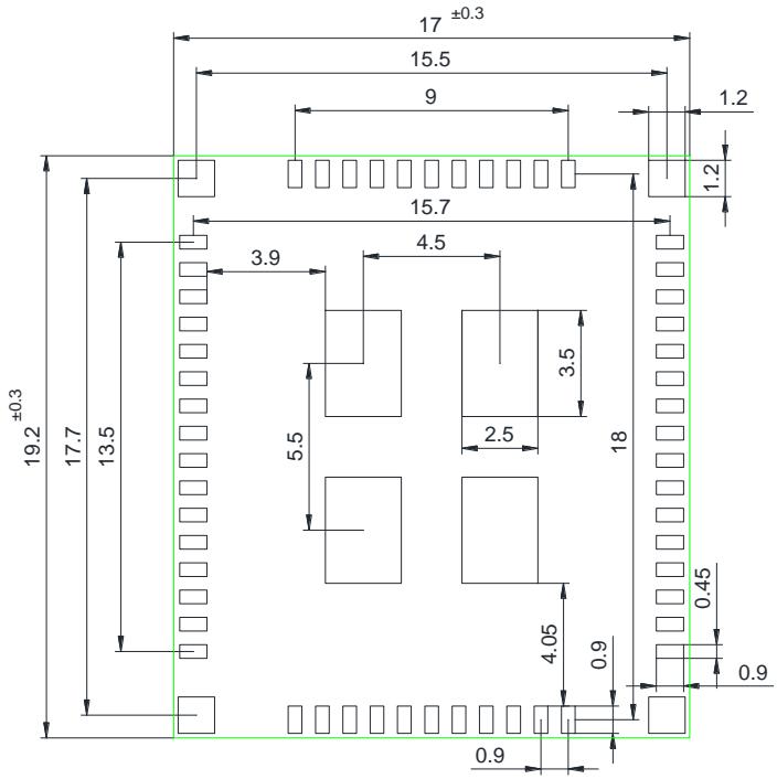
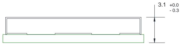
Dimensions
Operating condition
1) Recommended operation conditions
| Parameter | Min | Max | Unit |
| Operating Temperature Range | -40 | +85 | °C |
| Supply Voltage : VBATT (3.3V) | 3.01) | 3.6 | V |
| Supply Voltage : VIO (1.8V to 3.3V) | 1.62 | 3.6 | V |
2) Current consumption
| Parameter | Average | Unit |
| Stand-by (BT & WLAN) | 10 | mA |
| WLAN Continuous Rx | 180 | mA |
| WLAN Continuous Tx2) | 790 | mA |
| Bluetooth Connection | 20 | mA |
Boot up sequence
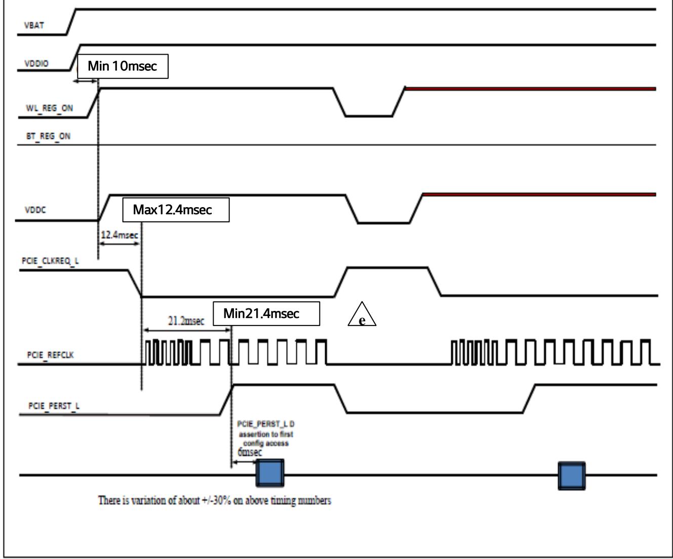
Figure 47. WLAN Power-Up Sequence for PCIe Host
General Features
BT(V5.1) + 2.4GHz/5GHz Wi-Fi 5(802.11a/b/g/n/ac) 2.4G SISO / 5G 2x2 MIMO Module
1) Features
Operation Voltage is 3.3V/1.8V Dual Power Rail
- Up to 866 Mbps data rate(802.11ac wave2 compliant)
Automotive Module
-
All components are AEC-Q 100/200 qualified
-
Support 2 Antenna port
- ANT0: Bluetooth/WLAN 5GHz, ANT1: WLAN WLAN2.4&5GHz
- Integrated WLAN PA, LNA (CYW88459) and RF Switch
RoHS Compliant - Size : 19.2 x 17.0 x 3.1mm
- Support bandwidth : HT20 / HT40 / VHT80
- Interface: PCIe(WLAN), UART, PCM/I2S(BT)
Package type : SMD type(LGA)
Bluetooth(BT5.1 + EDR compliant)
1) Bluetooth Key Features
- Support for Bluetooth 5.1 features
- GATT Caching
- Angle of Arrival (AoA) and Angle of Departure (AoD)
- Advertising Channel Index Randomization
-
Selective parts of Minor Feature Enhancements batch1
-
Fully supports Bluetooth 5.0 features:
-
LE 2 Mbits/s
- LE Long Range, S2/S8 coding
- LE Higher Output Power
- LE Advertising Extensions
- LE Channel Selection Algorithm #2
- LE High Duty Cycle Non-Connectable Advertising
-
Slot Availability Mask (SAM)
-
Fully supports Bluetooth 4.2 features
-
LE Data Packet Length Extension
- LE Secure Connections
- Link Layer privacy
- Link Layer Extended Scanner Filter policies
General Features
Bluetooth(BT5.1 + EDR compliant)
- Fully supports Bluetooth 4.1 features
- BR/EDR secure connections
- eSCO reserved slots clarification
- Train nudging
- Generalized interlaced scan
- Connectionless Slave broadcast
- Unencrypted unicast connectionless data support
- Low duty cycle directed advertising
- 32-bit UUID support in LE
- LE dual mode topology
- Piconet clock adjustment
- LE L2CAP connection oriented channel support
- LE privacy v1.1
- LE Link Layer topology
-LEping - Fast advertising interval
- HCI UART baud rates up to 4 Mbits/s supporting maximum Bluetooth data rates
- Multipoint operation with up to seven active slaves
- Maximum of seven simultaneous active ACL links
- Maximum of three simultaneous active SCO and eSCO connections with scatternet support
- Narrowband and wideband packet loss concealment
- Scatternet operation with up to four active piconets with background scan and support for scatter mode
- High-speed HCI UART transport support with low-power out-of-band BT_DEV WAKE and BT_HOST_WAKE signaling
- Channel quality driven data rate and packet type selection
- Standard Bluetooth test modes
- Extended radio and production test mode features
- Full support for power savings modes
- Bluetooth clock request
- Bluetooth standard sniff
- Deep-sleep modes and software regulator shutdown
General Features
WLAN
1) WLAN RF band & modulation Features
- Dual-band 2.4GHz and 5GHz 802.11 a/b/g/n/ac(802.11ac compliant)
- Dual-stream up to 866Mbps data rate
Supports 20, 40 and 80MHz channels with optional SGI(256 QAM modulation) - Tx and Rx low-density parity check(LDPC)
Supports IEEE 802.11ac/n beamforming - Supports two antennas with one dedicated to Bluetooth and WLAN and one to WLAN.
- PCIe mode complies with PCI Express base specification revision 3.0 for x1 lane and power management running at Gen1 speeds
- WPA and WPA2(Personal) support for powerful encryption and authentication
- AES and TKIP in hardware for faster data encryption and IEEE 802.11i compatibility
- Reference WLAN subsystem provides Wi-Fi protected Setup(WPS)
2) WLAN MAC features
- Enhanced MAC for supporting IEEE 802.11ac features
- Transmission and reception of aggregated MPDUs(A-MPDU) for high throughput(HT)
- Support for power management schemes, including WMM power-saving multi-poll(PSMP) and multiphase PSMP operation
- Support for immediate ACK and block-ACK policies
- Inter-frame space timing support, including RIFS
- Back-off counters in hardware for supporting multiple priorities as specified in the WMM specification
- Timing synchronization function(TSF), network allocation vector(NAV) maintenance, and target beacon transmission time(TBTT) generation in hardware
- Hardware offload for AES-CCMP, legacy WPA TKIP, legacy WEP ciphers, WAPI, and support for key management
- WPA, WAPI STA, and WPA2/WPA3 support for powerful encryption and authentication
- Programmable independent basic service set(IBSS) or infrastructure basic service set functionality
General Features
WLAN
3) WLAN PHY features
- Programmable data rates from MCS0-9 in 20MHz, 40MHz, and 80MHz channels, as specified in IEEE 802.11ac
- Improved performance with 2x2 channel smoothing and spur canceller support
Supports Optional short GI and Green field modes in Tx and Rx - Tx and Rx LDPC for improved range and power efficiency
- Beamforming support
Supports IEEE 802.11h/k for worldwide operation - Advanced algorithms for low power, enhanced sensitivity, range, and reliability
- IEEE 802.11a, 11b, 11g, 11n, 11ac single stream PHY standards
- Designed to meet FCC and other worldwide regulatory requirements
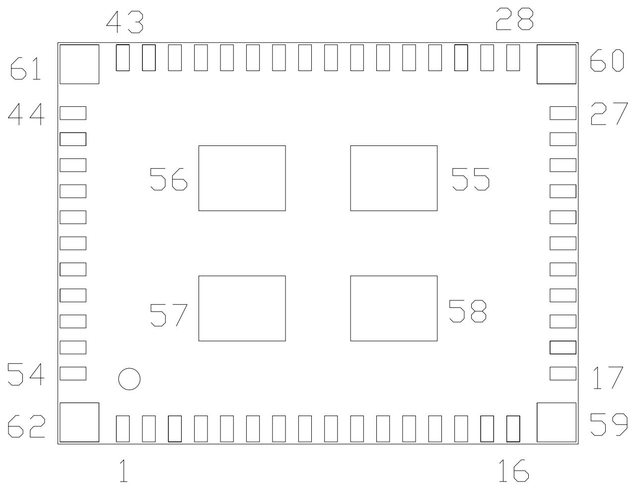
Pin Configuration
Pin Configuration
| No | Pin Name | I/O | Description |
| 1 | BT_UART_RXD | I/O | Bluetooth UART signal input |
| 2 | BT_UART_TXD | I/O | Bluetooth UART signal output |
| 3 | BTPCM_SYNC | I/O | PCM sync signal, can be master (output) or slave (input) |
| 4 | BTPCM_CLK | I/O | PCM clock, can be master (output) or slave (input) |
| 5 | BTPCM_IN | I | PCM data input |
| 6 | BTPCM_OUT | O | PCM data output |
| 7 | GND | - | Ground |
| 8 | PCIE_PERST_N | I | PCIE system reset. |
| 9 | PCIE_PME_L | O | PCIE power management event output |
| 10 | PCIE_CLKREQ_N | O | PCIE clock request signal |
| 11 | PCIE_CLK_N | I | PCIE differential clock input negative |
| 12 | PCIE_CLK_P | I | PCIE differential clock input positive |
| 13 | PCIE_TD_N | O | PCIE Transmitter differential negative |
| 14 | PCIE_TD_P | O | PCIE Transmitter differential positive |
| 15 | PCIE_RD_N | I | PCIE Receiver differential negative |
| 16 | PCIE_RD_P | I | PCIE Receiver differential positive |
| 17 | PCIE_EN | I | PCIE_ENABLE: Low: PCIE Disabled, High: PCIE Enabled |
| 18 | WL_DEV_WAKE | I | WLAN device wake from host |
| 19 | BT_DEV_WAKE | I | Bluetooth device wake from host |
| 20 | SDIO_DIS | I | SDIO_DISABLE: For use of PCIe → High |
| 21 | SDIO_DATA3 | I/O | SDIO data line 3 |
| 22 | SDIO_DATA2 | I/O | SDIO data line 2 |
| 23 | SDIO_CLK | I | SDIO clock |
| 24 | SDIOPAD | I | SDIOPADVDDIO: For use of PCIe → High |
| 25 | SDIO_DATA1 | I/O | SDIO data line 1 |
| 26 | SDIO_DATA0 | I/O | SDIO data line 0 |
| 27 | SDIO_CMD | I/O | SDIO command line |
| 28 | GND | - | Ground |
| 29 | CO_EX_OUT1 | O | 3-Wire Co-Existence Out1 |
| 30 | CO_EX_OUT0 | O | 3-Wire Co-Existence Out0 |
Pin Configuration
| No | Pin Name | I/O | Description |
| 31 | CO_EX_IN | I | 3-Wire Co-Existence In |
| 32 | BT_RST_N | I | Bluetooth Reset - Active-low reset input |
| 33 | GND | - | Ground |
| 34 | VBAT | I | Positive supply - Supply voltage : Typical 3.3V. |
| 35 | GND | - | Ground |
| 36 | Version Pin | - | Ground |
| 37 | VIO | I | BT, WLAN VDDIO supply voltage.(3.3V or 1.8V) - BT and WLAN should be same power rail |
| 38 | GND | - | Ground |
| 39 | NC | - | Floating |
| 40 | GND | - | Ground |
| 41 | WL_REG_ON | I | WLAN Power on reset - Internal 200KΩ pull-down |
| 42 | BT_REG_ON | I | BT Power on Reset |
| 43 | LPO | I | Low power clock input (32.768KHz, 200~1800mV P-P) |
| 44 | WL_HOST_WAKE | O | WLAN host wake from device |
| 45 | BT_HOST_WAKE | O | Bluetooth host wake from device |
| 46 | GND | - | Ground |
| 47 | GND | - | Ground |
| 48 | ANT_CORE0 | I/O | WLAN 5G RF with Bluetooth RF ANT |
| 49 | GND | - | Ground |
| 50 | ANT_CORE1 | I/O | WLAN 2.4G, 5G RF ANT |
| 51 | GND | - | Ground |
| 52 | GND | - | Ground |
| 53 | BT_UART_CTS_N | I/O | Bluetooth UART clear to send |
| 54 | BT_UART_RTS_N | I/O | Bluetooth UART request to send |
| 55 | GND | - | Ground |
| 56 | GND | - | Ground |
| 57 | GND | - | Ground |
| 58 | GND | - | Ground |
| 59 | GND | - | Ground |
| 60 | GND | - | Ground |
| 61 | GND | - | Ground |
| 62 | GND | - | Ground |
Module Integration Guide
-
Applicable FCC Rules
-
CFR 47 Part 15.247
-
Operational Condition
The module is limited to OEM installation ONLY. The OEM integrator is responsible for ensuring that the end-user has no manual instruction to remove or install module.
- Limited Module Procedure
ATC5CPL004 is limited Module. The module doesn't have its own power supply regulation.
Therefore, the host product manufacturer must design the host product
so that a constant voltage of 3.3V is applied to the module.
-
Trace antenna desings : N/A
-
RF Exposure consideration (CFR 47 Part 1, 1.1307(b), 1.1310)
This equipment complies with FCC radiation exposure limits set forth for an uncontrolled environment.
This equipment should be installed and operated with minimum 20 cm between the radiator and human body.
6. Antenna
This modular has PCB pattern antenna. Any changes of antenna designs might require additional assessment. The Host antenna type shall be same type and antenna gain shall be less or equal to below information.
| Item | Contents | |
| Antenna Type | PCB Pattern Antenna | |
| Antenna peak gain | Ant 1 | 2 400 MHz ~ 2 483.5 MHz: 2.28 dBi |
| 5 150 MHz ~ 5 250 MHz: 1.68 dBi | ||
| 5 250 MHz ~ 5 350 MHz: 1.68 dBi | ||
| 5 470 MHz ~ 5 725 MHz: 2.38 dBi | ||
| 5 725 MHz ~ 5 850 MHz: 3.04 dBi | ||
| Ant 2 | 2 400 MHz ~ 2 483.5 MHz: 1.84 dBi | |
| 5 150 MHz ~ 5 250 MHz: 1.90 dBi | ||
| 5 250 MHz ~ 5 350 MHz: 2.92 dBi | ||
| 5 470 MHz ~ 5 725 MHz: 3.55 dBi | ||
| 5 725 MHz ~ 5 850 MHz: 3.32 dBi | ||
7. Label and compliance information
The end user manual shall include all required regulatory information/warnings as shown in this manual. If the FCC identification number is not visible when the module is installed inside another device, then the outside of the device into which the module is installed must also display a label referring to the enclosed module.
This exterior label can use wording such as the following:
"Contains FCC ID : YZP-ATC5CPL004" any similar wording that expresses the same meaning may be used.
8. Information on test modes and additional testing requirements
This modular was tested in standalone configuration. Integration of this modular into a host equipment would require additional testing.
9. Additional testing, Part 15 Subpart B disclaimer
The grantee should include a statement that the modular transmitter is only FCC authorized for the specific rule parts (i.e., FCC transmitter rules) listed on the grant, and that the host product manufacturer is responsible for compliance to any other FCC rules that apply to the host not covered by the modular transmitter grant of certification. If the grantee markets their product as being Part 15 Subpart B compliant (when it also contains unintentional-radiator digital circuitry), then the grantee shall provide a notice stating that the final host product still requires Part 15 Subpart B compliance testing with the modular transmitter installed.
Module Integration Guide
10. ISED Statement
This device contains licence-exempt transmitter(s)/receiver(s) that comply with Innovation, Science and Economic Development Canada's licence-exempt RSS(s).
Operation is subject to the following two conditions:
(1) This device may not cause interference.
(2) This device must accept any interference, including interference that may cause undesired operation of the device.
Please notice that if the IC identification number is not visible when the module is installed inside another device, then the outside of the device into which the module is installed must also display a label referring to the enclosed module. This exterior label can use wording such as the following: "Contains IC : 7414C-ATC5CPL004" any similar wording that expresses the same meaning may be used.
This equipment complies with IC radiation exposure limits set forth for an uncontrolled environment. This equipment should be installed and operated with a minimum distance of 20 cm (7.8 inches) between the antenna and your body.
NOTE: THE MANUFACTURER IS NOT RESPONSIBLE FOR ANY RADIO OR TV
INTERFERENCE CAUSED BY UNAUTHORIZED MODIFICATIONS TO THIS
EQUIPMENT. SUCH MODIFICATIONS COULD Void THE USER'S AUTHORITY TO OPERATE THE EQUIPMENT.