USER MANUAL 6502 ERARD
The information in this manual has been reviewed and is believed to be entirely reliable. However, no responsibility is assumed for inaccuracies. The material in this manual is for informational purposes only and is subject to change without notice.
Second Edition
©MOS TECHNOLOGY, INC. 1976
"All Rights Reserved"
MOS TECHNOLOGY, INC.
950 Rittenhouse Road
Norristown, PA 19401

TABLE OF CONTENTS
1.0 Manual Introduction. 1
1.1 Microprocessor Architecture. 2
CHAPTER 2 THE DATA BUS, ACCUMULATOR AND ARITHMETIC UNIT
2.0 The Data Bus 3
2.1 The Accumulator. 4
2.1.1 LDA--Load Accumulator with Memory. 4
2.1.2 STA--Store Accumulator in Memory 5
2.2 The Arithmetic Unit. 6
2.2.1 ADC--Add Memory with Carry to Accumulator. 7
2.2.1.0 Multiple Precision Addition. 8
2.2.1.1 Signed Arithmetic. 10
2.2.1.2 Decimal Addition 13
2.2.1.3 Add Summary. 14
2.2.2 SBC--Subtract Memory from Accumulator with Borrow.. 14
2.2.2.0 Multiple Precision Subtraction 16
2.2.2.1 Signed Arithmetic. 18
2.2.2.2 Decimal Subtract 19
2.2.3 Carry and Overflow During Arithmetic Operations. 20
2.2.4 Logical Operands 20
2.2.4.1 AND--"AND" Memory with Accumulator 20
2.2.4.2 ORA--"OR"Memory with Accumulator. 21
2.2.4.3 EOR--"Exclusive OR" Memory with Accumulator. 21
CHAPTER 3 CONCEPTS OF FLAGS AND STATUS REGISTER
3.0 Carry Flag (C) 24
3.0.1 SEC--Set Carry Flag. 24
3.0.2 CLC--Clear Carry Flag. 25
3.1 Zero Flag (Z). 25
3.2 Interrupt Disable (I). 25
3.2.1 SEI--Set Interrupt Disable 26
3.2.2 CLI--Clear Interrupt Disable 26
3.3 Decimal Mode Flag (D). 26
3.3.1 SED--Set Decimal Mode. 26
3.3.2 CLD--Clear Decimal Mode. 27
3.4 Break Command (B). 27
3.5 Expansion Bit. 27
3.6 Overflow (V) 27
3.6.1 CLV--Clear Overflow Flag 28
3.6.2 Determination of Overflow. 28
3.7 Negative Flag (N). 29
3.8 Flag Summary 30
CHAPTER 4 TEST, BRANCH AND JUMP INSTRUCTIONS
4.0 Concepts of Program Sequence 31
4.0.1 Use of Program Counter to Fetch an Instruction 33
4.0.2 JMP--Jump to New Location. 36
4.1 Branching. 37
4.1.1 Basic Concept of Relative Addressing 38
4.1.2 Branch Instructions. 40
4.1.2.1 BMI--Branch on Result Minus. 40
4.1.2.2 BPL--Branch on Result Plus 40
4.1.2.3 BCC--Branch on Carry Clear 40
4.1.2.4 BCS--Branch on Carry Set 40
4.1.2.5 BEQ--Branch on Result Zero 41
4.1.2.6 BNE--Branch on Result Not Zero 41
4.1.2.7 BVS--Branch on Overflow Set. 41
4.1.2.8 BVC--Branch on Overflow Clear. 41
4.1.3 Branch Summary 42
4.1.4 Solution to Branch Out of Range. 42
4.2 Test Instructions. 45
4.2.1 CMP--Compare Memory and Accumulator. 45
4.2.2 Bit Testing. 47
4.2.2.1 BIT--Test Bits in Memory with Accumulator. 47
CHAPTER 5 NON-INDEXING ADDRESSING TECHNIQUES
5.0 Addressing Techniques. 50
5.1 Concepts of Pipelining and Program Sequence. 52
5.2 Memory Utilization 56
5.2.1 I/O Control. 56
5.2.2 Memory Allocation. 57
5.3 Implied Addressing 57
5.4 Immediate Addressing 59
5.5 Absolute Addressing. 59
5.6 Zero Page Addressing 61
5.7 Relative Addressing. 63
CHAPTER 6 INDEX REGISTERS AND INDEX ADDRESSING CONCEPTS
6.0 General Concept of Indexing. 69
6.1 Absolute Indexed 79
6.2 Zero Page Indexed. 81
6.3 Indirect Addressing. 83
6.4 Indexed Indirect Addressing. 85
6.5 Indirect Indexed Addressing. 87
6.6 Indirect Absolute. 92
6.7 Application of Indexes 92
CHAPTER 7 INDEX REGISTER INSTRUCTIONS
7.0 LDX--Load Index Register X from Memory 96
7.1 LDY--Load Index Register Y from Memory 96
7.2 STX--Store Index Register X in Memory. 97
7.3 STY--Store Index Register Y in Memory. 97
7.4 INX--Increment Index Register X by One 97
7.5 INY--Increment Index Register Y by One 97
7.6 DEX--Decrement Index Register X by One 98
7.7 DEY--Decrement Index Register Y by One 98
7.8 CPX--Compare Index Register X to Memory. 99
7.9 CPY--Compare Index Register Y to Memory. 99
7.10 Transfers Between the Index Registers and Accumulator. 100
7.11 TAX--Transfer Accumulator to Index X 100
7.12 TXA--Transfer Index X to Accumulator 100
7.13 TAY--Transfer Accumulator to Index Y 101
7.14 TYA--Transfer Index Y to Accumulator 101
7.15 Summary of Index Register Applications and Manipulations . 102
CHAPTER 8 STACK PROCESSING
8.0 Introduction to Stack and to Push Down Stack Concept 103
8.1 JSR--Jump to Subroutine. 104
8.2 RTS--Return from Subroutine. 108
8.3 Implementation of Stack in MCS6501 Through MCS6505 . . . 112
8.3.1 Summary of Stack Implementation. 115
8.4 Use of the Stack by the Programmer 116
8.5 PHA--Push Accumulator on Stack 117
8.6 PLA--Pull Accumulator from Stack 118
8.7 Use of Pushes and Pulls to Communicate Variables Between Subroutine Operations 119
8.8 TXS--Transfer Index X to Stack Pointer 120
8.9 TSX--Transfer Stack Pointer to Index X.. 122
8.10 Saving of the Processor Status 122
8.11 PHP--Push Processor Status on Stack. 122
8.12 PLP--Pull Processor Status from Stack. 123
8.13 Summary on the Stack 123
CHAPTER 9 RESET AND INTERRUPT CONSIDERATIONS
9.0 Vectors. 124
9.1 Reset or Restart 125
9.2 Start Function 126
9.3 Programmer Considerations for Initialization Sequences 127
9.4 Restart. 129
9.5 Interrupt Considerations 129
9.6 RTI--Return from Interrupt 132
9.7 Software Polling for Interrupt Causes. 137
9.8 Fully Vectored Interrupts. 140
9.8.1JMPIndirect. 141
9.9 Interrupt Summary. 142
9.10 Non-Maskable Interrupt 142
9.11 BRK--Break Command 144
9.12 Memory Map 146
CHAPTER 10 SHIFT AND MEMORY MODIFY INSTRUCTIONS
10.0 Definition of Shift and Rotate 147
10.1 LSR--Logical Shift Right 148
10.2 ASL--Arithmetic Shift Left 149
10.3 ROL--Rotate Left 149
10.4 ROR--Rotate Right. 150
10.5 Accumulator Mode Addressing. 150
10.6 Read/Modify/Write Instructions 151
10.7 INC--Increment Memory by One 154
10.8 DEC--Decrement Memory by One 155
10.9 General Note on Read/Modify/Write Instructions 155
CHAPTER 11 PERIPHERAL PROGRAMMING
11.0 Review of MCS6520 for I/O Operations 156
11.1 MCS6520 Interrupt Control. 158
11.2 Implementation Tricks for Use of the MCS6520 Peripheral Interface Devices 161
11.2.1 Shortcut Polling Sequences 161
11.2.2 Bit Organization on MCS6520s 162
11.2.3 Use of READ/MODIFY/WRITE Instruction for Keyboard Encoding. 163
11.3 MCS6530 Programming. 166
11.3.1 Reading of the Counter Register. 166
11.4 How to Organize to Implement Coding. 166
11.4.1 Label Standards. 168
11.5 Comprehensive I/O Program. 170
APPENDICES
A. Instruction List, Alphabetic by Mnemonic, Definition of Instruction Groups. A-1
MCS6501 - MCS6505 Microprocessor Instruction Set--
Alphabetic Sequence. A-2
A.1 Introduction. A-3
A.2 Group One Instructions. A-3
A.3 Group Two Instructions. A-4
A.4 Group Three Instructions. A-5
B. Instruction List, Alphabetic by Mnemonic, with OP CODEs, Execution Cycles and Memory Requirements. B-1
C. Instruction Addressing Modes and Related Execution Times.. C-1
D. Operation Code Instruction Listing Hexadecimal Sequence . . D-1
E. Summary of Addressing Modes
E.1 Implied Addressing. E-2
E.2 Immediate Addressing. E-3
E.3 Absolute Addressing E-3
E.4 Zero Page Addressing. E-4
E.5 Relative Addressing . E-4
E.6 Absolute Indexed Addressing . E-5
E.7 Zero Page Indexed Addressing. E-6
E.8 Indexed Indirect Addressing E-7
E.9 Indirect Indexed Addressing . E-8
F. MCS650X Programming Model . . . . . . . . . . . . . . F-1
G. Discussion--Indirect Addressing . . . . . . . . . . . G-1
H. Review of Binary and Binary Coded Decimal Arithmetic.. H-1
LIST OF EXAMPLES
CHAPTER 2 THE DATA BUS, ACCUMULATOR AND ARITHMETIC UNIT
2.1 Add 2 Numbers with Carry; No Carry Generation. 7
2.2 Add 2 Numbers with Carry; Carry Generation 8
2.3 Adding Two 16-Bit Numbers. 9
2.4 Add Two 16-Bit Numbers, No Carry from Low Order Add. 9
2.5 Add Two 16-Bit Numbers, with Carry from Low Order Add. . . 10
2.6 Add 2 Positive Numbers with No Overflow. 11
2.7 Add 2 Positive Numbers with Overflow 12
2.8 Add Positive and Negative Number with Positive Result.. 12
2.9 Add Positive and Negative Number with Negative Result.. 12
2.10 Add 2 Negative Numbers without Overflow. 12
2.11 Add 2 Negative Numbers with Overflow 13
2.12 Decimal Addition 13
2.13 Subtract 2 Numbers with Borrow; Positive Result. 15
2.14 Subtract 2 Numbers with Borrow; Negative Result. 16
2.15 Subtracting Two 16-Bit Numbers 16
2.16 Subtract in Double Precision Format; Positive Result 17
2.17 Subtract in Double Precision Format; Negative Result 18
2.18 Decimal Subtraction. 19
2.19 Clearing a Bit with "AND". 21
2.20 Setting a Bit with "OR". 21
2.21 Complementing a Byte with "EOR".
CHAPTER 4 TEST, BRANCH AND JUMP INSTRUCTIONS
4.1 Accessing Instructions with the P-Counter Value. 33
4.2 Accessing Data Addressing with P-Counter Value 34
4.3 Use of JMP Instruction 36
4.4 Illustration of "Branch on Carry Set". 38
4.5 Sequencing Two Branch Instructions 39
4.6 Use of JMP to Branch Out of Range. 43
4.7 Using the CMP Instruction. 46
4.8 Sample Program Using the BIT Test. 48
CHAPTER 5 NON-INDEXING ADDRESSING TECHNIQUES
5.1 Using Absolute Addressing. 51
5.2 Demonstration of "Pipelining" Effect 54
5.3 Illustration of Implied Addressing 58
5.4 Illustration of Immediate Addressing 59
5.5 Illustration of Absolute Addressing. 60
5.6 Illustration of Zero Page Addressing 62
5.7 Illustration of Relative Addressing; Branch Not Taken.. 63
5.8 Illustration of Relative Addressing; Branch Positive Taken, No Crossing of Page Boundaries 64
5.9 Illustration of Relative Addressing; Branch Negative Taken, Crossing of Page Boundaries. 65
CHAPTER 6 INDEX REGISTERS AND INDEX ADDRESSING CONCEPTS
6.1 Moving Five Bytes of Data with Straight Line Code. 70
6.2 Moving Five Bytes of Data with Loop. 72
6.3 Coded Detail of Moving Fields with Loop. 73
6.4 Moving Five Bytes of Data with Index Register. 76
6.5 Moving Five Bytes of Data by Decrementing the Index Register. 77
6.6 Absolute Indexed; with No Page Crossing. 79
6.7 Absolute Indexed; with Page Crossing 80
6.8 Illustration of Zero Page Indexing 82
6.9 Demonstrating the Wrap-Around. 83
6.10 Illustration of Indexed Indirect Addressing. 86
6.11 Indirect Indexed Addressing (No Page Crossing) 88
6.12 Indirect Indexed Addressing (with Page Crossing) 89
6.13 Absolute Indexed Add--Sample Program 90
6.14 Indexed Indirect Add--Sample Program 90
6.15 Move N Bytes (N < 256) 94
6.16 Move N Bytes (N > 256) 95
CHAPTER 8 STACK PROCESSING
8.1 Basic Stack Map for 3-Deep JMP to Subroutine 104
8.2 Basic Stack Operation. 105
8.3 Illustration of JSR Instruction. 106
8.4 Illustration of RTS Instruction. 109
8.5 Memory Map for RTS Instruction 111
8.6 Expansion of RTS Memory Map. 111
8.7 Call-a-Move Subroutine Using Preassigned Memory Locations. 116
8.8 Operation of PHA, Assuming Stack at 01FF 118
8.9 Operation of PLA Stack from Example 8.8. 119
8.10 Call-a-Move Subroutine Using the Stack to Communicate.. 119
8.11 Jump to Subroutine (JSR) Followed by Parameters. 121
CHAPTER 9 RESET AND INTERRUPT CONSIDERATIONS
9.1 Illustration of Start Cycle. 127
9.2 Interrupt Sequence 131
9.3 Return from Interrupt. 133
9.4 Illustration of Save and Restore for Interrupts. 133
9.5 Interrupt Polling. 137
9.6 Illustration of JMP Indirect 141
9.7 Break-Interrupt Processing 145
9.8 Patching with a Break Utilizing PROMs. 146
CHAPTER 10 SHIFT AND MEMORY MODIFY INSTRUCTIONS
10.1 General Shift and Rotate 147
10.2 Rotate Accumulator Left. 150
10.3 Rotate Memory Left Absolute, X. 151
10.4 Move a New BCD Number into Field 154
CHAPTER 11 PERIPHERAL PROGRAMMING
11.1 The MCS6520 Register Map 156
11.2 General PIA Initialization 157
11.3 Interrupt Mode Setup 159
11.4 CA2; CB2 Output Control. 159
11.5 Routine to Change CBl or CB2 Using Bit 3 Control 160
11.6 Polling the MCS6520. 161
11.7 Coding for Strobing an 8 x 8 Keyboard. 164
11.8 Polling for Active Signal. 172

CHAPTER 2 THE DATA BUS, ACCUMULATOR AND ARITHMETIC UNIT
2.1 Partial Block Diagram of MCS650X. 3
2.2 Partial Block Diagram Including Arithmetic Icgcic Unit of MCS650X 6
2.3 Byte Orientation with Sign Position 11
CHAPTER 3 CONCEPTS OF FLAGS AND STATUS REGISTER
3.1 Partial Block Diagram of MCS650X Including P-Register 23
3.2 Processor Status Register, "P". 24
CHAPTER 4 TEST, BRANCH AND JUMP INSTRUCTIONS
4.1 Partial Block Diagram of MCS650X Including Program Counter and Internal Address Bus 31
4.2 Use of Conditional Test 37
CHAPTER 5 NON-INDEXING ADDRESSING TECHNIQUES
5.1 Address Bus and Relation to Memory Field. 54
5.2 Example of Timing--MCS650X Family 55
CHAPTER 6 INDEX REGISTERS AND INDEX ADDRESSING CONCEPTS
6.1 Moving Five Bytes of Data with Loop 72
6.2 Moving Five Bytes of Data with Counter. 75
6.3 Partial Block Diagram of MCS650X Including Index Register 78
6.4 Indirect Addressing--Pictorial Drawing. 84
6.5 Indexed Indirect Addressing 85
6.6 Indirect Indexed Addressing 87
CHAPTER 8 STACK PROCESSING
8.1 Partial Block Diagram of MCS650X Including Stack Pointer, S 113
CHAPTER 10 SHIFT AND MEMORY MODIFY INSTRUCTIONS
10.1 Flow Chart for Moving in a New BCD Number 153
CHAPTER 11 PERIPHERAL PROGRAMMING
11.1 Keyboard Encoding Matrix Program. 163
11.2 Keyboard Strobe Sequence. 165
11.3 Program Flow-Polling for Active Signal. 171
CHAPTER 1
1.0 MANUAL INTRODUCTION
Welcome to the MCS650X product family. This manual is designed to work in conjunction with the Hardware Manual which describes the basic hardware considerations when using the MOS Technology, Inc. microcomputer family.
Before reading this manual, it is suggested that the reader acquaint himself with the Hardware Manual in order to understand the components available in this system, how these components are interconnected, and their basic architecture. Developed in this manual is the concept of microprocessor internal architecture and how it is used, with attention given to input/output considerations. Familiarity with the hardware will facilitate easier understanding of these important concepts.
In order to best serve the total customer base, this manual is written in two levels. The first is a very basic introduction to the MCS650X family, and the second level is for the user who has to refer to the manual on more than an occasional basis and who wants to rapidly scan and find specific sections. For the user who is quite familiar with programming and the MCS650X instruction set, the appendices are the best reference in the sense that all the data which is discussed in detail in the manual is summarized in a series of tables for convenience.
It is recommended that the user who is an experienced programmer and familiar with microprocessors still take the time to read through the manual in detail. Some of the architectural concepts are different from those found in second generation machines and this manual instructs the user how to optimize the utilization of the microprocessor while providing an introduction of its basic concepts.
Criticism of this manual is welcomed at all times. Of particular interest are cases where one could not, by use of the index and appendix, rapidly find the answer to a question which developed in the course of designing a microprocessor system. Welcomed are any comments which will enhance the content and format of this manual in future editions or addendum.
1.1 MICROPROCESSOR ARCHITECTURE
The MCS6501, MCS6502, MCS6503, MCS6504, and MCS6505 are all 8-bit microprocessors. That means that 8 bits of data are transferred or operated upon during each instruction cycle or operation cycle.
All devices in the MCS650X family operate on data 8 bits at a time, although some of the operations will look like serial or 16-bit wide operations. In a future section, discussed will be the use of sequential operations on an 8-bit basis and how one can accomplish 16-bit effective operands and addressing.
The computer industry, for some time, has been treating 8-bit combinations of data by a term known as a "byte." In many large computers which operate simultaneously on multiple bytes of data, the number of bytes which are transferred and operated on by the machine in parallel are called a "word." Because these microprocessors are 8-bit microprocessors, the words and bytes are of equal length. Therefore, for convenience through the discussion of the basic 8-bit processors, "byte" and "word" will be used synonymously although in some of the expanded versions there will exist a 16-bit word composed of two 8-bit bytes.
CHAPTER 2
THE DATA BUS, ACCUMULATOR AND ARITHMETIC UNIT
2.0 THE DATA BUS
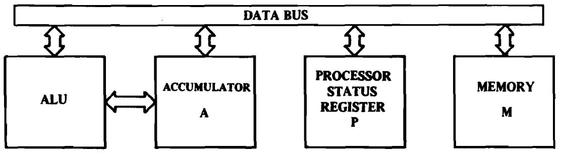
Although most of the following discussion will consider how one operates with a general purpose register called the accumulator, it must be understood that data has to transfer between the accumulator and outside sources by means of passing through the microprocessor to 8 lines called the data bus. The outside sources include the program which controls the microprocessor, the memory which will be used as interim storage for internal registers when they are to be used in a current operation, and the actual communications to the world through input/output ports. Later in this document performance of transfers to and from each of these devices will be discussed. However, at present, discussion will center on the microprocessor itself.
Partial Block Diagram of MCS650X
FIGURE 2.1
The only operation of the data bus is to transfer data between memory and the processor's internal registers such as the accumulator. Figure 2.1 displays the basic communication between the accumulator, A, and the memory, M, through the use of 8 bi-directional data lines called the data bus.
2.1 THE ACCUMULATOR
The accumulator is a register in which data is kept on which operations are performed. All operations between memory locations must be communicated through the accumulator or one of the auxiliary index registers. The accumulator is used as a temporary storage in moving data from one memory location to another. Therefore, the first use for the accumulator (A) is just in transferring data from memory to the accumulator or from the accumulator to memory. One can bring data into the accumulator, perform operations such as AND/OR on it, test the results of those operations, set new bits into it, or transfer it back out to the outside world. It serves as an interim storage for a series of operations such as adding 2 values together; where one of them is loaded into the accumulator, the second one added to it, and the results stored in the accumulator. The accumulator really acts as two functions: 1) It is one of the primary storage points for the machine; 2) It is the point at which intermediate results are normally stored.
2.1.1 LDA--Load Accumulator with Memory
When instruction LDA is executed by the microprocessor, data is transferred from memory to the accumulator and stored in the accumulator.
Rather than continuing to give a word picture of the operation, introduced will be the symbolic representation M A , where the arrow means "transfer to." Therefore the LDA instruction symbolic representation is read, "memory transferred to the accumulator."
LDA affects the contents of the accumulator, does not affect the carry or overflow flags; sets the zero flag if the accumulator is zero as a result of the LDA, otherwise resets the zero flag; sets the negative flag if bit 7 of the accumulator is a 1, otherwise resets the negative flag.
Although yet to be developed is the concept of addressing modes, for reference purpose, LDA is a "Group One" instruction and has all of the major addressing modes of the machine available to it as stated in Appendix A. These addressing modes include Immediate; Absolute; Zero Page; Absolute, X; Absolute, Y; Zero Page, X; Indexed Indirect; and Indirect Indexed.
2.1.2 STA--Store Accumulator in Memory
This instruction transfers the contents of the accumulator to memory.
The symbolic representation for this instruction is A M .
This instruction affects none of the flags in the processor status register and does not affect the accumulator.
It is a "Group One" instruction and has the following addressing modes available to it: Absolute; Zero Page; Absolute, X; Absolute, Y; Zero Page, X; Indexed Indirect; and Indirect Indexed.
2.2 THE ARITHMETIC UNIT
One of the functions to be expected from any computer is the ability to compute or perform arithmetic operations. Even in a simple control problem, one often finds it useful to add 2 numbers in order to determine that a value has been reached, or subtract 2 numbers to calculate a new value which must be obtained. In addition, many problems involve some rudimentary form of decimal or binary arithmetic; certainly many applications of the microprocessor will involve both. The MCS650X has an 8-bit arithmetic unit which interfaces to the accumulator as shown in Figure 2.2.
Partial Block Diagram including Arithmetic Logic Unit of MCS650X
FIGURE 2.2
The arithmetic unit is composed of several major parts. The most important of these is the circuitry necessary to perform a two's complement add of 8-bit parallel values and generate an 8 parallel bit binary result plus a carry. A review of binary and binary coded decimal (BCD) arithmetic is presented in Appendix H. However, a quick review of the concept of "carry" is in order. The largest range than can be represented in an 8-bit number is 256 with values ranging between 0 and 255. If we add any 2 numbers which result in a sum which is greater than 255, we represent the result with a ninth bit plus the 8 bits of the excess over 255. The ninth bit is called "carry."
2.2.1 ADC--Add Memory to Accumulator with Carry
This instruction adds the value of memory and carry from the previous operation to the value of the accumulator and stores the result in the accumulator.
The symbolic representation for this instruction is A + M + C A .
This instruction affects the accumulator; sets the carry flag when the sum of a binary add exceeds 255 or when the sum of a decimal add exceeds 99, otherwise carry is reset. The overflow flag is set when the sign or bit 7 is changed due to the result exceeding +127 or -128, otherwise overflow is reset. The negative flag is set if the accumulator result contains bit 7 on, otherwise the negative flag is reset. The zero flag is set if the accumulator result is 0, otherwise the zero flag is reset.
It is a "Group One" instruction and has the following addressing modes: Immediate; Absolute; Zero Page; Absolute, X; Absolute, Y; Zero Page, X; Indexed Indirect; and Indirect Indexed.
The ninth bit of the result is stored in the carry flag and the remaining 8 bits reside in the accumulator. The carry flag can be thought of as a flag bit which is remote from the accumulator itself but which is directly affected by accumulator operations as though it were a ninth bit in the accumulator. The primary reason for not viewing the carry bit as merely a ninth bit in the accumulator is that one has program control over its state by being able to set (to "1") or clear (to "0") the bit and, of course, it is not part of the 8-bit accumulator in data transfer operations. Examples employing the Add with Carry operation follow.
Example 2.1: Add 2 numbers with carry; no carry generation
| 0000 | 1101 | 13 = (A)* |
| 1101 | 0011 | 211 = (M)* |
| 1 | 1 = CARRY |
| Carry = /0/ | 1110 | 0001 | 225 = (A) |
*(A) and (M) refer to the "contents" of the accumulator and "contents" of memory respectively.
$$
\begin{array}{l} 1 1 1 1 \quad 1 1 1 0 \quad 2 5 4 = (\mathrm {A}) \ 0 0 0 0 \quad 0 1 1 0 \quad 6 = (\mathrm {M}) \ \text {C a r r y} = \sqrt {1 /} \quad \overline {{0 0 0 0}} \quad \frac {1}{0 1 0 1} \quad \frac {1}{5} = \text {(A)} \ \end{array}
$$
While the accumulator contains "5," the carry flag signals the user that the result exceeded 255 and, therefore, the result can be properly interpreted as 256 + 5 = 261 .
2.2.1.0 Multiple Precision Addition
To perform the addition of 2 numbers, one issues to the microprocessor an ADC instruction which adds the memory and the accumulator and stores the results in the accumulator with the carry bit going set if the results exceeded 255.
To add numbers which had significantly higher value than 255, it would be necessary to represent these numbers by a series of serial 8-bit numbers. With the 16 bits in 2 serial 8-bit numbers, it is possible to represent binary numbers of greater than 65,000 in value. In order to add two 16-bit numbers together and thus accomplish double precision addition, one first loads the lowest byte of one number into the accumulator, clears the carry flag and then adds the second number to the first number in the accumulator using the ADC command. One would then store this result into another memory location using the STA command. The carry flag would now represent the carry from the lowest byte to the highest byte. One could then load the high order byte of the first number, add with carry again to the high value of the second number, and store the result in the high order byte of the result. Thus, it can be seen that the carry allows us to perform as much precision arithmetic as is necessary. The example listing below displays the commands used to execute the addition of two 16-bit numbers.
Example 2.3: Adding two 16-bit numbers
| High Order Byte | Low Order Byte |
| First Number | H1 | L1 |
| Second Number | H2 | L2 |
| Result of Addition | H3 | L3 |
| LDA | L1 | Load low order byte, first number |
| CLC | | Clear carry flag (carry = 0) |
| ADC | L2 | Add L1 to low order byte, second num-
ber |
| STA | L3 | Store result in memory, carry flag is
still set if set in ADC operation |
| LDA | H1 | Load high order byte, first number |
| ADC | H2 | Add H1 and carry value from first ADC
operation to high order byte, second
number |
| STA | H3 | Store result in memory |
In this example it was necessary to clear the carry flag before starting the add instruction. This, of course, means that commands exist that set and clear the carry flag allowing for addition without values generated from the prior operation. One could also, at the end of the program, check to see if the result exceeded 16 bits by testing the carry flag. Exactly how one alters and tests flags will be discussed in the Flag and Branches Section. The examples below display the concept of carry from the addition of the low order bytes.
Example 2.4: Add two 16-bit numbers, no carry from low order add
| 0000 | 0001 | 0000 | 0010 | 258 |
| 0001 | 0000 | 0001 | 0000 | 4112 |
| Add | low order bytes: | (clear carry) |
| 0000 | 0010 | (A) | |
| 0001 | 0000 | (M) | |
| Carry = /0/ | 0001 | 0010 | (A) | |
| Add | high | order bytes | (carry = 0): |
| 0000 | 0001 | (A) | |
| 0001 | 0000 | (M) | |
| Carry = /0/ | 0001 | 0001 | CARRY |
| Result = 0001 | 0001 | 0001 | 0010 = 4370 |
Example 2.5: Add two 16-bit numbers, with carry from low order add
| 0000 | 0001 | 1000 | 0000 | 384 |
| 0000 | 0000 | 1000 | 0000 | 128 |
| Add low order bytes: (clear carry) |
| Carry = /1/ | 1000 | 0000 | (A) | | |
| 1000 | 0000 | (M) | | |
| 0000 | 0000 | (A) | | |
| Add high order bytes: (carry = 1) |
| Carry = /0/ | 0000 | 0001 | (A) | | |
| 0000 | 0000 | (M) | | |
| 0000 | 0010 | CARRY | | |
| Result = 0000 | 0010 | 0000 | 0000 | 512 | |
2.2.1.1 Signed Arithmetic
It is possible to look at the add operation and the way data is represented in memory in a different way. If, in the 16-bit problem (Examples 2.4 and 2.5), one were working with 15 bits of precision (in other words, 15 bits of valid data) plus 1 bit of sign (0 for positive and 1 for negative), it would be possible to perform signed binary arithmetic without changing the adder, but by merely changing the way the results are interpreted. In order to facilitate this concept, the microprocessor has the ability to represent positive or negative numbers by means of a sign flag which will be discussed at length in Section 3.7. In the MCS650X family, bit 7 is the sign position bit. This means that the highest order byte in a series of bytes should have the sign in the eighth position. If, for simplicity, one talks about signed 8-bit numbers, it would mean that one was allowed only 128 combinations of each sign because that is the most that can be represented in 7 bits, with the eighth bit or the highest bit reserved for the sign position.
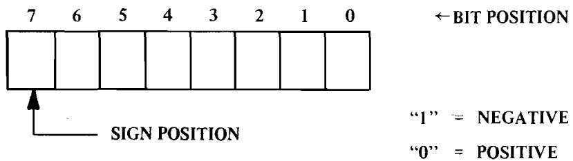
Byte Orientation with Sign Position
FIGURE 2.3
In the following examples of signed arithmetic it should be noted that operations are occurring on a 7-bit field of numbers and that any carry generated out of that field will reside in the eighth bit--not in the carry flag discussed during the add operations. The generation of a carry out of the field is the same as when adding two 8-bit numbers, except for the fact that the normal carry flag does not correctly represent the fact that the field has been exceeded. This is because the true carry from adding the two 7-bit numbers resides in the sign bit position. Therefore, the carry flag has no real meaning. Instead, there is a separate flag, the overflow flag, used to indicate when a carry from 7 bits has occurred and allows the user to write correction programs.
In each example, the negative numbers are in two's complement form. Also included in each result will be the status of the carry and overflow flags. The overflow flag is set whenever the sign bit (bit 7) is changed as a result of the operation.
Example 2.6: Add 2 positive numbers with no overflow
| 0000 | 0101 | +5 | (A) |
| Carry = /0/ | 0000 | 0111 | +7 | (M) |
| 0000 | 1100 | +12 | (A) |
| Overflow = /0/ | "0" in bit 7 indicates positive result. |
| Note that both the carry and overflow flag remain cleared. |
Example 2.7: Add 2 positive numbers with overflow
$$
\text {C a r r y} = \underline {{0 /}} \quad \begin{array}{l l l l} 0 1 1 1 & 1 1 1 1 & + 1 2 7 & (\mathrm {A}) \ 0 0 0 0 & 0 0 1 0 & + \underline {{2}} & (\mathrm {M}) \ \hline 1 0 0 0 & 0 0 0 1 & ^ {\prime \prime} - 1 2 7 ^ {\prime \prime} & (\mathrm {A}) \end{array}
$$
Overflow = 1/ "l" in bit 7 indicates negative result and the two's complement of the result is 127; however, the overflow flag is set indicating the allowable range was exceeded in the addition.
Therefore, examination of the overflow indicated that the result was in fact not negative but that the bit 7 position represented an overflow beyond the value of 127. Hence the user is flagged of an incorrect result and a correction routine (program) must follow.
Example 2.8: Add positive and negative number with positive result
$$
\text {C a r r y} = \frac {0 0 0 0}{1 / 1} \quad \frac {0 1 0 1}{0 0 0 0} \quad \frac {+ 5}{0 0 1 0} \quad \frac {- 3}{+ 2} \quad \text {(A)}
$$
Overflow = 0/ "0" in bit 7 indicates positive result. (Recall that though the carry flag is set, it has no meaning in signed operations.)
Example 2.9: Add positive and negative number with negative result
$$
\text {C a r r y} = \sqrt {0 /} \quad \begin{array}{l l l l l} 0 0 0 0 & 0 1 0 1 & + 5 & (\mathrm {A}) \ \frac {1 1 1 1}{1 1 1 1} & \frac {1 0 0 1}{1 1 1 0} & - 7 & (\mathrm {M}) \ \frac {1 1 1 1}{1 1 1 0} & \frac {- 2}{- 2} & (\mathrm {A}) \end{array}
$$
Overflow = 0/ "1" in bit 7 indicates negative result.
Example 2.10: Add 2 negative numbers without overflow
$$
\text {C a r r y} = \underline {{1 /}} \quad \begin{array}{l l l l l} 1 1 1 1 & 1 0 1 1 & - 5 & (\mathrm {A}) \ \frac {1 1 1 1}{1 1 1 1} & \frac {1 0 0 1}{0 1 0 0} & - 7 & (\mathrm {M}) \ \frac {1 1 1 1}{1 1 1 1} & \frac {- 7}{- 1 2} & (\mathrm {A}) \end{array}
$$
Overflow = 0 "1" in bit 7 indicates negative result.
$$
\text {C a r r y} = \underline {{/ 1 /}} \quad \begin{array}{l l l l} 1 0 1 1 & 1 1 1 0 & - 6 6 & (\mathrm {A}) \ \frac {1 0 1 1}{0 1 1 1} & \frac {1 1 1 1}{1 1 0 1} & - 6 5 & (\mathrm {M}) \ \hline \end{array}
$$
Overflow = 11 "0" indicates positive result, but the overflow flag is set indicating that the allowable range was exceeded in the operation. Without the overflow indication, the result would be interpreted as +125. The overflow, however, indicated that the result was negative and exceeded the value -128. Hence the user is flagged of an incorrect result, indicating the need for a correction routine.
2.2.1.2 Decimal Addition
There is a way for the user to organize data for decimal operations. The MOS Technology, Inc. MCS650X microprocessors have a modified adder which allows the user to represent his numbers as two 4-bit binary coded decimals (BCD) numbers packed into a single byte. This is a unique feature of the MCS650X family in that the operation in the following example can be performed.
Example 2.12: Decimal addition
| CLC | | | Clear Carry Flag |
| SED | | | Set Decimal Mode |
| LDA | 0111 | 1001 | 79 |
| ADC | 0001 | 0100 | +14 |
| STA | 1001 | 0011 | 93 |
The microprocessor adder has the unique capability of performing real time correction to the normal expected binary result without any direct interference from the programmer. Other popular microprocessors require a separate instruction (Decimal Adjust) which corrects the direct binary result of the arithmetic unit to obtain the same final results as are available on this microprocessor directly.
In order to make the same arithmetic unit perform either as a binary adder or as a decimal adder, the user chooses the mode in which he is going to operate (either decimal or binary) by setting
another flip-flop in the microprocessor called the decimal flag. As shown in this example, one not only initializes the adder by clearing the carry flag, but also puts the processor into decimal mode with the SED instruction. Even though this also requires 1 instruction, it is possible to put the machine in decimal mode once and perform many long strings of decimal numbers without further user intervention. The "Decimal Adjust" feature on other microprocessors requires programming subsequent to each binary operation.
2.2.1.3 Add Summary
In summary, the basic arithmetic unit is a binary adder which, under control of the ADC command, performs binary arithmetic on the accumulator and data, storing the result in the accumulator. Depending on the way the user looks at the data which is presented to the adder and the results which are obtained from it, the user can determine whether or not the result exceeds 255 binary or 99 decimal; he can perform precision arithmetic by use of the ninth bit or carry flag; he can control whether or not the microprocessor is a decimal adder by setting the decimal mode; and he can represent his numbers as signed binary numbers by analyzing other flags that are set in the machine.
2.2.2 SBC Subtract Memory from Accumulator with Borrow
This instruction subtracts the value of memory and borrow from the value of the accumulator, using two's complement arithmetic, and stores the result in the accumulator. Borrow is defined as the carry flag complemented; therefore, a resultant carry flag indicates that a borrow has not occurred.
The symbolic representation for this instruction is A - M - A .
This instruction affects the accumulator. The carry flag is set if the result is greater than or equal to 0. The carry flag is reset when the result is less than 0, indicating a borrow. The overflow flag is set when the result exceeds +127 or -127, otherwise it
is reset. The negative flag is set if the result in the accumulator has bit 7 on, otherwise it is reset. The Z flag is set if the result in the accumulator is 0, otherwise it is reset.
It is a "Group One" instruction. It has addressing modes Immediate; Absolute; Zero Page; Absolute, X; Absolute, Y; Zero Page, X; Indexed Indirect; and Indirect Indexed.
In a binary machine, the classical way to perform arithmetic is by using two's complement notation. In using two's complement notation, any subtraction operation becomes a sequence of bit complementations and additions. This reduces the complexity of the circuits required to perform a subtraction.
When the SBC instruction is used in single precision subtraction, there will normally be no borrow; therefore, the programmer must set the carry flag, by using the SEC (Set carry to 1) instruction, before using the SBC instruction. The microprocessor adds the carry flag to the complemented memory data, resulting in a true two's complement form of the memory value with its sign inverted.
Example 2.13: Subtract 2 numbers with borrow; positive result Assume a single precision subtraction where A contains 5 and M contains 3. The carry flag must be set to a 1 using the SEC instruction, thereby representing the no-borrow condition.
The adder changes the sign of M by taking the two's complement of M. This involves complementing M and adding the carry bit.
$$
\begin{array}{c c c} \mathrm {M} = 3 & 0 0 0 0 & 0 0 1 1 \ \text {C o m p l e m e n t e d M} & 1 1 1 1 & 1 1 0 0 \ \text {A d d C} = 1 & & 1 \ - \mathrm {M} = - 3 & 1 1 1 1 & 1 1 0 1 \end{array}
$$
The adder adds A and the two's complement -M together. This operation occurs simultaneously with the complement operation.
$$
\begin{array}{r l r l} \mathrm {A} & = 5 & 0 0 0 0 & 0 1 0 1 \ \mathrm {A d d} - \mathrm {M} & = - 3 & 1 1 1 1 & 1 1 0 1 \ \mathrm {C a r r y} & = / \overline {{1 /}} & 0 0 0 0 & 0 0 1 0 = + 2 \end{array}
$$
The presence of the carry flag after this operation indicates that No Borrow was required, therefore the result is +2.
Assume a single precision subtraction where A contains 5 and M contains 6. Set the carry flag to a 1 with SEC to indicate No Borrow.
$$
\begin{array}{c c c c} \mathrm {M} = 6 & 0 0 0 0 & 0 1 1 0 \ \text {C o m p l e m e n t e d M} & 1 1 1 1 & 1 0 0 1 & 1 \frac {1}{2} \text {c o m p} \ \text {A d d C} = 1 & & 1 \ - \mathrm {M} = - 6 & \overline {{1 1 1 1}} & \overline {{1 0 1 0}} & 2 ^ {\prime} \mathrm {s} \end{array}
$$
$$
\begin{array}{r l r} \mathrm {A} = 5 & 0 0 0 0 & 0 1 0 1 \ \text {A d d} - \mathrm {M} = - 6 & \underline {{1 1 1 1}} & \underline {{1 0 1 0}} \ \text {C a r r y} = \overline {{0 /}} & \overline {{1 1 1 1}} & \overline {{1 1 1 1}} = - 1 \end{array}
$$
The absence of the carry flag after this operation indicates that a borrow was required, therefore the result is a -1 in two's complement form. The absolute (unsigned) result in straight binary could be obtained by taking the two's complement of this number.
2.2.2.0 Multiple Precision Subtraction
Double precision subtraction is implemented in a fashion similar to addition. An example for subtracting a 16-bit number and storing the result follows:
Example 2.15: Subtracting two 16-bit numbers
| | High Order Byte | Low Order Byte |
| First Number | H1 | L1 |
| Second Number | H2 | L2 |
| Result of Subtraction | H3 | L3 |
| SEC | | Set Carry | |
| LDA | L1 | Load Low Order Byte, First Number |
| SBC | L2 | Subtract with Borrow, Low Order Byte of Second Number from L1 |
| STA | L3 | Store Result in Memory |
| LDA | H1 | Load High Order Byte, First Number |
| SBC | H2 | Subtract with Borrow, High Order Byte of Second Number from H1 |
| STA | H3 | Store Result in Memory |
Example 2.16: Subtract in double precision format; positive result
Assume a double precision subtraction where 255 is to be subtracted from 512 for an example. Since there has been no borrow coming into this subtraction operation, the carry flag must be set.
Following are the 2 numbers in binary form:
| High Order Byte | Low Order Byte |
| A field = 512 | 0000 | 0010 | 0000 | 0000 |
| M field = 255 | 0000 | 0000 | 1111 | 1111 |
Since the adder can only operate on single byte numbers, the programmer must operate on the low order bytes first.
$$
\begin{array}{c c c} \mathrm {M} = 1 1 1 1 & 1 1 1 1 \ \text {C o m p l e m e n t e d} \mathrm {M} = 0 0 0 0 & 0 0 0 0 \ \text {A d d C} = 1 & 1 \ - \mathrm {M} & 0 0 0 0 & 0 0 0 1 \end{array}
$$
$$
\begin{array}{r l} & \mathrm {A} = 0 0 0 0 \quad 0 0 0 0 \ \mathrm {A d d} & - \mathrm {M} = 0 0 0 0 \quad 0 0 0 1 \ \mathrm {C a r r y} = & \overline {{0 /}} \quad 0 0 0 0 \quad 0 0 0 1 \end{array}
$$
The carry is brought over to the subtract operation on the high order bytes.
$$
\begin{array}{l} \begin{array}{c c c} \mathrm {M} = 0 0 0 0 & 0 0 0 0 \ \text {C o m p l e m e n t e d} \mathrm {M} = 1 1 1 1 & 1 1 1 1 \ \text {A d d C} = 0 & 0 \ - \mathrm {M} & 1 1 1 1 & 1 1 1 1 \end{array} \ \begin{array}{r l} & \mathrm {A} = 0 0 0 0 \quad 0 0 1 0 \ \mathrm {A d d} & - \mathrm {M} = 1 1 1 1 \quad 1 1 1 1 \ \mathrm {C a r r y} = & \underline {{/ 1 /}} \quad 0 0 0 0 \quad 0 0 0 1 \end{array} \ \end{array}
$$
The result in binary form follows:
$$
\text {C a r r y} = \underline {{1 /}} \quad 0 0 0 0 \quad 0 0 0 1 \quad 0 0 0 0 \quad 0 0 0 1 = + 2 5 7
$$
The presence of the carry flag after the highest order byte subtraction indicates that the entire number required No Borrow, therefore it is a positive number in straight binary form.
Example 2.17: Subtract in double precision format; negative result
Now assume a double precision subtraction where 512 is to be subtracted from 255. Again, since there has been no borrow coming into this subtraction operation, the carry flag must be set.
Following are the two numbers in binary form:
| High Order Byte | Low Order Byte |
| A field = 255 | 0000 | 0000 | 1111 | 1111 |
| M field = 512 | 0000 | 0010 | 0000 | 0000 |
Operating on the low order byte:
$$
\begin{array}{l} \begin{array}{r l} & \mathrm {M} = 0 0 0 0 \quad 0 0 0 0 \ & \overline {{\mathrm {M}}} = 1 1 1 1 \quad 1 1 1 1 \ \text {A d d C} = \frac {1}{/ 1 /} & \frac {1}{0 0 0 0} \quad 0 0 0 0 \ \text {C a r r y} = - \mathrm {M} \end{array} \ \begin{array}{l} \text {A} = 1 1 1 1 \ \text {A d d - M} = \frac {\sqrt {1 /}}{1 /} \quad \frac {0 0 0 0}{1 1 1 1} \quad 1 1 1 1 \end{array} \ \end{array}
$$
The presence of the carry = 1 indicates no borrow.
The carry is now brought over to the high order byte subtract operation:
$$
\begin{array}{l} \begin{array}{r l} & \mathrm {M} = 0 0 0 0 \quad 0 0 1 0 \ & \overline {{\mathrm {M}}} = 1 1 1 1 \quad 1 1 0 1 \ \text {A d d C} = 1 & \frac {1}{1 1 1 1} \quad 1 1 1 0 \end{array} \ \begin{array}{r l} & \text {A} = 0 0 0 0 \quad 0 0 0 0 \ & \overline {{\mathsf {M}}} + \underline {{\mathsf {C}}} = \underline {{1 1 1 1}} \quad 1 1 1 0 \ \text {C a r r y} = \underline {{/ 0 /}} \quad \overline {{1 1 1 1}} \quad 1 1 1 0 \end{array} \ \end{array}
$$
The result in binary form is:
$$
\text {C a r r y} = \sqrt {0 /} 1 1 1 1 \quad 1 1 1 0 \quad 1 1 1 1 \quad 1 1 1 1 = - 2 5 7
$$
Carry = 100 indicates the presence of a borrow, therefore the number is negative and is in two's complement form.
2.2.2.1 Signed Arithmetic
Signed numbers can be subtracted, using the SBC instruction, just as easily as they can be added. The microprocessor converts the numbers from memory to its two's complemented form and then adds it to the value of the accumulator just as it does in an unsigned
subtract described in Section 2.2.2. The addition operation is identical to that described, and to the examples given in Section 2.2.1.1
It should be remembered that before using the SBC instruction, either signed or unsigned, the carry flag must be set to a 1 in order to indicate a no borrow condition. The resultant carry flag has no meaning after a signed arithmetic operation.
2.2.2.2 Decimal Subtract
As indicated in the Section 2.2.1.2, it is possible to represent numbers as packed 4-bit BCD numbers. In this case, which is again unique to this microprocessor, it is possible to make the adder act as though it is a decimal adder. In this case, the function of the machine is one of correcting for the subtraction of positive numbers by complementing the number, setting the carry and performing binary arithmetic with an automatic correction at the time the result is stored in the accumulator. The unique capabilities of this adder give the results as shown in the next example.
Example 2.18: Decimal Subtraction
| SED | | | Set Decimal Mode |
| SEC | | | Set Carry Flag |
| LDA | 0100 | 0100 | 44 |
| SBC | 0010 | 1001 | 29 |
| STA | 0001 | 0101 | 15 |
By setting the decimal mode and setting the carry flag, one can subtract number 29 from number 44 with the results in the accumulator automatically being 15.
As has been indicated, one can perform both addition and subtraction when the machine is set in decimal mode, treating the bytes to be added as unsigned, positive, binary coded digits. The carry flag in addition represents the case when the result in the number exceeded 99 and in subtraction the absence of the carry flag represents a true borrow situation.
2.2.3 Carry and Overflow During Arithmetic Operations
It is necessary to set or reset the carry flag prior to the beginning of any arithmetic instruction. Because the carry flag is set or reset as a result of the arithmetic operation at the end of the loop, one can test the flag to determine whether or not a carry or a borrow occurred in the operation. By proper use of the overflow flag one can treat the high order bit of any set of bytes as a sign bit as long as the results of the negative numbers are carried in two's complement form. The microprocessor also sets the overflow flip-flop to indicate when a result larger than can be stored in a 7-bit field has occurred and when the resultant sign is incorrect. In binary arithmetic the carry flag set indicates results in excess of 256, and in decimal arithmetic indicates results in excess of 99. Although the input carry is very important to these operations, a simple rule is: set the carry flag prior to subtract; clear the carry flag prior to add.
2.2.4 Logical Operands
In implementing a parallel binary adder there are several useful logic functions which are subsets of a binary add operation. In the MCS650X family, these subsets are used to implement the logical operands "AND," "OR," and "EOR" (Exclusive Or). These operations are used to test and control bit manipulations.
2.2.4.1 AND--Memory with Accumulator
The AND instructions transfer the accumulator and memory to the adder which performs a bit-by-bit AND operation and stores the result back in the accumulator.
This instruction affects the accumulator; sets the zero flag if the result in the accumulator is 0, otherwise resets the zero flag; sets the negative flag if the result in the accumulator has bit 7 on, otherwise resets the negative flag.
This is symbolically represented by A M A .
AND is a "Group One" instruction having addressing modes of Immediate; Absolute; Zero Page; Absolute, X; Absolute, Y; Zero Page, X; Indexed Indirect; and Indirect Indexed.
One of the uses for the AND operation is that of resetting a bit in memory. In the example below,
Example 2.19: Clearing a bit with AND
LDA 1100 X111, where X is 0 or 1
AND 1111 0111
STA 1100 0111
a byte is loaded into the accumulator and the AND instruction resets the accumulator bit 3 to 0. The accumulator is then stored back into memory, thereby resetting the bit.
2.2.4.2 ORA "OR" Memory with Accumulator
The ORA instruction transfers the memory and the accumulator to the adder which performs a binary "OR" on a bit-by-bit basis and stores the result in the accumulator.
This is indicated symbolically by A M A .
This instruction affects the accumulator; sets the zero flag if the result in the accumulator is 0, otherwise resets the zero flag; sets the negative flag if the result in the accumulator has bit 7 on, otherwise resets the negative flag. ORA is a "Group One" instruction. It has the addressing modes Immediate; Absolute; Zero Page; Absolute,X; Absolute,Y; Zero Page,X; Indexed Indirect; and Indirect Indexed.
To set a bit, the OR instruction is used as shown below:
Example 2.20: Setting a bit with OR
LDA 1110 X111, where X is O or 1
ORA 0000 1000
STA 1110 1111
2.2.4.3 EOR--"Exclusive OR" Memory with Accumulator
The EOR instruction transfers the memory and the accumulator to the adder which performs a binary "EXCLUSIVE OR" on a bit-by-bit basis and stores the result in the accumulator.
This is indicated symbolically by A M A .
This instruction affects the accumulator; sets the zero flag if the result in the accumulator is 0, otherwise resets the zero flag; sets the negative flag if the result in the accumulator has bit 7 on, otherwise resets the negative flag.
EOR is a "Group One" instruction having addressing modes of Immediate; Absolute; Zero Page; Absolute, X; Absolute, Y; Zero Page, X; Indexed Indirect; and Indirect Indexed.
One of the uses of the EOR instruction is in complementing bytes. This is accomplished below by exclusive ORA-ing the byte with all 1's.
Example 2.21: Complementing a byte with EOR
LDA 1010 1111
EOR 1111 1111
STA 0101 0000
CHAPTER 3
CONCEPTS OF FLAGS AND STATUS REGISTER
One can view each of the individual flags or status bits in the machine as individual flip-flops. The carry flag can be considered the ninth bit of an arithmetic operation. The decimal mode flag is set and cleared by the user and used by the microprocessor to select either binary or decimal mode. For programming convenience the microprocessor treats all of the flags or status bits as component bits of a single 8-bit register. In Figure 3.1 the processor status register (or "P" register) is added to the block diagram.
Partial Block Diagram of MCS650X including P Register
FIGURE 3.1
Each of the individual flags or bits has its own particular meaning in the microprocessor as defined in Figure 3.2.
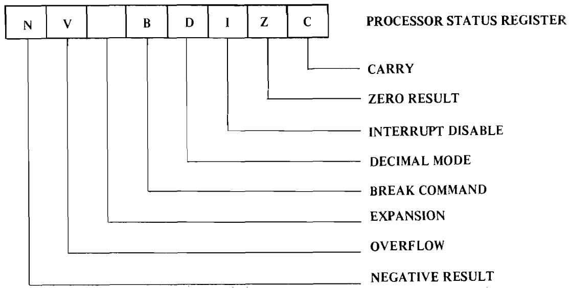
Processor Status Register
FIGURE 3.2
3.0 CARRY FLAG (C)
The carry bit which is modified as a result of specific arithmetic operations or by a set or clear carry command has been discussed previously. In the case of shift and rotate instruction, the carry bit is used as a ninth bit as it is in the arithmetic operation. The carry flag can be set or reset by the programmer. A SEC instruction will set and a CLC instruction will reset the carry flag. Operations which affect the carry are ADC, ASL, CLC, CMP, CPX, CPY, LSR, PLP, ROL, RTI, SBC, SEC.
3.0.1 SEC Set Carry Flag
This instruction initializes the carry flag to a l. This operation should normally precede a SBC loop. It is also useful when used with a ROI instruction to initialize a bit in memory to a l.
This instruction affects no registers in the microprocessor and no flags other than the carry flag which is set.
SEC is a single-byte instruction and its addressing mode is Implied.
3.0.2 CLC--Clear Carry Flag
This instruction initializes the carry flag to a 0. This operation should normally precede an ADC loop. It is also useful when used with a ROL instruction to clear a bit in memory.
This instruction affects no registers in the microprocessor and no flags other than the carry flag which is reset.
CLC is a single-byte instruction and its addressing mode is Implied.
3.1 ZERO FLAG(Z)
This flag is automatically set by the microprocessor during any data movement or calculation operation when the 8 bits of results of the operation are 0. Therefore, the bit is on ("1") when the results are 0, and off ("0") when the results are not equal to 0. The feature of the machine is similar to that of the PDP11 in the sense that operations which are decrementing index registers or memory locations have a built-in test for 0 as a result of decrementing to the 0 condition. It is also possible to test for 0 condition immediately following load and other logical operations, as opposed to processors which have to do a test and branch instruction. The Z flag is not directly settable or resettable by an instruction but is affected by the following instructions: ADC, AND, ASL, BIT, CMP, CPY, CPX, DEC, DEX, DEY, EOR, INC, INX, INY, LDA, LDX, LDY, LSR, ORA, PLA, PLP, ROL, RTI, SBC, TAX, TAY, TXA, TYA.
3.2 INTERRUPT DISABLE (I)
The interrupt disable is a flip-flop made use of by the programmer and by the microprocessor to control the operations of the interrupt request pin. A more detailed discussion of the effects of the interrupt disable are given in the discussion under interrupt control. However, the purpose of the interrupt disable is to disable the effects of the interrupt request pin. The interrupt disable, I, is set by the microprocessor during reset and interrupt commands. The I bit is reset by the CLI instruction or the PLP instruction, or at a return from interrupt in which the interrupt disable was reset prior to the interrupt. The interrupt flag may be set by the programmer using a SEI instruction and is cleared by the
programmer by using a CLI instruction. Instructions which affect the interrupt disable are BRK, CLI, PLP, RTI and SEI.
3.2.1 SEI--Set Interrupt Disable
This instruction initializes the interrupt disable to a 1. It is used to mask interrupt requests during system reset operations and during interrupt commands.
It affects no registers in the microprocessor and no flags other than the interrupt disable which is set.
SEI is a single-byte instruction and its addressing mode is Implied.
3.2.2 CLI--Clear Interrupt Disable
This instruction initializes the interrupt disable to a 0. This allows the microprocessor to receive interrupts.
It affects no registers in the microprocessor and no flags other than the interrupt disable which is cleared.
CLI is a single-byte instruction and its addressing mode is Implied.
3.3 DECIMAL MODE FLAG (D)
As discussed, the use of the decimal mode flag is to control whether or not the adder operates as a straight binary adder for add and subtract instructions or as a decimal adder for add and subtract instructions. The SED instruction sets the flag and the CLD instruction resets it. The only instructions which affect the decimal mode flag are CLD, PLP, RTI and SED.
3.3.1 SED--Set Decimal Mode
This instruction sets the decimal mode flag D to a 1. This makes all subsequent ADC and SBC instructions operate as a decimal arithmetic operation.
SED affects no registers in the microprocessor and no flags other than the decimal mode which is set to a 1.
3.3.2 CLD--Clear Decimal Mode
This instruction sets the decimal mode flag to a 0. This causes all subsequent ADC and SBC instructions to operate as simple binary operations.
CLD affects no registers in the microprocessor and no flags other than the decimal mode flag which is set to a 0.
3.4 BREAK COMMAND (B)
The break command flag is set only by the microprocessor and is used to determine during an interrupt service sequence whether or not the interrupt was caused by BRK command or by a real interrupt. A more detailed discussion of BRK is in the interrupt section. This bit should be considered to have meaning only during an analysis of a normal interrupt sequence. There are no instructions which can set or which reset this bit.
3.5 EXPANSION BIT
The next bit in the flag register is an unused bit. It is most likely that this bit will appear to be on when one is analyzing the bit pattern in the processor status register; however, no guarantee as to its state is made as this bit will be used in expanded versions of the microprocessor.
3.6 OVERFLOW(V)
As discussed in the section on arithmetic operations, if one is to look at the binary arithmetic operations as signed binary operations, there needs to be some indication of the fact the result of the arithmetic operation has a greater value than could be contained in the 7 bits of the result. This bit is the overflow bit and during ADC and SBC instructions represents a status of an overflow into the sign position. The user who is not using signed arithmetic can totally ignore this flag during his programming; however, this flag has the same meaning as the carry to the user who is using signed binary numbers. It indicates that a sign correction routine must be used if this bit is on after an add or subtract using signed numbers.
In addition to its use to monitor the validity of the sign bit in ADC and SBC instructions, the overflow flag in the MCS650X products is dramatically changed from PDP11 and the MC6800. In those systems the overflow flag was very carefully controlled so as to allow certain signed branches for analysis of signed numbers. These branches have been deleted from the MCS6500 series because of confusion and difficulty often associated with using them, and so therefore, the overflow flag is applicable only to the operation of ADC and SBC, and then only when using signed numbers.
However, in order to maximize the effectiveness of this testable flag the BIT instruction which may be used to sample interface devices, allows the overflow flag to reflect the condition of bit 6 in the sampled field. During a BIT instruction the overflow flag is set equal to the content of the bit 6 on the data tested with BIT instruction. When used in this mode, the overflow has nothing to do with signed arithmetic but is just another sense bit for the microprocessor. Instructions which affect the V flag are ADC, BIT, CLV, PLP, RTI and SBC. On certain versions of the microprocessor the V bit will also be available for stimulus from the outside world.
3.6.1 CLV--Clear Overflow Flag
This instruction clears the overflow flag to a 0. This command is used in conjunction with the set overflow pin which can change the state of the overflow flag with an external signal.
CLV affects no registers in the microprocessor and no flags other than the overflow flag which is set to a 0.
3.6.2 Determination of Overflow
To briefly recap the concept of overflow detection, one must understand that the machine signals an overflow based on the data entered to the operation and the final result. Since, with signed arithmetic, the range of numbers that be represented is +127 to -128, the overflow flag will never set when numbers of opposite sign are added, since their result will never exceed that range. The machine deals with this by recognizing that for any 2 positive numbers, the "bit 7" of each is a "0" and that for any arithmetic operation
yielding a result less than or equal to +127, the resultant "bit 7" must be a "0." If it is a 1, the overflow flag is set.
Similarly, when two negative numbers are added, the "bit 7" of each is a "1" and for any result yielding a value less than or equal to -128, the resultant "bit" must be a "1." If it is a 0, the overflow flag is set.
Therefore, the machine recognizes by knowledge of the "bit 7" of each of the numbers to be added what the resultant "bit 7" must be in a non-overflow situation. If these conditions are not met, the overflow flag goes set.
3.7 NEGATIVE FLAG (N)
As already discussed, one of the uses of the microprocessor is to perform arithmetic operations on signed numbers. To allow the user to readily sample the status of the sign bit (bit 7), the N flag is set equal to bit 7 of the resulting value in all data movement and data arithmetic. This means, for instance, after a signed add one can determine the sign of the result by sampling the N flag directly rather than finding a way to isolate bit 7. Although signs were the primary purpose for which the N flag was intended, its usefulness far exceeds that of strictly a sign bit. Because of every operation including simple moves and add operations the N bit is equal to the status of bit 7 as a result of the operation; its primary use becomes that of an easily testable bit. Almost all single-bit instructions, all interrupts and all I/O status flags use bit 7 as a sense bit. This allows the user to perform some type of memory access operation such as Load A followed by immediate conditional branch based on the status of bit 7 as reflected in the N flag. Like the Z bit, this flag is not settable or controllable by the programmer and represents the status of the last data movement operation. Instructions which affect the negative flag are ADC, AND, ASL, BIT, CMP, CPY, CPX, DEC, DEX, DEY, EOR, INC, INX, INY, LDA, LDX, LDY, LSR, ORA, PLA, PLP, ROL, BIT, SBC, TAX, TAY, TSX, TXA and TYA.
3.8 FLAG SUMMARY
To summarize, the microprocessor treats a series of flags or status bits as a single register called the "P" or "Program Status" register. Some of these flags are controllable only by the programmer (such as the D flag); others are controllable by both the user program and microprocessor (such as the interrupt disable flag). Some of them are set and reset by almost every processor operation, such as the N and Z flags. Each of these flags has its own meaning to the programmer at a particular point in time. When combined with the concept of conditional branches, they represent a powerful test and jump capability not normally found in a machine of this magnitude. Other than perhaps the carry flag which is used as part of the arithmetic instructions, the flags by themselves have relatively little meaning unless one has the ability to test them. For this purpose there is a series of conditional branch instructions designed into the machine.
CHAPTER 4
TEST, BRANCH AND JUMP INSTRUCTIONS
4.0 CONCEPTS OF PROGRAM SEQUENCE
In all the discussions up until now, there has been little discussion about how the microprocessor understands the instructions used to perform various arithmetic and accumulator manipulations. However, it is appropriate that the concept of a program and how the microprocessor determines each instruction be developed. More registers are required in the machine as shown in the figure below.
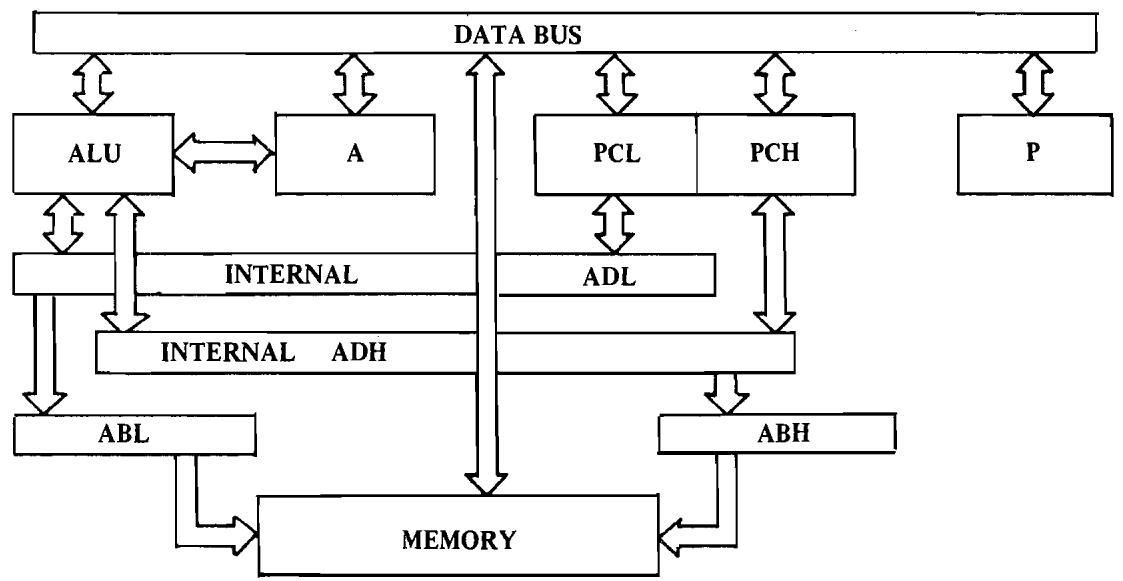
Partial Block Diagram of MCS650X Including Program
Counter and Internal Address Bus
FIGURE 4.1
Although two 8 bit registers have been added, they are the only registers in the machine that act as though they are one 16 bit register. They implement a concept known as program count or program sequence and subsequently their value will be referred to as PC or program count. In certain operations it may be convenient to talk about how one affects the program count low (PCL) which will be the lower 8 bit register or the program count high (PCH) which will be the higher 8 bit register. The reason for this register being 16 bits in length is that if it had only 8 bits it would only be able to reference 256 locations. Since it is through the address bus that one accesses memory, the program counter which defines the addressable location, should be as wide a word as possible.
The accessing of a memory location is called "addressing". It is the selection of a particular eight-bit data word (byte) out of the 65,536 possibilities for memory data locations. This selection is transmitted to the memory through the 16 address lines (ADH, ADL) of the microprocessor.
For a more detailed discussion of how an individual memory byte is selected by the address lines, the reader is referred to Chapter 1 of the Hardware Manual.
If the program counter was only 1 byte and if the bit pattern which allows the microprocessor to choose which instruction it wants to act on next, such as "LDA" as opposed to an "AND", was contained in one byte of data we could only have 256 program steps. Although the machine of this length might make an interesting toy, it would have no real practical value. Therefore, almost all of the competitive 8 bit microprocessors have chosen to go to a double length program counter. Even though some of the microprocessors of the MCS650X family do not have all of the output address lines necessary to allow the user to address 65K bytes of program (due to package pinout constraints), in all cases the program counter is capable of addressing a full 65K by virtue of its 16 bit length.
4.0.1 Use of Program Counter to Fetch an Instruction
The microprocessor contains an internal timing and state control counter. This counter, along with a decode matrix, governs the operation of the microprocessor on each clock cycle. When the state of the microprocessor indicates that a new instruction is needed, the program counter (program address pointer) is used to choose (address) the next memory location and the value which the memory sends back is decoded in order to determine what operation the MCS650X is going to perform next.
To use the program counter to perform this operation correctly, it must always be addressing the operation the user wants to perform next. This operation may be an instruction or may be data on which the instruction will operate.
In the MCS650X family, the program counter is set with the value of the address of an instruction. The microprocessor then puts the value of the program counter onto the address bus, transferring the 8 bits of data at that memory address into the instruction decode. The program counter then automatically increments by one and the microprocessor fetches further data for address operation necessary to complete the instruction. In the simple example below,
Example 4.1: Accessing Instructions with the P Counter Value
| P Counter* | Location Contents |
| 0100** | LDA | *Program Counter |
| 0101 | ADC | **Hexadecimal |
| 0102 | STA | Notation |
one can see how the program counter is used to access the instruction sequence load A, add with carry, and store the result. In this example, the program counter would start out containing 0100. The microprocessor would read location 0100 by using the program counter to access memory and would then interpret and implement the LDA instruction as previously described. The program counter will automatically increment by one on each instruction fetch, stepping to 0101. After performing the LDA, the microprocessor would fetch the
next instruction addressing memory with the program counter. This would pick up the ADC instruction, the add would then be performed, the program counter which has been incremented to 0102 would be used to address the next instruction, STA. The P counter incrementing once with each instruction is an oversimplified view of what actually transpires within the microprocessor.
The MCS650X processors usually require more than one byte to correctly interpret an instruction. The first byte of an instruction is called the OP CODE and is coded to contain the basic operation such as LDA (load accumulator with memory) and also the data necessary to allow the microprocessor to interpret the address of the data on which the operation will occur. In most cases, this address will appear in memory right after the OP CODE byte. This allows the microprocessor to use the program counter to access the address as well as the OP CODE.
The following example shows how the program counter picks up the instruction and the address of data located at address 5155.
Example 4.2: Accessing Data Address With P Counter Value
| P Counter | Location Contents |
| 0100 | LDA |
| 0101 | 55 |
| 0102 | 51 |
| 0103 | Next Instruction |
The OP CODE appears in Location Address 0100. The code for the 55 would appear next in Location Address 0101 and the 51 would appear in Location Address 0102, and the OP CODE for the next instruction appears in Location Address 0103. In this example, we see that the program counter is used not only to pick up the operation code, LDA, but is also used to pick up the address of the memory location from which the LDA is going to obtain its data. In this case, the program counter automatically is incremented three times to pick up the full instruction with the microprocessor interpreting each of the individual fetches as the appropriate data. In other words, the first
fetch is used to pick up the OP CODE, LDA, the second fetch is used to pick up the low order address byte of the data and the third fetch is used to pick up the high order address byte of the data. This is the form in which many of the microprocessor instructions will appear as it is the most simple form of addressing in the machine and allows referencing to any memory location.
Assuming that the microprocessor has the ability to start the program counter at a known instruction, it should be fairly obvious that the program counter would then continue to advance from that location up to the maximum memory location, roll over to the least memory location and continue incrementing through the memory, fetching instructions and addresses as it went. This would give us an interesting sequential program but one which lacked one tremendously powerful concept. The program would have no ability to perform tests or implement various options based on the results of those tests.
In the previous section, the concept of flags which are set as a result of the microprocessor operations was developed.
To use these flags, the program should be able to test them and then change the sequence of operations which are being performed depending on the result of the test. The program counter is going to continually put out an address, the microprocessor is going to fetch the instruction stored at that address and perform operations based on that instruction. In order to change a sequence of performed instructions by the microprocessor, the programmer must change the value in the program counter. Therefore, test instructions are incorporated which may result in a change of program count sequence as a result of performing one of the tests. The simplest way to change program sequence is to substitute a new value into the program counter location. In the MCS650X microprocessors the simplest way to change the program count sequence is with a JMP instruction.
4.0.2 JMP--Jump to New Location
In this instruction, the data from the memory location located in the program sequence after the OP CODE is loaded into the low order byte of the program counter (PCL) and the data from the next memory location after that is loaded into the high order byte of the program counter (PCH).
The symbolic notation for jump is (PC + 1) PCL , (PC + 2) PCH . As stated earlier, the "( )" means "contents of" a memory location. PC indicates the contents of the program counter at the time the OP CODE is fetched. Therefore (PC + 2) PCH reads, "the contents of the program counter two locations beyond the OP CODE fetch location are transferred to the new PC high order byte."
The addressing modes are Absolute and Absolute Indirect.
The JMP instruction affects no flags and only PCL and PCH.
The JMP instruction allows use of the program counter to access the new program counter value as illustrated by the following example:
Example 4.3: Use of JMP Instruction (Absolute Addressing Mode)
| Address | Data | Comments |
| 0100 | JMP | Jump to Location 3625 |
| 0101 | 25 | (New PCL byte) |
| 0102 | 36 | (New PCH byte) |
| 3625 | OP CODE | Next Instruction |
The program counter in the example starts out at location 100. The microprocessor loads a jump instruction. The program counter automatically increments to 101 where the microprocessor picks up and temporarily stores the 25. The program counter automatically increments to 102 where the microprocessor picks up the 36.
The 3625 is substituted into the program counter and is used to address the next instruction. Therefore, the JMP instruction contains within its address the new program counter location.
Although the jump allows the change of program sequence, it does so without performing any test. So it is a JMP instruction that is employed when it is desired to change the program counter no matter what conditions have occurred.
Another JMP addressing Mode in the Indirect Addressing Mode.
Before this technique can be understood, the basis of indirect addressing found in Chapter 6 must be reviewed. The JMP Indirect instruction is detailed in Chapter 9, page 141.
4.1 BRANCHING
To allow for conditional program sequence change, there are a series of branch instructions which test and perform optional changes of the program counter based on the status of the flags. To perform a conditional change of sequence, the microprocessor must interpret the instruction, test the value of a flag, and then change the P counter if the value agrees with the instruction. If the condition is not met, the program counter continues to increment in its normal fashion. Figure 4.2 illustrates how a conditional test might be used.
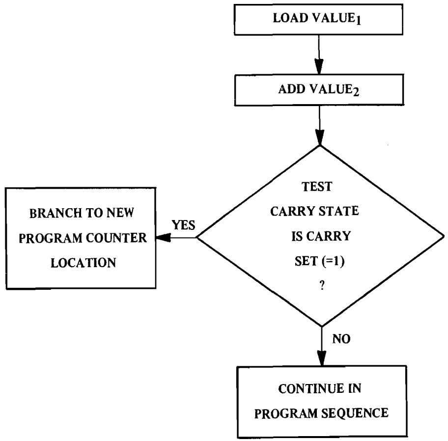
Use of Conditional Test
FIGURE 4.2
In this example, it is seen that generation of a carry from the add operation will allow an out-of-sequence branch to a new location.
4.1.1 Basic Concept of Relative Addressing
If one considers that the instruction JMP required three bytes, one for OP CODE, one for new program counter low (PCL) and one for new program counter high (PCH) it is seen that jump on carry set would also require three bytes. Because most programs for control require many continual jumps or branches, the MCS650X uses "relative" addressing for all conditional test instructions. To perform any branch, the program counter must be changed. In relative addressing, however, we add the value in the memory location following the OP CODE to the program counter. This allows us to specify a new program counter location with only two bytes, one for the OP CODE and one for the value to be added.
To illustrate this, in the following example, the branch on carry set (BCS) illustration is followed by a value of 50. If the carry is set, the new program location would be 108 + 50 = 158 ; in other words, it will take the branch.
Example 4.4: Illustration of "Branch on Carry Set"
| Address | Data | Comments |
| 0100 | LDA | Load First Value |
| 0101 | ADL1 | First Number, low byte |
| 0102 | ADH1 | First Number, high byte |
| 0103 | ADC | Add Second Value |
| 0104 | ADL2 | Second Number, low byte |
| 0105 | ADH2 | Second Number, high byte |
| 0106 | BCS | Test for Carry Set. If yes, branch to 0158 |
| 0107 | +50 | |
| 0108 | STA | If not, store results of add |
| 0109 | ADL3 | Result, low byte |
| 010A | ADH3 | Result, high byte |
| 0158 | OP CODE | New Instruction |
The 0108 represents the value of the program counter after reading the offset value. The program counter automatically increments so it can reference the next memory location on the next cycle. The add of the offset is a signed binary add as discussed in the arithmetic section. A positive branch is indicated by a 0 in bit 7 of the relative value, and a minus branch is in two's complement form and is indicated by a 1 in bit 7. The inherent capabilities of this type of notation system allow branch conditionally forward 127 bytes from the next instruction and back 128 bytes from that instruction. All branches in the MCS650X series are conditional relative branches and all have the form shown above. The advantage of relative addressing is best shown in the following example:
Example 4.5: Sequencing Two Branch Instructions
| Address | Data | Comments |
| 0100 | LDA | Load First Value |
| 0101 | ADL1 | |
| 0102 | ADH1 | |
| 0103 | ADC | Add Second Value |
| 0104 | ADL2 | |
| 0105 | ADH2 | |
| 0106 | BCS | Test for Carry Set. If yes, branch to 0158 |
| 0107 | +50 | |
| 0108 | BMI | Test for Minus Number. If yes, branch to 0095 |
| 0109 | -75 | |
| 010A | STA | If not, Store |
| 010B | ADL3 | |
| 010C | ADH3 | |
In this example, the previous single-branch example was modified to also test the resulting number to see if it is negative. In sequencing two-branch instructions, this loop is 2 bytes shorter by use of relative branches rather than 3 byte branches.
4.1.2 Branch Instructions
4.1.2.1 BMI - Branch on Result Minus
This instruction takes the conditional branch if the N bit is set.
BMI does not affect any of the flags or any other part of the machine other than the program counter and then only if the N bit is on.
The mode of addressing for BMI is Relative.
4.1.2.2 BPL - Branch on Result Plus
This instruction is the complementary branch to branch on result minus. It is a conditional branch which takes the branch when the N bit is reset (0). BPL is used to test if the previous result bit 7 was off (0) and branch on result minus is used to determine if the previous result was minus or bit 7 was on (1).
The instruction affects no flags or other registers other than the P counter and only affects the P counter when the N bit is reset.
The addressing mode is Relative.
4.1.2.3 BCC - Branch on Carry Clear
This instruction tests the state of the carry bit and takes a conditional branch if the carry bit is reset.
It affects no flags or registers other than the program counter and then only if the C flag is not on.
The addressing mode is Relative.
4.1.2.4 BCS - Branch on Carry Set
This instruction takes the conditional branch if the carry flag is on.
BCS does not affect any of the flags or registers except for the program counter and only then if the carry flag is on.
The addressing mode is Relative.
4.1.2.5 BEQ - Branch on Result Zero
This instruction could also be called "Branch on Equal." It takes a conditional branch whenever the Z flag is on or the previous result is equal to 0.
BEQ does not affect any of the flags or registers other than the program counter and only then when the Z flag is set.
The addressing mode is Relative.
4.1.2.6 BNE - Branch on Result Not Zero
This instruction could also be called "Branch on Not Equal." It tests the Z flag and takes the conditional branch if the Z flag is not on, indicating that the previous result was not zero.
BNE does not affect any of the flags or registers other than the program counter and only then if the Z flag is reset.
The addressing mode is Relative.
4.1.2.7 BVS - Branch on Overflow Set
This instruction tests the V flag and takes the conditional branch if V is on.
BVS does not affect any flags or registers other than the program counter and only when the overflow flag is set.
The addressing mode is Relative.
4.1.2.8 BVC - Branch on Overflow Clear
This instruction tests the status of the V flag and takes the conditional branch if the flag is not set.
BVC does not affect any of the flags and registers other than the program counter and only when the overflow flag is reset.
The addressing mode is Relative.
4.1.3 Branch Summary
To summarize, the MCS650X branches have two characteristics; each of them tests the state of a flag and then either accesses the next instruction in program sequence if the flag is not in the test state or adds the offset value to the PC value at the OP CODE of the next instruction (PC + 1) to allow the program to change operations. This allows the programmer the full ability to make decisions. By writing a sequence of branch instructions, any combination of conditions of the microprocessor may be determined and new action taken as a result of the tests.
There are four branch conditions in the MCS6501-5 microprocessors. These are branch on carry flag, branch of overflow flag, branch on N flag, and branch on zero flag. Each of the branches has a branch on flag set (1) or branch on flag clear (0).
4.1.4 Solution to Branch Out of Range
The branch relative instruction is unlike the jump instruction which can reach anywhere in memory, since branch relative is limited to +127 or -128 from the current program counter location. Although for many loops and many tests this is sufficient range, longer programs will occasionally find it necessary to conditionally branch to a location that is significantly further away than the branch command will directly reach. This is one of the uses of complementary branches. If a program should find it necessary to branch to a location which was significantly further away than 127, the following solution would facilitate the branch:
Example 4.6: Use of JMP to Branch Out of Range
| Address | Data | Comments |
| 100 | LDA | Load First Value |
| 101 | ADL1 | |
| 102 | ADH1 | |
| 103 | ADC | Add Second Value |
| 104 | ADL2 | |
| 105 | ADH2 | |
| 106 | BCC | Branch, if no carry, ahead 3 (to Point 2) |
| 107 | +3 | |
| 108 | JMP | If carry set, jump to location specified by ADH4, ADL4 |
| 109 | ADL4 | |
| 10A | ADH4 | |
| Point 2 | 10B | BMI | Check for Minus |
| 10C | Offset | |
| 10D | STA | |
| 10E | ADL3 | If not minus, Store Result |
| 10F | ADH3 | |
In this example, carry set is being checked. In order to accomplish this when the branch command would have to reach outside of the 128 range, the use of a complementary branch is required. Instead of doing the "branch on carry set" to the location, the "branch on carry clear" is utilized (a complementary instruction) which branches past the jump. If the complementary branch is not taken, the jump is the "branch on carry set" function.
This technique of branching past a jump with the complementary branch is a universal solution to the branch out of range problem.
Another solution is to find a like branch to the same location that is within range and although this involves two branches to transfer control, it does save memory locations.
By use of the relative branch less bytes of code are used than if a conditional jump had been used. However, in large programs, the branch out of range occurs more frequently. If the user can determine that a branch will be out of range by inspection, he should use the jump solution at the time he is writing the code. Otherwise, the
various assemblers indicate an out of range branch which will require recoding to use the jump solution.
NOTE: The jump solution causes 5 bytes of code to be substituted for 2 bytes of branch which in a symbolic assembly may force other branches to go out of range. This might cause several consecutive reassemblies but this technique will solve the problem.
4.2 TEST INSTRUCTIONS
Although most of the normal operations of the microprocessor involve setting of flags, there are specific instructions which are designed only to set flags for testing with the branch instruction.
4.2.1 CMP - Compare Memory and Accumulator
This instruction subtracts the contents of memory from the contents of the accumulator.
Its symbolic notation is A - M.
The use of the CMP affects the following flags: Z flag is set on an equal comparison, reset otherwise; the N flag is set or reset by the result bit 7, the carry flag is set when the value in memory is less than or equal to the accumulator, reset when it is greater than the accumulator. The accumulator is not affected.
It is a "Group One" instruction and therefore has as its addressing modes: Immediate; Zero Page; Zero Page, X; Absolute; Absolute, X; Absolute, Y; (Indirect, X); (Indirect), Y.
The purpose of the compare instruction is to allow the user to compare a value in memory to the accumulator without changing the value of the accumulator. An example of where this becomes extremely important is when one is receiving command instructions from an external device. In this case, an input byte may have several values. Each value can cause the program to perform a different operation. The only rapid way to determine the value of the input data is to compare the memory with a series of constants. It is fairly simple to perform "compare to constant" operations. By use of the immediate addressing mode which will be developed later, the following example compares an input to three values and branches to different locations for each:
Example 4.7: Using the CMP instruction
| Data | Comments |
| LDA | Load Value |
| ADL | Address Low |
| ADH | Address High |
| CMP | Compare COUNT 1 to Accumulator |
| COUNT 1 | |
| BEQ | If Equal, take the branch of OFFSET 1 |
| OFFSET 1 | |
| CMP | Compare COUNT 2 to Accumulator |
| COUNT 2 | |
| BEQ | If Equal, take the branch of OFFSET 2 |
| OFFSET 2 | |
| CMP | Compare COUNT 3 to Accumulator |
| COUNT 3 | |
| BEQ | If Equal, take the branch of OFFSET 3 |
| OFFSET 3 | |
| Next Inst. | Otherwise, go to Next Instruction based on default value (COUNT 4). |
This example shows how to use the default option. A value was compared against 3 values and if none were equal a fourth, or default value, is assumed. This is a useful technique for code minimization.
The compare instruction is designed to allow a signed comparison between 2 values assuming one makes appropriate use of the Z and N and C flags. In order to give maximum flexibility to the instruction, the instruction performs an effective subtract between the value in memory and the value in the accumulator. The reason it is an effective subtract is that subtraction allows the user to compare equal or less with one instruction.
The results of a compare are:
N
C
Z
V
Accumulator < Memory
Either
Reset
Reset
Unchanged
Accumulator = Memory
Reset
Set
Unchanged
Accumulator > Memory
Either
Set
Reset
Unchanged
So, to check if the accumulator is less than memory, the compare is followed by a BCC; to check if equal to is followed by a BEQ; and to check if greater it is followed by a BEQ followed by a BCS. Greater than or equal is checked by BCS.
4.2.2 Bit Testing
The comparison instruction is designed for cases when byte or multiple bytes of values are being compared; however, in the analysis of logic functions, it is very often necessary to determine the condition of an individual bit. One of the ways to accomplish this is with the use of the AND instruction as previously discussed. In other words, the user can load a value into the accumulator and AND it with a field that contains a one bit only in the corresponding bit position to the bit under test. By using a Branch on Zero Flag after the AND, the status of the bit in memory is testable by this technique. However, the use of this technique involves destroying the accumulator value with the AND instruction. Therefore, searching a table looking for a single bit in a given position would necessitate the reloading of the test value (mask) after each AND instruction. In order to allow memory sampling without disturbing the accumulator, the BIT instruction is used.
4.2.2.1 BIT - Test Bits in Memory with Accumulator
This instruction performs an AND between a memory location and the accumulator but does not store the result of the AND into the accumulator.
The symbolic notation is M A.
The bit instruction affects the N flag with N being set to the value of bit 7 of the memory being tested, the V flag with V being set equal to bit 6 of the memory being tested and Z being set by the result of the AND operation between the accumulator and the memory if the result is Zero, Z is reset otherwise. It does not affect the accumulator.
The addressing modes are Zero Page and Absolute.
The BIT instruction actually combines two instructions from the PDP-11 and MC6800, that of TST (Test Memory) and (BIT Test). This, like the compare test, allows the examination of an individual bit without disturbing the value in the accumulator and is illustrated by the example below:
Example 4.8: Sample Program Using the BIT Test
Data Comments
LDA Load MASK into Accumulator
MASK
BIT Test First Memory Value for Mask Bit
ADL1
ADH1
BNE Branch if Set
+50
BIT Test Second Memory Value for Mask Bit
ADL2
ADH2
BNE Branch if Set
-75
etc.
The value "MASK" loaded into the accumulator in this example is actually a descriptive title since, this byte is 8 bits, only one of which is a l. Using this byte in the AND operation inherent in the BIT test will effectively mask out all bits in the memory location under test except that bit position corresponding to the l residing in the accumulator. In Example 4.8, the MASK byte is AND'ed to the data found in location ADH1, ADL1 and if the bit under test is a l, the branch will be taken; if not a l, the second memory location will be tested with the same mask, etc.
In addition to the nondestructive feature of the bit which allows us to isolate an individual bit by use of the branch equal or branch no equal test, two modifications to the PDP-11 version of that instruction have been made in the MCS650X microprocessor. These are to allow a test of bit 7 and bit 6 of the field examined with the BIT test. This feature is particularly useful in serving polled interrupts and particularly in dealing with the MCS6520 (Peripheral Interface Device). This device has an interrupt sense bit in bit 6 and bit 7 of the status words. It is a standard of the M6800 bus that whenever possible, bit 7 reflects the interrupt status of an I/O device. This means that under normal circumstances, an analysis of the N flag after a load or BIT instruction should indicate the status of the bit 7 on the I/O device being sampled. To facilitate this test using
the Bit instruction, bit 7 from the memory being tested is set into the N flag irrespective of the value in the accumulator. This is different from the bit instruction in the M6800 which requires that bit 7 also be set on the accumulator to set N. The advantage to the user is that if he decides to test bit 7 in the memory, it is done directly by sampling the N bit with a Bit followed by branch minus or branch plus instruction. This means that I/O sampling can be accomplished at any time during the operation of instructions irrespective of the value preloaded in the accumulator.
Another feature of the BIT test is the setting of bit 6 into the V flag. As indicated previously, the V flag is normally reserved for overflow into the sign position during an add and subtract instruction. In other words, the V flag is not disturbed by normal instructions. When the BIT instruction is used, it is assumed that the user is trying to examine the memory that he is testing with the BIT instruction. In order to receive maximum value from a BIT instruction, bit 6 from the memory being tested is set into the V flag. In the case of a normal memory operation, this just means that the user should organize his memory such that both of his flags to be tested are in either bit 6 or bit 7, in which case an appropriate mask does not have to be loaded into the accumulator prior to implementing the BIT instruction. In the case of the MCS6520, the BIT instruction can be used for sampling interrupt, irrespective of the mask. This allows the programmer to totally interrogate both bit 6 and bit 7 of the MCS6520 without disturbing the accumulator. In the case of the concurrent interrupts, i.e., bit 6 and bit 7 both on, the fact that the V flag is automatically set by the BIT instruction allows the user to postpone testing for the "6th bit on" until after he has totally handled the interrupt "for bit 7 on" unless he performs an arithmetic operation subsequent to the BIT operation.

CHAPTER 5
NON-INDEXING ADDRESSING TECHNIQUES
5.0 ADDRESSING TECHNIQUES
The addressing modes of the MCS6500 family can be grouped into two major categories: Indexed and Non-Indexed Addressing. This section deals with the Non-Indexed mode of addressing. Before detailing the various modes available to the user, several concepts will be reviewed. The first of these is the concept of memory field, address bus and data bus. Then a brief introduction to two non-indexed addressing modes and timing will be made with the intent of preparing the reader for a discussion of program sequence and the internal activity of the microprocessor during execution of an instruction. This will be followed by a review of how one treats memory and the assorted allocation of memory space to the elements of RAM, ROM and I/O.
Subsequent to reading this section the user should have an understanding of the following fundamentals:
a) Memory Field
b) Address Bus
c) Data Bus
d) Cycle Timing
e) Program Sequence
f) Pipelining
With these tools in hand, the reader will be better prepared to readily comprehend the detailed definitions of the non-indexed addressing modes.
As discussed in Section 1.1 the MCS650X microprocessor family is organized around a 16-bit address function. All locations are accessed by a 16-bit word, even though in the case of the MCS6503, the MCS6504, and the MCS6505, only 11 or 12 bits are actually utilized.
Sixteen bits of address allow access to 65,536 memory locations, each of which, in the MCS650X family, consists of 8 bits of data. Figure 5.1 displays the total memory field and incorporates the concept of address bus and data bus. The memory address can be regarded as 256 pages (each page defined by the high order byte) of 256 memory locations (bytes) per page. It will be seen in the detailed discussion of addressing that the lowest order page, page zero, has special significance in the minimization of program code and execution time.
Much of the uniqueness of the MCS6500 product family has to do with how the 16-bit address is created. The simplest way to create a 16-bit address is for the programmer to indicate to the microprocessor the 16 bits necessary to access a particular operand on which the microprocessor is expected to operate. An instruction consists of 1, 2, or 3 bytes. It always takes 1 byte to specify the operation which is to be performed (OP CODE). This OP CODE is then followed by 0, 1, or 2 bytes of address depending on the specific operation involved. In the case of the simple instructions such as transfer accumulator to X, operations are performed internally and, therefore, no additional bytes are necessary. This instruction mode is known as "Implied" in the sense that the instruction contains both the OP CODE and the source and destination for the operation. This is the simplest form of addressing and applies to only a limited number of the instructions available in the MCS6500 family. Another form of addressing, absolute addressing, is the case when the programmer specifies directly to the microprocessor the address he wants the microprocessor to use in fetching the memory value on which the operation will occur. This form is illustrated by the example below.
Example 5.1: Using absolute addressing
| Clock Cycle | Address Bus | Data Bus |
| 1 | 0100 | LDA, Absolute |
| 2 | 0101 | ADL |
| 3 | 0102 | ADH |
| 4 | ADH, ADL | Data |
In this example, memory location 0100 contains the OP CODE "LDA Absolute." The next location, 0101, contains ADL which will be defined as the
"low order byte of the address," hence address low (ADL). Location 0102 contains ADH--the "high order byte of the address," hence address high (ADH). At the next clock cycle, the 16 bits composed of ADH and ADL are put on the address bus with the location defined by ADH, ADL containing the data to be loaded into the accumulator. The effective address of the data is best described in Figure 5.1, where the 16-bit address (AB00 through AB15) is composed of ADH and ADL.
This is the normal form for an absolute memory address. The first byte of the instruction which is picked up by the program counter is the operation code. This is interpreted by the microprocessor as "Load A - Absolute." At the same time that this Load A is being interpreted by the microprocessor, the microprocessor accesses the next memory location by putting the program counter content, which was incremented as the OP CODE was fetched, on the address bus.
5.1 CONCEPTS OF PIPELINING AND PROGRAM SEQUENCE
The overlap of fetching the next memory location while interpreting the current data from memory minimizes the operation time of a normal 2- or 3-byte instruction and is referred to as pipelining. It is this feature that allows a 2-byte instruction to only take 2 clock times and a 3-byte instruction to be interpreted in 3 clock cycles.
In the MCS650X microprocessors, a clock cycle is defined as 1 complete operation of each of the 2 phase clocks. Figure 5.2 is a sketch of the address and data bus timing as it relates to the system clocks.
The major point to be noted is that every clock cycle in the MCS650X microprocessor is a memory cycle in which memory is either read or written. Simultaneously with the read or write of memory, an internal operation of the microprocessor is also occurring.
| BINARY ADDRESS
High Order Low Order | DECIMAL
WORD
NUMBER | HEXADECIMAL
Address Code | ADDRESSABLE
MEMORY FIELD
(65536 Bytes) | |
| Page
Number | Byte
Number | |
| 15 | 14 | 13 | 12 | 11 | 10 | 9 | 8 | 7 | 6 | 5 | 4 | 3 | 2 | 1 | 0 |
| 0 | 0 | 0 | 0 | 0 | 0 | 0 | 0 | 0 | 0 | 0 | 0 | 0 | 0 | 0 | 0 |
| 0 | 0 | 0 | 0 | 0 | 0 | 0 | 0 | 0 | 0 | 0 | 0 | 0 | 1 | 1 | 1 |
| 0 | 0 | 0 | 0 | 0 | 0 | 0 | 0 | 1 | 1 | 1 | 1 | 1 | 1 | 1 | 1 |
| 0 | 0 | 0 | 0 | 0 | 0 | 0 | 0 | 1 | 1 | 1 | 1 | 1 | 1 | 1 | 1 |
| 0 | 0 | 0 | 0 | 0 | 0 | 1 | 0 | 0 | 0 | 0 | 0 | 0 | 0 | 0 | 0 |
| 1 | 1 | 1 | 1 | 1 | 1 | 1 | 0 | 1 | 1 | 1 | 1 | 1 | 1 | 1 | 1 |
| 1 | 1 | 1 | 1 | 1 | 1 | 1 | 0 | 0 | 0 | 0 | 0 | 0 | 0 | 65279 | FE - FF |
| 1 | 1 | 1 | 1 | 1 | 1 | 1 | 1 | 0 | 0 | 0 | 0 | 0 | 0 | 65280 | FF - 00 |
| 1 | 1 | 1 | 1 | 1 | 1 | 1 | 1 | 0 | 0 | 0 | 0 | 0 | 1 | 65281 | FF - 01 |
| 1 | 1 | 1 | 1 | 1 | 1 | 1 | 1 | 1 | 1 | 1 | 1 | 1 | 1 | 65535 | FF - FF |
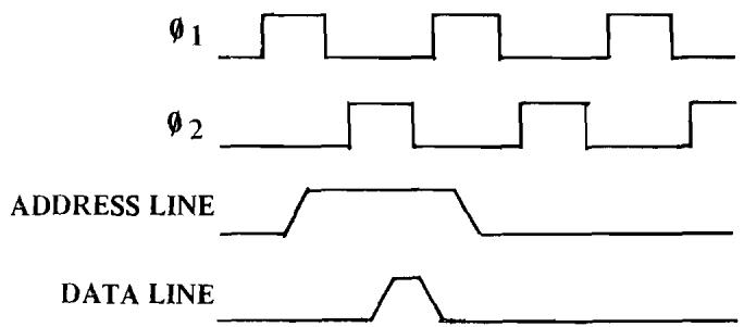
Example of Timing - MCS650X Family
FIGURE 5.2
The following example will let us analyze this effect:
Example 5.2: Demonstration of "Pipelining" effect
| Clock Cycles | External Operation | Address | Data | Internal Operation |
| 1 | Fetch OP CODE | 100 | ADC | Increment P-counter to 101 |
| 2 | Fetch first-address half from memory | 101 | ADL | Increment P-counter to 102, Interpret ADC instruction |
| 3 | Fetch second address half from memory | 102 | ADH | Increment P-counter to 103; Hold ADL |
| 4 | Fetch operand from memory | ADH, ADL | Data | Load Data |
| 5 | Fetch next OP CODE from memory | 103 | STA | Increment P-counter to 104, Perform ADC operation: A + M + C |
| 6 | Fetch address from memory | 104 | ADL | Increment P-counter to 105, Result of Add → accumulator, Interpret STA Instru-tion |
The above example shows the operation of an ADC, add with carry instruction, using absolute addressing. In the first cycle, the OP CODE is fetched from memory addressed by the P-counter. To implement the
look-ahead or pipeline in cycle two, the fetch of ADL address low is done simultaneously with the interpretation of the ADC absolute instruction. By the end of cycle 2, the microprocessor knows that it should access the next memory location for the address high as a result of interpretation of the absolute addressing mode.
The address low (ADL) is stored in the ALU while the address high (ADH) is being fetched in cycle 3.
On the fourth cycle, no internal operation is necessary while the microprocessor is putting the calculated value onto the address bus. However, during this cycle, the operand is loaded into the microprocessor.
The 4 cycles have all been involved with memory access for the ADC, absolute instruction. The first to fetch the instruction, the second to fetch the address low, the third to fetch the address high and the fourth to use the calculated address to fetch the operand. Because that completes the memory operations for this instruction, during the fifth cycle the microprocessor starts to fetch the next instruction from memory while it is completing the add operation from the first instruction. During the sixth cycle, the microprocessor is interpreting the new instruction fetched during cycle 5 while transferring the result of the add operation to the accumulator. This means that even though it really takes 6 cycles for the microprocessor to do the ADC instruction, the programmer only need concern himself with the first 4 cycles as the next 2 are overlapped as shown.
All instructions take at least 2 cycles; one to fetch the OP CODE and 1 to interpret the OP CODE and, with few exceptions, the number of cycles that an instruction takes is equal to the number of times that memory must be addressed.
The details of how each addressing mode is overlapped are described in the individual sections and for specific details of each cycle in various operations, the user is referred to the Hardware Manual, Appendix A.
All instructions take at least 2 cycles; one to fetch the OP CODE and 1 to interpret the OP CODE and, with few exceptions, the number of cycles that an instruction takes is equal to the number of times that memory must be addressed.
5.2 MEMORY UTILIZATION
As indicated, the 16-bit address allows the user to access greater than 65,000 separate locations. Most of the locations which will be accessed in the course of a control problem will be in program or P-counter referenced locations. A typical program will probably range from 1000 to 8000 bytes and will normally be implemented in fixed ROM or non-volatile alterable ROM.
A second type of memory will be the read-write memory in which the user keeps data such as working values, input and output data. Depending on the type of problem being addressed, this RAM usually ranges from 32 bytes to 8000 bytes, although most applications will be under 2000 bytes of RAM.
It would seem there is significant address space not used in most applications. To get the maximum benefit of the addressing space, 2 concepts are implemented in the MCS6500 family. These are the use of data addressing as I/O control and distributed address connections for minimum control lines. The latter concept utilizes the address bus, which is basic to and therefore pervasive in any microcomputer system, as a controlling network whenever possible. An example of this is the use of the address bus in selecting devices to interface with the microprocessor.
5.2.1 I/O Control
The advantages of accessing I/0 as memory are 1) the use of distributed address space allows for simple I/0 control lines and 2) all of the power of the instructions is applied to I/0 operations. This has the advantage of minimizing I/0 hardware and allows the programmer to be innovative in the application of I/0 devices in solving his problem.
All MCS6500 product family I/O devices contain 8-bit registers which are addressed by the microprocessor as though they were a memory byte. In the simplest case, the 8-bit register being read contains a 1 and 0's pattern which corresponds to the TTL voltage level applied to 8 input pins to the I/O device.
If the register was a flip-flop register driving 8 output pins with TTL levels, the storing of 8 bits of data with a STA instruction into that I/O register would, in effect, be programming the flip-flop to a specific desired state. Thus, one can use the instructions with the I/O just as any other memory location.
5.2.2 Memory Allocation
Figure 5.1 displays the relationship between memory, address bus and data bus while referencing the address values in hexadecimal notation. The previous section has dealt with utilization of memory address space for not only ROM and RAM but for I/O as well. At this time, the concept of allocation of the memory field of Figure 5.1 to the elements of ROM, RAM and I/O will be considered. The allocation below satisfies most applications requirements and represents an optimum allocation for minimization of programming code and speed.
Hexadecimal Address Suggested Allocation of Memory
| 0000 - 3FFF | RAM |
| 4000 - 7FFF | I/O |
| 8000 - FFFF | ROM |
It should be noted that the 3 memory blocks address definitions which, while not mandatory or required for proper system operation, do represent a logical assignment of space. The justification for this particular allocation will be presented in Section 9.12. In the meantime, the reader should retain the concept of the various memory blocks allocated to RAM, I/O and ROM as they are useful in the following discussion. With an understanding of pipelining and the concept of memory allocation, the next subject must be: in what manner can data be accessed from the memory field?
5.3 IMPLIED ADDRESSING
Implied addressing is a single-byte instruction.
The byte contains the OP CODE which stipulates an operation internal to the microprocessor. Instructions utilizing this type of addressing include operations which clear and set bits in the P (Processor Status) register, incrementing and decrementing internal registers and transferring
contents of one internal register to another internal register. Operations of this form take 2 clock cycles to execute. The first cycle is the OP CODE fetch and during this fetch, the program counter increments.
In the second cycle, the incremented P-counter is now the address of the next byte of the instruction. However, since the OP CODE totally defines the operation, the second memory fetch is worthless and any P-counter increment in the second cycle is suppressed. During the second cycle, the OP CODE is decoded with recognition of its single byte operation.
In the third cycle, the microprocessor repeats the same address to fetch the next OP CODE. This is the second time the memory address is fetched; once as the second byte of the first instruction and second, as the correct OP CODE address for the next instruction.
A symbolic representation of a 2-cycle instruction is given below. "PC" means "Program Counter."
Example 5.3: Illustration of implied addressing
| Clock Cycle | Address Bus | Program Counter | Data Bus | Comments |
| 1 | PC | PC + 1 | OP CODE | Fetch OP CODE |
| 2 | PC + 1 | PC + 1 | New
OP CODE | Ignore New
OP CODE;
Decode Old
OP CODE |
| 3 | PC + 1 | PC + 2 | New
OP CODE | Fetch New
OP CODE;
Execute Old
OP CODE |
Instructions which use implied addressing and require only 2 cycles include CLC, CLD, CLI, CLV, DEX, DEY, INX, INY, NOP, SEC, SED, SEI, TAX, TAY, TSX, TXA, TXS, TYA.
Instructions utilizing implied addressing and which require more than 2 cycles are stack operations which include BRK, PHA, PHP, PLA, PLP, RTI, RTS.
Immediate addressing is a 2-byte instruction.
The first byte contains the OP CODE specifying the operation and address mode. The second byte contains a constant value known to the programmer. It is often necessary to compare load and/or test against certain known values. Rather than requiring the user to define and load constants into some auxiliary RAM, the microprocessor allows the user to specify values which are known to him by the immediate addressing mode.
Example 5.4: Illustration of immediate addressing
| Clock Cycle | Address Bus | Program Counter | Data Bus | Comments |
| 1 | PC | PC + 1 | OP CODE | Fetch OP CODE |
| 2 | PC + 1 | PC + 2 | Data | Fetch Data, Decode OP CODE |
| 3 | PC + 2 | PC + 3 | New | Fetch New |
| | | OP CODE | OP CODE,Execute OldOP CODE |
Immediate addressing is the simplest form of constant manipulation available to the programmer. It requires a minimum execution time in the sense that 1 cycle is used in loading the OP CODE and as this CODE is being interpreted, the constant is being fetched.
Instructions utilizing immediate addressing are ADC, AND, CMP, CPX, CPY, EOR, LDA, LDX, LDY, ORA, and SBC.
5.5 ABSOLUTE ADDRESSING
Absolute addressing is a 3-byte instruction.
The first byte contains the OP CODE for specifying the operation and address mode. The second byte contains the low order byte of the effective address (that address which contains the data), while the third byte contains the high order byte of the effective address. Thus the programmer specifies the full 16-bit address and, since any memory location can be specified, this is considered the most normal mode for addressing. Other modes may be considered special subsets of this 16-bit addressing mode.
Example 5.5: Illustration of absolute addressing
| Clock Cycle | Address Bus | Program Counter | Data Bus | Comments |
| 1 | PC | PC + 1 | OP CODE | Fetch OP CODE |
| 2 | PC + 1 | PC + 2 | ADL | Fetch ADL, Decode OP CODE |
| 3 | PC + 2 | PC + 3 | ADH | Fetch ADH,Hold ADL |
| 4 | ADH, ADL | PC + 3 | Data | Fetch Data |
| 5 | PC + 3 | PC + 4 | NewOP CODE | Fetch NewOP CODE,Execute OldOP CODE |
The basic operation of the microprocessor in an Absolute address mode is to read the OP CODE in the first cycle while finishing the previous operation. In the second cycle, the microprocessor automatically reads the first byte after the OP CODE (in this case the address low) while interpreting the operation code. At the end of this cycle, the microprocessor knows that it needs a second byte for program sequence; therefore, 1 more byte will be accessed using the program counter while temporarily storing the address low. This occurs during the third cycle. In the fourth cycle, the operation is one of taking the address low and address high that were read during cycles 2 and 3 to address the operand. For example, in load A, the effective address is used to fetch from memory the data which is going to be loaded in the accumulator. In the case of storing, data is transferred from the accumulator to the addressed memory.
As was illustrated in the review of pipelining, depending on the instruction, it is possible for the microprocessor to start the next instruction fetch cycle after the effective address operation and independent of how many more internal cycles it may take to complete the OP CODE. The only exception to this is the case of "Jump Absolute" in which the address low and address high that are fetched in cycle 2 and cycle 3 are used as the 16-bit address for the next OP CODE. The jump absolute therefore only requires 3 cycles. In all other cases, absolute addressing takes 4 cycles, 3 to fetch the full instruction including the effective address, the fourth to perform the memory transfer called for in the instruction.
Absolute addressing always takes 3 bytes of program memory; 1 for the OP CODE, 1 for the address low, 1 for the address high, plus 1 byte of data memory (such as RAM) that is pointed to by the effective address.
Instructions which have absolute addressing capability include ADC, AND, ASL, BIT, CMP, CPX, CPY, DEC, EOR, INC, JMP, JSR, LDA, LDX, LDY, LSR, ORA, ROL, SEC, STA, STX, STY.
5.6 ZERO PAGE ADDRESSING
Zero page addressing is a 2-byte instruction. The first byte contains the OP CODE, while the second byte contains the effective address in page zero of memory.
As seen in absolute addressing, the ability to address anywhere in the 65K memory space costs 3 bytes of program space, plus a minimum of 4 cycles to perform address operations. In order to allow the user a shortening of both memory space and execution time, particularly when dealing with working registers and intermediate values, the MCS650X microprocessor family has a special addressing mode that assumes automatically the effective address high (ADH) to be in the lowest page of memory. In order to understand the page concept one should think of each of the various memory addresses as comprising a consecutive block of 256 locations which have an independent high order address associated with that block. Each block is called a page. Other than for zero page and for calculating indexed addresses which will be covered in the following sections, the microprocessor pays little attention to the page concept.
The microprocessor assumes that the high order byte of the effective address for instructions which contain OP CODES which indicate the zero page addressing option is all 0's (ADH = 00, hexadecimal). This allows the following sequence to occur.
Example 5.6: Illustration of zero page addressing
| Clock Cycle | Address Bus | Program Counter | Data Bus | Comments |
| 1 | PC | PC + 1 | OP CODE | Fetch OP CODE |
| 2 | PC + 1 | PC + 2 | ADL | Fetch ADL, De-code OP CODE |
| 3 | 00, ADL | PC + 2 | Data | Fetch Data |
| 4 | PC + 2 | PC + 3 | New | Fetch New |
| | | OP CODE | OP CODE, Exe-cute Old |
| | | | OP CODE |
On the first cycle, the microprocessor puts out the program counter, reads the OP CODE and increments the program counter. On the second cycle, the microprocessor puts out the program counter, reads the effective address low, interprets the OP CODE and increments the program counter. So far, the operations are identical to those described in the absolute addressing mode. However, by the end of the second cycle, the microprocessor has decoded the fact that this is a zero page operation and on the next cycle, it outputs address 00, as the effective address high, along with the address low that it just fetched and then either reads or writes memory at that location, depending on the OP CODE.
The advantage of zero page addressing is that it takes only 2 bytes, 1 for the OP CODE and 1 for the effective address low; and only 3 cycles, 1 to fetch the OP CODE, 1 to fetch the address low, and 1 to fetch the data, as opposed to absolute addressing which takes 3 bytes and 4 cycles.
In order to make most effective utilization of this concept, the user should organize his memory so that he is keeping his most frequently accessed RAM values in the memory locations between 0 and 255. If one organizes the zero page of memory properly, including moving data into these locations for longer loops, significant shortening of program code and execution time can be obtained.
The concept of zero page is so important that the various cross assemblers have error notations which indicate when improper use of this space is made. If one's coding is organized according to the guidelines shown in Section 5.2.2, one normally will find working storage located in values from 0 to 255. This is an important aspect of the discipline known as "memory management."
Once the pattern of coding for the MCS650X, which considers working storage or registers in the zero page, becomes a habit, one finds that in most control applications, all of the working registers will take advantage of this programming and the associated time reduction without any special effort on the user's part.
Instructions which allow zero page addressing include ADC, AND, ASL, BIT, CMP, CPX, CPY, DEC, EOR, INC, LDA, LDX, LDY, LSR, ORA, ROL, SBC, STA, STX, STY.
5.7 RELATIVE ADDRESSING
As discussed in Section 4.1, all of the branch operations in the microprocessor use the concept of relative addressing. In example 5.7, it is seen that for the case of the straightforward branch in which the branch is not taken, on the first program count cycle, the microprocessor puts out program counter as an address, fetches the OP CODE and finishes the previous operation. During the second cycle, the program counter is put on the address bus, picking up the relative offset. Internally, the microprocessor is decoding the OP CODE to determine that it is a branch instruction.
Example 5.7: Illustration of relative addressing branch not taken
| Cycle | Address Bus | Data Bus | External Operation | Internal Operation |
| 1 | 0100 | OP CODE | Fetch OP CODE | Finish Previous Operation, Increment Program Counter to 101 |
| 2 | 0101 | Offset | Fetch Offset | Interpret Instruc-tion, Increment Program Counter to 102 |
| 3 | 0102 | Next OP CODE | Fetch Next OP CODE | Check Flags, Increment Program Counter to 0103 |
This is only the second cycle of an internal operation; therefore, the microprocessor may be storing a computed value from the previous instruction at the same time it is finishing interpreting the present instruction. It is while doing the store operation that the flags in the machine get physically set; therefore, the microprocessor allows the program counter
to go 1 more cycle to allow itself time to determine the value of the flags. For example, if the previous instruction is ADC, the flags will not get set until the cycle in which the offset value is fetched.
During the third cycle, the microprocessor puts the incremented PC onto the address bus, fetches the next OP CODE and checks the flag in order to decide whether or not the program counter value that is going out is correct and that the branch is not going to be taken. Therefore, an additional type of pipeline, in this case fetching the next OP CODE in a branch sequence, accomplishes the implementation of a branch relative with no branch being taken. This requires 2 cycles. One cycle fetches the branch OP CODE and 1 cycle fetches the next operation, the relative offset. The second fetch is effectively ignored by virtue of the fact that the branch is not taken, so the program counter location has already been incremented and the next OP CODE has already been fetched by the microprocessor.
If in the above example it is assumed that the flag is set such that the branch is taken and the relative offset is +50 , the microprocessor takes a third cycle to perform the branch operation.
Example 5.8: Illustration of relative addressing branch positive taken, no crossing of page boundaries
| Cycle | Address Bus | Data Bus | External Operation | Internal Operation |
| 1 | 0100 | OP CODE | Fetch OP CODE | Finish Previous Operation, Increment Program Counter to 101 |
| 2 | 0101 | +50 | Fetch Offset | Interpret Instruction, Increment Program Counter to 102 |
| 3 | 0102 | Next OP CODE | Fetch Next OP CODE | Check Flags, Add Relative to PCL, Increment Program Counter to 103 |
| 4 | 0152 | Next OP CODE | Fetch Next OP CODE | Transfer Results to PCL, Increment Program Counter to 153 |
In Example 5.8, on the first cycle, a branch OP CODE is fetched while the previous operation is finished. On the second cycle, the offset is fetched while the branch instruction is being interpreted. On the third cycle, the microprocessor uses the adder to add the program count low to
the offset and also checks the flags. Because the program count for the next OP CODE in program sequence is already in the program counter and is being incremented, the microprocessor can allow the incrementation process to continue. If the value for the next instruction is indicated because the flag is not set, then the microprocessor loads the next OP CODE and the add of the program counter low to the offset value, is ignored as it was in the previous example.
If during the third cycle the flag is found to be the correct value for a branch, the OP CODE that has been fetched during this cycle is ignored. The microprocessor then updates the program counter with the results from the add operation, puts that value out on the address bus, which fetches a new OP CODE.
This gives the effect of a 3-cycle branch. Thus it can be seen that in a case where the branch is not taken, the microprocessor has an effective 2-cycle branch, i.e., 2 memory references. In the case when the branch is taken, the branch takes 3 cycles as long as the relative value does not force an update to the program counter high. In other words, 3 cycles are required if the page boundary is not crossed (recall the discussion of the "page" concept in Section 5.0). If in the above example the branch was back from address 0102 fifty locations, as opposed to +50 locations, the following result would occur:
Example 5.9: Illustration of relative addressing--branch negative taken, crossing of page boundary
| Cycle | Address Bus | Data Bus | External Operations | Internal Operations |
| 1 | 0100 | OP CODE | Fetch OP CODE | Finish Previous Instruction |
| 2 | 0101 | -50 | Fetch Offset | Interpret Instru-tion |
| 3 | 0102 | Next OP CODE | Fetch Next OP CODE | Check Flags Add Relative to PCL |
| 4 | 01B2 | Discarded Data | Fetch Dis-carded Data | Store Adder in PCL and Subtract 1 from PCH |
| 5 | 00B2 | Next OP CODE | Fetch Next OP CODE | Put Out New PCH and Increment PC to 00B3 |
In this example, the adder is used to perform the arithmetic operation, and the adder can do only the 8 bits of addition at a time. The minus branch crosses back over the page boundary, therefore an intermediate result is developed of O1B2 which has no intrinsic value because of the borrow which now has to be reflected into the program counter high. Since this example displays both a negative offset and the crossing of a page boundary, additional explanation is in order.
The value to which the offset will be added is 0102 (hexadecimal). The offset itself is -50 (hexadecimal).
Subtract low order byte:
$$
0 2 _ {\mathrm {H E X}} = 0 0 0 0 \quad 0 0 1 0
$$
$$
5 0 _ {\mathrm {H E X}} = 0 1 0 1 \quad 0 0 0 0
$$
Take two's complement of 50:
$$
\overline {{5 0}} \quad = 1 0 1 0 \quad 1 1 1 1
$$
$$
- 5 0 = \frac {1}{1 0 1 1}
$$
$$
\text {A d d} 0 2 \quad 0 0 0 0 \quad 0 0 1 0
$$
$$
- 5 0 \quad 1 0 1 1 \quad 0 0 0 0
$$
$$
\text {C a r r y} = \underline {{0 /}} \quad 1 0 1 1 \quad 0 0 1 0
$$
B 2
Up to this point, the PCH has not been affected; therefore the value on the address bus is 01B2.
The Carry = 0 , indicating a borrow.
Subtract high order byte:
$$
0 1 _ {\text {H E X}} = 0 0 0 0 \quad 0 0 0 1
$$
$$
0 0 _ {\mathrm {H E X}} = 0 0 0 0 \quad 0 0 0 0
$$
Take two's complement of 00:
$$
\text {A d d C a r r y} = \quad 0
$$
$$
\begin{array}{l} \overline {{0 0}} _ {\mathrm {H E X}} = 1 1 1 1 \quad 1 1 1 1 \ - 0 0 _ {\mathrm {H E X}} = \overline {{1 1 1 1}} \quad \overline {{1 1 1 1}} \ \end{array}
$$
$$
\text {A d d} 0 1 \quad 0 0 0 0 \quad 0 0 0 1
$$
$$
- 0 0 \quad 1 1 1 1 \quad 1 1 1 1
$$
$$
C a r r y = \sqrt {1 /} \quad 0 0 0 0 \quad 0 0 0 0
$$
0 0
The presence of the Carry indicates no borrow, hence a positive result.
At this time, after the arithmetic operation on both bytes of the P.C., the address bus will be: 00B2.
The microprocessor does put out on the address line the intermediate results (01B2), thereby reading a location within the page it was currently working in, the value of which is ignored. It then subtracts 1, or if this was a branch forward to the next page, the microprocessor would add 1 to program counter high in this fourth cycle. In the fifth cycle, the microprocessor will recognize that it has the correct new program counter high and program counter low and is able to start a new instruction operation, thereby giving an effective length to the branch operation when a page crossing is encountered of 4 cycles.
It should be noted that all of the above operations are automatic; once a branch instruction is encountered, the following relative value is calculated and put into the memory location after the branch instruction.
We can see, however, that it is possible to control the execution time of a branch. This is important for counting or estimating execution times of operations. For counting purposes, the following applies:
If a branch is normally not taken, assume 2 cycles for the branch.
If the branch is normally taken but it is not across the page boundary, assume 3 cycles for the branch.
If the branch is over a page boundary, then assume 4 cycles for the branch.
In loops which are repeated many times, one can assume some type of statistical factor between 3 and 2, or 4 and 2, depending on the probability of taking the branch versus not taking it.
In order to indicate to the programmer when the 4-cycle branch is taken as opposed to the 3-cycle branch, the various assemblers flag all branch operations which cross page boundaries with a warning message and if timing is important, the user can perhaps relocate his program in such a way that the branch does not cross page boundary.
It should be re-emphasized that other than for timing purposes, page boundary crossings can be ignored by the programmer.
To summarize, the relative addressing always takes 2 bytes, 1 for the OP CODE and 1 for the offset.
The execution time is as follows:
Branch with Not Taking the Branch 2 cycles
Branch When the Branch Is Taken But -- 3 cycles No Page Crossing
Branch When the Branch Is Taken with -- 4 cycles a Page Crossing
Only branch instructions have relative addressing. The branch instructions are: BCC, BEQ, BIT, BMI, BNE, BPL, BSC, BVC, BVS. For a more detailed explanation of relative offset calculations the reader is referred to Appendix H.

CHAPTER 6
INDEX REGISTERS AND INDEX ADDRESSED CONCEPTS
6.0 GENERAL CONCEPT OF INDEXING
In previous sections techniques for using the program counter to address memory locations after the operation code to develop the address for a particular operation have been discussed. Other than cases when the programmer directly changes the program memory, it can be considered that the addressing modes discussed up until now are fixed or directed addresses and each has the relative merits discussed under each individual section. However, a more powerful concept of addressing is that of computed addressing. There are basically two types of computed addressing; indexed addressing and indirect addressing.
Indexed addressing uses an address which is computed by means of modifying the address data accessed by the program counter with an internal register called an index register.
Indirect addressing uses a computed and stored address which is accessed by an indirect pointer in the programming sequence.
In the MCS650X product family, both of these modes are used and combinations of them are available.
Before undertaking the more difficult concepts of indirect addressing the concept of indexed instructions will be developed.
In order to move five bytes of memory from an address contained in FIELD 1 to another set of addresses, starting with FIELD 2, the following program could be written:
Example 6.1: Moving Five Bytes of Data With Straight Line Code
| LABEL | INSTRUCTION | OPERAND | COMMENTS |
| START | LDA | FIELD 1 | Move First Value |
| STA | FIELD 2 |
| LDA | FIELD 1 + 1 | Move Second Value |
| STA | FIELD 2 + 1 |
| LDA | FIELD 1 + 2 | Move Third Value |
| STA | FIELD 2 + 2 |
| LDA | FIELD 1 + 3 | Move Fourth Value |
| STA | FIELD 2 + 3 |
| LDA | FIELD 1 + 4 | Move Fifth Value |
| STA | FIELD 2 + 4 |
In this example, data is fetched from the first memory location in FIELD 1, as addressed by the next one or two bytes in program memory, stored temporarily in A and then written into the first memory location in FIELD 2, also addressed by the next one or two bytes in program memory. This sequence is repeated, with only the memory addresses changing, until all the data has been transferred. This type of programming is called straight line programming because each repetitive operation is a separate group of instructions listed in sequence or straight line form in program memory. This is necessary even though the instruction OP CODES are identical for each memory transfer operation because the specific memory addresses are different and require a different code to be written into the program memory for each transfer.
It takes a total of 10 instructions to accomplish the move when it is implemented this way. It should be noted that it is not indicated whether or not FIELD 1 and FIELD 2 are Zero Page addresses or Absolute addresses.
If they were Zero Page addresses, the total number of bytes consumed in solving the problem would be two bytes for each instruction and thereby requiring 20 bytes of memory; if both FIELD 1 and FIELD 2 were Absolute memory locations, each instruction would take 3 bytes and this program would require 30 bytes of program storage.
The Zero Page program would execute in three cycles per instruction or 30 cycles and the Absolute location version would execute in four cycles per instruction or 40 cycles.
A new concept has been introduced in this example, that of symbolic notation rather than actual locations for the instructions.
The form that this short program is written in uses symbolic addressing in which the address of the beginning of the program has a name START. Symbolic representations of addresses such as "START" are referred to as labels. The addresses in the two address field used in this example have also been given names, the first address of the first field is called FIELD 1; the first address of the second field is called FIELD 2. Each additional address in the fields has been given a number which is referenced to the first number; for example, the third byte in FIELD 1 is FIELD 1 + 2. All of these concepts are implemented to simplify the ease of writing a program because the user does not have to worry about the locations of FIELD 1 and FIELD 2 until after analyzing the memory needs of the whole program. Symbolic notation also results in a more readable program.
Translation from symbolic form instructions and addresses into actual numerical OP CODES and addresses is done by a program called a symbolic assembler. Several different versions of symbolic assemblers and cross assemblers are available for the MCS650X product family. Symbolic notation will be used throughout the remainder of this text because of its ease of understanding and because individual byte addresses are unnecessary although for an explanation of a particular mode, the byte representation may be used.
In this example, only direct addresses were used. A program to reduce the number of bytes required to move the five values follows:
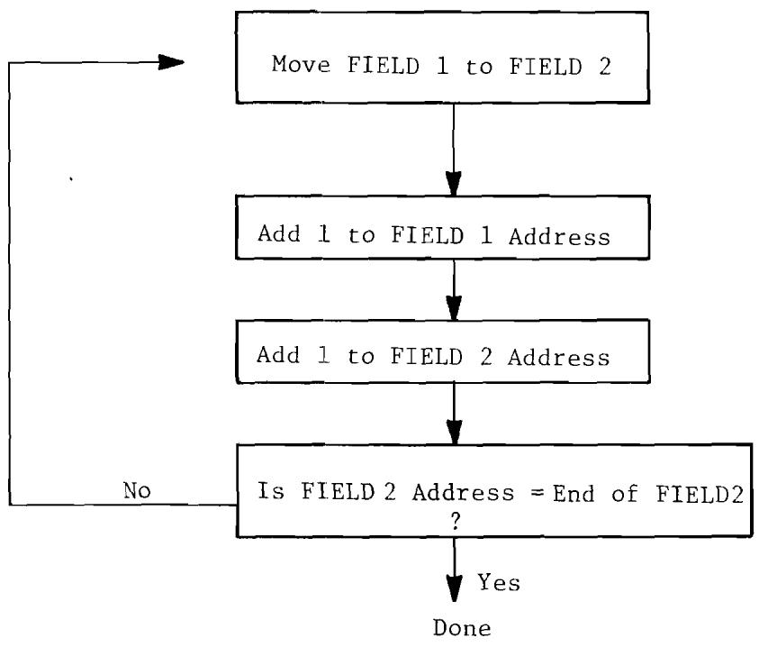
Flow Chart - Moving Five Bytes of Data with Loop
FIGURE 6.1
Example 6.2 is a program listing that corresponds to the flow chart:
Example 6.2: Moving Five Bytes of Data With Loop
| LABEL | INSTRUCTION | OPERAND | COMMENTS |
| INITIALIZE | CLC | | |
| START | LDA | FIELD 1 | Move Loop |
| OTHER | STA | FIELD 2 |
| LDA | START + 1 |
| ADC | #1 |
| STA | START + 1 |
| LDA | OTHER + 1 | Modify Move Values |
| ADC | #1 |
| STA | OTHER + 1 |
| CMP | #FIELD 2 + 5 | Check for End |
| BNE | START | |
NOTE: For ease of reading, labels have been written in the form "FIELD 1". This is incorrect format for use in the various symbolic assemblers. "FIELD 1" must be written "FIELD1" when coding for assembler formats.
Assuming Zero Page, direct addressing, Example 6.3 is written below with one byte per line just as it would appear in program memory. This will provide a more detailed description of Example 6.2.
Example 6.3: Coded Detail of Moving Fields With Loop
LABEL CODE NAMES COMMENTS
CLC Clear Carry
START LDA (FIELD 1)→A
FIELD 1
OTHER STA A→(FIELD 2)
FIELD 2
LDA From Address→A
START + 1
ADC A + 1→A
1
STA A→From Address
START + 1
LDA To Address→A
OTHER + 1
ADC A + 1→A
1
STA A + To Address
OTHER + 1
CMP A - ORIGINAL FIELD 2 + 5
ORIGINAL FIELD 2 + 5
BNE If not, loop to START
START
In this example, the program is modifying the addresses of one load instruction and one store instruction rather than writing ten instructions to move five bytes of data and fifty instructions to move twenty-five bytes of data.
The address of the Load A instruction is located in memory at START + 1 and the Store instruction at OTHER + 1. In order to perform this operation, the address must be modified once for each move operation until all of the data is moved.
Checking for the end of the moves is accomplished by checking the results of the address modification to determine if the address exceeds the end of the second field. When it does, the routine is complete.
If a hundred values were to be moved this program would remain 20 bytes long, whereas the solution to the first problem would require a program of 200 instructions.
The type of coding used in this example is called a "loop". Although the program loop in this case requires as many bytes as the original program, more values could be moved without increasing the length of the program. The greater the number of repetitive operations that are to be accomplished, the greater the advantage of the loop type program over straight line programming.
Important Note: The execution time required to move the five values is significantly longer using the loop program than the straight line program. In the straight line program, if a Zero Page operation is assumed, the time to perform the total move is 30 cycles. Using the loop program, the execution time to move five values is five times through the entire loop, which takes 25 cycles. Therefore the time to move five values is 125 cycles.
While loops have an advantage in coding space efficiency, all loops cost time. If the programmer has a problem that is extremely time dependent, taking the loop out and going to straight line programming, even though it is extremely inefficient in terms of its utilization of memory, will often solve the timing problem.
The straight line programming technique becomes very useful in some control applications. However, it is not recommended as a standard technique but should only be used when there are extreme timing problems. Using loops will normally save a significant number of bytes but they will always take more time.
The technique used in the loop program example has two major problems:
l. The necessity to modify program memory. This should be avoided to take advantage of the ability to put programs into read only memory with the corresponding savings in hardware costs.
- Although this is the minimalist form of computed addressing, less program bytes would be necessary than the more sophisticated form of program shown in the following flow chart:
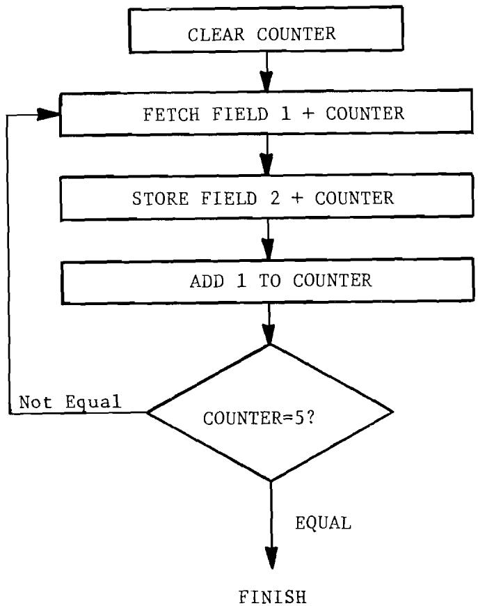
Moving Five Bytes of Data with Counter
FIGURE 6.2
In the MCS650X microprocessor family, the counter is called an index register. It is an 8-bit register which is loaded from memory and has the ability to have one added to it by an increment instruction (INX, INY) and can be compared directly to memory using the compare index instruction (CPX, CPY). Example 6.4 shows the program listing for the flow chart of Figure 6.2.
Example 6.4: Moving Five Bytes of Data With Index Registers
| BYTE | LABEL | INSTRUCTION | OPERAND | COMMENTS |
| 2 | | LDX | 0 | Load Index With Zero |
| 3 | LOOP | LDA | FIELD 1,X | |
| 3 | | STA | FIELD 2,X | |
| 1 | | INX | | Increment Count |
| 2 | | CPX | 5 | Compare For End |
| 2 | | BNE | LOOP | |
| 13 | for Absolute | | | |
In this example, index register X is used as an index and as a counter. It is initialized to zero. Data is fetched from memory at the address "FIELD 1 plus the value of register X", and placed in A. The data is then written from A to memory at the address "FIELD 2 plus the value of register X". Register X is incremented by one and compared with 5 in order to determine if all five data values have been transferred. If not the program loops back to LOOP. In this example, "FIELD 1" is called the "Base Address" which is the address to which indexing is referenced.
This only takes 11 or 13 bytes, depending on whether or not the field is in Page Zero or in absolute memory. It still takes 13 or 15 cycles per byte moved, again confirming that loops are excellent for coding space but not for execution time.
It can be seen from the example that there are basically two criterias for an index register; one, that it be a register which is easily incremented, compared, loaded, and stored, and two, that in a single instruction one can specify both the Base Address and the value of X.
In the MCS650X microprocessor, the way that the indexed instruction is symbolically represented is OP CODE, Address, X. This indicates to the symbolic assembler that an instruction OP CODE should be picked, which should specify either the absolute address modified by the content of index X register or Zero Page address modified by the content of index X register.
In performing these operations, the microprocessor fetches the instruction OP CODE as previously defined, and fetches the address, modifies the address from the memory by adding the index register to it prior to loading or storing the value of memory.
The index register is a counter. As discussed previously, one of the advantages of the flags in the microprocessor is that a value can be modified and its results tested. Assume the last example is modified so that instead of moving the first value in FIELD 1 to the first value in FIELD 2, the last value in FIELD 1 is moved first to the last value in FIELD 2, then the next to the last value, etc. and finally the first value. With the index register preloaded with 5 and using a decrement instruction the contents of the index register would end at zero after the 5 fields of data were transferred. The zero indicates that the number of times through the loop is correct and the loop exited by use of the zero test. The program listing for this modification is shown in Example 6.5:
Example 6.5: Moving Five Bytes of Data By Decrementing the Index Register
| LABEL | INSTRUCTION | OPERAND |
| LDX | 5 |
| LOOP | LDA | FIELD 1-1,X |
| STA | FIELD 2-1,X |
| DEX | |
| BNE | LOOP |
In this example, Index Register X is again used as an Address Counter but it will count backwards. It is initialized to five for this example. Data is fetched from memory at the address "FIELD 1 plus the value of Register X" and placed in A. The data is then written from A to memory at the address "FIELD 2 plus the value of Register X." Register X is decremented by one. If the decremented value is not zero, as determined by a Branch on Zero instruction, the program loops back to LOOP
The loop has been decreased to 9 or 11 bytes and the execution time per byte has been decreased from 15 cycles to 13 cycles per value
which shows the advantage of using the flag setting of the decrement index instruction.
The two index registers, X and Y, can now be added to the system block diagram as in Figure 6.3
Partial Block Diagram of MCS650X Including Index Registers FIGURE 6.3
Each of the index registers is 8 bits long and is loaded and stored from memory, using techniques similar to the accumulator. Because of this ability, they can be considered as auxiliary channels to flow data through the microprocessor. However, their primary use is in being added to addresses fetched from memory to form a modified effective address, as described previously. Both index registers have the ability to be compared to memory (CPX, CPY) and to be incremented (INX, INY) and decremented (DEX, DEY).
Because of OP CODE limitations, X and Y have slightly different uses. X is a little more flexible because it has Zero Page operations which Y does not have with exception of LDX and STX. Aside from which modes they modify, the registers are autonomous, independent and of equal value.
6.1 ABSOLUTE INDEXED
Absolute indexed address is absolute addressing with an index register added to the absolute address. The sequences that occur for indexed absolute addressing without page crossing are as follows:
Example 6.6: Absolute Indexed; With No Page Crossing
| Cycle | Address Bus | Data Bus | External Operation | Internal Operation |
| 1 | 0100 | OP CODE | Fetch OP CODE | Increment PC to 101, Finish Previous Instruction |
| 2 | 0101 | BAL | Fetch BAL | Increment PC to 102, Interpret In-struction |
| 3 | 0102 | BAH | Fetch BAH | Increment PC to 103, Calculate BAL + X |
| 4 | BAH,BAL+X | OPERAND | Put Out Effective Address | |
| 5 | 103 | Next OP CODE | Fetch Next OP CODE | Finish Operations |
BAL and BAH refer to the low and high order bytes of the base address, respectively. While the index X was used in Example 6.7, the index Y is equally applicable.
If a page is not crossed, the results of the address low + X does not cause a carry. The processor is able to pipeline the addition of the 8-bit index register to the lower byte of the base address (BAL) and not suffer any time degradation for absolute indexed addressing over straight absolute addressing. In other words, while BAH is being fetched, the add of X to BAL occurs. Both addressing modes require four cycles with
the only difference being that X or Y must be set at a known value and the OP CODE must indicate an index X or Y.
The second possibility is that when the index register is added to the address low of the base address that the resultant address is in the next page. This is illustrated in Example 6.7.
Example 6.7: Absolute Indexed; With Page Crossing
| Cycle | Address Bus | Data Bus | External Operation | Internal Operation |
| 1 | 0100 | OP CODE | Fetch OP CODE | Finish Previous Operation Increment PC to 101 |
| 2 | 0101 | BAL | Fetch BAL | Interpret Instruction Increment PC to 102 |
| 3 | 0102 | BAH | Fetch BAH | Add BAL + Index Increment PC to 103 |
| 4 | BAH,BAL +X | Data (Ignore) | Fetch Data (Data is ignored) | Add BAH + Carry |
| 5 | BAH+1, BAL+X | Data | Fetch Data | |
| 6 | 0103 | Next OP CODE | Fetch Next OP CODE | Finish Operation |
The most substantial difference between the page crossing operation and no page crossing is that during the fourth cycle, the address high and the calculated address low is put out, thereby incorrectly addressing the same page as the base address. This operation is carried on in parallel with the adding of the carry to the address high. During the fourth cycle the address high plus the carry from the adder is put on the address bus, moving the operation to the next page. Thus there are two effects from the page crossing. 1. The addressing of a false address. This is similar to what happens in a branch relative during a page crossing. 2. The operation takes one additional cycle while the new address high is calculated. As with the branch relative
this page crossing occurs independently of programmer action and there is no penalty in memory for having crossed the page boundary. It is possible for the programmer to predict a page crossing by knowing the value of the base address and the maximum offset value in the index register. If timing is of concern, the base address can be adjusted so that the address field is always in one page.
As with absolute addressing, absolute indexed is the most general form of indexing. It is possible to do absolute indexed modified by X, and absolute indexed modified by Y. Instructions which allow absolute indexed by X are ADC, AND, ASL, CMP, DEC, EOR, INC. LDA, LDY, LSR, ORA, ROL, SBC, and STA.
The instructions which allow indexed absolute by Y are ADC, AND, CMP, EOR, LDA, LDX, ORA, SBC, and STA.
6.2 ZEROPAGEINDEXED
As with non-computed addressing, there is a memory use advantage to the short-cut of Zero Page addressing. Except in LDX and STX instructions which can be modified by Y, Zero Page is only available modified by X. If the base address plus X exceeds the value that can be stored in a single byte, no carry is generated, therefore there is no page crossing phenomena. A wrap-around will occur within Page Zero. The following example illustrates the internal operations of Zero Page indexing.
Example 6.8: Illustration of Zero Page Indexing
| Cycle | Address Bus | Data Bus | External Operation | Internal Operation |
| 1 | 0100 | OP CODE | Fetch OP CODE | Finish Previous Operation, 0101 → PC |
| 2 | 0101 | BAL | Fetch Base Address Low (BAL) | Interpret Instruct- ion, 0102 → PC |
| 3 | 00,BAL | Data (Disc- carded | Fetch Discarded Data | Add: BAL + X |
| 4 | 00,BAL +X | Data | Fetch Data | |
| 5 | 0102 | Next OP CODE | Fetch Next OP CODE | Finish Operation |
As can be seen from the example, there is no time savings of Zero Page indexing over absolute indexing without page crossing. In the case of the indexed absolute during cycle 3 the address high is being fetched at the same time as the addition of the index to address low. In the case of the Zero Page, there is no opportunity for this type of overlap; therefore, indexed Zero Page instructions take one cycle longer than non-indexed instructions.
In both Zero Page indexed and absolute indexed with a page crossing, there are incorrect addresses calculated. Provisions have been made to make certain that only a READ operation occurs during this time. Memory modifying operations such as STORE, SHIFT, ROTATE, etc. have all been delayed until the correct address is available, thereby prohibiting any possibility of writing data in an incorrect location and destroying the previous data in that location.
As has been previously stated, there is no carry out of the Zero Page operation. 00 is forced into address high under all circumstances in cycle 4. For example, if the index register containing a value of 10 is to be added to base address containing a value of F7, the following operation would occur:
| Cycle | Address Bus | Internal Operation |
| 3 | 00F7 | F7 + 10 |
| 4 | 0007 | |
This indicated the wrap-around effect that occurs with Zero Page indexing with page crossing. This wrap-around does not increase the cycle time over that shown in the previous example.
Only index X is allowed as a modifier in Zero Page. Instructions which have this feature include ADC, AND, ASL, CMP, DEC, EOR, INC, LDA, LDY, LSR, ORA, ROL, SBC, STA and STY. Note that index Y is allowed in the instructions LDX and STX.
6.3 INDIRECT ADDRESSING
In solving a certain class of problems, it is sometimes necessary to have an address which is a truly computed value, not just a base address with some type of offset, but a value which is calculated or sometimes obtained as a group of addresses. In order to implement this type of indexing or addressing, the use of indirect addressing has been introduced.
In the MCS650X family indirect operations have a special form. The basic form of the indirect addressing is that of an instruction consisting of an OP CODE followed by a Zero Page address. The microprocessor obtains the effective address by picking up from the Zero Page address the effective address of the operation. The indirect addressing operation is much the same as absolute addressing except indirect addressing uses a Zero Page addressing operation to indirectly access the effective address. In the case of absolute addressing the value in the program counter is used as the address to pick up the effective address low, one is added to the program counter which is used to pick up the effective address high. In the case of indirect addressing, the next value after the OP CODE, as addressed with the program counter, is used as a pointer to address the effective
address low in the zero page. The pointer is then incremented by one with the effective address high fetched from the next memory location. The next cycle places the effective address high (ADH) and effective address low (ADL) on the address bus to fetch the data. An illustration of this is shown in Figure 6.4.
Indirect Addressing-Pictorial Drawing
FIGURE 6.4
The address following the instruction is really the address of an address, or "indirect" address. The indirect address is represented by IAL in the figure.
A more detailed definition of indirect addressing is included in the appendix.
Although the MCS650X microprocessor family has indirect operations, it has no simple indirect addressing such as described above. There are two modes of indirect addressing in the MCS650X microprocessor family: 1.) indexed indirect and 2.) indirect indexed.
6.4 INDEXED INDIRECT ADDRESSING
The major use of indexed indirect is in picking up data from a table or list of addresses to perform an operation. Examples where indexed indirect is applicable is in polling I/O devices or performing string or multiple string operations. Indexed indirect addressing uses the index register X. Instead of performing the indirect as shown in the Figure 6.4, the index register X is added to the Zero Page address, thereby allowing varying address for the indirect pointer. The operation and timing of the indexed indirect addressing is shown in Figure 6.5.
Indexed Indirect Addressing
FIGURE 6.5
Example 6.10: Illustration of Indexed Indirect Addressing
| Cycle | Address Bus | Data Bus | External Operation | Internal Operation |
| 1 | 0100 | OP CODE | Fetch OP CODE | Finish Previous Operation, 0101 → PC |
| 2 | 0101 | BAL | Fetch BAL | Interpret In-struction, 0102 → PC |
| 3 | 00,BAL | DATA (Dis-carded) | Fetch Discarded DATA | Add BAL + X |
| 4 | 00,BAL + X | ADL | Fetch ADL | Add 1 to BAL + X |
| 5 | 00,BAL + X + 1 | ADH | Fetch ADH | Hold ADL |
| 6 | ADH,ADL | DATA | Fetch DATA | |
| 7 | 0102 | Next OP | Fetch Next OP CODE | Finish Operation 0103 → PC |
One of the advantages of this type of indexing is that a 16-bit address can be fetched with only two bytes of memory, the byte that contains the OP CODE and the byte that contains the indirect pointer. It does require, however, that there be a table of addresses kept in a read/write memory which is more expensive than having it in read only memory. Therefore, this approach is normally reserved for applications where use of indexed indirect results in significant coding or throughput improvement or where the address being fetched is a variable computed address.
It is also obvious from the example that the user pays a minor time penalty for this form of addressing in that indexed indirect always takes six cycles to fetch a single operand which is 25% more than an absolute address and 50% more than a Zero Page reference to an operand. As in the Zero Page indexed, the operation in cycles three and four are located in Zero Page and there is no ability to carry over into the next page. It is possible to develop a value of the index plus the base address where the result exceeded 255, in this case the address put out is a wrap-around to the low part of the Page Zero.
Instructions which allow the use of indexed indirect are ADC, AND, CMP, EOR, LDA, ORA, SBC, STA.
6.5 INDIRECT INDEXED ADDRESSING
The indirect indexed instruction combines a feature of indirect addressing and a capability of indexing. The usefulness of this instruction is primarily for those operations in which one of several values could be used as part of a subroutine. By having an indirect pointer to the base operation and by using the index register Y in the normal counter type form, one can have the advantages of an address that points anywhere in memory, combined with the advantages of the counter offset capability of the index register.
Figure 6.6 illustrates the indirect indexed concept in flow form while Example 6.11 indicates the internal operation of a non-page rollover of an indirect index.
Indirect Indexed Addressing
FIGURE 6.6
Example 6.11: Indirect Indexed Addressing (No Page Crossing)
| Cycle | Address Bus | Data Bus | External Operation | Internal Operation |
| 1 | 0100 | OP CODE | Fetch OP CODE | Finish Previous Operation, 0101 → PC |
| 2 | 0101 | IAL | Fetch IAL | Interpret In-struction, 0102 → PC |
| 3 | 00, IAL | BAL | Fetch BAL | Add l to IAL |
| 4 | 00, IAL + 1 | BAH | Fetch BAH | Add BAL + Y |
| 5 | BAH, BAL + Y | DATA | Fetch Operand | |
| 6 | 0102 | Next OP CODE | Fetch Next OP CODE | Finish Operation 0103 → PC |
The indirect index still requires two bytes of program storage, one for the OP CODE, one for the indirect pointer. Once beyond the indirect, the indexing of the indirect memory location is just the same as though it was an absolute indexed operation in the sense that if there is no page crossing, pipelining occurs in the adding of the index register Y to address low while fetching address high, and therefore, the non-page crossing solution is one cycle shorter than the indexed indirect. In Example 6.12 it is seen that the page crossing problem that occurs with absolute indexed page crossing also occurs with indirect indexed addressing.
Example 6.12: Indirect Indexed Addressing (With Page Crossing)
| Cycle | Address Bus | Data Bus | External Operation | Internal Operation |
| 1 | 0100 | OP CODE | Load OP CODE | Finish Previous Operation, 0101 → PC |
| 2 | 0101 | IAL | Fetch IAL | Interpret Instruction, 0102 → PC |
| 3 | 00,IAL | BAL | Fetch BAL | Add 1 to IAL |
| 4 | 00,IAL + 1 | BAH | Fetch BAH | Add BAL to Y |
| 5 | BAH,BAL + Y | DATA (Dis-carded) | Fetch DATA (Discarded) | Add 1 to BAH |
| 6 | BAH + 1 BAL + Y | DATA | Fetch Data | |
| 7 | 0102 | Next OP CODE | Fetch Next OP CODE | Finish This Operation, 0103 → PC |
When there is a page crossing, the base address high and base address low plus Y are pointing to an incorrect location within a referenced page. However, it should be noted that the programmer has control of this incorrect reference in the sense that it is always pointing to the page of the base address. In one more cycle the correct address is referenced. As was true in the case of absolute indexed, the data at the incorrect address is only read. STA and the various read, modify, write memory commands all operate assuming that there will be a page crossing, take the extra cycle time to perform the add and carry and only perform a write on the sixth cycle rather than taking advantage of the five cycle short-cut which is available to read operations. This added cycle guarantees that a memory location will never be written into with incorrect data.
Instructions which allow the use of indexed indirect are ADC, AND, CMP, EOR, LDA, ORA, SBC, STA.
In the following two examples can be seen a comparison between the use of absolute modified by Y and indirect indexed addressing.
In these examples the same function is performed. Values from two memory locations are added and the result stored in a third memory location, assuming that there are several values to be added. The first example deals with known field locations. The second example, such as might be traditionally used in subroutines, deals with field locations that vary between routines. A two byte pointer for each routine using the subroutine is stored in Page Zero. The number of values to be added for each routine is also stored.
Example 6.13: Absolute Indexed Add - Sample Program
| #Bytes | Cycles | Label | Instruction | Comments |
| 2 | 2 | START | LDY #COUNT -1 | Set Y = End of FIELD |
| 3 | 4 | LOOP | LDA FIELD 1,Y | Load Location 1 |
| 3 | 4 | | ADC FIELD 2,Y | Add Location 2 |
| 3 | 4 | | STA FIELD 3,Y | Store in Location 3 |
| 1 | 2 | | DEY | |
| 2 | 3 | | BPL LOOP | Check for Less Than Zero |
| 14 | 19 | | Time for 10 Bytes = 171 Cycles |
Example 6.14: Indirect Indexed Add - Sample Program
| #Bytes | Cycles | Label | Instruction | Comments |
| 2 | 2 | START | LDY #COUNT -1 | Set Y = End of FIELD |
| 2 | 5 | LOOP | LDA (PNT1), Y | Load FIELD 1 Value |
| 2 | 5 | | ADC (PNT2), Y | Add FIELD 2 Value |
| 2 | 5 | | STA (PNT3), Y | Store FIELD 3 Value |
| 1 | 2 | | DEY | |
| 2 | 3 | | BPL LOOP | |
| 11 | 22 | | Time for 10 Bytes = 201 Cycles |
+6 bytes for pointers
The "count" term in these examples represents the number of sets of values to be added and stored. Loading the index register with COUNT-1 will allow a fall through the BPL instruction when computation on all set of values has been completed.
There is a definite saving in program storage using indirect because it only requires two bytes for each indirect pointer, the OP CODE plus the pointer of the Page Zero location, whereas in the case of the absolute, it takes three bytes, the OP CODE, address low and address high.
It is noted that there are six bytes of Page Zero memory used for pointers, two bytes for each pointer. The number of memory locations allocated to the problem are 17 for the indirect and 14 for the problem where the values are known. The execution time is longer in the indirect loop. Even though the increase in time for a single pass through the loop is only three cycles, if many values are to be transferred, it adds up. It is important to note that loops require time for setup but it is only used once. But in the loop itself, additional time is multiplied by the number of times the program goes through the loop; therefore, on problems where execution time is important, the time reduction effort should be placed on the loop.
Even though the loop time is longer and the actual memory expended is greater for the indexed indirect add, it has the advantage of not requiring determination of the locations of FIELD 1, FIELD 2, and FIELD 3 at the time the program was written as is necessary with absolute.
An attempt to define problems to take advantage of this shorter memory and execution time by defining fields should be investigated first. However, in almost every program, the same operation must be performed several times. In those cases, it is sometimes more useful to define a subroutine and set the values that the subroutine will operate on as fields in memory. Pointers to these fields are placed in the Zero Page of memory and then the indexed indirect operation is used to perform the function. This is the primary use of the indexed indirect operation.
6.6 INDIRECT ABSOLUTE
In the case of all of the indirect operations previously described, the indirect reference was always to a Page Zero location from which is picked up the effective address low and effective address high. There is an exception in the MCS650X microprocessor family for the jump instruction in which absolute indirect jumps are allowed. The use of the absolute indirect jump is best explained in the discussion on interrupts where the addressing mode and its capabilities are explained.
6.7 APPLICATION OF INDEXES
As has been developed in many of the previous examples, an index register has primary values as a modifier and as a counter. As a modifier to a base address operation, it allows the accessing of contiguous groups of data by simple modification of the index. This is the primary application of indexes and it is for this purpose they were created. By virtue of the fact that all of the MCS650X instructions have the base address in the instruction, or in the case of the indirect, in the pointer, a single index can usually be used to service an entire loop, because each of the many instructions in the loop normally are referring to the same relative value in each of the lists. An example is adding the third byte of a number to its corresponding third byte of another number, then storing the result in the memory location representing the third byte of the result; therefore, the index register only needs to contain three to accomplish all three of these offset functions.
Some other microprocessors use internal registers as indirect pointers. The single register requirement is a significant advantage of the type of indexing done in the MCS650X. Even though the MCS650X has two indexes, more often than not, a single index will solve many of the problems because of the fact that the data is normally organized in corresponding fields.
The second feature of the MCS650X type of indexing is that, if used properly, the index register also contains the count of the operations to be performed.
The examples have tried to show how to take advantage of that feature. There are two approaches to counting; forward counting and reverse counting. In forward counting, the data in memory can be organized such that the index register starts at zero and is added to on each successive operation. The disadvantage of this type of approach is that the compare index instruction, as used in Example 6.13 must be inserted into the loop in order to determine that the correct number of operations is completed.
The reverse counting approach has been used in the latter examples. The data must be organized for reverse counting operation. The first value to be operated on is at the end of the FIELD, the next value is one memory location in front of that, etc. The advantage of this type of operation is that it takes advantage of the combined decrement and test capability of the processor. There are two ways to use the test. First there is the case where the actual number of operations to be performed is loaded into the index register such as was done in Example 6.13. In this case, the index contains the correct count but if added to the base directly, would be pointing to one value beyond the FIELD because the base address contains the first byte. Therefore, when using the actual count in the index register, one always references to the base address minus one. This is easily accomplished as shown in the examples. The cross assembler accepts symbolic references in the form of base address minus one, and the microprocessor very carefully performs the operation shown.
The advantage of putting the actual count in the register is that the branch if not equal instruction (BNE) can be used because the value of the register goes to zero on the last operation.
The second alternative is to load the counter with the count minus one as done in Example 6.14. In this case, the actual value of the base address is used in the offset. However, the branch back to loop now is a branch plus, remembering that the value in the index register will not go to minus (all ones) until we decrement past zero.
Values of count minus one through zero will all take the branch. It is only when attempting to reference less than the base address that the loop will be completed.
Either approach gives minimum coding and only requires that the user develop a philosophy of always organizing his data with the first value at the end. In many cases, the operations such as MOVE can be performed even if the data is organized the other way. Experienced programmers find that this reverse counting form is actually more convenient to use and always results in minimum loop time and space.
Although for most applications, the 8-bit index register allows simple count in offset operations, there are a few operations where the 256 count that is available in the 8-bit register is not enough to perform the indexed operations. There are two solutions to this problem. First, to code the program with two sets of bases, that is duplicating the coding for the loop with two different address highs, each one a page apart. The second, more useful solution, is to go to indirect operations because the indirect pointer can be modified to allow an infinite indexed operation. An example of the move done under 256 and over 256 is shown in the following example:
Example: 6.16: Move N Bytes (N<256)
| Number of Cycles | Program Label | Instruction Mnemonics | OPERAND FIELD | Comments |
| 2 | | LDX | #BLOCK | Setup 2 Cycles |
| 4 | LOOP | LDA | FROM-1,X | |
| 4 | | STA | TO -1,X | LOOP Time: |
| 2 | | DEX | | 13 cycles |
| 3 | | BNE | LOOP | |
Memory Required:
11 Bytes
Example 6.17: Move N Bytes (N>256)
| Number of Cycles | Program Label | Instruction Mnemonics | operand FIELD | Comments |
| 2 | MOVE | LDA | #FROML | |
| 3 | | STA | FRPOINT | |
| 2 | | LDA | #FROMH | Move from address to |
| 3 | | STA | FRPOINT + 1 | an indirect pointer |
| 2 | | LDA | #TOL | |
| 3 | | STA | TOPOINT | Move A to address |
| 2 | | LDA | #TOH | to an index pointer |
| 3 | | STA | TOPOINT + 1 | |
| 2 | | LDX | #BLOCKS | Setup # of 256 blocks |
| 2 | | LDY | #0 | to move |
| 5 | LOOP | LDA | (FRPOINT),Y | Loop Time: 16 cycles/ |
| 6 | | STA | (TOPOINT),Y | byte. Move 256 bytes |
| 2 | | DEY | | |
| 3 | | BNE | LOOP | |
| 5 | SPECIAL | INC | FRPOINT + 1 | Increase high |
| 5 | | INC | TOPOINT + 1 | pointer |
| 2 | | DEX | | |
| 2 | | BMI | OUT | Check for last move |
| 3 | | BNE | LOOP | |
| 2 | | LDY | #COUNT | |
| 3 | | BNE | LOOP | Setup last move |
| OUT | --- | --- | |
| | | Memory required: 40 bytes |
CHAPTER 7
INDEX REGISTER INSTRUCTIONS
The index registers can be treated as auxiliary-general purpose registers, having the added ability of being incremented and decremented because of the normal operations in which they are required to perform.
7.0 LDX-LOAD INDEX REGISTER X FROM MEMORY
Load the index register X from memory.
The symbolic notation is M X .
LDX does not affect the C or V flags; sets Z if the value loaded was zero, otherwise resets it; sets N if the value loaded in bit 7 is a 1; otherwise N is reset, and affects only the X register. The addressing modes for LDX are Immediate; Absolute; Zero Page; Absolute Indexed by Y; and Zero Page Indexed by Y.
7.1 LDY-LOAD INDEX REGISTER Y FROM MEMORY
Load the index register Y from memory.
The symbolic notation is M Y .
LDY does not affect the C or V flags, sets the N flag if the value loaded in bit 7 is a 1, otherwise resets N, sets Z flag if the loaded value is zero otherwise resets Z and only affects the Y register. The addressing modes for load Y are Immediate; Absolute; Zero Page; Zero Indexed by X, Absolute Indexed by X.
7.2 STX - STORE INDEX REGISTER X IN MEMORY
Transfers value of X register to addressed memory location.
The symbolic notation is X M .
No flags or registers in the microprocessor are affected by the store operation. The addressing modes for STX are Absolute, Zero Page, and Zero Page Indexed by Y.
7.3 STY - STORE INDEX REGISTER Y IN MEMORY
Transfer the value of the Y register to the addressed memory location. The symbolic notation is Y M . STY does not affect any flags or registers in the microprocessor. The addressing modes for STY are Absolute; Zero Page; and Zero Page Indexed by X.
7.4 INX - INIncrement INDEX REGISTER X BY ONE
Increment X adds 1 to the current value of the X register. This is an 8-bit increment which does not affect the carry operation, therefore, if the value of X before the increment was FF, the resulting value is 00. The symbolic notation is X + 1 X . INX does not affect the carry or overflow flags; it sets the N flag if the result of the increment has a one in bit 7, otherwise resets N; sets the Z flag if the result of the increment is 0, otherwise it resets the Z flag. INX does not affect any other register other than the X register. INX is a single byte instruction and the only addressing mode is Implied.
7.5 INY - INIncrement INDEX REGISTER Y BY ONE
Increment Y increments or adds one to the current value in the Y register, storing the result in the Y register. As in the case of INX the primary application is to step thru a set of values using the Y register. The symbolic notation is Y + 1 Y . The INY does not affect the carry or overflow flags, sets the N flag if the result of the increment has a one in bit 7, otherwise resets N, sets Z if
as a result of the increment the Y register is zero otherwise resets the Z flag. Increment Y is a single byte instruction and the only addressing mode is Implied.
7.6 DEX - DECREMENT INDEX REGISTER X BY ONE
This instruction subtracts one from the current value of the index register X and stores the result in the index register X.
The symbolic notation is X - l X .
DEX does not affect the carry or overflow flag, it sets the N flag if it has bit 7 on as a result of the decrement, otherwise it resets the N flag; sets the Z flag if X is a 0 as a result of the decrement, otherwise it resets the Z flag.
DEX is a single byte instruction, the addressing mode is Implied.
7.7 DEY - DECREMENT INDEX REGISTER Y BY ONE
This instruction subtracts one from the current value in the index register Y and stores the result into the index register Y. The result does not affect or consider carry so that the value in the index register Y is decremented to 0 and then through 0 to FF.
Symbolic notation is Y - 1 Y .
Decrement Y does not affect the carry or overflow flags; if the Y register contains bit 7 on as a result of the decrement the N flag is set, otherwise the N flag is reset. If the Y register is 0 as a result of the decrement, the Z flag is set otherwise the Z flag is reset. This instruction only affects the index register Y.
DEY is a single byte instruction and the addressing mode is Implied.
NOTE: Decrement of the index registers is the most convenient method of using the index registers as a counter, in that the decrement involves setting the value N on as a result of having passed through 0 and sets Z on when the results of the decrement are 0.
7.8 CPX - COMPARE INDEX REGISTER X TO MEMORY
This instruction subtracts the value of the addressed memory location from the content of index register X using the adder but does not store the result; therefore, its only use is to set the N, Z and C flags to allow for comparison between the index register X and the value in memory.
The symbolic notation is X - M.
The CPX instruction does not affect any register in the machine; it also does not affect the overflow flag. It causes the carry to be set on if the absolute value of the index register X is equal to or greater than the data from memory. If the value of the memory is greater than the content of the index register X, carry is reset. If the results of the subtraction contain a bit 7, then the N flag is set, if not, it is reset. If the value in memory is equal to the value in index register X, the Z flag is set, otherwise it is reset.
The addressing modes for CPX are Immediate, Absolute and Zero Page.
7.9 CPY-COMPARE INDEX REGISTER Y TO MEMORY
This instruction performs a two's complement subtraction between the index register Y and the specified memory location. The results of the subtraction are not stored anywhere. The instruction is strictly used to set the flags.
The symbolic notation for CPY is Y - M.
CPY affects no registers in the microprocessor and also does not affect the overflow flag. If the value in the index register Y is equal to or greater than the value in the memory, the carry flag will be set, otherwise it will be cleared. If the results of the subtraction contain bit 7 on the N bit will be set, otherwise it will be cleared. If the value in the index register Y and the value in the memory are equal, the zero flag will be set, otherwise it will be cleared.
The addressing modes for CPY are Immediate, Absolute and Zero Page.
7.10 TRANSFERS BETWEEN THE INDEX REGISTERS AND ACCUMULATOR
There are four instructions which allow the accumulator and index registers to be interchanged. They are TXA, TAX which transfers the contents of the index register X to the accumulator A and back, and TYA, TAY which transfers the contents of the index register Y to the accumulator A and back. The usefulness of this will be discussed after the instructions.
7.11 TAX TRANSFER ACCUMULATOR TO INDEX X
This instruction takes the value from accumulator A and transfers or loads it into the index register X without disturbing the content of the accumulator A.
The symbolic notation for this is A X .
TAX only affects the index register X, does not affect the carry or overflow flags. The N flag is set if the resultant value in the index register X has bit 7 on, otherwise N is reset. The Z bit is set if the content of the register X is 0 as a result of the operation, otherwise it is reset. TAX is a single byte instruction and its addressing mode is Implied.
7.12 TXA - TRANSFER INDEX X TO ACCUMULATOR
This instruction moves the value that is in the index register X to the accumulator A without disturbing the content of the index register X.
The symbolic notation is X A .
TXA does not affect any register other than the accumulator and does not affect the carry or overflow flag. If the result in A has bit 7 on, then the N flag is set, otherwise it is reset. If the resultant value in the accumulator is 0, then the Z flag is set, otherwise it is reset.
The addressing mode is Implied, it is a single byte instruction.
7.13 TAY - TRANSFER ACCUMULATOR TO INDEX Y
This instruction moves the value of the accumulator into index register Y without affecting the accumulator.
The symbolic notation is A Y .
TAY instruction only affects the Y register and does not affect either the carry or overflow flags. If the index register Y has bit 7 on, then N is set, otherwise it is reset. If the content of the index register Y equals 0 as a result of the operation, Z is set on, otherwise it is reset.
TAY is a single byte instruction and the addressing mode is Implied.
7.14 TYA - TRANSFER INDEX Y TO ACCUMULATOR
This instruction moves the value that is in the index register Y to accumulator A without disturbing the content of the register Y.
The symbolic notation is Y A
TYA does not affect any other register other than the accumulator and does not affect the carry or overflow flag. If the result in the accumulator A has bit 7 on, the N flag is set, otherwise it is reset. If the resultant value in the accumulator A is 0, then the Z flag is set, otherwise it is reset.
The addressing mode is Implied and it is a single byte instruction.
Some of the applications of the transfer instructions between accumulator A and index registers X, Y are those when the user wishes to use the index register to access memory locations where there are multiple byte values between the addresses. In this application a count is loaded into the index register, the index register is transferred to the accumulator, a value such as 5, 7, 10, etc. is added immediate to the accumulator and results stored back into the index
register using the TAX or TAY instruction. The consequence of this type of operation is that it allows the microprocessor to address non-consecutive locations in memory. Another application is where the internal transfer instructions allow the index registers to hold intermediate values for the accumulator which allows rapid transfer to and from the accumulator to help solve high speed data shuffling problems.
7.15 SUMMARY OF INDEX REGISTER APPLICATIONS AND MANIPULATIONS
Primary use of index register X and Y is as offset and counters for data manipulation in which the index register is used to compute an address based on the value of the index register plus base address specified by the user, either in a fixed instruction format or in a variable pointer type format. In order to operate as both an offset and counter, index registers may be incremented or decremented by one or compared to values from memory. There are limitations on the applications of each of the index registers which have to do with formats which are unique to certain instruction addressing modes. Because of the ability of the index registers to be loaded, changed and stored, they are also useful as general purpose registers. They can be used as interim storages for moves between memory locations or for moves between memory and the accumulator.
One of the optimum uses of the indexing concept is the case when the index register is being used both as an offset and a counter. This type of operation uses the ability of the microprocessor to perform a decrement function on the index registers and set flags. Therefore, a single decrement instruction not only changes the value in the counter but can also perform a test on the count value.
CHAPTER 8
STACK PROCESSING
8.0 INTRODUCTION TO STACK AND TO PUSH DOWN STACK CONCEPT
In all of the discussions on addressing, it has been assumed that either the exact location or at least a relation to an exact location of a memory address was known.
Although this is true in most of the programming for control applications, there are certain types of programming and applications which require that the basic program not be working with known memory locations but only with a known order for accessing memory. This type of programming is called re-entrant coding and is often used in servicing interrupts.
To implement this type of addressing, the microprocessor maintains a separate address generator which is used by the program to access memory. This address generator uses a push down stack concept.
Discussions of push down stacks are usually best stated considering that if one were given 3 cards, an ace, a king and a ten and were told that the order of cards was important and asked to lay them down on the table in the order in which they were given, ace first, the king on top of it and finally the ten, and then if they were retrieved, 1 card at a time, the ten is retrieved first even though it was put on last, the king is retrieved second, the ace retrieved last, even though it was put on first.
The only commands needed to implement this operation are "put next card on stack" and "pull next card from the stack." The stack could be processing clubs and then go to diamonds and back to clubs. However, we know that while we are processing clubs, we will always find ten first, king second, etc.
The hardware implementation of the ordered card stack which just described is a 16-bit counter, into which the address of a memory location is stored. This counter is called a "Stack Pointer." Every time data is to be pushed onto the stack, the stack pointer is put out on the address bus, data is written into the memory addressed by the stack pointer, and the stack pointer is decremented by 1 as may be seen in Example 8.1. Every time data is pulled from the stack, the stack pointer is incremented by 1. The stack pointer is put out on the address bus, and data is read from the memory location addressed by the stack pointer. This implementation using the stack pointer gives the effect of a push down stack which is program independent addressing.
Example 8.1: Basic stack map for 3-deep JMP to subroutine sequence
| Stack Address | Data |
| 01FF | PCH 1 |
| 01FE | PCL 1 |
| 01FD | PCH 2 |
| 01FC | PCL 2 |
| 01FB | PCH 3 |
| 01FA | PCL 3 |
| 01F9 | |
In the above example, the stack pointer starts out at 01FF. The stack pointer is used to store the first state of the program counter by storing the content of program counter high at 01FF and the content of program counter low at 01FE. The stack pointer would now be pointed at 01FD. The second time the store program count is performed, the program counter high number is stored on the stack at 01FD and the program counter low is stored at 01FC. The stack pointer would now be pointing at 01FB. The same procedure is used to store the third program counter.
When data is taken from the stack, the PCL 3 will come first and the PCH 3 will come second just by adding 1 to the stack pointer before each memory read. The example above contains the program count for 3 successive jump and store operations where the jump transfers control to a subroutine and stores the value of the program counter onto the stack in order to remember to which address the program should return after completion of the subroutine.
Following is an example of a program that would create the Example 8.1 stack operation.
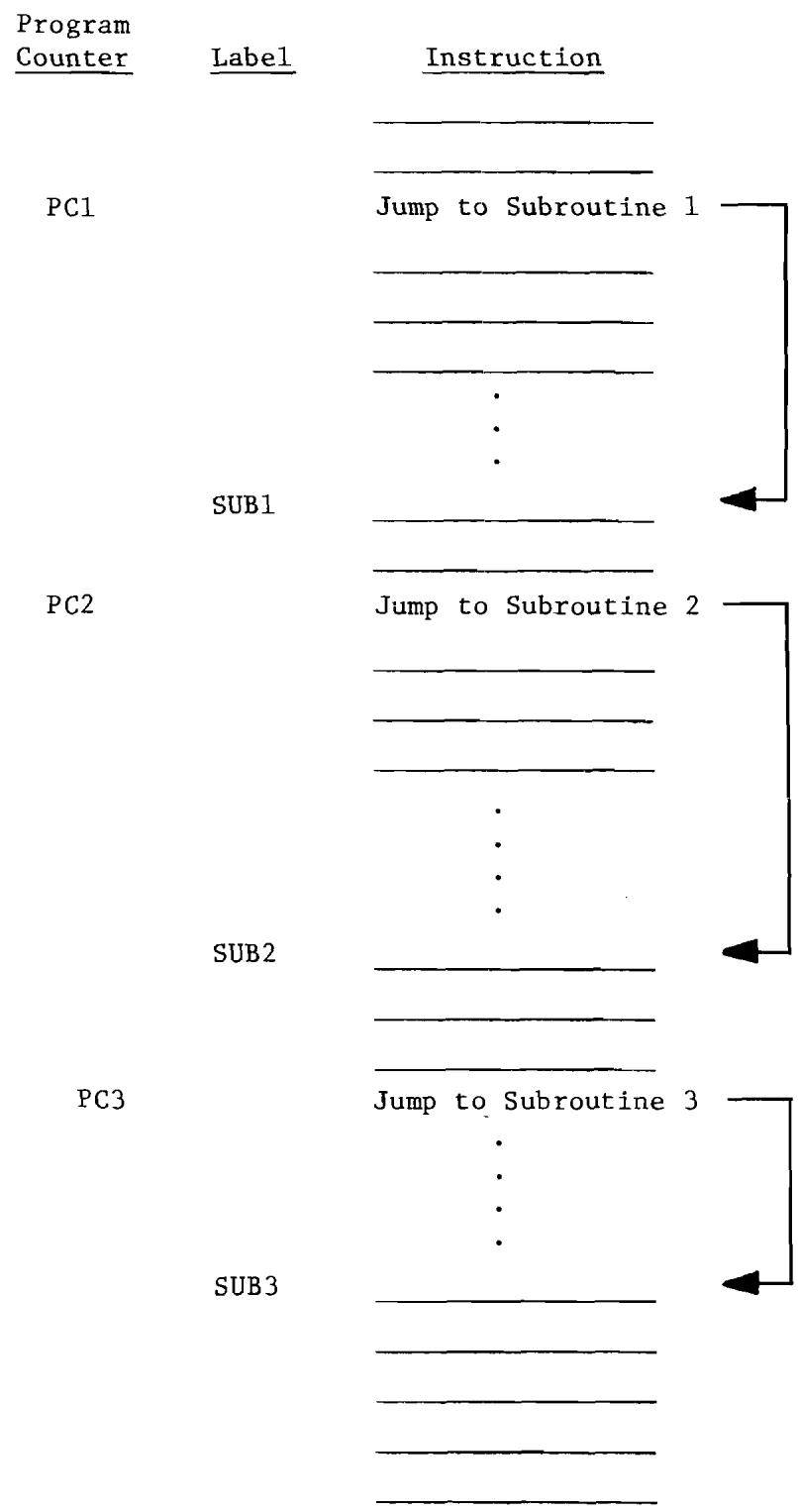
Example 8.2: Basic stack operation
This is known as subroutine nesting and is often encountered in solving complex control equations.
To correctly use the stack for this type of operation requires a jump to subroutine and a return from subroutine instruction.
8.1 JSR - JUMP TO SUBROUTINE
This instruction transfers control of the program counter to a subroutine location but leaves a return pointer on the stack to allow the user to return to perform the next instruction in the main program after the subroutine is complete. To accomplish this, JSR instruction stores the program counter address which points to the last byte of the jump instruction onto the stack using the stack pointer. The stack byte contains the program count high first, followed by program count low. The JSR then transfers the addresses following the jump instruction to the program counter low and the program counter high, thereby directing the program to begin at that new address.
The symbolic notation for this is PC + 2 (PC + 1) PCL (PC + 2) PCH
The JSR instruction affects no flags, causes the stack pointer to be decremented by 2 and substitutes new values into the program counter low and the program counter high. The addressing mode for the JSR is always Absolute.
Example 8.3 gives the details of a JSR instruction.
Example 8.3: Illustration of JSR instruction
| Program Memory |
| PC | Data |
| 0100 | JSR |
| 0101 | ADL |
| 0102 | ADH |
Stack Memory
| Stack Pointer | Stack |
| 01FD | |
| 01FE | 02 |
| 01FF | 01 |
| Cycle | Address Bus | Data Bus | External Operations | Internal Operations |
| 1 | 0100 | OP CODE | Fetch Instruction | Finish Previous Operation; Increment PC to 0101 |
| 2 | 0101 | New ADL | Fetch New ADL | Decode JSR; Increment PC to 0102 |
| 3 | 01FF | | | Store ADL |
| 4 | 01FF | PCH | Store PCH | Hold ADL, Decrement S to 01FE |
| 5 | 01FE | PCL | Store PCL | Hold ADL, Decrement S to 01FD |
| 6 | 0102 | ADH | Fetch ADH | Store Stack Pointer |
| 7 | ADH, ADL | New OP CODE | Fetch New OP CODE | ADL → PCLADH → PCH |
- S denotes "Stack Pointer."
In this example, it can be seen that during the first cycle the microprocessor fetches the JSR instruction. During the second cycle, address low for new program counter low is fetched. At the end of cycle 2, the microprocessor has decoded the JSR instruction and holds the address low in the microprocessor until the stack operations are complete.
NOTE: The stack is always stored in Page 1 (Hex address 0100-01FF).
The operation of the stack in the MCS650X microprocessor is such that the stack pointer is always left pointing at the next memory location into which data can be stored. In Example 8.3, the stack pointer is assumed to be at O1FF in the beginning and PC at location O100. During the third cycle, the microprocessor puts the stack pointer onto the address lines and on the fourth writes the contents of the current value of the program counter high, O1, into the memory location indicated by the stack pointer address. During the time that the write is being accomplished, the stack pointer is being automatically decremented by 1 to O1FE. During the fifth cycle the PCL is stored in the next memory location with the stack pointer being automatically decremented.
It should be noted that the program counter low, which is now stored in the stack, is pointing at the last address in the JSR sequence. This is not what would be expected as a result of a JSR instruction. It would be expected that the stack points at the next instruction. This apparent anomaly in the machine is corrected during the Return from Subroutine instruction.
Note: At the end of the JSR instruction, the values on the stack contain the program counter low and the program counter high which referenced the last address of the JSR instruction. Any subroutine calls which want to use the program counter as an intermediate pointer must consider this fact. It should be noted also that the Return from Subroutine instruction performs an automatic increment at the end of the RTS which means that any program counters which are substituted on the stack must be 1 byte or 1 pointer count less than the program count to which the programmer expects the RTS to return.
The advantage of delaying the accessing of the address high until after the current program counter can be written in the stack is that only the address low has to be stored in the microprocessor. This has the effect of shortening the JSR instruction by 1 byte and also minimizing internal storage requirements.
After both program counter low and high have been transferred to the stack, the program counter is used to access the next byte which is the address high for the JSR. During this operation, the sixth cycle, internally the microprocessor is storing the stack pointer which is now pointing at 01FD or the next location at which memory can be loaded.
During the seventh cycle the address high from the data bus and the address low stored in the microprocessor are transferred to the new program counter and are used to access the next OP CODE, thus making JSR a 6-cycle instruction.
At the completion of the subroutine the programmer wants to return to the instruction following the Jump-to-Subroutine instruction. This is accomplished by transferring the last 2 stack bytes to the program counter which allows the microprocessor to resume operations at the instruction following the JSR, and it is done by means of the RTS instruction.
8.2 RTS - RETURN FROM SUBROUTINE
This instruction loads the program count low and program count high from the stack into the program counter and increments the program counter so that it points to the instruction following the JSR. The stack pointer is adjusted by incrementing it twice.
The symbolic notation for the RTS is PC+, INC PC.
The RTS instruction does not affect any flags and affects only PCL and PCH. RTS is a single-byte instruction and its addressing mode is Implied.
The following Example 8.4 gives the details of the RTS instruction. It is the complete reverse of the JSR shown in Example 8.3.
Example 8.4: Illustration of RTS instruction
Program Memory
Stack Memory
| Stack Pointer | Stack |
| 01FD | ? |
| 01FE | 02 |
| 01FF | 01 |
Return from Subroutine (Example)
| Cycle | Address Bus | Data Bus | External Operations | Internal Operations |
| 1 | 0300 | OP CODE | Fetch OP CODE | Finish Previous Operation, 0301 → PC |
| 2 | 0301 | Discarded Data | Fetch Dis-carded Data | Decode RTS |
| 3 | 01FD | Discarded Data | Fetch Dis-carded Data | Increment Stack Pointer to 01FE |
| 4 | 01FE | 02 | Fetch PCL | Increment Stack Pointer to 01FF |
| 5 | 01FF | 01 | Fetch PCH | |
| 6 | 0102 | Discarded Data | Put Out PC | Increment PC by 1 to 0103 |
| 7 | 0103 | Next OP CODE | Fetch Next OP CODE | |
As we can see, the RTS instruction effectively unwinds what was done to the stack in the JSR instruction. Because RTS is a single-byte
instruction it wastes the second memory access in doing a look-ahead operation. During the second cycle the value located at the next program address after the RTS is read but not used in this operation. It should be noted that the stack is always left pointing at the next empty location, which means that to pull off the stack, the microprocessor has to wait 1 cycle while it adds 1 to the stack address. This is done to shorten the interrupt sequence which will be discussed below; therefore, cycle 3 is a dead cycle in which the microprocessor fetches but does not use the current value of the stack and, like the fetch of address low on Indexed and Zero Page Indexed operations, does nothing other than initialize the microprocessor to the proper state. It can be seen that the stack pointer decrements as data is pushed on to the stack and increments as data is pulled from the stack. In the fourth cycle of the RTS, the microprocessor puts out the O1FE address, reads the data stored there which is the program count low which was written in the second write cycle of the JSR. During the fifth cycle, the microprocessor puts out the incremented stack picking up the program count high which was written in the first write cycle of the JSR.
As is indicated during the discussions of JSR, the program counter stored on the stack really points to the last address of the JSR instruction itself; therefore, during the sixth cycle the RTS causes the program count from the stack to be incremented. That is the only purpose of the sixth cycle. Finally, in the seventh cycle, the incremented program counter is used to fetch the next instruction; therefore, RTS takes 6 cycles.
Because every subroutine requires 1 JSR followed by 1 RTS, the time to jump to and return from a subroutine is 12 cycles.
In the previous 2 examples, we have shown the operations of the JSR located in location 100 and the RTS located in location 300. The following pictorial diagram, Example 8.5, illustrates how the memory map for this operation might look:
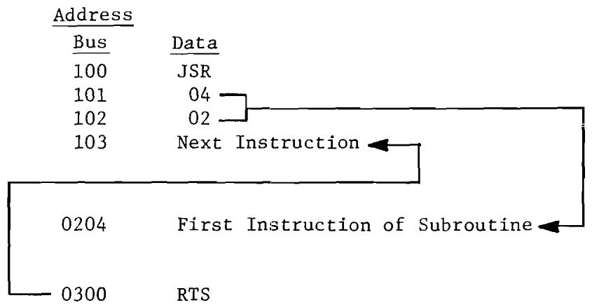
Example 8.5: Memory map for RTS instruction
With this capability of subroutine, the microprocessor allows the programmer to go from the main program to 1 subroutine, to the second subroutine, to a third subroutine, then finally working its way back to the main program. Example 8.6 is an expansion of Example 8.2 with the returns included.
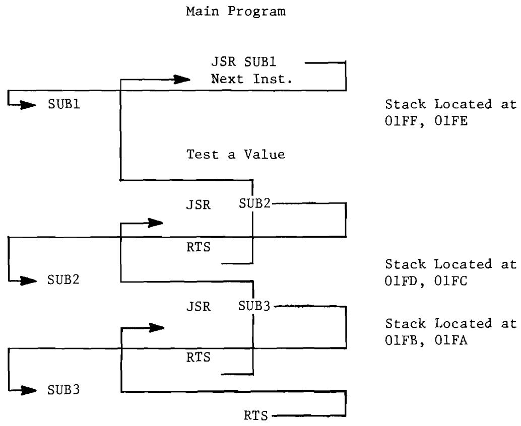
Example 8.6: Expansion of RTS memory map
This concept is known as nesting of subroutines, and the number of subroutines which can be called and returned from in such a manner is limited by only the length of the stack.
8.3 IMPLEMENTATION OF STACK IN MCS6501 THROUGH MCS6505
As we have seen, the primary requirement for the stack is that irrespective of where or when a stack operation is called, the microprocessor must have an independent counter or register which contains the current memory location value of the stack address. This register is called the Stack Pointer, S. The stack becomes an auxiliary field in memory which is basically independent of programmer control. We will discuss later how the stack pointer becomes initialized, but once it is initialized, the primary requirement is that it be self-adjusted; in other words, operations which put data on the stack cause the pointer to be decremented automatically; operations which take data off from the stack cause the pointer to be incremented automatically. Only under rare circumstances should the programmer find it necessary to move his stack from one location to another if he is using the stack as designed.
On this basis, there is no need for a stack to be longer than 256 bytes. To perform a single subroutine call takes only 2 bytes of stack memory. To perform an interrupt takes only 3 bytes of stack memory. Therefore, with 256 bytes, one can access 128 subroutines deep or interrupt ourselves 85 times. Therefore the length of the stack is extremely unlikely to be limiting. The MCS6501 through MCS6505 have a 256-byte stack length.
Figure 8.1, which is now the complete block diagram, shows all of the microprocessor registers. The 8-bit stack pointer register, S, has been added. It is initialized by the programmer and thereafter automatically increments or decrements, depending on whether data is being put on to the stack or taken off the stack by the microprocessor under control of the program or the interrupt lines.
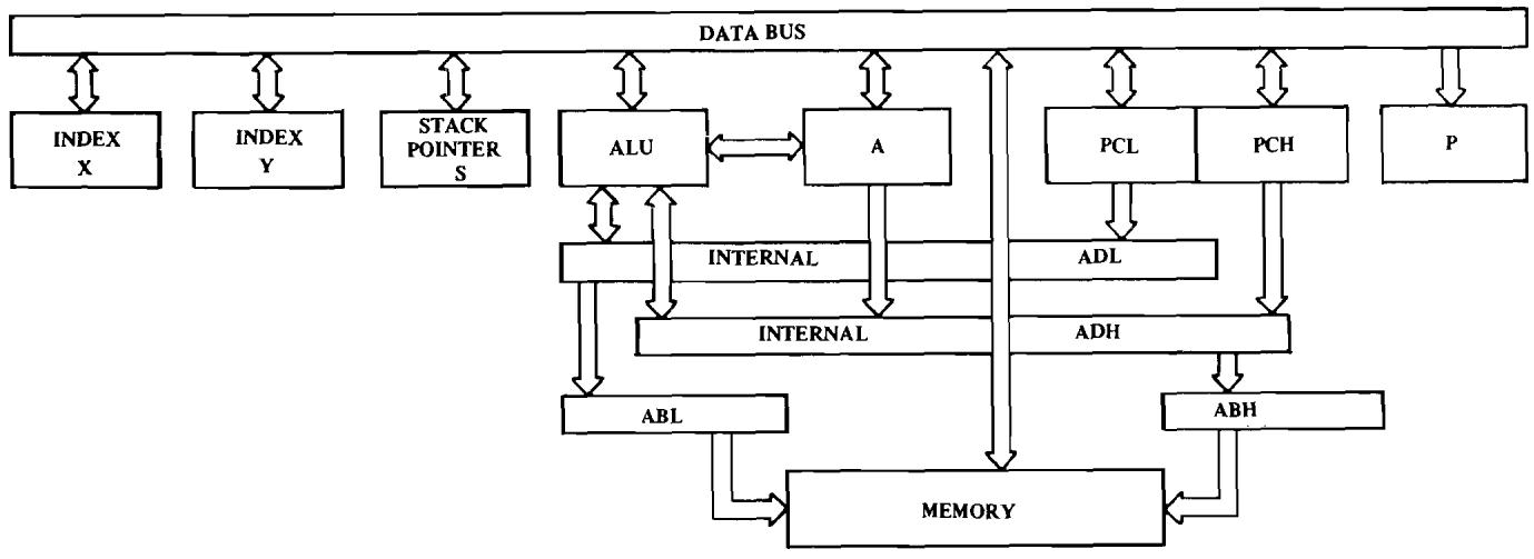
Partial Block Diagram of MCS650X Including Stack Pointer, S FIGURE 8.1
The primary purpose of the stack is to furnish a block of memory locations in which the microprocessor can write data such as the program counter for use in later processing. In many control systems the requirements for Read/Write memory are very small and the stack just represents another demand on Read/Write memory. Therefore these applications would like the stack to be in the Page Zero location in order that memory allocation for the stack, the Zero Page operations, and the indirect addresses can be performed. Therefore, one of the requirements of a stack is that it be easily locatable into Page Zero.
On the other hand, if more than 1 page of RAM is needed because of the amount of data that must be handled by the user programs, having the stack in Page Zero is an unnecessary waste of Page Zero memory in the sense that the stack can take no real advantage of being located in Zero Page, whereas other operations can.
In each of the examples, the stack has been located at high order address 01 followed by a low order address. In the same manner as the microprocessor forces locations 00 on to the high order 8 bits of the address lines for Zero Page operations, the microprocessor automatically puts 01 Hex on to the high order 8-bit address lines during each stack operation. This has the advantage to the user of locating the stack into Page One of memory which would be the next memory location added if the Zero Page operation requirements exceed Page Zero memory capacity. This has the advantage of the stack not requiring memory to be added specifically for the stack but only requiring the allocation of existing memory locations. It should be noted that the selected addressing concepts of the MCS650X microprocessor support devices would involve connecting the memories such that bit 8, which is the selection bit for the Page One versus Page Zero, is a "don't care" for operations in which the user does not need more than 1 page of Read/Write memory. This gives the user the effect of locating stack in Page Zero for those applications.
The second feature that should be noted from the examples is that the stack was located at the end of Page One and decremented from that point towards the beginning of the page. This is the natural operation of the stack. RAM memory comes in discrete increments, 64, 128, 256 bytes so the normal method of_allocating stack addressing is for the user to calculate the number of bytes probably needed for stack access. This could be done by analyzing the number of subroutines which might be called and the amount of data which might be put onto the stack in order to communicate between subroutines or the number of interrupts plus subroutines which might occur with the respective data that would be stored on the stack for each of them. By counting 3 bytes for each interrupt, 2 bytes for each jump to subroutine, plus 1 byte for each programmer-controlled stack operation, the microprocessor designer can estimate the amount of memory which must be allocated for the stack. This is part of his decision-making process in deciding how much memory is necessary for his whole program.
Once the allocation has been made, it is recommended that the user assign his working storage from the beginning of memory forward and always load his stack at the end of either Page Zero, Page One, or at the end of his physical memory which is located in one of those locations. This will
give the effect of having the highest bytes of memory allocated to the stack, lower bytes of memory allocated to user working storage and hopefully the two shall never overlap.
It should be noted that the natural operation of the stack, which often is called by hardware not totally under program control, is such that it will continue to decrement throughout the page to which it is allocated irrespective of the user's desire to have it do so. A normal mistake in allocation in memory can result in the user writing data into a memory location and later accessing it with another subroutine or another part of his program, only to find that the stack has very carefully written over that area as the result of its performing hardware control operations. This is one of the more difficult problems to diagnose. If this problem is suspected by the programmer, he should analyze memory locations higher than unexplained disturbed locations.
There is a distinctive pattern for stack operations which are unique to the user's program but which are quite predictable. An analysis of the value which has been destroyed will often indicate that it is part of an address which would normally be expected during the execution of the program between the time data was stored and the time it was fetched. This is a very strong indication of the fact that the stack somehow or other did get into the user's program area. This is almost always caused by improper control of interrupt lines or unexpected operations of interrupt or subroutine calls and has only 2 solutions: (1) If the operation is normal and predictable, the user must assign more memory to his program and particularly reassign his memory such that the stack has more room to operate; or (2) if the operation of the interrupt lines is not predictable, attention must be given to solving the hardware problem that causes this type of unpredictable operation.
8.3.1 Summary of Stack Implementation
The MCS6501 through MCS6505 microprocessors have a single 8-bit stack register. This register is automatically incremented and decremented under control of the microprocessor to perform stack manipulation operations, under direction of the user program or the interrupt lines. Once the programmer has initialized the stack pointer to the
end of whatever memory he wants the stack to operate in, the programmer can ignore stack addressing other than in those cases where there is an interference between stack operations and his normal program working space.
In the MCS6501 through MCS6505, the stack is automatically located in Page One. The microprocessor always puts out the address 0100 plus stack register for every stack operation. By selected memory techniques, the user can either locate the stack in Page Zero or Page One, depending on whether or not Page One exists for his hardware.
8.4 USE OF THE STACK BY THE PROGRAMMER
Discussed in Section 8.1 was the use of the JSR to call a subroutine. However, not indicated was the technique by which the subroutine knew which data to operate on. There are 3 classical techniques for communicating data between subroutines. The first and most straightforward technique is that each subroutine has a defined set of working registers located in the Page Zero in which the user has left values to be operated on by the subroutine. The registers can either contain the values directly or can contain indirect pointers to addresses to values which would be operated on. The following example shows the combination of these:
Example 8.7: Call-a-move subroutine using preassigned memory locations
Location 10 = Count
Location 11, 12 = Base from Address
Location 13, 14 = Base to Address
Main Line Routine
| No. of Bytes | Instruction | Comment |
| 2 | LDA #Count -1 | Load Fixed Value for the Move |
| 2 | STA 10 | |
| 2 | LDA #FRADH | Set up "FROM" Pointer |
| 2 | STA 12 | |
| 2 | LDA #FRADL | |
| 2 | STA 11 | |
| 2 | LDA #TOADL | |
| 2 | STA 13 | |
| 2 | LDA #TOADH | Set up "TO" Pointer |
| 2 | STA 14 | |
| 3/23 bytes | JSR SUB1 | |
Subroutine Coding
No. of
Bytes
Label
Instruction
2
SUB1
LDY 10
2
LOOP
LDA (11), Y
1
STA (13), Y
2
DEY
1
BNE LOOP
total 33 bytes
RTS
As has been previously developed, the loop time is the overriding consideration rather than setup time for a large number of executions.
It can be seen that we have used the techniques developed in previous sections of the indirect referencing, the jump to subroutine and the return from subroutine to perform this type of subroutine value communication.
In this operation, there was no use of the stack except for the program counter value.
A second form of communication is the use of the stack itself as an intermediate storage for data which is going to be communicated to the subroutine. In order for the programmer to use the stack as an intermediate storage, he needs instructions which allow him to put data on the stack and to read from the stack. These instructions are known as push and pull instructions.
8.5 PHA - PUSH ACCUMULATOR ON STACK
This instruction transfers the current value of the accumulator to the next location on the stack, automatically decrementing the stack to point to the next empty location.
The symbolic notation for this operation is A . Noted should be that the notation means push to the stack, means pull from the stack.
The Push A instruction only affects the stack pointer register which is decremented by 1 as a result of the operation. It affects no flags.
PHA is a single-byte instruction and its addressing mode is Implied.
The following example shows the operations which occur during Push A instruction.
Example 8.8: Operation of PHA, assuming stack at O1FF
| Cycles | Address Bus | Data Bus | External Operations | Internal Operations |
| 1 | 0100 | OP CODE | Fetch Instruction | Finish Previous Operation, Increment PC to 0101 |
| 2 | 0101 | Next OP CODE | Fetch Next OP CODE and Discard | Interpret PHA In-struction, Hold P-Counter |
| 3 | 01FF | (A) | Write A on Stack | Decrement Stack Pointer to 01FE |
| 4 | 0101 | Next OP CODE | Fetch Next OP CODE | |
As can be seen, the PHA takes 3 cycles and takes advantage of the fact that the stack pointer is pointing to the correct location to write the value of A. As a result of this operation, the stack pointer will be setting at O1FE. The notation (A) implies contents of A. Now that the data is on the stack, later on in the program the programmer will call for the data to be retrieved from the stack with a PLA instruction.
8.6 PLA - PULL ACCUMULATOR FROM STACK
This instruction adds 1 to the current value of the stack pointer and uses it to address the stack and loads the contents of the stack into the A register.
The symbolic notation for this is A .
The PLA instruction does not affect the carry or overflow flags. It sets N if the bit 7 is on in accumulator A as a result of instructions, otherwise it is reset. If accumulator A is zero as a result of the PLA, then the Z flag is set, otherwise it is reset. The PLA instruction changes content of the accumulator A to the contents of the memory location at stack register plus 1 and also increments the stack register.
The PLA instruction is a single-byte instruction and the addressing mode is Implied.
In the following example, the data stored on the stack in Example 8.8 is transferred to the accumulator.
Example 8.9: Operation of PLA stack from Example 8.8
| Cycles | Address Bus | Data Bus | External Operations | Internal Operations |
| 1 | 0200 | PLA | Fetch Instruction | Finish Previous Operation, Increment PC to 101 |
| 2 | 0201 | Next OP CODE | Fetch Next OP CODE and Discard | Interpret Instruction, Hold P-Counter |
| 3 | 01FE | | Read Stack | Increment Stack Pointer to 01FF |
| 4 | 01FF | (A) | Fetch A | Save Stack |
| 5 | 0201 | Next OP CODE | Fetch Next OP CODE | M → A |
When taking data off the stack, there is 1 extra cycle during which time the current contents of the stack register are accessed but not used and the stack pointer is incremented by 1 to allow access to the value that was previously stored on the stack. The stack pointer is left pointing at this location because it is now considered to be an empty location to be used by the stack during a subsequent operation.
8.7 USE OF PUSHES AND PULLS TO COMMUNICATE VARIABLES BETWEEN SUBROUTINE OPERATIONS
In Example 8.10, we perform the same operation as we did in Example 8.7; only here, instead of using fixed locations to pick up the pointers, we are going to use the stack as a communications vehicle:
Example 8.10: Call-a-move subroutine using the stack to communicate
| Location 11, 12 = Base "FROM" Address |
| Location 13, 14 = Base "TO" Address |
| Main Line Routine |
| Bytes | Instruction |
| 2 | LDA #Count -1 |
| 1 | PHA |
| 2 | LDA #FRADL |
| 1 | PHA |
| 2 | LDA #FRADH |
| 1 | PHA |
| 2 | LDA #TOADL |
| 1 | PHA |
| 2 | LDA #TOADH |
| 1 | PHA |
| 3 | JSR SUB1 |
| 18 | |
Subroutine
| Bytes | Label | Instruction | Comments |
| 2 | SUB1 | LDX 6 | |
| 1 | LOOP1 | PLA | |
| 2 | | STA 10,X | |
| 1 | | DEX | Move Stack to Memory |
| 2 | | BNE LOOP 1 | |
| 1 | | PLA | Set up Count |
| 1 | | TAY | |
| 2 | LOOP2 | LDA (11),Y | |
| 2 | | STA (13),Y | Move Memory Location |
| 1 | | DEY | |
| 2 | | BNE LOOP 2 | |
| 2 | | LDA 15 | |
| 1 | | PHA | |
| 2 | | LDA 16 | Restore PC to Stack |
| 1 | | PHA | |
| 1 | | RTS | |
| Total 42 Bytes |
We can see from this example that using the stack as a communication vehicle actually increases the number of bytes in the subroutine and the total bytes overall. However, the only time one should be using subroutines in this case is when the subroutine is fairly long and the number of times the subroutine is used is fairly frequent. This technique does reduce the number of bytes in the calling sequence. The calling sequence is normally repeated once for every time the instruction is called; therefore the use of the stack to communicate should result in a net reduction in the number of bytes used in the total program.
Up until this time, we have been considering that the stack is at a fixed location and that all stack references use the stack pointer. It has not been explained how the stack pointer in the microprocessor gets loaded and accessed. This is done through communication between the stack pointer and index register X.
8.8 TXS - TRANSFER INDEX X TO STACK POINTER
This instruction transfers the value in the index register X to the stack pointer.
Symbolic notation is X S .
TXS changes only the stack pointer, making it equal to the content of the index register X. It does not affect any of the flags.
TXS is a single-byte instruction and its addressing mode is Implied.
Another application for TXS is the concept of passing parameters to the subroutine by storing them immediately after the jump to subroutine instruction.
In Example 8.11, the from and to address, plus the count of number of values would be written right after the JSR instruction and its address.
By locating the stack in Page Zero, the address of the last byte of the JSR can be incremented to point at the parameter bytes and then used as an indirect pointer to move the parameter to its memory location.
The key to this approach is transferring the stack pointer to X which allows the program to operate directly on the address while it is in the stack.
It should be noted that this approach automatically leaves the address on the stack, positioned so that the RTS picks up the next OP CODE address.
Example 8.11: Jump to subroutine (JSR) followed by parameters
| Address Bus | Data |
| 0100 | JSR |
| 0101 | ADL |
| 0102 | ADH |
| 0103 | To High |
| 0104 | To Low |
| 0105 | From High |
| 0106 | From Low |
| 0107 | Count |
| 0108 | Next OP CODE |
Before concluding this discussion on subroutines and parameter passing, one should again note the use of subroutines should be limited to those cases where the user expects to duplicate code of significant length several times in the program. In these cases, and only in these cases, is subroutine call warranted rather than the normal mode of knowing the addresses and specifying them in an instruction. In all cases where timing is of significant interest, subroutines should also be avoided. Subroutines add significantly to the setup and execution time of problem solution. However, subroutines definitely have their place in microcomputer code and there have been presented 3 alternatives for use in application programs. The user will find a combination of the above techniques most useful for solving his particular problem.
8.9 TSX - TRANSFER STACK POINTER TO INDEX X
This instruction transfers the value in the stack pointer to the index register X.
Symbolic notation is S X .
TSX does not affect the carry or overflow flags. It sets N if bit 7 is on in index X as a result of the instruction, otherwise it is reset. If index X is zero as a result of the TSX, the Z flag is set, otherwise it is reset. TSX changes the value of index X, making it equal to the content of the stack pointer.
TSX is a single-byte instruction and the addressing mode is Implied.
8.10 SAVING OF THE PROCESSOR STATUS REGISTER
During the interrupt sequences, the current contents of the processor status register (P) are saved on the stack automatically. However, there are times in a program where the current contents of the P register must be saved for performing some type of other operation. A particular example of this would be the case of a subroutine which is called independently and which involves decimal arithmetic. It is important that the programmer keeps track of the arithmetic mode the program is in at all times. One way to do this is to establish the convention that the machine will always be in binary or decimal mode, with every subroutine changing its mode being responsible for restoring it back to the known state. This is a superior convention to the one that is about to be described.
A more general convention would be one in which the subroutine that wanted to change modes of operation would push P onto the stack, then set the decimal mode to perform the subroutine and then pull P back from the stack prior to returning from the subroutine.
Instructions which allow the user to accomplish this are as follows:
8.11 PHP - PUSH PROCESSOR STATUS ON STACK
This instruction transfers the contents of the processor status register unchanged to the stack, as governed by the stack pointer.
Symbolic notation for this is ^
The PHP instruction affects no registers or flags in the microprocessor.
PHP is a single-byte instruction and the addressing mode is Implied.
8.12 PLP - PULL PROCESSOR STATUS FROM STACK
This instruction transfers the next value on the stack to the Processor Status register, thereby changing all of the flags and setting the mode switches to the values from the stack.
Symbolic notation is P
The PLP instruction affects no registers in the processor other than the status register. This instruction could affect all flags in the status register.
PLP is a single-byte instruction and the addressing mode is Implied.
8.13 SUMMARY ON THE STACK
The stack in the MCS650X family is a push-down stack implemented by a processor register called the stack pointer which the programmer initializes by means of a Load X immediately followed by a TXS instruction and thereafter is controlled by the microprocessor which loads data into memory based on an address constructed by adding the contents of the stack pointer to a fixed address, Hex address 0100. Every time the microprocessor loads data into memory using the stack pointer, it automatically decrements the stack pointer, thereby leaving the stack pointer pointing at the next open memory byte. Every time the microprocessor accesses data from the stack, it adds 1 to the current value of the stack pointer and reads the memory location by putting out the address 0100 plus the stack pointer. The status register is automatically pointing at the next memory location to which data can now be written. The stack makes an interesting place to store interim data without the programmer having to worry about the actual memory location in which data will be directly stored.
There are 8 instructions which affect the stack. They are: BRK, JSR, PHA, PHP, PLA, PLP, RTI, and RTS.
BRK and RTI involve the handling of the interrupts.

CHAPTER 9
RESET AND INTERRUPT CONSIDERATIONS
9.0 VECTORS
Before developing the concepts of how the MCS650X Microprocessors handle interrupts and start-up, a brief definition of the concept of vector pointers needs to be developed.
In the sections on Jumps and Branches, it was always assumed that the program counter is changed by the microprocessor under control of the programmer while accessing addresses which were in program sequence. In order to get the microprocessor started and in order to properly handle external control or interrupt, there has been developed a different way of setting the program counter to point at a specific location. This concept is called vectored pointers. A vector pointer consists of a program counter high and program counter low value which, under control of the microprocessor, is loaded in the program counter when certain external events occur. The word vector is developed from the fact that the microprocessor directly controls the memory location from which a particular operation will fetch the program counter value and hence the concept of vector.
By allowing the programmer to specify the vector address and then by allowing the programmer to write coding that the address points to, the microprocessor makes available to the programmer all of the control necessary to develop a general purpose control program. The microprocessor has fixed address in memory from which it picks up the vectors. By this
implementation, minimum hardware in the microprocessor is obtained. Locations FFFA through FFFF are reserved for vector pointers for the microprocessor. Into these locations are stored respectively the interrupt vectors or pointers for: non-maskable interrupt, reset and interrupt request.
9.1 RESET OR RESTART
In the microprocessor, there is a state counter which controls when the microprocessor is going to use the program counter to access memory to pick up an instruction, then after the instruction is loaded, the microprocessor goes through a fixed sequence of interpreting instructions and then develops a series of operations which are based on the OP CODE decoding.
Up to this point, it has been assumed that the program counter was set at some location and that all program counter changes are then directed by the program once the program counter had been initialized.
Instructions exist for the initialization and loading of all other registers in the microprocessor except for the initial setting of the program counter. It is for this initial setting of the program counter to a fixed location in the restart vector location specified by the microprocessor programmer that the reset line in the microprocessor is primarily used.
The reset line is controlled during power on initialization and is a common line which is connected to all devices in the microcomputer system which have to be initialized to a known state. The initialization of most I/O devices is such that they are brought up in a benign state such that with minimum coding in the microcomputer, the programmer can configure and control the I/O in an orderly fashion.
The concept has important systems implications in systems where damage can be done if peripheral devices came up in unknown states. Therefore, in the MCS650X, power on or reset control operates at two levels.
First, by holding of an external line to ground, and having this external line connected to all the devices during power up transient conditions, the entire microcomputer system is initialized to a known disabled state. Second, the releases of the reset line from the ground or TTL zero condition to a TTL one condition causes the microprocessor to be automatically initialized, first by the internal hardware vector which causes it to be pointed to a known program location, and secondly through a software program which is written by the user to control the orderly start-up of the microcomputer system.
All of the MCS650X family parts also obey a discipline that while the reset line is low, the system is in a stop or reset state. The microprocessor is guaranteed to be in a Read state and upon release of the reset line from ground to positive, the microprocessor will continue to hold the line in a Read state until it has addressed the specified vectored count location, at which time control of the microprocessor is available to the programmer.
NOTE: The MC6800 family also follows this convention.
9.2 START FUNCTION
While the reset line is in the low state, it can be assumed that internal registers may be initialized to any random condition; therefore, no conditions about the internal state of the microprocessor are assumed other than that the microprocessor will, one cycle after the reset line goes high, implement the following sequence:
| Cycles | Address Bus | Data Bus | External Operation | Internal Operation |
| 1 | ? | ? | Don't Care | Hold During Reset |
| 2 | ? + 1 | ? | Don't Care | First Start State |
| 3 | 0100 + SP | ? | Don't Care | Second Start State |
| 4 | 0100 + SP-1 | ? | Don't Care | Third Start State |
| 5 | 0100 + SP-2 | ? | Don't Care | Fourth Start State |
| 6 | FFFC | Start PCL | Fetch First Vector | |
| 7 | FFFD | Start PCH | Fetch Second Vector | Hold PCL |
| 8 | PCH PCL | First | Load First OP CODE | |
| | OP CODE | | |
The start cycle actually takes seven cycles from the time the reset line is let go to TTL plus. On the eighth cycle, the vector fetched from the memory location FFFC and FFFD is used to access the next instruction. The microprocessor is now in a normal program load sequence, the location where the vector points should be the first OP CODE which the programmer desires to perform.
The second point that should be noted is that the microprocessor actually accesses the stack three times during the start sequence in cycles 3, 4 and 5. This is because the start sequence is in effect a specialized form of interrupt with the exception that the read/write line is disabled so that no writes to stack are accomplished during any of the cycles.
9.3 PROGRAMMER CONSIDERATIONS FOR INITIALIZATION SEQUENCES
There are two major facts to remember about initialization. One, the only automatic operations of the microprocessor during reset are to turn on the interrupt disable bit and to force the program counter to the vector location specified in locations FFFC and FFFD and to load the first instruction from that location. Therefore, the first operation in any normal program will be to initialize the stack. This should be done by having previously decided what the stack value should be for initial operations and then doing a LDX immediate of this value followed by a TXS. By this simple operation, the microprocessor is ready for any interrupt or non-maskable interrupt operation which might occur during the rest of the start-up sequence.
Once this is accomplished, the two non variable operations of the machine are under control. The program counter is initialized and under programmer control and the stack is initialized and under program control. The next operations during the initialization sequences will consist of configuring and setting up the various control functions necessary to perform the I/O desired for the microprocessor.
Specific discussion for considerations regarding the start-up are covered in Section 11.
The major things which have to be considered include the current state of the I/O device and the non destructive operations that will allow the state to be changed to the active state.
The initialization programs mostly consist of loading accumulator A immediately with a bit pattern and storing it in the data control register of an I/O device.
Note: The interrupt disable is automatically set by the microprocessor during the start sequence. This is to minimize the possibility of a series of interrupts occurring during the start-up sequence because of uncontrolled external values although it is usually possible to control interrupts as part of the configuration.
The programmer should consider two effects. First, that the non-maskable interrupt is not blockable by this technique since it would be possible to configure a device that was connected to a non-maskable interrupt and have to service the interrupt immediately. Secondly, the mask must be cleared at the end of the start sequence unless the user has specific reason to inhibit interrupts after he has done the start-up sequence. Therefore, the next to last instruction of the start-up sequence should be CLI.
It should be noted that the start-up routine is a series of sequential operations which should occur only during power on initialization and is the first step in the programmed logic machine.
Because the execution of the routine during power on occurs very seldom in the normal operation of the machine, the coding for power on sequence should tend to minimize the use of memory space rather than speed.
The last instruction in the start-up sequence should initialize the decimal mode flag to the normal setting for the program.
The next instruction should be the beginning of the user's normal programming for his device, everything preceding that being known as "housekeeping."
9.4 RESTART
It should be noted that the basic microprocessor control philosophy allows for a single common reset line which initializes all devices. This line can be used to clear the microprocessor to a known state and to reset all peripherals to a known state; therefore, it can be used as a result of power interruption, during the power on sequence, or as an external clear by the user to re-initialize the system.
As discussed in the hardware manual, restart is often used as an aid to making sure the microprocessor has been properly interconnected and that programs have been loaded in the correct locations.
9.5 INTERRUPT CONSIDERATIONS
Up until this point, the microprocessor has to proceed under program-mer control through a variety of sequences. The only way for the program-mer to change the sequence of operations of the microprocessor was to change the program counter location to point at new operations. The microprocessor is in control of fetching the next instruction at the conclusion of the current instruction. The only way that external events could control the microprocessor, if it were not for interrupts, would be for the programmer to periodically interrupt or stop processing data and check to see whether or not an external event which might cause him to change his direction has occurred. The problem with this technique is that
I/O events are usually asynchronous, i.e., not timed with the microprocessor internal instructions, therefore, it would be possible for the event to occur shortly after the programmer has stopped to look at I/O events which would mean that the event would not be sampled until the programmer took the time to stop his coding and sample again.
Because the sampling of I/O devices normally takes several byte counts or cycles to accomplish, the frequent insertion of checking routines into straight line code results in significant delays to the entire program. In trying to use this technique, there has to be a trade-off between the fact that the program wastes a significant amount of time checking events which have not yet occurred versus delaying checking of an event which has occurred and if not timely serviced the data may be lost.
In order to solve this dichotomy, the concept of interrupt is used to signal the microprocessor that an external event has occurred and the microprocessor should devote attention to it immediately. This technique accomplishes processing in which the microprocessor's program is interrupted and the event that caused the interrupt is serviced.
Transferring most of data and control to I/O devices in an interrupt driven environment will usually result in maximum program and/or program-mer efficiency. Each event is serviced when it occurs which means there is a minimum amount of delaying in servicing events, also a minimum amount of coding because of elimination of the need to determine occurrence of several events simultaneously; each interrupting event is handled as a unique combination. It is possible to interrupt an interrupt processing routine and, therefore, all the interrupt logic uses the stack which allows processing of successive interrupts without any penalty other than increasing the stack length.
A real world example of an event which should interrupt is when the user is given a panic button indicating to the microcomputer some event has occurred which requires total immediate attention of the microprocessor to solving that problem.
The action and events are as follows: The microprocessor user pushes the panic button; the panic switch sensor causes an external device to indicate to the microprocessor an interrupt is desired; the microprocessor checks the status of the internal interrupt inhibitsignal; if the internal inhibit is set, then the interrupt is ignored. However, if it is reset or when it becomes reset through some program reaction, the following set of operations occur:
Example 9.2: Interrupt Sequence
| Cycles | Address Bus | Data Bus | External Operation | Internal Operation |
| 1 | PC | OP CODE | Fetch OP CODE | Hold Program Counter,
Finish Previous
Operation |
| 2 | PC | OP CODE | Fetch OP CODE | Force a BRK
Instruction, Hold
P-Counter |
| 3 | 01FF | PCH | Store PCH on Stack | Decrement Stack
Pointer to 01FE |
| 4 | 01FE | PCL | Store PCL on Stack | Decrement Stack
Pointer to 01FD |
| 5 | 01FD | P | Store P on Stack | Decrement Stack
Pointer to 01FC |
| 6 | FFFE | New PCL | Fetch Vector Low | Put Away Stack |
| 7 | FFFF | New PCH | Fetch Vector High | Vector Low →
PCL and Set I |
| 8 | Vector | OP CODE | Fetch Interrupt | Increment PC to
PC + 1 |
| PCH PCL | | Program | |
As can be seen in Example 9.2, the microprocessor uses the stack to save the reentrant or recovery code and then uses the interrupt vectors FFFE and FFFF, (or FFFA and FFFB), depending on whether or not an interrupt request or a non-maskable interrupt request had occurred. It should be noted that the interrupt disable is turned on at this point by the microprocessor automatically.
Because the interrupt disable had to be off for an interrupt request to have been honored, the return from interrupt which loads the processor status from before the interrupt occurred has the effect of clearing the interrupt disable bit. After the interrupt has been acknowledged by the microprocessor by transferring to the proper vector location, there are a variety of operations which the user can perform to service the interrupt; however, all operations should end with a single instruction which reinitializes the microprocessor back to the point at which the interrupt occurred. This instruction is called the RTI instruction.
9.6 RTI - RETURN FROM INTERRUPT
This instruction transfers from the stack into the microprocessor the processor status and the program counter location for the instruction which was interrupted. By virtue of the interrupt having stored this data before executing the instruction and the fact that the RTI reinitializes the microprocessor to the same state as when it was interrupted, the combination of interrupt plus RTI allows truly reentrant coding.
The symbolic notation for RTI is P PC
The RTI instruction reinitializes all flags to the position to the point they were at the time the interrupt was taken and sets the program counter back to its pre-interrupt state. It affects no other registers in the microprocessor.
RTI is a single byte instruction and its addressing mode is Implied.
In the following example, we can see the internal operation of the RTI which restores the microprocessor:
Example 9.3: Return from Interrupt
| Cycles | Address Bus | Data Bus | External Operation | Internal Operation |
| 1 | 0300 | RTI | Fetch OP CODE | Finish Previous Operation,Increment PC to 0301 |
| 2 | 0301 | ? | Fetch Next OP CODE | Decode RTI |
| 3 | 01FC | ? | Discarded Stack Fetch | Increment Stack Pointer to 01FD |
| 4 | 01FD | P | Fetch P Register | Increment Stack Pointer to 01FE |
| 5 | 01FE | PCL | Fetch PCL | Increment Stack Point-er to 01FF, Hold PCL |
| 6 | 01FF | PCH | Fetch PCH | M→PCL, Store Stack Pointer |
| 7 | PCH PCL | OP CODE | Fetch OP CODE | Increment New PC |
Note the effects of the extra cycle (3) necessary to read data from stack which causes the RTI to take six cycles. The RTI has restored the stack, program counter and status register to the point they were at before the interrupt was acknowledged.
There is no automatic save of any of the other registers in the microprocessor. Because the interrupt occurred to allow data to be transferred using the microprocessor, the programmer must save the various internal registers at the time the interrupt is taken and restore them prior to returning from the interrupt. Saving of the registers is best done on the stack as this allows as many consecutive interrupts as the programming will allow for. Therefore, the routines which save all registers and restore them are as follows:
Example 9.4: Illustration of Save and Restore for Interrupts
| Cycle | Bytes | | | |
| 3 | 1 | SAVE | PHA | Save A |
| 2 | 1 | | TXA | Save X |
| 3 | 1 | | PHA | |
| 2 | 1 | | TYA | Save Y |
| 3 | 1 | | PHA | |
| 13 | 5 | | | |
| 4 | 1 | RESTORE | PLA | Restore Y |
| 2 | 1 | | TAY | |
| 4 | 1 | | PLA | Restore X |
| 2 | 1 | | TAX | |
| 4 | 1 | | PLA | Restore A |
| 16 | 5 | | | |
The SAVE coding assumes that the programmer wants to save and to restore registers A, X and Y. It should be noted that for many interrupts, the amount of coding that has to be performed in the interrupt is fairly small.
In this type of operation, it is usually more desirable to shorten the interrupt processing time and not use all of the registers in the machine. Therefore, a more normal interrupt processing routine would consist of just saving registers A and X which means that the restore routine would be just restore registers X and A. This has the effect of shortening the interrupt routine by two bytes, and also shortens the restore routine by two bytes and will cut 5 cycles out of the interrupt routine and 6 cycles out of the restore routine.
This technique combined with automatic features of the interrupt and the RTI allows multiple interrupts to occur with successive interrupts interrupting the current interrupt. This is one of the advantages of the use of the stack so that as many interrupts can interrupt other interrupts as can be held in the stack. The stack contains six bytes for every interrupt if all registers are saved, so 42 sequences of interrupts can be stored in one page. However, in more practical situations, consecutive interrupts hardly ever get more than about three deep.
The advantage of allowing an interrupt to interrupt an interrupt is that the whole concept behind the interrupt is that asynchronous events can be responded to as rapidly as possible; therefore, it is desirable to allow the processing to service one interrupt to be interrupted to service the second, as long as the first interrupt has been properly serviced.
To review how this is accomplished using the normal interrupt capability of the MCS650X, it is important that we review the bus concept which is inherent in the MCS6500 family and which is compatible with the M6800.
As has already been discussed, all I/O operations on this type of microprocessor are accomplished by reading and writing registers which
actually represent connections to physical devices or to physical pins which connect to physical devices.
Up until this point, this discussion has addressed itself to transferring of data into and out of the microprocessor. However, there is a concept that is inherent in the bus discipline that says that whenever an interrupt device capable of generating an interrupt desires to accomplish an interrupt, it performs two acts; first, it sets a bit, usually bit 7, in a register whose primary purpose is to communicate to the microprocessor the status of the device. The interrupting device causes one of perhaps many output lines to be brought low. These collector-or'd outputs are connected together to the IRQ pin on the MCS650X microprocessor.
The interrupt request to the MCS650X is the IRQ pin being at a TTL zero. In order to minimize the handshaking necessary to accomplish an interrupt, all interrupting devices obey a rule that says that once an interrupt has been requested by setting the bit and pulling interrupt low, the interrupt will be held by the device until the condition that caused the interrupt has been satisfied. This allows several devices to interrupt simultaneously and also allows the microprocessor to ignore an interrupt until it is ready to service it. This ignoring is done by the interrupt disable bit which can be set on by the programmer and is initialized on by the interrupt sequence or by the start sequence.
Once the interrupt line is low and interrupt disable is off, the microprocessor takes an interrupt which sets on the interrupt disable. The interrupt disable then keeps the input low line from causing more than one interrupt until an interrupt has been serviced. There is no other handshaking between the microprocessor and the interrupting device other than the collector-or'd line. This means that the microprocessor must use the normal addressing registers to determine which of several collector-or'd devices caused the line to go low and to process the interrupt which has been requested.
Once the processor has found the interrupting device by means of analyzing status bits which indicates an interrupt has been requested, the microprocessor then clears the status by reading or writing data as indicated by the status register.
It should be noted that a significant difference between status registers and data registers in I/O devices is that status registers are never cleared by being read, only by being written into or by the microprocessor transferring data from a data register which corresponds to some status in the status register. Detailed examples of this interaction are discussed in Chapter 11. The clearing of the status register also releases the collector-or'd output thereby releasing the interrupt pin request.
The basic interaction between the microprocessor and interrupting device is when interrupting device sets the status bit and brings its output IRQ line low. If its output IRQ line is connected to the microprocessor interrupt request line, the microprocessor waits until the interrupt disable is cleared, takes the interrupt vector, and sets the interrupt disable which inhibits further interrupts in the IRQ line. The microprocessor determines which interrupting device is causing an interrupt and transfers data from that device.
Transferring of data clears the interrupt status and the IRQ pin. At this point, the programmer could decide that he was ready to accept another interrupt even though the data may have been read but not yet operated on. Allowing interrupts at this point, gives the most efficient operation of the microprocessor in most applications.
There are also times when a programmer may be working on some coding the timing of which is so important that he cannot afford to allow an interrupt to occur. During these times, he needs to be able to turn on the interrupt disable. To accomplish this, the microprocessor has a set and clear interrupt disable capability.
9.7 SOFTWARE POLLING FOR INTERRUPT CAUSES
As was indicated above, any one of several devices are collector-or'd to cause an IRQ. The effect of any one of the devices or combination of them having polled the IRQ line low is always the same. The interrupt stores the current status of the program counter and processor on the stack and transfers to a fixed vector address. In servicing the interrupt, it is important to save those registers which will be used in the analysis of the interrupt and during the interrupt processing, so the normal first steps of the interrupt routine are to do the SAVE procedures.
The next operation is to determine which of the various potential interrupting devices caused the interrupt. To accomplish this, the programmer should make use of the fact that all interrupting devices signal the interrupt by a bit in the status register. All currently implemented 6800 and 6500 peripherals always have interrupt indicators; either bit 7 or bit 6 in their status register. Therefore, the basic loop that a user will use to verify the existence of an interrupt on one of five devices is as follows:
Example 9.5: Interrupt Polling
| No.of Bytes | Cycles | | |
| 3 | 4 | LDA | Status 1 |
| 2 | 2 | BMI | FIRST |
| 3 | 4 | LDA | Status 2 |
| 2 | 2 | BMI | SECOND |
| 3 | 4 | LDA | Status 3 |
| 2 | 2 | BMI | THIRD |
| 3 | 4 | LDA | Status 4 |
| 2 | 2 | BMI- | FOURTH |
| 3 | 4 | LDA | Status 5 |
| 2 | 2 | BMI | FIFTH |
| RES1 | JMP | to RESTORE |
| FIRST | LDA | DATA 1 |
| | CLI | |
| | Process 1 | |
| | etc. | |
In this example, the simplest case where the potential interrupts are indicated by bit 7 being on, has been assumed. This allows advantage to be taken of the free N-bit test by following the load of the first status register with a branch on result minus. If the first device has an active interrupt request, the BMI will be taken to FIRST where the data is transferred. This automatically clears the interrupt for the first device. To allow multiple interrupts, the load A is followed by the CLI instruction which allows the program to accept another interrupt. As a result of the CLI, one of two things can occur; there is not another interrupt currently active, in which case, the microprocessor will continue to process the first interrupt down to the point where the interrupt is complete and the first subroutine does a jump to RESTORE, which is the routine that unsaves the registers that were used in the process of servicing the interrupt. If another device has an active interrupt which occurred either prior to the first interrupt or subsequent to it but before the microprocessor has reached the point where the CLI occurs, then the microprocessor will immediately interrupt again following the CLI, go back and save registers as defined before and come back into the polling loop. Therefore, multiple interrupts are serviced in the order in which they are looked at in polling sequence. Polling means that the program is asking each device individually whether or not it is the one that requested an interrupt.
It should be noted that polling has the effect of giving perfect priority in the sense that no matter which two interrupts occur before the microprocessor gets to service one, the polling sequence always gives priority to the highest priority device first, then the second, then the third, etc. In light of the fact that this polling sequence requires no additional hardware to implement other than is available in the interrupting devices themselves, this is the least expensive form of interrupt and the one that should be used whenever possible because of its independence from external hardware.
Although it would appear that the last interrupting device in a sequence pays a significant time penalty based on the amount of instructions to be executed before the last device is serviced, the amount of time to perform polls is only six cycles per device and, therefore, the extra penalty that the last device has to pay over the first device is 24 cycles. This is in comparison to a minimum time to cause an interrupt (eight cycles), plus store time for registers (in the range of another 8 to 13 cycles) which means that the delay to the last devices is roughly twice what it would be for the first device.
This timing just described represents a most interesting part of the analysis of interrupts for a microprocessor. There is a significant amount of fixed overhead which must be paid for the interrupt. This overhead includes the fact that the interrupts can only occur at the end of an instruction so, therefore, if an interrupt occurs prior to the end of an instruction, the microprocessor delays until the end of the instruction to service it. Therefore, in doing the worst case analysis, one has to consider the fact that the interrupt might be occurring in the middle of a seven cycle, read/modify/write instruction which means that the worst case time to process the first instruction in an interrupt sequence is 14 cycles (7 cycles plus the 7 cycles for the interrupt).
In light of the fact that saving of additional registers is often required (at least the accumulator A must be saved), at least twice the number of cycles will be required. Consequently the absolute minimum worse case time for an interrupt is 17 cycles plus the time to transfer data which is another 4 cycles. Therefore interrupt driven systems must be capable of handling a delay of at least 20 cycles and more realistically, 20 to 50 cycles before the first interrupt is serviced. This means that devices which are running totally interrupt driven must not require successive bytes of data to be transferred to the microprocessor in less than 30 or 40 cycles and on a given system, only one device is capable of operating at that rate at one time. This limits the interrupt driven frequency of data transfer to 40KHZ at a one megahertz clock system and 80KHZ on a two megahertz clock system.
An even more serious problem is the timing delay when an interrupt has just started to be serviced. The interrupt mask is on and higher priority interrupts are blocked from service. In this case, the delay to the service can easily stretch out to 100 cycles before the interrupt mask is cleared. This is one of the reasons for clearing up the interrupt mask as soon as data is transferred. (The non-maskable interrupt which will be discussed later is one solution to this problem.) A second is to only use interrupts for systems that have adequate buffering and/or slower transfer rates. This does not imply that most microprocessor applications should not be primarily interrupt driven. The MCS650X interrupt system is designed to be very economical and easy to apply. It should be used for almost all control applications, other than when the throughput described is not sufficient to handle the particular problem. It should be remembered that at one megahertz the fast MCS650X is not really capable of handling problems with more than 50KHZ byte throughput for a sustained period of operation. It is also true that in most control applications, many of the signals occur at much slower rates or are bufferable so that the response time to a request for service is significantly longer than the 20 to 50 cycles that can normally be expected with a polling system. Because of this, it is expected that most applications will be quite satisfied using the polling technique described above.
9.8 FULLY VECTORED INTERRUPTS
However, there are occasions where several high speed peripherals can be managed by the microprocessor if the user is willing to make the investment to attain a truly vectored interrupt. There is a second level of interrupt vectoring possible by just putting one high priority device on the non-maskable interrupt line. However, the case when multiple inputs are desired with both priority encoding and true vectoring, the MCS650X when combined with appropriate hardware has the ability in the first polling instruction to transfer control to appropriate interrupting device service software.
The MCS6520 contains, in its two bytes of memory, an indirect pointer to the address of the subroutine in which resides the interrupt processing for the devices, which the priority encoder has selected. This gives an effective service time of approximately 24 cycles to a prioritized interrupt and is one of the primary applications of the jump indirect capability.
9.8.1 JMP Indirect
This instruction establishes a new value for the program counter.
It affects only the program counter in the microprocessor and affects no flags in the status register.
JMP Indirect is a three byte instruction.
In the JMP Indirect instruction, the second and third bytes of the instruction represent the indirect low and high bytes respectively of the memory location containing ADL. Once ADL is fetched, the program counter is incremented with the next memory location containing ADH.
Example 9.6: Illustration of JMP Indirect
| Cycle | Address Bus | Data Bus | External Operation | Internal Operation |
| 1 | 0100 | OP CODE | Fetch OP CODE | Finish Previous Operation. Increment PC to 0101 |
| 2 | 0101 | IAL | Fetch IAL | Interpret Instructions Increment PC to 102 |
| 3 | 0102 | IAH | Fetch IAH | Store IAL |
| 4 | IAH, IAL | ADL | Fetch ADL | Add 1 to IAL |
| 5 | IAH, IAL+1 | ADH | Fetch ADH | Store ADL |
| 6 | ADH, ADL | Next OP CODE | Fetch Next OP CODE | |
9.9 INTERRUPT SUMMARY
There is an interrupt request line (IRQ) that, when low, indicates one of the devices which are connected to the interrupt request line requires service. At the beginning of the interrupt service routine, the user should save, on the stack, whatever registers will be used in his interrupt processing routine. His program then goes through a polling sequence to determine the interrupting device by analyzing the status registers in the order of priority of service for the I/O devices. On finding a device which requires service, the data for that device should be read or written as soon as possible and the interrupt disable cleared so that the microprocessor can interrupt again to service lower priority devices. Devices with over 40KHz byte transfer, etc., and mixed devices with over 20KHz should not normally be run interrupt driven. All others should be run interrupt driven as it minimizes the service time and programming for interrupt I/O operations.
9.10 NON-MASKABLE INTERRUPT
As is discussed, it is often desirable to have the ability to interrupt an interrupt with a high priority device which cannot afford to wait during the time interrupts are disabled. For this reason, the MCS650X has a second interrupt line, called a Non-Maskable Interrupt. The input characteristics of this line are different than the interrupt request line which senses it needs service when it remains low. The non-maskable input is an edge sensitive input which means that when the collector-or'd input transitions from high to low, the microprocessor sets an internal flag such that at the beginning of the next instruction, no matter what the status of the interrupt disable, the microprocessor performs the interrupt sequence shown in Example 9.2 except that the vector pointer put out in cycle 6 and 7 is FFFA and FFFB.
This gives two effects of a non-maskable interrupt. First, no matter what the status of the interrupt disable, the non-maskable interrupt will interrupt at the beginning of the next instruction, therefore, the maximum response time to the vector point is 14 cycles. Secondly, the internal logic of the MCS650X is such that if an interrupt request and non-maskable interrupt occur simultaneously or if the non-maskable interrupt occurs prior to the time that the vectors are selected, the microprocessor
always assigns highest priority to the non-maskable interrupt. Therefore, the FFFA and FFFB vector are always taken if both interrupts are active at the time the vector is selected. Thus the non-maskable interrupt is always a higher priority fast response line, and can, in any given system be used to give priority to the high speed device.
It is possible to connect multiple devices to the non-maskable interrupt line except for the fact that the non-maskable interrupt is edge sensitive. Therefore, the same logic that allows the IRQ to stay low until the status has been checked and the data transferred will keep the non-maskable interrupt line in a low state until such time as the first interrupt is serviced. If subsequent to the first interrupt of a non-maskable interrupt line occurring, a second device which is collector-ored would have turned on its status and collector-or'd output, the clearing of the first interrupt request would not cause the line to re-initialize itself to the high state and the microprocessor would ignore the second interrupt. Therefore, multiple lines connected to the non-maskable interrupt must be carefully serviced.
In any case, NMI is always one free high priority vectored interrupt. By virtue of the fact that it goes to a different vector pointer, the microprocessor programmer can be guaranteed that in 17 cycles he can transfer data from the interrupting device on the non-maskable interrupt input.
The IRQ and NMI are lines which, externally to the microprocessor, control the action to the microprocessor through an interrupt sequence. As is mentioned during the discussion on the start command, the restart cycle is a pseudo interrupt operation with a different vector being selected for reset which has priority over both interrupt and non-maskable interrupt. Non-maskable interrupt has priority over interrupt. There is also a software technique which allows the user to simulate an interrupt with a microprocessor command, BRK. It is primarily used for causing the microprocessor to go to a halt condition or stop condition during program debugging.
9.11 BRK-BRACKOMMAND
The break command causes the microprocessor to go through an interrupt sequence under program control. This means that the program counter of the second byte after the BRK is automatically stored on the stack along with the processor status at the beginning of the break instruction. The microprocessor then transfers control to the interrupt vector.
Symbolic notation for break is PC + 2 (FFFE) PCL (FFFF) PCH.
Other than changing the program counter, the break instruction changes no values in either the registers or the flags.
The BRK is a single byte instruction and its addressing mode is Implied.
As is indicated, the most typical use for the break instruction is during program debugging. When the user decides that the particular program is not operating correctly, he may decide to patch in the break instruction over some code that already exists and halt the program when it gets to that point. In order to minimize the hardware cost of the break which is applicable only for debugging, the microprocessor makes use of the interrupt vector point to allow the user to trap out that a break has occurred. In order to know whether the vector was fetched in response to an interrupt or in response to a BRK instruction, the B flag is stored on the stack, at stack pointer plus 1, containing a one in the break bit position, indicating the interrupt was caused by a BRK instruction. The B bit in the stack contains 0 if it was caused by a normal IRQ. Therefore, the coding to analyze for this is as follows in Example 9.6.
Example 9.7: Break-Interrupt Processing
| Cycles | Bytes | Check for A BRK | Flag |
| 4 | 1 | PLA | Load status register |
| 3 | 1 | PHA | Restore onto Stack |
| 2 | 2 | AND # $ 10 | Isolate B Flag |
| 2/11 | 2/6 | BNE BRKP | Branch to Break Programming |
| | ↓ | |
| | Normal Interrupt Processing |
This coding can be inserted any place in the interrupt processing routine. During debugging, if the user can afford the execution time, it should be placed immediately after the save routine. If not, it can be put at the end of the polling routine which gives a priority to the polling devices as far as servicing the interrupts. However, it should be noted that in order not to lose the break, the returns from all interrupts during debugging should go through an equivalent routine.
Once the user has determined that the break is on, a second analysis and correction must be made. It does not operate in a normal manner of holding the program counter pointing at the next location in memory during the BRK instruction. Because of this, the value on the stack for the program counter is at the break instruction plus two. If the break had been patched over an instruction, this is usually of no significant consequence to the user. However, if it is desired to process the next byte after the break instruction, the use of decrement memory instructions in the stack must be used.
It is recommended that the user normally takes care of patching programs with break by processing a full instruction prior to returning and then use jump returns.
An interesting characteristic about the break instruction is that it's OP CODE is all zero's (0), therefore, BRK coding can be used to patch fusable link PROMS through a break to an E-ROM routine which inserts patch coding.
An example of using the break to patch with is shown below:
Example 9.8: Patching with a break utilizing PROMs
| Old Code | FC21 | LDA |
| FC22 | 05 |
| FC23 | 21 |
| FC24 | Next OP CODE |
| Patched | FC21 | BRK 00 |
| Code | FC22 | 05 |
| FC23 | 21 |
| FC24 | Next OP CODE |
The interrupt vector routine points to:
This coding substitutes:
| LDA 2106 |
| for the |
| LDA 2105 |
| coding at |
| FC21 |
by use of the BRK and a break processing routine.
9.12 MEMORY MAP
A series of requirements were discussed to this point for the memory organization which can be illustrated by the following memory map:
Hex Address
| 0000-00FF | RAM used for zero page and indirect memory addressing operation. |
| 0100-01FF | RAM used for stack processing and for absolute addressing. |
| 0200-3FFF | Normally RAM. |
| 4000-7FFF | Normally I/O |
| 8000-FFF9 | Program storage normally ROM. |
| FFFFA | Vector low address for NMI. |
| FFFFB | Vector high address for NMI. |
| FFFFC | Vector low address for RESET. |
| FFFFD | Vector high address for RESET. |
| FFFFE | Vector low address for IRQ + BRK. |
| FFFFF | Vector high address for IRQ + BRK. |
The addressing schemes for I/O control between locations 4000 and 8000 Hex, have not been fully developed. This is described in detail in the Hardware Manual, Chapter 2. The Zero Page addressing requires that RAM should be located starting in location 00. If more than one RAM page is necessary, RAM location 0100 through 01FF should be reserved for the stack or at least a portion of parts should be reserved for the stack with the rest of it being available to the user to use as normal RAM. Locations from 0200 up to 4000 are normally reserved for RAM expansion.
In small memory configurations such as are inherent in a MCS6530 class device, in order to minimize the addressing lines, page two (02XX) will be normally used for input/output as opposed to using the 40XX page which is used for devices which require significant amount of outboard RAM, ROM and I/O.
Because of the fact that the MCS650X has three very important vector points selected in highest order memory, it is usually more useful to write programs with the memory storage located at a starting address which allows the programmer to make sure that the last address in his ROM contains the start and interrupt vectors. Because of these allocations, the user finds himself working in three directions. RAM is assigned in location 0000 working up. I/O devices are started at location 4000 starting up and ROM starts at location FFFF and works down. Although this seems like an unusual concept, one must remember that the hardware really only gives performance to either end of memory and, therefore, data located in the middle has no priority one over the other. So starting at either end is just as useful a technique as starting at one end and working up.
In order to take maximum advantage of the capability of the microprocessor, particularly when using a symbolic assembler, working data should be located starting in the location 0, and stack addresses should be reserved until after analysis of the working storage requirements have been completed. Program storage should start in high order memory with some guess as to the amount of memory required being taken and that being taken as a start address. However, care should be taken to assign the three fixed vectors almost immediately at least symbolically as they are all necessary for correct operation of the microprocessor.
CHAPTER 10
SHIFT AND MEMORY MODIFY INSTRUCTIONS
10.0 DEFINITION OF SHIFT AND ROTATE
In many cases operations of the control systems must operate a bit at a time. Data is often available only bit-serial and sometimes sequential bit operations are the only way to solve a particular problem. In addition to that, in order to combine bits into a field, shift and rotate instructions are necessary. Multiply and divide routines all require the ability to move bits relative to one another in a full multiple byte field.
The shift instruction is one that takes a register such as the accumulator and moves all of the bits in the accumulator 1 bit to the right or 1 bit to the left. Examples of the shift and rotate instructions in the MCS650X are shown below:
Example 10.1: General shift and rotate
As you can see from our example, moving data 1 bit to the right is called shift right. The natural consequence of the shift right is that the input bit or high order bit in this case is set to 0. Moving the data in the register 1 bit to the left is called shift left. In this case, the 0 is inserted in the low order position. These are the 2 shift capabilities that exist in the MCS650X microprocessor.
It should be noted that in both cases, the bit that is shifted from the register, the low order bit in shift right, and the high order bit in shift left, is stored in the carry flag. This is to allow the programmer to test the bit by means of the carry branches that are available and also to allow the rotate capability to transfer bits in multiple precision shifts.
The second part of the multiple precision shift instruction is the rotate which is shown in Example 10.1, in which the value of the carry bit becomes the low order bit of the register, and the output bit from the shift is stored in carry.
10.1 LSR - LOGICAL SHIFT RIGHT
This instruction shifts either the accumulator or a specified memory location 1 bit to the right, with the higher bit of the result always being set to 0, and the low bit which is shifted out of the field being stored
in the carry flag.
The symbolic notation for LSR is
The shift right instruction either affects the accumulator by shifting it right 1 or is a read/modify/write instruction which changes a specified memory location but does not affect any internal registers. The shift right does not affect the overflow flag. The N flag is always reset. The Z flag is set if the result of the shift is 0 and reset otherwise. The carry is set equal to bit 0 of the input.
LSR is a read/write/modify instruction and has the following addressing modes: Accumulator; Zero Page; Zero Page, X; Absolute; Absolute, X.
10.2 ASL - ARITHMETIC SHIFT LEFT
The shift left instruction shifts either the accumulator or the address memory location 1 bit to the left, with the bit 0 always being set to 0 and the bit 7 output always being contained in the carry flag. ASL either shifts the accumulator left 1 bit or is a read/modify/write instruc
tion that affects only memory.
The symbolic notation for ASL is C 0
The instruction does not affect the overflow bit, sets N equal to the result bit 7 (bit 6 in the input), sets Z flag if the result is equal to 0, otherwise resets Z and stores the input bit 7 in the carry flag.
ASL is a readmodify/write instruction and has the following addressing modes: Accumulator; Zero Page; Zero Page, X; Absolute; Absolute, X
10.3 ROL - ROTATE LEFT
The rotate left instruction shifts either the accumulator or addressed memory left 1 bit, with the input carry being stored in bit 0 and with the input bit 7 being stored in the carry flags.
The symbolic notation for ROL is
The ROL instruction either shifts the accumulator left 1 bit and stores the carry in accumulator bit 0 or does not affect the internal registers at all. The ROL instruction sets carry equal to the input bit 7, sets N equal to the input bit 6, sets the Z flag if the result of the ro-tate is 0, otherwise it resets Z and does not affect the overflow flag at all.
ROL is a read/write instruction and it has the following addressing modes: Accumulator; Zero Page; Zero Page, X; Absolute; Absolute, X.
10.4 ROR - ROTATE RIGHT (Available on Microprocessors after June, 1976)
The rotate right instruction shifts either the accumulator or addressed memory right 1 bit with bit 0 shifted into the carry and carry shifted into bit 7.
The symbolic notation for ROR is
The ROR instruction either shifts the accumulator right 1 bit and stores the carry in accumulator bit 7 or does not affect the internal registers at all. The ROR instruction sets carry equal to input bit 0, sets N equal to the input carry and sets the Z flag if the result of the rotate is 0; otherwise it resets Z and does not affect the overflow flag at all.
ROR is a read/write instruction and it has the following addressing modes: Accumulator; Zero Page; Absolute; Zero Page, X; Absolute, X.
10.5 ACCUMULATOR MODE ADDRESSING
As indicated, all of the shift instructions can operate on the accumulator. This is a special addressing mode that is unique to the shift instructions and operates with the following set of operations:
Example 10.2: Rotate accumulator left
| Cycles | Address Bus | Data Bus | External Operation | Internal Operation |
| 1 | 100 | OP CODE | Fetch Next OP CODE | Finish Previous Operation; Increment PC to 101 |
| 2 | 101 | Next OP CODE | Fetch Dis-carded OP CODE | Decode Current In-struction; Hold P-Counter |
| 3 | 101 | Next OP CODE | Fetch Next OP CODE | Shift Through the Adder |
| 4 | 102 | ? | Fetch Second Byte | Store Results into A; Interpret Next OP CODE |
As we can see, the accumulator instructions have the same effect as the single-byte non-stack instructions in the sense that the instruction contains both the OP CODE and the register in which the operations are going to be performed; therefore, in cycle 2, the microprocessor holds the pro
gram counter and in cycle 3, fetches the same program counter location and starts the next instruction operation. At the same time, it is transferring the results from the adder into the accumulator; this is because of the look-ahead and pipelining characteristics of the MCS650X. The accumulator shift and rotate operations take only 2 cycles and 1 byte of memory.
10.6 READ/MODIFY/WRITE INSTRUCTIONS
The MCS650X has a series of instructions which allow the user to change the contents of memory directly with a single instruction. These instructions include all of the shift, rotate, increment and decrement memory instructions. The operation of each of these instructions is the same in that the addressing mode that is defined for the instruction is implemented the same way as if for normal instructions. After the address has been calculated, the effective address is used to read the memory location into the microprocessor arithmetic unit (ALU). The ALU performs the operation and then the same effective address is used to write the results back into memory. The most difficult operation is the addressing mode Absolute Indexed which is illustrated in Example 10.3 for the rotate left instruction, ROL:
Example 10.3: Rotate memory left Absolute, X
| Cycles | Address Bus | Data Bus | External Operation | Internal Operation |
| 1 | 100 | OP CODE | Fetch OP CODE | Finish Previous Operation, Increment PC to 101 |
| 2 | 101 | ADL | Fetch ADL | Decode Current In-struction, Increment PC to 102 |
| 3 | 102 | ADH | Fetch ADH | Add ADL + X, Increment PC to 103 |
| 4 | ADH, ADL + X | ? | False Read | Add Carry from Previous Add to ADH |
| 5 | ADH + C, ADL + X | Data | Fetch Value | |
| 6 | ADH + C, ADL + X | ? | Destroy Memory | Perform Rotate, Turn on Write |
| 7 | ADH + C, ADL + X | Shifted Data | Store Results | Set Flags |
| 8 | 103 | OP CODE | Fetch Next OP CODE | Increment PC to 104 |
Cycle 4 is a wasted cycle because read/modify/write instruction should wait until the carry had been added to the address high in order to avoid writing a false memory location. This is the same logic that is used in the store instruction in which the look-ahead or the short cut addressing mode is not taken advantage of. Cycle 4 is an intermediate read, and cycle 5 is when the actual data that is going to be operated on is read.
The address lines now hold at that address for cycles 5, 6 and 7. The microprocessor signals both itself and the outside world those operations during which it will not recognize the ready line. It does this by pulling the Write line. The Write line is pulled in cycle 6 because data is written into the memory location that is going to be written into again in cycle 7 with correct data.
Because data bits read from memory have to be modified and returned, there is no pipelining effect other than the overlap of the adding in the address low and index register. The 7 cycles it takes to perform read/modify/write Absolute Indexed,X instruction is the worst case in timing for any section of the machine except for interrupt. This unique ability to modify memory directly is perhaps best illustrated by the coding in Example 10.4 which is used to shift a 4-bit BCD number, which has been accumulated in the high 4 bits of the accumulator as part of the decoding operation, from the accumulator into a memory field. Figure 10.1 is a flow chart of this example. Examples such as this often occur in point-of-sale terminals and other machines in which BCD data is entered sequentially. This example assumes that the value is keyboard entered, through which data is entered into the accumulator from left to right but has to be shifted into memory from right to left. The value in the field before the shift is a 1729 which after the shift will be a 17,295.
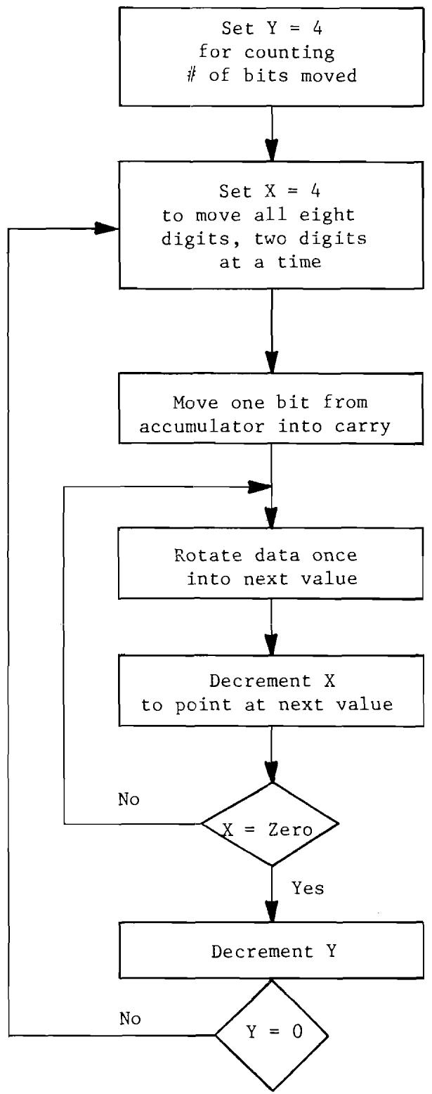
Flow Chart for Moving in a New BCD Number
FIGURE 10.1
| Before | After |
| Field | 00 | 00 |
| 00 | 01 |
| 17 | 72 |
| 29 | 95 |
| Accumulator | 50 | 00 |
Coding
| Bytes | Instruction |
| 2 | LDY 4 | set up for 4 moves |
| 2 | LOOP-2 | LDX 4 |
| 1 | ASLA | |
| 3 | LOOP-1 | ROL Price -1, X | |
| 1 | DEX | shift the field 1 bit |
| 2 | BNE | LOOP-1 | |
| 1 | DEY | shifts four times. |
| 2/14 | bytes | BNE | LOOP-2 |
There are several new concepts introduced in this example; the first is the use of index register Y as just a counter to count the number of times the character has been bit-shifted. It is a common approach to use bit shifts, as is implemented in the MCS650X family, to shift data into memory. The power of being able to communicate directly in memory is shown by shifting bits from one byte to the next byte using a single ROL indexed instruction. This example uses a loop within a loop and it should be noted that LOOP 1 occurs 4 times for every time LOOP 2 occurs. The internal loop is very important in the sense that this loop executes 16 times for the problem; therefore, its execution time should be optimized.
In addition to having the ability to shift and rotate memory, the MCS650X has the ability to increment and decrement memory locations.
10.7 INC - INIncrement MEMORY BY ONE
This instruction adds 1 to the contents of the addressed memory location.
The symbolic notation is M + l M
The increment memory instruction does not affect any internal registers and does not affect the carry or overflow flags. If bit 7 is on as the result of the increment, N is set, otherwise it is reset; if the increment causes the result to become 0, the Z flag is set on, otherwise it is reset.
The addressing modes for increment are: Zero Page; Zero Page, X; Absolute; Absolute, X.
10.8 DEC - DECREMENT MEMORY BY ONE
This instruction subtracts 1, in two's complement, from the contents of the addressed memory location.
Symbolic notation for this instruction is M - 1 M .
The decrement instruction does not affect any internal register in the microprocessor. It does not affect the carry or overflow flags. If bit 7 is on as a result of the decrement, then the N flag is set, otherwise it is reset. If the result of the decrement is 0, the Z flag is set, otherwise it is reset.
The addressing modes for decrement are: Zero Page; Zero Page, X; Absolute; Absolute, X.
In many examples through the report, we have used the ability to increment and decrement registers in the microprocessors. The advantages of incrementing and decrementing in memory are that it is possible to keep external counters or to directly influence a bit value by means of these instructions. It is sometimes useful during I/O instructions.
10.9 GENERAL NOTE ON READ/MODIFY/WRITE INSTRUCTIONS
The ability to read, modify and write memory is unique to MCS6500 class microprocessors. The usefulness of the instructions is limited only by the user's approach to organizing memory. Even though the instructions are fairly long in execution, they are significantly shorter than having to load and save other registers to perform the same function. Experience in organizing programs to take advantage of this manipulation of memory will allow the user to fully appreciate the power of these instructions.
CHAPTER 11 PERIPHERAL PROGRAMMING
11.0 REVIEW OF MCS6520 FOR I/O OPERATIONS
It should be noted that in the following discussions, the major difference between the MCS6530 I/O and the main register of the MCS6520 is that the extra bit in the control register need not be used in the MCS6530. All registers in the MCS6530 are directly addressable.
Example 11.1: The MCS6520 Register Map
| * = Base Address |
| PIAD | * = * + 1 |
| PIAC | * = * + 1 |
| PIBD | * = * + 1 |
| PIBC | * = * + 1 |
A SIDE
| A DATA DIRECT-
ION (AD) |
| A DATA (AD) |
| A CONTROL (AC) |
B SIDE
| B DATA DIRECT-
ION (BD) |
| B DATA (BD) |
| B CONTROL (BC) |
In Example 11.1 a programming form to describe the PIA is shown. The programming form is used in the Cross-Assembler and Resident Assembler with the MCS650X product family. The notation = is used to define any location. The notation means that the assembler instruct- ion counter is set equal to the value following the equal sign. The expression = * + 1 causes the assembler to recognize that there is one byte of memory associated with the term; therefore, we can see that the definition of the four registers PIAD, PIAC, PIBD and PIBC are consecutive memory locations starting at some base address, with
the first byte addressed as PIAD, the second byte addressed as PIAC, the third byte addressed as PIBD, and the fourth byte as PIBC. This is a normal way a MCS6520 would be organized and this is the way the programming form should be set up. The base address is picked up by an algorithm described in the hardware manual but normally it is a value between 4004 and 4080 Hex. Each MCS6520 is given a base address which works progressively up from 4004 Hex.
In Example 11.1 two registers are shown in dotted lines. This is because each of the A DATA (AD) and B DATA (BD) parts of the MCS6520 are actually two registers having the same address, one which specifies the direction of each of the input/output paths (the Data Direction Register), the second one which is actually the connection to the input/output paths (the Data Register). Because of pin limitations on the MCS6520, the microprocessor can only directly address one of the registers at a time. Differentiation as to which register is being connected to the microprocessor is a function of bit 2 in the respective control register (AC and BC). If bit 2 is off, the Data Direction Register is being addressed; if it is on, the Data Register is being addressed.
During the initialization sequence, therefore, the MCS6520 starts out with all registers at zero. This means that the microprocessor is addressing the Data Direction Register. The PIA initialization is done by writing the direction of the pins into the Data Direction Register (AD, BD) and then setting on the control flag as described below. After that, the program will normally be dealing with the data registers.
Example 11.2: General PIA Initialization
LDA # DIRECT
Initialize Direction
STA PIAD
Initialize Control
LDA # CONTR
STA PIAC
Example 11.2 illustrates a general form of initialization and can be completed for as many PIA's as there are in the system.
11.1 MCS6520 INTERRUPT CONTROL
The MCS6520 has a basic interrupt capability which is under control of the programmer. Almost all MCS6500 I/O devices that allow interrupts have an interrupt control register that allows the user to disable the interrupt. This will keep inputs which are not necessarily active from causing spurious interrupts which must be handled by the microprocessor. Examples of this are open tape loops or other signals which have high impedance noise sensitive inputs except when connected to some kind of media. In this type of application, normally the interrupt is enabled by some physical action from the person using the device such as loading of the cassette, pushing the power-on switch, etc. In the case of the MCS6520, there are two interrupt causing conditions for each control register.
Each of these interrupts concern themselves with one input pin. The Control Register allows the programmer to decide whether or not the pin is sensitive to positive edge signals or negative edge signals and whether or not an interrupt shall occur when the selected transition has occurred.
It should be noted that, therefore, it is possible for a line to cause a status bit to be set without causing an interrupt. The comprehensive I/O Program in Section 11.5 uses this combination.
Example 11.3: Interrupt Mode Setup
| Bit 7 Status Bit: | Bits 1 0 | Interrupt |
| Set on Negative Edge | 0 0 | No |
| Set on Negative Edge | 0 1 | Yes |
| Set on Positive Edge | 1 0 | No |
| Set on Positive Edge | 1 1 | Yes |
| Bit 6 Status Bit: | Bits 4 3* | Interrupt |
| Set on Negative Edge | 0 0 | No |
| Set on Negative Edge | 0 1 | Yes |
| Set on Positive Edge | 1 0 | No |
| Set on Positive Edge | 1 1 | Yes |
*if bit 5 equals zero
The proper combination of bits are usually determined during the design of the MCS6520 interconnection and form the constant which is loaded in the control register. The constant that is loaded in the control register should contain bit 2 on. For example, to allow bit 7 to be set on negative going signals with interrupt enable and bit 6 to be set on positive signals with interrupt disable, the control value would be Hex 15.
With bit 5 on, the pin that controls bit 6 can be set as an output pin. The output pin is either controllable by the microprocessor directly or acts as a handshake to reflect the status of reads and writes of the data register. The operation of the output pins CA2, CB2 depends on how bits 5, 4, and 3 are programmed, as shown in Example 11.4.
Example 11.4: CA2, CB2 Output Control
| CA2 Output With: | Bit 5 on |
| Bit 4 | Bit 3 |
| Low on read or write until bit 7 on | 0 | 0 |
| Low on read or write for one cycle | 0 | 1 |
| Always 0 | 1 | 0 |
| Always 1 | 1 | 1 |
The decision as to whether or not to use the one cycle low until bit 7 comes on is a hardware decision, depending on the device which is hooked to the pin.
It should be of interest to the programmer to note that bit 6 controls pins known as CA2 or CB2 which can be considered to be auxiliary outputs which are controlled by bit 3 assuming the processor is initialized so that bit 5 and bit 4 are ones.
Example 11.5 shows the use of controlling bit 3 using AND and OR instructions; however, it should be noted that this technique applies for any individual bit in the PIA data direction register also:
Example 11.5: Routine to Change CA2 or CB2 Using Bit 3 Control
Set CA2
LDA PIAC
ORA #\$08
STA PIAC
Clear CA2
LDA PIAC
AND #$F7
STA PIAC
Note: $ - Direction to Assembler for Hex Notation
- Direction toAssembler for Production Operator
By similar techniques, every pin in the microprocessors of the MCS6520 can be controlled. There are two particular notes to remember:
- In the MCS6520, both bit 6 and bit 7 are cleared on either side by reading of the corresponding data register if bit 6 has been set up as an input. This means that polling sequences for I/0 instructions should only read the status registers and then read the data registers after the status has been determined, otherwise false clearing of the status data may occur.
- Even though the handshake for the CB2 pin is on write of B data, a read of B data must be done to clear bit 7.
11.2 IMPLEMENTATION TRICKS FOR USE OF THE MCS6520 PERIPHERAL INTERFACE DEVICES
11.2.1 Shortcut Polling Sequences
In section 9.7, the techniques for using a LOAD A to poll for interrupts was covered; however, the I/O devices on the MCS6520 can either set bit 6 or bit 7 on to cause an interrupt; therefore, a different technique needs to be used to analyze the MCS6520 to, poll a series of 6520's each one of which could have caused the interrupt. It is for this purpose that the BIT instruction senses both bit 6 and bit 7. Coding for a full poll of a PIA is as shown:
Example 11.6: Polling the MCS6520
| Interrupt Vector | JMP STORE | |
| LDA #CO | Set up Mask for 6 and 7 |
| BIT PIAAC | Check for neither 6 or 7 |
| BEQ NXT1 | |
| BMI SEVEN | If 7, go to save-- |
| | otherwise clear |
| Process BIT | |
| 6 INTERRUPT | |
| NXTI | BIT PIABC | |
| BEQ NXTZ | |
| etc. | |
This program takes full advantage of the BIT instruction by checking for both bit 7 and 6 clear. BMI to SEVEN just checks N is on and that N is a higher priority. If bit 6 is one, the overflow bit will also be set, allowing the finish of the process seven routine to test the overflow and jump back to the process bit 6 coding.
Bit 6 and bit 7 were sampled by the single BIT instruction. Speed was accomplished by loading the mask for just bit 6 and 7 into the register which allows the BEQ instruction to determine that neither of the two flags is on.
This routine depends on the fact that in the MCS6520, if CA2 or CB2 is an output, bit 6 is always zero.
11.2.2 Bit Organization on MCS6520's
In the microprocessor, there is a definite positional preference for the testing of single bits. In the MCS6520 Data Direction Register, it is possible to select any combinations of input/output pins by the pattern that is loaded in the Data Direction Register. A one bit corresponds to an output and a zero bit corresponds to an input. The natural tendency would be to use MCS6520s with all eight bits organized into a byte. There is relatively little advantage to organizing this way unless the eight bits are to be treated as a single byte by the program. This is often not the case, more often the bits are a collection of switches, coils, lights, etc.
On such combinations, advantage should be taken of the fact that bit 7 is directly testable so that a more useful combination of eight pins on one MCS6520 register would be seven outputs and a single input with the single input on bit 7. This organization allows the programmer to load and branch on that location without ever having to perform a bit or shift instruction to isolate a particular bit.
A similar capability for setting a single bit involves the organization of data with seven inputs and a single output with a single output located in bit 0. This bit may be set or cleared by an INC or DEC instruction without affecting the rest of the bits in the register because the input pins ignore signals written from the microprocessor. Therefore, the more skilled MCS6500 programmer will often mix single outputs on bit 0 and a single input on bit 7 with bits of the corresponding opposite type.
11.2.3 Use of READ/MODIFY/WRITE Instruction For Keyboard Encoding
A rather unique use of the memory with a READ/MODIFY/WRITE operation involves setting the data register at all zeros, then using the three state output of the B side to sample a keyboard. The following Figure 11.1 shows the connection for a 64 key keyboard organized 8 × 8 :
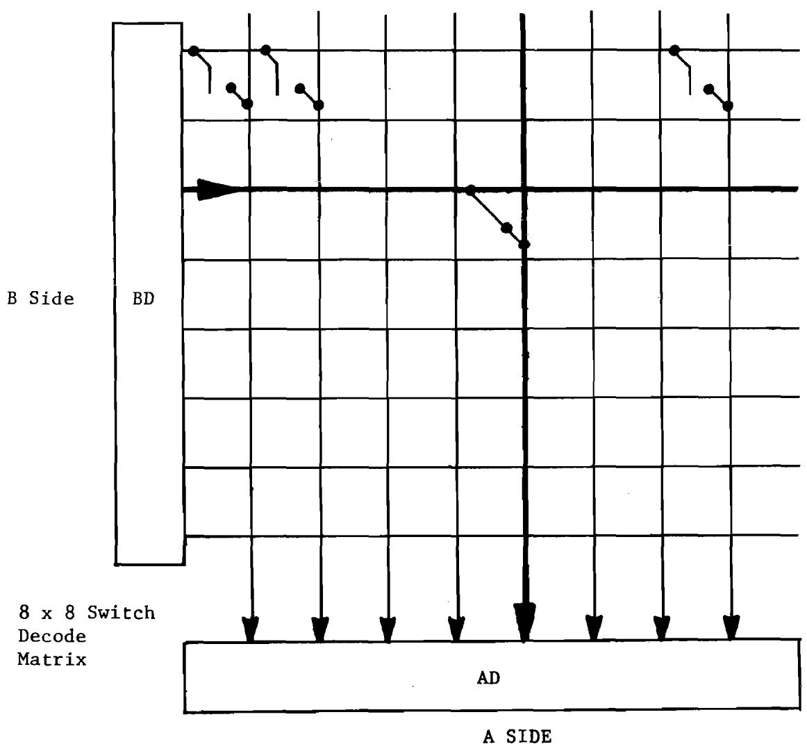
Keyboard Encoding Matrix Diagram
FIGURE 11.1
The B side is set up to act as a strobe so that each of the output lines will have a ground on it during one scan cycle. The eight A side data inputs are then sampled and decoded by the microprocessor giving a 64 key keyboard which is directly translatable into code.
Figure 11.1 and Example 11.7 make use of the capability of the microprocessor to move a bit through the MCS6520 register location. This program also uses the compare instruction and the ability to detect a carry during a shift.
Example 11.7: Coding for Strobing an 8 × 8 Keyboard
Output Strobe is indicated by a one in Data Director Register. Any connection is indicated by a zero in register bit.
| LDX #0
STX PIABD
LDA PIABC
AND #FB
STA PIABC
STX PIABC
SEC Set low end bit on |
| LOOP | ROL PIABD
BCS DONE
LDA PIAAD
CMP #FF
BEQ LOOP | Shift for Strobe
if all sampled, exit
Check for no zeros |
| DONE | ----- | If any zeros, then process them. |
A and PIABD can now be used to find out just what key is depressed.
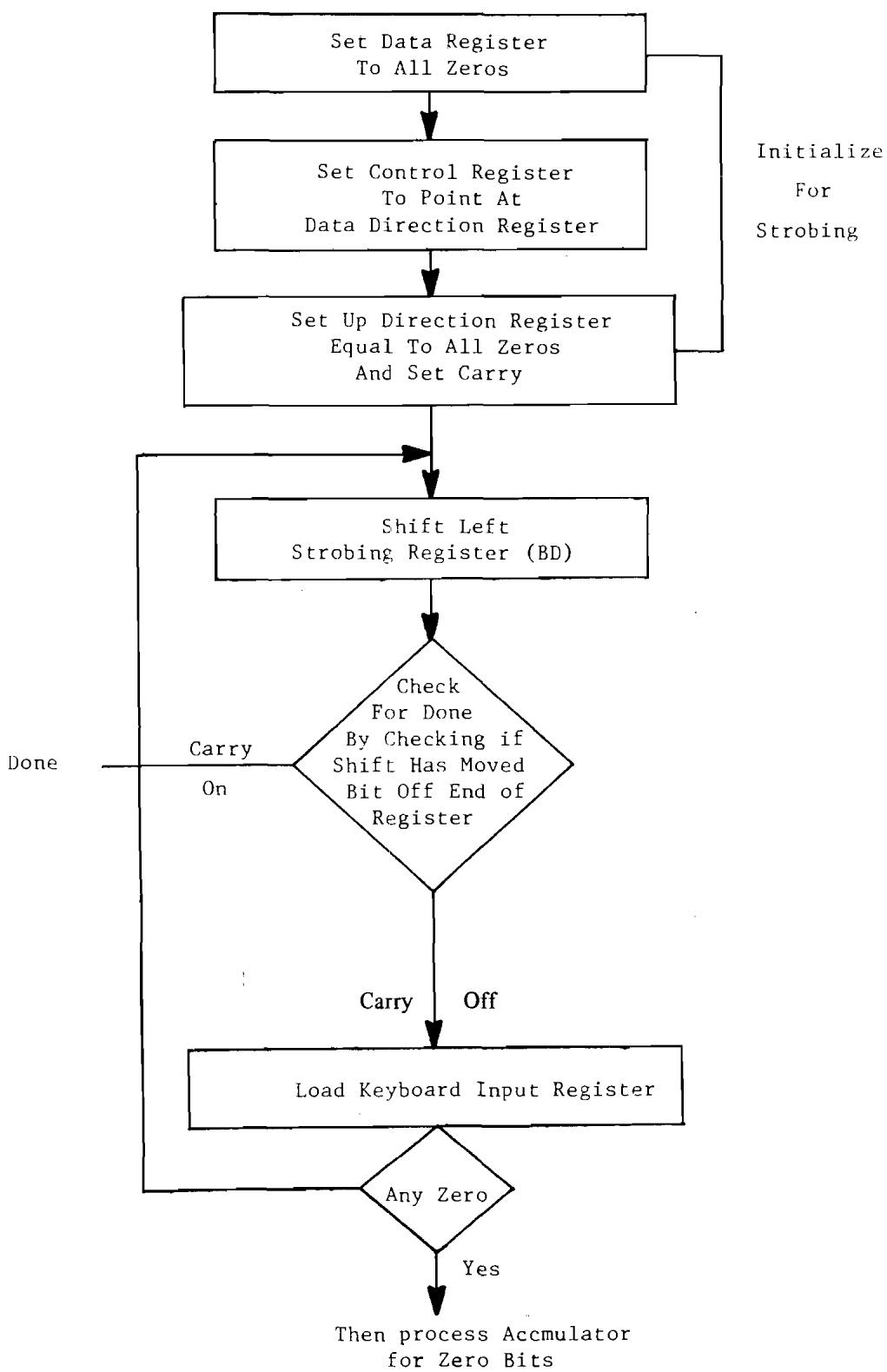
Keyboard Strobe Sequence
FIGURE 11.2
11.3 MCS6530 PROGRAMMING
Although they have separate addressing, the Data Direction and Input/Output Registers operate the same as on the MCS6520.
Programming of the Interval Timer has some special problems. First of all, the time is effectively located in all addresses from XXX4-XXXF. By picking the proper address, the programmer is able to control the P scale for the timeout. Initialization of the Interval Timer is done by a LOAD A followed by STORE A into the timing count. The value stored in the timing counter represents the number of states which the counter will count through. The address used to load will determine how many additional divisions of the basic clock cycle will be counted.
When the counter finally counts to zero, it continues to count past zero at the one cycle clock rate in order to give the user an opportunity to sample the Status Register, then come back and read the Count Register to determine how long it has been since an interrupt occurred.
Servicing an interrupt is the same for this Control Register as for any other interrupting register. Bit 7 is set on in the Status Register to indicate that the Interval Timer is in the interrupt state and bit 7 is reset by the reading of the Counter.
11.3.1 Reading of the Counter Register
Because of the nature of counting past zero, the number in the Count Register is in two's complement form. It can be added directly to and used to correct the next count in a sequential string of counts or for correction for one cycle accuracy.
11.4 HOW TO ORGANIZE TO IMPLEMENT CODING
The specific details of organizing to get coding assembled is a function of the software that is used to implement the coding. Two software programs are currently available for the MCS650X family.
The Cross Assembler is available on various time share systems or for batch use on the user's system. Its documentation is covered in
the Cross-Assembler Manual, publication number 6500-60. The Resident Assembler is available in the Microcomputer Development Terminal, as well as for sale in ROMs. The documentation for this is covered in the ResidentAssembler Manual, publication number 6500-65.
The major advantages of using an assembler are that the assembler takes mnemonics and labels and calculates the fixed code. Reference to the OP CODE tables in the appendix shows that coding in Hex is quite difficult because there is no ordered pattern to the instruction Hex codes.
The Cross Assembler or ResidentAssembler allows one to specify all inputs and outputs in symbolic form on a documented listing. Symbolic addressing is a technique which has the following advantages over numerical addressing:
-
It allows the user to postpone until the last minute actual memory allocation in a program which is being developed. In a microprocessor that has memory-oriented features such as Zero Page, memory management is important. It is desirable to have as many as possible of the read/write values in the Zero Page. However, until the coding is complete, the organization of Zero Page may be in doubt. Values which are originally assigned in Zero Page may not be as valuable there after some analysis of the coding either indicates that the applications of these values use indirect references or indexing by Y which does not allow the program to really take advantage of Zero Page locations whereas some other code which may not be as frequently used might still result in a code reduction by use of Zero Page. This allocation, if all the fields are defined symbolically, can be done on the final assembly without any changing in the user's codes.
-
Use of symbolic addresses for programming branches leads to a better documented program and as one soon determines calculation of relative branches is difficult and subject
to change any time a coding change is made. For example, if one has organized a program with a loop in which three or four branches all return to the same point and then discovers a programming error which requires a single instruction to be added between the return point and various branches, each branch would have to be edited and recalculated. The symbolic assembler accomplishes this automatically on the next assembly pass.
11.4.1 Label Standards
The MCS650X assemblers have been done on a reserve word basis in which the various mnemonics which have been described are always considered to be OP CODE mnemonics. If any three character fields exactly match a mnemonic then the assembler assumes that the field is an OP CODE and proceeds to evaluate the addressing. Any other label may be located in free form anywhere in the coding. This means that one should organize one's labels such that he never has a three character label which inadvertently might be considered an OP CODE. The easiest way to accomplish this is to always follow a pattern on labels.
Good programming practice requires that the user develop a systems flow chart for his own basic program and individual flow charts for subroutines before starting the coding. From the time the routine is flow charted, it is very easy for the user to then assign a mnemonic label to the basic subroutine.
In this text, notations like LOOP, LOOP 1, etc. are used. In an ADD, loop would be ADLP.
The MCS650X assembler allows six spaces for labels. It is good practice to use two characters to generally identify the subroutine, two more characters for mnemonic purposes and then a numbering system which allows correlation between various addresses within a LOOP within a subroutine. By strictly numbering such that ADLPl is different from ADLP3, each can be addresses within the same LOOP.

It is assumed that the PIA's are connected in the normal manner of Status Register Address equal to Data Register Address + 1.
The following table and flow chart defines the program implemented in the example.
Table #1 contains the address of all of the MCS6520 Status Registers.
Table #2 contains the address of the put-away location for the respective data.
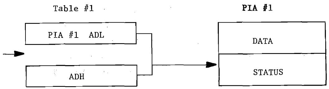
Using six character labels, there are a hundred combinations of code which could be used in a given routine or loop without the user having to think through the rest of mnemonic notation. The use of characters plus a numeric for all references is sound programming practice. The advantage of using this technique allows one to use three character mnemonics without ever interfering with the reserve word of the microprocessor OP CODE mnemonics because they never have a numeric in the mnemonic.
11.5 COMPREHENSIVE I/O PROGRAM
Figure 11.3 demonstrates the program flow in support of the Cross-Assembler listing (Example 11.9) of a time-sharing routine of a program which illustrates the use of the indexed indirect to perform a search of eight devices which have active signals for servicing. The implementation of the eight devices is done in MCS6520's where the MCS6520 status is set up to be a flag in bit 7 of a Control Register.

APPENDIX A
INSTRUCTION LIST
ALPHABETIC BY MNEMONIC
DEFINITION OF
INSTRUCTION GROUPS
| MCS6501-MCS6505 MICROPROCESSOR INSTRUCTION SET-ALPHABETIC SEQUENCE |
| ADC | Add Memory to Accumulator with Carry | JSR | Jump to New Location Saving Return Address |
| AND | "AND"Memory with Accumulator | | |
| ASL | Shift Left One Bit (Memory or Accumulator) | LDA | Load Accumulator with Memory |
| | LDX | Load Index X with Memory |
| BCC | Branch on Carry Clear | LDY | Load Index Y with Memory |
| BCS | Branch on Carry Set | LSR | Shift Right One Bit (Memory or Accumulator) |
| BEQ | Branch on Result Zero | | |
| BIT | Test Bits in Memory with Accumulator | NOP | No Operation |
| BMI | Branch on Result Minus | ORA | "OR"Memory with Accumulator |
| BNE | Branch on Result not Zero | | |
| BPL | Branch on Result Plus | PHA | Push Accumulator on Stack |
| BRK | Force Break | PHP | Push Processor Status on Stack |
| BVC | Branch on Overflow Clear | PLA | Pull Accumulator from Stack |
| BVS | Branch on Overflow Set | PLP | Pull Processor Status from Stack |
| CLC | Clear Carry Flag | ROL | Rotate One Bit Left (Memory or Accumulator) |
| CLD | Clear Decimal Mode | ROR | Rotate One Bit Right (Memory or Accumulator) |
| CLI | Clear Interrupt Disable Bit | RTI | Return from Interrupt |
| CLV | Clear Overflow Flag | RTS | Return from Subroutine |
| CMP | Compare Memory and Accumulator | | |
| CPX | Compare Memory and Index X | SBC | Subtract Memory from Accumulator with Borrow |
| CPY | Compare Memory and Index Y | SEC | Set Carry Flag |
| | SED | Set Decimal Mode |
| DEC | Decrement Memory by One | SEI | Set Interrupt Disable Status |
| DEX | Decrement Index X by One | STA | Store Accumulator in Memory |
| DEY | Decrement Index Y by One | STX | Store Index X in Memory |
| | STY | Store Index Y in Memory |
| EOR | "Exclusive-Or"Memory with Accumulator | | |
| | TAX | Transfer Accumulator to Index X |
| INC | Increment Memory by One | TAY | Transfer Accumulator to Index Y |
| INX | Increment Index X by One | TSX | Transfer Stack Pointer to Index X |
| INY | Increment Index Y by One | TXA | Transfer Index X to Accumulator |
| | TXS | Transfer Index X to Stack Pointer |
| JMP | Jump to New Location | TYA | Transfer Index Y to Accumulator |
A.1 INTRODUCTION
The microprocessor instruction set is divided into three basic groups. The first group has the greatest addressing flexibility and consists of the most general purpose instructions such as Load, Add, Store, etc. The second group includes the Read, Modify, Write instructions such as Shift, Increment, Decrement and the Register X movement instructions. The third group contains all the remaining instructions, including all stack operations, the register Y, compares for X and Y and instructions which do not fit naturally into Group One or Group Two.
There are eight Group One instructions, eight Group Two instructions, and all of the 39 remaining instructions are Group Three instructions.
The three groups are obtained by organizing the OP CODE pattern to give maximum addressing flexibility (16 addressing combinations) to Group One, to give eight combinations to Group Two instructions and the Group Three instructions are basically individually decoded.
A.2 GROUP ONE INSTRUCTIONS
These instructions are: Add With Carry (ADC), (AND), Compare (CMP), Exclusive Or (EOR), Load A (LDA), Or (ORA), Subtract With Carry (SBC), and Store A (STA). Each of these instructions has a potential for 16 addressing modes. However, in the MCS6501 through MCS6505, only eight of the available modes have been used.
Addressing modes for Group One are: Immediate, Zero Page, Zero Page Indexed by X, Absolute, Absolute Indexed by X, Absolute Indexed by Y, Indexed Indirect, Indirect Indexed. The unused eight addressing modes are to be used in future versions of the MCS650X product family to allow addressing of additional on-chip registers, of on-chip I/O ports, and to allow two byte word processing.
A.3 GROUP TWO INSTRUCTIONS
Group Two instructions are primarily Read, Modify, Write instructions. There are really two subcategories within the Group Two instructions. The components of the first group are shift and rotate instructions and are: Shift Right (LSR), Shift Left (ASL), Rotate Left (ROL), and Rotate Right (ROR).
The second subgroup includes the Increment (INC) and Decrement (DEC) instructions and the two index register X instructions, Load X (LDX) and Store X (STX). These instructions would normally have eight addressing modes available to them because of the bit pattern. However, to allow for upward expansion, only the following addressing modes have been defined: Zero Page, Zero Page Indexed by X, Absolute, Absolute Indexed by X, and a special Accumulator (or Register) mode. The four shift instructions all have register A operations; the incremented or decremented Load X and Store X instructions also have accumulator modes although the Increment and Decrement Accumulator has been reserved for other purposes. Load X from A has been assigned its own mnemonic, TAX. Also included in this group are the special functions of Decrement X which is one of the special cases of Store X. Included also in this group in the X decodes are the TXS and TSX instructions.
All Group One instructions have all addressing modes available to each instruction. In the case of Group Two instructions, another addressing mode has been added; that of the accumulator and the other special decodes have also been implemented in this basic group. However, the primary function of Group Two instructions is to perform some memory operation using the appropriate index.
It should be noted for documentation purposes that the X instructions have a special mode of addressing in which register Y is used for all indexing operations; thus, instead of Zero Page Indexed by X, X instructions have Zero Page Indexed by Y, and instead of having Absolute Indexed by X, X instructions have Absolute Indexed by Y.
A.4 GROUP THREE INSTRUCTIONS
There are really two major classifications of Group Three instructions; the modify Y register instructions, Load Y (LDY), Store Y (STY), Compare Y (CPY), and Compare X (CPX), instructions actually occupy about half of the OP CODE space for the Group Three instructions. Increment X (INX) and Increment Y (INY) are special subsets of the Compare X and Compare Y instructions and all of the branch instructions are in the Group Three instructions.
Instructions in this group consist of all of the branches: BCC, BCS, BEQ, BMI, BNE, BPL, BPC and BPS. All of the flag operations are also devoted to one addressing mode; they are: CLC, SEC, CLD, SED, CLI, SEI and CLV. All of the push and pull instructions and stack operation instructions are Group Three instructions. These include: BRK, JSR, PHA, PHP, PLA and PLP. The JMP and BIT instructions are also included in this group. There is no common addressing mode available to members of this group. Load Y, Store Y, BIT, Compare X and Compare Y have Zero Page and Absolute, and all of the Y and X instructions allow Zero Page Indexed operations and Immediate.
APPENDIX B
INSTRUCTION LIST
ALPHABETIC BY MNEMONIC
WITH OP CODES, EXECUTION CYCLES
AND MEMORY REQUIREMENTS
The following notation applies to this summary:
| A | Accumulator |
| X, Y | Index Registers |
| M | Memory |
| P | Processor Status Register |
| S | Stack Pointer |
| ✓ | Change |
| - | No Change |
| + | Add |
| ^ | Logical AND |
| - | Subtract |
| ¥ | Logical Exclusive Or |
| ↑ | Transfer from Stack |
| ↓ | Transfer to Stack |
| → | Transfer to |
| ← | Transfer to |
| V | Logical OR |
| PC | Program Counter |
| PCH | Program Counter High |
| PCL | Program Counter Low |
| OPER | OPERAND |
| # | IMMEDIATE ADDRESSING MODE |
Note: At the top of each table is located in parentheses a reference number (Ref: XX) which directs the user to that Section in the MCS6500 Microcomputer Family Programming Manual in which the instruction is defined and discussed.
Operation: A + M + C A, C
N Z C I D V
√√√--√
(Ref: 2.2.1)
| Addressing Mode | Assembly Language Form | OP CODE | No. Bytes | No. Cycles |
| Immediate | ADC | # Oper | 69 | 2 | 2 |
| Zero Page | ADC | Oper | 65 | 2 | 3 |
| Zero Page, X | ADC | Oper, X | 75 | 2 | 4 |
| Absolute | ADC | Oper | 6D | 3 | 4 |
| Absolute, X | ADC | Oper, X | 7D | 3 | 4* |
| Absolute, Y | ADC | Oper, Y | 79 | 3 | 4* |
| (Indirect, X) | ADC | (Oper, X) | 61 | 2 | 6 |
| (Indirect), Y | ADC | (Oper), Y | 71 | 2 | 5* |
- Add 1 if page boundary is crossed.
AND
"AND" memory with accumulator
AND
Logical AND to the accumulator
Operation: A M A
N Z C I D V
(Ref: 2.2.3.0)
√√--
| Addressing Mode | Assembly Language Form | OP CODE | No. Bytes | No. Cycles |
| Immediate | AND | # Oper | 29 | 2 | 2 |
| Zero Page | AND | Oper | 25 | 2 | 3 |
| Zero Page, X | AND | Oper, X | 35 | 2 | 4 |
| Absolute | AND | Oper | 2D | 3 | 4 |
| Absolute, X | AND | Oper, X | 3D | 3 | 4* |
| Absolute, Y | AND | Oper, Y | 39 | 3 | 4* |
| (Indirect, X) | AND | (Oper, X) | 21 | 2 | 6 |
| (Indirect), Y | AND | (Oper), Y | 31 | 2 | 5 |
* Add 1 if page boundary is crossed.
Operation: C 7 6 5 4 3 2 1 .
N Z C I D V
√√√---
(Ref: 10.2)
| Addressing Mode | Assembly Language Form | OP CODE | No. Bytes | No. Cycles |
| Accumulator | ASL A | ØA | 1 | 2 |
| Zero Page | ASL Oper | Ø6 | 2 | 5 |
| Zero Page, X | ASL Oper, X | 16 | 2 | 6 |
| Absolute | ASL Oper | ØE | 3 | 6 |
| Absolute, X | ASL Oper, X | 1E | 3 | 7 |
BCC
BCC Branch on Carry Clear
BCC
Operation: Branch on C =
N Z C I D V
(Ref: 4.1.1.3)
| Addressing Mode | Assembly Language Form | OP CODE | No. Bytes | No. Cycles |
| Relative | BCC Oper | 90 | 2 | 2* |
- Add 1 if branch occurs to same page.
- Add 2 if branch occurs to different page.
Operation: Branch on C = 1
N Z C I D V
(Ref: 4.1.1.4)
| Addressing Mode | Assembly Language Form | OP CODE | No. Bytes | No. Cycles |
| Relative | BCS Oper | B∅ | 2 | 2* |
- Add 1 if branch occurs to same page.
- Add 2 if branch occurs to next page.
BEQ
Operation: Branch on = 1
BEQ Branch on result zero
(Ref: 4.1.1.5)
N Z C I D V
| Addressing Mode | Assembly Language Form | OP CODE | No. Bytes | No. Cycles |
| Relative | BEQ Oper | FØ | 2 | 2* |
- Add 1 if branch occurs to same page.
- Add 2 if branch occurs to next page.
Operation: A ∧ M, M7 → N, M6 → V
Bit 6 and 7 are transferred to the status register. N Z C I D V If the result of A∧M is zero then Z = 1 , otherwise M_7 - - - M_6
$$
z = \emptyset
$$
(Ref: 4.2.1.1)
| Addressing Mode | Assembly Language Form | OP CODE | No. Bytes | No. Cycles |
| Zero Page | BIT Oper | 24 | 2 | 3 |
| Absolute | BIT Oper | 2C | 3 | 4 |
BMI
BMI Branch on result minus
BMI
Operation: Branch on N = 1
N Z C I D V
(Ref: 4.1.1.1)
| Addressing Mode | Assembly Language Form | OP CODE | No. Bytes | No. Cycles |
| Relative | BMI Oper | 30 | 2 | 2* |
- Add 1 if branch occurs to same page.
- Add 2 if branch occurs to different page.
Operation: Branch on Z = 0
N Z C I D V
(Ref: 4.1.1.6)
| Addressing Mode | Assembly Language Form | OP CODE | No. Bytes | No. Cycles |
| Relative | BNE Oper | D∅ | 2 | 2* |
- Add 1 if branch occurs to same page.
- Add 2 if branch occurs to different page.
BPL
BPL Branch on result plus
BPL
Operation: Branch on N =
N Z C I D V
(Ref: 4.1.1.2)
| Addressing Mode | Assembly Language Form | OP CODE | No. Bytes | No. Cycles |
| Relative | BPL Oper | 1∅ | 2 | 2* |
- Add 1 if branch occurs to same page.
- Add 2 if branch occurs to different page.
BRK
BRK Force Break
Operation: Forced Interrupt PC + 2 ↓ P ↓
N Z C I D V
(Ref: 9.11)
| Addressing Mode | Assembly Form | Language | OP CODE | No. Bytes | No. Cycles |
| Implied | BRK | ∅∅ | 1 | 7 | |
- A BRK command cannot be masked by setting I.
BVC
BVC Branch on overflow clear
Operation: Branch on V = 0
N Z C I D V
(Ref: 4.1.1.8)
| Addressing Mode | Assembly Language Form | OP CODE | No. Bytes | No. Cycles |
| Relative | BVC Oper | 5∅ | 2 | 2* |
- Add 1 if branch occurs to same page.
- Add 2 if branch occurs to different page.
BVS
Operation: Branch on V = 1
BVS Branch on overflow set
BVS
N Z C I D V
(Ref: 4.1.1.7)
| Addressing Mode | Assembly Language Form | OP CODE | No. Bytes | No. Cycles |
| Relative | BVS Oper | 7∅ | 2 | 2* |
- Add 1 if branch occurs to same page.
- Add 2 if branch occurs to different page.
CLC
Operation: C
CLC Clear carry flag
CLC
N Z C I D V
--0--
(Ref: 3.0.2)
| Addressing Mode | Assembly Language Form | OP CODE | No. Bytes | No. Cycles |
| Implied | CLC | 18 | 1 | 2 |
CLD
Operation: D
CLD Clear decimal mode
$$
\texttt {N Z C I D V}
$$
$$
- - - - \varnothing -
$$
(Ref: 3.3.2)
| Addressing Mode | Assembly Language Form | OP CODE | No. Bytes | No. Cycles |
| Implied | CLD | D8 | 1 | 2 |
CL
Operation: I
CLI Clear interrupt disable bit
$$
\texttt {N Z C I D V}
$$
(Ref: 3.2.2)
$$
- - - \varnothing - -
$$
| Addressing Mode | Assembly Language Form | OP CODE | No. Bytes | No. Cycles |
| Implied | CLI | 58 | 1 | 2 |
CLV
Operation: V
CLV Clear overflow flag
N Z C I D V
一 一 一 一 0
(Ref: 3.6.1)
| Addressing Mode | Assembly Language Form | OP CODE | No. Bytes | No. Cycles |
| Implied | CLV | B8 | 1 | 2 |
CMP
Operation: A - M
CMP Compare memory and accumulator
N Z C I D V
√√√---
(Ref: 4.2.1)
| Addressing Mode | Assembly Language Form | OP CODE | No. Bytes | No. Cycles |
| Immediate | CMP #Oper | C9 | 2 | 2 |
| Zero Page | CMP Oper | C5 | 2 | 3 |
| Zero Page, X | CMP Oper, X | D5 | 2 | 4 |
| Absolute | CMP Oper | CD | 3 | 4 |
| Absolute, X | CMP Oper, X | DD | 3 | 4* |
| Absolute, Y | CMP Oper, Y | D9 | 3 | 4* |
| (Indirect, X) | CMP (Oper, X) | C1 | 2 | 6 |
| (Indirect), Y | CMP (Oper), Y | D1 | 2 | 5* |
- Add 1 if page boundary is crossed.
(Ref: 7.8)
| Addressing Mode | Assembly Language Form | OP CODE | No. Bytes | No. Cycles |
| Immediate | CPX # Oper | E0 | 2 | 2 |
| Zero Page | CPX Oper | E4 | 2 | 3 |
| Absolute | CPX Oper | EC | 3 | 4 |
CPY
CPY Compare memory and index Y
CPY
Operation: Y - M
N Z C I D V
√√√--
(Ref: 7.9)
| Addressing Mode | Assembly Language Form | OP CODE | No. Bytes | No. Cycles |
| Immediate | CPY # Oper | C∅ | 2 | 2 |
| Zero Page | CPY Oper | C4 | 2 | 3 |
| Absolute | CPY Oper | CC | 3 | 4 |
DEC
DEC Decrement memory by one
DEC
Operation: M - 1 → M
N Z C I D V
√---
(Ref: 10.7)
| Addressing Mode | Assembly Language Form | OP CODE | No. Bytes | No. Cycles |
| Zero Page | DEC Oper | C6 | 2 | 5 |
| Zero Page, X | DEC Oper, X | D6 | 2 | 6 |
| Absolute | DEC Oper | CE | 3 | 6 |
| Absolute, X | DEC Oper, X | DE | 3 | 7 |
DEX
DEX Decrement index X by one
DEX
Operation: X - 1 → X
N Z C I D V
(Ref: 7.6)
√√---
| Addressing Mode | Assembly Language Form | OP CODE | No. Bytes | No. Cycles |
| Implied | DEX | CA | 1 | 2 |
Operation: Y - 1 Y
N Z C I D V
$$
\sqrt {} \sqrt {} - - - -
$$
(Ref: 7.7)
| Addressing Mode | Assembly Language Form | OP CODE | No. Bytes | No. Cycles |
| Implied | DEY | 88 | 1 | 2 |
EOR
EOR "Exclusive-Or" memory with accumulator
EOR
Operation: A
N Z C I D V
(Ref: 2.2.3.2)
$$
\sqrt {1} - \dots -
$$
| Addressing Mode | Assembly Language Form | OP CODE | No. Bytes | No. Cycles |
| Immediate | EOR #Oper | 49 | 2 | 2 |
| Zero Page | EOR Oper | 45 | 2 | 3 |
| Zero Page, X | EOR Oper, X | 55 | 2 | 4 |
| Absolute | EOR Oper | 4D | 3 | 4 |
| Absolute, X | EOR Oper, X | 5D | 3 | 4* |
| Absolute, Y | EOR Oper, Y | 59 | 3 | 4* |
| (Indirect, X) | EOR (Oper, X) | 41 | 2 | 6 |
| (Indirect), Y | EOR (Oper), Y | 51 | 2 | 5* |
- Add 1 if page boundary is crossed.
Operation: M + 1 M
N Z C I D V
√√---
(Ref: 10.6)
| Addressing Mode | Assembly Language Form | OP CODE | No. Bytes | No. Cycles |
| Zero Page | INC Oper | E6 | 2 | 5 |
| Zero Page, X | INC Oper, X | F6 | 2 | 6 |
| Absolute | INC Oper | EE | 3 | 6 |
| Absolute, X | INC Oper, X | FE | 3 | 7 |
INX
INX Increment Index X by one
INX
Operation: X + 1 X
N Z C I D V
√√--
(Ref: 7.4)
| Addressing Mode | Assembly Language Form | OP CODE | No. Bytes | No. Cycles |
| Implied | INX | E8 | 1 | 2 |
(Ref: 7.5)
| Addressing Mode | Assembly Language Form | OP CODE | No. Bytes | No. Cycles |
| Implied | INY | C8 | 1 | 2 |

JMP Jump to new location
(Ref: 4.0.2)
(Ref: 9.8.1)

| Addressing Mode | Assembly Language Form | OP CODE | No. Bytes | No. Cycles |
| Absolute | JMP Oper | 4C | 3 | 3 |
| Indirect | JMP (Oper) | 6C | 3 | 5 |
JSR
JSR Jump to new location saving return address
JSR
Operation: PC + 2 , (PC + 1) PCL
N Z C I D V
(PC + 2) PCH
(Ref: 8.1)
| Addressing Mode | Assembly Language Form | OP CODE | No. Bytes | No. Cycles |
| Absolute | JSR Oper | 20 | 3 | 6 |
LDA
LDA Load accumulator with memory
LDA
Operation: M → A
N Z C I D V
√√---
(Ref: 2.1.1)
| Addressing Mode | Assembly Language Form | OP CODE | No. Bytes | No. Cycles |
| Immediate | LDA # Oper | A9 | 2 | 2 |
| Zero Page | LDA Oper | A5 | 2 | 3 |
| Zero Page, X | LDA Oper, X | B5 | 2 | 4 |
| Absolute | LDA Oper | AD | 3 | 4 |
| Absolute, X | LDA Oper, X | BD | 3 | 4* |
| Absolute, Y | LDA Oper, Y | B9 | 3 | 4* |
| (Indirect, X) | LDA (Oper, X) | A1 | 2 | 6 |
| (Indirect), Y | LDA (Oper), Y | B1 | 2 | 5* |
- Add 1 if page boundary is crossed.
LDX
Operation: M X
LDX Load index X with memory
LDX
N Z C I D V
√√- - - -
(Ref: 7.0)
| Addressing Mode | Assembly Language Form | OP CODE | No. Bytes | No. Cycles |
| Immediate | LDX # Oper | A2 | 2 | 2 |
| Zero Page | LDX Oper | A6 | 2 | 3 |
| Zero Page, Y | LDX Oper, Y | B6 | 2 | 4 |
| Absolute | LDX Oper | AE | 3 | 4 |
| Absolute, Y | LDX Oper, Y | BE | 3 | 4* |
- Add 1 when page boundary is crossed.
LDY
Operation: M Y
LDY Load index Y with memory
LDY
N Z C I D V
√√---
(Ref: 7.1)
| Addressing Mode | Assembly Language Form | OP CODE | No. Bytes | No. Cycles |
| Immediate | LDY #Oper | A0 | 2 | 2 |
| Zero Page | LDY Oper | A4 | 2 | 3 |
| Zero Page, X | LDY Oper, X | B4 | 2 | 4 |
| Absolute | LDY Oper | AC | 3 | 4 |
| Absolute, X | LDY Oper, X | BC | 3 | 4* |
- Add 1 when page boundary is crossed.
Operation: 7 6 5 4 3 2 1 0 → C
N Z C I D V
0√√--
(Ref: 10.1)
| Addressing Mode | Assembly Language Form | OP CODE | No. Bytes | No. Cycles |
| Accumulator | LSR A | 4A | 1 | 2 |
| Zero Page | LSR Oper | 46 | 2 | 5 |
| Zero Page, X | LSR Oper, X | 56 | 2 | 6 |
| Absolute | LSR Oper | 4E | 3 | 6 |
| Absolute, X | LSR Oper, X | 5E | 3 | 7 |
NOP
NOP No operation
NOP
Operation: No Operation (2 cycles)
N Z C I D V
| Addressing Mode | Assembly Language Form | OP CODE | No. Bytes | No. Cycles |
| Implied | NOP | EA | 1 | 2 |
ORA
ORA "OR" memory with accumulator
ORA
Operation: A V M A
N Z C I D V
(Ref: 2.2.3.1)
√√---
| Addressing Mode | Assembly Language Form | OP CODE | No. Bytes | No. Cycles |
| Immediate | ORA #Oper | ∅9 | 2 | 2 |
| Zero Page | ORA Oper | ∅5 | 2 | 3 |
| Zero Page, X | ORA Oper, X | 15 | 2 | 4 |
| Absolute | ORA Oper | ∅D | 3 | 4 |
| Absolute, X | ORA Oper, X | 1D | 3 | 4* |
| Absolute, Y | ORA Oper, Y | 19 | 3 | 4* |
| (Indirect, X) | ORA (Oper, X) | ∅1 | 2 | 6 |
| (Indirect), Y | ORA (Oper), Y | 11 | 2 | 5 |
*Add1onpagecrossing
PHA
PHA Push accumulator on stack
PHA
Operation: A
N Z C I D V
(Ref: 8.5)
| Addressing Mode | Assembly Language Form | OP CODE | No. Bytes | No. Cycles |
| Implied | PHA | 48 | 1 | 3 |
(Ref: 8.11)
N Z C I D V
| Addressing Mode | Assembly Language Form | OP CODE | No. Bytes | No. Cycles |
| Implied | PHP | ∅8 | 1 | 3 |
PLA
Operation: A ↑
PLA Pull accumulator from stack
PLA
N Z C I D V
$$
\sqrt {} \sqrt {} - - - -
$$
(Ref: 8.6)
| Addressing Mode | Assembly Language Form | OP CODE | No. Bytes | No. Cycles |
| Implied | PLA | 68 | 1 | 4 |
(Ref: 8.12)
| Addressing Mode | Assembly Language Form | OP CODE | No. Bytes | No. Cycles |
| Implied | PLP | 28 | 1 | 4 |
ROL
ROL Rotate one bit left (memory or accumulator)
ROL
M or A 76543210 C
(Ref: 10.3)
| Addressing Mode | Assembly Language Form | OP CODE | No. Bytes | No. Cycles |
| Accumulator | ROL A | 2A | 1 | 2 |
| Zero Page | ROL Oper | 26 | 2 | 5 |
| Zero Page, X | ROL Oper, X | 36 | 2 | 6 |
| Absolute | ROL Oper | 2E | 3 | 6 |
| Absolute, X | ROL Oper, X | 3E | 3 | 7 |
Operation:
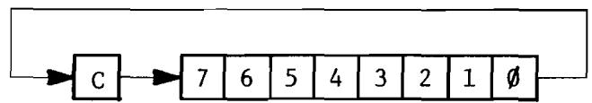
(Ref: 10.4)
N Z C I D V
√√√- - -
| Addressing Mode | Assembly Language Form | OP CODE | No. Bytes | No. Cycles |
| Accumulator | ROR A | 6A | 1 | 2 |
| Zero Page | ROR Oper | 66 | 2 | 5 |
| Zero Page,X | ROR Oper,X | 76 | 2 | 6 |
| Absolute | ROR Oper | 6E | 3 | 6 |
| Absolute,X | ROR Oper,X | 7E | 3 | 7 |
Note: ROR instruction will be available on MCS650X microprocessors after June, 1976.
RTI
RTI Return from interrupt
RTI
Operation: PC
N Z C I D V
From Stack
(Ref: 9.6)
| Addressing Mode | Assembly Language Form | OP CODE | No. Bytes | No. Cycles |
| Implied | RTI | 40' | 1 | 6 |
RTS
RTS Return from subroutine
RTS
Operation: PC+, PC + 1 → PC
N Z C I D V
(Ref: 8.2)
| Addressing Mode | Assembly Language Form | OP CODE | No. Bytes | No. Cycles |
| Implied | RTS | 6∅ | 1 | 6 |
Operation: A - M - C A
N Z C I D V
Note: = Borrow
(Ref: 2.2.2)
√√√--√
| Addressing Mode | Assembly Language Form | OP CODE | No. Bytes | No. Cycles |
| Immediate | SBC # Oper | E9 | 2 | 2 |
| Zero Page | SBC Oper | E5 | 2 | 3 |
| Zero Page, X | SBC Oper, X | F5 | 2 | 4 |
| Absolute | SBC Oper | ED | 3 | 4 |
| Absolute, X | SBC Oper, X | FD | 3 | 4* |
| Absolute, Y | SBC Oper, Y | F9 | 3 | 4* |
| (Indirect, X) | SBC (Oper, X) | E1 | 2 | 6 |
| (Indirect), Y | SBC (Oper), Y | F1 | 2 | 5* |
- Add 1 when page boundary is crossed.
SEC
SEC Set carry flag
SEC
Operation: 1 C
N Z C I D V
(Ref: 3.0.1)
--1--
| Addressing Mode | Assembly Language Form | OP CODE | No. Bytes | No. Cycles |
| Implied | SEC | 38 | 1 | 2 |
SED
Operation: 1 D
SED Set decimal mode
SED
N Z C I D V
--1
(Ref: 3.3.1)
| Addressing Mode | Assembly Language Form | OP CODE | No. Bytes | No. Cycles |
| Implied | SED | F8 | 1 | 2 |
SEI
Operation: 1 I
SEI Set interrupt disable status
SEI
N Z C I D V
$$
- - - 1 - -
$$
(Ref: 3.2.1)
| Addressing Mode | Assembly Language Form | OP CODE | No. Bytes | No. Cycles |
| Implied | SEI | 78 | 1 | 2 |
STA
Operation: A → M
STA Store accumulator in memory
N Z C I D V
(Ref: 2.1.2)
| Addressing Mode | Assembly Language Form | OP CODE | No. Bytes | No. Cycles |
| Zero Page | STA Oper | 85 | 2 | 3 |
| Zero Page, X | STA Oper, X | 95 | 2 | 4 |
| Absolute | STA Oper | 8D | 3 | 4 |
| Absolute, X | STA Oper, X | 9D | 3 | 5 |
| Absolute, Y | STA Oper, Y | 99 | 3 | 5 |
| (Indirect, X) | STA (Oper, X) | 81 | 2 | 6 |
| (Indirect), Y | STA (Oper), Y | 91 | 2 | 6 |
STX
Operation: X M
STX Store index X in memory
N Z C I D V
(Ref: 7.2)
STX
| Addressing Mode | Assembly Language Form | OP CODE | No. Bytes | No. Cycles |
| Zero Page | STX Oper | 86 | 2 | 3 |
| Zero Page, Y | STX Oper, Y | 96 | 2 | 4 |
| Absolute | STX Oper | 8E | 3 | 4 |
STY
Operation: Y M
STY Store index Y in memory
N Z C I D V
STY
(Ref: 7.3)
| Addressing Mode | Assembly Language Form | OP CODE | No. Bytes | No. Cycles |
| Zero Page | STY Oper | 84 | 2 | 3 |
| Zero Page, X | STY Oper, X | 94 | 2 | 4 |
| Absolute | STY Oper | 8C | 3 | 4 |
TAX
Operation: A X
TAX Transfer accumulator to index X
TAX
N Z C I D V
$$
\sqrt {v} - - - -
$$
(Ref: 7.11)
| Addressing Mode | Assembly Language Form | OP CODE | No. Bytes | No. Cycles |
| Implied | TAX | AA | 1 | 2 |
TAY
Operation: A Y
TAY Transfer accumulator to index Y
N Z C I D V
√√--
(Ref: 7.13)
| Addressing Mode | Assembly Language Form | OP CODE | No. Bytes | No. Cycles |
| Implied | TAY | A8 | 1 | 2 |
TYA
Operation: Y A
TYA Transfer index Y to accumulator
N Z C I D V
√√---
(Ref: 7.14)
| Addressing Mode | Assembly Language Form | OP CODE | No. Bytes | No. Cycles |
| Implied | TYA | 98 | 1 | 2 |
TSX
TSX Transfer stack pointer to index X
TSX
Operation: S X
N Z C I D V
(Ref: 8.9)
√√---
| Addressing Mode | Assembly Language Form | OP CODE | No. Bytes | No. Cycles |
| Implied | TSX | BA | 1 | 2 |
TXA
Operation: X A
TXA Transfer index X to accumulator
TXA
N Z C I D V
(Ref: 7.12)
√√---
| Addressing Mode | Assembly Language Form | OP CODE | No. Bytes | No. Cycles |
| Implied | TXA | 8A | 1 | 2 |
TXS
TXS Transfer index X to stack pointer
TXS
Operation: X S
N Z C I D V
(Ref: 8.8)
| Addressing Mode | Assembly Language Form | OP CODE | No. Bytes | No. Cycles |
| Implied | TXS | 9A | 1 | 2 |
APPENDIX C
INSTRUCTION ADDRESSING
MODES AND
INSTRUCTION ADDRESSING MODES AND RELATED EXECUTION TIMES (in clock cycles)
| Accumulator |
| Immediate | Zero Page | Zero Page, X | Zero Page, Y | Absolute | Absolute, X | Absolute, Y | Implied | Relative | (Indirect, X) | (Indirect, Y) |
| 2 | 2 | 3 | 4 | 4 | 4* | 4* | 4* | 2 | 6 | 5* | 6 |
| 2 | 3 | 4 | 4 | 4* | 4* | 4* | 3 | 6 | 5* | 6 |
| 2 | 2 | 3 | 4 | 4 | 4* | 4* | 4* | 3 | 6 | 5* | 6 |
| 2 | 3 | 4 | 4 | 4* | 4* | 4* | 3 | 6 | 5* | 6 |
| 2 | 2 | 5 | 6 | 6 | 7 | 7 | 7 | 6 | 6 | 5* | 6 |
| 2 | 5 | 6 | 6 | 7 | 7 | 7 | 6 | 6 | 5* | 6 |
| 2 | 2 | 3 | 4 | 4 | 4* | 4* | 4* | 2 | 6 | 5* | 6 |
| 2 | 3 | 4 | 4 | 5 | 5 | 5 | 2 | 6 | 6 | 6 |
| 2 | 2 | 3 | 4 | 4 | 5 | 5 | 5 | 2 | 6 | 6 | 6 |
| 2 | 3 | 4 | 4 | 5 | 5 | 5 | 2 | 6 | 6 | 6 |
| 2 | 2 | 3 | 4 | 4 | 5 | 5 | 5 | 2 | 6 | 6 | 6 |
| 2 | 3 | 4 | 4 | 5 | 5 | 5 | 2 | 6 | 6 | 6 |
| 2 | 2 | 3 | 4 | 4 | 5 | 5 | 5 | 2 | 5 | 5* | 6 |
| 2 | 3 | 4 | 4 | 5 | 5 | 5 | 2 | 6 | 6 | 6 |
| 2 | 2 | 3 | 4 | 4 | 5 | 5 | 5 | 2 | 6 | 6 | 6 |
| 2 | 3 | 4 | 4 | 5 | 5 | 5 | 2 | 6 | 6 | 6 |
| 2 | 2 | 3 | 4 | 4 | 5 | 5 | 5 | | | | |
| 2 | 3 | 4 | 4 | 5 | 5 | 5 | | | | |
- Add one cycle if indexing across page boundary
** Add one cycle if branch is taken, Add one additional if branching operation crosses page boundary
| Accumulator | Zero Page | Zero Page, X | Zero Page, Y | Absolute | Absolute, X | Absolute, Y | Implied | Relative | (Indirect, X) | (Indirect, Y) | Absolute Indirect |
|
| ADC | 2 | 3 | 4 | 4 | 4* | 4* | . | 6 | 5* | . | JSR | |
| AND | 2 | 3 | 4 | 4 | 4* | 4* | . | 6 | 5* | . | LDA | |
| ASL | 2 | 5 | 6 | 6 | 7 | . | . | . | . | . | LDX | |
| BCC | . | . | . | . | . | . | 2** | . | . | . | LDY | |
| BCS | . | . | . | . | . | . | 2** | . | . | . | LSR | |
| BEQ | . | . | . | . | . | . | 2** | . | . | . | NOP | |
| BIT | . | 3 | . | 4 | . | . | . | . | . | . | ORA | |
| BMI | . | . | . | . | . | . | 2** | . | . | . | PHA | |
| BNE | . | . | . | . | . | . | 2** | . | . | . | PHP | |
| BPL | . | . | . | . | . | . | 2** | . | . | . | PLA | |
| BRK | . | . | . | . | . | . | . | . | . | . | PLP | |
| BVC | . | . | . | . | . | . | 2** | . | . | . | ROL | |
| BVS | . | . | . | . | . | . | 2** | . | . | . | ROR | |
| CLC | . | . | . | . | . | . | 2 | . | . | . | RTI | |
| CLD | . | . | . | . | . | . | 2 | . | . | . | RTS | |
| CLI | . | . | . | . | . | . | 2 | . | . | . | SBC | |
| CLV | . | . | . | . | . | . | 2 | . | . | . | SEC | |
| CMP | 2 | 3 | 4 | 4 | 4* | 4* | . | 6 | 5* | . | SED | |
| CPX | 2 | 3 | . | 4 | . | . | . | . | . | . | SEI | |
| CPY | 2 | 3 | . | 4 | . | . | . | . | . | . | STA | |
| DEC | . | 5 | 6 | 6 | 7 | . | . | . | . | . | STX* | |
| DEX | . | . | . | . | . | . | 2 | . | . | . | STY** | |
| DEY | . | . | . | . | . | . | 2 | . | . | . | TAX | |
| EOR | 2 | 3 | 4 | 4 | 4* | 4* | . | 6 | 5 | . | TAY | |
| INC | . | 5 | 6 | 6 | 7 | . | . | . | . | . | TSX | |
| INX | . | . | . | . | . | . | 2 | . | . | . | TXA | |
| INY | . | . | . | . | . | . | 2 | . | . | . | TXS | |
| JMP | . | . | . | 3 | . | . | . | . | . | 5 | TYA | |
APPENDIX D
HEXIDECIMAL SEQUENCE
-BRK
1 - ORA - (Indirect,X)
02 - Future Expansion
3 -FutureExpansion
4 - Future Expansion
05 - ORA - Zero Page
06 - ASL - Zero Page
07 - Future Expansion
8 - PHP
09 - ORA - Immediate
A - ASL - Accumulator
_B -FutureExpansion
±b C - Future Expansion
D - ORA - Absolute
E - ASL - Absolute
±b -FutureExpansion
10 - BPL
11 - ORA - (Indirect),Y
12 - Future Expansion
13 - Future Expansion
14 - Future Expansion
15 - ORA - Zero Page,X
16 - ASL - Zero Page,X
17 - Future Expansion
18 - CLC
19 - ORA - Absolute, Y
lA - Future Expansion
1B - Future Expansion
lC - Future Expansion
LD - ORA - Absolute, X
1E - ASL - Absolute, X
lF - Future Expansion
2JSR
2.: - AND - (Indirect, X)
22 - Future Expansion
2.3 - Future Expansion
24 - BIT - Zero Page
25 - AND - Zero Page
26 - ROL - Zero Page
2' - Future Expansion
28 - PLP
2! - AND - Immediate
2A - ROL - Accumulator
23 - Future Expansion
2C - BIT - Absolute
31 - AND - (Indirect),Y
3:2 - Future Expansion
3.3 - Future Expansion
34 - Future Expansion
3.1 - AND - Zero Page, X
35 - ROL - Zero Page, X
37 - Future Expansion
3.3 - SEC
3) - AND - Absolute, Y
3A - Future Expansion
33 - Future Expansion
33 - Future Expansion
3) - AND - Absolute, X
3E - ROL - Absolute, X
3F - Future Expansion
40 - RTI
41 - EOR - (Indirect,X)
42 - Future Expansion
43 - Future Expansion
44 - Future Expansion
45 - EOR - Zero Page
46 - LSR - Zero Page
47 - Future Expansion
48 - PHA
49 - EOR - Immediate
4A - LSR - Accumulator
4B - Future Expansion
4C - JMP - Absolute
4D - EOR - Absolute
4E - LSR - Absolute
4F - Future Expansion
5Ø - BVC
51 - EOR - (Indirect),Y
52 - Future Expansion
53 - Future Expansion
54 - Future Expansion
55 - EOR - Zero Page,X
56 - LSR - Zero Page,X
57 - Future Expansion
58 - CLI
59 - EOR - Absolute, Y
5A - Future Expansion
5B - Future Expansion
5C - Future Expansion
5D - EOR - Absolute, X
5E - LSR - Absolute, X
5F - Future Expansion
6PS - RTS
-
62 - Future Expansion
6: - Future Expansion
64 - Future Expansion
65 - ADC - Zero Page
66 - ROR - Zero Page
67 - Future Expansion
68 - PLA
69 - ADC - Immediate
6A - ROR - Accumulator
6B - Future Expansion
6C - JMP - Indirect
6D - ADC - Absolute
6E - ROR - Absolute
6F - Future Expansion
70 - BVS
71 - ADC - (Indirect),Y
72 - Future Expansion
73 - Future Expansion
74 - Future Expansion
75 - ADC - Zero Page,X
76 -- ROR - Zero Page, X
77 -- Future Expansion
78 - SEI
79 - ADC - Absolute,Y
7A - Future Expansion
7B - Future Expansion
7C - Future Expansion
7D - ADC - Absolute, X
7E - ROR - Absolute, X
7F - Future Expansion
80 - Future Expansion
81 - STA - (Indirect, X)
82 - Future Expansion
83 - Future Expansion
84 - STY - Zero Page
85 - STA - Zero Page
86 - STX - Zero Page
87 - Future Expansion
88 - DEY
89 - Future Expansion
8A - TXA
8B - Future Expansion
8C - STY - Absolute
8D - STA - Absolute
8E - STX - Absolute
8F - Future Expansion
90 - BCC
91 - STA - (Indirect),Y
92 - Future Expansion
93 - Future Expansion
94 - STY - Zero Page, X
95 - STA - Zero Page,X
96 - STX - Zero Page,Y
97 - Future Expansion
98 - TYA
99 - STA - Absolute,Y
9A - TXS
9B - Future Expansion
9C - Future Expansion
9D - STA - Absolute, X
9E - Future Expansion
9F - Future Expansion
AL - LDY - Immediate
A1 - LDA - (Indirect,X)
A2 - LDX - Immediate
A3 - Future Expansion
A4 - LDY - Zero Page
A5 - LDA - Zero Page
A6 - LDX - Zero Page
A7 - Future Expansion
A8 - TAY
A9 - LDA - Immediate
AA - TAX
AB - Future Expansion
AC - LDY - Absolute
AD - LDA - Absolute
AE - LDX - Absolute
AF - Future Expansion
BØ - BCS
B1 - LDA - (Indirect),Y
B2 - Future Expansion
B3 - Future Expansion
B4 - LDY - Zero Page,X
B5 - LDA - Zero Page,X
B6 - LDX - Zero Page,Y
B7 - Future Expansion
B8 - CLV
B9 - LDA - Absolute, Y
BA - TSX
BB - Future Expansion
BC - LDY - Absolute, X
BD - LDA - Absolute, X
BE - LDX - Absolute,Y
BF - Future Expansion
CØ - CPY - Immediate
C1 - CMP - (Indirect,X)
C2 - Future Expansion
C3 - Future Expansion
C4 - CPY - Zero Page
C5 - CMP - Zero Page
C6 - DEC - Zero Page
C7 - Future Expansion
C8 - INY
C9 - CMP - Immediate
CA - DEX
CB - Future Expansion
CC - CPY - Absolute
CD - CMP - Absolute
CE - DEC - Absolute
CF - Future Expansion
DØ - BNE
D1 - CMP - (Indirect),Y
D2 - Future Expansion
D3 - Future Expansion
D4 - Future Expansion
D5 - CMP - Zero Page,X
D6 - DEC - Zero Page,X
D7 - Future Expansion
D8 - CLD
D9 - CMP - Absolute,Y
DA - Future Expansion
DB - Future Expansion
DC - Future Expansion
DD - CMP - Absolute, X
DE - DEC - Absolute, X
DF - Future Expansion
EØ - CPX - Immediate
El - SBC - (Indirect,X)
E2 - Future Expansion
E3 - Future Expansion
E4 - CPX - Zero Page
E5 - SBC - Zero Page
E6 - INC - Zero Page
E7 - Future Expansion
E8 - INX
E9 - SBC - Immediate
EA - NOP
EB - Future Expansion
EC - CPX - Absolute
ED - SBC - Absolute
EE - INC - Absolute
EF - Future Expansion
FØ - BEQ
F1 - SBC - (Indirect),Y
F2 - Future Expansion
F3 -- Future Expansion
F4 -- Future Expansion
F5 - SBC - Zero Page,X
F6 - INC - Zero Page,X
F7 -- Future Expansion
F8 - SED
F9 - SBC - Absolute,Y
FA - Future Expansion
FB - Future Expansion
FC - Future Expansion
FD - SBC - Absolute, X
FE - INC - Absolute, X
FF - Future Expansion
APPENDIX E
SUMMARY OF ADDRESSING MODES
This appendix is to serve the user in providing a reference for the MCS650X addressing modes. Each mode of address is shown with a symbolic illustration of the bus status at each cycle during the instruction fetch and execution. The example number as found in the text is provided for reference purposes.
E.1 IMPLIED ADDRESSING
Example 5.3: Illustration of implied address:ing
| Clock Cycle | Address Bus | Program Counter | Data Bus | Comments |
| 1 | PC | PC + 1 | OP CODE | Fetch OP CODE |
| 2 | PC + 1 | PC + 1 | New
OP CODE | Ignore New
OP CODE;
Decode Old
OP CODE |
| 3 | PC + 1 | PC + 2 | New
OP CODE | Fetch New
OP CODE;
Execute Old
OP CODE |
Example 5.4: Illustration of immediate addressing
Clock
Cycle
1
2
3
Address Bus
PC
PC + 1
PC + 2
Program Counter
PC + 1
PC + 2
PC + 3
Data Bus
E.3 ABSOLUTE ADDRESSING
Example 5.5: Illustration of absolute addressing
Clock
Cycle
1
2
3
4
5
Address Bus
PC
PC + 1
PC + 2
ADH, ADL
PC + 3
Program Counter
PC + 1
PC + 2
PC + 3
PC + 3
PC + 4
Data Bus
OP CODE
ADL
Example 5.6: Illustration of zero page addressing
| Clock Cycle | Address Bus | Program Counter | Data Bus | Comments |
| 1 | PC | PC + 1 | OP CODE | Fetch OP CODE |
| 2 | PC + 1 | PC + 2 | ADL | Fetch ADL, De-code OP CODE |
| 3 | OO, ADL | PC + 2 | Data | Fetch Data |
| 4 | PC + 2 | PC + 3 | New
OP CODE | Fetch New
OP CODE, Exe-cute Old
OP CODE |
E.5 RELATIVE ADDRESSING - (Branch Positive, no crossing of page boundaries)
Example 5.8: Illustration of relative addressing--branch positive taken, no crossing of page boundaries
| Cycle | Address Bus | Data Bus | External Operation | Internal Operation |
| 1 | 0100 | OP CODE | Fetch OP CODE: | Finish Previous Operation, Increment Program Counter to 101 |
| 2 | 0101 | +50 | Fetch Offset | Interpret Instruction, Increment Program Counter to 102 |
| 3 | 0102 | Next OP CODE | Fetch Next OP CODE: | Check Flags, Add Relative to PCL, Increment Program Counter to 103 |
| 4 | 0152 | Next OP CODE | Fetch Next OP CODE: | Transfer Results to PCL, Increment Program Counter to 153 |
E.6 ABSOLUTE INDEXED ADDRESSING - (with page crossing)
Step 5 is deleted and the data in step 4 is valid when no page crossing occurs.
Example 6.7: Absolute Indexed; With Page Crossing
| Cycle | Address Bus | Data Bus | External Operation | Internal Operation |
| 1 | 0100 | OP CODE | Fetch OP CODE | Finish Previous Operation Increment PC to 101 |
| 2 | 0101 | BAL | Fetch BAL | Interpret Instruction Increment PC to 102 |
| 3 | 0102 | BAH | Fetch BAH | Add BAL + Index Increment PC to 103 |
| 4 | BAH,BAL +X | Data (Ignore) | Fetch Data (Data is ignored) | Add BAH + Carry |
| 5 | BAH+1, BAL+X | Data | Fetch Data | |
| 6 | 0103 | Next OP CODE | Fetch Next OP CODE | Finish Operation |
Example 6.8: Illustration of Zero Page Indexing
| Cycle | Address Bus | Data Bus | External Operation | Internal Operation |
| 1 | 0100 | OP CODE | Fetch OP CODE | Finish Previous Operation |
| 2 | 0101 | BAL | Fetch Base Address Low (BAL) | Interpret Instruct- ion |
| 3 | 00,BAL | Data (Dis- carded | Fetch Discarded Data | Add: BAL + X |
| 4 | 00,BAL +X | Data | Fetch Data | |
| 5 | 0102 | Next OP CODE | Fetch Next OP CODE | Finish Operation |
Example 6.10: Illustration of Indexed Indirect Addressing
| Cycle | Address Bus | Data Bus | External Operation | Internal Operation |
| 1 | 0100 | OP CODE | Fetch OP CODE | Finish Previous Operation |
| 2 | 0101 | BAL | Fetch BAL | Interpret In-struction |
| 3 | 00,BAL | DATA (Dis-carded) | Fetch Discard-ed DATA | Add BAL + X |
| 4 | 00,BAL + X | ADL | Fetch ADL | Add 1 to BAL + X |
| 5 | 00,BAL + X + 1 | | Fetch ADH | Hold ADL |
| 6 | ADH,ADL | DATA | Fetch DATA | |
| 7 | 0102 | Next OP | Fetch Next OP CODE | Finish Operation |
E.9 INDIRECT INDEXED ADDRESSING (with page crossing)
Step 6 is deleted and the data in step 5 is valid when no page crossing occurs.
Example 6.12: Indirect Indexed Addressing (With Page Crossing)
| Cycle | Address Bus | Data Bus | External Operation | Internal Operation |
| 1 | 0100 | OP CODE | Load OP CODE | Finish Previous Operation |
| 2 | 0101 | IAL | Fetch IAL | Interpret In-struction |
| 3 | 00,IAL | BAL | Fetch BAL | Add 1 to IAL |
| 4 | 00,IAL + 1 | BAH | Fetch BAH | Add BAL to Y |
| 5 | BAH,BAL + Y | DATA (Dis-carded) | Fetch DATA (Discarded) | Add 1 to BAH |
| 6 | BAH + 1 BAL + Y | DATA | Fetch Data | |
| 7 | 0102 | Next OP CODE | Fetch Next OP CODE | Finish This Operation |
APPENDIX F
MCS650X
PROGRAMMING
MODEL
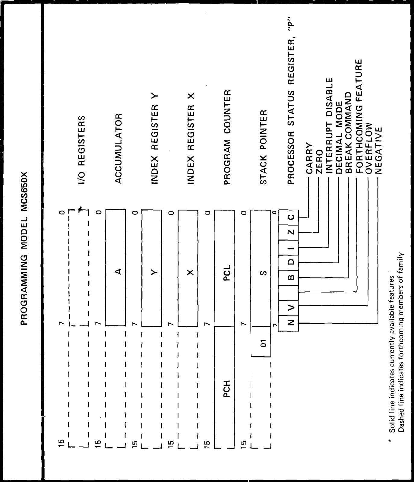
APPENDIX G
DISCUSSION - INDIRECT ADDRESSING
The MCS650X microprocessors have a special form of addressing known as Indirect. The writeup on Indirect addressing describes the basic operation of Indirect.
It is the intent of this discussion to acquaint the user with some of the uses and applications of Indirect addressing.
The Indirect address is really an address that would have been coded in line as in the case of Absolute except for the fact that the address is not known at the time the user writes the program. As has been indicated several times in the basic body of the documentation, it is significantly more efficient with the organization of the MCS650X to assign addresses and implement them if the addressing structure is known. However, that is not always possible to do. For instance, in order to minimize the coding of a subroutine or general purpose set of coding, it is often desirable to work with a range of addressing that is not possible to cover in a normal index, or in the case of subroutine where it is necessary for the addresses to be variable depending on which part of the whole program called the address.
It is probably this discussion which best amplifies the need for calculated addresses. It should be fairly obvious to the user that a general purpose subroutine cannot contain the address of the operations. Therefore, instead of having the instruction LDA followed by the value that the programmer wants to load, in a subroutine it may be desirable to do a Load A from a calculated or specified address.
The use of the Indirect Addressing Mode is to give the user a location in Page Zero in which can be put the calculated address. Then the subroutine instruction can call this calculated address using the form Load A from an address pointed to by the next byte in program sequence. The word "indirect" technically comes from the fact that instead of taking the address which is immediately following the instruction, the next value in program sequence is a pointer to the address.
The Indirect pointer will be referred to from now on as IAL, because it is a Zero Page address and, therefore, is a low order byte. The indirect instructions are written in the form "Load A" followed by IAL.
IAL points to an address which had been previously stored into Page Zero.
This gives the user the flexibility of addressing anywhere in memory with a calculated address. However, the real value of Indirect is not in just having Indirect but having the ability to have Indirect modified. This is the reason for which indirect indexed instruction is implemented rather than straight indirect. An example of the indirect indexed in subrouting is covered in Section 6.5, , but it should be noted that the indirect indexed instruction should be used whenever the user does not know the exact address at time of compilation. Although there may be other interesting and esoteric uses of the indirect index instruction, this is the most common one.
The second form of indirect is very powerful for certain types of applications. Chapter 11 shows the use of tables which have pointers and the advantage of running down one table of pointers until a match is found and then using the same index to address a second table to perform an operation. This is the classical stack processor type of architecture but it requires a special discipline at the time a program is originally defined. Both the indirects require a concept of memory management that is not obvious to the novice programmer.
The concept of indexed indirect is that memory has to be viewed as a series of tables, in which access to one set of tables is accomplished by indexing through a list of pointers. One set of tables might be searched to perform some type of testing or operation. Then the same index is then used to process another set of pointers. This concept is only applicable to operations in which a variety of inputs are being serviced. A classical application is when several remote devices are being managed by the same control program. An example might be having three teletypes tied on to a device, each teletype is being manually controlled and can be under control of the user program. In this type of message handling environment, the control program for the teletypes does nothing more than collect strings of data from the input device and then performs operations on the string
upon seeing a control signal, usually a carriage return in this case of the teletype. Because any one of the teletypes can be causing any one of the series of operations, this program does not lend itself well to the concept of absolute addressing. In fact, most of the subroutines which deal with the individual processing should be written address independent. This normally allows the addition of more devices without paying any penalty in terms of programming. Therefore, this is a subroutine or nonabsolute type of operation in which the indirect indexed would not apply because each of the various operations use a function of position. In other words, one can assign a series of tables that point at the teletype itself; another set that points at an outgoing message stream and another set that points to a series of tables which keep the status of the device. Each of these pointers is considered to be an individual address at the beginning of a string. Each string is a variable length. The teletype strings may consist of a three character message followed by a character return or a 40 character message followed by a character return. In the MCS650X, this system will be implemented by means of developing a series of indirect pointers. Each teletype will have an indirect pointer. Its I/O port has another indirect pointer that points at the put-away string, another one that points at the teletype message output string, another one that points at its status table. If all of the teletypes work this way, it can be seen that the coding to put data into the input message table is the same for all the teletypes and is totally independent of the teletype in which data is being stored.
The index register X serves as a control for the tables so that if all tables were sequentially organized, X would point at the proper value for each operation. A sample operation might be: read teletype three, transfer the data to teletype three input register, update teletype three counter, check to see that teletype three is still active, and decide whether or not to return to signal teletype three back. The coding to perform each of these operations would be exactly the same as coding for teletype two, if the tables were organized such that X was an index register for the pointers.
This is the type of string manipulation application for which indexed
indirect was designed and only when a program can be organized for this technique is the indirect used to its maximum potential. The advantages for organizing for this type of approach when the problem requires string manipulation is significant; the comprehensive I/O program is roughly one half the memory and one fourth the execution time of several other microprocessors which do not have this indexed indirect feature.
APPENDIX H
REVIEW OF BINARY
AND
BINARY CODED DECIMAL
ARITHMETIC
The number 1789 is assumed by most people to mean one thousand, seven hundred eighty-nine, or 1 × 10^3 + 7 × 10^2 + 8 × 10^1 + 9 × 10^0 . However, until the number base is defined, it might mean
$$
1 \times 1 6 ^ {3} + 7 \times 1 6 ^ {2} + 8 \times 1 6 ^ {1} + 9 \times 1 6 ^ {0}
$$
which is hexadecimal and the form used in the microprocessor.
In order to distinguish between numbers on different bases, mathematicians usually write 1789_10 or just 1789 for base 10, or decimal, and 1789_16 for base 16 for hexadecimal. Because very few computers or I/O devices allow subscripting, all hexadecimal numbers are preceded by a notation. Then 1789 means base 10 and1789 means base 16. Why hexadecimal? This is a convenient way of representing 2 digits in 8 bits.
The MCS650X is a byte-oriented microprocessor which means most operations have 8-bit operations.
There are 2 ways to look at 8 bits. The first is as 8 individual bits in which 00001000 means that bit 3 (bit 7 to 0 representation) is on and all other bits are off or as an 8-bit binary number in which case the value is
$$
\begin{array}{l} 0 x 2 ^ {7} + 0 x 2 ^ {6} + 0 x 2 ^ {5} + 0 x 2 ^ {4} + 1 x 2 ^ {3} + 0 x 2 ^ {2} + 0 x 2 ^ {1} + 0 x 2 ^ {0} = 8 \ \text {o r} \$ 0 8. \end{array}
$$
For logic analysis purposes, each bit is unique, but for arithmetic purposes, the 8 bits are treated as a binary number.
Binary Arithmetic Rules:
$$
\begin{array}{l} 0 + 0 = 0 \ 0 + 1 = 1 \ 1 + 0 = 1 \ 1 + 1 = 0 \text {w i t h a c a r r y} \ \end{array}
$$
Carry occurs when the resulting number is too long for the base. In decimal, 8 + 4 = 2 + 10. In hexadecimal, 8 +4 = $C (see hexadecimal details), so that 8 + 4 has a carry in base 10 but not in base 16.
Using these rules to add 8 + 2 in binary gives the following:
$$
\begin{array}{l l} 0 0 0 0 1 0 0 0 & 8 \ \hline 0 0 0 0 0 0 1 0 & + 2 \ \hline 0 0 0 0 1 0 1 0 & 1 0 \end{array} \qquad \begin{array}{l l} 1 x 2 ^ {3} \ \hline 1 x 2 ^ {1} \ \hline 1 x 2 ^ {3} + 1 x 2 ^ {1} \end{array}
$$
Therefore, any number from 0 - 255 may be represented in 8 bits, and binary addition performed using the basic binary add equation, Rj = (Aj Bj Cj - 1) , where, as defined previously, is notation for Exclusive-Or.
In most applications, it is also necessary to subtract. Subtract operations either require a different hardware implementation or a new way of representing numbers.
A combination of this is to implement a simple inverter in each bit. This would make
$$
\begin{array}{l l} 0 0 0 0 1 1 0 0 & 1 2 \ 1 1 1 1 0 0 1 1 & - 1 2 \end{array}
$$
However, when subtracting 12 from 12, the result should also be 0.
$$
\begin{array}{c c} 0 0 0 0 1 1 0 0 & + 1 2 \ 1 1 1 1 0 0 1 1 & - 1 2 \ \hline 1 1 1 1 1 1 1 1 & 0 \end{array}
$$
However, if a carry is added to the complemented number:
$$
\begin{array}{c c} 1 & \text {C a r r y} \ 0 0 0 0 1 1 0 0 & 1 2 \ \hline 1 1 1 1 0 0 1 1 & - 1 2 \ \hline 0 0 0 0 0 0 0 0 = & 0 \end{array}
$$
If, instead of representing -12 as the complement of 12, it is represented as the complement plus carry, the following is obtained:
$$
\begin{array}{r l} 1 1 1 1 0 0 1 1 & = \overline {{1 2}} \ 1 & = \text {C a r r y} \ \overline {{1 1 1 1 0 1 0 0}} & = - 1 2 \ \overline {{0 0 0 0 1 1 0 0}} & = \overline {{+ 1 2}} \ \overline {{0 0 0 0 0 0 0}} & = \overline {{0}} \end{array}
$$
This representation is called two's complement and represents the way that negative numbers are kept in the microcomputer. Below are examples of negative numbers represented in two's complement form.
$$
\begin{array}{r c l} - \emptyset & = & 0 0 0 0 0 0 0 0 \ - 1 & = & 1 1 1 1 1 1 1 1 \ - 2 & = & 1 1 1 1 1 1 1 0 \ - 3 & = & 1 1 1 1 1 1 0 1 \ - 4 & = & 1 1 1 1 1 1 0 0 \ - 5 & = & 1 1 1 1 1 0 1 1 \ - 6 & = & 1 1 1 1 1 0 1 0 \ - 7 & = & 1 1 1 1 1 0 0 1 \ - 8 & = & 1 1 1 1 1 0 0 0 \ - 9 & = & 1 1 1 1 0 1 1 1 \end{array}
$$
Hexadecimal is the representation of numbers to the base 16. The following table shows the advantages of Hex:
| Hexadecimal | Binary | Decimal |
| 0 | 0000 | 00 |
| 1 | 0001 | 01 |
| 2 | 0010 | 02 |
| 3 | 0C11 | 03 |
| 4 | 0100 | 04 |
| 5 | 0101 | 05 |
| 6 | 0110 | 06 |
| 7 | 0111 | 07 |
| 8 | 1000 | 08 |
| 9 | 1001 | 09 |
| A | 1010 | 10 |
| B | 1011 | 11 |
| C | 1100 | 12 |
| D | 1101 | 13 |
| E | 1110 | 14 |
| F | 1111 | 15 |
Because 16 is a multiple of 2, hexadecimal is a convenient shorthand for representation of 4 binary digits or bits. The rules on arithmetic also hold.
| Binary | Hex |
| 0100 1111 | 4F |
| + 0110 0010 | + 62 |
| 1011 0001 | B1 |
To take advantage of this shorthand, all addresses in this manual are shown in hexadecimal notation. It should be noted that the reader should learn to operate in Hex as soon as possible. Continual translation back to decimal is both time consuming and error prone. Working in Hex and binary will quickly force learning of hexadecimal manipulation and the familiarity with working with this convenient representation.
Although many microcomputer applications can successfully be accomplished with binary operations, some applications are best performed in decimal. Although the use of 1 decimal character per byte would be a legitimate way to solve this problem, this is an inefficient use of the capability of the 8-bit byte.
The microprocessor allows the use of packed BCD representation. This representation is, in 4-bit form:
$$
\begin{array}{l} 0 = 0 0 0 0 \ 1 = 0 0 0 1 \ 2 = 0 0 1 0 \ 3 = 0 0 1 1 \ 4 = 0 1 0 0 \ 5 = 0 1 0 1 \ 6 = 0 1 1 0 \ 7 = 0 1 1 1 \ 8 = 1 0 0 0 \ 9 = 1 0 0 1 \ \end{array}
$$
In BCD, the number 79 is represented:
$$
\begin{array}{l} \text {B i n a r y} \ 0 1 1 1 1 0 0 1 = \frac {\text {B C D}}{7 9} = \frac {\text {H e x}}{7 9} \end{array}
$$
The microprocessor automatically takes this into account and corrects for the fact that
| Decimal | BCD | Hex |
| 79 | 01111001 | 79 = 01111001 |
| +12 | 00010010 | 12 = 00010010 |
| 91 | 10010001 | 88 = 10001011 |
The only difference between Hex and BCD representation is that the microprocessor automatically adjusts for the fact that BCD does not allow for Hex values A - F during add and subtract operations.
The offset which follows a branch instruction is in signed two's complement form which means that
$$
\begin{array}{l} \$ + 50 = + 8 0 = 0 1 0 1 0 0 0 0 \ \text {a n d} \mathbb {S} - 5 0 = - 8 0 = 1 0 1 1 0 0 0 0 \ \text {P r o o f} = 0 \overline {{0 0 0 0 0 0 0 0}} \ \end{array}
$$
The sign for this operation is in bit 7 where an 0 equals positive and a 1 equals negative.
This bit is correct for the two's complement representation but also flags the microprocessor whether to carry or borrow from the address high byte.
The following 4 examples represent the combinations of offsets which might occur (all notations are in hexadecimal):
Example H.4.1: Forward reference, no page crossing
| 0105 | ENE | |
| 0106 | +55 | |
| 0107 | Next CP CODE | |
| To calculate next instruction if the branch is tail |
| Offset +55 | 0101C101 | |
| Address Low for next |
| OP CODE 07 | 00000111 | |
| 5C | 01011100 |
with no carry, giving 015c as the result.
Example H.4.2: Backward reference, no page crossing
015A BNE
015B -55
015C Next OP CODE
To calculate if branch is taken,
Offset -55 = AB = 10101011
+AddressLowfor
Next OP CODE +5C 5C 01011100 07 07 00000111
The carry is expected because of the negative offset and is ignored, thus giving 0107 as the result.
Example H.4.3: Backward reference if page boundary crossed
0105 BNE
0106 -55
0107 Next OP CODE
To calculate if branch is taken, first calculate a low byte
Offset -55 = AB = 10101011
Address Low for
Next OP CODE 07B2 = 07B2 = 0000011110110010
There is no carry from a negative offset; therefore, a carry must be made:
$$
- 1 = - 1 = \mathrm {F F} = 1 1 1 1 1 1 1
$$
$$
+ \text {A d d r e s s H i g h} = \frac {0 1}{0 0} = \frac {0 1}{0 0} = \frac {0 0 0 0 0 0 0 1}{0 0 0 0 0 0 0 0}
$$
This gives 00 B2 as a result.
Example H.4.4: Forward reference across page boundary
00B0 BNE
00B1 +55
00B2 Next OP COIE
To calculate next instruction if branch is taken,
Offset 55 = 01010101
Address Low
for Next
OP CODE B2 = 1011010
07 0000111
with carry on positive number.
+1 1 = 0000001 Address High 001 = 0000000000000001
which gives 0107.

MOSTECHNOLOGY, INC.
VALLEY FORGE CORPORATE CENTER
950 RITTENHOUSE ROAD, NORRISTOWN, PA. 19401
TEL: (215) 666-7950 TWX:510/660/4033