LE79234 - Electronic Components Microchip - Free user manual and instructions
Find the device manual for free LE79234 Microchip in PDF.

User questions about LE79234 Microchip
0 question about this device. Answer the ones you know or ask your own.
Ask a new question about this device
Download the instructions for your Electronic Components in PDF format for free! Find your manual LE79234 - Microchip and take your electronic device back in hand. On this page are published all the documents necessary for the use of your device. LE79234 by Microchip.
USER MANUAL LE79234 Microchip
Next Generation Carrier Chipset Hardware Design Guide
Revision Number: 14.0
Issue Date: January 2014
Document Number: 126583
Table of Contents
1.0 System Overview....6
1.1 Introduction 6
1.1.1 NGCC Feature Set....6
1.2 Physical Partitioning 7
1.3 Functional Partitioning....8
1.3.1 Host Interface....9
1.3.2 NGVCP and High Level Software 10
1.3.3 Low Level Interface 10
1.3.4 SLAC Peripherals Block....10
1.3.5 Voice DSP 10
1.3.6 Low Level Processor and Low Level Software 11
1.3.7 Common Analog Block....11
1.3.8 Digital Front End 11
1.3.9 Analog Front End....11
1.3.10 SLIC-SLAC Interface 11
2.0 Hardware Design Interfaces ...... 12
2.1 Host Bus Interface - VCP Device 12
2.1.1 General Purpose Parallel Interface - VCP Device 12
2.1.2 Serial Peripheral Interface - VCP Device....15
2.1.3 HBI Timing Requirements - VCP Device 15
2.2 Debug Interfaces - VCP Device....15
2.2.1 HBI/PCM Interface Header 15
2.2.2 Debug Port....17
2.3 Host Bus Interface - SLAC Device 17
2.3.1 SPI on SLAC Device 18
2.3.2 SLAC SPI Timing 19
2.4 VCP to SLAC Control Interface 22
2.4.1 VCP to SLAC Interface Signal Integrity 26
2.4.2 Hardware Reset....29
2.5 PCM Interface 30
2.5.1 PCM Interface - SLAC Device 30
2.5.1.1 PCM Transmit Interface - SLAC Device 31
2.5.1.2 PCM Receive Interface - SLAC Device 31
2.5.1.3 PCM Timing 31
2.5.2 PCM Interface - VCP Device 32
2.5.3 PCM Hardware Interfaces 33
2.5.3.1 PCM Signal Integrity 41
2.6 SLAC-SLIC Interface....41
2.6.1 RCVP, RCVN....41
2.6.2 DCA, DCB 41
2.6.3 IA, IB 41
2.6.4 IMT, VIMT, VAC....41
2.6.5 CANCEL....42
2.6.6 SVA, SVB....42
2.6.7 Battery Supplies and Battery Sense 42
2.6.8 LD, SEL, and P-Bus....42
2.6.9 Debug port 42
2.6.10 Sensitive Nodes....44
2.6.11 SLAC IO....45
2.7 EMC Network 45
2.8 Using a Single Negative Battery 45
3.0 Application Circuits and Parts Lists 46
Table of Contents
3.1 Configuration C Application Circuits ..... 47
3.2 Configuration C Parts Lists .... 50
3.2.1 Factory Calibration with Test 50
3.2.2 No Calibration with Test....51
3.2.3 No Calibration and No Test 52
3.3 Configuration D Application Circuits 53
3.4 Configuration D Parts List 55
3.4.1 In-Service Calibration and Test 55
3.5 Configuration E External Ringing Application Circuits....56
3.6 Configuration E External Ringing Parts List 58
3.6.1 Factory Calibration with Test 58
3.6.2 No Calibration with Test....59
3.6.3 No Calibration and No Test 60
3.7 Configuration F External Ringing Application Circuits....62
3.8 Configuration F External Ringing Parts List....64
3.8.1 In-Service Calibration and Test 64
3.9 VCP Device Application Circuits 66
3.9.1 VCP Device Parts List 69
4.0 Layout Considerations ....70
4.1 PCB Mounting Considerations 70
4.1.1 Le79271 SLIC Thermal Pad....70
4.1.2 Le79271 SLIC Footprint....71
4.1.3 Le79272 Dual SLIC Thermal Pad 72
4.1.4 Le79238 LGA Thermal Pad and Pins 72
4.2 SLIC Placement....73
4.3 PCB Thermal Performance 75
4.3.1 Airflow 75
4.3.1.1 Test Platform for Airflow Experiment 75
4.3.1.2 Electrical Set-up 77
4.3.1.3 Wind Tunnel Design....77
4.3.1.4 Thermocouple Measurements ..... 78
4.4 Thermal Resistance and Junction Temperature 79
4.5 Power and Bypass Capacitors 80
4.6 Grounding 81
4.7 EMI Capacitors 81
5.0 Power Supply Sizing 82
5.1 +3.3 V Supply 82
5.2 +1.8 V Supply 82
5.3 Battery Supplies 82
Figure 1 - 72 Channel NGCC Line Card with Le79124 VCP and Le79272 SLIC ....8
Figure 2 - NGCC Functional Block Diagram 9
Figure 3 - Host Bus Interface Layers 12
Figure 4 - GPI - 8-bit Parallel Control, Combined Read/Write and Data Strobe 13
Figure 5 - GPI - 8-bit Parallel Control, Separate Read and Write Strobes....13
Figure 6 - GPI - 16-bit Parallel Control, Combined Read/Write and Data Strobe ..... 14
Figure 7 - GPI - 16-bit Parallel Control, Separate Read and Write Strobes....14
Figure 8 - SPI - 4-wire 15
Figure 9 - Mictor Socket Pin-out 16
Figure 10 - Series Termination Resistor Placement. 16
Figure 11 - VCP Debug Port - Optional Header Interface 17
Figure 12 - Host Bus Interface Layers....18
Figure 13 - 4-wire Master-Slave Connections ..... 19
Figure 14 - Alternate Master-Slave Connections....19
Figure 15 - SS Framing Modes 20
Figure 16 - One Data Word Write in Byte Framing Mode ..... 21
Figure 17 - One Data Word Read in Word Framing Mode. 21
Figure 18 - Le79234 VCP to SLAC Interface - 32 Channel NGCC Line Card....22
Figure 19 - Le79124 VCP to SLAC Interface - 64 Channel NGCC Line Card....23
Figure 20 - Le79124 VCP to SLAC Interface - 72 Channel NGCC Line Card....24
Figure 21 - Le79128 VCP to SLAC Interface - 128 Channel NGCC Line Card . . . . . . . . . . . . . . . . . . . . . . . . . . . . . . . . . . . . . . . . . . . . . . . . . . . . . . . . . . . . . 25
Figure 22 - Le79234 VCP to SLAC 32-Channel Interface - Signal Integrity 26
Figure 23 - Le79124 VCP to SLAC 72-Channel Interface - Signal Integrity ..... 27
Figure 24 - Le79128 VCP to SLAC 128-Channel Interface - Signal Integrity ..... 28
Figure 25 - Hardware Reset. 29
Figure 26 - Hardware Reset for External Ringing Applications 29
Figure 27 - PCM Highway 8-bit Transfers 32
Figure 28 - PCM Highway 16-bit Transfers 33
Figure 29 - SLAC PCM Interface - Highway A. 35
Figure 30 - SLAC PCM Interface - Highway A & B 35
Figure 31 - VCP-SLAC PCM Interface - 32 Channel NGCC Line Card - Single PCM Highway . . . . . . . . . . . . . . . . . . . . . . . . . . . 36
Figure 32 - VCP-SLAC PCM Interface - 64 or 72 Channel NGCC Line Card - Single PCM Highway. . . . . . . . . 36
Figure 33 - VCP-SLAC PCM Interface - 72 Channel NGCC Line Card - Dual PCM Highways. . . . . . . . . . . . . . . . . . . . . . . . . . . . . . . . . . . . . . . . . . . . . . . . . . . . . .
Figure 34 - VCP-SLAC PCM Interface - 72 Channel NGCC Line Card - Two PCM Highways with a Single Clock and Frame Sync. 38
Figure 35 - VCP-SLAC PCM Interface - 72 Channel NGCC Line Card - Separate Voice and Test PCM Highways . 39
Figure 36 - VCP-SLAC PCM Interface - 128 Channel NGCC Line Card - Dual PCM Highways. . . . . . . . . . . . . . . . . . . . . . . . . . . 40
Figure 37 - SLAC-SLIC Internal Ringing Interface - One Channel Shown. 43
Figure 38 - SLAC-SLIC Interface - Sensitive Nodes 44
Figure 39 - SLAC Open Drain Relay Drivers 45
Figure 40 - Configuration C - POTS Application 47
Figure 41 - Configuration C - GPON Application (Negative Batteries only)....48
Figure 42 - Configuration C - IVD Application 49
Figure 43 - Configuration D - POTS Application 53
Figure 44 - Configuration D - IVD Application 54
Figure 45 - Configuration E - Battery-Backed Ringing POTS Application 56
Figure 46 - Configuration E - Earth-Backed Ringing POTS Application ..... 57
Figure 47 - Configuration F - Battery-Backed Ringing Application. 62
List of Figures
Figure 48 - Configuration F - Earth-Backed Ringing Application....63
Figure 49 - Le79124 VCP External Components. 66
Figure 50 - Le79234 VCP External Components. 67
Figure 51 - Le79128 VCP External Components. 68
Figure 52 - Recommended PCB Thermal Pad and Via Pattern for 28-Pin QFN 70
Figure 53 - Recommended PCB Footprint for 28-pin QFN Package....71
Figure 54 - Recommended PCB Thermal Pad and Via Pattern for 48-Pin QFN 72
Figure 55 - Possible SLIC Placement - Hub Arrangement. 73
Figure 56 - Possible SLIC Placement - Slot Arrangement....74
Figure 57 - Possible Dual SLIC Placement - Hub Arrangement 74
Figure 58 - Le51HR0140 Groupings and Board Layout 77
Figure 59 - Wind Tunnel and Load Board 78
Figure 60 - SLIC Surface Temperature Variation vs. Airflow, Normalized to Inlet Airflow at 22 °C ..... 79
Figure 61 - Power Calculator Example - Supply Currents in Active Mode....84
Figure 62 - Power Calculator Example - Supply Currents in Ringing 85
1.0 System Overview
1.1 Introduction
The Next Generation Carrier Chipset (NGCC) implements high line count POTS telephone interfaces, providing a complete BORSCHT capability for soft switch based Next Generation Networks. NGCC enables the design of POTS line cards which are DSL friendly, low cost, high performance, and software programmable for multiple country applications world wide. All AC, DC, and signaling parameters are fully programmable via microprocessor interfaces. Additionally, the NGCC has self-test and line-test capabilities to resolve faults to the line or line circuit.
This design guide is intended to familiarize the designer with the NGCC system and external interfaces. This guide provides hardware design, connection, application circuit, parts lists, and layout information. For detailed information on the functionality provided by the SLIC and SLAC devices, refer to the NGCC Designer's Guide document.
As the name suggests, the Hardware Design Guide is to be used as a guide and is not intended to be a substitute for a system validation. The design is the sole responsibility of the system integrator. Fully evaluate and test the design prior to deployment.
1.1.1 NGCC Feature Set
- Performs all battery feed, ringing, signalling, hybrid and test functions
- Optimized for Next Generation Broadband xDSL and triple play applications
- Controls state changes to eliminate transients that could cause CRC errors
- Two or three chip solution supports high density, multi-channel architecture
• Supports two negative batteries and one positive battery - Best-in-class GR-844 equivalent testing capability
-
Single hardware design meets multiple country requirements through software programming of:
-
Ringing waveform and frequency
• DC loop-feed characteristics and current-limit - Loop-supervision detection thresholds
- Off-hook debounce circuit
• Ground-key and ring-trip filters - Off-hook detect de-bounce interval
- Two-wire AC impedance
- Transhybrid balance
• Transmit and receive gains - Equalization
- Digital I/O pins
• A-law/μ-law and linear selection
• Supports wideband 7.0 kHz mode
• Supports internal battery-backed ringing
- Self-contained ringing generation and control
- Programmed ringing cadence
• Supports external battery-backed and earth-backed ringing (on ZL79258 SLAC device)
- Programmed ringing cadence and control
- Supports metering generation with envelope shaping
- Programmable metering cadencing
- Smooth polarity reversal
• Automatic CID and signalling and FSK and DTMF modes
- Tone generation
- Call progress tones
- Howler tones
- DTMF tones
- DTMF detection
- Modem support
• Supports both loop-start and ground-start signalling
• HBI and PCM interfaces
- On-hook transmission
• Power/service denial mode
• Line-feed characteristics independent of battery voltage
- Low idle-power per line
- Compatible with inexpensive protection networks
- Monitors two-wire interface voltages and currents for subscriber line diagnostics
- Can monitor and drive the A lead (Tip) and B lead (Ring) independently
- Extremely flexible
• Built-in voice-path test modes
- Integrated self-test features
- Two general purpose I/O pins per channel on SLAC, one specifically configured as a relay driver
- -40 to 85^ operation
- Small physical size
1.2 Physical Partitioning
The NGCC is partitioned into three chip types:
(1) Subscriber Line Interface Chip – SLIC or NGSLIC – Le79271 (single channel) or Le79272 (dual channel)
(2) Subscriber Line Audio Chip - SLAC or NGSLAC - Le79238 (internal ringing) or ZL79258 (internal/external ringing)
(3) Voice Control Processor – VCP or NGVCP – Le79124 (controls up to 72 channels) or Le79128 (controls up to 128 channels) or Le79234 (controls up to 32 channels). Use of the VCP device is optional.
Device acronyms are used with and without the NG prefix throughout this document.
See Figure 1 for a 72 channel line card block diagram.

flowchart
graph TD
    subgraph_Host_Interface["Host Interface"]
        A["SLIC"] --> B["SLAC SLAC"]
        C["SLIC"] --> D["SLAC"]
        E["SLIC"] --> F["SLAC"]
        G["SLIC"] --> H["SLAC"]
        I["SLIC"] --> J["SLAC"]
    end

    subgraph_Network_Interface["Network Interface"]
        K["SLIC"] --> L["SLAC"]
        M["SLIC"] --> N["SLAC"]
        O["SLIC"] --> P["SLAC"]
        Q["SLIC"] --> R["SLAC"]
        S["SLIC"] --> T["SLAC"]

    end

    subgraph_PCM_Bus["PCM bus (1 or 2)"]
        U["SPI1 bus"] --> V["Le79124 VCP"]
        W["SPI2 bus"] --> V
    end

    B --> V
    D --> V
    F --> V
    H --> V
    J --> V
    R --> V
    L --> V
    N --> V
    P --> V
    T --> V
    U --> V
    V --> W
    W --> X["Network Interface"]

    style Host_Interface fill:#f9f,stroke:#333
    style Network_Interface fill:#ccf,stroke:#333
Figure 1 - 72 Channel NGCC Line Card with Le79124 VCP and Le79272 SLIC
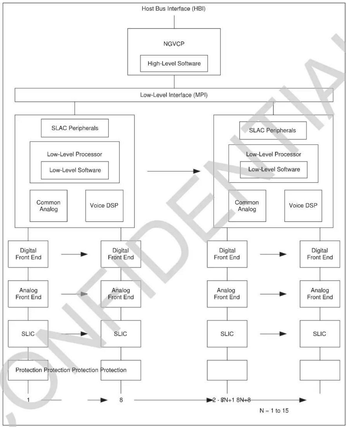
1.3 Functional Partitioning
The SLIC is a 150 V device that interfaces to the subscriber telephone line. It provides the power and voltage necessary to drive a wide variety of telephone lines.
The SLAC device contains channel specific Analog Front End (AFE) blocks, a Common Analog block, channel specific Digital Front End blocks, a voice DSP block, a Low Level Processor block and a Digital Peripherals block. An AFE block consists of the ADC and DAC units plus associated buffer circuits necessary to control and monitor the line voltages, line currents and battery voltages. A Digital Front End block contains the interpolators, decimators and metering logic. The Common Analog block contains the voltage reference and PLL. The Voice DSP block handles voice transmission. The Low Level Processor block handles DC feed control, supervision, DTMF detection and diagnostics front end processing. The Digital Peripherals block contains the control and PCM interfaces of the Low Level Interface.
The VCP device contains the call control and line diagnostics for the entire line card.
flowchart
graph TD
    A["Host Bus Interface (HBI)"] --> B["NGVCP"]
    B --> C["High-Level Software"]
    C --> D["Low-Level Interface (MPI)"]
    D --> E["SLAC Peripherals"]
    D --> F["SLAC Peripherals"]
    D --> G["Low-Level Processor"]
    D --> H["Low-Level Processor"]
    D --> I["Low-Level Software"]
    D --> J["Common Analog"]
    D --> K["Voice DSP"]
    E --> L["Digital Front End"]
    F --> M["Digital Front End"]
    G --> N["Analog Front End"]
    H --> O["Analog Front End"]
    I --> P["SLIC"]
    J --> Q["SLIC"]
    K --> R["SLIC"]
    L --> S["Protection Protection Protection"]
    M --> T["Protection Protection Protection"]
    N --> U["Protection Protection Protection"]
    O --> V["Protection Protection Protection"]
    P --> W["Protection Protection Protection"]
    Q --> X["Protection Protection Protection"]
    R --> Y["Protection Protection Protection"]
    S --> Z["Protection Protection Protection"]
    T --> AA["Protection Protection Protection"]
    U --> AB["Protection Protection Protection"]
    V --> AC["Protection Protection Protection"]
    W --> AD["Protection Protection Protection"]
    X --> AE["Protection Protection Protection"]
    Y --> AF["Protection Protection Protection"]
    Z --> AG["Protection Protection Protection"]
    AA --> AH["Protection Protection Protection"]
    AB --> AI["Protection Protection Protection"]
    AC --> AJ["Protection Protection Protection"]
    AD --> AK["Protection Protection Protection"]
    AE --> AL["Protection Protection Protection"]
    AF --> AM["Protection Protection Protection"]
    AG --> AN["Protection Protection Protection"]
    AH --> AO["Protection Protection Protection"]
    AI --> AP["Protection Protection Protection"]
    AJ --> AQ["Protection Protection Protection"]
    AK --> AR["Protection Protection Protection"]
    AL --> AS["Protection Protection Protection"]
    AM --> AT["Protection Protection Protection"]
    AN --> AU["Protection Protection Protection"]
    AO --> AV["Protection Protection Protection"]
    AP --> AW["Protection Protection Protection"]
    AQ --> AX["Protection Protection Protection"]
    AR --> AY["Protection Protection Protection"]
    AS --> AZ["Protection Protection Protection"]
    AT --> BA["Protection Protection Protection"]
    AU --> BB["Protection Protection Protection"]
    AV --> BC["Protection Protection Protection"]
    AW --> BD["Protection Protection Protection"]
    AX --> BE["Protection Protection Protection"]
    AY --> BF["Protection Protection Protection"]
    AZ --> BG["Protection Protection Protection"]
    BA --> BH["Protection Protection Protection"]
    BB --> BI["Protection Protection Protection"]
    BC --> BJ["Protection Protection Protection"]
    AD --> BK["Protection Protection Protection"]
    AE --> BL["Protection Protection Protection"]
    AF --> BM["Protection Protection Protection"]
    AG --> BN["Protection Protection Protection"]
    AH --> BO["Protection Protection Protection"]
    AI --> BP["Protection Protection Protection"]
    AJ --> BQ["Protection Protection Protection"]
    AK --> BR["Protection Protection Protection"]
    AL --> BS["Protection Protection Protection"]
    AM --> BT["Protection Protection Protection"]
    AN --> BU["Protection Protection Protection"]
    AO --> BV["Protection Protection Protection"]
    AP --> BW["Protection Protection Protection"]
    AQ --> BX["Protection Protection Protection"]
    BB --> BY["Protection Protection Protection"]
    BC --> BZ["Protection Protection Protection"]
Figure 2 - NGCC Functional Block Diagram
1.3.1 Host Interface
The NGVCP uses the Host Bus Interface (HBI) to communicate with the rest of the system.
1.3.2 NGVCP and High Level Software
The NGVCP firmware includes high level software that controls and coordinates call processing, line test primitives, tone processing and control, dial pulse and hook flash decode, CID and DTMF detection.
1.3.3 Low Level Interface
There are two interface buses between the NGVCP and the SLAC devices.
One bus is the PCM highway which carries the voice signals and data streams. The NGVCP can accommodate 1 or 2 PCM highways.
The other bus is the MPI control interface. The SLAC control will come either from the VCP device or from a user defined processor chip. The physical layer of the interface is an industry standard SPI bus. The transport layer allows setting of an in-band channel address and default memory page.
1.3.4 SLAC Peripherals Block
The SLAC Peripherals block implements the HBI and PCM interfaces as previously described.
1.3.5 Voice DSP
The SLAC device performs the codec and filter functions associated with the four-wire section of the subscriber line circuitry in a digital switch. These functions involve converting an analog voice signal into digital PCM samples and converting digital PCM samples back into an analog signal. During conversion, digital filters are used to band-limit the voice signals.
The user-programmable filters in the voice transmission section perform the following functions:
- Set the receive and transmit gain
- Perform the transhybrid balancing function
- Permit adjustment of the two-wire termination impedance
- Provide frequency attenuation adjustment (equalization) of the receive and transmit paths
- Selects narrowband 3.4 kHz mode or wideband 7.0 kHz mode
The PCM codes can be:
- 8-bit companded A-law with 8 kHz sampling
- 8-bit companded -law with 8 kHz sampling
- 16-bit linear two's-complement with 8 kHz sampling
- 16-bit linear two's-complement with 16 kHz sampling (wideband mode)
All narrowband programmable digital filter coefficients and supervision data can be calculated using WinSLAC ^™ software. The software allows the designer to enter a description of system requirements and WinSLAC returns the necessary data and plots the predicted system results. Digital filter coefficients for wideband operation are provided by Microsemi.
1.3.6 Low Level Processor and Low Level Software
Besides the codec functions, the integrated voice chip set provides all the sensing, feedback, and clocking necessary to completely control SLIC device functions with programmable parameters. System-level parameters under programmable control include active loop current limits, open circuit feed voltages, and loop supervision thresholds.
The NGCC provides loop supervision capability including off-hook, ring-trip, ground start, and ground-key detection. Detection thresholds for these functions are programmable. A programmable debounce timer is available that eliminates false detection due to contact bounce.
For subscriber line diagnostics, AC and DC line conditions can be monitored by connecting analog currents and voltages to ADCs. This gives the user's microprocessor the ability to configure the SLIC/SLAC system and make system and line tests. Both longitudinal and metallic resistance and capacitance can be measured. This allows identification of leakage resistance, line capacitance and telephones.
1.3.7 Common Analog Block
The Common Analog block contains the PLL and voltage reference for the octal SLAC.
1.3.8 Digital Front End
The Digital Front End block contains the interpolators for the DACs, the decimators for the ADC and the metering generation and cancellation logic.
1.3.9 Analog Front End
The Analog Front End block contains the ADCs and DACs necessary to interface to the SLIC plus the associated buffers.
1.3.10 SLIC-SLAC Interface
The SLIC is a voltage feed device which drives line voltage and measures line current. Feedback inside the SLAC is used to generate the appropriate input impedances and current limits.
There are three analog voltage control signals from the SLAC to the SLIC, the DC and low-frequency A-lead control voltage (DCA), the DC and low-frequency B-lead control voltage (DCB), and the combined voice and metering differential control voltage (RCVP, RCVN).
There are three analog current sense signals from the SLIC to the SLAC, IAB current (IMT); IA current (IA), and IB current (IB). The voice signal is generated from the measured IAB current. There is also a connection to a metering cancellation DAC to cancel the metering signal from the voice path to prevent metering overload in the transmit path.
There are sense resistors connected directly from the A (Tip) and B (Ring) leads to the SLAC to measure foreign voltages.
There are also sense resistors connected directly from the ringing feed resistor to the SLAC to measure ringing voltages for external ringing applications.
Finally, there is a digital control bus called the P-bus to control the operating modes of the SLIC.
2.0 Hardware Design Interfaces
This section discusses the supported hardware interfaces between the NGCC devices and between the NGCC devices and an external processor.
2.1 Host Bus Interface - VCP Device
The Host Bus Interface (HBI) on the VCP device provides a means for exchanging control, configuration, and status information with an external host processor. This interface is implemented through a combination of hardware and firmware. The design is layered as shown in Figure 3. Hardware provides a generic means for transporting data between the host and internal memory. The interpretation of the data is provided by firmware running on the VCP device. This layered architecture allows the definition of the application level interface to change by modifying the firmware.
The hardware interface of the HBI is the General Purpose Parallel Interface (GPI) or the Serial Peripheral Interface (SPI). Options are selected via the configuration pins, refer to Table 1.

flowchart
graph LR
    A["Firmware"] --> B["Application Layer"]
    C["Hardware"] --> D["Transport Layer"]
    C --> E["Physical Layer"]
    B --> F["Provides the application programmer's interface. Defines the meaning of payload data passed over the interface."]
    D --> G["Moves 16-bit data words between the physical layer and internal memory."]
    E --> H["Defines the pins, signal timing and electrical characteristics of the interface."]
Figure 3 - Host Bus Interface Layers
| CONF_2 - CONF_0 | Host Interface Parallel Data Width Parallel Read/Write Strobes | |
| 000 Parallel 8 Combined | ||
| 001 Parallel 8 $eparate | ||
| 010 Parallel 16 Combined | ||
| 011 Parallel 16 Separate | ||
| 100 Serial NA NA | ||
Table 1 - Configuration Assignments (CONF₂ - CONF₀)
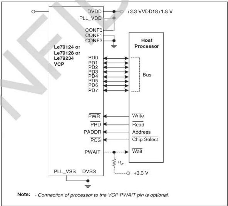
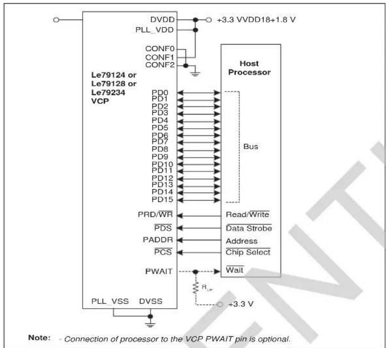
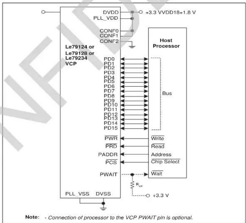
2.1.1 General Purpose Parallel Interface - VCP Device
The GPI has several configuration options and has been architected to connect gluelessly to a variety of external processors. The GPI interface uses a combination of write, read, data, address, and wait strobes; thus, a dedicated clock is not needed to synchronize the transfers.
The GPI can be configured for either 8-bit or 16-bit data bus transfers. Commands and data can be transferred across the parallel interface using either separate read and write strobes or using a combined read/write strobe and a data strobe.
A wait strobe can be used to indicate to the external processor that the interface is available for a transfer. When the wait strobe goes active, the interface is busy. The transfer will complete after the wait signal deasserts. The wait strobe pin polarity is programmable and defaults to tri-state. Note: an external pull-up or pull-down (depending on the programmed active state) is required.
The external interface connection diagrams for the four different GPI configurations are shown in Figure 4 through Figure 7.

text_image
DVDD PLL_VDD +3.3 VVDD18+1.8 V CONF0 CONF1 CONF2 Le79124 or Le79128 or Le79234 VCP Host Processor Bus PD0 PD1 PD2 PD3 PD4 PD5 PD6 PD7 PRD/WR PDS PADDR PCS PWAT Rus Read/Write Data Strobe Address Chip Select Wait PLL_VSS DVSS +3.3 V Note: - Connection of processor to the VCP PWAIT pin is optional.Figure 4 - GPI - 8-bit Parallel Control, Combined Read/Write and Data Strobe
text_image
DVDD PLL_VDD +3.3 VVDD18+1.8 V CONF0 CONF1 CONF2 Le79124 or Le79128 or Le79234 VCP Host Processor Bus PD0 PD1 PD2 PD3 PD4 PD5 PD6 PD7 PWR PRD PADDR PCS PWAT R_P Write Read Address Chip Select Wait PLL_VSS DVSS +3.3 V Note: - Connection of processor to the VCP PWAIT pin is optional.Figure 5 - GPI - 8-bit Parallel Control, Separate Read and Write Strobes
text_image
DVDD PLL_VDD CONF0 CONF1 CONF2 +3.3 VVDD18+1.8 V Le79124 or Le79128 or Le79234 VCP Host Processor Bus PD0 PD1 PD2 PD3 PD4 PD5 PD6 PD7 PD8 PD9 PD10 PD11 PD12 PD13 PD14 PD15 PRD/WR PDS PADDR PCS PWAIT PLL_VSS DVSS Read/Write Data Strobe Address Chip Select Wait R +3.3 V Note: - Connection of processor to the VCP PWAIT pin is optional.Figure 6 - GPI - 16-bit Parallel Control, Combined Read/Write and Data Strobe
text_image
DVDD PLL_VDD +3.3 VVDD18+1.8 V CONF0 CONF1 CONF2 Le79124 or Le79128 or Le79234 VCP Host Processor Bus PD0 PD1 PD2 PD3 PD4 PD5 PD6 PD7 PD8 PD9 PD10 PD11 PD12 PD13 PD14 PD15 PWR PRD PADDR PCS PWAIT PLL VSS DVSS Write Read Address Chip Select Wait R_UP +3.3 V Note: - Connection of processor to the VCP PWAIT pin is optional.Figure 7 - GPI - 16-bit Parallel Control, Separate Read and Write Strobes
2.1.2 Serial Peripheral Interface - VCP Device
The SPI is an alternate physical interface that can be used by the external host to communicate with the VCP device. The SPI interface is compatible with the SPI interface used by general DSP devices allowing the VCP to be interfaced without glue logic. The SPI has the same logical view as the GPI so the host can issue the same commands or data to the VCP regardless of the physical interface.
The most important factor with regards to the ability to use the SPI interface is not the clock speed or number of lines, but the host architecture. Required is a queued SPI with task resume capability and the host application broken into enough threads to allow for the SPI to not bottleneck or stall the network processor. Microsemi strongly recommends the GPI 16-bit architecture. If the SPI architecture is chosen, it is the responsibility of the software designer to correctly architect the host firmware.
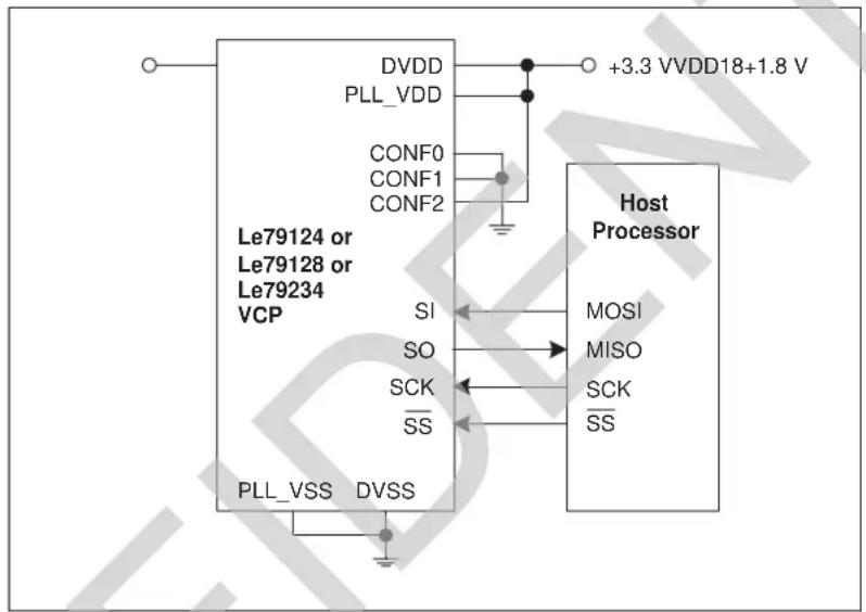
A 4-wire serial interface is shown in Figure 8. If the host processor does not provide a slave select and only one VCP is used, simply tie VCP to ground.
text_image
DVDD PLL_VDD CONF0 CONF1 CONF2 +3.3 VVDD18+1.8 V Le79124 or Le79128 or Le79234 VCP SI SO SCK SS PLL_VSS DVSS Host Processor MOSI MISO SCK SSFigure 8 - SPI - 4-wire
2.1.3 HBI Timing Requirements - VCP Device
Timing requirements and command and data structures for the VCP parallel and serial interfaces are detailed in the Le79124, Le79128, and Le79234 VCP data sheets.
2.2 Debug Interfaces - VCP Device
Microsemi recommends that footprints for two connectors be provided for in the PCB layout. Having access to the VCP HBI/PCM interface and Debug port can help to facilitate initial line card start-up.
2.2.1 HBI/PCM Interface Header
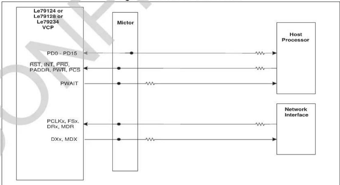
The HBI/PCM interface header is a 38-position matched impedance socket (Mictor) mounted on the line card. When properly configured, the header allows the line card to be controlled by the Microsemi Le71HP0300 or Le71HP0400 platform instead of the user's control interface. The header will receive a cable that interfaces to the platform's DIN connector.
The PCB should be laid out to accept a Tyco Electronics 38-position receptacle, part number 2-5767004-2, or equivalent. On production line cards, this socket does not need to be populated. Figure 9 defines the pin-out of the socket. Note that in addition to the 38 signal positions, the socket provides 5 ground connections.
When this interface is used, it needs to be isolated from the user's control interface. One way to provision for this is to use series termination resistors on each PCM and HBI signal and then to simply remove them if the debug interface is to be used. An example of series termination placement is shown in Figure 10. Signals driven from the Host Processor or Network Interface have series termination resistors placed near their respective drivers. Signals driven from the VCP have series termination resistors placed near the VCP, but placed on the other side of the mictor socket so that the mictor socket can be fully isolated during a debug implementation.

text_image
MICTOR 1 PCLKA 2 3 FSA 4 5 DRA (VCP) 6 7 DXA (VCP) 8 9 PCLKB PD15 10 11 FSB PD14 12 13 DRB (VCP) PD13 14 15 DXB (VCP) PD12 16 17 MPCLK PD11 18 19 MFS PD10 20 21 MDR (VCP) PD9 22 23 MDX (VCP) PD8 24 25 RST PD7 26 27 INT PD6 28 29 PRD PD5 30 31 PADDR PD4 32 33 PADDR PD3 34 35 PWAIT PD2 36 35 PWR PD1 38 37 PCS PD0 GND 39 40 41 42 43Figure 9 - Mictor Socket Pin-out
flowchart
graph LR
    A["Le79124 or Le79128 or Le79234 VCP"] -->|PD0 - PD15| B["Mictor"]
    A -->|RST, INT, PRD, PADDR, PWR, PCS| B
    A -->|PWAIT| B
    A -->|PCLKx, FSx, DRx, MDR| B
    A -->|DXx, MDX| B
    B --> C["Host Processor"]
    B --> D["Network Interface"]
Figure 10 - Series Termination Resistor Placement
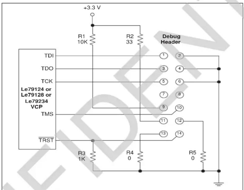
2.2.2 Debug Port
The Debug port on the VCP device consists of the TCK, TMS, TDI, TDO, and TRST pins. This port is for Microsemi debug use only. If debug of VCP operation becomes necessary, Microsemi may require access to this port.
Two Debug port access methods are presented.
The board can be laid out with a population option debug header and with population option pull-up and pull-down resistors. This interface is detailed in Figure 11. The 14-pin header pins should be spaced 2.54 mm (100 mils) row to row and 2.54 mm (100 mils) column to column.
An alternate approach is to simply bring TCK, TMS, TDI, TDO, and TRST pins out to test points with TRST tied to digital ground through a 1 KΩ resistor. This will allow easy access if it becomes necessary to jumper to the Debug port. Holding TRST low ensures that the Debug port is kept in reset during power supply bring-up. This resistor (R3 in Figure 11 and RTRST in Figure 49 and Figure 50) is recommended for all new designs.
text_image
+3.3 V R1 10K R2 33 Debug Header TDI TDO TCK Le79124 or Le79128 or Le79234 VCP TMS TRST R3 1K R4 0 R5 0Figure 11 - VCP Debug Port - Optional Header Interface
2.3 Host Bus Interface - SLAC Device
Like the VCP device, the Host Bus Interface for the SLAC device provides a means for exchanging control, configuration and status information with an external processor. This interface is implemented through a combination of hardware and firmware. The design is layered as shown in Figure 12. Hardware provides a generic means for transporting data between the host and internal memory. The interpretation of the data is provided by firmware running on the internal DSP. This layered architecture allows the definition of the application level interface to change by modifying the firmware.
The SLAC device supports a SPI hardware interface. The SPI (also referred to as a Microprocessor Peripheral Interface (MPI)) is compatible with the SPI used by general DSP devices, so interfacing with the SLAC device can be accomplished without glue logic.
The SPI is a common 4-wire synchronous serial interface. The HBI includes a slave SPI implementation, which means the serial clock is supplied by an external master. This slave SPI supports both 8-bit or 16-bit masters and supports masters that independently control chip select.

flowchart
graph LR
    A["Firmware"] --> B["Application Layer"]
    C["Hardware"] --> D["Transport Layer"]
    C --> E["Physical Layer"]
    B --> F["Provides the application programmer's interface. Defines the meaning of payload data passed over the interface."]
    D --> G["Moves 16-bit data words between the physical layer and internal memory."]
    E --> H["Defines the pins, signal timing and electrical characteristics of the interface."]
Figure 12 - Host Bus Interface Layers
2.3.1 SPI on SLAC Device
This section discusses direct connection of the SLAC device SPI to an external host processor, when no VCP device is used. Timing requirements and command and data structures for the SLAC SPI are detailed here.
When using the SPI port on the SLAC device to communicate with an external host processor, the SLAC device is the SPI slave and the external host is the SPI master. SPI signals are wired to the SLAC pins as shown in Table 2. The SLAC devices sample the input signal DIN on the rising edge of the clock and change the output signal DOUT on the falling edge of the clock.
| Signal Name (Pin Name) Type Description | |
| SCK (DCLK) I SPI clock | |
| MOSI (DIN) I SPI slave input/master output | |
| MISO (DOUT) O SPI slave output/master input | |
| SS (CS) I SPI Slave select low | |
Table 2 - SPI-SLAC Interconnect
Figure 13 shows the SPI interface system with a 4-wire SPI master. TI DSP devices and Motorola 68HC12 devices have a 4-wire SPI master. For example, the TI TMS320F28x chips can set the chip as the master (SPICTL[2]=1), 8-bit (SPICCR[3:0]=7) transfer with clock polarity (SPICCR[6]=1 falling), clock phase (CPICTL[3]=0 no delay) or with SPICCR[6]=0 (rising), CPICTL[3]=1 (delay) to connect to the SLAC device.
Figure 14 shows the SPI interface system with an alternate SPI master. Most Motorola DSP/controllers, except 68HC12 and ADI DSP, have 3-wire SPI masters. For example, Motorola 68HC05Cx SPCR register can set the Clock Phase (CPHA=0) with the clock polarity (CPOL=0) or CPHA=1 with CPOL=1 to interface with the SLAC device. One of the GPIO pins is needed to drive the CS pin of the SLAC device. As the SLAC device supports command framing on the CS pin, the GPIO pin of the master connecting to the CS pin of the slave is required, as shown in Figure 14.

flowchart
graph LR
    A["NGCC SLAC device(s)"] --> B["SPI Slave"]
    B --> C["MOSI"]
    B --> D["MISO"]
    B --> E["SCK"]
    B --> F["SS"]
    B --> G["DIN"]
    B --> H["DCLK"]
    B --> I["CS"]
    B --> J["MOSI"]
    B --> K["MISO"]
    B --> L["SCK"]
    B --> M["SS"]
    B --> N["SPI Master"]
Figure 13 - 4-wire Master-Slave Connections

flowchart
graph LR
    A["NGCC SLAC device(s)"] --> B["SPI Slave"]
    B --> C["DIN"]
    B --> D["DOUT"]
    B --> E["SCK/CS"]
    B --> F["MOSI"]
    B --> G["MISO"]
    B --> H["SCK"]
    B --> I["SS"]
    B --> J["GPIO"]
    K["SPI Master"] --> L["MOSI"]
    K --> M["MISO"]
    K --> N["SCK"]
    K --> O["SS"]
    K --> P["GPIO"]
Figure 14 - Alternate Master-Slave Connections
2.3.2 SLAC SPI Timing
In order to connect to different SPI masters and share the same logic view with the VCP GPI, the SPI slave of the SLAC device has the following designs:
- Separate DIN and DOUT pins.
• No daisy chain support. - No read latency: no latency between the read command word and the first data word.
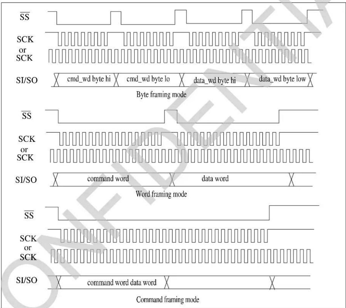
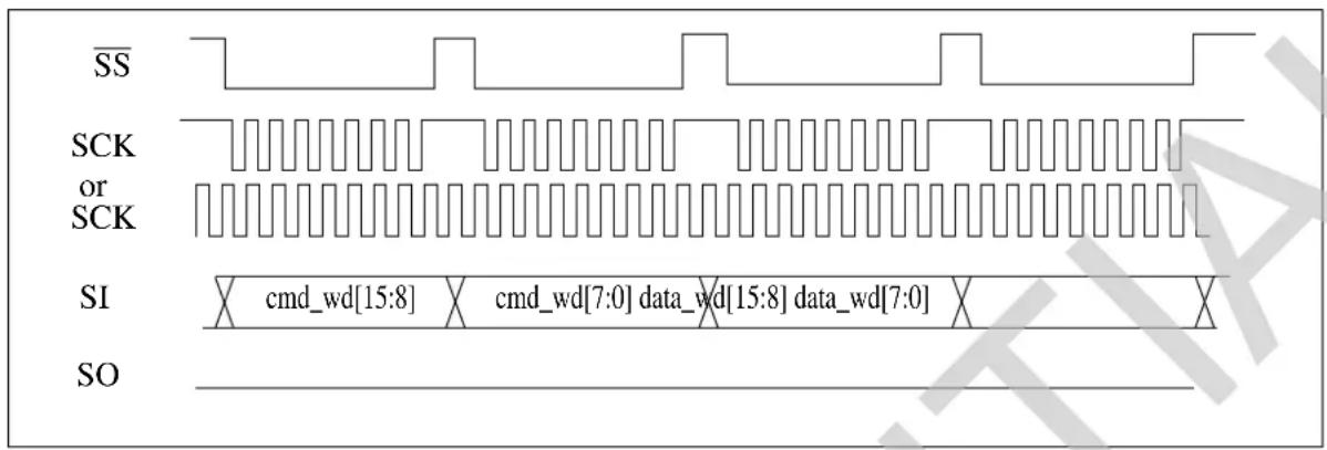
- CS pin supports byte/word framing, and command framing mode, as shown in Figure 15. The SPI slave state machine will reset if CS returns to High when the number of active SCK clock pulses is not equal to 8 or 16. If there is no clock, CS has to be Low for more than 125 ns (depending on the internal clock) to be recognized to reset the SPI slave state machine. In command framing mode, the transition of CSto High means the command has ended. This event resets the SPI slave state machine, and the next falling edge of CS starts a new command.
Figure 15 shows three kinds of framing modes based on the behavior of SS. In byte/word framing mode, SS is Low for 8/16 SCK clocks. For a two-word command, SS needs to toggle 4/2 times to complete the command transfer. In command framing mode, SS is Low for the whole duration of the command transfer. When the command is finished, SS will go back to High. If SS Low lasts shorter than the expected command length, the command is aborted and the SPI slave state machine resets. However if the user pulls SS Low longer than the expected command length, the extra words will start a new command sequence. In both byte/word framing mode and command framing mode, SCK can be free-running or absent when SS is inactive High.
Every time returns to High and the number of active SCK clocks is not equal to 8 or 16, the SPI slave state machine will reset. The next Low starts a new command sequence. In command framing mode, the transition back to High means the end of the command. If Low lasts less than 16 SCK clock cycles, no command byte is processed. If Low lasts more than 16 clock cycles, each 16-clock cycles triggers the SPI slave to process the word until returns back to High. The SPI slave will not reset state machine when Low lasts exactly 8 or 16 SCK clock cycles to support byte/word framing mode. In byte/word framing mode, the user has to be aware of the command length, as there is no indication of command boundary.
Command framing is the recommended mode of operation because this mode provides state machine synchronization of when the command word is expected.
text_image
SS SCK or SCK SI/SO cmd_wd byte hi cmd_wd byte lo data_wd byte hi data_wd byte low Byte framing mode SS SCK or SCK SI/SO command word data word Word framing mode SS SCK or SCK SI/SO command word data word Command framing modeFigure 15 - SS Framing Modes
The timing requirements for read and write accesses are shown in the following timing diagrams. The single data word read and write command is shown in Figure 16 and Figure 17.
text_image
SS SCK or SCK SI cmd_wd[15:8] cmd_wd[7:0] data_wd[15:8] data_wd[7:0] SOFigure 16 - One Data Word Write in Byte Framing Mode

text_image
SS SCK or SCK SI command word .... SO data wordFigure 17 - One Data Word Read in Word Framing Mode
Note 1: SCK may be stopped in the High or Low state indefinitely without loss of information. When is at Low state, every 16 SCK cycles the 16-bit received will be interpreted by the SPI interface logic.
Note 2: The first data bit is enabled on the falling edge of SS or on the falling edge of SCK, whichever occurs last.
Note 3: The SPI slave requires 61ns SS Off time just to make the transition of synchronized with SCK clock. In the command framing mode, there is no SS Off time between each 16-bit command/data and is held low until the end of command.
Note 4: If SS is not held low for 16 or 8 SCK cycles exactly, the SPI slave will reset. During byte or word framing mode, SS is held low for 8 or 16 SCK cycles. During command framing mode, SS is held low for the whole duration of the command. Besides, multiple commands can be transferred with SS low for the whole duration of the multiple commands. The rising edge of the SS indicates the end of the command sequence and resets the SPI slave.
2.4 VCP to SLAC Control Interface
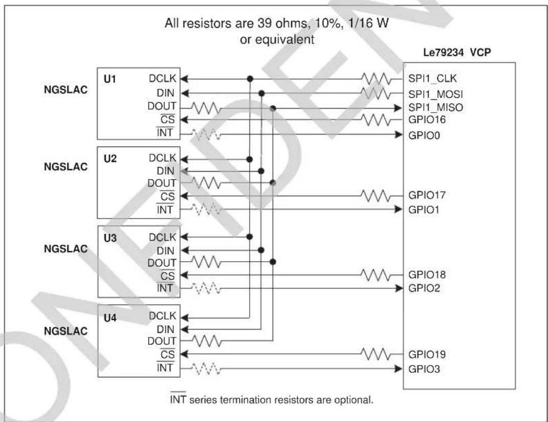
In addition to the GPI functional block, the VCP devices provide SPI ports which serve as the control interface between the VCP device and the SLAC devices. The Le79234 VCP device provides one SPI port and the Le79124 and Le79128 VCP devices provide two SPI ports (SPI1 and SPI2). The SPI interfaces are bussed to the SLAC MPI interface.
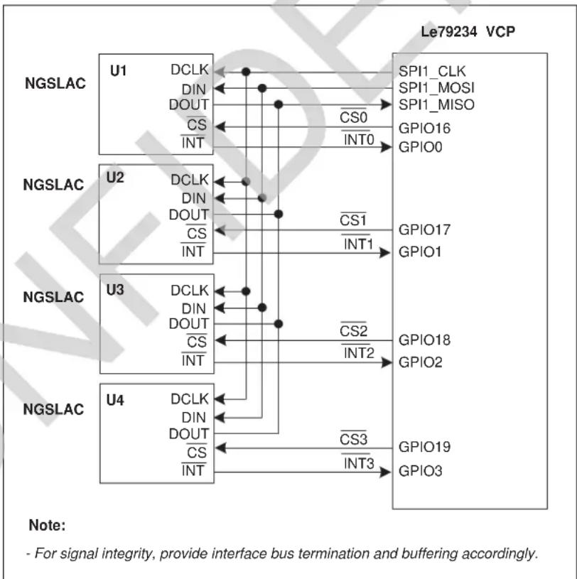
The Le79234 VCP can support up to 32 POTS channels, which is 4 octal SLAC devices. The SPI connections consist of VCP SPI port 1 controlling all 32 channels. VCP GPIO pins are used to control the SLAC chip select and receive SLAC interrupts. A Le79234 VCP to SLAC interface for 32 channels is presented in Figure 18.
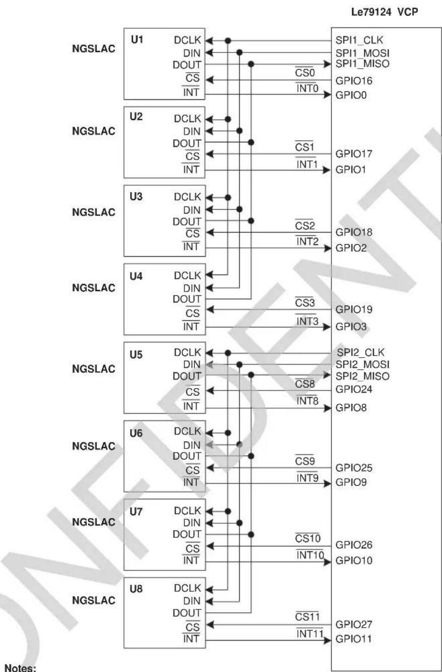
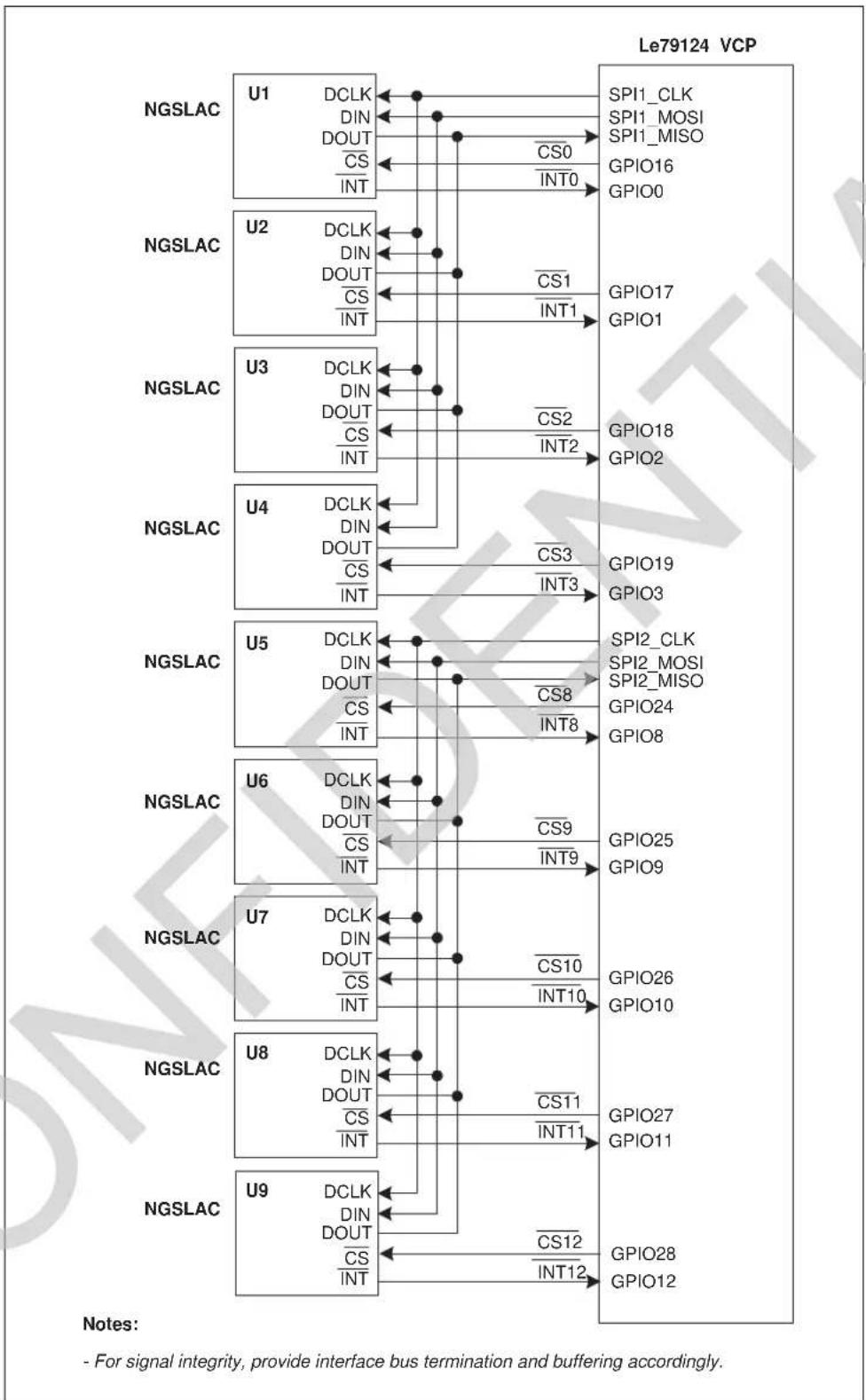
The Le79124 VCP can support up to 72 POTS channels, which is 9 octal SLAC devices. The SPI connections consist of VCP SPI port 1 controlling the first group of 32 channels and VCP SPI port 2 controlling the second group of up to 40 channels. VCP GPIO pins are used to control the SLAC chip select and receive SLAC interrupts. A Le79124 VCP to SLAC interface for 64 channels is presented in Figure 19; a Le79124 VCP to SLAC interface for 72 channels is presented in Figure 20.
The Le79128 VCP can support up to 128 POTS channels, which is 16 octal SLAC devices. The SPI connections consist of VCP SPI port 1 controlling the first group of 64 channels and VCP SPI port 2 controlling the second group of up to 64 channels. VCP GPIO pins are used to control the SLAC chip select and receive SLAC interrupts. A Le79128 VCP to SLAC interface for 128 channels is presented in Figure 21.
Signal integrity for these interfaces is presented in Section 2.4.1.
flowchart
graph TD
    subgraph NGSLAC_U1
        U1_1["CLK"] --> SPI1_CLK
        U1_1 --> SPI1_MOSI
        U1_1 --> SPI1_MISO
        U1_1 --> GPIO16
        U1_1 --> GPIO0
        U1_2["CLK"] --> SPI1_CLK
        U1_2 --> SPI1_MOSI
        U1_2 --> SPI1_MISO
        U1_2 --> GPIO16
        U1_2 --> GPIO0
        U1_3["CLK"] --> SPI1_CLK
        U1_3 --> SPI1_MOSI
        U1_3 --> SPI1_MISO
        U1_3 --> GPIO16
        U1_3 --> GPIO0
        U1_4["CLK"] --> SPI1_CLK
        U1_4 --> SPI1_MOSI
        U1_4 --> SPI1_MISO
        U1_4 --> GPIO16
        U1_4 --> GPIO0
        U1_5["CLK"] --> SPI1_CLK
        U1_5 --> SPI1_MOSI
        U1_5 --> SPI1_MISO
        U1_5 --> GPIO16
        U1_5 --> GPIO0
        U1_6["CLK"] --> SPI1_CLK
        U1_6 --> SPI1_MOSI
        U1_6 --> SPI1_MISO
        U1_6 --> GPIO16
        U1_6 --> GPIO0
        U1_7["CLK"] --> SPI1_CLK
        U1_7 --> SPI1_MOSI
        U1_7 --> SPI1_MISO
        U1_7 --> GPIO16
        U1_7 --> GPIO0
    end
    Note["Note:<br>- For signal integrity, provide interface bus termination and buffering accordingly."]
Figure 18 - Le79234 VCP to SLAC Interface - 32 Channel NGCC Line Card
flowchart
graph TD
    subgraph NGSLAC_U1
        U1_1["CLK"] --> SPI1_CLK
        U1_1 --> SPI1_MOSI
        U1_1 --> SPI1_MISO
        U1_1 --> GPIO16
        U1_1 --> GPIO0
        U1_2["CLK"] --> SPI1_CLK
        U1_2 --> SPI1_MOSI
        U1_2 --> SPI1_MISO
        U1_2 --> GPIO16
        U1_2 --> GPIO0
        U1_3["CLK"] --> SPI1_CLK
        U1_3 --> SPI1_MOSI
        U1_3 --> SPI1_MISO
        U1_3 --> GPIO16
        U1_3 --> GPIO0
        U1_4["CLK"] --> SPI1_CLK
        U1_4 --> SPI1_MOSI
        U1_4 --> SPI1_MISO
        U1_4 --> GPIO16
        U1_4 --> GPIO0
        U1_5["CLK"] --> SPI2_CLK
        U1_5 --> SPI2_MOSI
        U1_5 --> SPI2_MISO
        U1_5 --> GPIO24
        U1_5 --> GPIO8
        U1_6["CLK"] --> SPI2_CLK
        U1_6 --> SPI2_MOSI
        U1_6 --> SPI2_MISO
        U1_6 --> GPIO25
        U1_6 --> GPIO9
        U1_7["CLK"] --> SPI2_CLK
        U1_7 --> SPI2_MOSI
        U1_7 --> SPI2_MISO
        U1_7 --> GPIO26
        U1_7 --> GPIO10
        U1_8["CLK"] --> SPI2_CLK
        U1_8 --> SPI2_MOSI
        U1_8 --> SPI2_MISO
        U1_8 --> GPIO27
        U1_8 --> GPIO11
    end

    style NGSLAC_U1 fill:#f9f,stroke:#333
    style NGSLAC_U2 fill:#f9f,stroke:#333
    style NGSLAC_U3 fill:#f9f,stroke:#333
    style NGSLAC_U4 fill:#f9f,stroke:#333
    style NGSLAC_U5 fill:#f9f,stroke:#333
    style NGSLAC_U6 fill:#f9f,stroke:#333
    style NGSLAC_U7 fill:#f9f,stroke:#333
    style NGSLAC_U8 fill:#f9f,stroke:#333
Notes:
- For signal integrity, provide interface bus termination and buffering accordingly.
Figure 19 - Le79124 VCP to SLAC Interface - 64 Channel NGCC Line Card
flowchart
```mermaid
graph TD
    subgraph NGSLAC_U1
        U1_1["CLK"] --> SPI1_CLK
        U1_1 --> SPI1_MOSI
        U1_1 --> SPI1_MISO
        U1_1 --> GPIO16
        U1_1 --> GPIO0
        U1_2["CLK"] --> SPI1_CLK
        U1_2 --> SPI1_MOSI
        U1_2 --> SPI1_MISO
        U1_2 --> CS0
        U1_2 --> INT0
        U1_3["CLK"] --> SPI1_CLK
        U1_3 --> SPI1_MOSI
        U1_3 --> SPI1_MISO
        U1_3 --> CS1
        U1_3 --> INT1
        U1_4["CLK"] --> SPI1_CLK
        U1_4 --> SPI1_MOSI
        U1_4 --> SPI1_MISO
        U1_4 --> CS2
        U1_4 --> INT2
        U1_5["CLK"] --> SPI2_CLK
        U1_5 --> SPI2_MOSI
        U1_5 --> SPI2_MISO
        U1_5 --> CS8
        U1_5 --> INT8
        U1_6["CLK"] --> SPI2_CLK
        U1_6 --> SPI2_MOSI
        U1_6 --> SPI2_MISO
        U1_6 --> CS9
        U1_6 --> INT9
        U1_7["CLK"] --> SPI2_CLK
        U1_7 --> SPI2_MOSI
        U1_7 --> SPI2_MISO
        U1_7 --> CS10
        U1_7 --> INT10
        U1_8["CLK"] --> SPI2_CLK
        U1_8 --> SPI2_MOSI
        U1_8 --> SPI2_MISO
        U1_8 --> CS11
        U1_8 --> INT11
        U1_9["CLK"] --> SPI2_CLK
        U1_9 --> SPI2_MOSI
        U1_9 --> SPI2_MISO
        U1_9 --> CS12
        U1_9 --> INT12
    end

    note right of NGSLAC_U9: Note:
- For signal integrity, provide interface bus termination and buffering accordingly.
Note: Les79124 VCP
Figure 20 - Le79124 VCP to SLAC Interface - 72 Channel NGCC Line Card

flowchart
graph TD
    subgraph U1
        A["DCLK"] --> B["SPI1_CLK"]
        C["DIN"] --> D["SPI1_MOSI"]
        E["DOUT"] --> F["SPI1_MISO"]
        G["CS"] --> H["GPIO16"]
        I["INT"] --> J["GPIO0"]
        K["CS0"] --> L["INT0"]
    end

    subgraph U2
        M["DCLK"] --> N["SPI2_CLK"]
        O["DIN"] --> P["SPI2_MOSI"]
        Q["DOUT"] --> R["SPI2_MISO"]
        S["CS"] --> T["GPIO24"]
        U["INT"] --> V["GPIO8"]
        W["CS1"] --> X["INT1"]
        Y["INT2"] --> Z["GPIO17"]
        AA["GPIO2"] --> AB["GPIO1"]
        AC["CS2"] --> AD["GPIO18"]
        AE["INT2"] --> AF["GPIO2"]
        AG["INT3"] --> AH["GPIO19"]
        AI["INT4"] --> AJ["GPIO3"]
    end

    subgraph U3
        AK["DCLK"] --> AL["SPI2_CLK"]
        AM["DIN"] --> AN["SPI2_MOSI"]
        AO["DOUT"] --> AP["SPI2_MISO"]
        AQ["CS"] --> AR["GPIO25"]
        AS["INT"] --> AT["GPIO9"]
        AU["INT1"] --> AV["GPIO10"]
        AW["INT2"] --> AX["GPIO26"]
        AY["GPIO3"] --> AZ["GPIO10"]
        BA["INT3"] --> BB["GPIO11"]
    end

    subgraph U4
        BC["DCLK"] --> BD["SPI2_CLK"]
        BE["DIN"] --> BF["SPI2_MOSI"]
        BG["DOUT"] --> BH["SPI2_MISO"]
        BI["CS"] --> BJ["GPIO27"]
        BK["INT"] --> BL["GPIO11"]
        BM["INT3"] --> BN["GPIO11"]
    end

    subgraph U5
        BN["DCLK"] --> BO["SPI2_CLK"]
        BP["DIN"] --> BQ["SPI2_MOSI"]
        BR["DOUT"] --> BS["SPI2_MISO"]
        BT["CS"] --> BU["GPIO28"]
        BV["INT4"] --> BW["GPIO12"]
    end

    subgraph U6
        BW["DCLK"] --> BX["SPI2_CLK"]
        BY["DIN"] --> BZ["SPI2_MOSI"]
        BA["NGLSAC"] --> BB["NGLSAC"]

    subgraph U7
        BB["NGLSAC"] --> BC["NGLSAC"]

    subgraph U8
        BC["NGLSAC"] --> BD["NGLSAC"]

    A -->|DCLK| A
    C -->|DCLK| C
    M -->|DCLK| M
    B -->|DCLK| B
    BN -->|DCLK| BN
    BB -->|DCLK| BB
    BC -->|DCLK| BC
    BN -->|DCLK| BN
    A -->|DCLK| A
    C -->|DCLK| C
    M -->|DCLK| M
    B -->|DCLK| B
    BN -->|DCLK| BN
    A -->|DCLK| A
    C -->|DCLK| C
    M -->|DCLK| M
    B -->|DCLK| B
    BN -->|DCLK| BN
    A -->|DCLK| A
    C -->|DCLK| C
    M -->|DCLK| M
    B -->|DCLK| B
    BN -->|DCLK| BN
Notes:
- For signal integrity, provide interface bus termination and buffering accordingly.
Figure 21 - Le79128 VCP to SLAC Interface - 128 Channel NGCC Line Card
2.4.1 VCP to SLAC Interface Signal Integrity
Some measures are necessary to maintain signal integrity of the VCP to SLAC interface. The interface will operate at frequencies about 8 MHz. Rise and fall times at this frequency along with possible long trace lengths due to the bussed DCLK, DIN, and DOUT signals, warrants some form of signal integrity conditioning.
One approach is to use an FPGA to buffer all the interface signals. With an FPGA implementation, ensure that the propagation delays through the FPGA do not violate the data sheet timing specifications.
Another approach is to provide special conditioning to DCLK. SLAC data clock inputs are edge triggered, so fast clock rise and fall transitions need to be clean and free of reflections. Using a clock driver for the DCLK fanout to the SLAC devices will ensure clean transitions. Use a series termination resistor at the output of each clock driver.
If traces are kept as short as possible, a simple solution is to use series termination for all signals as shown in Figure 22 for the Le79234 VCP device, Figure 23 for the Le79124 VCP device, and Figure 24 for the Le79128 VCP device. Place the series termination resistors close to the respective VCP device or SLAC device as shown.
Whatever method of signal integrity is chosen, the design should be validated by running a signal integrity simulation analysis. IBIS models are available for the NGCC SLAC and VCP components.
flowchart
graph TD
    subgraph_INTEGRators_U1["NGSLAC U1"]
        A1["DCLK"] --> B1["SPI1_CLK"]
        A2["DIN"] --> B2["SPI1_MOSI"]
        A3["DOUT"] --> B3["SPI1_MISO"]
        A4["CS"] --> B4["GPIO16"]
        A5["INT"] --> B5["GPIO0"]
    end

    subgraph_INTEGRators_U2["NGSLAC U2"]
        A2["DCLK"] --> B2["GPIO17"]
        A3["DIN"] --> B3["GPIO1"]
        A4["DOUT"] --> B4["GPIO18"]
        A5["CS"] --> B5["GPIO2"]
        A6["INT"] --> B6["GPIO3"]
    end

    subgraph_INTEGRators_U3["NGSLAC U3"]
        A3["DCLK"] --> B3["GPIO18"]
        A4["DIN"] --> B4["GPIO2"]
        A5["CS"] --> B5["GPIO3"]
        A6["INT"] --> B6["GPIO19"]
    end

    subgraph_INTEGRators_U4["NGSLAC U4"]
        A4["DCLK"] --> B4["GPIO19"]
        A5["DIN"] --> B5["GPIO3"]
        A6["CS"] --> B6["GPIO3"]
    end

    note bottom
        INT series termination resistors are optional.
    end
Figure 22 - Le79234 VCP to SLAC 32-Channel Interface - Signal Integrity
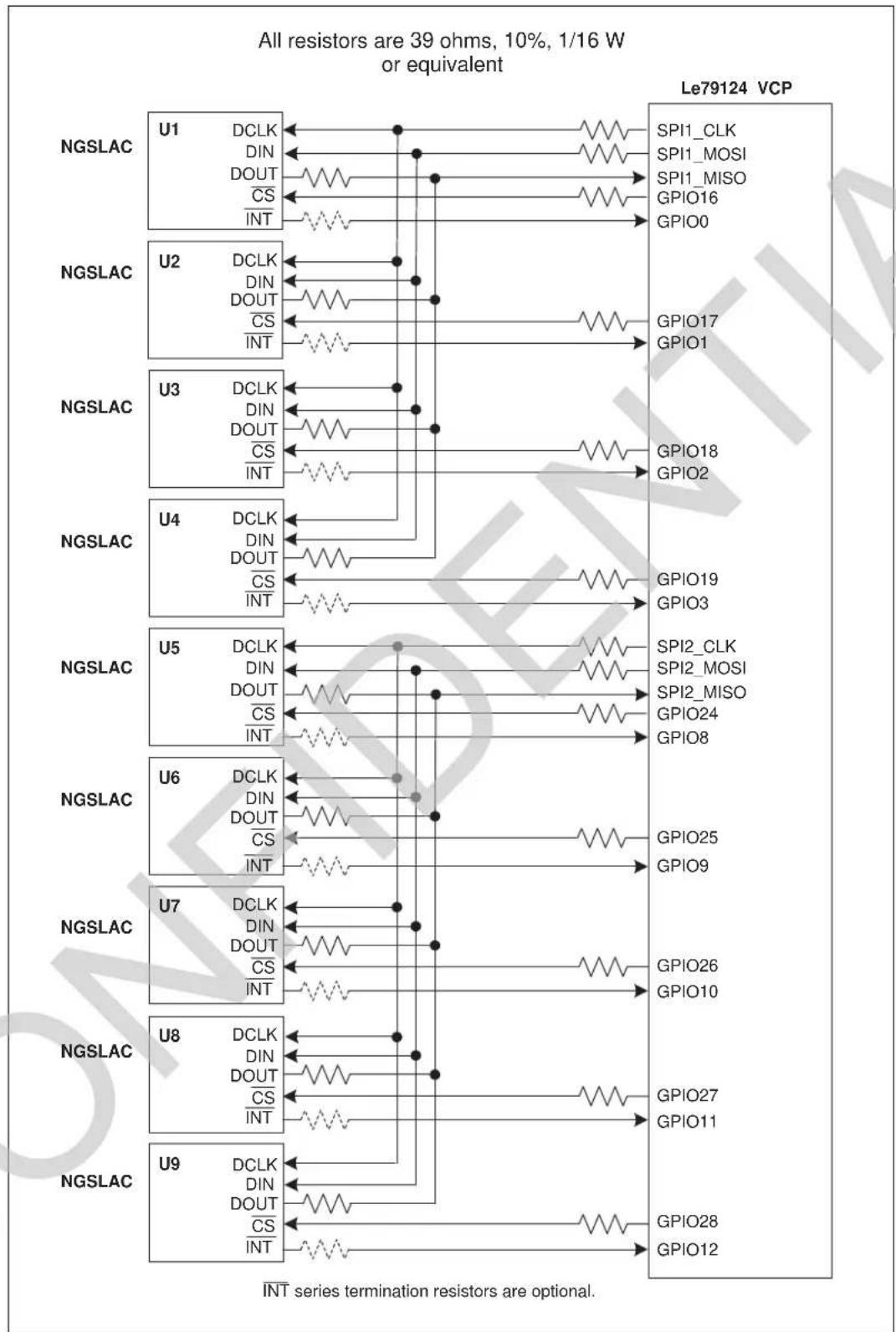
Figure 23 - Le79124 VCP to SLAC 72-Channel Interface - Signal Integrity
All resistors are 51 ohms, 10%, 1/16 W or equivalent

flowchart
graph TD
    subgraph NGSLAC_U1
        A1["DCLK"] --> B1["SPI1_CLK"]
        A1 --> B2["SPI1_MOSI"]
        A1 --> B3["SPI1_MISO"]
        A1 --> B4["GPIO16"]
        A1 --> B5["GPIO0"]
    end
    subgraph NGSLAC_U2
        A2["DCLK"] --> B2["GPIO17"]
        A2 --> B3["GPIO1"]
        A2 --> B4["GPIO1"]
        A2 --> B5["GPIO17"]
        A2 --> B6["GPIO1"]
        A2 --> B7["GPIO1"]
    end
    subgraph NGSLAC_U3
        A3["DCLK"] --> B3["GPIO18"]
        A3 --> B4["GPIO2"]
        A3 --> B5["GPIO2"]
        A3 --> B6["GPIO2"]
        A3 --> B7["GPIO2"]
    end
    subgraph NGSLAC_U8
        A8["DCLK"] --> B5["GPIO23"]
        A8 --> B6["GPIO7"]
        A8 --> B7["GPIO7"]
        A8 --> B8["GPIO7"]
    end
    subgraph NGSLAC_U9
        A9["DCLK"] --> B6["SPI2_CLK"]
        A9 --> B7["SPI2_MOSI"]
        A9 --> B8["SPI2_MISO"]
        A9 --> B9["GPIO24"]
        A9 --> B10["GPIO8"]
    end
    subgraph NGSLAC_U10
        A10["DCLK"] --> B10["GPIO25"]
        A10 --> B11["GPIO9"]
        A10 --> B12["GPIO25"]
    end
    subgraph NGSLAC_U11
        A11["DCLK"] --> B13["GPIO26"]
        A11 --> B14["GPIO10"]
    end
    subgraph NGSLAC_U16
        A16["DCLK"] --> B15["GPIO31"]
        A16 --> B16["GPIO15"]
    end
INT series termination resistors are optional.
Figure 24 - Le79128 VCP to SLAC 128-Channel Interface - Signal Integrity
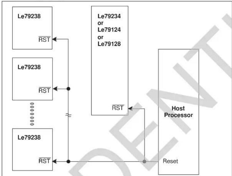
2.4.2 Hardware Reset
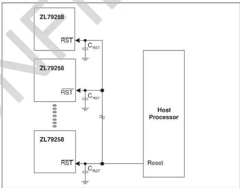
The VCP and SLAC devices require either a power up hardware reset or a hardware reset controlled by the host. Figure 26 shows a reset configuration where the host controls hardware reset of the VCP and SLAC devices. An advantage of this approach is the host can force a system reset at will. For this configuration, the host must hold hardware reset low until it completes its initial boot sequence.
For external ringing applications a capacitor to ground is recommended at the device reset pins. Figure illustrates hardware reset for an external ringing application.
flowchart
graph TD
    A["Le79238"] -->|RST| B["Le79234 or Le79124 or Le79128"]
    C["Le79238"] -->|RST| B
    D["..."] --> E["..."]
    F["Le79238"] -->|RST| G["Host Processor"]
    H["Reset"] --> I["Host Processor"]
    B -->|RST| G
    style A fill:#f9f,stroke:#333
    style C fill:#f9f,stroke:#333
    style D fill:#f9f,stroke:#333
    style F fill:#f9f,stroke:#333
    style H fill:#f9f,stroke:#333
    style B fill:#ccf,stroke:#333
    style G fill:#ccf,stroke:#333
    style I fill:#ccf,stroke:#333
Figure 25 - Hardware Reset
flowchart
graph TD
    A["ZL79258"] -->|RST| B["C_RST"]
    C["ZL79258"] -->|RST| D["C_RST"]
    E["ZL79258"] --> F["RST"]
    G["Host Processor"] --> H["Reset"]
    style A fill:#f9f,stroke:#333
    style C fill:#f9f,stroke:#333
    style E fill:#f9f,stroke:#333
    style G fill:#f9f,stroke:#333
    style B fill:#ccf,stroke:#333
    style D fill:#ccf,stroke:#333
    style F fill:#ccf,stroke:#333
    style H fill:#ccf,stroke:#333
Figure 26 - Hardware Reset for External Ringing Applications
2.5 PCM Interface
The PCM bus connects between the SLAC devices and the Network Interface, and the VCP device if used.
The PCM port of the SLAC and VCP devices interface to the external transmit and receive PCM highway(s). Dual PCM highways are supported.
Choice of PCM clock frequency and number of highways is dependent upon the number of channels and timeslot usage. A normal voice channel only requires a single 8-bit time slot but wideband mode (if used) requires four 8-bit time slots (two sets of 16-bit time slots). Testing requires two consecutive 8-bit time slots and the 15 kHz noise test requires 8 consecutive transmit channels to execute. An 8.192 MHz PCM clock provides 128 slots. For a 72 channel architecture if all 72 channels are assigned to individual 8-bit time slots, only 56 time slots are available for testing. So simply allocating two consecutive time slots to each channel is not possible with only one PCM highway.
Time slots are assigned on a per line basis via VP_OPTION_ID_TIMESLOT and the PCM highway is assigned on a per line basis via VP_OPTION_ID_PCM_HWY. Line test works in linear mode so two time slots per channel are required. For line test the VCP keeps an image of the time slot assignments, so there is no need to do a reassignment. But the host must make sure that the adjacent timeslot is not assigned as the VCP will not keep track of that. For instance, if there is a voice channel assigned to time slot 5, when a test is initiated on that same channel, the VCP will know the channel is on time slot 5, but the VCP will not check to see if time slot 6 is available – the VCP assumes this time slot is available.
Taking into account the device level restrictions listed below, an alternative approach to time slot assignment during testing is to put the voice time slots adjacent to each other and reserve a block of 8 time slots for testing. And if the 15 kHz noise test is to be used, reserve an additional block of 16 time slots.
A system operating with a dynamic time slot assignment architecture shall allocate a time slot to a channel before executing a line test on it in case the test function needs to perform a data transfer over the PCM bus.
Note these device level restrictions:
- Up to 4 lines in line testing simultaneously running per VCP device, of these, only 2 can be the 15kHz noise test.
- With VCP device use, up to 2 lines in line testing simultaneously running per SLAC device, of these, only 1 can be the 15kHz noise test. Without VCP device use, one line test running per SLAC device at a time.
2.5.1 PCM Interface - SLAC Device
The SLAC PCM port can transmit/receive 8-bit compressed (A-law/ -law) data or 16-bit linear data.
An 8 kHz frame sync signal indicating the beginning of a transmit/receive frame shall be supplied by the system and all time slots shall be referenced to it.
The SLAC devices will accept PCM clock frequencies (as defined in the SLAC data sheets) up to 8.192 MHz, synchronous to the frame sync signal. Thereby supporting up to 128 voice channels of 8-bits per highway in one frame of data.
Each time slot can carry one A-law or -law PCM voice channel. Two time slots are required to carry 16-bit linear data. The time slots are user programmable but are common for both highway channels. The transmit data can be sent out on highway A (DXA) or highway B (DXB) or both highways. This is programmable on a per channel basis.
When using the wideband transmission mode, two 16-bit linear samples are transmitted within each 8-kHz frame using two time slots. The API only allows allocating one time slot per channel and it will be used by the first byte of the first data word. The second byte of the first data word uses the adjacent time slot. The two bytes of the second data word will use a mirror time slot located exactly a half-frame away from the assigned time slot. Therefore, when using the wideband mode, the assigned time slot must be located within the first half of the 8-kHz frame.
Data can be transmitted on the positive or negative edge of PCLK. Receive data is always evaluated on the negative edge of PCLK.
To avoid timing and clock skew problems, the PCM port has a clock slot feature that allows the transmit and receive data to be independently offset from the zero time slot defined in relation to the frame sync signal applied. The clock slot permits 0-7 PCLK cycles of delay from the position defined by the applied frame synchronization signal.
| SLAC Pin Name | Type Reset Description | ||
| DXA | Output High Impedance | Primary downstream serial data output | |
| DXB | Output High Impedance | Secondary downstream serial data output | |
| Output High Impedance | Primary timeslot control signal (active low - open drain) | ||
| Output High Impedance | Secondary timeslot control signal (active low - open drain) | ||
| DRA Input Primary upstream serial data input | |||
| DRB Input Secondary upstream serial data input | |||
| PCLK Input PCM Interface clock | |||
| FS Input 8 kHz | Frame sync | ||
Table 3 - SLAC PCM Interface Pins
2.5.1.1 PCM Transmit Interface - SLAC Device
The PCM transmit interface controls the transmission of data onto the PCM highway through the output port selection circuitry and the time and clock slot control block. The time slot control signal (TSCx) goes low whenever PCM data is transmitted on the DX pin. These signals can be used for arbitration when there are multiple devices connected to the PCM bus. The data can be transmitted on either edge of PCLK. The clock edge at which the data is transmitted is selected by the XE bit in the Transmit Receive Clock Slot Register. The data is transmitted with the most significant bit first.
The Frame Sync (FS) pulse identifies time slot 0 of the transmit frame and all time slots are referenced to it.
2.5.1.2 PCM Receive Interface - SLAC Device
The PCM Receive interface logic controls the reception of the data bytes from the PCM highway. Each time slot is associated with one 8-bit data byte. The data is received with the most significant bit first. The received data coming on the DR pin is latched at the falling edge of PCLK.
2.5.1.3 PCM Timing
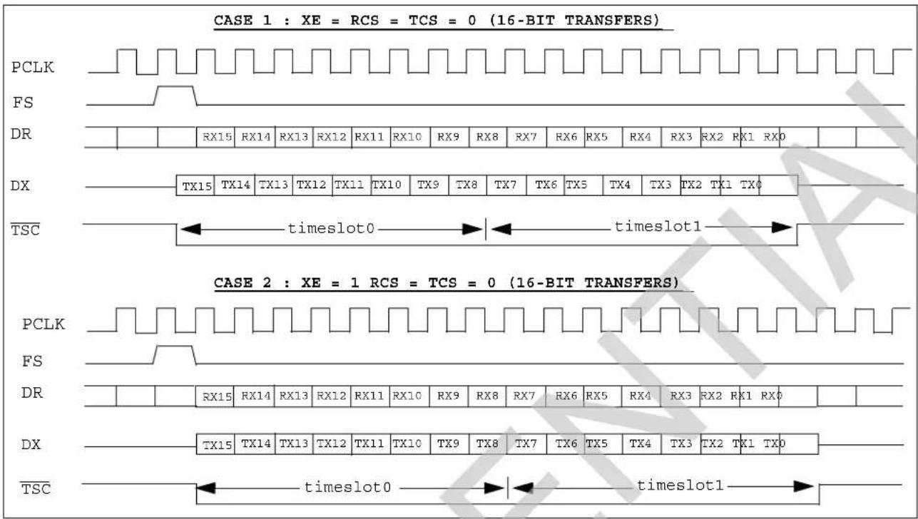
Figure 27 and Figure 28 illustrate the timing on the PCM highway for 8-bit and 16-bit transfers. Here is a key for the timing diagrams, these parameters are selected in the Device Profile.
- XE = 0, Transmit changes on negative edge of PCLK
- XE = 1 , Transmit changes on positive edge of PCLK
• RCS is Receive PCM Clock Slot delay number from 0 to 7
• TCS is Transmit PCM Clock Slot delay number from 0 to 7
2.5.2 PCM Interface - VCP Device
The VCP device connects to the SLAC PCM port. It uses the PCM highway for testing. The VCP PCM ports are described in Section 2.5.3.

text_image
CASE 1 : DEFAULT: XE = RCS = TCS = 0 (8-bit TRANSFERS) PCLK FS DR DX TSC Timeslot 0 CASE 2 : XE = 1 RCS = 2 TCS = 4 (8-bit TRANSFERS) PCLK FS DR DX TSC Timeslot 0Figure 27 - PCM Highway 8-bit Transfers
text_image
CASE 1 : XE = RCS = TCS = 0 (16-BIT TRANSFERS) PCLK FS DR DX TSC timeslot0 timeslot1 CASE 2 : XE = 1 RCS = TCS = 0 (16-BIT TRANSFERS) PCLK FS DR DX TSC timeslot0 timeslot1Figure 28 - PCM Highway 16-bit Transfers
2.5.3 PCM Hardware Interfaces
The PCM interface can be used in a variety of ways. To facilitate connection of this interface, a number of supported hardware interfaces are presented in the following figures. For all applications, unused PCM port pins are tied to ground to eliminate the potential of excess current draw and noise due to floating nodes.
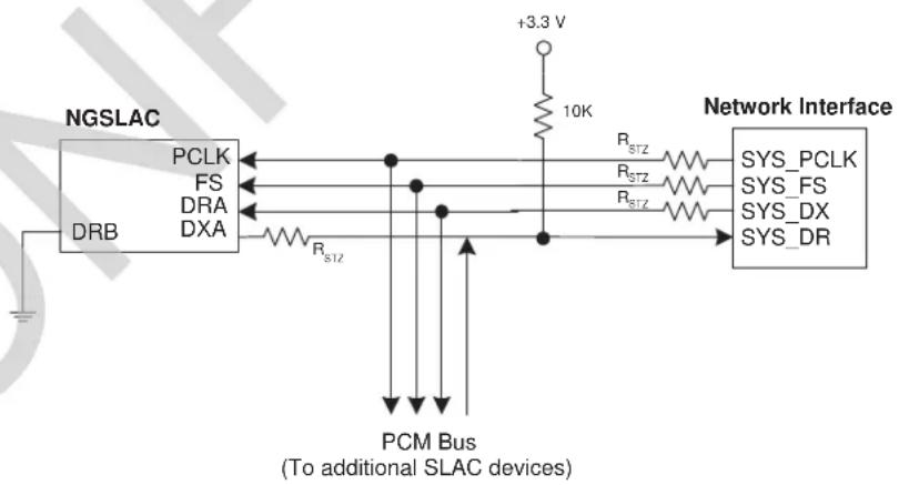
PCM wiring with use of the SLAC device only is shown in Figure 29 and Figure 30.
Figure 29 illustrates use of the SLAC Highway A port and Figure 30 illustrates use of both Highway A and Highway B ports. The SLAC requires PCLK and FS as inputs. System transmit (SYS_DX) is wired to SLAC data receive port (DRA or DRB). The SLAC data transmit port (DXA or DXB) is wired to the system receive (SYS_DR).
The remaining hardware interfaces all use the VCP device.
Two PCM blocks that reside on the VCP device are highlighted. There is a Slave PCM Highway A/Redundant block comprised of the PCLKA, FSA, DXA, DRA, TSCXA, TSCRA, PCLKB, FSB, DXB, DRB, TSCXB, and TSCRB pins, and a block used as the Slave PCM Highway B comprised of the MPCLK, MFS, MDX, and MDR pins. The Slave PCM Highway A/Redundant block requires PCLKA or PCLKB as inputs. The Slave PCM Highway B requires MPCLK as an input. PCLKA and PCLKB are monitored for clock faults.
The Slave PCM Highway A/Redundant block provides backplane driver tri-state control outputs TSCXA and TSCXB when DXA or DXB are active respectively. These are generally not used and do not appear in any of the following hardware drawings. The Slave PCM Highway B block does not have a tri-state control output.
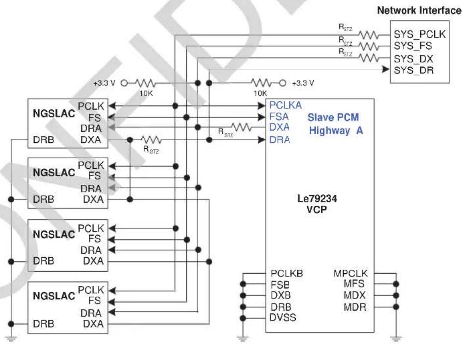
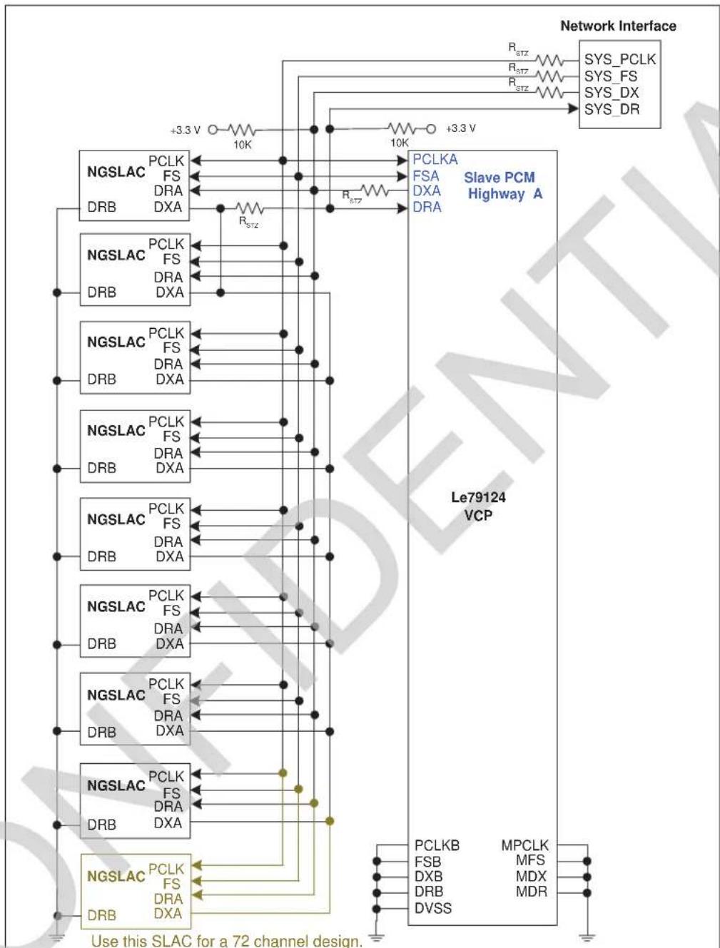
The first VCP hardware interface uses a single PCM highway. This architecture is presented for 32-channel, 64-channel, and 72-channel applications. The applications will support any valid PCM clock frequency.
A 32-channel PCM interface is shown in Figure 31 using the Le79234 VCP device. Four octal SLAC devices share the same PCM highway. VCP Slave PCM Highway A is used and it services voice and data for all channels. The PCM highway runs off of SYS_PCLK and SYS_FS from the backplane.
A 64-channel PCM interface is shown in Figure 32. Eight octal SLAC devices share the same PCM highway. VCP Slave PCM Highway A is used and it services voice and data for all channels. The PCM highway runs off of SYS_PCLK and SYS_FS from the backplane. For a 72-channel design, use a ninth SLAC device as shown in blue in Figure 32.
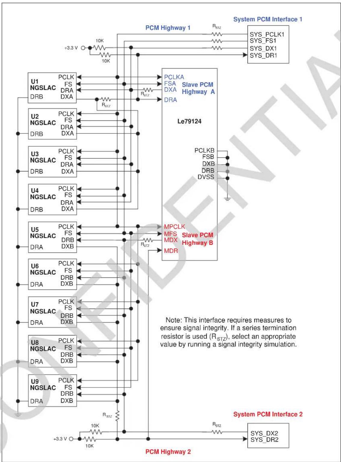
Figure 33 illustrates a Dual PCM highway option. The VCP Slave PCM Highway A services voice and data for the first group of 32 channels. The VCP Slave PCM Highway B services voice and data for the second group of 40 channels. Slave PCM Highway A is wired to SLAC PCM port A, Slave PCM Highway B is wired to SLAC PCM port B (that is, DRB and DXB of the SLAC). PCM Highway 1 runs off of SYS_PCLK1/SYS_FS1 and PCM Highway 2 runs off of SYS_PCLK2/SYS_FS2 from the backplane. PCLKB to MPCLK and FSB to MFS connections allow clock failure detection to monitor the Slave PCM Highway B. Tie PCLKB and FSB to ground if these connections are not used.
Figure 34 illustrates an alternative wiring for two PCM highways. Here both highways use a common PCLK and FS signal.
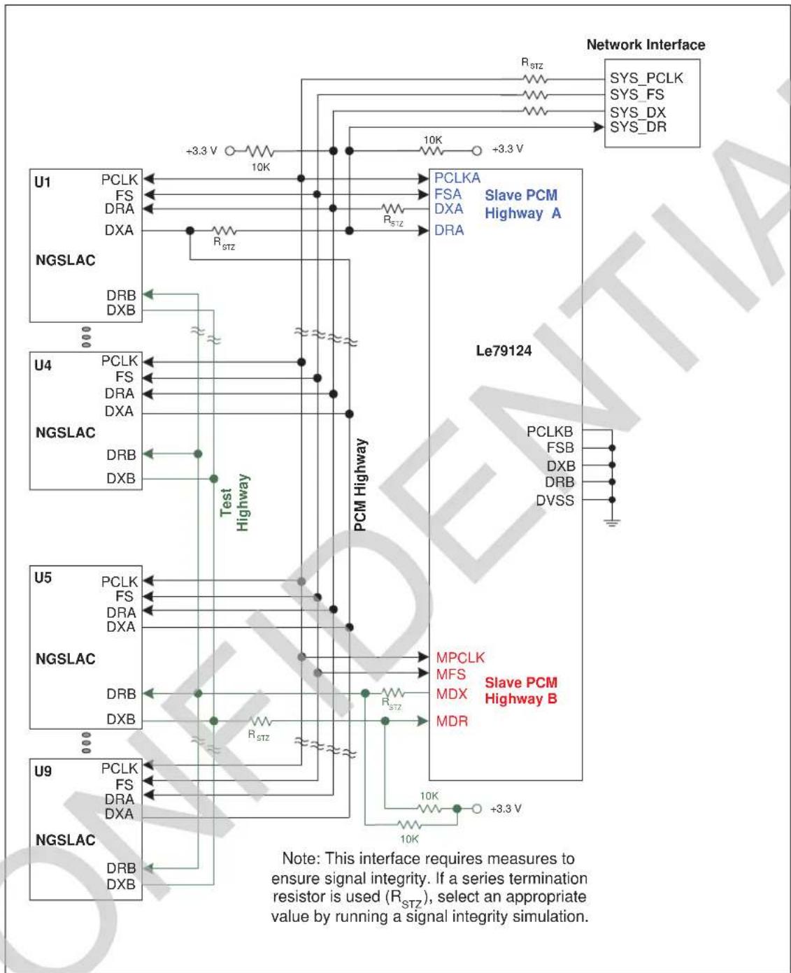
Figure 35 illustrates a separate Voice PCM highway and Test PCM highway option. The VCP Slave PCM Highway A services voice and data for all 72 channels. Slave PCM Highway A is wired to SLAC PCM port A on all SLAC devices. The VCP Slave PCM Highway B services all 72 channels but is dedicated to line testing. The Slave PCM Highway B is wired to SLAC port B (that is, DRB and DXB) on all SLAC devices. VCP MPCLK and MFS pins connect to SYS_PCLK and SYS_FS respectively, as the VCP Highway B is a slave to the clocking. The PCM and Test highways are synchronized and both run off of SYS_PCLK and SYS_FS from the backplane.
Figure 36 illustrates a Dual PCM highway option using the 128-channel Le79128 VCP device. The VCP Slave PCM Highway A services voice and data for the first group of 64 channels. The VCP Slave PCM Highway B services voice and data for the second group of 64 channels. Slave PCM Highway A is wired to SLAC PCM port A, Slave PCM Highway B is wired to SLAC PCM port B (that is, DRB and DXB of the SLAC). PCM Highway 1 runs off of SYS_PCLK1/SYS_FS1 and PCM Highway 2 runs off of SYS_PCLK2/SYS_FS2 from the backplane. PCLKB to MPCLK and FSB to MFS connections allow clock failure detection to monitor the Slave PCM Highway B. Tie PCLKB and FSB to ground if these connections are not used.
Note, even though the Le79124 VCP device is shown in the PCM highway options detailed in Figures 34 - 36, the Le79234 VCP device could also be used to control up to 32 channels.
text_image
NGSLAC DRB PCLK FS DRA DXA +3.3 V 10K Network Interface RSTZ RSTZ RSTZ SYS_PCLK SYS_FS SYS_DX SYS_DR PCM Bus (To additional SLAC devices)Note: This interface requires measures to ensure signal integrity. If a series termination resistor is used ( R_STZ ), select an appropriate value by running a signal integrity simulation.
Figure 29 - SLAC PCM Interface - Highway A

flowchart
graph TD
    A["NGSLAC"] --> B["PCLK"]
    A --> C["FS"]
    A --> D["DRA"]
    A --> E["DXA"]
    A --> F["DRB"]
    A --> G["DXB"]
    B --> H["R_STZ"]
    C --> I["R_STZ"]
    D --> J["R_STZ"]
    E --> K["R_STZ"]
    F --> L["R_STZ"]
    G --> M["R_STZ"]
    H --> N["+3.3 V"]
    I --> N
    J --> N
    K --> N
    L --> N
    M --> N
    N --> O["Network Interface"]
    style A fill:#f9f,stroke:#333
    style O fill:#ccf,stroke:#333
Note: This interface requires measures to ensure signal integrity. If a series termination resistor is used ( R_STZ ), select an appropriate value by running a signal integrity simulation.
Figure 30 - SLAC PCM Interface - Highway A & B
flowchart
graph TD
    A["Network Interface"] --> B["Slave PCM Highway A"]
    B --> C["Le79234 VCP"]
    C --> D["Network Interface"]
    subgraph Network Interface
        E["NGSLAC"] --> F["PCLK"]
        E --> G["FS"]
        E --> H["DRA"]
        E --> I["DXA"]
        J["NGSLAC"] --> K["PCLK"]
        J --> L["FS"]
        J --> M["DRA"]
        J --> N["DXA"]
        O["NGSLAC"] --> P["PCLK"]
        O --> Q["FS"]
        O --> R["DRA"]
        O --> S["DXA"]
        T["NGSLAC"] --> U["PCLK"]
        T --> V["FS"]
        T --> W["DRA"]
        T --> X["DXA"]
    end
    subgraph SlavePCM Highway A
        Y["PCLKA"] --> Z["FSA"]
        Y --> AA["DXA"]
        Y --> AB["DRA"]
    end
    subgraph SlavePCM Highway A
        AC["Slave PCM Highway A"] --> AD["Le79234 VCP"]
    end
    subgraph SlavePCM Highway A
        AE["PCLKB"] --> AF["MPCLK"]
        AE --> AG["MFS"]
        AE --> AH["MDX"]
        AE --> AI["MDR"]
        AJ["PCLKB"] --> AK["FSB"]
        AJ --> AL["DXB"]
        AJ --> AM["DRB"]
        AJ --> AN["DVSS"]
    end
Note: This interface requires measures to ensure signal integrity. If a series termination resistor is used ( R_STZ ), select an appropriate value by running a signal integrity simulation.
Figure 31 - VCP-SLAC PCM Interface - 32 Channel NGCC Line Card - Single PCM Highway
flowchart
graph TD
    subgraph Network Interference
        direction TB
        A["Network Interface"] --> B["Slave PCM Highway A"]
        B --> C["Le79124 VCP"]
    end

    subgraph Single Channel
        direction LR
        D["NGSLAC PCLK FS DRA DXA"] --> E["+3.3V 10K"]
        F["NGSLAC PCLK FS DRA DXA"] --> G["RSTZ"]
        H["NGSLAC PCLK FS DRA DXA"] --> I["RSTZ"]
        J["NGSLAC PCLK FS DRA DXA"] --> K["RSTZ"]
        L["NGSLAC PCLK FS DRA DXA"] --> M["RSTZ"]
        N["NGSLAC PCLK FS DRA DXA"] --> O["RSTZ"]
        P["NGSLAC PCLK FS DRA DXA"] --> Q["RSTZ"]
        R["NGSLAC PCLK FS DRA DXA"] --> S["RSTZ"]
        T["NGSLAC PCLK FS DRA DXA"] --> U["RSTZ"]
        V["NGSLAC PCLK FS DRA DXA"] --> W["RSTZ"]
        X["Use this SLAC for a 72 channel design."]
    end

    subgraph Control
        direction LR
        X
        Y
        Z
        AA
        AB
        AC
        AD
        AE
        AF
        AG
        AH
        AI
        AJ
        AK
        AL
        AM
        AN
        AO
        AP
        AQ
        AR
        AS
        AT
        AU
        AV
        AW
        AX
        AY
        AZ
        BA
        BB
        BC
        BD
        BE
        BF
        BG
        BH
        BI
        BJ
        BK
        BL
        BM
        BN
        BO
        BP
        BP
    end

    style Network Interference fill:#f9f,stroke:#333,stroke-width:2px
    style Single Channel fill:#ccf,stroke:#333,stroke-width:2px
Note: This interface requires measures to ensure signal integrity. If a series termination resistor is used ( R_STZ ), select an appropriate value by running a signal integrity simulation.
Figure 32 - VCP-SLAC PCM Interface - 64 or 72 Channel NGCC Line Card - Single PCM Highway

flowchart
graph TD
    subgraph_PCM_Highway_1["PCM Highway 1"]
        U1["NGSLAC"] --> PCLK1["PCLK"]
        U1 --> FS1["FS"]
        U1 --> DRA1["DRA"]
        U1 --> DXA1DXA1
        U2["NGSLAC"] --> PCLK2["PCLK"]
        U2 --> FS2["FS"]
        U2 --> DRA2["DRA"]
        U2 --> DXA2DXA2
        U3["NGSLAC"] --> PCLK3["PCLK"]
        U3 --> FS3["FS"]
        U3 --> DRA3["DRA"]
        U3 --> DXA3DXA3
        U4["NGSLAC"] --> PCLK4["PCLK"]
        U4 --> FS4["FS"]
        U4 --> DRA4["DRA"]
        U4 --> DXA4DXA4
        U5["NGSLAC"] --> PCLK5["PCLK"]
        U5 --> FS5["FS"]
        U5 --> DRA5["DRA"]
        U5 --> DXBDXBDXB
        U6["NGSLAC"] --> PCLK6["PCLK"]
        U6 --> FS6["FS"]
        U6 --> DRA6["DRA"]
        U6 --> DXBDXBDXB
        U7["NGSLAC"] --> PCLK7["PCLK"]
        U7 --> FS7["FS"]
        U7 --> DRA7["DRA"]
        U7 --> DXBDXBDXB
        U8["NGSLAC"] --> PCLK8["PCLK"]
        U8 --> FS8["FS"]
        U8 --> DRA8["DRA"]
        U8 --> DXBDXBDXB
    end

    subgraph_Slave_PCM_Highway_A["Slave PCM Highway A"]
        PCLKA["FSA"] --> SlaveA["Slave PCM Highway A"]
        DXA["DRA"] --> SlaveA
        DXB["DRA"] --> SlaveA
        DXB["VSS"] --> SlaveA
        SlaveA --> SlaveB["Slave PCM Highway B"]
        SlaveB --> SlaveA
    end

    Note1["Note: PCLKB to MPCLK and FSB to MFS connections are optional. Tie PCLKB and FSB to ground if these connections are not used."] --> Note2["Note: This interface requires measures to ensure signal integrity. If a series termination resistor is used (R_STZ), select an appropriate value by running a signal integrity simulation."]
    Note3["+3.3 V"] --> Note4["+3.3 V"]
    Note5["+3.0K"] --> Note6["+3.0K"]

    Note6["+3.0K"] --> Note7["+3.0K"]

    Note7["+3.0K"] --> Note8["+3.0K"]

    Note9["+3.0K"] --> Note10["+3.0K"]

    Note11["Network Interface"] --> Note12["Network Interface"]

    Note13["PCM Highway 2"] --> Note14["PCM Highway 2"]
Figure 33 - VCP-SLAC PCM Interface - 72 Channel NGCC Line Card - Dual PCM Highways
flowchart
graph TD
    subgraph System PCM Interface 1
        A["PCM Highway 1"] --> B["System PCM Interface 1"]
        B --> C["+3.3 V"]
        C --> D["10K"]
        D --> E["10K"]
        E --> F["+3.3 V"]
        F --> G["10K"]
        G --> H["10K"]
        H --> I["+3.3 V"]
        I --> J["10K"]
        J --> K["10K"]
        K --> L["+3.3 V"]
        L --> M["10K"]
        M --> N["10K"]
        N --> O["+3.3 V"]
        O --> P["10K"]
        P --> Q["10K"]
        Q --> R["+3.3 V"]
        R --> S["10K"]
        S --> T["10K"]
        T --> U["+3.3 V"]
        U --> V["10K"]
        V --> W["+3.3 V"]
        W --> X["10K"]
        X --> Y["+3.3 V"]
        Y --> Z["10K"]
        Z --> AA["+3.3 V"]
        AA --> AB["10K"]
        AB --> AC["+3.3 V"]
        AC --> AD["10K"]
        AD --> AE["+3.3 V"]
        AE --> AF["10K"]
        AF --> AG["+3.3 V"]
        AG --> AH["10K"]
        AH --> AI["+3.3 V"]
        AI --> AJ["10K"]
        AJ --> AK["+3.3 V"]
        AK --> AL["10K"]
        AL --> AM["+3.3 V"]
        AM --> AN["10K"]
        AN --> AO["+3.3 V"]
        AO --> AP["10K"]
        AP --> AQ["+3.3 V"]
        AQ --> AR["10K"]
        AR --> AS["+3.3 V"]
        AS --> AT["10K"]
        AT --> AU["+3.3 V"]
        AU --> AV["10K"]
        AV --> AW["+3.3 V"]
        AW --> AX["10K"]
        AX --> AY["+3.3 V"]
        AY --> AZ["10K"]
        AZ --> BA["+3.3 V"]
        BA --> BB["10K"]
        BB --> BC["+3.3 V"]
        BC --> BD["10K"]
        BD --> BE["+3.3 V"]
        BE --> BF["10K"]
        BF --> BG["+3.3 V"]
        BG --> BH["10K"]
        BH --> BI["+3.3 V"]
        BI --> BJ["10K"]
        BJ --> BK["+3.3 V"]
        BK --> BL["10K"]
        BL --> BM["+3.3 V"]
        BM --> BN["10K"]
        BN --> BO["+3.3 V"]
        BO --> BP["10K"]
        BP --> BQ["+3.3 V"]
        BQ --> BR["10K"]
        BR --> BS["+3.3 V"]
        BS --> BT["10K"]
        BT --> BU["+3.3 V"]
        BU --> BV["10K"]
        BV --> BW["+3.3 V"]
        BW --> BX["10K"]
        BX --> BY["+3.3 V"]
        BY --> BZ["10K"]
        BZ --> CA["+3.3 V"]
        CA --> CB["10K"]
        CB --> CC["+3.3 V"]
        CC --> CD["10K"]
        CD --> CE["+3.3 V"]
        CE --> CF["10K"]
        CF --> CG["+3.3 V"]
        CG --> CH["10K"]
        CH --> CI["+3.3 V"]
        CI --> CJ["10K"]
        CJ --> CK["+3.3 V"]
        CK --> CL["10K"]
        CL --> CM["+3.3 V"]
        CM --> CN["10K"]
        CN --> CO["+3.3 V"]
        CO --> CP["10K"]
        CP --> CQ["+3.3 V"]
        CQ --> CR["10K"]
        CR --> CS["+3.3 V"]
        CS --> CT["10K"]
        CT --> CU["+3.3 V"]
        CU --> CV["10K"]
        CV --> CW["+3.3 V"]
        CW --> CX["10K"]
        CX --> CY["+3.3 V"]
        CY --> CZ["10K"]
        CZ --> DA["+3.3 V"]
        DA --> DB["10K"]
        DB --> DC["+3.3 V"]
        DC --> DV["10K"]
        DV --> DW["+3.3 V"]
        DW --> DXA["DRA DXA"]
        DXA --> DA
    end

    subgraph System PCM Interface 2
        E
    end

    subgraph System PCM Interface 2
            E
            F
            G
            H
            I
            J
            K
            L
            M
            N
            O
            P
            Q
            R
            S
            T
            U
            V
            W
            X
            Y
            Z
            AA
            AB
            AC
            AD
            AE
            AF
            AG
            AH
            AI
            AJ
            AK
            AL
            AM
            AN
            AO
            AP
            AQ
            AR
            AS
            AT
            AU
            AV
            AW
            AX
            AY
            AZ
            BA
            BB
            BC
            BD
            BE
            BF
            BG
            BH
            BI
            BJ
            BK
            BL
            BM
            BN
            BO
            BP
            BP2
            BA2
            BA22
            BA222
            BA2222
            BA22222
            BA222222
            BA2222222
            BA22222222
            BA222222222
            BA2222222222
            BA22222222222
            BA222222222222
            BA2222222222222
            BA2222222222222
            BA2222222222222
            BA2222222222222
            BA2222222222222
            BA2222222222222
            BA2222<fcel>System PCM Interface 1
    +3.3V → PCLKA FSA Slave PCM Highway A Le79124 PCLKB FSB DPX DBD RDX DVSS MPCLK MFS Slave PCM Highway B MDR Note: This interface requires measures to ensure signal integrity. If a series termination resistor is used (RSTZ), select an appropriate value by running a signal integrity simulation.
    System PCM Interface 1 & 1 & 1 & 1 & 1 & 1 & 1 & 1 & 1 & 1 & 1 & 1 & 1 & 1 & 1 & 1 & 1 & 1 & 1 & 1 & 1 & 1 & 1 & 1 & 1 & 1 & 1 & 1 & 1 & 1 & 1 & 1 & 1 & 1 &
Figure 34 - VCP-SLAC PCM Interface - 72 Channel NGCC Line Card - Two PCM Highways with a Single Clock and Frame Sync
flowchart
graph TD
    subgraph NGSLAC
        U1["NGSLAC"] --> PCLK["PCLK"]
        PCLK --> FS["FS"]
        PCLK --> DRA["DRA"]
        PCLK --> DXA["DXA"]
        PCLK --> RSTZ["R_STZ"]
        RSTZ --> +3.3V["+3.3V"]
        +3.3V --> 10K["10K"]
        10K --> NetworkInterface["Network Interface"]
    end

    subgraph SlavePCMHighway_A
        U1 --> PCLKA["PCLKA"]
        PCLKA --> FSA["FSA"]
        PCLKA --> DXA["DXA"]
        PCLKA --> DRA["DRA"]
        PCLKA --> RSTZ["R_STZ"]
        RSTZ --> +3.3V
        +3.3V --> 10K
        10K --> NetworkInterface
    end

    subgraph SlavePCMHighway_B
        U4["NGSLAC"] --> PCLKB["PCLKB"]
        PCLKB --> FSB["FSB"]
        PCLKB --> DXB["DXB"]
        PCLKB --> DRB["DRB"]
        PCLKB --> DVSS["DVSS"]
        PCLKB --> RSTZ["R_STZ"]
        RSTZ --> +3.3V
        +3.3V --> 10K
        10K --> NetworkInterface
    end

    U5["NGSLAC"] --> PCLKP["PCLKP"]
        PCLKP --> FSP["FSP"]
        PCLKP --> DRAP["DRAP"]
        PCLKP --> DXA["DXA"]
        PCLKP --> RSTZR["R_STZ"]
        RSTZR --> +3.3V
        +3.3V --> 10K
        10K --> NetworkInterface
    end

    subgraph SlavePCMHighway_B
        U9["NGSLAC"] --> PCLKQ["PCLKQ"]
        U9 --> FSQ["FSQ"]
        U9 --> DRAQ["DRAQ"]
        U9 --> DXAQ["DRAQ"]
        U9 --> RSTZR["R_STZ"]
        RSTZR --> +3.3V
        +3.3V --> 10K
        10K --> NetworkInterface
    end

    Note["Note: This interface requires measures to ensure signal integrity. If a series termination resistor is used (R_STZ), select an appropriate value by running a signal integrity simulation."]
Figure 35 - VCP-SLAC PCM Interface - 72 Channel NGCC Line Card - Separate Voice and Test PCM Highways
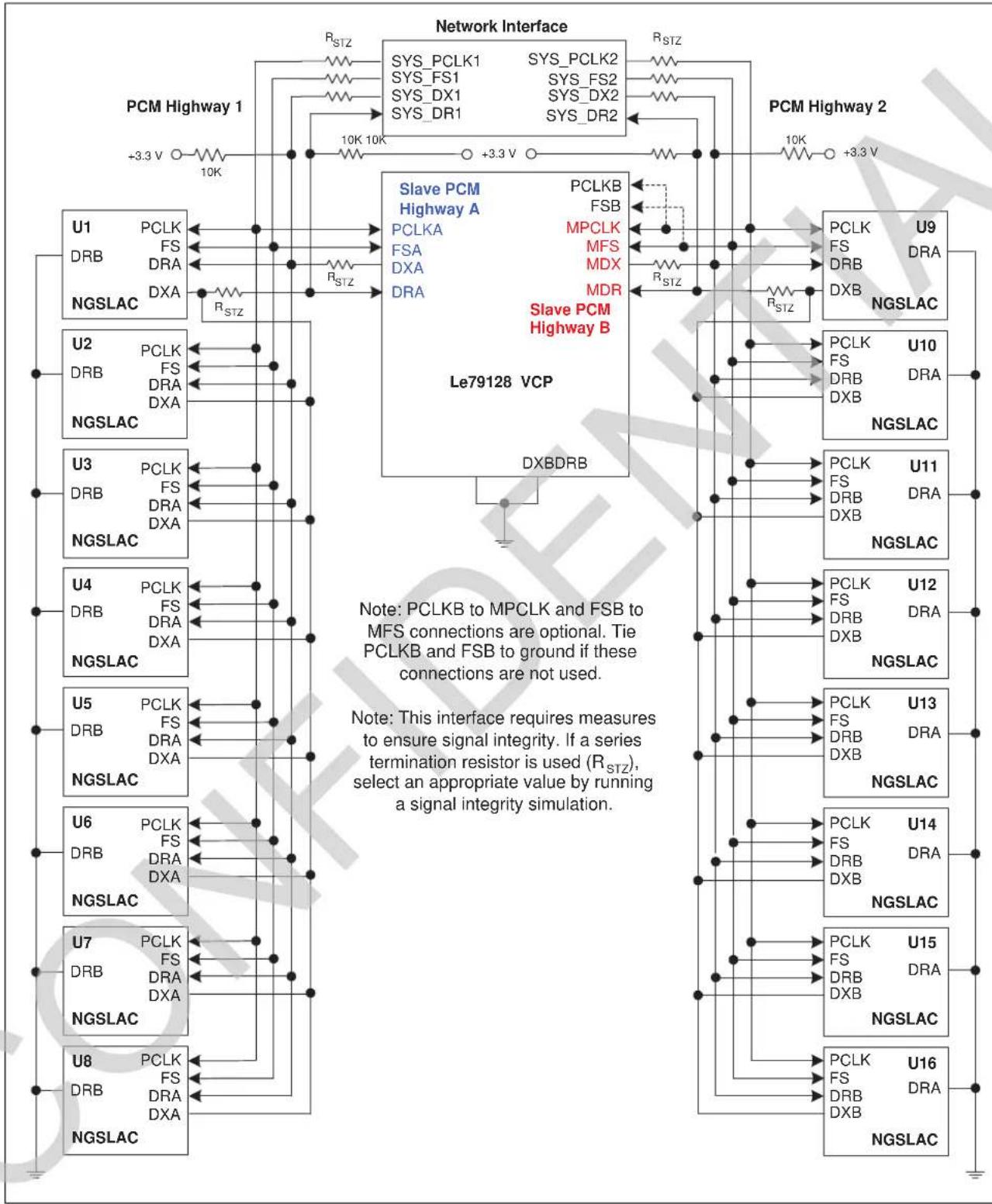
flowchart
graph TD
    subgraph_PCM_Highway_1["PCM Highway 1"]
        U1 -->|+3.3 V| RSTZ
        U1 -->|10K| RSTZ
        U1 -->|10K| RSTZ
        U1 -->|10K| RSTZ
        U1 -->|+3.3 V| Network_Interface["Network Interface"]
        U2 -->|+3.3 V| RSTZ
        U2 -->|10K| RSTZ
        U2 -->|10K| RSTZ
        U2 -->|10K| RSTZ
        U2 -->|10K| RSTZ
        U2 -->|10K| RSTZ
        U2 -->|10K| RSTZ
        U2 -->|10K| RSTZ
        U2 -->|10K| RSTZ
        U2 -.->|PCLK| RSTZ
        U2 -.->|FS| RSTZ
        U2 -.->|DRA| RSTZ
        U2 -.->|DXA| RSTZ
        U2 -.->|DXA| RSTZ
        U2 -.->|DXA| RSTZ
        U2 -.->|DXA| RSTZ
    end

    subgraph_Slave_PCM_Highway_A["Slave PCM Highway A"]
        PCLKA --> PCLKB
        FSA --> FSB
        DXA --> DXB
        DRA --> DXB
        DRA --> DXB
        DRA --> DXB
        DRA --> DXB
        DRA --> DXB
        DRA --> DXB
        DRA --> DXB
    end

    subgraph_Slave_PCM_Highway_B["Slave PCM Highway B"]
        PCLKB --> PCLKB
        FSB --> FSB
        MPCLK --> MPCLK
        MFS --> MFS
        MDX --> MDX
        MDR --> MDR
        MDR --> MDR
        MDR --> MDR
        MDR --> MDR
    end

    subgraph_Le79128_VCP["Le79128 VCP"]
        PCLKL --> PCLKL
        FS --> FS
        DRB --> DRB
        DXB --> DXB
        DXB --> DXB
        DXB --> DXB
        DXB --> DXB
    end

    subgraph_PCM_Highway_2["PCM Highway 2"]
        PCLKL --> PCLKL
        FS --> FS
        DRB --> DRB
        DXB --> DXB
        DXB --> DXB
        DXB --> DXB
        DXB --> DXB
        DXB --> DXB
    end

    subgraph_NGSLAC["NGSLAC"]
        PCLKL --> PCLKL
        FS --> FS
        DRB --> DRB
        DXB --> DXB
        DXB --> DXB
    end

    note["Note: PCLKB to MPCLK and FSB to MFS connections are optional. Tie PCLKB and FSB to ground if these connections are not used."]
    note["Note: This interface requires measures to ensure signal integrity. If a series termination resistor is used (R_STZ), select an appropriate value by running a signal integrity simulation."]
Figure 36 - VCP-SLAC PCM Interface - 128 Channel NGCC Line Card - Dual PCM Highways
2.5.3.1 PCM Signal Integrity
Some measures are necessary to maintain signal integrity at the system PCM interface. The system interface provides PCLK, FS, and DX signals to the SLAC and VCP devices. SLAC and VCP data clock inputs are edge triggered, so fast clock rise and fall transitions need to be clean and free of reflections.
Using a clock driver for the PCLK and FS fanout to the SLAC devices will ensure clean transitions. With this method, each SLAC device (or a smaller group of SLAC devices) has its own individual clock or frame sync signal routed to it. Use a series termination resistor at the output of each clock driver or other appropriate end termination.
Another approach is to use an FPGA to buffer all the PCM signals. If this approach is used, ensure that FPGA propagation delays do not violate the data sheet timing specifications.
If an FPGA is not used to buffer SLAC DXA, then a single series resistor after the final connection point of all the SLAC devices, as shown in all the hardware interfaces, may be adequate for this signal.
Whatever method of signal integrity is chosen, the design must be validated by running a signal integrity simulation analysis. IBIS models are available for the NGCC SLAC and VCP components.
2.6 SLAC-SLIC Interface
The analog interface between the SLAC and SLIC devices (for internal ringing) is shown in Figure 37. Component values for this and other interfaces are listed in Section 3.0.
2.6.1 RCVP, RCVN
This path provides the receive metallic transmission voltage to the loop, both the receive ac transmission signal and the metering signal go through this path. The receive differential interface is filtered between the SLAC and SLIC devices. R_CVP , R_CVN , and C_M make up the low pass noise filter.
2.6.2 DCA, DCB
This is the DC feed control path to the SLIC. The DC feed control path includes a low pass filter in order to limit noise on the voiceband and data band. This is made of the C_DCA and C_DCB capacitors and an internal resistance. The cut-off frequency of this low pass filter is nominally set to approximately 36 Hz using the defined external capacitance.
The corner frequency of the dc feed low-pass filter is a function of the internal source resistance feeding the signal to the external capacitor. A different internal resistor value is selected as necessary in order to provide a different time constant. The bandwidth of the DC feed path is increased to approximately 145 Hz during ringing, after an on-hook or an off-hook transition, after the firmware detects that the host has changed the dc feed template, during fast reversal, and during slow reversal if the line is on-hook.
The internal resistance can also be removed to obtain a very fast response such as to allow generating higher frequency signals during line testing. This increases the bandwidth to approximately 2 kHz.
2.6.3 IA, IB
A current proportional to the respective A or B lead current is directly connected from the SLIC to the SLAC.
2.6.4 IMT, VIMT, VAC
Metallic loop current proportional to the differential current in the SLIC devices A and B leads is directly coupled from the SLIC to the SLAC. R_IMT converts the current to a voltage for the VIMT SLAC input. C_VAC removes the dc content and the transmit ac transmission signal is applied to the SLAC VAC input.
2.6.5 CANCEL
If metering is used, capacitor C_CAN is required. During a metering burst, the SLAC applies a cancellation signal into the transmit path effectively removing any metering current sense.
2.6.6 SVA, SVB
These pins sense the A and B lead voltages through high impedance resistors. The tolerance of the resistors determines the accuracy of the integrated testing. A 1%, 200 ppm resistor can be used. For higher accuracy, use a 0.5%, 100 ppm resistor. If PTC protection is used, the sense resistors must be able to withstand high voltages from fault conditions when the PTC goes into its high impedance state. Select a resistor with an appropriate voltage rating.
2.6.7 Battery Supplies and Battery Sense
R_SPB , R_SLB , and R_SHB sense the battery voltages. If only one negative battery is used, connect both negative battery resistors ( R_SLB and R_SHB ) to the same supply and wire VBH to VBL as shown in Figure 37. If no positive supply is used, connect the sense resistor R_SPB to ground.
The battery sense pins are current inputs whose voltage is held at VREF.
2.6.8 LD, SEL, and P-Bus
These digital lines which control the SLIC state and switches are all direct connect lines between the SLAC and the SLIC.
The SLIC P-BUS interface uses a 4 bit parallel bus (SEL, P[2:0]) and eight individual load pins (LD[7:0]) to control the FXS state and Switch state of up to eight SLIC devices. The SEL signal determines whether the P[2:0] value is assigned to the FXS state of the SLIC device (SEL=0) or the Switch state of the SLIC device (SEL=1). The P[2:0] and SEL values are latched inside the SLIC on the rising edge of the active low LD[n] signal. The P-BUS operates continuously so that each channel's FXS and Switch states are automatically refreshed every 128 ms.
2.6.9 Debug port
DEBUG_CLK requires a pull-up to the +1.8 V or the +3.3 V supply and DEBUG_IO requires a pull-down to DGND. The most robust conditioning is to short DEBUG_CLK to +3.3 V and DEBUG_IO to DGND through 0 ohm resistors.

text_image
Overcurrent/ Overvoltage Protection ** A □ B □ VGND □ BATH □ BATP □ C_BDBI □ C_BDI BATP □ C_BATPI D_VBH BATH □ Optimal connection if BATL is not used BATL □ C_BATLI □ C_BATHI VCC TLD AD U1i Le79271 RCVP RCVN VREF DCB IA IB BD VBP VBH VBL BGND AGND RREF The exposed thermal pad should be connected to AGND or BGND*** Required for metering only * C_CANi IMT LD SEL SEL P0 P1 P2 R_REFI See Absolute Maximum Ratings +3.3 V R_SVB1I R_SVB2I R_SVA1I R_SVA2I R_CMI R_CVPi R_CVNI DCA DCAi C_DCAi C_VREF I C_DCBi C_VREFI C_DCBI VDD33_x SVBi AVDDxx +3.3 V C_VDD33_x C_AVDDxx R_DEBCLK RCVPi DEBUG_CLK VDD18_x +1.8 V C_FILT C_VDD18_x VREFI DEBUG_IO R_DEBIO U2 Le79238 IA_I IA_I IB_I IB_I CANCEL_I CANCEL_I IMT_I IMT_I SPB R_SPB BATP VIMT_I SLB R_SLB BATL VAC_I SHB R_SHB BATH IREF R_REF R_PSP R_SPB Channel 1 Channel 2 Channel 3 Channel 4 Channel 5 Channel 6 Channel 7 Channel 8 DGND x AGNDx NOTES: Connections are shown for one SLAC channel, i = channel number. * Optional components (Red). ** Consult Microsemi for optimized components (Blue). *** Refer to Layout Considerations (Green).Figure 37 - SLAC-SLIC Internal Ringing Interface - One Channel Shown
2.6.10 Sensitive Nodes
Highly sensitive analog nodes need to be protected from noise sources, especially noisy digital circuits. Sensitive analog nodes of the SLAC and SLIC are highlighted in Figure 38. These nodes require special consideration when routing, keep traces short and minimize vias. Components that have placement constraints are also shown, position these components as described in Figure 38.
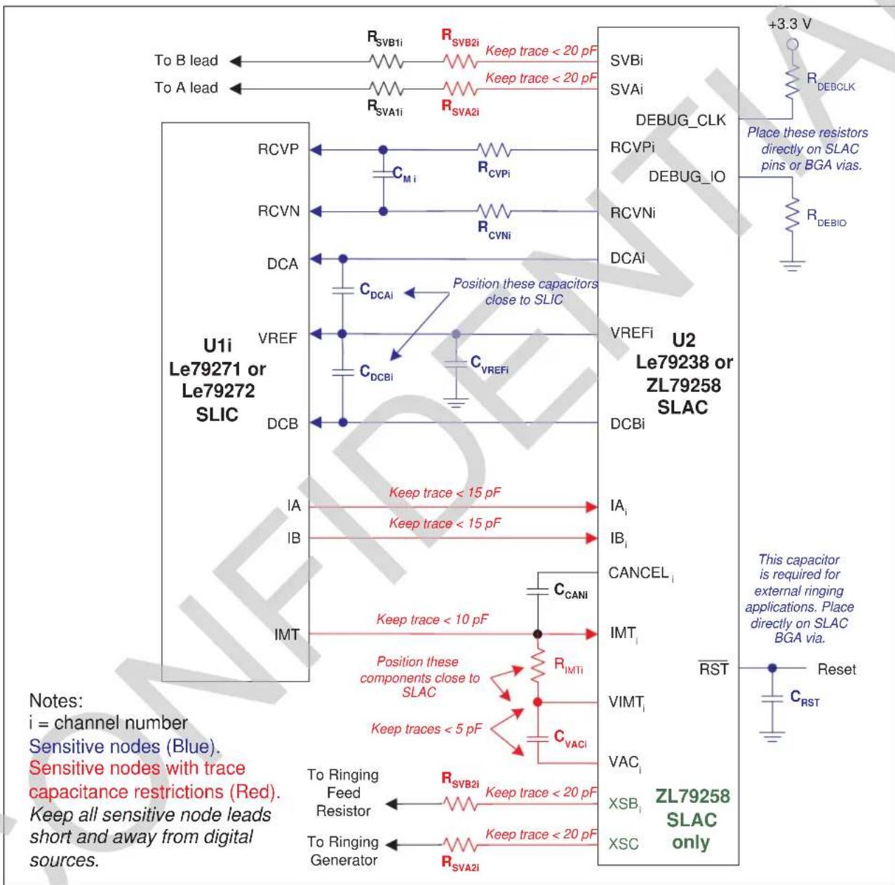
text_image
To B lead To A lead U1i Le79271 or Le79272 SLIC RCVP RCVN DCA VREF DCB IA IB IMT R_SVB1i R_SVB2i Keep trace < 20 pF Keep trace < 20 pF R_SVA1i R_SVA2i Position these capacitors close to SLIC C_M i R_CVPi R_CVNi C_DCAi C_DCBI C_VREFi C_CANi Keep trace < 15 pF Keep trace < 15 pF Position these components close to SLAC Keep trace < 10 pF Keep traces < 5 pF R_IMTi C_VACi R_SVB2i Keep trace < 20 pF To Ringing Feed Resistor To Ringing Generator Keep trace < 20 pF Keep trace < 20 pF +3.3 V SVAi DEBUG_CLK RCVPi DEBUG_IO RCVNi DCAi VREFi U2 Le79238 or ZL79258 SLAC DCBi IA_i IB_i CANCEL_i IMT_i VIMT_i VAC_i XSB_i ZL79258 SLAC only This capacitor is required for external ringing applications. Place directly on SLAC BGA via. Reset C_RST Notes: i = channel number Sensitive nodes (Blue). Sensitive nodes with trace capacitance restrictions (Red). Keep all sensitive node leads short and away from digital sources.Figure 38 - SLAC-SLIC Interface - Sensitive Nodes
In addition, the P-bus, SEL, and LD timing signals (Figure 37) must be kept separate from the analog circuitry. Avoid routing P-bus/SEL and LD timing signals near device pin areas unless route is on a different layer isolated by a ground plane.
2.6.11 SLAC IO
The SLAC provides two general purpose programmable input/output pins per channel, IO[1:8]_0 and IO[1:8]_1.
The IO[1:8]_0 pins are configured to drive a 3 V coil electromechanical relay. The IO[1:8]_0 pins can be programmed as open drain relay drivers. Built-in integrated flyback diodes eliminate the need for external diodes across the relay coils. Refer to Figure 39 for a schematic representation. These pins are commonly used to drive the calibration relay in Configuration D or the ringing relay for external ringing applications.
The other IO pins (IO[1:8]_1) are capable of sinking 10 mA when programmed as an output. These pins can be used with an external transistor to drive a relay.
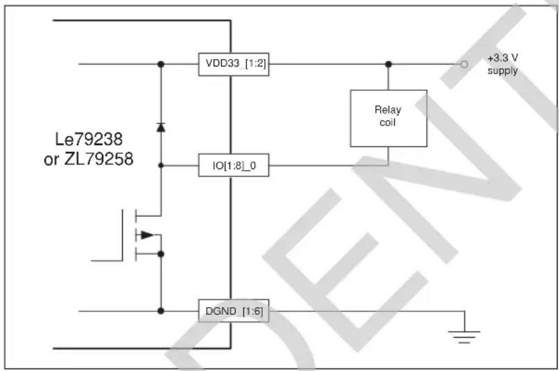
text_image
Le79238 or ZL79258 VDD33 [1:2] IO[1:8]_0 DGND [1:6] Relay coil +3.3 V supplyFigure 39 - SLAC Open Drain Relay Drivers
2.7 EMC Network
The AD/BD interface in Figure 37 shows two sets of EMI capacitors. The SLIC device only requires the C_ADi and C_BDi capacitance values to satisfy 3 V_RMS RF immunity requirements in a test board environment. However due to PCB layout and component placement, often additional decoupling is required to satisfy EMC. Refer to the EMI Capacitors Section 4.7 in Layout Considerations for more information on this topic.
The Host Test Library tests and accuracies assume a CADi and CBDi capacitance of 4.7 nF. If the capacitance value on AD and BD leads is increased, change the Host Test Library header file to reflect the appropriate capacitance value. The nominal capacitance from AD or BD to ground must be kept less than 10 nF.
For extensive information on EMC, request the Ve792 NGCC Electromagnetic Compatibility Application Note (Document ID# 142651).
2.8 Using a Single Negative Battery
Referring to Figure 37, if only one negative battery is to be used. Tie the SLIC VBL pin directly to the SLIC VBH pin. Do not connect VBL to the cathode side of D_VBHi .
3.0 Application Circuits and Parts Lists
Components required external to the SLIC, SLAC, and VCP devices are detailed in the following Application Circuits and Parts Lists. Use of the per channel test load and the metering capacitor are application dependent. Most component values and tolerances are predefined for a given application and are not to be varied. The IVD circuit varies dependant upon the application, so consult Microsemi for optimized components. Components that are not discussed here are protection components, consult Microsemi for recommendations for your design. Microsemi can provide part numbers for all the components listed in the Parts List.
The single channel Le79271 SLIC device can be substituted for the Le79272 Dual SLIC in any of the Application Circuits.
If the Le79238 SLAC in the 164-pin LGA package is used, refer to Section 4.1.4 and Section 4.6 for layout and connection information for its exposed pad.
Application circuits are provided for the supported hardware topologies. Parts Lists are provided for supported calibration and test options for a given hardware topology. The hardware topologies and calibration circuit are presented in detail in the various Software Package data sheets, as well as accuracies for the different test options. Configuration C, D, E, and F topologies are supported. Configuration C is a basic internal ringing configuration. Configuration D is similar but has the addition of an external relay to connect to a shared calibration circuit. Configuration E is a basic external ringing configuration. Configuration F supports an external ringing application that has an external relay to connect to a shared calibration circuit.
Figures 40-42 present application circuits for Configuration C. Figure 40 illustrates a POTS voice only application using three batteries, BATP for ringing and boosted battery, BATH for ringing, scan, and off-hook DC feed for long loops, and VBATL for off-hook DC feed for short loops. Figure 41 illustrates a voice only application circuit for short loop applications like GPON using only two negative batteries, BATH for ringing and scan and VBATL for off-hook DC feed. Figure 42 illustrates a voice and data (IVD) application using three batteries. Parts lists for these circuits follow. Parts lists are provided for three test scenarios, Factory Calibration with Test, No Calibration with Test, and No Calibration and No Test. Component tolerance is dependant upon the level of test and whether line card calibration is used. Values, ratings, and proper tolerances for each of these scenarios is detailed in the respective parts lists.
Figure 43 and Figure 44 present application circuits for Configuration D using three batteries. Figure 43 illustrates a POTS voice only application circuit and Figure 44 illustrates a voice and data (IVD) application. Configuration D has test capability and allows the line circuit to be calibrated when deployed. Values, ratings, and proper component tolerances for this scenario is detailed in the Configuration D Parts List.
Figure 45 and Figure 46 illustrate POTS voice only application circuits for external ringing Configuration E. A battery-backed and an earth-backed application are shown. This application uses two batteries. Values, ratings, and proper component tolerances are detailed in the Configuration E External Ringing Parts List.
Figure 47 and Figure 48 illustrate POTS voice only application circuits for external ringing Configuration F. Configuration F has test capability and allows the line circuit to be calibrated when deployed. A battery-backed and an earth-backed application are shown. This application uses two batteries. Values, ratings, and proper component tolerances are detailed in the Configuration F External Ringing Parts List.
Figure 49 shows the external components required for the Le79124 VCP device and Figure 50 shows the external components required for the Le79234 VCP device. VCP GPI control and PCM connections using a single PCM highway are illustrated. Figure 51 shows the external components required for the Le79128 VCP device. VCP GPI control and PCM connections using dual PCM highways are illustrated. Component values, ratings, and tolerances are detailed in the VCP Device Parts List. Note, any termination resistors used in the VCP to SLAC control interface, as discussed in Section 2.4.1, are not shown in these Figures or Parts List.
3.1 Configuration C Application Circuits
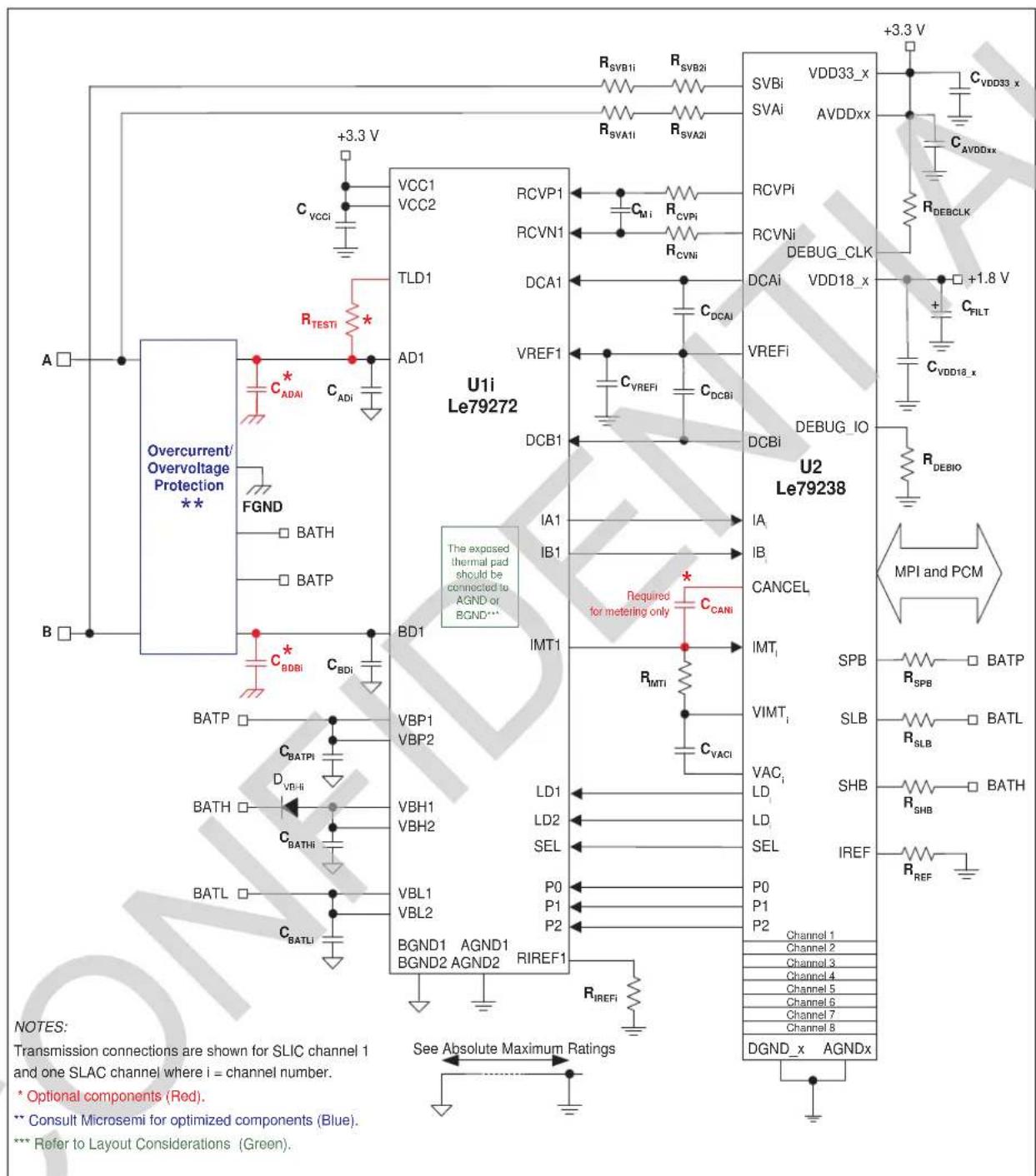
text_image
Overcurrent/ Overvoltage Protection ** FGND BATH BATP BD1 VBP1 VBP2 VBH1 VBH2 VBL1 VBL2 BGND1 AGND1 BGND2 AGND2 RIREF1 A B C_vcci C_ADAI C_ADi C_BDBi C_BDi BATP CBATPI D_VBI-i BATH CBATHi BATL CBATLI +3.3 V VCC1 VCC2 RCVP1 RCVN1 TLD1 DCA1 VREF1 DCB1 IA1 IB1 IMT1 LD1 LD2 SEL P0 P1 P2 R_SVB1i R_SVB2i R_SVA1i R_SVA2i R_CMI R_CVPI R_CVNI C_DCAI C_DCAI C_VREFI C_DCBI U1i Le79272 The exposed thermal pad should be connected to AGND or BOND*** The exposed thermal pad should be connected to AGND or BOND*** RGDP_1 RGDP_2 RGDP_3 RGDP_4 RGDP_5 RGDP_6 RGDP_7 RGDP_8 RGDP_9 RGDP_10 RGDP_11 RGDP_12 RGDP_13 RGDP_14 RGDP_15 RGDP_16 RGDP_17 RGDP_18 RGDP_19 RGDP_20 RGDP_21 RGDP_22 RGDP_23 RGDP_24 RGDP_25 RGDP_26 RGDP_27 RGDP_28 RGDP_29 RGDP_30 RGDP_31 RGDP_32 RGDP_33 x +3.3 V SVBi VDD33_x SVAi AVDDxx RCVPI RCVNI DEBUG_CLK DCAi VDD18_x +1.8 V C_FILT C_VDD18_x VREFI DEBUG_IO U2 Le79238 IA CANCEL IMT SPB R_SPB BATP VIMT SLB R_SLB BATL VAC LD SHB R_SHB BATH IREF R_REF R_PSP R_SPB BATP VIMT SLB R_SLB BATL VAC LD SHB R_SHB BATH IREF R_REF R_PSP R_SPB BATP VIMT SLB R_SLB BATL VAC LD SHB R_SHB BATH IREF R_REF R_PSP R_SPB BATP VIMT SLB R_SLB BATL VAC LD SHB R_SHB BATH IREF R_REF R_PSP R_SPB FATP VIMT SLB R_SLB BATL VAC LD SHB R_SHB BATH IREF R_REF R_PSP R_SPB FATP VIMT SLB R_SLB BATL VAC LD SHB R_SHB BATH IREF R_REF R_PSP R_SPB FATP VIMT SLB R_SLB BATL VAC LD SHB R_SHB BATH IREF R_REF R_PSP R_SPB FATP VIM T 2 Channel 3 Channel 4 Channel 5 Channel 6 Channel 7 Channel 8 DGND_x AGNDx See Absolute Maximum RatingsFigure 40 - Configuration C - POTS Application

text_image
A Overcurrent/ Overvoltage Protection ** FGND BATH B C* C_BDBi C_BDI VCC1 VCC2 RCVP1 RCVN1 TLD1 DCA1 VREF1 U1i Le79272 DCB1 IC IB1 IMT1 VD VDH1 VDH2 VDL1 VDL2 BGND1 AGND1 BGND2 AGND2 RREF1 The exposed thermal pad should be connected to AGND or BGND*** RDSTI R_TESTi +3.3 V C_VCCI C_ADAi C_ADI RDSTI RCVP1 RCVN1 TLD1 DCA1 VREF1 U1i Le79238 RDSTI RCVP1 RCVN1 TLD1 DCA1 VREF1 UCB1 IC IB1 IMT1 RDSTI RCVP1 RCVN1 TLD1 DCA1 VREF1 U2 Le79238 RDSTI RCVP1 RCVN1 TLD1 DCA1 VREF1 UCB1 IC RDSTI RCVP1 RCVN1 TLD1 DCA1 VREF1 U2 Le79238 RDSTI RCVP1 RCVN1 TLD1 DCA1 VREF1 UCB1 IC RDSTI RCVP1 RCVN1 TLD1 DCA1 VREF1 U2 Le79238 TDI RDSTI RCVP1 RCVN1 TLD1 DCA1 VREF1 UCB1 IC RDSTI RCVP1 RCVN1 TLD1 DCA1 VREF1 U2 Le79238 TDI RDSTI RCVP1 RCVN1 TLD1 DCA1 VREF1 UCB1 IC RD033_x SVBi AVDDxx +3.3 V C_VDD33_x C_AVDDxx C_AVDDxx R_DEBCLK R_DEBIO MPI and PCM SPB R_SPB BATP SLB R_SLB BATL SHB R_SHB BATH IREF R_REF R_PSP R_SPB BATP SLB R_SLB BATL SHB R_SHB BATH IREF R_REF R_PSP R_SPB BATP SLB R_SLB BATL SHB R_SHB BATH IREF R_REF R_PSP R_SPB BATP SLB R_SLB BATL SHB R_SHB BATH IREF R_REF R_PSP R_SPB BATP SLB R_SLB BATL SHB R_SHB BATH IREF S channel 1 Channel 2 Channel 3 Channel 4 Channel 5 Channel 6 Channel 7 Channel 8 DGND_x AGNDx See Absolute Maximum Ratings NOTES: Transmission connections are shown for SLIC channel 1 and one SLAC channel where i = channel number. * Optional components (Red). ** Consult Microsemi for optimized components (Blue). *** Refer to Layout Considerations (Green).Figure 41 - Configuration C - GPON Application (Negative Batteries only)

text_image
xDSL DATA MODEM A B C_SPI L_SPI C_SPI VCC1 VCC2 +3.3 V C_VCCI R_TESTI TLD1 AD1 FGND C_ADAI C_ADJ C_BDBI C_RDI U1i Le79272 RCVP1 RCVN1 DCA1 VREF1 DCB1 IA1 IB1 BD1 VBP1 VBP2 BATP C_BATPI BATH C_BATH BATL C_BATLI VBH1 VBH2 VBL1 VBL2 BGND1 AGND1 BGND2 AGND2 RREF1 LD1 LD2 SEL P0 P1 P2 R_IRERI See Absolute Maximum Ratings SvBi SVDD33_x SVAi AVDDxx +3.3 V C_VDD33_x C_AVDDxx RCVPi RCVNi DEBUG_CLK DCAi VDD18_x +1.8 V C_FILT C_VDD18_x VREFI DCBi DEBUG_IO U2 Le79238 R_DEBIO MPI and PCM IA IB CANCEL * Required for rotating only * C_CANI IMT_i SPB BATP VIMT_ SLB BATL VAC_ SHB BATH IREF R_SPB R_SLB R_SHB Channel 1 Channel 2 Channel 3 Channel 4 Channel 5 Channel 6 Channel 7 Channel 8 DGND_x AGNDx NOTES: Transmission connections are shown for SLIC channel 1 and one SLAC channel where i = channel number. * Optional components (Red). ** Consult Microsemi for optimized components (Blue). *** Refer to Layout Considerations (Green).Figure 42 - Configuration C - IVD Application
3.2 Configuration C Parts Lists
3.2.1 Factory Calibration with Test
The following list defines the parts and part values required to meet target specification limits for channel i of the line card. (i = 1,2,3,4,5,6,7,8).
| Item Type Value Tol. | Min Rating | Comments | Optional Components | |||
| U1i | Le79272 Dual SLIC device | |||||
| U2 Le79238 Octal SLAC device | ||||||
| D_VBHi | Diode 200 mA 100 V | |||||
| R_DEBCLK, R_DEBIO | Resistor 0 Ω 1/10 W | |||||
| R_IMTi | Resistor 4.02 kΩ 1% 1/16 W ±200 ppm/°C | |||||
| R_IREFi | Resistor | 49.9 kΩ | 1% | 1/16 W | SLIC device current reference | |
| R_REF | Resistor | 75 kΩ | 0.25% | 1/16 W | SLAC device current reference, ±50 ppm/°C | |
| R_CVPI, R_CVNi | Resistor 56 Ω 1% 1/16 W | |||||
| R_SVA1i, R_SVA2i, R_SVB1i, R_SVB2i | Resistor | 1.62 MΩ | 0.5% | 500 V | A/B sense resistors, ±100 ppm/°C | |
| R_SHB, R_SLB, R_SPB | Resistor | 1.62 MΩ | 1% | 150 V | Battery sense resistors | |
| R_TESTi | Resistor 2 k Ω | 1% 1 W | Test load | Optional, for testing | ||
| C_ADI, C_BDi | Capacitor | 4.7 nF | 5% 200 V | Ceramic, chip, X7R, EMI capacitor. Refer to Section 2.7 and Section 4.7 for more information. | ||
| C_ADAI, C_BDBi | Capacitor | 4.7 nF | 5% 200 V | Ceramic, chip, X7R, EMI capacitor. Refer to Section 2.7 and Section 4.7 for more information. | Optional, for EMC | |
| C_BATHi, C_BATLi, C_BATPi | Capacitor | 100 nF 20% | 100 V | Ceramic, chip, X7R. Voltage rating needs to exceed battery voltage. | C_BATPi not required for negative battery only applications | |
| C_FILT | Capacitor | 10 μF | 20% | 6.3 V | Ceramic or tantalum | |
| C_CANi | Capacitor | 2.2 nF | 10% | 6.3 V | Metering capacitor | Optional, for metering |
| C_DCAi, C_DCBi | Capacitor | 220 nF | 10% | 6.3 V | Ceramic, chip, X7R | |
| C_VACi | Capacitor | 100 nF | 20% | 6.3 V | Ceramic, chip, X7R | |
| C_VCCI, C_VDD18\_x, C_VDD33\_x, C_AVDDxx | Capacitor | 100 nF 20% | 6.3 V | Ceramic, chip, X7R, on SLAC device use one decoupling capacitor for each supply pin | ||
| C_VREFi | Capacitor | 470 nF | 20% | 6.3 V | Ceramic, chip, X7R | |
| C_Mi | Capacitor | 4.7 nF | 10% | 6.3 V | Ceramic, chip, X7R | |
| C_SPI | Capacitor | 33 nF | 10% | 400 V | Metallized film, withstand voltage of 600 VRMS | Optional, for IVD application, contact Microsemi |
| L_SPI | Inductor | |||||
3.2.2 No Calibration with Test
The following list defines the parts and part values required to meet target specification limits for channel i of the line card. (i = 1,2,3,4,5,6,7,8)
| Item Type Value Tol. | Min Rating | Comments | Optional Components | |||
| U_1i | Le79272 Dual SLIC device | |||||
| U2 Le79238 Octal SLAC device | ||||||
| D_VBHi | Diode 200 mA 100 V | |||||
| R_DEBCLK, R_DEBIO | Resistor 0 Ω 1/10 W | |||||
| R_IMTi | Resistor 4.02 kΩ 1% 1/16 W ±200 ppm/°C | |||||
| R_IREFi | Resistor 49.9 kΩ 1% 1/16 W SLIC device current reference | |||||
| R_REF | Resistor | 75 kΩ | 0.5% | 1/16 W | SLAC device current reference, ±100 ppm/°C | |
| R_CVPi, R_CVNi | Resistor 562 Ω 1% 1/16 W | |||||
| R_SVA1i, R_SVA2i, R_SVB1i, R_SVB2i | Resistor | 1.62 MΩ | 0.5% | 500 V | A/B sense resistors, ±100 ppm/°C | |
| R_SHB, R_SLB, R_SPB | Resistor | 1.62 MΩ | 1% | 150 V | Battery sense resistors | |
| R_TESTi | Resistor 2 kΩ | 1% 1 W | Test load | Optional, for testing | ||
| C_ADI, C_BDi | Capacitor | 4.7 nF | 5% 200 V | Ceramic, chip, X7R, EMI capacitor. Refer to Section 2.7 and Section 4.7 for more information. | ||
| C_ADAI, C_BDBi | Capacitor | 4.7 nF | 5% 200 V | Ceramic, chip, X7R, EMI capacitor. Refer to Section 2.7 and Section 4.7 for more information. | Optional, for EMC | |
| C_BATHi, C_BATLi, C_BATPi | Capacitor | 100 nF 20% | 100 V | Ceramic, chip, X7R. Voltage rating needs to exceed battery voltage. | C_BATPi not required for negative battery only applications | |
| C_FILT | Capacitor | 10 μF | 20% | 6.3 V | Ceramic or tantalum | |
| C_CANi | Capacitor | 2.2 nF | 10% | 6.3 V | Metering capacitor | Optional, for metering |
| C_DCAi, C_DCBi | Capacitor | 220 nF | 10% | 6.3 V | Ceramic, chip, X7R | |
| C_VACi | Capacitor | 100 nF | 20% | 6.3 V | Ceramic, chip, X7R | |
| C_VCCI, C_VDD18\_x, C_VDD33\_x, C_AVDDxx | Capacitor | 100 nF 20% | 6.3 V | Ceramic, chip, X7R, on SLAC device use one decoupling capacitor for each supply pin | ||
| C_VREFi | Capacitor | 470 nF | 20% | 6.3 V | Ceramic, chip, X7R | |
| C_Mi | Capacitor | 4.7 nF | 10% | 6.3 V | Ceramic, chip, X7R | |
| C_SPI | Capacitor | 33 nF | 10% | 400 V | Metallized film, withstand voltage of 600 VRMS | Optional, for IVD application, contact Microsemi |
| L_SPI | Inductor | |||||
3.2.3 No Calibration and No Test
The following list defines the parts and part values required to meet target specification limits for channel i of the line card. (i = 1,2,3,4,5,6,7,8)
| Item Type Value Tol. | Min Rating | Comments | Optional Components | |||
| U1_i | Le79272 Dual SLIC device | |||||
| U2 Le79238 Octal SLAC device | ||||||
| D_VBHi | Diode 200 mA 100 V | |||||
| R_DEBCLK, R_DEBIO | Resistor 0 Ω 1/10 W | |||||
| R_IMTi | Resistor | 4.02 kΩ | 1% | 1/16 W | ±200 ppm/°C | |
| R_IREFi | Resistor | 49.9 kΩ | 1% | 1/16 W | SLIC device current reference | |
| R_REF | Resistor | 75 kΩ | 0.5% | 1/16 W | SLAC device current reference, ±100 ppm/°C | |
| R_CVPi, R_CVNi | Resistor 56 Ω 1% 1/16 W | |||||
| R_SVA1i, R_SVA2i, R_SVB1i, R_SVB2i | Resistor | 1.62 MΩ | 1.0% | 500 V | A/B sense resistors, ±200 ppm/°C | |
| R_SHB, R_SLB, R_SPB | Resistor | 1.62 MΩ | 1% | 150 V | Battery sense resistors | |
| R_TESTi | Resistor 2 Ω | 1% 1 W | Test load | Optional, for testing | ||
| C_ADI, C_BDi | Capacitor | 4.7 nF | 10% | 200 V | Ceramic, chip, X7R, EMI capacitor. Refer to Section 2.7 and Section 4.7 for more information. | |
| C_ADAI, C_BDBi | Capacitor | 4.7 nF | 10% | 200 V | Ceramic, chip, X7R, EMI capacitor. Refer to Section 2.7 and Section 4.7 for more information. | Optional, for EMC |
| C_BATHi, C_BATLi, C_BATPi | Capacitor | 100 nF 20% | 100 V | Ceramic, chip, X7R. Voltage rating needs to exceed battery voltage. | C_BATPi not required for negative battery only applications | |
| C_FILT | Capacitor | 10 μF | 20% | 6.3 V | Ceramic or tantalum | |
| C_CANi | Capacitor | 2.2 nF | 10% | 6.3 V | Metering capacitor | Optional, for metering |
| C_DCAi, C_DCBi | Capacitor | 220 nF | 10% | 6.3 V | Ceramic, chip, X7R | |
| C_VACi | Capacitor | 100 nF | 20% | 6.3 V | Ceramic, chip, X7R | |
| C_VCCI, C_VDD18_x, C_VDD33_x, C_AVDDxx | Capacitor | 100 nF 20% | 6.3 V | Ceramic, chip, X7R, on SLAC device use one decoupling capacitor for each supply pin | ||
| C_VREFi | Capacitor | 470 nF | 20% | 6.3 V | Ceramic, chip, X7R | |
| C_Mi | Capacitor | 4.7 nF | 10% | 6.3 V | Ceramic, chip, X7R | |
| C_SPI | Capacitor | 33 nF | 10% | 400 V | Metallized film, withstand voltage of 600 VRMS | Optional, for IVD application, contact Microsemi |
| L_SPI | Inductor | |||||
3.3 Configuration D Application Circuits

text_image
CALIBRATION BUS K CALI A B +3.3 V IOI_0 Overcurrent/Overvoltage Protection ** FGND C_VCCI R_TEST1 C_ADAI C_ADJ VCC1 VCC2 RCVP1 RCVN1 TLD1 DCA1 AD1 VREF1 C_VREFI DCB1 IC1 IB1 IC2 IC3 IC4 IC5 IC6 IC7 IC8 IC9 IC10 IC11 IC12 IC13 IC14 IC15 IC16 IC17 IC18 IC19 IC20 IC21 IC22 IC23 IC24 IC25 IC26 IC27 IC28 IC29 IC30 IC31 IC32 IC33 IC34 IC35 IC36 IC37 IC38 IC39 IC40 IC41 IC42 IC43 IC44 IC45 IC46 IC47 IC48 IC49 IC50 IC51 IC52 IC53 IC54 IC55 IC56 IC57 IC58 IC59 IC60 IC61 IC62 IC63 IC64 IC65 IC66 IC67 IC68 IC69 IC70 IC71 IC72 IC73 IC74 IC75 IC76 IC77 IC78 IC79 IC80 +3.3 V VDD33_x SVBi AVDDxx SVAi C_VDDxxx RCVPi DEBUG_CLK DCAI VDD18_x +1.8 V C_FILT C_VDD18_x VREFI DEBUG_IO U2 Le79238 MPI and PCM SPB BATP R_SPB SLB R_SLB BATL VAC SHB R_SHB BATH IREF R_REF AGNDx Channel 1 Channel 2 Channel 3 Channel 4 Channel 5 Channel 6 Channel 7 Channel 8 DGND_x AGNDx See Absolute Maximum Ratings NOTES: Transmission connections are shown for SLIC channel 1 and one SLAC channel where i = channel number. * Optional components (Red). ** Consult Microsemi for optimized components (Blue). *** Refer to Layout Considerations (Green).Figure 43 - Configuration D - POTS Application
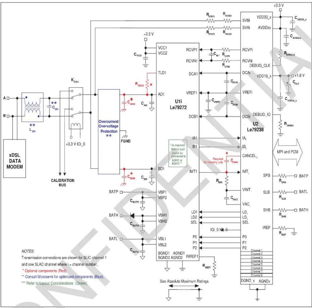
text_image
xDSL DATA MODEM A B K_CALI L_SPI +3.3 V IOI_0 CALIBRATION BUS VCC1 VCC2 C_VCCI R_TESTI * C_ADAI C_ADX FGND BD1 BATP BATH BATL C_BDBI C_BDX C_BATP C_BATHI C_BATLI VBP1 VBP2 VBH1 VBH2 VBL1 VBL2 BGND1 AGND1 BGND2 AGND2 RREF1 RDSTI RDSTI RDSTI RDSTI RDSTI RDSTI RDSTI RDSTI RDSTI RDSTI RDSTI RDSTI RDSTI RDSTI RDSTI RDSTI RDSTI RDSTI RDSTI RDSTI RDSTI RDSTI RDSTI RDSTI RDSTI RDST1 RDST1 RDST1 RDST1 RDST1 RDST1 RDST1 RDST1 RDST1 RDST1 RDST1 RDST1 RDST1 RDST1 RDST1 RDST1 RDST1 RDST1 RDST1 RDST1 RDST1 RDST1 RDST1 RDST1 RDST1 RDST2 RDST2 RDST2 RDST2 RDST2 RDST2 RDST2 RDST2 RDST2 RDST2 RDST2 RDST2 RDST2 RDST2 RDST2 RDST2 RDST2 RDST2 RDST2 RDST2 RDST2 RDST2 RDST2 RDST2 RDST2 RDST3_x VDD33_x SVAi AVDDxx C_VDD33_x RCVPI R_CVPI R_CYPI R_CYNII R_CYNII R_CYNI R_CYNII R_CYNII R_CYNII R_CYNII R_CYNII R_CYNII R_CYNII R_CYNII R_CYNII R_CYNII R_CYNII R_CYNII R_CYNII R_CYNII R_CYNII R_CYNII R_CYNII R_CYNII R_CYNII R_CYNII R_CYNII R_CYNII R_CYNII R_CYNII R_CYNII R_CYN II A +1.8 V C_FILT C_VDD18_x DCBI DEBUG_IO U2 Le79238 RD_BEO MPI and PCM +3.3 V RD_BEO RD_BEO RD_BEO RD_BEO RD_BEO RD_BEO RD_BEO RD_BEO RD_BEO RD_BEO RD_BEO RD_BEO RD_BEO RD_BEO RD_BEO RD_BEO RD_BEO RD_BEO RD_BEO RD_BEO RD_BEO RD_BEO RD_BEO RD_BEO RD_BEO RD_BEO RD_BEO RD_BEO RD_BEO RD_BEO RD_BEO RD_BEO RD_BEO RD_BEO DRSPB BATP SLPB BATL VAC LD SHB BATH IREF P0 P1 P2 Channel 1 Channel 2 Channel 3 Channel 4 Channel 5 Channel 6 Channel 7 Channel 8 DGND x AGNDx See Absolute Maximum Ratings NOTES: Transmission connections are shown for SLIC channel 1 and one SLAC channel where i = channel number. * Optional components (Red). ** Consult Microsemi for optimized components (Blue). *** Refer to Layout Considerations (Green).Figure 44 - Configuration D - IVD Application
3.4 Configuration D Parts List
3.4.1 In-Service Calibration and Test
The following list defines the parts and part values required to meet target specification limits for channel i of the line card. (i = 1,2,3,4,5,6,7,8)
| Item Type Value Tol. | Min Rating | Comments | Optional Components | |||
| U1i | Le79272 Dual SLIC device | |||||
| U2 Le79238 Octal SLAC device | ||||||
| KCALi | DPDT Relay | 3 V Test-In relay | ||||
| DVBHi | Diode 200 mA 100 V | |||||
| RDEBCLK, RDEBIO | Resistor 0 Ω 1/10 W | |||||
| RIMTi | Resistor | 4.02 kΩ | 1% | 1/16 W | ±200 ppm/°C | |
| RIREFi | Resistor | 49.9 kΩ | 1% | 1/16 W | SLIC device current reference | |
| RREF | Resistor | 75 kΩ | 0.5% | 1/16 W | SLAC device current reference, ±100 ppm/°C | |
| RCVPI, RCVNi | Resistor 56 Ω 1% 1/16 W | |||||
| RSVA1i, RSVA2i,RSVB1i, RSVB2i | Resistor | 1.62 MΩ | 1.0% | 500 V | A/B sense resistors, ±200 ppm/°C | |
| RSHB, RSLB, RSPB | Resistor | 1.62 MΩ | 1% | 150 V | Battery sense resistors | |
| RTESTi | Resistor 2 Ω | 1% 1 W | Test load | Optional, for testing | ||
| CADi, CBDi | Capacitor | 4.7 nF | 10% | 200 V | Ceramic, chip, X7R, EMI capacitor. Refer to Section 2.7 and Section 4.7 for more information. | |
| CADAi, CBDBi | Capacitor | 4.7 nF | 10% | 200 V | Ceramic, chip, X7R, EMI capacitor. Refer to Section 2.7 and Section 4.7 for more information. | Optional, for EMC |
| CBATHi, CBATLi,CBATPi | Capacitor | 100 nF 20% | 100 V | Ceramic, chip, X7R. Voltage rating needs to exceed battery voltage. | ||
| CFILT | Capacitor | 10 μF | 20% | 6.3 V | Ceramic or tantalum | |
| CCANi | Capacitor | 2.2 nF | 10% | 6.3 V | Metering capacitor | Optional, for metering |
| CDCAi, CDCBi | Capacitor | 220 nF | 10% | 6.3 V | Ceramic, chip, X7R | |
| CVACi | Capacitor | 100 nF | 20% | 6.3 V | Ceramic, chip, X7R | |
| CVCCI, CVDD18_x,CVDD33_x, CAVDDxx | Capacitor | 100 nF 20% | 6.3 V | Ceramic, chip, X7R, on SLAC device use one decoupling capacitor for each supply pin | ||
| CVREFi | Capacitor | 470 nF | 20% | 6.3 V | Ceramic, chip, X7R | |
| CMi | Capacitor | 4.7 nF | 10% | 6.3 V | Ceramic, chip, X7R | |
| CSPi | Capacitor | 33 nF | 10% | 400 V | Metallized film, withstand voltage of 600 VRMS | Optional, for IVD application, contact Microsemi |
| LSPi | Inductor | |||||
3.5 Configuration E External Ringing Application Circuits

text_image
A B R_SNAI C_SNAI K1 O_I_0 +3.3 V R_FAI R_FBI C_SNBI RFEEDI R_XSB1I R_XSB2I XSBi R_XSC1 R_XSC2 XSC RINGING BUS K2 Hsng Generator Host IO R_SNR C_SNR Ringing Return K1 Overvoltage Protection ** C_CADAI C_CADI FGND C_BDBI C_BDI VCC1 VCC2 RCVP1 RCVN1 TLD1 DCA1 VREF1 C_VREFi C_DCBI BD1 DCB1 IA1 IB1 C_CANI Required for metering only IMT1 R_IMTI C_VAGI VBP1 VBP2 VBH1 VBH2 VBL1 VBL2 BGND1 AGND1 AGND2 RREF1 BGND2 AGND2 RIFER1 RDST RDST RDST RDST RDST RDST RDST RDST RDST RDST RDST RDST RDST RDST RDST RDST RDST RDST RDST RDST RDST RDST RDST RDST RDST RDST RDST RDST RDST RDST RDST RDST RDST RDSTFigure 45 - Configuration E - Battery-Backed Ringing POTS Application

text_image
A B R_BNBI C_SNBI +3.3 V R_BNBI C_SNBI K1 R_FAI R_FBI R_SNAI C_SNBI Overvoltage Protection ** VCC1 VCC2 RCVP1 RCVN1 TLD1 DCA1 VREF1 C_CDAI AD1 C_ADAI C_AD1 FGND C_BDDI C_BDI BD1 U1i Le79272 RD1 RD2 RD3 RD4 RD5 RD6 RD7 RD8 RD9 RD10 RD11 RD12 RD13 RD14 RD15 RD16 RD17 RD18 RD19 RD20 RD21 RD22 RD23 RD24 RD25 RD26 RD27 RD28 RD29 RD30 RD31 RD32 RD33 RD34 RD35 RD36 RD37 RD38 RD39 RD40 RD41 RD42 RD43 RD44 RD45 RD46 RD47 RD48 RD49 RD50 RD51 RD52 RD53 RD54 RD55 RD56 RD57 RD58 RD59 RD60 RD61 RD62 RD63 RD64 RD65 RD66 RD67 RD68 RD69 RD70 RD71 RD72 RD73 RD74 RD75 RD76 RD77 RD78 RD79 RD80 RD81 RD82 RD83 RD84 RD85 RD86 RD87 RD88 RD89 RD90 RD91 RD92 RD93 RD94 RD95 RD96 RD97 RD98 RD99 RD100 RD101 RD102 RD103 RD104 RD105 RD106 RD107 RD108 RD109 RD110 RD111 RD112 RD113 RD114 RD115 RD116 RD117 RD118 RD119 RD120 RD121 RD122 RD123 RD124 RD125 RD126 RD127 RD128 RD129 RD130 RD131 RD132 RD133 RD134 RD135 RD136 RD137 RD138 RD139 RD140 RD141 RD142 RD143 RD144 RD145 RD146 RD147 RD148 RD149 RD150 RD151 RD152 RD153 RD154 RD155 RD156 RD157 RD158 RD159 RD160 RD161 RD162 RD163 RD164 RD165 RD166 RD167 RD168 RD169 RD170 RD171 RD172 RD173 RD174 RD175 RD176 RD177 RD178 RD179 RD180 +3.3 V VDD33_x +3.3 V VDD34_x SVDI SVAI AVDDxx C_VDD3_x C_AVDDxx R_DEBCLK R_CVDI R_DVDI R_DVDI R_DVDI R_DVDI R_DVDI R_DVDI R_DVDI R_DVDI R_DVDI R_DVDI R_DVDI R_DVDI R_DVDI R_DVDI R_DVDI R_DVDI R_DVDI R_DVDI R_DVDI R_DVDI R_DVDI R_DVDI R_DVDI R_DVDI R_DVDI R_nEaRnEaRnEaRnEaRnEaRnEaRnEaRnEaRnEaRnEaRnEaRnEaRnEaRnEaRnEaRnEaRnEaRnEaRnEaRnEaRnEaRnEaRnEaRnEaRnEaRnEaRdSvBbSvBbSvBbSvBbSvBbSvBbSvBbSvBbSvBbSvBbSvBbSvBbSvBbSvBbSvBbSvBbSvBbSvBbSvBbSvBbSvBbSvBbSvBbSvBbSvBbSvBcVDDX x AGNDx DVGND x AGNDx DVGND x AGNDx DVGND x AGNDx DVGND x AGNDx DVGND x AGNDx DVGND x AGNDx DVGND x AGNDx DVGND x AGNDx DVGND x AGNDx DVGND x AGNDx DVGND x AGNDx DVGND x AGNDx DVGND x AGNDx DVGND x AGNDx DVGND x AAGNDx DVGND x AGNDx DVGND x AGNDx DVGND x AGNDx DVGND x AGNDx DVGND x AGNDx DVGND x AGNDx DVGND x AGNDx DVGND x AGNDx DVGND x AGNDx DVGND x AGNDx DVGND x AGNDx DVGND x AGNDx DVGND x AGNDx DVGND x AGNDFigure 46 - Configuration E - Earth-Backed Ringing POTS Application
3.6 Configuration E External Ringing Parts List
3.6.1 Factory Calibration with Test
The following list defines the parts and part values required to meet target specification limits for channel i of the line card. (i = 1,2,3,4,5,6,7,8)
| Item Type Value Tol. | Min Rating | Comments | Optional Components | |||
| U_1i | Le79272 Dual SLIC device | |||||
| U2 ZL79258 Octal SLAC device | ||||||
| K_1i | DPDT 3 V | Ringing/Reset relay | ||||
| K2 | DPDT | 3 V | Ringing Bus relay ** | |||
| D_VBHi | Diode 200 mA 100 V | |||||
| R_DEBCLK, R_DEBIO | Resistor 0 Ω | 1/10 W | ||||
| R_FEEDI | Resistor | 510 Ω | 5% | 2 W | Ringing feed resistor, high voltage wirewound * | Use for battery-backed ringing |
| R_EBFi | Resistor | 200 Ω | 5% | 1 W | Ringing feed resistor, high voltage wirewound * | Use for earth-backed ringing |
| R_EBRi | Resistor | 450 Ω | 5% | 1 W | Ringing return resistor, high voltage wirewound * | |
| R_IMTi | Resistor | 4.02 kΩ | 1% | 1/16 W | ±200 ppm/°C | |
| R_IREFi | Resistor | 49.9 kΩ | 1% | 1/16 W | SLIC device current reference | |
| R_REF | Resistor | 75 kΩ | 0.25% | 1/16 W | SLAC device current reference, ±100 ppm/°C | |
| R_CVPI, R_CVNi | Resistor | 562 Ω | 1% | 1/16 W | ||
| R_SVA1i, R_SVA2i, R_SVB1i, R_SVB2i | Resistor | 1.62 MΩ | 0.5% | 500 V | A/B sense resistors, ±200 ppm/°C | |
| R_SHB, R_SLB | Resistor | 1.62 MΩ | 1% | 150 V | Battery sense resistors | |
| R_TESTi | Resistor 2 k Ω | 1% | 1 W | Test load | Optional, for testing | |
| R_SNAi, R_SNBi, R_SNAR, R_SNBR | Resistor | 1.0 kΩ | 1% | 1/8 W | Snubber resistor | |
| R_XSB1i, R_XSC1 | Resistor | 887 kΩ | 1% | 1/4 W | Ringing sense resistors, high voltage, surge rated * | |
| R_XSB2i, R_XSC2 | Resistor | 732 kΩ | 1% | 1/4 W | ||
| C_SNAi, C_SNAR | Capacitor | 100 nF 20% | 100 V | Snubber capacitor. Ceramic, chip, X7R. | Use for battery-backed ringing | |
| C_SNBI, C_SNBR | 200 V | |||||
| C_SNAi, C_SNAR | 200 V | Use for earth-backed ringing | ||||
| C_SNBI, C_SNBR | 100 V | |||||
| C_ADI, C_BDi | Capacitor | 4.7 nF | 5% | 200 V | Ceramic, chip, X7R, EMI capacitor. Refer to Section 2.7 and Section 4.7 for more information. | |
| C_ADAI, C_BDBi | Capacitor | 4.7 nF | 5% | 200 V | Optional, for EMC | |
| C_BATHi, C_BATLi | Capacitor | 100 nF 20% | 100 V | Ceramic, chip, X7R. Voltage rating needs to exceed battery voltage. | ||
| C_FILT | Capacitor | 10 μF | 20% | 6.3 V | Ceramic or tantalum | |
| C_CANi | Capacitor | 2.2 nF | 10% | 6.3 V | Metering capacitor | Optional, for metering |
| C_DCAi, C_DCBi | Capacitor | 220 nF | 10% | 6.3 V | Ceramic, chip, X7R | |
| C_VACi | Capacitor | 100 nF | 20% | 6.3 V | Ceramic, chip, X7R | |
| C_VCCI, C_VDD18_x, C_VDD33_x, C_AVDDxx | Capacitor | 100 nF 20% | 6.3 V | Ceramic, chip, X7R, on SLAC device use one decoupling capacitor for each supply pin | ||
| C_VREFi | Capacitor | 470 nF | 20% | 6.3 V | Ceramic, chip, X7R | |
| C_Mi | Capacitor | 4.7 nF | 10% | 6.3 V | Ceramic, chip, X7R | |
| C_RST | Capacitor 1 | 000 pF 10% | 6.3 V Ceramic, chip, X7R | |||
| * Component's voltage specification depends on ringing voltage, surge requirement, and ringing bus protection.** The Ringing/Reset relay can be used to disconnect the SLIC from the line to test foreign voltages if the Ringing Bus relay is actuated (no ringing signal applied). To implement this feature, it is advantageous to use multiple Ringing Bus relays to minimize the impact of testing on provisioned lines. | ||||||
3.6.2 No Calibration with Test
The following list defines the parts and part values required to meet target specification limits for channel i of the line card. (i = 1,2,3,4,5,6,7,8)
| Item Type Value Tol. | Min Rating | Comments | Optional Components | |||
| U1_i | Le79272 Dual SLIC device | |||||
| U2 ZL79258 Octal SLAC device | ||||||
| K1_i | DPDT 3 V | Ringing/Reset relay | ||||
| K2 | DPDT | 3 V | Ringing Bus relay ** | |||
| D_VBHi | Diode | 200 mA | 100 V | |||
| R_DEBCLK, R_DEBIO | Resistor | 0 Ω | 1/10 W | |||
| R_FEEDi | Resistor | 510 Ω | 5% | 2 W | Ringing feed resistor, high voltage wirewound * | Use for battery-backed ringing |
| R_EBFi | Resistor | 200 Ω | 5% | 1 W | Ringing feed resistor, high voltage wirewound * | Use for earth-backed ringing |
| R_EBRi | Resistor | 450 Ω | 5% | 1 W | Ringing return resistor, high voltage wirewound * | |
| R_IMTi | Resistor | 4.02 kΩ | 1% | 1/16 W | ±200 ppm/°C | |
| R_IREFi | Resistor | 49.9 kΩ | 1% | 1/16 W | SLIC device current reference | |
| R_REF | Resistor | 75 kΩ | 0.5% | 1/16 W | SLAC device current reference, ±100 ppm/°C | |
| R_CVPI, R_CVNi | Resistor | 562 Ω | 1% | 1/16 W | ||
| R_SVA1i, R_SVA2i, R_SVB1i, R_SVB2i | Resistor | 1.62 MΩ | 0.5% | 500 V | A/B sense resistors, ±200 ppm/°C | |
| R_SHB, R_SLB | Resistor | 1.62 MΩ | 1% | 150 V | Battery sense resistors | |
| R_TESTi | Resistor | 2 kΩ | 1% | 1 W | Test load | Optional, for testing |
| R_SNAi, R_SNBi, R_SNAR, R_SNBR | Resistor | 1.0 kΩ | 1% | 1/8 W | Snubber resistor | |
| R_XSB1i, R_XSC1 | Resistor | 887 kΩ | 1% | 1/4 W | Ringing sense resistors, high voltage, surge rated * | |
| R_XSB2i, R_XSC2 | Resistor | 732 kΩ | 1% | 1/4 W | ||
| C_SNAi, C_SNAR | Capacitor 100 nF | 20% | 100 V | Snubber capacitor. Ceramic, chip, X7R. | Use for battery-backed ringing | |
| C_SNBi, C_SNBR | 200 V | |||||
| C_SNAi, C_SNAR | 200 V | Use for earth-backed ringing | ||||
| C_SNBi, C_SNBR | 100 V | |||||
| C_ADI, C_BDi | Capacitor 4.7 nF | 5% | 200 V | Ceramic, chip, X7R, EMI capacitor. Refer to Section 2.7 and Section 4.7 for more information. | ||
| C_ADAi, C_BDBi | Capacitor | 4.7 nF | 5% | 200 V | Optional, for EMC | |
| C_BATHi, C_BATLi | Capacitor 100 nF | 20% | 100 V | Ceramic, chip, X7R. Voltage rating needs to exceed battery voltage. | ||
| C_FILT | Capacitor 10 μF | 20% | 63 V | Ceramic or tantalum | ||
| C_CANi | Capacitor | 2.2 nF | 10% | 6.3 V | Metering capacitor | Optional, for metering |
| C_DCAi, C_DCBi | Capacitor 20 nF | 10% | 6.3 V | Ceramic, chip, X7R | ||
| C_VACi | Capacitor 100 nF | 20% | 6.3 V | Ceramic, chip, X7R | ||
| C_VCCI, C_VDD18\_x, C_VDD33\_x, C_AVDDxx | Capacitor 1 | 100 nF 20% | 6.3 V | Ceramic, chip, X7R, on SLAC device use one decoupling capacitor for each supply pin | ||
| C_VREFi | Capacitor 4 | 70 nF 20% | 6.3 V Ceramic, chip, X7R | |||
| C_Mi | Capacitor 4 | 7 nF 10% | 6.3 V Ceramic, chip, X7R | |||
| C_RST | Capacitor 1 | 1000 pF 10% | 6.3 V Ceramic, chip, X7R | |||
| * Component's voltage specification depends on ringing voltage, surge requirement, and ringing bus protection.** The Ringing/Reset relay can be used to disconnect the SLIC from the line to test foreign voltages if the Ringing Bus relay is actuated (no ringing signal applied). To implement this feature, it is advantageous to use multiple Ringing Bus relays to minimize the impact of testing on provisioned lines. | ||||||
3.6.3 No Calibration and No Test
The following list defines the parts and part values required to meet target specification limits for channel i of the line card. (i = 1,2,3,4,5,6,7,8)
| Item Type Value Tol. | Min Rating | Comments | Optional Components | |||
| U_1_i | Le79272 Dual SLIC device | |||||
| U2 ZL79258 Octal SLAC device | ||||||
| K_1_i | DPDT | 3 V | Ringing/Reset relay | |||
| K2 | DPDT | 3 V | Ringing Bus relay ** | |||
| D_VBHi | Diode | 200 mA | 100 V | |||
| R_DEBCLK, R_DEBIO | Resistor 0 Ω | 1/10 W | ||||
| R_FEEDi | Resistor | 510 Ω | 5% | 2 W | Ringing feed resistor, high voltage wirewound * | Use for battery-backed ringing |
| R_EBFi | Resistor | 200 Ω | 5% | 1 W | Ringing feed resistor, high voltage wirewound * | Use for earth-backed ringing |
| R_EBRi | Resistor | 450 Ω | 5% | 1 W | Ringing return resistor, high voltage wirewound * | |
| R_IMTi | Resistor | 4.02 kΩ | 1% | 1/16 W | ±200 ppm/°C | |
| R_IREFi | Resistor | 49.9 kΩ | 1% | 1/16 W | SLIC device current reference | |
| R_REF | Resistor | 75 kΩ | 0.5% | 1/16 W | SLAC device current reference, ±100 ppm/°C | |
| R_CVPI, R_CVNi | Resistor | 562 Ω | 1% | 1/16 W | ||
| R_SVA1i, R_SVA2i, R_SVB1i, R_SVB2i | Resistor | 1.62 MΩ | 1.0% | 500 V | A/B sense resistors, ±200 ppm/°C | |
| R_SHB, R_SLB | Resistor | 1.62 MΩ | 1% | 150 V | Battery sense resistors | |
| R_TESTi | Resistor 2 k Ω | 1% | 1 W | Test load | Optional, for testing | |
| R_SNAi, R_SNBi, R_SNAR, R_SNBR | Resistor | 1.0 kΩ | 1% | 1/8 W | Snubber resistor | |
| R_XSB1i, R_XSC1 | Resistor | 887 kΩ | 1% | 1/4 W | Ringing sense resistors, high voltage, surge rated * | |
| R_XSB2i, R_XSC2 | Resistor | 732 kΩ | 1% | 1/4 W | ||
| C_SNAi, C_SNAR | Capacitor 100 nF 20% | 100 V | Snubber capacitor. Ceramic, chip, X7R. | Use for battery-backed ringing | ||
| C_SNBi, C_SNBR | 200 V | |||||
| C_SNAi, C_SNAR | 200 V | Use for earth-backed ringing | ||||
| C_SNBi, C_SNBR | 100 V | |||||
| C_ADI, C_BDi | Capacitor 4.7 nF 10% 200 V | Ceramic, chip, X7R, EMI capacitor. Refer to Section 2.7 and Section 4.7 for more information. Optional, for EMC | ||||
| C_ADAi, C_BDBi | Capacitor 4.7 nF 10% 200 V | |||||
| C_BATHi, C_BATLi | Capacitor 100 nF 20% 100 V | Ceramic, chip, X7R. Voltage rating needs to exceed battery voltage. | ||||
| C_FILT | Capacitor 10 μF 20% 6.3 V Ceramic or tantalum | |||||
| C_CANi | Capacitor 2 | 2 nF 10% | 6.3 V Metering capacitor | Optional, for metering | |
| C_DCAi, C_DCBi | Capacitor 2 | 20 nF 10% | 6.3 V Ceramic, chip, | X7R | |
| C_VACi | Capacitor 1 | 100 nF 20% | 6.3 V Ceramic, chip, | X7R | |
| C_VCCI, C_VDD18\_x C_VDD33\_x, C_AVDDxx | Capacitor 1 | 100 nF 20% | 6.3 V | Ceramic, chip, X7R, on SLAC device use one decoupling capacitor for each supply pin | |
| C_VREFi | Capacitor 4 | 70 nF 20% | 6.3 V Ceramic, chip, | X7R | |
| C_Mi | Capacitor 4 | 7 nF 10% | 6.3 V Ceramic, chip, | X7R | |
| C_RST | Capacitor 1 | 1000 pF 10% | 6.3 V Ceramic, chip, | X7R | |
| * Component's voltage specification depends on ringing voltage, surge requirement, and ringing bus protection.** The Ringing/Reset relay can be used to disconnect the SLIC from the line to test foreign voltages if the Ringing Bus relay is actuated (no ringing signal applied). To implement this feature, it is advantageous to use multiple Ringing Bus relays to minimize the impact of testing on provisioned lines. | |||||
3.7 Configuration F External Ringing Application Circuits
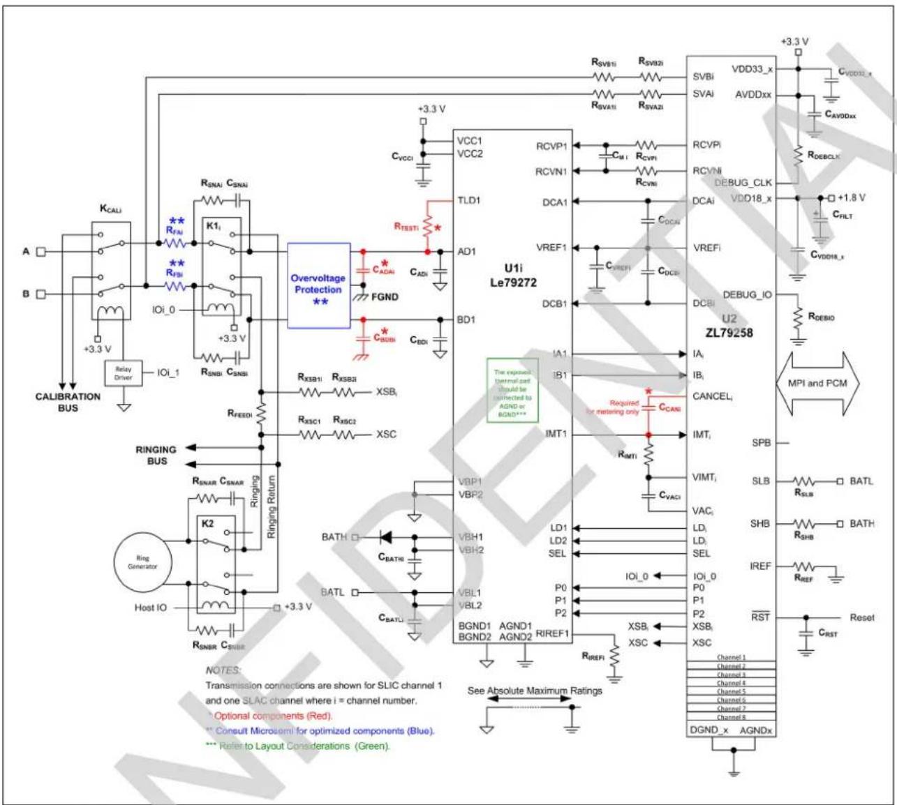
text_image
CALIBRATION BUS K_CALI A B +3.3 V Relay Driver IOI_1 K1 R_FNA R_SNAI C_SNAI R_FBI R_STI +3.3 V +3.3 V RGNB1 C_SNSI RGNB2 C_SNSI RGNB1 C_SNSI RGNB2 C_SNSI RGNB1 C_SNSI RGNB2 C_SNSI RGNB1 C_SNSI RGNB2 C_SNSI RGNB1 C_SNSI RGNB2 C_SNSI RGNB1 C_SNSI RGNB2 C_SNSI RGNB1 C_SNSI RGNB2 C_SNSI RGNB2 C_SNSI RGNB1 C_SNSI RGNB2 C_SNSI RGNB1 C_SNSI RGNB2 C_SNSI RGNB2 C_SNSI RGNB1 C_SNSI RGNB2 C_SNSI RGNB2 C_SNSI RGNB1 C_SNSI RGNB2 C_SNSI RGNB2 C_SNSI RGNB1 C_SNSI RGNB2 C_SNSI RGNB2 C_SNSI RGNB1 C_SNSI RGNB2 C_SNS1 RGNB2 C_SNS1 RGNB2 C_SNS1 RGNB2 C_SNS1 RGNB2 C_SNS1 RGNB2 C_SNS1 RGNB2 C_SNS1 RGNB2 C_SNS1 RGNB2 C_SNS1 RGNB2 C_SNS1 RGNB2 C_SNS1 RGNB2 C_SNS1 RGNB2 C_SNS1 RGNB1 C_SNSI RGNB2 C_SNSI RGNB2 C_SNSI RGNB2 C_SNSI RGNB2 C_SNSI RGNB2 C_SNSI RGNB2 C_SNSI RGNB2 C_SNSI RGNB2 C_SNSI RGNB2 C_SNSI RGNB2 C_SNSI RGNB2 C_SNSI RGNB2 C_SNSI RGNB2 C_SNS1 RGNB2 C_SNS1 RGNB2 C_SNS1 RGNB2 C_SNS1 RGNB2 C_SNS1 RGNB2 C_SNS1 RGNB2 C_SNS1 RGNB2 C_SNS1 RGNB2 C_SNS1 RGNB2 C_SNS1 RGNB2 C_SNS1 RGNB2 C_SNS0 RGNB2 C_SNS0 RGNB2 C_SNS0 RGNB2 C_SNS0 RGNB2 C_SNS0 RGNB2 C_SNS0 RGNB2 C_SNS0 RGNB2 C_SNS0 RGNB2 C_SNS0 RGNB2 C_SNS0 RGNB2 C_SNS0 RGNB2 C_SNS0 RGNB2 C_SNS0 RGNB1 C_SNSI RGNB2 C_SNSI RGNB2 C_SNSI RGNB2 C_SNSI RGNB2 C_SNSI RGNB2 C_SNSI RGNB2 C_SNSI RGNB2 C_SNSI RGNB2 C_SNSI RGNB2 C_SNSI RGNB2 C_SNSI RGNB2 C_SNSI RGNB1 C_ADAI RGNB2 C_ADAI RGNB2 C_ADAI RGNB2 C_ADAI RGNB2 C_ADAI RGNB2 C_ADAI RGNB2 C_ADAI RGNB2 C_ADAI RGNB2 C_ADAI RGNB2 C_ADAI RGNB2 C_ADAI RGNB2 C_ADAI RGNB2 C_ADAI RGNB2 C_ADAII RGNB2 C_ADAII RGNB2 C_ADAII RGNB2 C_ADAII RGNB2 C_ADAII RGNB2 C_ADAII RGNB2 C_ADAII RGNB2 C_ADAII RGNB2 C_ADAII RGNB2 C_ADAII RGNB2 C_ADAII RGNB2 C_ADAII RGNB2 C_ADAII RGNB1 U-V Le79272 RDST I VREF1 DCA1 VREF1 DCB1 IA1 IB1 IMT1 VBP1 VBP2 VBP1 LD1 LD2 SEL P0 P1 P2 BGND1 AGND1 BGND2 AGND2 RREF1 RREF1 SSB XSC XSB XSC RXVBI RSVBI RSVBI RSVBI RSVBI RSVBI RSVBI RSVBI RSVBI RSVBI RSVBI RSVBI RSVBI RSVBI RSVBI RSVBI RSVBI RSVBI RSVBI RSVBI RSVBI RSVBI RSVBI RSVBI RSVBI RSVBI RSVBI RSVBI RSVBI RSVBI RSVBI RSVBI RSVBI RSVBI RSVBCL KDVDD3X VVD3X VVD3X AVDDXX AAVDDXX AAVDDXX AAVDDXX AAVDDXX AAVDDXX AAVDDXX AAVDDXX AAVDDXX AAVDDXX AAVDDXX AAVDDXX AAVDDXX AAVDDXX AAVDDXX AAVDDXX AAVDDXX AAVDDXX AAVDDXX AAVDDXX AAVDDXX AAVDDXX AAVDDXX AAVDDXX AAVDDXX AAVDDXX A AVDDXX AAVDDXX AAVDDXX AAVDDXX AAVDDXX AAVDDXX AAVDDXX AAVDDXX AAVDDXX AAVDDXX AAVDDXX AAVDDXX AAVDDXX AAVDDXX AAVDDXX AAVDDXX AAVDDXX AAVDDXX AAVDDXX AAVDDXX AAVDDXX AAVDDXX AAVDDXX AAVDDXX AAVDDXX BVD3X X VVD3X X AVDDXX AVDDXX AVDDXX AVDDXX AVDDXX AVDDXX AVDDXX AVDDXX AVDDXX AVDDXX AVDDXX AVDDXX AVDDXX AVDDXX AVDDXX AVDDXX AVDDXX AVDDXX AVDDXX AVDDXX AVDDXX AVDDXX AVDDXX AVDDXX AVDDXX AVDDXX AVDCCX X VVD3X X AVDDXXX AVDDXXX AVDDXXX AVDDXXX AVDDXXX AVDDXXX AVDDXXX AVDDXXX AVDCCX X VVD3X X AVDDXXX AVDDXXX AVDDXXX AVDCCX X VVD3X X AVDDXXX AVDDXXX AVDCCX X VVD3X X AVDDXXX AVDDXXX AVDCCX X VVD3X X AVDDXXX AVDCCX X VVD3X X AVDCCX X AVDCCX X AVDCCX X AVDCCX X AVDCCX X AVDCCX X AVDCCX X AVDCCX X AVDCCX X AVDCCX X AVDCCX X AVDCCX X AVDCCX X AVDCCX X AVDCCX X AVDCCX X AVDCCX X AVDCCX X AVDCCX X AVDCCX X AVD5000000000000000000000000000000000000000000000000000000000000000000000000000000000000000000000000000055555555555555555555555555555555555555555555555555555555555555555555555555555555555555555555555555556666666666666666666666666666666666666666666666666666666666666666666666666666666666666666666666666666888888888888888888888888888888888888888888888888888888888888888888888888888888888888888888888888889999999999999999999999999999999999999999999999999999999999999999999999999999999999999999999999999999 4 4 4 4 4 4 4 4 4 4 4 4 4 4 4 4 4 4 4 4 4 4 4 4 4 4 4 4 4 4 4 4 4 4 4 4 4 4 4 4 4 4 4 4 4 4 4 4 4 4 7777777777777777777777777777777777777777777777777777777777777777777777777777777777777777777777777777Figure 47 - Configuration F - Battery-Backed Ringing Application
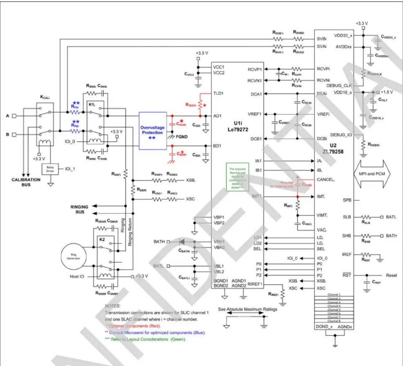
text_image
CALIBRATION BUS K_CALI A B +3.3 V R_EBI IOI_0 +3.3 V Relay Driver IOI_1 K1i R_SNAI C_SNAI R_FBI R_BNB C_SNB R_E_BFI R_XSB1 R_XSB2 XSBi R_EBRi R_XBC1 R_XBC2 XSC RINGING BUS K2 Ring Generator Host IO R_SNBR C_SNBR R_ESTI Overvoltage Protection ** VCC1 VCC2 C_VCCI C_CDAI C_CDDI C_BDI TLD1 AD1 FGND RDSTI C_BD1 RDSTI RDSTI RDSTI RDSTI RDSTI RDSTI RDSTI RDSTI RDSTI RDSTI RDSTI RDSTI RDSTI RDSTI RDSTI RDSTI RDSTI RDSTI RDSTI RDSTI RDSTI RDSTI RDSTI RDSTI RDSTI RDST1 RDST1 RDST1 RDST1 RDST1 RDST1 RDST1 RDST1 RDST1 RDST1 RDST1 RDST1 RDST1 RDST1 RDST1 RDST1 RDST1 RDST1 RDST1 RDST1 RDST1 RDST1 RDST1 RDST1 RDST1 RDST2 RDST2 RDST2 RDST2 RDST2 RDST2 RDST2 RDST2 RDST2 RDST2 RDST2 RDST2 RDST2 RDST2 RDST2 RDST2 RDST2 RDST2 RDST2 RDST2 RDST2 RDST2 RDST2 RDST2 RDST2 RDST3_x VDD33_x +3.3 V SVAi AVDDxx C_VDD33_x RCVPi RCVNi DEBUG_CLK VDD18_x +1.8 V C_VDD33_x A_VDDxx C_VDD33_x A_VDDxx C_VDD33_x A_VDDxx C_VDD33_x A_VDDxx C_VDD33_x A_VDDxx C_VDD33_x A_VDDxx C_VDD33_x A_VDDxx C_VDD33_x A_VDDxx C_VDD33_x A_VDDxx C_VDD33_x A_VDDxx C_VDD33_x A_VDDx x x x x x x x x x x x x x x x x x x x x x x x x x x x x x x x x x x x x x x x x x x x x x x x x x x x x x x x x x x x x x x x x x x x x x x x x x x x x x x x x x x x x x x x x x x x x x x x x x x x x yx yx yx yx yx yx yx yx yx yx yx yx yx yx yx yx yx yx yx yx yx yx yx yx yx yx yx yx yx yx yx yx yx yx yx yx yx yx yx yx yx yx yx yx yx yx yx yx yx yx y RD_BEIO U2 ZL79258 MPI and PCM The exposed thermal pot should be controlled for ADIGU# BGN1*** Request for transmitting only IMT1 IMT1 SPB VIMT1 SLB BATL VAC, SHB BATH LD, LD, SEL IOI_0 IREF R_REF Reset P0 P1 P2 XSB XSC XSB XSC XSB XSB XSB XSB XSB XSB XSB XSB XSB XSB XSB XSB XSB XSB XSB XSB XSB XSB XSB XSB XSB XSB XSB XSB XSB XSB XSB XSB XSB XSB XSB XSB XSB XSB XSB XSB XSB XSB XSB XSB XSB XSB XSB XSB XSB XSB XSB XSB XSB XSB XBBX AGND1 AGND2 AGND1 RREF1 See Absolute Maximum Ratings NOTES: Transmission connections are shown for SLIC channel 1 and one SLAC channel where i = channel number. * Optional components (Red) ** Consult Microsemi for optimized components (Blue). *** Refer to Layout Considerations (Green)Figure 48 - Configuration F - Earth-Backed Ringing Application
3.8 Configuration F External Ringing Parts List
3.8.1 In-Service Calibration and Test
The following list defines the parts and part values required to meet target specification limits for channel i of the line card. (i = 1,2,3,4,5,6,7,8)
| Item Type Value Tol. | Min Rating | Comments | Optional Components | |||
| U_1i | Le79272 Dual SLIC device | |||||
| U2 ZL79258 Octal SLAC device | ||||||
| K_1i | DPDT 3 V | Ringing/Reset relay | ||||
| K2 DPDT | 3 V | Ringing Bus relay ** | ||||
| K_CALi | DPDT | 3 V | Test-In | relay | ||
| Relay Driver Or equivalent circuitry | ||||||
| D_VBHi | Diode 200 mA | 100 V | ||||
| R_DEBCLK, R_DEBIO | Resistor | 0 Ω | 1/10 W | |||
| R_FEEDi | Resistor | 510 Ω | 5% | 2 W | Ringing feed resistor, high voltage wirewound * | Use for battery-backed ringing |
| R_EBFi | Resistor | 200 Ω | 5% | 1 W | Ringing feed resistor, high voltage wirewound * | Use for earth-backed ringing |
| R_EBRi | Resistor | 450 Ω | 5% | 1 W | Ringing return resistor, high voltage wirewound * | |
| R_IMTi | Resistor | 4.02 kΩ | 1% | 1/16 W | ±200 ppm/°C | |
| R_IREFi | Resistor | 49.9 kΩ | 1% | 1/16 W | SLIC device current reference | |
| R_REF | Resistor | 75 kΩ | 0.5% | 1/16 W | SLAC device current reference, ±100 ppm/°C | |
| R_CVPi, R_CVNi | Resistor | 562 Ω | 1% | 1/16 W | ||
| R_SVA1i, R_SVA2i, R_SVB1i, R_SVB2i | Resistor | 1.62 MΩ | 1.0% | 500 V | A/B sense resistors, ±200 ppm/°C | |
| R_SHB, R_SLB | Resistor | 1.62 MΩ | 1% | 150 V | Battery sense resistors | |
| R_TESTi | Resistor | 2 kΩ | 1% | 1 W | Test load | Optional, for testing |
| R_SNAi, R_SNBi, R_SNAR, R_SNBR | Resistor | 1.0 kΩ | 1% | 1/8 W | Snubber resistor | |
| R_XSB1i, R_XSC1 | Resistor | 887 kΩ | 1% | 1/4 W | Ringing sense resistors, high voltage, surge rated * | |
| R_XSB2i, R_XSC2 | Resistor | 732 kΩ | 1% | 1/4 W | ||
| C_SNAi, C_SNAR | Capacitor | 100 nF | 20% | 100 V | Snubber capacitor. Ceramic, chip, X7R. | Use for battery-backed ringing |
| C_SNBi, C_SNBR | 200 V | |||||
| C_SNAi, C_SNAR | 200 V | Use for earth-backed ringing | ||||
| C_SNBi, C_SNBR | 100 V | |||||
| C_ADi, C_BDi | Capacitor | 4.7 nF | 10% | 200 V | Ceramic, chip, X7R, EMI capacitor. Refer to Section 2.7 and Section 4.7 for more information. | |
| C_ADAi, C_BDBi | Capacitor | 4.7 nF | 10% | 200 V | Optional, for EMC | |
| C_BATHi, C_BATLi | Capacitor | 100 nF | 20% | 100 V | Ceramic, chip, X7R. Voltage rating needs to exceed battery voltage. | |
| C_FILT | Capacitor | 10 μF | 20% | 6.3 V | Ceramic or tantalum | |
| C_CANi | Capacitor | 2.2 nF | 10% | 6.3 V | Metering capacitor | Optional, for metering |
| C_DCAi, C_DCBi | Capacitor | 220 nF | 10% | 6.3 V | Ceramic, chip, X7R | |
| C_VACi | Capacitor | 100 nF | 20% | 6.3 V | Ceramic, chip, X7R | |
| C_VCCI, C_VDD18\_x, C_VDD33\_x, C_AVDDxx | Capacitor | 100 nF | 20% | 6.3 V | Ceramic, chip, X7R, on SLAC device use one decoupling capacitor for each supply pin | |
| C_VREFi | Capacitor 4 | 70 nF 20% | 6.3 V Ceramic, chip, X7R | ||
| C_Mi | Capacitor 4 | 7 nF 10% | 6.3 V Ceramic, chip, X7R | ||
| C_RST | Capacitor 1 | 000 pF 10% | 6.3 V Ceramic, chip, X7R | ||
| * Component's voltage specification depends on ringing voltage, surge requirement, and ringing bus protection.** The Ringing/Reset relay can be used to disconnect the SLIC from the line to test foreign voltages if the Ringing Bus relay is actuated (no ringing signal applied). To implement this feature, it is advantageous to use multiple Ringing Bus relays to minimize the impact of testing on provisioned lines. | |||||
3.9 VCP Device Application Circuits
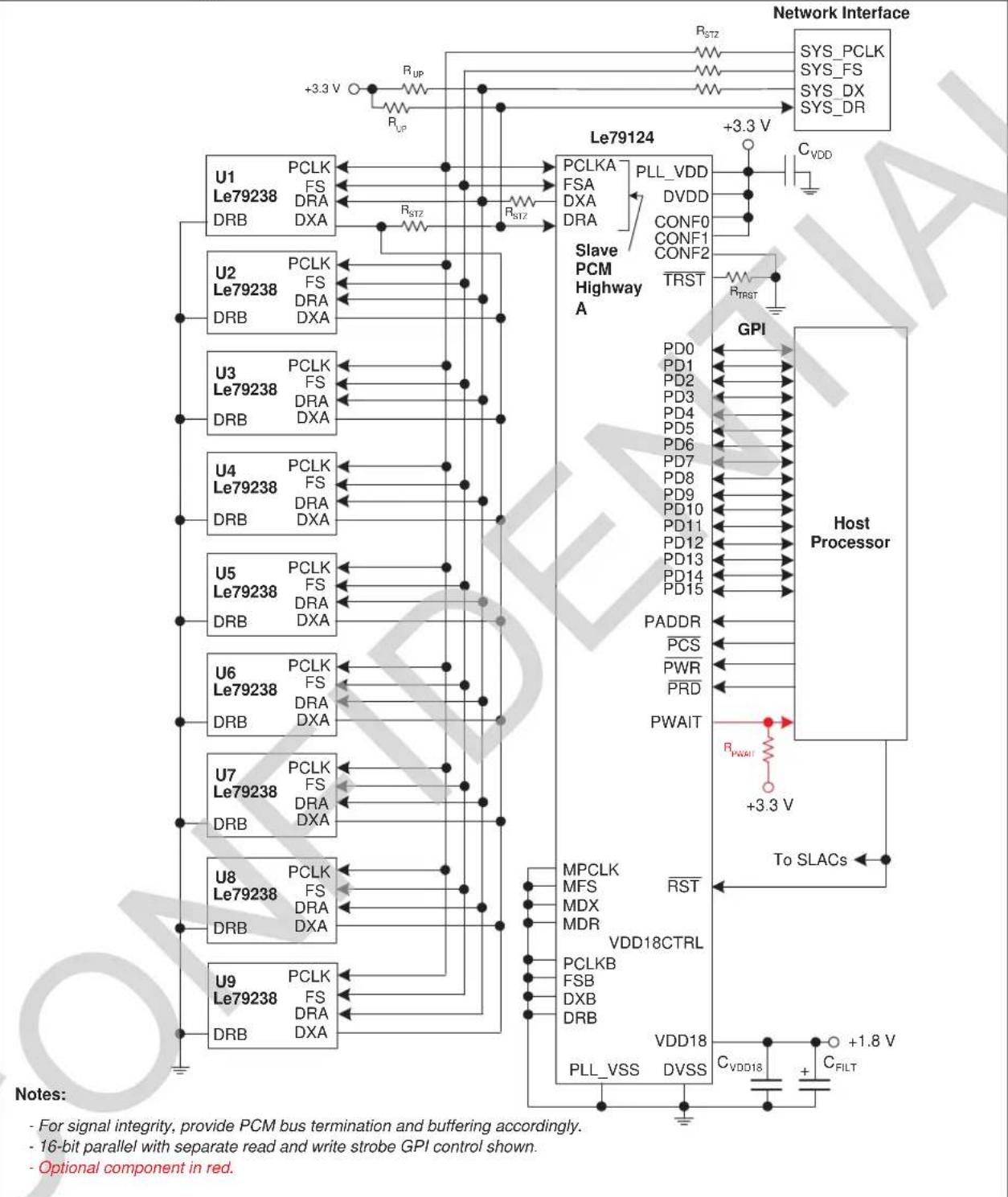
flowchart
graph TD
    subgraph_Network_Interface["Network Interface"]
        A["RSSTZ"] --> B["SYS_PCLK"]
        A --> C["SYS_FS"]
        A --> D["SYS_DX"]
        A --> E["SYS_DR"]
        F["R_UP"] --> G["+3.3 V"]
        H["R_UP"] --> I["Ground"]
    end

    subgraph_Host_Processor["Host Processor"]
        J["PCLKA"] --> K["FSA"]
        J --> L["DXA"]
        J --> M["DRA"]
        N["PLL_VDD"] --> O["DVDD"]
        P["CONF0"] --> Q["CONF1"]
        R["CONF2"] --> S["CONF2"]
        T["TRST"] --> U["TRST"]
        V["GPI"] --> W["+3.3 V"]
        X["PADDR"] --> Y["PCS"]
        Z["PDDR"] --> AA["PWR"]
        AB["PWAIT"] --> AC["PWR"]
        AD["To SLACs"] --> AE["+1.8 V"]
    end

    subgraph Host_Processor
        AF["PCLK"] --> AG["PCLK"]
        AH["PCLK"] --> AI["PCLK"]
        AJ["PCLK"] --> AK["PCLK"]
        AL["PCLK"] --> AM["PCLK"]
        AN["PCLK"] --> AO["PCLK"]
        AP["PCLK"] --> AQ["PCLK"]
        AR["PCLK"] --> AS["PCLK"]
        AT["PCLK"] --> AU["PCLK"]
        AV["PCLK"] --> AW["PCLK"]
        AX["PCLK"] --> AY["PCLK"]
        AZ["PCLK"] --> BA["PCLK"]
        BB["PCLK"] --> BC["PCLK"]
        BD["PCLK"] --> BE["PCLK"]
        BF["PCLK"] --> BG["PCLK"]
        BH["PCLK"] --> BI["PCLK"]
        BJ["PCLK"] --> BK["PCLK"]
        BL["PCLK"] --> BM["PCLK"]
        BN["PCLK"] --> BO["PCLK"]
        BP["PCLK"] --> BQ["PCLK"]
        BR["PCLK"] --> BS["PCLK"]
        BT["PCLK"] --> BU["PCLK"]
        BV["PCLK"] --> BW["PCLK"]
        BX["PCLK"] --> BY["PCLK"]
        BZ["PCLK"] --> CA["PCLK"]
        CB["PCLK"] --> DA["PCLK"]
        DBP["PCLK"] --> DBP
        DC["PCLK"] --> DCB["PCLK"]
        DV["PCLK"] --> DVSS["VSS"]
    end

    subgraph Host_Processor
        E
        F
        G
        H
        I
        J
        K
        L
        M
        N
        O
        P
        Q
        R
        S
        U
        V
        W
        X
        Y
        Z
        AA
        AB
        AC
        AD
        AE
        AF
        AH
        AI
        AJ
        AK
        AL
        AM
        AN
        AO
        AP
        AQ
        AR
    end

    Note1["Notes:"]
    Note2["- For signal integrity, provide PCM bus termination and buffering accordingly."]
    Note3["- 16-bit parallel with separate read and write strobe GPI control shown."]
    Note4["- Optional component in red."]
Figure 49 - Le79124 VCP External Components
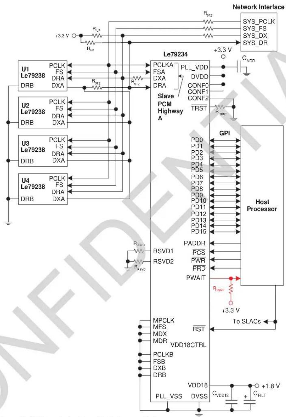
flowchart
graph TD
    subgraph_Network_Interface["Network Interface"]
        R_UP --> R_UP_bar
        R_UP_bar --> R_UP
        R_UP_bar --> R_UP_bar_bar
        R_UP_bar --> R_UP_bar_bar
        R_UP_bar --> R_UP_bar_bar
        R_UP_bar --> R_UP_bar_bar
        R_UP_bar --> R_UP_bar_bar
        R_UP_bar --> R_UP_bar_bar
        R_UP_bar --> R_UP_bar_bar
        R_UP_bar --> R_UP_bar_bar
        R_UP_bar --> R_UP_bar_bar
        R_UP_bar --> R_UP_bar_bar
        R_UP_bar --> R_UP_bar<|ref_end|><|rotate_up|>
    end

    subgraph_Host_Processor["Host Processor"]
        R_STZ --> R_STZ_bar
        R_DVD --> R_DVD_bar
        R_DVD_bar --> R_DVD_bar
        R_DVD_bar --> R_DVD_bar
        R_DVD_bar --> R_DVD_bar
        R_DVD_bar --> R_DVD_bar
        R_DVD_bar --> R_DVD_bar
        R_DVD_bar --> R_DVD_bar
        R_DVD_bar --> R_DVD_bar
        R_DVD_bar --> R_DVD_bar
        R_DVD_bar --> R_DVD_bar
        R_DVD_bar <-->|+3.3 V| To_SLACs["To SLACs"]
        R_RSDV --> R_RSDV_bar
        R_RSDV --> R_RSDV_bar
        R_RSDV --> R_RSDV_bar
        R_RSDV --> R_RSDV_bar
        R_RSDV --> R_RSDV_bar
        R_RSDV --> R_RSDV_bar
        R_RSDV --> R_RSDV_bar
        R_RSDV --> R_RSDV_bar
        R_RSDV --> R_RSDV_bar
        R_RSPD --> R_RSPD_bar
        R_RSPD --> R_RSPD_bar
        R_RSPD --> R_RSPD_bar
        R_RSPD --> R_RSPD_bar
        R_RSPD --> R_RSPD_bar
        R_RSPD --> R_RSPD_bar
        R_RSPD --> R_RSPD_bar
        R_RSPD --> R_RSPD_bar
        R_RSPD --> R_RSPD_bar
        GPI["Giplifier"] --> PDD0["PD0"]
        GPI --> PD1["PD1"]
        GPI --> PD2["PD2"]
        GPI --> PD3["PD3"]
        GPI --> PD4["PD4"]
        GPI --> PD5["PD5"]
        GPI --> PD6["PD6"]
        GPI --> PD7["PD7"]
        GPI --> PD8["PD8"]
        GPI --> PD9["PD9"]
        GPI --> PD10["PD10"]
        GPI --> PD11["PD11"]
        GPI --> PD12["PD12"]
        GPI --> PD13["PD13"]
        GPI --> PD14["PD14"]
        GPI --> PD15["PD15"]
        PADDR["Address"] --> PCS["PCS"]
        PWR["Power"] --> PRD["PRD"]
        PWAIT["PWAIT"] --> PWAIT_bar<|ref_end|><|rotate_up|>
    end

    subgraph_Host_Processor["Host Processor"]
        SLSA["To SLACs"] --> +3.3V["+3.3 V"]
        +3.3V --> To_SLACs["To SLACs"]
    end

    subgraph Host_Processor
        VDD18["To SLACs"] --> VDD18bar["VDD18CTRL"]
        VDD18bar --> VDD18bar["VDD18CTRL"]
        VDD18bar --> VDD18bar["VDD18CTRL"]
    end

    subgraph Host_Processor
        VDD18bar --> VDD18bar["VDD18CTRL"]
        VDD18bar --> VDD18bar["VDD18CTRL"]
    end

    subgraph Host_Processor
        VDD18bar --> VDD18bar["VDD18CTRL"]
        VDD18bar --> VDD18bar["VDD18CTRL"]
    end

    subgraph Host_Processor
        VDD18bar --> PLL_VSS["PLL_VSS DVSS"]
        VDD18bar --> PLL_VSS["VSS DVSS"]
    end

    subgraph Host_Processor
        VDD18bar --> PLL_VSS["VSS DVSS"]
    end

    subgraph Host_Processor
        VDD18bar --> PLL_VSS["VSS DVSS"]
    end

    subgraph Host_Processor
        VDD18bar --> PLL_VSS["VSS DVSS"]
    end

    subgraph Host_Processor
        VDD18bar --> PLL_VSS["VSS DVSS"]
    end

    subgraph Host_Processor
Notes:
- For signal integrity, provide PCM bus termination and buffering accordingly.
- 16-bit parallel with separate read and write strobe GPI control shown.
- Optional component (in red).
Figure 50 - Le79234 VCP External Components
flowchart
graph TD
    subgraph_PCM_Highway_1["PCM Highway 1"]
        A["PCM Highway 1"] --> B["Network Interface"]
        B --> C["Slave PCM Highway A"]
        B --> D["Slave PCM Highway B"]
    end

    subgraph_PCM_Highway_2["PCM Highway 2"]
        E["PCM Highway 2"] --> F["Slave PCM Highway B"]
        E --> G["Host Processor"]
    end

    subgraph_PLCs["PLC"]
        H["PLL_VDD"] --> I["DVDD"]
        J["CONF0"] --> K["CONF1"]
        L["CONF2"] --> M["TRST"]
        N["PCLKA"] --> O["FSA"]
        P["DRA"] --> Q["DRA"]
        R["RSTZ"] --> S["RSTZ"]
        T["RSSTZ"] --> U["RSTZ"]
        V["PCLKB"] --> W["FSB"]
        X["MPCLK"] --> Y["MFS"]
        Z["MDX"] --> AA["MDR"]
        AB["PCLK"] --> AC["FS"]
        AD["DRB"] --> AE["DRB"]
        AF["DXB"] --> AG["DXB"]
        AH["U1"] --> AI["DRB"]
        AJ["U8"] --> AK["DL79238"]

    subgraph PLCs
        AL["PCLK"] --> AM["FS"]
        AN["PCLKB"] --> AO["FSB"]
        AP["PCLK"] --> AQ["FS"]
        AR["PCLKB"] --> AS["FSB"]
        AT["PCLKB"] --> AU["FS"]
        AV["PCLKB"] --> AW["FS"]
        AX["PCLKB"] --> AY["FS"]
        AZ["PCLKB"] --> BA["FS"]
        BB["PCLKB"] --> BC["FS"]
        BD["PCLKB"] --> BE["FS"]
        BF["PCLKB"] --> BG["FS"]
    end

    note1["Notes: For signal integrity, provide PCM bus termination and buffering accordingly"]
    note2["- 16-bit parallel with separate read and write strobe GPI control shown"]
    note3["- Optional component (in red)."]
    note4["RST"]
    note5["VDD18CTRL"]
    note6["To SLACs"]
    note7["+3.3 V"]
    note8["+1.8 V"]
    note9["C_FILT"]
    note10["GPI"]
    note11["PDD0"]
    note12["PD1"]
    note13["PD2"]
    note14["PD3"]
    note15["PD4"]
    note16["PD5"]
    note17["PD6"]
    note18["PD7"]
    note19["PD8"]
    note20["PD9"]
    note21["PD10"]
    note22["PD11"]
    note23["PD12"]
    note24["PD13"]
    note25["PD14"]
    note26["PD15"]
    note27["PADDR"]
    note28["PCS"]
    note29["PWR"]
    note30["PRD"]
    note31["PWAIT"]
    note32["VDD18CTRL"]
    note33["RST"]
    note34["VDD18"]
    note35["PLL_VSS DVSS"]
    note36["C_VDD18 + C_FILT"]
    note37["+3.3 V"]
    note38["+3.3 V"]
    note39["+3.3 V"]
    note40["+3.3 V"]
    note41["+3.3 V"]
    note42["+3.3 V"]
    note43["+3.3 V"]
    note44["+3.3 V"]
    note45["+3.3 V"]
    note46["+3.3 V"]
    note47["+3.3 V"]
    note48["+3.3 V"]
    note49["+3.3 V"]
    note50["+3.3 V"]
    note51["+3.3 V"]
    note52["+3.3 V"]
    note53["+3.3 V"]
    note54["+3.3 V"]
    note55["+3.3 V"]
    note56["+3.3 V"]
    note57["+3.3 V"]
    note58["+3.3 V"]
    note59["+3.3 V"]
    note60["+3.3 V"]

    Note10
    Note11
    Note12
    Note13
    Note14
    Note15
    Note16
    Note17
    Note18
    Note19
    Note20
    Note21
    Note22
    Note23
    Note24
    Note25
    Note26
    Note27
    Note28
    Note29
    Note30
    Note31
    Note32
    Note33
    Note34
    Note35
    Note36
    Note37
    Note38
    Note39
    Note40
    Note41
    Note42
    Note43
    Note44
    Note45
    Note46
    Note47
    Note48
    Note49
    Note50
    Note51
    Note52
    Note53
    Note54
    Note55
    Note56
    Note57
    Note58
    Note59
    Note60

    Note10
    Note11
    Note12
    Note13
    Note14
    Note15
    Note16
    Note17
    Note18
    Note19
    Note20
    Note21
    Note22
    Note23
    Note24
    Note25
    Note26
    Note27
    Note28
    Note2A -->|PCLKA| B
    B -->|PCLKB| C

    subgraph "Slave PCM Highway A"
        B -->|Slave PCM Highway B|
        B -->|Slave PCM Highway B_A|
        B -->|Slave PCM Highway B_B|
        B -->|Slave PCM Highway B_C|
        B -->|Slave PCM Highway B_DA|
        B -->|Slave PCM Highway B_DRA|
        B -->|Slave PCM Highway B_FSA|
        B -->|Slave PCM Highway B_DXA|
        B -->|Slave PCM Highway B_PCLKB|
        B -->|Slave PCM Highway B_FSB|
        B -->|Slave PCM Highway B_MPCLK|
        B -->|Slave PCM Highway B_MFS|
        B -->|Slave PCM Highway B_MDX|
        B -->|Slave PCM Highway B_MDR|
        B -->|Slave PCM Highway B_RSTZ|
        B -->|Slave PCM Highway B_PCLKB_FSA_FDA_XDADXTRSNDI_WDSF_DS_DXDIN_DXDIN_DXDIN_DXDIN_DXDIN_DXDIN_DXDIN_DXDIN_DXDIN_DXDIN_DXDIN_DXDIN_DXDIN_DXDIN_DXDIN_DXDIN_DXDIN_DXDIN_DXDIN_DXDIN_DXDIN_DXDIN_DXDIN_DXDIN_DXDIN_DXDIN_DXDIN_DXDIN_DXDIN_DXDIN_DXDIN_DXDIN_DXDIN_DXDIN DXDIN_DXDIN_DXDIN_DXDIN_DXDIN_DXDIN_DXDIN_DXDIN_DXDIN_DXDIN_DXDIN_DXDIN_DXDIN_DXDIN_DXDIN_DXDIN_DXDIN_DXDIN_DXDIN_DXDIN_DXDIN_DXDIN_DXDIN_DXDIN_DXDIN_DXDIN_DXDIN_DXDIN_DXDIN_DXDIN_DXDIN_DXDIN_DXDIN_DDIN_DDIN_DDIN_DDIN_DDIN_DDIN_DDIN_DDIN_DDIN_DDIN_DDIN_DDIN_DDIN_DDIN_DDIN_DDIN_DDIN_DDIN_DDIN_DDIN_DDIN_DDIN_DDIN_DDIN_DDIN_DDIN_DDIN_DDIN_DDIN_DDIN_DDIN_DDIN_DDIN_DDID_NH0_0_0_0_0_0_0_0_0_0_0_0_0_0_0_0_0_0_0_0_0_0_0_0_0_0_0_0_0_0_0_0_0_0_0_0_0_0_0_0_0_0_0_0_0_0_0_0_0_0_0  "For signal integrity, provide PCM bus termination and buffering accordingly"
            - 16-bit parallel with separate read and write strobe GPI control shown"
            - Optional component (in red)

    subgraph "Host Processor"
        C["PLL_VDD"] --> D["VDD"]
        E["DVDD"] --> F["CONF"]
        G["CONF"]
        H["TRST"] --> I["PLL_VDD"]
        J["PLL_VDD"] --> K["VDD"]
        L["PLL_VDD"] --> L["VDD"]
        M["PLL_VDD"] --> N["VDD"]
        O["PLL_VDD"] --> O["VDD"]
        P["PLL_VDD"] --> P["VDD"]
        Q["PLL_VDD"] --> Q["VDD"]
        R["PLL_VDD"] --> R["VDD"]
        S["PLL_VDD"] --> S["VDD"]
        T["PLL_VDD"] --> T["VDD"]
        U["PLL_VDD"] --> U["VDD"]
        V["PLL_VDD"] --> V["VDD"]
        W["PLL_VDD"] --> W["VDD"]
        X["PLL_VDD"] --> X["VDD"]
        Y["PLL_VDD"] --> Y["VDD"]
        Z["PLL_VDD"] --> Z["VDD"]
        AA["PLL_VDD"] --> AA["VDD"]
        AB["PLL_VDD"] --> AB["VDD"]
        AC["PLL_VDD"] --> AC["VDD"]
        AD["PLL_VDD"] --> AD["VDD"]
        AE["PLL_VDD"] --> AE["VDD"]
        AF["PLL_VDD"] --> AF["VDD"]
        AG["PLL_VDD"] --> AG["VDD"]
        AH["PLL_VDD"] --> AH["VDD"]
        AI["PLL_VDD"] --> AI["VDD"]
        AJ["PLL_VDD"] --> AJ["VDD"]
        AK["PLL_VDD"] --> AK["VDD"]
        AL["PLL_VDD"] --> AL["VDD"]
        AM["PLL_VDD"] --> AM["VDD"]
        AN["PLL_VDD"] --> AN["VDD"]
        AO["PLL_VDD"] --> AO["VDD"]
        AP["PLL_VDD"] --> AP["VDD"]
        AQ["PLL_VDD"] --> AQ["VDD"]
        AR["PLL_VDD"] --> AR["VDD"]
        AS["PLL_VDD"] --> AS["VDD"]
        AT["PLL_VDD"] --> AT["VDD"]
        AU["PLL_VDD"] --> AU["VDD"]
        AV["PLL_VDD"] --> AV["VDD"]
        AW["PLL_VDD"] --> AW["VDD"]
        AX["PLL_VDD"] --> AX["VDD"]
        AY["PLL_VDD"] --> AY["VDD"]
        AZ["PLL_VDD"] --> AZ["VDD"]
        BA["PLL_VDD"] --> BA["VDD"]
        BB["PLL_VDD"] --> BB["VDD"]
        BC["PLL_VDD"] --> BC["VDD"]
        BD["PLL_VDD"] --> BD["VDD"]
        BE["PLL_VDD"] --> BE["VDD"]
        BF["PLL_VDD"] --> BF["VDD"]
        BG["PLL_VDD"] --> BG["VDD"]
        BH["PLL_VDD"] --> BH["VDD"]
        BI["PLL_VDD"] --> BI["VDD"]
        BJ["PLL_VDD"] --> BJ["VDD"]
        BK["PLL_VDD"] --> BK["VDD"]
        BL["PLL_VDD"] --> BL["VDD"]
        BM["PLL_VDD"] --> BM["VDD"]
        BN["PLL_VDD"] --> BN["VDD"]
        BO["PLL_VDD"] --> BO["VDD"]
        BP["PLL_VDD"] --> BP["VWD"]
Figure 51 - Le79128 VCP External Components
3.9.1 VCP Device Parts List
The following table lists the external components required for the VCP device and the PCM highway as shown in the Application Circuits.
| Item | Qty | Type | Value | Tol. | Rating | Comments |
| C_FILT | 1 Capacitor 10 μF 20% 6.3 V Ceramic or tantalum | |||||
| C_VDD | 9 Capacitor 100 nF 20% 10 V Ceramic | |||||
| C_VDD18 | 4 Capacitor 100 nF 20% 10 V Ceramic | |||||
| R_UP | 2 or 4 | Resistor | 10 KΩ | 10% | 1/16 W | Use 2 per PCM Highway |
| R_STZ | 5 or 10 | Resistor | 39 Ω | 10% | 1/16 W | Use 1 set per PCM Highway.Select appropriate value for transmission line. |
| R_TRST | 1 Resistor | 1 KΩ 10% 1/16 W | Refer to Section 2.2.2 for debug port options. | |||
| R_RSVD | 2 | Resistor | 10 KΩ | 10% 1/16 W | Required for Le79234 device only | |
| R_PWAIT | 1 | Resistor | 10 KΩ | 10% | 1/16 W | Required if PWAIT is used |
4.0 Layout Considerations
4.1 PCB Mounting Considerations
The Le79271 and Le79272 SLIC devices are packaged in thermally enhanced QFN packages that feature an exposed heat slug on the underside. The Le792388 LGA SLAC device also has an exposed heat slug. Recommended assembly requires that the package heat slug be soldered to an exposed copper surface (pad) on the PCB. In order to ensure adequate heat transfer from the package thermal pad and hence the device junction, the PCB must be designed with adequate heat sinking.
The exposed copper pad must be sunk to internal copper planes using a number of vias. In this way, the pad acts like a large heat sink. The copper pad must be electrically tied to AGND or BGND (or AGND/DGND in case of Le792388 164-pin LGA SLAC). Large internal copper planes should always be part of a PCB design employing these devices in order to meet specified thermal behavior.
The number, placement, and size of the connecting vias is of critical importance. If the vias are too large or too numerous, solder paste will wick into them and away from the thermal slug. If the vias are too small or too few, solder paste may bubble underneath the thermal slug and raise the package leads off the PCB lands.
4.1.1 Le79271 SLIC Thermal Pad
The Le79271 package's heat slug measures 3.4 mm by 2.4 mm. Ideally, the PCB pad area should be this size or slightly larger. However, a minimum clearance of 0.15 mm between the thermal pad and the pin pads must be maintained to prevent solder bridging. The thermal pad must be defined on all layers.
The recommended via pattern for the Le79271 SLIC is shown in Figure 52. This pattern uses 15 vias. Drill hole sizes are specified as 0.33 mm (\~13 mils). These vias need to be plated. Do not use thermal reliefs on these vias. Via pitch spacing is 0.76 mm (\~30 mils). All vias connect to an internal AGND or BGND plane. The two vias highlighted in red should be positioned exactly as shown to optimize thermal transfer from the SLIC die to the internal ground layers.
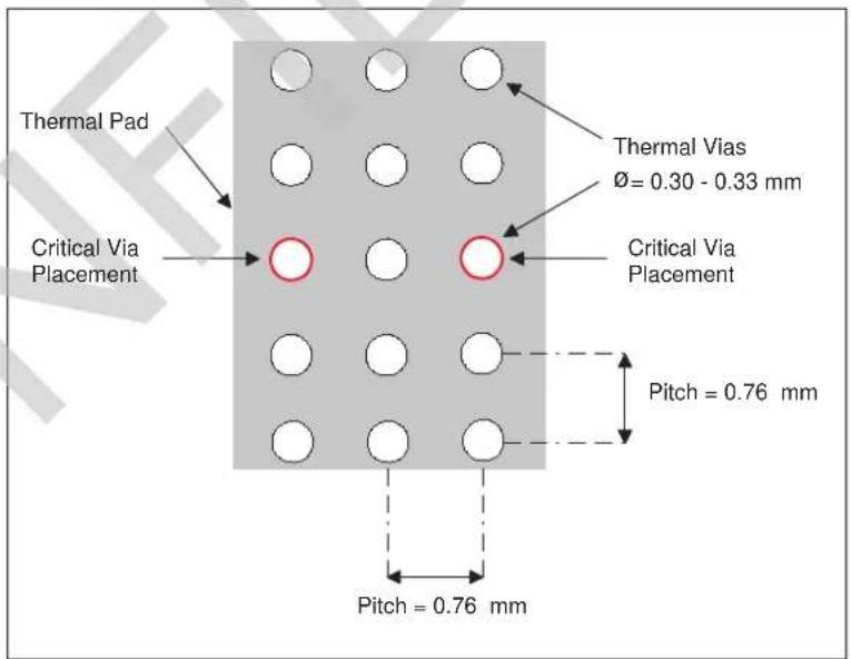
text_image
Thermal Pad Critical Via Placement Thermal Vias Ø=0.30 - 0.33 mm Critical Via Placement Pitch = 0.76 mm Pitch = 0.76 mmFigure 52 - Recommended PCB Thermal Pad and Via Pattern for 28-Pin QFN
4.1.2 Le79271 SLIC Footprint
The footprint used on Microsemi evaluation boards for the Le79271 SLIC is detailed in Figure 53. To help prevent solder bridging between pin pads, and between pin pads and the thermal pad, adhere to the spacings as noted. The pin pad layout allows for a 0.07 mm toe fillet, this can be extended as desired.
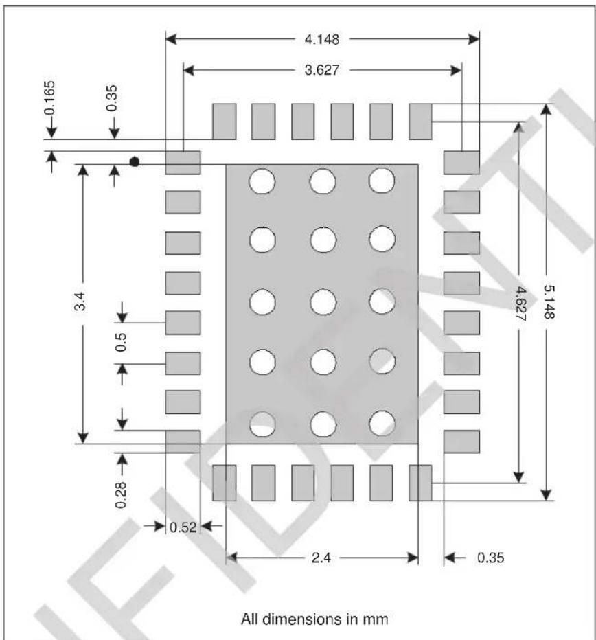
text_image
0.165 0.35 4.148 3.627 3.4 0.5 4.627 5.148 0.28 0.52 0.35 2.4 All dimensions in mmFigure 53 - Recommended PCB Footprint for 28-pin QFN Package
4.1.3 Le79272 Dual SLIC Thermal Pad
The Le79272 package's heat slug measures 5.4 mm by 5.4 mm. Ideally, the PCB pad area should be this size or slightly larger. However, a minimum clearance of 0.15 mm between the thermal pad and the pin pads must be maintained to prevent solder bridging. The thermal pad must be defined on all layers.
The recommended PCB thermal pad and via pattern for the Le79272 Dual SLIC is shown in Figure 54. This pattern uses 49 vias. Drill hole sizes are specified as 0.33 mm (\~13 mils). These vias need to be plated. Do not use thermal reliefs on these vias. Via pitch spacing is 0.76 mm (\~30 mils). All vias connect to an internal AGND or BGND plane. The four vias highlighted in red should be positioned exactly as shown to optimize thermal transfer from the SLIC die to the internal ground layers.

text_image
5.4 mm Thermal Pad 5.4 mm Critical Via Placements Top View Pitch = 0.76 mm Pitch = 0.76 mm Thermal Vias Ø= 0.30 - 0.33 mm Critical Via Placements Pitch = 0.76 mmFigure 54 - Recommended PCB Thermal Pad and Via Pattern for 48-Pin QFN
4.1.4 Le79238 LGA Thermal Pad and Pins
Recommendations for layout and mounting of the Le792388 LGA SLAC device are provided in the Dual Row QFN Stencil Design, Le792388VQC Product Application Note, Document ID# 148192.
4.2 SLIC Placement
Allowing adequate spacing between the SLIC devices is key to thermal management. There are a number of ways to position the SLIC devices relative to the SLAC devices. Possible placements for the Le79271 SLIC device are illustrated in Figure 55 and Figure 56. A placement for the Le79272 dual SLIC device is illustrated in Figure 57. Figure 55 and Figure 57 show a hub arrangement where the SLIC devices surround a central SLAC device. Figure 56 shows a slot arrangement where the SLAC is to one side and the SLIC devices protrude out in two rows.
The proper amount of SLIC spacing is dependant upon air flow, number of ground pour layers, copper thickness, SLIC power dissipation during DC feed and ringing, and traffic. Center-to-center spacing should be on the order of 16 mm (630 mils) minimum for the Le79271 SLIC device and 30 mm (1181 mils) minimum for the Le79272 dual SLIC device. A thermal analysis study must be performed to validate any desired component placement. For a given SLIC center-to-center spacing, the hub arrangement generally will have better thermal performance then the slot arrangement.

text_image
Conceptual diagram only, Not to scale. SLIC Devices (RED) SLAC Devices (BLUE)Figure 55 - Possible SLIC Placement - Hub Arrangement
Conceptual diagram only, Not to scale.

natural_image
Grid of red and blue squares arranged in rows and columns, with a white triangular shape at the bottom right (no text or symbols)SLIC Devices (RED) SLAC Devices (BLUE)
Figure 56 - Possible SLIC Placement - Slot Arrangement

text_image
Conceptual diagram only, Not to scale. SLIC Devices (RED) SLAC Devices (BLUE)Figure 57 - Possible Dual SLIC Placement - Hub Arrangement
4.3 PCB Thermal Performance
Good thermal performance depends on the overall system design. The system designer must ensure that individual devices do not exceed maximum thermal ratings and that the devices are not exposed to an ambient temperature that exceeds the maximum device ratings.
To maximize PCB thermal capabilities:
- Use the thermal pad PCB footprints provided.
- Provide adequate device spacing.
- Minimize current limit values and battery voltage potentials.
- Use additional PCB ground layers.
- Use poured ground on all signal layers.
- Use different ground layers to connect adjacent SLIC thermal pads.
- Keep traces away from the PCB thermal pad or run traces perpendicular to the thermal pad so not to restrict heat flow away from the thermal pad.
- Use a copper weighting of 1.0 ounce for ground layers.
- Use air flow.
It may be possible to satisfy PCB thermal performance with a different footprint or different copper weighting. A thermal analysis must be performed to validate a PCB design.
4.3.1 Airflow
In addition to the thermal mass of the PCB, airflow is critical to a robust system design. The system designer should do all due diligence with respect to airflow. The NGCC chip set provides the ability to significantly increase the number of voice channels on a given PCB card size. Airflow that was adequate on an older, less dense design may not be adequate with a high density PCB design. In other words, the airflow used for a 32 line per card system may not be adequate for a 72 line per card system.
The effect of airflow on the thermal performance of the 28-pin QFN package is illustrated here by measurements taken on a test platform in a controlled airflow environment. SLIC package surface temperature was measured vs. airflow velocity on a 72 channel reference design.
4.3.1.1 Test Platform for Airflow Experiment
A 72 channel board (Le51HR0140) was designed by Microsemi Semiconductor to be used as the test platform for the airflow experiments. The board consists of 72 Le79271 SLIC devices and 9 simulated SLAC devices. To simplify control, SLIC devices were used for the SLAC positions to emulate the DC power dissipation of the SLAC devices. In addition, a separate load board was designed to allow load control and hence power dissipation tweaking of each individual channel.
The Le51HR0140 was designed as a 10 layer board with 12 ounce copper; the laminates are 8 mil thick FR408. Length and width of the board is 24 cm by 22.5 cm. The overall thickness of the board is 80 mils. Copper was poured in the voids in all signal layers. The stack up is listed in Table 4.
| Layer Name | Material Thickness mil Copper Pour | |
| Top Copper 0.7 No | ||
| Laminate FR408 8 - | ||
| Ground 1 Copper 0.7 Yes | ||
| Laminate FR408 8 - | ||
| Signal 1 Copper 0.7 Yes | ||
| Laminate FR408 8 - | ||
| Power 1 Copper 0.7 Yes | ||
| Laminate FR408 8 - | ||
| Signal 2 Copper 0.7 Yes | ||
| Laminate FR408 8 - | ||
| Signal 3 Copper 0.7 Yes | ||
| Laminate FR408 8 - | ||
| Power 2 Copper 0.7 Yes | ||
| Laminate FR408 8 - | ||
| Signal 4 Copper 0.7 Yes | ||
| Laminate FR408 8 - | ||
| Ground 2 Copper 0.7 Yes | ||
| Laminate FR408 8 - | ||
| Bottom Copper 0.7 No | ||
Table 4 - Le51HR0140 Board Layers
The Le51HR0140 board layout is shown in Figure 58. The Le51HR0140 has 9 groups of 8 channels of SLIC devices. Each grouping of 8 SLIC devices surrounds the SLAC emulating SLIC device in the hub arrangement. The grouping numbers are identified in Figure 58. The thermal pad layout used on all the SLIC devices is as illustrated in Figure 53. Note that the 176-pin LQFP SLAC footprint is shown for placement spacing only, the SLAC emulating SLIC device is centered in the hub arrangement.
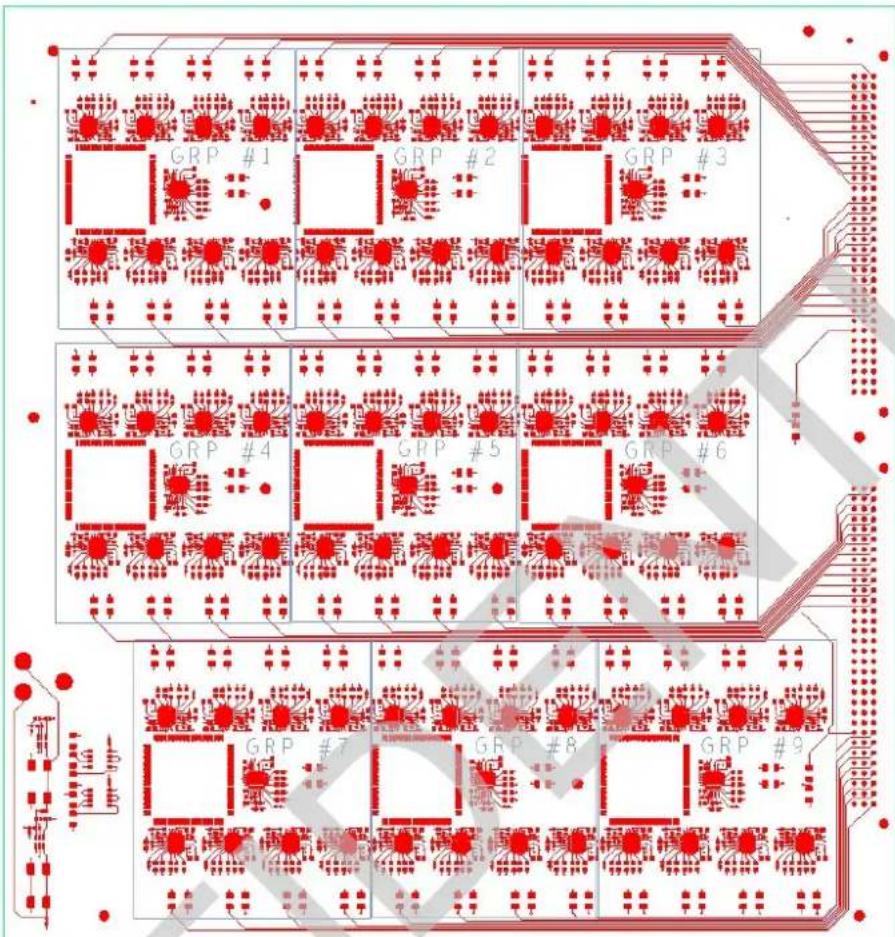
text_image
GRP #1 GRP #2 GRP #3 GRP #4 GRP #5 GRP #6 GRP #7 GRP #8 GRP #9Figure 58 - Le51HR0140 Groupings and Board Layout
4.3.1.2 Electrical Set-up
For the following experiment:
Loop current for SLIC devices in groups 1-4 and 6-9 were set to 24 mA using a high battery of -52 V. Power dissipation of a SLIC in the off-hook active state with a short loop under this condition is 0.8 W.
Loop current for SLIC devices in group 5 were set to 40 mA using a high battery of -52 V. Power dissipation of a SLIC in the off-hook active state with a short loop under this condition is 1.2 W.
Power dissipation for all SLAC emulating SLIC devices was set to 0.85 Watts.
4.3.1.3 Wind Tunnel Design
To enable controlled airflow measurements a wind tunnel was created. The wind tunnel is pictured in Figure 59. On the side of the wind tunnel there is an opening to allow for the load/power board to connect to the Le51HR0140 board under test.
The wind tunnel inlet is 18" from the Le51HR0140 board under test and the air outlet is 24" from the board under test. This distance provides adequate spacing to minimize turbulence and produce an even air flow across the board.
Two dc variable speed fans control the air flow (pictured in the foreground). Three mounting slots are provided for mounting an airflow velocity meter - left, center, and right. These slots are located at the other end of the wind tunnel.
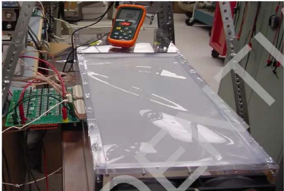
natural_image
Laboratory setup with electronic circuit board, transparent enclosure, and multimeter (no visible text or symbols)Figure 59 - Wind Tunnel and Load Board
4.3.1.4 Thermocouple Measurements
Thermocouples were attached to the top of the SLIC and SLAC emulating SLIC devices on the top of the Le51HR0140 board. Thermocouple data was collected versus airflow using the electrical set-up described in Section 4.3.1.2.
Air inlet temperature was room temperature and measured. Airflow was varied from 0 m/s (meters per second) to 3 m/s in 0.5 m/s steps. The SLIC thermocouple data is plotted versus airflow in Figure 60. Note that U34, U38, and U40 are SLIC devices in group 5.
Surface Temperature Variation vs. Airflow
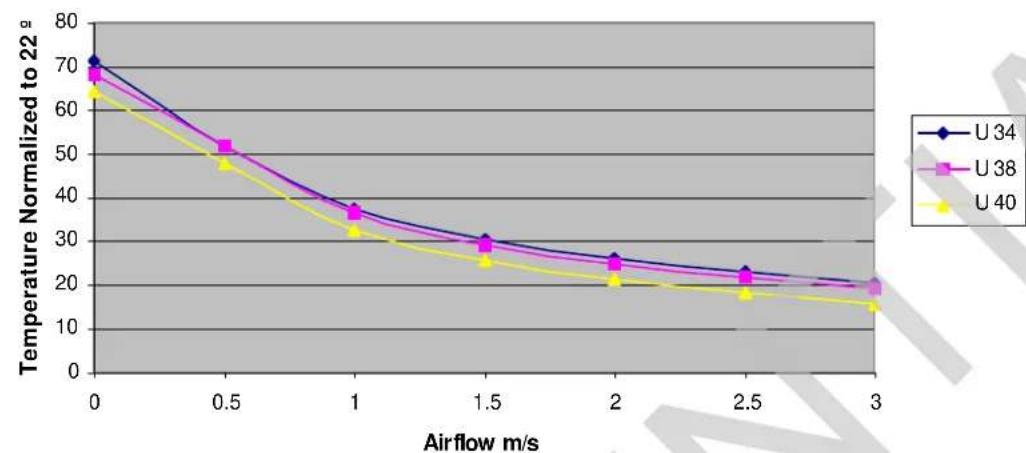
line
| Airflow m/s | U 34 | U 38 | U 40 | | ----------- | ---- | ---- | ---- | | 0 | 70 | 68 | 65 | | 0.5 | 55 | 52 | 48 | | 1 | 38 | 36 | 32 | | 1.5 | 30 | 29 | 25 | | 2 | 25 | 24 | 20 | | 2.5 | 22 | 21 | 18 | | 3 | 20 | 19 | 15 |Figure 60 - SLIC Surface Temperature Variation vs. Airflow, Normalized to Inlet Airflow at 22 °C
Figure 60 shows the effect of airflow on the surface temperature of the SLIC devices. With no airflow, the SLIC surface temperature rose 70 °C over ambient. Ambient was measured as 22 °C. With 3 m/s airflow, the surface temperature of the SLIC devices only rose by 20 °C over ambient.
This graph illustrates how beneficial airflow can be to reducing board temperature of a given design. Individual results will vary depending on the PCB layout, construction and electrical operation.
4.4 Thermal Resistance and Junction Temperature
The following table lists thermal resistance and junction temperature values for the various NGCC devices and packages.
| Device Part Number Package Theta-JA Psi-JT Theta-JB Theta-JC | Max.JunctionTemp | ||||||
| NGSLIC | Le79271MQC 28 | -Pin QFN 32.9 °C/W | 0.6 °C/W 9.8 | °C/W 22.5 °C/W 150 °C | |||
| Le79272PQC 48 | -Pin QFN 23.3 °C/W | 0.3 °C/W 6.6 | °C/W 12.5 °C/W 150 °C | ||||
| NGSLAC | Le792388TVC 17 | 6-Pin LQFP 29.9 °C/W 0.2 °C/W 25.3 °C/W 4.3 °C/W 125 °C | |||||
| Le792388VQC 16 | 4-Pin LGA 16.8 °C/W 0.1 °C/W 4.7 °C/W 3.2 °C/W 125 °C | ||||||
| ZL792388GDG 19 | 6-Pin BGA 22.1 °C/W 0.1 °C/W 9.7 °C/W 39 °C/W 125 °C | ||||||
| ZL792588GDG2 19 | 6-Pin BGA 22.1 °C/W 0.1 °C/W 9.7 °C/W 39 °C/W 125 °C | ||||||
| Device Part Number Package | Theta-JA Psi-JT Theta-JB | Theta-JC | Max.JunctionTemp | ||
| NGVCP | Le79124KVC 128-Pin TQFP 33.7 °C/W 0.1 °C/W 28.5 °C/W 4.3 °C/W 125 °C | ||||
| ZL79124GDG(2) 144-Pin LBGA 28.6 °C/W 0.1 °C/W 15.5 °C/W 5.7 °C/W 125 °C | |||||
| Le79128KVC 128-Pin TQFP 33.7 °C/W 0.1 °C/W 28.5 °C/W 4.3 °C/W 125 °C | |||||
| ZL79128GDG2 144-Pin LBGA 28.6 °C/W 0.1 °C/W 15.5 °C/W 5.7 °C/W 125 °C | |||||
| Le79234KVC 128-Pin TQFP 33.7 °C/W 0.1 °C/W 28.5 °C/W 4.3 °C/W 125 °C | |||||
| ZL79234GDG(2) 144-Pin LBGA 28.6 °C/W 0.1 °C/W 15.5 °C/W 5.7 °C/W 125 °C |
Note: Values are referenced to a 2 signal, 2 power 4-layer JEDEC test board under free air convection conditions.
4.5 Power and Bypass Capacitors
Power should be routed to the SLIC devices using thick PCB traces. To minimize noise coupling, do not use a power plane for the SLIC devices. Power planes are strongly recommended for the VCP and SLAC VDD18.
Bypass capacitors should be placed as close as practical to the device's power pins and use as little PCB trace as possible. A 0.1 F, 10 V ceramic capacitor is recommended for VCC and VDD supplies.
The Le79271 SLIC device has only a single VCC pin. Therefore, only a single bypass capacitor is needed to AGND. Use a bypass capacitor on each of the VCC pins of the Le79272 Dual SLIC device.
The SLAC LQFP and LGA devices have two VDD33, four VDD18, and four AVDD pins. One bypass capacitor per pin is optimal. Also, one 10 F filter capacitor per SLAC device is strongly recommended on the VDD18 node. Ferrite beads can be used on the VDD33 and VDD18 supplies as long as the power supply tolerances, as specified in the data sheet Electrical Ranges section, are adhered to. The SLAC BGA device has additional power and ground pins, these pins can share the aforementioned bypass capacitors. To minimize voltage drop from the +1.8 V supply to the BGA pins, connect the BGA VDD18 pins together using a power plane.
The VCP TQFP device has eight DVDD, one PLL_VDD, and four VDD18 pins. One bypass capacitor per pin is optimal for the TQFP device. The VCP BGA device, which has additional power and ground pins, can share the aforementioned bypass capacitors. Also one 10 F filter capacitor per device is required on the VDD18 node.
The battery supplies also require bypass capacitors. A 0.1 F, 100 V or 200 V ceramic capacitor is recommended. The Le79271 SLIC devices have a single pin for each battery. VBL should have its own bypass capacitor. If a battery referenced overvoltage protector is used, the required decoupling of the protector can serve as the VBH and VBP bypass capacitors and no additional capacitors are required. The Le79272 Dual SLIC device has two pins for each battery. VBL1 and VBL2 can be tied together and can share a bypass capacitor. If a battery referenced overvoltage protector is used, the required decoupling of the protector can serve as the VBH and VBP bypass capacitors and no additional capacitors are required.
Bypass capacitors can be placed on the top side of the board along side the device pins or on the bottom side underneath the device itself. In either case, the capacitors will likely connect to power and ground through vias to internal layers. For best performance, larger vias with larger drill holes are recommended to maintain low impedance and to avoid inductive effects.
4.6 Grounding
The Le79271 SLIC device has one BGND and one AGND pin and the underside exposed thermal pad which needs to be tied to one of these grounds. The Le79272 Dual SLIC device has two BGND and two AGND pins and the underside exposed thermal pad which needs to be tied to one of these grounds.
The SLAC LQFP device has six DGND and eight AGND pins. The SLAC BGA device has seven DGND and twelve AGND pins. The ground for the SLAC LGA device is its exposed pad. The exposed pad is soldered to a thermal pad. This thermal pad needs to be tied to a BGND/AGND layer. Tie the thermal pad to ground by pouring ground between the array of pin vias at the four corners of the package. Additional ground strapping can be realized by extending the thermal pad on all layers to vias on the four corners that tie into the BGND/AGND layer.
The VCP TQFP device has ten DVSS and one PLL_VSS ground pin. The VCP BGA device has twelve DVSS and one PLL_VSS ground pin.
There are a number of grounding schemes that can be deployed. The recommended configuration for most applications is to join AGND, BGND, DGND, and DVSS commonly on the PCB as one large plane. Fault ground (FGND) from the protector can be part of that ground plane too, but FGND is generally only joined with the AGND/BGND/DGND/DVSS plane at the edge of the board connector. FGND needs to be tied to earth ground and adequately sized to carry surge currents. Some designs may choose to separate the battery ground, but in all cases, AGND and DGND should tie to a large internal common plane. The SLIC device specifies that no more than a 3 V differential can exist between BGND and AGND during surge conditions and no more than 300 mV can exist in normal operating modes.
4.7 EMI Capacitors
In order to satisfy 3 V_RMS (Level 2) RF conducted immunity requirements, capacitors must be placed on A and B leads to shunt the interference to ground. Disposing of telephone port EMI at the board edge is the most effective approach but usually not the most cost efficient due to the price of high voltage capacitors. The application circuits in Section 3.0 use EMI capacitors whose voltage is bounded by the protector. C_ADAi and C_BDBi should be positioned as close as possible to the protector; C_ADi and C_BDi should be positioned as close as possible to the SLIC leads. Capacitors placed close to the protector will provide an effective initial shunt of EMI to ground. The EMI capacitors are listed as having a value of 4.7 nF. The actual value of capacitance may need to be adjusted after EMC board testing. Depending on board layout, it may be beneficial to increase the value of C_ADAi and C_BDBi and decrease the value of C_ADi and C_BDi . The total capacitance on AD or BD to ground must be kept <10 nF. Therefore, the EMI capacitor footprint should be sized to accommodate any capacitance value between 1 to 10 nF of these 200 V, X7R capacitors.
An effective high frequency ground for the EMI capacitors is required. Tying C_ADAi and C_BDBi to fault ground is recommended.
Refer to the Ve792 NGCC Electromagnetic Compatibility Application Note (Document ID# 142651) for more information on satisfying conducted immunity and for information on how to satisfy a 10 V_RMS (Level 3) conducted immunity requirement.
5.0 Power Supply Sizing
This section provides guidance in determining the current required of the Next Generation Carrier Chipset devices.
5.1 +3.3 V Supply
The current required of each NGCC device can be determined by referring to the SLIC, SLAC, and VCP device data sheets.
For the SLIC device, use the maximum value in Active state from the Supply Current Specification and multiply this by the total number of SLIC channels.
For the SLAC device, multiply the maximum power in the Nonoperational Active state from the AC/DC Specifications by the number of active channels (usually 8) and divide by 3.3. This is the current required of one SLAC device. Multiply this by the number of SLAC devices in use.
If the VCP device is used, obtain the maximum DVDD/PLL_VDD power from the DC Specifications and divide by 3.3. This is the current required of one VCP device.
The maximum ratings account for temperature, processing, and supply variation. So simply sum the currents together to obtain the total current required of the NGCC devices from the +3.3 V supply.
5.2 +1.8 V Supply
The +1.8 V supply current required of the SLAC and VCP device can be obtained from the data sheets.
For the SLAC device, multiply the maximum power in the Nonoperational Active state from the AC/DC Specifications by the number of active channels (usually 8) and divide by 1.8. This is the current required of one SLAC device. Use no less than 200 mA per SLAC device. Multiply this by the number of SLAC devices in use.
If the VCP device is used, obtain the maximum VDD18 power from the DC Specifications and divide by 1.8. This is the current required of one VCP device.
Sum the currents together to obtain the total current required of the +1.8 V supply. Use of the maximum ratings accounts for temperature, processing, and supply variation.
5.3 Battery Supplies
Microsemi offers an excel spreadsheet Power Calculator to assist in sizing of the VBL, VBH, and VBP battery supplies. The Power Calculator graphs SLIC power dissipation and power consumption in Active and Ringing states as a function of various user inputs versus loop length. The Power Calculator accepts the following user inputs:
- Battery voltages
- System series resistance
- DC feed parameters
- Ringing amplitude
- Ringing bias
- Ringing load
- Ringing cadence
5.3.1 VBL
VBL current draw for a given channel is at its maximum when the SLIC device is in Active Low Battery state and a line has a very short loop or is shorted (point A in Figure 61). The total current draw consists of the loop current plus a small amount of SLIC device consumption.
VBL should be sized according to the expected number of lines off-hook. The Power Calculator displays the total current consumption (as IVBL) in the Power Supply Currents in Active Mode graph. Multiply the point A value by the expected number of lines off-hook and add >25% for margin. Usually taking the current at the 200 ohm point is sufficient for sizing this power supply.
5.3.2 VBH
The VBH supply is used for DC feed and for internal ringing.
For DC feed, VBH current draw for a given channel is at its maximum either when the DC operation point is near the automatic battery switch point or when a line initially goes off-hook.
When supplying steady-state loop current, VBH power dissipation for a given line is at its maximum when the loop resistance is such that the DC operating point is near the VBH to VBL switch point. The Power Calculator displays this information, see point B in Figure 61. The total current at point B consists of the loop current plus a small amount of SLIC device consumption.
When a phone initially goes off-hook, loop current is limited by the loop resistance and an analog current limit resident in the SLAC device. After about 25 msec, the DC feed circuitry begins regulating the line. The analog current limit can be as high as 110 mA. For power supply sizing it is prudent to assume that some number of lines will be drawing 110 mA for 25 msec. If a bulk call testing unit is used however to evaluate the system design, it is likely that many lines will be taken off-hook at the same time. One could size the power supply to accommodate this current draw, but this may not be necessary. First, this condition will only occur in the test environment and is not a realistic field condition. Second, one can usually rely on the transient response characteristics of the power supply to hold its voltage even if the transient current draw is larger than the rated supply current. Third, if there is a droop in supply voltage during a multiple off-hook transient, a drop in voltage will reduce the load current and have a self-regulating effect. Fourth, with NGCC tip voltage is fixed and ring voltage is programmed with respect to ground. The off-hook impedance used for loop supervision is determined by dividing the measured tip-to-ring voltage by the metallic current. These design factors keep off-hooks from being lost during a supply droop and calls are not dropped during the 25 ms interval.
Determining which DC feed current to use for a given line depends on off-hook assumptions. Except on very long loops, the transient when a phone initially goes off-hook requires the most current. To determine the VBH current allotment for off-hook transient current, multiply the desired number of lines going off-hook at exactly the same time by 110 mA. To determine the VBH current allotment for steady-state feeding of off-hook current, multiply the number of lines that can be off-hook at one time by the current at point B as calculated by the Power Calculator. Sum the currents. This represents the current required for DC feed.
Power Supply Currents in Active Mode (Per Line)

line
| Rexternal (ohms) | IVBH (mA) | IVBL (mA) | IVCC (mA) | | ---------------- | --------- | --------- | --------- | | 0 | 0 | 27 | 4 | | 900 | 0 | 27 | 4 | | 1000 | 27 | 0 | 4 | | 3000 | 18 | 0 | 4 |Figure 61 - Power Calculator Example - Supply Currents in Active Mode
VBH current is also used for internal ringing. The VBH current draw during ringing is the same as the current draw from the VBP supply. Refer to the VBP section for an explanation on ringing current. The number of lines in ringing at a given time should be considered and added to the required DC feed VBH current. Add >25% to the total current for margin.
5.3.3 VBP
The VBP supply is used for internal ringing in long loop and heavy ringing load applications; it can also be used to drive long loops in Boosted Battery mode.
Ringing current for a given line varies depending on the load. The Power Calculator allows the user to define the REN load. Ringing current will increase for the period of time after a phone goes off-hook until ring-trip occurs. The Power Calculator displays the ringing current in the user defined load at the end of the user defined loop during ringing cadence before and after ring-trip. An example of this is shown in Figure 62. In this example the user defined loop resistance is 500 ohms. Loop resistance will limit the current during off-hook, so even though the Power Calculator displays the long loop current, it is important to consider that the maximum current when the phone is off-hook can be as high as 110 mA if a short loop is used.
To determine the required VBP supply current, use the peak value of expected number of lines ringing at the same time plus the peak value of the expected number of lines in off-hook at the same time (allow 110 mA for short loop lines in ring-trip). Add >25% to the result for margin. Remember, the number of lines in ringing at the same time can be minimized by controlling the ringing cadence.
If Boosted Battery mode is used, VBP needs to source the maximum user defined loop current. Multiply the loop current by the expected number of off-hook lines in Boosted Battery mode at one time and add 25% for margin. Add this current to the required VBP current during ringing.
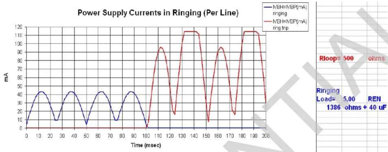
line
| Time (msec) | MBH=MBP(mA) ringing (mA) | MBH=MBP(mA) ring trip (mA) | |-------------|--------------------------|----------------------------| | 0 | 5 | 0 | | 10 | 45 | 0 | | 20 | 10 | 0 | | 30 | 45 | 0 | | 40 | 10 | 0 | | 50 | 5 | 0 | | 60 | 45 | 0 | | 70 | 10 | 0 | | 80 | 45 | 0 | | 90 | 10 | 0 | | 100 | 5 | 0 | | 110 | 95 | 95 | | 120 | 15 | 15 | | 130 | 115 | 115 | | 140 | 115 | 115 | | 150 | 10 | 10 | | 160 | 95 | 95 | | 170 | 15 | 15 | | 180 | 115 | 115 | | 190 | 115 | 115 | | 200 | 30 | 30 |Figure 62 - Power Calculator Example - Supply Currents in Ringing
Information relating to products and services furnished herein by Microsemi Corporation or its subsidiaries (collectively "Microsemi") is believed to be reliable. However, Microsemi assumes no liability for errors that may appear in this publication, or for liability otherwise arising from the application or use of any such information, product or service or for any infringement of patents or other intellectual property rights owned by third parties which may result from such application or use. Neither the supply of such information or purchase of product or service conveys any license, either express or implied, under patents or other intellectual property rights owned by Microsemi or licensed from third parties by Microsemi, whatsoever. Purchasers of products are also hereby notified that the use of product in certain ways or in combination with Microsemi, or non-Microsemi furnished goods or services may infringe patents or other intellectual property rights owned by Microsemi.
This publication is issued to provide information only and (unless agreed by Microsemi in writing) may not be used, applied or reproduced for any purpose nor form part of any order or contract nor to be regarded as a representation relating to the products or services concerned. The products, their specifications, services and other information appearing in this publication are subject to change by Microsemi without notice. No warranty or guarantee express or implied is made regarding the capability, performance or suitability of any product or service. Information concerning possible methods of use is provided as a guide only and does not constitute any guarantee that such methods of use will be satisfactory in a specific piece of equipment. It is the user's responsibility to fully determine the performance and suitability of any equipment using such information and to ensure that any publication or data used is up to date and has not been superseded. Manufacturing does not necessarily include testing of all functions or parameters. These products are not suitable for use in any medical and other products whose failure to perform may result in significant injury or death to the user. All products and materials are sold and services provided subject to Microsemi's conditions of sale which are available on request.
For more information about all Microsemi products
visit our website at
www.microsemi.com
TECHNICAL DOCUMENTATION – NOT FOR RESALE

Microsemi.
Microsemi Corporate Headquarters
One Enterprise, Aliso Viejo CA 92656 USA
Within the USA: +1 (949) 380-6100
Sales: +1 (949) 380-6136
Microsemi Corporation (NASDAQ: MSCC) offers a comprehensive portfolio of semiconductor solutions for: aerospace, defense and security; enterprise and communications; and industrial and alternative energy markets. Products include mixed-signal ICs, SoCs, and ASICs; programmable logic solutions; power management products; timing and voice processing devices; RF solutions; discrete components; and systems. Microsemi is headquartered in Aliso Viejo, Calif. Learn more at www.microsemi.com.
© 2014 Microsemi Corporation. All rights reserved. Microsemi and the Microsemi logo are trademarks of Microsemi Corporation. All other trademarks and service marks are the property of their respective owners.