SY58620L - Transceiver Microchip - Free user manual and instructions
Find the device manual for free SY58620L Microchip in PDF.

User questions about SY58620L Microchip
0 question about this device. Answer the ones you know or ask your own.
Ask a new question about this device
Download the instructions for your Transceiver in PDF format for free! Find your manual SY58620L - Microchip and take your electronic device back in hand. On this page are published all the documents necessary for the use of your device. SY58620L by Microchip.
USER MANUAL SY58620L Microchip
The SY58620L is a low jitter, high-speed transceiver with a variable swing CML transmitter buffer and a CML high-gain receiver optimized for precision telecom and enterprise server transmission line and backplane data management. The SY58620L distributes data to 4.25Gbps guaranteed over temperature and voltage.
The SY58620L transmitter differential input includes Micrel's unique, 3-pin input termination architecture that directly interfaces to any (AC- or DC-coupled) differential signal as small as 100mV (200mV PP) without any termination resistor network in the signal path. The receiver differential input is optimized to interface directly to AC-coupled signals as small as 10mV (20mV PP). The outputs are 50Ω source -terminated CML with extremely fast rise/fall time.
To support remote self-testing, the SY58620L features a high-speed loopback test mode. The input control signal LOOPBACK enables an internal loopback path from the transmitter input to the receiver output.
The SY58620L operates from a 3.3V ±10% supply and is guaranteed over the full industrial temperature range of -40°C to +85°C. The SY58620L is part of Micrel's high-speed, Precision Edge® product line.
All support documentation can be found on Micrel's web site at: www.micrel.com.
Applications
- Backplane management
• Active cable transceivers
• SONET/SDH data/clock applications
• 4X Fibre Channel applications
Typical Applications

text_image
System Rack SY58620 TXQ /TXQ Cable System Rack SY58620 RXIN /RXINPrecision Edge is a registered trademark of Micrel, Inc.

Precision Edge®
Features
• Guaranteed AC performance over temperature and voltage:
- Maximum Throughput 4.25Gbps
- <120ps t /t time
- Transmitter
- Patented input termination directly interfaces to AC- or DC-coupled differential inputs
- Variable swing CML output
- Receiver
- 32dB high-gain Input
- Internal 50Ω input termination
- Accepts AC-coupled input signals as small as 10mV (20mV PP)
- 400mV (800mV PP) differential CML output swing
- Loss-of-Signal (LOS)
- High-gain, TTL-compatible LOS output with internal 4.75kΩ pull-up
-
Programmable LOS level set
-
Ultra-low jitter design
- <5psRMS random jitter
- Patent-pending MUX isolates the receiver and the transmitter channels minimizing on crosstalk
- Selectable loopback diagnostic mode
- Output enable
• Power supply +3.3V ±10% - Industrial temperature range -40°C to +85°C
• Available in 24-pin (4mm x 4mm) QFN
Markets
- Precision telecom
- Enterprise server
- ATE
• Test and measurement - Precision telecom
- Enterprise server
- ATE
• Test and measurement
Functional Block Diagram

flowchart
graph TD
    A["LOSLVL"] --> B["VREF"]
    B --> C["R_LOSLVL (External Resistor)"]
    C --> D["2.8kΩ (Internal pull-down)"]
    D --> E["(Internal Reference)"]
    E --> F["OC-TTL Buffer"]
    F --> G["4.75kΩ (Internal pull-up)"]
    G --> H["LOS"]
    I["RXIN"] --> J["VREF = V_CC_RXIN - 1.3V"]
    J --> K["Limiting Amplifier"]
    K --> L["Level Detect"]
    L --> M["MUX"]
    M --> N["0"]
    N --> O["CML Buffer"]
    O --> P["25kΩ (Internal pull-down)"]
    P --> Q["TTL Buffer"]
    Q --> R["GND"]
    S["/RXIN"] --> T["(Internal Reference)"]
    T --> U["TTL Buffer"]
    U --> V["GND"]
    W["LOOPBACK"] --> X["25kΩ (Internal pull-down)"]
    X --> Y["GND"]
    Z["TXVCTRL"] --> AA["CML Buffer"]
    AB["/TXQ"] --> AC["TTL Buffer"]
    AD["/TXEN"] --> AE["GND"]
    AF["VREF_CTRL"] --> AG["25kΩ (Internal pull-down)"]
    AG --> AH["MUX"]
    AH --> AI["1"]
    AI --> AJ["0"]
    AJ --> AK["25kΩ (Internal pull-down)"]
    AK --> AL["TTL Buffer"]
    AL --> AM["GND"]
    AN["TXVT"] --> AO["50Ω"]
    AP["/TXIN"] --> AQ["50Ω"]
    AR["TXVREF-AC"] --> AS["50Ω"]
    AT["VREF"] --> AU["GND"]
    AV["VCC"] --> AW["R_LOSLVL (External Resistor)"]
    AW --> AX["4.75kΩ (Internal pull-up)"]
    AX --> AY["LOS"]
Note:
It is recommended that R
LOSLVL ≤ 10k . See the "Typical Operating Characteristics" section for more details.
Ordering Information ^(1)
| Part Number Package | Type | Operating Range | Package Marking Lead Finish | |
| SY58620LMG | QFN-24 | Industrial | 620L with Pb-Free bar-line indicator | NiPdAuPb-Free |
| SY58620LMGTR ^(2) | QFN-24 | Industrial | 620L with Pb-Free bar-line indicator | NiPdAuPb-Free |
Notes:
-
Contact factory for die availability. Dice are guaranteed at T_A = 25^ , DC Electricals only.
-
Tape and Reel.
Pin Configuration

other
| Pin Number | Pin Name | Value | | :--- | :--- | :--- | | 1 | RXIN | 1 | | 2 | /RXIN | 2 | | 3 | GND | 3 | | 4 | VCC_TXQ | 4 | | 5 | TXQ | 5 | | 6 | /TXQ | 6 | | 7 | /TXEN | 7 | | 8 | VREF_CTRL | 8 | | 9 | TXVCTRL | 9 | | 10 | TXVREF_AC | 10 | | 11 | TXVT | 11 | | 12 | VCC | 12 | | 13 | TXIN | 13 | | 14 | VCC | 14 | | 15 | /RXQ | 15 | | 16 | /RXQ | 16 | | 17 | RXQ | 17 | | 18 | VCC | 18 | | 19 | LOSLVL | 19 | GND, LOOPBACK, LOS, VCC_RXIN, RXEN, LOSLVL 24, 23, 22, 21, 20, 19 24, 23, 22, 21, 20, 19 24, 23, 22, 21, 20, 19 24, 23, 22, 21, 20, 19 24, 23, 22, 21, 20, 19 24, 2324-Pin QFN
Pin Description
Inputs
| Pin Number | Pin Name | Pin Description |
| 23 LOOPBACK | LOOPBACK Mode Control. TTL/CMOS control input. LOOPBACK is an active HIGH signal used to control the LOOPBACK MUX. LOOPBACK is internally connected to a 25kΩ pull-down resistor and will default to a LOW state if left open. V_TH = V_CC/2 . | |
| 20 /RXEN | Receiver Output Control. TTL/CMOS control input. /RXEN is an active LOW signal used to enable the receiver outputs. /RXEN is internally connected to a 25kΩ pull-down resistor and will default to a LOW state if left open. V_TH = V_CC/2 . | |
| 1, 2 | RXIN, /RXIN | Receiver Differential Input. Input accepts AC differential signals as small as 10mV (20mV _PP ). Each pin internally terminates to V_CC\_RXIN-1.3V (internal voltage reference) through 50Ω. Input will default to an indeterminate state if RXIN inputs are left open. See figure 6b. |
| 7 /TXEN | Transmitter Output Control. TTL/CMOS control input. /TXEN is an active LOW signal used to enable the transmitter output. /TXEN is internally connected to a 25kΩ pull-down resistor and will default to a LOW state if left open. V_TH = V_CC/2 . | |
| 14, 13 | TXIN, /TXIN | Transmitter Differential Input. Input accepts AC- or DC-coupled differential signals as small as 100mV (200mV _PP ). Each pin terminates to the TXVTpin through 50Ω. Input will default to an indeterminate state if TXIN inputs are left open. See figure 6a. |
| 9 TXVCTRL | Transmitter Output Swing Control. Input that controls the output amplitude of the transmitter. The operating range of the control input is from V_REF\_CTRL (max swing) to V_CC (min swing). Control of the output swing is obtained with a variable resistor between V_REF\_CTRL and V_CC\_TXQ through a wiper driving TXVCTRL. Setting TXVCTRL to V_CC\_TXQ sets the output swing to min swing. Refer to the “Interface Applications” and “Output Stage” sections for more details. | |
| 11 TXVT | Input Termination Center-Tap. Each side of the transmitter differential input pair terminates to the TXVT pin. The TXVT pin provides a center-tap to a termination network for maximum interface flexibility. Refer to the “Input Stage” section for more details. | |
Outputs
| Pin Number | Pin Name | Pin Description |
| 22 LOS | Loss-of-Signal Output. TTL-compatible output with internal 4.75kΩ pull-up resistor. Loss-of-Signal asserts to logic HIGH when the receiver input amplitudes falls below the threshold set by LOSLVL. | |
| 19 | LOSLVL | RX Loss-of-Signal Level Set. A resistor (R _LOSLVL ) connected between LOSLVL and V _CC sets the threshold for the data input amplitude at which the LOS output is asserted. Default is max sensitivity. LOSLVL is used to set the Loss-of-Signal (LOS) voltage. It is internally connected to a 2.8kΩ pull-down resistor to an internal V _REF voltage source. See “Typical Operating Characteristics,” and “Application Implementation” sections for more details. |
| 17, 16 | RXQ, /RXQ | Receiver Differential Output. Output is CML compatible. Refer to the “Truth Table” and “Output Stage” sections for more details. Unused output pair may be left open. The output is designed to drive 400mV (800mV _PP ) into 50Ω to V _CC or 100Ω across the pair. |
| 5, 6 TXQ, /TXQ | Transmitter Differential Variable Swing Output. Output is CML compatible. Please refer to the “Truth Table” and “Output Stage” sections for more details. Unused output pair may be left open. The output is designed to drive 80mV (160mV _PP ) min swing to 400mV (800mV _PP ) typ. swing into 50Ω to V _CC\_TXQ or drive 100Ω across the pair depending on TXVCTRL. | |
| 8 VREF_CTRL | Transmitter Output Reference Voltage. Output biases to V _CC\_TXQ -1.3V. Connecting V _REF\_CTRL to TXVCTRL sets the transmitter output swing to max swing. | |
| 10 TXVREF-AC | Transmitter Input Reference Voltage. This output biases to V _CC -1.3V. It is used when AC coupling the transmitter input. For AC-coupled applications, connect TXVREF-AC to the TXVT pin and bypass with a 0.01μF low ESR capacitors to V _CC . See “Input Stage” section for more details. Maximum sink/source current is ±1.5mA. |
Power Pins
| Pin Number | Pin Name | Pin Description |
| 3, 24 | GND, Exposed Pad | Ground. GND pins and exposed pad must be connected to the same ground plane. |
| 12, 15, 18 VCC | 3.3V ±10% Positive Power Supply. Bypass with 0.1μF//0.01μF low ESR capacitors and place as close to each V_CC pins as possible. Power pins are not connected internally and must be connected to the same power supply externally. | |
| 21 VCC_RXIN | 3.3V ±10% Receive Input Power Supply. Bypass with 0.1μF//0.01μF low ESR capacitors and place as close to the V_CC\_RXIN pin as possible. Power pins are not connected internally and must be connected to the same power supply externally. | |
| 4 VCC_TXQ | 3.3V ±10% Output Transmit Power Supply. Bypass with 0.1μF//0.01μF low ESR capacitors and place as close to the V_CC\_TXQ pin as possible. Power pins are not connected internally and must be connected to the same power supply externally. |
Truth Table
| LOOPBACK | RXQ TXQ | |
| 0 RXIN | TXIN | |
| 1 TXIN | RXIN |
Absolute Maximum Ratings ^(1)
Supply Voltage
(V_CC, V_CC_TXQ, V_CC_RXIN) -0.5V to +4.0V
Input Voltage
LOSLVL V_REF -1.2V to V_CC
LOOPBACK....-0.5V to Vcc
/TXEN, /RXEN -0.5V to Vcc
TXVCTRL....VREF_CTRL-1.2V to Vcc
TXIN, /TXIN....-0.5V to Vcc
Source or Sink Current on
TXVT....±100mA
LOS....±5mA
RXQ, /RXQ ±25mA
TXQ, /TXQ ±25mA
RXIN, /RXIN....±10mA
TXIN, /TXIN....±50mA
TXVREF-AC, VREF-CTRL ....±2mA
Lead Temperature (soldering, 20sec.) 260°C
Storage Temperature ( T_s ) -65^ to +150^
Operating Ratings ^(2)
Supply Voltage
(V_CC, V_CC_TXQ, V_CC_RXIN) +3.0V to +3.6V
Ambient Temperature ( T_A )....-40°C to +85°C
Package Thermal Resistance ^(3)
QFN (θ JA)
Still-Air 50°C/W
QFN (ψ JB)
Junction-to-Board 30°C/W
DC Electrical Characteristics ^(4)
T_A = -40^ to +85^ , unless otherwise stated.
| Symbol | Parameter | Condition | Min | Typ | Max | Units |
| V_CC | Power Supply | 3 | 3.3 | 3.6 | V | |
| V_CC\_TXQ | Transmit Power Supply | 3 | 3.3 | 3.6 | V | |
| V_CC\_RXIN | Receive Power Supply | 3 | 3.3 | 3.6 | V | |
| Icc | Power Supply Current | No load, max. V_CC | 100 | 150 | mA |
Receiver Input DC Electrical Characteristics
V_CC RXIN = 3.3V ± 10% ; T_A = -40^ to +85^ , unless otherwise stated.
| Symbol | Parameter | Condition | Min | Typ | Max | Units |
| R_IN | Input Resistance (RXIN to VREF) | 45 | 50 | 55 | ||
| R_DIFF\_IN | Input Resistance (RXIN to /RXIN) | 90 | 100 | 110 | ||
| V_IN | Input Voltage Swing (RXIN, /RXIN) | See Figure 5a AC-coupled | 10 | 900 | mV | |
| V_DIFF\_IN | Differential Input Voltage Swing |RXIN - /RXIN| | See Figure 5b AC-coupled | 20 | 1800 | mV | |
| V_REF | Internal Reference Voltage | V_CC\_RXIN -1.48 | V_CC\_RXIN -1.32 | V_CC\_RXIN -1.16 | V |
Notes:
- Permanent device damage may occur if absolute maximum ratings are exceeded. This is a stress rating only and functional operation is not implied at conditions other than those detailed in the operational sections of this data sheet. Exposure to absolute maximum rating conditions for extended periods may affect device reliability.
- The data sheet limits are not guaranteed if the device is operated beyond the operating ratings.
- Package thermal resistance assumes exposed pad is soldered (or equivalent) to the devices most negative potential on the PCB. _JA and _JB values are determined for a 4-layer board in still-air, unless otherwise stated.
- The circuit is designed to meet the DC specifications shown in the above table after thermal equilibrium has been established.
Receiver Output DC Electrical Characteristics
V_CC = 3.3V ± 10% , R_L = 100 across the outputs; T_A = -40^ to +85^ , unless otherwise stated.
| Symbol | Parameter | Condition | Min | Typ | Max | Units |
| V_OH Output HIGH Voltage (RXQ, /RXQ) | R_L = 50 to V_CC | V_CC - 0.020 | V_CC - 0.010 | V_CC | V | |
| V_OUT Output Voltage Swing (RXQ, /RXQ) | See Figure 5a | 325 | 400 | 500 | mV | |
| V_DIFF\_OUT Differential Output Voltage Swing (RXQ, /RXQ) | See Figure 5b | 650 | 800 | 1000 | mV | |
| R_OUT | Single-Ended Output Impedance | 45 | 50 | 55 | Ω | |
| R_DIFF\_OUT | Differential Output Impedance | 90 | 100 | 110 | Ω | |
| V_OFFSET | Differential Output Offset | R_L = 50 to V_CC , limiting mode | -140 | +140 | mV | |
Transmitter Input DC Electrical Characteristics
V_CC = 3.3V ± 10% ; T_A = -40^ to +85^ , unless otherwise stated.
| Symbol | Parameter | Condition | Min | Typ | Max | Units |
| R_IN | Input Resistance(TXIN to TXVT) | 45 | 50 | 55 | Ω | |
| R_DIFF\_IN | Differential Input Resistance(TXIN to /TXIN) | 90 | 100 | 110 | Ω | |
| V_IH | Input HIGH Voltage(TXIN, /TXIN) | 1.2 | V_CC | V | ||
| V_IL | Input LOW Voltage(TXIN, /TXIN) | 0 | V | _IH -0.1 | V | |
| V_IN | Input Voltage Swing(TXIN, /TXIN) | See Figure 5a | 0.1 | V_CC | V | |
| V_DIFF\_IN | Differential Input Voltage Swing|TXIN - /TXIN| | See Figure 5b | 0.2 | V | ||
| V_T\_IN | TXIN, /TXIN to VT | 1.28 | V | |||
| V_TXVREF\_AC | Output Reference Voltage | V_CC -1.4 | V_CC -1.3 | V_CC -1.2 | V | |
| V_REF\_CTRL | Output Reference Voltage | V_CC -1.4 | V_CC -1.3 | V_CC -1.2 | V | |
| V_TXVCTRL | Input Voltage(TXVCTRL) | V_REF\_CTRL | VCC V |
Transmitter Output DC Electrical Characteristics
V_CC_TXQ = 3.3V ± 10% , R_L = 100 across the outputs; T_A = -40^ to +85^ , unless otherwise stated.
| Symbol | Parameter | Condition | Min | Typ | Max | Units |
| V_OH | Output HIGH Voltage (TXQ, /TXQ) | R_L = 50 to V_CC\_TXQ | V_CC\_TXQ-0.020 | V_CC\_TXQ-0.005 | V_CC\_TXQ | V |
| V_OUT | Output Voltage Swing (TXQ, /TXQ) | TXVCTRL = V_REF\_CTRL See Figure 5a | 325 | 400 | mV | |
| TXVCTRL = V_CC\_TXQ See Figure 5a | 80 | mV | ||||
| V_DIFF\_OUT | Differential Output Voltage Swing (TXQ, /TXQ) | TXVCTRL = V_REF\_CTRL See Figure 5b | 650 | 800 | mV | |
| TXVCTRL = V_CC\_TXQ See Figure 5b | 160 | mV | ||||
| R_OUT | Single-Ended Output Impedance | 45 | 50 | 55 | ||
| R_DIFF\_OUT | Differential Output Impedance | 90 | 100 | 110 |
LVTTL/CMOS INPUT DC Electrical Characteristics ^(5)
V_CC = 3.3V ± 10% ; T_A = -40^ to +85^ , unless otherwise stated.
| Symbol | Parameter | Condition | Min | Typ | Max | Units |
| V_IL /TXEN, /RXEN, LOOPBACK 0.8 V | ||||||
| V_IH | /TXEN, /RXEN, LOOPBACK | 2 | V | |||
| I_IL | /TXEN, /RXEN, LOOPBACK I | _IL@V_IN=0.5V | 0 | 50 | μA | |
| I_IH | /TXEN, /RXEN, LOOPBACK I | _IH@V_IN=V_CC | 300 | μA |
Note:
- /TXEN, /RXEN, and LOOPBACK have an internal pull-down 25kΩ resistor.
LOS DC Electrical Characteristics
V_CC = 3.3V ± 10% ; T_A = -40^ to +85^ .
| Symbol | Parameter | Condition | Min | Typ | Max | Units |
| V_LOSLVL | L O S L V L Voltage Range V | REF V | cc | V | ||
| V_OH Output | HIGH Voltage I | SOURCE = -100μA; V_CC ≥ 3.3V | 2.4 | V | ||
| V_OL | Output LOW Voltage | I_OL= 2mA | 0.5 | V | ||
| VSR | LOS Sensitivity Range | 7 | 35 | mVpp | ||
| LOS_AL | Low LOS Assert Level | R_LOSLVL= 10kΩ 2^7-1 Data Pattern, Note 7 622Mbps | 15 | mV | ||
| 4.25Gbps | 10 | mV | ||||
| LOS_DL | Low LOS De-assert Level | R_LOSLVL= 10kΩ 2^7-1 Data Pattern, Note 7 622Mbps | 20 | mV | ||
| 4.25Gbps | 15 | mV | ||||
| HYS_L | Low LOS Hysteresis | R_LOSLVL= 10kΩ, limiting mode 2^7-1 Data Pattern, Note 6 and 7 622Mbps | 3 | dB | ||
| 4.25Gbps | 5.5 | dB | ||||
| LOS_AM | Medium LOS Assert Level | R_LOSLVL= 5kΩ 2^7-1 Data Pattern, Note 7 622Mbps | 20 | mV | ||
| 4.25Gbps | 15 | mV | ||||
| LOS_DM | Medium LOS De-assert Level | R_LOSLVL= 5kΩ 2^7-1 Data Pattern, Note 7 622Mbps | 30 | mV | ||
| 4.25Gbps | 25 | mV | ||||
| HYS_M | Medium LOS Hysteresis R | J_LOSLVL= 5kΩ, limiting mode 2^7-1 Data Pattern, Note 6 and 7 622Mbps | 4 | dB | ||
| 4.25Gbps | 5.5 | dB | ||||
| LOS_AH | High LOS Assert Level | R_LOSLVL= 1kΩ 2^7-1 Data Pattern, Note 7 622Mbps | 35 | mV | ||
| 4.25Gbps | 30 | mV | ||||
| LOS_DH | High LOS De-assert Level | R_LOSLVL= 1kΩ 2^7-1 Data Pattern, Note 7 622Mbps | 60 | mV | ||
| 4.25Gbps | 55 | mV | ||||
| HYS_H | High LOS Hysteresis | R_LOSLVL= 1kΩ, limiting mode 2^7-1 Data Pattern, Note 6 and 7 622Mbps | 5 | dB | ||
| 4.25Gbps | 5.5 | dB |
Notes:
- Hysteresis is defined as: 20_10(_AssertVoltageSD_De-assertVoltage)dB.
- See the "Typical Operating Characteristics" section for more details on R_LOSLVL and its associated LOS assert and de-assert amplitudes for a 2^7 - 1 PRBS data pattern. See the "PRBS Discussion" section for more details on the 2^7 - 1 PRBS data pattern.
AC Electrical Characteristics ^(8)
V_CC = V_CC_TXQ = V_CC_RXIN = 3.3V ± 10% , R_L = 100 across the outputs; T_A = -40^ to +85^ , unless otherwise stated.
Receiver and Transmitter
| Symbol | Parameter | Condition | Min | Typ | Max | Units |
| t_JITTER | Deterministic Jitter (DJ) | Note 9 | Note 13 | p_SPP | ||
| Random Jitter (RJ) | Note 10 | 0.7 | 5 | p_S_RMS | ||
| Crosstalk-Induced Jitter | Note 11 | 1.2 | p_S_RMS |
Receiver
| Symbol | Parameter | Condition | Min | Typ | Max | Units |
| F_MAX | Maximum Operating Frequency | V_RXIN ≥ 10mV (20mV_PP) | 4.25 | Gbps | ||
| BW | -3dB | V_RXIN ≥ 10mV (20mV_PP) | 2.5 | GHz | ||
| S_21 | Single-Ended Gain | Linear mode | 32 | dB | ||
| A_V(DIFF) | Differential Voltage Gain | Linear mode | 38 | dB | ||
| t_r, t_f | Output Rise/Fall Time(20% to 80%) | Limiting mode | 60 | 120 | ps | |
| LOS Frequency Range | LOS Operating Frequency Range | Note 12 | 0.622 | 4.25 | Gbps | |
| t_OFF | LOS De-assert Time | 0.1 | 0.5 | μs | ||
| t_ON | LOS Assert Time | 0.2 | 0.5 | μs |
Transmitter
| Symbol | Parameter | Condition | Min | Typ | Max | Units |
| F_MAX | Maximum Operating Frequency | V_TXIN ≥ 100mV (200mV_PP) | 4.25 | Gbps | ||
| BW | -3dB | V_REF\_CTRL ≤ TXCTRL ≤ V_CC\_TXQ | 3.5 | GHz | ||
| t_r, t_f | Output Rise/Fall Time(20% to 80%) | V_TXVCTRL = VREF\_CTRL | 50 | 120 | ps |
Notes:
- High-frequency AC-parameters are guaranteed by design and characterization.
- Deterministic jitter is measured with both K28.5 and 2^23 -1 PRBS data-pattern, measured at <f_MAX . V_IN = 10mV (20mVpp) RX, 100mV (200mVpp) TX. See the “PRBS Discussion” section for more details on the K28.5 and 2^23 -1 PRBS data pattern.
- Random jitter is measured with a K28.7 comma detect character pattern, measured at <f_MAX . V_IN=10mV(20mVpp)RX , 100mV (200mVpp) TX. See the “PRBS Discussion” section for more details on the K28.7 PRBS data pattern.
- Crosstalk is measured at the output while applying two similar differential clock frequencies that are asynchronous with respect to each other at the inputs.
- LOS is guaranteed to be chatter-free at f_MAX ≥ 622 Mpbs or f_MAX ≥ 311 MHz with V_RXIN ≥ 10 mV (20mV PP) with a 2^7 - 1 PRBS data pattern.
- Contact factory for limits.
Detailed Description
Receiver
The receiver AC-coupled differential input distributes data to 4.25Gbps with signals as small as 10mV (20mV PP ) or as large as 900mV (1.8V PP ). The receiver input features an internal 50Ω input termination connected to an internal reference which optimizes the inputs for AC-coupled signals. Input signals are linearly amplified with 38dB of differential gain and the output signal is limited to 400mV (800mV _PP ).
The receiver output buffer features 50Ω source termination resistors and a current source that provides 400mV (800mV _PP ) swing into 50Ω termination. The output buffer terminates to standard CML loads (100Ω across the output pair or equivalent). See the “Output Stage Receiver” section for more details.
Transmitter
The transmitter differential input includes Micrel's unique, patented 3-pin input termination architecture that directly interfaces to any (AC- or DC-coupled) differential signal as small as 100mV (200mV _pp ) without any termination resistor network in the signal path.
The transmitter output buffer terminates to standard CML loads (100Ω across the output pair, or equivalent). The output buffer is a special variable swing CML buffer controlled by TXVCTRL. The output buffer features 50Ω source termination and a current source that provides 400mV (800mV PP) swing into 50Ω transmission lines. See the next section and Figures 1a and 1b for more details on how to control the variable output swing feature.
text_image
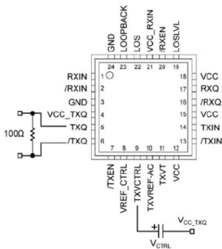
GND LOOPBACK LOS VCC_RXIN /RXEN /LOSLVL RXIN /RXIN GND VCC_TXQ TXQ /TXQ 100Ω 24 23 22 21 20 19 1 24 23 22 21 20 19 VCC /RXQ /VCC TXIN /TXIN TXEN VREF_CTRL TXVCTRL TXVREF_AC TXVT VCC VCC_TXQ + - VCTRLFigure 1a. Voltage Source Implementation
text_image
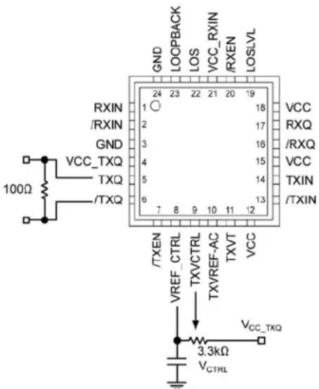
GND LOOPBACK LOS VCC_RXIN /RXEN /LOSLVL RXIN 18 VCC 17 /RXQ 16 VCC 15 TXIN 14 /TXIN 13 TXQ 12 TXVREF-AC 11 TXVT 10 TXVCTRL 9 TXVCTRL 8 TXVCTRL 7 TXEN 6 TXQ 5 TXQ 4 TXQ 3 TXQ 2 TXQ 1 VREF_CTRL VCC_TXQ 3.3kΩ V_CTRLFigure 1b. Alternative Implementation
Transmitter CML Variable-Swing Output Buffer
- Connecting V_REF_CTRL to TXVCTRL sets the transmitter output buffer to maximum swing
- Setting TXVCTRL to V_CC_TXQ , sets the transmitter output buffer to minimum swing
- Control of the transmitter output buffer swing can be obtained by using a variable resistor connected between V_REF_CTRL and V_CC_TXQ with a wiper connected to TXVCTRL as shown in Figure 1b
Receiver LOS
The SY58620L features a chatter-free Loss-of-Signal (LOS) TTL compatible output with an internal 4.75kΩ pull-up resistor. LOS circuitry monitors the input receiver signal and asserts a signal when the input signal falls below the threshold set by the programmable LOS level set pin (LOSLVL). When the amplitude of the receiver input signal falls below the threshold, LOS is asserted HIGH with a response time of \~0.2uS. LOS can be fed into /RXEN to maintain output stability by disabling the output during a Loss-of-Signal condition. Figure 2a and 2b shows the LOS connection to /RXEN. When /RXEN is HIGH, the output signal RXQ is held LOW and /RXQ is held HIGH. Typically, 2dB of LOS hysteresis is adequate to prevent the receiver output from chattering. LOS operation is optimized for data rates ≥622Mbps with an input receiver amplitude of at least 10mV (20mV _PP ). Due to the long time constant in slower data rates below 622Mbps, the SY58620L LOS function does not guarantee chatter-free operation for low amplitude signals.
LOSLVL sets the threshold of the LOS input amplitude detection. Connecting an external resistor, R_LOSLVL , between VCC and LOSLVL sets the input amplitude
LOS detection trip-point by setting up a voltage divider between VCC and V_REF (an internal voltage source set at V_CC-1.3V ), since there is a 2.8kΩ internal resistor connected between LOSLVL and V_REF . The input voltage range of LOSLVL ranges from V_CC to V_REF . See the "Functional Block Diagram" section and Figures 2a and 2b, to see how R_LOSLVL sets up a voltage divider between VCC and V_REF . Refer to the "LOS Output DC Electrical Characteristics" table and "Typical Operating Characteristics" section to see how different R_LOSLVL values affect LOS sensitivity.
text_image
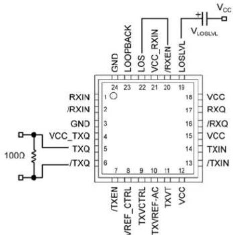
100Ω RXIN /RXIN GND VCC_TXQ TXQ /TXQ GND LOOPBACK LOS VCC_RXIN /RXEN /LOSLVL VCCI VCCI RXQ /RXQ VCC TXIN /TXIN TXEN /VREF_CTRL TXVCTRL TXVREF_AC TXVT VCC 7 8 9 10 11 12 1 2 3 4 5 6 18 17 16 15 14 13 24 23 22 21 20 19Figure 2a. Voltage Source Implementation

text_image
100Ω RXIN /RXIN GND VCC_TXQ TXQ /TXQ GND LOOPBACK LOS VCC_RXIN /RXEN /LOSLVL VCC RXQ /RXQ VCC TXIN /TXIN TXVREF-AC TXVT VCC 7 8 9 10 11 12 TXEN /VREF_CTRL TXVCTRL TXVREF-AC TXVT VCCFigure 2b. Alternative Implementation
LOS Output
- Connecting the input /RXEN to the LOS output as shown in Figures 2a and 2b, maintains receiver output stability under a Loss-of-Signal condition
-
Sensitivity of the LOS signal can be programmed using the LOSLVL input by using a variable resistor connected to VCC with a wiper connected to LOSLVL, as shown in Figure 2b
-
≥ 2dB hysteresis is insured if R_LOSLVL ≤ 10k .
- LOS is guaranteed chatter-free at f ≥ 622Mbps (311MHz)
Hysteresis
The SY58620L provides a minimum of 2dB of LOS hysteresis, see the Figure 3 for more details.

line
| Time | Input | |------|-------| | Low | High | | Mid | Low | | High | High |Figure 3. LOS Hysteresis Assert/De-assert
Hysteresis is defined as: 20Log_10( + AB)
Loopback
To support diagnostic system testing, the SY58620L features a loopback test mode, activated by setting LOOPBACK to logic HIGH. Loopback mode enables an internal loopback path from the transmitter input to the receiver output and supports the full 4.25Gbps data rate throughput.
Crosstalk
The SY58620 features a patent-pending isolation between the receiver and transmitter channels. The following guide lines can be used to minimize on layout induced crosstalk:
1. Ground Stripping
Ground stripping is an effective method to reduce crosstalk. Ground stripping involves running a ground trace between the receiver and transmitter channels.
2. Vertical and Horizontal Traces
Another way to reduce crosstalk is to route the receiver and transmitter channels on separate layers with an embedded ground or power supply layer between the layers. When routing the traces on different layers, run the receiver traces horizontal to the transmitter traces and route the transmitter traces vertical to the receiver traces.
PRBS Discussion
LOS Testing
The LOS function is tested with a 2^7-1 PRBS (Pseudo Random Bit Stream) data pattern. A PRBS data pattern of 2^7-1 is used because it is a good approximation to an 8b10b-encoded NRZ data stream. 8b10b encodes 8 bits of data and replaces it with 10 bits of symbol. The extra bits are added to improve transition density and the BER (Bit Error Rate) of the system.
Deterministic Jitter Testing and the K28.5 Pattern
The K28.5 (11000001010011111010) and 2 ^23 -1 PRBS data patterns are used to characterize DJ because both data patterns have lower spectral frequency content which provides a best approximation to scrambled NRZ data streams.
Random Jitter Testing and the K28.7 Pattern
The K28.7 (1111100000...) data pattern is used to measure RJ since the pattern is free of DJ. In addition, because the K28.7 data pattern can be used to compare the T_N ( N^TH period) to the T_0 ( 1^st period), low frequency jitter components can be accumulated.
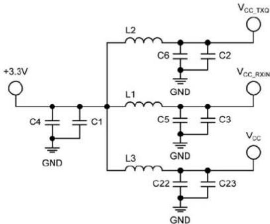
Power Supply Filtering
Although the SY58620L is fully differential, it is recommended that the power supplies are filtered as shown in Figure 4.
text_image
+3.3V C4 GND L1 C1 L2 C6 C2 GND L3 C5 C3 GND C22 C23 GND VCC_TXQ VCC_RXIN VCCFigure 4. Power Supply Filtering Scheme
| Item Description | |
| C1, C2, C3, C23 | 0.1μF Capacitor |
| C4, C5, C6, C22 | 0.01μF Capacitor |
| L1, L2, L3 | 1.2μH Ferrite Bead Inductor |
Table 1. Bill of Materials
Typical Operating Characteristics
V_CC = V_CC_TXQ = V_CC_RXIN = 3.3V ± 10% , R_L = 100 across the outputs; T_A = 25^ , unless otherwise stated.

line
| R_LOSLVL (kΩ) | DE-assert (mV) | Assert (mV) | | ------------- | -------------- | ----------- | | 0 | 90 | 50 | | 5 | 30 | 20 | | 10 | 20 | 15 | | 15 | 15 | 10 |
line
| R_LOSLVL (kΩ) | DE-assert (mV) | Assert (mV) | | ------------- | -------------- | ----------- | | 0 | 80 | 40 | | 5 | 20 | 15 | | 10 | 15 | 10 | | 15 | 10 | 5 |
line
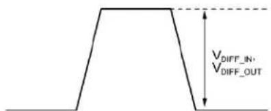
| R_LOSLVL (kΩ) | Hysteresis (dB) | | ------------- | --------------- | | 0 | 5.5 | | 5 | 5.0 | | 10 | 3.5 | | 15 | 2.5 |Single-Ended and Differential Swings

Figure 5a. Single-Ended Voltage Swing
text_image
VDIFF_IN, VDIFF_OUTFigure 5b. Differential Voltage Swing
Differential Input Stage

text_image
Vcc TXIN 50Ω TXVT 50Ω /TXIN GNDFigure 6a. TX Simplified Differential Input Stage

text_image
VREF = VCC_RXIN-1.3V (Internal Voltage Reference) 50Ω 50Ω /RXIN VCC_RXIN GNDFigure 6b. RX Simplified Differential Input Stage
Output Stage
Receiver

text_image
Vcc 50Ω 50Ω Ω Zo = 50Ω /Ω Zo = 50Ω 100Ω 16mA GNDFigure 7a. Receiver CML DC-Coupled Output
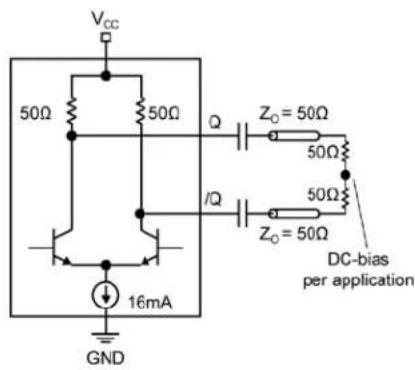
text_image
Vcc 50Ω 50Ω Q /Ω 16mA GND Zc = 50Ω 50Ω Zc = 50Ω DC-bias per applicationFigure 7b. Receiver CML AC-Coupled Output

text_image
Vcc 50Ω 50Ω Q Zo = 50Ω /Q Zo = 50Ω 16mA GND Vcc 50Ω 50ΩFigure 7c. Receiver CML DC-Coupled Output (50Ω to Vcc)
Transmitter
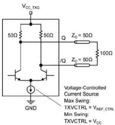
text_image
VCC_TXQ 50Ω 50Ω Q Z0 = 50Ω /Ω Z0 = 50Ω 100Ω GND Voltage-Controlled Current Source Max Swing: TXVCTRL = VREF_CTRL Min Swing: TXVCTRL = VCCFigure 7d. Transmitter CML DC-Coupled Output
text_image
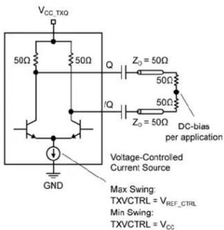
VCC_TXQ 50Ω 50Ω Q /Q Zo = 50Ω 50Ω 50Ω Zo = 50Ω DC-bias per application Voltage-Controlled Current Source GND Max Swing: TXVCTRL = VREF_CTRL Min Swing: TXVCTRL = VCCFigure 7e. Transmitter CML AC-Coupled Output

text_image
VCC_TXQ 50Ω 50Ω Q ZO = 50Ω I/Q ZO = 50Ω Voltage-Controlled Current Source GND Max Swing: TXVCTRL = VREF_CTRL Min Swing: TXVCTRL = VCCFigure 7f. Transmitter CML DC-Coupled Output (50Ω to Vcc)
Interface Applications

text_image
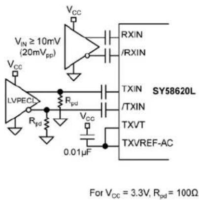
VCC ≥ 10mV (20mVpp) VIN VCC LVPECL VCC 0.01μF NC Rpd TXIN /TXIN TXVT TXVREF-AC RXIN /RXIN SY58620L For VCC = 3.3V, Rpd = 50Ω.Figure 8a. LVPECL Interface (TX DC-Coupled/RX AC-Coupled)
text_image
VCC ≥ 10mV (20mVpp) VIN VCC LVPECL Rpd Rpd VCC 0.01μF TXIN /TXIN TXVT TXVREF-AC SY58620L For VCC = 3.3V, Rpd = 100Ω.Figure 8b. LVPECL Interface (TX AC-Coupled/RX AC-Coupled)
text_image
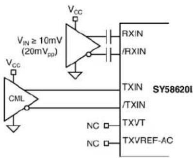
V_IN ≥ 10mV (20mV_pp) V_CC CML V_CC RXIN /RXIN TXIN /TXIN NC TXVT NC TXVREF-AC SY58620IFigure 8c. CML Interface (TX DC-Coupled/RX AC-Coupled)
text_image
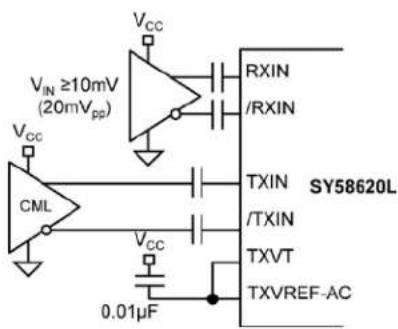
VCC ≥10mV (20mVpp) VIN VCC CML VCC 0.01μF RXIN /RXIN TXIN /TXIN TXVT TXVREF-AC SY58620LFigure 8d. CML Interface (TX AC-Coupled/RX AC-Coupled)

text_image
V_IN ≥ 10mV (20mV_{pp}) V_CC V_CC LVDS TXIN /TXIN NC TXVT NC TXVREF-AC SY58620LFigure 8e. LVDS Interface (TX DC-Coupled/RX AC-Coupled)
Related Product and Support Documentation
| Part Number | Function | Data Sheet Link |
| SY58621L Precision 3.2 Gbps CML/LVPECL Transceiver with Integrated Loopback | www.micrel.com/product-info/products/sy58621l.shtml | |
| HBW Solutions | New Products and Applications | www.micrel.com/product-info/products/solutions.shtml |
Package Information

NOTE:
1. ALL DIMENSIONS ARE IN MILLIMETERS (mm).
2. THE PIN#1 IDENTIFIER MUST EXIST ON THE TOP SURFACE OF PACKAGE BY USING IDENTIFICATION MARK OR OTHER FEATURE OF PACKAGE BODY.
3. FEATURE OF PACKAGE BODY.
CHAMFER STYLE PIN 1 IDENTIFIER ON BOTTOM SIDE
24-Pin QFN
MICREL, INC. 2180 FORTUNE DRIVE SAN JOSE, CA 95131 USA
TEL +1 (408) 944-0800 FAX +1 (408) 474-1000 WEB http://www.micrel.com
The information furnished by Micrel in this data sheet is believed to be accurate and reliable. However, no responsibility is assumed by Micrel for its use. Micrel reserves the right to change circuitry and specifications at any time without notification to the customer.
Micrel Products are not designed or authorized for use as components in life support appliances, devices or systems where malfunction of a product can reasonably be expected to result in personal injury. Life support devices or systems are devices or systems that (a) are intended for surgical implant into the body or (b) support or sustain life, and whose failure to perform can be reasonably expected to result in a significant injury to the user. A Purchaser's use or sale of Micrel Products for use in life support appliances, devices or systems is a Purchaser's own risk and Purchaser agrees to fully indemnify Micrel for any damages resulting from such use or sale.
© 2006 Micrel, Incorporated.