SY87725L - Transceiver Microchip - Free user manual and instructions
Find the device manual for free SY87725L Microchip in PDF.

User questions about SY87725L Microchip
0 question about this device. Answer the ones you know or ask your own.
Ask a new question about this device
Download the instructions for your Transceiver in PDF format for free! Find your manual SY87725L - Microchip and take your electronic device back in hand. On this page are published all the documents necessary for the use of your device. SY87725L by Microchip.
USER MANUAL SY87725L Microchip
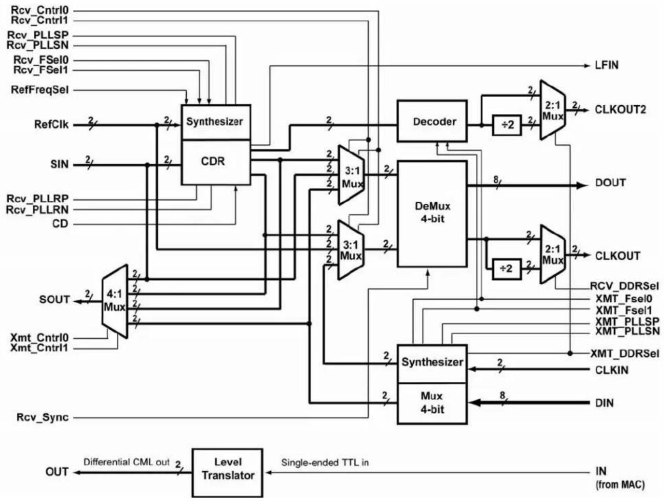
The SY87725L is a single chip transceiver for data rates up to 2.5Gbps. On the receive side, it includes a complete clock recovery and data retiming circuit with an integrated 4-bit serial-to-parallel data converter. On the transmit side, it includes a synthesizer with an integrated 4-bit parallel-to-serial data converter.
The SY87725L receiver has a synthesizer that generates an internal clock from an externally supplied TTL or PECL REFCLK that can be either 155.52MHz or 77.76MHz. This internal clock can be used by the clock recovery PLL if an absence of transitions on the input serial data stream prevents normal clock recovery. This enables it to provide a stable clock source in the absence of transitions on the incoming serial data stream.
The transmit synthesizer uses the CLKIN parallel data clock to generate its own serial rate clock locked to CLKIN. This enables the transmit and receive to operate at different data rates.
The serial interface for both the transmit and receive functions feature industry standard high-speed differential CML I/O. The parallel interfaces feature high-speed LVDS I/O with an internal 100Ω termination on the LVDS inputs.
The first bit for the serial-to-parallel conversion can be moved using the RCV_SYNC input. The RCV_SYNC input enables the parallel word boundary to move up in time by one bit time for each pulse. This allows it to in effect "swallow" one bit each time the RCV_SYNC pulse is asserted.
Datasheets and support documentation can be found on Micrel's web site at: www.micrel.com.
Features
- Single 3.3V supply and 1W typ. power consumption
• 2.5G/1.25G/625Mbps down stream
• 1.25G/625M/156Mbps up stream
• 4-bit Serdes with LVDS interfaces - Serial Data input sensitivity of 30mV typical
- Training mode for fast lock acquisition
- Link Fault Indicator (LFIN: "HIGH" = Locked)
- Separate training and MUX synthesizers
- Loop back function for diagnostics
- TTL-CML Translator for MAC-to-Laser diode driver burst control
- Selectable double data rate option for low cost FPGA/ASIC MAC implementation
• Available in Pb-Free (10mm x 10mm) 64-pin EPAD-TQFP
Applications
• BPON/GPON/GEPON/EPON
Markets
- FTTH/FTTP
Functional Block Diagram
flowchart
graph TD
    A["Input"] --> B["Resistors"]
    B --> C["Decoder"]
    C --> D["2:1 Mux"]
    D --> E["CLKOUT2"]
    B --> F["3:1 Mux"]
    F --> G["DeMux 4-bit"]
    G --> H["÷2"]
    H --> I["2:1 Mux"]
    I --> J["DOUT"]
    B --> K["4:1 Mux"]
    K --> L["Decoder"]
    L --> M["÷2"]
    M --> N["2:1 Mux"]
    N --> O["CLKOUT"]
    B --> P["Xmt_Cntrl0 Xmt_Cntrl1"]
    P --> Q["Level Translator"]
    Q --> R["Differential CML out"]
    R --> S["OUT"]
    S --> T["IN (from MAC)"]
    T --> U["Single-ended TTL in"]
    U --> V["Output"]
    style A fill:#f9f,stroke:#333
    style B fill:#ccf,stroke:#333
    style C fill:#cfc,stroke:#333
    style D fill:#fcc,stroke:#333
    style E fill:#cff,stroke:#333
    style F fill:#ffc,stroke:#333
    style G fill:#fcc,stroke:#333
    style H fill:#ffc,stroke:#333
    style I fill:#fcc,stroke:#333
    style J fill:#ffc,stroke:#333
    style K fill:#fcc,stroke:#333
    style L fill:#fcc,stroke:#333
    style M fill:#fcc,stroke:#333
    style N fill:#fcc,stroke:#333
    style O fill:#fcc,stroke:#333
    style P fill:#fcc,stroke:#333
    style Q fill:#fcc,stroke:#333
    style R fill:#fcc,stroke:#333
    style S fill:#fcc,stroke:#333
    style T fill:#fcc,stroke:#333
    style U fill:#fcc,stroke:#333
Pin Configuration

text_image
RCV_CNTRL1 RCV_DDRSEL CD REFCLKN REFCLKP RCV_SYNC GND VCC SINN SINP VCC OUTN OUTP VCCO SOUTN SOUTP 64 63 62 61 60 59 58 57 56 55 54 53 52 51 50 49 RCV_PLLSN 1 RCV_PLLSP 2 RCV_FSEL0 3 RCV_CNTRL0 4 RCV_FSEL1 5 RCV_PLLRP 6 RCV_PLLRN 7 VCCA 8 GNDA 9 XMT_FSEL0 10 XMT_PLLSN 11 XMT_PLLSP 12 TESTb 13 XMT_FSEL1 14 REFFREQSEL 15 XMT_CNTRL0 16 17 18 19 20 21 22 23 24 25 26 27 28 29 30 31 32 XMT_CNTRL1 LFIN VCC TEST (GND) GND CLKINP CLKINN XMT_DDRSEL DINOP DINON DINIP DININN DIN2P DIN2N DIN3P DIN3N 48 IN 47 VCC DOUT3N 46 DOUT3P 45 DOUT2N 44 DOUT2P 43 DOUT1N 42 DOUT1P 41 DOUT1P 40 DOUT0N 39 DOUT0P 38 VCC CLKOUTN 37 CLKOUTP 36 GND CLKOUT2N 35 GND CLKOUT2P64-Pin EPAD-TQFP (T64-1)
Ordering Information
| Part Number | Package Type | Operating Range | Package Marking | Lead Finish |
| SY87725LHY | H64-1 | Industrial | SY87725LHY with Pb-Free bar-line indicator | Pb-Free Matte-Sn |
| SY87725LHYTR^(2) | H64-1 | Industrial | SY87725LHY with Pb-Free bar-line indicator | Pb-Free Matte-Sn |
Notes:
- Contact factory for die availability. Dice are guaranteed at T_A=25^ , DC electricals only.
- Tape and Reel.
Pin Description
RECEIVE SECTION SIGNALS
| Pin Number | Pin Name | Pin Description |
| 55, 56 | SINP, SINN | Serial Data In (Differential LVPECL Input): This input receives the serial differential data stream. An internal PLL recovers the embedded clock and data. |
| 60, 61 | REFCLKP, REFCLKN, | Reference Clock (TTL or Differential LVPECL Input): This input accepts either single-ended TTL or differential LVPECL signals and is used as the reference for the internal frequency synthesizer and the “training” frequency for the receiver PLL to keep it centered in the absence of data at the SIN input. The REFCLKN input has an internal reference circuit that applies the threshold voltage in case of a single-ended TTL-signal at REFCLKP. REFCLKN has an internal 75kΩ to GND and can be left open in that case. |
| 15 | REFFREQSEL | Reference Clock Frequency Select (TTL Input): Selects REFCLK frequency of 77.76MHz when LOW or 155.52MHz when HIGH. |
| 6, 7 | RCV_PLLRP, RCV_PLLRN | Clock Recovery PLL Loop Filter: External loop filter pins for the receive PLL. |
| 1, 2 | RCV_PLLSN, RCV_PLLSP | Clock Synthesis PLL Loop Filter: External loop filter pins for the clock synthesis PLL. |
| 59 | RCV_SYNC | Receive Synchronizer (TTL Input): Single-ended asynchronous input to set the word boundary on the 4-bit parallel data |
| 3, 5 | RCV_FSEL0, RCV_FSEL1 | Receive Frequency Control (TTL Inputs): Two single-ended frequency selects for receive synthesizer. |
| 39, 40, 41, 42, 43, 44, 45, 46 | DOUTOP, DOUTON, DOUT1P, DOUT1N, DOUT2P, DOUT2N, DOUT3P, DOUT3N | Parallel Data Out (LVDS Outputs): These are the four pairs of receive parallel data outputs. |
| 33, 34 | CLKOUT2P, CLKOUT2N | Parallel Clock Out (LVDS Output): This output is the recovered clock at the transmit byte clock rate and provides a clock that can be used as a reference clock to drive CLKIN. |
| 36, 37 | CLKOUTP, CLKOUTN | Parallel Clock Out (LVDS Output): This output is the recovered clock divided by 4 or 8 to provide the parallel data rate clock. |
| 18 | LFIN | Link Fault Indicator (TTL Output): When HIGH, LFIN indicates CDR is “in-lock” and when LOW it indicates CDR loss-of-lock. |
| 63 | RCV_DDRSEL | Double Data Rate Select (TTL Input): Selects either parallel data rate clock for normal operation or one-half of parallel data rate clock for double data rate applications. |
| 62 | CD | Carrier Detect Input (LVPECL input): When HIGH, CD indicates the carrier is present and when LOW it indicates the loss of carrier. |
TRANSMIT SECTION SIGNALS
| 25, 26, 27,28, 29, 30,31, 32 | DIN0P, DIN0N,DIN1P, DIN1N,DIN2P, DIN2N,DIN3P, DIN3N | Parallel Data In (LVDS Inputs): These are the four pairs of transmit parallel data inputs. Each Differential pair has a 100Ω internal termination across the pair. |
| 22, 23 | CLKINP, CLKINN | Parallel Clock In (LVDS Input): This input is the transmit parallel (byte-rate) clock. |
| 10, 14 | XMT_FSEL0,XMT_FSEL1 | Transmit Frequency Control (TTL Inputs): Two single-ended frequency selects for transmit synthesizer. |
| 11, 12 | XMT_PLLSN,XMT_PLLSP | Clock Synthesis PLL Loop Filter: External loop filter pins for the clock synthesis PLL. |
| 49, 50 | SOUTP, SOUTN | Serial Data Out (Differential CML Output): This is the serial differential data stream output. |
| 24 | XMT_DDRSEL | Double Data Rate Select (TTL Input): Selects either parallel data rate clock for normal operation or one-half of parallel data rate clock for double data rate applications. |
LOOPBACK CONTROLS
| Pin Number | Pin Name | Pin Description |
| 16, 17 | XMT_CNTRL0,XMT_CNTRL1 | Transmit Loop back Multiplexer Control (TTL Inputs): Two single-ended control lines to control the data flow for remote loop back or normal serial data output. |
| 4, 64 | RCV_CNTRL0,RCV_CNTRL1 | Receive Loop back Multiplexer Control (TTL Inputs): Two single-ended control lines to control the data flow for local loop back or recovered serial data into the 1:4 DeMUX. |
TRANSLATOR SIGNALS
| 48 | IN | Signal from MAC to be translated (TTL Input) |
| 52, 53 | OUTP, OUTN | Signal to Laser Diode Driver (CML Differential Output) |
POWER PINS AND TEST PIN
| 13 | Testb | Test Mode Pin: When held LOW activates test mode. (For factory use only, leave open for normal operation.) |
| 20 | Test | Test Mode Pin: When held HIGH activates test mode. (For factory use only, must be tied to GND for normal operation.). |
| 8 | VCCA | Analog Power: Connect to +3.3V power supply. Bypass with 0.1μF//0.1μF low ESR capacitors as close to VCCA pin as possible. |
| 9 | GNDA | Analog Ground pin and exposed pad must be connected to the same ground plane. |
| 19, 38, 47, 54, 57 | VCC | Core Power: Connect to +3.3V power supply. Bypass with 0.1μF//0.1μF low ESR capacitors as close to VCC pins as possible. |
| 21, 35, 58 | GND, Exposed Pad | Core Ground: Ground pins and exposed pad must be connected to the same ground plane. |
| 51 | VCCO | CML Output Power: Connect to +3.3V power supply. Bypass with 0.1μF//0.1μF low ESR capacitors as close to VCCO pin as possible. |
Functional Description
The SY87725L is a fully integrated transceiver with an integrated serial-to-4-bit DeMUX and 4-bit-to-serial Multiplexer.
Receive Section
Clock and Data Recovery Function
The Clock Recovery function includes a synthesizer that generates a stable frequency based on the REFCLK input. The REFCLK input can be either a differential PECL input or a single-ended TTL input. It can also be either 77.76MHz or 155.52MHz as selected by REFFREQSEL. The synthesized frequency derived from the REFCLK is within 1000ppm of the incoming serial data rate and is used by the Clock and Data Recovery (CDR) circuit to "train" to the correct frequency range. This training function minimizes the acquisition time for the CDR to lock onto the incoming data stream by keeping the CDR frequency within close range of the recovered clock in the case of loss of data.
The RCV_FSEL0 and RCV_FSEL1 inputs select the receive data rate. For example, these inputs can be used to select an OC-48, OC-24 or OC-12 data rate for the serial data in, SIN. The typical input sensitivity of SIN is 30mV.
The Clock Recovery function also generates CLKOUT2 that is controlled by the XMT_DDRSEL input for regular or double data rate applications. If a clean, low-jitter byte-rate clock is not available for CLKIN to the Transmit Synthesizer, CLKOUT2 can be used as the reference clock.
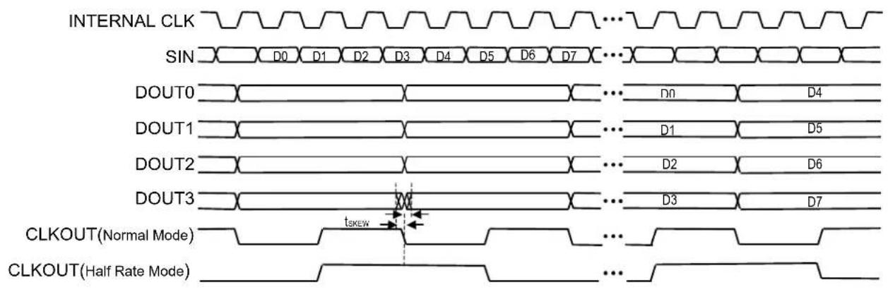
DeMUX Function
The recovered serial data from the CDR is converted to a 4-bit parallel word by a 1:4 de-multiplexer. The serial-to-parallel conversion sequence is LSB first, i.e. first serial bit in is DOUT0, second serial bit in is DOUT1, etc. A RCV_SYNC pulse input is used to set the word boundary of the 4-bit parallel word. A single pulse, applied asynchronously for a minimum of two input clock cycles to the RCV_SYNC input, causes the start bit of conversion to occur one bit earlier.
The CLKOUT output is the parallel data rate clock to be used with the DOUT parallel data from the DeMUX. It is selectable by the RCV_DDRSEL input to be either at the parallel data rate or one-half the parallel data rate for double data rate applications.
Transmit Section
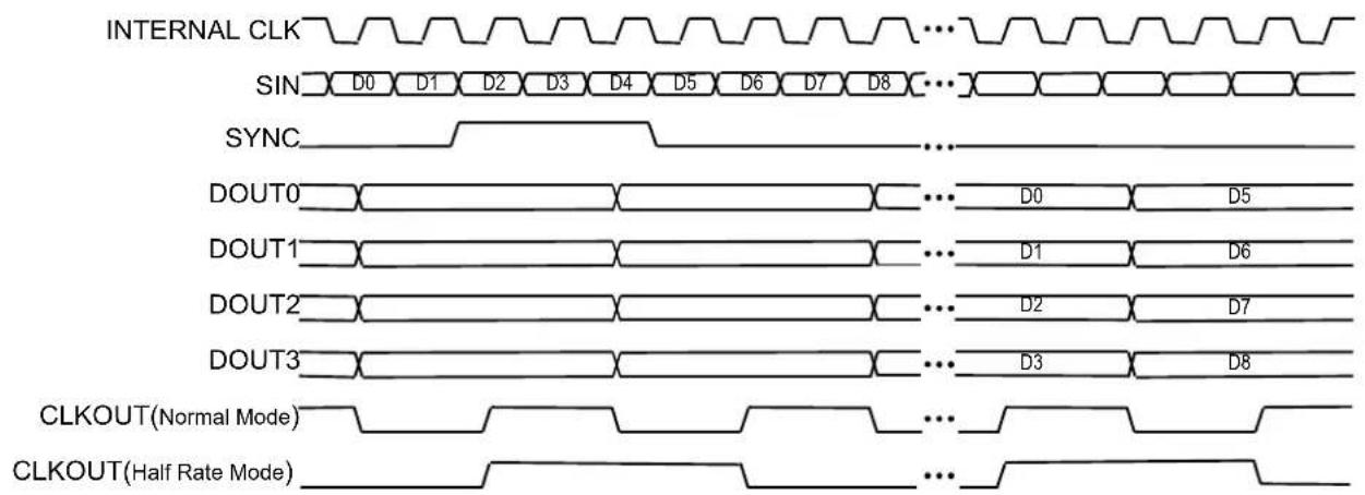
Synthesizer Function
The SY87725L Transmit Synthesizer uses the divide-by-4 parallel clock input or a divide-by-8 clock input when double data rate is selected as a reference clock. The XMT_FSEL0 and XMT_FSEL1 inputs select the TX data rate. For example, these inputs can be used to select an OC-24, OC-12 or OC-3 rate for the serial data out, SOUT.
MUX Function
The 4-bit parallel data input is converted to a serial data stream with a 4:1 multiplexer. The parallel-to-serial conversion sequence is LSB first, i.e. DIN0 will be shifted out first, followed by DIN1, etc.
Auto-Alignment Function
Because the 4-bit parallel data input can have an arbitrary phase relationship with the transmit byte-rate clock input (CLKIN), an auto-alignment function is included in the transmit parallel-to-serial circuit.
The phase of the 4-bit parallel data is sampled and compared with the phase of the incoming CLKIN. If the clock and data are not in the proper phase relationship, the phase is internally adjusted to insure that the data will be sampled at the optimal time. This can result in a variation of the latency between the parallel data in and the serial data out (TDOUT) of up to three CLKIN clock cycles.
Loopback Function
Two 3:1 multiplexers are provided to allow Local or Remote Loopback.
Frequency Selections
| XMT_FSEL0 | XMT_FSEL1 | TX DATA RATE |
| 0 | 0 | 155.52Mbps |
| 1 | 0 | 622.08Mbps |
| 0 | 1 | 1244.16Mbps |
| 1 | 1 | N/A |
Table 1. Transmit Frequency Selection
| RCV_FSEL0 | RCV_FSEL1 | RX DATA RATE |
| 0 | 0 | N/A |
| 1 | 0 | 622.08Mbps |
| 0 | 1 | 1244.16Mbps |
| 1 | 1 | 2488.32Mbps |
Table 2. Receive Frequency Selection
| XMT_FSEL0 | XMT_FSEL1 | XMT_DDRSEL | CLKOUT2 |
| 0 | 0 | 0 | 38.88MHz |
| 1 | 0 | 0 | 155.52MHz |
| 0 | 1 | 0 | 311.04MHz |
| 1 | 1 | 0 | N/A |
| 0 | 0 | 1 | 19.44MHz |
| 1 | 0 | 1 | 77.76MHz |
| 0 | 1 | 1 | 155.52MHz |
| 1 | 1 | 1 | N/A |
Table 3. CLKOUT2 Frequency Selection
| RCV_CNTRL0 | RCV_CNTRL1 | XMT_DDRSEL | RCV_DDRSEL | DOUT | CLKOUT |
| 0 | 0 | 0 | 0 | N/A | N/A |
| 1 | 0 | 0 | 0 | DIN | CLKIN |
| 0 | 1 | 0 | 0 | SIN (bypass) | REFCLK/4 |
| 1 | 1 | 0 | 0 | SIN (Recovered Data) | Recovered Clock/4 |
| 0 | 0 | 1 | 0 | N/A | N/A |
| 1 | 0 | 1 | 0 | DIN | 2 * CLKIN |
| 0 | 1 | 1 | 0 | SIN (bypass) | REFCLK/4 |
| 1 | 1 | 1 | 0 | SIN (Recovered Data) | Recovered Clock/4 |
| 0 | 0 | 0 | 1 | N/A | N/A |
| 1 | 0 | 0 | 1 | DIN | CLKIN/2 |
| 0 | 1 | 0 | 1 | SIN (bypass) | REFCLK/8 |
| 1 | 1 | 0 | 1 | SIN (Recovered Data) | Recovered Clock/8 |
| 0 | 0 | 1 | 1 | N/A | N/A |
| 1 | 0 | 1 | 1 | DIN | CLKIN |
| 0 | 1 | 1 | 1 | SIN (bypass) | REFCLK/8 |
| 1 | 1 | 1 | 1 | SIN (Recovered Data) | Recovered Clock/8 |
Table 4. Local Loopback Controls
| XMT_CNTRL0 | XMT_CNTRL1 | SOUT |
| 0 | 0 | SIN (Bypass CDR) |
| 1 | 0 | Recovered Clock (from SIN) |
| 0 | 1 | Recovered Data (from SIN) |
| 1 | 1 | DIN (Normal Data Flow) |
Table 5. Remote Loopback Controls
Loop Filter Components

chemical
Simple RC circuit diagram with resistor and capacitor components labeled PLLSP or PLLRP and PLLSN or PLLRN| R | C | |
| Rcv_PLLS | 1.2kΩ | 1μF |
| Rcv_PLLR | 390Ω | 1μF |
| XMT_PLLS | 1.2kΩ | 1μF |
Table 6. Synthesizer & Clock Recovery Loop Filter Values
Absolute Maximum Ratings ^(1)
Supply Voltage ( V_cc ) -0.5V to +4.6V
Input Voltage ( V_IN )....-0.5V to V_CC
LVDS Output Current (I _OUT )...... ±10mA
CML Outputs
Voltage.... V_CC -1.0V to V_CC +0.5V
Current ±25mA
Lead Temperature (soldering, 20 sec.) ....+260°C
Storage Temperature ( T_s ) -65^ to +150^
Operating Ratings ^(2)
Supply Voltage (Vcc) +3.15V to +3.45V
Ambient Temperature ( T_A ) -40^ to +85^
Package Thermal Resistance ^(3)
MLF® θJB
Still-Air 35°C/W
MLF®ψJB
Junction-to-Board 7°C/W
DC Electrical Characteristics ^(4)
T_A = -40^ to +85^ , unless noted.
| Symbol | Parameter | Condition | Min | Typ | Max | Units |
| V_CC | Power Supply | 3.15 | 3.3 | 3.45 | V | |
| I_CC | Power Supply Current | No load, max. V_CC | 300 | 380 | mA |
LVPECL Electrical Characteristics ^(4)
V_CC = V_CCA = V_CCO = 3.3V ± 5% ; GND = GNDA = 0V; T_A = -40^ C to +85^ C , unless otherwise noted.
| Symbol | Parameter | Condition | Min | Typ | Max | Units |
| V_IH | Input HIGH Voltage | V_CC-1.165 | V_CC-0.88 | V | ||
| V_IL | Input LOW Voltage | V_CC-1.810 | V_CC-1.475 | V |
CML Output Electrical Characteristics ^(4)
V_CC = V_CCA = V_CCO = 3.3V ± 5% ; GND = GNDA = 0V; T_A = -40^ to +85^ , unless otherwise noted.
| Symbol | Parameter | Condition | Min | Typ | Max | Units |
| V_OH | Output HIGH Voltage | V_CC-0.020 | V_CC-0.010 | V_CC | V | |
| V_OUT | Output LOW Voltage | 325 | 400 | mV | ||
| V_DIFF\_OUT | Differential Output Voltage | 650 | 800 | mV |
Notes:
- Permanent device damage may occur if absolute maximum ratings are exceeded. This is a stress rating only and functional operation is not implied at conditions other than those detailed in the operational sections of this data sheet. Exposure to absolute maximum rating conditions for extended periods may affect device reliability
- The data sheet limits are not guaranteed if the device is operated beyond the operating ratings.
- Package Thermal Resistance assumes exposed pad is soldered (or equivalent) to the devices most negative potential on the PCB. 0_JB assumes a 4-layer PCB. _JA in still air unless otherwise stated.
- The circuit is designed to meet the DC specifications shown in the above table after thermal equilibrium has been established.
LVTTL/CMOS DC Electrical Characteristics ^(5)
V_CC = V_CCA = V_CCO = 3.3V ± 5% ; GND = GNDA = 0V; T_A = -40^ to +85°C, unless otherwise noted.
| Symbol | Parameter | Condition | Min | Typ | Max | Units |
| V_IH | Input HIGH Voltage | 2.0 | V_CC | V | ||
| V_IL | Input LOW Voltage | 0 | 0.8 | V | ||
| I_IH | Input HIGH Current | -125 | 30 | μA | ||
| I_IL | Input LOW Current | -300 | μA | |||
| V_OH | Output HIGH Voltage | I_OH = 100μA | 2.0 | V | ||
| V_OL | Output LOW Voltage | I_OI = 4mA | 0.5 | V | ||
| I_OS | Output Short-Circuit Current | V_OUT = 0V (max. 1sec.) | -100 | -15 | mA |
LVDS DC Electrical Characteristics ^(5)
V_CC = V_CCA = V_CCO = 3.3V ± 5% ; GND = GNDA = 0V, R_L = 100 across output pair; T_A = -40^ to +85^ , unless otherwise noted.
| Symbol | Parameter | Condition | Min | Typ | Max | Units |
| V_IN-Range | Input Voltage Range | 0 | 2.4 | V | ||
| V_IN | Input Voltage Swing | 100 | 500 | mV | ||
| V_DIFF-IN | Differential Input Voltage Swing | 200 | 1000 | mV | ||
| R_IN | Input Differential Resistance | 85 | 100 | 115 | Ω | |
| V_OUT | Output Voltage Swing | 325 | mV | |||
| V_DIFF-OUT | Differential Output Voltage Swing | 650 | mV | |||
| V_OCM | Output Common Mode Voltage | 1.125 | 1.275 | V | ||
| V_OCM | Change in Output Common Mode Voltage | -50 | +50 | mV |
Note:
- The circuit is designed to meet the DC specifications shown in the above table after thermal equilibrium has been established.
AC Electrical Characteristics ^(6)
V_CC = V_CCA = V_CCO = 3.3V ± 5% ; GND = GNDA = 0V; T_A = -40^ to +85°C, unless otherwise noted
| Symbol | Parameter | Condition | Min | Typ | Max | Units |
| SIN_MAX | SIN Maximum Data Rate | 2.5 | Gbps | |||
| SOUT_MAX | SOUT Maximum Data Rate | 1.25 | Gbps | |||
| t_ACQ | Acquisition Lock Time | 15 | μs | |||
| Frequency Difference, LFIN shows Out-of-Lock | 1000 | ppm | ||||
| t_CPWH | REFCLK Pulse Width HIGH Time | 2.5 | ns | |||
| t_CPWL | REFCLK Pulse Width LOW Time | 2.5 | ns | |||
| t_SKEW | Parallel CLKOUT to Parallel Data Out Skew | See “Figure 1” | -150 | +150 | ps | |
| t_PR, t_PF | CML Output Rise/Fall Time (20% to 80%) | At full output swing | 40 | 70 | 100 | ps |
| t_LR, t_LF | LVDS Output Rise/Fall Time (20% to 80%) | At full output swing | 100 | 250 | 400 | ps |
| t_DC | CLKOUT, CLKOUT2 Duty Cycle | 45 | 55 | % |
Note:
- The circuit is designed to meet the DC specifications shown in the above table after thermal equilibrium has been established.
Timing Diagrams
Receive Timing
text_image
INTERNAL CLK SIN DOUT0 DOUT1 DOUT2 DOUT3 CLKOUT(Normal Mode) CLKOUT(Half Rate Mode)Figure 1. 1:4 Serial-to-Parallel Conversion
text_image
INTERNAL CLK SIN D0 D1 D2 D3 D4 D5 D6 D7 D8 ... SYNC ... DOUT0 ... D0 D5 DOUT1 ... D1 D6 DOUT2 ... D2 D7 DOUT3 ... D3 D8 CLKOUT(Normal Mode) ... CLKOUT(Half Rate Mode) ...Figure 2. 1:4 Serial-to-Parallel Conversion with SYNC Pulse
Transmit Timing
text_image
CLKIN (Normal Mode) CLKIN (Half Rate Mode) DIN0 D0 D4 DIN1 D1 D5 DIN2 D2 D6 DIN3 D3 D7 INTERNAL SERIAL CLK SOUT ... D0 D1 D2 D3Figure 3. 4:1 Parallel-to-Serial Conversion
Applications Sections
This section illustrates the various operating modes of the SY87725L with the appropriate control signals.
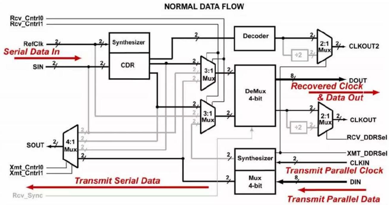
Normal Data Flow
Receive Section
The diagram below shows the data paths in a normal operating mode. In this case, downstream data at a serial rate of 2.5Gbps is arriving at SIN and the recovered 4-bit parallel data is exiting at DOUT at 625Mbps. This is not the double data rate mode (DDR) so the parallel rate is the serial rate ÷ 4.
Transmit Section
On the transmit side, the upstream data appears at DIN in a 4-bit wide parallel format at 312.5Mbps and exits at SOUT at a 1.25Gbps serial rate. The CLKIN input is synchronous with the parallel data at DIN.
The loopback control signals RCV_CNTRL0, RCV_CNTRL1, XMT_CNTRL0, XMT_CNTRL1 shown in the table below select the clock and data paths for normal operation. The RCV_DDRSel input is selecting the CLKOUT to be in normal rate (÷ 4) mode.
flowchart
graph TD
    A["RefClk"] -->|2/2| B["Synthesizer"]
    C["SIN"] -->|2/2| B
    B --> D["CDR"]
    D --> E["3:1 Mux"]
    E --> F["Decoder"]
    F --> G["÷2"]
    G --> H["2:1 Mux"]
    H --> I["CLKOUT2"]
    J["SOUT"] --> K["4:1 Mux"]
    L["Xmt_Cntrl0 Xmt_Cntrl1"] --> K
    K --> M["Transmit Serial Data"]
    M --> N["Recovery Clock & Data Out"]
    O["Rcv_Sync"] --> P["Transmit Parallel Data"]
    Q["Decoder"] --> R["÷2"]
    R --> S["2:1 Mux"]
    S --> T["CLKOUT"]
    U["DeMux 4-bit"] --> V["÷2"]
    V --> W["2:1 Mux"]
    W --> X["RCV_DDRSel"]
    Y["Synthesizer"] --> Z["Mux 4-bit"]
    AA["Transmit Parallel Clock"] --> AB["DIN"]
    AC["Recovery Clock & Data Out"] --> AD["XMT_DDRSel"]
    AE["Recovery Clock & Data Out"] --> AF["CLKIN"]
Figure 4. Normal Data Flow
| RCV_CNTRL0 | RCV_CNTRL1 | XMT_CNTRL0 | XMT_CNTRL1 | RCV_DDRSEL |
| 1 | 1 | 1 | 1 | 0 |
Table 7. Loopback and DDR Select Control Signals
| RCV_FSEL0 | RCV_FSEL1 | XMT_FSEL0 | XMT_FSEL1 |
| 1 | 1 | 0 | 1 |
Table 8. Transmit and Receive Frequency Select
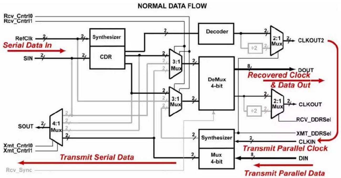
Normal Data Flow (Secondary Clock)
Receive Section
This mode is identical to the Normal Mode in the
previous section, but utilizes CLKOUT2 to be used as the transmit parallel clock. In this mode, CLKOUT2 must be externally connected to CLKIN as shown in the block diagram below.
flowchart
graph TD
    A["RefClk"] -->|2| B["Synthesizer"]
    C["SIN"] -->|2| B
    B --> D["CDR"]
    D --> E["3:1 Mux"]
    E --> F["Decoder"]
    F --> G["2:1 Mux"]
    G --> H["CLKOUT2"]
    I["SOUT"] --> J["4:1 Mux"]
    K["Xmt_Cntrl0"] --> L["Xmt_Cntrl1"]
    M["Transmit Serial Data"] --> N["Transmit Parallel Data"]
    O["Rcv_Sync"] --> P["4:1 Mux"]
    Q["Recovered Clock & Data Out"] --> R["2:1 Mux"]
    S["DIN"] --> T["Transmit Parallel Data"]
    U["2:1 Mux"] --> V["2:1 Mux"]
    W["2:1 Mux"] --> X["2:1 Mux"]
    Y["2:1 Mux"] --> Z["2:1 Mux"]
    AA["2:1 Mux"] --> AB["2:1 Mux"]
    AC["2:1 Mux"] --> AD["2:1 Mux"]
    AE["2:1 Mux"] --> AF["2:1 Mux"]
    AG["2:1 Mux"] --> AH["2:1 Mux"]
    AI["2:1 Mux"] --> AJ["2:1 Mux"]
    AK["2:1 Mux"] --> AL["2:1 Mux"]
    AM["2:1 Mux"] --> AN["2:1 Mux"]
    AO["2:1 Mux"] --> AP["2:1 Mux"]
    AQ["2:1 Mux"] --> AR["2:1 Mux"]
    AS["2:1 Mux"] --> AT["2:1 Mux"]
    AU["2:1 Mux"] --> AV["2:1 Mux"]
    AW["2:1 Mux"] --> AX["2:1 Mux"]
    AY["RefeClk In"] --> AZ["2/7"]
    BA["SIN"] --> BB["2/7"]
    BC["4:1 Mux"] --> BD["2/7"]
    BE["Xmt_Cntrl0"] --> BF["2/7"]
    BG["Xmt_Cntrl1"] --> BH["2/7"]
    BI["SOUT"] --> BJ["2/7"]
    BK["Xmt_Cntrl0"] --> BL["2/7"]
    BM["Xmt_Cntrl1"] --> BN["2/7"]
    BO["SOUT"] --> BP["2/7"]
    BQ["Xmt_Cntrl0"] --> BR["2/7"]
    BS["Xmt_Cntrl1"] --> BT["2/7"]
    BU["SOUT"] --> BV["2/7"]
    BW["Xmt_Cntrl0"] --> BX["2/7"]
    BY["Xmt_Cntrl1"] --> BZ["2/7"]
    CA["SOUT"] --> CB["2/7"]
    CC["Xmt_Cntrl0"] --> CD["2/7"]
    DD["Xmt_Cntrl1"] --> DE["2/7"]
    FD["SIN"] --> DG["2/7"]
    DH["SIN"] --> DI["2/7"]
    DJ["SOUT"] --> DK["XMT_DDRSel"]
    DL["XMT_DDRSel"] --> DV["XMT_DDRSel"]
    DW["XMT_DDRSel"] --> DX["XMT_DDRSel"]
    DB["XMT_DDRSel"] --> DC["YXMT_DDRSel"]
    DD["YXMT_DDRSel"] --> DDY["YXMT_DDRSel"]
    DC["YXMT_DDRSel"] --> DCZ["YXMT_DDRSel"]
    DA["YXMT_DDRSel"] --> DA["YXMT_DDRSel"]
    DB["YXMT_DDRSel"] --> DB["YXMT_DDRSel"]
    DC["YXMT_DDRSel"] --> DC["YXMT_DDRSel"]
    DD["YXMT_DDRSel"] --> DD["YXMT_DDRSel"]
    DC["YXMT_DDRSel"] --> DC["YXMT_DDRSel"]
    DD["YXMT_DDRSel"] --> DD["YXMT_DDRSel"]
    DC["YXMT_DDRSel"] --> DC["YXMT_DDRSel"]
    DD["YXMT_DDRSel"] --> DD["YXMT_DDRSel"]
    DC["YXMT_DDRSel"] --> DC["YXMT_DDRSel"]
    DD["YXMT_DDRSel"] --> DD["YXMT_DDSEl"]
    DC["YXMT_DDSEl"] --> DC["YXMT_DDSEl"]
    DD["YXMT_DDSEl"] --> DD["YXMT_DDSEl"]
    DC["YXMT_DDSEl"] --> DC["YXMT_DDSEl"]
    DD["YXMT_DDSEl"] --> DC["YXMT_DDSEl"]
    DC["YXMT_DDSEl"] --> DC["YXMT_DDSEl"]
Figure 5. Normal Data Flow
| RCV_CNTRL0 | RCV_CNTRL1 | XMT_CNTRL0 | XMT_CNTRL1 | RCV_DDRSEL |
| 1 | 1 | 1 | 1 | 0 |
Table 9. Loopback and DDR Select Control Signals
| RCV_FSEL0 | RCV_FSEL1 | XMT_FSEL0 | XMT_FSEL1 |
| 1 | 1 | 0 | 1 |
Table 10. Transmit and Receive Frequency Select
Remote Loopback Mode 00
This is the simplest of the loopback modes as its main purpose is to verify if the link is OK.
It is possible to combine this with Local Loopback modes; however, it is intended to be a stand-alone test mode.

flowchart
graph TD
    A["RefClk"] -->|2| B["Synthesizer"]
    C["SIN"] -->|2| B
    D["Loopback Data"] -->|2| E["4:1 Mux"]
    F["SOUT"] -->|2| E
    G["Xmt_Cntrl0"] -->|2| E
    H["Xmt_Cntrl1"] -->|2| E
    I["Rcv_Sync"] -->|2| E
    B --> J["CDR"]
    J --> K["3:1 Mux"]
    K --> L["DeMux 4-bit"]
    L --> M["Decoder"]
    M --> N["÷2"]
    N --> O["2:1 Mux"]
    O --> P["CLKOUT2"]
    O --> Q["DOUT"]
    L --> R["÷2"]
    R --> S["2:1 Mux"]
    S --> T["CLKOUT"]
    S --> U["RCV_DDRSel"]
    U --> V["XMT_DDRSel"]
    V --> W["CLKIN"]
    V --> X["DIN"]
    L --> Y["Synthesizer"]
    Y --> Z["Mux 4-bit"]
    Z --> AA["Output"]
Figure 6. Remote Loopback Data Flow
| XMT_CNTRL0 | XMT_CNTRL1 |
| 0 | 0 |
Table 11. Loopback Control Signals
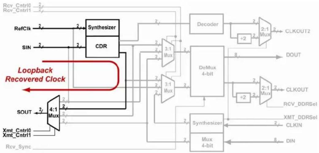
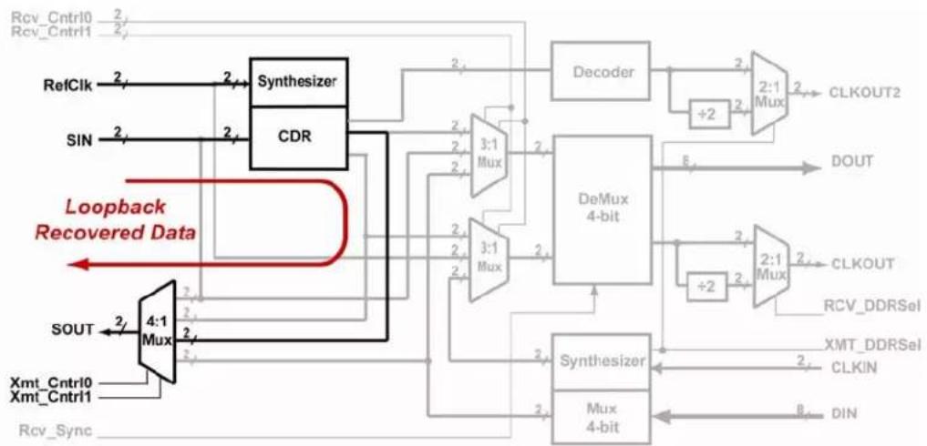
Remote Loopback Modes 01 and 10
These modes verify the operation of the CDR by
looping back the recovered clock or data.
The REFCLK is necessary for normal operation of the CDR.
flowchart
graph TD
    A["RefClk"] -->|2| B["Synthesizer"]
    C["SIN"] -->|2| B
    D["SOUT"] -->|2| E["4:1 Mux"]
    F["Xmt_Cntrl0"] --> E
    G["Xmt_Cntrl1"] --> E
    H["Rcv_Sync"] --> E
    I["Decoder"] --> J["+2"]
    K["3:1 Mux"] --> L["DeMux 4-bit"]
    M["3:1 Mux"] --> L
    N["+2"] --> O["2:1 Mux"]
    P["CLKOUT2"] --> Q["DOUT"]
    R["CLKOUT"] --> S["2:1 Mux"]
    T["RCV_DDRSel"] --> U["XMT_DDRSel"]
    V["CLKIN"] --> W["DIN"]
    X["DIN"] --> Y["Mux 4-bit"]
    Z["Loopback Recovered Clock"] --> AA["CDR"]
    AB["2:1 Mux"] --> AC["DeMux 4-bit"]
    AD["2:1 Mux"] --> AE["Synthesizer"]
    AF["2:1 Mux"] --> AG["Mux 4-bit"]
Figure 7. Remote Loopback Recovered Clock Flow
| XMT_CNTRL0 | XMT_CNTRL1 |
| 1 | 0 |
Table 12. Loopback Control Signals
flowchart
graph TD
    A["RefClk"] -->|2| B["Synthesizer"]
    C["SIN"] -->|2| B
    D["SOUT"] -->|2| E["4:1 Mux"]
    F["Xmt_Cntrl0"] --> E
    G["Xmt_Cntrl1"] --> E
    H["Rcv_Sync"] --> I["3:1 Mux"]
    I --> J["Decoder"]
    K["Deco"] --> L["+2 Mux"]
    L --> M["CLKOUT2"]
    N["DeMux 4-bit"] --> O["+2 Mux"]
    O --> P["DOUT"]
    Q["Synthesizer"] --> R["Mux 4-bit"]
    S["3:1 Mux"] --> T["3:1 Mux"]
    U["DeMux 4-bit"] --> V["3:1 Mux"]
    W["Synthesizer"] --> X["Mux 4-bit"]
    Y["3:1 Mux"] --> Z["3:1 Mux"]
    AA["DeMux 4-bit"] --> AB["3:1 Mux"]
    AC["3:1 Mux"] --> AD["3:1 Mux"]
    AE["DeMux 4-bit"] --> AF["3:1 Mux"]
    AG["3:1 Mux"] --> AH["3:1 Mux"]
    AI["DeMux 4-bit"] --> AJ["3:1 Mux"]
    AK["DeMux 4-bit"] --> AL["3:1 Mux"]
    AM["DeMux 4-bit"] --> AN["3:1 Mux"]
    AO["DeMux 4-bit"] --> AP["3:1 Mux"]
    AQ["DeMux 4-bit"] --> AR["3:1 Mux"]
    AS["DeMux 4-bit"] --> AT["3:1 Mux"]
    AU["DeMux 4-bit"] --> AV["3:1 Mux"]
    AW["DeMux 4-bit"] --> AX["3:1 Mux"]
    AY["Loopback Recovered Data"] --> AZ["2"]
    BA["Rcv_Cntrl0"] --> BB["2"]
    BC["Rcv_Cntrl1"] --> BD["2"]
Figure 8. Remote Loopback Recovered Data Flow
| XMT_CNTRL0 | XMT_CNTRL1 |
| 0 | 1 |
Table 13. Loopback Control Signals
CDR Bypass Mode
This mode bypasses the CDR and feeds SIN directly into the DeMUX. Because the CDR is bypassed, there is no recovered clock in this mode. The RefClk is fed directly into the DeMUX and is the serial rate clock.
Therefore, in this mode only, the RefClk is not used by the Synthesizer but will be at the same frequency as the SIN data rate. In this mode the maximum SIN data rate is 155.52Mbps and the matching RefClk frequency will be 155.52MHz. The Data at SIN is sampled at the falling edge of REFCLK.

flowchart
graph TD
    A["RefClk"] -->|2| B["Serial Data In"]
    C["SIN"] -->|2| B
    B --> D["Synthesizer"]
    D --> E["CDR"]
    E --> F["3:1 Mux"]
    F --> G["DeMux 4-bit"]
    G --> H["Decoder"]
    H --> I["÷2"]
    I --> J["2:1 Mux"]
    J --> K["CLKOUT2"]
    L["SOUT"] --> M["4:1 Mux"]
    M --> N["Xmt_Cntrl0"]
    M --> O["Xmt_Cntrl1"]
    P["Rcv_Sync"] --> Q["Synthesizer"]
    Q --> R["Mux 4-bit"]
    S["Xmt_Sync"] --> T["Synthesizer"]
    T --> U["Mux 4-bit"]
    V["DOUT"] --> W["Parallel Data Out"]
    X["DIN"] --> Y["RCV_DDRSel"]
    Z["XMT_DDRSel"] --> AA["CLKIN"]
    AB["DIN"] --> AC["RCV_DDRSel"]
Figure 9. CDR Bypass Mode
| RCV_CNTRL0 | RCV_CNTRL1 |
| 0 | 1 |
Table 14. Loopback Control Signals
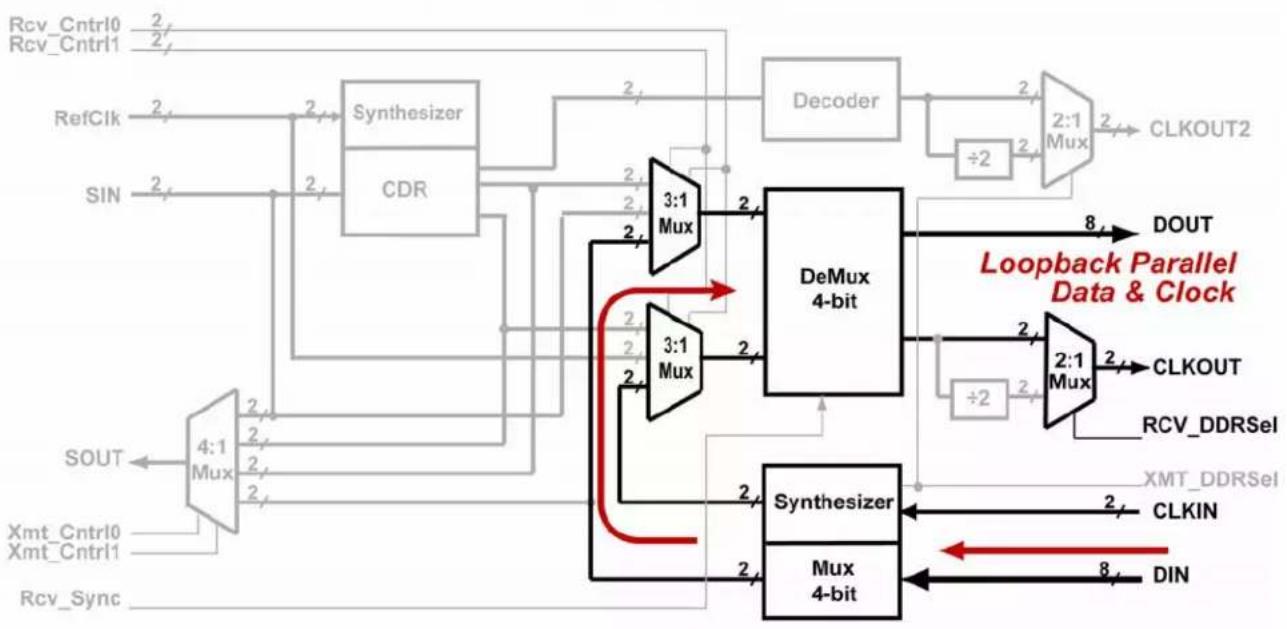
Local Loopback Mode
This mode loops the serial data out of the Mux back to the serial input of the DeMux. This allows the
operation of the Mux and DeMux to be verified through the parallel interface.
LOCAL LOOPBACK DATA FLOW
flowchart
graph TD
    A["RefClk"] --> B["Synthesizer"]
    C["SIN"] --> B
    B --> D["CDR"]
    D --> E["Decoder"]
    E --> F["÷2"]
    F --> G["2:1 Mux"]
    G --> H["CLKOUT2"]
    I["SOUT"] --> J["4:1 Mux"]
    K["Xmt_Cntrl0"] --> J
    L["Xmt_Cntrl1"] --> J
    M["Rcv_Sync"] --> N["4:1 Mux"]
    O["DeMux 4-bit"] --> P["3:1 Mux"]
    P --> Q["3:1 Mux"]
    Q --> R["Synthesizer"]
    Q --> S["Mux 4-bit"]
    T["DOUT"] --> U["Loopback Parallel Data & Clock"]
    V["DIN"] --> W["ClockIN"]
    X["DOUT"] --> Y["Loopback Parallel Data & Clock"]
    Z["DIN"] --> AA["Loopback Parallel Data & Clock"]
Figure 10. Local Loopback Data Flow
| RCV_CNTRL0 | RCV_CNTRL1 |
| 1 | 0 |
Table 15. Loopback Control Signals
Package Information
text_image
12.00 [0.472] BSC SQ. 10.00 [0.394] BSC SQ. 4.50 +0.03 -0.03 [0.177 -0.012] 64 49 1 48 1.20 [0.047] MAX. 0.50 [0.020] BSC SEE DETAIL "A" 0.22 +0.08 -0.08 [0.009 -0.002] 0.01 [0.004] 16 17 32 33 48 1.1 [0.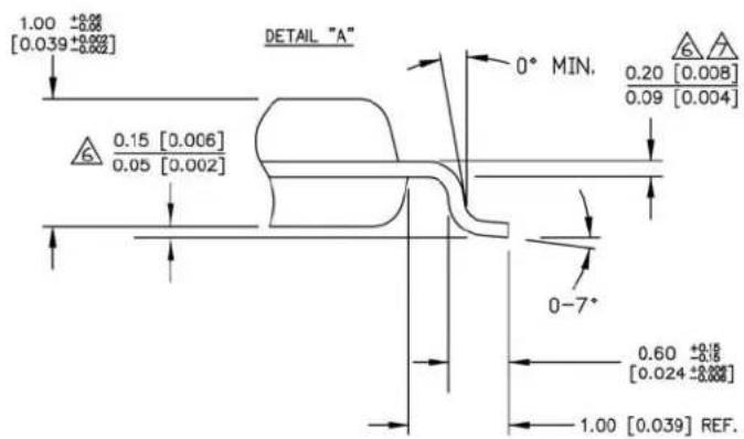
text_image
1.00 ±0.88 [0.039 ±0.88] DETAIL "A" 0° MIN. 0.20 [0.008] 0.09 [0.004] 0.15 [0.006] 0.05 [0.002] 0-7° 0.60 ±0.18 [0.024 ±0.88] 1.00 [0.039] REF.NOTES:
1. DIMENSIONS ARE IN MM[INCHES].
2. CONTROLLING DIMENSION: MM
3. EXPOSED PAD: Cu WITH Sn/Pb PLATING.
4. DIMENSION DOES NOT INCLUDE MOLD FLASH OF 0.254[0.010] MAX.
5. DIE UP ORIENTATION SHOWN. EXPOSED PAD IS VISIBLE FROM BOTTOM OF PACKAGE.
6. MAXIMUM AND MINIMUM SPECIFICATIONS ARE INDICATED AS FOLLOWS: MAX
MIN
THIS DIMENSION INCLUDES LEAD FINISH.
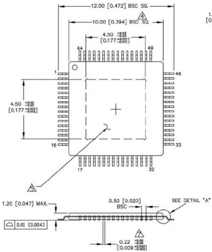
64-Pin EPAD-TQFP (T64-1)
MICREL, INC. 2180 FORTUNE DRIVE SAN JOSE, CA 95131 USA
TEL +1 (408) 944-0800 FAX +1 (408) 474-1000 WEB http://www.micrel.com
The information furnished by Micrel in this data sheet is believed to be accurate and reliable. However, no responsibility is assumed by Micrel for its use. Micrel reserves the right to change circuitry and specifications at any time without notification to the customer.
Micrel Products are not designed or authorized for use as components in life support appliances, devices or systems where malfunction of a product can reasonably be expected to result in personal injury. Life support devices or systems are devices or systems that (a) are intended for surgical implant into the body or (b) support or sustain life, and whose failure to perform can be reasonably expected to result in a significant injury to the user. A Purchaser's use or sale of Micrel Products for use in life support appliances, devices or systems is a Purchaser's own risk and Purchaser agrees to fully indemnify Micrel for any damages resulting from such use or sale.
© 2006 Micrel, Incorporated.