MIC5376 - Voltage regulator Microchip - Free user manual and instructions
Find the device manual for free MIC5376 Microchip in PDF.

User questions about MIC5376 Microchip
0 question about this device. Answer the ones you know or ask your own.
Ask a new question about this device
Download the instructions for your Voltage regulator in PDF format for free! Find your manual MIC5376 - Microchip and take your electronic device back in hand. On this page are published all the documents necessary for the use of your device. MIC5376 by Microchip.
USER MANUAL MIC5376 Microchip
High Performance Low Dropout 150 mA LDO
Features
• 4-Lead 1 mm x 1 mm UDFN: MIC5376
• 8-Lead 1.2 mm x 1.2 mm Thin QFN: MIC5377/8
- Low-Cost 5-Lead SC-70 Package Available
- Low Dropout Voltage: 120 mV at 150 mA
- Input Voltage Range: 2.5V to 5.5V
• 150 mA Guaranteed Output Current
- Stable with 0402 Ceramic Capacitors as Low as 1 F
• Low Quiescent Current: 29 μA
• Excellent Load/Line Transient Response
• Fixed Output Voltages: MIC5376
- Adjustable Output Voltages: MIC5377/8
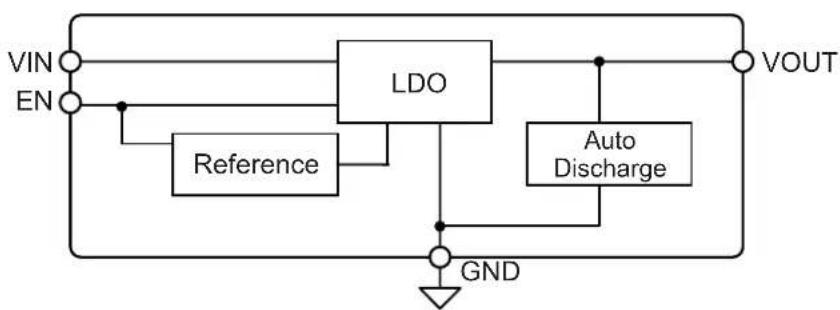
• Output Discharge Circuit: MIC5376/8
• High Output Accuracy - ±2% Initial Accuracy
• Thermal Shutdown and Current Limit Protection
Applications
- Mobile Phones
- Digital Cameras
• GPS, PDAs, PMP, Handhelds - Portable Electronics
General Description
The MIC5376, MIC5377, and MIC5378 are advanced, general purpose linear regulators that offer low dropout in ultra-small packages. The MIC5376 provides a fixed output voltage in a 1 mm x 1 mm UDFN package while the MIC5377 and MIC5378 provide adjustable output voltages in a 1.2 mm x 1.2 mm Thin QFN package. When the MIC5376 or MIC5378 are disabled, an internal resistive load is automatically applied to the output to discharge the output capacitor. The MIC5376/7/8 are capable of sourcing 150 mA output current with low dropout, making it an ideal solution for any portable electronic application.
Ideal for battery-powered applications, the MIC5376/7/8 offer 2% initial accuracy, low dropout voltage (120 mV at 150 mA), and ground current (typically 29 μA). The MIC5376/7/8 can also be put into a zero-off-mode current state, drawing virtually no current when disabled.
The MIC5376 is available in lead-free (RoHS compliant) 1 mm x 1 mm UDFN and SC-70-5 packages. The MIC5377/8 are available in lead-free (RoHS compliant) 1.2 mm x 1.2 mm Thin QFN and SC-70-5 packages.
The MIC5376/7/8 have an operating junction temperature range of -40^ to 125^ .
Typical Application Circuit
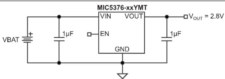
text_image
MIC5376-xxYMT VIN VOUT EN GND VBAT + 1µF 1µF VOUT = 2.8VPackage Types
MIC5376 (Fixed Output)
4-Lead 1 mm x 1 mm UDFN (MT) (Top View)
text_image
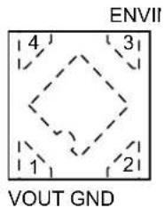
ENVII 4 3 1 2 VOUT GNDMIC5377/8 (Adjustable Output)
8-Lead 1.2 mm x 1.2 mm TQFN (MT) (Top View)
text_image
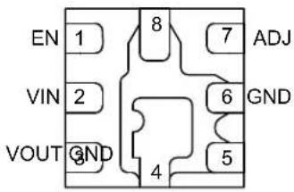
EN 1 VIN 2 VOUT GND 8 7 ADJ 6 GND 5 4MIC5376 (Fixed Output)
5-Lead SC-70 (C5) (Top View)

text_image
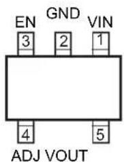
EN GND VIN 3 2 1 4 5 NC VOUTMIC5377/8 (Adjustable Output)
5-Lead SC-70 (C5) (Top View)
text_image
EN GND VIN 3 2 1 4 5 ADJ VOUTFunctional Block Diagram
MIC5376 Block Diagram
flowchart
graph TD
    A["VIN"] --> B["LDO"]
    C["EN"] --> B
    B --> D["VOUT"]
    E["Reference"] --> B
    F["Auto Discharge"] --> B
    G["GND"] --> H["Ground"]
MIC5377/8 Block Diagram
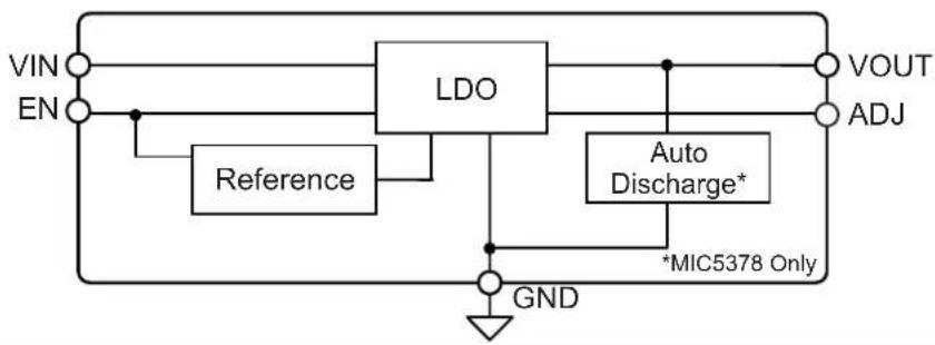
flowchart
graph TD
    VIN["VIN"] --> LDO["LDO"]
    EN["EN"] --> LDO
    LDO --> VOUT["VOUT"]
    LDO --> ADJ["ADJ"]
    Reference["Reference"] --> LDO
    Auto["Auto Discharge*"] --> LDO
    GND["GND"] --> LDO
    LDO --> *MIC5378_Only["*MIC5378 Only"]
1.0 ELECTRICAL CHARACTERISTICS
Absolute Maximum Ratings †
Supply Voltage ( V_IN ) 0V to +6V
Enable Voltage ( V_EN )....0V to V_IN
Power Dissipation ( P_D ) (Note 1) Internally Limited
Lead Temperature (Soldering, 5 sec.)....+260°C
Junction Temperature ( T_J )....-40°C to +125°C
Storage Temperature ( T_S )....-65°C to +150°C
ESD Rating (Note 2) 2 kV
Operating Ratings ††
Supply Voltage ( V_IN ) 2.5V to 5.5V
Enable Voltage ( V_EN ) 0V to V_IN
Junction Temperature ( T_J )....-40°C to +125°C
Package Thermal Resistance
1 mm x 1 mm UDFN-4 ( _JA ) ....250°C/W
1.2 mm x 1.2 mm TQFN-8 ( _JA )....250°C/W
SC-70-5 ( _JA ) 256.5°C/W
† Notice: Stresses above those listed under “Absolute Maximum Ratings” may cause permanent damage to the device. This is a stress rating only and functional operation of the device at those or any other conditions above those indicated in the operational sections of this specification is not intended. Exposure to maximum rating conditions for extended periods may affect device reliability.
†† Notice: The device is not guaranteed to function outside its operating ratings.
Note 1: The maximum allowable power dissipation of any T_A (ambient temperature) is P_D(MAX) = (T_J(MAX) - T_A)/_JA . Exceeding the maximum allowable power dissipation will result in excessive die temperature, and the regulator will go into thermal shutdown.
2: Devices are ESD sensitive. Handling precautions are recommended. Human body model, 1.5 kΩ in series with 100 pF.
ELECTRICAL CHARACTERISTICS
Electrical Characteristics: V_IN = V_EN = V_OUT + 1V ; C_IN = C_OUT = 1 F for V_OUT ≥ 2.5V , C_IN = C_OUT = 2.2 F for V_OUT < 2.5V ; I_OUT = 100 A ; T_J = +25^ , bold values indicate -40^ to +125^ , unless noted. Note 1
| Parameter Sym. Min. Typ. Max. Units Conditions | ||||||
| Output Voltage Accuracy V | OUT | -2.0 — | 2.0 | % Variation from nominal V OUT | ||
| -3.0 — | 3.0 | |||||
| Line Regulation | V_OUT / V_OUT | — 0.0 | 2 0.3 % V | IN= V_OUT + 1 V to 5.5V; I_OUT = 100 A | ||
| Load Regulation (Note 2) | V_OUT / V_OUT | — 0.3 | 1.0 | % | I_OUT = 100 A to 150 mA | |
| Dropout Voltage (Note 3) | V_DO | — | 45 | 100 | mV I | I_OUT = 50 mA |
| — | 120 200 | OUT=150 mA | ||||
| Ground Pin Current (Note 4) | I_GND | — | 29 | 45 μA | I | OUT=0 mA |
| Ground Pin Current in Shutdown | I_GND - SHDN | — 0.05 | 1 | μA V | EN≤0.2V | |
| Ripple Rejection | PSRR | — | 60 | — | dB | f=1 kHz; C_OUT = 1 F |
| — | 50 | — | f=10 kHz; C_OUT = 1 F | |||
| Current Limit | I_LIM | 200 37 | 0 550 | mA V | OUT=0V | |
| Output Voltage Noise | e_n | — | 200 | — μV | RMS | C_OUT = 1 F,10 Hz to 100kHz |
| Auto-Discharge NFET Resistance | R_DS(ON) | — | 30 | — | Ω V | EN=0V; V_IN = 3.6 V |
| Reference Voltage (MIC5377/8) | ||||||
| Reference Voltage Accuracy | V_REF | 0.97 | 1 | 1.03 | V | — |
| Adjust Pin Input Current | I_ADJ - BIAS | — 0.0 | 1 — μA | — | ||
| Enable Input | ||||||
| Enable Input Voltage | V_EN | — | — 0.2 | V Logic | Logic low. | |
| 1.2 — | — | high. | ||||
| Enable Input Current | I_EN | — 0.0 | 1 | μA V | V_IL ≤ 0.2 V | |
| — 0.0 | 1 | IH≥1.2V | ||||
| Turn-On Time | t_ON | — | 45 | 100 | μs | C_OUT = 1 F;I_OUT = 150 mA |
Note 1: Specification for packaged product only.
2: Regulation is measured at constant junction temperature using low duty cycle pulse testing.
3: Dropout voltage is defined as the input-to-output differential at which the output voltage drops 2% below its nominal value measured at 1V differential. For outputs below 2.5V, dropout voltage is the input-to-output differential with the minimum input voltage 2.5V.
4: Ground pin current is the regulator quiescent current. The total current drawn from the supply is the sum of the load current plus the ground pin current.
TEMPERATURE SPECIFICATIONS
| Parameters Sym. Min. Typ. Max. Units Conditions | ||||||
| Temperature Ranges | ||||||
| Junction Temperature Range T | J | -40 — | +125 °C — | |||
| Lead Temperature | — | — | — | +260 | °C | Soldering, 5 sec. |
| Storage Temperature | T_S | -65 — | +150 °C — | |||
| Package Thermal Resistances | ||||||
| Thermal Resistance, 1x1 UDFN 4-Ld θ | JA | — 250 | — | °C/W — | ||
| Thermal Resistance, 1.2x1.2 TQFN 8-Ld | _JA | — 250 | — | °C/W — | ||
| Thermal Resistance, SC-70-5 | _JA | — | 256.5 | — °C/W — | ||
Note 1: The maximum allowable power dissipation is a function of ambient temperature, the maximum allowable junction temperature and the thermal resistance from junction to air (i.e., T_A , T_J , _JA ). Exceeding the maximum allowable power dissipation will cause the device operating junction temperature to exceed the maximum +125°C rating. Sustained junction temperatures above +125°C can impact the device reliability.
2.0 TYPICAL PERFORMANCE CURVES
Note: The graphs and tables provided following this note are a statistical summary based on a limited number of samples and are provided for informational purposes only. The performance characteristics listed herein are not tested or guaranteed. In some graphs or tables, the data presented may be outside the specified operating range (e.g., outside specified power supply range) and therefore outside the warranted range.
line
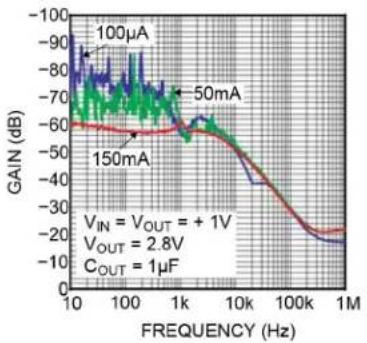
| FREQUENCY (Hz) | GAIN (dB) for 100μA | GAIN (dB) for 50mA | GAIN (dB) for 150mA | | -------------- | ------------------- | ------------------ | ------------------- | | 10 | -90 | -60 | -60 | | 100 | -70 | -60 | -60 | | 1k | -60 | -60 | -60 | | 10k | -40 | -40 | -40 | | 100k | -20 | -20 | -20 | | 1M | -20 | -20 | -20 |FIGURE 2-1: Power Supply Rejection Ratio.
line
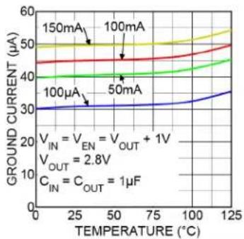
| TEMPERATURE (°C) | GROUND CURRENT (μA) | | ---------------- | ------------------- | | 25 | 30 | | 50 | 30 | | 75 | 30 | | 100 | 30 | | 125 | 30 |FIGURE 2-4: Ground Current vs. Temperature.
line
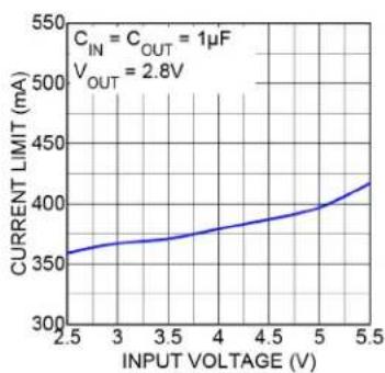
| INPUT VOLTAGE (V) | CURRENT LIMIT (mA) | | ----------------- | ------------------ | | 2.5 | 360 | | 3.0 | 370 | | 3.5 | 375 | | 4.0 | 385 | | 4.5 | 395 | | 5.0 | 405 | | 5.5 | 420 |FIGURE 2-2: Current Limit vs. Input Voltage.
line
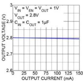
| OUTPUT CURRENT (mA) | OUTPUT VOLTAGE (V) | | ------------------- | ------------------ | | 0 | 2.8 | | 25 | 2.8 | | 50 | 2.8 | | 75 | 2.8 | | 100 | 2.8 | | 125 | 2.8 | | 150 | 2.8 |FIGURE 2-5: Output Voltage vs. Load Current.

line
| OUTPUT CURRENT (mA) | GROUND CURRENT (μA) | | ------------------- | --------------------- | | 0 | 30 | | 25 | 36 | | 50 | 39 | | 75 | 41 | | 100 | 43 | | 125 | 45 | | 150 | 47 |FIGURE 2-3: Ground Current vs. Output Current.
line
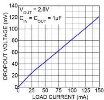
| LOAD CURRENT (mA) | DROPOUT VOLTAGE (mV) | | ----------------- | -------------------- | | 0 | 0 | | 25 | 25 | | 50 | 50 | | 75 | 75 | | 100 | 100 | | 125 | 125 | | 150 | 150 |FIGURE 2-6: Dropout Voltage vs. Load Current.
line
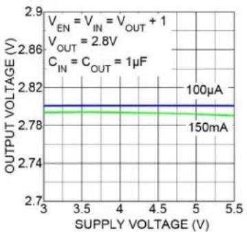
| SUPPLY VOLTAGE (V) | OUTPUT VOLTAGE (V) | | ------------------ | ------------------ | | 3.0 | 2.78 | | 3.5 | 2.78 | | 4.0 | 2.78 | | 4.5 | 2.78 | | 5.0 | 2.78 | | 5.5 | 2.78 |FIGURE 2-7: Output Voltage vs Supply Voltage.
line
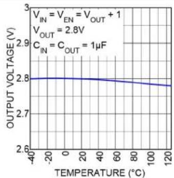
| TEMPERATURE (°C) | OUTPUT VOLTAGE (V) | | ---------------- | ------------------ | | -40 | 2.8 | | 0 | 2.8 | | 20 | 2.8 | | 40 | 2.8 | | 60 | 2.8 | | 80 | 2.8 | | 100 | 2.8 | | 120 | 2.8 |FIGURE 2-10: Output Voltage vs Temperature.

line
| SUPPLY VOLTAGE (V) | 150mA | 100mA | 100μA | | ------------------ | ----- | ----- | ----- | | 3.0 | 50 | 45 | 28 | | 3.5 | 50 | 45 | 28 | | 4.0 | 50 | 45 | 28 | | 4.5 | 50 | 45 | 28 | | 5.0 | 50 | 45 | 28 | | 5.5 | 50 | 45 | 28 |FIGURE 2-8: Ground Current vs Supply Voltage.
line
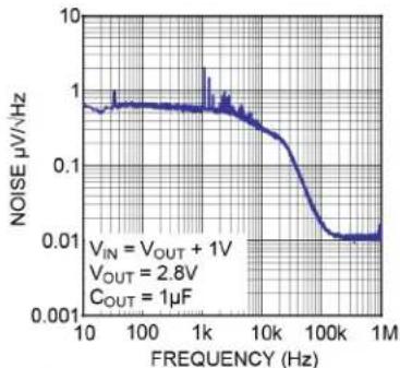
| FREQUENCY (Hz) | NOISE μV/Hz | | -------------- | ----------- | | 10 | ~0.5 | | 100 | ~0.4 | | 1k | ~0.3 | | 10k | ~0.1 | | 100k | ~0.01 | | 1M | ~0.01 |FIGURE 2-11: Output Noise Spectral Density.
line
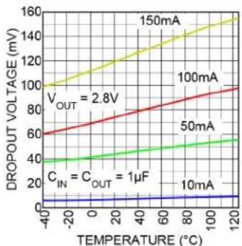
| TEMPERATURE (°C) | DROPOUT VOLTAGE (mV) | | ---------------- | -------------------- | | -40 | 100 | | -20 | 110 | | 0 | 120 | | 20 | 130 | | 40 | 140 | | 60 | 150 | | 80 | 160 | | 100 | 170 | | 120 | 180 |FIGURE 2-9: Dropout Voltage vs Temperature.

line
| Time (40μs/div) | ENABLE VOLTAGE (1V/div) | OUTPUT VOLTAGE (1V/div) | | --------------- | ------------------------ | ------------------------ | | 0 | 0 | 0 | | 0.5 | 0 | 0 | | 1.0 | 0 | 0 | | 1.5 | 0 | 0 | | 2.0 | 0 | 0 | | 2.5 | 0 | 0 | | 3.0 | 0 | 0 | | 3.5 | 0 | 0 | | 4.0 | 0 | 0 | | 4.5 | 0 | 0 | | 5.0 | 0 | 0 | | 5.5 | 0 | 0 | | 6.0 | 0 | 0 | | 6.5 | 0 | 0 | | 7.0 | 0 | 0 | | 7.5 | 0 | 0 | | 8.0 | 0 | 0 | | 8.5 | 0 | 0 | | 9.0 | 0 | 0 | | 9.5 | 0 | 0 | | 10.0 | 0 | 0 | | 10.5 | 0 | 0 | | 11.0 | 0 | 0 | | 11.5 | 0 | 0 | | 12.0 | 0 | 0 | | 12.5 | 0 | 0 | | 13.0 | 0 | 0 | | 13.5 | 0 | 0 | | 14.0 | 0 | 0 | | 14.5 | 0 | 0 | | 15.0 | 0 | 0 | | 15.5 | 0 | 0 | | 16.0 | 0 | 0 | | 16.5 | 0 | 0 | | 17.0 | 0 | 0 | | 17.5 | 0 | 0 | | 18.0 | 0 | 0 | | 18.5 | 0 | 0 | | 19.0 | 0 | 0 | | 19.5 | 0 | 0 | | 20.0 | 0 | 0 | | 20.5 | 0 | 0 | | 21.0 | 0 | 0 | | 21.5 | 0 | 0 | | 22.0 | 0 | 0 | | 22.5 | 0 | 0 | | 23.0 | 0 | 0 | | 23.5 | 0 | 0 | | 24.0 | 0 | 0 | | 24.5 | 0 | 0 | | 25.0 | 0 | 0 | | 25.5 | 0 | 0 | | 26.0 | 0 | 0 | | 26.5 | 0 | 0 | | 27.0 | 0 | 0 | | 27.5 | 0 | 0 | | 28.0 | 0 | 0 | | 28.5 | 0 | 0 | | 29.0 | 0 | 0 | | 29.5 | 0 | 0 | | 30.0 | 0 | 0 | | | | | | | | | | | | | | | | | | | | | | | | | | | | | | | | | | | | | | | | | | | | | | | | | | | | | | | | | | | | | | | | | | | | | | | | | | | | | | | | | | | | | | | | | | | | | | | | | | | | | | | | | | | | | | | | | | | | | | | | | | | | | | | | | | | | | | | | | | | | | | | | | | | | | | | | | | | | | | | | | | | | | | | | | | | | | | | | | | | | | | | | | | | | | | | | | | | | | | | | | | | | | | | | | | | | | | | | | | | | | | | | | | | | | | | | | | | | | | | | | | | | | | | | | | | | | | | | | | | | | | | | | | | | | | | | | | | | | | | | | | | | | | | | | | | | | / (Output) / (Enable) / (Output) / (Enable) / (Output) / (Enable) / (Output) / (Enable) / (Enable) / (Enable) / (Enable) / (Enable) / (Enable) / (Enable) / (Enable) / (Enable) / (Enable) / (Enable) / (Enable) / (Enable) / (Enable) / (Enable) / (Enable) / (Enable) / (Lower Limit) / (Lower Limit) / (Lower Limit) / (Lower Limit) / (Lower Limit) / (Lower Limit) / (Lower Limit) / (Lower Limit) / (Lower Limit) / (Lower Limit) / (Lower Limit) / (Lower Limit) / (Lower Limit) / (Lower Limit) / (Lower Limit) / (Lower Limit) / (Lower Limit) / (Lower Limit) / (Lower Limit) / (Lower Limit) / (Lower Limit) / (Lower Limit) / (Lower Limit) / (Lower Limit) / (Lower Limit) / (Lower Limit) / (Lower Limit) / (Lower Limit) / (Lower Limit) / (Lower Limit) / (Upper Limit) / (Upper Limit) / (Upper Limit) / (Upper Limit) / (Upper Limit) / (Upper Limit) / (Upper Limit) / (Upper Limit) / (Upper Limit) / (Upper Limit) / (Upper Limit) / (Upper Limit) / (Upper Limit) / (Upper Limit) / (Upper Limit)|FIGURE 2-12: Enable Turn-On.
line
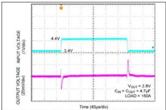
| Time (μs) | Input Voltage (1V/div) | Output Voltage (20m/div) | |-----------|------------------------|--------------------------| | 0 | 4.4 | ~2.8 | | 40 | 3.4 | ~2.8 | | Peak | 4.4 | ~2.8 | | Load | 3.4 | ~2.8 |FIGURE 2-13: Line Transient 2.8V (3.4V to 4.4V).
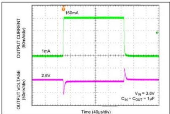
FIGURE 2-14: Load Transient 2.8V (1 mA to 150 mA).
line
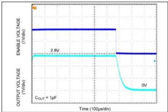
| Time (100μs/div) | ENABLE VOLTAGE (1V/div) | OUTPUT VOLTAGE (1V/div) | | ---------------- | ---------------------- | ----------------------- | | 0 | 2.8 | 0 | | >0 | 2.8 | <0 |FIGURE 2-15: MIC5376 Auto-Discharge (No Load).
3.0 PIN DESCRIPTIONS
The descriptions of the pins are listed in Table 3-1.
TABLE 3-1: PIN FUNCTION TABLE
| Pin NumberMIC5376UDFN 4-Ld | Pin NumberMIC5376SC-70-5 | Pin NumberMIC5377/8TQFN 8-Ld | Pin NumberMIC5377/8SC-70-5 | Pin Name | Description |
| 3 3 1 3 EN | Enable Input. Active-High. High = on, low = off. Do not leave floating. | ||||
| 4 1 2 1 VIN Supply Input. | |||||
| 1 5 3 5 VOUT Output Voltage. | |||||
| 2 2 4, 5, 6, 8 2 GND Ground. | |||||
| — — | 7 4 | ADJ | Adjust Pin: Feedback input from external divider. | ||
| — | 4 | — | — | NC | No connection. |
| HS Pad — — ePAD | Exposed Heat Sink Pad. Connected to ground internally. | ||||
4.0 APPLICATION INFORMATION
MIC5376, MIC5377, and MIC5378 are low-noise 150 mA LDO regulators. The MIC5376 and MIC5378 include an auto-discharge circuit that is switched on when the regulator is disabled through the enable pin. The MIC5376/7/8 regulators are protected from damage due to fault conditions, offering linear current limiting and thermal shutdown.
4.1 Input Capacitor
The MIC5376/7/8 are high-performance, high bandwidth devices. An input capacitor of 1 F is required from the input to ground to provide stability. Low-ESR ceramic capacitors provide optimal performance at a minimum of space. Additional high-frequency capacitors, such as small-valued NPO dielectric-type capacitors, help filter out high-frequency noise and are good practice in any RF-based circuit. X5R or X7R dielectrics are recommended for the input capacitor. Y5V dielectrics lose most of their capacitance over temperature and are, therefore, not recommended.
4.2 Output Capacitor
For output voltages ≥ 2.5V, the MIC5376/7/8 require a minimum 1 F output capacitor. For output voltages below 2.5V, a 2.2 F minimum output capacitor is required. The design is optimized for use with low-ESR ceramic chip capacitors. High-ESR capacitors are not recommended because they may cause high frequency oscillation. The output capacitor can be increased, but performance does not improve significantly with larger capacitance.
X7R/X5R dielectric-type ceramic capacitors are recommended because of their temperature performance. X7R-type capacitors change capacitance by 15% over their operating temperature range and are the most stable type of ceramic capacitors. Z5U and Y5V dielectric capacitors change value by as much as 50% and 60%, respectively, over their operating temperature ranges. To use a ceramic chip capacitor with Y5V dielectric, the value must be much higher than an X7R ceramic capacitor to ensure the same minimum capacitance over the equivalent operating temperature range.
4.3 No-Load Stability
Unlike many other voltage regulators, the MIC5376/7/8 will remain stable and in regulation with no load. This is especially important in CMOS RAM keep-alive applications.
4.4 Enable/Shutdown
The MIC5376/7/8 is provided with an active-high enable pin that allows the regulator to be disabled. Forcing the enable pin low disables the regulator and sends it into a "zero" off-mode-current state. In this state, current consumed by the regulator goes nearly to zero. Forcing the enable pin high enables the output voltage. The active-high enable pin uses CMOS technology and the enable pin cannot be left floating; a floating enable pin may cause an indeterminate state on the output.
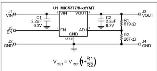
4.5 Adjustable Regulator Design
The MIC5377/8 adjustable version allows setting the output voltage down to 1V with the use of two external feedback resistors.
text_image
U1 MIC5377/8-xxYMT VIN VOUT 2 VIN C1 2.2µF 6.3V EN GND ADJ 3 C2 2.2µF 6.3V R1 619kΩ J3 VOUT J5 EN 1 4,5,6,8 GND R2 267kΩ J4 GND J2 GND VOUT = VREF (1+R1/R2)FIGURE 4-1: Adjustable Regulator with Resistors.
4.6 Thermal Considerations
The MIC5376/7/8 are designed to provide 150 mA of continuous current in a very small package. Maximum ambient operating temperature can be calculated based on the output current and the voltage drop across the part. For example if the input voltage is 3.6V, the output voltage is 2.8V, and the output current is 150 mA, the actual power dissipation of the regulator circuit can be determined using the following equation:
EQUATION 4-1:
$$ P _ {D} = (V _ {I N} - V _ {O U T}) \times I _ {O U T} + V _ {I N} \times I _ {G N D} $$
Because these devices are CMOS and the ground current is typically <100 A over the load range, the power dissipation contributed by the ground current is <1% and can be ignored for this calculation.
EQUATION 4-2:
$$ P _ {D} = (3. 6 V - 2. 8 V) \times 1 5 0 m A = 0. 1 2 W $$
To determine the maximum ambient operating temperature of the package, use the junction-to-ambient thermal resistance of the device and the following basic equation:
EQUATION 4-3:
$$ P _ {D (M A X)} = \frac {T _ {J (M A X)} - T _ {A}}{\theta_ {J A}} $$
The maximum junction temperature of the device is +125°C. The thermal resistance is 250°C/W for the UDFN/TQFN packages and 256.5°C/W for the SC-70-5.
Substituting P_D for P_D(MAX) and solving for the ambient operating temperature will give the maximum operating conditions for the regulator circuit. The junction-to-ambient thermal resistance for the minimum footprint is 250^/W .
The maximum power dissipation must not be exceeded for proper operation.
For example, when operating the MIC5376-2.8YMT at an input voltage of 3.6V and 150 mA load with a minimum footprint layout, the maximum ambient operating temperature ( T_A ) can be determined as follows:
EQUATION 4-4:
$$ 0. 1 2 W = (1 2 5 ^ {\circ} C - T _ {A}) / 2 5 0 ^ {\circ} C / \mathrm{W} $$
$$ T _ {A} = 9 5 ^ {\circ} C $$
Therefore, a maximum ambient operating temperature of +95°C is allowed for a 1 mm x 1 mm UDFN package. For a full discussion of heat sinking and thermal effects on voltage regulators, refer to the "Regulator Thermals" section of Microchip's Designing with Low-Dropout Voltage Regulators handbook.
5.0 PACKAGING INFORMATION
5.1 Package Marking Information
5-Lead SC-70 ^* (Front)
XXX
Example
2T8
5-Lead SC-70 ^* (Back)
NNN
Example
943
4-Lead UDFN ^ 8-Lead TQFN ^
XX
Example
TT
TABLE 5-1: DEVICE MARKING CODES
| Part Number Output Voltage Marking Code | ||
| MIC5376-2.8YC5 2.8V 2T | __8 | |
| MIC5376-2.8YMT 2.8V TT | ||
| MIC5377YC5 Adjustable | AH | __A |
| MIC5377YMT | Adjustable | AH |
| MIC5378YC5 Adjustable | A6 | __7 |
| MIC5378YMT | Adjustable | 67A |
Legend: XX...X Product code or customer-specific information
Y Year code (last digit of calendar year)
YY Year code (last 2 digits of calendar year)
WW Week code (week of January 1 is week '01')
NNN Alphanumeric traceability code
e3 Pb-free JEDEC® designator for Matte Tin (Sn)
* This package is Pb-free. The Pb-free JEDEC designator (e3) can be found on the outer packaging for this package.
•, ▲, ▼ Pin one index is identified by a dot, delta up, or delta down (triangle mark).
Note: In the event the full Microchip part number cannot be marked on one line, it will be carried over to the next line, thus limiting the number of available characters for customer-specific information. Package may or may not include the corporate logo.
Underbar (_) and/or Overbar (−) symbol may not be to scale.
Note: If the full seven-character YYWWNNN code cannot fit on the package, the following truncated codes are used based on the available marking space:
6 Characters = YWWNNN; 5 Characters = WWNNN; 4 Characters = WNNN; 3 Characters = NNN;
2 Characters = NN; 1 Character = N
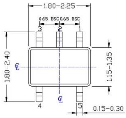
5-Lead SC-70 Package Outline & Recommended Land Pattern
TITLE
5 LEAD SC70 PACKAGE OUTLINE & RECOMMENDED LAND PATTERN
DRAWING
SC70-5LD-PL-1
UNIT MM
text_image
1.80-2.25 0.65 BSC 0.65 BSC 3 2 1 1.80-2.40 G 1.15-1.35 4 G 5 0.15-0.30TOP VIEW
text_image
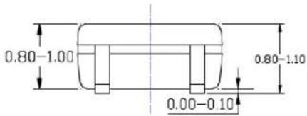
0.80-1.00 0.80-1.10 0.00-0.10SIDE VIEW
text_image
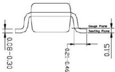
0.08-0.30 0.21-0.46 0.15 Gauge Plane Seating PlaneEND VIEW
text_image
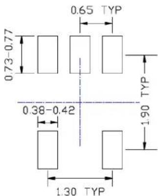
0.73-0.77 0.65 TYP 0.38-0.42 1.90 TYP 1.30 TYPRECOMMENDED LAND PATTERN
NOTE
- ALL DIMENSIONS ARE IN MILLIMETERS.
- DIMENSIONS ARE INCLUSIVE OF PLATING.
- DIMENSIONS ARE EXCLUSIVE OF MOLD FLASH & METAL BURR.
Note: For the most current package drawings, please see the Microchip Packaging Specification located at http://www.microchip.com/packaging.
4-Lead 1 mm x 1 mm UDFN Package Outline and Recommended Land Pattern
4-Lead Ultra Thin Plastic Dual Flat, No Lead Package (HCA) - 1x1 mm Body [UDFN]
Note: For the most current package drawings, please see the Microchip Packaging Specification located at http://www.microchip.com/packaging
![Microchip MIC5376 - 4-Lead Ultra Thin Plastic Dual Flat, No Lead Package (HCA) - 1x1 mm Body [UDFN] - 1](/content/2026/06/1222011/images/835a49d71c0d03e0a0da30d6c23ab5a67880874578168f438c9d777d965e7d3d.jpg)
Microchip Technology Drawing C04-1149 Rev A Sheet 1 of 2
4-Lead Ultra Thin Plastic Dual Flat, No Lead Package (HCA) - 1x1 mm Body [UDFN]
Note: For the most current package drawings, please see the Microchip Packaging Specification located at http://www.microchip.com/packaging
![Microchip MIC5376 - 4-Lead Ultra Thin Plastic Dual Flat, No Lead Package (HCA) - 1x1 mm Body [UDFN] - 1](/content/2026/06/1222011/images/ec33d93f4786f0e726d875b87e8e1607a4b5f7205e99760ed9318f5c79347c95.jpg)
natural_image
Isometric line drawing of two 3D rectangular blocks with internal cutouts and mounting holes (no text or symbols)| Units | MILLIMETERS | |||
| Dimension Limits | MIN | NOM | MAX | |
| Number of Terminals | N | 4 | ||
| Pitch | e | 0.65 BSC | ||
| Overall Height | A | 0.50 | 0.55 | 0.60 |
| Standoff | A1 | 0.00 | 0.02 | 0.05 |
| Terminal Thickness | A3 | 0.152 REF | ||
| Overall Length | D | 1.00 BSC | ||
| Exposed Pad Length | D2 0.45 | 0.50 0.55 | ||
| Overall Width | E | 1.00 BSC | ||
| Exposed Pad Width | E2 | 0.45 | 0.50 | 0.55 |
| Terminal Width | b | 0.175 | 0.225 | 0.275 |
| Terminal Length | L | 0.20 | 0.25 | 0.30 |
Notes:
- Pin 1 visual index feature may vary, but must be located within the hatched area.
- Package is saw singulated
- Dimensioning and tolerancing per ASME Y14.5M BSC: Basic Dimension. Theoretically exact value shown without tolerances. REF: Reference Dimension, usually without tolerance, for information purposes only.
Microchip Technology Drawing C04-1149 Rev A Sheet 2 of 2
4-Lead Ultra Thin Plastic Dual Flat, No Lead Package (HCA) - 1x1 mm Body [UDFN]
Note: For the most current package drawings, please see the Microchip Packaging Specification located at http://www.microchip.com/packaging
![Microchip MIC5376 - 4-Lead Ultra Thin Plastic Dual Flat, No Lead Package (HCA) - 1x1 mm Body [UDFN] - 1](/content/2026/06/1222011/images/bc7ce5ef57d40cfed7d1838e7e9d89f7446c66a9a05de378a12e2f0226237ee6.jpg)
text_image
E X2 4 3 Y2 ØV C Y3 0.47 2X CH Y1 1 2 45° X1 SILK SCREENRECOMMENDED LAND PATTERN
| Units | MILLIMETERS | |||
| Dimension Limits | MIN | NOM | MAX | |
| Contact Pitch | E | 0.65 BSC | ||
| Center Pad Width | X2 | 0.48 | ||
| Center Pad Length | Y2 | 0.48 | ||
| C | 0 | |||
| Contact Pad Width (X4) | X1 | 0.25 | ||
| Contact Pad Length (X3) | Y1 | 0.40 | ||
| Terminal 1 Pad Length | Y3 | 0.47 | ||
| Contact Pad Chamfer (X3) | CH | 0.18 | ||
| Thermal Via Diameter V | 0.30 | |||
9.0gnicapS daP tcati
Notes:
- Dimensioning and tolerancing per ASME Y14.5M
BSC: Basic Dimension. Theoretically exact value shown without tolerances.
- For best soldering results, thermal vias, if used, should be filled or tented to avoid solder loss during reflow process
Microchip Technology Drawing C04-3149 Rev A
8-Lead 1.2 mm x 1.2 mm TQFN Package Outline and Recommended Land Pattern
TITLE
8 LEAD TQFN 1.2x1.2mm PACKAGE OUTLINE & RECOMMENDED LAND PATTERN
DRAWING
TQFN1212-8LD-PL-1
UNIT
MM

text_image
1 TRIANGLE IARKING 1.200±0.050 8 7 1.200±0.050 3 4 5TOP VIEW
NOTE: 1, 2, 3
text_image
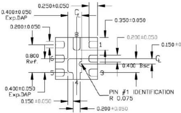
0.400±0.050 Exp.DAP 0.200±0.050 0.800 Ref. 0.400±0.050 Exp.DAP 0.150±0.050 0.250±0.050 C 8 1 3 4 PIN #1 IDENTIFICATION R 0.075 0.200±0.050 0.350±0.050 0.200±0.050 0.150±0 BscBOTTOM VIEW
NOTE: 1, 2

text_image
0.550±0.050 TING PLANE 0.000-0.050 0.152 Ref.SIDE VIEW
NOTE: 1, 2
text_image
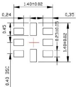
140±0.02 0,24 0,35 0,45 0,23±0.05 140±0.02 0,40 BSCRECOMMENDED LAND PATTERN
NOTE:
- MAX PACKAGE WARPAGE IS 0.05MM
- MAX ALLOWABLE BURR IS 0.076MM IN ALL DIRECTIONS
- PIN #1 IS ON TOP WILL BE LASER MARKED
Note: For the most current package drawings, please see the Microchip Packaging Specification located at http://www.microchip.com/packaging.
NOTES:
APPENDIX A: REVISION HISTORY
Revision A (October 2018)
- Converted Micrel document MIC5376/7/8 to Microchip data sheet template DS20006080A.
- Minor grammatical text changes throughout.
- All reference to and information about the MIC5375 has been removed.
Revision B (February 2022)
- Updated the Package Marking Information drawing with the most current marking information.
- Updated the 4-Lead 1 mm x 1 mm UDFN Package Outline and Recommended Land Pattern drawing with the most current drawing.
NOTES:
PRODUCT IDENTIFICATION SYSTEM
To order or obtain information, e.g., on pricing or delivery, contact your local Microchip representative or sales office.
Device
Part No.
-X.X
Output
Voltage
X
Junction
Temp. Range
XX
Package
-XX
Media Type
| Device: | MIC5376: High Performance Low Dropout 150 mA LDO with Fixed Output Voltage and Output Discharge CircuitMIC5377: High Performance Low Dropout 150 mA LDO with Adjustable Output VoltageMIC5378: High Performance Low Dropout 150 mA LDO with Adjustable Output Voltage and Output Discharge Circuit |
| Output Voltage: | 2.8 = 2.8V (MIC5376 only)= Adjustable (MIC5377 or MIC5378 only) |
| Junction Temperature Range: | Y = -40°C to +125°C, RoHS-Compliant |
| Package: | C5 = 5-Lead SC-70 (MIC5376/7/8)MT = 4-Lead 1 mm x 1 mm UDFN (MIC5376)MT = 8-Lead 1.2 mm x 1.2 mm TQFN (MIC5377/8) |
| Media Type: | TR = 3000/Reel (C5 package option)TR = 5000/Reel (MIC5377/8 MT package options)TZ = 10000/Reel (MIC5376 MT package option) |
Examples:
a) MIC5376-2.8YC5-TR: MIC5376, 2.8V Output
Voltage, -40^ to +125^
Temperature Range,
5-Lead SC-70, 3000/Reel
b) MIC5376-2.8YMT-TZ: MIC5376, 2.8V Output
Voltage, -40^ to +125^
Temperature Range,
4-Lead UDFN, 10000/Reel
c) MIC5377YC5-TR: MIC5377, Adjustable Output
Voltage, -40^ to +125^
Temperature Range,
5-Lead SC-70, 3000/Reel
d) MIC5377YMT-TR: MIC5377, Adjustable Output
Voltage, -40^ to +125^
Temperature Range
8-Lead TQFN, 5000/Reel
e) MIC5378YC5-TR: MIC5378, Adjustable Output
Voltage, -40^ to +125^
Temperature Range,
5-Lead SC-70, 3000/Reel
f) MIC5378YMT-TR: MIC5378, Adjustable Output
Voltage, -40^ to +125^
Temperature Range,
8-Lead TQFN, 5000/Reel
Note 1: Tape and Reel identifier only appears in the catalog part number description. This identifier is used for ordering purposes and is not printed on the device package. Check with your Microchip Sales Office for package availability with the Tape and Reel option.
NOTES:
Note the following details of the code protection feature on Microchip products:
• Microchip products meet the specifications contained in their particular Microchip Data Sheet.
- Microchip believes that its family of products is secure when used in the intended manner, within operating specifications, and under normal conditions.
- Microchip values and aggressively protects its intellectual property rights. Attempts to breach the code protection features of Microchip product is strictly prohibited and may violate the Digital Millennium Copyright Act.
- Neither Microchip nor any other semiconductor manufacturer can guarantee the security of its code. Code protection does not mean that we are guaranteeing the product is “unbreakable”. Code protection is constantly evolving. Microchip is committed to continuously improving the code protection features of our products.
This publication and the information herein may be used only with Microchip products, including to design, test, and integrate Microchip products with your application. Use of this information in any other manner violates these terms. Information regarding device applications is provided only for your convenience and may be superseded by updates. It is your responsibility to ensure that your application meets with your specifications. Contact your local Microchip sales office for additional support or, obtain additional support at https://www.microchip.com/en-us/support/design-help/client-support-services.
THIS INFORMATION IS PROVIDED BY MICROCHIP "AS IS". MICROCHIP MAKES NO REPRESENTATIONS OR WARRANTIES OF ANY KIND WHETHER EXPRESS OR IMPLIED, WRITTEN OR ORAL, STATUTORY OR OTHERWISE, RELATED TO THE INFORMATION INCLUDING BUT NOT LIMITED TO ANY IMPLIED WARRANTIES OF NON-INFRINGEMENT, MERCHANTABILITY, AND FITNESS FOR A PARTICULAR PURPOSE, OR WARRANTIES RELATED TO ITS CONDITION, QUALITY, OR PERFORMANCE.
IN NO EVENT WILL MICROCHIP BE LIABLE FOR ANY INDIRECT, SPECIAL, PUNITIVE, INCIDENTAL, OR CONSEQUENTIAL LOSS, DAMAGE, COST, OR EXPENSE OF ANY KIND WHATSOEVER RELATED TO THE INFORMATION OR ITS USE, HOWEVER CAUSED, EVEN IF MICROCHIP HAS BEEN ADVISED OF THE POSSIBILITY OR THE DAMAGES ARE FORESEEABLE. TO THE FULLEST EXTENT ALLOWED BY LAW, MICROCHIP'S TOTAL LIABILITY ON ALL CLAIMS IN ANY WAY RELATED TO THE INFORMATION OR ITS USE WILL NOT EXCEED THE AMOUNT OF FEES, IF ANY, THAT YOU HAVE PAID DIRECTLY TO MICROCHIP FOR THE INFORMATION.
Use of Microchip devices in life support and/or safety applications is entirely at the buyer's risk, and the buyer agrees to defend, indemnify and hold harmless Microchip from any and all damages, claims, suits, or expenses resulting from such use. No licenses are conveyed, implicitly or otherwise, under any Microchip intellectual property rights unless otherwise stated.
For information regarding Microchip's Quality Management Systems, please visit www.microchip.com/quality.
Trademarks
The Microchip name and logo, the Microchip logo, Adaptec, AnyRate, AVR, AVR logo, AVR Freaks, BesTime, BitCloud, CryptoMemory, CryptoRF, dsPIC, flexPWR, HELDO, IGLOO, JukeBlox, KeeLoq, Kleer, LANCheck, LinkMD, maXStylus, maXTouch, MediaLB, megaAVR, Microsemi, Microsemi logo, MOST, MOST logo, MPLAB, OptoLyzer, PIC, picoPower, PICSTART, PIC32 logo, PolarFire, Prochip Designer, QTouch, SAM-BA, SenGenuity, SpyNIC, SST, SST Logo, SuperFlash, Symmetricom, SyncServer, Tachyon, TimeSource, tinyAVR, UNI/O, Vectron, and XMEGA are registered trademarks of Microchip Technology Incorporated in the U.S.A. and other countries.
AgileSwitch, APT, ClockWorks, The Embedded Control Solutions Company, EtherSynch, Flashtec, Hyper Speed Control, HyperLight Load, IntelliMOS, Libero, motorBench, mTouch, Powermite 3, Precision Edge, ProASIC, ProASIC Plus, ProASIC Plus logo, Quiet-Wire, SmartFusion, SyncWorld, Temux, TimeCesium, TimeHub, TimePictra, TimeProvider, TrueTime, WinPath, and ZL are registered trademarks of Microchip Technology Incorporated in the U.S.A.
Adjacent Key Suppression, AKS, Analog-for-the-Digital Age, Any Capacitor, AnyIn, AnyOut, Augmented Switching, BlueSky, BodyCom, CodeGuard, CryptoAuthentication, CryptoAutomotive, CryptoCompanion, CryptoController, dsPICDEM, dsPICDEM.net, Dynamic Average Matching, DAM, ECAN, Espresso T1S, EtherGREEN, GridTime, IdealBridge, In-Circuit Serial Programming, ICSP, INICnet, Intelligent Paralleling, Inter-Chip Connectivity, JitterBlocker, Knob-on-Display, maxCrypto, maxView, memBrain, Mindi, MiWi, MPASM, MPF, MPLAB Certified logo, MPLIB, MPLINK, MultiTRAK, NetDetach, NVM Express, NVMe, Omniscient Code Generation, PICDEM, PICDEM.net, PICkit, PICtail, PowerSmart, PureSilicon, QMatrix, REAL ICE, Ripple Blocker, RTAX, RTG4, SAM-ICE, Serial Quad I/O, simpleMAP, SimpliPHY, SmartBuffer, SmartHLS, SMART-I.S., storClad, SQI, SuperSwitcher, SuperSwitcher II, Switchtec, SynchroPHY, Total Endurance, TSHARC, USBCheck, VariSense, VectorBlox, VeriPHY, ViewSpan, WiperLock, XpressConnect, and ZENA are trademarks of Microchip Technology Incorporated in the U.S.A. and other countries.
SQTP is a service mark of Microchip Technology Incorporated in the U.S.A.
The Adaptec logo, Frequency on Demand, Silicon Storage Technology, Symmcom, and Trusted Time are registered trademarks of Microchip Technology Inc. in other countries.
GestIC is a registered trademark of Microchip Technology Germany II GmbH & Co. KG, a subsidiary of Microchip Technology Inc., in other countries.
All other trademarks mentioned herein are property of their respective companies.
© 2018 - 2022, Microchip Technology Incorporated and its subsidiaries.
All Rights Reserved.
ISBN: 978-1-5224-9784-4
Worldwide Sales and Service
AMERICAS
Corporate Office
2355 West Chandler Blvd.
Chandler, AZ 85224-6199
Tel: 480-792-7200
Fax: 480-792-7277
Technical Support:
http://www.microchip.com/
support
Web Address:
www.microchip.com
Atlanta
Duluth, GA
Tel: 678-957-9614
Fax: 678-957-1455
Austin, TX
Tel: 512-257-3370
Boston
Westborough, MA
Tel: 774-760-0087
Fax: 774-760-0088
Chicago
Itasca, IL
Tel: 630-285-0071
Fax: 630-285-0075
Dallas
Addison, TX
Tel: 972-818-7423
Fax: 972-818-2924
Detroit
Novi, MI
Tel: 248-848-4000
Houston, TX
Tel: 281-894-5983
Indianapolis
Noblesville, IN
Tel: 317-773-8323
Fax: 317-773-5453
Tel: 317-536-2380
Los Angeles
Mission Viejo, CA
Tel: 949-462-9523
Fax: 949-462-9608
Tel: 951-273-7800
Raleigh, NC
Tel: 919-844-7510
New York, NY
Tel: 631-435-6000
San Jose, CA
Tel: 408-735-9110
Tel: 408-436-4270
Canada - Toron
Tel: 905-695-1980
Fax: 905-695-2078
ASIA/PACIFIC
Australia - Sydney
Tel: 61-2-9868-6733
China - Beijing
Tel: 86-10-8569-7000
China - Chengdu
Tel: 86-28-8665-5511
China - Chongqing
Tel: 86-23-8980-9588
China - Dongguan
Tel: 86-769-8702-9880
China - Guangzhou
Tel: 86-20-8755-8029
China - Hangzhou
Tel: 86-571-8792-8115
China - Hong Kong SAR
Tel: 852-2943-5100
China - Nanjing
Tel: 86-25-8473-2460
China - Qingdao
Tel: 86-532-8502-7355
China - Shanghai
Tel: 86-21-3326-8000
China - Shenyang
Tel: 86-24-2334-2829
China - Shenzhen
Tel: 86-755-8864-2200
China - Suzhou
Tel: 86-186-6233-1526
China - Wuhan
Tel: 86-27-5980-5300
China - Xian
Tel: 86-29-8833-7252
China - Xiamen
Tel: 86-592-2388138
China - Zhuhai
Tel: 86-756-3210040
ASIA/PACIFIC
India - Bangalore
Tel: 91-80-3090-4444
India - New Delhi
Tel: 91-11-4160-8631
India - Pune
Tel: 91-20-4121-0141
Japan - Osaka
Tel: 81-6-6152-7160
Japan - Tokyo
Tel: 81-3-6880-3770
Korea - Daegu
Tel: 82-53-744-4301
Korea - Seoul
Tel: 82-2-554-7200
Malaysia - Kuala Lumpur
Tel: 60-3-7651-7906
Malaysia - Penang
Tel: 60-4-227-8870
Philippines - Manila
Tel: 63-2-634-9065
Singapore
Tel: 65-6334-8870
Taiwan - Hsin Chu
Tel: 886-3-577-8366
Taiwan - Kaohsiung
Tel: 886-7-213-7830
Taiwan - Taipei
Tel: 886-2-2508-8600
Thailand - Bangkok
Tel: 66-2-694-1351
Tel: 43-7242-2244-39
Fax: 43-7242-2244-393
Denmark - Copenhagen
Tel: 45-4485-5910
Fax: 45-4485-2829
Finland - Espoo
Tel: 358-9-4520-820
France - Paris
Tel: 33-1-69-53-63-20
Fax: 33-1-69-30-90-79
Germany - Garching
Tel: 49-8931-9700
Germany - Haan
Tel: 49-2129-3766400
Germany - Heilbronn
Tel: 49-7131-72400
Germany - Karlsruhe
Tel: 49-721-625370
Germany - Munich
Tel: 49-89-627-144-0
Fax: 49-89-627-144-44
Germany - Rosenheim
Tel: 49-8031-354-560
Israel - Ra'anana
Tel: 972-9-744-7705
Italy - Milan
Tel: 39-0331-742611
Fax: 39-0331-466781
Italy - Padova
Tel: 39-049-7625286
Netherlands - Drunen
Tel: 31-416-690399
Fax: 31-416-690340
Norway - Trondheim
Tel: 47-7288-4388
Poland - Warsaw
Tel: 48-22-3325737
Romania - Bucharest
Tel: 40-21-407-87-50
Spain - Madrid
Tel: 34-91-708-08-90
Fax: 34-91-708-08-91
Sweden - Gothenberg
Tel: 46-31-704-60-40
Sweden - Stockholm
Tel: 46-8-5090-4654
UK - Wokingham
Tel: 44-118-921-5800
Fax: 44-118-921-5820