34VL02 - EEPROM Memory Microchip - Free user manual and instructions
Find the device manual for free 34VL02 Microchip in PDF.

User questions about 34VL02 Microchip
0 question about this device. Answer the ones you know or ask your own.
Ask a new question about this device
Download the instructions for your EEPROM Memory in PDF format for free! Find your manual 34VL02 - Microchip and take your electronic device back in hand. On this page are published all the documents necessary for the use of your device. 34VL02 by Microchip.
USER MANUAL 34VL02 Microchip
2K I ^2 C ^TM Serial EEPROM Software Write-Protect
Features:
- Permanent and Resettable Software Write-Protect for Lower Half of the Array (00h-7Fh)
- Single Supply with Operation Down to 1.5V
• Low-Power CMOS Technology: - Read current 1 mA, typical
- Standby current, 100 nA, typical
- 2-Wire Serial Interface Bus, I ^2 C ^TM Compatible
- Cascadable up to Eight Devices
• Schmitt Trigger Inputs for Noise Suppression - Output Slope Control to Eliminate Ground Bounce
• 100 kHz and 400 kHz Compatibility
• Page Write Time 3 ms, typical
• Self-Timed Erase/Write Cycle
• 16-Byte Page Write Buffer
• ESD Protection > 4,000V
• Hardware Write Protection for Entire Array
• More than 1 Million Erase/Write Cycles
• Data Retention > 200 Years - 8-Lead PDIP, SOIC, TSSOP, MSOP and TDFN packages
• 6-Lead SOT-23 Package
• Pb-free and RoHS Compliant
• Temperature Range: - -20°C to +85°C
Device Selection Table
| Part Number | Vcc Range | Max. Clock Frequency |
| 34VL02 1.5-3.6 | 400 kHz | (1) |
Note 1: 100 kHz for Vcc <1.8V
Package Types

text_image
PDIP/SOIC/TSSOP/MSOP/TDFN A0 1 8 Vcc A1 2 7 WP A2 3 6 SCL Vss 4 5 SDA A0 1 8 Vcc A1 2 7 WP A2 3 6 SCL Vss 4 5 SDA SOT-23 SCL 1 6 Vcc Vss 2 5 A0 SDA 3 4 A1Description:
The Microchip Technology Inc. 34VL02 is a 2 Kbit Electrically Erasable PROM capable of operation across a broad voltage range (1.5V to 3.6V). This device has two software write-protect features for the lower half of the array, as well as an external pin that can be used to write-protect the entire array. This allows the system designer to protect none, half, or all of the array, depending on the application. The device is organized as one block of 256 x 8-bit memory with a 2-wire serial interface. Low-voltage design permits operation down to 1.5V, with standby and active currents of only 100 nA and 1 mA, respectively. The 34VL02 also has a page write capability for up to 16 bytes of data. The 34VL02 is available in the standard 8-pin PDIP, surface mount SOIC, TSSOP, MSOP and TDFN packages. The 34VL02 is also available in the 6-lead, SOT-23 package.
Block Diagram
flowchart
graph TD
    A["A0 A1 A2"] --> B["I/O Control Logic"]
    C["SDA SCL"] --> B
    D["Vcc"] --> E["Memory Control Logic"]
    F["Vss"] --> E
    B --> G["XDEC"]
    E --> G
    G --> H["HV Generator"]
    H --> I["Software write-protected area (00h-7Fh)"]
    I --> J["Standard Array"]
    J --> K["Write-Protect Circuitry"]
    K --> L["YDEC"]
    L --> M["Sense Amp. R/W Control"]
    M --> N["WP"]
    N --> B
1.0 ELECTRICAL CHARACTERISTICS
Absolute Maximum Ratings ^()
Vcc....6.5V
All inputs and outputs w.r.t. VsS -0.3V to Vcc +1.0V
Storage temperature ....-65°C to +150°C
Ambient temperature with power applied....-20°C to +85°C
ESD protection on all pins ≥ 4 kV
† NOTICE: Stresses above those listed under “Absolute Maximum Ratings” may cause permanent damage to the device. These are stress ratings only and functional operation of the device at these or any other conditions above those indicated in the operation sections of the specifications is not implied. Exposure to Absolute Maximum Rating conditions for extended periods may affect device reliability.
TABLE 1-1: DC SPECIFICATIONS
| DC CHARACTERISTICS | Vcc = +1.5V to +3.6VTemperature Range: -20°C to +85°C | ||||||
| Param.No. | Symbol | Characteristic Min. Typ. | Max. Units | Conditions | |||
| — | A0, A1, A2, SCL, SDA and WP pins | — | — | — | — | — | |
| D1 | VIH | High-level input voltage | 0.7 Vcc | — | — | V | — |
| D2 | VIL | Low-level input voltage | — | — | 0.3 Vcc | V | 0.2 Vcc for Vcc < 2.5V |
| D3 | VHYS | Hysteresis of Schmitt Trigger inputs | 0.05 Vcc | — | — | V | (Note) |
| D4 | VOL | Low-level output voltage | — | — | 0.40 | V | IOL = 3.0 mA, Vcc = 2.5V |
| D5 | VHV | High-Voltage Detect | 7 | — | 10 | V | A0 Pin only, Vcc < 2.2V |
| Vcc + 4.8 | — | 10 | V | A0 Pin only, Vcc ≥ 2.2V | |||
| D6 | ILI | Input leakage current | — | — | ±1 | μA | VIN = Vss or Vcc |
| D7 | ILO | Output leakage current | — | — | ±1 | μA | VOUT = Vss or Vcc |
| D8 CIN, | COUT | Pin capacitance(all inputs/outputs) | — | — | 10 | pF | Vcc = 3.6V (Note)TA = 25°C |
| D9 | Icc write | Operating current | — | 0.1 | 3 | mA | Vcc = 3.6V |
| D10 | Icc read | — | 0.05 | 1 | mA | — | |
| D11 | Iccs | Standby current | — | 0.01 | 1 | μA | SDA = SCL = VccA0, A1, A2, WP = Vss |
Note: This parameter is periodically sampled and not 100% tested.
TABLE 1-2: AC SPECIFICATIONS
| AC CHARACTERISTICS | Vcc = +1.5V to +3.6VTemperature Range: -20°C to +85°C | |||||
| Param.No. | Symbol C | characteristic Min. Max. Units Conditions | ||||
| 1 | FCLK Clock frequency — | — | 100400 | kHz | 1.5V ≤ Vcc < 1.8V1.8V ≤ Vcc ≤ 3.6V | |
| 2 | THIGH Clock high time 4000 | 600 | —— | ns | 1.5V ≤ Vcc < 1.8V1.8V ≤ Vcc ≤ 3.6V | |
| 3 | TLOW Clock low time | 47001300 | —— | ns | 1.5V ≤ Vcc < 1.8V1.8V ≤ Vcc ≤ 3.6V | |
| 4 | TR SDA and SCL rise time (Note 1) | —— | 1000300 | ns | 1.5V ≤ Vcc < 1.8V1.8V ≤ Vcc ≤ 3.6V | |
| 5 | TF SDA and SCL fall time (Note 1) | —— | 1000300 | ns | 1.5V ≤ Vcc < 1.8V1.8V ≤ Vcc ≤ 3.6V | |
| 6 | THD:STA Start condition hold time | 4000600 | —— | ns | 1.5V ≤ Vcc < 1.8V1.8V ≤ Vcc ≤ 3.6V | |
| 7 | TSU:STA Start condition setup time | 4700600 | —— | ns | 1.5V ≤ Vcc < 1.8V1.8V ≤ Vcc ≤ 3.6V | |
| 8 | THD:DAT Data input hold time | 0 | — | ns | (Note 2) | |
| 9 | TSU:DAT Data input setup time | 250100 | —— | ns | 1.5V ≤ Vcc < 1.8V1.8V ≤ Vcc ≤ 3.6V | |
| 10 | TSU:STO Stop condition setup time | 4000600 | —— | ns | 1.5V ≤ Vcc < 1.8V1.8V ≤ Vcc ≤ 3.6V | |
| 11 | TSU:WP WP setup time | 4000600 | —— | ns | 1.5V ≤ Vcc < 1.8V1.8V ≤ Vcc ≤ 3.6V | |
| 12 | THD:WP WP hold time | 4700600 | —— | ns | 1.5V ≤ Vcc < 1.8V1.8V ≤ Vcc ≤ 3.6V | |
| 13 | TAA Output valid from clock (Note 2) | —— | 3500900 | ns | 1.5V ≤ Vcc < 1.8V1.8V ≤ Vcc ≤ 3.6V | |
| 14 | TBUF Bus free time: Time the bus must be free before a new transmission can start | 13004700 | —— | ns | 1.5V ≤ Vcc < 1.8V1.8V ≤ Vcc ≤ 3.6V | |
| 16 | TSP Input filter spike suppression (SDA and SCL pins) | — | 50 | ns | (Note 1 and Note 3) | |
| 17 | TWC Write cycle time (byte or page) | — | 5 | ms | — | |
| 18 | — Endurance | 1M | — | cycles | 25°C, Vcc = 3.6V, Block mode (Note 4) | |
Note 1: Not 100% tested. CB = total capacitance of one bus line in pF.
2: As a transmitter, the device must provide an internal minimum delay time to bridge the undefined region (minimum 300 ns) of the falling edge of SCL to avoid unintended generation of Start or Stop conditions.
3: The combined TSP and VHYS specifications are due to new Schmitt Trigger inputs, which provide improved noise spike suppression. This eliminates the need for a TI specification for standard operation.
4: This parameter is not tested but ensured by characterization. For endurance estimates in a specific application, please consult the Total Endurance™ Model which can be obtained from Microchip's web site at www.microchip.com.
FIGURE 1-1: BUS TIMING DATA
text_image
SCL 7 5 2 D4 4 SDA In 3 8 9 10 16 13 14 SDA Out WP (protected) (unprotected) 11 122.0 FUNCTIONAL DESCRIPTION
The 34VL02 has two Software Write-Protect features that allow you to protect half of the array from being written (Addresses 00h-7Fh). One command, Software Write-Protect (SWP) will prevent writes to half of the array and is resettable by using the Clear Software Write-Protect (CSWP) command. The other command is Permanent Software Write-Protect (PSWP), which is not resettable and will permanently lock half the array from being written to. The device still has an external pin (WP) that allows you to protect the entire array if so desired.
The 34VL02 supports a bidirectional 2-wire bus and data transmission protocol. A device that sends data onto the bus is defined as a transmitter, and a device receiving data, as a receiver. The bus has to be controlled by a master device, which generates the Serial Clock (SCL), controls the bus access and generates the Start and Stop conditions, while the 34VL02 works as slave. Both master and slave can operate as transmitter or receiver, but the master device determines which mode is activated.
3.0 BUS CHARACTERISTICS
The following bus protocol has been defined:
- Data transfer may be initiated only when the bus is not busy.
- During data transfer, the data line must remain stable whenever the clock line is high. Changes in the data line while the clock line is high will be interpreted as a Start or Stop condition.
Accordingly, the following bus conditions have been defined (Figure 3-1).
3.1 Bus Not Busy (A)
Both data and clock lines remain high.
3.2 Start Data Transfer (B)
A high-to-low transition of the SDA line while the clock (SCL) is high determines a Start condition. All commands must be preceded by a Start condition.
3.3 Stop Data Transfer (C)
A low-to-high transition of the SDA line while the clock (SCL) is high determines a Stop condition. All operations must be ended with a Stop condition.
3.4 Data Valid (D)
The state of the data line represents valid data when, after a Start condition, the data line is stable for the duration of the high period of the clock signal.
The data on the line must be changed during the low period of the clock signal. There is one clock pulse per bit of data.
Each data transfer is initiated with a Start condition and terminated with a Stop condition. The number of data bytes transferred between the Start and Stop conditions is determined by the master device and is, theoretically, unlimited; although only the last sixteen will be stored when doing a write operation. When an overwrite does occur, it will replace data in a first-in, first-out (FIFO) fashion.
3.5 Acknowledge
Each receiving device, when addressed, is obliged to generate an Acknowledge after the reception of each byte. Exceptions to this rule relating to software write protection are described in Section 7.0 "Write Protection". The master device must generate an extra clock pulse, which is associated with this Acknowledge bit.
Note: The 34VL02 does not generate any Acknowledge bits if an internal programming cycle is in progress.
The device that acknowledges has to pull down the SDA line during the Acknowledge clock pulse in such a way that the SDA line is stable low during the high period of the acknowledge related clock pulse. Of course, setup and hold times must be taken into account. During reads, a master must signal an end-of-data to the slave by not generating an Acknowledge bit on the last byte that has been clocked out of the slave. In this case, the slave (34VL02) will leave the data line high to enable the master to generate the Stop condition.
FIGURE 3-1: DATA TRANSFER SEQUENCE ON THE SERIAL BUS
text_image
SCL (A) (B) (D) (D) (A)(C) SDA Start Condition Address or Acknowledge Valid Data Allowed to Change Stop Condition3.6 Device Addressing
A control byte is the first byte received following the Start condition from the master device. The first part of the control byte consists of a 4-bit control code which is set to '1010' for normal read and write operations and '0110' for writing to the write-protect register. The control byte is followed by three Chip Select bits (A2, A1, A0). The Chip Select bits allow the use of up to eight 34VL02 devices on the same bus and are used to determine which device is accessed. The Chip Select bits in the control byte must correspond to the logic levels on the corresponding A2, A1 and A0 pins for the device to respond.
The eighth bit of slave address determines if the master device wants to read or write to the 34VL02 (Figure 3-2). When set to a one, a read operation is selected. When set to a zero, a write operation is selected.
| Operation | Control Code | Chip Select | R/W |
| Read | 1010 | A2 A1 A0 | 1 |
| Write | 1010 | A2 A1 A0 | 0 |
| Write-Protect Register | 0110 | A2 A1 A0 | 0 |
FIGURE 3-2: CONTROL BYTE
ALLOCATION

flowchart
graph TD
    A["Start"] --> B["Slave Address"]
    B --> C["R/W A"]
    D["OR"] --> E["A1 A0"]
    F["OR"] --> G["A2 A1 A0"]
    H["OR"] --> I["A2 A1 A0"]
4.0 WRITE OPERATIONS
4.1 Byte Write
Following the Start signal from the master, the device code(4 bits), the Chip Select bits (3 bits) and the R/W bit, which is a logic low, are placed onto the bus by the master transmitter. This indicates to the addressed slave receiver that a byte with a word address will follow, once it has generated an Acknowledge bit during the ninth clock cycle. Therefore, the next byte transmitted by the master is the word address and will be written into the Address Pointer of the 34VL02.
After receiving another Acknowledge signal from the 34VL02, the master device will transmit the data word to be written into the addressed memory location. The 34VL02 acknowledges again and the master generates a Stop condition. This initiates the internal write cycle, which means that during this time, the 34VL02 will not generate Acknowledge signals (Figure 4-1). If an attempt is made to write to the array when the software or hardware write protection has been enabled, the device will acknowledge the command, but no data will be written. The write cycle time must be observed even if the write protection is enabled.
4.2 Page Write
The write control byte, word address and the first data byte are transmitted to the 34VL02 in the same way as in a byte write. Instead of generating a Stop condition, the master transmits up to 15 additional data bytes to the 34VL02, which are temporarily stored in the on-chip page buffer and will be written into the memory after the master has transmitted a Stop condition. Upon receipt of each word, the four lower order Address Pointer bits are internally incremented by one. The higher order four bits of the word address remain constant. If the master should transmit more than 16 bytes prior to generating the Stop condition, the address counter will roll over and the previously received data will be overwritten. As with the byte write operation, once the Stop condition is received, an internal write cycle will begin
(Figure 4-2). If an attempt is made to write to the array when the hardware write protection has been enabled, the device will acknowledge the command, but no data will be written. The write cycle time must be observed even if the write protection is enabled.
Note: Page write operations are limited to writing bytes within a single physical page, regardless of the number of bytes actually being written. Physical page boundaries start at addresses that are integer multiples of the page buffer size (or 'page size') and end at addresses that are integer multiples of [page size - 1]. If a Page Write command attempts to write across a physical page boundary, the result is that the data wraps around to the beginning of the current page (overwriting data previously stored there), instead of being written to the next page, as might be expected. It is therefore necessary for the application software to prevent page write operations that would attempt to cross a page boundary.
FIGURE 4-1: BYTE WRITE
flowchart
graph LR
    A["Bus Activity Master"] --> B["START"]
    B --> C["Control Byte"]
    C --> D["SDA Line"]
    D --> E["ACK"]
    E --> F["Word Address"]
    F --> G["ACK"]
    G --> H["Data"]
    H --> I["ACK"]
    I --> J["STOP"]
    style A fill:#f9f,stroke:#333
    style J fill:#f9f,stroke:#333
FIGURE 4-2: PAGE WRITE

flowchart
graph LR
    A["Start"] --> B["Control Byte"]
    B --> C["Word Address (n)"]
    C --> D["Data (n) Data (Data 5(n + 1))"]
    D --> E["STOP"]
    F["Start"] --> G["S"]
    G --> H["ACK"]
    H --> I["A"]
    I --> J["ACK"]
    J --> K["A"]
    K --> L["ACK"]
    L --> M["A"]
    M --> N["ACK"]
    N --> O["A"]
    O --> P["P"]
    style A fill:#f9f,stroke:#333
    style F fill:#f9f,stroke:#333
    style G fill:#ccf,stroke:#333
    style H fill:#cfc,stroke:#333
    style I fill:#cfc,stroke:#333
    style J fill:#cfc,stroke:#333
    style K fill:#cfc,stroke:#333
    style L fill:#cfc,stroke:#333
    style M fill:#cfc,stroke:#333
    style N fill:#cfc,stroke:#333
    style O fill:#cfc,stroke:#333
5.0 ACKNOWLEDGE POLLING
Since the device will not acknowledge during a write cycle, this can be used to determine when the cycle is complete (this feature can be used to maximize bus throughput). Once the Stop condition for a Write command has been issued from the master, the device initiates the internally timed write cycle. ACK polling can be initiated immediately. This involves the master sending a Start condition followed by the control byte for a Write command (R/W = 0). If the device is still busy with the write cycle, then no ACK will be returned. If the cycle is complete, then the device will return the ACK and the master can then proceed with the next Read or Write command. See Figure 5-1 for flow diagram.
FIGURE 5-1: ACKNOWLEDGE
POLLING FLOW
flowchart
graph TD
    A["Send Write Command"] --> B["Send Stop Condition to Initiate Write Cycle"]
    B --> C["Send Start"]
    C --> D["Send Control Byte with R/W = 0"]
    D --> E{Did Device Acknowledge (ACK = 0)?}
    E -->|No| C
    E -->|Yes| F["Next Operation"]
6.0 READ OPERATION
Read operations are initiated in the same way as write operations, with the exception that the R/W bit of the slave address is set to 1'. There are three basic types of read operations: current address read, random read and sequential read.
6.1 Current Address Read
The 34VL02 contains an address counter that maintains the address of the last word accessed, internally incremented by '1'. Therefore, if the previous access (either a read or write operation) was to address n, the next current address read operation would access data from address n+1. Upon receipt of the slave address with R/W bit set to '1', the 34VL02 issues an acknowledge and transmits the 8-bit data word. The master will not acknowledge the transfer, but does generate a Stop condition and the 34VL02 discontinues transmission (Figure 6-1).
6.2 Random Read
Random read operations allow the master to access any memory location in a random manner. To perform this type of read operation, the word address must first be set. This is done by sending the word address to the 34VL02 as part of a write operation. Once the word address is sent, the master generates a Start condition following the acknowledge. This terminates the write operation, but not before the internal Address Pointer is set. The master then issues the control byte again, but with the R/W bit set to a '1'. The 34VL02 then issues an acknowledge and transmits the 8-bit data word. The master will not acknowledge the transfer, but does generate a Stop condition and the 34VL02 discontinues transmission (Figure 6-2).
6.3 Sequential Read
Sequential reads are initiated in the same way as a random read, with the exception that after the 34VL02 transmits the first data byte, the master issues acknowledge, as opposed to a Stop condition in a random read. This directs the 34VL02 to transmit the next sequentially addressed 8-bit word (Figure 6-3).
To provide sequential reads, the 34VL02 contains an internal Address Pointer, which is incremented by one at the completion of each operation. This Address Pointer allows the entire memory contents to be serially read during one operation.
6.4 Contiguous Addressing Across Multiple Devices
The Chip Select bits (A2, A1, A0) can be used to expand the contiguous address space for up to 16K bits by adding up to eight 34VL02 devices on the same bus. In this case, software can use A0 of the control byte as address bit A8; A1 as address bit A9, and A2 as address bit A10. It is not possible to sequentially read across device boundaries.
6.5 Noise Protection and Brown-Out
The 34VL02 employs a Vcc threshold detector circuit which disables the internal erase/write logic if the Vcc is below 1.35V at nominal conditions.
The SCL and SDA inputs have Schmitt Trigger and filter circuits which suppress noise spikes to assure proper device operation, even on a noisy bus.
FIGURE 6-1: CURRENT ADDRESS READ

flowchart
graph LR
    A["Start"] --> B["Control Byte"]
    B --> C["Data (n)"]
    C --> D["STOP"]
    E["SDA Line"] --> F["Bus Activity"]
    G["ACK"] --> H["Data (n)"]
    I["ACK"] --> J["Data (n)"]
    K["P"] --> L["Data (n)"]
FIGURE 6-2: RANDOM READ
flowchart
graph LR
    A["Bus Activity Master"] --> B["START"]
    B --> C["Control Byte"]
    C --> D["SDA Line"]
    D --> E["ACK"]
    E --> F["Word Address (n)"]
    F --> G["ACK"]
    G --> H["START"]
    H --> I["Control Byte"]
    I --> J["ACK"]
    J --> K["Data (n)"]
    K --> L["STOP"]
    L --> M["ACK"]
FIGURE 6-3: SEQUENTIAL READ
text_image
Bus Activity Master Control Byte Data (n) Data (n + 1) Data (n + 2) Data (n + X) SDA Line Bus Activity A C K A C K A C K A N O ACK STOP P ACK7.0 WRITE PROTECTION
The 34VL02 has two software write-protect features (SWP and PSWP) that allows the lower half of the array (addresses 00h-7Fh) to be write-protected, as well as a WP pin that can be used to protect the entire array. The permanent software write-protect feature is enabled by sending the device a special command. Once this feature has been enabled, it cannot be reversed. The resettable software write-protect feature is also enabled by sending the device a special command but can be reset by issuing another special command. In addition to the software protect features, there is a WP pin that can be used to write-protect the entire array, regardless of whether the software write-protect register has been written or not.
Table 7-2 and Table 7-3 describe how the 34VL02 will acknowledge specific commands under various circumstances.
7.1 Hardware Write Protection
The WP pin allows the user to write-protect the entire array (00-FF) when the pin is tied to Vcc. If the pin is tied to Vss the write protection is disabled.
7.2 Software Write Protection (SWP) and Clear Software Write Protection (CSWP)
In addition to hardware write-protect the 34VL02 has an additional software write-protect feature that, when set, protects the first 128 bytes (00-7Fh) of the array from being written.
Setting the software write protection is done by sending the SWP instruction. SWP can also then be cleared by issuing a CSWP instruction (see Figure 7-1).
These two instructions follow the same format as the BYTE WRITE instruction with the exception of the Device Type Identifier, (typically '1010', instead changes to '0110'). Once this identifier is recognized by the device, the rest of the Byte Write command, address and data, are "don't cares". In addition to the identifier, high voltage must be applied to the A0 pin of the device and specific levels must be present on A1 and A2. See Table 7-1 for the available commands.
7.3 Permanent Software Write-Protect (PSWP)
The Permanent software write protection, or PSWP is another instruction that may be used to permanently protect the first 128 byte of the array. Once this command is issued, the user will no longer have the ability to clear this feature regardless of instruction, power cycling, or state of the WP pin. Also, once this instruction has been executed, the device will no longer acknowledge the device identifier '0110'.
FIGURE 7-1: SOFTWARE WRITE PROTECTION FOR SWP, CSWP, PSWP, OR CPSWP

flowchart
graph TD
    A["Start"] --> B["Control Byte"]
    B --> C["Address Byte"]
    C --> D["Data"]
    D --> E["STOP"]
    style A fill:#f9f,stroke:#333
    style B fill:#ccf,stroke:#333
    style C fill:#cfc,stroke:#333
    style D fill:#fcc,stroke:#333
    style E fill:#cff,stroke:#333
TABLE 7-1: SOFTWARE WRITE PROTECTION INSTRUCTION SET WP = 0
| Address Pins | Device Type Identifier | Chip Select Bits R/W | — | ||||||||
| A2 A1 | A0 B7 | B6 B5 | B4 B3 | B2 B1 | B0 | ||||||
| SWP V | ss | Vss | VHV | 0 | 1 | 1 | 0 | 0 | 0 | 1 | 0 |
| CSWP | Vss | Vcc | VHV | 0 | 1 | 1 | 0 | 0 | 1 | 1 | 0 |
| PSWP | A2 | A1 | A0 | 0 | 1 | 1 | 0 | A2 | A1 | A0 | 0 |
| Read SWP | Vss | Vss | VHV | 0 | 1 | 1 | 0 | 0 | 0 | 1 | 1 |
| Read CSWP | Vss | Vcc | VHV | 0 | 1 | 1 | 0 | 0 | 1 | 1 | 1 |
| Read PSWP | A2 | A1 | A0 | 0 | 1 | 1 | 0 | A2 | A1 | A0 | 1 |
| 1. A0 is used to detect VHV for the SWP and CSWP commands.2. B3, B2 and B1 are compared to the A2, A1 and A0 external pins, respectively on the 34XX02. | |||||||||||
TABLE 7-2: ACKNOWLEDGE TABLE FOR WRITE OR WRITE PROTECTION WITH R/W = 0
| Status | Write-Protect | Instruction ACK | Address ACK | Data Byte ACK | Write Cycle | |
| Permanently Protected x | PSWP, SWP, CSWP | No Ack | Don't Care | No Ack | No Ack | |
| PAGE or BYTE WRITE in lower 128 bytes | Ack | Address | Ack | Data | ||
| Protected with SWP | 0 | SWP | No Ack | Don't Care | No Ack | Don't Care |
| CSWP | Ack | Don't Care | Ack | Don't Care | ||
| PSWP | Ack | Don't Care | Ack | Don't Care | ||
| PAGE or BYTE WRITE in lower 128 bytes | Ack | Address | Ack | Data | ||
| 1 | SWP | No Ack | Don't Care | No Ack | Don't Care | |
| CSWP | Ack | Don't Care | Ack | Don't Care | ||
| PSWP | Ack | Don't Care | Ack | Don't Care | ||
| PAGE or BYTE WRITE | Ack | Address | Ack | Data | ||
| Not Protected | 0 | PSWP, SWP, or CSWP | Ack | Don't Care | Ack | Don't Care |
| PAGE or BYTE WRITE | Ack | Address Ack | Data Ack | Yes | ||
| 1 | PSWP, SWP, or CSWP | Ack | Don't Care | Ack | Don't Care | |
| PAGE or BYTE WRITE | Ack | Address | Ack | Address |
TABLE 7-3: ACKNOWLEDGE TABLE FOR WRITE OR WRITE PROTECTION WITH R/W = 1
| Status | Instruction | ACK |
| Permanently Protected | PSWP, SWP, CSWP | No Ack |
| Protected with SWP | SWP | No Ack |
| CSWP | Ack | |
| PSWP | Ack | |
| Not protected | PSWP, SWP, CSWP | Ack |
8.0 PIN DESCRIPTIONS
The descriptions of the pins are listed in Table 8-1.
TABLE 8-1: PIN FUNCTION TABLE
| Symbol P | DIP SOIC T | SSOP MSOP | TDFN SOT-23 Description | ||||
| A0 | 1 | 1 | 1 | 1 | 1 | 5 | Chip Address Input |
| A1 | 2 | 2 | 2 | 2 | 2 | 4 | Chip Address Input |
| A2 | 3 | 3 | 3 | 3 | 3 | NC | Chip Address Input |
| Vss | 4 | 4 | 4 | 4 | 4 | 2 | Ground |
| SDA | 5 | 5 | 5 | 5 | 5 | 3 | Serial Address/Data I/O |
| SCL | 6 | 6 | 6 | 6 | 6 | 1 | Serial Clock |
| WP | 7 | 7 | 7 | 7 | 7 | NC | Write-Protect Input |
| Vcc | 8 | 8 | 8 | 8 | 8 | 6 | +1.5V to 3.6V Power Supply |
8.1 A0, A1, A2
The levels on these inputs are compared with the corresponding bits in the slave address. The chip is selected if the compare is true.
Up to eight 34VL02 devices may be connected to the same bus by using different Chip Select bit combinations. These inputs must be connected to either Vss or Vcc.
The A0 pin is also used to detect VHv.
8.2 Serial Address/Data Input/Output (SDA)
This is a bidirectional pin used to transfer addresses and data into and data out of the device. It is an open drain terminal. Therefore, the SDA bus requires a pull-up resistor to Vcc (typical 10 kΩ for 100 kHz, 2 kΩ for 400 kHz).
For normal data transfer, SDA is allowed to change only during SCL low. Changes during SCL high are reserved for indicating the Start and Stop conditions.
8.3 Serial Clock (SCL)
This input is used to synchronize the data transfer to and from the device.
8.4 Write-Protect (WP)
This is the hardware write-protect pin. It can be tied to Vcc or Vss. If tied to Vcc, the hardware write protection is enabled. If the WP pin is tied to Vss, the hardware write protection is disabled.
9.0 PACKAGING INFORMATION
9.1 Package Marking Information
8-Lead PDIP (300 mil)
Example:
8-Lead SOIC (3.90 mm)
Example:
8-Lead TSSOP
text_image
XXXX TYWW NNNExample:

text_image
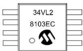
34V2 810 3EC8-Lead MSOP

text_image
XXXXXT YWWNNNExample:
text_image
34VL2 8103EC8-Lead 2x3 TDFN

Example:
| Part Number | 1st Line Marking Codes | |||
| TSSOP MSOP TDFN SOT-23 | ||||
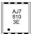
| 34VL02 34V | 2 34VL2T AJ7 SMNN | |||
6-Lead SOT-23

Example:
Legend: XX...X Part number or part number code
T Temperature (I, E)
Y Year code (last digit of calendar year)
YY Year code (last 2 digits of calendar year)
WW Week code (week of January 1 is week '01')
NNN Alphanumeric traceability code (2 characters for small packages)
Pb-free JEDEC designator for Matte Tin (Sn)
Note: For very small packages with no room for the Pb-free JEDEC designator
e3, the marking will only appear on the outer carton or reel label.
Note: In the event the full Microchip part number cannot be marked on one line, it will be carried over to the next line, thus limiting the number of available characters for customer-specific information.
Note: Please visit www.microchip.com/Pbfree for the latest information on Pb-free conversion.
*Standard OTP marking consists of Microchip part number, year code, week code, and traceability code.
8-Lead Plastic Dual In-Line (P) - 300 mil Body [PDIP]
Note: For the most current package drawings, please see the Microchip Packaging Specification located at http://www.microchip.com/packaging
![Microchip 34VL02 - 8-Lead Plastic Dual In-Line (P) - 300 mil Body [PDIP] - 1](/content/2026/06/1221732/images/67d4435801881d83dddc685fb39ce8e856ba763273dd68de9fc2d52fd511f877.jpg)
| UnitsVINCHES | ||||
| Dimension LimitsvMINvNOMvMAX | ||||
| Number of PinsvNv8 | ||||
| Pitchvev.100 BSC | ||||
| Top to Seating PlaneAv- - | .210 | |||
| Molded Package Thickness | A2 | .115 | .130 | .195 |
| Base to Seating Plane | A1 | .015 | - | - |
| Shoulder to Shoulder Width | E | .290 | .310 | .325 |
| Molded Package Width | E1 | .240 | .250 | .280 |
| Overall Length | D | .348 | .365 | .400 |
| Tip to Seating Plane | L | .115 | .130 | .150 |
| Lead Thicknessvc .008 .010 | .015 | |||
| Upper Lead Width | b1 | .040 | .060 | .070 |
| Lower Lead Width | b | .014 | .018 | .022 |
| Overall Row Spacing § | eB | - | - | .430 |
Notes:
- Pin 1 visual index feature may vary, but must be located with the hatched area.
2.v§ Significant Characteristic. - Dimensions D and E1 do not include mold flash or protrusions. Mold flash or protrusions shall not exceed .010" per side.
4.vDimensioning and tolerancing per ASME Y14.5M.
BSC: Basic Dimension. Theoretically exact value shown without tolerances.
Microchip Technology Drawing C04-018B
8-Lead Plastic Small Outline (SN) – Narrow, 3.90 mm Body [SOIC]
Note: For the most current package drawings, please see the Microchip Packaging Specification located at http://www.microchip.com/packaging
![Microchip 34VL02 - 8-Lead Plastic Small Outline (SN) – Narrow, 3.90 mm Body [SOIC] - 1](/content/2026/06/1221732/images/502a16eae97b08f0c3ced0288fff2a62129a87da5405320cf88e79d04abfff80.jpg)
| UnitsvMILLIMETERS | ||||
| Dimension LimitsvMINvNOMvMAX | ||||
| Number of PinsvNv8 | ||||
| Pitchvev1.27 BSC | ||||
| Overall Height | Av- | - | 1.75 | |
| Molded Package Thickness | A2 | 1.25 | - | - |
| Standoff § | A1 | 0.10 | - | 0.25 |
| Overall Width | E | 6.00 BSC | ||
| Molded Package Width | E1 | 3.90 BSC | ||
| Overall Length | D | 4.90 BSC | ||
| Chamfer (optional) | h | 0.25 | - | 0.50 |
| Foot Length | L | 0.40 | - | 1.27 |
| Footprint | L1 | 1.04 REF | ||
| Foot Angle | 0° | - | 8° | |
| Lead Thicknessvc 0.17 | - | 0.25 | ||
| Lead Width | b | 0.31 | - | 0.51 |
| Mold Draft Angle Top | 5° | - | 15° | |
| Mold Draft Angle Bottom | 5° | - | 15° | |
Notes:
- Pin 1 visual index feature may vary, but must be located within the hatched area.
2.v§ Significant Characteristic. - Dimensions D and E1 do not include mold flash or protrusions. Mold flash or protrusions shall not exceed 0.15 mm per side.
4.vDimensioning and tolerancing per ASME Y14.5M.
BSC:vBasic Dimension. Theoretically exact value shown without tolerances.
REF: Reference Dimension, usually without tolerance, for information purposes only.
Microchip Technology Drawing C04-057B
8-Lead Plastic Small Outline (SN) – Narrow, 3.90 mm Body [SOIC]
Note: For the most current package drawings, please see the Microchip Packaging Specification located at http://www.microchip.com/packaging
![Microchip 34VL02 - 8-Lead Plastic Small Outline (SN) – Narrow, 3.90 mm Body [SOIC] - 1](/content/2026/06/1221732/images/7fbb207f2455df2c6af2e070248cda407907becfddf32901946502b5ce8212b8.jpg)
text_image
E C SILK SCREEN Y1 X1RECOMMENDED LAND PATTERN
| Units | MILLIMETERS | |||
| Dimension Limits | MIN | NOM | MAX | |
| Contact Pitch | E | 1.27 BSC | ||
| Contact Pad Spacing | C | 5.40 | ||
| Contact Pad Width (X8) | X1 | 0.60 | ||
| Contact Pad Length (X8) | Y1 | 1.55 | ||
Notes:
1. Dimensioning and tolerancing per ASME Y14.5M
BSC: Basic Dimension. Theoretically exact value shown without tolerances.
Microchip Technology Drawing No. C04-2057A
8-Lead Plastic Thin Shrink Small Outline (ST) - 4.4 mm Body [TSSOP]
Note: For the most current package drawings, please see the Microchip Packaging Specification located at http://www.microchip.com/packaging
![Microchip 34VL02 - 8-Lead Plastic Thin Shrink Small Outline (ST) - 4.4 mm Body [TSSOP] - 1](/content/2026/06/1221732/images/e8c2b2f96c02511e79fd9f05cdab0ef71fad9b854fbcf206cbeb59c69860a19f.jpg)
| UnitsvMILLIMETERS | ||||
| Dimension Limitsv MINvNOMvMAX | ||||
| Number of PinsvNv8 | ||||
| Pitchvev0.65 BSC | ||||
| Overall Height | Av- | - | 1.20 | |
| Molded Package Thickness | A2 | 0.80 | 1.00 | 1.05 |
| Standoff | A1 | 0.05 | - | 0.15 |
| Overall Width | E | 6.40 BSC | ||
| Molded Package Width | E1 | 4.30 | 4.40 | 4.50 |
| Molded Package Length | D | 2.90 | 3.00 | 3.10 |
| Foot Length | L | 0.45 | 0.60 | 0.75 |
| Footprint | L1 | 1.00 REF | ||
| Foot Angle | 0° | - | 8° | |
| Lead Thicknessvc 0.09 | - | 0.20 | ||
| Lead Width | b | 0.19 | - | 0.30 |
Notes:
- Pin 1 visual index feature may vary, but must be located within the hatched area.
- Dimensions D and E1 do not include mold flash or protrusions. Mold flash or protrusions shall not exceed 0.15 mm per side.
3.vDimensioning and tolerancing per ASME Y14.5M.
BSC:vBasic Dimension. Theoretically exact value shown without tolerances.
REF: Reference Dimension, usually without tolerance, for information purposes only.
Microchip Technology Drawing C04-086B
8-Lead Plastic Micro Small Outline Package (MS) [MSOP]
Note: For the most current package drawings, please see the Microchip Packaging Specification located at http://www.microchip.com/packaging
![Microchip 34VL02 - 8-Lead Plastic Micro Small Outline Package (MS) [MSOP] - 1](/content/2026/06/1221732/images/136d1083c1d85dcf7e7d42033f758af74655d5c4f57c1b3e561886b440c32e14.jpg)
| UnitsVMILLIMETERS | ||||
| Dimension LimitsVMINvNOMvMAX | ||||
| Number of PinsvNv8 | ||||
| Pitchvev0.65 BSC | ||||
| Overall Height | Av- | - | 1.10 | |
| Molded Package Thickness | A2 | 0.75 | 0.85 | 0.95 |
| Standoff | A1 | 0.00 | - | 0.15 |
| Overall Width | E | 4.90 BSC | ||
| Molded Package Width | E1 | 3.00 BSC | ||
| Overall Length | D | 3.00 BSC | ||
| Foot Length | L | 0.40 | 0.60 | 0.80 |
| Footprint | L1 | 0.95 REF | ||
| Foot Angle | 0° | - | 8° | |
| Lead Thicknessvc 0.08 | - | 0.23 | ||
| Lead Width | b | 0.22 | - | 0.40 |
Notes:
- Pin 1 visual index feature may vary, but must be located within the hatched area.
- Dimensions D and E1 do not include mold flash or protrusions. Mold flash or protrusions shall not exceed 0.15 mm per side.
3.vDimensioning and tolerancing per ASME Y14.5M.
BSC:vBasic Dimension. Theoretically exact value shown without tolerances.
REF: Reference Dimension, usually without tolerance, for information purposes only.
Microchip Technology Drawing C04-111B
8-Lead Plastic Dual Flat, No Lead Package (MN) - 2x3x0.75 mm Body [TDFN]
Note: For the most current package drawings, please see the Microchip Packaging Specification located at http://www.microchip.com/packaging
![Microchip 34VL02 - 8-Lead Plastic Dual Flat, No Lead Package (MN) - 2x3x0.75 mm Body [TDFN] - 1](/content/2026/06/1221732/images/041a52357814f6d45458341d6bc439c0741bdcf649251d872f559b2c7557569e.jpg)
| Units | MILLIMETERS | |||
| Dimension Limits | MIN | NOM | MAX | |
| Number of Pins | N | 8 | ||
| Pitch | e | 0.50 BSC | ||
| Overall Height | A | 0.70 | 0.75 | 0.80 |
| Standoff | A1 | 0.00 | 0.02 | 0.05 |
| Contact Thickness | A3 | 0.20 REF | ||
| Overall Length | D | 2.00 BSC | ||
| Overall Width | E | 3.00 BSC | ||
| Exposed Pad Length | D2 | 1.20 | - | 1.60 |
| Exposed Pad Width | E2 | 1.20 | - | 1.60 |
| Contact Width | b | 0.20 | 0.25 | 0.30 |
| Contact Length | L | 0.25 | 0.30 | 0.45 |
| Contact-to-Exposed Pad | K | 0.20 | - | - |
Notes:
- Pin 1 visual index feature may vary, but must be located within the hatched area.
- Package may have one or more exposed tie bars at ends.
- Package is saw singulated
- Dimensioning and tolerancing per ASME Y14.5M
BSC: Basic Dimension. Theoretically exact value shown without tolerances.
REF: Reference Dimension, usually without tolerance, for information purposes only.
Microchip Technology Drawing No. C04-129B
8-Lead Plastic Dual Flat, No Lead Package (MN) - 2x3x0.75 mm Body [TDFN]
Note: For the most current package drawings, please see the Microchip Packaging Specification located at http://www.microchip.com/packaging
![Microchip 34VL02 - 8-Lead Plastic Dual Flat, No Lead Package (MN) - 2x3x0.75 mm Body [TDFN] - 1](/content/2026/06/1221732/images/ccec2b8cd133a386a71f46506af3b710c9654f3dbdaeb3d165bf81dcd7920968.jpg)
text_image
W2 G SILK SCREEN C1 T2 Y1 E X1RECOMMENDED LAND PATTERN
| Units | MILLIMETERS | |||
| Dimension Limits | MIN | NOM | MAX | |
| Contact Pitch | E | 0.50 BSC | ||
| Optional Center Pad Width | W2 | 1.46 | ||
| Optional Center Pad Length | T2 | 1.36 | ||
| Contact Pad Spacing | C1 | 3.00 | ||
| Contact Pad Width (X8) | X1 | 0.30 | ||
| Contact Pad Length (X8) | Y1 | 0.75 | ||
| Distance Between Pads | G | 0.20 | ||
Notes:
1. Dimensioning and tolerancing per ASME Y14.5M
BSC: Basic Dimension. Theoretically exact value shown without tolerances.
Microchip Technology Drawing No. C04-2129A
6-Lead Plastic Small Outline Transistor (OT) [SOT-23]
Note: For the most current package drawings, please see the Microchip Packaging Specification located at http://www.microchip.com/packaging
![Microchip 34VL02 - 6-Lead Plastic Small Outline Transistor (OT) [SOT-23] - 1](/content/2026/06/1221732/images/76471d4a6c0e2a7f10d4d872290bd2395bba56bcb049f8d3680dd8bbcdd9bead.jpg)
| UnitsvMILLIMETERS | ||||
| Dimension LimitsvMINvNOMvMAX | ||||
| Number of PinsvNv6 | ||||
| Pitchvev0.95 BSC | ||||
| Outside Lead Pitchve1 | 1.90 BSC | |||
| Overall Height | A | 0.90 | - | 1.45 |
| Molded Package Thickness | A2 | 0.89 | - | 1.30 |
| Standoff | A1 | 0.00 | - | 0.15 |
| Overall Width | E | 2.20 | - | 3.20 |
| Molded Package Width | E1 | 1.30 | - | 1.80 |
| Overall Length | D | 2.70 | - | 3.10 |
| Foot Length | L | 0.10 | - | 0.60 |
| Footprint | L1 | 0.35 | - | 0.80 |
| Foot Angle | 0^ | - | 30^ | |
| Lead Thicknessvc 0.08 | - | 0.26 | ||
| Lead Width | b | 0.20 | - | 0.51 |
Notes:
- Dimensions D and E1 do not include mold flash or protrusions. Mold flash or protrusions shall not exceed 0.127 mm per side.
2.vDimensioning and tolerancing per ASME Y14.5M.
BSC:vBasic Dimension. Theoretically exact value shown without tolerances.
Microchip Technology Drawing C04-028B
APPENDIX A: REVISION HISTORY
Revision A (3/2008)
Original release of this document.
NOTES:
Microchip provides online support via our WWW site at www.microchip.com. This web site is used as a means to make files and information easily available to customers. Accessible by using your favorite Internet browser, the web site contains the following information:
- Product Support – Data sheets and errata, application notes and sample programs, design resources, user's guides and hardware support documents, latest software releases and archived software
- General Technical Support – Frequently Asked Questions (FAQ), technical support requests, online discussion groups, Microchip consultant program member listing
- Business of Microchip – Product selector and ordering guides, latest Microchip press releases, listing of seminars and events, listings of Microchip sales offices, distributors and factory representatives
CUSTOMER CHANGE NOTIFICATION SERVICE
Microchip's customer notification service helps keep customers current on Microchip products. Subscribers will receive e-mail notification whenever there are changes, updates, revisions or errata related to a specified product family or development tool of interest.
To register, access the Microchip web site at www.microchip.com, click on Customer Change Notification and follow the registration instructions.
CUSTOMER SUPPORT
Users of Microchip products can receive assistance through several channels:
• Distributor or Representative
- Local Sales Office
• Field Application Engineer (FAE)
- Technical Support
• Development Systems Information Line
Customers should contact their distributor, representative or field application engineer (FAE) for support. Local sales offices are also available to help customers. A listing of sales offices and locations is included in the back of this document.
Technical support is available through the web site at: http://support.microchip.com
READER RESPONSE
It is our intention to provide you with the best documentation possible to ensure successful use of your Microchip product. If you wish to provide your comments on organization, clarity, subject matter, and ways in which our documentation can better serve you, please FAX your comments to the Technical Publications Manager at (480) 792-4150.
Please list the following information, and use this outline to provide us with your comments about this document.
To: Technical Publications Manager
Total Pages Sent ____
RE: Reader Response
From: Name
Company
Address
City / State / ZIP / Country
Telephone: (____) ____ - ____
FAX: (____) ____ - ____
Application (optional):
Would you like a reply? Y N
Device:
Literature
DS22079A34VL02
Number:
Questions:
-
What are the best features of this document?
-
How does this document meet your hardware and software development needs?
-
Do you find the organization of this document easy to follow? If not, why?
-
What additions to the document do you think would enhance the structure and subject?
-
What deletions from the document could be made without affecting the overall usefulness?
-
Is there any incorrect or misleading information (what and where)?
-
How would you improve this document?
PRODUCT IDENTIFICATION SYSTEM
To order or obtain information, e.g., on pricing or delivery, refer to the factory or the listed sales office.

text_image
PART NO. X /XX Device Range PackageTemperatureDevice: 34VL02: = 1.5V, 2 Kbit I ^2 C Serial EEPROM 34VL02T: = 1.5V, 2 Kbit I ^2 C Serial EEPROM (Tape and Reel)
Temperature Blank = -20°C to +85°C
Range:
Package: OT = Plastic Small Outline (SOT-23), 6-lead P = Plastic DIP (300 mil body), 8-lead SN = Plastic SOIC (3.90 mm body), 8-lead ST = Plastic TSSOP (4.4 mm), 8-lead MS = Plastic Micro Small Outline (MSOP), 8-lead MNY* = Plastic Dual Flat (TDFN), no lead package, 2x3 mm body, 8-lead
Note 1: "Y" indicates a Nickel Palladium Gold (NiPdAu) finish.
Examples:
a) 34VL02T/OT: Tape and Reel, 1.5V, SOT-23 package
b) 34VL02T/ST: Tape and Reel, 1.5V, TSSOP package
c) 34VL02T/MNY: Tape and Reel, 1.5V, TDFN package
NOTES:
Note the following details of the code protection feature on Microchip devices:
• Microchip products meet the specification contained in their particular Microchip Data Sheet.
- Microchip believes that its family of products is one of the most secure families of its kind on the market today, when used in the intended manner and under normal conditions.
- There are dishonest and possibly illegal methods used to breach the code protection feature. All of these methods, to our knowledge, require using the Microchip products in a manner outside the operating specifications contained in Microchip's Data Sheets. Most likely, the person doing so is engaged in theft of intellectual property.
- Microchip is willing to work with the customer who is concerned about the integrity of their code.
- Neither Microchip nor any other semiconductor manufacturer can guarantee the security of their code. Code protection does not mean that we are guaranteeing the product as "unbreakable."
Code protection is constantly evolving. We at Microchip are committed to continuously improving the code protection features of our products. Attempts to break Microchip's code protection feature may be a violation of the Digital Millennium Copyright Act. If such acts allow unauthorized access to your software or other copyrighted work, you may have a right to sue for relief under that Act.
Information contained in this publication regarding device applications and the like is provided only for your convenience and may be superseded by updates. It is your responsibility to ensure that your application meets with your specifications. MICROCHIP MAKES NO REPRESENTATIONS OR WARRANTIES OF ANY KIND WHETHER EXPRESS OR IMPLIED, WRITTEN OR ORAL, STATUTORY OR OTHERWISE, RELATED TO THE INFORMATION, INCLUDING BUT NOT LIMITED TO ITS CONDITION, QUALITY, PERFORMANCE, MERCHANTABILITY OR FITNESS FOR PURPOSE. Microchip disclaims all liability arising from this information and its use. Use of Microchip devices in life support and/or safety applications is entirely at the buyer's risk, and the buyer agrees to defend, indemnify and hold harmless Microchip from any and all damages, claims, suits, or expenses resulting from such use. No licenses are conveyed, implicitly or otherwise, under any Microchip intellectual property rights.
Trademarks
The Microchip name and logo, the Microchip logo, Accuron, dsPIC, KEELOQ, KEELOQ logo, MPLAB, PIC, PICmicro, PICSTART, PRO MATE, rfPIC and SmartShunt are registered trademarks of Microchip Technology Incorporated in the U.S.A. and other countries.
FilterLab, Linear Active Thermistor, MXDEV, MXLAB, SEEVAL, SmartSensor and The Embedded Control Solutions Company are registered trademarks of Microchip Technology Incorporated in the U.S.A.
Analog-for-the-Digital Age, Application Maestro, CodeGuard, dsPICDEM, dsPICDEM.net, dsPICworks, dsSPEAK, ECAN, ECONOMONITOR, FanSense, In-Circuit Serial Programming, ICSP, ICEPIC, Mindi, MiWi, MPASM, MPLAB Certified logo, MPLIB, MPLINK, mTouch, PICkit, PICDEM, PICDEM.net, PICtail, PIC ^32 logo, PowerCal, PowerInfo, PowerMate, PowerTool, REAL ICE, rfLAB, Select Mode, Total Endurance, UNI/O, WiperLock and ZENA are trademarks of Microchip Technology Incorporated in the U.S.A. and other countries.
SQTP is a service mark of Microchip Technology Incorporated in the U.S.A.
All other trademarks mentioned herein are property of their respective companies.
© 2008, Microchip Technology Incorporated, Printed in the U.S.A., All Rights Reserved.

Printed on recycled paper.
QUALITY MANAGEMENT SYSTEM CERTIFIED BY DNV
=ISO/TS 16949:2002=
Microchip received ISO/TS-16949:2002 certification for its worldwide headquarters, design and wafer fabrication facilities in Chandler and Tempe, Arizona; Gresham, Oregon and design centers in California and India. The Company's quality system processes and procedures are for its PIC® MCUs and dsPIC® DSCs, KEELOQ® code hopping devices, Serial EEPROMs, microperipherals, nonvolatile memory and analog products. In addition, Microchip's quality system for the design and manufacture of development systems is ISO 9001:2000 certified.
WORLDWIDE SALES AND SERVICE
AMERICAS
Corporate Office
2355 West Chandler Blvd.
Chandler, AZ 85224-6199
Tel: 480-792-7200
Fax: 480-792-7277
Technical Support:
http://support.microchip.com
Web Address:
www.microchip.com
Atlanta
Duluth. GA
Tel: 678-957-9614
Fax: 678-957-1455
Boston
Westborough, MA
Tel: 774-760-0087
Fax: 774-760-0088
Chicago
Itasca, IL
Tel: 630-285-0071
Fax: 630-285-0075
Dallas
Addison, TX
Tel: 972-818-7423
Fax: 972-818-2924
Detroit
Farmington Hills, MI
Tel: 248-538-2250
Fax: 248-538-2260
Kokomo
Kokomo, IN
Tel: 765-864-8360
Fax: 765-864-8387
Los Angeles
Mission Viejo, CA
Tel: 949-462-9523
Fax: 949-462-9608
Santa Clara
Santa Clara, CA
Tel: 408-961-6444
Fax: 408-961-6445
Toronto
Mississauga, Ontario,
Canada
Tel: 905-673-0699
Fax: 905-673-6509
ASIA/PACIFIC
Asia Pacific Office
Suites 3707-14, 37th Floor
Tower 6, The Gateway
Harbour City, Kowloon
Hong Kong
Tel: 852-2401-1200
Fax: 852-2401-3431
Australia - Sydney
Tel: 61-2-9868-6733
Fax: 61-2-9868-6755
China - Beijing
Tel: 86-10-8528-2100
Fax: 86-10-8528-2104
China - Chengdu
Tel: 86-28-8665-5511
Fax: 86-28-8665-7889
China - Hong Kong SAR
Tel: 852-2401-1200
Fax: 852-2401-3431
China - Nanjing
Tel: 86-25-8473-2460
Fax: 86-25-8473-2470
China - Qingdao
Tel: 86-532-8502-7355
Fax: 86-532-8502-7205
China - Shanghai
Tel: 86-21-5407-5533
Fax: 86-21-5407-5066
China - Shenyang
Tel: 86-24-2334-2829
Fax: 86-24-2334-2393
China - Shenzhen
Tel: 86-755-8203-2660
Fax: 86-755-8203-1760
China - Wuhan
Tel: 86-27-5980-5300
Fax: 86-27-5980-5118
China - Xiamen
Tel: 86-592-2388138
Fax: 86-592-2388130
China - Xian
Tel: 86-29-8833-7252
Fax: 86-29-8833-7256
China - Zhuhai
Tel: 86-756-3210040
Fax: 86-756-3210049
ASIA/PACIFIC
India - Bangalore
Tel: 91-80-4182-8400
Fax: 91-80-4182-8422
India - New Delhi
Tel: 91-11-4160-8631
Fax: 91-11-4160-8632
India - Pune
Tel: 91-20-2566-1512
Fax: 91-20-2566-1513
Japan - Yokohama
Tel: 81-45-471-6166
Fax: 81-45-471-6122
Korea - Daegu
Tel: 82-53-744-4301
Fax: 82-53-744-4302
Korea - Seoul
Tel: 82-2-554-7200
Fax: 82-2-558-5932 or
82-2-558-5934
Malaysia - Kuala Lumpur
Tel: 60-3-6201-9857
Fax: 60-3-6201-9859
Malaysia - Penang
Tel: 60-4-227-8870
Fax: 60-4-227-4068
Philippines - Manila
Tel: 63-2-634-9065
Fax: 63-2-634-9069
Singapore
Tel: 65-6334-8870
Fax: 65-6334-8850
Taiwan - Hsin Chu
Tel: 886-3-572-9526
Fax: 886-3-572-6459
Taiwan - Kaohsiung
Tel: 886-7-536-4818
Fax: 886-7-536-4803
Taiwan - Taipei
Tel: 886-2-2500-6610
Fax: 886-2-2508-0102
Thailand - Bangkok
Tel: 66-2-694-1351
Fax: 66-2-694-1350
EUROPE
Austria - Wels
Tel: 43-7242-2244-39
Fax: 43-7242-2244-393
Denmark - Copenhagen
Tel: 45-4450-2828
Fax: 45-4485-2829
France - Paris
Tel: 33-1-69-53-63-20
Fax: 33-1-69-30-90-79
Germany - Munich
Tel: 49-89-627-144-0
Fax: 49-89-627-144-44
Italy - Milan
Tel: 39-0331-742611
Fax: 39-0331-466781
Netherlands - Drunen
Tel: 31-416-690399
Fax: 31-416-690340
Spain - Madrid
Tel: 34-91-708-08-90
Fax: 34-91-708-08-91
UK - Wokingham
Tel: 44-118-921-5869
Fax: 44-118-921-5820