11AA020 - EEPROM Memory Microchip - Free user manual and instructions
Find the device manual for free 11AA020 Microchip in PDF.

User questions about 11AA020 Microchip
0 question about this device. Answer the ones you know or ask your own.
Ask a new question about this device
Download the instructions for your EEPROM Memory in PDF format for free! Find your manual 11AA020 - Microchip and take your electronic device back in hand. On this page are published all the documents necessary for the use of your device. 11AA020 by Microchip.
USER MANUAL 11AA020 Microchip
1-Kbit to 16-Kbit UNI/O ^® Serial EEPROM Family Data Sheet
Features
- Single I/O, UNI/O ^ Serial Interface Bus
• Low-Power CMOS Technology:
- 1 mA active current, typical
- 1 μA standby current (max.) (I-temp)
- 128 x 8 through 2,048 x 8 Bit Organizations
• Schmitt Trigger Inputs for Noise Suppression - Output Slope Control to Eliminate Ground Bounce
- 100 kbps Max. Bit Rate – Equivalent to 100 kHz Clock Frequency
- Self-Timed Write Cycle (including Auto-Erase)
• Page-Write Buffer for up to 16 Bytes
• STATUS Register for Added Control:
- Write enable latch bit
- Write-In-Progress bit
- Block Write Protection:
- Protect none, 1/4, 1/2 or all of array
• Built-in Write Protection:
- Power-on/off data protection circuitry
- Write enable latch
• High Reliability:
- Endurance: 1,000,000 erase/write cycles
- Data retention: > 200 years
- ESD protection: > 4,000V
- RoHS Compliant
• Available Temperature Ranges:
- Industrial (I): -40°C to +85°C
- Extended (E): -40°C to +125°C
• Automotive AEC-Q100 Qualified
Packages
• 3-lead SOT-23 and TO-92 Packages
• 4-lead Chip Scale Package
• 8-lead PDIP, SOIC, MSOP and TDFN Packages
Pin Function Table
| Name Function | |
| SCIO | Serial Clock, Data Input/Output |
| Vss | Ground |
| Vcc | Supply Voltage |
Description
The Microchip Technology Inc. 11AAXXX/11LCXXX (11XX ^(1) ) devices are a family of 1-Kbit through 16-Kbit Serial Electrically Erasable PROMs. The devices are organized in blocks of x8-bit memory and support the patented ^(2) single I/O UNI/O ^ serial bus. By Manchester encoding techniques, the clock and data are combined into a single, serial bit stream (SCIO), where the clock signal is extracted by the receiver to correctly decode the timing and value of each bit.
Low-voltage design permits operation down to 1.8V (for 11AAXX devices), with standby and active currents of only 1 A and 1 mA, respectively.
using
Note 1: 11XX is used in this document as a generic part number for the 11 series devices.
2: Microchip's UNI/O® Bus products are covered by some or all of the following patents issued in the U.S.A.: 7.376,020 & 7,788,430.
Package Types (not to scale)
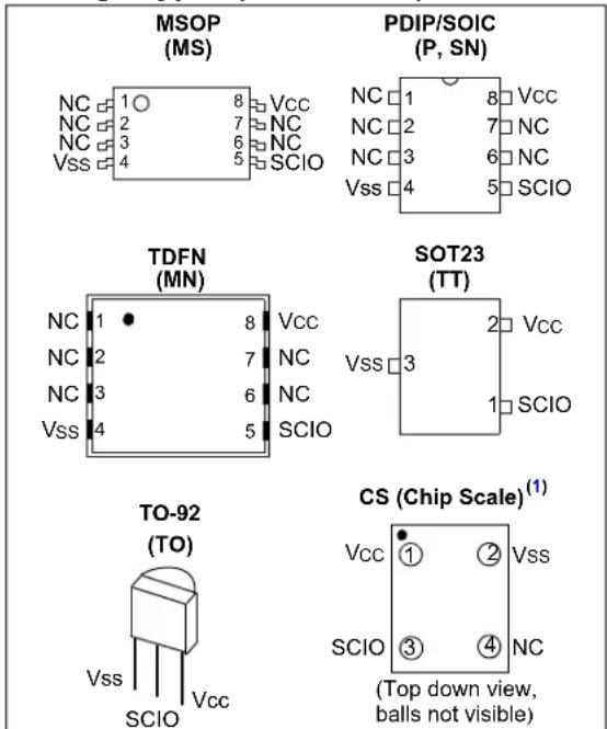
Note 1: Available in I-temp, "AA" only.
DEVICE SELECTION TABLE
| Part Number | Density (bits) | Organization | V cc Range | Page Size (Bytes) | Temp. Ranges | Device Address | Packages |
| 11LC010 1 | Kbit 128 x | 8 2.5V-5.5V 16 | I,E 0xA0 | P, SN, MS, MN, TO, TT | |||
| 11AA010 1 | Kbit 128 x | 8 1.8V-5.5V 16 | I 0xA0 | P, SN, MS, MN, TO, TT, CS | |||
| 11LC020 2 | Kbit 256 x | 8 2.5V-5.5V 16 | I,E 0xA0 | P, SN, MS, MN, TO, TT | |||
| 11AA020 2 | Kbit 256 x | 8 1.8V-5.5V 16 | I 0xA0 | P, SN, MS, MN, TO, TT, CS | |||
| 11LC040 4 | Kbit 512 x | 8 2.5V-5.5V 16 | I,E 0xA0 | P, SN, MS, MN, TO, TT | |||
| 11AA040 4 | Kbit 512 x | 8 1.8V-5.5V 16 | I 0xA0 | P, SN, MS, MN, TO, TT, CS | |||
| 11LC080 8 | Kbit 1,024 | x 8 2.5V-5.5V | 16 I,E 0xA0 | P, SN, MS, MN, TO, TT | |||
| 11AA080 8 | Kbit 1,024 | x 8 1.8V-5.5V | 16 I 0xA0 | P, SN, MS, MN, TO, TT, CS | |||
| 11LC160 | 16 Kbit | 2,048 x 8 | 2.5V-5.5V | 16 | I,E | 0xA0 | P, SN, MS, MN, TO, TT |
| 11AA160 | 16 Kbit | 2,048 x 8 | 1.8V-5.5V | 16 | I | 0xA0 | P, SN, MS, MN, TO, TT,CS |
| 11LC161 | 16 Kbit | 2,048 x 8 | 2.5V-5.5V | 16 | I, E | 0xA1 | P, SN, MS, MN, TO, TT |
| 11AA161 | 16 Kbit | 2,048 x 8 | 1.8V-5.5V | 16 | I | 0xA1 | P, SN, MS, MN, TO, TT, CS |
1.0 ELECTRICAL CHARACTERISTICS
Absolute Maximum Ratings (†)
Vcc....6.5V
SCIO w.r.t. Vss....-0.6V to Vcc+1.0V
Storage temperature....-65°C to 150°C
Ambient temperature under bias....-40°C to 125°C
ESD protection on all pins....4 kV
† NOTICE: Stresses above those listed under 'Absolute Maximum Ratings' may cause permanent damage to the device. This is a stress rating only and functional operation of the device at those or any other conditions above those indicated in the operational listings of this specification is not implied. Exposure to maximum rating conditions for an extended period of time may affect device reliability.
TABLE 1-1: DC CHARACTERISTICS
| DC CHARACTERISTICS | Electrical Characteristics:Industrial (I): V cc = 2.5V to 5.5V TA = -40°C to +85°CVcc = 1.8V to 2.5V TA = -20°C to +85°CExtended (E): Vcc = 2.5V to 5.5V TA = -40°C to +125°C | |||||
| Param.No. | Sym. C | Characteristic Min. Max. | Units Test | Conditions | ||
| D1 | VIH | High-level input voltage | 0.7*Vcc | Vcc+1 | V | — |
| D2 | VIL | Low-level input voltage | -0.3 0.3*V cc | V | Vcc ≥ 2.5V | |
| -0.3 0.2*V cc | V | Vcc < 2.5V | ||||
| D3 | VHYS | Hysteresis of Schmitt Trigger inputs (SCIO) | 0.05*Vcc | — | V | Vcc ≥ 2.5V (Note 1) |
| D4 | VOH | High-level output voltage | Vcc -0.5 | — | V | IoH = -300 μA, Vcc = 5.5V |
| Vcc -0.5 | — | V | IoH = -200 μA, Vcc = 2.5V | |||
| D5 | VOL | Low-level output voltage | — | 0.4 | V | Iol = 300 μA, Vcc = 5.5V |
| — | 0.4 | V | Iol = 200 μA, Vcc = 2.5V | |||
| D6 | Io | Output current limit (Note 2) | — | ±4 | mA | Vcc = 5.5V (Note 1) |
| — | ±3 | mA | Vcc = 2.5V (Note 1) | |||
| D7 | ILI | Input leakage current (SCIO) | — | ±1 | μA | VIN = Vss or Vcc |
| D8 | CINT | Internal Capacitance (all inputs and outputs) | — | 7 | pF | TA = 25°C, FCLK = 1 MHz,Vcc = 5.0V (Note 1) |
| D9 | Icc Read | Read Operating Current | — | 3 | mA | Vcc=5.5V; FBUS=100 kHz, CB=100 pF |
| — | 1 | mA | Vcc=2.5V; FBUS=100 kHz, CB=100 pF | |||
| D10 | Icc Write | Write Operating Current | — | 5 | mA | Vcc = 5.5V |
| — | 3 | mA | Vcc = 2.5V | |||
| D11 | Iccs | Standby Current | — | 5 | μA | Vcc = 5.5VTA = 125°C |
| — | 1 | μA | Vcc = 5.5VTA = 85°C | |||
| D12 | ICCI | Idle Mode Current | — | 50 | μA | Vcc = 5.5V |
Note 1: This parameter is periodically sampled and is not 100% tested.
2: The SCIO output driver impedance will vary to ensure lo is not exceeded.
TABLE 1-2: AC CHARACTERISTICS
| AC CHARACTERISTICS | Electrical Characteristics:Industrial (I): V cc = 2.5V to 5.5VVcc = 1.8V to 2.5VExtended (E): Vcc = 2.5V to 5.5V | |||||
| Param.No. | Sym. | Characteristic Min. Max. Units Test Conditions | ||||
| 1 | FBUS | Serial bus frequency | 10 | 100 | kHz | — |
| 2 | TE | Bit period | 10 | 100 | μs | — |
| 3 | TJIT | Input edge jitter tolerance | — | ±0.06 | UI | (Note 2) |
| 4 | FDRIFT | Serial bus frequency drift rate tolerance | — | ±0.50 | % per byte | — |
| 5 | FDEV | Serial bus frequency drift limit | — | ±5 | % per command | — |
| 6 | TOJIT | Output edge jitter | — | ±0.25 | UI | (Note 2) |
| 7 | TR | SCIO input rise time (Note 1) | — | 100 | ns | — |
| 8 | TF | SCIO input fall time (Note 1) | — | 100 | ns | — |
| 9 | TSTBY | Standby pulse time | 600 | — | μs | — |
| 10 | TSS | Start header setup time | 10 | — | μs | — |
| 11 | THDR | Start header low pulse time | 5 | — | μs | — |
| 12 | TSP | Input filter spike suppression (SCIO) | — | 50 | ns | (Note 1) |
| 13 | TWC | Write cycle time (byte or page) | — | 5 | m | Write, WRSR commands |
| — | 10 | ms | ERAL, SETAL commands | |||
| 14 | — | Endurance (per page) | 1M | — | cycles | 25°C, Vcc = 5.5V |
Note 1: This parameter is periodically sampled and is not 100% tested.
2: A Unit Interval (UI) is equal to 1-bit period (TE) at the current bus frequency.
3: This parameter is not tested but ensured by characterization.
TABLE 1-3: AC TEST CONDITIONS
| AC Waveform: | |
| VLO = 0.2V | |
| VHI = VCC - 0.2V | |
| CL = 100 pF | |
| Timing Measurement Reference Level | |
| Input | 0.5 Vcc |
| Output | 0.5 Vcc |
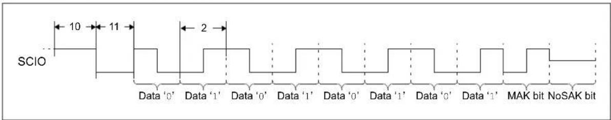
FIGURE 1-1: BUS TIMING - START HEADER
other
| Data Type | Value | |-----------|-------| | SCIO | 10 | | Data '0' | 11 | | Data '1' | 2 | | Data '0' | | | Data '1' | | | Data '0' | | | Data '1' | | | Data '0' | | | Data '1' | | | Data '0' | | | Data '1' | | | MAK bit | NoSAK bit | The diagram shows a repeating pattern of rectangular pulses between 10 and 2 units along the x-axis. There are no labels for the data series.FIGURE 1-2: BUS TIMING – DATA

text_image
SCIO 2 12 7 8 Data '0' Data '1' Data '1' Data '0'FIGURE 1-3: BUS TIMING - STANDBY PULSE

text_image
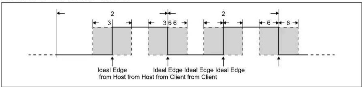
SCIO 9 Standby ModeFIGURE 1-4: BUS TIMING - JITTER
text_image
2 3 3 6 6 2 6 6 Ideal Edge Ideal Edge Ideal Edge from Host from Host from Client from Client2.0 PIN DESCRIPTIONS
The descriptions of the pins are listed in Table 2-1.
TABLE 2-1: PIN FUNCTION TABLE
| Name 3-pin SOT-23 3-pin | TO-92 4-pin CS | 8-pin PDIP/SOIC/MSOP/TDFN | Description | |
| SCIO 1 2 3 5 Serial Clock, Data Input/Output | ||||
| Vcc 2 3 1 8 Supply Voltage | ||||
| Vss 3 1 2 4 Ground | ||||
| NC | — | — | 4 | 1,2,3,6,7 No Internal Connection |
2.1 Serial Clock, Data Input/Output (SCIO)
SCIO is a bidirectional pin used to transfer commands and addresses into, as well as data into and out of, the device. The serial clock is embedded into the data stream through Manchester encoding. Each bit is represented by a signal transition at the middle of the bit period.
3.0 FUNCTIONAL DESCRIPTION
3.1 Principles of Operation
The 11AAXXX/11LCXXX family of serial EEPROMs support the UNI/O ^® protocol. They can be interfaced with microcontrollers, including Microchip's PIC ^® microcontrollers, ASICs, or any other device with an available discrete I/O line that can be configured properly to match the UNI/O protocol.
The 11AAXXX/11LCXXX devices contain an 8-bit instruction register. The devices are accessed via the SCIO pin.
Table 5-1 contains a list of the possible instruction bytes and format for device operation. All instructions, addresses, and data are transferred MSb first, LSb last.
Data is embedded into the I/O stream through Manchester encoding. The bus is controlled by a host device which determines the clock period, controls the bus access and initiates all operations, while the 11AAXXX/11LCXXX works as client. Both host and client can operate as transmitter or receiver, but the host device determines which mode is active.
FIGURE 3-1: BLOCK DIAGRAM

flowchart
graph TD
    A["STATUS Register"] --> B["I/O Control Logic"]
    B --> C["Current-Limited Slope Control"]
    C --> D["SCIO"]
    D --> E["Memory Control Logic"]
    E --> F["X Dec"]
    F --> G["EEPROM Array"]
    G --> H["Page Latches"]
    H --> I["Y Decoder"]
    I --> J["Sense Amp. R/W Control"]
    J --> K["Vcc"]
    J --> L["Vss"]
    K --> E
    L --> E
    M["HV Generator"] --> G
4.0 BUS CHARACTERISTICS
4.1 Standby Pulse
When the host has control of SCIO, a standby pulse can be generated by holding SCIO high for TSTBY. At this time, the 11AAXXX/11LCXXX will reset and return to Standby mode. Subsequently, a high-to-low transition on SCIO (the first low pulse of the header) will return the device to the active state.
Once a command is terminated satisfactorily (i.e., via a NoMAK/SAK combination during the Acknowledge sequence), performing a standby pulse is not required to begin a new command as long as the device to be selected is the same device selected during the previous command. However, a period of Tss must be observed after the end of the command and before the beginning of the start header. After Tss, the start header (including THDR low pulse) can be transmitted in order to begin the new command.
If a command is terminated in any manner other than a NoMAK/SAK combination, then the host must perform a standby pulse before beginning a new command, regardless of which device is to be selected.
Note: After a POR/BOR event occurs, a low-to-high transition on SCIO must be generated before proceeding with communication, including a standby pulse.
An example of two consecutive commands is shown in Figure 4-1. Note that the device address is the same for both commands, indicating that the same device is being selected both times.
A standby pulse cannot be generated while the client has control of SCIO. In this situation, the host must wait for the client to finish transmitting and to release SCIO before the pulse can be generated.
If, at any point during a command, an error is detected by the host, a standby pulse should be generated and the command should be performed again.
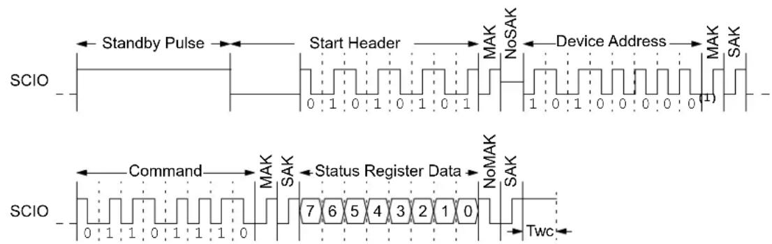
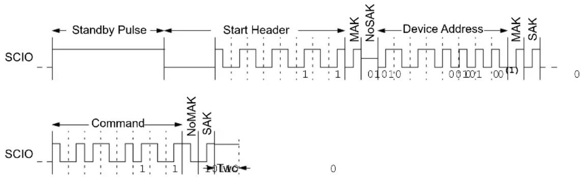
FIGURE 4-1: CONSECUTIVE COMMANDS EXAMPLE

text_image
Standby Pulse(1) Start Header MAK NoSAK Device Address MAK SAK SCIO 01010 00 00101 Start Header MAK NoSAK Device Address MAK SAK SCIO NoMAK SAK TSS 1 1 01010 0 00 00101Note 1: After a POR/BOR event, a low-to-high transition on SCIO must occur before the first standby pulse.
4.2 Start Data Transfer
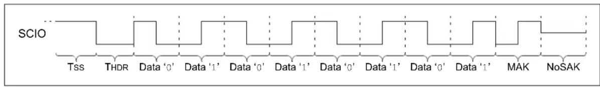
All operations must be preceded by a start header. The start header consists of holding SCIO low for a period of THDR, followed by transmitting an 8-bit '01010101' code. This code is used to synchronize the client's internal clock period with the host's clock period, so accurate timing is very important.
When a standby pulse is not required (i.e., between successive commands to the same device), a period of Tss must be observed at the end of the command and before the beginning of the start header.
Figure 4-2 shows the waveform for the start header, including the required Acknowledge sequence at the end of the byte.
FIGURE 4-2: START HEADER
text_image
SCIO Tss THDR Data '0' Data '1' Data '0' Data '1' Data '0' Data '1' Data '0' Data '1' MAK NoSAK4.3 Acknowledge
An Acknowledge routine occurs after each byte is transmitted, including the start header. This routine consists of two bits. The first bit is transmitted by the host, and the second bit is transmitted by the client.
Note: A MAK must always be transmitted following the start header.
The Host Acknowledge, or MAK, is signified by transmitting a '1', and informs the client that the current operation is to be continued. Conversely, a Not Acknowledge, or NoMAK, is signified by transmitting a '0', and is used to end the current operation (and initiate the write cycle for write operations).
Note: When a NoMAK is used to end a WRITE or WRSR instruction, the write cycle is not initiated if no bytes of data have been received.
The Client Acknowledge, or SAK, is also signified by transmitting a '1', and confirms proper communication. However, unlike the NoMAK, the NoSAK is signified by the lack of a middle edge during the bit period.
Note: To guard against bus contention, a NoSAK will occur after the start header.
A NoSAK will occur for the following events:
- Following the start header
- Following the device address, if no client on the bus matches the transmitted address
- Following the command byte, if the command is invalid, including Read, CRRD, Write, WRSR, SETAL and ERAL during a write cycle.
- If the client becomes out of sync with the host
- If a command is terminated prematurely by using a NoMAK, with the exception of immediately after the device address.
See Figure 4-3 and Figure 4-4 for details.
If a NoSAK is received from the client after any byte (except the start header), an error has occurred. The host should then perform a standby pulse and begin the desired command again.
FIGURE 4-3: ACKNOWLEDGE ROUTINE

flowchart
graph TD
    A["MAK"] --> B["SAK"]
    style A fill:#f9f,stroke:#333
    style B fill:#bbf,stroke:#333
    note right of A "Host Client"
    note right of B "MAK"
    note right of B "SAK"
FIGURE 4-4: ACKNOWLEDGE BITS

text_image
MAK ('1') SAK ('1') NoMAK ('0') NoSAK(1)Note 1: A NoSAK is defined as any sequence that is not a valid SAK.
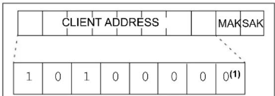
4.4 Device Addressing
A device address byte is the first byte received from the host device following the start header. The device address byte consists of a four-bit family code. For the 11AAXXX/11LCXXX, this is set as '1010'. The last four bits of the device address byte are the device code, which is hardwired to '0000' on the 11XXXX0 devices.
The device code on 11XXXX1 devices is hardwired to '0001'. This allows both 11XXXX0 and 11XXXX1 devices to be used on the same bus without address conflicts.
FIGURE 4-5: DEVICE ADDRESS BYTE ALLOCATION
text_image
CLIENT ADDRESS MAKSAK 1 0 1 0 0 0 0 0(1)Note 1: This bit is a '1' on the 11XXXX1.
4.5 Bus Conflict Protection
To help guard against high current conditions arising from bus conflicts, the 11AAXXX/11LCXXX features a current-limited output driver. The IOL and IOH specifications describe the maximum current that can be sunk or sourced, respectively, by the SCIO pin. The 11AAXXX/11LCXXX will vary the output driver impedance to ensure that the maximum current level is not exceeded.
4.6 Device Standby
The 11AAXXX/11LCXXX features a low-power Standby mode during which the device is waiting to begin a new command. A high-to-low transition on SCIO will exit low-power mode and prepare the device for receiving the start header.
Standby mode will be entered upon the following conditions:
- A NoMAK followed by a SAK (i.e., valid termination of a command)
- Reception of a standby pulse
Note: In the case of the WRITE, WRSR, SETAL or ERAL commands, the write cycle is initiated upon receipt of the NoMAK, assuming all other write requirements have been met.
4.7 Device Idle
The 11AAXXX/11LCXXX features an Idle mode during which all serial data is ignored until a standby pulse occurs. Idle mode will be entered upon the following conditions:
- Invalid device address
- Invalid command byte, including Read, CRRD, Write, WRSR, SETAL and ERAL during a write cycle.
- Missed edge transition
- Reception of a MAK following a WREN, WRDI, SETAL or ERAL command byte
- Reception of a MAK following the data byte of a WRSR command
An invalid start header will indirectly cause the device to enter Idle mode. Whether or not the start header is invalid cannot be detected by the client, but will prevent the client from synchronizing properly with the host. If the client is not synchronized with the host, an edge transition will be missed, thus causing the device to enter Idle mode.
4.8 Synchronization
At the beginning of every command, the 11AAXXX/11LCXXX utilizes the start header to determine the host's bus clock period. This period is then used as a reference for all subsequent communication within that command.
The 11AAXXX/11LCXXX features re-synchronization circuitry, which will monitor the position of the middle data edge during each MAK bit and will subsequently adjust the internal time reference to remain synchronized with the host.
There are two variables which can cause the 11AAXXX/11LCXXX to lose synchronization. The first is frequency drift, defined as a change in the bit period,
TE. The second is edge jitter, which is a single occurrence change in the position of an edge within a bit period, while the bit period itself remains constant.
4.8.1 FREQUENCY DRIFT
Within a system, there is a possibility that frequencies can drift due to changes in voltage, temperature, etc. The re-synchronization circuitry provides some tolerance for such frequency drift. The tolerance range is specified by two parameters, FDRIFT and FDEV. FDRIFT specifies the maximum tolerable change in bus frequency per byte. FDEV specifies the overall limit in frequency deviation within an operation (i.e., from the end of the start header until communication is terminated for that operation). The start header at the beginning of the next operation will reset the re-synchronization circuitry and allow for another FDEV amount of frequency drift.
4.8.2 EDGE JITTER
Ensuring that edge transitions from the host always occur exactly in the middle or end of the bit period is not always possible. Therefore, the re-synchronization circuitry is designed to provide some tolerance for edge jitter.
The 11XX adjusts its phase every MAK bit, so TIJIT specifies the maximum allowable peak-to-peak jitter relative to the previous MAK bit. Since the position of the previous MAK bit would be difficult to measure by the host, the minimum and maximum jitter values for a system should be considered the worst-case. These values will be based on the execution time for different branch paths in software, jitter due to thermal noise, etc.
The difference between the minimum and maximum values, as a percentage of the bit period, should be calculated and then compared against TIJIT to determine jitter compliance.
Note: Because the 11AAXXX/11LCXXX only re-synchronizes during the MAK bit, the overall ability to remain synchronized depends on a combination of frequency drift and edge jitter (i.e., if the MAK bit edge is experiencing the maximum allowable edge jitter, then there is no room for frequency drift). Conversely, if the frequency has drifted to the maximum amount tolerable within a byte, then no edge jitter can be present.
5.0 DEVICE COMMANDS
After the device address byte, a command byte must be sent by the host to indicate the type of operation to be performed. The code for each instruction is listed in Table 5-1.
TABLE 5-1: INSTRUCTION SET
| Instruction Name | Instruction Code Hex Code Description | |||
| READ 0000 | 0011 0x03 Read data from memory array beginning at specified address | |||
| CRRD 0000 | 0110 0x06 Read data from current location in memory array | |||
| WRITE 0110 | 1100 0x6C Write data to memory array beginning at specified address | |||
| WREN 1001 | 0110 0x96 Set the write enable latch (enable write operations) | |||
| WRDI 1001 | 0001 0x91 Reset the write enable latch (disable write operations) | |||
| RDSR 0000 | 0101 0x05 Read STATUS register | |||
| WRSR 0110 | 1110 0x6E Write STATUS register | |||
| ERAL 0110 | 1101 0x6D Write‘ | 0x00' to entire array | ||
| SETAL | 0110 0111 | 0x67 | Write '0xFF' to entire array | |
5.1 Read Instruction
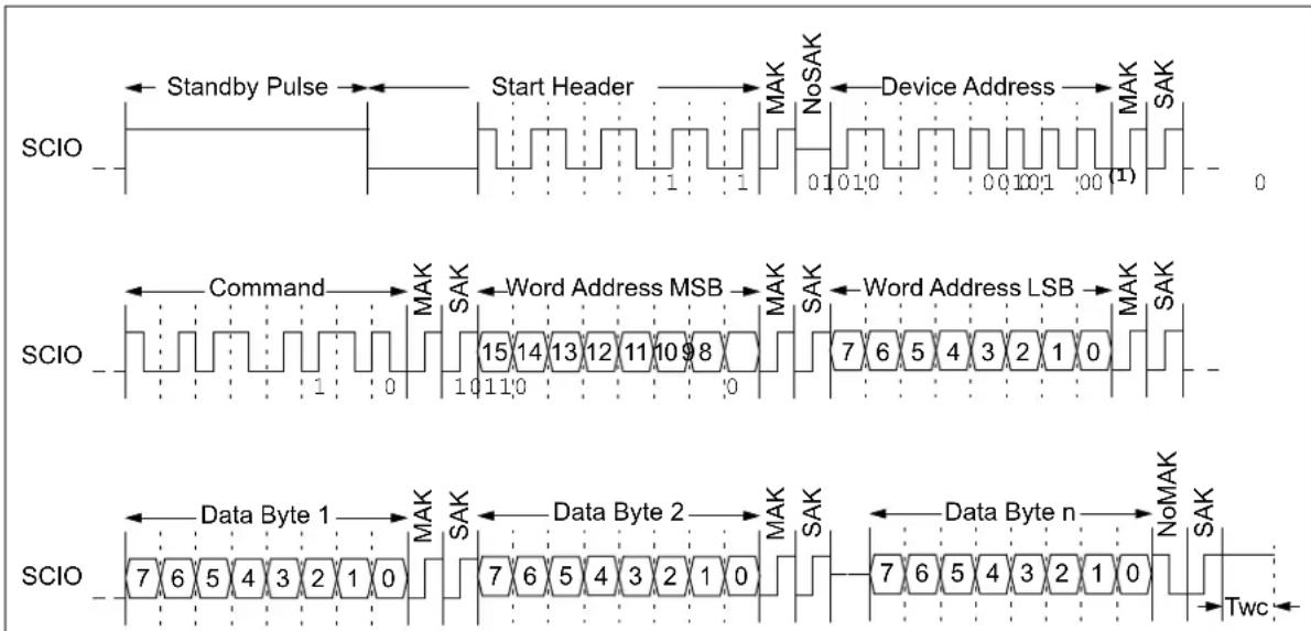
The Read command allows the host to access any memory location in a random manner. After the READ instruction has been sent to the client, the two bytes of the Word Address are transmitted, with an Acknowledge sequence being performed after each byte. Then, the client sends the first data byte to the host. If more data is to be read, the host sends a MAK, indicating that the client should output the next data byte. This continues until the host sends a NoMAK, which ends the operation.
To provide sequential reads in this manner, the 11AAXXX/11LCXXX contains an internal Address Pointer which is incremented by one after the transmission of each byte. This Address Pointer allows the memory contents to be serially read during one operation. When the highest address is reached, the Address Pointer rolls over to address '0x000' if the host chooses to continue the operation by providing a MAK.
FIGURE 5-1: READ COMMAND SEQUENCE

text_image
Standby Pulse Start Header MAK NoSAK Device Address MAK SAK SCIO 0 1 0 1 0 1 0 1 1 0 1 0 0 0 0 0 (1) Command MAK SAK Word Address MSB MAK SAK Word Address LSB MAK SAK 15 14 13 12 11 10 9 8 7 6 5 4 3 2 1 0 SCIO 0 0 0 0 0 1 1 Data Byte 1 MAK SAK Data Byte 2 MAK SAK Data Byte n NoMAK SAK 7 6 5 4 3 2 1 0 7 6 5 4 3 2 1 0 Note 1: For the 11XXXX1, this bit must be a '1'.5.2 Current Address Read (CRRD) Instruction
The internal address counter featured on the 11AAXXX/11LCXXX maintains the address of the last memory array location accessed. The CRRD instruction allows the host to read data back beginning from this current location. Consequently, no word address is provided upon issuing this command.
Note that, except for the initial word address, the READ and CRRD instructions are identical, including the ability to continue requesting data through the use of MAKs in order to sequentially read from the array.
As with the READ instruction, the CRRD instruction is terminated by transmitting a NoMAK.
Table 5-2 lists the events upon which the internal address counter is modified.
TABLE 5-2: INTERNAL ADDRESS COUNTER
| Command | Event Action | |
| — Power-on | Reset Counter is undefined | |
| READ or WRITE | MAK edge following each Address byte | Counter is updated with newly received value |
| READ, WRITE or CRRD | MAK/NoMAK edge following each data byte | Counter is incremented by 1 |
Note 1: If, following each data byte in a READ, WRITE or CRRD instruction, neither a MAK nor a NoMAK edge is received (i.e., if a standby pulse occurs instead), the internal address counter will not be incremented.
2: During a Write command, once the last data byte for a page has been loaded, the internal Address Pointer will rollover to the beginning of the selected page.
FIGURE 5-2: CRRD COMMAND SEQUENCE

Note 1: For the 11XXXX1, this bit must be a '1'.
5.3 Write Instruction
Prior to any attempt to write data to the 11AAXXX/11LCXXX, the write enable latch must be set by issuing the WREN instruction (see Section 5.4 "Write Enable (WREN) and Write Disable (WRDI) Instructions").
Once the write enable latch is set, the user may proceed with issuing a WRITE instruction (including the header and device address bytes) followed by the MSB and LSB of the Word Address. Once the last Acknowledge sequence has been performed, the host transmits the data byte to be written.
The 11AAXXX/11LCXXX features a 16-byte page buffer, meaning that up to 16 bytes can be written at one time. To utilize this feature, the host can transmit up to 16 data bytes to the 11AAXXX/11LCXXX, which are temporarily stored in the page buffer. After each data byte, the host sends a MAK, indicating whether or not another data byte is to follow. A NoMAK indicates that no more data is to follow, and as such will initiate the internal write cycle.
Note: If a NoMAK is generated before any data has been provided, or if a standby pulse occurs before the NoMAK is generated, the 11AAXXX/11LCXXX will be reset, and the write cycle will not be initiated.
Upon receipt of each word, the four lower-order Address Pointer bits are internally incremented by one. The higher-order bits of the word address remain constant. If the host should transmit data past the end of the page, the address counter will roll over to the beginning of the page, where further received data will be written.
Note: Page write operations are limited to writing bytes within a single physical page, regardless of the number of bytes actually being written. Physical page boundaries start at addresses that are integer multiples of the page size (16 bytes) and end at addresses that are integer multiples of the page size minus 1. As an example, the page that begins at address 0x30 ends at address 0x3F. If a page Write command attempts to write across a physical page boundary, the result is that the data wraps around to the beginning of the current page (overwriting data previously stored there), instead of being written to the next page as might be expected. It is, therefore, necessary for the application software to prevent page write operations that would attempt to cross a page boundary.
FIGURE 5-3: WRITE COMMAND SEQUENCE
text_image
Standby Pulse Start Header MAK NoSAK Device Address MAK SAK SCIO 0 1 0 0 1 0 0 1 0 0 1 0 0 1 0 0 1 0 0 1 0 0 1 0 0 1 0 0 1 0 0 1 0 0 1 0 0 1 0 0 1 0 0 1 0 0 1 0 0 1 0 0 0 1 0 0 1 0 0 1 0 0 1 0 0 1 0 0 1 0 0 1 0 0 1 0 0 1 0 0 1 0 0 1 0 0 1 0 0 1 0 0 1 0 0 1 0 0 1 0 2 0 1 0 2 0 1 0 3 0 1 0 4 0 1 0 5 0 1 0 6 0 1 0 7 0 1 0Note 1: For the 11XXXX1, this bit must be a '1'.
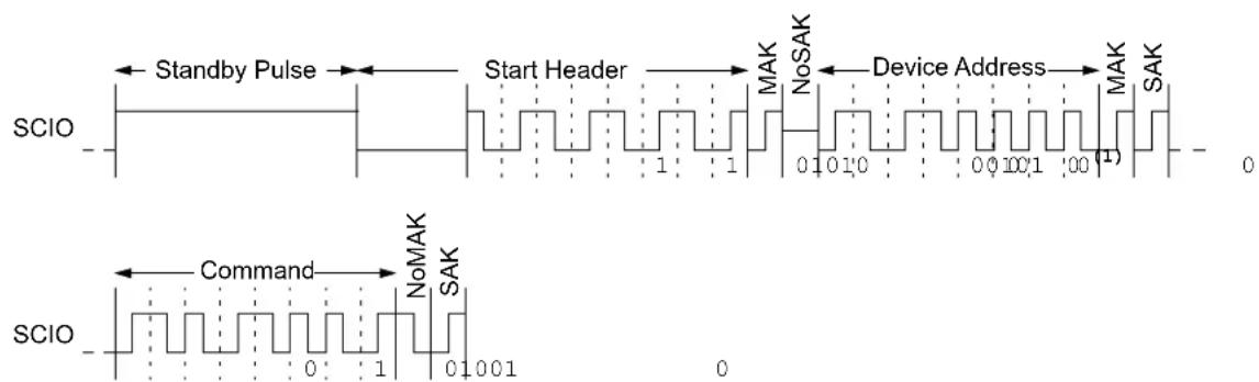
5.4 Write Enable (WREN) and Write Disable (WRDI) Instructions
The 11XX contains a write enable latch. See Table 7-1 for the Write-Protect Functionality Matrix. This latch must be set before any write operation will be completed internally. The WREN instruction will set the latch, and the WRDI instruction will reset the latch.
Note: The WREN and WRDI instructions must be terminated with a NoMAK following the command byte. If a NoMAK is not received at this point, the command will be considered invalid, and the device will go into Idle mode without responding with a SAK or executing the command.
The following is a list of conditions under which the write enable latch will be reset:
- Power-up
- WRDI instruction successfully executed
- WRSR instruction successfully executed
• WRITE instruction successfully executed
• ERAL instruction successfully executed - SETAL instruction successfully executed
FIGURE 5-4: WRITE ENABLE COMMAND SEQUENCE

text_image
Standby Pulse Start Header MAK NoSAK Device Address MAK SAK SCIO 01010 001001:00(1) 0 Command NoMAK SAK SCIONote 1: For the 11XXXX1, this bit must be a '1'.
FIGURE 5-5: WRITE DISABLE COMMAND SEQUENCE
text_image
Standby Pulse Start Header MAK NoSAK Device Address MAK SAK SCIO 010100100(1) 0 Command NoMAK SAK SCIONote 1: For the 11XXXX1, this bit must be a '1'.
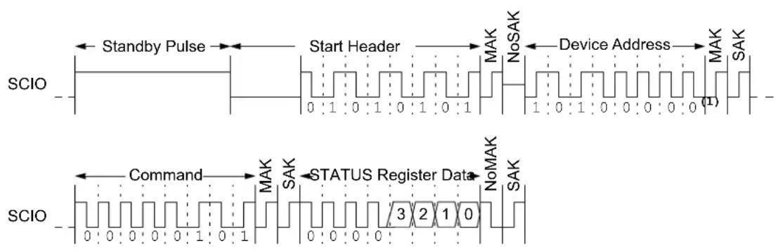
5.5 Read Status Register (RDSR) Instruction
The RDSR instruction provides access to the STATUS register. The STATUS register may be read at any time, even during a write cycle. The STATUS register is formatted as follows:
| 7 | 6 | 5 | 4 | 3 | 2 | 1 | 0 |
| XX | XX | BP1 | BPO | WEL WIP | |||
| Note: Bits 4-7 are don't cares, and will read as '0'. | |||||||
The Write-In-Process (WIP) bit indicates whether the 11AAXXX/11LCXXX is busy with a write operation. When set to a '1', a write is in progress. When set to a '0', no write is in progress. This bit is read-only.
The Write Enable Latch (WEL) bit indicates the status of the write enable latch. When set to a '1', the latch allows writes to the array. When set to a 0', the latch prohibits writes to the array. This bit is set and cleared using the WREN and WRDI instructions, respectively. This bit is read-only for any other instruction.
The Block Protection (BP0 and BP1) bits indicate which blocks are currently write-protected. These bits are set by the user through the WRSR instruction. These bits are nonvolatile.
Note: If Read Status Register command is initiated while the 11XX is currently executing an internal write cycle on the STATUS register, the new Block Protection bit values will be read during the entire command.
The WIP and WEL bits will update dynamically (asynchronous to issuing the RDSR instruction). Furthermore, after the STATUS register data is received, the host can provide a MAK during the Acknowledge sequence to request that the data be transmitted again. This allows the host to continuously monitor the WIP and WEL bits without the need to issue another full command.
Once the host is finished, it provides a NoMAK to end the operation.
Note: The current drawn for a Read Status Register command during a write cycle is a combination of the Icc Read and Icc Write operating currents.
FIGURE 5-6: READ STATUS REGISTER COMMAND SEQUENCE
text_image
Standby Pulse Start Header MAK NoSAK Device Address MAK SAK SCIO 0 1 0 1 0 1 0 1 1 0 1 0 0 0 0 0 0 (T) Command MAK SAK STATUS Register Data NoMAK SAK SCIO 0 0 0 0 0 1 0 1 3 2 1 0Note 1: For the 11XXXX1, this bit must be a '1'.
Note 2: The STATUS register data can continuously be read, or polled, by transmitting a MAK in place of the NoMAK.
5.6 Write Status Register (WRSR) Instruction
The WRSR instruction allows the user to select one of four levels of protection for the array by writing to the appropriate bits in the STATUS register. The array is divided into four segments. The user has the ability to write-protect none, one, two, or all four of the segments of the array. The partitioning is controlled as illustrated in Table 5-3.
After transmitting the STATUS register data, the host must transmit a NoMAK during the Acknowledge sequence in order to initiate the internal write cycle.
Note: The WRSR instruction must be terminated with a NoMAK following the data byte. If a NoMAK is not received at this point, the command will be considered invalid, and the device will go into Idle mode without responding with a SAK or executing the command.
TABLE 5-3: ARRAY PROTECTION
| BP1 BP0 Address Ranges Write-Protected Address Ranges Unprotected | |||
| 0 | 0 | None All | |
| 0 | 1 | Upper 1/4 | Lower 3/4 |
| 1 | 0 | Upper 1/2 | Lower 1/2 |
| 1 | 1 | All None | |
TABLE 5-4: PROTECTED ARRAY ADDRESS LOCATIONS
| Density | Upper 1/4 | Upper 1/2 | All Sectors |
| 1K | 60h-7Fh | 40h-7Fh | 00h-7Fh |
| 2K | C0h-FFh | 80h-FFh | 00h-FFh |
| 4K | 180h-1FFh | 100h-1FFh | 000h-1FFh |
| 8K | 300h-3FFh | 200h-3FFh | 000h-3FFh |
| 16K | 600h-7FFh | 400h-7FFh | 000h-7FFh |
FIGURE 5-7: WRITE STATUS REGISTER COMMAND SEQUENCE
text_image
Standby Pulse Start Header MAK NoSAK Device Address MAK SAK SCIO 0 1 0 1 0 1 0 1 1 0 1 0 0 0 0 0 0 (1) Command MAK SAK Status Register Data NoMAK SAK SCIO 0 1 1 0 1 1 1 0 7 6 5 4 3 2 1 0 TwcNote 1: For the 11XXXX1, this bit must be a '1'.
5.7 Erase All (ERAL) Instruction
The ERAL instruction allows the user to write '0x00' to the entire memory array with one command. Note that the write enable latch (WEL) must first be set by issuing the WREN instruction.
Once the write enable latch is set, the user may proceed with issuing a ERAL instruction (including the header and device address bytes). Immediately after the NoMAK bit has been transmitted by the host, the internal write cycle is initiated, during which time all words of the memory array are written to '0x00'.
The ERAL instruction is ignored if either of the Block Protect bits (BP0, BP1) are not 0, meaning 1/4, 1/2, or all of the array is protected.
Note: The ERAL instruction must be terminated with a NoMAK following the command byte. If a NoMAK is not received at this point, the command will be considered invalid, and the device will go into Idle mode without responding with a SAK or executing the command.
FIGURE 5-8: ERASE ALL COMMAND SEQUENCE
text_image
Standby Pulse Start Header MAK NoSAK Device Address MAK SAK SCIO 010100(1) 0 Command NoMAK SAK SCIO 1 1 1 TwoNote 1: For the 11XXXX1, this bit must be a '1'.
5.8 Set All (SETAL) Instruction
The SETAL instruction allows the user to write '0xFF' to the entire memory array with one command. Note that the write enable latch (WEL) must first be set by issuing the WREN instruction.
Once the write enable latch is set, the user may proceed with issuing a SETAL instruction (including the header and device address bytes). Immediately after the NoMAK bit has been transmitted by the host, the internal write cycle is initiated, during which time all words of the memory array are written to '0xFF'.
The SETAL instruction is ignored if either of the Block Protect bits (BP0, BP1) are not 0, meaning 1/4, 1/2, or all of the array is protected.
Note: The SETAL instruction must be terminated with a NoMAK following the command byte. If a NoMAK is not received at this point, the command will be considered invalid, and the device will go into Idle mode without responding with a SAK or executing the command.
FIGURE 5-9: SET ALL COMMAND SEQUENCE

text_image
Standby Pulse Start Header MAK NoSAK Device Address MAK SAK SCIO 0 1 0 1 0 0 1 0 0 (1) 0 Command NoMAK SAK SCIO 1 1 1 1 1 TwoNote 1: For the 11XXXX1, this bit must be a '1'.
6.0 DATA PROTECTION
The following protection has been implemented to prevent inadvertent writes to the array:
- The Write Enable Latch (WEL) is reset on power-up
- A Write Enable (WREN) instruction must be issued to set the write enable latch
- After a write, ERAL, SETAL or WRSR command, the write enable latch is reset
- Commands to access the array or write to the STATUS register are ignored during an internal write cycle and programming is not affected
7.0 POWER-ON STATE
The 11AAXXX/11LCXXX powers on in the following state:
- The device is in low-power Shutdown mode, requiring a low-to-high transition on SCIO to enter Idle mode
• The Write Enable Latch (WEL) is reset - The internal Address Pointer is undefined
- A low-to-high transition, standby pulse and subsequent high-to-low transition on SCIO (the first low pulse of the header) are required to enter the active state
TABLE 7-1: WRITE PROTECT FUNCTIONALITY MATRIX
| WEL Protected Blocks Unprotected Blocks | Status Register | |
| 0 Protected Protected | ||
| 1 Protected Writable Writable |
8.0 PACKAGING INFORMATION
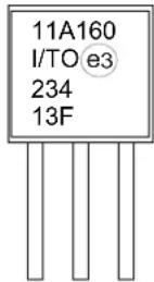
8.1 Package Marking Information
8-Lead PDIP

Example:
| 8-Lead PDIP Package Marking (Pb-Free) | |||
| Device Line 1 Marking Device Line 1 Marking | |||
| 11AA010 11AA010 | 11LC010 11LC010 | ||
| 11AA020 11AA020 | 11LC020 11LC020 | ||
| 11AA040 11AA040 | 11LC040 11LC040 | ||
| 11AA080 11AA080 | 11LC080 11LC080 | ||
| 11AA160 11AA160 | 11LC160 11LC160 | ||
| 11AA161 11AA161 | 11LC161 11LC161 | ||
| Note: T = Temperature Grade (I, E) | |||
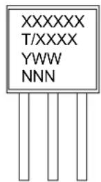
Legend: XX...X Part number or part number code
T Temperature (I, E)
Y Year code (last digit of calendar year)
YY Year code (last 2 digits of calendar year)
WW Week code (week of January 1 is week '01')
NNN Alphanumeric traceability code (2 characters for small packages)
e3 RoHS-compliant JEDEC® designator for Matte Tin (Sn)
Note: Standard OTP marking consists of Microchip part number, year code, week code and traceability code.
Note: For very small packages with no room for the JEDEC® designator e3, the marking will only appear on the outer carton or reel label.
Note: In the event the full Microchip part number cannot be marked on one line, it will be carried over to the next line, thus limiting the number of available characters for customer-specific information.
8-Lead SOIC

Example:
| 8-Lead SOIC Package Marking (Pb-Free) | |||
| Device Line 1 Marking Device Line 1 Marking | |||
| 11AA010 11AA010T | 11LC010 11LC010T | ||
| 11AA020 11AA020T | 11LC020 11LC020T | ||
| 11AA040 11AA040T | 11LC040 11LC040T | ||
| 11AA080 11AA080T | 11LC080 11LC080T | ||
| 11AA160 11AA160T | 11LC160 11LC160T | ||
| 11AA161 11AA161T | 11LC161 11LC161T | ||
| Note: T = Temperature Grade (I, E) | |||
Legend: XX...X Part number or part number code
T Temperature (I, E)
Y Year code (last digit of calendar year)
YY Year code (last 2 digits of calendar year)
WW Week code (week of January 1 is week '01')
NNN Alphanumeric traceability code (2 characters for small packages)
e3 RoHS-compliant JEDEC® designator for Matte Tin (Sn)
Note: Standard OTP marking consists of Microchip part number, year code, week code and traceability code.
Note: For very small packages with no room for the JEDEC® designator e3, the marking will only appear on the outer carton or reel label.
Note: In the event the full Microchip part number cannot be marked on one line, it will be carried over to the next line, thus limiting the number of available characters for customer-specific information.
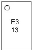
8-Lead MSOP (150 mil)

Example:
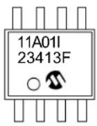
| 8-Lead MSOP Package Marking (Pb-Free) | |||
| Device Line 1 Marking Device Line 1 Marking | |||
| 11AA010 11A01T | 1LC010 11L01T | ||
| 11AA020 11A02T | 1LC020 11L02T | ||
| 11AA040 11A04T | 1LC040 11L04T | ||
| 11AA080 11A08T | 1LC080 11L08T | ||
| 11AA160 11AAT | 1LC160 11LAT | ||
| 11AA161 11AA1T | 1LC161 11LA1T | ||
| Note: T = Temperature Grade (I, E) | |||
Legend: XX...X Part number or part number code
T Temperature (I, E)
Y Year code (last digit of calendar year)
YY Year code (last 2 digits of calendar year)
WW Week code (week of January 1 is week '01')
NNN Alphanumeric traceability code (2 characters for small packages)
e3 RoHS-compliant JEDEC® designator for Matte Tin (Sn)
Note: Standard OTP marking consists of Microchip part number, year code, week code and traceability code.
Note: For very small packages with no room for the JEDEC® designator e3, the marking will only appear on the outer carton or reel label.
Note: In the event the full Microchip part number cannot be marked on one line, it will be carried over to the next line, thus limiting the number of available characters for customer-specific information.
8-Lead 2x3 TDFN

Example:
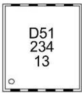
| 8-Lead 2x3 TDFN Package Marking (Pb-Free) | ||||
| Device I-Temp | Marking Device I-Temp | Marking E-Temp Marking | ||
| 11AA010 D11 1 | 1LC010 D14 D15 | |||
| 11AA020 D21 1 | 1LC020 D24 D25 | |||
| 11AA040 D31 1 | 1LC040 D34 D35 | |||
| 11AA080 D41 1 | 1LC080 D44 D45 | |||
| 11AA160 D51 1 | 1LC160 D54 D55 | |||
| 11AA161 D5D 1 | 1LC161 D5G D5H | |||
Legend: XX...X Part number or part number code
T Temperature (I, E)
Y Year code (last digit of calendar year)
YY Year code (last 2 digits of calendar year)
WW Week code (week of January 1 is week '01')
NNN Alphanumeric traceability code (2 characters for small packages)
e3 RoHS-compliant JEDEC® designator for Matte Tin (Sn)
Note: Standard OTP marking consists of Microchip part number, year code, week code and traceability code.
Note: For very small packages with no room for the JEDEC® designator e3, the marking will only appear on the outer carton or reel label.
Note: In the event the full Microchip part number cannot be marked on one line, it will be carried over to the next line, thus limiting the number of available characters for customer-specific information.
3-Lead SOT-23

Example:
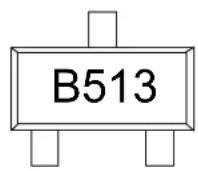
| 3-Lead SOT-23 Package Marking (Pb-Free) | ||||
| Device I-Temp | Marking Device I-Temp | Marking E-Temp Marking | ||
| 11AA010 B1NN | 11LC010 M1NN N1NN | |||
| 11AA020 B2NN | 11LC020 M2NN N2NN | |||
| 11AA040 B3NN | 11LC040 M3NN N3NN | |||
| 11AA080 B4NN | 11LC080 M4NN N4NN | |||
| 11AA160 B5NN | 11LC160 M5NN N5NN | |||
| 11AA161 B0NN | 11LC161 M0NN N0NN | |||
Legend: XX...X Part number or part number code
T Temperature (I, E)
Y Year code (last digit of calendar year)
YY Year code (last 2 digits of calendar year)
WW Week code (week of January 1 is week '01')
NNN Alphanumeric traceability code (2 characters for small packages)
e3
RoHS-compliant JEDEC® designator for Matte Tin (Sn)
Note: Standard OTP marking consists of Microchip part number, year code, week code and traceability code.
Note: For very small packages with no room for the JEDEC® designator e3, the marking will only appear on the outer carton or reel label.
Note: In the event the full Microchip part number cannot be marked on one line, it will be carried over to the next line, thus limiting the number of available characters for customer-specific information.
3-Lead TO-92
Example:
| 3-Lead TO-92 Package Marking (Pb-Free) | |||
| Device Line 1 Marking Device Line 1 Marking | |||
| 11AA010 11A010 1 | 1LC010 11L010 | ||
| 11AA020 11A020 1 | 1LC020 11L020 | ||
| 11AA040 11A040 1 | 1LC040 11L040 | ||
| 11AA080 11A080 1 | 1LC080 11L080 | ||
| 11AA160 11A160 1 | 1LC160 11L160 | ||
| 11AA161 11A161 1 | 1LC161 11L161 | ||
| Note: T = Temperature Grade (I, E) | |||
| Legend: XX...X Part number or part number codeT Temperature (I, E)Y Year code (last digit of calendar year)YY Year code (last 2 digits of calendar year)WW Week code (week of January 1 is week '01')NNN Alphanumeric traceability code (2 characters for small packages)e3 RoHS-compliant JEDEC® designator for Matte Tin (Sn) |
| Note: Standard OTP marking consists of Microchip part number, year code, week code and traceability code.Note: For very small packages with no room for the JEDEC® designator e3 , the marking will only appear on the outer carton or reel label.Note: In the event the full Microchip part number cannot be marked on one line, it will be carried over to the next line, thus limiting the number of available characters for customer-specific information. |
4-Lead Chip Scale

Example:
| 4-Lead Chip Scale Package Marking (Pb-Free) | |
| Device Line 1 Marking | |
| 11AA010 AW | |
| 11AA020 BW | |
| 11AA040 CW | |
| 11AA080 DW | |
| 11AA160 EW | |
| 11AA161 HW | |
| Legend: XX...X Part number or part number code | |
| T Temperature (I, E) | |
| Y Year code (last digit of calendar year) | |
| YY Year code (last 2 digits of calendar year) | |
| WW Week code (week of January 1 is week '01') | |
| NNN Alphanumeric traceability code (2 characters for small packages) | |
| e3 | RoHS-compliant®designEDCfor Matte Tin (Sn) |
Note: Standard OTP marking consists of Microchip part number, year code, week code and traceability code.
Note: For very small packages with no room for the JEDEC ^® designator e3, the marking will only appear on the outer carton or reel label.
Note: In the event the full Microchip part number cannot be marked on one line, it will be carried over to the next line, thus limiting the number of available characters for customer-specific information.
8-Lead Plastic Dual In-Line (P) - 300 mil Body [PDIP]
Note: For the most current package drawings, please see the Microchip Packaging Specification located at http://www.microchip.com/packaging
![Microchip 11AA020 - 8-Lead Plastic Dual In-Line (P) - 300 mil Body [PDIP] - 1](/content/2026/06/1221682/images/b5622e93428d80a22bd34f9a3a7ede26d0ac6015ca114a3e3e1a1a229391e828.jpg)
text_image
NOTE 1 1 2 D A B E1 TOP VIEW![Microchip 11AA020 - 8-Lead Plastic Dual In-Line (P) - 300 mil Body [PDIP] - 2](/content/2026/06/1221682/images/d3ece25df74ebac4b3a9d93677d233325498c794b7ca7f3f45b4724173238367.jpg)
natural_image
Line drawing of an integrated circuit chip with multiple pins (no text or symbols)![Microchip 11AA020 - 8-Lead Plastic Dual In-Line (P) - 300 mil Body [PDIP] - 3](/content/2026/06/1221682/images/d69f5508926b5cfc7969a99d0e6be244a386708e5276e9f3142eefec21785894.jpg)
text_image
PLANE A C A1 A2 L 8X b1 8X b e .010®![Microchip 11AA020 - 8-Lead Plastic Dual In-Line (P) - 300 mil Body [PDIP] - 4](/content/2026/06/1221682/images/1031012662716792f64c9aaebf449cf01e8c2c1adef7e4eda01ce64a7313c08d.jpg)
text_image
E c eBEND VIEWSIDE VIEW
Microchip Technology Drawing No. C04-018-P Rev F Sheet 1 of 2
8-Lead Plastic Dual In-Line (P) - 300 mil Body [PDIP]
Note: For the most current package drawings, please see the Microchip Packaging Specification located at http://www.microchip.com/packaging
![Microchip 11AA020 - 8-Lead Plastic Dual In-Line (P) - 300 mil Body [PDIP] - 1](/content/2026/06/1221682/images/59b52067d1c7dc63f265b60baa4d1bf9e24f49a6a7e11ec7510a7c94fe364e91.jpg)
text_image
DATUM A b e ZALTERNATE LEAD DESIGN
(NOTE 5)
![Microchip 11AA020 - 8-Lead Plastic Dual In-Line (P) - 300 mil Body [PDIP] - 2](/content/2026/06/1221682/images/e39c9f45b2d8d768025e0f8dbea003299a613c5597459cacf898ad6f01fda17c.jpg)
text_image
DATUM A a2 b e| Units | INCHES | |||
| Dimension Limits | MIN NOM MAX | |||
| Number of Pins N 8 | ||||
| Pitch | e | .100 BSC | ||
| Top to Seating Plane A - - .210 | ||||
| Molded Package Thickness A2 .115 | .130 .195 | |||
| Base to Seating Plane | A1 .015 | - | - | |
| Shoulder to Shoulder Width | E | .290 .310 | .325 | |
| Molded Package Width | E1 .240 .250 .280 | |||
| Overall Length | D | .348 .365 | .400 | |
| Tip to Seating Plane | L | .115 .130 | .150 | |
| Lead Thickness | c | .008 .010 | .015 | |
| Upper Lead Width | b1 | .040 .060 | .070 | |
| Lower Lead Width | b | .014 .013 | .022 | |
| Overall Row Spacing § | eB - - .430 | |||
Notes:
1. Pin 1 visual index feature may vary, but must be located within the hatched area.
2. § Significant Characteristic
3. Dimensions D and E1 do not include mold flash or protrusions. Mold flash or protrusions shall not exceed .010" per side.
4. Dimensioning and tolerancing per ASME Y14.5M BSC: Basic Dimension. Theoretically exact value shown without tolerances.
5. Lead design above seating plane may vary, based on assembly vendor.
Microchip Technology Drawing No. C04-018-P Rev F Sheet 2 of 2
8-Lead Plastic Small Outline (SN) - Narrow, 3.90 mm (.150 In.) Body [SOIC]
Note: For the most current package drawings, please see the Microchip Packaging Specification located at http://www.microchip.com/packaging
![Microchip 11AA020 - 8-Lead Plastic Small Outline (SN) - Narrow, 3.90 mm (.150 In.) Body [SOIC] - 1](/content/2026/06/1221682/images/38b866a01946503e835851a4a5a300d2eb1eb2fa0013678ea5a97e911c43e0db.jpg)
text_image
2X 0.10 C A-B E1 E1/2 NOTE 5 A N D 2X 0.10 C A-B E/2 E 2X 0.10 C A-B NOTE 1 1 2 e B NX b NOTE 5 0.25 M A-B DTOP VIEW
![Microchip 11AA020 - 8-Lead Plastic Small Outline (SN) - Narrow, 3.90 mm (.150 In.) Body [SOIC] - 2](/content/2026/06/1221682/images/f340a55b5e2cb6c33814652e31cd43d1471596cfabeabaee26dbf7d11cd821d1.jpg)
text_image
SEATING PLANE A A2 A1 SIDE VIEW // 0.10 C 8X 0.10 C![Microchip 11AA020 - 8-Lead Plastic Small Outline (SN) - Narrow, 3.90 mm (.150 In.) Body [SOIC] - 3](/content/2026/06/1221682/images/dc97f169f8e9464e7436f561effa535fab1805056e163b19be58985a193d69ca.jpg)
text_image
4X θ1 θ2 R1 R c L (L1) 4X θ1 h H SEE VIEW C VIEW A-AVIEW C
Microchip Technology Drawing No. C04-057-SN Rev K Sheet 1 of 2
8-Lead Plastic Small Outline (SN) - Narrow, 3.90 mm (.150 In.) Body [SOIC]
Note: For the most current package drawings, please see the Microchip Packaging Specification located at http://www.microchip.com/packaging
![Microchip 11AA020 - 8-Lead Plastic Small Outline (SN) - Narrow, 3.90 mm (.150 In.) Body [SOIC] - 1](/content/2026/06/1221682/images/5ae52ac02414438ee6fcd65c0cd9183ad203df6cedb8b1135ae13ce6a02444ef.jpg)
natural_image
Isometric line drawing of an integrated circuit chip with four pins (no text or symbols)| Units | MILLIMETERS | |||
| Dimension Limits | MIN | NOM | MAX | |
| NNumber of Pins 8 | ||||
| Pitch | e | 1.27 BSC | ||
| AOver### He### | ||||
| —1.25A | ||||
| Standoff § | A1 | 0.10 | - | 0.25 |
| 6.00 BSCEOverall Width | ||||
| Molded Package Width | E1 | 3.90 BSC | ||
| 4.90 BSCDOverall Leng | ||||
| Chamfer (Optional) | h | 0.25 | - | 0.50 |
| Foot Length | L | 0.40 | - | 1.27 |
| Footprint | L1 | 1.04 REF | ||
| Lead Thickness | c | 0.25–0.1 | ||
| Lead Width | b | 0.51–0.3 | ||
| Lead Bend Radius | R | 0.07 | - | - |
| Lead Bend Radius | R1 | 0.07 | - | - |
| Foot Angle 0° – 8° | θ | |||
| Mold Draft Angle | θ1 | 5° – | 15° | |
| θ2 | —0°Le | |||
ght 2Molded Package Thickness
Notes:
-
Pin 1 visual index feature may vary, but must be located within the hatched area.
-
§ Significant Characteristic
-
Dimensions D and E1 do not include mold flash or protrusions. Mold flash or protrusions shall not exceed 0.15mm per side.
-
Dimensioning and tolerancing per ASME Y14.5M
BSC: Basic Dimension. Theoretically exact value shown without tolerances.
REF: Reference Dimension, usually without tolerance, for information purposes only.
- Datums A & B to be determined at Datum H.
Microchip Technology Drawing No. C04-057-SN Rev K Sheet 2 of 2
8-Lead Plastic Small Outline (SN) - Narrow, 3.90 mm (.150 In.) Body [SOIC]
Note: For the most current package drawings, please see the Microchip Packaging Specification located at http://www.microchip.com/packaging
![Microchip 11AA020 - 8-Lead Plastic Small Outline (SN) - Narrow, 3.90 mm (.150 In.) Body [SOIC] - 1](/content/2026/06/1221682/images/fc147426d9fc8585d7132d629664ccc5cf597a87b80db25bddc8b2df88bf4049.jpg)
text_image
SILK SCREEN C Y1 X1 ERECOMMENDED LAND PATTERN
| Units | MILLIMETERS | |||
| Dimension Limits | MIN | NOM | MAX | |
| Contact Pitch | E | 1.27 BSC | ||
| CContact Pad Spacing40 | ||||
| Contact Pad Width (X8) | X1 | 0.60 | ||
| Contact Pad Length (X8) | Y1 | 1.55 | ||
Notes:
Dimensioning and tolerancing per ASME Y14.5M1.
BSC: Basic Dimension. Theoretically exact value shown without tolerances.
Microchip Technology Drawing C04-2057-SN Rev K
8-Lead Plastic Micro Small Outline Package (MS) - 3x3 mm Body [MSOP]
Note: For the most current package drawings, please see the Microchip Packaging Specification located at http://www.microchip.com/packaging
![Microchip 11AA020 - 8-Lead Plastic Micro Small Outline Package (MS) - 3x3 mm Body [MSOP] - 1](/content/2026/06/1221682/images/5694607ffc561c60c0701ee70172c83ba2eaf913de6d45a26b647d5f7ab66412.jpg)
text_image
2X 0.20 H D D/2 A N E1/2 E1 E E/2 E 2X 0.20 H NOTE 1 1 2 e B 2X 4 TIPS 0.25 CTOP VIEW
![Microchip 11AA020 - 8-Lead Plastic Micro Small Outline Package (MS) - 3x3 mm Body [MSOP] - 2](/content/2026/06/1221682/images/2a01ede976e8fd8ab8c462941d0d59e17b71446766cf6c8927deeb57bff226f1.jpg)
text_image
A A2 A1 8X 0.10 C SEATING PLANE C 8X b ⊕ 0.25 M A-B D ASIDE VIEW
![Microchip 11AA020 - 8-Lead Plastic Micro Small Outline Package (MS) - 3x3 mm Body [MSOP] - 3](/content/2026/06/1221682/images/3489e1575f8cc64047d5f4ccba023e5634e3774208eee87c352af7955cd1c976.jpg)
text_image
H SEE DETAIL BVIEW A-A
Microchip Technology Drawing C04-111-MS Rev F Sheet 1 of 2
8-Lead Plastic Micro Small Outline Package (MS) - 3x3 mm Body [MSOP]
Note: For the most current package drawings, please see the Microchip Packaging Specification located at http://www.microchip.com/packaging
![Microchip 11AA020 - 8-Lead Plastic Micro Small Outline Package (MS) - 3x3 mm Body [MSOP] - 1](/content/2026/06/1221682/images/a2935d1be8c4d551a71b42ff6e056321314b36a9d771113255464ef94ca5bac6.jpg)
text_image
4X θ1 R1 H R SEATING PLANE C L (L1) c θ 4X θ1![Microchip 11AA020 - 8-Lead Plastic Micro Small Outline Package (MS) - 3x3 mm Body [MSOP] - 2](/content/2026/06/1221682/images/a78ef69817b84dfbd38c52039ed615e699b8c53a22bc80378dee5491834b7f3a.jpg)
natural_image
Isometric line drawing of an integrated circuit chip with multiple pins (no text or symbols)DETAIL B
| Units | MILLIMETERS | |||
| Dimension Limits | MIN | NOM | MAX | |
| Number of Terminals | N | 8 | ||
| Pitch | e | 0.65 BSC | ||
| Overall Height | A | - | - | 1.10 |
| Standoff | A1 | 0.00 | - | 0.15 |
| Molded Package Thickness | A2 | 0.75 | 0.85 | 0.95 |
| Overall Length D 3.00 BSC | ||||
| Overall Width | E | 4.90 BSC | ||
| Molded Package Width | E1 | 3.00 BSC | ||
| Terminal Width | b | 0.22 | - | 0.40 |
| Terminal Thickness | c | 0 | . | 0 8 |
| Terminal Length | L | 0.40 | 0.60 | 0.80 |
| L1 0 | 95 REFFootprint | |||
| R | -0.07 | -Lead Bend | ||
| R1 | -0.07 | -Lead Bend | ||
| θ | -0° 8° | Foot Angle | ||
| θ1 | -5° 15° | Mold Draft Angle | ||
Notes:
1. Pin 1 visual index feature may vary, but must be located within the hatched area.
2. Dimensions D and E1 do not include mold flash or protrusions. Mold flash or protrusions shall not exceed 0.15mm per side.
3. Dimensioning and tolerancing per ASME Y14.5M
BSC: Basic Dimension. Theoretically exact value shown without tolerances.
REF: Reference Dimension, usually without tolerance, for information purposes only.
Microchip Technology Drawing C04-111-MS Rev F Sheet 2 of 2
8-Lead Plastic Micro Small Outline Package (MS) - 3x3 mm Body [MSOP]
Note: For the most current package drawings, please see the Microchip Packaging Specification located at http://www.microchip.com/packaging
![Microchip 11AA020 - 8-Lead Plastic Micro Small Outline Package (MS) - 3x3 mm Body [MSOP] - 1](/content/2026/06/1221682/images/185b31a6ee8d8839c5de94117d0ecb8cfb9b17c480cf71740e3019f2eaaebf4a.jpg)
text_image
GX C G1 SILK SCREEN Y X ERECOMMENDED LAND PATTERN
| Units | MILLIMETERS | |||
| Dimension Limits | MIN | NOM | MAX | |
| Contact Pitch | E | 0.65 BSC | ||
| CContact Pad Spacing 4.40 | ||||
| Contact Pad Width (X8) | X | 0.45 | ||
| Contact Pad Length (X8) | Y | 1.45 | ||
| Contact Pad to Contact Pad (X4) G1 | 2.95 | |||
| Contact Pad to Contact Pad (X6) GX | 0.20 | |||
Notes:
Dimensioning and tolerancing per ASME Y14.5M1.
BSC: Basic Dimension. Theoretically exact value shown without tolerances.
Microchip Technology Drawing C04-2111-MS Rev F
8-Lead Plastic Dual Flat, No Lead Package (MN) - 2x3x0.8 mm Body [TDFN] With 1.4x1.3 mm Exposed Pad (JEDEC Package type WDFN)
Note: For the most current package drawings, please see the Microchip Packaging Specification located at http://www.microchip.com/packaging
![Microchip 11AA020 - 8-Lead Plastic Dual Flat, No Lead Package (MN) - 2x3x0.8 mm Body [TDFN] With 1.4x1.3 mm Exposed Pad (JEDEC Package type WDFN) - 1](/content/2026/06/1221682/images/79280dbc6fd1646b1c234d085559ebdf29160765ccca86a4f874173945da17b6.jpg)
text_image
(DATUM A) (DATUM B) NOTE 1 2X 0.15 C 2X 0.15 C TOP VIEW SEATING PLANE C A A1 // 0.10 C 8X 0.08 C SIDE VIEW L D2 NOTE 1 E2 K N e 8X b BOTTOM VIEW ⊕ 0.10® A B ⊕ 0.10® A B ⊕ 0.10® A B ⊕ 0.10® A B ⊕ 0.05®Microchip Technology Drawing No. C04-129-MN Rev E Sheet 1 of 2
8-Lead Plastic Dual Flat, No Lead Package (MN) - 2x3x0.8 mm Body [TDFN] With 1.4x1.3 mm Exposed Pad (JEDEC Package type WDFN)
Note: For the most current package drawings, please see the Microchip Packaging Specification located at http://www.microchip.com/packaging
![Microchip 11AA020 - 8-Lead Plastic Dual Flat, No Lead Package (MN) - 2x3x0.8 mm Body [TDFN] With 1.4x1.3 mm Exposed Pad (JEDEC Package type WDFN) - 1](/content/2026/06/1221682/images/a409e81443ed90e09a08e1eeef397309c2d1d3017930138d851430e3fb41dbdf.jpg)
natural_image
Technical line drawing of two electronic components with pins, no text or symbols present| Units | MILLIMETERS | |||
| Dimension Limits | MIN | NOM | MAX | |
| Number of Pins | N | 8 | ||
| Pitch | e | 0.50 BSC | ||
| Overall Height | A | 0.70 | 0.75 | 0.80 |
| Standoff | A1 | 0.00 | 0.02 | 0.05 |
| Contact Thickness | A3 | 0.20 REF | ||
| Overall Length | D | 2.00 BSC | ||
| Overall Width | E | 3.00 BSC | ||
| Exposed Pad Length | D2 | 1.35 | 1.40 | 1.45 |
| Exposed Pad Width | E2 | 1.25 | 1.30 | 1.35 |
| Contact Width | b | 0.20 | 0.25 | 0.30 |
| Contact Length | L | 0.25 | 0.30 | 0.45 |
| Contact-to-Exposed Pad | K 0.20 | - | - | |
Notes:
- Pin 1 visual index feature may vary, but must be located within the hatched area.
- Package may have one or more exposed tie bars at ends.
- Package is saw singulated
- Dimensioning and tolerancing per ASME Y14.5M
BSC: Basic Dimension. Theoretically exact value shown without tolerances.
REF: Reference Dimension, usually without tolerance, for information purposes only.
Microchip Technology Drawing No. C04-129-MN Rev E Sheet 2 of 2
8-Lead Plastic Dual Flat, No Lead Package (MN) - 2x3x0.8 mm Body [TDFN] With 1.4x1.3 mm Exposed Pad (JEDEC Package type WDFN)
Note: For the most current package drawings, please see the Microchip Packaging Specification located at http://www.microchip.com/packaging
![Microchip 11AA020 - 8-Lead Plastic Dual Flat, No Lead Package (MN) - 2x3x0.8 mm Body [TDFN] With 1.4x1.3 mm Exposed Pad (JEDEC Package type WDFN) - 1](/content/2026/06/1221682/images/02eb4b05b1daa73cc3637399736e42aec0416f95e19ec7801fd884758fcf4c72.jpg)
text_image
X2 EV 8 ØV C Y2 EV Y1 SILK SCREEN 1 2 X1 ERECOMMENDED LAND PATTERN
| Units | MILLIMETERS | |||
| Dimension Limits | MIN | NOM | MAX | |
| Contact Pitch | E | 0.50 BSC | ||
| Optional Center Pad Width | X2 | 1.60 | ||
| Optional Center Pad Length | Y2 | 1.50 | ||
| CContact Pad Spacing 2.90 | ||||
| Contact Pad Width (X8) | X1 | 0.25 | ||
| Contact Pad Length (X8) | Y1 | 0.85 | ||
| Thermal Via Diameter V | 0.30 | |||
| Thermal Via Pitch EV | 1.00 | |||
Notes:
- Dimensioning and tolerancing per ASME Y14.5M
BSC: Basic Dimension. Theoretically exact value shown without tolerances.
- For best soldering results, thermal vias, if used, should be filled or tented to avoid solder loss during reflow process
Microchip Technology Drawing No. C04-129-MN Rev. B
3-Lead Plastic Transistor Outline (TO) [TO-92]
Note: For the most current package drawings, please see the Microchip Packaging Specification located at http://www.microchip.com/packaging
![Microchip 11AA020 - 3-Lead Plastic Transistor Outline (TO) [TO-92] - 1](/content/2026/06/1221682/images/009988029219a866cba56e55906e9a468a68171bc5af79a1c16f98d51b5d6030.jpg)
text_image
L A e 1 2 N 3X b E (DATUM A) (DATUM B) TOP VIEW ⊕ 0.006® A ®![Microchip 11AA020 - 3-Lead Plastic Transistor Outline (TO) [TO-92] - 2](/content/2026/06/1221682/images/995a6b845ec900520241c059183d36e255c426fd0beef95e2139bf127894573b.jpg)
text_image
A A c SIDE VIEW D![Microchip 11AA020 - 3-Lead Plastic Transistor Outline (TO) [TO-92] - 3](/content/2026/06/1221682/images/cbc94ddd078f4f0add04bce20c5ad43c96caa62f55fc1c7b262e3a287d6e9f40.jpg)
text_image
VIEW A-A RMicrochip Technology Drawing C04-101-TO Rev D Sheet 1 of 2
3-Lead Plastic Transistor Outline (TO) [TO-92]
Note: For the most current package drawings, please see the Microchip Packaging Specification located at http://www.microchip.com/packaging
![Microchip 11AA020 - 3-Lead Plastic Transistor Outline (TO) [TO-92] - 1](/content/2026/06/1221682/images/410124de59ad7d890fd3476699d3e9a83dbdf2b068e12fc33d90731c9afead44.jpg)
natural_image
Isometric line drawing of a three-pin electronic component (no text or symbols)| INCHESUnits | ||||
| NOM | MAXMIN | |||
| 3NNumber of Pins | ||||
| Pitch | e | .050 BSC | ||
| - | .165.125DBottom to Pac | |||
| - | .205.175EOverall Width | |||
| - | .210.170AOverall Length | |||
| - | .105.080RMolded Packa | |||
| Tip to Seating Plane L .500 - | - | |||
| Lead Thickness | c | - | .021.014 | |
| - | .022.014bLead Width | |||
Notes:
- Dimensions D and E do not include mold flash or protrusions. Mold flash or protrusions shall not exceed .005" per side.
- Dimensioning and tolerancing per ASME Y14.5M BSC: Basic Dimension. Theoretically exact value shown without tolerances.
Microchip Technology Drawing C04-101-TO Rev D Sheet 2 of 2
3-Lead Plastic Small Outline Transistor (TT) [SOT-23]
Note: For the most current package drawings, please see the Microchip Packaging Specification located at http://www.microchip.com/packaging
![Microchip 11AA020 - 3-Lead Plastic Small Outline Transistor (TT) [SOT-23] - 1](/content/2026/06/1221682/images/4fac4478710d9e0d0f70f0bc87712bf491d20e0b6743698a14116ed5d23e25e0.jpg)
text_image
(DATUM A) (DATUM B) 1 2 3X b e e1 D A B N E1 E Φ 0.10MC A BTOP VIEW
![Microchip 11AA020 - 3-Lead Plastic Small Outline Transistor (TT) [SOT-23] - 2](/content/2026/06/1221682/images/780da0a8ce4dba41d13cbb3d9182559c175e11183267433479d8da7ed0ec6f81.jpg)
text_image
SEATING PLANE A A2 3X 0.10 C SIDE VIEW A1 A![Microchip 11AA020 - 3-Lead Plastic Small Outline Transistor (TT) [SOT-23] - 3](/content/2026/06/1221682/images/2bd64c9de65c4fdbe3a4691e1578bebf514b37ab12bf6c28897d8a0725eadf50.jpg)
text_image
H c L (L1) φVIEW A-A
Microchip Technology Drawing C04-104 (TT) Rev C Sheet 1 of 2
3-Lead Plastic Small Outline Transistor (TT) [SOT-23]
Note: For the most current package drawings, please see the Microchip Packaging Specification located at http://www.microchip.com/packaging
![Microchip 11AA020 - 3-Lead Plastic Small Outline Transistor (TT) [SOT-23] - 1](/content/2026/06/1221682/images/3e43aed020d814c0d428df3b7522d097b7fc3bfeb6068da6bc7f51c8ad700dde.jpg)
natural_image
Isometric line drawing of a rectangular electronic component with four base notches (no text or symbols)| Units | MILLIMETERS | |||
| MAXNOMMINDimension Limits | ||||
| 3NNumber of Pins | ||||
| Lead Pitch | e | 0.95 BSC | ||
| Outside Lead Pitch | e1 | 1.90 BSC | ||
| Overall Height | A | 0.89 | - | 1.12 |
| 1.020.950.79A2Molded Package | ||||
| Standoff | A1 | 0.01 | - | 0.10 |
| Overall Width | E | 2.10 | - | 2.64 |
| Molded Package Width | E1 | 1.401.301.16 | ||
| 3.052.902.67DOverall Length | ||||
| 0.600.500.13LFoot Length | ||||
| Footprint | (L1) | 0.42 REF | ||
| Foot Angle | φ | 0° | - | 10° |
| Lead Thickness | c | 0.20-0.08 | ||
| Lead Width | b | 0.54-0.30 | ||
Notes:
- Dimensions D and E1 do not include mold flash or protrusions. Mold flash or protrusions shall not exceed 0.127mm per side.
- Dimensioning and tolerancing per ASME Y14.5M BSC: Basic Dimension. Theoretically exact value shown without tolerances. REF: Reference Dimension, usually without tolerance, for information purposes only.
Microchip Technology Drawing C04-104 (TT) Rev C Sheet 2 of 2
3-Lead Plastic Small Outline Transistor (TT) [SOT-23]
Note: For the most current package drawings, please see the Microchip Packaging Specification located at http://www.microchip.com/packaging
![Microchip 11AA020 - 3-Lead Plastic Small Outline Transistor (TT) [SOT-23] - 1](/content/2026/06/1221682/images/ca35eb952ecb312fadf0c07d91889a9e50176f74e0fdb2e3bc76f7ea130d059e.jpg)
text_image
3 SILK SCREEN C Y1 1 2 X1 ERECOMMENDED LAND PATTERN
| Units | MILLIMETERS | |||
| Dimension Limits | MIN | NOM | MAX | |
| Contact Pitch | E | 0.95 BSC | ||
| CContact Pad Spacing30 | ||||
| Contact Pad Width (X3) | X1 | 0.65 | ||
| Contact Pad Length (X3) | Y1 | 1.10 | ||
Notes:
- Dimensioning and tolerancing per ASME Y14.5M
BSC: Basic Dimension. Theoretically exact value shown without tolerances. - For best soldering results, thermal vias, if used, should be filled or tented to avoid solder loss during reflow process
Microchip Technology Drawing C04-2104 (TT) Rev B
4-Lead Chip Scale Package (CS) - [CSP]
Note: For the most current package drawings, please see the Microchip Packaging Specification located at http://www.microchip.com/packaging

text_image
0.10 C 2X D/2 1 A NOTE 1 E/2 A E 0.10 C 2X TOP VIEW 0.12 C A1 SEATING PLANE C A2 A D1 D1/2 B (DATUM A) (DATUM B) A E1/2 NXØb 0.15 M C A B 0.08 M C BOTTOM VIEWMicrochip Technology Drawing C04-6008A Sheet 1 of 2
4-Lead Chip Scale Package (CS) - [CSP]
Note: For the most current package drawings, please see the Microchip Packaging Specification located at http://www.microchip.com/packaging
![Microchip 11AA020 - 4-Lead Chip Scale Package (CS) - [CSP] - 1](/content/2026/06/1221682/images/8144733e5cd31b9ad878b81d7efe63ea5d4fb2401a91c0da02dbfa3b5a5048ef.jpg)
natural_image
Isometric line drawing of a rectangular block with four circular holes on top (no text or symbols)| Units | MILLIMETERS | |||
| Dimension Limits | MIN | NOM | MAX | |
| Number of Contacts | N | 4 | ||
| Adjacent Column X-Pitch | D1 | 0.400 BSC | ||
| Adjacent Row Y-Pitch | E1 | 0.900 BSC | ||
| Overall Height | A | 0.47 | 0.51 | 0.55 |
| Die Height | A2 | 0.33 | 0.35 | 0.37 |
| Bump Height | A1 | 0.14 | 0.16 | 0.18 |
| Overall Width | D | NOTE 4 | ||
| Overall Length | E | NOTE 4 | ||
| Ball Diameter | b | 0.18 | 0.20 | 0.22 |
Notes:
- Orientation reference feature may vary, but must be located within the hatched area.
- Package is saw singulated.
- Dimensioning and tolerancing per ASME Y14.5M. BSC: Basic Dimension. Theoretically exact value shown without tolerances. REF: Reference Dimension, usually without tolerance, for information purposes only.
- Package size varies with specific devices. Please see the specific Product Data Sheet.
Microchip Technology Drawing C04-6008A Sheet 2 of 2
4-Lead Chip Scale Package (CS) - [CSP]
Note: For the most current package drawings, please see the Microchip Packaging Specification located at http://www.microchip.com/packaging
![Microchip 11AA020 - 4-Lead Chip Scale Package (CS) - [CSP] - 1](/content/2026/06/1221682/images/910c074c57750f6aaec77c99b59d9bf30ba2b606af13cbd8febb8da0fa3fc591.jpg)
text_image
D1 G1 E1 ØX1 G2RECOMMENDED LAND PATTERN
| Units | MILLIMETERS | |||
| Dimension Limits | MIN | NOM | MAX | |
| Number of Contacts | N | 4 | ||
| Contact Pad Spacing | D1 | 0.40 | ||
| Contact Pad Spacing | E1 | 0.90 | ||
| Contact Pad Diameter (X4) | ∅X1 | 0.20 | ||
| Distance Between Pads | G1 | 0.70 | ||
| Distance Between Pads | G2 | 0.20 | ||
Notes:
1. Dimensioning and tolerancing per ASME Y14.5M
BSC: Basic Dimension. Theoretically exact value shown without tolerances.
Microchip Technology Drawing No. C04-8008A
APPENDIX A: REVISION HISTORY
Revision K (03/23)
Updated formatting to current template; Replaced terminology "Master" and "Slave" with "Host" and "Client" respectively; Added Automotive PIS.
Revision J (04/11)
Added new Patent No.; Revised Table 1-2, Param Nos 3 and 4.
Revision H (03/10)
Added 4-lead Chip Scale package.
Revision G (12/09)
Added 11AA161/11LC161 device.
Revision F (10/09)
Added 3-lead TO-92 Package.
Revision E (09/08)
Updated UNI/O trademark; Revised Table 1-2, parameters 3 and 5; Updated package drawings.
Revision D (04/08)
Revised document status to Preliminary; General updates.
Revision C (03/08)
Removed patent pending notice; Revised Tables 1-1 and 1-2; Section 3.3 (bullet 3) and 3.7 (bullet 2); Product ID System.
Revision B (01/08)
Revised SOT-23 Package Type; Revised DFN package to TDFN; Section 3.3 (added new bullet item); Section 4.5 note; Table 7-1.
Revision A (10/07)
Original release of this document.
NOTES:
THE MICROCHIP WEBSITE
Microchip provides online support via our website at www.microchip.com. This website is used as a means to make files and information easily available to customers. Accessible by using your favorite Internet browser, the website contains the following information:
- Product Support – Data sheets and errata, application notes and sample programs, design resources, user's guides and hardware support documents, latest software releases and archived software
- General Technical Support – Frequently Asked Questions (FAQ), technical support requests, online discussion groups, Microchip consultant program member listing
- Business of Microchip – Product selector and ordering guides, latest Microchip press releases, listing of seminars and events, listings of Microchip sales offices, distributors and factory representatives
CUSTOMER CHANGE NOTIFICATION SERVICE
Microchip's customer notification service helps keep customers current on Microchip products. Subscribers will receive e-mail notification whenever there are changes, updates, revisions or errata related to a specified product family or development tool of interest.
To register, access the Microchip website at www.microchip.com. Under "Support", click on "Customer Change Notification" and follow the registration instructions.
CUSTOMER SUPPORT
Users of Microchip products can receive assistance through several channels:
• Distributor or Representative
- Local Sales Office
• Field Application Engineer (FAE)
- Technical Support
Customers should contact their distributor, representative or Field Application Engineer (FAE) for support. Local sales offices are also available to help customers. A listing of sales offices and locations is included in the back of this document.
Technical support is available through the website at: http://microchip.com/support
NOTES:
PRODUCT IDENTIFICATION SYSTEM (NON-AUTOMOTIVE)
To order or obtain information, e.g., on pricing or delivery, refer to the factory or the listed sales office.


Device: 11AA01 = 1-Kbit, 1.8V UNI/O Serial EEPROM
11LC01 = 1-Kbit, 2.5V UNI/O Serial EEPROM
11AA02 = 2-Kbit, 1.8V UNI/O Serial EEPROM
11LC02 = 2-Kbit, 2.5V UNI/O Serial EEPROM
11AA04 = 4-Kbit, 1.8V UNI/O Serial EEPROM
11LC04 = 4-Kbit, 2.5V UNI/O Serial EEPROM
11AA08 = 8-Kbit, 1.8V UNI/O Serial EEPROM
11LC08 = 8-Kbit, 2.5V UNI/O Serial EEPROM
11AA16 = 16-Kbit, 1.8V UNI/O Serial EEPROM
11LC16 = 16-Kbit, 2.5V UNI/O Serial EEPROM
Device Address: 0 = Standard Address - 0xA0
1 = Alternate Address - 0xA1 (11XX161 only)
Tape & Reel: T = Tape and Reel ^(1)
Blank = Tube
Temperature I = -40°C to +85°C (Industrial)
Range: E = -40°C to +125°C (Extended)
Package: P = 8-lead Plastic DIP (300 mil body)
SN = 8-lead Plastic SOIC (3.90 mm body)
MS = 8-lead Plastic Micro Small Outline (MSOP)
MNY ^27 = 8-lead 2x3 mm TDFN
TO = 3-lead Plastic TO-92
TT (2) = 3-lead SOT-23 (Tape and Reel only)
CS16K ^(3) = Chip Scale (CS), 4-lead (I-temp, "AA", Tape and
Reel only)
Examples:
oe) & RealA010-I/P: 1-Kbit, 1.8V Serial EEPROM, Industrial temp., Standard address, PDIP package
b) 11LC160T-E/TT: 16-Kbit, 2.5V Serial EEPROM, Extended temp., Tape & Reel, SOT-23 package
c) 11AA080-I/MS: 8-Kbit, 1.8V Serial EEPROM, Industrial temp., Standard address, MSOP package
d) 11LC020T-I/SN: 2-Kbit, 2.5V Serial EEPROM, Industrial temp., Tape & Reel, Standard Address, SOIC package
e) 11AA040T-I/MNY: 4-Kbit, 1.8V Serial EEPROM, Industrial temp., Tape and Reel, Standard Address, 2 x 3 mm TDFN package, Nickel Palladium Gold finish
f) 11LC161-I/SN: 16-Kbit, 2.5V Serial EEPROM, Industrial temp., Alternate address, SOIC package
g) 11AA020T-I/CS16K: 2-Kbit, 1.8V Serial EEPROM, Industrial temp., Standard address, Chip Scale package
Note 1: Tape and Reel identifier only appears in the catalog part number description. This identifier is used for ordering purposes and is not printed on the device package. Check with your Microchip Sales Office for package availability with the Tape and Reel option.
2: "Y" indicates a Nickel Palladium Gold (NiP-dAu) finish.
3: "16K" indicates 160K technology.
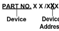
PRODUCT IDENTIFICATION SYSTEM (AUTOMOTIVE)
To order or obtain information, e.g., on pricing or delivery, refer to the factory or the listed sales office.

text_image
PART NO. X X /XXX Device Device Address (1) — Range Package Temperature XXX (2,3)Device: 11LC08 = 8-Kbit, 2.5V UNI/O Serial EEPROM
Device Address: 0 = Standard Address - 0xA0
Tape & Reel: T = Tape and Reel ^(1) Blank = Tube
Temperature I = -40°C to +85°C AEC-Q100 Grade 3 Range: E = -40°C to +125°C AEC-Q100 Grade 1
Package: TT = 3-lead SOT-23 (Tape and Reel only)
Variant ^(2,3) : 16KVAO = Standard Automotive, 16K Process 16KVXX = Customer-Specific Automotive, 16K Process
Examples:
ape1&ReelT-E/TT16KVAO: 8-Kbit, 2.5V Serial EEPROM, Tape and Reel, Automotive Grade 1, Standard address, SOT-23 package
Note 1: Tape and Reel identifier only appears in the catalog part number description. This identifier is used for ordering purposes and is not printed on the device package. Check with your Microchip Sales Office for package availability with the Tape and Reel option.
2: The VAO/VXX automotive variants have been designed, manufactured, tested and qualified in accordance with AEC-Q100 requirements for automotive applications.
3: For customers requesting a PPAP, a customer-specific part number will be generated and provided. A PPAP is not provided for VAO part numbers.
Note the following details of the code protection feature on Microchip products:
• Microchip products meet the specifications contained in their particular Microchip Data Sheet.
- Microchip believes that its family of products is secure when used in the intended manner, within operating specifications, and under normal conditions.
- Microchip values and aggressively protects its intellectual property rights. Attempts to breach the code protection features of Microchip product is strictly prohibited and may violate the Digital Millennium Copyright Act.
- Neither Microchip nor any other semiconductor manufacturer can guarantee the security of its code. Code protection does not mean that we are guaranteeing the product is "unbreakable" Code protection is constantly evolving. Microchip is committed to continuously improving the code protection features of our products.
This publication and the information herein may be used only with Microchip products, including to design, test, and integrate Microchip products with your application. Use of this information in any other manner violates these terms. Information regarding device applications is provided only for your convenience and may be superseded by updates. It is your responsibility to ensure that your application meets with your specifications. Contact your local Microchip sales office for additional support or, obtain additional support at https://www.microchip.com/en-us/support/design-help/client-support-services.
THIS INFORMATION IS PROVIDED BY MICROCHIP "AS IS". MICROCHIP MAKES NO REPRESENTATIONS OR WARRANTIES OF ANY KIND WHETHER EXPRESS OR IMPLIED, WRITTEN OR ORAL, STATUTORY OR OTHERWISE, RELATED TO THE INFORMATION INCLUDING BUT NOT LIMITED TO ANY IMPLIED WARRANTIES OF NON-INFRINGEMENT, MERCHANTABILITY, AND FITNESS FOR A PARTICULAR PURPOSE, OR WARRANTIES RELATED TO ITS CONDITION, QUALITY, OR PERFORMANCE.
IN NO EVENT WILL MICROCHIP BE LIABLE FOR ANY INDIRECT, SPECIAL, PUNITIVE, INCIDENTAL, OR CONSEQUENTIAL LOSS, DAMAGE, COST, OR EXPENSE OF ANY KIND WHATSOEVER RELATED TO THE INFORMATION OR ITS USE, HOWEVER CAUSED, EVEN IF MICROCHIP HAS BEEN ADVISED OF THE POSSIBILITY OR THE DAMAGES ARE FORESEEABLE. TO THE FULLEST EXTENT ALLOWED BY LAW, MICROCHIP'S TOTAL LIABILITY ON ALL CLAIMS IN ANY WAY RELATED TO THE INFORMATION OR ITS USE WILL NOT EXCEED THE AMOUNT OF FEES, IF ANY, THAT YOU HAVE PAID DIRECTLY TO MICROCHIP FOR THE INFORMATION.
Use of Microchip devices in life support and/or safety applications is entirely at the buyer's risk, and the buyer agrees to defend, indemnify and hold harmless Microchip from any and all damages, claims, suits, or expenses resulting from such use. No licenses are conveyed, implicitly or otherwise, under any Microchip intellectual property rights unless otherwise stated.
Trademarks
The Microchip name and logo, the Microchip logo, Adaptec, AVR, AVR logo, AVR Freaks, BesTime, BitCloud, CryptoMemory, CryptoRF, dsPIC, flexPWR, HELDO, IGLOO, JukeBlox, KeeLoq, Kleer, LANCheck, LinkMD, maXStylus, maXTouch, MediaLB, megaAVR, Microsemi, Microsemi logo, MOST, MOST logo, MPLAB, OptoLyzer, PIC, picoPower, PICSTART, PIC32 logo, PolarFire, Prochip Designer, QTouch, SAM-BA, SenGenuity, SpyNIC, SST, SST Logo, SuperFlash, Symmetricom, SyncServer, Tachyon, TimeSource, tinyAVR, UNI/O, Vectron, and XMEGA are registered trademarks of Microchip Technology Incorporated in the U.S.A. and other countries.
AgileSwitch, APT, ClockWorks, The Embedded Control Solutions Company, EtherSynch, Flashtec, Hyper Speed Control, HyperLight Load, Libero, motorBench, mTouch, Powermite 3, Precision Edge, ProASIC, ProASIC Plus, ProASIC Plus logo, Quiet-Wire, SmartFusion, SyncWorld, Temux, TimeCesium, TimeHub, TimePictra, TimeProvider, TrueTime, and ZL are registered trademarks of Microchip Technology Incorporated in the U.S.A.
Adjacent Key Suppression, AKS, Analog-for-the-Digital Age, Any Capacitor, AnyIn, AnyOut, Augmented Switching, BlueSky, BodyCom, Clockstudio, CodeGuard, CryptoAuthentication, CryptoAutomotive, CryptoCompanion, CryptoController, dsPICDEM, dsPICDEM.net, Dynamic Average Matching, DAM, ECAN, Espresso T1S, EtherGREEN, GridTime, IdealBridge, In-Circuit Serial Programming, ICSP, INICnet, Intelligent Paralleling, IntelliMOS, Inter-Chip Connectivity, JitterBlocker, Knob-on-Display, KoD, maxCrypto, maxView, memBrain, Mindi, MiWi, MPASM, MPF, MPLAB Certified logo, MPLIB, MPLINK, MultiTRAK, NetDetach, Omniscient Code Generation, PICDEM, PICDEM.net, PICkit, PICtail, PowerSmart, PureSilicon, QMatrix, REAL ICE, Ripple Blocker, RTAX, RTG4, SAM-ICE, Serial Quad I/O, simpleMAP, SimpliPHY, SmartBuffer, SmartHLS, SMART-I.S., storClad, SQI, SuperSwitcher, SuperSwitcher II, Switchtec, SynchroPHY, Total Endurance, Trusted Time, TSHARC, USBCheck, VariSense, VectorBlox, VeriPHY, ViewSpan, WiperLock, XpressConnect, and ZENA are trademarks of Microchip Technology Incorporated in the U.S.A. and other countries.
SQTP is a service mark of Microchip Technology Incorporated in the U.S.A.
The Adaptec logo, Frequency on Demand, Silicon Storage Technology, and Symmcom are registered trademarks of Microchip Technology Inc. in other countries.
GestIC is a registered trademark of Microchip Technology Germany II GmbH & Co. KG, a subsidiary of Microchip Technology Inc., in other countries.
All other trademarks mentioned herein are property of their respective companies.
© 2011-2023, Microchip Technology Incorporated and its subsidiaries.
All Rights Reserved.
ISBN: 978-1-6683-2185-0
For information regarding Microchip's Quality Management Systems, please visit www.microchip.com/quality.
Worldwide Sales and Service
AMERICAS
Corporate Office
2355 West Chandler Blvd
Chandler, AZ 85224-6199
Tel: 480-792-7200
Fax: 480-792-7277
Technical Support:
http://www.micro-
chip.com/support
Web Address:
www.microchip.com
Atlanta
Duluth, GA
Tel: 678-957-9614
Fax: 678-957-1455
Austin, TX
Tel: 512-257-3370
Boston
Westborough, MA
Tel: 774-760-0087
Fax: 774-760-0088
Chicago
Itasca, IL
Tel: 630-285-0071
Fax: 630-285-0075
Dallas
Addison, TX
Tel: 972-818-7423
Fax: 972-818-2924
Detroit
Novi, MI
Tel: 248-848-4000
Houston, TX
Tel: 281-894-5983
Indianapolis
Noblesville, IN
Tel: 317-773-8323
Fax: 317-773-5453
Tel: 317-536-2380
Los Angeles
Mission Viejo, CA
Tel: 949-462-9523
Fax: 949-462-9608
Tel: 951-273-7800
Raleigh, NC
Tel: 919-844-7510
New York, NY
Tel: 631-435-6000
San Jose, CA
Tel: 408-735-9110
Tel: 408-436-4270
Canada - Toronto
Tel: 905-695-1980
Fax: 905-695-2078
ASIA/PACIFIC
Australia - Sydney
Tel: 61-2-9868-6733
China - Beijing
Tel: 86-10-8569-7000
China - Chengdu
Tel: 86-28-8665-5511
China - Chongqing
Tel: 86-23-8980-9588
China - Dongguan
Tel: 86-769-8702-9880
China - Guangzhou
Tel: 86-20-8755-8029
China - Hangzhou
Tel: 86-571-8792-8115
China - Hong Kong SAR
Tel: 852-2943-5100
China - Nanjing
Tel: 86-25-8473-2460
China - Qingdao
Tel: 86-532-8502-7355
China - Shanghai
Tel: 86-21-3326-8000
China - Shenyang
Tel: 86-24-2334-2829
China - Shenzhen
Tel: 86-755-8864-2200
China - Suzhou
Tel: 86-186-6233-1526
China - Wuhan
Tel: 86-27-5980-5300
China - Xian
Tel: 86-29-8833-7252
China - Xiamen
Tel: 86-592-2388138
China - Zhuhai
Tel: 86-756-3210040
ASIA/PACIFIC
India - Bangalore
Tel: 91-80-3090-4444
India - New Delhi
Tel: 91-11-4160-8631
India - Pune
Tel: 91-20-4121-0141
Japan - Osaka
Tel: 81-6-6152-7160
Japan - Tokyo
Tel: 81-3-6880-3770
Korea - Daegu
Tel: 82-53-744-4301
Korea - Seoul
Tel: 82-2-554-7200
Malaysia - Kuala Lumpur
Tel: 60-3-7651-7906
Malaysia - Penang
Tel: 60-4-227-8870
Philippines - Manila
Tel: 63-2-634-9065
Singapore
Tel: 65-6334-8870
Taiwan - Hsin Chu
Tel: 886-3-577-8366
Taiwan - Kaohsiung
Tel: 886-7-213-7830
Taiwan - Taipei
Tel: 886-2-2508-8600
Thailand - Bangkok
Tel: 66-2-694-1351
Tel: 43-7242-2244-39
Fax: 43-7242-2244-393
Denmark - Copenhagen
Tel: 45-4485-5910
Fax: 45-4485-2829
Finland - Espoo
Tel: 358-9-4520-820
France - Paris
Tel: 33-1-69-53-63-20
Fax: 33-1-69-30-90-79
Germany - Garching
Tel: 49-8931-9700
Germany - Haan
Tel: 49-2129-3766400
Germany - Heilbronn
Tel: 49-7131-72400
Germany - Karlsruhe
Tel: 49-721-625370
Germany - Munich
Tel: 49-89-627-144-0
Fax: 49-89-627-144-44
Germany - Rosenheim
Tel: 49-8031-354-560
Israel - Ra'anana
Tel: 972-9-744-7705
Italy - Milan
Tel: 39-0331-742611
Fax: 39-0331-466781
Italy - Padova
Tel: 39-049-7625286
Netherlands - Drunen
Tel: 31-416-690399
Fax: 31-416-690340
Norway - Trondheim
Tel: 47-7288-4388
Poland - Warsaw
Tel: 48-22-3325737
Romania - Bucharest
Tel: 40-21-407-87-50
Spain - Madrid
Tel: 34-91-708-08-90
Fax: 34-91-708-08-91
Sweden - Gothenberg
Tel: 46-31-704-60-40
Sweden - Stockholm
Tel: 46-8-5090-4654
UK - Wokingham
Tel: 44-118-921-5800
Fax: 44-118-921-5820