SR087DB1 - Power Supply Microchip - Free user manual and instructions
Find the device manual for free SR087DB1 Microchip in PDF.

User questions about SR087DB1 Microchip
0 question about this device. Answer the ones you know or ask your own.
Ask a new question about this device
Download the instructions for your Power Supply in PDF format for free! Find your manual SR087DB1 - Microchip and take your electronic device back in hand. On this page are published all the documents necessary for the use of your device. SR087DB1 by Microchip.
USER MANUAL SR087DB1 Microchip
Inductorless Switching Off-line Power Supply Demoboard
Introduction:
The Supertex SR087DB1 is an inductorless switching power supply intended for operation directly from a 120/230VAC line. Two outputs, 12.6V and 5.0V are provided.
The operating principle is to turn on a pass transistor when the rectified AC input is below the output voltage, and to turn it off when the output storage capacitor is charged up to the regulation point. Since the output capacitor charges up the rising edge of a sine wave, reasonable efficiencies can be obtained without the use of magnetics.
Instructions on page 2 and 3 describe how the demoboard may be modified to better suit applications that are not satisfied by the board as provided. For a full description of SR087, see the SR087 datasheet.
Specifications
| Parameter Value | ||
| AC Input ( V_IN ): | 90 to 270VAC45Hz to 65Hz | |
| Output voltages: V_OUT (no load) V_REG | 12.6V ± 8% ^1 5.0V ± 5% | |
| Output current, max: I_REG I_OUT + I_REG | 120VAC60mA100mA | 230VAC60mA60mA |
| Efficiency, typ. ^2 (full load): 52% 44% | ||
| Standby power, typ. (no load): 62mW 200mW | ||
Notes:
ne 1. Adjustable from 9.0V to 50V.
2. Referenced to V_OUT
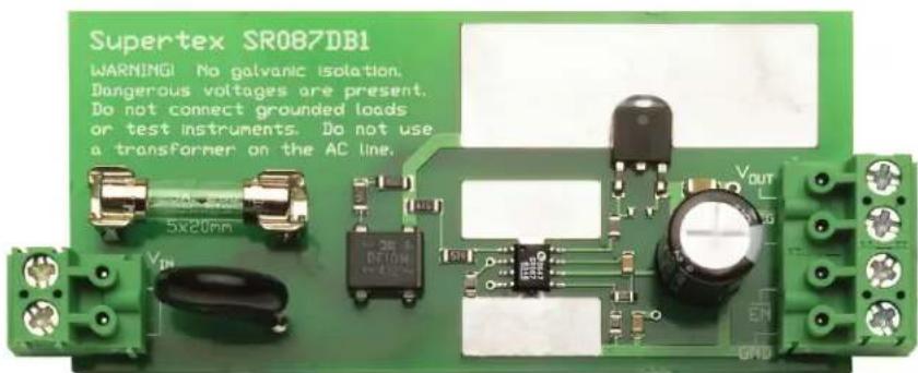
Board Layout and Connection Diagram
text_image
Supertex SR087DB1 WARNING! No galvanic isolation. Dangerous voltages are present. Do not connect grounded loads or test instruments. Do not use a transformer on the AC line.
text_image
WARNING!!! Do not connect earth-grounded loads or test instruments. Doing so will short the AC line, resulting in damage to the instrument, load, and/or the SR087 circuit. Use floating instruments or high voltage differential probes. Do not use a transformer on the AC line. Supertex SR087DB1 Warning! No galvanic isolation. Dangerous voltages are present. Do not connect grounded loads or test equipment. Do not use a transformer on the AC line. WARNING!!! No galvanic isolation. Dangerous voltages are present when connect to the AC line. V_IN 90 - 270VAC 50/60Hz J1 V_IN Z1 R1 R2 R3 D1 R4 IC1 Q1 C5 C2 V_OUT V_REG (12.6V) R8 C1 C3 R6 R5 C4 EN GND J2 V_REG (5.0V) ENABLE GNDTerminal blocks J1 and J2 may be removed by pulling straight up.
Connections:
V_IN - Connect to a 120/230VAC line. The AC input is protected by a 275V metal oxide varistor (MOV) and a 1.25A slow-blow fuse.
Do not use a transformer on the input line. The high inductance creates inductive kickback, which can overload the MOV.
The SR087DB1 will not operate from uninterruptible power supplies having a square wave output. This type of output is usually referred to as “modified sine wave”.
GND - Circuit common. Since galvanic isolation is not provided, connecting this point to an earth-grounded instrument, (such as an oscilloscope), will short the AC line, resulting in circuit and/or instrument damage.
Also note that GND may be at a higher potential with respect to earth ground, even if the AC is switched off. Use caution!
V_OUT - The main output. No-load output voltage is 12.6V. Because the V_OUT storage capacitor (C3) recharges twice per input cycle, this output will have a certain amount of 100/120Hz ripple, depending upon the load. The SR087
regulates the peak output voltage, not the average, thus the average voltage will decrease under load.
V_OUT is adjustable from 9.0 to 50V. See the modifications section on page 3. A source-only external voltage may be applied to this output.
Do not connect earth-grounded loads or instruments!
V_REG - The regulated output, 5.0V nominal output voltage. V_REG is the output of a linear regulator internal to the SR087, which in turn is supplied by V_OUT . Thus any load on V_REG is effectively a load on V_OUT . V_REG requires at least 4.0V of headroom to operate. Being a linear regulator, the SR087 will dissipate power as I_REG is increased, up to 460mW at 60mA.
Enable - A logic low (<0.2V) enables Q_1 switching. A logic high (>0.75 • V_REG ) disables Q_1 , shutting down V_OUT and thus V_REG . However, if an external voltage is applied to V_OUT when disabled, V_REG will continue to function and provide a 5.0V output.
The input has 20kΩ pull-down. If unused, Enable should be left unconnected or connected to ground.
Schematic

text_image
90 to 270VAC 50/60Hz VIN F1 1.25A Z1 275V 50A D1 1.0kV, 1.0A R1 200kΩ R2 200kΩ R3 510kΩ R4 510kΩ Q1 STGD5NB120SZ C2 1.0μF C3 470μF VOUT 12.6VDC GND do not connect to earth ground! not installed optional EMI suppressor R8 0Ω C1 100nF VIN GATE VGD VOUT FB EN 2 EN SR087 GND 3 VREG 5 VREG 4 C4 100nF R7 20kΩ R6 12.4kΩModifications
Output Voltage
V_OUT may be adjusted in the range of 9.0 to 50V ^1 by changing feedback resistor R_5 according to the following equation. Keep in mind that the peak output voltage is regulated, not the average, therefore the average output voltage will decrease (and ripple increase) with increased loads.
$$ R _ {5} = R _ {6} \cdot \left[ \left(V _ {\text {OUT}} / 1. 2 5 V\right) - 1 \right] \quad \text {EQ.} 1 $$
Leave R_6 at 12.4kΩ - it assures a minimum 100μA load required for the proper operation of the SR087. Change 3R and R4 according to the equation 4. It may be necessary to replace C_2 and C_3 with capacitors having a higher voltage rating. For C_3 , use a low ESR capacitor with an adequate ripple current rating (800mArms). Use ceramic for C_2 .
Since V_REG is a linear regulator supplied from V_OUT , the maximum current available from V_REG is reduced as V_OUT is increased due to power considerations.
$$ I _ {R E G (M A X)} = \frac {1 . 5 W}{V _ {O U T} - 3 . 3 V} \quad E Q. 2 $$
or 60mA, whichever is less.
Output Ripple
Storage capacitor C_3 was sized to provide about 2V_P-P ripple at 100mA combined load ( I_OUT + I_REG ). For lighter loads, C_3 may be reduced. Conversely, C_3 may be increased for lower ripple. Use a low ESR capacitor with an adequate ripple current rating (measure using a current probe). Efficiency and output current capability may drop with increased capacitance because of a smaller conduction angle associated with lower ripple. Due to feedback hysteresis, ripple cannot be reduced below 4%.
$$ V _ {R I P P L E (P - P)} \approx \frac {I _ {O U T} + I _ {R E G}}{2 f _ {I N} C _ {3}} \quad \text { EQ.3 } $$
Input Voltage
To reduce standby power for 230VAC-only applications, or for supply voltages less than 90Vrms, R_1 and R_4 should be changed according to equation 4 below. R_1 + R_2 should remain at 400kΩ.
R_2 and R_4 are employed to ensure adequate creepage distances and resistor voltage ratings for 230VAC operation. For 120VAC-only applications they may be omitted (replaced with shorts), with R_1 = 1.0M and R_3 = 430k .
Conducted EMI
As supplied, the SR087DB1 meets 47CFR Part 15 Class B and CISPR 14-1 requirements for conducted emissions at combined load currents ( I_OUT + I_REG ) of less than 20mA. For higher load currents, an RC network ( R_8 & C_5 ) can be used before the IGBT gate to slow down the falling edge. This has the effect of reducing harmonics, lowering conducted EMI. Suggested values of 22kΩ and 390pF allow the SR087DB1 to meet EMI requirements at combined load currents of 60mA for 120VAC and 40mA for 230VAC.
Slowing down the falling edge results in the output voltage overshooting the intended regulation point, causing the peak V_OUT voltage to be higher than expected. This may be compensated for by entering a slightly lower value for V_OUT into equation 1 when selecting feedback resistors. Slowing down the falling edge also increases switching losses, resulting in slightly decreased efficiency.
$$ R _ {3} + R _ {4} \text { Equation } $$
$$ (R 3 + R 4) < \frac {\sqrt {2 V _ {I N} ^ {2} - V _ {X} ^ {2}} - V _ {X} \cos^ {1} \left(\frac {V _ {X}}{\sqrt {2} V _ {I N}}\right)}{\pi \cdot 2 5 \mu A} \text {Eq.4} $$
$$ w h e r e V _ {x} = V _ {o u t} + 1 5 V $$
Use the minimum anticipated RMS value for _IN . Take resistor tolerance into account, selecting the next lower standard value. Choosing a lower value has no effect other than slightly higher standby power.
Note:
- V_REG requires at least 4.0V of headroom to provide 3.3V. Therefore V_OUT including ripple and tolerance, must not fall below 7.3V.
Bill of Materials
| Item # | Description Value Tol Rating | Package Manufacturer | Manufacturer's Part Number | ||||
| F1 Fuse, slow-blow 1.25A - 250V | 5x20mm | any - | |||||
| Z1 | MOV | 275V | - | 50A | 14mm | any | - |
| D1 | Diode bridge | - | - | 1.0kV, 1.0A | - | any | - |
| R1, R2 | Resistor | 200kΩ | 5% | 200V | 1206 | any | - |
| R3, R4 | Resistor | 510kΩ | 5% | 200V | 1206 | any | - |
| R5 | Resistor | 113kΩ | 1% | - | 0805 | any | - |
| R6 | Resistor | 12.4kΩ | 1% | - | 0805 | any | - |
| R7 | Resistor | 20kΩ | 1% | - | 0805 | any | - |
| R8 | not installed | 0Ω | - | - | 0805 | any | - |
| C1 | Capacitor, cer X7R | 100nF | 10% | 25V | 0805 | any | - |
| C2 | Capacitor, cer X7R | 1.0μF | 10% | 25V | 1206 | any | - |
| C3 | Capacitor, alum, Io ESR | 470μF | 20% | 25V, 800mA ^1 | - | Nichicon | UHE1E471MPD6 |
| C4 | Capacitor, cer X7R | 100μF | 10% | 16V | 0805 | any | - |
| C5 | not installed | - | - | - | 0805 | - | - |
| Q1 | IGBT | - | - | 1.2kV, 5.0A | D-pak | ST | STGD5NB120SZ |
| IC1 Power supply controller | -- | - | Power 8-Lead SOIC | Supertex | SR087SG-G | ||
Note: 1. At 100/120Hz
Supertex inc. does not recommend the use of its products in life support applications, and will not knowingly sell them for use in such applications unless it receives an adequate “product liability indemnification insurance agreement.” Supertex Inc. does not assume responsibility for use of devices described, and limits its liability to the replacement of the devices determined defective due to workmanship. No responsibility is assumed for possible omissions and inaccuracies. Circuitry and specifications are subject to change without notice. For the latest product specifications refer to the Supertex Inc. (website: http://www.supertex.com)
©2014 Supertex inc. All rights reserved. Unauthorized use or reproduction is prohibited.