SR10DB1 - Power Supply Microchip - Free user manual and instructions
Find the device manual for free SR10DB1 Microchip in PDF.

User questions about SR10DB1 Microchip
0 question about this device. Answer the ones you know or ask your own.
Ask a new question about this device
Download the instructions for your Power Supply in PDF format for free! Find your manual SR10DB1 - Microchip and take your electronic device back in hand. On this page are published all the documents necessary for the use of your device. SR10DB1 by Microchip.
USER MANUAL SR10DB1 Microchip
Inductorless Switching Power Supply Demoboard
Introduction:
The Supertex SR10 is an inductorless switching power supply controller intended for operation directly from a rectified 120/240VAC line. Due to the capacitor-coupled, switched shunt topology (CCSS), it exhibits low standby power and good efficiency while employing no magnetics nor high voltage electrolytic capacitors.
To meet a wide variety of applications, the SR10DB1 is highly configurable. Many components are socketed. Half or full-wave rectification is jumper-selectable. Output voltage is jumper-selectable to 3 fixed voltages or may be set anywhere in the range of 6 - 28V using an on-board feedback divider.
Specifications
| Parameter Value | |
| AC Input | 90VAC to 275VAC50Hz to 60Hz |
| Output voltage | 6V, 12V, 24V ±10%or 6-28V using divider |
| Output current^1 | up to 50mA |
| No-load input power^1 | as low as 20mW |
| Efficiency^1 | up to 75% |
| Actual board size 88mm x 28mm | |
Notes:
1. Dependent upon configuration and degree of transient protection.
Board Layout and Connection Diagram
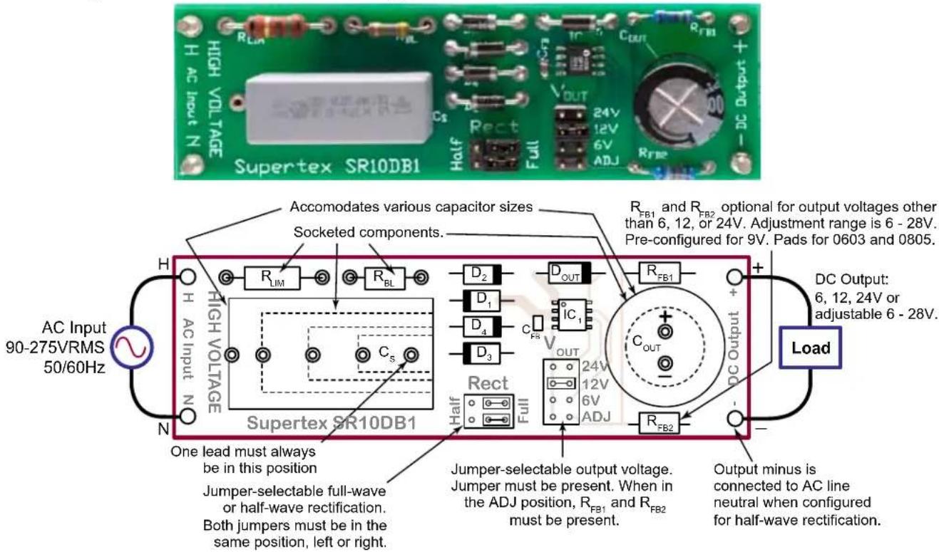
text_image
High voltage Supertex SR10DB1 AC Input 90-275VRMS 50/60Hz H AC Input N R_LIM High voltage R_BL C_s AC input N N Supertex SR10DB1 Accomodates various capacitor sizes Socketed components. R_FB1 and R_FB2 optional for output voltages other than 6, 12, or 24V. Adjustment range is 6 - 28V. Pre-configured for 9V. Pads for 0603 and 0805. D_2 D_1 D_4 D_3 D_OUT IC_1 C_Fs R_FB1 R_FB2 C_OUT DC Output: 6, 12, 24V or adjustable 6 - 28V. Load One lead must always be in this position Jumper-selectable full-wave or half-wave rectification. Both jumpers must be in the same position, left or right. Jumper-selectable output voltage. Jumper must be present. When in the ADJ position, R_FB1 and R_FB2 must be present. Output minus is connected to AC line neutral when configured for half-wave rectification.AC Input (H and N)
Connect to the AC line. The 'H' terminal should be connected to the AC line hot conductor. The 'N' terminal should be connected to the AC line neutral conductor. When configured for half-wave rectification, the N terminal is connected to the DC output minus (−) terminal.
DC Output (+ and -)
Connect the load to these terminals. Do not connect earth-grounded loads or test equipment without using an isolation transformer on the AC line.
Output voltage is jumper-selectable at 6, 12, or 24V, or it may be set in the range of 6 - 28V using the R _FB feedback divider and setting the jumper to ADJ.
Schematic
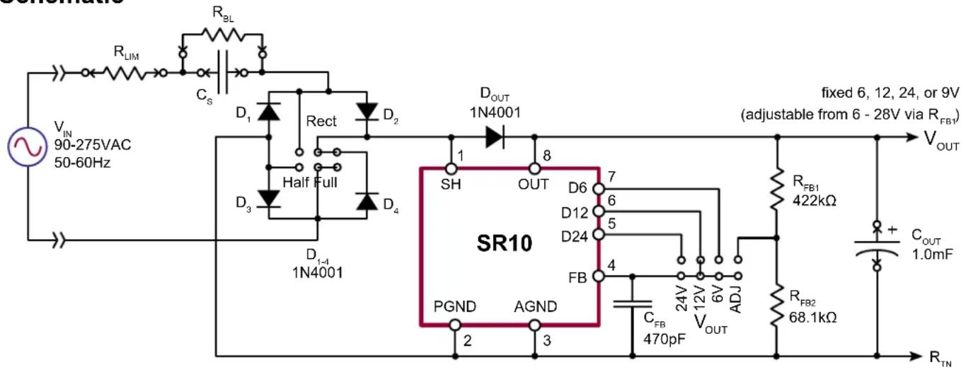
text_image
V_IN 90-275VAC 50-60Hz R_LIM R_BL C_S D_1 Rect D_2 D_3 Half Full D_4 D_{1-4} 1N4001 D_OUT 1N4001 SR10 1 8 SH OUT D6 7 6 D12 5 D24 FB 4 PGND AGND 2 3 C_FB 470pF 24V 12V 6V ADJ V_OUT fixed 6, 12, 24, or 9V (adjustable from 6 - 28V via R_FB1) R_FB1 422kΩ R_FB2 68.1kΩ R_TN + C_OUT 1.0mFBill of Materials
| Designation | Description | Value | Rating | Mfg | PN |
| R_LIM | Resistor, fusible | 22Ω | 2W | any | — |
| R_BL | Resistor | 4.7MΩ | 1/4W | any | — |
| R_FB1 | Resistor | 422kΩ | 1/4W | any | — |
| R_FB2 | Resistor | 68.1kΩ | 1/4W | any | — |
| C_S | Capacitor, film | 220nF to 2.2μF | 275VAC,X2 | any | — |
| C_OUT | Capacitor, alum | 220μF min | 35V | any | — |
| C_FB | Capacitor, ceramic NPO | 470pF | 6V | any | — |
| D_1-4 | Rectifier | — | 1A, 50V | any | 1N4001 |
| D_OUT | Rectifier | — | 1A, 50V | any | 1N4001 |
| IC_1 | CCSS regulator | — | — | Supertex | SR10 |
Socketed Components
The SR10DB1 is provided with all components pre-installed. Other components may be substituted for the on-board components to meet other requirements.
Refer to the above schematic and BOM, and the drawing and photo on page 1 to determine the proper locations for the components.
Output Voltage
Fixed output voltages of 6V, 12V, or 24V may be selected by setting the appropriate jumper on the V_OUT header.
For other output voltages, the on-board resistive feedback divider may be used to provide any voltage in the range of 6 - 28V. To maintain a minimum 15 A through the feedback divider, only R_FB1 should be changed.
$$ R _ {F B 1} = R _ {F B 2} \left(\frac {V _ {O U T}}{V _ {F B}} - 1\right) = 6 8. 1 k \Omega \left(\frac {V _ {O U T}}{1 . 2 5 V} - 1\right) $$
Output Current ( C_s selection)
Output current is primarily dependent on input voltage, C_s value, and rectification (full or half). Given the minimum input voltage and choice of rectification, the minimum value of C_s
is given by the following equations. Don't forget to take tolerances into account. The SR10 is powered by V_OUT , so the available output current is reduced by the SR10's operating current (150μA nom, 200μA max). Current may also be reduced \~5% due to losses.
For standard capacitance values, see the table on page 4.
Full-wave:
$$ C _ {s} \geq \frac {I _ {O U T}}{4 f _ {I N} (V _ {I N} \sqrt {2} - V _ {O U T} - 3 V _ {D})} $$
Half-wave:
$$ C _ {s} \geq \frac {I _ {O U T}}{f _ {I N} (2 V _ {I N} \sqrt {2} - V _ {O U T} - 2 V _ {D})} $$
where: I_OUT is the maximum output current
f_IN is the AC line frequency
C_s is the series cap on the AC line
V_IN is the RMS AC line voltage
V_OUT is the DC output voltage
V_D is the diode forward voltage ( 700mV )
Limiting Resistor ( R_LIM )
The limiting resistor in series with the AC line is to protect against transients on the AC line. For safety reasons it fusible and is the most upstream component on the AC line. Higher values provide greater protection but at the expense of higher losses.
$$ P _ {\mathrm{LIM}} \approx (V _ {I N} \cdot 2 \pi f _ {I N} \cdot C _ {S}) ^ {2} \cdot R _ {L I M} $$
Output Capacitor ( C_OUT )
The output capacitor serves 2 functions - it supplies the load when the shunt is on, and helps absorb transients on the AC line. The supplied value may be lowered but at the expense of higher ripple voltage and increased output voltage during a transient.
Input Power Measurements
The high ratio between the imaginary and real power components makes power measurements difficult. To make accurate measurements of real power, the imaginary component may be eliminated by measuring input voltage after C_s . This excludes C_s losses, but AC rated film capacitors exhibit very low losses, so the error is minimal.
Since the PCB is laid out with R_LIM upstream of C_S for safety reasons, it must be relocated after C_S if R_LIM losses are to be included.
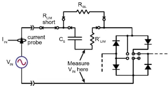
text_image
R_LIM short R_BL I_IN current probe C_S R'_LIM V_IN Measure V_IN hereDo not connect earth-grounded instruments when operating off the AC line! Use either battery-powered equipment, high voltage differential probes, or an isolation transformer on the AC line. Note that many Variacs (variable transformers) do not provide isolation.
Ideally, R_BL should be removed. Its contribution to loss is approximately V_IN^2 / R_BL
Since the input current is not a perfect sine wave, real power cannot be obtained by simply multiplying RMS input current by RMS input voltage. One way to make correct measurements is by multiplying instantaneous current by instantaneous voltage on a time-point basis and taking the average over an integer number of 50/60Hz cycles. At low load currents the shunt turns off only occasionally, requiring a long time window for accurate power measurements.
is This measurement technique may be performed on most digital oscilloscopes. When taking the average, be sure to window the average over an integer number of cycles.
Driving LEDs
The SR10 can be configured to provide a constant-current output to drive LEDs. A current sense resistor ( R_SNS ) is used to convert LED current to the 1.25V feedback voltage required by the SR10.
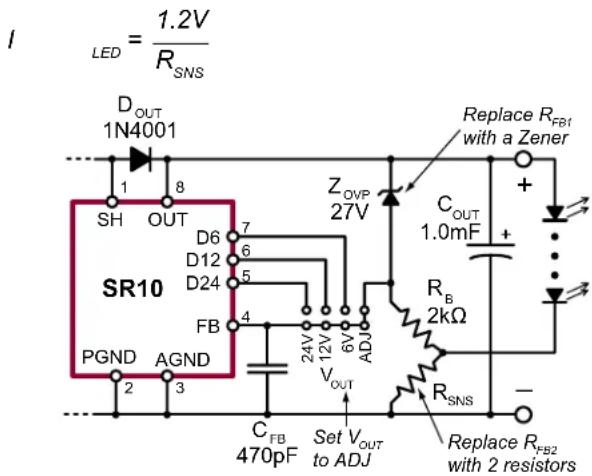
text_image
LED = 1.2V R_SNS D_OUT 1N4001 SH OUT SR10 PGND AGND 2 3 7 6 5 4 FB D6 D12 D24 Z_OVP 27V 24V 12V 6V ADJ V_OUT C_FB 470pF Set V_OUT to ADJ C_OUT 1.0mF + + R_B 2kΩ R_SNS - Replace R_FB1 with a Zener Replace R_FB2 with 2 resistorsDriving LEDs
When operated over a wide supply voltage range, a small C_OUT can result in overcharging at higher line voltages. It may take several cycles for the voltage to drop back down to the regulation threshold. This may cause visible flicker. The remedy is to increase C_OUT .
To protect against open LEDs, an overvoltage protection (OVP) circuit is employed. The OVP level is set by the value of the OVP Zener. R_B limits the current thru the Zener.
$$ V _ {O V P} = V _ {z} + 1. 2 V $$
C_s Table
The following table is based on the previously provided equations for C_s . Actual output current may be less due to losses ( 5% less). AC line voltage is assumed to be 90 - 135VRMS @ 60Hz or 190 - 275VRMS @ 50Hz. Slashed cells exceed recommended operating conditions for peak shunt current at 85°C.
For universal 120V and 240V operation choose C_s based on 120VAC and make sure that operation at 240VAC does not fall in a slashed cell. The relevant cells are adjacent to each other. For example, if 50mA at 12V is needed and full rectification used, a C_s capacitor of 2.2 F ± 10% provides 53.8mA at 120VAC (90VAC low line). But at 240VAC, the cell to the right (240VAC column) is slashed, and universal operation is not possible. This assumes 120VAC low line is 90VAC and 240VAC high line is 275VAC. For other high/low voltages use the equations.
Output current capability (mA)
| C_s | C_sTol | 6V Output 12V Output 24V Output | |||||||||||
| Half Full Half Full Half Full | |||||||||||||
| 120V 60Hz | 240V 50Hz | 120V 60Hz | 240V 50Hz | 120V 60Hz | 240V 50Hz | 120V 60Hz | 240V 50Hz | 120V 60Hz | 240V 50Hz | 120V 60Hz | 240V 50Hz | ||
| 220nF | 10% 2 | 9 5.2 5.7 | 10.3 2.9 | 5.2 5.4 | 10.1 2.7 | 5.1 4.8 | 9.6 | ||||||
| 20% 2 | 6 4.7 5.0 | 9.2 2.5 | 4.6 4.8 9 | 0.2 4.4 | 5 4.3 8.5 | ||||||||
| 330nF | 10% 4 | 4 7.9 8.5 | 15.5 4.3 | 7.8 8.1 | 15.1 4.1 | 7.6 7.2 | 14.4 | ||||||
| 20% | 3.9 | 7.0 | 7.6 | 13.8 | 3.8 | 6.9 | 7.2 | 13.4 | 3.6 | 6.8 | 6.4 | 12.8 | |
| 470nF | 10% 6 | 3 11.2 1 | 2.1 22.0 | 6.1 11.1 | 11.5 21.5 | 5 5.8 10.8 | 10.3 20.5 | ||||||
| 20% 5 | 6 10.0 1 | 0.8 19.6 | 5.4 9.9 1 | 0.2 19.1 | 5.2 9.6 | 9.1 18.2 | |||||||
| 680nF | 10% 9 | 1 16.2 1 | 7.5 31.9 | 8.9 16.0 | 16.6 31.2 | 8.4 15.7 | 14.9 29.7 | ||||||
| 20% 8 | 1 14.4 1 | 5.6 28.4 | 7.9 14.3 | 14.8 27.7 | 7.5 13.9 | 13.2 26.4 | |||||||
| 1.0μF | 10% | 13.3 | 23.9 | 25.7 | 46.9 | 13.0 | 23.6 | 24.4 | 45.8 | 12.4 | 23.0 | 21.9 | 43.7 |
| 20% 1 | 1.9 21.2 | 22.9 41.7 | 11.6 21 | 0 21.7 | 40.7 11.0 | 20.5 19 | 4 38.8 | ||||||
| 1.5μF | 10% | 20.0 | 35.8 | 38.6 | 70.4 | 19.5 | 35.4 | 36.7 | 68.7 | 18.6 | 34.6 | 32.8 | 65.5 |
| 20% | 17.8 | 31.8 | 34.3 | 62.5 | 17.4 | 31.4 | 32.6 | 61.1 | 16.5 | 30.7 | 29.1 | 58.2 | |
| 2.2μF | 10% | 29.4 | 52.5 | 56.6 | 103.2 | 28.6 | 51.9 | 53.8 | 100.8 | 27.2 | 50.7 | 48.1 | 96.1 |
| 20% | 6.1 46.6 | 50.3 91.7 | 25.5 46.1 | 47.8 | 89.6 24.2 | 45.1 42.7 | 85.4 | ||||||

= Exceeds Recommended Operating Limits
Supertex inc. does not recommend the use of its products in life support applications, and will not knowingly sell them for use in such applications unless it receives an adequate "product liability indemnification insurance agreement." Supertex Inc. does not assume responsibility for use of devices described, and limits its liability to the replacement of the devices determined defective due to workmanship. No responsibility is assumed for possible omissions and inaccuracies. Circuitry and specifications are subject to change without notice. For the latest product specifications refer to the Supertex inc. (website: http://www.supertex.com)