PIC32MZ1024ECM124 - Electronic component Microchip - Free user manual and instructions
Find the device manual for free PIC32MZ1024ECM124 Microchip in PDF.

User questions about PIC32MZ1024ECM124 Microchip
0 question about this device. Answer the ones you know or ask your own.
Ask a new question about this device
Download the instructions for your Electronic component in PDF format for free! Find your manual PIC32MZ1024ECM124 - Microchip and take your electronic device back in hand. On this page are published all the documents necessary for the use of your device. PIC32MZ1024ECM124 by Microchip.
USER MANUAL PIC32MZ1024ECM124 Microchip
32-bit MCUs (up to 2 MB Live-Update Flash and 512 KB SRAM) with Audio and Graphics Interfaces, HS USB, Ethernet, and Advanced Analog
Operating Conditions
- 2.3V to 3.6V, -40°C to +85°C, DC to 200 MHz
Core: 200 MHz (up to 330 DMIPS) microAptiv™
• 16 KB I-Cache, 4 KB D-Cache
- MMU for optimum embedded OS execution
- microMIPS™ mode for up to 35% smaller code size
- DSP-enhanced core:
- Four 64-bit accumulators
- Single-cycle MAC, saturating and fractional math
• Code-efficient (C and Assembly) architecture
Clock Management
- Internal oscillator
- Programmable PLLs and oscillator clock sources
• Fail-Safe Clock Monitor (FSCM) - Independent Watchdog Timers (WDT) and Deadman Timer (DMT)
- Fast wake-up and start-up
Power Management
- Low-power modes (Sleep and Idle)
- Integrated Power-on Reset and Brown-out Reset
Memory Interfaces
• 50 MHz External Bus Interface (EBI)
• 50 MHz Serial Quad Interface (SQI)
Audio and Graphics Interfaces
• Graphics interfaces: EBI or PMP
• Audio data communication: I ^2 S, LJ, and RJ
• Audio control interfaces: SPI and I 2C
• Audio master clock: Fractional clock frequencies with USB synchronization
High-Speed (HS) Communication Interfaces (with Dedicated DMA)
• USB 2.0-compliant Hi-Speed On-The-Go (OTG) controller
• 10/100 Mbps Ethernet MAC with MII and RMII interface
Security Features
- Crypto Engine with a RNG for data encryption/decryption and authentication (AES, 3DES, SHA, MD5, and HMAC)
- Advanced memory protection:
- Peripheral and memory region access control
Direct Memory Access (DMA)
• Eight channels with automatic data size detection
- Programmable Cyclic Redundancy Check (CRC)
Advanced Analog Features
• 10-bit ADC resolution and up to 48 analog inputs
• Flexible and independent ADC trigger sources
- Two comparators with 32 programmable voltage references
• Temperature sensor with ±2°C accuracy
Communication Interfaces
- Two CAN modules (with dedicated DMA channels): - 2.0B Active with DeviceNet™ addressing support
- Six UART modules (25 Mbps):
- Supports LIN 1.2 and IrDA ^® protocols
- Six 4-wire SPI modules
- SQI configurable as an additional SPI module (50 MHz)
• F i 2Cmodules (up to 1 Mbaud) with SMBus support
• Parallel Master Port (PMP) - Peripheral Pin Select (PPS) to enable function remap
Timers/Output Compare/Input Capture
- Nine 16-bit or up to four 32-bit timers/counters
• Nine Output Compare (OC) modules
• Nine Input Capture (IC) modules - PPS to enable function remap
• Real-Time Clock and Calendar (RTCC) module
Input/Output
- 5V-tolerant pins with up to 32 mA source/sink
- Selectable open drain, pull-ups, and pull-downs
• External interrupts on all I/O pins
Qualification and Class B Support
• Class B Safety Library, IEC 60730
- Back-up internal oscillator
Debugger Development Support
• In-circuit and in-application programming
• 4 - w i r®EnInMancePJTAG interface
• Unlimited software and 12 complex breakpoints
- IEEE 1149.2-compatible (JTAG) boundary scan
• Non-intrusive hardware-based instruction trace
Software and Tools Support
• C/C++ compiler with native DSP/fractional support
• M P L® Harmony Integrated Software Framework
• TCP/IP, USB, Graphics, and mTouch™ middleware
- MFi, Android™, and Bluetooth ^ audio frameworks
- RTOS Kernels: Express Logic ThreadX, FreeRTOS™, OPENRTOS®, Micriμm® μC/OS™, and SEGGER embOS®
Packages
| Type QFN TQFP VTLA LQFP | |||||||
| Pin Count | 64 | 64 | 100 | 144 | 124 | 144 | |
| I/O Pins (up to) | 53 | 53 | 78 | 120 | 98 | 120 | |
| Contact/Lead Pitch | 0.50 mm | 0.50 mm | 0.40 mm | 0.50 mm | 0.40 mm | 0.50 mm | 0.50 mm |
| Dimensions | 9x9x0.9 mm | 10x10x1 mm | 12x12x1 mm | 14x14x1 mm | 16x16x1 mm | 9x9x0.9 mm | 20x20x1.40 mm |
TABLE 1: PIC32MZ EC FAMILY FEATURES
| Device | Program Memory (KB) | Data Memory (KB) | Pins | Packages | Boot Flash Memory (KB) | Remappable Peripherals | Crypto | RNG | DMA Channels (Programmable/Dedicated) | ADC (Channels) | Analog Comparators | USB 2.0 HS OTG | I^2C | PMP | EBI | SQI | RTCC | Ethernet | I/O Pins | JTAG | Trace | |||||
| Remappable Pins | Timers/Capture ^(1) Compare ^(1) | UART | SPIU ^2 S | External Interrupts ^(2) | CAN 2.0B | |||||||||||||||||||||
| PIC32MZ1024ECG064 | 1024 | 512 64 | TQFP, QFN | 160 34 | 9/9/9 | 6 4 5 | 0 | N | Y | 8 | / / 24 | 1 1 1 1 1 | 2 5 8 2 5 8 | 4 | Y | N | Y | Y | Y | 46 | Y | Y | ||||
| PIC32MZ1024ECH064 | 2 | N | Y | 8 | ||||||||||||||||||||||
| PIC32MZ1024ECM064 | 2 | Y | Y | 8 | ||||||||||||||||||||||
| PIC32MZ2048ECG064 | 2048 | 0 | N | Y | 8 | |||||||||||||||||||||
| PIC32MZ2048ECH064 | 2 | N | Y | 8 | ||||||||||||||||||||||
| PIC32MZ2048ECM064 | 2 | Y | Y | 8 | ||||||||||||||||||||||
| PIC32MZ1024ECG100 | 1024 | 512 | 100 | TQFP | 160 | 51 | 9/9/9 | 6 | 6 | 5 | 0 | N | Y | 8 | / / 40 | 1 1 1 1 | 2 5 8 2 5 8 | 5 | Y | Y | Y | Y | Y | 78 | Y | Y |
| PIC32MZ1024ECH100 | 2 | N | Y | 8 | ||||||||||||||||||||||
| PIC32MZ1024ECM100 | 2 | Y | Y | 8 | ||||||||||||||||||||||
| PIC32MZ2048ECG100 | 2048 | 0 | N | Y | 8 | |||||||||||||||||||||
| PIC32MZ2048ECH100 | 2 | N | Y | 8 | ||||||||||||||||||||||
| PIC32MZ2048ECM100 | 2 | Y | Y | 8 | ||||||||||||||||||||||
| PIC32MZ1024ECG124 | 1024 | 512 | 124 | VTLA | 160 | 53 | 9/9/9 | 6 | 6 | 5 | 0 | N | Y | 8 | / / 48 | 1 1 1 1 | 2 5 8 2 5 8 | 5 | Y | Y | Y | Y | Y | 97 | Y | Y |
| PIC32MZ1024ECH124 | 2 | N | Y | 8 | ||||||||||||||||||||||
| PIC32MZ1024ECM124 | 2 | Y | Y | 8 | ||||||||||||||||||||||
| PIC32MZ2048ECG124 | 2048 | 0 | N | Y | 8 | |||||||||||||||||||||
| PIC32MZ2048ECH124 | 2 | N | Y | 8 | ||||||||||||||||||||||
| PIC32MZ2048ECM124 | 2 | Y | Y | 8 | ||||||||||||||||||||||
| PIC32MZ1024ECG144 | 1024 | 512 | 144 | LQFP, TQFP | 160 53 | 9/9/9 | 6 6 5 | 0 | N | Y | 8 | / / 48 | 1 1 1 1 | 2 5 8 2 5 8 | 5 | Y | Y | Y | Y | Y | 120 | Y | Y | |||
| PIC32MZ1024ECH144 | 2 | N | Y | 8 | ||||||||||||||||||||||
| PIC32MZ1024ECM144 | 2 | Y | Y | 8 | ||||||||||||||||||||||
| PIC32MZ2048ECG144 | 2048 | 0 | N | Y | 8 | |||||||||||||||||||||
| PIC32MZ2048ECH144 | 2 | N | Y | 8 | ||||||||||||||||||||||
| PIC32MZ2048ECM144 | 2 | Y | Y | 8 | ||||||||||||||||||||||
Note 1: Eight out of nine timers are remappable.
2: Four out of five external interrupts are remappable.
Device Pin Tables
TABLE 2: PIN NAMES FOR 64-PIN DEVICES
| 64-PIN QFN(4) AND TQFP (TOP VIEW)PIC32MZ0512EC(E/F/K)064PIC32MZ1024EC(G/H/M)064PIC32MZ1024EC(E/F/K)064PIC32MZ2048EC(G/H/M)064 | ||||
| Pin # Full Pin Name Pin # Full Pin Name | ||||
| 1 AN 17/ETXEN/RPE5/PMD5/RE5 | 33 | VBUS | ||
| 2 AN 16/ETXD0/PMD6/RE6 34 V | USB3V3 | |||
| 3 AN 15/ETXD1/PMD7/RE7 35 V | SS | |||
| 4 AN 14/C1IND/RPG6/SCK2/PMA5/RG6 36 D- | ||||
| 5 AN 13/C1INC/RPG7/SDA4/PMA4/RG7 37 D+ | ||||
| 6 AN 12/C2IND/RPG8/SCL4/PMA3/RG8 38 RPF3/USBID/RF3 | ||||
| 7 Vss | 39 | VDD | ||
| 8 VDD | 40 | Vss | ||
| 9 M C L R | 41 RPF4/SDA5/PMA9/RF4 | |||
| 10 AN 11/C2INC/RPG9/PMA2/RG9 | 42 RP | F5/SCL5/PMA8/RF5 | ||
| 11 AN 45/C1INA/RPB5/RB5 | 43 AE | RXD0/ETXD2/RPD9/SDA1/PMCS2/PMA15/RD9 | ||
| 12 AN 4/C1INB/RB4 | 44 E | OL/RPD10/SCL1/SCK4/RD10 | ||
| 13 AN 3/C2INA/RPB3/RB3 | 45 AE | RXCLK/AEREFCLK/ECRS/RPD11/PMCS1/PMA14/RD11 | ||
| 14 AN 2/C2INB/RPB2/RB2 | 46 AE | RXD1/ETXD3/RPD0/RTCC/INT0/RD0 | ||
| 15 PGEC1/V REF-/CVREF-/AN1/RPB1/RB1 | 47 SO | SCI/RPC13/RC13 | ||
| 16 PGED1/V REF+/CVREF+/AN0/RPB0/PMA6/RB0 | 48 SO | SCO/RPC14/T1CK/RC14 | ||
| 17 PGEC2/AN46/RPB6/RB6 | 49 E | MDIO/AEMDIO/RPD1/SCK1/RD1 | ||
| 18 PGED2/AN47/RPB7/RB7 | 50 ET | XERR/AETXEN/RPD2/SDA3/RD2 | ||
| 19 AV DD | 51 | AERXERR/ETXCLK/RPD3/SCL3/RD3 | ||
| 20 AVss | 52 SO | ICS0/RPD4/PMWR/RD4 | ||
| 21 AN 48/RPB8/PMA10/RB8 | 53 | SQICS1/RPD5/PMRD/RD5 | ||
| 22 AN 49/RPB9/PMA7/RB9 | 54 V | DD | ||
| 23 TMS/CV REFOUT/AN5/RPB10/PMA13/RB10 | 55 | Vss | ||
| 24 TDO/AN6/PMA12/RB11 | 56 ERXD3/AETXD1/RPF0/RF0 | |||
| 25 Vss | 57 | TRCLK/SQICLK/ERXD2/AETXD0/RPF1/RF1 | ||
| 26 VDD | 58 TR | D0/SQID0/ERXD1/PMD0/RE0 | ||
| 27 TCK/AN7/PMA11/RB12 | 59 V | SS | ||
| 28 TDI/AN8/RB13 | 60 V | DD | ||
| 29 AN 9/RPB14/SCK3/PMA1/RB14 | 61 TRD1 | SQID1/ERXD0/PMD1/RE1 | ||
| 30 AN 10/EMDC/AEMDC/RPB15/OCFB/PMA0/RB15 | 62 TR | D2/SQID2/ERXDV/ECRSDV/AECRSDV/PMD2/RE2 | ||
| 31 OSC1/CLKI/RC12 | 63 TR | D3/SQID3/ERXCLK/EREFCLK/RPE3/PMD3/RE3 | ||
| 32 OSC2/CLKO/RC15 | 64 AN 18 | ERXERR/PMD4/RE4 | ||
Note 1: The RPn pins can be used by remappable peripherals. See Table 1 for the available peripherals and Section 12.3 "Peripheral Pin Select (PPS)" for restrictions.
2: Every I/O port pin (RBx-RGx) can be used as a change notification pin (CNBx-CNGx). See Section 12.0 "I/O Ports" for more information.
3: Shaded pins are 5V tolerant.
4: The metal plane at the bottom of the device is not connected to any pins and is recommended to be connected to Vss externally.
TABLE 3: PIN NAMES FOR 100-PIN DEVICES
100-PIN TQFP (TOP VIEW)PIC32MZ0512EC(E/F/K)100PIC32MZ1024EC(G/H/M)100PIC32MZ1024EC(E/F/K)100PIC32MZ2048EC(G/H/M)100  | ||||
| Pin # | Full Pin Name Pin # Full Pin Name | F13 | ||
| 1 AN23/AERXERR/RG15 36 V | SS | |||
| 2 EBIA5/AN34/PMA5/RA5 37 V | DD | |||
| 3 EBID5/AN17/RPE5/PMD5/RE5 38 TCK/EBIA19/AN29/RA1 | ||||
| 4 EBID6/AN16/PMD6/RE6 39 TDI/EBIA18/AN30/RPF13/SCK5/R | ||||
| 5 EBID7/AN15/PMD7/RE7 40 TDO/EBIA17/AN31/RPF12/RF12 | ||||
| 6 EBIA6/AN22/RPC1/PMA6/RC1 41 EBIA11/AN7/ERXD0/AECRS/PMA11/RB12 | ||||
| 7 EBIA12/AN21/RPC2/PMA12/RC2 | 42 AN8/ERXD1/AECOL/RB13 | |||
| 8 EBWE/AN20/RPC3/PMWR/RC3 | 43 EBIA1/AN9/ERXD2/AETXD3/RPB14/SCK3/PMA1/RB14 | |||
| 9 EBIOE/AN19/RPC4/PMRD/RC4 | 44 EBIA0/AN10/ERXD3/AETXD2/RPB15/OCFB/PMA0/RB15 | |||
| 10 AN14/C1IND/ECOL/RPG6/SCK2/RG6 | 45 V | SS | ||
| 11 EBIA4/AN13/C1INC/ECRS/RPG7/SDA4/PMA4/RG7 | 46 V | DD | ||
| 12 EBIA3/AN12/C2IND/ERXDV/ECRSDV/AERXDV/AECRSDV/RPG8/SCL4/PMA3/RG8 | 47 AN32/AETXD0/RPD14/RD14 | |||
| 13 Vss | 48 AN33/AETXD1/RPD15/SCK6/RD15 | |||
| 14 VDD | 49 OSC1/CLKI/RC12 | |||
| 15 MCLR | 50 OSC2/CLKO/RC15 | |||
| 16 EBIA2/AN11/C2INC/ERXCLK/EREFCLK/AERXCLK/AEREFCLK/RPG9/PMA2/RG9 | 51 | Vbus | ||
| 17 TMS/EBIA16/AN24/RA0 52 V | USB3V3 | |||
| 18 AN25/AERXD0/RPE8/RE8 | 53 V | SS | ||
| 19 AN26/AERXD1/RPE9/RE9 | 54 D- | |||
| 20 AN45/C1INA/RPB5/RB5 | 55 D+ | |||
| 21 AN4/C1INB/RB4 | 56 RPF3/USBID/RF3 | |||
| 22 AN3/C2INA/RPB3/RB3 | 57 EBIRDY3/RPF2/SDA3/RF2 | |||
| 23 AN2/C2INB/RPB2/RB2 | 58 EBIRDY2/RPF8/SCL3/RF8 | |||
| 24 PGEC1/AN1/RPB1/RB1 | 59 EBICS0/SCL2/RA2 | |||
| 25 PGED1/AN0/RPB0/RB0 | 60 EBIRDY1/SDA2/RA3 | |||
| 26 PGEC2/AN46/RPB6/RB6 | 61 EBIA14/PMCS1/PMA14/RA4 | |||
| 27 PGED2/AN47/RPB7/RB7 | 62 V | DD | ||
| 28 VREF-/CVREF-/AN27/AERXD2/RA9 | 63 V | SS | ||
| 29 VREF+/CVREF+/AN28/AERXD3/RA10 | 64 EBIA9/RPF4/SDA5/PMA9/RF4 | |||
| 30 AV DD | 65 EBIA8/RPF5/SCL5/PMA8/RF5 | |||
| 31 AV SS | 66 AETXCLK/RPA14/SCL1/RA14 | |||
| 32 EBIA10/AN48/RPB8/PMA10/RB8 | 67 AETXEN/RPA15/SDA1/RA15 | |||
| 33 EBIA7/AN49/RPB9/PMA7/RB9 | 68 EBIA15/RPD9/PMCS2/PMA15/RD9 | |||
| 34 EBIA13/CV REFOUT/AN5/RPB10/PMA13/RB10 | 69 RPD10/SCK4/RD10 | |||
| 35 AN6/ERXERR/AETXERR/RB11 | 70 EMDC/AEMDC/RPD11/RD11 | |||
Note 1: The RPn pins can be used by remappable peripherals. See Table 1 for the available peripherals and Section 12.3 "Peripheral Pin Select (PPS)" for restrictions.
2: Every I/O port pin (RAx-RGx) can be used as a change notification pin (CNAx-CNGx). See Section 12.0 "I/O Ports" for more information.
3: Shaded pins are 5V tolerant.
TABLE 3: PIN NAMES FOR 100-PIN DEVICES (CONTINUED)
100-PIN TQFP (TOP VIEW)PIC32MZ0512EC(E/F/K)100PIC32MZ1024EC(G/H/M)100PIC32MZ1024EC(E/F/K)100PIC32MZ2048EC(G/H/M)100  | ||||
| Pin # | Full Pin Name | Pin # | Full Pin Name | |
| 71 EMDIO/AEMDIO/RPD0/RTCC/INT0/RD0 86 EBID10/ETXD0/RPF1 | /PMD10/RF1 | |||
| 72 SOSCI/RPC13/RC13 | 87 EBID9/ETXERR/RPG1/PMD9/RG1 | |||
| 73 SOSCO/RPC14/T1CK/RC14 | 88 EBID8/RPG0/PMD8/RG0 | |||
| 74 VDD | 89 TRCLK/SQICLK/RA6 | |||
| 75 Vss | 90 TRD3/SQID3/RA7 | |||
| 76 RPD1/SCK1/RD1 91 EBID0/PMD0/RE0 | ||||
| 77 EBID14/ETXEN/RPD2/PMD14/RD2 92 V | SS | |||
| 78 EBID15/ETXCLK/RPD3/PMD15/RD3 93 V | DD | |||
| 79 EBID12/ETXD2/RPD12/PMD12/RD12 94 EBID1/PMD1/RE1 | ||||
| 80 EBID13/ETXD3/PMD13/RD13 95 TRD2/SQID2/RG14 | ||||
| 81 SQICS0/RPD4/RD4 96 TRD1/SQID1/RG12 | ||||
| 82 SQICS1/RPD5/RD5 97 TRD0/SQID0/RG13 | ||||
| 83 VDD | 98 EBID2/PMD2/RE2 | |||
| 84 Vss | 99 EBID3/RPE3/PMD3/RE3 | |||
| 85 EBID11/ETXD1/RPF0/PMD11/RF0 100 EBID4/AN18/PMD4/RE4 | ||||
Note 1: The RPn pins can be used by remappable peripherals. See Table 1 for the available peripherals and Section 12.3 "Peripheral Pin Select (PPS)" for restrictions.
2: Every I/O port pin (RAx-RGx) can be used as a change notification pin (CNAx-CNGx). See Section 12.0 "I/O Ports" for more information.
3: Shaded pins are 5V tolerant.
TABLE 4: PIN NAMES FOR 124-PIN DEVICES
| 124-PIN VTLA (BOTTOM VIEW)PIC32MZ0512EC(E/F/K)124PIC32MZ1024EC(G/H/M)124PIC32MZ1024EC(E/F/K)124PIC32MZ2048EC(G/H/M)124 |  Pola Pola | |||
| Package Pin # | Full Pin Name | Package Pin # | Full Pin Name | |
| A1 No Connect | A35 V | BUS | ||
| A2 AN23/RG15 A36 V | USB3V3 | |||
| A3 EBID5/AN17/RPE5/PMD5/RE5 A37 D- | ||||
| A4 EBID7/AN15/PMD7/RE7 A38 RPF3/USBID/RF3 | ||||
| A5 AN35/ETXD0/RJ8 | A39 EBIRDY2/RPF8/SCL3/RF8 | |||
| A6 EBIA12/AN21/RPC2/PMA12/RC2 | A40 ERXD3/RH9 | |||
| A7 EBIOE /AN19/RPC4/PMRD/RC4 A41 EBICS0/SCL2/RA2 | ||||
| A8 EBIA4/AN13/C1INC/RPG7/SDA4/PMA4/RG7 | A42 EBIA14/PMCS1/PMA14/RA4 | |||
| A9 Vss | A43 V | SS | ||
| A10 MCLR A44 EBIA8/RPF5/SCL5/PMA8/RF5 | ||||
| A11 TMS/EBIA16/AN24/RA0 | A45 RPA15/SDA1/RA15 | |||
| A12 AN26/RPE9/RE9 | A46 RPD10/SCK4/RD10 | |||
| A13 AN4/C1INB/RB4 | A47 ECRS/RH12 | |||
| A14 AN3/C2INA/RPB3/RB3 | A48 RPD0/RTCC/INT0/RD0 | |||
| A15 V DD | A49 SOSCO/RPC14/T1CK/RC14 | |||
| A16 AN2/C2INB/RPB2/RB2 A50 V | DD | |||
| A17 PGE C1/AN1/RPB1/RB1 | A51 V | SS | ||
| A18 PGED1/AN0/RPB0/RB0 | A52 RPD1/SCK1/RD1 | |||
| A19 PGED2/AN47/RPB7/RB7 | A53 EBID15/RPD3/PMD15/RD3 | |||
| A20 VREF+/CV REF+/AN28/RA10 | A54 EBID13/PMD13/RD13 | |||
| A21 AV SS | A55 EMDO/RJ1 | |||
| A22 AN39/ETXD3/RH1 | A56 SQCSO/RPD4/RD4 | |||
| A23 EBIA7/AN49/RPB9/PMA7/RB9 | A57 ETXEN/RPD6/RD6 | |||
| A24 AN6/RB11 | A58 V | DD | ||
| A25 V DD | A59 EBID11/RPF0/PMD11/RF0 | |||
| A26 TD/EBIA18/AN30/RPF13/SCK5/RF13 | A60 EBID9/RPG1/PMD9/RG1 | |||
| A27 EBIA11/AN7/PMA11/RB12 | A61 TRCLK/SQICLK/RA6 | |||
| A28 EBIA1/AN9/RPB14/SCK3/PMA1/RB14 | A62 RJ4 | |||
| A29 V SS | A63 V | SS | ||
| A30 AN40/ERXERR/RH4 | A64 EBID1/PMD1/RE1 | |||
| A31 AN42/ERXD2/RH6 | A65 TRD1/SQID1/RG12 | |||
| A32 AN33/RPD15/SCK6/RD15 | A66 EBID2/SQID2/PMD2/RE2 | |||
| A33 OSC2/CLKO/RC15 | A67 EBID4/AN18/PMD4/RE4 | |||
| A34 No Connect | A68 No Connect | |||
Note 1: The RPn pins can be used by remappable peripherals. See Table 1 for the available peripherals and Section 12.3 "Peripheral Pin Select (PPS)" for restrictions.
2: Every I/O port pin (RAX-RJx) can be used as a change notification pin (CNAx-CNJx). See Section 12.0 "I/O Ports" for more information.
3: Shaded pins are 5V tolerant.
4: The metal plane at the bottom of the device is not connected to any pins and is recommended to be connected to Vss externally.
TABLE 4: PIN NAMES FOR 124-PIN DEVICES (CONTINUED)
124-PIN VTLA (BOTTOM VIEW)
PIC32MZ0512EC(E/F/K)124
PIC32MZ1024EC(G/H/M)124
PIC32MZ1024EC(E/F/K)124
PIC32MZ2048EC(G/H/M)124

text_image
A17 B13 B29 A34 B1 B56 B41 A51 A1 A68 Parity Indicator| Package Pin # | Full Pin Name |
| B1 EBIA5/AN34/PMA5/RA5 B29 V | |
| B2 EBID6/AN16/PMD6/RE6 B30 D+ | |
| B3 EBIA6/AN22/RPC1/PMA6/RC1 | |
| B4 AN36/ETXD1/RJ9 | |
| B5 EBIWE /AN20/RPC3/PMWR/RC3 B33 ECOL/RH10 | |
| B6 AN14/C1IND/RPG6/SCK2/RG6 | |
| B7 EBIA3/AN12/C2IND/RPG8/SCL4/PMA3/RG8 | |
| B8 | VDD |
| B9 EBIA2/AN11/C2INC/RPG9/PMA2/RG9 | |
| B10 AN25/RPE8/RE8 | |
| B11 AN45/C1INA/RPB5/RB5 | |
| B12 AN37/ERXCLK/EREFCLK/RJ11 | |
| B13 V | SS |
| B14 PGE C2/AN46/RPB6/RB6 | |
| B15 V | REF-/CVREF-/AN27/RA9 B43 EBID12/RPD12/PMD12/RD1 |
| B16 AV | DD |
| B17 AN38/ETXD2/RH0 | |
| B18 EBIA10/AN48/RPB8/PMA10/RB8 | |
| B19 EBIA13/CV REFOUT/AN5/RPB10/PMA13/RB10 B47 ETXCLK | |
| B20 V | SS |
| B21 TCK/EBIA19/AN29/RA1 B49 EBID10/RPF1/PMD10/RF1 | |
| B22 TDO/EBIA17/AN31/RPF12/RF12 | |
| B23 AN8/RB13 | |
| B24 EBIA0/AN10/RPB15/OCFB/PMA0/RB15 | |
| B25 V | DD |
| B26 AN41/ERXD1/RH5 B54 TRD2/SQID2/RG14 | |
| B27 AN32/AETXD0/RPD14/RD14 | |
| B28 OSC1/CLKI/RC12 | |
| Package Pin # | Full Pin Name |
| SS | |
| B31 RPF2/SDA3/RF2 | |
| B32 ERXD0/RH8 | |
| B34 EBIRDY1/SDA2/RA3 | |
| B35 V | DD |
| B36 EBIA9/RPF4/SDA5/PMA9/RF4 | |
| B37 RPA14/SCL1/RA14 | |
| B38 EBIA15/RPD9/PMCS2/PMA15/RD9 | |
| B39 EMDC/RPD11/RD11 | |
| B40 ERXDV/ECRSDV/RH13 | |
| B41 SOSCI/RPC13/RC13 | |
| B42 EBID14/RPD2/PMD14/RD2 | |
| B44 ETXERR/RJ0 | |
| B45 EBIRDY3/RJ2 | |
| B46 SQCS1/RPD5/RD5 | |
| I/RD7 | |
| B48 V | SS |
| B50 EBID8/RPG0/PMD8/RG0 | |
| B51 TRD3/SQID3/RA7 | |
| B52 EBID0/PMD0/RE0 | |
| B53 V | DD |
| B55 TRD0/SQID0/RG13 | |
| B56 EBID3/RPE3/PMD3/RE3 | |
Note 1: The RPn pins can be used by remappable peripherals. See Table 1 for the available peripherals and Section 12.3 "Peripheral Pin Select (PPS)" for restrictions.
2: Every I/O port pin (RAx-RJx) can be used as a change notification pin (CNAx-CNJx). See Section 12.0 "I/O Ports" for more information.
3: Shaded pins are 5V tolerant.
4: The metal plane at the bottom of the device is not connected to any pins and is recommended to be connected to VSS externally.
TABLE 5: PIN NAMES FOR 144-PIN DEVICES
| 144-PIN LQFP AND TQFP (TOP VIEW)PIC32MZ0512EC(E/F/K)144PIC32MZ1024EC(G/H/M)144PIC32MZ1024EC(E/F/K)144PIC32MZ2048EC(G/H/M)144 | 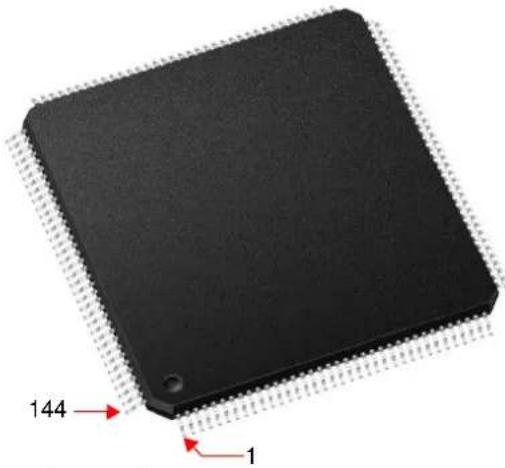 | |||
| Pin Number | Full Pin Name | Pin Number | Full Pin Name | |
| 1 AN23/RG15 37 PGEC2/AN46/RPB6/RB6 | ||||
| 2 EBIA5/AN34/PMA5/RA5 38 PGED2/AN47/RPB7/RB7 | ||||
| 3 EBID5/AN17/RPE5/PMD5/RE5 39 V | REF-/CVREF-/AN27/RA9 | |||
| 4 EBID6/AN16/PMD6/RE6 40 V | REF+/CVREF+/AN28/RA10 | |||
| 5 EBID7/AN15/PMD7/RE7 41 AV | DD | |||
| 6 EBIA6/AN22/RPC1/PMA6/RC1 42 AV | SS | |||
| 7 AN35/ETXD0/RJ8 43 AN38/ETXD2/RH0 | ||||
| 8 AN36/ETXD1/RJ9 44 AN39/ETXD3/RH1 | ||||
| 9 EBIES0/RJ12 45 EBIRP/RH2 | — | |||
| 10 EBIBS1/RJ10 46 RH3 | ||||
| 11 EBIA12/AN21/RPC2/PMA12/RC2 | 47 EBIA10/AN48/RPB8/PMA10/RB8 | |||
| 12 EBIWE /AN20/RPC3/PMWR/RC3 | 48 EBIA7/AN49/RPB9/PMA7/RB9 | |||
| 13 EBIOE/AN19/RPC4/PMRD/RC4 | 49 CV | REFOUT/AN5/RPB10/RB10 | ||
| 14 AN14/C1IND/RPG6/SCK2/RG6 | 50 AN6/RB11 | |||
| 15 AN13/C1INC/RPG7/SDA4/RG7 | 51 EBIA1/PMA1/RK1 | |||
| 16 AN12/C2IND/RPG8/SCL4/RG8 | 52 EBIA3/PMA3/RK2 | |||
| 17 Vss | 53 EBIA17/RK3 | |||
| 18 VDD | 54 | Vss | ||
| 19 EBIA16/RK0 | 55 V | DD | ||
| 20 MCLR | 56 TCK/AN29/RA1 | |||
| 21 EBIA2/AN11/C2INC/RPG9/PMA2/RG9 | 57 TDI/AN30/RPF13/SCK5/RF13 | |||
| 22 TM$/AN24/RA0 | 58 TDO/AN31/RPF12/RF12 | |||
| 23 AN25/RPE8/RE8 | 59 AN7/RB12 | |||
| 24 AN26/RPE9/RE9 | 60 AN8/RB13 | |||
| 25 AN45/C1INA/RPB5/RB5 | 61 AN9/RPB14/SCK3/RB14 | |||
| 26 AN4/C1INB/RB4 | 62 AN10/RPB15/OCFB/RB15 | |||
| 27 AN37/ERXCLK/EREFCLK/RJ11 | 63 V | SS | ||
| 28 EBIA13/PMA13/RJ13 | 64 V | DD | ||
| 29 EBIA11/PMA11/RJ14 | 65 AN40/ERXERR/RH4 | |||
| 30 EBIA0/PMA0/RJ15 | 66 AN41/ERXD1/RH5 | |||
| 31 AN3/C2INA/RPB3/RB3 | 67 AN42/ERXD2/RH6 | |||
| 32 Vss | 68 EBIA4/PMA4/RH7 | |||
| 33 VDD | 69 AN32/RPD14/RD14 | |||
| 34 AN2/C2INB/RPB2/RB2 | 70 AN33/RPD15/SCK6/RD15 | |||
| 35 PGEC1/AN1/RPB1/RB1 | 71 OSC1/CLKI/RC12 | |||
| 36 PGED1/AN0/RPB0/RB0 | 72 OSC2/CLKO/RC15 | |||
Note 1: The RPn pins can be used by remappable peripherals. See Table 1 for the available peripherals and Section 12.3 "Peripheral Pin Select (PPS)" for restrictions.
2: Every I/O port pin (RAx-RKx) can be used as a change notification pin (CNAx-CNKx). See Section 12.0 "I/O Ports" for more information.
3: Shaded pins are 5V tolerant.
TABLE 5: PIN NAMES FOR 144-PIN DEVICES (CONTINUED)
| 144-PIN LQFP AND TQFP (TOP VIEW)PIC32MZ0512EC(E/F/K)144PIC32MZ1024EC(G/H/M)144PIC32MZ1024EC(E/F/K)144PIC32MZ2048EC(G/H/M)144 | |||
| Pin Number | Full Pin Name | Pin Number Full Pin Name | |
| 73 | VBUS | 109 RPD1/SCK1/RD1 | |
| 74 | VUSB3V3 | 110 EBID14/RPD2/PMD14/RD2 | |
| 75 | Vss | 111 EBID15/RPD3/PMD15/RD3 | |
| 76 D- | 112 EBID12/RPD12/PMD12/RD12 | ||
| 77 D+ | 13 EBID13/PMD13/RD13 | ||
| 78 RPF3/USBID/RF3 | 114 ETXERR/RJ0 | ||
| 79 SDA3/RPF2/RF2 115 EMDIO/RJ1 | |||
| 80 SCL3/RPF8/RF8 116 EBIRDY3/RJ2 | |||
| 81 ERXD0/RH8 117 EBIA22/RJ3 | |||
| 82 ERXD3/RH9 118 SQICS0/RPD4/RD4 | |||
| 83 ECOL/RH10 119 SQICS1/RPD5/RD5 | |||
| 84 EBIRDY2/RH11 120 ETXEN/RPD6/RD6 | |||
| 85 SCL2/RA2 | 121 ETXCLK/RPD7/RD7 | ||
| 86 EBIRDY1/SDA2/RA3 | 122 V DD | ||
| 87 EBIA14/PMCS1/PMA14/RA4 | 123 V SS | ||
| 88 | VDD | 124 EBID11/RPF0/PMD11/RF0 | |
| 89 | VSS | 125 EBID10/RPF1/PMD10/RF1 | |
| 90 EBIA9/RPF4/SDA5/PMA9/RF4 | 126 EBIA21/RK7 | ||
| 91 EBIA8/RPF5/SCL5/PMA8/RF5 | 127 EBID9/RPG1/PMD9/RG1 | ||
| 92 EBIA18/RK4 | 128 EBID8/RPG0/PMD8/RG0 | ||
| 93 EBIA19/RK5 | 129 TRCLK/SQICLK/RA6 | ||
| 94 EBIA20/RK6 | 130 TRD3/SQID3/RA7 | ||
| 95 RPA14/SCL1/RA14 | 131 EBICS0/RJ4 | ||
| 96 RPA15/SDA1/RA15 | 132 EBICS1/RJ5 | ||
| 97 | EBIA15/RPD9/PMCS2/PMA15/RD9 | 133 EBICS2/RJ6 | |
| 98 RPD10/SCK4/RD10 | 134 EBICS3/RJ7 | ||
| 99 EMDC/RPD11/RD11 | 135 EBID0/PMD0/RE0 | ||
| 100 ECRS/RH12 | 136 V SS | ||
| 101 ERXDV/ECRSDV/RH13 | 137 V DD | ||
| 102 RH14 | 138 EBID1/PMD1/RE1 | ||
| 103 EBIA23/RH15 | 139 TRD2/SQID2/RG14 | ||
| 104 RPDO/RTCC/INT0/RD0 | 140 TRD1/SQID1/RG12 | ||
| 105 SOSCI/RPC13/RC13 | 141 TRD0/SQID0/RG13 | ||
| 106 SOSCO/RPC14/T1CK/RC14 | 142 EBID2/PMD2/RE2 | ||
| 107 V DD | 143 EBID3/RPE3/PMD3/RE3 | ||
| 108 V SS | 144 EBID4/AN18/PMD4/RE4 | ||
Note 1: The RPn pins can be used by remappable peripherals. See Table 1 for the available peripherals and Section 12.3 "Peripheral Pin Select (PPS)" for restrictions.
2: Every I/O port pin (RAx-RKx) can be used as a change notification pin (CNAx-CNKx). See Section 12.0 "I/O Ports" for more information.
3: Shaded pins are 5V tolerant.
NOTES:
Table of Contents
1.0 Device Overview 15
2.0 Guidelines for Getting Started with 32-bit Microcontrollers 37
3.0 CPU 47
4.0 Memory Organization....59
5.0 Flash Program Memory....97
6.0 Resets....107
7.0 CPU Exceptions and Interrupt Controller 113
8.0 Oscillator Configuration....149
9.0 Prefetch Module 161
10.0 Direct Memory Access (DMA) Controller 165
11.0 Hi-Speed USB with On-The-Go (OTG) 189
12.0 I/O Ports 237
13.0 Timer1 273
14.0 Timer2/3, Timer4/5, Timer6/7, and Timer8/9 277
15.0 Deadman Timer (DMT) 283
16.0 Watchdog Timer (WDT) 291
17.0 Input Capture....295
18.0 Output Compare....299
19.0 Serial Peripheral Interface (SPI) and Inter-IC Sound (I^2S) 305
20.0 Serial Quad Interface (SQI) 315
21.0 Inter-Integrated Circuit (I ^2 C) 339
22.0 Universal Asynchronous Receiver Transmitter (UART) 347
23.0 Parallel Master Port (PMP) 355
24.0 External Bus Interface (EBI) 365
25.0 Real-Time Clock and Calendar (RTCC) 373
26.0 Crypto Engine 383
27.0 Random Number Generator (RNG) 403
28.0 Pipelined Analog-to-Digital Converter (ADC) 409
29.0 Controller Area Network (CAN) 439
30.0 Ethernet Controller 477
31.0 Comparator 521
32.0 Comparator Voltage Reference (CV REF) 525
33.0 Power-Saving Features 529
34.0 Special Features 535
35.0 Instruction Set 559
36.0 Development Support....561
37.0 Electrical Characteristics....565
38.0 AC and DC Characteristics Graphs 613
39.0 Packaging Information....615
The Microchip Web Site 663
Customer Change Notification Service 663
Customer Support 663
Product Identification System 664
TO OUR VALUED CUSTOMERS
It is our intention to provide our valued customers with the best documentation possible to ensure successful use of your Microchip products. To this end, we will continue to improve our publications to better suit your needs. Our publications will be refined and enhanced as new volumes and updates are introduced.
If you have any questions or comments regarding this publication, please contact the Marketing Communications Department via E-mail at docerrors@microchip.com. We welcome your feedback.
Most Current Data Sheet
To obtain the most up-to-date version of this data sheet, please register at our Worldwide Web site at:
http://www.microchip.com
You can determine the version of a data sheet by examining its literature number found on the bottom outside corner of any page. The last character of the literature number is the version number, (e.g., DS30000000A is version A of document DS30000000).
Errata
An errata sheet, describing minor operational differences from the data sheet and recommended workarounds, may exist for current devices. As device/documentation issues become known to us, we will publish an errata sheet. The errata will specify the revision of silicon and revision of document to which it applies.
To determine if an errata sheet exists for a particular device, please check with one of the following:
- Microchip's Worldwide Web site; http://www.microchip.com
- Your local Microchip sales office (see last page)
When contacting a sales office, please specify which device, revision of silicon and data sheet (include literature number) you are using.
Customer Notification System
Register on our web site at www.microchip.com to receive the most current information on all of our products.
Referenced Sources
This device data sheet is based on the following individual sections of the "PIC32 Family Reference Manual". These documents should be considered as the general reference for the operation of a particular module or device feature.
Note: To access the following documents, refer to the Documentation > Reference Manuals section of the Microchip PIC32 website: http://www.microchip.com/pic32.
• Section 1. "Introduction" (DS60001127)
• Section 7. "Resets" (DS60001118)
• Section 8. "Interrupt Controller" (DS60001108)
• Section 9. "Watchdog, Deadman, and Power-up Timers" (DS60001114)
• Section 10. "Power-Saving Features" (DS60001130)
• Section 12. "I/O Ports" (DS60001120)
• Section 13. "Parallel Master Port (PMP)" (DS60001128)
• Section 14. "Timers" (DS60001105)
• Section 15. "Input Capture" (DS60001122)
• Section 16. "Output Compare" (DS60001111)
• Section 18. "12-bit Pipelined Analog-to-Digital Converter (ADC)" (DS60001194)
• Section 19. "Comparator" (DS60001110)
• Section 20. "Comparator Voltage Reference (CV REF)" (DS60001109)
• Section 21. "Universal Asynchronous Receiver Transmitter (UART)" (DS60001107)
• Section 23. "Serial Peripheral Interface (SPI)" (DS60001106)
- Section 24. "Inter-Integrated Circuit (I ^2 C)" (DS60001116)
• Section 29. “Real-Time Clock and Calendar (RTCC)” (DS60001125)
• Section 31. "Direct Memory Access (DMA) Controller" (DS60001117)
• Section 32. "Configuration" (DS60001124)
• Section 33. "Programming and Diagnostics" (DS60001129)
• Section 34. "Controller Area Network (CAN)" (DS60001154)
• Section 35. "Ethernet Controller" (DS60001155)
• Section 41. "Prefetch Module for Devices with L1 CPU Cache" (DS60001183)
• Section 42. "Oscillators with Enhanced PLL" (DS60001250)
• Section 46. "Serial Quad Interface (SQL)" (DS60001244)
• Section 47. "External Bus Interface (EBI)" (DS60001245)
• Section 48. "Memory Organization and Permissions" (DS60001214)
• Section 49. "Crypto Engine (CE) and Random Number Generator (RNG)" (DS60001246)
- Section 50. "CPU for Devices with MIPS32® microAptiv™ and M-Class Cores" (DS60001192)
• Section 51. "Hi-Speed USB with On-The-Go (OTG)" (DS60001326)
• Section 52. "Flash Program Memory with Support for Live Update" (DS60001193)
NOTES:
1.0 DEVICE OVERVIEW
Note: This data sheet summarizes the features of the PIC32MZ Embedded Connectivity (EC) Family of devices. It is not intended to be a comprehensive reference source. To complement the information in this data sheet, refer to the documents provided in the Documentation > Reference Manual section of the Microchip PIC32 web site (www.microchip.com/pic32).
This data sheet contains device-specific information for PIC32MZ Embedded Connectivity (EC) devices.
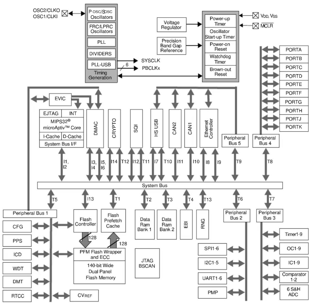
Figure 1-1 illustrates a general block diagram of the core and peripheral modules in the PIC32MZ EC family of devices.
Table 1-21 through Table 1-22 list the pinout I/O descriptions for the pins shown in the device pin tables (see Table 2 through Table 5).
FIGURE 1-1: PIC32MZ EC FAMILY BLOCK DIAGRAM
flowchart
graph TD
    subgraph System Bus
        A["Peripheral Bus 1"] --> B["Flash Controller"]
        C["Peripheral Bus 2"] --> D["Data Ram Bank 1"]
        E["Peripheral Bus 3"] --> F["Data Ram Bank 2"]
        G["Peripheral Bus 4"] --> H["Peripheral Bus 5"]
        I["Peripheral Bus 5"] --> J["Peripheral Bus 6"]
        K["Peripheral Bus 6"] --> L["Peripheral Bus 7"]
        M["Peripheral Bus 7"] --> N["Peripheral Bus 8"]
        O["Peripheral Bus 8"] --> P["Peripheral Bus 9"]
        Q["Peripheral Bus 9"] --> R["Peripheral Bus 10"]
        S["Peripheral Bus 10"] --> T["Peripheral Bus 11"]
        U["Peripheral Bus 11"] --> V["Peripheral Bus 12"]
        W["Peripheral Bus 12"] --> X["Peripheral Bus 13"]
        Y["Peripheral Bus 13"] --> Z["Peripheral Bus 14"]
        AA["Peripheral Bus 14"] --> AB["PFM Flash Wrapper and ECC"]
        AC["Peripheral Bus 14"] --> AD["140-bit Wide Dual Panel Flash Memory"]
        AE["Peripheral Bus 14"] --> AF["CVREF"]
        AG["Peripheral Bus 14"] --> AH["CPG"]
        AI["Peripheral Bus 14"] --> AJ["PPS"]
        AK["Peripheral Bus 14"] --> AL["ICD"]
        AM["Peripheral Bus 14"] --> AN["WDT"]
        AO["Peripheral Bus 14"] --> AP["DMT"]
        AQ["Peripheral Bus 14"] --> AR["RTCC"]
    end

    subgraph System Bus
        AS["EVIC"] --> AT["DMAC"]
        AU["MIPS32® microAptiv™ Core"] --> AV["I-Cache"]
        AW["D-Cache"] --> AX["System Bus I/F"]
        AY["EJTAG"] --> AZ["INT"]
        BA["MCLR"] --> BB["MCLR"]
    end

    subgraph Timing Generation
        BC["POLI"] --> BD["FRC/LPRC Oscillators"]
        BE["Voltage Regulator"] --> BF["POLL"]
        BG["PRESS"] --> BH["DIVIDERS"]
        BI["PDLL-USB"] --> BJ["Timing Generation"]
    end

    subgraph SYSCLK PBCLKx
        BK["Voltage Regulator"] --> BL["Policator Start-up Timer"]
        BM["Power-on Reset"] --> BN["Power-on Reset"]
        BO["Watchdog Timer"] --> BP["Brown-out Reset"]
    end

    subgraph Power-up Timer
        BQ["Power-up Timer"] --> BR["Oscillator Start-up Timer"]
        BS["Power-on Reset"] --> BT["Power-on Reset"]
        BU["Brown-out Reset"] --> BV["Brown-out Reset"]
    end

    subgraph System Bus
        BW["T12"] --> BX["T11"]
        BY["T10"] --> BZ["T9"]
        CA["T11"] --> BZ
        CB["T10"] --> BZ
        CC["T11"] --> BZ
        DD["T10"] --> BZ
        DV["T9"] --> BZ
    end

    subgraph Timing Generation
        DW["T6"] --> BX
        BX --> BX
    end

    subgraph SYSCLK PBCLKx
        BX <--> DC["VDD, Vss"]
        BX <--> DB["MCLR"]

    subgraph Timing Generation
        DC <--> DC
    end

    subgraph System Bus
        DB <--> DC
    end

    subgraph SYSCLK PBCLKx
        DC <--> DC
    end

    subgraph System Bus
        DC <--> DC
    end

    subgraph System Bus
        DC <--> DC
    end

    subgraph SYSCLK PBCLKx
        DC <--> DC
    end

    subgraph System Bus
        DC <--> DC
    end

    subgraph SYSCLK PBCLKx
        DC <--> DC
    end

    subgraph System Bus
        DC <--> DC
    end

    subgraph SYSCLK PBCLKx
        DC <--> DC
    end

    subgraph System Bus
        DC <--> DC
    end

    subgraph SYSCLK PBCLKx
Note: Not all features are available on all devices. Refer to TABLE 1: "PIC32MZ EC Family Features" for the list of features by device.
TABLE 1-1: ADC1 PINOUT I/O DESCRIPTIONS
| Pin Name | Pin Number | Pin Type | Buffer Type | Description | |||
| 64-pin QFN/ TQFP | 100-pin TQFP | 124-pin VTLA | 144-pin TQFP/ LQFP | ||||
| AN0 16 25 A | 18 36 I Analog | Analog | Input Channels | ||||
| AN1 15 24 A | 17 35 I Analog | ||||||
| AN2 14 23 A | 16 34 I Analog | ||||||
| AN3 13 22 A | 14 31 I Analog | ||||||
| AN4 12 21 A | 13 26 I Analog | ||||||
| AN5 23 34 B | 19 49 I Analog | ||||||
| AN6 24 35 A | 24 50 I Analog | ||||||
| AN7 27 41 A | 27 59 I Analog | ||||||
| AN8 28 42 B | 23 60 I Analog | ||||||
| AN9 29 43 A | 28 61 I Analog | ||||||
| AN10 30 44 B | 24 62 I Analog | ||||||
| AN11 | 10 16 | B9 21 I Analog | |||||
| AN12 | 6 | 12 | B7 16 I Analog | ||||
| AN13 | 5 | 11 | A8 15 I Analog | ||||
| AN14 | 4 | 10 | B6 14 I Analog | ||||
| AN15 | 3 | 5 | A4 | 5 | I | Analog | |
| AN16 | 2 | 4 | B2 | 4 | I | Analog | |
| AN17 | 1 | 3 | A3 | 3 | I | Analog | |
| AN18 64 | 100 A67 144 | I Analog | |||||
| AN19 | — | 9 | A7 13 I Analog | ||||
| AN20 | — | 8 | B5 12 I Analog | ||||
| AN21 | — | 7 | A6 | 11 | I | Analog | |
| AN22 | — | 6 | B3 | 6 | I | Analog | |
| AN23 | — | 1 | A2 | 1 | I | Analog | |
| AN24 | — | 17 A11 | 22 I Analog | ||||
| AN25 | — | 18 B10 | 23 I Analog | ||||
| AN26 | — | 19 A12 | 24 I Analog | ||||
| AN27 | — | 28 B15 | 39 I Analog | ||||
| AN28 | — | 29 A20 | 40 I Analog | ||||
| AN29 | — | 38 B21 | 56 I Analog | ||||
| AN30 | — | 39 A26 | 57 I Analog | ||||
| AN31 | — | 40 B22 | 58 I Analog | ||||
| AN32 | — | 47 B27 | 69 I Analog | ||||
| AN33 | — | 48 A32 | 70 I Analog | ||||
| AN34 | — | 2 | B1 | 2 | I | Analog | |
| AN35 | — | — | A5 | 7 | I | Analog | |
Legend: CMOS = CMOS-compatible input or output
ST = Schmitt Trigger input with CMOS levels
TTL = Transistor-transistor Logic input buffer
Analog = Analog input P = Power
O = Output I = Input
PPS = Peripheral Pin Select
TABLE 1-1: ADC1 PINOUT I/O DESCRIPTIONS (CONTINUED)
| Pin Name | Pin Number | Pin Type | Buffer Type | Description | |||
| 64-pin QFN/ TQFP | 100-pin TQFP | 124-pin VTLA | 144-pin TQFP/ LQFP | ||||
| AN36 — — | B4 8 I Analog | Analog Input Channels | |||||
| AN37 — — | B12 27 I Analog | ||||||
| AN38 — — | B17 43 I Analog | ||||||
| AN39 — — | A22 44 I Analog | ||||||
| AN40 — — | A30 65 I Analog | ||||||
| AN41 — — | B26 66 I Analog | ||||||
| AN42 — — | A31 67 I Analog | ||||||
| AN45 11 20 | B11 25 I Analog | ||||||
| AN46 | 17 26 | B14 | 37 I Analog | ||||
| AN47 | 18 27 | A19 | 38 I Analog | ||||
| AN48 | 21 32 | B18 | 47 I Analog | ||||
| AN49 | 22 33 | A23 | 48 I Analog | ||||
Legend: CMOS = CMOS-compatible input or output
ST = Schmitt Trigger input with CMOS levels
TTL = Transistor-transistor Logic input buffer
Analog = Analog input P = Power
O = Output I = Input
PPS = Peripheral Pin Select
TABLE 1-2: OSCILLATOR PINOUT I/O DESCRIPTIONS
| Pin Name | Pin Number | Pin Type | Buffer Type | Description | |||
| 64-pin QFN/ TQFP | 100-pin TQFP | 124-pin VTLA | 144-pin TQFP/ LQFP | ||||
| CLKI 31 49 B28 71 I ST | CMOS External clock | source input. | Always associated with OSC1 pin function. | ||||
| CLKO | 32 | 50 | A33 | 72 | O | — | Oscillator crystal output. Connects to crystal or resonator in Crystal Oscillator mode. Optionally functions as CLKO in RC and EC modes. Always associated with OSC2 pin function. |
| OSC1 31 49 B28 71 I ST | CMOS Oscillator crystal input. | ST buffer when configured in RC mode; CMOS otherwise. | |||||
| OSC2 | 32 | 50 | A33 | 72 | O | — | Oscillator crystal output. Connects to crystal or resonator in Crystal Oscillator mode. Optionally functions as CLKO in RC and EC modes. |
| SOSCI | 47 | 72 | B41 | 105 | I | ST/CMOS | 32.768 kHz low-power oscillator crystal input; CMOS otherwise. |
| SOSCO | 48 | 73 | A49 | 106 | O | — | 32.768 low-power oscillator crystal output. |
| REFCLKI1 | PPS | PPS | PPS | PPS | I | — | Reference Clock Generator Inputs 1-4 |
| REFCLKI3 | PPS | PPS | PPS | PPS | I | — | |
| REFCLKI4 | PPS | PPS | PPS | PPS | I | — | |
| REFCLKO1 | PPS | PPS | PPS | PPS | O | — | Reference Clock Generator Outputs 1-4 |
| REFCLKO3 | PPS | PPS | PPS | PPS | O | — | |
| REFCLKO4 | PPS | PPS | PPS | PPS | O | — | |
Legend: CMOS = CMOS-compatible input or output
ST = Schmitt Trigger input with CMOS levels
TTL = Transistor-transistor Logic input buffer
Analog = Analog input
O = Output
P = Power
I = Input
PPS = Peripheral Pin Select
TABLE 1-3: IC1 THROUGH IC9 PINOUT I/O DESCRIPTIONS
| Pin Name | Pin Number | Pin Type | Buffer Type | Description | |||
| 64-pin QFN/ TQFP | 100-pin TQFP | 124-pin VTLA | 144-pin TQFP/ LQFP | ||||
| Input Capture | |||||||
| IC1 | PPS | PPS | PPS | PPS | I | ST | Input Capture Inputs 1-9 |
| IC2 | PPS | PPS | PPS | PPS | I | ST | |
| IC3 | PPS | PPS | PPS | PPS | I | ST | |
| IC4 | PPS | PPS | PPS | PPS | I | ST | |
| IC5 | PPS | PPS | PPS | PPS | I | ST | |
| IC6 | PPS | PPS | PPS | PPS | I | ST | |
| IC7 | PPS | PPS | PPS | PPS | I | ST | |
| IC8 | PPS | PPS | PPS | PPS | I | ST | |
| IC9 | PPS | PPS | PPS | PPS | I | ST | |
Legend: CMOS = CMOS-compatible input or output
ST = Schmitt Trigger input with CMOS levels
TTL = Transistor-transistor Logic input buffer
Analog = Analog input
O = Output
P = Power
I = Input
PPS = Peripheral Pin Select
TABLE 1-4: OC1 THROUGH OC9 PINOUT I/O DESCRIPTIONS
| Pin Name | Pin Number | Pin Type | Buffer Type | Description | |||
| 64-pin QFN/ TQFP | 100-pin TQFP | 124-pin VTLA | 144-pin TQFP/ LQFP | ||||
| Output Compare | |||||||
| OC1 PPS PPS PPS PPS S O — Output Compare Outputs 1-9 | |||||||
| OC2 PPS PPS PPS PPS S O — | |||||||
| OC3 PPS PPS PPS PPS S O — | |||||||
| OC4 PPS PPS PPS PPS S O — | |||||||
| OC5 PPS PPS PPS PPS S O — | |||||||
| OC6 PPS PPS PPS PPS S O — | |||||||
| OC7 PPS PPS PPS PPS S O — | |||||||
| OC8 PPS PPS PPS PPS S O — | |||||||
| OC9 PPS PPS PPS PPS S O — | |||||||
| OCFA PPS PPS PPS PPS I | ST Output Compare Fault A Input | ||||||
| OCFB | 30 | 44 | B24 | 62 | I | ST | Output Compare Fault B Input |
Legend: CMOS = CMOS-compatible input or output
ST = Schmitt Trigger input with CMOS levels
TTL = Transistor-transistor Logic input buffer
Analog = Analog input P = Power
O = Output I = Input
PPS = Peripheral Pin Select
TABLE 1-5: EXTERNAL INTERRUPTS PINOUT I/O DESCRIPTIONS
| Pin Name | Pin Number | Pin Type | Buffer Type | Description | |||
| 64-pin QFN/ TQFP | 100-pin TQFP | 124-pin VTLA | 144-pin TQFP/ LQFP | ||||
| External Interrupts | |||||||
| INT0 | 46 | 71 | A48 | 104 | I | ST | External Interrupt 0 |
| INT1 | PPS | PPS | PPS | PPS | I | ST | External Interrupt 1 |
| INT2 | PPS | PPS | PPS | PPS | I | ST | External Interrupt 2 |
| INT3 | PPS | PPS | PPS | PPS | I | ST | External Interrupt 3 |
| INT4 | PPS | PPS | PPS | PPS | I | ST | External Interrupt 4 |
Legend: CMOS = CMOS-compatible input or output
ST = Schmitt Trigger input with CMOS levels
TTL = Transistor-transistor Logic input buffer
Analog = Analog input P = Power
O = Output I = Input
PPS = Peripheral Pin Select
TABLE 1-6: PORTA THROUGH PORTK PINOUT I/O DESCRIPTIONS
| Pin Name | Pin Number | Pin Type | Buffer Type | Description | |||
| 64-pin QFN/ TQFP | 100-pin TQFP | 124-pin VTLA | 144-pin TQFP/ LQFP | ||||
| PORTA | |||||||
| RA0 — 17 A | 11 22 I/O ST | PORTA is a bidirectional I/O port | |||||
| RA1 — 38 B | 21 56 I/O ST | ||||||
| RA2 — 59 A | 41 85 I/O ST | ||||||
| RA3 — 60 B | 34 86 I/O ST | ||||||
| RA4 — 61 A | 42 87 I/O ST | ||||||
| RA5 — | 2 | B1 | 2 I/O ST | ||||
| RA6 — 89 A | 61 129 | I/O ST | |||||
| RA7 — 90 B | 51 130 | I/O ST | |||||
| RA9 — 28 B | 15 39 I/O ST | ||||||
| RA10 | — 29 A | 20 40 I/O ST | |||||
| RA14 | — 66 B | 37 95 I/O ST | |||||
| RA15 | — 67 A | 45 96 I/O ST | |||||
| PORTB | |||||||
| RB0 | 16 | 25 A18 | 36 I/O ST | PORTB is a bidirectional I/O port | |||
| RB1 | 15 | 24 A17 | 35 I/O ST | ||||
| RB2 | 14 | 23 A16 | 34 I/O ST | ||||
| RB3 | 13 | 22 A14 | 31 I/O ST | ||||
| RB4 | 12 | 21 A13 | 26 I/O ST | ||||
| RB5 11 20 B | 11 25 | I/O ST | |||||
| RB6 | 17 | 26 B14 | 37 I/O ST | ||||
| RB7 | 18 | 27 A19 | 38 I/O ST | ||||
| RB8 | 21 | 32 B18 | 47 I/O ST | ||||
| RB9 | 22 | 33 A23 | 48 I/O ST | ||||
| RB10 | 23 | 34 B19 | 49 I/O ST | ||||
| RB11 | 24 | 35 A24 | 50 I/O ST | ||||
| RB12 | 27 | 41 A27 | 59 I/O ST | ||||
| RB13 | 28 | 42 B23 | 60 I/O ST | ||||
| RB14 | 29 | 43 A28 | 61 I/O ST | ||||
| RB15 | 30 | 44 B24 | 62 I/O ST | ||||
| PORTC | |||||||
| RC1 | — | 6 | B3 | 6 | I/O | ST | PORTC is a bidirectional I/O port |
| RC2 | — | 7 | A6 | 11 | I/O | ST | |
| RC3 | — | 8 | B5 12 | I/O ST | |||
| RC4 | — | 9 | A7 13 | I/O ST | |||
| RC12 | 31 | 49 B28 | 71 I/O ST | ||||
| RC13 | 47 | 72 | B41 | 105 | I/O | ST | |
| RC14 | 48 | 73 | A49 | 106 | I/O | ST | |
| RC15 | 32 | 50 A33 | 72 I/O ST | ||||
Legend: CMOS = CMOS-compatible input or output
ST = Schmitt Trigger input with CMOS levels
TTL = Transistor-transistor Logic input buffer
Analog = Analog input P = Power
O = Output I = Input
PPS = Peripheral Pin Select
TABLE 1-6: PORTA THROUGH PORTK PINOUT I/O DESCRIPTIONS (CONTINUED)
| Pin Name | Pin Number | Pin Type | Buffer Type | Description | |||
| 64-pin QFN/ TQFP | 100-pin TQFP | 124-pin VTLA | 144-pin TQFP/ LQFP | ||||
| PORTD | |||||||
| RD0 46 71 A | 48 104 I/O | ST PORTD is a bidirectional I/O port | |||||
| RD1 49 76 A | 52 109 I/O | ST | |||||
| RD2 50 77 B | 42 110 I/O | ST | |||||
| RD3 51 78 A | 53 111 I/O | ST | |||||
| RD4 52 81 A | 56 118 I/O | ST | |||||
| RD5 53 82 B | 46 119 I/O | ST | |||||
| RD6 — | — | A57 120 I/O ST | |||||
| RD7 — | — | B47 121 I/O ST | |||||
| RD9 43 68 | B38 | 97 | I/O ST | ||||
| RD10 | 44 69 A | 46 98 I/O ST | |||||
| RD11 | 45 | 70 | B39 | 99 | I/O | ST | |
| RD12 | — | 79 B43 | 112 I/O ST | ||||
| RD13 | — | 80 A54 | 113 I/O ST | ||||
| RD14 | — | 47 | B27 | 69 | I/O | ST | |
| RD15 | — | 48 | A32 | 70 | I/O | ST | |
| PORTE | |||||||
| RE0 58 91 B | 52 135 I/O | ST PORTE is a bidirectional I/O port | |||||
| RE1 61 94 A | 64 138 I/O | ST | |||||
| RE2 62 98 A | 66 142 I/O | ST | |||||
| RE3 63 99 B | 56 143 I/O | ST | |||||
| RE4 64 | 100 | A67 144 I/O ST | |||||
| RE5 | 1 | 3 | A3 | 3 | I/O | ST | |
| RE6 | 2 | 4 | B2 | 4 | I/O | ST | |
| RE7 | 3 | 5 | A4 | 5 | I/O | ST | |
| RE8 | — | 18 | B10 | 23 | I/O | ST | |
| RE9 | — | 19 | A12 | 24 | I/O | ST | |
| PORTF | |||||||
| RF0 | 56 85 A | 59 124 I/O | ST PORTF is a bidirectional I/O port | ||||
| RF1 | 57 86 | B49 | 125 I/O ST | ||||
| RF2 | — | 57 | B31 | 79 | I/O | ST | |
| RF3 | 38 | 56 | A38 | 78 | I/O | ST | |
| RF4 | 41 | 64 | B36 | 90 | I/O | ST | |
| RF5 | 42 | 65 | A44 | 91 | I/O | ST | |
| RF8 | — | 58 | A39 | 80 | I/O | ST | |
| RF12 | — | 40 | B22 | 58 | I/O | ST | |
| RF13 | — | 39 | A26 | 57 | I/O | ST | |
Legend: CMOS = CMOS-compatible input or output
ST = Schmitt Trigger input with CMOS levels
TTL = Transistor-transistor Logic input buffer
Analog = Analog input P = Power
O = Output I = Input
PPS = Peripheral Pin Select
TABLE 1-6: PORTA THROUGH PORTK PINOUT I/O DESCRIPTIONS (CONTINUED)
| Pin Name | Pin Number | Pin Type | Buffer Type | Description | |||
| 64-pin QFN/ TQFP | 100-pin TQFP | 124-pin VTLA | 144-pin TQFP/ LQFP | ||||
| PORTG | |||||||
| RG0 — 88 B | 50 128 I/O | ST PORTG is a bidirectional I/O port | |||||
| RG1 — 87 A | 60 127 I/O | ST | |||||
| RG6 4 10 B | 14 I/O ST | ||||||
| RG7 5 11 | A8 15 | I/O ST | |||||
| RG8 6 12 B | 16 I/O ST | ||||||
| RG9 | 10 | 16 B9 | 21 I/O ST | ||||
| RG12 | — 96 | A65 140 I/O | ST | ||||
| RG13 | — 97 | B55 141 I/O | ST | ||||
| RG14 | — 95 | B54 139 I/O | ST | ||||
| RG15 | — 1 | A2 1 | I/O ST | ||||
| PORTH | |||||||
| RH0 | — | — | B17 | 43 | I/O | ST | PORTH is a bidirectional I/O port |
| RH1 | — | — | A22 | 44 | I/O | ST | |
| RH2 | — | — | — | 45 | I/O | ST | |
| RH3 | — | — | — | 46 | I/O | ST | |
| RH4 | — | — | A30 | 65 | I/O | ST | |
| RH5 | — | — | B26 | 66 | I/O | ST | |
| RH6 | — | — | A31 | 67 | I/O | ST | |
| RH7 | — | — | — | 68 | I/O | ST | |
| RH8 | — | — | B32 | 81 | I/O | ST | |
| RH9 | — | — | A40 | 82 | I/O | ST | |
| RH10 | — | — | B33 | 83 | I/O | ST | |
| RH11 | — | — | — | 84 | I/O | ST | |
| RH12 | — | — | A47 100 | I/O ST | |||
| RH13 | — | — | B40 101 | I/O ST | |||
| RH14 | — | — | — | 102 | I/O | ST | |
| RH15 | — | — | — | 103 | I/O | ST | |
| PORTJ | |||||||
| RJ0 | — | — | B44 | 114 | I/O | ST | PORTJ is a bidirectional I/O port |
| RJ1 | — | — | A55 | 115 | I/O | ST | |
| RJ2 | — | — | B45 | 116 | I/O | ST | |
| RJ3 | — | — | — | 117 | I/O | ST | |
| RJ4 | — | — | A62 | 131 | I/O | ST | |
| RJ5 | — | — | — | 132 | I/O | ST | |
| RJ6 | — | — | — | 133 | I/O | ST | |
| RJ7 | — | — | — | 134 | I/O | ST | |
| RJ8 | — | — | A5 7 I/O ST | ||||
| RJ9 | — | — | B4 8 I/O ST | ||||
| RJ10 | — | — | — | 10 | I/O | ST | |
| RJ11 | — | — | B12 | 27 | I/O | ST | |
| RJ12 | — | — | — | 9 | I/O | ST | |
| RJ13 | — | — | — | 28 | I/O | ST | |
| RJ14 | — | — | — | 29 | I/O | ST | |
| RJ15 | — | — | — | 30 | I/O | ST | |
| Legend: CMOS = CMOS-compatible input or output Analog = Analog input P = PowerST = Schmitt Trigger input with CMOS levels O = Output I = InputTTL = Transistor-transistor Logic input buffer PPS = Peripheral Pin SelectPORTK | |||||||
| RK0 — — — | 19 I/O ST | PORTK is a bidirectional I/O port | |||||
| RK1 — — — | 51 I/O ST | ||||||
| RK2 — — — | 52 I/O ST | ||||||
| RK3 — — — | 53 I/O ST | ||||||
| RK4 — — — | 92 I/O ST | ||||||
| RK5 — — — | 93 I/O ST | ||||||
| RK6 — — — | 94 I/O ST | ||||||
| RK7 — — — | 126 I/O ST | ||||||
Legend: CMOS = CMOS-compatible input or output
ST = Schmitt Trigger input with CMOS levels
TTL = Transistor-transistor Logic input buffer
Analog = Analog input P = Power
O = Output I = Input
PPS = Peripheral Pin Select
TABLE 1-7: TIMER1 THROUGH TIMER9 AND RTCC PINOUT I/O DESCRIPTIONS
| Pin Name | Pin Number | Pin Type | Buffer Type | Description | |||
| 64-pin QFN/ TQFP | 100-pin TQFP | 124-pin VTLA | 144-pin TQFP/ LQFP | ||||
| Timer1 through Timer9 | |||||||
| T1CK 48 73 | A49 106 I $T Timer1 External Clock Input | ||||||
| T2CK | PPS | PPS | PPS | PPS | I | ST | Timer2 External Clock Input |
| T3CK | PPS | PPS | PPS | PPS | I | ST | Timer3 External Clock Input |
| T4CK | PPS | PPS | PPS | PPS | I | ST | Timer4 External Clock Input |
| T5CK | PPS | PPS | PPS | PPS | I | ST | Timer5 External Clock Input |
| T6CK | PPS | PPS | PPS | PPS | I | ST | Timer6 External Clock Input |
| T7CK | PPS | PPS | PPS | PPS | I | ST | Timer7 External Clock Input |
| T8CK | PPS | PPS | PPS | PPS | I | ST | Timer8 External Clock Input |
| T9CK | PPS | PPS | PPS | PPS | I | ST | Timer9 External Clock Input |
| Real-Time Clock and Calendar | |||||||
| RTCC | 46 | 71 | A48 | 104 | O | — | Real-Time Clock Alarm/Seconds Output |
Legend: CMOS = CMOS-compatible input or output
ST = Schmitt Trigger input with CMOS levels
TTL = Transistor-transistor Logic input buffer
Analog = Analog input P = Power
O = Output I = Input
PPS = Peripheral Pin Select
TABLE 1-8: UART1 THROUGH UART6 PINOUT I/O DESCRIPTIONS
| Pin Name | Pin Number | Pin Type | Buffer Type | Description | |||
| 64-pin QFN/ TQFP | 100-pin TQFP | 124-pin VTLA | 144-pin TQFP/ LQFP | ||||
| Universal Asynchronous Receiver Transmitter 1 | |||||||
| U1RX PPS PPS PPS PPS PPS I ST UA | RT1 Rece | ve | |||||
| U1TX PPS PPS PPS PPS PPS O | — U | ART1 Tran | smit | ||||
| U1CTS | PPS PPS PPS PPS I ST UART1 Clear to Send | ||||||
| U1RTS | PPS PPS PPS PPS O | — U | ART1 Ready to Send | ||||
| Universal Asynchronous Receiver Transmitter 2 | |||||||
| U2RX PPS PPS PPS PPS I ST UA | RT2 Rece | ve | |||||
| U2TX PPS PPS PPS PPS O | — U | ART2 Tran | smit | ||||
| U2CTS | PPS PPS PPS PPS I ST UART2 Clear To Send | ||||||
| U2RTS | PPS | PPS | PPS | PPS | O | — | UART2 Ready To Send |
| Universal Asynchronous Receiver Transmitter 3 | |||||||
| U3RX PPS PPS PPS PPS I ST UART3 Rece | ve | ||||||
| U3TX PPS PPS PPS PPS O | — U | ART3 Tran | smit | ||||
| U3CTS | PPS PPS PPS PPS I ST UART3 Clear to Send | ||||||
| U3RTS | PPS PPS PPS PPS O | — U | ART3 Ready to Send | ||||
| Universal Asynchronous Receiver Transmitter 4 | |||||||
| U4RX PPS PPS PPS PPS I ST UART4 Rece | ve | ||||||
| U4TX PPS PPS PPS PPS O | — U | ART4 Tran | smit | ||||
| U4CTS | PPS PPS PPS PPS I ST UART4 Clear to Send | ||||||
| U4RTS | PPS PPS PPS PPS O | — U | ART4 Ready to Send | ||||
| Universal Asynchronous Receiver Transmitter 5 | |||||||
| U5RX PPS PPS PPS PPS I ST UART5 Rece | ve | ||||||
| U5TX PPS PPS PPS PPS O | — U | ART5 Tran | smit | ||||
| U5CTS | PPS PPS PPS PPS I ST UART5 Clear to Send | ||||||
| U5RTS | PPS PPS PPS PPS O | — U | ART5 Ready to Send | ||||
| Universal Asynchronous Receiver Transmitter 6 | |||||||
| U6RX PPS PPS PPS PPS I ST UART6 Rece | ve | ||||||
| U6TX PPS PPS PPS PPS O | — U | ART6 Tran | smit | ||||
| U6CTS | PPS PPS PPS PPS I ST UART6 Clear to Send | ||||||
| U6RTS | PPS PPS PPS PPS O | — U | ART6 Ready to Send | ||||
Legend: CMOS = CMOS-compatible input or output ST = Schmitt Trigger input with CMOS levels TTL = Transistor-transistor Logic input buffer
Analog = Analog input O = Output PPS = Peripheral Pin Select
P = Power I = Input
TABLE 1-9: SPI1 THROUGH SPI 6 PINOUT I/O DESCRIPTIONS
| Pin Name | Pin Number | Pin Type | Buffer Type | Description | |||
| 64-pin QFN/ TQFP | 100-pin TQFP | 124-pin VTLA | 144-pin TQFP/ LQFP | ||||
| Serial Peripheral Interface 1 | |||||||
| SCK1 49 76 | A52 109 I/O | ST SPI1 Synchronous | is Serial | Clock Input/Output | |||
| SDI1 | PPS | PPS | PPS | PPS | I | ST | SPI1 Data In |
| SDO1 | PPS | PPS | PPS | PPS | O | — | SPI1 Data Out |
| SS1 | PPS | PPS | PPS | PPS | I/O | ST | SPI1 Slave Synchronization Or Frame Pulse I/O |
| Serial Peripheral Interface 2 | |||||||
| SCK2 | 4 | 10 | B6 | 14 | I/O | ST | SPI2 Synchronous Serial Clock Input/output |
| SDI2 | PPS | PPS | PPS | PPS | I | ST | SPI2 Data In |
| SDO2 | PPS | PPS | PPS | PPS | O | — | SPI2 Data Out |
| SS2 | PPS | PPS | PPS | PPS | I/O | ST | SPI2 Slave Synchronization Or Frame Pulse I/O |
| Serial Peripheral Interface 3 | |||||||
| SCK3 | 29 | 43 | A28 | 61 | I/O | ST | SPI3 Synchronous Serial Clock Input/Output |
| SDI3 | PPS | PPS | PPS | PPS | I | ST | SPI3 Data In |
| SDO3 | PPS | PPS | PPS | PPS | O | — | SPI3 Data Out |
| SS3 | PPS | PPS | PPS | PPS | I/O | ST | SPI3 Slave Synchronization Or Frame Pulse I/O |
| Serial Peripheral Interface 4 | |||||||
| SCK4 | 44 | 69 | A46 | 98 | I/O | ST | SPI4 Synchronous Serial Clock Input/Output |
| SDI4 | PPS | PPS | PPS | PPS | I | ST | SPI4 Data In |
| SDO4 | PPS | PPS | PPS | PPS | O | — | SPI4 Data Out |
| SS4 | PPS | PPS | PPS | PPS | I/O | ST | SPI4 Slave Synchronization Or Frame Pulse I/O |
| Serial Peripheral Interface 5 | |||||||
| SCK5 | — | 39 | A26 | 57 | I/O | ST | SPI5 Synchronous Serial Clock Input/Output |
| SDI5 | — | PPS | PPS | PPS | I | ST | SPI5 Data In |
| SDO5 | — | PPS | PPS | PPS | O | — | SPI5 Data Out |
| SS5 | — | PPS | PPS | PPS | I/O | ST | SPI5 Slave Synchronization Or Frame Pulse I/O |
| Serial Peripheral Interface 6 | |||||||
| SCK6 | — | 48 | A32 | 70 | I/O | ST | SPI6 Synchronous Serial Clock Input/Output |
| SDI6 | — | PPS | PPS | PPS | I | ST | SPI6 Data In |
| SDO6 | — | PPS | PPS | PPS | O | — | SPI6 Data Out |
| SS6 | — | PPS | PPS | PPS | I/O | ST | SPI6 Slave Synchronization Or Frame Pulse I/O |
Legend: CMOS = CMOS-compatible input or output
ST = Schmitt Trigger input with CMOS levels
TTL = Transistor-transistor Logic input buffer
Analog = Analog input P = Power
O = Output I = Input
PPS = Peripheral Pin Select
TABLE 1-10: I2C1 THROUGH I2C5 PINOUT I/O DESCRIPTIONS
| Pin Name | Pin Number | Pin Type | Buffer Type | Description | |||
| 64-pin QFN/ TQFP | 100-pin TQFP | 124-pin VTLA | 144-pin TQFP/ LQFP | ||||
| Inter-Integrated Circuit 1 | |||||||
| SCL1 44 66 | B37 95 I/O | ST I2C1 Synchronous | Serial Clock Input/Output | ||||
| SDA1 43 67 | A45 96 I/O | ST I2C1 Synchronous | Serial Data Input/Output | ||||
| Inter-Integrated Circuit 2 | |||||||
| SCL2 | — | 59 A41 | 85 I/O ST | I2C2 Synchronous | Serial Clock Input/Output | ||
| SDA2 | — | 60 B34 | 86 I/O ST | I2C2 Synchronous | Serial Data Input/Output | ||
| Inter-Integrated Circuit 3 | |||||||
| SCL3 51 58 | A39 80 I/O | ST I2C3 Synchronous | Serial Clock Input/Output | ||||
| SDA3 50 57 | B31 79 I/O | ST I2C3 Synchronous | Serial Data Input/Output | ||||
| Inter-Integrated Circuit 4 | |||||||
| SCL4 | 6 | 12 | B7 | 16 | I/O | ST | I2C4 Synchronous Serial Clock Input/Output |
| SDA4 | 5 | 11 | A8 | 15 | I/O | ST | I2C4 Synchronous Serial Data Input/Output |
| Inter-Integrated Circuit 5 | |||||||
| SCL5 42 65 | A44 91 I/O | ST I2C5 Synchronous | Serial Clock Input/Output | ||||
| SDA5 41 64 | B36 90 I/O | ST I2C5 Synchronous | Serial Data Input/Output | ||||
Legend: CMOS = CMOS-compatible input or output ST = Schmitt Trigger input with CMOS levels TTL = Transistor-transistor Logic input buffer
Analog = Analog input O = Output PPS = Peripheral Pin Select
P = Power I = Input
TABLE 1-11: COMPARATOR 1, COMPARATOR 2 AND CREF PINOUT I/O DESCRIPTIONS
| Pin Name | Pin Number | Pin Type | Buffer Type | Description | |||
| 64-pin QFN/ TQFP | 100-pin TQFP | 124-pin VTLA | 144-pin TQFP/ LQFP | ||||
| Comparator Voltage Reference | |||||||
| CVREF+ | 16 | 29 | A20 | 40 | I | Analog | Comparator Voltage Reference (High) Input |
| CVREF- | 15 | 28 | B15 | 39 | I | Analog | Comparator Voltage Reference (Low) Input |
| CVREFOUT | 23 | 34 | B19 | 49 | O | Analog | Comparator Voltage Reference Output |
| Comparator 1 | |||||||
| C1INA | 11 | 20 | B11 | 25 | I | Analog | Comparator 1 Positive Input |
| C1INB | 12 | 21 | A13 | 26 | I | Analog | Comparator 1 Selectable Negative Input |
| C1INC | 5 | 11 | A8 | 15 | I | Analog | |
| C1IND | 4 | 10 | B6 | 14 | I | Analog | |
| C1OUT | PPS | PPS | PPS | PPS | O | — | Comparator 1 Output |
| Comparator 2 | |||||||
| C2INA | 13 | 22 | A14 | 31 | I | Analog | Comparator 2 Positive Input |
| C2INB | 14 | 23 | A16 | 34 | I | Analog | Comparator 2 Selectable Negative Input |
| C2INC | 10 | 16 | B9 | 21 | I | Analog | |
| C2IND | 6 | 12 | B7 | 16 | I | Analog | |
| C2OUT | PPS | PPS | PPS | PPS | O | — | Comparator 2 Output |
Legend: CMOS = CMOS-compatible input or output ST = Schmitt Trigger input with CMOS levels TTL = Transistor-transistor Logic input buffer
Analog = Analog input O = Output PPS = Peripheral Pin Select
P = Power I = Input
TABLE 1-12: PMP PINOUT I/O DESCRIPTIONS
| Pin Name | Pin Number | Pin Type | Buffer Type | Description | |||
| 64-pin QFN/ TQFP | 100-pin TQFP | 124-pin VTLA | 144-pin TQFP/ LQFP | ||||
| PMA0 30 44 | B24 30 I/O | TTL/ST | Parallel Master | Port Address bit | 0 Input (Buffered Slave modes) and Output (Master modes) | ||
| PMA1 29 43 | A28 51 I/O | TTL/ST | Parallel Master | Port Address bit | 1 Input (Buffered Slave modes) and Output (Master modes) | ||
| PMA2 | 10 | 16 | B9 | 21 | O | — | Parallel Master Port Address (Demultiplexed Master modes) |
| PMA3 | 6 | 12 B7 | 52 | O — | |||
| PMA4 | 5 | 11 A8 | 68 | O — | |||
| PMA5 | 4 | 2 | B1 | 2 | O | — | |
| PMA6 | 16 | 6 | B3 | 6 | O | — | |
| PMA7 | 22 | 33 | A23 | 48 | O | — | |
| PMA8 | 42 | 65 | A44 | 91 | O | — | |
| PMA9 | 41 | 64 | B36 | 90 | O | — | |
| PMA10 | 21 | 32 | B18 | 47 | O | — | |
| PMA11 | 27 | 41 | A27 | 29 | O | — | |
| PMA12 | 24 | 7 | A6 | 11 | O | — | |
| PMA13 | 23 | 34 | B19 | 28 | O | — | |
| PMA14 | 45 | 61 | A42 | 87 | O | — | |
| PMA15 | 43 | 68 | B38 | 97 | O | — | |
| PMCS1 | 45 | 61 | A42 | 87 | O | — | Parallel Master Port Chip Select 1 Strobe |
| PMCS2 | 43 | 68 | B38 | 97 | O | — | Parallel Master Port Chip Select 2 Strobe |
| PMD0 | 58 | 91 | B52 | 135 | I/O | TTL/ST | Parallel Master Port Data (Demultiplexed Master mode) or Address/Data (Multiplexed Master modes) |
| PMD1 | 61 94 | A64 | 138 | I/O TTL/ST | |||
| PMD2 | 62 98 | A66 | 142 | I/O TTL/ST | |||
| PMD3 | 63 99 | B56 | 143 | I/O TTL/ST | |||
| PMD4 | 64 | 100 | A67 | 144 | I/O | TTL/ST | |
| PMD5 | 1 | 3 | A3 | 3 | I/O | TTL/ST | |
| PMD6 | 2 | 4 | B2 | 4 | I/O | TTL/ST | |
| PMD7 | 3 | 5 | A4 | 5 | I/O | TTL/ST | |
| PMD8 | — | 88 | B50 | 128 | I/O | TTL/ST | |
| PMD9 | — | 87 | A60 | 127 | I/O | TTL/ST | |
| PMD10 | — | 86 | B49 | 125 | I/O | TTL/ST | |
| PMD11 | — | 85 | A59 | 124 | I/O | TTL/ST | |
| PMD12 | — | 79 | B43 | 112 | I/O | TTL/ST | |
| PMD13 | — | 80 | A54 | 113 | I/O | TTL/ST | |
| PMD14 | — | 77 | B42 | 110 | I/O | TTL/ST | |
| PMD15 | — | 78 | A53 | 111 | I/O | TTL/ST | |
| PMALL | 30 | 44 | B24 | 30 | O | — | Parallel Master Port Address Latch Enable Low Byte (Multiplexed Master modes) |
| PMALH | 29 | 43 | A28 | 51 | O | — | Parallel Master Port Address Latch Enable High Byte (Multiplexed Master modes) |
| PMRD | 53 | 9 | A7 | 13 | O | — | Parallel Master Port Read Strobe |
| PMWR | 52 | 8 | B5 | 12 | O | — | Parallel Master Port Write Strobe |
Legend: CMOS = CMOS-compatible input or output
ST = Schmitt Trigger input with CMOS levels
TTL = Transistor-transistor Logic input buffer
Analog = Analog input
O = Output
P = Power
I = Input
PPS = Peripheral Pin Select
TABLE 1-13: EBI PINOUT I/O DESCRIPTIONS
| Pin Name | Pin Number | Pin Type | Buffer Type | Description | |||
| 64-pin QFN/ TQFP | 100-pin TQFP | 124-pin VTLA | 144-pin TQFP/ LQFP | ||||
| EBIA0 — 44 | B24 30 O | External | Bus Interface Address | Bus | |||
| EBIA1 — 43 | A28 | 51 O | — | ||||
| EBIA2 — 16 | B9 | 21 O | — | ||||
| EBIA3 — 12 | B7 | 52 O | — | ||||
| EBIA4 — | 11 A8 | 68 O | — | ||||
| EBIA5 — | 2 B1 | 2 O | — | ||||
| EBIA6 — | 6 B3 | 6 O | — | ||||
| EBIA7 — 33 | A23 | 48 O | — | ||||
| EBIA8 — 65 | A44 | 91 O | — | ||||
| EBIA9 — 64 | B36 | 90 O | — | ||||
| EBIA10 | — 32 | B18 | 47 C | — | |||
| EBIA11 | — 41 | A27 | 29 O | — | |||
| EBIA12 | — | 7 | A6 | 11 | O | — | |
| EBIA13 | — 34 | B19 | 28 C | — | |||
| EBIA14 | — 61 | A42 | 87 C | — | |||
| EBIA15 | — 68 | B38 | 97 C | — | |||
| EBIA16 | — 17 | A11 | 19 O | — | |||
| EBIA17 | — 40 | B22 | 53 C | — | |||
| EBIA18 | — 39 | A26 | 92 C | — | |||
| EBIA19 | — 38 | B21 | 93 C | — | |||
| EBIA20 | — | — | — | 94 | O | — | |
| EBIA21 | — | — | — | 126 | O | — | |
| EBIA22 | — | — | — | 117 | O | — | |
| EBIA23 | — | — | — | 103 | O | — | |
| EBID0 | — | 91 | B52 | 135 | I/O | ST | External Bus Interface Data I/O Bus |
| EBID1 | — | 94 | A64 | 138 | I/O | ST | |
| EBID2 | — | 98 | A66 | 142 | I/O | ST | |
| EBID3 | — | 99 | B56 | 143 | I/O | ST | |
| EBID4 | — | 100 | A67 | 144 | I/O | ST | |
| EBID5 | — | 3 | A3 | 3 | I/O | ST | |
| EBID6 | — | 4 | B2 | 4 | I/O | ST | |
| EBID7 | — | 5 | A4 | 5 | I/O | ST | |
| EBID8 | — | 88 | B50 | 128 | I/O | ST | |
| EBID9 | — | 87 | A60 | 127 | I/O | ST | |
| EBID10 | — | 86 | B49 | 125 | I/O | ST | |
| EBID11 | — 85 | A59 | 124 I/O ST | ||||
| EBID12 | — | 79 | B43 | 112 | I/O | ST | |
| EBID13 | — | 80 | A54 | 113 | I/O | ST | |
| EBID14 | — | 77 | B42 | 110 | I/O | ST | |
| EBID15 | — | 78 | A53 | 111 | I/O | ST | |
| EBIBS0 | — | — | — | 9 | O | — | External Bus Interface Byte Select |
| EBIBS1 | — | — | — | 10 | O | — | |
| EBICS0 | — 59 | A41 | 131 O | — External Bus Interface Chip | Select | ||
| EBICS1 | — | — | — | 132 | O | — | |
| EBICS2 | — | — | — | 133 | O | — | |
| EBICS3 | — | — | — | 134 | O | — | |
Legend: CMOS = CMOS-compatible input or output
ST = Schmitt Trigger input with CMOS levels
TTL = Transistor-transistor Logic input buffer
Analog = Analog input P = Power
O = Output I = Input
PPS = Peripheral Pin Select
TABLE 1-13: EBI PINOUT I/O DESCRIPTIONS (CONTINUED)
| Pin Name | Pin Number | Pin Type | Buffer Type | Description | |||
| 64-pin QFN/ TQFP | 100-pin TQFP | 124-pin VTLA | 144-pin TQFP/ LQFP | ||||
| EBIOE | — 9 A7 | 13 O — External Bus Interface | Interface | Output Enable | |||
| EBIRDY1 — | 60 B34 86 | I ST External Bus Interface Ready Input | |||||
| EBIRDY2 — | 58 A39 | 84 I | ST | ||||
| EBIRDY3 — | 57 B45 | 116 I ST | |||||
| EBIRP | — — | — 45 O — External Bus Interface | Flash Reset | Pin | |||
| EBIWE | — 8 B5 | 12 O — External Bus Interface | Write Enable | ||||
Legend: CMOS = CMOS-compatible input or output ST = Schmitt Trigger input with CMOS levels TTL = Transistor-transistor Logic input buffer
Analog = Analog input O = Output PPS = Peripheral Pin Select
P = Power I = Input
TABLE 1-14: USB PINOUT I/O DESCRIPTIONS
| Pin Name | Pin Number | Pin Type | Buffer Type | Description | |||
| 64-pin QFN/ TQFP | 100-pin TQFP | 124-pin VTLA | 144-pin TQFP/ LQFP | ||||
| VBUS | 33 51 | A35 73 I An | alog USB bus power | monitor | |||
| VUSB3V3 | 34 52 | A36 74 P — | USB internal transceiver | supply. If the USB module is not used, this pin must be connected to Vss. When connected, the shared pin functions on USBID will not be available. | |||
| D+ | 37 55 | B30 77 | I/O | Analog USB D+ | |||
| D- | 36 54 | A37 76 | I/O | Analog USB D- | |||
| USBID | 38 | 56 | A38 | 78 | I | ST | USB OTG ID detect |
Legend: CMOS = CMOS-compatible input or output ST = Schmitt Trigger input with CMOS levels TTL = Transistor-transistor Logic input buffer
Analog = Analog input O = Output PPS = Peripheral Pin Select
P = Power I = Input
TABLE 1-15: CAN1 AND CAN2 PINOUT I/O DESCRIPTIONS
| Pin Name | Pin Number | Pin Type | Buffer Type | Description | |||
| 64-pin QFN/ TQFP | 100-pin TQFP | 124-pin VTLA | 144-pin TQFP/ LQFP | ||||
| C1TX | PPS | PPS | PPS | PPS | O | — | CAN1 Bus Transmit Pin |
| C1RX | PPS | PPS | PPS | PPS | I | ST | CAN1 Bus Receive Pin |
| C2TX | PPS | PPS | PPS | PPS | O | — | CAN2 Bus Transmit Pin |
| C2RX | PPS | PPS | PPS | PPS | I | ST | CAN2 Bus Receive Pin |
Legend: CMOS = CMOS-compatible input or output ST = Schmitt Trigger input with CMOS levels TTL = Transistor-transistor Logic input buffer
Analog = Analog input O = Output PPS = Peripheral Pin Select
P = Power I = Input
TABLE 1-16: ETHERNET MII I/O DESCRIPTIONS
| Pin Name | Pin Number | Pin Type | Buffer Type | Description | |||
| 64-pin QFN/ TQFP | 100-pin TQFP | 124-pin VTLA | 144-pin TQFP/ LQFP | ||||
| ERXD0 61 41 | B32 81 I | ST Ethernet | Receive Data 0 | ||||
| ERXD1 58 42 | B26 66 I | ST Ethernet | Receive Data 1 | ||||
| ERXD2 57 43 | A31 67 I | ST Ethernet | Receive Data 2 | ||||
| ERXD3 56 44 | A40 82 I | ST Ethernet | Receive Data 3 | ||||
| ERXERR 64 | 35 A30 65 | I ST Ethernet | Receive Error Input | ||||
| ERXDV 62 12 | B40 101 | I ST | Ethernet Receive Data Valid | ||||
| ERXCLK | 63 16 | B12 27 I ST | Ethernet Receive Clock | ||||
| ETXD0 | 2 | 86 | A5 | 7 | O | — | Ethernet Transmit Data 0 |
| ETXD1 | 3 | 85 | B4 | 8 | O | — | Ethernet Transmit Data 1 |
| ETXD2 | 43 | 79 | B17 | 43 | O | — | Ethernet Transmit Data 2 |
| ETXD3 | 46 | 80 | A22 | 44 | O | — | Ethernet Transmit Data 3 |
| ETXERR | 50 | 87 | B44 | 114 | O | — | Ethernet Transmit Error |
| ETXEN | 1 | 77 | A57 | 120 | O | — | Ethernet Transmit Enable |
| ETXCLK | 51 | 78 | B47 | 121 | I | ST | Ethernet Transmit Clock |
| ECOL | 44 10 | B33 83 I ST | Ethernet Collision Detect | ||||
| ECRS | 45 | 11 | A47 | 100 | I | ST | Ethernet Carrier Sense |
| EMDC | 30 | 70 | B39 | 99 | O | — | Ethernet Management Data Clock |
| EMDIO | 49 | 71 | A55 | 115 | I/O | — | Ethernet Management Data |
Legend: CMOS = CMOS-compatible input or output
ST = Schmitt Trigger input with CMOS levels
TTL = Transistor-transistor Logic input buffer
Analog = Analog input P = Power
O = Output I = Input
PPS = Peripheral Pin Select
TABLE 1-17: ETHERNET RMII PINOUT I/O DESCRIPTIONS
| Pin Name | Pin Number | Pin Type | Buffer Type | Description | |||
| 64-pin QFN/ TQFP | 100-pin TQFP | 124-pin VTLA | 144-pin TQFP/ LQFP | ||||
| Ethernet MII Interface | |||||||
| ERXD0 | 61 | 41 | B32 | 81 | I | ST | Ethernet Receive Data 0 |
| ERXD1 | 58 | 42 | B26 | 66 | I | ST | Ethernet Receive Data 1 |
| ERXERR | 64 | 35 | A30 | 65 | I | ST | Ethernet Receive Error Input |
| ETXD0 | 2 | 86 | A5 | 7 | O | — | Ethernet Transmit Data 0 |
| ETXD1 | 3 | 85 | B4 | 8 | O | — | Ethernet Transmit Data 1 |
| ETXEN | 1 | 77 | A57 | 120 | O | — | Ethernet Transmit Enable |
| EMDC | 30 | 70 | B39 | 99 | O | — | Ethernet Management Data Clock |
| EMDIO | 49 | 71 | A55 | 115 | I/O | — | Ethernet Management Data |
| EREFCLK | 63 | 16 | B12 | 27 | I | ST | Ethernet Reference Clock |
| ECRSDV | 62 | 12 | B40 | 101 | I | ST | Ethernet Carrier Sense Data Valid |
Legend: CMOS = CMOS-compatible input or output
ST = Schmitt Trigger input with CMOS levels
TTL = Transistor-transistor Logic input buffer
Analog = Analog input P = Power
O = Output I = Input
PPS = Peripheral Pin Select
TABLE 1-18: ALTERNATE ETHERNET MII PINOUT I/O DESCRIPTIONS
| Pin Name | Pin Number | Pin Type | Buffer Type | Description | |||
| 64-pin QFN/ TQFP | 100-pin TQFP | 124-pin VTLA | 144-pin TQFP/ LQFP | ||||
| AERXD0 — | 18 — — I ST | Alternate | Ethernet | Receive Data 0 | |||
| AERXD1 — | 19 — — I ST | Alternate | Ethernet | Receive Data 1 | |||
| AERXD2 — | 28 — — I ST | Alternate | Ethernet | Receive Data 2 | |||
| AERXD3 — | 29 — — I ST | Alternate | Ethernet | Receive Data 3 | |||
| AERXERR — | 1 — — I ST | Alternate | Ethernet | Receive Error Input | |||
| AERXDV | — 12 — — I ST | Alternate Ethernet | Receive Data Valid | ||||
| AERXCLK | — 16 — — I ST | Alternate Ethernet | Receive Clock | ||||
| AETXD0 | — | 47 | — | — | O | — | Alternate Ethernet Transmit Data 0 |
| AETXD1 | — | 48 | — | — | O | — | Alternate Ethernet Transmit Data 1 |
| AETXD2 | — | 44 | — | — | O | — | Alternate Ethernet Transmit Data 2 |
| AETXD3 | — | 43 | — | — | O | — | Alternate Ethernet Transmit Data 3 |
| AETXERR | — | 35 | — | — | O | — | Alternate Ethernet Transmit Error |
| AECOL | — 42 — — I ST | Alternate Ethernet | Collision Detect | ||||
| AECRS — 41 — — I ST | Alternate Ethernet Carrier Sense | ||||||
| AETXCLK | — 66 — — I ST | Alternate Ethernet | Transmit Clock | ||||
| AEMDC | — | 70 | — | — | O | — | Alternate Ethernet Management Data Clock |
| AEMDIO | — | 71 | — | — | I/O | — | Alternate Ethernet Management Data |
| AETXEN | — | 67 | — | — | O | — | Alternate Ethernet Transmit Enable |
Legend: CMOS = CMOS-compatible input or output
ST = Schmitt Trigger input with CMOS levels
TTL = Transistor-transistor Logic input buffer
Analog = Analog input P = Power
O = Output I = Input
PPS = Peripheral Pin Select
TABLE 1-19: ALTERNATE ETHERNET RMII PINOUT I/O DESCRIPTIONS
| Pin Name | Pin Number | Pin Type | Buffer Type | Description | |||
| 64-pin QFN/ TQFP | 100-pin TQFP | 124-pin VTLA | 144-pin TQFP/ LQFP | ||||
| AERXD0 | 43 | 18 | — | — | I | ST | Alternate Ethernet Receive Data 0 |
| AERXD1 | 46 | 19 | — | — | I | ST | Alternate Ethernet Receive Data 1 |
| AERXERR | 51 | 1 | — | — | I | ST | Alternate Ethernet Receive Error Input |
| AETXD0 | 57 | 47 | — | — | O | — | Alternate Ethernet Transmit Data 0 |
| AETXD1 | 56 | 48 | — | — | O | — | Alternate Ethernet Transmit Data 1 |
| AEMDC | 30 | 70 | — | — | O | — | Alternate Ethernet Management Data Clock |
| AEMDIO | 49 | 71 | — | — | I/O | — | Alternate Ethernet Management Data |
| AETXEN | 50 | 67 | — | — | O | — | Alternate Ethernet Transmit Enable |
| AEREFCLK | 45 | 16 | — | — | I | ST | Alternate Ethernet Reference Clock |
| AECRSDV | 62 | 12 | — | — | I | ST | Alternate Ethernet Carrier Sense Data Valid |
Legend: CMOS = CMOS-compatible input or output
ST = Schmitt Trigger input with CMOS levels
TTL = Transistor-transistor Logic input buffer
Analog = Analog input P = Power
O = Output I = Input
PPS = Peripheral Pin Select
TABLE 1-20: SQI1 PINOUT I/O DESCRIPTIONS
| Pin Name | Pin Number | Pin Type | Buffer Type | Description | |||
| 64-pin QFN/ TQFP | 100-pin TQFP | 124-pin VTLA | 144-pin TQFP/ LQFP | ||||
| SQICLK 57 89 A61 129 | O — Serial | Quad Interface Clock | |||||
| SQICS0 | 52 81 A56 118 | O — Serial Quad | Interface | Chip Select 0 | |||
| SQICS1 | 53 82 B46 119 | O — Serial Quad | Interface | Chip Select 1 | |||
| SQID0 | 58 | 97 | B55 | 141 | I/O | ST | Serial Quad Interface Data 0 |
| SQID1 | 61 | 96 | A65 | 140 | I/O | ST | Serial Quad Interface Data 1 |
| SQID2 | 62 | 95 | B54 | 139 | I/O | ST | Serial Quad Interface Data 2 |
| SQID3 | 63 | 90 | B51 | 130 | I/O | ST | Serial Quad Interface Data 3 |
| Legend: | CMOS = CMOS-compatible input or outputST = Schmitt Trigger input with CMOS levelsTTL = Transistor-transistor Logic input buffer | Analog = Analog inputO = OutputPPS = Peripheral Pin Select | P = PowerI = Input |
TABLE 1-21: POWER, GROUND, AND VOLTAGE REFERENCE PINOUT I/O DESCRIPTIONS
| Pin Name | Pin Number | Pin Type | Buffer Type | Description | |||
| 64-pin QFN/ TQFP | 100-pin TQFP | 124-pin VTLA | 144-pin TQFP/ LQFP | ||||
| Power and Ground | |||||||
| AVDD | 19 | 30 | B16 | 41 | P | P | Positive supply for analog modules. This pin must be connected at all times. |
| AVss | 20 | 31 | A21 | 42 | P | P | Ground reference for analog modules. This pin must be connected at all times |
| VDD | 8, 26, 39, 54, 60 | 14, 37, 46, 62, 74, 83, 93 | B8, A15, A25, B25, B35, A50, A58, B53 | 18, 33, 55, 64, 88, 107, 122, 137 | P | — | Positive supply for peripheral logic and I/O pins. This pin must be connected at all times. |
| Vss | 7, 25, 35, 40, 55, 59 | 13, 36, 45, 53, 63, 75, 84, 92 | A9, B13, B20, B29, A29, A43, A51, B48, A63 | 17, 32, 54, 63, 75, 89, 108, 123, 136 | P | — | Ground reference for logic, I/O pins, and USB. This pin must be connected at all times. |
| Voltage Reference | |||||||
| VREF+ | 16 | 29 | A20 | 40 | I | Analog | Analog Voltage Reference (High) Input |
| VREF- | 15 | 28 | B15 | 39 | I | Analog | Analog Voltage Reference (Low) Input |
| Legend: | CMOS = CMOS-compatible input or output | Analog = Analog input | P = Power |
| ST = Schmitt Trigger input with CMOS levels | O = Output | I = Input | |
| TTL = Transistor-transistor Logic input buffer | PPS = Peripheral Pin Select |
TABLE 1-22: JTAG, TRACE, AND PROGRAMMING/DEBUGGING PINOUT I/O DESCRIPTIONS
| Pin Name | Pin Number | Pin Type | Buffer Type | Description | |||
| 64-pin QFN/ TQFP | 100-pin TQFP | 124-pin VTLA | 144-pin TQFP/ LQFP | ||||
| JTAG | |||||||
| TCK 27 38 B | 21 56 I ST | JTAG Test | Clock Input | Pin | |||
| TDI | 28 39 | A26 57 I ST | JTAG Test | Data Input | Pin | ||
| TDO | 24 | 40 | B22 | 58 | O | — | JTAG Test Data Output Pin |
| TMS | 23 17 | A11 | 22 I ST JTAG | Test Mode | Select Pin | ||
| Trace | |||||||
| TRCLK | 57 | 89 | A61 | 129 | O | — | Trace Clock |
| TRD0 | 58 | 97 | B55 | 141 | O | — | Trace Data bits 0-3 |
| TRD1 | 61 | 96 | A65 | 140 | O | — | |
| TRD2 | 62 | 95 | B54 | 139 | O | — | |
| TRD3 | 63 | 90 | B51 | 130 | O | — | |
| Programming/Debugging | |||||||
| PGED1 | 16 | 25 | A18 | 36 | I/O | ST | Data I/O pin for Programming/Debugging Communication Channel 1 |
| PGEC1 | 15 24 | A17 35 I ST | Clock input | pin for Programming/Debugging | I/O | ST | Data I/O pin for Programming/Debugging Communication Channel 2 |
| PGED2 | 18 | 27 | A19 | 38 | I/O | ST | Data I/O pin for Programming/Debugging Communication Channel 2 |
| PGEC2 | 17 26 | B14 37 I ST | Clock input | pin for Programming/Debugging | I/P | ST | Master Clear (Reset) input. This pin is an active-low Reset to the device. |
| MCLR | 9 | 15 | A10 | 20 | I/P | ST | Master Clear (Reset) input. This pin is an active-low Reset to the device. |
Legend: CMOS = CMOS-compatible input or output
ST = Schmitt Trigger input with CMOS levels
TTL = Transistor-transistor Logic input buffer
Analog = Analog input P = Power
O = Output I = Input
PPS = Peripheral Pin Select
NOTES:
2.0 GUIDELINES FOR GETTING STARTED WITH 32-BIT MICROCONTROLLERS
Note: This data sheet summarizes the features of the PIC32MZ Embedded Connectivity (EC) Family of devices. It is not intended to be a comprehensive reference source. To complement the information in this data sheet, refer to the documents provided in the Documentation > Reference Manual section of the Microchip PIC32 web site (www.microchip.com/pic32).
2.1 Basic Connection Requirements
Note: The PIC32MZ EC family of devices require a unique VDD ramp-up time. Please refer to parameter DC17 in Table 37-4 of 37.0 "Electrical Characteristics" before finalizing regulator design.
Getting started with the PIC32MZ EC family of 32-bit Microcontrollers (MCUs) requires attention to a minimal set of device pin connections before proceeding with development. The following is a list of pin names, which must always be connected:
- A I DD and Vss pins (see 2.2 "Decoupling Capacitors")
- A I DD and AVSS pins, even if the ADC module is not used (see 2.2 "Decoupling Capacitors")
- MCLR pin (see 2.3 "Master Clear (MCLR) Pin")
- PGECx/PGEDx pins, used for In-Circuit Serial Programming (ICSP™) and debugging purposes (see 2.4 "ICSP Pins")
- OSC1 and OSC2 pins, when external oscillator source is used (see 2.7 "External Oscillator Pins")
The following pin(s) may be required as well:
VREF+/VREF- pins, used when external voltage reference for the ADC module is implemented.
Note: The AV DD and AVss pins must be connected, regardless of ADC use and the ADC voltage reference source.
2.2 Decoupling Capacitors
The use of decoupling capacitors on power supply pins, such as VDD, VSS, AVDD and AVSS is required. See Figure 2-1.
Consider the following criteria when using decoupling capacitors:
- Value and type of capacitor: A value of 0.1 F (100 nF), 10-20V is recommended. The capacitor should be a low Equivalent Series Resistance (low-ESR) capacitor and have resonance frequency in the range of 20 MHz and higher. It is further recommended that ceramic capacitors be used.
- Placement on the printed circuit board: The decoupling capacitors should be placed as close to the pins as possible. It is recommended that the capacitors be placed on the same side of the board as the device. If space is constricted, the capacitor can be placed on another layer on the PCB using a via; however, ensure that the trace length from the pin to the capacitor is within one-quarter inch (6 mm) in length.
- Handling high frequency noise: If the board is experiencing high frequency noise, upward of tens of MHz, add a second ceramic-type capacitor in parallel to the above described decoupling capacitor. The value of the second capacitor can be in the range of 0.01 F to 0.001 F . Place this second capacitor next to the primary decoupling capacitor. In high-speed circuit designs, consider implementing a decade pair of capacitances as close to the power and ground pins as possible. For example, 0.1 F in parallel with 0.001 F .
- Maximizing performance: On the board layout from the power supply circuit, run the power and return traces to the decoupling capacitors first, and then to the device pins. This ensures that the decoupling capacitors are first in the power chain. Equally important is to keep the trace length between the capacitor and the power pins to a minimum thereby reducing PCB track inductance.
Note: The PIC32MZ EC family of devices require a unique VDD ramp-up time. Please refer to parameter DC17 in Table 37-4 of 37.0 "Electrical Characteristics" before finalizing regulator design.
FIGURE 2-1: RECOMMENDED MINIMUM CONNECTION
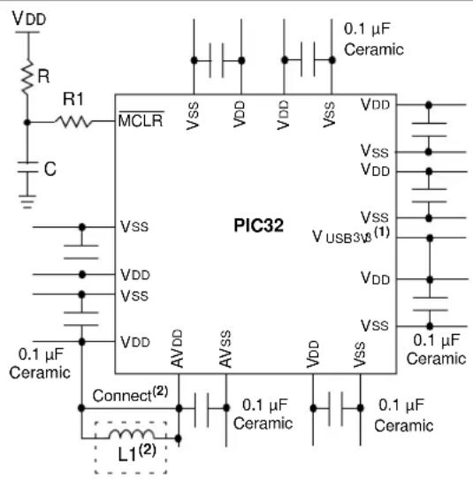
text_image
VDD R1 MCLR VSS VDD VDD VSS 0.1 μF Ceramic VSS VDD PIC32 VUSB3v(1) VSS VDD VSS 0.1 μF Ceramic 0.1 μF Ceramic VDD VSS AVDD AVSS VDD VSS 0.1 μF Ceramic Connect(2) 0.1 μF Ceramic 0.1 μF Ceramic L1(2)Note 1: If the USB module is not used, this pin must not be connected to VDD.
2: As an option, instead of a hard-wired connection, an inductor (L1) can be substituted between VDD and AVDD to improve ADC noise rejection. The inductor impedance should be less than 1 and the inductor capacity greater than 10 mA.
Where:
$$ f = \frac {F _ {C N V}}{2} \quad (\text { i.e., ADC conversion rate } / 2) $$
$$ f = \frac {1}{(2 \pi \sqrt {L C})} $$
$$ L = \left(\frac {1}{(2 \pi f \sqrt {C})}\right) ^ {2} $$
2.2.1 BULK CAPACITORS
The use of a bulk capacitor is recommended to improve power supply stability. Typical values range from 4.7 F to 47 F. This capacitor should be located as close to the device as possible.
2.3 Master Clear (MCLR) Pin
The MCLR pin provides for two specific device functions:
- Device Reset
• Device programming and debugging
Pulling The MCLR pin low generates a device Reset. Figure 2-2 illustrates a typical MCLR circuit. During device programming and debugging, the resistance and capacitance that can be added to the pin must be considered. Device programmers and debuggers drive the MCLR pin. Consequently, specific voltage levels (VIH and VIL) and fast signal transitions must not be adversely affected. Therefore, specific values of R and C will need to be adjusted based on the application and PCB requirements.
For example, as illustrated in Figure 2-2, it is recommended that the capacitor C, be isolated from the MCLR pin during programming and debugging operations.
Place the components illustrated in Figure 2-2 within one-quarter inch (6 mm) from the MCLR pin.
FIGURE 2-2: EXAMPLE OF MCLR PIN CONNECTIONS ^(1,2,3)
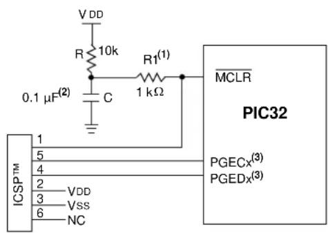
text_image
VDD R 10k 0.1 μF(2) C R1(1) 1 kΩ MCLR PIC32 5 4 2 VDD 3 Vss 6 NC PGECx(3) PGEDx(3)Note 1: 470 ≤ R1 ≤ 1 will limit any current flowing into MCLR from the external capacitor C, in the event of MCLR pin breakdown, due to Electrostatic Discharge (ESD) or Electrical Overstress (EOS). Ensure that the MCLR pin VH and VII specifications are met without interfering with the Debug/Programmer tools.
2: The capacitor can be sized to prevent unintentional Resets from brief glitches or to extend the device Reset period during POR.
3: No pull-ups or bypass capacitors are allowed on active debug/program PGECx/PGEDx pins.
2.4 ICSP Pins
The PGECx and PGEDx pins are used for In-Circuit Serial Programming™ (ICSP™) and debugging purposes. It is recommended to keep the trace length between the ICSP connector and the ICSP pins on the device as short as possible. If the ICSP connector is expected to experience an ESD event, a series resistor is recommended, with the value in the range of a few tens of Ohms, not to exceed 100 Ohms.
Pull-up resistors, series diodes and capacitors on the PGECx and PGEDx pins are not recommended as they will interfere with the programmer/debugger communications to the device. If such discrete components are an application requirement, they should be removed from the circuit during programming and debugging. Alternatively, refer to the AC/DC characteristics and timing requirements information in the respective device Flash programming specification for information on capacitive loading limits and pin input voltage high (VIH) and input low (VIL) requirements.
Ensure that the "Communication Channel Select" (i.e., PGECx/PGEDx pins) programmed into the device matches the physical connections for the ICSP to MPLAB® ICD 3 or MPLAB REAL ICE™.
For more information on ICD 3 and REAL ICE connection requirements, refer to the following documents that are available from the Microchip web site.
- "Using MPLAB ^ ICD 3" (poster) (DS50001765)
- "MPLAB ^ ICD 3 Design Advisory" (DS50001764)
- "MPLAB ^ REAL ICE ^TM In-Circuit Debugger User's Guide" (DS50001616)
- "Using MPLAB ^ REAL ICE ^TM Emulator" (poster) (DS50001749)
2.5 JTAG
The TMS, TDO, TDI and TCK pins are used for testing and debugging according to the Joint Test Action Group (JTAG) standard. It is recommended to keep the trace length between the JTAG connector and the JTAG pins on the device as short as possible. If the JTAG connector is expected to experience an ESD event, a series resistor is recommended, with the value in the range of a few tens of Ohms, not to exceed 100 Ohms.
Pull-up resistors, series diodes and capacitors on the TMS, TDO, TDI and TCK pins are not recommended as they will interfere with the programmer/debugger communications to the device. If such discrete components are an application requirement, they should be removed from the circuit during programming and debugging. Alternatively, refer to the AC/DC characteristics and timing requirements information in the respective device Flash programming specification for information on capacitive loading limits and pin input voltage high (VIH) and input low (VL) requirements.
2.6 Trace
The trace pins can be connected to a hardware trace-enabled programmer to provide a compressed real-time instruction trace. When used for trace, the TRD3, TRD2, TRD1, TRD0 and TRCLK pins should be dedicated for this use. The trace hardware requires a 22 Ohm series resistor between the trace pins and the trace connector.
2.7 External Oscillator Pins
Many MCUs have options for at least two oscillators: a high-frequency primary oscillator and a low-frequency secondary oscillator (refer to Section 8.0 “Oscillator Configuration” for details).
The oscillator circuit should be placed on the same side of the board as the device. Also, place the oscillator circuit close to the respective oscillator pins, not exceeding one-half inch (12 mm) distance between them. The load capacitors should be placed next to the oscillator itself, on the same side of the board. Use a grounded copper pour around the oscillator circuit to isolate them from surrounding circuits. The grounded copper pour should be routed directly to the MCU ground. Do not run any signal traces or power traces inside the ground pour. Also, if using a two-sided board, avoid any traces on the other side of the board where the crystal is placed. A suggested layout is illustrated in Figure 2-3.
FIGURE 2-3: SUGGESTED OSCILLATOR CIRCUIT PLACEMENT
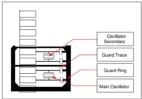
text_image
Oscillator Secondary Guard Trace Guard Ring Main Oscillator2.7.1 CRYSTAL OSCILLATOR DESIGN CONSIDERATION
The following example assumptions are used to calculate the Primary Oscillator loading capacitor values:
• CIN = PIC32_OSC2_Pin Capacitance = \~4-5 pF
• COUT = PIC32_OSC1_Pin Capacitance = \~4-5 pF
- C1 and C2 = XTAL manufacturing recommended loading capacitance
- Estimated PCB stray capacitance, (i.e., 12 mm length) = 2.5 pF
Crystals with a speed of 4 MHz to 12 MHz that meet the following requirements will meet the PIC32MZ EC oscillation requirements when configured, as depicted in Figure 8-1.
- Manufacturer Drive Level (min) ≤ 10 μW (hard requirements, 1 μW preferred).
- Manufacturer ESR ≤ 50Ω (hard requirement, lower is better).
2.7.1.1 Calculating XTAL Capacitive Loading:
- PIC32 C IN = COUT = \~4 pF (PIC32 OSCI and OSCO package pin capacitance).
- C1 MFG = C2MFG = Manufacturer Recommended Load Capacitance.
- CLOAD = {{[CIN + C1MFG] [C2MFG + COUT] / [CIN + C1MFG + C2MFG + COUT]} + estimated PCB stray capacitance (2.5 pF). (Simplified) CLOAD = (((CIN + C1 MFG) / 2) + 2.5 pF).
Actual C1, C2 Load value to use:
• C 2 ±OAD
• C 1 =LO(ADC-2 pF)
Note: These recommendations are atypical, and are only applicable to the PIC32MZ EC family.
2.7.1.2 Validated Crystals
Temperature Range: (-45°C to +110°C)
V_DD=2.4V to 3.6V, RP=1M , RK=10k
• ABLS-12.000 MHz-L4Q-T (12 MHz surface mount)
Note: These recommendations are atypical, and only applicable to the PIC32MZ EC family.
2.7.1.3 Additional Microchip References
• A N 5 8 8 "P1 Microcontroller Oscillator Design Guide"
- A N 8 2 6 "Crystal Oscillator Basics and Crystal Selection for rfPIC™ and PICmicro® Devices"
• A N 8 4 9 "Basic P1O5mator Design"
2.8 Unused I/Os
Unused I/O pins should not be allowed to float as inputs. They can be configured as outputs and driven to a logic-low state.
Alternatively, inputs can be reserved by connecting the pin to Vss through a 1k to 10k resistor and configuring the pin as an input.
2.9 Designing for High-Speed Peripherals
The PIC32MZ EC family devices have peripherals that operate at frequencies much higher than typical for an embedded environment. Table 2-1 lists the peripherals that produce high-speed signals on their external pins:
TABLE 2-1: PERIPHERALS THAT PRODUCE HS SIGNALS ON EXTERNAL PINS
| Peripheral | High-Speed Signal Pins | Maximum Speed on Signal Pin |
| EBI | EBIAx, EBIDx | 50 MHz |
| SQI1 | SQICLK, , SQIDx | 50 MHz |
| HS USB | D+, D- | 480 MHz |
Due to these high-speed signals, it is important to take into consideration several factors when designing a product that uses these peripherals, as well as the PCB on which these components will be placed. Adhering to these recommendations will help achieve the following goals:
- Minimize the effects of electromagnetic interference to the proper operation of the product
- Ensure signals arrive at their intended destination at the same time
- Minimize crosstalk
- Maintain signal integrity
- Reduce system noise
- Minimize ground bounce and power sag
2.9.1 SYSTEM DESIGN
2.9.1.1 Impedance Matching
When selecting parts to place on high-speed buses, particularly the SQI bus, if the impedance of the peripheral device does not match the impedance of the pins on the PIC32MZ EC device to which it is connected, signal reflections could result, thereby degrading the quality of the signal.
If it is not possible to select a product that matches impedance, place a series resistor at the load to create the matching impedance. See Figure 2-4 for an example.
FIGURE 2-4: SERIES RESISTOR
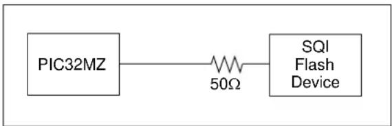
text_image
PIC32MZ 50Ω SQI Flash Device2.9.1.2 PCB Layout Recommendations
The following list contains recommendations that will help ensure the PCB layout will promote the goals previously listed.
- Component Placement
- Place bypass capacitors as close to their component power and ground pins as possible, and place them on the same side of the PCB
- Devices on the same bus that have larger setup times should be placed closer to the PIC32MZ EC device
- Power and Ground
- Multi-layer PCBs will allow separate power and ground planes
- Each ground pin should be connected to the ground plane individually
- Place bypass capacitor vias as close to the pad as possible (preferably inside the pad)
- If power and ground planes are not used, maximize width for power and ground traces
- Use low-ESR, surface-mount bypass capacitors
- Clocks and Oscillators
- Place crystals as close as possible to the PIC32MZ EC device OSC/SOSC pins
- Do not route high-speed signals near the clock or oscillator
- Avoid via usage and branches in clock lines (SQICLK)
- Place termination resistors at the end of clock lines
- Traces
- Higher-priority signals should have the shortest traces
- Match trace lengths for parallel buses (EBIAx, EBIDx, SQIDx)
- Avoid long run lengths on parallel traces to reduce coupling
- Make the clock traces as straight as possible
- Use rounded turns rather than right-angle turns
- Have traces on different layers intersect on right angles to minimize crosstalk
- Maximize the distance between traces, preferably no less than three times the trace width
- Power traces should be as short and as wide as possible
- High-speed traces should be placed close to the ground plane
2.10 Considerations When Interfacing to Remotely Powered Circuits
2.10.1 NON-5V TOLERANT INPUT PINS
A quick review of the absolute maximum rating section in 37.0 "Electrical Characteristics" will indicate that the voltage on any non-5v tolerant pin may not exceed AVDD/VDD + 0.3V. Figure 2-5 shows an example of a remote circuit using an independent power source, which is powered while connected to a PIC32 non-5V tolerant circuit that is not powered.
FIGURE 2-5: PIC32 NON-5V TOLERANT CIRCUIT EXAMPLE
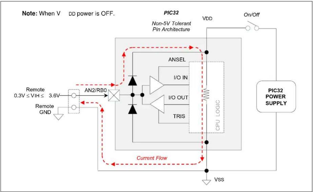
flowchart
graph TD
    A["Remote 0.3V ≤ VIH ≤ 3.6V"] --> B["AN2/RB0"]
    C["Remote GND"] --> B
    B --> D["AnSEL"]
    D --> E["I/O IN"]
    D --> F["I/O OUT"]
    D --> G["TRIS"]
    H["VDD"] --> I["On/Off"]
    I --> J["CPU LOGIC"]
    J --> K["VSS"]
    L["PIC32 POWER SUPPLY"] --> M["On/Off"]
    N["Note: When V DD power is OFF."] --> O["Current Flow"]
    O --> P["AND Gate"]
    style A fill:#f9f,stroke:#333
    style C fill:#f9f,stroke:#333
    style H fill:#ccf,stroke:#333
    style L fill:#cfc,stroke:#333
Without proper signal isolation, on non-5V tolerant pins, the remote signal can power the PIC32 device through the high side ESD protection diodes. Besides violating the absolute maximum rating specification when VDD of the PIC32 device is restored and ramping up or ramping down, it can also negatively affect the internal Power-on Reset (POR) and Brown-out Reset (BOR) circuits, which can lead to improper initialization of internal PIC32 logic circuits. In these cases, it is recommended to implement digital or analog signal isolation as depicted in Figure 2-6, as appropriate. This is indicative of all industry microcontrollers and not just Microchip products.
TABLE 2-2: EXAMPLES OF DIGITAL/ ANALOG ISOLATORS WITH OPTIONAL LEVEL TRANSLATION
| Example Digital/Analog Signal Isolation Circuits | Inductive Coupling | Capacitive Coupling | Opto Coupling | Analog/Digital Switch |
| ADuM7241 / 40 ARZ (1 Mbps) X | — — | — | ||
| ADuM7241 / 40 CRZ (25 Mbps) | X — | — — | ||
| ISO721 — X — — | ||||
| LTV-829S (2 Channel) | — — | X — | ||
| LTV-849S (4 Channel) | — — | X — | ||
| FSA266 / NC7WB66 | — — | — | X |
FIGURE 2-6: DIGITAL/ANALOG SIGNAL ISOLATION CIRCUITS
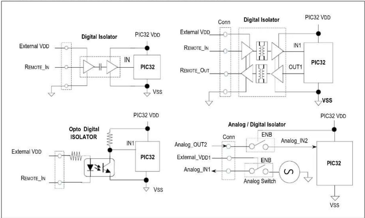
flowchart
Circuit diagrams of PIC32 and VDD-based analog-to-digital isolation systems, showing connections between external, remote, and digital isolators.2.10.2 5V TOLERANT INPUT PINS
The internal high side diode on 5V tolerant pins are bussed to an internal floating node, rather than being connected to VDD, as shown in Figure 2-7. Voltages on these pins, if VDD < 2.3V, should not exceed roughly 3.2V relative to Vss of the PIC32 device. Voltage of 3.6V or higher will violate the absolute maximum specification, and will stress the oxide layer separating the high side floating node, which impacts device reliability. If a remotely powered "digital-only" signal can be guaranteed to always be ≤ 3.2V relative to Vss on the PIC32 device side, a 5V tolerant pin could be used without the need for a digital isolator. This is assuming there is not a ground loop issue, logic ground of the two circuits not at the same absolute level, and a remote logic low input is not less than Vss - 0.3V.
FIGURE 2-7: PIC32 5V TOLERANT PIN ARCHITECTURE EXAMPLE

flowchart
graph TD
    A["Remote GND"] --> B["Remote VIH = 2.5V"]
    B --> C["RG10"]
    C --> D["Floating Bus Oxide BV = 3.6V if VDD < 2.3V"]
    D --> E["OXIDE"]
    E --> F["ANSEL"]
    F --> G["I/O IN"]
    F --> H["I/O OUT"]
    F --> I["TRIS"]
    G --> J["CPU LOGIC"]
    H --> J
    I --> J
    J --> K["VSS"]
    L["On/Off"] --> M["PIC32 POWER SUPPLY"]
    N["VDD"] --> O["On/Off"]
    P["VSS"] --> Q["AnSEL"]
    R["VSS"] --> S["TRIS"]
2.10.2.1 EMI Suppression Considerations
The use of LDO regulators is preferred to reduce overall system noise and provide a cleaner power source. However, when utilizing switching Buck/Boost regulators as the local power source for PIC32MZ EF devices, as well as in electrically noisy environments, users should evaluate the use of T-Filters (i.e., L-C-L) on the power pins, as shown in Figure 2-8. In addition to a more stable power source, use of this type of T-Filter can greatly reduce susceptibility to EMI sources and events.
FIGURE 2-8:

text_image
Ferrite Chip SMD DCR = 0.15Ω (max) 600 ma ISAT 300Ω @ 100 MHz PN#: 1-1624117-3 VDD Ferrite Chips 0.01 μF 0.1 μF VDD VSS VSS VDD PIC32MZ VSS VDD 0.1 μF 0.1 μF VSS VDD 0.1 μF 0.1 μF VSS VDD 0.1 μF 0.1 μF AVDD AVSS VSS VDD 0.1 μF 0.1 μF 0.1 μF Ferrite Chips VDD 0.01 μF2.11 Typical Application Connection Examples
Examples of typical application connections are shown in Figure 2-9 and Figure 2-10.
FIGURE 2-9: AUDIO PLAYBACK APPLICATION
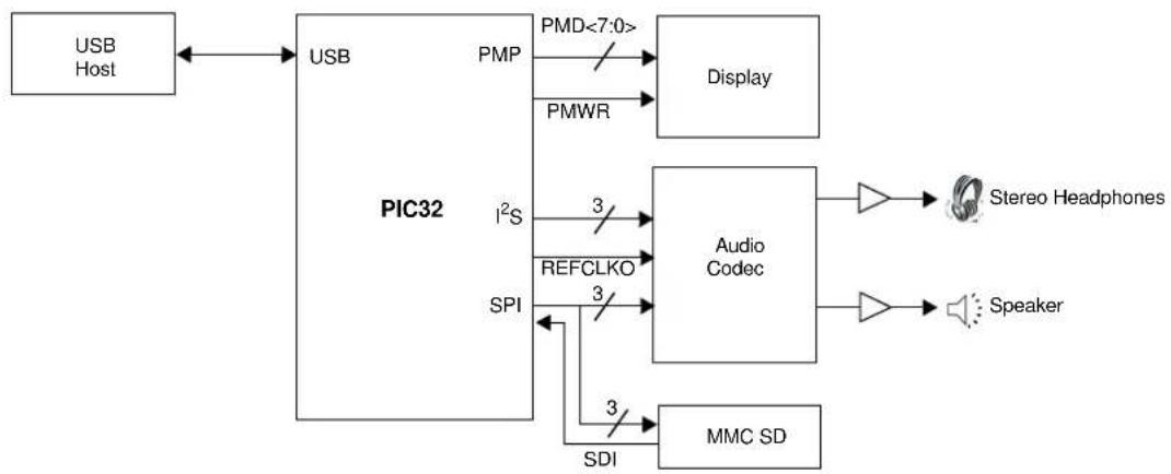
flowchart
graph LR
    A["USB Host"] <--> B["USB"]
    B --> C["PMP"]
    C --> D["Display"]
    B --> E["PMD<7:0>"]
    E --> D
    B --> F["PMWR"]
    F --> D
    B --> G["I²S"]
    G --> H["Audio Codec"]
    H --> I["Stereo Headphones"]
    H --> J["Speaker"]
    B --> K["REFCLKO"]
    K --> L["MMC SD"]
    B --> M["SPI"]
    M --> N["SDI"]
    N --> O["3/"]
    O --> H
FIGURE 2-10: LOW-COST CONTROLLERLESS (LCC) GRAPHICS APPLICATION WITH PROJECTED CAPACITIVE TOUCH
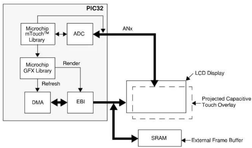
flowchart
graph TD
    A["Microchip mTouch™ Library"] --> B["Microchip GFX Library"]
    B --> C["DMA"]
    B --> D["EBI"]
    D --> E["LED Display"]
    E --> F["Projected Capacitive Touch Overlay"]
    F --> G["SRAM"]
    G --> H["External Frame Buffer"]
    I["ADC"] --> B
    J["Render"] --> D
    K["ANx"] --> E
    L["PIC32"] --> A
    L --> B
3.0 CPU
Note: This data sheet summarizes the features of the PIC32MZ Embedded Connectivity (EC) Family of devices. It is not intended to be a comprehensive reference source. To complement the information in this data sheet, refer to Section 50. "CPU for Devices with MIPS32® microAptiv™ and M-Class Cores" (DS60001192), which is available from the Documentation > Reference Manual section of the Microchip PIC32 web site (www.microchip.com/pic32).
MIPS32 ^® microAptiv ^™ Microprocessor Core resources are available at: www.imgtec.com.
The MIPS32 ^® microAptiv ^™ Microprocessor Core is the heart of the PIC32MZ EC family device processor. The CPU fetches instructions, decodes each instruction, fetches source operands, executes each instruction and writes the results of instruction execution to the proper destinations.
3.1 Features
PIC32MZ EC family processor core key features:
- 5-stage pipeline
• 32-bit address and data paths - MIPS32 ^® Enhanced Architecture (Release 2):
- Multiply-accumulate and multiply-subtract instructions
- Targeted multiply instruction
- Zero/One detect instructions
- WAIT instruction
- Conditional move instructions (MOVN, MOVZ)
- Vectored interrupts
- Programmable exception vector base
- Atomic interrupt enable/disable
- GPR shadow registers to minimize latency for interrupt handlers
- Bit field manipulation instructions
- Virtual memory support
- microMIPS™ compatible instruction set:
- Improves code size density over MIPS32, while maintaining MIPS32 performance.
- Supports all MIPS32 instructions (except branch- likely instructions)
- Fifteen additional 32-bit instructions and 39 16-bit instructions corresponding to commonly-used MIPS32 instructions
- Stack pointer implicit in instruction
- MIPS32 assembly and ABI compatible
- MMU with Translation Lookaside Buffer (TLB) mechanism:
- 16 dual-entry fully associative Joint TLB
- 4-entry fully associative Instruction TLB
- 4-entry fully associative Data TLB
- 4 KB pages
- Separate L1 data and instruction caches:
- 16 KB 4-way Instruction Cache (I-Cache)
- 4 KB 4-way Data Cache (D-Cache)
• Autonomous Multiply/Divide Unit (MDU):
- Maximum issue rate of one 32x32 multiply per clock
- Early-in iterative divide. Minimum 12 and maximum 38 clock latency (dividend (rs) sign extension-dependent)
- Power Control:
- Minimum frequency: 0 MHz
- Low-Power mode (triggered by WAIT instruction)
- Extensive use of local gated clocks
- EJTAG Debug and Instruction Trace:
- Support for single stepping
- Virtual instruction and data address/value breakpoints
- Hardware breakpoint supports both address match and address range triggering.
- Eight instruction and four data complex breakpoints
- iFlowtrace ^® version 2.0 support:
- Real-time instruction program counter
- Special events trace capability
- Two performance counters with 34 user-selectable countable events
- Disabled if the processor enters Debug mode
- Four Watch registers:
- Instruction, Data Read, Data Write options
- Address match masking options
- DSP ASE Extension:
- Native fractional format data type operations
- Register Single Instruction Multiple Data (SIMD) operations (add, subtract, multiply, shift)
- GPR-based shift
- Bit manipulation
- Compare-Pick
- DSP Control Access
- Indexed-Load
- Branch
- Multiplication of complex operands
- Variable bit insertion and extraction
- Virtual circular buffers
- Arithmetic saturation and overflow handling
- Zero-cycle overhead saturation and rounding operations
A block diagram of the PIC32MZ EC family processor core is shown in Figure 3-1.
FIGURE 3-1: PIC32MZ EC FAMILY MICROPROCESSOR CORE
BLOCK DIAGRAM
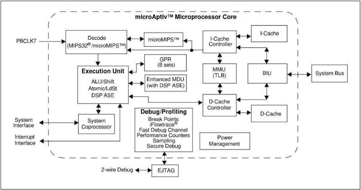
flowchart
graph TD
    A["PBCLK7"] --> B["Decode (MIPS32®/microMIPSTM)"]
    B --> C["Execution Unit"]
    C --> D["ALU/Shift Atomic/LdSt DSP ASE"]
    D --> E["System Coprocessor"]
    E --> F["Debug/Profiling Break Points iFlowtrace® Fast Debug Channel Performance Counters Sampling Secure Debug"]
    F --> G["EJTAG"]
    G --> H["2-wire Debug"]
    H --> I["Power Management"]
    I --> J["D-Cache Controller"]
    J --> K["MMU (TLB)"]
    K --> L["I-Cache Controller"]
    L --> M["BIU"]
    M --> N["System Bus"]
    C --> O["GPR (8 sets)"]
    C --> P["Enhanced MDU (with DSP ASE)"]
    C --> Q["System Interface"]
    C --> R["Interrupt Interface"]
    R --> S["System Coprocessor"]
    S --> T["Debug/Profiling Break Points iFlowtrace® Fast Debug Channel Performance Counters Sampling Secure Debug"]
    T --> U["D-Cache Controller"]
    U --> V["I-Cache Controller"]
    V --> W["BIU"]
    W --> X["System Bus"]
3.2 Architecture Overview
The MIPS32 microAptiv Microprocessor core in PIC32MZ EC family devices contains several logic blocks working together in parallel, providing an efficient high-performance computing engine. The following blocks are included with the core:
- Execution unit
• General Purpose Register (GPR) - Multiply/Divide Unit (MDU)
• System control coprocessor (CP0)
• Memory Management Unit (MMU) - Instruction/Data cache controllers
• Power Management - Instructions and data caches
- microMIPS support
• Enhanced JTAG (EJTAG) controller
3.2.1 EXECUTION UNIT
The processor core execution unit implements a load/store architecture with single-cycle ALU operations (logical, shift, add, subtract) and an autonomous multiply/divide unit. The core contains thirty-two 32-bit General Purpose Registers (GPRs) used for integer operations and address calculation. Seven additional register file shadow sets (containing thirty-two registers) are added to minimize context switching overhead during interrupt/exception processing. The register file consists of two read ports and one write port and is fully bypassed to minimize operation latency in the pipeline.
The execution unit includes:
• 32-bit adder used for calculating the data address
- Address unit for calculating the next instruction address
- Logic for branch determination and branch target address calculation
- Load aligner
- Bypass multiplexers used to avoid stalls when executing instruction streams where data producing instructions are followed closely by consumers of their results
- Leading Zero/One detect unit for implementing the CLZ and CLO instructions
- Arithmetic Logic Unit (ALU) for performing arithmetic and bitwise logical operations
- Shifter and store aligner
- DSP ALU and logic block for performing DSP instructions, such as arithmetic/shift/compare operations
3.2.2 MULTIPLY/DIVIDE UNIT (MDU)
The processor core includes a Multiply/Divide Unit (MDU) that contains a separate pipeline for multiply and divide operations, and DSP ASE multiply instructions. This pipeline operates in parallel with the Integer Unit (IU) pipeline and does not stall when the IU pipeline stalls. This allows MDU operations to be partially masked by system stalls and/or other integer unit instructions.
The high-performance MDU consists of a 32x32 booth recoded multiplier, four pairs of result/accumulation registers (HI and LO), a divide state machine, and the necessary multiplexers and control logic. The first number shown ('32' of 32x32) represents the rs operand. The second number ('32' of 32x32) represents the rt operand.
The MDU supports execution of one multiply or multiply-accumulate operation every clock cycle.
Divide operations are implemented with a simple 1-bit-per-clock iterative algorithm. An early-in detection checks the sign extension of the dividend (rs) operand. If rs is 8 bits wide, 23 iterations are skipped. For a 16-bit wide rs, 15 iterations are skipped and for a 24-bit wide rs, 7 iterations are skipped. Any attempt to issue a subsequent MDU instruction while a divide is still active causes an IU pipeline stall until the divide operation has completed.
Table 3-1 lists the repeat rate (peak issue rate of cycles until the operation can be reissued) and latency (number of cycles until a result is available) for the processor core multiply and divide instructions. The approximate latency and repeat rates are listed in terms of pipeline clocks.
TABLE 3-1: MIPS32 microAptiv MICROPROCESSOR CORE HIGH-PERFORMANCE INTEGER MULTIPLY/DIVIDE UNIT LATENCIES AND REPEAT RATES
| Opcode | Operand Size (mul rt) (div rs) | Latency | Repeat Rate |
| MULT/MULTU, MADD/MADDU,MSUB/MSUBU (HI/LO destination) | 16 bits | 5 | 1 |
| 32 bits | 5 | 1 | |
| MUL (GPR destination) | 16 bits | 5 | 1 |
| 32 bits | 5 | 1 | |
| DIV/DIVU | 8 bits | 12/14 | 12/14 |
| 16 bits | 20/22 | 20/22 | |
| 24 bits | 28/30 | 28/30 | |
| 32 bits | 36/38 | 36/38 |
The MIPS architecture defines that the result of a multiply or divide operation be placed in one of four pairs of HI and LO registers. Using the Move-From-HI (MFHI) and Move-From-LO (MFLO) instructions, these values can be transferred to the General Purpose Register file.
In addition to the HI/LO targeted operations, the MIPS32 architecture also defines a multiply instruction, MUL, which places the least significant results in the primary register file instead of the HI/LO register pair. By avoiding the explicit MFLO instruction required when using the LO register, and by supporting multiple destination registers, the throughput of multiply-intensive operations is increased.
Two other instructions, Multiply-Add (MADD) and Multiply-Subtract (MSUB), are used to perform the multiply-accumulate and multiply-subtract operations. The MADD instruction multiplies two numbers and then adds the product to the current contents of the HI and LO registers. Similarly, the MSUB instruction multiplies two operands and then subtracts the product from the HI and LO registers. The MADD and MSUB operations are commonly used in DSP algorithms.
The MDU also implements various shift instructions operating on the HI/LO register and multiply instructions as defined in the DSP ASE. The MDU supports all of the data types required for this purpose and includes three extra HI/LO registers as defined by the ASE.
Table 3-2 lists the latencies and repeat rates for the DSP multiply and dot-product operations. The approximate latencies and repeat rates are listed in terms of pipeline clocks.
TABLE 3-2: DSP-RELATED LATENCIES AND REPEAT RATES
| Op code Latency | Repeat Rate | |
| Multiply and dot-product without saturation after accumulation | 5 | 1 |
| Multiply and dot-product with saturation after accumulation | 5 | 1 |
| Multiply without accumulation | 5 | 1 |
3.2.3 SYSTEM CONTROL COPROCESSOR (CP0)
In the MIPS architecture, CP0 is responsible for the virtual-to-physical address translation and cache protocols, the exception control system, the processor's diagnostics capability, the operating modes (Kernel, User and Debug) and whether interrupts are enabled or disabled. Configuration information, such as cache size and set associativity, and the presence of options like microMIPS, is also available by accessing the CP0 registers, listed in Table 3-3.
TABLE 3-3: COPROCESSOR 0 REGISTERS
| Register Number | Register Name | Function |
| 0 Index | Index into the TLB array (microAptiv MPU only). | |
| 1 Random | Randomly generated index into the TLB array (microAptiv MPU only). | |
| 2 Entry | Lo0 Low-order portion of the TLB entry for even-numbered virtual pages (microAptiv MPU only). | |
| 3 Entry | Lo1 Low-order portion of the TLB entry for odd-numbered virtual pages (microAptiv MPU only). | |
| 4 | C o n UserLocal | Pointer to the page table entry in memory (microAptiv MPU only).User information that can be written by privileged software and read via the RDHWR instruction. |
| 5 Page | Mask/ PageGrain | PageMask controls the variable page sizes in TLB entries. PageGrain enables support of 1 KB pages in the TLB (microAptiv MPU only). |
| 6 Wired | Controls the number of fixed (i.e., wired) TLB entries (microAptiv MPU only). | |
| 7 | HWREna | Enables access via the RDHWR instruction to selected hardware registers in Non-privileged mode. |
| 8 Bad | VAddr Reports the address for the most recent address-related exception. | |
| 9 Count | Processor cycle count. | |
| 10 Entry | Hi High-order portion of the TLB entry (microAptiv MPU only). | |
| 11 | Compare Core timer interrupt control. | |
| 12 Status | Processor status and control. | |
| IntCtl | Interrupt control of vector spacing. | |
| SRSCtl | Shadow register set control. | |
| SRSMap Shadow register mapping control. | ||
| View_IPL | Allows the Priority Level to be read/written without extracting or inserting that bit from/to the Status register. | |
| SRSMAP2 | Contains two 4-bit fields that provide the mapping from a vector number to the shadow set number to use when servicing such an interrupt. | |
| 13 Cause | Describes the cause of the last exception. | |
| NestedExc | Contains the error and exception level status bit values that existed prior to the current exception. | |
| View_RIPL | Enables read access to the RIPL bit that is available in the Cause register. | |
| 14 | EPC | Program counter at last exception. |
| NestedEPC | Contains the exception program counter that existed prior to the current exception. | |
| 15 | PRID | Processor identification and revision |
| Ebase | Exception base address of exception vectors. | |
| CDMMBase | Common device memory map base. | |
| 16 | Config | Configuration register. |
| Config1 | Configuration register 1. | |
| Config2 | Configuration register 2. | |
| Config3 | Configuration register 3. | |
| Config4 | Configuration register 4. | |
| Config5 | Configuration register 5. | |
| Config7 | Configuration register 7. | |
| 17 LLa | Addr Load link address (microAptiv MPU only). | |
| 18 WatchLo | Low-order watchpoint address (microAptiv MPU only). | |
| 19 WatchHi | High-order watchpoint address (microAptiv MPU only). | |
| 20-22 | Reserved | Reserved in the PIC32 core. |
| 23 | Debug EJTAG debug register. | |
| TraceControl EJTAG trace control. | ||
| TraceControl2 EJTAG trace control 2. | ||
| UserTraceData1 EJTAG user trace data 1 register. | ||
| TraceBPC EJTAG trace breakpoint register. | ||
| Debug2 Debug control/exception status 1. | ||
| 24 | DEPC Program counter at last debug exception. | |
| UserTraceData2 EJTAG user trace data 2 register. | ||
| 25 | PerfCtl0 Performance counter 0 control. | |
| PerfCnt0 | Performance counter 0. | |
| PerfCtl1 | Performance counter 1 control. | |
| PerfCnt1 | Performance counter 1. | |
| 26 | ErrCtl | Software test enable of way-select and data RAM arrays for I-Cache and D-Cache (microAptiv MPU only). |
| 27 | Reserved | Reserved in the PIC32 core. |
| 28 | TagLo/DataLo | Low-order portion of cache tag interface (microAptiv MPU only). |
| 29 | Reserved | Reserved in the PIC32 core. |
| 30 | ErrorEPC | Program counter at last error exception. |
| 31 | DeSave Debug exception save. | |
3.3 Power Management
The processor core offers a number of power management features, including low-power design, active power management and power-down modes of operation. The core is a static design that supports slowing or halting the clocks, which reduces system power consumption during Idle periods.
3.3.1 INSTRUCTION-CONTROLLED POWER MANAGEMENT
The mechanism for invoking Power-Down mode is through execution of the WAIT instruction. For more information on power management, see Section 33.0 "Power-Saving Features".
The majority of the power consumed by the processor core is in the clock tree and clocking registers. The PIC32MZ family makes extensive use of local gated-clocks to reduce this dynamic power consumption.
3.4 L1 Instruction and Data Caches
3.4.1 INSTRUCTION CACHE (I-CACHE)
The I-Cache is an on-core memory block of 16 Kbytes. Because the I-Cache is virtually indexed, the virtual-to-physical address translation occurs in parallel with the cache access rather than having to wait for the physical address translation. The tag holds 22 bits of physical address, a valid bit, and a lock bit. The LRU replacement bits are stored in a separate array.
The I-Cache block also contains and manages the instruction line fill buffer. Besides accumulating data to be written to the cache, instruction fetches that reference data in the line fill buffer are serviced either by a bypass of that data, or data coming from the external interface. The I-Cache control logic controls the bypass function.
The processor core supports I-Cache locking. Cache locking allows critical code or data segments to be locked into the cache on a per-line basis, enabling the system programmer to maximize the efficiency of the system cache.
The cache locking function is always available on all I-Cache entries. Entries can then be marked as locked or unlocked on a per entry basis using the CACHE instruction.
3.4.2 DATA CACHE (D-CACHE)
The D-Cache is an on-core memory block of 4 Kbytes. This virtually indexed, physically tagged cache is protected. Because the D-Cache is virtually indexed, the virtual-to-physical address translation occurs in parallel with the cache access. The tag holds 22 bits of physical address, a valid bit, and a lock bit. There is an additional array holding dirty bits and LRU replacement algorithm bits for each set of the cache.
In addition to I-Cache locking, the processor core also supports a D-Cache locking mechanism identical to the I-Cache. Critical data segments are locked into the cache on a per-line basis. The locked contents can be updated on a store hit, but cannot be selected for replacement on a cache miss.
The D-Cache locking function is always available on all D-Cache entries. Entries can then be marked as locked or unlocked on a per-entry basis using the CACHE instruction.
3.4.3 ATTRIBUTES
The processor core I-Cache and D-Cache attributes are listed in the Configuration registers (see Register 3-1 through Register 3-4).
3.5 EJTAG Debug Support
The processor core provides for an Enhanced JTAG (EJTAG) interface for use in the software debug of application and kernel code. In addition to standard User mode and Kernel modes of operation, the processor core provides a Debug mode that is entered after a debug exception (derived from a hardware breakpoint, single-step exception, etc.) is taken and continues until a Debug Exception Return (DERET) instruction is executed. During this time, the processor executes the debug exception handler routine.
The EJTAG interface operates through the Test Access Port (TAP), a serial communication port used for transferring test data in and out of the core. In addition to the standard JTAG instructions, special instructions defined in the EJTAG specification specify which registers are selected and how they are used.
3.6 MIPS DSP ASE Extension
The MIPS DSP Application-Specific Extension Revision 2 is an extension to the MIPS32 architecture. This extension comprises new integer instructions and states that include new HI/LO accumulator register pairs and a DSP control register. This extension is crucial in a wide range of DSP, multimedia, and DSP-like algorithms covering Audio and Video processing applications. The extension supports native fractional format data type operations, register Single Instruction Multiple Data (SIMD) operations, such as add, subtract, multiply, and shift. In addition, the extension includes the following features that are essential in making DSP algorithms computationally efficient:
• Support for multiplication of complex operands
- Variable bit insertion and extraction
- Implementation and use of virtual circular buffers
- Arithmetic saturation and overflow handling support
- Zero cycle overhead saturation and rounding operations
3.7 microAptiv™ Core Configuration
Register 3-1 through Register 3-4 show the default configuration of the microAptiv core, which is included on PIC32MZ EC family devices.
REGISTER 3-1: CONFIG: CONFIGURATION REGISTER; CP0 REGISTER 16, SELECT 0
| Bit Range | Bit 31/23/15/7 | Bit 30/22/14/6 | Bit 29/21/13/5 | Bit 28/20/12/4 | Bit 27/19/11/3 | Bit 26/18/10/2 | Bit 25/17/9/1 | Bit 24/16/8/0 |
| 31:24 | r-1 U-0 U-0 | U-0 U-0 U-0 U-0 | R-0 | |||||
| — | — | — | — | — | — | — | ISP | |
| 23:16 | R-0 | R-0 R-1 R-0 | U-0 R-1 R-0 | R-0 | ||||
| DSP | UDI | SB | MDU | — | MM<1:0> | BM | ||
| 15:8 | R-0 | R-0 R-0 R-0 | R-0 R-1 | R-0 | R-0 | |||
| BE | AT<1:0> | AR<2:0> | MT<2:1> | |||||
| 7:0 | R-1 | U-0 | U-0 | U-0 | U-0 | R/W-0 | R/W-1 | R/W-0 |
| MT<0> | — | — | — | — | K0<2:0> | |||
| Legend: | r = Reserved bit | ||
| R = Readable bit | W = Writable bit | U = Unimplemented bit, read as ‘0’ | |
| -n = Value at POR | ‘1’ = Bit is set | ‘0’ = Bit is cleared | x = Bit is unknown |
bit 31 Reserved: This bit is hardwired to '1' to indicate the presence of the Config1 register.
bit 30-25 Unimplemented: Read as '0'
bit 24 ISP: Instruction Scratch Pad RAM bit 0 = Instruction Scratch Pad RAM is not implemented
bit 23 DSP: Data Scratch Pad RAM bit 0 = Data Scratch Pad RAM is not implemented
bit 22 UDI: User-defined bit 0 = CorExtend User-Defined Instructions are not implemented
bit 21 SB: SimpleBE bit 1 = Only Simple Byte Enables are allowed on the internal bus interface
bit 20 MDU: Multiply/Divide Unit bit 0 = Fast, high-performance MDU
bit 19 Unimplemented: Read as '0'
bit 18-17 MM<1:0>: Merge Mode bits 10 = Merging is allowed
bit 16 BM: Burst Mode bit 0 = Burst order is sequential
bit 15 BE: Endian Mode bit 0 = Little-endian
bit 14-13 AT<1:0>: Architecture Type bits 00 = MIPS32
bit 12-10 AR<2:0>: Architecture Revision Level bits 001 = MIPS32 Release 2
bit 9-7 MT<2:0>: MMU Type bits 001 = microAptiv MPU Microprocessor core uses a TLB-based MMU
bit 6-3 Unimplemented: Read as '0'
bit 2-0 K0<2:0>: Kseg0 Coherency Algorithm bits 011 = Cacheable, non-coherent, write-back, write allocate 010 = Uncached 001 = Cacheable, non-coherent, write-through, write allocate 000 = Cacheable, non-coherent, write-through, no write allocate All other values are not used and are mapped to other values. Values 100, 101, and 110 are mapped to 010. Value 111 is mapped to 010.
REGISTER 3-2: CONFIG1: CONFIGURATION REGISTER 1; CP0 REGISTER 16, SELECT 1
| Bit Range | Bit 31/23/15/7 | Bit 30/22/14/6 | Bit 29/21/13/5 | Bit 28/20/12/4 | Bit 27/19/11/3 | Bit 26/18/10/2 | Bit 25/17/9/1 | Bit 24/16/8/0 |
| 31:24 | r-1 R-0 R-0 | R-1 R-1 R-1 R-1 | R-0 | |||||
| — MMU | Size<5:0> IS<2> | |||||||
| 23:16 | R-1 R-0 R-0 | R-1 R-1 R-0 R-1 | R-1 | |||||
| IS<1:0> IL<2:0> IA<2:0> | ||||||||
| 15:8 | R-0 R-0 R-0 | R-0 R-1 R-1 R-0 | R-1 | |||||
| DS<2:0> DL<2:0> DA<2:1> | ||||||||
| 7:0 | R-1 U-0 U-0 | R-1 R-1 R-0 R-1 | R-0 | |||||
| DA<0> | — | — | PC | WR | CA | EP | FP | |
| Legend: | r = Reserved bit | ||
| R = Readable bit | W = Writable bit | U = Unimplemented bit, read as ‘0’ | |
| -n = Value at POR | ‘1’ = Bit is set | ‘0’ = Bit is cleared | x = Bit is unknown |
bit 31 Reserved: This bit is hardwired to a '1' to indicate the presence of the Config2 register.
bit 30-25 MMU Size<5:0>: Contains the number of TLB entries minus 1
001111 = 16 TLB entries
bit 24-22 IS<2:0>: Instruction Cache Sets bits
010 = Contains 256 instruction cache sets per way
bit 21-19 IL<2:0>: Instruction-Cache Line bits
011 = Contains instruction cache line size of 16 bytes
bit 18-16 IA<2:0: Instruction-Cache Associativity bits
011 = Contains 4-way instruction cache associativity
bit 15-13 DS<2:0>: Data-Cache Sets bits
000 = Contains 64 data cache sets per way
bit 12-10 DL<2:0>: Data-Cache Line bits
011 = Contains data cache line size of 16 bytes
bit 9-7 DA<2:0>: Data-Cache Associativity bits
011 = Contains the 4-way set associativity for the data cache
bit 6-5 Unimplemented: Read as '0'
bit 4 PC: Performance Counter bit
1 = The processor core contains Performance Counters
bit 3 WR: Watch Register Presence bit
1 = No Watch registers are present
bit 2 CA: Code Compression Implemented bit
0 = No MIPS16e® present
bit 1 EP: EJTAG Present bit
1 = Core implements EJTAG
bit 0 FP: Floating Point Unit bit
0 = Floating Point Unit is not implemented
REGISTER 3-3: CONFIG3: CONFIGURATION REGISTER 3; CP0 REGISTER 16, SELECT 3
| Bit Range | Bit 31/23/15/7 | Bit 30/22/14/6 | Bit 29/21/13/5 | Bit 28/20/12/4 | Bit 27/19/11/3 | Bit 26/18/10/2 | Bit 25/17/9/1 | Bit 24/16/8/0 |
| 31:24 | r-1 U-0 U-0 | U-0 U-0 | U-0 U-0 | U-0 | ||||
| — — — | — — — — | — — — — | — | |||||
| 23:16 | U-0 R-0 R-1 | R-0 R-0 | R-0 R-1 | R/W-y | ||||
| — | IPLW<1:0> | MMAR<2:0> | MCU | ISAONEXC^(1) | ||||
| 15:8 | R-y | R-y R-1 | R-1 R-1 | R-1 U-0 R-1 | ||||
| ISA<1:0>(^1) | ULRI | RXI | DSP2P | DSPP | — | ITL | ||
| 7:0 | U-0 R-1 R-1 | R-0 R-1 | U-0 U-0 | R-0 | ||||
| — | VEIC | VINT | SP | CDMM | — | — | TL | |
| Legend: | r = Reserved bit | y = Value set from Configuration bits on POR |
| R = Readable bit | W = Writable bit U = Unimplemented bit, read as ‘0’ | |
| -n = Value at POR | ‘1’ = Bit is set | ‘0’ = Bit is cleared x = Bit is unknown |
bit 31 Reserved: This bit is hardwired as '1' to indicate the presence of the Config4 register
bit 30-23 Unimplemented: Read as '0'
bit 22-21 IPLW<1:0>: Width of the Status IPL and Cause RIPL bits 01 = IPL and RIPL bits are 8-bits in width
bit 20-18 MMAR<2:0>: microMIPS Architecture Revision Level bits 000 = Release 1
bit 17 MCU: MIPS MCU ASE Implemented bit 1 = MCU ASE is implemented
bit 16 ISAONEXC: ISA on Exception bit ^(1) 1 = microMIPS is used on entrance to an exception vector 0 = MIPS32 ISA is used on entrance to an exception vector
bit 15-14 ISA<1:0>: Instruction Set Availability bits ^(1) 11 = Both MIPS32 and microMIPS are implemented; microMIPS is used when coming out of reset
10 = Both MIPS32 and microMIPS are implemented; MIPS32 ISA used when coming out of reset
bit 13 ULRI: UserLocal Register Implemented bit 1 = UserLocal Coprocessor 0 register is implemented
bit 12 RXI: RIE and XIE Implemented in PageGrain bit 1 = RIE and XIE bits are implemented
bit 11 DSP2P: MIPS DSP ASE Revision 2 Presence bit 1 = DSP Revision 2 is present
bit 10 DSPP: MIPS DSP ASE Presence bit 1 = DSP is present
bit 9 Unimplemented: Read as '0'
bit 8 ITL: Indicates that iFlowtrace hardware is present 1 = The iFlowtrace is implemented in the core
bit 7 Unimplemented: Read as '0'
bit 6 VEIC: External Vector Interrupt Controller bit 1 = Support for an external interrupt controller is implemented.
bit 5 VINT: Vector Interrupt bit 1 = Vector interrupts are implemented
bit 4 SP: Small Page bit 0 = 4 KB page size
bit 3 CDMM: Common Device Memory Map bit 1 = CDMM is implemented
bit 2-1 Unimplemented: Read as '0'
bit 0 TL: Trace Logic bit 0 = Trace logic is not implemented
Note 1: These bits are set based on the value of the BOOTISA Configuration bit (DEVCFG0<6>).
REGISTER 3-4: CONFIG5: CONFIGURATION REGISTER 5; CP0 REGISTER 16, SELECT 5
| Bit Range | Bit 31/23/15/7 | Bit 30/22/14/6 | Bit 29/21/13/5 | Bit 28/20/12/4 | Bit 27/19/11/3 | Bit 26/18/10/2 | Bit 25/17/9/1 | Bit 24/16/8/0 |
| 31:24 | U-0 U-0 U-0 | U-0 U-0 U-0 U-0 | U-0 | |||||
| — — — | — — — — — | |||||||
| 23:16 | U-0 U-0 U-0 | U-0 U-0 U-0 U-0 | U-0 | |||||
| — — — | — — — — — | |||||||
| 15:8 | U-0 U-0 U-0 | U-0 U-0 U-0 U-0 | U-0 | |||||
| — — — | — — — — — | |||||||
| 7:0 | U-0 U-0 U-0 | U-0 U-0 U-0 U-0 | R-1 | |||||
| — — — | — — — — | N | F |
| Legend: | r = Reserved | ||
| R = Readable bit | W = Writable bit U = Unimplemented bit, read as '0' | ||
| -n = Value at POR | '1' = Bit is set | '0' = Bit is cleared | x = Bit is unknown |
bit 31-1 Unimplemented: Read as '0'
bit 0 NF: Nested Fault bit
1 = Nested Fault feature is implemented
REGISTER 3-5: CONFIG7: CONFIGURATION REGISTER 7; CP0 REGISTER 16, SELECT 7
| Bit Range | Bit 31/23/15/7 | Bit 30/22/14/6 | Bit 29/21/13/5 | Bit 28/20/12/4 | Bit 27/19/11/3 | Bit 26/18/10/2 | Bit 25/17/9/1 | Bit 24/16/8/0 |
| 31:24 | R-1 | U-0 | U-0 | U-0 | U-0 | U-0 | U-0 | U-0 |
| WII — — | — — — — — | |||||||
| 23:16 | U-0 | U-0 | U-0 | U-0 | U-0 | U-0 | U-0 | U-0 |
| — — — | — — — — — | |||||||
| 15:8 | U-0 | U-0 | U-0 | U-0 | U-0 | U-0 | U-0 | U-0 |
| — — — | — — — — — | |||||||
| 7:0 | U-0 | U-0 | U-0 | U-0 | U-0 | U-0 | U-0 | U-0 |
| — — — | — — — — — |
| Legend: | |||
| R = Readable bit | W = Writable bit | U = Unimplemented bit, read as '0' | |
| -n = Value at POR | '1' = Bit is set | '0' = Bit is cleared | x = Bit is unknown |
bit 31 WII: Wait IE Ignore bit
1 = Indicates that this processor will allow an interrupt to unblock a WAIT instruction
bit 30-0 Unimplemented: Read as '0'
NOTES:
4.0 MEMORY ORGANIZATION
Note:
This data sheet summarizes the features of the PIC32MZ Embedded Connectivity (EC) Family of devices. This document is not intended to be a comprehensive reference source. For detailed information, refer to Section 48. "Memory Organization and Permissions" (DS60001214), which is available from the Documentation > Reference Manual section of the Microchip PIC32 web site (www.microchip.com/pic32).
PIC32MZ EC microcontrollers provide 4 GB of unified virtual memory address space. All memory regions, including program, data memory, Special Function Registers (SFRs) and Configuration registers, reside in this address space at their respective unique addresses. The program and data memories can be optionally partitioned into user and kernel memories. In addition, PIC32MZ EC devices allow execution from data memory.
Key features include:
• 32-bit native data width
- Separate User (KUSEG) and Kernel (KSEG0/KSEG1/KSEG2/KSEG3) mode address space
- Separate boot Flash memory for protected code
- Robust bus exception handling to intercept runaway code
- Cacheable (KSEG0/KSEG2) and non-cacheable (KSEG1/KSEG3) address regions
- Read-Write permission access to predefined memory regions
4.1 Memory Layout
PIC32MZ EC microcontrollers implement two address schemes: virtual and physical. All hardware resources, such as program memory, data memory and peripherals, are located at their respective physical addresses. Virtual addresses are exclusively used by the CPU to fetch and execute instructions as well as access peripherals. Physical addresses are used by bus master peripherals, such as DMA and the Flash controller, that access memory independently of the CPU.
The main memory maps for the PIC32MZ EC devices are illustrated in Figure 4-1 through Figure 4-4. Figure 4-5 provides memory map information for boot Flash and boot alias. Table 4-1 provides memory map information for SFRs.
FIGURE 4-1: MEMORY MAP FOR DEVICES WITH 512 KB OF PROGRAM MEMORY (1,2)

bar_stacked
| Virtual Memory Map | KSEG1KSEG0 | Physical Memory Map | | ------------------- | ---------- | ------------------- | | 0xFFFFFFF | Reserved | 0xFFFFFFF | | 0xF4000000 | Reserved | 0x3FFFFFFF | | 0xF3FFFFFF | External Memory via SQI | 0x33FFFFFFF | | 0xF0000000 | Reserved | External Memory via SQI | | 0xE4000000 | Reserved | 0x30000000 | | 0xE3FFFFFF | External Memory via EBI | Reserved | | 0xE0000000 | Reserved | 0x24000000 | | 0xD4000000 | Reserved | 0x23FFFFFFF | | 0xD3FFFFFF | External Memory via SQI | Reserved | | 0xD0000000 | Reserved | External Memory via EBI | | 0xC4000000 | Reserved Reserve | Boot Flash (see Figure 4-5) | | 0xC3FFFFFF | External Memory via EBI | Reserved | | 0xC0000000 | Reserved | SFRs (see Table 4-1) | | 0xBFFFFFF | Reserved | Reserved0xBF8FFFFF | | 0xBFC74000 | Reserved | Program Flash | | 0xBFC73FFF | Boot Flash (see Figure 4-5) | Reserved | | 0xBFC00000 | Reserved | Reserved | | 0xBF900000 | SFRs (see Table 4-1) | Reserved | | 0xBF800000 | Reserved | RAM(3) | | 0xBD808000 | Reserved | Reserved | | 0xBD7FFFF | Program Flash | Reserved | | 0xBD000000 | Reserved | Reserved | | 0xA0221111 | Reserved | Reserved | | 0xA1111111 | RAM(3) | Reserved | | 0xA1111111 | Reserved | Reserved | | 0xA1111111 | Reserved | Reserved | | 0xA1111111 | Reserved | Reserved | | 0xA1111111 | Reserved | Reserved | | 0xA1111111 | Reserved | Reserved | | 0xA1111111 | Reserved | Reserved | | | 0xA1111111 | Reserved | Reserved | | 0xA1111111 | Reserved | Reserved | | 0xA1111111 | Reserved | Reserved | | 0xA1111111 | Reserved | Reserved | | 0xA1111111 | Reserved | Reserved | | 0xA9FC742222 | Reserved | Reserved | | 0x9FC732222 | Boot Flash (see Figure 4-5) | Reserved | | 0x9FC732222 | Reserved | Reserved | | 0x9FC732222 | Program Flash | Reserved | | 0x9D882222 | Reserved | Reserved | | 0x9D882222 | Program Flash | Reserved | | 0x9D882222 | Reserved | Reserved | | 0x9D772222 | Reserved | Reserved | | 0x9D772222 | Program Flash | Reserved | | 0x9D772222 | Reserved | Reserved | | 0x9D762222 | Reserved | Reserved | | 0x9D762222 | Program Flash | Reserved | | 0x9D762222 | Reserved | Reserved | | 0x9D752222 | Reserved | Reserved | | 0x9D752222 | Program Flash | Reserved | | 0x9D752222 | Reserved | Reserved | | 0x9D742222 | Reserved | Reserved | | 0x9D742222 | Program Flash | Reserved | | 0x9D742222 | Reserved | Reserved | | 0x9D732222 | Reserved | Reserved | | 0x9D732222 | Program Flash | Reserved | | 0x9D732222 | Reserved | Reserved | | 0x9D722222 | Program Flash | Reserved | | 0x9D722222 | Reserved | Reserved | | 0x9D712222 | Reserved | Reserved | | 0x9D712222 | Program Flash | Reserved | | 0x9D712222 | Reserved | Reserved | | 0x9D7633333 | Reserved | Reserved | | 0x9D7633333 | Program Flash | Reserved | | 0x9D7633333 | Reserved | Reserved | | 0x9D7533333 | Reserved | Reserved | | 0x9D7533333 | Program Flash | Reserved | | 0x9D7533333 | Reserved | Reserved | | 0x9D7434444 | Reserved | Reserved | | 0x9D7434444 | Program Flash | Reserved | | 0x9D7434444 | Reserved | Reserved | | 0x9D7344444 | Program Flash | Reserved | | 0x9D7344444 | Reserved | Reserved | | 0x9D7344444 | Program Flash (see Figure 4-5) - Program Flash (see Table 4-5) - Reserved - Program Flash (see Table 4-5) - Reserved - Program Flash (see Table 4-5) - Reserved - Program Flash (see Table 4-5) - Reserved - Program Flash (see Table 4-5) - Reserved - Program Flash (see Table 4-5) - Reserved - Program Flash (see Table 4-5) - Reserved - Program Flash (see Table 4-5) - Reserved - Program Flash (see Table 4 - Modified) - Program Flash (see Table 4-5) - Reserved - Program Flash (see Table 4-5) - Reserved - Program Flash (see Table 4-5) - Reserved - Program Flash (see Table 4-5) - Reserved - Program Flash (see Table 4-5) - Reserved - Program Flash (see Table 4-5) - Reserved - Program Flash (see Table 4-5) - Reserved - Program Flash (see Table 5 - Modified) - Program Flash (see Table 5 - Modified) - Program Flash (see Table 5 - Modified) - Program Flash (see Table 5 - Modified) - Program Flash (see Table 5 - Modified) - Program Flash (see Table 5 - Modified) - Program Flash (see Table 5 - Modified) - Program Flash (see Table 5 - Modified) - Program Flash (see Table 5 - Modified) - Program Flash (see Table 5 - Modified) = SRDF6FF, SRDF6FF, SRDF6FF, SRDF6FF, SRDF6FF, SRDF6FF, SRDF6FF, SRDF6FF, SRDF6FF, SRDF6FF, SRDF6FF, SRDF6FF, SRDF6FF, SRDF6FF, SRDF6FF, SRDF6FF, SRDF6FF, SRDF6FF, SRDF6FF, SRDF6FF, SRDF6FFNote 1: Memory areas are not shown to scale.
2: The Cache, MMU, and TLB are initialized by compiler start-up code.
3: RAM memory is divided into two equal banks: RAM Bank 1 and RAM Bank 2 on a half boundary.
4: The MMU must be enabled and the TLB must be set up to access this segment.
FIGURE 4-2: MEMORY MAP FOR DEVICES WITH 1024 KB OF PROGRAM MEMORY AND 256 KB OF RAM ^(1,2)
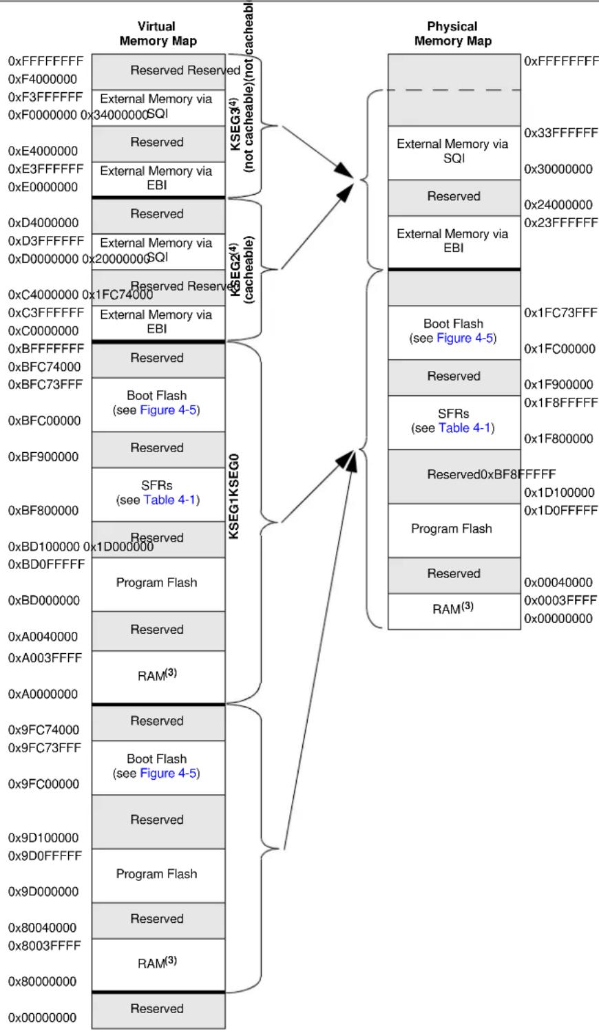
Note 1: Memory areas are not shown to scale.
2: The Cache, MMU, and TLB are initialized by compiler start-up code.
3: RAM memory is divided into two equal banks: RAM Bank 1 and RAM Bank 2 on a half boundary.
4: The MMU must be enabled and the TLB must be set up to access this segment.
FIGURE 4-3: MEMORY MAP FOR DEVICES WITH 1024 KB OF PROGRAM MEMORY AND 512 KB OF RAM ^(1,2)
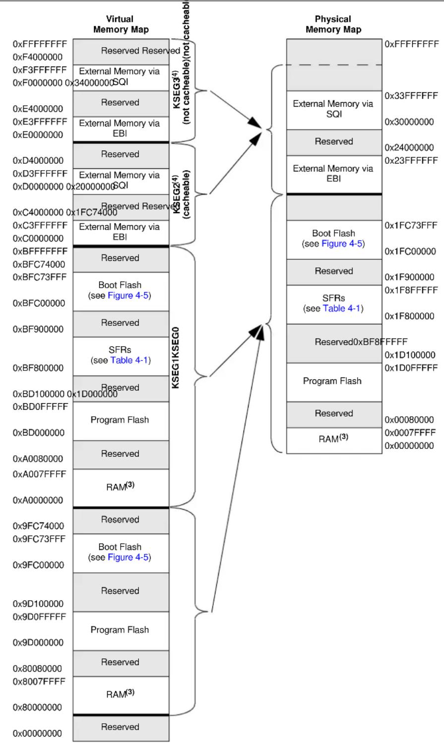
bar_stacked
| Virtual Memory Map | KSEG1KSEG0 | Physical Memory Map | | ------------------ | ---------- | ------------------- | | 0xFFFFFFF | Reserved | 0xFFFFFFF | | 0xF4000000 | Reserved | 0x33FFFFFF | | 0xF3FFFFFF | External Memory via SQI | 0x33FFFFFF | | 0xF0000000 0x34000000 | Reserved | External Memory via SQI | | 0xE4000000 | Reserved | 0x30000000 | | 0xE3FFFFFF | External Memory via EBI | Reserved | | 0xE0000000 | Reserved | 0x24000000 | | 0xD4000000 | Reserved | 0x23FFFFFF | | 0xD3FFFFFF | External Memory via SQI | Reserved | | 0xD0000000 0x20000006 | Reserved | External Memory via EBI | | 0xC4000000 0x1FC74000 | Reserved | Boot Flash (see Figure 4-5) | | 0xC3FFFFFF | Reserved | 0x1FC73FFF | | 0xC0000000 | Reserved | 0x1FC00000 | | 0xBFFFFFF | Reserved | Reserved | | 0xBFC74000 | Reserved | SFRs (see Table 4-1) | | 0xBFC73FFF | Boot Flash (see Figure 4-5) | Reserved | | 0xBFC00000 | Reserved | Reserved(See Table 4-1) | | 0xBF900000 | Reserved | Reserved(See Table 4-1) | | 0xBF800000 | SFRs (see Table 4-1) | Program Flash | | 0xBD1D1D1D1D1D1D1D1D1D1D1D1D1D1D1D1D1D1D1D1D1D1D1D1D1D1D1D1D1D1D1D1D1D1D1D1D1D1D1D1D1D1D1D1D1D1D1D1D1D1D1 D1D1D1D1D1D1D1D1D1D1D1D1D1D1D1D1D1D1D1D1D1D1D1D1D1D1D1D1D1D1D1D1D1D1D1D1D1D1D1D1D1D1D1D1D1D1D1D1D1D1CFF | | 0xBDF8888888888888888888888888888888888888888888888888888888888888888888888888888888888888888888888888888B | 2xBD74747777777777777777777777777777777777777777777777777777777777777777777777777777777777777777777777777777| | 2x9FC6666666666666666666666666666666666666666666666666666666666666666666666666666666666666666666666666666 | | 2x9FC333333333333333333333333333333333333333333333333333333333333333333333333333333333333Note 1: Memory areas are not shown to scale.
2: The Cache, MMU, and TLB are initialized by compiler start-up code.
3: RAM memory is divided into two equal banks: RAM Bank 1 and RAM Bank 2 on a half boundary.
4: The MMU must be enabled and the TLB must be set up to access this segment.
FIGURE 4-4: MEMORY MAP FOR DEVICES WITH 2048 KB OF PROGRAM MEMORY (1,2)

Note 1: Memory areas are not shown to scale.
2: The Cache, MMU, and TLB are initialized by compiler start-up code.
3: RAM memory is divided into two equal banks: RAM Bank 1 and RAM Bank 2 on a half boundary.
4: The MMU must be enabled and the TLB must be set up to access this segment.
FIGURE 4-5: BOOT AND ALIAS MEMORY MAP
| Physical Memory Map(1) | 0x1FC74000 |
| Sequence/Configuration Space(3) | 0x1FC700000x1FC6FF00 |
| Boot Flash 2 | 0x1FC60000 |
| Reserved 0x1FC54028 | |
| Serial Number(5) | 0x1FC54020 |
| ADC Calibration Space (3) | 0x1FC54000 |
| Sequence/Configuration Space(4) | 0x1FC500000x1FC4FF00 |
| Boot Flash 1 | 0x1FC40000 |
| Reserved | 0x1FC34000 |
| Unused Configuration Space(6) | 0x1FC300000x1FC2FF00 |
| Upper Boot Alias | 0x1FC20000 |
| Reserved | 0x1FC14000 |
| Configuration Space(2,3) | 0x1FC100000x1FC0FF00 |
| Lower Boot Alias | 0x1FC00000 |
Note 1: Memory areas are not shown to scale.
2: Memory locations 0x1FC0FF40 through 0x1FC0FFFC are used to initialize Configuration registers (see Section 34.0 "Special Features").
3: Memory locations 0x1FC54000 through 0x1FC54010 are used to initialize the ADC Calibration registers (see Section 34.0 "Special Features").
4: Refer to Section 4.1.1 "Boot Flash Sequence and Configuration Spaces" for more information.
5: Memory locations 0x1FC54020 and 0x1FC54024 contain a unique device serial number (see Section 34.0 "Special Features").
6: This configuration space cannot be used for executing code in the upper boot alias.
TABLE 4-1: SFR MEMORY MAP
| Peripheral | Virtual Address | |
| Base | Offset Start | |
| System Bus(1) | 0xBF8F0000 | 0x0000 |
| RNG | 0xBF8E0000 | 0x6000 |
| Crypto 0x5000 | ||
| USB 0x3000 | ||
| SQI1 0x2000 | ||
| EBI 0x1000 | ||
| Prefetch 0x0000 | ||
| Ethernet | 0xBF880000 | 0x2000 |
| CAN1 and CAN2 0x0000 | ||
| PORTA-PORTK | 0xBF860000 | 0x0000 |
| Comparator 1, 2 | 0xBF840000 | 0xC000 |
| ADC1 | 0xB000 | |
| OC1-OC9 | 0x4000 | |
| IC1-IC9 | 0x2000 | |
| Timer1-Timer9 | 0x0000 | |
| PMP | 0xBF820000 | 0xE000 |
| UART1-UART6 | 0x2000 | |
| SPI1-SPI6 | 0x1000 | |
| I2C1-I2C5 | 0x0000 | |
| DMA | 0xBF810000 | 0x1000 |
| Interrupt Controller | 0x0000 | |
| PPS | 0xBF800000 | 0x1400 |
| Oscillator | 0x1200 | |
| CVREF | 0x0E00 | |
| RTCC | 0x0C00 | |
| Deadman Timer | 0x0A00 | |
| Watchdog Timer | 0x0800 | |
| Flash Controller | 0x0600 | |
| Configuration | 0x0000 | |
Note 1: Refer to 4.2 "System Bus Arbitration" for important legal information.
4.1.1 BOOT FLASH SEQUENCE AND CONFIGURATION SPACES
Sequence space is used to identify which boot Flash is aliased by aliased regions. If the value programmed into the TSEQ<15:0> bits of the BF1SEQ0 word is equal to or greater than the value programmed into the TSEQ<15:0> bits of the BF2SEQ0 word, Boot Flash 1 is aliased by the lower boot alias region, and Boot Flash 2 is aliased by the upper boot alias region. If TSEQ<15:0> bits of BF2SEQ0 is greater than TSEQ<15:0> bits of BF1SEQ0, the opposite is true (see Table 4-2 and Table 4-3 for BFxSEQ0 word memory locations).
The CSEQ<15:0> bits must contain the complement value of the TSEQ<15:0> bits; otherwise, the value of TSEQ<15:0> is considered invalid, and an alternate sequence is used. See Section 4.1.2 "Alternate Sequence and Configuration Words" for more information.
Once boot Flash memories are aliased, configuration space located in the lower boot alias region is used as the basis for the Configuration words, DEVSIGN0, DEVCP0, and DEVCFGx (and the associated alternate configuration registers). This means that the boot Flash region to be aliased by lower boot alias region memory must contain configuration values in the appropriate memory locations.
Note: Do not use word program operation (NVMOP<3:0>=0001) when programming data into the sequence and configuration spaces.
4.1.2 ALTERNATE SEQUENCE AND CONFIGURATION WORDS
Every word in the configuration space and sequence space has an associated alternate word (designated by the letter A as the first letter in the name of the word). During device start-up, primary words are read and if uncorrectable ECC errors are found, the BCFGERR (RCON<27>) flag is set and alternate words are used. If uncorrectable ECC errors are found in primary and alternate words, the BCFGFAIL (RCON<26>) flag is set and the default configuration is used.
TABLE 4-2: BOOT FLASH 1 SEQUENCE AND CONFIGURATION WORDS SUMMARY
Legend: x = unknown value on Reset; — = Reserved, read as '1'. Reset values are shown in hexadecimal.
TABLE 4-3: BOOT FLASH 2 SEQUENCE AND CONFIGURATION WORDS SUMMARY
| Virtual Address(BFC6,#) | Register Name | Bit Range | Bits | All Resets | ||||||||||||||||
| 31/15 30 | 14 29/13 | 28/12 27/11 | 26/10 25/9 | 24/8 23/7 | 22/6 21/5 | 20/4 19/3 | 18/2 17/1 | 16/0 | ||||||||||||
| FF40 | ABF2DEVCFG3 31:0 | Note: See Table 34-2 for the bit descriptions. | xxxxx | |||||||||||||||||
| FF44 | ABF2DEVCFG2 31:0 xxxx | |||||||||||||||||||
| FF48 | ABF2DEVCFG1 31:0 xxxx | |||||||||||||||||||
| FF4C | ABF2DEVCFG0 31:0 xxxx | |||||||||||||||||||
| FF50 | ABF2DEVCP3 31:0 xxxx | |||||||||||||||||||
| FF54 | ABF2DEVCP2 31:0 xxxx | |||||||||||||||||||
| FF58 | ABF2DEVCP1 31:0 xxxx | |||||||||||||||||||
| FF5C | ABF2DEVCP0 31:0 xxxx | |||||||||||||||||||
| FF60 | ABF2DEVSIGN3 31:0 xxxx | |||||||||||||||||||
| FF64 | ABF2DEVSIGN2 31:0 xxxx | |||||||||||||||||||
| FF68 | ABF2DEVSIGN1 31:0 xxxx | |||||||||||||||||||
| FF6C | ABF2DEVSIGN0 31:0 xxxx | |||||||||||||||||||
| FF70 | ABF2SEQ3 | 31:16 | —— | —— | —— | —— | —— | —— | xxxxx | |||||||||||
| 15:0 | —— | —— | —— | —— | —— | —— | xxxxx | |||||||||||||
| FF74 | ABF2SEQ2 | 31:16 | —— | —— | —— | —— | —— | —— | xxxxx | |||||||||||
| 15:0 | —— | —— | —— | —— | —— | —— | xxxxx | |||||||||||||
| FF78 | ABF2SEQ1 | 31:16 | —— | —— | —— | —— | —— | —— | xxxxx | |||||||||||
| 15:0 | —— | —— | —— | —— | —— | —— | xxxxx | |||||||||||||
| FF7C | ABF2SEQ0 | 31:16 | CSEQ<15:0> | xxxxx | ||||||||||||||||
| 15:0 | TSEQ<15:0> | xxxxx | ||||||||||||||||||
| FFC0 | BF2DEVCFG3 | 31:0 | Note: See Table 34-1 for the bit descriptions. | xxxxx | ||||||||||||||||
| FFC4 | BF2DEVCFG2 | 31:0 xxxx | ||||||||||||||||||
| FFC8 | BF2DEVCFG1 | 31:0 xxxx | ||||||||||||||||||
| FFCC | BF2DEVCFG0 | 31:0 xxxx | ||||||||||||||||||
| FFD0 | BF2DEVCP3 31:0 xxxx | |||||||||||||||||||
| FFD4 | BF2DEVCP2 31:0 xxxx | |||||||||||||||||||
| FFD8 | BF2DEVCP1 31:0 xxxx | |||||||||||||||||||
| FFDC | BF2DEVCP0 31:0 xxxx | |||||||||||||||||||
| FFE0 | BF2DEVSIGN3 | 31:0 xxxx | ||||||||||||||||||
| FFE4 | BF2DEVSIGN2 | 31:0 xxxx | ||||||||||||||||||
| FFE8 | BF2DEVSIGN1 | 31:0 xxxx | ||||||||||||||||||
| FFEC | BF2DEVSIGN0 | 31:0 xxxx | ||||||||||||||||||
| FFF0 | BF2SEQ3 | 31:16 | —— | —— | —— | —— | —— | —— | xxxxx | |||||||||||
| 15:0 | —— | —— | —— | —— | —— | —— | xxxxx | |||||||||||||
| FFF4 | BF2SEQ2 | 31:16 | —— | —— | —— | —— | —— | —— | xxxxx | |||||||||||
| 15:0 | —— | —— | —— | —— | —— | —— | xxxxx | |||||||||||||
| FFF8 | BF2SEQ1 | 31:16 | —— | —— | —— | —— | —— | —— | xxxxx | |||||||||||
| 15:0 | —— | —— | —— | —— | —— | —— | xxxxx | |||||||||||||
| FFFC | BF2SEQ0 | 31:16 | CSEQ<15:0> | xxxxx | ||||||||||||||||
| 15:0 | TSEQ<15:0> | xxxxx | ||||||||||||||||||
Legend: x = unknown value on Reset; — = Reserved, read as '1'. Reset values are shown in hexadecimal.
REGISTER 4-1: BFxSEQ0/ABFxSEQ0: BOOT FLASH 'x' SEQUENCE WORD 0 REGISTER ('x' = 1 AND 2)
| Legend: P = Programmable bit |
| R = Readable bit W = Writable bit U = Unimplemented bit, read as '0' |
| -n = Value at POR '1' = Bit is set '0' = Bit is cleared x = Bit is unknown |
bit 31-16 CSEQ<15:0>: Boot Flash Complement Sequence Number bits
bit 15-0 TSEQ<15:0>: Boot Flash True Sequence Number bits
Note: The BFxSEQ1 through BFxSEQ3 and ABFxSEQ1 through ABFxSEQ3 registers are used for Quad Word programming operation when programming the BFxSEQ0/ABFxSEQ0 registers, and do not contain any valid information.
4.2 System Bus Arbitration
Note: The System Bus interconnect implements one or more instantiations of the SonicsSX® interconnect from Sonics, Inc. This document contains materials that are (c) 2003-2015 Sonics, Inc., and that constitute proprietary information of Sonics, Inc. SonicsSX is a registered trademark of Sonics, Inc. All such materials and trademarks are used under license from Sonics, Inc.
As shown in the PIC32MZ EC Family Block Diagram (see Figure 1-1), there are multiple initiator modules (I1 through I14) in the system that can access various target modules (T1 through T13). Table 4-4 illustrates which initiator can access which target. The System Bus supports simultaneous access to targets by initiators, so long as the initiators are accessing different targets. The System Bus will perform arbitration, if multiple initiators attempt to access the same target.
TABLE 4-4: INITIATORS TO TARGETS ACCESS ASSOCIATION
| Target # | I n i | t | i | a | t | o | r | l | D | 1 | 2 | 3 | 4 | 5 | 6 |
| Name CPU DMA Read DMA Write USB | Ethernet Read | Ethernet Write | CAN1 | CAN2 | SQI1 | Flash Controller | Crypto | ||||||||
| 1 | Flash Memory:Program FlashBoot FlashPrefetch Module | X | X | X | X | X | X | X | |||||||
| 2 | RAM Bank 1 Memory | X | X | X | X | X | X | X | X | X | X | X | |||
| 3 | RAM Bank 2 Memory | X | X | X | X | X | X | X | X | X | X | X | |||
| 4 | External Memory via EBI and EBI Module | X | X | X | X | X | X | X | X | X | X | ||||
| 5 | Peripheral Set 1:System Control, Flash Control, DMT, RTCC, CVR, PPS Input, PPS Output, Interrupts, DMA, WDT | X | X | X | |||||||||||
| 6 | Peripheral Set 2:SPI1-SPI6I2C1-I2C5UART1-UART6PMP | X | X | X | |||||||||||
| 7 | Peripheral Set 3:Timer1-Timer9IC1-IC9OC1-OC9ADC1Comparator 1Comparator 2 | X | X | X | |||||||||||
| 8 | Peripheral Set 4:PORTA-PORTK | X | X | X | |||||||||||
| 9 | Peripheral Set 5:CAN1CAN2Ethernet Controller | X | X | X | |||||||||||
| 10 | Peripheral Set 6:USB | X | |||||||||||||
| 11 | External Memory via SQI1 and SQI1 Module | X | |||||||||||||
| 12 | Peripheral Set 7:Crypto Engine | X | |||||||||||||
| 13 | Peripheral Set 8:RNG Module | X | |||||||||||||
The System Bus arbitration scheme implements a non-programmable, Least Recently Serviced (LRS) priority, which provides Quality Of Service (QOS) for most initiators. However, some initiators can use Fixed High Priority (HIGH) arbitration to guarantee their access to data.
The arbitration scheme for the available initiators is shown in Table 4-5.
TABLE 4-5: INITIATOR ID AND QOS
| Name | ID | QOS |
| CPU | 1 | LRS^(1) |
| CPU | 2 | HIGH^(1,2) |
| DMA Read | 3 | LRS^(1) |
| DMA Read | 4 | HIGH^(1,2) |
| DMA Write | 5 | LRS^(1) |
| DMA Write | 6 | HIGH^(1,2) |
| USB | 7 | LRS |
| Ethernet Read | 8 | LRS |
| Ethernet Write | 9 | LRS |
| CAN1 | 10 | LRS |
| CAN2 | 11 | LRS |
| SQI1 | 12 | LRS |
| Flash Controller | 13 | HIGH^(2) |
| Crypto | 14 | LRS |
Note 1: When accessing SRAM, the DMAPRI bit (CFGCON<25>) and the CPUPRI bit (CFGCON<24>) provide arbitration control for the DMA and CPU (when servicing an interrupt (i.e., EXL = 1)), respectively, by selecting the use of LRS or HIGH When using HIGH, the DMA and CPU get arbitration preference over all initiators using LRS.
2: Using HIGH arbitration can have serious negative effects on other initiators. Therefore, it is recommended to not enable this type of arbitration for an initiator that uses significant system bandwidth. HIGH arbitration is intended to be used for low bandwidth applications that require low latency, such as LCC graphics applications.
4.3 Permission Access and System Bus Registers
The System Bus on PIC32MZ EC family of microcontrollers provides access control capabilities for the transaction initiators on the System Bus.
The System Bus divides the entire memory space into fourteen target regions and permits access to each target by initiators via permission groups. Four Permission Groups (0 through 3) can be assigned to each initiator. Each permission group is independent of the others and can have exclusive or shared access to a region.
Using the CFGPG register (see Register 34-10 in Section 34.0 "Special Features"), Boot firmware can assign a permission group to each initiator, which can make requests on the System Bus.
The available targets and their regions, as well as the associated control registers to assign protection, are described and listed in Table 4-6.
Register 4-2 through Register 4-10 are used for setting and controlling access permission groups and regions.
To change these registers, they must be unlocked in hardware. The register lock is controlled by the PGLOCK Configuration bit (CFGCON<11>). Setting PGLOCK prevents writes to the control registers; clearing PGLOCK allows writes.
To set or clear the PGLOCK bit, an unlock sequence must be executed. Refer to Section 42. "Oscillators with Enhanced PLL" (DS60001250) in the "PIC32 Family Reference Manual" for details.
TABLE 4-6: SYSTEM BUS TARGETS AND ASSOCIATED PROTECTION REGISTERS
| Target Number | Target Description^(5) | SBTxREGy Register SBTxRDy Register SBTxWRy Register | ||||||||||
| Name | Region Base (BASE<21:0>) (see Note 2) | Physical Start Address | Region Size (SIZE<4:0>) (see Note 3) | Region Size | Priority (PRI) | Priority Level | Name | Read Permission (GROUP3, GROUP2, GROUP1, GROUP0) | Name | Write Permission (GROUP3, GROUP2, GROUP1, GROUP0) | ||
| 0 | System Bus | SBT0REG0 R | 0x1F8F0000 R 64 KB | — 0 | SBT0RD0 R/W | (1) | SBT0WR0 | R/W(1) | ||||
| SBT0REG1 R | 0x1F8F8000 R 32 KB | — 3 | SBT0RD1 R/W | (1) | SBT0WR1 | R/W(1) | ||||||
| 1 | Flash Memory(6):Program FlashBoot FlashPrefetch Module | SBT1REG0 R | 0x1D000000 | R | (4) | R(4) | — 0 | SBT1RD0 R/W | (1) | SBT1WR0 | 0, 0, 0, 0 | |
| SBT1REG2 | R | 0x1F8E0000 | R | 4 KB | 1 | 2 | SBT1RD2 | R/W(1) | SBT1WR2 | R/W(1) | ||
| SBT1REG3 | R/W | R/W | R/W | R/W | 1 | 2 | SBT1RD3 | R/W(1) | SBT1WR3 | 0, 0, 0, 0 | ||
| SBT1REG4 | R/W | R/W | R/W | R/W | 1 | 2 | SBT1RD4 | R/W(1) | SBT1WR4 | 0, 0, 0, 0 | ||
| SBT1REG5 | R/W | R/W | R/W | R/W | 1 | 2 | SBT1RD5 | R/W(1) | SBT1WR5 | 0, 0, 0, 0 | ||
| SBT1REG6 | R/W | R/W | R/W | R/W | 1 | 2 | SBT1RD6 | R/W(1) | SBT1WR6 | 0, 0, 0, 0 | ||
| SBT1REG7 | R/W | R/W | R/W | R/W | 0 | 1 | SBT1RD7 | R/W(1) | SBT1WR7 | 0, 0, 0, 0 | ||
| SBT1REG8 | R/W | R/W | R/W | R/W | 0 | 1 | SBT1RD8 | R/W(1) | SBT1WR8 | 0, 0, 0, 0 | ||
| 2 | RAM Bank 1 Memory | SBT2REG0 R | 0x00000000 | R | (4) | R(4) | — 0 | SBT2RD0 R/W | (1) | SBT2WR0 | R/W(1) | |
| SBT2REG1 | R/W | R/W | R/W | R/W | — | 3 | SBT2RD1 | R/W(1) | SBT2WR1 | R/W(1) | ||
| SBT2REG2 | R/W | R/W | R/W | R/W | 0 | 1 | SBT2RD2 | R/W(1) | SBT2WR2 | R/W(1) | ||
| 3 | RAM Bank 2 Memory | SBT3REG0 | R(4) | R(4) | R(4) | R(4) | — 0 | SBT3RD0 R/W | (1) | SBT3WR0 | R/W(1) | |
| SBT3REG1 | R/W | R/W | R/W | R/W | — | 3 | SBT3RD1 | R/W(1) | SBT3WR1 | R/W(1) | ||
| SBT3REG2 | R/W | R/W | R/W | R/W | 0 | 1 | SBT3RD2 | R/W(1) | SBT3WR2 | R/W(1) | ||
| 4 | External Memory via EBI and EBI Module^(6) | SBT4REG0 | R | 0x20000000 | R | 64 MB | — | 0 | SBT4RD0 | R/W(1) | SBT4WR0 | R/W(1) |
| SBT4REG2 | R | 0x1F8E1000 | R | 4 KB | 0 | 1 | SBT4RD2 | R/W(1) | SBT4WR2 | R/W(1) | ||
| 5 | Peripheral Set 1:System ControlFlash ControlDMT/WDTRTCCCVRPPS InputPPS OutputInterruptsDMA | SBT5REG0 | R 0x1F800000 R 128 KB | — 0 | SBT5RD0 R/W | (1) | SBT5WR0 | R/W(1) | ||||
| SBT5REG1 | R/W | R/W | R/W | R/W | — | 3 | SBT5RD1 | R/W(1) | SBT5WR1 | R/W(1) | ||
| SBT5REG2 | R/W | R/W | R/W | R/W | 0 | 1 | SBT5RD2 | R/W(1) | SBT5WR2 | R/W(1) | ||
Legend: R = Read; R/W = Read/Write; 'x' in a register name = 0-13; 'y' in a register name = 0-8.
Note 1: Reset values for these bits are '0', '1', '1', '1', respectively.
2: The BASE<21:0> bits must be set to the corresponding Physical Address and right shifted by 10 bits. For Read-only bits, this value is set by hardware on Reset.
3: The SIZE<4:0> bits must be set to the corresponding Region Size, based on the following formula: Region Size = 2 ^(SIZE-1) x 1024 bytes. For read-only bits, this value is set by hardware on Reset.
4: Refer to the Device Memory Maps (Figure 4-1 through Figure 4-4) for specific device memory sizes and start addresses.
5: See Table 4-1 for information on specific target memory size and start addresses.
6: The SBTxREG1 SFRs are reserved, and therefore, are not listed in this table for this target.
TABLE 4-6: SYSTEM BUS TARGETS AND ASSOCIATED PROTECTION REGISTERS (CONTINUED)
| Target Number | Target Description^(5) | SBTxREGy Register | SBTxRDy Register | SBTxWRy Register | ||||||||
| Name | Region Base (BASE<21:0>) (see Note 2) | Physical Start Address | Region Size (SIZE<4:0>) (see Note 3) | Region Size | Priority (PRI) | Priority Level | Name | Read Permission (GROUP3, GROUP2, GROUP1, GROUP0) | Name | Write Permission (GROUP3, GROUP2, GROUP1, GROUP0) | ||
| 6 | Peripheral Set 2:SP11-SPI6I2C1-I2C5UART1-UART6PMP | SBT6REG0 R | 0x1F820000 R 64 KB | — 0 SBT6RD0 R/W | (1) | SBT6WR0 R/W | (1) | |||||
| SBT6REG1 R/W | R/W R/W R/W — 3 SBT6RD1 R/W | (1) | SBT6WR1 R/W | (1) | ||||||||
| 7 | Peripheral Set 3:Timer1-Timer9IC1-IC9OC1-OC9ADC1Comparator 1Comparator 2 | SBT7REG0 R | 0x1F840000 R 64 KB | — 0 SBT7RD0 R/W | (1) | SBT7WR0 R/W | (1) | |||||
| SBT7REG1 R/W | R/W R/W R/W — 3 SBT7RD1 R/W | (1) | SBT7WR1 R/W | (1) | ||||||||
| 8 | Peripheral Set 4:PORTA-PORTK | SBT8REG0 R | 0x1F860000 R 64 KB | — 0 SBT8RD0 R/W | (1) | SBT8WR0 R/W | (1) | |||||
| SBT8REG1 R/W | R/W R/W R/W — 3 SBT8RD1 R/W | (1) | SBT8WR1 R/W | (1) | ||||||||
| 9 | Peripheral Set 5:CAN1CAN2Ethernet Controller | SBT9REG0 R | 0x1F880000 R 64 KB | — 0 SBT9RD0 R/W | (1) | SBT9WR0 R/W | (1) | |||||
| SBT9REG1 R/W | R/W R/W R/W — 3 SBT9RD1 R/W | (1) | SBT9WR1 R/W | (1) | ||||||||
| 10 | Peripheral Set 6:USB | SBT10REG0 | R 0x1F8E 3000 R | 4 KB | — 0 SBT10RD0 | R/W | (1) | SBT10WR0 | R/W^(1) | |||
| 11 | External Memory via SQI1 and SQI1 Module | SBT11REG0 | R 0x30000 0000 R | 64 MB | — 0 SBT11RD0 | R/W | (1) | SBT11WR0 | R/W^(1) | |||
| SBT11REG1 | R | 0x1F8E2000 | R | 4 KB | — | 3 | SBT11RD1 | R/W^(1) | SBT11WR1 | R/W^(1) | ||
| 12 | Peripheral Set 7:Crypto Engine | SBT12REG0 | R 0x1F8E 5000 R | 4 KB | — 0 SBT12RD0 | R/W | (1) | SBT12WR0 | R/W^(1) | |||
| 13 | Peripheral Set 8:RNG Module | SBT13REG0 | R 0x1F8E 6000 R | 4 KB | — 0 SBT13RD0 | R/W | (1) | SBT13WR0 | R/W^(1) | |||
Legend: R = Read; R/W = Read/Write; 'x' in a register name = 0-13; 'y' in a register name = 0-8.
Note 1: Reset values for these bits are '0', '1', '1', '2', respectively.
2: The BASE<21:0> bits must be set to the corresponding Physical Address and right shifted by 10 bits. For Read-only bits, this value is set by hardware on Reset.
3: The SIZE<4:0> bits must be set to the corresponding Region Size, based on the following formula: Region Size = 2(SIZE-1) x 1024 bytes. For read-only bits, this value is set by hardware on Reset.
4: Refer to the Device Memory Maps (Figure 4-1 through Figure 4-4) for specific device memory sizes and start addresses.
5: See Table 4-1 for information on specific target memory size and start addresses.
6: The SBTxREG1 SFRs are reserved, and therefore, are not listed in this table for this target.
TABLE 4-7: SYSTEM BUS REGISTER MAP
| Virtual Address(BF8F_#) | Register Name | Bit Range | Bits | All Resets | ||||||||||||||||
| 31/15 | 30/14 29 | 13 28/12 27 | 11 26/10 25 | 9 24/8 23 | 7 22/6 21/5 | 20/4 19/3 | 18/2 17/1 16 | 0 | ||||||||||||
| 0510 | SBFLAG | 31:16 | — | — | — | — | — | — | — | — | — | — | — | — | — | — | — | — | — | 0000 |
| 15:0 | — | — | T13PGV | T12PGV | T11PGV | T10PGV | T9PGV | T8PGV | T7PGV | T6PGV | T5PGV | T4PGV | T3PGV | T2PGV | T1PGV | T0PGV | 0000 | |||
Legend: x = unknown value on Reset; — = unimplemented, read as '0'. Reset values are shown in hexadecimal.
TABLE 4-8: SYSTEM BUS TARGET 0 REGISTER MAP
Legend: x = unknown value on Reset; — = unimplemented, read as '0'. Reset values are shown in hexadecimal.
Note: For reset values listed as 'xxxx', please refer to Table 4-6 for the actual reset values.
TABLE 4-9: SYSTEM BUS TARGET 1 REGISTER MAP
Legend: x = unknown value on Reset; — = unimplemented, read as 'c'. Reset values are shown in hexadecimal.
Note: For reset values listed as 'xxxx', please refer to Table 4-6 for the actual reset values.
TABLE 4-9: SYSTEM BUS TARGET 1 REGISTER MAP (CONTINUED)
Legend: x = unknown value on Reset; — = unimplemented, read as '0'. Reset values are shown in hexadecimal. Note: For reset values listed as 'xxxx', please refer to Table 4-6 for the actual reset values.
TABLE 4-10: SYSTEM BUS TARGET 2 REGISTER MAP
Legend: x = unknown value on Reset; — = unimplemented, read as '0'. Reset values are shown in hexadecimal. Note: For reset values listed as 'xxxx', please refer to Table 4-6 for the actual reset values.
TABLE 4-11: SYSTEM BUS TARGET 3 REGISTER MAP
Legend: x = unknown value on Reset; — = unimplemented, read as 'u'. Reset values are shown in hexadecimal. Note: For reset values listed as 'xxxx', please refer to Table 4-6 for the actual reset values.
TABLE 4-12: SYSTEM BUS TARGET 4 REGISTER MAP
Legend: x = unknown value on Reset; — = unimplemented, read as '0'. Reset values are shown in hexadecimal.
Note: For reset values listed as 'xxxx', please refer to Table 4-6 for the actual reset values.
TABLE 4-13: SYSTEM BUS TARGET 5 REGISTER MAP
Legend: x = unknown value on Reset; — = unimplemented, read as 'u'. Reset values are shown in hexadecimal. Note: For reset values listed as 'xxxx', please refer to Table 4-6 for the actual reset values.
TABLE 4-14: SYSTEM BUS TARGET 6 REGISTER MAP
Legend: x = unknown value on Reset; — = unimplemented, read as '0'. Reset values are shown in hexadecimal.
Note: For reset values listed as 'xxxx', please refer to Table 4-6 for the actual reset values.
TABLE 4-15: SYSTEM BUS TARGET 7 REGISTER MAP
Legend: x = unknown value on Reset; — = unimplemented, read as '0'. Reset values are shown in hexadecimal. Note: For reset values listed as 'xxxx', please refer to Table 4-6 for the actual reset values.
TABLE 4-16: SYSTEM BUS TARGET 8 REGISTER MAP
Legend: x = unknown value on Reset; — = unimplemented, read as '0'. Reset values are shown in hexadecimal.
Note: For reset values listed as 'xxxx', please refer to Table 4-6 for the actual reset values.
TABLE 4-17: SYSTEM BUS TARGET 9 REGISTER MAP
Legend: x = unknown value on Reset; — = unimplemented, read as '0'. Reset values are shown in hexadecimal. Note: For reset values listed as 'xxxx', please refer to Table 4-6 for the actual reset values.
TABLE 4-18: SYSTEM BUS TARGET 10 REGISTER MAP
Legend: x = unknown value on Reset; — = unimplemented, read as 'c'. Reset values are shown in hexadecimal. Note: For reset values listed as 'xxxx', please refer to Table 4-6 for the actual reset values.
TABLE 4-19: SYSTEM BUS TARGET 11 REGISTER MAP
Legend: x = unknown value on Reset; — = unimplemented, read as '0'. Reset values are shown in hexadecimal. Note: For reset values listed as 'xxxx', please refer to Table 4-6 for the actual reset values.
TABLE 4-20: SYSTEM BUS TARGET 12 REGISTER MAP
Legend: x = unknown value on Reset; — = unimplemented, read as '0'. Reset values are shown in hexadecimal. Note: For reset values listed as 'xxxx', please refer to Table 4-6 for the actual reset values.
TABLE 4-21: SYSTEM BUS TARGET 13 REGISTER MAP
Legend: x = unknown value on Reset; — = unimplemented, read as '0'. Reset values are shown in hexadecimal. Note: For reset values listed as 'xxxx', please refer to Table 4-6 for the actual reset values.
REGISTER 4-2: SBFLAG: SYSTEM BUS STATUS FLAG REGISTER
| Bit Range | Bit 31/23/15/7 | Bit 30/22/14/6 | Bit 29/21/13/5 | Bit 28/20/12/4 | Bit 27/19/11/3 | Bit 26/18/10/2 | Bit 25/17/9/1 | Bit 24/16/8/0 |
| 31:24 | U-0 U-0 U-0 | U-0 U-0 U-0 | U-0 U-0 | |||||
| — — — | — — — — | — | ||||||
| 23:16 | U-0 U-0 U-0 | U-0 U-0 U-0 | U-0 U-0 | |||||
| — — — | — — — — | — | ||||||
| 15:8 | U-0 U-0 R-0 | R-0 R-0 | R-0 R-0 | |||||
| — | — | T13PGV | T12PGV | T11PGV | T10PGV | T9PGV | T8PGV | |
| 7:0 | R-0 R-0 R-0 | R-0 R-0 | R-0 R-0 | |||||
| T7PGV | T6PGV | T5PGV | T4PGV | T3PGV | T2PGV | T1PGV | T0PGV |
Legend:
| R = Readable bit | W = Writable bit U = Unimplemented bit, read as '0' |
| -n = Value at POR | '1' = Bit is set '0' = Bit is cleared |
bit 31-14 Unimplemented: Read as '0'
bit 13-0 TxPGV: Target 'x' Permission Group Violation Status bits ('x' = 0-13)
Refer to Table 4-6 for the list of available targets and their descriptions.
1 = Target is reporting a Permission Group (PG) violation
0 = Target is not reporting a PG violation
Note: All errors are cleared at the source (i.e., SBTxELOG1, SBTxELOG2, SBTxECLRS, or SBTxECLRM registers).
REGISTER 4-3: SBTxELOG1: SYSTEM BUS TARGET 'x' ERROR LOG REGISTER 1 ('x' = 0-13)
| Bit Range | Bit 31/23/15/7 | Bit 30/22/14/6 | Bit 29/21/13/5 | Bit 28/20/12/4 | Bit 27/19/11/3 | Bit 26/18/10/2 | Bit 25/17/9/1 | Bit 24/16/8/0 |
| 31:24 | R/W-0, C U-0 | U-0 U-0 R/W-0, C | R/W-0, C R/W-0, C R/W-0, C | |||||
| MULTI — | — — | C | O | D | ||||
| 23:16 | U-0 U-0 U-0 | U-0 U-0 U-0 | U-0 U-0 | |||||
| — — — | — | — — — | — | |||||
| 15:8 | R-0 R-0 R-0 | R-0 R-0 R-0 | R-0 R-0 | |||||
| INITID<7:0> | ||||||||
| 7:0 | R-0 R-0 R-0 | R-0 U-0 R-0 R-0 | R-0 | |||||
| REGION<3:0> | — | CMD<2:0> | ||||||
| Legend: | C = Clearable bit | |
| R = Readable bit | W = Writable bit | U = Unimplemented bit, read as ‘0’ |
| -n = Value at POR | ‘1’ = Bit is set | ‘0’ = Bit is cleared |
bit 31 MULTI: Multiple Permission Violations Status bit
This bit is cleared by writing a '1'.
1 = Multiple errors have been detected
0 = No multiple errors have been detected
bit 30-28 Unimplemented: Read as '0'
bit 27-24 CODE<3:0>: Error Code bits
Indicates the type of error that was detected. These bits are cleared by writing a '1'.
1111 = Reserved
1101 = Reserved
.
•
0011 = Permission violation
0010 = Reserved
0001 = Reserved
0000 = No error
bit 23-16 Unimplemented: Read as '0'
bit 15-8 INITID<7:0>: Initiator ID of Requester bits
11111111 = Reserved
-
•
00001111 = Reserved
00001110 = Crypto Engine
00001101 = Flash Controller
00001100 = SQI1
00001011 = CAN2
00001010 = CAN1
00001001 = Ethernet Write
00001000 = Ethernet Read
00000111 = USB
00000110 = DMA Write (DMAPRI (CFGCON<25>) = 1)
00000101 = DMA Write (DMAPRI (CFGCON<25>) = 0)
00000100 = DMA Read (DMAPRI (CFGCON<25>) = 1)
00000011 = DMA Read (DMAPRI (CFGCON<25>) = 0)
00000010 = CPU (CPUPRI (CFGCON<24>) = 1)
00000001 = CPU (CPUPRI (CFGCON<25>) = 0)
00000000 = Reserved
Note: Refer to Table 4-6 for the list of available targets and their descriptions.
REGISTER 4-3: SBTxELOG1: SYSTEM BUS TARGET 'x' ERROR LOG REGISTER 1
('x' = 0-13) (CONTINUED)
bit 7-4 REGION<3:0>: Requested Region Number bits
1111 - 0000 = Target's region that reported a permission group violation
bit 3 Unimplemented: Read as '0'
bit 2-0 CMD<2:0>: Transaction Command of the Requester bits
111 = Reserved
110 = Reserved
101 = Write (a non-posted write)
100 = Reserved
011 = Read (a locked read caused by a Read-Modify-Write transaction)
010 = Read
001 = Write
000 = Idle
Note: Refer to Table 4-6 for the list of available targets and their descriptions.
REGISTER 4-4: SBTxELOG2: SYSTEM BUS TARGET 'x' ERROR LOG REGISTER 2 ('x' = 0-13)
| Bit Range | Bit 31/23/15/7 | Bit 30/22/14/6 | Bit 29/21/13/5 | Bit 28/20/12/4 | Bit 27/19/11/3 | Bit 26/18/10/2 | Bit 25/17/9/1 | Bit 24/16/8/0 |
| 31:24 | U-0 U-0 U-0 | U-0 U-0 U-0 | U-0 U-0 | |||||
| ——— | ——— —— —— | |||||||
| 23:16 | U-0 U-0 U-0 | U-0 U-0 | U-0 U-0 U-0 | U-0 | ||||
| ——— | ——— —— —— | |||||||
| 15:8 | U-0 U-0 U-0 | U-0 U-0 | U-0 U-0 | U-0 | ||||
| ——— | ——— —— —— | |||||||
| 7:0 | U-0 U-0 U-0 | U-0 U-0 | U-0 R-0 | R-0 | ||||
| ——— | ——— —— GROUP<1:0> | |||||||
Legend:
R = Readable bit W = Writable bit U = Unimplemented bit, read as '0' -n = Value at POR '1' = Bit is set '0' = Bit is cleared
bit 31-3 Unimplemented: Read as '0'
bit 1-0 GROUP<1:0>: Requested Permissions Group bits
11 = Group 3 10 = Group 2 01 = Group 1 00 = Group 0
Note: Refer to Table 4-6 for the list of available targets and their descriptions.
REGISTER 4-5: SBTxECON: SYSTEM BUS TARGET 'x' ERROR CONTROL REGISTER ('x' = 0-13)
| Bit Range | Bit 31/23/15/7 | Bit 30/22/14/6 | Bit 29/21/13/5 | Bit 28/20/12/4 | Bit 27/19/11/3 | Bit 26/18/10/2 | Bit 25/17/9/1 | Bit 24/16/8/0 |
| 31:24 | U-0 | U-0 | U-0 | U-0 | U-0 | U-0 | U-0 | R/W-0 |
| — — — | — — — — | ERRP | ||||||
| 23:16 | U-0 U-0 U-0 | U-0 U-0 U-0 | U-0 U-0 | |||||
| — — — | — — — — | |||||||
| 15:8 | U-0 U-0 U-0 | U-0 U-0 | U-0 U-0 U-0 | |||||
| — — — | — — — — | |||||||
| 7:0 | U-0 U-0 U-0 | U-0 U-0 | U-0 U-0 U-0 | |||||
| — — — | — — — — |
Legend:
R = Readable bit W = Writable bit U = Unimplemented bit, read as '0' -n = Value at POR '1' = Bit is set '0' = Bit is cleared
bit 31-25 Unimplemented: Read as '0'
bit 24 ERRP: Error Control bit
1 = Report protection group violation errors
0 = Do not report protection group violation errors
bit 23-0 Unimplemented: Read as '0'
Note: Refer to Table 4-6 for the list of available targets and their descriptions.
REGISTER 4-6: SBTxECLRS: SYSTEM BUS TARGET 'x' SINGLE ERROR CLEAR REGISTER ('x' = 0-13)
| Bit Range | Bit 31/23/15/7 | Bit 30/22/14/6 | Bit 29/21/13/5 | Bit 28/20/12/4 | Bit 27/19/11/3 | Bit 26/18/10/2 | Bit 25/17/9/1 | Bit 24/16/8/0 |
| 31:24 | U-0 U-0 U-0 | U-0 U-0 U-0 | U-0 | |||||
| —— — | —— — — — — | |||||||
| 23:16 | U-0 U-0 U-0 | U-0 U-0 U-0 | U-0 | |||||
| —— — | —— — — — — | |||||||
| 15:8 | U-0 U-0 U-0 | U-0 U-0 U-0 | U-0 | |||||
| —— — | —— — — — — | |||||||
| 7:0 | U-0 U-0 U-0 | U-0 U-0 U-0 | U-0 R-0 | |||||
| —— — | —— — — — — | CLEAR |
Legend:
| R = Readable bit W = Writable bit | U = Unimplemented bit, read as '0' |
| -n = Value at POR | '1' = Bit is set '0' = Bit is cleared |
bit 31-1 Unimplemented: Read as '0'
bit 0 CLEAR: Clear Single Error on Read bit
A single error as reported via SBTxELOG1 and SBTxELOG2 is cleared by a read of this register.
Note: Refer to Table 4-6 for the list of available targets and their descriptions.
REGISTER 4-7: SBTxECLRM: SYSTEM BUS TARGET 'x' MULTIPLE ERROR CLEAR REGISTER ('x' = 0-13)
| Bit Range | Bit 31/23/15/7 | Bit 30/22/14/6 | Bit 29/21/13/5 | Bit 28/20/12/4 | Bit 27/19/11/3 | Bit 26/18/10/2 | Bit 25/17/9/1 | Bit 24/16/8/0 |
| 31:24 | U-0 U-0 U-0 | U-0 U-0 U-0 | U-0 U-0 | |||||
| —— — | —— — — — — | |||||||
| 23:16 | U-0 U-0 U-0 | U-0 U-0 | U-0 U-0 U-0 | |||||
| —— — | —— — — — — | |||||||
| 15:8 | U-0 U-0 U-0 | U-0 U-0 | U-0 U-0 U-0 | |||||
| —— — | —— — — — — | |||||||
| 7:0 | U-0 U-0 U-0 | U-0 U-0 | U-0 U-0 R-0 | |||||
| —— — | —— — — — — CLEAR | |||||||
Legend:
| R = Readable bit | W = Writable bit | U = Unimplemented bit, read as '0' |
| -n = Value at POR | '1' = Bit is set | '0' = Bit is cleared |
bit 31-1 Unimplemented: Read as '0'
bit 0 CLEAR: Clear Multiple Errors on Read bit
Multiple errors as reported via SBTxELOG1 and SBTxELOG2 is cleared by a read of this register.
Note: Refer to Table 4-6 for the list of available targets and their descriptions.
REGISTER 4-8: SBTxREGy: SYSTEM BUS TARGET 'x' REGION 'y' REGISTER
('x' = 0-13; 'y' = 0-8)
| Bit Range | Bit 31/23/15/7 | Bit 30/22/14/6 | Bit 29/21/13/5 | Bit 28/20/12/4 | Bit 27/19/11/3 | Bit 26/18/10/2 | Bit 25/17/9/1 | Bit 24/16/8/0 |
| 31:24 | R/W0 R/W-0 | R/W0 R/W-0 R/W0 | R/W0 R/W-0 R/W0 | R/W-0 | ||||
| BASE<21:14> | ||||||||
| 23:16 | R/W-0 R/W-0 | R/W-0 R/W-0 | R/W-0 R/W-0 R/W-0 | R/W-0 R/W-0 | ||||
| BASE<13:6> | ||||||||
| 15:8 | R/W-0 R/W-0 | R/W-0 R/W-0 | R/W-0 R/W-0 R-0 | U-0 | ||||
| BASE<5:0> | PRI | — | ||||||
| 7:0 | R/W-0 | R/W-0 | R/W-0 | R/W-0 | R/W-0 | U-0 | U-0 | U-0 |
| SIZE<4:0> | — | — | — | |||||
Legend:
| R = Readable bit | W = Writable bit | U = Unimplemented bit, read as ‘0’ |
| -n = Value at POR | ‘1’ = Bit is set | ‘0’ = Bit is cleared |
bit 31-10 BASE<21:0>: Region Base Address bits
bit 9 PRI: Region Priority Level bit
1 = Level 2
0 = Level 1
bit 8 Unimplemented: Read as '0'
bit 7-3 SIZE<4:0>: Region Size bits
Permissions for a region are only active is the SIZE is non-zero.
11111 = Region size = 2(SIZE - 1) x 1024 (bytes)
•
•
•
00001 = Region size = 2(SIZE - 1) x 1024 (bytes)
00000 = Region is not present
bit 2-0 Unimplemented: Read as '0'
Note 1: Refer to Table 4-6 for the list of available targets and their descriptions.
2: For some target regions, certain bits in this register are read-only with preset values. See Table 4-6 for more information.
REGISTER 4-9: SBTxRDy: SYSTEM BUS TARGET 'x' REGION 'y' READ PERMISSIONS REGISTER ('x' = 0-13; 'y' = 0-8)
| Bit Range | Bit 31/23/15/7 | Bit 30/22/14/6 | Bit 29/21/13/5 | Bit 28/20/12/4 | Bit 27/19/11/3 | Bit 26/18/10/2 | Bit 25/17/9/1 | Bit 24/16/8/0 |
| 31:24 | U-0 U-0 U-0 | U-0 U-0 U-0 | U-0 | |||||
| ——— | ——— —— —— | |||||||
| 23:16 | U-0 U-0 U-0 | U-0 U-0 U-0 | U-0 | |||||
| ——— | ——— —— —— | |||||||
| 15:8 | U-0 U-0 U-0 | U-0 U-0 U-0 | U-0 | |||||
| ——— | ——— —— —— | |||||||
| 7:0 | U-0 U-0 U-0 | U-0 R/W-0 R/W-1 | R/W-1 R/W-1 | |||||
| — | — | — | — | GROUP3 | GROUP2 | GROUP1 | GROUP0 |
Legend:
| R = Readable bit | W = Writable bit | U = Unimplemented bit, read as ‘0’ |
| -n = Value at POR | ‘1’ = Bit is set | ‘0’ = Bit is cleared |
bit 31-4 Unimplemented: Read as '0'
bit 3 Group3: Group3 Read Permissions bits
1 = Privilege Group 3 has read permission
0 = Privilege Group 3 does not have read permission
bit 2 Group2: Group2 Read Permissions bits
1 = Privilege Group 2 has read permission
0 = Privilege Group 2 does not have read permission
bit 1 Group1: Group1 Read Permissions bits
1 = Privilege Group 1 has read permission
0 = Privilege Group 1 does not have read permission
bit 0 Group0: Group0 Read Permissions bits
1 = Privilege Group 0 has read permission
0 = Privilege Group 0 does not have read permission
Note 1: Refer to Table 4-6 for the list of available targets and their descriptions.
2: For some target regions, certain bits in this register are read-only with preset values. See Table 4-6 for more information.
REGISTER 4-10: SBTxWRy: SYSTEM BUS TARGET 'x' REGION 'y' WRITE PERMISSIONS REGISTER ('x' = 0-13; 'y' = 0-8)
| Bit Range | Bit 31/23/15/7 | Bit 30/22/14/6 | Bit 29/21/13/5 | Bit 28/20/12/4 | Bit 27/19/11/3 | Bit 26/18/10/2 | Bit 25/17/9/1 | Bit 24/16/8/0 |
| 31:24 | U-0 U-0 U-0 | U-0 U-0 U-0 | U-0 | |||||
| ——— | ——— —— —— | |||||||
| 23:16 | U-0 U-0 U-0 | U-0 U-0 U-0 | U-0 | |||||
| ——— | ——— —— —— | |||||||
| 15:8 | U-0 U-0 U-0 | U-0 U-0 U-0 | U-0 | |||||
| ——— | ——— —— —— | |||||||
| 7:0 | U-0 U-0 U-0 | U-0 R/W-0 R/W-1 | R/W-1 R/W-1 | |||||
| — | — | — | — | GROUP3 | GROUP2 | GROUP1 | GROUP0 |
Legend:
| R = Readable bit | W = Writable bit U = Unimplemented bit, read as '0' |
| -n = Value at POR | '1' = Bit is set '0' = Bit is cleared |
bit 31-4 Unimplemented: Read as '0'
bit 3 Group3: Group 3 Write Permissions bits
1 = Privilege Group 3 has write permission
0 = Privilege Group 3 does not have write permission
bit 2 Group2: Group 2 Write Permissions bits
1 = Privilege Group 2 has write permission
0 = Privilege Group 2 does not have write permission
bit 1 Group1: Group 1 Write Permissions bits
1 = Privilege Group 1 has write permission
0 = Privilege Group 1 does not have write permission
bit 0 Group0: Group 0 Write Permissions bits
1 = Privilege Group 0 has write permission
0 = Privilege Group 0 does not have write permission
Note 1: Refer to Table 4-6 for the list of available targets and their descriptions.
2: For some target regions, certain bits in this register are read-only with preset values. See Table 4-6 for more information.
5.0 FLASH PROGRAM MEMORY
Note: This data sheet summarizes the features of the PIC32MZ Embedded Connectivity (EC) Family of devices. It is not intended to be a comprehensive reference source. To complement the information in this data sheet, refer to Section 52. “Flash Program Memory with Support for Live Update” (DS60001193), which is available from the Documentation > Reference Manual section of the Microchip PIC32 web site (www.microchip.com/pic32).
PIC32MZ EC devices contain an internal Flash program memory for executing user code, which includes the following features:
- Two Flash banks for live update support
- Dual boot support
- Write protection for program and boot Flash
- ECC support
There are three methods by which the user can program this memory:
- Run-Time Self-Programming (RTSP)
- EJTAG Programming
- In-Circuit Serial Programming™ (ICSP™)
RTSP is performed by software executing from either Flash or RAM memory. Information about RTSP techniques is available in Section 52. "Flash Program Memory with Support for Live Update" (DS60001193) in the "PIC32 Family Reference Manual".
EJTAG is performed using the EJTAG port of the device and an EJTAG capable programmer.
ICSP is performed using a serial data connection to the device and allows much faster programming times than RTSP.
The EJTAG and ICSP methods are described in the "PIC32 Flash Programming Specification" (DS60001145), which is available for download from the Microchip website.
Note: In PIC32MZ EC devices, the Flash page size is 16 KB (4096 IW) and the row size is 2 KB (512 IW).
5.1 Flash Control Registers
TABLE 5-1: FLASH CONTROLLER REGISTER MAP
| Virtual Address(BF00_f) | Register Name | Bit Range | Bits | All Resets | |||||||||||||||
| 31/15 30 | 4 29/13 28 | 12 27/11 26 | 10 25/9 24 | 8 23/7 22/6 | 21/5 20/4 | 19/3 18/2 17 | 1/1 16/0 | ||||||||||||
| 0600 | NVMCON(1) | 31:16 | — | — | — | — | — | — | — | — | — | — | — | — | — | — | — | — | 0000 |
| 15:0 | WR | WREN | WRERR | LVDERR | — | — | — | — | SWAP | — | — | — | NVMOP<31:0> | 0000 | |||||
| 0610 | NVMKEY | 31:16 | NVMKEY<31:0> | 0000 | |||||||||||||||
| 15:0 | 0000 | ||||||||||||||||||
| 0620 | NVMADDR(1) | 31:16 | NVMADDR<31:0> | 0000 | |||||||||||||||
| 15:0 | 0000 | ||||||||||||||||||
| 0630 | NVMDATA0 | 31:16 | NVMDATA0<31:0> | 0000 | |||||||||||||||
| 15:0 | 0000 | ||||||||||||||||||
| 0640 | NVMDATA1 | 31:16 | NVMDATA1<31:0> | 0000 | |||||||||||||||
| 15:0 | 0000 | ||||||||||||||||||
| 0650 | NVMDATA2 | 31:16 | NVMDATA2<31:0> | 0000 | |||||||||||||||
| 15:0 | 0000 | ||||||||||||||||||
| 0660 | NVMDATA3 | 31:16 | NVMDATA3<31:0> | 0000 | |||||||||||||||
| 15:0 | 0000 | ||||||||||||||||||
| 0670 | NVMSRC ADDR | 31:16 | NVMSRCADDR<31:0> | 0000 | |||||||||||||||
| 15:0 | 0000 | ||||||||||||||||||
| 0680 | NVMPWP(1) | 31:16 | PWPULOCK | — | — | — | — | — | — | — | PWP<23:16> | 0000 | |||||||
| 15:0 | PWP<15:0> | 0000 | |||||||||||||||||
| 0690 | NVMBWP(1) | 31:16 | — | — | — | — | — | — | — | — | — | — | — | — | — | — | — | — | 0000 |
| 15:0 | LBWPULOCK | — | — | LBWP4 | LBWP3 | LBWP2 | LBWP1 | LBWP0 | UBWPULOCK | — | — | UBWP4 | UBWP3 | UBWP2 | UBWP1 | UBWP0 | 9TDF | ||
Legend: x = unknown value on Reset; — = unimplemented, read as '0'. Reset values are shown in hexadecimal.
Note 1: This register has corresponding CLR, SET, and INV registers at their virtual addresses, plus offsets of 0x4, 0x8 and 0xC, respectively. See Section 12.2 "CLR, SET, and INV Registers" for more information.
REGISTER 5-1: NVMCON: PROGRAMMING CONTROL REGISTER
| Bit Range | Bit 31/23/15/7 | Bit 30/22/14/6 | Bit 29/21/13/5 | Bit 28/20/12/4 | Bit 27/19/11/3 | Bit 26/18/10/2 | Bit 25/17/9/1 | Bit 24/16/8/0 |
| 31:24 | U-0 U-0 U-0 | U-0 U-0 U-0 U-0 | U-0 | |||||
| — — — | — — — — | — | ||||||
| 23:16 | U-0 U-0 U-0 | U-0 U-0 U-0 U-0 | U-0 | |||||
| — — — | — — — — | — | ||||||
| 15:8 | R/W-0, HC | R/W-0 | R-0, HS, HC | R-0, HS, HC | U-0 | U-0 | U-0 | U-0 |
| WR(1) | WREN(1) | WRERR(1) | LVDERR(1) | — — — | — | |||
| 7:0 | R/W-0 | U-0 | U-0 | U-0 | R/W-0 | R/W-0 | R/W-0 | R/W-0 |
| SWAP | — | — | — | NVMOP<3:0> | ||||
| Legend: | HS = Hardware Set | HC = Hardware Cleared | |
| R = Readable bit | W = Writable bit U = Unimplemented bit, read as ‘0’ | ||
| -n = Value at POR | ‘1’ = Bit is set | ‘0’ = Bit is cleared | x = Bit is unknown |
bit 31-16 Unimplemented: Read as '0'
bit 15 WR: Write Control bit ^(1)
This bit cannot be cleared and can be set only when WREN = 1 and the unlock sequence has been performed.
1 = Initiate a Flash operation
0 = Flash operation is complete or inactive
bit 14 WREN: Write Enable bit ^(1)
1 = Enable writes to the WR bit and disables writes to the NVMOP<3:0> bits
0 = Disable writes to WR bit and enables writes to the NVMOP<3:0> bits
bit 13 WRERR: Write Error bit ^(1)
This bit can be cleared only by setting the NVMOP<3:0> bits = 0000 and initiating a Flash operation.
1 = Program or erase sequence did not complete successfully
0 = Program or erase sequence completed normally
bit 12 LVDERR: Low-Voltage Detect Error bit ^(1)
This bit can be cleared only by setting the NVMOP<3:0> bits = 0000 and initiating a Flash operation.
1 = Low-voltage detected (possible data corruption, if WRERR is set)
0 = Voltage level is acceptable for programming
bit 11-8 Unimplemented: Read as '0'
bit 7 SWAP: Program Flash Bank Swap Control bit
This bit can be modified only when the WREN bit is '0' and the unlock sequence has been performed.
1 = Program Flash Bank 2 is mapped to the lower mapped region and program Flash Bank 1 is mapped to the upper mapped region
0 = Program Flash Bank 1 is mapped to the lower mapped region and program Flash Bank 2 is mapped to the upper mapped region
bit 6-4 Unimplemented: Read as '0'
Note 1: These bits are only reset by a Power-on Reset (POR) and are not affected by other reset sources.
2: This operation results in a "no operation" (NOP) when the Dynamic Flash ECC Configuration bits = 00 (FECCCON<1:0> (DVCFG0<9:8>)), which enables ECC at all times. For all other FECCCON<1:0> bit settings, this command will execute, but will not write the ECC bits for the word and can cause DED errors if dynamic Flash ECC is enabled (FECCCON<1:0> = 01). Refer to Section 52. "Flash Program Memory with Support for Live Update" (DS60001193) for information regarding ECC and Flash programming.
REGISTER 5-1: NVMCON: PROGRAMMING CONTROL REGISTER (CONTINUED)
bit 3-0 NVMOP<3:0>: NVM Operation bits
These bits are only writable when WREN = 0.
1111 = Reserved
•
•
1000 = Reserved
0111 = Program erase operation: erase all of program Flash memory (all pages must be unprotected, PWP<23:0> = 0x000000)
0110 = Upper program Flash memory erase operation: erases only the upper mapped region of program Flash (all pages in that region must be unprotected)
0101 = Lower program Flash memory erase operation: erases only the lower mapped region of program Flash (all pages in that region must be unprotected)
0100 = Page erase operation: erases page selected by NVMADDR, if it is not write-protected
0011 = Row program operation: programs row selected by NVMADDR, if it is not write-protected
0010 = Quad Word (128-bit) program operation: programs the 128-bit Flash word selected by NVMADDR, if it is not write-protected
0001 = Word program operation: programs word selected by NVMADDR, if it is not write-protected ^(2)
0000 = No operation
Note 1: These bits are only reset by a Power-on Reset (POR) and are not affected by other reset sources.
2: This operation results in a "no operation" (NOP) when the Dynamic Flash ECC Configuration bits = 00 (FECCCON<1:0> (DVCFG0<9:8>)), which enables ECC at all times. For all other FECCCON<1:0> bit settings, this command will execute, but will not write the ECC bits for the word and can cause DED errors if dynamic Flash ECC is enabled (FECCCON<1:0> = 01). Refer to Section 52. "Flash Program Memory with Support for Live Update" (DS60001193) for information regarding ECC and Flash programming.
REGISTER 5-2: NVMKEY: PROGRAMMING UNLOCK REGISTER
| Bit Range | Bit 31/23/15/7 | Bit 30/22/14/6 | Bit 29/21/13/5 | Bit 28/20/12/4 | Bit 27/19/11/3 | Bit 26/18/10/2 | Bit 25/17/9/1 | Bit 24/16/8/0 |
| 31:24 | W-0 W-0 W-0 W-0 W-0 W-0 | W-0 W-0 | ||||||
| NVMKEY<31:24> | ||||||||
| 23:16 | W-0 W-0 W-0 W-0 W-0 W-0 | W-0 W-0 | ||||||
| NVMKEY<23:16> | ||||||||
| 15:8 | W-0 W-0 W-0 W-0 W-0 W-0 | W-0 W-0 | ||||||
| NVMKEY<15:8> | ||||||||
| 7:0 | W-0 W-0 W-0 W-0 W-0 W-0 | W-0 W-0 | ||||||
| NVMKEY<7:0> | ||||||||
Legend:
R = Readable bit W = Writable bit U = Unimplemented bit, read as '0' -n = Value at POR '1' = Bit is set '0' = Bit is cleared x = Bit is unknown
bit 31-0 NVMKEY<31:0>: Unlock Register bits
These bits are write-only, and read as '0' on any read
Note: This register is used as part of the unlock sequence to prevent inadvertent writes to the PFM.
REGISTER 5-3: NVMADDR: FLASH ADDRESS REGISTER
| Bit Range | Bit 31/23/15/7 | Bit 30/22/14/6 | Bit 29/21/13/5 | Bit 28/20/12/4 | Bit 27/19/11/3 | Bit 26/18/10/2 | Bit 25/17/9/1 | Bit 24/16/8/0 |
| 31:24 | R/W-0 | R/W-0 | R/W-0 | R/W-0 | R/W-0 | R/W-0 | R/W-0 | R/W-0 |
| NVMADDR<31:24>(1) | ||||||||
| 23:16 | R/W-0 | R/W-0 | R/W-0 | R/W-0 | R/W-0 | R/W-0 | R/W-0 | R/W-0 |
| NVMADDR<23:16>(1) | ||||||||
| 15:8 | R/W-0 | R/W-0 | R/W-0 | R/W-0 | R/W-0 | R/W-0 | R/W-0 | R/W-0 |
| NVMADDR<15:8>(1) | ||||||||
| 7:0 | R/W-0 | R/W-0 | R/W-0 | R/W-0 | R/W-0 | R/W-0 | R/W-0 | R/W-0 |
| NVMADDR<7:0>(1) | ||||||||
Legend:
R = Readable bit W = Writable bit U = Unimplemented bit, read as '0' -n = Value at POR '1' = Bit is set '0' = Bit is cleared x = Bit is unknown
bit 31-0 NVMADDR<31:0>: Flash Address bits (1)
| NVMOP<3:0>Selection | Flash Address Bits (NVMADDR<31:0>) |
| Page Erase | Address identifies the page to erase (NVMADDR<13:0> are ignored). |
| Row Program | Address identifies the row to program (NVMADDR<11:0> are ignored). |
| Word Program | Address identifies the word to program (NVMADDR<1:0> are ignored). |
| Quad Word Program | Address identifies the quad word (128-bit) to program (NVMADDR<3:0> bits are ignored). |
Note 1: For all other NVMOP<3:0> bit settings, the Flash address is ignored. See the NVMCON register (Register 5-1) for additional information on these bits.
Note: The bits in this register are only reset by a Power-on Reset (POR) and are not affected by other reset sources.
REGISTER 5-4: NVMDATAx: FLASH DATA REGISTER (x = 0-3)
| Bit Range | Bit 31/23/15/7 | Bit 30/22/14/6 | Bit 29/21/13/5 | Bit 28/20/12/4 | Bit 27/19/11/3 | Bit 26/18/10/2 | Bit 25/17/9/1 | Bit 24/16/8/0 |
| 31:24 | R/W-0 R/W-0 | R/W-0 R/W-0 | R/W-0 R/W-0 R/W-0 | R/W-0 | ||||
| NVMDATA<31:24> | ||||||||
| 23:16 | R/W-0 R/W-0 | R/W-0 R/W-0 | R/W-0 R/W-0 R/W-0 | R/W-0 | ||||
| NVMDATA<23:16> | ||||||||
| 15:8 | R/W-0 R/W-0 | R/W-0 R/W-0 | R/W-0 R/W-0 R/W-0 | R/W-0 | ||||
| NVMDATA<15:8> | ||||||||
| 7:0 | R/W-0 R/W-0 | R/W-0 R/W-0 | R/W-0 R/W-0 R/W-0 | R/W-0 | ||||
| NVMDATA<7:0> | ||||||||
Legend:
R = Readable bit W = Writable bit U = Unimplemented bit, read as '0' -n = Value at POR '1' = Bit is set '0' = Bit is cleared x = Bit is unknown
bit 31-0 NVMDATA<31:0>: Flash Data bits
Word Program: Writes NVMDATA0 to the target Flash address defined in NVMADDR
Quad Word Program: Writes NVMDATA3:NVMDATA2:NVMDATA1:NVMDATA0 to the target Flash address defined in NVMADDR. NVMDATA0 contains the Least Significant Instruction Word.
Note: The bits in this register are only reset by a Power-on Reset (POR) and are not affected by other reset sources.
REGISTER 5-5: NVMSRCADDR: SOURCE DATA ADDRESS REGISTER
| Bit Range | Bit 31/23/15/7 | Bit 30/22/14/6 | Bit 29/21/13/5 | Bit 28/20/12/4 | Bit 27/19/11/3 | Bit 26/18/10/2 | Bit 25/17/9/1 | Bit 24/16/8/0 |
| 31:24 | R/W-0 | R/W-0 | R/W-0 | R/W-0 | R/W-0 | R/W-0 | R/W-0 | R/W-0 |
| NVMSRCADDR<31:24> | ||||||||
| 23:16 | R/W-0 | R/W-0 | R/W-0 | R/W-0 | R/W-0 | R/W-0 | R/W-0 | R/W-0 |
| NVMSRCADDR<23:16> | ||||||||
| 15:8 | R/W-0 | R/W-0 | R/W-0 | R/W-0 | R/W-0 | R/W-0 | R/W-0 | R/W-0 |
| NVMSRCADDR<15:8> | ||||||||
| 7:0 | R/W-0 | R/W-0 | R/W-0 | R/W-0 | R/W-0 | R/W-0 | R/W-0 | R/W-0 |
| NVMSRCADDR<7:0> | ||||||||
Legend:
R = Readable bit W = Writable bit U = Unimplemented bit, read as '0' -n = Value at POR '1' = Bit is set '0' = Bit is cleared x = Bit is unknown
bit 31-0 NVMSRCADDR<31:0>: Source Data Address bits
The system physical address of the data to be programmed into the Flash when the NVMOP<3:0> bits (NVMCON<3:0>) are set to perform row programming.
Note: The bits in this register are only reset by a Power-on Reset (POR) and are not affected by other reset sources.
REGISTER 5-6: NVMPWP: PROGRAM FLASH WRITE-PROTECT REGISTER
| Bit Range | Bit 31/23/15/7 | Bit 30/22/14/6 | Bit 29/21/13/5 | Bit 28/20/12/4 | Bit 27/19/11/3 | Bit 26/18/10/2 | Bit 25/17/9/1 | Bit 24/16/8/0 |
| 31:24 | R/W-1 U-0 U-0 | U-0 U-0 U-0 | U-0 U-0 | |||||
| PWPULOCK — | — — — — | — | — | |||||
| 23:16 | R/W-0 | R/W-0 | R/W-0 | R/W-0 | R/W-0 | R/W-0 | R/W-0 | R/W-0 |
| PWP<23:16> | ||||||||
| 15:8 | R/W-0 | R/W-0 | R-0 R-0 R-0 | 0 R-0 R-0 R-0 | ||||
| PWP<15:8> | ||||||||
| 7:0 | R-0 | R-0 R-0 R-0 | 0 R-0 R-0 R-0 | 0 | ||||
| PWP<7:0> | ||||||||
Legend:
| R = Readable bit | W = Writable bit | U = Unimplemented bit, read as '0' |
| -n = Value at POR | '1' = Bit is set | '0' = Bit is cleared x = Bit is unknown |
bit 31 PWPULOCK: Program Flash Memory Page Write-protect Unlock bit
1 = Register is not locked and can be modified
0 = Register is locked and cannot be modified
This bit is only clearable and cannot be set except by any reset.
bit 30-24 Unimplemented: Read as '0'
bit 23-0 PWP<23:0>: Flash Program Write-protect (Page) Address bits
Physical memory below address 0x1Dxxxxxx is write protected, where 'xxxxxx' is specified by PWP<23:0>. When PWP<23:0> has a value of '0', write protection is disabled for the entire program Flash. If the specified address falls within the page, the entire page and all pages below the current page will be protected.
Note: The bits in this register are only writable when the NVMKEY unlock sequence is followed.
REGISTER 5-7: NVMBWP: FLASH BOOT (PAGE) WRITE-PROTECT REGISTER
| Bit Range | Bit 31/23/15/7 | Bit 30/22/14/6 | Bit 29/21/13/5 | Bit 28/20/12/4 | Bit 27/19/11/3 | Bit 26/18/10/2 | Bit 25/17/9/1 | Bit 24/16/8/0 |
| 31:24 | U-0 U-0 U-0 | U-0 U-0 U-0 U-0 | U-0 | |||||
| — — — | — — — — | |||||||
| 23:16 | U-0 U-0 U-0 | U-0 U-0 U-0 U-0 | U-0 | |||||
| — — — | — — — — | |||||||
| 15:8 | R/W-1 | U-0 | U-0 | R/W-1 | R/W-1 | R/W-1 | R/W-1 | R/W-1 |
| LBWPULOCK | — | — | LBWP4(1) | LBWP3(1) | LBWP2(1) | LBWP1(1) | LBWP0(1) | |
| 7:0 | R/W-1 | r-1 | U-0 | R/W-1 | R/W-1 | R/W-1 | R/W-1 | R/W-1 |
| UBWPULOCK | — | — | UBWP4(1) | UBWP3(1) | UBWP2(1) | UBWP1(1) | UBWP0(1) |
| Legend: | r = Reserved | |
| R = Readable bit | W = Writable bit | U = Unimplemented bit, read as '0' |
| -n = Value at POR | ‘1’ = Bit is set | ‘0’ = Bit is cleared x = Bit is unknown |
bit 31-16 Unimplemented: Read as '0'
bit 15 LBWPULOCK: Lower Boot Alias Write-protect Unlock bit
1 = LBWPx bits are not locked and can be modified
0 = LBWPx bits are locked and cannot be modified
This bit is only clearable and cannot be set except by any reset.
bit 14-13 Unimplemented: Read as '0'
bit 12 LBWP4: Lower Boot Alias Page 4 Write-protect bit ^(1)
1 = Write protection for physical address 0x01FC10000 through 0x1FC13FFF enabled
0 = Write protection for physical address 0x01FC10000 through 0x1FC13FFF disabled
bit 11 LBWP3: Lower Boot Alias Page 3 Write-protect bit ^(1)
1 = Write protection for physical address 0x01FC0C000 through 0x1FC0FFFF enabled
0 = Write protection for physical address 0x01FC0C000 through 0x1FC0FFFF disabled
bit 10 LBWP2: Lower Boot Alias Page 2 Write-protect bit ^(1)
1 = Write protection for physical address 0x01FC08000 through 0x1FC0BFFF enabled
0 = Write protection for physical address 0x01FC08000 through 0x1FC0BFFF disabled
bit 9 LBWP1: Lower Boot Alias Page 1 Write-protect bit ^(1)
1 = Write protection for physical address 0x01FC04000 through 0x1FC07FFF enabled
0 = Write protection for physical address 0x01FC04000 through 0x1FC07FFF disabled
bit 8 LBWP0: Lower Boot Alias Page 0 Write-protect bit ^(1)
1 = Write protection for physical address 0x01FC00000 through 0x1FC03FFF enabled
0 = Write protection for physical address 0x01FC00000 through 0x1FC03FFF disabled
bit 7 UBWPULOCK: Upper Boot Alias Write-protect Unlock bit
1 = UBWPx bits are not locked and can be modified
0 = UBWPx bits are locked and cannot be modified
This bit is only user-clearable and cannot be set except by any reset.
bit 6 Reserved: This bit is reserved for use by development tools
bit 5 Unimplemented: Read as '0'
Note 1: These bits are only available when the NVMKEY unlock sequence is performed and the associated Lock bit (LBWPULOCK or UBWPULOCK) is set.
Note: The bits in this register are only writable when the NVMKEY unlock sequence is followed.
REGISTER 5-7: NVMBWP: FLASH BOOT (PAGE) WRITE-PROTECT REGISTER
bit 4 UBWP4: Upper Boot Alias Page 4 Write-protect bit (1)
1 = Write protection for physical address 0x01FC30000 through 0x1FC33FFF enabled
0 = Write protection for physical address 0x01FC30000 through 0x1FC33FFF disabled
bit 3 UBWP3: Upper Boot Alias Page 3 Write-protect bit (1)
1 = Write protection for physical address 0x01FC2C000 through 0x1FC2FFFF enabled
0 = Write protection for physical address 0x01FC2C000 through 0x1FC2FFFF disabled
bit 2 UBWP2: Upper Boot Alias Page 2 Write-protect bit (1)
1 = Write protection for physical address 0x01FC28000 through 0x1FC2BFFF enabled
0 = Write protection for physical address 0x01FC28000 through 0x1FC2BFFF disabled
bit 1 UBWP1: Upper Boot Alias Page 1 Write-protect bit (1)
1 = Write protection for physical address 0x01FC24000 through 0x1FC27FFF enabled
0 = Write protection for physical address 0x01FC24000 through 0x1FC27FFF disabled
bit 0 UBWP0: Upper Boot Alias Page 0 Write-protect bit (1)
1 = Write protection for physical address 0x01FC20000 through 0x1FC23FFF enabled
0 = Write protection for physical address 0x01FC20000 through 0x1FC23FFF disabled
Note 1: These bits are only available when the NVMKEY unlock sequence is performed and the associated Lock bit (LBWPULOCK or UBWPULOCK) is set.
Note: The bits in this register are only writable when the NVMKEY unlock sequence is followed.
NOTES:
6.0 RESETS
Note: This data sheet summarizes the features of the PIC32MZ Embedded Connectivity (EC) Family of devices. It is not intended to be a comprehensive reference source. To complement the information in this data sheet, refer to Section 7. "Resets" (DS60001118), which is available from the Documentation > Reference Manual section of the Microchip PIC32 web site (www.microchip.com/pic32).
The Reset module combines all Reset sources and controls the device Master Reset signal, SYSRST. The device Reset sources are as follows:
• Power-on Reset (POR)
- Master Clear Reset pin (MCLR)
- Software Reset (SWR)
- Watchdog Timer Reset (WDTR)
- Brown-out Reset (BOR)
- Configuration Mismatch Reset (CMR)
- Deadman Timer Reset (DMTR)
A simplified block diagram of the Reset module is illustrated in Figure 6-1.
FIGURE 6-1: SYSTEM RESET BLOCK DIAGRAM
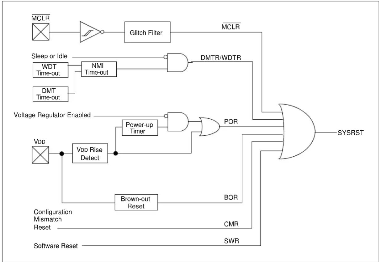
flowchart
graph TD
    A["MCLR"] --> B["Amplifier"]
    B --> C["Glitch Filter"]
    C --> D["MCLR"]
    E["Sleep or Idle"] --> F["WDT Time-out"]
    E --> G["DMT Time-out"]
    F --> H["NMI Time-out"]
    G --> H
    H --> I["AND"]
    I --> J["DMTR/WDTR"]
    K["Voltage Regulator Enabled"] --> L["Power-up Timer"]
    L --> M["AND"]
    M --> N["POR"]
    O["VDD"] --> P["VDD Rise Detect"]
    P --> Q["Brown-out Reset"]
    Q --> R["BOR"]
    S["Configuration Mismatch Reset"] --> T["CMR"]
    U["Software Reset"] --> V["SWR"]
    W["SYSRST"] --> N
6.1 Reset Control Registers
TABLE 6-1: RESETS REGISTER MAP
Legend: x = unknown value on Reset; — = unimplemented, read as 'D'. Reset values are shown in hexadecimal.
REGISTER 6-1: RCON: RESET CONTROL REGISTER
| Bit Range | Bit 31/23/15/7 | Bit 30/22/14/6 | Bit 29/21/13/5 | Bit 28/20/12/4 | Bit 27/19/11/3 | Bit 26/18/10/2 | Bit 25/17/9/1 | Bit 24/16/8/0 |
| 31:24 | U-0 U-0 U-0 | U-0 RW-0, HS | R/W-0, HS U-0 | U-0 | ||||
| — | — | — | — | BCFGERR | BCFGFAIL | — | — | |
| 23:16 | U-0 U-0 U-0 | U-0 | U-0 | U-0 | U-0 U-0 | |||
| — — — | — — | — | — | — | ||||
| 15:8 | U-0 U-0 U-0 | U-0 U-0 | U-0 | R/W-0, H$ | U-0 | |||
| — | — | — | — | — | — | CMR | — | |
| 7:0 | R/W-0, HS | R/W-0, HS | R/W-0, HS | R/W-0, HS | R/W-0, HS | R/W-0, HS | R/W-1, HS | R/W-1, HS |
| EXTR | SWR | DMTO | WDTO | SLEEP | IDLE | BOR(1) | POR(1) |
| Legend: | HS = Hardware Set HC = Hardware Cleared | ||
| R = Readable bit | W = Writable bit | U = Unimplemented bit, read as ‘0’ | |
| -n = Value at POR | ‘1’ = Bit is set | ‘0’ = Bit is cleared | x = Bit is unknown |
bit 31-28 Unimplemented: Read as '0'
bit 27 BCFGERR: Primary Configuration Registers Error Flag bit
1 = An error occurred during a read of the primary configuration registers
0 = No error occurred during a read of the primary configuration registers
bit 26 BCFGFAIL: Primary/Secondary Configuration Registers Error Flag bit
1 = An error occurred during a read of the primary and alternate configuration registers
0 = No error occurred during a read of the primary and alternate configuration registers
bit 25-10 Unimplemented: Read as '0'
bit 9 CMR: Configuration Mismatch Reset Flag bit
1 = A Configuration Mismatch Reset has occurred
0 = A Configuration Mismatch Reset has not occurred
bit 8 Unimplemented: Read as '0'
bit 7 EXTR: External Reset (MCLR) Pin Flag bit
1 = Master Clear (pin) Reset has occurred
0 = Master Clear (pin) Reset has not occurred
bit 6 SWR: Software Reset Flag bit
1 = Software Reset was executed
0 = Software Reset was not executed
bit 5 DMTO: Deadman Timer Time-out Flag bit
1 = A DMT time-out has occurred
0 = A DMT time-out has not occurred
bit 4 WDTO: Watchdog Timer Time-out Flag bit
1 = WDT Time-out has occurred
0 = WDT Time-out has not occurred
bit 3 SLEEP: Wake From Sleep Flag bit
1 = Device was in Sleep mode
0 = Device was not in Sleep mode
bit 2 IDLE: Wake From Idle Flag bit
1 = Device was in Idle mode
0 = Device was not in Idle mode
bit 1 BOR: Brown-out Reset Flag bit ^(1)
1 = Brown-out Reset has occurred
0 = Brown-out Reset has not occurred
bit 0 POR: Power-on Reset Flag bit ^(1)
1 = Power-on Reset has occurred
0 = Power-on Reset has not occurred
Note 1: User software must clear this bit to view the next detection.
REGISTER 6-2: RSWRST: SOFTWARE RESET REGISTER
| Bit Range | Bit 31/23/15/7 | Bit 30/22/14/6 | Bit 29/21/13/5 | Bit 28/20/12/4 | Bit 27/19/11/3 | Bit 26/18/10/2 | Bit 25/17/9/1 | Bit 24/16/8/0 |
| 31:24 | U-0 U-0 U-0 | U-0 U-0 U-0 U-0 | U-0 | |||||
| — — — | — — — | — | — | |||||
| 23:16 | U-0 U-0 U-0 | U-0 U-0 U-0 U-0 | U-0 | |||||
| — — — | — — — | — | — | |||||
| 15:8 | U-0 U-0 U-0 | U-0 U-0 U-0 U-0 | U-0 | |||||
| — — — | — — — | — | — | |||||
| 7:0 | U-0 U-0 U-0 | U-0 U-0 U-0 U-0 | 0 | W-0, HC | ||||
| — | — | — | — | — | — | — | SWRST(1,2) |
| Legend: | HC = Hardware Cleared | ||
| R = Readable bit | W = Writable bit U = Unimplemented bit, read as '0' | ||
| -n = Value at POR | '1' = Bit is set | '0' = Bit is cleared | x = Bit is unknown |
bit 31-1 Unimplemented: Read as '0'
bit 0 SWRST: Software Reset Trigger bit ^(1,2)
1 = Enable software Reset event
0 = No effect
Note 1: The system unlock sequence must be performed before the SWRST bit can be written. Refer to Section 42. "Oscillators with Enhanced PLL" (DS60001250) in the "PIC32 Family Reference Manual" for details.
2: Once this bit is set, any read of the RSWRST register will cause a reset to occur.
REGISTER 6-3: RNMICON: NON-MASKABLE INTERRUPT (NMI) CONTROL REGISTER
| Bit Range | Bit 31/23/15/7 | Bit 30/22/14/6 | Bit 29/21/13/5 | Bit 28/20/12/4 | Bit 27/19/11/3 | Bit 26/18/10/2 | Bit 25/17/9/1 | Bit 24/16/8/0 |
| 31:24 | U-0 U-0 U-0 | U-0 U-0 U-0 | R/W-0 R/W-0 | |||||
| — — — | — — — | D | M | T | O W | D | T | |
| 23:16 | R/W-0 | U-0 U-0 U-0 | U-0 U-0 | R/W-0 R/W-0 | ||||
| SWNMI | — | — | — | — | — | CF | WDTS | |
| 15:8 | U-0 U-0 U-0 | U-0 U-0 U-0 | U-0 | U-0 | ||||
| — — — | — — — | — | — | |||||
| 7:0 | R/W-0 | R/W-0 | R/W-0 | R/W-0 | R/W-0 | R/W-0 | R/W-0 | R/W-0 |
| NMICNT<7:0> | ||||||||
Legend:
| R = Readable bit | W = Writable bit U = Unimplemented bit, read as ‘0’ | ||
| -n = Value at POR | ‘1’ = Bit is set | ‘0’ = Bit is cleared | x = Bit is unknown |
bit 31-26 Unimplemented: Read as '0'
bit 25 DMTO: Deadman Timer Time-out Flag bit
1 = DMT time-out has occurred and caused a NMI
0 = DMT time-out has not occurred
Setting this bit will cause a DMT NMI event, and NMICNT will begin counting.
bit 24 WDTO: Watchdog Timer Time-Out Flag bit
1 = WDT time-out has occurred and caused a NMI
0 = WDT time-out has not occurred
Setting this bit will cause a WDT NMI event, and MNICNT will begin counting.
bit 23 SWNMI: Software NMI Trigger.
1 = An NMI will be generated
0 = An NMI will not be generated
bit 22-18 Unimplemented: Read as '0'
bit 17 CF: Clock Fail Detect bit
1 = FSCM has detected clock failure and caused an NMI
0 = FSCM has not detected clock failure
Setting this bit will cause a CF NMI event, but will not cause a clock switch to the BFRC.
bit 16 WDTS: Watchdog Timer Time-out in Sleep Mode Flag bit
1 = WDT time-out has occurred during Sleep mode and caused a wake-up from sleep
0 = WDT time-out has not occurred during Sleep mode
Setting this bit will cause a WDT NMI.
bit 15-8 Unimplemented: Read as '0'
bit 7-0 NMICNT<7:0>: NMI Reset Counter Value bits
These bits specify the reload value used by the NMI reset counter.
11111111-00000001 = Number of SYSCLK cycles before a device Reset occurs ^(1)
00000000 = No delay between NMI assertion and device Reset event
Note 1: When a Watchdog Timer NMI event (when not in Sleep mode) or a Deadman Timer NMI event is triggered the NMICNT will start decrementing. When NMICNT reaches zero, the device is Reset. This NMI reset counter is only applicable to these two specific NMI events.
Note: The system unlock sequence must be performed before the SWRST bit can be written. Refer to Section 42. "Oscillators with Enhanced PLL" (DS60001250) in the "PIC32 Family Reference Manual" for details.
REGISTER 6-4: PWRCON: POWER CONTROL REGISTER
| Bit Range | Bit 31/23/15/7 | Bit 30/22/14/6 | Bit 29/21/13/5 | Bit 28/20/12/4 | Bit 27/19/11/3 | Bit 26/18/10/2 | Bit 25/17/9/1 | Bit 24/16/8/0 |
| 31:24 | U-0 U-0 U-0 | U-0 U-0 U-0 U-0 | U-0 | |||||
| — — — | — — — | — | — | |||||
| 23:16 | U-0 U-0 U-0 | U-0 U-0 U-0 U-0 | U-0 | |||||
| — — — | — — — | — | — | |||||
| 15:8 | U-0 U-0 U-0 | U-0 U-0 U-0 U-0 | U-0 | |||||
| — — — | — — — | — | — | |||||
| 7:0 | U-0 U-0 U-0 | U-0 U-0 U-0 U-0 | 0 | R/W-0 | ||||
| — | — | — | — | — | — | — | VREGS |
Legend:
| R = Readable bit | W = Writable bit U = Unimplemented bit, read as '0' | ||
| -n = Value at POR | '1' = Bit is set | '0' = Bit is cleared | x = Bit is unknown |
bit 31-1 Unimplemented: Read as '0'
bit 0 VREGS: Voltage Regulator Stand-by Enable bit
1 = Voltage regulator will remain active during Sleep
0 = Voltage regulator will go to Stand-by mode during Sleep
7.0 CPU EXCEPTIONS AND INTERRUPT CONTROLLER
Note: This data sheet summarizes the features of the PIC32MZ Embedded Connectivity (EC) Family of devices. It is not intended to be a comprehensive reference source. To complement the information in this data sheet, refer to Section 8. "Interrupt Controller" (DS60001108) and Section 50. "CPU for Devices with MIPS32® microAptiv™ and M-Class Cores" (DS60001192), which are available from the Documentation > Reference Manual section of the Microchip PIC32 web site (www.microchip.com/pic32).
PIC32MZ EC devices generate interrupt requests in response to interrupt events from peripheral modules. The Interrupt Controller module exists outside of the CPU and prioritizes the interrupt events before presenting them to the CPU.
The CPU handles interrupt events as part of the exception handling mechanism, which is described in Section 7.1 "CPU Exceptions".
The Interrupt Controller module includes the following features:
- Up to 190 interrupt sources and vectors with dedicated programmable offsets, eliminating the need for redirection
- Single and multi-vector mode operations
- Five external interrupts with edge polarity control
- Interrupt proximity timer
- Seven user-selectable priority levels for each vector
- Four user-selectable subpriority levels within each priority
- Seven shadow register sets that can be used for any priority level, eliminating software context switch and reducing interrupt latency
- Software can generate any interrupt
Figure 7-1 shows the block diagram for the Interrupt Controller and CPU exceptions.
FIGURE 7-1: CPU EXCEPTIONS AND INTERRUPT CONTROLLER MODULE BLOCK DIAGRAM

flowchart
graph LR
    A["Interrupt Requests"] --> B["Interrupt Controller"]
    C["SYSCLK"] --> B
    B --> D["Vector Number and Offset"]
    B --> E["Priority Level"]
    B --> F["Shadow Set Number"]
    D --> G["CPU Core (Exception Handling)"]
    E --> G
    F --> G
7.1 CPU Exceptions
CPU coprocessor 0 contains the logic for identifying and managing exceptions. Exceptions can be caused by a variety of sources, including boundary cases in data, external events or program errors. Table 7-1 lists the exception types in order of priority.
TABLE 7-1: MIPS32 ^ microAptiv™ MICROPROCESSOR CORE EXCEPTION TYPES
| Exception Type(In Order of Priority) | Description Branches to | StatusBits Set | Debug BitsSet | EXCCODE | XC32 Function Name | |
| Highest Priority | ||||||
| Reset | Assertion MCLR or a Power-on Reset (POR). | 0xBFC0_0000 | BEV, ERL | — | — | _on_reset |
| Soft Reset | Assertion of a software Reset. | 0xBFC0_0000 | BEV, SR, ERL | — | — | _on_reset |
| DSS | EJTAG debug single step. | 0xBFC0_0480 | — | DSS | — | — |
| DINT | EJTAG debug interrupt. Caused by the assertion of the external EJ_DINT input or by setting the EjtagBrk bit in the ECR register. | 0xBFC0_0480 | — | DINT | — | — |
| NMI | Assertion of NMI signal. | 0xBFC0_0000 | BEV, NMI, ERL | — | — | _nmi_handler |
| Machine Check | TLB write that conflicts with an existing entry. | EBASE+0x180 | MCHECK, EXL | — | 0x18 _general_exception_handler | |
| Interrupt | Assertion of unmasked hardware or software interrupt signal. | See Table 7-2. | IPL<2:0> | — | 0x00 | See Table 7-2. |
| Deferred Watch | Deferred watch (unmasked by K|DM=>!(K|DM) transition). | EBASE+0x180 | WP, EXL | — | 0x17 | _general_exception_handler |
| DIB | EJTAG debug hardware instruction break matched. | 0xBFC0_0480 | — | DIB | — | — |
| WATCH | A reference to an address that is in one of the Watch registers (fetch). | EBASE+0x180 | EXL | — | 0x17 | _general_exception_handler |
| AdEL | Fetch address alignment error. Fetch reference to protected address. | EBASE+0x180 | EXL | — | 0x04 | _general_exception_handler |
| TLBL | Fetch TLB miss or fetch TLB hit to page with V = 0. | EBASE if Status.EXL = 0 | — | — | 0x02 | — |
| EBASE+0x180 if Status.EXL == 1 | — | — | 0x02 | _general_exception_handler | ||
| TLBL Execute Inhibit | An instruction fetch matched a valid TLB entry that had the XI bit set. | EBASE+0x180 | EXL | — | 0x14 | _general_exception_handler |
| IBE | Instruction fetch bus error. | EBASE+0x180 | EXL | — | 0x06 | _general_exception_handler |
| Exception Type(In Order of Priority) | Description | Branches to | StatusBits Set | Debug BitsSet | EXCCODE | XC32 Function Name |
| Instruction Validity Exceptions | An instruction could not be completed because it was not allowed to access the required resources (Coprocessor Unusable) or was illegal (Reserved Instruction). If both exceptions occur on the same instruction, the Coprocessor Unusable Exception takes priority over the Reserved Instruction Exception. | EBASE+0x180 EXL | — 0x0A or | 0x0B | _general_exception_handler | |
| Execute Exception | An instruction-based exception occurred: Integer overflow, trap, system call, breakpoint, floating point, or DSP ASE state disabled exception. | EBASE+0x180 | EXL | — | 0x08-0x0C | _general_exception_handler |
| Tr | Execution of a trap (when trap condition is true). | EBASE+0x180 | EXL | — | 0x0D | _general_exception_handler |
| DDBL/DDBS EJTAG Data Address Break (address only) or EJTAG data value break on store (address + value). | 0xBFC0_0480 — | DDBL or DDBS | — | — | — | |
| WATCH | A reference to an address that is in one of the Watch registers (data). | EBASE+0x180 | EXL | — | 0x17 | _general_exception_handler |
| AdEL | Load address alignment error. User mode load reference to kernel address. | EBASE+0x180 | EXL | — | 0x04 | _general_exception_handler |
| AdES | Store address alignment error. User mode store to kernel address. | EBASE+0x180 | EXL | — | 0x05 | _general_exception_handler |
| TLBL | Load TLB miss or load TLB hit to page with V = 0. | EBASE+0x180 | EXL | — | 0x02 | _general_exception_handler |
| TLBS | Store TLB miss or store TLB hit to page with V = 0. | EBASE+0x180 | EXL | — | 0x03 | _general_exception_handler |
| DBE | Load or store bus error. | EBASE+0x180 | EXL | — | 0x07 | _general_exception_handler |
| DDBL | EJTAG data hardware breakpoint matched in load data compare. | 0xBFC0_0480 | — | DDBL | — | — |
| CBrk | EJTAG complex breakpoint. | 0xBFC0_0480 | — | DIBIMPR,DDBLIMPR,and/orDDBSIMPR | — | — |
| Lowest Priority | ||||||
7.2 Interrupts
The PIC32MZ EC family uses variable offsets for vector spacing. This allows the interrupt vector spacing to be configured according to application needs. A unique interrupt vector offset can be set for each vector using its associated OFFx register.
For details on the Variable Offset feature, refer to 8.5.2 "Variable Offset" in Section 8. "Interrupt Controller" (DS60001108) of the "PIC32 Family Reference Manual".
Table 7-2 provides the Interrupt IRQ, vector and bit location information.
TABLE 7-2: INTERRUPT IRQ, VECTOR AND BIT LOCATION
| Interrupt Source(1) | XC32 Vector Name | IRQ # | Vector # | Interrupt Bit Location | Persistent Interrupt | |||
| Flag Enable Priority Sub-priority | ||||||||
| Highest Natural Order Priority | ||||||||
| Core Timer Interrupt | _CORE_TIMER_VECTOR | 0 | OFF000<17:1> | IFS0<0> | IEC0<0> | IPC0<4:2> | IPC0<1:0> | No |
| Core Software Interrupt 0 | _CORE_SOFTWARE_0_VECTOR | 1 | OFF001<17:1> | IFS0<1> | IEC0<1> | IPC0<12:10> | IPC0<9:8> | No |
| Core Software Interrupt 1 | _CORE_SOFTWARE_1_VECTOR | 2 | OFF002<17:1> | IFS0<2> | IEC0<2> | IPC0<20:18> | IPC0<17:16> | No |
| External Interrupt | _EXTERNAL_0_VECTOR | 3 | OFF003<17:1> | IFS0<3> | IEC0<3> | IPC0<28:26> | IPC0<25:24> | No |
| Timer1 | _TIMER_1_VECTOR | 4 | OFF004<17:1> | IFS0<4> | IEC0<4> | IPC1<4:2> | IPC1<1:0> | No |
| Input Capture 1 Error | _INPUT_CAPTURE_1_ERROR_VECTOR | 5 | OFF005<17:1> | IFS0<5> | IEC0<5> | IPC1<12:10> | IPC1<9:8> | Yes |
| Input Capture 1 | _INPUT_CAPTURE_1_VECTOR | 6 | OFF006<17:1> | IFS0<6> | IEC0<6> | IPC1<20:18> | IPC1<17:16> | Yes |
| Output Compare 1 | _OUTPUT_COMPARE_1_VECTOR | 7 | OFF007<17:1> | IFS0<7> | IEC0<7> | IPC1<28:26> | IPC1<25:24> | No |
| External Interrupt 1 | _EXTERNAL_1_VECTOR | 8 | OFF008<17:1> | IFS0<8> | IEC0<8> | IPC2<4:2> | IPC2<1:0> | No |
| Timer2 | _TIMER_2_VECTOR | 9 | OFF009<17:1> | IFS0<9> | IEC0<9> | IPC2<12:10> | IPC2<9:8> | No |
| Input Capture 2 Error | _INPUT_CAPTURE_2_ERROR_VECTOR | 10 | OFF010<17:1> | IFS0<10> | IEC0<10> | IPC2<20:18> | IPC2<17:16> | Yes |
| Input Capture 2 | _INPUT_CAPTURE_2_VECTOR | 11 | OFF011<17:1> | IFS0<11> | IEC0<11> | IPC2<28:26> | IPC2<25:24> | Yes |
| Output Compare 2 | _OUTPUT_COMPARE_2_VECTOR | 12 | OFF012<17:1> | IFS0<12> | IEC0<12> | IPC3<4:2> | IPC3<1:0> | No |
| External Interrupt 2 | _EXTERNAL_2_VECTOR | 13 | OFF013<17:1> | IFS0<13> | IEC0<13> | IPC3<12:10> | IPC3<9:8> | No |
| Timer3 | _TIMER_3_VECTOR | 14 | OFF014<17:1> | IFS0<14> | IEC0<14> | IPC3<20:18> | IPC3<17:16> | No |
| Input Capture 3 Error | _INPUT_CAPTURE_3_ERROR_VECTOR | 15 | OFF015<17:1> | IFS0<15> | IEC0<15> | IPC3<28:26> | IPC3<25:24> | Yes |
| Input Capture 3 | INPUT_CAPTURE_3_VECTOR | 16 | OFF016<17:1> | IFS0<16> | IEC0<16> | IPC4<4:2> | IPC4<1:0> | Yes |
| Output Compare 3 | _OUTPUT_COMPARE_3_VECTOR | 17 | OFF017<17:1> | IFS0<17> | IEC0<17> | IPC4<12:10> | IPC4<9:8> | No |
| External Interrupt 3 | _EXTERNAL_3_VECTOR | 18 | OFF018<17:1> | IFS0<18> | IEC0<18> | IPC4<20:18> | IPC4<17:16> | No |
| Timer4 | _TIMER_4_VECTOR | 19 | OFF019<17:1> | IFS0<19> | IEC0<19> | IPC4<28:26> | IPC4<25:24> | No |
| Input Capture 4 Error | _INPUT_CAPTURE_4_ERROR_VECTOR | 20 | OFF020<17:1> | IFS0<20> | IEC0<20> | IPC5<4:2> | IPC5<1:0> | Yes |
Note 1: Not all interrupt sources are available on all devices. See TABLE 1: "PIC32MZ EC Family Features" for the list of available peripherals.
2: This interrupt source is not available on 64-pin devices.
3: This interrupt source is not available on 100-pin devices.
4: This interrupt source is not available on 124-pin devices.
TABLE 7-2: INTERRUPT IRQ, VECTOR AND BIT LOCATION (CONTINUED)
| Interrupt Source^(1) | XC32 Vector Name | IRQ # | Vector # | Interrupt Bit Location | Persistent Interrupt | |||
| Flag | Enable | Priority | Sub-priority | |||||
| Input Capture 4 | _INPUT_CAPTURE_4_VECTOR | 21 | OFF021<17:1> | IFS0<21> | IEC0<21> | IPC5<12:10> | IPC5<9:8> | Yes |
| Output Compare 4 | _OUTPUT_COMPARE_4_VECTOR | 22 | OFF022<17:1> | IFS0<22> | IEC0<22> | IPC5<20:18> | IPC5<17:16> | No |
| External Interrupt 4 | _EXTERNAL_4_VECTOR | 23 | OFF023<17:1> | IFS0<23> | IEC0<23> | IPC5<28:26> | IPC5<25:24> | No |
| Timer5 | _TIMER_5_VECTOR | 24 | OFF024<17:1> | IFS0<24> | IEC0<24> | IPC6<4:2> | IPC6<1:0> | No |
| Input Capture 5 Error | _INPUT_CAPTURE_5_ERROR_VECTOR | 25 | OFF025<17:1> | IFS0<25> | IEC0<25> | IPC6<12:10> | IPC6<9:8> | Yes |
| Input Capture 5 | _INPUT_CAPTURE_5_VECTOR | 26 | OFF026<17:1> | IFS0<26> | IEC0<26> | IPC6<20:18> | IPC6<17:16> | Yes |
| Output Compare 5 | _OUTPUT_COMPARE_5_VECTOR | 27 | OFF027<17:1> | IFS0<27> | IEC0<27> | IPC6<28:26> | IPC6<25:24> | No |
| Timer6 | _TIMER_6_VECTOR | 28 | OFF028<17:1> | IFS0<28> | IEC0<28> | IPC7<4:2> | IPC7<1:0> | No |
| Input Capture 6 Error | _INPUT_CAPTURE_6_ERROR_VECTOR | 29 | OFF029<17:1> | IFS0<29> | IEC0<29> | IPC7<12:10> | IPC7<9:8> | Yes |
| Input Capture 6 | _INPUT_CAPTURE_6_VECTOR | 30 | OFF030<17:1> | IFS0<30> | IEC0<30> | IPC7<20:18> | IPC7<17:16> | Yes |
| Output Compare 6 | _OUTPUT_COMPARE_6_VECTOR | 31 | OFF031<17:1> | IFS0<31> | IEC0<31> | IPC7<28:26> | IPC7<25:24> | No |
| Timer7 | _TIMER_7_VECTOR | 32 | OFF032<17:1> | IFS1<0> | IEC1<0> | IPC8<4:2> | IPC8<1:0> | No |
| Input Capture 7 Error | _INPUT_CAPTURE_7_ERROR_VECTOR | 33 | OFF033<17:1> | IFS1<1> | IEC1<1> | IPC8<12:10> | IPC8<9:8> | Yes |
| Input Capture 7 | INPUT_CAPTURE_7_VECTOR | 34 | OFF034<17:1> | IFS1<2> | IEC1<2> | IPC8<20:18> | IPC8<17:16> | Yes |
| Output Compare 7 | _OUTPUT_COMPARE_7_VECTOR | 35 | OFF035<17:1> | IFS1<3> | IEC1<3> | IPC8<28:26> | IPC8<25:24> | No |
| Timer8 | _TIMER_8_VECTOR | 36 | OFF036<17:1> | IFS1<4> | IEC1<4> | IPC9<4:2> | IPC9<1:0> | No |
| Input Capture 8 Error | _INPUT_CAPTURE_8_ERROR_VECTOR | 37 | OFF037<17:1> | IFS1<5> | IEC1<5> | IPC9<12:10> | IPC9<9:8> | Yes |
| Input Capture 8 | _INPUT_CAPTURE_8_VECTOR | 38 | OFF038<17:1> | IFS1<6> | IEC1<6> | IPC9<20:18> | IPC9<17:16> | Yes |
| Output Compare 8 | _OUTPUT_COMPARE_8_VECTOR | 39 | OFF039<17:1> | IFS1<7> | IEC1<7> | IPC9<28:26> | IPC9<25:24> | No |
| Timer9 | _TIMER_9_VECTOR | 40 | OFF040<17:1> | IFS1<8> | IEC1<8> | IPC10<4:2> | IPC10<1:0> | No |
| Input Capture 9 Error | _INPUT_CAPTURE_9_ERROR_VECTOR | 41 | OFF041<17:1> | IFS1<9> | IEC1<9> | IPC10<12:10> | IPC10<9:8> | Yes |
| Input Capture 9 | _INPUT_CAPTURE_9_VECTOR | 42 | OFF042<17:1> | IFS1<10> | IEC1<10> | IPC10<20:18> | IPC10<17:16> | Yes |
| Output Compare 9 | _OUTPUT_COMPARE_9_VECTOR | 43 | OFF043<17:1> | IFS1<11> | IEC1<11> | IPC10<28:26> | IPC10<25:24> | No |
| ADC1 Global Interrupt | _ADC1_VECTOR | 44 | OFF044<17:1> | IFS1<12> | IEC1<12> | IPC11<4:2> | IPC11<1:0> | Yes |
| Reserved | — | 45 | — | — | — | — | — | — |
| ADC1 Digital Comparator 1 | _ADC1_DC1_VECTOR | 46 | OFF046<17:1> | IFS1<14> | IEC1<14> | IPC11<20:18> | IPC11<17:16> | Yes |
| ADC1 Digital Comparator 2 | _ADC1_DC2_VECTOR | 47 | OFF047<17:1> | IFS1<15> | IEC1<15> | IPC11<28:26> | IPC11<25:24> | Yes |
Note 1: Not all interrupt sources are available on all devices. See TABLE 1: "PIC32MZ EC Family Features" for the list of available peripherals.
2: This interrupt source is not available on 64-pin devices.
3: This interrupt source is not available on 100-pin devices.
4: This interrupt source is not available on 124-pin devices.
TABLE 7-2: INTERRUPT IRQ, VECTOR AND BIT LOCATION (CONTINUED)
| Interrupt Source(1) | XC32 Vector Name | IRQ # | Vector # | Interrupt Bit Location | Persistent Interrupt | |||
| Flag | Enable | Priority | Sub-priority | |||||
| ADC1 Digital Comparator 3 | _ADC1_DC3_VECTOR | 48 | OFF048<17:1> | IFS1<16> | IEC1<16> | IPC12<4:2> | IPC12<1:0> | Yes |
| ADC1 Digital Comparator 4 | _ADC1_DC4_VECTOR | 49 | OFF049<17:1> | IFS1<17> | IEC1<17> | IPC12<12:10> | IPC12<9:8> | Yes |
| ADC1 Digital Comparator 5 | _ADC1_DC5_VECTOR | 50 | OFF050<17:1> | IFS1<18> | IEC1<18> | IPC12<20:18> | IPC12<17:16> | Yes |
| ADC1 Digital Comparator 6 | _ADC1_DC6_VECTOR | 51 | OFF051<17:1> | IFS1<19> | IEC1<19> | IPC12<28:26> | IPC12<25:24> | Yes |
| ADC1 Digital Filter 1 | _ADC1_DF1_VECTOR | 52 | OFF052<17:1> | IFS1<20> | IEC1<20> | IPC13<4:2> | IPC13<1:0> | Yes |
| ADC1 Digital Filter 2 | _ADC1_DF2_VECTOR | 53 | OFF053<17:1> | IFS1<21> | IEC1<21> | IPC13<12:10> | IPC13<9:8> | Yes |
| ADC1 Digital Filter 3 | _ADC1_DF3_VECTOR | 54 | OFF054<17:1> | IFS1<22> | IEC1<22> | IPC13<20:18> | IPC13<17:16> | Yes |
| ADC1 Digital Filter 4 | _ADC1_DF4_VECTOR | 55 | OFF055<17:1> | IFS1<23> | IEC1<23> | IPC13<28:26> | IPC13<25:24> | Yes |
| ADC1 Digital Filter 5 | _ADC1_DF5_VECTOR | 56 | OFF056<17:1> | IFS1<24> | IEC1<24> | IPC14<4:2> | IPC14<1:0> | Yes |
| ADC1 Digital Filter 6 | _ADC1_DF6_VECTOR | 57 | OFF057<17:1> | IFS1<25> | IEC1<25> | IPC14<12:10> | IPC14<9:8> | Yes |
| Reserved | — | 58 | — | — | — | — | — | — |
| ADC1 Data 0 | _ADC1_DATA0_VECTOR | 59 | OFF059<17:1> | IFS1<27> | IEC1<27> | IPC14<28:26> | IPC14<25:24> | Yes |
| ADC1 Data 1 | _ADC1_DATA1_VECTOR | 60 | OFF060<17:1> | IFS1<28> | IEC1<28> | IPC15<4:2> | IPC15<1:0> | Yes |
| ADC1 Data 2 | _ADC1_DATA2_VECTOR | 61 | OFF061<17:1> | IFS1<29> | IEC1<29> | IPC15<12:10> | IPC15<9:8> | Yes |
| ADC1 Data 3 | _ADC1_DATA3_VECTOR | 62 | OFF062<17:1> | IFS1<30> | IEC1<30> | IPC15<20:18> | IPC15<17:16> | Yes |
| ADC1 Data 4 | _ADC1_DATA4_VECTOR | 63 | OFF063<17:1> | IFS1<31> | IEC1<31> | IPC15<28:26> | IPC15<25:24> | Yes |
| ADC1 Data 5 | _ADC1_DATA5_VECTOR | 64 | OFF064<17:1> | IFS2<0> | IEC2<0> | IPC16<4:2> | IPC16<1:0> | Yes |
| ADC1 Data 6 | _ADC1_DATA6_VECTOR | 65 | OFF065<17:1> | IFS2<1> | IEC2<1> | IPC16<12:10> | IPC16<9:8> | Yes |
| ADC1 Data 7 | _ADC1_DATA7_VECTOR | 66 | OFF066<17:1> | IFS2<2> | IEC2<2> | IPC16<20:18> | IPC16<17:16> | Yes |
| ADC1 Data 8 | _ADC1_DATA8_VECTOR | 67 | OFF067<17:1> | IFS2<3> | IEC2<3> | IPC16<28:26> | IPC16<25:24> | Yes |
| ADC1 Data 9 | _ADC1_DATA9_VECTOR | 68 | OFF068<17:1> | IFS2<4> | IEC2<4> | IPC17<4:2> | IPC17<1:0> | Yes |
| ADC1 Data 10 | _ADC1_DATA10_VECTOR | 69 | OFF069<17:1> | IFS2<5> | IEC2<5> | IPC17<12:10> | IPC17<9:8> | Yes |
| ADC1 Data 11 | _ADC1_DATA11_VECTOR | 70 | OFF070<17:1> | IFS2<6> | IEC2<6> | IPC17<20:18> | IPC17<17:16> | Yes |
| ADC1 Data 12 | _ADC1_DATA12_VECTOR | 71 | OFF071<17:1> | IFS2<7> | IEC2<7> | IPC17<28:26> | IPC17<25:24> | Yes |
| ADC1 Data 13 | _ADC1_DATA13_VECTOR | 72 | OFF072<17:1> | IFS2<8> | IEC2<8> | IPC18<4:2> | IPC18<1:0> | Yes |
| ADC1 Data 14 | _ADC1_DATA14_VECTOR | 73 | OFF073<17:1> | IFS2<9> | IEC2<9> | IPC18<12:10> | IPC18<9:8> | Yes |
| ADC1 Data 15 | _ADC1_DATA15_VECTOR | 74 | OFF074<17:1> | IFS2<10> | IEC2<10> | IPC18<20:18> | IPC18<17:16> | Yes |
Note 1: Not all interrupt sources are available on all devices. See TABLE 1: "PIC32MZ EC Family Features" for the list of available peripherals.
2: This interrupt source is not available on 64-pin devices.
3: This interrupt source is not available on 100-pin devices.
4: This interrupt source is not available on 124-pin devices.
TABLE 7-2: INTERRUPT IRQ, VECTOR AND BIT LOCATION (CONTINUED)
| Interrupt Source^(1) | XC32 Vector Name | IRQ # | Vector # | Interrupt Bit Location | Persistent Interrupt | |||
| Flag | Enable | Priority | Sub-priority | |||||
| ADC1 Data 16 | _ADC1_DATA16_VECTOR | 75 | OFF075<17:1> | IFS2<11> | IEC2<11> | IPC18<28:26> | IPC18<25:24> | Yes |
| ADC1 Data 17 | _ADC1_DATA17_VECTOR | 76 | OFF076<17:1> | IFS2<12> | IEC2<12> | IPC19<4:2> | IPC19<1:0> | Yes |
| ADC1 Data 18 | _ADC1_DATA18_VECTOR | 77 | OFF077<17:1> | IFS2<13> | IEC2<13> | IPC19<12:10> | IPC19<9:8> | Yes |
| ADC1 Data 19^(2) | _ADC1_DATA19_VECTOR | 78 | OFF078<17:1> | IFS2<14> | IEC2<14> | IPC19<20:18> | IPC19<17:16> | Yes |
| ADC1 Data 20^(2) | _ADC1_DATA20_VECTOR | 79 | OFF079<17:1> | IFS2<15> | IEC2<15> | IPC19<28:26> | IPC19<25:24> | Yes |
| ADC1 Data 21^(2) | _ADC1_DATA21_VECTOR | 80 | OFF080<17:1> | IFS2<16> | IEC2<16> | IPC20<4:2> | IPC20<1:0> | Yes |
| ADC1 Data 22^(2) | _ADC1_DATA22_VECTOR | 81 | OFF081<17:1> | IFS2<17> | IEC2<17> | IPC20<12:10> | IPC20<9:8> | Yes |
| ADC1 Data 23^(2) | _ADC1_DATA23_VECTOR | 82 | OFF082<17:1> | IFS2<18> | IEC2<18> | IPC20<20:18> | IPC20<17:16> | Yes |
| ADC1 Data 24^(2) | _ADC1_DATA24_VECTOR | 83 | OFF083<17:1> | IFS2<19> | IEC2<19> | IPC20<28:26> | IPC20<25:24> | Yes |
| ADC1 Data 25^(2) | _ADC1_DATA25_VECTOR | 84 | OFF084<17:1> | IFS2<20> | IEC2<20> | IPC21<4:2> | IPC21<1:0> | Yes |
| ADC1 Data 26^(2) | _ADC1_DATA26_VECTOR | 85 | OFF085<17:1> | IFS2<21> | IEC2<21> | IPC21<12:10> | IPC21<9:8> | Yes |
| ADC1 Data 27^(2) | _ADC1_DATA27_VECTOR | 86 | OFF086<17:1> | IFS2<22> | IEC2<22> | IPC21<20:18> | IPC21<17:16> | Yes |
| ADC1 Data 28^(2) | _ADC1_DATA28_VECTOR | 87 | OFF087<17:1> | IFS2<23> | IEC2<23> | IPC21<28:26> | IPC21<25:24> | Yes |
| ADC1 Data 29^(2) | _ADC1_DATA29_VECTOR | 88 | OFF088<17:1> | IFS2<24> | IEC2<24> | IPC22<4:2> | IPC22<1:0> | Yes |
| ADC1 Data 30^(2) | _ADC1_DATA30_VECTOR | 89 | OFF089<17:1> | IFS2<25> | IEC2<25> | IPC22<12:10> | IPC22<9:8> | Yes |
| ADC1 Data 31^(2) | _ADC1_DATA31_VECTOR | 90 | OFF090<17:1> | IFS2<26> | IEC2<26> | IPC22<20:18> | IPC22<17:16> | Yes |
| ADC1 Data 32^(2) | _ADC1_DATA32_VECTOR | 91 | OFF091<17:1> | IFS2<27> | IEC2<27> | IPC22<28:26> | IPC22<25:24> | Yes |
| ADC1 Data 33^(2) | _ADC1_DATA33_VECTOR | 92 | OFF092<17:1> | IFS2<28> | IEC2<28> | IPC23<4:2> | IPC23<1:0> | Yes |
| ADC1 Data 34^(2) | _ADC1_DATA34_VECTOR | 93 | OFF093<17:1> | IFS2<29> | IEC2<29> | IPC23<12:10> | IPC23<9:8> | Yes |
| ADC1 Data 35^(2,3) | _ADC1_DATA35_VECTOR | 94 | OFF094<17:1> | IFS2<30> | IEC2<30> | IPC23<20:18> | IPC23<17:16> | Yes |
| ADC1 Data 36^(2,3) | _ADC1_DATA36_VECTOR | 95 | OFF095<17:1> | IFS2<31> | IEC2<31> | IPC23<28:26> | IPC23<25:24> | Yes |
| ADC1 Data 37^(2,3) | _ADC1_DATA37_VECTOR | 96 | OFF096<17:1> | IFS3<0> | IEC3<0> | IPC24<4:2> | IPC24<1:0> | Yes |
| ADC1 Data 38^(2,3) | _ADC1_DATA38_VECTOR | 97 | OFF097<17:1> | IFS3<1> | IEC3<1> | IPC24<12:10> | IPC24<9:8> | Yes |
| ADC1 Data 39^(2,3) | _ADC1_DATA39_VECTOR | 98 | OFF098<17:1> | IFS3<2> | IEC3<2> | IPC24<20:18> | IPC24<17:16> | Yes |
| ADC1 Data 40^(2,3) | _ADC1_DATA40_VECTOR | 99 | OFF099<17:1> | IFS3<3> | IEC3<3> | IPC24<28:26> | IPC24<25:24> | Yes |
| ADC1 Data 41^(2,3) | _ADC1_DATA41_VECTOR | 100 | OFF100<17:1> | IFS3<4> | IEC3<4> | IPC25<4:2> | IPC25<1:0> | Yes |
| ADC1 Data 42^(2,3) | _ADC1_DATA42_VECTOR | 101 | OFF101<17:1> | IFS3<5> | IEC3<5> | IPC25<12:10> | IPC25<9:8> | Yes |
Note 1: Not all interrupt sources are available on all devices. See TABLE 1: "PIC32MZ EC Family Features" for the list of available peripherals.
2: This interrupt source is not available on 64-pin devices.
3: This interrupt source is not available on 100-pin devices.
4: This interrupt source is not available on 124-pin devices.
TABLE 7-2: INTERRUPT IRQ, VECTOR AND BIT LOCATION (CONTINUED)
| Interrupt Source^(1) | XC32 Vector Name | IRQ # | Vector # | Interrupt Bit Location | Persistent Interrupt | |||
| Flag | Enable | Priority | Sub-priority | |||||
| ADC1 Data 43 | _ADC1_DATA43_VECTOR | 102 | OFF102<17:1> | IFS3<6> | IEC3<6> | IPC25<20:18> | IPC25<17:16> | Yes |
| ADC1 Data 44 | _ADC1_DATA44_VECTOR | 103 | OFF103<17:1> | IFS3<7> | IEC3<7> | IPC25<28:26> | IPC25<25:24> | Yes |
| Core Performance Counter Interrupt | _CORE_PERF_COUNT_VECTOR | 104 | OFF104<17:1> | IFS3<8> | IEC3<8> | IPC26<4:2> | IPC26<1:0> | No |
| Core Fast Debug Channel Interrupt | CORE_FAST_DEBUG_CHAN_VECTOR | 105 | OFF105<17:1> | IFS3<9> | IEC3<9> | IPC26<12:10> | IPC26<9:8> | Yes |
| System Bus Protection Violation | _SYSTEM_BUS_PROTECTION_VECTOR | 106 | OFF106<17:1> | IFS3<10> | IEC3<10> | IPC26<20:18> | IPC26<17:16> | Yes |
| Crypto Engine Event | _CRYPTO_VECTOR | 107 | OFF107<17:1> | IFS3<11> | IEC3<11> | IPC26<28:26> | IPC26<25:24> | Yes |
| Reserved | — | 108 | — | — | — | — | — | — |
| SPI1 Fault | _SPI1_FAULT_VECTOR | 109 | OFF109<17:1> | IFS3<13> | IEC3<13> | IPC27<12:10> | IPC27<9:8> | Yes |
| SPI1 Receive Done | _SPI1_RX_VECTOR | 110 | OFF110<17:1> | IFS3<14> | IEC3<14> | IPC27<20:18> | IPC27<17:16> | Yes |
| SPI1 Transfer Done | _SPI1_TX_VECTOR | 111 | OFF111<17:1> | IFS3<15> | IEC3<15> | IPC27<28:26> | IPC27<25:24> | Yes |
| UART1 Fault | _UART1_FAULT_VECTOR | 112 | OFF112<17:1> | IFS3<16> | IEC3<16> | IPC28<4:2> | IPC28<1:0> | Yes |
| UART1 Receive Done | _UART1_RX_VECTOR | 113 | OFF113<17:1> | IFS3<17> | IEC3<17> | IPC28<12:10> | IPC28<9:8> | Yes |
| UART1 Transfer Done | _UART1_TX_VECTOR | 114 | OFF114<17:1> | IFS3<18> | IEC3<18> | IPC28<20:18> | IPC28<17:16> | Yes |
| I2C1 Bus Collision Event | _I2C1_BUS_VECTOR | 115 | OFF115<17:1> | IFS3<19> | IEC3<19> | IPC28<28:26> | IPC28<25:24> | Yes |
| I2C1 Slave Event | _I2C1_SLAVE_VECTOR | 116 | OFF116<17:1> | IFS3<20> | IEC3<20> | IPC29<4:2> | IPC29<1:0> | Yes |
| I2C1 Master Event | _I2C1_MASTER_VECTOR | 117 | OFF117<17:1> | IFS3<21> | IEC3<21> | IPC29<12:10> | IPC29<9:8> | Yes |
| PORTA Input Change Interrupt(2) | _CHANGE_NOTICE_A_VECTOR | 118 | OFF118<17:1> | IFS3<22> | IEC3<22> | IPC29<20:18> | IPC29<17:16> | Yes |
| PORTB Input Change Interrupt | _CHANGE_NOTICE_B_VECTOR | 119 | OFF119<17:1> | IFS3<23> | IEC3<23> | IPC29<28:26> | IPC29<25:24> | Yes |
| PORTC Input Change Interrupt | CHANGE_NOTICE_C_VECTOR | 120 | OFF120<17:1> | IFS3<24> | IEC3<24> | IPC30<4:2> | IPC30<1:0> | Yes |
| PORTD Input Change Interrupt | CHANGE_NOTICE_D_VECTOR | 121 | OFF121<17:1> | IFS3<25> | IEC3<25> | IPC30<12:10> | IPC30<9:8> | Yes |
| PORTE Input Change Interrupt | _CHANGE_NOTICE_E_VECTOR | 122 | OFF122<17:1> | IFS3<26> | IEC3<26> | IPC30<20:18> | IPC30<17:16> | Yes |
| PORTF Input Change Interrupt | CHANGE_NOTICE_F_VECTOR | 123 | OFF123<17:1> | IFS3<27> | IEC3<27> | IPC30<28:26> | IPC30<25:24> | Yes |
| PORTG Input Change Interrupt | CHANGE_NOTICE_G_VECTOR | 124 | OFF124<17:1> | IFS3<28> | IEC3<28> | IPC31<4:2> | IPC31<1:0> | Yes |
| PORTH Input Change Interrupt(2,3) | CHANGE_NOTICE_H_VECTOR | 125 | OFF125<17:1> | IFS3<29> | IEC3<29> | IPC31<12:10> | IPC31<9:8> | Yes |
| PORTJ Input Change Interrupt(2,3) | _CHANGE_NOTICE_J_VECTOR | 126 | OFF126<17:1> | IFS3<30> | IEC3<30> | IPC31<20:18> | IPC31<17:16> | Yes |
| PORTK Input Change Interrupt(2,3,4) | _CHANGE_NOTICE_K_VECTOR | 127 | OFF127<17:1> | IFS3<31> | IEC3<31> | IPC31<28:26> | IPC31<25:24> | Yes |
| Parallel Master Port | PMP_VECTOR | 128 | OFF128<17:1> | IFS4<0> | IEC4<0> | IPC32<4:2> | IPC32<1:0> | Yes |
Note 1: Not all interrupt sources are available on all devices. See TABLE 1: "PIC32MZ EC Family Features" for the list of available peripherals.
2: This interrupt source is not available on 64-pin devices.
3: This interrupt source is not available on 100-pin devices.
4: This interrupt source is not available on 124-pin devices.
TABLE 7-2: INTERRUPT IRQ, VECTOR AND BIT LOCATION (CONTINUED)
| Interrupt Source^(1) | XC32 Vector Name | IRQ # | Vector # | Interrupt Bit Location | Persistent Interrupt | |||
| Flag | Enable | Priority | Sub-priority | |||||
| Parallel Master Port Error | _PMP_ERROR_VECTOR | 129 | OFF129<17:1> | IFS4<1> | IEC4<1> | IPC32<12:10> | IPC32<9:8> | Yes |
| Comparator 1 Interrupt | _COMPARATOR_1_VECTOR | 130 | OFF130<17:1> | IFS4<2> | IEC4<2> | IPC32<20:18> | IPC32<17:16> | No |
| Comparator 2 Interrupt | _COMPARATOR_2_VECTOR | 131 | OFF131<17:1> | IFS4<3> | IEC4<3> | IPC32<28:26> | IPC32<25:24> | No |
| USB General Event | _USB1_VECTOR | 132 | OFF132<17:1> | IFS4<4> | IEC4<4> | IPC33<4:2> | IPC33<1:0> | Yes |
| USB DMA Event | _USB1_DMA_VECTOR | 133 | OFF133<17:1> | IFS4<5> | IEC4<5> | IPC33<12:10> | IPC33<9:8> | Yes |
| DMA Channel 0 | _DMA0_VECTOR | 134 | OFF134<17:1> | IFS4<6> | IEC4<6> | IPC33<20:18> | IPC33<17:16> | No |
| DMA Channel 1 | _DMA1_VECTOR | 135 | OFF135<17:1> | IFS4<7> | IEC4<7> | IPC33<28:26> | IPC33<25:24> | No |
| DMA Channel 2 | _DMA2_VECTOR | 136 | OFF136<17:1> | IFS4<8> | IEC4<8> | IPC34<4:2> | IPC34<1:0> | No |
| DMA Channel 3 | _DMA3_VECTOR | 137 | OFF137<17:1> | IFS4<9> | IEC4<9> | IPC34<12:10> | IPC34<9:8> | No |
| DMA Channel 4 | _DMA4_VECTOR | 138 | OFF138<17:1> | IFS4<10> | IEC4<10> | IPC34<20:18> | IPC34<17:16> | No |
| DMA Channel 5 | _DMA5_VECTOR | 139 | OFF139<17:1> | IFS4<11> | IEC4<11> | IPC34<28:26> | IPC34<25:24> | No |
| DMA Channel 6 | _DMA6_VECTOR | 140 | OFF140<17:1> | IFS4<12> | IEC4<12> | IPC35<4:2> | IPC35<1:0> | No |
| DMA Channel 7 | _DMA7_VECTOR | 141 | OFF141<17:1> | IFS4<13> | IEC4<13> | IPC35<12:10> | IPC35<9:8> | No |
| SPI2 Fault | _SPI2_FAULT_VECTOR | 142 | OFF142<17:1> | IFS4<14> | IEC4<14> | IPC35<20:18> | IPC35<17:16> | Yes |
| SPI2 Receive Done | _SPI2_RX_VECTOR | 143 | OFF143<17:1> | IFS4<15> | IEC4<15> | IPC35<28:26> | IPC35<25:24> | Yes |
| SPI2 Transfer Done | _SPI2_TX_VECTOR | 144 | OFF144<17:1> | IFS4<16> | IEC4<16> | IPC36<4:2> | IPC36<1:0> | Yes |
| UART2 Fault | _UART2_FAULT_VECTOR | 145 | OFF145<17:1> | IFS4<17> | IEC4<17> | IPC36<12:10> | IPC36<9:8> | Yes |
| UART2 Receive Done | _UART2_RX_VECTOR | 146 | OFF146<17:1> | IFS4<18> | IEC4<18> | IPC36<20:18> | IPC36<17:16> | Yes |
| UART2 Transfer Done | _UART2_TX_VECTOR | 147 | OFF147<17:1> | IFS4<19> | IEC4<19> | IPC36<28:26> | IPC36<25:24> | Yes |
| I2C2 Bus Collision Event^(2) | _I2C2_BUS_VECTOR | 148 | OFF148<17:1> | IFS4<20> | IEC4<20> | IPC37<4:2> | IPC37<1:0> | Yes |
| I2C2 Slave Event^(2) | _I2C2_SLAVE_VECTOR | 149 | OFF149<17:1> | IFS4<21> | IEC4<21> | IPC37<12:10> | IPC37<9:8> | Yes |
| I2C2 Master Event^(2) | _I2C2_MASTER_VECTOR | 150 | OFF150<17:1> | IFS4<22> | IEC4<22> | IPC37<20:18> | IPC37<17:16> | Yes |
| Control Area Network 1 | _CAN1_VECTOR | 151 | OFF151<17:1> | IFS4<23> | IEC4<23> | IPC37<28:26> | IPC37<25:24> | Yes |
| Control Area Network 2 | _CAN2_VECTOR | 152 | OFF152<17:1> | IFS4<24> | IEC4<24> | IPC38<4:2> | IPC38<1:0> | Yes |
| Ethernet Interrupt | _ETHERNET_VECTOR | 153 | OFF153<17:1> | IFS4<25> | IEC4<25> | IPC38<12:10> | IPC38<9:8> | Yes |
| SPI3 Fault | _SPI3_FAULT_VECTOR | 154 | OFF154<17:1> | IFS4<26> | IEC4<26> | IPC38<20:18> | IPC38<17:16> | Yes |
| SPI3 Receive Done | _SPI3_RX_VECTOR | 155 | OFF155<17:1> | IFS4<27> | IEC4<27> | IPC38<28:26> | IPC38<25:24> | Yes |
Note 1: Not all interrupt sources are available on all devices. See TABLE 1: "PIC32MZ EC Family Features" for the list of available peripherals.
2: This interrupt source is not available on 64-pin devices.
3: This interrupt source is not available on 100-pin devices.
4: This interrupt source is not available on 124-pin devices.
TABLE 7-2: INTERRUPT IRQ, VECTOR AND BIT LOCATION (CONTINUED)
| Interrupt Source(1) | XC32 Vector Name | IRQ # | Vector # | Interrupt Bit Location | Persistent Interrupt | |||
| Flag | Enable | Priority | Sub-priority | |||||
| SPI3 Transfer Done | _SPI3_TX_VECTOR | 156 | OFF156<17:1> | IFS4<28> | IEC4<28> | IPC39<4:2> | IPC39<1:0> | Yes |
| UART3 Fault | _UART3_FAULT_VECTOR | 157 | OFF157<17:1> | IFS4<29> | IEC4<29> | IPC39<12:10> | IPC39<9:8> | Yes |
| UART3 Receive Done | _UART3_RX_VECTOR | 158 | OFF158<17:1> | IFS4<30> | IEC4<30> | IPC39<20:18> | IPC39<17:16> | Yes |
| UART3 Transfer Done | _UART3_TX_VECTOR | 159 | OFF159<17:1> | IFS4<31> | IEC4<31> | IPC39<28:26> | IPC39<25:24> | Yes |
| I2C3 Bus Collision Event | _I2C3_BUS_VECTOR | 160 | OFF160<17:1> | IFS5<0> | IEC5<0> | IPC40<4:2> | IPC40<1:0> | Yes |
| I2C3 Slave Event | _I2C3_SLAVE_VECTOR | 161 | OFF161<17:1> | IFS5<1> | IEC5<1> | IPC40<12:10> | IPC40<9:8> | Yes |
| I2C3 Master Event | _I2C3_MASTER_VECTOR | 162 | OFF162<17:1> | IFS5<2> | IEC5<2> | IPC40<20:18> | IPC40<17:16> | Yes |
| SPI4 Fault | _SPI4_FAULT_VECTOR | 163 | OFF163<17:1> | IFS5<3> | IEC5<3> | IPC40<28:26> | IPC40<25:24> | Yes |
| SPI4 Receive Done | _SPI4_RX_VECTOR | 164 | OFF164<17:1> | IFS5<4> | IEC5<4> | IPC41<4:2> | IPC41<1:0> | Yes |
| SPI4 Transfer Done | _SPI4_TX_VECTOR | 165 | OFF165<17:1> | IFS5<5> | IEC5<5> | IPC41<12:10> | IPC41<9:8> | Yes |
| Real Time Clock | _RTCC_VECTOR | 166 | OFF166<17:1> | IFS5<6> | IEC5<6> | IPC41<20:18> | IPC41<17:16> | No |
| Flash Control Event | _FLASH_CONTROL_VECTOR | 167 | OFF167<17:1> | IFS5<7> | IEC5<7> | IPC41<28:26> | IPC41<25:24> | No |
| Prefetch Module SEC Event | _PREFETCH_VECTOR | 168 | OFF168<17:1> | IFS5<8> | IEC5<8> | IPC42<4:2> | IPC42<1:0> | Yes |
| SQI1 Event | _SQI1_VECTOR | 169 | OFF169<17:1> | IFS5<9> | IEC5<9> | IPC42<12:10> | IPC42<9:8> | Yes |
| UART4 Fault | _UART4_FAULT_VECTOR | 170 | OFF170<17:1> | IFS5<10> | IEC5<10> | IPC42<20:18> | IPC42<17:16> | Yes |
| UART4 Receive Done | _UART4_RX_VECTOR | 171 | OFF171<17:1> | IFS5<11> | IEC5<11> | IPC42<28:26> | IPC42<25:24> | Yes |
| UART4 Transfer Done | _UART4_TX_VECTOR | 172 | OFF172<17:1> | IFS5<12> | IEC5<12> | IPC43<4:2> | IPC43<1:0> | Yes |
| I2C4 Bus Collision Event | _I2C4_BUS_VECTOR | 173 | OFF173<17:1> | IFS5<13> | IEC5<13> | IPC43<12:10> | IPC43<9:8> | Yes |
| I2C4 Slave Event | _I2C4_SLAVE_VECTOR | 174 | OFF174<17:1> | IFS5<14> | IEC5<14> | IPC43<20:18> | IPC43<17:16> | Yes |
| I2C4 Master Event | _I2C4_MASTER_VECTOR | 175 | OFF175<17:1> | IFS5<15> | IEC5<15> | IPC43<28:26> | IPC43<25:24> | Yes |
| SPI5 Fault(2) | _SPI5_FAULT_VECTOR | 176 | OFF176<17:1> | IFS5<16> | IEC5<16> | IPC44<4:2> | IPC44<1:0> | Yes |
| SPI5 Receive Done(2) | _SPI5_RX_VECTOR | 177 | OFF177<17:1> | IFS5<17> | IEC5<17> | IPC44<12:10> | IPC44<9:8> | Yes |
| SPI5 Transfer Done(2) | _SPI5_TX_VECTOR | 178 | OFF178<17:1> | IFS5<18> | IEC5<18> | IPC44<20:18> | IPC44<17:16> | Yes |
| UART5 Fault | _UART5_FAULT_VECTOR | 179 | OFF179<17:1> | IFS5<19> | IEC5<19> | IPC44<28:26> | IPC44<25:24> | Yes |
| UART5 Receive Done | _UART5_RX_VECTOR | 180 | OFF180<17:1> | IFS5<20> | IEC5<20> | IPC45<4:2> | IPC45<1:0> | Yes |
| UART5 Transfer Done | _UART5_TX_VECTOR | 181 | OFF181<17:1> | IFS5<21> | IEC5<21> | IPC45<12:10> | IPC45<9:8> | Yes |
| I2C5 Bus Collision Event | _I2C5_BUS_VECTOR | 182 | OFF182<17:1> | IFS5<22> | IEC5<22> | IPC45<20:18> | IPC45<17:16> | Yes |
Note 1: Not all interrupt sources are available on all devices. See TABLE 1: "PIC32MZ EC Family Features" for the list of available peripherals.
2: This interrupt source is not available on 64-pin devices.
3: This interrupt source is not available on 100-pin devices.
4: This interrupt source is not available on 124-pin devices.
TABLE 7-2: INTERRUPT IRQ, VECTOR AND BIT LOCATION (CONTINUED)
| Interrupt Source^(1) | XC32 Vector Name | IRQ # | Vector # | Interrupt Bit Location | Persistent Interrupt | |||
| Flag | Enable | Priority | Sub-priority | |||||
| I2C5 Slave Event | I2C5_SLAVE_VECTOR | 183 | OFF183<17:1> | IFS5<23> | IEC5<23> | IPC45<28:26> | IPC45<25:24> | Yes |
| I2C5 Master Event | I2C5_MASTER_VECTOR | 184 | OFF184<17:1> | IFS5<24> | IEC5<24> | IPC46<4:2> | IPC46<1:0> | Yes |
| SPI6 Fault(2) | _SPI6_FAULT_VECTOR | 185 | OFF185<17:1> | IFS5<25> | IEC5<25> | IPC46<12:10> | IPC46<9:8> | Yes |
| SPI6 Receive Done(2) | _SPI6_RX_VECTOR | 186 | OFF186<17:1> | IFS5<26> | IEC5<26> | IPC46<20:18> | IPC46<17:16> | Yes |
| SPI6 Transfer Done(2) | _SPI6_TX_VECTOR | 187 | OFF187<17:1> | IFS5<27> | IEC5<27> | IPC46<28:26> | IPC46<25:24> | Yes |
| UART6 Fault | _UART6_FAULT_VECTOR | 188 | OFF188<17:1> | IFS5<28> | IEC5<28> | IPC47<4:2> | IPC47<1:0> | Yes |
| UART6 Receive Done | _UART6_RX_VECTOR | 189 | OFF189<17:1> | IFS5<29> | IEC5<29> | IPC47<12:10> | IPC47<9:8> | Yes |
| UART6 Transfer Done | _UART6_TX_VECTOR | 190 | OFF190<17:1> | IFS5<30> | IEC5<30> | IPC47<20:18> | IPC47<17:16> | Yes |
| Lowest Natural Order Priority | ||||||||
Note 1: Not all interrupt sources are available on all devices. See TABLE 1: "PIC32MZ EC Family Features" for the list of available peripherals.
2: This interrupt source is not available on 64-pin devices.
3: This interrupt source is not available on 100-pin devices.
4: This interrupt source is not available on 124-pin devices.
7.3 Interrupt Control Registers
TABLE 7-3: INTERRUPT REGISTER MAP
| Virtual Address(BF61_2) | Register Name(1) | Bit Range | Bits | All Resets | ||||||||||||||||
| 31/15 | 30/14 | 29/13 | 28/12 | 27/11 | 26/10 | 25/9 | 24/8 | 23/7 | 22/6 | 21/5 | 20/4 | 19/3 | 18/2 | 17/1 | 16/0 | |||||
| 0000 | INTCON | 31:16 | — | — | — | — | — | — | — | — | — | — | — | — | — | — | — | — | 0000 | |
| 15:0 | — | — | — | MVEC | — | TPC<2:0> | — | — | — | INT4EP | INT3EP | INT2EP | INT1EP | INT0EP | 0000 | |||||
| 0010 | PRISS | 31:16 | PRI7SS<3:0> | PRI6SS<3:0> | PRI5SS<3:0> | PRI4SS<3:0> | 0000 | |||||||||||||
| 15:0 | PRI3SS<3:0> | PRI2SS<3:0> | PRI1SS<3:0> | — | — | — | SS0 | 0000 | ||||||||||||
| 0020 | INTSTAT | 31:16 | — | — | — | — | — | — | — | — | — | — | — | — | — | — | — | — | 0000 | |
| 15:0 | — | — | — | — | — | SRIPL<2:0> | SIRQ<7:0> | 0000 | ||||||||||||
| 0030 | IPTMR | 31:16 | IPTMR<31:0> | 0000 | ||||||||||||||||
| 15:0 | 0000 | |||||||||||||||||||
| 0040 | IFS0 | 31:16 | OC6IF | IC6IF | IC6EIF | T6IF | OC5IF | IC5IF | IC5EIF | T5IF | INT4IF | OC4IF | IC4IF | IC4EIF | T4IF | INT3IF | OC3IF | IC3IF | 0000 | |
| 15:0 | IC3EIF | T3IF | INT2IF | OC2IF | IC2IF | IC2EIF | T2IF | INT1IF | OC1IF | IC1IF | IC1EIF | T1IF | INT0IF | CS1IF | CS0IF | CTIF | 0000 | |||
| 0050 | IFS1 | 31:16 | AD1D4IF | AD1D3IF | AD1D2IF | AD1D1IF | AD1D0IF | — | AD1DF6IF | AD1DF5IF | AD1DF4IF | AD1DF3IF | AD1DF2IF | AD1DF1IF | AD1DC6IF | AD1DC5IF | AD1DC4IF | AD1DC3IF | 0000 | |
| 15:0 | AD1DC2IF | AD1DC1IF | — | AD1IF | OC9IF | IC9IF | IC9EIF | T9IF | OC8IF | IC8IF | IC8EIF | T8IF | OC7IF | IC7IF | IC7EIF | T7IF | 0000 | |||
| 0060 | IFS2(5) | 31:16 | AD1D36IF | AD1D35IF | AD1D34IF | AD1D33IF | AD1D32IF | AD1D31IF | AD1D30IF | AD1D29IF | AD1D28IF | AD1D27IF | AD1D26IF | AD1D25IF | AD1D24IF | AD1D23IF | AD1D22IF | AD1D21IF | 0000 | |
| 15:0 | AD1D20IF | AD1D19IF | AD1D18IF | AD1D17IF | AD1D16IF | AD1D15IF | AD1D14IF | AD1D13IF | AD1D12IF | AD1D11IF | AD1D10IF | AD1D9IF | AD1D8IF | AD1D7IF | AD1D6IF | AD1D5IF | 0000 | |||
| 0070 | IFS3(6) | 31:16 | CNKIF | CNJIF | CNHIF | CNGIF | CNFIF | CNEIF | CNDIF | CNCIF | CNBIF | CNAIF | I2C1MIF | I2C1SIF | I2C1BIF | U1TXIF | U1RXIF | U1EIF | 0000 | |
| 15:0 | SPI1TXIF | SPI1RXIF | SPI1EIF | — | CRPTIF | SBIF | CFDCIF | CPCIF | AD1D44IF | AD1D43IF | AD1D42IF | AD1D41IF | AD1D40IF | AD1D39IF | AD1D38IF | AD1D37IF | 0000 | |||
| 0080 | IFS4 | 31:16 | U3TXIF | U3RXIF | U3EIF | SPI3TXIF | SPI3RXIF | SPI3EIF | ETHIF | CAN2IF(3) | CAN1IF(3) | I2C2MIF(2) | I2C2SIF(2) | I2C2BIF(2) | U2TXIF | U2RXIF | U2EIF | SPI2TXIF | 0000 | |
| 15:0 | SPI2RXIF | SPI2EIF | DMA7IF | DMA6IF | DMA5IF | DMA4IF | DMA3IF | DMA2IF | DMA1IF | DMA0IF | USBDMAIF | USBIF | CMP2IF | CMP1IF | PMPEIF | PMPIF | 0000 | |||
| 0090 | IFS5 | 31:16 | — | U6TXIF | U6RXIF | U6EIF | SPI6TX(2) | SPI6RXIF(2) | SPI5IF(2) | I2C5MIF | I2C5SIF | I2C5BIF | U5TXIF | U5RXIF | U5EIF | SPI5TXIF(2) | SPI5RXIF(2) | SPI5EIF(2) | 0000 | |
| 15:0 | I2C4MIF | I2C4SIF | I2C4BIF | U4TXIF | U4RXIF | U4EIF | SQI1IF | PREIF | FCEIF | RTCCIF | SPI4TXIF | SPI4RXIF | SPI4EIF | I2C3MIF | I2C3SIF | I2C3BIF | 0000 | |||
| 00C0 | IEC0 | 31:16 | OC6IE | OC6IE | IC6EIE | T6IE | OC5IE | IC5IE | IC5EIE | T5IE | INT4IE | OC4IE | IC4IE | IC4EIE | T4IE | INT3IE | OC3IE | IC3IE | 0000 | |
| 15:0 | IC3EIE | T3IE | INT2IE | OC2IE | IC2IE | IC2EIE | T2IE | INT1IE | OC1IE | IC1IE | IC1EIE | T1IE | INT0IE | CS1IE | CS0IE | CTIE | 0000 | |||
| 00D0 | IEC1 | 31:16 | AD1D4IE | AD1D3IE | AD1D2IE | AD1D1IE | AD1D0IE | — | AD1DF6IE | AD1DF5IE | AD1DF4IE | AD1DF3IE | AD1DF2IE | AD1DF1IE | AD1DC6IE | AD1DC5IE | AD1DC4IE | AD1DC3IE | 0000 | |
| 15:0 | AD1DC2IE | AD1DC1IE | — | AD1IE | OC9IE | IC9IE | IC9EIE | T9IE | OC8IE | IC8IE | IC8EIE | T8IE | OC7IE | IC7IE | IC7EIE | T7IE | 0000 | |||
| 00E0 | IEC2(5) | 31:16 | AD1D36IE | AD1D35IE | AD1D34IE | AD1D33IE | AD1D32IE | AD1D31IE | AD1D30IE | AD1D29IE | AD1D28IE | AD1D27IE | AD1D26IE | AD1D25IE | AD1D24IE | AD1D23IE | AD1D22IE | AD1D21IE | 0000 | |
| 15:0 | AD1D20IE | AD1D19IE | AD1D18IE | AD1D17IE | AD1D16IE | AD1D15IE | AD1D14IE | AD1D13IE | AD1D12IE | AD1D11IE | AD1D10IE | AD1D9IE | AD1D8IE | AD1D7IE | AD1D6IE | AD1D5IE | 0000 | |||
| 00F0 | IEC3(6) | 31:16 | CNKIE | CNJIE | CNHIE | CNGIE | CNFIE | CNEIE | CNDIE | CNCIE | CNBIE | CNAIE | I2C1MIE | I2C1SIE | I2C1BIE | U1TXIE | U1RXIE | U1EIE | 0000 | |
| 15:0 | SPI1TXIE | SPI1RXIE | SPI1EIE | — | CRPTIE | SBIE | CFDCIE | CPCIE | AD1D44IE | AD1D43IE | AD1D42IE | AD1D41IE | AD1D40IE | AD1D39IE | AD1D38IE | AD1D37IE | 0000 | |||
Legend: x = unknown value on Reset; — = unimplemented, read as '0'. Reset values are shown in hexadecimal.
Note 1: All registers in this table with the exception of the OFFx registers, have corresponding CLR, SET, and INV registers at their virtual addresses, plus offsets of 0x4, 0x8 and 0xC, respectively. See Section 12.2 "CLR, SET, and INV Registers" for more information
2: This bit or register is not available on 64-pin devices.
3: This bit or register is not available on devices without a CAN module
4: This bit or register is not available on 100-pin devices.
5: Bits 31 and 30 are not available on 64-pin and 100-pin devices; bits 29 through 14 are not available on 64-pin devices.
6: Bits 31, 30, 29. and bits 5 through 0 are not available on 64-pin and 100-pin devices; bit 31 is not available on 124-pin devices; bit 22 is not available on 64-pin devices.
7: This bit or register is not available on devices without a Crypto module.
8: This bit or register is not available on 124-pin devices.
TABLE 7-3: INTERRUPT REGISTER MAP (CONTINUED)
| Virtual Address(BF31_2) | Register Name(1) | Bit Range | Bits | All Resets | |||||||||||||||
| 31/15 | 30/14 | 29/13 | 28/12 | 27/11 | 26/10 | 25/9 | 24/8 | 23/7 | 22/6 | 21/5 | 20/4 | 19/3 | 18/2 | 17/1 | 16/0 | ||||
| 0100 | IEC4 | 31:16 | U3TXIE | U3RXIE | U3EIE | SPI3TXIE | SPI3RXIE | SPI3EIE | ETHIE | CAN2IE(3) | CAN1IE(3) | I2C2MIE(2) | I2C2SIE(2) | I2C2BIE(2) | U2TXIE | U2RXIE | U2EIE | SPI2TXIE | 0000 |
| 15:0 | SPI2RXIE | SPI2EIE | DMA7IE | DMA6IE | DMA5IE | DMA4IE | DMA3IE | DMA2IE | DMA1IE | DMA0IE | USBDMAIE | USBIE | CMP2IE | CMP1IE | PMPEIE | PMPIE | 0000 | ||
| 0110 | IEC5 | 31:16 | — | U6TXIE | U6RXIE | U6EIE | SPI6TXIE(2) | SPI6RXIE(2) | SPI6IE(2) | I2C5MIE | I2C5SIE | I2C5BIE | U5TXIE | U5RXIE | U5EIE | SPI6TXIE(2) | SPI5RXIE(2) | SPI5EIE(2) | 0000 |
| 15:0 | I2C4MIE | I2C4SIE | I2C4BIE | U4TXIE | U4RXIE | U4EIE | SQLIE | PREIE | FCEIE | RTCCIE | SPI4TXIE | SPI4RXIE | SPI4EIE | I2C3MIE | I2C3SIE | I2C3BIE | 0000 | ||
| 0140 | IPC0 | 31:16 | — | — | — | INT0IP<2.0> | INT0IS<1.0> | — | — | — | CS1IP<2.0> | CS1IS<1.0> | 0000 | ||||||
| 15:0 | — | — | — | CS0IP<2.0> | CS0IS<1.0> | — | — | — | CTIP<2.0> | CTIS<1.0> | 0000 | ||||||||
| 0150 | IPC1 | 31:16 | — | — | — | OC1IP<2.0> | OC1IS<1.0> | — | — | — | IC1IP<2.0> | IC1IS<1.0> | 0000 | ||||||
| 15:0 | — | — | — | IC1EIP<2.0> | IC1IS<1.0> | — | — | — | T1IP<2.0> | T1IS<1.0> | 0000 | ||||||||
| 0160 | IPC2 | 31:16 | — | — | — | IC2IP<2.0> | IC2IS<1.0> | — | — | — | IC2EIP<2.0> | IC2EIS<1.0> | 0000 | ||||||
| 15:0 | — | — | — | T2IP<2.0> | T2IS<1.0> | — | — | — | INT1IP<2.0> | INT1IS<1.0> | 0000 | ||||||||
| 0170 | IPC3 | 31:16 | — | — | — | IC3EIP<2.0> | IC3EIS<1.0> | — | — | — | T3IP<2.0> | T3IS<1.0> | 0000 | ||||||
| 15:0 | — | — | — | INT2IP<2.0> | INT2IS<1.0> | — | — | — | OC2IP<2.0> | OC2IS<1.0> | 0000 | ||||||||
| 0180 | IPC4 | 31:16 | — | — | — | T4IP<2.0> | T4IS<1.0> | — | — | — | INT3IP<2.0> | INT3IS<1.0> | 0000 | ||||||
| 15:0 | — | — | — | OC3IP<2.0> | OC3IS<1.0> | — | — | — | IC3IP<2.0> | IC3IS<1.0> | 0000 | ||||||||
| 0190 | IPC5 | 31:16 | — | — | — | INT4IP<2.0> | INT4IS<1.0> | — | — | — | OC4IP<2.0> | OC4IS<1.0> | 0000 | ||||||
| 15:0 | — | — | — | IC4IP<2.0> | IC4IS<1.0> | — | — | — | IC4EIP<2.0> | IC4EIS<1.0> | 0000 | ||||||||
| 01A0 | IPC6 | 31:16 | — | — | — | OC5IP<2.0> | OC5IS<1.0> | — | — | — | IC5IP<2.0> | IC5IS<1.0> | 0000 | ||||||
| 15:0 | — | — | — | IC5EIP<2.0> | IC5EIS<1.0> | — | — | — | T5IP<2.0> | T5IS<1.0> | 0000 | ||||||||
| 01B0 | IPC7 | 31:16 | — | — | — | OC6IP<2.0> | OC6IS<1.0> | — | — | — | IC6IP<2.0> | IC6IS<1.0> | 0000 | ||||||
| 15:0 | — | — | — | IC6EIP<2.0> | IC6EIS<1.0> | — | — | — | T6IP<2.0> | T6IS<1.0> | 0000 | ||||||||
| 01C0 | IPC8 | 31:16 | — | — | — | OC7IP<2.0> | OC7IS<1.0> | — | — | — | IC7IP<2.0> | IC7IS<1.0> | 0000 | ||||||
| 15:0 | — | — | — | IC7EIP<2.0> | IC7EIS<1.0> | — | — | — | T7IP<2.0> | T7IS<1.0> | 0000 | ||||||||
| 01D0 | IPC9 | 31:16 | — | — | — | OC8IP<2.0> | OC8IS<1.0> | — | — | — | IC8IP<2.0> | IC8IS<1.0> | 0000 | ||||||
| 15:0 | — | — | — | IC8EIP<2.0> | IC8EIS<1.0> | — | — | — | T8IP<2.0> | T8IS<1.0> | 0000 | ||||||||
| 01E0 | IPC10 | 31:16 | — | — | — | OC9IP<2.0> | OC9IS<1.0> | — | — | — | IC9IP<2.0> | IC9IS<1.0> | 0000 | ||||||
| 15:0 | — | — | — | IC9EIP<2.0> | IC9EIS<1.0> | — | — | — | T9IP<2.0> | T9IS<1.0> | 0000 | ||||||||
| 01F0 | IPC11 | 31:16 | — | — | — | AD1DC2IP<2.0> | AD1DC2IS<1.0> | — | — | — | AD1DC1IP<2.0> | AD1DC1IS<1.0> | 0000 | ||||||
| 15:0 | — | — | — | — | — | — | — | — | — | — | — | AD1IP<2.0> | AD1IS<1.0> | 0000 | |||||
| 0200 | IPC12 | 31:16 | — | — | — | AD1DC6IP<2.0> | AD1DC6IS<1.0> | — | — | — | AD1DC5IP<2.0> | AD1DC5IS<1.0> | 0000 | ||||||
| 15:0 | — | — | — | AD1DC4IP<2.0> | AD1DC4IS<1.0> | — | — | — | AD1DC3IP<2.0> | AD1DC3IS<1.0> | 0000 | ||||||||
Legend: x = unknown value on Reset; — = unimplemented, read as '0'. Reset values are shown in hexadecimal.
Note 1: All registers in this table with the exception of the OFFx registers, have corresponding CLR, SET, and INV registers at their virtual addresses, plus offsets of 0x4, 0x8 and 0xC, respectively. See Section 12.2 "CLR, SET, and INV
Registers" for more information.
2: This bit or register is not available on 64-pin devices.
3: This bit or register is not available on devices without a CAN module.
4: This bit or register is not available on 100-pin devices.
5: Bits 31 and 30 are not available on 64-pin and 100-pin devices; bits 29 through 14 are not available on 64-pin devices.
6: Bits 31, 30, 29. and bits 5 through 0 are not available on 64-pin and 100-pin devices; bit 31 is not available on 124-pin devices; bit 22 is not available on 64-pin devices.
7: This bit or register is not available on devices without a Crypto module.
8: This bit or register is not available on 124-pin devices.
TABLE 7-3: INTERRUPT REGISTER MAP (CONTINUED)
| Virtual Address(BF61_2) | Register Name(1) | Bit Range | Bits | All Resets | |||||||||||||||
| 31/15 | 30/14 | 29/13 | 28/12 | 27/11 | 26/10 | 25/9 | 24/8 | 23/7 | 22/6 | 21/5 | 20/4 | 19/3 | 18/2 | 17/1 | 16/0 | ||||
| 0210 | IPC13 | 31:16 | — | — | — | AD1DF4IP<2.0> | AD1DF4IS<1.0> | — | — | — | AD1DF3IP<2.0> | AD1DF3IS<1.0> | 0000 | ||||||
| 15:0 | — | — | — | AD1DF2IP<2.0> | AD1DF2IS<1.0> | — | — | — | AD1DF1IP<2.0> | AD1DF1IS<1.0> | 0000 | ||||||||
| 0220 | IPC14 | 31:16 | — | — | — | AD1D0IP<2.0> | AD1D0IS<1.0> | — | — | — | — | — | — | — | — | 0000 | |||
| 15:0 | — | — | — | AD1DF8IP<2.0> | AD1DF8IS<1.0> | — | — | — | AD1DF5IP<2.0> | AD1DF5IS<1.0> | 0000 | ||||||||
| 0230 | IPC15 | 31:16 | — | — | — | AD1D4IP<2.0> | AD1D4IS<1.0> | — | — | — | AD1D3IP<2.0> | AD1D3IS<1.0> | 0000 | ||||||
| 15:0 | — | — | — | AD1D2IP<2.0> | AD1D2IS<1.0> | — | — | — | AD1D1IP<2.0> | AD1D1IS<1.0> | 0000 | ||||||||
| 0240 | IPC16 | 31:16 | — | — | — | AD1D8IP<2.0> | AD1D8IS<1.0> | — | — | — | AD1D7IP<2.0> | AD1D7IS<1.0> | 0000 | ||||||
| 15:0 | — | — | — | AD1D6IP<2.0> | AD1D6IS<1.0> | — | — | — | AD1D5IP<2.0> | AD1D5IS<1.0> | 0000 | ||||||||
| 0250 | IPC17 | 31:16 | — | — | — | AD1D12IP<2.0> | AD1D12IS<1.0> | — | — | — | AD1D11IP<2.0> | AD1D11IS<1.0> | 0000 | ||||||
| 15:0 | — | — | — | AD1D10IP<2.0> | AD1D10IS<1.0> | — | — | — | AD1D9IP<2.0> | AD1D9IS<1.0> | 0000 | ||||||||
| 0260 | IPC18 | 31:16 | — | — | — | AD1D16IP<2.0> | AD1D16IS<1.0> | — | — | — | AD1D15IP<2.0> | AD1D15IS<1.0> | 0000 | ||||||
| 15:0 | — | — | — | AD1D14IP<2.0> | AD1D14IS<1.0> | — | — | — | AD1D13IP<2.0> | AD1D13IS<1.0> | 0000 | ||||||||
| 0270 | IPC19 | 31:16 | — | — | AD1D20IP<2.0> | (2) | AD1D20IS<1.0>(2) | — | — | AD1D19IP<2.0> | (2) | AD1D19IS<1.0>(2) | 0000 | ||||||
| 15:0 | — | — | — | AD1D18IP<2.0> | AD1D18IS<1.0> | — | — | — | AD1D17IP<2.0> | AD1D17IS<1.0> | 0000 | ||||||||
| 0280 | IPC20 | 31:16 | — | — | AD1D24IP<2.0> | (2) | AD1D24IS<1.0>(2) | — | — | AD1D23IP<2.0> | (2) | AD1D23IS<1.0>(2) | 0000 | ||||||
| 15:0 | — | — | AD1D22IP<2.0> | (2) | AD1D22IS<1.0>(2) | — | — | AD1D21IP<2.0> | (2) | AD1D21IS<1.0>(2) | 0000 | ||||||||
| 0290 | IPC21 | 31:16 | — | — | AD1D28IP<2.0> | (2) | AD1D28IS<1.0>(2) | — | — | AD1D27IP<2.0> | (2) | AD1D27IS<1.0>(2) | 0000 | ||||||
| 15:0 | — | — | AD1D25IP<2.0> | (2) | AD1D26IS<1.0>(2) | — | — | AD1D25IP<2.0> | (2) | AD1D25IS<1.0>(2) | 0000 | ||||||||
| 02A0 | IPC22 | 31:16 | — | — | AD1D32IP<2.0> | (2) | AD1D32IS<1.0>(2) | — | — | AD1D31IP<2.0> | (2) | AD1D31IS<1.0>(2) | 0000 | ||||||
| 15:0 | — | — | AD1D30IP<2.0> | (2) | AD1D30IS<1.0>(2) | — | — | AD1D29IP<2.0> | (2) | AD1D29IS<1.0>(2) | 0000 | ||||||||
| 02B0 | IPC23 | 31:16 | — | — | AD1D36IP<2.0> | (2,4) | AD1D36IS<1.0>(2,4) | — | — | AD1D35IP<2.0> | (2,4) | AD1D35IS<1.0>(2,4) | 0000 | ||||||
| 15:0 | — | — | AD1D34IP<2.0> | (2) | AD1D34IS<1.0>(2) | — | — | AD1D33IP<2.0> | (2) | AD1D33IS<1.0>(2) | 0000 | ||||||||
| 02C0 | IPC24 | 31:16 | — | — | AD1D40IP<2.0> | (2,4) | AD1D40IS<1.0>(2,4) | — | — | AD1D39IP<2.0> | (2,4) | AD1D39IS<1.0>(2,4) | 0000 | ||||||
| 15:0 | — | — | AD1D38IP<2.0> | (2,4) | AD1D38IS<1.0>(2,4) | — | — | AD1D37IP<2.0> | (2,4) | AD1D37IS<1.0>(2,4) | 0000 | ||||||||
| 02D0 | IPC25 | 31:16 | — | — | — | AD1D44IP<2.0> | AD1D44IS<1.0> | — | — | — | AD1D43IP<2.0> | AD1D43IS<1.0> | 0000 | ||||||
| 15:0 | — | — | AD1D42IP<2.0> | (2,4) | AD1D42IS<1.0>(2,4) | — | — | AD1D41IP<2.0> | (2,4) | AD1D41IS<1.0>(2,4) | 0000 | ||||||||
| 02E0 | IPC26 | 31:16 | — | — | CRPTIP<2.0> | (7) | CRPTIS<1.0>(7) | — | — | — | SBIP<2.0> | SBIS<1.0> | 0000 | ||||||
| 15:0 | — | — | — | CFDCIP<2.0> | CFDCIS<1.0> | — | — | — | CPCIP<2.0> | CPCIS<1.0> | 0000 | ||||||||
| 02F0 | IPC27 | 31:16 | — | — | — | SPIITXIP<2.0> | SPIITXIS<1.0> | — | — | — | SPI1RXIP<2.0> | SPI1RXIS<1.0> | 0000 | ||||||
| 15:0 | — | — | — | SPIIIEIP<2.0> | SPIIIEIS<1.0> | — | — | — | — | — | — | — | — | 0000 | |||||
Legend: x = unknown value on Reset; — = unimplemented, read as '0'. Reset values are shown in hexadecimal.
Note 1: AI registers in this table with the exception of the OFFx registers, have corresponding CLR, SET, and INV registers at their virtual addresses, plus offsets of 0x4, 0x8 and 0xC, respectively. See Section 12.2 "CLR, SET, and INV
Registers" for more information.
2: This bit or register is not available on 64-pin devices.
3: This bit or register is not available on devices without a CAN module.
4* This bit or register is not available on 100-pin devices.
5: Bits 31 and 30 are not available on 64-pin and 100-pin devices; bits 29 through 14 are not available on 64-pin devices.
6: Bits 31. 30. 29. and bits 5 through 0 are not available on 64-pin and 100-pin devices; bit 31 is not available on 124-pin devices; bit 22 is not available on 64-pin devices.
7: This bit or register is not available on devices without a Coprin module.
8: This bit or register is not available on 124-pin devices.
TABLE 7-3: INTERRUPT REGISTER MAP (CONTINUED)
Legend: x = unknown value on Reset; — = unimplemented, read as '0'. Reset values are shown in hexadecimal.
Note 1: All registers in this table with the exception of the OFFx registers, have corresponding CLR, SET, and INV registers at their virtual addresses, plus offsets of 0x4, 0x8 and 0xC, respectively. See Section 12.2 "CLR, SET, and INV
Registers" for more information.
2: This bit or register is not available on 64-pin devices.
3: This bit or register is not available on devices without a CAN module.
4: This bit or register is not available on 100 pin devices.
4: This bit or register is not available on 100-pin devices.
5: Bits 31 and 30 are not available on 64-pin and 100-pin devices; bits 29 through 14 are not available on 64-pin devices.
6: Bits 31, 30, 29, and bits 5 through 0 are not available on 54-pin and 100-pin devices; bit 31 is not available on 124-pin devices; bit 22 is not available on 64-pin devices.
7: This bit or register is not available on devices without a Crypto module.
8: This bit or register is not available on 124-pin devices.
6. This bit of register is not available on 124-pin devices.
TABLE 7-3: INTERRUPT REGISTER MAP (CONTINUED)
Legend: x = unknown value on Reset; — = unimplemented, read as '0'. Reset values are shown in hexadecimal.
Note 1: All registers in this table with the exception of the OFFx registers, have corresponding CLR, SET, and INV registers at their virtual addresses, plus offsets of 0x4, 0x8 and 0xC, respectively. See Section 12.2 "CLR, SET, and INV Registers" for more information
2: This bit or register is not available on 64-pin devices.
3: This bit or register is not available on devices without a CAN module.
4: This bit or register is not available on 100-pin devices.
5: Bits 31 and 30 are not available on 64-pin and 100-pin devices; bits 29 through 14 are not available on 64-pin devices.
6: Bits 31, 30, 29, and bits 5 through 0 are not available on 64-pin and 100-pin devices; bit 31 is not available on 124-pin devices; bit 22 is not available on 64-pin devices.
7: This bit or register is not available on devices without a Crypto module.
8: This bit or register is not available on 124-pin devices.
TABLE 7-3: INTERRUPT REGISTER MAP (CONTINUED)
Legend: x = unknown value on Reset; — = unimplemented, read as '0'. Reset values are shown in hexadecimal.
Note 1: All registers in this table with the exception of the OFFx registers, have corresponding CLR, SET, and INV registers at their virtual addresses, plus offsets of 0x4, 0x8 and 0xC, respectively. See Section 12.2 "CLR, SET, and INV
Registers" for more information.
2: This bit or register is not available on 64-pin devices.
3: This bit or register is not available on devices without a CAN module.
4: This bit or register is not available on 100-pin devices.
5: Bits 31 and 30 are not available on 64-pin and 100-pin devices; bits 29 through 14 are not available on 64-pin devices.
6: Bits 31, 30, 29, and bits 5 through 0 are not available on 64-pin and 100-pin devices; bit 31 is not available on 124-pin devices; bit 22 is not available on 64-pin devices.
7: This bit or register is not available on devices without a Crypto module.
8: This bit or register is not available on 124-pin devices.
TABLE 7-3: INTERRUPT REGISTER MAP (CONTINUED)
Legend: x = unknown value on Reset; — = unimplemented, read as '0'. Reset values are shown in hexadecimal.
Note 1: All registers in this table with the exception of the OFFx registers, have corresponding CLR, SET, and INV registers at their virtual addresses, plus offsets of 0x4, 0x8 and 0xC, respectively. See Section 12.2 "CLR, SET, and INV Registers" for more information
2: This bit or register is not available on 64-pin devices.
3: This bit or register is not available on devices without a CAN module.
4: This bit or register is not available on 100-pin devices.
5: Bits 31 and 30 are not available on 64-pin and 100-pin devices; bits 29 through 14 are not available on 64-pin devices.
6: Bits 31, 30, 29, and bits 5 through 0 are not available on 64-pin and 100-pin devices; bit 31 is not available on 124-pin devices; bit 22 is not available on 64-pin devices.
7: This bit or register is not available on devices without a Crypto module.
8: This bit or register is not available on 124-pin devices.
TABLE 7-3: INTERRUPT REGISTER MAP (CONTINUED)
Legend: x = unknown value on Reset; — = unimplemented, read as '0'. Reset values are shown in hexadecimal.
Note 1: All registers in this table with the exception of the OFFx registers, have corresponding CLR, SET, and INV registers at their virtual addresses, plus offsets of 0x4, 0x8 and 0xC, respectively. See Section 12.2 "CLR, SET, and INV
Registers" for more information.
2: This bit or register is not available on 64-pin devices.
3: This bit or register is not available on devices without a CAN module.
4: This bit or register is not available on 100-pin devices.
5: Bits 31 and 30 are not available on 64-pin and 100-pin devices; bits 29 through 14 are not available on 64-pin devices.
6: Bits 31, 30, 29. and bits 5 through 0 are not available on 64-pin and 100-pin devices: bit 31 is not available on 124-pin devices: bit 22 is not available on 64-pin devices.
7: This bit or register is not available on devices without a Crypto module.
8: This bit or register is not available on 124-pin devices.
TABLE 7-3: INTERRUPT REGISTER MAP (CONTINUED)
Legend: x = unknown value on Reset; — = unimplemented, read as '0'. Reset values are shown in hexadecimal.
Note 1: All registers in this table with the exception of the OFFx registers, have corresponding CLR, SET, and INV registers at their virtual addresses, plus offsets of 0x4, 0x8 and 0xC, respectively. See Section 12.2 "CLR, SET, and INV Registers" for more information
2: This bit or register is not available on 64-pin devices.
3: This bit or register is not available on devices without a CAN module.
4: This bit or register is not available on 100-pin devices.
5: Bits 31 and 30 are not available on 64-pin and 100-pin devices; bits 29 through 14 are not available on 64-pin devices.
6: Bits 31, 30, 29, and bits 5 through 0 are not available on 64-pin and 100-pin devices; bit 31 is not available on 124-pin devices; bit 22 is not available on 64-pin devices.
7: This bit or register is not available on devices without a Crypto module.
8: This bit or register is not available on 124-pin devices.
TABLE 7-3: INTERRUPT REGISTER MAP (CONTINUED)
Legend: x = unknown value on Reset; — = unimplemented, read as '0'. Reset values are shown in hexadecimal.
Note 1: All registers in this table with the exception of the OFFx registers, have corresponding CLR, SET, and INV registers at their virtual addresses, plus offsets of 0x4, 0x8 and 0xC, respectively. See Section 12.2 "CLR, SET, and INV Registers" for more information.
2: This bit or register is not available on 64-pin devices.
3: This bit or register is not available on devices without a CAN module.
4: This bit or register is not available on 100-pin devices.
5: Bits 31 and 30 are not available on 64-pin and 100-pin devices; bits 29 through 14 are not available on 64-pin devices.
6: Bits 31, 30, 29, and bits 5 through 0 are not available on 64-pin and 100-pin devices; bit 31 is not available on 124-pin devices; bit 22 is not available on 64-pin devices.
7: This bit or register is not available on devices without a Crypto module.
8: This bit or register is not available on 124-pin devices.
TABLE 7-3: INTERRUPT REGISTER MAP (CONTINUED)
Legend: x = unknown value on Reset; — = unimplemented, read as '0'. Reset values are shown in hexadecimal.
Note 1: All registers in this table with the exception of the OFFx registers, have corresponding CLR, SET, and INV registers at their virtual addresses, plus offsets of 0x4, 0x8 and 0xC, respectively. See Section 12.2 "CLR, SET, and INV Registers" for more information
2: This bit or register is not available on 64-pin devices.
3: This bit or register is not available on devices without a CAN module.
4: This bit or register is not available on 100-pin devices.
5: Bits 31 and 30 are not available on 64-pin and 100-pin devices; bits 29 through 14 are not available on 64-pin devices.
6: Bits 31, 30, 29, and bits 5 through 0 are not available on 64-pin and 100-pin devices; bit 31 is not available on 124-pin devices; bit 22 is not available on 64-pin devices.
7: This bit or register is not available on devices without a Crypto module.
8: This bit or register is not available on 124-pin devices.
TABLE 7-3: INTERRUPT REGISTER MAP (CONTINUED)
Legend: x = unknown value on Reset; — = unimplemented, read as '0'. Reset values are shown in hexadecimal.
Note 1: All registers in this table with the exception of the OFFx registers, have corresponding CLR, SET, and INV registers at their virtual addresses, plus offsets of 0x4, 0x8 and 0xC, respectively. See Section 12.2 "CLR, SET, and INV
Registers" for more information.
2: This bit or register is not available on 64-pin devices.
3: This bit or register is not available on devices without a CAN module.
4: This bit or register is not available on 100-pin devices.
5: Bits 31 and 30 are not available on 64-pin and 100-pin devices; bits 29 through 14 are not available on 64-pin devices.
6: Bits 31, 30, 29, and bits 5 through 0 are not available on 64-pin and 100-pin devices; bit 31 is not available on 124-pin devices; bit 22 is not available on 64-pin devices.
7: This bit or register is not available on devices without a Crypto module.
8: This bit or register is not available on 124-pin devices.
TABLE 7-3: INTERRUPT REGISTER MAP (CONTINUED)
Legend: x = unknown value on Reset; — = unimplemented, read as '0'. Reset values are shown in hexadecimal.
Note 1: All registers in this table with the exception of the OFFx registers, have corresponding CLR, SET, and INV registers at their virtual addresses, plus offsets of 0x4, 0x8 and 0xC, respectively. See Section 12.2 "CLR, SET, and INV Registers" for more information
2: This bit or register is not available on 64-pin devices.
3: This bit or register is not available on devices without a CAN module.
4: This bit or register is not available on 100-pin devices.
5: Bits 31 and 30 are not available on 64-pin and 100-pin devices; bits 29 through 14 are not available on 64-pin devices.
6: Bits 31, 30, 29, and bits 5 through 0 are not available on 64-pin and 100-pin devices; bit 31 is not available on 124-pin devices; bit 22 is not available on 64-pin devices.
7: This bit or register is not available on devices without a Crypto module.
8: This bit or register is not available on 124-pin devices.
TABLE 7-3: INTERRUPT REGISTER MAP (CONTINUED)
Legend: x = unknown value on Reset; — = unimplemented, read as '0'. Reset values are shown in hexadecimal.
Note 1: All registers in this table with the exception of the OFFx registers, have corresponding CLR. SET, and INV registers at their virtual addresses, plus offsets of 0x4, 0x8 and 0xC, respectively. See Section 12.2 "CLR, SET, and INV
Registers" for more information.
2: This bit or register is not available on 64-pin devices.
3: This bit or register is not available on devices without a CAN module.
4: This bit or register is not available on 100-pin devices.
5: Bits 31 and 30 are not available on 64-pin and 100-pin devices; bits 29 through 14 are not available on 64-pin devices.
6: Bits 31, 30, 29, and bits 5 through 0 are not available on 64-pin and 100-pin devices; bit 31 is not available on 124-pin devices; bit 22 is not available on 64-pin devices.
7: This bit or register is not available on devices without a Crypto module.
8: This bit or register is not available on 124-pin devices.
TABLE 7-3: INTERRUPT REGISTER MAP (CONTINUED)
Legend: x = unknown value on Reset; — = unimplemented, read as '0'. Reset values are shown in hexadecimal.
Note 1: All registers in this table with the exception of the OFFx registers, have corresponding CLR, SET, and INV registers at their virtual addresses, plus offsets of 0x4, 0x8 and 0xC, respectively. See Section 12.2 "CLR, SET, and INV
Registers" for more information.
2: This bit or register is not available on 64-pin devices.
2: This bit or register is not available on devices without a CAN module.
4: This bit as registers is not available on 100-pin devices.
4. This ON OF Regulator is not available on TVV-Off Devices.
5. Date: 01 and 02 are not available on 04 pts and 100 pts devices, but 09 through 14 are not available on 04 pts devices.
5: Bits 31 and 32 are not available on 64-pin and 100-pin devices; bits 29 through 14 are not available on 64-pin devices.
6: Bits 31, 30, 29, and bits 5 through 0 are not available on 64-pin and 100-pin devices; bit 31 is not available on 124-pin devices; bit 22 is not available on 64-pin devices.
7: This bit or register is not available on devices without a Crypto module.
B: This bit or register is not available on 124-pin devices
REGISTER 7-1: INTCON: INTERRUPT CONTROL REGISTER
| Bit Range | Bit 31/23/15/7 | Bit 30/22/14/6 | Bit 29/21/13/5 | Bit 28/20/12/4 | Bit 27/19/11/3 | Bit 26/18/10/2 | Bit 25/17/9/1 | Bit 24/16/8/0 |
| 31:24 | U-0 U-0 U-0 | U-0 U-0 U-0 | U-0 U-0 | |||||
| — — — | — — — | — | — | |||||
| 23:16 | U-0 U-0 U-0 | U-0 U-0 U-0 | U-0 U-0 | |||||
| — — — | — — — | — | — | |||||
| 15:8 | U-0 | U-0 | U-0 | R/W-0 | U-0 | R/W-0 | R/W-0 | R/W-0 |
| — | — | — | MVEC | — | TPC<2:0> | |||
| 7:0 | U-0 | U-0 | U-0 | R/W-0 | R/W-0 | R/W-0 | R/W-0 | R/W-0 |
| — | — | — | INT4EP | INT3EP | INT2EP | INT1EP | INT0EP | |
Legend:
| R = Readable bit | W = Writable bit U = Unimplemented bit, read as ‘0’ | ||
| -n = Value at POR | ‘1’ = Bit is set | ‘0’ = Bit is cleared | x = Bit is unknown |
bit 31-13 Unimplemented: Read as '0'
bit 12 MVEC: Multi Vector Configuration bit
1 = Interrupt controller configured for multi vectored mode
0 = Interrupt controller configured for single vectored mode
bit 11 Unimplemented: Read as '0'
bit 10-8 TPC<2:0>: Interrupt Proximity Timer Control bits
111 = Interrupts of group priority 7 or lower start the Interrupt Proximity timer
110 = Interrupts of group priority 6 or lower start the Interrupt Proximity timer
101 = Interrupts of group priority 5 or lower start the Interrupt Proximity timer
100 = Interrupts of group priority 4 or lower start the Interrupt Proximity timer
011 = Interrupts of group priority 3 or lower start the Interrupt Proximity timer
010 = Interrupts of group priority 2 or lower start the Interrupt Proximity timer
001 = Interrupts of group priority 1 start the Interrupt Proximity timer
000 = Disables Interrupt Proximity timer
bit 7-5 Unimplemented: Read as '0'
bit 4 INT4EP: External Interrupt 4 Edge Polarity Control bit
bit 3 INT3EP: External Interrupt 3 Edge Polarity Control bit
bit 0 INTOEP: External Interrupt 0 Edge Polarity Control bit
| Legend: | |||
| R = Readable bit | W = Writable bit | U = Unimplemented bit, read as ‘0’ | |
| -n = Value at POR | ‘1’ = Bit is set | ‘0’ = Bit is cleared | x = Bit is unknown |
bit 31-28 PRI7SS<3:0>: Interrupt with Priority Level 7 Shadow Set bits ^(1)
1xxx = Reserved (by default, an interrupt with a priority level of 7 uses Shadow Set 0)
0111 = Interrupt with a priority level of 7 uses Shadow Set 7
0110 = Interrupt with a priority level of 7 uses Shadow Set 6
.
。
-
•
0001 = Interrupt with a priority level of 7 uses Shadow Set 1
0000 = Interrupt with a priority level of 7 uses Shadow Set 0
bit 27-24 PRI6SS<3:0>: Interrupt with Priority Level 6 Shadow Set bits ^(1)
1xxx = Reserved (by default, an interrupt with a priority level of 6 uses Shadow Set 0)
0111 = Interrupt with a priority level of 6 uses Shadow Set 7
0110 = Interrupt with a priority level of 6 uses Shadow Set 6
.
广力云智慧零售收银系统
•
•
0001 = Interrupt with a priority level of 6 uses Shadow Set 1
0000 = Interrupt with a priority level of 6 uses Shadow Set 0
bit 23-20 PRI5SS<3:0>: Interrupt with Priority Level 5 Shadow Set bits ^(1)
1xxx = Reserved (by default, an interrupt with a priority level of 5 uses Shadow Set 0)
0111 = Interrupt with a priority level of 5 uses Shadow Set 7
0110 = Interrupt with a priority level of 5 uses Shadow Set 6
.
.
.
0001 = Interrupt with a priority level of 5 uses Shadow Set 1
0000 = Interrupt with a priority level of 5 uses Shadow Set 0
bit 19-16 PRI4SS<3:0>: Interrupt with Priority Level 4 Shadow Set bits ^(1)
1xxx = Reserved (by default, an interrupt with a priority level of 4 uses Shadow Set 0)
0111 = Interrupt with a priority level of 4 uses Shadow Set 7
0110 = Interrupt with a priority level of 4 uses Shadow Set 6
.
.
-
0001 = Interrupt with a priority level of 4 uses Shadow Set 1
0000 = Interrupt with a priority level of 4 uses Shadow Set 0
Note 1: These bits are ignored if the MVEC bit (INTCON<12>) = 0.
REGISTER 7-2: PRISS: PRIORITY SHADOW SELECT REGISTER (CONTINUED)
bit 15-12 PRI3SS<3:0>: Interrupt with Priority Level 3 Shadow Set bits ^(1) 1xxx = Reserved (by default, an interrupt with a priority level of 3 uses Shadow Set 0)
0111 = Interrupt with a priority level of 3 uses Shadow Set 7
0110 = Interrupt with a priority level of 3 uses Shadow Set 6
·
·
·
0001 = Interrupt with a priority level of 3 uses Shadow Set 1
0000 = Interrupt with a priority level of 3 uses Shadow Set 0
bit 11-8 PRI2SS<3:0>: Interrupt with Priority Level 2 Shadow Set bits ^(1) 1xxx = Reserved (by default, an interrupt with a priority level of 2 uses Shadow Set 0)
0111 = Interrupt with a priority level of 2 uses Shadow Set 7
0110 = Interrupt with a priority level of 2 uses Shadow Set 6
·
·
·
0001 = Interrupt with a priority level of 2 uses Shadow Set 1
0000 = Interrupt with a priority level of 2 uses Shadow Set 0
bit 7-4 PRI1SS<3:0>: Interrupt with Priority Level 1 Shadow Set bits ^(1) 1xxx = Reserved (by default, an interrupt with a priority level of 1 uses Shadow Set 0)
0111 = Interrupt with a priority level of 1 uses Shadow Set 7
0110 = Interrupt with a priority level of 1 uses Shadow Set 6
·
·
·
0001 = Interrupt with a priority level of 1 uses Shadow Set 1
0000 = Interrupt with a priority level of 1 uses Shadow Set 0
bit 3-1 Unimplemented: Read as '0'
bit 0 SS0: Single Vector Shadow Register Set bit
1 = Single vector is presented with a shadow set
0 = Single vector is not presented with a shadow set
Note 1: These bits are ignored if the MVEC bit (INTCON<12>) = 0.
REGISTER 7-3: INTSTAT: INTERRUPT STATUS REGISTER
| Bit Range | Bit 31/23/15/7 | Bit 30/22/14/6 | Bit 29/21/13/5 | Bit 28/20/12/4 | Bit 27/19/11/3 | Bit 26/18/10/2 | Bit 25/17/9/1 | Bit 24/16/8/0 |
| 31:24 | U-0 U-0 U-0 | U-0 U-0 U-0 | U-0 U-0 | |||||
| — — — | — — | — | — | — | ||||
| 23:16 | U-0 U-0 U-0 | U-0 U-0 | U-0 U-0 U-0 | — | — | |||
| — — — | — — | — | — | — | ||||
| 15:8 | U-0 U-0 U-0 | U-0 U-0 | R-0 R-0 | — | — | |||
| — | — | — | — | — | SRIPL<2:0> | |||
| 7:0 | R-0 R-0 R-0 | R-0 R-0 | R-0 R-0 | — | — | |||
| SIRQ<7:0> | ||||||||
Legend:
| R = Readable bit | W = Writable bit U = Unimplemented bit, read as '0' | ||
| -n = Value at POR | '1' = Bit is set | '0' = Bit is cleared | x = Bit is unknown |
bit 31-11 Unimplemented: Read as '0'
bit 10-8 SRIPL<2:0>: Requested Priority Level bits for Single Vector Mode bits
111-000 = The priority level of the latest interrupt presented to the CPU
bit 7-6 Unimplemented: Read as '0'
bit 7-0 SIRQ<7:0>: Last Interrupt Request Serviced Status bits
11111111-00000000 = The last interrupt request number serviced by the CPU
REGISTER 7-4: IPTMR: INTERRUPT PROXIMITY TIMER REGISTER
| Bit Range | Bit 31/23/15/7 | Bit 30/22/14/6 | Bit 29/21/13/5 | Bit 28/20/12/4 | Bit 27/19/11/3 | Bit 26/18/10/2 | Bit 25/17/9/1 | Bit 24/16/8/0 |
| 31:24 | R/W-0 | R/W-0 | R/W-0 | R/W-0 | R/W-0 | R/W-0 | R/W-0 | R/W-0 |
| IPTMR<31:24> | ||||||||
| 23:16 | R/W-0 | R/W-0 | R/W-0 | R/W-0 | R/W-0 | R/W-0 | R/W-0 | R/W-0 |
| IPTMR<23:16> | ||||||||
| 15:8 | R/W-0 | R/W-0 | R/W-0 | R/W-0 | R/W-0 | R/W-0 | R/W-0 | R/W-0 |
| IPTMR<15:8> | ||||||||
| 7:0 | R/W-0 | R/W-0 | R/W-0 | R/W-0 | R/W-0 | R/W-0 | R/W-0 | R/W-0 |
| IPTMR<7:0> | ||||||||
Legend:
| R = Readable bit | W = Writable bit | U = Unimplemented bit, read as '0' |
| -n = Value at POR | '1' = Bit is set | '0' = Bit is cleared x = Bit is unknown |
bit 31-0 IPTMR<31:0>: Interrupt Proximity Timer Reload bits
Used by the Interrupt Proximity Timer as a reload value when the Interrupt Proximity timer is triggered by an interrupt event.
REGISTER 7-5: IFSx: INTERRUPT FLAG STATUS REGISTER
| Bit Range | Bit 31/23/15/7 | Bit 30/22/14/6 | Bit 29/21/13/5 | Bit 28/20/12/4 | Bit 27/19/11/3 | Bit 26/18/10/2 | Bit 25/17/9/1 | Bit 24/16/8/0 |
| 31:24 | R/W-0 R/W-0 | R/W-0 R/W-0 | R/W-0 R/W-0 R/W-0 | R/W-0 R/W-0 | R/W-0 | |||
| IFS31 IFS | IFS29 IFS | 28 IFS27 IFS | 26 IFS25 IFS | 24 | ||||
| 23:16 | R/W-0 R/W-0 | R/W-0 R/W-0 | R/W-0 R/W-0 R/W-0 | R/W-0 R/W-0 | R/W-0 | |||
| IFS23 IFS | IFS21 IFS | 20 IFS19 IFS | 18 IFS17 IFS | 16 | ||||
| 15:8 | R/W-0 R/W-0 | R/W-0 R/W-0 | R/W-0 R/W-0 R/W-0 | R/W-0 | ||||
| IFS15 | IFS14 | IFS13 | IFS12 | IFS11 | IFS10 | IFS9 | IFS8 | |
| 7:0 | R/W-0 R/W-0 | R/W-0 R/W-0 | R/W-0 R/W-0 R/W-0 | R/W-0 | ||||
| IFS7 | IFS6 | IFS5 | IFS4 | IFS3 | IFS2 | IFS1 | IFS0 |
Legend:
| R = Readable bit | W = Writable bit | U = Unimplemented bit, read as '0' |
| -n = Value at POR | '1' = Bit is set | '0' = Bit is cleared x = Bit is unknown |
bit 31-0 IFS31-IFS0: Interrupt Flag Status bits
1 = Interrupt request has occurred
0 = No interrupt request has occurred
Note: This register represents a generic definition of the IFSx register. Refer to Table 7-2 for the exact bit definitions.
REGISTER 7-6: IECx: INTERRUPT ENABLE CONTROL REGISTER
| Bit Range | Bit 31/23/15/7 | Bit 30/22/14/6 | Bit 29/21/13/5 | Bit 28/20/12/4 | Bit 27/19/11/3 | Bit 26/18/10/2 | Bit 25/17/9/1 | Bit 24/16/8/0 |
| 31:24 | R/W-0 R/W-0 | R/W-0 R/W-0 | R/W-0 R/W-0 R/W-0 | R/W-0 | ||||
| IEC31 | IEC30 | IEC29 | IEC28 | IEC27 | IEC26 | IEC25 | IEC24 | |
| 23:16 | R/W-0 R/W-0 | R/W-0 R/W-0 | R/W-0 R/W-0 R/W-0 | R/W-0 | ||||
| IEC23 | IEC22 | IEC21 | IEC20 | IEC19 | IEC18 | IEC17 | IEC16 | |
| 15:8 | R/W-0 R/W-0 | R/W-0 R/W-0 | R/W-0 R/W-0 R/W-0 | R/W-0 | ||||
| IEC15 | IEC14 | IEC13 | IEC12 | IEC11 | IEC10 | IEC9 | IEC8 | |
| 7:0 | R/W-0 R/W-0 | R/W-0 R/W-0 | R/W-0 R/W-0 R/W-0 | R/W-0 | ||||
| IEC7 | IEC6 | IEC5 | IEC4 | IEC3 | IEC2 | IEC1 | IEC0 |
Legend:
| R = Readable bit | W = Writable bit | U = Unimplemented bit, read as '0' |
| -n = Value at POR | '1' = Bit is set | '0' = Bit is cleared x = Bit is unknown |
bit 31-0 IEC31-IEC0: Interrupt Enable bits
1 = Interrupt is enabled
0 = Interrupt is disabled
Note: This register represents a generic definition of the IECx register. Refer to Table 7-2 for the exact bit definitions.
REGISTER 7-7: IPCx: INTERRUPT PRIORITY CONTROL REGISTER
| Bit Range | Bit 31/23/15/7 | Bit 30/22/14/6 | Bit 29/21/13/5 | Bit 28/20/12/4 | Bit 27/19/11/3 | Bit 26/18/10/2 | Bit 25/17/9/1 | Bit 24/16/8/0 |
| 31:24 | U-0 U-0 U-0 | R/W-0 R/W-0 | R/W-0 R/W-0 R/W-0 | |||||
| — — — | IP3<2:0> | IS3<1:0> | ||||||
| 23:16 | U-0 U-0 U-0 | R/W-0 R/W-0 | R/W-0 R/W-0 R/W-0 | |||||
| — — — | IP2<2:0> | IS2<1:0> | ||||||
| 15:8 | U-0 U-0 U-0 | R/W-0 R/W-0 | R/W-0 R/W-0 R/W-0 | |||||
| — — — | IP1<2:0> | IS1<1:0> | ||||||
| 7:0 | U-0 U-0 U-0 | R/W-0 R/W-0 | R/W-0 R/W-0 R/W-0 | |||||
| — — — | IP0<2:0> | ISO<1:0> | ||||||
Legend:
| R = Readable bit | W = Writable bit | U = Unimplemented bit, read as '0' |
| -n = Value at POR | '1' = Bit is set | '0' = Bit is cleared x = Bit is unknown |
bit 31-29 Unimplemented: Read as '0'
bit 28-26 IP3<2:0>: Interrupt Priority bits
111 = Interrupt priority is 7
•
•
010 = Interrupt priority is 2
001 = Interrupt priority is 1
000 = Interrupt is disabled
bit 25-24 IS3<1:0>: Interrupt Subpriority bits
11 = Interrupt subpriority is 3
10 = Interrupt subpriority is 2
01 = Interrupt subpriority is 1
00 = Interrupt subpriority is 0
bit 23-21 Unimplemented: Read as '0'
bit 20-18 IP2<2:0>: Interrupt Priority bits
111 = Interrupt priority is 7
-
•
010 = Interrupt priority is 2
001 = Interrupt priority is 1
000 = Interrupt is disabled
bit 17-16 IS2<1:0>: Interrupt Subpriority bits
11 = Interrupt subpriority is 3
10 = Interrupt subpriority is 2
01 = Interrupt subpriority is 1
00 = Interrupt subpriority is 0
bit 15-13 Unimplemented: Read as '0'
Note: This register represents a generic definition of the IPCx register. Refer to Table 7-2 for the exact bit definitions.
REGISTER 7-7: IPCx: INTERRUPT PRIORITY CONTROL REGISTER (CONTINUED)
bit 12-10 IP1<2:0>: Interrupt Priority bits
    111 = Interrupt priority is 7
    :
    010 = Interrupt priority is 2
    001 = Interrupt priority is 1
    000 = Interrupt is disabled
bit 9-8 IS1<1:0>: Interrupt Subpriority bits
    11 = Interrupt subpriority is 3
    10 = Interrupt subpriority is 2
    01 = Interrupt subpriority is 1
    00 = Interrupt subpriority is 0
bit 7-5 Unimplemented: Read as '0'
bit 4-2 IP0<2:0>: Interrupt Priority bits
    111 = Interrupt priority is 7
    :
    010 = Interrupt priority is 2
    001 = Interrupt priority is 1
    000 = Interrupt is disabled
bit 1-0 ISO<1:0>: Interrupt Subpriority bits
    11 = Interrupt subpriority is 3
    10 = Interrupt subpriority is 2
    01 = Interrupt subpriority is 1
    00 = Interrupt subpriority is 0
Note: This register represents a generic definition of the IPCx register. Refer to Table 7-2 for the exact bit definitions.
REGISTER 7-8: OFFx: INTERRUPT VECTOR ADDRESS OFFSET REGISTER (x = 0-190)
| Legend: | |||
| R = Readable bit | W = Writable bit U = Unimplemented bit, read as ‘0’ | ||
| -n = Value at POR | ‘1’ = Bit is set | ‘0’ = Bit is cleared | x = Bit is unknown |
bit 31-16 Unimplemented: Read as '0'
bit 17-1 VOFF<17:1>: Interrupt Vector 'x' Address Offset bits
bit 0 Unimplemented: Read as '0'
8.0 OSCILLATOR CONFIGURATION
Note: This data sheet summarizes the features of the PIC32MZ Embedded Connectivity (EC) Family of devices. It is not intended to be a comprehensive reference source. To complement the information in this data sheet, refer to Section 42. "Oscillators with Enhanced PLL" (DS60001250), which is available from the Documentation > Reference Manual section of the Microchip PIC32 web site (www.microchip.com/pic32).
The PIC32MZ EC oscillator system has the following modules and features:
- A total of five external and internal oscillator options as clock sources
- On-Chip PLL with user-selectable input divider, multiplier and output divider to boost operating frequency on select internal and external oscillator sources
- On-Chip user-selectable divisor postscaler on select oscillator sources
- Software-controllable switching between various clock sources
- A Fail-Safe Clock Monitor (FSCM) that detects clock failure and permits safe application recovery or shutdown with dedicated Back-up FRC (BFRC)
• Dedicated On-Chip PLL for USB peripheral - Flexible reference clock output
- Multiple clock branches for peripherals for better performance flexibility
A block diagram of the oscillator system is provided in Figure 8-1. Table 8-1 shows the clock distribution.
FIGURE 8-1: PIC32MZ EC FAMILY OSCILLATOR DIAGRAM

flowchart
graph TD
    A["USB PLL"] --> B["UPPLLSELUPLLEN"]
    B --> C["System PLL"]
    C --> D["PLLCLK"]
    D --> E["÷N"]
    E --> F["FIN(6)"]
    F --> G["PLL x M"]
    G --> H["PLL RANGE<2:0>(M)"]
    H --> I["÷N"]
    I --> J["FPLL(6)"]
    J --> K["REFCLKIx"]
    K --> L["POSC"]
    K --> M["FRC"]
    K --> N["LPRC"]
    K --> O["Sosc"]
    K --> P["PBCCLK1"]
    K --> Q["SYSCLK"]
    K --> R["BFRC"]
    L --> S["Reference Clock(5)"]
    M --> T["REFOxCON"]
    M --> U["REFOxTRIM"]
    T --> V["ROTRIM<8:0>(M)"]
    U --> W["OE"]
    V --> X["÷2×(N M/512)"]
    W --> Y["REFCLKOx"]
    X --> Z["RODIV<14:0>(N)"]
    Y --> AA["REFCLKOx"]
    Z --> AB["To SPI, ADC, SQI"]
    AA --> AC["'x' = 1-4'"]
    D --> AD["To USB PLL"]
    AD --> AE["VDD"]
    AE --> AF["XTAL"]
    AF --> AG["1 MΩ"]
    AG --> AH["OSC1"]
    AH --> AI["10 KΩ"]
    AI --> AJ["RF(2)"]
    AJ --> AK["Enable"]
    AK --> AL["OSC2(4)"]
    AL --> AM["Primary Oscillator (Posc)"]
    AM --> AN["To SYSCLK Mux"]
    AN --> AO["SPLL"]
    AO --> AP["SPLL"]
    AP --> AQ["Posc (HS, EC)"]
    AQ --> AR["Peripheral Bus Clock(5)"]
    AR --> AS["Postscaler"]
    AS --> AT["Peripherals, CPU"]
    AT --> AU["PBCCLKx"]
    AU --> AV["'x' = 1-5, 7, 8'"]
    AQ --> AW["To ADC and Flash"]
    AW --> AX["FRC Oscillator 8 MHz typical"]
    AX --> AY["TUN<5:0>"]
    AY --> AZ["Backup FRC Oscillator 8 MHz typical"]
    AZ --> BA["BFRC"]
    BA --> BB["LPRC Oscillator"]
    BB --> BC["32.768 kHz"]
    BC --> BD["SOSC"]
    BD --> BE["SOSCI"]
    BE --> BF["SOSCEN"]
    BF --> BG["SOSC"]
    BG --> BH["SOSC"]
    BH --> BI["SOSCL"]
    BI --> BJ["SOSCO"]
    BJ --> BK["SOSCI"]
    BK --> BL["SOSCO"]
    BL --> BM["SOSCI"]
    BM --> BN["SOSCO"]
    BN --> BO["SOSCI"]
    BO --> BP["SOSCO"]
    BP --> BQ["SOSCI"]
Notes: 1. A series resistor, RS, may be required for AT strip cut crystals, or to eliminate clipping. Alternately, to increase oscillator circuit gain, add a parallel resistor, RP.
2. The internal feedback resistor, RF, is typically in the range of 2 to 10 MΩ.
3. Refer to Section 42. "Oscillators with Enhanced PLL" (DS60001250) in the "PIC32 Family Reference Manual" for help in determining the best oscillator components.
4. PBCLK1 divided by 2 is available on the OSC2 pin in certain clock modes.
5. Shaded regions indicate multiple instantiations of a peripheral or feature.
6. Refer to Table 37-19 in Section 37.0 "Electrical Characteristics" for frequency limitations.
TABLE 8-1: SYSTEM AND PERIPHERAL CLOCK DISTRIBUTION
| Peripheral | Clock Source | |||||||||||||||
| FRC | LPRC | SOSC | SYSCLK | USBCLK | PBCLK1^(1) | PBCLK2 | PBCLK3 | PBCLK4 | PBCLK5 | PBCLK7 | PBCLK8 | REFCLK01 | REFCLK02 | REFCLK03 | ||
| CPU X | ||||||||||||||||
| WDT X X | (2) | |||||||||||||||
| Deadman Timer X | (2) | X | ||||||||||||||
| Flash X | (2) | X^(2) | X^(2) | |||||||||||||
| ADC | X | X X | (3) | X | ||||||||||||
| Comparator | X | |||||||||||||||
| Crypto | X | |||||||||||||||
| RNG | X | |||||||||||||||
| USB | X | X^(3) | ||||||||||||||
| CAN | X | |||||||||||||||
| Ethernet | X^(3) | |||||||||||||||
| PMP | X | |||||||||||||||
| I2C | X | |||||||||||||||
| UART | X | |||||||||||||||
| RTCC | X | X | X^(2) | |||||||||||||
| EBI | X | |||||||||||||||
| SQI | X^(3) | X | ||||||||||||||
| SPI | X | X | ||||||||||||||
| Timers | X^(4) | X | ||||||||||||||
| Output Compare | X | |||||||||||||||
| Input Capture | X | |||||||||||||||
| Ports | X | |||||||||||||||
| DMA | X | |||||||||||||||
| Interrupts | X | |||||||||||||||
| Prefetch | X | |||||||||||||||
| OSC2 Pin | X^(5) | |||||||||||||||
Note 1: PBCLK1 is used by system modules and cannot be turned off.
2: SYSCLK/PBCLK1 is used to fetch data from/to the Flash Controller, while the FRC clock is used for programming.
3: Special Function Register (SFR) access only.
4: Timer1 only.
5: PBCLK1 divided by 2 is available on the OSC2 pin in certain clock modes.
8.1 Fail-Safe Clock Monitor (FSCM)
The PIC32MZ EC oscillator system includes a Fail-safe Clock Monitor (FSCM). The FSCM monitors the SYSCLK for continuous operation. If it detects that the SYSCLK has failed, it switches the SYSCLK over to the BFRC oscillator and triggers a NMI. The BFRC is an untuned 8 MHz oscillator that will drive the SYSCLK during FSCM event. When the NMI is executed, soft -ware can attempt to restart the main oscillator or shut down the system.
In Sleep mode both the SYSCLK and the FSCM halt, which prevents FSCM detection.
8.2 Oscillator Control Registers
TABLE 8-2: OSCILLATOR CONFIGURATION REGISTER MAP
Legend: x = unknown value on Reset; — = unimplemented, read as '0'. Reset values are shown in hexadecimal.
Note 1: Reset values are dependent on the DEVCFGx Configuration bits and the type of reset.
REGISTER 8-1: OSCCON: OSCILLATOR CONTROL REGISTER
| Bit Range | Bit 31/23/15/7 | Bit 30/22/14/6 | Bit 29/21/13/5 | Bit 28/20/12/4 | Bit 27/19/11/3 | Bit 26/18/10/2 | Bit 25/17/9/1 | Bit 24/16/8/0 |
| 31:24 | U-0 U-0 U-0 | U-0 U-0 R/W-0 | R/W-0 R/W-0 | |||||
| — — — | — — FRCD | IV<2:0> | ||||||
| 23:16 | R/W-0 R-0 | U-0 U-0 U-0 | U-0 | U-0 | U-0 | |||
| DRMEN | SOSCRDY | — | — | — | — | — | — | |
| 15:8 | U-0 R-0 R-0 | R-0 U-0 R/W-y | R/W-y | R/W-y | ||||
| — | COSC<2:0> | — | NOSC<2:0> | |||||
| 7:0 | R/W-0 | R-0 | R-0 | R/W-0 | R/W-0, HS | U-0 | R/W-y | R/W-y |
| CLKLOCK | ULOCK | SLOCK | SLPEN | CF | — | SOSCEN | OSWEN^(1) | |
| Legend: | y = Value set from Configuration bits on POR | HS = Hardware Set |
| R = Readable bit | W = Writable bit U = Unimplemented bit, read as ‘0’ | |
| -n = Value at POR | ‘1’ = Bit is set ‘0’ = Bit is cleared | x = Bit is unknown |
bit 31-27 Unimplemented: Read as '0'
bit 26-24 FRCDIV<2:0>: Internal Fast RC (FRC) Oscillator Clock Divider bits
111 = FRC divided by 256
110 = FRC divided by 64
101 = FRC divided by 32
100 = FRC divided by 16
011 = FRC divided by 8
010 = FRC divided by 4
001 = FRC divided by 2
000 = FRC divided by 1 (default setting)
bit 23 DRMEN: Dream Mode Enable bit
1 = Dream mode is enabled
0 = Dream mode is disabled
bit 22 SOSCRDY: Secondary Oscillator (SOSC) Ready Indicator bit
1 = Indicates that the Secondary Oscillator is running and is stable
0 = Secondary Oscillator is still warming up or is turned off
bit 21-15 Unimplemented: Read as '0'
bit 14-12 COSC<2:0>: Current Oscillator Selection bits
111 = Internal Fast RC (FRC) Oscillator divided by FRCDIV<2:0> bits (FRCDIV)
110 = Back-up Fast RC (BFRC) Oscillator
101 = Internal Low-Power RC (LPRC) Oscillator
100 = Secondary Oscillator (SOSC)
011 = Reserved
010 = Primary Oscillator (Posc) (HS or EC)
001 = System PLL (SPLL)
000 = Internal Fast RC (FRC) Oscillator divided by FRCDIV<2:0> bits (FRCDIV)
bit 11 Unimplemented: Read as '0'
Note 1: The reset value for this bit depends on the setting of the IESO (DEVCFG1<7>) bit. When IESO = 1, the reset value is '1'. When IESO = 0, the reset value is '0'.
Note: Writes to this register require an unlock sequence. Refer to Section 42. “Oscillators with Enhanced PLL” (DS60001250) in the “PIC32 Family Reference Manual” for details.
REGISTER 8-1: OSCCON: OSCILLATOR CONTROL REGISTER
bit 10-8 NOSC<2:0>: New Oscillator Selection bits
111 = Internal Fast RC (FRC) Oscillator divided by FRCDIV<2:0> bits (FRCDIV)
110 = Reserved
101 = Internal Low-Power RC (LPRC) Oscillator
100 = Secondary Oscillator (S osc)
011 = Reserved
010 = Primary Oscillator (P osc) (HS or EC)
001 = System PLL (SPLL)
000 = Internal Fast RC (FRC) Oscillator divided by FRCDIV<2:0> bits (FRCDIV)
On Reset, these bits are set to the value of the FNOSC<2:0> Configuration bits (DEVCFG1<2:0>).
bit 7 CLKLOCK: Clock Selection Lock Enable bit
1 = Clock and PLL selections are locked
0 = Clock and PLL selections are not locked and may be modified
bit 6 ULOCK: USB PLL Lock Status bit
1 = Indicates that the USB PLL module is in lock or USB PLL module start-up timer is satisfied
0 = Indicates that the USB PLL module is out of lock or USB PLL module start-up timer is in progress or USB PLL is disabled
bit 5 SLOCK: System PLL Lock Status bit
1 = System PLL module is in lock or module start-up timer is satisfied
0 = System PLL module is out of lock, start-up timer is running or system PLL is disabled
bit 4 SLPEN: Sleep Mode Enable bit
1 = Device will enter Sleep mode when a WAIT instruction is executed
0 = Device will enter Idle mode when a WAIT instruction is executed
bit 3 CF: Clock Fail Detect bit
1 = FSCM has detected a clock failure
0 = No clock failure has been detected
bit 2 Unimplemented: Read as '0'
bit 1 SOSCEN: Secondary Oscillator (S osc) Enable bit
1 = Enable Secondary Oscillator
0 = Disable Secondary Oscillator
bit 0 OSWEN: Oscillator Switch Enable bit (1)
1 = Initiate an oscillator switch to selection specified by NOSC<2:0> bits
0 = Oscillator switch is complete
Note 1: The reset value for this bit depends on the setting of the IESO (DEVCFG1<7>) bit. When IESO = 1, the reset value is '1'. When IESO = 0, the reset value is '0'.
Note: Writes to this register require an unlock sequence. Refer to Section 42. "Oscillators with Enhanced PLL" (DS60001250) in the "PIC32 Family Reference Manual" for details.
REGISTER 8-2: OSCTUN: FRC TUNING REGISTER
| Bit Range | Bit 31/23/15/7 | Bit 30/22/14/6 | Bit 29/21/13/5 | Bit 28/20/12/4 | Bit 27/19/11/3 | Bit 26/18/10/2 | Bit 25/17/9/1 | Bit 24/16/8/0 |
| 31:24 | U-0 U-0 U-0 | U-0 U-0 U-0 | U-0 U-0 | |||||
| —— — | —— — — — — | |||||||
| 23:16 | U-0 R-0 U-0 | U-0 U-0 | U-0 U-0 U-0 | |||||
| —— — | —— — — — — | |||||||
| 15:8 | U-0 R-0 U-0 | U-0 U-0 | U-0 U-0 U-0 | |||||
| —— — | —— — — — — | |||||||
| 7:0 | U-0 U-0 R-0 | W-0 R/W-0 | R/W-0 R/W-0 R/W-0 | |||||
| —— TUN<5:0> | (1) | |||||||
Legend:
R = Readable bit W = Writable bit U = Unimplemented bit, read as '0'
-n = Value at POR '1' = Bit is set '0' = Bit is cleared x = Bit is unknown
bit 31-6 Unimplemented: Read as '0'
bit 5-0 TUN<5:0>: FRC Oscillator Tuning bits ^(1) 100000 = Center frequency -12.5%
100001 =
•
•
•
111111 =
000000 = Center frequency; Oscillator runs at minimal frequency (8 MHz)
000001 =
•
•
•
011110 =
011111 = Center frequency +12.5%
Note 1: OSCTUN functionality has been provided to help customers compensate for temperature effects on the FRC frequency over a wide range of temperatures. The tuning step size is an approximation, and is neither characterized, nor tested.
Note: Writes to this register require an unlock sequence. Refer to Section 42. "Oscillators with Enhanced PLL" (DS60001250) in the "PIC32 Family Reference Manual" for details.
REGISTER 8-3: SPLLCON: SYSTEM PLL CONTROL REGISTER
| Bit Range | Bit 31/23/15/7 | Bit 30/22/14/6 | Bit 29/21/13/5 | Bit 28/20/12/4 | Bit 27/19/11/3 | Bit 26/18/10/2 | Bit 25/17/9/1 | Bit 24/16/8/0 |
| 31:24 | U-0 U-0 U-0 | U-0 U-0 R/W-y | R/W-y R/W-y | |||||
| — — — | — — PLLODIV<2:0> | |||||||
| 23:16 | U-0 R/W-y | R/W-y R/W-y R/W-y | R/W-y R/W-y R/W-y | R/W-y | ||||
| — PLLMULT<6:0> | ||||||||
| 15:8 | U-0 U-0 U-0 | U-0 U-0 R/W-y | R/W-y R/W-y | |||||
| — PLLIDIV<2:0> | ||||||||
| 7:0 | R/W-y U-0 | U-0 U-0 R/W-y | R/W-y R/W-y | |||||
| PLLICLK — | — — — PLLRANGE<2:0> | |||||||
| Legend: y = Value set from Configuration bits on POR | |||
| R = Readable bit | W = Writable bit | U = Unimplemented bit, read as ‘0’ | |
| -n = Value at POR | ‘1’ = Bit is set | ‘0’ = Bit is cleared | x = Bit is unknown |
bit 31-27 Unimplemented: Read as '0'
bit 26-24 PLLODIV<2:0>: System PLL Output Clock Divider bits
111 = Reserved
110 = Reserved
101 = PLL Divide by 32
100 = PLL Divide by 16
011 = PLL Divide by 8
010 = PLL Divide by 4
001 = PLL Divide by 2
000 = Reserved
The default setting is specified by the FPLLODIV<2:0> Configuration bits in the DEVCFG2 register. Refer to Register 34-5 in Section 34.0 "Special Features" for information.
bit 23 Unimplemented: Read as '0'
bit 22-16 PLLMULT<6:0>: System PLL Multiplier bits
1111111 = Multiply by 128
1111110 = Multiply by 127
1111101 = Multiply by 126
1111100 = Multiply by 125
•
•
•
0000000 = Multiply by 1
The default setting is specified by the FPLLMULT<6:0> Configuration bits in the DEVCFG2 register. Refer to Register 34-5 in Section 34.0 "Special Features" for information.
bit 15-11 Unimplemented: Read as '0'
Note 1: Writes to this register require an unlock sequence. Refer to Section 42. “Oscillators with Enhanced PLL” (DS60001250) in the “PIC32 Family Reference Manual” for details.
2: Writes to this register are not allowed if the SPLL is selected as a clock source (COSC<2:0>=001).
REGISTER 8-3: SPLLCON: SYSTEM PLL CONTROL REGISTER
bit 10-8 PLLIDIV<2:0>: System PLL Input Clock Divider bits
111 = Divide by 8
110 = Divide by 7
101 = Divide by 6
100 = Divide by 5
011 = Divide by 4
010 = Divide by 3
001 = Divide by 2
000 = Divide by 1
The default setting is specified by the FPLLIDIV<2:0> Configuration bits in the DEVCFG2 register. Refer to Register 34-5 in Section 34.0 "Special Features" for information. If the PLLICLK bit is set for FRC, this setting is ignored by the PLL and the divider is set for Divide-by-1.
bit 7 PLLICLK: System PLL Input Clock Source bit
1 = FRC is selected as the input to the System PLL
0 = Posc is selected as the input to the System PLL
The POR default is specified by the FPLLICLK Configuration bit in the DEVCFG2 register. Refer to Register 34-5 in Section 34.0 "Special Features" for information.
bit 6-3 Unimplemented: Read as '0'
bit 2-0 PLLRANGE<2:0>: System PLL Frequency Range Selection bits
111 = Reserved
110 = Reserved
101 = 34-64 MHz
100 = 21-42 MHz
011 = 13-26 MHz
010 = 8-16 MHz
001 = 5-10 MHz
000 = Bypass
The default setting is specified by the FPLL RNG<2:0> Configuration bits in the DEVCFG2 register. Refer to Register 34-5 in Section 34.0 "Special Features" for information.
Note 1: Writes to this register require an unlock sequence. Refer to Section 42. “Oscillators with Enhanced PLL” (DS60001250) in the “PIC32 Family Reference Manual” for details.
2: Writes to this register are not allowed if the SPLL is selected as a clock source (COSC<2:0>=001).
REGISTER 8-4: REFOxCON: REFERENCE OSCILLATOR CONTROL REGISTER (x = 1-4)
| Bit Range | Bit 31/23/15/7 | Bit 30/22/14/6 | Bit 29/21/13/5 | Bit 28/20/12/4 | Bit 27/19/11/3 | Bit 26/18/10/2 | Bit 25/17/9/1 | Bit 24/16/8/0 |
| 31:24 | U-0 R/W-0 | R/W-0 R/W-0 R/W-0 | R/W-0 R/W-0 R/W-0 | R/W-0 | ||||
| — RODIV<14:8> | ||||||||
| 23:16 | R/W-0 R/W-0 | R/W-0 R/W-0 | R/W-0 R/W-0 R/W-0 | R/W-0 | ||||
| RODIV<7:0> | ||||||||
| 15:8 | R/W-0 U-0 | R/W-0 R/W-0 R/W-0 | U-0 R/W-0, HC | R-0, HS, HC | ||||
| ON(1) | — | SIDL | OE | RSLP^(2) | — | DIVSWEN | ACTIVE(1) | |
| 7:0 | U-0 | U-0 | U-0 | U-0 | R/W-0 | R/W-0 | R/W-0 | R/W-0 |
| — | — | — | — | ROSEL<3:0>(3) | ||||
| Legend: | HC = Hardware Clearable | HS = Hardware Settable |
| R = Readable bit | W = Writable bit | U = Unimplemented bit, read as '0' |
| -n = Value at POR | '1' = Bit is set | '0' = Bit is cleared x = Bit is unknown |
bit 31 Unimplemented: Read as '0'
bit 30-16 RODIV<14:0> Reference Clock Divider bits
The value selects the reference clock divider bits (see Figure 8-1 for details). A value of '0' selects no divider.
bit 15 ON: Output Enable bit ^(1)
1 = Reference Oscillator Module enabled
0 = Reference Oscillator Module disabled
bit 14 Unimplemented: Read as '0'
bit 13 SIDL: Peripheral Stop in Idle Mode bit
1 = Discontinue module operation when device enters Idle mode
0 = Continue module operation in Idle mode
bit 12 OE: Reference Clock Output Enable bit
1 = Reference clock is driven out on REFCLKOx pin
0 = Reference clock is not driven out on REFCLKOx pin
bit 11 RSLP: Reference Oscillator Module Run in Sleep bit ^(2)
1 = Reference Oscillator Module output continues to run in Sleep
0 = Reference Oscillator Module output is disabled in Sleep
bit 10 Unimplemented: Read as '0'
bit 9 DIVSWEN: Divider Switch Enable bit
1 = Divider switch is in progress
0 = Divider switch is complete
bit 8 ACTIVE: Reference Clock Request Status bit ^(1)
1 = Reference clock request is active
0 = Reference clock request is not active
bit 7-4 Unimplemented: Read as '0'
bit 3-0 ROSEL<3:0>: Reference Clock Source Select bits ^(3)
1111 = Reserved
•
•
:
1001 = BFRC
1000 = REFCLKIx
0111 = System PLL output
0110 = Reserved
0101 = SOSC
0100 = LPRC
0011 = FRC
0010 = Posc
0001 = PBCLK1
0000 = SYSCLK
Note 1: Do not write to this register when the ON bit is not equal to the ACTIVE bit.
2: This bit is ignored when the ROSEL<3:0> bits = 0000 or 0001.
3: The ROSEL<3:0> bits should not be written while the ACTIVE bit is '1', as undefined behavior may result.
REGISTER 8-5: REFOxTRIM: REFERENCE OSCILLATOR TRIM REGISTER (x = 1-4)
| Bit Range | Bit 31/23/15/7 | Bit 30/22/14/6 | Bit 29/21/13/5 | Bit 28/20/12/4 | Bit 27/19/11/3 | Bit 26/18/10/2 | Bit 25/17/9/1 | Bit 24/16/8/0 |
| 31:24 | R/W-0 R/W-0 | R/W-0 R/W-0 R/W-0 | R/W-0 R/W-0 R/W-0 | R/W-0 | ||||
| ROTRIM<8:1> | ||||||||
| 23:16 | R/W-0 R-0 U-0 | U-0 U-0 U-0 U-0 | U-0 U-0 | |||||
| ROTRIM<0> | — — — — — | — — | ||||||
| 15:8 | U-0 R-0 U-0 | U-0 U-0 U-0 | U-0 U-0 | |||||
| — — — | — — — — — | |||||||
| 7:0 | U-0 U-0 U-0 | U-0 U-0 U-0 | U-0 U-0 | |||||
| — — — | — — — — — | |||||||
| Legend: | y = Value set from Configuration bits on POR | ||
| R = Readable bit | W = Writable bit | U = Unimplemented bit, read as ‘0’ | |
| -n = Value at POR | ‘1’ = Bit is set | ‘0’ = Bit is cleared | x = Bit is unknown |
bit 31-23 ROTRIM<8:0>: Reference Oscillator Trim bits
111111111 = 511/512 divisor added to RODIV value
111111110 = 510/512 divisor added to RODIV value
•
•
•
100000000 = 256/512 divisor added to RODIV value
•
•
•
000000010 = 2/512 divisor added to RODIV value
000000001 = 1/512 divisor added to RODIV value
000000000 = 0 divisor added to RODIV value
bit 22-0 Unimplemented: Read as '0'
Note 1: While the ON bit (REFOxCON<15>) is '1', writes to this register do not take effect until the DIVSWEN bit is also set to '1'.
2: Do not write to this register when the ON bit (REFOxCON<15>) is not equal to the ACTIVE bit (REFOxCON<8>).
3: Specified values in this register do not take effect if RODIV<14:0> (REFOxCON<30:16>) = 0.
REGISTER 8-6: PBxDIV: PERIPHERAL BUS 'x' CLOCK DIVISOR CONTROL REGISTER ('x' = 1-8)
| Bit Range | Bit 31/23/15/7 | Bit 30/22/14/6 | Bit 29/21/13/5 | Bit 28/20/12/4 | Bit 27/19/11/3 | Bit 26/18/10/2 | Bit 25/17/9/1 | Bit 24/16/8/0 |
| 31:24 | U-0 U-0 U-0 | U-0 U-0 U-0 U-0 | U-0 | |||||
| — — — | — — — — | |||||||
| 23:16 | U-0 U-0 U-0 | U-0 U-0 U-0 U-0 | U-0 | |||||
| — — — | — — — — | |||||||
| 15:8 | R/W-1 U-0 U-0 | U-0 R-1 U-0 | U-0 U-0 | |||||
| ON(1) | — — — | PBDIVRDY | — — — | |||||
| 7:0 | U-0 | R/W-x | R/W-x | R/W-x | R/W-x | R/W-x | R/W-x | R/W-x |
| — | PBDIV<6:0> | |||||||
Legend:
| R = Readable bit | W = Writable bit | U = Unimplemented bit, read as '0' |
| -n = Value at POR | '1' = Bit is set | '0' = Bit is cleared x = Bit is unknown |
bit 31-16 Unimplemented: Read as '0'
bit 15 ON: Peripheral Bus 'x' Output Clock Enable bit ^(1)
1 = Output clock is enabled
0 = Output clock is disabled
bit 14-12 Unimplemented: Read as '0'
bit 11 PBDIVRDY: Peripheral Bus 'x' Clock Divisor Ready bit
1 = Clock divisor logic is not switching divisors and the PBxDIV<6:0> bits may be written
0 = Clock divisor logic is currently switching values and the PBxDIV<6:0> bits cannot be written
bit 10-7 Unimplemented: Read as '0'
bit 6-0 PBDIV<6:0>: Peripheral Bus 'x' Clock Divisor Control bits
1111111 = PBCLKx is SYSCLK divided by 128
1111110 = PBCLKx is SYSCLK divided by 127
•
•
•
0000011 = PBCLKx is SYSCLK divided by 4
0000010 = PBCLKx is SYSCLK divided by 3
0000001 = PBCLKx is SYSCLK divided by 2 (default value for x ≠ 7)
0000000 = PBCLKx is SYSCLK divided by 1 (default value for x = 7)
Note 1: The clock for peripheral bus 1 cannot be turned off. Therefore, the ON bit in the PB1DIV register cannot be written as a '0'.
Note: Writes to this register require an unlock sequence. Refer to Section 42. "Oscillators with Enhanced PLL" (DS60001250) in the "PIC32 Family Reference Manual" for details.
9.0 PREFETCH MODULE
Note: This data sheet summarizes the features of the PIC32MZ Embedded Connectivity (EC) Family of devices. It is not intended to be a comprehensive reference source. To complement the information in this data sheet, refer to Section 41. "Prefetch Module for Devices with L1 CPU Cache" (DS60001183), which is available from the Documentation > Reference Manual section of the Microchip PIC32 web site (www.microchip.com/pic32).
The Prefetch module is a performance enhancing module that is included in PIC32MZ EC family devices. When running at high-clock rates, Wait states must be inserted into Program Flash Memory (PFM) read transactions to meet the access time of the PFM. Wait states can be hidden to the core by prefetching and storing instructions in a temporary holding area that the CPU can access quickly. Although the data path to the CPU is 32 bits wide, the data path to the PFM is 128 bits wide. This wide data path provides the same bandwidth to the CPU as a 32-bit path running at four times the frequency.
The Prefetch module holds a subset of PFM in temporary holding spaces known as lines. Each line contains a tag and data field. Normally, the lines hold a copy of what is currently in memory to make instructions or data available to the CPU without Flash Wait states.
9.1 Features
- 4x16 byte fully-associative lines
• One line for CPU instructions
• One line for CPU data - Two lines for peripheral data
• 16-byte parallel memory fetch - Configurable predictive prefetch
- Error detection and correction
A simplified block diagram of the Prefetch module is shown in Figure 9-1.
FIGURE 9-1: PREFETCH MODULE BLOCK DIAGRAM
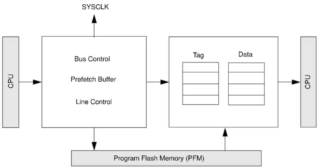
flowchart
graph TD
    CPU["CPU"] --> BusControl["Bus Control"]
    BusControl --> PrefetchBuffer["Prefetch Buffer"]
    BusControl --> LineControl["Line Control"]
    BusControl --> ProgramFlashMemory["Program Flash Memory (PFM)"]
    BusControl --> SYSCLK["SYSCLK"]
    BusControl --> Tag["Tag"]
    BusControl --> Data["Data"]
    BusControl --> CPU2["CPU"]
    ProgramFlashMemory --> Data
    Data --> CPU2
9.2 Prefetch Control Registers
TABLE 9-1: PREFETCH REGISTER MAP
Legend: x = unknown value on Reset, — = unimplemented, read as '0'. Reset values are shown in hexadecimal.
Note 1: All registers in this table have corresponding CLR, SET, and INV registers at its virtual address, plus an offset of 0x4, 0x8 and 0xC, respectively. See Section 12.2 "CLR, SET, and INV Registers" for more information.
REGISTER 9-1: PRECON: PREFETCH MODULE CONTROL REGISTER
| Bit Range | Bit31/23/15/7 | Bit30/22/14/6 | Bit29/21/13/5 | Bit28/20/12/4 | Bit27/19/11/3 | Bit26/18/10/2 | Bit25/17/9/1 | Bit24/16/8/0 |
| 31:24 | U-0 U-0 | U-0 U-0 U-0 R/W | U-0 | U-0 | ||||
| — — — | — — PFMSECEN | — | — | |||||
| 23:16 | U-0 U-0 | U-0 U-0 U-0 | U-0 | U-0 | U-0 | |||
| — — — | — — | — | — | — | ||||
| 15:8 | U-0 U-0 | U-0 U-0 U-0 | U-0 | U-0 | U-0 | |||
| — — — | — — | — | — | — | ||||
| 7:0 | U-0 | U-0 | R/W-0 | R/W-0 | U-0 | R/W-1 | R/W-1 | R/W-1 |
| — | — | PREFEN<1:0> | — | PFMWS<2:0>(1) | ||||
Legend:
| R = Readable bit | W = Writable bit U = Unimplemented bit, read as '0' | ||
| -n = Value at POR | '1' = Bit is set | '0' = Bit is cleared | x = Bit is unknown |
bit 31-27 Unimplemented: Read as '0'
bit 26 PFMSECEN: Flash SEC Interrupt Enable bit
1 = Generate an interrupt when the PFMSEC bit (PRESTAT<26>) is set
0 = Do not generate an interrupt when the PFMSEC bit is set
bit 25-6 Unimplemented: Read as '0'
bit 5-4 PREFEN<1:0>: Predictive Prefetch Enable bits
11 = Enable predictive prefetch for any address
10 = Enable predictive prefetch for CPU instructions and CPU data
01 = Enable predictive prefetch for CPU instructions only
00 = Disable predictive prefetch
bit 3 Unimplemented: Read as '0'
bit 2-0 PFMWS<2:0>: PFM Access Time Defined in Terms of SYSCLK Wait States bits ^(1)
111 = Seven Wait states
.
•
•
010 = Two Wait states
001 = One Wait state
000 = Zero Wait states
Note 1: For the Wait states to SYSCLK relationship, refer to Table 37-13 in Section37.0 “Electrical Characteristics”.
REGISTER 9-2: PRESTAT: PREFETCH MODULE STATUS REGISTER
| Bit Range | Bit 31/23/15/7 | Bit 30/22/14/6 | Bit 29/21/13/5 | Bit 28/20/12/4 | Bit 27/19/11/3 | Bit 26/18/10/2 | Bit 25/17/9/1 | Bit 24/16/8/0 |
| 31:24 | U-0 U-0 | U-0 U-0 | R/W-0, HS | R/W-0, HS | U-0 | U-0 | ||
| — — — | — PFMDED | PFMSEC — | — | |||||
| 23:16 | U-0 U-0 | U-0 U-0 | U-0 U-0 | U-0 U-0 | ||||
| — — — | — — — — | — | ||||||
| 15:8 | U-0 U-0 | U-0 U-0 | U-0 U-0 | U-0 U-0 | ||||
| — — — | — — — — | — | ||||||
| 7:0 | R/W-0 R/W | R/W-0 | R/W-0 | R/W-0 R/W-0 | R/W-0 R/W-0 | |||
| PFMSECCNT<7:0> | ||||||||
Legend: HS = Hardware Set
R = Readable bit W = Writable bit U = Unimplemented bit, read as '0'
-n = Value at POR
'1' = Bit is set
'0' = Bit is cleared
x = Bit is unknown
bit 31-28 Unimplemented: Read as '0'
bit 27 PFMDED: Flash Double-bit Error Detected (DED) Status bit
This bit is set in hardware and can only be cleared (i.e., set to '0') in software.
1 = A DED error has occurred
0 = A DED error has not occurred
bit 26 PFMSEC: Flash Single-bit Error Corrected (SEC) Status bit
1 = A SEC error occurred when PFMSECCNT<7:0> was equal to '0'
0 = A SEC error has not occurred
bit 25-8 Unimplemented: Read as '0'
bit 7-0 PFMSECCNT<7:0>: Flash SEC Count bits
11111111 - 00000000 = SEC count
This field decrements by one each time an SEC error occurs. It will hold at zero on the two-hundred and fifty-sixth error. When an SEC error occurs, when PFMSECCNT = 0, the PFMSEC status bit is set. If PFMSECEN is also set, an interrupt is generated.
Note: These bits count all SEC errors and are not limited to SEC errors on unique addresses.
10.0 DIRECT MEMORY ACCESS (DMA) CONTROLLER
Note: This data sheet summarizes the features of the PIC32MZ Embedded Connectivity (EC) Family of devices. It is not intended to be a comprehensive reference source. To complement the information in this data sheet, refer to Section 31. "Direct Memory Access (DMA) Controller" (DS60001117), which is available from the Documentation > Reference Manual section of the Microchip PIC32 web site (www.microchip.com/pic32).
The Direct Memory Access (DMA) Controller is a bus master module useful for data transfers between different devices without CPU intervention. The source and destination of a DMA transfer can be any of the memory mapped modules existent in the device such as SPI, UART, PMP, etc., or memory itself.
Note: To avoid cache coherency problems on devices with L1 cache, DMA buffers must only be allocated or accessed from the KSEG1 segment.
Following are some of the key features of the DMA Controller module:
• Eight identical channels, each featuring:
- Auto-increment source and destination address registers
- Source and destination pointers
- Memory to memory and memory to peripheral transfers
• Automatic word-size detection:
- Transfer granularity, down to byte level
- Bytes need not be word-aligned at source and destination
• Fixed priority channel arbitration
- Flexible DMA channel operating modes:
- Manual (software) or automatic (interrupt) DMA requests
- One-Shot or Auto-Repeat Block Transfer modes
- Channel-to-channel chaining
- Flexible DMA requests:
- A DMA request can be selected from any of the peripheral interrupt sources
- Each channel can select any (appropriate) observable interrupt as its DMA request source
- A DMA transfer abort can be selected from any of the peripheral interrupt sources
- Up to 2-byte Pattern (data) match transfer termination
- Multiple DMA channel status interrupts:
- DMA channel block transfer complete
- Source empty or half empty
- Destination full or half full
- DMA transfer aborted due to an external event
- Invalid DMA address generated
• DMA debug support features:
- Most recent error address accessed by a DMA channel
- Most recent DMA channel to transfer data
• CRC Generation module:
- CRC module can be assigned to any of the available channels
- CRC module is highly configurable
FIGURE 10-1: DMA BLOCK DIAGRAM
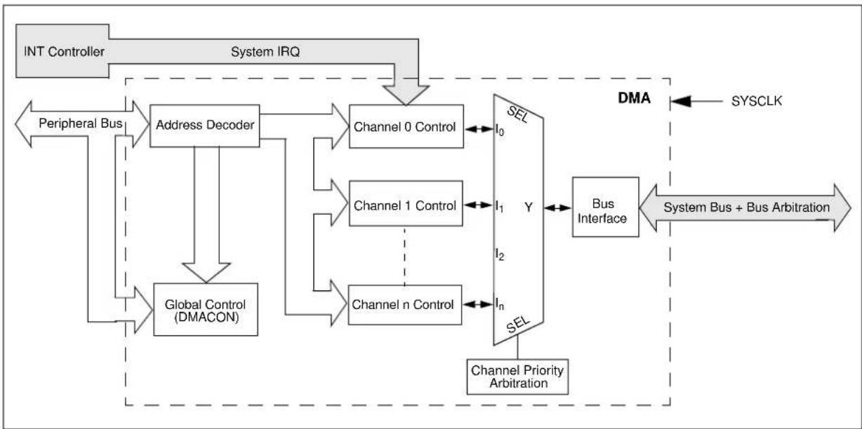
flowchart
graph TD
    A["INT Controller"] --> B["System IRQ"]
    B --> C["Address Decoder"]
    C --> D["Channel 0 Control"]
    C --> E["Channel 1 Control"]
    C --> F["Channel n Control"]
    D --> G["SEM"]
    E --> G
    F --> G
    G --> H["Channel Priority Arbitration"]
    H --> I["Bus Interface"]
    I --> J["System Bus + Bus Arbitration"]
    J --> K["DMA"]
    K --> L["SYSCLK"]
    L --> M["Peripheral Bus"]
    M --> N["Global Control (DMACON)"]
    N --> C
    style A fill:#ccc,stroke:#333
    style K fill:#fff,stroke:#333
10.1 DMA Control Registers
TABLE 10-1: DMA GLOBAL REGISTER MAP
Legend: x = unknown value on Reset; — = unimplemented, read as '0'. Reset values are shown in hexadecimal.
Note 1: All registers in this table have corresponding CLR, SET, and INV registers at its virtual address, plus an offset of 0x4, 0x8 and 0xC, respectively. See Section 12.2 "CLR, SET, and INV Registers" for more information.
TABLE 10-2: DMA CRC REGISTER MAP
| Virtual Address(BF81_#) | Register Name | Bit Range | Bits | All Resets | ||||||||||||||
| 31/15 | 30/14 | 29/13 | 28/12 | 27/11 | 26/10 | 25/9 | 24/8 | 23/7 | 22/6 | 21/5 | 20/4 | 19/3 | 18/2 | 17/1 | 16/0 | |||
| 1030 | DCRCCON | 31:16 | — | — | BYTEO<1:0> | WBO | — | — | BITO | — | — | — | — | — | — | — | 0000 | |
| 15:0 | — | — | — | PLEN<4:0> | CRCEN | CRCAPP | CRCTYP | — | — | CRCCH<2:0> | 0000 | |||||||
| 1040 | DCRCDATA | 31:16 | DCRCDATA<31:0> | 0000 | ||||||||||||||
| 15:0 | 0000 | |||||||||||||||||
| 1050 | DCRCXOR | 31:16 | DCRCXOR<31:0> | 0000 | ||||||||||||||
| 15:0 | 0000 | |||||||||||||||||
Legend: x = unknown value on Reset; — = unimplemented, read as '0'. Reset values are shown in hexadecimal.
Note 1: All registers in this table have corresponding CLR, SET, and INV registers at their virtual addresses, plus offsets of 0x4, 0x8 and 0xC, respectively. See Section 12.2 "CLR, SET, and INV Registlers" for more information.
TABLE 10-3: DMA CHANNEL 0 THROUGH CHANNEL 7 REGISTER MAP
Legend: x = unknown value on Reset; — = unimplemented, read as '0'. Reset values are shown in hexadecimal.
Note 1: All registers in this table have corresponding CLR, SET, and INV registers at their virtual addresses, plus offsets of 0x4, 0x8 and 0xC, respectively. See Section 12.2 "CLR, SET, and INV Registers" for more information.
TABLE 10-3: DMA CHANNEL 0 THROUGH CHANNEL 7 REGISTER MAP (CONTINUED)
| Virtual Address(BF81 #) | Register Name(1) | Bit Range | Bits | All Resets | |||||||||||||||
| 31/15 | 30/14 | 29/13 | 28/12 | 27/11 | 26/10 | 25/9 | 24/8 | 23/7 | 22/6 | 21/5 | 20/4 | 19/3 | 18/2 | 17/1 | 16/0 | ||||
| 1390 | DCH4SSA | 31:16 | CHSSA<31:0> | 0000 | |||||||||||||||
| 15:0 | |||||||||||||||||||
| 13A0 | DCH4DSA | 31:16 | CHDSA<31:0> | 0000 | |||||||||||||||
| 15:0 | |||||||||||||||||||
| 13B0 | DCH4SSIZ | 31:16 | —— | —— | —— | —— | —— | —— | —— | ||||||||||
| 15:0 | CHSSIZ<15:0> 0000 | ||||||||||||||||||
| 13C0 | DCH4DSIZ | 31:16 | —— | —— | —— | —— | —— | —— | —— | ||||||||||
| 15:0 | CHDSIZ<15:0> 0000 | ||||||||||||||||||
| 13D0 | DCH4SPTR | 31:16 | —— | —— | —— | —— | —— | —— | —— | ||||||||||
| 15:0 | CHSPTR<15:0> 0000 | ||||||||||||||||||
| 13E0 | DCH4DPTR | 31:16 | —— | —— | —— | —— | —— | —— | —— | ||||||||||
| 15:0 | CHDPTR<15:0> 0000 | ||||||||||||||||||
| 13F0 | DCH4CSIZ | 31:16 | —— | —— | —— | —— | —— | —— | —— | ||||||||||
| 15:0 | CHCSIZ<15:0> 0000 | ||||||||||||||||||
| 1400 | DCH4CPTR | 31:16 | —— | —— | —— | —— | —— | —— | —— | ||||||||||
| 15:0 | CHCPTR<15:0> 0000 | ||||||||||||||||||
| 1410 | DCH4DAT | 31:16 | —— | —— | —— | —— | —— | —— | —— | ||||||||||
| 15:0 | CHPDAT<15:0> 0000 | ||||||||||||||||||
| 1420 | DCH5CON | 31:16 | CHPIGN<7:0> | —— | —— | —— | 0000 | ||||||||||||
| 15:0 | CHBUSY | — | CHPIGNEN | — | CHPATLEN | — | — | CHCHNS | CHEN | CHAED | CHCHN | CHAEN | — | CHEDET | CHPRI<1:0> | 0000 | |||
| 1430 | DCH5ECON | 31:16 | — | — | — | — | — | — | — | — | CHAIRQ<7:0> | 0025 | |||||||
| 15:0 | CHSIRQ<7:0> | CFORCE | CABORT | PATEN | SIRQEN | AIRQEN | — | — | — | FF00 | |||||||||
| 1440 | DCH5INT | 31:16 | — | — | — | — | — | — | — | — | CHSDIE | CHSHIE | CHDDIE | CHDHIE | CHBCIE | CHCCIE | CHTAIE | CHERIE | 0000 |
| 15:0 | — | — | — | — | — | — | — | — | CHSDIF | CHSHIF | CHDDIF | CHDHIF | CHBCIF | CHCCIF | CHTAIF | CHERIF | 0000 | ||
| 1450 | DCH5SSA | 31:16 | CHSSA<31:0> | 0000 | |||||||||||||||
| 15:0 | |||||||||||||||||||
| 1460 | DCH5DSA | 31:16 | CHDSA<31:0> | 0000 | |||||||||||||||
| 15:0 | |||||||||||||||||||
| 1470 | DCH5SSIZ | 31:16 | —— | —— | —— | —— | —— | —— | —— | ||||||||||
| 15:0 | CHSSIZ<15:0> | 0000 | |||||||||||||||||
| 1480 | DCH5DSIZ | 31:16 | —— | —— | —— | —— | —— | —— | —— | ||||||||||
| 15:0 | CHDSIZ<15:0> 0000 | ||||||||||||||||||
| 1490 | DCH5SPTR | 31:16 | —— | —— | —— | —— | —— | —— | —— | ||||||||||
| 15:0 | CHSPTR<15:0> 0000 | ||||||||||||||||||
Legend: x = unknown value on Reset; — = unimplemented, read as '0'. Reset values are shown in hexadecimal.
Note 1: All registers in this table have corresponding CLR, SET, and INV registers at their virtual addresses, plus offsets of 0x4, 0x8 and 0xC, respectively. See Section 12.2 "CLR, SET, and INV Registers" for more information.
TABLE 10-3: DMA CHANNEL 0 THROUGH CHANNEL 7 REGISTER MAP (CONTINUED)
Legend: x = unknown value on Reset; — = unimplemented, read as '0'. Reset values are shown in hexadecimal.
Note 1: All registers in this table have corresponding CLR, SET, and INV registers at their virtual addresses, plus offsets of 0x4, 0x8 and 0xC, respectively. See Section 12.2 "CLR, SET, and INV Registers" for more information.
REGISTER 10-1: DMACON: DMA CONTROLLER CONTROL REGISTER
| Bit Range | Bit 31/23/15/7 | Bit 30/22/14/6 | Bit 29/21/13/5 | Bit 28/20/12/4 | Bit 27/19/11/3 | Bit 26/18/10/2 | Bit 25/17/9/1 | Bit 24/16/8/0 |
| 31:24 | U-0 U-0 U-0 | U-0 U-0 U-0 U-0 | U-0 | |||||
| — — — | — — — — | — | ||||||
| 23:16 | U-0 U-0 U-0 | U-0 U-0 U-0 U-0 | U-0 | |||||
| — — — | — — — — | — | ||||||
| 15:8 | R/W-0 U-0 | U-0 | R/W-0 | R/W-0 | U-0 U-0 U-0 | |||
| ON | — | — | SUSPEND | DMABUSY | — | — | — | |
| 7:0 | U-0 U-0 U-0 | U-0 U-0 U-0 | U-0 | |||||
| — — — | — — — — | — |
Legend:
| R = Readable bit | W = Writable bit U = Unimplemented bit, read as ‘0’ | ||
| -n = Value at POR | ‘1’ = Bit is set | ‘0’ = Bit is cleared | x = Bit is unknown |
bit 31-16 Unimplemented: Read as '0'
bit 15 ON: DMA On bit
1 = DMA module is enabled
0 = DMA module is disabled
bit 14-13 Unimplemented: Read as '0'
bit 12 SUSPEND: DMA Suspend bit
1 = DMA transfers are suspended to allow CPU uninterrupted access to data bus
0 = DMA operates normally
bit 11 DMABUSY: DMA Module Busy bit
1 = DMA module is active and is transferring data
0 = DMA module is disabled and not actively transferring data
bit 10-0 Unimplemented: Read as '0'
REGISTER 10-2: DMASTAT: DMA STATUS REGISTER
| Bit Range | Bit 31/23/15/7 | Bit 30/22/14/6 | Bit 29/21/13/5 | Bit 28/20/12/4 | Bit 27/19/11/3 | Bit 26/18/10/2 | Bit 25/17/9/1 | Bit 24/16/8/0 |
| 31:24 | R-0 U-0 U-0 | U-0 U-0 U-0 U-0 | U-0 | |||||
| RDWR — | — — — — — | — | ||||||
| 23:16 | U-0 U-0 U-0 | U-0 U-0 U-0 U-0 | U-0 | |||||
| — | — — — | — — — — | ||||||
| 15:8 | U-0 U-0 U-0 | U-0 U-0 U-0 U-0 | U-0 | |||||
| — | — — — | — — — — | ||||||
| 7:0 | U-0 U-0 U-0 | U-0 U-0 R-0 R-0 | R-0 | |||||
| — | — — — | — | DMACH<2:0> | |||||
Legend:
| R = Readable bit | W = Writable bit U = Unimplemented bit, read as '0' | ||
| -n = Value at POR | ‘1’ = Bit is set | ‘0’ = Bit is cleared | x = Bit is unknown |
bit 31 RDWR: Read/Write Status bit
1 = Last DMA bus access when an error was detected was a read
0 = Last DMA bus access when an error was detected was a write
bit 30-3 Unimplemented: Read as '0'
bit 2-0 DMACH<2:0>: DMA Channel bits
These bits contain the value of the most recent active DMA channel when an error was detected.
REGISTER 10-3: DMAADDR: DMA ADDRESS REGISTER
| Bit Range | Bit 31/23/15/7 | Bit 30/22/14/6 | Bit 29/21/13/5 | Bit 28/20/12/4 | Bit 27/19/11/3 | Bit 26/18/10/2 | Bit 25/17/9/1 | Bit 24/16/8/0 |
| 31:24 | R-0 | R-0 | R-0 | R-0 | R-0 | R-0 | R-0 | R-0 |
| DMAADDR<31:24> | ||||||||
| 23:16 | R-0 | R-0 | R-0 | R-0 | R-0 | R-0 | R-0 | R-0 |
| DMAADDR<23:16> | ||||||||
| 15:8 | R-0 | R-0 | R-0 | R-0 | R-0 | R-0 | R-0 | R-0 |
| DMAADDR<15:8> | ||||||||
| 7:0 | R-0 | R-0 | R-0 | R-0 | R-0 | R-0 | R-0 | R-0 |
| DMAADDR<7:0> | ||||||||
Legend:
| R = Readable bit | W = Writable bit | U = Unimplemented bit, read as ‘0’ |
| -n = Value at POR | ‘1’ = Bit is set | ‘0’ = Bit is cleared x = Bit is unknown |
bit 31-0 DMAADDR<31:0>: DMA Module Address bits
These bits contain the address of the most recent DMA access when an error was detected.
REGISTER 10-4: DCRCCON: DMA CRC CONTROL REGISTER
| Bit Range | Bit 31/23/15/7 | Bit 30/22/14/6 | Bit 29/21/13/5 | Bit 28/20/12/4 | Bit 27/19/11/3 | Bit 26/18/10/2 | Bit 25/17/9/1 | Bit 24/16/8/0 |
| 31:24 | U-0 U-0 R/W-0 R/W-0 R/W-0 | U-0 U-0 R/W-0 | ||||||
| — — BYTO<1:0> WBO | (1) | — | — | BITO | ||||
| 23:16 | U-0 U-0 | U-0 | U-0 | U-0 U-0 | U-0 U-0 | |||
| — | — | — | — | — | — | — | — | |
| 15:8 | U-0 | U-0 | U-0 | R/W-0 | R/W-0 | R/W-0 | R/W-0 | R/W-0 |
| — — | — | PLEN<4:0> (1) | ||||||
| 7:0 | R/W-0 | R/W-0 | R/W-0 | U-0 | U-0 | R/W-0 | R/W-0 | R/W-0 |
| CRCEN | CRCAPP(1) | CRCTYP | — | — | CRCCH<2:0> | |||
Legend:
| R = Readable bit | W = Writable bit | U = Unimplemented bit, read as '0' |
| -n = Value at POR | '1' = Bit is set | '0' = Bit is cleared x = Bit is unknown |
bit 31-30 Unimplemented: Read as '0'
bit 29-28 BYTO<1:0>: CRC Byte Order Selection bits
11 = Endian byte swap on half-word boundaries (i.e., source half-word order with reverse source byte order per half-word)
10 = Swap half-words on word boundaries (i.e., reverse source half-word order with source byte order per half-word)
01 = Endian byte swap on word boundaries (i.e., reverse source byte order)
00 = No swapping (i.e., source byte order)
bit 27 WBO: CRC Write Byte Order Selection bit ^(1)
1 = Source data is written to the destination re-ordered as defined by BYTO<1:0>
0 = Source data is written to the destination unaltered
bit 26-25 Unimplemented: Read as '0'
bit 24 BITO: CRC Bit Order Selection bit
When CRCTYP (DCRCCON<15>) = 1 (CRC module is in IP Header mode):
1 = The IP header checksum is calculated Least Significant bit (LSb) first (i.e., reflected)
0 = The IP header checksum is calculated Most Significant bit (MSb) first (i.e., not reflected)
When CRCTYP (DCRCCON<15>) = 0 (CRC module is in LFSR mode):
1 = The LFSR CRC is calculated Least Significant bit first (i.e., reflected)
0 = The LFSR CRC is calculated Most Significant bit first (i.e., not reflected)
bit 23-13 Unimplemented: Read as '0'
bit 12-8 PLEN<4:0>: Polynomial Length bits ^(1)
When CRCTYP (DCRCCON<15>) = 1 (CRC module is in IP Header mode):
These bits are unused.
When CRCTYP (DCRCCON<15>) = 0 (CRC module is in LFSR mode):
Denotes the length of the polynomial - 1.
bit 7 CRCEN: CRC Enable bit
1 = CRC module is enabled and channel transfers are routed through the CRC module
0 = CRC module is disabled and channel transfers proceed normally
Note 1: When WBO = 1, unaligned transfers are not supported and the CRCAPP bit cannot be set.
REGISTER 10-4: DCRCCON: DMA CRC CONTROL REGISTER (CONTINUED)
bit 6 CRCAPP: CRC Append Mode bit (1)
1 = The DMA transfers data from the source into the CRC but NOT to the destination. When a block transfer completes the DMA writes the calculated CRC value to the location given by CHxDSA
0 = The DMA transfers data from the source through the CRC obeying WBO as it writes the data to the destination
bit 5 CRCTYP: CRC Type Selection bit
1 = The CRC module will calculate an IP header checksum
0 = The CRC module will calculate a LFSR CRC
bit 4-3 Unimplemented: Read as '0'
bit 2-0 CRCCH<2:0>: CRC Channel Select bits
111 = CRC is assigned to Channel 7
110 = CRC is assigned to Channel 6
101 = CRC is assigned to Channel 5
100 = CRC is assigned to Channel 4
011 = CRC is assigned to Channel 3
010 = CRC is assigned to Channel 2
001 = CRC is assigned to Channel 1
000 = CRC is assigned to Channel 0
Note 1: When WBO = 1, unaligned transfers are not supported and the CRCAPP bit cannot be set.
REGISTER 10-5: DCRCDATA: DMA CRC DATA REGISTER
| Bit Range | Bit 31/23/15/7 | Bit 30/22/14/6 | Bit 29/21/13/5 | Bit 28/20/12/4 | Bit 27/19/11/3 | Bit 26/18/10/2 | Bit 25/17/9/1 | Bit 24/16/8/0 |
| 31:24 | R/W-0 R/W-0 | R/W-0 R/W-0 R/W-0 | R/W-0 R/W-0 R/W-0 | R/W-0 | ||||
| DCRCDATA<31:24> | ||||||||
| 23:16 | R/W-0 R/W-0 | R/W-0 R/W-0 R/W-0 | R/W-0 R/W-0 R/W-0 | R/W-0 | ||||
| DCRCDATA<23:16> | ||||||||
| 15:8 | R/W-0 R/W-0 | R/W-0 R/W-0 R/W-0 | R/W-0 R/W-0 R/W-0 | R/W-0 | ||||
| DCRCDATA<15:8> | ||||||||
| 7:0 | R/W-0 R/W-0 | R/W-0 R/W-0 R/W-0 | R/W-0 R/W-0 R/W-0 | R/W-0 | ||||
| DCRCDATA<7:0> | ||||||||
Legend:
R = Readable bit W = Writable bit U = Unimplemented bit, read as '0' -n = Value at POR '1' = Bit is set '0' = Bit is cleared x = Bit is unknown
bit 31-0 DCRCDATA<31:0>: CRC Data Register bits
Writing to this register will seed the CRC generator. Reading from this register will return the current value of the CRC. Bits greater than PLEN will return '0' on any read.
When CRCTYP (DCRCCON<15>) = 1 (CRC module is in IP Header mode):
Only the lower 16 bits contain IP header checksum information. The upper 16 bits are always '0'. Data written to this register is converted and read back in 1's complement form (i.e., current IP header checksum value).
When CRCTYP (DCRCCON<15>) = 0 (CRC module is in LFSR mode):
Bits greater than PLEN will return '0' on any read.
REGISTER 10-6: DCRCXOR: DMA CRCXOR ENABLE REGISTER
| Bit Range | Bit 31/23/15/7 | Bit 30/22/14/6 | Bit 29/21/13/5 | Bit 28/20/12/4 | Bit 27/19/11/3 | Bit 26/18/10/2 | Bit 25/17/9/1 | Bit 24/16/8/0 |
| 31:24 | R/W-0 | R/W-0 | R/W-0 | R/W-0 | R/W-0 | R/W-0 | R/W-0 | R/W-0 |
| DCRCXOR<31:24> | ||||||||
| 23:16 | R/W-0 | R/W-0 | R/W-0 | R/W-0 | R/W-0 | R/W-0 | R/W-0 | R/W-0 |
| DCRCXOR<23:16> | ||||||||
| 15:8 | R/W-0 | R/W-0 | R/W-0 | R/W-0 | R/W-0 | R/W-0 | R/W-0 | R/W-0 |
| DCRCXOR<15:8> | ||||||||
| 7:0 | R/W-0 | R/W-0 | R/W-0 | R/W-0 | R/W-0 | R/W-0 | R/W-0 | R/W-0 |
| DCRCXOR<7:0> | ||||||||
Legend:
R = Readable bit W = Writable bit U = Unimplemented bit, read as '0' -n = Value at POR '1' = Bit is set '0' = Bit is cleared x = Bit is unknown
bit 31-0 DCRCXOR<31:0>: CRC XOR Register bits
When CRCTYP (DCRCCON<15>) = 1 (CRC module is in IP Header mode):
This register is unused.
When CRCTYP (DCRCCON<15>) = 0 (CRC module is in LFSR mode):
1 = Enable the XOR input to the Shift register
0 = Disable the XOR input to the Shift register; data is shifted in directly from the previous stage in the register
REGISTER 10-7: DCHxCON: DMA CHANNEL x CONTROL REGISTER
| Bit Range | Bit 31/23/15/7 | Bit 30/22/14/6 | Bit 29/21/13/5 | Bit 28/20/12/4 | Bit 27/19/11/3 | Bit 26/18/10/2 | Bit 25/17/9/1 | Bit 24/16/8/0 |
| 31:24 | R/W-0 R/W-0 | R/W-0 R/W-0 | R/W-0 R/W-0 | R/W-0 R/W-0 | ||||
| CHPIGN<7:0> | ||||||||
| 23:16 | U-0 U-0 U-0 | U-0 U-0 | U-0 U-0 | |||||
| — | — | — | — | — | — | — | — | |
| 15:8 | R/W-0 | U-0 | R/W-0 | U-0 | R/W-0 | U-0 | U-0 | R/W-0 |
| CHBUSY | — | CHIPGNEN | — | CHPATLEN | — | — | CHCHNS(1) | |
| 7:0 | R/W-0 R/W-0 | R/W-0 R/W-0 | U-0 R-0 | R/W-0 | R/W-0 | |||
| CHEN(2) | CHAED | CHCHN | CHAEN | — | CHEDET | CHPRI<1:0> | ||
Legend:
| R = Readable bit | W = Writable bit | U = Unimplemented bit, read as ‘0’ |
| -n = Value at POR | ‘1’ = Bit is set | ‘0’ = Bit is cleared x = Bit is unknown |
bit 31-24 CHPIGN<7:0>: Channel Register Data bits
Pattern Terminate mode:
Any byte matching these bits during a pattern match may be ignored during the pattern match determination when the CHPIGNEN bit is set. If a byte is read that is identical to this data byte, the pattern match logic will treat it as a "don't care" when the pattern matching logic is enabled and the CHPIGEN bit is set.
bit 23-16 Unimplemented: Read as '0'
bit 15 CHBUSY: Channel Busy bit
1 = Channel is active or has been enabled
0 = Channel is inactive or has been disabled
bit 14 Unimplemented: Read as '0'
bit 13 CHPIGNEN: Enable Pattern Ignore Byte bit
1 = Treat any byte that matches the CHPIGN<7:0> bits as a "don't care" when pattern matching is enabled 0 = Disable this feature
bit 12 Unimplemented: Read as '0'
bit 11 CHPATLEN: Pattern Length bit
1 = 2 byte length
0 = 1 byte length
bit 10-9 Unimplemented: Read as '0'
bit 8 CHCHNS: Chain Channel Selection bit ^(1)
1 = Chain to channel lower in natural priority (CH1 will be enabled by CH2 transfer complete)
0 = Chain to channel higher in natural priority (CH1 will be enabled by CH0 transfer complete)
bit 7 CHEN: Channel Enable bit ^(2)
1 = Channel is enabled
0 = Channel is disabled
bit 6 CHAED: Channel Allow Events If Disabled bit
1 = Channel start/abort events will be registered, even if the channel is disabled
0 = Channel start/abort events will be ignored if the channel is disabled
bit 5 CHCHN: Channel Chain Enable bit
1 = Allow channel to be chained
0 = Do not allow channel to be chained
Note 1: The chain selection bit takes effect when chaining is enabled (i.e., CHCHN = 1).
2: When the channel is suspended by clearing this bit, the user application should poll the CHBUSY bit (if available on the device variant) to see when the channel is suspended, as it may take some clock cycles to complete a current transaction before the channel is suspended.
REGISTER 10-7: DCHxCON: DMA CHANNEL x CONTROL REGISTER (CONTINUED)
bit 4 CHAEN: Channel Automatic Enable bit
1 = Channel is continuously enabled, and not automatically disabled after a block transfer is complete
0 = Channel is disabled on block transfer complete
bit 3 Unimplemented: Read as '0'
bit 2 CHEDET: Channel Event Detected bit
1 = An event has been detected
0 = No events have been detected
bit 1-0 CHPRI<1:0>: Channel Priority bits
11 = Channel has priority 3 (highest)
10 = Channel has priority 2
01 = Channel has priority 1
00 = Channel has priority 0
Note 1: The chain selection bit takes effect when chaining is enabled (i.e., CHCHN = 1).
2: When the channel is suspended by clearing this bit, the user application should poll the CHBUSY bit (if available on the device variant) to see when the channel is suspended, as it may take some clock cycles to complete a current transaction before the channel is suspended.
REGISTER 10-8: DCHxECON: DMA CHANNEL x EVENT CONTROL REGISTER
| Bit Range | Bit 31/23/15/7 | Bit 30/22/14/6 | Bit 29/21/13/5 | Bit 28/20/12/4 | Bit 27/19/11/3 | Bit 26/18/10/2 | Bit 25/17/9/1 | Bit 24/16/8/0 |
| 31:24 | U-0 U-0 U-0 | U-0 U-0 U-0 U-0 | U-0 | |||||
| —— ——— ——— | ||||||||
| 23:16 | R/W-1 | R/W-1 | R/W-1 | R/W-1 | R/W-1 | R/W-1 | R/W-1 | R/W-1 |
| CHAIRQ<7:0>(1) | ||||||||
| 15:8 | R/W-1 | R/W-1 | R/W-1 | R/W-1 | R/W-1 | R/W-1 | R/W-1 | R/W-1 |
| CHSIRQ<7:0>(1) | ||||||||
| 7:0 | S-0 S-0 | R/W-0 R | W-0 | R/W-0 | U-0 U-0 U-0 | |||
| CFORCE | CABORT | PATEN | SIRQEN | AIRQEN | — | — | — | |
| Legend: | S = Settable bit | ||
| R = Readable bit | W = Writable bit U = Unimplemented bit, read as ‘0’ | ||
| -n = Value at POR | ‘1’ = Bit is set | ‘0’ = Bit is cleared | x = Bit is unknown |
bit 31-24 Unimplemented: Read as '0'
bit 23-16 CHAIRQ<7:0>: Channel Transfer Abort IRQ bits ^(1)
11111111 = Interrupt 255 will abort any transfers in progress and set CHAIF flag
•
•
.
00000001 = Interrupt 1 will abort any transfers in progress and set CHAIF flag
00000000 = Interrupt 0 will abort any transfers in progress and set CHAIF flag
bit 15-8 CHSIRQ<7:0>: Channel Transfer Start IRQ bits ^(1)
11111111 = Interrupt 255 will initiate a DMA transfer
•
•
•
00000001 = Interrupt 1 will initiate a DMA transfer
00000000 = Interrupt 0 will initiate a DMA transfer
bit 7 CFORCE: DMA Forced Transfer bit
1 = A DMA transfer is forced to begin when this bit is written to a '1'
0 = This bit always reads '0'
bit 6 CABORT: DMA Abort Transfer bit
1 = A DMA transfer is aborted when this bit is written to a '1'
0 = This bit always reads '0'
bit 5 PATEN: Channel Pattern Match Abort Enable bit
1 = Abort transfer and clear CHEN on pattern match
0 = Pattern match is disabled
bit 4 SIRQEN: Channel Start IRQ Enable bit
1 = Start channel cell transfer if an interrupt matching CHSIRQ occurs
0 = Interrupt number CHSIRQ is ignored and does not start a transfer
bit 3 AIRQEN: Channel Abort IRQ Enable bit
1 = Channel transfer is aborted if an interrupt matching CHAIRQ occurs
0 = Interrupt number CHAIRQ is ignored and does not terminate a transfer
bit 2-0 Unimplemented: Read as '0'
Note 1: See Table 7-2: "Interrupt IRQ, Vector and Bit Location" for the list of available interrupt IRQ sources.
REGISTER 10-9: DCHxINT: DMA CHANNEL x INTERRUPT CONTROL REGISTER
| Bit Range | Bit 31/23/15/7 | Bit 30/22/14/6 | Bit 29/21/13/5 | Bit 28/20/12/4 | Bit 27/19/11/3 | Bit 26/18/10/2 | Bit 25/17/9/1 | Bit 24/16/8/0 |
| 31:24 | U-0 U-0 U-0 | U-0 U-0 U-0 U-0 | U-0 | |||||
| ——— | ——— —— | |||||||
| 23:16 | R/W-0 | R/W-0 | R/W-0 | R/W-0 | R/W-0 | R/W-0 | R/W-0 | R/W-0 |
| CHSDIE | CHSHIE | CHDDIE | CHDHIE | CHBCIE | CHCCIE | CHTAIE | CHERIE | |
| 15:8 | U-0 U-0 U-0 | U-0 U-0 U-0 U-0 | U-0 | |||||
| ——— | ——— —— | |||||||
| 7:0 | R/W-0 | R/W-0 | R/W-0 | R/W-0 | R/W-0 | R/W-0 | R/W-0 | R/W-0 |
| CHSDIF | CHSHIF | CHDDIF | CHDHIF | CHBCIF | CHCCIF | CHTAIF | CHERIF |
Legend:
| R = Readable bit | W = Writable bit U = Unimplemented bit, read as '0' |
| -n = Value at POR | '1' = Bit is set '0' = Bit is cleared x = Bit is unknown |
bit 31-24 Unimplemented: Read as '0'
bit 23 CHSDIE: Channel Source Done Interrupt Enable bit
1 = Interrupt is enabled
0 = Interrupt is disabled
bit 22 CHSHIE: Channel Source Half Empty Interrupt Enable bit
1 = Interrupt is enabled
0 = Interrupt is disabled
bit 21 CHDDIE: Channel Destination Done Interrupt Enable bit
1 = Interrupt is enabled
0 = Interrupt is disabled
bit 20 CHDHIE: Channel Destination Half Full Interrupt Enable bit
1 = Interrupt is enabled
0 = Interrupt is disabled
bit 19 CHBCIE: Channel Block Transfer Complete Interrupt Enable bit
1 = Interrupt is enabled
0 = Interrupt is disabled
bit 18 CHCCIE: Channel Cell Transfer Complete Interrupt Enable bit
1 = Interrupt is enabled
0 = Interrupt is disabled
bit 17 CHTAIE: Channel Transfer Abort Interrupt Enable bit
1 = Interrupt is enabled
0 = Interrupt is disabled
bit 16 CHERIE: Channel Address Error Interrupt Enable bit
1 = Interrupt is enabled
0 = Interrupt is disabled
bit 15-8 Unimplemented: Read as '0'
bit 7 CHSDIF: Channel Source Done Interrupt Flag bit
1 = Channel Source Pointer has reached end of source (CHSPTR = CHSSIZ)
0 = No interrupt is pending
bit 6 CHSHIF: Channel Source Half Empty Interrupt Flag bit
1 = Channel Source Pointer has reached midpoint of source (CHSPTR = CHSSIZ/2)
0 = No interrupt is pending
REGISTER 10-9: DCHxINT: DMA CHANNEL x INTERRUPT CONTROL REGISTER (CONTINUED)
bit 5 CHDDIF: Channel Destination Done Interrupt Flag bit
1 = Channel Destination Pointer has reached end of destination (CHDPTR = CHDSIZ)
0 = No interrupt is pending
bit 4 CHDHIF: Channel Destination Half Full Interrupt Flag bit
1 = Channel Destination Pointer has reached midpoint of destination (CHDPTR = CHDSIZ/2)
0 = No interrupt is pending
bit 3 CHBCIF: Channel Block Transfer Complete Interrupt Flag bit
1 = A block transfer has been completed (the larger of CHSSIZ/CHDSIZ bytes has been transferred), or a pattern match event occurs
0 = No interrupt is pending
bit 2 CHCCIF: Channel Cell Transfer Complete Interrupt Flag bit
1 = A cell transfer has been completed (CHCSIZ bytes have been transferred)
0 = No interrupt is pending
bit 1 CHTAIF: Channel Transfer Abort Interrupt Flag bit
1 = An interrupt matching CHAIRQ has been detected and the DMA transfer has been aborted
0 = No interrupt is pending
bit 0 CHERIF: Channel Address Error Interrupt Flag bit
1 = A channel address error has been detected
Either the source or the destination address is invalid.
0 = No interrupt is pending
REGISTER 10-10: DCHxSSA: DMA CHANNEL x SOURCE START ADDRESS REGISTER
| Bit Range | Bit31/23/15/7 | Bit30/22/14/6 | Bit29/21/13/5 | Bit28/20/12/4 | Bit27/19/11/3 | Bit26/18/10/2 | Bit25/17/9/1 | Bit24/16/8/0 |
| 31:24 | R/W-0 R/W-0 | R/W-0 R/W-0 R/W-0 | W-0 R/W-0 R/W-0 | R/W-0 | ||||
| CHSSA<31:24> | ||||||||
| 23:16 | R/W-0 R/W-0 | R/W-0 R/W-0 R/W-0 | W-0 R/W-0 R/W-0 | R/W-0 | ||||
| CHSSA<23:16> | ||||||||
| 15:8 | R/W-0 R/W-0 | R/W-0 R/W-0 R/W-0 | W-0 R/W-0 R/W-0 | R/W-0 | ||||
| CHSSA<15:8> | ||||||||
| 7:0 | R/W-0 R/W-0 | R/W-0 R/W-0 R/W-0 | W-0 R/W-0 R/W-0 | R/W-0 | ||||
| CHSSA<7:0> | ||||||||
Legend:
R = Readable bit W = Writable bit U = Unimplemented bit, read as '0' -n = Value at POR '1' = Bit is set '0' = Bit is cleared x = Bit is unknown
bit 31-0 CHSSA<31:0> Channel Source Start Address bits
Channel source start address.
Note: This must be the physical address of the source.
REGISTER 10-11: DCHxDSA: DMA CHANNEL x DESTINATION START ADDRESS REGISTER
| Bit Range | Bit 31/23/15/7 | Bit 30/22/14/6 | Bit 29/21/13/5 | Bit 28/20/12/4 | Bit 27/19/11/3 | Bit 26/18/10/2 | Bit 25/17/9/1 | Bit 24/16/8/0 |
| 31:24 | R/W-0 | R/W-0 | R/W-0 | R/W-0 | R/W-0 | R/W-0 | R/W-0 | R/W-0 |
| CHDSA<31:24> | ||||||||
| 23:16 | R/W-0 | R/W-0 | R/W-0 | R/W-0 | R/W-0 | R/W-0 | R/W-0 | R/W-0 |
| CHDSA<23:16> | ||||||||
| 15:8 | R/W-0 | R/W-0 | R/W-0 | R/W-0 | R/W-0 | R/W-0 | R/W-0 | R/W-0 |
| CHDSA<15:8> | ||||||||
| 7:0 | R/W-0 | R/W-0 | R/W-0 | R/W-0 | R/W-0 | R/W-0 | R/W-0 | R/W-0 |
| CHDSA<7:0> | ||||||||
Legend:
R = Readable bit W = Writable bit U = Unimplemented bit, read as '0' -n = Value at POR '1' = Bit is set '0' = Bit is cleared x = Bit is unknown
bit 31-0 CHDSA<31:0>: Channel Destination Start Address bits
Channel destination start address.
Note: This must be the physical address of the destination.
REGISTER 10-12: DCHxSSIZ: DMA CHANNEL x SOURCE SIZE REGISTER
| Bit Range | Bit 31/23/15/7 | Bit 30/22/14/6 | Bit 29/21/13/5 | Bit 28/20/12/4 | Bit 27/19/11/3 | Bit 26/18/10/2 | Bit 25/17/9/1 | Bit 24/16/8/0 |
| 31:24 | U-0 U-0 U-0 | U-0 U-0 U-0 | U-0 | |||||
| —— ——— ——— ——— ——— ——— ——— ——— ——— ——— ——— ——— ——— ——— ——— ——— ——— ——— ——— ——— ——— ——— ——— ——— ——— ——— ——— ——— ——— ——— ——— ——— ——— ——— ——— ——— ——— ——— ——— ——— ——— ——— ——— ——— ——— ——— ——— ——— ——— ——— ——— | ||||||||
| 23:16 | U-0 U-0 U-0 | U-0 U-0 U-0 | U-0 | |||||
| —— ——— ——— ——— ——— ——— ——— ——— ——— ——— ——— ——— ——— ——— ——— ——— ——— ——— ——— ——— ——— ——— ——— ——— ——— ——— ——— ——— ——— ——— ——— ——— ——— —— | ||||||||
| 15:8 | R/W-0 | R/W-0 | R/W-0 | R/W-0 | R/W-0 | R/W-0 | R/W-0 | R/W-0 |
| CHSSIZ<15:8> | ||||||||
| 7:0 | R/W-0 | R/W-0 | R/W-0 | R/W-0 | R/W-0 | R/W-0 | R/W-0 | R/W-0 |
| CHSSIZ<7:0> | ||||||||
Legend:
| R = Readable bit | W = Writable bit U = Unimplemented bit, read as '0' |
| -n = Value at POR | '1' = Bit is set '0' = Bit is cleared x = Bit is unknown |
bit 31-16 Unimplemented: Read as '0'
bit 15-0 CHSSIZ<15:0>: Channel Source Size bits
1111111111111111 = 65,535 byte source size
•
•
•
0000000000000010 = 2 byte source size
0000000000000001 = 1 byte source size
0000000000000000 = 65,536 byte source size
REGISTER 10-13: DCHxDSIZ: DMA CHANNEL x DESTINATION SIZE REGISTER
| Bit Range | Bit 31/23/15/7 | Bit 30/22/14/6 | Bit 29/21/13/5 | Bit 28/20/12/4 | Bit 27/19/11/3 | Bit 26/18/10/2 | Bit 25/17/9/1 | Bit 24/16/8/0 |
| 31:24 | U-0 U-0 U-0 | U-0 U-0 U-0 | U-0 | |||||
| —— —— | —— —— —— | |||||||
| 23:16 | U-0 U-0 U-0 | U-0 U-0 U-0 | U-0 | |||||
| —— —— | —— —— —— | |||||||
| 15:8 | R/W-0 | R/W-0 | R/W-0 | R/W-0 | R/W-0 | R/W-0 | R/W-0 | R/W-0 |
| CHDSIZ<15:8> | ||||||||
| 7:0 | R/W-0 | R/W-0 | R/W-0 | R/W-0 | R/W-0 | R/W-0 | R/W-0 | R/W-0 |
| CHDSIZ<7:0> | ||||||||
Legend:
| R = Readable bit | W = Writable bit | U = Unimplemented bit, read as ‘0’ |
| -n = Value at POR | ‘1’ = Bit is set | ‘0’ = Bit is cleared x = Bit is unknown |
bit 31-16 Unimplemented: Read as '0'
bit 15-0 CHDSIZ<15:0>: Channel Destination Size bits
1111111111111111 = 65,535 byte destination size
•
•
-
0000000000000010 = 2 byte destination size
0000000000000001 = 1 byte destination size
0000000000000000 = 65,536 byte destination size
REGISTER 10-14: DCHxSPTR: DMA CHANNEL x SOURCE POINTER REGISTER
| Bit Range | Bit 31/23/15/7 | Bit 30/22/14/6 | Bit 29/21/13/5 | Bit 28/20/12/4 | Bit 27/19/11/3 | Bit 26/18/10/2 | Bit 25/17/9/1 | Bit 24/16/8/0 |
| 31:24 | U-0 U-0 U-0 | U-0 U-0 U-0 U-0 | U-0 | |||||
| ——— | ——— —— | |||||||
| 23:16 | U-0 U-0 U-0 | U-0 U-0 U-0 U-0 | U-0 | |||||
| ——— | ——— —— | |||||||
| 15:8 | R-0 R-0 R-0 | R-0 R-0 R-0 R-0 | R-0 | |||||
| CHSPTR<15:8> | ||||||||
| 7:0 | R-0 R-0 R-0 | R-0 R-0 R-0 R-0 | R-0 | |||||
| CHSPTR<7:0> | ||||||||
Legend:
R = Readable bit W = Writable bit U = Unimplemented bit, read as '0'
-n = Value at POR '1' = Bit is set '0' = Bit is cleared x = Bit is unknown
bit 31-16 Unimplemented: Read as '0'
bit 15-0 CHSPTR<15:0>: Channel Source Pointer bits
11111111111111111 = Points to byte 65,535 of the source
•
•
•
0000000000000001 = Points to byte 1 of the source
00000000000000000 = Points to byte 0 of the source
Note: When in Pattern Detect mode, this register is reset on a pattern detect.
REGISTER 10-15: DCHxDPTR: DMA CHANNEL x DESTINATION POINTER REGISTER
| Bit Range | Bit 31/23/15/7 | Bit 30/22/14/6 | Bit 29/21/13/5 | Bit 28/20/12/4 | Bit 27/19/11/3 | Bit 26/18/10/2 | Bit 25/17/9/1 | Bit 24/16/8/0 |
| 31:24 | U-0 | U-0 | U-0 | U-0 | U-0 | U-0 | U-0 | U-0 |
| — — — — | — | — — — — | ||||||
| 23:16 | U-0 | U-0 | U-0 | U-0 | U-0 | U-0 | U-0 | U-0 |
| — — — — | — | — — — — | ||||||
| 15:8 | R-0 | R-0 | R-0 | R-0 | R-0 | R-0 | R-0 | R-0 |
| CHDPTR<15:8> | ||||||||
| 7:0 | R-0 | R-0 | R-0 | R-0 | R-0 | R-0 | R-0 | R-0 |
| CHDPTR<7:0> | ||||||||
Legend:
| R = Readable bit | W = Writable bit | U = Unimplemented bit, read as '0' |
| -n = Value at POR | '1' = Bit is set | '0' = Bit is cleared x = Bit is unknown |
bit 31-16 Unimplemented: Read as '0'
bit 15-0 CHDPTR<15:0>: Channel Destination Pointer bits
11111111111111111 = Points to byte 65,535 of the destination
•
•
•
000000000000001 = Points to byte 1 of the destination
0000000000000000 = Points to byte 0 of the destination
REGISTER 10-16: DCHxCSIZ: DMA CHANNEL x CELL-SIZE REGISTER
| Bit Range | Bit 31/23/15/7 | Bit 30/22/14/6 | Bit 29/21/13/5 | Bit 28/20/12/4 | Bit 27/19/11/3 | Bit 26/18/10/2 | Bit 25/17/9/1 | Bit 24/16/8/0 |
| 31:24 | U-0 U-0 U-0 | U-0 U-0 U-0 | U-0 | |||||
| ——— | ——— | ——— | ||||||
| 23:16 | U-0 U-0 U-0 | U-0 U-0 U-0 | U-0 | |||||
| ——— | ——— | ——— | ||||||
| 15:8 | R/W-0 | R/W-0 | R/W-0 | R/W-0 | R/W-0 | R/W-0 | R/W-0 | R/W-0 |
| CHCSIZ<15:8> | ||||||||
| 7:0 | R/W-0 | R/W-0 | R/W-0 | R/W-0 | R/W-0 | R/W-0 | R/W-0 | R/W-0 |
| CHCSIZ<7:0> | ||||||||
Legend:
| R = Readable bit | W = Writable bit U = Unimplemented bit, read as '0' |
| -n = Value at POR | '1' = Bit is set '0' = Bit is cleared x = Bit is unknown |
bit 31-16 Unimplemented: Read as '0'
bit 15-0 CHCSIZ<15:0>: Channel Cell-Size bits
11111111111111111 = 65,535 bytes transferred on an event
•
•
000000000000010 = 2 bytes transferred on an event
0000000000000001= 1 byte transferred on an event
0000000000000000 = 65,536 bytes transferred on an event
REGISTER 10-17: DCHxCPTR: DMA CHANNEL x CELL POINTER REGISTER
| Bit Range | Bit 31/23/15/7 | Bit 30/22/14/6 | Bit 29/21/13/5 | Bit 28/20/12/4 | Bit 27/19/11/3 | Bit 26/18/10/2 | Bit 25/17/9/1 | Bit 24/16/8/0 |
| 31:24 | U-0 U-0 U-0 | U-0 U-0 U-0 U-0 | U-0 | |||||
| —— — | —— — — — — | |||||||
| 23:16 | U-0 U-0 U-0 | U-0 U-0 U-0 U-0 | U-0 | |||||
| —— — | —— — — — — | |||||||
| 15:8 | R-0 R-0 R-0 | R-0 R-0 R-0 R-0 | R-0 | |||||
| CHCPTR<15:8> | ||||||||
| 7:0 | R-0 R-0 R-0 | R-0 R-0 R-0 R-0 | R-0 | |||||
| CHCPTR<7:0> | ||||||||
Legend:
| R = Readable bit | W = Writable bit | U = Unimplemented bit, read as ‘0’ |
| -n = Value at POR | ‘1’ = Bit is set | ‘0’ = Bit is cleared x = Bit is unknown |
bit 31-16 Unimplemented: Read as '0'
bit 15-0 CHCPTR<15:0>: Channel Cell Progress Pointer bits
1111111111111111 = 65,535 bytes have been transferred since the last event
•
•
000000000000001 = 1 byte has been transferred since the last event
0000000000000000 = 0 bytes have been transferred since the last event
Note: When in Pattern Detect mode, this register is reset on a pattern detect.
REGISTER 10-18: DCHxDAT: DMA CHANNEL x PATTERN DATA REGISTER
| Bit Range | Bit 31/23/15/7 | Bit 30/22/14/6 | Bit 29/21/13/5 | Bit 28/20/12/4 | Bit 27/19/11/3 | Bit 26/18/10/2 | Bit 25/17/9/1 | Bit 24/16/8/0 |
| 31:24 | U-0 U-0 U-0 | U-0 U-0 U-0 U-0 | U-0 | |||||
| ——— | ——— —— | |||||||
| 23:16 | U-0 U-0 U-0 | U-0 U-0 U-0 U-0 | U-0 | |||||
| ——— | ——— —— | |||||||
| 15:8 | R/W-0 | R/W-0 | R/W-0 | R/W-0 | R/W-0 | R/W-0 | R/W-0 | R/W-0 |
| CHPDAT<15:8> | ||||||||
| 7:0 | R/W-0 | R/W-0 | R/W-0 | R/W-0 | R/W-0 | R/W-0 | R/W-0 | R/W-0 |
| CHPDAT<7:0> | ||||||||
Legend:
| R = Readable bit | W = Writable bit U = Unimplemented bit, read as '0' |
| -n = Value at POR | ‘1’ = Bit is set ‘0’ = Bit is cleared x = Bit is unknown |
bit 31-16 Unimplemented: Read as '0'
bit 15-0 CHPDAT<15:0>: Channel Data Register bits
Pattern Terminate mode:
Data to be matched must be stored in this register to allow terminate on match.
All other modes:
Unused.
NOTES:
11.0 HI-SPEED USB WITH ON-THE-GO (OTG)
Note: This data sheet summarizes the features of the PIC32MZ Embedded Connectivity (EC) Family of devices. It is not intended to be a comprehensive reference source. To complement the information in this data sheet, refer to Section 51. "Hi-Speed USB with On-The-Go (OTG)" (DS60001232), which is available from the Documentation > Reference Manual section of the Microchip PIC32 web site (www.microchip.com/pic32).
The Universal Serial Bus (USB) module contains analog and digital components to provide a USB 2.0 embedded host, device, or OTG implementation with a minimum of external components.
The module supports Hi-Speed, Full-Speed, or Low-Speed in any of the operating modes. This module in Host mode is intended for use as an embedded host and therefore does not implement a UHCI or OHCI controller.
The USB module consists of the RAM controller, packet encode/decode, UTM synchronization, endpoint control, a dedicated USB DMA controller, pull-up and pull-down resistors, and the register interface. A block diagram of the PIC32 USB OTG module is presented in Figure 11-1.
Note: To avoid cache coherency problems on devices with L1 cache, USB buffers must only be allocated or accessed from the KSEG1 segment.
The USB module includes the following features:
- USB Hi-Speed, Full-Speed, and Low-Speed support for host and device
- USB OTG support with one or more Hi-Speed, Full-Speed, or Low-Speed device
- Integrated signaling resistors
- Integrated analog comparators for V BUS monitoring
- Integrated USB transceiver
- Transaction handshaking performed by hardware
- Integrated 8-channel DMA to access system RAM and Flash
- Seven transmit endpoints and seven receive endpoints, in addition to Endpoint 0
- Session Request Protocol (SRP) and Host Negotiation Protocol (HNP) support
- Suspend and resume signaling support
• Dynamic FIFO sizing - Integrated RAM for the FIFOs, eliminating the need for system RAM for the FIFOs
- Link power management support
Note 1: The implementation and use of the USB specifications, as well as other third party specifications or technologies, may require licensing; including, but not limited to, USB Implementers Forum, Inc. (also referred to as USB-IF). The user is fully responsible for investigating and satisfying any applicable licensing obligations.
2: If the USB module is used, the Primary Oscillator (POSC) is limited to either 12 MHz or 24 MHz.
FIGURE 11-1: PIC32MZ EC FAMILY USB INTERFACE DIAGRAM

flowchart
graph TD
    A["USB PLL"] -->|UPLLEN| B["Endpoint Control"]
    A -->|UPLL FSEL| B
    B --> C["Combine Endpoints"]
    C --> D["EP0 Control Host"]
    C --> E["EPO Control Function"]
    C --> F["EP1 - EP7 Control"]
    D --> G["Transmit"]
    D --> H["Receive"]
    E --> I["Host Transaction Scheduler"]
    F --> I
    I --> J["Interrupt Control"]
    J --> K["EP Reg Decoder"]
    J --> L["Common Regs"]
    J --> M["Cycle Control"]
    M --> N["FIFO Decoder"]
    O["USB 2.0 HS PHY"] --> P["UTM Synchronization"]
    P --> Q["Data Sync"]
    P --> R["HS Negotiation"]
    P --> S["HNP/SRP"]
    P --> T["Timers"]
    U["Link Power Management"] --> V["Packet Encode/Decode"]
    V --> W["Packet Encode"]
    V --> X["Packet Decode"]
    V --> Y["CRC Gen/Check"]
    W --> Z["RX Buff"]
    W --> AA["RX Buff"]
    W --> AB["TX Buff"]
    W --> AC["TX Buff"]
    W --> AD["Cycle Control"]
    AD --> AE["RAM"]
    AF["DMA Requests"] --> J
    AG["Interrupts"] --> J
    AH["System Bus Slave mode"] --> AI
11.1 USB OTG Control Registers
TABLE 11-1: USB REGISTER MAP
| Virtual Address | Register Name | Bit Range | Bits | All Resets | |||||||||||||||
| 31/15 | 30/14 | 29/13 | 28/12 | 27/11 | 26/10 | 25/9 | 24/8 | 23/7 | 22/6 | 21/5 | 20/4 | 19/3 | 18/2 | 17/1 | 16/0 | ||||
| USBCSR0 | 31:16 | — | — | — | — | — | — | — | — | EP7TXIF | EP6TXIF | EP5TXIF | EP4TXIF | EP3TXIF | EP2TXIF | EP1TXIF | EP0IF | 3000 | |
| 15:0 | ISOUPD^(1) | SOFT CONN(1) | HSEN | HSMODE | RESET | RESUME | SUSP MODE | SUSPEN | — | FUNC<6:0> (1) | 2000 | ||||||||
| _(2) | _(2) | _(2) | _(2) | _(2) | _(2) | _(2) | _(2) | _(2) | |||||||||||
| 3004 | USBCSR1 | 31:16 | — | — | — | — | — | — | — | — | EP7TXIE | EP6TXIE | EP5TXIE | EP4TXIE | EP3TXIE | EP2TXIE | EP1TXIE | EP0IE | 3005 |
| 15:0 | — | — | — | — | — | — | — | — | EP7RXIF | EP5RXIF | EP5RXIF | EP4RXIF | EP3RXIF | EP2RXIF | EP1RXIF | — | 3000 | ||
| 3008 | USBCSR2 | 31:16 | VBUSIE | SESSRQIE | DISCONIE | CONNIE | SOFIE | RESETIE | RESUMEIE | SUSPIE | VBUSIF | SESSREQIF | DISCONIF | CONNIF | SOFIF | RESETIF | RESUMEIF | SUSPIF | 3000 |
| 15:0 | — | — | — | — | — | — | — | — | EP7RXIE | EP6RXIE | EP5RXIE | EP4RXIE | EP3RXIE | EP2RXIE | EP1RXIE | — | 3000 | ||
| 300C | USBCSR3 | 31:16 | FORCEHST | FIFOACC | FORCEFS | FORCEHS | PACKET | TESTK | TESTJ | NAK | — | — | — | — | ENDPOINT<3:0> | 3000 | |||
| 15:0 | — | — | — | — | — | — | — | — | RFRMNUM<10:0> | 3000 | |||||||||
| 3010 | USB IE0CSR0 (3) | 31:16 | — | — | — | — | _(1) | _(1) | _(1) | FLSHFIFO | SVC SETEND(1) | SVCRPR(1) | SEND STALL(1) | SETUP END(1) | DATAEND(1) | SENT STALL(1) | TXPKT RDY | RXPKT RDY | 3000 |
| DISPING(2) | DTWREN(2) | DATA TGGL(2) | NAK TMOUT(2) | STATPKT(2) | REQPKT(2) | ERROR(2) | SETUP PKT(2) | RXSTALL(2) | 3000 | ||||||||||
| 15:0 | — | — | — | — | — | — | — | — | — | — | — | — | — | — | — | — | 3000 | ||
| 3018 | USB IE0CSR2 (3) | 31:16 | — | — | — | — | NAKLIM<4:0> (2) | SPEED<1.0> (2) | — | — | — | — | — | — | 3000 | ||||
| 15:0 | — | — | — | — | — | — | — | — | — | — | — | — | — | — | — | — | 3000 | ||
| 301C | USB IE0CSR3 (3) | 31:16 | MPRXEN | MPTXEN | BIGEND | HBRXEN | HBTXEN | DYNFIOS | SOFTCONE | UTMIDWID | — | — | — | — | — | — | — | — | 2x00 |
| 15:0 | — | — | — | — | — | — | — | — | — | — | — | — | — | — | — | — | 3000 | ||
| 3010 | USB IENCSR0(4) | 31:16 | AUTOSET | ISO(1) | MODE | DMA REQEN | FRC DATTG | DMA REQMD | _(1) | _(1) | INCOMP TX(1) | CLRDT | SENT STALL(1) | SEND STALL(1) | FLUSH | UNDER RUN(1) | FIFONE | TXPKT RDY | 3000 |
| — | DTWREN(2) | DATA TGGL(2) | NAK TMOUT(2) | RXSTALL(2) | SETUPPKT(2) | ERROR(2) | 3000 | ||||||||||||
| 15:0 | MULT<4:0> | TXMAXP<10:0> | 3000 | ||||||||||||||||
| 3014 | USB IENCSR1(4) | 31:16 | AUTOCLR | ISO(1) | DMA REQEN | DISNYET(1) | DMA REQMD | _(1) | _(1) | INCOM PRX | CLRDT | SENTSTALL(1) | SENDSTALL(1) | FLUSH | DATAERR(1) | OVERRUN(1) | FIFOFULL | RXPKT RDY | 3000 |
| AUTOIRQ(2) | PIDERIF(2) | DATA TWEN(2) | DATA TGGL(2) | RXSTALL(2) | REQPKT(2) | DERR-NAKT(1) | ERROR(2) | 3000 | |||||||||||
| 15:0 | MULT<4:0> | RXMAXP<10:0> | 3000 | ||||||||||||||||
| 3018 | USB IENCSR2(4) | 31:16 | TXINTERV<7:0> (2) | SPEED<1.0> (2) | PROTOCOL<1:0> | TEP<3:0> | 3000 | ||||||||||||
| 15:0 | — | — | — | 3000 | |||||||||||||||
| 301C | USB IENCSR9(3) | 31:16 | RXFIFOSZ<3:0> | TXFIFOSZ<3:0> | — | — | — | — | — | — | — | — | 3000 | ||||||
| 15:0 | RXINTERV<7:0> | SPEED<1:0> | PROTOCOL<1:0> | TEP<3:0> | 3000 | ||||||||||||||
| 3020 | USB FIFO0 | 31:16 | DATA<31:16> | 3000 | |||||||||||||||
| 15:0 | DATA<15:0> | 3000 | |||||||||||||||||
| 3024 | USB FIFO1 | 31:16 | DATA<31:16> | 3000 | |||||||||||||||
| 15:0 | DATA<15:0> | 3000 | |||||||||||||||||
Legend: x = unknown value on Reset; — = unimplemented, read as '0'. Reset values are shown in hexadecimal.
Note
1: Device mode
2: Host mode
3: Definition for Endpoint 0 (ENDPOINT<3:0>/USBCSB<19:16>) = 0)
4: Definition for Endpoints 1-7 (ENDPOINT<3:0> (USBCSR<19:16>) = 1 through 7).
TABLE 11-1: USB REGISTER MAP (CONTINUED)
| Virtual Address | Register Name | Bit Range | Bits | All Resets | |||||||||||||||
| 31/15 | 30/14 | 29/13 | 26/12 | 27/11 | 26/10 | 25/9 | 24/8 | 23/7 | 22/6 | 21/5 | 20/4 | 19/3 | 18/2 | 17/1 | 16/0 | ||||
| 3028 | USB FIFO2 | 31:16 | DATA<31:16> 0000 | ||||||||||||||||
| 15:0 | DATA<15:0> 0000 | ||||||||||||||||||
| 302C | USB FIFO3 | 31:16 | DATA<31:16> 0000 | ||||||||||||||||
| 15:0 | DATA<15:0> 0000 | ||||||||||||||||||
| 3030 | USB FIFO4 | 31:16 | DATA<31:16> 0000 | ||||||||||||||||
| 15:0 | DATA<15:0> 0000 | ||||||||||||||||||
| 3034 | USB FIFO5 | 31:16 | DATA<31:16> 0000 | ||||||||||||||||
| 15:0 | DATA<15:0> 0000 | ||||||||||||||||||
| 3038 | USB FIFO6 | 31:16 | DATA<31:16> 0000 | ||||||||||||||||
| 15:0 | DATA<15:0> 0000 | ||||||||||||||||||
| 303C | USB FIFO7 | 31:16 | DATA<31:16> 0000 | ||||||||||||||||
| 15:0 | DATA<15:0> 0000 | ||||||||||||||||||
| 3060 | USBOTG | 31:16 | — | — | — | RXDPB | RXFIFOSZ<3:0> | — | — | — | TXDPB | TXFIFOSZ<3:0> | 2000 | ||||||
| 15:0 | — | — | — | — | — | — | TXEDMA | RXEDMA | BDEV | FSDEV | LSDEV | VBUS<1:0> | HOSTMODE | HOSTREQ | SESSION | 2000 | |||
| 3064 | USB FFOA | 31:16 | — | — | — | RXFIFOAD<12:0> | 2000 | ||||||||||||
| 15:0 | — | — | — | TXFIFOAD<12:0> | 2000 | ||||||||||||||
| 306C | USB HWVER | 31:16 | — | — | — | — | — | — | — | — | — | — | — | — | — | — | — | 2000 | |
| 15:0 | RC | VERMAJOR<4:0> | VERMINOR<9:0> | 2000 | |||||||||||||||
| 3078 | USB INFO | 31:16 | VPLEN<7:0> | WTCON<3:0> | WTID<3:0> | 2000 | |||||||||||||
| 15:0 | DMACHANS<3:0> | RAMBITS<3:0> | RXENDPTS<3:0> | TXENDPTS<3:0> | 8:37 | ||||||||||||||
| 307C | USB EOFRST | 31:16 | — | — | — | — | — | — | NRSTX | NRST | LSEOF<7:0> | 2000 | |||||||
| 15:0 | FSEOF<7:0> | HSEOF<7:0> | 1730 | ||||||||||||||||
| 3080 | USB EOTXA | 31:16 | — | TXHUBPRT<5:0> | MULTTRAN | TXHUBADD<6:0> | 2000 | ||||||||||||
| 15:0 | — | — | — | — | — | — | — | — | — | TXFADDR<6:0> | 2000 | ||||||||
| 3084 | USB EORXA | 31:16 | — | RXHUBPRT<6:0> | MULTTRAN | RXHUBADD<6:0> | 2000 | ||||||||||||
| 15:0 | — | — | — | — | — | — | — | — | — | — | — | — | — | — | — | 2000 | |||
| 3088 | USB EITXA | 31:16 | — | TXHUBPRT<5:0> | MULTTRAN | TXHUBADD<6:0> | 2000 | ||||||||||||
| 15:0 | — | — | — | — | — | — | — | — | — | TXFADDR<6:0> | 2000 | ||||||||
| 31:16 | — | RXHUBPRT<6:0> | MULTTRAN | RXHUBADD<6:0> | 2000 | ||||||||||||||
| 308C | USB EIRXA | 15:0 | — | — | — | — | — | — | — | — | — | RXFADDR<6:0> | 2000 | ||||||
| 31:16 | — | TXHUBPRT<6:0> | MULTTRAN | TXHUBADD<6:0> | 2000 | ||||||||||||||
| 15:0 | — | — | — | — | — | — | — | — | — | TXFADDR<6:0> | 2000 | ||||||||
| 3090 | USB E2TXA | 31:16 | — | RXHUBPRT<6:0> | MULTTRAN | RXHUBADD<6:0> | 2000 | ||||||||||||
| 15:0 | — | — | — | — | — | — | — | — | — | RXFADDR<6:0> | 2000 | ||||||||
| 3094 | USB E2RXA | 31:16 | — | TXHUBPRT<6:0> | MULTTRAN | TXHUBADD<6:0> | 2000 | ||||||||||||
| 15:0 | — | — | — | — | — | — | — | — | — | TXFADDR<6:0> | 2000 | ||||||||
| 2098 | USB E3TXA | 31:16 | — | TXHUBPRT<6:0> | MULTTRAN | TXHUBADD<6:0> | 2000 | ||||||||||||
| 15:0 | — | — | — | — | — | — | — | — | — | TXFADDR<6:0> | 2000 | ||||||||
Legend: x = unknown value on Reset; — = unimplemented, read as '0'. Resel values are shown in hexadecimal.
Note 1: Device mode
2: Host mode.
3: Definition for Endpoint 0 (ENDPOINT<3:0> {USBCSR<19:16>} = 0).
4: Definition for Endpoints 1-7 (ENDPOINT<3:0> (USBCSR<19:16>) = 1 through 7).
TABLE 11-1: USB REGISTER MAP (CONTINUED)
| Virtual Address | Register Name | Bit Range | Bits | All Resets | |||||||||||||||
| 31/15 | 30/14 | 29/13 | 28/12 | 27/11 | 26/10 | 25/9 | 24/8 | 23/7 | 22/6 | 21/5 | 20/4 | 19/3 | 18/2 | 17/1 | 16/0 | ||||
| 309C | USB E3RXA | 31:16 | — | RXHUBPRT<6.0> | MULTTRAN | RXHUBADD<6.0> | 2000 | ||||||||||||
| 15:0 | — | — | — | — | — | — | — | — | — | — | RXFADDR<6.0> | 2000 | |||||||
| 30A0 | US BE4TXA | 31:16 | — | TXHUBPRT<6.0> | MULTTRAN | TXHUBADD<6.0> | 2000 | ||||||||||||
| 15:0 | — | — | — | — | — | — | — | — | — | — | TXFADDR<6.0> | 2000 | |||||||
| 30A4 | USB E4RXA | 31:16 | — | RXHUBPRT<6.0> | MULTTRAN | RXHUBADD<6.0> | 2000 | ||||||||||||
| 15:0 | — | — | — | — | — | — | — | — | — | — | RXFADDR<6.0> | 2000. | |||||||
| 30AB | USB E5TXA | 31:16 | — | TXHUBPRT<6.0> | MULTTRAN | TXHUBADD<6.0> | 2000 | ||||||||||||
| 15:0 | — | — | — | — | — | — | — | — | — | — | TXFADDR<6.0> | 2000. | |||||||
| 30AC | USB E5RXA | 31:16 | — | RXHUBPRT<6.0> | MULTTRAN | RXHUBADD<6.0> | 2000 | ||||||||||||
| 15:0 | — | — | — | — | — | — | — | — | — | — | RXFADDR<6.0> | 2000 . | |||||||
| 30B0 | USB E6TXA | 31:16 | — | TXHUBPRT<6.0> | MULTTRAN | TXHUBADD<6.0> | 2000 | ||||||||||||
| 15:0 | — | — | — | — | — | — | — | — | — | — | TXFADDR<6.0> | 2000 . | |||||||
| 30B4 | USB E6RXA | 31:16 | — | RXHUBPRT<6.0> | MULTTRAN | RXHUBADD<6.0> | 2000 | ||||||||||||
| 15:0 | — | — | — | — | — | — | — | — | — | — | RXFADDR<6.0> | 2000 2 | |||||||
| 30B8 | USB E7TXA | 31:16 | — | TXHUBPRT<6.0> | MULTTRAN | TXHUBADD<6.0> | 2000 | ||||||||||||
| 15:0 | — | — | — | — | — | — | — | — | — | — | TXFADDR<6.0> | 2000 2 | |||||||
| 30BC | USB E7RXA | 31:16 | — | RXHUBPRT<6.0> | MULTTRAN | RXHUBADD<6.0> | 2000 | ||||||||||||
| 15:0 | — | — | — | — | — | — | — | — | — | — | RXFADDR<6.0> | 2000 - | |||||||
| 3100 | USB E0CSR0 | 31:16 | Indexed by the same bits in USBIE0CSR0 | 2000 | |||||||||||||||
| 15:0 | 2000 - | ||||||||||||||||||
| 3106 | USB E0CSR2 | 31:16 | Indexed by the same bits in USBIE0CSR2 | 2000 | |||||||||||||||
| 15:0 | 2000 - | ||||||||||||||||||
| 310C | USB E0CSR3 | 31:16 | Indexed by the same bits in USBIE0CSR3 | 2000 | |||||||||||||||
| 15:0 | 2000 - | ||||||||||||||||||
| 3110 | USB E1CSR0 | 31:16 | Indexed by the same bits in USBIE1CSR0 | 2000 | |||||||||||||||
| 15:0 | 2000 - | ||||||||||||||||||
| 3114 | USB E1CSR1 | 31:16 | Indexed by the same bits in USBIE1CSR1 | 2000 | |||||||||||||||
| 15:0 | 2000 - | ||||||||||||||||||
| 3118 | USB E1CSR2 | 31:16 | Indexed by the same bits in USBIE1CSR2 | 2000 | |||||||||||||||
| 15:0 | 2000 - | ||||||||||||||||||
| 311C | USB E1CSR3 | 31:16 | Indexed by the same bits in USBIE1CSR3 | 2000 | |||||||||||||||
| 15:0 | 2000 - | ||||||||||||||||||
| 3129 | USB E2CSR0 | 31:16 | Indexed by the same bits in USBIE2CSR0 | 2000 | |||||||||||||||
| 15:0 | 2000 - | ||||||||||||||||||
| 3124 | USB E2CSR1 | 31:16 | Indexed by the same bits in USBIE2CSR1 | 2000 | |||||||||||||||
| 15:0 | 2000 - | ||||||||||||||||||
Legend: x = unknown value on Reset; — = unimplemented, read as '0'. Reset values are shown in hexadecimal.
Note
1:
2: Host mode
3: Definition for Endpoint 0 (ENDPOINT<3:0> (USBCSB<19:16>) = 0)
4: Definition for Endpoints 1-7 (ENDPOINT<3:0> (USBCSR<19:16>) = 1 through 7)
TABLE 11-1: USB REGISTER MAP (CONTINUED)
| Virtual Address | Register Name | Bit Range | Bits | All Resets | ||||||||||||||
| 31/15 | 30/14 | 29/13 | 26/12 | 27/11 | 26/10 | 25/9 | 24/8 | 23/7 | 22/6 | 21/5 | 20/4 | 19/3 | 18/2 | 17/1 | 16/0 | |||
| 3128 | USB E2CSR2 | 31:16 | Indexed by the same bits in USBIE2CSR2 | C000 | ||||||||||||||
| 15:0 | C00 | |||||||||||||||||
| 312C | USB E2CSR3 | 31:16 | Indexed by the same bits in USBIE2CSR3 | C000 | ||||||||||||||
| 15:0 | C00 | |||||||||||||||||
| 3130 | USB E3CSR0 | 31:16 | Indexed by the same bits in USBIE3CSR0 | C000 | ||||||||||||||
| 15:0 | C00 | |||||||||||||||||
| 3134 | USB E3CSR1 | 31:16 | Indexed by the same bits in USBIE3CSR1 | C000 | ||||||||||||||
| 15:0 | C00 | |||||||||||||||||
| 3138 | USB E3CSR2 | 31:16 | Indexed by the same bits in USBIE3CSR2 | C000 | ||||||||||||||
| 15:0 | C00 | |||||||||||||||||
| 313C | USB E3CSR3 | 31:16 | Indexed by the same bits in USBIE3CSR3 | C000 | ||||||||||||||
| 15:0 | C00 | |||||||||||||||||
| 3140 | USB E4CSR0 | 31:16 | Indexed by the same bits in USBIE4CSR0 | C000 | ||||||||||||||
| 15:0 | C00 | |||||||||||||||||
| 3144 | USB E4CSR1 | 31:16 | Indexed by the same bits in USBIE4CSR1 | C000 | ||||||||||||||
| 15:0 | C00 | |||||||||||||||||
| 3148 | USB E4CSR2 | 31:16 | Indexed by the same bits in USBIE4CSR2 | C000 | ||||||||||||||
| 15:0 | C00 | |||||||||||||||||
| 314C | USB E4CSR3 | 31:16 | Indexed by the same bits in USBIE4CSR3 | C000 | ||||||||||||||
| 15:0 | C00 | |||||||||||||||||
| 3150 | USB E5CSR0 | 31:16 | Indexed by the same bits in USBIE5CSR0 | C000 | ||||||||||||||
| 15:0 | C00 | |||||||||||||||||
| 3154 | USB E6CSR1 | 31:16 | Indexed by the same bits in USBIE5CSR1 | C000 | ||||||||||||||
| 15:0 | C00 | |||||||||||||||||
| 3158 | USB E5CSR2 | 31:16 | Indexed by the same bits in USBIE5CSR2 | C000 | ||||||||||||||
| 15:0 | C00 | |||||||||||||||||
| 315C | USB E6CSR3 | 31:16 | Indexed by the same bits in USBIE5CSR3 | C000 | ||||||||||||||
| 15:0 | C00 | |||||||||||||||||
| 3160 | USB E6CSR0 | 31:16 | Indexed by the same bits in USBIE6CSR0 | C000 | ||||||||||||||
| 15:0 | C00 | |||||||||||||||||
| 3164 | USB E6CSR1 | 31:16 | Indexed by the same bits in USBIE6CSR1 | C000 | ||||||||||||||
| 15:0 | C00 | |||||||||||||||||
| 3168 | USB E6CSR2 | 31:16 | Indexed by the same bits in USBIE6CSR2 | C000 | ||||||||||||||
| 15:0 | C00 | |||||||||||||||||
| 316C | USB E6CSR3 | 31:16 | Indexed by the same bits in USBIE6CSR3 | C000 | ||||||||||||||
| 15:0 | C00 | |||||||||||||||||
Legend: x = unknown value on Reset; — = unimplemented, read as '0'. Resel values are shown in hexadecimal.
1: Device mode
2: Host mode.
3: Definition for Endpoint 0 (ENDPOINT<3:0> {USBCSR<19:16>} = 0).
4: Definition for Endpoints 1-7 (ENDPOINT<3:0> (USBCSR<19:16>) = 1 through 7).
TABLE 11-1: USB REGISTER MAP (CONTINUED)
| Virtual Address | Register Name | Bit Range | Bits | All Resets | |||||||||||||||
| 31/15 | 30/14 | 29/13 | 28/12 | 27/11 | 26/10 | 25/9 | 24/8 | 23/7 | 22/6 | 21/5 | 20/4 | 19/3 | 18/2 | 17/1 | 16/0 | ||||
| 3170 | USB E7CSR0 | 31:16 | Indexed by the same bits in USBIE7CSR0 | C000 | |||||||||||||||
| 15:0 | C00 | ||||||||||||||||||
| 3174 | USB E7CSR1 | 31:16 | Indexed by the same bits in USBIE7CSR1 | C000 | |||||||||||||||
| 15:0 | C00 | ||||||||||||||||||
| 3178 | USB E7CSR2 | 31:16 | Indexed by the same bits in USBIE7CSR2 | C000 | |||||||||||||||
| 15:0 | C00 | ||||||||||||||||||
| 317C | USB E7CSR3 | 31:16 | Indexed by the same bits in USBIE7CSR3 | C000 | |||||||||||||||
| 15:0 | C00 | ||||||||||||||||||
| 3200 | USB DMAINT | 31:16 | — | — | — | — | — | — | — | — | — | — | — | — | — | — | — | — | C000 |
| 15:0 | — | — | — | — | — | — | — | — | DMABIF | DMA7IF | DMA8IF | DMA9IF | DMA4IF | DMA3IF | DMA2IF | DMA1IF | C000 | ||
| 3204 | USB DMA1C | 31:16 | — | — | — | — | — | — | — | — | — | — | — | — | — | — | — | — | C000 |
| 15:0 | — | — | — | — | — | DMABRSTM<1.0> | DMAERR | DMAEP<3.0> | DMAIE | DMAMODE | DMADIR | DMAEN | C000 | ||||||
| 3208 | USB DMA1A | 31:16 | DMAADDR<31:16> | C000 | |||||||||||||||
| 15:0 | DMAADDR<15.0> | C000 | |||||||||||||||||
| 320C | USB DMAIN | 31:16 | DMACOUNT<31:16> | C000 | |||||||||||||||
| 15:0 | DMACOUNT<15.0> | C000 | |||||||||||||||||
| 3214 | USB DMA2C | 31:16 | — | — | — | — | — | — | — | — | — | — | — | — | — | — | — | — | C000 |
| 15:0 | — | — | — | — | — | DMABRSTM<1.0> | DMAERR | DMAEP<3.0> | DMAIE | DMAMODE | DMADIR | DMAEN | C000 | ||||||
| 3218 | USB DMA2A | 31:16 | DMAADDR<31:16> | C000 | |||||||||||||||
| 15:0 | DMAADDR<15.0> | C000 | |||||||||||||||||
| 321C | USB DMA2N | 31:16 | DMACOUNT<31:16> | C000 | |||||||||||||||
| 15:0 | DMACOUNT<15.0> | C000 | |||||||||||||||||
| 3224 | USB DMA3C | 31:16 | — | — | — | — | — | — | — | — | — | — | — | — | — | — | — | — | C000 |
| 15:0 | — | — | — | — | — | DMABRSTM<1.0> | DMAERR | DMAEP<3.0> | DMAIE | DMAMODE | DMADIR | DNAEN | C000 | ||||||
| 3228 | USB DMA3A | 31:16 | DMAADDR<31:16> | C000 | |||||||||||||||
| 15:0 | DMAADDR<15.0> | C000 | |||||||||||||||||
| 322C | USB DMA3N | 31:16 | DMACOUNT<31:16> | C000 | |||||||||||||||
| 15:0 | DMACOUNT<15.0> | C000 | |||||||||||||||||
| 3234 | USB DMA4C | 31:16 | — | — | — | — | — | — | — | — | — | — | — | — | — | — | — | — | C000 |
| 15:0 | — | — | — | — | — | DMABRSTM<1.0> | DMAERR | DMAEP<3.0> | DMAIE | DMAMODE | DMADIR | DAENA | C000 | ||||||
| 3238 | USB DMA4A | 31:16 | DMAADDR<31:16> | C000 | |||||||||||||||
| 15:0 | DMAADDR<15.0> | C000 | |||||||||||||||||
| 323C | USB DMA4N | 31:16 | DMACOUNT<31:16> | C000 | |||||||||||||||
| 15:0 | DMACOUNT<15.0> | C000 | |||||||||||||||||
| 3244 | USB DMA5C | 31:16 | — | — | — | — | — | — | — | — | — | — | — | — | — | — | — | — | C000 |
| 15:0 | — | — | — | — | — | DMABRSTM<1.0> | DMAERR | DMAEP<3.0> | DMAIE | DMAMODE | DMADIR | DLAENA | C000 | ||||||
Legend: x = unknown value on Reset; — = unimplemented, read as '0'. Reset values are shown in hexadecimal.
Note
1:
2: Host mode
3: Definition for Endpoint 0 (ENDPOINT<3:0> / USB/CSB<19:16>) = 0)
4: Definition for Endpoints 1-7 (ENDPOINT<3:0> (USBCSR<19:16>) = 1 through 7).
TABLE 11-1: USB REGISTER MAP (CONTINUED)
Legend: x = unknown value on Reset; — = unimplemented, read as '0'. Resel values are shown in hexadecimal.
Note 1: Device mode
2: Host mode.
3: Definition for Endpoint 0 (ENDPOINT<3:0> (USBCSR<19:15>) = 0).
4: Definition for Endpoints 1-7 (ENDPOINT<3:0> (USBCSR<19:16>) = 1 through 7)
TABLE 11-1: USB REGISTER MAP (CONTINUED)
| Virtual Address | Register Name | Bit Range | Bits | All Resets | |||||||||||||||
| 31/15 | 30/14 | 29/13 | 28/12 | 27/11 | 26/10 | 25/9 | 24/8 | 23/7 | 22/6 | 21/5 | 20/4 | 19/3 | 18/2 | 17/1 | 16/0 | ||||
| 3340 | USB DP8FD | 31:16 | — | — | — | — | — | — | — | — | EP7TXD | EP6TXD | EP5TXD | EP4TXD | EP3TXD | EP2TXD | EP1TXD | — | 0000 |
| 15:0 | — | — | — | — | — | — | — | — | EP7RXD | EP6RXD | EP5RXD | EP4RXD | EP3RXD | EP2RXD | EP1RXD | — | 0000 | ||
| 3344 | USB TMCON1 | 31:16 | THHSRTN<15:0> | 0506 | |||||||||||||||
| 15:0 | TUCH<15:0> | 4074 | |||||||||||||||||
| 3348 | USB TMCON2 | 31:16 | — | — | — | — | — | — | — | — | — | — | — | — | — | — | — | — | 0000 |
| 15:0 | — | — | — | — | — | — | — | — | — | — | — | — | THSBT<3:0> | 0000 | |||||
| 3360 | USB LPMRI | 31:16 | — | LPM ERRIE | LPM RESIE | LPMACKIE | LPMNYIE | LPMSTIE | LPMTOIE | — | — | — | LPMNAK(1)—(2) | LPMEN<1.0> | LPMRES | LPMXMT | 000000000 | ||
| 15:0 | ENDPOINT<3:0> | — | — | — | RMTWAK | HIRD<3:0> | LNKSTATE<3:0> | 0000 | |||||||||||
| 3364 | USB LMPR2 | 31:16 | — | — | — | — | — | — | — | — | — | — | — | — | — | — | — | — | 0000 |
| 15:0 | LPMFADDR<6:0> | — | — | LPMERR(1)—(2) | LPMRES | LPMNC | LPMACK | LPMNY | LPMST | 00000000 | |||||||||
Legend: x = unknown value on Reset; — = unimplemented, read as '0'. Reset values are shown in hexadecimal.
Note 1: Device mode
2: Host mode
3: Definition for Endpoint 0 (ENDPOINT<3:0> (USBCSB<19:16>) = 0)
4: Definition for Endpoints 1-7 (ENDPOINT<3:0> (USBCSR<19:16>) = 1 through 7).
REGISTER 11-1: USBCSR0: USB CONTROL STATUS REGISTER 0
| Bit Range | Bit 31/23/15/7 | Bit 30/22/14/6 | Bit 29/21/13/5 | Bit 28/20/12/4 | Bit 27/19/11/3 | Bit 26/18/10/2 | Bit 25/17/9/1 | Bit 24/16/8/0 |
| 31:24 | U-0 U-0 U-0 U-0 U-0 U-0 | U-0 | ||||||
| — — — | — — — | — | — | |||||
| 23:16 | R-0, HS | R-0, HS | R-0, HS | R-0, HS | R-0, HS | R-0, HS | R-0, HS | R-0, HS |
| EP7TXIF | EP6TXIF | EP5TXIF | EP4TXIF | EP3TXIF | EP2TXIF | EP1TXIF | EP0IF | |
| 15:8 | R/W-0 | R/W-0 | R/W-1 | R-0, HS | R-0 | R/W-0 | R-0, HC | R/W-0 |
| ISOUPD | SOFTCONN | HSEN | HSMODE | RESET | RESUME | SUSPMODE | SUSPEN | |
| — | — | |||||||
| 7:0 | U-0 | R/W-0 | R/W-0 | R/W-0 | R/W-0 | R/W-0 | R/W-0 | R/W-0 |
| — | FUNC<6:0> | |||||||
| — — | — — | — | — | — | ||||
| Legend: | HS = Hardware Settable HC = Hardware Clearable | ||
| R = Readable bit | W = Writable bit U = Unimplemented bit, read as ‘0’ | ||
| -n = Value at POR | ‘1’ = Bit is set | ‘0’ = Bit is cleared | x = Bit is unknown |
bit 31-24 Unimplemented: Read as '0'
bit 23-17 EP7TXIF:EP1TXIF: Endpoint 'n' TX Interrupt Flag bit
1 = Endpoint has a transmit interrupt to be serviced
0 = No interrupt event
bit 16 EP0IF: Endpoint 0 Interrupt bit
1 = Endpoint 0 has an interrupt to be serviced
0 = No interrupt event
All EPxTX and EP0 bits are cleared when the byte is read. Therefore, these bits must be read independently from the remaining bits in this register to avoid accidental clearing.
bit 15 ISOUPD: ISO Update bit (Device mode only; unimplemented in Host mode)
1 = USB module will wait for a SOF token from the time TXPKTRDY is set before sending the packet
0 = No change in behavior
This bit only affects endpoints performing isochronous transfers when in Device mode. This bit is unimplemented in Host mode.
bit 14 SOFTCONN: Soft Connect/Disconnect Feature Selection bit
1 = The USB D+/D- lines are enabled and active
0 = The USB D+/D- lines are disabled and are tri-stated
This bit is only available in Device mode.
bit 13 HSEN: Hi-Speed Enable bit
1 = The USB module will negotiate for Hi-Speed mode when the device is reset by the hub
0 = Module only operates in Full-Speed mode
bit 12 HSMODE: Hi-Speed Mode Status bit
1 = Hi-Speed mode successfully negotiated during USB reset
0 = Module is not in Hi-Speed mode
In Device mode, this bit becomes valid when a USB reset completes. In Host mode, it becomes valid when the RESET bit is cleared.
bit 11 RESET: Module Reset Status bit
1 = Reset signaling is present on the bus
0 = Normal module operation
In Device mode, this bit is read-only. In Host mode, this bit is read/write.
REGISTER 11-1: USBCSR0: USB CONTROL STATUS REGISTER 0 (CONTINUED)
bit 10 RESUME: Resume from Suspend control bit
1 = Generate Resume signaling when the device is in Suspend mode
0 = Stop Resume signaling
In Device mode, the software should clear this bit after 10 ms (a maximum of 15 ms) to end Resume signaling. In Host mode, the software should clear this bit after 20 ms.
bit 9 SUSPMODE: Suspend Mode status bit
1 = The USB module is in Suspend mode
0 = The USB module is in Normal operations
This bit is read-only in Device mode. In Host mode, it can be set by software, and is cleared by hardware.
bit 8 SUSPEN: Suspend Mode Enable bit
1 = Suspend mode is enabled
0 = Suspend mode is not enabled
bit 7 Unimplemented: Read as '0'
bit 6-0 FUNC<6:0>: Device Function Address bits
These bits are only available in Device mode. This field is written with the address received through a SET_ADDRESS command, which will then be used for decoding the function address in subsequent token packets.
REGISTER 11-2: USBCSR1: USB CONTROL STATUS REGISTER 1
| Bit Range | Bit 31/23/15/7 | Bit 30/22/14/6 | Bit 29/21/13/5 | Bit 28/20/12/4 | Bit 27/19/11/3 | Bit 26/18/10/2 | Bit 25/17/9/1 | Bit 24/16/8/0 |
| 31:24 | U-0 U-0 U-0 U-0 U-0 U-0 U-0 | |||||||
| — — — | — — — — — | |||||||
| 23:16 | R/W-1 R/W-1 R/W-1 R/W-1 R/W-1 R/W-1 R/W-1 | R/W-0 | ||||||
| EP7TXIE EP6TXIE EP5TXIE EP4TXIE EP3TXIE EP2TXIE EP1TXIE EP0IE | ||||||||
| 15:8 | U-0 U-0 U-0 U-0 U-0 U-0 U-0 | |||||||
| — — — | — — — — — | |||||||
| 7:0 | R-0, HS R-0, HS R-0, HS R-0, HS R-0, HS U-0 | |||||||
| EP7RXIF EP6RXIF EP5RXIF EP4RXIF EP3RXIF EP2RXIF EP1RXIF — | ||||||||
Legend:
| R = Readable bit | W = Writable bit | U = Unimplemented bit, read as '0' |
| -n = Value at POR | '1' = Bit is set | '0' = Bit is cleared x = Bit is unknown |
bit 31-24 Unimplemented: Read as '0'
bit 23-17 EP7TXIE:EP1TXIE: Endpoint 'n' Transmit Interrupt Enable bits
1 = Endpoint Transmit interrupt events are enabled
0 = Endpoint Transmit interrupt events are not enabled
bit 16 EPOIE: Endpoint 0 Interrupt Enable bit
1 = Endpoint 0 interrupt events are enabled
0 = Endpoint 0 interrupt events are not enabled
bit 15-8 Unimplemented: Read as '0'
bit 7-1 EP7RXIF:EP1RXIF: Endpoint 'n' RX Interrupt bit
1 = Endpoint has a receive event to be serviced
0 = No interrupt event
bit 0 Unimplemented: Read as '0'
REGISTER 11-3: USBCSR2: USB CONTROL STATUS REGISTER 2
| Bit Range | Bit 31/23/15/7 | Bit 30/22/14/6 | Bit 29/21/13/5 | Bit 28/20/12/4 | Bit 27/19/11/3 | Bit 26/18/10/2 | Bit 25/17/9/1 | Bit 24/16/8/0 |
| 31:24 | R/W-0 R/W-0 | R/W-0 R/W-0 R | W-0 R/W-1 R/W-1 | R/W-0 | ||||
| VBUSERRIE | SESSRQIE D | ISCONIE CONNIE SOFIE | RESETIE RESUMEIE SUSPIE | |||||
| 23:16 | R-0, HS | R-0, HS | R-0, HS | R-0, HS | R-0, HS | R-0, HS | R-0, HS | R-0, HS |
| VBUSERRIF | SESSRQIF | DISCONIF | CONNIF | SOFIF | RESETIF | RESUMEIF | SUSPIF | |
| 15:8 | U-0 | U-0 | U-0 | U-0 | U-0 | U-0 | U-0 | U-0 |
| — | — | — | — | — | — | — | — | |
| 7:0 | R/W-1 R/W-1 | R/W-1 R/W-1 R | W-1 R/W-1 R/W-1 | U-0 | ||||
| EP7RXIE | EP6RXIE | EP5RXIE | EP4RXIE | EP3RXIE | EP2RXIE | EP1RXIE | — | |
| Legend: | HS = Hardware Settable | ||
| R = Readable bit | W = Writable bit | U = Unimplemented bit, read as ‘0’ | |
| -n = Value at POR | ‘1’ = Bit is set | ‘0’ = Bit is cleared | x = Bit is unknown |
bit 31 VBUSERRIE: VBUS Error Interrupt Enable bit
1 = VBUS error interrupt is enabled
0 = VBUS error interrupt is disabled
bit 30 SESSRQIE: Session Request Interrupt Enable bit
1 = Session request interrupt is enabled
0 = Session request interrupt is disabled
bit 29 DISCONIE: Device Disconnect Interrupt Enable bit
1 = Device disconnect interrupt is enabled
0 = Device disconnect interrupt is disabled
bit 28 CONNIE: Device Connection Interrupt Enable bit
1 = Device connection interrupt is enabled
0 = Device connection interrupt is disabled
bit 27 SOFIE: Start of Frame Interrupt Enable bit
1 = Start of Frame event interrupt is enabled
0 = Start of Frame event interrupt is disabled
bit 26 RESETIE: Reset/Babble Interrupt Enable bit
1 = Interrupt when reset (Device mode) or Babble (Host mode) is enabled
0 = Reset/Babble interrupt is disabled
bit 25 RESUMEIE: Resume Interrupt Enable bit
1 = Resume signaling interrupt is enabled
0 = Resume signaling interrupt is disabled
bit 24 SUSPIE: Suspend Interrupt Enable bit
1 = Suspend signaling interrupt is enabled
0 = Suspend signaling interrupt is disabled
bit 23 VBUSERRIF: V BUS Error Interrupt bit
1 = VBUS has dropped below the VBUS valid threshold during a session
0 = No interrupt
bit 22 SESSRQIF: Session Request Interrupt bit
1 = Session request signaling has been detected
0 = No session request detected
bit 21 DISCONIF: Device Disconnect Interrupt bit
1 = In Host mode, indicates when a device disconnect is detected. In Device mode, indicates when a session ends.
0 = No device disconnect detected
bit 20 CONNIF: Device Connection Interrupt bit
1 = In Host mode, indicates when a device connection is detected
0 = No device connection detected
REGISTER 11-3: USBCSR2: USB CONTROL STATUS REGISTER 2 (CONTINUED)
bit 19 SOFIF: Start of Frame Interrupt bit
1 = A new frame has started
0 = No start of frame detected
bit 18 RESETIF: Reset/Babble Interrupt bit
1 = In Host mode, indicates babble is detected. In Device mode, indicates reset signaling is detected on the bus.
0 = No reset/babble detected
bit 17 RESUMEIF: Resume Interrupt bit
1 = Resume signaling is detected on the bus while USB module is in Suspend mode
0 = No Resume signaling detected
bit 16 SUSPIF: Suspend Interrupt bit
1 = Suspend signaling is detected on the bus (Device mode)
0 = No suspend signaling detected
bit 15-8 Unimplemented: Read as '0'
bit 7-1 EP7RXIE:EP1RXIE: Endpoint 'n' Receive Interrupt Enable bit
1 = Receive interrupt is enabled for this endpoint
0 = Receive interrupt is not enabled
bit 0 Unimplemented: Read as '0'
REGISTER 11-4: USBCSR3: USB CONTROL STATUS REGISTER 3
| Bit Range | Bit 31/23/15/7 | Bit 30/22/14/6 | Bit 29/21/13/5 | Bit 28/20/12/4 | Bit 27/19/11/3 | Bit 26/18/10/2 | Bit 25/17/9/1 | Bit 24/16/8/0 |
| 31:24 | R/W-0 R/W-0, HC R/W-0 R/W-0 R/W-0 R/W-0 R/W-0 | |||||||
| FORCEHST FIFOACC FORCEFS FORCEHS PACKET TESTK TESTJ NAK | ||||||||
| 23:16 | U-0 | U-0 | U-0 | U-0 | R/W-0 | R/W-0 | R/W-0 | R/W-0 |
| — | — | — | — | ENDPOINT<3:0> | ||||
| 15:8 | U-0 | U-0 | U-0 | U-0 | U-0 | R-0 | R-0 | R-0 |
| — | — | — | — | — | RFRMUM<10:8> | |||
| 7:0 | R-0 | R-0 | R-0 | R-0 | R-0 | R-0 | R-0 | R-0 |
| RFRMNUM<7:0> | ||||||||
| Legend: | HC = Hardware Cleared | |
| R = Readable bit | W = Writable bit | U = Unimplemented bit, read as ‘0’ |
| -n = Value at POR | ‘1’ = Bit is set | ‘0’ = Bit is cleared x = Bit is unknown |
bit 31 FORCEHST: Test Mode Force Host Select bit
1 = Forces USB module into Host mode, regardless of whether it is connected to any peripheral
0 = Normal operation
bit 30 FIFOACC: Test Mode Endpoint 0 FIFO Transfer Force bit
1 = Transfers the packet in the Endpoint 0 TX FIFO to the Endpoint 0 RX FIFO
0 = No transfer
bit 29 FORCEFS: Test mode Force Full-Speed Mode Select bit
This bit is only active if FORCEHST = 1.
1 = Forces USB module into Full-Speed mode. Undefined behavior if FORCEHS = 1.
0 = If FORCEHS = 0, places USB module into Low-Speed mode.
bit 28 FORCEHS: Test mode Force Hi-Speed Mode Select bit
This bit is only active if FORCEHST = 1.
1 = Forces USB module into Hi-Speed mode. Undefined behavior if FORCEFS = 1.
0 = If FORCEFS = 0, places USB module into Low-Speed mode.
bit 27 PACKET: Test Packet Test Mode Select bit
This bit is only active if module is in Hi-Speed mode.
1 = The USB module repetitively transmits on the bus a 53-byte test packet. Test packet must be loaded into the Endpoint 0 FIFO before the test mode is entered.
0 = Normal operation
bit 26 TESTK: Test_K Test Mode Select bit
1 = Enters Test_K test mode. The USB module transmits a continuous K on the bus.
0 = Normal operation
This bit is only active if the USB module is in Hi-Speed mode.
bit 25 TESTJ: Test_J Test Mode Select bit
1 = Enters Test_J test mode. The USB module transmits a continuous J on the bus.
0 = Normal operation
This bit is only active if the USB module is in Hi-Speed mode.
bit 24 NAK: Test SEO NAK Test Mode Select bit
1 = Enter Test_SE0_NAK test mode. The USB module remains in Hi-Speed mode but responds to any valid IN token with a NAK
0 = Normal operation
This mode is only active if module is in Hi-Speed mode.
bit 23-20 Unimplemented: Read as '0'
REGISTER 11-4: USBCSR3: USB CONTROL STATUS REGISTER 3 (CONTINUED)
bit 19-16 ENDPOINT<3:0>: Endpoint Registers Select bits
1111 = Reserved
.
.
.
1000 = Reserved
0111 = Endpoint 7
.
.
0000 = Endpoint 0
These bits select which endpoint registers are accessed through addresses 3010-301F.
bit 15-11 Unimplemented: Read as '0'
bit 10-0 RFRMNUM<10:0>: Last Received Frame Number bits
REGISTER 11-5: USBIE0CSR0: USB INDEXED ENDPOINT CONTROL STATUS REGISTER 0 (ENDPOINT 0)
| Bit Range | Bit 31/23/15/7 | Bit 30/22/14/6 | Bit 29/21/13/5 | Bit 28/20/12/4 | Bit 27/19/11/3 | Bit 26/18/10/2 | Bit 25/17/9/1 | Bit 24/16/8/0 |
| 31:24 | U-0 U-0 U-0 | U-0 R/W-0 R/ | W-0, HC R/W-0 R/ | W-0, HC | ||||
| — — — | — | — — — | FLSHFIFO | |||||
| DISPING | DTWREN | DATATGGL | ||||||
| 23:16 | R/W-0, HC | R/W-0, HC | R/W-0, HC | R/C-0, HS | R/W-0, HS | R-0, HS | R-0 | R-0 |
| SVCSETEND | SVCRPR | SENDSTALL | SETUPEND | DATAEND | SENTSTALL | TXPKTRDY | RXPKTRDY | |
| NAKTMOUT | STATPKT | REQPKT | ERROR | SETUPPKT | RXSTALL | |||
| 15:8 | U-0 | U-0 | U-0 | U-0 | U-0 | U-0 | U-0 | U-0 |
| — — — | — | — | — | — — | ||||
| 7:0 | U-0 | U-0 | U-0 | U-0 | U-0 | U-0 | U-0 | U-0 |
| — — — | — | — | — | — — |
| Legend: | HC = Hardware Cleared | HS = Hardware Set | |
| R = Readable bit | W = Writable bit U = Unimplemented bit, read as ‘0’ | ||
| -n = Value at POR | ‘1’ = Bit is set | ‘0’ = Bit is cleared | x = Bit is unknown |
bit 31-28 Unimplemented: Read as '0'
bit 27 DISPING: Disable Ping tokens control bit (Host mode)
1 = USB Module will not issue PING tokens in data and status phases of a Hi-Speed Control transfer
0 = Ping tokens are issued
bit 26 DTWREN: Data Toggle Write Enable bit (Host mode)
1 = Enable the current state of the Endpoint 0 data toggle to be written. Automatically cleared.
0 = Disable data toggle write
bit 25 DATATGGL: Data Toggle bit (Host mode)
When read, this bit indicates the current state of the Endpoint 0 data toggle.
If DTWREN = 1, this bit is writable with the desired setting.
If DTWREN = 0, this bit is read-only.
bit 24 FLSHFIFO: Flush FIFO Control bit
1 = Flush the next packet to be transmitted/read from the Endpoint 0 FIFO. The FIFO pointer is reset and the TXPKTRDY/RXPKTRDY bit is cleared. Automatically cleared when the operation completes. Should only be used when TXPKTRDY/RXPKTRDY = 1.
0 = No Flush operation
bit 23 SVCSETEND: Clear SETUPEND Control bit (Device mode)
1 = Clear the SETUPEND bit in this register. This bit is automatically cleared.
0 = Do not clear
NAKTMOUT: NAK Time-out Control bit (Host mode)
1 = Endpoint 0 is halted following the receipt of NAK responses for longer than the time set by the NAKLIM<4:0> bits (USBICSR<28:24>)
0 = Allow the endpoint to continue
bit 22 SVCRPR: Serviced RXPKTRDY Clear Control bit (Device mode)
1 = Clear the RXPKTRDY bit in this register. This bit is automatically cleared.
0 = Do not clear
STATPKT: Status Stage Transaction Control bit (Host mode)
1 = When set at the same time as the TXPKTRDY or REQPKT bit is set, performs a status stage transaction
0 = Do not perform a status stage transaction
REGISTER 11-5: USBIE0CSR0: USB INDEXED ENDPOINT CONTROL STATUS REGISTER 0 (ENDPOINT 0) (CONTINUED)
bit 21 SENDSTALL: Send Stall Control bit (Device mode)
1 = Terminate the current transaction and transmit a STALL handshake. This bit is automatically cleared.
0 = Do not send STALL handshake.
REQPKT: IN transaction Request Control bit (Host mode)
1 = Request an IN transaction. This bit is cleared when the RXPKTRDY bit is set.
0 = Do not request an IN transaction
bit 20 SETUP: Early Control Transaction End Status bit (Device mode)
1 = A control transaction ended before the DATAEND bit has been set. An interrupt will be generated and the FIFO flushed at this time.
0 = Normal operation
This bit is cleared by writing a '1' to the SVCSETEND bit in this register.
ERROR: No Response Error Status bit (Host mode)
1 = Three attempts have been made to perform a transaction with no response from the peripheral. An interrupt is generated.
0 = Clear this flag. Software must write a '0' to this bit to clear it.
bit 19 DATAEND: End of Data Control bit (Device mode)
The software sets this bit when:
- Setting TXPKTRDY for the last data packet
- Clearing RXPKTRDY after unloading the last data packet
- Setting TXPKTRDY for a zero length data packet
Hardware clears this bit.
SETUPPKT: Send a SETUP token Control bit (Host mode)
1 = When set at the same time as the TXPKTRDY bit is set, the module sends a SETUP token instead of an OUT token for the transaction
0 = Normal OUT token operation
Setting this bit also clears the Data Toggle.
bit 18 SENTSTALL: STALL sent status bit (Device mode)
1 = STALL handshake has been transmitted
0 = Software clear of bit
RXSTALL: STALL handshake received Status bit (Host mode)
1 = STALL handshake was received
0 = Software clear of bit
bit 17 TXPKTRDY: TX Packet Ready Control bit
1 = Data packet has been loaded into the FIFO. It is cleared automatically.
0 = No data packet is ready for transmit
bit 16 RXPKTRDY: RX Packet Ready Status bit
1 = Data packet has been received. Interrupt is generated (when enabled) when this bit is set.
0 = No data packet has been received
This bit is cleared by setting the SVCRPR bit.
bit 15-0 Unimplemented: Read as '0'
REGISTER 11-6: USBIE0CSR2: USB INDEXED ENDPOINT CONTROL STATUS REGISTER 2 (ENDPOINT 0)
| Bit Range | Bit 31/23/15/7 | Bit 30/22/14/6 | Bit 29/21/13/5 | Bit 28/20/12/4 | Bit 27/19/11/3 | Bit 26/18/10/2 | Bit 25/17/9/1 | Bit 24/16/8/0 |
| 31:24 | U-0 U-0 U | 0 R/W-0 R/W-0 | R/W-0 R/W-0 R/W-0 | 0 | ||||
| — — — | NAKLIM<4:0> | |||||||
| 23:16 | R/W-0 R/W | 0 U-0 | U-0 | U-0 U-0 U-0 U-0 | ||||
| SPEED<1:0> | — | — | — — — | — | ||||
| 15:8 | U-0 U-0 U | 0 | U-0 | U-0 U-0 U-0 U-0 | ||||
| — — — | — | — — — — | ||||||
| 7:0 | U-0 R-0 R | 0 | R-0 | R-0 R-0 R-0 R-0 | ||||
| — | RXCNT<6:0> | |||||||
Legend:
| R = Readable bit | W = Writable bit | U = Unimplemented bit, read as '0' |
| -n = Value at POR | '1' = Bit is set | '0' = Bit is cleared x = Bit is unknown |
bit 31-29 Unimplemented: Read as '0'
bit 28-24 NAKLIM<4:0>: Endpoint 0 NAK Limit bits
The number of frames/microframes (Hi-Speed transfers) after which Endpoint 0 should time-out on receiving a stream of NAK responses.
bit 23-22 SPEED<1:0>: Operating Speed Control bits
11 = Low-Speed
10 = Full-Speed
01 = Hi-Speed
00 = Reserved
bit 21-7 Unimplemented: Read as '0'
bit 6-0 RXCNT<6:0>: Receive Count bits
The number of received data bytes in the Endpoint 0 FIFO. The value returned changes as the contents of the FIFO change and is only valid while RXPKTRDY is set.
REGISTER 11-7: USBIE0CSR3: USB INDEXED ENDPOINT CONTROL STATUS REGISTER 3 (ENDPOINT 0)
| Bit Range | Bit 31/23/15/7 | Bit 30/22/14/6 | Bit 29/21/13/5 | Bit 28/20/12/4 | Bit 27/19/11/3 | Bit 26/18/10/2 | Bit 25/17/9/1 | Bit 24/16/8/0 |
| 31:24 | R-x R-x R-0 | R-x R-x R-x R-1 | R-0 | |||||
| MPRXEN | MPTXEN | BIGEND | HBRXEN | HBTXEN | DYNFIFOS | SOFTCONE | UTMIDWID | |
| 23:16 | U-0 | U-0 U-0 U-0 | U-0 U-0 | U-0 U-0 | ||||
| — | — | — | — | — | — | — | — | |
| 15:8 | U-0 | U-0 U-0 | U-0 U-0 | U-0 U-0 | ||||
| — | — | — | — | — | — | — | — | |
| 7:0 | U-0 | U-0 U-0 | U-0 U-0 | U-0 U-0 | ||||
| — | — | — | — | — | — | — | — | |
| Legend: | |||
| R = Readable bit | W = Writable bit | U = Unimplemented bit, read as ‘0’ | |
| -n = Value at POR | ‘1’ = Bit is set | ‘0’ = Bit is cleared | x = Bit is unknown |
bit 31 MPRXEN: Automatic Amalgamation Option bit
1 = Automatic amalgamation of bulk packets is done
0 = No automatic amalgamation
bit 30 MPTXEN: Automatic Splitting Option bit
1 = Automatic splitting of bulk packets is done
0 = No automatic splitting
bit 29 BIGEND: Byte Ordering Option bit
1 = Big Endian ordering
0 = Little Endian ordering
bit 28 HBRXEN: High-bandwidth RX ISO Option bit
1 = High-bandwidth RX ISO endpoint support is selected
0 = No High-bandwidth RX ISO support
bit 27 HBTXEN: High-bandwidth TX ISO Option bit
1 = High-bandwidth TX ISO endpoint support is selected
0 = No High-bandwidth TX ISO support
bit 26 DYNFIFOS: Dynamic FIFO Sizing Option bit
1 = Dynamic FIFO sizing is supported
0 = No Dynamic FIFO sizing
bit 25 SOFTCONE: Soft Connect/Disconnect Option bit
1 = Soft Connect/Disconnect is supported
0 = Soft Connect/Disconnect is not supported
bit 24 UTMIDWID: UTMI+ Data Width Option bit
Always '0', indicating 8-bit UTMI+ data width
bit 23-0 Unimplemented: Read as '0'
REGISTER 11-8: USBIENCSR0: USB INDEXED ENDPOINT CONTROL STATUS REGISTER 0 (ENDPOINT 1-7)
| Bit Range | Bit 31/23/15/7 | Bit 30/22/14/6 | Bit 29/21/13/5 | Bit 28/20/12/4 | Bit 27/19/11/3 | Bit 26/18/10/2 | Bit 25/17/9/1 | Bit 24/16/8/0 |
| 31:24 | R/W-0 R/W | 0 R/W-0 R/W-0 | R/W-0 R/W-0 R/W-0 | R/W-0 | ||||
| AUTOSET | ISO | MODE DM | MAREQEN FR | CDATTG DMA | AREQMD | — | — | |
| — | DATAWEN | DATATGGL | ||||||
| 23:16 | R/W-0, HS | R/W-0, HC | R/W-0, HS | R/W-0 | R/W-0 | R/W-0, HS | R/W-0 | R/W-0, HC |
| INCOMPTX | CLRDT | SENTSTALL | SENDSTALL | FLUSH | UNDERRUN | FIFONE | TXPKTRDY | |
| NAKTMOUT | RXSTALL | SETUPPKT | ERROR | |||||
| 15:8 | R/W-0 R/W | 0 R/W-0 R/W-0 | R/W-0 R/W-0 R/W-0 | R/W-0 | ||||
| MULT<4:0> | TXMAXP<10:8> | |||||||
| 7:0 | R/W-0 R/W | 0 R/W-0 R/W-0 | R/W-0 R/W-0 R/W-0 | R/W-0 | ||||
| TXMAXP<7:0> | ||||||||
| Legend: | |||
| R = Readable bit | W = Writable bit | U = Unimplemented bit, read as ‘0’ | |
| -n = Value at POR | ‘1’ = Bit is set | ‘0’ = Bit is cleared | x = Bit is unknown |
bit 31 AUTOSET: Auto Set Control bit
1 = TXPKTRDY will be automatically set when data of the maximum packet size (value in TXMAXP) is loaded into the TX FIFO. If a packet of less than the maximum packet size is loaded, then TXPKTRDY will have to be set manually.
0 = TXPKTRDY must be set manually for all packet sizes
bit 30 ISO: Isochronous TX Endpoint Enable bit (Device mode)
1 = Enables the endpoint for Isochronous transfers
0 = Disables the endpoint for Isochronous transfers and enables it for Bulk or Interrupt transfers.
This bit only has an effect in Device mode. In Host mode, it always returns '0'.
bit 29 MODE: Endpoint Direction Control bit
1 = Endpoint is TX
0 = Endpoint is RX
This bit only has any effect where the same endpoint FIFO is used for both TX and RX transactions.
bit 28 DMAREQEN: Endpoint DMA Request Enable bit
1 = DMA requests are enabled for this endpoint
0 = DMA requests are disabled for this endpoint
bit 27 FRCDATTG: Force Endpoint Data Toggle Control bit
1 = Forces the endpoint data toggle to switch and the data packet to be cleared from the FIFO, regardless of whether an ACK was received.
0 = No forced behavior
bit 26 DMAREQMD: Endpoint DMA Request Mode Control bit
1 = DMA Request Mode 1
0 = DMA Request Mode 0
This bit must not be cleared either before or in the same cycle as the above DMAREQEN bit is cleared.
bit 25 DATAWEN: Data Toggle Write Enable bit (Host mode)
1 = Enable the current state of the TX Endpoint data toggle (DATATGGL) to be written
0 = Disables writing the DATATGGL bit
bit 24 DATATGGL: Data Toggle Control bit (Host mode)
When read, this bit indicates the current state of the TX Endpoint data toggle. If DATAWEN = 1, this bit may be written with the required setting of the data toggle. If DATAWEN = 0, any value written to this bit is ignored.
REGISTER 11-8: USBIENCSR0: USB INDEXED ENDPOINT CONTROL STATUS REGISTER 0 (ENDPOINT 1-7) (CONTINUED)
bit 23 INCOMPTX: Incomplete TX Status bit (Device mode)
1 = For high-bandwidth Isochronous endpoint, a large packet has been split into two or three packets for transmission but insufficient IN tokens have been received to send all the parts
0 = Normal operation
In anything other than isochronous transfers, this bit will always return '0'.
NAKTMOUT: NAK Time-out status bit (Host mode)
1 = TX endpoint is halted following the receipt of NAK responses for longer than the NAKLIM setting
0 = Written by software to clear this bit
bit 22 CLRDT: Clear Data Toggle Control bit
1 = Resets the endpoint data toggle to '0'
0 = Do not clear the data toggle
bit 21 SENTSTALL: STALL handshake transmission status bit (Device mode)
1 = STALL handshake is transmitted. The FIFO is flushed and the TXPKTRDY bit is cleared.
0 = Written by software to clear this bit
RXSTALL: STALL receipt bit (Host mode)
1 = STALL handshake is received. Any DMA request in progress is stopped, the FIFO is completely flushed and the TXPKTRDY bit is cleared.
0 = Written by software to clear this bit
bit 20 SENDSTALL: STALL handshake transmission control bit (Device mode)
1 = Issue a STALL handshake to an IN token
0 = Terminate stall condition
This bit has no effect when the endpoint is being used for Isochronous transfers.
SETUPPKT: Definition bit (Host mode)
1 = When set at the same time as the TXPKTRDY bit is set, send a SETUP token instead of an OUT token for the transaction. This also clears the Data Toggle.
0 = Normal OUT token for the transaction
bit 19 FLUSH: FIFO Flush control bit
1 = Flush the latest packet from the endpoint TX FIFO. The FIFO pointer is reset, TXPKTRDY is cleared and an interrupt is generated.
0 = Do not flush the FIFO
bit 18 UNDERRUN: Underrun status bit (Device mode)
1 = An IN token has been received when TXPKTRDY is not set.
0 = Written by software to clear this bit.
ERROR: Handshake failure status bit (Host mode)
1 = Three attempts have been made to send a packet and no handshake packet has been received
0 = Written by software to clear this bit.
bit 17 FIFONE: FIFO Not Empty status bit
1 = There is at least 1 packet in the TX FIFO
0 = TX FIFO is empty
bit 16 TXPKTRDY: TX Packet Ready Control bit
The software sets this bit after loading a data packet into the FIFO. It is cleared automatically when a data packet has been transmitted. This bit is also automatically cleared prior to loading a second packet into a double-buffered FIFO.
REGISTER 11-8: USBIENCSR0: USB INDEXED ENDPOINT CONTROL STATUS REGISTER 0 (ENDPOINT 1-7) (CONTINUED)
bit 15-11 MULT<4:0>: Multiplier Control bits
For Isochronous/Interrupt endpoints or of packet splitting on Bulk endpoints, multiplies TXMAXP by MULT+1 for the payload size.
For Bulk endpoints, MULT can be up to 32 and defines the number of "USB" packets of the specified payload into which a single data packet placed in the FIFO should be split, prior to transfer. The data packet is required to be an exact multiple of the payload specified by TXMAXP.
For Isochronous/Interrupts endpoints operating in Hi-Speed mode, MULT may be either 2 or 3 and specifies the maximum number of such transactions that can take place in a single microframe.
bit 10-0 TXMAXP<10:0>: Maximum TX Payload per transaction Control bits
This field sets the maximum payload (in bytes) transmitted in a single transaction. The value is subject to the constraints placed by the USB Specification on packet sizes for Bulk, Interrupt and Isochronous transfers in Full-Speed and Hi-Speed operations.
TXMAXP must be set to an even number of bytes for proper interrupt generation in DMA Mode 1.
REGISTER 11-9: USBIENCSR1: USB INDEXED ENDPOINT CONTROL STATUS REGISTER 1 (ENDPOINT 1-7)
| Bit Range | Bit 31/23/15/7 | Bit 30/22/14/6 | Bit 29/21/13/5 | Bit 28/20/12/4 | Bit 27/19/11/3 | Bit 26/18/10/2 | Bit 25/17/9/1 | Bit 24/16/8/0 |
| 31:24 | R/W-0 R/W-0 R/W-0 R/W-0 R/W-0 R/W-0 | |||||||
| AUTOCLR | ISO | DMAREQEN DERR DATAT | DISNYET | DMAREQMD TGGL | — | — | INCOMPRX | |
| AUTORQ PI | WEN DATA | |||||||
| 23:16 | R/W-0, HC | R/W-0, HS | R/W-0 | R/W-0, HC | R-0, HS | R/W-0, HS | R-0, HSC | R/W-0, HS |
| CLRDT | SENTSTALL | SENDSTALL | FLUSH | DATAERR | OVERRUN | FIFOFULL | RXPKTRDY | |
| RXSTALL | REQPKT | DERRNAKT | ERROR | |||||
| 15:8 | R/W-0 | R/W-0 | R/W-0 | R/W-0 | R/W-0 | R/W-0 | R/W-0 | R/W-0 |
| MULT<4:0> | RXMAXP<10:8> | |||||||
| 7:0 | R/W-0 | R/W-0 | R/W-0 | R/W-0 | R/W-0 | R/W-0 | R/W-0 | R/W-0 |
| RXMAXP<7:0> | ||||||||
| Legend: | HC = Hardware Clearable HS = Hardware Settable | ||
| R = Readable bit | W = Writable bit | U = Unimplemented bit, read as ‘0’ | |
| -n = Value at POR | ‘1’ = Bit is set | ‘0’ = Bit is cleared | x = Bit is unknown |
bit 31 AUTOCLR: RXPKTRDY Automatic Clear Control bit
1 = RXPKTRDY will be automatically cleared when a packet of RXMAXP bytes has been unloaded from the RX FIFO. When packets of less than the maximum packet size are unloaded, RXPKTRDY will have to be cleared manually. When using a DMA to unload the RX FIFO, data is read from the RX FIFO in 4-byte chunks regardless of the RXMAXP.
0 = No automatic clearing of RXPKTRDY
This bit should not be set for high-bandwidth Isochronous endpoints.
bit 30 ISO: Isochronous Endpoint Control bit (Device mode)
1 = Enable the RX endpoint for Isochronous transfers
0 = Enable the RX endpoint for Bulk/Interrupt transfers
AUTORQ: Automatic Packet Request Control bit (Host mode)
1 = REQPKT will be automatically set when RXPKTRDY bit is cleared.
0 = No automatic packet request
This bit is automatically cleared when a short packet is received.
bit 29 DMAREQEN: DMA Request Enable Control bit
1 = Enable DMA requests for the RX endpoint.
0 = Disable DMA requests for the RX endpoint.
bit 28 DISNYET: Disable NYET Handshakes Control/PID Error Status bit (Device mode)
1 = In Bulk/Interrupt transactions, disables the sending of NYET handshakes. All successfully received RX packets are ACKed including at the point at which the FIFO becomes full.
0 = Normal operation.
In Bulk/Interrupt transactions, this bit only has any effect in Hi-Speed mode, in which mode it should be set for all Interrupt endpoints.
PIDERR: PID Error Status bit (Host mode)
1 = In ISO transactions, this indicates a PID error in the received packet.
0 = No error
bit 27 DMAREQMD: DMA Request Mode Selection bit
1 = DMA Request Mode 1
0 = DMA Request Mode 0
REGISTER 11-9: USBIENCSR1: USB INDEXED ENDPOINT CONTROL STATUS REGISTER 1 (ENDPOINT 1-7) (CONTINUED)
bit 26 DATATWEN: Data Toggle Write Enable Control bit (Host mode)
1 = DATATGGL can be written
0 = DATATGGL is not writable
bit 25 DATATGGL: Data Toggle bit (Host mode)
When read, this bit indicates the current state of the endpoint data toggle.
If DATATWEN = 1, this bit may be written with the required setting of the data toggle.
If DATATWEN = 0, any value written to this bit is ignored.
bit 24 INCOMPRX: Incomplete Packet Status bit
1 = The packet in the RX FIFO during a high-bandwidth Isochronous/Interrupt transfer is incomplete because parts of the data were not received
0 = Written by then software to clear this bit
In anything other than Isochronous transfer, this bit will always return '0'.
bit 23 CLRDT: Clear Data Toggle Control bit
1 = Reset the endpoint data toggle to '0'
0 = Leave endpoint data toggle alone
bit 22 SENTSTALL: STALL Handshake Status bit (Device mode)
1 = STALL handshake is transmitted
0 = Written by the software to clear this bit
RXSTALL: STALL Handshake Receive Status bit (Host mode)
1 = A STALL handshake has been received. An interrupt is generated.
0 = Written by the software to clear this bit
bit 21 SENDSTALL: STALL Handshake Control bit (Device mode)
1 = Issue a STALL handshake
0 = Terminate stall condition
REQPKT: IN Transaction Request Control bit (Host mode)
1 = Request an IN transaction.
0 = No request
This bit is cleared when RXPKTRDY is set.
bit 20 FLUSH: Flush FIFO Control bit
1 = Flush the next packet to be read from the endpoint RX FIFO. The FIFO pointer is reset and the RXPKTRDY bit is cleared. This should only be used when RXPKTRDY is set. If the FIFO is double-buffered, FLUSH may need to be set twice to completely clear the FIFO.
0 = Normal FIFO operation
This bit is automatically cleared.
bit 19 DATAERR: Data Packet Error Status bit (Device mode)
1 = The data packet has a CRC or bit-stuff error.
0 = No data error
This bit is cleared when RXPKTRDY is cleared. This bit is only valid when the endpoint is operating in ISO mode. In Bulk mode, it always returns '0'.
DERRNAKT: Data Error/NAK Time-out Status bit (Host mode)
1 = The data packet has a CRC or bit-stuff error. In Bulk mode, the RX endpoint is halted following the receipt of NAK responses for longer than the time set as the NAK limit.
0 = No data or NAK time-out error
REGISTER 11-9: USBIENCSR1: USB INDEXED ENDPOINT CONTROL STATUS REGISTER 1 (ENDPOINT 1-7) (CONTINUED)
bit 18 OVERRUN: Data Overrun Status bit (Device mode)
1 = An OUT packet cannot be loaded into the RX FIFO.
0 = Written by software to clear this bit
This bit is only valid when the endpoint is operating in ISO mode. In Bulk mode, it always returns zero.
ERROR: No Data Packet Received Status bit (Host mode)
1 = Three attempts have been made to receive a packet and no data packet has been received. An interrupt is generated.
0 = Written by the software to clear this bit.
This bit is only valid when the RX endpoint is operating in Bulk or Interrupt mode. In ISO mode, it always returns zero.
bit 17 FIFOFULL: FIFO Full Status bit
1 = No more packets can be loaded into the RX FIFO
0 = The RX FIFO has at least one free space
bit 16 RXPKTRDY: Data Packet Reception Status bit
1 = A data packet has been received. An interrupt is generated.
0 = Written by software to clear this bit when the packet has been unloaded from the RX FIFO.
bit 15-11 MULT<4:0>: Multiplier Control bits
For Isochronous/Interrupt endpoints or of packet splitting on Bulk endpoints, multiplies TXMAXP by MULT+1 for the payload size.
For Bulk endpoints, MULT can be up to 32 and defines the number of "USB" packets of the specified payload into which a single data packet placed in the FIFO should be split, prior to transfer. The data packet is required to be an exact multiple of the payload specified by TXMAXP.
For Isochronous/Interrupts endpoints operating in Hi-Speed mode, MULT may be either 2 or 3 and specifies the maximum number of such transactions that can take place in a single microframe.
bit 10-0 RXMAXP<10:0>: Maximum RX Payload Per Transaction Control bits
This field sets the maximum payload (in bytes) transmitted in a single transaction. The value is subject to the constraints placed by the USB Specification on packet sizes for Bulk, Interrupt and Isochronous transfers in Full-Speed and Hi-Speed operations.
RXMAXP must be set to an even number of bytes for proper interrupt generation in DMA Mode 1.
REGISTER 11-10: USBIENCSR2: USB INDEXED ENDPOINT CONTROL STATUS REGISTER 2 (ENDPOINT 1-7)
| Bit Range | Bit 31/23/15/7 | Bit 30/22/14/6 | Bit 29/21/13/5 | Bit 28/20/12/4 | Bit 27/19/11/3 | Bit 26/18/10/2 | Bit 25/17/9/1 | Bit 24/16/8/0 |
| 31:24 | R/W-0 R/W | 0 R/W-0 R/W-0 | R/W-0 R/W-0 R/W | 0 R/W-0 | ||||
| TXINTERV<7:0> | ||||||||
| 23:16 | R/W-0 R/W | 0 R/W-0 R/W-0 | R/W-0 R/W-0 R/W | 0 R/W-0 | ||||
| SPEED<1:0> PRO | OCOL<1:0> TEP<3:0> | |||||||
| 15:8 | U-0 U-0 R | 0 R-0 | R-0 | R-0 R-0 | R-0 | |||
| —— | RXCNT<13:8> | |||||||
| 7:0 | R-0 R-0 R | 0 R-0 | R-0 | R-0 R-0 | R-0 | |||
| RXCNT<7:0> | ||||||||
| Legend: | HC = Hardware Clearable HS = Hardware Settable | ||
| R = Readable bit | W = Writable bit | U = Unimplemented bit, read as ‘0’ | |
| -n = Value at POR | ‘1’ = Bit is set | ‘0’ = Bit is cleared | x = Bit is unknown |
bit 31-24 TXINTERV<7:0>: Endpoint TX Polling Interval/NAK Limit bits (Host mode)
For Interrupt and Isochronous transfers, this field defines the polling interval for the endpoint. For Bulk endpoints, this field sets the number of frames/microframes after which the endpoint should time out on receiving a stream of NAK responses.
The following table describes the valid values and interpretation for these bits:
| Transfer Type | Speed | Valid Values (m) | Interpretation |
| Interrupt | Low/Full | 0x01 to 0xFF | Polling interval is ‘m’ frames. |
| High 0x01 to | 0x10 Polling interval is 2 ^(m-1) frames. | ||
| Isochronous | Full or High | 0x01 to 0x10 | Polling interval is 2^(m-1) frames/microframes. |
| Bulk | Full or High | 0x02 to 0x10 | NAK limit is 2^(m-1) frames/microframes. A value of ‘0’ or ‘1’ disables the NAK time-out function. |
bit 23-22 SPEED<1:0>: TX Endpoint Operating Speed Control bits (Host mode)
11 = Low-Speed
10 = Full-Speed
01 = Hi-Speed
00 = Reserved
bit 21-20 PROTOCOL<1:0>: TX Endpoint Protocol Control bits
11 = Interrupt
10 = Bulk
01 = Isochronous
00 = Control
bit 19-16 TEP<3:0>: TX Target Endpoint Number bits
This value is the endpoint number contained in the TX endpoint descriptor returned to the USB module during device enumeration.
bit 15-14 Unimplemented: Read as '0'
bit 13-0 RXCNT<13:0>: Receive Count bits
The number of received data bytes in the endpoint RX FIFO. The value returned changes as the contents of the FIFO change and is only valid while RXPKTRDY is set.
REGISTER 11-11: USBIENCSR3: USB INDEXED ENDPOINT CONTROL STATUS REGISTER 3 (ENDPOINT 1-7)
| Legend: | |||
| R = Readable bit | W = Writable bit | U = Unimplemented bit, read as '0' | |
| -n = Value at POR | '1' = Bit is set | '0' = Bit is cleared | x = Bit is unknown |
bit 31-28 RXFIFOSZ<3:0>: Receive FIFO Size bits
1111 = Reserved
1110 = Reserved
1101 = 8192 bytes
1100 = 4096 bytes
•
•
•
0011 = 8 bytes
0010 = Reserved
0001 = Reserved
0000 = Reserved or endpoint has not been configured
This register only has this interpretation when dynamic sizing is not selected. It is not valid where dynamic FIFO sizing is used.
bit 27-24 TXFIFOSZ<3:0>: Transmit FIFO Size bits
1111 = Reserved
1110 = Reserved
1101 = 8192 bytes
1100 = 4096 bytes
•
•
•
0011 = 8 bytes
0010 = Reserved
0001 = Reserved
0000 = Reserved or endpoint has not been configured
This register only has this interpretation when dynamic sizing is not selected. It is not valid where dynamic FIFO sizing is used.
bit 23-16 Unimplemented: Read as '0'
REGISTER 11-11: USBIENCSR3: USB INDEXED ENDPOINT CONTROL STATUS REGISTER 3 (ENDPOINT 1-7) (CONTINUED)
bit 15-8 RXINTERV<7:0>: Endpoint RX Polling Interval/NAK Limit bits
For Interrupt and Isochronous transfers, this field defines the polling interval for the endpoint. For Bulk endpoints, this field sets the number of frames/microframes after which the endpoint should time out on receiving a stream of NAK responses.
The following table describes the valid values and meaning for this field:
| Transfer Type S | Speed Valid Values | (m) Interpretation | |
| Interrupt Low/Full 0x01 to 0xFF Polling interval is ‘m’ frames. | |||
| Isochronous Full or High 0x01 to 0x10 Polling interval is 2 (m-1) frames. | |||
| Bulk | Full or High | 0x02 to 0x10 NAK limit is 2 (m-1) frames/microframes. A value of ‘0’ or ‘1’ disables the NAK time-out function. | |
bit 7-6 SPEED<1:0>: RX Endpoint Operating Speed Control bits
11 = Low-Speed
10 = Full-Speed
01 = Hi-Speed
00 = Reserved
bit 5-4 PROTOCOL<1:0>: RX Endpoint Protocol Control bits
11 = Interrupt
10 = Bulk
01 = Isochronous
00 = Control
bit 3-0 TEP<3:0>: RX Target Endpoint Number bits
This value is the endpoint number contained in the TX endpoint descriptor returned to the USB module during device enumeration.
REGISTER 11-12: USBFIFOx: USB FIFO DATA REGISTER 'x' ('x' = 0-7)
| Bit Range | Bit 31/23/15/7 | Bit 30/22/14/6 | Bit 29/21/13/5 | Bit 28/20/12/4 | Bit 27/19/11/3 | Bit 26/18/10/2 | Bit 25/17/9/1 | Bit 24/16/8/0 |
| 31:24 | R/W-0 R/W-0 | R/W-0 R/W-0 | R/W-0 R/W-0 | R/W-0 | ||||
| DATA<31:24> | ||||||||
| 23:16 | R/W-0 R/W-0 | R/W-0 R/W-0 | R/W-0 R/W-0 | R/W-0 | ||||
| DATA<23:16> | ||||||||
| 15:8 | R/W-0 R/W-0 | R/W-0 R/W-0 | R/W-0 R/W-0 | R/W-0 | ||||
| DATA<15:8> | ||||||||
| 7:0 | R/W-0 R/W-0 | R/W-0 R/W-0 | R/W-0 R/W-0 | R/W-0 | ||||
| DATA<7:0> | ||||||||
Legend:
R = Readable bit W = Writable bit U = Unimplemented bit, read as '0' -n = Value at POR '1' = Bit is set '0' = Bit is cleared x = Bit is unknown
bit 31-0 DATA<31:0>: USB Transmit/Receive FIFO Data bits
Writes to this register loads data into the TxFIFO for the corresponding endpoint. Reading from this register unloads data from the RxFIFO for the corresponding endpoint.
Transfers may be 8-bit, 16-bit or 32-bit as required, and any combination of access is allowed provided the data accessed is contiguous. However, all transfers associated with one packet must be of the same width so that data is consistently byte-, word- or double-word aligned. The last transfer may contain fewer bytes than the previous transfers in order to complete an odd-byte or odd-word transfer.
REGISTER 11-13: USBOTG: USB OTG CONTROL/STATUS REGISTER
| Bit Range | Bit 31/23/15/7 | Bit 30/22/14/6 | Bit 29/21/13/5 | Bit 28/20/12/4 | Bit 27/19/11/3 | Bit 26/18/10/2 | Bit 25/17/9/1 | Bit 24/16/8/0 |
| 31:24 | U-0 U-0 U | R/W-0 R/W-0 | R/W-0 R/W-0 R/W-0 | - | ||||
| — — — | RXDPB RXFIFOSZ<3:0> | |||||||
| 23:16 | U-0 U-0 U | R/W-0 R/W-0 | R/W-0 R/W-0 R/W-0 | - | ||||
| — — — | TXDPB TXFIFOSZ<3:0> | |||||||
| 15:8 | U-0 U-0 U | U-0 U-0 U-0 | R/W-0 | R/W-0 | ||||
| — — — | — — | — TXEDMA RXEDMA | ||||||
| 7:0 | R-1 R-0 R | R-0 R-0 R-0 R | W-0, HC | R/W-0 | ||||
| BDEV | FSDEV | LSDEV | VBUS<1:0> | HOSTMODE | HOSTREQ | SESSION | ||
Legend:
| R = Readable bit | W = Writable bit | U = Unimplemented bit, read as ‘0’ |
| -n = Value at POR | ‘1’ = Bit is set | ‘0’ = Bit is cleared x = Bit is unknown |
bit 31-29 Unimplemented: Read as '0'
bit 28 RXDPB: RX Endpoint Double-packet Buffering Control bit
1 = Double-packet buffer is supported. This doubles the size set in RXFIFOSZ.
0 = Double-packet buffer is not supported
bit 27-24 RXFIFOSZ<3:0>: RX Endpoint FIFO Packet Size bits
The maximum packet size to allowed for (before any splitting within the FIFO of Bulk/High-Bandwidth packets prior to transmission)
1111 = Reserved
•
•
•
1010 = Reserved
1001 = 4096 bytes
1000 = 2048 bytes
0111 = 1024 bytes
0110 = 512 bytes
0101 = 256 bytes
0100 = 128 bytes
0011 = 64 bytes
0010 = 32 bytes
0001 = 16 bytes
0000 = 8 bytes
bit 23-21 Unimplemented: Read as '0'
bit 20 TXDPB: TX Endpoint Double-packet Buffering Control bit
1 = Double-packet buffer is supported. This doubles the size set in TXFIFOSZ.
0 = Double-packet buffer is not supported
REGISTER 11-13: USBOTG: USB OTG CONTROL/STATUS REGISTER (CONTINUED)
bit 19-16 TXFIFOSZ<3:0>: TX Endpoint FIFO packet size bits
The maximum packet size to allowed for (before any splitting within the FIFO of Bulk/High-Bandwidth packets prior to transmission)
1111 = Reserved
•
.
•
1010 = Reserved
1001 = 4096 bytes
1000 = 2048 bytes
0111 = 1024 bytes
0110 = 512 bytes
0101 = 256 bytes
0100 = 128 bytes
0011 = 64 bytes
0010 = 32 bytes
0001 = 16 bytes
0000 = 8 bytes
bit 15-10 Unimplemented: Read as '0'
bit 9 TXEDMA: TX Endpoint DMA Assertion Control bit
1 = DMA_REQ signal for all IN endpoints will be deasserted when MAXP-8 bytes have been written to an endpoint. This is Early mode.
0 = DMA_REQ signal for all IN endpoints will be deasserted when MAXP bytes have been written to an endpoint. This is Late mode.
bit 8 RXEDMA: RX Endpoint DMA Assertion Control bit
1 = DMA_REQ signal for all OUT endpoints will be deasserted when MAXP-8 bytes have been written to an endpoint. This is Early mode.
0 = DMA_REQ signal for all OUT endpoints will be deasserted when MAXP bytes have been written to an endpoint. This is Late mode.
bit 7 BDEV: USB Device Type bit
1 = USB is operating as a 'B' device
0 = USB is operating as an 'A' device
bit 6 FSDEV: Full-Speed/Hi-Speed device detection bit (Host mode)
1 = A Full-Speed or Hi-Speed device has been detected being connected to the port
0 = No Full-Speed or Hi-Speed device detected
bit 5 LSDEV: Low-Speed Device Detection bit (Host mode)
1 = A Low-Speed device has been detected being connected to the port
0 = No Low-Speed device detected
bit 4-3 VBUS<1:0>: V BUS Level Detection bits
11 = Above VBUS Valid
10 = Above AValid, below VBus Valid
01 = Above Session End, below AValid
00 = Below Session End
bit 2 HOSTMODE: Host Mode bit
1 = USB module is acting as a Host
0 = USB module is not acting as a Host
bit 1 HOSTREQ: Host Request Control bit
'B' device only:
1 = USB module initiates the Host Negotiation when Suspend mode is entered. This bit is cleared when Host Negotiation is completed.
0 = Host Negotiation is not taking place
REGISTER 11-13: USBOTG: USB OTG CONTROL/STATUS REGISTER (CONTINUED)
bit 0 SESSION: Active Session Control/Status bit
'A' device:
1 = Start a session
0 = End a session
'B' device:
1 = (Read) Session has started or is in progress, (Write) Initiate the Session Request Protocol
0 = When USB module is in Suspend mode, clearing this bit will cause a software disconnect
Clearing this bit when the USB module is not suspended will result in undefined behavior.
REGISTER 11-14: USBFIFOA: USB FIFO ADDRESS REGISTER
| Bit Range | Bit 31/23/15/7 | Bit 30/22/14/6 | Bit 29/21/13/5 | Bit 28/20/12/4 | Bit 27/19/11/3 | Bit 26/18/10/2 | Bit 25/17/9/1 | Bit 24/16/8/0 |
| 31:24 | U-0 U-0 U-0 | R/W-0 R/W-0 R/W-0 | R/W-0 R/W-0 R/W-0 | 0 | ||||
| — — — | RXFIFOAD<12:8> | |||||||
| 23:16 | R/W-0 R/W-0 | R/W-0 R/W-0 R/W-0 | R/W-0 R/W-0 R/W-0 | R/W-0 | ||||
| RXFIFOAD<7:0> | ||||||||
| 15:8 | U-0 U-0 U-0 | R/W-0 R/W-0 R/W-0 | R/W-0 R/W-0 R/W-0 | 0 | ||||
| — — — | TXFIFOAD<12:8> | |||||||
| 7:0 | R/W-0 R/W-0 | R/W-0 R/W-0 R/W-0 | R/W-0 R/W-0 R/W-0 | R/W-0 | ||||
| TXFIFOAD<7:0> | ||||||||
Legend:
R = Readable bit W = Writable bit U = Unimplemented bit, read as '0'
-n = Value at POR
'1' = Bit is set
'0' = Bit is cleared
x = Bit is unknown
bit 31-29 Unimplemented: Read as '0'
bit 28-16 RXFIFOAD<12:0>: Receive Endpoint FIFO Address bits
Start address of the endpoint FIFO in units of 8 bytes as follows:
11111111111111 = 0xFF8
•
•
•
0000000000010 = 0x0010
0000000000001 = 0x0008
00000000000000 = 0x0000
bit 15-13 Unimplemented: Read as '0'
bit 12-0 TXFIFOAD<12:0>: Transmit Endpoint FIFO Address bits
Start address of the endpoint FIFO in units of 8 bytes as follows:
11111111111111 = 0xFF8
•
•
•
0000000000010 = 0x0010
0000000000001 = 0x0008
00000000000000 = 0x0000
REGISTER 11-15: USBHWVER: USB HARDWARE VERSION REGISTER
| Bit Range | Bit 31/23/15/7 | Bit 30/22/14/6 | Bit 29/21/13/5 | Bit 28/20/12/4 | Bit 27/19/11/3 | Bit 26/18/10/2 | Bit 25/17/9/1 | Bit 24/16/8/0 |
| 31:24 | U-0 U-0 U-0 | U-0 U-0 U-0 | U-0 U-0 | |||||
| — — — | — — — — — | |||||||
| 23:16 | U-0 U-0 U-0 | U-0 U-0 | U-0 U-0 | |||||
| — — — | — — — — — | |||||||
| 15:8 | R-0 R-0 R-0 | R-0 R-1 | R-0 R-0 | |||||
| RC VERMAJOR<4:0> | VERMINOR<9:8> | |||||||
| 7:0 | R-0 R-0 R-0 | R-0 R-0 | R-0 R-0 | |||||
| VERMINOR<7:0> | ||||||||
Legend:
R = Readable bit W = Writable bit U = Unimplemented bit, read as '0' -n = Value at POR '1' = Bit is set '0' = Bit is cleared x = Bit is unknown
bit 31-16 Unimplemented: Read as '0'
bit 15 RC: Release Candidate bit
1 = USB module was created using a release candidate
0 = USB module was created using a full release
bit 14-10 VERMAJOR<4:0>: USB Module Major Version number bits
This read-only number is the Major version number for the USB module.
bit 9-0 VERMINOR<9:0>: USB Module Minor Version number bits
This read-only number is the Minor version number for the USB module.
REGISTER 11-16: USBINFO: USB INFORMATION REGISTER
| Bit Range | Bit 31/23/15/7 | Bit 30/22/14/6 | Bit 29/21/13/5 | Bit 28/20/12/4 | Bit 27/19/11/3 | Bit 26/18/10/2 | Bit 25/17/9/1 | Bit 24/16/8/0 |
| 31:24 | R/W-0 R/W-0 | R/W-1 R/W-1 | R/W-1 R/W-1 | R/W-0 | ||||
| VPLEN<7:0> | ||||||||
| 23:16 | R/W-0 R/W-1 | R/W-0 R/W-1 | R/W-1 R/W-1 | R/W-0 | R/W-0 | |||
| WTCON<3:0> WTID<3:0> | ||||||||
| 15:8 | R-1 R-0 R-0 | R-0 R-1 | R-0 R-0 | |||||
| DMACHANS<3:0> RAMBITS<3:0> | ||||||||
| 7:0 | R-0 R-1 R-1 | R-1 R-0 | R-1 R-1 | |||||
| RXENDPTS<3:0> TXENDPTS<3:0> | ||||||||
Legend:
R = Readable bit W = Writable bit U = Unimplemented bit, read as '0' -n = Value at POR '1' = Bit is set '0' = Bit is cleared x = Bit is unknown
bit 31-24 VPLEN<7:0>: VBUS pulsing charge length bits
Sets the duration of the VBUS pulsing charge in units of 546.1 s. (The default setting corresponds to 32.77 ms.)
bit 23-20 WTCON<3:0>: Connect/Disconnect filter control bits
Sets the wait to be applied to allow for the connect/disconnect filter in units of 533.3 ns. The default setting corresponds to 2.667 s.
bit 19-6 WTID<3:0>: ID delay valid control bits
Sets the delay to be applied from IDPULLUP being asserted to IDDIG being considered valid in units of 4.369ms. The default setting corresponds to 52.43ms.
bit 15-12 DMACHANS<3:0>: DMA Channels bits
These read-only bits provide the number of DMA channels in the USB module. For the PIC32MZ EC family, this number is 8.
bit 11-8 RAMBITS<3:0>: RAM address bus width bits
These read-only bits provide the width of the RAM address bus. For the PIC32MZ EC family, this number is 12.
bit 7-4 RXENDPTS<3:0>: Included RX Endpoints bits
This read-only register gives the number of RX endpoints in the design. For the PIC32MZ EC family, this number is 7.
bit 3-0 TXENDPTS<3:0>: Included TX Endpoints bits
These read-only bits provide the number of TX endpoints in the design. For the PIC32MZ EC family, this number is 7.
REGISTER 11-17: USBEOFRST: USB END-OF-FRAME/SOFT RESET CONTROL REGISTER
| Bit Range | Bit 31/23/15/7 | Bit 30/22/14/6 | Bit 29/21/13/5 | Bit 28/20/12/4 | Bit 27/19/11/3 | Bit 26/18/10/2 | Bit 25/17/9/1 | Bit 24/16/8/0 |
| 31:24 | U-0 U-0 U-0 | U-0 U-0 U-0 R/W-0 R/W-0 | ||||||
| — — — | — — — NR$TX NRST | |||||||
| 23:16 | R/W-0 R/W-1 | R/W-1 R/W-1 R/W-0 | R/W-0 R.W-0 R/W-1 | R/W-0 | ||||
| LSEOF<7:0> | ||||||||
| 15:8 | R/W-0 R/W-1 | R/W-1 R/W-1 R/W-0 | R/W-0 R.W-1 R/W-1 | R/W-1 | ||||
| FSEOF<7:0> | ||||||||
| 7:0 | R/W-1 R/W-0 | R/W-0 R/W-0 R/W-0 | R/W-0 R.W-0 R/W-0 | R/W-0 | ||||
| HSEOF<7:0> | ||||||||
Legend:
| R = Readable bit W = Writable bit U = Unimplemented bit, read as '0' | ||
| -n = Value at POR | ‘1’ = Bit is set | ‘0’ = Bit is cleared x = Bit is unknown |
bit 31-26 Unimplemented: Read as '0'
bit 25 NRSTX: Reset of XCLK Domain bit
1 = Reset the XCLK domain, which is clock recovered from the received data by the PHY
0 = Normal operation
bit 24 NRST: Reset of CLK Domain bit
1 = Reset the CLK domain, which is clock recovered from the peripheral bus
0 = Normal operation
bit 23-16 LSEOF<7:0>: Low-Speed EOF bits
These bits set the Low-Speed transaction in units of 1.067 s (default setting is 121.6 s) prior to the EOF to stop new transactions from beginning.
bit 15-8 FSEOF<7:0>: Full-Speed EOF bits
These bits set the Full-Speed transaction in units of 533.3 s (default setting is 63.46 s) prior to the EOF to stop new transactions from beginning.
bit 7-0 HSEOF<7:0>: Hi-Speed EOF bits
These bits set the Hi-Speed transaction in units of 133.3 s (default setting is 17.07~ s ) prior to the EOF to stop new transactions from beginning.
REGISTER 11-18: USBExTXA: USB ENDPOINT 'x' TRANSMIT ADDRESS REGISTER
| Bit Range | Bit 31/23/15/7 | Bit 30/22/14/6 | Bit 29/21/13/5 | Bit 28/20/12/4 | Bit 27/19/11/3 | Bit 26/18/10/2 | Bit 25/17/9/1 | Bit 24/16/8/0 |
| 31:24 | U-0 R/W-0 | R/W-0 R/W-0 R/W-0 R/W-0 R/W-0 | R/W-0 | |||||
| — TXHUBPRT<6:0> | ||||||||
| 23:16 | R/W-0 R/W-0 | R/W-0 R/W-0 R/W-0 R/W-0 | R/W-0 | |||||
| MULTTRAN | TXHUBADD<6:0> | |||||||
| 15:8 | U-0 U-0 U-0 | U-0 U-0 U-0 U-0 | U-0 | |||||
| — | — | — | — | — | — | — | — | |
| 7:0 | U-0 R/W-0 | R/W-0 R/W-0 R/W-0 | R/W-0 | |||||
| — | TXFADDR<6:0> | |||||||
| Legend: | |||
| R = Readable bit | W = Writable bit | U = Unimplemented bit, read as ‘0’ | |
| -n = Value at POR | ‘1’ = Bit is set | ‘0’ = Bit is cleared | x = Bit is unknown |
bit 31 Unimplemented: Read as '0'
bit 30-24 TXHUBPRT<6:0>: TX Hub Port bits (Host mode)
When a low- or Full-Speed device is connected to this endpoint via a Hi-Speed USB 2.0 hub, this field records the port number of that USB 2.0 hub.
bit 23 MULTTRAN: TX Hub Multiple Translators bit (Host mode)
1 = The USB 2.0 hub has multiple transaction translators
0 = The USB 2.0 hub has a single transaction translator
bit 22-16 TXHUBADD<6:0>: TX Hub Address bits (Host mode)
When a Low-Speed or Full-Speed device is connected to this endpoint via a Hi-Speed USB 2.0 hub, these bits record the address of the USB 2.0 hub.
bit 15-7 Unimplemented: Read as '0'
bit 6-0 TXFADDR<6:0>: TX Functional Address bits (Host mode)
Specifies the address for the target function that is be accessed through the associated endpoint. It needs to be defined for each TX endpoint that is used.
REGISTER 11-19: USBExRXA: USB ENDPOINT 'x' RECEIVE ADDRESS REGISTER
| Bit Range | Bit 31/23/15/7 | Bit 30/22/14/6 | Bit 29/21/13/5 | Bit 28/20/12/4 | Bit 27/19/11/3 | Bit 26/18/10/2 | Bit 25/17/9/1 | Bit 24/16/8/0 |
| 31:24 | U-0 R/W-0 | R/W-0 R/W-0 R/W-0 R/W-0 R/W-0 | ||||||
| — RXHUBPRT<6:0> | ||||||||
| 23:16 | R/W-0 R/W-0 | R/W-0 R/W-0 R/W-0 R/W-0 | ||||||
| MULTTRAN | RXHUBADD<6:0> | |||||||
| 15:8 | U-0 | U-0 | U-0 | U-0 | U-0 | U-0 | U-0 | U-0 |
| — | — | — | — | — | — | — | — | |
| 7:0 | U-0 R/W-0 | R/W-0 R/W-0 R/W-0 R/W-0 | ||||||
| — | RXFADDR<6:0> | |||||||
| Legend: | HC = Hardware Clearable HS = Hardware Settable | |
| R = Readable bit | W = Writable bit | U = Unimplemented bit, read as ‘0’ |
| -n = Value at POR | ‘1’ = Bit is set | ‘0’ = Bit is cleared x = Bit is unknown |
bit 31 Unimplemented: Read as '0'
bit 30-24 RXHUBPRT<6:0>: RX Hub Port bits (Host mode)
When a low- or Full-Speed device is connected to this endpoint via a Hi-Speed USB 2.0 hub, this field records the port number of that USB 2.0 hub.
bit 23 MULTTRAN: RX Hub Multiple Translators bit (Host mode)
1 = The USB 2.0 hub has multiple transaction translators
0 = The USB 2.0 hub has a single transaction translator
bit 22-16 TXHUBADD<6:0>: RX Hub Address bits (Host mode)
When a Low-Speed or Full-Speed device is connected to this endpoint via a Hi-Speed USB 2.0 hub, these bits record the address of the USB 2.0 hub.
bit 15-7 Unimplemented: Read as '0'
bit 6-0 RXFADDR<6:0>: RX Functional Address bits (Host mode)
Specifies the address for the target function that is be accessed through the associated endpoint. It needs to be defined for each RX endpoint that is used.
REGISTER 11-20: USBDMAINT: USB DMA INTERRUPT REGISTER
| Bit Range | Bit 31/23/15/7 | Bit 30/22/14/6 | Bit 29/21/13/5 | Bit 28/20/12/4 | Bit 27/19/11/3 | Bit 26/18/10/2 | Bit 25/17/9/1 | Bit 24/16/8/0 |
| 31:24 | U-0 U-0 U-0 U-0 U-0 U-0 U-0 | |||||||
| — — — | — — — — — | |||||||
| 23:16 | U-0 U-0 U-0 U-0 U-0 U-0 U-0 | |||||||
| — — — | — — — — — | |||||||
| 15:8 | U-0 U-0 U-0 U-0 U-0 U-0 U-0 | |||||||
| — — — | — — — — — | |||||||
| 7:0 | R/W-0, HS R/W-0, HS R/W-0, HS R/W-0, HS R/W-0, HS R/W-0, HS R/W-0, HS | |||||||
| DMA8IF DMA7IF DMA6IF DMA5IF DMA4IF DMA3IF DMA2IF DMA1IF | ||||||||
Legend:
| R = Readable bit W = Writable bit U = Unimplemented bit, read as '0' |
| -n = Value at POR '1' = Bit is set '0' = Bit is cleared x = Bit is unknown |
bit 31-8 Unimplemented: Read as '0'
bit 7-0 DMAxIF: DMA Channel 'x' Interrupt bit
1 = The DMA channel has an interrupt event
0 = No interrupt event
All bits are cleared on a read of the register.
REGISTER 11-21: USBDMAxC: USB DMA CHANNEL 'x' CONTROL REGISTER ('x' = 1-8)
| Bit Range | Bit 31/23/15/7 | Bit 30/22/14/6 | Bit 29/21/13/5 | Bit 28/20/12/4 | Bit 27/19/11/3 | Bit 26/18/10/2 | Bit 25/17/9/1 | Bit 24/16/8/0 |
| 31:24 | U-0 U-0 U-0 | U-0 U-0 U-0 | U-0 U-0 | |||||
| — — — | — — — — — | |||||||
| 23:16 | U-0 U-0 U-0 | U-0 U-0 | U-0 U-0 U-0 | |||||
| — — — | — — — — — | |||||||
| 15:8 | U-0 U-0 U-0 | U-0 U-0 R/W-0 | R/W-0 R/W-0 | |||||
| — — — | — — — DMABRSTM<1:0> | DMAERR | ||||||
| 7:0 | R/W-0 R/W-0 | R/W-0 R/W-0 | R/W-0 R/W-0 | R/W-0 | ||||
| DMAEP<3:0> | DMAIE DMAMODE | DMADIR | DMAEN | |||||
Legend:
| R = Readable bit | W = Writable bit | U = Unimplemented bit, read as ‘0’ |
| -n = Value at POR | ‘1’ = Bit is set | ‘0’ = Bit is cleared x = Bit is unknown |
bit 31-11 Unimplemented: Read as '0'
bit 10-9 DMABRSTM<1:0>: DMA Burst Mode Selection bit
11 = Burst Mode 3: INCR16, INCR8, INCR4 or unspecified length
10 = Burst Mode 2: INCR8, INCR4 or unspecified length
01 = Burst Mode 1: INCR4 or unspecified length
00 = Burst Mode 0: Bursts of unspecified length
bit 8 DMAERR: Bus Error bit
1 = A bus error has been observed on the input
0 = The software writes this to clear the error
bit 7-4 DMAEP<3:0>: DMA Endpoint Assignment bits
These bits hold the endpoint that the DMA channel is assigned to. Valid values are 0-7.
bit 3 DMAIE: DMA Interrupt Enable bit
1 = Interrupt is enabled for this channel
0 = Interrupt is disabled for this channel
bit 2 DMAMODE: DMA Transfer Mode bit
1 = DMA Mode1 Transfers
0 = DMA Mode0 Transfers
bit 1 DMADIR: DMA Transfer Direction bit
1 = DMA Read (TX endpoint)
0 = DMA Write (RX endpoint)
bit 0 DMAEN: DMA Enable bit
1 = Enable the DMA transfer and start the transfer
0 = Disable the DMA transfer
REGISTER 11-22: USBDMAxA: USB DMA CHANNEL 'x' MEMORY ADDRESS REGISTER ('x' = 1-8)
| Bit Range | Bit 31/23/15/7 | Bit 30/22/14/6 | Bit 29/21/13/5 | Bit 28/20/12/4 | Bit 27/19/11/3 | Bit 26/18/10/2 | Bit 25/17/9/1 | Bit 24/16/8/0 |
| 31:24 | R/W-0 R/W-0 | R/W-0 R/W-0 | R/W-0 R/W-0 | R/W-0 | ||||
| DMAADDR<31:24> | ||||||||
| 23:16 | R/W-0 R/W-0 | R/W-0 R/W-0 | R/W-0 R/W-0 | R/W-0 | ||||
| DMAADDR<23:16> | ||||||||
| 15:8 | R/W-0 R/W-0 | R/W-0 R/W-0 | R/W-0 R/W-0 | R/W-0 | ||||
| DMAADDR<15:8> | ||||||||
| 7:0 | R/W-0 R/W-0 | R/W-0 R/W-0 | R/W-0 R/W-0 | R-0 | ||||
| DMAADDR<7:0> | ||||||||
Legend:
| R = Readable bit W = Writable bit U = Unimplemented bit, read as '0' |
| -n = Value at POR '1' = Bit is set '0' = Bit is cleared x = Bit is unknown |
bit 31-0 DMAADDR<31:0>: DMA Memory Address bits
This register identifies the current memory address of the corresponding DMA channel. The initial memory address written to this register during initialization must have a value such that its modulo 4 value is equal to '0'. The lower two bits of this register are read only and cannot be set by software. As the DMA transfer progresses, the memory address will increment as bytes are transferred.
REGISTER 11-23: USBDMAxN: USB DMA CHANNEL 'x' COUNT REGISTER ('X' = 1-8)
| Bit Range | Bit 31/23/15/7 | Bit 30/22/14/6 | Bit 29/21/13/5 | Bit 28/20/12/4 | Bit 27/19/11/3 | Bit 26/18/10/2 | Bit 25/17/9/1 | Bit 24/16/8/0 |
| 31:24 | R/W-0 | R/W-0 | R/W-0 | R/W-0 | R/W-0 | R/W-0 | R/W-0 | R/W-0 |
| DMACOUNT<31:24> | ||||||||
| 23:16 | R/W-0 | R/W-0 | R/W-0 | R/W-0 | R/W-0 | R/W-0 | R/W-0 | R/W-0 |
| DMACOUNT<23:16> | ||||||||
| 15:8 | R/W-0 | R/W-0 | R/W-0 | R/W-0 | R/W-0 | R/W-0 | R/W-0 | R/W-0 |
| DMACOUNT<15:8> | ||||||||
| 7:0 | R/W-0 | R/W-0 | R/W-0 | R/W-0 | R/W-0 | R/W-0 | R/W-0 | R/W-0 |
| DMACOUNT<7:0> | ||||||||
Legend:
| R = Readable bit | W = Writable bit | U = Unimplemented bit, read as '0' |
| -n = Value at POR | '1' = Bit is set | '0' = Bit is cleared x = Bit is unknown |
bit 31-0 DMACOUNT<31:0>: DMA Transfer Count bits
This register identifies the current DMA count of the transfer. Software will set the initial count of the transfer which identifies the entire transfer length. As the count progresses this count is decremented as bytes are transferred.
REGISTER 11-24: USBExRPC: USB ENDPOINT 'x' REQUEST PACKET COUNT REGISTER (HOST MODE ONLY) ('x' = 1-7)
| Bit Range | Bit 31/23/15/7 | Bit 30/22/14/6 | Bit 29/21/13/5 | Bit 28/20/12/4 | Bit 27/19/11/3 | Bit 26/18/10/2 | Bit 25/17/9/1 | Bit 24/16/8/0 |
| 31:24 | U-0 U-0 U-0 | U-0 U-0 U-0 | U-0 | |||||
| — — — | — — — — — | |||||||
| 23:16 | U-0 U-0 U-0 | U-0 U-0 U-0 | U-0 | |||||
| — — — | — — — — — | |||||||
| 15:8 | R/W-0 R/W-0 | R/W-0 R/W-0 | R/W-0 R/W-0 | R/W-0 | ||||
| RQPKTCNT<15:8> | ||||||||
| 7:0 | R/W-0 R/W-0 | R/W-0 R/W-0 | R/W-0 R/W-0 | R/W-0 | ||||
| RQPKTCNT<7:0> | ||||||||
Legend:
R = Readable bit W = Writable bit U = Unimplemented bit, read as '0' -n = Value at POR '1' = Bit is set '0' = Bit is cleared x = Bit is unknown
bit 31-16 Unimplemented: Read as '0'
bit 15-0 RQPKTCNT<15:0>: Request Packet Count bits
Sets the number of packets of size MAXP that are to be transferred in a block transfer. This register is only available in Host mode when AUTOREQ is set.
REGISTER 11-25: USBDPBFD: USB DOUBLE PACKET BUFFER DISABLE REGISTER
| Bit Range | Bit 31/23/15/7 | Bit 30/22/14/6 | Bit 29/21/13/5 | Bit 28/20/12/4 | Bit 27/19/11/3 | Bit 26/18/10/2 | Bit 25/17/9/1 | Bit 24/16/8/0 |
| 31:24 | U-0 | U-0 | U-0 | U-0 | U-0 | U-0 | U-0 | U-0 |
| — — | — — | — — | — — | — | ||||
| 23:16 | R/W-0 | R/W-0 | R/W-0 | R/W-0 | R/W-0 | R/W-0 | R/W-0 | U-0 |
| EP7TXD | EP6TXD | EP5TXD | EP4TXD | EP3TXD | EP2TXD | EP1TXD | — | |
| 15:8 | U-0 | U-0 | U-0 | U-0 | U-0 | U-0 | U-0 | U-0 |
| — — | — — | — — | — — | — | ||||
| 7:0 | R/W-0 | R/W-0 | R/W-0 | R/W-0 | R/W-0 | R/W-0 | R/W-0 | U-0 |
| EP7RXD | EP6RXD | EP5RXD | EP4RXD | EP3RXD | EP2RXD | EP1RXD | — |
Legend:
R = Readable bit W = Writable bit U = Unimplemented bit, read as '0' -n = Value at POR '1' = Bit is set '0' = Bit is cleared x = Bit is unknown
bit 31-17 EP7TXD:EP1TXD: TX Endpoint 'x' Double Packet Buffer Disable bits
1 = TX double packet buffering is disabled for endpoint 'x' 0 = TX double packet buffering is enabled for endpoint 'x'
bit 16 Unimplemented: Read as '0'
bit 15-1 EP7RXD:EP1RXD: RX Endpoint 'x' Double Packet Buffer Disable bits
1 = RX double packet buffering is disabled for endpoint 'x' 0 = RX double packet buffering is enabled for endpoint 'x'
bit 0 Unimplemented: Read as '0'
REGISTER 11-26: USBTMCON1: USB TIMING CONTROL REGISTER 1
| Bit Range | Bit 31/23/15/7 | Bit 30/22/14/6 | Bit 29/21/13/5 | Bit 28/20/12/4 | Bit 27/19/11/3 | Bit 26/18/10/2 | Bit 25/17/9/1 | Bit 24/16/8/0 |
| 31:24 | R/W-0 R/W-0 | R/W-0 R/W-0 | R/W-0 R/W-1 | R/W-0 R/W-1 | ||||
| THHSRTN<15:8> | ||||||||
| 23:16 | R/W-1 R/W-1 | R/W-1 R/W-0 | R/W-0 R/W-1 | R/W-1 R/W-0 | ||||
| THHSRTN<7:0> | ||||||||
| 15:8 | R/W-0 R/W-1 | R/W-0 R/W-0 | R/W-0 R/W-0 | R/W-0 R/W-0 | ||||
| TUCH<15:8> | ||||||||
| 7:0 | R/W-0 R/W-1 | R/W-1 R/W-1 | R/W-0 R/W-1 | R/W-0 R/W-0 | ||||
| TUCH<7:0> | ||||||||
Legend:
R = Readable bit W = Writable bit U = Unimplemented bit, read as '0' -n = Value at POR '1' = Bit is set '0' = Bit is cleared x = Bit is unknown
bit 31-16 THHSRTN:<15:0>: Hi-Speed Resume Signaling Delay bits
These bits set the delay from the end of Hi-Speed resume signaling (acting as a Host) to enable the UTM normal operating mode.
bit 15-0 TUCH<15:0>: Chirp Time-out bits
These bits set the chirp time-out. This number, when multiplied by 4, represents the number of USB module clock cycles before the time-out occurs.
Note: Use of this register will allow the Hi-Speed time-out to be set to values that are greater than the maximum specified in the USB 2.0 specification, making the USB module non-compliant.
REGISTER 11-27: USBTMCON2: USB TIMING CONTROL REGISTER 2
| Bit Range | Bit 31/23/15/7 | Bit 30/22/14/6 | Bit 29/21/13/5 | Bit 28/20/12/4 | Bit 27/19/11/3 | Bit 26/18/10/2 | Bit 25/17/9/1 | Bit 24/16/8/0 |
| 31:24 | U-0 | U-0 | U-0 | U-0 | U-0 | U-0 | U-0 | U-0 |
| — | — | — | — | — | — | — | — | |
| 23:16 | U-0 | U-0 | U-0 | U-0 | U-0 | U-0 | U-0 | U-0 |
| — | — | — | — | — | — | — | — | |
| 15:8 | U-0 | U-0 | U-0 | U-0 | U-0 | U-0 | U-0 | U-0 |
| — | — | — | — | — | — | — | — | |
| 7:0 | U-0 | U-0 | U-0 | U-0 | R/W-0 | R/W-0 | R/W-0 | R/W-0 |
| — | — | — | — | THBST<3:0> | ||||
Legend:
R = Readable bit W = Writable bit U = Unimplemented bit, read as '0' -n = Value at POR '1' = Bit is set '0' = Bit is cleared x = Bit is unknown
bit 31-4 Unimplemented: Read as '0'
bit 3-0 THBST<3:0>: High Speed Time-out Adder bits
These bits represent the value to be added to the minimum high speed time-out period of 736 bit times. The time-out period can be increased in increments of 64 Hi-Speed bit times (133 ns).
Note: Use of this register will allow the Hi-Speed time-out to be set to values that are greater than the maximum specified in the USB 2.0 specification, making the USB module non-compliant.
REGISTER 11-28: USBLPMR1: USB LINK POWER MANAGEMENT CONTROL REGISTER 1
| Bit Range | Bit 31/23/15/7 | Bit 30/22/14/6 | Bit 29/21/13/5 | Bit 28/20/12/4 | Bit 27/19/11/3 | Bit 26/18/10/2 | Bit 25/17/9/1 | Bit 24/16/8/0 |
| 31:24 | U-0 U-0 R/W-0 R/W-0 R/W-0 R/W-0 R/W-0 | W-0 | ||||||
| — — LPMERRIE LPMRESIE LPMACKIE LPMNYIE LPMSTIE LPMTOIE | ||||||||
| 23:16 | U-0 U-0 U-0 R/W-0 R/W-0 R/W-0 R/W-0, HC | R/W-0, HC | ||||||
| — | — | — | LPMNAK | LPMEN<1:0> | LPMRES | LPMXMT | ||
| 15:8 | R-0 R-0 R-0 R-0 U-0 U-0 U-0 R-0 | |||||||
| ENDPOINT<3:0> | — | — | — | RMTWAK | ||||
| 7:0 | R-0 R-0 R-0 R-0 R-0 R-0 R-0 | |||||||
| HIRD<3:0> | LNKSTATE<3:0> | |||||||
| Legend: | HC = Hardware Clearable | ||
| R = Readable bit | W = Writable bit | U = Unimplemented bit, read as ‘0’ | |
| -n = Value at POR | ‘1’ = Bit is set | ‘0’ = Bit is cleared | x = Bit is unknown |
bit 31-30 Unimplemented: Read as '0'
bit 29 LPMERRIE: LPM Error Interrupt Enable bit
1 = LPMERR interrupt is enabled
0 = LPMERR interrupt is disabled
bit 28 LPMRESIE: LPM Resume Interrupt Enable bit
1 = LPMRES interrupt is enabled
0 = LPMRES interrupt is disabled
bit 27 LPMACKIE: LPM Acknowledge Interrupt Enable bit
1 = Enable the LPMACK Interrupt
0 = Disable the LPMACK Interrupt
bit 26 LPMNYIE: LPM NYET Interrupt Enable bit
1 = Enable the LPMNYET Interrupt
0 = Disable the LPMNYET Interrupt
bit 25 LPMSTIE: LPM STALL Interrupt Enable bit
1 = Enable the LPMST Interrupt
0 = Disable the LPMST Interrupt
bit 24 LPMTOIE: LPM Time-out Interrupt Enable bit
1 = Enable the LPMTO Interrupt
0 = Disable the LPMTO Interrupt
bit 23-21 Unimplemented: Read as '0'
bit 20 LPMNAK: LPM-only Transaction Setting bit
1 = All endpoints will respond to all transactions other than a LPM transaction with a NAK
0 = Normal transaction operation
Setting this bit to '1' will only take effect after the USB module as been LPM suspended.
bit 19-18 LPMEN<1:0>: LPM Enable bits (Device mode)
11 = LPM and Extended transactions are supported
10 = LPM is supported and Extended transactions are not supported
01 = LPM is not supported but Extended transactions are supported
00 = LPM and Extended transactions are not supported
bit 17 LPMRES: LPM Resume bit
1 = Initiate resume (remote wake-up). Resume signaling is asserted for 50 μs.
0 = No resume operation
This bit is self-clearing.
REGISTER 11-28: USBLPMR1: USB LINK POWER MANAGEMENT CONTROL REGISTER 1 (CONTINUED)
bit 16 LPMXMT: LPM Transition to the L1 State bit When in Device mode:
1 = USB module will transition to the L1 state upon the receipt of the next LPM transaction. LPMEN must be set to `0b11. Both LPMXMT and LPMEN must be set in the same cycle.
0 = Maintain current state
When LPMXMT and LPMEN are set, the USB module can respond in the following ways:
- If no data is pending (all TX FIFOs are empty), the USB module will respond with an ACK. The bit will self clear and a software interrupt will be generated.
- If data is pending (data resides in at least one TX FIFO), the USB module will respond with a NYET. In this case, the bit will not self clear however a software interrupt will be generated.
When in Host mode:
1 = USB module will transmit an LPM transaction. This bit is self clearing, and will be immediately cleared upon receipt of any Token or three time-outs have occurred.
0 = Maintain current state
bit 15-12 ENDPOINT<3:0>: LPM Token Packet Endpoint bits
This is the endpoint in the token packet of the LPM transaction.
bit 11-9 Unimplemented: Read as '0'
bit 8 RMTWAK: Remote Wake-up Enable bit
This bit is applied on a temporary basis only and is only applied to the current suspend state.
1 = Remote wake-up is enabled
0 = Remote wake-up is disabled
bit 7-4 HIRD<3:0>: Host Initiated Resume Duration bits
The minimum time the host will drive resume on the bus. The value in this register corresponds to an actual resume time of:
Resume Time = 50 μs + HIRD * 75 μs. The resulting range is 50 μs to 1200 μs.
bit 3-0 LNKSTATE<3:0>: Link State bits
This value is provided by the host to the peripheral to indicate what state the peripheral must transition to after the receipt and acceptance of a LPM transaction. The only valid value for this register is '1' for Sleep State (L1). All other values are reserved.
REGISTER 11-29: USBLPMR2: USB LINK POWER MANAGEMENT CONTROL REGISTER 2
| Bit Range | Bit 31/23/15/7 | Bit 30/22/14/6 | Bit 29/21/13/5 | Bit 28/20/12/4 | Bit 27/19/11/3 | Bit 26/18/10/2 | Bit 25/17/9/1 | Bit 24/16/8/0 |
| 31:24 | U-0 U-0 U-0 U-0 U-0 U-0 | |||||||
| —— — | —— — — — — — | |||||||
| 23:16 | U-0 U-0 U-0 U-0 U-0 U-0 | |||||||
| —— — | —— — — — — — | |||||||
| 15:8 | U-0 | R/W-0 | R/W-0 | R/W-0 | R/W-0 | R/W-0 | R/W-0 | R/W-0 |
| — | LPMFADDR<6:0> | |||||||
| 7:0 | U-0 U-0 R-0 | R-0, HS | R-0, HS | R-0, HS | R-0, HS | R-0, HS | ||
| — | — | LPMERRIF | LPMRESIF | LPMNCIF | LPMACKIF | LPMNYIF | LPMSTIF | |
| Legend: | HS = Hardware Settable | ||
| R = Readable bit | W = Writable bit U = Unimplemented bit, read as ‘0’ | ||
| -n = Value at POR | ‘1’ = Bit is set | ‘0’ = Bit is cleared | x = Bit is unknown |
bit 31-15 Unimplemented: Read as '0'
bit 14-8 LPMFADDR<6:0>: LPM Payload Function Address bits
These bits contain the address of the LPM payload function.
bit 7-6 Unimplemented: Read as '0'
bit 5 LPMERRIF: LPM Error Interrupt Flag bit (Device mode)
1 = An LPM transaction was received that had a LINKSTATE field that is not supported. The response will be a STALL.
0 = No error condition
bit 4 LPMRESIF: LPM Resume Interrupt Flag bit
1 = The USB module has resumed (for any reason)
0 = No Resume condition
bit 3 LPMNCIF: LPM NC Interrupt Flag bit
When in Device mode:
1 = The USB module received a LPM transaction and responded with a NYET due to data pending in the RX FIFOs.
0 = No NC interrupt condition
When in Host mode:
1 = A LPM transaction is transmitted and the device responded with an ACK
0 = No NC interrupt condition
bit 2 LPMACKIF: LPM ACK Interrupt Flag bit
When in Device mode:
1 = A LPM transaction was received and the USB Module responded with an ACK
0 = No ACK interrupt condition
When in Host mode:
1 = The LPM transaction is transmitted and the device responds with an ACK
0 = No ACK interrupt condition
bit 1 LPMNYIF: LPM NYET Interrupt Flag bit
When in Device mode:
1 = A LPM transaction is received and the USB Module responded with a NYET
0 = No NYET interrupt flag
When in Host mode:
1 = A LPM transaction is transmitted and the device responded with an NYET
0 = No NYET interrupt flag
REGISTER 11-29: USBLPMR2: USB LINK POWER MANAGEMENT CONTROL REGISTER 2
bit 0 LPMSTIF: LPM STALL Interrupt Flag bit
When in Device mode:
1 = A LPM transaction was received and the USB Module responded with a STALL
0 = No Stall condition
When in Host mode:
1 = A LPM transaction was transmitted and the device responded with a STALL
0 = No Stall condition
12.0 I/O PORTS
Note: This data sheet summarizes the features of the PIC32MZ Embedded Connectivity (EC) Family of devices. It is not intended to be a comprehensive reference source. To complement the information in this data sheet, refer to Section 12. "I/O Ports" (DS60001120), which is available from the Documentation > Reference Manual section of the Microchip PIC32 web site (www.microchip.com/pic32).
General purpose I/O pins are the simplest of peripherals. They allow the PIC32MZ EC family device to monitor and control other devices. To add flexibility and functionality, some pins are multiplexed with alternate function(s). These functions depend on which peripheral features are on the device. In general, when a peripheral is functioning, that pin may not be used as a general purpose I/O pin.
Key features of the I/O ports include:
- Individual output pin open-drain enable/disable
- Individual input pin weak pull-up and pull-down
- Monitor selective inputs and generate interrupt when change in pin state is detected
• Operation during Sleep and Idle modes - Fast bit manipulation using CLR, SET, and INV registers
Figure 12-1 illustrates a block diagram of a typical multiplexed I/O port.
FIGURE 12-1: BLOCK DIAGRAM OF A TYPICAL MULTIPLEXED PORT STRUCTURE
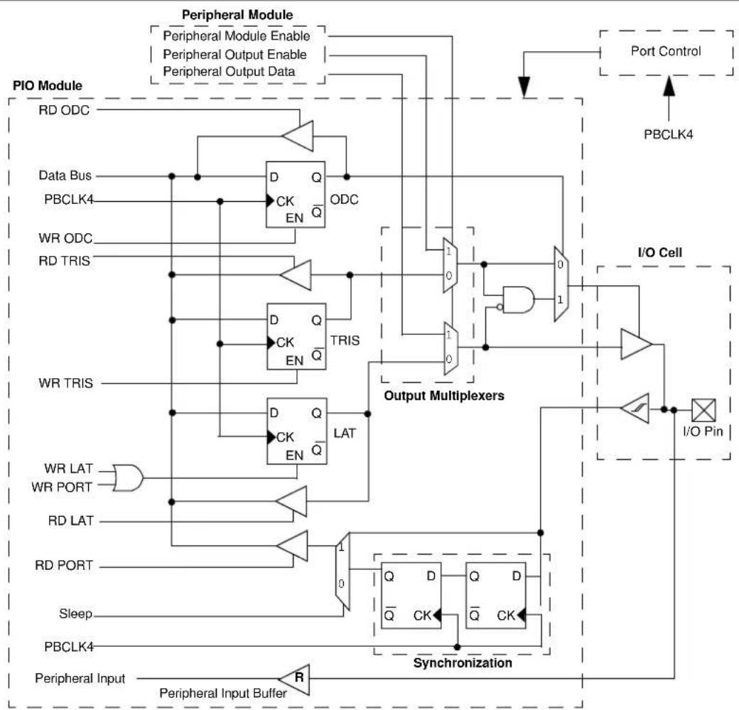
flowchart
graph TD
    A["Peripheral Module"] --> B["Data Bus"]
    A --> C["WR ODC"]
    A --> D["RD TRIS"]
    A --> E["WR TRIS"]
    A --> F["WR LAT"]
    A --> G["WR PORT"]
    A --> H["RD LAT"]
    A --> I["RD PORT"]
    A --> J["Sleep"]
    A --> K["PBCLK4"]
    A --> L["Peripheral Input"]
    L --> M["Peripheral Input Buffer"]
    M --> N["Output Multiplexers"]
    N --> O["I/O Pin"]
    O --> P["Port Control"]
    P --> Q["PBCLK4"]
    N --> R["Q D Q D"]
    N --> S["Q̅ CK"]
    N --> T["Synchronization"]
    T --> U["Output Multiplexers"]
    U --> V["I/O Cell"]
    V --> W["Output Multiplexers"]
    W --> X["Output Multiplexers"]
    X --> Y["I/O Pin"]
    Y --> Z["Output Multiplexers"]
    Z --> AA["Output Multiplexers"]
    AA --> AB["Output Multiplexers"]
    AB --> AC["I/O Pin"]
    AC --> AD["Output Multiplexers"]
    AD --> AE["I/O Pin"]
    AE --> AF["Output Multiplexers"]
    AF --> AG["I/O Pin"]
    AG --> AH["Output Multiplexers"]
    AH --> AI["I/O Pin"]
    AI --> AJ["Output Multiplexers"]
    AJ --> AK["I/O Pin"]
    AK --> AL["Output Multiplexers"]
    AL --> AM["I/O Pin"]
    AM --> AN["Output Multiplexers"]
    AN --> AO["I/O Pin"]
    AO --> AP["Output Multiplexers"]
    AP --> AQ["I/O Pin"]
    AQ --> AR["Output Multiplexers"]
    AR --> AS["I/O Pin"]
    AS --> AT["Output Multiplexers"]
    AT --> AU["I/O Pin"]
    AU --> AV["Output Multiplexers"]
    AV --> AW["I/O Pin"]
    AW --> AX["Output Multiplexers"]
    AX --> AY["I/O Pin"]
    AY --> AZ["Output Multiplexers"]
    AZ --> BA["I/O Pin"]
    BA --> BB["Output Multiplexers"]
    BB --> BC["I/O Pin"]
    BC --> BD["Output Multiplexers"]
    BD --> BE["I/O Pin"]
    BE --> BF["Output Multiplexers"]
    BF --> BG["I/O Pin"]
    BG --> BH["Output Multiplexers"]
    BH --> BI["I/O Pin"]
    BI --> BJ["Output Multiplexers"]
    BJ --> BK["I/O Pin"]
    BK --> BL["Output Multiplexers"]
    BL --> BM["I/O Pin"]
    BM --> BN["Output Multiplexers"]
    BN --> BO["I/O Pin"]
    BO --> BP["Output Multiplexers"]
    BP --> BQ["I/O Pin"]
    BQ --> BR["Output Multiplexers"]
    BR --> BS["I/O Pin"]
    BS --> BT["Output Multiplexers"]
    BT --> BU["I/O Pin"]
    BU --> BV["Output Multiplexers"]
    BV --> BW["I/O Pin"]
    BW --> BX["Output Multiplexers"]
    BX --> BY["I/O Pin"]
    BY --> BZ["Output Multiplexers"]
Legend: R = Peripheral input buffer types may vary. Refer to Table 1-1 for peripheral details. Note: This block diagram is a general representation of a shared port/peripheral structure for illustration purposes only. The actual structure for any specific port/peripheral combination may be different than shown here.
12.1 Parallel I/O (PIO) Ports
All port pins have ten registers directly associated with their operation as digital I/O. The data direction register (TRISx) determines whether the pin is an input or an output. If the data direction bit is a '1', then the pin is an input. All port pins are defined as inputs after a Reset. Reads from the latch (LATx) read the latch. Writes to the latch write the latch. Reads from the port (PORTx) read the port pins, while writes to the port pins write the latch.
12.1.1 OPEN-DRAIN CONFIGURATION
In addition to the PORTx, LATx, and TRISx registers for data control, some port pins can also be individually configured for either digital or open-drain output. This is controlled by the Open-Drain Control register, ODCx, associated with each port. Setting any of the bits configures the corresponding pin to act as an open-drain output.
The open-drain feature allows the generation of outputs higher than VDD (e.g., 5V) on any desired 5V-tolerant pins by using external pull-up resistors. The maximum open-drain voltage allowed is the same as the maximum VIH specification.
Refer to the pin name tables (Table 2 through Table 5) for the available pins and their functionality.
12.1.2 CONFIGURING ANALOG AND DIGITAL PORT PINS
The ANSELx register controls the operation of the analog port pins. The port pins that are to function as analog inputs must have their corresponding ANSEL and TRIS bits set. In order to use port pins for I/O functionality with digital modules, such as Timers, UARTs, etc., the corresponding ANSELx bit must be cleared.
The ANSELx register has a default value of 0xFFFF; therefore, all pins that share analog functions are analog (not digital) by default.
If the TRIS bit is cleared (output) while the ANSELx bit is set, the digital output level (VOH or VOL) is converted by an analog peripheral, such as the ADC module or Comparator module.
When the PORT register is read, all pins configured as analog input channels are read as cleared (a low level).
Pins configured as digital inputs do not convert an analog input. Analog levels on any pin defined as a digital input (including the ANx pins) can cause the input buffer to consume current that exceeds the device specifications.
12.1.3 I/O PORT WRITE/READ TIMING
One instruction cycle is required between a port direction change or port write operation and a read operation of the same port. Typically this instruction would be an NOP.
12.1.4 INPUT CHANGE NOTIFICATION
The input change notification function of the I/O ports allows the PIC32MZ EC devices to generate interrupt requests to the processor in response to a change-of-state on selected input pins. This feature can detect input change-of-states even in Sleep mode, when the clocks are disabled. Every I/O port pin can be selected (enabled) for generating an interrupt request on a change-of-state.
Five control registers are associated with the CN functionality of each I/O port. The CNENx registers contain the CN interrupt enable control bits for each of the input pins. Setting any of these bits enables a CN interrupt for the corresponding pins.
The CNSTATx register indicates whether a change occurred on the corresponding pin since the last read of the PORTx bit.
Each I/O pin also has a weak pull-up and a weak pull-down connected to it. The pull-ups act as a current source or sink source connected to the pin, and eliminate the need for external resistors when push-button or keypad devices are connected. The pull-ups and pull-downs are enabled separately using the CNPUx and the CNPDx registers, which contain the control bits for each of the pins. Setting any of the control bits enables the weak pull-ups and/or pull-downs for the corresponding pins.
Note: Pull-ups and pull-downs on change notification pins should always be disabled when the port pin is configured as a digital output.
An additional control register (CNCONx) is shown in Register 12-3.
12.2 CLR, SET, and INV Registers
Every I/O module register has a corresponding CLR (clear), SET (set) and INV (invert) register designed to provide fast atomic bit manipulations. As the name of the register implies, a value written to a SET, CLR or INV register effectively performs the implied operation, but only on the corresponding base register and only bits specified as '1' are modified. Bits specified as '0' are not modified.
Reading SET, CLR and INV registers returns undefined values. To see the affects of a write operation to a SET, CLR or INV register, the base register must be read.
12.3 Peripheral Pin Select (PPS)
A major challenge in general purpose devices is providing the largest possible set of peripheral features while minimizing the conflict of features on I/O pins. The challenge is even greater on low pin-count devices. In an application where more than one peripheral needs to be assigned to a single pin, inconvenient workarounds in application code or a complete redesign may be the only option.
PPS configuration provides an alternative to these choices by enabling peripheral set selection and their placement on a wide range of I/O pins. By increasing the pinout options available on a particular device, users can better tailor the device to their entire application, rather than trimming the application to fit the device.
The PPS configuration feature operates over a fixed subset of digital I/O pins. Users may independently map the input and/or output of most digital peripherals to these I/O pins. PPS is performed in software and generally does not require the device to be reprogrammed. Hardware safeguards are included that prevent accidental or spurious changes to the peripheral mapping once it has been established.
12.3.1 AVAILABLE PINS
The number of available pins is dependent on the particular device and its pin count. Pins that support the PPS feature include the designation "RPn" in their full pin designation, where "RP" designates a remappable peripheral and "n" is the remappable port number.
12.3.2 AVAILABLE PERIPHERALS
The peripherals managed by the PPS are all digital-only peripherals. These include general serial communications (UART, SPI, and CAN), general purpose timer clock inputs, timer-related peripherals (input capture and output compare), interrupt-on-change inputs, and reference clocks (input and output).
In comparison, some digital-only peripheral modules are never included in the PPS feature. This is because the peripheral's function requires special I/O circuitry on a specific port and cannot be easily connected to multiple pins. These modules include among others. A similar requirement excludes all modules with analog inputs, such as the Analog-to-Digital Converter (ADC).
A key difference between remappable and non-remappable peripherals is that remappable peripherals are not associated with a default I/O pin. The peripheral must always be assigned to a specific I/O pin before it can be used. In contrast, non-remappable peripherals are always available on a default pin, assuming that the peripheral is active and not conflicting with another peripheral.
When a remappable peripheral is active on a given I/O pin, it takes priority over all other digital I/O and digital communication peripherals associated with the pin. Priority is given regardless of the type of peripheral that is mapped. Remappable peripherals never take priority over any analog functions associated with the pin.
12.3.3 CONTROLLING PPS
PPS features are controlled through two sets of SFRs: one to map peripheral inputs, and one to map outputs. Because they are separately controlled, a particular peripheral's input and output (if the peripheral has both) can be placed on any selectable function pin without constraint.
The association of a peripheral to a peripheral-selectable pin is handled in two different ways, depending on whether an input or output is being mapped.
12.3.4 INPUT MAPPING
The inputs of the PPS options are mapped on the basis of the peripheral. That is, a control register associated with a peripheral dictates the pin it will be mapped to. The [pin name]R registers, where [pin name] refers to the peripheral pins listed in Table 12-1, are used to configure peripheral input mapping (see Register 12-1). Each register contains sets of 4 bit fields. Programming these bit fields with an appropriate value maps the RPn pin with the corresponding value to that peripheral. For any given device, the valid range of values for any bit field is shown in Table 12-1.
For example, Figure 12-2 illustrates the remappable pin selection for the U1RX input.
FIGURE 12-2: REMAPPABLE INPUT EXAMPLE FOR U1RX
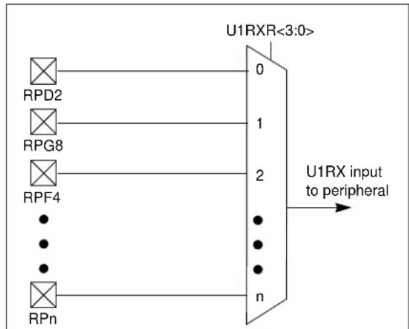
flowchart
graph LR
    A["RPD2"] --> B["U1RXR<3:0>"]
    C["RPG8"] --> B
    D["RPF4"] --> B
    E["..."] --> B
    F["RPn"] --> B
    B --> G["U1RX input to peripheral"]
Note: For input only, PPS functionality does not have priority over TRISx settings. Therefore, when configuring RPn pin for input, the corresponding bit in the TRISx register must also be configured for input (set to '1').
TABLE 12-1: INPUT PIN SELECTION
| Peripheral Pin | [pin name]R SFR | [pin name]R bits | [pin name]R Value to RPn Pin Selection |
| INT3 | INT3R | INT3R<3:0> | 0000 = RPD2 |
| T2CK T2CKR T2CKR<3:0> | 0001 = RPG8 | ||
| T6CK T6CKR T6CKR<3:0> | 0010 = RPF4 | ||
| IC3 IC3R IC3R<3:0> | 0011 = RPD10 | ||
| IC7 IC7R IC7R<3:0> | 0100 = RPF1 | ||
| U1RX U1RXR | U1RXR<3:0> | 0101 = RPB9 | |
| 2CTS | U2CTSR | U2CTSR<3:0> | 0110 = RPB10 |
| U5RX U5RXR | U5RXR<3:0> | 0111 = RPC14 | |
| 6CTS | U6CTSR | U6CTSR<3:0> | 1000 = RPB5 |
| SDI1 | SDI1R | SDI1R<3:0> | 1001 = Reserved |
| SDI3 | SDI3R | SDI3R<3:0> | 1010 = RPC1(1) |
| SDI5^(1) | SDI5R^(1) | SDI5R<3:0>(1) | 1011 = RPD14(1) |
| 6^(1) | SS6R^(1) | SS6R<3:0>(1) | 1100 = RPG1(1) |
| REFCLKI1 | REFCLKI1R | REFCLKI1R<3:0> | 1101 = RPA14(1) |
| 1110 = RPD6(2) | |||
| 1111 = Reserved | |||
| INT4 | INT4R | INT4R<3:0> | 0000 = RPD3 |
| T5CK T5CKR T5CKR<3:0> | 0001 = RPG7 | ||
| T7CK T7CKR T7CKR<3:0> | 0010 = RPF5 | ||
| IC4 IC4R IC4R<3:0> | 0011 = RPD11 | ||
| IC8 IC8R IC8R<3:0> | 0100 = RPF0 | ||
| 0101 = RPB1 | |||
| 0110 = RPE5 | |||
| U3RX U3RXR | U3RXR<3:0> | 0111 = RPC13 | |
| 1000 = RPB3 | |||
| 4CTS | U4CTSR | U4CTSR<3:0> | 1001 = Reserved |
| SDI2 | SDI2R | SDI2R<3:0> | 1010 = RPC4(1) |
| SDI4 | SDI4R | SDI4R<3:0> | 1011 = RPD15(1) |
| C1RX^(3) | C1RXR^(3) | C1RXR<3:0>(3) | 1100 = RPG0(1) |
| REFCLKI4 | REFCLKI4R | REFCLKI4R<3:0> | 1101 = RPA15(1) |
| 1110 = RPD7(2) | |||
| 1111 = Reserved | |||
| INT2 | INT2R | INT2R<3:0> | 0000 = RPD9 |
| T3CK T3CKR T3CKR<3:0> | 0001 = RPG6 | ||
| T8CK T8CKR T8CKR<3:0> | 0010 = RPB8 | ||
| IC2 IC2R IC2R<3:0> | 0011 = RPB15 | ||
| IC5 IC5R IC5R<3:0> | 0100 = RPD4 | ||
| IC9 IC9R IC9R<3:0> | 0101 = RPB0 | ||
| 1CTS | U1CTSR | U1CTSR<3:0> | 0110 = RPE3 |
| 0111 = RPB7 | |||
| U2RX U2RXR | U2RXR<3:0> | 1000 = Reserved | |
| 5CTS | U5CTSR | U5CTSR<3:0> | 1001 = RPF12(1) |
| 1 | SS1R | SS1R<3:0> | 1010 = RPD12(1) |
| 3 | SS3R | SS3R<3:0> | 1011 = RPF8(1) |
| 4 | SS4R | SS4R<3:0> | 1100 = RPC3(1) |
| 5^(1) | SS5R^(1) | SS5R<3:0>(1) | 1101 = RPE9(1) |
| C2RX^(3) | C2RXR^(3) | C2RXR<3:0>(3) | 1110 = Reserved |
| 1111 = Reserved |
Note 1: This selection is not available on 64-pin devices.
2: This selection is not available on 64-pin or 100-pin devices.
3: This selection is not available on devices without a CAN module.
TABLE 12-1: INPUT PIN SELECTION (CONTINUED)
| Peripheral Pin | [pin name]R SFR | [pin name]R bits | [pin name]R Value to RPn Pin Selection |
| INT1 | INT1R | INT1R<3:0> | 0000 = RPD10001 = RPG90010 = RPB140011 = RPD00100 = Reserved0101 = RPB60110 = RPD50111 = RPB21000 = RPF31001 = RPF13(1)1010 = No Connect1011 = RPF2(1)1100 = RPC2(1)1101 = RPE8(1)1110 = Reserved1111 = Reserved |
| T4CK T4CKR T4CKR<3:0> | |||
| T9CK T9CKR T9CKR<3:0> | |||
| IC1 IC1R IC1R<3:0> | |||
| IC6 IC6R IC6R<3:0> | |||
| 3CTS | U3CTSR U3CTSR<3:0> | ||
| U4RX U4RXR U4RXR<3:0> | |||
| U6RX U6RXR U6RXR<3:0> | |||
| 2 | SS2R SS2R<3:0> | ||
| SDI6^(1) | SDI6R^(1) | SDI6R<3:0>(1) | |
| OCFA | OCFAR | OCFAR<3:0> | |
| REFCLKI3 | REFCLKI3R | REFCLKI3R<3:0> |
Note 1: This selection is not available on 64-pin devices.
2: This selection is not available on 64-pin or 100-pin devices.
3: This selection is not available on devices without a CAN module.
12.3.5 OUTPUT MAPPING
In contrast to inputs, the outputs of the PPS options are mapped on the basis of the pin. In this case, a control register associated with a particular pin dictates the peripheral output to be mapped. The RPnR registers (Register 12-2) are used to control output mapping. Like the [pin name]R registers, each register contains sets of 4 bit fields. The value of the bit field corresponds to one of the peripherals, and that peripheral's output is mapped to the pin (see Table 12-2 and Figure 12-3).
A null output is associated with the output register reset value of '0'. This is done to ensure that remappable outputs remain disconnected from all output pins by default.
FIGURE 12-3: EXAMPLE OF
MULTIPLEXING OF
REMAPPABLE OUTPUT
FOR RPF0

text_image
RPF0R<3:0> Default U1TX Output U2RTS Output Output Data REFCLKO1 14 15 RPF012.3.6 CONTROLLING CONFIGURATION CHANGES
Because peripheral remapping can be changed during run time, some restrictions on peripheral remapping are needed to prevent accidental configuration changes. PIC32MZ EC devices include two features to prevent alterations to the peripheral map:
• Control register lock sequence
- Configuration bit select lock
12.3.6.1 Control Register Lock
Under normal operation, writes to the RPnR and [pin name]R registers are not allowed. Attempted writes appear to execute normally, but the contents of the registers remain unchanged. To change these registers, they must be unlocked in hardware. The register lock is controlled by the IOLOCK Configuration bit (CFGCON<13>). Setting IOLOCK prevents writes to the control registers; clearing IOLOCK allows writes.
To set or clear the IOLOCK bit, an unlock sequence must be executed. Refer to Section 42. "Oscillators with Enhanced PLL" (DS60001250) in the "PIC32 Family Reference Manual" for details.
12.3.6.2 Configuration Bit Select Lock
As an additional level of safety, the device can be configured to prevent more than one write session to the RPnR and [pin name]R registers. The IOL1WAY Configuration bit (DEVCFG3<29>) blocks the IOLOCK bit from being cleared after it has been set once. If IOLOCK remains set, the register unlock procedure does not execute, and the PPS control registers cannot be written to. The only way to clear the bit and re-enable peripheral remapping is to perform a device Reset.
In the default (unprogrammed) state, IOL1WAY is set, restricting users to one write session.
TABLE 12-2: OUTPUT PIN SELECTION
| RPn Port Pin RPnR | SFR RPnR bits | RPnR Value to Peripheral Selection | |
| RPD2 RPD2R | RPD2R<3:0> 0000 = No | Connect | |
| RPG8 RPG8R | RPG8R<3:0> | 0001 = U3TX0010 = 4RTS 0011 = Reserved0100 = Reserved0101 = SDO10110 = SDO20111 = SDO31000 = Reserved1001 = SDO5^(1) 1010 = 6^(1) 1011 = OC31100 = OC61101 = REFCLKO41110 = C2OUT1111 = C1TX ^(3) | |
| RPF4 RPF4R | RPF4R<3:0> | ||
| RPD10 RPD10R | RPD10R<3:0> | ||
| RPF1 RPF1R | RPF1R<3:0> | ||
| RPB9 | RPB9R | RPB9R<3:0> | |
| RPB10 | RPB10R | RPB10R<3:0> | |
| RPC14 RPC14R | RPC14R<3:0> | ||
| RPB5 | RPB5R | RPB5R<3:0> | |
| RPC1^(1) | RPC1R^(1) | RPC1R<3:0>(1) | |
| RPD14^(1) | RPD14R^(1) | RPD14R<3:0>(1) | |
| RPG1^(1) | RPG1R^(1) | RPG1R<3:0>(1) | |
| RPA14^(1) | RPA14R^(1) | RPA14R<3:0>(1) | |
| RPD6^(2) | RPD6R^(2) | RPD6R<3:0>(2) | |
| RPD3 RPD3R | RPD3R<3:0> 0000 = No | Connect | |
| RPG7 RPG7R | RPG7R<3:0> | 0001 = U1TX0010 = 2RTS 0011 = U5TX0100 = 6RTS 0101 = SDO10110 = SDO20111 = SDO31000 = SDO41001 = SDO5^(1) 1010 = Reserved1011 = OC41100 = OC71101 = Reserved1110 = Reserved1111 = REFCLKO1 | |
| RPF5 RPF5R | RPF5R<3:0> | ||
| RPD11 | RPD11R | RPD11R<3:0> | |
| RPF0 RPF0R | RPF0R<3:0> | ||
| RPB1 | RPB1R | RPB1R<3:0> | |
| RPE5 | RPE5R | RPE5R<3:0> | |
| RPC13 RPC13R | RPC13R<3:0> | ||
| RPB3 | RPB3R | RPB3R<3:0> | |
| RPC4^(1) | RPC4R^(1) | RPC4R<3:0>(1) | |
| RPD15^(1) | RPD15R^(1) | RPD15R<3:0>(1) | |
| RPG0^(1) | RPG0R^(1) | RPG0R<3:0>(1) | |
| RPA15^(1) | RPA15R^(1) | RPA15R<3:0>(1) | |
| RPD7^(2) | RPD7R^(2) | RPD7R<3:0>(2) | |
| RPD9 RPD9R | RPD9R<3:0> 0000 = No | Connect | |
| RPG6 RPG6R | RPG6R<3:0> | 0001 = 3RTS 0010 = U4TX0011 = Reserved0100 = U6TX0101 = SS10110 = Reserved0111 = SS31000 = SS41001 = 5^(1) 1010 = SDO6^(1) 1011 = OC51100 = OC81101 = Reserved1110 = C1OUT1111 = REFCLKO3 | |
| RPB8 | RPB8R | RPB8R<3:0> | |
| RPB15 | RPB15R | RPB15R<3:0> | |
| RPD4 RPD4R | RPD4R<3:0> | ||
| RPB0 | RPB0R | RPB0R<3:0> | |
| RPE3 | RPE3R | RPE3R<3:0> | |
| RPB7 | RPB7R | RPB7R<3:0> | |
| RPF12^(1) | RPF12R^(1) | RPF12R<3:0>(1) | |
| RPD12^(1) | RPD12R^(1) | RPD12R<3:0>(1) | |
| RPF8^(1) | RPF8R^(1) | RPF8R<3:0>(1) | |
| RPC3^(1) | RPC3R^(1) | RPC3R<3:0>(1) | |
| RPE9^(1) | RPE9R^(1) | RPE9R<3:0>(1) |
Note 1: This selection is not available on 64-pin devices.
2: This selection is not available on 64-pin or 100-pin devices.
3: This selection is not available on devices without a CAN module.
TABLE 12-2: OUTPUT PIN SELECTION (CONTINUED)
| RPn Port Pin | RPnR SFR | RPnR bits | RPnR Value to Peripheral Selection |
| RPD1 RPD1R | RPD1R<3:0> | 0000 = No Connect | |
| RPG9 RPG9R | RPG9R<3:0> | 0001 = U1RTS | |
| RPB14 RPB14R | RPB14R<3:0> | 0010 = U2TX | |
| RPD0 RPD0R | RPD0R<3:0> | 0011 = U5RTS | |
| RPB6 RPB6R | RPB6R<3:0> | 0100 = U6TX | |
| RPD5 RPD5R | RPD5R<3:0> | 0101 = Reserved | |
| RPB2 RPB2R | RPB2R<3:0> | 0110 = SS2 | |
| RPF3 RPF3R | RPF3R<3:0> | 0111 = Reserved | |
| RPF13^(1) | RPF13R^(1) | RPF13R<3:0>(1) | 1000 = SDO4 |
| RPC2^(1) | RPC2R^(1) | RPC2R<3:0>(1) | 1001 = Reserved |
| RPE8^(1) | RPE8R^(1) | RPE8R<3:0>(1) | 1010 = SDO6 ^(1) |
| RPF2^(1) | RPF2R^(1) | RPF2R<3:0>(1) | 1011 = OC2 |
| 1100 = OC1 | |||
| 1101 = OC9 | |||
| 1110 = Reserved | |||
| 1111 = C2TX ^(3) |
Note 1: This selection is not available on 64-pin devices.
2: This selection is not available on 64-pin or 100-pin devices.
3: This selection is not available on devices without a CAN module.
12.4 I/O Ports Control Registers
TABLE 12-3: PORTA REGISTER MAP FOR 100-PIN, 124-PIN, AND 144-PIN DEVICES ONLY
| Virtual Address (BF86_#) | Register Name! | Bit Range | Bits | All Resets | |||||||||||||||
| 31/15 | 30/14 | 29/13 | 28/12 | 27/11 | 26/10 | 25/9 | 24/8 | 23/7 | 22/6 | 21/5 | 20/4 | 19/3 | 18/2 | 17/1 | 16/0 | ||||
| 0000 | ANSELA | 31:16 | ——— | ——— | ——— | ——— | 0000 | ||||||||||||
| 15:0 | — | — | — | — | — | ANSA10 | ANSA9 | — | — | — | ANSA5 | — | — | — | ANSA1 | ANSA0 | 0623 | ||
| 0010 | TRISA | 31:16 | ——— | ——— | ——— | ——— | 0000 | ||||||||||||
| 15:0 | TRISA15 | TRISA14 | — | — | — | TRISA10 | TRISA9 | — | TRISA7 | TRISA6 | TRISA5 | TRISA4 | TRISA3 | TRISA2 | TRISA1 | TRISA0 | C627 | ||
| 0020 | PORTA | 31:16 | ——— | ——— | ——— | ——— | 0000 | ||||||||||||
| 15:0 | RA15 | RA14 | — | — | — | RA10 | RA9 | — | RA7 | RA6 | RA5 | RA4 | RA3 | RA2 | RA1 | RA0 | xxxx | ||
| 0030 | ATA | 31:16 | ——— | ——— | ——— | ——— | 0000 | ||||||||||||
| 15:0 | LATA15 | LATA14 | — | — | — | LATA10 | LATA9 | — | LATA7 | LATA6 | LATA5 | LATA4 | LATA3 | LATA2 | LATA1 | LATA0 | xxxx | ||
| 0040 | ODCA | 31:16 | ——— | ——— | ——— | ——— | 0000 | ||||||||||||
| 15:0 | ODCA15 | ODCA14 | — | — | — | ODCA10 | ODCA9 | — | ODCA7 | ODCA6 | ODCA5 | ODCA4 | ODCA3 | ODCA2 | ODCA1 | ODCA0 | 0000 | ||
| 0050 | CNPUA | 31:16 | ——— | ——— | ——— | ——— | 0000 | ||||||||||||
| 15:0 | CNPUA15 | CNPUA14 | — | — | — | CNPUA10 | CNPUA9 | — | CNPUA7 | CNPUA6 | CNPUA5 | CNPUA4 | CNPUA3 | CNPUA2 | CNPUA1 | CNPUA0 | 0000 | ||
| 0060 | CNPDA | 31:16 | ——— | ——— | ——— | ——— | 0000 | ||||||||||||
| 15:0 | CNPDA15 | CNPDA14 | — | — | — | CNPDA10 | CNPDA9 | — | CNPDA7 | CNPDA6 | CNPDA5 | CNPDA4 | CNPDA3 | CNPDA2 | CNPDA1 | CNPDA0 | 0000 | ||
| 0070 | CNCONA | 31:16 | ——— | ——— | ——— | ——— | 0000 | ||||||||||||
| 15:0 | ON | — | SIDL | — | — | — | — | — | — | — | — | — | — | — | — | — | 0000 | ||
| 0080 | CNENA | 31:16 | — | — | — | — | — | — | — | — | — | — | — | — | — | — | — | — | 0000 |
| 15:0 | CNIEA15 | CNIEA14 | — | — | — | CNIEA10 | CNIEA9 | — | CNIEA7 | CNIEA6 | CNIEA5 | CNIEA4 | CNIEA3 | CNIEA2 | CNIEA1 | CNIEA0 | 0000 | ||
| 0090 | CNSTATA | 31:16 | — | — | — | — | — | — | — | — | — | — | — | — | — | — | — | — | 0000 |
| 15:0 | CN STATA15 | CN STATA14 | ——— | CN STATA10 | CN STATA9 | — | CN STATA7 | CN STATA6 | CN STATA5 | CN STATA4 | CN STATA3 | CN STATA2 | CN STATA1 | CN STATA0 | 0000 | ||||
Legend: x = Unknown value on Reset; — = Unimplemented, read as '0'; Reset values are shown in hexadecimal.
Note 1: All registers in this table have corresponding CLR, SET, and INV registers at its virtual address, plus an offset of 0x4, 0x8 and 0xC, respectively. See Section 12.2 "CLR, SET, and INV Registers" for more information.
TABLE 12-4: PORTB REGISTER MAP
| Virtual Address (BF86 #) | Register Name(1) | Bit Range | Bits | All Resets | ||||||||||||||||
| 31/15 | 30/14 | 29/13 | 28/12 | 27/11 | 26/10 | 25/9 | 24/8 | 23/7 | 22/6 | 21/5 | 20/4 | 19/3 | 18/2 | 17/1 | 16/0 | |||||
| 0100 | ANSELB | 31:16 | — | — | — | — | — | — | — | — | — | — | — | — | — | — | — | — | 0000 | |
| 15:0 | ANSB15 | ANSB14 | ANSB13 | ANSB12 | ANSB11 | ANSB10 | ANSB9 | ANSB8 | ANSB7 | ANSB6 | ANSB5 | ANSB41 | ANSB3 | ANSB2 | ANSB1 | ANSB0 | PPTFF | |||
| 0110 | TRISB | 31:16 | — | — | — | — | — | — | — | — | — | — | — | — | — | — | — | — | 0000 | |
| 15:0 | TRISB15 | TRISB14 | TRISB13 | TRISB12 | TRISB11 | TRISB10 | TRISB9 | TRISB8 | TRISB7 | TRISB6 | TRISB5 | TRISB4 | TRISB3 | TRISB2 | TRISB1 | TRISB0 | PPTFF | |||
| 0120 | PORTB | 31:16 | — | — | — | — | — | — | — | — | — | — | — | — | — | — | — | — | 0000 | |
| 15:0 | RB15 | RB14 | RB13 | RB12 | RB11 | RB10 | RB9 | RB8 | RB7 | RB6 | RB5 | RB4 | RB3 | RB2 | RB1 | RB0 | xxxx | |||
| 0130 | LATB | 31:16 | — | — | — | — | — | — | — | — | — | — | — | — | — | — | — | — | 0000 | |
| 15:0 | LATB15 | LATB14 | LATB13 | LATB12 | LATB11 | LATB10 | LATB9 | LATB8 | LATB7 | LATB6 | LATB5 | LATB4 | LATB3 | LATB2 | LATB1 | LATB0 | xxxx | |||
| 0140 | ODCB | 31:16 | — | — | — | — | — | — | — | — | — | — | — | — | — | — | — | — | 0000 | |
| 15:0 | ODCB15 | ODCB14 | ODCB13 | ODCB12 | ODCB11 | ODCB10 | ODCB9 | ODCB8 | ODCB7 | ODCB6 | ODCB5 | ODCB4 | ODCB3 | ODCB2 | ODCB1 | ODCB0 | 0000 | |||
| 0150 | CNPUB | 31:16 | — | — | — | — | — | — | — | — | — | — | — | — | — | — | — | — | 0000 | |
| 15:0 | CNPUB15 | CNPUB14 | CNPUB13 | CNPUB12 | CNPUB11 | CNPUB10 | CNPUB9 | CNPUB8 | CNPUB7 | CNPUB6 | CNPUB5 | CNPUB4 | CNPUB3 | CNPUB2 | CNPUB1 | CNPUB0 | 0000 | |||
| 0160 | CNPDB | 31:16 | — | — | — | — | — | — | — | — | — | — | — | — | — | — | — | — | 0000 | |
| 15:0 | CNPDB15 | CNPDB14 | CNPDB13 | CNPDB12 | CNPDB11 | CNPDB10 | CNPDB9 | CNPDB8 | CNPDB7 | CNPDB6 | CNPDB5 | CNPDB4 | CNPDB3 | CNPDB2 | CNPDB1 | CNPDB0 | 0000 | |||
| 0170 | CNCONB | 31:16 | — | — | — | — | — | — | — | — | — | — | — | — | — | — | — | — | 0000 | |
| 15:0 | ON | — | SIDL | — | — | — | — | — | — | — | — | — | — | — | — | — | 0000 | |||
| 0180 | CNENB | 31:16 | — | — | — | — | — | — | — | — | — | — | — | — | — | — | — | — | 0000 | |
| 15:0 | CNIEB15 | CNIEB14 | CNIEB13 | CNIEB12 | CNIEB11 | CNIEB10 | CNIEB9 | CNIEB8 | CNIEB7 | CNIEB6 | CNIEB5 | CNIEB4 | CNIEB3 | CNIEB2 | CNIEB1 | CNIEB0 | 0000 | |||
| 0190 | CNSTATE | 31:16 | — | — | — | — | — | — | — | — | — | — | — | — | — | — | — | — | 0000 | |
| 15:0 | CN STATB15 | CN STATB14 | CN STATB13 | CN STATB12 | CN STATB11 | CN STATB10 | CN STATB9 | CN STATB8 | CN STATB7 | CN STATB6 | CN STATB5 | CN STATB4 | CN STATB3 | CN STATB2 | CN STATB1 | CN STATB0 | 0000 | |||
Legend: x = Unknown value on Reset; — = Unimplemented, read as 'c'; Reset values are shown in hexadecimal.
Note 1: All registers in this table have corresponding CLR, SET, and INV registers at its virtual address, plus an offset of 0x4, 0x8 and 0xC, respectively. See Section 12.2 "CLR, SET, and INV Registers" for more information.
TABLE 12-5: PORTC REGISTER MAP FOR 100-PIN, 124-PIN, AND 144-PIN DEVICES ONLY
Legend: x = Unknown value on Reset; — = Unimplemented, read as '0'; Reset values are shown in hexadecimal.
Note 1: All registers in this table have corresponding CLR, SET, and INV registers at its virtual address, plus an offset of 0x4, 0x8 and 0xC, respectively. See Section 12.2 "CLR, SET, and INV Registers" for more information.
TABLE 12-6: PORTC REGISTER MAP FOR 64-PIN DEVICES ONLY
Legend: x = Unknown value on Reset; — = Unimplemented, read as '0'; Reset values are shown in hexadecimal. Note 1: All registers in this table have corresponding CLR, SET, and INV registers at its virtual address, plus an offset of 0x4, 0x8 and 0xC, respectively. See Section 12.2 "CLR, SET, and INV Registers" for more information.
TABLE 12-7: PORTD REGISTER MAP FOR 124-PIN AND 144-PIN DEVICES ONLY
Legend: x = Unknown value on Reset; — = Unimplemented, read as "0"; Reset values are shown in hexadecimal. Note 1: All registers in this table have corresponding CLR, SET, and INV registers at its virtual address, plus an offset of 0x4, 0x8 and 0xC, respectively. See Section 12.2 "CLR, SET, and INV Registers" for more information.
TABLE 12-8: PORTD REGISTER MAP FOR 100-PIN DEVICES ONLY
Legend: x = Unknown value on Reset; — = Unimplemented, read as '0'; Reset values are shown in hexadecimal.
Note 1: All registers in this table have corresponding CLR, SET, and INV registers at its virtual address, plus an offset of 0x4, 0x8 and 0xC, respectively. See Section 12.2 "CLR, SET, and INV Registers" for more information.
TABLE 12-9: PORTD REGISTER MAP FOR 64-PIN DEVICES ONLY
Legend: x = Unknown value on Reset; — = Unimplemented, read as '0'; Reset values are shown in hexadecimal.
Note 1: All registers in this table have corresponding CLR, SET, and INV registers at its virtual address, plus an offset of 0x4, 0x8 and 0xC, respectively. See Section 12.2 "CLR, SET, and INV Registers" for more information.
TABLE 12-10: PORTE REGISTER MAP FOR 100-PIN, 124-PIN, AND 144-PIN DEVICES ONLY
Legend: x = Unknown value on Reset; — = Unimplemented, read as '0'; Reset values are shown in hexadecimal. Note 1: All registers in this table have corresponding CLR, SET, and INV registers at its virtual address, plus an offset of 0x4, 0x8 and 0xC, respectively. See Section 12.2 "CLR, SET, and INV Registers" for more information.
TABLE 12-11: PORTE REGISTER MAP FOR 64-PIN DEVICES ONLY
Legend: x = Unknown value on Reset; — = Unimplemented, read as °0; Reset values are shown in hexadecimal. Note 1: All registers in this table have corresponding CLR, SET, and INV registers at its virtual address, plus an offset of 0x4, 0x8 and 0xC, respectively. See Section 12.2 "CLR, SET, and INV Registers" for more information.
TABLE 12-12: PORTF REGISTER MAP FOR 100-PIN, 124-PIN, AND 144-PIN DEVICES ONLY
Legend: x = Unknown value on Reset; — = Unimplemented, read as '0'; Reset values are shown in hexadecimal.
Note 1: All registers in this table have corresponding CLR, SET, and INV registers at its virtual address, plus an offset of 0x4, 0x8 and 0xC, respectively. See Section 12.2 "CLR, SET, and INV Registers" for more information.
TABLE 12-13: PORTF REGISTER MAP FOR 64-PIN DEVICES ONLY
Legend: x = Unknown value on Reset; — = Unimplemented, read as '0'; Reset values are shown in hexadecimal.
Note 1: All registers in this table have corresponding CLR, SET, and INV registers at its virtual address, plus an offset of 0x4, 0x8 and 0xC, respectively. See Section 12.2 "CLR, SET, and INV Registers" for more information.
TABLE 12-14: PORTG REGISTER MAP FOR 100-PIN, 124-PIN, AND 144-PIN DEVICES ONLY
Legend: x = Unknown value on Reset; — = Unimplemented, read as '0'; Reset values are shown in hexadecimal. Note 1: All registers in this table have corresponding CLR, SET, and INV registers at its virtual address, plus an offset of 0x4, 0x8, and 0xC, respectively. See Section 12.2 "CLR, SET, and INV Registers" for more information.
TABLE 12-15: PORTG REGISTER MAP FOR 64-PIN DEVICES ONLY
Legend: x = Unknown value on Reset; — = Unimplemented, read as 00; Reset values are shown in hexadecimal. Note 1: All registers in this table have corresponding CLR, SET, and INV registers at its virtual address, plus an offset of 0x4, 0x8 and 0xC, respectively. See Section 12.2 "CLR, SET, and INV Registers" for more information.
TABLE 12-16: PORTH REGISTER MAP FOR 124-PIN DEVICES ONLY
Legend: x = Unknown value on Reset; — = Unimplemented, read as 'c'; Reset values are shown in hexadecimal. Note 1: All registers in this table have corresponding CLR, SET, and INV registers at its virtual address, plus an offset of 0x4, 0x8, and 0xC, respectively. See Section 12.2 "CLR, SET, and INV Registers" for more information.
TABLE 12-17: PORTH REGISTER MAP FOR 144-PIN DEVICES ONLY
| Virtual Address (BF66_#) | Register Name(1) | Bit Range | Bits | All Resets | |||||||||||||||
| 31/15 | 30/14 | 29/13 | 28/12 | 27/11 | 26/10 | 25/9 | 24/8 | 23/7 | 22/6 | 21/5 | 20/4 | 19/3 | 18/2 | 17/1 | 16/0 | ||||
| 0700 | ANSELH | 31:16 | — | — | — | — | — | — | — | — | — | — | — | — | — | — | — | — | 0000 |
| 15:0 | — | — | — | — | — | — | — | — | — | ANSH6 | ANSH5 | ANSH4 | — | — | ANSH1 | ANSH0 | 0073 | ||
| 0710 | TRISH | 31:16 | — | — | — | — | — | — | — | — | — | — | — | — | — | — | — | — | 0000 |
| 15:0 | TRISH15 | TRISH14 | TRISH13 | TRISH12 | TRISH11 | TRISH10 | TRISH9 | TRISH8 | TRISH7 | TRISH6 | TRISH5 | TRISH4 | TRISH3 | TRISH2 | TRISH1 | TRISH0 | PFFT | ||
| 0720 | PORTH | 31:16 | — | — | — | — | — | — | — | — | — | — | — | — | — | — | — | — | 0000 |
| 15:0 | RH15 | RH14 | RH13 | RH12 | RH11 | RH10 | RH9 | RH8 | RH7 | RH6 | RH5 | RH4 | RH3 | RH2 | RH1 | RH0 | xxxxx | ||
| 0730 | LATH | 31:16 | — | — | — | — | — | — | — | — | — | — | — | — | — | — | — | — | 0000 |
| 15:0 | LATH15 | LATH14 | LATH13 | LATH12 | LATH11 | LATH10 | LATH9 | LATH8 | LATH7 | LATH6 | LATH5 | LATH4 | LATH3 | LATH2 | LATH1 | LATH0 | xxxxx | ||
| 0740 | ODCH | 31:16 | — | — | — | — | — | — | — | — | — | — | — | — | — | — | — | — | 0000 |
| 15:0 | ODCH15 | ODCH14 | ODCH13 | ODCH12 | ODCH11 | ODCH10 | ODCH9 | ODCH8 | ODCH7 | ODCH6 | ODCH5 | ODCH4 | ODCH3 | ODCH2 | ODCH1 | ODCH0 | 0000 | ||
| 0750 | CNPUH | 31:16 | — | — | — | — | — | — | — | — | — | — | — | — | — | — | — | — | 0000 |
| 15:0 | CNPUH15 | CNPUH14 | CNPUH13 | CNPUH12 | CNPUH11 | CNPUH10 | CNPUH9 | CNPUH8 | CNPUH7 | CNPUH6 | CNPUH5 | CNPUH4 | CNPUH3 | CNPUH2 | CNPUH1 | CNPUH0 | 0000 | ||
| 0760 | CNPDH | 31:16 | — | — | — | — | — | — | — | — | — | — | — | — | — | — | — | — | 0000 |
| 15:0 | CNPDH15 | CNPDH14 | CNPDH13 | CNPDH12 | CNPDH11 | CNPDH10 | CNPDH9 | CNPDH8 | CNPDH7 | CNPDH6 | CNPDH5 | CNPDH4 | CNPDH3 | CNPDH2 | CNPDH1 | CNPDH0 | 0000 | ||
| 0770 | CNCONH | 31:16 | — | — | — | — | — | — | — | — | — | — | — | — | — | — | — | — | 0000 |
| 15:0 | ON | — | SIDL | — | — | — | — | — | — | — | — | — | — | — | — | — | 0000 | ||
| 0780 | CNENH | 31:16 | — | — | — | — | — | — | — | — | — | — | — | — | — | — | — | — | 0000 |
| 15:0 | CNIEH15 | CNIEH14 | CNIEH13 | CNIEH12 | CNIEH11 | CNIEH10 | CNIEH9 | CNIEH8 | CNIEH7 | CNIEH6 | CNIEH5 | CNIEH4 | CNIEH3 | CNIEH2 | CNIEH1 | CNIEH0 | 0000 | ||
| 0790 | CNSTATH | 31:16 | — | — | — | — | — | — | — | — | — | — | — | — | — | — | — | — | 0000 |
| 15:0 | CNSTATH15 | CNSTATH14 | CNSTATH13 | CNSTATH12 | CNSTATH11 | CNSTATH10 | CNSTATH9 | CNSTATH8 | CNSTATH7 | CNSTATH6 | CNSTATH5 | CNSTATH4 | CNSTATH3 | CNSTATH2 | CNSTATH1 | CNSTATH0 | 0000 | ||
Legend: x = Unknown value on Reset; — = Unimplemented, read as '0'; Reset values are shown in hexadecimal. Note 1: All registers in this table have corresponding CLR, SET, and INV registers at its virtual address, plus an offset of 0x4, 0x8, and 0xC, respectively. See Section 12.2 "CLR, SET, and INV Registers" for more information.
TABLE 12-18: PORTJ REGISTER MAP FOR 124-PIN DEVICES ONLY
Legend: x = Unknown value on Reset; — = Unimplemented, read as '0'; Reset values are shown in hexadecimal. Note 1: All registers in this table have corresponding CLR, SET, and INV registers at its virtual address, plus an offset of 0x4, 0x8, and 0xC, respectively. See Section 12.2 "CLR, SET, and INV Registers" for more information.
TABLE 12-19: PORTJ REGISTER MAP FOR 144-PIN DEVICES ONLY
Legend: x = Unknown value on Reset; — = Unimplemented, read as '0'; Reset values are shown in hexadecimal. Note 1: All registers in this table have corresponding CLR, SET, and INV registers at its virtual address, plus an offset of 0x4, 0x8, and 0xC, respectively. See Section 12.2 "CLR, SET, and INV Registers" for more information.
TABLE 12-20: PORTK REGISTER MAP FOR 144-PIN DEVICES ONLY
Legend: x = Unknown value on Reset; — = Unimplemented, read as '0'; Reset values are shown in hexadecimal. Note 1: All registers in this table have corresponding CLR, SET, and INV registers at its virtual address, plus an offset of 0x4, 0x8, and 0xC, respectively. See Section 12.2 "CLR, SET, and INV Registers" for more information.
TABLE 12-21: PERIPHERAL PIN SELECT INPUT REGISTER MAP
Legend: x = unknown value on Reset; — = unimplemented, read as '0'. Reset values are shown in hexadecimal.
Note 1: This register is not available on 64-pin devices.
2: This register is not available on devices without a CAN module.
TABLE 12-21: PERIPHERAL PIN SELECT INPUT REGISTER MAP (CONTINUED)
Legend: x = unknown value on Reset; — = unimplemented, read as '0'. Reset values are shown in hexadecimal.
1: This register is not available on 64-pin devices
2: This register is not available on devices without a CAN module.
TABLE 12-21: PERIPHERAL PIN SELECT INPUT REGISTER MAP (CONTINUED)
Legend: x = unknown value on Reset; — = unimplemented, read as '0'. Reset values are shown in hexadecimal.
Note 1: This register is not available on 64-pin devices.
2: This register is not available on devices without a CAN module.
TABLE 12-21: PERIPHERAL PIN SELECT INPUT REGISTER MAP (CONTINUED)
| Virtual Address (BF80 #) | Register Name | Bit Range | Bits | All Resets | ||||||||||||||||
| 31/15 | 30/14 | 29/13 | 28/12 | 27/11 | 26/10 | 25/9 | 24/8 | 23/7 | 22/6 | 21/5 | 20/4 | 19/3 | 18/2 | 17/1 | 16/0 | |||||
| 14DC | SS6R (1) | 31:16 | —— | —— | —— | —— | — | 0000 | ||||||||||||
| 15:0 | —— | —— | —— | —— | — | SS6R<3:0>0000 | ||||||||||||||
| 14E0 | C1RXR (2) | 31:16 | —— | —— | —— | —— | —— | 0000 | ||||||||||||
| 15:0 | —— | —— | —— | —— | C | 1 | R | X | R | < | ||||||||||
| 14E4 | C2RXR (2) | 31:16 | —— | —— | —— | —— | —— | 0000 | ||||||||||||
| 15:0 | —— | —— | —— | —— | C | 2 | R | X | R | < | ||||||||||
| 14E8 | REFCLKI1R | 31:16 | —— | —— | —— | —— | —— | 0000 | ||||||||||||
| 15:0 | — | — | — | — | — | — | — | — | — | — | — | — | — | REFCLKI1R<3:0> | 0000 | |||||
| 14F0 | REFCLKI3R | 31:16 | —— | —— | —— | —— | —— | 0000 | ||||||||||||
| 15:0 | — | — | — | — | — | — | — | — | — | — | — | — | — | REFCLKI3R<3:0> | 0000 | |||||
| 14F4 | REFCLKI4R | 31:16 | —— | —— | —— | —— | —— | 0000 | ||||||||||||
| 15:0 | — | — | — | — | — | — | — | — | — | — | — | — | — | REFCLKI4R<3:0> | 0000 | |||||
Legend: x = unknown value on Reset; — = unimplemented, read as '0'. Reset values are shown in hexadecimal.
Note 1: This register is not available on 64-pin devices.
2: This register is not available on devices without a CAN module.
TABLE 12-22: PERIPHERAL PIN SELECT OUTPUT REGISTER MAP
Legend: x = unknown value on Reset; — = unimplemented, read as '0'. Reset values are shown in hexadecimal.
Note 1: This register is not available on 64-pin devices.
2: This register is not available on 64-pin and 100-pin devices.
TABLE 12-22: PERIPHERAL PIN SELECT OUTPUT REGISTER MAP (CONTINUED)
Legend: x = unknown value on Reset; — = unimplemented, read as 'D'. Reset values are shown in hexadecimal.
1: This register is not available on 64-pin devices.
2: This register is not available on 64-pin and 100-pin devices.
TABLE 12-22: PERIPHERAL PIN SELECT OUTPUT REGISTER MAP (CONTINUED)
Legend: x = unknown value on Reset; — = unimplemented, read as '0'. Reset values are shown in hexadecimal.
Note 1: This register is not available on 64-pin devices.
2: This register is not available on 64-pin and 100-pin devices.
REGISTER 12-1: [pin name]R: PERIPHERAL PIN SELECT INPUT REGISTER
| Bit Range | Bit 31/23/15/7 | Bit 30/22/14/6 | Bit 29/21/13/5 | Bit 28/20/12/4 | Bit 27/19/11/3 | Bit 26/18/10/2 | Bit 25/17/9/1 | Bit 24/16/8/0 |
| 31:24 | U-0 U-0 U-0 | U-0 U-0 U-0 U-0 | U-0 | |||||
| — — — | — — — | — | — | |||||
| 23:16 | U-0 U-0 U-0 | U-0 U-0 U-0 U-0 | U-0 | |||||
| — — — | — — — | — | — | |||||
| 15:8 | U-0 U-0 U-0 | U-0 U-0 U-0 U-0 | U-0 | |||||
| — — — | — — — | — | — | |||||
| 7:0 | U-0 | U-0 | U-0 | U-0 | R/W-0 | R/W-0 | R/W-0 | R/W-0 |
| — | — | — | — | [pin name]R<3:0> | ||||
Legend:
| R = Readable bit | W = Writable bit U = Unimplemented bit, read as '0' | ||
| -n = Value at POR | '1' = Bit is set | '0' = Bit is cleared | x = Bit is unknown |
bit 31-4 Unimplemented: Read as '0'
bit 3-0 [pin name]R<3:0>: Peripheral Pin Select Input bits
Where [pin name] refers to the pins that are used to configure peripheral input mapping. See Table 12-1 for input pin selection values.
Note: Register values can only be changed if the IOLOCK Configuration bit (CFGCON<13>) = 0.
REGISTER 12-2: RPnR: PERIPHERAL PIN SELECT OUTPUT REGISTER
| Bit Range | Bit 31/23/15/7 | Bit 30/22/14/6 | Bit 29/21/13/5 | Bit 28/20/12/4 | Bit 27/19/11/3 | Bit 26/18/10/2 | Bit 25/17/9/1 | Bit 24/16/8/0 |
| 31:24 | U-0 U-0 U-0 | U-0 U-0 U-0 U-0 | U-0 | |||||
| — — — | — — — | — | — | |||||
| 23:16 | U-0 U-0 U-0 | U-0 U-0 U-0 U-0 | U-0 | |||||
| — — — | — — — | — | — | |||||
| 15:8 | U-0 U-0 U-0 | U-0 U-0 U-0 U-0 | U-0 | |||||
| — — — | — — — | — | — | |||||
| 7:0 | U-0 | U-0 | U-0 | U-0 | R/W-0 | R/W-0 | R/W-0 | R/W-0 |
| — — — | — | RPnR<3:0> | ||||||
Legend:
| R = Readable bit | W = Writable bit U = Unimplemented bit, read as '0' | ||
| -n = Value at POR | '1' = Bit is set | '0' = Bit is cleared | x = Bit is unknown |
bit 31-4 Unimplemented: Read as '0'
bit 3-0 RPnR<3:0>: Peripheral Pin Select Output bits
See Table 12-2 for output pin selection values.
Note: Register values can only be changed if the IOLOCK Configuration bit (CFGCON<13>) = 0.
REGISTER 12-3: CNCONx: CHANGE NOTICE CONTROL FOR PORTx REGISTER (x = A - G)
| Bit Range | Bit 31/23/15/7 | Bit 30/22/14/6 | Bit 29/21/13/5 | Bit 28/20/12/4 | Bit 27/19/11/3 | Bit 26/18/10/2 | Bit 25/17/9/1 | Bit 24/16/8/0 |
| 31:24 | U-0 U-0 U-0 | U-0 U-0 U-0 U-0 | U-0 | |||||
| — — — | — — — | — | — | |||||
| 23:16 | U-0 U-0 U-0 | U-0 U-0 U-0 U-0 | U-0 | |||||
| — — — | — — — | — | — | |||||
| 15:8 | R/W-0 | U-0 | R/W-0 | U-0 U-0 U-0 | U-0 U-0 | |||
| ON | — | SIDL | — | — | — | — | — | |
| 7:0 | U-0 U-0 U-0 | U-0 U-0 U-0 U-0 | U-0 | |||||
| — — — | — — — | — | — |
Legend:
| R = Readable bit | W = Writable bit U = Unimplemented bit, read as ‘0’ | ||
| -n = Value at POR | ‘1’ = Bit is set | ‘0’ = Bit is cleared | x = Bit is unknown |
bit 31-16 Unimplemented: Read as '0'
bit 15 ON: Change Notice (CN) Control ON bit
1 = CN is enabled
0 = CN is disabled
bit 14 Unimplemented: Read as '0'
bit 13 SIDL: Stop in Idle Control bit
1 = CPU Idle mode halts CN operation
0 = CPU Idle mode does not affect CN operation
bit 12-0 Unimplemented: Read as '0'
NOTES:
13.0 TIMER1
Note: This data sheet summarizes the features of the PIC32MZ Embedded Connectivity (EC) Family of devices. It is not intended to be a comprehensive reference source. To complement the information in this data sheet, refer to Section 14. “Timers” (DS60001105), which is available from the Documentation > Reference Manual section of the Microchip PIC32 web site (www.microchip.com/pic32).
PIC32MZ EC devices feature one synchronous/asynchronous 16-bit timer that can operate as a free-running interval timer for various timing applications and counting external events. This timer can also be used with the Low-Power Secondary Oscillator (SOSC) for real-time clock applications.
The following modes are supported by Timer1:
• Synchronous Internal Timer
- Synchronous Internal Gated Timer
• Synchronous External Timer
- Asynchronous External Timer
13.1 Additional Supported Features
- Selectable clock prescaler
- Timer operation during Sleep and Idle modes
- Fast bit manipulation using CLR, SET, and INV registers
- Asynchronous mode can be used with the S osc to function as a real-time clock
- ADC event trigger
FIGURE 13-1: TIMER1 BLOCK DIAGRAM

flowchart
graph TD
    A["Trigger to ADC"] --> B["Equal"]
    B --> C["PR1"]
    C --> D["16-bit Comparator"]
    D --> E["TMR1"]
    E --> F["TSYNC"]
    F --> G["Sync"]
    G --> H["T1IF Event Flag"]
    H --> I["TGATE"]
    I --> J["Q"]
    J --> K["D"]
    K --> L["TGATE"]
    L --> M["TCS"]
    M --> N["ON"]
    N --> O["Prescaler 1, 8, 64, 256"]
    O --> P["TCKPS<1:0>"]
    Q["SOSCO/T1CK"] --> R["SOSCEN(1)"]
    S["SOSCI"] --> T["SOSCEN(1)"]
    R --> U["Gate Sync"]
    T --> V["Gate Sync"]
    U --> W["PBCLK3"]
    V --> X["AND Gate"]
    W --> Y["x 1"]
    X --> Z["x 1"]
    Y --> AA["0 0"]
    Z --> AB["0 0"]
Note 1: The default state of the SOSCEN bit (OSCCON<1>) during a device Reset is controlled by the FSOSCEN bit in Configuration Word, DEVCFG1.
13.2 Timer1 Control Register
TABLE 13-1: TIMER1 REGISTER MAP
| Virtual Address(BF84 #) | Register Name(1) | Bit Range | Bits | All Resets | |||||||||||||||
| 31/15 | 30/14 | 29/13 | 28/12 | 27/11 | 26/10 | 25/9 | 24/8 | 23/7 | 22/6 | 21/5 | 20/4 | 19/3 | 18/2 | 17/1 | 16/0 | ||||
| 0000 | T1CON | 31:16 | —— | —— | —— | —— | 0000 | ||||||||||||
| 15:0 | ON | — | SIDL | TWDIS | TWIP | — | — | — | TGATE | — | TCKPS<1:0> | — | TSYNC | TCS | — | 0000 | |||
| 0010 | TMR1 | 31:16 | —— | —— | —— | —— | 0000 | ||||||||||||
| 15:0 | TMR1<15:0> | 0000 | |||||||||||||||||
| 0020 | PR1 | 31:16 | —— | —— | —— | —— | 0000 | ||||||||||||
| 15:0 | PR1<15:0> | FFFF | |||||||||||||||||
Legend: x = unknown value on Reset; — = unimplemented, read as '0'. Reset values are shown in hexadecimal.
Note 1: All registers in this table have corresponding CLR, SET, and INV registers at their virtual addresses, plus offsets of 0x4, 0x8 and 0xC, respectively. See Section 12.2 "CLR, SET, and INV Registers" for more information.
REGISTER 13-1: T1CON: TYPE A TIMER CONTROL REGISTER
| Bit Range | Bit 31/23/15/7 | Bit 30/22/14/6 | Bit 29/21/13/5 | Bit 28/20/12/4 | Bit 27/19/11/3 | Bit 26/18/10/2 | Bit 25/17/9/1 | Bit 24/16/8/0 |
| 31:24 | U-0 U-0 U-0 | U-0 U-0 U-0 U-0 | U-0 | |||||
| — — — | — — — — — | |||||||
| 23:16 | U-0 U-0 U-0 | U-0 U-0 U-0 U-0 | U-0 | |||||
| — — — | — — — — — | |||||||
| 15:8 | R/W-0 | U-0 | R/W-0 | R/W-0 | R-0 | U-0 | U-0 | U-0 |
| ON | — | SIDL | TWDIS | TWIP | — | — | — | |
| 7:0 | R/W-0 | U-0 | R/W-0 | R/W-0 | U-0 | R/W-0 | R/W-0 | U-0 |
| TGATE | — | TCKPS<1:0> | — | TSYNC | TCS | — | ||
Legend:
| R = Readable bit | W = Writable bit | U = Unimplemented bit, read as '0' |
| -n = Value at POR | '1' = Bit is set | '0' = Bit is cleared x = Bit is unknown |
bit 31-16 Unimplemented: Read as '0'
bit 15 ON: Timer On bit
1 = Timer is enabled
0 = Timer is disabled
bit 14 Unimplemented: Read as '0'
bit 13 SIDL: Stop in Idle Mode bit
1 = Discontinue operation when device enters Idle mode
0 = Continue operation even in Idle mode
bit 12 TWDIS: Asynchronous Timer Write Disable bit
1 = Writes to TMR1 are ignored until pending write operation completes
0 = Back-to-back writes are enabled (Legacy Asynchronous Timer functionality)
bit 11 TWIP: Asynchronous Timer Write in Progress bit
In Asynchronous Timer mode:
1 = Asynchronous write to TMR1 register in progress
0 = Asynchronous write to TMR1 register complete
In Synchronous Timer mode:
This bit is read as '0'.
bit 10-8 Unimplemented: Read as '0'
bit 7 TGATE: Timer Gated Time Accumulation Enable bit
When TCS = 1:
This bit is ignored.
When TCS = 0:
1 = Gated time accumulation is enabled
0 = Gated time accumulation is disabled
bit 6 Unimplemented: Read as '0'
bit 5-4 TCKPS<1:0>: Timer Input Clock Prescale Select bits
11 = 1:256 prescale value
10 = 1:64 prescale value
01 = 1:8 prescale value
00 = 1:1 prescale value
bit 3 Unimplemented: Read as '0'
REGISTER 13-1: T1CON: TYPE A TIMER CONTROL REGISTER (CONTINUED)
bit 2 TSYNC: Timer External Clock Input Synchronization Selection bit
When TCS = 1:
1 = External clock input is synchronized
0 = External clock input is not synchronized
When TCS = 0:
This bit is ignored.
bit 1 TCS: Timer Clock Source Select bit
1 = External clock from T1CKI pin
0 = Internal peripheral clock
bit 0 Unimplemented: Read as '0'
14.0 TIMER2/3, TIMER4/5, TIMER6/7, AND TIMER8/9
Note: This data sheet summarizes the features of the PIC32MZ Embedded Connectivity (EC) Family of devices. It is not intended to be a comprehensive reference source. To complement the information in this data sheet, refer to Section 14. "Timers" (DS60001105), which is available from the Documentation > Reference Manual section of the Microchip PIC32 web site (www.microchip.com/pic32).
This family of devices features eight synchronous 16-bit timers (default) that can operate as a free-running interval timer for various timing applications and counting external events.
The following modes are supported:
- Synchronous internal 16-bit timer
- Synchronous internal 16-bit gated timer
- Synchronous external 16-bit timer
Four 32-bit synchronous timers are available by combining Timer2 with Timer3, Timer4 with Timer5, Timer6 with Timer7, and Timer8 with Timer9.
The 32-bit timers can operate in one of three modes:
- Synchronous internal 32-bit timer
- Synchronous internal 32-bit gated timer
- Synchronous external 32-bit timer
14.1 Additional Features
- Selectable clock prescaler
- Timers operational during CPU idle
- Time base for Input Capture and Output Compare modules (Timer2 through Timer7 only)
- ADC event trigger (Timer3 and Timer5 only)
- Fast bit manipulation using CLR, SET, and INV registers
FIGURE 14-1: TIMER2 THROUGH TIMER9 BLOCK DIAGRAM (16-BIT)
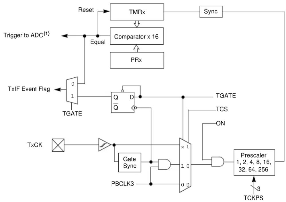
flowchart
graph TD
    A["Trigger to ADC(1)"] --> B["Equal"]
    B --> C["TMRx"]
    C --> D["Comparator x 16"]
    D --> E["PRx"]
    E --> F["Sync"]
    F --> G["Prescaler 1, 2, 4, 8, 16, 32, 64, 256"]
    G --> H["TCKPS"]
    I["TxIF Event Flag"] --> J["0/1 TGATE"]
    J --> K["Q/Q̅"]
    K --> L["x 1"]
    L --> M["Gate Sync"]
    M --> N["PBCLK3"]
    N --> O["x 1"]
    O --> P["TGATE"]
    Q["TxCK"] --> R["×"]
    R --> S["Gate Sync"]
    S --> T["x 1"]
    T --> U["TCS"]
    U --> V["ON"]
    V --> W["Prescaler"]
    X["Reset"] --> C
Note 1: The ADC event trigger is available on Timer3 and Timer5 only.
FIGURE 14-2: TIMER2/3, TIMER4/5, TIMER6/7, AND TIMER8/9 BLOCK DIAGRAM (32-BIT)
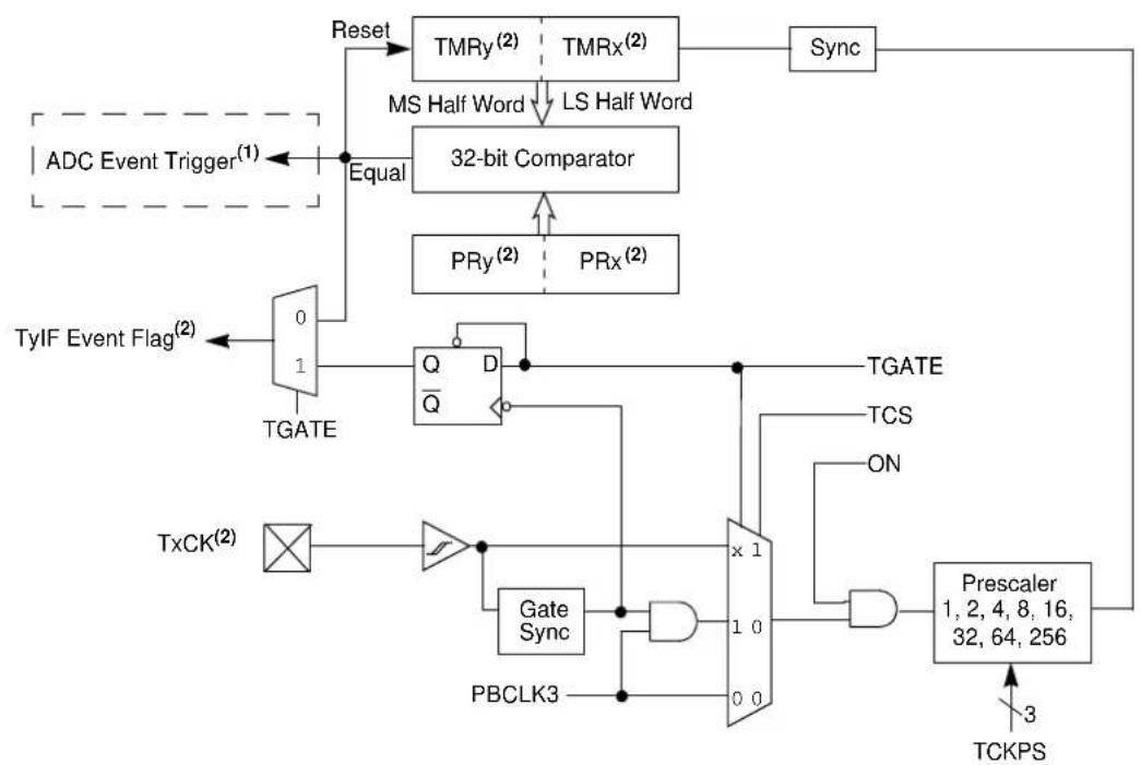
flowchart
graph TD
    A["ADC Event Trigger(1)"] --> B["Equal"]
    B --> C["TyIF Event Flag(2)"]
    C --> D["TGATE"]
    D --> E["Q D̅"]
    E --> F["x 1"]
    F --> G["Gate Sync"]
    G --> H["PBCLK3"]
    H --> I["0 0"]
    I --> J["x 1"]
    J --> K["TGATE"]
    K --> L["TCS"]
    L --> M["ON"]
    M --> N["Prescaler 1, 2, 4, 8, 16, 32, 64, 256"]
    N --> O["TCKPS"]
    P["Reset"] --> Q["TMRy(2) TMRx(2)"]
    Q --> R["Sync"]
    R --> S["TS"]
    S --> T["PRx(2)"]
    T --> U["3"]
    U --> V["TXCK(2)"]
    V --> W["Gate Sync"]
    W --> X["x 1"]
    X --> Y["x 1"]
    Y --> Z["x 1"]
    Z --> AA["x 1"]
    AA --> AB["x 1"]
    AB --> AC["x 1"]
    AC --> AD["x 1"]
    AD --> AE["x 1"]
    AE --> AF["x 1"]
    AF --> AG["x 1"]
    AG --> AH["x 1"]
    AH --> AI["x 1"]
    AI --> AJ["x 1"]
    AJ --> AK["x 1"]
    AK --> AL["x 1"]
    AL --> AM["x 1"]
    AM --> AN["x 1"]
    AN --> AO["x 1"]
    AO --> AP["x 1"]
    AP --> AQ["x 1"]
    AQ --> AR["x 1"]
    AR --> AS["x 1"]
Note 1: ADC event trigger is available only on the Timer2/3 and Timer4/5 pairs. 2: In this diagram, 'x' represents Timer2, 4, 6, or 8, and 'y' represents Timer3, 5, 7, or 9.
14.2 Timer2-Timer9 Control Registers
TABLE 14-1: TIMER2 THROUGH TIMER9 REGISTER MAP
| Virtual Address(BF84 #) | Register Name(1) | Bit Range | Bits | All Resets | |||||||||||||||
| 31/15 | 30/14 | 29/13 | 28/12 | 27/11 | 26/10 | 25/9 | 24/8 | 23/7 | 22/6 | 21/5 | 20/4 | 19/3 | 18/2 | 17/1 | 16/0 | ||||
| 0200 | T2CON | 31:16 | —— | —— | —— | —— | 0000 | ||||||||||||
| 15:0 | ON | — | SIDL | — | — | — | — | — | TGATE | TCKPS<2:0> | T32 | — | TCS | — | 0000 | ||||
| 0210 | TMR2 | 31:16 | —— | —— | —— | —— | 0000 | ||||||||||||
| 15:0 | TMR2<15:0> | 0000 | |||||||||||||||||
| 0220 | PR2 | 31:16 | —— | —— | —— | —— | 0000 | ||||||||||||
| 15:0 | PR2<15:0> | FFFF | |||||||||||||||||
| 0400 | T3CON | 31:16 | —— | —— | —— | —— | 0000 | ||||||||||||
| 15:0 | ON | — | SIDL | — | — | — | — | — | TGATE | TCKPS<2:0> | — | — | TCS | — | 0000 | ||||
| 0410 | TMR3 | 31:16 | —— | —— | —— | —— | 0000 | ||||||||||||
| 15:0 | TMR3<15:0> | 0000 | |||||||||||||||||
| 0420 | PR3 | 31:16 | —— | —— | —— | —— | 0000 | ||||||||||||
| 15:0 | PR3<15:0> | FFFF | |||||||||||||||||
| 0600 | T4CON | 31:16 | —— | —— | —— | —— | 0000 | ||||||||||||
| 15:0 | ON | — | SIDL | — | — | — | — | — | TGATE | TCKPS<2:0> | T32 | — | TCS | — | 0000 | ||||
| 0610 | TMR4 | 31:16 | —— | —— | —— | —— | 0000 | ||||||||||||
| 15:0 | TMR4<15:0> | 0000 | |||||||||||||||||
| 0620 | PR4 | 31:16 | —— | —— | —— | —— | 0000 | ||||||||||||
| 15:0 | PR4<15:0> | FFFF | |||||||||||||||||
| 0800 | T5CON | 31:16 | —— | —— | —— | —— | 0000 | ||||||||||||
| 15:0 | ON | — | SIDL | — | — | — | — | — | TGATE | TCKPS<2:0> | — | — | TCS | — | 0000 | ||||
| 0810 | TMR5 | 31:16 | —— | —— | —— | —— | 0000 | ||||||||||||
| 15:0 | TMR5<15:0> | 0000 | |||||||||||||||||
| 0820 | PR5 | 31:16 | —— | —— | —— | —— | 0000 | ||||||||||||
| 15:0 | PR5<15:0> | FFFF | |||||||||||||||||
| 0A00 | T6CON | 31:16 | —— | —— | —— | —— | 0000 | ||||||||||||
| 15:0 | ON | — | SIDL | — | — | — | — | — | TGATE | TCKPS<2:0> | T32 | — | TCS | — | 0000 | ||||
| 0A10 | TMR6 | 31:16 | —— | —— | —— | —— | 0000 | ||||||||||||
| 15:0 | TMR2<15:0> | 0000 | |||||||||||||||||
| 0A20 | PR6 | 31:16 | —— | —— | —— | —— | 0000 | ||||||||||||
| 15:0 | PR2<15:0> | FFFF | |||||||||||||||||
| 0C00 | T7CON | 31:16 | —— | —— | —— | —— | 0000 | ||||||||||||
| 15:0 | ON | — | SIDL | — | — | — | — | — | TGATE | TCKPS<2:0> | — | — | TCS | — | 0000 | ||||
Legend: x = unknown value on Reset; — = unimplemented, read as '0'. Reset values are shown in hexadecimal.
Note 1: All registers in this table have corresponding CLR, SET, and INV registers at their virtual addresses, plus offsets of 0x4, 0x8 and 0xC, respectively. See Section 12.2 "CLR, SET, and INV Registers" for more information.
TABLE 14-1: TIMER2 THROUGH TIMER9 REGISTER MAP (CONTINUED)
| Virtual Address(BF84 #) | Register Name(1) | Bit Range | Bits | All Resets | |||||||||||||||
| 31/15 | 30/14 | 29/13 | 28/12 | 27/11 | 26/10 | 25/9 | 24/8 | 23/7 | 22/6 | 21/5 | 20/4 | 19/3 | 18/2 | 17/1 | 16/0 | ||||
| 0C10 | TMR7 | 31:16 | —— | —— | —— | —— | 0000 | ||||||||||||
| 15:0 | TMR3<15:0> 0000 | ||||||||||||||||||
| 0C20 | PR7 | 31:16 | —— | —— | —— | —— | 0000 | ||||||||||||
| 15:0 | PR3<15:0> PFFF | ||||||||||||||||||
| 0E00 | T8CON | 31:16 | —— | —— | —— | —— | 0000 | ||||||||||||
| 15:0 | ON | — | SIDL | — | — | — | — | — | TGATE | TCKPS<2:0> | T32 | — | TCS | — | 0000 | ||||
| 0E10 | TMR8 | 31:16 | —— | —— | —— | —— | 0000 | ||||||||||||
| 15:0 | TMR4<15:0> 0000 | ||||||||||||||||||
| 0E20 | PR8 | 31:16 | —— | —— | —— | —— | 0000 | ||||||||||||
| 15:0 | PR4<15:0> PFFF | ||||||||||||||||||
| 1000 | T9CON | 31:16 | —— | —— | —— | —— | 0000 | ||||||||||||
| 15:0 | ON | — | SIDL | — | — | — | — | — | TGATE | TCKPS<2:0> | — | — | TCS | — | 0000 | ||||
| 1010 | TMR9 | 31:16 | —— | —— | —— | —— | 0000 | ||||||||||||
| 15:0 | TMR5<15:0> 0000 | ||||||||||||||||||
| 1020 | PR9 | 31:16 | —— | —— | —— | —— | 0000 | ||||||||||||
| 15:0 | PR5<15:0> PFFF | ||||||||||||||||||
Legend: x = unknown value on Reset; — = unimplemented, read as '0'. Reset values are shown in hexadecimal.
Note 1: All registers in this table have corresponding CLR, SET, and INV registers at their virtual addresses, plus offsets of 0x4, 0x8 and 0xC, respectively. See Section 12.2 "CLR, SET, and INV Registers" for more information.
REGISTER 14-1: TxCON: TYPE B TIMER CONTROL REGISTER ('x' = 2-9)
| Bit Range | Bit 31/23/15/7 | Bit 30/22/14/6 | Bit 29/21/13/5 | Bit 28/20/12/4 | Bit 27/19/11/3 | Bit 26/18/10/2 | Bit 25/17/9/1 | Bit 24/16/8/0 |
| 31:24 | U-0 U-0 U-0 | U-0 U-0 U-0 U-0 | U-0 | |||||
| — — — | — — — — — | |||||||
| 23:16 | U-0 U-0 U-0 | U-0 U-0 U-0 U-0 | U-0 | |||||
| — — — | — — — — — | |||||||
| 15:8 | R/W-0 U-0 R/W-0 | R/W-0 U-0 U-0 U-0 | U-0 U-0 | |||||
| ON(1) | — | SIDL(2) | — — — | — — | ||||
| 7:0 | R/W-0 | R/W-0 | R/W-0 | R/W-0 | R/W-0 | U-0 | R/W-0 | U-0 |
| TGATE(1) | TCKPS<2:0>(1) | T32(3) | — | TCS(1) | — | |||
Legend:
| R = Readable bit | W = Writable bit U = Unimplemented bit, read as '0' |
| -n = Value at POR | '1' = Bit is set '0' = Bit is cleared x = Bit is unknown |
bit 31-16 Unimplemented: Read as '0'
bit 15 ON: Timer On bit ^(1)
1 = Module is enabled
0 = Module is disabled
bit 14 Unimplemented: Read as '0'
bit 13 SIDL: Stop in Idle Mode bit ^(2)
1 = Discontinue operation when device enters Idle mode
0 = Continue operation even in Idle mode
bit 12-8 Unimplemented: Read as '0'
bit 7 TGATE: Timer Gated Time Accumulation Enable bit ^(1)
When TCS = 1:
This bit is ignored and is read as '0'.
When TCS = 0:
1 = Gated time accumulation is enabled
0 = Gated time accumulation is disabled
bit 6-4 TCKPS<2:0>: Timer Input Clock Prescale Select bits ^(1)
111 = 1:256 prescale value
110 = 1:64 prescale value
101 = 1:32 prescale value
100 = 1:16 prescale value
011 = 1:8 prescale value
010 = 1:4 prescale value
001 = 1:2 prescale value
000 = 1:1 prescale value
bit 3 T32: 32-Bit Timer Mode Select bit ^(3)
1 = Odd numbered and even numbered timers form a 32-bit timer
0 = Odd numbered and even numbered timers form a separate 16-bit timer
Note 1: While operating in 32-bit mode, this bit has no effect for odd numbered timers (Timer1, Timer3, Timer5, Timer7, and Timer9). All timer functions are set through the even numbered timers.
2: While operating in 32-bit mode, this bit must be cleared on odd numbered timers to enable the 32-bit timer in Idle mode.
3: This bit is available only on even numbered timers (Timer2, Timer4, Timer6, and Timer8).
REGISTER 14-1: TxCON: TYPE B TIMER CONTROL REGISTER ('x' = 2-9) (CONTINUED)
bit 2 Unimplemented: Read as '0'
bit 1 TCS: Timer Clock Source Select bit (1)
1 = External clock from TxCK pin
0 = Internal peripheral clock
bit 0 Unimplemented: Read as '0'
Note 1: While operating in 32-bit mode, this bit has no effect for odd numbered timers (Timer1, Timer3, Timer5, Timer7, and Timer9). All timer functions are set through the even numbered timers.
2: While operating in 32-bit mode, this bit must be cleared on odd numbered timers to enable the 32-bit timer in Idle mode.
3: This bit is available only on even numbered timers (Timer2, Timer4, Timer6, and Timer8).
15.0 DEADMAN TIMER (DMT)
Note: This data sheet summarizes the features of the PIC32MZ Embedded Connectivity (EC) Family family of devices. It is not intended to be a comprehensive reference source. To complement the information in this data sheet, refer to Section 9. "Watchdog, Deadman, and Power-up Timers" (DS60001114), which is available from the Documentation > Reference Manual section of the Microchip PIC32 web site (www.microchip.com/pic32).
The primary function of the Deadman Timer (DMT) is to reset the processor in the event of a software malfunction. The DMT is a free-running instruction fetch timer, which is clocked whenever an instruction fetch occurs until a count match occurs. Instructions are not fetched when the processor is in Sleep mode.
The DMT consists of a 32-bit counter with a time-out count match value as specified by the DMTCNT<3:0> bits in the DEVCFG1 Configuration register.
A Deadman Timer is typically used in mission critical and safety critical applications, where any single failure of the software functionality and sequencing must be detected.
Figure 15-1 shows a block diagram of the Deadman Timer module.
FIGURE 15-1: DEADMAN TIMER BLOCK DIAGRAM

flowchart
graph TD
    A[""Improper sequence" flag"] --> B["Instruction Fetched Strobe"]
    B --> C["System Reset"]
    C --> D{32-bit counter}
    D -->|32| E["(COUNTER) = DMT Max Count^(1)"]
    D -->|32| F["(COUNTER) ≥ DMT Window Interval^(2)"]
    F --> G["Window Interval Open"]
    H["Counter Initialization Value"] --> D
    I["ON"] --> J["Force DMT Event"]
    J --> D
    K[""Proper Clear Sequence" Flag"] --> L["Clock"]
    L --> M["32-bit counter"]
    N["PBCLK7"] --> O["Clock"]
    P["System Reset"] --> Q["DMT Count Reset Load"]
    Q --> D
    R["ON"] --> S["DMT event to NMI^(3)"]
    S --> D
Note 1: DMT Max Count is controlled by the DMTCNT<3:0> bits in the DEVCFG1 Configuration register.
2: DMT Window Interval is controlled by the DMTINTV<2:0> bits in the DEVCFG1 Configuration register.
3: Refer to Section 6.0 "Resets" for more information.
15.1 Deadman Timer Control Registers
TABLE 15-1: DEADMAN TIMER REGISTER MAP
Legend: x = unknown value on Reset; — = unimplemented, read as 'u'. Reset values are shown in hexadecimal.
REGISTER 15-1: DMTCON: DEADMAN TIMER CONTROL REGISTER
| R = Readable bit | W = Writable bit U = Unimplemented bit, read as ‘0’ |
| -n = Value at POR | ‘1’ = Bit is set ‘0’ = Bit is cleared x = Bit is unknown |
bit 31-16 Unimplemented: Read as '0'
bit 15 ON: Deadman Timer Module Enable bit ^(1)
1 = Deadman Timer module is enabled
0 = Deadman Timer module is disabled
bit 13-0 Unimplemented: Read as '0'
Note 1: This bit only has control when FDMTEN (DEVCFG1<3>) = 0.
REGISTER 15-2: DMTPRECLR: DEADMAN TIMER PRECLEAR REGISTER
| Bit Range | Bit31/23/15/7 | Bit30/22/14/6 | Bit29/21/13/5 | Bit28/20/12/4 | Bit27/19/11/3 | Bit26/18/10/2 | Bit25/17/9/1 | Bit24/16/8/0 |
| 31:24 | U-0 U-0 U-0 | U-0 U-0 U-0 | U-0 | |||||
| —— — | —— — — — — | |||||||
| 23:16 | U-0 U-0 U-0 | U-0 U-0 U-0 | U-0 | |||||
| —— — | —— — — — — | |||||||
| 15:8 | R/W-0 | R/W-0 | R/W-0 | R/W-0 | R/W-0 | R/W-0 | R/W-0 | R/W-0 |
| STEP1<7:0> | ||||||||
| 7:0 | U-0 U-0 U-0 | U-0 U-0 U-0 | U-0 | |||||
| —— — | —— — — — — | |||||||
Legend:
| R = Readable bit | W = Writable bit | U = Unimplemented bit, read as '0' |
| -n = Value at POR | '1' = Bit is set | '0' = Bit is cleared x = Bit is unknown |
bit 31-16 Unimplemented: Read as '0'
bit 15-8 STEP1<7:0>: Preclear Enable bits
01000000 = Enables the Deadman Timer Preclear (Step 1)
All other write patterns = Set BAD1 flag.
These bits are cleared when a DMT reset event occurs. STEP1<7:0> is also cleared if the
STEP2<7:0> bits are loaded with the correct value in the correct sequence.
bit 7-0 Unimplemented: Read as '0'
REGISTER 15-3: DMTCLR: DEADMAN TIMER CLEAR REGISTER
| Bit Range | Bit31/23/15/7 | Bit30/22/14/6 | Bit29/21/13/5 | Bit28/20/12/4 | Bit27/19/11/3 | Bit26/18/10/2 | Bit25/17/9/1 | Bit24/16/8/0 |
| 31:24 | U-0 U-0 U-0 | U-0 U-0 U-0 | U-0 U-0 | |||||
| — — — | — — — — — | |||||||
| 23:16 | U-0 U-0 U-0 | U-0 U-0 U-0 | U-0 U-0 | |||||
| — — — | — — — — — | |||||||
| 15:8 | U-0 U-0 U-0 | U-0 U-0 U-0 | U-0 U-0 | |||||
| — — — | — — — — — | |||||||
| 7:0 | R/W-0 | R/W-0 | R/W-0 | R/W-0 | R/W-0 | R/W-0 | R/W-0 | R/W-0 |
| STEP2<7:0> | ||||||||
Legend:
| R = Readable bit | W = Writable bit U = Unimplemented bit, read as '0' |
| -n = Value at POR | '1' = Bit is set '0' = Bit is cleared x = Bit is unknown |
bit 31-8
Unimplemented: Read as '0'
bit 7-0
STEP2<7:0>: Clear Timer bits
00001000 = Clears STEP1<7:0>, STEP2<7:0> and the Deadman Timer if, and only if, preceded by correct loading of STEP1<7:0> bits in the correct sequence. The write to these bits may be verified by reading DMTCNT and observing the counter being reset.
All other write patterns = Set BAD2 bit, the value of STEP1<7:0> will remain unchanged, and the new value being written STEP2<7:0> will be captured. These bits are also cleared when a DMT reset event occurs.
REGISTER 15-4: DMTSTAT: DEADMAN TIMER STATUS REGISTER
| Bit Range | Bit31/23/15/7 | Bit30/22/14/6 | Bit29/21/13/5 | Bit28/20/12/4 | Bit27/19/11/3 | Bit26/18/10/2 | Bit25/17/9/1 | Bit24/16/8/0 |
| 31:24 | U-0 U-0 U-0 | U-0 U-0 U-0 | U-0 U-0 | |||||
| — — — | — — | — | — — | |||||
| 23:16 | U-0 U-0 U-0 | U-0 U-0 U-0 | U-0 U-0 | |||||
| — — — | — — | — | — — | |||||
| 15:8 | U-0 U-0 U-0 | U-0 U-0 U-0 | U-0 U-0 | |||||
| — — — | — — | — | — — | |||||
| 7:0 | R-0, HC | R-0, HC | R-0, HC | R/W-0 | R/W-0 | R/W-0 | R/W-0 | R-0 |
| BAD1 | BAD2 | DMTEVENT | WINOPN |
| Legend: | HC = Hardware Cleared | ||
| R = Readable bit | W = Writable bit | U = Unimplemented bit, read as ‘0’ | |
| -n = Value at POR | ‘1’ = Bit is set | ‘0’ = Bit is cleared | x = Bit is unknown |
bit 31-8 Unimplemented: Read as '0'
bit 7 BAD1: Bad STEP1<7:0> Value Detect bit
1 = Incorrect STEP1<7:0> value was detected
0 = Incorrect STEP1<7:0> value was not detected
bit 6 BAD2: Bad STEP2<7:0> Value Detect bit
1 = Incorrect STEP2<7:0> value was detected
0 = Incorrect STEP2<7:0> value was not detected
bit 5 DMTEVENT: Deadman Timer Event bit
1 = Deadman timer event was detected (counter expired or bad STEP1<7:0> or STEP2<7:0> value was entered prior to counter increment)
0 = Deadman timer even was not detected
bit 4-1 Unimplemented: Read as '0'
bit 0 WINOPN: Deadman Timer Clear Window bit
1 = Deadman timer clear window is open
0 = Deadman timer clear window is not open
REGISTER 15-5: DMTCNT: DEADMAN TIMER COUNT REGISTER
| Bit Range | Bit31/23/15/7 | Bit30/22/14/6 | Bit29/21/13/5 | Bit28/20/12/4 | Bit27/19/11/3 | Bit26/18/10/2 | Bit25/17/9/1 | Bit24/16/8/0 |
| 31:24 | R-0 R-0 R-0 R-0 R-0 R-0 R-0 | |||||||
| COUNTER<31:24> | ||||||||
| 23:16 | R-0 R-0 R-0 R-0 R-0 R-0 R-0 | |||||||
| COUNTER<23:16> | ||||||||
| 15:8 | R-0 R-0 R-0 R-0 R-0 R-0 R-0 | |||||||
| COUNTER<15:8> | ||||||||
| 7:0 | R-0 R-0 R-0 R-0 R-0 R-0 R-0 | |||||||
| COUNTER<7:0> | ||||||||
Legend:
| R = Readable bit W = Writable bit U = Unimplemented bit, read as '0' |
| -n = Value at POR '1' = Bit is set '0' = Bit is cleared x = Bit is unknown |
bit 31-8
COUNTER<31:0>: Read current contents of DMT counter
REGISTER 15-6: DMTPSCNT: POST STATUS CONFIGURE DMT COUNT STATUS REGISTER
| Bit Range | Bit31/23/15/7 | Bit30/22/14/6 | Bit29/21/13/5 | Bit28/20/12/4 | Bit27/19/11/3 | Bit26/18/10/2 | Bit25/17/9/1 | Bit24/16/8/0 |
| 31:24 | R-0 R-0 R-0 | R-0 R-0 R-0 R-0 R-0 | ||||||
| PSCNT<31:24> | ||||||||
| 23:16 | R-0 R-0 R-0 | R-0 R-0 R-0 R-0 R-0 | ||||||
| PSCNT<23:16> | ||||||||
| 15:8 | R-0 R-0 R-0 | R-0 R-0 R-0 R-0 R-0 | ||||||
| PSCNT<15:8> | ||||||||
| 7:0 | R-0 | R-0 | R-0 | R-y | R-y | R-y | R-y | R-y |
| PSCNT<7:0> | ||||||||
| Legend: | y = Value set from Configuration bits on POR | |
| R = Readable bit | W = Writable bit | U = Unimplemented bit, read as ‘0’ |
| -n = Value at POR | ‘1’ = Bit is set | ‘0’ = Bit is cleared x = Bit is unknown |
bit 31-8 PSCNT<31:0>: DMT Instruction Count Value Configuration Status bits
This is always the value of the DMTCNT<3:0> bits in the DEVCFG1 Configuration register.
REGISTER 15-7: DMTPSINTV: POST STATUS CONFIGURE DMT INTERVAL STATUS REGISTER
| Bit Range | Bit31/23/15/7 | Bit30/22/14/6 | Bit29/21/13/5 | Bit28/20/12/4 | Bit27/19/11/3 | Bit26/18/10/2 | Bit25/17/9/1 | Bit24/16/8/0 |
| 31:24 | R-0 R-0 R-0 R-0 R-0 R-0 R-0 | |||||||
| PSINTV<31:24> | ||||||||
| 23:16 | R-0 R-0 R-0 R-0 R-0 R-0 R-0 | |||||||
| PSINTV<23:16> | ||||||||
| 15:8 | R-0 R-0 R-0 R-0 R-0 R-0 R-0 | |||||||
| PSINTV<15:8> | ||||||||
| 7:0 | R-0 R-0 R-0 R-0 R-0 R-y R-y | |||||||
| PSINTV<7:0> | ||||||||
Legend: y = Value set from Configuration bits on POR R = Readable bit W = Writable bit U = Unimplemented bit, read as '0' -n = Value at POR '1' = Bit is set '0' = Bit is cleared x = Bit is unknown
bit 31-8 PSINTV<31:0>: DMT Window Interval Configuration Status bits
This is always the value of the DMTINTV<2:0> bits in the DEVCFG1 Configuration register.
NOTES:
16.0 WATCHDOG TIMER (WDT)
Note: This data sheet summarizes the features of the PIC32MZ Embedded Connectivity (EC) Family family of devices. It is not intended to be a comprehensive reference source. To complement the information in this data sheet, refer to Section 9. “Watchdog, Deadman, and Power-up Timers” (DS60001114), which is available from the Documentation > Reference Manual section of the Microchip PIC32 web site (www.microchip.com/pic32).
When enabled, the Watchdog Timer (WDT) operates from the internal Low-Power Oscillator (LPRC) clock source and can be used to detect system software malfunctions by resetting the device if the WDT is not cleared periodically in software. Various WDT time-out periods can be selected using the WDT postscaler. The WDT can also be used to wake the device from Sleep or Idle mode.
Some of the key features of the WDT module are:
- Configuration or software controlled
- User-configurable time-out period
- Can wake the device from Sleep or Idle
FIGURE 16-1: WATCHDOG TIMER BLOCK DIAGRAM

flowchart
graph TD
    A["Reset Event"] --> B["WDT Counter Reset"]
    C["ON"] --> B
    D["ON"] --> B
    E["ON"] --> B
    F["AND"] --> B
    G["LPRC"] --> H["Clock"]
    H --> I["25-bit Counter"]
    I --> J["25"]
    J --> K["Decoder"]
    K --> L["FWDTPS<4:0> (DEVCFG1<20:16>)"]
    M["Power Save"] --> N["0/1"]
    N --> O["WDT Event to NMI(1)"]
    P["25"] --> Q["AND"]
    Q --> I
Note 1: Refer to Section 6.0 "Resets" for more information.
16.1 Watchdog Timer Control Registers
TABLE 16-1: WATCHDOG TIMER REGISTER MAP
| Virtual Address (BF80 #) | Register Name | Bit Range | Bits | All Resets | |||||||||||||||
| 31/15 | 30/14 | 29/13 | 28/12 | 27/11 | 26/10 | 25/9 | 24/8 | 23/7 | 22/6 | 21/5 | 20/4 | 19/3 | 18/2 | 17/1 | 16/0 | ||||
| 0800 | WDTCON (1) | 31:16 | WDTCLRKEY<15:0> | 0000 | |||||||||||||||
| 15:0 | ON | — | — | — | — | — | — | — | — | SWDTPS<4:0> | WDTWINEN | — | x0xx | ||||||
Legend: x = unknown value on Reset; — = unimplemented, read as '0'. Reset values are shown in hexadecimal.
Note 1: This register has corresponding CLR, SET, and INV registers at its virtual address, plus an offset of 0x4, 0x8 and 0xC, respectively. See Section 12.2 "CLR, SET, and INV Registers" for more information.
REGISTER 16-1: WDTCON: WATCHDOG TIMER CONTROL REGISTER
| Bit Range | Bit 31/23/15/7 | Bit 30/22/14/6 | Bit 29/21/13/5 | Bit 28/20/12/4 | Bit 27/19/11/3 | Bit 26/18/10/2 | Bit 25/17/9/1 | Bit 24/16/8/0 |
| 31:24 | W-0 W-0 W-0 W-0 W-0 W-0 W-0 | |||||||
| WDTCLRKEY<15:8> | ||||||||
| 23:16 | W-0 W-0 W-0 W-0 W-0 W-0 W-0 | |||||||
| WDTCLRKEY<7:0> | ||||||||
| 15:8 | R/W-y U-0 U-0 U-0 U-0 U-0 U-0 | |||||||
| ON(1) | — — — | — | — | — | — | |||
| 7:0 | U-0 R-y R-y R-y R-y R-W-0 | U-0 | ||||||
| — | SWDTPS<4:0> | WDTWINEN | — | |||||
| Legend: | y = Values set from Configuration bits on POR | ||
| R = Readable bit | W = Writable bit U = Unimplemented bit, read as ‘0’ | ||
| -n = Value at POR | ‘1’ = Bit is set | ‘0’ = Bit is cleared | x = Bit is unknown |
bit 31-16 WDTCLRKEY<15:0>: Watchdog Timer Clear Key bits
To clear the Watchdog Timer to prevent a time-out, software must write the value 0x5743 to this location using a single 16-bit write.
bit 15 ON: Watchdog Timer Enable bit ^(1)
1 = The WDT is enabled
0 = The WDT is disabled
bit 14-7 Unimplemented: Read as '0'
bit 6-2 SWDTPS<4:0>: Shadow Copy of Watchdog Timer Postscaler Value from Device Configuration bits On reset, these bits are set to the values of the WDTPS <4:0> Configuration bits in DEVCFG1.
bit 1 WDTWINEN: Watchdog Timer Window Enable bit
1 = Enable windowed Watchdog Timer
0 = Disable windowed Watchdog Timer
bit 0 Unimplemented: Read as '0'
Note 1: This bit only has control when FWDTEN (DEVCFG1<23>) = 0.
NOTES:
17.0 INPUT CAPTURE
Note: This data sheet summarizes the features of the PIC32MZ Embedded Connectivity (EC) Family of devices. It is not intended to be a comprehensive reference source. To complement the information in this data sheet, refer to Section 15. "Input Capture" (DS60001122), which is available from the Documentation > Reference Manual section of the Microchip PIC32 web site (www.microchip.com/pic32).
The Input Capture module is useful in applications requiring frequency (period) and pulse measurement.
The Input Capture module captures the 16-bit or 32-bit value of the selected Time Base registers when an event occurs at the ICx pin.
Capture events are caused by the following:
• Capture timer value on every edge (rising and falling), specified edge first
• Prescaler capture event modes:
- Capture timer value on every 4th rising edge of input at ICx pin
- Capture timer value on every 16th rising edge of input at ICx pin
Each input capture channel can select between one of six 16-bit timers for the time base, or two of six 16-bit timers together to form a 32-bit timer. The selected timer can use either an internal or external clock.
Other operational features include:
• Device wake-up from capture pin during Sleep and Idle modes
- Interrupt on input capture event
- 4-word FIFO buffer for capture values; Interrupt optionally generated after 1, 2, 3, or 4 buffer locations are filled
- Input capture can also be used to provide additional sources of external interrupts
FIGURE 17-1: INPUT CAPTURE BLOCK DIAGRAM
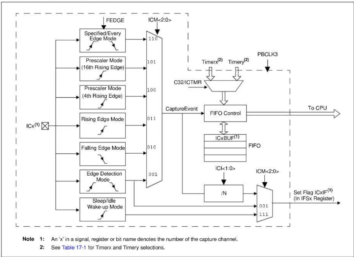
flowchart
graph TD
    A["ICx(1)"] --> B["Specified/Every Edge Mode"]
    B --> C["Prescaler Mode (16th Rising Edge)"]
    C --> D["Prescaler Mode (4th Rising Edge)"]
    D --> E["Rising Edge Mode"]
    E --> F["Falling Edge Mode"]
    F --> G["Edge Detection Mode"]
    G --> H["Sleep/Idle Wake-up Mode"]
    H --> I["ICM<2:0>"]
    I --> J["ICX(1)"]
    J --> K["Specified/Every Edge Mode"]
    K --> L["Prescaler Mode (16th Rising Edge)"]
    L --> M["Prescaler Mode (4th Rising Edge)"]
    M --> N["Rising Edge Mode"]
    N --> O["Falling Edge Mode"]
    O --> P["Edge Detection Mode"]
    P --> Q["Sleep/Idle Wake-up Mode"]
    Q --> R["ICM<2:0>"]
    R --> S["Set Flag ICxIF(1) (In IFSx Register)"]
    S --> T["To CPU"]
    T --> U["FIFO Control"]
    U --> V["ICxBUF(1)"]
    V --> W["ICI<1:0>"]
    W --> X["/N"]
    X --> Y["ICM<2:0>"]
    Y --> Z["To CPU"]
    Z --> AA["PBCLK3"]
    AA --> AB["C32/ICTMR"]
    AB --> AC["Timerx(2)"]
    AC --> AD["Timery(2)"]
    AD --> AE["ICM<2:0>"]
    AE --> AF["To CPU"]
    AF --> AG["To CPU"]
    AG --> AH["To CPU"]
    AH --> AI["To CPU"]
    AI --> AJ["To CPU"]
    AJ --> AK["To CPU"]
The timer source for each Input Capture module depends on the setting of the ICACLK bit in the CFGCON register. The available configurations are shown in Table 17-1.
TABLE 17-1: TIMER SOURCE CONFIGURATIONS
| Input Capture Module | Timerx Timery | |
| ICACLK (CFGCON<17>) = 0 | ||
| IC1 | Timer2 | Timer3 |
| . | . | . |
| . | . | . |
| IC9 | Timer 2 | Timer 3 |
| ICACLK (CFGCON<17>) = 1 | ||
| IC1 Timer4 | Timer5 | |
| IC2 Timer4 | Timer5 | |
| IC3 Timer4 | Timer5 | |
| IC4 Timer2 | Timer3 | |
| IC5 Timer2 | Timer3 | |
| IC6 Timer2 | Timer3 | |
| IC7 Timer6 | Timer7 | |
| IC8 Timer6 | Timer7 | |
| IC9 Timer6 | Timer7 | |
17.1 Input Capture Control Registers
TABLE 17-2: INPUT CAPTURE 1 THROUGH INPUT CAPTURE 9 REGISTER MAP
Legend: x = unknown value on Reset; — = unimplemented, read as '0'. Reset values are shown in hexadecimal. Note 1: This register has corresponding CLR, SET, and INV registers at its virtual address, plus an offset of 0x4, 0x8 and 0xC, respectively. See Section 12.2 "CLR, SET, and INV Registers" for more information.
REGISTER 17-1: IC xCON: INPUT CAPTURE x CONTROL REGISTER
| Bit Range | Bit31/23/15/7 | Bit30/22/14/6 | Bit29/21/13/5 | Bit28/20/12/4 | Bit27/19/11/3 | Bit26/18/10/2 | Bit25/17/9/1 | Bit24/16/8/0 |
| 31:24 | U-0 U-0 U-0 | U-0 U-0 U-0 | U-0 U-0 | |||||
| — — — | — — — — | — | ||||||
| 23:16 | U-0 U-0 U-0 | U-0 U-0 U-0 | U-0 U-0 | |||||
| — — — | — — — — | — | ||||||
| 15:8 | R/W-0 U-0 | R/W-0 | U-0 U-0 U-0 | R/W-0 | R/W-0 | |||
| ON | — | SIDL | — | — | — | FEDGE | C32 | |
| 7:0 | R/W-0 | R/W-0 | R/W-0 | R-0 | R-0 | R/W-0 | R/W-0 | R/W-0 |
| ICTMR | ICI<1:0> | ICOV | ICBNE | ICM<2:0> | ||||
| Legend: | ||
| R = Readable bit | W = Writable bit U = Unimplemented bit | |
| -n = Bit Value at POR: ('0', '1', x = unknown) | P = Programmable bit | r = Reserved bit |
| bit 31-16 | Unimplemented: Read as ‘0’ |
| bit 15 | ON: Input Capture Module Enable bit1 = Module enabled0 = Disable and reset module, disable clocks, disable interrupt generation and allow SFR modifications |
| bit 14 | Unimplemented: Read as ‘0’ |
| bit 13 | SIDL: Stop in Idle Control bit1 = Halt in CPU Idle mode0 = Continue to operate in CPU Idle mode |
| bit 12-10 | Unimplemented: Read as ‘0’ |
| bit 9 | FEDGE: First Capture Edge Select bit (only used in mode 6, ICM<2:0> = 110)1 = Capture rising edge first0 = Capture falling edge first |
| bit 8 C32: 32-bit Capture Select bit | |
| 1 = 32-bit timer resource capture0 = 16-bit timer resource capture | |
| bit 7 | ICTMR: Timer Select bit (Does not affect timer selection when C32 (ICxCON<8>) is ‘1’)(1)0 = Timery is the counter source for capture1 = Timerx is the counter source for capture |
| bit 6-5 | ICI<1:0>: Interrupt Control bits11 = Interrupt on every fourth capture event10 = Interrupt on every third capture event01 = Interrupt on every second capture event00 = Interrupt on every capture event |
| bit 4 | ICOV: Input Capture Overflow Status Flag bit (read-only)1 = Input capture overflow occurred0 = No input capture overflow occurred |
| bit 3 | ICBNE: Input Capture Buffer Not Empty Status bit (read-only)1 = Input capture buffer is not empty; at least one more capture value can be read0 = Input capture buffer is empty |
| bit 2-0 | ICM<2:0>: Input Capture Mode Select bits111 = Interrupt-Only mode (only supported while in Sleep mode or Idle mode)110 = Simple Capture Event mode – every edge, specified edge first and every edge thereafter101 = Prescaled Capture Event mode – every sixteenth rising edge100 = Prescaled Capture Event mode – every fourth rising edge011 = Simple Capture Event mode – every rising edge010 = Simple Capture Event mode – every falling edge001 = Edge Detect mode – every edge (rising and falling)000 = Input Capture module is disabled |
Note 1: Refer to Table 17-1 for Timerx and Timery selections.
18.0 OUTPUT COMPARE
Note: This data sheet summarizes the features of the PIC32MZ Embedded Connectivity (EC) Family of devices. It is not intended to be a comprehensive reference source. To complement the information in this data sheet, refer to Section 16. "Output Compare" (DS60001111), which is available from the Documentation > Reference Manual section of the Microchip PIC32 web site (www.microchip.com/pic32).
The Output Compare module is used to generate a single pulse or a train of pulses in response to selected time base events.
For all modes of operation, the Output Compare module compares the values stored in the OCxR and/or the OCxRS registers to the value in the selected timer.
When a match occurs, the Output Compare module generates an event based on the selected mode of operation.
The following are some of the key features:
- Multiple Output Compare modules in a device
- Programmable interrupt generation on compare event
- Single and Dual Compare modes
- Single and continuous output pulse generation
- Pulse-Width Modulation (PWM) mode
- Hardware-based PWM Fault detection and automatic output disable
- Programmable selection of 16-bit or 32-bit time bases
- Can operate from either of two available 16-bit time bases or a single 32-bit time base
- ADC event trigger
FIGURE 18-1: OUTPUT COMPARE MODULE BLOCK DIAGRAM

flowchart
graph TD
    A["OCxRS(1)"] --> B["Comparator"]
    C["OCxR(1)"] --> B
    D["Timerx(3)"] --> E["0 1"]
    F["Timery(3)"] --> E
    G["Timerx(3) Rollover"] --> H["0 1"]
    I["Timery(3) Rollover"] --> H
    J["Set Flag bit OCxIF(1)"] --> K["Output Logic"]
    L["OCM<2:0> Mode Select"] --> K
    M["OUTPUT Enable Logic"] --> K
    N["Trigger to ADC(4)"] --> K
    O["OCx(1)"] --> P["Output Logic"]
    Q["OCFA or OCFB(2)"] --> P
    P --> K
    style A fill:#f9f,stroke:#333
    style C fill:#f9f,stroke:#333
    style D fill:#f9f,stroke:#333
    style J fill:#f9f,stroke:#333
    style K fill:#ccf,stroke:#333
    style P fill:#ccf,stroke:#333
The timer source for each Output Compare module depends on the setting of the OCACLK bit in the CFGCON register. The available configurations are shown in Table 18-1.
TABLE 18-1: TIMER SOURCE CONFIGURATIONS
| Output Compare Module | Timerx Timery | |
| OCACLK (CFGCON<16>) = 0 | ||
| OC1 | Timer2 | Timer3 |
| . | . | . |
| . | . | . |
| OC9 | Timer 2 | Timer 3 |
| OCACLK (CFGCON<16>) = 1 | ||
| OC1 Timer4 | Timer5 | |
| OC2 Timer4 | Timer5 | |
| OC3 Timer4 | Timer5 | |
| OC4 Timer2 | Timer3 | |
| OC5 Timer2 | Timer3 | |
| OC6 Timer2 | Timer3 | |
| OC7 Timer6 | Timer7 | |
| OC8 Timer6 | Timer7 | |
| OC9 Timer6 | Timer7 | |
18.1 Output Compare Control Registers
TABLE 18-2: OUTPUT COMPARE 1 THROUGH OUTPUT COMPARE 9 REGISTER MAP
| Virtual Address (BF84_#) | Registry Name | Bit Range | Bits | All Resets | |||||||||||||||
| 31/15 | 30/14 | 29/13 | 28/12 | 27/11 | 26/10 | 25/9 | 24/8 | 23/7 | 22/6 | 21/5 | 20/4 | 19/3 | 18/2 | 17/1 | 16/0 | ||||
| 4000 | OC1CON | 31:16 | —— | —— | —— | —— | —— | 0000 | |||||||||||
| 15:0 | ON | — | SIDL | — | — | — | — | — | — | — | OC32 | OCFLT | OCTSEL | OCM<2:0> | 0000 | ||||
| 4010 | OC1R | 31:16 | OC1R<31:0> | xxxxx | |||||||||||||||
| 15:0 | xxxxx | ||||||||||||||||||
| 4020 | OC1RS | 31:16 | OC1RS<31:0> | xxxxx | |||||||||||||||
| 15:0 | xxxxx | ||||||||||||||||||
| 4200 | OC2CON | 31:16 | —— | —— | —— | —— | —— | 0000 | |||||||||||
| 15:0 | ON | — | SIDL | — | — | — | — | — | — | — | OC32 | OCFLT | OCTSEL | OCM<2:0> | 0000 | ||||
| 4210 | OC2R | 31:16 | OC2R<31:0> | xxxxx | |||||||||||||||
| 15:0 | xxxxx | ||||||||||||||||||
| 4220 | OC2RS | 31:16 | OC2RS<31:0> | xxxxx | |||||||||||||||
| 15:0 | xxxxx | ||||||||||||||||||
| 4400 | OC3CON | 31:16 | —— | —— | —— | —— | —— | 0000 | |||||||||||
| 15:0 | ON | — | SIDL | — | — | — | — | — | — | — | OC32 | OCFLT | OCTSEL | OCM<2:0> | 0000 | ||||
| 4410 | OC3R | 31:16 | OC3R<31:0> | xxxxx | |||||||||||||||
| 15:0 | xxxxx | ||||||||||||||||||
| 4420 | OC3RS | 31:16 | OC3RS<31:0> | xxxxx | |||||||||||||||
| 15:0 | xxxxx | ||||||||||||||||||
| 4600 | OC4CON | 31:16 | —— | —— | —— | —— | —— | 0000 | |||||||||||
| 15:0 | ON | — | SIDL | — | — | — | — | — | — | — | OC32 | OCFLT | OCTSEL | OCM<2:0> | 0000 | ||||
| 4610 | OC4R | 31:16 | OC4R<31:0> | xxxxx | |||||||||||||||
| 15:0 | xxxxx | ||||||||||||||||||
| 4620 | OC4RS | 31:16 | OC4RS<31:0> | xxxxx | |||||||||||||||
| 15:0 | xxxxx | ||||||||||||||||||
| 4800 | OC5CON | 31:16 | —— | —— | —— | —— | —— | 0000 | |||||||||||
| 15:0 | ON | — | SIDL | — | — | — | — | — | — | — | OC32 | OCFLT | OCTSEL | OCM<2:0> | 0000 | ||||
| 4810 | OC5R | 31:16 | OC5R<31:0> | xxxxx | |||||||||||||||
| 15:0 | xxxxx | ||||||||||||||||||
| 4820 | OC5RS | 31:16 | OC5RS<31:0> | xxxxx | |||||||||||||||
| 15:0 | xxxxx | ||||||||||||||||||
Legend: x = unknown value on Reset; — = unimplemented, read as '0'. Reset values are shown in hexadecimal.
Note 1: All registers in this table have corresponding CLR, SET, and INV registers at their virtual addresses, plus offsets of 0x4, 0x8 and 0xC, respectively. See Section 12.2 "CLR, SET, and INV Registers" for more information.
TABLE 18-2: OUTPUT COMPARE 1 THROUGH OUTPUT COMPARE 9 REGISTER MAP (CONTINUED)
| Virtual Address (BF84_#) | Register Name? | Bit Range | Bits | All Resets | ||||||||||||||||
| 31/15 | 30/14 | 29/13 | 28/12 | 27/11 | 26/10 | 25/9 | 24/8 | 23/7 | 22/6 | 21/5 | 20/4 | 19/3 | 18/2 | 17/1 | 16/0 | |||||
| 4A00 | OC6CON | 31:16 | —— | —— | —— | —— | —— | 0000 | ||||||||||||
| 15:0 | ON | — | SIDL | — | — | — | — | — | — | — | OC32 | OCFLT | OCTSEL | OCM<2:0> | 0000 | |||||
| 4A10 | OC6R | 31:16 | OC6R<31:0> | xxxxx | ||||||||||||||||
| 15:0 | xxxxx | |||||||||||||||||||
| 4A20 | OC6RS | 31:16 | OC6RS<31:0> | xxxxx | ||||||||||||||||
| 15:0 | xxxxx | |||||||||||||||||||
| 4C00 | OC7CON | 31:16 | —— | —— | —— | —— | —— | 0000 | ||||||||||||
| 15:0 | ON | — | SIDL | — | — | — | — | — | — | — | OC32 | OCFLT | OCTSEL | OCM<2:0> | 0000 | |||||
| 4C10 | OC7R | 31:16 | OC7R<31:0> | xxxxx | ||||||||||||||||
| 15:0 | xxxxx | |||||||||||||||||||
| 4C20 | OC7RS | 31:16 | OC7RS<31:0> | xxxxx | ||||||||||||||||
| 15:0 | xxxxx | |||||||||||||||||||
| 4E00 | OC8CON | 31:16 | —— | —— | —— | —— | —— | 0000 | ||||||||||||
| 15:0 | ON | — | SIDL | — | — | — | — | — | — | — | OC32 | OCFLT | OCTSEL | OCM<2:0> | 0000 | |||||
| 4E10 | OC8R | 31:16 | OC8R<31:0> | xxxxx | ||||||||||||||||
| 15:0 | xxxxx | |||||||||||||||||||
| 4E20 | OC8RS | 31:16 | OC8RS<31:0> | xxxxx | ||||||||||||||||
| 15:0 | xxxxx | |||||||||||||||||||
| 5000 | OC9CON | 31:16 | —— | —— | —— | —— | —— | 0000 | ||||||||||||
| 15:0 | ON | — | SIDL | — | — | — | — | — | — | — | OC32 | OCFLT | OCTSEL | OCM<2:0> | 0000 | |||||
| 5010 | OC9R | 31:16 | OC9R<31:0> | xxxxx | ||||||||||||||||
| 15:0 | xxxxx | |||||||||||||||||||
| 5020 | OC9RS | 31:16 | OC9RS<31:0> | xxxxx | ||||||||||||||||
| 15:0 | ||||||||||||||||||||
Legend: x = unknown value on Reset; — = unimplemented, read as 'u'. Reset values are shown in hexadecimal.
Note 1: All registers in this table have corresponding CLR, SET, and INV registers at their virtual addresses, plus offsets of 0x4, 0x8 and 0xC, respectively. See Section 12.2 "CLR, SET, and INV Registers" for more information.
REGISTER 18-1: OCxCON: OUTPUT COMPARE 'x' CONTROL REGISTER
| Bit Range | Bit 31/23/15/7 | Bit 30/22/14/6 | Bit 29/21/13/5 | Bit 28/20/12/4 | Bit 27/19/11/3 | Bit 26/18/10/2 | Bit 25/17/9/1 | Bit 24/16/8/0 |
| 31:24 | U-0 U-0 U-0 | U-0 U-0 U-0 U-0 | U-0 | |||||
| — — — | — — — — — | |||||||
| 23:16 | U-0 U-0 U-0 | U-0 U-0 U-0 U-0 | U-0 | |||||
| — — — | — — — — — | |||||||
| 15:8 | R/W-0 U-0 R/W-0 | U-0 U-0 U-0 | U-0 U-0 | |||||
| ON | — | SIDL | — | — | — | — | — | |
| 7:0 | U-0 | U-0 | R/W-0 | R-0 | R/W-0 | R/W-0 | R/W-0 | R/W-0 |
| — — | OC32 | OCFLT | (1) | OCTSEL(2) | OCM<2:0> | |||
Legend:
| R = Readable bit | W = Writable bit U = Unimplemented bit, read as '0' |
| -n = Value at POR | '1' = Bit is set '0' = Bit is cleared x = Bit is unknown |
bit 31-16 Unimplemented: Read as '0'
bit 15 ON: Output Compare Peripheral On bit
1 = Output Compare peripheral is enabled
0 = Output Compare peripheral is disabled
bit 14 Unimplemented: Read as '0'
bit 13 SIDL: Stop in Idle Mode bit
1 = Discontinue operation when CPU enters Idle mode
0 = Continue operation in Idle mode
bit 12-6 Unimplemented: Read as '0'
bit 5 OC32: 32-bit Compare Mode bit
1 = OCxR<31:0> and/or OCxRS<31:0> are used for comparisons to the 32-bit timer source
0 = OCxR<15:0> and OCxRS<15:0> are used for comparisons to the 16-bit timer source
bit 4 OCFLT: PWM Fault Condition Status bit ^(1)
1 = PWM Fault condition has occurred (cleared in HW only)
0 = No PWM Fault condition has occurred
bit 3 OCTSEL: Output Compare Timer Select bit ^(2)
1 = Timery is the clock source for this Output Compare module
0 = Timerx is the clock source for this Output Compare module
bit 2-0 OCM<2:0>: Output Compare Mode Select bits
111 = PWM mode on OCx; Fault pin enabled
110 = PWM mode on OCx; Fault pin disabled
101 = Initialize OCx pin low; generate continuous output pulses on OCx pin
100 = Initialize OCx pin low; generate single output pulse on OCx pin
011 = Compare event toggles OCx pin
010 = Initialize OCx pin high; compare event forces OCx pin low
001 = Initialize OCx pin low; compare event forces OCx pin high
000 = Output compare peripheral is disabled but continues to draw current
Note 1: This bit is only used when OCM<2:0> = '111'. It is read as '0' in all other modes.
2: Refer to Table 18-1 for Timerx and Timery selections.
NOTES:
19.0 SERIAL PERIPHERAL INTERFACE (SPI) AND INTER-IC SOUND (I²S)
Note: This data sheet summarizes the features of the PIC32MZ Embedded Connectivity (EC) Family of devices. It is not intended to be a comprehensive reference source. To complement the information in this data sheet, refer to Section 23. "Serial Peripheral Interface (SPI)" (DS60001106), which is available from the Documentation > Reference Manual section of the Microchip PIC32 web site (www.microchip.com/pic32).
The SPI/I²S module is a synchronous serial interface that is useful for communicating with external peripherals and other microcontroller devices, as well as digital audio devices. These peripheral devices may be Serial EEPROMs, Shift registers, display drivers, Analog-to-Digital Converters (ADC), etc.
The SPI/I²S module is compatible with Motorola® SPI and SIOP interfaces.
The following are some of the key features of the SPI module:
• Master and Slave modes support
- Four different clock formats
• Enhanced Framed SPI protocol support
- User-configurable 8-bit, 16-bit and 32-bit data width
- Separate SPI FIFO buffers for receive and transmit
- FIFO buffers act as 4/8/16-level deep FIFOs based on 32/16/8-bit data width
- Programmable interrupt event on every 8-bit, 16-bit and 32-bit data transfer
• Operation during Sleep and Idle modes
• Audio Codec Support:
- I²S protocol
- Left-justified
- Right-justified
- PCM
FIGURE 19-1: SPI/I ^2 S MODULE BLOCK DIAGRAM
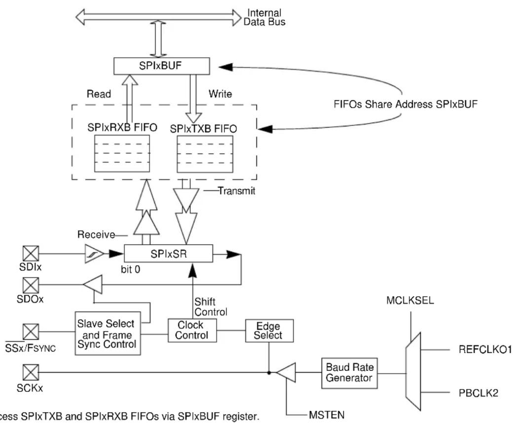
flowchart
graph TD
    A["Internal Data Bus"] <--> B["SPIxBUF"]
    B <--> C["SPIxRXB FIFO"]
    B <--> D["SPIxTXB FIFO"]
    C <--> E["SPIxSR"]
    D <--> E
    E --> F["SDIx"]
    E --> G["SDOx"]
    E --> H["SSx/FSYNC"]
    E --> I["SCKx"]
    E --> J["Slave Select and Frame Sync Control"]
    J --> K["Clock Control"]
    K --> L["Edge Select"]
    L --> M["Baud Rate Generator"]
    M --> N["MCLKSEL"]
    N --> O["REFCLK01"]
    N --> P["PBCLK2"]
    Q["Write"] --> B
    R["Receive"] --> E
    S["Shift Control"] --> K
    T["MSTEN"] --> M
    U["FIFOs Share Address SPIxBUF"] --> B
    V["Access SPIxTXB and SPIxRXB FIFOs via SPIxBUF register."] --> M
19.1 SPI Control Registers
TABLE 19-1: SPI1 THROUGH SPI6 REGISTER MAP
Legend: x = unknown value on Reset; — = unimplemented, read as '0'. Reset values are shown in hexadecimal.
Note 1: All registers in this table except SPIxBUF have corresponding CLR, SET, and INV registers at their virtual addresses, plus offsets of 0x4, 0x8 and 0xC, respectively. See Section 12.2 "CLR, SET, and INV Registers" for more information.
TABLE 19-1: SPI1 THROUGH SPI6 REGISTER MAP (CONTINUED)
| Virtual Address(BFB2 #) | Register Name? | Bit Range | Bits | All Resets | |||||||||||||||
| 31/15 | 30/14 | 29/13 | 28/12 | 27/11 | 26/10 | 25/9 | 24/8 | 23/7 | 22/6 | 21/5 | 20/4 | 19/3 | 18/2 | 17/1 | 16/0 | ||||
| 1600 | SPI4CON | 31:16 | FRMEN | FRMSYNC | FRMPOL | MSSEN | FRMSYPW | FRMCNT<2:0> | MCLKSEL | — | — | — | — | — | SPIFE | ENHBUF | 0000 | ||
| 15:0 | ON | — | SIDL | DISSDO | MODE32 | MODE16 | SMP | CKE | SSEN | CKP | MSTEN | DISSDI | STXISEL<1:0> | SRXISEL<1:0> | 0000 | ||||
| 1610 | SPI4STAT | 31:16 | — | — | — | RXBUFELM<4:0> | — | — | — | TXBUFELM<4:0> | 0000 | ||||||||
| 15:0 | — | — | — | FRMERR | SPIBUSY | — | — | SPITUR | SRMT | SPIROV | SPIRBE | — | SPITBE | — | SPITBF | SPIRBF | 0000 | ||
| 1620 | SPI4BUF | 31:16 | DATA<31:0> | 0000 | |||||||||||||||
| 15:0 | 0000 | ||||||||||||||||||
| 1630 | SPI4BRG | 31:16 | — | — | — | — | — | — | — | — | — | — | — | — | — | — | — | — | 0000 |
| 15:0 | — | — | — | — | — | — | — | BRG<8:0> | 0000 | ||||||||||
| 1640 | SPI4CON2 | 31:16 | — | — | — | — | — | — | — | — | — | — | — | — | — | — | — | — | 0000 |
| 15:0 | SPI SGNEXT | — | — | FRM ERREN | SPI ROVEN | SPI TUREN | IGNROV | IGNTUR | AUDEN | — | — | — | AUD MONO | — | AUDMOD<1:0> | 0000 | |||
| 1800 | SPI5CON | 31:16 | FRMEN | FRMSYNC | FRMPOL | MSSEN | FRMSYPW | FRMCNT<2:0> | MCLKSEL | — | — | — | — | — | SPIFE | ENHBUF | 0000 | ||
| 15:0 | ON | — | SIDL | DISSDO | MODE32 | MODE16 | SMP | CKE | SEN | CKP | MSTEN | DISSDI | STXISEL<1:0> | SRXISEL<1:0> | 0000 | ||||
| 1810 | SPI5STAT | 31:16 | — | — | — | RXBUFELM<4:0> | — | — | — | TXBUFELM<4:0> | 0000 | ||||||||
| 15:0 | — | — | — | FRMERR | SPIBUSY | — | — | SPITUR | SRMT | SPIROV | SPIRBE | — | SPITBIE | — | SPITBF | SPIRBF | 0008 | ||
| 1820 | SPI5BUF | 31:16 | DATA<31:0> | 0000 | |||||||||||||||
| 15:0 | 0000 | ||||||||||||||||||
| 1830 | SPI5BRG | 31:16 | — | — | — | — | — | — | — | — | — | — | — | — | — | — | — | — | 0000 |
| 15:0 | — | — | — | — | — | — | — | BRG<8:0> | 0000 | ||||||||||
| 1840 | SPI5CON2 | 31:16 | — | — | — | — | — | — | — | — | — | — | — | — | — | — | — | — | 0000 |
| 15:0 | SPI SGNEXT | — | — | FRM ERREN | SPI ROVEN | SPI TUREN | IGNROV | IGNTUR | AUDEN | — | — | — | AUD MONO | — | |||||
| 1A00 | SPI6CON | 31:16 | FRMEN | FRMSYNC | FRMPOL | MSSEN | FRMSYPW | FRMCNT<2:0> | MCLKSEL | — | — | — | — | — | SPIFE | ENHBUF | 0000 | ||
| 15:0 | ON | — | SIDL | DISSDO | MODE32 | MODE16 | SMP | CKE | SENN | CKP | MSTEN | DISSDI | STXISEL<1:0> | SRXISEL<1:0> | 0000 | ||||
| 1A10 | SPI6STAT | 31:16 | — | — | — | RXBUFELM<4:0> | — | — | — | TXBUFELM<4:0> | 0000 | ||||||||
| 15:0 | — | — | — | FRMERR | SPIBUSY | — | — | SPITUR | SRMT | SPIROV | SPIRBE | — | SPITBBIE | — | SPITBF | SPIRBF | 0008 | ||
| 1A20 | SPI6BUF | 31:16 | DATA<31:0> | 0000 | |||||||||||||||
| 15:0 | 0000 | ||||||||||||||||||
| 1A30 | SPI6BRG | 31:16 | — | — | — | — | — | — | — | — | — | — | — | — | — | — | — | — | 0000 |
| 15:0 | — | — | — | — | — | — | — | BRG<8:0> | |||||||||||
| 1A40 | SPI6CON2 | 31:16 | — | — | — | — | — | — | — | — | — | — | — | — | — | — | — | — | 0000 |
| 15:0 | SPI SGNEXT | — | — | FRM ERREN | SPI ROVEN | SPI TUREN | IGNROV | IGNTUR | AUDEN | — | — | — | AUD MONO | — | |||||
Legend: x = unknown value on Reset; — = unimplemented, read as 'D'. Reset values are shown in hexadecimal.
Note 1: All registers in this table except SPIxBUF have corresponding CLR, SET, and INV registers at their virtual addresses, plus offsets of 0x4, 0x8 and 0xC, respectively. See Section 12.2 "CLR, SET, and INV Registers" for more information.
REGISTER 19-1: SPIxCON: SPI CONTROL REGISTER
| Bit Range | Bit 31/23/15/7 | Bit 30/22/14/6 | Bit 29/21/13/5 | Bit 28/20/12/4 | Bit 27/19/11/3 | Bit 26/18/10/2 | Bit 25/17/9/1 | Bit 24/16/8/0 |
| 31:24 | R/W-0 R/W-0 | R/W-0 R/W-0 | R/W-0 R/W-0 R/W-0 | R/W-0 | ||||
| FRMEN FRMSYNC FRMPOL MSSEN | FRMSYPW | FRMCNT<2:0> | ||||||
| 23:16 | R/W-0 | U-0 | U-0 | U-0 | U-0 | U-0 | R/W-0 | R/W-0 |
| MCLKSEL^(1) | — | — | — | — | — | SPIFE | ENHBUF^(1) | |
| 15:8 | R/W-0 U-0 | R/W-0 | R/W-0 R/W-0 R/W-0 | R/W-0 R/W-0 R/W-0 | ||||
| ON | — | SIDL | DISSDO^(4) | MODE32 | MODE16 | SMP | CKE^(2) | |
| 7:0 | R/W-0 R/W-0 | R/W-0 R/W-0 | R/W-0 R/W-0 R/W-0 | R/W-0 | ||||
| SSEN | CKP^(3) | MSTEN | DISSDI^(4) | STXISEL<1:0> | SRXISEL<1:0> | |||
| Legend: | |||
| R = Readable bit | W = Writable bit | U = Unimplemented bit, read as '0' | |
| -n = Value at POR | ‘1’ = Bit is set | ‘0’ = Bit is cleared | x = Bit is unknown |
bit 31 FRMEN: Framed SPI Support bit
1 = Framed SPI support is enabled (SSx pin used as FSYNC input/output)
0 = Framed SPI support is disabled
bit 30 FRMSYNC: Frame Sync Pulse Direction Control on pin bit (Framed SPI mode only)
1 = Frame sync pulse input (Slave mode)
0 = Frame sync pulse output (Master mode)
bit 29 FRMPOL: Frame Sync Polarity bit (Framed SPI mode only)
1 = Frame pulse is active-high
0 = Frame pulse is active-low
bit 28 MSSEN: Master Mode Slave Select Enable bit
1 = Slave select SPI support enabled. The pin is automatically driven during transmission in Master mode. Polarity is determined by the FRMPOL bit.
0 = Slave select SPI support is disabled.
bit 27 FRMSYPW: Frame Sync Pulse Width bit
1 = Frame sync pulse is one character wide
0 = Frame sync pulse is one clock wide
bit 26-24 FRMCNT<2:0>: Frame Sync Pulse Counter bits. Controls the number of data characters transmitted per pulse. This bit is only valid in Framed mode.
111 = Reserved
110 = Reserved
101 = Generate a frame sync pulse on every 32 data characters
100 = Generate a frame sync pulse on every 16 data characters
011 = Generate a frame sync pulse on every 8 data characters
010 = Generate a frame sync pulse on every 4 data characters
001 = Generate a frame sync pulse on every 2 data characters
000 = Generate a frame sync pulse on every data character
bit 23 MCLKSEL: Master Clock Enable bit ^(1)
1 = REFCLKO1 is used by the Baud Rate Generator
0 = PBCLK2 is used by the Baud Rate Generator
bit 22-18 Unimplemented: Read as '0'
Note 1: This bit can only be written when the ON bit = 0. Refer to Section 37.0 “Electrical Characteristics” for maximum clock frequency requirements.
2: This bit is not used in the Framed SPI mode. The user should program this bit to '0' for the Framed SPI mode (FRMEN = 1).
3: When AUDEN = 1, the SPI/I²S module functions as if the CKP bit is equal to '1', regardless of the actual value of the CKP bit.
4: This bit present for legacy compatibility and is superseded by PPS functionality on these devices (see Section 12.3 "Peripheral Pin Select (PPS)" for more information).
REGISTER 19-1: SPIxCON: SPI CONTROL REGISTER (CONTINUED)
bit 17 SPIFE: Frame Sync Pulse Edge Select bit (Framed SPI mode only)
1 = Frame synchronization pulse coincides with the first bit clock
0 = Frame synchronization pulse precedes the first bit clock
bit 16 ENHBUF: Enhanced Buffer Enable bit (1)
1 = Enhanced Buffer mode is enabled
0 = Enhanced Buffer mode is disabled
bit 15 ON: SPI/I ^2 S Module On bit
1 = SPI/I ^2 S module is enabled
0 = SPI/I 2S module is disabled
bit 14 Unimplemented: Read as '0'
bit 13 SIDL: Stop in Idle Mode bit
1 = Discontinue operation when CPU enters in Idle mode
0 = Continue operation in Idle mode
bit 12 DISSDO: Disable SDOx pin bit (4)
1 = SDOx pin is not used by the module. Pin is controlled by associated PORT register
0 = SDOx pin is controlled by the module
bit 11-10 MODE<32,16>: 32/16-Bit Communication Select bits
When AUDEN = 1:
MODE32 MODE16 Communication
| 1 | 1 | 24-bit Data, 32-bit FIFO, 32-bit Channel/64-bit Frame |
| 1 | 0 | 32-bit Data, 32-bit FIFO, 32-bit Channel/64-bit Frame |
| 0 | 1 | 16-bit Data, 16-bit FIFO, 32-bit Channel/64-bit Frame |
| 0 | 0 | 16-bit Data, 16-bit FIFO, 16-bit Channel/32-bit Frame |
When AUDEN = 0:
MODE32 MODE16 Communication
| 1 | x | 32-bit |
| 0 | 1 | 16-bit |
| 0 | 0 | 8-bit |
bit 9 SMP: SPI Data Input Sample Phase bit
Master mode (MSTEN = 1):
1 = Input data sampled at end of data output time
0 = Input data sampled at middle of data output time
Slave mode (MSTEN = 0):
SMP value is ignored when SPI is used in Slave mode. The module always uses SMP = 0.
bit 8 CKE: SPI Clock Edge Select bit (2)
1 = Serial output data changes on transition from active clock state to Idle clock state (see CKP bit)
0 = Serial output data changes on transition from Idle clock state to active clock state (see CKP bit)
bit 7 SSEN: Slave Select Enable (Slave mode) bit
1 = pin used for Slave mode
0 = pin not used for Slave mode, pin controlled by port function.
bit 6 CKP: Clock Polarity Select bit (3)
1 = Idle state for clock is a high level; active state is a low level
0 = Idle state for clock is a low level; active state is a high level
Note 1: This bit can only be written when the ON bit = 0. Refer to Section 37.0 “Electrical Characteristics” for maximum clock frequency requirements.
2: This bit is not used in the Framed SPI mode. The user should program this bit to '0' for the Framed SPI mode (FRMEN = 1).
3: When AUDEN = 1, the SPI/I²S module functions as if the CKP bit is equal to '1', regardless of the actual value of the CKP bit.
4: This bit present for legacy compatibility and is superseded by PPS functionality on these devices (see Section 12.3 "Peripheral Pin Select (PPS)" for more information).
REGISTER 19-1: SPIxCON: SPI CONTROL REGISTER (CONTINUED)
bit 5 MSTEN: Master Mode Enable bit
1 = Master mode
1 = SDI pin is not used by the SPI module (pin is controlled by PORT function)
0 = SDI pin is controlled by the SPI module
bit 3-2 STXISEL<1:0>: SPI Transmit Buffer Empty Interrupt Mode bits
11 = Interrupt is generated when the buffer is not full (has one or more empty elements)
10 = Interrupt is generated when the buffer is empty by one-half or more
01 = Interrupt is generated when the buffer is completely empty
00 = Interrupt is generated when the last transfer is shifted out of SPISR and transmit operations are complete
bit 1-0 SRXISEL<1:0>: SPI Receive Buffer Full Interrupt Mode bits
11 = Interrupt is generated when the buffer is full
10 = Interrupt is generated when the buffer is full by one-half or more
01 = Interrupt is generated when the buffer is not empty
00 = Interrupt is generated when the last word in the receive buffer is read (i.e., buffer is empty)
Note 1: This bit can only be written when the ON bit = 0. Refer to Section 37.0 “Electrical Characteristics” for maximum clock frequency requirements.
2: This bit is not used in the Framed SPI mode. The user should program this bit to '0' for the Framed SPI mode (FRMEN = 1).
3: When AUDEN = 1, the SPI/I²S module functions as if the CKP bit is equal to '1', regardless of the actual value of the CKP bit.
4: This bit present for legacy compatibility and is superseded by PPS functionality on these devices (see Section 12.3 "Peripheral Pin Select (PPS)" for more information).
REGISTER 19-2: SPIxCON2: SPI CONTROL REGISTER 2
| Bit Range | Bit 31/23/15/7 | Bit 30/22/14/6 | Bit 29/21/13/5 | Bit 28/20/12/4 | Bit 27/19/11/3 | Bit 26/18/10/2 | Bit 25/17/9/1 | Bit 24/16/8/0 |
| 31:24 | U-0 U-0 U-0 | U-0 U-0 U-0 | U-0 | |||||
| — — — | — — — | — | — | |||||
| 23:16 | U-0 U-0 U-0 | U-0 U-0 U-0 | U-0 | |||||
| — — — | — — — | — | — | |||||
| 15:8 | R/W-0 | U-0 | U-0 | R/W-0 | R/W-0 | R/W-0 | R/W-0 | R/W-0 |
| SPISGNEXT | — | — | FRMERREN | SPIROVEN | SPITUREN | IGNROV | IGNTUR | |
| 7:0 | R/W-0 | U-0 | U-0 | U-0 | R/W-0 | U-0 | R/W-0 | R/W-0 |
| AUDEN(1) | — — — | AUDMONO | (1,2) | — | AUDMOD<1:0>(1,2) | |||
Legend:
| R = Readable bit | W = Writable bit | U = Unimplemented bit, read as '0' |
| -n = Value at POR | ‘1’ = Bit is set | ‘0’ = Bit is cleared x = Bit is unknown |
bit 31-16 Unimplemented: Read as '0'
bit 15 SPISGNEXT: Sign Extend Read Data from the RX FIFO bit
1 = Data from RX FIFO is sign extended
0 = Data from RX FIFO is not sign extended
bit 14-13 Unimplemented: Read as '0'
bit 12 FRMERREN: Enable Interrupt Events via FRMERR bit
1 = Frame Error overflow generates error events
0 = Frame Error does not generate error events
bit 11 SPIROVEN: Enable Interrupt Events via SPIROV bit
1 = Receive overflow generates error events
0 = Receive overflow does not generate error events
bit 10 SPITUREN: Enable Interrupt Events via SPITUR bit
1 = Transmit Underrun Generates Error Events
0 = Transmit Underrun Does Not Generate Error Events
bit 9 IGNROV: Ignore Receive Overflow bit (for Audio Data Transmissions)
1 = A ROV is not a critical error; during ROV data in the FIFO is not overwritten by receive data
0 = A ROV is a critical error which stop SPI operation
bit 8 IGNTUR: Ignore Transmit Underrun bit (for Audio Data Transmissions)
1 = A TUR is not a critical error and zeros are transmitted until the SPIxTXB is not empty
0 = A TUR is a critical error which stop SPI operation
bit 7 AUDEN: Enable Audio CODEC Support bit ^(1)
1 = Audio protocol enabled
0 = Audio protocol disabled
bit 6-5 Unimplemented: Read as '0'
bit 3 AUDMONO: Transmit Audio Data Format bit ^(1,2)
1 = Audio data is mono (Each data word is transmitted on both left and right channels)
0 = Audio data is stereo
bit 2 Unimplemented: Read as '0'
bit 1-0 AUDMOD<1:0>: Audio Protocol Mode bit ^(1,2)
11 = PCM/DSP mode
10 = Right Justified mode
01 = Left Justified mode
00 = I²S mode
Note 1: This bit can only be written when the ON bit = 0.
2: This bit is only valid for AUDEN = 1.
| Legend: C = Clearable bit | HS = Set in hardware | ||
| R = Readable bit | W = Writable bit | U = Unimplemented bit, read as ‘0’ | |
| -n = Value at POR | ‘1’ = Bit is set | ‘0’ = Bit is cleared | x = Bit is unknown |
bit 31-29 Unimplemented: Read as '0'
bit 28-24 RXBUFELM<4:0>: Receive Buffer Element Count bits (valid only when ENHBUF = 1)
bit 23-21 Unimplemented: Read as '0'
bit 20-16 TXBUFELM<4:0>: Transmit Buffer Element Count bits (valid only when ENHBUF = 1)
bit 15-13 Unimplemented: Read as '0'
bit 12 FRMERR: SPI Frame Error status bit
1 = Frame error detected
0 = No Frame error detected
This bit is only valid when FRMEN = 1.
bit 11 SPIBUSY: SPI Activity Status bit
1 = SPI peripheral is currently busy with some transactions
0 = SPI peripheral is currently idle
bit 10-9 Unimplemented: Read as '0'
bit 8 SPITUR: Transmit Under Run bit
1 = Transmit buffer has encountered an underrun condition
0 = Transmit buffer has no underrun condition
This bit is only valid in Framed Sync mode; the underrun condition must be cleared by disabling/re-enabling the module.
bit 7 SRMT: Shift Register Empty bit (valid only when ENHBUF = 1)
1 = When SPI module shift register is empty
0 = When SPI module shift register is not empty
bit 6 SPIROV: Receive Overflow Flag bit
1 = A new data is completely received and discarded. The user software has not read the previous data in the SPIxBUF register.
0 = No overflow has occurred
This bit is set in hardware; can only be cleared (= 0) in software.
bit 5 SPIRBE: RX FIFO Empty bit (valid only when ENHBUF = 1)
1 = RX FIFO is empty (CRPTR = SWPTR)
0 = RX FIFO is not empty (CRPTR ≠ SWPTR)
bit 4 Unimplemented: Read as '0'
1 = Transmit buffer, SPIxTXB is empty
0 = Transmit buffer, SPIxTXB is not empty
Automatically set in hardware when SPI transfers data from SPIxTXB to SPIxSR.
Automatically cleared in hardware when SPIxBUF is written to, loading SPIxTXB.
bit 2 Unimplemented: Read as '0'
bit 1 SPITBF: SPI Transmit Buffer Full Status bit
1 = Transmit not yet started, SPITXB is full
0 = Transmit buffer is not full
Standard Buffer Mode:
Automatically set in hardware when the core writes to the SPIBUF location, loading SPITXB.
Automatically cleared in hardware when the SPI module transfers data from SPITXB to SPISR.
Enhanced Buffer Mode:
Set when CWPTR + 1 = SRPTR; cleared otherwise
bit 0 SPIRBF: SPI Receive Buffer Full Status bit
1 = Receive buffer, SPIxRXB is full
0 = Receive buffer, SPIxRXB is not full
Standard Buffer Mode:
Automatically set in hardware when the SPI module transfers data from SPIxSR to SPIxRXB.
Automatically cleared in hardware when SPIxBUF is read from, reading SPIxRXB.
Enhanced Buffer Mode:
Set when SWPTR + 1 = CRPTR; cleared otherwise
NOTES:
20.0 SERIAL QUAD INTERFACE (SQI)
Note: This data sheet summarizes the features of the PIC32MZ Embedded Connectivity (EC) Family of devices. It is not intended to be a comprehensive reference source. To complement the information in this data sheet, refer to Section 46. “Serial Quad Interface (SQI)” (DS60001244), which is available from the Documentation > Reference Manual section of the Microchip PIC32 web site (www.microchip.com/pic32).
The SQI module is a synchronous serial interface that provides access to serial Flash memories and other serial devices. The SQI module supports Single Lane (identical to SPI), Dual Lane, and Quad Lane modes.
Note: To avoid cache coherency problems on devices with L1 cache, SQL buffers must only be allocated or accessed from the KSEG1 segment.
The SQI module offers the following key features:
• Supports Single, Dual, and Quad Lane modes
- Programmable command sequence
- eXecute-In-Place (XIP)
- Data transfer:
- Programmed I/O mode (PIO)
- Buffer descriptor DMA
• Supports High-Speed Serial Flash mode and SPI Mode 0 and Mode 3
- Programmable Clock Polarity (CPOL) and Clock Phase (CPHA) bits
• Supports up to two Chip Selects
• Supports up to four bytes of Flash address
- Programmable interrupt thresholds
• 32-byte transmit data buffer
• 32-byte receive data buffer
• 4-word controller buffer
Note: Once the SQI module is configured, external devices are memory mapped into KSEG2 (see Figure 4-1 through Figure 4-4 in Section 4.0 “Memory Organization” for more information). The MMU must be enabled and the TLB must be set up to access this memory (see Section 50. “CPU for Devices with MIPS32® microAptiv™ and M-Class Cores” (DS60001192) in the “PIC32 Family Reference Manual” for more information).
FIGURE 20-1: SQI MODULE BLOCK DIAGRAM
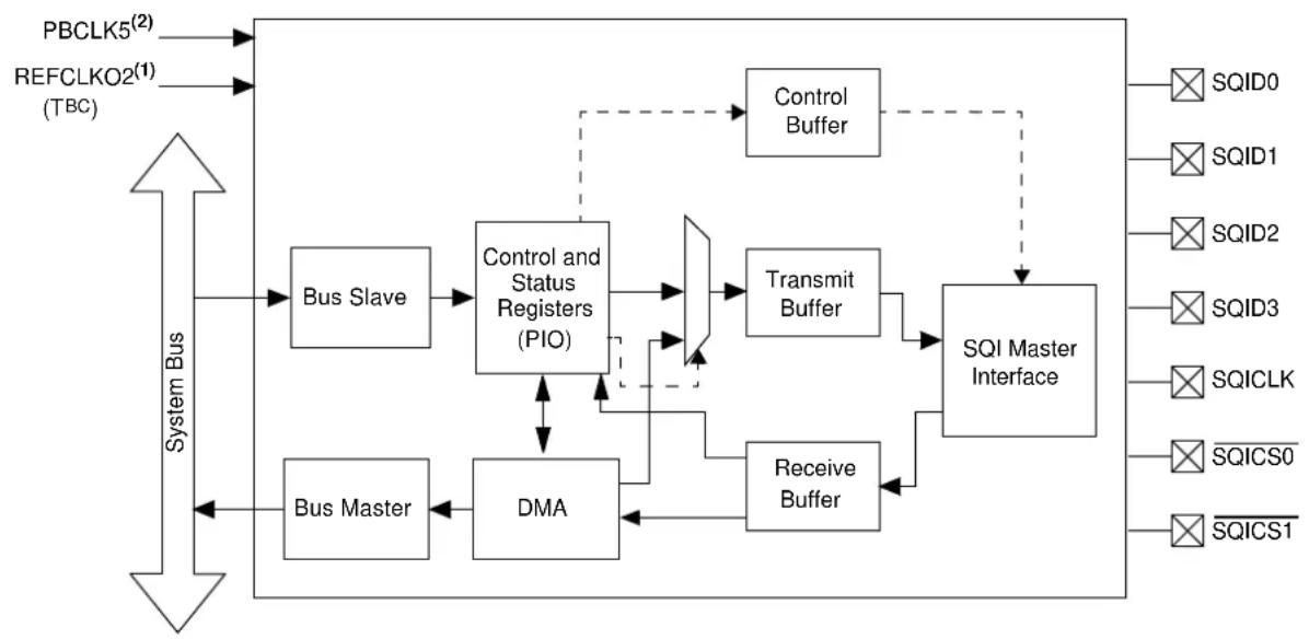
flowchart
graph TD
    A["PBCLK5(2)"] --> B["Control Buffer"]
    C["REFCLKO2(1) (TBC)"] --> B
    B --> D["Control and Status Registers (PIO)"]
    D --> E["Transmit Buffer"]
    E --> F["SQI Master Interface"]
    G["Bus Slave"] --> D
    H["Bus Master"] --> I["DMA"]
    I --> J["Receive Buffer"]
    J --> F
    K["Control Buffer"] -.-> D
    L["BU Slave"] --> D
    M["BU Master"] --> I
    N["SGI"] --> F
    O["SGI"] --> F
    P["SGI"] --> F
    Q["SGI"] --> F
    R["SGI"] --> F
    S["SGI"] --> F
    T["SGI"] --> F
    U["SGI"] --> F
    V["SGI"] --> F
    W["SGI"] --> F
    X["SGI"] --> F
    Y["SGI"] --> F
    Z["SGI"] --> F
Note 1: When configuring the REFCLKO2 clock source, a value of '0' for the ROTRIM<8:0> bits must be selected.
2: This clock source is only used for SQL Special Function Register (SFR) access.
20.1 SQI Control Registers
TABLE 20-1: SERIAL QUADRATURE INTERFACE (SQI) REGISTER MAP
Legend: x = unknown value on Reset; — = unimplemented, read as '0'. Reset values are shown in hexadecimal.
REGISTER 20-1: SQI1XCON1: SQI XIP CONTROL REGISTER 1
| Bit Range | Bit 31/23/15/7 | Bit 30/22/14/6 | Bit 29/21/13/5 | Bit 28/20/12/4 | Bit 27/19/11/3 | Bit 26/18/10/2 | Bit 25/17/9/1 | Bit 24/16/8/0 |
| 31:24 | U-0 U-0 U-0 | U-0 U-0 U-0 U-0 | U-0 | |||||
| —— ——— ——— | ||||||||
| 23:16 | R/W-0 | R/W-0 | R/W-0 | R/W-0 | R/W-0 | R/W-0 | R/W-0 | R/W-0 |
| DUMMYBYTES<2:0> | ADDRBYTES<2:0> | READOPCODE<7:6> | ||||||
| 15:8 | R-0 R-0 R-0 | R-0 R-0 R-0 | R/W-0 | R/W-0 | ||||
| READOPCODE<5:0> | TYPEDATA<1:0> | |||||||
| 7:0 | R/W-0 | R/W-0 | R/W-0 | R/W-0 | R/W-0 | R/W-0 | R/W-0 | R/W-0 |
| TYPEDUMMY<1:0> | TYPEMODE<1:0> | TYPEADDR<1:0> | TYPECMD<1:0> | |||||
Legend:
| R = Readable bit | W = Writable bit U = Unimplemented bit, read as '0' |
| -n = Value at POR | '1' = Bit is set '0' = Bit is cleared x = Bit is unknown |
bit 31-24 Unimplemented: Read as '0'
bit 23-21 DUMMYBYTES<2:0>: Transmit Dummy Bytes bits
111 = Transmit seven dummy bytes after the address bytes
•
.
•
011 = Transmit three dummy bytes after the address bytes
010 = Transmit two dummy bytes after the address bytes
001 = Transmit one dummy bytes after the address bytes
000 = Transmit zero dummy bytes after the address bytes
bit 20-18 ADDRBYTES<2:0>: Address Cycle bits
111 = Reserved
•
•
•
101 = Reserved
100 = Four address bytes
011 = Three address bytes
010 = Two address bytes
001 = One address bytes
000 = Zero address bytes
bit 17-10 READOPCODE<7:0>: Op code Value for Read Operation bits
These bits contain the 8-bit op code value for read operation.
bit 9-8 TYPEDATA<1:0>: SQI Type Data Enable bits
The boot controller will receive the data in Single Lane, Dual Lane, or Quad Lane.
11 = Reserved
10 = Quad Lane mode data is enabled
01 = Dual Lane mode data is enabled
00 = Single Lane mode data is enabled
bit 7-6 TYPEDUMMY<1:0>: SQL Type Dummy Enable bits
The boot controller will send the dummy in Single Lane, Dual Lane, or Quad Lane.
11 = Reserved
10 = Quad Lane mode dummy is enabled
01 = Dual Lane mode dummy is enabled
00 = Single Lane mode dummy is enabled
REGISTER 20-1: SQI1XCON1: SQI XIP CONTROL REGISTER 1 (CONTINUED)
bit 5-4 TYPEMODE<1:0>: SQI Type Mode Enable bits
The boot controller will send the mode in Single Lane, Dual Lane, or Quad Lane.
11 = Reserved
10 = Quad Lane mode is enabled
01 = Dual Lane mode is enabled
00 = Single Lane mode is enabled
bit 3-2 TYPEADDR<1:0>: SQI Type Address Enable bits
The boot controller will send the address in Single Lane, Dual Lane, or Quad Lane.
11 = Reserved
10 = Quad Lane mode address is enabled
01 = Dual Lane mode address is enabled
00 = Single Lane mode address is enabled
bit 1-0 TYPECMD<1:0>: SQI Type Command Enable bits
The boot controller will send the command in Single Lane, Dual Lane, or Quad Lane.
11 = Reserved
10 = Quad Lane mode command is enabled
01 = Dual Lane mode command is enabled
00 = Single Lane mode command is enabled
REGISTER 20-2: SQI1XCON2: SQI XIP CONTROL REGISTER 2
| Bit Range | Bit 31/23/15/7 | Bit 30/22/14/6 | Bit 29/21/13/5 | Bit 28/20/12/4 | Bit 27/19/11/3 | Bit 26/18/10/2 | Bit 25/17/9/1 | Bit 24/16/8/0 |
| 31:24 | U-0 U-0 U-0 | U-0 U-0 U-0 U-0 | U-0 | |||||
| ——— | ——— —— | |||||||
| 23:16 | U-0 U-0 U-0 | U-0 U-0 U-0 U-0 | U-0 | |||||
| ——— | ——— —— | |||||||
| 15:8 | U-0 | U-0 | U-0 | U-0 | R/W-0 | R/W-0 | R/W-0 | R/W-0 |
| — | — | — | — | DEVSEL<1:0> | MODEBYTES<1:0> | |||
| 7:0 | R/W-0 | R/W-0 | R/W-0 | R/W-0 | R/W-0 | R/W-0 | R/W-0 | R/W-0 |
| MODECODE<7:0> | ||||||||
Legend:
| R = Readable bit | W = Writable bit U = Unimplemented bit, read as '0' |
| -n = Value at POR | '1' = Bit is set '0' = Bit is cleared x = Bit is unknown |
bit 31-12 Unimplemented: Read as '0'
bit 11-10 DEVSEL<1:0>: Device Select bits
11 = Reserved
10 = Reserved
01 = Device 1 is selected
00 = Device 0 is selected
bit 9-8 MODEBYTES<1:0>: Mode Byte Cycle Enable bits
11 = Three cycles
10 = Two cycles
01 = One cycle
00 = Zero cycles
bit 7-0 MODECODE<7:0>: Mode Code Value bits
These bits contain the 8-bit code value for the mode bits.
REGISTER 20-3: SQI1CFG: SQI CONFIGURATION REGISTER
| Bit Range | Bit 31/23/15/7 | Bit 30/22/14/6 | Bit 29/21/13/5 | Bit 28/20/12/4 | Bit 27/19/11/3 | Bit 26/18/10/2 | Bit 25/17/9/1 | Bit 24/16/8/0 |
| 31:24 | R/W-0 U-0 U-0 U-0 U-0 R/W-0 R/W-0 | |||||||
| SQIEN — | ——— | CSEN<1:0> | ||||||
| 23:16 | U-0 | U-0 | R/W-0 | R/W-0 | U-0 | U-0 | U-0 | R/W-0, HC |
| — | — | DATAEN<1:0> | — | — | — | RESET | ||
| 15:8 | U-0 | r-0 | r-0 | R/W-0 | r-0 | R/W-0 | R/W-0 | R/W-0 |
| ——— | BURSTEN | (1) | — HOLD | WP | SERMODE | |||
| 7:0 | R/W-0 | U-0 | R/W-0 | R/W-0 | R/W-0 | R/W-0 | R/W-0 | R/W-0 |
| RXLATCH | — | LSBF | CPOL | CPHA | MODE<2:0> | |||
| Legend: | HC = Hardware Cleared | r = Reserved | |
| R = Readable bit | W = Writable bit | U = Unimplemented bit, read as ‘0’ | |
| -n = Value at POR | ‘1’ = Bit is set | ‘0’ = Bit is cleared | x = Bit is unknown |
bit 31 SQIEN: SQL Enable bit
1 = SQL module is enabled
0 = SQL module is disabled
bit 30-26 Unimplemented: Read as '0'
bit 25-24 CSEN<1:0>: Chip Select Output Enable bits
11 = Chip Select 0 and Chip Select 1 are used
10 = Chip Select 1 is used (Chip Select 0 is not used)
01 = Chip Select 0 is used (Chip Select 1 is not used)
00 = Chip Select 0 and Chip Select 1 are not used
bit 23-22 Unimplemented: Read as '0'
bit 21-20 DATAEN<1:0>: Data Output Enable bits
11 = Reserved
10 = SQID3-SQID0 outputs are enabled
01 = SQID1 and SQID0 data outputs are enabled
00 = SQID0 data output is enabled
bit 19-17 Unimplemented: Read as '0'
bit 16 RESET: Software Reset Select bit
This bit is automatically cleared by the SQL module. All of the internal state machines and FIFO pointers are reset by this reset pulse.
1 = A reset pulse is generated
0 = A reset pulse is not generated
bit 15 Unimplemented: Read as '0'
bit 14-13 Reserved: Must be programmed as '0'
bit 12 BURSTEN: Burst Configuration bit ^(1)
1 = Burst is enabled
0 = Burst is not enabled
bit 11 Reserved: Must be programmed as '0'
bit 10 HOLD: Hold bit
In Single Lane or Dual Lane mode, this bit is used to drive the SQID3 pin, which can be used for devices with a HOLD input pin. The meaning of the values for this bit will depend on the device to which SQID3 is connected.
Note 1: This bit must be programmed as '1'.
REGISTER 20-3: SQI1CFG: SQI CONFIGURATION REGISTER (CONTINUED)
bit 9 WP: Write Protect bit
In Single Lane or Dual Lane mode, this bit is used to drive the SQID2 pin, which can be used with devices with a write-protect pin. The meaning of the values for this bit will depend on the device to which SQID2 is connected.
bit 8 SERMODE: Serial Flash Mode Select bit
1 = Hardware ignores CPHA and CPOL bit settings and sends and latches negative edge of SQI CLK 0 = Clock phase and polarity are controlled by the CPHA and CPOL bit settings
bit 7 RXLATCH: RX Latch Control During TX Mode bit
1 = RX Data sent to RX FIFO when CMDINIT<1:0> (SQICON<17:16>) is set to TX 0 = RX Data is discarded when CMDINIT (SQICON<17:16>) is set to TX
bit 6 Unimplemented: Read as '0'
bit 5 LSBF: Data Format Select bit
1 = LSB is sent or received first 0 = MSB is sent or received first
bit 4 CPOL: Clock Polarity Select bit
1 = Active-low SQICLK (SQICLK high is the Idle state) 0 = Active-high SQICLK (SQICLK low is the Idle state)
bit 3 CPHA: Clock Phase Select bit
1 = SQICLK starts toggling at the start of the first data bit 0 = SQICLK starts toggling at the middle of the first data bit
bit 2-0 MODE<2:0>: Mode Select bits
111 = Reserved • • • 100 = Reserved 011 = XIP mode is selected (when this mode is entered, the module behaves as if executing in place (XIP), but uses the register data to control timing) 010 = DMA mode is selected 001 = CPU mode is selected (the module is controlled by the CPU in PIO mode. This mode is entered when leaving Boot or XIP mode) 000 = Reserved
Note 1: This bit must be programmed as '1'.
REGISTER 20-4: SQI1CON: SQI CONTROL REGISTER
| Bit Range | Bit 31/23/15/7 | Bit 30/22/14/6 | Bit 29/21/13/5 | Bit 28/20/12/4 | Bit 27/19/11/3 | Bit 26/18/10/2 | Bit 25/17/9/1 | Bit 24/16/8/0 |
| 31:24 | U-0 U-0 U-0 | U-0 U-0 U-0 U-0 | U-0 | |||||
| — — — | — | — | — | — | ||||
| 23:16 | U-0 | R/W-0 | R/W-0 | R/W-0 | R/W-0 | R/W-0 | R/W-0 | |
| — | DASSERT | DEVSEL<1:0> | LANEMODE<1:0> | CMDINIT<1:0> | ||||
| 15:8 | R/W-0 | R/W-0 | R/W-0 | R/W-0 | R/W-0 | R/W-0 | R/W-0 | R/W-0 |
| TXRXCOUNT<15:8> | ||||||||
| 7:0 | R/W-0 | R/W-0 | R/W-0 | R/W-0 | R/W-0 | R/W-0 | R/W-0 | R/W-0 |
| TXRXCOUNT<7:0> | ||||||||
Legend:
| R = Readable bit | W = Writable bit | U = Unimplemented bit, read as '0' |
| -n = Value at POR | '1' = Bit is set | '0' = Bit is cleared x = Bit is unknown |
bit 31-23 Unimplemented: Read as '0'
bit 22 DASSERT: Chip Select Assert bit
1 = Chip Select is deasserted after transmission or reception of the specified number of bytes
0 = Chip Select is not deasserted after transmission or reception of the specified number of bytes
bit 21-20 DEVSEL<1:0>: SQL Device Select bits
11 = Reserved
10 = Reserved
01 = Select Device 1
00 = Select Device 0
bit 19-18 LANEMODE<1:0>: SQI Lane Mode Select bits
11 = Reserved
10 = Quad Lane mode
01 = Dual Lane mode
00 = Single Lane mode
bit 17-16 CMDINIT<1:0>: Command Initiation Mode Select bits
If it is Transmit, commands are initiated based on a write to the transmit register or the contents of TX FIFO. If CMDINIT is Receive, commands are initiated based on reads to the read register or RX FIFO availability.
11 = Reserved
10 = Receive
01 = Transmit
00 = Idle
bit 15-0 TXRXCOUNT<15:0>: Transmit/Receive Count bits
These bits specify the total number of bytes to transmit or received (based on CMDINIT)
REGISTER 20-5: SQI1CLKCON: SQI CLOCK CONTROL REGISTER
| Bit Range | Bit 31/23/15/7 | Bit 30/22/14/6 | Bit 29/21/13/5 | Bit 28/20/12/4 | Bit 27/19/11/3 | Bit 26/18/10/2 | Bit 25/17/9/1 | Bit 24/16/8/0 |
| 31:24 | U-0 U-0 U-0 | U-0 U-0 U-0 U-0 | U-0 | |||||
| ——— | —— — — — — | |||||||
| 23:16 | U-0 U-0 U-0 | U-0 U-0 U-0 U-0 | U-0 | |||||
| ——— | —— — — — — | |||||||
| 15:8 | R/W-0 | R/W-0 | R/W-0 | R/W-0 | R/W-0 | R/W-0 | R/W-0 | R/W-0 |
| CLKDIV<7:0>(1) | ||||||||
| 7:0 | U-0 U-0 U-0 | U-0 | U-0 U-0 R-0 R/W-0 | |||||
| ——— | —— — — | STABLE | EN | |||||
Legend:
| R = Readable bit | W = Writable bit U = Unimplemented bit, read as '0' |
| -n = Value at POR | '1' = Bit is set '0' = Bit is cleared x = Bit is unknown |
bit 31-16 Unimplemented: Read as '0'
bit 15-8 CLKDIV<7:0>: SQI Clock Tsq Frequency Select bit ^(1)
10000000 = Base clock TBC is divided by 512
01000000 = Base clock TBC is divided by 256
00100000 = Base clock TBC is divided by 128
00010000 = Base clock TBC is divided by 64
00001000 = Base clock TBC is divided by 32
00000100 = Base clock TBC is divided by 16
00000010 = Base clock TBC is divided by 8
00000001 = Base clock TBC is divided by 4
00000000 = Base clock TBC is divided by 2
Setting these bits to '00000000' specifies the highest frequency of the SQI clock.
bit 7-2 Unimplemented: Read as '0'
bit 1 STABLE: TsQI Clock Stable Select bit
This bit is set to '1' when the SQL clock, TSQL, is stable after writing a '1' to the EN bit.
1 = TSQL clock is stable
0 = TSQI clock is not stable
bit 0 EN: TSQI Clock Enable Select bit
When clock oscillation is stable, the SQI module will set the STABLE bit to '1'.
1 = Enable the SQI clock (T SQI) (when clock oscillation is stable, the SQI module sets the STABLE bit to '1')
0 = Disable the SQI clock (TsqI) (the SQI module should stop its clock to enter a low power state); SFRs can still be accessed, as they use PBCLK5
Note 1: Refer to Table in Section 37.0 “Electrical Characteristics” for the maximum clock frequency specifications.
REGISTER 20-6: SQI1CMDTHR: SQI COMMAND THRESHOLD REGISTER
| Bit Range | Bit 31/23/15/7 | Bit 30/22/14/6 | Bit 29/21/13/5 | Bit 28/20/12/4 | Bit 27/19/11/3 | Bit 26/18/10/2 | Bit 25/17/9/1 | Bit 24/16/8/0 |
| 31:24 | U-0 U-0 U-0 | U-0 U-0 U-0 U-0 | U-0 | |||||
| — — — | — — — — | |||||||
| 23:16 | U-0 U-0 U-0 | U-0 U-0 U-0 U-0 | U-0 | |||||
| — — — | — — — — | |||||||
| 15:8 | U-0 | U-0 | U-0 | R/W-0 | R/W-0 | R/W-0 | R/W-0 | R/W-0 |
| — — — | TXCMDTHR<4:0> | |||||||
| 7:0 | U-0 | U-0 | U-0 | R/W-0 | R/W-0 | R/W-0 | R/W-0 | R/W-0 |
| — — — | RXCMDTHR<4:0> (1) | |||||||
Legend:
| R = Readable bit | W = Writable bit U = Unimplemented bit, read as '0' |
| -n = Value at POR | ‘1’ = Bit is set ‘0’ = Bit is cleared x = Bit is unknown |
bit 31-13 Unimplemented: Read as '0'
bit 12-8 TXCMDTHR<4:0>: Transmit Command Threshold bits
In transmit initiation mode, the SQI module performs a transmit operation when transmit command threshold bytes are present in the TX FIFO. For 16-bit mode, the value should be multiple of two. These bits should usually be set to '1' for normal Flash commands, and set to a higher value for page programming. For 16-bit mode, the value should be a multiple of two.
bit 7-5 Unimplemented: Read as '0'
bit 4-0 RXCMDTHR<4:0>: Receive Command Threshold bits ^(1)
In receive initiation mode, the SQI module attempts to perform receive operations to fetch the receive command threshold number of bytes in the receive buffer. If space for these bytes is not present in the FIFO, the SQI will not initiate a transfer. For 16-bit mode, the value should be a multiple of two.
If software performs any reads, thereby reducing the FIFO count, hardware would initiate a receive transfer to make the FIFO count equal to the value in these bits. If software would not like any more words latched into the FIFO, command initiation mode needs to be changed to Idle before any FIFO reads by software.
In the case of Boot/XIP mode, the SQI module will use the System Bus burst size, instead of the receive command threshold value.
Note 1: These bits should only be programmed when a receive is not active (i.e., during Idle mode or a transmit).
REGISTER 20-7: SQI1INTTHR: SQI INTERRUPT THRESHOLD REGISTER
| Bit Range | Bit 31/23/15/7 | Bit 30/22/14/6 | Bit 29/21/13/5 | Bit 28/20/12/4 | Bit 27/19/11/3 | Bit 26/18/10/2 | Bit 25/17/9/1 | Bit 24/16/8/0 |
| 31:24 | U-0 U-0 U-0 | U-0 U-0 U-0 U-0 | U-0 | |||||
| ——— | ——— —— | |||||||
| 23:16 | U-0 U-0 U-0 | U-0 U-0 U-0 U-0 | U-0 | |||||
| ——— | ——— —— | |||||||
| 15:8 | U-0 | U-0 | U-0 | R/W-0 | R/W-0 | R/W-0 | R/W-0 | R/W-0 |
| — | — | — | TXINTTHR<4:0> | |||||
| 7:0 | U-0 | U-0 | U-0 | R/W-0 | R/W-0 | R/W-0 | R/W-0 | R/W-0 |
| ——— | RXINTTHR<4:0> | |||||||
Legend:
| R = Readable bit | W = Writable bit U = Unimplemented bit, read as '0' |
| -n = Value at POR | '1' = Bit is set '0' = Bit is cleared x = Bit is unknown |
bit 31-13 Unimplemented: Read as '0'
bit 12-8 TXINTTHR<4:0>: Transmit Interrupt Threshold bits
A transmit interrupt is set when the transmit FIFO has more space than the transmit interrupt threshold bytes. For 16-bit mode, the value should be a multiple of two.
bit 7-5 Unimplemented: Read as '0'
bit 4-0 RXINTTHR<4:0>: Receive Interrupt Threshold bits
A receive interrupt is set when the receive FIFO count is larger than or equal to the receive interrupt threshold value. RXINTTHR is the number of bytes in the receive FIFO. For 16-bit mode, the value should be a multiple of two.
REGISTER 20-8: SQI1INTEN: SQI INTERRUPT ENABLE REGISTER
| Bit Range | Bit 31/23/15/7 | Bit 30/22/14/6 | Bit 29/21/13/5 | Bit 28/20/12/4 | Bit 27/19/11/3 | Bit 26/18/10/2 | Bit 25/17/9/1 | Bit 24/16/8/0 |
| 31:24 | U-0 U-0 U-0 | U-0 U-0 U-0 U-0 | U-0 | |||||
| — | — | — | — | — | — | — | — | |
| 23:16 | U-0 U-0 U-0 | U-0 U-0 U-0 U-0 | U-0 | |||||
| — | — | — | — | — | — | — | — | |
| 15:8 | U-0 U-0 U-0 | U-0 U-0 | R/W-0 | R/W-0 | R/W-0 | |||
| — — — | — | — | PKTCOMPIE | BDDONEIE | CONTHRIE | |||
| 7:0 | R/W-0 | R/W-0 | R/W-0 | R/W-0 | R/W-0 | R/W-0 | R/W-0 | R/W-0 |
| CONEMPTYIE | CONFULLIE | RXTHRIE | RXFULLIE | RXEMPTYIE | TXTHRIE | TXFULLIE | TXEMPTYIE |
| Legend: | HS = Hardware Set | ||
| R = Readable bit | W = Writable bit | U = Unimplemented bit, read as ‘0’ | |
| -n = Value at POR | ‘1’ = Bit is set | ‘0’ = Bit is cleared | x = Bit is unknown |
bit 31-11 Unimplemented: Read as '0'
bit 10 PKTCOMPIE: DMA Buffer Descriptor Packet Complete Interrupt Enable bit
1 = Interrupts are enabled
0 = Interrupts are not enabled
bit 9 BDDONEIE: DMA Buffer Descriptor Done Interrupt Enable bit
1 = Interrupt is enabled
0 = Interrupt is disabled
bit 8 CONTHRIE: Control Buffer Threshold Interrupt Enable bit
1 = Interrupt is enabled
0 = Interrupt is disabled
bit 7 CONEMPTYIE: Control Buffer Empty Interrupt bit
1 = Interrupt is enabled
0 = Interrupt is disabled
bit 6 CONFULLIE: Control Buffer Full Interrupt Enable bit
This bit enables an interrupt when the receive FIFO buffer is full.
1 = Interrupt is enabled
0 = Interrupt is disabled
bit 5 RXTHRIE: Receive Buffer Threshold Interrupt Enable bit
1 = Interrupt is enabled
0 = Interrupt is disabled
bit 4 RXFULLIE: Receive Buffer Full Interrupt Enable bit
1 = Interrupt is enabled
0 = Interrupt is disabled
bit 3 RXEMPTYIE: Receive Buffer Empty Interrupt Enable bit
1 = Interrupt is enabled
0 = Interrupt is disabled
bit 2 TXTHRIE: Transmit Threshold Interrupt Enable bit
1 = Interrupt is enabled
0 = Interrupt is disabled
bit 1 TXFULLIE: Transmit Buffer Full Interrupt Enable bit
1 = Interrupt is enabled
0 = Interrupt is disabled
bit 0 TXEMPTYIE: Transmit Buffer Empty Interrupt Enable bit
1 = Interrupt is enabled
0 = Interrupt is disabled
REGISTER 20-9: SQI1INTSTAT: SQI INTERRUPT STATUS REGISTER
| Bit Range | Bit 31/23/15/7 | Bit 30/22/14/6 | Bit 29/21/13/5 | Bit 28/20/12/4 | Bit 27/19/11/3 | Bit 26/18/10/2 | Bit 25/17/9/1 | Bit 24/16/8/0 |
| 31:24 | U-0 U-0 U-0 | U-0 U-0 U-0 U-0 | U-0 | |||||
| ——— | ——— | ——— | ||||||
| 23:16 | U-0 U-0 U-0 | U-0 U-0 U-0 U-0 | U-0 | |||||
| ——— | ——— | ——— | ||||||
| 15:8 | U-0 U-0 U-0 | U-0 U-0 R/W-0, | HS R/W-0, | HS R/W-0, | HS | |||
| ——— | ——— | PKT COMPIF | BD DONEIF | CON THRIF | ||||
| 7:0 | R/W-1, HS | R/W-0, HS | R/W-1, HS | R/W-0, HS | R/W-1, HS | R/W-1, HS | R/W-0, HS | R/W-1, HS |
| CON EMPTYIF | CON FULLIF | RXTHRIF^(1) | RXFULLIF | RX EMPTYIF | TXTHRIF | TXFULLIF | TX EMPTYIF |
| Legend: | HS = Hardware Set | ||
| R = Readable bit | W = Writable bit U = Unimplemented bit, read as ‘0’ | ||
| -n = Value at POR | ‘1’ = Bit is set | ‘0’ = Bit is cleared | x = Bit is unknown |
bit 31-11 Unimplemented: Read as '0'
bit 10 PKTCOMPIF: DMA Buffer Descriptor Processor Packet Completion Interrupt Status bit
1 = DMA BD packet is complete
0 = DMA BD packet is in progress
bit 9 BDDONEIF: DMA Buffer Descriptor Done Interrupt Status bit
1 = DMA BD process is done
0 = DMA BD process is in progress
bit 8 CONTHRIF: Control Buffer Threshold Interrupt Status bit
1 = The control buffer has more than THRES words of space available
0 = The control buffer has less than THRES words of space available
bit 7 CONEMPTYIF: Control Buffer Empty Interrupt Status bit
1 = Control buffer is empty
0 = Control buffer is not empty
bit 6 CONFULLIF: Control Buffer Full Interrupt Status bit
1 = Control buffer is full
0 = Control buffer is not full
bit 5 RXTHRIF: Receive Buffer Threshold Interrupt Status bit ^(1)
1 = Receive buffer has more than RXINTTHR words of space available
0 = Receive buffer has less than RXINTTHR words of space available
bit 4 RXFULLIF: Receive Buffer Full Interrupt Status bit
1 = Receive buffer is full
0 = Receive buffer is not full
bit 3 RXEMPTYIF: Receive Buffer Empty Interrupt Status bit
1 = Receive buffer is empty
0 = Receive buffer is not empty
bit 2 TXTHRIF: Transmit Buffer Interrupt Status bit
1 = Transmit buffer has more than TXINTTHR words of space available
0 = Transmit buffer has less than TXINTTHR words of space available
Note 1: In the case of Boot/XIP mode, the POR value of the receive buffer threshold is zero. Therefore, this bit will be set to a '1', immediately after a POR until a read request on the System Bus bus is received.
Note: The bits in the register are cleared by writing a '1' to the corresponding bit position.
REGISTER 20-9: SQI1INTSTAT: SQI INTERRUPT STATUS REGISTER (CONTINUED)
bit 1 TXFULLIF: Transmit Buffer Full Interrupt Status bit
1 = The transmit buffer is full
0 = The transmit buffer is not full
bit 0 TXEMPTYIF: Transmit Buffer Empty Interrupt Status bit
1 = The transmit buffer is empty
0 = The transmit buffer has content
Note 1: In the case of Boot/XIP mode, the POR value of the receive buffer threshold is zero. Therefore, this bit will be set to a '1', immediately after a POR until a read request on the System Bus bus is received.
Note: The bits in the register are cleared by writing a '1' to the corresponding bit position.
REGISTER 20-10: SQI1TXDATA: SQI TRANSMIT DATA BUFFER REGISTER
| Bit Range | Bit 31/23/15/7 | Bit 30/22/14/6 | Bit 29/21/13/5 | Bit 28/20/12/4 | Bit 27/19/11/3 | Bit 26/18/10/2 | Bit 25/17/9/1 | Bit 24/16/8/0 |
| 31:24 | R/W-0 R/W-0 | R/W-0 R/W-0 R | W-0 R/W-0 R/W-0 | R/W-0 | ||||
| TXDATA<31:24> | ||||||||
| 23:16 | R/W-0 R/W-0 | R/W-0 R/W-0 R | W-0 R/W-0 R/W-0 | R/W-0 | ||||
| TXDATA<23:16> | ||||||||
| 15:8 | R/W-0 R/W-0 | R/W-0 R/W-0 R | W-0 R/W-0 R/W-0 | R/W-0 | ||||
| TXDATA<15:8> | ||||||||
| 7:0 | R/W-0 R/W-0 | R/W-0 R/W-0 R | W-0 R/W-0 R/W-0 | R/W-0 | ||||
| TXDATA<7:0> | ||||||||
Legend:
| R = Readable bit W = Writable bit U = Unimplemented bit, read as '0' | |||
| -n = Value at POR | '1' = Bit is set | '0' = Bit is cleared | x = Bit is unknown |
bit 31-0 TXDATA<31:0>: Transmit Command Data bits
Data is loaded into this register before being transmitted. Just prior to the beginning of a data transfer, the data in TXDATA is loaded into the shift register (SFDR).
Multiple writes to TXDATA can occur even while a transfer is already in progress. There can be a maximum of eight commands that can be queued.
REGISTER 20-11: SQI1RXDATA: SQI RECEIVE DATA BUFFER REGISTER
| Bit Range | Bit 31/23/15/7 | Bit 30/22/14/6 | Bit 29/21/13/5 | Bit 28/20/12/4 | Bit 27/19/11/3 | Bit 26/18/10/2 | Bit 25/17/9/1 | Bit 24/16/8/0 |
| 31:24 | R-0 | R-0 | R-0 | R-0 | R-0 | R-0 | R-0 | R-0 |
| RXDATA<31:24> | ||||||||
| 23:16 | R-0 | R-0 | R-0 | R-0 | R-0 | R-0 | R-0 | R-0 |
| RXDATA<23:16> | ||||||||
| 15:8 | R-0 | R-0 | R-0 | R-0 | R-0 | R-0 | R-0 | R-0 |
| RXDATA<15:8> | ||||||||
| 7:0 | R-0 | R-0 | R-0 | R-0 | R-0 | R-0 | R-0 | R-0 |
| RXDATA<7:0> | ||||||||
Legend:
| R = Readable bit | W = Writable bit | U = Unimplemented bit, read as ‘0’ |
| -n = Value at POR | ‘1’ = Bit is set | ‘0’ = Bit is cleared x = Bit is unknown |
bit 31-0 RXDATA<31:0>: Receive Data Buffer bits
At the end of a data transfer, the data in the shift register is loaded into the RXDATA register. This register works like a FIFO. The depth of the receive buffer is eight words. These bits indicate the starting write block address for an erase operation.
REGISTER 20-12: SQI1STAT1: SQI STATUS REGISTER 1
| Bit Range | Bit 31/23/15/7 | Bit 30/22/14/6 | Bit 29/21/13/5 | Bit 28/20/12/4 | Bit 27/19/11/3 | Bit 26/18/10/2 | Bit 25/17/9/1 | Bit 24/16/8/0 |
| 31:24 | U-0 U-0 U-0 | U-0 U-0 U-0 U-0 | U-0 | |||||
| —— — | —— — — — — | |||||||
| 23:16 | R-0 R-0 R-0 | R-0 R-0 R-0 R-0 | R-0 | |||||
| TXFIFOFREE<7:0> | ||||||||
| 15:8 | U-0 U-0 U-0 | U-0 U-0 U-0 U-0 | U-0 | |||||
| —— — | —— — — — — | |||||||
| 7:0 | R-0 R-0 R-0 | R-0 R-0 R-0 R-0 | R-0 | |||||
| RXFIFOCNT<7:0> | ||||||||
Legend:
| R = Readable bit W = Writable bit U = Unimplemented bit, read as '0' | ||
| -n = Value at POR | ‘1’ = Bit is set | ‘0’ = Bit is cleared x = Bit is unknown |
bit 31-24 Unimplemented: Read as '0'
bit 23-16 TXFIFOFREE<7:0>: Transmit FIFO Available Word Space bits
bit 15-8 Unimplemented: Read as '0'
bit 7-0 RXFIFOCNT<7:0>: Number of words of read data in the FIFO
REGISTER 20-13: SQI1STAT2: SQI STATUS REGISTER 2
| Bit Range | Bit 31/23/15/7 | Bit 30/22/14/6 | Bit 29/21/13/5 | Bit 28/20/12/4 | Bit 27/19/11/3 | Bit 26/18/10/2 | Bit 25/17/9/1 | Bit 24/16/8/0 |
| 31:24 | U-0 U-0 U-0 | U-0 U-0 U-0 | U-0 | |||||
| — — — | — — — — | — | ||||||
| 23:16 | U-0 U-0 U-0 | U-0 U-0 U-0 | U-0 | |||||
| — — — | — — — — | — | ||||||
| 15:8 | U-0 U-0 U-0 | U-0 U-0 U-0 | U-0 | |||||
| — — — | — — — — | — | ||||||
| 7:0 | U-0 R-0 R-0 | R-0 R-0 | R-0 | |||||
| — | SQID3 | SQID2 | SQID1 | SQID0 | — | RXUN | TXOV |
Legend:
| R = Readable bit | W = Writable bit U = Unimplemented bit, read as '0' |
| -n = Value at POR | '1' = Bit is set '0' = Bit is cleared x = Bit is unknown |
bit 31-7 Unimplemented: Read as '0'
bit 6 SQID3: SQID3 Status bits
1 = Data is present on SQID3
0 = Data is not present on SQID3
bit 5 SQID2: SQID2 Status bits
1 = Data is present on SQID2
0 = Data is not present on SQID2
bit 4 SQID1: SQID1 Status bits
1 = Data is present on SQID1
0 = Data is not present on SQID1
bit 3 SQID0: SQID0 Status bits
1 = Data is present on SQID0
0 = Data is not present on SQID0
bit 2 Unimplemented: Read as '0'
bit 1 RXUN: Receive FIFO Underflow Status bit
1 = Receive FIFO Underflow has occurred
0 = Receive FIFO underflow has not occurred
bit 0 TXOV: Transmit FIFO Overflow Status bit
1 = Transmit FIFO overflow has occurred
0 = Transmit FIFO overflow has not occurred
REGISTER 20-14: SQI1BDCON: SQI BUFFER DESCRIPTOR CONTROL REGISTER
| Bit Range | Bit 31/23/15/7 | Bit 30/22/14/6 | Bit 29/21/13/5 | Bit 28/20/12/4 | Bit 27/19/11/3 | Bit 26/18/10/2 | Bit 25/17/9/1 | Bit 24/16/8/0 |
| 31:24 | U-0 U-0 U-0 | U-0 U-0 U-0 U-0 | U-0 | |||||
| — — — | — — — — — | |||||||
| 23:16 | U-0 U-0 U-0 | U-0 U-0 U-0 U-0 | U-0 | |||||
| — — — | — — — — — | |||||||
| 15:8 | U-0 U-0 U-0 | U-0 U-0 U-0 U-0 | U-0 | |||||
| — — — | — — — — — | |||||||
| 7:0 | U-0 | U-0 | U-0 | U-0 | U-0 | R/W-0 | R/W-0 | R/W-0 |
| — | — | — | — | — | START | POLLEN | DMAEN |
Legend:
| R = Readable bit | W = Writable bit U = Unimplemented bit, read as '0' |
| -n = Value at POR | ‘1’ = Bit is set ‘0’ = Bit is cleared x = Bit is unknown |
bit 31-3 Unimplemented: Read as '0'
bit 2 START: Buffer Descriptor Processor Start bit
1 = Start the buffer descriptor processor
0 = Disable the buffer descriptor processor
bit 1 POLLEN: Buffer Descriptor Poll Enable bit
1 = BDP poll enabled
0 = BDP poll is not enabled
bit 0 DMAEN: DMA Enable bit
1 = DMA is enabled
0 = DMA is disabled
REGISTER 20-15: SQI1BDCURADD: SQI BUFFER DESCRIPTOR CURRENT ADDRESS REGISTER
| Bit Range | Bit 31/23/15/7 | Bit 30/22/14/6 | Bit 29/21/13/5 | Bit 28/20/12/4 | Bit 27/19/11/3 | Bit 26/18/10/2 | Bit 25/17/9/1 | Bit 24/16/8/0 |
| 31:24 | R-0 | R-0 | R-0 | R-0 | R-0 | R-0 | R-0 | R-0 |
| BDCURRADDR<31:24> | ||||||||
| 23:16 | R-0 | R-0 | R-0 | R-0 | R-0 | R-0 | R-0 | R-0 |
| BDCURRADDR<23:16> | ||||||||
| 15:8 | R-0 | R-0 | R-0 | R-0 | R-0 | R-0 | R-0 | R-0 |
| BDCURRADDR<15:8> | ||||||||
| 7:0 | R-0 | R-0 | R-0 | R-0 | R-0 | R-0 | R-0 | R-0 |
| BDCURRADDR<7:0> | ||||||||
Legend:
| R = Readable bit | W = Writable bit | U = Unimplemented bit, read as ‘0’ |
| -n = Value at POR | ‘1’ = Bit is set | ‘0’ = Bit is cleared x = Bit is unknown |
bit 31-0 BDCURRADDR<31:0>: Current Buffer Descriptor Address bits
These bits contain the address of the current descriptor being processed by the Buffer Descriptor Processor.
REGISTER 20-16: SQI1BDBASEADD: SQI BUFFER DESCRIPTOR BASE ADDRESS REGISTER
| Bit Range | Bit 31/23/15/7 | Bit 30/22/14/6 | Bit 29/21/13/5 | Bit 28/20/12/4 | Bit 27/19/11/3 | Bit 26/18/10/2 | Bit 25/17/9/1 | Bit 24/16/8/0 |
| 31:24 | R/W-0 R/W-0 | R/W-0 R/W-0 R | W-0 R/W-0 R/W-0 | R/W-0 | ||||
| BDADDR<31:24> | ||||||||
| 23:16 | R/W-0 R/W-0 | R/W-0 R/W-0 R | W-0 R/W-0 R/W-0 | R/W-0 | ||||
| BDADDR<23:16> | ||||||||
| 15:8 | R/W-0 R/W-0 | R/W-0 R/W-0 R | W-0 R/W-0 R/W-0 | R/W-0 | ||||
| BDADDR<15:8> | ||||||||
| 7:0 | R/W-0 R/W-0 | R/W-0 R/W-0 R | W-0 R/W-0 R/W-0 | R/W-0 | ||||
| BDADDR<7:0> | ||||||||
Legend:
| R = Readable bit W = Writable bit U = Unimplemented bit, read as '0' |
| -n = Value at POR '1' = Bit is set '0' = Bit is cleared x = Bit is unknown |
bit 31-0 BDADDR<31:0>: DMA Base Address bits
These bits contain the base address of the DMA. This register should be updated only when the DMA is idle.
REGISTER 20-17: SQI1BDSTAT: SQI BUFFER DESCRIPTOR STATUS REGISTER
| Bit Range | Bit 31/23/15/7 | Bit 30/22/14/6 | Bit 29/21/13/5 | Bit 28/20/12/4 | Bit 27/19/11/3 | Bit 26/18/10/2 | Bit 25/17/9/1 | Bit 24/16/8/0 |
| 31:24 | U-0 | U-0 | U-0 | U-0 | U-0 | U-0 | U-0 | U-0 |
| — | — | — | — | — | — | — | — | |
| 23:16 | U-0 | U-0 | R-x | R-x | R-x | R-x | R-x | R-x |
| — | — | BDSTATE<3:0> | DMASTART | DMAACTV | ||||
| 15:8 | R-x | R-x | R-x | R-x | R-x | R-x | R-x | R-x |
| BDCON<15:8> | ||||||||
| 7:0 | R-x | R-x | R-x | R-x | R-x | R-x | R-x | R-x |
| BDCON<7:0> | ||||||||
Legend:
| R = Readable bit | W = Writable bit | U = Unimplemented bit, read as '0' |
| -n = Value at POR | '1' = Bit is set | '0' = Bit is cleared x = Bit is unknown |
bit 31-22 Unimplemented: Read as '0'
bit 21-18 BDSTATE<3:0>: DMA Buffer Descriptor Processor State Status bits
These bits return the current state of the buffer descriptor processor:
5 = Fetched buffer descriptor is disabled
4 = Descriptor is done
3 = Data phase
2 = Buffer descriptor is loading
1 = Descriptor fetch request is pending
0 = Idle
bit 17 DMASTART: DMA Buffer Descriptor Processor Start Status bit
1 = DMA has started
0 = DMA has not started
bit 16 DMAACTV: DMA Buffer Descriptor Processor Active Status bit
1 = Buffer Descriptor Processor is active
0 = Buffer Descriptor Processor is idle
bit 15-0 BDCON<15:0>: DMA Buffer Descriptor Control Word bits
These bits contain the current buffer descriptor control word.
REGISTER 20-18: SQI1BDPOLLCON: SQI BUFFER DESCRIPTOR POLL CONTROL REGISTER
| Bit Range | Bit 31/23/15/7 | Bit 30/22/14/6 | Bit 29/21/13/5 | Bit 28/20/12/4 | Bit 27/19/11/3 | Bit 26/18/10/2 | Bit 25/17/9/1 | Bit 24/16/8/0 |
| 31:24 | U-0 U-0 U-0 | U-0 U-0 U-0 U-0 | U-0 | |||||
| ——— | ——— —— | |||||||
| 23:16 | U-0 U-0 U-0 | U-0 U-0 U-0 U-0 | U-0 | |||||
| ——— | ——— —— | |||||||
| 15:8 | R/W-0 | R/W-0 | R/W-0 | R/W-0 | R/W-0 | R/W-0 | R/W-0 | R/W-0 |
| POLLCON<15:8> | ||||||||
| 7:0 | R/W-0 | R/W-0 | R/W-0 | R/W-0 | R/W-0 | R/W-0 | R/W-0 | R/W-0 |
| POLLCON<7:0> | ||||||||
Legend:
| R = Readable bit | W = Writable bit U = Unimplemented bit, read as '0' |
| -n = Value at POR | ‘1’ = Bit is set ‘0’ = Bit is cleared x = Bit is unknown |
bit 31-16 Unimplemented: Read as '0'
bit 15-0 POLLCON<15:0>: Buffer Descriptor Processor Poll Status bits
These bits indicate the number of cycles the BDP block would wait before refetching the descriptor control word if the previous descriptor fetched was disabled.
REGISTER 20-19: SQI1BDTXDSTAT: SQI BUFFER DESCRIPTOR DMA TRANSMIT STATUS REGISTER
| Bit Range | Bit 31/23/15/7 | Bit 30/22/14/6 | Bit 29/21/13/5 | Bit 28/20/12/4 | Bit 27/19/11/3 | Bit 26/18/10/2 | Bit 25/17/9/1 | Bit 24/16/8/0 |
| 31:24 | U-0 U-0 U-0 | R-x R-x R-x | R-x U-0 | |||||
| — | — | — | TXSTATE<3:0> | — | ||||
| 23:16 | U-0 | U-0 | U-0 | R-x | R-x | R-x | R-x | R-x |
| — — — | TXBUFCNT<4:0> | |||||||
| 15:8 | U-0 | U-0 | U-0 | U-0 | U-0 | U-0 | U-0 | U-0 |
| — — — | — — — — | |||||||
| 7:0 | R-x | R-x | R-x | R-x | R-x | R-x | R-x | R-x |
| TXCURBUFLEN<7:0> | ||||||||
Legend:
| R = Readable bit | W = Writable bit | U = Unimplemented bit, read as ‘0’ |
| -n = Value at POR | ‘1’ = Bit is set | ‘0’ = Bit is cleared x = Bit is unknown |
bit 31-29 Unimplemented: Read as '0'
bit 28-25 TXSTATE<3:0>: Current DMA Transmit State Status bits
These bits provide information on the current DMA receive states.
bit 24-21 Unimplemented: Read as '0'
bit 20-16 TXBUFCNT<4:0>: DMA Buffer Byte Count Status bits
These bits provide information on the internal FIFO space.
bit 15-8 Unimplemented: Read as '0'
bit 7-0 TXCURBUFLEN<7:0>: Current DMA Transmit Buffer Length Status bits
These bits provide the length of the current DMA transmit buffer.
REGISTER 20-20: SQI1BDRXDSTAT: SQI BUFFER DESCRIPTOR DMA RECEIVE STATUS REGISTER
| Bit Range | Bit 31/23/15/7 | Bit 30/22/14/6 | Bit 29/21/13/5 | Bit 28/20/12/4 | Bit 27/19/11/3 | Bit 26/18/10/2 | Bit 25/17/9/1 | Bit 24/16/8/0 |
| 31:24 | U-0 U-0 U-0 | R-x R-x R-x R-x | U-0 | |||||
| — — — | RXSTATE<3 | 0> — | ||||||
| 23:16 | U-0 U-0 U-0 | R-x R-x R-x R-x | R-x | |||||
| — — — | RXBUFCNT<4:0> | |||||||
| 15:8 | U-0 U-0 U-0 | U-0 U-0 U-0 | U-0 | |||||
| — | — | — | — | — | — | — | — | |
| 7:0 | R-x R-x R-x | R-x | R-x R-x R-x R-x | |||||
| RXCURBUFLEN<7:0> | ||||||||
Legend:
| R = Readable bit | W = Writable bit | U = Unimplemented bit, read as '0' |
| -n = Value at POR | '1' = Bit is set | '0' = Bit is cleared x = Bit is unknown |
bit 31-29 Unimplemented: Read as '0'
bit 28-25 RXSTATE<3:0>: Current DMA Receive State Status bits
These bits provide information on the current DMA receive states.
bit 24-21 Unimplemented: Read as '0'
bit 20-16 RXBUFCNT<4:0>: DMA Buffer Byte Count Status bits
These bits provide information on the internal FIFO space.
bit 15-8 Unimplemented: Read as '0'
bit 7-0 RXCURBUFLEN<7:0>: Current DMA Receive Buffer Length Status bits
These bits provide the length of the current DMA receive buffer.
REGISTER 20-21: SQI1THR: SQI THRESHOLD CONTROL REGISTER
| Bit Range | Bit 31/23/15/7 | Bit 30/22/14/6 | Bit 29/21/13/5 | Bit 28/20/12/4 | Bit 27/19/11/3 | Bit 26/18/10/2 | Bit 25/17/9/1 | Bit 24/16/8/0 |
| 31:24 | U-0 U-0 U-0 | U-0 U-0 U-0 U-0 | U-0 | |||||
| — — — | — — — — — | |||||||
| 23:16 | U-0 U-0 U-0 | U-0 U-0 U-0 U-0 | U-0 | |||||
| — — — | — — — — — | |||||||
| 15:8 | U-0 U-0 U-0 | U-0 U-0 U-0 U-0 | U-0 | |||||
| — — — | — — — — — | |||||||
| 7:0 | U-0 | U-0 | U-0 | R/W-0 | R/W-0 | R/W-0 | R/W-0 | R/W-0 |
| — — — | THRES<4:0> | |||||||
Legend:
| R = Readable bit | W = Writable bit | U = Unimplemented bit, read as '0' |
| -n = Value at POR | '1' = Bit is set | '0' = Bit is cleared x = Bit is unknown |
bit 31-5 Unimplemented: Read as '0'
bit 4-0 THRES<4:0>: SQL Control Threshold Value bits
The SQI control threshold interrupt is asserted when the amount of space in indicated by THRES<4:0> is available in the SQI control buffer.
REGISTER 20-22: SQI1INTSEN: SQI INTERRUPT SIGNAL ENABLE REGISTER
| Bit Range | Bit 31/23/15/7 | Bit 30/22/14/6 | Bit 29/21/13/5 | Bit 28/20/12/4 | Bit 27/19/11/3 | Bit 26/18/10/2 | Bit 25/17/9/1 | Bit 24/16/8/0 |
| 31:24 | U-0 U-0 U-0 | U-0 U-0 U-0 U-0 | U-0 | |||||
| — — — | — — — — | — | ||||||
| 23:16 | U-0 U-0 U-0 | U-0 U-0 U-0 U-0 | U-0 | |||||
| — — — | — — — — | — | ||||||
| 15:8 | U-0 U-0 U-0 | U-0 U-0 R/W-0 | R/W-0 | R/W-0 | ||||
| — — — | — — | PKT | DONEISE | BDDONEISE | CONTHRISE | |||
| 7:0 | R/W-0 | R/W-0 | R/W-0 | R/W-0 | R/W-0 | R/W-0 | R/W-0 | R/W-0 |
| CONEMPTYISE | CONFULLISE | RXTHRISE | RXFULLISE | RXEMPTYISE | TXTHRISE | TXFULLISE | TXEMPTYISE |
Legend:
| R = Readable bit | W = Writable bit | U = Unimplemented bit, read as '0' |
| -n = Value at POR | '1' = Bit is set | '0' = Bit is cleared x = Bit is unknown |
bit 31-11 Unimplemented: Read as '0'
bit 10 PKTDONEISE: Receive Error Interrupt Signal Enable bit
1 = Interrupt signal is enabled
0 = Interrupt signal is disabled
bit 9 BDDONEISE: Transmit Error Interrupt Signal Enable bit
1 = Interrupt signal is enabled
0 = Interrupt signal is disabled
bit 8 CONTHRISE: Control Buffer Threshold Interrupt Signal Enable bit
1 = Interrupt signal is enabled
0 = Interrupt signal is disabled
bit 7 CONEMPTYISE: Control Buffer Empty Interrupt Signal Enable bit
1 = Interrupt signal is enabled
0 = Interrupt signal is disabled
bit 6 CONFULLISE: Control Buffer Full Interrupt Signal Enable bit
1 = Interrupt signal is enabled
0 = Interrupt signal is disabled
bit 5 RXTHRISE: Receive Buffer Threshold Interrupt Signal Enable bit
1 = Interrupt signal is enabled
0 = Interrupt signal is disabled
bit 4 RXFULLISE: Receive Buffer Full Interrupt Signal Enable bit
1 = Interrupt signal is enabled
0 = Interrupt signal is disabled
bit 3 RXEMPTYISE: Receive Buffer Empty Interrupt Signal Enable bit
1 = Interrupt signal is enabled
0 = Interrupt signal is disabled
bit 2 TXTHRISE: Transmit Buffer Threshold Interrupt Signal Enable bit
1 = Interrupt signal is enabled
0 = Interrupt signal is disabled
bit 1 TXFULLISE: Transmit Buffer Full Interrupt Signal Enable bit
1 = Interrupt signal is enabled
0 = Interrupt signal is disabled
bit 0 TXEMPTYISE: Transmit Buffer Empty Interrupt Signal Enable bit
1 = Interrupt signal is enabled
0 = Interrupt signal is disabled
21.0 INTER-INTEGRATED CIRCUIT (I²C)
Note: This data sheet summarizes the features of the PIC32MZ Embedded Connectivity (EC) Family of devices. It is not intended to be a comprehensive reference source. To complement the information in this data sheet, refer to Section 24. “Inter-Integrated Circuit (I²C)” (DS60001116), which is available from the Documentation > Reference Manual section of the Microchip PIC32 web site (www.microchip.com/pic32).
The I²C module provides complete hardware support for both Slave and Multi-Master modes of the I²C serial communication standard.
Each I²C module has a 2-pin interface:
- SCLx pin is clock
- SDAx pin is data
Each I²C module offers the following key features:
- I²C interface supporting both master and slave operation
- I²C Slave mode supports 7-bit and 10-bit addressing
- I²C Master mode supports 7-bit and 10-bit addressing
- I^2C port allows bidirectional transfers between master and slaves
- Serial clock synchronization for the I ^2 C port can be used as a handshake mechanism to suspend and resume serial transfer (SCLREL control)
- I²C supports multi-master operation; detects bus collision and arbitrates accordingly
- Provides support for address bit masking
- SMBus support
Figure 21-1 illustrates the C module block diagram.
FIGURE 21-1: I ^2 C BLOCK DIAGRAM

flowchart
graph TD
    A["I2CxRCV"] --> B["Shift Clock"]
    C["I2CxRSR"] --> D["Match Detect"]
    E["I2CxADD"] --> F["Address Match"]
    G["I2CxMSK"] --> H["Write"]
    G --> I["Read"]
    J["Start and Stop Bit Detect"] --> K["Control Logic"]
    L["Start and Stop Bit Generation"] --> K
    M["Collision Detect"] --> K
    N["Acknowledge Generation"] --> K
    O["Clock Stretching"] --> K
    P["I2CxTRN"] --> Q["Shift Clock"]
    R["Reload Control"] --> S["BRG Down Counter"]
    T["I2CxBRG"] --> U["Write"]
    V["PBCLK2"] --> W["Shift Clock"]
    X["SCLx"] --> Y["Shift Clock"]
    Z["SDAx"] --> AA["Shift Clock"]
    AB["Internal Data Bus"] --> AC["Read"]
    AD["Write"] --> AE["Write"]
    AF["Write"] --> AG["Write"]
    AH["Write"] --> AI["Write"]
    AJ["Write"] --> AK["Write"]
    AL["Write"] --> AM["Write"]
21.1 I ^2 C Control Registers
TABLE 21-1: I2C1 THROUGH I2C5 REGISTER MAP
Legend: x = unknown value on Reset; — = unimplemented, read as '0'. Reset values are shown in hexadecimal.
Note 1: All registers in this table except I2CxRCV have corresponding CLR, SET, and INV registers at their virtual addresses, plus offsets of 0x4, 0x8 and 0xC, respectively. See Section 12.2 "CLR, SET, and INV Registers" for more information.
2: This register is not available on 64-pin devices.
TABLE 21-1: I2C1 THROUGH I2C5 REGISTER MAP (CONTINUED)
| Virtual Address (BF82. #) | Register Name(1) | Bit Range | Bits | All Resets | ||||||||||||||||
| 31/15 | 30/14 | 29/13 | 28/12 | 27/11 | 26/10 | 25/9 | 24/8 | 23/7 | 22/6 | 21/5 | 20/4 | 19/3 | 18/2 | 17/1 | 16/0 | |||||
| 0430 | I2C3MSK | 31:16 | —— | —— | —— | —— | 0000 | |||||||||||||
| 15:0 | — | — | — | — | — | — | — | Address Mask Register | 0000 | |||||||||||
| 0440 | I2C3BRG | 31:16 | —— | —— | —— | —— | 0000 | |||||||||||||
| 15:0 | Baud Rate Generator Register 0000 | |||||||||||||||||||
| 0450 | I2C3TRN | 31:16 | —— | —— | —— | —— | 0000 | |||||||||||||
| 15:0 | — | — | — | — | — | — | — | — | Transmit Register | 0000 | ||||||||||
| 0460 | I2C3RCV | 31:16 | —— | —— | —— | —— | 0000 | |||||||||||||
| 15:0 | — | — | — | — | — | — | — | — | Receive Register | 0000 | ||||||||||
| 0600 | I2C4CON | 31:16 | —— | —— | — | PCIE | SCIE | BOEN | SDAHT | SBCDE | AHEN | DHEN | 0000 | |||||||
| 15:0 | ON | — | SIDL | SCLREL | STRICT | A10M | DISSLW | SMEN | GCEN | STREN | ACKDT | ACKEN | RCEN | PEN | RSEN | SEN | 1000 | |||
| 0610 | I2C4STAT | 31:16 | —— | —— | —— | —— | 0000 | |||||||||||||
| 15:0 | ACKSTAT | TRSTAT | ACKTIM | — | — | BCL | GCSTAT | ADD10 | IWCOL | I2COV | D/A | P | S | R/W | RBF | TBF | 0000 | |||
| 0620 | I2C4ADD | 31:16 | —— | —— | —— | —— | 0000 | |||||||||||||
| 15:0 | — | — | — | — | — | — | — | Address Register | 0000 | |||||||||||
| 0630 | I2C4MSK | 31:16 | —— | —— | —— | —— | 0000 | |||||||||||||
| 15:0 | — | — | — | — | — | — | — | Address Mask Register | 0000 | |||||||||||
| 0640 | I2C4BRG | 31:16 | —— | —— | —— | —— | 0000 | |||||||||||||
| 15:0 | Baud Rate Generator Register 0000 | |||||||||||||||||||
| 0650 | I2C4TRN | 31:16 | —— | —— | —— | —— | 0000 | |||||||||||||
| 15:0 | — | — | — | — | — | — | — | — | Transmit Register | 0000 | ||||||||||
| 0660 | I2C4RCV | 31:16 | —— | —— | —— | —— | 0000 | |||||||||||||
| 15:0 | — | — | — | — | — | — | — | — | Receive Register | 0000 | ||||||||||
| 0800 | I2C5CON | 31:16 | —— | —— | — | PCIE | SCIE | BOEN | SDAHT | SBCDE | AHEN | DHEN | 0000 | |||||||
| 15:0 | ON | — | SIDL | SCLREL | STRICT | A10M | DISSLW | SMEN | GCEN | STREN | ACKDT | ACKEN | RCEN | PGEN | RSEN | SEN | 1000 | |||
| 0810 | I2C5STAT | 31:16 | —— | —— | —— | —— | 0000 | |||||||||||||
| 15:0 | ACKSTAT | TRSTAT | ACKTIM | — | — | BCL | GCSTAT | ADD10 | IWCOL | I2COV | D/A | P | S | R/W | RBF | TBF | 0000 | |||
| 0820 | I2C5ADD | 31:16 | —— | —— | —— | —— | 0000 | |||||||||||||
| 15:0 | — | — | — | — | — | — | — | Address Register | 0000 | |||||||||||
| 0830 | I2C5MSK | 31:16 | —— | —— | —— | —— | 0000 | |||||||||||||
| 15:0 | — | — | — | — | — | — | — | Address Mask Register | 0000 | |||||||||||
| 0840 | I2C5BRG | 31:16 | —— | —— | —— | —— | 0000 | |||||||||||||
| 15:0 | Baud Rate Generator Register 0000 | |||||||||||||||||||
| 0850 | I2C5TRN | 31:16 | —— | —— | —— | —— | 0000 | |||||||||||||
| 15:0 | — | — | — | — | — | — | — | — | Transmit Register | 0000 | ||||||||||
| 0860 | I2C5RCV | 31:16 | —— | —— | —— | —— | 0000 | |||||||||||||
| 15:0 | — | — | — | — | — | — | — | — | Receive Register | 0000 | ||||||||||
Legend: x = unknown value on Reset; — = unimplemented, read as '0'. Reset values are shown in hexadecimal.
Note 1: All registers in this table except I2CxRCV have corresponding CLR. SET. and INV registers at their virtual addresses, plus offsets of 0x4. 0x8 and 0xC, respectively. See Section 12.2 °CLR. SET. and
INV Registers" for more information.
2: This register is not available on 64-pin devices.
REGISTER 21-1: I2C xCON: I²C CONTROL REGISTER
| Bit Range | Bit 31/23/15/7 | Bit 30/22/14/6 | Bit 29/21/13/5 | Bit 28/20/12/4 | Bit 27/19/11/3 | Bit 26/18/10/2 | Bit 25/17/9/1 | Bit 24/16/8/0 |
| 31:24 | U-0 U-0 U-0 | U-0 U-0 U-0 U-0 | U-0 | |||||
| — — — | — — — — | — | ||||||
| 23:16 | U-0 | R/W-0 | R/W-0 | R/W-0 | R/W-0 | R/W-0 | R/W-0 | R/W-0 |
| — | PCIE | SCIE | BOEN | SDAHT | SBCDE | AHEN | DHEN | |
| 15:8 | R/W-0 | U-0 | R/W-0 | R/W-1, HC | R/W-0 | R/W-0 | R/W-0 | R/W-0 |
| ON | — | SIDL | SCKREL | STRICT | A10M | DISSLW | SMEN | |
| 7:0 | R/W-0 | R/W-0 | R/W-0 | R/W-0, HC | R/W-0, HC | R/W-0, HC | R/W-0, HC | R/W-0, HC |
| GCEN | STREN | ACKDT | ACKEN | RCEN | PEN | RSEN | SEN |
| Legend: | HC = Cleared in Hardware | |
| R = Readable bit | W = Writable bit U = Unimplemented bit, read as ‘0’ | |
| -n = Value at POR | ‘1’ = Bit is set ‘0’ = Bit is cleared x = Bit is unknown |
bit 31-23 Unimplemented: Read as '0'
bit 22 PCIE: Stop Condition Interrupt Enable bit ( ^2 C Slave mode only)
1 = Enable interrupt on detection of Stop condition
0 = Stop detection interrupts are disabled
bit 21 SCIE: Start Condition Interrupt Enable bit ( ^2 C Slave mode only)
1 = Enable interrupt on detection of Start or Restart conditions
0 = Start detection interrupts are disabled
bit 20 BOEN: Buffer Overwrite Enable bit ( ^12 C Slave mode only)
1 = I2CxRCV is updated and ACK is generated for a received address/data byte, ignoring the state of the I2COV bit (I2CxSTAT<6>) only if the RBF bit (I2CxSTAT<2>) = 0
0 = I2CxRCV is only updated when the I2COV bit (I2CxSTAT<6>) is clear
bit 19 SDAHT: SDA Hold Time Selection bit
1 = Minimum of 300 ns hold time on SDA after the falling edge of SCL
0 = Minimum of 100 ns hold time on SDA after the falling edge of SCL
bit 18 SBCDE: Slave Mode Bus Collision Detect Enable bit (I²C Slave mode only)
1 = Enable slave bus collision interrupts
0 = Slave bus collision interrupts are disabled
bit 18 AHEN: Address Hold Enable bit (Slave mode only)
1 = Following the 8th falling edge of SCL for a matching received address byte; SCKREL bit will be cleared and the SCL will be held low.
0 = Address holding is disabled
bit 16 DHEN: Data Hold Enable bit (I²C Slave mode only)
1 = Following the 8th falling edge of SCL for a received data byte; slave hardware clears the SCKREL bit and SCL is held low
0 = Data holding is disabled
bit 15 ON: I²C Enable bit
1 = Enables the I²C module and configures the SDA and SCL pins as serial port pins
0 = Disables the I²C module; all I²C pins are controlled by PORT functions
bit 14 Unimplemented: Read as '0'
bit 13 SIDL: Stop in Idle Mode bit
1 = Discontinue module operation when device enters Idle mode
0 = Continue module operation in Idle mode
REGISTER 21-1: I2C xCON: I²C CONTROL REGISTER (CONTINUED)
bit 12 SCLREL: SCLx Release Control bit (when operating as I²C slave)
1 = Release SCLx clock
0 = Hold SCLx clock low (clock stretch)
If STREN = 1:
Bit is R/W (i.e., software can write '0' to initiate stretch and write '1' to release clock). Hardware clear at beginning of slave transmission. Hardware clear at end of slave reception.
If STREN = 0:
Bit is R/S (i.e., software can only write '1' to release clock). Hardware clear at beginning of slave transmission.
bit 11 STRICT: Strict I ^2 C Reserved Address Rule Enable bit
1 = Strict reserved addressing is enforced. Device does not respond to reserved address space or generate addresses in reserved address space.
0 = Strict I 2C Reserved Address Rule not enabled
bit 10 A10M: 10-bit Slave Address bit
1 = I2CxADD is a 10-bit slave address
0 = I2CxADD is a 7-bit slave address
bit 9 DISSLW: Disable Slew Rate Control bit
1 = Slew rate control disabled
0 = Slew rate control enabled
bit 8 SMEN: SMBus Input Levels bit
1 = Enable I/O pin thresholds compliant with SMBus specification
0 = Disable SMBus input thresholds
bit 7 GCEN: General Call Enable bit (when operating as I ^2 C slave)
1 = Enable interrupt when a general call address is received in the I2CxRSR (module is enabled for reception)
0 = General call address disabled
bit 6 STREN: SCLx Clock Stretch Enable bit (when operating as I²C slave) Used in conjunction with SCLREL bit.
1 = Enable software or receive clock stretching
0 = Disable software or receive clock stretching
bit 5 ACKDT: Acknowledge Data bit (when operating as I²C master, applicable during master receive) Value that is transmitted when the software initiates an Acknowledge sequence.
1 = Send NACK during Acknowledge
0 = Send ACK during Acknowledge
bit 4 ACKEN: Acknowledge Sequence Enable bit (when operating as I²C master, applicable during master receive)
1 = Initiate Acknowledge sequence on SDAx and SCLx pins and transmit ACKDT data bit. Hardware clear at end of master Acknowledge sequence.
0 = Acknowledge sequence not in progress
bit 3 RCEN: Receive Enable bit (when operating as I ^2 C master)
1 = Enables Receive mode for I²C. Hardware clear at end of eighth bit of master receive data byte.
0 = Receive sequence not in progress
bit 2 PEN: Stop Condition Enable bit (when operating as I²C master)
1 = Initiate Stop condition on SDAx and SCLx pins. Hardware clear at end of master Stop sequence.
0 = Stop condition not in progress
bit 1 RSEN: Repeated Start Condition Enable bit (when operating as I²C master)
1 = Initiate Repeated Start condition on SDAx and SCLx pins. Hardware clear at end of master Repeated Start sequence.
0 = Repeated Start condition not in progress
bit 0 SEN: Start Condition Enable bit (when operating as I²C master)
1 = Initiate Start condition on SDAx and SCLx pins. Hardware clear at end of master Start sequence.
0 = Start condition not in progress
REGISTER 21-2: I2C xSTAT: ^2 C STATUS REGISTER
| Bit Range | Bit 31/23/15/7 | Bit 30/22/14/6 | Bit 29/21/13/5 | Bit 28/20/12/4 | Bit 27/19/11/3 | Bit 26/18/10/2 | Bit 25/17/9/1 | Bit 24/16/8/0 |
| 31:24 | U-0 U-0 U-0 | U-0 U-0 U-0 U-0 | U-0 | |||||
| — — — | — — — — | |||||||
| 23:16 | U-0 U-0 U-0 | U-0 U-0 U-0 U-0 | U-0 | |||||
| — — — | — — — — | |||||||
| 15:8 | R-0, HS, HC | R-0, HS, HC | R/C-0, HS, HC | U-0 | U-0 | R/C-0, HS | R-0, HS, HC | R-0, HS, HC |
| ACKSTAT | TRSTAT | ACKTIM | — | — | BCL | GCSTAT | ADD10 | |
| 7:0 | R/C-0, HS | R/C-0, HS | R-0, HS, HC | R/C-0, HS, HC | R/C-0, HS, HC | R-0, HS, HC | R-0, HS, HC | R-0, HS, HC |
| IWCOL | I2COV | D_A | P | S | R_W | RBF | TBF |
| Legend: | HS = Hardware Set | HC = Hardware Cleared | |
| R = Readable bit | W = Writable bit U = Unimplemented bit, read as '0' | ||
| -n = Value at POR | '1' = Bit is set | '0' = Bit is cleared | C = Clearable bit |
bit 31-16 Unimplemented: Read as '0'
bit 15 ACKSTAT: Acknowledge Status bit
(when operating as ^2C master, applicable to master transmit operation)
1 = NACK received from slave
0 = ACK received from slave
Hardware set or clear at end of slave Acknowledge.
bit 14 TRSTAT: Transmit Status bit (when operating as I²C master, applicable to master transmit operation)
1 = Master transmit is in progress (8 bits + ACK)
0 = Master transmit is not in progress
Hardware set at beginning of master transmission. Hardware clear at end of slave Acknowledge.
bit 13 ACKTIM: Acknowledge Time Status bit (Valid in I²C Slave mode only)
1 = I²C bus is in an Acknowledge sequence, set on 8th falling edge of SCL clock
0 = Not an Acknowledge sequence, cleared on 9th rising edge of SCL clock
bit 12-11 Unimplemented: Read as '0'
bit 10 BCL: Master Bus Collision Detect bit
1 = A bus collision has been detected during a master operation
0 = No collision
Hardware set at detection of bus collision.
bit 9 GCSTAT: General Call Status bit
1 = General call address was received
0 = General call address was not received
Hardware set when address matches general call address. Hardware clear at Stop detection.
bit 8 ADD10: 10-bit Address Status bit
1 = 10-bit address was matched
0 = 10-bit address was not matched
Hardware set at match of 2nd byte of matched 10-bit address. Hardware clear at Stop detection.
bit 7 IWCOL: Write Collision Detect bit
1 = An attempt to write the I2CxTRN register failed because the C module is busy
0 = No collision
Hardware set at occurrence of write to I2CxTRN while busy (cleared by software).
bit 6 I2COV: Receive Overflow Flag bit
1 = A byte was received while the I2CxRCV register is still holding the previous byte
0 = No overflow
Hardware set at attempt to transfer I2CxRSR to I2CxRCV (cleared by software).
REGISTER 21-2: I2C xSTAT: ^2 C STATUS REGISTER (CONTINUED)
bit 5 D_A: Data/Address bit (when operating as I ^2 C slave)
1 = Indicates that the last byte received was data
0 = Indicates that the last byte received was device address
Hardware clear at device address match. Hardware set by reception of slave byte.
bit 4 P: Stop bit
1 = Indicates that a Stop bit has been detected last
0 = Stop bit was not detected last
Hardware set or clear when Start, Repeated Start or Stop detected.
bit 3 S: Start bit
1 = Indicates that a Start (or Repeated Start) bit has been detected last
0 = Start bit was not detected last
Hardware set or clear when Start, Repeated Start or Stop detected.
bit 2 R_W: Read/Write Information bit (when operating as I²C slave)
1 = Read - indicates data transfer is output from slave
0 = Write - indicates data transfer is input to slave
Hardware set or clear after reception of I^2C device address byte.
bit 1 RBF: Receive Buffer Full Status bit
1 = Receive complete, I2CxRCV is full
0 = Receive not complete, I2CxRCV is empty
Hardware set when I2CxRCV is written with received byte. Hardware clear when software reads I2CxRCV.
bit 0 TBF: Transmit Buffer Full Status bit
1 = Transmit in progress, I2CxTRN is full
0 = Transmit complete, I2CxTRN is empty
Hardware set when software writes I2CxTRN. Hardware clear at completion of data transmission.
22.0 UNIVERSAL ASYNCHRONOUS RECEIVER TRANSMITTER (UART)
Note: This data sheet summarizes the features of the PIC32MZ Embedded Connectivity (EC) Family of devices. It is not intended to be a comprehensive reference source. To complement the information in this data sheet, refer to Section 21. “Universal Asynchronous Receiver Transmitter (UART)” (DS60001107), which is available from the Documentation > Reference Manual section of the Microchip PIC32 web site (www.microchip.com/pic32).
The UART module is one of the serial I/O modules available in PIC32MZ EC family devices. The UART is a full-duplex, asynchronous communication channel that communicates with peripheral devices and personal computers through protocols, such as RS-232, RS-485, LIN, and IrDA®. The module also supports the hardware flow control option, with UxCTS and UxRTS pins, and also includes an IrDA encoder and decoder.
The following are primary features of the UART module:
• Full-duplex, 8-bit or 9-bit data transmission
• Even, Odd or No Parity options (for 8-bit data)
- One or two Stop bits
• Hardware auto-baud feature
• Hardware flow control option
- Fully integrated Baud Rate Generator (BRG) with 16-bit prescaler
- Baud rates ranging from 76 bps to 25 Mbps at 100 MHz (PBCLK2)
- 8-level deep First-In-First-Out (FIFO) transmit data buffer
- 8-level deep FIFO receive data buffer
- Parity, framing and buffer overrun error detection
- Support for interrupt-only on address detect (9th bit = 1)
- Separate transmit and receive interrupts
- Loopback mode for diagnostic support
• LIN Protocol support
- IrDA encoder and decoder with 16x baud clock output for external IrDA encoder/decoder support
Figure 22-1 illustrates a simplified block diagram of the UART module.
FIGURE 22-1: UART SIMPLIFIED BLOCK DIAGRAM

flowchart
graph TD
    A["PBCLK2"] --> B["Baud Rate Generator"]
    A --> C["IrDA®"]
    A --> D["Hardware Flow Control"]
    A --> E["UARTx Receiver"]
    A --> F["UARTx Transmitter"]
    B --> G["Inverter"]
    C --> G
    D --> G
    E --> G
    F --> G
    G --> H["UxRTS/BCLKx"]
    G --> I["UxCTS"]
    G --> J["UxRX"]
    G --> K["UxTX"]
22.1 UART Control Registers
TABLE 22-1: UART1 THROUGH UART6 REGISTER MAP
Legend: x = unknown value on Reset; — = unimplemented, read as '0'. Reset values are shown in hexadecimal.
Note 1: This register has corresponding CLR, SET, and INV registers at its virtual address, plus an offset of 0x4, 0x8 and 0xC, respectively. See Section 12.2 "CLR, SET, and INV Registers" for more information.
TABLE 22-1: UART1 THROUGH UART6 REGISTER MAP (CONTINUED)
Legend: x = unknown value on Reset; — = unimplemented, read as '0'. Reset values are shown in hexadecimal.
Note 1: This register has corresponding CLR, SET, and INV registers at its virtual address, plus an offset of 0x4, 0x8 and 0xC, respectively. See Section 12.2 "CLR, SET, and INV Registers" for more information.
REGISTER 22-1: UxMODE: UARTx MODE REGISTER
| Bit Range | Bit 31/23/15/7 | Bit 30/22/14/6 | Bit 29/21/13/5 | Bit 28/20/12/4 | Bit 27/19/11/3 | Bit 26/18/10/2 | Bit 25/17/9/1 | Bit 24/16/8/0 |
| 31:24 | U-0 U-0 U-0 | U-0 U-0 U-0 U-0 | U-0 | |||||
| ——— | ——— —— | |||||||
| 23:16 | U-0 U-0 U-0 | U-0 U-0 U-0 U-0 | U-0 | |||||
| ——— | ——— —— | |||||||
| 15:8 | R/W-0 | U-0 | R/W-0 | R/W-0 | R/W-0 | U-0 | R/W-0 | R/W-0 |
| ON | — | SIDL | IREN | RTSMD | — | UEN<1:0>(1) | ||
| 7:0 | R/W-0 | R/W-0 | R/W-0 | R/W-0 | R/W-0 | R/W-0 | R/W-0 | R/W-0 |
| WAKE | LPBACK | ABAUD | RXINV | BRGH | PDSEL<1:0> | STSEL | ||
Legend:
| R = Readable bit | W = Writable bit U = Unimplemented bit, read as '0' |
| -n = Value at POR | '1' = Bit is set '0' = Bit is cleared x = Bit is unknown |
bit 31-16 Unimplemented: Read as '0'
bit 15 ON: UARTx Enable bit
1 = UARTx is enabled. UARTx pins are controlled by UARTx as defined by UEN<1:0> and UTXEN control bits
0 = UARTx is disabled. All UARTx pins are controlled by corresponding bits in the PORTx, TRISx and LATx registers; UARTx power consumption is minimal
bit 14 Unimplemented: Read as '0'
bit 13 SIDL: Stop in Idle Mode bit
1 = Discontinue operation when device enters Idle mode
0 = Continue operation in Idle mode
bit 12 IREN: IrDA Encoder and Decoder Enable bit
1 = IrDA is enabled
0 = IrDA is disabled
bit 11 RTSMD: Mode Selection for UxRTS Pin bit
1 = pin is in Simplex mode
0 = UxRTS pin is in Flow Control mode
bit 10 Unimplemented: Read as '0'
bit 9-8 UEN<1:0>: UARTx Enable bits ^(1)
11 = UxTX, UxRX and UxBCLK pins are enabled and used; pin is controlled by corresponding bits in the PORTx register
10 = UxTX, UxRX, and pins are enabled and used
01 = UxTX, UxRX and UxRTS pins are enabled and used; UxCTS pin is controlled by corresponding bits in the PORTx register
00 = UxTX and UxRX pins are enabled and used; and /UxBCLK pins are controlled by corresponding bits in the PORTx register
bit 7 WAKE: Enable Wake-up on Start bit Detect During Sleep Mode bit
1 = Wake-up enabled
0 = Wake-up disabled
bit 6 LPBACK: UARTx Loopback Mode Select bit
1 = Loopback mode is enabled
0 = Loopback mode is disabled
Note 1: These bits are present for legacy compatibility, and are superseded by PPS functionality on these devices (see Section 12.3 “Peripheral Pin Select (PPS)” for more information).
REGISTER 22-1: UxMODE: UARTx MODE REGISTER (CONTINUED)
bit 5 ABAUD: Auto-Baud Enable bit
1 = Enable baud rate measurement on the next character (requires reception of Sync character (0x55); cleared by hardware upon completion)
0 = Baud rate measurement disabled or completed
bit 4 RXINV: Receive Polarity Inversion bit
1 = UxRX Idle state is '0'
0 = UxRX Idle state is '1'
bit 3 BRGH: High Baud Rate Enable bit
1 = High-Speed mode - 4x baud clock enabled
0 = Standard Speed mode - 16x baud clock enabled
bit 2-1 PDSEL<1:0>: Parity and Data Selection bits
11 = 9-bit data, no parity
10 = 8-bit data, odd parity
01 = 8-bit data, even parity
00 = 8-bit data, no parity
bit 0 STSEL: Stop Selection bit
1 = Two Stop bits
0 = One Stop bit
Note 1: These bits are present for legacy compatibility, and are superseded by PPS functionality on these devices (see Section 12.3 “Peripheral Pin Select (PPS)” for more information).
REGISTER 22-2: UxSTA: UARTx STATUS AND CONTROL REGISTER
| Bit Range | Bit 31/23/15/7 | Bit 30/22/14/6 | Bit 29/21/13/5 | Bit 28/20/12/4 | Bit 27/19/11/3 | Bit 26/18/10/2 | Bit 25/17/9/1 | Bit 24/16/8/0 |
| 31:24 | U-0 U-0 U-0 | U-0 U-0 U-0 U-0 | R/W-0 | |||||
| ——— | ——— | A | D M | _ | E N | |||
| 23:16 | R/W-0 | R/W-0 | R/W-0 | R/W-0 | R/W-0 | R/W-0 | R/W-0 | R/W-0 |
| ADDR<7:0> | ||||||||
| 15:8 | R/W-0 | R/W-0 | R/W-0 | R/W-0 | R/W-0 | R/W-0 | R-0 | R-1 |
| UTXISEL<1:0> | UTXINV | URXEN | UTXBRK | UTXEN | UTXBF | TRMT | ||
| 7:0 | R/W-0 | R/W-0 | R/W-0 | R-1 | R-0 | R-0 | R/W-0 | R-0 |
| URXISEL<1:0> | ADDEN | RIDLE | PERR | FERR | OERR | URXDA | ||
Legend:
| R = Readable bit | W = Writable bit | U = Unimplemented bit, read as '0' |
| -n = Value at POR | '1' = Bit is set | '0' = Bit is cleared x = Bit is unknown |
bit 31-25 Unimplemented: Read as '0'
bit 24 ADM_EN: Automatic Address Detect Mode Enable bit
1 = Automatic Address Detect mode is enabled
0 = Automatic Address Detect mode is disabled
bit 23-16 ADDR<7:0>: Automatic Address Mask bits
When the ADM_EN bit is '1', this value defines the address character to use for automatic address detection.
bit 15-14 UTXISEL<1:0>: TX Interrupt Mode Selection bits
11 = Reserved, do not use
10 = Interrupt is generated and asserted while the transmit buffer is empty
01 = Interrupt is generated and asserted when all characters have been transmitted
00 = Interrupt is generated and asserted while the transmit buffer contains at least one empty space
bit 13 UTXINV: Transmit Polarity Inversion bit
If IrDA mode is disabled (i.e., IREN (UxMODE<12>) is '0'):
1 = UxTX Idle state is '0'
0 = UxTX Idle state is '1'
If IrDA mode is enabled (i.e., IREN (UxMODE<12>) is '1'):
1 = IrDA encoded UxTX Idle state is '1'
0 = IrDA encoded UxTX Idle state is '0'
bit 12 URXEN: Receiver Enable bit
1 = UARTx receiver is enabled. UxRX pin is controlled by UARTx (if ON = 1)
0 = UARTx receiver is disabled. UxRX pin is ignored by the UARTx module
bit 11 UTXBRK: Transmit Break bit
1 = Send Break on next transmission. Start bit followed by twelve '0' bits, followed by Stop bit; cleared by hardware upon completion
0 = Break transmission is disabled or completed
bit 10 UTXEN: Transmit Enable bit
1 = UARTx transmitter is enabled. UxTX pin is controlled by UARTx (if ON = 1)
0 = UARTx transmitter is disabled. Any pending transmission is aborted and buffer is reset
bit 9 UTXBF: Transmit Buffer Full Status bit (read-only)
1 = Transmit buffer is full
0 = Transmit buffer is not full, at least one more character can be written
bit 8 TRMT: Transmit Shift Register is Empty bit (read-only)
1 = Transmit shift register is empty and transmit buffer is empty (the last transmission has completed)
0 = Transmit shift register is not empty, a transmission is in progress or queued in the transmit buffer
REGISTER 22-2: UxSTA: UARTx STATUS AND CONTROL REGISTER (CONTINUED)
bit 7-6 URXISEL<1:0>: Receive Interrupt Mode Selection bit
11 = Reserved
10 = Interrupt flag bit is asserted while receive buffer is 3/4 or more full
01 = Interrupt flag bit is asserted while receive buffer is 1/2 or more full
00 = Interrupt flag bit is asserted while receive buffer is not empty (i.e., has at least one data character)
bit 5 ADDEN: Address Character Detect bit (bit 8 of received data = 1)
1 = Address Detect mode is enabled. If 9-bit mode is not selected, this control bit has no effect
0 = Address Detect mode is disabled
bit 4 RIDLE: Receiver Idle bit (read-only)
1 = Receiver is Idle
0 = Data is being received
bit 3 PERR: Parity Error Status bit (read-only)
1 = Parity error has been detected for the current character
0 = Parity error has not been detected
bit 2 FERR: Framing Error Status bit (read-only)
1 = Framing error has been detected for the current character
0 = Framing error has not been detected
bit 1 OERR: Receive Buffer Overrun Error Status bit.
This bit is set in hardware and can only be cleared (= 0) in software. Clearing a previously set OERR bit resets the receiver buffer and RSR to empty state.
1 = Receive buffer has overflowed
0 = Receive buffer has not overflowed
bit 0 URXDA: Receive Buffer Data Available bit (read-only)
1 = Receive buffer has data, at least one more character can be read
0 = Receive buffer is empty
Figure 22-2 and Figure 22-3 illustrate typical receive and transmit timing for the UART module.
FIGURE 22-2: UART RECEPTION

flowchart
graph TD
    A["Read to UxRXREG"] --> B["Char 1"]
    B --> C["Char 2-4"]
    C --> D["Char 5-10"]
    D --> E["Char 11-13"]

    F["UxRX"] --> G["Start 1 Stop Start 2 Stop 4 Start 5 Stop 10 Start 11 Stop 13"]
    H["RIDLE"] --> I["Cleared by Software"]
    J["OERR"] --> K["Cleared by Software"]

    L["UxRXIF URXISEL = 00"] --> M["Cleared by Software"]

    N["UxRXIF URXISEL = 01"] --> O["Cleared by Software"]

    P["UxRXIF URXISEL = 10"] --> Q["Cleared by Software"]
FIGURE 22-3: TRANSMISSION (8-BIT OR 9-BIT DATA)
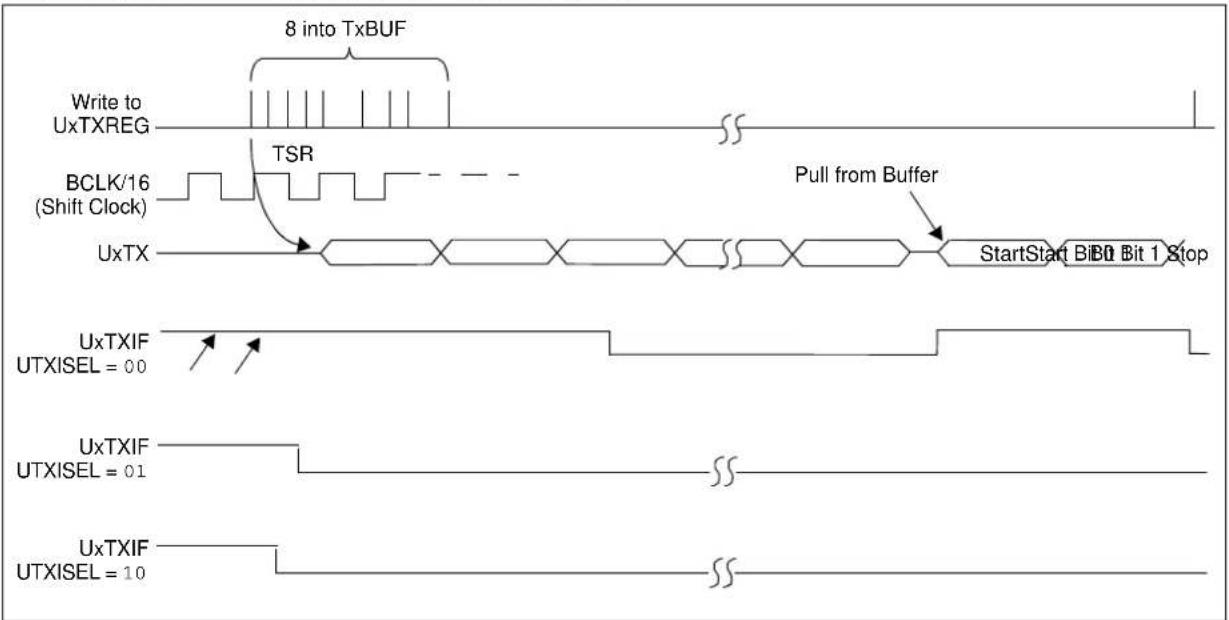
flowchart
graph TD
    A["Write to UxTXREG"] --> B["8 into TxBUF"]
    B --> C["TSR"]
    C --> D["BCLK/16 (Shift Clock)"]
    D --> E["UxTX"]
    E --> F["Pull from Buffer"]
    F --> G["StartStart Bit Bit 1 Stop"]
    G --> H["UxTXIF UTXISEL = 00"]
    H --> I["UxTXIF UTXISEL = 01"]
    I --> J["UxTXIF UTXISEL = 10"]
    J --> K["SS"]
    style A fill:#f9f,stroke:#333
    style B fill:#ccf,stroke:#333
    style C fill:#cfc,stroke:#333
    style D fill:#fcc,stroke:#333
    style E fill:#cff,stroke:#333
    style F fill:#ffc,stroke:#333
    style G fill:#cfc,stroke:#333
    style H fill:#fcc,stroke:#333
    style I fill:#ffc,stroke:#333
    style J fill:#fcc,stroke:#333
    style K fill:#ffc,stroke:#333
PIC32MZ Embedded Connectivity (EC) Family
23.0 PARALLEL MASTER PORT (PMP)
Note: This data sheet summarizes the features of the PIC32MZ Embedded Connectivity (EC) Family of devices. It is not intended to be a comprehensive reference source. To complement the information in this data sheet, refer to Section 13. "Parallel Master Port (PMP)" (DS60001128), which is available from the Documentation > Reference Manual section of the Microchip PIC32 web site (www.microchip.com/pic32).
The PMP is a parallel 8-bit/16-bit input/output module specifically designed to communicate with a wide variety of parallel devices, such as communications peripherals, LCDs, external memory devices and microcontrollers. Because the interface to parallel peripherals varies significantly, the PMP module is highly configurable.
Key features of the PMP module include:
- 8-bit,16-bit interface
- Up to 16 programmable address lines
- Up to two Chip Select lines
- Programmable strobe options:
- Individual read and write strobes, or
- Read/write strobe with enable strobe
- Address auto-increment/auto-decrement
- Programmable address/data multiplexing
- Programmable polarity on control signals
• Parallel Slave Port support:
- Legacy addressable
- Address support
- 4-byte deep auto-incrementing buffer
• Programmable Wait states
- Operate during Sleep and Idle modes
- Fast bit manipulation using CLR, SET, and INV registers
Note: On 64-pin devices, data pins PMD<15:8> are not available in 16-bit Master modes.
FIGURE 23-1: PMP MODULE PINOUT AND CONNECTIONS TO EXTERNAL DEVICES
| PBCLK2 | Address Bus | |||
| Data Bus | ||||
| Parallel Master Port | PMA0 PMALL | Control Lines | ||
| PMA1 PMALH | ||||
| PMA<13:2> | Up to 16-bit Address | Flash EEPROM SRAM | ||
| PMA14 PMCS1 | ||||
| PMA15 PMCS2 | ||||
| PMRD PMRD/PMWR | ||||
| PMWR PMENB | Microcontroller | LCD | FIFO Buffer | |
| PMD<7:0> PMD<15:8>(1) | 8-bit/16-bit Data (with or without multiplexed addressing) | |||
Note: On 64-pin devices, data pins PMD<15:8> are not available in 16-bit Master modes.
23.1 PMP Control Registers
TABLE 23-1: PARALLEL MASTER PORT REGISTER MAP
| Virtual Address (BF82_#) | Register Name(1) | Bit Range | Bits | All Resets | |||||||||||||||
| 31/15 | 30/14 | 29/13 | 28/12 | 27/11 | 26/10 | 25/9 | 24/8 | 23/7 | 22/6 | 21/5 | 20/4 | 19/3 | 18/2 | 17/1 | 16/0 | ||||
| E000 | PMCON | 31:16 | ——— | ——— | 0000 | ||||||||||||||
| 15:0 | ON | — | SIDL | ADRMUX<1:0> | PMPCTL | PTWREN | PTRDEN | CSF<1:0> | ALP | CS2P | CS1P | — | WRSP | RDSP | 0000 | ||||
| E010 | PMMODE | 31:16 | ——— | ——— | 0000 | ||||||||||||||
| 15:0 | BUSY | IRQM<1:0> | INCM<1:0> | MODE16 | MODE<1:0> | WAITB<1:0> | WAITM<3:0> | WAITE<1:0> | 0000 | ||||||||||
| E020 | PMADDR | 31:16 | ——— | ——— | 0000 | ||||||||||||||
| 15:0 | CS2 CS1 | 0000 | |||||||||||||||||
| ADDR15 | ADDR14 | ||||||||||||||||||
| E030 | PMDOUT | 31:16 | DATAOUT<31:0> | 0000 | |||||||||||||||
| 15:0 | 0000 | ||||||||||||||||||
| E040 | PMDIN | 31:16 | DATAIN<31:0> | 0000 | |||||||||||||||
| 15:0 | 0000 | ||||||||||||||||||
| E050 | PMAEN | 31:16 | ——— | ——— | 0000 | ||||||||||||||
| 15:0 | PTEN<15:0> | 0000 | |||||||||||||||||
| E060 | PMSTAT | 31:16 | ——— | ——— | 0000 | ||||||||||||||
| 15:0 | IBF | IBOV | — | — | IB3F | IB2F | IB1F | IB0F | OBE | OBUF | — | — | OB3E | OB2E | OB1E | OB0E | 000E | ||
Legend: x = unknown value on Reset; — = unimplemented, read as '0'. Reset values are shown in hexadecimal.
Note 1: All registers in this table have corresponding CLR, SET, and INV registers at their virtual addresses, plus offsets of 0x4, 0x8 and 0xC, respectively. See Section 12.2 "CLR, SET, and INV Registers" for more information.
REGISTER 23-1: PMCON: PARALLEL PORT CONTROL REGISTER
| Bit Range | Bit 31/23/15/7 | Bit 30/22/14/6 | Bit 29/21/13/5 | Bit 28/20/12/4 | Bit 27/19/11/3 | Bit 26/18/10/2 | Bit 25/17/9/1 | Bit 24/16/8/0 |
| 31:24 | U-0 U-0 U-0 | U-0 U-0 U-0 | U-0 | |||||
| — — — | — — — — — | |||||||
| 23:16 | U-0 U-0 U-0 | U-0 U-0 U-0 | U-0 | |||||
| — — — | — — — — — | |||||||
| 15:8 | R/W-0 U-0 | R/W-0 R/W-0 | R/W-0 R/W-0 | R/W-0 | ||||
| ON — | S | I | D ADRMUX<1:0> | PMPTTL PTWREN PTRDEN | ||||
| 7:0 | R/W-0 R/W | 0 R/W-0 R/W-0 | R/W-0 U-0 | R/W-0 | ||||
| CSF<1:0>(1) | ALP(1) | CS2P(1) | CS1P(1) | — WRSP | RDSP | |||
Legend:
| R = Readable bit | W = Writable bit | U = Unimplemented bit, read as '0' |
| -n = Value at POR | ‘1’ = Bit is set | ‘0’ = Bit is cleared x = Bit is unknown |
bit 31-16 Unimplemented: Read as '0'
bit 15 ON: Parallel Master Port Enable bit
1 = PMP enabled
0 = PMP disabled, no off-chip access performed
bit 14 Unimplemented: Read as '0'
bit 13 SIDL: Stop in Idle Mode bit
1 = Discontinue module operation when device enters Idle mode
0 = Continue module operation in Idle mode
bit 12-11 ADRMUX<1:0>: Address/Data Multiplexing Selection bits
11 = Lower 8 bits of address are multiplexed on PMD<15:0> pins; upper 8 bits are not used
10 = All 16 bits of address are multiplexed on PMD<15:0> pins
01 = Lower 8 bits of address are multiplexed on PMD<7:0> pins, upper bits are on PMA<15:8>
00 = Address and data appear on separate pins
bit 10 PMPTTL: PMP Module TTL Input Buffer Select bit
1 = PMP module uses TTL input buffers
0 = PMP module uses Schmitt Trigger input buffer
bit 9 PTWREN: Write Enable Strobe Port Enable bit
1 = PMWR/PMENB port enabled
0 = PMWR/PMENB port disabled
bit 8 PTRDEN: Read/Write Strobe Port Enable bit
1 = PMRD/PMWR port enabled
0 = PMRD/PMWR port disabled
bit 7-6 CSF<1:0>: Chip Select Function bits (1)
11 = Reserved
10 = PMCS1 and PMCS2 function as Chip Select
01 = PMCS2 functions as Chip Select and PMCS1 functions as address bit 14
00 = PMCS1 and PMCS2 function as address bit 14 and address bit 15
bit 5 ALP: Address Latch Polarity bit ^(1)
1 = Active-high (PMALL and PMALH)
0 = Active-low (PMALL and PMALH)
bit 4 CS2P: Chip Select 2 Polarity bit ^(1)
1 = Active-high (PMCS2)
0 = Active-low (PMCS2)
Note 1: These bits have no effect when their corresponding pins are used as address lines.
REGISTER 23-1: PMCON: PARALLEL PORT CONTROL REGISTER (CONTINUED)
bit 3 CS1P: Chip Select 1 Polarity bit (1)
1 = Active-high (PMCS1)
0 = Active - low w (PMCS1
bit 2 Unimplemented: Read as '0'
bit 1 WRSP: Write Strobe Polarity bit
For Slave Modes and Master mode 2 (MODE<1:0> = 00,01,10):
1 = Write strobe active-high (PMWR)
0 = Write strobe active-low (PMWR)
For Master mode 1 (MODE<1:0> = 11):
1 = Enable strobe active-high (PMENB)
0 = Enable strobe active-low (PMENB)
bit 0 RDSP: Read Strobe Polarity bit
For Slave modes and Master mode 2 (MODE<1:0> = 00,01,10):
1 = Read Strobe active-high (PMRD)
0 = Read Strobe active-low (PMRD)
For Master mode 1 (MODE<1:0> = 11):
1 = Read/write strobe active-high (PMRD/PMWR)
0 = Read/write strobe active-low (PMRD/PMWR)
Note 1: These bits have no effect when their corresponding pins are used as address lines.
REGISTER 23-2: PMMODE: PARALLEL PORT MODE REGISTER
| Bit Range | Bit 31/23/15/7 | Bit 30/22/14/6 | Bit 29/21/13/5 | Bit 28/20/12/4 | Bit 27/19/11/3 | Bit 26/18/10/2 | Bit 25/17/9/1 | Bit 24/16/8/0 |
| 31:24 | U-0 U-0 U-0 | U-0 U-0 U-0 U-0 | U-0 | |||||
| —— | —— | —— | ||||||
| 23:16 | U-0 U-0 U-0 | U-0 U-0 U-0 U-0 | U-0 | |||||
| —— | —— | —— | ||||||
| 15:8 | R-0 R/W-0 | R/W-0 R/W-0 R/W-0 | R/W-0 R/W-0 R/W-0 | R/W-0 | ||||
| BUSY IRQM<1:0> INCM<1:0> MODE16 MODE<1:0> | ||||||||
| 7:0 | R/W-0 R/W-0 | R/W-0 R/W-0 R/W-0 | W-0 R/W-0 R/W-0 | R/W-0 | ||||
| WAITB<1:0>(1) | WAITM<3:0>(1) | WAITE<1:0>(1) | ||||||
Legend:
| R = Readable bit | W = Writable bit | U = Unimplemented bit, read as ‘0’ |
| -n = Value at POR | ‘1’ = Bit is set | ‘0’ = Bit is cleared x = Bit is unknown |
bit 31-16 Unimplemented: Read as '0'
bit 15 BUSY: Busy bit (Master mode only)
1 = Port is busy
0 = Port is not busy
bit 14-13 IRQM<1:0>: Interrupt Request Mode bits
11 = Reserved, do not use
10 = Interrupt generated when Read Buffer 3 is read or Write Buffer 3 is written (Buffered PSP mode)
or on a read or write operation when PMA<1:0>=11 (Addressable Slave mode only)
01 = Interrupt generated at the end of the read/write cycle
00 = No Interrupt generated
bit 12-11 INCM<1:0>: Increment Mode bits
11 = Slave mode read and write buffers auto-increment (MODE<1:0> = 00 only)
10 = Decrement ADDR<15:0> and ADDR<14> by 1 every read/write cycle(2)
01 = Increment ADDR<15:0> and ADDR<14> by 1 every read/write cycle(2)
00 = No increment or decrement of address
bit 10 MODE16: 8/16-bit Mode bit
1 = 16-bit mode: a read or write to the data register invokes a single 16-bit transfer
0 = 8-bit mode: a read or write to the data register invokes a single 8-bit transfer
bit 9-8 MODE<1:0>: Parallel Port Mode Select bits
11 = Master mode 1 (PMCSx, PMRD/PMWR, PMENB, PMA
10 = Master mode 2 (PMCSx, PMRD, PMWR, PMA
01 = Enhanced Slave mode, control signals (PMRD, PMWR, PMCSx, PMD<7:0>, and PMA<1:0>)
00 = Legacy Parallel Slave Port, control signals (PMRD, PMWR, PMCSx, and PMD<7:0>)
bit 7-6 WAITB<1:0>: Data Setup to Read/Write Strobe Wait States bits ^(1)
11 = Data wait of 4 TPBCLK2; multiplexed address phase of 4 T PBCLK2
10 = Data wait of 3 TPBCLK2; multiplexed address phase of 3 T PBCLK2
01 = Data wait of 2 TPBCLK2; multiplexed address phase of 2 T PBCLK2
00 = Data wait of 1 TPBCLK2; multiplexed address phase of 1 T PBCLK2 (default)
Note 1: Whenever WAITM<3:0> = 0000, WAITB and WAITE bits are ignored and forced to 1 TPBCLK2 cycle for a write operation; WAITB = 1 TPBCLK2 cycle, WAITE = 0 TPBCLK2 cycles for a read operation.
2: Address bits 14 and 15 are is not subject to auto-increment/decrement if configured as Chip Select.
3: The PMD<15:8> bits are not active is the MODE16 bit = 1.
REGISTER 23-2: PMMODE: PARALLEL PORT MODE REGISTER (CONTINUED)
bit 5-2 WAITM<3:0>: Data Read/Write Strobe Wait States bits ^(1) 1111 = Wait of 16 TPBCLK2
•
•
•
0001 = Wait of 2 TPBCLK2
0000 = Wait of 1 TPBCLK2 (default)
bit 1-0 WAITE<1:0>: Data Hold After Read/Write Strobe Wait States bits ^(1) 11 = Wait of 4 TPBCLK2
10 = Wait of 3 TPBCLK2
01 = Wait of 2 TPBCLK2
00 = Wait of 1 TPBCLK2 (default)
For Read operations:
11 = Wait of 3 TPBCLK2
10 = Wait of 2 TPBCLK2
01 = Wait of 1 TPBCLK2
00 = Wait of 0 TPBCLK2 (default)
Note 1: Whenever WAITM<3:0> = 0000, WAITB and WAITE bits are ignored and forced to 1 TPBCLK2 cycle for a write operation; WAITB = 1 TPBCLK2 cycle, WAITE = 0 TPBCLK2 cycles for a read operation. 2: Address bits 14 and 15 are is not subject to auto-increment/decrement if configured as Chip Select. 3: The PMD<15:8> bits are not active is the MODE16 bit = 1.
REGISTER 23-3: PMADDR: PARALLEL PORT ADDRESS REGISTER
| Bit Range | Bit 31/23/15/7 | Bit 30/22/14/6 | Bit 29/21/13/5 | Bit 28/20/12/4 | Bit 27/19/11/3 | Bit 26/18/10/2 | Bit 25/17/9/1 | Bit 24/16/8/0 |
| 31:24 | U-0 U-0 U-0 | U-0 U-0 U-0 U-0 | U-0 | |||||
| ——— | ——— —— | |||||||
| 23:16 | U-0 U-0 U-0 | U-0 U-0 U-0 U-0 | U-0 | |||||
| ——— | ——— —— | |||||||
| 15:8 | R/W-0 R/W-0 | R/W-0 R/W-0 R/W | W-0 R/W-0 R/W-0 | R/W-0 | ||||
| CS2(1) | CS1(3) | ADDR<13:8> | ||||||
| ADDR15(2) | ADDR14(4) | |||||||
| 7:0 | R/W-0 R/W-0 | R/W-0 R/W-0 R/W | W-0 R/W-0 R/W-0 | R/W-0 | ||||
| ADDR<7:0> | ||||||||
Legend:
R = Readable bit W = Writable bit U = Unimplemented bit, read as '0' -n = Value at POR '1' = Bit is set '0' = Bit is cleared x = Bit is unknown
bit 31-16 Unimplemented: Read as '0'
bit 15 CS2: Chip Select 2 bit ^(1)
1 = Chip Select 2 is active
0 = Chip Select 2 is inactive
bit 15 ADDR<15>: Target Address bit 15 ^(2)
bit 14 CS1: Chip Select 1 bit ^(3)
1 = Chip Select 1 is active
0 = Chip Select 1 is inactive
bit 14 ADDR<14>: Target Address bit 14 ^(4)
bit 13-0 ADDR<13:0>: Address bits
Note 1: When the CSF<1:0> bits (PMCON<7:6>) = 10 or 01.
2: When the CSF<1:0> bits (PMCON<7:6>) = 00.
3: When the CSF<1:0> bits (PMCON<7:6>) = 10.
4: When the CSF<1:0> bits (PMCON<7:6>) = 00 or 01.
Note: If the DUALBUF bit (PMCON<17>) = 0, the bits in this register control both read and write target addressing. If the DUALBUF bit = 1, the bits in this register are not used. In this instance, use the PMRADDR register for Read operations and the PMWADDR register for Write operations.
REGISTER 23-4: PMAEN: PARALLEL PORT PIN ENABLE REGISTER
| Bit Range | Bit 31/23/15/7 | Bit 30/22/14/6 | Bit 29/21/13/5 | Bit 28/20/12/4 | Bit 27/19/11/3 | Bit 26/18/10/2 | Bit 25/17/9/1 | Bit 24/16/8/0 |
| 31:24 | U-0 U-0 U-0 | U-0 U-0 U-0 | U-0 U-0 | |||||
| —— — | —— — — — — — | |||||||
| 23:16 | U-0 U-0 U-0 | U-0 U-0 U-0 | U-0 U-0 | |||||
| —— — | —— — — — — — | |||||||
| 15:8 | R/W-0 R/W-0 | R/W-0 R/W-0 | R/W-0 R/W-0 | R/W-0 R/W-0 | ||||
| PTEN<15:14> PTEN<13:8> | ||||||||
| 7:0 | R/W-0 R/W-0 | R/W-0 R/W-0 | R/W-0 R/W-0 | R/W-0 R/W-0 | ||||
| PTEN<7:0> | ||||||||
Legend:
R = Readable bit W = Writable bit U = Unimplemented bit, read as '0' -n = Value at POR '1' = Bit is set '0' = Bit is cleared x = Bit is unknown
bit 31-15 Unimplemented: Read as '0'
bit 15-14 PTEN<15:14>: PMCS1 Strobe Enable bits
1 = PMA15 and PMA14 function as either PMA<15:14> or PMCS1 and PMCS2 ^(1) 0 = PMA15 and PMA14 function as port I/O
bit 13-2 PTEN<13:2>: PMP Address Port Enable bits
1 = PMA<13:2> function as PMP address lines 0 = PMA<13:2> function as port I/O
bit 1-0 PTEN<1:0>: PMALH/PMALL Strobe Enable bits
1 = PMA1 and PMA0 function as either PMA<1:0> or PMALH and PMALL ^(2) 0 = PMA1 and PMA0 pads function as port I/O
Note 1: The use of these pins as PMA15 and PMA14 or CS1 and CS2 is selected by the CSF<1:0> bits in the PMCON register.
2: The use of these pins as PMA1/PMA0 or PMALH/PMALL depends on the Address/Data Multiplex mode selected by bits ADRMUX<1:0> in the PMCON register.
REGISTER 23-5: PMSTAT: PARALLEL PORT STATUS REGISTER (SLAVE MODES ONLY)
| Bit Range | Bit 31/23/15/7 | Bit 30/22/14/6 | Bit 29/21/13/5 | Bit 28/20/12/4 | Bit 27/19/11/3 | Bit 26/18/10/2 | Bit 25/17/9/1 | Bit 24/16/8/0 |
| 31:24 | U-0 U-0 U-0 | U-0 U-0 U-0 | U-0 | |||||
| — — — | — — — — | — | ||||||
| 23:16 | U-0 U-0 U-0 | U-0 U-0 U-0 | U-0 | |||||
| — — — | — — — — | — | ||||||
| 15:8 | R-0 R/W-0, HS, SC U-0 U-0 | R-0 R-0 R-0 R-0 | ||||||
| IBF IBOV — — IB3F IB2F IB1F IB0F | ||||||||
| 7:0 | R-1 R/W-0, HS, SC U-0 U-0 | R-1 R-1 R-1 R-1 | ||||||
| OBE | OBUF | — | — | OB3E | OB2E | OB1E | OB0E | |
| Legend: | HS = Hardware Set | SC = Software Cleared |
| R = Readable bit | W = Writable bit | U = Unimplemented bit, read as ‘0’ |
| -n = Value at POR | ‘1’ = Bit is set | ‘0’ = Bit is cleared x = Bit is unknown |
bit 31-16 Unimplemented: Read as '0'
bit 15 IBF: Input Buffer Full Status bit
1 = All writable input buffer registers are full
0 = Some or all of the writable input buffer registers are empty
bit 14 IBOV: Input Buffer Overflow Status bit
1 = A write attempt to a full input byte buffer occurred (must be cleared in software)
0 = No overflow occurred
bit 13-12 Unimplemented: Read as '0'
bit 11-8 IBxF: Input Buffer x Status Full bits
1 = Input Buffer contains data that has not been read (reading buffer will clear this bit)
0 = Input Buffer does not contain any unread data
bit 7 OBE: Output Buffer Empty Status bit
1 = All readable output buffer registers are empty
0 = Some or all of the readable output buffer registers are full
bit 6 OBUF: Output Buffer Underflow Status bit
1 = A read occurred from an empty output byte buffer (must be cleared in software)
0 = No underflow occurred
bit 5-4 Unimplemented: Read as '0'
bit 3-0 OBxE: Output Buffer x Status Empty bits
1 = Output buffer is empty (writing data to the buffer will clear this bit)
0 = Output buffer contains data that has not been transmitted
NOTES:
24.0 EXTERNAL BUS INTERFACE (EBI)
| Note: This data sheet summarizes the features of the PIC32MZ Embedded Connectivity (EC) Family of devices. It is not intended to be a comprehensive reference source. To complement the information in this data sheet, refer to Section 47. “External Bus Interface (EBI)” (DS60001245), which is available from the Documentation > Reference Manual section of the Microchip PIC32 web site (www.microchip.com/pic32). |
The External Bus Interface (EBI) module provides a high-speed, convenient way to interface external parallel memory devices to the PIC32MZ EC family device.
With the EBI module, it is possible to connect asynchronous SRAM and NOR Flash devices, as well as non-memory devices such as camera sensors and LCDs.
The features of the EBI module depend on the pin count of the PIC32MZ EC device, as shown in Table 24-1.
TABLE 24-1: EBI MODULE FEATURES
| Feature | Number of Device Pins | ||
| 100 1 | 24 144 | ||
| Async SRAM Y Y | Y | ||
| Async NOR Flash | Y | Y | Y |
| Available address lines | 20 | 20 | 24 |
| 8-bit data bus support | Y | Y | Y |
| 16-bit data bus support | Y | Y | Y |
| Available Chip Selects | 1 | 1 4 | |
| Timing mode sets | 3 | 3 3 | |
| 8-bit R/W from 16-bit bus | N | N | Y |
| Non-memory device | Y | Y | Y |
| LCD | Y | Y | Y |
Note: Once the EBI module is configured, external devices will be memory mapped and can be access from KSEG2 memory space (see Figure 4-1 through Figure 4-4 in Section 4.0 "Memory Organization" for more information). The MMU must be enabled and the TLB must be set up to access this memory (see Section 50. "CPU for Devices with MIPS32® microAptiv™ and M-Class Cores" (DS60001192) in the "PIC32 Family Reference Manual" for more information).
FIGURE 24-1: EBI SYSTEM BLOCK DIAGRAM

flowchart
graph LR
    PBCLK8 --> BusInterface["Bus Interface"]
    SystemBus["System Bus"] --> BusInterface
    BusInterface --> ControlRegisters["Control Registers"]
    BusInterface --> Data_FIFO["Data FIFO"]
    BusInterface --> Address_FIFO["Address FIFO"]

    ExternalBus["External Bus Interface"] --> MemoryInterface["Memory Interface"]
    MemoryInterface --> AddressDecoder["Address Decoder"]
    MemoryInterface --> ControlRegisters["Control Registers"]
    MemoryInterface --> Static_Memory_Controller["Static Memory Controller"]

    ExternalBus --> EBIA<23:0>[EBIA<23:0>]
    ExternalBus --> EBID<15:0>[EBID<15:0>]
    ExternalBus --> EBIBS<1:0>[EBIBS<1:0>]
    ExternalBus --> EBICS<3:0>[EBICS<3:0>]
    ExternalBus --> EBIOE["EBIOE"]
    ExternalBus --> EBIRP["EBIRP"]
    ExternalBus --> EBIWE["EBIWE"]
    ExternalBus --> EBIRDY<3:1>[EBIRDY<3:1>]
24.1 EBI Control Registers
TABLE 24-2: EBI REGISTER MAP
Legend: x = unknown value on Reset; — = unimplemented, read as '0'. Reset values are shown in hexadecimal.
Note 1: This register is not available on 64-pin devices.
2: This register is available on 144-pin devices only.
REGISTER 24-1: EBICSx: EXTERNAL BUS INTERFACE CHIP SELECT REGISTER ('x' = 0-3)
| Bit Range | Bit 31/23/15/7 | Bit 30/22/14/6 | Bit 29/21/13/5 | Bit 28/20/12/4 | Bit 27/19/11/3 | Bit 26/18/10/2 | Bit 25/17/9/1 | Bit 24/16/8/0 |
| 31:24 | R/W-0 R/W | 0 R/W-0 R/W-0 | R/W-0 R/W-0 R/W | 0 R/W-0 | ||||
| CSADDR<15:8> | ||||||||
| 23:16 | R/W-0 R/W | 0 R/W-0 R/W-0 | R/W-0 R/W-0 R/W | 0 R/W-0 | ||||
| CSADDR<7:0> | ||||||||
| 15:8 | U-0 U-0 U-0 | U-0 U-0 U-0 | U-0 U-0 | |||||
| — — — | — — — — — | |||||||
| 7:0 | U-0 U-0 U-0 | U-0 U-0 U-0 | U-0 U-0 | |||||
| — — — | — — — — — | |||||||
Legend:
R = Readable bit W = Writable bit U = Unimplemented bit, read as '0'
-n = Value at POR '1' = Bit is set '0' = Bit is cleared x = Bit is unknown
bit 31-16 CSADDR<15:0>: Base Address for Device bits
Address in physical memory, which will select the external device.
bit 15-0 Unimplemented: Read as '0'
REGISTER 24-2: EBIMSKx: EXTERNAL BUS INTERFACE ADDRESS MASK REGISTER ('x' = 0-3)
| Bit Range | Bit 31/23/15/7 | Bit 30/22/14/6 | Bit 29/21/13/5 | Bit 28/20/12/4 | Bit 27/19/11/3 | Bit 26/18/10/2 | Bit 25/17/9/1 | Bit 24/16/8/0 | |
| 31:24 | U | - | 0 | U | - | 0 | U | - | 0 |
| —— | —— | —— | |||||||
| 23:16 | U | - | 0 | U | - | 0 | U | - | 0 |
| —— | —— | —— | |||||||
| 15:8 | U-0 U-0 U-0 U-0 U-0 R/W-0 R/W-0 R/W-0 | ||||||||
| —— — — REGSEL<2:0> | |||||||||
| 7:0 | R/W-0 R/W | 0 R/W-1 R/W-0 R/W-0 R/W-0 R/W-0 R/W-0 | |||||||
| MEMTYPE<2:0> MEMSIZE<4:0> (1) | |||||||||
Legend:
R = Readable bit W = Writable bit U = Unimplemented bit, read as '0'
-n = Value at POR '1' = Bit is set '0' = Bit is cleared x = Bit is unknown
bit 31-11 Unimplemented: Read as '0'
bit 10-8 REGSEL<2:0>: Timing Register Set for Chip Select 'x' bits
111 = Reserved
:
.
011 = Reserved
010 = Use EBISMT2
001 = Use EBISMT1
000 = Use EBISMT0
bit 7-5 MEMTYPE<2:0>: Select Memory Type for Chip Select 'x' bits
111 = Reserved
:
.
011 = Reserved
010 = NOR-Flash
001 = SRAM
000 = Reserved
bit 4-0 MEMSIZE<4:0>: Select Memory Size for Chip Select 'x' bits ^(1) 11111 = Reserved
·
·
·
01010 = Reserved
01001 = 16 MB
01000 = 8 MB
00111 = 4 MB
00110 = 2 MB
00101 = 1 MB
00100 = 512 KB
00011 = 256 KB
00010 = 128 KB
00001 = 64 KB (smaller memories alias within this range)
00000 = Chip Select is not used
Note 1: The specified value for these bits depends on the number of available address lines. Refer to the specific device pin table (Table 2 through Table 5) for the available address lines.
REGISTER 24-3: EBISMTx: EXTERNAL BUS INTERFACE STATIC MEMORY TIMING REGISTER ('x' = 0-2)
| Bit Range | Bit 31/23/15/7 | Bit 30/22/14/6 | Bit 29/21/13/5 | Bit 28/20/12/4 | Bit 27/19/11/3 | Bit 26/18/10/2 | Bit 25/17/9/1 | Bit 24/16/8/0 |
| 31:24 | U-0 U-0 U-0 | U-0 U-0 R/W-1 | R/W-0 R/W-0 | |||||
| — — — | — — RDYMODE PAGESI | ZE<1:0> | ||||||
| 23:16 | R/W-0 R/W-0 | R/W-0 R/W-1 R | W-1 R/W-1 R/W-0 | R/W-0 | ||||
| PAGEMODE | TPRC<3:0> | (1) | TBTA<2:0>(1) | |||||
| 15:8 | R/W-0 R/W-0 | R/W-1 R/W-0 R | W-1 R/W-1 R/W-0 | R/W-1 | ||||
| TWP<5:0>(1) | TWR<1:0>(1) | |||||||
| 7:0 | R/W-0 R/W-1 | R/W-0 R/W-0 R | W-1 R/W-0 R/W-1 | R/W-1 | ||||
| TAS<1:0>(1) | TRC<5:0>(1) | |||||||
Legend:
| R = Readable bit | W = Writable bit | U = Unimplemented bit, read as '0' |
| -n = Value at POR | '1' = Bit is set | '0' = Bit is cleared x = Bit is unknown |
bit 31-27 Unimplemented: Read as '0'
bit 26 RDYMODE: Data Ready Device Select bit
The device associated with register set 'x' is a data-ready device, and will use the EBIRDYx pin.
1 = EBIRDYx input is used
0 = EBIRDYx input is not used
bit 25-24 PAGESIZE<1:0>: Page Size for Page Mode Device bits
11 = 32-word page
10 = 16-word page
01 = 8-word page
00 = 4-word page
bit 23 PAGEMODE: Memory Device Page Mode Support bit
1 = Device supports Page mode
0 = Device does not support Page mode
bit 22-19 TPRC<3:0>: Page Mode Read Cycle Time bits ^(1)
Read cycle time is TPRC + 1 clock cycle.
bit 18-16 TBTA<2:0>: Data Bus Turnaround Time bits ^(1)
Clock cycles (0-7) for static memory between read-to-write, write-to-read, and read-to-read when Chip Select changes.
bit 15-10 TWP<5:0>: Write Pulse Width bits ^(1)
Write pulse width is TWP + 1 clock cycle.
bit 9-8 TWR<1:0>: Write Address/Data Hold Time bits ^(1)
Number of clock cycles to hold address or data on the bus.
bit 7-6 TAS<1:0>: Write Address Setup Time bits ^(1)
Clock cycles for address setup time. A value of '0' is only valid in the case of SSRAM.
bit 5-0 TRC<5:0>: Read Cycle Time bits ^(1)
Read cycle time is TRC + 1 clock cycle.
Note 1: Please refer to Section 47. "External Bus Interface (EBI)" (DS60001245) in the "PIC32 Family Reference Manual" for the EBI timing diagrams and additional information.
REGISTER 24-4: EBIFTRPD: EXTERNAL BUS INTERFACE FLASH TIMING REGISTER
| Bit Range | Bit 31/23/15/7 | Bit 30/22/14/6 | Bit 29/21/13/5 | Bit 28/20/12/4 | Bit 27/19/11/3 | Bit 26/18/10/2 | Bit 25/17/9/1 | Bit 24/16/8/0 |
| 31:24 | U-0 U-0 U-0 | U-0 U-0 U-0 | U-0 U-0 | |||||
| — — — | — — — — — | |||||||
| 23:16 | U-0 U-0 U-0 | U-0 U-0 | U-0 U-0 U-0 | |||||
| — — — | — — — — — | |||||||
| 15:8 | U-0 U-0 U-0 | U-0 R/W-0 | R/W-0 | R/W-0 R/W-0 | ||||
| — — — | — TRPD<11:8> | |||||||
| 7:0 | R/W-0 R/W | 0 R/W-0 | R/W-0 | R/W-0 R/W-0 | 0 R/W-0 | |||
| TRPD<7:0> | ||||||||
Legend:
| R = Readable bit W = Writable bit U = Unimplemented bit, read as '0' | ||
| -n = Value at POR | ‘1’ = Bit is set | ‘0’ = Bit is cleared x = Bit is unknown |
bit 31-12 Unimplemented: Read as '0'
bit 11-0 TRPD<11:0>: Flash Timing bits
These bits define the number of clock cycles to wait after resetting the external Flash memory before any read/write access.
REGISTER 24-5: EBISMCON: EXTERNAL BUS INTERFACE STATIC MEMORY CONTROL REGISTER
| Bit Range | Bit 31/23/15/7 | Bit 30/22/14/6 | Bit 29/21/13/5 | Bit 28/20/12/4 | Bit 27/19/11/3 | Bit 26/18/10/2 | Bit 25/17/9/1 | Bit 24/16/8/0 |
| 31:24 | U-0 U-0 U-0 U-0 U-0 U-0 U-0 | |||||||
| — — — — | — — — — | |||||||
| 23:16 | U-0 U-0 U-0 U-0 U-0 U-0 U-0 | |||||||
| — — — — | — — — — | |||||||
| 15:8 | R/W-0 R/W-0 R/W-0 R/W-0 R/W-0 R/W-1 | R/W-0 | ||||||
| SMDWIDTH2<2:0> | SMDWIDTH1<2:0> | SMDWIDTH0<2:1> | ||||||
| 7:0 | R/W-0 | U-0 U-0 U-0 U-0 U-0 U-0 | R/W-1 | |||||
| SMDWIDTH0<0> | — | — | — | — | — | — | SMRP | |
Legend:
| R = Readable bit | W = Writable bit | U = Unimplemented bit, read as '0' |
| -n = Value at POR | '1' = Bit is set | '0' = Bit is cleared x = Bit is unknown |
bit 31-16 Unimplemented: Read as '0'
bit 15-13 SMDWIDTH2<2:0>: Static Memory Width for Register EBISMT2 bits
111 = Reserved
110 = Reserved
101 = Reserved
100 = 8 bits
011 = Reserved
010 = Reserved
001 = Reserved
000 = 16 bits
bit 12-10 SMDWIDTH1<2:0>: Static Memory Width for Register EBISMT1 bits
111 = Reserved
110 = Reserved
101 = Reserved
100 = 8 bits
011 = Reserved
010 = Reserved
001 = Reserved
000 = 16 bits
bit 9-7 SMDWIDTH0<2:0>: Static Memory Width for Register EBISMT0 bits
111 = Reserved
110 = Reserved
101 = Reserved
100 = 8 bits
011 = Reserved
010 = Reserved
001 = Reserved
000 = 16 bits
bit 6-1 Unimplemented: Read as '0'
bit 0 SMRP: Flash Reset/Power-down mode Select bit
After a Reset, the controller internally performs a power-down for Flash, and then sets this bit to '1'.
1 = Flash is taken out of Power-down mode
0 = Flash is forced into Power-down mode
NOTES:
25.0 REAL-TIME CLOCK AND CALENDAR (RTCC)
Note: This data sheet summarizes the features of the PIC32MZ Embedded Connectivity (EC) Family of devices. It is not intended to be a comprehensive reference source. To complement the information in this data sheet, refer to Section 29. “Real-Time Clock and Calendar (RTCC)” (DS60001125), which is available from the Documentation > Reference Manual section of the Microchip PIC32 web site (www.microchip.com/pic32).
The RTCC module is intended for applications in which accurate time must be maintained for extended periods of time with minimal or no CPU intervention. Low-power optimization provides extended battery lifetime while keeping track of time.
The following are key features of the RTCC module:
• Time: hours, minutes and seconds
• 24-hour format (military time)
- Visibility of one-half second period
- Provides calendar: Weekday, date, month and year
- Alarm intervals are configurable for half of a second, one second, 10 seconds, one minute, 10 minutes, one hour, one day, one week, one month, and one year
- Alarm repeat with decrementing counter
- Alarm with indefinite repeat: Chime
• Year range: 2000 to 2099
- Leap year correction
• BCD format for smaller firmware overhead
- Optimized for long-term battery operation
• Fractional second synchronization
- User calibration of the clock crystal frequency with auto-adjust
- Calibration range: ±0.66 seconds error per month
- Calibrates up to 260 ppm of crystal error
- Uses external 32.768 kHz crystal or 32 kHz internal oscillator
- Alarm pulse, seconds clock, or internal clock output on RTCC pin
FIGURE 25-1: RTCC BLOCK DIAGRAM

flowchart
graph TD
    A["32.768 kHz Input from Secondary Oscillator (SOSC)"] --> B["RTCC Prescalers"]
    C["32 kHz Input from Internal Oscillator (LPRC)"] --> B
    B --> D["0.5 seconds"]
    D --> E["RTCC Timer"]
    E --> F["Comparator"]
    F --> G["Compare Registers with Masks"]
    G --> H["Repeat Counter"]
    H --> I["RTCC Interrupt Logic"]
    I --> J["RTCC Interrupt"]
    J --> K["RTCOE"]
    K --> L["RTCC Pin"]
    M["Year, MTH, DAY"] --> N["RTCVAL"]
    O["WKDAY"] --> N
    P["HR, MIN, SEC"] --> N
    Q["MTH, DAY"] --> R["ALRMVAL"]
    S["WKDAY"] --> R
    T["HR, MIN, SEC"] --> R
    U["RTCOUTSEL<1:0>"] --> V["RTCC Interrupt"]
    W["Alarm Event"] --> I
    X["Alarm Pulse"] --> I
    Y["Seconds Pulse"] --> I
    Z["TRTC"] --> I
25.1 RTCC Control Registers
TABLE 25-1: RTCC REGISTER MAP
| Virtual Address(BF80 #) | Register Name(1) | Bit Range | Bits | All Resets | |||||||||||||||
| 31/15 | 30/14 | 29/13 | 28/12 | 27/11 | 26/10 | 25/9 | 24/8 | 23/7 | 22/6 | 21/5 | 20/4 | 19/3 | 18/2 | 17/1 | 16/0 | ||||
| 0C00 | RTCCON | 31:16 | — | — | — | — | — | — | CAL<9:0> | 0000 | |||||||||
| 15:0 | ON | — | SIDL | — | — | RTCCLKSEL<1:0> | RTCOUTSEL<1:0> | RTCCLKON | — | — | RTCWREN | RTCSYNC | HALFSEC | RTCOE | 0000 | ||||
| 0C10 | RTCALRM | 31:16 | — | — | — | — | — | — | — | — | — | — | — | — | — | — | — | 0000 | |
| 15:0 | ALRMEN | CHIME | PIV | ALRMSYNC | AMASK<3:0> | ARPT<7:0> | 0000 | ||||||||||||
| 0C20 | RTCTIME | 31:16 | — | — | HR10<1:0> | HR01<3:0> | — | MIN10<2:0> | MIN01<3:0> | xxxxx | |||||||||
| 15:0 | — | SEC10<2:0> | SEC01<3:0> | — | — | — | — | — | — | — | xx00 | ||||||||
| 0C30 | RTCDATE | 31:16 | YEAR10<3:0> | YEAR01<3:0> | — | — | — | MONTH10 | MONTH01<3:0> | xxxxx | |||||||||
| 15:0 | — | — | DAY10<1:0> | DAY01<3:0> | — | — | — | — | — | WDAY01<2:0> | xx00 | ||||||||
| 0C40 | ALRMTIME | 31:16 | — | — | HR10<1:0> | HR01<3:0> | — | MIN10<2:0> | MIN01<3:0> | xxxxx | |||||||||
| 15:0 | — | SEC10<2:0> | SEC01<3:0> | — | — | — | — | — | — | xx00 | |||||||||
| 0C50 | ALRMDATE | 31:16 | — | — | — | — | — | — | — | — | — | — | — | MONTH10 | MONTH01<3:0> | 00xx | |||
| 15:0 | — | — | DAY10<1:0> | DAY01<3:0> | — | — | — | — | — | WDAY01<2:0> | xx00x | ||||||||
Legend: x = unknown value on Reset; — = unimplemented, read as '0'. Reset values are shown in hexadecimal.
Note 1: All registers in this table have corresponding CLR, SET, and INV registers at its virtual address, plus an offset of 0x4, 0x8 and 0xC, respectively. See Section 12.2 "CLR, SET, and INV Registers" for more information.
REGISTER 25-1: RTCCON: REAL-TIME CLOCK AND CALENDAR CONTROL REGISTER
| Bit Range | Bit 31/23/15/7 | Bit 30/22/14/6 | Bit 29/21/13/5 | Bit 28/20/12/4 | Bit 27/19/11/3 | Bit 26/18/10/2 | Bit 25/17/9/1 | Bit 24/16/8/0 |
| 31:24 | U-0 U-0 U-0 | U-0 U-0 U-0 R/W-0 | R/W-0 | |||||
| —— — — — | — — — | C | A | L | < 9 | |||
| 23:16 | R/W-0 R/W-0 | R/W-0 R/W-0 | R/W-0 R/W-0 | R/W-0 | R/W-0 R/W-0 | |||
| CAL<7:0> | ||||||||
| 15:8 | R/W-0 | U-0 | R/W-0 | U-0 | U-0 | R/W-0 | R/W-0 | R/W-0 |
| ON(1) | — | SIDL | — | — | RTCCLKSEL<1:0> | RTC OUTSEL<1>(2) | ||
| 7:0 | R/W-0 R-0 U-0 | U-0 | R/W-0 | R-0 R-0 R/W-0 | ||||
| RTC OUTSEL<0>(2) | RTC CLKON(5) | — | — | RTC WREN(3) | RTC SYNC | HALFSEC(4) | RTCOE | |
| Legend: | |||
| R = Readable bit | W = Writable bit | U = Unimplemented bit, read as ‘0’ | |
| -n = Value at POR | ‘1’ = Bit is set | ‘0’ = Bit is cleared | x = Bit is unknown |
bit 31-26 Unimplemented: Read as '0'
bit 25-16 CAL<9:0>: Real-Time Clock Drift Calibration bits, which contain a signed 10-bit integer value
0111111111 = Maximum positive adjustment, adds 511 real-time clock pulses every one minute
0000000001 = Minimum positive adjustment, adds 1 real-time clock pulse every one minute
0000000000 = No adjustment
1111111111 = Minimum negative adjustment, subtracts 1 real-time clock pulse every one minute
.
.
.
1000000000 = Maximum negative adjustment, subtracts 512 real-time clock pulses every one minute
bit 15 ON: RTCC On bit ^(1)
1 = RTCC module is enabled
0 = RTCC module is disabled
bit 14 Unimplemented: Read as '0'
bit 13 SIDL: Stop in Idle Mode bit
1 = Disables RTCC operation when CPU enters Idle mode
0 = Continue normal operation when CPU enters Idle mode
bit 12-11 Unimplemented: Read as '0'
Note 1: The ON bit is only writable when RTCWREN = 1.
2: Requires RTCOE = 1 (RTCCON<0>) for the output to be active.
3: The RTCWREN bit can be set only when the write sequence is enabled.
4: This bit is read-only. It is cleared to '0' on a write to the seconds bit fields (RTCTIME<14:8>).
5: This bit is undefined when RTCCLKSEL<1:0>=00 (LPRC is the clock source).
Note: This register is reset only on a Power-on Reset (POR).
REGISTER 25-1: RTCCON: REAL-TIME CLOCK AND CALENDAR CONTROL REGISTER
bit 10-9 RTCCLKSEL<1:0>: RTCC Clock Select bits
When a new value is written to these bits, the Seconds Value register should also be written to properly reset the clock prescalers in the RTCC.
11 = Reserved
10 = Reserved
01 = RTCC uses the external 32.768 kHz Secondary Oscillator (SOSC)
00 = RTCC uses the internal 32 kHz oscillator (LPRC)
bit 8-7 RTCOUTSEL<1:0>: RTCC Output Data Select bits (2)
11 = Reserved
10 = RTCC Clock is presented on the RTCC pin
01 = Seconds Clock is presented on the RTCC pin
00 = Alarm Pulse is presented on the RTCC pin when the alarm interrupt is triggered
bit 6 RTCCLKON: RTCC Clock Enable Status bit (5)
1 = RTCC Clock is actively running
0 = RTCC Clock is not running
bit 5-4 Unimplemented: Read as '0'
bit 3 RTCWREN: Real-Time Clock Value Registers Write Enable bit ^(3)
1 = Real-Time Clock Value registers can be written to by the user
0 = Real-Time Clock Value registers are locked out from being written to by the user
bit 2 RTCSYNC: Real-Time Clock Value Registers Read Synchronization bit
1 = Real-time clock value registers can change while reading (due to a rollover ripple that results in an invalid data read). If the register is read twice and results in the same data, the data can be assumed to be valid.
0 = Real-time clock value registers can be read without concern about a rollover ripple
bit 1 HALFSEC: Half-Second Status bit (4)
1 = Second half period of a second
0 = First half period of a second
bit 0 RTCOE: RTCC Output Enable bit
1 = RTCC output is enabled
0 = RTCC output is not enabled
Note 1: The ON bit is only writable when RTCWREN = 1.
2: Requires RTCOE = 1 (RTCCON<0>) for the output to be active.
3: The RTCWREN bit can be set only when the write sequence is enabled.
4: This bit is read-only. It is cleared to '0' on a write to the seconds bit fields (RTCTIME<14:8>).
5: This bit is undefined when RTCCLKSEL<1:0> = 00 (LPRC is the clock source).
Note: This register is reset only on a Power-on Reset (POR).
REGISTER 25-2: RTCALRM: REAL-TIME CLOCK ALARM CONTROL REGISTER
| Bit Range | Bit 31/23/15/7 | Bit 30/22/14/6 | Bit 29/21/13/5 | Bit 28/20/12/4 | Bit 27/19/11/3 | Bit 26/18/10/2 | Bit 25/17/9/1 | Bit 24/16/8/0 |
| 31:24 | U-0 U-0 U-0 | U-0 U-0 U-0 U-0 | U-0 | |||||
| — — — | — — | — | — — | |||||
| 23:16 | U-0 U-0 U-0 | U-0 U-0 U-0 U-0 | U-0 | |||||
| — — — | — — | — | — — | |||||
| 15:8 | R/W-0 | R/W-0 | R/W-0 | R-0 | R/W-0 | R/W-0 | R/W-0 | R/W-0 |
| ALRMEN(1,2) | CHIME(2) | PIV(2) | ALRMSYNC | AMASK<3:0>(2) | ||||
| 7:0 | R/W-0 | R/W-0 | R/W-0 | R/W-0 | R/W-0 | R/W-0 | R/W-0 | R/W-0 |
| ARPT<7:0>(2) | ||||||||
Legend:
| R = Readable bit | W = Writable bit | U = Unimplemented bit, read as '0' |
| -n = Value at POR | '1' = Bit is set | '0' = Bit is cleared x = Bit is unknown |
bit 31-16 Unimplemented: Read as '0'
bit 15 ALRMEN: Alarm Enable bit ^(1,2)
1 = Alarm is enabled
0 = Alarm is disabled
bit 14 CHIME: Chime Enable bit ^(2)
1 = Chime is enabled - ARPT<7:0> is allowed to rollover from 0x00 to 0xFF
0 = Chime is disabled - ARPT<7:0> stops once it reaches 0x00
bit 13 PIV: Alarm Pulse Initial Value bit ^(2)
When ALRMEN = 0, PIV is writable and determines the initial value of the Alarm Pulse.
When ALRMEN = 1, PIV is read-only and returns the state of the Alarm Pulse.
bit 12 ALRMSYNC: Alarm Sync bit
1 = ARPT<7:0> and ALRMEN may change as a result of a half second rollover during a read.
The ARPT must be read repeatedly until the same value is read twice. This must be done since multiple bits may be changing.
0 = ARPT<7:0> and ALRMEN can be read without concerns of rollover because the prescaler is more than 32 real-time clocks away from a half-second rollover
bit 11-8 AMASK<3:0>: Alarm Mask Configuration bits ^(2)
0000 = Every half-second
0001 = Every second
0010 = Every 10 seconds
0011 = Every minute
0100 = Every 10 minutes
0101 = Every hour
0110 = Once a day
0111 = Once a week
1000 = Once a month
1001 = Once a year (except when configured for February 29, once every four years)
1010 = Reserved
1011 = Reserved
11xx = Reserved
Note 1: Hardware clears the ALRMEN bit anytime the alarm event occurs, when ARPT<7:0> = 00 and CHIME = 0.
2: This field should not be written when the RTCC ON bit = '1' (RTCCON<15>) and ALRMSYNC = 1.
Note: This register is reset only on a Power-on Reset (POR).
REGISTER 25-2: RTCALRM: REAL-TIME CLOCK ALARM CONTROL REGISTER (CONTINUED)
bit 7-0 ARPT<7:0>: Alarm Repeat Counter Value bits (2)
11111111 = Alarm will trigger 256 times
:
.
00000000 = Alarm will trigger one time
The counter decrements on any alarm event. The counter only rolls over from 0x00 to 0xFF if CHIME = 1.
Note 1: Hardware clears the ALRMEN bit anytime the alarm event occurs, when ARPT<7:0> = 00 and CHIME = 0. 2: This field should not be written when the RTCC ON bit = '1' (RTCCON<15>) and ALRMSYNC = 1.
Note: This register is reset only on a Power-on Reset (POR).
REGISTER 25-3: RTCTIME: REAL-TIME CLOCK TIME VALUE REGISTER
| Bit Range | Bit 31/23/15/7 | Bit 30/22/14/6 | Bit 29/21/13/5 | Bit 28/20/12/4 | Bit 27/19/11/3 | Bit 26/18/10/2 | Bit 25/17/9/1 | Bit 24/16/8/0 |
| 31:24 | U-0 U-0 R/W-x R/W-x R/W-x | R/W-x R/W-x R/W-x | ||||||
| — — HR10<1:0> HR01<3:0> | ||||||||
| 23:16 | U-0 | R/W-x R/W-x R/W-x R/W-x R/W-x | ||||||
| — | MIN10<2:0> | MIN01<3:0> | ||||||
| 15:8 | U-0 | R/W-x R/W-x R/W-x R/W-x | ||||||
| — | SEC10<2:0> | SEC01<3:0> | ||||||
| 7:0 | U-0 | U-0 | U-0 | U-0 | U-0 | U-0 | U-0 | U-0 |
| — | — | — | — | — | — | — | — | |
Legend:
| R = Readable bit | W = Writable bit | U = Unimplemented bit, read as '0' |
| -n = Value at POR | '1' = Bit is set | '0' = Bit is cleared x = Bit is unknown |
bit 31-30 Unimplemented: Read as '0'
bit 29-28 HR10<1:0>: Binary-Coded Decimal Value of Hours bits, tens digit; contains a value from 0 to 2
bit 27-24 HR01<3:0>: Binary-Coded Decimal Value of Hours bits, ones digit; contains a value from 0 to 9
bit 23 Unimplemented: Read as '0'
bit 22-20 MIN10<2:0>: Binary-Coded Decimal Value of Minutes bits, tens digit; contains a value from 0 to 5
bit 19-16 MIN01<3:0>: Binary-Coded Decimal Value of Minutes bits, ones digit; contains a value from 0 to 9
bit 15 Unimplemented: Read as '0'
bit 14-12 SEC10<2:0>: Binary-Coded Decimal Value of Seconds bits, tens digit; contains a value from 0 to 5
bit 11-8 SEC01<3:0>: Binary-Coded Decimal Value of Seconds bits, ones digit; contains a value from 0 to 9
bit 7-0 Unimplemented: Read as '0'
Note: This register is only writable when RTCWREN = 1 (RTCCON<3>).
REGISTER 25-4: RTCDATE: REAL-TIME CLOCK DATE VALUE REGISTER
| Bit Range | Bit 31/23/15/7 | Bit 30/22/14/6 | Bit 29/21/13/5 | Bit 28/20/12/4 | Bit 27/19/11/3 | Bit 26/18/10/2 | Bit 25/17/9/1 | Bit 24/16/8/0 |
| 31:24 | R/W-x R/W-x | R/W-x R/W-x R/W-x | W-x R/W-x R/W-x | R/W-x | ||||
| YEAR10<3:0> YEAR01<3:0> | ||||||||
| 23:16 | U-0 U-0 U-0 | R/W-x R/W-x R/W-x | W-x R/W-x R/W-x | |||||
| — | — | — | MONTH10 | MONTH01<3:0> | ||||
| 15:8 | U-0 U-0 R/W-x | R/W-x R/W-x R/W-x | R/W-x R/W-x R/W-x | |||||
| — | — | DAY10<1:0> | DAY01<3:0> | |||||
| 7:0 | U-0 U-0 U-0 | U-0 | U-0 | R/W-x R/W-x R/W-x | ||||
| — | — | — | — | — | WDAY01<2:0> | |||
| Legend: | |||
| R = Readable bit | W = Writable bit | U = Unimplemented bit, read as ‘0’ | |
| -n = Value at POR | ‘1’ = Bit is set | ‘0’ = Bit is cleared | x = Bit is unknown |
bit 31-28 YEAR10<3:0>: Binary-Coded Decimal Value of Years bits, tens digit
bit 27-24 YEAR01<3:0>: Binary-Coded Decimal Value of Years bits, ones digit
bit 23-21 Unimplemented: Read as '0'
bit 20 MONTH10: Binary-Coded Decimal Value of Months bit, tens digit; contains a value from 0 to 1
bit 19-16 MONTH01<3:0>: Binary-Coded Decimal Value of Months bits, ones digit; contains a value from 0 to 9
bit 15-14 Unimplemented: Read as '0'
bit 13-12 DAY10<1:0>: Binary-Coded Decimal Value of Days bits, tens digit; contains a value from 0 to 3
bit 11-8 DAY01<3:0>: Binary-Coded Decimal Value of Days bits, ones digit; contains a value from 0 to 9
bit 7-3 Unimplemented: Read as '0'
bit 2-0 WDAY01<2:0>: Binary-Coded Decimal Value of Weekdays bits, ones digit; contains a value from 0 to 6
Note: This register is only writable when RTCWREN = 1 (RTCCON<3>).
REGISTER 25-5: ALRMTIME: ALARM TIME VALUE REGISTER
| Bit Range | Bit 31/23/15/7 | Bit 30/22/14/6 | Bit 29/21/13/5 | Bit 28/20/12/4 | Bit 27/19/11/3 | Bit 26/18/10/2 | Bit 25/17/9/1 | Bit 24/16/8/0 |
| 31:24 | U-0 U-0 R/W-x R/W-x R/W-x | R/W-x R/W-x R/W-x | ||||||
| — — HR10<1:0> HR01<3:0> | ||||||||
| 23:16 | U-0 | R/W-x R/W-x R/W-x R/W-x R/W-x | ||||||
| — | MIN10<2:0> | MIN01<3:0> | ||||||
| 15:8 | U-0 | R/W-x R/W-x R/W-x R/W-x | ||||||
| — | SEC10<2:0> | SEC01<3:0> | ||||||
| 7:0 | U-0 | U-0 | U-0 | U-0 | U-0 | U-0 | U-0 | U-0 |
| — | — | — | — | — | — | — | — | |
Legend:
| R = Readable bit | W = Writable bit | U = Unimplemented bit, read as '0' |
| -n = Value at POR | '1' = Bit is set | '0' = Bit is cleared x = Bit is unknown |
bit 31-30 Unimplemented: Read as '0'
bit 29-28 HR10<1:0>: Binary Coded Decimal value of hours bits, tens digit; contains a value from 0 to 2
bit 27-24 HR01<3:0>: Binary Coded Decimal value of hours bits, ones digit; contains a value from 0 to 9
bit 23 Unimplemented: Read as '0'
bit 22-20 MIN10<2:0>: Binary Coded Decimal value of minutes bits, tens digit; contains a value from 0 to 5
bit 19-16 MIN01<3:0>: Binary Coded Decimal value of minutes bits, ones digit; contains a value from 0 to 9
bit 15 Unimplemented: Read as '0'
bit 14-12 SEC10<2:0>: Binary Coded Decimal value of seconds bits, tens digit; contains a value from 0 to 5
bit 11-8 SEC01<3:0>: Binary Coded Decimal value of seconds bits, ones digit; contains a value from 0 to 9
bit 7-0 Unimplemented: Read as '0'
REGISTER 25-6: ALRMDATE: ALARM DATE VALUE REGISTER
| Bit Range | Bit 31/23/15/7 | Bit 30/22/14/6 | Bit 29/21/13/5 | Bit 28/20/12/4 | Bit 27/19/11/3 | Bit 26/18/10/2 | Bit 25/17/9/1 | Bit 24/16/8/0 |
| 31:24 | U-0 U-0 U-0 | U-0 U-0 U-0 U-0 | U-0 | |||||
| —— | —— | —— | ||||||
| 23:16 | U-0 | U-0 | U-0 | R/W-x | R/W-x | R/W-x | R/W-x | R/W-x |
| —— | MONTH10 | MONTH01<3:0> | ||||||
| 15:8 | U-0 | U-0 | R/W-x | R/W-x | R/W-x | R/W-x | R/W-x | R/W-x |
| —— | DAY10<1:0> | DAY01<3:0> | ||||||
| 7:0 | U-0 U-0 U-0 | U-0 U-0 | R/W-x | R/W-x | R/W-x | |||
| —— | —— | WDAY01<2:0> | ||||||
Legend:
| R = Readable bit | W = Writable bit | U = Unimplemented bit, read as '0' |
| -n = Value at POR | '1' = Bit is set | '0' = Bit is cleared x = Bit is unknown |
bit 31-21 Unimplemented: Read as '0'
bit 20 MONTH10: Binary Coded Decimal value of months bit, tens digit; contains a value from 0 to 1
bit 19-16 MONTH01<3:0>: Binary Coded Decimal value of months bits, ones digit; contains a value from 0 to 9
bit 15-14 Unimplemented: Read as '0'
bit 13-12 DAY10<1:0>: Binary Coded Decimal value of days bits, tens digit; contains a value from 0 to 3
bit 11-8 DAY01<3:0>: Binary Coded Decimal value of days bits, ones digit; contains a value from 0 to 9
bit 7-3 Unimplemented: Read as '0'
bit 2-0 WDAY01<2:0>: Binary Coded Decimal value of weekdays bits, ones digit; contains a value from 0 to 6
26.0 CRYPTO ENGINE
Note: This data sheet summarizes the features of the PIC32MZ Embedded Connectivity (EC) Family of devices. It is not intended to be a comprehensive reference source. To complement the information in this data sheet, refer to Section 49. “Crypto Engine (CE) and Random Number Generator (RNG)” (DS60001246), which is available from the Documentation > Reference Manual section of the Microchip PIC32 web site (www.microchip.com/pic32).
The Crypto Engine is intended to accelerate applications that need cryptographic functions. By executing these functions in the hardware module, software overhead is reduced, and actions such as encryption, decryption, and authentication can execute much more quickly.
The Crypto Engine uses an internal descriptor-based DMA for efficient programming of the security association data and packet pointers (allowing scatter/gather data fetching). An intelligent state machine schedules the Crypto Engines based on the protocol selection and packet boundaries. The hardware engines can perform the encryption and authentication in sequence or in parallel.
Note: To avoid cache coherency problems on devices with L1 cache, Crypto buffers must only be allocated or accessed from the KSEG1 segment.
Key features of the Crypto Engine include:
- Bulk ciphers and hash engines
- Integrated DMA to off-load processing:
- Buffer descriptor-based
- Secure association per buffer descriptor
- Some functions can execute in parallel
Bulk ciphers that are handled by the Crypto Engine include:
• AES:
- 128-bit, 192-bit, and 256-bit key sizes
- CBC, ECB, CTR, CFB, and OFB modes
• DES/TDES:
- CBC, ECB, CFB, and OFB modes
Authentication engines that are available through the Crypto Engine include:
• S H A - 1
• S H A - 2 5 6
• M D - 5
• AES-GCM
- HMAC operation (for all authentication engines)
The rate of data that can be processed by the Crypto Engine depends on a number of factors, including:
- Which engine is in use
- Whether the engines are used in parallel or in series
- The demands on source and destination memories by other parts of the system (i.e., CPU, DMA, etc.)
- The speed of PBCLK5, which drives the Crypto Engine
Table 26-1 shows typical performance for various engines.
TABLE 26-1: CRYPTO ENGINE PERFORMANCE
| Engine/ Algorithm | Performance Factor (Mbps/MHz) | Maximum Mbps (PBCLK5 = 100 MHz) |
| DES | 14.4 | 1440 |
| TDES | 6.6 | 660 |
| AES-128 | 9.0 | 900 |
| AES-192 | 7.9 | 790 |
| AES-256 | 7.2 | 720 |
| MD5 | 15.6 | 1560 |
| SHA-1 | 13.2 | 1320 |
| SHA-256 | 9.3 | 930 |
FIGURE 26-1: CRYPTO ENGINE BLOCK DIAGRAM
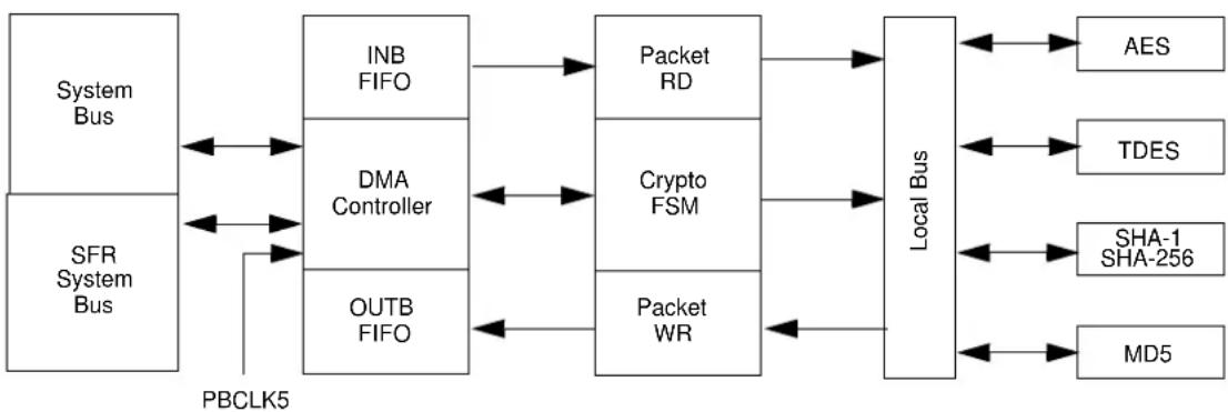
flowchart
graph LR
    A["System Bus"] <--> B["SFR System Bus"]
    C["INB FIFO"] --> D["Packet RD"]
    E["DMA Controller"] --> F["Crypto FSM"]
    G["OUTB FIFO"] --> H["Packet WR"]
    I["Local Bus"] --> J["AES"]
    I --> K["TDES"]
    I --> L["SHA-1 SHA-256"]
    I --> M["MD5"]
    A <--> C
    C <--> E
    C <--> G
    C <--> I
    D <--> F
    D <--> H
    F <--> H
    H <--> I
    I <--> J
    I <--> K
    I <--> L
    I <--> M
    P["PBCLK5"] --> A
26.1 Crypto Engine Control Registers
TABLE 26-2: CRYPTO ENGINE REGISTER MAP
Legend: x = unknown value on Reset; — = unimplemented, read as '0'. Reset values are shown in hexadecimal.
REGISTER 26-1: CEVER: CRYPTO ENGINE REVISION, VERSION, AND ID REGISTER
| Bit Range | Bit 31/23/15/7 | Bit 30/22/14/6 | Bit 29/21/13/5 | Bit 28/20/12/4 | Bit 27/19/11/3 | Bit 26/18/10/2 | Bit 25/17/9/1 | Bit 24/16/8/0 |
| 31:24 | R-0 R-0 R-0 | R-0 R-0 R-0 R-0 | R-0 | |||||
| REVISION<7:0> | ||||||||
| 23:16 | R-0 R-0 R-0 | R-0 R-0 R-0 R-0 | R-0 | |||||
| VERSION<7:0> | ||||||||
| 15:8 | R-0 R-0 R-0 | R-0 R-0 R-0 R-0 | R-0 | |||||
| ID<15:8> | ||||||||
| 7:0 | R-0 R-0 R-0 | R-0 R-0 R-0 R-0 | R-0 | |||||
| ID<7:0> | ||||||||
Legend:
R = Readable bit W = Writable bit U = Unimplemented bit, read as '0' -n = Value at POR '1' = Bit is set '0' = Bit is cleared x = Bit is unknown
bit 31-24 REVISION<7:0>: Crypto Engine Revision bits
bit 23-16 VERSION<7:0>: Crypto Engine Version bits
bit 15-0 ID<15:0>: Crypto Engine Identification bits
REGISTER 26-2: CECON: CRYPTO ENGINE CONTROL REGISTER
| Bit Range | Bit 31/23/15/7 | Bit 30/22/14/6 | Bit 29/21/13/5 | Bit 28/20/12/4 | Bit 27/19/11/3 | Bit 26/18/10/2 | Bit 25/17/9/1 | Bit 24/16/8/0 |
| 31:24 | U-0 U-0 U-0 | U-0 U-0 U-0 | U-0 | |||||
| — — — | — — — — — | |||||||
| 23:16 | U-0 U-0 U-0 | U-0 U-0 U-0 | U-0 | |||||
| — — — | — — — — — | |||||||
| 15:8 | U-0 U-0 U-0 | U-0 U-0 U-0 | U-0 | |||||
| — — — | — — — — — | |||||||
| 7:0 | U-0 | R/W-0, HC | R/W-0 | U-0 | U-0 | R/W-0 | R/W-0 | R/W-0 |
| — | SWRST | SWAPEN | — | — | BDPCHST | BDPPLEN | DMAEN |
| Legend: | HC = Hardware Cleared | ||
| R = Readable bit | W = Writable bit U = Unimplemented bit, read as ‘0’ | ||
| -n = Value at POR | ‘1’ = Bit is set | ‘0’ = Bit is cleared | x = Bit is unknown |
bit 31-7 Unimplemented: Read as '0'
bit 6 SWRST: Software Reset bit
1 = Initiate a software reset of the Crypto Engine
0 = Normal operation
bit 5 SWAPEN: I/O Swap Enable bit
1 = Input data is byte swapped when read by dedicated DMA
0 = Input data is not byte swapped when read by dedicated DMA
bit 4-3 Unimplemented: Read as '0'
bit 2 BDPCHST: Buffer Descriptor Processor (BDP) Fetch Enable bit
This bit should be enabled only after all DMA descriptor programming is completed.
1 = BDP descriptor fetch is enabled
0 = BDP descriptor fetch is disabled
bit 1 BDPPLEN: Buffer Descriptor Processor Poll Enable bit
This bit should be enabled only after all DMA descriptor programming is completed.
1 = Poll for descriptor until valid bit is set
0 = Do not poll
bit 0 DMAEN: DMA Enable bit
1 = Crypto Engine DMA is enabled
0 = Crypto Engine DMA is disabled
REGISTER 26-3: CEBDADDR: CRYPTO ENGINE BUFFER DESCRIPTOR REGISTER
| Bit Range | Bit 31/23/15/7 | Bit 30/22/14/6 | Bit 29/21/13/5 | Bit 28/20/12/4 | Bit 27/19/11/3 | Bit 26/18/10/2 | Bit 25/17/9/1 | Bit 24/16/8/0 |
| 31:24 | R-0 R-0 R-0 | R-0 R-0 R-0 R-0 | R-0 | |||||
| BDPADDR<31:24> | ||||||||
| 23:16 | R-0 R-0 R-0 | R-0 R-0 R-0 R-0 | R-0 | |||||
| BDPADDR<23:16> | ||||||||
| 15:8 | R-0 R-0 R-0 | R-0 R-0 R-0 R-0 | R-0 | |||||
| BDPADDR<15:8> | ||||||||
| 7:0 | R-0 R-0 R-0 | R-0 R-0 R-0 R-0 | R-0 | |||||
| BDPADDR<7:0> | ||||||||
Legend:
R = Readable bit W = Writable bit U = Unimplemented bit, read as '0' -n = Value at POR '1' = Bit is set '0' = Bit is cleared x = Bit is unknown
bit 31-0 BDPADDR<31:0>: Current Buffer Descriptor Process Address Status bits
These bits contain the current descriptor address that is being processed by the Buffer Descriptor Processor (BDP).
REGISTER 26-4: CEBDPADDR: CRYPTO ENGINE BUFFER DESCRIPTOR PROCESSOR REGISTER
| Bit Range | Bit 31/23/15/7 | Bit 30/22/14/6 | Bit 29/21/13/5 | Bit 28/20/12/4 | Bit 27/19/11/3 | Bit 26/18/10/2 | Bit 25/17/9/1 | Bit 24/16/8/0 |
| 31:24 | R/W-0 | R/W-0 | R/W-0 | R/W-0 | R/W-0 | R/W-0 | R/W-0 | R/W-0 |
| BASEADDR<31:24> | ||||||||
| 23:16 | R/W-0 | R/W-0 | R/W-0 | R/W-0 | R/W-0 | R/W-0 | R/W-0 | R/W-0 |
| BASEADDR<23:16> | ||||||||
| 15:8 | R/W-0 | R/W-0 | R/W-0 | R/W-0 | R/W-0 | R/W-0 | R/W-0 | R/W-0 |
| BASEADDR<15:8> | ||||||||
| 7:0 | R/W-0 | R/W-0 | R/W-0 | R/W-0 | R/W-0 | R/W-0 | R/W-0 | R/W-0 |
| BASEADDR<7:0> | ||||||||
Legend:
R = Readable bit W = Writable bit U = Unimplemented bit, read as '0' -n = Value at POR '1' = Bit is set '0' = Bit is cleared x = Bit is unknown
bit 31-0 BASEADDR<31:0>: Buffer Descriptor Base Address bits
These bits contain the physical address of the first Buffer Descriptor in the Buffer Descriptor chain. When enabled, the Crypto DMA begins fetching Buffer Descriptors from this address.
REGISTER 26-5: CESTAT: CRYPTO ENGINE STATUS REGISTER
| Bit Range | Bit 31/23/15/7 | Bit 30/22/14/6 | Bit 29/21/13/5 | Bit 28/20/12/4 | Bit 27/19/11/3 | Bit 26/18/10/2 | Bit 25/17/9/1 | Bit 24/16/8/0 |
| 31:24 | R-0 R-0 R-0 R-0 R-0 R-0 R-0 | R-0 | ||||||
| ERRMODE<2:0> ERROP<2:0> ERRPHASE<1:0> | ||||||||
| 23:16 | U-0 U-0 R-0 R-0 R-0 R-0 R-0 R-0 | |||||||
| — | — | BDSTATE | START | ACTIVE | ||||
| 15:8 | R-0 R-0 R-0 R-0 R-0 R-0 R-0 | R-0 | ||||||
| BDCTRL<15:8> | ||||||||
| 7:0 | R-0 R-0 R-0 R-0 R-0 R-0 R-0 | R-0 | ||||||
| BDCTRL<7:0> | ||||||||
| Legend: | |||
| R = Readable bit | W = Writable bit | U = Unimplemented bit, read as ‘0’ | |
| -n = Value at POR | ‘1’ = Bit is set | ‘0’ = Bit is cleared | x = Bit is unknown |
bit 31-29 ERRMOD<2:0>: Internal Error Mode Status bits
111 = Reserved
110 = Reserved
101 = Reserved
100 = Reserved
011 = CEK operation
010 = KEK operation
001 = Preboot authentication
000 = Normal operation
bit 28-26 ERROP<2:0>: Internal Error Operation Status bits
111 = Reserved
110 = Reserved
101 = Reserved
100 = Authentication
011 = Reserved
010 = Decryption
001 = Encryption
000 = Reserved
bit 25-24 ERRPHASE<1:0>: Internal Error Phase of DMA Status bits
11 = Destination data
10 = Source data
01 = Security Association (SA) access
00 = Buffer Descriptor (BD) access
bit 23-22 Unimplemented: Read as '0'
bit 21-18 BDSTATE<3:0>: Buffer Descriptor Processor State Status bits
These bits contain a number, which indicates the current state of the BDP:
1111 = Reserved
-
:
0111 = Reserved
0110 = SA fetch
0101 = Fetch BDP is disabled
0100 = Descriptor is done
0011 = Data phase
0010 = BDP is loading
0001 = Descriptor fetch request is pending
0000 = BDP is idle
bit 17 START: DMA Start Status bit
1 = DMA start has occurred
0 = DMA start has not occurred
REGISTER 26-5: CESTAT: CRYPTO ENGINE STATUS REGISTER (CONTINUED)
bit 16 ACTIVE: Buffer Descriptor Processor Status bit
1 = BDP is active
0 = BDP is idle
bit 15-0 BDCTRL<15:0>: Descriptor Control Word Status bits
These bits contain the current descriptor control word.
REGISTER 26-6: CEINTSRC: CRYPTO ENGINE INTERRUPT SOURCE REGISTER
| Bit Range | Bit 31/23/15/7 | Bit 30/22/14/6 | Bit 29/21/13/5 | Bit 28/20/12/4 | Bit 27/19/11/3 | Bit 26/18/10/2 | Bit 25/17/9/1 | Bit 24/16/8/0 |
| 31:24 | U-0 U-0 U-0 | U-0 U-0 U-0 U-0 | U-0 | |||||
| — — — | — — — — — | |||||||
| 23:16 | U-0 U-0 U-0 | U-0 U-0 U-0 U-0 | U-0 | |||||
| — — — | — — — — — | |||||||
| 15:8 | U-0 U-0 U-0 | U-0 U-0 U-0 U-0 | U-0 | |||||
| — — — | — — — — — | |||||||
| 7:0 | U-0 U-0 U-0 | U-0 R-0 R-0 R-0 | R-0 | |||||
| — | — | — | — | AREIF | PKTIF | CBDIF | PENDIF |
Legend:
| R = Readable bit | W = Writable bit U = Unimplemented bit, read as '0' |
| -n = Value at POR | '1' = Bit is set '0' = Bit is cleared x = Bit is unknown |
bit 31-4 Unimplemented: Read as '0'
bit 3 AREIF: Access Response Error Interrupt bit
1 = Error occurred trying to access memory outside the Crypto Engine
0 = No error has occurred
bit 2 PKTIF: DMA Packet Completion Interrupt Status bit
1 = DMA packet was completed
0 = DMA packet was not completed
bit 1 CBDIF: BD Transmit Status bit
1 = Last BD transmit was processed
0 = Last BD transmit has not been processed
bit 0 PENDIF: Crypto Engine Interrupt Pending Status bit
1 = Crypto Engine interrupt is pending (this value is the result of an OR of all interrupts in the Crypto Engine)
0 = Crypto Engine interrupt is not pending
REGISTER 26-7: CEINTEN: CRYPTO ENGINE INTERRUPT ENABLE REGISTER
| Bit Range | Bit 31/23/15/7 | Bit 30/22/14/6 | Bit 29/21/13/5 | Bit 28/20/12/4 | Bit 27/19/11/3 | Bit 26/18/10/2 | Bit 25/17/9/1 | Bit 24/16/8/0 |
| 31:24 | U-0 U-0 U-0 | U-0 U-0 U-0 U-0 | U-0 | |||||
| — — — | — — — — — | |||||||
| 23:16 | U-0 U-0 U-0 | U-0 U-0 U-0 U-0 | U-0 | |||||
| — — — | — — — — — | |||||||
| 15:8 | U-0 U-0 U-0 | U-0 U-0 U-0 U-0 | U-0 | |||||
| — — — | — — — — — | |||||||
| 7:0 | U-0 | U-0 | U-0 | U-0 | R/W-0 | R/W-0 | R/W-0 | R/W-0 |
| — | — | — | — | AREIE | PKTIE | BDPIE | PENDIE^(1) |
Legend:
| R = Readable bit | W = Writable bit U = Unimplemented bit, read as '0' |
| -n = Value at POR | ‘1’ = Bit is set ‘0’ = Bit is cleared x = Bit is unknown |
bit 31-4 Unimplemented: Read as '0'
bit 3 AREIE: Access Response Error Interrupt Enable bit
1 = Access response error interrupts are enabled
0 = Access response error interrupts are not enabled
bit 2 PKTIE: DMA Packet Completion Interrupt Enable bit
1 = DMA packet completion interrupts are enabled
0 = DMA packet completion interrupts are not enabled
bit 1 BDPIE: DMA Buffer Descriptor Processor Interrupt Enable bit
1 = BDP interrupts are enabled
0 = BDP interrupts are not enabled
bit 0 PENDIE: Master Interrupt Enable bit ^(1)
1 = Crypto Engine interrupts are enabled
0 = Crypto Engine interrupts are not enabled
Note 1: The PENDIE bit is a Global enable bit and must be enabled together with the other interrupts desired.
REGISTER 26-8: CEPOLLCON: CRYPTO ENGINE POLL CONTROL REGISTER
| Bit Range | Bit 31/23/15/7 | Bit 30/22/14/6 | Bit 29/21/13/5 | Bit 28/20/12/4 | Bit 27/19/11/3 | Bit 26/18/10/2 | Bit 25/17/9/1 | Bit 24/16/8/0 |
| 31:24 | U-0 U-0 U-0 | U-0 U-0 U-0 U-0 | U-0 | |||||
| ——— | ——— —— —— | |||||||
| 23:16 | U-0 U-0 U-0 | U-0 U-0 U-0 U-0 | U-0 | |||||
| ——— | —— —— —— | |||||||
| 15:8 | R/W-0 | R/W-0 | R/W-0 | R/W-0 | R/W-0 | R/W-0 | R/W-0 | R/W-0 |
| BDPPLCON<15:8> | ||||||||
| 7:0 | R/W-0 | R/W-0 | R/W-0 | R/W-0 | R/W-0 | R/W-0 | R/W-0 | R/W-0 |
| BDPPLCON<7:0> | ||||||||
| Legend: | |||
| R = Readable bit | W = Writable bit | U = Unimplemented bit, read as ‘0’ | |
| -n = Value at POR | ‘1’ = Bit is set | ‘0’ = Bit is cleared | x = Bit is unknown |
bit 31-16 Unimplemented: Read as '0'
bit 15 BDPPLCON<15:0>: Buffer Descriptor Processor Poll Control bits
These bits determine the number of SYSCLK cycles that the Crypto DMA would wait before refetching the descriptor control word if the Buffer Descriptor fetched was disabled.
REGISTER 26-9: CEHDLEN: CRYPTO ENGINE HEADER LENGTH REGISTER
| Bit Range | Bit 31/23/15/7 | Bit 30/22/14/6 | Bit 29/21/13/5 | Bit 28/20/12/4 | Bit 27/19/11/3 | Bit 26/18/10/2 | Bit 25/17/9/1 | Bit 24/16/8/0 |
| 31:24 | U-0 U-0 U-0 | U-0 U-0 U-0 U-0 | U-0 | |||||
| ——— | ——— —— | |||||||
| 23:16 | U-0 U-0 U-0 | U-0 U-0 U-0 U-0 | U-0 | |||||
| ——— | ——— —— | |||||||
| 15:8 | U-0 U-0 U-0 | U-0 U-0 U-0 U-0 | U-0 | |||||
| ——— | ——— —— | |||||||
| 7:0 | R/W-0 | R/W-0 | R/W-0 | R/W-0 | R/W-0 | R/W-0 | R/W-0 | R/W-0 |
| HDRLEN<7:0> | ||||||||
Legend:
| R = Readable bit | W = Writable bit U = Unimplemented bit, read as '0' |
| -n = Value at POR | ‘1’ = Bit is set ‘0’ = Bit is cleared x = Bit is unknown |
bit 31-8 Unimplemented: Read as '0'
bit 7-0 HDRLEN<7:0>: DMA Header Length bits
For every packet, skip this length of locations and start filling the data.
REGISTER 26-10: CETRLLEN: CRYPTO ENGINE TRAILER LENGTH REGISTER
| Bit Range | Bit 31/23/15/7 | Bit 30/22/14/6 | Bit 29/21/13/5 | Bit 28/20/12/4 | Bit 27/19/11/3 | Bit 26/18/10/2 | Bit 25/17/9/1 | Bit 24/16/8/0 |
| 31:24 | U-0 U-0 U-0 | U-0 U-0 U-0 U-0 U-0 | ||||||
| ——— | ——— —— —— | |||||||
| 23:16 | U-0 | U-0 | U-0 | U-0 | U-0 | U-0 | U-0 | U-0 |
| ——— | ——— —— —— | |||||||
| 15:8 | U-0 | U-0 | U-0 | U-0 | U-0 | U-0 | U-0 | U-0 |
| ——— | ——— —— —— | |||||||
| 7:0 | R/W-0 | R/W-0 | R/W-0 | R/W-0 | R/W-0 | R/W-0 | R/W-0 | R/W-0 |
| TRLRLEN<7:0> | ||||||||
Legend:
| R = Readable bit | W = Writable bit | U = Unimplemented bit, read as '0' |
| -n = Value at POR | '1' = Bit is set | '0' = Bit is cleared x = Bit is unknown |
bit 31-8 Unimplemented: Read as '0'
bit 7-0 TRLRLEN<7:0>: DMA Trailer Length bits
For every packet, skip this length of locations at the end of the current packet and start putting the next packet.
26.2 Crypto Engine Buffer Descriptors
Host software creates a linked list of buffer descriptors and the hardware updates them. Table 26-3 provides a list of the Crypto Engine buffer descriptors, followed by format descriptions of each buffer descriptor (see Figure 26-2 through Figure 26-9).
TABLE 26-3: CRYPTO ENGINE BUFFER DESCRIPTORS
| Name (see Note 1) | Bit31/2315/7 | Bit30/22/14/6 | Bit29/21/13/5 | Bit28/20/12/4 | Bit27/19/11/3 | Bit26/18/10/2 | Bit25/17/9/1 | Bit24/16/8/0 | |
| BD_CTRL | 31:24 | DESC_EN | — | CRY_MODE<2:0> | — | — | — | ||
| 23:16 | — | SA_FETCH_EN | — | — | LAST_BD | LIFM | PKT_INT_EN | CBD_INT_EN | |
| 15:8 | BD_BUFLEN<15:8> | ||||||||
| 7:0 | BD_BUFLEN<7:0> | ||||||||
| BD_SA_ADDR | 31:24 | BD_SAADDR<31:24> | |||||||
| 23:16 | BD_SAADDR<23:16> | ||||||||
| 15:8 | BD_SAADDR<15:8> | ||||||||
| 7:0 | BD_SAADR<7:0> | ||||||||
| BD_SCRADDR | 31:24 | BD_SRCADDR<31:24> | |||||||
| 23:16 | BD_SRCADDR<23:16> | ||||||||
| 15:8 | BD_SRCADDR<15:8> | ||||||||
| 7:0 | BD_SRCADDR<7:0> | ||||||||
| BD_DSTADDR | 31:24 | BD_DSTADDR<31:24> | |||||||
| 23:16 | BD_DSTADDR<23:16> | ||||||||
| 15:8 | BD_DSTADDR<15:8> | ||||||||
| 7:0 | BD_DSTADDR<7:0> | ||||||||
| BD_NXTPTR | 31:24 | BD_NXTADDR<31:24> | |||||||
| 23:16 | BD_NXTADDR<23:16> | ||||||||
| 15:8 | BD_NXTADDR<15:8> | ||||||||
| 7:0 | BD_NXTADDR<7:0> | ||||||||
| BD_UPDPTR | 31:24 | BD_UPDADDR<31:24> | |||||||
| 23:16 | BD_UPDADDR<23:16> | ||||||||
| 15:8 | BD_UPDADDR<15:8> | ||||||||
| 7:0 | BD_UPDADDR<7:0> | ||||||||
| BD_MSG_LEN | 31:24 | MSG_LENGTH<31:24> | |||||||
| 23:16 | MSG_LENGTH<23:16> | ||||||||
| 15:8 | MSG_LENGTH<15:8> | ||||||||
| 7:0 | MSG_LENGTH<7:0> | ||||||||
| BD_ENC_OFF | 31:24 | ENCR_OFFSET<31:24> | |||||||
| 23:16 | ENCR_OFFSET<23:16> | ||||||||
| 15:8 | ENCR_OFFSET<15:8> | ||||||||
| 7:0 | ENCR_OFFSET<7:0> | ||||||||
Note 1: The buffer descriptor must be allocated in memory on a 64-bit boundary.
FIGURE 26-2: FORMAT OF BD_CTRL
| Bit Range | Bit 31/23/15/7 | Bit 30/22/14/6 | Bit 29/21/13/5 | Bit 28/20/12/4 | Bit 27/19/11/3 | Bit 26/18/10/2 | Bit 25/17/9/1 | Bit 24/16/8/0 |
| 31-24 DESC_EN | — CRY_MODE<2:0> — — — | |||||||
| 23-16 | — | SA nuclei | —— LAST_BD LIFM | PKT_INT_EN | CBD_INT_EN | |||
| 15-8 | BD_BUFLEN<15:8> | |||||||
| 7-0 | BD_BUFLEN<7:0> | |||||||
bit 31 DESC_EN: Descriptor Enable
1 = The descriptor is owned by hardware. After processing the BD, hardware resets this bit to '0'.
0 = The descriptor is owned by software
bit 30 Unimplemented: Must be written as '0'
bit 29-27 CRY_MODE<2:0>: Crypto Mode
111 = Reserved
110 = Reserved
101 = Reserved
100 = Reserved
011 = CEK operation
010 = KEK operation
001 = Preboot authentication
000 = Normal operation
bit 22 SA_FETCH_EN: Fetch Security Association From External Memory
1 = Fetch SA from the SA pointer. This bit needs to be set to '1' for every new packet.
0 = Use current fetched SA or the internal SA
bit 21-20 Unimplemented: Must be written as '0'
bit 19 LAST_BD: Last Buffer Descriptors
1 = Last Buffer Descriptor in the chain
0 = More Buffer Descriptors in the chain
After the last BD, the CEBDADDR goes to the base address in CEBDPADDR.
bit 18 LIFM: Last In Frame
In case of Receive Packets (from H/W-> Host), this field is filled by the Hardware to indicate whether the packet goes across multiple buffer descriptors. In case of transmit packets (from Host -> H/W), this field indicates whether this BD is the last in the frame.
bit 17 PKT_INT_EN: Packet Interrupt Enable
Generate an interrupt after processing the current buffer descriptor, if it is the end of the packet.
bit 16 CBD_INT_EN: CBD Interrupt Enable
Generate an interrupt after processing the current buffer descriptor.
bit 15-0 BD_BUFLEN<15:0>: Buffer Descriptor Length
This field contains the length of the buffer and is updated with the actual length filled by the receiver.
FIGURE 26-3: FORMAT OF BD_SADDR
| Bit Range | Bit 31/23/15/7 | Bit 30/22/14/6 | Bit 29/21/13/5 | Bit 28/20/12/4 | Bit 27/19/11/3 | Bit 26/18/10/2 | Bit 25/17/9/1 | Bit 24/16/8/0 |
| 31-24 BD_SAADDR<31:24> | ||||||||
| 23-16 BD_SAADDR<23:16> | ||||||||
| 15-8 | BD_SAADDR<15:8> | |||||||
| 7-0 | BD_SAADDR<7:0> | |||||||
bit 31-0 BD_SAADDR<31:0>: Security Association IP Session Address
The sessions' SA pointer has the keys and IV values.
FIGURE 26-4: FORMAT OF BD_SRCADDR
| Bit Range | Bit 31/23/15/7 | Bit 30/22/14/6 | Bit 29/21/13/5 | Bit 28/20/12/4 | Bit 27/19/11/3 | Bit 26/18/10/2 | Bit 25/17/9/1 | Bit 24/16/8/0 |
| 31-24 BD_SCRADDR<31:24> | ||||||||
| 23-16 BD_SCRADDR<23:16> | ||||||||
| 15-8 BD_SCRADDR<15:8> | ||||||||
| 7-0 BD_SCRADDR<7:0> | ||||||||
bit 31-0 BD_SCRADDR: Buffer Source Address
The source address of the buffer that needs to be passed through the PE-CRDMA for encryption or authentication. This address must be on a 32-bit boundary.
FIGURE 26-5: FORMAT OF BD_DSTADDR
| Bit Range | Bit 31/23/15/7 | Bit 30/22/14/6 | Bit 29/21/13/5 | Bit 28/20/12/4 | Bit 27/19/11/3 | Bit 26/18/10/2 | Bit 25/17/9/1 | Bit 24/16/8/0 |
| 31-24 BD_DSTADDR<31:24> | ||||||||
| 23-16 BD_DSTADDR<23:16> | ||||||||
| 15-8 BD_DSTADDR<15:8> | ||||||||
| 7-0 BD_DSTADDR<7:0> | ||||||||
bit 31-0 BD_DSTADDR: Buffer Destination Address
The destination address of the buffer that needs to be passed through the PE-CRDMA for encryption or authentication. This address must be on a 32-bit boundary.
FIGURE 26-6: FORMAT OF BD_NXTADDR
| Bit Range | Bit 31/23/15/7 | Bit 30/22/14/6 | Bit 29/21/13/5 | Bit 28/20/12/4 | Bit 27/19/11/3 | Bit 26/18/10/2 | Bit 25/17/9/1 | Bit 24/16/8/0 |
| 31-24 BD_NXTADDR<31:24> | ||||||||
| 23-16 BD_NXTADDR<23:16> | ||||||||
| 15-8 BD_NXTADDR<15:8> | ||||||||
| 7-0 BD_NXTADDR<7:0> | ||||||||
bit 31-0 BD_NXTADDR: Next BD Pointer Address Has Next Buffer Descriptor
The next buffer can be a next segment of the previous buffer or a new packet.
FIGURE 26-7: FORMAT OF BD_UPDPTR
| Bit Range | Bit 31/23/15/7 | Bit 30/22/14/6 | Bit 29/21/13/5 | Bit 28/20/12/4 | Bit 27/19/11/3 | Bit 26/18/10/2 | Bit 25/17/9/1 | Bit 24/16/8/0 |
| 31-24 BD_UPDADDR<31:24> | ||||||||
| 23-16 BD_UPDADDR<23:16> | ||||||||
| 15-8 BD_UPDADDR<15:8> | ||||||||
| 7-0 BD_UPDADDR<7:0> | ||||||||
bit 31-0 BD_UPDADDR: UPD Address Location
The update address has the location where the CRDMA results are posted. The updated results are the ICV values, key output values as needed.
FIGURE 26-8: FORMAT OF BD_MSG_LEN
| Bit Range | Bit 31/23/15/7 | Bit 30/22/14/6 | Bit 29/21/13/5 | Bit 28/20/12/4 | Bit 27/19/11/3 | Bit 26/18/10/2 | Bit 25/17/9/1 | Bit 24/16/8/0 |
| 31-24 MSG_LENGTH<31:24> | ||||||||
| 23-16 MSG_LENGTH<23:16> | ||||||||
| 15-8 MSG_LENGTH<15:8> | ||||||||
| 7-0 MSG_LENGTH<7:0> | ||||||||
bit 31-0 MSG_LENGTH: Total Message Length
Total message length for the hash and HMAC algorithms in bytes. Total number of crypto bytes in case of GCM algorithm (LEN-C).
FIGURE 26-9: FORMAT OF BD_ENC_OFF
| Bit Range | Bit 31/23/15/7 | Bit 30/22/14/6 | Bit 29/21/13/5 | Bit 28/20/12/4 | Bit 27/19/11/3 | Bit 26/18/10/2 | Bit 25/17/9/1 | Bit 24/16/8/0 |
| 31-24 ENCR_OFFSET<31:24> | ||||||||
| 23-16 ENCR_OFFSET<23:16> | ||||||||
| 15-8 ENCR_OFFSET<15:8> | ||||||||
| 7-0 ENCR_OFFSET<7:0> | ||||||||
bit 31-0 ENCR_OFFSET: Encryption Offset
Encryption offset for the multi-task test cases (both encryption and authentication). The number of AAD bytes in the case of GCM algorithm (LEN-A).
26.3 Security Association Structure
Table 26-4 shows the Security Association Structure.
The Crypto Engine uses the Security Association to determine the settings for processing a Buffer Descriptor Processor. The Security Association contains:
• Which algorithm to use
- Whether to use engines in parallel (for both authentication and encryption/decryption)
- The size of the key
- Authentication key
- Encryption/decryption key
- Authentication Initialization Vector (IV)
- Encryption IV
TABLE 26-4: CRYPTO ENGINE SECURITY ASSOCIATION STRUCTURE
| Name | Bit31/23/15/7 | Bit30/22/14/6 | Bit29/21/13/5 | Bit28/20/12/4 | Bit27/19/11/3 | Bit26/18/10/2 | Bit25/17/9/1 | Bit24/16/8/0 | |
| SA_CTRL | 31:24 | — | — | VERIFY | — | NO_RX | OR_EN | ICVONLY | IRFLAG |
| 23:16 | LNC | LOADIV | FB | FLAGS | — | — | — | ALGO<6> | |
| 15:8 | ALGO<5:0> | ENCTYPE | KEYSIZE<1> | ||||||
| 7:0 | KEYSIZE<0> | MULTITASK<2:0> | CRYPTOALGO<3:0> | ||||||
| SA_AUTHKEY1 | 31:24 | AUTHKEY<31:24> | |||||||
| 23:16 | AUTHKEY<23:16> | ||||||||
| 15:8 | AUTHKEY<15:8> | ||||||||
| 7:0 | AUTHKEY<7:0> | ||||||||
| SA_AUTHKEY2 | 31:24 | AUTHKEY<31:24> | |||||||
| 23:16 | AUTHKEY<23:16> | ||||||||
| 15:8 | AUTHKEY<15:8> | ||||||||
| 7:0 | AUTHKEY<7:0> | ||||||||
| SA AUTHKEY3 | 31:24 | AUTHKEY<31:24> | |||||||
| 23:16 | AUTHKEY<23:16> | ||||||||
| 15:8 | AUTHKEY<15:8> | ||||||||
| 7:0 | AUTHKEY<7:0> | ||||||||
| SAAUTHKEY4 | 31:24 | AUTHKEY<31:24> | |||||||
| 23:16 | AUTHKEY<23:16> | ||||||||
| 15:8 | AUTHKEY<15:8> | ||||||||
| 7:0 | AUTHKEY<7:0> | ||||||||
| SAAuthKEY5 | 31:24 | AUTHKEY<31:24> | |||||||
| 23:16 | AUTHKEY<23:16> | ||||||||
| 15:8 | AUTHKEY<15:8> | ||||||||
| 7:0 | AUTHKEY<7:0> | ||||||||
| SA AuthKEY6 | 31:24 | AUTHKEY<31:24> | |||||||
| 23:16 | AUTHKEY<23:16> | ||||||||
| 15:8 | AUTHKEY<15:8> | ||||||||
| 7:0 | AUTHKEY<7:0> | ||||||||
| SA_UITHKEY7 | 31:24 | AUTHKEY<31:24> | |||||||
| 23:16 | AUTHKEY<23:16> | ||||||||
| 15:8 | AUTHKEY<15:8> | ||||||||
| 7:0 | AUTHKEY<7:0> | ||||||||
| SA_AUTHKEY8 | 31:24 | AUTHKEY<31:24> | |||||||
| 23:16 | AUTHKEY<23:16> | ||||||||
| 15:8 | AUTHKEY<15:8> | ||||||||
| 7:0 | AUTHKEY<7:0> | ||||||||
| SA_ENCKEY1 | 31:24 | ENCKEY<31:24> | |||||||
| 23:16 | ENCKEY<23:16> | ||||||||
| 15:8 | ENCKEY<15:8> | ||||||||
| 7:0 | ENCKEY<7:0> | ||||||||
| SA_ENCKEY2 | 31:2423:16 | ENCKEY<31:24>ENCKEY<23:16> | |||||||
| 15:8 | ENCKEY<15:8> | ||||||||
| 7:0 | ENCKEY<7:0> | ||||||||
| SA_ENCKEY3 31 | 1:24 | ENCKEY<31:24> | |||||||
| 23:16 | ENCKEY<23:16> | ||||||||
| 15:8 | ENCKEY<15:8> | ||||||||
| 7:0 | ENCKEY<7:0> | ||||||||
| SA_ENCKEY4 31 | 1:24 | ENCKEY<31:24> | |||||||
| 23:16 | ENCKEY<23:16> | ||||||||
| 15:8 | ENCKEY<15:8> | ||||||||
| 7:0 | ENCKEY<7:0> | ||||||||
| SA_ENCKEY5 31 | 1:24 | ENCKEY<31:24> | |||||||
| 23:16 | ENCKEY<23:16> | ||||||||
| 15:8 | ENCKEY<15:8> | ||||||||
| 7:0 | ENCKEY<7:0> | ||||||||
| SA_ENCKEY6 31 | 1:24 | ENCKEY<31:24> | |||||||
| 23:16 | ENCKEY<23:16> | ||||||||
| 15:8 | ENCKEY<15:8> | ||||||||
| 7:0 | ENCKEY<7:0> | 15:8 | ENCKEY<15:8> | ||||||
| SA_ENCKEY7 31 | 1:24 | ENCKEY<31:24> | |||||||
| 23:16 | ENCKEY<23:16> | ||||||||
| 15:8 | ENCKEY<15:8> | ||||||||
| 7:0 | ENCKEY<7:0> | ||||||||
| SA_ENCKEY8 31 | 1:24 | ENCKEY<31:24> | |||||||
| 23:16 | ENCKEY<23:16> | ||||||||
| 15:8 | ENCKEY<15:8> | ||||||||
| 7:0 | ENCKEY<7:0> | ||||||||
| SA_AUTHIV1 31 | 24 | AUTHIV<31:24> | |||||||
| 23:16 | AUTHIV<23:16> | ||||||||
| 15:8 | AUTHIV<15:8> | ||||||||
| 7:0 | AUTHIV<7:0> | 24 | AUTHIV<31:24> | ||||||
| SA_AUTHIV2 31 | 24 | AUTHIV<31:24> | |||||||
| 23:16 | AUTHIV<23:16> | ||||||||
| 15:8 | AUTHIV<15:8> | ||||||||
| 7:0 | AUTHIV<7:0> | 24 | AUTHIV<31:31> | ||||||
| SA_AUTHIV3 31 | 24 | AUTHIV<31:24> | |||||||
| 23:16 | AUTHIV<23:16> | ||||||||
| 15:8 | AUTHIV<15:8> | ||||||||
| 7:0 | AUTHIV<7:0> | 24 | AUTHIV<31:16> | ||||||
| SA_AUTHIV4 31 | 24 | AUTHIV<31:24> | |||||||
| 23:16 | AUTHIV<23:16> | ||||||||
| 15:8 | AUTHIV<15:8> | ||||||||
| 7:0 | AUTHIV<7:0> | 24 | AUTHIV<31:41> | ||||||
| SA_AUTHIV5 31 | 24 | AUTHIV<31:24> | |||||||
| 23:16 | AUTHIV<23:16> | ||||||||
| 15:8 | AUTHIV<15:8> | ||||||||
| 7:0 | AUTHIV<7:0> | 24 | AUTHIV<31:51> | ||||||
| SA_AUTHIV6 31 | 24 | AUTHIV<31:24> | |||||||
| 23:16 | AUTHIV<23:16> | ||||||||
| 15:8 | AUTHIV<15:8> | ||||||||
| 7:0 | AUTHIV<7:0> | 24 | AUTHIV<31:61> | ||||||
| SA_AUTHIV7 31 | 24 | AUTHIV<31:24> | |||||||
| 23:16 | AUTHIV<23:16> | ||||||||
| 15:8 | AUTHIV<15:8> | ||||||||
| 7:0 | AUTHIV<7:0> | 24 | AUTHIV<31:71> | ||||||
| SA_AUTHIV8 31 | 24 | AUTHIV<31:24> | |||||||
| 23:16 | AUTHIV<23:16> | ||||||||
| 15:8 | AUTHIV<15:8> | ||||||||
| 7:0 | AUTHIV<7:0> | 24 | AUTHIV<31:81> | ||||||
| SA_ENCIV1 31:24 | ENCIV<31:24> | ||||||||
| 23:16 | ENCIV<23:16> | ||||||||
| 15:8 | ENCIV<15:8> | ||||||||
| 7:0 | ENCIV<7:0> | ||||||||
| SA_ENCIV2 31:24 | ENCIV<31:24> | ||||||||
| 23:16 | ENCIV<23:16> | ||||||||
| 15:8 | ENCIV<15:8> | ||||||||
| 7:0 | ENCIV<7:0> | ||||||||
| SATNCIV3 31:24 | ENCIV<31:24> | ||||||||
| 23:16 | ENCIV<23:16> | ||||||||
| 15:8 | ENCIV<15:8> | ||||||||
| 7:0 | ENCIV<7:0> | ||||||||
| SANCIV4 31:24 | ENCIV<31:24> | ||||||||
| 23:16 | ENCIV<23:16> | ||||||||
| 15:8 | ENCIV<15:8> | ||||||||
| 7:0 | ENCIV<7:0> | ||||||||
Figure 26-10 shows the Security Association control word structure.
The Crypto Engine fetches different structures for different flows and ensures that hardware fetches minimum words from SA required for processing. The structure is ready for hardware optimal data fetches.
FIGURE 26-10: FORMAT OF SA_CTRL
| Bit Range | Bit 31/23/15/7 | Bit 30/22/14/6 | Bit 29/21/13/5 | Bit 28/20/12/4 | Bit 27/19/11/3 | Bit 26/18/10/2 | Bit 25/17/9/1 | Bit 24/16/8/0 |
| 31-24 | — | — | VERIFY | — | NO_RX | OR_EN | ICVONLY | IRFLAG |
| 23-16 | LNC | LOADIV | FB | FLAGS | — | — | — | ALGO<6> |
| 15-8 | ALGO<5:0> | ENC | KEY SIZE<1> | |||||
| 7-0 | KEY SIZE<0> | MULTITASK<2:0> | CRYPTOALGO<3:0> | |||||
bit 31-30 Reserved: Do not use
bit 29 VERIFY: NIST Procedure Verification Setting
1 = NIST procedures are to be used
0 = Do not use NIST procedures
bit 28 Reserved: Do not use
bit 27 NO_RX: Receive DMA Control Setting
1 = Only calculate ICV for authentication calculations
0 = Normal processing
bit 26 OR_EN: OR Register Bits Enable Setting
1 = OR the register bits with the internal value of the CSR register
0 = Normal processing
bit 25 ICVONLY: Incomplete Check Value Only Flag
This affects the SHA-1 algorithm only. It has no effect on the AES algorithm.
1 = Only three words of the HMAC result are available
0 = All results from the HMAC result are available
bit 24 IRFLAG: Immediate Result of Hash Setting
This bit is set when the immediate result for hashing is requested.
1 = Save the immediate result for hashing
0 = Do not save the immediate result
bit 23 LNC: Load New Keys Setting
1 = Load a new set of keys for encryption and authentication
0 = Do not load new keys
bit 22 LOADIV: Load IV Setting
1 = Load the IV from this Security Association
0 = Use the next IV
bit 21 FB: First Block Setting
This bit indicates that this is the first block of data to feed the IV value.
1 = Indicates this is the first block of data
0 = Indicates this is not the first block of data
bit 20 FLAGS: Incoming/Outgoing Flow Setting
1 = Security Association is associated with an outgoing flow
0 = Security Association is associated with an incoming flow
bit 19-17 Reserved: Do not use
Figure 26-10: Format of SA_CTRL (Continued)
bit 16-10 ALGO<6:0>: Type of Algorithm to Use
1xxxxxx = HMAC 1
x1xxxxxx = SHA-256
xx1xxxxx = SHA1
xxx1xxx = MD5
xxx1xxx = AES
xxxxx1x = TDES
xxxxx1x1 = DES
bit 9 ENC: Type of Encryption Setting 1 = Encryption 0 = Decryption
bit 8-7 KEYSIZE<1:0>: Size of Keys in SA_AUTHKEYx or SA_ENCKEYx 11 = Reserved; do not use 10 = 256 bits 01 = 192 bits 00 = 128 bits(1)
bit 6-4 MULTITASK<2:0>: How to Combine Parallel Operations in the Crypto Engine 111 = Parallel pass (decrypt and authenticate incoming data in parallel) 101 = Pipe pass (encrypt the incoming data, and then perform authentication on the encrypted data) 011 = Reserved 010 = Reserved 001 = Reserved 000 = Encryption or authentication or decryption (no pass)
bit 3-0 CRYPTOALGO: Mode of operation for the Crypto Algorithm
1111 = Reserved
1110 = AES_GCM (for AES processing)
1101 = RCTR (for AES processing)
1100 = RCBC_MAC (for AES processing)
1011 = ROFB (for AES processing)
1010 = RCFB (for AES processing)
1001 = RCBC (for AES processing)
1000 = REBC (for AES processing)
0111 = TOFB (for Triple-DES processing)
0110 = TCFB (for Triple-DES processing)
0101 = TCBC (for Triple-DES processing)
0100 = TECB (for Triple-DES processing)
0011 = OFB (for DES processing)
0010 = CFB (for DES processing)
0001 = CBC (for DES processing)
0000 = ECB (for DES processing)
Note 1: This setting does not alter the size of SA_AUTHKEYx or SA_ENCKEYx in the Security Association, only the number of bits of SA_AUTHKEYx and SA_ENCKEYx that are used.
27.0 RANDOM NUMBER GENERATOR (RNG)
Note: This data sheet summarizes the features of the PIC32MZ Embedded Connectivity (EC) Family of devices. It is not intended to be a comprehensive reference source. To complement the information in this data sheet, refer to Section 49. "Crypto Engine (CE) and Random Number Generator (RNG)" (DS60001246), which is available from the Documentation > Reference Manual section of the Microchip PIC32 web site (www.microchip.com/pic32).
The Random Number Generator (RNG) core implements a thermal noise-based, True Random Number Generator (TRNG) and a cryptographically secure Pseudo-Random Number Generator (PRNG).
The TRNG uses multiple ring oscillators and the inherent thermal noise of integrated circuits to generate true random numbers that can initialize the PRNG.
The PRNG is a flexible LSFR, which is capable of manifesting a maximal length LFSR of up to 64-bits.
The following are some of the key features of the Random Number Generator:
• TRNG:
- Up to 25 Mbps of random bits
- Multi-Ring Oscillator based design
- Built-in Bias Corrector
- PRNG:
- L S F R - b a s e d
- Up to 64-bit polynomial length
- Programmable polynomial
- TRNG can be seed value
TABLE 27-1: RANDOM NUMBER
GENERATOR BLOCK
DIAGRAM
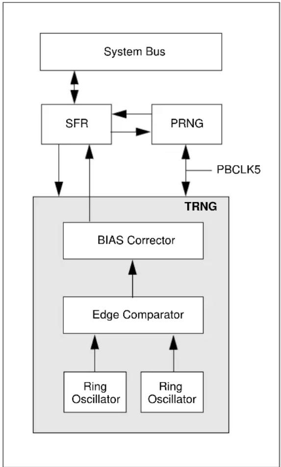
flowchart
graph TD
    A["System Bus"] --> B["SFR"]
    A --> C["PRNG"]
    B --> D["TRNG"]
    C --> D
    D --> E["BIAS Corrector"]
    E --> F["Edge Comparator"]
    F --> G["Ring Oscillator"]
    F --> H["Ring Oscillator"]
    G --> I["PBCLK5"]
    H --> I
    B <--> C
    D <--> E
27.1 RNG Control Registers
TABLE 27-2: RANDOM NUMBER GENERATOR (RNG) REGISTER MAP
| Virtual Address (BF8E_#) | Register Name | Bit Range | Bits | All Resets | |||||||||||||||
| 31/15 | 30/14 | 29/13 | 28/12 | 27/11 | 26/10 | 25/9 | 24/8 | 23/7 | 22/6 | 21/5 | 20/4 | 19/3 | 18/2 | 17/1 | 16/0 | ||||
| 6000 | RNGVER | 31:16 | ID<15:0>xxxx | ||||||||||||||||
| 15:0 | VERSION<7:0> | Revision<7:0> | xxxx | ||||||||||||||||
| 6004 | RNGCON | 31:16 | — | — | — | — | — | — | — | — | — | — | — | — | — | — | — | — | 0000 |
| 15:0 | — | — | — | LOAD | — | CONT | PRNGEN | TRNGEN | PLEN<7:0> | 0064 | |||||||||
| 6008 | RNGPOLY1 | 31:16 | POLY<31:0> | FFFF | |||||||||||||||
| 15:0 | 0000 | ||||||||||||||||||
| 600C | RNGPOLY2 | 31:16 | POLY<31:0> | FFFF | |||||||||||||||
| 15:0 | 0000 | ||||||||||||||||||
| 6010 | RNGNUMGEN1 | 31:16 | RNG<31:0> | FFFF | |||||||||||||||
| 15:0 | FFFF | ||||||||||||||||||
| 6014 | RNGNUMGEN2 | 31:16 | RNG<31:0> | FFFF | |||||||||||||||
| 15:0 | FFFF | ||||||||||||||||||
| 6018 | RNGSEED1 | 31:16 | SEED<31:0> | 0000 | |||||||||||||||
| 15:0 | 0000 | ||||||||||||||||||
| 601C | RNGSEED2 | 31:16 | SEED<31:0> | 0000 | |||||||||||||||
| 15:0 | 0000 | ||||||||||||||||||
| 6020 | RNGCNT | 31:16 | — | — | — | — | — | — | — | — | — | — | — | — | — | — | — | — | 0000 |
| 15:0 | — | — | — | — | — | — | — | — | — | — | RCNT<6:0> | 0000 | |||||||
Legend: x = unknown value on Reset; — = unimplemented, read as '0'. Reset values are shown in hexadecimal.
REGISTER 27-1: RNGVER: RANDOM NUMBER GENERATOR VERSION REGISTER
| Bit Range | Bit 31/23/15/7 | Bit 30/22/14/6 | Bit 29/21/13/5 | Bit 28/20/12/4 | Bit 27/19/11/3 | Bit 26/18/10/2 | Bit 25/17/9/1 | Bit 24/16/8/0 |
| 31:24 | R-0 R-0 R-0 | R-0 R-0 R-0 R-0 | R-0 | |||||
| ID<15:8> | ||||||||
| 23:16 | R-0 R-0 R-0 | R-0 R-0 R-0 R-0 | R-0 | |||||
| ID<7:0> | ||||||||
| 15:8 | R-0 R-0 R-0 | R-0 R-0 R-0 R-0 | R-0 | |||||
| VERSION<7:0> | ||||||||
| 7:0 | R-0 R-0 R-0 | R-0 R-0 R-0 R-0 | R-0 | |||||
| REVISION<7:0> | ||||||||
Legend:
R = Readable bit W = Writable bit U = Unimplemented bit, read as '0' -n = Value at POR '1' = Bit is set '0' = Bit is cleared x = Bit is unknown
bit 31-16 ID<15:0>: Block Identification bits
bit 15-8 VERSION<7:0>: Block Version bits
bit 7-0 REVISION<7:0>: Block Revision bits
REGISTER 27-2: RNGCON: RANDOM NUMBER GENERATOR CONTROL REGISTER
| Bit Range | Bit 31/23/15/7 | Bit 30/22/14/6 | Bit 29/21/13/5 | Bit 28/20/12/4 | Bit 27/19/11/3 | Bit 26/18/10/2 | Bit 25/17/9/1 | Bit 24/16/8/0 |
| 31:24 | U-0 U-0 U-0 | U-0 U-0 U-0 U-0 | U-0 | |||||
| — — — | — — — — | |||||||
| 23:16 | U-0 U-0 U-0 | U-0 U-0 U-0 U-0 | U-0 | |||||
| — — — | — — — — | |||||||
| 15:8 | U-0 | U-0 | U-0 | R/W-0 | U-0 | R/W-0 | R/W-0 | R/W-0 |
| — | — | — | LOAD | — | CONT | PRNGEN | TRNGEN | |
| 7:0 | R/W-0 | R/W-1 | R/W-1 | R/W-0 | R/W-0 | R/W-1 | R/W-0 | R/W-0 |
| PLEN<7:0> | ||||||||
Legend:
| R = Readable bit | W = Writable bit U = Unimplemented bit, read as '0' |
| -n = Value at POR | '1' = Bit is set '0' = Bit is cleared x = Bit is unknown |
bit 31-13 Unimplemented: Read as '0'
bit 12 LOAD: Device Select bit
This bit is self-clearing and is used to load the seed from the TRNG (i.e., the random value) as a seed to the PRNG.
bit 11 Unimplemented: Read as '0'
bit 10 CONT: PRNG Number Shift Enable bit
1 = The PRNG random number is shifted every cycle
0 = The PRNG random number is shifted when the previous value is removed
bit 9 PRNGEN: PRNG Operation Enable bit
1 = PRNG operation is enabled
0 = PRNG operation is not enabled
bit 8 TRNGEN: TRNG Operation Enable bit
1 = TRNG operation is enabled
0 = TRNG operation is not enabled
bit 7-0 PLEN<7:0>: PRNG Polynomial Length bits
These bits contain the length of the polynomial used for the PRNG.
REGISTER 27-3: RNGPOLYx: RANDOM NUMBER GENERATOR POLYNOMIAL REGISTER 'x' ('x' = 1 OR 2)
| Bit Range | Bit 31/23/15/7 | Bit 30/22/14/6 | Bit 29/21/13/5 | Bit 28/20/12/4 | Bit 27/19/11/3 | Bit 26/18/10/2 | Bit 25/17/9/1 | Bit 24/16/8/0 |
| 31:24 | R/W-1 R/W-1 | R/W-1 R/W-1 R | W-1 R/W-1 R/W-1 | R/W-1 | ||||
| POLY<31:24> | ||||||||
| 23:16 | R/W-1 R/W-1 | R/W-1 R/W-1 R | W-1 R/W-1 R/W-1 | R/W-1 | ||||
| POLY<23:16> | ||||||||
| 15:8 | R/W-0 R/W-0 | R/W-0 R/W-0 R | W-0 R/W-0 R/W-0 | R/W-0 | ||||
| POLY<15:8> | ||||||||
| 7:0 | R/W-0 R/W-0 | R/W-0 R/W-0 R | W-0 R/W-0 R/W-0 | R/W-0 | ||||
| POLY<7:0> | ||||||||
Legend:
R = Readable bit W = Writable bit U = Unimplemented bit, read as '0' -n = Value at POR '1' = Bit is set '0' = Bit is cleared x = Bit is unknown
bit 31-0 POLY<31:0>: PRNG LFSR Polynomial MSb/LSb bits (RNGPOLY1 = LSb, RNGPOLY2 = MSb)
REGISTER 27-4: RNGNUMGENx: RANDOM NUMBER GENERATOR REGISTER 'x' ('x' = 1 OR 2)
| Bit Range | Bit 31/23/15/7 | Bit 30/22/14/6 | Bit 29/21/13/5 | Bit 28/20/12/4 | Bit 27/19/11/3 | Bit 26/18/10/2 | Bit 25/17/9/1 | Bit 24/16/8/0 |
| 31:24 | R/W-1 | R/W-1 | R/W-1 | R/W-1 | R/W-1 | R/W-1 | R/W-1 | R/W-1 |
| RNG<31:24> | ||||||||
| 23:16 | R/W-1 | R/W-1 | R/W-1 | R/W-1 | R/W-1 | R/W-1 | R/W-1 | R/W-1 |
| RNG<23:16> | ||||||||
| 15:8 | R/W-1 | R/W-1 | R/W-1 | R/W-1 | R/W-1 | R/W-1 | R/W-1 | R/W-1 |
| RNG<15:8> | ||||||||
| 7:0 | R/W-1 | R/W-1 | R/W-1 | R/W-1 | R/W-1 | R/W-1 | R/W-1 | R/W-1 |
| RNG<7:0> | ||||||||
Legend:
R = Readable bit W = Writable bit U = Unimplemented bit, read as '0' -n = Value at POR '1' = Bit is set '0' = Bit is cleared x = Bit is unknown
bit 31-0 RNG<31:0>: Current PRNG MSb/LSb Value bits (RNGNUMGEN1 = LSb, RNGNUMGEN2 = MSb)
REGISTER 27-5: RNGSEEDx: TRUE RANDOM NUMBER GENERATOR SEED REGISTER 'x' ('x' = 1 OR 2)
| Bit Range | Bit 31/23/15/7 | Bit 30/22/14/6 | Bit 29/21/13/5 | Bit 28/20/12/4 | Bit 27/19/11/3 | Bit 26/18/10/2 | Bit 25/17/9/1 | Bit 24/16/8/0 |
| 31:24 | R-0 R-0 R-0 | R-0 R-0 R-0 R-0 | R-0 | |||||
| SEED<31:24> | ||||||||
| 23:16 | R-0 R-0 R-0 | R-0 R-0 R-0 R-0 | R-0 | |||||
| SEED<23:16> | ||||||||
| 15:8 | R-0 R-0 R-0 | R-0 R-0 R-0 R-0 | R-0 | |||||
| SEED<15:8> | ||||||||
| 7:0 | R-0 R-0 R-0 | R-0 R-0 R-0 R-0 | R-0 | |||||
| SEED<7:0> | ||||||||
Legend:
R = Readable bit W = Writable bit U = Unimplemented bit, read as '0' -n = Value at POR '1' = Bit is set '0' = Bit is cleared x = Bit is unknown
bit 31-0 SEED<31:0>: TRNG MSb/LSb Value bits (RNGSEED1 = LSb, RNGSEED2 = MSb)
REGISTER 27-6: RNGCNT: TRUE RANDOM NUMBER GENERATOR COUNT REGISTER
| Bit Range | Bit 31/23/15/7 | Bit 30/22/14/6 | Bit 29/21/13/5 | Bit 28/20/12/4 | Bit 27/19/11/3 | Bit 26/18/10/2 | Bit 25/17/9/1 | Bit 24/16/8/0 |
| 31:24 | U-0 U-0 U-0 | U-0 | U-0 U-0 U-0 U-0 | |||||
| — | — | — | — | — | — | — | — | |
| 23:16 | U-0 | U-0 | U-0 | U-0 | U-0 | U-0 | U-0 | U-0 |
| — | — | — | — | — | — | — | — | |
| 15:8 | U-0 | U-0 | U-0 | U-0 | U-0 | U-0 | U-0 | U-0 |
| — | — | — | — | — | — | — | — | |
| 7:0 | U-0 | R/W-0 | R/W-0 | R/W-0 | R/W-0 | R/W-0 | R/W-0 | R/W-0 |
| — | RCNT<6:0> | |||||||
Legend:
R = Readable bit W = Writable bit U = Unimplemented bit, read as '0' -n = Value at POR '1' = Bit is set '0' = Bit is cleared x = Bit is unknown
bit 31-7 Unimplemented: Read as '0'
bit 6-0 RCNT<6:0>: Number of Valid TRNG MSB 32 bits
28.0 PIPELINED ANALOG-TO-DIGITAL CONVERTER (ADC)
Note: This data sheet summarizes the features of the PIC32MZ Embedded Connectivity (EC) Family of devices. It is not intended to be a comprehensive reference source. To complement the information in this data sheet, refer to Section 18. "12-bit Pipelined Analog-to-Digital Converter (ADC)" (DS60001194), which is available from the Documentation > Reference Manual section of the Microchip PIC32 web site (www.microchip.com/pic32).
The PIC32MZ EC Pipelined Analog-to-Digital Converter (ADC) includes the following features:
- 10-bit resolution
- Six-stage conversion pipeline
- External voltage reference input pins
- Six Sample and Hold (S&H) circuits, SH0 - SH5:
- Five dedicated S&H circuits with individual input selection and individual conversion trigger selection for high-speed conversions
- One shared S&H circuit with automatic Input Scan mode and common conversion trigger selection
- Up to 48 analog input sources, in addition to the internal voltage reference and an internal temperature sensor
- 32-bit conversion result registers with dedicated interrupts:
- Conversion result can be formatted as unsigned or signed fractional or integer data
- Six digital comparators with dedicated interrupts:
Multiple comparison options - Assignable to specific analog input
- Six oversampling filters with dedicated interrupts:
- Provides increased resolution
Assignable to specific analog input
• Operation during Sleep and Idle modes
Besides the analog inputs that can be converted, there are two analog input pins for external voltage reference connections. These voltage reference inputs can be shared with other analog input pins, and can also be used by other analog module references.
The analog inputs are connected through multiplexers (MUXs) to the S&H circuits. Each of the dedicated S&H circuits, is assigned to analog inputs, and can optionally use another analog input in a differential configuration. The dedicated S&H circuits are used for high-speed and precise sampling/conversion of time sensitive or transient inputs.
The sixth S&H circuit, SH5, can be used in Input Scan mode and is connected to all the available analog inputs on a device, along with internal voltage reference and the temperature sensor signals. Input Scan mode sequentially converts user-specified analog input sources. The control registers specify the analog input sources that are included in the scanning sequence.
A simplified block diagram of the ADC1 module is illustrated in Figure 28-1. Diagrams for the Dedicated and Shared ADC modules are provided in Figure 28-2 and Figure 28-3, respectively.
FIGURE 28-1: ADC1 MODULE BLOCK DIAGRAM
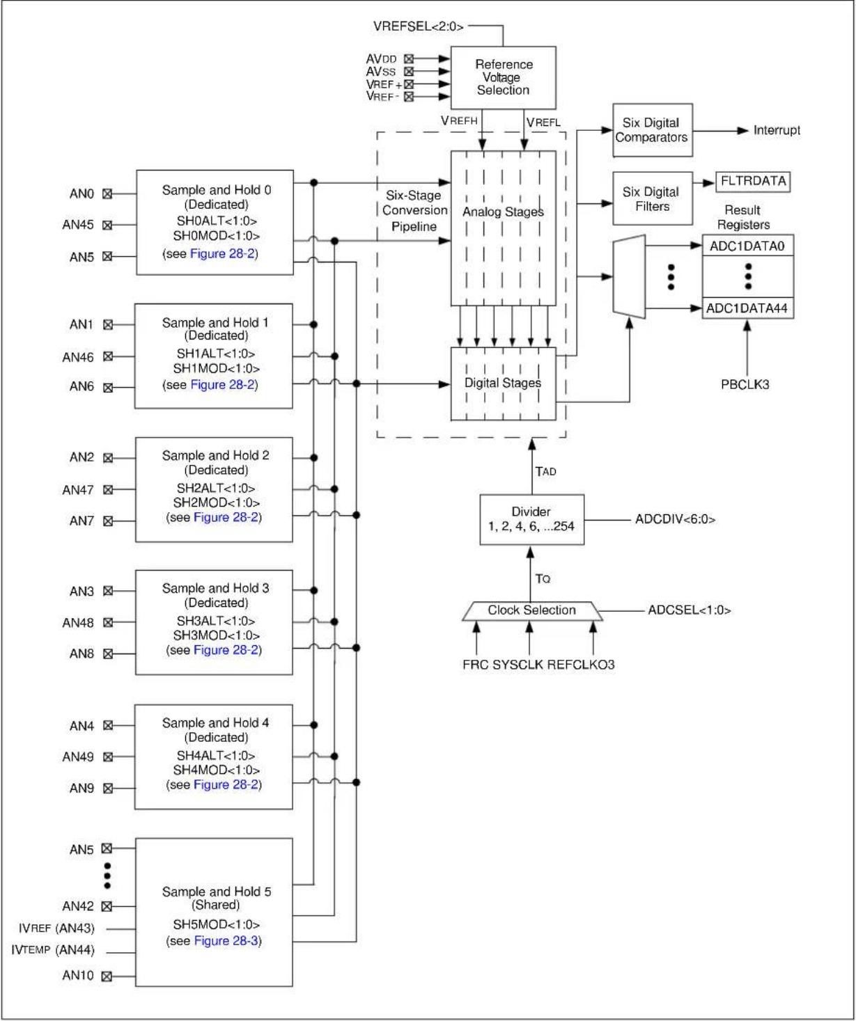
flowchart
graph TD
    A["AN0"] --> B["Sample and Hold 0 (Dedicated)"]
    AN45 --> B
    AN5 --> B
    AN1 --> C["Sample and Hold 1 (Dedicated)"]
    AN46 --> C
    AN6 --> D["Sample and Hold 2 (Dedicated)"]
    AN2 --> E["Sample and Hold 3 (Dedicated)"]
    AN47 --> E
    AN7 --> F["Sample and Hold 4 (Dedicated)"]
    AN3 --> G["Sample and Hold 5 (Shared)"]
    AN48 --> G
    AN9 --> G
    AN5 --> G
    AN42 --> G
    IVREF(AN43) --> G
    IVTEMP(AN44) --> G
    AN10 --> G
    SH0ALT<1:0> --> B
    SH0MOD<1:0> --> B
    SH1ALT<1:0> --> C
    SH1MOD<1:0> --> C
    SH2ALT<1:0> --> D
    SH2MOD<1:0> --> D
    SH3ALT<1:0> --> E
    SH3MOD<1:0> --> E
    SH4ALT<1:0> --> F
    SH4MOD<1:0> --> F
    SH5MOD<1:0> --> G
    ReferenceVoltageSelection["Reference Voltage Selection"] --> B
    AnalogStages["Analog Stages"] --> B
    DigitalStages["Digital Stages"] --> B
    SixDigitalComparators["Six Digital Comparators"] --> Interrupt["Interrupt"]
    SixDigitalFilters["Six Digital Filters"] --> FLTRDATA["FLTRDATA"]
    DigitalFilters --> ResultRegisters["Result Registers"]
    DigitalStages --> ADC1DATA0["ADC1DATA0"]
    DigitalStages --> ADC1DATA44["ADC1DATA44"]
    ADC1DATA0 --> PBCLK3["PBCLK3"]
    ADC1DATA44 --> PBCLK3
    TAD["TAD"] --> Divider["Divider 1, 2, 4, 6,...254"]
    ClockSelection["Clock Selection"] --> ADCDIV["ADCDIV<6:0>"]
    ADCDIV --> ADCSEL["ADCSEL<1:0>"]
    ADCDIV --> FRCSYSCLKREFCLKO3["FRC SYSCLK REFCLKO3"]
    VREFSEL<2:0> --> ReferenceVoltageSelection
    AVDD --> ReferenceVoltageSelection
    AVSS --> ReferenceVoltageSelection
    VREF+ --> ReferenceVoltageSelection
    VREF- --> ReferenceVoltageSelection
FIGURE 28-2: DEDICATED S&H 0-4 BLOCK DIAGRAM

flowchart
graph TD
    A["Positive Input (Class 1)"] --> B["00"]
    C["Alternate Positive Input"] --> D["01"]
    E["Negative Input"] --> F["0x"]
    B --> G["Single-Ended"]
    D --> G
    F --> G
    G --> H["S&H"]
    H --> I["To Analog Stages"]
    G --> J["Differential"]
    J --> K["SHxMOD<1:0>"]
    K --> L["Channel Configuration"]
    L --> M["To Digital Stages"]
    N["VREFL"] --> G
    O["SHxALT<1:0>"] --> L
    P["SHxALT<1:0>"] --> L
    Q["SHxMOD<1:0>"] --> L
FIGURE 28-3: SHARED S&H 5 BLOCK DIAGRAM
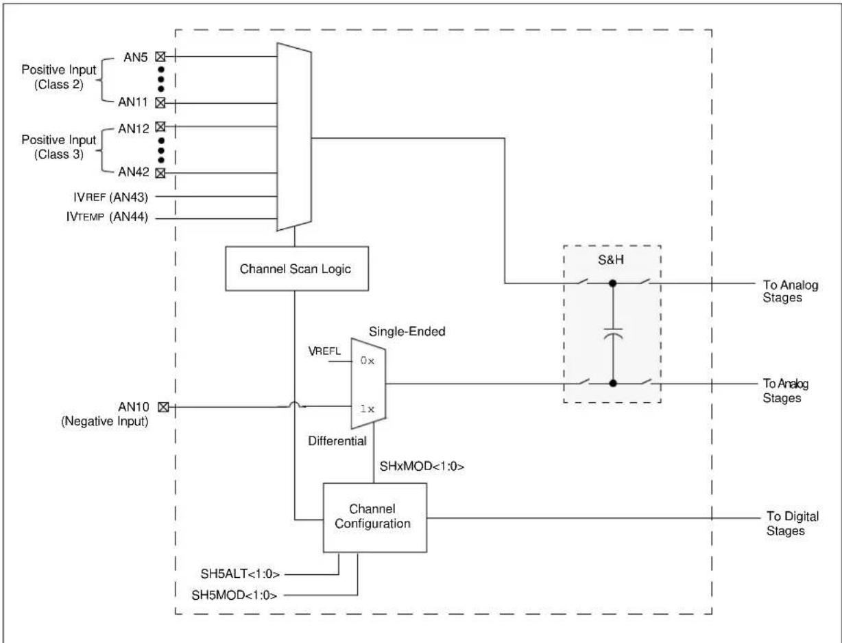
flowchart
graph TD
    A["Positive Input (Class 2)"] --> B["AN5"]
    A --> C["AN11"]
    D["Positive Input (Class 3)"] --> E["AN12"]
    D --> F["AN42"]
    G["IVREF (AN43)"] --> H["Channel Scan Logic"]
    I["IVTEMP (AN44)"] --> H
    H --> J["Single-Ended"]
    J --> K["VREFL 0x"]
    J --> L["Differential 1x"]
    J --> M["SHxMOD<1:0>"]
    N["AN10 (Negative Input)"] --> O["Channel Configuration"]
    P["S&H"] --> Q["To Analog Stages"]
    R["SH5ALT<1:0>"] --> O
    S["SH5MOD<1:0>"] --> O
    O --> T["To Digital Stages"]
28.1 ADC Configuration Requirements
Note: A related code example is available in the latest release of MPLAB Harmony (visit http://www.micochip.com/harmony for more information).
To meet ADC specifications, the following steps must be performed:
- Set the ADC Configuration words, as follows:
AD1CAL1 = 0xB3341210;
AD1CAL2 = 0x01FFA769;
AD1CAL3 = 0x0BBBBBB8;
AD1CAL4 = 0x000004AC;
AD1CAL5 = 0x02028002;
- Perform self-calibration. The input mode for SH0-SH5 must be set to the unipolar differential input mode by setting the SHxMOD<1:0> bits (AD1MOD<1:0>) = 10.
Note: SH0 through SH4 functionality and ADC Differential mode are not supported; however, both are required for auto-calibration. Sampling must be performed on SH5 only.
In addition, the following restrictions apply:
Supported ADC operating modes:
- Scan mode only with DMA interrupt
- The maximum number of used ANx inputs are limited by the available DMA channels (maximum of eight)
- The first (8) conversion after enabling the ADC must be discarded
• ADC Single-ended mode only - The ADC Clock, T AD, must be limited to 500 kHz ≤ TAD ≤ 1 MHz (i.e., 2 μs ≤ TAD ≤ 1 μs).
- HDW Oversampling is supported, but is not required, and will not impair accuracy; however, it will reduce the ADC ANx input throughput by the oversample ratio in use
- A N xINVmaximum is limited to ≤ 2.5V
- V_REF+ ≤ V_DD = AV_DD ≥ 2.5V
- Use of external VREF+ and VREF- pins only for ADC reference (VREFSEL<2:0> bits are equal to 'b011):
- VREF- = Can be connected to AVss externally, but not internally
- VREF+ can be connected to AVDD externally if required, but not internally
Unsupported ADC operating modes:
- Software polling of ADC status bits
- Manual software ADC triggering
- ADC interrupt modes (use DMA Interrupt mode)
- ADC SFR accesses by the CPU while ADC is operating
- ADC Boost or low-power mode.
- Individual ADC Input Conversion Requests (i.e., RQCNVRT bit in the ADCCON3 register)
- Use of ADC S&H Channels 0-4 except for calibration
- Any ADC references other than external VREF+ and VREF- pins
- ADC Differential mode
28.2 ADC Control Registers
TABLE 28-1: ADC REGISTER MAP
| Virtual Address(BFD_1#) | Register Name | Bit Range | Bits | All Resets | ||||||||||||||||
| 31/15 | 30/14 | 29/13 | 28/12 | 27/11 | 26/10 | 25/9 | 24/8 | 23/7 | 22/6 | 21/5 | 20/4 | 19/3 | 18/2 | 17/1 | 16/0 | |||||
| B000 | AD1CON1 | 31:16 | FILTRDLY4:0> | STRGSRC<4:0> | — | — | — | EIE<2:0> | 0000 | |||||||||||
| 15:0 | ADCEN | — | ADSIDL | — | FRACT | — | — | — | — | — | — | — | — | — | — | — | 0000 | |||
| B004 | AD1CON2 | 31:16 | ADCRDY | — | — | — | — | — | — | — | — | SAMC<7:0> | 0000 | |||||||
| 15:0 | — | BOOST | LOWPWR | — | — | — | ADCSEL<1:0> | — | ADCDIV<6:0> | 0000 | ||||||||||
| B008 | AD1CON3 | 31:16 | CAL | GSWTRG | RQCNVRT | — | — | — | — | — | — | — | — | — | — | — | — | — | 0000 | |
| 15:0 | — | — | — | VREFSEL<2:0> | — | — | — | — | ADINSEL<5:0> | 0000 | ||||||||||
| B00C | AD1IMOD | 31:16 | — | — | — | — | — | — | SH4ALT<1:0> | SH3ALT<1:0> | SH2ALT<1:0> | SH1ALT<1:0> | SH0ALT<1:0> | 0000 | ||||||
| 15:0 | — | — | — | — | SH5MOD<1:0> | SH4MOD<1:0> | SH3MOD<1:0> | SH2MOD<1:0> | SH1MOD<1:0> | SH0MOD<1:0> | 0000 | |||||||||
| B010 | AD1GIRQEN1 | 31:16 | AGIEN31 | AGIEN30 | AGIEN29 | AGIEN28 | AGIEN27 | AGIEN26 | AGIEN25 | AGIEN24 | AGIEN23 | AGIEN22 | AGIEN21 | AGIEN20 | AGIEN19 | AGIEN18 | AGIEN17 | AGIEN16 | 0000 | |
| 15:0 | AGIEN15 | AGIEN14 | AGIEN13 | AGIEN12 | AGIEN11 | AGIEN10 | AGIEN9 | AGIEN8 | AGIEN7 | AGIEN6 | AGIEN5 | AGIEN4 | AGIEN3 | AGIEN2 | AGIEN1 | AGIEN0 | 0000 | |||
| B014 | AD1GIRQEN2 | 31:16 | — | — | — | — | — | — | — | — | — | — | — | — | — | — | — | — | 0000 | |
| 15:0 | — | — | — | AGIEN14 | AGIEN13 | AGIEN12 | AGIEN11 | AGIEN10 | AGIEN9 | AGIEN8 | AGIEN7 | AGIEN6 | AGIEN5 | AGIEN4 | AGIEN3 | AGIEN2 | 0000 | |||
| B018 | AD1CSS1 | 31:16 | CSS31 | CSS30 | CSS29 | CSS28 | CSS27 | CSS26 | CSS25 | CSS24 | CSS23 | CSS22 | CSS21 | CSS20 | CSS19 | CSS18 | CSS17 | CSS16 | 0000 | |
| 15:0 | CSS15 | CSS14 | CSS13 | CSS12 | CSS11 | CSS10 | CSS9 | CSS8 | CSS7 | CSS6 | CSS5 | CSS4 | CSS3 | CSS2 | CSS1 | CSS0 | 0000 | |||
| B01C | AD1CSS2 | 31:16 | — | — | — | — | — | — | — | — | — | — | — | — | — | — | — | — | 0000 | |
| 15:0 | — | — | — | CSS44 | CSS43 | CSS42 | CSS41 | CSS40 | CSS39 | CSS38 | CSS37 | CSS36 | CSS35 | CSS34 | CSS33 | CSS32 | 0000 | |||
| B020 | AD1DSTAT1 | 31:16 | ARDY31 | ARDY30 | ARDY29 | ARDY28 | ARDY27 | ARDY26 | ARDY25 | ARDY24 | ARDY23 | ARDY22 | ARDY21 | ARDY20 | ARDY19 | ARDY18 | ARDY17 | ARDY16 | 0000 | |
| 15:0 | ARDY15 | ARDY14 | ARDY13 | ARDY12 | ARDY11 | ARDY10 | ARDY9 | ARDY9 | ARDY7 | ARDY6 | ARDY5 | ARDY4 | ARDY3 | ARDY2 | ARDY1 | ARDY0 | 0000 | |||
| B024 | AD1DSTAT2 | 31:16 | — | — | — | — | — | — | — | — | — | — | — | — | — | — | — | — | 0000 | |
| 15:0 | — | — | — | ARDY44 | ARDY43 | ARDY42 | ARDY41 | ARDY40 | ARDY39 | ARDY38 | ARDY37 | ARDY36 | ARDY35 | ARDY34 | ARDY33 | ARDY32 | 0000 | |||
| B028 | AD1CMPEN1 | 31:16 | CMPE31 | CMPE30 | CMPE29 | CMPE28 | CMPE27 | CMPE26 | CMPE25 | CMPE24 | CMPE23 | CMPE22 | CMPE21 | CMPE20 | CMPE19 | CMPE18 | CMPE17 | CMPE16 | 0000 | |
| 15:0 | CMPE15 | CMPE14 | CMPE13 | CMPE12 | CMPE11 | CMPE10 | CMPE9 | CMPE8 | CMPE7 | CMPE6 | CMPE5 | CMPE4 | CMPE3 | CMPE2 | CMPE1 | CMPE0 | 0000 | |||
| B02C | AD1CMP1 | 31:16 | ACMPHI<15:0> | 0000 | ||||||||||||||||
| 15:0 | ADCMPLLO<15:0> | 0000 | ||||||||||||||||||
| B030 | AD1CMPEN2 | 31:16 | CMPE31 | CMPE30 | CMPE29 | CMPE28 | CMPE27 | CMPE26 | CMPE25 | CMPE24 | CMPE23 | CMPE22 | CMPE21 | CMPE20 | CMPE19 | CMPE18 | CMPE17 | CMPE16 | 0000 | |
| 15.0 | CMPE15 | CMPE14 | CMPE13 | CMPE12 | CMPE11 | CMPE10 | CMPE9 | CMPE8 | CMPE7 | CMPE6 | CMPE5 | CMPE4 | CMPE3 | CMPE2 | CMPE1 | CMPE0 | 0000 | |||
| B034 | AD1CMP2 | 31:16 | ADCMPHI<15:0> | 0000 | ||||||||||||||||
| 15:0 | ADCMPLLO<15:0> | 0000 | ||||||||||||||||||
| B038 | AD1CMPEN3 | 31:16 | CMPE31 | CMPE30 | CMPE29 | CMPE28 | CMPE27 | CMPE26 | CMPE25 | CMPE24 | CMPE23 | CMPE22 | CMPE21 | CMPE20 | CMPE19 | CMPE18 | CMPE17 | CMPE16 | 0000 | |
| 15;0 | CMPE15 | CMPE14 | CMPE13 | CMPE12 | CMPE11 | CMPE10 | CMPE9 | CMPE8 | CMPE7 | CMPE6 | CMPE5 | CMPE4 | CMPE3 | CMPE2 | CMPE1 | CMPE0 | 0000 | |||
| B03C | AD1CMP3 | 31:16 | ADCMPHI<15:0> | 0000 | ||||||||||||||||
| 15:0 | ADCMPLLO<15:0> | 0000 | ||||||||||||||||||
| B040 | AD1CMPEN4 | 31:16 | CMPE31 | CMPE30 | CMPE29 | CMPE28 | CMPE27 | CMPE26 | CMPE25 | CMPE24 | CMPE23 | CMPE22 | CMPE21 | CMPE20 | CMPE19 | CMPE18 | CMPE17 | CMPE16 | 0000 | |
| 15,0 | CMPE15 | CMPE14 | CMPE13 | CMPE12 | CMPE11 | CMPE10 | CMPE9 | CMPE8 | CMPE7 | CMPE6 | CMPE5 | CMPE4 | CMPE3 | CMPE2 | CMPE1 | CMPE0 | 0000 | |||
| B044 | AD1CMP4 | 31:16 | ADCMPHI<15:0> | 0000 | ||||||||||||||||
| 15:0 | ADCMPLLO<15:0> | 0000 | ||||||||||||||||||
| Virtual Address(BP64_#) | Register Name | Bit Range | Bits | All Resets | ||||||||||||||||
| 31/15 | 30/14 | 29/13 | 28/12 | 27/11 | 26/10 | 25/9 | 24/8 | 23/7 | 22/6 | 21/5 | 20/4 | 19/3 | 18/2 | 17/1 | 16/0 | |||||
| B04B | AD1CMPEN5 | 31:16 | CMPE31 | CMPE30 | CMPE29 | CMPE28 | CMPE27 | CMPE26 | CMPE25 | CMPE24 | CMPE23 | CMPE22 | CMPE21 | CMPE20 | CMPE19 | CMPE18 | CMPE17 | CMPE16 | 0000 | |
| 15:0 | CMPE15 | CMPE14 | CMPE13 | CMPE12 | CMPE11 | CMPE10 | CMPE9 | CMPE8 | CMPE7 | CMPE6 | CMPE5 | CMPE4 | CMPE3 | CMPE2 | CMPE1 | CMPE0 | 0000 | |||
| B04C | AD1CMP5 | 31:16 | ADCMPHI<15:0> | 0000 | ||||||||||||||||
| 15:0 | ADCMPLO<15:0> | 0000 | ||||||||||||||||||
| B050 | AD1CMPEN6 | 31:16 | CMPE31 | CMPE30 | CMPE29 | CMPE28 | CMPE27 | CMPE26 | CMPE25 | CMPE24 | CMPE23 | CMPE22 | CMPE21 | CMPE20 | CMPE19 | CMPE18 | CMPE17 | CMPE16 | 0000 | |
| 15.0 | CMPE15 | CMPE14 | CMPE13 | CMPE12 | CMPE11 | CMPE10 | CMPE9 | CMPE8 | CMPE7 | CMPE6 | CMPE5 | CMPE4 | CMPE3 | CMPE2 | CMPE1 | CMPE0 | 0000 | |||
| B054 | AD1CMP6 | 31:16 | ADCMPHI<15:0> | 0000 | ||||||||||||||||
| 15:0 | ADCMPLO<15:0> | 0000 | ||||||||||||||||||
| B058 | AD1FLTR1 | 31:16 | AFEN | — | — | OVRSAM<2:0> | AFGIEN | AFRDY | — | — | CHNLID<5:0> | 0000 | ||||||||
| 15:0 | FLTRDATA<15:0> | 0000 | ||||||||||||||||||
| B05C | AD1FLTR2 | 31:16 | AFEN | — | — | OVRSAM<2:0> | AFGIEN | AFRDY | — | — | CHNLID<5:0> | 0000 | ||||||||
| 15:0 | FLTRDATA<15:0> | 0000 | ||||||||||||||||||
| BC60 | AD1FLTR3 | 31:16 | AFEN | — | — | OVRSAM<2:0> | AFGIEN | AFRDY | — | — | CHNLID<5:0> | 0000 | ||||||||
| 15:0 | FLTRDATA<15:0> | 0000 | ||||||||||||||||||
| BO64 | AD1FLTR4 | 31:16 | AFEN | — | — | OVRSAM<2:0> | AFGIEN | AFRDY | — | — | CHNLID<5:0> | 0000 | ||||||||
| 15:0 | FLTRDATA<15:0> | 0000 | ||||||||||||||||||
| BD68 | AD1FLTR5 | 31:16 | AFEN | — | — | OVRSAM<2:0> | AFGIEN | AFRDY | — | — | CHNLID<5:0> | 0000 | ||||||||
| 15:0 | FLTRDATA<15:0> | 0000 | ||||||||||||||||||
| BG6C | AD1FLTR6 | 31:16 | AFEN | — | — | OVRSAM<2:0> | AFGIEN | AFRDY | — | — | CHNLID<5:0> | 0000 | ||||||||
| 15:0 | FLTRDATA<15:0> | 0000 | ||||||||||||||||||
| BT070 | AD1TRG1 | 31:16 | — | — | — | TRGSRC3<4:0> | — | — | — | TRGSRC2<4:0> | 0000 | |||||||||
| 15:0 | — | — | — | TRGSRC1<4:0> | — | — | — | TRGSRC0<4:0> | 0000 | |||||||||||
| B074 | AD1TRG2 | 31:16 | — | — | — | TRGSRC7<4:0> | — | — | — | TRGSRC6<4:0> | 0000 | |||||||||
| 15:0 | — | — | — | TRGSRC5<4:0> | — | — | — | TRGSRC4<4:0> | 0000 | |||||||||||
| B078 | AD1TRG3 | 31:16 | — | — | — | TRGSRC11<4:0> | — | — | — | TRGSRC10<4:0> | 0000 | |||||||||
| 15:0 | — | — | — | TRGSRC9<4:0> | — | — | — | TRGSRC8<4:0> | 0000 | |||||||||||
| B090 | AD1CMPCON1 | 31:16 | — | — | — | — | — | — | — | — | — | — | — | — | — | — | — | — | 0000 | |
| 15:0 | — | — | — | AINID<4:0> | ENDCMP | DCMPGIEN | DCMPED | IEBTWN | IEHIHI | IEHILO | IELOHI | IELOLO | 0000 | |||||||
| B094 | AD1CMPCON2 | 31:16 | — | — | — | — | — | — | — | — | — | — | — | — | — | — | — | — | 0000 | |
| 15:0 | — | — | — | AINID<4:0> | ENDCMP | DCMPGIEN | DCMPED | IEBTWN | IEHIHI | IEHILO | IELOHI | |||||||||
| B098 | AD1CMPCON3 | 31:16 | — | — | — | — | — | — | — | — | — | — | — | — | — | — | — | — | 0000 | |
| 15:0 | — | — | — | AINID<4:0> | ENDCMP | DCMPGIEN | DCMPED | IEBTWN | IEHIHI | IEHILO | IELOHI, IIELOLO | |||||||||
| B09C | AD1CMPCON4 | 31:16 | — | — | — | — | — | — | — | — | — | — | — | — | — | — | — | — | 0000 | |
| 15:0 | — | — | — | AINID<4:0> | ENDCMP | DCMPGIEN | DCMPED | IEBTWN | IEHIHI | IEHILO | IELOHI IIELOLO | |||||||||
| B0A0 | AD1CMPCON5 | 31:16 | — | — | — | — | — | — | — | — | — | — | — | — | — | — | — | — | 0000 | |
| 15:0 | — | — | — | AINID<4:0> | ENDCMP | DCMPGIEN | DCMPED | IEBTWN | IEHIHI | IEHILO | IELOHI IIELOLO | |||||||||
| B0A4 | AD1CMPCON6 | 31:16 | — | — | — | — | — | — | — | — | — | — | — | — | — | — | — | — | 0000 | |
| 15:0 | — | — | — | AINID<4:0> | ENDCMP | DCMPGIEN | DCMPED | IEBTWN | IEHIHI | IEHILO | IELOHI . IIELOLO | |||||||||
| Virtual Address(BFD_1) | Register Name | Bit Range | Bits | All Resets | ||||||||||||||||
| 31/15 | 30/14 | 29/13 | 28/12 | 27/11 | 26/10 | 25/9 | 24/8 | 23/7 | 22/6 | 21/5 | 20/4 | 19/3 | 18/2 | 17/1 | 16/0 | |||||
| B0B8 | AD1DATA0 | 31:16 | ADC Output Register 0 <31:16> 0000 | |||||||||||||||||
| 15:0 | ADC Output Register 0 <15:0> 0000 | |||||||||||||||||||
| B0BC | AD1DATA1 | 31:16 | ADC Output Register 1 <31:16> 0000 | |||||||||||||||||
| 15:0 | ADC Output Register 1 <15:0> 0000 | |||||||||||||||||||
| B0C0 | AD1DATA2 | 31:16 | ADC Output Register 2 <31:16> 0000 | |||||||||||||||||
| 15:0 | ADC Output Register 2 <15:0> 0000 | |||||||||||||||||||
| B0C4 | AD1DATA3 | 31:16 | ADC Output Register 3 <31:16> 0000 | |||||||||||||||||
| 15:0 | ADC Output Register 3 <15:0> 0000 | |||||||||||||||||||
| B0C8 | AD1DATA4 | 31:16 | ADC Output Register 4 <31:16> 0000 | |||||||||||||||||
| 15:0 | ADC Output Register 4 <15:0> 0000 | |||||||||||||||||||
| B0CC | AD1DATA5 | 31:16 | ADC Output Register 5 <31:16> 0000 | |||||||||||||||||
| 15:0 | ADC Output Register <15:0> 0000 | |||||||||||||||||||
| B0D0 | AD1DATA6 | 31:16 | ADC Output Register 6 <31:16> 0000 | |||||||||||||||||
| 15:0 | ADC Output Register 6 <15:0> 0000 | |||||||||||||||||||
| B0D4 | AD1DATA7 | 31:16 | ADC Output Register 7 <31:16> 0000 | |||||||||||||||||
| 15:0 | ADC Output Register 7 <15:0> 0000 | |||||||||||||||||||
| B0D8 | AD1DATA8 | 31:16 | ADC Output Register 8 <31:16> 0000 | |||||||||||||||||
| 15:0 | ADC Output Register 8 <15:0> 0000 | |||||||||||||||||||
| B0DC | AD1DATA9 | 31:16 | ADC Output Register 9 <31:16> 0000 | |||||||||||||||||
| 15:0 | ADC Output Register 9 <15:0> 0000 | |||||||||||||||||||
| B0E0 | AD1DATA10 | 31:16 | ADC Output Register 10 <31:16> 0000 | |||||||||||||||||
| 15:0 | ADC Output Register 10 <15:0> 0000 | |||||||||||||||||||
| B0E4 | AD1DATA11 | 31:16 | ADC Output Register 11 <31:16> 0000 | |||||||||||||||||
| 15:0 | ADC Output Register 11 <15:0> 0000 | |||||||||||||||||||
| B0E8 | AD1DATA12 | 31:16 | ADC Output Register 12 <31:16> 0000 | |||||||||||||||||
| 15:0 | ADC Output Register 12 <15:0> 0000 | |||||||||||||||||||
| B0EC | AD1DATA13 | 31:16 | ADC Output Register 13 <31:16> 0000 | |||||||||||||||||
| 15:0 | ADC Output Register 13 <15:0> 0000 | |||||||||||||||||||
| B0F0 | AD1DATA14 | 31:16 | ADC Output Register 14 <31:16> 0000 | |||||||||||||||||
| 15:0 | ADC Output Register 14 <15:0> 0000 | |||||||||||||||||||
| B0F4 | AD1DATA15 | 31:16 | ADC Output Register 15 <31:16> 0000 | |||||||||||||||||
| 15:0 | ADC Output Register 15 <15:0> 0000 | |||||||||||||||||||
| B0F8 | AD1DATA16 | 31:16 | ADC Output Register 16 <31:16> 0000 | |||||||||||||||||
| 15:0 | ADC Output Register 16 <15:0> 0000 | |||||||||||||||||||
| B0FC | AD1DATA17 | 31:16 | ADC Output Register 17 <31:16> 0000 | |||||||||||||||||
| 15:0 | ADC Output Register 17 <15:0> | 0000 | ||||||||||||||||||
| B100 | AD1DATA18 | 31:16 | ADC Output Register 18 <31:16> 0000 | |||||||||||||||||
| 15:0 | ADC Output Register 18 <15:0> | 0000 | ||||||||||||||||||
| Virtual Address (EFE4_f) | Register Name | Bit Range | Bits | All Resets | ||||||||||||||||
| 31/15 | 30/14 | 29/13 | 28/12 | 27/11 | 26/10 | 25/9 | 24/8 | 23/7 | 22/6 | 21/5 | 20/4 | 19/3 | 18/2 | 17/1 | 16/0 | |||||
| B104 | AD1DATA19 | 31:16 | ADC Output Register 19 <31:16> 0000 | |||||||||||||||||
| 15:0 | ADC Output Register 19<15:0> 0000 | |||||||||||||||||||
| B108 | AD1DATA20 | 31:16 | ADC Output Register 20 <31:16> 0000 | |||||||||||||||||
| 15:0 | ADC Output Register 20<15:0> 0000 | |||||||||||||||||||
| B10C | AD1DATA21 | 31:16 | ADC Output Register 21 <31:16> 0000 | |||||||||||||||||
| 15:0 | ADC Output Register 21 <15:0> 0000 | |||||||||||||||||||
| B110 | AD1DATA22 | 31:16 | ADC Output Register 22 <31:16> 0000 | |||||||||||||||||
| 15:0 | ADC Output Register 22<15:0> 0000 | |||||||||||||||||||
| B114 | AD1DATA23 | 31:16 | ADC Output Register 23 <31:16> 0000 | |||||||||||||||||
| 15:0 | ADC Output Register 23<15:0> 0000 | |||||||||||||||||||
| B118 | AD1DATA24 | 31:16 | ADC Output Register 24 <31:16> 0000 | |||||||||||||||||
| 15:0 | ADC Output Register 24<15:0> 0000 | |||||||||||||||||||
| B11C | AD1DATA25 | 31:16 | ADC Output Register 25 <31:16> 0000 | |||||||||||||||||
| 15:0 | ADC Output Register 25 <15:0> 0000 | |||||||||||||||||||
| B120 | AD1DATA26 | 31:16 | ADC Output Register 26 <31:16> 0000 | |||||||||||||||||
| 15:0 | ADC Output Register 26<15:0> 0000 | |||||||||||||||||||
| B124 | AD1DATA27 | 31:16 | ADC Output Register 27 <31:16> 0000 | |||||||||||||||||
| 15:0 | ADC Output Register 27<15:0> 0000 | |||||||||||||||||||
| B129 | AD1DATA28 | 31:16 | ADC Output Register 28 <31:16> 0000 | |||||||||||||||||
| 15:0 | ADC Output Register 28<15:0> 0000 | |||||||||||||||||||
| B12C | AD1DATA29 | 31:16 | ADC Output Register 29 <31:16> 0000 | |||||||||||||||||
| 15:0 | ADC Output Register 29 <15:0> 0000 | |||||||||||||||||||
| B130 | AD1DATA30 | 31:16 | ADC Output Register 30 <31:16> 0000 | |||||||||||||||||
| 15:0 | ADC Output Register 30<15:0> 0000 | |||||||||||||||||||
| B134 | AD1DATA31 | 31:16 | ADC Output Register 31 <31:16> 0000 | |||||||||||||||||
| 15:0 | ADC Output Register 31 <15:0> 0000 | |||||||||||||||||||
| B138 | AD1DATA32 | 31:16 | ADC Output Register 32 <31:16> 0000 | |||||||||||||||||
| 15:0 | ADC Output Register 32 <15:0> 0000 | |||||||||||||||||||
| B13C | AD1DATA33 | 31:16 | ADC Output Register 33 <31:16> 0000 | |||||||||||||||||
| 15:0 | ADC Output Register 33 <15:0> 0000 | |||||||||||||||||||
| B140 | AD1DATA34 | 31:16 | ADC Output Register 34 <31:16> 0000 | |||||||||||||||||
| 15:0 | ADC Output Register 34 <15:0> 0000 | |||||||||||||||||||
| B144 | AD1DATA35 | 31:16 | ADC Output Register 35 <31:16> 0000 | |||||||||||||||||
| 15:0 | ADC Output Register 35 <15:0> 0000 | |||||||||||||||||||
| B148 | AD1DATA36 | 31:16 | ADC Output Register 36 <31:16> 0000 | |||||||||||||||||
| 15:0 | ADC Output Register 36 <15:0> 0000 | |||||||||||||||||||
| B14C | AD1DATA37 | 31:16 | ADC Output Register 37 <31:16> 0000 | |||||||||||||||||
| 15:0 | ADC Output Register 37 <15:0> 0000 | |||||||||||||||||||
| Virtual Address(BF64_f) | Register Name | Bit Range | Bits | All Resets | ||||||||||||||||
| 31/15 | 30/14 | 29/13 | 28/12 | 27/11 | 26/10 | 25/9 | 24/8 | 23/7 | 22/6 | 21/5 | 20/4 | 19/3 | 18/2 | 17/1 | 16/0 | |||||
| B150 | AD1DATA38 | 31:16 | ADC Output Register 38 <31:16> 0000 | |||||||||||||||||
| 15:0 | ADC Output Register 38 <15:0> 0000 | |||||||||||||||||||
| B154 | AD1DATA39 | 31:16 | ADC Output Register 38 <31:16> 0000 | |||||||||||||||||
| 15:0 | ADC Output Register 38 <15:0> 0000 | |||||||||||||||||||
| B158 | AD1DATA40 | 31:16 | ADC Output Register 40 <31:16> 0000 | |||||||||||||||||
| 15:0 | ADC Output Register 40 <15:0> 0000 | |||||||||||||||||||
| B15C | AD1DATA41 | 31:16 | ADC Output Register 41 <31:16> 0000 | |||||||||||||||||
| 15:0 | ADC Output Register 41 <15:0> 0000 | |||||||||||||||||||
| B160 | AD1DATA42 | 31:16 | ADC Output Register 42 <31:16> 0000 | |||||||||||||||||
| 15:0 | ADC Output Register 42 <15:0> 0000 | |||||||||||||||||||
| B164 | AD1DATA43 | 31:16 | ADC Output Register 43 <31:16> 0000 | |||||||||||||||||
| 15:0 | ADC Output Register 43 <15:0> 0000 | |||||||||||||||||||
| B168 | AD1DATA44 | 31:16 | ADC Output Register 44 <31:16> 0000 | |||||||||||||||||
| 15:0 | ADC Output Register 44 <15:0> 0000 | |||||||||||||||||||
| B200 | AD1CAL1 | 31:16 | ADC Calibration Data 0000 | |||||||||||||||||
| 15:0 | ADC Calibration Data 0000 | |||||||||||||||||||
| B204 | AD1CAL2 | 31:16 | ADC Calibration Data 0000 | |||||||||||||||||
| 15:0 | ADC Calibration Data 0000 | |||||||||||||||||||
| B208 | AD1CAL3 | 31:16 | ADC Calibration Data 0000 | |||||||||||||||||
| 15:0 | ADC Calibration Data 0000 | |||||||||||||||||||
| B20C | AD1CAL4 | 31:16 | ADC Calibration Data 0000 | |||||||||||||||||
| 15:0 | ADC Calibration Data 0000 | |||||||||||||||||||
| B210 | AD1CAL5 | 31:16 | ADC Calibration Data 0000 | |||||||||||||||||
| 15:0 | ADC Calibration Data 0000 | |||||||||||||||||||
Legend: x = unknown value on Reset; — = unimplemented, read as '0'. Reset values are shown in hexadecimal.
REGISTER 28-1: AD1CON1: ADC1 CONTROL REGISTER 1
| Bit Range | Bit31/23/15/7 | Bit30/22/14/6 | Bit29/21/13/5 | Bit28/20/12/4 | Bit27/19/11/3 | Bit26/18/10/2 | Bit25/17/9/1 | Bit24/16/8/0 |
| 31:24 | R/W-0 R/W-0 R/W-0 R/W-0 R/W-0 R/W-0 R/W-0 | |||||||
| FILTRDLY<4:0> STRGSRC<4:2> | ||||||||
| 23:16 | R/W-0 R/W-0 U-0 U-0 U-0 R/W-0 R/W-0 | R/W-0 | ||||||
| STRGSRC<1:0> | — | — | — | EIE<2:0>(1) | ||||
| 15:8 | R/W-0 | U-0 R/W-0 | U-0 | R/W-0 U-0 U-0 | U-0 | |||
| ADCEN(2,4) | — | ADSIDL | — | FRACT | — | — | — | |
| 7:0 | U-0 | U-0 | U-0 | U-0 | U-0 | U-0 | U-0 | U-0 |
| — | — | — | — | — | — | — | — | |
Legend:
| R = Readable bit | W = Writable bit | U = Unimplemented bit, read as ‘0’ |
| -n = Value at POR | ‘1’ = Bit is set | ‘0’ = Bit is cleared x = Bit is unknown |
bit 31-27 FILTRDLY<4:0>: Oversampling Digital Filter Delay bits
Specifies the sampling time for subsequent automatic triggers when using the Oversampling Digital Filter. Sample time is 1.5 + FILTRDLY < 4:0 > TAD.
11111 = Sample time is 32.5 TAD
11110 = Sample time is 31.5 TAD
•
•
00001 = Sample time is 2.5 TAD
00000 = Sample time is 1.5 TAD
bit 26-22 STRGSRC<4:0>: Scan Trigger Source Select bits
11111 = Reserved
•
:
01101 = Reserved
01100 = Comparator 2 COUT ^(3)
01011 = Comparator 1 COUT ^(3)
01010 = OCMP5 ^(3)
01001 = OCMP3 ^(3)
01000 = OCMP1 ^(3)
00111 = TMR5 match
00110 = TMR3 match
00101 = TMR1 match
00100 = INT0
00011 = Reserved
00010 = Reserved
00001 = Global software trigger (GSWTRG)
00000 = No trigger
Note 1: The early interrupt feature should not be used if polling any of the ARDY bits to determine if the conversion is complete. Early interrupts should be used only when all results from the ADC module are retrieved using an individual interrupt routine to fetch ADC results.
2: The ADCEN bit should be set only after the ADC module has been configured. Changing ADC Configuration bits when ADCEN = 1, will result in unpredictable behavior. When ADCEN = 0, the ADC clocks are disabled, the internal control logic is reset, and all status flags used by the module are cleared. However, the SFRs are available for reading and writing.
3: The rising edge of the module output signal triggers an ADC conversion. See Figure 18-1 in Section 18.0 "Output Compare" and Figure 31-1 in Section 31.0 "Comparator" for more information.
4: See 28.1 "ADC Configuration Requirements" for detailed ADC calibration information.
Note: The ADC module is not available for normal operations until the ADCRDY bit (AD1CON2<31>) is set.
REGISTER 28-1: AD1CON1: ADC1 CONTROL REGISTER 1 (CONTINUED)
bit 21-19 Unimplemented: Read as '0'
bit 18-16 EIE<2:0>: Early Interrupt Enable bits (1)
These bits select the number of clocks prior to the actual arrival of valid data when the associated ARDYx bit is set. Since the ARDYx bit triggers an interrupt, these bits allow for early interrupt generation.
| 111 = The data ready bit, ARDYx, is set 7 TAD clocks prior to when the data is ready |
| 110 = The data ready bit, ARDYx, is set 6 TAD clocks prior to when the data is ready |
| 101 = The data ready bit, ARDYx, is set 5 TAD clocks prior to when the data is ready |
| 100 = The data ready bit, ARDYx, is set 4 TAD clocks prior to when the data is ready |
| 011 = The data ready bit, ARDYx, is set 3 TAD clocks prior to when the data is ready |
| 010 = The data ready bit, ARDYx, is set 2 TAD clocks prior to when the data is ready |
| 001 = The data ready bit, ARDYx, is set 1 TAD clock prior to when the data is ready |
| 000 = The data ready bit, ARDYx, when the data is ready |
bit 15 ADCEN: ADC Operating Mode bit (2,4)
1 = ADC module is enabled
0 = ADC module is off
bit 14 Unimplemented: Read as '0'
bit 13 ADSIDL: Stop in Idle Mode bit
| 1 = Discontinue module operation when device enters Idle mode |
| 0 = Continue module operation in Idle mode |
bit 12 Unimplemented: Read as '0'
bit 11 FRACT: Fractional Data Output Format bit
1 = Fractional
0 = Integer
bit 10-0 Unimplemented: Read as '0'
Note 1: The early interrupt feature should not be used if polling any of the ARDY bits to determine if the conversion is complete. Early interrupts should be used only when all results from the ADC module are retrieved using an individual interrupt routine to fetch ADC results.
2: The ADCEN bit should be set only after the ADC module has been configured. Changing ADC Configuration bits when ADCEN = 1, will result in unpredictable behavior. When ADCEN = 0, the ADC clocks are disabled, the internal control logic is reset, and all status flags used by the module are cleared. However, the SFRs are available for reading and writing.
3: The rising edge of the module output signal triggers an ADC conversion. See Figure 18-1 in Section 18.0 "Output Compare" and Figure 31-1 in Section 31.0 "Comparator" for more information.
4: See 28.1 "ADC Configuration Requirements" for detailed ADC calibration information.
Note: The ADC module is not available for normal operations until the ADCRDY bit (AD1CON2<31>) is set.
REGISTER 28-2: AD1CON2: ADC1 CONTROL REGISTER 2
| Bit Range | Bit31/23/15/7 | Bit30/22/14/6 | Bit29/21/13/5 | Bit28/20/12/4 | Bit27/19/11/3 | Bit26/18/10/2 | Bit25/17/9/1 | Bit24/16/8/0 |
| 31:24 | R-0, HS, HC | U-0 U-0 U-0 U-0 | U-0 U-0 U-0 | |||||
| ADCRDY^(1) | — — — | — — — | — | |||||
| 23:16 | R/W-0 | R/W-0 | R/W-0 | R/W-0 | R/W-0 | R/W-0 | R/W-0 | R/W-0 |
| SAMC<7:0> | ||||||||
| 15:8 | U-0 | R/W-0 | R/W-0 | U-0 | U-0 | U-0 | R/W-0 | R/W-0 |
| — | BOOST | LOWPWR | — | — | — | ADCSEL<1:0>(2) | ||
| 7:0 | U-0 | R/W-0 | R/W-0 | R/W-0 | R/W-0 | R/W-0 | R/W-0 | R/W-0 |
| — | ADCDIV<6:0>(2) | |||||||
| Legend: | HS = Hardware Set | HC = Hardware Cleared |
| R = Readable bit | W = Writable bit | U = Unimplemented bit, read as '0' |
| -n = Value at POR | '1' = Bit is set | '0' = Bit is cleared x = Bit is unknown |
| bit 31 | ADCRDY: ADC Ready bit(1) |
| 1 = ADC module is ready for normal operation | |
| 0 = ADC is not ready for use | |
| bit 30-24 | Unimplemented: Read as '0' |
| bit 23-16 | SAMC<7:0>: Sample Time for Shared S&H bits |
| 11111111 = 256 TAD | |
| : | |
| : | |
| 00000001 = 2 TAD | |
| 00000000 = 1 TAD | |
| This field specifies the number of ADC clock cycles allocated to the ADC sample time for the shared S&H circuit. | |
| bit 15 | Unimplemented: Read as '0' |
| bit 14 | BOOST: Voltage Reference Boost bit |
| 1 = Boost VREF | |
| 0 = Do not boost VREF | |
| Changing the state of this bit requires that the ADC module be recalibrated by setting the CAL bit (AD1CON3<31>). | |
| bit 13 | LOWPWR: ADC Low-power bit |
| 1 = Force the ADC module into a low-power state | |
| 0 = Exit ADC low-power state | |
| bit 12-10 | Unimplemented: Read as '0' |
| bit 9-8 | ADCSEL<1:0>: ADC Clock Source (TQ) bits(2) |
| 11 = FRC | |
| 10 = REFCLKO3 | |
| 01 = SYSCLK | |
| 00 = Reserved | |
| bit 7 | Unimplemented: Read as '0' |
Note 1: This bit is set to '0' when ADCEN (AD1CON1<15>) = 0.
2: These bits should be configured prior to enabling the ADC by setting the ADCEN bit (AD1CON1<15>) = 1.
REGISTER 28-2: AD1CON2: ADC1 CONTROL REGISTER 2 (CONTINUED)
bit 6-0 ADCDIV<6:0>: ADC Input Clock Divider bits (2)
These bits divide the selected clock source to derive the desired ADC clock rate (T AD).
1111111 = 2 TQ * (ADCDIV<6:0>) = 254 * TQ = TAD
.
.
.
0000011 = 2 TQ * (ADCDIV<6:0>) = 6 * TQ = TAD
0000010 = 2 TQ * (ADCDIV<6:0>) = 4 * TQ = TAD
0000001 = 2 TQ * (ADCDIV<6:0>) = 2 * TQ = TAD
0000000 = TQ = TAD
Note 1: This bit is set to '0' when ADCEN (AD1CON1<15>) = 0.
2: These bits should be configured prior to enabling the ADC by setting the ADCEN bit (AD1CON1<15>) = 1.
REGISTER 28-3: AD1CON3: ADC1 CONTROL REGISTER 3
| Bit Range | Bit 31/23/15/7 | Bit 30/22/14/6 | Bit 29/21/13/5 | Bit 28/20/12/4 | Bit 27/19/11/3 | Bit 26/18/10/2 | Bit 25/17/9/1 | Bit 24/16/8/0 |
| 31:24 | R/W-0, HC R/W-0, HC R/W-0, HC U-0 U-0 | U-0 U-0 U-0 | ||||||
| CAL(2) | GSWTRG | RQCNVRT — — | — — | — | ||||
| 23:16 | U-0 | U-0 | U-0 | U-0 U-0 | U-0 U-0 U-0 | |||
| — | — | — | — | — | — | — | — | |
| 15:8 | U-0 | U-0 | U-0 | R/W-0 | R/W-0 | R/W-0 | U-0 | U-0 |
| — | — | — | VREFSEL<2:0>(1) | — | — | |||
| 7:0 | U-0 | U-0 | R/W-0 | R/W-0 | R/W-0 | R/W-0 | R/W-0 | R/W-0 |
| — | — | ADINSEL<5:0> | ||||||
| Legend: | HC = Hardware Cleared | ||
| R = Readable bit | W = Writable bit | U = Unimplemented bit, read as ‘0’ | |
| -n = Value at POR | ‘1’ = Bit is set | ‘0’ = Bit is cleared | x = Bit is unknown |
bit 31 CAL: Calibration bit ^(2)
1 = Initiate an ADC calibration cycle
0 = Calibration cycle is not in progress
bit 30 GSWTRG: Global Software Trigger bit
1 = Trigger analog-to-digital conversion for ADC inputs that have selected the GSWTRG bit as the trigger signal, either through the associated TRGSRC<4:0> bits in the AD1TRGn registers or through the STRGSRC<4:0> bits in the AD1CON1 register
0 = This bit is automatically cleared
bit 29 RQCNVRT: Individual ADC Input Conversion Request bit
This bit and its associated ADINSEL<5:0> bits enable the user to individually request an analog-to-digital conversion of an analog input without having to reprogram the TRGSRC<4:0> bits or the STRGSRC<4:0> bits. This is very useful during debugging or error handling situations where the user software needs to obtain an immediate ADC result of a specific input.
1 = Trigger the conversion of the selected ADC input as specified by the ADINSEL<5:0> bits
0 = This bit is automatically cleared
bit 28-13 Unimplemented: Read as '0'
bit 12-10 VREFSEL<2:0>: VREF Input Selection bits ^(1)
| VREFSEL<2:0> | V | REFH | VREFL |
| 111 | Reserved | Reserved | |
| 110 | Reserved | Reserved | |
| 101 | Reserved | Reserved | |
| 100 | Reserved | Reserved | |
| 011 | VREF+ | VREF- | |
| 010 | AVDD | VREF- | |
| 001 | VREF+ | AVss | |
| 000 | AVDD | AVss |
bit 9-6 Unimplemented: Read as '0'
Note 1: These bits should be configured prior to enabling the ADC module by setting the ADCEN bit (AD1CON1<15>=1).
2: See 28.1 "ADC Configuration Requirements" for detailed ADC calibration information.
REGISTER 28-3: AD1CON3: ADC1 CONTROL REGISTER 3 (CONTINUED)
bit 5-0 ADINSEL<5:0>: ADC Input Select bits
This binary encoded bit-field selects the ADC module input to be converted when the RQCNVRT bit is set.
111111 = Reserved
•
•
•
101101 = Reserved
101100 = IVTEMP
101011 = IVREF
101010 = AN42
•
•
•
000010 = AN2
000001 = AN1
000000 = AN0
Note 1: These bits should be configured prior to enabling the ADC module by setting the ADCEN bit (AD1CON1<15>=1).
2: See 28.1 "ADC Configuration Requirements" for detailed ADC calibration information.
REGISTER 28-4: AD1IMOD: ADC1 INPUT MODE CONTROL REGISTER
| Bit Range | Bit31/23/15/7 | Bit30/22/14/6 | Bit29/21/13/5 | Bit28/20/12/4 | Bit27/19/11/3 | Bit26/18/10/2 | Bit25/17/9/1 | Bit24/16/8/0 |
| 31:24 | U-0 U-0 | U-0 U-0 U-0 U-0 | R/W-0 R/W-0 | |||||
| — — — | — — — SH4ALT<1:0> | (1,2) | ||||||
| 23:16 | R/W-0 R/W-0 | R/W-0 R/W-0 | R/W-0 R/W-0 | R/W-0 R/W-0 | ||||
| SH3ALT<1:0>(1,2) | SH2ALT<1:0>(1,2) | SH1ALT<1:0>(1,2) | SH0ALT<1:0>(1,2) | |||||
| 15:8 | U-0 U-0 | U-0 U-0 | R/W-0 R/W-0 | R/W-0 R/W-0 | ||||
| — — — | — SH5MOD | <1:0> SH4MOD<1:0> | ||||||
| 7:0 | R/W-0 R/W-0 | R/W-0 R/W-0 | R/W-0 | R/W-0 | R/W-0 | |||
| SH3MOD<1:0> | SH2MOD<1:0> | SH1MOD<1:0> | SH0MOD<1:0> | |||||
Legend:
| R = Readable bit | W = Writable bit | U = Unimplemented bit, read as '0' |
| -n = Value at POR | '1' = Bit is set | '0' = Bit is cleared x = Bit is unknown |
bit 31-26 Unimplemented: Read as '0'
bit 25-24 SH4ALT<1:0>: Analog Input to Dedicated S&H 4 (SH4) Select bits ^(1,2)
11 = Reserved
10 = Reserved
01 = Alternate input AN49
00 = Default Class 1 input AN4
bit 23-22 SH3ALT<1:0>: Analog Input to Dedicated S&H 3 (SH3) Select bits ^(1,2)
11 = Reserved
10 = Reserved
01 = Alternate input AN48
00 = Default Class 1 input AN3
bit 21-20 SH2ALT<1:0>: Analog Input to Dedicated S&H 2 (SH2) Select bits ^(1,2)
11 = Reserved
10 = Reserved
01 = Alternate input AN47
00 = Default Class 1 input AN2
bit 19-18 SH1ALT<1:0>: Analog Input to Dedicated S&H 1 (SH1) Select bits ^(1,2)
11 = Reserved
10 = Reserved
01 = Alternate input AN46
00 = Default Class 1 input AN1
bit 17-16 SH0ALT<1:0>: Analog Input to Dedicated S&H 0 (SH0) Select bits ^(1,2)
11 = Reserved
10 = Reserved
01 = Alternate input AN45
00 = Default Class 1 input AN0
bit 15-12 Unimplemented: Read as '0'
Note 1: Alternate inputs are only available for Class 1 Inputs.
2: When an alternate input is selected (SHxALT<1:0>≠0), the data, status, and control registers for the default Class 1 input are still used. Selecting an alternate input changes the physical input source only.
REGISTER 28-4: AD1IMOD: ADC1 INPUT MODE CONTROL REGISTER (CONTINUED)
| bit 11-10 | SH5MOD<1:0>: Input Configuration for S&H 5 (SH5) Select bits |
| 11 = Differential inputs, two's complement (signed) data output | |
| 10 = Differential inputs, unipolar encoded (unsigned) data output | |
| 01 = Single ended inputs, two's complement (signed) data output | |
| 00 = Single ended inputs, unipolar encoded (unsigned) data output |
| bit 9-8 | SH4MOD<1:0>: Input Configuration for S&H 4 (SH4) Select bits |
| 11 = Differential inputs, two's complement (signed) data output | |
| 10 = Differential inputs, unipolar encoded (unsigned) data output | |
| 01 = Single ended inputs, two's complement (signed) data output | |
| 00 = Single ended inputs, unipolar encoded (unsigned) data output |
| bit 7-6 | SH3MOD<1:0>: Input Configuration for S&H 3 (SH3) Select bits |
| 11 = Differential inputs, two's complement (signed) data output | |
| 10 = Differential inputs, unipolar encoded (unsigned) data output | |
| 01 = Single ended inputs, two's complement (signed) data output | |
| 00 = Single ended inputs, unipolar encoded (unsigned) data output |
| bit 5-4 | SH2MOD<1:0>: Input Configuration for S&H 2 (SH2) Select bits |
| 11 = Differential inputs, two's complement (signed) data output | |
| 10 = Differential inputs, unipolar encoded (unsigned) data output | |
| 01 = Single ended inputs, two's complement (signed) data output | |
| 00 = Single ended inputs, unipolar encoded (unsigned) data output |
| bit 3-2 | SH1MOD<1:0>: Input Configuration for S&H 1 (SH1) Select bits |
| 11 = Differential inputs, two's complement (signed) data output | |
| 10 = Differential inputs, unipolar encoded (unsigned) data output | |
| 01 = Single ended inputs, two's complement (signed) data output | |
| 00 = Single ended inputs, unipolar encoded (unsigned) data output |
| bit 1-0 | SH0MOD<1:0>: Input Configuration for S&H 0 (SH0) Select bits |
| 11 = Differential inputs, two's complement (signed) data output | |
| 10 = Differential inputs, unipolar encoded (unsigned) data output | |
| 01 = Single ended inputs, two's complement (signed) data output | |
| 00 = Single ended inputs, unipolar encoded (unsigned) data output |
Note 1: Alternate inputs are only available for Class 1 Inputs.
2: When an alternate input is selected (SHxALT<1:0> ≠ 0), the data, status, and control registers for the default Class 1 input are still used. Selecting an alternate input changes the physical input source only.
REGISTER 28-5: AD1GIRQEN1: ADC1 GLOBAL INTERRUPT ENABLE REGISTER 1
| Bit Range | Bit31/23/15/7 | Bit30/22/14/6 | Bit29/21/13/5 | Bit28/20/12/4 | Bit27/19/11/3 | Bit26/18/10/2 | Bit25/17/9/1 | Bit24/16/8/0 |
| 31:24 | R/W-0 R/W-0 R/W-0 R/W-0 R/W-0 R/W-0 R/W-0 | |||||||
| AGIEN31 AGIEN30 AGIEN29 AGIEN28 AGIEN27 | AGIEN26 AGIEN25 AGIEN24 | |||||||
| 23:16 | R/W-0 R/W-0 R/W-0 R/W-0 R/W-0 R/W-0 R/W-0 | |||||||
| AGIEN23 AGIEN22 AGIEN21 AGIEN20 AGIEN19 | AGIEN18 AGIEN17 AGIEN16 | |||||||
| 15:8 | R/W-0 R/W-0 R/W-0 R/W-0 R/W-0 R/W-0 R/W-0 | |||||||
| AGIEN15 AGIEN14 AGIEN13 AGIEN12 AGIEN11 | AGIEN10 AGIEN9 AGIEN8 | |||||||
| 7:0 | R/W-0 R/W-0 R/W-0 R/W-0 R/W-0 R/W-0 R/W-0 | |||||||
| AGIEN7 | AGIEN6 | AGIEN5 | AGIEN4 | AGIEN3 | AGIEN2 | AGIEN1 | AGIEN0 | |
Legend:
| R = Readable bit | W = Writable bit | U = Unimplemented bit, read as '0' |
| -n = Value at POR | '1' = Bit is set | '0' = Bit is cleared x = Bit is unknown |
bit 31-0 AGIENx: Global ADC Interrupt Enable bits ('x' = 0-31)
1 = A data ready event (transition from 0 to 1 of the ARDYx bit) will generate a Global ADC interrupt
0 = No global interrupt is generated on a data ready event
The Global ADC Interrupt is enabled by setting a bit in the IECx registers (refer to Section 7.0 “CPU Exceptions and Interrupt Controller” for details).
Note 1: The enable bits do not affect assertion of the individual interrupt output. Interrupts generated for individual ARDY events are enabled in the IECx register.
2: AGIENx = ANx, where 'x' = 0-31.
REGISTER 28-6: AD1GIRQEN2: ADC1 GLOBAL INTERRUPT ENABLE REGISTER 2
| Bit Range | Bit31/23/15/7 | Bit30/22/14/6 | Bit29/21/13/5 | Bit28/20/12/4 | Bit27/19/11/3 | Bit26/18/10/2 | Bit25/17/9/1 | Bit24/16/8/0 |
| 31:24 | U-0 U-0 | U-0 U-0 U-0 U-0 | U-0 U-0 | |||||
| — — — | — — — — — | — | ||||||
| 23:16 | U-0 U-0 | U-0 U-0 U-0 U-0 | U-0 U-0 | |||||
| — — — | — — — — — | — | ||||||
| 15:8 | U-0 U-0 | U-0 R/W-0 R/W | R/W-0 R/W-0 R/W | R/W-0 | R/W-0 | |||
| — | — | — | AGIEN44 | AGIEN43 | AGIEN42 | AGIEN41 | AGIEN40 | |
| 7:0 | R/W-0 | R/W-0 | R/W-0 | R/W-0 | R/W-0 | R/W-0 | R/W-0 | R/W-0 |
| AGIEN39 | AGIEN38 | AGIEN37 | AGIEN36 | AGIEN35 | AGIEN34 | AGIEN33 | AGIEN32 |
Legend:
| R = Readable bit | W = Writable bit U = Unimplemented bit, read as '0' |
| -n = Value at POR | '1' = Bit is set '0' = Bit is cleared x = Bit is unknown |
bit 31-13 Unimplemented: Read as '0'
bit 12-0 AGIENx: Global ADC Interrupt Enable bits ('x' = 32-44)
1 = A data ready event (transition from 0 to 1 of the ARDYx bit) will generate a Global ADC interrupt 0 = No global interrupt is generated on a data ready event
Note 1: The enable bits do not affect assertion of the individual interrupt output. Interrupts generated for individual ARDYx events are enabled in the IECx register.
2: AGIENx = ANx, where 'x' = 32-42, AGIEN43 = IVREF, and AGIEN44 = IVTEMP.
REGISTER 28-7: AD1CSS1: ADC1 INPUT SCAN SELECT REGISTER 1
| Bit Range | Bit31/23/15/7 | Bit30/22/14/6 | Bit29/21/13/5 | Bit28/20/12/4 | Bit27/19/11/3 | Bit26/18/10/2 | Bit25/17/9/1 | Bit24/16/8/0 |
| 31:24 | R/W-0 R/W-0 R/W-0 R/W-0 | R/W-0 R/W-0 R/W-0 | ||||||
| CSS31 CSS30 CSS29 | CSS28 CSS27 | CSS26 CSS25 | CSS24 | |||||
| 23:16 | R/W-0 R/W-0 R/W-0 | R/W-0 R/W-0 | R/W-0 R/W-0 | |||||
| CSS23 CSS22 CSS21 | CSS20 CSS19 | CSS18 CSS17 | CSS16 | |||||
| 15:8 | R/W-0 R/W-0 R/W-0 | R/W-0 R/W-0 | R/W-0 R/W-0 | |||||
| CSS15 CSS14 CSS13 | CSS12 CSS11 | CSS10 CSS9 | CSS8 | |||||
| 7:0 | R/W-0 R/W-0 R/W-0 | R/W-0 R/W-0 | R/W-0 R/W-0 | |||||
| CSS7 CSS6 CS | S5 CSS4 | CSS3 | CSS2 CSS1 | CSS0 | ||||
Legend:
| R = Readable bit | W = Writable bit | U = Unimplemented bit, read as '0' |
| -n = Value at POR | '1' = Bit is set | '0' = Bit is cleared x = Bit is unknown |
bit 31-0 CSSx: ADC Input Scan Select bits ('x' = 0-31)
1 = Select ANx for input scan
0 = Skip ANx for input scan
Note 1: CSSx = ANx, where 'x' = 0-31.
2: Class 1 and Class 2 analog inputs must select the STRIG input as the trigger source if they are to be scanned through the CSSx bits. Refer to the bit descriptions in the AD1TRGn register (Register 28-15) for selecting the STRIG option.
REGISTER 28-8: AD1CSS2: ADC1 INPUT SCAN SELECT REGISTER 2
| Bit Range | Bit31/23/15/7 | Bit30/22/14/6 | Bit29/21/13/5 | Bit28/20/12/4 | Bit27/19/11/3 | Bit26/18/10/2 | Bit25/17/9/1 | Bit24/16/8/0 |
| 31:24 | U-0 | U-0 | U-0 | U-0 | U-0 | U-0 | U-0 | U-0 |
| — | — | — | — | — | — | — | — | |
| 23:16 | U-0 | U-0 | U-0 | U-0 | U-0 | U-0 | U-0 | U-0 |
| — | — | — | — | — | — | — | — | |
| 15:8 | U-0 | U-0 | U-0 | R/W-0 | R/W-0 | R/W-0 | R/W-0 | R/W-0 |
| — | — | — | CSS44 | CSS43 | CSS42 | CSS41 | CSS40 | |
| 7:0 | R/W-0 | R/W-0 R/W | -0 R/W-0 R/W | -0 R/W-0 R/W-0 | R/W-0 | |||
| CSS39 CSS38 CSS37 | CSS36 CSS35 CSS34 CSS33 CSS32 | |||||||
Legend:
| R = Readable bit | W = Writable bit | U = Unimplemented bit, read as '0' |
| -n = Value at POR | ‘1’ = Bit is set | ‘0’ = Bit is cleared x = Bit is unknown |
bit 31-13 Unimplemented: Read as '0'
bit 12-0 CSSx: ADC Input Scan Select bits ('x' = 32-44)
1 = Select ANx for input scan
0 = Skip ANx for input scan
Note 1: CSSx = ANx, where 'x' = 32-42, CSS43 = IVREF, and CS44 = IVTEMP.
2: Class 1 and Class 2 analog inputs must select the STRIG input as the trigger source if they are to be scanned through the CSSx bits. Refer to the bit descriptions in the AD1TRGn register (Register 28-15) for selecting the STRIG option.
REGISTER 28-9: AD1DSTAT1: ADC1 DATA READY STATUS REGISTER 1
| Bit Range | Bit31/23/15/7 | Bit30/22/14/6 | Bit29/21/13/5 | Bit28/20/12/4 | Bit27/19/11/3 | Bit26/18/10/2 | Bit25/17/9/1 | Bit24/16/8/0 |
| 31:24 | R-0, HS, HC | R-0, HS, HC | R-0, HS, HC | R-0, HS, HC | R-0, HS, HC | R-0, HS, HC | R-0, HS, HC | R-0, HS, HC |
| ARDY31 A | RDY30 ARDY | 29 ARDY28 | ARDY27 ARDY26 ARDY25 ARDY24 | |||||
| 23:16 | R-0, HS, HC | R-0, HS, HC | R-0, HS, HC | R-0, HS, HC | R-0, HS, HC | R-0, HS, HC | R-0, HS, HC | R-0, HS, HC |
| ARDY23 A | RDY22 ARDY | 21 ARDY20 | ARDY19 ARDY18 ARDY17 ARDY16 | |||||
| 15:8 | R-0, HS, HC | R-0, HS, HC | R-0, HS, HC | R-0, HS, HC | R-0, HS, HC | R-0, HS, HC | R-0, HS, HC | R-0, HS, HC |
| ARDY15 A | RDY14 ARDY | 13 ARDY12 | ARDY11 ARDY10 ARDY9 ARDY8 | |||||
| 7:0 | R-0, HS, HC | R-0, HS, HC | R-0, HS, HC | R-0, HS, HC | R-0, HS, HC | R-0, HS, HC | R-0, HS, HC | R-0, HS, HC |
| ARDY7 ARDY6 ARDY5 ARDY4 | ARDY3 ARDY2 ARDY1 ARDY0 | |||||||
| Legend: | HS = Hardware Set | HC = Hardware Cleared |
| R = Readable bit | W = Writable bit | U = Unimplemented bit, read as ‘0’ |
| -n = Value at POR | ‘1’ = Bit is set | ‘0’ = Bit is cleared x = Bit is unknown |
bit 31-0 ARDYx: Conversion Data Ready for Corresponding Analog Input Ready bits ('x' = 31-0)
1 = This bit is set when data is ready in the buffer. An interrupt will be generated if the appropriate bit in the IECx register is set or if enabled for the ADC Global interrupt in the AD1GIRQEN register.
0 = This bit is cleared when the associated data register is read
Note: ARDYx = ANx, where 'x' = 0-31.
REGISTER 28-10: AD1DSTAT2: ADC1 DATA READY STATUS REGISTER 2
| Bit Range | Bit31/23/15/7 | Bit30/22/14/6 | Bit29/21/13/5 | Bit28/20/12/4 | Bit27/19/11/3 | Bit26/18/10/2 | Bit25/17/9/1 | Bit24/16/8/0 |
| 31:24 | U-0 | U-0 | U-0 | U-0 | U-0 | U-0 | U-0 | U-0 |
| — | — | — | — | — | — | — | — | |
| 23:16 | U-0 | U-0 | U-0 | U-0 | U-0 | U-0 | U-0 | U-0 |
| — | — | — | — | — | — | — | — | |
| 15:8 | U-0 | U-0 | U-0 | R-0, HS, HC | R-0, HS, HC | R-0, HS, HC | R-0, HS, HC | R-0, HS, HC |
| — | — | — | ARDY44 | ARDY43 | ARDY42 | ARDY41 | ARDY40 | |
| 7:0 | R-0, HS, HC | R-0, HS, HC | R-0, HS, HC | R-0, HS, HC | R-0, HS, HC | R-0, HS, HC | R-0, HS, HC | R-0, HS, HC |
| ARDY39 | ARDY38 | ARDY37 | ARDY36 | ARDY35 | ARDY34 | ARDY33 | ARDY32 |
| Legend: | HS = Hardware Set | HC = Hardware Cleared |
| R = Readable bit | W = Writable bit | U = Unimplemented bit, read as ‘0’ |
| -n = Value at POR | ‘1’ = Bit is set | ‘0’ = Bit is cleared x = Bit is unknown |
bit 31-13 Unimplemented: Read as '0'
bit 12-0 ARDYx: Conversion Data Ready for Corresponding Analog Input Ready bits ('x' = 32-44)
1 = This bit is set when data is ready in the buffer. An interrupt will be generated if the appropriate bit in the IECx register is set or if enabled for the ADC Global interrupt in the AD1GIRQEN register.
0 = This bit is cleared when the associated data register is read
Note: ARDYx = ANx, where 'x' = 32-42, ARDY43 = IVREF, and ARDY44 = IVTEMP.
REGISTER 28-11: AD1CMPCONn: ADC1 DIGITAL COMPARATOR CONTROL REGISTER 'n' ('n' = 1, 2, 3, 4, 5, OR 6)
| Bit Range | Bit31/23/15/7 | Bit30/22/14/6 | Bit29/21/13/5 | Bit28/20/12/4 | Bit27/19/11/3 | Bit26/18/10/2 | Bit25/17/9/1 | Bit24/16/8/0 |
| 31:24 | U-0 U-0 | U-0 U-0 U-0 U-0 U-0 U-0 | ||||||
| — — — | — — | — | — — | |||||
| 23:16 | U-0 U-0 | U-0 U-0 U-0 U-0 U-0 U-0 | ||||||
| — — — | — — | — | — — | |||||
| 15:8 | U-0 | U-0 | U-0 | R-0, HS, HC | R-0, HS, HC | R-0, HS, HC | R-0, HS, HC | R-0, HS, HC |
| — — — | AINID<4:0> | |||||||
| 7:0 | R/W-0 | R/W-0 | R-0, HS, HC | R/W-0 | R/W-0 | R/W-0 | R/W-0 | R/W-0 |
| ENDCMP | DCMPGIEN(1) | DCMPED | IEBTWN(1) | IEHIHI(1) | IEHILO(1) | IELOHI(1) | IELOLO(1) | |
| Legend: | HS = Hardware Set HC = Hardware Cleared | ||
| R = Readable bit | W = Writable bit | U = Unimplemented bit, read as '0' | |
| -n = Value at POR | ‘1’ = Bit is set | ‘0’ = Bit is cleared | x = Bit is unknown |
bit 31-13 Unimplemented: Read as '0'
bit 12-8 AINID<4:0>: Analog Input Identification (ID) bits
When a digital comparator event occurs, these read-only bits contain the analog input identification number. AINID = ANx, where 'x' = 0-31.
bit 7 ENDCMP: Digital Comparator Enable bit
1 = Digital Comparator is enabled
0 = Digital Comparator is not enabled, and the DCMPED status bit is cleared
bit 6 DCMPGIEN: Digital Comparator Global ADC Interrupt Enable bit ^(1)
1 = A Digital Comparator Event (DCMPED transitions from '0' to '1') will generate a Global ADC interrupt.
0 = A Digital Comparator Event will not generate a Global ADC interrupt.
bit 5 DCMPED: Digital Comparator Event Detected Status bit
1 = This bit is set by the digital comparator hardware when a comparison event is detected. An interrupt will be generated if the appropriate bit in the IECx register is set or if enabled for the ADC Global interrupt in the DCMPGIEN bit.
0 = This bit is cleared by reading the AINID<4:0> bits or when the ADC module is disabled
bit 4 IEBTWN: Between Low/High Digital Comparator Event bit ^(1)
1 = Generate a digital comparator event when ADCMPLO<15:0> ≤ DATA<31:0> < ADCMPHI<15:0>
0 = Do not generate a digital comparator event
bit 3 IEHIHI: High/High Digital Comparator Event bit ^(1)
1 = Generate a Digital Comparator Event when ADCMPHI<15:0> ≤ DATA<31:0>
0 = Do not generate a digital comparator event when ADCMPHI<15:0> ≤ DATA<31:0>
bit 2 IEHILO: High/Low Digital Comparator Event bit ^(1)
1 = Generate a Digital Comparator Event when DATA<31:0>< ADCMPHI<15:0>
0 = Do not generate a digital comparator event when DATA<31:0× ADCMPHI<15:0>
bit 1 IELOHI: Low/High Digital Comparator Event bit ^(1)
1 = Generate a Digital Comparator Event when ADCMPLO<15:0> ≤ DATA<31:0>
0 = Do not generate a digital comparator event when ADCMPLO<15:0> ≤ DATA<31:0>
bit 0 IELOLO: Low/Low Digital Comparator Event bit ^(1)
1 = Generate a Digital Comparator Event when DATA<31:0>< ADCMPLO<15:0>
0 = Do not generate a digital comparator event when DATA<31:0× ADCMPLO<15:0>
Note 1: Changing these bits while the Digital Comparator is enabled (ENDCMP = 1) can result in unpredictable behavior.
REGISTER 28-12: AD1CMPENn: ADC1 DIGITAL COMPARATOR ENABLE REGISTER 'n' ('n' = 1, 2, 3, 4, 5 OR 6)
| Bit Range | Bit31/23/15/7 | Bit30/22/14/6 | Bit29/21/13/5 | Bit28/20/12/4 | Bit27/19/11/3 | Bit26/18/10/2 | Bit25/17/9/1 | Bit24/16/8/0 |
| 31:24 | R/W-0 R/W-0 R/W-0 R/W-0 R/W-0 R/W-0 R/W-0 | |||||||
| CMPE31 CMPE30 CMPE29 CMPE28 CMPE27 CMPE26 CMPE25 CMPE24 | ||||||||
| 23:16 | R/W-0 R/W-0 R/W-0 R/W-0 R/W-0 R/W-0 R/W-0 | |||||||
| CMPE23 CMPE22 CMPE21 CMPE20 CMPE19 CMPE18 CMPE17 CMPE16 | ||||||||
| 15:8 | R/W-0 R/W-0 R/W-0 R/W-0 R/W-0 R/W-0 R/W-0 | |||||||
| CMPE15 CMPE14 CMPE13 CMPE12 CMPE11 CMPE10 CMPE9 CMPE8 | ||||||||
| 7:0 | R/W-0 R/W-0 R/W-0 R/W-0 R/W-0 R/W-0 R/W-0 | |||||||
| CMPE7 CMPE6 CMPE5 CMPE4 CMPE3 CMPE2 CMPE1 CMPE0 | ||||||||
Legend:
| R = Readable bit | W = Writable bit | U = Unimplemented bit, read as '0' |
| -n = Value at POR | '1' = Bit is set | '0' = Bit is cleared x = Bit is unknown |
bit 31-0 CMPE31:CMPE0: ADC1 Digital Comparator Enable bits
These bits enable conversion results corresponding to the Analog Input to be processed by the digital comparator.
Note 1: CMPEx = ANx, where 'x' = 0-31.
2: Changing the bits in this register while the Digital Comparator is enabled (ENDCMP = 1) can result in unpredictable behavior.
REGISTER 28-13: AD1CMPn: ADC1 DIGITAL COMPARATOR REGISTER 'n' ('n' = 1, 2, 3, 4, 5 OR 6)
| Bit Range | Bit31/23/15/7 | Bit30/22/14/6 | Bit29/21/13/5 | Bit28/20/12/4 | Bit27/19/11/3 | Bit26/18/10/2 | Bit25/17/9/1 | Bit24/16/8/0 |
| 31:24 | R/W-0 R/W-0 R/W-0 R/W-0 | 0 R/W-0 R/W-0 | R/W-0 R/W-0 | |||||
| ADCMPHI<15:8> | ||||||||
| 23:16 | R/W-0 R/W-0 R/W-0 R/W-0 | 0 R/W-0 R/W-0 | R/W-0 R/W-0 | |||||
| ADCMPHI<7:0> | ||||||||
| 15:8 | R/W-0 R/W-0 R/W-0 R/W-0 | 0 R/W-0 R/W-0 | R/W-0 R/W-0 | |||||
| ADCMPO<15:8> | ||||||||
| 7:0 | R/W-0 R/W-0 R/W-0 R/W-0 | 0 R/W-0 R/W-0 | R/W-0 R/W-0 | |||||
| ADCMPO<7:0> | ||||||||
Legend:
R = Readable bit W = Writable bit U = Unimplemented bit, read as '0' -n = Value at POR '1' = Bit is set '0' = Bit is cleared x = Bit is unknown
bit 31-16 ADCMPHI<15:0>: Digital Analog Comparator High Limit Value bits
These bits store the high limit value, which is used for comparisons with the analog-to-digital conversion data. The user is responsible for formatting the data as signed or unsigned to match the data format as specified by the SHxMOD<1:0> bits for the associated S&H circuit and the FRACT bit.
bit 15-0 ADCMPLO<15:0>: Digital Analog Comparator Low Limit Value bits
These bits store the low limit value, which is used for comparisons with the analog-to-digital conversion data. The user is responsible for formatting the data as signed or unsigned to match the data format as specified by the SHxMOD<1:0> bits for the associated S&H circuit and the FRACT bit.
Note: Changing the bits in this register while the Digital Comparator is enabled (ENDCMP = 1) can result in unpredictable behavior.
REGISTER 28-14: AD1FLTRn: ADC1 FILTER REGISTER 'n' ('n' = 1, 2, 3, 4, 5, OR 6)
| Bit Range | Bit 31/23/15/7 | Bit 30/22/14/6 | Bit 29/21/13/5 | Bit 28/20/12/4 | Bit 27/19/11/3 | Bit 26/18/10/2 | Bit 25/17/9/1 | Bit 24/16/8/0 |
| 31:24 | R/W-0 U-0 | U-0 R/W-0 R/W | W-0 R/W-0 R/W | 0 R/W-0, HS | ||||
| AFEN — | — OVRSAM<2:0> AFGIEN | AFRDY | ||||||
| 23:16 | U-0 | U-0 | R/W-0 | R/W-0 | R/W-0 | R/W-0 | R/W-0 | R/W-0 |
| — | — | CHNLID<5:0> | ||||||
| 15:8 | R-0, HS, HC | R-0, HS, HC | R-0, HS, HC | R-0, HS, HC | R-0, HS, HC | R-0, HS, HC | R-0, HS, HC | R-0, HS, HC |
| FLTRDATA<15:8> | ||||||||
| 7:0 | R-0, HS, HC | R-0, HS, HC | R-0, HS, HC | R-0, HS, HC | R-0, HS, HC | R-0, HS, HC | R-0, HS, HC | R-0, HS, HC |
| FLTRDATA<7:0> | ||||||||
| Legend: | HS = Hardware Set | HC = Hardware Cleared |
| R = Readable bit | W = Writable bit | U = Unimplemented bit, read as ‘0’ |
| -n = Value at POR | ‘1’ = Bit is set | ‘0’ = Bit is cleared x = Bit is unknown |
bit 31 AFEN: Oversampling Filter Enable bit
1 = Oversampling filter is enabled
0 = Oversampling filter is disabled and the AFRDY bit is cleared
bit 30-29 Unimplemented: Read as '0'
bit 28-26 OVRSAM<2:0>: Oversampling Filter Ratio bits
111 = 128x (shift sum 3 bits to right, output data is in 15.1 format)
110 = 32x (shift sum 2 bits to right, output data is in 14.1 format)
101 = 8x (shift sum 1 bit to right, output data is in 13.1 format)
100 = 2x (shift sum 0 bits to right, output data is in 12.1 format)
011 = 256x (shift sum 4 bits to right, output data is 16 bits)
010 = 64x (shift sum 3 bits to right, output data is 15 bits)
001 = 16x (shift sum 2 bits to right, output data is 14 bits)
000 = 4x (shift sum 1 bit to right, output data is 13 bits)
bit 25 AFGIEN: Oversampling Filter Global ADC Interrupt Enable bit
1 = An Oversampling Filter Data Ready event (AFRDY transitions from '0' to '1') will generate an ADC Global Interrupt
0 = An Oversampling Filter Data Ready event will not generate an ADC Global Interrupt
bit 24 AFRDY: Oversampling Filter Data Ready Flag bit
1 = This bit is set when data is ready in the FLTRDATA<15:0> bits
0 = This bit is cleared when FLTRDATA<15:0> is read, or if the module is disabled
bit 23-22 Unimplemented: Read as '0'
bit 21-16 CHNLID<5:0>: Channel ID Selection bits
These bits specify the analog input to be used as the oversampling filter data source.
111111 = Reserved
•
•
.
101101 = Reserved
101100 = IVTEMP
101011 = IVREF
101010 = AN42
•
•
•
000010 = AN2
000001 = AN1
000000 = AN0
bit 15-0 FLTRDATA<15:0>: Oversampling Filter Data Output Value bits
These bits contain the oversampling filter result.
REGISTER 28-15: AD1TRG1: ADC1 INPUT CONVERT CONTROL REGISTER 1
| Bit Range | Bit 31/23/15/7 | Bit 30/22/14/6 | Bit 29/21/13/5 | Bit 28/20/12/4 | Bit 27/19/11/3 | Bit 26/18/10/2 | Bit 25/17/9/1 | Bit 24/16/8/0 |
| 31:24 | U-0 U-0 | U-0 R/W-0 R/W-0 | R/W-0 R/W-0 | R/W-0 | ||||
| — — — | T | R (1) | ||||||
| 23:16 | U-0 U-0 | U-0 R/W-0 R/W-0 | R/W-0 R/W-0 | R/W-0 | ||||
| — — — | T | R (1) | ||||||
| 15:8 | U-0 U-0 | U-0 R/W-0 R/W-0 | R/W-0 R/W-0 | R/W-0 | ||||
| — — — | T | R (1) | ||||||
| 7:0 | U-0 U-0 | U-0 R/W-0 R/W-0 | R/W-0 R/W-0 | R/W-0 | ||||
| — — — | T | R (1) | ||||||
Legend:
| R = Readable bit | W = Writable bit | U = Unimplemented bit, read as '0' |
| -n = Value at POR | '1' = Bit is set | '0' = Bit is cleared x = Bit is unknown |
bit 31-29 Unimplemented: Read as '0'
bit 28-24 TRGSRC3<4:0>: Trigger Source for Conversion of Analog Channel AN3 Select bits ^(1)
11111 = Reserved
•
-
-
01101 = Reserved
01100 = Comparator 2 COUT(2)
01011 = Comparator 1 COUT(2)
01010 = OCMP5(2)
01001 = OCMP3(2)
01000 = OCMP1(2)
00111 = TMR5 match
00110 = TMR3 match
00101 = TMR1 match
00100 = INTO
00011 = STRIG ^(3)
00010 = Reserved
00001 = Global software trigger (GSWTRG)
00000 = No trigger
bit 23-21 Unimplemented: Read as '0'
bit 20-16 TRGSRC2<4:0>: Trigger Source for Conversion of Analog Channel AN2 Select bits ^(1)
See bits 28-24 for bit value definitions.
bit 15-13 Unimplemented: Read as '0'
bit 12-8 TRGSRC1<4:0>: Trigger Source for Conversion of Analog Channel AN1 Select bits ^(1)
See bits 28-24 for bit value definitions.
bit 7-5 Unimplemented: Read as '0'
bit 4-0 TRGSRC0<4:0>: Trigger Source for Conversion of Analog Channel AN0 Select bits ^(1)
See bits 28-24 for bit value definitions.
Note 1: If the same trigger source is used for multiple ANx channels, the trigger source must wait until the hold time for all channels has completed (due to the last trigger) and the sample time for all ANx channels is satisfied before issuing the next trigger. This condition can cause hole insertions into the ADC pipeline and affect overall ADC throughput.
2: The rising edge of the associated module output signal triggers the conversion. Refer to the block diagram of the specific module for more information.
3: Using STRIG as the trigger source specifies this input to use the Scan Trigger source for its trigger. The STRGSRC<4:0> bits (AD1CON1<26:22>), as well as the appropriate CSSx bit(s) in the AD1CSS1 and AD1CSS2 registers must be set for proper scan operation.
REGISTER 28-16: AD1TRG2: ADC1 INPUT CONVERT CONTROL REGISTER 2
| Bit Range | Bit 31/23/15/7 | Bit 30/22/14/6 | Bit 29/21/13/5 | Bit 28/20/12/4 | Bit 27/19/11/3 | Bit 26/18/10/2 | Bit 25/17/9/1 | Bit 24/16/8/0 |
| 31:24 | U-0 U-0 | U-0 R/W-0 R/W-0 | R/W-0 R/W-0 | |||||
| — — — | T | R (1) | G | |||||
| 23:16 | U-0 U-0 | U-0 R/W-0 R/W-0 | R/W-0 R/W-0 | R/W-0 | ||||
| — — — | T | R (1) | G | |||||
| 15:8 | U-0 U-0 | U-0 R/W-0 R/W-0 | R/W-0 R/W-0 | R/W-0 | ||||
| — — — | T | R (1) | G | |||||
| 7:0 | U-0 U-0 | U-0 R/W-0 R/W-0 | R/W-0 R/W-0 | R/W-0 | ||||
| — — — | T | R (1) | G | |||||
Legend:
| R = Readable bit | W = Writable bit U = Unimplemented bit, read as ‘0’ |
| -n = Value at POR | ‘1’ = Bit is set ‘0’ = Bit is cleared x = Bit is unknown |
bit 31-29 Unimplemented: Read as '0'
bit 28-24 TRGSRC7<4:0>: Trigger Source for Conversion of Analog Channel AN7 Select bits ^(1)
11111 = Reserved
•
.
•
01101 = Reserved
01100 = Comparator 2 COUT(2)
01011 = Comparator 1 COUT(2)
01010 = OCMP5(2)
01001 = OCMP3(2)
01000 = OCMP1(2)
00111 = TMR5 match
00110 = TMR3 match
00101 = TMR1 match
00100 = INTO
00011 = STRIG(3)
00010 = Reserved
00001 = Global software trigger (GSWTRG)
00000 = No trigger
bit 23-21 Unimplemented: Read as '0'
bit 20-16 TRGSRC6<4:0>: Trigger Source for Conversion of Analog Channel AN6 Select bits ^(1)
See bits 28-24 for bit value definitions.
bit 15-13 Unimplemented: Read as '0'
bit 12-8 TRGSRC5<4:0>: Trigger Source for Conversion of Analog Channel AN5 Select bits ^(1)
See bits 28-24 for bit value definitions.
bit 7-5 Unimplemented: Read as '0'
bit 4-0 TRGSRC4<4:0>: Trigger Source for Conversion of Analog Channel AN4 Select bits ^(1)
See bits 28-24 for bit value definitions.
Note 1: If the same trigger source is used for multiple ANx channels, the trigger source must wait until the hold time for all channels has completed (due to the last trigger) and the sample time for all ANx channels is satisfied before issuing the next trigger. This condition can cause hole insertions into the ADC pipeline and affect overall ADC throughput.
2: The rising edge of the associated module output signal triggers the conversion. Refer to the block diagram of the specific module for more information.
3: Using STRIG as the trigger source specifies this input to use the Scan Trigger source for its trigger. The STRGSRC<4:0> bits (AD1CON1<26:22>), as well as the appropriate CSSx bit(s) in the AD1CSS1 and AD1CSS2 registers must be set for proper scan operation.
REGISTER 28-17: AD1TRG3: ADC1 INPUT CONVERT CONTROL REGISTER 3
| Bit Range | Bit 31/23/15/7 | Bit 30/22/14/6 | Bit 29/21/13/5 | Bit 28/20/12/4 | Bit 27/19/11/3 | Bit 26/18/10/2 | Bit 25/17/9/1 | Bit 24/16/8/0 |
| 31:24 | U-0 U-0 | U-0 R/W-0 R/W-0 | R/W-0 R/W-0 | R/W-0 | ||||
| — — — | TRGSRC11<4:0> | (1) | ||||||
| 23:16 | U-0 U-0 | U-0 R/W-0 R/W-0 | R/W-0 R/W-0 | R/W-0 | ||||
| — — — | TRGSRC10<4:0> | (1) | ||||||
| 15:8 | U-0 U-0 | U-0 R/W-0 R/W-0 | R/W-0 R/W-0 | R/W-0 | ||||
| — | — | — | TRGSRC9<4:0>(1) | |||||
| 7:0 | U-0 U-0 | U-0 R/W-0 R/W-0 | R/W-0 R/W-0 | R/W-0 | ||||
| — | — | — | TRGSRC8<4:0>(1) | |||||
Legend:
| R = Readable bit | W = Writable bit | U = Unimplemented bit, read as '0' |
| -n = Value at POR | '1' = Bit is set | '0' = Bit is cleared x = Bit is unknown |
bit 31-29 Unimplemented: Read as '0'
bit 28-24 TRGSRC11<4:0>: Trigger Source for Conversion of Analog Channel AN11 Select bits ^(1)
11111 = Reserved
•
-
-
01101 = Reserved
01100 = Comparator 2 COUT(2)
01011 = Comparator 1 COUT(2)
01010 = OCMP5(2)
01001 = OCMP3(2)
01000 = OCMP1(2)
00111 = TMR5 match
00110 = TMR3 match
00101 = TMR1 match
00100 = INTO
00011 = STRIG ^(3)
00010 = Reserved
00001 = Global software trigger (GSWTRG)
00000 = No trigger
bit 23-21 Unimplemented: Read as '0'
bit 20-16 TRGSRC10<4:0>: Trigger Source for Conversion of Analog Channel AN10 Select bits ^(1)
See bits 28-24 for bit value definitions.
bit 15-13 Unimplemented: Read as '0'
bit 12-8 TRGSRC9<4:0>: Trigger Source for Conversion of Analog Channel AN9 Select bits ^(1)
See bits 28-24 for bit value definitions.
bit 7-5 Unimplemented: Read as '0'
bit 4-0 TRGSRC8<4:0>: Trigger Source for Conversion of Analog Channel AN8 Select bits ^(1)
See bits 28-24 for bit value definitions.
Note 1: If the same trigger source is used for multiple ANx channels, the trigger source must wait until the hold time for all channels has completed (due to the last trigger) and the sample time for all ANx channels is satisfied before issuing the next trigger. This condition can cause hole insertions into the ADC pipeline and affect overall ADC throughput.
2: The rising edge of the associated module output signal triggers the conversion. Refer to the block diagram of the specific module for more information.
3: Using STRIG as the trigger source specifies this input to use the Scan Trigger source for its trigger. The STRGSRC<4:0> bits (AD1CON1<26:22>), as well as the appropriate CSSx bit(s) in the AD1CSS1 and AD1CSS2 registers must be set for proper scan operation.
REGISTER 28-18: AD1DATAn: ADC1 DATA OUTPUT REGISTER ('n' = 0 through 44)
| Bit Range | Bit31/23/15/7 | Bit30/22/14/6 | Bit29/21/13/5 | Bit28/20/12/4 | Bit27/19/11/3 | Bit26/18/10/2 | Bit25/17/9/1 | Bit24/16/8/0 |
| 31:24 | R-0 R-0 | R-0 R-0 R-0 R-0 | R-0 R-0 | |||||
| DATA<31:24> | ||||||||
| 23:16 | R-0 R-0 | R-0 R-0 R-0 R-0 | R-0 R-0 | |||||
| DATA<23:16> | ||||||||
| 15:8 | R-0 R-0 | R-0 R-0 R-0 R-0 | R-0 R-0 | |||||
| DATA<15:8> | ||||||||
| 7:0 | R-0 R-0 | R-0 R-0 R-0 R-0 | R-0 R-0 | |||||
| DATA<7:0> | ||||||||
Legend:
R = Readable bit W = Writable bit U = Unimplemented bit, read as '0' -n = Value at POR '1' = Bit is set '0' = Bit is cleared x = Bit is unknown
bit 31-0 DATA<31:0>: Data Output Value bits (formatted as specified by the SHxMOD<1:0> bits for the associated S&H circuits and the FRACT bit)
Note: AD1DATAn = ANx, where 'x' and 'n' = 0-42, AD1DATA 43 = IVREF, and AD1DATA44 = IVEMP.
REGISTER 28-19: AD1CALx: ADC1 CALIBRATION REGISTER 'X' ('X' = 1-5)
| Bit Range | Bit 31/23/15/7 | Bit 30/22/14/6 | Bit 29/21/13/5 | Bit 28/20/12/4 | Bit 27/19/11/3 | Bit 26/18/10/2 | Bit 25/17/9/1 | Bit 24/16/8/0 |
| 31:24 | R/W-0 R/W | -0 R/W-0 R/W-0 | R/W-0 R/W-0 | R/W-0 R/W-0 | ||||
| ADCAL<31:24> | ||||||||
| 23:16 | R/W-0 R/W | -0 R/W-0 R/W-0 | R/W-0 R/W-0 | R/W-0 R/W-0 | ||||
| ADCAL<23:16> | ||||||||
| 15:8 | R/W-0 R/W | -0 R/W-0 R/W-0 | R/W-0 R/W-0 | R/W-0 R/W-0 | ||||
| ADCAL<15:8> | ||||||||
| 7:0 | R/W-0 R/W | -0 R/W-0 R/W-0 | R/W-0 R/W-0 | R/W-0 R/W-0 | ||||
| ADCAL<7:0> | ||||||||
Legend:
R = Readable bit W = Writable bit U = Unimplemented bit, read as '0' -n = Value at POR '1' = Bit is set '0' = Bit is cleared x = Bit is unknown
bit 31-0 ADCAL<31:0>: Calibration Data for the ADC Module bits
This data must be copied from the corresponding DEVADCx register. Refer to Section 34.1 "Configuration Bits" for more information.
29.0 CONTROLLER AREA NETWORK (CAN)
Note: This data sheet summarizes the features of the PIC32MZ Embedded Connectivity (EC) Family of devices. It is not intended to be a comprehensive reference source. To complement the information in this data sheet, refer to Section 34. "Controller Area Network (CAN)" (DS60001154), which is available from the Documentation > Reference Manual section of the Microchip PIC32 web site (www.microchip.com/pic32).
The Controller Area Network (CAN) module supports the following key features:
• Standards Compliance:
- Full CAN 2.0B compliance
- Programmable bit rate up to 1 Mbps
- Message Reception and Transmission:
- 32 message FIFOs
- Each FIFO can have up to 32 messages for a total of 1024 messages
- FIFO can be a transmit message FIFO or a receive message FIFO
- User-defined priority levels for message FIFOs used for transmission
- 32 acceptance filters for message filtering
- Four acceptance filter mask registers for message filtering
- Automatic response to remote transmit request
- DeviceNet™ addressing support
• Additional Features:
- Loopback, Listen All Messages and Listen Only modes for self-test, system diagnostics and bus monitoring
- Low-power operating modes
- CAN module is a bus master on the PIC32 System Bus
- Use of DMA is not required
- Dedicated time-stamp timer
- Dedicated DMA channels
- Data-only Message Reception mode
Figure 29-1 illustrates the general structure of the CAN module.
Note: To avoid cache coherency problems on devices with L1 cache, CAN buffers must only be allocated or accessed from the KSEG1 segment.
FIGURE 29-1: PIC32 CAN MODULE BLOCK DIAGRAM

flowchart
graph TD
    A["CxTX"] --> B["32 Filters 4 Masks"]
    C["CxRX"] --> B
    B --> D["CAN Module"]
    D --> E["CPU"]
    F["Up to 32 Message Buffers"] --> G["FIFO0"]
    H["System RAM"] --> I["FIFO1"]
    J["CAN Message FIFO (up to 32 FIFOs)"] --> K["FIFO31"]
    L["Message Buffer Size 2 or 4 Words"] --> M["Message Buffer 31"]
    N["Message Buffer 1"] --> O["Message Buffer 0"]
    P["Message Buffer 31"] --> Q["Message Buffer 0"]
    R["PBCLK5"] --> B
29.1 CAN Control Registers
Note: The 'i' shown in register names denotes CAN1 or CAN2.
TABLE 29-1: CAN1 REGISTER SUMMARY FOR PIC32MZXXXXECF AND PIC32MZXXXXECH DEVICES
| Virtual Address(BF88_#) | Register Name(1) | Bit Range | Bits | All Resets | |||||||||||||||
| 31/15 | 30/14 | 29/13 | 28/12 | 27/11 | 26/10 | 25/9 | 24/8 | 23/7 | 22/6 | 21/5 | 20/4 | 19/3 | 18/2 | 17/1 | 16/0 | ||||
| 0000 | C1CON | 31:16 | — | — | — | — | ABAT | REQOP<2:0> | OPMOD<2:0> | CANCAP | — | — | — | — | 0480 | ||||
| 15:0 | ON | — | SIDLE | — | CANBUSY | — | — | — | — | — | — | — | DNCNT<4:0> | 0000 | |||||
| 0010 | C1CFG | 31:16 | — | — | — | — | — | — | — | — | — | WAKFIL | — | — | — | SEG2PH<2:0> | 0000 | ||
| 15:0 | SEG2PHTS | SAM | SEG1PH<2:0> | PRSEG<2:0> | SJW<1:0> | BRP<5:0> | 0000 | ||||||||||||
| 0020 | C1INT | 31:16 | IVRIE | WAKIE | CERRIE | SERRIE | RBOVIE | — | — | — | — | — | — | — | MODIE | CTMRIE | RBIE | TBIE | 0000 |
| 15:0 | IVRIF | WAKIF | CERRIF | SERRIF | RBOVIF | — | — | — | — | — | — | — | MODIF | CTMRIE | RBIF | TBIF | 0000 | ||
| 0030 | C1VEC | 31:16 | — | — | — | — | — | — | — | — | — | — | — | — | — | — | — | — | 0000 |
| 15:0 | — | — | — | FILHIT<4:0> | — | ICODE<6:0> | 0040 | ||||||||||||
| 0040 | C1TREC | 31:16 | — | — | — | — | — | — | — | — | — | — | TXBO | TXBP | RXBP | TXWARN | RXWARN | EWARN | 0000 |
| 15:0 | TERRCNT<7:0> | RERRCNT<7:0> | 0000 | ||||||||||||||||
| 0050 | C1FSTAT | 31:16 | FIFOIP31 | FIFOIP30 | FIFOIP29 | FIFOIP28 | FIFOIP27 | FIFOIP26 | FIFOIP25 | FIFOIP24 | FIFOIP23 | FIFOIP22 | FIFOIP21 | FIFOIP20 | FIFOIP19 | FIFOIP18 | FIFOIP17 | FIFOIP16 | 0000 |
| 15:0 | FIFOIP15 | FIFOIP14 | FIFOIP13 | FIFOIP12 | FIFOIP11 | FIFOIP10 | FIFOIP9 | FIFOIP8 | FIFOIP7 | FIFOIP6 | FIFOIP5 | FIFOIP4 | FIFOIP3 | FIFOIP2 | FIFOIP1 | FIFOIP0 | 0000 | ||
| 0060 | C1RXOVF | 31:16 | RXOVF31 | RXOVF30 | RXOVF29 | RXOVF28 | RXOVF27 | RXOVF26 | RXOVF25 | RXOVF24 | RXOVF23 | RXOVF22 | RXOVF21 | RXOVF20 | RXOVF19 | RXOVF18 | RXOVF17 | RXOVF16 | 0000 |
| 15:0 | RXOVF15 | RXOVF14 | RXOVF13 | RXOVF12 | RXOVF11 | RXOVF10 | RXOVF9 | RXOVF8 | RXOVF7 | RXOVF6 | RXOVF5 | RXOVF4 | RXOVF3 | RXOVF2 | RXOVF1 | RXOVF0 | 0000 | ||
| 0070 | C1TMR | 31:16 | CANTS<15:0> | 0000 | |||||||||||||||
| 15:0 | CANTSPRE<15:0> | 0000 | |||||||||||||||||
| 0080 | C1RXM0 | 31:16 | SID<10:0> | — | MIDE | — | EID<17:16> | xxxxx | |||||||||||
| 15:0 | EID<15:0> | xxxxx | |||||||||||||||||
| 0090 | C1RXM1 | 31:16 | SID<10:0> | — | MIDE | — | EID<17:16> | xxxxx | |||||||||||
| 15:0 | EID<15:0> | xxxxx | |||||||||||||||||
| 00A0 | C1RXM2 | 31:16 | SID<10:0> | — | MIDE | — | EID<17:16> | xxxxx | |||||||||||
| 15:0 | EID<15:0> | xxxxx | |||||||||||||||||
| 00B0 | C1RXM3 | 31:16 | SID<10:0> | — | MIDE | — | EID<17:16> | xxxxx | |||||||||||
| 15:0 | EID<15:0> | xxxxx | |||||||||||||||||
| 00C0 | C1FLTCON0 | 31:16 | FLTEN3 | MSEL3<1:0> | FSEL3<4:0> | FLTEN2 | MSEL2<1:0> | FSEL2<4:0> | 0000 | ||||||||||
| 15:0 | FLTEN1 | MSEL1<1:0> | FSEL1<4:0> | FLTEN0 | MSEL0<1:0> | FSEL0<4:0> | 0000 | ||||||||||||
| 00D0 | C1FLTCON1 | 31:16 | FLTEN7 | MSEL7<1:0> | FSEL7<4:0> | FLTEN6 | MSEL6<1:0> | FSEL6<4:0> | 0000 | ||||||||||
| 15:0 | FLTEN5 | MSEL5<1:0> | FSEL5<4:0> | FLTEN4 | MSEL4<1:0> | FSEL4<4:0> | 0000 | ||||||||||||
| 00E0 | C1FLTCON2 | 31:16 | FLTEN11 | MSEL11<1:0> | FSEL11<4:0> | FLTEN10 | MSEL10<1:0> | FSEL10<4:0> | 0000 | ||||||||||
| 15:0 | FLTEN9 | MSEL9<1:0> | FSEL9<4:0> | FLTEN8 | MSEL8<1:0> | FSEL8<4:0> | 0000 | ||||||||||||
| Virtual Address(BF88 #) | Register Name(1) | Bit Range | Bits | All Resets | |||||||||||||||
| 31/15 | 30/14 | 29/13 | 28/12 | 27/11 | 26/10 | 25/9 | 24/8 | 23/7 | 22/6 | 21/5 | 20/4 | 19/3 | 18/2 | 17/1 | 16/0 | ||||
| 00F0 | C1FLTCON3 | 31:16 | FLTEN15 | MSEL15<1:0> | FSEL15<4:0> | FLTEN14 | MSEL14<1:0> | FSEL14<4:0> | 0000 | ||||||||||
| 15:0 | FLTEN13 | MSEL13<1:0> | FSEL13<4:0> | FLTEN12 | MSEL12<1:0> | FSEL12<4:0> | 0000 | ||||||||||||
| 0100 | C1FLTCON4 | 31:16 | FLTEN19 | MSEL19<1:0> | FSEL19<4:0> | FLTEN18 | MSEL18<1:0> | FSEL18<4:0> | 0000 | ||||||||||
| 15:0 | FLTEN17 | MSEL17<1:0> | FSEL17<4:0> | FLTEN16 | MSEL16<1:0> | FSEL16<4:0> | 0000 | ||||||||||||
| 0110 | C1FLTCON5 | 31:16 | FLTEN23 | MSEL23<1:0> | FSEL23<4:0> | FLTEN22 | MSEL22<1:0> | FSEL22<4:0> | 0000 | ||||||||||
| 15:0 | FLTEN21 | MSEL21<1:0> | FSEL21<4:0> | FLTEN20 | MSEL20<1:0> | FSEL20<4:0> | 0000 | ||||||||||||
| 0120 | C1FLTCON6 | 31:16 | FLTEN27 | MSEL27<1:0> | FSEL27<4:0> | FLTEN26 | MSEL26<1:0> | FSEL26<4:0> | 0000 | ||||||||||
| 15:0 | FLTEN25 | MSEL25<1:0> | FSEL25<4:0> | FLTEN24 | MSEL24<1:0> | FSEL24<4:0> | 0000 | ||||||||||||
| 0130 | C1FLTCON7 | 31:16 | FLTEN31 | MSEL31<1:0> | FSEL31<4:0> | FLTEN30 | MSEL30<1:0> | FSEL30<4:0> | 0000 | ||||||||||
| 15:0 | FLTEN29 | MSEL29<1:0> | FSEL29<4:0> | FLTEN28 | MSEL28<1:0> | FSEL28<4:0> | 0000 | ||||||||||||
| 0140-0330 | C1RXFn(n = 0-31) | 31:16 | SID<10:0> | — | EXID | — | EID<17:16> | xxxxx | |||||||||||
| 15:0 | EID<15:0> | xxxxx | |||||||||||||||||
| 0340 | C1FIFOBA | 31:16 | C1FIFOBA<31:0> | 0000 | |||||||||||||||
| 15:0 | 0000 | ||||||||||||||||||
| 0350 | C1FIFOCONn(n = 0) | 31:16 | — | — | — | — | — | — | — | — | — | — | — | FSIZE<4:0> | 0000 | ||||
| 15:0 | — | FRESET | UINC | DONLY | — | — | — | — | TXEN | TXABAT | TXLARB | TXERR | TXREQ | RTREN | TXPR<1:0> | 0000 | |||
| 0360 | C1FIFOINTn(n = 0) | 31:16 | — | — | — | — | — | TXNFULLIE | TXHALFIE | TXEMPTYIE | — | — | — | — | RXOVFLIE | RXFULLIE | RXHALFIE | RXNEMPTYIE | 0000 |
| 15:0 | — | — | — | — | — | TXNFULLIF | TXHALFIF | TXEMPTYIF | — | — | — | — | RXOVFLIF | RXFULLIF | RXHALFIF | RXNEMPTYIF | 0000 | ||
| 0370 | C1FIFOUAn(n = 0) | 31:16 | C1FIFOUA<31:0> | 0000 | |||||||||||||||
| 15:0 | 0000 | ||||||||||||||||||
| 0380 | C1FIFOCIn(n = 0) | 31:16 | — | — | — | — | — | — | — | — | — | — | — | — | — | — | — | — | 0000 |
| 15:0 | — | — | — | — | — | — | — | — | — | — | — | C1FIFOCI<4:0> | 0000 | ||||||
| 0390-0B40 | C1FIFOCONnC1FIFOINTnC1FIFOUAnC1FIFOCIn(n = 1-31) | 31:16 | — | — | — | — | — | — | — | — | — | — | — | FSIZE<4:0> | 0000 | ||||
| 15:0 | — | FRESET | UINC | DONLY | — | — | — | — | TXEN | TXABAT | TXLARB | TXERR | TXREQ | RTREN | TXPR<1:o> | 0000 | |||
| 31:16 | — | — | — | — | — | TXNFULLIE | TXHALFIE | TXEMPTYIE | — | — | — | — | RXOVFLIE | RXFULLIE | RXHALFIE | RXNEMPTYIE | 0000 | ||
| 15:0 | — | — | — | — | — | TXNFULLIF | TXHALFIF | TXEMPTYIF | — | — | RXOVFLIF | RXFULLIF | RXHALFIF | RXNEMPTYIF | 0000 | ||||
| 31:16 | C1FIFOUA<31:0> | 0000 | |||||||||||||||||
| 15:0 | 0000 | ||||||||||||||||||
| 31:16 | — | — | — | — | — | — | — | — | — | — | — | — | — | — | — | — | 0000 | ||
| 15:0 | — | — | — | — | — | — | — | — | — | — | — | C1FIFOCI<4:0> | 0000 | ||||||
Legend: x = unknown value on Reset: — = unimplemented, read as '0'. Reset values are shown in hexadecimal. Note 1: All registers in this table have corresponding CLR, SET, and INV registers at their virtual addresses, plus offsets of 0x4, 0x8 and 0xC, respectively. See Section 12.2 "CLR, SET, and INV Registers" for more information.
TABLE 29-2: CAN2 REGISTER SUMMARY FOR PIC32MZXXXXECF AND PIC32MZXXXXECH DEVICES
| Virtual Address(BF88,#) | Register Name(f) | Bit Range | Bits | All Resets | |||||||||||||||
| 31/15 30 | 14 29/13 | 28/12 27/11 | 26/10 25/9 | 24/8 23/7 | 22/6 21/5 20 | 4 19/3 18/2 | 17/1 16/0 | ||||||||||||
| 1000 | C2CON | 31:16 | — | — | — | — | ABAT | REQOP<2:0> | OPMOD<2:0> | CANCAP | — | — | — | — | 0480 | ||||
| 15:0 | ON | — | SIDLE | — | CANBUSY | — | — | — | — | — | — | DNCNT<4:0> | 0000 | ||||||
| 1010 | C2CFG | 31:16 | — | — | — | — | — | — | — | — | — | WAKFIL | — | — | — | SEG2PH<2:0> | 0000 | ||
| 15:0 | SEG2PHTS | SAM | SEG1PH<2:0> | PRSEG<2:0> | SJW<1:0> | BRP<5:0> | 0000 | ||||||||||||
| 1020 | C2INT | 31:16 | IVRIE | WAKIE | CERRIE | SERRIE | RBOVIE | — | — | — | — | — | — | — | MODIE | CTMRIE | RBIE | TBIE | 0000 |
| 15:0 | IVRIF | WAKIF | CERRIF | SERRIF | RBOVIF | — | — | — | — | — | — | — | MODIF | CTMRIF | RBIF | TBIF | 0000 | ||
| 1030 | C2VEC | 31:16 | — | — | — | — | — | — | — | — | — | — | — | — | — | — | — | — | 0000 |
| 15:0 | — | — | — | — | FILHIT<4:0> | — | ICODE<6:0> | 0040 | |||||||||||
| 1040 | C2TREC | 31:16 | — | — | — | — | — | — | — | — | — | TXBO | TXBP | RXBP | TXWARN | RXWARN | EWARN | 0000 | |
| 15:0 | TERRCNT<7:0> | RERRCNT<7:0> | 0000 | ||||||||||||||||
| 1050 | C2FSTAT | 31:16 | FIFOIP31 | FIFOIP30 | FIFOIP29 | FIFOIP28 | FIFOIP27 | FIFOIP26 | FIFOIP25 | FIFOIP24 | FIFOIP23 | FIFOIP22 | FIFOIP21 | FIFOIP20 | FIFOIP19 | FIFOIP18 | FIFOIP17 | FIFOIP16 | 0000 |
| 15:0 | FIFOIP15 | FIFOIP14 | FIFOIP13 | FIFOIP12 | FIFOIP11 | FIFOIP10 | FIFOIP9 | FIFOIP8 | FIFOIP7 | FIFOIP6 | FIFOIP5 | FIFOIP4 | FIFOIP3 | FIFOIP2 | FIFOIP1 | FIFOIP0 | 0000 | ||
| 1060 | C2RXOVF | 31:16 | RXOVF31 | RXOVF30 | RXOVF29 | RXOVF28 | RXOVF27 | RXOVF26 | RXOVF25 | RXOVF24 | RXOVF23 | RXOVF22 | RXOVF21 | RXOVF20 | RXOVF19 | RXOVF18 | RXOVF17 | RXOVF16 | 0000 |
| 15:0 | RXOVF15 | RXOVF14 | RXOVF13 | RXOVF12 | RXOVF11 | RXOVF10 | RXOVF9 | RXOVF8 | RXOVF7 | RXOVF6 | RXOVF5 | RXOVF4 | RXOVF3 | RXOVF2 | RXOVF1 | RXOVF0 | 0000 | ||
| 1070 | C2TMR | 31:16 | CANTS<15:0> | 0000 | |||||||||||||||
| 15:0 | CANTSPRE<15:0> | 0000 | |||||||||||||||||
| 1080 | C2RXM0 | 31:16 | SID<10:0> | — | MIDE | — | EID<17:16> | xxxxx | |||||||||||
| 15:0 | EID<15:0> | xxxxx | |||||||||||||||||
| 10A0 | C2RXM1 | 31:16 | SID<10:0> | — | MIDE | — | EID<17:16> | xxxxx | |||||||||||
| 15:0 | EID<15:0> | xxxxx | |||||||||||||||||
| 10B0 | C2RXM2 | 31:16 | SID<10:0> | — | MIDE | — | EID<17:16> | xxxxx | |||||||||||
| 15:0 | EID<15:0> | xxxxx | |||||||||||||||||
| 10B0 | C2RXM3 | 31:16 | SID<10:0> | — | MIDE | — | EID<17:16> | xxxxx | |||||||||||
| 15:0 | EID<15:0> | xxxxx | |||||||||||||||||
| 1010 | C2FLTCON0 | 31:16 | FLTEN3 | MSEL3<1:0> | FSEL3<4:0> | FLTEN2 | MSEL2<1:0> | FSEL2<4:0> | 0000 | ||||||||||
| 15:0 | FLTEN1 | MSEL1<1:0> | FSEL1<4:0> | FLTEN0 | MSEL0<1:0> | FSEL0<4:0> | 0000 | ||||||||||||
| 10D0 | C2FLTCON1 | 31:16 | FLTEN7 | MSEL7<1:0> | FSEL7<4:0> | FLTEN6 | MSEL6<1:0> | FSEL6<4:0> | 0000 | ||||||||||
| 15:0 | FLTEN5 | MSEL5<1:0> | FSEL5<4:0> | FLTEN4 | MSEL4<1:0> | FSEL4<4:0> | 0000 | ||||||||||||
| 10E0 | C2FLTCON2 | 31:16 | FLTEN11 | MSEL11<1:0> | FSEL11<4:0> | FLTEN10 | MSEL10<1:0> | FSEL10<4:0> | 0000 | ||||||||||
| 15:0 | FLTEN9 | MSEL9<1:0> | FSEL9<4:0> | FLTEN8 | MSEL8<1:0> | FSEL8<4:0> | 0000 | ||||||||||||
| 10F0 | C2FLTCON3 | 31:16 | FLTEN15 | MSEL15<1:0> | FSEL15<4:0> | FLTEN14 | MSEL14<1:0> | FSEL14<4:0> | 0000 | ||||||||||
| 15:0 | FLTEN13 | MSEL13<1:0> | FSEL13<4:0> | FLTEN12 | MSEL12<1:0> | FSEL12<4:0> | 0000 | ||||||||||||
Legend: x = unknown value on Reset: — = unimplemented, read as '0'. Reset values are shown in hexadecimal.
Note 1: All registers in this table have corresponding CLR, SET, and INV registers at their virtual addresses, plus offsets of 0x4, 0x8 and 0xC, respectively. See Section 12.2 "CLR, SET, and INV Registers" for more information.
TABLE 29-2: CAN2 REGISTER SUMMARY FOR PIC32MZXXXXECF AND PIC32MZXXXXECH DEVICES (CONTINUED)
| Virtual Address(BFB8,#) | Register Name(1) | Bit Range | Bits | All Resets | |||||||||||||||
| 31/15 | 30/14 | 29/13 | 28/12 | 27/11 | 26/10 | 25/9 | 24/8 | 23/7 | 22/6 | 21/5 | 20/4 | 19/3 | 18/2 | 17/1 | 16/0 | ||||
| 1100 | C2FLTCON4 | 31:16 | FLTEN19 M | SEL19<1:0> | FSEL19<4:0> | FLTEN18 MSEL18<1:0> | FSEL18<4:0> | 0000 | |||||||||||
| 15:0 | FLTEN17 M | SEL17<1:0> | FSEL17<4:0> | FLTEN16 MSEL16<1:0> | FSEL16<4:0> | 0000 | |||||||||||||
| 1110 | C2FLTCON5 | 31:16 | FLTEN23 M | SEL23<1:0> | FSEL23<4:0> | FLTEN22 MSEL22<1:0> | FSEL22<4:0> | 0000 | |||||||||||
| 15:0 | FLTEN21 M | SEL21<1:0> | FSEL21<4:0> | FLTEN20 MSEL20<1:0> | FSEL20<4:0> | 0000 | |||||||||||||
| 1120 | C2FLTCON6 | 31:16 | FLTEN27 M | SEL27<1:0> | FSEL27<4:0> | FLTEN26 MSEL26<1:0> | FSEL26<4:0> | 0000 | |||||||||||
| 15:0 | FLTEN25 M | SEL25<1:0> | FSEL25<4:0> | FLTEN24 MSEL24<1:0> | FSEL24<4:0> | 0000 | |||||||||||||
| 1130 | C2FLTCON7 | 31:16 | FLTEN31 M | SEL31<1:0> | FSEL31<4:0> | FLTEN30 MSEL30<1:0> | FSEL30<4:0> | 0000 | |||||||||||
| 15:0 | FLTEN29 M | SEL29<1:0> | FSEL29<4:0> | FLTEN28 MSEL28<1:0> | FSEL28<4:0> | 0000 | |||||||||||||
| 1140-1330 | C2RXFn(n=0-31) | 31:16 | SID<10:0> | —EXID — | EID<17:16> | xxxxx | |||||||||||||
| 15:0 | EID<15:0> | xxxxx | |||||||||||||||||
| 1340 | C2FIFOBA | 31:16 | C2FIFOBA<31:0> | 0000 | |||||||||||||||
| 15:0 | 0000 | ||||||||||||||||||
| 1350 | C2FIFOCONn(n=0) | 31:16 | — | — | — | — | — | — | — | — | — | — | — | FSIZE<4:0> | 0000 | ||||
| 15:0 | — | FRESET | UINC | DONLY | — | — | — | — | TXEN | TXABAT | TXLARB | TXERR | TXREQ | RTREN | TXPRI<1:0> | 0000 | |||
| 1360 | C2FIFOINTn(n=0) | 31:16 | — | — | — | — | — | TXNFULLIE | TXHALFIE | TXEMPTYIE | — | — | — | — | RXOVFLIE | RXFULLIE | RXHALFIE | RXNEMPTYIE | 0000 |
| 15:0 | — | — | — | — | — | TXNFULLIF | TXHALFIF | TXEMPTYIF | — | — | — | — | RXOVFLIF | RXFULLIF | RXHALFIF | RXNEMPTYIE | 0000 | ||
| 1370 | C2FIFOUAn(n=0) | 31:16 | C2FIFOUA<31:0> | 0000 | |||||||||||||||
| 15:0 | 0000 | ||||||||||||||||||
| 1380 | C2FIFOCIn(n=0) | 31:16 | — | — | — | — | — | — | — | — | — | — | — | — | — | — | — | — | 0000 |
| 15:0 | — | — | — | — | — | — | — | — | — | — | — | C2FIFOCI<4:0> | 0000 | ||||||
| 1390-1B40 | C2FIFOCONnC2FIFOINTnC2FIFOUAnC2FIFOCIn(n=1-31) | 31:16 | — | — | — | — | — | — | — | — | — | — | — | FSIZE<4:0> | 0000 | ||||
| 15:0 | — | FRESET | UINC | DONLY | — | — | — | — | TXEN | TXABAT | TXLARB | TXERR | TXREQ | RTREN | TXPRI<1: 0> | 0000 | |||
| 31:16 | — | — | — | — | — | TXNFULLIE | TXHALFIE | TXEMPTYIE | — | — | — | — | RXOVFLIE | RXFULLIE | RXHALFIE | RXNEMPTYIE | 0000 | ||
| 15:0 | — | — | — | — | — | TXNFULLIF | TXHALFIF | TXEMPTYIF | — | — | — | RXOVFLIF | RXFULLIF | RXHALFIF | RXNEMPTYIE | 0000 | |||
| 31:16 | C2FIFOUA<31:0> | 0000 | |||||||||||||||||
| 15:0 | 0000 | ||||||||||||||||||
| 31:16 | — | — | — | — | — | — | — | — | — | — | — | — | — | — | — | — | 0000 | ||
| 15:0 | — | — | — | — | — | — | — | — | — | — | — | C2FIFOCI<4:0> | 0000 | ||||||
Legend: x = unknown value on Reset; — = unimplemented, read as '0'. Reset values are shown in hexadecimal. Note 1: All registers in this table have corresponding CLR, SET, and INV registers at their virtual addresses, plus offsets of 0x4, 0x8 and 0xC, respectively. See Section 12.2 "CLR, SET, and INV Registers" for more information.
REGISTER 29-1: CiCON: CAN MODULE CONTROL REGISTER
| Bit Range | Bit 31/23/15/7 | Bit 30/22/14/6 | Bit 29/21/13/5 | Bit 28/20/12/4 | Bit 27/19/11/3 | Bit 26/18/10/2 | Bit 25/17/9/1 | Bit 24/16/8/0 |
| 31:24 | U-0 U-0 U-0 U-0 S/HC-0 R/W-1 R/W-0 R/W-0 | |||||||
| — — — | — ABAT REQOP<2:0> | |||||||
| 23:16 | R-1 | R-0 | R-0 | R/W-0 | U-0 | U-0 | U-0 | U-0 |
| OPMOD<2:0> | CANCAP | — | — | — | — | |||
| 15:8 | R/W-0 | U-0 | R/W-0 | U-0 | R-0 | U-0 | U-0 | U-0 |
| ON(1) | — | SIDLE | — | CANBUSY | — | — | — | |
| 7:0 | U-0 | U-0 | U-0 | R/W-0 | R/W-0 | R/W-0 | R/W-0 | R/W-0 |
| — — — | DNCNT<4:0> | |||||||
| Legend: | HC = Hardware Clear | S = Settable bit | |
| R = Readable bit | W = Writable bit | P = Programmable bit | r = Reserved bit |
| U = Unimplemented bit | -n = Bit Value at POR: ('0', '1', x = Unknown) | ||
bit 31-28 Unimplemented: Read as '0'
bit 27 ABAT: Abort All Pending Transmissions bit
1 = Signal all transmit buffers to abort transmission
0 = Module will clear this bit when all transmissions aborted
bit 26-24 REQOP<2:0>: Request Operation Mode bits
111 = Set Listen All Messages mode
110 = Reserved - Do not use
101 = Reserved - Do not use
100 = Set Configuration mode
011 = Set Listen Only mode
010 = Set Loopback mode
001 = Set Disable mode
000 = Set Normal Operation mode
bit 23-21 OPMOD<2:0>: Operation Mode Status bits
111 = Module is in Listen All Messages mode
110 = Reserved
101 = Reserved
100 = Module is in Configuration mode
011 = Module is in Listen Only mode
010 = Module is in Loopback mode
001 = Module is in Disable mode
000 = Module is in Normal Operation mode
bit 20 CANCAP: CAN Message Receive Time Stamp Timer Capture Enable bit
1 = CANTMR value is stored on valid message reception and is stored with the message
0 = Disable CAN message receive time stamp timer capture and stop CANTMR to conserve power
bit 19-16 Unimplemented: Read as '0'
bit 15 ON: CAN On bit ^(1)
1 = CAN module is enabled
0 = CAN module is disabled
bit 14 Unimplemented: Read as '0'
Note 1: If the user application clears this bit, it may take a number of cycles before the CAN module completes the current transaction and responds to this request. The user application should poll the CANBUSY bit to verify that the request has been honored.
REGISTER 29-1: CiCON: CAN MODULE CONTROL REGISTER (CONTINUED)
bit 13 SIDLE: CAN Stop in Idle bit
1 = CAN Stops operation when system enters Idle mode
0 = CAN continues operation when system enters Idle mode
bit 12 Unimplemented: Read as '0' bit 11 CANBUSY: CAN Module is Busy bit 1 = The CAN module is active 0 = The CAN module is completely disabled
bit 10-5 Unimplemented: Read as '0' bit 4-0 DNCNT<4:0>: Device Net Filter Bit Number bits 10011-11111 = Invalid Selection (compare up to 18-bits of data with EID) 10010 = Compare up to data byte 2 bit 6 with EID17 (CiRXFn<17>) • • • 00001 = Compare up to data byte 0 bit 7 with EID0 (CiRXFn<0>) 00000 = Do not compare data bytes
Note 1: If the user application clears this bit, it may take a number of cycles before the CAN module completes the current transaction and responds to this request. The user application should poll the CANBUSY bit to verify that the request has been honored.
REGISTER 29-2: CiCFG: CAN BAUD RATE CONFIGURATION REGISTER
| Bit Range | Bit 31/23/15/7 | Bit 30/22/14/6 | Bit 29/21/13/5 | Bit 28/20/12/4 | Bit 27/19/11/3 | Bit 26/18/10/2 | Bit 25/17/9/1 | Bit 24/16/8/0 |
| 31:24 | U-0 U-0 U-0 U-0 U-0 U-0 U-0 | |||||||
| ——— | ———— | |||||||
| 23:16 | U-0 | R/W-0 | U-0 | U-0 | U-0 | R/W-0 | R/W-0 | R/W-0 |
| — | WAKFIL | — | — | — | SEG2PH<2:0>(1,4) | |||
| 15:8 | R/W-0 | R/W-0 | R/W-0 | R/W-0 | R/W-0 | R/W-0 | R/W-0 | R/W-0 |
| SEG2PHTS^(1) | SAM^(2) | SEG1PH<2:0>(4) | PRSEG<2:0>(4) | |||||
| 7:0 | R/W-0 | R/W-0 | R/W-0 | R/W-0 | R/W-0 | R/W-0 | R/W-0 | R/W-0 |
| SJW<1:0>(3) | BRP<5:0> | |||||||
| Legend: | HC = Hardware Clear | S = Settable bit | |
| R = Readable bit | W = Writable bit | P = Programmable bit | r = Reserved bit |
| U = Unimplemented bit | -n = Bit Value at POR: ('0', '1', x = Unknown) | ||
bit 31-23 Unimplemented: Read as '0'
bit 22 WAKFIL: CAN Bus Line Filter Enable bit
1 = Use CAN bus line filter for wake-up
0 = CAN bus line filter is not used for wake-up
bit 21-19 Unimplemented: Read as '0'
bit 18-16 SEG2PH<2:0>: Phase Buffer Segment 2 bits ^(1,4)
111 = Length is 8 x TQ
.
•
•
000 = Length is 1 x TQ
bit 15 SEG2PHTS: Phase Segment 2 Time Select bit ^(1)
1 = Freely programmable
0 = Maximum of SEG1PH or Information Processing Time, whichever is greater
bit 14 SAM: Sample of the CAN Bus Line bit ^(2)
1 = Bus line is sampled three times at the sample point
0 = Bus line is sampled once at the sample point
bit 13-11 SEG1PH<2:0>: Phase Buffer Segment 1 bits ^(4)
111 = Length is 8 x TQ
•
•
•
000 = Length is 1 x TQ
Note 1: SEG2PH ≤ SEG1PH. If SEG2PHTS is clear, SEG2PH will be set automatically.
2: 3 Time bit sampling is not allowed for BRP < 2.
3: SJW ≤ SEG2PH.
4: The Time Quanta per bit must be greater than 7 (that is, TQBIT > 7).
Note: This register can only be modified when the CAN module is in Configuration mode (OPMOD<2:0>(CiCON<23:21>) = 100).
REGISTER 29-2: CiCFG: CAN BAUD RATE CONFIGURATION REGISTER (CONTINUED)
bit 10-8 PRSEG<2:0>: Propagation Time Segment bits (4)
111 = Length is 8 x TQ
•
•
•
000 = Length is 1 x TQ
bit 7-6 SJW<1:0>: Synchronization Jump Width bits (3)
11 = Length is 4 x TQ
10 = Length is 3 x TQ
01 = Length is 2 x TQ
00 = Length is 1 x TQ
bit 5-0 BRP<5:0>: Baud Rate Prescaler bits
111111 = TQ = (2 x 64)/TPBCLK5
111110 = TQ = (2 x 63)/TPBCLK5
.
.
.
.
000001 = TQ = (2 x 2)/TPBCLK5
000000 = TQ = (2 x 1)/TPBCLK5
Note 1: SEG2PH ≤ SEG1PH. If SEG2PHTS is clear, SEG2PH will be set automatically.
2: 3 Time bit sampling is not allowed for BRP < 2.
3: SJW ≤ SEG2PH.
4: The Time Quanta per bit must be greater than 7 (that is, T QBIT > 7).
Note: This register can only be modified when the CAN module is in Configuration mode (OPMOD<2:0>(CiCON<23:21>) = 100).
REGISTER 29-3: CiINT: CAN INTERRUPT REGISTER
| Bit Range | Bit 31/23/15/7 | Bit 30/22/14/6 | Bit 29/21/13/5 | Bit 28/20/12/4 | Bit 27/19/11/3 | Bit 26/18/10/2 | Bit 25/17/9/1 | Bit 24/16/8/0 |
| 31:24 | R/W-0 R/W-0 R/W-0 R/W-0 R/W-0 U-0 U-0 U-0 | |||||||
| IVRIE WAKIE CERRIE | SERRIE RBOVIE — — — | |||||||
| 23:16 | U-0 U-0 U-0 U-0 R/W-0 R/W-0 R/W-0 R/W-0 | |||||||
| — — — | — MODIE CTMRIE | RBIE | TBIE | |||||
| 15:8 | R/W-0 R/W-0 R/W-0 R/W-0 R/W-0 U-0 U-0 U-0 | |||||||
| IVRIF | WAKIF | CERRIF | SERRIF^(1) | RBOVIF — — | ||||
| 7:0 | U-0 U-0 U-0 U-0 R/W-0 R/W-0 R/W-0 R/W-0 | |||||||
| — | — | — | — | MODIF | CTMRIF | RBIF | TBIF | |
Legend:
| R = Readable bit W = Writable bit | U = Unimplemented bit, read as '0' |
| -n = Value at POR '1' = Bit is set | '0' = Bit is cleared x = Bit is unknown |
bit 31 IVRIE: Invalid Message Received Interrupt Enable bit
1 = Interrupt request enabled
0 = Interrupt request not enabled
bit 30 WAKIE: CAN Bus Activity Wake-up Interrupt Enable bit
1 = Interrupt request enabled
0 = Interrupt request not enabled
bit 29 CERRIE: CAN Bus Error Interrupt Enable bit
1 = Interrupt request enabled
0 = Interrupt request not enabled
bit 28 SERRIE: System Error Interrupt Enable bit
1 = Interrupt request enabled
0 = Interrupt request not enabled
bit 27 RBOVIE: Receive Buffer Overflow Interrupt Enable bit
1 = Interrupt request enabled
0 = Interrupt request not enabled
bit 26-20 Unimplemented: Read as '0'
bit 19 MODIE: Mode Change Interrupt Enable bit
1 = Interrupt request enabled
0 = Interrupt request not enabled
bit 18 CTMRIE: CAN Timestamp Timer Interrupt Enable bit
1 = Interrupt request enabled
0 = Interrupt request not enabled
bit 17 RBIE: Receive Buffer Interrupt Enable bit
1 = Interrupt request enabled
0 = Interrupt request not enabled
bit 16 TBIE: Transmit Buffer Interrupt Enable bit
1 = Interrupt request enabled
0 = Interrupt request not enabled
bit 15 IVRIF: Invalid Message Received Interrupt Flag bit
1 = An invalid messages interrupt has occurred
0 = An invalid message interrupt has not occurred
Note 1: This bit can only be cleared by turning the CAN module Off and On by clearing or setting the ON bit (CiCON<15>).
REGISTER 29-3: CiINT: CAN INTERRUPT REGISTER (CONTINUED)
bit 14 WAKIF: CAN Bus Activity Wake-up Interrupt Flag bit
1 = A bus wake-up activity interrupt has occurred
0 = A bus wake-up activity interrupt has not occurred
bit 13 CERRIF: CAN Bus Error Interrupt Flag bit
1 = A CAN bus error has occurred
0 = A CAN bus error has not occurred
bit 12 SERRIF: System Error Interrupt Flag bit (1)
1 = A system error occurred (typically an illegal address was presented to the System Bus)
0 = A system error has not occurred
bit 11 RBOVIF: Receive Buffer Overflow Interrupt Flag bit
1 = A receive buffer overflow has occurred
0 = A receive buffer overflow has not occurred
bit 10-4 Unimplemented: Read as '0'
bit 3 MODIF: CAN Mode Change Interrupt Flag bit
1 = A CAN module mode change has occurred (OPMOD<2:0> has changed to reflect REQOP)
0 = A CAN module mode change has not occurred
bit 2 CTMRIF: CAN Timer Overflow Interrupt Flag bit
1 = A CAN timer (CANTMR) overflow has occurred
0 = A CAN timer (CANTMR) overflow has not occurred
bit 1 RBIF: Receive Buffer Interrupt Flag bit
1 = A receive buffer interrupt is pending
0 = A receive buffer interrupt is not pending
bit 0 TBIF: Transmit Buffer Interrupt Flag bit
1 = A transmit buffer interrupt is pending
0 = A transmit buffer interrupt is not pending
Note 1: This bit can only be cleared by turning the CAN module Off and On by clearing or setting the ON bit (CiCON<15>).
REGISTER 29-4: CiVEC: CAN INTERRUPT CODE REGISTER
| Bit Range | Bit 31/23/15/7 | Bit 30/22/14/6 | Bit 29/21/13/5 | Bit 28/20/12/4 | Bit 27/19/11/3 | Bit 26/18/10/2 | Bit 25/17/9/1 | Bit 24/16/8/0 |
| 31:24 | U-0 U-0 U-0 U-0 U-0 U-0 U-0 | |||||||
| — — — | — — — — — | |||||||
| 23:16 | U-0 U-0 U-0 U-0 U-0 U-0 U-0 | |||||||
| — — — | — — — — — | |||||||
| 15:8 | U-0 U-0 U-0 R-0 R-0 R-0 R-0 R-0 | |||||||
| — — — | F | I | ||||||
| 7:0 | U-0 R-1 R-0 R-0 R-0 R-0 R-0 R-0 | |||||||
| — | I (1) C | |||||||
Legend:
R = Readable bit W = Writable bit U = Unimplemented bit, read as '0'
-n = Value at POR '1' = Bit is set '0' = Bit is cleared x = Bit is unknown
bit 31-13 Unimplemented: Read as '0'
bit 12-8 FILHIT<4:0>: Filter Hit Number bit
11111 = Filter 31
11110 = Filter 30
•
.
•
00001 = Filter 1
00000 = Filter 0
bit 7 Unimplemented: Read as '0'
bit 6-0 ICODE<6:0>: Interrupt Flag Code bits ^(1)
1001000-1111111 = Reserved
1001000 = Invalid message received (IVRIF)
1000111 = CAN module mode change (MODIF)
1000110 = CAN timestamp timer (CTMRIF)
1000101 = Bus bandwidth error (SERRIF)
1000100 = Address error interrupt (SERRIF)
1000011 = Receive FIFO overflow interrupt (RBOVIF)
1000010 = Wake-up interrupt (WAKIF)
1000001 = Error Interrupt (CERRIF)
1000000 = No interrupt
0100000-0111111 = Reserved
0011111 = FIFO31 Interrupt (CiFSTAT<31> set)
0011110 = FIFO30 Interrupt (CiFSTAT<30> set)
•
•
•
0000001 = FIFO1 Interrupt (CiFSTAT<1> set)
0000000 = FIFO0 Interrupt (CiFSTAT<0> set)
Note 1: These bits are only updated for enabled interrupts.
REGISTER 29-5: CiTREC: CAN TRANSMIT/RECEIVE ERROR COUNT REGISTER
| Bit Range | Bit 31/23/15/7 | Bit 30/22/14/6 | Bit 29/21/13/5 | Bit 28/20/12/4 | Bit 27/19/11/3 | Bit 26/18/10/2 | Bit 25/17/9/1 | Bit 24/16/8/0 |
| 31:24 | U-0 U-0 U-0 U-0 U-0 U-0 U-0 | |||||||
| — — — | — — — — | |||||||
| 23:16 | U-0 U-0 R-0 R-0 R-0 R-0 R-0 R-0 | |||||||
| — — TXBO TXBP RXBP TXWARN RXWARN EWARN | ||||||||
| 15:8 | R-0 R-0 R-0 R-0 R-0 R-0 R-0 | |||||||
| TERRCNT<7:0> | ||||||||
| 7:0 | R-0 R-0 R-0 R-0 R-0 R-0 R-0 | |||||||
| RERRCNT<7:0> | ||||||||
Legend:
| R = Readable bit W = Writable bit U = Unimplemented bit, read as '0' | |||
| -n = Value at POR | '1' = Bit is set | '0' = Bit is cleared | x = Bit is unknown |
bit 31-22 Unimplemented: Read as '0'
bit 21 TXBO: Transmitter in Error State Bus OFF (TERRCNT ≥ 256)
bit 20 TXBP: Transmitter in Error State Bus Passive (TERRCNT ≥ 128)
bit 19 RXBP: Receiver in Error State Bus Passive (RERRCNT ≥ 128)
bit 18 TXWARN: Transmitter in Error State Warning (128 > TERRCNT ≥ 96)
bit 17 RXWARN: Receiver in Error State Warning (128 > RERRCNT ≥ 96)
bit 16 EWARN: Transmitter or Receiver is in Error State Warning
bit 15-8 TERRCNT<7:0>: Transmit Error Counter
bit 7-0 RERRCNT<7:0>: Receive Error Counter
REGISTER 29-6: CiFSTAT: CAN FIFO STATUS REGISTER
| Bit Range | Bit 31/23/15/7 | Bit 30/22/14/6 | Bit 29/21/13/5 | Bit 28/20/12/4 | Bit 27/19/11/3 | Bit 26/18/10/2 | Bit 25/17/9/1 | Bit 24/16/8/0 |
| 31:24 | R-0 | R-0 | R-0 | R-0 | R-0 | R-0 | R-0 | R-0 |
| FIFOIP31 | FIFOIP30 | FIFOIP29 | FIFOIP28 | FIFOIP27 | FIFOIP26 | FIFOIP25 | FIFOIP24 | |
| 23:16 | R-0 | R-0 | R-0 | R-0 | R-0 | R-0 | R-0 | R-0 |
| FIFOIP23 | FIFOIP22 | FIFOIP21 | FIFOIP20 | FIFOIP19 | FIFOIP18 | FIFOIP17 | FIFOIP16 | |
| 15:8 | R-0 | R-0 | R-0 | R-0 | R-0 | R-0 | R-0 | R-0 |
| FIFOIP15 | FIFOIP14 | FIFOIP13 | FIFOIP12 | FIFOIP11 | FIFOIP10 | FIFOIP9 | FIFOIP8 | |
| 7:0 | R-0 | R-0 | R-0 | R-0 | R-0 | R-0 | R-0 | R-0 |
| FIFOIP7 | FIFOIP6 | FIFOIP5 | FIFOIP4 | FIFOIP3 | FIFOIP2 | FIFOIP1 | FIFOIP0 |
Legend:
| R = Readable bit W = Writable bit U = Unimplemented bit, read as '0' | ||
| -n = Value at POR | '1' = Bit is set | '0' = Bit is cleared |
bit 31-0 FIFOIP<31:0>: FIFOn Interrupt Pending bits
1 = One or more enabled FIFO interrupts are pending
0 = No FIFO interrupts are pending
REGISTER 29-7: CiRXOVF: CAN RECEIVE FIFO OVERFLOW STATUS REGISTER
| Bit Range | Bit 31/23/15/7 | Bit 30/22/14/6 | Bit 29/21/13/5 | Bit 28/20/12/4 | Bit 27/19/11/3 | Bit 26/18/10/2 | Bit 25/17/9/1 | Bit 24/16/8/0 |
| 31:24 | R-0 R-0 R-0 R-0 R-0 R-0 R-0 | |||||||
| RXOVF31 | RXOVF30 | RXOVF29 | RXOVF28 | RXOVF27 | RXOVF26 | RXOVF25 | RXOVF24 | |
| 23:16 | R-0 R-0 R-0 R-0 R-0 R-0 R-0 | |||||||
| RXOVF23 | RXOVF22 | RXOVF21 | RXOVF20 | RXOVF19 | RXOVF18 | RXOVF17 | RXOVF16 | |
| 15:8 | R-0 R-0 R-0 R-0 R-0 R-0 R-0 | |||||||
| RXOVF15 | RXOVF14 | RXOVF13 | RXOVF12 | RXOVF11 | RXOVF10 | RXOVF9 | RXOVF8 | |
| 7:0 | R-0 R-0 R-0 R-0 R-0 R-0 R-0 | |||||||
| RXOVF7 | RXOVF6 | RXOVF5 | RXOVF4 | RXOVF3 | RXOVF2 | RXOVF1 | RXOVF0 | |
Legend:
| R = Readable bit W = Writable bit | U = Unimplemented bit, read as '0' |
| -n = Value at POR '1' = Bit is set | '0' = Bit is cleared x = Bit is unknown |
bit 31-0 RXOVF<31:0>: FIFOn Receive Overflow Interrupt Pending bit
1 = FIFO has overflowed
0 = FIFO has not overflowed
REGISTER 29-8: CiTMR: CAN TIMER REGISTER
| Bit Range | Bit 31/23/15/7 | Bit 30/22/14/6 | Bit 29/21/13/5 | Bit 28/20/12/4 | Bit 27/19/11/3 | Bit 26/18/10/2 | Bit 25/17/9/1 | Bit 24/16/8/0 |
| 31:24 | R/W-0 | R/W-0 | R/W-0 | R/W-0 | R/W-0 | R/W-0 | R/W-0 | R/W-0 |
| CANTS<15:8> | ||||||||
| 23:16 | R/W-0 | R/W-0 | R/W-0 | R/W-0 | R/W-0 | R/W-0 | R/W-0 | R/W-0 |
| CANTS<7:0> | ||||||||
| 15:8 | R/W-0 | R/W-0 | R/W-0 | R/W-0 | R/W-0 | R/W-0 | R/W-0 | R/W-0 |
| CANTSPRE<15:8> | ||||||||
| 7:0 | R/W-0 | R/W-0 | R/W-0 | R/W-0 | R/W-0 | R/W-0 | R/W-0 | R/W-0 |
| CANTSPRE<7:0> | ||||||||
Legend:
| R = Readable bit | W = Writable bit | U = Unimplemented bit, read as '0' |
| -n = Value at POR | '1' = Bit is set | '0' = Bit is cleared x = Bit is unknown |
bit 31-0 CANTS<15:0>: CAN Time Stamp Timer bits
This is a free-running timer that increments every CANTSPRE system clocks when the CANCAP bit (CiCON<20>) is set.
bit 15-0 CANTSPRE<15:0>: CAN Time Stamp Timer Prescaler bits
1111 1111 1111 1111 = CAN time stamp timer (CANTS) increments every 65,535 system clocks
• • • 0000 0000 0000 0000 = CAN time stamp timer (CANTS) increments every system clock
Note 1: CiTMR will be frozen when CANCAP = 0.
2: The CiTMR prescaler count will be reset on any write to CiTMR (CANTSPRE will be unaffected).
REGISTER 29-9: CiRXMN: CAN ACCEPTANCE FILTER MASK N REGISTER (N = 0, 1, 2 OR 3)
| Bit Range | Bit 31/23/15/7 | Bit 30/22/14/6 | Bit 29/21/13/5 | Bit 28/20/12/4 | Bit 27/19/11/3 | Bit 26/18/10/2 | Bit 25/17/9/1 | Bit 24/16/8/0 |
| 31:24 | R/W-0 R/W-0 R/W-0 R/W-0 R/W-0 R/W-0 R/W-0 R/W-0 | |||||||
| SID<10:3> | ||||||||
| 23:16 | R/W-0 R/W-0 R/W-0 U-0 R/W-0 U-0 R/W-0 R/W-0 | |||||||
| SID<2:0> | — | MIDE | — | EID<17:16> | ||||
| 15:8 | R/W-0 R/W-0 R/W-0 R/W-0 R/W-0 R/W-0 R/W-0 R/W-0 | |||||||
| EID<15:8> | ||||||||
| 7:0 | R/W-0 R/W-0 R/W-0 R/W-0 R/W-0 R/W-0 R/W-0 | |||||||
| EID<7:0> | ||||||||
Legend:
| R = Readable bit | W = Writable bit | U = Unimplemented bit, read as '0' |
| -n = Value at POR | '1' = Bit is set | '0' = Bit is cleared x = Bit is unknown |
bit 31-21 SID<10:0>: Standard Identifier bits
1 = Include bit, SIDx, in filter comparison
0 = Bit SIDx is 'don't care' in filter operation
bit 20 Unimplemented: Read as '0'
bit 19 MIDE: Identifier Receive Mode bit
1 = Match only message types (standard/extended address) that correspond to the EXID bit in filter
0 = Match either standard or extended address message if filters match (that is, if (Filter SID) = (Message SID) or if (FILTER SID/EID) = (Message SID/EID))
bit 18 Unimplemented: Read as '0'
bit 17-0 EID<17:0>: Extended Identifier bits
1 = Include bit, EIDx, in filter comparison
0 = Bit EIDx is 'don't care' in filter operation
Note: This register can only be modified when the CAN module is in Configuration mode (OPMOD<2:0>(CiCON<23:21>) = 100).
REGISTER 29-10: CiFLTCON0: CAN FILTER CONTROL REGISTER 0
| Bit Range | Bit31/23/15/7 | Bit30/22/14/6 | Bit29/21/13/5 | Bit28/20/12/4 | Bit27/19/11/3 | Bit26/18/10/2 | Bit25/17/9/1 | Bit24/16/8/0 |
| 31:24 | R/W-0 R/W-0 R/W-0 R/W-0 R/W-0 R/W-0 R/W-0 R/W-0 | |||||||
| FLTEN3 MSEL3<1:0> FSEL3<4:0> | ||||||||
| 23:16 | R/W-0 R/W-0 R/W-0 R/W-0 R/W-0 R/W-0 R/W-0 R/W-0 | |||||||
| FLTEN2 MSEL2<1:0> FSEL2<4:0> | ||||||||
| 15:8 | R/W-0 R/W-0 R/W-0 R/W-0 R/W-0 R/W-0 R/W-0 R/W-0 | |||||||
| FLTEN1 MSEL1<1:0> FSEL1<4:0> | ||||||||
| 7:0 | R/W-0 R/W-0 R/W-0 R/W-0 R/W-0 R/W-0 R/W-0 R/W-0 | |||||||
| FLTEN0 MSEL0<1:0> FSEL0<4:0> | ||||||||
| Legend: | |||
| R = Readable bit W = Writable bit U = Unimplemented bit, read as '0' | |||
| -n = Value at POR | '1' = Bit is set | '0' = Bit is cleared | x = Bit is unknown |
bit 31 FLTEN3: Filter 3 Enable bit
1 = Filter is enabled
0 = Filter is disabled
bit 30-29 MSEL3<1:0>: Filter 3 Mask Select bits
11 = Acceptance Mask 3 selected
10 = Acceptance Mask 2 selected
01 = Acceptance Mask 1 selected
00 = Acceptance Mask 0 selected
bit 28-24 FSEL3<4:0>: FIFO Selection bits
11111 = Message matching filter is stored in FIFO buffer 31
11110 = Message matching filter is stored in FIFO buffer 30
bit 23 FLTEN2: Filter 2 Enable bit
•
•
•
00001 = Message matching filter is stored in FIFO buffer 1
00000 = Message matching filter is stored in FIFO buffer 0
bit 23 FLTEN2: Filter 2 Enable bit
1 = Filter is enabled
0 = Filter is disabled
bit 22-21 MSEL2<1:0>: Filter 2 Mask Select bits
11 = Acceptance Mask 3 selected
10 = Acceptance Mask 2 selected
01 = Acceptance Mask 1 selected
00 = Acceptance Mask 0 selected
bit 20-16 FSEL2<4:0>: FIFO Selection bits
11111 = Message matching filter is stored in FIFO buffer 31
11110 = Message matching filter is stored in FIFO buffer 30
.
•
•
00001 = Message matching filter is stored in FIFO buffer 1
00000 = Message matching filter is stored in FIFO buffer 0
Note: The bits in this register can only be modified if the corresponding filter enable (FLTENn) bit is '0'.
REGISTER 29-10: CiFLTCON0: CAN FILTER CONTROL REGISTER 0 (CONTINUED)
bit 15 FLTEN1: Filter 1 Enable bit
1 = Filter is enabled
0 = Filter is disabled
bit 14-13 MSEL1<1:0>: Filter 1 Mask Select bits 11 = Acceptance Mask 3 selected 10 = Acceptance Mask 2 selected 01 = Acceptance Mask 1 selected 00 = Acceptance Mask 0 selected
bit 12-8 FSEL1<4:0>: FIFO Selection bits 11111 = Message matching filter is stored in FIFO buffer 31 11110 = Message matching filter is stored in FIFO buffer 30 • • • 00001 = Message matching filter is stored in FIFO buffer 1 00000 = Message matching filter is stored in FIFO buffer 0
bit 7 FLTENO: Filter 0 Enable bit 1 = Filter is enabled 0 = Filter is disabled
bit 6-5 MSEL0<1:0>: Filter 0 Mask Select bits 11 = Acceptance Mask 3 selected 10 = Acceptance Mask 2 selected 01 = Acceptance Mask 1 selected 00 = Acceptance Mask 0 selected
bit 4-0 FSEL0<4:0>: FIFO Selection bits 11111 = Message matching filter is stored in FIFO buffer 31 11110 = Message matching filter is stored in FIFO buffer 30 • • • 00001 = Message matching filter is stored in FIFO buffer 1 00000 = Message matching filter is stored in FIFO buffer 0
Note: The bits in this register can only be modified if the corresponding filter enable (FLTENn) bit is '0'.
REGISTER 29-11: CiFLTCON1: CAN FILTER CONTROL REGISTER 1
| Bit Range | Bit 31/23/15/7 | Bit 30/22/14/6 | Bit 29/21/13/5 | Bit 28/20/12/4 | Bit 27/19/11/3 | Bit 26/18/10/2 | Bit 25/17/9/1 | Bit 24/16/8/0 |
| 31:24 | R/W-0 R/W-0 R/W-0 R/W-0 R/W-0 R/W-0 R/W-0 | |||||||
| FLTEN7 MS EL7<1:0> FSEL7<4:0> | ||||||||
| 23:16 | R/W-0 R/W-0 R/W-0 R/W-0 R/W-0 R/W-0 R/W-0 | |||||||
| FLTEN6 MS EL6<1:0> FSEL6<4:0> | ||||||||
| 15:8 | R/W-0 R/W-0 R/W-0 R/W-0 R/W-0 R/W-0 R/W-0 | |||||||
| FLTEN5 MS EL5<1:0> FSEL5<4:0> | ||||||||
| 7:0 | R/W-0 R/W-0 R/W-0 R/W-0 R/W-0 R/W-0 R/W-0 | |||||||
| FLTEN4 MS EL4<1:0> FSEL4<4:0> | ||||||||
Legend:
| R = Readable bit W = Writable bit | U = Unimplemented bit, read as '0' |
| -n = Value at POR '1' = Bit is set | '0' = Bit is cleared x = Bit is unknown |
bit 31 FLTEN7: Filter 7 Enable bit
1 = Filter is enabled
0 = Filter is disabled
bit 30-29 MSEL7<1:0>: Filter 7 Mask Select bits
11 = Acceptance Mask 3 selected
10 = Acceptance Mask 2 selected
01 = Acceptance Mask 1 selected
00 = Acceptance Mask 0 selected
bit 28-24 FSEL7<4:0>: FIFO Selection bits
11111 = Message matching filter is stored in FIFO buffer 31
11110 = Message matching filter is stored in FIFO buffer 30
•
•
•
00001 = Message matching filter is stored in FIFO buffer 1
00000 = Message matching filter is stored in FIFO buffer 0
bit 23 FLTEN6: Filter 6 Enable bit
1 = Filter is enabled
0 = Filter is disabled
bit 22-21 MSEL6<1:0>: Filter 6 Mask Select bits
11 = Acceptance Mask 3 selected
10 = Acceptance Mask 2 selected
01 = Acceptance Mask 1 selected
00 = Acceptance Mask 0 selected
bit 20-16 FSEL6<4:0>: FIFO Selection bits
11111 = Message matching filter is stored in FIFO buffer 31
11110 = Message matching filter is stored in FIFO buffer 30
•
•
•
00001 = Message matching filter is stored in FIFO buffer 1
00000 = Message matching filter is stored in FIFO buffer 0
Note: The bits in this register can only be modified if the corresponding filter enable (FLTENn) bit is '0'.
REGISTER 29-11: CiFLTCON1: CAN FILTER CONTROL REGISTER 1 (CONTINUED)
bit 15 FLTEN5: Filter 17 Enable bit
1 = Filter is enabled
0 = Filter is disabled
bit 14-13 MSEL5<1:0>: Filter 5 Mask Select bits 11 = Acceptance Mask 3 selected 10 = Acceptance Mask 2 selected 01 = Acceptance Mask 1 selected 00 = Acceptance Mask 0 selected
bit 12-8 FSEL5<4:0>: FIFO Selection bits 11111 = Message matching filter is stored in FIFO buffer 31 11110 = Message matching filter is stored in FIFO buffer 30 • • • 00001 = Message matching filter is stored in FIFO buffer 1 00000 = Message matching filter is stored in FIFO buffer 0
bit 7 FLTEN4: Filter 4 Enable bit 1 = Filter is enabled 0 = Filter is disabled
bit 6-5 MSEL4<1:0>: Filter 4 Mask Select bits 11 = Acceptance Mask 3 selected 10 = Acceptance Mask 2 selected 01 = Acceptance Mask 1 selected 00 = Acceptance Mask 0 selected
bit 4-0 FSEL4<4:0>: FIFO Selection bits 11111 = Message matching filter is stored in FIFO buffer 31 11110 = Message matching filter is stored in FIFO buffer 30 • • • 00001 = Message matching filter is stored in FIFO buffer 1 00000 = Message matching filter is stored in FIFO buffer 0
Note: The bits in this register can only be modified if the corresponding filter enable (FLTENn) bit is '0'.
REGISTER 29-12: CiFLTCON2: CAN FILTER CONTROL REGISTER 2
| Bit Range | Bit 31/23/15/7 | Bit 30/22/14/6 | Bit 29/21/13/5 | Bit 28/20/12/4 | Bit 27/19/11/3 | Bit 26/18/10/2 | Bit 25/17/9/1 | Bit 24/16/8/0 |
| 31:24 | R/W-0 R/W-0 R/W-0 R/W-0 R/W-0 R/W-0 R/W-0 R/W-0 | |||||||
| FLTEN11 MSEL11<1:0> FSEL11<4:0> | ||||||||
| 23:16 | R/W-0 R/W-0 R/W-0 R/W-0 R/W-0 R/W-0 R/W-0 R/W-0 | |||||||
| FLTEN10 | MSEL10<1:0> | FSEL10<4:0> | ||||||
| 15:8 | R/W-0 R/W-0 R/W-0 R/W-0 R/W-0 R/W-0 R/W-0 | |||||||
| FLTEN9 | MSEL9<1:0> | FSEL9<4:0> | ||||||
| 7:0 | R/W-0 R/W-0 R/W-0 R/W-0 R/W-0 R/W-0 R/W-0 | |||||||
| FLTEN8 | MSEL8<1:0> | FSEL8<4:0> | ||||||
Legend:
| R = Readable bit | W = Writable bit | U = Unimplemented bit, read as '0' |
| -n = Value at POR | '1' = Bit is set | '0' = Bit is cleared x = Bit is unknown |
bit 31 FLTEN11: Filter 11 Enable bit
1 = Filter is enabled
0 = Filter is disabled
bit 30-29 MSEL11<1:0>: Filter 11 Mask Select bits
11 = Acceptance Mask 3 selected
10 = Acceptance Mask 2 selected
01 = Acceptance Mask 1 selected
00 = Acceptance Mask 0 selected
bit 28-24 FSEL11<4:0>: FIFO Selection bits
11111 = Message matching filter is stored in FIFO buffer 31
11110 = Message matching filter is stored in FIFO buffer 30
•
•
•
00001 = Message matching filter is stored in FIFO buffer 1
00000 = Message matching filter is stored in FIFO buffer 0
bit 23 FLTEN10: Filter 10 Enable bit
1 = Filter is enabled
0 = Filter is disabled
bit 22-21 MSEL10<1:0>: Filter 10 Mask Select bits
11 = Acceptance Mask 3 selected
10 = Acceptance Mask 2 selected
01 = Acceptance Mask 1 selected
00 = Acceptance Mask 0 selected
bit 20-16 FSEL10<4:0>: FIFO Selection bits
11111 = Message matching filter is stored in FIFO buffer 31
11110 = Message matching filter is stored in FIFO buffer 30
.
.
•
00001 = Message matching filter is stored in FIFO buffer 1
00000 = Message matching filter is stored in FIFO buffer 0
Note: The bits in this register can only be modified if the corresponding filter enable (FLTENn) bit is '0'.
REGISTER 29-12: CiFLTCON2: CAN FILTER CONTROL REGISTER 2 (CONTINUED)
bit 15 FLTEN9: Filter 9 Enable bit
1 = Filter is enabled
0 = Filter is disabled
bit 14-13 MSEL9<1:0>: Filter 9 Mask Select bits 11 = Acceptance Mask 3 selected 10 = Acceptance Mask 2 selected 01 = Acceptance Mask 1 selected 00 = Acceptance Mask 0 selected
bit 12-8 FSEL9<4:0>: FIFO Selection bits 11111 = Message matching filter is stored in FIFO buffer 31 11110 = Message matching filter is stored in FIFO buffer 30 • • • 00001 = Message matching filter is stored in FIFO buffer 1 00000 = Message matching filter is stored in FIFO buffer 0
bit 7 FLTEN8: Filter 8 Enable bit 1 = Filter is enabled 0 = Filter is disabled
bit 6-5 MSEL8<1:0>: Filter 8 Mask Select bits 11 = Acceptance Mask 3 selected 10 = Acceptance Mask 2 selected 01 = Acceptance Mask 1 selected 00 = Acceptance Mask 0 selected
bit 4-0 FSEL8<4:0>: FIFO Selection bits 11111 = Message matching filter is stored in FIFO buffer 31 11110 = Message matching filter is stored in FIFO buffer 30 • • • 00001 = Message matching filter is stored in FIFO buffer 1 00000 = Message matching filter is stored in FIFO buffer 0
Note: The bits in this register can only be modified if the corresponding filter enable (FLTENn) bit is '0'.
REGISTER 29-13: CiFLTCON3: CAN FILTER CONTROL REGISTER 3
| Bit Range | Bit 31/23/15/7 | Bit 30/22/14/6 | Bit 29/21/13/5 | Bit 28/20/12/4 | Bit 27/19/11/3 | Bit 26/18/10/2 | Bit 25/17/9/1 | Bit 24/16/8/0 |
| 31:24 | R/W-0 R/W-0 R/W-0 R/W-0 R/W-0 R/W-0 R/W-0 | |||||||
| FLTEN15 MSEL15<1:0> FSEL15<4:0> | ||||||||
| 23:16 | R/W-0 R/W-0 R/W-0 R/W-0 R/W-0 R/W-0 R/W-0 | |||||||
| FLTEN14 MSEL14<1:0> FSEL14<4:0> | ||||||||
| 15:8 | R/W-0 R/W-0 R/W-0 R/W-0 R/W-0 R/W-0 R/W-0 | |||||||
| FLTEN13 MSEL13<1:0> FSEL13<4:0> | ||||||||
| 7:0 | R/W-0 R/W-0 R/W-0 R/W-0 R/W-0 R/W-0 R/W-0 | |||||||
| FLTEN12 MSEL12<1:0> FSEL12<4:0> | ||||||||
Legend:
R = Readable bit W = Writable bit U = Unimplemented bit, read as '0'
-n = Value at POR '1' = Bit is set '0' = Bit is cleared x = Bit is unknown
bit 31 FLTEN15: Filter 15 Enable bit
1 = Filter is enabled
0 = Filter is disabled
bit 30-29 MSEL15<1:0>: Filter 15 Mask Select bits
11 = Acceptance Mask 3 selected
10 = Acceptance Mask 2 selected
01 = Acceptance Mask 1 selected
00 = Acceptance Mask 0 selected
bit 28-24 FSEL15<4:0>: FIFO Selection bits
11111 = Message matching filter is stored in FIFO buffer 31
11110 = Message matching filter is stored in FIFO buffer 30
•
•
•
00001 = Message matching filter is stored in FIFO buffer 1
00000 = Message matching filter is stored in FIFO buffer 0
bit 23 FLTEN14: Filter 14 Enable bit
1 = Filter is enabled
0 = Filter is disabled
bit 22-21 MSEL14<1:0>: Filter 14 Mask Select bits
11 = Acceptance Mask 3 selected
10 = Acceptance Mask 2 selected
01 = Acceptance Mask 1 selected
00 = Acceptance Mask 0 selected
bit 20-16 FSEL14<4:0>: FIFO Selection bits
11111 = Message matching filter is stored in FIFO buffer 31
11110 = Message matching filter is stored in FIFO buffer 30
.
•
•
00001 = Message matching filter is stored in FIFO buffer 1
00000 = Message matching filter is stored in FIFO buffer 0
Note: The bits in this register can only be modified if the corresponding filter enable (FLTENn) bit is '0'.
REGISTER 29-13: CiFLTCON3: CAN FILTER CONTROL REGISTER 3 (CONTINUED)
bit 15 FLTEN13: Filter 13 Enable bit
1 = Filter is enabled
0 = Filter is disabled
bit 14-13 MSEL13<1:0>: Filter 13 Mask Select bits 11 = Acceptance Mask 3 selected 10 = Acceptance Mask 2 selected 01 = Acceptance Mask 1 selected 00 = Acceptance Mask 0 selected
bit 12-8 FSEL13<4:0>: FIFO Selection bits 11111 = Message matching filter is stored in FIFO buffer 31 11110 = Message matching filter is stored in FIFO buffer 30 • • • 00001 = Message matching filter is stored in FIFO buffer 1 00000 = Message matching filter is stored in FIFO buffer 0
bit 7 FLTEN12: Filter 12 Enable bit 1 = Filter is enabled 0 = Filter is disabled
bit 6-5 MSEL12<1:0>: Filter 12 Mask Select bits 11 = Acceptance Mask 3 selected 10 = Acceptance Mask 2 selected 01 = Acceptance Mask 1 selected 00 = Acceptance Mask 0 selected
bit 4-0 FSEL12<4:0>: FIFO Selection bits 11111 = Message matching filter is stored in FIFO buffer 31 11110 = Message matching filter is stored in FIFO buffer 30 • • • 00001 = Message matching filter is stored in FIFO buffer 1 00000 = Message matching filter is stored in FIFO buffer 0
Note: The bits in this register can only be modified if the corresponding filter enable (FLTENn) bit is '0'.
REGISTER 29-14: CiFLTCON4: CAN FILTER CONTROL REGISTER 4
| Bit Range | Bit 31/23/15/7 | Bit 30/22/14/6 | Bit 29/21/13/5 | Bit 28/20/12/4 | Bit 27/19/11/3 | Bit 26/18/10/2 | Bit 25/17/9/1 | Bit 24/16/8/0 |
| 31:24 | R/W-0 R/W-0 R/W-0 R/W-0 R/W-0 R/W-0 R/W-0 R/W-0 | |||||||
| FLTEN19 MSEL19<1:0> FSEL19<4:0> | ||||||||
| 23:16 | R/W-0 R/W-0 R/W-0 R/W-0 R/W-0 R/W-0 R/W-0 R/W-0 | |||||||
| FLTEN18 MSEL18<1:0> FSEL18<4:0> | ||||||||
| 15:8 | R/W-0 R/W-0 R/W-0 R/W-0 R/W-0 R/W-0 R/W-0 R/W-0 | |||||||
| FLTEN17 MSEL17<1:0> FSEL17<4:0> | ||||||||
| 7:0 | R/W-0 R/W-0 R/W-0 R/W-0 R/W-0 R/W-0 R/W-0 R/W-0 | |||||||
| FLTEN16 MSEL16<1:0> FSEL16<4:0> | ||||||||
Legend:
R = Readable bit W = Writable bit U = Unimplemented bit, read as '0'
-n = Value at POR '1' = Bit is set '0' = Bit is cleared x = Bit is unknown
bit 31 FLTEN19: Filter 19 Enable bit
1 = Filter is enabled
0 = Filter is disabled
bit 30-29 MSEL19<1:0>: Filter 19 Mask Select bits
11 = Acceptance Mask 3 selected
10 = Acceptance Mask 2 selected
01 = Acceptance Mask 1 selected
00 = Acceptance Mask 0 selected
bit 28-24 FSEL19<4:0>: FIFO Selection bits
11111 = Message matching filter is stored in FIFO buffer 31
11110 = Message matching filter is stored in FIFO buffer 30
.
.
.
00001 = Message matching filter is stored in FIFO buffer 1
00000 = Message matching filter is stored in FIFO buffer 0
bit 23 FLTEN18: Filter 18 Enable bit
1 = Filter is enabled
0 = Filter is disabled
bit 22-21 MSEL18<1:0>: Filter 18 Mask Select bits
11 = Acceptance Mask 3 selected
10 = Acceptance Mask 2 selected
01 = Acceptance Mask 1 selected
00 = Acceptance Mask 0 selected
bit 20-16 FSEL18<4:0>: FIFO Selection bits
11111 = Message matching filter is stored in FIFO buffer 31
11110 = Message matching filter is stored in FIFO buffer 30
.
.
.
00001 = Message matching filter is stored in FIFO buffer 1
00000 = Message matching filter is stored in FIFO buffer 0
Note: The bits in this register can only be modified if the corresponding filter enable (FLTENn) bit is '0'.
REGISTER 29-14: CiFLTCON4: CAN FILTER CONTROL REGISTER 4 (CONTINUED)
bit 15 FLTEN17: Filter 13 Enable bit
1 = Filter is enabled
0 = Filter is disabled
bit 14-13 MSEL17<1:0>: Filter 17 Mask Select bits 11 = Acceptance Mask 3 selected 10 = Acceptance Mask 2 selected 01 = Acceptance Mask 1 selected 00 = Acceptance Mask 0 selected
bit 12-8 FSEL17<4:0>: FIFO Selection bits 11111 = Message matching filter is stored in FIFO buffer 31 11110 = Message matching filter is stored in FIFO buffer 30 • • • 00001 = Message matching filter is stored in FIFO buffer 1 00000 = Message matching filter is stored in FIFO buffer 0
bit 7 FLTEN16: Filter 16 Enable bit 1 = Filter is enabled 0 = Filter is disabled
bit 6-5 MSEL16<1:0>: Filter 16 Mask Select bits 11 = Acceptance Mask 3 selected 10 = Acceptance Mask 2 selected 01 = Acceptance Mask 1 selected 00 = Acceptance Mask 0 selected
bit 4-0 FSEL16<4:0>: FIFO Selection bits 11111 = Message matching filter is stored in FIFO buffer 31 11110 = Message matching filter is stored in FIFO buffer 30 • • • 00001 = Message matching filter is stored in FIFO buffer 1 00000 = Message matching filter is stored in FIFO buffer 0
Note: The bits in this register can only be modified if the corresponding filter enable (FLTENn) bit is '0'.
REGISTER 29-15: CiFLTCON5: CAN FILTER CONTROL REGISTER 5
| Bit Range | Bit 31/23/15/7 | Bit 30/22/14/6 | Bit 29/21/13/5 | Bit 28/20/12/4 | Bit 27/19/11/3 | Bit 26/18/10/2 | Bit 25/17/9/1 | Bit 24/16/8/0 |
| 31:24 | R/W-0 R/W-0 R/W-0 R/W-0 R/W-0 R/W-0 R/W-0 | |||||||
| FLTEN23 MSEL23<1:0> FSEL23<4:0> | ||||||||
| 23:16 | R/W-0 R/W-0 R/W-0 R/W-0 R/W-0 R/W-0 R/W-0 | |||||||
| FLTEN22 MSEL22<1:0> FSEL22<4:0> | ||||||||
| 15:8 | R/W-0 R/W-0 R/W-0 R/W-0 R/W-0 R/W-0 R/W-0 | |||||||
| FLTEN21 MSEL21<1:0> FSEL21<4:0> | ||||||||
| 7:0 | R/W-0 R/W-0 R/W-0 R/W-0 R/W-0 R/W-0 R/W-0 | |||||||
| FLTEN20 MSEL20<1:0> FSEL20<4:0> | ||||||||
Legend:
| R = Readable bit W = Writable bit U = Unimplemented bit, read as '0' | |||
| -n = Value at POR | '1' = Bit is set | '0' = Bit is cleared | x = Bit is unknown |
bit 31 FLTEN23: Filter 23 Enable bit
1 = Filter is enabled
0 = Filter is disabled
bit 30-29 MSEL23<1:0>: Filter 23 Mask Select bits
11 = Acceptance Mask 3 selected
10 = Acceptance Mask 2 selected
01 = Acceptance Mask 1 selected
00 = Acceptance Mask 0 selected
bit 28-24 FSEL23<4:0>: FIFO Selection bits
11111 = Message matching filter is stored in FIFO buffer 31
11110 = Message matching filter is stored in FIFO buffer 30
•
•
00001 = Message matching filter is stored in FIFO buffer 1
00000 = Message matching filter is stored in FIFO buffer 0
bit 23 FLTEN22: Filter 22 Enable bit
1 = Filter is enabled
0 = Filter is disabled
bit 22-21 MSEL22<1:0>: Filter 22 Mask Select bits
11 = Acceptance Mask 3 selected
10 = Acceptance Mask 2 selected
01 = Acceptance Mask 1 selected
00 = Acceptance Mask 0 selected
bit 20-16 FSEL22<4:0>: FIFO Selection bits
11111 = Message matching filter is stored in FIFO buffer 31
11110 = Message matching filter is stored in FIFO buffer 30
.
•
.
00001 = Message matching filter is stored in FIFO buffer 1
00000 = Message matching filter is stored in FIFO buffer 0
Note: The bits in this register can only be modified if the corresponding filter enable (FLTENn) bit is '0'.
REGISTER 29-15: CiFLTCON5: CAN FILTER CONTROL REGISTER 5 (CONTINUED)
bit 15 FLTEN21: Filter 21 Enable bit
1 = Filter is enabled
0 = Filter is disabled
bit 14-13 MSEL21<1:0>: Filter 21 Mask Select bits 11 = Acceptance Mask 3 selected 10 = Acceptance Mask 2 selected 01 = Acceptance Mask 1 selected 00 = Acceptance Mask 0 selected
bit 12-8 FSEL21<4:0>: FIFO Selection bits 11111 = Message matching filter is stored in FIFO buffer 31 11110 = Message matching filter is stored in FIFO buffer 30 • • • 00001 = Message matching filter is stored in FIFO buffer 1 00000 = Message matching filter is stored in FIFO buffer 0
bit 7 FLTEN20: Filter 20 Enable bit 1 = Filter is enabled 0 = Filter is disabled
bit 6-5 MSEL20<1:0>: Filter 20 Mask Select bits 11 = Acceptance Mask 3 selected 10 = Acceptance Mask 2 selected 01 = Acceptance Mask 1 selected 00 = Acceptance Mask 0 selected
bit 4-0 FSEL20<4:0>: FIFO Selection bits 11111 = Message matching filter is stored in FIFO buffer 31 11110 = Message matching filter is stored in FIFO buffer 30 • • • 00001 = Message matching filter is stored in FIFO buffer 1 00000 = Message matching filter is stored in FIFO buffer 0
Note: The bits in this register can only be modified if the corresponding filter enable (FLTENn) bit is '0'.
REGISTER 29-16: CiFLTCON6: CAN FILTER CONTROL REGISTER 6
| Bit Range | Bit 31/23/15/7 | Bit 30/22/14/6 | Bit 29/21/13/5 | Bit 28/20/12/4 | Bit 27/19/11/3 | Bit 26/18/10/2 | Bit 25/17/9/1 | Bit 24/16/8/0 |
| 31:24 | R/W-0 R/W-0 R/W-0 R/W-0 R/W-0 R/W-0 R/W-0 R/W-0 | |||||||
| FLTEN27 MSEL27<1:0> FSEL27<4:0> | ||||||||
| 23:16 | R/W-0 R/W-0 R/W-0 R/W-0 R/W-0 R/W-0 R/W-0 R/W-0 | |||||||
| FLTEN26 MSEL26<1:0> FSEL26<4:0> | ||||||||
| 15:8 | R/W-0 R/W-0 R/W-0 R/W-0 R/W-0 R/W-0 R/W-0 R/W-0 | |||||||
| FLTEN25 MSEL25<1:0> FSEL25<4:0> | ||||||||
| 7:0 | R/W-0 R/W-0 R/W-0 R/W-0 R/W-0 R/W-0 R/W-0 | |||||||
| FLTEN24 MSEL24<1:0> FSEL24<4:0> | ||||||||
Legend:
R = Readable bit W = Writable bit U = Unimplemented bit, read as '0'
-n = Value at POR '1' = Bit is set '0' = Bit is cleared x = Bit is unknown
bit 31 FLTEN27: Filter 27 Enable bit
1 = Filter is enabled
0 = Filter is disabled
bit 30-29 MSEL27<1:0>: Filter 27 Mask Select bits
11 = Acceptance Mask 3 selected
10 = Acceptance Mask 2 selected
01 = Acceptance Mask 1 selected
00 = Acceptance Mask 0 selected
bit 28-24 FSEL27<4:0>: FIFO Selection bits
11111 = Message matching filter is stored in FIFO buffer 31
11110 = Message matching filter is stored in FIFO buffer 30
•
•
•
00001 = Message matching filter is stored in FIFO buffer 1
00000 = Message matching filter is stored in FIFO buffer 0
bit 23 FLTEN26: Filter 26 Enable bit
1 = Filter is enabled
0 = Filter is disabled
bit 22-21 MSEL26<1:0>: Filter 26 Mask Select bits
11 = Acceptance Mask 3 selected
10 = Acceptance Mask 2 selected
01 = Acceptance Mask 1 selected
00 = Acceptance Mask 0 selected
bit 20-16 FSEL26<4:0>: FIFO Selection bits
11111 = Message matching filter is stored in FIFO buffer 31
11110 = Message matching filter is stored in FIFO buffer 30
•
•
•
00001 = Message matching filter is stored in FIFO buffer 1
00000 = Message matching filter is stored in FIFO buffer 0
Note: The bits in this register can only be modified if the corresponding filter enable (FLTENn) bit is '0'.
REGISTER 29-16: CiFLTCON6: CAN FILTER CONTROL REGISTER 6 (CONTINUED)
bit 15 FLTEN25: Filter 25 Enable bit
1 = Filter is enabled
0 = Filter is disabled
bit 14-13 MSEL25<1:0>: Filter 25 Mask Select bits 11 = Acceptance Mask 3 selected 10 = Acceptance Mask 2 selected 01 = Acceptance Mask 1 selected 00 = Acceptance Mask 0 selected
bit 12-8 FSEL25<4:0>: FIFO Selection bits 11111 = Message matching filter is stored in FIFO buffer 31 11110 = Message matching filter is stored in FIFO buffer 30 • • • 00001 = Message matching filter is stored in FIFO buffer 1 00000 = Message matching filter is stored in FIFO buffer 0
bit 7 FLTEN24: Filter 24 Enable bit 1 = Filter is enabled 0 = Filter is disabled
bit 6-5 MSEL24<1:0>: Filter 24 Mask Select bits 11 = Acceptance Mask 3 selected 10 = Acceptance Mask 2 selected 01 = Acceptance Mask 1 selected 00 = Acceptance Mask 0 selected
bit 4-0 FSEL24<4:0>: FIFO Selection bits 11111 = Message matching filter is stored in FIFO buffer 31 11110 = Message matching filter is stored in FIFO buffer 30 • • • 00001 = Message matching filter is stored in FIFO buffer 1 00000 = Message matching filter is stored in FIFO buffer 0
Note: The bits in this register can only be modified if the corresponding filter enable (FLTENn) bit is '0'.
REGISTER 29-17: CiFLTCON7: CAN FILTER CONTROL REGISTER 7
| Bit Range | Bit 31/23/15/7 | Bit 30/22/14/6 | Bit 29/21/13/5 | Bit 28/20/12/4 | Bit 27/19/11/3 | Bit 26/18/10/2 | Bit 25/17/9/1 | Bit 24/16/8/0 |
| 31:24 | R/W-0 R/W-0 R/W-0 R/W-0 R/W-0 R/W-0 R/W-0 | |||||||
| FLTEN31 MSEL31<1:0> FSEL31<4:0> | ||||||||
| 23:16 | R/W-0 R/W-0 R/W-0 R/W-0 R/W-0 R/W-0 R/W-0 | |||||||
| FLTEN30 MSEL30<1:0> FSEL30<4:0> | ||||||||
| 15:8 | R/W-0 R/W-0 R/W-0 R/W-0 R/W-0 R/W-0 R/W-0 | |||||||
| FLTEN29 MSEL29<1:0> FSEL29<4:0> | ||||||||
| 7:0 | R/W-0 R/W-0 R/W-0 R/W-0 R/W-0 R/W-0 R/W-0 | |||||||
| FLTEN28 MSEL28<1:0> FSEL28<4:0> | ||||||||
Legend:
R = Readable bit W = Writable bit U = Unimplemented bit, read as '0'
-n = Value at POR '1' = Bit is set '0' = Bit is cleared x = Bit is unknown
bit 31 FLTEN31: Filter 31 Enable bit
1 = Filter is enabled
0 = Filter is disabled
bit 30-29 MSEL31<1:0>: Filter 31 Mask Select bits
11 = Acceptance Mask 3 selected
10 = Acceptance Mask 2 selected
01 = Acceptance Mask 1 selected
00 = Acceptance Mask 0 selected
bit 28-24 FSEL31<4:0>: FIFO Selection bits
11111 = Message matching filter is stored in FIFO buffer 31
11110 = Message matching filter is stored in FIFO buffer 30
•
•
•
00001 = Message matching filter is stored in FIFO buffer 1
00000 = Message matching filter is stored in FIFO buffer 0
bit 23 FLTEN30: Filter 30Enable bit
1 = Filter is enabled
0 = Filter is disabled
bit 22-21 MSEL30<1:0>: Filter 30Mask Select bits
11 = Acceptance Mask 3 selected
10 = Acceptance Mask 2 selected
01 = Acceptance Mask 1 selected
00 = Acceptance Mask 0 selected
bit 20-16 FSEL30<4:0>: FIFO Selection bits
11111 = Message matching filter is stored in FIFO buffer 31
11110 = Message matching filter is stored in FIFO buffer 30
•
•
•
00001 = Message matching filter is stored in FIFO buffer 1
00000 = Message matching filter is stored in FIFO buffer 0
Note: The bits in this register can only be modified if the corresponding filter enable (FLTENn) bit is '0'.
REGISTER 29-17: CiFLTCON7: CAN FILTER CONTROL REGISTER 7 (CONTINUED)
bit 15 FLTEN29: Filter 29 Enable bit
1 = Filter is enabled
0 = Filter is disabled
bit 14-13 MSEL29<1:0>: Filter 29 Mask Select bits
11 = Acceptance Mask 3 selected
10 = Acceptance Mask 2 selected
01 = Acceptance Mask 1 selected
00 = Acceptance Mask 0 selected
bit 12-8 FSEL29<4:0>: FIFO Selection bits
11111 = Message matching filter is stored in FIFO buffer 31
11110 = Message matching filter is stored in FIFO buffer 30
•
•
•
00001 = Message matching filter is stored in FIFO buffer 1
00000 = Message matching filter is stored in FIFO buffer 0
bit 7 FLTEN28: Filter 28 Enable bit
1 = Filter is enabled
0 = Filter is disabled
bit 6-5 MSEL28<1:0>: Filter 28 Mask Select bits
11 = Acceptance Mask 3 selected
10 = Acceptance Mask 2 selected
01 = Acceptance Mask 1 selected
00 = Acceptance Mask 0 selected
bit 4-0 FSEL28<4:0>: FIFO Selection bits
11111 = Message matching filter is stored in FIFO buffer 31
11110 = Message matching filter is stored in FIFO buffer 30
•
•
•
00001 = Message matching filter is stored in FIFO buffer 1
00000 = Message matching filter is stored in FIFO buffer 0
Note: The bits in this register can only be modified if the corresponding filter enable (FLTENn) bit is '0'.
REGISTER 29-18: CiRXFn: CAN ACCEPTANCE FILTER N REGISTER 7 (n = 0 THROUGH 31)
| Bit Range | Bit 31/23/15/7 | Bit 30/22/14/6 | Bit 29/21/13/5 | Bit 28/20/12/4 | Bit 27/19/11/3 | Bit 26/18/10/2 | Bit 25/17/9/1 | Bit 24/16/8/0 |
| 31:24 | R/W-x R/W-x R/W-x R/W-x R/W-x R/W-x R/W-x R/W-x | |||||||
| SID<10:3> | ||||||||
| 23:16 | R/W-x R/W-x R/W-x U-0 R/W-0 U-0 R/W-x R/W-x | |||||||
| SID<2:0> — EXID — | E | I | D | < | 1 | |||
| 15:8 | R/W-x R/W-x R/W-x R/W-x R/W-x R/W-x R/W-x R/W-x | |||||||
| EID<15:8> | ||||||||
| 7:0 | R/W-x R/W-x R/W-x R/W-x R/W-x R/W-x R/W-x R/W-x | |||||||
| EID<7:0> | ||||||||
Legend:
R = Readable bit W = Writable bit U = Unimplemented bit, read as '0' -n = Value at POR '1' = Bit is set '0' = Bit is cleared x = Bit is unknown
bit 31-21 SID<10:0>: Standard Identifier bits
1 = Message address bit SIDx must be '1' to match filter
0 = Message address bit SIDx must be '0' to match filter
bit 20 Unimplemented: Read as '0'
bit 19 EXID: Extended Identifier Enable bits
1 = Match only messages with extended identifier addresses
0 = Match only messages with standard identifier addresses
bit 18 Unimplemented: Read as '0'
bit 17-0 EID<17:0>: Extended Identifier bits
1 = Message address bit EIDx must be '1' to match filter
0 = Message address bit EIDx must be '0' to match filter
Note: This register can only be modified when the filter is disabled (FLTENn = 0).
REGISTER 29-19: CiFIFOBA: CAN MESSAGE BUFFER BASE ADDRESS REGISTER
| Bit Range | Bit 31/23/15/7 | Bit 30/22/14/6 | Bit 29/21/13/5 | Bit 28/20/12/4 | Bit 27/19/11/3 | Bit 26/18/10/2 | Bit 25/17/9/1 | Bit 24/16/8/0 |
| 31:24 | R/W-0 R/W-0 R/W-0 R/W-0 R/W-0 R/W-0 R/W-0 R/W-0 | |||||||
| CiFIFOBA<31:24> | ||||||||
| 23:16 | R/W-0 R/W-0 R/W-0 R/W-0 R/W-0 R/W-0 R/W-0 R/W-0 | |||||||
| CiFIFOBA<23:16> | ||||||||
| 15:8 | R/W-0 R/W-0 R/W-0 R/W-0 R/W-0 R/W-0 R/W-0 R/W-0 | |||||||
| CiFIFOBA<15:8> | ||||||||
| 7:0 | R/W-0 R/W-0 R/W-0 R/W-0 R/W-0 R/W-0 R-0 | (1) | R-0(1) | |||||
| CiFIFOBA<7:0> | ||||||||
Legend:
R = Readable bit W = Writable bit U = Unimplemented bit, read as '0' -n = Value at POR '1' = Bit is set '0' = Bit is cleared x = Bit is unknown
bit 31-0 CiFIFOBA<31:0>: CAN FIFO Base Address bits
These bits define the base address of all message buffers. Individual message buffers are located based on the size of the previous message buffers. This address is a physical address. Note that bits <1:0> are read-only and read '0', forcing the messages to be 32-bit word-aligned in device RAM.
Note 1: This bit is unimplemented and will always read '0', which forces word-alignment of messages.
Note: This register can only be modified when the CAN module is in Configuration mode (OPMOD<2:0>(CiCON<23:21>) = 100).
REGISTER 29-20: CiFIFOCONn: CAN FIFO CONTROL REGISTER (n = 0 THROUGH 31)
| Bit Range | Bit 31/23/15/7 | Bit 30/22/14/6 | Bit 29/21/13/5 | Bit 28/20/12/4 | Bit 27/19/11/3 | Bit 26/18/10/2 | Bit 25/17/9/1 | Bit 24/16/8/0 |
| 31:24 | U-0 U-0 U-0 U-0 U-0 U-0 U-0 | |||||||
| — — — | — — — — — | |||||||
| 23:16 | U-0 U-0 U-0 R/W-0 R/W-0 R/W-0 R/W-0 R/W-0 | |||||||
| — — — | F (1) | |||||||
| 15:8 | U-0 S/HC-0 S/HC-0 R/W-0 U-0 U-0 U-0 U-0 | |||||||
| — | FRESET | UINC | DONLY(1) | — — — — | — | |||
| 7:0 | R/W-0 R-0 R-0 R/W-0 R/W-0 R/W-0 R/W-0 | |||||||
| TXEN | TXABAT(2) | TXLARB(3) | TXERR(3) | TXREQ | RTREN | TXPR<1:0> | ||
Legend:
| R = Readable bit | W = Writable bit | U = Unimplemented bit, read as '0' |
| -n = Value at POR | '1' = Bit is set | '0' = Bit is cleared x = Bit is unknown |
bit 31-21 Unimplemented: Read as '0'
bit 20-16 FSIZE<4:0>: FIFO Size bits ^(1)
11111 = FIFO is 32 messages deep
.
•
•
00010 = FIFO is 3 messages deep
00001 = FIFO is 2 messages deep
00000 = FIFO is 1 message deep
bit 15 Unimplemented: Read as '0'
bit 14 FRESET: FIFO Reset bits
1 = FIFO will be reset when bit is set, cleared by hardware when FIFO is reset. After setting, the user should poll if this bit is clear before taking any action
0 = No effect
bit 13 UINC: Increment Head/Tail bit
TXEN = 1: (FIFO configured as a Transmit FIFO)
When this bit is set the FIFO head will increment by a single message
TXEN = 0: (FIFO configured as a Receive FIFO)
When this bit is set the FIFO tail will increment by a single message
bit 12 DONLY: Store Message Data Only bit ^(1)
TXEN = 1: (FIFO configured as a Transmit FIFO)
This bit is not used and has no effect.
TXEN = 0: (FIFO configured as a Receive FIFO)
1 = Only data bytes will be stored in the FIFO
0 = Full message is stored, including identifier
bit 11-8 Unimplemented: Read as '0'
bit 7 TXEN: TX/RX Buffer Selection bit
1 = FIFO is a Transmit FIFO
0 = FIFO is a Receive FIFO
Note 1: These bits can only be modified when the CAN module is in Configuration mode (OPMOD<2:0> bits (CiCON<23:21>) = 100).
2: This bit is updated when a message completes (or aborts) or when the FIFO is reset.
3: This bit is reset on any read of this register or when the FIFO is reset.
REGISTER 29-20: CiFIFOCONn: CAN FIFO CONTROL REGISTER (n = 0 THROUGH 31)
bit 6 TXABAT: Message Aborted bit (2)
1 = Message was aborted
0 = Message completed successfully
bit 5 TXLARB: Message Lost Arbitration bit (3)
1 = Message lost arbitration while being sent
0 = Message did not loose arbitration while being sent
bit 4 TXERR: Error Detected During Transmission bit (3)
1 = A bus error occurred while the message was being sent
0 = A bus error did not occur while the message was being sent
bit 3 TXREQ: Message Send Request
TXEN = 1: (FIFO configured as a Transmit FIFO)
Setting this bit to '1' requests sending a message.
The bit will automatically clear when all the messages queued in the FIFO are successfully sent Clearing the bit to '0' while set ('1') will request a message abort.
TXEN = 0: (FIFO configured as a Receive FIFO)
This bit has no effect.
bit 2 RTREN: Auto RTR Enable bit
1 = When a remote transmit is received, TXREQ will be set
0 = When a remote transmit is received, TXREQ will be unaffected
bit 1-0 TXPR<1:0>: Message Transmit Priority bits
11 = Highest Message Priority
10 = High Intermediate Message Priority
01 = Low Intermediate Message Priority
00 = Lowest Message Priority
Note 1: These bits can only be modified when the CAN module is in Configuration mode (OPMOD<2:0> bits (CiCON<23:21>) = 100).
2: This bit is updated when a message completes (or aborts) or when the FIFO is reset.
3: This bit is reset on any read of this register or when the FIFO is reset.
REGISTER 29-21: CiFIFOINTn: CAN FIFO INTERRUPT REGISTER (n = 0 THROUGH 31)
| Bit Range | Bit 31/23/15/7 | Bit 30/22/14/6 | Bit 29/21/13/5 | Bit 28/20/12/4 | Bit 27/19/11/3 | Bit 26/18/10/2 | Bit 25/17/9/1 | Bit 24/16/8/0 |
| 31:24 | U-0 U-0 U-0 U-0 U-0 R/W-0 R/W-0 R/W-0 | |||||||
| — — — — TXNFULLIE TXHALFIE TXEMPTYIE | ||||||||
| 23:16 | U-0 U-0 U-0 U-0 R/W-0 R/W-0 R/W-0 R/W-0 | |||||||
| — | — | — | — | RXOVFLIE | RXFULLIE | RXHALFIE | RXNEMPTYIE | |
| 15:8 | U-0 U-0 U-0 U-0 U-0 R-0 R-0 R-0 | |||||||
| — | — | — | — | — | TXNFULLIF(1) | TXHALFIF TXEMPTYIF (1) | ||
| 7:0 | U-0 U-0 U-0 U-0 R/W-0 R-0 R-0 R-0 | |||||||
| — — — — RXOVFLIF RXFULLIF | (1) | RXHALFIF(1) | RXNEMPTYIF(1) | |||||
Legend:
| R = Readable bit | W = Writable bit | U = Unimplemented bit, read as '0' |
| -n = Value at POR | '1' = Bit is set | '0' = Bit is cleared x = Bit is unknown |
bit 31-27 Unimplemented: Read as '0'
bit 26 TXNFULLIE: Transmit FIFO Not Full Interrupt Enable bit
1 = Interrupt enabled for FIFO not full
0 = Interrupt disabled for FIFO not full
bit 25 TXHALFIE: Transmit FIFO Half Full Interrupt Enable bit
1 = Interrupt enabled for FIFO half full
0 = Interrupt disabled for FIFO half full
bit 24 TXEMPTYIE: Transmit FIFO Empty Interrupt Enable bit
1 = Interrupt enabled for FIFO empty
0 = Interrupt disabled for FIFO empty
bit 23-20 Unimplemented: Read as '0'
bit 19 RXOVFLIE: Overflow Interrupt Enable bit
1 = Interrupt enabled for overflow event
0 = Interrupt disabled for overflow event
bit 18 RXFULLIE: Full Interrupt Enable bit
1 = Interrupt enabled for FIFO full
0 = Interrupt disabled for FIFO full
bit 17 RXHALFIE: FIFO Half Full Interrupt Enable bit
1 = Interrupt enabled for FIFO half full
0 = Interrupt disabled for FIFO half full
bit 16 RXNEMPTYIE: Empty Interrupt Enable bit
1 = Interrupt enabled for FIFO not empty
0 = Interrupt disabled for FIFO not empty
bit 15-11 Unimplemented: Read as '0'
bit 10 TXNFULLIF: Transmit FIFO Not Full Interrupt Flag bit ^(1)
TXEN = 1: (FIFO configured as a Transmit Buffer)
1 = FIFO is not full
0 = FIFO is full
TXEN = 0: (FIFO configured as a Receive Buffer)
Unused, reads '0'
Note 1: This bit is read-only and reflects the status of the FIFO.
REGISTER 29-21: CiFIFOINTn: CAN FIFO INTERRUPT REGISTER (n = 0 THROUGH 31)
bit 9 TXHALFIF: FIFO Transmit FIFO Half Empty Interrupt Flag bit ^(1) TXEN = 1: (FIFO configured as a Transmit Buffer)
1 = FIFO is ≤ half full
0 = FIFO is > half full
TXEN = 0: (FIFO configured as a Receive Buffer)
Unused, reads '0'
bit 8 TXEMPTYIF: Transmit FIFO Empty Interrupt Flag bit (1)
TXEN = 1: (FIFO configured as a Transmit Buffer)
1 = FIFO is empty
0 = FIFO is not empty, at least 1 message queued to be transmitted
TXEN = 0: (FIFO configured as a Receive Buffer)
Unused, reads '0'
bit 7-4 Unimplemented: Read as '0'
bit 3 RXOVFLIF: Receive FIFO Overflow Interrupt Flag bit
TXEN = 1: (FIFO configured as a Transmit Buffer)
Unused, reads '0'
TXEN = 0: (FIFO configured as a Receive Buffer)
1 = Overflow event has occurred
0 = No overflow event occurred
bit 2 RXFULLIF: Receive FIFO Full Interrupt Flag bit (1)
TXEN = 1: (FIFO configured as a Transmit Buffer)
Unused, reads '0'
TXEN = 0: (FIFO configured as a Receive Buffer)
1 = FIFO is full
0 = FIFO is not full
bit 1 RXHALFIF: Receive FIFO Half Full Interrupt Flag bit ^(1) TXEN = 1: (FIFO configured as a Transmit Buffer)
Unused, reads '0'
TXEN = 0: (FIFO configured as a Receive Buffer)
1 = FIFO is ≥ half full
0 = FIFO is < half full
bit 0 RXNEMPTYIF: Receive Buffer Not Empty Interrupt Flag bit ^(1) TXEN = 1: (FIFO configured as a Transmit Buffer)
Unused, reads '0'
TXEN = 0: (FIFO configured as a Receive Buffer)
1 = FIFO is not empty, has at least 1 message
0 = FIFO is empty
Note 1: This bit is read-only and reflects the status of the FIFO.
REGISTER 29-22: CiFIFOUAn: CAN FIFO USER ADDRESS REGISTER (n = 0 THROUGH 31)
| Bit Range | Bit 31/23/15/7 | Bit 30/22/14/6 | Bit 29/21/13/5 | Bit 28/20/12/4 | Bit 27/19/11/3 | Bit 26/18/10/2 | Bit 25/17/9/1 | Bit 24/16/8/0 |
| 31:24 | R-x R-x R-x R-x R-x R-x R-x | |||||||
| CiFIFOUAn<31:24> | ||||||||
| 23:16 | R-x R-x R-x R-x R-x R-x R-x | |||||||
| CiFIFOUAn<23:16> | ||||||||
| 15:8 | R-x R-x R-x R-x R-x R-x R-x | |||||||
| CiFIFOUAn<15:8> | ||||||||
| 7:0 | R-x R-x R-x R-x R-x R-0 | (1) | R-0(1) | |||||
| CiFIFOUAn<7:0> | ||||||||
Legend:
R = Readable bit W = Writable bit U = Unimplemented bit, read as '0' -n = Value at POR '1' = Bit is set '0' = Bit is cleared x = Bit is unknown
bit 31-0 CiFIFOUAn<31:0>: CAN FIFO User Address bits
TXEN = 1: (FIFO configured as a Transmit Buffer)
A read of this register will return the address where the next message is to be written (FIFO head).
TXEN = 0: (FIFO configured as a Receive Buffer)
A read of this register will return the address where the next message is to be read (FIFO tail).
Note 1: This bit will always read '0', which forces byte-alignment of messages.
Note: This register is not guaranteed to read correctly in Configuration mode, and should only be accessed when the module is not in Configuration mode.
REGISTER 29-23: CiFIFOCIn: CAN MODULE MESSAGE INDEX REGISTER (n = 0 THROUGH 31)
| Bit Range | Bit 31/23/15/7 | Bit 30/22/14/6 | Bit 29/21/13/5 | Bit 28/20/12/4 | Bit 27/19/11/3 | Bit 26/18/10/2 | Bit 25/17/9/1 | Bit 24/16/8/0 |
| 31:24 | U-0 | U-0 | U-0 | U-0 | U-0 | U-0 | U-0 | U-0 |
| — | — | — | — | — | — | — | — | |
| 23:16 | U-0 | U-0 | U-0 | U-0 | U-0 | U-0 | U-0 | U-0 |
| — | — | — | — | — | — | — | — | |
| 15:8 | U-0 | U-0 | U-0 | U-0 | U-0 | U-0 | U-0 | U-0 |
| — | — | — | — | — | — | — | — | |
| 7:0 | U-0 | U-0 | U-0 | R-0 | R-0 | R-0 | R-0 | R-0 |
| — | — | — | CiFIFOCIn<4:0> | |||||
Legend:
R = Readable bit W = Writable bit U = Unimplemented bit, read as '0' -n = Value at POR '1' = Bit is set '0' = Bit is cleared x = Bit is unknown
bit 31-5 Unimplemented: Read as '0'
bit 4-0 CiFIFOCIn<4:0>: CAN Side FIFO Message Index bits
TXEN = 1: (FIFO configured as a Transmit Buffer)
A read of this register will return an index to the message that the FIFO will next attempt to transmit.
TXEN = 0: (FIFO configured as a Receive Buffer)
A read of this register will return an index to the message that the FIFO will use to save the next message.
30.0 ETHERNET CONTROLLER
Note: This data sheet summarizes the features of the PIC32MZ Embedded Connectivity (EC) Family of devices. It is not intended to be a comprehensive reference source. To complement the information in this data sheet, refer to Section 35. "Ethernet Controller" (DS60001155), which is available from the Documentation > Reference Manual section of the Microchip PIC32 web site (www.microchip.com/pic32).
The Ethernet controller is a bus master module that interfaces with an off-chip Physical Layer (PHY) to implement a complete Ethernet node in a system.
Key features of the Ethernet Controller include:
• Supports 10/100 Mbps data transfer rates
• Supports full-duplex and half-duplex operation
• Supports RMII and MII PHY interface
• Supports MIIM PHY management interface
• Supports both manual and automatic Flow Control
- RAM descriptor-based DMA operation for both receive and transmit path
- Fully configurable interrupts
- Configurable receive packet filtering
- CRC check
- 64-byte pattern match
- Broadcast, multi-cast and uni-cast packets
- Magic Packet™
- 64-bit hash table
- Runt packet
• Supports packet payload checksum calculation
• Supports various hardware statistics counters
Figure 30-1 illustrates a block diagram of the Ethernet controller.
Note: To avoid cache coherency problems on devices with L1 cache, Ethernet buffers must only be allocated or accessed from the KSEG1 segment.
FIGURE 30-1: ETHERNET CONTROLLER BLOCK DIAGRAM
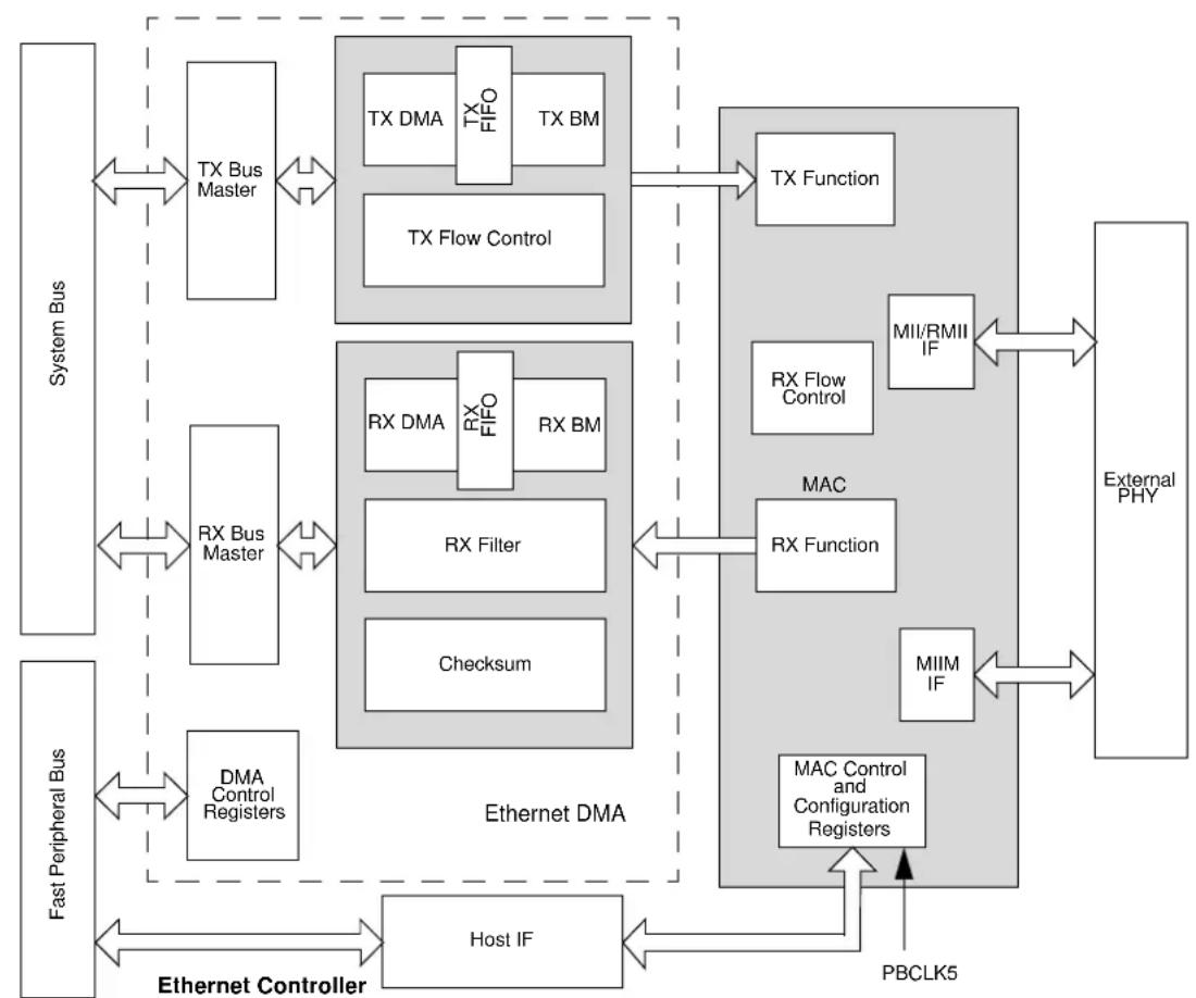
flowchart
graph TD
    subgraph System Bus
        A["TX Bus Master"] <--> B["TX DMA"]
        B <--> C["TX FIFO"]
        C <--> D["TX BM"]
        D <--> E["TX Flow Control"]
    end

    subgraph Fast Peripheral Bus
        F["RX Bus Master"] <--> G["RX DMA"]
        G <--> H["RX FIFO"]
        H <--> I["RX BM"]
        I --> J["RX Filter"]
        J --> K["Checksum"]
    end

    subgraph Ethernet DMA
        L["External PHY"] <--> M["MII/RMII IF"]
        M <--> N["RX Flow Control"]
        N <--> O["MAC"]
        O <--> P["RX Function"]
    end

    subgraph Fast Peripheral Bus
        Q["Fast Peripheral Bus"] <--> R["DMA Control Registers"]
        R --> S["Host IF"]
        S --> T["Host IF"]
    end

    subgraph Ethernet Controller
        U["Host IF"] <--> V["Host IF"]
        V --> W["Host IF"]
        W --> X["Host IF"]
        X --> Y["Host IF"]
        Y --> Z["Host IF"]
        Z --> AA["Host IF"]
        AA --> AB["Host IF"]
        AB --> AC["Host IF"]
        AC --> AD["Host IF"]
        AD --> AE["Host IF"]
        AE --> AF["Host IF"]
        AF --> AG["Host IF"]
        AG --> AH["Host IF"]
        AH --> AI["Host IF"]
        AI --> AJ["Host IF"]
        AJ --> AK["Host IF"]
        AK --> AL["Host IF"]
        AL --> AM["Host IF"]
        AM --> AN["Host IF"]
        AN --> AO["Host IF"]
        AO --> AP["Host IF"]
        AP --> AQ["Host IF"]
        AQ --> AR["Host IF"]
        AR --> AS["Host IF"]
        AS --> AT["Host IF"]
        AT --> AU["Host IF"]
        AU --> AV["Host IF"]
        AV --> AW["Host IF"]
        AW --> AX["Host IF"]
        AX --> AY["Host IF"]
        AY --> AZ["Host IF"]
        AZ --> BA["Host IF"]
        BA --> BB["Host IF"]
        BB --> BC["Host IF"]
        BC --> BD["Host IF"]
        BD --> BE["Host IF"]
        BE --> BF["Host IF"]
        BF --> BG["Host IF"]
        BG --> BH["Host IF"]
        BH --> BI["Host IF"]
        BI --> BJ["Host IF"]
        BJ --> BK["Host IF"]
        BK --> BL["Host IF"]
        BL --> BM["Host IF"]
        BM --> BN["Host IF"]
        BN --> BO["Host IF"]
        BO --> BP["Host IF"]
        BP --> BQ["Host IF"]
        BQ --> BR["Host IF"]
        BR --> BS["Host IF"]
        BS --> BT["Host IF"]
        BT --> BU["Host IF"]
        BU --> BV["Host IF"]
        BV --> BW["Host IF"]
        BW --> BX["Host IF"]
        BX --> BY["Host IF"]
        BY --> BZ["Host IF"]
        BZ --> CA["Host IF"]
        CA --> CB["Host IF"]
        CB --> CC["Host IF"]
        CC --> CD["Host IF"]
        CD --> CE["Host IF"]
        CE --> CF["Host IF"]
        CF --> CG["Host IF"]
        CG --> CH["Host IF"]
        CH --> CI["Host IF"]
        CI --> CJ["Host IF"]
        CJ --> CK["Host IF"]
        CK --> CR["Host IF"]
        CR --> CS["Host IF"]
        CS --> CT["Host IF"]
        CT --> CU["Host IF"]
        CU --> CV["Host IF"]
        CV --> CW["Host IF"]
        CW --> CX["Host IF"]
        CX --> CY["Host IF"]
        CY --> CZ["Host IF"]
        CZ --> DA["Host IF"]
    end

    subgraph External PHY
    AD
    AE
    AF
    AG
    AH
    AI
    AJ
    AK
    AL
    AM
    AN
    AO
    AP
    AQ
    AR
    AS
    AT
    AU
    AV
    AW
    AX
    AY
    AZ
    BA
    BB
    BC
    BD
    BE
    BF
    BG
    BH
    BI
    BJ
    BK
    BL
    BM
    BN
    BO
    BP
    BQ
    CA
    AD
    AE
    AF
    AG
    AH
    AI
    AJ
    AK
    AL
    AM
    AN
    AO
    AP
    AQ
    AR
    AS
    AT
    AU
    AV
    AW
    AX
    AY
    AZ
    BA
    BB
    BC
    BD
    BE
    BF
    BG
    BH
    BI
    AJ
    AK
    AL
    AM
    AN
    AO
    AP
    AQ
    AR
    AS
    AT
    AU
    AV
    AW
    AX
    AY
    AZ
    BA
    BB
    BC
    BD
    BE
    BF
    BG
    BH
    BI
    AJ
    AK
    AL
    AM
    AN
    AO
   AP
    AQ
    AR
    AS
    AT
    AU
    AV
    AW
   AX
   AB
   AC
   BF
Table 30-1, Table 30-2, Table 30-3 and Table 30-4 show four interfaces and the associated pins that can be used with the Ethernet Controller.
TABLE 30-1: MII MODE DEFAULT INTERFACE SIGNALS (FMIIEN = 1, FETHIO = 1)
| Pin Name Description | |
| EMDC Management Clock | |
| EMDIO Management I/O | |
| ETXCLK Transmit Clock | |
| ETXEN Transmit Enable | |
| ETXD0 | Transmit Data |
| ETXD1 | Transmit Data |
| ETXD2 | Transmit Data |
| ETXD3 | Transmit Data |
| ETXERR | Transmit Error |
| ERXCLK | Receive Clock |
| ERXDV | Receive Data Valid |
| ERXD0 Receive Data | |
| ERXD1 Receive Data | |
| ERXD2 Receive Data | |
| ERXD3 Receive Data | |
| ERXERR | Receive Error |
| ECRS | Carrier Sense |
| ECOL | Collision Indication |
TABLE 30-2: RMII MODE DEFAULT INTERFACE SIGNALS (FMIIEN = 0, FETHIO = 1)
| Pin Name Description | |
| EMDC Management Clock | |
| EMDIO Management I/O | |
| ETXEN Transmit Enable | |
| ETXD0 | Transmit Data |
| ETXD1 | Transmit Data |
| EREFCLK | Reference Clock |
| ECRSDV | Carrier Sense – Receive Data Valid |
| ERXD0 Receive Data | |
| ERXD1 Receive Data | |
| ERXERR | Receive Error |
Note: Ethernet controller pins that are not used by a selected interface can be used by other peripherals.
TABLE 30-3: MII MODE ALTERNATE INTERFACE SIGNALS (FMIEN = 1, FETHIO = 0)
| Pin Name Description | |
| AEMDC | Management Clock |
| AEMDIO | Management I/O |
| AETXCLK | Transmit Clock |
| AETXEN | Transmit Enable |
| AETXD0 Transmit Data | |
| AETXD1 Transmit Data | |
| AETXD2 Transmit Data | |
| AETXD3 Transmit Data | |
| AETXERR | Transmit Error |
| AERXCLK | Receive Clock |
| AERXDV | Receive Data Valid |
| AERXD0 | Receive Data |
| AERXD1 | Receive Data |
| AERXD2 | Receive Data |
| AERXD3 | Receive Data |
| AERXERR | Receive Error |
| AECRS | Carrier Sense |
| AECOL | Collision Indication |
Note: The MII mode Alternate Interface is not available on 64-pin devices.
TABLE 30-4: RMII MODE ALTERNATE INTERFACE SIGNALS (FMIEN = 0, FETHIO = 0)
| Pin Name Description | |
| AEMDC | Management Clock |
| AEMDIO | Management I/O |
| AETXEN | Transmit Enable |
| AETXD0 Transmit Data | |
| AETXD1 Transmit Data | |
| AEREFCLK | Reference Clock |
| AECRSDV | Carrier Sense – Receive Data Valid |
| AERXD0 | Receive Data |
| AERXD1 | Receive Data |
| AERXERR | Receive Error |
30.1 Ethernet Control Registers
TABLE 30-5: ETHERNET CONTROLLER REGISTER SUMMARY
Legend: x = unknown value on Reset: — = unimplemented, read as '0'. Reset values are shown in hexadecimal.
Note 1: All registers in this table (with the exception of ETHSTAT) have corresponding CLR, SET, and INV registers at their virtual addresses, plus offsets of 0x4, 0x8 and 0xC, respectively. See Section 12.2 "CLR, SET, and INV Registers" for more information.
2: Reset values default to the factory programmed value.
TABLE 30-5: ETHERNET CONTROLLER REGISTER SUMMARY (CONTINUED)
Legend: x = unknown value on Reset; — = unimplemented, read as '0'. Reset values are shown in hexadecimal.
Note 1: All registers in this table (with the exception of ETHSTAT) have corresponding CLR, SET, and INV registers at their virtual addresses, plus offsets of 0x4, 0x8 and 0xC, respectively. See Section 12.2 "CLR, SET, and INV Registers" for more information.
2: Reset values default to the factory programmed value.
TABLE 30-5: ETHERNET CONTROLLER REGISTER SUMMARY (CONTINUED)
| Virtual Address(BF88 #) | Register Name(1) | Bit Range | Bits | All Resets | ||||||||||||||||
| 31/15 | 30/14 | 29/13 | 28/12 | 27/11 | 26/10 | 25/9 | 24/8 | 23/7 | 22/6 | 21/5 | 20/4 | 19/3 | 18/2 | 17/1 | 16/0 | |||||
| 22B0 | EMAC1 MWTD | 31:16 | ——— | ——— | ——— | ——— | 00:00 | |||||||||||||
| 15:0 | WWD<15:0> | 00:00 | ||||||||||||||||||
| 22C0 | EMAC1 MRDD | 31:16 | ——— | ——— | ——— | ——— | 00:00 | |||||||||||||
| 15:0 | RIDD<15:0> | 00:00 | ||||||||||||||||||
| 22D0 | EMAC1 MIND | 31:16 | ——— | ——— | ——— | ——— | 00:00 | |||||||||||||
| 15:0 | — | — | — | — | — | — | — | — | — | — | — | — | LINKFAIL | NOTVALID | SCAN | MIIMBUSY | 00:00 | |||
| 2300 | EMAC1 SAD(2) | 31:16 | ——— | ——— | ——— | ——— | xxxxx | |||||||||||||
| 15:0 | STNADDR6<7:0> STNADDR5<7:0> | xxxxx | ||||||||||||||||||
| 2310 | EMAC1 SA1(2) | 31:16 | ——— | ——— | ——— | ——— | xxxxx | |||||||||||||
| 15:0 | STNADDR4<7:0> STNADDR3<7:0> | xxxxx | ||||||||||||||||||
| 2320 | EMAC1 SA2(2) | 31:16 | ——— | ——— | ——— | ——— | xxxxx | |||||||||||||
| 15:0 | STNADDR2<7:0> STNADDR1<7:0> | xxxxx | ||||||||||||||||||
Legend: x = unknown value on Reset; — = unimplemented, read as '0'. Reset values are shown in hexadecimal.
Note 1: All registers in this table (with the exception of ETHSTAT) have corresponding CLR, SET, and INV registers at their virtual addresses, plus offsets of 0x4, 0x8 and 0xC, respectively. See Section 12.2 "CLR, SET, and INV Registers" for more information.
2: Reset values default to the factory programmed value.
REGISTER 30-1: ETHCON1: ETHERNET CONTROLLER CONTROL REGISTER 1
| Bit Range | Bit31/23/15/7 | Bit30/22/14/6 | Bit29/21/13/5 | Bit28/20/12/4 | Bit27/19/11/3 | Bit26/18/10/2 | Bit25/17/9/1 | Bit24/16/8/0 |
| 31:24 | R/W-0 R/W | -0 R/W-0 R/W | 0 R/W-0 R/W | 0 R/W-0 R/W-0 | ||||
| PTV<15:8> | ||||||||
| 23:16 | R/W-0 R/W | -0 R/W-0 R/W | 0 R/W-0 R/W | 0 R/W-0 R/W-0 | ||||
| PTV<7:0> | ||||||||
| 15:8 | R/W-0 U-0 | R/W-0 U-0 U-0 | U-0 R/W-0 R/W | W-0 | ||||
| ON | — | SIDL | — | — | — | TXRTS | RXEN(1) | |
| 7:0 | R/W-0 | U-0 | U-0 | R/W-0 | U-0 | U-0 | U-0 | R/W-0 |
| AUTOFC | — | — | MANFC | — | — | — | BUFCDEC | |
Legend:
| R = Readable bit | W = Writable bit | U = Unimplemented bit, read as ‘0’ |
| -n = Value at POR | ‘1’ = Bit is set | ‘0’ = Bit is cleared x = Bit is unknown |
bit 31-16 PTV<15:0>: PAUSE Timer Value bits
PAUSE Timer Value used for Flow Control.
This register should only be written when RXEN (ETHCON1<8>) is not set.
These bits are only used for Flow Control operations.
bit 15 ON: Ethernet ON bit
1 = Ethernet module is enabled
0 = Ethernet module is disabled
bit 14 Unimplemented: Read as '0'
bit 13 SIDL: Ethernet Stop in Idle Mode bit
1 = Ethernet module transfers are paused during Idle mode
0 = Ethernet module transfers continue during Idle mode
bit 12-10 Unimplemented: Read as '0'
bit 9 TXRTS: Transmit Request to Send bit
1 = Activate the TX logic and send the packet(s) defined in the TX EDT
0 = Stop transmit (when cleared by software) or transmit done (when cleared by hardware)
After the bit is written with a '1', it will clear to a '0' whenever the transmit logic has finished transmitting the requested packets in the Ethernet Descriptor Table (EDT). If a '0' is written by the CPU, the transmit logic finishes the current packet's transmission and then stops any further.
This bit only affects TX operations.
bit 8 RXEN: Receive Enable bit (1)
1 = Enable RX logic, packets are received and stored in the RX buffer as controlled by the filter configuration
0 = Disable RX logic, no packets are received in the RX buffer
This bit only affects RX operations.
Note 1: It is not recommended to clear the RXEN bit and then make changes to any RX related field/register. The Ethernet Controller must be reinitialized (ON cleared to '0'), and then the RX changes applied.
REGISTER 30-1: ETHCON1: ETHERNET CONTROLLER CONTROL REGISTER 1 (CONTINUED)
bit 7 AUTOFC: Automatic Flow Control bit
1 = Automatic Flow Control enabled
0 = Automatic Flow Control disabled
Setting this bit will enable automatic Flow Control. If set, the full and empty watermarks are used to automatically enable and disable the Flow Control, respectively. When the number of received buffers BUFCNT (ETHSTAT<16:23>) rises to the full watermark, Flow Control is automatically enabled. When the BUFCNT falls to the empty watermark, Flow Control is automatically disabled.
This bit is only used for Flow Control operations and affects both TX and RX operations.
bit 6-5 Unimplemented: Read as '0'
bit 4 MANFC: Manual Flow Control bit
1 = Manual Flow Control is enabled
0 = Manual Flow Control is disabled
Setting this bit will enable manual Flow Control. If set, the Flow Control logic will send a PAUSE frame using the PAUSE timer value in the PTV register. It will then resend a PAUSE frame every 128 * PTV<15:0>/2 TX clock cycles until the bit is cleared.
Note: For 10 Mbps operation, TX clock runs at 2.5 MHz. For 100 Mbps operation, TX clock runs at 25 MHz.
When this bit is cleared, the Flow Control logic will automatically send a PAUSE frame with a 0x0000 PAUSE timer value to disable Flow Control.
This bit is only used for Flow Control operations and affects both TX and RX operations.
bit 3-1 Unimplemented: Read as '0'
bit 0 BUFCDEC: Descriptor Buffer Count Decrement bit
The BUFCDEC bit is a write-1 bit that reads as '0'. When written with a '1', the Descriptor Buffer Counter, BUFCNT, will decrement by one. If BUFCNT is incremented by the RX logic at the same time that this bit is written, the BUFCNT value will remain unchanged. Writing a '0' will have no effect.
This bit is only used for RX operations.
Note 1: It is not recommended to clear the RXEN bit and then make changes to any RX related field/register. The Ethernet Controller must be reinitialized (ON cleared to '0'), and then the RX changes applied.
REGISTER 30-2: ETHCON2: ETHERNET CONTROLLER CONTROL REGISTER 2
| Bit Range | Bit31/23/15/7 | Bit30/22/14/6 | Bit29/21/13/5 | Bit28/20/12/4 | Bit27/19/11/3 | Bit26/18/10/2 | Bit25/17/9/1 | Bit24/16/8/0 |
| 31:24 | U-0 U-0 | U-0 U-0 | U-0 U-0 | U-0 U-0 | ||||
| — — — | — — — — | — | ||||||
| 23:16 | U-0 U-0 | U-0 U-0 | U-0 U-0 | U-0 U-0 | ||||
| — — — | — — — — | — | ||||||
| 15:8 | U-0 U-0 | U-0 U-0 | R/W-0 R/W-0 | R/W-0 | ||||
| — — — | — — | RXBUFSZ<6:4> | ||||||
| 7:0 | R/W-0 | R/W-0 | R/W-0 R/W-0 | U-0 U-0 | U-0 U-0 | |||
| RXBUFSZ<3:0> | — — — | — | ||||||
| Legend: | ||
| R = Readable bit | W = Writable bit U = Unimplemented bit, read as ‘0’ | |
| -n = Value at POR | ‘1’ = Bit is set | ‘0’ = Bit is cleared x = Bit is unknown |
bit 31-11 Unimplemented: Read as '0'
bit 10-4 RXBUFSZ<6:0>: RX Data Buffer Size for All RX Descriptors (in 16-byte increments) bits
1111111 = RX data Buffer size for descriptors is 2032 bytes
.
•
.
1100000 = RX data Buffer size for descriptors is 1536 bytes
•
•
•
0000011 = RX data Buffer size for descriptors is 48 bytes
0000010 = RX data Buffer size for descriptors is 32 bytes
0000001 = RX data Buffer size for descriptors is 16 bytes
0000000 = Reserved
bit 3-0 Unimplemented: Read as '0'
Note 1: This register is only used for RX operations.
2: The bits in this register may only be changed while the RXEN bit (ETHCON1<8>) = 0.
REGISTER 30-3: ETHTXST: ETHERNET CONTROLLER TX PACKET DESCRIPTOR START ADDRESS REGISTER
| Bit Range | Bit 31/23/15/7 | Bit 30/22/14/6 | Bit 29/21/13/5 | Bit 28/20/12/4 | Bit 27/19/11/3 | Bit 26/18/10/2 | Bit 25/17/9/1 | Bit 24/16/8/0 |
| 31:24 | R/W-0 R/W-0 R/W-0 R/W-0 | R/W-0 R/W-0 R/W-0 | ||||||
| TXSTADDR<31:24> | ||||||||
| 23:16 | R/W-0 R/W-0 R/W-0 R/W-0 | R/W-0 R/W-0 R/W-0 | ||||||
| TXSTADDR<23:16> | ||||||||
| 15:8 | R/W-0 R/W-0 R/W-0 R/W-0 | R/W-0 R/W-0 R/W-0 | ||||||
| TXSTADDR<15:8> | ||||||||
| 7:0 | R/W-0 R/W-0 R/W-0 R/W-0 | R/W-0 R/W-0 U-0 U-0 | ||||||
| TXSTADDR<7:2> | — | — | ||||||
Legend:
| R = Readable bit | W = Writable bit | U = Unimplemented bit, read as '0' |
| -n = Value at POR | ‘1’ = Bit is set | ‘0’ = Bit is cleared x = Bit is unknown |
bit 31-2 TXSTADDR<31:2>: Starting Address of First Transmit Descriptor bits
This register should not be written while any transmit, receive or DMA operations are in progress. This address must be 4-byte aligned (bits 1-0 must be '00').
bit 1-0 Unimplemented: Read as '0'
Note 1: This register is only used for TX operations.
2: This register will be updated by hardware with the last descriptor used by the last successfully transmitted packet.
REGISTER 30-4: ETHRXST: ETHERNET CONTROLLER RX PACKET DESCRIPTOR START ADDRESS REGISTER
| Bit Range | Bit 31/23/15/7 | Bit 30/22/14/6 | Bit 29/21/13/5 | Bit 28/20/12/4 | Bit 27/19/11/3 | Bit 26/18/10/2 | Bit 25/17/9/1 | Bit 24/16/8/0 |
| 31:24 | R/W-0 | R/W-0 | R/W-0 | R/W-0 | R/W-0 | R/W-0 | R/W-0 | R/W-0 |
| RXSTADDR<31:24> | ||||||||
| 23:16 | R/W-0 | R/W-0 | R/W-0 | R/W-0 | R/W-0 | R/W-0 | R/W-0 | R/W-0 |
| RXSTADDR<23:16> | ||||||||
| 15:8 | R/W-0 | R/W-0 | R/W-0 | R/W-0 | R/W-0 | R/W-0 | R/W-0 | R/W-0 |
| RXSTADDR<15:8> | ||||||||
| 7:0 | R/W-0 | R/W-0 | R/W-0 | R/W-0 | R/W-0 | R/W-0 | U-0 | U-0 |
| RXSTADDR<7:2> | — | — | ||||||
Legend:
| R = Readable bit | W = Writable bit | U = Unimplemented bit, read as ‘0’ |
| -n = Value at POR | ‘1’ = Bit is set | ‘0’ = Bit is cleared x = Bit is unknown |
bit 31-2 RXSTADDR<31:2>: Starting Address of First Receive Descriptor bits
This register should not be written while any transmit, receive or DMA operations are in progress.
This address must be 4-byte aligned (bits 1-0 must be '00').
bit 1-0 Unimplemented: Read as '0'
Note 1: This register is only used for RX operations.
2: This register will be updated by hardware with the last descriptor used by the last successfully transmitted packet.
REGISTER 30-5: ETHHT0: ETHERNET CONTROLLER HASH TABLE 0 REGISTER
| Bit Range | Bit 31/23/15/7 | Bit 30/22/14/6 | Bit 29/21/13/5 | Bit 28/20/12/4 | Bit 27/19/11/3 | Bit 26/18/10/2 | Bit 25/17/9/1 | Bit 24/16/8/0 |
| 31:24 | R/W-0 R/W | R/W-0 R/W-0 R/W | R/W-0 R/W-0 | R/W-0 R/W-0 | ||||
| HT<31:24> | ||||||||
| 23:16 | R/W-0 R/W | R/W-0 R/W-0 R/W | R/W-0 R/W-0 | R/W-0 R/W-0 | ||||
| HT<23:16> | ||||||||
| 15:8 | R/W-0 R/W | R/W-0 R/W-0 R/W | R/W-0 R/W-0 | R/W-0 R/W-0 | ||||
| HT<15:8> | ||||||||
| 7:0 | R/W-0 R/W | R/W-0 R/W-0 R/W | R/W-0 R/W-0 | R/W-0 R/W-0 | ||||
| HT<7:0> | ||||||||
Legend:
R = Readable bit W = Writable bit U = Unimplemented bit, read as '0' -n = Value at POR '1' = Bit is set '0' = Bit is cleared x = Bit is unknown
bit 31-0 HT<31:0>: Hash Table Bytes 0-3 bits
Note 1: This register is only used for RX operations.
2: The bits in this register may only be changed while the RXEN bit (ETHCON1<8>) = 0 or the HTEN bit (ETHRXFC<15>) = 0.
REGISTER 30-6: ETHHT1: ETHERNET CONTROLLER HASH TABLE 1 REGISTER
| Bit Range | Bit31/23/15/7 | Bit30/22/14/6 | Bit29/21/13/5 | Bit28/20/12/4 | Bit27/19/11/3 | Bit26/18/10/2 | Bit25/17/9/1 | Bit24/16/8/0 |
| 31:24 | R/W-0 | R/W-0 | R/W-0 | R/W-0 | R/W-0 | R/W-0 | R/W-0 | R/W-0 |
| HT<63:56> | ||||||||
| 23:16 | R/W-0 | R/W-0 | R/W-0 | R/W-0 | R/W-0 | R/W-0 | R/W-0 | R/W-0 |
| HT<55:48> | ||||||||
| 15:8 | R/W-0 | R/W-0 | R/W-0 | R/W-0 | R/W-0 | R/W-0 | R/W-0 | R/W-0 |
| HT<47:40> | ||||||||
| 7:0 | R/W-0 | R/W-0 | R/W-0 | R/W-0 | R/W-0 | R/W-0 | R/W-0 | R/W-0 |
| HT<39:32> | ||||||||
Legend:
R = Readable bit W = Writable bit U = Unimplemented bit, read as '0' -n = Value at POR '1' = Bit is set '0' = Bit is cleared x = Bit is unknown
bit 31-0 HT<63:32>: Hash Table Bytes 4-7 bits
Note 1: This register is only used for RX operations.
2: The bits in this register may only be changed while the RXEN bit (ETHCON1<8>) = 0 or the HTEN bit (ETHRXFC<15>) = 0.
REGISTER 30-7: ETHPMM0: ETHERNET CONTROLLER PATTERN MATCH MASK 0 REGISTER
| Bit Range | Bit31/23/15/7 | Bit30/22/14/6 | Bit29/21/13/5 | Bit28/20/12/4 | Bit27/19/11/3 | Bit26/18/10/2 | Bit25/17/9/1 | Bit24/16/8/0 |
| 31:24 | R/W-0 R/W | -0 R/W-0 R/W | -0 R/W-0 R/W | -0 R/W-0 R/W | -0 R/W-0 R/W | -0 | ||
| PMM<31:24> | ||||||||
| 23:16 | R/W-0 R/W | -0 R/W-0 R/W | -0 R/W-0 R/W | -0 R/W-0 R/W | -0 R/W-0 R/W | -0 | ||
| PMM<23:16> | ||||||||
| 15:8 | R/W-0 R/W | -0 R/W-0 R/W | -0 R/W-0 R/W | -0 R/W-0 R/W | -0 R/W-0 R/W | -0 | ||
| PMM<15:8> | ||||||||
| 7:0 | R/W-0 R/W | -0 R/W-0 R/W | -0 R/W-0 R/W | -0 R/W-0 R/W | -0 R/W-0 R/W | -0 | ||
| PMM<7:0> | ||||||||
Legend:
R = Readable bit W = Writable bit U = Unimplemented bit, read as '0' -n = Value at POR '1' = Bit is set '0' = Bit is cleared x = Bit is unknown
bit 31-24 PMM<31:24>: Pattern Match Mask 3 bits
bit 23-16 PMM<23:16>: Pattern Match Mask 2 bits
bit 15-8 PMM<15:8>: Pattern Match Mask 1 bits
bit 7-0 PMM<7:0>: Pattern Match Mask 0 bits
Note 1: This register is only used for RX operations.
2: The bits in this register may only be changed while the RXEN bit (ETHCON1<8>) = 0 or the PMMODE bit (ETHRXFC<11:8>) = 0.
REGISTER 30-8: ETHPMM1: ETHERNET CONTROLLER PATTERN MATCH MASK 1 REGISTER
| Bit Range | Bit31/23/15/7 | Bit30/22/14/6 | Bit29/21/13/5 | Bit28/20/12/4 | Bit27/19/11/3 | Bit26/18/10/2 | Bit25/17/9/1 | Bit24/16/8/0 |
| 31:24 | R/W-0 | R/W-0 | R/W-0 | R/W-0 | R/W-0 | R/W-0 | R/W-0 | R/W-0 |
| PMM<63:56> | ||||||||
| 23:16 | R/W-0 | R/W-0 | R/W-0 | R/W-0 | R/W-0 | R/W-0 | R/W-0 | R/W-0 |
| PMM<55:48> | ||||||||
| 15:8 | R/W-0 | R/W-0 | R/W-0 | R/W-0 | R/W-0 | R/W-0 | R/W-0 | R/W-0 |
| PMM<47:40> | ||||||||
| 7:0 | R/W-0 | R/W-0 | R/W-0 | R/W-0 | R/W-0 | R/W-0 | R/W-0 | R/W-0 |
| PMM<39:32> | ||||||||
Legend:
R = Readable bit W = Writable bit U = Unimplemented bit, read as '0' -n = Value at POR '1' = Bit is set '0' = Bit is cleared x = Bit is unknown
bit 31-24 PMM<63:56>: Pattern Match Mask 7 bits
bit 23-16 PMM<55:48>: Pattern Match Mask 6 bits
bit 15-8 PMM<47:40>: Pattern Match Mask 5 bits
bit 7-0 PMM<39:32>: Pattern Match Mask 4 bits
Note 1: This register is only used for RX operations.
2: The bits in this register may only be changed while the RXEN bit (ETHCON1<8>) = 0 or the PMMODE bit (ETHRXFC<11:8>) = 0.
REGISTER 30-9: ETHPMCS: ETHERNET CONTROLLER PATTERN MATCH CHECKSUM REGISTER
| Bit Range | Bit31/23/15/7 | Bit30/22/14/6 | Bit29/21/13/5 | Bit28/20/12/4 | Bit27/19/11/3 | Bit26/18/10/2 | Bit25/17/9/1 | Bit24/16/8/0 |
| 31:24 | U-0 U-0 | U-0 U-0 | U-0 U-0 | U-0 U-0 | ||||
| — — — | — — — — | — | ||||||
| 23:16 | U-0 U-0 | U-0 U-0 | U-0 U-0 | U-0 U-0 | ||||
| — — — | — — — — | — | ||||||
| 15:8 | R/W-0 R/W | R/W-0 | R/W-0 | R/W-0 | R/W-0 | R/W-0 | ||
| PMCS<15:8> | ||||||||
| 7:0 | R/W-0 R/W | R/W-0 | R/W-0 | R/W-0 | R/W-0 | R/W-0 | ||
| PMCS<7:0> | ||||||||
Legend:
R = Readable bit W = Writable bit U = Unimplemented bit, read as '0' -n = Value at POR '1' = Bit is set '0' = Bit is cleared x = Bit is unknown
bit 31-16 Unimplemented: Read as '0'
bit 15-8 PMCS<15:8>: Pattern Match Checksum 1 bits
bit 7-0 PMCS<7:0>: Pattern Match Checksum 0 bits
Note 1: This register is only used for RX operations.
2: The bits in this register may only be changed while the RXEN bit (ETHCON1<8>) = 0 or the PMMODE bit (ETHRXFC<11:8>) = 0.
REGISTER 30-10: ETHPMO: ETHERNET CONTROLLER PATTERN MATCH OFFSET REGISTER
| Bit Range | Bit 31/23/15/7 | Bit 30/22/14/6 | Bit 29/21/13/5 | Bit 28/20/12/4 | Bit 27/19/11/3 | Bit 26/18/10/2 | Bit 25/17/9/1 | Bit 24/16/8/0 |
| 31:24 | U-0 | U-0 | U-0 | U-0 | U-0 | U-0 | U-0 | U-0 |
| — — | — — | — — | — — | — — | ||||
| 23:16 | U-0 | U-0 | U-0 | U-0 | U-0 | U-0 | U-0 | U-0 |
| — — | — — | — — | — — | — — | ||||
| 15:8 | R/W-0 | R/W-0 | R/W-0 | R/W-0 | R/W-0 | R/W-0 | R/W-0 | R/W-0 |
| PMO<15:8> | ||||||||
| 7:0 | R/W-0 | R/W-0 | R/W-0 | R/W-0 | R/W-0 | R/W-0 | R/W-0 | R/W-0 |
| PMO<7:0> | ||||||||
Legend:
R = Readable bit W = Writable bit U = Unimplemented bit, read as '0' -n = Value at POR '1' = Bit is set '0' = Bit is cleared x = Bit is unknown
bit 31-16 Unimplemented: Read as '0'
bit 15-0 PMO<15:0>: Pattern Match Offset 1 bits
Note 1: This register is only used for RX operations.
2: The bits in this register may only be changed while the RXEN bit (ETHCON1<8>) = 0 or the PMMODE bit (ETHRXFC<11:8>) = 0.
REGISTER 30-11: ETHRXFC: ETHERNET CONTROLLER RECEIVE FILTER CONFIGURATION REGISTER
| Bit Range | Bit 31/23/15/7 | Bit 30/22/14/6 | Bit 29/21/13/5 | Bit 28/20/12/4 | Bit 27/19/11/3 | Bit 26/18/10/2 | Bit 25/17/9/1 | Bit 24/16/8/0 |
| 31:24 | U-0 U-0 U-0 | U-0 U-0 U-0 | U-0 U-0 | |||||
| — — — | — — — | — | — | |||||
| 23:16 | U-0 U-0 U-0 | U-0 U-0 U-0 | U-0 U-0 | |||||
| — — — | — — — | — | — | |||||
| 15:8 | R/W-0 | R/W-0 | U-0 | R/W-0 | R/W-0 | R/W-0 | R/W-0 | R/W-0 |
| HTEN | MPEN | — | NOTPM | PMMODE<3:0> | ||||
| 7:0 | R/W-0 | R/W-0 | R/W-0 | R/W-0 | R/W-0 | R/W-0 | R/W-0 | R/W-0 |
| CRCERREN | CRCOKEN | RUNTERREN | RUNTEN | UCEN | NOTMEEN | MCEN | BCEN | |
Legend:
| R = Readable bit | W = Writable bit | U = Unimplemented bit, read as '0' |
| -n = Value at POR | '1' = Bit is set | '0' = Bit is cleared x = Bit is unknown |
bit 31-16 Unimplemented: Read as '0'
bit 15 HTEN: Enable Hash Table Filtering bit
1 = Enable Hash Table Filtering
0 = Disable Hash Table Filtering
bit 14 MPEN: Magic Packet™ Enable bit
1 = Enable Magic Packet Filtering
0 = Disable Magic Packet Filtering
bit 13 Unimplemented: Read as '0'
bit 12 NOTPM: Pattern Match Inversion bit
1 = The Pattern Match Checksum must not match for a successful Pattern Match to occur
0 = The Pattern Match Checksum must match for a successful Pattern Match to occur
This bit determines whether Pattern Match Checksum must match in order for a successful Pattern Match to occur.
bit 11-8 PMMODE<3:0>: Pattern Match Mode bits
1001 = Pattern match is successful if (NOTPM = 1 XOR Pattern Match Checksum matches) AND (Packet = Magic Packet) ^(1,3)
1000 = Pattern match is successful if (NOTPM = 1 XOR Pattern Match Checksum matches) AND (Hash Table Filter match) ^(1,2)
0111 = Pattern match is successful if (NOTPM = 1 XOR Pattern Match Checksum matches) AND (Destination Address = Broadcast Address) ^(1)
0110 = Pattern match is successful if (NOTPM = 1 XOR Pattern Match Checksum matches) AND (Destination Address = Broadcast Address) ^(1)
0101 = Pattern match is successful if (NOTPM = 1 XOR Pattern Match Checksum matches) AND (Destination Address = Unicast Address) ^(1)
0100 = Pattern match is successful if (NOTPM = 1 XOR Pattern Match Checksum matches) AND (Destination Address = Unicast Address) ^(1)
0011 = Pattern match is successful if (NOTPM = 1 XOR Pattern Match Checksum matches) AND (Destination Address = Station Address) ^(1)
0010 = Pattern match is successful if (NOTPM = 1 XOR Pattern Match Checksum matches) AND (Destination Address = Station Address) ^(1)
0001 = Pattern match is successful if (NOTPM = 1 XOR Pattern Match Checksum matches) ^(1)
0000 = Pattern Match is disabled; pattern match is always unsuccessful
Note 1: XOR = True when either one or the other conditions are true, but not both.
2: This Hash Table Filter match is active regardless of the value of the HTEN bit.
3: This Magic Packet Filter match is active regardless of the value of the MPEN bit.
Note 1: This register is only used for RX operations.
2: The bits in this register may only be changed while the RXEN bit (ETHCON1<8>) = 0.
REGISTER 30-11: ETHRXFC: ETHERNET CONTROLLER RECEIVE FILTER CONFIGURATION REGISTER (CONTINUED)
bit 7 CRCERREN: CRC Error Collection Enable bit
1 = The received packet CRC must be invalid for the packet to be accepted
0 = Disable CRC Error Collection filtering
This bit allows the user to collect all packets that have an invalid CRC.
bit 6 CRCOKEN: CRC OK Enable bit
1 = The received packet CRC must be valid for the packet to be accepted
0 = Disable CRC filtering
This bit allows the user to reject all packets that have an invalid CRC.
bit 5 RUNTERREN: Runt Error Collection Enable bit
1 = The received packet must be a runt packet for the packet to be accepted
0 = Disable Runt Error Collection filtering
This bit allows the user to collect all packets that are runt packets. For this filter, a runt packet is defined as any packet with a size of less than 64 bytes (when CRCOKEN = 0) or any packet with a size of less than 64 bytes that has a valid CRC (when CRCOKEN = 1).
bit 4 RUNTEN: Runt Enable bit
1 = The received packet must not be a runt packet for the packet to be accepted
0 = Disable Runt filtering
This bit allows the user to reject all runt packets. For this filter, a runt packet is defined as any packet with a size of less than 64 bytes.
bit 3 UCEN: Unicast Enable bit
1 = Enable Unicast Filtering
0 = Disable Unicast Filtering
This bit allows the user to accept all unicast packets whose Destination Address matches the Station Address.
bit 2 NOTMEEN: Not Me Unicast Enable bit
1 = Enable Not Me Unicast Filtering
0 = Disable Not Me Unicast Filtering
This bit allows the user to accept all unicast packets whose Destination Address does not match the Station Address.
bit 1 MCEN: Multicast Enable bit
1 = Enable Multicast Filtering
0 = Disable Multicast Filtering
This bit allows the user to accept all Multicast Address packets.
bit 0 BCEN: Broadcast Enable bit
1 = Enable Broadcast Filtering
0 = Disable Broadcast Filtering
This bit allows the user to accept all Broadcast Address packets.
Note 1: XOR = True when either one or the other conditions are true, but not both.
2: This Hash Table Filter match is active regardless of the value of the HTEN bit.
3: This Magic Packet Filter match is active regardless of the value of the MPEN bit.
Note 1: This register is only used for RX operations.
2: The bits in this register may only be changed while the RXEN bit (ETHCON1<8>) = 0.
REGISTER 30-12: ETHRXWM: ETHERNET CONTROLLER RECEIVE WATERMARKS REGISTER
| Bit Range | Bit31/23/15/7 | Bit30/22/14/6 | Bit29/21/13/5 | Bit28/20/12/4 | Bit27/19/11/3 | Bit26/18/10/2 | Bit25/17/9/1 | Bit24/16/8/0 |
| 31:24 | U-0 U-0 | U-0 U-0 U-0 | U-0 U-0 | |||||
| — — — | — — — — | — | ||||||
| 23:16 | R/W-0 R/W | R/W-0 R/W-0 | R/W-0 R/W-0 | R/W-0 R/W-0 | R/W-0 R/W-0 | |||
| RXFWM<7:0> | ||||||||
| 15:8 | U-0 U-0 | U-0 U-0 | U-0 U-0 | |||||
| — — — | — — — — | — | ||||||
| 7:0 | R/W-0 R/W | R/W-0 R/W-0 | R/W-0 R/W-0 | R/W-0 R/W-0 | ||||
| RXEWM<7:0> | ||||||||
Legend:
R = Readable bit W = Writable bit U = Unimplemented bit, read as '0' -n = Value at POR '1' = Bit is set '0' = Bit is cleared x = Bit is unknown
bit 31-24 Unimplemented: Read as '0'
bit 23-16 RXFWM<7:0>: Receive Full Watermark bits
The software controlled RX Buffer Full Watermark Pointer is compared against the RX BUFCNT to determine the full watermark condition for the FWMARK interrupt and for enabling Flow Control when automatic Flow Control is enabled. The Full Watermark Pointer should always be greater than the Empty Watermark Pointer.
bit 15-8 Unimplemented: Read as '0'
bit 7-0 RXEWM<7:0>: Receive Empty Watermark bits
The software controlled RX Buffer Empty Watermark Pointer is compared against the RX BUFCNT to determine the empty watermark condition for the EWMARK interrupt and for disabling Flow Control when automatic Flow Control is enabled. The Empty Watermark Pointer should always be less than the Full Watermark Pointer.
Note: This register is only used for RX operations.
REGISTER 30-13: ETHIEN: ETHERNET CONTROLLER INTERRUPT ENABLE REGISTER
| Bit Range | Bit 31/23/15/7 | Bit 30/22/14/6 | Bit 29/21/13/5 | Bit 28/20/12/4 | Bit 27/19/11/3 | Bit 26/18/10/2 | Bit 25/17/9/1 | Bit 24/16/8/0 |
| 31:24 | U-0 U-0 U-0 | U-0 U-0 U-0 | U-0 | |||||
| — — — | — — — — — | |||||||
| 23:16 | U-0 U-0 U-0 | U-0 U-0 U-0 | U-0 | |||||
| — — — | — — — — — | |||||||
| 15:8 | U-0 R/W-0 | R/W-0 U-0 | U-0 | R/W-0 | R/W-0 | |||
| — | TXBUSEIE ^(1) | RXBUSEIE ^(2) | — — | EWMARKIE | ^(2) | FWMARKIE ^(2) | ||
| 7:0 | R/W-0 | R/W-0 | R/W-0 | U-0 | R/W-0 | R/W-0 | R/W-0 | R/W-0 |
| RXDONEIE ^(2) | PKTPENDIE ^(2) | RXACTIE ^(2) | — | TXDONEIE ^(1) | TXABORTIE ^(1) | RXBUFNAIE ^(2) | RXOVFLWIE ^(2) | |
Legend:
| R = Readable bit | W = Writable bit | U = Unimplemented bit, read as '0' |
| -n = Value at POR | '1' = Bit is set | '0' = Bit is cleared x = Bit is unknown |
bit 31-15 Unimplemented: Read as '0'
bit 14 TXBUSEIE: Transmit BVCI Bus Error Interrupt Enable bit ^(1)
1 = Enable TXBUS Error Interrupt
0 = Disable TXBUS Error Interrupt
bit 13 RXBUSEIE: Receive BVCI Bus Error Interrupt Enable bit(2)
1 = Enable RXBUS Error Interrupt
0 = Disable RXBUS Error Interrupt
bit 12-10 Unimplemented: Read as '0'
bit 9 EWMARKIE: Empty Watermark Interrupt Enable bit ^(2)
1 = Enable EWMARK Interrupt
0 = Disable EWMARK Interrupt
bit 8 FWMARKIE: Full Watermark Interrupt Enable bit ^(2)
1 = Enable FWMARK Interrupt
0 = Disable FWMARK Interrupt
bit 7 RXDONEIE: Receiver Done Interrupt Enable bit ^(2)
1 = Enable RXDONE Interrupt
0 = Disable RXDONE Interrupt
bit 6 PKTPENDIE: Packet Pending Interrupt Enable bit ^(2)
1 = Enable PKTPEND Interrupt
0 = Disable PKTPEND Interrupt
bit 5 RXACTIE: RX Activity Interrupt Enable bit
1 = Enable RXACT Interrupt
0 = Disable RXACT Interrupt
bit 4 Unimplemented: Read as '0'
bit 3 TXDONEIE: Transmitter Done Interrupt Enable bit ^(1)
1 = Enable TXDONE Interrupt
0 = Disable TXDONE Interrupt
bit 2 TXABORTIE: Transmitter Abort Interrupt Enable bit ^(1)
1 = Enable TXABORT Interrupt
0 = Disable TXABORT Interrupt
bit 1 RXBUFNAIE: Receive Buffer Not Available Interrupt Enable bit ^(2)
1 = Enable RXBUFNA Interrupt
0 = Disable RXBUFNA Interrupt
bit 0 RXOVFLWIE: Receive FIFO Overflow Interrupt Enable bit ^(2)
1 = Enable RXOVFLW Interrupt
0 = Disable RXOVFLW Interrupt
Note 1: This bit is only used for TX operations.
2: This bit is only used for RX operations.
REGISTER 30-14: ETHIRQ: ETHERNET CONTROLLER INTERRUPT REQUEST REGISTER
| Bit Range | Bit31/23/15/7 | Bit30/22/14/6 | Bit29/21/13/5 | Bit28/20/12/4 | Bit27/19/11/3 | Bit26/18/10/2 | Bit25/17/9/1 | Bit24/16/8/0 |
| 31:24 | U-0 U-0 | U-0 U-0 U-0 | U-0 U-0 | |||||
| — — — | — — — | — | — | |||||
| 23:16 | U-0 U-0 | U-0 U-0 U-0 | U-0 U-0 | |||||
| — — — | — — — | — | — | |||||
| 15:8 | U-0 | R/W-0 | R/W-0 | U-0 | U-0 | U-0 | R/W-0 | R/W-0 |
| — | TXBUSE(1) | RXBUSE(2) | — | — | — | EWMARK(2) | FWMARK(2) | |
| 7:0 | R/W-0 | R/W-0 | R/W-0 | U-0 | R/W-0 | R/W-0 | R/W-0 | R/W-0 |
| RXDONE(2) | PKTPEND(2) | RXACT(2) | — | TXDONE(1) | TXABORT(1) | RXBUFNA(2) | RXOVFLW(2) |
Legend:
| R = Readable bit | W = Writable bit U = Unimplemented bit, read as '0' |
| -n = Value at POR | '1' = Bit is set '0' = Bit is cleared x = Bit is unknown |
bit 31-15 Unimplemented: Read as '0'
bit 14 TXBUSE: Transmit BVCI Bus Error Interrupt bit ^(1)
1 = BVCI Bus Error has occurred
0 = BVCI Bus Error has not occurred
This bit is set when the TX DMA encounters a BVCI Bus error during a memory access. It is cleared by either a Reset or CPU write of a '1' to the CLR register.
bit 13 RXBUSE: Receive BVCI Bus Error Interrupt bit ^(2)
1 = BVCI Bus Error has occurred
0 = BVCI Bus Error has not occurred
This bit is set when the RX DMA encounters a BVCI Bus error during a memory access. It is cleared by either a Reset or CPU write of a '1' to the CLR register.
bit 12-10 Unimplemented: Read as '0'
bit 9 EWMARK: Empty Watermark Interrupt bit ^(2)
1 = Empty Watermark pointer reached
0 = No interrupt pending
This bit is set when the RX Descriptor Buffer Count is less than or equal to the value in the
RXEWM bit (ETHRXWM<0:7>) value. It is cleared by BUFCNT bit (ETHSTAT<16:23>)
being incremented by hardware. Writing a '0' or a '1' has no effect.
bit 8 FWMARK: Full Watermark Interrupt bit ^(2)
1 = Full Watermark pointer reached
0 = No interrupt pending
This bit is set when the RX Descriptor Buffer Count is greater than or equal to the value in the RXFWM bit (ETHRXWM<16:23>) field. It is cleared by writing the BUFCDEC (ETHCON1<0>) bit to decrement the BUFCNT counter. Writing a '0' or a '1' has no effect.
Note 1: This bit is only used for TX operations.
2: This bit is only used for RX operations.
Note: It is recommended to use the SET, CLR, or INV registers to set or clear any bit in this register. Setting or clearing any bits in this register should only be done for debug/test purposes.
REGISTER 30-14: ETHIRQ: ETHERNET CONTROLLER INTERRUPT REQUEST REGISTER
bit 7 RXDONE: Receive Done Interrupt bit (2)
1 = RX packet was successfully received
0 = No interrupt pending
This bit is set whenever an RX packet is successfully received. It is cleared by either a Reset or CPU write of a '1' to the CLR register.
bit 6 PKTPEND: Packet Pending Interrupt bit (2)
1 = RX packet pending in memory
0 = RX packet is not pending in memory
This bit is set when the BUFCNT counter has a value other than '0'. It is cleared by either a Reset or by writing the BUFCDEC bit to decrement the BUFCNT counter. Writing a '0' or a '1' has no effect.
bit 5 RXACT: Receive Activity Interrupt bit (2)
1 = RX packet data was successfully received
0 = No interrupt pending
This bit is set whenever RX packet data is stored in the RXBM FIFO. It is cleared by either a Reset or CPU write of a '1' to the CLR register.
bit 4 Unimplemented: Read as '0'
bit 3 TXDONE: Transmit Done Interrupt bit (1)
1 = TX packet was successfully sent
0 = No interrupt pending
This bit is set when the currently transmitted TX packet completes transmission, and the Transmit Status Vector is loaded into the first descriptor used for the packet. It is cleared by either a Reset or CPU write of a '1' to the CLR register.
bit 2 TXABORT: Transmit Abort Condition Interrupt bit (1)
1 = TX abort condition occurred on the last TX packet
0 = No interrupt pending
This bit is set when the MAC aborts the transmission of a TX packet for one of the following reasons:
- Jumbo TX packet abort
- Underrun abort
• Excessive defer abort
- Late collision abort
• Excessive collisions abort
This bit is cleared by either a Reset or CPU write of a '1' to the CLR register.
bit 1 RXBUFNA: Receive Buffer Not Available Interrupt bit ^(2)
1 = RX Buffer Descriptor Not Available condition has occurred
0 = No interrupt pending
This bit is set by a RX Buffer Descriptor Overrun condition. It is cleared by either a Reset or a CPU write of a '1' to the CLR register.
bit 0 RXOVFLW: Receive FIFO Over Flow Error bit (2)
1 = RX FIFO Overflow Error condition has occurred
0 = No interrupt pending
RXOVFLW is set by the RXBM Logic for an RX FIFO Overflow condition. It is cleared by either a Reset or CPU write of a '1' to the CLR register.
Note 1: This bit is only used for TX operations.
2: This bit is only used for RX operations.
Note: It is recommended to use the SET, CLR, or INV registers to set or clear any bit in this register. Setting or clearing any bits in this register should only be done for debug/test purposes.
REGISTER 30-15: ETHSTAT: ETHERNET CONTROLLER STATUS REGISTER
| Bit Range | Bit 31/23/15/7 | Bit 30/22/14/6 | Bit 29/21/13/5 | Bit 28/20/12/4 | Bit 27/19/11/3 | Bit 26/18/10/2 | Bit 25/17/9/1 | Bit 24/16/8/0 |
| 31:24 | U-0 U-0 U-0 | U-0 U-0 U-0 U-0 | U-0 | |||||
| — — — | — — | — — | — | |||||
| 23:16 | R/W-0 | R/W-0 | R/W-0 | R/W-0 | R/W-0 | R/W-0 | R/W-0 | R/W-0 |
| BUFCNT<7:0>(1) | ||||||||
| 15:8 | U-0 U-0 U-0 | U-0 U-0 U-0 U-0 | U-0 | |||||
| — — — | — — | — — | — | |||||
| 7:0 | R/W-0 | R/W-0 R/W | U-0 | U-0 | U-0 | U-0 | ||
| ETHBUSY(4,5) | TXBUSY(2,6) | RXBUSY(3,6) | — — | — | — | — | ||
Legend:
| R = Readable bit | W = Writable bit | U = Unimplemented bit, read as '0' |
| -n = Value at POR | '1' = Bit is set | '0' = Bit is cleared x = Bit is unknown |
bit 31-24 Unimplemented: Read as '0'
bit 23-16 BUFCNT<7:0>: Packet Buffer Count bits ^(1)
Number of packet buffers received in memory. Once a packet has been successfully received, this register is incremented by hardware based on the number of descriptors used by the packet. Software decrements the counter (by writing to the BUFCDEC bit (ETHCON1<0>) for each descriptor used) after a packet has been read out of the buffer. The register does not roll over (0xFF to 0x00) when hardware tries to increment the register and the register is already at 0xFF. Conversely, the register does not roll under (0x00 to 0xFF) when software tries to decrement the register and the register is already at 0x0000. When software attempts to decrement the counter at the same time that the hardware attempts to increment the counter, the counter value will remain unchanged.
When this register value reaches 0xFF, the RX logic will halt (only if automatic Flow Control is enabled) awaiting software to write the BUFCDEC bit in order to decrement the register below 0xFF.
If automatic Flow Control is disabled, the RXDMA will continue processing and the BUFCNT will saturate at a value of 0xFF.
When this register is non-zero, the PKTPEND status bit will be set and an interrupt may be generated, depending on the value of the ETHIEN bit
When the ETHRXST register is written, the BUFCNT counter is automatically cleared to 0x00.
Note: BUFCNT will not be cleared when ON is set to '0'. This enables software to continue to utilize and decrement this count.
bit 15-8 Unimplemented: Read as '0'
bit 7 ETHBUSY: Ethernet Module busy bit ^(4,5)
1 = Ethernet logic has been turned on (ON (ETHCON1<15>) = 1) or is completing a transaction
0 = Ethernet logic is idle
This bit indicates that the module has been turned on or is completing a transaction after being turned off.
Note 1: This bit is only used for RX operations.
2: This bit is only affected by TX operations.
3: This bit is only affected by RX operations.
4: This bit is affected by TX and RX operations.
5: This bit will be set when the ON bit (ETHCON1<15>) = 1.
6: This bit will be cleared when the ON bit (ETHCON1<15>) = 0.
REGISTER 30-15: ETHSTAT: ETHERNET CONTROLLER STATUS REGISTER (CONTINUED)
bit 6 TXBUSY: Transmit Busy bit (2,6)
1 = TX logic is receiving data
0 = TX logic is idle
This bit indicates that a packet is currently being transmitted. A change in this status bit is not necessarily reflected by the TXDONE interrupt, as TX packets may be aborted or rejected by the MAC.
bit 5 RXBUSY: Receive Busy bit (3,6)
1 = RX logic is receiving data
0 = RX logic is idle
This bit indicates that a packet is currently being received. A change in this status bit is not necessarily reflected by the RXDONE interrupt, as RX packets may be aborted or rejected by the RX filter.
bit 4-0 Unimplemented: Read as '0'
Note 1: This bit is only used for RX operations.
2: This bit is only affected by TX operations.
3: This bit is only affected by RX operations.
4: This bit is affected by TX and RX operations.
5: This bit will be set when the ON bit (ETHCON1<15>) = 1.
6: This bit will be cleared when the ON bit (ETHCON1<15>) = 0.
REGISTER 30-16: ETHRXOVFLOW: ETHERNET CONTROLLER RECEIVE OVERFLOW STATISTICS REGISTER
| Bit Range | Bit31/23/15/7 | Bit30/22/14/6 | Bit29/21/13/5 | Bit28/20/12/4 | Bit27/19/11/3 | Bit26/18/10/2 | Bit25/17/9/1 | Bit24/16/8/0 |
| 31:24 | U-0 U-0 | U-0 U-0 | U-0 U-0 | U-0 U-0 | ||||
| — — — | — — — — | — | ||||||
| 23:16 | U-0 U-0 | U-0 U-0 | U-0 U-0 | U-0 U-0 | ||||
| — — — | — — — — | — | ||||||
| 15:8 | R/W-0 R/W | R/W-0 | R/W-0 | R/W-0 | R/W-0 | R/W-0 | ||
| RXOVFLWCNT<15:8> | ||||||||
| 7:0 | R/W-0 R/W | R/W-0 | R/W-0 | R/W-0 | R/W-0 | R/W-0 | ||
| RXOVFLWCNT<7:0> | ||||||||
Legend:
R = Readable bit W = Writable bit U = Unimplemented bit, read as '0' -n = Value at POR '1' = Bit is set '0' = Bit is cleared x = Bit is unknown
bit 31-16 Unimplemented: Read as '0'
bit 15-0 RXOVFLWCNT<15:0>: Dropped Receive Frames Count bits
Increment counter for frames accepted by the RX filter and subsequently dropped due to internal receive error (RXFIFO overrun). This event also sets the RXOVFLW bit (ETHIRQ<0>) interrupt flag.
Note 1: This register is only used for RX operations.
2: This register is automatically cleared by hardware after a read operation, unless the byte enables for bytes 0/1 are '0'.
3: It is recommended to use the SET, CLR, or INV registers to set or clear any bit in this register. Setting or clearing any bits in this register should only be done for debug/test purposes.
REGISTER 30-17: ETHFRMTXOK: ETHERNET CONTROLLER FRAMES TRANSMITTED OK STATISTICS REGISTER
| Bit Range | Bit 31/23/15/7 | Bit 30/22/14/6 | Bit 29/21/13/5 | Bit 28/20/12/4 | Bit 27/19/11/3 | Bit 26/18/10/2 | Bit 25/17/9/1 | Bit 24/16/8/0 |
| 31:24 | U-0 U-0 | U-0 U-0 U-0 | U-0 U-0 | |||||
| ——— | ——— —— —— | |||||||
| 23:16 | U-0 U-0 | U-0 U-0 U-0 | U-0 U-0 | |||||
| ——— | ——— —— —— | |||||||
| 15:8 | R/W-0 R/W | R/W-0 R/W-0 | R/W-0 R/W-0 | R/W-0 R/W-0 | ||||
| FRMTXOKCNT<15:8> | ||||||||
| 7:0 | R/W-0 R/W | R/W-0 R/W-0 | R/W-0 R/W-0 | R/W-0 R/W-0 | ||||
| FRMTXOKCNT<7:0> | ||||||||
Legend:
R = Readable bit W = Writable bit U = Unimplemented bit, read as '0' -n = Value at POR '1' = Bit is set '0' = Bit is cleared x = Bit is unknown
bit 31-16 Unimplemented: Read as '0'
bit 15-0 FRMTXOKCNT<15:0>: Frame Transmitted OK Count bits Increment counter for frames successfully transmitted.
Note 1: This register is only used for TX operations.
2: This register is automatically cleared by hardware after a read operation, unless the byte enables for bytes 0/1 are '0'.
3: It is recommended to use the SET, CLR, or INV registers to set or clear any bit in this register. Setting or clearing any bits in this register should only be done for debug/test purposes.
REGISTER 30-18: ETHSCOLFRM: ETHERNET CONTROLLER SINGLE COLLISION FRAMES STATISTICS REGISTER
| Bit Range | Bit31/23/15/7 | Bit30/22/14/6 | Bit29/21/13/5 | Bit28/20/12/4 | Bit27/19/11/3 | Bit26/18/10/2 | Bit25/17/9/1 | Bit24/16/8/0 |
| 31:24 | U-0 U-0 | U-0 U-0 | U-0 U-0 | U-0 U-0 | ||||
| — — — | — — — — | — | ||||||
| 23:16 | U-0 U-0 | U-0 U-0 | U-0 U-0 | U-0 U-0 | ||||
| — — — | — — — — | — | ||||||
| 15:8 | R/W-0 R/W | R/W-0 | R/W-0 | R/W-0 | R/W-0 | R/W-0 | ||
| SCOLFRMCNT<15:8> | ||||||||
| 7:0 | R/W-0 R/W | R/W-0 | R/W-0 | R/W-0 | R/W-0 | R/W-0 | ||
| SCOLFRMCNT<7:0> | ||||||||
Legend:
R = Readable bit W = Writable bit U = Unimplemented bit, read as '0' -n = Value at POR '1' = Bit is set '0' = Bit is cleared x = Bit is unknown
bit 31-16 Unimplemented: Read as '0'
bit 15-0 SCOLFRMCNT<15:0>: Single Collision Frame Count bits
Increment count for frames that were successfully transmitted on the second try.
Note 1: This register is only used for TX operations.
2: This register is automatically cleared by hardware after a read operation, unless the byte enables for bytes 0/1 are '0'.
3: It is recommended to use the SET, CLR, or INV registers to set or clear any bit in this register. Setting or clearing any bits in this register should only be done for debug/test purposes.
REGISTER 30-19: ETHMCOLFRM: ETHERNET CONTROLLER MULTIPLE COLLISION FRAMES STATISTICS REGISTER
| Bit Range | Bit 31/23/15/7 | Bit 30/22/14/6 | Bit 29/21/13/5 | Bit 28/20/12/4 | Bit 27/19/11/3 | Bit 26/18/10/2 | Bit 25/17/9/1 | Bit 24/16/8/0 |
| 31:24 | U-0 U-0 U | -U U-0 U-0 U-0 | U-0 U-0 | |||||
| ——— | —— — — — — | |||||||
| 23:16 | U-0 U-0 U | -U U-0 U-0 U-0 | U-0 U-0 | |||||
| ——— | —— — — — — | |||||||
| 15:8 | R/W-0 R/W | -R/W-0 R/W-0 | R/W-0 R/W-0 | R/W-0 R/W-0 | ||||
| MCOLFRMCNT<15:8> | ||||||||
| 7:0 | R/W-0 R/W | -R/W-0 R/W-0 | R/W-0 R/W-0 | R/W-0 R/W-0 | ||||
| MCOLFRMCNT<7:0> | ||||||||
Legend:
| R = Readable bit | W = Writable bit U = Unimplemented bit, read as '0' |
| -n = Value at POR | ‘1’ = Bit is set ‘0’ = Bit is cleared x = Bit is unknown |
bit 31-16 Unimplemented: Read as '0'
bit 15-0 MCOLFRMCNT<15:0>: Multiple Collision Frame Count bits
Increment count for frames that were successfully transmitted after there was more than one collision.
Note 1: This register is only used for TX operations.
2: This register is automatically cleared by hardware after a read operation, unless the byte enables for bytes 0/1 are '0'.
3: It is recommended to use the SET, CLR, or INV registers to set or clear any bit in this register. Setting or clearing any bits in this register should only be done for debug/test purposes.
REGISTER 30-20: ETHFRMRXOK: ETHERNET CONTROLLER FRAMES RECEIVED OK STATISTICS REGISTER
| Bit Range | Bit 31/23/15/7 | Bit 30/22/14/6 | Bit 29/21/13/5 | Bit 28/20/12/4 | Bit 27/19/11/3 | Bit 26/18/10/2 | Bit 25/17/9/1 | Bit 24/16/8/0 |
| 31:24 | U-0 U-0 | U-0 U-0 U-0 U-0 | U-0 U-0 | |||||
| — — — | — — — — — | |||||||
| 23:16 | U-0 U-0 | U-0 U-0 U-0 U-0 | U-0 U-0 | |||||
| — — — | — — — — — | |||||||
| 15:8 | R/W-0 R/W | R/W-0 R/W-0 R/W | R/W-0 R/W-0 | R/W-0 R/W-0 | ||||
| FRMRXOKCNT<15:8> | ||||||||
| 7:0 | R/W-0 R/W | R/W-0 R/W-0 R/W | R/W-0 R/W-0 | R/W-0 R/W-0 | ||||
| FRMRXOKCNT<7:0> | ||||||||
Legend:
R = Readable bit W = Writable bit U = Unimplemented bit, read as '0' -n = Value at POR '1' = Bit is set '0' = Bit is cleared x = Bit is unknown
bit 31-16 Unimplemented: Read as '0'
bit 15-0 FRMRXOKCNT<15:0>: Frames Received OK Count bits
Increment count for frames received successfully by the RX Filter. This count will not be incremented if there is a Frame Check Sequence (FCS) or Alignment error.
Note 1: This register is only used for RX operations.
2: This register is automatically cleared by hardware after a read operation, unless the byte enables for bytes 0/1 are '0'.
3: It is recommended to use the SET, CLR, or INV registers to set or clear any bit in this register. Setting or clearing any bits in this register should only be done for debug/test purposes.
REGISTER 30-21: ETHFCSERR: ETHERNET CONTROLLER FRAME CHECK SEQUENCE ERROR STATISTICS REGISTER
| Bit Range | Bit 31/23/15/7 | Bit 30/22/14/6 | Bit 29/21/13/5 | Bit 28/20/12/4 | Bit 27/19/11/3 | Bit 26/18/10/2 | Bit 25/17/9/1 | Bit 24/16/8/0 |
| 31:24 | U-0 U-0 U-0 U-0 U-0 U-0 | U-0 U-0 | ||||||
| —— — | —— — — — — | |||||||
| 23:16 | U-0 U-0 U-0 U-0 U-0 U-0 | U-0 U-0 | ||||||
| —— — | —— — — — — | |||||||
| 15:8 | R/W-0 R/W-0 R/W-0 R/W-0 R/W-0 R/W-0 | R/W-0 R/W-0 | R/W-0 R/W-0 | |||||
| FCSERRCNT<15:8> | ||||||||
| 7:0 | R/W-0 R/W-0 R/W-0 R/W-0 R/W-0 R/W-0 | R/W-0 R/W-0 | R/W-0 R/W-0 | |||||
| FCSERRCNT<7:0> | ||||||||
Legend:
| R = Readable bit | W = Writable bit | U = Unimplemented bit, read as '0' |
| -n = Value at POR | '1' = Bit is set | '0' = Bit is cleared x = Bit is unknown |
bit 31-16 Unimplemented: Read as '0'
bit 15-0 FCSERRCNT<15:0>: FCS Error Count bits
Increment count for frames received with FCS error and the frame length in bits is an integral multiple of 8 bits.
Note 1: This register is only used for RX operations.
2: This register is automatically cleared by hardware after a read operation, unless the byte enables for bytes 0/1 are '0'.
3: It is recommended to use the SET, CLR, or INV registers to set or clear any bit in this register. Setting or clearing any bits in this register should be only done for debug/test purposes.
REGISTER 30-22: ETHALGNERR: ETHERNET CONTROLLER ALIGNMENT ERRORS STATISTICS REGISTER
| R = Readable bit | W = Writable bit | U = Unimplemented bit, read as '0' |
| -n = Value at POR | '1' = Bit is set | '0' = Bit is cleared x = Bit is unknown |
bit 31-16 Unimplemented: Read as '0'
bit 15-0 ALGNERRCNT<15:0>: Alignment Error Count bits
Increment count for frames with alignment errors. Note that an alignment error is a frame that has an FCS error and the frame length in bits is not an integral multiple of 8 bits (a.k.a., dribble nibble)
Note 1: This register is only used for RX operations.
2: This register is automatically cleared by hardware after a read operation, unless the byte enables for bytes 0/1 are '0'.
3: It is recommended to use the SET, CLR, or INV registers to set or clear any bit in this register. Setting or clearing any bits in this register should be only done for debug/test purposes.
REGISTER 30-23: EMAC1CFG1: ETHERNET CONTROLLER MAC CONFIGURATION 1 REGISTER
| Bit Range | Bit 31/23/15/7 | Bit 30/22/14/6 | Bit 29/21/13/5 | Bit 28/20/12/4 | Bit 27/19/11/3 | Bit 26/18/10/2 | Bit 25/17/9/1 | Bit 24/16/8/0 |
| 31:24 | U-0 U-0 U-0 | U-0 U-0 U-0 | U-0 U-0 | |||||
| — — — | — — | — | — | — | ||||
| 23:16 | U-0 U-0 U-0 | U-0 U-0 U-0 | U-0 U-0 | |||||
| — — — | — — | — | — | — | ||||
| 15:8 | R/W-1 | R/W-0 | U-0 | U-0 | R/W-0 | R/W-0 | R/W-0 | R/W-0 |
| SOFT RESET | SIM RESET | — | — | RESET RMCS | RESET RFUN | RESET TMCS | RESET TFUN | |
| 7:0 | U-0 | U-0 | U-0 | R/W-0 | R/W-1 | R/W-1 | R/W-0 | R/W-1 |
| — — — | LOOPBACK | TX PAUSE | RX PAUSE | PASSALL | RX ENABLE | |||
Legend:
| R = Readable bit | W = Writable bit | U = Unimplemented bit, read as '0' |
| -n = Value at POR | ‘1’ = Bit is set | ‘0’ = Bit is cleared x = Bit is unknown |
bit 31-16 Unimplemented: Read as '0'
bit 15 SOFTRESET: Soft Reset bit
Setting this bit will put the MACMII in reset. Its default value is '1'.
bit 14 SIMRESET: Simulation Reset bit
Setting this bit will cause a reset to the random number generator within the Transmit Function.
bit 13-12 Unimplemented: Read as '0'
bit 11 RESETRMCS: Reset MCS/RX bit
Setting this bit will put the MAC Control Sub-layer/Receive domain logic in reset.
bit 10 RESETRFUN: Reset RX Function bit
Setting this bit will put the MAC Receive function logic in reset.
bit 9 RESETMCS: Reset MCS/TX bit
Setting this bit will put the MAC Control Sub-layer/TX domain logic in reset.
bit 8 RESETTFUN: Reset TX Function bit
Setting this bit will put the MAC Transmit function logic in reset.
bit 7-5 Unimplemented: Read as '0'
bit 4 LOOPBACK: MAC Loopback mode bit
1 = MAC Transmit interface is loop backed to the MAC Receive interface
0 = MAC normal operation
bit 3 TXPAUSE: MAC TX Flow Control bit
1 = PAUSE Flow Control frames are allowed to be transmitted
0 = PAUSE Flow Control frames are blocked
bit 2 RXPAUSE: MAC RX Flow Control bit
1 = The MAC acts upon received PAUSE Flow Control frames
0 = Received PAUSE Flow Control frames are ignored
bit 1 PASSALL: MAC Pass all Receive Frames bit
1 = The MAC will accept all frames regardless of type (Normal vs. Control)
0 = The received Control frames are ignored
bit 0 RXENABLE: MAC Receive Enable bit
1 = Enable the MAC receiving of frames
0 = Disable the MAC receiving of frames
Note: Both 16-bit and 32-bit accesses are allowed to these registers (including the SET, CLR and INV registers). 8-bit accesses are not allowed and are ignored by the hardware.
REGISTER 30-24: EMAC1CFG2: ETHERNET CONTROLLER MAC CONFIGURATION 2 REGISTER
| Bit Range | Bit 31/23/15/7 | Bit 30/22/14/6 | Bit 29/21/13/5 | Bit 28/20/12/4 | Bit 27/19/11/3 | Bit 26/18/10/2 | Bit 25/17/9/1 | Bit 25/16/8/0 |
| 31:24 | U-0 U-0 U-0 U-0 U-0 U-0 | U-0 U-0 | ||||||
| — — — | — — — — | — | ||||||
| 23:16 | U-0 U-0 U-0 U-0 U-0 U-0 | U-0 U-0 | ||||||
| — — — | — — — — | — | ||||||
| 15:8 | U-0 | R/W-1 | R/W-0 | R/W-0 | U-0 | U-0 | R/W-0 | R/W-0 |
| — | EXCESS DFR | BPNOBK OFF | NOBK OFF | — — | LONGPRE | PUREPRE | ||
| 7:0 | R/W-1 | R/W-0 | R/W-1 | R/W-1 | R/W-0 | R/W-0 | R/W-1 | R/W-0 |
| AUTO PAD(1,2) | VLAN PAD(1,2) | PAD ENABLE(1,3) | CRC ENABLE | DELAYCRC | HUGEFRM | LENGTHCK | FULLDPLX | |
Legend:
| R = Readable bit | W = Writable bit | U = Unimplemented bit, read as '0' |
| -n = Value at POR | '1' = Bit is set | '0' = Bit is cleared x = Bit is unknown |
bit 31-15 Unimplemented: Read as '0'
bit 14 EXCESSDER: Excess Defer bit
1 = The MAC will defer to carrier indefinitely as per the Standard
0 = The MAC will abort when the excessive deferral limit is reached
bit 13 BPNOBKOFF: Backpressure/No Backoff bit
1 = The MAC after incidentally causing a collision during backpressure will immediately retransmit without backoff reducing the chance of further collisions and ensuring transmit packets get sent
0 = The MAC will not remove the backoff
bit 12 NOBKOFF: No Backoff bit
1 = Following a collision, the MAC will immediately retransmit rather than using the Binary Exponential Back-off algorithm as specified in the Standard
0 = Following a collision, the MAC will use the Binary Exponential Backoff algorithm
bit 11-10 Unimplemented: Read as '0'
bit 9 LONGPRE: Long Preamble Enforcement bit
1 = The MAC only allows receive packets which contain preamble fields less than 12 bytes in length
0 = The MAC allows any length preamble as per the Standard
bit 8 PUREPRE: Pure Preamble Enforcement bit
1 = The MAC will verify the content of the preamble to ensure it contains 0x55 and is error-free. A packet with errors in its preamble is discarded
0 = The MAC does not perform any preamble checking
bit 7 AUTOPAD: Automatic Detect Pad Enable bit ^(1,2)
1 = The MAC will automatically detect the type of frame, either tagged or untagged, by comparing the two octets following the source address with 0x8100 (VLAN Protocol ID) and pad accordingly
0 = The MAC does not perform automatic detection
Note 1: Table 30-6 provides a description of the pad function based on the configuration of this register.
2: This bit is ignored if the PADENABLE bit is cleared.
3: This bit is used in conjunction with the AUTOPAD and VLANPAD bits.
Note: Both 16-bit and 32-bit accesses are allowed to these registers (including the SET, CLR and INV registers). 8-bit accesses are not allowed and are ignored by the hardware
REGISTER 30-24: EMAC1CFG2: ETHERNET CONTROLLER MAC CONFIGURATION 2 REGISTER
bit 6 VLANPAD: VLAN Pad Enable bit (1,2)
1 = The MAC will pad all short frames to 64 bytes and append a valid CRC
0 = The MAC does not perform padding of short frames
bit 5 PADENABLE: Pad/CRC Enable bit (1,3)
1 = The MAC will pad all short frames
0 = The frames presented to the MAC have a valid length
bit 4 CRCENABLE: CRC Enable1 bit
1 = The MAC will append a CRC to every frame whether padding was required or not. Must be set if the PADENABLE bit is set.
0 = The frames presented to the MAC have a valid CRC
bit 3 DELAYCRC: Delayed CRC bit
This bit determines the number of bytes, if any, of proprietary header information that exist on the front of the IEEE 802.3 frames.
1 = Four bytes of header (ignored by the CRC function)
0 = No proprietary header
bit 2 HUGEFRM: Huge Frame enable bit
1 = Frames of any length are transmitted and received
0 = Huge frames are not allowed for receive or transmit
bit 1 LENGTHCK: Frame Length checking bit
1 = Both transmit and receive frame lengths are compared to the Length/Type field. If the Length/Type field represents a length then the check is performed. Mismatches are reported on the transmit/receive statistics vector.
0 = Length/Type field check is not performed
bit 0 FULLDPLX: Full-Duplex Operation bit
1 = The MAC operates in Full-Duplex mode
0 = The MAC operates in Half-Duplex mode
Note 1: Table 30-6 provides a description of the pad function based on the configuration of this register.
2: This bit is ignored if the PADENABLE bit is cleared.
3: This bit is used in conjunction with the AUTOPAD and VLANPAD bits.
Note: Both 16-bit and 32-bit accesses are allowed to these registers (including the SET, CLR and INV registers). 8-bit accesses are not allowed and are ignored by the hardware
| R = Readable bit | W = Writable bit U = Unimplemented bit, read as '0' | ||
| -n = Value at POR | '1' = Bit is set | '0' = Bit is cleared | x = Bit is unknown |
bit 31-7 Unimplemented: Read as '0'
bit 6-0 B2BIPKTGP<6:0>: Back-to-Back Interpacket Gap bits
This is a programmable field representing the nibble time offset of the minimum possible period between the end of any transmitted packet, to the beginning of the next. In Full-Duplex mode, the register value should be the desired period in nibble times minus 3. In Half-Duplex mode, the register value should be the desired period in nibble times minus 6. In Full-Duplex the recommended setting is 0x15 (21d), which represents the minimum IPG of 0.96 μs (in 100 Mbps) or 9.6 μs (in 10 Mbps). In Half-Duplex mode, the recommended setting is 0x12 (18d), which also represents the minimum IPG of 0.96 μs (in 100 Mbps) or 9.6 μs (in 10 Mbps).
Note: Both 16-bit and 32-bit accesses are allowed to these registers (including the SET, CLR and INV registers). 8-bit accesses are not allowed and are ignored by the hardware.
REGISTER 30-26: EMAC1IPGR: ETHERNET CONTROLLER MAC NON-BACK-TO-BACK INTERPACKET GAP REGISTER
| Bit Range | Bit 31/23/15/7 | Bit 30/22/14/6 | Bit 29/21/13/5 | Bit 28/20/12/4 | Bit 27/19/11/3 | Bit 26/18/10/2 | Bit 25/17/9/1 | Bit 24/16/8/0 |
| 31:24 | U-0 U-0 U | U-0 U-0 U-0 U-0 | U-0 U-0 | |||||
| — — — | — — — — | |||||||
| 23:16 | U-0 U-0 U | U-0 U-0 U-0 U-0 | U-0 U-0 | |||||
| — — — | — — — — | |||||||
| 15:8 | U-0 | R/W-0 | R/W-0 | R/W-0 | R/W-1 | R/W-1 | R/W-0 | R/W-0 |
| — | NB2BIPKTGP1<6:0> | |||||||
| 7:0 | U-0 | R/W-0 | R/W-0 | R/W-1 | R/W-0 | R/W-0 | R/W-1 | R/W-0 |
| — | NB2BIPKTGP2<6:0> | |||||||
Legend:
| R = Readable bit | W = Writable bit | U = Unimplemented bit, read as '0' |
| -n = Value at POR | '1' = Bit is set | '0' = Bit is cleared x = Bit is unknown |
bit 31-15 Unimplemented: Read as '0'
bit 14-8 NB2BIPKTGP1<6:0>: Non-Back-to-Back Interpacket Gap Part 1 bits
This is a programmable field representing the optional carrierSense window referenced in section 4.2.3.2.1 "Deference" of the IEEE 80.23 Specification. If carrier is detected during the timing of IPGR1, the MAC defers to carrier. If, however, carrier becomes after IPGR1, the MAC continues timing IPGR2 and transmits, knowingly causing a collision, thus ensuring fair access to medium. Its range of values is 0x0 to IPGR2. Its recommend value is 0xC (12d).
bit 7 Unimplemented: Read as '0'
bit 6-0 NB2BIPKTGP2<6:0>: Non-Back-to-Back Interpacket Gap Part 2 bits
This is a programmable field representing the non-back-to-back Inter-Packet-Gap. Its recommended value is 0x12 (18d), which represents the minimum IPG of 0.96 s (in 100 Mbps) or 9.6 s (in 10 Mbps).
Note: Both 16-bit and 32-bit accesses are allowed to these registers (including the SET, CLR and INV registers). 8-bit accesses are not allowed and are ignored by the hardware.
REGISTER 30-27: EMAC1CLRT: ETHERNET CONTROLLER MAC COLLISION WINDOW/RETRY LIMIT REGISTER
| Bit Range | Bit 31/23/15/7 | Bit 30/22/14/6 | Bit 29/21/13/5 | Bit 28/20/12/4 | Bit 27/19/11/3 | Bit 26/18/10/2 | Bit 25/17/9/1 | Bit 24/16/8/0 |
| 31:24 | U-0 U-0 U-0 U-0 U-0 U-0 | U-0 U-0 | ||||||
| — — — | — — — — — | |||||||
| 23:16 | U-0 U-0 U-0 U-0 U-0 U-0 | U-0 U-0 | ||||||
| — — — | — — — — — | |||||||
| 15:8 | U-0 | U-0 | R/W-1 | R/W-1 | R/W-0 | R/W-1 | R/W-1 | R/W-1 |
| — — | CWINDOW<5:0> | |||||||
| 7:0 | U-0 | U-0 | U-0 | U-0 | R/W-1 | R/W-1 | R/W-1 | R/W-1 |
| — — — — | RETX<3:0> | |||||||
Legend:
| R = Readable bit | W = Writable bit | U = Unimplemented bit, read as '0' |
| -n = Value at POR | '1' = Bit is set | '0' = Bit is cleared x = Bit is unknown |
bit 31-14 Unimplemented: Read as '0'
bit 13-8 CWINDOW<5:0>: Collision Window bits
This is a programmable field representing the slot time or collision window during which collisions occur in properly configured networks. Since the collision window starts at the beginning of transmission, the preamble and SFD is included. Its default of 0x37 (55d) corresponds to the count of frame bytes at the end of the window.
bit 7-4 Unimplemented: Read as '0'
bit 3-0 RETX<3:0>: Retransmission Maximum bits
This is a programmable field specifying the number of retransmission attempts following a collision before aborting the packet due to excessive collisions. The Standard specifies the maximum number of attempts (attemptLimit) to be 0xF (15d). Its default is '0xF'.
Note: Both 16-bit and 32-bit accesses are allowed to these registers (including the SET, CLR and INV registers). 8-bit accesses are not allowed and are ignored by the hardware.
REGISTER 30-28: EMAC1MAXF: ETHERNET CONTROLLER MAC MAXIMUM FRAME LENGTH REGISTER
| Bit Range | Bit 31/23/15/7 | Bit 30/22/14/6 | Bit 29/21/13/5 | Bit 28/20/12/4 | Bit 27/19/11/3 | Bit 26/18/10/2 | Bit 25/17/9/1 | Bit 24/16/8/0 |
| 31:24 | U-0 U-0 U-0 U-0 U-0 U-0 | U-0 U-0 | ||||||
| ——— | ——— —— —— | |||||||
| 23:16 | U-0 U-0 U-0 U-0 U-0 U-0 | U-0 U-0 | ||||||
| ——— | ——— —— —— | |||||||
| 15:8 | R/W-0 | R/W-0 | R/W-0 | R/W-0 | R/W-0 | R/W-1 | R/W-0 | R/W-1 |
| MACMAXF<15:8>(1) | ||||||||
| 7:0 | R/W-1 | R/W-1 | R/W-1 | R/W-0 | R/W-1 | R/W-1 | R/W-1 | R/W-0 |
| MACMAXF<7:0>(1) | ||||||||
Legend:
| R = Readable bit | W = Writable bit | U = Unimplemented bit, read as '0' |
| -n = Value at POR | '1' = Bit is set | '0' = Bit is cleared x = Bit is unknown |
bit 31-16 Unimplemented: Read as '0'
bit 15-0 MACMAXF<15:0>: Maximum Frame Length bits ^(1)
These bits reset to 0x05EE, which represents a maximum receive frame of 1518 octets. An untagged maximum size Ethernet frame is 1518 octets. A tagged frame adds four octets for a total of 1522 octets. If a shorter/longer maximum length restriction is desired, program this 16-bit field.
Note 1: If a proprietary header is allowed, this bit should be adjusted accordingly. For example, if 4-byte headers are prepended to frames, MACMAXF could be set to 1527 octets. This would allow the maximum VLAN tagged frame plus the 4-byte header.
Note: Both 16-bit and 32-bit accesses are allowed to these registers (including the SET, CLR and INV registers). 8-bit accesses are not allowed and are ignored by the hardware.
REGISTER 30-29: EMAC1SUPP: ETHERNET CONTROLLER MAC PHY SUPPORT REGISTER
| Bit Range | Bit 31/23/15/7 | Bit 30/22/14/6 | Bit 29/21/13/5 | Bit 28/20/12/4 | Bit 27/19/11/3 | Bit 26/18/10/2 | Bit 25/17/9/1 | Bit 24/16/8/0 |
| 31:24 | U-0 U-0 | U-0 U-0 U-0 | U-0 U-0 U-0 | |||||
| — | — | — | — | — | — | — | — | |
| 23:16 | U-0 U-0 | U-0 U-0 U-0 | U-0 U-0 U-0 | |||||
| — | — | — | — | — | — | — | — | |
| 15:8 | U-0 U-0 | U-0 U-0 | R/W-0 U-0 | U-0 | R/W-0 | |||
| — — — | — RESETMII | (1) | — | — | SPEEDRMII(1) | |||
| 7:0 | U-0 U-0 | U-0 U-0 U-0 | U-0 U-0 U-0 | |||||
| — | — | — | — | — | — | — | — | |
Legend:
| R = Readable bit | W = Writable bit | U = Unimplemented bit, read as '0' |
| -n = Value at POR | '1' = Bit is set | '0' = Bit is cleared x = Bit is unknown |
bit 31-12 Unimplemented: Read as '0'
bit 11 RESETRMII: Reset RMII Logic bit ^(1)
1 = Reset the MAC RMII module
0 = Normal operation.
bit 10-9 Unimplemented: Read as '0'
bit 8 SPEEDRMII: RMII Speed bit ^(1)
This bit configures the Reduced MII logic for the current operating speed.
1 = RMII is running at 100 Mbps
0 = RMII is running at 10 Mbps
bit 7-0 Unimplemented: Read as '0'
Note 1: This bit is only used for the RMII module.
Note: Both 16-bit and 32-bit accesses are allowed to these registers (including the SET, CLR and INV registers). 8-bit accesses are not allowed and are ignored by the hardware.
REGISTER 30-30: EMAC1TEST: ETHERNET CONTROLLER MAC TEST REGISTER
| Bit Range | Bit 31/23/15/7 | Bit 30/22/14/6 | Bit 29/21/13/5 | Bit 28/20/12/4 | Bit 27/19/11/3 | Bit 26/18/10/2 | Bit 25/17/9/1 | Bit 24/16/8/0 |
| 31:24 | U-0 U-0 U-0 | U-0 U-0 U-0 | U-0 U-0 | |||||
| —— — | —— — — — — | |||||||
| 23:16 | U-0 U-0 U-0 | U-0 U-0 U-0 | U-0 U-0 | |||||
| —— — | —— — — — — | |||||||
| 15:8 | U-0 U-0 U-0 | U-0 U-0 U-0 | U-0 U-0 | |||||
| —— — | —— — — — — | |||||||
| 7:0 | U-0 U-0 U-0 | U-0 U-0 R/W-0 | R/W-0 | R/W-0 | ||||
| —— — | —— TESTBP TESTPAUSE | (1) | SHRTQNTA(1) | |||||
Legend:
| R = Readable bit | W = Writable bit | U = Unimplemented bit, read as '0' |
| -n = Value at POR | ‘1’ = Bit is set | ‘0’ = Bit is cleared x = Bit is unknown |
bit 31-3 Unimplemented: Read as '0'
bit 2 TESTBP: Test Backpressure bit
1 = The MAC will assert backpressure on the link. Backpressure causes preamble to be transmitted, raising carrier sense. A transmit packet from the system will be sent during backpressure.
0 = Normal operation
bit 1 TESTPAUSE: Test PAUSE bit ^(1)
1 = The MAC Control sub-layer will inhibit transmissions, just as if a PAUSE Receive Control frame with a non-zero pause time parameter was received
0 = Normal operation
bit 0 SHRTQNTA: Shortcut PAUSE Quanta bit ^(1)
1 = The MAC reduces the effective PAUSE Quanta from 64 byte-times to 1 byte-time
0 = Normal operation
Note 1: This bit is only used for testing purposes.
Note: Both 16-bit and 32-bit accesses are allowed to these registers (including the SET, CLR and INV registers). 8-bit accesses are not allowed and are ignored by the hardware.
REGISTER 30-31: EMAC1MCFG: ETHERNET CONTROLLER MAC MII MANAGEMENT CONFIGURATION REGISTER
| Bit Range | Bit 31/23/15/7 | Bit 30/22/14/6 | Bit 29/21/13/5 | Bit 28/20/12/4 | Bit 27/19/11/3 | Bit 26/18/10/2 | Bit 25/17/9/1 | Bit 24/16/8/0 |
| 31:24 | U-0 U-0 U-0 | U-0 U-0 U-0 | U-0 U-0 | |||||
| — | — | — | — | — | — | — | — | |
| 23:16 | U-0 U-0 U-0 | U-0 U-0 U-0 | U-0 U-0 | |||||
| — | — | — | — | — | — | — | — | |
| 15:8 | R/W-0 U-0 U-0 | U-0 U-0 U-0 | U-0 U-0 | |||||
| RESETMGMT | — | — | — | — | — | — | — | |
| 7:0 | U-0 | U-0 | R/W-1 | R/W-0 | R/W-0 | R/W-0 | R/W-0 | R/W-0 |
| — — | CLKSEL<3:0> (1) | NOPRE | SCANINC | |||||
Legend:
| R = Readable bit | W = Writable bit | U = Unimplemented bit, read as '0' |
| -n = Value at POR | '1' = Bit is set | '0' = Bit is cleared x = Bit is unknown |
bit 31-16 Unimplemented: Read as '0'
bit 15 RESETMGMT: Test Reset MII Management bit
1 = Reset the MII Management module
0 = Normal Operation
bit 14-6 Unimplemented: Read as '0'
bit 5-2 CLKSEL<3:0>: MII Management Clock Select 1 bits ^(1)
These bits are used by the clock divide logic in creating the MII Management Clock (MDC), which the IEEE 802.3 Specification defines to be no faster than 2.5 MHz. Some PHYs support clock rates up to 12.5 MHz.
bit 1 NOPRE: Suppress Preamble bit
1 = The MII Management will perform read/write cycles without the 32-bit preamble field. Some PHYs support suppressed preamble
0 = Normal read/write cycles are performed
bit 0 SCANINC: Scan Increment bit
1 = The MII Management module will perform read cycles across a range of PHYs. The read cycles will start from address 1 through the value set in EMAC1MADR
0 = Continuous reads of the same PHY
Note 1: Table 30-7 provides a description of the clock divider encoding.
| Note: | Both 16-bit and 32-bit accesses are allowed to these registers (including the SET, CLR and INV registers).8-bit accesses are not allowed and are ignored by the hardware. |
TABLE 30-7: MIIM CLOCK SELECTION
| MIIM Clock Select | EMAC1MCFG<5:2> |
| TPBCLK5 divided by 4 | 000x |
| TPBCLK5 divided by 6 | 0010 |
| TPBCLK5 divided by 8 | 0011 |
| TPBCLK5 divided by 10 | 0100 |
| TPBCLK5 divided by 14 | 0101 |
| TPBCLK5 divided by 20 | 0110 |
| TPBCLK5 divided by 28 | 0111 |
| TPBCLK5 divided by 40 | 1000 |
| TPBCLK5 divided by 48 | 1001 |
| TPBCLK5 divided by 50 | 1010 |
| Undefined | Any other combination |
REGISTER 30-32: EMAC1MCMD: ETHERNET CONTROLLER MAC MII MANAGEMENT COMMAND REGISTER
| Bit Range | Bit 31/23/15/7 | Bit 30/22/14/6 | Bit 29/21/13/5 | Bit 28/20/12/4 | Bit 27/19/11/3 | Bit 26/18/10/2 | Bit 25/17/9/1 | Bit 24/16/8/0 |
| 31:24 | U-0 U-0 U | -U-0 U-0 U-0 U-0 U | -U-0 | |||||
| ——— | —— — — — — | |||||||
| 23:16 | U-0 U-0 U | -U-0 U-0 U-0 U-0 U | -U-0 | |||||
| ——— | —— — — — — | |||||||
| 15:8 | U-0 U-0 U | -U-0 U-0 U-0 U-0 U | -U-0 | |||||
| ——— | —— — — — — | |||||||
| 7:0 | U-0 U-0 U | -U-0 U-0 U-0 U-0 | R/W-0 | R/W-0 | ||||
| ——— | —— — — | SCAN READ | ||||||
Legend:
| R = Readable bit | W = Writable bit | U = Unimplemented bit, read as ‘0’ |
| -n = Value at POR | ‘1’ = Bit is set | ‘0’ = Bit is cleared x = Bit is unknown |
bit 31-2 Unimplemented: Read as '0'
bit 1 SCAN: MII Management Scan Mode bit
1 = The MII Management module will perform read cycles continuously (for example, useful for monitoring the Link Fail)
0 = Normal Operation
bit 0 READ: MII Management Read Command bit
1 = The MII Management module will perform a single read cycle. The read data is returned in the EMAC1MRDD register
0 = The MII Management module will perform a write cycle. The write data is taken from the EMAC1MWTD register
Note: Both 16-bit and 32-bit accesses are allowed to these registers (including the SET, CLR and INV registers). 8-bit accesses are not allowed and are ignored by the hardware.
REGISTER 30-33: EMAC1MADR: ETHERNET CONTROLLER MAC MII MANAGEMENT ADDRESS REGISTER
| Bit Range | Bit 31/23/15/7 | Bit 30/22/14/6 | Bit 29/21/13/5 | Bit 28/20/12/4 | Bit 27/19/11/3 | Bit 26/18/10/2 | Bit 25/17/9/1 | Bit 24/16/8/0 |
| 31:24 | U-0 U-0 U-0 U-0 U-0 U-0 | U-0 U-0 | ||||||
| ——— | ——— —— | |||||||
| 23:16 | U-0 U-0 U-0 U-0 U-0 U-0 | U-0 U-0 | ||||||
| ——— | ——— —— | |||||||
| 15:8 | U-0 | U-0 | U-0 | R/W-0 | R/W-0 | R/W-0 | R/W-0 | R/W-1 |
| ——— | PHYADDR<4:0> | |||||||
| 7:0 | U-0 | U-0 | U-0 | R/W-0 | R/W-0 | R/W-0 | R/W-0 | R/W-0 |
| ——— | REGADDR<4:0> | |||||||
Legend:
| R = Readable bit | W = Writable bit U = Unimplemented bit, read as '0' |
| -n = Value at POR | '1' = Bit is set '0' = Bit is cleared x = Bit is unknown |
bit 31-13 Unimplemented: Read as '0'
bit 12-8 PHYADDR<4:0>: MII Management PHY Address bits
This field represents the 5-bit PHY Address field of Management cycles. Up to 31 PHYs can be addressed (0 is reserved).
bit 7-5 Unimplemented: Read as '0'
bit 4-0 REGADDR<4:0>: MII Management Register Address bits
This field represents the 5-bit Register Address field of Management cycles. Up to 32 registers can be accessed.
Note: Both 16-bit and 32-bit accesses are allowed to these registers (including the SET, CLR and INV registers). 8-bit accesses are not allowed and are ignored by the hardware.
REGISTER 30-34: EMAC1MWTD: ETHERNET CONTROLLER MAC MII MANAGEMENT WRITE DATA REGISTER
| Bit Range | Bit 31/23/15/7 | Bit 30/22/14/6 | Bit 29/21/13/5 | Bit 28/20/12/4 | Bit 27/19/11/3 | Bit 26/18/10/2 | Bit 25/17/9/1 | Bit 24/16/8/0 |
| 31:24 | U-0 U-0 U-0 | U-0 U-0 U-0 | U-0 U-0 | |||||
| —— — | —— — | —— — | ||||||
| 23:16 | U-0 U-0 U-0 | U-0 U-0 U-0 | U-0 U-0 | |||||
| —— — | —— — | —— — | ||||||
| 15:8 | R/W-0 | R/W-0 | R/W-0 | R/W-0 | R/W-0 | R/W-0 | R/W-0 | R/W-0 |
| MWTD<15:8> | ||||||||
| 7:0 | R/W-0 | R/W-0 | R/W-0 | R/W-0 | R/W-0 | R/W-0 | R/W-0 | R/W-0 |
| MWTD<7:0> | ||||||||
Legend:
| R = Readable bit | W = Writable bit | U = Unimplemented bit, read as '0' |
| -n = Value at POR | '1' = Bit is set | '0' = Bit is cleared x = Bit is unknown |
bit 31-16 Unimplemented: Read as '0'
bit 15-0 MWTD<15:0>: MII Management Write Data bits
When written, a MII Management write cycle is performed using the 16-bit data and the preconfigured PHY and Register addresses from the EMAC1MADR register.
Note: Both 16-bit and 32-bit accesses are allowed to these registers (including the SET, CLR and INV registers). 8-bit accesses are not allowed and are ignored by the hardware.
REGISTER 30-35: EMAC1MRDD: ETHERNET CONTROLLER MAC MII MANAGEMENT READ DATA REGISTER
| Bit Range | Bit 31/23/15/7 | Bit 30/22/14/6 | Bit 29/21/13/5 | Bit 28/20/12/4 | Bit 27/19/11/3 | Bit 26/18/10/2 | Bit 25/17/9/1 | Bit 24/16/8/0 |
| 31:24 | U-0 | U-0 | U-0 | U-0 | U-0 | U-0 | U-0 | U-0 |
| — | — — — | — — — — | ||||||
| 23:16 | U-0 | U-0 | U-0 | U-0 | U-0 | U-0 | U-0 | U-0 |
| — | — — — | — — — — | ||||||
| 15:8 | R/W-0 | R/W-0 | R/W-0 | R/W-0 | R/W-0 | R/W-0 | R/W-0 | R/W-0 |
| MRDD<15:8> | ||||||||
| 7:0 | R/W-0 | R/W-0 | R/W-0 | R/W-0 | R/W-0 | R/W-0 | R/W-0 | R/W-0 |
| MRDD<7:0> | ||||||||
Legend:
| R = Readable bit | W = Writable bit | U = Unimplemented bit, read as '0' |
| -n = Value at POR | '1' = Bit is set | '0' = Bit is cleared x = Bit is unknown |
bit 31-16 Unimplemented: Read as '0'
bit 15-0 MRDD<15:0>: MII Management Read Data bits
Following a MII Management Read Cycle, the 16-bit data can be read from this location.
Note: Both 16-bit and 32-bit accesses are allowed to these registers (including the SET, CLR and INV registers). 8-bit accesses are not allowed and are ignored by the hardware.
REGISTER 30-36: EMAC1MIND: ETHERNET CONTROLLER MAC MII MANAGEMENT INDICATORS REGISTER
| Bit Range | Bit 31/23/15/7 | Bit 30/22/14/6 | Bit 29/21/13/5 | Bit 28/20/12/4 | Bit 27/19/11/3 | Bit 26/18/10/2 | Bit 25/17/9/1 | Bit 24/16/8/0 |
| 31:24 | U-0 U-0 U | -U-0 U-0 U-0 U | -U-0 U-0 | |||||
| —— — | —— — — — | |||||||
| 23:16 | U-0 U-0 U | -U-0 U-0 U-0 U | -U-0 U-0 | |||||
| —— — | —— — — — | |||||||
| 15:8 | U-0 U-0 U | -U-0 U-0 U-0 U | -U-0 U-0 | |||||
| —— — | —— — — — | |||||||
| 7:0 | U-0 U-0 U | -U-0 R/W-0 R/W-0 R/W-0 R/W-0 | ||||||
| —— — | — LINKFAIL NOTVALID | SCAN MIIMBUSY | ||||||
Legend:
| R = Readable bit | W = Writable bit | U = Unimplemented bit, read as '0' |
| -n = Value at POR | '1' = Bit is set | '0' = Bit is cleared x = Bit is unknown |
bit 31-4 Unimplemented: Read as '0'
bit 3 LINKFAIL: Link Fail bit
When '1' is returned - indicates link fail has occurred. This bit reflects the value last read from the PHY status register.
bit 2 NOTVALID: MII Management Read Data Not Valid bit
When '1' is returned - indicates an MII management read cycle has not completed and the Read Data is not yet valid.
bit 1 SCAN: MII Management Scanning bit
When '1' is returned - indicates a scan operation (continuous MII Management Read cycles) is in progress.
bit 0 MIIMBUSY: MII Management Busy bit
When '1' is returned - indicates MII Management module is currently performing an MII Management Read or Write cycle.
Note: Both 16-bit and 32-bit accesses are allowed to these registers (including the SET, CLR and INV registers). 8-bit accesses are not allowed and are ignored by the hardware.
REGISTER 30-37: EMAC1SA0: ETHERNET CONTROLLER MAC STATION ADDRESS 0 REGISTER
| Bit Range | Bit 31/23/15/7 | Bit 30/22/14/6 | Bit 29/21/13/5 | Bit 28/20/12/4 | Bit 27/19/11/3 | Bit 26/18/10/2 | Bit 25/17/9/1 | Bit 24/16/8/0 |
| 31:24 | U-0 U-0 U | U-0 U-0 U-0 U-0 U | U-0 U-0 | |||||
| ——— | —— — — — — | |||||||
| 23:16 | U-0 U-0 U | U-0 U-0 U-0 U-0 U | U-0 U-0 | |||||
| ——— | —— — — — — | |||||||
| 15:8 | R/W-P | R/W-P | R/W-P | R/W-P | R/W-P | R/W-P | R/W-P | R/W-P |
| STNADDR6<7:0> | ||||||||
| 7:0 | R/W-P | R/W-P | R/W-P | R/W-P | R/W-P | R/W-P | R/W-P | R/W-P |
| STNADDR5<7:0> | ||||||||
| Legend: | P = Programmable bit | |
| R = Readable bit | W = Writable bit | U = Unimplemented bit, read as ‘0’ |
| -n = Value at POR | ‘1’ = Bit is set | ‘0’ = Bit is cleared x = Bit is unknown |
bit 31-16 Unimplemented: Read as '0'
bit 15-8 STNADDR6<7:0>: Station Address Octet 6 bits
These bits hold the sixth transmitted octet of the station address.
bit 7-0 STNADDR5<7:0>: Station Address Octet 5 bits
These bits hold the fifth transmitted octet of the station address.
| Note 1: | Both 16-bit and 32-bit accesses are allowed to these registers (including the SET, CLR and INV registers).8-bit accesses are not allowed and are ignored by the hardware. |
| 2: | This register is loaded at reset from the factory preprogrammed station address. |
REGISTER 30-38: EMAC1SA1: ETHERNET CONTROLLER MAC STATION ADDRESS 1 REGISTER
| Bit Range | Bit 31/23/15/7 | Bit 30/22/14/6 | Bit 29/21/13/5 | Bit 28/20/12/4 | Bit 27/19/11/3 | Bit 26/18/10/2 | Bit 25/17/9/1 | Bit 24/16/8/0 |
| 31:24 | U-0 U-0 U | U-0 U-0 U-0 U-0 | U-0 U-0 | |||||
| ——— | ——— —— —— | |||||||
| 23:16 | U-0 U-0 U | U-0 U-0 U-0 U-0 | U-0 U-0 | |||||
| ——— | ——— —— —— | |||||||
| 15:8 | R/W-P R/W | P R/W-P R/W | P R/W-P R/W | P R/W-P R/W-P | ||||
| STNADDR4<7:0> | ||||||||
| 7:0 | R/W-P R/W | P R/W-P R/W | P R/W-P R/W | P R/W-P R/W-P | ||||
| STNADDR3<7:0> | ||||||||
Legend: P = Programmable bit
R = Readable bit W = Writable bit U = Unimplemented bit, read as '0'
-n = Value at POR
'1' = Bit is set
'0' = Bit is cleared
x = Bit is unknown
bit 31-16 Unimplemented: Read as '0'
bit 15-8 STNADDR4<7:0>: Station Address Octet 4 bits
These bits hold the fourth transmitted octet of the station address.
bit 7-0 STNADDR3<7:0>: Station Address Octet 3 bits
These bits hold the third transmitted octet of the station address.
Note 1: Both 16-bit and 32-bit accesses are allowed to these registers (including the SET, CLR and INV registers). 8-bit accesses are not allowed and are ignored by the hardware.
2: This register is loaded at reset from the factory preprogrammed station address.
REGISTER 30-39: EMAC1SA2: ETHERNET CONTROLLER MAC STATION ADDRESS 2 REGISTER
| Bit Range | Bit 31/23/15/7 | Bit 30/22/14/6 | Bit 29/21/13/5 | Bit 28/20/12/4 | Bit 27/19/11/3 | Bit 26/18/10/2 | Bit 25/17/9/1 | Bit 24/16/8/0 |
| 31:24 | U-0 U-0 U-0 U-0 U-0 U-0 U-0 | |||||||
| ——— | ——— — — — — — | |||||||
| 23:16 | U-0 U-0 U-0 U-0 U-0 U-0 U-0 | |||||||
| ——— | ——— — — — — | |||||||
| 15:8 | R/W-P R/W | P R/W-P R/W-P | R/W-P R/W-P | R/W-P R/W-P | ||||
| STNADDR2<7:0> | ||||||||
| 7:0 | R/W-P R/W | P R/W-P R/W-P | R/W-P R/W-P | R/W-P R/W-P | ||||
| STNADDR1<7:0> | ||||||||
Legend: P = Programmable bit
R = Readable bit W = Writable bit U = Unimplemented bit, read as '0'
-n = Value at POR
'1' = Bit is set
'0' = Bit is cleared
x = Bit is unknown
bit 31-16 Reserved: Maintain as '0'; ignore read
bit 15-8 STNADDR2<7:0>: Station Address Octet 2 bits
These bits hold the second transmitted octet of the station address.
bit 7-0 STNADDR1<7:0>: Station Address Octet 1 bits
These bits hold the most significant (first transmitted) octet of the station address.
Note 1: Both 16-bit and 32-bit accesses are allowed to these registers (including the SET, CLR and INV registers). 8-bit accesses are not allowed and are ignored by the hardware.
2: This register is loaded at reset from the factory preprogrammed station address.
31.0 COMPARATOR
Note: This data sheet summarizes the features of the PIC32MZ Embedded Connectivity (EC) Family of devices. It is not intended to be a comprehensive reference source. To complement the information in this data sheet, refer to Section 19. "Comparator" (DS60001110), which is available from the Documentation > Reference Manual section of the Microchip PIC32 web site (www.microchip.com/pic32).
The Analog Comparator module consists of two comparators that can be configured in a variety of ways.
Key features of the Analog Comparator module are:
- Differential inputs
- Rail-to-rail operation
- Selectable output polarity
- Selectable inputs:
- Analog inputs multiplexed with I/O pins
- On-chip internal absolute voltage reference
- Comparator voltage reference (CV REF)
- Selectable interrupt generation
A block diagram of the comparator module is illustrated in Figure 31-1.
FIGURE 31-1: COMPARATOR BLOCK DIAGRAM

flowchart
graph TD
    subgraph_CM1_CON["CM1CON<1:0>"]
        C1INB --> CCH1["CCCH<1:0> (CM1CON<1:0>)"]
        C1INC --> CCH1
        C1IND --> CCH1
        C1INA --> CREF["CREF (CM1CON<4>)"]
        C2INB --> CCH2["CCCH<1:0> (CM2CON<1:0>)"]
        C2INC --> CCH2
        C2IND --> CREF
        C2INA --> CREF
        CREF --> CMP1["+CMP1"]
        CMP1 --> COE["COE (CM1CON<14>)"]
        COE --> C1OUT["C1OUT"]
        CMP1 --> CPOL["CPOL (CM1CON<13>)"]
        CPOL --> D["D Q"]
        D --> COUT["COUT (CM1CON<8>) and Trigger to ADC"]
        COUT --> C1OUTC["C1OUT (CMSTAT<2>)"]
        CREF --> CMP2["+CMP2"]
        CMP2 --> COE2["COE (CM2CON<14>)"]
        COE2 --> C2OUT["C2OUT"]
        CMP2 --> CPOL2["CPOL (CM2CON<13>)"]
        CPOL2 --> D["D Q"]
        D --> COUTC["COUT (CM2CON<8>) and Trigger to ADC"]
        COUTC --> C2OUTC["C2OUT (CMSTAT<1>)"]
        CREF --> CVREF["CVREF(1)"]
        CVREF --> Internal["Internal (1.2V)"]
    end
    style CMP1 fill:#f9f,stroke:#333
    style CMP2 fill:#f9f,stroke:#333
    style COE fill:#ccf,stroke:#333
    style COE2 fill:#ccf,stroke:#333
    style CREF fill:#ccf,stroke:#333
    style CREF fill:#ccf,stroke:#333
    style COE fill:#ccf,stroke:#333
    style COE2 fill:#ccf,stroke:#333
    style D fill:#ccf,stroke:#333
    style COUTC fill:#ccf,stroke:#333
    style COUTCQ fill:#ccf,stroke:#333
    style C2OUTC fill:#ccf,stroke:#333
    style C2OUTCQ fill:#ccf,stroke:#333
Note 1: Internally connected. See Section 32.0 "Comparator Voltage Reference (CVREF)" for more information.
31.1 Comparator Control Registers
TABLE 31-1: COMPARATOR REGISTER MAP
Legend: x = unknown value on Reset; — = unimplemented, read as '0'. Reset values are shown in hexadecimal.
Note 1: All registers in this table have corresponding CLR. SET, and INV registers at their virtual addresses, plus offsets of 0x4, 0x8 and 0xC, respectively. See Section 12.2 "CLR, SET, and INV Registers" for more information.
REGISTER 31-1: CMxCON: COMPARATOR CONTROL REGISTER
| Bit Range | Bit 31/23/15/7 | Bit 30/22/14/6 | Bit 29/21/13/5 | Bit 28/20/12/4 | Bit 27/19/11/3 | Bit 26/18/10/2 | Bit 25/17/9/1 | Bit 24/16/8/0 |
| 31:24 | U-0 U-0 U-0 | U-0 U-0 U-0 U-0 | U-0 | |||||
| — — — | — — | — — | — | |||||
| 23:16 | U-0 U-0 U-0 | U-0 U-0 U-0 U-0 | U-0 | |||||
| — — — | — — | — — | — | |||||
| 15:8 | R/W-0 | R/W-0 | R/W-0 | U-0 | U-0 | U-0 | U-0 | R-0 |
| ON COE | CPOL | (1) | — | — | — | — | COUT | |
| 7:0 | R/W-1 | R/W-1 | U-0 | R/W-0 | U-0 | U-0 | R/W-1 | R/W-1 |
| EVPOL<1:0> | — | CREF | — | — | CCH<1:0> | |||
Legend:
| R = Readable bit | W = Writable bit U = Unimplemented bit, read as '0' |
| -n = Value at POR | '1' = Bit is set '0' = Bit is cleared x = Bit is unknown |
bit 31-16 Unimplemented: Read as '0'
bit 15 ON: Comparator ON bit
1 = Module is enabled. Setting this bit does not affect the other bits in this register
0 = Module is disabled and does not consume current. Clearing this bit does not affect the other bits in this register
bit 14 COE: Comparator Output Enable bit
1 = Comparator output is driven on the output CxOUT pin
0 = Comparator output is not driven on the output CxOUT pin
bit 13 CPOL: Comparator Output Inversion bit ^(1)
1 = Output is inverted
0 = Output is not inverted
bit 12-9 Unimplemented: Read as '0'
bit 8 COUT: Comparator Output bit
1 = Output of the Comparator is a '1'
0 = Output of the Comparator is a '0'
bit 7-6 EVPOL<1:0>: Interrupt Event Polarity Select bits
11 = Comparator interrupt is generated on a low-to-high or high-to-low transition of the comparator output
10 = Comparator interrupt is generated on a high-to-low transition of the comparator output
01 = Comparator interrupt is generated on a low-to-high transition of the comparator output
00 = Comparator interrupt generation is disabled
bit 5 Unimplemented: Read as '0'
bit 4 CREF: Comparator Positive Input Configure bit
1 = Comparator non-inverting input is connected to the internal CVREF
0 = Comparator non-inverting input is connected to the CXINA pin
bit 3-2 Unimplemented: Read as '0'
bit 1-0 CCH<1:0>: Comparator Negative Input Select bits for Comparator
11 = Comparator inverting input is connected to the IVREF
10 = Comparator inverting input is connected to the CxIND pin
01 = Comparator inverting input is connected to the CxINC pin
00 = Comparator inverting input is connected to the CxINB pin
Note 1: Setting this bit will invert the signal to the comparator interrupt generator as well. This will result in an interrupt being generated on the opposite edge from the one selected by EVPOL<1:0>.
REGISTER 31-2: CMSTAT: COMPARATOR STATUS REGISTER
| Bit Range | Bit 31/23/15/7 | Bit 30/22/14/6 | Bit 29/21/13/5 | Bit 28/20/12/4 | Bit 27/19/11/3 | Bit 26/18/10/2 | Bit 25/17/9/1 | Bit 24/16/8/0 |
| 31:24 | U-0 U-0 U-0 | U-0 U-0 U-0 U-0 | U-0 | |||||
| — — — | — — — — | — | ||||||
| 23:16 | U-0 U-0 U-0 | U-0 U-0 U-0 U-0 | U-0 | |||||
| — — — | — — — — | — | ||||||
| 15:8 | U-0 U-0 | R/W-0 | U-0 U-0 | U-0 U-0 U-0 | ||||
| — | — | SIDL | — | — | — | — | — | |
| 7:0 | U-0 U-0 U-0 | U-0 U-0 U-0 R-0 | R-0 | |||||
| — — — | — — — | C2OUT | C1OUT |
Legend:
| R = Readable bit | W = Writable bit U = Unimplemented bit, read as '0' |
| -n = Value at POR | '1' = Bit is set '0' = Bit is cleared x = Bit is unknown |
bit 31-14 Unimplemented: Read as '0'
bit 13 SIDL: Stop in IDLE Control bit
1 = All Comparator modules are disabled in IDLE mode
0 = All Comparator modules continue to operate in the IDLE mode
bit 12-2 Unimplemented: Read as '0'
bit 1 C2OUT: Comparator Output bit
1 = Output of Comparator 2 is a '1'
0 = Output of Comparator 2 is a '0'
bit 0 C1OUT: Comparator Output bit
1 = Output of Comparator 1 is a '1'
0 = Output of Comparator 1 is a '0'
32.0 COMPARATOR VOLTAGE REFERENCE (CVREF)
Note: This data sheet summarizes the features of the PIC32MZ Embedded Connectivity (EC) Family of devices. It is not intended to be a comprehensive reference source. To complement the information in this data sheet, refer to Section 20. "Comparator Voltage Reference (CVREF)" (DS60001109), which is available from the Documentation > Reference Manual section of the Microchip PIC32 web site (www.microchip.com/pic32).
The CVREF module is a 16-tap, resistor ladder network that provides a selectable reference voltage. Although its primary purpose is to provide a reference for the analog comparators, it also may be used independently of them.
The resistor ladder is segmented to provide two ranges of voltage reference values and has a power-down function to conserve power when the reference is not being used. The module's supply reference can be provided from either device VDD/VSS or an external voltage reference. The CVREF output is available for the comparators and typically available for pin output.
The comparator voltage reference has the following features:
• High and low range selection
- Sixteen output levels available for each range
- Internally connected to comparators to conserve device pins
• Output can be connected to a pin
A block diagram of the CVREF module is illustrated in Figure 32-1.
FIGURE 32-1: COMPARATOR VOLTAGE REFERENCE BLOCK DIAGRAM
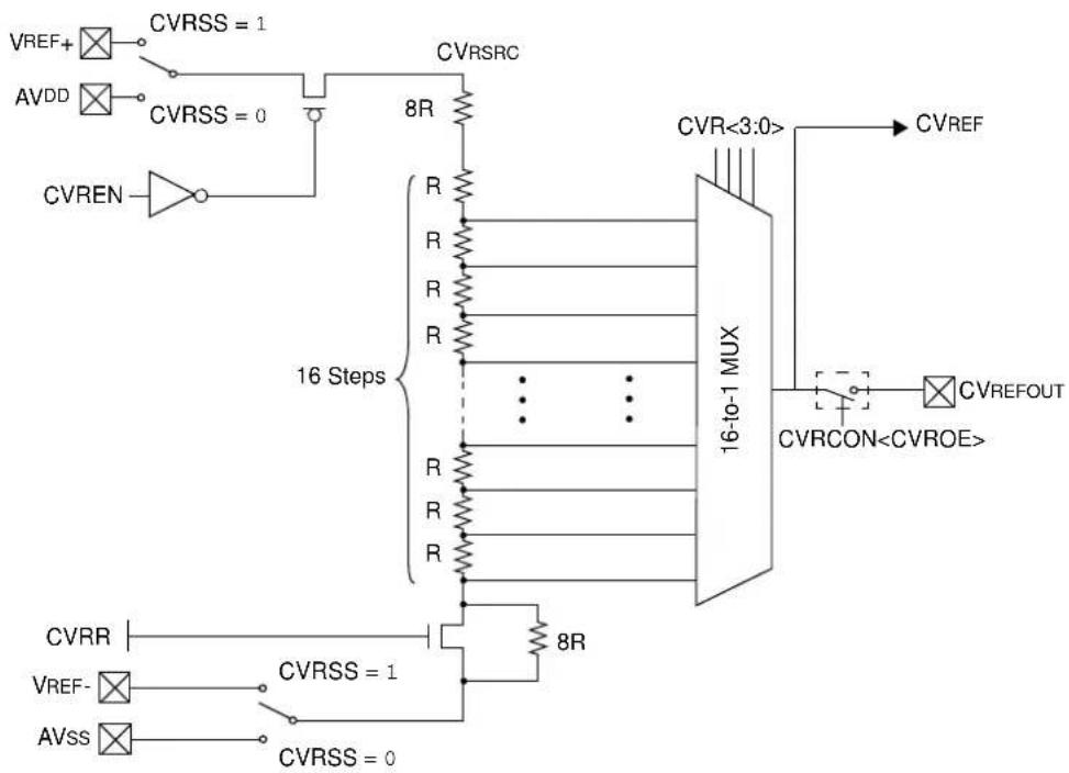
flowchart
graph TD
    A["VREF+"] --> B["×"]
    C["AVDD"] --> D["×"]
    E["CVREN"] --> F["○"]
    G["CVRSS = 1"] --> H["○"]
    I["CVRSS = 0"] --> J["○"]
    K["8R"] --> L["CVRSRC"]
    M["R"] --> N["16 Steps"]
    O["R"] --> N
    P["R"] --> N
    Q["R"] --> N
    R["R"] --> N
    S["..."] --> N
    T["R"] --> N
    U["R"] --> N
    V["R"] --> N
    W["8R"] --> X["16-to-1 MUX"]
    Y["CVRCON"] --> Z["×"]
    AA["CVREFOUT"] --> AB["×"]
    AC["CVRREF"] --> AD["×"]
    AE["CVRFF"] --> AF["×"]
    AG["CVRSS = 1"] --> AH["○"]
    AI["CVRSS = 0"] --> AJ["○"]
32.1 Comparator Voltage Reference Control Registers
TABLE 32-1: COMPARATOR VOLTAGE REFERENCE REGISTER MAP
| Virtual Address(BF80_#) | Register Name(1) | Bit Range | Bits | All Resets | |||||||||||||||
| 31/15 | 30/14 | 29/13 | 28/12 | 27/11 | 26/10 | 25/9 | 24/8 | 23/7 | 22/6 | 21/5 | 20/4 | 19/3 | 18/2 | 17/1 | 16/0 | ||||
| OE00 | CVRCON | 31:16 | — | — | — | — | — | — | — | — | — | — | — | — | — | — | — | — | 0000 |
| 15:0 | ON | — | — | — | — | — | — | — | — | CVROE | CVRR | CVRSS | CVR<3:0> | 0000 | |||||
Legend: x = unknown value on Reset; — = unimplemented, read as 'D'. Reset values are shown in hexadecimal
Note 1: The register in this table has corresponding CLR, SET, and INV registers at their virtual addresses, plus offsets of 0x4, 0x8 and 0xC, respectively. See Section 12.2 "CLR, SET, and INV Registers" for more information.
REGISTER 32-1: CVRCON: COMPARATOR VOLTAGE REFERENCE CONTROL REGISTER
| Bit Range | Bit 31/23/15/7 | Bit 30/22/14/6 | Bit 29/21/13/5 | Bit 28/20/12/4 | Bit 27/19/11/3 | Bit 26/18/10/2 | Bit 25/17/9/1 | Bit 24/16/8/0 |
| 31:24 | U-0 U-0 U-0 | U-0 U-0 U-0 U-0 | U-0 | |||||
| — — — | — — — — | |||||||
| 23:16 | U-0 U-0 U-0 | U-0 U-0 U-0 U-0 | U-0 | |||||
| — — — | — — — — | |||||||
| 15:8 | R/W-0 U-0 U-0 | U-0 U-0 U-0 U-0 | U-0 U-0 | |||||
| ON | — — — | — — — — | ||||||
| 7:0 | U-0 | R/W-0 | R/W-0 | R/W-0 | R/W-0 | R/W-0 | R/W-0 | R/W-0 |
| — | CVROE | CVRR | CVRSS | CVR<3:0> | ||||
Legend:
| R = Readable bit | W = Writable bit U = Unimplemented bit, read as '0' |
| -n = Value at POR | '1' = Bit is set '0' = Bit is cleared x = Bit is unknown |
bit 31-16 Unimplemented: Read as '0'
bit 15 ON: Comparator Voltage Reference On bit
1 = Module is enabled Setting this bit does not affect other bits in the register. 0 = Module is disabled and does not consume current. Clearing this bit does not affect the other bits in the register.
bit 14-7 Unimplemented: Read as '0'
bit 6 CVROE: CVREFOUT Enable bit
1 = Voltage level is output on CVREFOUT pin 0 = Voltage level is disconnected from CVREFOUT pin
bit 5 CVRR: CVREF Range Selection bit
1 = 0 to 0.625 CVRSRC, with CVRSRC/24 step size 0 = 0.25 CVRSRC to 0.719 CVRSRC, with CVRSRC/32 step size
bit 4 CVRSS: CVREF Source Selection bit
1 = Comparator voltage reference source, CV RSRC = (VREF+) - (VREF-)
0 = Comparator voltage reference source, CV RSRC = AVDD - AVSS
bit 3-0 CVR<3:0>: CVREF Value Selection 0 ≤ CVR<3:0> ≤ 15 bits
When CVRR = 1: CVREF = (CVR<3:0>/24) • (CVRSRC)
When CVRR = 0: CVREF = 1/4 • (CVRSRC) + (CVR<3:0>/32) • (CVRSRC)
NOTES:
33.0 POWER-SAVING FEATURES
Note: This data sheet summarizes the features of the PIC32MZ Embedded Connectivity (EC) Family of devices. It is not intended to be a comprehensive reference source. To complement the information in this data sheet, refer to Section 10. "Power-Saving Features" (DS60001130), which is available from the Documentation > Reference Manual section of the Microchip PIC32 web site (www.microchip.com/pic32).
This section describes power-saving features for the PIC32MZ EC devices. These devices offer various methods and modes that allow the user to balance power consumption with device performance. In all of the methods and modes described in this section, power-saving is controlled by software.
33.1 Power Saving with CPU Running
When the CPU is running, power consumption can be controlled by reducing the CPU clock frequency, lowering the speed of PBCLK7, or selecting a lower power clock source (i.e., LPRC or SOSC).
In addition, the Peripheral Bus Scaling mode is available for each peripheral bus where peripherals are clocked at reduced speed by selecting a higher divider for the associated PBCLKx, or by disabling the clock completely.
33.2 Power-Saving with CPU Halted
Peripherals and the CPU can be Halted or disabled to further reduce power consumption.
33.2.1 SLEEP MODE
Sleep mode has the lowest power consumption of the device power-saving operating modes. The CPU and most peripherals are Halted and the associated clocks are disabled. Select peripherals can continue to operate in Sleep mode and can be used to wake the device from Sleep. See the individual peripheral module sections for descriptions of behavior in Sleep.
Sleep mode includes the following characteristics:
- There can be a wake-up delay based on the oscillator selection
- The Fail-Safe Clock Monitor (FSCM) does not operate during Sleep mode
- The BOR circuit remains operative during Sleep mode
- The WDT, if enabled, is not automatically cleared prior to entering Sleep mode
- Some peripherals can continue to operate at limited functionality in Sleep mode. These peripherals include I/O pins that detect a change in the input signal, WDT, ADC, UART and peripherals that use an external clock input or the internal LPRC oscillator (e.g., RTCC, Timer1 and Input Capture).
- I/O pins continue to sink or source current in the same manner as they do when the device is not in Sleep
The processor will exit, or 'wake-up', from Sleep on one of the following events:
- On any interrupt from an enabled source that is operating in Sleep. The interrupt priority must be greater than the current CPU priority.
- On any form of device Reset
- On a WDT time-out
If the interrupt priority is lower than or equal to the current priority, the CPU will remain Halted, but the peripheral bus clocks will start running and the device will enter into Idle mode.
33.2.2 IDLE MODE
In Idle mode, the CPU is Halted; however, all clocks are still enabled. This allows peripherals to continue to operate. Peripherals can be individually configured to Halt when entering Idle by setting their respective SIDL bit. Latency, when exiting Idle mode, is very low due to the CPU oscillator source remaining active.
The device enters Idle mode when the SLPEN bit (OSCCON<4>) is clear and a WAIT instruction is executed.
The processor will wake or exit from Idle mode on the following events:
- On any interrupt event for which the interrupt source is enabled. The priority of the interrupt event must be greater than the current priority of the CPU. If the priority of the interrupt event is lower than or equal to current priority of the CPU, the CPU will remain Halted and the device will remain in Idle mode.
- On any form of device Reset
- On a WDT time-out interrupt
33.3 Peripheral Module Disable
The Peripheral Module Disable (PMD) registers provide a method to disable a peripheral module by stopping all clock sources supplied to that module. When a peripheral is disabled using the appropriate PMD control bit, the peripheral is in a minimum power consumption state. The control and status registers associated with the peripheral are also disabled, so writes to those registers do not have effect and read values are invalid.
To disable a peripheral, the associated PMDx bit must be set to '1'. To enable a peripheral, the associated PMDx bit must be cleared (default). See Table 33-1 for more information.
Note: Disabling a peripheral module while it's ON bit is set, may result in undefined behavior. The ON bit for the associated peripheral module must be cleared prior to disable a module via the PMDx bits.
TABLE 33-1: PERIPHERAL MODULE DISABLE BITS AND LOCATIONS (1)
| Peripheral | PMDx bit Name | Register Name and Bit Location |
| ADC1 | AD1MD | PMD1<0> |
| Comparator Voltage Reference | CVRMD | PMD1<12> |
| Comparator 1 | CMP1MD | PMD2<0> |
| Comparator 2 | CMP2MD | PMD2<1> |
| Input Capture 1 | IC1MD | PMD3<0> |
| Input Capture 2 | IC2MD | PMD3<1> |
| Input Capture 3 | IC3MD | PMD3<2> |
| Input Capture 4 | IC4MD | PMD3<3> |
| Input Capture 5 | IC5MD | PMD3<4> |
| Input Capture 6 | IC6MD | PMD3<5> |
| Input Capture 7 | IC7MD | PMD3<6> |
| Input Capture 8 | IC8MD | PMD3<7> |
| Input Capture 9 | IC9MD | PMD3<8> |
| Output Compare 1 | OC1MD | PMD3<16> |
| Output Compare 2 | OC2MD | PMD3<17> |
| Output Compare 3 | OC3MD | PMD3<18> |
| Output Compare 4 | OC4MD | PMD3<19> |
| Output Compare 5 | OC5MD | PMD3<20> |
| Output Compare 6 | OC6MD | PMD3<21> |
| Output Compare 7 | OC7MD | PMD3<22> |
| Output Compare 8 | OC8MD | PMD3<23> |
| Output Compare 9 | OC9MD | PMD3<24> |
| Timer1 | T1MD | PMD4<0> |
| Timer2 | T2MD | PMD4<1> |
| Timer3 | T3MD | PMD4<2> |
| Timer4 | T4MD | PMD4<3> |
| Timer5 | T5MD | PMD4<4> |
| Timer6 | T6MD | PMD4<5> |
| Timer7 | T7MD | PMD4<6> |
| Timer8 | T8MD | PMD4<7> |
| Timer9 | T9MD | PMD4<8> |
| UART1 | U1MD | PMD5<0> |
| UART2 | U2MD | PMD5<1> |
Note 1: Not all modules and associated PMDx bits are available on all devices. See TABLE 1: "PIC32MZ EC Family Features" for the lists of available peripherals.
2: Module must not be busy after clearing the associated ON bit and prior to setting the USBMD bit.
TABLE 33-1: PERIPHERAL MODULE DISABLE BITS AND LOCATIONS ^(1) (CONTINUED)
| Peripheral | PMDx bit Name | Register Name and Bit Location |
| UART3 U3MD PMD5<2> | ||
| UART4 U4MD PMD5<3> | ||
| UART5 U5MD PMD5<4> | ||
| UART6 U6MD PMD5<5> | ||
| SPI1 SPI1MD PMD5<8> | ||
| SPI2 SPI2MD PMD5<9> | ||
| SPI3 SPI3MD PMD5<10> | ||
| SPI4 SPI4MD PMD5<11> | ||
| SPI5 SPI5MD PMD5<12> | ||
| SPI6 SPI6MD PMD5<13> | ||
| I2C1 I2C1MD PMD5<16> | ||
| I2C2 I2C2MD PMD5<17> | ||
| I2C3 I2C3MD PMD5<18> | ||
| I2C4 I2C4MD PMD5<19> | ||
| I2C5 I2C5MD PMD5<20> | ||
| USB(2) | USBMD PMD5<24> | |
| CAN1 CAN1MD PMD5<28> | ||
| CAN2 CAN2MD PMD5<29> | ||
| RTCC RTCCMD PMD6<0> | ||
| Reference Clock Output 1 | REFO1MD | PMD6<8> |
| Reference Clock Output 2 | REFO2MD | PMD6<9> |
| Reference Clock Output 3 | REFO3MD | PMD6<10> |
| Reference Clock Output 4 | REFO4MD | PMD6<11> |
| PMP PMPMD PMD6<16> | ||
| EBI | EBIMD PMD6<17> | |
| SQI1 | SQI1MD | PMD6<23> |
| Ethernet | ETHMD PMD6<28> | |
| DMA | DMAMD PMD7<4> | |
| Random Number Generator | RNGMD | PMD7<20> |
| Crypto | CRYPTMD | PMD7<22> |
Note 1: Not all modules and associated PMDx bits are available on all devices. See TABLE 1: "PIC32MZ EC Family Features" for the lists of available peripherals.
2: Module must not be busy after clearing the associated ON bit and prior to setting the USBMD bit.
33.3.1 CONTROLLING CONFIGURATION CHANGES
Because peripherals can be disabled during run time, some restrictions on disabling peripherals are needed to prevent accidental configuration changes. PIC32MZ EC devices include two features to prevent alterations to enabled or disabled peripherals:
• Control register lock sequence
- Configuration bit select lock
33.3.1.1 Control Register Lock
Under normal operation, writes to the PMDx registers are not allowed. Attempted writes appear to execute normally, but the contents of the registers remain unchanged. To change these registers, they must be unlocked in hardware. The register lock is controlled by the PMDLOCK Configuration bit (CFGCON<12>). Setting PMDLOCK prevents writes to the control registers; clearing PMDLOCK allows writes.
To set or clear PMDLOCK, an unlock sequence must be executed. Refer to Section 42. "Oscillators with Enhanced PLL" (DS60001250) in the "PIC32 Family Reference Manual" for details.
33.3.1.2 Configuration Bit Select Lock
As an additional level of safety, the device can be configured to prevent more than one write session to the PMDx registers. The PMDL1WAY Configuration bit (DEVCFG3<28>) blocks the PMDLOCK bit from being cleared after it has been set once. If PMDLOCK remains set, the register unlock procedure does not execute, and the PPS control registers cannot be written to. The only way to clear the bit and re-enable PMD functionality is to perform a device Reset.
TABLE 33-2: PERIPHERAL MODULE DISABLE REGISTER SUMMARY
Legend: x = unknown value on Reset; — = unimplemented, read as '0'. Reset values are shown in hexadecimal.
Note 1: Reset values are dependent on the device variant.
NOTES:
34.0 SPECIAL FEATURES
| Note: This data sheet summarizes the features of the PIC32MZ Embedded Connectivity (EC) Family of devices. However, it is not intended to be a comprehensive reference source. To complement the information in this data sheet, refer to Section 32. “Configuration” (DS60001124) and Section 33. “Programming and Diagnostics” (DS60001129), which are available from the Documentation > Reference Manual section of the Microchip PIC32 web site (www.microchip.com/pic32). |
PIC32MZ EC devices include several features intended to maximize application flexibility and reliability and minimize cost through elimination of external components. These are:
- Flexible device configuration
• Joint Test Action Group (JTAG) interface - In-Circuit Serial Programming™ (ICSP™)
- Internal temperature sensor
34.1 Configuration Bits
PIC32MZ EC devices contain two Boot Flash memories (Boot Flash 1 and Boot Flash 2), each with an associated configuration space. These configuration spaces can be programmed to contain various device configurations. Configuration space that is aliased by the Lower Boot Alias memory region is used to provide values for Configuration registers listed below. See
4.1.1 "Boot Flash Sequence and Configuration Spaces" for more information.
- DEVSIGN0/ADEVSIGN0: Device Signature Word 0 Register
- DEVCP0/ADEVCP0: Device Code-Protect 0 Register
- DEVCFG0/ADEVCFG0: Device Configuration Word 0
- DEVCFG1/ADEVCFG1: Device Configuration Word 1
- DEVCFG2/ADEVCFG2: Device Configuration Word 2
- DEVCFG3/ADEVCFG3: Device Configuration Word 3
The following run-time programmable Configuration registers provide additional configuration control:
• CFGCON: Configuration Control Register
• CFGEBIA: External Bus Interface Address Pin Configuration Register
• CFGEBIC: External Bus Interface Control Pin Configuration Register
- CFGPG: Permission Group Configuration Register
In addition, the DEVID register (see Register 34-11) provides device and revision information, the DEVADC1 through DEVADC5 registers (see Register 34-12) provide ADC module calibration data, and the DEVSN0 and DEVSN1 registers contain a unique serial number of the device (see Register 34-13).
Note: Do not use word program operation (NVMOP<3:0>=0001) when programming the device words that are described in this section.
34.2 Registers
TABLE 34-1: DEVCFG: DEVICE CONFIGURATION WORD SUMMARY
Legend: x = unknown value on Reset; — = Reserved, read as '1'. Reset values are shown in hexadecimal.
TABLE 34-2: ADEVCFG: ALTERNATE DEVICE CONFIGURATION WORD SUMMARY
Legend: x = unknown value on Reset; — = Reserved, read as '1'. Reset values are shown in hexadecimal.
TABLE 34-3: DEVICE ID, REVISION, AND CONFIGURATION SUMMARY
| Virtual Address (BF60 #) | Register Name | Bit Range | Bits | All Resets (2) | |||||||||||||||
| 31/15 30 | 14 29/13 | 28/12 27/11 | 26/10 25/9 | 24/8 23/7 | 22/6 21/5 20 | 14 19/3 18/2 | 17/1 16/0 | ||||||||||||
| 0000 | CFGCON | 31:16 | — | — | — | — | — | — | DMAPRI | CPUPRI | — | — | — | — | — | — | ICACLK | OCACLK | 0000 |
| 15:0 | — | — | IOLOCK | PMDLOCK | PGLOCK | — | — | USBSSEN | — | — | ECCCON<1:0> | JTAGEN | TROEN | — | TDOEN | 0005 | |||
| 0020 | DEVID | 31:16 | VER<3:0> | DEVID<27:16> | xxxxx | ||||||||||||||
| 15:0 | DEVID<15:0> | xxxxx | |||||||||||||||||
| 0030 | SYSKEY | 31:16 | SYSKEY<31:0> | 0000 | |||||||||||||||
| 15:0 | 0000 | ||||||||||||||||||
| 00C0 | CFGEBIA (2) | 31:16 | EBIPINEN | — | — | — | — | — | — | — | EBIA23EN | EBIA22EN | EBIA21EN | EBIA20EN | EBIA19EN | EBIA18EN | EBIA17EN | EBIA16EN | 0000 |
| 15:0 | EBIA15EN | EBIA14EN | EBIA13EN | EBIA12EN | EBIA11EN | EBIA10EN | EBIA9EN | EBIA8EN | EBIA7EN | EBIA6EN | EBIA5EN | EBIA4EN | EBIA3EN | EBIA2EN | EBIA1EN | EBIA0EN | 0000 | ||
| 00D0 | CFGEBIC(2) | 31:16 | — | EBI RDYINV3 | EBI RDYINV2 | EBI RDYINV1 | — | EBI RDYEN3 | EBI RDYEN2 | EBI RDYEN1 | —— | —— | EBI RDYLVL | EBIRPEN | 0000 | ||||
| 15:0 | — | — | EBIWEEN | EBIOEEN | — | — | EBIBSEN1 | EBIBSEN0 | EBICSEN3 | EBICSEN2 | EBICSEN1 | EBICSEN0 | — | — | EBIDEN1 | EBIDENO | 0000 | ||
| 00E0 | CFGPG | 31:16 | — | — | — | — | — | — | CRYPTPG<1:0> | FCPG<1:0> | SQI1PG<1:0> | — | — | ETHPG<1:0> | 0000 | ||||
| 15:0 | CAN2PG<1:0> | CAN1PG<1:0> | — | — | USBPG<1:0> | — | — | DMAPG<1:0> | — | — | CPUPG<1:0> | 0000 | |||||||
Legend: x = unknown value on Reset; — = unimplemented, read as '0'. Reset values are shown in hexadecimal.
Note 1: Reset values are dependent on the device variant.
2: This register is not available on 64-pin devices.
TABLE 34-4: DEVICE ADC CALIBRATION SUMMARY
| Virtual Address (BFCS.#) | Register Name | Bit Range | Bits | All Resets(1) | |||||||||||||||
| 31/15 | 30/14 | 29/13 | 28/12 | 27/11 | 26/10 | 25/9 | 24/8 | 23/7 | 22/6 | 21/5 | 20/4 | 19/3 | 18/2 | 17/1 | 16/0 | ||||
| 4000 | DEVADC1 | 31:16 | ADC Calibration Data <31:16> | xxxxx | |||||||||||||||
| 15:0 | ADC Calibration Data <15:0> | xxxxx | |||||||||||||||||
| 4004 | DEVADC2 | 31:16 | ADC Calibration Data <31:16> | xxxxx | |||||||||||||||
| 15:0 | ADC Calibration Data <15:0> | xxxxx | |||||||||||||||||
| 4008 | DEVADC3 | 31:16 | ADC Calibration Data <31:16> | xxxxx | |||||||||||||||
| 15:0 | ADC Calibration Data <15:0> | xxxxx | |||||||||||||||||
| 400C | DEVADC4 | 31:16 | ADC Calibration Data <31:16> | xxxxx | |||||||||||||||
| 15:0 | ADC Calibration Data <15:0> | xxxxx | |||||||||||||||||
| 4010 | DEVADC5 | 31:16 | ADC Calibration Data <31:16> | xxxxx | |||||||||||||||
| 15:0 | ADC Calibration Data <15:0> | xxxxx | |||||||||||||||||
Legend: x = unknown value on Reset.
Note 1: Reset values are dependent on the device variant.
TABLE 34-5: DEVICE SERIAL NUMBER SUMMARY
| Virtual Address (BFCS #) | Register Name | Bit Range | Bits | All Resets (1) | ||||||||||||||||
| 31/15 30 | 14 29/13 | 28/12 27/11 | 26/10 25/9 | 24/8 23/7 | 22/6 21/5 20 | 4 19/3 18/2 | 17/1 16/0 | |||||||||||||
| 4020 | DEVSN0 | 31:16 | Device Serial Number <31:16> xxxx | |||||||||||||||||
| 15:0 | Device Serial Number <15:0> xxxx | |||||||||||||||||||
| 4024 | DEVSN1 | 31:16 | Device Serial Number <31:16> xxxx | |||||||||||||||||
| 15:0 | Device Serial Number <15:0> xxxx | |||||||||||||||||||
Legend: x = unknown value on Reset.
Note 1: Reset values are dependent on the device variant.
REGISTER 34-1: DEVSIGN0/ADEVSIGN0: DEVICE SIGNATURE WORD 0 REGISTER
| Bit Range | Bit 31/23/15/7 | Bit 30/22/14/6 | Bit 29/21/13/5 | Bit 28/20/12/4 | Bit 27/19/11/3 | Bit 26/18/10/2 | Bit 25/17/9/1 | Bit 24/16/8/0 |
| 31:24 | r-0 r-1 r-1 | r-1 r-1 r-1 r-1 r-1 | ||||||
| ——— | —— — — — — | |||||||
| 23:16 | r-1 r-1 r-1 | r-1 r-1 r-1 r-1 r-1 | ||||||
| ——— | —— — — — — | |||||||
| 15:8 | r-1 r-1 r-1 | r-1 r-1 r-1 r-1 r-1 | ||||||
| ——— | —— — — — — | |||||||
| 7:0 | r-1 r-1 r-1 | r-1 r-1 r-1 r-1 r-1 | ||||||
| ——— | —— — — — — |
Legend: r = Reserved bit
R = Readable bit W = Writable bit U = Unimplemented bit, read as '0'
-n = Value at POR '1' = Bit is set '0' = Bit is cleared x = Bit is unknown
bit 31 Reserved: Write as '0'
bit 30-0 Reserved: Write as '1'
Note: The DEVSIGN1 through DEVSIGN3 and ADEVSIGN1 through ADEVSIGN3 registers are used for Quad Word programming operation when programming the DEVSIGN0/ADESIGN0 registers, and do not contain any valid information.
REGISTER 34-2: DEVCP0/ADEVCP0: DEVICE CODE-PROTECT 0 REGISTER
| Bit Range | Bit 31/23/15/7 | Bit 30/22/14/6 | Bit 29/21/13/5 | Bit 28/20/12/4 | Bit 27/19/11/3 | Bit 26/18/10/2 | Bit 25/17/9/1 | Bit 24/16/8/0 |
| 31:24 | r-1 r-1 r-1 | R/P | r-1 r-1 r-1 r-1 | |||||
| — — — | CP | — — — — | ||||||
| 23:16 | r-1 r-1 r-1 | r-1 | r-1 r-1 r-1 r-1 | |||||
| — — — | — — — — — | |||||||
| 15:8 | r-1 r-1 r-1 | r-1 | r-1 r-1 r-1 r-1 | |||||
| — — — | — — — — — | |||||||
| 7:0 | r-1 r-1 r-1 | r-1 | r-1 r-1 r-1 r-1 | |||||
| — — — | — — — — — |
| Legend: | r = Reserved bit | P = Programmable bit |
| R = Readable bit | W = Writable bit | U = Unimplemented bit, read as ‘0’ |
| -n = Value at POR | ‘1’ = Bit is set | ‘0’ = Bit is cleared x = Bit is unknown |
bit 31-29 Reserved: Write as '1'
bit 28 CP: Code-Protect bit
Prevents boot and program Flash memory from being read or modified by an external programming device.
1 = Protection is disabled
0 = Protection is enabled
bit 27-0 Reserved: Write as '1'
Note: The DEVCP1 through DEVCP3 and ADEVCP1 through ADEVCP3 registers are used for Quad Word programming operation when programming the DEVCP0/ADEVCP0 registers, and do not contain any valid information.
REGISTER 34-3: DEVCFG0/ADEVCFG0: DEVICE CONFIGURATION WORD 0
| Bit Range | Bit 31/23/15/7 | Bit 30/22/14/6 | Bit 29/21/13/5 | Bit 28/20/12/4 | Bit 27/19/11/3 | Bit 26/18/10/2 | Bit 25/17/9/1 | Bit 24/16/8/0 |
| 31:24 | r-0 R/P r-1 | r-1 r-1 r-1 r-1 r-1 | ||||||
| — EJTAGBEN — — — — | ||||||||
| 23:16 | r-1 r-1 r-1 r-1 r-1 r-1 | |||||||
| — — — — — — — — | ||||||||
| 15:8 | r-1 R/P R/P R/P r-1 | R/P | R/P | R/P | ||||
| — | DBGPER<2:0> | — | FSLEEP | FECCCON<1:0> | ||||
| 7:0 | r-1 | R/P | R/P | R/P | R/P | R/P | R/P | R/P |
| — | BOOTISA | TRCEN | ICESEL<1:0> | JTAGEN(1) | DEBUG<1:0> | |||
| Legend: | r = Reserved bit P = Programmable bit | ||
| R = Readable bit | W = Writable bit U = Unimplemented bit, read as ‘0’ | ||
| -n = Value at POR | ‘1’ = Bit is set | ‘0’ = Bit is cleared | x = Bit is unknown |
bit 31 Reserved: Write as '0'
bit 30 EJTAGBEN: EJTAG Boot Enable bit
1 = Normal EJTAG functionality
0 = Reduced EJTAG functionality
bit 29-15 Reserved: Write as '1'
bit 14-12 DBGPER<2:0>: Debug Mode CPU Access Permission bits
1xx = Allow CPU access to Permission Group 2 permission regions
x1x = Allow CPU access to Permission Group 1 permission regions
xx1 = Allow CPU access to Permission Group 0 permission regions
0xx = Deny CPU access to Permission Group 2 permission regions
x0x = Deny CPU access to Permission Group 1 permission regions
xx0 = Deny CPU access to Permission Group 0 permission regions
When the CPU is in Debug mode and the CPU1PG<1:0> bits (CFGPG<1:0>) are set to a denied permission group as defined by DBGPER<2:0>, the transaction request is assigned Group 3 permissions.
bit 11 Reserved: Write as '1'
bit 10 FSLEEP: Flash Sleep Mode bit
1 = Flash is powered down when the device is in Sleep mode
0 = Flash power down is controlled by the VREGS bit (PWRCON<1>)
bit 9-8 FECCCON<1:0>: Dynamic Flash ECC Configuration bits
Upon a device Reset, the value of these bits is copied to the ECCCON<1:0> bits (CFGCON<5:4>).
11 = ECC and dynamic ECC are disabled (ECCCON<1:0> bits are writable)
10 = ECC and dynamic ECC are disabled (ECCCON<1:0> bits are locked)
01 = Dynamic Flash ECC is enabled (ECCCON<1:0> bits are locked)
00 = Flash ECC is enabled (ECCCON<1:0> bits are locked; disables word Flash writes)
bit 7 Reserved: Write as '1'
bit 6 BOOTISA: Boot ISA Selection bit
1 = Boot code and Exception code is MIPS32®
(ISAONEXC bit is set to '0' and the ISA<1:0> bits are set to '10' in the CP0 Config3 register)
0 = Boot code and Exception code is microMIPS™
(ISAONEXC bit is set to '1' and the ISA<1:0> bits are set to '11' in the CP0 Config3 register)
bit 5 TRCEN: Trace Enable bit
1 = Trace features in the CPU are enabled
0 = Trace features in the CPU are disabled
Note 1: This bit sets the value of the JTAGEN bit in the CFGCON register.
REGISTER 34-3: DEVCFG0/ADEVCFG0: DEVICE CONFIGURATION WORD 0 (CONTINUED)
bit 4-3 ICESEL<1:0>: In-Circuit Emulator/Debugger Communication Channel Select bits
11 = PGEC1/PGED1 pair is used
10 = PGEC2/PGED2 pair is used
01 = Reserved
00 = Reserved
bit 2 JTAGEN: JTAG Enable bit (1) 1 = JTAG is enabled 0 = JTAG is disabled
bit 1-0 DEBUG<1:0>: Background Debugger Enable bits (forced to '11' if code-protect is enabled) 1x = Debugger is disabled 0x = Debugger is enabled
Note 1: This bit sets the value of the JTAGEN bit in the CFGCON register.
REGISTER 34-4: DEVCFG1/ADEVCFG1: DEVICE CONFIGURATION WORD 1
| Legend: | r = Reserved bit | P = Programmable bit |
| R = Readable bit | W = Writable bit | U = Unimplemented bit, read as ‘0’ |
| -n = Value at POR | ‘1’ = Bit is set | ‘0’ = Bit is cleared x = Bit is unknown |
bit 31 FDMTEN: Deadman Timer enable bit
1 = Deadman Timer is enabled and cannot be disabled by software
0 = Deadman Timer is disabled and can be enabled by software
bit 30-26 DMTCNT<4:0>: Deadman Timer Count Select bits
11111 = Reserved
•
•
11000 = Reserved
10111 = 2 ^31 (2147483648)
10110 = 2 ^30 (1073741824)
10101 = 2 ^29 (536870912)
10100 = 2 ^28 (268435456)
•
.
00001 = 2^9 (512)
00000 = 2^8 (256)
bit 25-24 FWDTWINSZ<1:0>: Watchdog Timer Window Size bits
11 = Window size is 25%
10 = Window size is 37.5%
01 = Window size is 50%
00 = Window size is 75%
bit 23 FWD TEN: Watchdog Timer Enable bit
1 = Watchdog Timer is enabled and cannot be disabled by software
0 = Watchdog Timer is not enabled; it can be enabled in software
bit 22 WINDIS: Watchdog Timer Window Enable bit
1 = Watchdog Timer is in non-Window mode
0 = Watchdog Timer is in Window mode
bit 21 WDTSPGM: Watchdog Timer Stop During Flash Programming bit
1 = Watchdog Timer stops during Flash programming
0 = Watchdog Timer runs during Flash programming (for read/execute while programming Flash applications)
REGISTER 34-4: DEVCFG1/ADEVCFG1: DEVICE CONFIGURATION WORD 1 (CONTINUED)
bit 20-16 WDTPS<4:0>: Watchdog Timer Postscale Select bits
10100 = 1:1048576
10011 = 1:524288
10010 = 1:262144
10001 = 1:131072
10000 = 1:65536
01111 = 1:32768
01110 = 1:16384
01101 = 1:8192
01100 = 1:4096
01011 = 1:2048
01010 = 1:1024
01001 = 1:512
01000 = 1:256
00111 = 1:128
00110 = 1:64
00101 = 1:32
00100 = 1:16
00011 = 1:8
00010 = 1:4
00001 = 1:2
00000 = 1:1
All other combinations not shown result in operation = 10100
bit 15-14 FCKSM<1:0>: Clock Switching and Monitoring Selection Configuration bits
11 = Clock switching is enabled and clock monitoring is enabled
10 = Clock switching is disabled and clock monitoring is enabled
01 = Clock switching is enabled and clock monitoring is disabled
00 = Clock switching is disabled and clock monitoring is disabled
bit 13-11 Reserved: Write as '1'
bit 10 OSCIOFNC: CLKO Enable Configuration bit
1 = CLKO output disabled
0 = CLKO output signal active on the OSC2 pin; Primary Oscillator must be disabled or configured for the External Clock mode (EC) for the CLKO to be active (POSCMOD<1:0> = 11 or 00)
bit 9-8 POSCMOD<1:0>: Primary Oscillator Configuration bits
11 = Posc disabled
10 = HS Oscillator mode selected
01 = Reserved
00 = EC mode selected
bit 7 IESO: Internal External Switchover bit
1 = Internal External Switchover mode is enabled (Two-Speed Start-up is enabled)
0 = Internal External Switchover mode is disabled (Two-Speed Start-up is disabled)
bit 6 FSOSCEN: Secondary Oscillator Enable bit
1 = Enable Sosc
0 = Disable Sosc
bit 5-3 DMTINV<2:0>: Deadman Timer Count Window Interval bits
111 = Window/Interval value is 127/128 counter value
110 = Window/Interval value is 63/64 counter value
101 = Window/Interval value is 31/32 counter value
100 = Window/Interval value is 15/16 counter value
011 = Window/Interval value is 7/8 counter value
010 = Window/Interval value is 3/4 counter value
001 = Window/Interval value is 1/2 counter value
000 = Window/Interval value is zero
REGISTER 34-4: DEVCFG1/ADEVCFG1: DEVICE CONFIGURATION WORD 1 (CONTINUED)
bit 2-0 FNOSC<2:0>: Oscillator Selection bits
111 = FRC divided by FRCDIV<2:0> bits (FRCDIV)
110 = Reserved
101 = LPRC
100 = SOSC
011 = Reserved
010 = Posc (HS, EC)
001 = SPLL
000 = FRC divided by FRCDIV<2:0> bits (FRCDIV)
REGISTER 34-5: DEVCFG2/ADEVCFG2: DEVICE CONFIGURATION WORD 2
| Legend: | r = Reserved bit P = Programmable bit | ||
| R = Readable bit | W = Writable bit U = Unimplemented bit, read as ‘0’ | ||
| -n = Value at POR | ‘1’ = Bit is set | ‘0’ = Bit is cleared | x = Bit is unknown |
bit 31 Reserved: Write as '1'
bit 30 UPLLFSEL: USB PLL Input Frequency Select bit
1 = UPLL input clock is 24 MHz
0 = UPLL input clock is 12 MHz
bit 29-19 Reserved: Write as '1'
bit 18-16 FPLLODIV<2:0>: Default System PLL Output Divisor bits
111 = PLL output divided by 32
110 = PLL output divided by 32
101 = PLL output divided by 32
100 = PLL output divided by 16
011 = PLL output divided by 8
010 = PLL output divided by 4
001 = PLL output divided by 2
000 = PLL output divided by 2
bit 15 Reserved: Write as '1'
bit 14-8 FPLLMULT<6:0>: System PLL Feedback Divider bits
1111111 = Multiply by 128
1111110 = Multiply by 127
1111101 = Multiply by 126
1111100 = Multiply by 125
•
•
•
0000000 = Multiply by 1
bit 7 FPLLICLK: System PLL Input Clock Select bit
1 = FRC is selected as input to the System PLL
0 = Posc is selected as input to the System PLL
bit 6-4 FPLLRNG<2:0>: System PLL Divided Input Clock Frequency Range bits
111 = Reserved
110 = Reserved
101 = 34-64 MHz
100 = 21-42 MHz
011 = 13-26 MHz
010 = 8-16 MHz
001 = 5-10 MHz
000 = Bypass
REGISTER 34-5: DEVCFG2/ADEVCFG2: DEVICE CONFIGURATION WORD 2 (CONTINUED)
bit 3 Reserved: Write as '1'
bit 2-0 FPLLIDIV<2:0>: PLL Input Divider bits
111 = Divide by 8
110 = Divide by 7
101 = Divide by 6
100 = Divide by 5
011 = Divide by 4
010 = Divide by 3
001 = Divide by 2
000 = Divide by 1
REGISTER 34-6: DEVCFG3/ADEVCFG3: DEVICE CONFIGURATION WORD 3
| Legend: | r = Reserved bit | P = Programmable bit |
| R = Readable bit | W = Writable bit | U = Unimplemented bit, read as '0' |
| -n = Value at POR | ‘1’ = Bit is set | ‘0’ = Bit is cleared x = Bit is unknown |
bit 31 Reserved: Write as '1'
bit 30 FUSBIDIO: USB USBID Selection bit
1 = USBID pin is controlled by the USB module
0 = USBID pin is controlled by the port function
If USBMD is '1', USBID reverts to port control.
bit 29 IOL1WAY: Peripheral Pin Select Configuration bit
1 = Allow only one reconfiguration
0 = Allow multiple reconfigurations
bit 28 PMDL1WAY: Peripheral Module Disable Configuration bit
1 = Allow only one reconfiguration
0 = Allow multiple reconfigurations
bit 27 PGL1WAY: Permission Group Lock One Way Configuration bit
1 = Allow only one reconfiguration
0 = Allow multiple reconfigurations
bit 26 Reserved: Write as '1'
bit 25 FETHIO: Ethernet I/O Pin Selection Configuration bit
1 = Default Ethernet I/O pins
0 = Alternate Ethernet I/O pins
This bit is ignored for devices that do not have an alternate Ethernet pin selection.
bit 24 FMIIEN: Ethernet MII Enable Configuration bit
1 = MII is enabled
0 = RMII is enabled
bit 23-16 Reserved: Write as '1'
bit 15-0 USERID<15:0>: This is a 16-bit value that is user-defined and is readable via ICSP™ and JTAG
REGISTER 34-7: CFGCON: CONFIGURATION CONTROL REGISTER
| Bit Range | Bit 31/23/15/7 | Bit 30/22/14/6 | Bit 29/21/13/5 | Bit 28/20/12/4 | Bit 27/19/11/3 | Bit 26/18/10/2 | Bit 25/17/9/1 | Bit 24/16/8/0 |
| 31:24 | U-0 U-0 U-0 U-0 U-0 R/W-0 R/W-0 | |||||||
| —— — — — — | D M | A P | R I | (1) | CPUPRI^(1) | |||
| 23:16 | U-0 U-0 U-0 U-0 U-0 R/W-0 R/W-0 | |||||||
| —— — — — — | ICACLK | (1) | OCACLK^(1) | |||||
| 15:8 | U-0 | U-0 | R/W-0 | R/W-0 | R/W-0 | U-0 | U-0 | R/W-0 |
| —— | IOLOCK | (1) | PMDLOCK^(1) | PGLOCK^(1) | — | — | USBSSEN^(1) | |
| 7:0 | U-0 | U-0 | R/W-1 | R/W-1 | R/W-1 | R/W-0 | U-0 | R/W-1 |
| — | — | ECCCON<1:0> | JTAGEN | TROEN | — | TDOEN | ||
Legend:
| R = Readable bit | W = Writable bit | U = Unimplemented bit, read as '0' |
| -n = Value at POR | ‘1’ = Bit is set | ‘0’ = Bit is cleared x = Bit is unknown |
bit 31-26 Unimplemented: Read as '0'
bit 25 DMAPRI: DMA Read and DMA Write Arbitration Priority to SRAM bit ^(1)
1 = DMA gets High Priority access to SRAM
0 = DMA uses Least Recently Serviced Arbitration (same as other initiators)
bit 24 CPUPRI: CPU Arbitration Priority to SRAM When Servicing an Interrupt bit ^(1)
1 = CPU gets High Priority access to SRAM
0 = CPU uses Least Recently Serviced Arbitration (same as other initiators)
bit 23-18 Unimplemented: Read as '0'
bit 17 ICACLK: Input Capture Alternate Clock Selection bit ^(1)
1 = Input Capture modules use an alternative Timer pair as their timebase clock
0 = All Input Capture modules use Timer2/3 as their timebase clock
bit 16 OCACLK: Output Compare Alternate Clock Selection bit ^(1)
1 = Output Compare modules use an alternative Timer pair as their timebase clock
0 = All Output Compare modules use Timer2/3 as their timebase clock
bit 15-14 Unimplemented: Read as '0'
bit 13 IOLOCK: Peripheral Pin Select Lock bit ^(1)
1 = Peripheral Pin Select is locked. Writes to PPS registers are not allowed
0 = Peripheral Pin Select is not locked. Writes to PPS registers are allowed
bit 12 PMDLOCK: Peripheral Module Disable bit ^(1)
1 = Peripheral module is locked. Writes to PMD registers are not allowed
0 = Peripheral module is not locked. Writes to PMD registers are allowed
bit 11 PGLOCK: Permission Group Lock bit ^(1)
1 = Permission Group registers are locked. Writes to PG registers are not allowed
0 = Permission Group registers are not locked. Writes to PG registers are allowed
bit 10-9 Unimplemented: Read as '0'
bit 8 USBSSEN: USB Suspend Sleep Enable bit ^(1)
Enables features for USB PHY clock shutdown in Sleep mode.
1 = USB PHY clock is shut down when Sleep mode is active
0 = USB PHY clock continues to run when Sleep is active
bit 7-6 Unimplemented: Read as '0'
Note 1: To change this bit, the unlock sequence must be performed. Refer to Section 42. "Oscillators with Enhanced PLL" (DS60001250) in the "PIC32 Family Reference Manual" for details.
REGISTER 34-7: CFGCON: CONFIGURATION CONTROL REGISTER (CONTINUED)
bit 5-4 ECCCON<1:0>: Flash ECC Configuration bits
11 = ECC and dynamic ECC are disabled (ECCCON<1:0> bits are writable)
10 = ECC and dynamic ECC are disabled (ECCCON<1:0> bits are locked)
01 = Dynamic Flash ECC is enabled (ECCCON<1:0> bits are locked)
00 = Flash ECC is enabled (ECCCON<1:0> bits are locked; disables word Flash writes)
bit 3 JTAGEN: JTAG Port Enable bit
1 = Enable the JTAG port
0 = Disable the JTAG port
bit 2 TROEN: Trace Output Enable bit
1 = Enable trace outputs and start trace clock (trace probe must be present)
0 = Disable trace outputs and stop trace clock
bit 1 Unimplemented: Read as '0'
bit 0 TDOEN: TDO Enable for 2-Wire JTAG
1 = 2-wire JTAG protocol uses TDO
0 = 2-wire JTAG protocol does not use TDO
Note 1: To change this bit, the unlock sequence must be performed. Refer to Section 42. "Oscillators with Enhanced PLL" (DS60001250) in the "PIC32 Family Reference Manual" for details.
REGISTER 34-8: CFGEBIA: EXTERNAL BUS INTERFACE ADDRESS PIN CONFIGURATION REGISTER
| Bit Range | Bit 31/23/15/7 | Bit 30/22/14/6 | Bit 29/21/13/5 | Bit 28/20/12/4 | Bit 27/19/11/3 | Bit 26/18/10/2 | Bit 25/17/9/1 | Bit 24/16/8/0 |
| 31:24 | R/W-0 U-0 | U-0 U-0 U-0 U-0 | U-0 U-0 | |||||
| EBIPINEN | — | — | — | — | — | — | — | |
| 23:16 | R/W-0 R/W | 0 R/W-0 R/W-0 | R/W-0 R/W-0 R/W | 0 R/W-0 | ||||
| EBIA23EN | EBIA22EN | EBIA21EN | EBIA20EN | EBIA19EN | EBIA18EN | EBIA17EN | EBIA16EN | |
| 15:8 | R/W-0 R/W | 0 R/W-0 R/W-0 | R/W-0 R/W-0 R/W | 0 R/W-0 | ||||
| EBIA15EN | EBIA14EN | EBIA13EN | EBIA12EN | EBIA11EN | EBIA10EN | EBIA9EN | EBIA8EN | |
| 7:0 | R/W-0 R/W | 0 R/W-0 R/W-0 | R/W-0 R/W-0 R/W | 0 R/W-0 | ||||
| EBIA7EN | EBIA6EN | EBIA5EN | EBIA4EN | EBIA3EN | EBIA2EN | EBIA1EN | EBIA0EN |
Legend:
| R = Readable bit W = Writable bit | U = Unimplemented bit, read as '0' | ||
| -n = Value at POR | ‘1’ = Bit is set | ‘0’ = Bit is cleared | x = Bit is unknown |
bit 31 EBIPINEN: EBI Pin Enable bit
1 = EBI controls access of pins shared with PMP
0 = Pins shared with EBI are available for general use
bit 30-24 Unimplemented: Read as '0'
bit 23-0 EBIA23EN:EBIA0EN: EBI Address Pin Enable bits
1 = EBIAx pin is enabled for use by EBI
0 = EBIAX pin has is available for general use
Note: When EBIMD = 1, the bits in this register are ignored and the pins are available for general use.
REGISTER 34-9: CFGEBIC: EXTERNAL BUS INTERFACE CONTROL PIN CONFIGURATION REGISTER
| Bit Range | Bit 31/23/15/7 | Bit 30/22/14/6 | Bit 29/21/13/5 | Bit 28/20/12/4 | Bit 27/19/11/3 | Bit 26/18/10/2 | Bit 25/17/9/1 | Bit 24/16/8/0 |
| 31:24 | U-0 R/W-0 | R/W-0 R/W-0 U-0 | R/W-0 R/W-0 R/W-0 | |||||
| — EBI | RDYINV3 | EBI RDYINV2 | EBI RDYINV1 | — | EBI RDYEN3 | EBI RDYEN2 | EBI RDYEN1 | |
| 23:16 | U-0 U-0 U-0 | U-0 U-0 U-0 R/W-0 | ||||||
| — — — | — — — EBIRDYLVL EBIRPEN | |||||||
| 15:8 | U-0 U-0 R/W-0 | R/W-0 U-0 U-0 R/W-0 | ||||||
| — | — | EBIWEEN | EBIOEEN | — | — | EBIBSEN1 | EBIBSEN0 | |
| 7:0 | R/W-0 R/W | 0 R/W-0 R/W-0 U-0 | U-0 | 0 R/W-0 R/W-0 | ||||
| EBICSEN3 | EBICSEN2 | EBICSEN1 | EBICSEN0 | — | — | EBIDEN1 | EBIDEN0 | |
Legend:
| R = Readable bit | W = Writable bit | U = Unimplemented bit, read as '0' |
| -n = Value at POR | '1' = Bit is set | '0' = Bit is cleared x = Bit is unknown |
bit 31 Unimplemented: Read as '0'
bit 30 EBIRDYINV3: EBIRDY3 Inversion Control bit
1 = Invert EBIRDY3 pin before use
0 = Do not invert EBIRDY3 pin before use
bit 29 EBIRDYINV2: EBIRDY2 Inversion Control bit
1 = Invert EBIRDY2 pin before use
0 = Do not invert EBIRDY2 pin before use
bit 28 EBIRDYINV1: EBIRDY1 Inversion Control bit
1 = Invert EBIRDY1 pin before use
0 = Do not invert EBIRDY1 pin before use
bit 27 Unimplemented: Read as '0'
bit 26 EBIRDYEN3: EBIRDY3 Pin Enable bit
1 = EBIRDY3 pin is enabled for use by the EBI module
0 = EBIRDY3 pin is available for general use
bit 25 EBIRDYEN2: EBIRDY2 Pin Enable bit
1 = EBIRDY2 pin is enabled for use by the EBI module
0 = EBIRDY2 pin is available for general use
bit 24 EBIRDYEN1: EBIRDY1 Pin Enable bit
1 = EBIRDY1 pin is enabled for use by the EBI module
0 = EBIRDY1 pin is available for general use
bit 23-18 Unimplemented: Read as '0'
bit 17 EBIRDYLVL: EBIRDYx Pin Sensitivity Control bit
1 = Use level detect for EBIRDYx pins
0 = Use edge detect for EBIRDYx pins
bit 16 EBIRPEN: EBIRP Pin Sensitivity Control bit
1 = EBIRP pin is enabled for use by the EBI module
0 = EBIRP pin is available for general use
bit 15-14 Unimplemented: Read as '0'
Note: When EBIMD = 1, the bits in this register are ignored and the pins are available for general use.
REGISTER 34-9: CFGEBIC: EXTERNAL BUS INTERFACE CONTROL PIN CONFIGURATION REGISTER (CONTINUED)
bit 13 EBIWEEN: EBIWE Pin Enable bit
1 = pin is enabled for use by the EBI module
0 = EBIWE pin is available for general use
bit 12 EBIOEEN: EBIOE Pin Enable bit
1 = EBIOE pin is enabled for use by the EBI module
0 = EBIOE pin is available for general use
bit 11-10 Unimplemented: Read as '0'
bit 9 EBIBSEN1: EBIBS1 Pin Enable bit
1 = 1 pin is enabled for use by the EBI module
0 = EBIBS1 pin is available for general use
bit 8 EBIBSEN0: EBIBS0 Pin Enable bit
1 = 0 pin is enabled for use by the EBI module
0 = EBIBS0 pin is available for general use
bit 7 EBICSEN3: EBICS3 Pin Enable bit
1 = 3 pin is enabled for use by the EBI module
0 = EBICS3 pin is available for general use
bit 6 EBICSEN2: EBICS2 Pin Enable bit
1 = 2 pin is enabled for use by the EBI module
0 = EBICS2 pin is available for general use
bit 5 EBICSEN1: EBICS1 Pin Enable bit
1 = 1 pin is enabled for use by the EBI module
0 = EBICS1 pin is available for general use
bit 4 EBICSEN0: EBICS0 Pin Enable bit
1 = 0 pin is enabled for use by the EBI module
0 = EBICS0 pin is available for general use
bit 3-2 Unimplemented: Read as '0'
bit 1 EBIDEN1: EBI Data Upper Byte Pin Enable bit
1 = EBID<15:8> pins are enabled for use by the EBI module
0 = EBID<15:8> pins have reverted to general use
bit 0 EBIDENO: EBI Data Lower Byte Pin Enable bit
1 = EBID<7:0> pins are enabled for use by the EBI module
0 = EBID<7:0> pins have reverted to general use
Note: When EBIMD = 1, the bits in this register are ignored and the pins are available for general use.
REGISTER 34-10: CFGPG: PERMISSION GROUP CONFIGURATION REGISTER
| Bit Range | Bit 31/23/15/7 | Bit 30/22/14/6 | Bit 29/21/13/5 | Bit 28/20/12/4 | Bit 27/19/11/3 | Bit 26/18/10/2 | Bit 25/17/9/1 | Bit 24/16/8/0 |
| 31:24 | U-0 U-0 U-0 | U-0 U-0 U-0 R/W-0 R/W-0 | ||||||
| — — — | — — — CRYPTPG<1:0> | |||||||
| 23:16 | R/W-0 R/W-0 | R/W-0 R/W-0 R/W-0 U-0 | U-0 U-0 R/W-0 R/W-0 | |||||
| FCPG<1:0> | SQI1PG<1:0> | — | — | ETHPG<1:0> | ||||
| 15:8 | R/W-0 R/W-0 | R/W-0 R/W-0 R/W-0 U-0 | U-0 U-0 R/W-0 R/W-0 | |||||
| CAN2PG<1:0> | CAN1PG<1:0> | — | — | USBPG<1:0> | ||||
| 7:0 | U-0 U-0 | R/W-0 R/W-0 | U-0 U-0 R/W-0 R/W-0 | |||||
| — | — | DMAPG<1:0> | — | — | CPUPG<1:0> | |||
Legend:
| R = Readable bit | W = Writable bit U = Unimplemented bit, read as '0' |
| -n = Value at POR | '1' = Bit is set '0' = Bit is cleared |
bit 31-26 Unimplemented: Read as '0'
bit 25-24 CRYPTPG<1:0>: Crypto Engine Permission Group bits
11 = Initiator is assigned to Permission Group 3
10 = Initiator is assigned to Permission Group 2
01 = Initiator is assigned to Permission Group 1
00 = Initiator is assigned to Permission Group 0
bit 23-22 FCPG<1:0>: Flash Control Permission Group bits
Same definition as bits 25-24.
bit 21-20 SQL1PG<1:0>: SQI Module Permission Group bits
Same definition as bits 25-24.
bit 19-18 Unimplemented: Read as '0'
bit 17-16 ETHPG<1:0>: Ethernet Module Permission Group bits
Same definition as bits 25-24.
bit 15-14 CAN2PG<1:0>: CAN2 Module Permission Group bits
Same definition as bits 25-24.
bit 13-12 CAN1PG<1:0>: CAN1 Module Permission Group bits
Same definition as bits 25-24.
bit 11-10 Unimplemented: Read as '0'
bit 9-8 USBPG<1:0>: USB Module Permission Group bits
Same definition as bits 25-24.
bit 7-6 Unimplemented: Read as '0'
bit 5-4 DMAPG<1:0>: DMA Module Permission Group bits
Same definition as bits 25-24.
bit 3-2 Unimplemented: Read as '0'
bit 1-0 CPUPG<1:0>: CPU Permission Group bits
Same definition as bits 25-24.
REGISTER 34-11: DEVID: DEVICE AND REVISION ID REGISTER
| Bit Range | Bit 31/23/15/7 | Bit 30/22/14/6 | Bit 29/21/13/5 | Bit 28/20/12/4 | Bit 27/19/11/3 | Bit 26/18/10/2 | Bit 25/17/9/1 | Bit 24/16/8/0 |
| 31:24 | R | R | R | R | R | R | R | R |
| VER<3:0>(1) | DEVID<27:24>(1) | |||||||
| 23:16 | R | R | R | R | R | R | R | R |
| DEVID<23:16>(1) | ||||||||
| 15:8 | R | R | R | R | R | R | R | R |
| DEVID<15:8>(1) | ||||||||
| 7:0 | R | R | R | R | R | R | R | R |
| DEVID<7:0>(1) | ||||||||
Legend:
R = Readable bit W = Writable bit U = Unimplemented bit, read as '0' -n = Value at POR '1' = Bit is set '0' = Bit is cleared x = Bit is unknown
bit 31-28 VER<3:0>: Revision Identifier bits (1)
bit 27-0 DEVID<27:0>: Device ID (1)
Note 1: See the "PIC32 Flash Programming Specification" (DS60001145) for a list of Revision and Device ID values.
REGISTER 34-12: DEVADCx: DEVICE ADC CALIBRATION REGISTER 'x' ('x' = 1-5)
| Bit Range | Bit31/23/15/7 | Bit30/22/14/6 | Bit29/21/13/5 | Bit28/20/12/4 | Bit27/19/11/3 | Bit26/18/10/2 | Bit25/17/9/1 | Bit24/16/8/0 |
| 31:24 | R | R | R | R | R | R | R | R |
| ADCAL<31:24> | ||||||||
| 23:16 | R | R | R | R | R | R | R | R |
| ADCAL<23:16> | ||||||||
| 15:8 | R | R | R | R | R | R | R | R |
| ADCAL<15:8> | ||||||||
| 7:0 | R | R | R | R | R | R | R | R |
| ADCAL<7:0> | ||||||||
Legend:
R = Readable bit W = Writable bit U = Unimplemented bit, read as '0' -n = Value at POR '1' = Bit is set '0' = Bit is cleared x = Bit is unknown
bit 31-0 ADCAL<31:0>: Calibration Data for the ADC Module bits
This data must be copied to the corresponding AD1CALx register. Refer to Section 28.0 "Pipelined Analog-to-Digital Converter (ADC)" for more information.
REGISTER 34-13: DEVSNx: DEVICE SERIAL NUMBER REGISTER 'x' ('x' = 0, 1)
| Bit Range | Bit31/23/15/7 | Bit30/22/14/6 | Bit29/21/13/5 | Bit28/20/12/4 | Bit27/19/11/3 | Bit26/18/10/2 | Bit25/17/9/1 | Bit24/16/8/0 |
| 31:24 | R | R | R | R | R | R | R | |
| SN<31:24> | ||||||||
| 23:16 | R | R | R | R | R | R | R | |
| SN<23:16> | ||||||||
| 15:8 | R | R | R | R | R | R | R | |
| SN<15:8> | ||||||||
| 7:0 | R | R | R | R | R | R | R | |
| SN<7:0> | ||||||||
Legend:
R = Readable bit W = Writable bit U = Unimplemented bit, read as '0' -n = Value at POR '1' = Bit is set '0' = Bit is cleared x = Bit is unknown
bit 31-0 SN<31:0>: Device Unique Serial Number bits
34.3 On-Chip Voltage Regulator
The core and digital logic for all PIC32MZ EC devices is designed to operate at a nominal 1.8V. To simplify system designs, devices in the PIC32MZ EC family incorporate an on-chip regulator providing the required core logic voltage from VDD.
34.3.1 ON-CHIP REGULATOR AND POR
It takes a fixed delay for the on-chip regulator to generate an output. During this time, designated as TPU, code execution is disabled. TPU is applied every time the device resumes operation after any power-down, including Sleep mode.
34.3.2 ON-CHIP REGULATOR AND BOR
PIC32MZ EC devices also have a simple brown-out capability. If the voltage supplied to the regulator is inadequate to maintain a regulated level, the regulator Reset circuitry will generate a Brown-out Reset. This event is captured by the BOR flag bit (RCON<1>). The brown-out voltage levels are specific in Section 37.1 "DC Characteristics".
34.4 On-chip Temperature Sensor
PIC32MZ EC devices include a temperature sensor that provides accurate measurement of a device's junction temperature (see Section 37.2 "AC Characteristics and Timing Parameters" for more information).
The temperature sensor is connected to the ADC module and can be measured using the shared S&H circuit (see Section 28.0 "Pipelined Analog-to-Digital Converter (ADC)" for more information).
34.5 Programming and Diagnostics
PIC32MZ EC devices provide a complete range of programming and diagnostic features that can increase the flexibility of any application using them. These features allow system designers to include:
- Simplified field programmability using two-wire In-Circuit Serial Programming™ (ICSP™) interfaces
- Debugging using ICSP
- Programming and debugging capabilities using the EJTAG extension of JTAG
- JTAG boundary scan testing for device and board diagnostics
PIC32 devices incorporate two programming and diagnostic modules, and a trace controller, that provide a range of functions to the application developer.
FIGURE 34-1: BLOCK DIAGRAM OF
PROGRAMMING,
DEBUGGING AND TRACE
PORTS
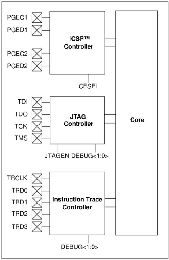
flowchart
graph TD
    A["PGEC1"] --> B["ICSP™ Controller"]
    C["PGED1"] --> B
    D["PGEC2"] --> B
    E["PGED2"] --> B
    B --> F["ICESEL"]
    G["TDI"] --> H["JTAG Controller"]
    I["TDO"] --> H
    J["TCK"] --> H
    K["TMS"] --> H
    H --> L["Core"]
    M["TRCLK"] --> N["Instruction Trace Controller"]
    O["TRD0"] --> N
    P["TRD1"] --> N
    Q["TRD2"] --> N
    R["TRD3"] --> N
    N --> S["DEBUG<1:0>"]
NOTES:
35.0 INSTRUCTION SET
The PIC32MZ Embedded Connectivity (EC) Family family instruction set complies with the MIPS32 ^® Release 2 instruction set architecture. The PIC32MZ EC device family does not support the following features:
- Core extend instructions
• Coprocessor 1 instructions
• Coprocessor 2 instructions
Note: Refer to "MIPS32 ^® Architecture for Programmers Volume II: The MIPS32 ^® Instruction Set" at www.imgtec.com for more information.
NOTES:
36.0 DEVELOPMENT SUPPORT
The PIC ^® microcontrollers (MCU) and dsPIC ^® digital signal controllers (DSC) are supported with a full range of software and hardware development tools:
• Integrated Development Environment
- MPLAB ^® X IDE Software
- Compilers/Assemblers/Linkers
- MPLAB XC Compiler
- MPASM ^TM Assembler
- M P L™ Object Linker/MPLIB™ Object Librarian
- MPLAB Assembler/Linker/Librarian for Various Device Families
- Simulators
- MPLAB X SIM Software Simulator
- Emulators
- MPLAB REAL ICE™ In-Circuit Emulator
• In-Circuit Debuggers/Programmers
- MPLAB ICD 3
- PICkit™ 3
• Device Programmers
- MPLAB PM3 Device Programmer
- Low-Cost Demonstration/Development Boards, Evaluation Kits and Starter Kits
• Third-party development tools
36.1 MPLAB X Integrated Development Environment Software
The MPLAB X IDE is a single, unified graphical user interface for Microchip and third-party software, and hardware development tool that runs on Windows ^® , Linux and Mac OS ^® X. Based on the NetBeans IDE, MPLAB X IDE is an entirely new IDE with a host of free software components and plug-ins for high-performance application development and debugging. Moving between tools and upgrading from software simulators to hardware debugging and programming tools is simple with the seamless user interface.
With complete project management, visual call graphs, a configurable watch window and a feature-rich editor that includes code completion and context menus, MPLAB X IDE is flexible and friendly enough for new users. With the ability to support multiple tools on multiple projects with simultaneous debugging, MPLAB X IDE is also suitable for the needs of experienced users.
Feature-Rich Editor:
• Color syntax highlighting
- Smart code completion makes suggestions and provides hints as you type
• Automatic code formatting based on user-defined rules
- Live parsing
User-Friendly, Customizable Interface:
- Fully customizable interface: toolbars, toolbar buttons, windows, window placement, etc.
- Call graph window
Project-Based Workspaces:
- Multiple projects
- Multiple tools
- Multiple configurations
- Simultaneous debugging sessions
File History and Bug Tracking:
- Local file history feature
• Built-in support for Bugzilla issue tracker
36.2 MPLAB XC Compilers
The MPLAB XC Compilers are complete ANSI C compilers for all of Microchip's 8, 16, and 32-bit MCU and DSC devices. These compilers provide powerful integration capabilities, superior code optimization and ease of use. MPLAB XC Compilers run on Windows, Linux or MAC OS X.
For easy source level debugging, the compilers provide debug information that is optimized to the MPLAB X IDE.
The free MPLAB XC Compiler editions support all devices and commands, with no time or memory restrictions, and offer sufficient code optimization for most applications.
MPLAB XC Compilers include an assembler, linker and utilities. The assembler generates relocatable object files that can then be archived or linked with other relocatable object files and archives to create an executable file. MPLAB XC Compiler uses the assembler to produce its object file. Notable features of the assembler include:
- Support for the entire device instruction set
- Support for fixed-point and floating-point data
- Command-line interface
- Rich directive set
• Flexible macro language - MPLAB X IDE compatibility
36.3 MPASM Assembler
The MPASM Assembler is a full-featured, universal macro assembler for PIC10/12/16/18 MCUs.
The MPASM Assembler generates relocatable object files for the MPLINK Object Linker, Intel® standard HEX files, MAP files to detail memory usage and symbol reference, absolute LST files that contain source lines and generated machine code, and COFF files for debugging.
The MPASM Assembler features include:
• Integration into MPLAB X IDE projects
- User-defined macros to streamline assembly code
- Conditional assembly for multipurpose source files
- Directives that allow complete control over the assembly process
36.4 MPLINK Object Linker/MPLIB Object Librarian
The MPLINK Object Linker combines relocatable objects created by the MPASM Assembler. It can link relocatable objects from precompiled libraries, using directives from a linker script.
The MPLIB Object Librarian manages the creation and modification of library files of precompiled code. When a routine from a library is called from a source file, only the modules that contain that routine will be linked in with the application. This allows large libraries to be used efficiently in many different applications.
The object linker/library features include:
• Efficient linking of single libraries instead of many smaller files
- Enhanced code maintainability by grouping related modules together
- Flexible creation of libraries with easy module listing, replacement, deletion and extraction
36.5 MPLAB Assembler, Linker and Librarian for Various Device Families
MPLAB Assembler produces relocatable machine code from symbolic assembly language for PIC24, PIC32 and dsPIC DSC devices. MPLAB XC Compiler uses the assembler to produce its object file. The assembler generates relocatable object files that can then be archived or linked with other relocatable object files and archives to create an executable file. Notable features of the assembler include:
- Support for the entire device instruction set
- Support for fixed-point and floating-point data
- Command-line interface
- Rich directive set
- Flexible macro language
- MPLAB X IDE compatibility
36.6 MPLAB X SIM Software Simulator
The MPLAB X SIM Software Simulator allows code development in a PC-hosted environment by simulating the PIC MCUs and dsPIC DSCs on an instruction level. On any given instruction, the data areas can be examined or modified and stimuli can be applied from a comprehensive stimulus controller. Registers can be logged to files for further run-time analysis. The trace buffer and logic analyzer display extend the power of the simulator to record and track program execution, actions on I/O, most peripherals and internal registers.
The MPLAB X SIM Software Simulator fully supports symbolic debugging using the MPLAB XC Compilers, and the MPASM and MPLAB Assemblers. The soft ware simulator offers the flexibility to develop and debug code outside of the hardware laboratory environment, making it an excellent, economical software development tool.
36.7 MPLAB REAL ICE In-Circuit Emulator System
The MPLAB REAL ICE In-Circuit Emulator System is Microchip's next generation high-speed emulator for Microchip Flash DSC and MCU devices. It debugs and programs all 8, 16 and 32-bit MCU, and DSC devices with the easy-to-use, powerful graphical user interface of the MPLAB X IDE.
The emulator is connected to the design engineer's PC using a high-speed USB 2.0 interface and is connected to the target with either a connector compatible with in-circuit debugger systems (RJ-11) or with the new high-speed, noise tolerant, Low-Voltage Differential Signal (LVDS) interconnection (CAT5).
The emulator is field upgradable through future firmware downloads in MPLAB X IDE. MPLAB REAL ICE offers significant advantages over competitive emulators including full-speed emulation, run-time variable watches, trace analysis, complex breakpoints, logic probes, a ruggedized probe interface and long (up to three meters) interconnection cables.
36.8 MPLAB ICD 3 In-Circuit Debugger System
The MPLAB ICD 3 In-Circuit Debugger System is Microchip's most cost-effective, high-speed hardware debugger/programmer for Microchip Flash DSC and MCU devices. It debugs and programs PIC Flash microcontrollers and dsPIC DSCs with the powerful, yet easy-to-use graphical user interface of the MPLAB IDE.
The MPLAB ICD 3 In-Circuit Debugger probe is connected to the design engineer's PC using a high-speed USB 2.0 interface and is connected to the target with a connector compatible with the MPLAB ICD 2 or MPLAB REAL ICE systems (RJ-11). MPLAB ICD 3 supports all MPLAB ICD 2 headers.
36.9 PICkit 3 In-Circuit Debugger/Programmer
The MPLAB PICkit 3 allows debugging and programming of PIC and dsPIC Flash microcontrollers at a most affordable price point using the powerful graphical user interface of the MPLAB IDE. The MPLAB PICkit 3 is connected to the design engineer's PC using a full-speed USB interface and can be connected to the target via a Microchip debug (RJ-11) connector (compatible with MPLAB ICD 3 and MPLAB REAL ICE). The connector uses two device I/O pins and the Reset line to implement in-circuit debugging and In-Circuit Serial Programming™ (ICSP™).
36.10 MPLAB PM3 Device Programmer
The MPLAB PM3 Device Programmer is a universal, CE compliant device programmer with programmable voltage verification at VDDMIN and VDDMAX for maximum reliability. It features a large LCD display (128 x 64) for menus and error messages, and a modular, detachable socket assembly to support various package types. The ICSP cable assembly is included as a standard item. In Stand-Alone mode, the MPLAB PM3 Device Programmer can read, verify and program PIC devices without a PC connection. It can also set code protection in this mode. The MPLAB PM3 connects to the host PC via an RS-232 or USB cable. The MPLAB PM3 has high-speed communications and optimized algorithms for quick programming of large memory devices, and incorporates an MMC card for file storage and data applications.
36.11 Demonstration/Development Boards, Evaluation Kits, and Starter Kits
A wide variety of demonstration, development and evaluation boards for various PIC MCUs and dsPIC DSCs allows quick application development on fully functional systems. Most boards include prototyping areas for adding custom circuitry and provide application firmware and source code for examination and modification.
The boards support a variety of features, including LEDs, temperature sensors, switches, speakers, RS-232 interfaces, LCD displays, potentiometers and additional EEPROM memory.
The demonstration and development boards can be used in teaching environments, for prototyping custom circuits and for learning about various microcontroller applications.
In addition to the PICDEM™ and dsPICDEM™ demonstration/development board series of circuits, Microchip has a line of evaluation kits and demonstration software for analog filter design, KEELOQ® security ICs, CAN, IrDA®, PowerSmart battery management, SEEVAL® evaluation system, Sigma-Delta ADC, flow rate sensing, plus many more.
Also available are starter kits that contain everything needed to experience the specified device. This usually includes a single application and debug capability, all on one board.
Check the Microchip web page (www.microchip.com) for the complete list of demonstration, development and evaluation kits.
36.12 Third-Party Development Tools
Microchip also offers a great collection of tools from third-party vendors. These tools are carefully selected to offer good value and unique functionality.
• Device Programmers and Gang Programmers from companies, such as SoftLog and CCS
- Software Tools from companies, such as Gimpel and Trace Systems
- Protocol Analyzers from companies, such as Saleae and Total Phase
- Demonstration Boards from companies, such as MikroElektronika, Digilent® and Olimex
- Embedded Ethernet Solutions from companies, such as EZ Web Lynx, WIZnet and IPLogika®
37.0 ELECTRICAL CHARACTERISTICS
This section provides an overview of the PIC32MZ EC electrical characteristics. Additional information will be provided in future revisions of this document as it becomes available.
Absolute maximum ratings for the PIC32MZ EC devices are listed below. Exposure to these maximum rating conditions for extended periods may affect device reliability. Functional operation of the device at these or any other conditions, above the parameters indicated in the operation listings of this specification, is not implied.
Absolute Maximum Ratings
(See Note 1)
Ambient temperature under bias....-40°C to +85°C
Storage temperature....-65°C to +150°C
Voltage on VDD with respect to VSS -0.3V to +4.0V
Voltage on any pin that is not 5V tolerant, with respect to Vss (Note 3)....-0.3V to (VDD + 0.3V)
Voltage on any 5V tolerant pin with respect to Vss when VDD ≥ 2.3V (Note 3).... -0.3V to +5.5V
Voltage on any 5V tolerant pin with respect to Vss when VDD < 2.3V (Note 3).... -0.3V to +3.6V
Voltage on D+ or D- pin with respect to USB3V3.... -0.3V to (USB3V3 + 0.3V)
Voltage on VBUS with respect to Vss -0.3V to +5.5V
Maximum current out of Vss pin(s)....200 mA
Maximum current into VDD pin(s) (Note 2)....200 mA
Maximum current sunk/sourced by any 4x I/O pin (Note 4)....15 mA
Maximum current sunk/sourced by any 8x I/O pin (Note 4)....25 mA
Maximum current sunk/sourced by any 12x I/O pin (Note 4)....33 mA
Maximum current sunk by all ports 150 mA
Maximum current sourced by all ports (Note 2)....150 mA
Note 1: Stresses above those listed under “Absolute Maximum Ratings” may cause permanent damage to the device. This is a stress rating only and functional operation of the device at those or any other conditions, above those indicated in the operation listings of this specification, is not implied. Exposure to maximum rating conditions for extended periods may affect device reliability.
2: Maximum allowable current is a function of device maximum power dissipation (see Table 37-2).
3: See the pin name tables (Table 2 through Table 4) for the 5V tolerant pins.
4: Characterized, but not tested. Refer to parameters DO10, DO20, and DO20a for the 4x, 8x, and 12x I/O pin lists.
37.1 DC Characteristics
TABLE 37-1: OPERATING MIPS VS. VOLTAGE
| Characteristic | VDD Range (in Volts) (Note 1) | Temp. Range (in °C) | Max. Frequency | Comment |
| PIC32MZ EC Devices | ||||
| DC5 | 2.3V-3.6V | -40°C to +85°C | 200 MHz | — |
Note 1: Overall functional device operation at V BORMIN < VDD < VDDMIN is guaranteed, but not characterized. All device Analog modules, such as ADC, etc., will function, but with degraded performance below VDMIN. Refer to parameter BO10 in Table 37-5 for BOR values.
TABLE 37-2: THERMAL OPERATING CONDITIONS
| Rating | Symbol | Min. | Typ. | Max. | Unit |
| Industrial Temperature Devices | |||||
| Operating Junction Temperature Range | TJ | -40 | — | +125 | °C |
| Operating Ambient Temperature Range | TA | -40 | — | +85 | °C |
| Power Dissipation: | |||||
| Internal Chip Power Dissipation: P_INT = V_DD × (I_DD - S_IOH) | P_D | P_INT + P_I/O | W | ||
| I/O Pin Power Dissipation: P_I/O = S (_DD - V_OH × I_OH) + S (V_OL × I_OL) | |||||
| Maximum Allowed Power Dissipation | P_DMAX | (T_J - T_A)/_JA | W | ||
TABLE 37-3: THERMAL PACKAGING CHARACTERISTICS
| Characteristics | Symbol | Typ. | Max. | Unit | Notes |
| Package Thermal Resistance, 64-pin QFN (9x9x0.9 mm) | _JA | 28 | — | °C/W | 1 |
| Package Thermal Resistance, 64-pin TQFP (10x10x1 mm) | _JA | 49 | — | °C/W | 1 |
| Package Thermal Resistance, 100-pin TQFP (12x12x1 mm) | _JA | 43 | — | °C/W | 1 |
| Package Thermal Resistance, 100-pin TQFP (14x14x1 mm) | _JA | 40 | — | °C/W | 1 |
| Package Thermal Resistance, 124-pin VTLA (9x9x0.9 mm) | _JA | 30 | — | °C/W | 1 |
| Package Thermal Resistance, 144-pin TQFP (16x16x1 mm) | _JA | 42 | — | °C/W | 1 |
| Package Thermal Resistance, 144-pin LQFP (20x20x1.4 mm) | _JA | 39 | — | °C/W | 1 |
Note 1: Junction to ambient thermal resistance, Theta- JA (0JA) numbers are achieved by package simulations.
TABLE 37-4: DC TEMPERATURE AND VOLTAGE SPECIFICATIONS
| DC CHARACTERISTICS | Standard Operating Conditions: 2.3V to 3.6V(unless otherwise stated)Operating temperature -40°C ≤ T A ≤ +85°C for Industrial | ||||||
| Param.No. | Symbol | Characteristics Min. Typ. Max. Units | Conditions | ||||
| Operating Voltage | |||||||
| DC10 V | DD | Supply Voltage (Note 1) | 2.3 | — | 3.6 | V | — |
| DC12 V | DR | RAM Data Retention Voltage(Note 2) | 1.75 | — | — | V | — |
| DC16 V | POR | VDD Start Voltageto Ensure InternalPower-on Reset Signal (Note 3) | 1.75 | — | — | V | — |
| DC17 SV | DD | VDD Rise Rateto Ensure InternalPower-on Reset Signal | 0.00004 | — | 0.0004 | V/μs | — |
Note 1: Overall functional device operation at V BORMIN < VDD < VDDMIN is guaranteed, but not characterized. All device Analog modules, such as ADC, etc., will function, but with degraded performance below VDDMIN. Refer to parameter BO10 in Table 37-5 for BOR values.
2: This is the limit to which V DD can be lowered without losing RAM data.
3: This is the limit to which V DD must be lowered to ensure Power-on Reset.
TABLE 37-5: ELECTRICAL CHARACTERISTICS: BOR
| DC CHARACTERISTICS | Standard Operating Conditions: 2.3V to 3.6V(unless otherwise stated)Operating temperature -40°C ≤ TA ≤ +85°C for Industrial | ||||||
| Param.No. | Symbol | Characteristics | Min.(1) | Typ. | Max. | Units | Conditions |
| BO10 | VBOR | BOR Event on VDD transition high-to-low (Note 2) | 1.9 | — | 2.3 | V | — |
Note 1: Parameters are for design guidance only and are not tested in manufacturing.
2: Overall functional device operation at VORMIN < VDD < VDDMIN is tested, but not characterized. All device Analog modules, such as ADC, etc., will function, but with degraded performance below VDDMIN.
TABLE 37-6: DC CHARACTERISTICS: OPERATING CURRENT (I DD)
| DC CHARACTERISTICS | Standard Operating Conditions: 2.3V to 3.6V(unless otherwise stated)Operating temperature -40°C ≤ T A ≤ +85°C for Industrial | |||
| Parameter No. | Typical (3) | Maximum Units Conditions | ||
| Operating Current (IDD)(1) | ||||
| DC20 | 8 | 25 | mA | 4 MHz (Note 4,5) |
| DC21 | 10 | 30 | mA | 10 MHz (Note 5) |
| DC22 | 32 | 65 | mA | 60 MHz (Note 2,4) |
| DC23 | 40 | 75 | mA | 80 MHz (Note 2,4) |
| DC25 | 61 | 95 | mA | 130 MHz (Note 2,4) |
| DC26 | 72 | 110 | mA | 160 MHz (Note 2,4) |
| DC28 | 81 | 120 | mA | 180 MHz (Note 2,4) |
| DC27a | 92 | 130 | mA | 200 MHz (Note 2) |
| DC27b | 78 | 100 | mA | 200 MHz (Note 4,5) |
Note 1: A device's IDD supply current is mainly a function of the operating voltage and frequency. Other factors, such as PBCLK (Peripheral Bus Clock) frequency, number of peripheral modules enabled, internal code execution pattern, I/O pin loading and switching rate, oscillator type, as well as temperature, can have an impact on the current consumption.
2: The test conditions for I DD measurements are as follows:
- Oscillator mode is EC (for 8 MHz and below) and EC+PLL (for above 8 MHz) with OSC1 driven by external square wave from rail-to-rail, (OSC1 input clock input over/undershoot < 100 mV required)
- OSC2/CLKO is configured as an I/O input pin
- USB PLL is disabled (USBMD = 1), VUSB3v3 is connected to Vss
- CPU, Program Flash, and SRAM data memory are operational, Program Flash memory Wait states are equal to two
• L1 Cache and Prefetch modules are enabled
- No peripheral modules are operating, (ON bit = 0), and the associated PMD bit is set. All clocks are disabled ON bit (PBxDIV<15>) = 0 (x ≠ 1,7)
- WDT, DMT, Clock Switching, Fail-Safe Clock Monitor, and Secondary Oscillator are disabled
- All I/O pins are configured as inputs and pulled to Vss
- = V_DD
• CPU executing while(1) statement from Flash
• RTCC and JTAG are disabled
3: Data in "Typical" column is at 3.3V, +25°C at specified operating frequency unless otherwise stated. Parameters are for design guidance only and are not tested.
4: This parameter is characterized, but not tested in manufacturing.
5: Note 2 applies with the following exceptions: L1 Cache and Prefetch modules are disabled, Program Flash memory Wait states are equal to seven.
TABLE 37-7: DC CHARACTERISTICS: IDLE CURRENT (I IDLE)
| DC CHARACTERISTICS | Standard Operating Conditions: 2.3V to 3.6V(unless otherwise stated)Operating temperature -40°C ≤ T A ≤ +85°C for Industrial | |||
| Parameter No. | Typical (2) | Maximum Units Conditions | ||
| Idle Current (IDLE): Core Off, Clock on Base Current (Note 1) | ||||
| DC30a 7 22 mA | 4 MHz (Note 3) | |||
| DC31a 8 24 mA | 10 MHz | |||
| DC32a | 13 | 32 | mA | 60 MHz (Note 3) |
| DC33a | 21 | 42 | mA | 130 MHz (Note 3) |
| DC34 | 26 | 48 | mA | 180 MHz (Note 3) |
| DC35 | 28 | 52 mA | 200 MHz | |
Note 1: The test conditions for I IDLE current measurements are as follows:
- Oscillator mode is EC (for 8 MHz and below) and EC+PLL (for above 8 MHz) with OSC1 driven by external square wave from rail-to-rail, (OSC1 input clock input over/undershoot < 100 mV required)
- OSC2/CLKO is configured as an I/O input pin
- USB PLL is disabled (USBPMD = 1), VUSB3V3 is connected to Vss, PBCLKx divisor = 1:128 ('x' ≠ 7)
• CPU is in Idle mode (CPU core Halted)
• L1 Cache and Prefetch modules are disabled
- No peripheral modules are operating, (ON bit = 0), but the associated PMD bit is cleared (except USBPMD)
- WDT, DMT, Clock Switching, Fail-Safe Clock Monitor, and Secondary Oscillator are disabled
- All I/O pins are configured as inputs and pulled to Vss
- = VDD
• RTCC and JTAG are disabled
2: Data in "Typical" column is at 3.3V, +25°C unless otherwise stated. Parameters are for design guidance only and are not tested.
3: This parameter is characterized, but not tested in manufacturing.
TABLE 37-8: DC CHARACTERISTICS: POWER-DOWN CURRENT (I PD)
| DC CHARACTERISTICS | Standard Operating Conditions: 2.3V to 3.6V (unless otherwise stated)Operating temperature -40°C ≤ T A ≤ +85°C for Industrial | ||||
| Param.No. | Typical (2) | Maximum Units Conditions | |||
| Power-Down Current (PD) (Note 1) | |||||
| DC40k 2.5 | 12 mA -40°C | Base Power-Down Current | |||
| DC40l | 5 | 12 | mA | +25°C | |
| DC40n | 11.5 30 mA | +85°C | |||
| Module Differential Current | |||||
| DC41e | 15 | 50 | μA | 3.6V | Watchdog Timer Current: ΔIwDT (Note 3) |
| DC42e | 25 | 50 | μA | 3.6V | RTCC + Timer1 w/32 kHz Crystal: ΔIRTCC (Note 3) |
| DC43d | 1.2 | 1.5 | mA | 3.6V | ADC: ΔIADC (Notes 3, 4) |
| DC44 | 15 | 50 | μA | 3.6V | Deadman Timer Current: ΔIDMT (Note 3) |
Note 1: The test conditions for IPD current measurements are as follows:
- Oscillator mode is EC (for 8 MHz and below) and EC+PLL (for above 8 MHz) with OSC1 driven by external square wave from rail-to-rail, (OSC1 input clock input over/undershoot < 100 mV required)
- OSC2/CLKO is configured as an I/O input pin
- USB PLL is disabled (USBMD = 1), VUSB3V3 is connected to Vss
• CPU is in Sleep mode
• L1 Cache and Prefetch modules are disabled
- No peripheral modules are operating, (ON bit = 0), and the associated PMD bit is set. All clocks are disabled ON bit (PBxDIV<15>) = 0 (x ≠ 1,7)
- WDT, DMT, Clock Switching, Fail-Safe Clock Monitor, and Secondary Oscillator are disabled
- All I/O pins are configured as inputs and pulled to Vss
- = V_DD
• RTCC and JTAG are disabled
• Voltage regulator is in Stand-by mode (VREGS = 0)
2: Data in the "Typical" column is at 3.3V, +25°C unless otherwise stated. Parameters are for design guidance only and are not tested.
3: The current is the additional current consumed when the module is enabled. This current should be added to the base IPD current.
4: Voltage regulator is operational (VREGS = 1)
TABLE 37-9: DC CHARACTERISTICS: I/O PIN INPUT SPECIFICATIONS
| DC CHARACTERISTICS | Standard Operating Conditions: 2.3V to 3.6V (unless otherwise stated)Operating temperature -40°C ≤ T A ≤ +85°C for Industrial | ||||||
| Param.No. | Symbol | Characteristics Min. Typ. | (1) | Max. Units Conditions | |||
| DI10 I/O | VIL | Input Low Voltage | |||||
| Pins with | PMP V | SS | — | 0 DD | V | 5 V | |
| I/O Pins V | SS | — | 0.2 VDD | V | |||
| DI18 SD | Ax, SCLx | V | SS | — | 0.3 VDD | V SMBus disabled(Note 4) | |
| DI19 SD | Ax, SCLx | V | SS | — | 0.8 | V SMBus enabled(Note 4) | |
| DI20 I/O | VIH | Input High Voltage | |||||
| Pins not | 5V-tolerant (5) | 0.80 * VDD | — | VDD | V (Note 4,6) | ||
| I/O Pins 5V-tolerant with PMP(5) | 0.80 * VDD | — | 5.5 | V (Note 4,6) | |||
| I/O Pins 5V-tolerant(5) | 0.80 * VDD | — | 5.5 | V | |||
| DI28a | SDAx, SCLx on non-5V tolerant pins(5) | 0.80 * VDD | — | VDD | V SMBus disabled(Note 4,6) | ||
| DI29a | SDAx, SCLx on non-5V tolerant pins(5) | 2.1 | — | VDD | V SMBus enabled,2.3V ≤ VPIN ≤ 5.5(Note 4,6) | ||
| DI28b | SDAx, SCLx on 5V tolerant pins(5) | 0.80 * VDD | — | 5.5 | V SMBus disabled(Note 4,6) | ||
| DI29b | SDAx, SCLx on 5V tolerant pins(5) | 2.1 | — | 5.5 | V SMBus enabled,2.3V ≤ VPIN ≤ 5.5(Note 4,6) | ||
| DI30 | ICNPU | Change Notification Pull-up Current | — | — | -40 | μA | VDD = 3.3V, VPIN = VSS(Note 3,6) |
| DI31 | ICNPD | Change Notification Pull-down Current(4) | 40 | — — | μA | V | DD = 3.3V, VPIN = VDD |
Note 1: Data in "Typical" column is at 3.3V, +25°C unless otherwise stated. Parameters are for design guidance only and are not tested.
2: The leakage current on the MCLR pin is strongly dependent on the applied voltage level. The specified levels represent normal operating conditions. Higher leakage current may be measured at different input voltages.
3: Negative current is defined as current sourced by the pin.
4: This parameter is characterized, but not tested in manufacturing.
5: See the pin name tables (Table 2 through Table 4) for the 5V-tolerant pins.
6: The VH specifications are only in relation to externally applied inputs, and not with respect to the user-selectable internal pull-ups. External open drain input signals utilizing the internal pull-ups of the PIC32 device are guaranteed to be recognized only as a logic "high" internally to the PIC32 device, provided that the external load does not exceed the minimum value of CNPU. For External "input" logic inputs that require a pull-up source, to guarantee the minimum VH of those components, it is recommended to use an external pull-up resistor rather than the internal pull-ups of the PIC32 device.
TABLE 37-9: DC CHARACTERISTICS: I/O PIN INPUT SPECIFICATIONS (CONTINUED)
| DC CHARACTERISTICS | Standard Operating Conditions: 2.3V to 3.6V (unless otherwise stated)Operating temperature -40°C ≤ TA ≤ +85°C for Industrial | ||||||
| Param.No. | Symbol | Characteristics | Min. | Typ.^(1) | Max. | Units | Conditions |
| DI50 I | IL | Input Leakage Current (Note 3) | |||||
| I/O Ports (with the following three exceptions) | — | — | _+ | SS μAVPIN ≤ VDD, Pin at high-impedance | |||
| SOSCI/RPC13/RC13 — — | +500 μAV | — | SS ≤ VPIN ≤ VDD, Pin at high-impedance | ||||
| SOSCO/RPC14/TI1CK/RC14 | — | — | _+ | SS00 μAV ≤ VDD, Pin at high-impedance | |||
| RPF3/USBID/RF3 — — +500 μAV | — | SS ≤ VPIN ≤ VDD, Pin at high-impedance | |||||
| DI51 I | IL | Analog Input Pins — — +1 μAV | — | SS ≤ VPIN ≤ VDD, Pin at high-impedance | |||
| DI55 | IIL | ^(2) | — | — | _+ | SS μAVPIN ≤ VDD | |
| DI56 I | IL | OSC1 | — — +1 μAV | — | SS ≤ VPIN ≤ VDD, HS mode | ||
Note 1: Data in "Typical" column is at 3.3V, +25°C unless otherwise stated. Parameters are for design guidance only and are not tested.
2: The leakage current on the pin is strongly dependent on the applied voltage level. The specified levels represent normal operating conditions. Higher leakage current may be measured at different input voltages.
3: Negative current is defined as current sourced by the pin.
4: This parameter is characterized, but not tested in manufacturing.
5: See the pin name tables (Table 2 through Table 4) for the 5V-tolerant pins.
6: The VIH specifications are only in relation to externally applied inputs, and not with respect to the user-selectable internal pull-ups. External open drain input signals utilizing the internal pull-ups of the PIC32 device are guaranteed to be recognized only as a logic "high" internally to the PIC32 device, provided that the external load does not exceed the minimum value of CNPU. For External "input" logic inputs that require a pull-up source, to guarantee the minimum VIH of those components, it is recommended to use an external pull-up resistor rather than the internal pull-ups of the PIC32 device.
TABLE 37-10: DC CHARACTERISTICS: I/O PIN INPUT INJECTION CURRENT SPECIFICATIONS
| DC CHARACTERISTICS | Standard Operating Conditions: 2.3V to 3.6V (unless otherwise stated)Operating temperature -40°C ≤ TA ≤ +85°C for Industrial | ||||||
| Param.No. | Symbol | Characteristics Min. Typ. | (1) | Max. Units Conditions | |||
| DI60a I | ICL | Input Low Injection Current | 0 | — | -5(2,5) | mA | This parameter applies to all pins, with the exception of RB10. Maximum IICH current for this exception is 0 mA. |
| DI60b I | ICH | Input High Injection Current | 0 | — | +5(3,4,5) | mA | This parameter applies to all pins, with the exception of all 5V tolerant pins, OSC1, OSC2, SOSCI, SOSCO, D+, D-, and RB10. Maximum IICH current for these exceptions is 0 mA. |
| DI60c | ΣIiCT | Total Input Injection Current (sum of all I/O and control pins) | -20(6) | — | +20(6) | mA | Absolute instantaneous sum of all ± input injection currents from all I/O pins(| IICL + | IICH |) ≤ ΣIiCT |
Note 1: Data in “Typical” column is at 3.3V, +25°C unless otherwise stated. Parameters are for design guidance only and are not tested.
2: VIL source < (Vss - 0.3). Characterized but not tested.
3: VIH source > (VDD + 0.3) for non-5V tolerant pins only.
4: Digital 5V tolerant pins do not have an internal high side diode to VDD, and therefore, cannot tolerate any "positive" input injection current.
5: Injection currents > | 0 | can affect the ADC results by approximately 4 to 6 counts (i.e., VIH Source > (VDD + 0.3) or VIL source < (VSS - 0.3)).
6: Any number and/or combination of I/O pins not excluded under IICL or IICH conditions are permitted provided the "absolute instantaneous" sum of the input injection currents from all pins do not exceed the specified limit. If Note 2, IICL = (((Vss - 0.3) - VIL source) / Rs). If Note 3, IICH = ((IICH source - (VDD + 0.3)) / RS). RS = Resistance between input source voltage and device pin. If (VSS - 0.3) ≤ VSOURCE ≤ (VDD + 0.3), injection current = 0.
TABLE 37-11: DC CHARACTERISTICS: I/O PIN OUTPUT SPECIFICATIONS
| DC CHARACTERISTICS | Standard Operating Conditions: 2.3V to 3.6V(unless otherwise stated)Operating temperature -40°C ≤ TA ≤ +85°C for Industrial | ||||||
| Param. | Sym. | Characteristic Min. Typ. Max. Units Conditions | (1) | ||||
| DO10 | VOL | Output Low VoltageI/O Pins4x Sink Driver Pins -RA3, RA9, RA10, RA14, RA15RB0-7, RB11, RB13RC12-RC15RD0, RD6-RD7, RD11, RD14RE8, RE9RF2, RF3, RF8RG15RH0, RH1, RH4-RH6, RH8-RH13RJ0-RJ2, RJ8, RJ9, RJ11 | — | — | 0 | . | 4OL≤10mA, VDD=3.3V |
| Output Low VoltageI/O Pins:8x Sink Driver Pins -RA0-RA2, RA4, RA5RB8-RB10, RB12, RB14, RB15RC1-RC4RD1-RD5, RD9, RD10, RD12, RD13, RD15RE4-RE7RF0, RF4, RF5, RF12, RF13RG0, RG1, RG6-RG9RH2, RH3, RH7, RH14, RH15RJ3-RJ7, RJ10, RJ12-RJ15RK0-RK7 | — | — | 0 | .V | 4OL≤15 mA, VDD=3.3V | ||
| Output Low VoltageI/O Pins:12x Sink Driver Pins -RA6, RA7RE0-RE3RF1RG12-RG14 | — | — | 0 | .V | 4OL≤20 mA, VDD=3.3V | ||
| DO20 V | OH | Output High VoltageI/O Pins:4x Source Driver Pins -RA3, RA9, RA10, RA14, RA15RB0-7, RB11, RB13RC12-RC15RD0, RD6-RD7, RD11, RD14RE8, RE9RF2, RF3, RF8RG15RH0, RH1, RH4-RH6, RH8-RH13RJ0-RJ2, RJ8, RJ9, RJ11 | 2.4 — | — V I | OH ≥ -10 mA, VDD = 3.3V | ||
| Output High VoltageI/O Pins:8x Source Driver Pins -RA0-RA2, RA4, RA5RB8-RB10, RB12, RB14, RB15RC1-RC4RD1-RD5, RD9, RD10, RD12, RD13, RD15RE4-RE7RF0, RF4, RF5, RF12, RF13RG0, RG1, RG6-RG9RH2, RH3, RH7, RH14, RH15RJ3-RJ7, RJ10, RJ12-RJ15RK0-RK7 | 2.4 — | — V I | OH ≥ -15 mA, VDD = 3.3V | ||||
| Output High VoltageI/O Pins:12x Source Driver Pins -RA6, RA7RE0-RE3RF1RG12-RG14 | 2.4 — | — V I | OH ≥ -20 mA, VDD = 3.3V | ||||
| Param. | Sym. | Characteristic Min. Typ. Max. Units | Conditions | (1) | |||
| DO20a | V OH1 | Output High VoltageI/O Pins:4x Source Driver Pins -RA3, RA9, RA10, RA14, RA15RB0-7, RB11, RB13RC12-RC15RD0, RD6-RD7, RD11, RD14RE8, RE9RF2, RF3, RF8RG15RH0, RH1, RH4-RH6, RH8-RH13RJ0-RJ2, RJ8, RJ9, RJ11 | 1.5 — | — V I | OH ≥ -14 mA, VDD = 3.3V | ||
| 2.0 — | — V I | OH ≥ -12 mA, VDD = 3.3V | |||||
| 3.0 — | — V I | OH ≥ -7 mA, VDD = 3.3V | |||||
| Output High VoltageI/O Pins:8x Source Driver Pins -RA0-RA2, RA4, RA5RB8-RB10, RB12, RB14, RB15RC1-RC4RD1-RD5, RD9, RD10, RD12, RD13, RD15RE4-RE7RF0, RF4, RF5, RF12, RF13RG0, RG1, RG6-RG9RH2, RH3, RH7, RH14, RH15RJ3-RJ7, RJ10, RJ12-RJ15RK0-RK7 | 1.5 — | — V I | OH ≥ -22 mA, VDD = 3.3V | ||||
| 2.0 — | — V I | OH ≥ -18 mA, VDD = 3.3V | |||||
| 3.0 — | — V I | OH ≥ -10 mA, VDD = 3.3V | |||||
| Output High VoltageI/O Pins:12x Source Driver Pins -RA6, RA7RE0-RE3RF1RG12-RG14 | 1.5 — | — V I | OH ≥ -32 mA, VDD = 3.3V | ||||
| 2.0 — | — V I | OH ≥ -25 mA, VDD = 3.3V | |||||
| 3.0 — | — V I | OH ≥ -14 mA, VDD = 3.3V | |||||
Note 1: Parameters are characterized, but not tested.
TABLE 37-12: DC CHARACTERISTICS: PROGRAM MEMORY (3)
| DC CHARACTERISTICS | Standard Operating Conditions: 2.3V to 3.6V(unless otherwise stated)Operating temperature -40°C ≤ T A ≤ +85°C for Industrial | ||||||
| Param.No. | Sym. | Characteristics Min. Typ. | (1) | Max. Units Conditions | |||
| D130a E D130b | P | Cell Endurance 10,000 — — | E/W | Without | ECC | ||
| 20,000 | — — | E/W | With ECC | ||||
| D131 | VPR | VDD for Read | VDDMIN | — | VDDMAX | V | — |
| D132 | VPEW | VDD for Erase or Write | VDDMIN | — | VDDMAX | V | — |
| D134a T D134b | RETD | Characteristic Retention | 10 | — | — | Year | Without ECC |
| 20 | — | — | Year | With ECC | |||
| D135 | IDDP | Supply Current during Programming | — | — | 30 | mA | — |
| D136 | TRW | Row Write Cycle Time (Notes 2, 4) | — | 66813 | — | FRC Cycles | — |
| D137 | TQWW | Quad Word Write Cycle Time (Note 4) | — | 773 — | FRC | Cycles | — |
| D138 | TWW | Word Write Cycle Time (Note 4) | — | 383 — | FRC | Cycles | — |
| D139 | TCE | Chip Erase Cycle Time (Note 4) | — | 515373 | — | FRC Cycles | — |
| D140 | TPFE | All Program Flash (Upper and Lower regions) Erase Cycle Time (Note 4) | — | 256909 | — | FRC Cycles | — |
| D141 | TPBE | Program Flash (Upper or Lower regions) Erase Cycle Time (Note 4) | — | 128453 | — | FRC Cycles | — |
| D142 | TPGE | Page Erase Cycle Time (Note 4) | — | 128453 | — | FRC Cycles | — |
Note 1: Data in "Typical" column is at 3.3V, +25°C unless otherwise stated.
2: The minimum PBCLK5 for row programming is 4 MHz.
3: Refer to the "PIC32 Flash Programming Specification" (DS60001145) for operating conditions during programming and erase cycles.
4: This parameter depends on FRC accuracy (see Table 37-20) and FRC tuning values (see the OSCTUN register: Register 8-2).
TABLE 37-13: DC CHARACTERISTICS: PROGRAM FLASH MEMORY WAIT STATES
| DC CHARACTERISTICS | Standard Operating Conditions: 2.3V to 3.6V(unless otherwise stated)Operating temperature -40°C ≤ T A ≤ +85°C for Industrial | ||
| Required Flash Wait States(1) | SYSCLK | Units | Conditions |
| With ECC: | |||
| 0 Wait states | 0 < SYSCLK ≤ 66 | MHz | — |
| 1 Wait state | 66 < SYSCLK ≤ 133 | ||
| 2 Wait states | 133 < SYSCLK ≤ 200 | ||
| Without ECC: | |||
| 0 Wait states | 0 < SYSCLK ≤ 83 | MHz | — |
| 1 Wait state | 83 < SYSCLK ≤ 166 | ||
| 2 Wait states | 166 < SYSCLK ≤ 200 | ||
Note 1: To use Wait states, the PFMWS<2:0> bits must be written with the desired Wait state value.
TABLE 37-14: COMPARATOR SPECIFICATIONS
| DC CHARACTERISTICS | Standard Operating Conditions (see Note 3): 2.3V to 3.6V(unless otherwise stated)Operating temperature -40°C ≤ TA ≤ +85°C for Industrial | ||||||
| Param.No. | Symbol | Characteristics Min. Typ. Max. Units | Comments | ||||
| D300 V | IOFF | Input Offset Voltage — ±10 — | mV | AV | DD = VDD,AVSS = VSS | ||
| D301 V | ICM | Input Common Mode Voltage | 0 | — | VDD | V | AVDD = VDD,AVSS = VSS(Note 2) |
| D302 | CMRR | Common Mode Rejection Ratio | 55 | — | — | dB | Max VICM = (VDD - 1)V(Note 2) |
| D303 T | RESP | Response Time | — | 150 | — | ns | AVDD = VDD,AVSS = VSS(Notes 1,2) |
| D304 ON | N2 OV | Comparator Enabled to Output Valid | — | — | 10 | μs | Comparator module is configured before setting the comparator ON bit(Note 2) |
| D305 IV | REF | Internal Voltage Reference | 1.194 | 1.2 | 1.206 | V | — |
Note 1: Response time measured with one comparator input at (VDD - 1.5)/2, while the other input transitions from Vss to VDD.
2: These parameters are characterized but not tested.
3: The Comparator module is functional at VBORMIN < VDD < VDDMIN, but with degraded performance. Unless otherwise stated, module functionality is guaranteed, but not characterized.
TABLE 37-15: COMPARATOR VOLTAGE REFERENCE SPECIFICATIONS
| DC CHARACTERISTICS | Standard Operating Conditions (see Note 3): 2.3V to 3.6V(unless otherwise stated)Operating temperature -40°C ≤ T A ≤ +85°C for Industrial | ||||||
| Param.No. | Symbol | Characteristics | Min. | Typ. | Max. | Units | Comments |
| D312 T | SET | Internal 4-bit DACComparator ReferenceSettling time | — | — | 10 | μs | See Note 1 |
| D313 DAC REFH | CVREF Input VoltageReference Range | AVSS | — | AVDD | V | CVRSRC with CVRSS = 0 | |
| VREF- — | V | REF+ | V | CVRSRC with CVRSS = 1 | |||
| D314 DV REF | CVREF ProgrammableOutput Range | 0 | — | 0.625 xDACREFH | V | 0 to 0.625 DACREFH withDACREFH/24 step size | |
| 0.25 xDACREFH | — | 0.719 xDACREFH | V | 0.25 x DACREFH to 0.719DACREFH with DACREFH/32step size | |||
| D315 DAC RES | Resolution | — | — | DACREFH/24 | CVRCON= 1 | ||
| — | — | DACREFH/32 | CVRCON= 0 | ||||
| D316 DAC ACC | Absolute Accuracy(2) | — | — | 1/4 | LSB | DACREFH/24,CVRCON= 1 | |
| — | — | 1/2 | LSB | DACREFH/32,CVRCON= 0 | |||
Note 1: Settling time was measured while CVRR = 1 and CVR<3:0> transitions from '0000' to '1111'. This parameter is characterized, but is not tested in manufacturing.
2: These parameters are characterized but not tested.
37.2 AC Characteristics and Timing Parameters
The information contained in this section defines PIC32MZ EC device AC characteristics and timing parameters.
FIGURE 37-1: LOAD CONDITIONS FOR DEVICE TIMING SPECIFICATIONS
Load Condition 1 – for all pins except OSC2 Load Condition 2 – for OSC2 (in EC mode)

chemical
Circuit diagram with Pin, RL, CL components and associated resistance valuesTABLE 37-16: CAPACITIVE LOADING REQUIREMENTS ON OUTPUT PINS
| AC CHARACTERISTICS | Standard Operating Conditions: 2.3V to 3.6V(unless otherwise stated)Operating temperature -40°C ≤ T A≤ +85°C for Industrial | ||||||
| Param.No. | Symbol | Characteristics | Min. | Typ.^(1) | Max. | Units | Conditions |
| DO50 | Cosco | OSC2 Pin | — | — | 15 | pF | In HS mode when the external clock is used to drive OSC1 |
| DO56 | CL | All I/O pins | — | — | 50 | pF | EC mode for OSC2 |
| DO58 | C8 | SCLx, SDAx | — | — | 400 | pF | In I^2C mode |
Note 1: Data in "Typical" column is at 3.3V, +25°C unless otherwise stated. Parameters are for design guidance only and are not tested.
FIGURE 37-2: EXTERNAL CLOCK TIMING
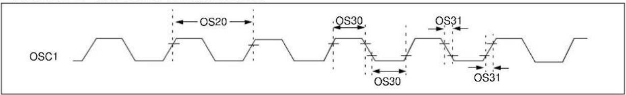
text_image
OSC1 OS20 OS30 OS31 OS30 OS31TABLE 37-17: EXTERNAL CLOCK TIMING REQUIREMENTS
| AC CHARACTERISTICS | Standard Operating Conditions: 2.3V to 3.6V(unless otherwise stated)Operating temperature -40°C ≤ T A ≤ +85°C for Industrial | ||||||
| Param.No. | Symbol | Characteristics Minimum Typical | (1) | Maximum Units | Conditions | ||
| OS10 F | osc | External CLKI Frequency(External clocks allowed onlyin EC and ECP LL modes) | DC | — | 64 | MHz | EC (Note 2,3) |
| OS13 | Oscillator Crystal Frequency | 4 | — | 32 | MHz | HS (Note 2,3) | |
| OS15 | 32 | 32.768 | 100 | kHz | Sosc (Note 2) | ||
| OS20 T | osc | Tosc = 1/Fosc | — | — | — | — | See parameter OS10 for Fosc value |
| OS30 T | osL,TosH | External Clock In (OSC1)High or Low Time | 0.375 x Tosc | — | — | ns | EC (Note 2) |
| OS31 T | osR,TosF | External Clock In (OSC1)Rise or Fall Time | — | — | 7.5 | ns | EC (Note 2) |
| OS40 T | OST | Oscillator Start-up Timer Period(Only applies to HS, HSPLL,and Sosc Clock Oscillatormodes) | — | 1024 | — | Tosc | (Note 2) |
| OS41 T | FSCM | Primary Clock Fail SafeTime-out Period | — | 2 | — | ms | (Note 2) |
| OS42 G | M | External OscillatorTransconductance | — | 400 | — | μA/V | VDD=3.3V,TA=+25°C,HS(Note 2) |
Note 1: Data in "Typical" column is at 3.3V, +25°C unless otherwise stated. Parameters are characterized but are not tested.
2: This parameter is characterized, but not tested in manufacturing.
3: See parameter OS50 for PLL input frequency limitations.
TABLE 37-18: SYSTEM TIMING REQUIREMENTS
| AC CHARACTERISTICS | Standard Operating Conditions: 2.3V to 3.6V(unless otherwise stated)Operating temperature -40°C ≤ T A ≤ +85°C for Industrial | ||||||
| Param.No. | Symbol | Characteristics | Minimum | Typical | Maximum | Units | Conditions |
| OS51 F | SYS | System Frequency | DC | — | 200 | MHz | USB module disabled |
| 30 | — | 200 | MHz | USB module enabled | |||
| OS55aOS55b | FPB | Peripheral Bus Frequency | DC | — | 100 | MHz | For PBCLKx, ‘x’ ≠ 7 |
| DC | — | 200 | MHz | For PBCLK7 | |||
| OS56 F | REF | Reference Clock Frequency | — | — | 50 | MHz | For REFCLK1, 3, 4and REFCLKO1, 3, 4pins |
TABLE 37-19: PLL CLOCK TIMING SPECIFICATIONS
| AC CHARACTERISTICS | Standard Operating Conditions: 2.3V to 3.6V(unless otherwise stated)Operating temperature -40°C ≤ T A ≤ +85°C for Industrial | ||||||
| Param.No. | Symbol | Characteristics(1) | Min. | Typ. | Max. | Units | Conditions |
| OS50 | FIN | PLL Input Frequency Range | 5 | — | 64 | MHz | ECPLL, HSPLL, FRCPLL modes |
| OS52 | TLOCK | PLL Start-up Time (Lock Time) | — | — | 100 | μs | — |
| OS53 | DCLK | CLKO Stability(2)(Period Jitter or Cumulative) | -0.25 | — | +0.25 | % | Measured over 100 ms period |
| OS54 | FVco | PLL Vco Frequency Range | 350 | — | 700 | MHz | — |
| OS54a F | PLL | PLL Output Frequency Range | 10 | — | 200 | MHz | — |
Note 1: These parameters are characterized, but not tested in manufacturing.
2: This jitter specification is based on clock-cycle by clock-cycle measurements. To get the effective jitter for individual time-bases on communication clocks, use the following formula:
$$ E f f e c t i v e J i t t e r = \frac {D _ {C L K}}{\sqrt {\frac {P B C L K 2}{C o m m u n i c a t i o n C l o c k}}} $$
For example, if PBCLK2 = 100 MHz and SPI bit rate = 50 MHz, the effective jitter is as follows:
$$ E f f e c t i v e J i t t e r = \frac {D _ {C L K}}{\sqrt {\frac {1 0 0}{5 0}}} = \frac {D _ {C L K}}{1 . 4 1} $$
TABLE 37-20: INTERNAL FRC ACCURACY
| AC CHARACTERISTICS | Standard Operating Conditions: 2.3V to 3.6V(unless otherwise stated)Operating temperature -40°C ≤ TA ≤ +85°C for Industrial | |||||
| Param.No. | Characteristics Min. | Typ. Max. | Units | Conditions | ||
| Internal FRC Accuracy @ 8.00 MHz(1) | ||||||
| F20 | FRC | -5 | — | +5 | % | 0°C ≤ TA ≤ +85°C |
| -8 | — | +8 | % | -40°C ≤ TA ≤ +85°C | ||
Note 1: Frequency calibrated at +25°C and 3.3V. The TUN bits can be used to compensate for temperature drift.
TABLE 37-21: INTERNAL LPRC ACCURACY
| AC CHARACTERISTICS | Standard Operating Conditions: 2.3V to 3.6V(unless otherwise stated)Operating temperature -40°C ≤ TA ≤ +85°C for Industrial | |||||
| Param.No. | Characteristics | Min. | Typ. | Max. | Units | Conditions |
| Internal LPRC @ 32.768 kHz(1) | ||||||
| F21 | LPRC | -8 | — | +8 | % | 0°C ≤ TA ≤ +85°C |
| -25 | — | +25 | % | -40°C ≤ TA < +85°C | ||
Note 1: Change of LPRC frequency as VDD changes.
TABLE 37-22: INTERNAL BACKUP FRC (BFRC) ACCURACY
| AC CHARACTERISTICS | Standard Operating Conditions: 2.3V to 3.6V(unless otherwise stated)Operating temperature -40°C ≤ TA ≤ +85°C for Industrial | |||||
| Param.No. | Characteristics | Min. | Typ. | Max. | Units | Conditions |
| Internal BFRC Accuracy @ 8 MHz1 | ||||||
| F22 | BFRC | -30 | — | +30 | % | — |
FIGURE 37-3: I/O TIMING CHARACTERISTICS
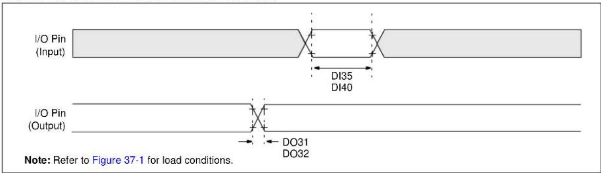
text_image
I/O Pin (Input) DI35 DI40 I/O Pin (Output) DO31 DO32 Note: Refer to Figure 37-1 for load conditions.TABLE 37-23: I/O TIMING REQUIREMENTS
| AC CHARACTERISTICS | Standard Operating Conditions: 2.3V to 3.6V(unless otherwise stated)Operating temperature -40°C ≤ T A ≤ +85°C for Industrial | ||||||
| Param.No. | Symbol | Characteristics (2) | Min. Typ. (1) | Max. Units Conditions | |||
| DO31 | TIOR | Port Output Rise TimeI/O Pins:4x Source Driver Pins -RA3, RA9, RA10, RA14, RA15RB0-7, RB11, RB13RC12-RC15RD0, RD6-RD7, RD11, RD14RE8, RE9RF2, RF3, RF8RG15RH0, RH1, RH4-RH6, RH8-RH13RJ0-RJ2, RJ8, RJ9, RJ11 | — — 9.5 ns C | LOAD = 50 pF | |||
| — — | 6 | ns | C | LOAD = 20 pF | |||
| Port Output Rise TimeI/O Pins:8x Source Driver Pins -RA0-RA2, RA4, RA5RB8-RB10, RB12, RB14, RB15RC1-RC4RD1-RD5, RD9, RD10, RD12,RD13, RD15RE4-RE7RF0, RF4, RF5, RF12, RF13RG0, RG1, RG6-RG9RH2, RH3, RH7, RH14, RH15RJ3-RJ7, RJ10, RJ12-RJ15RK0-RK7 | — — | 8 | ns | C | LOAD = 50 pF | ||
| — — | 6 | ns | C | LOAD = 20 pF | |||
| Port Output Rise TimeI/O Pins:12x Source Driver Pins -RA6, RA7RE0-RE3RF1RG12-RG14 | — — 3.5 ns C | LOAD = 50 pF | |||||
| — — | 2 | ns | C | LOAD = 20 pF | |||
Note 1: Data in "Typical" column is at 3.3V, +25°C unless otherwise stated.
2: This parameter is characterized, but not tested in manufacturing.
TABLE 37-23: I/O TIMING REQUIREMENTS (CONTINUED)
| AC CHARACTERISTICS | Standard Operating Conditions: 2.3V to 3.6V(unless otherwise stated)Operating temperature -40°C ≤ TA ≤ +85°C for Industrial | ||||||
| Param.No. | Symbol | Characteristics (2) | Min. | Typ.^(1) | Max. | Units | Conditions |
| DO32 | TioF | Port Output Fall TimeI/O Pins:4x Source Driver Pins -RA3, RA9, RA10, RA14, RA15RB0-7, RB11, RB13RC12-RC15RD0, RD6-RD7, RD11, RD14RE8, RE9RF2, RF3, RF8RG15RH0, RH1, RH4-RH6, RH8-RH13RJ0-RJ2, RJ8, RJ9, RJ11 | — — 9.5 ns C | LOAD = 50 pF | |||
| — — 6 ns C | LOAD = 20 pF | ||||||
| Port Output Fall TimeI/O Pins:8x Source Driver Pins -RA0-RA2, RA4, RA5RB8-RB10, RB12, RB14, RB15RC1-RC4RD1-RD5, RD9, RD10, RD12,RD13, RD15RE4-RE7RF0, RF4, RF5, RF12, RF13RG0, RG1, RG6-RG9RH2, RH3, RH7, RH14, RH15RJ3-RJ7, RJ10, RJ12-RJ15RK0-RK7 | — — 8 ns C | LOAD = 50 pF | |||||
| — — 6 ns C | LOAD = 20 pF | ||||||
| Port Output Fall TimeI/O Pins:12x Source Driver Pins -RA6, RA7RE0-RE3RF1RG12-RG14 | — — 3.5 ns C | LOAD = 50 pF | |||||
| — — 2 ns C | LOAD = 20 pF | ||||||
| DI35 T | INP | INTx Pin High or Low Time 5 — — | ns — | ||||
| DI40 T | RBP | CNx High or Low Time (input) 5 — | — ns — | ||||
Note 1: Data in "Typical" column is at 3.3V, +25°C unless otherwise stated.
2: This parameter is characterized, but not tested in manufacturing.
FIGURE 37-4: POWER-ON RESET TIMING CHARACTERISTICS
Internal Voltage Regulator Enabled
Clock Sources = (FRC, FRCDIV, FRCDIV16, FRCPLL, EC, ECPLL and LPRC)

text_image
VDD VPOR (TSYSDLY) SY02 Power-up Sequence (Note 2) SY00 (TPU) (Note 1) CPU Starts Fetching CodeInternal Voltage Regulator Enabled
Clock Sources = (HS, HSPLL, and Sosc)
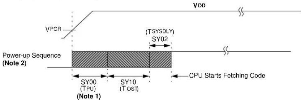
text_image
VDD VPOR (TSYSDLY) SY02 Power-up Sequence (Note 2) SY00 (TPU) SY10 (TOST) CPU Starts Fetching Code (Note 1)Note 1: The power-up period will be extended if the power-up sequence completes before the device exits from BOR (VDD < VDDMIN). 2: Includes interval voltage regulator stabilization delay.
FIGURE 37-5: EXTERNAL RESET TIMING CHARACTERISTICS

flowchart
graph TD
    A["MCLR"] --> B["TMCLR (SY20)"]
    B --> C["Reset Sequence"]
    D["BOR"] --> E["TBOR (SY30)"]
    E --> F["(TSYSDLY) SY02"]
    F --> G["CPU Starts Fetching Code"]
    H["Reset Sequence"] --> I["(TSYSDLY) SY02"]
    I --> J["CPU Starts Fetching Code"]
    K["Clock Sources = (FRC, FRCDIV, FRCDIV16, FRCPLL, EC, ECPLL and LPRC)"] --> L["Output"]
    style A fill:#f9f,stroke:#333
    style D fill:#f9f,stroke:#333
    style H fill:#f9f,stroke:#333
    style K fill:#f9f,stroke:#333
    style B fill:#ccf,stroke:#333
    style E fill:#ccf,stroke:#333
    style F fill:#cfc,stroke:#333
    style I fill:#cfc,stroke:#333
    style J fill:#cfc,stroke:#333
    style L fill:#fcc,stroke:#333
TABLE 37-24: RESETS TIMING
| AC CHARACTERISTICS | Standard Operating Conditions: 2.3V to 3.6V(unless otherwise stated)Operating temperature -40°C ≤ T A ≤ +85°C for Industrial | ||||||
| Param.No. | Symbol | Characteristics (1) | Min. Typ. (2) | Max. Units Conditions | |||
| SY00 T | PU | Power-up PeriodInternal Voltage Regulator Enabled | — 400 | 600 μs | — | ||
| SY02 T | SYSDLY | System Delay Period:Time Required to Reload DeviceConfiguration Fuses plus SYSCLKDelay before First instruction is Fetched. | — | 1 μs +8 SYSCLKcycles | — | — | — |
| SY20 T | MCLR | MCLR Pulse Width (low) | 2 | — | — | μs | — |
| SY30 T | BOR | BOR Pulse Width (low) | — | 1 | — | μs | — |
Note 1: These parameters are characterized, but not tested in manufacturing.
2: Data in "Typ" column is at 3.3V, +25°C unless otherwise stated. Characterized by design but not tested.
FIGURE 37-6: TIMER1-TIMER9 EXTERNAL CLOCK TIMING CHARACTERISTICS
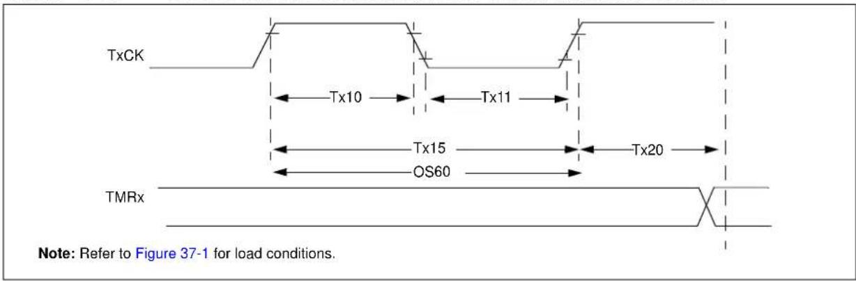
text_image
TxCK Tx10 Tx11 Tx15 Tx20 OS60 TMRx Note: Refer to Figure 37-1 for load conditions.TABLE 37-25: TIMER1 EXTERNAL CLOCK TIMING REQUIREMENTS (1)
| AC CHARACTERISTICS | Standard Operating Conditions: 2.3V to 3.6V(unless otherwise stated)Operating temperature -40°C ≤ T A ≤ +85°C for Industrial | |||||||
| Param.No. | Symbol | Characteristics (2) | Min. | Typ. | Max. | Units | Conditions | |
| TA10 T | TxH TxCK | High Time | Synchronous,with prescaler | [(12.5 ns or 1 TPBCLK3)/N] + 20 ns | — | — | ns | Must also meet parameter TA15(Note 3) |
| Asynchronous,with prescaler | 10 | — | — | ns | — | |||
| TA11 | TTXL TxCK | Low Time | Synchronous,with prescaler | [(12.5 ns or 1 TPBCLK3)/N] + 20 ns | — | — | ns | Must also meet parameter TA15(Note 3) |
| Asynchronous,with prescaler | 10 | — | — | ns | — | |||
| TA15 T | TXP | TxCKInput Period | Synchronous,with prescaler | [(Greater of 20 ns or 2 TPBCLK3)/N] + 30 ns | — — | ns V | DD > 2.7V(Note 3) | |
| [(Greater of 20 ns or 2 TPBCLK3)/N] + 50 ns | — — | ns V | DD < 2.7V(Note 3) | |||||
| Asynchronous,with prescaler | 20 | — — | ns V | DD > 2.7V | ||||
| 50 | — — | ns V | DD < 2.7V | |||||
| OS60 | FT1 | SOSC1/T1CK OscillatorInput Frequency Range(oscillator enabled by settingTCS bit (T1CON<1>)) | 32 | — | 50 | kHz | — | |
| TA20 T | CKEXTMRL | Delay from External TxCKClock Edge to TimerIncrement | — | 1 | TPBCLK3 | — | ||
Note 1: Timer1 is a Type A.
2: This parameter is characterized, but not tested in manufacturing.
3: N = Prescale Value (1, 8, 64, 256).
TABLE 37-26: TIMER2-TIMER9 EXTERNAL CLOCK TIMING REQUIREMENTS
| AC CHARACTERISTICS | Standard Operating Conditions: 2.3V to 3.6V(unless otherwise stated)Operating temperature -40°C ≤ T A ≤ +85°C for Industrial | |||||||
| Param.No. | Symbol | Characteristics (1) | Min. Max. Units | Conditions | ||||
| TB10 T | TXH | T x High Time | SynchConous, With prescaler | [(12.5 ns or 1 TPBCLK3)/N] + 25 ns | — | n | s M meet parameter TB15 | N =prescale value(1, 2, 4, 8, 16, 32, 64, 256) s |
| TB11 | TtXL | TxCK Low Time | Synchronous, with prescaler | [(12.5 ns or 1 TPBCLK3)/N] + 25 ns | — | n | s M meet parameter TB15 | |
| TB15 T | TXP | TxCK Input Period | Synchronous, with prescaler | [(Greater of [(25 ns or 2 TPBCLK3)/N] + 30 ns | — | ns | VDD > 2.7V | |
| [(Greater of [(25 ns or 2 TPBCLK3)/N] + 50 ns | — | ns | VDD < 2.7V | |||||
| TB20 T | CKEXTMRL | Delay from External TxCK Clock Edge to Timer Increment | — | 1 | TPBCLK3 | — | ||
Note 1: These parameters are characterized, but not tested in manufacturing.
FIGURE 37-7: INPUT CAPTURE (CAPx) TIMING CHARACTERISTICS

text_image
ICx IC10 IC11 IC15 Note: Refer to Figure 37-1 for load conditions.TABLE 37-27: INPUT CAPTURE MODULE TIMING REQUIREMENTS
| AC CHARACTERISTICS | Standard Operating Conditions: 2.3V to 3.6V(unless otherwise stated)Operating temperature -40°C ≤ TA ≤ +85°C for Industrial | |||||||
| Param.No. | Symbol | Characteristics(1) | Min. | Max. | Units | Conditions | ||
| IC10 | TccL | ICx Input Low Time | [(12.5 ns or 1 TPBCLK3)/N] + 25 ns | — | ns | Must also meet parameter IC15. | N = prescale value (1, 4, 16) | |
| IC11 | TccH | ICx Input High Time | [(12.5 ns or 1 TPBCLK3)/N] + 25 ns | — | ns | Must also meet parameter IC15. | ||
| IC15 | TccP | ICx Input Period | [(25 ns or 2 TPBCLK3)/N] + 50 ns | — | ns — | |||
Note 1: These parameters are characterized, but not tested in manufacturing.
FIGURE 37-8: OUTPUT COMPARE MODULE (OCx) TIMING CHARACTERISTICS

text_image
OCx (Output Compare or PWM mode) OC11 → ← OC10 ←Note: Refer to Figure 37-1 for load conditions.
TABLE 37-28: OUTPUT COMPARE MODULE TIMING REQUIREMENTS
| AC CHARACTERISTICS | Standard Operating Conditions: 2.3V to 3.6V(unless otherwise stated)Operating temperature -40°C ≤ T A ≤ +85°C for Industrial | ||||||
| Param.No. | Symbol | Characteristics (1) | Min. Typical (2) | Max. Units Conditions | |||
| OC10 T | ccF | OCx Output Fall Time | — | — | — | ns | See parameter DO32 |
| OC11 | TccR | OCx Output Rise Time | — | — | — | ns | See parameter DO31 |
Note 1: These parameters are characterized, but not tested in manufacturing.
2: Data in "Typical" column is at 3.3V, +25°C unless otherwise stated. Parameters are for design guidance only and are not tested.
FIGURE 37-9: OCx/PWM MODULE TIMING CHARACTERISTICS

text_image
OCFA/OCFB OC20 OC15 OCx OCx is tri-stated Note: Refer to Figure 37-1 for load conditions.TABLE 37-29: SIMPLE OCx/PWM MODE TIMING REQUIREMENTS
| AC CHARACTERISTICS | Standard Operating Conditions: 2.3V to 3.6V(unless otherwise stated)Operating temperature -40°C ≤ TA ≤ +85°C for Industrial | ||||||
| Param No. | Symbol | Characteristics(1) | Min Typ. (2) | Max | Units | Conditions | |
| OC15 | TFD | Fault Input to PWM I/O Change | — | — | 50 | ns | — |
| OC20 | TFLT | Fault Input Pulse Width | 50 | — | — | ns | — |
Note 1: These parameters are characterized, but not tested in manufacturing.
2: Data in "Typical" column is at 3.3V, +25°C unless otherwise stated. Parameters are for design guidance only and are not tested.
FIGURE 37-10: SPIx MODULE MASTER MODE (CKE = 0) TIMING CHARACTERISTICS
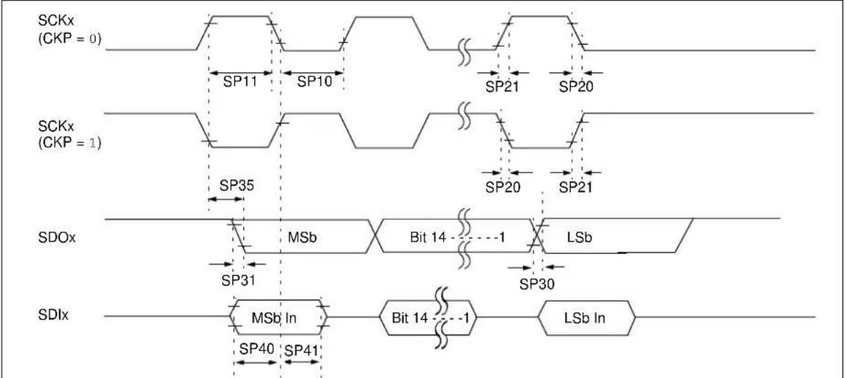
flowchart
graph TD
    A["SCKx (CKP = 0)"] --> B["SP11"]
    B --> C["SP10"]
    C --> D["SP21"]
    D --> E["SP20"]
    F["SCKx (CKP = 1)"] --> G["SP35"]
    G --> H["SP20"]
    H --> I["SP21"]
    J["SDOx"] --> K["MSb"]
    K --> L["Bit 14 - -1"]
    L --> M["LSb"]
    N["SDIx"] --> O["MSb In"]
    O --> P["Bit 14 - -1"]
    P --> Q["LSb In"]
    style A fill:#f9f,stroke:#333
    style F fill:#f9f,stroke:#333
    style J fill:#f9f,stroke:#333
    style N fill:#f9f,stroke:#333
    style K fill:#ccf,stroke:#333
    style L fill:#ccf,stroke:#333
    style O fill:#ccf,stroke:#333
    style P fill:#ccf,stroke:#333
Note: Refer to Figure 37-1 for load conditions.
TABLE 37-30: SPIx MASTER MODE (CKE = 0) TIMING REQUIREMENTS
| AC CHARACTERISTICS | Standard Operating Conditions: 2.3V to 3.6V(unless otherwise stated)Operating temperature -40°C ≤ T A≤ +85°C for Industrial | ||||||
| Param.No. | Symbol C | Characteristics (1) | Min. Typ. (2) | Max. Units Conditions | |||
| SP10 T | scL | SCKx Output Low Time (Note 3) | Tsck/2 —— ns | — | |||
| SP11 | Tsch | SCKx Output High Time(Note 3) | Tsck/2 —— ns | — | |||
| SP20 T | scF | SCKx Output Fall Time (Note 4) | — | — — ns | See parameter DO32 | ||
| SP21 T | scR | SCKx Output Rise Time (Note 4) | — | — | — | ns | See parameter DO31 |
| SP30 T | doF | SDOx Data Output Fall Time (Note 4) | — | — | — | ns | See parameter DO32 |
| SP31 T | doR | SDOx Data Output Rise Time (Note 4) | — | — | — | ns | See parameter DO31 |
| SP35 T | sCH2doV,TscL2doV | SDOx Data Output Valid after SCKx Edge | — | — | 7 | ns | VDD > 2.7V |
| — | — | 10 | ns | VDD < 2.7V | |||
| SP40 T | DIV2sCH,TDIV2sCL | Setup Time of SDIx Data Input to SCKx Edge | 5 | — — ns | — | ||
| SP41 T | sCH2dIL,TscL2dIL | Hold Time of SDIx Data Input to SCKx Edge | 5 | — — ns | — | ||
Note 1: These parameters are characterized, but not tested in manufacturing.
2: Data in "Typical" column is at 3.3V, +25°C unless otherwise stated. Parameters are for design guidance only and are not tested.
3: The minimum clock period for SCKx is 20 ns. Therefore, the clock generated in Master mode must not violate this specification.
4: Assumes 10 pF load on all SPIx pins.
FIGURE 37-11: SPIx MODULE MASTER MODE (CKE = 1) TIMING CHARACTERISTICS
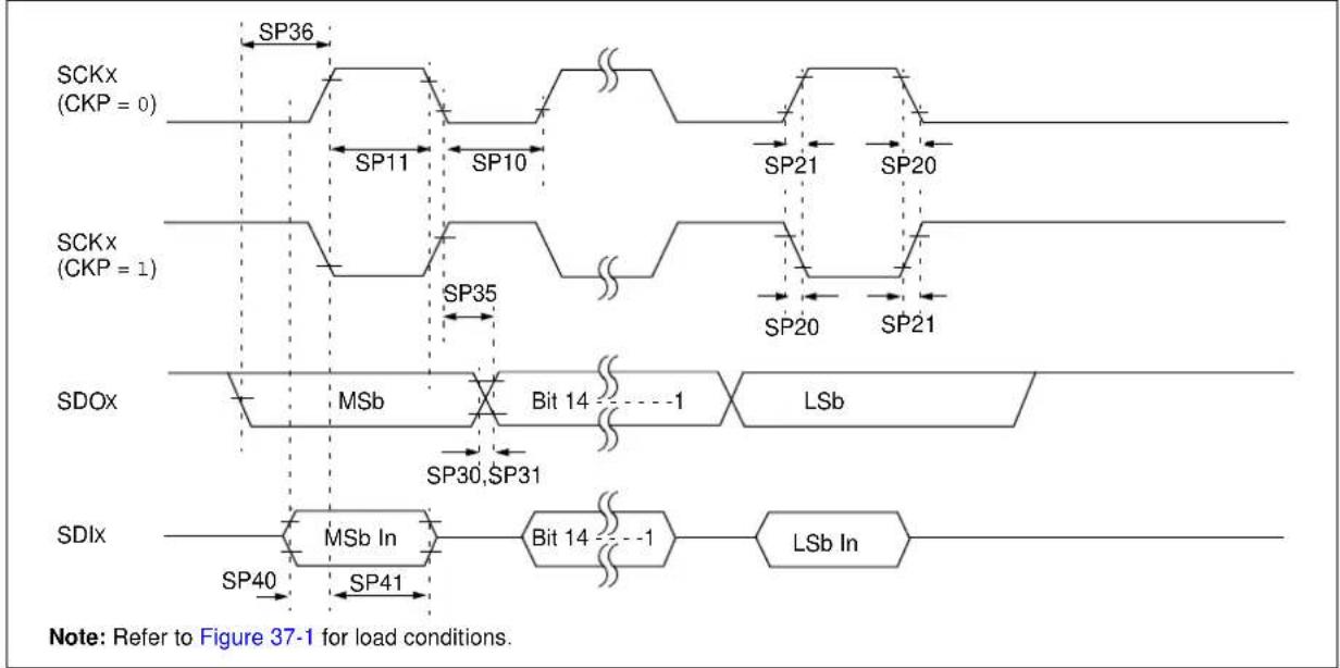
flowchart
graph TD
    A["SCKx (CKP = 0)"] --> B["SP36"]
    B --> C["SP11"]
    C --> D["SP10"]
    D --> E["SP21"]
    E --> F["SP20"]
    G["SCKx (CKP = 1)"] --> H["SP35"]
    H --> I["SP20"]
    I --> J["SP21"]
    K["SDOx"] --> L["MSb"]
    L --> M["Bit 14"]
    M --> N["LSb"]
    O["SDIx"] --> P["MSb In"]
    P --> Q["Bit 14"]
    Q --> R["LSb In"]
    S["Note: Refer to Figure 37-1 for load conditions."]
TABLE 37-31: SPIx MODULE MASTER MODE (CKE = 1) TIMING REQUIREMENTS
| AC CHARACTERISTICS | Standard Operating Conditions: 2.3V to 3.6V(unless otherwise stated)Operating temperature -40°C ≤ T A ≤ +85°C for Industrial | ||||||
| Param.No. | Symbol | Characteristics (1) | Min. Typ. (2) | Max. Units Conditions | |||
| SP10 T | SCL SCKx | Output Low Time (Note 3) | TSCK/2 — — | ns | — | ||
| SP11 | TSCH | SCKx Output High Time(Note 3) | TSCK/2 — — | ns | — | ||
| SP20 T | SCF SCKx | Output Fall Time (Note 4) | — | — | — | ns | See parameter DO32 |
| SP21 T | SCR | SCKx Output Rise Time (Note 4) | — | — | — | ns | See parameter DO31 |
| SP30 T | DOF | SDOx Data Output Fall Time(Note 4) | — | — | — | ns | See parameter DO32 |
| SP31 T | DOR | SDOx Data Output Rise Time(Note 4) | — | — | — | ns | See parameter DO31 |
| SP35 T | SCH2DOV,TSCL2DOV | SDOx Data Output Valid afterSCKx Edge | — | — | 7 | ns | VDD > 2.7V |
| — | 10 | VDD < 2.7V | |||||
| SP36 T | DOV2SC,TDOV2SCL | SDOx Data Output Setup toFirst SCKx Edge | 7 | —— | ns | — | |
| SP40 T | DIV2SCH,TDIV2SCL | Setup Time of SDIx Data Input toSCKx Edge | 7 | —— | ns | V | DD > 2.7V |
| 10 | VDD < 2.7V | ||||||
| SP41 T | SCH2DIL,TSCL2DIL | Hold Time of SDIx Data Inputto SCKx Edge | 7 | —— | ns | V | DD > 2.7V |
| 10 | —— | ns | V | DD < 2.7V | |||
Note 1: These parameters are characterized, but not tested in manufacturing.
2: Data in "Typical" column is at 3.3V, +25°C unless otherwise stated. Parameters are for design guidance only and are not tested.
3: The minimum clock period for SCKx is 20 ns. Therefore, the clock generated in Master mode must not violate this specification.
4: Assumes 10 pF load on all SPIx pins.
FIGURE 37-12: SPIx MODULE SLAVE MODE (CKE = 0) TIMING CHARACTERISTICS
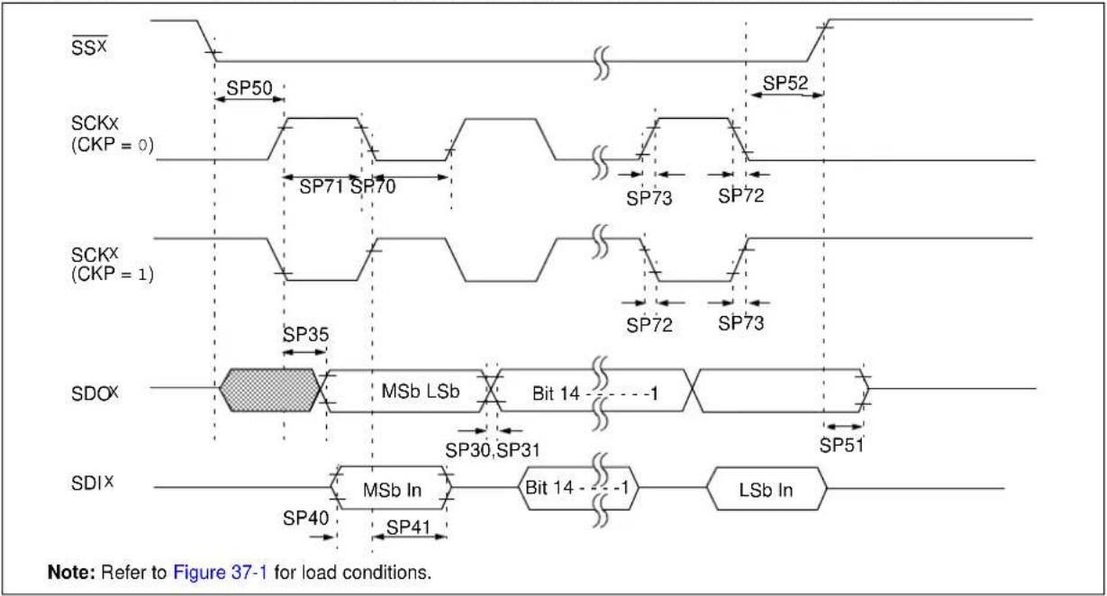
flowchart
graph TD
    subgraph SSX
        A["SSX"] --> B["SP50"]
        B --> C["SCKx (CKP = 0)"]
        C --> D["SP71 SP70"]
        D --> E["SP52"]
        E --> F["SP73"]
        F --> G["SCKx (CKP = 1)"]
        G --> H["SP72"]
        H --> I["SP73"]
    end
    subgraph SCKx
        J["SCKx (CKP = 0)"] --> K["SP50"]
        K --> L["SCKx (CKP = 1)"]
        L --> M["SP71 SP70"]
        M --> N["SCKx (CKP = 1)"]
        N --> O["SP52"]
        O --> P["SP73"]
    end
    subgraph SDOx
        Q["SDOx"] --> R["MSb LSb"]
        R --> S["Bit 14 -1"]
        S --> T["SP51"]
        T --> U["SP30, SP31"]
        U --> V["SP40"]
        V --> W["MSb In"]
        W --> X["Bit 14 -1"]
        X --> Y["LSb In"]
        Y --> Z["SP41"]
    end
    subgraph SDIX
        AA["SDIX"] --> AB["MSb In"]
        AB --> AC["Bit 14 -1"]
        AC --> AD["LSb In"]
        AD --> AE["SP40"]
        AE --> AF["SP41"]
    end
    Note["Refer to Figure 37-1 for load conditions."]
TABLE 37-32: SPIx MODULE SLAVE MODE (CKE = 0) TIMING REQUIREMENTS
| AC CHARACTERISTICS | Standard Operating Conditions: 2.3V to 3.6V (unless otherwise stated)Operating temperature -40°C ≤ TA ≤ +85°C for Industrial | ||||||
| Param.No. | Symbol C | Characteristics (1) | Min. Typ. (2) | Max. Units Conditions | |||
| SP70 T | sCL | SCKx Input Low Time (Note 3) | Tsck/2 | — | — | ns | — |
| SP71 T | sCH | SCKx Input High Time (Note 3) | Tsck/2 | — | — | ns | — |
| SP72 T | sCF | SCKx Input Fall Time | — | — | — | ns | See parameter DO32 |
| SP73 T | SCR | SCKx Input Rise Time | — | — | — | ns | See parameter DO31 |
| SP30 T | DOF | SDOx Data Output Fall Time (Note 4) | — | — | — | ns | See parameter DO32 |
| SP31 T | DOR | SDOx Data Output Rise Time (Note 4) | — | — | — | ns | See parameter DO31 |
| SP35 T | sCH2DOV,TsCL2DOV | SDOx Data Output Valid after SCKx Edge | — | — | 7 | ns V | DD > 2.7V |
| — | — | 10 | ns | VDD < 2.7V | |||
| SP40 T | DIV2sCH,TDIV2sCL | Setup Time of SDIx Data Input to SCKx Edge | 5 | — | — | ns | — |
| SP41 T | sCH2DL,TsCL2DIL | Hold Time of SDIx Data Input to SCKx Edge | 5 | — | — | ns | — |
| SP50 T | ssL2sCH,TssL2sCL | to SCKx ↑ or SCKx Input | 88 | — | — | ns | — |
| SP51 T | SSH2DOZ | to SDOx OutputHigh-Impedance (Note 3) | 2.5 | — | 12 | ns | — |
| SP52 | Tsch2 sHTscL2ssH | after SCKx Edge | 10 | — | — | ns | — |
Note 1: These parameters are characterized, but not tested in manufacturing.
2: Data in "Typical" column is at 3.3V, +25°C unless otherwise stated. Parameters are for design guidance only and are not tested.
3: The minimum clock period for SCKx is 20 ns.
4: Assumes 10 pF load on all SPIx pins.
FIGURE 37-13: SPIx MODULE SLAVE MODE (CKE = 1) TIMING CHARACTERISTICS

flowchart
graph TD
    subgraph SSx
        A["SP60"] --> B["SP50"]
        B --> C["SCKx (CKP = 0)"]
        C --> D["SP71"]
        D --> E["SCKx (CKP = 1)"]
        E --> F["SP70"]
        F --> G["SCKx (CKP = 0)"]
        G --> H["SP73"]
        H --> I["SCKx (CKP = 1)"]
        I --> J["SP72"]
        J --> K["SCKx (CKP = 1)"]
        K --> L["SP73"]
        L --> M["SCKx (CKP = 1)"]
        M --> N["SP35"]
        N --> O["SCKx (CKP = 1)"]
        O --> P["SP72"]
        P --> Q["SCKx (CKP = 1)"]
        Q --> R["SP73"]
        R --> S["SCKx (CKP = 1)"]
    end

    subgraph SDOx
        T["MSb"] --> U["Bit 14"] --> V["LSb"]
        W["SP30, SP31"] --> X["SP51"]
        Y["SP40"] --> Z["MSb In Bit 14"] --> AA["LSb In"]
        AB["SP41"] --> AC["MSb In Bit 14"] --> AD["LSb In"]
    end

    subgraph SDIx
        AE["SP40"] --> AF["MSb In Bit 14"] --> AG["LSb In"]
        AH["SP41"] --> AI["MSb In Bit 14"] --> AJ["LSb In"]
        AK["SP51"] --> AL["MSb In Bit 14"] --> AM["LSb In"]
    end

    note right of A: Refer to Figure 37-1 for load conditions.
    note right of B: SP52
    note right of C: SP70
    note right of D: SP73
    note right of E: SP72
    note right of F: SP73
    note right of G: SP72
    note right of H: SP73
    note right of I: SP72
    note right of J: SP73
    note right of K: SP72
    note right of L: SP51
    note right of M: SP51
    note right of N: SP51
    note right of O: SP51
    note right of P: SP51
    note right of Q: SP51
    note right of R: SP51
    note right of S: SP51
    note right of T: SP51
    note right of U: SP51
    note right of V: SP51
    note right of W: SP51
    note right of X: SP51
    note right of Y: SP51
    note right of Z: SP51
    note right of AA: SP51
    note right of AB: SP51
    note right of AC: SP51
    note right of AD: SP51
    note right of AE: SP51
    note right of AF: SP51
    note right of AG: SP51
    note right of AH: SP51
    note right of AI: SP51
    note right of AJ: SP51
    note right of AK: SP51
    note right of AL: SP51
TABLE 37-33: SPIx MODULE SLAVE MODE (CKE = 1) TIMING REQUIREMENTS
| AC CHARACTERISTICS | Standard Operating Conditions: 2.3V to 3.6V(unless otherwise stated)Operating temperature -40°C ≤ TA ≤ +85°C for Industrial | ||||||
| Param.No. | Symbol | Characteristics (1) | Min. Typ. (2) | Max. Units Conditions | |||
| SP70 T | sCL | SCKx Input Low Time (Note 3) | TsCK/2 — | — ns | — | ||
| SP71 T | sCH | SCKx Input High Time (Note 3) | TsCK/2 — | — ns | — | ||
| SP72 T | sCF | SCKx Input Fall Time | — | — | 10 | ns | — |
| SP73 T | sCR | SCKx Input Rise Time | — | — | 10 | ns | — |
| SP30 T | DOF | SDOx Data Output Fall Time(Note 4) | — | — | — | ns | See parameter DO32 |
| SP31 T | dOR | SDOx Data Output Rise Time(Note 4) | — | — | — | ns | See parameter DO31 |
| SP35 T | sCH2dOV,TsCL2dOV | SDOx Data Output Valid after SCKx Edge | — | — | 10 | ns | VDD > 2.7V |
| — | — | 15 | ns | VDD < 2.7V | |||
| SP40 T | DIV2sCH,TDIV2sCL | Setup Time of SDIx Data Input to SCKx Edge | 0 — | — ns | — | ||
| SP41 T | sCH2dIL,TsCL2dIL | Hold Time of SDIx Data Input to SCKx Edge | 7 — | — ns | — | ||
| SP50 T | ssL2sCH,TssL2scl | SSx ↓ to SCKx ↓ or SCKx ↑ Input | 88 | — | — | ns | — |
Note 1: These parameters are characterized, but not tested in manufacturing.
2: Data in "Typical" column is at 3.3V, +25°C unless otherwise stated. Parameters are for design guidance only and are not tested.
3: The minimum clock period for SCKx is 20 ns.
4: Assumes 10 pF load on all SPIx pins.
TABLE 37-33: SPIx MODULE SLAVE MODE (CKE = 1) TIMING REQUIREMENTS (CONTINUED)
| AC CHARACTERISTICS | Standard Operating Conditions: 2.3V to 3.6V(unless otherwise stated)Operating temperature -40°C ≤ TA ≤ +85°C for Industrial | ||||||
| Param.No. | Symbol | Characteristics(1) | Min. Typ. (2) | Max. | Units | Conditions | |
| SP51 T | ssH2doZ | to SDO x OutputHigh-Impedance(Note 4) | 2.5 — | 12 ns — | |||
| SP52 T | scH2ssHTscL2ssH | after SCKx Edge | 10 | — | — | ns | — |
| SP60 T | ssL2doV S | DOx Data Output Valid after Edge | — | — | 12.5 | ns | — |
Note 1: These parameters are characterized, but not tested in manufacturing.
2: Data in "Typical" column is at 3.3V, +25°C unless otherwise stated. Parameters are for design guidance only and are not tested.
3: The minimum clock period for SCKx is 20 ns.
4: Assumes 10 pF load on all SPIx pins.
FIGURE 37-14: SQI SERIAL INPUT TIMING CHARACTERISTICS
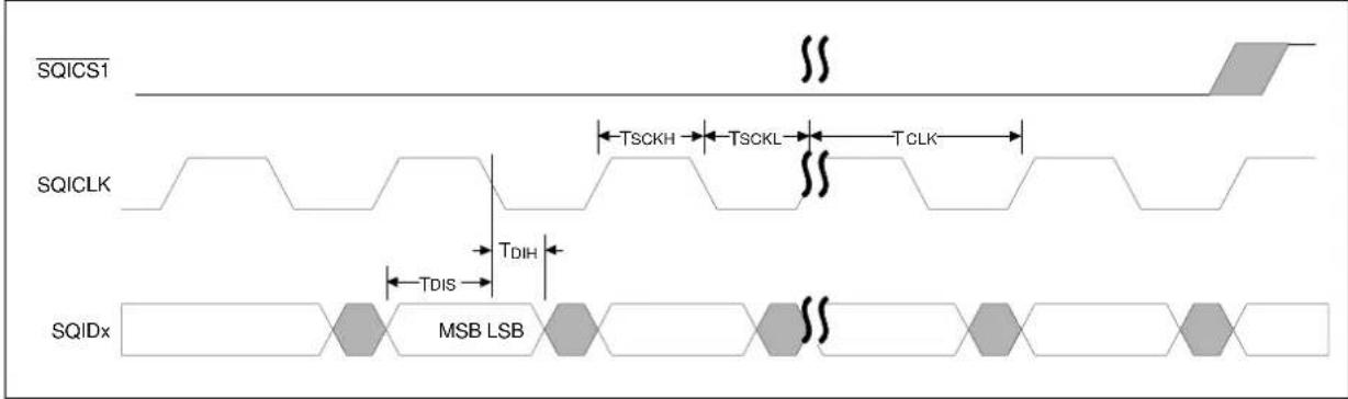
text_image
SQICS1 SQICLK SQIDx MSB LSBFIGURE 37-15: SQI SERIAL OUTPUT TIMING CHARACTERISTICS
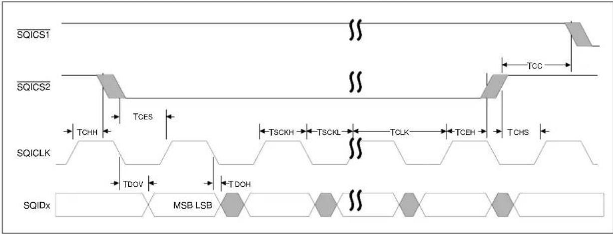
text_image
SQICS1 SQICS2 TCC TCHH TCES TSCKH TSCKL TCLK TCEH TCHS SQICLK TDOV TDOH SQIDX MSB LSBTABLE 37-34: SQI TIMING REQUIREMENTS
| AC CHARACTERISTICS | Standard Operating Conditions: 2.3V to 3.6V(unless otherwise stated)Operating temperature -40°C ≤ T A ≤ +85°C for Industrial | ||||||
| Param.No. | Symbol | Characteristic | Min. | Typ. | Max. | Units | Conditions |
| SQ10 | FCLK | Serial Clock Frequency (1/TsqI) | — | — | 50 | MHz | — |
| SQ11 | TSCKH | Serial Clock High Time | 5.5 | — | — | ns | — |
| SQ12 | TSCKL | Serial Clock Low Time | 5.5 | — | — | ns | — |
| SQ13 | TSCKR | Serial Clock Rise Time | — | — | — | ns | See parameter DO31 |
| SQ14 | TSCKF | Serial Clock Fall Time | — | — | — | ns | See parameter DO32 |
| SQ15 | TCSS (TCES) | CS Active Setup Time | 5 | — | — | ns | — |
| SQ16 | TCSH (TCEH) | CS Active Hold Time | 5 | — | — | ns | — |
| SQ17 | TCHS | CS Not Active Setup Time | 3 | — | — | ns | — |
| SQ18 | TCHH | CS Not Active Hold Time | 3 | — | — | ns | — |
| SQ22 | TDIS | Data In Setup Time | 6 | — | — | ns | — |
| SQ23 | TDIH | Data In Hold Time | 3 | — | — | ns | — |
| SQ24 | TDOH | Data Out Hold | 0 | — | — | ns | — |
| SQ25 | TDOV | Data Out Valid | — | — | 6 | ns | — |
FIGURE 37-16: I2Cx BUS START/STOP BITS TIMING CHARACTERISTICS (MASTER MODE)
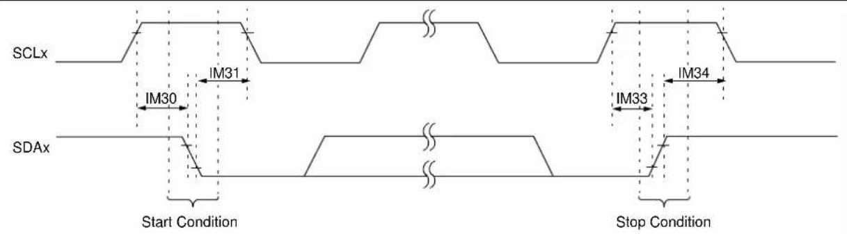
text_image
SCLx IM30 IM31 SDAx Start Condition Stop Condition IM33 IM34Note: Refer to Figure 37-1 for load conditions.
FIGURE 37-17: I2Cx BUS DATA TIMING CHARACTERISTICS (MASTER MODE)
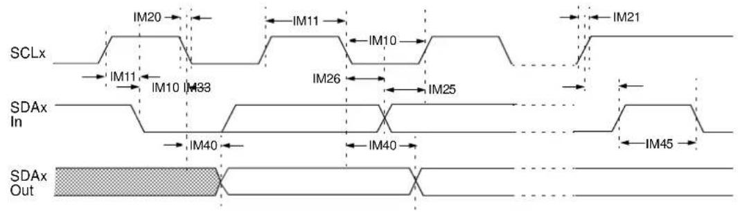
text_image
SCLx IM20 IM11 IM10 IM21 IM11 IM10 IM33 IM26 IM25 SDAx In IM40 IM40 IM45 SDAx OutNote: Refer to Figure 37-1 for load conditions.
TABLE 37-35: I2Cx BUS DATA TIMING REQUIREMENTS (MASTER MODE)
| AC CHARACTERISTICS | Standard Operating Conditions: 2.3V to 3.6V(unless otherwise stated)Operating temperature -40°C ≤ T A ≤ +85°C for Industrial | ||||||
| Param.No. | Symbol | Characteristics Min. | (1) | Max. Units Conditions | |||
| IM10 T | LO:SCL | Clock Low Time 1 | 00 kHz mode T | PBCLK2 * (BRG + 2) | — | μs | — |
| 400 kHz mode | TPBCLK2 * (BRG + 2) | — | μs | — | |||
| 1 MHz mode(Note 2) | TPBCLK2 * (BRG + 2) | — | μs | — | |||
| IM11 | THI:SCL | Clock High Time | 100 kHz mode | TPBCLK2 * (BRG + 2) | — | μs | — |
| 400 kHz mode | TPBCLK2 * (BRG + 2) | — | μs | — | |||
| 1 MHz mode(Note 2) | TPBCLK2 * (BRG + 2) | — | μs | — | |||
| IM20 T | F:SCL | SDAx and SCLxFall Time | 100 kHz mode | — | 300 | ns | CB is specified to be from 10 to 400 pF |
| 400 kHz mode | 20 + 0.1 CB | 300 | ns | ||||
| 1 MHz mode(Note 2) | — | 100 | ns | ||||
Note 1: BRG is the value of the FC Baud Rate Generator.
2: Maximum pin capacitance = 10 pF for all I2Cx pins (for 1 MHz mode only).
3: The typical value for this parameter is 104 ns.
TABLE 37-35: I2Cx BUS DATA TIMING REQUIREMENTS (MASTER MODE) (CONTINUED)
| AC CHARACTERISTICS | Standard Operating Conditions: 2.3V to 3.6V(unless otherwise stated)Operating temperature -40°C ≤ TA ≤ +85°C for Industrial | ||||||
| Param.No. | Symbol | Characteristics | Min.(1) | Max. | Units | Conditions | |
| IM21 T | R:SCL | SDAx and SCLx Rise Time | 100 kHz mode | — 1000 ns C | B is specified to be from 10 to 400 pF | ||
| 400 kHz mode 2 | 20 + 0.1 C B | 300 ns | |||||
| 1 MHz mode (Note 2) | — 300 ns | ||||||
| IM25 T | SU:DAT | Data Input Setup Time | 100 kHz mode 2 | 50 — ns — | |||
| 400 kHz mode 1 | 100 — ns | ||||||
| 1 MHz mode (Note 2) | 100 — ns | ||||||
| IM26 T | HD:DAT | Data Input Hold Time | 100 kHz mode | 0 | — | μs | — |
| 400 kHz mode | 0 | 0.9 | μs | ||||
| 1 MHz mode (Note 2) | 0 | 0.3 | μs | ||||
| IM30 T | SU:STA | Start Condition Setup Time | 100 kHz mode | TPBCLK2 * (BRG + 2) | — | μs | Only relevant for Repeated Start condition |
| 400 kHz mode | TPBCLK2 * (BRG + 2) | — | μs | ||||
| 1 MHz mode (Note 2) | TPBCLK2 * (BRG + 2) | — | μs | ||||
| IM31 T | HD:STA | Start Condition Hold Time | 100 kHz mode | TPBCLK2 * (BRG + 2) | — | μs | After this period, the first clock pulse is generated |
| 400 kHz mode | TPBCLK2 * (BRG + 2) | — | μs | ||||
| 1 MHz mode (Note 2) | TPBCLK2 * (BRG + 2) | — | μs | ||||
| IM33 T | SU:STO | Stop Condition Setup Time | 100 kHz mode | TPBCLK2 * (BRG + 2) | — | μs — | |
| 400 kHz mode | TPBCLK2 * (BRG + 2) | — | μs | ||||
| 1 MHz mode (Note 2) | TPBCLK2 * (BRG + 2) | — | μs | ||||
| IM34 T | HD:STO | Stop Condition Hold Time | 100 kHz mode | TPBCLK2 * (BRG + 2) | — | ns — | |
| 400 kHz mode | TPBCLK2 * (BRG + 2) | — | ns | ||||
| 1 MHz mode (Note 2) | TPBCLK2 * (BRG + 2) | — | ns | ||||
| IM40 T | AA:SCL | Output Valid from Clock | 100 kHz mode | — | 3500 | ns | — |
| 400 kHz mode | — | 1000 | ns | — | |||
| 1 MHz mode (Note 2) | — 350 ns — | ||||||
| IM45 T | BF:SDA | Bus Free Time | 100 kHz mode | 4.7 | — | μs | The amount of time the bus must be free before a new transmission can start |
| 400 kHz mode | 1.3 | — | μs | ||||
| 1 MHz mode (Note 2) | 0.5 | — | μs | ||||
| IM50 C | B | Bus Capacitive Loading | — | — | pF | See parameter DO58 | |
| IM51 T | PGD | Pulse Gobbler Delay | 52 | 312 | ns | See Note 3 | |
Note 1: BRG is the value of the PC Baud Rate Generator.
2: Maximum pin capacitance = 10 pF for all I2Cx pins (for 1 MHz mode only).
3: The typical value for this parameter is 104 ns.
FIGURE 37-18: I2Cx BUS START/STOP BITS TIMING CHARACTERISTICS (SLAVE MODE)
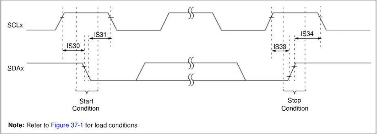
text_image
SCLx IS30 IS31 SDAx Start Condition Stop Condition IS33 IS34 Note: Refer to Figure 37-1 for load conditions.FIGURE 37-19: I2Cx BUS DATA TIMING CHARACTERISTICS (SLAVE MODE)
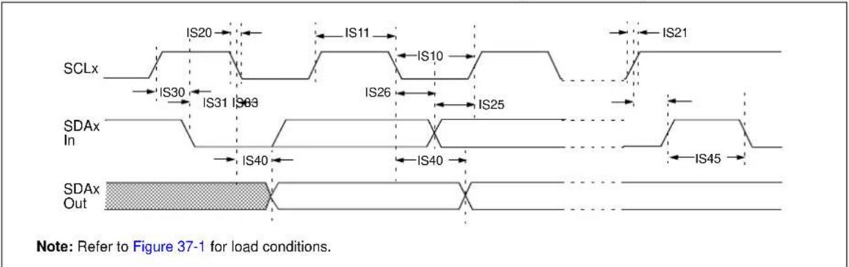
other
| Signal | Value | |------------|-------| | SCLx | IS20 | | SCLx | IS11 | | SCLx | IS10 | | SCLx | IS21 | | SDAx In | IS30 | | SDAx In | IS31 | | SDAx In | IS63 | | SDAx In | IS26 | | SDAx In | IS25 | | SDAx Out | IS40 | | SDAx Out | IS40 | | SDAx Out | IS45 |TABLE 37-36: I2Cx BUS DATA TIMING REQUIREMENTS (SLAVE MODE)
| AC CHARACTERISTICS | Standard Operating Conditions: 2.3V to 3.6V(unless otherwise stated)Operating temperature -40°C ≤ TA ≤ +85°C for Industrial | ||||||
| Param.No. | Symbol | Characteristics | Min. | Max. | Units | Conditions | |
| IS10 T | LO SCL | Clock Low Time | 100 kHz mode | 4.7 | — | μs | PBCLK2 must operate at a minimum of 800 kHz |
| 400 kHz mode | 1.3 | — | μs | PBCLK 2must operate at a minimum of 3.2 MHz | |||
| 1 MHz mode (Note 1) | 0.5 — μs | — | |||||
| IS11 | THI: SCL | Clock High Time | 100 kHz mode | 4.0 | — | μs | PBCLK2 must operate at a minimum of 800 kHz |
| 400 kHz mode | 0.6 | — | μs | PBCLK2 must operate at a minimum of 3.2 MHz | |||
| 1 MHz mode (Note 1) | 0.5 — μs | — | |||||
| IS20 T | F:SCL | SDAx and SCLxFall Time | 100 kHz mode | — 300 ns C | B is specified to be from 10 to 400 pF | ||
| 400 kHz mode | 20 + 0.1 C B | 300 ns | |||||
| 1 MHz mode(Note 1) | — 100 ns | ||||||
| IS21 T | R:SCL | SDAx and SCLx Rise Time | 100 kHz mode | — 1000 ns C | B is specified to be from 10 to 400 pF | ||
| 400 kHz mode | 20 + 0.1 C B | 300 ns | |||||
| 1 MHz mode(Note 1) | — 300 ns | ||||||
| IS25 T | SU:DAT | Data Input Setup Time | 100 kHz mode | 250 — ns — | |||
| 400 kHz mode | 100 — ns | ||||||
| 1 MHz mode(Note 1) | 100 — ns | ||||||
| IS26 T | HD:DAT | Data Input Hold Time | 100 kHz mode | 0 | — | ns | — |
| 400 kHz mode | 0 | 0.9 | μs | ||||
| 1 MHz mode(Note 1) | 0 | 0.3 | μs | ||||
| IS30 T | SU:STA | Start Condition Setup Time | 100 kHz mode | 4700 | — | ns | Only relevant for Repeated Start condition |
| 400 kHz mode | 600 — ns | ||||||
| 1 MHz mode(Note 1) | 250 — ns | ||||||
| IS31 T | HD:STA | Start Condition Hold Time | 100 kHz mode | 4000 | — | ns | After this period, the first clock pulse is generated |
| 400 kHz mode | 600 — ns | ||||||
| 1 MHz mode(Note 1) | 250 — ns | ||||||
| IS33 T | SU:STO | Stop Condition Setup Time | 100 kHz mode | 4000 | — | ns | — |
| 400 kHz mode | 600 — ns | ||||||
| 1 MHz mode(Note 1) | 600 — ns | ||||||
| IS34 T | HD:STO | Stop Condition Hold Time | 100 kHz mode | 4000 | — | ns | — |
| 400 kHz mode | 600 — ns | ||||||
| 1 MHz mode(Note 1) | 250 ns | ||||||
| IS40 T | AA:SCL | Output Valid from Clock | 100 kHz mode | 0 | 3500 | ns | — |
| 400 kHz mode | 0 | 1000 | ns | ||||
| 1 MHz mode(Note 1) | 0 | 350 ns | |||||
| IS45 T | BF:SDA | Bus Free Time | 100 kHz mode | 4.7 | — | μs | The amount of time the bus must be free before a new transmission can start |
| 400 kHz mode | 1.3 | — | μs | ||||
| 1 MHz mode(Note 1) | 0.5 | — μs | |||||
| IS50 C | B | Bus Capacitive Loading | — | — | pF | See parameter DO58 | |
Note 1: Maximum pin capacitance = 10 pF for all I2Cx pins (for 1 MHz mode only).
FIGURE 37-20: CANx MODULE I/O TIMING CHARACTERISTICS

text_image
CiTx Pin (output) Old Value New Value CA10 CA11 CiRx Pin (input) CA20TABLE 37-37: CANx MODULE I/O TIMING REQUIREMENTS
| AC CHARACTERISTICS | Standard Operating Conditions: 2.3V to 3.6V(unless otherwise stated)Operating temperature -40°C ≤ T A ≤ +85°C for Industrial | ||||||
| Param No. | Symbol | Characteristic (1) | Min. Typ. (2) | Max. Units Conditions | |||
| CA10 | TioF | Port Output Fall Time | — | — | — | ns | See parameter DO32 |
| CA11 | TioR | Port Output Rise Time | — | — | — | ns | See parameter DO31 |
| CA20 | Tcwf | Pulse Width to TriggerCAN Wake-up Filter | 700 | — | — | ns | — |
Note 1: These parameters are characterized but not tested in manufacturing.
2: Data in "Typ" column is at 3.3V, +25°C unless otherwise stated. Parameters are for design guidance only and are not tested.
TABLE 37-38: ADC1 MODULE SPECIFICATIONS
| AC CHARACTERISTICS(5,6) | Standard Operating Conditions (see Notes 3,5): 2.3V to 3.6V(unless otherwise stated)Operating temperature -40°C ≤ T A ≤ +85°C for Industrial | ||||||
| Param. | Symbol | Characteristics Min. | Typ. Max. | Units | Conditions | ||
| Device Supply | |||||||
| AD01 AV | DD | Module VDD Supply Greater of VDD-0.3 or 2.3 | — | Lesser of VDD+0.3 or 3.6 | V | — | |
| AD02 AV | SS | Module Vss Supply | Vss | — | Vss+0.3 | V | — |
| Reference Inputs | |||||||
| AD05 V | REFH | Reference Voltage High | AVss+1.2 | — | AVDD | V | VREFH = VREF+ (Note 1) |
| AD06 V | REFL | Reference Voltage Low | AVss | — | VREFH-1.2 | V | (Note 1) |
| AD07 V | REF | Absolute Reference Voltage (VREFH-VREFL) | 1.2 | — | AVDD | V | (Note 4) |
| AD08 AD08a | IREF | Current Drain | — | 100 .002 | 150 1 | μA μA | ADC operating ADC off |
| Analog Input | |||||||
| AD12 V | INH-VINL | Full-Scale Input Range | -VREFH 0 | — | VREFH + VREFH | V V | Differential Single-ended |
| AD14 V | INCM | Common Mode Input Voltage | AVss+ VREF/2 | — | AVDD-VREF/2 | V | — |
| AD17 R | IN | Recommended Impedance of Analog Voltage Source | — | — | 200 | Ω | (Note 1) For minimum sampling time |
| ADC Accuracy - Measurements with External VREF+/VREF- | |||||||
| AD20c | Nr | Resolution | 10 data bits | bits | — | ||
| AD21c | INL | Integral Nonlinearity | — | ±2 | — | LSb | VINL = VREF- = VREFL = 0V, VREF+ = VREFH = 2.5V |
| AD22c | DNL | Differential Nonlinearity | — | ±2 | — | LSb | VINL = VREF- = VREFL = 0V, VREF+ = VREFH = 2.5V |
| AD23c | GERR | Gain Error | — | ±8 | — | LSb | VINL = VREF- = VREFL = 0V, VREF+ = VREFH = 2.5V |
| AD24c | EOFF | Offset Error | — | ±10 | — | LSb | VINL = VREF- = 0V, AVDD = 2.5V |
| AD25e | — | Monotonicity | — | — | — | — | Guaranteed |
| Dynamic Performance | |||||||
| AD31b $INAD Signal to Noise and Distortion | 48 | — | >54 | dB | (Note 2) | ||
| AD34b | ENOB | Effective Number of bits | 8 | — | 9 | bits | (Note 2) |
Note 1: These parameters are not characterized or tested in manufacturing.
2: Characterized with a 1 kHz sine wave.
3: The ADC module is functional at VBORMIN < VDD < VDDMIN, but with degraded performance. Unless otherwise stated, module functionality is guaranteed, but not characterized.
4: The BOOST (AD1CON2<6>) bit must be set to '1' when VREF ≤ 1.8V.
5: Specifications are based on adherence to the requirements listed in 28.1 "ADC Configuration Requirements".
6: External precision VREF+ and VREF- must be used at all times.
TABLE 37-39: ANALOG-TO-DIGITAL CONVERSION TIMING REQUIREMENTS
| AC CHARACTERISTICS(2,5,6) | Standard Operating Conditions (see Notes 3,5): 2.3V to 3.6V(unless otherwise stated)Operating temperature -40°C ≤ T A ≤ +85°C for Industrial | ||||||
| Param.No. | Symbol | Characteristics Min. Typ. | (1) | Max. Units Conditions | |||
| Clock Parameters | |||||||
| AD50 T | AD | ADC ClockPeriod | 62.5 — 1000 ns | — | |||
| Throughput Rate | |||||||
| AD51 F | TP | SH0 – SH4(Class 1 Inputs) | — | — | — | — | SH0-SH4 functionality is not supported.Sampling must be performed on SH5 only. SeeNotes 3 and 4. |
| SH5(Class 2 and 3Inputs) | — | — | 500 | ksps | Single Class 2 or 3 input, 16 MHz ADC Clock,Source impedance ≤ 200 Ω, SAMC = 3,Assumes there are no pending sampleconversion operations at time of trigger. (SeeNotes 3 and 4.) | ||
| ConversionPipeline | — | — | 16 | Msps | Not applicable | ||
| Timing Parameters | |||||||
| AD60 T | SAMP | Sample Timefor SH0-SH4(Class 1 Inputs) | — | — | — | TAD | SH0-SH4 functionality is not supported.Sampling must be performed on SH5 only. |
| Sample Timefor SH5(Class 2 and 3Inputs) | 3693568133256 | — | — | TAD | Source Impedance ≤ 200 Ω, 16 MHz ADC clockSource Impedance ≤ 500 Ω, 16 MHz ADC clockSource Impedance ≤ 1 KΩ, 16 MHz ADC clockSource Impedance ≤ 5 KΩ, 16 MHz ADC clockSource Impedance ≤ 10 KΩ, 16 MHz ADC clockSource Impedance ≤ 20 KΩ, 16 MHz ADC clockSource Impedance ≤ 35 KΩ, 16 MHz ADC clock | ||
| AD62 T | CONV | ConversionTime (aftersample time iscomplete) | — | — | 10 | TAD | SH0-SH4 functionality is not supported.Sampling must be performed on SH5 only.For SH5, TSAMP + TCONV provides Trigger todata ready timing; |
| AD64 T | CAL | Calibration Time | — | 160 | — | TAD | — |
| AD65 T | WAKE | Wake-up timefrom Low-Power Mode | — | 2 | — | TAD | — |
Note 1: These parameters are not characterized, or tested in manufacturing.
2: The ADC module is functional at VBORMIN < VDD < VDDMIN, but with degraded performance. Unless otherwise stated, module functionality is guaranteed, but not characterized.
3: Assuming correct PLL configuration (i.e., 192 MHz system clock).
4: Assuming 4x Oversampling mode.
5: Specifications are based on adherence to the requirements listed in 28.1 "ADC Configuration Requirements".
6: All data was collected using a dedicated external precision voltage source connected to VREF+ and with VREF- tied to external AVss.
TABLE 37-40: TEMPERATURE SENSOR SPECIFICATIONS
| AC CHARACTERISTICS | Standard Operating Conditions (see Note 1): 2.3V to 3.6V(unless otherwise stated)Operating temperature -40°C ≤ T A ≤ +85°C for Industrial | ||||||
| Param.No. | Symbol | Characteristics Min. Typ. | Max. Units | Conditions | |||
| TS10 V | TS | Rate of Change — -5 — mV/°C | — | ||||
| TS11 | TR | Resolution | — | ±2 | — | °C | — |
| TS12 IV | TEMP | Voltage Range | 0.2 | — | 1.2 | V | — |
| TS13 T | MIN | Minimum Temperature | — | -40 | — | °C | IVTEMP = 1.2V |
| TS14 T | MAX | Maximum Temperature | — | 125 | — | °C | IVTEMP = 0.38V |
Note 1: The temperature sensor is functional at VBORMIN < VDD < VDDMIN, but with degraded performance. Unless otherwise stated, module functionality is tested, but not characterized.
FIGURE 37-21: PARALLEL SLAVE PORT TIMING

text_image
PMCSx PS5 PMRD PS6 PMWR PS4 PS7 PMDTABLE 37-41: PARALLEL SLAVE PORT REQUIREMENTS
| AC CHARACTERISTICS | Standard Operating Conditions: 2.3V to 3.6V(unless otherwise stated)Operating temperature -40°C ≤ T A ≤ +85°C for Industrial | ||||||
| Param.No. | Symbol | Characteristics (1) | Min. Typ. | Max. Units Conditions | |||
| PS1 | TdtV2wrH | Data In Valid before PMWR orPMCSx Inactive (setup time) | 20 | — | — | ns | — |
| PS2 | TwrH2dtI | PMWR or PMCSx Inactive to Data-in Invalid (hold time) | 40 | — | — | ns | — |
| PS3 | TrdL2dtV | PMRD and PMCSx Active to Data-out Valid | — | — | 60 | ns | — |
| PS4 | TrdH2dtI | PMRD Active or PMCSx Inactive to Data-out Invalid | 0 | — | 10 | ns | — |
| PS5 | Tcs | PMCSx Active Time | TPBCLK2 + 40 | — | — | ns | — |
| PS6 T | WR | PMWR Active Time | TPBCLK2 + 25 | — | — | ns | — |
| PS7 T | RD | PMRD Active Time | TPBCLK2 + 25 | — | — | ns | — |
Note 1: These parameters are characterized, but not tested in manufacturing.
FIGURE 37-22: PARALLEL MASTER PORT READ TIMING DIAGRAM
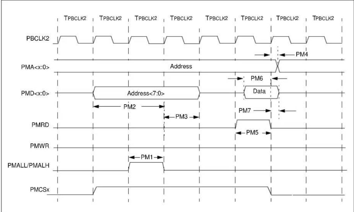
text_image
TPBCLK2 TPBCLK2 TPBCLK2 TPBCLK2 TPBCLK2 TPBCLK2 TPBCLK2 TPBCLK2 TPBCLK2 TPBCLK2 TPBCLK2 TPBCLK2 PBATABLE 37-42: PARALLEL MASTER PORT READ TIMING REQUIREMENTS
| AC CHARACTERISTICS | Standard Operating Conditions: 2.3V to 3.6V(unless otherwise stated)Operating temperature -40°C ≤ T A ≤ +85°C for Industrial | ||||||
| Param.No. | Symbol | Characteristics (1) | Min. Typ. Max. Units Conditions | ||||
| PM1 T | LAT | PMALL/PMALH Pulse Width — 1 | T | PBCLK2 | — — | — | |
| PM2 T | ADSU | Address Out Valid to PMALL/PMALH Invalid (address setup time) | — 2 T | PBCLK2 | — — | — | |
| PM3 T | ADHOLD | PMALL/PMALH Invalid to Address Out Invalid (address hold time) | — 1 T | PBCLK2 | — — | — | |
| PM4 T | AHOLD | PMRD Inactive to Address Out Invalid(address hold time) | 5 | — | — | ns | — |
| PM5 T | RD | PMRD Pulse Width | — 1 T | PBCLK2 | — — | — | |
| PM6 T | DSU | PMRD or PMENB Active to Data In Valid (data setup time) | 15 | — | — | ns | — |
| PM7 T | DHOLD | PMRD or PMENB Inactive to Data In Invalid (data hold time) | 5 | — | — | ns | — |
Note 1: These parameters are characterized, but not tested in manufacturing.
FIGURE 37-23: PARALLEL MASTER PORT WRITE TIMING DIAGRAM

text_image
TPBCLK2 TPBCLK2 TPBCLK2 TPBCLK2 TPBCLK2 TPBCLK2 TPBCLK2 TPBCLK2 TPBCLK2 PBCLK2 PMATABLE 37-43: PARALLEL MASTER PORT WRITE TIMING REQUIREMENTS
| AC CHARACTERISTICS | Standard Operating Conditions: 2.3V to 3.6V(unless otherwise stated)Operating temperature -40°C ≤ T A ≤ +85°C for Industrial | ||||||
| Param.No. | Symbol | Characteristics (1) | Min. | Typ. | Max. | Units | Conditions |
| PM11 T | WR | PMWR Pulse Width — 1 T | PBCLK2 | — — | — | ||
| PM12 | TDVSU | Data Out Valid before PMWR or PMENB goes Inactive (data setup time) | — 2 T | PBCLK2 | — — | — | |
| PM13 | TDVHOLD | PMWR or PMEMB Invalid to Data Out Invalid (data hold time) | — 1 T | PBCLK2 | — — | — | |
Note 1: These parameters are characterized, but not tested in manufacturing.
TABLE 37-44: USB OTG ELECTRICAL SPECIFICATIONS
| AC CHARACTERISTICS | Standard Operating Conditions: 2.3V to 3.6V (unless otherwise stated)Operating temperature -40°C ≤ T A ≤ +85°C for Industrial | ||||||
| Param.No. | Symbol | Characteristics (1) | Min. | Typ. | Max. | Units | Conditions |
| USB313 | V USB3V3 | USB Voltage 3.0 — 3.6 V Voltage on V | USB3V3must be in this range for proper USB operation | ||||
| Low-Speed and Full-Speed Modes | |||||||
| USB315 | V ILUSB | Input Low Voltage for USB Buffer | — | — | 0.8 | V | — |
| USB316 | V IHUSB | Input High Voltage for USB Buffer | 2.0 | — | — | V | — |
| USB318 | V DIFS | Differential Input Sensitivity | 0.2 | — | — | V | The difference between D+ and D- must exceed this value while VCM is met |
| USB319 | VCM Differential Common Mode Range 0.8 — 2.5 V | — | |||||
| USB321 | V OL | Voltage Output Low | 0.0 | — | 0.3 | V | 1.425 kΩ load connected to VUSB3V3 |
| USB322 | V OH | Voltage Output High | 2.8 | — | 3.6 | V | 14.25 kΩ load connected to ground |
| Hi-Speed Mode | |||||||
| USB323 | V HSDI | Differential input signal level | 150 | — | — | mV | — |
| USB324 | V HSSQ | SQ detection threshold | 100 | — | 150 | mV | — |
| USB325 | V HSCM | Common mode voltage range | -50 | — | 500 | mV | — |
| USB326 | V HSOH | Data signaling high | 360 | — | 440 | mV | — |
| USB327 | V HSOL | Data signaling low | -10 | — | 10 | mV | — |
| USB328 | V CHIRPJ | Chirp J level | 700 | — | 1100 | mV | — |
| USB329 | V CHIRPK | Chirp K level | -900 | — | -500 | mV | — |
| USB330 | Z HSDRV | Driver output resistance | — | 45 | — | Ω | — |
Note 1: These parameters are characterized, but not tested in manufacturing.
TABLE 37-45: ETHERNET MODULE SPECIFICATIONS
| AC CHARACTERISTICS | Standard Operating Conditions: 2.3V to 3.6V(unless otherwise stated)Operating temperature -40°C ≤ T A≤+85°C for Industrial | |||||
| Param.No. | Characteristic | Min. | Typ. | Max. | Units | Conditions |
| MIIM Timing Requirements | ||||||
| ET1 | MDC Duty Cycle | 40 | — | 60 | % | — |
| ET2 | MDC Period | 400 | — | — | ns | — |
| ET3 | MDIO Output Setup and Hold | 10 | — | 10 | ns | See Figure 37-24 |
| ET4 | MDIO Input Setup and Hold | 0 | — | 300 | ns | See Figure 37-25 |
| MII Timing Requirements | ||||||
| ET5 | TX Clock Frequency | — | 25 | — | MHz | — |
| ET6 | TX Clock Duty Cycle | 35 | — | 65 | % | — |
| ET7 | ETXDx, ETEN, ETXERR Output Delay | 0 | — | 25 | ns | See Figure 37-26 |
| ET8 | RX Clock Frequency | — | 25 | — | MHz | — |
| ET9 | RX Clock Duty Cycle | 35 | — | 65 | % | — |
| ET10 | ERXDx, ERXDV, ERXERR Setup and Hold | 10 | — | 30 | ns | See Figure 37-27 |
| RMII Timing Requirements | ||||||
| ET11 | Reference Clock Frequency | — | 50 | — | MHz | — |
| ET12 | Reference Clock Duty Cycle | 35 | — | 65 | % | — |
| ET13 | ETXDx, ETEN, Setup and Hold | 2 | — | 16 | ns | — |
| ET14 | ERXDx, ERXDV, ERXERR Setup and Hold | 2 | — | 16 | ns | — |
FIGURE 37-24: MDIO SOURCED BY THE PIC32 DEVICE

text_image
MDC VIHMIN VILMAX MDIO VIHMIN VILMAX (Setup) ET3 → ← ET3 (Hold)FIGURE 37-25: MDIO SOURCED BY THE PHY

text_image
MDC VIHMIN VILMAX MDIO VIHMIN VILMAX ET4FIGURE 37-26: TRANSMIT SIGNAL TIMING RELATIONSHIPS AT THE MII

text_image
TX Clock VIHMIN VILMAX ETXD<3:0>, ETEN, ETXERR VIHMIN VILMAX ET7FIGURE 37-27: RECEIVE SIGNAL TIMING RELATIONSHIPS AT THE MII
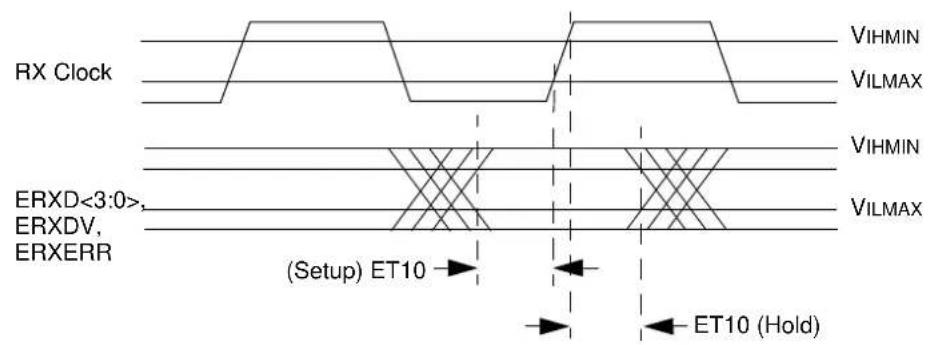
text_image
RX Clock VIHMIN VILMAX VIHMIN ERXD<3:0>, ERXDV, ERXERR (VSetup) ET10 ET10 (Hold)FIGURE 37-28: EBI PAGE READ TIMING
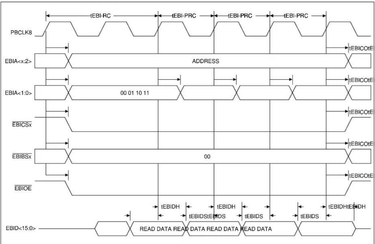
flowchart
graph TD
    A["PBCLK8"] --> B["tEBI-RC"]
    B --> C["tEBI-PRC"]
    C --> D["tEBI-PRC"]
    D --> E["tEBI-PRC"]
    F["EBIA<x:2>"] --> G["ADDRESS"]
    G --> H["tEBICOtE"]
    I["EBIA<1:0>"] --> J["00 01 10 11"]
    J --> K["tEBICOtE"]
    L["EBICSx"] --> M["00"]
    M --> N["tEBICOtE"]
    O["EBIBSx"] --> P["00"]
    P --> Q["tEBICOtE"]
    R["EBIOE"] --> S["READ DATA READ DATA READ DATA READ DATA"]
    S --> T["tEBIDHtEBIDH"]
    U["EBID<15:0>"] --> V["READ DATA READ DATA READ DATA READ DATA"]
    V --> W["tEBIDHtEBIDH"]
    X["Time Label"] --> Y["Time Label"]
    Z["Time Label"] --> AA["Time Label"]
FIGURE 37-29: EBI WRITE TIMING
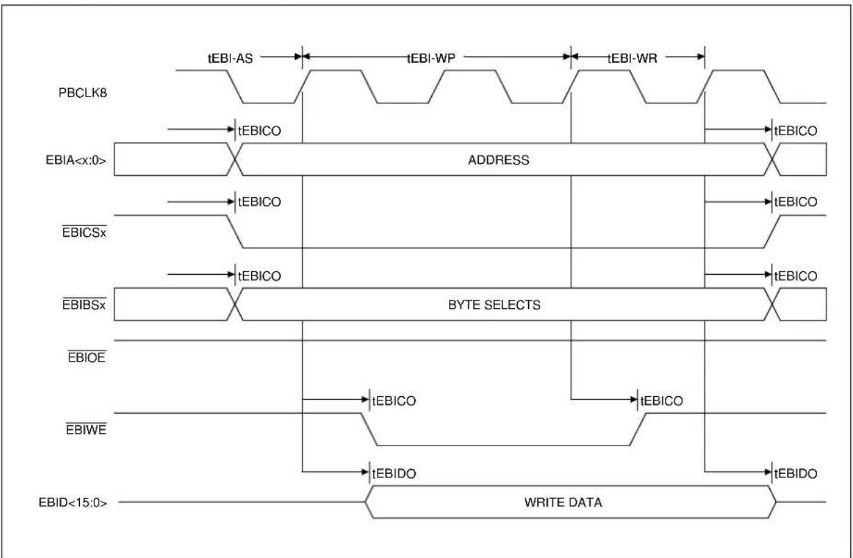
flowchart
graph TD
    A["PBCLK8"] --> B["tEBI-AS"]
    B --> C["tEBI-WP"]
    C --> D["tEBI-WR"]
    D --> E["tEBICO"]
    F["EBIA<x:0>"] --> G["ADDRESS"]
    H["EBICSx"] --> I["tEBICO"]
    J["EBIBSx"] --> K["tEBICO"]
    L["EBIOE"] --> M["tEBICO"]
    N["EBIWE"] --> O["tEBIDO"]
    P["EBID<15:0>"] --> Q["WRITE DATA"]
TABLE 37-46: EBI TIMING REQUIREMENTS
| AC CHARACTERISTICS | Standard Operating Conditions: 2.3V to 3.6V(unless otherwise stated)Operating temperature -40°C ≤ T A ≤ +85°C for Industrial | ||||||
| Param.No. | Symbol | Characteristic | Min. | Typ. | Max. | Units | Conditions |
| EB10 T | EBICLK | Internal EBI Clock Period(PBCLK8) | 10 — | — | ns — | ||
| EB11 | TEBIRC | EBI Read Cycle Time(TRC<5:0>) | 20 — | — | ns — | ||
| EB12 T | EBIPRC | EBI Page Read Cycle Time(TPRC<3:0>) | 20 — | — | ns — | ||
| EB13 T | EBIAS | EBI Write Address Setup (TAS<1:0>) | 10 | — | — | ns | — |
| EB14 T | EBIWP | EBI Write Pulse Width(TWP<5:0>) | 10 — | — | ns — | ||
| EB15 T | EBIWR | EBI Write Recovery Time(TWR<1:0>) | 10 — | — | ns — | ||
| EB16 T | EBICO | EBI Output Control Signal Delay | — | — | 5 | ns | See Note 1 |
| EB17 T | EBIDO | EBI Output Data Signal Delay | — | — | 5 | ns | See Note 1 |
| EB18 T | EBIDS | EBI Input Data Setup | 5 | — | — | ns | See Note 1 |
| EB19 T | EBIDH | EBI Input Data Hold | 3 | — | — | ns | See Note 1, 2 |
Note 1: Maximum pin capacitance = 10 pF.
2: Hold time from EBI Address change is 0 ns.
TABLE 37-47: EBI THROUGHPUT REQUIREMENTS
| AC CHARACTERISTICS | Standard Operating Conditions: 2.3V to 3.6V(unless otherwise stated)Operating temperature -40°C ≤ TA ≤ +85°C for Industrial | |||||
| Param.No. | Characteristic | Min. | Typ. | Max. | Units | Conditions |
| EB20 | Asynchronous SRAM Read | — | 100 | — | Mbps | — |
| EB21 | Asynchronous SRAM Write | — | 533 | — | Mbps | — |
Note 1: Maximum pin capacitance = 10 pF.
2: Hold time from EBI Address change is 0 ns.
FIGURE 37-30: EJTAG TIMING CHARACTERISTICS
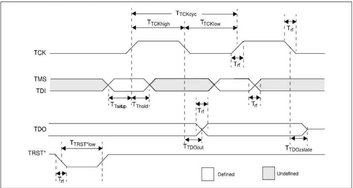
text_image
TCK TMS TDI TDO TRST* TTRST*low TTRSThigh TTRKcyc TTRKlow Trf Trf Trf Trf Trf Trf Trf TDOzstate Defined Undefined DefinedTABLE 37-48: EJTAG TIMING REQUIREMENTS
| AC CHARACTERISTICS | Standard Operating Conditions: 2.3V to 3.6V(unless otherwise stated)Operating temperature -40°C ≤ T A ≤ +85°C for Industrial | |||||
| Param.No. | Symbol Description (1) | Min. Max. Units Conditions | ||||
| EJ1 T | TCKCYC | TCK Cycle Time | 25 | — | ns | — |
| EJ2 T | TCKHIGH | TCK High Time | 10 | — | ns | — |
| EJ3 T | TCKLOW | TCK Low Time | 10 | — | ns | — |
| EJ4 T | TSETUP | TAP Signals Setup Time Before Rising TCK | 5 | — | ns | — |
| EJ5 T | THOLD | TAP Signals Hold Time After Rising TCK | 3 | — | ns | — |
| EJ6 T | TDOOUT | TDO Output Delay Time from Falling TCK | — | 5 | ns | — |
| EJ7 T | TDOZSTATE | TDO 3-State Delay Time from Falling TCK | — | 5 | ns | — |
| EJ8 T | TRSTLOW | TRST Low Time | 25 | — | ns | — |
| EJ9 T | RF | TAP Signals Rise/Fall Time, All Input and Output | — | — | ns | — |
Note 1: These parameters are characterized, but not tested in manufacturing.
38.0 AC AND DC CHARACTERISTICS GRAPHS
Note: The graphs provided are a statistical summary based on a limited number of samples and are provided for design guidance purposes only. The performance characteristics listed herein are not tested or guaranteed. In some graphs, the data presented may be outside the specified operating range (e.g., outside specified power supply range) and therefore, outside the warranted range.
FIGURE 38-1: V OH - 4x DRIVER PINS

line
| x_value | y_value | | ------- | ------- | | 0.000 | -0.045 | | 0.01 | -0.046 | | 0.02 | -0.047 | | 0.03 | -0.048 | | 0.04 | -0.049 | | 0.05 | -0.050 | | 0.06 | -0.051 | | 0.07 | -0.052 | | 0.08 | -0.053 | | 0.09 | -0.054 | | 0.1 | -0.055 | | 0.11 | -0.056 | | 0.12 | -0.057 | | 0.13 | -0.058 | | 0.14 | -0.059 | | 0.15 | -0.060 | | 0.16 | -0.061 | | 0.17 | -0.062 | | 0.18 | -0.063 | | 0.19 | -0.064 | | 0.2 | -0.065 | | 0.21 | -0.066 | | 0.22 | -0.067 | | 0.23 | -0.068 | | 0.24 | -0.069 | | 0.25 | -0.070 | | 0.26 | -0.071 | | 0.27 | -0.072 | | 0.28 | -0.073 | | 0.29 | -0.074 | | 0.3 | -0.075 | | 0.31 | -0.076 | | 0.32 | -0.077 | | 0.33 | -0.078 | | 0.34 | -0.079 | | 0.35 | -0.080 | | 0.36 | -0.081 | | 0.37 | -0.082 | | 0.38 | -0.083 | | 0.39 | -0.084 | | 0.4 | -0.085 | | 0.41 | -0.086 | | 0.42 | -0.087 | | 0.43 | -0.088 | | 0.44 | -0.089 | | 0.45 | -0.090 | | 0.46 | -0.091 | | 0.47 | -0.092 | | 0.48 | -0.093 | | 0.49 | -0.094 | | 0.5 | -0.095 | | 0.51 | -0.096 | | 0.52 | -0.097 | | 0.53 | -0.098 | | 0.54 | -0.099 | | 0.55 | -0.1 | | 0.56 | - | | 1 | - | | 2 | - | | 3 | - | | 4 | - | | 5 | - | | 6 | - | | 7 | - | | 8 | - | | 9 | - | | 1 | - | | 2 | - | | 3 | - | | 4 | - | | 5 | - | | 6 | - | | 7 | - | | 8 | - | | 9 | - | | 1 | - | | 2 | - | | 3 | - |FIGURE 38-3: V OH - 8x DRIVER PINS

line
| x | y | | ---- | ------- | | 0.00 | -0.085 | | 0.50 | -0.087 | | 1.00 | -0.089 | | 1.50 | -0.072 | | 2.00 | -0.060 | | 2.50 | -0.045 | | 3.00 | -0.025 | | 3.50 | -0.010 |FIGURE 38-2: V OL - 4x DRIVER PINS

line
| VOLT (V) | IOL (A) | | -------- | ------- | | 0.000 | 0.000 | | 0.01 | 0.015 | | 0.02 | 0.025 | | 0.03 | 0.035 | | 0.035 | 0.045 |FIGURE 38-4: V OL - 8x DRIVER PINS
line
| VOL (V) | IOL (A) | | ------- | ------- | | 0.00 | 0.000 | | 0.50 | 0.030 | | 1.00 | 0.060 | | 1.50 | 0.070 | | 2.00 | 0.075 | | 2.50 | 0.078 | | 3.00 | 0.079 | | 3.50 | 0.080 |FIGURE 38-5: V OH - 12x DRIVER PINS

line
| x_value | y_value | | ------- | ------- | | 0.000 | -0.120 | | 0.01 | -0.125 | | 0.02 | -0.130 | | 0.03 | -0.135 | | 0.04 | -0.140 | | 0.05 | -0.145 | | 0.06 | -0.150 | | 0.07 | -0.155 | | 0.08 | -0.160 | | 0.09 | -0.165 | | 0.1 | -0.170 | | 0.11 | -0.175 | | 0.12 | -0.180 | | 0.13 | -0.185 | | 0.14 | -0.190 | | 0.15 | -0.195 | | 0.16 | -0.200 | | 0.17 | -0.205 | | 0.18 | -0.210 | | 0.19 | -0.215 | | 0.2 | -0.220 | | 0.21 | -0.225 | | 0.22 | -0.230 | | 0.23 | -0.235 | | 0.24 | -0.240 | | 0.25 | -0.245 | | 0.26 | -0.250 | | 0.27 | -0.255 | | 0.28 | -0.260 | | 0.29 | -0.265 | | 0.3 | -0.270 | | 0.31 | -0.275 | | 0.32 | -0.280 | | 0.33 | -0.285 | | 0.34 | -0.290 | | 0.35 | -0.295 | | 0.36 | -0.300 | | 0.37 | -0.305 | | 0.38 | -0.310 | | 0.39 | -0.315 | | 0.4 | -0.320 | | 0.41 | -0.325 | | 0.42 | -0.330 | | 0.43 | -0.335 | | 0.44 | -0.340 | | 0.45 | -0.345 | | 0.46 | -0.350 | | 0.47 | -0.355 | | 0.48 | -0.360 | | 0.49 | -0.365 | | 0.5 | -0.370 | | 0.51 | -0.375 | | 0.52 | -0.380 | | 0.53 | -0.385 | | 0.54 | -0.390 | | 0.55 | -0.395 | | 0.56 | -0.400 | | 0.57 | -0.405 | | 0.58 | -0.410 | | 0.59 | -0.415 | | 0.6 | -0.420 | | 0.61 | -0.425 | | 0.62 | -0.430 | | 0.63 | -0.435 | | 0.64 | -0.440 | | 0.65 | -0.445 | | 0.66 | -0.450 | | 0.67 | -0.455 | | 0.68 | -0.460 | | 0.69 | -0.465 | | 0.7 | -0.470 | | 0.71 | -0.475 | | 0.72 | -0.480 | | 0.73 | -0.485 | | 0.74 | -0.490 | | 0.75 | -0.495 | | 0.76 | -0.5 | | 0.77 | -0.5 | | 0.78 | -0.5 | | 0.79 | -0.5 | | 0.8 | -0.5 | | 0.81 | -0.5 | | 0.82 | -0.5 | | 0.83 | -0.5 | | 0.84 | -0.5 | | 0.85 | -0.5 | | 0.86 | -0.5 | | 0.87 | -0.5 | | 0.88 | -0.5 | | 0.89 | -0.5 | | 0.9 | -0.5 | | 1 | - |FIGURE 38-6: V OL - 12x DRIVER PINS
line
| VOL (V) | IOL (A) | | ------- | ------- | | 0.000 | 0.000 | | 0.501 | 0.040 | | 1.001 | 0.060 | | 1.502 | 0.080 | | 2.002 | 0.090 | | 2.503 | 0.100 | | 3.003 | 0.100 | | 3.503 | 0.100 |FIGURE 38-7: TYPICAL TEMPERATURE SENSOR VOLTAGE
line
| Temperature (Celsius) | Voltage (V) | | --------------------- | ----------- | | -4 | 1.250 | | 3 | 1.150 | | 0 | 1.050 | | -2 | 0.950 | | 0 | 0.850 | | 2 | 0.750 | | 3 | 0.550 |39.0 PACKAGING INFORMATION
39.1 Package Marking Information
64-Lead QFN (9x9x0.9 mm)

text_image
PIC32 XXXXXXXXXX XXXXXXXXXX XXXXXXXXXX YYWWNNNExample
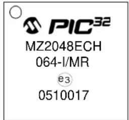
text_image
PIC32 MZ2048ECH 064-I/MR e3 051001764-Lead TQFP (10x10x1 mm)
text_image
PIC32 XXXXXXXXXX XXXXXXXXXX XXXXXXXXXX YYWWNNNExample
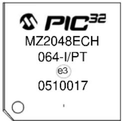
text_image
PIC32 MZ2048ECH 064-I/PT e3 0510017100-Lead TQFP (14x14x1 mm)
text_image
PIC32 XXXXXXXXXXXX XXXXXXXXXXXX XXXXXXXXXXXX YYWWNNNExample

text_image
PIC32 MZ2048ECH 100-I/PF e3 0510017Legend: XX...X Customer-specific information Y Year code (last digit of calendar year) YY Year code (last 2 digits of calendar year) WW Week code (week of January 1 is week '01') NNN Alphanumeric traceability code Pb-free JEDEC designator for Matte Tin (Sn) * This package is Pb-free. The Pb-free JEDEC designator (e3) can be found on the outer packaging for this package.
Note: In the event the full Microchip part number cannot be marked on one line, it will be carried over to the next line, thus limiting the number of available characters for customer-specific information.
39.1 Package Marking Information (Continued)
100-Lead TQFP (12x12x1 mm)

PIC32
XXXXXXXXXXXXXX
XXXXXXXXXXXXXX
XXXXXXXXXXXXXX
YYWWNNN
124-Lead VTLA (9x9x0.9 mm)

PIC32
XXXXXXXXXXXX
XXXXXXXXXX
XXXXXXXXXXXX
YYWWNNN
144-Lead TQFP (16x16x1 mm)

PIC32
XXXXXXXXXXXXXX
XXXXXXXXXXXXXX
XXXXXXXXXXXXXX
YYWWNNN
144-Lead LQFP (20x20x1.40 mm)

PIC32
XXXXXXXXXXXXXX
XXXXXXXXXXXXXX
XXXXXXXXXXXXXX
YYWWNNN
| Legend: | XX...X Customer-specific informationY Year code (last digit of calendar year)YY Year code (last 2 digits of calendar year)WW Week code (week of January 1 is week '01')NNN Alphanumeric traceability codePb-free JEDEC designator for Matte Tin (Sn)* This package is Pb-free. The Pb-free JEDEC designator (e3 can be found on the outer packaging for this package. |
| Note: | In the event the full Microchip part number cannot be marked on one line, it will be carried over to the next line, thus limiting the number of available characters for customer-specific information. |
Example

PIC32
MZ2048ECH
100-I/PT
e3
0510017
Example

PIC32
MZ2048ECH
124-I/TL
e3
0510017
Example

PIC32
MZ2048ECH
144-I/PH
e3
0510017
Example

PIC32
MZ2048ECH
144-I/PL
e3
0510017
39.2 Package Details
64-Lead Plastic Quad Flat, No Lead Package (MR) - 9x9x0.9 mm Body [QFN] With 7.70 x 7.70 Exposed Pad [QFN]
Note: For the most current package drawings, please see the Microchip Packaging Specification located at http://www.microchip.com/packaging

Microchip Technology Drawing C04-213B Sheet 1 of 2
64-Lead Plastic Quad Flat, No Lead Package (MR) - 9x9x0.9 mm Body [QFN] With 7.70 x 7.70 Exposed Pad [QFN]
Note: For the most current package drawings, please see the Microchip Packaging Specification located at http://www.microchip.com/packaging
![Microchip PIC32MZ1024ECM124 - 64-Lead Plastic Quad Flat, No Lead Package (MR) - 9x9x0.9 mm Body [QFN] With 7.70 x 7.70 Exposed Pad [QFN] - 1](/content/2026/06/1217674/images/13c382834d226cdd4063dbc733326cc8b5045903fd17bb4b747d504a3d8ace69.jpg)
natural_image
Two isometric diagrams of rectangular electronic components with square bases and circular side elements, no text or symbols present.| Units | MILLIMETERS | |||
| Dimension Limits | MIN NO | M | MAX | |
| Number of Pins | N | 64 | ||
| Pitch | e | 0.50 BSC | ||
| Overall Height | A | 0.80 0.90 | 0.85 | |
| Standoff | A1 | 0.00 0.05 | 0.02 | |
| Contact Thickness | A3 | 0.20 REF | ||
| Overall Width | E | 9.00 BSC | ||
| Exposed Pad Width | E2 | 7.807.60 | ||
| Overall Length | D | 9.00 BSC | ||
| Exposed Pad Length | D2 | 7.707.60 | 7.80 | |
| Contact Width | b | 0.20 | 0.25 | 0.30 |
| 0.500.30 | ||||
| Contact-to-Exposed Pad | K | - | ||
7.70
0.40Contact Length L 0.20 -
Notes:
- Pin 1 visual index feature may vary, but must be located within the hatched area.
- Package is saw singulated.
- Dimensioning and tolerancing per ASME Y14.5M.
BSC: Basic Dimension. Theoretically exact value shown without tolerances.
REF: Reference Dimension, usually without tolerance, for information purposes only.
Microchip Technology Drawing C04-213B Sheet 2 of 2
64-Lead Plastic Quad Flat, No Lead Package (MR) - 9x9x0.9 mm Body [QFN] With 0.40 mm Contact Length and 7.70x7.70mm Exposed Pad
Note: For the most current package drawings, please see the Microchip Packaging Specification located at http://www.microchip.com/packaging

text_image
C1 W2 EV 64 2 C2 T2 ØV EV G Y1 X1 E SILK SCREENRECOMMENDED LAND PATTERN
| Units | MILLIMETERS | |||
| Dimension Limits | MIN | NOM | MAX | |
| Contact Pitch | E | 0.50 BSC | ||
| Optional Center Pad Width | W2 | 7.50 | ||
| Optional Center Pad Length | T2 | 7.50 | ||
| C1Contact Pad Spacing 8.90 | ||||
| Contact Pad Spacing | C2 | 8.90 | ||
| Contact Pad Width (X20) | X1 | 0.30 | ||
| Contact Pad Length (X20) | Y1 | 0.90 | ||
| Contact Pad to Center Pad (X20) G | 0.20 | |||
| Thermal Via Diameter V | 0.30 | |||
| Thermal Via Pitch EV | 1.00 | |||
Notes:
- Dimensioning and tolerancing per ASME Y14.5M
BSC: Basic Dimension. Theoretically exact value shown without tolerances.
- For best soldering results, thermal vias, if used, should be filled or tented to avoid solder loss during reflow process
Microchip Technology Drawing No. C04-2213B
64-Lead Plastic Thin Quad Flatpack (PT)-10x10x1 mm Body, 2.00 mm Footprint [TQFP]
Note: For the most current package drawings, please see the Microchip Packaging Specification located at http://www.microchip.com/packaging
![Microchip PIC32MZ1024ECM124 - 64-Lead Plastic Thin Quad Flatpack (PT)-10x10x1 mm Body, 2.00 mm Footprint [TQFP] - 1](/content/2026/06/1217674/images/606cf3fff5b3734a178600ac65d95cb435ab092a0946d5b5eb5b2692cbb17781.jpg)
text_image
NOTE 2 A N SEE DETAIL 1 4X N/4 TIPS 0.20 C A-B D NOTE 1 D1 D1/2 D A B E1/2 A A E1 4X 0.20 H A-B DTOP VIEW
![Microchip PIC32MZ1024ECM124 - 64-Lead Plastic Thin Quad Flatpack (PT)-10x10x1 mm Body, 2.00 mm Footprint [TQFP] - 2](/content/2026/06/1217674/images/de34c1f579800e31d2efd4406cbe241944c39e401f9e46f1ffc231d1b4a7e951.jpg)
text_image
SEATING PLANE A C A2 0.05 0.08 C 64 X b A1 e ⊕ 0.08® A-B DSIDE VIEW
Microchip Technology Drawing C04-085C Sheet 1 of 2
64-Lead Plastic Thin Quad Flatpack (PT)-10x10x1 mm Body, 2.00 mm Footprint [TQFP]
Note: For the most current package drawings, please see the Microchip Packaging Specification located at http://www.microchip.com/packaging
![Microchip PIC32MZ1024ECM124 - 64-Lead Plastic Thin Quad Flatpack (PT)-10x10x1 mm Body, 2.00 mm Footprint [TQFP] - 1](/content/2026/06/1217674/images/f35b2a171b5f787a94bee6c1fa6375caa99dc2b06148906880a6da36370c298c.jpg)
text_image
α H β L (L1) C θ SECTION A-A X=A-B OR D e/2 XDETAIL 1
| Units | MILLIMETERS | |||
| Dimension Limits | MIN | NOM | MAX | |
| NNumber of Leads 64 | ||||
| Lead Pitch | e | 0.50 BSC | ||
| A | Over 20 Height | |||
| 1.051.000.95A2Molded Package | ||||
| 0.15-0.05A1Standoff | ||||
| 0.750.600.45LFoot Length | ||||
| Footprint | L1 | 1.00 REF | ||
| Foot Angle | 7°3.5°0° | |||
| 12.00 BSCEOverall Width | ||||
| 12.00 BSCDOverall Length | ||||
| 10.00 BSCE1Molded Package Width | ||||
| Molded Package Length | D1 | 10.00 BSC | ||
| Lead Thickness | c | 0.20-0.09 | ||
| Lead Width | b | 0.270.220.17 | ||
| Mold Draft Angle Top | 13°12°11° | |||
| Mold Draft Angle Bottom | 13°12°11° | |||
Notes:
- Pin 1 visual index feature may vary, but must be located within the hatched area.
- Chamfers at corners are optional; size may vary.
- Dimensions D1 and E1 do not include mold flash or protrusions. Mold flash or protrusions shall not exceed 0.25mm per side.
- Dimensioning and tolerancing per ASME Y14.5M
BSC: Basic Dimension. Theoretically exact value shown without tolerances.
REF: Reference Dimension, usually without tolerance, for information purposes only.
Microchip Technology Drawing C04-085C Sheet 2 of 2
64-Lead Plastic Thin Quad Flatpack (PT)-10x10x1 mm Body, 2.00 mm Footprint [TQFP]
Note: For the most current package drawings, please see the Microchip Packaging Specification located at http://www.microchip.com/packaging
![Microchip PIC32MZ1024ECM124 - 64-Lead Plastic Thin Quad Flatpack (PT)-10x10x1 mm Body, 2.00 mm Footprint [TQFP] - 1](/content/2026/06/1217674/images/2dfb98b579b91cf46237499dbbf3c63b007fe85657fd9989c2cece471ec989df.jpg)
text_image
C1 C2 E G Y1 X1RECOMMENDED LAND PATTERN
| Units | MILLIMETERS | |||
| Dimension Limits | MIN | NOM | MAX | |
| Contact Pitch | E | 0.50 BSC | ||
| C1Contact Pad Spacing40 | ||||
| Contact Pad Spacing | C2 | 11.40 | ||
| Contact Pad Width (X28) | X1 | 0.30 | ||
| Contact Pad Length (X28) | Y1 | 1.50 | ||
| GDistance Between Pads 0.20 | ||||
Notes:
1. Dimensioning and tolerancing per ASME Y14.5M
BSC: Basic Dimension. Theoretically exact value shown without tolerances.
Microchip Technology Drawing C04-2085B Sheet 1 of 1
100-Lead Plastic Thin Quad Flatpack (PF) - 14x14x1 mm Body, 2.00 mm [TQFP]
Note: For the most current package drawings, please see the Microchip Packaging Specification located at http://www.microchip.com/packaging
![Microchip PIC32MZ1024ECM124 - 100-Lead Plastic Thin Quad Flatpack (PF) - 14x14x1 mm Body, 2.00 mm [TQFP] - 1](/content/2026/06/1217674/images/c28897a43dbf886059fdcfd9453199ea2c826f31fb525443a8af1e1d235b883c.jpg)
text_image
D D1 E1 E e b N NOTE 1 1 23 NOTE 2 c β φ L![Microchip PIC32MZ1024ECM124 - 100-Lead Plastic Thin Quad Flatpack (PF) - 14x14x1 mm Body, 2.00 mm [TQFP] - 2](/content/2026/06/1217674/images/4727d5473188f3e57b5ce2b66d1d055085029095328da8aa26eb301d583f9753.jpg)
text_image
A A1 L1 α A2| Units | MILLIMETERS | |||
| Dimension Limits | MINsNOMsMAX | |||
| Number of Leads | Ns | 100 | ||
| Lead Pitchses0.50 BSC | ||||
| Overall HeightsAs- - | 1.20 | |||
| Molded Package Thickness | A2 | 0.95 | 1.00 | 1.05 |
| Standoff | A1 | 0.05 | - | 0.15 |
| Foot Length | L | 0.45 | 0.60 | 0.75 |
| Footprint | L1 | 1.00 REF | ||
| Foot Angle | 0^ | 3.5^ | 7^ | |
| Overall Width | E | 16.00 BSC | ||
| Overall Length | D | 16.00 BSC | ||
| Molded Package Width | E1 | 14.00 BSC | ||
| Molded Package Length | D1 | 14.00 BSC | ||
| Lead Thickness | c | 0.09 | - | 0.20 |
| Lead Width | b | 0.17 | 0.22 | 0.27 |
| Mold Draft Angle Top | 11^ | 12^ | 13^ | |
| Mold Draft Angle Bottom | 11^ | 12^ | 13^ | |
Notes:
1.sPin 1 visual index feature may vary, but must be located within the hatched area.
2.sChamfers at corners are optional; size may vary.
3. Dimensions D1 and E1 do not include mold flash or protrusions. Mold flash or protrusions shall not exceed 0.25 mm per side.
4.sDimensioning and tolerancing per ASME Y14.5M.
BSC:sBasic Dimension. Theoretically exact value shown without tolerances.
REF:sReference Dimension, usually without tolerance, for information purposes only.
Microchip Technology Drawing C04-110B
100-Lead Plastic Thin Quad Flatpack (PF) - 14x14x1 mm Body 2.00 mm Footprint [TQFP]
Note: For the most current package drawings, please see the Microchip Packaging Specification located at http://www.microchip.com/packaging
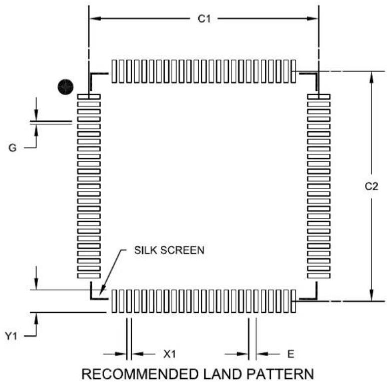
text_image
C1 G SILK SCREEN Y1 X1 E C2 RECOMMENDED LAND PATTERN| Units | MILLIMETERS | |||
| Dimension Limits | MIN | NOM | MAX | |
| Contact Pitch | E | 0.50 BSC | ||
| Contact Pad Spacing | C1 | 15.40 | ||
| Contact Pad Spacing | C2 | 15.40 | ||
| Contact Pad Width (X100) | X1 | 0.30 | ||
| Contact Pad Length (X100) | Y1 | 1.50 | ||
| Distance Between Pads | G | 0.20 | ||
Notes:
1. Dimensioning and tolerancing per ASME Y14.5M
BSC: Basic Dimension. Theoretically exact value shown without tolerances.
Microchip Technology Drawing No. C04-2110B
100-Lead Plastic Thin Quad Flatpack (PT) - 12x12x1 mm Body, 2.00 mm [TQFP]
Note: For the most current package drawings, please see the Microchip Packaging Specification located at http://www.microchip.com/packaging
![Microchip PIC32MZ1024ECM124 - 100-Lead Plastic Thin Quad Flatpack (PT) - 12x12x1 mm Body, 2.00 mm [TQFP] - 1](/content/2026/06/1217674/images/a31ea42a6bb02eee90a741257550577860ec6a0ffe27f0a0840cab8fbb10aaa8.jpg)
text_image
D D1 E1 E e b N NOTE 1 123 NOTE 2 c β φ L A A1 L1 A2 α| Units | MILLIMETERS | |||
| Dimension Limitss | MINsNOMsMAX | |||
| Number of Leads | Ns | 100 | ||
| Lead Pitchses0.40 BSC | ||||
| Overall HeightsAs- - | 1.20 | |||
| Molded Package Thickness | A2 | 0.95 | 1.00 | 1.05 |
| Standoff | A1 | 0.05 | - | 0.15 |
| Foot Length | L | 0.45 | 0.60 | 0.75 |
| Footprint | L1 | 1.00 REF | ||
| Foot Angle | 0° | 3.5° | 7° | |
| Overall Width | E | 14.00 BSC | ||
| Overall Length | D | 14.00 BSC | ||
| Molded Package Width | E1 | 12.00 BSC | ||
| Molded Package Length | D1 | 12.00 BSC | ||
| Lead Thickness | c | 0.09 | - | 0.20 |
| Lead Width | b | 0.13 | 0.18 | 0.23 |
| Mold Draft Angle Top | 11° | 12° | 13° | |
| Mold Draft Angle Bottom | 11° | 12° | 13° | |
Notes:
1.sPin 1 visual index feature may vary, but must be located within the hatched area.
2.sChamfers at corners are optional; size may vary.
- Dimensions D1 and E1 do not include mold flash or protrusions. Mold flash or protrusions shall not exceed 0.25 mm per side.
4.sDimensioning and tolerancing per ASME Y14.5M.
BSC:sBasic Dimension. Theoretically exact value shown without tolerances.
REF:sReference Dimension, usually without tolerance, for information purposes only.
Microchip Technology Drawing C04-100B
100-Lead Plastic Thin Quad Flatpack (PT)-12x12x1mm Body, 2.00 mm Footprint [TQFP]
Note: For the most current package drawings, please see the Microchip Packaging Specification located at http://www.microchip.com/packaging
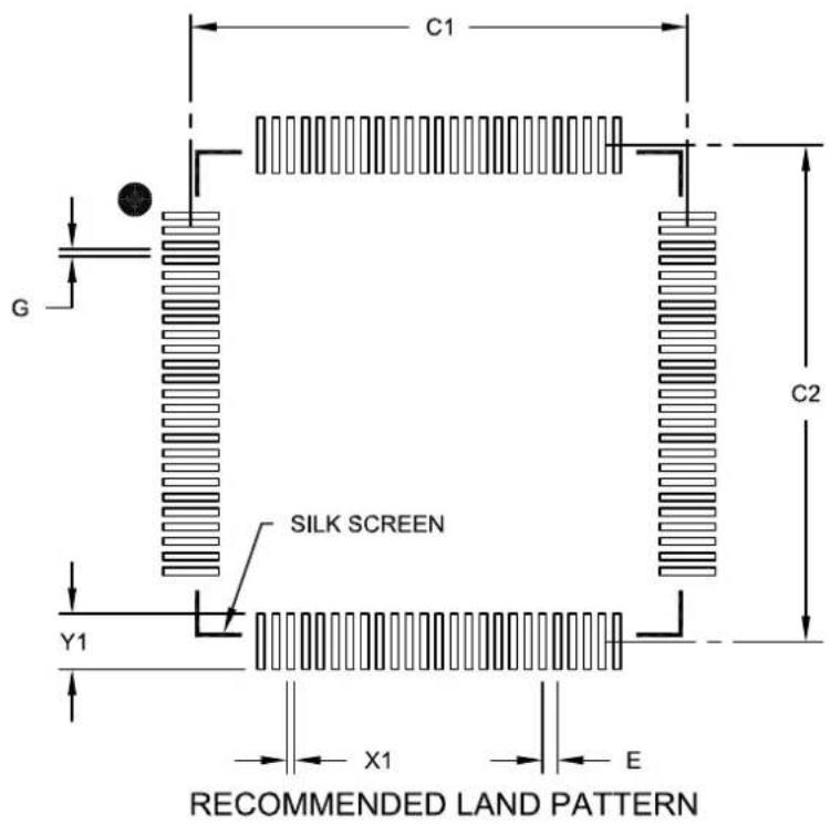
text_image
C1 G SILK SCREEN Y1 X1 E C2 RECOMMENDED LAND PATTERN| Units | MILLIMETERS | |||
| Dimension Limits | MIN | NOM | MAX | |
| Contact Pitch | E | 0.40 BSC | ||
| Contact Pad Spacing | C1 | 13.40 | ||
| Contact Pad Spacing | C2 | 13.40 | ||
| Contact Pad Width (X100) | X1 | 0.20 | ||
| Contact Pad Length (X100) | Y1 | 1.50 | ||
| Distance Between Pads | G | 0.20 | ||
Notes:
1. Dimensioning and tolerancing per ASME Y14.5M
BSC: Basic Dimension. Theoretically exact value shown without tolerances.
Microchip Technology Drawing No. C04-2100B
124-Terminal Very Thin Leadless Array Package (TL) - 9x9x0.9 mm Body [VTLA]
Note: For the most current package drawings, please see the Microchip Packaging Specification located at http://www.microchip.com/packaging
![Microchip PIC32MZ1024ECM124 - 124-Terminal Very Thin Leadless Array Package (TL) - 9x9x0.9 mm Body [VTLA] - 1](/content/2026/06/1217674/images/669f3526e888648b5e4066aa4b1db545adeea06c62486c2d48071fd73056a9ce.jpg)
text_image
NOTE 1 (DATUM A) (DATUM B) 2X 0.10 C 2X 0.10 C TOP VIEW A B E // 0.10 C SEATING PLANE C SIDE VIEW A1 124X 0.08 C A17 B14 D2 0.10 C A B B28 A34 A16 B13 A35 B29 e E2 NOTE 1 B1 A1 B56 B42 A51 B41 A50 K 124X b 0.10 M C A B 0.05 M C BOTTOM VIEWMicrochip Technology Drawing C04-193A Sheet 1 of 2
124-Terminal Very Thin Leadless Array Package (TL) - 9x9x0.9 mm Body [VTLA]
Note: For the most current package drawings, please see the Microchip Packaging Specification located at http://www.microchip.com/packaging
![Microchip PIC32MZ1024ECM124 - 124-Terminal Very Thin Leadless Array Package (TL) - 9x9x0.9 mm Body [VTLA] - 1](/content/2026/06/1217674/images/ddb5fc87bfa029c6f565dbf4799a968f71b97bf8f8a3eebe2628cb0433e7df90.jpg)
text_image
NX L eR TERMINAL TIP (DATUM A OR B) eT/2 DETAIL A EXPOSED Cu (0.025) EXPOSED Cu (0.125) SECTION B-B| Units | MILLIMETERS | |||
| Dimension Limits | MIN | NOM | MAX | |
| Number of Pins | N | 124 | ||
| Pitch | eT | 0.50 BSC | ||
| Pitch (Inner to outer terminal ring) | eR | 0.50 BSC | ||
| Overall Height | A | 0.80 | 0.85 | 0.90 |
| Standoff | A1 | 0.00 | - | 0.05 |
| Overall Width | E | 9.00 BSC | ||
| Exposed Pad Width | E2 | 6.40 | 6.55 | 6.70 |
| Overall Length | D | 9.00 BSC | ||
| Exposed Pad Length | D2 | 6.40 | 6.55 | 6.70 |
| Contact Width | b | 0.20 | 0.25 | 0.30 |
| Contact Length | L | 0.20 | 0.25 | 0.30 |
| Contact-to-Exposed Pad | K | 0.20 | - | - |
Notes:
- Pin 1 visual index feature may vary, but must be located within the hatched area.
- Package is saw singulated.
- Dimensioning and tolerancing per ASME Y14.5M.
BSC: Basic Dimension. Theoretically exact value shown without tolerances.
REF: Reference Dimension, usually without tolerance, for information purposes only.
Microchip Technology Drawing C04-193A Sheet 2 of 2
124-Very Thin Leadless Array Package (TL) - 9x9x0.9 mm Body [VTLA]
Note: For the most current package drawings, please see the Microchip Packaging Specification located at http://www.microchip.com/packaging
![Microchip PIC32MZ1024ECM124 - 124-Very Thin Leadless Array Package (TL) - 9x9x0.9 mm Body [VTLA] - 1](/content/2026/06/1217674/images/baf172c849b70fda0df75c34053f4f59fb837dbe633e6bbd347474c440f899de.jpg)
text_image
E X1 E/2 G4 G3 X2 E T2 C2 G1 G5 X4 G2 W3 W2 C1 SILK SCREENRECOMMENDED LAND PATTERN
| Units | MILLIMETERS | |||
| Dimension Limits | MIN | NOM | MAX | |
| Contact Pitch 0.50 BSCE | ||||
| Pad Clearance G1 | 0.20 | |||
| Pad Clearance G2 | 0.20 | |||
| Pad Clearance G3 | 0.20 | |||
| Pad Clearance G4 | 0.20 | |||
| Contact to Center Pad Clearance (X4) G$ | 0.30 | |||
| Optional Center Pad Width T2 | 6.60 | |||
| Optional Center Pad Length | W2 | 6.60 | ||
| Optional Center Pad Chamfer (X4) | W3 | 0.10 | ||
| Contact Pad Spacing | C1 | 8.50 | ||
| Contact Pad Spacing | C2 | 8.50 | ||
| Contact Pad Width (X124) | X1 | 0.30 | ||
| Contact Pad Length (X124) | X2 | 0.30 | ||
Notes:
1. Dimensioning and tolerancing per ASME Y14.5M
BSC: Basic Dimension. Theoretically exact value shown without tolerances.
Microchip Technology Drawing No. C04-2193A
144-Lead Plastic Thin Quad Flatpack (PH)-16x16x1mm Body, 2.00 mm Footprint [TQFP]
Note: For the most current package drawings, please see the Microchip Packaging Specification located at http://www.microchip.com/packaging
![Microchip PIC32MZ1024ECM124 - 144-Lead Plastic Thin Quad Flatpack (PH)-16x16x1mm Body, 2.00 mm Footprint [TQFP] - 1](/content/2026/06/1217674/images/7e6bfa4ff59ea5b7886b6c13d11cc0548d1da841782517afed14a87aaa0e46b4.jpg)
text_image
2X 0.20 C (DATUM A) (DATUM B) e 2X 0.20 C NOTE 1 2X 0.20 C 12 144X b e/2 E1 E 2X 0.20 C TOP VIEW Φ 0.16M C A B 0.08M C SEATING PLANE C A // 0.10 C 0.08 C END VIEW SEE DETAIL AMicrochip Technology Drawing C04-155B Sheet 1 of 2
144-Lead Plastic Thin Quad Flatpack (PH)-16x16x1mm Body, 2.00 mm Footprint [TQFP]
Note: For the most current package drawings, please see the Microchip Packaging Specification located at http://www.microchip.com/packaging
![Microchip PIC32MZ1024ECM124 - 144-Lead Plastic Thin Quad Flatpack (PH)-16x16x1mm Body, 2.00 mm Footprint [TQFP] - 1](/content/2026/06/1217674/images/7802af21ffe5e40fcb44f3969ee25610d763779958d1e1f6d6b09ddb7a1cc77e.jpg)
text_image
A2 A1 L (L1) 0° MIN c 0 - 7°DETAIL A
![Microchip PIC32MZ1024ECM124 - 144-Lead Plastic Thin Quad Flatpack (PH)-16x16x1mm Body, 2.00 mm Footprint [TQFP] - 2](/content/2026/06/1217674/images/002a8434b44e1c7d8d5ca2b58a5e877ef1b005b5d4598d1196ea765bf4a63cc2.jpg)
natural_image
Isometric diagram of a rectangular structure with diagonal supports and textured edges (no text or symbols)| Units | MILLIMETERS | |||
| Dimension Limits | MIN | NOM | MAX | |
| Number of Pins | N | 144 | ||
| Lead Pitch | e | 0.40 BSC | ||
| Overall Height | A | - | - | 1.20 |
| Molded PackageThickness | A2 | 0.95 | 1.00 | 1.05 |
| Standoff | A1 | 0.05 | - | 0.15 |
| Foot Length | L | 0.45 | 0.60 | 0.75 |
| Footprint | L1 | 1.00 REF | ||
| Overall Width | D | 18.00 BSC | ||
| Overall Length | E | 18.00 BSC | ||
| Molded Body Width | D1 | 16.00 BSC | ||
| Molded Body Length | E1 | 16.00 BSC | ||
| Lead Thickness | c | 0.09 | - | 0.20 |
| Lead Width | b | 0.13 | - | 0.23 |
Notes:
- Pin 1 visual index feature may vary, but must be located within the hatched area.
- Package is saw singulated.
- Dimensioning and tolerancing per ASME Y14.5M.
BSC: Basic Dimension. Theoretically exact value shown without tolerances.
REF: Reference Dimension, usually without tolerance, for information purposes only.
Microchip Technology Drawing C04-155B Sheet 2 of 2
144-Lead Plastic Thin Quad Flat Pack (PH) - 16x16 mm Body, 2.00 mm Footprint [TQFP]
Note: For the most current package drawings, please see the Microchip Packaging Specification located at http://www.microchip.com/packaging

text_image
C1 C2 E G Y1 X1 SILK SCREENRECOMMENDED LAND PATTERN
| Units | MILLIMETERS | |||
| Dimension Limits | MIN | NOM | MAX | |
| Contact Pitch | E | 0.40 BSC | ||
| Contact Pad Spacing | C1 | 17.40 | ||
| Contact Pad Spacing | C2 | 17.40 | ||
| Contact Pad Width (X144) | X1 | 0.20 | ||
| Contact Pad Length (X144) | Y1 | 1.45 | ||
| Distance Between Pads | G | 0.20 | ||
Notes:
1. Dimensioning and tolerancing per ASME Y14.5M
BSC: Basic Dimension. Theoretically exact value shown without tolerances.
Microchip Technology Drawing No. C04-2155B
144-Lead Plastic Low Profile Quad Flatpack (PL) - 20x20x1.40 mm Body, with 2.00 mm Footprint [LQFP]
Note: For the most current package drawings, please see the Microchip Packaging Specification located at http://www.microchip.com/packaging
![Microchip PIC32MZ1024ECM124 - 144-Lead Plastic Low Profile Quad Flatpack (PL) - 20x20x1.40 mm Body, with 2.00 mm Footprint [LQFP] - 1](/content/2026/06/1217674/images/4f9c1311e846ec82c591ca66b7b8f6c7bad14d80bcfd48bda71369ba03a745a5.jpg)
text_image
2X 0.20 C (DATUM A) (DATUM B) e 2X 0.20 C NOTE 1 2X 0.20 C 12 144X b e/2 E1 E 2X 0.20 C TOP VIEW SEATING PLANE C A // 0.10 C 0.08 C SEE DETAIL AMicrochip Technology Drawing C04-044B Sheet 1 of 2
144-Lead Plastic Low Profile Quad Flatpack (PL) - 20x20x1.40 mm Body, with 2.00 mm Footprint [LQFP]
Note: For the most current package drawings, please see the Microchip Packaging Specification located at http://www.microchip.com/packaging
![Microchip PIC32MZ1024ECM124 - 144-Lead Plastic Low Profile Quad Flatpack (PL) - 20x20x1.40 mm Body, with 2.00 mm Footprint [LQFP] - 1](/content/2026/06/1217674/images/6b09708b60b0998e80bec875836c55a9e139cb88eb2c91de999c880e8eaaf4e2.jpg)
text_image
A2 A1 (L1) 0° MIN c 0 - 7° LDETAIL A
![Microchip PIC32MZ1024ECM124 - 144-Lead Plastic Low Profile Quad Flatpack (PL) - 20x20x1.40 mm Body, with 2.00 mm Footprint [LQFP] - 2](/content/2026/06/1217674/images/00168ec5aa3f4280a09cd3a22bd6b5d7bcdfb4db4f5c6867b497fb51188e3f2d.jpg)
natural_image
Isometric line drawing of a rectangular electronic component with coiled pins at the base (no text or symbols)| Units | MILLIMETERS | |||
| Dimension Limits | MIN | NOM | MAX | |
| Number of Leads | N | 144 | ||
| Lead Pitch | e | 0.50 BSC | ||
| Overall Height | A | - | - | 1.60 |
| Molded Package Height | A2 | 1.35 | 1.40 | 1.45 |
| Standoff | A1 | 0.05 | - | 0.15 |
| Foot Length | L | 0.45 | 0.60 | 0.75 |
| Footprint | L1 | 1.00 (REF) | ||
| Overall Width | E | 22.00 BSC | ||
| Overall Length | D | 22.00 BSC | ||
| Molded Body Width | E1 | 20.00 BSC | ||
| Molded Body Length | D1 | 20.00 BSC | ||
| Lead Thickness | c | 0.09 | - | 0.20 |
| Lead Width | b | 0.17 | 0.22 | 0.27 |
Notes:
1. Pin 1 visual index feature may vary, but must be located within the hatched area.
2. Package is saw singulated.
3. Dimensioning and tolerancing per ASME Y14.5M.
BSC: Basic Dimension. Theoretically exact value shown without tolerances.
REF: Reference Dimension, usually without tolerance, for information purposes only.
Microchip Technology Drawing C04-044B Sheet 2 of 2
144-Lead Plastic Low Profile Quad Flatpack (PL) - 20x20x1.40 mm Body [LQFP] 2.00 mm Footprint
Note: For the most current package drawings, please see the Microchip Packaging Specification located at http://www.microchip.com/packaging
![Microchip PIC32MZ1024ECM124 - 144-Lead Plastic Low Profile Quad Flatpack (PL) - 20x20x1.40 mm Body, with 2.00 mm Footprint [LQFP] - 3](/content/2026/06/1217674/images/2c412e8e121bcde0822a05b813b6f3b7ee114318bf0cbf5234e3aa5d29a1be8d.jpg)
text_image
C1 E SILK SCREEN C2 Y1 X1RECOMMENDED LAND PATTERN
| Units | MILLIMETERS | |||
| Dimension Limits | MIN | NOM | MAX | |
| Contact Pitch | E | 0.50 BSC | ||
| Contact Pad Spacing | C1 | 21.40 | ||
| Contact Pad Spacing | C2 | 21.40 | ||
| Contact Pad Width (X144) | X1 | 0.30 | ||
| Contact Pad Length (X144) | Y1 | 1.55 | ||
Notes:
- Dimensioning and tolerancing per ASME Y14.5M
BSC: Basic Dimension. Theoretically exact value shown without tolerances.
Microchip Technology Drawing No. C04-2044B
NOTES:
APPENDIX A: MIGRATING FROM PIC32MX5XX/6XX/7XX TO PIC32MZ
This appendix provides an overview of considerations for migrating from PIC32MX5XX/6XX/7XX devices to the PIC32MZ family of devices. The code developed for PIC32MX5XX/6XX/7XX devices can be ported to PIC32MZ devices after making the appropriate changes outlined below.
The PIC32MZ devices are based on a new architecture, and feature many improvements and new capabilities over PIC32MX5XX/6XX/7XX devices.
A.1 Oscillator and PLL Configuration
Because the maximum speed of the PIC32MZ family is 200 MHz, the configuration of the oscillator is different from prior PIC32MX5XX/6XX/7XX devices.
Table A-1 summarizes the differences (indicated by Bold type) between the family devices for the oscillator.
TABLE A-1: OSCILLATOR CONFIGURATION DIFFERENCES
| PIC32MX5XX/6XX/7XX Feature PIC32MZ Feature | |
| Primary Oscillator Configuration | |
| On PIC32MX devices, XT mode had to be selected if the input frequency was in the 3 MHz to 10 MHz range (4-10 for PLL), and HS mode had to be selected if the input frequency was in the 10 MHz to 20 MHz range. | On PIC32MZ devices, HS mode has a wider input frequency range (4 MHz to 32 MHz). The bit setting of '01' is Reserved. |
| POSCMOD<1:0> (DEVCFG1<9:8>) | POSCMOD<1:0> (DEVCFG1<9:8>) |
| 11 = Primary Oscillator disabled | 11 = Primary Oscillator disabled |
| 10 = HS Oscillator mode selected | 10 = HS Oscillator mode selected |
| 01 = XT Oscillator mode selected | 01 = Reserved |
| 00 = External Clock mode selected | 00 = External Clock mode selected |
| On PIC32MX devices, crystal mode could be selected with the HS or XT Posc setting, but an external oscillator could be fed into the OSC1/CLKI pin and the part would operate normally. | On PIC32MZ devices, this option is not available. External oscillator signals should not be fed into the OSC1/CLKI pin with the Posc set to HS mode. |
| Oscillator Selection | |
| On PIC32MX devices, clock selection choices are as follows: | On PIC32MZ devices, clock selection choices are as follows: |
| FNOSC<2:0> (DEVCFG1<2:0>) | FNOSC<2:0> (DEVCFG1<2:0>) |
| NOSC<2:0> (OSCCON<10:8>) | NOSC<2:0> (OSCCON<10:8>) |
| 111 = FRCDIV | 111 = FRCDIV |
| 110 = FRCDIV16 | 110 = Reserved |
| 101 = LPRC | 101 = LPRC |
| 100 = SOSC | 100 = SOSC |
| 011 = POSC with PLL module | 011 = Reserved |
| 010 = POSC (XT, HS, EC) | 010 = POSC (HS or EC) |
| 001 = FRCDIV+PLL | 001 = System PLL (SPLL) |
| 000 = FRC | 000 = FRCDIV |
| COSC<2:0> (OSCCON<14:12>) | COSC<2:0> (OSCCON<14:12>) |
| 111 = FRC divided by FRCDIV | 111 = FRC divided by FRCDIV |
| 110 = FRC divided by 16 | 110 = BFRC |
| 101 = LPRC | 101 = LPRC |
| 100 = SOSC | 100 = SOSC |
| 011 = POSC + PLL module | 011 = Reserved |
| 010 = POSC | 010 = POSC |
| 001 = FRCPLL | 001 = System PLL |
| 000 = FRC | 000 = FRC divided by FRCDIV |
| Secondary Oscillator Enable | |
| The location of the SOSCEN bit in the Flash Configuration Words has moved. | |
| FSOSCEN (DEVCFG1<5>) | FSOSCEN (DEVCFG1<6>) |
| PIC32MX5XX/6XX/7XX Feature PIC32MZ Feature | |
| PLL Configuration | |
| The FNOSC<2:0> and NOSC<2:0> bits select between POSC and FRC.FNOSC<2:0> (DEVCFG1<2:0>)NOSC<2:0> (OSCCON<10:8>) | Selection of which input clock (POSC or FRC) is now done through the FPLLICLK/PLLICLK bits.FPLLICLK (DEVCFG2<7>)PLLICLK (SPLLCON<7>) |
| On PIC32MX devices, the input frequency to the PLL had to be between 4 MHz and 5 MHz. FPLLIDIV selected how to divide the input frequency to give it the appropriate range.FPLLIDIV<2:0> (DEVCFG2<2:0>)111 = 12x divider110 = 10x divider101 = 6x divider100 = 5x divider011 = 4x divider010 = 3x divider001 = 2x divider000 = 1x divider | On PIC32MZ devices, the input range for the PLL is wider (5 MHz to 64 MHz). The input divider values have changed, and new FPLLRNG/PLLNG bits have been added to indicate under what range the input frequency falls.FPLLIDIV<2:0> (DEVCFG2<2:0>)PLLIDIV<2:0> (SPLLCON<2:0>)111 = Divide by 8110 = Divide by 7101 = Divide by 6100 = Divide by 5011 = Divide by 4010 = Divide by 3001 = Divide by 2000 = Divide by 1FPLLNG<2:0> (DEVCFG2<6:4>)PLLNG<2:0> (SPLLCON<2:0>)111 = Reserved110 = Reserved101 = 34-64 MHz100 = 21-42 MHz011 = 13-26 MHz010 = 8-16 MHz001 = 5-10 MHz000 = Bypass |
| On PIC32MX devices, the output frequency of PLL is between 60 MHz and 120 MHz. The PLL multiplier and divider bits configure the PLL for this range.FPLLMUL<2:0> (DEVCFG2<6:4>)PLLMULT<2:0> (OSCCON<18:16>)111 = 24x multiplier110 = 21x multiplier101 = 20x multiplier100 = 19x multiplier011 = 18x multiplier010 = 17x multiplier001 = 16x multiplier000 = 15x multiplier | The PLL multiplier and divider on PIC32MZ devices have a wider range to accommodate the wider PLL specification range of 10 MHz to 200 MHz.FPLLMULT<6:0> (DEVCFG2<14:8>)PLLMULT<6:0> (SPLLCON<22:16>)1111111 = Multiply by 128111110 = Multiply by 127111101 = Multiply by 126111100 = Multiply by 125···0000000 = Multiply by 1 |
| FPLLODIV<2:0> (DEVCFG2<18:16>)PLLODIV<2:0> (OSCCON<29:27>)111 = 24x multiplier110 = 21x multiplier101 = 20x multiplier100 = 19x multiplier011 = 18x multiplier010 = 17x multiplier001 = 16x multiplier000 = 15x multiplier | FPLLODIV<2:0> (DEVCFG2<18:16>)PLLODIV<2:0> (SPLLCON<26:24>)111 = PLL Divide by 32110 = PLL Divide by 32101 = PLL Divide by 32100 = PLL Divide by 16011 = PLL Divide by 8010 = PLL Divide by 4001 = PLL Divide by 2000 = PLL Divide by 2 |
| Crystal/Oscillator Selection for USB | |
| Any frequency that can be divided down to 4 MHz using UPLLIDIV, including 4, 8, 12, 16, 20, 40, and 48MHz. | If the USB module is used, the Primary Oscillator is limited to either 12 MHz or 24 MHz. Which frequency is used is selected using the UPLLFSEL (DEVCFG2<30>) bit. |
| USB PLL Configuration | |
| On PIC32MX devices, the PLL for the USB requires an input frequency of 4 MHz.UPLLIDIV<2:0>(DEVCFG2<10:8>)111 = 12x divider110 = 10x divider101 = 6x divider100 = 5x divider011 = 4x divider010 = 3x divider010 = 3x divider001 = 2x divider000 = 1x divider | On PIC32MZ devices, the HS USB PHY requires an input frequency of 12 MHz or 24 MHz. UPLLIDIV has been replaced with UPLLFSEL.UPLLFSEL (DEVCFG2<30>)1 = UPLL input clock is 24 MHz0 = UPLL input clock is 12 MHz |
| Peripheral Bus Clock Configuration | |
| On PIC32MX devices, there is one peripheral bus, and the clock for that bus is divided from the SYSCLK using FPBDIV/PBDIV. In addition, the maximum PBCLK frequency is the same as SYSCLK.FPBDIV<1:0>(DEVCFG1<5:4>)PBDIV<1:0>(OSCCON<20:19>)11 = PBCLK is SYSCLK divided by 810 = PBCLK is SYSCLK divided by 401 = PBCLK is SYSCLK divided by 200 = PBCLK is SYSCLK divided by 1 | On PIC32MZ devices, there are eight peripheral buses with their own clocks. FPBDIV is removed, and each PBDIV is in its own register for each PBCLK. The initial PBCLK speed is fixed at reset, and the maximum PBCLK speed is limited to 100 MHz for all buses, with the exception of PBCLK7, which is 200 MHz.PBDIV<6:0>(PBxDIV<6:0>)1111111 = PBCLKx is SYSCLK divided by 1281111110 = PBCLKx is SYSCLK divided by 127•••0000011 = PBCLKx is SYSCLK divided by 40000010 = PBCLKx is SYSCLK divided by 30000001 = PBCLKx is SYSCLK divided by 2(default value for x ≠ 7)0000000 = PBCLKx is SYSCLK divided by 1(default value for x = 7) |
| CPU Clock Configuration | |
| On PIC32MX devices, the CPU clock is derived from SYSCLK. | On PIC32MZ devices, the CPU clock is derived from PBCLK7. |
| FRCDIV Default | |
| On PIC32MX devices, the default value for FRCDIV was to divide the FRC clock by two.FRCDIV<2:0>(OSCCON<26:24>)111 = FRC divided by 256110 = FRC divided by 64101 = FRC divided by 32100 = FRC divided by 16011 = FRC divided by 8010 = FRC divided by 4001 = FRC divided by 2 (default)000 = FRC divided by 1 | On PIC32MZ devices, the default has been changed to divide by one.FRCDIV<2:0>(OSCCON<26:24>)111 = FRC divided by 256110 = FRC divided by 64101 = FRC divided by 32100 = FRC divided by 16011 = FRC divided by 8010 = FRC divided by 4001 = FRC divided by 2000 = FRC divided by 1 (default) |
| Fail-Safe Clock Monitor (FSCM) | |
| On PIC32MX devices, the internal FRC became the clock source on a failure of the clock source. | On PIC32MZ devices, a separate internal Backup FRC (BFRC) becomes the clock source upon a failure at the clock source. |
| On PIC32MX devices, a clock failure resulted in the triggering of a specific interrupt when the switchover was complete.FSCM generates an interrupt. FSCM generates a NMI. | On PIC32MZ devices, a NMI is triggered instead, and must be handled by the NMI routine. |
| FCKSM<1:0>(DEVCFG1<15:14>)1x = Clock switching is disabled, FSCM is disabled01 = Clock switching is enabled, FSCM is disabled00 = Clock switching is enabled, FSCM is enabled | The definitions of the FCKSM<1:0> bits has changed on PIC32MZ devices.FCKSM<1:0>(DEVCFG1<15:14>)11 = Clock switching is enabled and clock monitoring is enabled10 = Clock switching is disabled and clock monitoring is enabled01 = Clock switching is enabled and clock monitoring is disabled00 = Clock switching is disabled and clock monitoring is disabled |
| On PIC32MX devices, the CF (OSCCON<3>) bit indicates a clock failure. Writing to this bit initiates a FSCM event. | On PIC32MZ devices, the CF (OSCCON<3>) bit has the same functionality as that of PIC32MX device; however, an additional CF(RNMICON<1>) bit is available to indicate a NMI event. Writing to this bit causes a NMI event, but not a FSCM event. |
| On PIC32MX devices, the CLKLOCK (OSCCON<7>) bit is controlled by the FSCM.CLKLOCK (OSCCON<7>)If clock switching and monitoring is disabled (FCKSM<1:0>= 1x):1 = Clock and PLL selections are locked0 = Clock and PLL selections are not locked and may be modifiedIf clock switching and monitoring is enabled (FCKSM<1:0>= 0x):Clock and PLL selections are never locked and may be modified. | On PIC32MZ devices, the CLKLOCK (OSCCON<7>) bit is not impacted by the FSCM.CLKLOCK (OSCCON<7>)1 = Clock and PLL selections are locked0 = Clock and PLL selections are not locked and may be modified |
Table A-2 illustrates the difference in code setup of the respective parts for maximum speed using an external 24 MHz crystal.
TABLE A-2: CODE DIFFERENCES FOR MAXIMUM SPEED USING AN EXTERNAL 24 MHz CRYSTAL
| PIC32MX5XX/6XX/7XX at 80 MHz PIC32MZ at 200 MHz | |
| #include | #include |
| #pragma config POSCMOD = HS | #pragma config POSCMOD = HS |
| #pragma config FNOSC = PRIPLL | #pragma config FNOSC = SPLL |
| #pragma config FPLLIDIV = DIV_6 | #pragma config FPLLICLK = PLL_POSC |
| #pragma config FPLLIDIV = DIV_3 | |
| #pragma config FPLLRNG = RANGE_5_10_MHZ | |
| #pragma config FPLLMUL = MUL_20 | #pragma config FPLLMULT = MUL_50 |
| #pragma config FPLLODIV = DIV_1 | #pragma config FPLLODIV = DIV_2 |
| #define SYSFREQ (80000000L) | #define SYSFREQ (200000000L) |
A.2 Analog-to-Digital Converter (ADC)
The PIC32MZ family of devices has a new Pipelined ADC module that replaces the 10-bit ADC module in PIC32MX5XX/6XX/7XX devices; therefore, the use of Bold type to show differences is not used in the following table. Note that not all register differences are described in this section; however, the key feature differences are listed in Table A-3.
TABLE A-3: ADC DIFFERENCES
| PIC32MX5XX/6XX/7XX Feature PIC32MZ Feature | |
| Clock Selection and Operating Frequency (TAD) | |
| On PIC32MX devices, the ADC clock was derived from either the FRC or from the PBCLK.ADRC (AD1CON3<15>)1 = FRC clock0 = Clock derived from Peripheral Bus Clock (PBCLK) | On PIC32MZ devices, the three possible sources of the ADC clock are FRC, REFCLKO3, and SYSCLK.ADCSEL<1:0> (AD1CON1<9:8>)11 = FRC10 = REFCLKO301 = SYSCLK00 = Reserved |
| On PIC32MX devices, if the ADC clock was derived from the PBCLK, that frequency was divided further down, with a maximum divisor of 512, and a minimum divisor of two.ADCS<7:0> (AD1CON3<7:0>)11111111 = 512 * TPB = TAD···00000001 = 4 * TPB = TAD00000000 = 2 * TPB = TAD | On PIC32MZ devices, any ADC clock source can be divided down, with a maximum divisor of 254. The input clock can also be fed directly to the ADC.ADCDIV<6:0> (AD1CON1<6:0>)1111111 = 254 * TQ = TAD···0000011 = 6 * TQ = TAD0000010 = 4 * TQ = TAD0000001 = 2 * TQ = TAD0000000 = TQ = TAD |
| Scan Trigger Source | |
| On PIC32MX devices, there are four sources that can trigger a scan conversion in the ADC module: Auto, Timer3, INT0, and clearing the SAMP bit.SSRC<2:0> (AD1CON1<7:5>)111 = Auto convert110 = Reserved101 = Reserved100 = Reserved011 = Reserved010 = Timer3 period match001 = Active transition on INT0 pin000 = Clearing SAMP bitPIC32MX5XX/6XX/7XX Feature PIC32MZ Feature | On PIC32MZ devices, the list of sources for triggering a scan conversion has been expanded to include the comparators, Output Compare, and two additional Timers. In addition, trigger sources can be simulated by setting the RQCNVRT (AD1CON3<29>) bit.STRGSRC<4:0> (AD1CON1<26:22>)11111 = Reserved···01101 = Reserved01100 = Comparator 2 COUT01011 = Comparator 1 COUT01010 = OCMP501001 = OCMP301000 = OCMP100111 = TMR5 match00110 = TMR3 match00101 = TMR1 match00100 = INT000011 = Reserved00010 = Reserved00001 = Global software trigger (GSWTRG)00000 = No trigger |
| Output Format | |
| On PIC32MX devices, the output format was decided for all ADC channels based on the setting of the FORM<2:0> bits. | On PIC32MZ devices, the FRACT bit determines whether fractional or integer format is used. Then, each channel can have its own setting for input (differential or single-ended) and sign (signed or unsigned) using the SHxMOD<1:0> bits. |
| FORM<2:0>(AD1CON1<10:8>)011 = Signed Fractional 16-bit010 = Fractional 16-bit001 = Signed Integer 16-bit000 = Integer 16-bit111 = Signed Fractional 32-bit110 = Fractional 32-bit101 = Signed Integer 32-bit100 = Integer 32-bit | FRACT (AD1CON1<11>)1 = Fractional0 = IntegerSHxMOD<1:0>(AD1IMOD,)11 = Differential inputs, two's complement (signed) data output10 = Differential inputs, unipolar encoded (unsigned) data output01 = Single-ended inputs, two's complement (signed) data output00 = Single-ended inputs, unipolar encoded (unsigned) data output |
| Interrupts | |
| On PIC32MX devices, an interrupt is triggered from the ADC module when a certain number of conversions have taken place, irrespective of which channel was converted. | On PIC32MZ devices, the ADC module can trigger an interrupt for each channel when it is converted. Use the Interrupt Controller bits, IEC1<31:27>, IEC2<31:0>, and IEC3<7:0>, to enable/disable them.In addition, the ADC support one global interrupt to indicate conversion on any number of channels. |
| SMPI<3:0>(AD1CON2<5:2>)1111 = Interrupt for each 16th sample/convert sequence1110 = Interrupt for each 15th sample/convert sequence···0001 = Interrupt for each 2nd sample/convert sequence0000 = Interrupt for each sample/convert sequence | AGIENxx (AD1GIRQENx,)1 = Data ready event will generate a Global ADC interrupt0 = No global interrupt |
| ADC Calibration | |
| On PIC32MX devices, the ADC module can be used immediately, once it is enabled. | PIC32MZ devices require a calibration step prior to operation. This is done by copying the calibration data from DEVADCx to the corresponding AD1CALx register. When the ADC is enabled with ADCEN=1, a calibration step is run and ADCRDY will be set to 1 by the hardware when the calibration sequence is complete. |
| I/O Pin Analog Function Selection | |
| On PIC32MX devices, the analog function of an I/O pin was determined by the PCFGx bit in the AD1PCFG register.PCFGx (AD1PCFG,)1 = Analog input pin in Digital mode0 = Analog input pin in Analog mode | On PIC32MZ devices, the analog selection function has been moved into a separate register on each I/O port. Note that the sense of the bit is different.ANSxy (ANSELx,)1 = Analog input pin in Analog mode0 = Analog input pin in Digital mode |
| Debug Mode | |
| On PIC32MX devices, when stopping on a breakpoint during debugging, the ADC module can be configured to stop or continue execution from the Freeze Peripherals dialog in MPLAB X IDE. | On PIC32MZ devices, the ADC module continues operating when stopping on a breakpoint during debugging. |
| Electrical Specifications and Timing Requirements | |
| Refer to “Section 31. Electrical Characteristics” in the PIC32MX5XX/6XX/7XX Data Sheet for ADC module specifications and timing requirements. | On PIC32MZ devices, the ADC module sampling and conversion time and other specifications have changed. Refer to 37.0 “Electrical Characteristics” for more information. |
A.3 CPU
The CPU in the PIC32MZ family of devices has been changed to the MIPS microAptiv™ MPU architecture. This CPU includes DSP ASE, internal data and instruction L1 caches, and a TLB-based MMU.
Table A-4 summarizes some of the key differences (indicated by Bold type) in the internal CPU registers.
TABLE A-4: CPU DIFFERENCES
| PIC32MX5XX/6XX/7XX Feature PIC32MZ Feature | |
| L1 Data and Instruction Cache and Prefetch Wait States | |
| On PIC32MX devices, the cache was included in the prefetch module outside the CPU.PREFEN<1:0> (CHECON<5:4>)11 = Enable predictive prefetch for both cacheable and non-cacheable regions10 = Enable predictive prefetch for non-cacheable regions only01 = Enable predictive prefetch for cacheable regions only00 = Disable predictive prefetchDCSZ<1:0> (CHECON<9:8>)Changing these bits causes all lines to be reinitialized to the “invalid” state.11 = Enable data caching with a size of 4 lines10 = Enable data caching with a size of 2 lines01 = Enable data caching with a size of 1 line00 = Disable data cachingCHECOH (CHECON<16>)1 = Invalidate all data and instruction lines0 = Invalidate all data and instruction lines that are not locked | On PIC32MZ devices, the CPU has a separate L1 instruction and data cache in the core. The PREFEN<1:0> bits still enable the prefetch module; however, the K0<2:0> bits in the CP0 registers controls the internal L1 cache for the designated regions.PREFEN<1:0> (PRECON<5:4>)11 = Enable predictive prefetch for any address10 = Enable predictive prefetch for CPU instructions and CPU data01 = Enable predictive prefetch for CPU instructions only00 = Disable predictive prefetchK0<2:0> (CP0 Reg 16, Select 0)011 = Cacheable, non-coherent, write-back, write allocate010 = Uncached001 = Cacheable, non-coherent, write-through, write allocate000 = Cacheable, non-coherent, write-through, no write allocate |
| PFMWS<2:0> (CHECON<2:0>)111 = Seven Wait states110 = Six Wait states101 = Five Wait states100 = Four Wait states011 = Three Wait states010 = Two Wait states (61-80 MHz)001 = One Wait state (31-60 MHz)000 = Zero Wait state (0-30 MHz) | The Program Flash Memory read wait state frequency points have changed in PIC32MZ devices. The register for accessing the PFMWS field has changed from CHECON to PRECON.PFMWS<2:0> (PRECON<2:0>)111 = Seven Wait states•••011 = Three Wait states010 = Two Wait states (133-200 MHz)001 = One Wait state (66-133 MHz)000 = Zero Wait states (0-66 MHz)Note: Wait states listed are for ECC enabled. |
| Core Instruction Execution | |
| On PIC32MX devices, the CPU can execute MIPS16e instructions and uses a 16-bit instruction set, which reduces memory size.MIPS16e® | On PIC32MZ devices, the CPU can operate a mode called microMIPS. microMIPS mode is an enhanced MIPS32® instruction set that uses both 16-bit and 32-bit opcodes. This mode of operation reduces memory size with minimum performance impact.microMIPSTMThe BOOTISA (DEVCFG0<6>) Configuration bit controls the MIPS32 and microMIPS modes for boot and exception code.1 = Boot code and Exception code is MIPS32®(ISAONEXC bit is set to '0' and the ISA<1:0> bits are set to '10' in the CP0 Config3 register)0 = Boot code and Exception code is microMIPSTM(ISAONEXC bit is set to '1' and the ISA<1:0> bits are set to '11' in the CP0 Config3 register) |
A.4 Resets
The PIC32MZ family of devices has updated the resets modules to incorporate the new handling of NMI resets from the WDT, DMT, and the FSCM. In addition, some bits have been moved, as summarized in Table A-5.
TABLE A-5: RESET DIFFERENCES
| PIC32MX5XX/6XX/7XX Feature PIC32MZ Feature | |
| Power Reset | |
| VREGS (RCON<8>)1 = Regulator is enabled and is on during Sleep mode0 = Regulator is disabled and is off during Sleep mode | The VREGS bit, which controls whether the internal regulator is enabled in Sleep mode, has been moved from RCON in PIC32MX5XX/6XX/7XX devices to a new PWRCON register in PIC32MZ devices.VREGS (PWRCON<0>)1 = Voltage regulator will remain active during Sleep0 = Voltage regulator will go to Stand-by mode during Sleep |
| Watchdog Timer Reset | |
| On PIC32MX devices, a WDT expiration immediately triggers a device reset.WDT expiration immediately causes a device reset. | On PIC32MZ devices, the WDT expiration now causes a NMI. The WDTO bit in RNMICON indicates that the WDT caused the NMI. A new timer, NMICNT, runs when the WDT NMI is triggered, and if it expires, the device is reset.WDT expiration causes a NMI, which can then trigger the device reset.WDTO (RNMICON<24>)1 = WDT time-out has occurred and caused a NMI0 = WDT time-out has not occurredNMICNT<7:0> (RNMICON<7:0>) |
A.5 USB
The PIC32MZ family of devices has a new Hi-Speed USB module, which requires the updated USB stack from Microchip. In addition, the USB PLL was also updated. See Section A.1 "Oscillator and PLL Configuration" for more information and Table A-6 for a list of additional differences.
TABLE A-6: USB DIFFERENCES
| PIC32MX5XX/6XX/7XX Feature PIC32MZ Feature | |
| Debug Mode | |
| On PIC32MX devices, when stopping on a breakpoint during debugging, the USB module can be configured to stop or continue execution from the Freeze Peripherals dialog in MPLAB X IDE. | On PIC32MZ devices, the USB module continues operating when stopping on a breakpoint during debugging. |
| VBUSON Pin | |
| PIC32MX devices feature a VBUSON pin for controlling the external transceiver power supply. | On PIC32MZ devices, the VBUSON pin is not available. A port pin can be used to achieve the same functionality. |
A.6 DMA
The DMA controller in PIC32MZ devices is similar to the DMA controller in PIC32MX5XX/6XX/7XX devices. New features include the extension of pattern matching to two by bytes and the addition of the optional Pattern Ignore mode. Table A-7 lists differences (indicated by Bold type) that will affect software migration.
TABLE A-7: DMA DIFFERENCES
| PIC32MX5XX/6XX/7XX Feature PIC32MZ Feature | |
| Read/Write Status on Error | |
| RDWR (DMASTAT<3>)1 = Last DMA bus access when an error was detected was a read0 = Last DMA bus access when an error was detected was a write | The RDWR bit has moved from DMASTAT<3> in PIC32MX5XX/6XX/7XX devices to DMASTAT<31> in PIC32MZ devices.RDWR (DMASTAT<31>)1 = Last DMA bus access when an error was detected was a read0 = Last DMA bus access when an error was detected was a write |
| Source-to-Destination Transfer | |
| On PIC32MX devices, a DMA channel performs a read of the source data and completes the transfer of this data into the destination address before it is ready to read the next data from the source. | On PIC32MZ devices, the DMA implements a 4-deep queue for data transfers. A DMA channel reads the source data and places it into the queue, regardless of whether previous data in the queue has been delivered to the destination address. |
A.7 Interrupts and Exceptions
The key difference between Interrupt Controllers in PIC32MX5XX/6XX/7XX devices and PIC32MZ devices concerns vector spacing. Previous PIC32MX devices had fixed vector spacing, which is adjustable in set increments, and every interrupt had the same amount of space. PIC32MZ devices replace this with a variable offset spacing, where each interrupt has an offset register to determine where to begin execution.
In addition, the IFSx, IECx, and IPCx registers for old peripherals have shifted to different registers due to new peripherals. Please refer to Section 7.0 "CPU Exceptions and Interrupt Controller" to determine where the interrupts are now located.
Table A-8 lists differences (indicated by Bold type) in the registers that will affect software migration.
TABLE A-8: INTERRUPT DIFFERENCES
| PIC32MX5XX/6XX/7XX Feature PIC32MZ Feature | |
| Vector Spacing | |
| On PIC32MX devices, the vector spacing was determined by the VS field in the CPU core. | On PIC32MZ devices, the vector spacing is variable and determined by the Interrupt controller. The VOFFx<17:1> bits in the OFFx register are set to the offset from EBASE where the interrupt service routine is located. |
| VS<4:0>(IntCtl<9:5>: CP0 Register 12, Select 1)10000 = 512-byte vector spacing01000 = 256-byte vector spacing00100 = 128-byte vector spacing00010 = 64-byte vector spacing00001 = 32-byte vector spacing00000 = 0-byte vector spacing | VOFFx<17:1> (OFFx<17:1>) Interrupt Vector ‘x’ Address Offset bits |
| Shadow Register Sets | |
| On PIC32MX devices, there was one shadow register set which could be used during interrupt processing. Which interrupt priority could use the shadow register set was determined by the FSRS-SEL field in DEVCFG3 and SS0 on INTCON.FSRSSEL<2:0>(DEVCFG3<18:16>)111 = Assign Interrupt Priority 7 to a shadow register set110 = Assign Interrupt Priority 6 to a shadow register set···001 = Assign Interrupt Priority 1 to a shadow register set000 = All interrupt priorities are assigned to a shadow register setSS0 (INTCON<16>)1 = Single vector is presented with a shadow register set0 = Single vector is not presented with a shadow register set | On PIC32MZ devices, there are seven shadow register sets, and each priority level can be assigned a shadow register set to use via the PRIxSS<3:0> bits in the PRISS register. The SS0 bit is also moved to PRISS<0>.PRIxSS<3:0> PRISS1xxx = Reserved (by default, an interrupt with a priority level of x uses Shadow Set 0)0111 = Interrupt with a priority level of x uses Shadow Set 70110 = Interrupt with a priority level of x uses Shadow Set 6···0001 = Interrupt with a priority level of x uses Shadow Set 10000 = Interrupt with a priority level of x uses Shadow Set 0SS0 (PRISS<0>)1 = Single vector is presented with a shadow register set0 = Single vector is not presented with a shadow register set |
| Status | |
| PIC32MX devices, the VEC<5:0> bits show which interrupt is being serviced. | On PIC32MZ devices, the SIRQ<7:0> bits show the IRQ number of the interrupt last serviced. |
| VEC<5:0>(INTSTAT<5:0>)11111-00000 = The interrupt vector that is presented to the CPU | SIRQ<7:0> (INTSTAT<7:0>)11111111-00000000 = The last interrupt request number serviced by the CPU |
A.8 Flash Programming
The PIC32MZ family of devices incorporates a new Flash memory technology. Applications ported from PIC32MX5XX/6XX/7XX devices that take advantage of Run-time Self Programming will need to adjust the Flash programming steps to incorporate these changes.
Table A-9 lists the differences (indicated by Bold type) that will affect software migration.
TABLE A-9: FLASH PROGRAMMING DIFFERENCES
| PIC32MX5XX/6XX/7XX Feature PIC32MZ Feature | |
| Program Flash Write Protection | |
| On PIC32MX devices, the Program Flash write-protect bits are part of the Flash Configuration words (DEVCFG0).PWP<7:0> (DEVCFG0<19:12>)11111111 = Disabled11111110 = 0xBD000FFF11111101 = 0xBD001FFF11111100 = 0xBD002FFF11111011 = 0xBD003FFF11111010 = 0xBD004FFF11111001 = 0xBD005FFF11111000 = 0xBD006FFF11110111 = 0xBD007FFF11110110 = 0xBD008FFF11110101 = 0xBD009FFF11110100 = 0xBD00AFFF11110011 = 0xBD00BFFF11110010 = 0xBD00CFFF11110001 = 0xBD00DFFF11110000 = 0xBD00EFFF11101111 = 0xBD00FFFF.01111111 = 0xBD07FFFF | On PIC32MZ devices, the write-protect register is contained separately as the NVMPWP register. It has been expanded to 24 bits, and now represents the address below, which all Flash memory is protected. Note that the lower 14 bits are forced to zero, so that all memory locations in the page are protected.PWP<23:0> (NVMPWP<23:0>)Physical memory below address 0x1Dxxxxxx is write protected, where ‘xxxxxx’ is specified by PWP<23:0>. When PWP<23:0> has a value of ‘0’, write protection is disabled for the entire program Flash. If the specified address falls within the page, the entire page and all pages below the current page will be protected. |
| Code Protection | |
| On PIC32MX devices, code protection is enabled by the CP (DEVCFG<28>) bit. | On PIC32MZ devices, code protection is enabled by the CP (DEVCP0<28>) bit. |
| Boot Flash Write Protection | |
| On PIC32MX devices, Boot Flash write protection is enable by the BWP (DEVCFG<24>) bit and protects the entire Boot Flash memory. | On PIC32MZ devices, Boot Flash write protection is divided into pages and is enable by the LBWPx and UBWPx bits in the NVMBWP register. |
| Low-Voltage Detect Status | |
| LVDSTAT (NVMCON<11>)1 = Low-voltage event is active0 = Low-voltage event is not active | The LVDSTAT bit is not available in PIC32MZ devices. |
| PIC32MX5XX/6XX/7XX Feature PIC32MZ Feature | |
| Flash Programming | |
| NVMOP<3:0> (NVMCON<3:0>)1111 = Reserved···0111 = Reserved0110 = No operation0101 = Program Flash (PFM) erase operation0100 = Page erase operation0011 = Row program operation0010 = No operation0001 = Word program operation0000 = No operation | The op codes for programming the Flash memory have been changed to accommodate the new quad-word programming and dual-panel features. The row size has changed to 2 KB (512 IW) from 128 IW. The page size has changed to 16 KB (4K IW) from 4 KB (1K IW). Note that the NVMOP register is now protected, and requires the WREN bit be set to enable modification.NVMOP<3:0> (NVMCON<3:0>)1111 = Reserved···1000 = Reserved0111 = Program erase operation0110 = Upper program Flash memory erase operation0101 = Lower program Flash memory erase operation0100 = Page erase operation0011 = Row program operation0010 = Quad Word (128-bit) program operation0001 = Word program operation0000 = No operation |
| PIC32MX devices feature a single NVMDATA register for word programming.NVMDATA NVMDATAx, where 'x' = 0 through 3 | On PIC32MZ devices, to support quad word programming, the NVMDATA register has been expanded to four words. |
| Flash Endurance and Retention | |
| PIC32MX devices support Flash endurance and retention of up to 20K E/W cycles and 20 years. | On PIC32MZ devices, ECC must be enabled to support the same endurance and retention as PIC32MX devices. |
| Configuration Words | |
| On PIC32MX devices, Configuration Words can be programmed with Word or Row program operation. | On PIC32MZ devices, all Configuration Words must be programmed with Quad Word operation. |
| Configuration Words Reserved Bit | |
| On PIC32MX devices, the DEVCFG0<15> bit is Reserved and must be programmed to '0'. | On PIC32MZ devices, this bit is DEVSIGN0<31>. |
A.9 Other Peripherals and Features
Most of the remaining peripherals on PIC32MZ devices act identical to their counterparts on PIC32MX5XX/6XX/7XX devices. The main differences have to do with handling the increased peripheral bus clock speed and additional clock sources.
Table A-10 lists the differences (indicated by Bold type) that will affect software and hardware migration.
TABLE A-10: PERIPHERAL DIFFERENCES
| PIC32MX5XX/6XX/7XX Feature PIC32MZ Feature | |
| I^2C | |
| On PIC32MX devices, all pins are 5V-tolerant. | On PIC32MZ devices, the I2C4 port uses non-5V tolerant pins,and will have different VOL/VOH specifications. |
| I2CxBRG<11:0> | The Baud Rate Generator register has been expanded from 12bits to 16 bits.I2CxBRG<15:0> |
| Watchdog Timer | |
| Clearing the Watchdog Timer on PIC32MX5XX/6XX/7XXdevices required writing a ‘1’ to the WDTCLR bit.WDTCLR (WDTCON<0>) | On PIC32MZ devices, the WDTCLR bit has been replaced withthe 16-bit WDTCLRKEY, which must be written with a specificvalue (0x5743) to clear the Watchdog Timer. In addition, theWDTSPGM (DEVCFG1<21>) bit is used to control operation ofthe Watchdog Timer during Flash programming.WDTCLRKEY<15:0> (WDTCON<31:16>) |
| RTCC | |
| On PIC32MX devices, the output of the RTCC pin was selectedbetween the Seconds Clock or the Alarm Pulse.RTCSECSEL (RTCCON<7>)1 = RTCC Seconds Clock is selected for the RTCC pin0 = RTCC Alarm Pulse is selected for the RTCC pin | On PIC32MZ devices, the RTCC Clock is added as an option.RTCSECSEL has been renamed RTCOUTSEL and expanded totwo bits.RTCOUTSEL<1:0> (RTCCON<8:7>)11 = Reserved10 = RTCC Clock is presented on the RTCC pin01 = Seconds Clock is presented on the RTCC pin00 = Alarm Pulse is presented on the RTCC pin when the alarminterrupt is triggered |
| On PIC32MX devices, the Secondary Oscillator (Sosc) servesas the input clock for the RTCC module. | On PIC32MZ devices, an additional clock source, LPRC, isavailable as a choice for the input clock.RTCCLKSEL<1:0> (RTCCON<10:9>)11 = Reserved10 = Reserved01 = RTCC uses the external 32.768 kHz SOSC00 = RTCC uses the internal 32 kHz oscillator (LPRC) |
| Ethernet | |
| CLKSEL<3:0> (EMAC1MCFG<5:2>)1000 = SYSCLK divided by 400111 = SYSCLK divided by 280110 = SYSCLK divided by 200101 = SYSCLK divided by 140100 = SYSCLK divided by 100011 = SYSCLK divided by 80010 = SYSCLK divided by 6000x = SYSCLK divided by 4 | On PIC32MZ devices, the input clock divider for the Ethernet module has expanded options to accommodate the faster peripheral bus clock.CLKSEL<3:0> (EMAC1MCFG<5:2>)1010 = PBCLK5 divided by 501001 = PBCLK5 divided by 481000 = PBCLK5 divided by 400111 = PBCLK5 divided by 280110 = PBCLK5 divided by 200101 = PBCLK5 divided by 140100 = PBCLK5 divided by 100011 = PBCLK5 divided by 80010 = PBCLK5 divided by 6000x = PBCLK5 divided by 4 |
| Comparator/Comparator Voltage Reference | |
| On PIC32MX devices, it was possible to select the VREF+ pin as the output to the CVREFOUT pin.VREFSEL (CVRCON<10>)1 = CVREF = VREF+0 = CVREF is generated by the resistor network | On PIC32MZ devices, the CVREFOUT pin must come from the resistor network.This bit is not available. |
| On PIC32MX devices, the internal voltage reference (IVREF) could be chosen by the BGSEL<1:0> bits.BGSEL<1:0> (CVRCON<9:8>)11 = IVREF = VREF+10 = Reserved01 = IVREF = 0.6V (nominal, default)00 = IVREF = 1.2V (nominal) | On PIC32MZ devices, IVREF is fixed and cannot be changed.These bits are not available. |
| Change Notification | |
| On PIC32MX devices, Change Notification is controlled by the CNCON, CNEN, and CNPUE registers. | On PIC32MZ devices, Change Notification functionality has been relocated into each I/O port and is controlled by the CNPUx, CNPDx, CNCONx, CNENx, and CNSTATx registers. |
| System Bus | |
| On PIC32MX devices, the System Bus registers can be used to configure RAM memory for data and program memory partitions, cacheability of Flash memory, and RAM Wait states. These registers are: BMXCON, BMXDKPBA, BMXDUDBA, BMXDUPBA, BMXPUPBA, BMXDRMSZ, BMXPFMSZ, and BMXBOOTSZ. | On PIC32MZ devices, a new System Bus is utilized that supports using RAM memory for program or data without the need for special configuration. Therefore, no special registers are associated with the System Bus to configure these features. |
| On PIC32MX devices, various arbitration modes are used as initiators on the System Bus. These modes can be selected by the BMXARB<2:0> (BMXCON<2:0>) bits. | On PIC32MZ devices, a new arbitration scheme has been implemented on the System Bus. All initiators use the Least Recently Serviced (LRS) scheme, with the exception of the DMA, CPU, and the Flash Controller.The Flash Controller always has High priority over LRS initiators. The DMA and CPU (when servicing an interrupt) can be selected to have LRS or High priority using the DMAPRI (CFGCON<25>) and CPUPRI (CFGCON<24>) bits. |
A.10 Package Differences
In general, PIC32MZ devices are mostly pin compatible with PIC32MX5XX/6XX/7XX devices; however, some pins are not. In particular, the VDD and VSS pins have been added and moved to different pins. In addition, I/O functions that were on fixed pins now will largely be on remappable pins.
TABLE A-11: PACKAGE DIFFERENCES
| PIC32MX5XX/6XX/7XX Feature PIC32MZ Feature | |
| VCAP Pin | |
| On PIC32MX devices, an external capacitor is required between a VCAP pin and GND, which provides a filtering capacitor for the internal voltage regulator.A low-ESR capacitor (typically 10 μF) is required on the VCAP pin. | On PIC32MZ devices, this requirement has been removed.No VCAP pin. |
| VDD and VSS Pins | |
| VDD on 64-pin packages: 10, 26, 38, 57VDD on 100-pin packages: 2, 16, 37, 46, 62, 86 | There are more VDD pins on PIC32MZ devices, and many are located on different pins.VDD on 64-pin packages: 8, 26, 39, 54, 60VDD on 100-pin packages: 14, 37, 46, 62, 74, 83, 93 |
| Vss on 64-pin packages: 9, 25, 41Vss on 100-pin packages: 15, 36, 45, 65, 75 | There are more Vss pins on PIC32MZ devices, and many are located on different pins.Vss on 64-pin packages: 7, 25, 35, 40, 55, 59Vss on 100-pin packages: 13, 36, 45, 53, 63, 75, 84, 92 |
| PPS I/O Pins | |
| All peripheral functions are fixed as to what pin upon which they operate. | Peripheral functions on PIC32MZ devices are now routed through a PPS module, which routes the signals to the desired pins. When migrating software, it is necessary to initialize the PPS I/O functions in order to get the signal to and from the correct pin.PPS functionality for the following peripherals:CANUARTSPI (except SCK)Input CaptureOutput CompareExternal Interrupt (except INT0)Timer Clocks (except Timer1)Reference Clocks (except REFCLK2) |
APPENDIX B: REVISION HISTORY
Revision A (February 2013)
This is the initial released version of the document.
Revision B (November 2013)
Throughout the document, references to Microchip documentation numbers have been updated to reflect a new 8-digit numbering scheme now in use by Microchip. For example, DS61191 is now DS60001191.
The revision includes the following major changes, which are referenced by their respective chapter in Table B-1.
In addition, minor updates to text and formatting were incorporated throughout the document.
TABLE B-1: MAJOR SECTION UPDATES
| Section Name Update Description | |
| “32-bit MCUs (up to 2 MB Live-Update Flash and 512 KB SRAM) with Audio and Graphics Interfaces, HS USB, Ethernet, and Advanced Analog” | All Family Feature tables were updated (see Table 1 and Table 2).The device part numbers were updated in all pin tables (see Table 3 through Table6). |
| 1.0 “Device Overview” | Updated the Pinout I/O Descriptions for 64-pin QFN/TQFP devices for SPI5 and SPI6 (see Table 1-9). |
| 2.0 “Guidelines for Getting Started with 32-bit Microcontrollers” | Updated the MCLR Pin Connections example (see Figure 2-2).Removed the Termination Resistor diagram (formerly Figure 2-4). |
| 4.0 “Memory Organization” | Updated the Boot and Alias Memory Map (see Figure 4-5).Updated the Boot Flash 1 and Boot Flash 2 Sequence and Configuration Words Summaries (see Table4-2 and Table 4-3, respectively).Added the Watchdog Timer (WDT) to Target 5 in the Initiators to Targets Access Association and System Bus Targets and Associated Protection Registers (see Table4-4 and Table 4-6, respectively). In addition, the reset values in Note 1 of Table4-6 were updated.The CODE<3:0> bit value definitions and the default POR values for the CMD<2:0> bits were updated (see Register 4-3).The default POR value for the GROUP3 bit was updated (see Register 4-9 and Register 4-10). |
| 5.0 “Flash Program Memory” | The All Resets value for the lower 16 bits of the NVMBWP register was updated (see Table5-1). |
| 6.0 “Resets” | The Brown-out Reset block was removed from the Configuration Mismatch Reset (CMR) in the System Reset Block Diagram (see Figure6-1).Removed the EXT bit from RNMICON register in the Resets Register Map (see Table6-1). |
| 7.0 “CPU Exceptions and Interrupt Controller” | Note 2 and Note 3 were added to Interrupt IRQ, Vector and Bit Location (see Table7-2).Notes 4, 5, and 6 were added to the Interrupt Register Map (see Table 7-3). |
| 9.0 “Prefetch Module” | Updated the bit value definitions for the PFMWS<2:0> bits (see Register 9-1). |
| 10.0 “Direct Memory Access (DMA) Controller” | The CHPDAT bits were updated to <15:0> in the DCHxDAT registers (see Table10-3). |
| 20.0 “Serial Quad Interface (SQI)” | The SQI1CMDTHR, SQI1INTTHR, SQI1BDTXDSTAT, and SQI1BDRXDSTAT registers were updated (see Table20-1, Register 20-6, Register 20-7, Register 20-19, and Register 20-20). |
| 28.0 “12-bit Pipelined Analog-to-Digital Converter (ADC)” | Figure 28-1, Figure 28-2, and Figure 28-3 were updated.Register names were updated in the ADC Register Map (see Table 28-1).The OVRSAM<2:0> bit values were updated (see Register 28-14). |
| 34.0 “Special Features” | The DEVCFG3/ADEVCFG3 register was updated (see Register 34-6). |
| 37.0 “Electrical Characteristics” | Various electrical specifications were updated, including:The minimum value for parameter DC10 (V DD) in the DC Temperature and Voltage Specifications was updated (see Table37-4).The minimum and maximum values for parameter BO10 (VBOR) were updated in the BOR Electrical Characteristics (see Table37-4).Updated the third and fourth bullet list items in Note 2 in DC Characteristics: Operating Current (IDD) (see Table 37-6).Updated the third and fourth bullet list items in Note 1 in DC Characteristics: Idle Current (IIDLE) (see Table 37-7).Updated the third and fourth bullet list items in Note 1 in DC Characteristics: Power-Down Current (IPD) (see Table 37-8).Added Note 6 and updated parameters DI20, DI28a, DI28b, DI30, and DI31 in DC Characteristics: I/O Pin Input Specifications (see Table37-9).Added DC Characteristics: I/O Pin Input Injection Current Specifications (see Table37-10).Added parameter DO50 to Capacitive Loading Requirements on Output Pins (see Table 37-15).Note 3 was added and the Conditions were updated for parameter OS42 in the External Clock Timing Requirements (see Table37-16).Updated the Minimum value for parameter OS51 (Fsys) in the System Timing Requirements (see Table37-17).Added parameter OS54a and updated the Maximum value for parameter OS50 in the PLL Clock Timing Specifications (see Table37-18).The Internal Backup FRC (BFRC) Accuracy specification was added (see Table 37-21).The SQI Input and Output Timing Characteristics diagram were updated (see Figure 37-14 and Figure 37-15).The SQI Timing Requirements were updated (see Table 37-33).Parameter AD13 was removed (see Table 37-37).The Min. and Max. values for parameter TS12 and the Conditions for parameter TS13 and TS14 in the Temperature Sensor Specifications were updated (see Table 36-39). |
| 38.0 “AC and DC Characteristics Graphs” | Updated Typical Temperature Sensor Voltage (see Figure 38-7). |
| Appendix A: “Migrating from PIC32MX5XX/6XX/7XX to PIC32MZ” | New appendix for migrating to PIC32MZ devices was added. |
Revision B (November 2013)
The revision includes the following major changes, which are referenced by their respective chapter in Table B-2.
In addition, minor updates to text and formatting were incorporated throughout the document.
TABLE B-2: MAJOR SECTION UPDATES
| Section Name Update Description | |
| “32-bit MCUs (up to 2 MB Live-Update Flash and 512 KB SRAM) with Audio and Graphics Interfaces, HS USB, Ethernet, and Advanced Analog” | V-Temp Operating Conditions (-40°C to +105°C)were added. Extended Operating Conditions (-40°C to +125°C) were updated. |
| 2.0 “Guidelines for Getting Started with 32-bit Microcontrollers” | Updated the MCLR Pin Connections example (see Figure 2-2). Removed the Termination Resistor diagram (formerly Figure 2-4). |
| 28.0 “12-bit Pipelined Analog-to-Digital Converter (ADC)” | Added 28.1 “ADC Configuration Requirements”. |
| 37.0 “Electrical Characteristics” | Various electrical specifications were updated, including:• The Standard Operating Conditions were updated to 2.3V and V-Temp specifications were added to the DC and AC Characteristics tables throughout the chapter• Specifications were updated in the following tables:- Table 37-1: “Operating MIPS vs. Voltage”- Table 37-2: “Thermal Operating Conditions”- Table 37-3: “Thermal Packaging Characteristics”- Table 37-4: “DC Temperature and Voltage Specifications”- Table 37-5: “Electrical Characteristics: BOR”- Table 37-6: “DC Characteristics: Operating Current (Idd)”- Table 37-7: “DC Characteristics: Idle Current (Iidle)”- Table 37-8: “DC Characteristics: Power-Down Current (lpd)”- Table 37-17: “System Timing Requirements”- Table 37-19: “Internal FRC Accuracy”- Table 37-20: “Internal LPRC Accuracy”- Table 37-21: “Internal Backup FRC (BFRC) Accuracy”- Table 37-33: “SQI Timing Requirements”- Table 37-37: “ADC1 Module Specifications”- Table 36-38: “Analog-to-Digital Conversion Timing Requirements” |
Revision C (July 2014)
The following global updates were incorporated throughout the data sheet:
- All instances of OSCI and OSCO in the pin tables were changed to: OSC1 and OSC2, respectively
• V-Temp Operating Conditions: 180 MHz, -40°C ≤ TA ≤ +105°C were added - Operating Conditions voltage range was changed to 2.3V to 3.6V
In addition, the following major updates were made, which are referenced by their respective chapter in Table B-3:
TABLE B-3: MAJOR SECTION UPDATES
| Section Name Update Description | |
| 26.0 “Crypto Engine” | Updated the Crypto Engine Buffer Descriptors (see Table 26-3).Updated the Security Association Control Word Structure (see Figure 26-10). |
| 28.0 “Pipelined Analog-to-Digital Converter (ADC)” | Added 28.1 “ADC Configuration Requirements”. |
| 37.0 “Electrical Characteristics” | Updated the DC Temperature and Voltage Specifications (see Table 37-4).Updated parameter DC20 and DC21 in the Operating Current Specifications (see Table 37-6).Updated parameter DC30a and DC31a in the Idle Current Specifications (see Table 37-7).Updated the Power-Down Current Specifications (see Table 37-8).Updated the I/O Pin Input Specifications (see Table 37-9).Updated the System Timing Requirements (see Table 37-17).Updated the Internal FRC Accuracy Specifications (see Table 37-19).Updated the Internal LPRC Accuracy Specifications (see Table 37-20).Updated the Internal BFRC Accuracy Specifications (see Table 37-21).Updated the SQI Timing Requirements (see Table 37-33).Updated the ADC1 Module Specifications (see Table 37-37).Updated the Analog-to-Digital Conversion Timing Requirements (see Table 37-38).Updated the USB OTG Specification: USB322 (see Table 37-43). |
Revision D (April 2015)
In this revision, all references to Extended temperature (-40°C to +125°C) were removed throughout the data sheet.
The revision also includes the following major changes, which are referenced by their respective chapter in Table B-4.
In addition, minor updates to text and formatting were incorporated throughout the document.
TABLE B-4: MAJOR SECTION UPDATES
| Section Name Update Description | |
| 32-bit MCUs (up to 2 MB Live-Update Flash and 512 KB SRAM) with Audio and Graphics Interfaces, HS USB, Ethernet, and Advanced Analog | Pin 38 in Table 3 was updated.Pin 56 in Table 4 was updated.Pin A38 in Table 5 was updated. |
| 2.0 “Guidelines for Getting Started with 32-bit Microcontrollers” | Note 1 in the The Recommended Minimum Connection was updated (see Figure 2-1).Updated Section 2.7.1 “Crystal Oscillator Design Consideration”.Added 2.10 “Considerations When Interfacing to Remotely Powered Circuits”. |
| 25.0 “Real-Time Clock and Calendar (RTCC)” | The following registers were updated:RTCTIME (see Register 25-3)RTCDATE (see Register 25-4)ALRMTIME (see Register 25-5)ALRMDATE (see Register 25-6) |
| 37.0 “Electrical Characteristics” | Parameter DI150 in the I/O Pin Input Specifications was updated (see Table37-9).Parameter D312 in the Comparator Specifications was removed (see Table37-14).Comparator Voltage Reference Specifications were added (see Table 37-15).Parameter F20 in the Internal FRC Accuracy specifications was updated (see Table37-20).Parameter F21 in the Internal LPRC Accuracy specifications was updated (see Table37-21).The minimum and typical values for parameter PM7 in the Parallel Master Port Read Timing Requirements were updated (see Table37-42).The EBI Throughput Specifications were added (see Table 37-47). |
Revision E (October 2015)
Note: The Preliminary footer, which was inadvertently omitted in the "D" revision of the document was added.
In this revision, all references to the V-Temp temperature range (-40°C to +105°C) were removed throughout the data sheet.
This revision also includes the following major changes, which are referenced by their respective chapter in Table B-5.
TABLE B-5: MAJOR SECTION UPDATES
| Section Name Update Description | |
| 32-bit MCUs (up to 2 MB Live-Update Flash and 512 KB SRAM) with Audio and Graphics Interfaces, HS USB, Ethernet, and Advanced Analog | Removed the shading from the RPF3/USBID/RF3 pins, which are not 5V tolerant in the Device Pin Tables (see Table2 through Table 5). |
| 1.0 “Device Overview” | Updated the USB Pinout I/O Description for the VUSB3v3 pin (see Table 1-14). |
| 2.0 “Guidelines for Getting Started with 32-bit Microcontrollers” | Added 2.10.2.1 “EMI Suppression Considerations”. |
| 3.0 “CPU” | Updated the K0<2:0>: Kseg0 Coherency Algorithm bits in the Configuration Register; CP0 Register 16, Select 0 (see Register 3-1). |
| 4.0 “Memory Organization” | The Boot and Alias Memory Map was updated (see Figure 4-5).Note 1 was added to the SFR Memory Map (see Table 4-1).Legal information for the System Bus was added (see4.2 “System Bus Arbitration”). |
| 7.0 “CPU Exceptions and Interrupt Controller” | Updated the Notes in the Interrupt Register Map (see Table 7-3). |
| 8.0 “Oscillator Configuration” | The System and Peripheral Clock Distribution was updated (see Table 8-1).The PLLIDIV<2:0>: System PLL Input Clock Divider bits in the SPLLCON register were updated (see Register 8-3). |
| 9.0 “Prefetch Module” | The PRESTAT register was updated (see Register 9-2). |
| 11.0 “Hi-Speed USB with On-The-Go (OTG)” | The USBCSR2 register was updated (see Register 11-3). |
| 23.0 “Parallel Master Port (PMP)” | The PMADDR register was updated (see Register 23-3). |
| 24.0 “External Bus Interface (EBI)” | The EBISMTx register was updated (see Register 24-3). |
| 37.0 “Electrical Characteristics” | The Operating Current specifications were updated (see Table 37-6).The Idle Current specifications were updated (see Table 37-7).The Power-down Current specifications were updated (see Table 37-8).The I/O Pin Input VIH specifications were updated (see Table 37-9).The conditions for parameter DI60b (lich) in the I/O Pin Input Injection Current Specifications were updated (see Table37-10).The Internal FRC Accuracy specifications were updated (see Table 37-20).The Internal LPRC Accuracy specifications were updated (see Table 37-21). |
Revision F (June 2016)
The Preliminary status was removed and minor typographical updates to text and formatting were incorporated.
This revision also includes the following changes, which are referenced by their respective chapter in Table B-6.
TABLE B-6: MAJOR SECTION UPDATES
| Section Name Update | Description |
| 7.0 “CPU Exceptions and Interrupt Controller” | The Cache Error microprocessor exception type was removed (see Table 7-1). |
| 8.0 “Oscillator Configuration” | The bit value definitions for the PLLODIV<2:0> bits in the System PLL Control register were updated (see Register 8-3). |
| 11.0 “Hi-Speed USB with On-The-Go (OTG)” | The VBUS bit value is updated (see Register 11-13) |
| 37.0 “Electrical Characteristics” | The typical value and the units for parameter OS42 in the External Clock Timing Requirements were updated (see Table37-17). |
| 39.0 “Packaging Information” | The 64-pin QFN (MR) package drawings land pattern were updated. |
| Appendix A: “Migrating from PIC32MX5XX/6XX/7XX to PIC32MZ” | The Primary Oscillator Configuration section of the Oscillator Configuration Differences was updated (see TableA-1). |
Revision G (December 2016)
A recommendation was added to the first page, indicating that the PIC32MZ Embedded Connectivity (EC) Family of devices are not recommended for use in new designs. Instead, the PIC32MZ Embedded Connectivity with Floating Point Unit (EF) Family of devices should be used.
TABLE B-7: MAJOR SECTION UPDATES
| Section Name Update | Description |
| 4.0 “Memory Organization” | Updated Figure 4-1 through Figure 4-5 |
INDEX
A
AC Characteristics ....579
ADC Specifications....601
Analog-to-Digital Conversion Requirements......602
EJTAG Timing Requirements 612
Ethernet 608
Internal FRC Accuracy....582
Internal RC Accuracy....582
OTG Electrical Specifications 607
Parallel Master Port Read Requirements ....605
Parallel Master Port Write.... 606
Parallel Master Port Write Requirements......606
Parallel Slave Port Requirements....604
PLL Clock Timing....581
Assembler
MPASM Assembler....562
B
Block Diagrams
Comparator I/O Operating Modes....521
Comparator Voltage Reference 525
CPU 48
Crypto Engine....383
DMA....165
Ethernet Controller....477
I2C Circuit 340
Input Capture 295
Interrupt Controller....113
JTAG Programming, Debugging and Trace Ports ....557
Output Compare Module.... 299
PIC32 CAN Module....439
PMP Pinout and Connections to External Devices... 355
Prefetch Module....161
Prefetch Module Block Diagram 161
Random Number Generator (RNG)......403
Reset System....107
RTCC....373
Serial Quad Interface (SQI) 315
SPI Module 305
Timer1....273
Timer2/3/4/5 (16-Bit)......277
Typical Multiplexed Port Structure ......237
UART 347
WDT and Power-up Timer 291
Brown-out Reset (BOR)
and On-Chip Voltage Regulator....557
C
C Compilers
MPLAB C18 562
Comparator
Specifications....578
Comparator Module ....521
parator Voltage Reference (CVref.....525
Configuration Bit
iguring Analog Port Pins......238
Controller Area Network (CAN)....439
CP0 Register 16, Select 1) 55
CP0 Register 16, Select 2) ....57
CP0 Register 16, Select 3) 56
CPU
Architecture Overview....49
Coprocessor 0 Registers ....51
Core Exception Types 114
EJTAG Debug Support.... 53
Power Management 53
CPU Module 37,47
Crypto Engine.... 383
Customer Change Notification Service.... 663
Customer Notification Service 663
Customer Support....663
D
DC Characteristics.... 566
I/O Pin Input Specifications 571, 573
I/O Pin Output Specifications.... 574
Idle Current (IIDLE).... 569
Power-Down Current (IPD) 570
Program Memory....577
Temperature and Voltage Specifications.... 567
Development Support.... 561
Direct Memory Access (DMA) Controller.... 165
E
Electrical Characteristics 565
AC....579
Errata....12
Ethernet Controller 477
ETHPMM0 (Ethernet Controller Pattern Match Mask 0)... 487
ETHPMM1 (Ethernet Controller Pattern Match Mask 1)... 487
External Bus Interface (EBI) 365
External Clock
Timer1 Timing Requirements 587
Timer2, 3, 4, 5 Timing Requirements .... 588
Timing Requirements 580
F
Flash Program Memory 97, 107
RTSP Operation 97
H
High-Voltage Detect (HVD).... 109
|
I/O Ports 237
Parallel I/O (PIO) 238
Write/Read Timing.... 238
Input Change Notification 238
Instruction Set.... 559
Inter-Integrated Circuit (I2C.... 339
Internet Address 663
Interrupt Controller
IRG, Vector and Bit Location.... 116
M
Memory Maps
Devices with 1024 KB Program Memory and 512 KB
RAM 61,62
Devices with 2048 KB Program Memory....63
Devices with 512 KB Program Memory....60
Memory Organization 59
Layout....59
Microchip Internet Web Site 663
MPLAB ASM30 Assembler, Linker, Librarian.... 562
MPLAB Integrated Development Environment Software.. 561
MPLAB PM3 Device Programmer.... 563
MPLAB REAL ICE In-Circuit Emulator System 563
MPLINK Object Linker/MPLIB Object Librarian ....562
0
Oscillator Configuration....149
Output Compare....299
P
Packaging 615
Details....617
Marking 615
Parallel Master Port (PMP) 355
PIC32 Family USB Interface Diagram....190
Pinout I/O Descriptions (table) .16, 18, 19, 20, 24, 25, 26, 27, 28, 29, 31, 32, 33, 34, 35
Power-on Reset (POR) and On-Chip Voltage Regulator....557
Power-Saving Features....529 with CPU Running....529
Prefetch Module....161
R
Random Number Generator (RNG) 403
Real-Time Clock and Calendar (RTCC)....373
Register Map
ADC 413
Comparator....522
Comparator Voltage Reference 526
Device ADC Calibration Summary....538
Device Configuration Word Summary....536, 537
Device Serial Number Summary....539
DMA Channel 0-3 ....167
DMA CRC 166
DMA Global....166
EBI 366
Flash Controller....98, 284, 292
I2C1 Through I2C5 341
Input Capture 1-9 297
Interrupt....124
Output Compare1-9 301
Parallel Master Port 356
Peripheral Pin Select Input 263
Peripheral Pin Select Output....267
PORTA....245
PORTB....246
PORTC 247, 248
PORTD 249, 250, 251
PORTE....252, 253
PORTF....254, 255
PORTG 257
PORTH 258, 259
PORTK....260, 261, 262
Prefetch....162
RTCC....374
SPI1 through SPI6 ....306
System Bus....74
System Bus Target 0 74
System Bus Target 1 75
System Bus Target 10 85
System Bus Target 11 86
System Bus Target 12 87
System Bus Target 13 88
System Bus Target 2 ....77
System Bus Target 3 78
System Bus Target 4 ....79
System Bus Target 5 80
System Bus Target 6 81
System Bus Target 7....82
System Bus Target 8.... 83
System Bus Target 9....84
System Control 108, 152
Timer1-Timer9 274, 279
UART1-5.... 348
USB 191
Registers
[pin name]R (Peripheral Pin Select Input) 270
AD1CAL1 (ADC1 Calibration 1)...... 438
AD1CALx (ADC1 Calibration Register) 438
AD1CMPn (ADC1 Digital Comparator 1)...... 432
AD1CON1 (A/D Control 1).... 382
AD1CON1 (ADC Control 1).... 382
AD1CON1 (ADC1 Control 1).... 418
AD1CON2 (ADC1 Control 2).... 420
AD1CON3 (ADC1 Control 3).... 422
AD1DATAn (ADC1 Data Output) 437
AD1FLTRn (ADC1 Filter Register) 433
AD1IMOD (ADC1 Input Mode Control).... 424
AD1IRQEN1 (ADC1 Global Interrupt Enable 1) ..... 426
ALRMDATE (Alarm Date Value) 382
ALRMDATECLR (ALRMDATE Clear) 382
ALRMDATESET (ALRMDATE Set).... 382
ALRMTIME (Alarm Time Value).... 381
ALRMTIMECLR (ALRMTIME Clear) 382
ALRMTIMEINV (ALRMTIME Invert) 382
ALRMTIMESET (ALRMTIME Set).... 382
CHECON (Cache Control).... 164
CM1CON (Comparator 1 Control)....523
CMSTAT (Comparator Control Register).... 524
CNCONx (Change Notice Control for PORTx)...... 271
CONFIG
(CP0 Register 16, Select 0)....54
CONFIG1
(CONFIG1 Register.... 55
CONFIG2
(CONFIG2 Register.... 57
CONFIG3
(CONFIG3 Register.... 56
CVRCON (Comparator Voltage Reference Control) 527
DCHxCON (DMA Channel x Control).... 178
DCHxCPTR (DMA Channel x Cell Pointer) 186
DCHxCSIZ (DMA Channel x Cell-Size).... 186
DCHxDAT (DMA Channel x Pattern Data) 187
DCHxDPTR (Channel x Destination Pointer) 185
DCHxDSA (DMA Channel x Destination
Start Address).... 183
DCHxDSIZ (DMA Channel x Destination Size) ..... 184
DCHxECON (DMA Channel x Event Control) ..... 180
DCHxINT (DMA Channel x Interrupt Control).... 181
DCHxSPTR (DMA Channel x Source Pointer) ..... 185
DCHxSSA (DMA Channel x Source Start Address). 183
DCHxSSIZ (DMA Channel x Source Size) 184
DCRCCON (DMA CRC Control).... 175
DCRCDATA (DMA CRC Data).... 177
DCRCXOR (DMA CRCXOR Enable) 177
DEVCFG0 (Device Configuration Word 0....541
DEVCFG1 (Device Configuration Word 1....543
DEVCFG2 (Device Configuration Word 2.... 546
DEVCFG3 (Device Configuration Word 3....548
DEVID (Device and Revision ID).... 68, 540, 555
DMAADDR (DMA Address).... 174
DMAADDR (DMR Address).... 174
DMACON (DMA Controller Control).... 173
DMASTAT (DMA Status) 174
DMSTAT (Deadman Timer Status)......287
DMTCLR (Deadman Timer Clear) 286
DMTCNT (Deadman Timer Count) 288
DMTCON (Deadman Timer Control) 285
DMTPRECLR (Deadman Timer Preclear) ......285
EBICSx (External Bus Interface Chip Select) .. 367, 370, 551, 552
EBIMSKx (External Bus Interface Address Mask)....368
EBISMCON (External Bus Interface Static Memory Control)....371
EBISMTx (External Bus Interface Static Memory Timing) 369
EMAC1CFG1 (Ethernet Controller MAC Configuration 1) 504
EMAC1CFG2 (Ethernet Controller MAC Configuration 2) 505
EMAC1CLRT (Ethernet Controller MAC Collision Window/Retry Limit)....509
EMAC1IPGR (Ethernet Controller MAC Non-Back-to-Back Interpacket Gap)....508
EMAC1IPGT (Ethernet Controller MAC Back-to-Back Interpacket Gap)....507
EMAC1MADR (Ethernet Controller MAC MII Management Address) 515
EMAC1MAXF (Ethernet Controller MAC Maximum Frame Length) 510
EMAC1MCFG (Ethernet Controller MAC MII Management Configuration) 513
EMAC1MCMD (Ethernet Controller MAC MII Management Command)....514
EMAC1MIND (Ethernet Controller MAC MII Management Indicators) 517
EMAC1MRDD (Ethernet Controller MAC MII Management Read Data) 516
EMAC1MWTD (Ethernet Controller MAC MII Management Write Data)....516
EMAC1SA0 (Ethernet Controller MAC Station Address 0)....518
EMAC1SA1 (Ethernet Controller MAC Station Address 1)....519
EMAC1SA2 (Ethernet Controller MAC Station Address 2)....520
EMAC1SUPP (Ethernet Controller MAC PHY Support) . 511
EMAC1TEST (Ethernet Controller MAC Test)....512
ETHALGNERR (Ethernet Controller Alignment Errors Statistics) 503
ETHCON1 (Ethernet Controller Control 1)...... 482
ETHCON2 (Ethernet Controller Control 2)...... 484
ETHFCSERR (Ethernet Controller Frame Check Sequence Error Statistics) 502
ETHFRMRXOK (Ethernet Controller Frames Received OK Statistics)....501
ETHFRMTXOK (Ethernet Controller Frames Transmitted OK Statistics)....498
ETHHT0 (Ethernet Controller Hash Table 0)......486
ETHHT1 (Ethernet Controller Hash Table 1)......486
ETHIEN (Ethernet Controller Interrupt Enable)...... 492
ETHIRQ (Ethernet Controller Interrupt Request)..... 493
ETHMCOLFRM (Ethernet Controller Multiple Collision Frames Statistics)....500
ETHPM0 (Ethernet Controller Pattern Match Offset) 488
ETHPMCS (Ethernet Controller Pattern Match Check-sum)....488
ETHRXFC (Ethernet Controller Receive Filter Configuration) 489
ETHRXOVFLOW (Ethernet Controller Receive Overflow Statistics).... 497
ETHRXST (Ethernet Controller RX Packet Descriptor Start Address).... 485
ETHRXWM (Ethernet Controller Receive Watermarks) . 491
ETHSCOLFRM (Ethernet Controller Single Collision Frames Statistics).... 499
ETHSTAT (Ethernet Controller Status) 495
ETHTXST (Ethernet Controller TX Packet Descriptor Start Address) 485
I2CxCON (I2C Control).... 343
I2CxSTAT (I2C Status).... 345
ICxCON (Input Capture x Control).... 298
IFSx (Interrupt Flag Status) 145
INTCON (Interrupt Control) 141
INTSTAT (Interrupt Status).... 144
IPCx (Interrupt Priority Control) 146
IPTMR Interrupt Proximity Timer).... 144
NVMADDR (Flash Address).... 101
NVMBWP (Flash Boot (Page) Write-protect) ...... 104
NVMCON (Programming Control).... 99
NVMDATA (Flash Data) 102
NVMKEY (Programming Unlock) 101
NVMPWP (Program Flash Write-Protect) 103
NVMSRCADDR (Source Data Address) 102
OCxCON (Output Compare x Control).... 303
OSCCON (Oscillator Control).... 153
OSCTUN (FRC Tuning).... 155
PMADDR (Parallel Port Address).... 361
PMAEN (Parallel Port Pin Enable) 362
PMCON (Parallel Port Control).... 357
PMMODE (Parallel Port Mode) 359
PMSTAT (Parallel Port Status (Slave Modes Only) . 363
PRECON (Prefetch Module Control).... 163
PRISS (Priority Shadow Select) 142
PSCNT (Post Status Configure DMT Count Status) 288
PSINTV (Post Status Configure DMT Interval Status) ... 289
REFOCON (Reference Oscillator Control)...... 158
REFOTRIM (Reference Oscillator Trim)...... 159
RPnR (Peripheral Pin Select Output) 270
RSWRST (Software Reset).... 110, 111, 112
RTCCON (RTCC Control) 375
RTCDATE (RTC Date Value).... 380
RTCTIME (RTC Time Value).... 379
SBTxECLRM (System Bus Target 'x' Multiple Error Clear 93
SBTxECLRS (System Bus Target 'x' Single Error Single) 93
SBTxECON (System Bus Target 'x' Error Control) .... 92
SBTxELOG1 (System Bus Target 'x' Error Log 1) ..... 90
SBTxELOG2 (System Bus Target 'x' Error Log 2) ..... 92
SBTxRDy (System Bus Target 'x' Region 'y' Read Per-missions) 95
SBTxREGy (System Bus Target 'x' Region 'y')...... 94
SBTxWRy (System Bus Target 'x' Region 'y' Write Per-missions) 96
SPIxCON (SPI Control).... 308
SPIxCON2 (SPI Control 2) 311
SQI1XCON1 (SQI XIP Control 1)....318
SQI1XCON2 (SQI XIP Control Register 2)......320
T1CON (Type A Timer Control) 275
TxCON (Type B Timer Control) 281
USBCSR0 (USB Control Status 0) ......198
USBCSR1 (USB Control Status 1) 200
USBCSR2 (USB Control Status 2) ......201
USBCSR3 (USB Control Status 3) ......203
USBDMAxA (USB DMA Channel 'x' Memory Address).. 230
USBDMAxC (USB DMA Channel 'x' Control)......229
USBDMAxC (USB DMA Channel 'x' Count)......230
USBDPBDF (USB Double Packet Buffer Disable)....231
USBEOFRST (USB End-of-Frame/Soft Reset Control).. 225
USBExRPC (USB Endpoint 'x' Request Packet Count (Host Mode Only))......231
USBExRXA (USB Endpoint 'x' Receive Address) ....227
USBExTXA (USB Endpoint 'x' Transmit Address)....226
USBFIFOA (USB FIFO Address)......222
USBHWVER (USB Hardware Version)......223
USBICSR0 (USB Indexed Endpoint Control Status 0 (Endpoint 0)).....205
USBICSR0 (USB Indexed Endpoint Control Status 0 (Endpoint 1-7)....209
USBICSR1 (USB Indexed Endpoint Control Status 1 (Endpoint 1-7)....212
USBICSR2 (USB Indexed Endpoint Control Status 2 (Endpoint 0)....207
USBICSR2 (USB Indexed Endpoint Control Status 2 (Endpoint 1-7 ....215
USBICSR3 (USB Indexed Endpoint Control Status 3 (Endpoint 0)....208
USBICSR3 (USB Indexed Endpoint Control Status 3 (Endpoint 1-7)....216
USBINFO (USB Information) 224
USBLPMR1 (USB Link Power Management Control).....233
USBLPMR2 (USB Link Power Management Control 2).. 235
USBTMCON1 (USB Timing Control 1) ......232
USBTMCON2 (USB Timing Control 2) ......232
WDTCON (Watchdog Timer Control)......293
Revision History......652
RTCALRM (RTC ALARM Control)....377
s
Serial Peripheral Interface (SPI) 305
Serial Quad Interface (SQI)....315
Software Simulator (MPLAB SIM)....563
Special Features ....535
T
Timer1 Module.... 273
Timer2/3, Timer4/5, Timer6/7, and Timer8/9 Modules ..... 277
Timing Diagrams
CAN I/O 600
EJTAG....612
External Clock.... 580
I/O Characteristics.... 583
I2Cx Bus Data (Master Mode) 596
I2Cx Bus Data (Slave Mode) 598
I2Cx Bus Start/Stop Bits (Master Mode).... 596
I2Cx Bus Start/Stop Bits (Slave Mode).... 598
Input Capture (CAPx) 588
OCx/PWM....589
Output Compare (OCx).... 589
Parallel Master Port Read.... 605
Parallel Master Port Write.... 606
Parallel Slave Port.... 604
SPIx Master Mode (CKE = 0) 590
SPIx Master Mode (CKE = 1) 591
SPIx Slave Mode (CKE = 0) 592
SPIx Slave Mode (CKE = 1) 593
Timer1, 2, 3, 4, 5 External Clock 587
UART Reception.... 354
UART Transmission (8-bit or 9-bit Data) ...... 354
Timing Requirements
CLKO and I/O 583
Timing Specifications
CAN I/O Requirements.... 600
I2Cx Bus Data Requirements (Master Mode).... 596
I2Cx Bus Data Requirements (Slave Mode).... 598
Input Capture Requirements.... 588
Output Compare Requirements.... 589
Simple OCx/PWM Mode Requirements 589
SPIx Master Mode (CKE = 0) Requirements...... 590
SPIx Master Mode (CKE = 1) Requirements...... 591
SPIx Slave Mode (CKE = 1) Requirements...... 593
SPIx Slave Mode Requirements (CKE = 0)....592
U
UART 347
USB On-The-Go (OTG).... 189
V
Voltage Regulator (On-Chip) 557
W
WWW Address 663
WWW, On-Line Support 12
Microchip provides online support via our WWW site at www.microchip.com. This web site is used as a means to make files and information easily available to customers. Accessible by using your favorite Internet browser, the web site contains the following information:
- Product Support – Data sheets and errata, application notes and sample programs, design resources, user's guides and hardware support documents, latest software releases and archived software
- General Technical Support—Frequently Asked Questions (FAQ), technical support requests, online discussion groups, Microchip consultant program member listing
- Business of Microchip – Product selector and ordering guides, latest Microchip press releases, listing of seminars and events, listings of Microchip sales offices, distributors and factory representatives
CUSTOMER CHANGE NOTIFICATION SERVICE
Microchip's customer notification service helps keep customers current on Microchip products. Subscribers will receive e-mail notification whenever there are changes, updates, revisions or errata related to a specified product family or development tool of interest.
To register, access the Microchip web site at www.microchip.com. Under "Support", click on "Customer Change Notification" and follow the registration instructions.
CUSTOMER SUPPORT
Users of Microchip products can receive assistance through several channels:
• Distributor or Representative
- Local Sales Office
• Field Application Engineer (FAE)
- Technical Support
Customers should contact their distributor, representative or Field Application Engineer (FAE) for support. Local sales offices are also available to help customers. A listing of sales offices and locations is included in the back of this document.
Technical support is available through the web site at: http://microchip.com/support
PRODUCT IDENTIFICATION SYSTEM
To order or obtain information, e.g., on pricing or delivery, refer to the factory or the listed sales office.
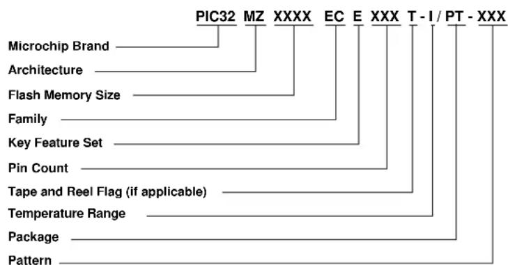
flowchart
graph TD
    A["PIC32"] --> B["Microchip Brand"]
    A --> C["Architecture"]
    A --> D["Flash Memory Size"]
    A --> E["Family"]
    A --> F["Key Feature Set"]
    A --> G["Pin Count"]
    A --> H["Tape and Reel Flag (if applicable)"]
    A --> I["Temperature Range"]
    A --> J["Package"]
    A --> K["Pattern"]
Example:
PIC32MZ2048ECH144-I/PT: Embedded Connectivity PIC32, MIPS32 ^® microAptiv ^™ MPU core, 2048 KB program memory, 144-pin, Industrial temperature, TQFP package.
Flash Memory Family
Architecture MZ = MIPS32
^® microAptiv ^TM MPU Core
Flash Memory Size 0512 = 512 KB 1024 = 1024 KB 2048 = 2048 KB
Family EC = Embedded Connectivity Microcontroller Family
Key Feature E = PIC32 EC Family Features (no CAN, no Crypto) F = PIC32 EC Family Features (CAN, no Crypto) G = PIC32 EC Family Features (no CAN, no Crypto) H = PIC32 EC Family Features (CAN, no Crypto) K = PIC32 EC Family Features (Crypto and CAN) M = PIC32 EC Family Features (Crypto and CAN)
Pin Count 064 = 64-pin 100 = 100-pin 124 = 124-pin 144 = 144-pin
Temperature Range I = -40°C to +85°C (Industrial)
Package MR = 64-Lead (9x9x0.9 mm) QFN (Plastic Quad Flatpack) PT = 64-Lead (10x10x1 mm) TQFP (Thin Quad Flatpack) PT = 100-Lead (12x12x1 mm) TQFP (Thin Quad Flatpack) PF = 100-Lead (14x14x1 mm) TQFP (Thin Quad Flatpack) TL = 124-Lead (9x9x0.9 mm) VTLA (Very Thin Leadless Array) PH = 144-Lead (16x16x1 mm) TQFP (Thin Quad Flatpack) PL = 144-Lead (20x20x1.40 mm) LQFP (Low Profile Quad Flatpack)
Pattern Three-digit QTP, SQTP, Code or Special Requirements (blank otherwise) ES = Engineering Sample
Note the following details of the code protection feature on Microchip devices:
• Microchip products meet the specification contained in their particular Microchip Data Sheet.
- Microchip believes that its family of products is one of the most secure families of its kind on the market today, when used in the intended manner and under normal conditions.
- There are dishonest and possibly illegal methods used to breach the code protection feature. All of these methods, to our knowledge, require using the Microchip products in a manner outside the operating specifications contained in Microchip's Data Sheets. Most likely, the person doing so is engaged in theft of intellectual property.
- Microchip is willing to work with the customer who is concerned about the integrity of their code.
- Neither Microchip nor any other semiconductor manufacturer can guarantee the security of their code. Code protection does not mean that we are guaranteeing the product as “unbreakable.”
Code protection is constantly evolving. We at Microchip are committed to continuously improving the code protection features of our products. Attempts to break Microchip's code protection feature may be a violation of the Digital Millennium Copyright Act. If such acts allow unauthorized access to your software or other copyrighted work, you may have a right to sue for relief under that Act.
Information contained in this publication regarding device applications and the like is provided only for your convenience and may be superseded by updates. It is your responsibility to ensure that your application meets with your specifications. MICROCHIP MAKES NO REPRESENTATIONS OR WARRANTIES OF ANY KIND WHETHER EXPRESS OR IMPLIED, WRITTEN OR ORAL, STATUTORY OR OTHERWISE, RELATED TO THE INFORMATION, INCLUDING BUT NOT LIMITED TO ITS CONDITION, QUALITY, PERFORMANCE, MERCHANTABILITY OR FITNESS FOR PURPOSE. Microchip disclaims all liability arising from this information and its use. Use of Microchip devices in life support and/or safety applications is entirely at the buyer's risk, and the buyer agrees to defend, indemnify and hold harmless Microchip from any and all damages, claims, suits, or expenses resulting from such use. No licenses are conveyed, implicitly or otherwise, under any Microchip intellectual property rights unless otherwise stated.
Microchip received ISO/TS-16949:2009 certification for its worldwide headquarters, design and wafer fabrication facilities in Chandler and Tempe, Arizona; Gresham, Oregon and design centers in California and India. The Company's quality system processes and procedures are for its PIC® MCUs and dsPIC® DSCs, KEELOQ® code hopping devices, Serial EEPROMs, microperipherals, nonvolatile memory and analog products. In addition, Microchip's quality system for the design and manufacture of development systems is ISO 9001:2000 certified.
QUALITY MANAGEMENT SYSTEM CERTIFIED BY DNV = ISO/TS 16949=
Trademarks
The Microchip name and logo, the Microchip logo, AnyRate, AVR, AVR logo, AVR Freaks, BeaconThings, BitCloud, CryptoMemory, CryptoRF, dsPIC, FlashFlex, flexPWR, Heldo, JukeBlox, KEELOQ, KEELOQ logo, Kleer, LANCheck, LINK MD, maXStylus, maXTouch, MediaLB, megaAVR, MOST, MOST logo, MPLAB, OptoLyzer, PIC, picoPower, PICSTART, PIC32 logo, Prochip Designer, QTouch, RightTouch, SAM-BA, SpyNIC, SST, SST Logo, SuperFlash, tinyAVR, UNI/O, and XMEGA are registered trademarks of Microchip Technology Incorporated in the U.S.A. and other countries.
ClockWorks, The Embedded Control Solutions Company, EtherSynch, Hyper Speed Control, HyperLight Load, IntelliMOS, mTouch, Precision Edge, and Quiet-Wire are registered trademarks of Microchip Technology Incorporated in the U.S.A.
Adjacent Key Suppression, AKS, Analog-for-the-Digital Age, Any Capacitor, AnyIn, AnyOut, BodyCom, chipKIT, chipKIT logo, CodeGuard, CryptoAuthentication, CryptoCompanion, CryptoController, dsPICDEM, dsPICDEM.net, Dynamic Average Matching, DAM, ECAN, EtherGREEN, In-Circuit Serial Programming, ICSP, Inter-Chip Connectivity, JitterBlocker, KleerNet, KleerNet logo, Mindi, MiWi, motorBench, MPASM, MPF, MPLAB Certified logo, MPLIB, MPLINK, MultiTRAK, NetDetach, Omniscient Code Generation, PICDEM, PICDEM.net, PICkit, PICtail, PureSilicon, QMatrix, RightTouch logo, REAL ICE, Ripple Blocker, SAM-ICE, Serial Quad I/O, SMART-I.S., SQL, SuperSwitcher, SuperSwitcher II, Total Endurance, TSHARC, USBCheck, VariSense, ViewSpan, WiperLock, Wireless DNA, and ZENA are trademarks of Microchip Technology Incorporated in the U.S.A. and other countries.
SQTP is a service mark of Microchip Technology Incorporated in the U.S.A.
Silicon Storage Technology is a registered trademark of Microchip Technology Inc. in other countries.
GestIC is a registered trademark of Microchip Technology Germany II GmbH & Co. KG, a subsidiary of Microchip Technology Inc., in other countries.
All other trademarks mentioned herein are property of their respective companies.
© 2013-2016, Microchip Technology Incorporated, All Rights Reserved.
ISBN: 978-1-5224-1186-4
Worldwide Sales and Service
AMERICAS
Corporate Office
2355 West Chandler Blvd.
Chandler, AZ 85224-6199
Tel: 480-792-7200
Fax: 480-792-7277
Technical Support:
http://www.microchip.com/
support
Web Address:
www.microchip.com
Atlanta
Duluth, GA
Tel: 678-957-9614
Fax: 678-957-1455
Austin, TX
Tel: 512-257-3370
Boston
Westborough, MA
Tel: 774-760-0087
Fax: 774-760-0088
Chicago
Itasca, IL
Tel: 630-285-0071
Fax: 630-285-0075
Dallas
Addison, TX
Tel: 972-818-7423
Fax: 972-818-2924
Detroit
Novi, MI
Tel: 248-848-4000
Houston, TX
Tel: 281-894-5983
Indianapolis
Noblesville, IN
Tel: 317-773-8323
Fax: 317-773-5453
Tel: 317-536-2380
Los Angeles
Mission Viejo, CA
Tel: 949-462-9523
Fax: 949-462-9608
Tel: 951-273-7800
Raleigh, NC
Tel: 919-844-7510
New York, NY
Tel: 631-435-6000
San Jose, CA
Tel: 408-735-9110
Tel: 408-436-4270
Canada - Toronto
Tel: 905-695-1980
Fax: 905-695-2078
ASIA/PACIFIC
Asia Pacific Office
Suites 3707-14, 37th Floor
Tower 6, The Gateway
Harbour City, Kowloon
Hong Kong
Tel: 852-2943-5100
Fax: 852-2401-3431
Australia - Sydney
Tel: 61-2-9868-6733
Fax: 61-2-9868-6755
China - Beijing
Tel: 86-10-8569-7000
Fax: 86-10-8528-2104
China - Chengdu
Tel: 86-28-8665-5511
Fax: 86-28-8665-7889
China - Chongqing
Tel: 86-23-8980-9588
Fax: 86-23-8980-9500
China - Dongguan
Tel: 86-769-8702-9880
China - Guangzhou
Tel: 86-20-8755-8029
China - Hangzhou
Tel: 86-571-8792-8115
Fax: 86-571-8792-8116
China - Hong Kong SAR
Tel: 852-2943-5100
Fax: 852-2401-3431
China - Nanjing
Tel: 86-25-8473-2460
Fax: 86-25-8473-2470
China - Qingdao
Tel: 86-532-8502-7355
Fax: 86-532-8502-7205
China - Shanghai
Tel: 86-21-3326-8000
Fax: 86-21-3326-8021
China - Shenyang
Tel: 86-24-2334-2829
Fax: 86-24-2334-2393
China - Shenzhen
Tel: 86-755-8864-2200
Fax: 86-755-8203-1760
China - Wuhan
Tel: 86-27-5980-5300
Fax: 86-27-5980-5118
China - Xian
Tel: 86-29-8833-7252
Fax: 86-29-8833-7256
ASIA/PACIFIC
China - Xiamen
Tel: 86-592-2388138
Fax: 86-592-2388130
China - Zhuhai
Tel: 86-756-3210040
Fax: 86-756-3210049
India - Bangalore
Tel: 91-80-3090-4444
Fax: 91-80-3090-4123
India - New Delhi
Tel: 91-11-4160-8631
Fax: 91-11-4160-8632
India - Pune
Tel: 91-20-3019-1500
Japan - Osaka
Tel: 81-6-6152-7160
Fax: 81-6-6152-9310
Japan - Tokyo
Tel: 81-3-6880-3770
Fax: 81-3-6880-3771
Korea - Daegu
Tel: 82-53-744-4301
Fax: 82-53-744-4302
Korea - Seoul
Tel: 82-2-554-7200
Fax: 82-2-558-5932 or
82-2-558-5934
Malaysia - Kuala Lumpur
Tel: 60-3-6201-9857
Fax: 60-3-6201-9859
Malaysia - Penang
Tel: 60-4-227-8870
Fax: 60-4-227-4068
Philippines - Manila
Tel: 63-2-634-9065
Fax: 63-2-634-9069
Singapore
Tel: 65-6334-8870
Fax: 65-6334-8850
Taiwan - Hsin Chu
Tel: 886-3-5778-366
Fax: 886-3-5770-955
Taiwan - Kaohsiung
Tel: 886-7-213-7830
Taiwan - Taipei
Tel: 886-2-2508-8600
Fax: 886-2-2508-0102
Thailand - Bangkok
Tel: 66-2-694-1351
Fax: 66-2-694-1350
EUROPE
Austria - Wels
Tel: 43-7242-2244-39
Fax: 43-7242-2244-393
Denmark - Copenhagen
Tel: 45-4450-2828
Fax: 45-4485-2829
Finland - Espoo
Tel: 358-9-4520-820
France - Paris
Tel: 33-1-69-53-63-20
Fax: 33-1-69-30-90-79
France - Saint Cloud
Tel: 33-1-30-60-70-00
Germany - Garching
Tel: 49-8931-9700
Germany - Haan
Tel: 49-2129-3766400
Germany - Heilbronn
Tel: 49-7131-67-3636
Germany - Karlsruhe
Tel: 49-721-625370
Germany - Munich
Tel: 49-89-627-144-0
Fax: 49-89-627-144-44
Germany - Rosenheim
Tel: 49-8031-354-560
Israel - Ra'anana
Tel: 972-9-744-7705
Italy - Milan
Tel: 39-0331-742611
Fax: 39-0331-466781
Italy - Padova
Tel:39-049-7625286
Netherlands - Drunen
Tel: 31-416-690399
Fax: 31-416-690340
Norway-Trondheim
Tel: 47-7289-7561
Poland - Warsaw
Tel: 48-22-3325737
Romania - Bucharest
Tel: 40-21-407-87-50
Spain - Madrid
Tel: 34-91-708-08-90
Fax: 34-91-708-08-91
Sweden - Gothenberg
Tel: 46-31-704-60-40
Sweden - Stockholm
Tel: 46-8-5090-4654
UK - Wokingham
Tel: 44-118-921-5800
Fax: 44-118-921-5820