EVB-USB3330 - Development board Microchip - Free user manual and instructions
Find the device manual for free EVB-USB3330 Microchip in PDF.

User questions about EVB-USB3330 Microchip
0 question about this device. Answer the ones you know or ask your own.
Ask a new question about this device
Download the instructions for your Development board in PDF format for free! Find your manual EVB-USB3330 - Microchip and take your electronic device back in hand. On this page are published all the documents necessary for the use of your device. EVB-USB3330 by Microchip.
USER MANUAL EVB-USB3330 Microchip
EVB-USB3330 USB Transceiver Evaluation Board User Manual

text_image
USB320X CUSTOMER REFERENCE BOARD M14GG-30045 TriadElectronic.com SMSC®Copyright © 2009 SMSC or its subsidiaries. All rights reserved.
Circuit diagrams and other information relating to SMSC products are included as a means of illustrating typical applications. Consequently, complete information sufficient for construction purposes is not necessarily given. Although the information has been checked and is believed to be accurate, no responsibility is assumed for inaccuracies. SMSC reserves the right to make changes to specifications and product descriptions at any time without notice. Contact your local SMSC sales office to obtain the latest specifications before placing your product order. The provision of this information does not convey to the purchaser of the described semiconductor devices any licenses under any patent rights or other intellectual property rights of SMSC or others. All sales are expressly conditional on your agreement to the terms and conditions of the most recently dated version of SMSC's standard Terms of Sale Agreement dated before the date of your order (the "Terms of Sale Agreement"). The product may contain design defects or errors known as anomalies which may cause the product's functions to deviate from published specifications. Anomaly sheets are available upon request. SMSC products are not designed, intended, authorized or warranted for use in any life support or other application where product failure could cause or contribute to personal injury or severe property damage. Any and all such uses without prior written approval of an Officer of SMSC and further testing and/or modification will be fully at the risk of the customer. Copies of this document or other SMSC literature, as well as the Terms of Sale Agreement, may be obtained by visiting SMSC's website at http://www.smsc.com. SMSC is a registered trademark of Standard Microsystems Corporation ("SMSC"). Product names and company names are the trademarks of their respective holders.
SMSC DISCLAIMS AND EXCLUDES ANY AND ALL WARRANTIES, INCLUDING WITHOUT LIMITATION ANY AND ALL IMPLIED WARRANTIES OF MERCHANTABILITY, FITNESS FOR A PARTICULAR PURPOSE, TITLE, AND AGAINST INFRINGEMENT AND THE LIKE, AND ANY AND ALL WARRANTIES ARISING FROM ANY COURSE OF DEALING OR USAGE OF TRADE. IN NO EVENT SHALL SMSC BE LIABLE FOR ANY DIRECT, INCIDENTAL, INDIRECT, SPECIAL, PUNITIVE, OR CONSEQUENTIAL DAMAGES; OR FOR LOST DATA, PROFITS, SAVINGS OR REVENUES OF ANY KIND; REGARDLESS OF THE FORM OF ACTION, WHETHER BASED ON CONTRACT; TORT; NEGLIGENCE OF SMSC OR OTHERS; STRICT LIABILITY; BREACH OF WARRANTY; OR OTHERWISE; WHETHER OR NOT ANY REMEDY OF BUYER IS HELD TO HAVE FAILED OF ITS ESSENTIAL PURPOSE, AND WHETHER OR NOT SMSC HAS BEEN ADVISED OF THE POSSIBILITY OF SUCH DAMAGES.
1 Introduction
This user manual is for the USB3330 USB Transceiver Evaluation Board (EVB) for use with USB3330 products.
The USB3330 features a ULPI interface to support systems with USB Host, Device, or On-the-Go (OTG) capability. SMSC supplies a complete family of transceiver products to meet the needs of many applications.
2 Overview
The EVB-USB3330 is a Daughter Card designed to plug into a user's test system using a T&MT connector. The card attaches to a USB link layer to create a USB Host, Device, or On-the-Go (OTG) system. The board edge connector meets the UTMI+ Low Pin Interface (ULPI) Standard requirements for the T&MT connector.
A link to the ULPI Working Group Page is available at www.smsc.com or may be obtained from your local FAE. The EVB-USB3330 includes USB3330 packaged silicon and all external components required for the USB transceiver function.
This manual describes PCB assembly PCB-7164AZ.
2.1 Supplying VBUS Voltage
In Host or OTG operation, the EVB-USB3330 must provide 5 Volts on V_BUS at the USB connector. The EVB-USB3330 includes a switch that can drive V_BUS using the 5 Volt supply that comes from pin 28 of the T&MT connector.
The VBUS switch is controlled by the DRVVBUS pin on the T&MT connector. The presence of a zero ohm resistor at R13 will route the 5V signal to the part and USB connectors. If R13 is empty then the EVB will not supply 5V. The board will operate as a USB Peripheral. The 5 Volt switch is backdrive protected when in the off state. See Section 2.7 and Section 2.8 for more information on configuring the EVB-USB3330 for OTG and Host operation.
The zero ohm resistor on R24 can be removed to permanently leave the VBUS switch on.
2.2 Edge Connector for Digital I/O
The T&MT edge connector is compliant to the ULPI specification. Part numbers and manufacturers for this connector and it's mate are given in Table 2.1
Table 2.1 Edge Connector on the EVB-USB3330
| PART NUMBER DESCRIPTION MANUFACTURER | ||
| 2-557101-5 100 pin edge connector on EVB-USB3330 AMP | ||
| 2-557-101-5 Mating connector to the EVB-USB3330 AMP | ||
| 1-1734037-0 Alternate 100 pin edge connector for EVB-USB3330 TYCO | ||
| 1-1734099-0 | Alternate mating connector to the EVB-USB3330 | TYCO |
2.3 REFCLK Frequency Selection
The EVB-USB3330 offers a user selectable reference clock frequency. R11, R14-R16 are used to configure the REF[1:0] signals which will select the reference clock frequency desired on the EVB-USB3330. Ensure that the frequency of the reference clock or reference crystal being used matches the desired operation frequency configured based on Table 2.2 below. By default, the EVB-USB3330
is configured for 26MHz REFCLK operation. The Resistor pads are either installed with a zero ohm resistor, or left empty.
Table 2.2 Reference Frequency Selection Resistor Configurations
| R11 R16 | R14 R15 REFCLK FREQUENCY | |||
| EMPTY INSTALL INSTALL | EMPTY 13.0 | MHz | ||
| INSTALL EMPTY | EMPTY 24.0 | MHz | ||
| EMPTY INSTALL EMPTY | INSTALL 19.2 | MHz | ||
| INSTALL EMPTY | INSTALL 26.0 | MHz (Default) | ||
2.4 USB Connector
A standard Mini-AB connector is provided to attach a USB cable or connector. The footprint can also accept a micro-AB connector. See the bill of materials in Section 6 for connector part numbers. Do not substitute a different part number for the Mini-AB receptacle or a short circuit of the USB signals may result at the micro-AB connector PCB footprint.
2.5 VBUS Present Detection
The USB controller must detect VBUS when a USB cable is attached in device mode or when the USB controller turns on VBUS in host or OTG mode. The USB connector VBUS signal is connected to the VBUS pin of the USB3330. The USB3330 includes all of the comparators required to detect VBUS and report the state of VBUS to the USB controller via the ULPI bus.
2.6 ULPI Signal Test Points
Probe points at location J2, provide access to all ULPI signals. Install the Tektronix logic analyzer probe retention kit at J2 to probe these signals. Ordering information for the retention kit is provided in the bill of materials
2.7 Converting the EVB to an OTG System
"Out of the box", the EVB-USB3330 is delivered as a USB Device system. To convert it to be a USB OTG development board, the following modifications must be made:
- Install R13 (zero ohm resistor). This connects the VBUS 5V switch to the VBUS signal.
- Remove R23. This is the R_VBUS value required for a USB Device.
- Install R10 (1.0K, 1W resistor). This is the R_VBUS value required for a USB OTG Device.
Since the USB3330 is designed to accommodate up to 30V on VBUS, R10 is rated at 1W to accommodate this entire voltage range. Refer to the USB333X datasheet for more information on sizing this resistor
2.8 Converting the EVB to a Host System
"Out of the box", the EVB-USB3330 is delivered as a USB Device System. To convert it to be a USB Host development board, the following modifications must be made:
- Install R13 (zero ohm resistor). This connects the VBUS 5V switch to the VBUS signal.
- Install C20 (150uF capacitor). This increases the value of C_VBUS to be USB 2.0 Host compliant.
2.9 Converting the EVB to Support ULPI Clock Input Mode
"Out of the box", the EVB-USB3330 uses an oscillator (X1) as the clock reference, and is configured for ULPI Clock Output Mode where CLKOUT sources a 60MHz clock. To convert the EVB to support ULPI Clock Input Mode, the following changes must be made:
- Install R12 (zero ohm resistor). This shorts CLKOUT to VDD18.
- Install R3 (zero ohm resistor). This shorts REFCLK to the System Clock pin on the T&MT connector.
- Remove R4 and R7. This will disconnect the onboard reference clock source from the part.
Refer to the USB3330 datasheet for more information on ULPI Clock Input Mode.
2.10 T&MT Pin Description
The T&MT signal names, pin number and function are described in Table 43 and Table 44 of the ULPI Specification rev 1.1.
The EVB-USB3330 fully implements a ULPI compliant interface to the T&MT connector, including support for ULPI Clock Input Mode. This EVB supports a 1.8V ULPI I/O voltage. All signals are described in Table 2.3
Table 2.3 T&MT Connector Pin Definitions
| PIN NAME DESCRIPTION DIRECTION | |||
| 86, 36,85, 34,83, 33,82, 31 | DATA[7:0]Refer to Schematic for Connector Pin Assignment | ULPI Data Bus IN/OUT | |
| 96 STP | ULPI | STP Signal | INPUT TO EVB |
| 70 DIR | ULPI | DIR Signal | OUTPUT FROM EVB |
| 71 NXT | ULPI | NXT Signal | OUTPUT FROM EVB |
| 90 CLKOUT | ULPI | Clock Signal | OUTPUT FROM EVB |
| 14 DRVVBUS | VBUS | Switch enable. When high the VBUS switch will turn on routing 5V to the VBUS pin (if R13 is present) | INPUT |
| 55 VBUS_FAULT_N | Driven low by the VBUS switch (U2) in the event of a switch fault condition. | OUTPUT | |
| 17 RESET | Asserting RESET will place the USB3330 in a low power state. Upon exiting this state (RESET=0), all ULPI registers will contain power-on reset values. | INPUT | |
| 47 VBUS_IN | This pin is not connected | NO CONNECT | |
| 28 VBUS_OUT | +5V from the T&MT connector | INPUT TO EVB | |
| 8,16, 57,69 | VDD | +3.3V from the T&MT connector | INPUT TO EVB |
| 52 | SYSTEM_CLOCK | Optional clock input to EVB. The EVB is built with the USB3330 REFCLK provided by an oscillator. See Section 2.9 for more information on configuring the EVB-USB3330 for ULPI Clock Input mode. | NO CONNECT (input to EVB if R3 is installed) |
Table 2.3 T&MT Connector Pin Definitions
| PIN NAME DESCRIPTION DIRECTION | |||
| 100 PSU_SHD_N This pin is driven low indicating that +3.3V must be sourced from the link through the T&MT connector pins 8, 16, 57, 69 and +5.0V must be sourced from the link through the T&MT connector pin 28. | OUTPUTFROM EVB | ||
| 49 DC_PSNT_N This pin is driven low indicating a daughter card is present. | OUTPUTFROM EVB | ||
3 Getting Started
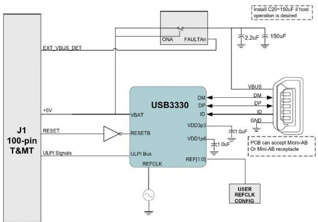
The block diagram in Figure 3.1 gives a simplified view of the EVB-USB3330. The EVB-USB3330 is ready for device operation. To modify the board for OTG or Host applications, refer to Section 2.7 or Section 2.8, respectively.
It is required to provide +5V to T&MT connector pin 28 and +3.3V on T&MT pins 8,16,57,69 to power the EVB-USB3330.
The EVB-USB3330 is built with a USB Mini-AB receptacle. Do not substitute a Mini-AB receptacle different from the one specified in the bill of materials, or a short circuit may occur on the USB signals at the Micro-AB connector PCB footprint.
flowchart
graph TD
    A["J1 100-pin T&MT"] -->|EXT_VBUS_DET| B["USB3330"]
    A -->|+5V| C["RESET"]
    A -->|ULPI Signals| D["RESETB"]
    B --> E["VBAT"]
    B --> F["REFCLK"]
    B --> G["VDD3p3"]
    B --> H["VDD1p8"]
    B --> I["DM"]
    B --> J["DP"]
    B --> K["ID"]
    B --> L["REF[1:0"]]
    B --> M["1.0uF"]
    B --> N["GND"]
    B --> O["2.2uF"]
    B --> P["150uF"]
    B --> Q["ONA"]
    B --> R["FAULTAn"]
    B --> S["USB3330"]
    S --> T["VBUS"]
    S --> U["PCB can accept Micro-AB Or Mini-AB receptacle"]
    S --> V["USER REFCLK CONFIG"]
    style S fill:#cce5ff,stroke:#333
Figure 3.1 Block Diagram of EVB-USB3330
When the EVB-USB3330 is powered on, check the following things to be certain the board is functioning normally:
- RESET should be de-asserted (logic low at the T&MT connector and RESETB at the USB3330 should be logic high = VDD18). If RESETB=0, the USB3330 will be in a low power state.
The voltage at R2 (RBIAS) should be 0.8V DC. If this voltage is not present, the USB3330 is in a low power state.
There should be a digital 60 MHz square wave signal at T&MT connector pin 90. The amplitude should be approximately 1.8V. This is the CLKOUT signal of the USB3330 (Except when the part is configured for Clock Input Mode see Section 2.9 for more details.)
The voltage at C3 should be approximately 3.3V. This is the USB3330 internal 3.3V voltage regulator output.
The voltage at C4 should be 1.8V. This is the USB3330 internal 1.8V regulator output.
4 Protecting VBUS from Non-Compliant VBUS Voltages
The USB3330 is fully tolerant to VBUS voltages up to 30V. An external resistor on the VBUS line ( R_VBUS ) is required for the integrated overvoltage protection circuit in the USB3330. R_VBUS is either R10 or R23 on the EVB-USB3330. For peripheral and host applications, R_VBUS is 10K (install R23, remove R10). For OTG applications, R_VBUS is 1K (install R10, remove R23).
5 EVB-USB3330 Schematic

text_image
EVB-USB3330 Evaluation Board T&MT Connector This portion of the schematic shows components needed for PHY to operate in a HS device application. USB3330 REFCLK Source UBP1 Testpoints ULPI Testpoints REFCLK Source For Host/OTG applications a VBUS switch is required For host applications 150 uF to ground is required on VBUS to comply with the USB2.0 specification. R13 Samp Power Capac / OTG UHV Peripulse1 SMSC SELECTED BY: USB2.0 USB3330 Collector Reference Board SMSC Selected by: USB2.0 For R13 For Host/OTG applications a VBUS switch is requiredFigure 5.1 EVB-USB3330 Schematic
PCB: PCB7164AZ-A00
Transceiver: USB3330
BOM Rev: A Date 12/2/2008
| Item Number | Ref Des | QTY | Value Tolerance | Description | Manufacturer Manufacturer Part Number | Digikey Part Number | ||
| 10 C1 | 2.2μF, 50V ±10% | CAP | CER 2.2UF | 50V X7R 1206 | Murata Electronics North America | GRM31CR71H225KA88L | 490-3367-1-ND | |
| 20 | C3, C4 | 2 | 1.0μF, 6.3V | 20% | CAP CER 1.0UF 6.3V X5R 0402 | Murata Electronics North America | GRM155R60J105KE19D | 490-1320-1-ND |
| 30 | C2, C8, C9, C11, C13 | 5 | 0.1μF, 10V | 20% | CAP CER 0.1UF 16V Y5V 0402 | Kemet | C0402C104K8PACTU | 399-3027-1-ND |
| 40 | C20 | DNP | 150.0μF,16V | ±20% | CAP 150UF 16V ELECT FK SMD | PANASONIC | EEV-FK1C151XP | PCE3512CT-ND |
| 50 | R1 | 1 | 100K | ±5% | RES 100K OHM 1/16W 5% 0402 SMD | Vishay/Dale | CRCW0402100KJNED | 541-100KJCT-ND |
| 60 | R2 | 1 | 8.06K | ±1% | RES 8.06K OHM 1/16W 1% 0402 SMD | Vishay/Dale | CRCW04028K06FKED | 541-8.06KLCT-ND |
| 70 | R3, R4, R12, R13, R14, R16 | DNP | ZERO | ±5% | RES ZERO OHM 1/16W 5% 0402 SMD | PANASONIC | ERJ-2GE0R00X | P0.0JCT-ND |
| 80 | R7, R11, R15, R24 | 4 | ZERO | ±5% | RES ZERO OHM 1/16W 5% 0402 SMD | PANASONIC | ERJ-2GE0R00X | P0.0JCT-ND |
| 90 | R5, R9 | 2 | 10K | ±5% | RES 10K OHM 1/16W 5% 0402 SMD | PANASONIC | ERJ-2GEJ103X | P10KJCT-ND |
| 100 | R6 | DNP | 10K | ±5% | RES 10K OHM 1/16W 5% 0402 SMD | PANASONIC | ERJ-2GEJ103X | P10KJCT-ND |
| 110 | R10 | DNP | 1K | 1% | RES 1K OHM 1W 2512 SMD | PANASONIC | ERJ-1TYF102U | PT1KAECT-ND |
| 120 | R23 | 1 | 20K | 1% | RES 20.0K OHM 1/10W 0603 SMD | YAGEO | RC0603FR-0720KL | 311-20.0KHRCT-ND |
| 130 | U2 | 1 | IC SW USB DUAL W/FB 10-UMAX | Maxim Integrated Products | MAX1823BEUB+ | MAX1823BEUB+-ND | ||
| 140 | U5 | 1 | IC SINGLE BUFFER, OD OUTPUT SOT-23-5 | TEXAS INSTRUMENTS | SN74LVC1G07DBVR | 296-8485-1-ND | ||
| 150 | U6 | DNP | IC SINGLE INVERTER-GATE SOT-23-5 | TEXAS INSTRUMENTS | SN74LVC1G04DBVR | 296-11599-1-ND | ||
| 160 | U8 | 1 | IC SINGLE INVERTER-GATE SOT-23-5 | TEXAS INSTRUMENTS | SN74LVC1G04DBVR | 296-11599-1-ND | ||
| 170 | U10 | 1 | USB High Speed Transceiver | SMSC | USB3330A-GL-TR | |||
| 180 | P1 | DNP | CONN RCPT MICRO USB AB SMD R/A | Hirose Electric Co Ltd | ZX62-AB-5P | H11495CT-ND | ||
| 190 | P2 | 1 | USB-OTG, Mini AB Receptacle, Surface Mount Right Angle | Molex/Waldom Electronics Corp | 56579-0576 | WM17122CT-ND | ||
| 200 | J1 | 1 | RCPT ASSY,R/A,CHAMP 050,100 P | TYCO ELECTRONICS/AMP | 1-1734037-0 | A33470-ND | ||
| 210 | J2 | DNP | Retention Kit for P6960/P6980 Logic analyzer Probe | Tektronix | 020-2539-00 | |||
| 220 | TP1, TP2, TP3 | 3 | PC TEST POINT MINIATURE SMT | Keystone Electronics | 5015 | 5015KCT-ND | ||
| 230 | X1 | 1 | Note 1 | OSCILLATOR PROG 3.3V +~50PPM SMD 26.0MHz | ABRACON CORPORATION | AP3S-BLANKS | AP3S3EC-ND |
Note 1 Oscillator frequency depends on frequency selected by U10 pins REFSL[2:0]. Frequency must be specified at time of order.
Figure 6.1 EVB-USB3330 Bill of Materials
7 Revision History
Table 7.1 Revision History
| REVISION LEVEL & DATE SECTION/FIGURE/ENTRY CORRECTION | ||
| Rev. 1.1(02-02-10) | Cosmetic changes | |
| Rev. 1.0(08-19-09) | Initial Release | |