mcp4132 - Electronic Components Microchip - Free user manual and instructions
Find the device manual for free mcp4132 Microchip in PDF.

User questions about mcp4132 Microchip
0 question about this device. Answer the ones you know or ask your own.
Ask a new question about this device
Download the instructions for your Electronic Components in PDF format for free! Find your manual mcp4132 - Microchip and take your electronic device back in hand. On this page are published all the documents necessary for the use of your device. mcp4132 by Microchip.
USER MANUAL mcp4132 Microchip
7/8-Bit Single/Dual SPI Digital POT with Volatile Memory
Features
- Single or Dual Resistor Network options
- Potentiometer or Rheostat configuration options
• Resistor Network Resolution - 7-bit: 128 Resistors (129 Steps)
- 8-bit: 256 Resistors (257 Steps)
- R_AB Resistances options of:
- 5 k Ω
- 1 0 k Ω
- 5 0 k Ω
- 100 kΩ
• Zero Scale to Full-Scale Wiper operation
- Low Wiper Resistance: 75 (typical)
- Low Tempco:
- Absolute (Rheostat): 50 ppm typical (0°C to 70°C)
- Ratiometric (Potentiometer): 15 ppm typical
• SPI Serial Interface (10 MHz, modes 0,0 & 1,1)
- High-Speed Read/Writes to wiper registers
- SDI/SDO multiplexing (MCP41X1 only)
- Resistor Network Terminal Disconnect Feature via:
- Shutdown pin (SHDN)
- Terminal Control (TCON) Register
- Brown-out reset protection (1.5V typical)
- Serial Interface Inactive current (2.5 uA typical)
• High-Voltage Tolerant Digital Inputs: Up to 12.5V
• Supports Split Rail Applications - Internal weak pull-up on all digital inputs
- Wide Operating Voltage:
- 2.7V to 5.5V - Device Characteristics Specified
- 1.8V to 5.5V - Device Operation
- Wide Bandwidth (-3 dB) Operation:
- 2 MHz (typical) for 5.0 kΩ device
- Extended temperature range (-40°C to +125°C)
Description
The MCP41XX and MCP42XX devices offer a wide range of product offerings using an SPI interface. This family of devices support 7-bit and 8-bit resistor networks, and Potentiometer and Rheostat pinouts.
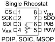
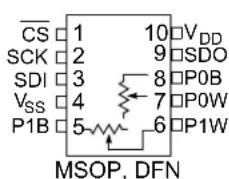
Package Types (top view)
MCP41X1
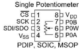
text_image
Single Potentiometer CS 1 8 VDD SCK 2 7 P0B SDI/SDO 3 6 P0W Vss 4 5 P0A PDIP, SOIC, MSOPMCP41X2

text_image
CS 1 ○ 8 VDD SCK 2 EP 7 P0B SDI/SDO 3 9 6 P0W Vss 4 5 P0A 3x3 DFN*
text_image
CS 1 ○ 8 VDD SCK 2 EP 7 SDO SDI 3 9 6 P0B Vss 4 5 P0W 3x3 DFN*MCP42X1 Dual Potentiometers
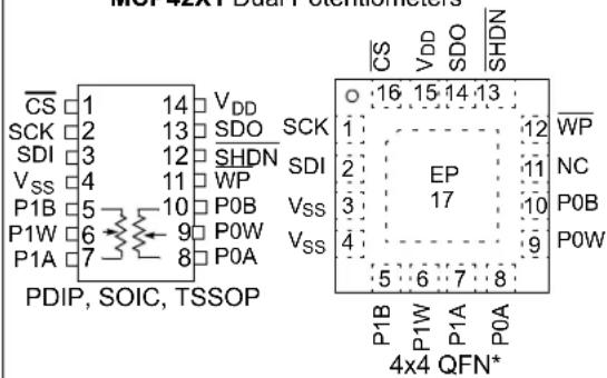
text_image
CS 1 14 VDD SCK 2 13 SDO SCK SDI 3 12 SHDN Vss 4 11 WP P1B 5 10 P0B P0W P1W 6 9 P0A P1A 7 8 PDIP, SOIC, TSSOP EP 17 CS VDD SDO SHDN 16 15 14 13 12 WP NC P0B P0W 4 5 6 7 8 P1B P1W P1A P0A 4x4 QFN*MCP42X2 Dual Rheostat
text_image
CS 1 10 VDD SCK 2 9 SDO SDI 3 8 P0B VSS 4 7 P0W P1B 5 6 P1W MSOP, DFN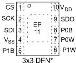
text_image
CS 1 ○ 10 VDD SCK 2 EP 9 SDO SDI 3 11 8 P0B Vss 4 7 P0W P1B 5 6 P1W 3x3 DFN** Includes Exposed Thermal Pad (EP); see Table 3-1.
Device Block Diagram

flowchart
graph TD
    A["V_DD"] --> B["Power-up/ Brown-out Control"]
    C["V_SS"] --> B
    D["CS"] --> E["SPI Serial Interface Module & Control Logic (WiperLock™ Technology)"]
    F["SCK"] --> E
    G["SDI"] --> E
    H["SDO"] --> E
    I["NC"] --> E
    J["SHDN"] --> E
    K["For Dual Potentiometer Devices Only"] --> L["Memory (4x9)"]
    L --> M["Wiper0 Wiper1 TCON STATUS"]
    N["For Dual Resistor Network Devices Only"] --> O["Resistor Network 0 (Pot 0)"]
    N --> P["Resistor Network 1 (Pot 1)"]
    N --> Q["Resistor Network 1 & TCON Register"]
    R["P0A"] <--> S["Resistor Network 0 (Pot 0)"]
    R["P0B"] <--> T["Resistor Network 1 (Pot 1)"]
    R["P1A"] <--> U["Resistor Network 1 & TCON Register"]
    R["P1B"] <--> V["Resistor Network 1 & TCON Register"]
    S --> W["Wiper 0 & TCON Register"]
    T --> X["Wiper 1 & TCON Register"]
    U --> Y["Wiper 1 & TCON Register"]
    V --> Z["Wiper 1 & TCON Register"]
Device Features
| Device | # of POTs | Wiper Configuration | Control Interface | Memory Type | WiperLock Technology | POR Wiper Setting | Resistance (typical) | # of Steps | V_DD Operating Range (2) | |
| R_AB Options (kΩ) | Wiper - R_W (Ω) | |||||||||
| MCP4131 (3) | 1 | Potentiometer(1) | SPI | RAM | No | Mid-Scale | 5.0, 10.0, 50.0, 100.0 | 0.75 129 | 1.8V to 5.5V | |
| MCP4132 (3) | 1 | Rheostat | SPI | RAM | No | Mid-Scale | 5.0, 10.0, 50.0, 100.0 | 75 | 129 | 1.8V to 5.5V |
| MCP4141 | 1 | Potentiometer (1) | SPI | EE | Yes | NV Wiper | 5.0, 10.0, 50.0, 100.0 | 75 | 129 | 2.7V to 5.5V |
| MCP4142 | 1 | Rheostat | SPI | EE | Yes | NV Wiper | 5.0, 10.0, 50.0, 100.0 | 75 | 129 | 2.7V to 5.5V |
| MCP4151 (3) | 1 | Potentiometer(1) | SPI | RAM | No | Mid-Scale | 5.0, 10.0, 50.0, 100.0 | 75 | 257 | 1.8V to 5.5V |
| MCP4152 (3) | 1 | Rheostat | SPI | RAM | No | Mid-Scale | 5.0, 10.0, 50.0, 100.0 | 75 | 257 | 1.8V to 5.5V |
| MCP4161 | 1 | Potentiometer (1) | SPI | EE | Yes | NV Wiper | 5.0, 10.0, 50.0, 100.0 | 75 | 257 | 2.7V to 5.5V |
| MCP4162 | 1 | Rheostat | SPI | EE | Yes | NV Wiper | 5.0, 10.0, 50.0, 100.0 | 75 | 257 | 2.7V to 5.5V |
| MCP4231 (3) | 2 | Potentiometer(1) | SPI | RAM | No | Mid-Scale | 5.0, 10.0, 50.0, 100.0 | 75 | 129 | 1.8V to 5.5V |
| MCP4232 (3) | 2 | Rheostat | SPI | RAM | No | Mid-Scale | 5.0, 10.0, 50.0, 100.0 | 75 | 129 | 1.8V to 5.5V |
| MCP4241 | 2 | Potentiometer (1) | SPI | EE | Yes | NV Wiper | 5.0, 10.0, 50.0, 100.0 | 75 | 129 | 2.7V to 5.5V |
| MCP4242 | 2 | Rheostat | SPI | EE | Yes | NV Wiper | 5.0, 10.0, 50.0, 100.0 | 75 | 129 | 2.7V to 5.5V |
| MCP4251 (3) | 2 | Potentiometer(1) | SPI | RAM | No | Mid-Scale | 5.0, 10.0, 50.0, 100.0 | 75 | 257 | 1.8V to 5.5V |
| MCP4252 (3) | 2 | Rheostat | SPI | RAM | No | Mid-Scale | 5.0, 10.0, 50.0, 100.0 | 75 | 257 | 1.8V to 5.5V |
| MCP4261 | 2 | Potentiometer (1) | SPI | EE | Yes | NV Wiper | 5.0, 10.0, 50.0, 100.0 | 75 | 257 | 2.7V to 5.5V |
| MCP4262 | 2 | Rheostat | SPI | EE | Yes | NV Wiper | 5.0, 10.0, 50.0, 100.0 | 75 | 257 | 2.7V to 5.5V |
Note 1: Floating either terminal (A or B) allows the device to be used as a Rheostat (variable resistor).
2: Analog characteristics only tested from 2.7V to 5.5V unless otherwise noted.
3: Please check Microchip web site for device release and availability.
1.0 ELECTRICAL CHARACTERISTICS
Absolute Maximum Ratings †
Voltage on V_DD with respect to V_SS -0.6V to +7.0V
Voltage on CS, SCK, SDI, SDI/SDO, and
SHDN with respect to V_SS -0.6V to 12.5V
Voltage on all other pins (PxA, PxW, PxB, and
SDO) with respect to V_SS -0.3V to V_DD + 0.3V
Input clamp current, I_IK
(V_I<0,V_I>V_DD,V_I>V_PPON HV pins) ± 20mA
Output clamp current, I_OK
(V_O<0 or V_O>V_DD) ±20 mA
Maximum output current sunk by any Output pin
.25 mA
Maximum output current sourced by any Output pin
.25 mA
Maximum current out of V_SS pin 100 mA
Maximum current into V_DD pin 100 mA
Maximum current into PxA, PxW & PxB pins ....±2.5 mA
Storage temperature ....-65°C to +150°C
Ambient temperature with power applied
-40°C to +125°C
Total power dissipation (Note 1) 400 mW
Soldering temperature of leads (10 seconds) ....+300°C
ESD protection on all pins ≥ 4 kV (HBM),
≥ 300V (MM)
Maximum Junction Temperature (T _J ) ....+150°C
Note 1: Power dissipation is calculated as follows:
Pdis = VDD x {IDD - ∑ IOH} + ∑ {(VDD-VOH) x IOH} + ∑ (Vol x IOL)
† Notice: Stresses above those listed under "Maximum Ratings" may cause permanent damage to the device. This is a stress rating only and functional operation of the device at those or any other conditions above those indicated in the operational listings of this specification is not implied. Exposure to maximum rating conditions for extended periods may affect device reliability.
AC/DC CHARACTERISTICS
| DC Characteristics | Standard Operating Conditions (unless otherwise specified)Operating Temperature -40°C ≤ TA ≤ +125°C (extended)All parameters apply across the specified operating ranges unless noted. V_DD = +2.7V to 5.5V, 5 kΩ, 10 kΩ, 50 kΩ, 100 kΩ devices.Typical specifications represent values for V_DD = 5.5V , T_A = +25°C . | ||||||
| Parameters Sym | Min Typ Max | Units Conditions | |||||
| Supply Voltage V | _DD | 2.7 — 5.5 V | |||||
| 1.8 — 2.7 V Serial Interface only. | |||||||
| , SDI, SDO,SCK, SHDN pinVoltage Range | V_HV | V_SS | — | 12.5V | V | _DDV ≥ 4.5V | The pin will be at oneof three input levels( V_IL , V_IH or V_IHH ). (Note 6) |
| V_SS | — | V_DD + 8.0V | V | V_DD < 4.5V | |||
| V_DD Start Voltageto ensure WiperReset | V_BOR | — | — 1.65 V | RAM retention voltage ( V_RAM ) < V_BOR | |||
| V_DD Rise Rate toensure Power-onReset | V_DDRR | (Note 9) | V/ms | ||||
| Delay after deviceexits the resetstate( V_DD > V_BOR ) | T_BORD | — | 10 | 20 | μs | ||
| Supply Current(Note 10) | _DD | — | — | 450 | μA | Serial Interface Active, V_DD = 5.5V , = V_IL , SCK @ 5 MHz,write all 0's to volatile Wiper 0 (address0h) | |
| — 2.5 | 5 | μA Serial Interface Inactive, = V_IH , V_DD = 5.5V | |||||
| — | 0.55 | 1 mA | Serial | Interface Active, V_DD = 5.5V , = V_IHH ,SCK @ 5 MHz,decrement volatile Wiper 0 (address 0h) | |||
Note 1: Resistance is defined as the resistance between terminal A to terminal B.
2: INL and DNL are measured at V_W with V_A = V_DD and V_B = V_SS .
3: MCP4XX1 only.
4: MCP4XX2 only, includes V_WZSE and V_WFSE .
5: Resistor terminals A, W and B's polarity with respect to each other is not restricted.
6: This specification by design.
7: Non-linearity is affected by wiper resistance ( R_W ), which changes significantly over voltage and temperature.
8: The MCP4XX1 is externally connected to match the configurations of the MCP41X2 and MCP42X2, and then tested.
9: POR/BOR is not rate dependent.
10: Supply current is independent of current through the resistor network.
AC/DC CHARACTERISTICS (CONTINUED)
| DC Characteristics | Standard Operating Conditions (unless otherwise specified)Operating Temperature -40°C ≤ TA ≤ +125°C (extended)All parameters apply across the specified operating ranges unless noted.VDD = +2.7V to 5.5V, 5 kΩ, 10 kΩ, 50 kΩ, 100 kΩ devices.Typical specifications represent values for VDD = 5.5V, TA = +25°C. | ||||||
| Parameters | Sym | Min | Typ | Max | Units | Conditions | |
| Resistance(±20%) | RAB | 4.0 | 5 | 6.0 | kΩ | -502 devices (Note 1) | |
| 8.0 | 10 | 12.0 | kΩ | -103 devices (Note 1) | |||
| 40.0 | 50 | 60.0 | kΩ | -503 devices (Note 1) | |||
| 80.0 | 100 | 120.0 | kΩ | -104 devices (Note 1) | |||
| Resolution N 257 Taps 8-bit No | Missing Codes | ||||||
| 129 Taps 7-bit | No Missing Codes | ||||||
| Step Resistance | RS | — | RAB / (256) | — | Ω | 8-bit | Note 6 |
| — | RAB / (128) | — | Ω | 7-bit | Note 6 | ||
| Nominal Resistance Match | |RAB0 - RAB1| / RAB | — | 0.2 | 1.25 | % | MCP42X1 devices only | |
| |RBW0 - RBW1| / RBW | — | 0.25 | 1.5 | % | MCP42X2 devices only,Code = Full-Scale | ||
| Wiper Resistance(Note 3, Note 4) | RW | — | 75 | 160 | Ω | VDD=5.5 V, IW=2.0 mA, code = 00h | |
| — | 75 | 300 | Ω | VDD=2.7 V, IW=2.0 mA, code = 00h | |||
| Nominal ResistanceTempco | ΔRAB/ΔT | — | 50 | — | ppm/°C | TA=-20°C to +70°C | |
| — | 100 — | ppm/°CT | A=-40°C to +85°C | ||||
| — | 150 — | ppm/°CT | A=-40°C to +125°C | ||||
| Ratiometeric Tempco | ΔVWB/ΔT | — | 15 | — | ppm/°C | Code = Midscale (80h or 40h) | |
| Resistor Terminal Input Voltage Range (Terminals A, B and W) | VA, VW, VB | VSS | — | VDD | V | Note 5, Note 6 | |
| Maximum current through A, W or B | IW | — | — | 2.5 | mA | Note 6, Worst case current through wiper when wiper is either Full-Scale or Zero Scale. | |
| Leakage current into A, W or B | IWL | — | 100 | — | nA | MCP4XX1 PxA = PxW = PxB = VSS | |
| — | 100 | — | nA | MCP4XX2 PxB = PxW = VSS | |||
Note 1: Resistance is defined as the resistance between terminal A to terminal B.
2: INL and DNL are measured at V_W with V_A = V_DD and V_B = V_SS .
3: MCP4XX1 only.
4: MCP4XX2 only, includes V_WZSE and V_WFSE .
5: Resistor terminals A, W and B's polarity with respect to each other is not restricted.
6: This specification by design.
7: Non-linearity is affected by wiper resistance ( R_W ), which changes significantly over voltage and temperature.
8: The MCP4XX1 is externally connected to match the configurations of the MCP41X2 and MCP42X2, and then tested.
9: POR/BOR is not rate dependent.
10: Supply current is independent of current through the resistor network.
AC/DC CHARACTERISTICS (CONTINUED)
| DC Characteristics | Standard Operating Conditions (unless otherwise specified)Operating Temperature -40^ ≤ T_A ≤ +125^ (extended)All parameters apply across the specified operating ranges unless noted. V_DD = +2.7V to 5.5V, 5 kΩ, 10 kΩ, 50 kΩ, 100 kΩ devices.Typical specifications represent values for V_DD = 5.5V , T_A = +25^ . | |||||||
| Parameters | Sym | Min | Typ | Max | Units | Conditions | ||
| Full-Scale Error(MCP4XX1 only)(8-bit code = 100h,7-bit code = 80h) | V_WFSE | -6.0 | -0.1 | — | LSb | 5 kΩ≤ V | 8-bit | 3.0V ≤ V_DD ≤ 5.5V |
| -4.0 | -0.1 — | LSb 7-bit | 3.0V | _DD ≤ 5.5V | ||||
| -3.5 | -0.1 | — | LSb | 10 kΩ | 8-bit | 3.0V ≤ V_DD ≤ 5.5V | ||
| -2.0 | -0.1 | — | LSb | 7-bit | 3.0V ≤ V_DD ≤ 5.5V | |||
| -0.8 | -0.1 | — | LSb | 50 kΩ≤ V | 8-bit | 3.0V ≤ V_DD ≤ 5.5V | ||
| -0.5 | -0.1 — | LSb 7-bit | 3.0V | _DD ≤ 5.5V | ||||
| -0.5 | -0.1 | — | LSb | 100 kΩ | 8-bit | 3.0V ≤ V_DD ≤ 5.5V | ||
| -0.5 | -0.1 | — | LSb | 7-bit | 3.0V ≤ V_DD ≤ 5.5V | |||
| Zero-Scale Error(MCP4XX1 only)(8-bit code = 00h,7-bit code = 00h) | V_WZSE | — | +0.1 | +6.0 | LSb | 5 kΩ | 8-bit | 3.0V ≤ V_DD ≤ 5.5V |
| — | +0.1 | +3.0 | LSb | 7-bit | 3.0V ≤ V_DD ≤ 5.5V | |||
| — | +0.1 | +3.5 | LSb | 10 kΩ | 8-bit | 3.0V ≤ V_DD ≤ 5.5V | ||
| — | +0.1 | +2.0 | LSb | 7-bit | 3.0V ≤ V_DD ≤ 5.5V | |||
| — | +0.1 | +0.8 | LSb | 50 kΩ | 8-bit | 3.0V ≤ V_DD ≤ 5.5V | ||
| — | +0.1 | +0.5 | LSb | 7-bit | 3.0V ≤ V_DD ≤ 5.5V | |||
| — | +0.1 | +0.5 | LSb | 100 kΩ | 8-bit | 3.0V ≤ V_DD ≤ 5.5V | ||
| — | +0.1 | +0.5 | LSb | 7-bit | 3.0V ≤ V_DD ≤ 5.5V | |||
| PotentiometerIntegralNon-linearity | INL | -1 | ±0.5 | +1 | LSb | 8-bit | 3.0V ≤ V_DD ≤ 5.5VMCP4XX1 devices only(Note 2) | |
| -0.5 | ±0.25 | +0.5 | LSb 7-bit | |||||
| PotentiometerDifferentialNon-linearity | DNL | -0.5 | ±0.25 | +0.5 | LSb | 8-bit | 3.0V ≤ V_DD ≤ 5.5VMCP4XX1 devices only(Note 2) | |
| -0.25 | ±0.125 | +0.25 | LSb 7-bit | |||||
| Bandwidth -3 dB(See Figure 2-64,load = 30 pF) | BW | — | 2 | — | MHz | 5 kΩ | 8-bit | Code = 80h |
| — | 2 | — | MHz | 7-bit | Code = 40h | |||
| — | 1 | — | MHz | 10 kΩ | 8-bit | Code = 80h | ||
| — | 1 | — | MHz | 7-bit | Code = 40h | |||
| — | 200 | — | kHz | 50 kΩ | 8-bit | Code = 80h | ||
| — | 200 | — | kHz | 7-bit | Code = 40h | |||
| — | 100 | — | kHz | 100 kΩ | 8-bit | Code = 80h | ||
| — | 100 | — | kHz | 7-bit | Code = 40h | |||
Note 1: Resistance is defined as the resistance between terminal A to terminal B.
2: INL and DNL are measured at V_W with V_A = V_DD and V_B = V_SS .
3: MCP4XX1 only.
4: MCP4XX2 only, includes V_WZSE and V_WFSE
5: Resistor terminals A, W and B's polarity with respect to each other is not restricted.
6: This specification by design.
7: Non-linearity is affected by wiper resistance ( R_W ), which changes significantly over voltage and temperature.
8: The MCP4XX1 is externally connected to match the configurations of the MCP41X2 and MCP42X2, and then tested.
9: POR/BOR is not rate dependent.
10: Supply current is independent of current through the resistor network.
AC/DC CHARACTERISTICS (CONTINUED)
| DC Characteristics | Standard Operating Conditions (unless otherwise specified)Operating Temperature -40^ ≤ T_A ≤ +125^ (extended)All parameters apply across the specified operating ranges unless noted. V_DD = +2.7V to 5.5V, 5 kΩ, 10 kΩ, 50 kΩ, 100 kΩ devices.Typical specifications represent values for V_DD = 5.5V , T_A = +25^ . | |||||||
| Parameters | Sym | Min | Typ | Max | Units | Conditions | ||
| Rheostat Integral Non-linearityMCP41X1(Note 4, Note 8)MCP4XX2 devices only(Note 4) | R-INL | -1.5 | ±0.5 | +1.5 | LSb | 5 kΩ | 8-bit | 5.5V, I_W = 900 μA |
| -8.25 +4 | .5 +8.25 | LSb 3.0V, I | _W = 480 μA(Note 7) | |||||
| Section 2.0 1.8V | ||||||||
| -1.125 | ±0.5 | +1.125 | LSb | 7-bit | 5.5V, I_W = 900 μA | |||
| -6.0 | +4.5 | +6.0 | LSb | 3.0V, I_W = 480 μA(Note 7) | ||||
| Section 2.0 1.8V | ||||||||
| -1.5 | ±0.5 | +1.5 | LSb | 10 kΩ | 8-bit | 5.5V, I_W = 450 μA | ||
| -5.5 | +2.5 | +5.5 | LSb | 3.0V, I_W = 240 μA(Note 7) | ||||
| Section 2.0 1.8V | ||||||||
| -1.125 | ±0.5 | +1.125 | LSb | 7-bit | 5.5V, I_W = 450 μA | |||
| -4.0 | +2.5 | +4.0 | LSb | 3.0V, I_W = 240 μA(Note 7) | ||||
| Section 2.0 1.8V | ||||||||
| -1.5 | ±0.5 | +1.5 | LSb | 50 kΩ | 8-bit | 5.5V, I_W = 90 μA | ||
| -2.0 | +1 | +2.0 | LSb | 3.0V, I_W = 48 μA(Note 7) | ||||
| Section 2.0 1.8V | ||||||||
| -1.125 | ±0.5 | +1.125 | LSb | 7-bit | 5.5V, I_W = 90 μA | |||
| -1.5 | +1 | +1.5 | LSb | 3.0V, I_W = 48 μA(Note 7) | ||||
| Section 2.0 1.8V | ||||||||
| -1.0 | ±0.5 | +1.0 | LSb | 100 kΩ | 8-bit | 5.5V, I_W = 45 μA | ||
| -1.5 | +0.25 | +1.5 | LSb | 3.0V, I_W = 24 μA(Note 7) | ||||
| Section 2.0 1.8V | ||||||||
| -0.8 | ±0.5 | +0.8 | LSb | 7-bit | 5.5V, I_W = 45 μA | |||
| -1.125 | +0.25 | +1.125 | LSb | 3.0V, I_W = 24 μA(Note 7) | ||||
| Section 2.0 1.8v | ||||||||
Note 1: Resistance is defined as the resistance between terminal A to terminal B.
2: INL and DNL are measured at V_W with V_A = V_DD and V_B = V_SS .
3: MCP4XX1 only.
4: MCP4XX2 only, includes V_WZSE and V_WFSE .
5: Resistor terminals A, W and B's polarity with respect to each other is not restricted.
6: This specification by design.
7: Non-linearity is affected by wiper resistance ( R_W ), which changes significantly over voltage and temperature.
8: The MCP4XX1 is externally connected to match the configurations of the MCP41X2 and MCP42X2, and then tested.
9: POR/BOR is not rate dependent.
10: Supply current is independent of current through the resistor network.
AC/DC CHARACTERISTICS (CONTINUED)
| DC Characteristics | Standard Operating Conditions (unless otherwise specified)Operating Temperature -40^ ≤ T_A ≤ +125^ (extended)All parameters apply across the specified operating ranges unless noted. V_DD = +2.7V to 5.5V, 5 kΩ, 10 kΩ, 50 kΩ, 100 kΩ devices.Typical specifications represent values for V_DD = 5.5V , T_A = +25^ . | |||||||
| Parameters | Sym | Min | Typ | Max | Units | Conditions | ||
| RheostatDifferentialNon-linearityMCP41X1(Note 4, Note 8)MCP4XX2devices only(Note 4) | R-DNL | -0.5 | ±0.25 | +0.5 | LSb | 5 kΩ7-bit | 8-bit | 5.5V, I_W = 900 μA |
| -1.0 | +0.5 | +1.0 | LSb | 3.0V (Note 7) | ||||
| Section 2.0 1.8V | ||||||||
| -0.375 ±0.25 +0.375 LSb | 5.5V, I | _W = 900 μA | ||||||
| -0.75 | +0.5 | +0.75 | LSb | 3.0V (Note 7) | ||||
| Section 2.0 1.8V | ||||||||
| -0.5 | ±0.25 | +0.5 | LSb | 10 kΩ7-bit | 8-bit | 5.5V, I_W = 450 μA | ||
| -1.0 | +0.25 | +1.0 | LSb | 3.0V (Note 7) | ||||
| Section 2.0 1.8V | ||||||||
| -0.375 ±0.25 +0.375 LSb | 5.5V, I | _W = 450 μA | ||||||
| -0.75 | +0.5 | +0.75 | LSb | 3.0V (Note 7) | ||||
| Section 2.0 1.8V | ||||||||
| -0.5 | ±0.25 | +0.5 | LSb | 50 kΩ7-bit | 8-bit | 5.5V, I_W = 90 μA | ||
| -0.5 | ±0.25 | +0.5 | LSb | 3.0V (Note 7) | ||||
| Section 2.0 1.8V | ||||||||
| -0.375 ±0.25 +0.375 LSb | 5.5V, I | _W = 90 μA | ||||||
| -0.375 | ±0.25 | +0.375 | LSb | 3.0V (Note 7) | ||||
| Section 2.0 1.8V | ||||||||
| -0.5 | ±0.25 | +0.5 | LSb | 100 kΩ7-bit | 8-bit | 5.5V, I_W = 45 μA | ||
| -0.5 | ±0.25 | +0.5 | LSb | 3.0V (Note 7) | ||||
| Section 2.0 1.8V | ||||||||
| -0.375 ±0.25 +0.375 LSb | 5.5V, I | _w = 45 μA | ||||||
| -0.375 | ±0.25 | +0.375 | LSb | 3.0V (Note 7) | ||||
| 1.8V | ||||||||
| Capacitance ( P_A ) | C_AW | — | 75 | — | pF | f =1 MHz, Code = Full-Scale | ||
| Capacitance ( P_w ) | C_W | — | 120 | — | pF | f =1 MHz, Code = Full-Scale | ||
| Capacitance ( P_B ) | C_BW | — | 75 | — | pF | f =1 MHz, Code = Full-Scale | ||
Note 1: Resistance is defined as the resistance between terminal A to terminal B.
2: INL and DNL are measured at V_W with V_A = V_DD and V_B = V_SS .
3: MCP4XX1 only.
4: MCP4XX2 only, includes V_WZSE and V_WFSE .
5: Resistor terminals A, W and B's polarity with respect to each other is not restricted.
6: This specification by design.
7: Non-linearity is affected by wiper resistance ( R_W ), which changes significantly over voltage and temperature.
8: The MCP4XX1 is externally connected to match the configurations of the MCP41X2 and MCP42X2, and then tested.
9: POR/BOR is not rate dependent.
10: Supply current is independent of current through the resistor network.
AC/DC CHARACTERISTICS (CONTINUED)
| DC Characteristics | Standard Operating Conditions (unless otherwise specified)Operating Temperature -40^ ≤ T_A ≤ +125^ (extended)All parameters apply across the specified operating ranges unless noted. V_DD = +2.7V to 5.5V, 5 kΩ, 10 kΩ, 50 kΩ, 100 kΩ devices.Typical specifications represent values for V_DD = 5.5V , T_A = +25^ . | |||||
| Parameters | Sym | Min | Typ | Max | Units | Conditions |
| Digital Inputs/Outputs (CS, SDI, SDO, SCK, SHDN) | ||||||
| Schmitt Trigger High Input Threshold | V_IH | 0.45 V_DD | — | — | V_DD ≤ 5.5V . 7 V(Allows 2.7V Digital V_DD with 5V Analog V_DD ) | |
| 0.5 V_DD | — | — | V_DD ≤ 2.7V . 8 V | |||
| Schmitt Trigger Low Input Threshold | V_IL | — — 0.2V | _DD | V | ||
| Hysteresis of Schmitt Trigger Inputs | V_HYS | — | 0 _DD | — | V V | |
| High Voltage Limit V MAX | — | — | 1 (6) | V Pin can | tolerate V 5 MAX or less. | |
| Output Low Voltage (SDO) | V_OL | V_SS | — | 0 _DD | 3/ | V_OL = 5 mA , V_DD = 5.5V |
| V_SS | — | 0 _DD | 3/ | V_OL = 1 mA , V_DD = 1.8V | ||
| Output High Voltage (SDO) | V_OH | 0.7 V_DD | — | V_DD | V | I_OH = -2.5 mA , V_DD = 5.5V |
| 0.7 V_DD | — | V_DD | V | I_OL = -1 mA , V_DD = 1.8V | ||
| Weak Pull-up / Pull-down Current | I_PU | — — 1.75 mA Internal V | _DD pull-up, V_IHH pull-down, V_DD = 5.5V , V_ = 12.5V | |||
| — | 170 | — | μA | _CS pin, V_DD = 5.5V , V_ = 3V | ||
| _CS Pull-up / Pull-down Resistance | R_CS | — | 16 | — | kΩ | V_DD = 5.5V , V_ = 3V |
| Input Leakage Current | I_IL | -1 | — | 1 | μA | V_IN = V_DD and V_IN = V_SS |
| Pin Capacitance | C_IN, C_OUT | — | 10 | — | pF | f_C = 20 MHz |
| RAM (Wiper) Value | ||||||
| Value Range | N | 0h | — | 1FFh | hex | 8-bit device |
| 0h | — 1FFh hex 7-bit | device | ||||
| POR/BOR Value | N | — | 80h | — | hex | 8-bit device |
| — | 40h | — | hex | 7-bit device | ||
Note 1: Resistance is defined as the resistance between terminal A to terminal B.
2: INL and DNL are measured at V_W with V_A = V_DD and V_B = V_SS .
3: MCP4XX1 only.
4: MCP4XX2 only, includes V_WZSE and V_WFSE .
5: Resistor terminals A, W and B's polarity with respect to each other is not restricted.
6: This specification by design.
7: Non-linearity is affected by wiper resistance ( R_W ), which changes significantly over voltage and temperature.
8: The MCP4XX1 is externally connected to match the configurations of the MCP41X2 and MCP42X2, and then tested.
9: POR/BOR is not rate dependent.
10: Supply current is independent of current through the resistor network.
AC/DC CHARACTERISTICS (CONTINUED)
| DC Characteristics | Standard Operating Conditions (unless otherwise specified)Operating Temperature -40^ ≤ T _A ≤ +125^ (extended)All parameters apply across the specified operating ranges unless noted. V_DD = +2.7V to 5.5V, 5 kΩ, 10 kΩ, 50 kΩ, 100 kΩ devices.Typical specifications represent values for V_DD = 5.5V , T_A = +25^ . | |||||
| Parameters Sym Min Typ Max | Units Conditions | |||||
| Power Requirements | ||||||
| Power SupplySensitivity(MCP41X2 andMCP42X2 only) | PSS — 0. | 0015 0.003 | 5 %/% 8-bit V | _DD = 2.7V to 5.5V, V_A = 2.7V , Code = 80h | ||
| — 0.00 | 15 0.003 | 5 %/% 7-bit V | _DD = 2.7V to 5.5V, V_A = 2.7V , Code = 40h | |||
Note 1: Resistance is defined as the resistance between terminal A to terminal B.
2: INL and DNL are measured at V_W with V_A = V_DD and V_B = V_SS .
3: MCP4XX1 only.
4: MCP4XX2 only, includes V_WZSE and V_WFSE .
5: Resistor terminals A, W and B's polarity with respect to each other is not restricted.
6: This specification by design.
7: Non-linearity is affected by wiper resistance ( R_W ), which changes significantly over voltage and temperature.
8: The MCP4XX1 is externally connected to match the configurations of the MCP41X2 and MCP42X2, and then tested.
9: POR/BOR is not rate dependent.
10: Supply current is independent of current through the resistor network.
1.1 SPI Mode Timing Waveforms and Requirements
text_image
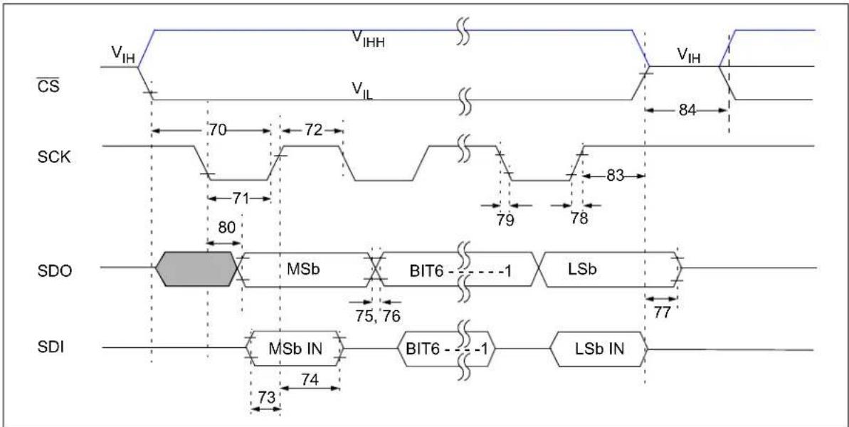
CS V_IH V_IHH V_IL 84 SCK 70 72 83 71 79 78 80 SDO MSb BIT6 -1 LSb 75, 76 77 SDI MSb IN BIT6 -1 LSb IN 73 74FIGURE 1-1: SPI Timing Waveform (Mode = 11).
TABLE 1-1: SPI REQUIREMENTS (MODE = 11)
| # C | characteristic Symbol Min Max Units Conditions | |||||
| SCK Input Frequency F | SCK | — | 1 | 0 | _DD = 2.7V to 5.5V | |
| — | 1 | MHz | _DD = 1.8V to 2.7V | |||
| 70 | Active ( V_IL or V_IHH ) to SCK↑ input | TcsA2scH | 60 | — | ns | |
| 71 | SCK input high time | TscH | 45 | — | ns | V_DD = 2.7V to 5.5V |
| 500 | — | ns | V_DD = 1.8V to 2.7V | |||
| 72 | SCK input low time | TscL | 45 | — | ns | V_DD = 2.7V to 5.5V |
| 500 | — | ns | V_DD = 1.8V to 2.7V | |||
| 73 | Setup time of SDI input to SCK↑ edge | T_DIV2scH | 10 | — | ns | |
| 74 | Hold time of SDI input from SCK↑ edge | TscH2DIL | 20 | — | ns | |
| 77 | Inactive ( V_IH ) to SDO output hi-impedance | TcsH2DOZ | — | 50 | ns | Note 1 |
| 80 | SDO data output valid after SCK↓ edge | TscL2DOV | — | 70 | ns | V_DD = 2.7V to 5.5V |
| 170 | ns | V_DD = 1.8V to 2.7V | ||||
| 83 | Inactive ( V_IH ) after SCK↑ edge | TscH2csl | 100 | — | ns | V_DD = 2.7V to 5.5V |
| 1 | ms | V_DD = 1.8V to 2.7V | ||||
| 84 | Hold time of Inactive ( V_IH ) to Active ( V_IL or V_IHH ) | TcsA2csl | 50 | — | ns |
Note 1: This specification by design.

text_image
CS VIH 82 VIHH VIL VIH 84 SCK 70 71 72 80 83 SDO MSb BIT6 LSb 77 SDI 73 75, 76 MSb IN BIT6 LSb IN 74FIGURE 1-2: SPI Timing Waveform (Mode = 00).
TABLE 1-2: SPI REQUIREMENTS (MODE = 00)
| # Characteristic Symbol Min Max Units Conditions | ||||||
| SCK Input Frequency F | sck | — | 1 | 0 | _DD = 2.7V to 5.5V | |
| — | 1 | M | _DD H1.8V to2.7V V | |||
| 70 | Active ( V_IL or V_IHH ) to SCK↑ input | TcsA2scH | 60 | — | ns | |
| 71 | SCK input high time | TscH | 45 | — | ns | V_DD = 2.7V to 5.5V |
| 500 | — | ns | V_DD = 1.8V to 2.7V | |||
| 72 | SCK input low time | TscL | 45 | — | ns | V_DD = 2.7V to 5.5V |
| 500 | — | ns | V_DD = 1.8V to 2.7V | |||
| 73 | Setup time of SDI input to SCK↑ edge | T_DIV2scH | 10 | — | ns | |
| 74 | Hold time of SDI input from SCK↑ edge | T_scH2dIL | 20 | — | ns | |
| 77 | Inactive ( V_IH ) to SDO output hi-impedance | TcsH2doZ | — | 50 | ns | Note 1 |
| 80 | SDO data output valid after SCK↓ edge | TscL2doV | — | 70 | ns | V_DD = 2.7V to 5.5V |
| 170 | ns | V_DD = 1.8V to 2.7V | ||||
| 82 | SDO data output valid after Active ( V_IL or V_IHH ) | TssL2doV — 70 ns | ||||
| 83 | Inactive ( V_IH ) after SCK↓ edge | TscH2csl | 100 | — | ns | V_DD = 2.7V to 5.5V |
| 1 | ms | V_DD = 1.8V to 2.7V | ||||
| 84 | Hold time of Inactive ( V_IH ) to Active ( V_IL or V_IHH ) | TcsA2csl | 50 | — | ns | |
Note 1: This specification by design.
V
TABLE 1-3: SPI REQUIREMENTS FOR SDI/SDO MULTIPLEXED (READ OPERATION ONLY) ^(2)
| Characteristic Symbol Min Max Units Conditions | |||||
| SCK Input Frequency F | SCK | — | 2 | 5 | Q_DD = 2k7V to 515V z |
| Active ( V_IL or V_IHH ) to SCK↑ input | TcsA2scH | 60 | — | ns | |
| SCK input high time | TscH | 1.8 — us | |||
| SCK input low time | TscL | 1.8 — ns | |||
| Setup time of SDI input to SCK↑ edge | TDIV2scH | 40 | — ns | ||
| Hold time of SDI input from SCK↑ edge | TscH2DIL | 40 | — | ns | |
| Inactive ( V_IH ) to SDO output hi-impedance | TcsH2DoZ | — | 50 | ns | Note 1 |
| SDO data output valid after SCK↓ edge | TscL2DoV | — | 1.6 | us | |
| SDO data output valid after Active ( V_IL or V_IHH ) | TssL2doV — | 50 | ns | ||
| Inactive ( V_IH ) after SCK↓ edge | TscH2csl | 100 | — | ns | |
| Hold time of Inactive ( V_IH ) to Active ( V_IL or V_IHH ) | TcsA2csl | 50 | — | ns | |
Note 1: This specification by design.
2: This table is for the devices where the SPI's SDI and SDO pins are multiplexed (SDI/SDO) and a Read command is issued. This is NOT required for SDI/SDO operation with the Increment, Decrement, or Write commands. This data rate can be increased by having external pull-up resistors to increase the rising edges of each bit.
TEMPERATURE CHARACTERISTICS
| Electrical Specifications: Unless otherwise indicated, V_DD = +2.7V to +5.5V , V_SS = G N D . | ||||||
| Parameters Sym Min Typ Max Units Conditions | ||||||
| Temperature Ranges | ||||||
| Specified Temperature Range T | A | -40 — | +125 °C | |||
| Operating Temperature Range T | A | -40 — | +125 °C | |||
| Storage Temperature Range | T_A | -65 — | +150 °C | |||
| Thermal Package Resistances | ||||||
| Thermal Resistance, 8L-DFN (3x3) | _JA | — | 84.5 — | °C/W | ||
| Thermal Resistance, 8L-MSOP | _JA | — | 211 | — | °C/W | |
| Thermal Resistance, 8L-PDIP | _JA | — | 89.3 — | °C/W | ||
| Thermal Resistance, 8L-SOIC 0 | JA | — | 149.5 | — | °C/W | |
| Thermal Resistance, 10L-DFN (3x3) | _JA | — | 57 | — | °C/W | |
| Thermal Resistance, 10L-MSOP | _JA | — | 211 | — | °C/W | |
| Thermal Resistance, 14L-PDIP | _JA | — | 70 | — | °C/W | |
| Thermal Resistance, 14L-SOIC | _JA | — | 95.3 | — | °C/W | |
| Thermal Resistance, 14L-TSSOP | _JA | — | 100 | — | °C/W | |
| Thermal Resistance, 16L-QFN | _JA | — | 47 | — | °C/W | |
2.0 TYPICAL PERFORMANCE CURVES
Note: The graphs and tables provided following this note are a statistical summary based on a limited number of samples and are provided for informational purposes only. The performance characteristics listed herein are not tested or guaranteed. In some graphs or tables, the data presented may be outside the specified operating range (e.g., outside specified power supply range) and therefore outside the warranted range.
Note: Unless otherwise indicated, T_A = +25^ , V_DD = 5V , V_SS = 0V .
line
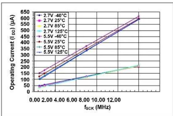
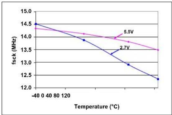
| fsck (MHz) | 2.7V -40°C | 2.7V 25°C | 2.7V 85°C | 2.7V 125°C | 5.5V -40°C | 5.5V 25°C | 5.5V 85°C | 5.5V 125°C | | ---------- | ---------- | --------- | --------- | ---------- | ---------- | --------- | --------- | ---------- | | 0.00 | 100 | 100 | 100 | 100 | 100 | 100 | 100 | 100 | | 2.00 | 150 | 150 | 150 | 150 | 150 | 150 | 150 | 150 | | 4.00 | 200 | 200 | 200 | 200 | 200 | 200 | 200 | 200 | | 6.00 | 250 | 250 | 250 | 250 | 250 | 250 | 250 | 250 | | 8.00 | 300 | 300 | 300 | 300 | 300 | 300 | 300 | 300 | | 10.00 | 350 | 350 | 350 | 350 | 350 | 350 | 350 | 350 | | 12.00 | 400 | 400 | 400 | 400 | 400 | 400 | 400 | 400 | | >12.00 | ~600 | ~600 | ~600 | ~600 | ~600 | ~600 | ~600 | ~600 |FIGURE 2-1: Device Current (I DD ) vs. SPI Frequency ( fSCK ) and Ambient Temperature ( V_DD = 2.7V and 5.5V).
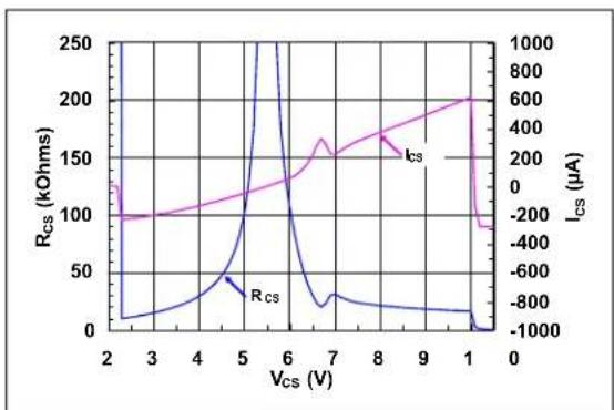
FIGURE 2-3: CS Pull-up/Pull-down Resistance ( R_ ) and Current ( I_ ) vs. CS Input Voltage ( V_ ) ( V_DD = 5.5V ).

line
| Ambient Temperature (°C) | Standby Current (Istby) (µA) | | ------------------------ | --------------------------- | | -40 | 0.8 | | 25 | 0.9 | | 85 | 1.0 | | 125 | 1.2 |FIGURE 2-2: Device Current (I SHDN) and V_DD . ( = V_DD) vs. Ambient Temperature.
line
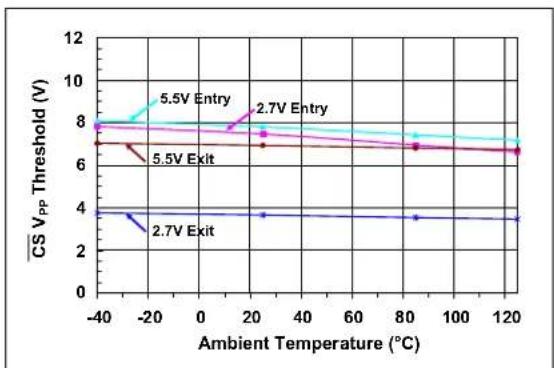
| Ambient Temperature (°C) | 5.5V Entry | 2.7V Entry | 2.7V Exit | | ------------------------ | ---------- | ---------- | --------- | | -40 | 8.0 | 8.0 | 4.0 | | 20 | 7.5 | 7.5 | 3.5 | | 120 | 7.0 | 6.5 | 3.5 |FIGURE 2-4: CS High Input Entry/Exit Threshold vs. Ambient Temperature and V_DD .
Note: Unless otherwise indicated, T_A = +25^ , V_DD = 5V , V_SS = 0V .
line
| Wiper Setting (decimal) | Wiper Resistance (Rw) | Error (Lsb) | | ----------------------- | ---------------------- | ----------- | | 0 | ~60 | ~0.0 | | 32 | ~55 | ~-0.05 | | 64 | ~50 | ~-0.1 | | 96 | ~45 | ~-0.15 | | 128 | ~40 | ~-0.2 | | 160 | ~35 | ~-0.2 | | 192 | ~30 | ~-0.2 | | 224 | ~25 | ~-0.2 | | 256 | ~20 | ~-0.2 |FIGURE 2-5: 5 k Pot Mode - R_W() , INL (LSb), DNL (LSb) vs. Wiper Setting and Ambient Temperature ( V_DD = 5.5V ).

line
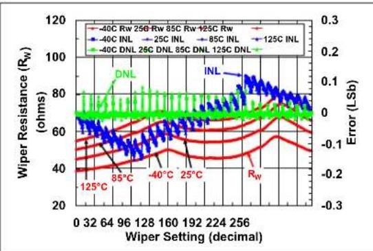
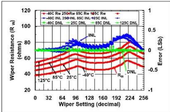
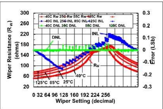
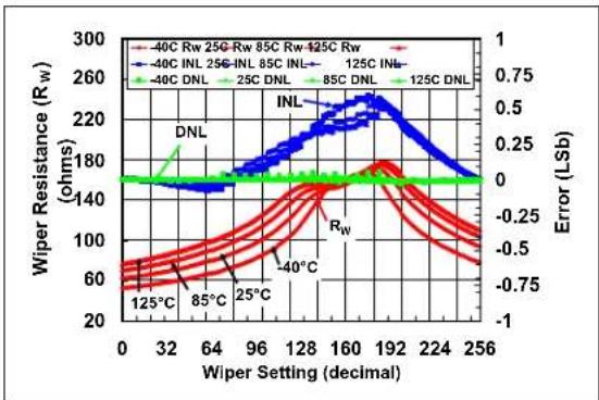
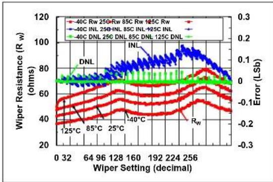
| Wiper Setting (decimal) | -40C Rw 25C Rw 85C Rw 125C Rw | -40C INL | 25C INL | 85C INL | 125C INL | -40C DNL | 25C DNL | 85C DNL | 125C DNL | | ----------------------- | ----------------------------- | -------- | ------- | ------- | -------- | -------- | ------- | ------- | -------- | | 0 | ~40 | ~40 | ~40 | ~40 | ~40 | ~40 | ~40 | ~40 | ~40 | | 32 | ~45 | ~45 | ~45 | ~45 | ~45 | ~45 | ~45 | ~45 | ~45 | | 64 | ~50 | ~50 | ~50 | ~50 | ~50 | ~50 | ~50 | ~50 | ~50 | | 96 | ~60 | ~60 | ~60 | ~60 | ~60 | ~60 | ~60 | ~60 | ~60 | | 128 | ~70 | ~70 | ~70 | ~70 | ~70 | ~70 | ~70 | ~70 | ~70 | | 160 | ~80 | ~80 | ~80 | ~80 | ~80 | ~80 | ~80 | ~80 | ~80 | | 192 | ~90 | ~90 | ~90 | ~90 | ~90 | ~90 | ~90 | ~90 | ~90 | | 224 | ~100 | ~100 | ~100 | ~100 | ~100 | ~100 | ~100 | ~100 | ~100 | | 256 | ~95 | ~95 | ~95 | ~95 | ~95 | ~95 | ~95 | ~95 | ~95 |FIGURE 2-8: 5 k Ω Rheo Mode - R_W() , INL (LSb), DNL (LSb) vs. Wiper Setting and Ambient Temperature ( V_DD = 5.5V).

line
| Wiper Setting (decimal) | Wiper Resistance (R_W) | Error (LSb) | | ----------------------- | ------------------------ | ----------- | | 0 | 60 | -0.3 | | 32 | 100 | -0.1 | | 64 | 140 | 0.0 | | 96 | 180 | 0.1 | | 128 | 220 | 0.2 | | 160 | 260 | 0.3 | | 192 | 240 | 0.2 | | 224 | 200 | 0.1 | | 256 | 160 | 0.0 |FIGURE 2-6: 5 k Pot Mode - R_W() , INL (LSb), DNL (LSb) vs. Wiper Setting and Ambient Temperature ( V_DD = 3.0V ).

line
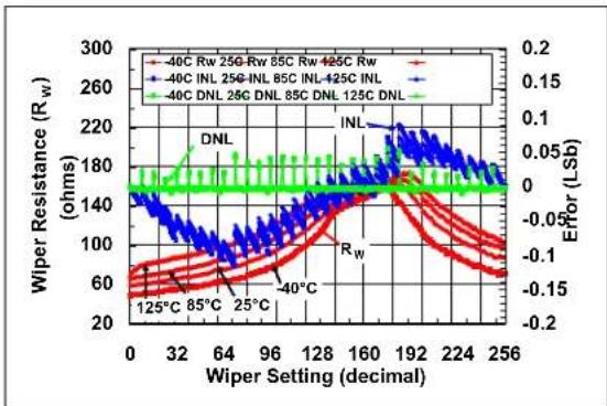
| Wiper Setting (decimal) | 40C Rw 250°Rw 85C Rw 125C Rw | 40C INL | 25C INL | 85C INL | 125C INL | -40C DNL | 25C DNL | 85C DNL | 125C DNL | | ----------------------- | ----------------------------- | ------- | ------- | ------- | -------- | -------- | ------- | ------- | -------- | | 0 | ~60 | ~60 | ~60 | ~60 | ~60 | ~60 | ~60 | ~60 | ~60 | | 32 | ~70 | ~70 | ~70 | ~70 | ~70 | ~70 | ~70 | ~70 | ~70 | | 64 | ~80 | ~80 | ~80 | ~80 | ~80 | ~80 | ~80 | ~80 | ~80 | | 96 | ~100 | ~100 | ~100 | ~100 | ~100 | ~100 | ~100 | ~100 | ~100 | | 128 | ~140 | ~140 | ~140 | ~140 | ~140 | ~140 | ~140 | ~140 | ~140 | | 160 | ~220 | ~220 | ~220 | ~220 | ~220 | ~220 | ~220 | ~220 | ~220 | | 192 | ~260 | ~260 | ~260 | ~260 | ~260 | ~260 | ~260 | ~260 | ~260 | | 224 | ~180 | ~180 | ~180 | ~180 | ~180 | ~180 | ~180 | ~180 | ~180 | | 256 | ~100 | ~100 | ~100 | ~100 | ~100 | ~100 | ~100 | ~100 | ~100 |FIGURE 2-9: 5 k Ω Rheo Mode - R_W() , INL (LSb), DNL (LSb) vs. Wiper Setting and Ambient Temperature ( V_DD = 3.0V ).

line
| Wiper Setting (decimal) | Wiper Resistance (R_W) (ohms) | Error (LSb) | | ----------------------- | ------------------------------ | ----------- | | 0 | 0 | -0.3 | | 64 | ~1000 | ~0.1 | | 128 | ~2000 | ~0.3 | | 192 | ~1500 | ~0.2 | | 256 | ~500 | ~-0.2 |FIGURE 2-7: 5 k Ω Pot Mode - R_W(Ω), INL (LSb), DNL (LSb) vs. Wiper Setting and Ambient Temperature (V_DD = 1.8V).

line
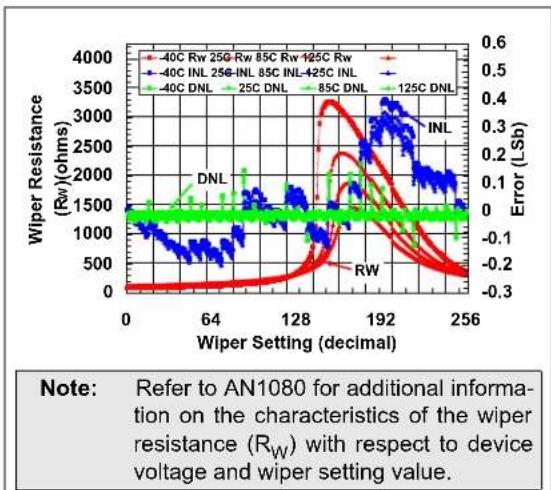
| Wiper Setting (decimal) | Wiper Resistance (R_W) (ohms) | Error (L_Sb) | | ----------------------- | ------------------------------ | ------------ | | 0 | 0 | 0 | | 64 | ~100 | ~-1 | | 128 | ~2200 | ~98 | | 192 | ~1500 | ~78 | | 256 | ~500 | ~38 |FIGURE 2-10: 5 k Ω Rheo Mode - R_W() , INL (LSb), DNL (LSb) vs. Wiper Setting and Ambient Temperature ( V_DD = 1.8V ).
Note: Unless otherwise indicated, T_A = +25^ , V_DD = 5V , V_SS = 0V .
line
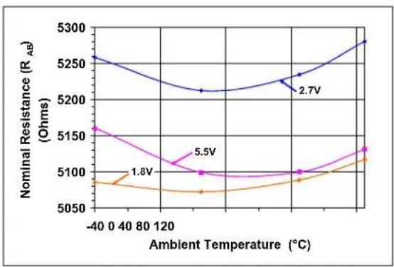
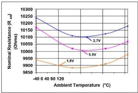
| Ambient Temperature (°C) | 1.8V | 5.5V | 2.7V | | ------------------------ | ------ | ------ | ------ | | -40 | 5160 | 5160 | 5260 | | 0 | 5100 | 5100 | 5220 | | 40 | 5090 | 5090 | 5210 | | 80 | 5080 | 5080 | 5200 | | 120 | 5070 | 5070 | 5190 | | 160 | 5080 | 5080 | 5230 | | 200 | 5100 | 5100 | 5260 | | 240 | 5120 | 5120 | 5280 |FIGURE 2-11: 5 k -Nominal Resistance ( ) vs. Ambient Temperature and V_DD .
line
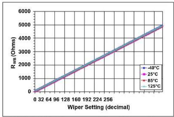
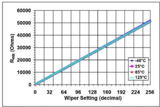
| Wiper Setting (decimal) | -40°C | 25°C | 85°C | 125°C | | ----------------------- | ----- | ---- | ---- | ----- | | 0 | 0 | 0 | 0 | 0 | | 32 | 32 | 32 | 32 | 32 | | 64 | 64 | 64 | 64 | 64 | | 96 | 96 | 96 | 96 | 96 | | 128 | 128 | 128 | 128 | 128 | | 160 | 160 | 160 | 160 | 160 | | 192 | 192 | 192 | 192 | 192 | | 224 | 224 | 224 | 224 | 224 | | 256 | 256 | 256 | 256 | 256 | | 288 | 288 | 288 | 288 | 288 | | 320 | 320 | 320 | 320 | 320 | | 352 | 352 | 352 | 352 | 352 | | 384 | 384 | 384 | 384 | 384 | | 416 | 416 | 416 | 416 | 416 | | 448 | 448 | 448 | 448 | 448 | | 480 | 480 | 480 | 480 | 480 | | 512 | 512 | 512 | 512 | 512 | | 544 | 544 | 544 | 544 | 544 | | 576 | 576 | 576 | 576 | 576 | | 608 | 608 | 608 | 608 | 608 | | 640 | 640 | 640 | 640 | 640 | | Note: The data for all temperatures is not explicitly labeled in the code. The chart type is a line graph, but it plots a single line representing RWB (Ohms) against Wiper Setting (decimal). The legend indicates four temperature conditions: -40°C, -25°C, -85°C, and -125°C. The line color corresponds to the temperature value. There is only one data series in this view.FIGURE 2-12: 5 k - R_WB() vs. Wiper Setting and Ambient Temperature.
Note: Unless otherwise indicated, T_A = +25^ , V_DD = 5V , V_SS = 0V .
text_image
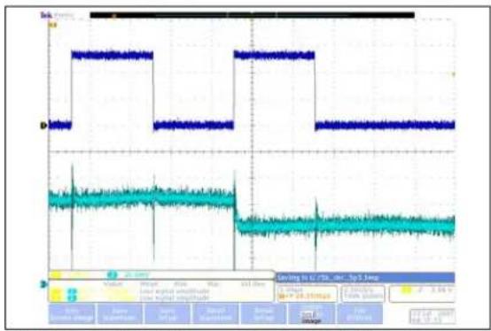
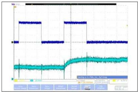
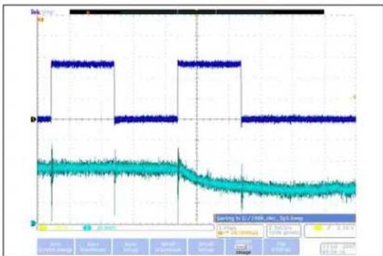
Gnding to 1278, dwt., 3pS.1mp Value Wave: Rate Max: 101 MHz Local digital modulator Local digital modulator Gnding to 1278, dwt., 3pS.1mp Value Wave: Rate Max: 101 MHz Local digital modulator Local digital modulator Gnding to 1278, dwt., 3pS.1mp Value Wave: Rate Max: 101 MHz Local digital modulator Local digital modulator Gnding to 1278, dwt.: 0.0000 Max: 101 MHz Local digital modulator Local digital modulator Gnding to 1278, dwt.: 0.0000 Max: 101 MHzFIGURE 2-13: 5 k -Low-Voltage Decrement Wiper Settling Time ( V_DD = 5.5V ) (1 s/Div).
text_image
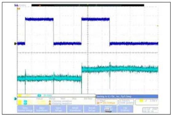
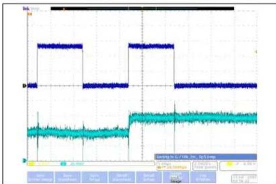
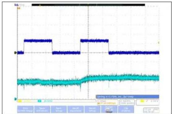
Govering to CC/DC_1er_2cp5_Smp Covings to CC/DC_1er_2cp5_Smp Data Wave Signal 0.000% Growth Current Current Signal Current Signal Current Current Current Current Current Current Current Current Current Current Current Current Current Current Current Current Current Current Current Current Current Current Current Current Current Current Current Current Current Current Current Current Current Current Current Current Current Current Current Current Current Current Current Current Current Current Current Current Current Current Covings to CC/DC_1er_2cp5_SmpFIGURE 2-16: 5 k -Low-Voltage Increment Wiper Settling Time ( V_DD = 5.5V ) (1 s/Div).

text_image
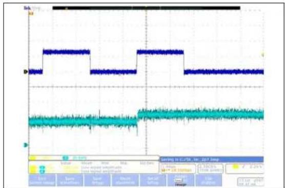
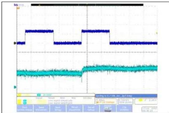
Oscilloscope waveform display showing square wave signal and corresponding voltage waveform with labeled parametersFIGURE 2-14: 5 k -Low-Voltage Decrement Wiper Settling Time ( V_DD = 2.7V ) (1 s/Div).
text_image
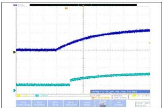
Digital oscilloscope waveform display showing square wave and sine wave signals with time scale and control panelFIGURE 2-17: 5 k -Low-Voltage Increment Wiper Settling Time ( V_DD = 2.7V ) (1 s/Div).
line
| Time (ms) | Value | | --------- | ----- | | 0 | 0 | | 10 | 0 | | 20 | 0 | | 30 | 0 | | 40 | 0 | | 50 | 0 | | 60 | 0 | | 70 | 0 | | 80 | 0 | | 90 | 0 | | 100 | 0 | | 110 | 0 | | 120 | 0 | | 130 | 0 | | 140 | 0 | | 150 | 0 | | 160 | 0 | | 170 | 0 | | 180 | 0 | | 190 | 0 | | 200 | 0 | | 210 | 0 | | 220 | 0 | | 230 | 0 | | 240 | 0 | | 250 | 0 | | 260 | 0 | | 270 | 0 | | 280 | 0 | | 290 | 0 | | 300 | 0 | | 310 | 0 | | 320 | 0 | | 330 | 0 | | 340 | 0 | | 350 | 0 | | 360 | 0 | | 370 | 0 | | 380 | 0 | | 390 | 0 | | 400 | 0 | | 410 | 0 | | 420 | 0 | | 430 | 0 | | 440 | 0 | | 450 | 0 | | 460 | 0 | | 470 | 0 | | 480 | 0 | | 490 | 0 | | 500 | 0 | | 510 | 0 | | 520 | 0 | | 530 | 0 | | 540 | 0 | | 550 | 0 | | 560 | 0 | | 570 | 0 | | 580 | 0 | | 590 | 0 | | 600 | 0 | | 610 | 0 | | 620 | 0 | | 630 | 0 | | 640 | 0 | | 650 | 0 | | 660 | 0 | | 670 | 0 | | 680 | 0 | | 690 | 0 | | 700 | 0 | | 710 | 0 | | 720 | 0 | | 730 | 0 | | 740 | 0 | | 750 | 0 | | 760 | 0 | | 770 | 0 | | 780 | 0 | | 790 | 0 | | 800 | 0 | | 810 | 0 | | 820 | 0 | | 830 | 0 | | 840 | 0 | | 850 | 0 | | 860 | 0 | | 870 | 0 | | 880 | 0 | | 890 | 0 | | 900 | 0 | | 910 | 0 | | 920 | 0 | | 930 | 0 | | 940 | 0 | | 950 | 0 | | 960 | 0 | | 970 | 0 | | 980 | 0 | | 990 | 0 | | >12 | >1 |FIGURE 2-15: 5 k Ω - Power-Up Wiper Response Time (20 ms/Div).
Note: Unless otherwise indicated, T_A = +25^ , V_DD = 5V , V_SS = 0V .

line
| Wiper Setting (decimal) | Wiper Resistance (Rw) (ohms) | Error (LSb) | | ----------------------- | ----------------------------- | ----------- | | 0 | ~60 | ~0.0 | | 25 | ~50 | ~-0.1 | | 50 | ~40 | ~0.0 | | 75 | ~30 | ~0.1 | | 100 | ~25 | ~0.0 | | 125 | ~20 | ~-0.1 | | 150 | ~25 | ~0.0 | | 175 | ~30 | ~0.1 | | 200 | ~40 | ~0.1 | | 225 | ~50 | ~0.0 | | 250 | ~60 | ~-0.1 |FIGURE 2-18: 10 k Ω Pot Mode - R_W() , INL (LSb), DNL (LSb) vs. Wiper Setting and Ambient Temperature ( V_DD = 5.5V ).
line
| Wiper Setting (decimal) | 40C Rw 25G Rw 85C Rw 125C Rw | 40C INL 25G-INL 85C INL-125C INL | 40C DNL | 25C DNL | 85C DNL | 125C DNL | | ----------------------- | ----------------------------- | ---------------------------------- | ------- | ------- | ------- | -------- | | 0 | ~60 | ~70 | ~60 | ~70 | ~70 | ~70 | | 32 | ~65 | ~75 | ~65 | ~75 | ~75 | ~75 | | 64 | ~70 | ~80 | ~70 | ~80 | ~80 | ~80 | | 96 | ~75 | ~85 | ~75 | ~85 | ~85 | ~85 | | 128 | ~80 | ~90 | ~80 | ~90 | ~90 | ~90 | | 160 | ~85 | ~95 | ~85 | ~95 | ~95 | ~95 | | 192 | ~90 | ~100 | ~90 | ~100 | ~100 | ~100 | | 224 | ~95 | ~105 | ~95 | ~105 | ~105 | ~105 | | 256 | ~100 | ~110 | ~100 | ~110 | ~110 | ~110 |FIGURE 2-21: 10 k Ω Rheo Mode - R_W() , INL (LSb), DNL (LSb) vs. Wiper Setting and Ambient Temperature ( V_DD = 5.5V ).
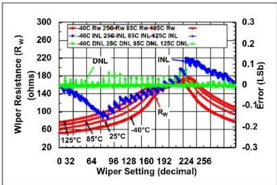
FIGURE 2-19: 10 k Ω Pot Mode - R_W() , INL (LSb), DNL (LSb) vs. Wiper Setting and Ambient Temperature ( V_DD = 3.0V ).

line
| Wiper Setting (decimal) | Wiper Resistance (R_w) (ohms) | Error (Lsb) | | ----------------------- | ------------------------------ | ----------- | | 0 | 60 | -1.5 | | 25 | 70 | -1.0 | | 50 | 80 | -0.5 | | 75 | 90 | 0.0 | | 100 | 100 | 0.5 | | 125 | 110 | 1.0 | | 150 | 130 | 1.5 | | 175 | 160 | 2.0 | | 200 | 180 | 2.5 | | 225 | 140 | 1.5 | | 250 | 100 | 0.5 |FIGURE 2-22: 10 k Ω Rheo Mode - R_W() , INL (LSb), DNL (LSb) vs. Wiper Setting and Ambient Temperature ( V_DD = 3.0V ).
line
| Wiper Setting (decimal) | Wiper Resistance (Rw) | Error (LSb) | | ----------------------- | --------------------- | ----------- | | 0 | 0 | 0 | | 64 | 1000 | 0 | | 128 | 2000 | 0 | | 192 | 3000 | 0 | | 256 | 1500 | 0 |FIGURE 2-20: 10 k Ω Pot Mode - R_W() , INL (LSb), DNL (LSb) vs. Wiper Setting and Ambient Temperature ( V_DD = 1.8V ).

line
| Wiper Setting (decimal) | Wiper Resistance (Rw) (ohms) | Error (LSb) | | ----------------------- | ----------------------------- | ----------- | | 64 | ~500 | ~0 | | 128 | ~1000 | ~18 | | 192 | ~3500 | ~78 | | 256 | ~500 | ~0 |FIGURE 2-23: 10 k Ω Rheo Mode - R_W() , INL (LSb), DNL (LSb) vs. Wiper Setting and Ambient Temperature ( V_DD = 1.8V ).
Note: Unless otherwise indicated, T_A = +25^ , V_DD = 5V , V_SS = 0V .
line
| Ambient Temperature (°C) | Nominal Resistance (R_AB) (Ohms) | | ------------------------ | -------------------------------- | | -40 | 10250 | | 0 | 10150 | | 40 | 10100 | | 80 | 10050 | | 120 | 10000 | | 160 | 9950 | | 200 | 9900 | | 240 | 9850 |FIGURE 2-24: 10 k -Nominal Resistance ( ) vs. Ambient Temperature and V_DD .

line
| Wiper Setting (decimal) | -40°C | 25°C | 85°C | 125°C | | ----------------------- | ----- | ---- | ---- | ----- | | 0 | 0 | 0 | 0 | 0 | | 32 | ~1500 | ~1500| ~1500| ~1500 | | 64 | ~3000 | ~3000| ~3000| ~3000 | | 96 | ~4500 | ~4500| ~4500| ~4500 | | 128 | ~6000 | ~6000| ~6000| ~6000 | | 160 | ~7500 | ~7500| ~7500| ~7500 | | 192 | ~9000 | ~9000| ~9000| ~9000 | | 224 | ~10500| ~10500| ~10500| ~10500| | 256 | ~12000| ~12000| ~12000| ~12000|FIGURE 2-25: 10 k - R_WB() vs. Wiper Setting and Ambient Temperature.
Note: Unless otherwise indicated, T_A = +25^ , V_DD = 5V , V_SS = 0V .
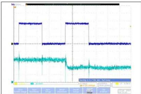
FIGURE 2-26: 10 k Ω - Low-Voltage Decrement Wiper Settling Time ( V_DD = 5.5V ) (1 μs/Div).
text_image
D Serving by G. T. Fife, Inc. Day 5 Time 10:30 AM 2:00 PM 3:00 PM 4:00 PM 5:00 PM 6:00 PM 7:00 PM 8:00 PM 9:00 PM 10:00 PM 11:00 PM 12:00 PM 13:00 PM 14:00 PM 15:00 PM 16:00 PM 17:00 PM 18:00 PM 19:00 PM 20:00 PM 21:00 PM 22:00 PM 23:00 PM 24:00 PM 25:00 PM 26:00 PM 27:00 PM 28:00 PM 29:00 PM 30:00 PM 31:00 PM 32:00 PM 33:00 PM 34:00 PM 35:00 PM 36:00 PM 37:00 PM 38:00 PM 39:00 PM 40:00 PM 41:00 PM 42:00 PM 43:00 PM 44:00 PM 45:00 PM 46:00 PM 47:00 PM 48:00 PM 49:00 PM 50:00 PMFIGURE 2-28: 10 k -Low-Voltage Increment Wiper Settling Time ( V_DD = 5.5V ) (1 s/Div).

line
| Time (s) | Value | Mean | Max | Min | Syst | |----------|-------|------|-----|-----|------| | 0 | 0 | 0 | 0 | 0 | 0 | | 10 | 0 | 0 | 0 | 0 | 0 | | 20 | 0 | 0 | 0 | 0 | 0 | | 30 | 0 | 0 | 0 | 0 | 0 | | 40 | 0 | 0 | 0 | 0 | 0 | | 50 | 0 | 0 | 0 | 0 | 0 | | 60 | 0 | 0 | 0 | 0 | 0 | | 70 | 0 | 0 | 0 | 0 | 0 | | 80 | 0 | 0 | 0 | 0 | 0 | | 90 | 0 | 0 | 0 | 0 | 0 | | 100 | 0 | 0 | 0 | 0 | 0 | | 110 | 0 | 0 | 0 | 0 | 0 | | 120 | 0 | 0 | 0 | 0 | 0 | | 130 | 0 | 0 | 0 | 0 | 0 | | 140 | 0 | 0 | 0 | 0 | 0 | | 150 | 0 | 0 | 0 | 0 | 0 | | 160 | 0 | 0 | 0 | 0 | 0 | | 170 | 0 | 0 | 0 | 0 | 0 | | 180 | 0 | 0 | 0 | 0 | 0 | | 190 | 0 | 0 | 0 | 0 | 0 | | 200 | 0 | 0 | 0 | 0 | 0 | | 210 | 0 | 0 | 0 | 0 | 0 | | 220 | 0 | 0 | 0 | 0 | 0 | | 230 | 0 | 0 | 0 | 0 | 0 | | 240 | 0 | 0 | 0 | 0 | 0 | | 250 | 0 | 0 | 0 | 0 | 0 | | 260 | 0 | 0 | 0 | 0 | 0 | | 270 | 0 | 0 | 0 | 0 | 0 | | 280 | 0 | 0 | 0 | 0 | 0 | | 290 | 0 | 0 | 0 | 0 | 0 | | 300 | 0 | 0 | 0 | 0 | 0 | | ... | ... ...| ... ...| ... | ...| ...FIGURE 2-27: 10 k Ω - Low-Voltage Decrement Wiper Settling Time ( V_DD = 2.7V ) (1 μs/Div).
line
| Time (s) | Value | |----------|-------| | 0 | 0 | | 1 | 0 | | 2 | 0 | | 3 | 0 | | 4 | 0 | | 5 | 0 | | 6 | 0 | | 7 | 0 | | 8 | 0 | | 9 | 0 | | 10 | 0 | | 11 | 0 | | 12 | 0 | | 13 | 0 | | 14 | 0 | | 15 | 0 | | 16 | 0 | | 17 | 0 | | 18 | 0 | | 19 | 0 | | 20 | 0 | | 21 | 0 | | 22 | 0 | | 23 | 0 | | 24 | 0 | | 25 | 0 | | 26 | 0 | | 27 | 0 | | 28 | 0 | | 29 | 0 | | 30 | 0 | | 31 | 0 | | 32 | 0 | | 33 | 0 | | 34 | 0 | | 35 | 0 | | 36 | 0 | | 37 | 0 | | 38 | 0 | | 39 | 0 | | 40 | 0 | | 41 | 0 | | 42 | 0 | | 43 | 0 | | 44 | 0 | | 45 | 0 | | 46 | 0 | | 47 | 0 | | 48 | 0 | | 49 | 0 | | 50 | 0 | | 51 | 0 | | 52 | 0 | | 53 | 0 | | 54 | 0 | | 55 | 0 | | 56 | 0 | | 57 | 0 | | 58 | 0 | | 59 | 0 | | 60 | 0 | | 61 | 0 | | 62 | 0 | | 63 | 0 | | 64 | 0 | | 65 | 0 | | 66 | 0 | | 67 | 0 | | 68 | 0 | | 69 | 0 | | 70 | 0 | | 71 | 0 | | 72 | 0 | | 73 | 0 | | 74 | 0 | | 75 | 0 | | 76 | 0 | | 77 | 0 | | 78 | 0 | | 79 | 0 | | 80 | 0 | | 81 | 0 | | 82 | 0 | | 83 | 0 | | 84 | 0 | | 85 | 0 | | 86 | 0 | | 87 | 0 | | 88 | 0 | | 89 | 0 | | 90 | 0 | | 91 | 0 | | 92 | 0 | | 93 | 0 | | 94 | 0 | | 95 | 0 | | 96 | 0 | | 97 | 0 | | 98 | 0 | | 99 | 0 | | Note: The data provided in the code is as follows: 'Outing to C:/UK, Inc. for Z Days' and 'Data points'. The values are estimated based on the input 'Value' and 'Time' parameters. The output 'Date' is calculated from the formula 'Time = S/N' and is not explicitly labeled in the image. There is no label for the output.FIGURE 2-29: 10 k -Low-Voltage Increment Wiper Settling Time ( V_DD = 2.7V ) (1 s/Div).
Note: Unless otherwise indicated, T_A = +25^ , V_DD = 5V , V_SS = 0V .

FIGURE 2-30: 50 k Pot Mode - R_W() , INL (LSb), DNL (LSb) vs. Wiper Setting and Ambient Temperature ( V_DD = 5.5V ).
line
| Wiper Setting (decimal) | Wiper Resistance (Rw) (ohms) | Error (LSb) | | ----------------------- | ---------------------------- | ----------- | | 0 | ~140 | ~0.0 | | 32 | ~130 | ~0.0 | | 64 | ~120 | ~0.0 | | 96 | ~110 | ~0.0 | | 128 | ~100 | ~0.0 | | 160 | ~90 | ~0.0 | | 192 | ~80 | ~0.0 | | 224 | ~70 | ~0.0 | | 256 | ~60 | ~0.0 |FIGURE 2-31: 50 k Ω Pot Mode - R_W() , INL (LSb), DNL (LSb) vs. Wiper Setting and Ambient Temperature ( V_DD = 3.0V ).

line
| Wiper Setting (decimal) | Wiper Resistance (R_W) (ohms) | Error (LSb) | | ----------------------- | ------------------------------ | ----------- | | 0 | 0 | 0 | | 64 | ~3000 | ~0.1 | | 128 | ~6000 | ~0.0 | | 192 | ~11000 | ~0.3 | | 256 | ~7000 | ~0.0 |FIGURE 2-32: 50 k Pot Mode - R_W() , INL (LSb), DNL (LSb) vs. Wiper Setting and Ambient Temperature ( V_DD=1.8V ).

line
| Wiper Setting (decimal) | Wiper Resistance (Rw) (ohms) | Error (LSb) | | ----------------------- | ----------------------------- | ----------- | | 0 | ~30 | ~0.0 | | 32 | ~40 | ~0.0 | | 64 | ~50 | ~0.0 | | 96 | ~60 | ~0.0 | | 128 | ~70 | ~0.0 | | 160 | ~80 | ~0.0 | | 192 | ~90 | ~0.0 | | 224 | ~100 | ~0.0 | | 256 | ~90 | ~0.0 | | 32 | ~70 | ~0.0 | | 64 | ~60 | ~0.0 | | 96 | ~50 | ~0.0 | | 128 | ~40 | ~0.0 | | 160 | ~30 | ~0.0 | | 192 | ~20 | ~0.0 | | 224 | ~10 | ~0.0 | | 256 | ~5 | ~0.0 |FIGURE 2-33: 50 k Ω Rheo Mode - R_W() , INL (LSb), DNL (LSb) vs. Wiper Setting and Ambient Temperature ( V_DD = 5.5V ).
line
| Wiper Setting (decimal) | Wiper Resistance (Rw) | Error (LSb) | | ----------------------- | ---------------------- | ----------- | | 0 | 60 | -0.75 | | 32 | 140 | 0 | | 64 | 180 | 0.25 | | 96 | 220 | 0.5 | | 128 | 260 | 0.75 | | 160 | 240 | 0.5 | | 192 | 220 | 0.25 | | 224 | 180 | -0.25 | | 256 | 140 | -0.75 |FIGURE 2-34: 50 k Ω Rheo Mode - R_W() , INL (LSb), DNL (LSb) vs. Wiper Setting and Ambient Temperature ( V_DD = 3.0V ).

line
| Wiper Setting (decimal) | Wiper Resistance (Rw) (ohms) | Error (LSb) | | ----------------------- | ----------------------------- | ----------- | | 0 | 0 | 0 | | 25 | 0 | 0 | | 50 | 0 | 0 | | 75 | 0 | 0 | | 100 | 0 | 0 | | 125 | 0 | 0 | | 150 | 12000 | 63.5 | | 175 | 11000 | 58.5 | | 200 | 9000 | 53.5 | | 225 | 7000 | 48.5 | | 250 | 5000 | 43.5 |FIGURE 2-35: 50 k Ω Rheo Mode - R_W() , INL (LSb), DNL (LSb) vs. Wiper Setting and Ambient Temperature ( V_DD = 1.8V ).
Note: Unless otherwise indicated, T_A = +25^ , V_DD = 5V , V_SS = 0V .

FIGURE 2-36: 50 k Ω-Nominal Resistance (Ω) vs. Ambient Temperature and V_DD .
line
| Wiper Setting (decimal) | -40°C | 25°C | 85°C | 125°C | | ----------------------- | ----- | ---- | ---- | ----- | | 0 | 0 | 0 | 0 | 0 | | 32 | ~10000| ~10000| ~10000| ~10000| | 64 | ~20000| ~20000| ~20000| ~20000| | 96 | ~30000| ~30000| ~30000| ~30000| | 128 | ~40000| ~40000| ~40000| ~40000| | 160 | ~50000| ~50000| ~50000| ~50000| | 192 | ~60000| ~60000| ~60000| ~60000| | 224 | ~70000| ~70000| ~70000| ~70000| | 256 | ~80000| ~80000| ~80000| ~80000|FIGURE 2-37: 50 k - R_WB() vs. Wiper Setting and Ambient Temperature.
Note: Unless otherwise indicated, T_A = +25^ , V_DD = 5V , V_SS = 0V .

line
| Time (s) | Signal Value | |----------|--------------| | 0 | 0 | | 1 | 0 | | 2 | 0 | | 3 | 0 | | 4 | 0 | | 5 | 0 | | 6 | 0 | | 7 | 0 | | 8 | 0 | | 9 | 0 | | 10 | 0 | | 11 | 0 | | 12 | 0 | | 13 | 0 | | 14 | 0 | | 15 | 0 | | 16 | 0 | | 17 | 0 | | 18 | 0 | | 19 | 0 | | 20 | 0 | | 21 | 0 | | 22 | 0 | | 23 | 0 | | 24 | 0 | | 25 | 0 | | 26 | 0 | | 27 | 0 | | 28 | 0 | | 29 | 0 | | 30 | 0 | | 31 | 0 | | 32 | 0 | | 33 | 0 | | 34 | 0 | | 35 | 0 | | 36 | 0 | | 37 | 0 | | 38 | 0 | | 39 | 0 | | 40 | 0 | | 41 | 0 | | 42 | 0 | | 43 | 0 | | 44 | 0 | | 45 | 0 | | 46 | 0 | | 47 | 0 | | 48 | 0 | | 49 | 0 | | 50 | 0 | | 51 | 0 | | 52 | 0 | | 53 | 0 | | 54 | 0 | | 55 | 0 | | 56 | 0 | | 57 | 0 | | 58 | 0 | | 59 | 0 | | 60 | 0 | | 61 | 0 | | 62 | 0 | | 63 | 0 | | 64 | 0 | | 65 | 0 | | 66 | 0 | | 67 | 0 | | 68 | 0 | | 69 | 0 | | 70 | 0 | | 71 | 0 | | 72 | 0 | | 73 | 0 | | 74 | 0 | | 75 | 0 | | 76 | 0 | | 77 | 0 | | 78 | 0 | | 79 | 0 | | 80 | 0 | | 81 | 0 | | 82 | 0 | | 83 | 0 | | 84 | 0 | | 85 | 0 | | 86 | 0 | | 87 | 0 | | 88 | 0 | | 89 | 0 | | 90 | 0 | | 91 | 0 | | 92 | 0 | | 93 | 0 | | 94 | 0 | | 95 | 0 | | 96 | 0 | | 97 | 0 | | 98 | 0 | | 99 | 0 | | Note: The actual values may vary due to the random nature of the data generation. The provided values are just an example. The code does not output any data points from this image. The output values are estimated based on the input data. The output values are calculated using the formula "E" and the number of samples. The output values are estimated using the formula "GPT" and the number of samples. The output values are estimated using the formula "Time Green". The output values are estimated using the formula "Time Green". The output values are estimated using the formula "GPT" and the number of samples. The output values are estimated using the formula "GPT" and the number of samples. The output values are estimated using the formula "GPT" and the number of samples. The output values are estimated using the formula "GPT" and the number of samples. The output values are estimated using the formula "GPT" and the number of samples. The output values are estimated using the formula "GPT" and the number of samples. The output values are estimated using the formula "Time Green". The output values are estimated using the formula "GPT" and the number of samples. The output values are estimated using the formula "Time Green". The output values are estimated using the formula "GPT" and the number of samples. The output values are estimated using the formula "GPT" and the number of samples. The output values are estimated using the formula "GPT" and the number of samples. The output values are estimated using the formula "GPT" and the number of samples. The output values are estimated using the formula "GPT" and the number only one sample. The output values are estimated using the formula "GPT" and the number of samples. The output values are estimated using the formula "GPT" and the number of samples. The output values are estimated using the formula "GPT" and the number of samples. The output values are estimated using the formula "GPT" and the number of samples. The output values are estimated using the formula "GPT" and the number of samples. The output values are estimated using the formula 'Time Green'. The output values are estimated using the formula 'Time Green'. The output values are estimated using the formula 'Time Green'. The output values are estimated using the formula 'GPT' and the number of samples. The output values are estimated using the formula 'GPT' and the number of samples. The output values are estimated using the formula 'GPT' and the number of samples. The output values are estimated using the formula 'GPT' and the number of samples. The output values are estimated using the formula 'Time Green'. The output values are estimated using the formula 'Time Green'. The output values are estimated using the formula 'Time Green'. The output values are estimated using the formula 'Time Green'. The output values are estimated using the formula 'GPT' and the number of samples. The output values are estimated using the formula 'GPT' and the number of samples. The output values are estimated using the formula 'GPT' and the number of samples. The output values are estimated using the formula 'Time Green'. The output values are estimated using the formula 'Time Green'. The output values are estimated using the formula 'Time Green'. The output values are estimated using the formula 'GPT' and the number of samples. The output values are estimated using the formula 'GPT' and the number of samples. The output values are estimated using the formula 'GPT' and the number of samples. The output values were estimated using these two conditions: “Time Green”. “Time Green”. “Time Green”. “Time Green”. “Time Green”. “Time Green”. “Time Green”. “Time Green”. “Time Green”. “Time Green”. “Time Green”. “Time Green”. “Time Green”. “Time Green”. “Time Green”. “Time Green”. “Time Green”. “Time Green”. “Time Green”. “Time Green”. “Time Green”. “Time Green”. “Time Green”. “Time Green”. “Time Green”. “Time Green”, “Time Green”, “Time Green”, “Time Green”, “Time Green”, “Time Green”, “Time Green”, “Time Green”, “Time Green”, “Time Green”, “Time Green”, “Time Green”, “Time Green”, “Time Green”, “Time Green”, “Time Green”, “Time Green”, “Time Green”, “Time Green”, “Time Green”, “Time Green”, “Time Green”, “Time Green”, “Time Green”, “Time Green”, “Time Green”FIGURE 2-38: 50 k -Low-Voltage Decrement Wiper Settling Time ( V_DD = 5.5V ) (1 s/Div).
text_image
Syst Wave Gelating to CC/State, Inc., Syst Wave 100% 200% 300% 400% 500% 600% 700% 800% 900% 1000% 1100% 1200% 1300% 1400% 1500% 1600% 1700% 1800% 1900% 2000% 2100% 2200% 2300% 2400% 2500% 2600% 2700% 2800% 2900% 3000% 3100% 3200% 3300% 3400% 3500% 3600% 3700% 3800% 3900% 4000% 4100% 4200% 4300% 4400% 4500% 4600% 4700% 4800% 4900% 5000% 5100% 5200% 5300% 5400% 5500% 5600% 5700% 5800% 5900% 6000% 6100% 6200% 6300% 6400% 6500% 6600% 6700% 6800% 6900% 7000% 7100% 7200% 7300% 7400% 7500% 7600% 7700% 7800% 7900% 8000% 8100% 8200% 8300% 8400% 8500% 8600% 8700% 8800% 8900% 9000% 9100% 9200% 9300% 9400% 9500% 9600% 9700% 9800% 9900% 100 p = 1.5V Current Signal Current Signal Current Signal Current Signal Current Signal Current Signal Current Signal Current Signal Current Signal Current Signal Current Signal Current Signal Current Signal Current Signal Current Signal Current Signal Current Signal Current Signal Current Signal Current Signal Current Signal Current Signal Current Signal Current Signal Current Signal Current Signal Current Signal Current Signal Current Signal Current Signal Current Signal Current Signal Current Signal Current SignalFIGURE 2-40: 50 k -Low-Voltage Increment Wiper Settling Time ( V_DD = 5.5V ) (1 s/Div).

FIGURE 2-39: 50 k -Low-Voltage Decrement Wiper Settling Time ( V_DD = 2.7V ) (1 s/Div).
line
| Time (s) | Signal Value | |----------|--------------| | 0 | 0 | | 1 | 1 | | 2 | 0 | | 3 | 1 | | 4 | 0 | | 5 | 1 | | 6 | 0 | | 7 | 1 | | 8 | 0 | | 9 | 1 | | 10 | 0 | | 11 | 1 | | 12 | 0 | | 13 | 1 | | 14 | 0 | | 15 | 1 | | 16 | 0 | | 17 | 1 | | 18 | 0 | | 19 | 1 | | 20 | 0 | | 21 | 1 | | 22 | 0 | | 23 | 1 | | 24 | 0 | | 25 | 1 | | 26 | 0 | | 27 | 1 | | 28 | 0 | | 29 | 1 | | 30 | 0 | | 31 | 1 | | 32 | 0 | | 33 | 1 | | 34 | 0 | | 35 | 1 | | 36 | 0 | | 37 | 1 | | 38 | 0 | | 39 | 1 | | 40 | 0 | | 41 | 1 | | 42 | 0 | | 43 | 1 | | 44 | 0 | | 45 | 1 | | 46 | 0 | | 47 | 1 | | 48 | 0 | | 49 | 1 | | 50 | 0 | | 51 | 1 | | 52 | 0 | | 53 | 1 | | 54 | 0 | | 55 | 1 | | 56 | 0 | | 57 | 1 | | 58 | 0 | | 59 | 1 | | 60 | 0 | | 61 | 1 | | 62 | 0 | | 63 | 1 | | 64 | 0 | | 65 | 1 | | 66 | 0 | | 67 | 1 | | 68 | 0 | | 69 | 1 | | 70 | 0 | | 71 | 1 | | 72 | 0 | | 73 | 1 | | 74 | 0 | | 75 | 1 | | 76 | 0 | | 77 | 1 | | 78 | 0 | | 79 | 1 | | 80 | 0 | | 81 | 1 | | 82 | 0 | | 83 | 1 | | 84 | 0 | | 85 | 1 | | 86 | 0 | | 87 | 1 | | 88 | 0 | | 89 | 1 | | 90 | 0 | | 91 | 1 | | 92 | 0 | | 93 | 1 | | 94 | 0 | | 95 | 1 | | 96 | 0 | | 97 | 1 | | 98 | 0 | | 99 | 1 | | Note: The actual values for 'Data Series Group' and 'Sample of Data' are not provided in the code. The 'Data Series Group' has a value of 'Value'.FIGURE 2-41: 50 k -Low-Voltage Increment Wiper Settling Time ( V_DD = 2.7V ) (1 s/Div).
Note: Unless otherwise indicated, T_A = +25^ , V_DD = 5V , V_SS = 0V .

line
| Wiper Setting (decimal) | Wiper Resistance (Rw) (ohms) | Error (Lsb) | | ----------------------- | ----------------------------- | ----------- | | 0 | ~60 | ~0.0 | | 32 | ~50 | ~-0.05 | | 64 | ~45 | ~-0.07 | | 96 | ~40 | ~-0.08 | | 128 | ~35 | ~-0.09 | | 160 | ~30 | ~-0.1 | | 192 | ~25 | ~-0.11 | | 224 | ~20 | ~-0.12 | | 256 | ~15 | ~-0.13 |FIGURE 2-42: 100 k Ω Pot Mode - R W (Ω), INL (LSb), DNL (LSb) vs. Wiper Setting and Ambient Temperature (V DD = 5.5V).
line
| Wiper Setting (decimal) | Wiper Resistance (Rw) (ohms) | Error (LSb) | | ----------------------- | ----------------------------- | ----------- | | 0 | ~30 | ~0 | | 32 | ~40 | ~0 | | 64 | ~50 | ~0 | | 96 | ~60 | ~0 | | 128 | ~70 | ~0 | | 160 | ~80 | ~0 | | 192 | ~90 | ~0 | | 224 | ~100 | ~0 | | 256 | ~90 | ~0 | | 32 | ~70 | ~0 | | 64 | ~80 | ~0 | | 96 | ~90 | ~0 | | 128 | ~100 | ~0 | | 160 | ~90 | ~0 | | 192 | ~80 | ~0 | | 224 | ~70 | ~0 | | 256 | ~60 | ~0 | | 32 | ~50 | ~0 | | 64 | ~60 | ~0 | | 96 | ~70 | ~0 | | 128 | ~80 | ~0 | | 160 | ~90 | ~0 | | 192 | ~100 | ~0 | | 224 | ~90 | ~0 | | 256 | ~80 | ~0 | | 32 | ~40 | ~-0.1 | | 64 | ~50 | ~-0.1 | | 96 | ~60 | ~-0.1 | | 128 | ~70 | ~-0.1 | | 160 | ~80 | ~-0.1 | | 192 | ~90 | ~-0.1 | | 224 | ~100 | ~-0.1 | | 256 | ~90 | ~-0.1 | | 32 | ~35 | ~-0.2 | | 64 | ~45 | ~-0.2 | | 96 | ~55 | ~-0.2 | | 128 | ~65 | ~-0.2 | | 160 | ~75 | ~-0.2 | | 192 | ~85 | ~-0.2 | | 224 | ~95 | ~-0.2 | | 256 | ~85 | ~-0.2 | | 32 | ~30 | ~-0.3 | | 64 | ~40 | ~-0.3 | | 96 | ~50 | ~-0.3 | | 128 | ~60 | ~-0.3 | | 160 | ~70 | ~-0.3 | | 192 | ~80 | ~-0.3 | | 224 | ~90 | ~-0.3 | | 256 | ~80 | ~-0.3 | | 32 | ~25 | ~-0.3 | | 64 | ~35 | ~-0.3 | | 96 | ~45 | ~-0.3 | | 128 | ~55 | ~-0.3 | | 160 | ~65 | ~-0.3 | | 192 | ~75 | ~-0.3 | | 224 | ~85 | ~-0.3 | | 256 | ~75 | ~-0.3 | | 32 | ~15 | ~-0.3 | | 64 | ~25 | ~-0.3 | | 96 | ~35 | ~-0.3 | | 128 | ~45 | ~-0.3 | | 160 | ~55 | ~-0.3 | | 192 | ~65 | ~-0.3 | | 224 | ~75 | ~-0.3 | | 256 | ~65 | ~-0.3 | | 32 | ~15 | ~-0.3 | | 64 | ~25 | ~-0.3 | | 96 | ~35 | ~-0.3 | | 128 | ~45 | ~-0.3 | | 160 | ~55 | ~-0.1 | | 192 | ~65 | ~-0.1 | | 224 | ~75 | - | | 256 | ~65 | - | | 32 | ~15 | - | | 64 | ~25 | - | | 96 | ~35 | - | | 128 | ~45 | - | | 160 | ~55 | - | | 192 | ~65 | - | | 224 | ~75 | - | | 256 | ~65 | - | | 32 | ~15 | - | | 64 | ~25 | - | | 96 | ~35 | - | | 128 | ~45 | - | | 160 | ~55 (INL) | - | | 192 | ~65 (INL) | - | | 224 | ~75 (INL) | - | | 256 | ~65 (DNL) | - | | 32 | ~15 | - | | 64 | ~25 (DNL) | - | | 96 | ~35 (DNL) | - | | 128 | ~45 (DNL) | - | | 160 | ~55 (DNL) | - | | 192 | ~65 (DNL) | - | | 224 | ~75 (DNL) | - | | 256 | ~65 (DNL) | - | | 32 | ~15 | - | | 64 | ~25 (DNL) | - | | 96 | ~35 (DNL) | - | | 128 | ~45 (DNL) | - | | — — | — | — | | — — (inferred from visual position) to the right of the chart: The numbers inside the chart are not explicitly provided in the code.FIGURE 2-45: 100 k Ω Rheo Mode - R_W ( ), INL (LSb), DNL (LSb) vs. Wiper Setting and Ambient Temperature ( V_DD = 5.5V ).
line
| Wiper Setting (decimal) | 40C Rw 25G-Rw 85C Rw 405C Rw | 40C INL 25G-INL 85C INL-425C INL | 40C DNL 25G DNL 85C DNL 125C DNL | DNL | | ----------------------- | ----------------------------- | ---------------------------------- | ---------------------------------- | --- | | 0 | ~140 | ~140 | ~140 | ~0.05 | | 32 | ~130 | ~130 | ~130 | ~0.05 | | 64 | ~120 | ~120 | ~120 | ~0.05 | | 96 | ~110 | ~110 | ~110 | ~0.05 | | 128 | ~100 | ~100 | ~100 | ~0.05 | | 160 | ~90 | ~90 | ~90 | ~0.05 | | 192 | ~80 | ~80 | ~80 | ~0.05 | | 224 | ~70 | ~70 | ~70 | ~0.05 | | 256 | ~60 | ~60 | ~60 | ~0.05 |FIGURE 2-43: 100 k Ω Pot Mode - R_W() , INL (LSb), DNL (LSb) vs. Wiper Setting and Ambient Temperature ( V_DD = 3.0V ).
line
| Wiper Setting (decimal) | Wiper Resistance (Rw) (ohms) | Error (LSb) | | ----------------------- | ----------------------------- | ----------- | | 0 | 60 | -0.4 | | 32 | 180 | 0.0 | | 64 | 180 | 0.0 | | 96 | 180 | 0.0 | | 128 | 180 | 0.0 | | 160 | 180 | 0.0 | | 192 | 180 | 0.0 | | 224 | 180 | 0.0 | | 256 | 180 | 0.0 |FIGURE 2-46: 100 k Ω Rheo Mode - R_W (Ω), INL (LSb), DNL (LSb) vs. Wiper Setting and Ambient Temperature ( V_DD = 3.0V ).

line
| Wiper Setting (decimal) | Wiper Resistance (R_W) (ohms) | Error (LSb) | | ----------------------- | ------------------------------ | ----------- | | 0 | 0 | -0.35 | | 64 | ~15000 | ~0.05 | | 128 | ~10000 | ~0.05 | | 192 | ~25000 | ~0.15 | | 256 | ~15000 | ~0.05 |FIGURE 2-44: 100 k Ω Pot Mode - R W (Ω), INL (LSb), DNL (LSb) vs. Wiper Setting and Ambient Temperature (V DD = 1.8V).

FIGURE 2-47: 100 k Ω Rheo Mode - R_W ( ), INL (LSb), DNL (LSb) vs. Wiper Setting and Ambient Temperature ( V_DD = 1.8V ).
Note: Unless otherwise indicated, T_A = +25^ , V_DD = 5V , V_SS = 0V .
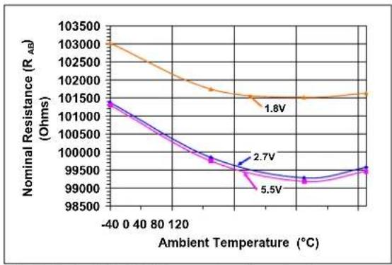
line
| Ambient Temperature (°C) | 1.8V | 2.7V | 5.5V | | ------------------------ | -------- | -------- | -------- | | -40 | 103000 | 101500 | 101500 | | 0 | 102500 | 101000 | 101000 | | 40 | 102000 | 100500 | 100500 | | 80 | 101500 | 100000 | 100000 | | 120 | 101500 | 99500 | 99500 | | 160 | 101500 | 99500 | 99500 | | 200 | 101500 | 99500 | 99500 | | 240 | 101500 | 99500 | 99500 |FIGURE 2-48: 100 k Ω - Nominal
Resistance ( ) vs. Ambient Temperature and V_DD .

line
| Wiper Setting (decimal) | -40°C | 25°C | 85°C | 125°C | | ----------------------- | ------- | ------- | ------- | ------- | | 0 | 0 | 0 | 0 | 0 | | 32 | ~10000 | ~10000 | ~10000 | ~10000 | | 64 | ~20000 | ~20000 | ~20000 | ~20000 | | 96 | ~30000 | ~30000 | ~30000 | ~30000 | | 128 | ~40000 | ~40000 | ~40000 | ~40000 | | 160 | ~50000 | ~50000 | ~50000 | ~50000 | | 192 | ~60000 | ~60000 | ~60000 | ~60000 | | 224 | ~70000 | ~70000 | ~70000 | ~70000 | | 256 | ~80000 | ~80000 | ~80000 | ~80000 | | >256 | >100000 | >100000 | >100000 | >100000 |FIGURE 2-49: 100 k - R_WB() vs. Wiper Setting and Ambient Temperature.
Note: Unless otherwise indicated, T_A = +25^ , V_DD = 5V , V_SS = 0V .
line
| Time (s) | Signal Value | |----------|--------------| | 0 | 100 | | 1 | 100 | | 2 | 100 | | 3 | 100 | | 4 | 100 | | 5 | 100 | | 6 | 100 | | 7 | 100 | | 8 | 100 | | 9 | 100 | | 10 | 100 | | 11 | 100 | | 12 | 100 | | 13 | 100 | | 14 | 100 | | 15 | 100 | | 16 | 100 | | 17 | 100 | | 18 | 100 | | 19 | 100 | | 20 | 100 | | 21 | 100 | | 22 | 100 | | 23 | 100 | | 24 | 100 | | 25 | 100 | | 26 | 100 | | 27 | 100 | | 28 | 100 | | 29 | 100 | | 30 | 100 | | 31 | 100 | | 32 | 100 | | 33 | 100 | | 34 | 100 | | 35 | 100 | | 36 | 100 | | 37 | 100 | | 38 | 100 | | 39 | 100 | | 40 | 100 | | 41 | 100 | | 42 | 100 | | 43 | 100 | | 44 | 100 | | 45 | 100 | | 46 | 100 | | 47 | 100 | | 48 | 100 | | 49 | 100 | | 50 | 100 | | 51 | 100 | | 52 | 100 | | 53 | 100 | | 54 | 100 | | 55 | 100 | | 56 | 100 | | 57 | 100 | | 58 | 100 | | 59 | 100 | | 60 | 100 | | 61 | 100 | | 62 | 100 | | 63 | 100 | | 64 | 100 | | 65 | 100 | | 66 | 100 | | 67 | 100 | | 68 | 100 | | 69 | 100 | | 70 | 100 | | 71 | 100 | | 72 | 100 | | 73 | 100 | | 74 | 100 | | 75 | 100 | | 76 | 100 | | 77 | 100 | | 78 | 100 | | 79 | 100 | | 80 | 100 | | 81 | 100 | | 82 | 100 | | 83 | 100 | | 84 | 100 | | 85 | 100 | | 86 | 100 | | 87 | 100 | | 88 | 100 | | 89 | 100 | | 90 | 100 | | 91 | 100 | | 92 | 100 | | 93 | 100 | | 94 | 100 | | 95 | 100 | | 96 | 100 | | 97 | 100 | | 98 | 100 | | 99 | 100 | | Note: The actual values for 'T' and 'U' are not provided in the code. The code does not output any data from this image. Please provide the actual values for 'U'.FIGURE 2-50: 100 k Ω - Low-Voltage Decrement Wiper Settling Time ( V_DD = 5.5V ) (1 μs/Div).

line
| Time (s) | Blue Waveform Value | Green Waveform Value | |----------|---------------------|----------------------| | 0 | 100 | -20 | | 1 | 100 | -20 | | 2 | 100 | -20 | | 3 | 100 | -20 | | 4 | 100 | -20 | | 5 | 100 | -20 | | 6 | 100 | -20 | | 7 | 100 | -20 | | 8 | 100 | -20 | | 9 | 100 | -20 | | 10 | 100 | -20 | | 11 | 100 | -20 | | 12 | 100 | -20 | | 13 | 100 | -20 | | 14 | 100 | -20 | | 15 | 100 | -20 | | 16 | 100 | -20 | | 17 | 100 | -20 | | 18 | 100 | -20 | | 19 | 100 | -20 | | 20 | 100 | -20 | | 21 | 100 | -20 | | 22 | 100 | -20 | | 23 | 100 | -20 | | 24 | 100 | -20 | | 25 | 100 | -20 | | 26 | 100 | -20 | | 27 | 100 | -20 | | 28 | 100 | -20 | | 29 | 100 | -20 | | 30 | 100 | -20 | | 31 | 100 | -20 | | 32 | 100 | -20 | | 33 | 100 | -20 | | 34 | 100 | -20 | | 35 | 100 | -20 | | 36 | 100 | -20 | | 37 | 100 | -20 | | 38 | 100 | -20 | | 39 | 100 | -20 | | 40 | 100 | -20 | | 41 | 100 | -20 | | 42 | 100 | -20 | | 43 | 100 | -20 | | 44 | 100 | -20 | | 45 | 100 | -20 | | 46 | 100 | -20 | | 47 | 100 | -20 | | 48 | 100 | -20 | | 49 | 100 | -20 | | 50 | 100 | -20 | | 51 | 100 | -20 | | 52 | 100 | -20 | | 53 | 100 | -20 | | 54 | 100 | -20 | | 55 | 100 | -20 | | 56 | 100 | -20 | | 57 | 100 | -20 | | 58 | 100 | -20 | | 59 | 100 | -20 | | 60 | 100 | -20 | | 61 | 100 | -20 | | 62 | 100 | -20 | | 63 | 100 | -20 | | 64 | 100 | -20 | | 65 | 100 | -20 | | 66 | 100 | -20 | | 67 | 100 | -20 | | 68 | 100 | -20 | | 69 | 100 | -20 | | 70 | 100 | -20 | | 71 | 100 | -20 | | 72 | 100 | -20 | | 73 | 100 | -20 | | 74 | 100 | -20 | | 75 | 100 | -20 | | 76 | 100 | -20 | | 77 | 100 | -20 | | 78 | 100 | -20 | | 79 | 100 | -20 | | 80 | 100 | -20 | | 81 | 100 | -20 | | 82 | 100 | -20 | | 83 | 100 | -20 | | 84 | 100 | -20 | | 85 | 100 | -20 | | 86 | 100 | -20 | | 87 | 100 | -20 | | 88 | 100 | -20 | | 89 | 100 | -20 | | 90 | 100 | -20 | | 91 | 100 | -20 | | 92 | 100 | -20 | | 93 | 100 | -20 | | 94 | 100 | -20 | | 95 | 100 | -20 | | 96 | 100 | -20 | | 97 | 100 | -20 | | 98 | 100 | -20 | | 99 | 100 | -2 v | | | | | | (approx.) (approx.) (approx.) (approx.) (approx.) (approx.) (approx.) (approx.) (approx.) (approx.) (approx.) (approx.) (approx.) (approx.) (approx.) (approx.) (approx.) (approx.) (approx.) (approx.) (approx.) (approx.) (approx.) (approx.) (approx.) (approx.) (approx.) (approx.) (approx.) (approx.) (approx.) (approx.) (approx.) (approx.) (approx.) (approx.) (approx.) (approx.) (approx.) (approx.) (approx.) (approx.) (approx.) (approx.) (approx.) (approx.) (approx.) (approx.) (approx.) (approx.) (approx.) (approx.) (approx.) (approx.) (approx.) (approx.) (approx.) (approx.) (approx.) (approx.) (approx.) (approx.) (approx.) (approx.) (approx.) (approx.) (approx.) (approx.) (approx.) (approx.) (approx.) (approx.) (approx.) (approx.) (approx.) (approx.) (approx.) (approx.) (approx.) (approx.) (approx.) (approx.) (approx.) (approx.) (approx.) (approx.) (approx.) (approx.) (approx.) (approx.) (approx.) (approx.) (approx.) (approx.) (approx.) (approx.) (approx.) (approx.) (approx.) (approx.) (approx.) (approx.) (approx.) (approx.) (approx.) (approx.) (approx.) (approx.) (approx.) (approx.) (approx.) (approx.) (approx.) (approx.) (approx.) (approx.) (approx.) (approx.) (approx.) (approx.) (approx.) (approx.) (approx.)(v) [value] [value] [value] [value] [value] [value] [value] [value] [value] [value] [value] [value] [value] [value] [value] [value] [value] [value] [value] [value] [value] [value] [value] [value] [value] [value] [value] [p-value] [p-value] [p-value] [p-value] [p-value] [p-value] [p-value] [p-value] [p-value] [p-value] [p-value] [p-value] [p-value] [p-value] [p-value] [p-value] [p-value] [p-value] [p-value] [p-value] [p value] [p value] [p value] [p value] [p value] [p value] [p value] [p value] [p value] [p value] [p value] [p value] [p value] [p value] [p value] [p value] [p value] [p value] [p value] [p value] [p values] [p values] [p values] [p values] [p values] [p values] [p values] [p values] [p values] [p values] [p values] [p values] [p values] [p values] [p values] [p values] [p values] [p values] [p values] [p values] [p ranges] [p ranges] [p ranges] [p ranges] [p ranges] [p ranges] [p ranges] [p ranges] [p ranges] [p ranges] [p ranges] [p ranges] [p ranges] [p ranges] [p ranges] [p ranges] [p ranges] [p ranges] [p ranges] [p ranges] [p range] [m²/ha²/min²/min²/min²/min²/min²/min²/min²/min²/min²/min²/min²/min²/min²/min²/min²/min²/min²/min²/min²/min²/min²/min²/min²/min²/min²/min²/min²/min²/min²/min²/min²/min²/min²/min²/min²/min²/min²/min²/min²/min²/min²/min²/min²/min²/min²/min²/min²/min²/min²/min²/kg /mm³ /mm³ /mm³ /mm³ /mm³ /mm³ /mm³ /mm³ /mm³ /mm³ /mm³ /mm³ /mm³ /mm³ /mm³ /mm³ /mm³ /mm³ /mm³ /mm³ /mm³ /mm³ /mm³ /mm³ /mm³ /mm⁴ /mm³ /mm³ /mm³ /mm³ /mm³ /mm³ /mm³ /mm³ /mm³ /mm³ /mm³ /mm³ /mm³ /mm³ /mm³ /mm³ /mm³ /mm³ /mm³ /mm³ /mm³ /mm³ /mm³ /mm³ /mm² /mm²/min²/min²/min²/min²/min²/min²/min²/min²/min²/min²/min²/min²/min²/min²/min²/min²/min²/min²/min²/min²/min²/min²/min²/min²/min²/min²/min²/min²/min²/min²/min²/min²/min²/min²/min²/min²/min²/min²/min²/min²/min²/min²/min²/min²/min²/min²/min²/min²/min²min / mm³ / mm³ / mm³ / mm³ / mm³ / mm³ / mm³ / mm³ / mm³ / mm³ / mm³ / mm³ / mm³ / mm³ / mm³ / mm³ / mm³ / mm³ / mm³ / mm³ / mm³ / mm³ / mm³ / mm³ / mm³ / mm³ / mm³ nan nan nan nan nan nan nan nan nan nan nan nan nan nan nan nan nan nan nan nan nan nan nan nan nan nan nan nan nan nan nan nan nan nan nan nan nan nan nan nan nan nan nan nan nan nan nan nan nan nan nan nan nan nan nan nan nan nan nan nan nan nan nan nan nan nan nan nan nan nan nan nan nan nan nan nan nan nan nan nan nan nan nan nan nan nan nan nan nan nan nan nan nan nan nan nan nan nan nan nan nanFIGURE 2-52: 100 k -Low-Voltage Increment Wiper Settling Time ( V_DD = 2.7V ) (1 s/Div).

line
| Time (ms) | Square Wave Amplitude | Square Wave Baseline | Signal Wave Amplitude | Signal Wave Baseline | |-----------|------------------------|------------------------|------------------------|------------------------| | 0 | 0 | 0 | 0 | 0 | | 10 | 100 | 100 | 100 | 100 | | 20 | 100 | 100 | 100 | 100 | | 30 | 100 | 100 | 100 | 100 | | 40 | 100 | 100 | 100 | 100 | | 50 | 100 | 100 | 100 | 100 | | 60 | 100 | 100 | 100 | 100 | | 70 | 100 | 100 | 100 | 100 | | 80 | 100 | 100 | 100 | 100 | | 90 | 100 | 100 | 100 | 100 | | 100 | 10 | 5 | 5 | 5 | | 110 | 5 | 5 | 5 | 5 | | 120 | 5 | 5 | 5 | 5 | | 130 | 5 | 5 | 5 | 5 | | 140 | 5 | 5 | 5 | 5 | | 150 | 5 | 5 | 5 | 5 | | 160 | 5 | 5 | 5 | 5 | | 170 | 5 | 5 | 5 | 5 | | 180 | 5 | 5 | 5 | 5 | | 190 | 5 | 5 | 5 | 5 | | 200 | 5 | 5 | 5 | 5 | | 210 | 5 | 5 | 5 | 5 | | 220 | 5 | 5 | 5 | 5 | | 230 | 5 | 5 | 5 | 5 | | 240 | 5 | 5 | 5 | 5 | | 250 | 5 | 5 | 5 | 5 | | 260 | 5 | 5 | 5 | 5 | | 270 | 5 | 5 | 5 | 5 | | 280 | 5 | 5 | 5 | 5 | | 290 | 5 | 5 | 5 | 5 | | 300 | 5 | 5 | 5 | 5 | | | | | | | | | | | | | | | | | | | | | | | | | | | | | | | | | | | | | | | | | | | | | | | | | | | | | | | | | | | | |FIGURE 2-51: 100 k Ω - Low-Voltage Decrement Wiper Settling Time ( V_DD = 2.7V ) (1 μs/Div).

line
| Time (μs) | Signal 1 (dB) | Signal 2 (dB) | |-----------|---------------|---------------| | 0 | 0 | 0 | | 1 | 0 | 0 | | 2 | 0 | 0 | | 3 | 0 | 0 | | 4 | 0 | 0 | | 5 | 0 | 0 | | 6 | 0 | 0 | | 7 | 0 | 0 | | 8 | 0 | 0 | | 9 | 0 | 0 | | 10 | 0 | 0 | | 11 | 0 | 0 | | 12 | 0 | 0 | | 13 | 0 | 0 | | 14 | 0 | 0 | | 15 | 0 | 0 | | 16 | 0 | 0 | | 17 | 0 | 0 | | 18 | 0 | 0 | | 19 | 0 | 0 | | 20 | 0 | 0 | | 21 | 0 | 0 | | 22 | 0 | 0 | | 23 | 0 | 0 | | 24 | 0 | 0 | | 25 | 0 | 0 | | 26 | 0 | 0 | | 27 | 0 | 0 | | 28 | 0 | 0 | | 29 | 0 | 0 | | 30 | 0 | 0 | | 31 | 0 | 0 | | 32 | 0 | 0 | | 33 | 0 | 0 | | 34 | 0 | 0 | | 35 | 0 | 0 | | 36 | 0 | 0 | | 37 | 0 | 0 | | 38 | 0 | 0 | | 39 | 0 | 0 | | 40 | 0 | 0 | | 41 | 0 | 0 | | 42 | 0 | 0 | | 43 | 0 | 0 | | 44 | 0 | 0 | | 45 | 0 | 0 | | 46 | 0 | 0 | | 47 | 0 | 0 | | 48 | 0 | 0 | | 49 | 0 | 0 | | 50 | 0 | 0 | | ... | ... | ... | | ... | ... | ... | | ... | ... | ... | | ... | ... | ... | | ... | ... | ... | | ... | ... | ... | | ... | ... | ... | | ... | ... | ... | | ... | ... | ... | | ... | ... | ... | | ... | ... | ... (Note: The 'Fig' labels are not explicitly provided in the code.) |FIGURE 2-53: 100 k Ω - Power-Up Wiper Response Time (1 μs/Div).
Note: Unless otherwise indicated, T_A = +25^ , V_DD = 5V , V_SS = 0V .
line
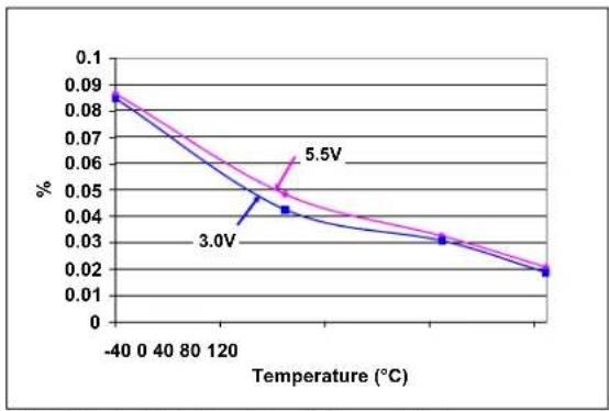
| Temperature (°C) | 5.5V (%) | 3.0V (%) | |---|---|---| | -40 | 0.087 | 0.086 | | 120 | 0.05 | 0.042 | | 120+ | 0.032 | 0.031 | | 120+ | 0.02 | 0.02 |FIGURE 2-54: Resistor Network 0 to Resistor Network 1 R_AB(5k) Mismatch vs. V_DD and Temperature.
line
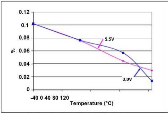
| Temperature (°C) | 5.5V | 3.0V | | ---------------- | ------ | ------ | | -40 | 0.10 | 0.10 | | 120 | 0.08 | 0.08 | | 30 | 0.06 | 0.06 | | 40 | 0.04 | 0.04 | | 50 | 0.03 | 0.03 | | 60 | 0.02 | 0.02 |FIGURE 2-56: Resistor Network 0 to Resistor Network 1 R_AB (50 kΩ) Mismatch vs. V_DD and Temperature.
line
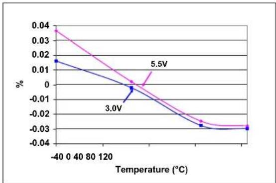
| Temperature (°C) | 3.0V | 5.5V | | ---------------- | ------ | ------ | | -40 | 0.018 | 0.040 | | 120 | -0.005 | 0.005 | | 160 | -0.030 | -0.025 |FIGURE 2-55: Resistor Network 0 to Resistor Network 1 R_AB (10 kΩ) Mismatch vs. V_DD and Temperature.

line
| Temperature (°C) | 3.0V | 5.5V | | ---------------- | ------ | ------ | | -40 | 0.045 | 0.048 | | 10 | 0.015 | 0.025 | | 60 | -0.005 | -0.015 | | 110 | -0.025 | -0.025 |FIGURE 2-57: Resistor Network 0 to Resistor Network 1 R_AB (100 kΩ) Mismatch vs. V_DD and Temperature.
Note: Unless otherwise indicated, T_A = +25^ , V_DD = 5V , V_SS = 0V .

line
| Temperature (°C) | V_H (V) | | ---------------- | ------- | | -40 | 1.1 | | 120 | 1.1 | | 80 | 1.1 | | 60 | 1.1 | | 40 | 1.1 | | 20 | 1.1 | | 0 | 1.1 |FIGURE 2-58: V IH (SDI, SCK, CS, and SHDN) vs. VDD and Temperature.
line
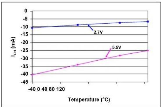
| Temperature (°C) | I_OH (mA) at 2.7V | I_OH (mA) at 5.5V | |---|---|---| | -40 | -10 | -40 | | 120 | -10 | -35 | | 60 | -10 | -30 | | 120 | -8 | -25 |FIGURE 2-60: I OH (SDO) vs. VDD and Temperature.

line
| Temperature (°C) | 5.5V | 2.7V | | ---------------- | ----- | ----- | | -40 | 1.38 | 0.90 | | 120 | 1.32 | 0.88 | | 60 | 1.28 | 0.84 | | 120 | 1.26 | 0.82 |FIGURE 2-59: V IL (SDI, SCK, CS, and SHDN) vs. VDD and Temperature.
line
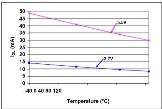
| Temperature (°C) | 5.5V (mA) | 2.7V (mA) | | ---------------- | --------- | --------- | | -40 | 50 | 14 | | 120 | 40 | 12 | | 360 | 35 | 10 | | 640 | 30 | 8 |FIGURE 2-61: I OL (SDO) vs. VDD and Temperature.
Note: Unless otherwise indicated, T_A = +25^ , V_DD = 5V , V_SS = 0V .

line
| Temperature (°C) | V_DD (V) | | ---------------- | -------- | | -40 | 1.0 | | 80 | 0.9 | | 120 | 0.8 | | 160 | 0.8 | | 200 | 0.7 | | 240 | 0.7 |FIGURE 2-62: POR/BOR Trip point vs. V and Temperature.
2.1 Test Circuits
text_image
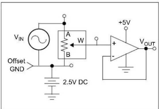
VIN Offset GND A W B 2.5V DC +5V - VOUTFIGURE 2-64: -3 db Gain vs. Frequency Test.
line
| Temperature (°C) | fsck (MHz) - 5.5V | fsck (MHz) - 2.7V | | ---------------- | ----------------- | ----------------- | | -40 | 14.5 | 14.5 | | 0 | 14.3 | 14.3 | | 40 | 14.1 | 14.0 | | 80 | 13.9 | 13.7 | | 120 | 13.6 | 13.4 | | 160 | 13.3 | 13.0 | | 200 | 13.0 | 12.7 | | 240 | 12.7 | 12.4 |FIGURE 2-63: SCK Input Frequency vs. Voltage and Temperature.
3.0 PIN DESCRIPTIONS
The descriptions of the pins are listed in Table3-1.
Additional descriptions of the device pins follows.
TABLE 3-1: PINOUT DESCRIPTION FOR THE MCP413X/415X/423X/425X
| Pin | Weak Pull-up/ down (2) | Standard Function | |||||||
| Single Dual | Symbol I/O | Buffer Type | |||||||
| Rheo Pot (1) | Rheo | Pot | |||||||
| 8L 8L | 10L 14L | 16L | |||||||
| 1 | 1 | 1 | 1 | 16 | I | HV w/ST | “smart” | SPI Chip Select Input | |
| 2 | 2 | 2 | 2 | 1 | SCK | I | HV w/ST | “smart” | SPI Clock Input |
| 3 | — | 3 | 3 | 2 | SDI | I | HV w/ST | “smart” | SPI Serial Data Input |
| — | 3 | — | — | — | SDI/SDO | I/O | HV w/ST | “smart” | SPI Serial Data Input/Output (Note 1, Note 3) |
| 4 | 4 | 4 | 4 | 3, 4 | V_SS | — | P | — | Ground |
| — | — | 5 | 5 | 5 | P1B | A | Analog | No | Potentiometer 1 Terminal B |
| — | — | 6 | 6 | 6 | P1W | A | Analog | No | Potentiometer 1 Wiper Terminal |
| — | — | — | 7 | 7 | P1A | A | Analog | No | Potentiometer 1 Terminal A |
| — | 5 | — | 8 | 8 | P0A | A | Analog | No | Potentiometer 0 Terminal A |
| 5 | 6 | 7 | 9 | 9 | P0W | A | Analog | No | Potentiometer 0 Wiper Terminal |
| 6 | 7 | 8 | 10 | 10 | P0B | A | Analog | No | Potentiometer 0 Terminal B |
| — | — | — | 12 | 13 | I | HV w/ST | “smart” | Hardware Shutdown | |
| 7 | — | 9 | 13 | 14 | SDO | O | O | No | SPI Serial Data Out |
| 8 | 8 | 10 | 14 | 15 | V_DD | — | P | — Positive Power Supply Input | |
| — | — | — | 11 | 11,12 | NC | — | — | — | No Connection |
| 9 | 9 | 11 | — | 17 | EP | — | — | — | Exposed Pad (Note 4) |
Legend: HV w/ST = High Voltage tolerant input (with Schmidt trigger input)
A = Analog pins (Potentiometer terminals) I = digital input (high Z)
O = digital output I/O = Input / Output
P = Power
Note 1: The 8-lead Single Potentiometer devices are pin limited so the SDO pin is multiplexed with the SDI pin (SDI/SDO pin). After the Address/Command (first 6-bits) are received, If a valid Read command has been requested, the SDO pin starts driving the requested read data onto the SDI/SDO pin.
2: The pin's "smart" pull-up shuts off while the pin is forced low. This is done to reduce the standby and shutdown current.
3: The SDO is an open drain output, which uses the internal "smart" pull-up. The SDI input data rate can be at the maximum SPI frequency. the SDO output data rate will be limited by the "speed" of the pull-up, customers can increase the rate with external pull-up resistors.
4: The DFN and QFN packages have a contact on the bottom of the package. This contact is conductively connected to the die substrate, and therefore should be unconnected or connected to the same ground as the device's V_SS pin.
3.1 Chip Select (CS)
The pin is the serial interface's chip select input. Forcing the pin to V_IL enables the serial commands. Forcing the pin to V_IHH enables the high-voltage serial commands.
3.2 Serial Data In (SDI)
The SDI pin is the serial interfaces Serial Data In pin. This pin is connected to the Host Controllers SDO pin.
3.3 Serial Data In / Serial Data Out (SDI/SDO)
On the MCP41X1 devices, pin-out limitations do not allow for individual SDI and SDO pins. On these devices, the SDI and SDO pins are multiplexed.
The MCP41X1 serial interface knows when the pin needs to change from being an input (SDI) to being an output (SDO). The Host Controller's SDO pin must be properly protected from a drive conflict.
3.4 Ground (V ss)
The V_SS pin is the device ground reference.
3.5 Potentiometer Terminal B
The terminal B pin is connected to the internal potentiometer's terminal B.
The potentiometer's terminal B is the fixed connection to the Zero Scale wiper value of the digital potentiometer. This corresponds to a wiper value of 0x00 for both 7-bit and 8-bit devices.
The terminal B pin does not have a polarity relative to the terminal W or A pins. The terminal B pin can support both positive and negative current. The voltage on terminal B must be between V_SS and V_DD .
MCP42XX devices have two terminal B pins, one for each resistor network.
3.6 Potentiometer Wiper (W) Terminal
The terminal W pin is connected to the internal potentiometer's terminal W (the wiper). The wiper terminal is the adjustable terminal of the digital potentiometer. The terminal W pin does not have a polarity relative to terminals A or B pins. The terminal W pin can support both positive and negative current. The voltage on terminal W must be between V_SS and V_DD .
MCP42XX devices have two terminal W pins, one for each resistor network.
3.7 Potentiometer Terminal A
The terminal A pin is available on the MCP4XX1 devices, and is connected to the internal potentiometer's terminal A.
The potentiometer's terminal A is the fixed connection to the Full-Scale wiper value of the digital potentiometer. This corresponds to a wiper value of 0x100 for 8-bit devices or 0x80 for 7-bit devices.
The terminal A pin does not have a polarity relative to the terminal W or B pins. The terminal A pin can support both positive and negative current. The voltage on terminal A must be between V_SS and V_DD .
The terminal A pin is not available on the MCP4XX2 devices, and the internally terminal A signal is floating.
MCP42X1 devices have two terminal A pins, one for each resistor network.
3.8 Shutdown (SHDN)
The SHDN pin is used to force the resistor network terminals into the hardware shutdown state.
3.9 Serial Data Out (SDO)
The SDO pin is the serial interfaces Serial Data Out pin. This pin is connected to the Host Controllers SDI pin.
This pin allows the Host Controller to read the digital potentiometers registers, or monitor the state of the command error bit.
3.10 Positive Power Supply Input (V DD)
The V_DD pin is the device's positive power supply input. The input power supply is relative to V_SS .
While the device V_DD < V_min (2.7V), the electrical performance of the device may not meet the data sheet specifications.
3.11 No Connection (NC)
These pins are not internally connected and should be either connected to V_DD or V_SS to reduce possible noise coupling.
3.12 Exposed Pad (EP)
This pad is conductively connected to the device's substrate. This pad should be tied to the same potential as the V_SS pin (or left unconnected). This pad could be used to assist as a heat sink for the device when connected to a PCB heat sink.
4.0 FUNCTIONAL OVERVIEW
This Data Sheet covers a family of thirty-two Digital Potentiometer and Rheostat devices that will be referred to as MCP4XXX. The MCP4XX1 devices are the Potentiometer configuration, while the MCP4XX2 devices are the Rheostat configuration.
As the Device Block Diagram shows, there are four main functional blocks. These are:
- POR/BOR Operation
- Memory Map
- Resistor Network
- Serial Interface (SPI)
The POR/BOR operation and the Memory Map are discussed in this section and the Resistor Network and SPI operation are described in their own sections. The Device Commands commands are discussed in Section 7.0.
4.1 POR/BOR Operation
The Power-on Reset is the case where the device is having power applied to it from V_SS . The Brown-out Reset occurs when a device had power applied to it, and that power (voltage) drops below the specified range.
The devices RAM retention voltage ( V_RAM ) is lower than the POR/BOR voltage trip point ( V_POR/V_BOR ). The maximum V_POR/V_BOR voltage is less than 1.8V.
When V_POR/V_BOR < V_DD < 2.7V , the electrical performance may not meet the data sheet specifications. In this region, the device is capable of incrementing, decrementing, reading and writing to its volatile memory if the proper serial command is executed.
4.1.1 POWER-ON RESET
When the device powers up, the device V_DD will cross the V_POR/V_BOR voltage. Once the V_DD voltage crosses the V_POR/V_BOR voltage the following happens:
- Volatile wiper register is loaded with the default wiper value
- The TCON register is loaded it's default value
• The device is capable of digital operation
4.1.2 BROWN-OUT RESET
When the device powers down, the device V_DD will cross the V_POR/V_BOR voltage.
Once the V_DD voltage decreases below the V_POR/V_BOR voltage the following happens:
- Serial Interface is disabled
If the V_DD voltage decreases below the V_RAM voltage the following happens:
• Volatile wiper registers may become corrupted
• TCON register may become corrupted
As the voltage recovers above the V_POR/V_BOR voltage see Section 4.1.1 "Power-on Reset".
Serial commands not completed due to a brown-out condition may cause the memory location to become corrupted.
4.2 Memory Map
The device memory is 16 locations that are 9-bits wide (16x9 bits). This memory space contains four volatile locations (see Table 4-1).
TABLE 4-1: MEMORY MAP
| Address Function Memory Type | ||
| 00h Volatile Wiper 0 RAM | ||
| 01h Volatile Wiper 1 RAM | ||
| 02h Reserved — | ||
| 03h | Reserved | |
| 04h Volatile TCON Register RAM | ||
| 05h Status Register RAM | ||
| 06h-0Fh Reserved — | ||
4.2.1 VOLATILE MEMORY (RAM)
There are four Volatile Memory locations. These are:
- Volatile Wiper 0
- Volatile Wiper 1
(Dual Resistor Network devices only)
- Status Register
• Terminal Control (TCON) Register
The volatile memory starts functioning at the RAM retention voltage ( V_RAM ).
4.2.1.1 Status (STATUS) Register
The STATUS register is placed at Address 05h.
This register contains 5 status bits. These bits show the state of the Shutdown bit. The STATUS register can be accessed via the READ commands. Register 4-1 describes each STATUS register bit.
REGISTER 4-1: STATUS REGISTER
| R-1 R-1 R-1 R-1 R-0 R-x R-x R-x R-x | |||||
| D8:D5 RESV RESV RESV SHDN | RESV | ||||
| bit 7 bit 0 | |||||
Legend:
| R = Readable bit | W = Writable bit | U = Unimplemented bit, read as '0' |
| -n = Value at POR | '1' = Bit is set | '0' = Bit is cleared x = Bit is unknown |
bit 8-5 D8:D5: Reserved. Forced to "1"
bit 4-2 RESV: Reserved
bit 1 SHDN: Hardware Shutdown pin Status bit (Refer to Section 5.3 "Shutdown" for further information)
This bit indicates if the Hardware shutdown pin (SHDN) is low. A hardware shutdown disconnects the Terminal A and forces the wiper (Terminal W) to Terminal B (see Figure 5-2). While the device is in Hardware Shutdown (the SHDN pin is low) the serial interface is operational so the STATUS register may be read.
1 = MCP4XXX is in the Hardware Shutdown state
0 = MCP4XXX is NOT in the Hardware Shutdown state
bit 0 RESV: Reserved
4.2.1.2 Terminal Control (TCON) Register
This register contains 8 control bits. Four bits are for Wiper 0, and four bits are for Wiper 1. Register 4-2 describes each bit of the TCON register.
The state of each resistor network terminal connection is individually controlled. That is, each terminal connection (A, B and W) can be individually connected/disconnected from the resistor network. This allows the system to minimize the currents through the digital potentiometer.
The value that is written to this register will appear on the resistor network terminals when the serial command has completed.
On a POR/BOR this register is loaded with 1FFh (9-bits), for all terminals connected. The Host Controller needs to detect the POR/BOR event and then update the Volatile TCON register value.
REGISTER 4-2: TCON BITS (1, 2)
| R-1 R/W-1 R/W-1 R/W-1 R/W-1 R/W-1 R/W-1 R/W-1 R/W-1 | ||||||
| D8 R1HW R1A R1W R1B R0HW R0A R0W R0B | ||||||
| bit 8 bit 0 | ||||||
Legend:
| R = Readable bit | W = Writable bit | U = Unimplemented bit, read as '0' |
| -n = Value at POR | '1' = Bit is set | '0' = Bit is cleared x = Bit is unknown |
bit 8 D8: Reserved. Forced to "1"
bit 7 R1HW: Resistor 1 Hardware Configuration Control bit
This bit forces Resistor 1 into the "shutdown" configuration of the Hardware pin
1 = Resistor 1 is NOT forced to the hardware pin "shutdown" configuration
0 = Resistor 1 is forced to the hardware pin "shutdown" configuration
bit 6 R1A: Resistor 1 Terminal A (P1A pin) Connect Control bit
This bit connects/disconnects the Resistor 1 Terminal A to the Resistor 1 Network
1 = P1A pin is connected to the Resistor 1 Network
0 = P1A pin is disconnected from the Resistor 1 Network
bit 5 R1W: Resistor 1 Wiper (P1W pin) Connect Control bit
This bit connects/disconnects the Resistor 1 Wiper to the Resistor 1 Network
1 = P1W pin is connected to the Resistor 1 Network
0 = P1W pin is disconnected from the Resistor 1 Network
bit 4 R1B: Resistor 1 Terminal B (P1B pin) Connect Control bit
This bit connects/disconnects the Resistor 1 Terminal B to the Resistor 1 Network
1 = P1B pin is connected to the Resistor 1 Network
0 = P1B pin is disconnected from the Resistor 1 Network
bit 3 R0HW: Resistor 0 Hardware Configuration Control bit
This bit forces Resistor 0 into the "shutdown" configuration of the Hardware pin
1 = Resistor 0 is NOT forced to the hardware pin "shutdown" configuration
0 = Resistor 0 is forced to the hardware pin "shutdown" configuration
bit 2 R0A: Resistor 0 Terminal A (P0A pin) Connect Control bit
This bit connects/disconnects the Resistor 0 Terminal A to the Resistor 0 Network
1 = P0A pin is connected to the Resistor 0 Network
0 = P0A pin is disconnected from the Resistor 0 Network
bit 1 R0W: Resistor 0 Wiper (P0W pin) Connect Control bit
This bit connects/disconnects the Resistor 0 Wiper to the Resistor 0 Network
1 = POW pin is connected to the Resistor 0 Network
0 = POW pin is disconnected from the Resistor 0 Network
bit 0 R0B: Resistor 0 Terminal B (P0B pin) Connect Control bit
This bit connects/disconnects the Resistor 0 Terminal B to the Resistor 0 Network
1 = P0B pin is connected to the Resistor 0 Network
0 = P0B pin is disconnected from the Resistor 0 Network
Note 1: The hardware SHDN pin (when active) overrides the state of these bits. When the SHDN pin returns to the inactive state, the TCON register will control the state of the terminals. The SHDN pin does not modify the state of the TCON bits.
2: These bits do not affect the wiper register values.
5.0 RESISTOR NETWORK
The Resistor Network has either 7-bit or 8-bit resolution. Each Resistor Network allows zero scale to full-scale connections. Figure 5-1 shows a block diagram for the resistive network of a device.
The Resistor Network is made up of several parts. These include:
- Resistor Ladder
- Wiper
- Shutdown (Terminal Connections)
Devices have either one or two resistor networks, These are referred to as Pot 0 and Pot 1.

text_image
A 8-Bit 7-Bit N = 257 N = 128 (100h) (80h) R_W (1) R_W (1) 256 127 (RW (FFh) (7Fh) R_W (1) 255 126 (FEh) (7Eh) R_W (1) R_W (1) 1 1 (01h) (01h) R_W (1) 0 0 (00h) (00h) Analog Mux B R_S R_S WNote 1: The wiper resistance is dependent on several factors including, wiper code, device V_DD , Terminal voltages (on A, B, and W), and temperature.
Also for the same conditions, each tap selection resistance has a small variation. This R_W variation has greater effects on some specifications (such as INL) for the smaller resistance devices (5.0 kΩ compared to larger resistance devices (100.0 kΩ).
FIGURE 5-1: Resistor Block Diagram.
5.1 Resistor Ladder Module
The resistor ladder is a series of equal value resistors ( R_S ) with a connection point (tap) between the two resistors. The total number of resistors in the series (ladder) determines the R_AB resistance (see Figure 5-1). The end points of the resistor ladder are connected to analog switches which are connected to the device Terminal A and Terminal B pins. The R_AB (and R_S ) resistance has small variations over voltage and temperature.
For an 8-bit device, there are 256 resistors in a string between terminal A and terminal B. The wiper can be set to tap onto any of these 256 resistors thus providing 257 possible settings (including terminal A and terminal B).
For a 7-bit device, there are 128 resistors in a string between terminal A and terminal B. The wiper can be set to tap onto any of these 128 resistors thus providing 129 possible settings (including terminal A and terminal B).
Equation 5-1 shows the calculation for the step resistance.
EQUATION 5-1: R S CALCULATION
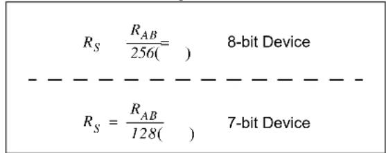
text_image
R_S = \frac{R_{AB}}{256(=)} \quad 8\text{-bit Device} - - - - - - - - - - - - - R_S = \frac{R_{AB}}{128(} \quad 7\text{-bit Device}5.2 Wiper
Each tap point (between the R_S resistors) is a connection point for an analog switch. The opposite side of the analog switch is connected to a common signal which is connected to the Terminal W (Wiper) pin.
A value in the volatile wiper register selects which analog switch to close, connecting the W terminal to the selected node of the resistor ladder.
The wiper can connect directly to Terminal B or to Terminal A. A zero-scale connections, connects the Terminal W (wiper) to Terminal B (wiper setting of 000h). A full-scale connections, connects the Terminal W (wiper) to Terminal A (wiper setting of 100h or 80h). In these configurations the only resistance between the Terminal W and the other Terminal (A or B) is that of the analog switches.
A wiper setting value greater than full-scale (wiper setting of 100h for 8-bit device or 80h for 7-bit devices) will also be a Full-Scale setting (Terminal W (wiper) connected to Terminal A). Table 5-1 illustrates the full wiper setting map.
Equation 5-2 illustrates the calculation used to determine the resistance between the wiper and terminal B.
EQUATION 5-2: R WB CALCULATION
| R_WB = _ABN256( + R)W | 8-bit Device |
| N = 0 to 256 (decimal) | |
| R_WB = _ABN128( + R)W | 7-bit Device |
| N = 0 to 128 (decimal) |
TABLE 5-1: VOLATILE WIPER VALUE VS. WIPER POSITION MAP
| Wiper Setting | Properties | |
| 7-bit Pot | 8-bit Pot | |
| 3FFh081h | 3FFh101h | Reserved (Full-Scale (W = A)),Increment and Decrement commands ignored |
| 080h 100h Full-Scale (W = A),Increment commands ignored | ||
| 07Fh041h | 0FFh081 | W = N |
| 040h 080h W = N (Mid-Scale) | ||
| 03Fh001h | 07Fh001 | W = N |
| 000h 000h Zero Scale (W = B)Decrement command ignored | ||
A POR/BOR event will load the Volatile Wiper register value with the default value. Table 5-2 shows the default values offered. Custom POR/BOR options are available. Contact the local Microchip Sales Office.
TABLE 5-2: DEFAULT FACTORY SETTINGS SELECTION
| Resistance Code | Typical R_AB Value | Default POR Wiper Setting | Wiper Code | |
| 8-bit 7-bit | ||||
| -502 | 5.0 kΩ | Mid-scale | 80h | 40h |
| -103 | 10.0 kΩ | Mid-scale | 80h | 40h |
| -503 | 50.0 kΩ | Mid-scale | 80h | 40h |
| -104 | 100.0 kΩ | Mid-scale | 80h | 40h |
5.3 Shutdown
Shutdown is used to minimize the device's current consumption. The MCP4XXX has two methods to achieve this. These are:
• Hardware Shutdown Pin (SHDN)
• Terminal Control Register (TCON)
The Hardware Shutdown pin is backwards compatible with the MCP42XXX devices.
5.3.1 HARDWARE SHUTDOWN PIN (SHDN)
The SHDN pin is available on the dual potentiometer devices. When the SHDN pin is forced active ( V_IL ):
• The P0A and P1A terminals are disconnected
- The P0W and P1W terminals are simultaneously connect to the P0B and P1B terminals, respectively (see Figure 5-2)
- The Serial Interface is NOT disabled, and all Serial Interface activity is executed
The Hardware Shutdown pin mode does NOT corrupt the values in the Volatile Wiper Registers nor the TCON register. When the Shutdown mode is exited (SHDN pin is inactive ( V_IH )):
- The device returns to the Wiper setting specified by the Volatile Wiper value
- The TCON register bits return to controlling the terminal connection state

text_image
A Resistor Network B WFIGURE 5-2: Hardware Shutdown
Resistor Network Configuration.
5.3.2 TERMINAL CONTROL REGISTER (TCON)
The Terminal Control (TCON) register is a volatile register used to configure the connection of each resistor network terminal pin (A, B, and W) to the Resistor Network. This register is shown in Register 4-2.
The RxHW bits forces the selected resistor network into the same state as the SHDN pin. Alternate low-power configurations may be achieved with the RxA, RxW, and RxB bits.
Note: When the RxHW bit forces the resistor network into the hardware SHDN state, the state of the TCON register RxA, RxW, and RxB bits is overridden (ignored). When the state of the RxHW bit no longer forces the resistor network into the hardware SHDN state, the TCON register RxA, RxW, and RxB bits return to controlling the terminal connection state. In other words, the RxHW bit does not corrupt the state of the RxA, RxW, and RxB bits.
5.3.3 INTERACTION OF SHDN PIN AND TCON REGISTER
Figure 5-3 shows how the SHDN pin signal and the RxHW bit signal interact to control the hardware shutdown of each resistor network (independently). Using the TCON bits allows each resistor network (Pot 0 and Pot 1) to be individually "shutdown" while the hardware pin forces both resistor networks to be "shutdown" at the same time.
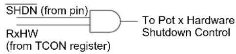
text_image
SHDN (from pin) RxHW (from TCON register) To Pot x Hardware Shutdown ControlFIGURE 5-3: RxHW bit and SHDN pin Interaction.
NOTES:
6.0 SERIAL INTERFACE (SPI)
The MCP4XXX devices support the SPI serial protocol. This SPI operates in the slave mode (does not generate the serial clock).
The SPI interface uses up to four pins. These are:
- - Chip Select
- SCK - Serial Clock
• SDI - Serial Data In
• SDO - Serial Data Out
Typical SPI Interfaces are shown in Figure 6-1. In the SPI interface, The Master's Output pin is connected to the Slave's Input pin and the Master's Input pin is connected to the Slave's Output pin.
The MCP4XXX SPI's module supports two (of the four) standard SPI modes. These are Mode 0, 0 and 1, 1. The SPI mode is determined by the state of the SCK pin ( V_IH or V_IL ) on the when the CS pin transitions from inactive ( V_IH ) to active ( V_IL or V_IHH ).
All SPI interface signals are high-voltage tolerant.
Typical SPI Interface Connections

flowchart
graph LR
    A["Host Controller"] --> B["MDP4XXX"]
    B --> C["SDO"]
    B --> D["SDI"]
    B --> E["SCK"]
    B --> F["I/O (1)"]
    C --> G["(Master Out - Slave In (MOSI) )"]
    D --> H["(Master In - Slave Out (MISO) )"]
    E --> I["SCK"]
    F --> J["CS"]
Typical MCP41X1 SPI Interface Connections (Host Controller Hardware SPI)
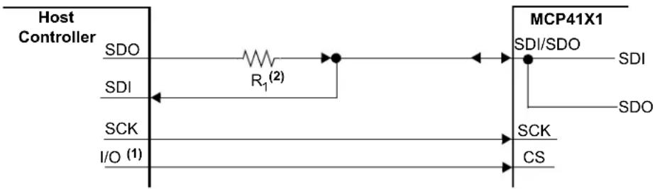
flowchart
graph LR
    A["Host Controller"] -->|SDO| B["R₁⁽²⁾"]
    A -->|SDI| B
    A -->|SCK| C["I/O⁽¹⁾"]
    A -->|CS| D["MCP41X1"]
    B --> E["SDI/SDO"]
    D --> F["SDI"]
    D --> G["SDO"]
Alternate MCP41X1 SPI Interface Connections (Host Controller Firmware SPI)
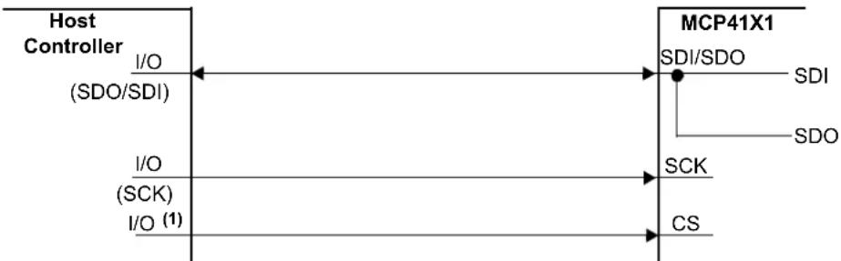
flowchart
graph LR
    A["Host Controller"] -->|I/O (SDO/SDI)| B["MCP41X1"]
    A -->|I/O (SCK)| B
    A -->|I/O (1)| B
    B -->|SDI/SDO| C["SDI"]
    B -->|SDO| D["SCK"]
    B -->|CS| E["CS"]
Note 1: If High voltage commands are desired, some type of external circuitry needs to be implemented.
2: R_1 must be sized to ensure V_IL and V_IH of the devices are met.
FIGURE 6-1: Typical SPI Interface Block Diagram.
6.1 SDI, SDO, SCK, and CS Operation
The operation of the four SPI interface pins are discussed in this section. These pins are:
• SDI (Serial Data In)
• SDO (Serial Data Out)
• SCK (Serial Clock)
- (Chip Select)
The serial interface works on either 8-bit or 16-bit boundaries depending on the selected command. The Chip Select (CS) pin frames the SPI commands.
6.1.1 SERIAL DATA IN (SDI)
The Serial Data In (SDI) signal is the data signal into the device. The value on this pin is latched on the rising edge of the SCK signal.
6.1.2 SERIAL DATA OUT (SDO)
The Serial Data Out (SDO) signal is the data signal out of the device. The value on this pin is driven on the falling edge of the SCK signal.
Once the pin is forced to the active level ( V_IL or V_IHH ), the SDO pin will be driven. The state of the SDO pin is determined by the serial bit's position in the command, the command selected, and if there is a command error state (CMDERR).
6.1.3 SDI/SDO
Note: MCP41X1 Devices Only .
For device packages that do not have enough pins for both an SDI and SDO pin, the SDI and SDO functionality is multiplexed onto a single I/O pin called SDI/SDO.
The SDO will only be driven for the command error bit (CMDERR) and during the data bits of a read command (after the memory address and command has been received).
6.1.3.1 SDI/SDO Operation
Figure 6-2 shows a block diagram of the SDI/SDO pin. The SDI signal has an internal “smart” pull-up. The value of this pull-up determines the frequency that data can be read from the device. An external pull-up can be added to the SDI/SDO pin to improve the rise time and therefore improve the frequency that data can be read.
Note: To support the High voltage requirement of the SDI function, the SDO function is an open drain output.
Data written on the SDI/SDO pin can be at the maximum SPI frequency.
Note: Care must be take to ensure that a Drive conflict does not exist between the Host Controllers SDO pin (or software SDI/SDO pin) and the MCP41x1 SDI/SDO pin (see Figure 6-1).
On the falling edge of the SCK pin during the C0 bit (see Figure 7-1), the SDI/SDO pin will start outputting the SDO value. The SDO signal overrides the control of the smart pull-up, such that whenever the SDI/SDO pin is outputting data, the smart pull-up is enabled.
The SDI/SDO pin will change from an input (SDI) to an output (SDO) after the state machine has received the Address and Command bits of the Command Byte. If the command is a Read command, then the SDI/SDO pin will remain an output for the remainder of the command. For any other command, the SDI/SDO pin returns to an input.

text_image
SDI/SDO "smart" pull-up SDI Open Drain Control Logic SDOFIGURE 6-2: Serial I/O Mux Block Diagram.
6.1.4 SERIAL CLOCK (SCK)
The SPI interface is specified to operate up to 10 MHz. The actual clock rate depends on the configuration of the system and the serial command used. Table 6-1 shows the SCK frequency for different configurations.
TABLE 6-1: SCK FREQUENCY
| Memory Type Access | Command | ||
| Read | Write, Increment, Decrement | ||
| Volatile Memory | SDI, SDO 1 | 10 MHz 10 MHz | |
| SDI/SDO^(1) | 250 kHz (2) | 10 MHz | |
Note 1: MCP41X1 devices only.
2: This is the maximum clock frequency without an external pull-up resistor.
6.1.5 THE CS SIGNAL
The Chip Select ( ) signal is used to select the device and frame a command sequence. To start a command, or sequence of commands, the signal must transition from the inactive state ( V_IH ) to an active state ( V_IL or V_IHH ).
After the CS signal has gone active, the SDO pin is driven and the clock bit counter is reset.
Note: There is a required delay after the CS pin goes active to the 1st edge of the SCK pin.
If an error condition occurs for an SPI command, then the Command byte's Command Error (CMDERR) bit (on the SDO pin) will be driven low (_IL) . To exit the error condition, the user must take the CS pin to the V_IH level.
When the pin returns to the inactive state ( V_IH ) the SPI module resets (including the address pointer). While the pin is in the inactive state ( V_IH ), the serial interface is ignored. This allows the Host Controller to interface to other SPI devices using the same SDI, SDO, and SCK signals.
The pin has an internal pull-up resistor. The resistor is disabled when the voltage on the pin is at the V_IL level. This means that when the pin is not driven, the internal pull-up resistor will pull this signal to the V_IH level. When the pin is driven low ( V_IL ), the resistance becomes very large to reduce the device current consumption.
The high voltage capability of the pin allows MCP413X/415X/423X/425X devices to be used in systems previously designed for the MCP414X/416X/424X/426X devices.
6.2 The SPI Modes
The SPI module supports two (of the four) standard SPI modes. These are Mode 0,0 and 1,1. The mode is determined by the state of the SDI pin on the rising edge of the 1st clock bit (of the 8-bit byte).
6.2.1 MODE 0,0
In Mode 0,0: SCK idle state = low ( V_IL ), data is clocked in on the SDI pin on the rising edge of SCK and clocked out on the SDO pin on the falling edge of SCK.
6.2.2 MODE 1,1
In Mode 1,1: SCK idle state = high ( V_IH ), data is clocked in on the SDI pin on the rising edge of SCK and clocked out on the SDO pin on the falling edge of SCK.
6.3 SPI Waveforms
Figure 6-3 through Figure 6-8 show the different SPI command waveforms. Figure 6-3 and Figure 6-4 are read and write commands. Figure 6-5 and Figure 6-6 are read commands when the SDI and SDO pins are multiplexed on the same pin (SDI/SDO). Figure 6-7 and Figure 6-8 are increment and decrement commands.

text_image
CS V_IH V_IHH (1) V_IL SCK Write to SSPBUF CMDERR bit SDO bit15 bit14 bit13 bit12 bit11 bit10 bit9 bit8 bit7 bit6 bit5 bit4 bit3 bit2 bit1 bit0 SDI AD3'AD2'AD1'AD0 bit15 bit14 bit13 bit12 bit9 bit8 bit7 bit6 bit5 bit4 bit3 bit2 bit1 bit0 Input SampleNote 1: V_IHH is supported for compatibility with the MCP414X/6X and MCP424X/6X devices high voltage operation.
FIGURE 6-3: 16-Bit Commands (Write, Read) - SPI Waveform (Mode 1,1).

text_image
V_IH V_IHH(1) V_IL CS SCK Write to SSPBUF CMDERR bit SDO bit15 bit14 bit13 bit12 bit11 bit10 bit9 bit8 bit7 bit6 bit5 bit4 bit3 bit2 bit1 bit0 SDI AD3 AD2 AD1 AD0 X D8 D7 D6 D5 D4 D3 D2 D1 D0 bit15 bit14 bit13 bit12 bit11 bit10 bit9 bit8 bit7 bit6 bit5 bit4 bit3 bit2 bit1 bit0 Input SampleNote 1: V_IHH is supported for compatibility with the MCP414X/6X and MCP424X/6X devices high voltage operation.
FIGURE 6-4: 16-Bit Commands (Write, Read) - SPI Waveform (Mode 0,0).
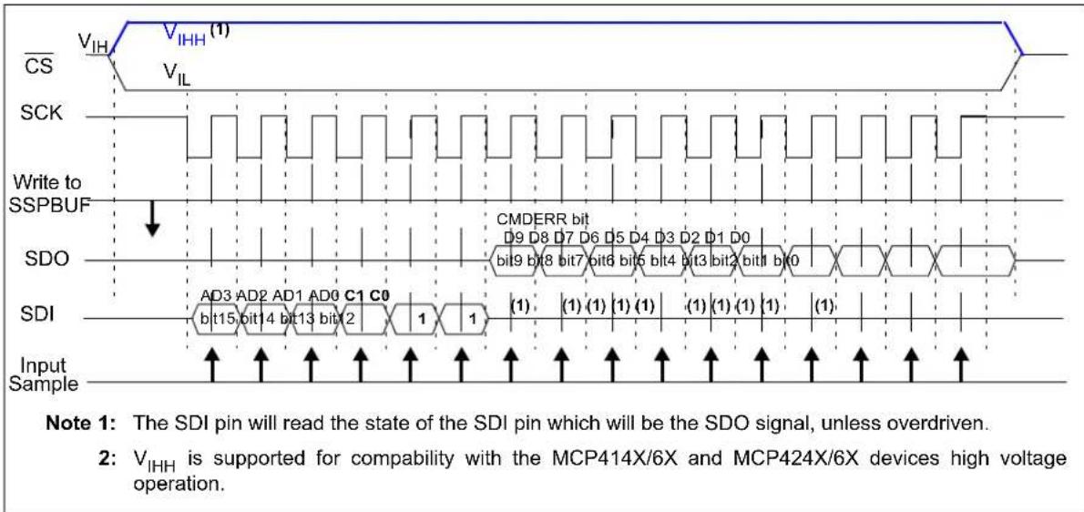
other
| Signal | Bit 1 | Bit 2 | Bit 3 | Bit 4 | Bit 5 | Bit 6 | Bit 7 | Bit 8 | |--------|-------|-------|-------|-------|-------|-------|-------|-------| | V_IH | | | | | | | | | | V_IHH | | | | | | | | | | V_IL | | | | | | | | | | SCK | | | | | | | | | | Write to SSPBUF | | | | | | | | | | SDO | | | | | | | | | | SDI | AD3 | AD2 | AD1 | AD0 | C1 | C0 | | | | Input Sample | bit15 | bit14 | bit13 | bit2 | bit1 | | | | Note: The SDI pin will read the state of the SDI pin which will be the SDO signal, unless overdriven. Note: V_IHH is supported for compatibility with the MCP414X/6X and MCP424X/6X devices high voltage operation.FIGURE 6-5: 16-Bit Read Command for Devices with SDI/SDO multiplexed - SPI Waveform (Mode 1,1).
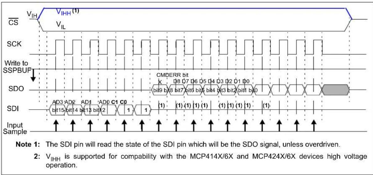
other
| Signal | Bit Position | Value | |--------|--------------|-------| | CS | V_IH | V_IH(1) | | CS | V_IL | V_IL | | SCK | | | | Write to SSPBUF | | | | SDO | | CMDERR bit D8 D7 D6 D5 D4 D3 D2 D1 D0 bit9 bit8 bit7 bit6 bit5 bit4 bit3 bit2 bit1 bit0 | | SDI | | AD3 AD2 AD1 AD0 C1 C0 (1) (1) (1) (1) (1) (1) (1) (1) (1) (1) | | Input Sample | | ↑ ↑↑↑↑↑↑↑↑↑↑↑↑↑↑↑↑↑↑↑↑↑↑↑↑↑↑↑↑↑↑↑↑↑↑↑↑↑↑↑↑↑↑↑↑↑↑↑↑↑↑↑↑↑↑↑↑↑↓ |FIGURE 6-6: 16-Bit Read Command for Devices with SDI/SDO multiplexed - SPI Waveform (Mode 0,0).
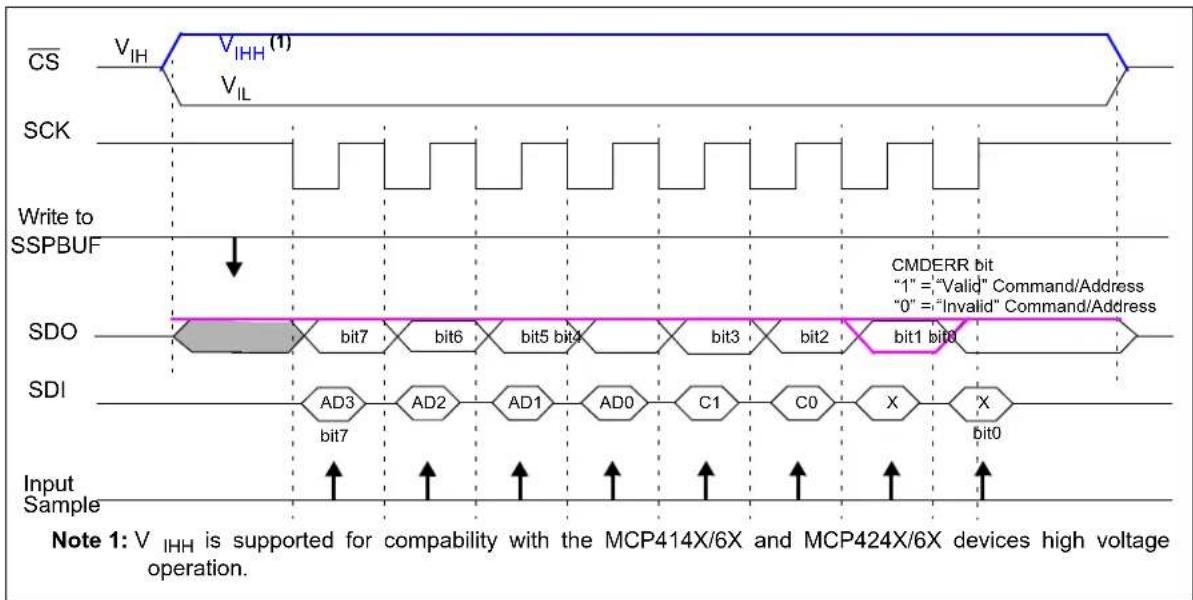
other
| Signal | Bit | Value | |------------|------|-------| | CS | bit7 | V_IH | | SCK | bit6 | V_IHH(1) | | Write to SSPBUF | bit5 | V_IL | | SDO | bit3 | bit7 | | SDI | bit2 | bit6 | | Input Sample | bit0 | bit0 |FIGURE 6-7: 8-Bit Commands (Increment, Decrement, Modify - SPI Waveform with PIC MCU (Mode 1,1).
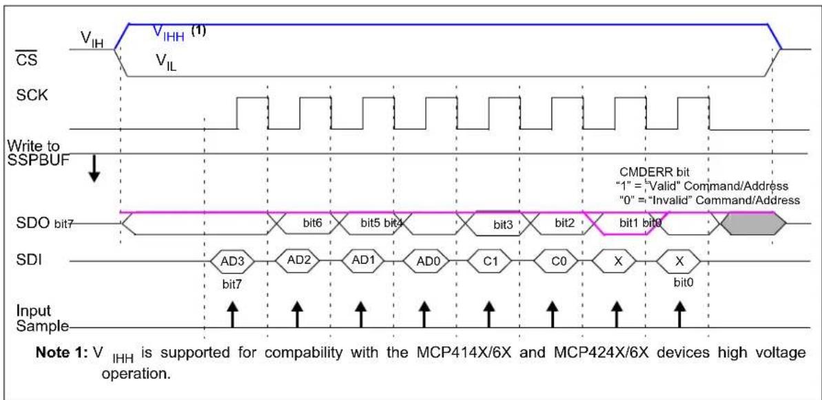
other
| Signal | Bit Address | Description | |--------|-------------|-----------| | CS | V_IH | V_IH (1) | | SCK | | | | Write to SSPBUF | | | | SDO bit7 | | CMDERR bit "1" = "Valid" Command/Address, "0" = "Invalid" Command/Address | | SDI | | | | Input Sample | | | Note 1: V_IHH is supported for compatibility with the MCP414X/6X and MCP424X/6X devices high voltage operation.FIGURE 6-8: 8-Bit Commands (Increment, Decrement, Modify - SPI Waveform with PIC MCU (Mode 0,0).
7.0 DEVICE COMMANDS
The MCP4XXX's SPI command format supports 16 memory address locations and four commands. Each command has two modes. These are:
• Normal Serial Commands
• High-Voltage Serial Commands
Normal serial commands are those where the pin is driven to V_IL . High Voltage Serial Commands, pin is driven to V_IHH , for compatibility with systems that also support the MCP414X/416X/424X/426X devices. High Voltage Serial Commands operate identically to their corresponding Normal Serial Command. In each mode, there are four possible commands. These commands are shown in Table 7-1.
The 8-bit commands (Increment Wiper and Decrement Wiper commands) contain a Command Byte, see Figure 7-1, while 16-bit commands (Read Data and Write Data commands) contain a Command Byte and a Data Byte. The Command Byte contains two data bits, see Figure 7-1.
Table 7-2 shows the supported commands for each memory location and the corresponding values on the SDI and SDO pins.
Table 7-3 shows an overview of all the SPI commands and their interaction with other device features.
7.1 Command Byte
The Command Byte has three fields, the Address, the Command, and 2 Data bits, see Figure 7-1. Currently only one of the data bits is defined (D8). This is for the Write command.
The device memory is accessed when the master sends a proper Command Byte to select the desired operation. The memory location getting accessed is contained in the Command Byte's AD3:AD0 bits. The action desired is contained in the Command Byte's C1:C0 bits, see Table7-1. C1:C0 determines if the desired memory location will be read, written, Incremented (wiper setting +1) or Decremented (wiper setting -1). The Increment and Decrement commands are only valid on the volatile wiper registers.
As the Command Byte is being loaded into the device (on the SDI pin), the device's SDO pin is driving. The SDO pin will output high bits for the first six bits of that command. On the 7th bit, the SDO pin will output the CMDERR bit state (see Section 7.3 "Error Condition"). The 8th bit state depends on the command selected.
TABLE 7-1: COMMAND BIT OVERVIEW
| C1:C0 Bit States | Command # of Bits | |
| 11 | Read Data 16-Bits | |
| 00 | Write Data 16-Bits | |
| 01 | Increment | 8-Bits |
| 10 | Decrement | 8-Bits |

text_image
8-bit Command Command Byte A A A A C C D D D D 1 0 9 8 3 2 1 Memory Address Data Bits Command Bits 16-bit Command Command Byte A A A A C C D D D D D D D D D 1 0 9 8 7 6 5 4 3 2 1 0 3 2 1 0 Memory Address Data Bits Command Bits Command Bits C C 1 0 0 0 = Write Data 0 1 = INCR 1 0 = DECR 1 1 = Read DataFIGURE 7-1: General SPI Command Formats.
TABLE 7-2: MEMORY MAP AND THE SUPPORTED COMMANDS
| Address | Command | Data(10-bits) (1) | SPI String (Binary) | ||
| Value Function | MOSI (SDI pin) MISO | (SDO pin) (2) | |||
| 00h Volatile Wiper 0 Write | Data nn nnnn nnnn 0000 | 00nn nnnn nnnn 1 | 111 1111 1111 1111 | ||
| Read Data nn nnnn nnnn | 0000 11nn nnnn | nnnn 1111 111n nnnn nnnn | |||
| Increment Wiper — 0000 | 0100 | 1111 1111 | |||
| Decrement Wiper | — 0000 1000 | 1111 1111 | |||
| 01h Volatile Wiper 1 Write | Data nn nnnn nnnn 0001 | 00nn nnnn nnnn 1 | 111 1111 1111 1111 | ||
| Read Data nn nnnn nnnn | 0001 11nn nnnn | nnnn 1111 111n nnnn nnnn | |||
| Increment Wiper — 0001 | 0100 | 1111 1111 | |||
| Decrement Wiper | — 0001 1000 | 1111 1111 | |||
| 02h | Reserved | — | — | — | — |
| 03h | Reserved | — | — | — | — |
| 04h Volatile TCON Register | Write Data | nn nnnn nnnn 01 | 00 00nn nnnn nnnn 1111 1111 1111 1111 | ||
| Read Data nn nnnn nnnn | 0100 11nn nnnn | nnnn 1111 111n nnnn nnnn | |||
| 05h Status Register Read Data nn nnnn nnnn 0101 11nn nnnn nnnn 1111 111n nnnn nnnn | |||||
| 06h-0Fh | Reserved | — | — | — | — |
Note 1: The Data Memory is only 9-bits wide, so the MSb is ignored by the device.
2: All these Address/Command combinations are valid, so the CMDERR bit is set. Any other Address/Command combination is a command error state and the CMDERR bit will be clear.
7.2 Data Byte
Only the Read Command and the Write Command use the Data Byte, see Figure 7-1. These commands concatenate the 8-bits of the Data Byte with the one data bit (D8) contained in the Command Byte to form 9-bits of data (D8:D0). The Command Byte format supports up to 9-bits of data so that the 8-bit resistor network can be set to Full-Scale (100h or greater). This allows wiper connections to Terminal A and to Terminal B.
The D9 bit is currently unused, and corresponds to the position on the SDO data of the CMDERR bit.
7.3 Error Condition
The CMDERR bit indicates if the four address bits received (AD3:AD0) and the two command bits received (C1:C0) are a valid combination (see Table 4-1). The CMDERR bit is high if the combination is valid and low if the combination is invalid.
SPI commands that do not have a multiple of 8 clocks are ignored.
Once an error condition has occurred, any following commands are ignored. All following SDO bits will be low until the CMDERR condition is cleared by forcing the pin to the inactive state ( V_IH ).
7.3.1 ABORTING A TRANSMISSION
All SPI transmissions must have the correct number of SCK pulses to be executed. The command is not executed until the complete number of clocks have been received. If the pin is forced to the inactive state (V_IH) the serial interface is reset. Partial commands are not executed.
SPI is more susceptible to noise than other bus protocols. The most likely case is that this noise corrupts the value of the data being clocked into the MCP4XXX or the SCK pin is injected with extra clock pulses. This may cause data to be corrupted in the device, or a command error to occur, since the address and command bits were not a valid combination. The extra SCK pulse will also cause the SPI data (SDI) and clock (SCK) to be out of sync. Forcing the CS pin to the inactive state ( V_IH ) resets the serial interface. The SPI interface will ignore activity on the SDI and SCK pins until the CS pin transition to the active state is detected ( V_IH to V_IL or V_IH to V_IHH ).
Note 1: When data is not being received by the MCP4XXX, it is recommended that the CS pin be forced to the inactive level ( V_IL )
2: It is also recommended that long continuous command strings should be broken down into single commands or shorter continuous command strings. This reduces the probability of noise on the SCK pin corrupting the desired SPI commands.
7.4 Continuous Commands
The device supports the ability to execute commands continuously. While the pin is in the active state ( V_IL or V_IHH ). Any sequence of valid commands may be received.
The following example is a valid sequence of events:
- CS pin driven active (V IL or V IHH).
- Read Command.
- Increment Command (Wiper 0).
- Increment Command (Wiper 0).
- Decrement Command (Wiper 1).
- Write Command.
- Write Command.
- CS pin driven inactive (V _IH ).
Note 1: It is recommended that while the pin is active, only one type of command should be issued. When changing commands, it is recommended to take the pin inactive then force it back to the active state.
2: It is also recommended that long command strings should be broken down into shorter command strings. This reduces the probability of noise on the SCK pin corrupting the desired SPI command string.
TABLE 7-3: COMMANDS
| Command Name # of Bits | High Voltage (V_IHH) on CS pin? | |
| Write Data 16-Bits — | ||
| Read Data 16-Bits — | ||
| Increment Wiper | 8-Bits | |
| Decrement Wiper | 8-Bits | |
| High Voltage Write Data 16-Bits Yes | ||
| High Voltage Read Data 16-Bits Yes | ||
| High Voltage Increment Wiper | 8-Bits | |
| High Voltage Decrement Wiper | 8-Bits |
7.5 Write Data
Normal and High Voltage
Note: The High Voltage Write Data command is supported for compatibility with system that also support MCP414X/416X/424X/426X devices.
The Write command is a 16-bit command. The format of the command is shown in Figure 7-2.
A Write command to a Volatile memory location changes that location after a properly formatted Write Command (16-clock) have been received.
7.5.1 SINGLE WRITE
The write operation requires that the pin be in the active state ( V_IL or V_IHH ). Typically, the pin will be in the inactive state ( V_IH ) and is driven to the active state ( V_IL ). The 16-bit Write Command (Command Byte and Data Byte) is then clocked in on the SCK and SDI pins. Once all 16 bits have been received, the specified volatile address is updated. A write will not occur if the write command isn't exactly 16 clocks pulses. This protects against system issues from corrupting the memory locations.
Figure 6-3 and Figure 6-4 show possible waveforms for a single write.
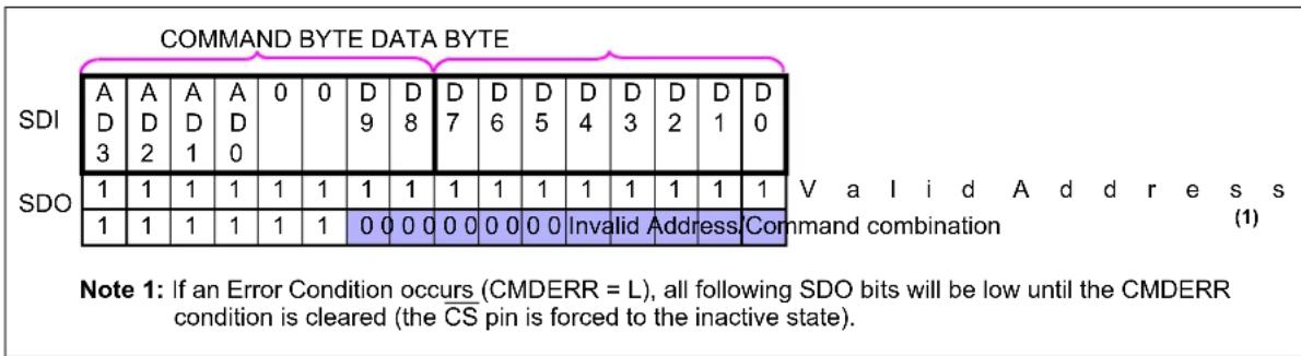
other
COMMAND BYTE DATA BYTE | Bit | Command Combination | | :--- | :--- | | 1 | Valid Address | | 2 | Command Combination | | 3 | Command Combination | | 4 | Command Combination | | 5 | Command Combination | | 6 | Command Combination | | 7 | Command Combination | | 8 | Command Combination | | 9 | Command Combination | | 10 | Command Combination | | 11 | Command Combination | | 12 | Command Combination | | 13 | Command Combination | | 14 | Command Combination | | 15 | Command Combination | | 16 | Command Combination | | 17 | Command Combination | | 18 | Command Combination | | 19 | Command Combination | | 20 | Command Combination | | 21 | Command Combination | | 22 | Command Combination | | 23 | Command Combination | | 24 | Command Combination | | 25 | Command Combination | | 26 | Command Combination | | 27 | Command Combination | | 28 | Command Combination | | 29 | Command Combination | | 30 | Command Combination | | 31 | Command Combination | | 32 | Command Combination | | 33 | Command Combination | | 34 | Command Combination | | 35 | Command Combination | | 36 | Command Combination | | 37 | Command Combination | | 38 | Command Combination | | 39 | Command Combination | | 40 | Command Combination | | 41 | Command Combination | | 42 | Command Combination | | 43 | Command Combination | | 44 | Command Combination | | 45 | Command Combination | | 46 | Command Combination | | 47 | Command Combination | | 48 | Command Combination | | 49 | Command Combination | | 50 | Command Combination | | Note 1: If an Error Condition occurs (CMDERR = L), all following SDO bits will be low until the CMDERR condition is cleared (the CS pin is forced to the inactive state).FIGURE 7-2: Write Command - SDI and SDO States.
7.5.2 CONTINUOUS WRITES
Continuous writes are possible only when writing to the volatile memory registers (address 00h, 01h, and 04h).
Figure 7-3 shows the sequence for three continuous writes. The writes do not need to be to the same volatile memory address.
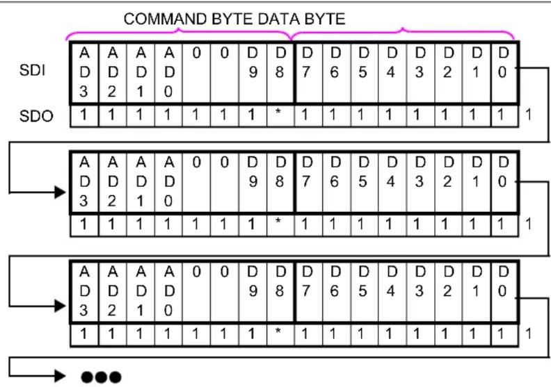
text_image
COMMAND BYTE DATA BYTE SDI A D 3 A D 2 A D 1 A D 0 SDO 1 1 1 1 1 1 1 * 1 1 1 1 1 1 1 1 1 A D 3 A D 2 A D 1 A D 0 1 1 1 1 1 1 1 * 1 1 1 1 1 1 1 1 1 A D 3 A D 2 A D 1 A D 0 1 1 1 1 1 1 1 * 1 1 1 1 1 1 1 1 1 ●●●Note 1: If a Command Error (CMDERR) occurs at this bit location (*), then all following SDO bits will be driven low until the CS pin is driven inactive (V _IH ).
FIGURE 7-3: Continuous Write Sequence.
7.6 Read Data
Normal and High Voltage
Note: The High Voltage Read Data command is supported for compatibility with system that also support MCP414X/416X/424X/426X devices.
The Read command is a 16-bit command. The format of the command is shown in Figure 7-4.
The first 6-bits of the Read command determine the address and the command. The 7th clock will output the CMDERR bit on the SDO pin. The remaining 9-clocks the device will transmit the 9 data bits (D8:D0) of the specified address (AD3:AD0).
Figure 7-4 shows the SDI and SDO information for a Read command.
7.6.1 SINGLE READ
The read operation requires that the pin be in the active state ( V_IL or V_IHH ). Typically, the pin will be in the inactive state ( V_IH ) and is driven to the active state ( V_IL or V_IHH ). The 16-bit Read Command (Command Byte and Data Byte) is then clocked in on the SCK and SDI pins. The SDO pin starts driving data on the 7th bit (CMDERR bit) and the addressed data comes out on the 8th through 16th clocks. Figure 6-3 through Figure 6-6 show possible waveforms for a single read.
Figure 6-5 and Figure 6-6 show the single read waveforms when the SDI and SDO signals are multiplexed on the same pin. For additional information on the multiplexing of these signals, refer to Section 6.1.3 "SDI/SDO".

text_image
COMMAND BYTE DATA BYTE SDI A D A D A 1 1 X X X X X X X X X X X 3 2 1 0 SDO 1 1 1 1 1 1 D D D D D D D D 8 7 6 5 4 3 2 1 0 1 1 1 1 1 1 0 0 0 0 0 0 0 0 0 0 0 Valid Address/Command combination A t t e m p t e d M e n Memory location. READ DATAFIGURE 7-4: Read Command - SDI and SDO States.
7.6.2 CONTINUOUS READS
Continuous reads allows the devices memory to be read quickly. Continuous reads are possible to all memory locations.
Figure 7-5 shows the sequence for three continuous reads. The reads do not need to be to the same memory address.
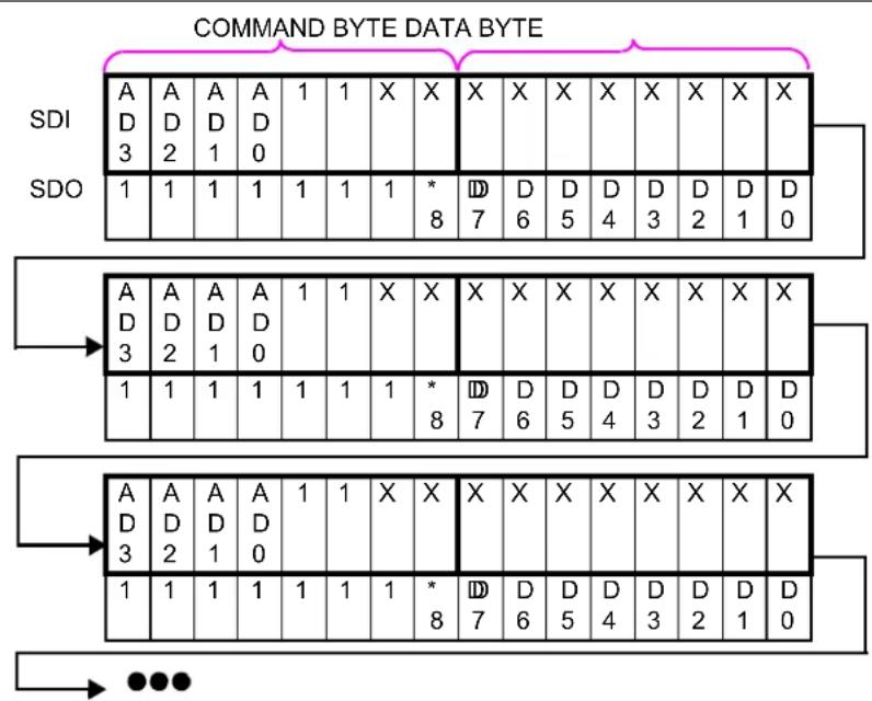
text_image
COMMAND BYTE DATA BYTE SDI A D 3 A D 2 A D 1 A D 0 1 1 X 8 X X X X X X X X X SDO 1 1 1 1 1 1 1 * 8 D7 D6 D5 D4 D3 D2 D1 D0 A D 3 A D 2 A D 1 A D 0 1 1 X 8 X X X X X X X X 1 1 1 1 1 1 1 * 8 D7 D6 D5 D4 D3 D2 D1 D0 A D 3 A D 2 A D 1 A D 0 1 1 X 8 X X X X X X X X 1 1 1 1 1 1 1 * 8 D7 D6 D5 D4 D3 D2 D1 D0 ●●●Note 1: If a Command Error (CMDERR) occurs at this bit location (*), then all following SDO bits will be driven low until the CS pin is driven inactive ( V_IH ).
FIGURE 7-5: Continuous Read Sequence.
7.7 Increment Wiper Normal and High Voltage
Note: The High Voltage Increment Wiper command is supported for compatibility with system that also support MCP414X/416X/424X/426X devices.
The Increment Command is an 8-bit command. The Increment Command can only be issued to wiper memory locations. The format of the command is shown in Figure 7-6.
An Increment Command to the wiper memory location changes that location after a properly formatted command (8-clocks) have been received.
Increment commands provide a quick and easy method to modify the value of the wiper location by +1 with minimal overhead.
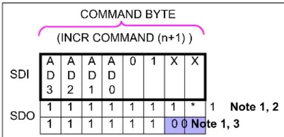
text_image
COMMAND BYTE (INCR COMMAND (n+1)) SDI A A A A 0 1 X X D D D D 0 3 2 1 0 SDO 1 1 1 1 1 1 1 * 1 Note 1, 2 1 1 1 1 1 1 0 0 Note 1, 3Note 1: Only functions when writing the volatile wiper registers (AD3:AD0) 0h and 1h.
2: Valid Address/Command combination.
3: Invalid Address/Command combination all following SDO bits will be low until the CMDERR condition is cleared.
(the CS pin is forced to the inactive state).
4: If a Command Error (CMDERR) occurs at this bit location (*), then all following SDO bits will be driven low until the CS pin is driven inactive (V _IH ).
FIGURE 7-6: Increment Command - SDI and SDO States.
7.7.1 SINGLE INCREMENT
Typically, the pin starts at the inactive state ( V_IH ), but may be already be in the active state due to the completion of another command.
Figure 6-7 through Figure 6-8 show possible waveforms for a single increment. The increment operation requires that the pin be in the active state ( V_IL or V_IHH ). Typically, the pin will be in the inactive state ( V_IH ) and is driven to the active state ( V_IL or V_IHH ). The 8-bit Increment Command (Command Byte) is then clocked in on the SDI pin by the SCK pins. The SDO pin drives the CMDERR bit on the 7th clock.
The wiper value will increment up to 100h on 8-bit devices and 80h on 7-bit devices. After the wiper value has reached Full-Scale (8-bit =100h, 7-bit =80h), the wiper value will not be incremented further. If the Wiper register has a value between 101h and 1FFh, the Increment command is disabled. See Table 7-4 for additional information on the Increment Command versus the current volatile wiper value.
The Increment operations only require the Increment command byte while the pin is active ( V_IL or V_IHH ) for a single increment.
After the wiper is incremented to the desired position, the pin should be forced to V_IH to ensure that unexpected transitions on the SCK pin do not cause the wiper setting to change. Driving the pin to V_IH should occur as soon as possible (within device specifications) after the last desired increment occurs.
TABLE 7-4: INCREMENT OPERATION VS. VOLATILE WIPER VALUE
| Current Wiper Setting | Wiper (W) Properties | Increment Command Operates? | |
| 7-bit Pot | 8-bit Pot | ||
| 3FFh081h | 3FFh101h | Reserved(Full-Scale (W = A)) | No |
| 080h | 100h | Full-Scale (W = A) | No |
| 07Fh041h | 0FFh081 | W = N | Yes |
| 040h | 080h | W = N (Mid-Scale) | |
| 03Fh001h | 07Fh001 | W = N | |
| 000h | 000h | Zero Scale (W = B) | Yes |
7.7.2 CONTINUOUS INCREMENTS
Continuous Increments are possible only when writing to the wiper registers.
Figure 7-7 shows a Continuous Increment sequence for three continuous writes. The writes do not need to be to the same volatile memory address.
When executing an continuous Increment commands, the selected wiper will be altered from n to n+1 for each Increment command received. The wiper value will increment up to 100h on 8-bit devices and 80h on 7-bit devices. After the wiper value has reached Full-Scale (8-bit =100h, 7-bit =80h), the wiper value will not be incremented further. If the Wiper register has a value between 101h and 1FFh, the Increment command is disabled.
Increment commands can be sent repeatedly without raising until a desired condition is met. The value in the Volatile Wiper register can be read using a Read Command.
When executing a continuous command string, The Increment command can be followed by any other valid command.
The wiper terminal will move after the command has been received (8th clock).
After the wiper is incremented to the desired position, the pin should be forced to V_IH to ensure that unexpected transitions (on the SCK pin do not cause the wiper setting to change). Driving the pin to V_IH should occur as soon as possible (within device specifications) after the last desired increment occurs.

text_image
COMMAND BYTE (INCR COMMAND (n+1) ) (INCR COMMAND (n+2) ) COMMAND BYTE (INCR COMMAND (n+3) ) SDI A D 3 A D 2 A D 1 A D 0 0 1 X X A D 3 A D 2 A D 1 A D 0 0 1 X X SDO 1 1 1 1 1 1 1 * 1 1 1 1 1 1 1 1 1 1 * 1 1 1 1 1 1 1 * 1 1 1 1 1 1 1 0 0 0 0 0 0 0 0 0 0 0 0 0 Note 3,4 1 1 1 1 1 1 1 1 1 1 1 1 1 0 0 0 0 0 0 0 0 0 Note 3,4 1 1 1 1 1 1 1 1 1 1 1 1 1 1 1 1 1 1 1 1 Note 3,4 Note 1: Only functions when writing the volatile wiper registers (AD3:AD0) 0h and 1h. 2: Valid Address/Command combination. 3: Invalid Address/Command combination. 4: If an Error Condition occurs (CMDERR = L), all following SDO bits will be low until the CMDERR condition is cleared (the CS pin is forced to the inactive state).FIGURE 7-7: Continuous Increment Command - SDI and SDO States.
7.8 Decrement Wiper Normal and High Voltage
Note: The High Voltage Decrement Wiper command is supported for compatibility with system that also support MCP414X/416X/424X/426X devices.
The Decrement Command is an 8-bit command. The Decrement Command can only be issued to wiper memory locations. The format of the command is shown in Figure 7-6.
An Decrement Command to the wiper memory location changes that location after a properly formatted command (8-clocks) have been received.
Decrement commands provide a quick and easy method to modify the value of the wiper location by -1 with minimal overhead.
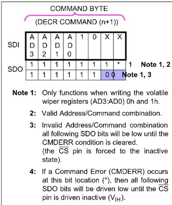
text_image
COMMAND BYTE (DECR COMMAND (n+1)) SDI A A A A 1 0 X X D D D D 1 D 3 2 1 0 SDO 1 1 1 1 1 1 1 * 1 Note 1, 2 1 1 1 1 1 1 0 0 Note 1, 3 Note 1: Only functions when writing the volatile wiper registers (AD3:AD0) 0h and 1h. 2: Valid Address/Command combination. 3: Invalid Address/Command combination all following SDO bits will be low until the CMDERR condition is cleared. (the CS pin is forced to the inactive state). 4: If a Command Error (CMDERR) occurs at this bit location (*), then all following SDO bits will be driven low until the CS pin is driven inactive (V_IH).FIGURE 7-8: Decrement Command - SDI and SDO States.
7.8.1 SINGLE DECREMENT
Typically the pin starts at the inactive state (V_IH) , but may be already be in the active state due to the completion of another command.
Figure 6-7 through Figure 6-8 show possible waveforms for a single Decrement. The decrement operation requires that the pin be in the active state ( V_IL or V_IHH ). Typically the pin will be in the inactive state ( V_IH ) and is driven to the active state ( V_IL or V_IHH ). Then the 8-bit Decrement Command (Command Byte) is clocked in on the SDI pin by the SCK pins. The SDO pin drives the CMDERR bit on the 7th clock.
The wiper value will decrement from the wipers Full-Scale value (100h on 8-bit devices and 80h on 7-bit devices). Above the wipers Full-Scale value (8-bit =101h to 1FFh, 7-bit = 81h to FFh), the decrement command is disabled. If the Wiper register has a Zero Scale value (000h), then the wiper value will not decrement. See Table 7-4 for additional information on the Decrement Command vs. the current volatile wiper value.
The Decrement commands only require the Decrement command byte, while the pin is active ( V_IL or V_IHH ) for a single decrement.
After the wiper is decremented to the desired position, the pin should be forced to V_IH to ensure that unexpected transitions on the SCK pin do not cause the wiper setting to change. Driving the pin to V_IH should occur as soon as possible (within device specifications) after the last desired decrement occurs.
TABLE 7-5: DECREMENT OPERATION VS. VOLATILE WIPER VALUE
| Current Wiper Setting | Wiper (W) Properties | Decrement Command Operates? | |
| 7-bit Pot | 8-bit Pot | ||
| 3FFh081h | 3FFh101h | Reserved(Full-Scale (W = A)) | No |
| 080h | 100h | Full-Scale (W = A) | Yes |
| 07Fh041h | 0FFh081 | W = N | Yes |
| 040h | 080h | W = N (Mid-Scale) | |
| 03Fh001h | 07Fh001 | W = N | |
| 000h | 000h | Zero Scale (W = B) | No |
7.8.2 CONTINUOUS DECREMENTS
Continuous Decrements are possible only when writing to the wiper registers.
Figure 7-9 shows a continuous Decrement sequence for three continuous writes. The writes do not need to be to the same volatile memory address.
When executing an continuous Decrement commands, the selected wiper will be altered from n to n-1 for each Decrement command received. The wiper value will decrement from the wipers Full-Scale value (100h on 8-bit devices and 80h on 7-bit devices). Above the wipers Full-Scale value (8-bit =101h to 1FFh, 7-bit = 81h to FFh), the decrement command is disabled. If the Wiper register has a Zero Scale value (000h), then the wiper value will not decrement. See Table 7-4 for additional information on the Decrement Command vs. the current volatile wiper value.
Decrement commands can be sent repeatedly without raising until a desired condition is met. The value in the Volatile Wiper register can be read using a Read Command.
When executing a continuous command string, The Decrement command can be followed by any other valid command.
The wiper terminal will move after the command has been received (8th clock).
After the wiper is decremented to the desired position, the pin should be forced to V_IH to ensure that “unexpected” transitions (on the SCK pin do not cause the wiper setting to change). Driving the pin to V_IH should occur as soon as possible (within device specifications) after the last desired decrement occurs.
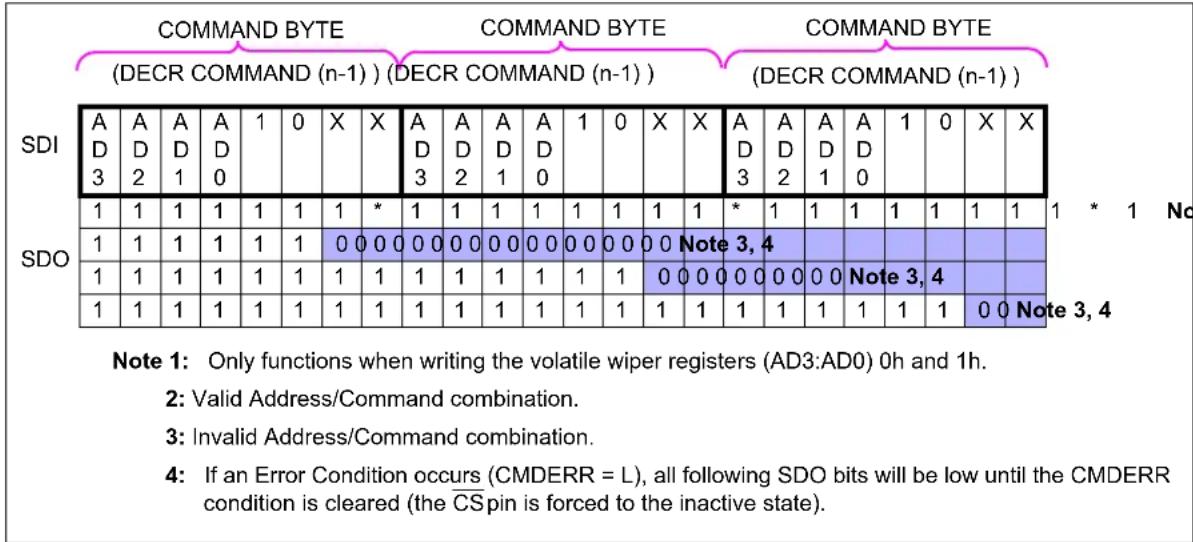
text_image
COMMAND BYTE (DECR COMMAND (n-1) ) (DECR COMMAND (n-1) ) COMMAND BYTE (DECR COMMAND (n-1) ) SDI A D 3 A D 2 A D 1 A D 0 1 0 X X A D 3 A D 2 A D 1 A D 0 1 0 X X SDO 1 1 1 1 1 1 1 * 1 1 1 1 1 1 1 1 1 1 * 1 1 1 1 1 1 1 * 1 1 1 1 1 1 1 0 0 0 0 0 0 0 0 0 0 0 0 0 Note 3,4 1 1 1 1 1 1 1 1 1 1 1 1 1 0 0 0 0 0 0 0 0 0 Note 3,4 1 1 1 1 1 1 1 1 1 1 1 1 1 1 1 1 1 1 1 Note 3,4 Note 1: Only functions when writing the volatile wiper registers (AD3:AD0) 0h and 1h. 2: Valid Address/Command combination. 3: Invalid Address/Command combination. 4: If an Error Condition occurs (CMDERR = L), all following SDO bits will be low until the CMDERR condition is cleared (the CSpin is forced to the inactive state).FIGURE 7-9: Continuous Decrement Command - SDI and SDO States.
8.0 APPLICATIONS EXAMPLES
Digital potentiometers have a multitude of practical uses in modern electronic circuits. The most popular uses include precision calibration of set point thresholds, sensor trimming, LCD bias trimming, audio attenuation, adjustable power supplies, motor control overcurrent trip setting, adjustable gain amplifiers and offset trimming. The MCP413X/415X/423X/425X devices can be used to replace the common mechanical trim pot in applications where the operating and terminal voltages are within CMOS process limitations ( V_DD = 2.7V to 5.5V).
8.1 Split Rail Applications
All inputs that would be used to interface to a Host Controller support High Voltage on their input pin. This allows the MCP4XXX device to be used in split power rail applications.
An example of this is a battery application where the PIC ^® MCU is directly powered by the battery supply (4.8V) and the MCP4XXX device is powered by the 3.3V regulated voltage.
For SPI applications, these inputs are:
• CS
• S C K
• SDI (or SDI/SDO)
: SHDN
Figure 8-1 through Figure 8-2 show three example split rail systems. In this system, the MCP4XXX interface input signals need to be able to support the PIC MCU output high voltage ( V_OH ).
In Example #1 (Figure 8-1), the MCP4XXX interface input signals need to be able to support the PIC MCU output high voltage ( V_OH ). If the split rail voltage delta becomes too large, then the customer may be required to do some level shifting due to MCP4XXX V_OH levels related to Host Controller V_IH levels.
In Example #2 (Figure 8-2), the MCP4XXX interface input signals need to be able to support the lower voltage of the PIC MCU output high voltage level ( V_OH ).
Table 8-1 shows an example PIC microcontroller I/O voltage specifications and the MCP4XXX specifications. So this PIC MCU operating at 3.3V will drive a V_OH at 2.64V, and for the MCP4XXX operating at 5.5V, the V_IH is 2.47V. Therefore, the interface signals meet specifications.

flowchart
graph TD
    A["5V"] --> B["Voltage Regulator"]
    B --> C["3V"]
    C --> D["MCP4XXX"]
    D --> E["SDI"]
    D --> F["CS"]
    D --> G["SCK"]
    D --> H["SHDN"]
    D --> I["SDO"]
    D --> J["SHDN"]
    D --> K["SDO"]
FIGURE 8-1: Example Split Rail System 1.

flowchart
graph TD
    A["Voltage Regulator"] -->|3V| B["PIC MCU"]
    B --> C["SDI"]
    B --> D["CS"]
    B --> E["SCK"]
    B --> F["SHDN"]
    B --> G["SDO"]
    H["MCP4XXX"] -->|5V| I["5V"]
    I --> J["SDI"]
    I --> K["CS"]
    I --> L["SCK"]
    I --> M["SHDN"]
    I --> N["SDO"]
FIGURE 8-2: Example Split Rail System 2.
TABLE 8-1: V OH - VIH COMPARISONS
| PIC (1) | MCP4XXX (2) | Comment | ||||
| V_DD | V_IH | V_OH | V_DD | V_IH | V_OH | |
| 5.5 4.4 | 4.4 2 | 7 1.21 | 5 — | (3) | ||
| 5.0 4.0 | 4.0 3 | 0 1.35 | — | (3) | ||
| 4.5 3.6 | 3.6 3 | 3 1.48 | 5 — | (3) | ||
| 3.3 2.6 | 4 2.6 | 4.5 2 | 025 — | (3) | ||
| 3.0 2.4 | 2.4 5 | 0 2.25 | — | (3) | ||
| 2.7 2.1 | 6 2.16 | 5.5 2 | 475 — | (3) | ||
Note 1: V_OH minimum = 0.8 * V_DD ;
$$ V _ {O L} \text { maximum } = 0. 6 V $$
$$ V _ {I H} \text { minimum } = 0. 8 * V _ {D D}; $$
$$ V _ {I L} \text { maximum } = 0. 2 * V _ {D D}; $$
2: V_OH minimum (SDA only) =;
$$ V _ {O L} \text { maximum } = 0. 2 * V _ {D D} $$
$$ V _ {I H} \text { minimum } = 0. 4 5 * V _ {D D}; $$
$$ V _ {I L} \text { maximum } = 0. 2 * V _ {D D} $$
3: The only MCP4XXX output pin is SDO, which is Open-Drain (or Open-Drain with Internal Pull-up) with High Voltage Support
8.2 Techniques to force the CS pin to V_IHH
The circuit in Figure 8-3 shows a method using the TC1240A doubling charge pump. When the SHDN pin is high, the TC1240A is off, and the level on the pin is controlled by the PIC® microcontrollers (MCUs) IO2 pin.
When the SHDN pin is low, the TC1240A is on and the V_OUT voltage is 2 × V_DD . The resistor R_1 allows the CS pin to go higher than the voltage such that the PIC MCU's IO2 pin "clamps" at approximately V_DD .

text_image
PIC MCU IO1 IO2 TC1240A V_IN SHDN V_OUT C+ C- C1 R1 CS MCP402X C2FIGURE 8-3: Using the TC1240A to generate the V_IHH voltage.
The circuit in Figure 8-4 shows the method used on the MCP402X Non-volatile Digital Potentiometer Evaluation Board (Part Number: MCP402XEV). This method requires that the system voltage be approximately 5V. This ensures that when the PIC10F206 enters a brown-out condition, there is an insufficient voltage level on the pin to change the stored value of the wiper. The MCP402X Non-volatile Digital Potentiometer Evaluation Board User's Guide (DS51546) contains a complete schematic.
GP0 is a general purpose I/O pin, while GP2 can either be a general purpose I/O pin or it can output the internal clock.
For the serial commands, configure the GP2 pin as an input (high-impedance). The output state of the GP0 pin will determine the voltage on the pin ( V_IL or V_IH ).
For high-voltage serial commands, force the GP0 output pin to output a high level ( V_OH ) and configure the GP2 pin to output the internal clock. This will form a charge pump and increase the voltage on the CS pin (when the system voltage is approximately 5V).

text_image
PIC10F206 GP0 R1 GPO GPO C1 C2 MCP4XXX CSFIGURE 8-4: MCP4XXX Non-Volatile Digital Potentiometer Evaluation Board (MCP402XEV) implementation to generate the V_IHH voltage.
8.3 Using Shutdown Modes
Figure 8-5 shows a possible application circuit where the independent terminals could be used. Disconnecting the wiper allows the transistor input to be taken to the Bias voltage level (disconnecting A and or B may be desired to reduce system current). Disconnecting Terminal A modifies the transistor input by the R_BW rheostat value to the Common B. Disconnecting Terminal B modifies the transistor input by the R_AW rheostat value to the Common A. The Common A and Common B connections could be connected to V_DD and V_SS .
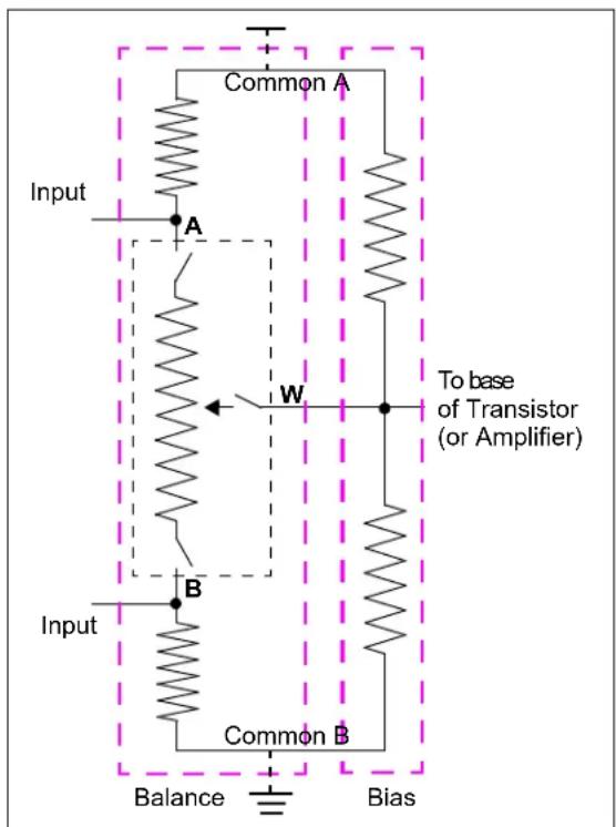
text_image
Common A Input A W To base of Transistor (or Amplifier) Input B Common B Balance BiasFIGURE 8-5: Example Application Circuit using Terminal Disconnects.
8.4 Design Considerations
In the design of a system with the MCP4XXX devices, the following considerations should be taken into account:
• Power Supply Considerations
- Layout Considerations
8.4.1 POWER SUPPLY CONSIDERATIONS
The typical application will require a bypass capacitor in order to filter high-frequency noise, which can be induced onto the power supply's traces. The bypass capacitor helps to minimize the effect of these noise sources on signal integrity. Figure 8-6 illustrates an appropriate bypass strategy.
In this example, the recommended bypass capacitor value is 0.1 F. This capacitor should be placed as close (within 4 mm) to the device power pin ( V_DD ) as possible.
The power source supplying these devices should be as clean as possible. If the application circuit has separate digital and analog power supplies, V_DD and V_SS should reside on the analog plane.
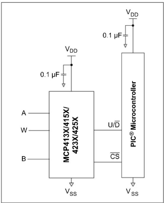
text_image
VDD 0.1 μF A W B MCP413X/415X/ 423X/425X U/D CS PIC® Microcontroller VSS VDD 0.1 μF VSSFIGURE 8-6: Typical Microcontroller Connections.
8.4.2 LAYOUT CONSIDERATIONS
Inductively-coupled AC transients and digital switching noise can degrade the input and output signal integrity, potentially masking the MCP4XXX's performance. Careful board layout minimizes these effects and increases the Signal-to-Noise Ratio (SNR). Multi-layer boards utilizing a low-inductance ground plane, isolated inputs, isolated outputs and proper decoupling are critical to achieving the performance that the silicon is capable of providing. Particularly harsh environments may require shielding of critical signals.
If low noise is desired, breadboards and wire-wrapped boards are not recommended.
8.4.3 RESISTOR TEMPCO
Characterization curves of the resistor temperature coefficient (Tempco) are shown in Figure 2-11, Figure 2-24, Figure 2-36, and Figure 2-48.
These curves show that the resistor network is designed to correct for the change in resistance as temperature increases. This technique reduces the end to end change is R_AB resistance.
8.4.4 HIGH VOLTAGE TOLERANT PINS
High Voltage support ( V_IHH ) on the Serial Interface pins supports two features. These are:
- In-Circuit Accommodation of split rail applications and power supply sync issues
- Compatibility with systems that also support MCP414X/416X /424X/426X devices
NOTES:
9.0 DEVELOPMENT SUPPORT
9.1 Development Tools
Several development tools are available to assist in your design and evaluation of the MCP4XXX devices. The currently available tools are shown in Table9-1.
These boards may be purchased directly from the Microchip web site at www.microchip.com.
9.2 Technical Documentation
Several additional technical documents are available to assist you in your design and development. These technical documents include Application Notes, Technical Briefs, and Design Guides. Table 9-2 shows some of these documents.
TABLE 9-1: DEVELOPMENT TOOLS
| Board Name Part # Supported Devices | ||
| MCP42XX Digital Potentiometer PICtail Plus Demo Board | MCP42XXDM-PTPLS | MCP42XX |
| MCP4XXX Digital Potentiometer Daughter Board (1) | MCP4XXXDM-DB | MCP42XXX, MCP42XX, MCP4021, and MCP4011 |
| 8-pin SOIC/MSOP/TSSOP/DIP Evaluation Board | SOIC8EV | Any 8-pin device in DIP, SOIC, MSOP, or TSSOP package |
| 14-pin SOIC/MSOP/DIP Evaluation Board | SOIC14EV | Any 14-pin device in DIP, SOIC, or MSOP package |
Note 1: Requires the use of a PICDEM Demo board (see User's Guide for details)
TABLE 9-2: TECHNICAL DOCUMENTATION
| Application Note Number | Title | Literature # |
| AN1080 | Understanding Digital Potentiometers Resistor Variations | DS01080 |
| AN737 | Using Digital Potentiometers to Design Low Pass Adjustable Filters | DS00737 |
| AN692 | Using a Digital Potentiometer to Optimize a Precision Single Supply Photo Detect | DS00692 |
| AN691 | Optimizing the Digital Potentiometer in Precision Circuits | DS00691 |
| AN219 | Comparing Digital Potentiometers to Mechanical Potentiometers | DS00219 |
| — | Digital Potentiometer Design Guide | DS22017 |
| — | Signal Chain Design Guide | DS21825 |
NOTES:
10.0 PACKAGING INFORMATION
10.1 Package Marking Information
8-Lead DFN (3x3)
| XXXX |
| YYWW |
| NNN |
| Part Number Code | Part Number Code | |
| MCP4131-502E/MF | DAAE | MCP4132-502E/MF DAAY |
| MCP4131-103E/MF | DAAF | MCP4132-103E/MF DAAZ |
| MCP4131-104E/MF | DAAH M | MCP4132-104E/MF DABB |
| MCP4131-503E/MF | DAAG MCP | 4132-503E/MF DABA |
| MCP4151-502E/MF | DAAP | MCP4152-502E/MF DAAA |
| MCP4151-103E/MF | DAAQ MCP | 4152-103E/MF DABD |
| MCP4151-104E/MF | DAAS | MCP4152-104E/MF DAAD |
| MCP4151-503E/MF | DAAR M | MCP4152-503E/MF DAAC |
Example:
| DAAE0817256 |
8-Lead MSOP
| XXXXXX |
| YWWNNN |
| Part Number Code | Part Number Code | ||
| MCP4131-502E/MS | 413152 | MCP4132-502E/MS | 413252 |
| MCP4131-103E/MS | 413113 | MCP4132-103E/MS | 413213 |
| MCP4131-104E/MS | 413114 | MCP4132-104E/MS | 413214 |
| MCP4131-503E/MS | 413153 | MCP4132-503E/MS | 413253 |
| MCP4151-502E/MS | 415152 | MCP4152-502E/MS | 415252 |
| MCP4151-103E/MS | 415113 | MCP4152-103E/MS | 415213 |
| MCP4151-104E/MS | 415114 | MCP4152-104E/MS | 415214 |
| MCP4151-503E/MS | 415153 | MCP4152-503E/MS | 415253 |
Example
| 413152 |
| 817256 |
8-Lead PDIP
| XXXXXXXX |
| XXXXNNN |
| ○ |
| YYWW |
8-Lead SOIC
| XXXXXXXXXXXXYYWW |
| ○ NNN |
Example
| 4131-502E/P e3560817 |
Example
| 4131502E |
| SN^e3^0817 |
| ○ 256 |
Legend: XX...X Customer-specific information
Y Year code (last digit of calendar year)
YY Year code (last 2 digits of calendar year)
WW Week code (week of January 1 is week '01')
NNN Alphanumeric traceability code
eBb-free JEDEC designator for Matte Tin (Sn)
* This package is Pb-free. The Pb-free JEDEC designator (e3) can be found on the outer packaging for this package.
Note: In the event the full Microchip part number cannot be marked on one line, it will be carried over to the next line, thus limiting the number of available characters for customer-specific information.
Package Marking Information (Continued)
10-Lead DFN (3x3)
| Part Number Code | Part Number Code | |
| MCP4232-502E/MF | BAEH MCP4252-502E/MF BAES | |
| MCP4232-103E/MF | BAEJ MCP4252-103E/MF BAET | |
| MCP4232-104E/MF | BAEL MCP4252-104E/MF BAEV | |
| MCP4232-503E/MF | BAEK MCP4252-503E/MF BAEU |
Example:

10-Lead MSOP
| Part Number Code | Part Number Code | |
| MCP4232-502E/MS | 423252 MCP4252-502E/MS 4252 | 52 |
| MCP4232-103E/MS | 423213 MCP4252-103E/MS 4252 | 13 |
| MCP4232-104E/MS | 423214 MCP4252-104E/MS 4252 | 14 |
| MCP4232-503E/MS | 423253 MCP4252-503E/MS 4252 | 53 |
Example
14-Lead PDIP

text_image
XXXXXXXXXXXX XXXXXXXXXXXXX YYWWNNN14-Lead SOIC (.150")

Example
text_image
MCP4251 502E/P 63 0817256Example
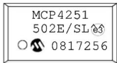
14-Lead TSSOP
text_image
XXXXXXXXX YYWW NNNExample

text_image
4251502E 0817 25616-Lead QFN

text_image
XXXXX XXXXXX XXXXXX YWWNNNExample

text_image
4251 502 E/MLe3 08172568-Lead Plastic Dual Flat, No Lead Package (MF) - 3x3x0.9 mm Body [DFN]
Note: For the most current package drawings, please see the Microchip Packaging Specification located at http://www.microchip.com/packaging
![Microchip mcp4132 - 8-Lead Plastic Dual Flat, No Lead Package (MF) - 3x3x0.9 mm Body [DFN] - 1](/content/2026/06/1214660/images/d94a2b013063f7dc499dbcff7d748e3cfcb67ec639a74cb30413ea2e1ac97a6b.jpg)
text_image
D N E NOTE 1 1 2TOP VIEW
![Microchip mcp4132 - 8-Lead Plastic Dual Flat, No Lead Package (MF) - 3x3x0.9 mm Body [DFN] - 2](/content/2026/06/1214660/images/439b5755e4e971c3a2be3fea63a0222fd81dba0617bb1a625f327666c98a6fa0.jpg)
text_image
EXPOSED PAD K b e N L E2 NOTE 1 2 1 D2BOTTOM VIEW
![Microchip mcp4132 - 8-Lead Plastic Dual Flat, No Lead Package (MF) - 3x3x0.9 mm Body [DFN] - 3](/content/2026/06/1214660/images/a65ffd83a6b931e842f2a882774c85fe6426f5aa2e54b2c19b7823f32158d030.jpg)
text_image
A A3 A1![Microchip mcp4132 - 8-Lead Plastic Dual Flat, No Lead Package (MF) - 3x3x0.9 mm Body [DFN] - 4](/content/2026/06/1214660/images/361f0b51aae2947aad0f3f7ec5138fd988f439c79b9ef171aa7acda765be88b9.jpg)
text_image
NOTE 2| Units | MILLIMETERS | |||
| Dimension Limitss | MINsNOMsMAX | |||
| Number of Pins | Ns | 8 | ||
| Pitchses0.65 BSC | ||||
| Overall HeightsAs0.80 0.90 | 1.00 | |||
| Standoff | A1 | 0.00 | 0.02 | 0.05 |
| Contact Thickness | A3 | 0.20 REF | ||
| Overall Length | D | 3.00 BSC | ||
| Exposed Pad Width | E2 | 0.00 | - | 1.60 |
| Overall Width | E | 3.00 BSC | ||
| Exposed Pad Length | D2 | 0.00 | - | 2.40 |
| Contact Width | b | 0.25 | 0.30 | 0.35 |
| Contact Length | L | 0.20 | 0.30 | 0.55 |
| Contact-to-Exposed Pad | K | 0.20 | - | - |
Notes:
1.sPin 1 visual index feature may vary, but must be located within the hatched area.
2. sPackage may have one or more exposed tie bars at ends.
3.sPackage is saw singulated.
4.sDimensioning and tolerancing per ASME Y14.5M.
BSC:sBasic Dimension. Theoretically exact value shown without tolerances.
REF:sReference Dimension, usually without tolerance, for information purposes only.
Microchip Technology Drawing C04-062B
8-Lead Plastic Dual Flat, No Lead Package (MF) - 3x3x0.9 mm Body [DFN]
Note: For the most current package drawings, please see the Microchip Packaging Specification located at http://www.microchip.com/packaging
![Microchip mcp4132 - 8-Lead Plastic Dual Flat, No Lead Package (MF) - 3x3x0.9 mm Body [DFN] - 1](/content/2026/06/1214660/images/5f298d1bd042b202d0d291b08557e2151e0f29b2b61ce41b8c0eb85783897929.jpg)
text_image
W2 G C1 T2 E X1 Y1 SILK SCREENRECOMMENDED LAND PATTERN
| Units | MILLIMETERS | |||
| Dimension Limits | MIN | NOM | MAX | |
| Contact Pitch | E | 0.65 BSC | ||
| Optional Center Pad Width | W2 | 2.40 | ||
| Optional Center Pad Length | T2 | 1.55 | ||
| Contact Pad Spacing | C1 | 3.10 | ||
| Contact Pad Width (X8) | X1 | 0.35 | ||
| Contact Pad Length (X8) | Y1 | 0.65 | ||
| Distance Between Pads | G | 0.30 | ||
Notes:
- Dimensioning and tolerancing per ASME Y14.5M
BSC: Basic Dimension. Theoretically exact value shown without tolerances.
Microchip Technology Drawing No. C04-2062A
8-Lead Plastic Dual In-Line (P) - 300 mil Body [PDIP]
Note: For the most current package drawings, please see the Microchip Packaging Specification located at http://www.microchip.com/packaging
![Microchip mcp4132 - 8-Lead Plastic Dual In-Line (P) - 300 mil Body [PDIP] - 1](/content/2026/06/1214660/images/edd1211cbfbe105797ab686fcabf3452c832cf989d09016fe998a9c2f66b3675.jpg)
| Units | INCHES | |||
| Dimension Limitss | MINsNOMsMAX | |||
| Number of Pins | Ns | 8 | ||
| Pitchses.100 BSC | ||||
| Top to Seating PlanesAs-s-s.210 | ||||
| Molded Package Thickness | A2 | .115 | .130 | .195 |
| Base to Seating Plane | A1 | .015s-s- | ||
| Shoulder to Shoulder Width | E | .290 | .310 | .325 |
| Molded Package Width | E1 | .240 | .250 | .280 |
| Overall Length | D | .348 | .365 | .400 |
| Tip to Seating Plane | L | .115 | .130 | .150 |
| Lead Thickness | c | .008 | .010 | .015 |
| Upper Lead Width | b1 | .040 | .060 | .070 |
| Lower Lead Width | b | .014 | .018 | .022 |
| Overall Row Spacing § | eB | -s-s.430 | ||
Notes:
1.sPin 1 visual index feature may vary, but must be located with the hatched area.
2.s§ Significant Characteristic.
3. Dimensions D and E1 do not include mold flash or protrusions. Mold flash or protrusions shall not exceed .010" per side.
4.sDimensioning and tolerancing per ASME Y14.5M.
BSC: Basic Dimension. Theoretically exact value shown without tolerances.
Microchip Technology Drawing C04-018B
8-Lead Plastic Micro Small Outline Package (MS) [MSOP]
Note: For the most current package drawings, please see the Microchip Packaging Specification located at http://www.microchip.com/packaging
![Microchip mcp4132 - 8-Lead Plastic Micro Small Outline Package (MS) [MSOP] - 1](/content/2026/06/1214660/images/543ffe75d3e9d9b32565fdf58679567d0f165508595b45f18b4e6d80103169e8.jpg)
text_image
D N E1 E NOTE 1 1 2 e b A A2 A1![Microchip mcp4132 - 8-Lead Plastic Micro Small Outline Package (MS) [MSOP] - 2](/content/2026/06/1214660/images/9a956e84601f203af5db17482169d213e197e60f275f2537dbc8872c93e873bb.jpg)
natural_image
Isometric line drawing of an integrated circuit chip with multiple pins (no text or symbols)![Microchip mcp4132 - 8-Lead Plastic Micro Small Outline Package (MS) [MSOP] - 3](/content/2026/06/1214660/images/378c24d26861ca0037c438159081ad80ac464ca73d43e694452d952e6cbae253.jpg)
text_image
C L1 L φ| Units | MILLIMETERS | |||
| Dimension Limitss | MINsNOMsMAX | |||
| Number of Pins | Ns | 8 | ||
| Pitchses0.65 BSC | ||||
| Overall HeightsAs-s- 1.10 | ||||
| Molded Package Thickness | A2 | 0.75 | 0.85 | 0.95 |
| Standoff | A1 | 0.00 | - | 0.15 |
| Overall Width | E | 4.90 BSC | ||
| Molded Package Width | E1 | 3.00 BSC | ||
| Overall Length | D | 3.00 BSC | ||
| Foot Length | L | 0.40 | 0.60 | 0.80 |
| Footprint | L1 | 0.95 REF | ||
| Foot Angle | 0° | - | 8° | |
| Lead Thickness | c | 0.08 | - | 0.23 |
| Lead Width | b | 0.22 | - | 0.40 |
Notes:
1.sPin 1 visual index feature may vary, but must be located within the hatched area.
- Dimensions D and E1 do not include mold flash or protrusions. Mold flash or protrusions shall not exceed 0.15 mm per side.
3.sDimensioning and tolerancing per ASME Y14.5M.
BSC:sBasic Dimension. Theoretically exact value shown without tolerances.
REF:sReference Dimension, usually without tolerance, for information purposes only.
Microchip Technology Drawing C04-111B
8-Lead Plastic Small Outline (SN) – Narrow, 3.90 mm Body [SOIC]
Note: For the most current package drawings, please see the Microchip Packaging Specification located at http://www.microchip.com/packaging
![Microchip mcp4132 - 8-Lead Plastic Small Outline (SN) – Narrow, 3.90 mm Body [SOIC] - 1](/content/2026/06/1214660/images/bb1be258380a16073c98508030b9e0d25d0d847e0b995f3cadf8e834c7814060.jpg)
text_image
D N e E1 E NOTE 1 1 2 3 b![Microchip mcp4132 - 8-Lead Plastic Small Outline (SN) – Narrow, 3.90 mm Body [SOIC] - 2](/content/2026/06/1214660/images/273468eea6bd045669f1f31d7d12f04f4df1a159654e69bb94a1ff7d2b79431a.jpg)
natural_image
Isometric line drawing of an integrated circuit chip (no text or symbols)![Microchip mcp4132 - 8-Lead Plastic Small Outline (SN) – Narrow, 3.90 mm Body [SOIC] - 3](/content/2026/06/1214660/images/3b2e809a89e4b9e5ff1493e7ac93498fb3168b7ee346f37cf88516e270044482.jpg)
text_image
A A1 A2![Microchip mcp4132 - 8-Lead Plastic Small Outline (SN) – Narrow, 3.90 mm Body [SOIC] - 4](/content/2026/06/1214660/images/d23f85433744b0f58da5cdf103646e23be444505348c17d64a70024e1ace1061.jpg)
text_image
h h φ L L1 α c β| Units | MILLIMETERS | |||
| Dimension Limitss | MINsNOMsMAX | |||
| Number of Pins | Ns | 8 | ||
| Pitchses1.27 BSC | ||||
| Overall HeightsAs-s- 1.75 | ||||
| Molded Package Thickness | A2 | 1.25 | - | - |
| Standoff § | A1 | 0.10 | - | 0.25 |
| Overall Width | E | 6.00 BSC | ||
| Molded Package Width | E1 | 3.90 BSC | ||
| Overall Length | D | 4.90 BSC | ||
| Chamfer (optional) | h | 0.25 | - | 0.50 |
| Foot Length | L | 0.40 | - | 1.27 |
| Footprint | L1 | 1.04 REF | ||
| Foot Angle | 0° | - | 8° | |
| Lead Thickness | c | 0.17 | - | 0.25 |
| Lead Width | b | 0.31 | - | 0.51 |
| Mold Draft Angle Top | 5° | - | 15° | |
| Mold Draft Angle Bottom | 5° | - | 15° | |
Notes:
1.sPin 1 visual index feature may vary, but must be located within the hatched area.
2.s§ Significant Characteristic.
- Dimensions D and E1 do not include mold flash or protrusions. Mold flash or protrusions shall not exceed 0.15 mm per side.
4.sDimensioning and tolerancing per ASME Y14.5M.
BSC:sBasic Dimension. Theoretically exact value shown without tolerances.
REF:sReference Dimension, usually without tolerance, for information purposes only.
Microchip Technology Drawing C04-057B
8-Lead Plastic Small Outline (SN) – Narrow, 3.90 mm Body [SOIC]
Note: For the most current package drawings, please see the Microchip Packaging Specification located at http://www.microchip.com/packaging
![Microchip mcp4132 - 8-Lead Plastic Small Outline (SN) – Narrow, 3.90 mm Body [SOIC] - 1](/content/2026/06/1214660/images/1889ce9ec3dc3c70e0e7f453c6082f4f34ecf77654610e37909bdae67fe808ac.jpg)
text_image
E C SILK SCREEN Y1 X1RECOMMENDED LAND PATTERN
| Units | MILLIMETERS | |||
| Dimension Limits | MIN | NOM | MAX | |
| Contact Pitch | E | 1.27 BSC | ||
| Contact Pad Spacing | C | 5.40 | ||
| Contact Pad Width (X8) | X1 | 0.60 | ||
| Contact Pad Length (X8) | Y1 | 1.55 | ||
Notes:
- Dimensioning and tolerancing per ASME Y14.5M
BSC: Basic Dimension. Theoretically exact value shown without tolerances.
Microchip Technology Drawing No. C04-2057A
10-Lead Plastic Dual Flat, No Lead Package (MF) - 3x3x0.9 mm Body [DFN]
Note: For the most current package drawings, please see the Microchip Packaging Specification located at http://www.microchip.com/packaging
![Microchip mcp4132 - 10-Lead Plastic Dual Flat, No Lead Package (MF) - 3x3x0.9 mm Body [DFN] - 1](/content/2026/06/1214660/images/08945176b6517ce71187e24f94e8a2b09f7ef73a309fbb351f967c2cc3d8a9c5.jpg)
text_image
D N E NOTE 1 1 2![Microchip mcp4132 - 10-Lead Plastic Dual Flat, No Lead Package (MF) - 3x3x0.9 mm Body [DFN] - 2](/content/2026/06/1214660/images/056440540816f06acdd365a0d3437e0aff36b00d401b992aa7a0b46971953a1f.jpg)
text_image
b e N L K E2 EXPOSED PAD NOTE 1 2 1 D2TOP VIEW
![Microchip mcp4132 - 10-Lead Plastic Dual Flat, No Lead Package (MF) - 3x3x0.9 mm Body [DFN] - 3](/content/2026/06/1214660/images/202e5dafb7b3bc7eebaf1eea9bd684710075b5814f78d44dec091c94a030fbc8.jpg)
text_image
A A3 A1BOTTOM VIEW
![Microchip mcp4132 - 10-Lead Plastic Dual Flat, No Lead Package (MF) - 3x3x0.9 mm Body [DFN] - 4](/content/2026/06/1214660/images/379b59d47877c2b93cfd1600255dc289ae6c1ac1a4295930a577312c26349fa5.jpg)
text_image
NOTE 2| Units | MILLIMETERS | |||
| Dimension Limitss | MINsNOMsMAX | |||
| Number of Pins | Ns | 10 | ||
| Pitchses0.50 BSC | ||||
| Overall HeightsAs0.80 0.90 | 1.00 | |||
| Standoff | A1 | 0.00 | 0.02 | 0.05 |
| Contact Thickness | A3 | 0.20 REF | ||
| Overall Length | D | 3.00 BSC | ||
| Exposed Pad Length | D2 | 2.20 | 2.35 | 2.48 |
| Overall Width | E | 3.00 BSC | ||
| Exposed Pad Width | E2 | 1.40 | 1.58 | 1.75 |
| Contact Width | b | 0.18 | 0.25 | 0.30 |
| Contact Length | L | 0.30 | 0.40 | 0.50 |
| Contact-to-Exposed Pad | K | 0.20 | - | - |
Notes:
- sPin 1 visual index feature may vary, but must be located within the hatched area.
2.sPackage may have one or more exposed tie bars at ends.
3.sPackage is saw singulated.
4.sDimensioning and tolerancing per ASME Y14.5M.
BSC:sBasic Dimension. Theoretically exact value shown without tolerances.
REF:sReference Dimension, usually without tolerance, for information purposes only.
Microchip Technology Drawing C04-063B
10-Lead Plastic Dual Flat, No Lead Package (MF) - 3x3x0.9 mm Body [DFN]
Note: For the most current package drawings, please see the Microchip Packaging Specification located at http://www.microchip.com/packaging
![Microchip mcp4132 - 10-Lead Plastic Dual Flat, No Lead Package (MF) - 3x3x0.9 mm Body [DFN] - 1](/content/2026/06/1214660/images/e48fd3fabc11f5ce59b09c6501aad1faf01184dc5ace65587f1f217e3ad1ea50.jpg)
text_image
W2 G Y1 C1 T2 E X1 SILK SCREENRECOMMENDED LAND PATTERN
| Units | MILLIMETERS | |||
| Dimension Limits | MIN | NOM | MAX | |
| Contact Pitch | E | 0.50 BSC | ||
| Optional Center Pad Width | W2 | 2.48 | ||
| Optional Center Pad Length | T2 | 1.55 | ||
| Contact Pad Spacing | C1 | 3.10 | ||
| Contact Pad Width (X8) | X1 | 0.30 | ||
| Contact Pad Length (X8) | Y1 | 0.65 | ||
| Distance Between Pads | G | 0.20 | ||
Notes:
- Dimensioning and tolerancing per ASME Y14.5M
BSC: Basic Dimension. Theoretically exact value shown without tolerances.
Microchip Technology Drawing No. C04-2063A
10-Lead Plastic Micro Small Outline Package (UN) [MSOP]
Note: For the most current package drawings, please see the Microchip Packaging Specification located at http://www.microchip.com/packaging
![Microchip mcp4132 - 10-Lead Plastic Micro Small Outline Package (UN) [MSOP] - 1](/content/2026/06/1214660/images/806ad4f281173d41dd112f61327fc59a976549c755bf4292205ef668ae7ce3cc.jpg)
| Units | MILLIMETERS | |||
| Dimension Limits | MINsNOMsMAX | |||
| Number of Pins | Ns | 10 | ||
| Pitchses0.50 BSC | ||||
| Overall HeightsAs-s- 1.10 | ||||
| Molded Package Thickness | A2 | 0.75 | 0.85 | 0.95 |
| Standoff | A1 | 0.00 | - | 0.15 |
| Overall Width | E | 4.90 BSC | ||
| Molded Package Width | E1 | 3.00 BSC | ||
| Overall Length | D | 3.00 BSC | ||
| Foot Length | L | 0.40 | 0.60 | 0.80 |
| Footprint | L1 | 0.95 REF | ||
| Foot Angle | 0° | - | 8° | |
| Lead Thickness | c | 0.08 | - | 0.23 |
| Lead Width | b | 0.15 | - | 0.33 |
Notes:
1.sPin 1 visual index feature may vary, but must be located within the hatched area.
2. Dimensions D and E1 do not include mold flash or protrusions. Mold flash or protrusions shall not exceed 0.15 mm per side.
3.sDimensioning and tolerancing per ASME Y14.5M.
BSC:sBasic Dimension. Theoretically exact value shown without tolerances.
REF:sReference Dimension, usually without tolerance, for information purposes only.
Microchip Technology Drawing C04-021B
14-Lead Plastic Dual In-Line (P) - 300 mil Body [PDIP]
Note: For the most current package drawings, please see the Microchip Packaging Specification located at http://www.microchip.com/packaging
![Microchip mcp4132 - 14-Lead Plastic Dual In-Line (P) - 300 mil Body [PDIP] - 1](/content/2026/06/1214660/images/96ae7c537d514703ab0ccc2b4fbd214a0fcfd8022223dbac9333d72a5374124a.jpg)
| Units | INCHES | |||
| Dimension Limitss | MINsNOMsMAX | |||
| Number of Pins | Ns | 14 | ||
| Pitchses.100 BSC | ||||
| Top to Seating PlanesAs-s-s.210 | ||||
| Molded Package Thickness | A2 | .115 | .130 | .195 |
| Base to Seating Plane | A1 | .015 | -s- | |
| Shoulder to Shoulder Width | E | .290 | .310 | .325 |
| Molded Package Width | E1 | .240 | .250 | .280 |
| Overall Length | D | .735 | .750 | .775 |
| Tip to Seating Plane | L | .115 | .130 | .150 |
| Lead Thickness | c | .008 | .010 | .015 |
| Upper Lead Width | b1 | .045 | .060 | .070 |
| Lower Lead Width | b | .014 | .018 | .022 |
| Overall Row Spacing § | eB | -s-s.430 | ||
Notes:
1.sPin 1 visual index feature may vary, but must be located with the hatched area.
2.s§ Significant Characteristic.
3. Dimensions D and E1 do not include mold flash or protrusions. Mold flash or protrusions shall not exceed .010" per side.
4.sDimensioning and tolerancing per ASME Y14.5M.
BSC: Basic Dimension. Theoretically exact value shown without tolerances.
Microchip Technology Drawing C04-005B
14-Lead Plastic Small Outline (SL) – Narrow, 3.90 mm Body [SOIC]
Note: For the most current package drawings, please see the Microchip Packaging Specification located at http://www.microchip.com/packaging
![Microchip mcp4132 - 14-Lead Plastic Small Outline (SL) – Narrow, 3.90 mm Body [SOIC] - 1](/content/2026/06/1214660/images/99abd26ed9ca7bab0268eaab9ddeedcd487d857d686478453ad005e97e76e862.jpg)
text_image
NOTE 1 1 2 3 b D N E E1 e![Microchip mcp4132 - 14-Lead Plastic Small Outline (SL) – Narrow, 3.90 mm Body [SOIC] - 2](/content/2026/06/1214660/images/8f18ef11657d52803c8b61cf391f4f455079f8bbe1dcff7e85bf9f39495b1bb4.jpg)
natural_image
Isometric line drawing of an integrated circuit chip with multiple pins (no text or symbols)![Microchip mcp4132 - 14-Lead Plastic Small Outline (SL) – Narrow, 3.90 mm Body [SOIC] - 3](/content/2026/06/1214660/images/509f2e604e30789ac827e2a77920dd667fe6407cdae091c5b66c9adcfada326e.jpg)
text_image
A A1 A2![Microchip mcp4132 - 14-Lead Plastic Small Outline (SL) – Narrow, 3.90 mm Body [SOIC] - 4](/content/2026/06/1214660/images/a98fcba40104a88738b8a330f92971beba03a76426dfc1c2eda5bd9a72bd3afa.jpg)
text_image
h h φ L L1 α c β| Units | MILLIMETERS | |||
| Dimension Limits | MINsNOMsMAX | |||
| Number of Pins | Ns | 14 | ||
| Pitchses1.27 BSC | ||||
| Overall HeightsAs-s- 1.75 | ||||
| Molded Package Thickness | A2 | 1.25 | - | - |
| Standoff § | A1 | 0.10 | - | 0.25 |
| Overall Width | E | 6.00 BSC | ||
| Molded Package Width | E1 | 3.90 BSC | ||
| Overall Length | D | 8.65 BSC | ||
| Chamfer (optional) | h | 0.25 | - | 0.50 |
| Foot Length | L | 0.40 | - | 1.27 |
| Footprint | L1 | 1.04 REF | ||
| Foot Angle | 0° | - | 8° | |
| Lead Thickness | c | 0.17 | - | 0.25 |
| Lead Width | b | 0.31 | - | 0.51 |
| Mold Draft Angle Top | 5° | - | 15° | |
| Mold Draft Angle Bottom | 5° | - | 15° | |
Notes:
1.sPin 1 visual index feature may vary, but must be located within the hatched area.
2.s§ Significant Characteristic.
- Dimensions D and E1 do not include mold flash or protrusions. Mold flash or protrusions shall not exceed 0.15 mm per side.
4.sDimensioning and tolerancing per ASME Y14.5M.
BSC:sBasic Dimension. Theoretically exact value shown without tolerances.
REF:sReference Dimension, usually without tolerance, for information purposes only.
Microchip Technology Drawing C04-065B
14-Lead Plastic Small Outline (SL) - Narrow, 3.90 mm Body [SOIC]
Note: For the most current package drawings, please see the Microchip Packaging Specification located at http://www.microchip.com/packaging
text_image
Gx C G SILK SCREEN Y E XRECOMMENDED LAND PATTERN
| Units | MILLIMETERS | |||
| Dimension Limits | MIN | NOM | MAX | |
| Contact Pitch | E | 1.27 BSC | ||
| Contact Pad Spacing | C | 5.40 | ||
| Contact Pad Width | X | 0.60 | ||
| Contact Pad Length | Y | 1.50 | ||
| Distance Between Pads | Gx | 0.67 | ||
| Distance Between Pads | G | 3.90 | ||
Notes:
1. Dimensioning and tolerancing per ASME Y14.5M
BSC: Basic Dimension. Theoretically exact value shown without tolerances.
Microchip Technology Drawing No. C04-2065A
14-Lead Plastic Thin Shrink Small Outline (ST) - 4.4 mm Body [TSSOP]
Note: For the most current package drawings, please see the Microchip Packaging Specification located at http://www.microchip.com/packaging
![Microchip mcp4132 - 14-Lead Plastic Thin Shrink Small Outline (ST) - 4.4 mm Body [TSSOP] - 1](/content/2026/06/1214660/images/b328fb3d5b2746d41452c9013f4f0ca40c262ac0e332f96ef827a1b4c7d811c5.jpg)
text_image
D N E1 E NOTE 1 1 2 b e![Microchip mcp4132 - 14-Lead Plastic Thin Shrink Small Outline (ST) - 4.4 mm Body [TSSOP] - 2](/content/2026/06/1214660/images/27dcbdb84bb586ba3104ff0cfd908b82d378246d82a7d33ceeab0ca952cbe6c6.jpg)
natural_image
Isometric line drawing of an integrated circuit chip with multiple pins (no text or symbols)![Microchip mcp4132 - 14-Lead Plastic Thin Shrink Small Outline (ST) - 4.4 mm Body [TSSOP] - 3](/content/2026/06/1214660/images/2442442272927f341d75b068b4f33b3539034615809e6f53982624b4d5c4e10e.jpg)
text_image
A A1 A2![Microchip mcp4132 - 14-Lead Plastic Thin Shrink Small Outline (ST) - 4.4 mm Body [TSSOP] - 4](/content/2026/06/1214660/images/7abcf4e5f2b1a9cdcbfbf2c24def38edafc9a78f057dda5ea108d19d69c8e28a.jpg)
text_image
C L1 L φ| Units | MILLIMETERS | |||
| Dimension Limitss | MINsNOMsMAX | |||
| Number of Pins | Ns | 14 | ||
| Pitchses0.65 BSC | ||||
| Overall HeightsAs-s- 1.20 | ||||
| Molded Package Thickness | A2 | 0.80 | 1.00 | 1.05 |
| Standoff | A1 | 0.05 | - | 0.15 |
| Overall Width | E | 6.40 BSC | ||
| Molded Package Width | E1 | 4.30 | 4.40 | 4.50 |
| Molded Package Length | D | 4.90 | 5.00 | 5.10 |
| Foot Length | L | 0.45 | 0.60 | 0.75 |
| Footprint | L1 | 1.00 REF | ||
| Foot Angle | 0^ | - | 8^ | |
| Lead Thickness | c | 0.09 | - | 0.20 |
| Lead Width | b | 0.19 | - | 0.30 |
Notes:
1.sPin 1 visual index feature may vary, but must be located within the hatched area.
- Dimensions D and E1 do not include mold flash or protrusions. Mold flash or protrusions shall not exceed 0.15 mm per side.
3.sDimensioning and tolerancing per ASME Y14.5M.
BSC:sBasic Dimension. Theoretically exact value shown without tolerances.
REF:sReference Dimension, usually without tolerance, for information purposes only.
Microchip Technology Drawing C04-087B
16-Lead Plastic Quad Flat, No Lead Package (ML) - 4x4x0.9 mm Body [QFN]
Note: For the most current package drawings, please see the Microchip Packaging Specification located at http://www.microchip.com/packaging
![Microchip mcp4132 - 16-Lead Plastic Quad Flat, No Lead Package (ML) - 4x4x0.9 mm Body [QFN] - 1](/content/2026/06/1214660/images/a2ea71c5d04f3ce48b0190534cdb1c69571dea4835206d850b86ddbf2d285d99.jpg)
| Units | MILLIMETERS | |||
| Dimension Limitss | MINsNOMsMAX | |||
| Number of Pins | Ns | 16 | ||
| Pitchses0.65 BSC | ||||
| Overall HeightsAs0.80 0.90 | 1.00 | |||
| Standoff | A1 | 0.00 | 0.02 | 0.05 |
| Contact Thickness | A3 | 0.20 REF | ||
| Overall Width | E | 4.00 BSC | ||
| Exposed Pad Width | E2 | 2.50 | 2.65 | 2.80 |
| Overall Length | D | 4.00 BSC | ||
| Exposed Pad Length | D2 | 2.50 | 2.65 | 2.80 |
| Contact Width | b | 0.25 | 0.30 | 0.35 |
| Contact Length | L | 0.30 | 0.40 | 0.50 |
| Contact-to-Exposed Pad | K | 0.20 | - | - |
Notes:
1.sPin 1 visual index feature may vary, but must be located within the hatched area.
2.sPackage is saw singulated.
3.sDimensioning and tolerancing per ASME Y14.5M.
BSC:sBasic Dimension. Theoretically exact value shown without tolerances.
REF:sReference Dimension, usually without tolerance, for information purposes only.
Microchip Technology Drawing C04-127B
16-Lead Plastic Quad Flat, No Lead Package (ML) - 4x4x0.9mm Body [QFN]
Note: For the most current package drawings, please see the Microchip Packaging Specification located at http://www.microchip.com/packaging
text_image
C1 W2 C2 T2 E G Y1 X1 SILK SCREENRECOMMENDED LAND PATTERN
| Units | MILLIMETERS | |||
| Dimension Limits | MIN | NOM | MAX | |
| Contact Pitch | E | 0.65 BSC | ||
| Optional Center Pad Width | W2 | 2.50 | ||
| Optional Center Pad Length | T2 | 2.50 | ||
| Contact Pad Spacing | C1 | 4.00 | ||
| Contact Pad Spacing | C2 | 4.00 | ||
| Contact Pad Width (X28) | X1 | 0.35 | ||
| Contact Pad Length (X28) | Y1 | 0.80 | ||
| Distance Between Pads | G | 0.30 | ||
Notes:
1. Dimensioning and tolerancing per ASME Y14.5M
BSC: Basic Dimension. Theoretically exact value shown without tolerances.
Microchip Technology Drawing No. C04-2127A
NOTES:
APPENDIX A: REVISION HISTORY
Revision B (December 2008)
The following is the list of modifications:
- Updated I_PU specifications to specify test conditions and new limit.
- Updated DFN package in "Package Types (top view)", including Exposed Thermal Pad sample (EP).
- Added new descriptions in Section 3.0 "Pin Descriptions".
- Added new Development Tool support items.
- Updated Package Outline section.
Revision A (September 2007)
• Original Release of this Document.
APPENDIX B: MIGRATING FROM THE MCP41XXX AND MCP42XXX DEVICES
This is intended to give an overview of some of the differences to be aware of when migrating from the MCP41XXX and MCP42XXX devices.
B.1 MCP41XXX to MCP41XX Differences
Here are some of the differences to be aware of:
- SI pin is now SDI/SDO pin, and the contents of the device memory can be read.
- Need to address the Terminal Connect Feature (TCON register) of MCP41XX.
- MCP41XX supports software Shutdown mode.
- New 5 kΩ version.
- MCP41XX have 7-bit resolution options.
- Alternate pinout versions (for Rheostat configuration).
- Verify device's electrical specifications.
- Interface signals are now high voltage tolerant.
- Interface signals now have internal pull-up resistors.
B.2 MCP42XXX to MCP42XX Differences
Here are some of the differences to be aware of:
- Daisy chaining of devices is no longer supported.
- SDO pin allows contents of device memory to be read.
- Need to address the Terminal Connect Feature (TCON register) of MCP42XX.
- MCP42XX supports software Shutdown mode.
- New 5 kΩ version.
- MCP42XX have 7-bit resolution options.
- Alternate package/pinout versions (for Rheostat configuration).
- Verify device's electrical specifications.
- Interface signals are now high voltage tolerant
- Interface signals now have internal pull-up resistors.
NOTES:
PRODUCT IDENTIFICATION SYSTEM
To order or obtain information, e.g., on pricing or delivery, refer to the factory or the listed sales office.
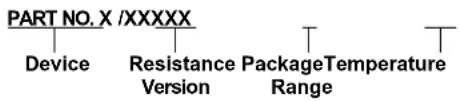
text_image
PART NO. X /XXXXX Device Resistance Version Package Temperature RangeDevice MCP4131: Single Volatile 7-bit Potentiometer
MCP4131T: Single Volatile 7-bit Potentiometer
(Tape and Reel)
MCP4132: Single Volatile 7-bit Rheostat
MCP4132T: Single Volatile 7-bit Rheostat
(Tape and Reel)
MCP4151: Single Volatile 8-bit Potentiometer
MCP4151T: Single Volatile 8-bit Potentiometer
(Tape and Reel)
MCP4152: Single Volatile 8-bit Rheostat
MCP4152T: Single Volatile 8-bit Rheostat
(Tape and Reel)
MCP4231: Dual Volatile 7-bit Potentiometer
MCP4231T: Dual Volatile 7-bit Potentiometer
(Tape and Reel)
MCP4232: Dual Volatile 7-bit Rheostat
MCP4232T: Dual Volatile 7-bit Rheostat
(Tape and Reel)
MCP4251: Dual Volatile 8-bit Potentiometer
MCP4251T: Dual Volatile 8-bit Potentiometer
(Tape and Reel)
MCP4252: Dual Volatile 8-bit Rheostat
MCP4252T: Dual Volatile 8-bit Rheostat
(Tape and Reel)
Resistance Version: 502 = 5 kΩ
103 = 10 kΩ
503 = 50 kΩ
104 = 100 kΩ
Temperature Range I = -40°C to +85°C (Industrial)
E = -40°C to +125°C (Extended)
Package MF = Plastic Dual Flat No-lead (3x3 DFN), 8/10-lead
ML = Plastic Quad Flat No-lead (QFN), 16-lead
MS = Plastic Micro Small Outline (MSOP), 8-lead
P = Plastic Dual In-line (PDIP) (300 mil), 8/14-lead
SN = Plastic Small Outline (SOIC), (150 mil), 8-lead
SL = Plastic Small Outline (SOIC), (150 mil), 14-lead
ST = Plastic Thin Shrink Small Outline (TSSOP), 14-lead
UN = Plastic Micro Small Outline (MSOP), 10-lead
Examples:
a) MCP4131-502E/XX: 5 kΩ, 8LD Device
b) MCP4131T-502E/XX: T/R, 5 kΩ, 8LD Device
c) MCP4131-103E/XX: 10 kΩ, 8-LD Device
d) MCP4131T-103E/XX: T/R, 10 kΩ, 8LD Device
e) MCP4131-503E/XX: 50 kΩ, 8LD Device
f) MCP4131T-503E/XX: T/R, 50 kΩ, 8LD Device
g) MCP4131-104E/XX: 100 kΩ, 8LD Device
h) MCP4131T-104E/XX: T/R, 100 kΩ, 8LD Device
a) MCP4132-502E/XX: 5 kΩ, 8LD Device
b) MCP4132T-502E/XX: T/R, 5 kΩ, 8LD Device
c) MCP4132-103E/XX: 10 kΩ, 8-LD Device
d) MCP4132T-103E/XX: T/R, 10 kΩ, 8LD Device
e) MCP4132-503E/XX: 50 kΩ, 8LD Device
f) MCP4132T-503E/XX: T/R, 50 kΩ, 8LD Device
g) MCP4132-104E/XX: 100 kΩ, 8LD Device
h) MCP4132T-104E/XX: T/R, 100 kΩ, 8LD Device
a) MCP4151-502E/XX: 5 kΩ, 8LD Device
b) MCP4151T-502E/XX: T/R, 5 kΩ, 8LD Device
c) MCP4151-103E/XX: 10 kΩ, 8-LD Device
d) MCP4151T-103E/XX: T/R, 10 kΩ, 8LD Device
e) MCP4151-503E/XX: 50 kΩ, 8LD Device
f) MCP4151T-503E/XX: T/R, 50 kΩ, 8LD Device
g) MCP4151-104E/XX: 100 kΩ, 8LD Device
h) MCP4151T-104E/XX: T/R, 100 kΩ, 8LD Device
a) MCP4152-502E/XX: 5 kΩ, 8LD Device
b) MCP4152T-502E/XX: T/R, 5 kΩ, 8LD Device
c) MCP4152-103E/XX: 10 kΩ, 8-LD Device
d) MCP4152T-103E/XX: T/R, 10 kΩ, 8LD Device
e) MCP4152-503E/XX: 50 kΩ, 8LD Device
f) MCP4152T-503E/XX: T/R, 50 kΩ, 8LD Device
g) MCP4152-104E/XX: 100 kΩ, 8LD Device
h) MCP4152T-104E/XX: T/R, 100 kΩ, 8LD Device
a) MCP4231-502E/XX: 5 kΩ, 8LD Device
b) MCP4231T-502E/XX: T/R, 5 kΩΩ, 8LD Device
c) MCP4231-103E/XX: 10 kΩ, 8-LD Device
d) MCP4231T-103E/XX: T/R, 10 kΩ, 8LD Device
e) MCP4231-503E/XX: 50 kΩ, 8LD Device
f) MCP4231T-503E/XX: T/R, 50 kΩ, 8LD Device
g) MCP4231-104E/XX: 100 kΩ, 8LD Device
h) MCP4231T-104E/XX: T/R, 100 kΩ, 8LD Device
a) MCP4232-502E/XX: 5 kΩ, 8LD Device
b) MCP4232T-502E/XX: T/R, 5 kΩ, 8LD Device
c) MCP4232-103E/XX: 10 kΩ, 8-LD Device
d) MCP4232T-103E/XX: T/R, 10 kΩ, 8LD Device
e) MCP4232-503E/XX: 50 kΩ, 8LD Device
f) MCP4232T-503E/XX: T/R, 50 kΩ, 8LD Device
g) MCP4232-104E/XX: 100 kΩ, 8LD Device
h) MCP4232T-104E/XX: T/R, 100 kΩ, 8LD Device
a) MCP4251-502E/XX: 5 kΩ, 8LD Device
b) MCP4251T-502E/XX: T/R, 5 kΩ, 8LD Device
c) MCP4251-103E/XX: 10 kΩ, 8-LD Device
d) MCP4251T-103E/XX: T/R, 10 kΩ, 8LD Device
e) MCP4251-503E/XX: 50 kΩ, 8LD Device
f) MCP4251T-503E/XX: T/R, 50 kΩ, 8LD Device
g) MCP4251-104E/XX: 100 kΩ, 8LD Device
h) MCP4251T-104E/XX: T/R, 100 kΩ, 8LD Device
a) MCP4252-502E/XX: 5 kΩ, 8LD Device
b) MCP4252T-502E/XX: T/R, 5 kΩ, 8LD Device
c) MCP4252-103E/XX: 10 kΩ, 8-LD Device
d) MCP4252T-103E/XX: T/R, 10 kΩ, 8LD Device
e) MCP4252-503E/XX: 50 kΩ, 8LD Device
f) MCP4252T-503E/XX: T/R, 50 kΩ, 8LD Device
g) MCP4252-104E/XX: 100 kΩ, 8LD Device
h) MCP4252T-104E/XX: T/R, 100 kΩ, 8LD Device
XX = MF for 8/10-lead 3x3 DFN
= ML for 16-lead QFN
= MS for 8-lead MSOP
= P for 8/14-lead PDIP
= SN for 8-lead SOIC
= SL for 14-lead SOIC
= ST for 14-lead TSSOP
= UN for 10-lead MSOP
NOTES:
Note the following details of the code protection feature on Microchip devices:
• Microchip products meet the specification contained in their particular Microchip Data Sheet.
- Microchip believes that its family of products is one of the most secure families of its kind on the market today, when used in the intended manner and under normal conditions.
- There are dishonest and possibly illegal methods used to breach the code protection feature. All of these methods, to our knowledge, require using the Microchip products in a manner outside the operating specifications contained in Microchip's Data Sheets. Most likely, the person doing so is engaged in theft of intellectual property.
• Microchip is willing to work with the customer who is concerned about the integrity of their code.
- Neither Microchip nor any other semiconductor manufacturer can guarantee the security of their code. Code protection does not mean that we are guaranteeing the product as "unbreakable."
Code protection is constantly evolving. We at Microchip are committed to continuously improving the code protection features of our products. Attempts to break Microchip's code protection feature may be a violation of the Digital Millennium Copyright Act. If such acts allow unauthorized access to your software or other copyrighted work, you may have a right to sue for relief under that Act.
Information contained in this publication regarding device applications and the like is provided only for your convenience and may be superseded by updates. It is your responsibility to ensure that your application meets with your specifications. MICROCHIP MAKES NO REPRESENTATIONS OR WARRANTIES OF ANY KIND WHETHER EXPRESS OR IMPLIED, WRITTEN OR ORAL, STATUTORY OR OTHERWISE, RELATED TO THE INFORMATION, INCLUDING BUT NOT LIMITED TO ITS CONDITION, QUALITY, PERFORMANCE, MERCHANTABILITY OR FITNESS FOR PURPOSE. Microchip disclaims all liability arising from this information and its use. Use of Microchip devices in life support and/or safety applications is entirely at the buyer's risk, and the buyer agrees to defend, indemnify and hold harmless Microchip from any and all damages, claims, suits, or expenses resulting from such use. No licenses are conveyed, implicitly or otherwise, under any Microchip intellectual property rights.
Trademarks
The Microchip name and logo, the Microchip logo, Accuron, dsPIC, KEELOQ, KEELOQ logo, MPLAB, PIC, PICmicro, PICSTART, rfPIC, SmartShunt and UNI/O are registered trademarks of Microchip Technology Incorporated in the U.S.A. and other countries.
FilterLab, Linear Active Thermistor, MXDEV, MXLAB, SEEVAL, SmartSensor and The Embedded Control Solutions Company are registered trademarks of Microchip Technology Incorporated in the U.S.A.
Analog-for-the-Digital Age, Application Maestro, CodeGuard, dsPICDEM, dsPICDEM.net, dsPICworks, dsSPEAK, ECAN, ECONOMONITOR, FanSense, In-Circuit Serial Programming, ICSP, ICEPIC, Mindi, MiWi, MPASM, MPLAB Certified logo, MPLIB, MPLINK, mTouch, PICkit, PICDEM, PICDEM.net, PICtail, PIC ^32 logo, PowerCal, PowerInfo, PowerMate, PowerTool, REAL ICE, rfLAB, Select Mode, Total Endurance, WiperLock and ZENA are trademarks of Microchip Technology Incorporated in the U.S.A. and other countries.
SQTP is a service mark of Microchip Technology Incorporated in the U.S.A.
All other trademarks mentioned herein are property of their respective companies.
© 2008, Microchip Technology Incorporated, Printed in the U.S.A., All Rights Reserved.

Printed on recycled paper.
QUALITY MANAGEMENT SYSTEM CERTIFIED BY DNV
=ISO/TS 16949:2002=
Microchip received ISO/TS-16949:2002 certification for its worldwide headquarters, design and wafer fabrication facilities in Chandler and Tempe, Arizona; Gresham, Oregon and design centers in California and India. The Company's quality system processes and procedures are for its PIC® MCUs and dsPIC® DSCs, KEELOG® code hopping devices, Serial EEPROMs, microperipherals, nonvolatile memory and analog products. In addition, Microchip's quality system for the design and manufacture of development systems is ISO 9001:2000 certified.
WORLDWIDE SALES AND SERVICE
AMERICAS
Corporate Office
2355 West Chandler Blvd.
Chandler, AZ 85224-6199
Tel: 480-792-7200
Fax: 480-792-7277
Technical Support:
http://support.microchip.com
Web Address:
www.microchip.com
Atlanta
Duluth, GA
Tel: 678-957-9614
Fax: 678-957-1455
Boston
Westborough, MA
Tel: 774-760-0087
Fax: 774-760-0088
Chicago
Itasca, IL
Tel: 630-285-0071
Fax: 630-285-0075
Dallas
Addison, TX
Tel: 972-818-7423
Fax: 972-818-2924
Detroit
Farmington Hills, MI
Tel: 248-538-2250
Fax: 248-538-2260
Kokomo
Kokomo, IN
Tel: 765-864-8360
Fax: 765-864-8387
Los Angeles
Mission Viejo, CA
Tel: 949-462-9523
Fax: 949-462-9608
Santa Clara
Santa Clara, CA
Tel: 408-961-6444
Fax: 408-961-6445
Toronto
Mississauga, Ontario,
Canada
Tel: 905-673-0699
Fax: 905-673-6509
ASIA/PACIFIC
Asia Pacific Office
Suites 3707-14, 37th Floor
Tower 6, The Gateway
Harbour City, Kowloon
Hong Kong
Tel: 852-2401-1200
Fax: 852-2401-3431
Australia - Sydney
Tel: 61-2-9868-6733
Fax: 61-2-9868-6755
China - Beijing
Tel: 86-10-8528-2100
Fax: 86-10-8528-2104
China - Chengdu
Tel: 86-28-8665-5511
Fax: 86-28-8665-7889
China - Hong Kong SAR
Tel: 852-2401-1200
Fax: 852-2401-3431
China - Nanjing
Tel: 86-25-8473-2460
Fax: 86-25-8473-2470
China - Qingdao
Tel: 86-532-8502-7355
Fax: 86-532-8502-7205
China - Shanghai
Tel: 86-21-5407-5533
Fax: 86-21-5407-5066
China - Shenyang
Tel: 86-24-2334-2829
Fax: 86-24-2334-2393
China - Shenzhen
Tel: 86-755-8203-2660
Fax: 86-755-8203-1760
China - Wuhan
Tel: 86-27-5980-5300
Fax: 86-27-5980-5118
China - Xiamen
Tel: 86-592-2388138
Fax: 86-592-2388130
China - Xian
Tel: 86-29-8833-7252
Fax: 86-29-8833-7256
China - Zhuhai
Tel: 86-756-3210040
Fax: 86-756-3210049
ASIA/PACIFIC
India - Bangalore
Tel: 91-80-4182-8400
Fax: 91-80-4182-8422
India - New Delhi
Tel: 91-11-4160-8631
Fax: 91-11-4160-8632
India - Pune
Tel: 91-20-2566-1512
Fax: 91-20-2566-1513
Japan - Yokohama
Tel: 81-45-471-6166
Fax: 81-45-471-6122
Korea - Daegu
Tel: 82-53-744-4301
Fax: 82-53-744-4302
Korea - Seoul
Tel: 82-2-554-7200
Fax: 82-2-558-5932 or
82-2-558-5934
Malaysia - Kuala Lumpur
Tel: 60-3-6201-9857
Fax: 60-3-6201-9859
Malaysia - Penang
Tel: 60-4-227-8870
Fax: 60-4-227-4068
Philippines - Manila
Tel: 63-2-634-9065
Fax: 63-2-634-9069
Singapore
Tel: 65-6334-8870
Fax: 65-6334-8850
Taiwan - Hsin Chu
Tel: 886-3-572-9526
Fax: 886-3-572-6459
Taiwan - Kaohsiung
Tel: 886-7-536-4818
Fax: 886-7-536-4803
Taiwan - Taipei
Tel: 886-2-2500-6610
Fax: 886-2-2508-0102
Thailand - Bangkok
Tel: 66-2-694-1351
Fax: 66-2-694-1350
EUROPE
Austria - Wels
Tel: 43-7242-2244-39
Fax: 43-7242-2244-393
Denmark - Copenhagen
Tel: 45-4450-2828
Fax: 45-4485-2829
France - Paris
Tel: 33-1-69-53-63-20
Fax: 33-1-69-30-90-79
Germany - Munich
Tel: 49-89-627-144-0
Fax: 49-89-627-144-44
Italy - Milan
Tel: 39-0331-742611
Fax: 39-0331-466781
Netherlands - Drunen
Tel: 31-416-690399
Fax: 31-416-690340
Spain - Madrid
Tel: 34-91-708-08-90
Fax: 34-91-708-08-91
UK - Wokingham
Tel: 44-118-921-5869
Fax: 44-118-921-5820