SQF-CM8 710 - SSD Advantech - Free user manual and instructions
Find the device manual for free SQF-CM8 710 Advantech in PDF.

User questions about SQF-CM8 710 Advantech
0 question about this device. Answer the ones you know or ask your own.
Ask a new question about this device
Download the instructions for your SSD in PDF format for free! Find your manual SQF-CM8 710 - Advantech and take your electronic device back in hand. On this page are published all the documents necessary for the use of your device. SQF-CM8 710 by Advantech.
USER MANUAL SQF-CM8 710 Advantech
- Overview ...... 4
- Features .... 5
- Specification Table....6
- General Description 8
- Pin Assignment and Description ...... 11
6.NVMe Command List 13
7.Identify Device Data 14 - SMART Attributes....17
- System Power Consumption 18
- Physical Dimension.... 19
Appendix: Part Number Table 20
Revision History
| Rev. | Date | History |
| 0.1 | 2018/1/25 | 1. Preliminary release |
| 0.2 | 2018/2/22 | 1. Adjust Features information |
| 0.3 | 2018/3/9 | 1. Add TBW test result |
| 0.4 | 2018/6/19 | 1. Add test result |
| 0.5 | 2018/6/25 | 1. Add test result |
| 0.6 | 2018/10/12 | 1. Add operation temperature information |
| 0.7 | 2019/5/22 | 1. Updated product model |
| 0.8 | 2020/1/9 | 1. Updated Pin Assignment and Description |
Advantech reserves the right to make changes without further notice to any products or data herein to improve reliability, function, or design. Information furnished by Advantech is believed to be accurate and reliable. However, Advantech does not assure any liability arising out of the application or use of this information, nor the application or use of any product or circuit described herein, neither does it convey any license under its patent rights nor the rights of others.
Copyright © 1983-2019 Advantech Co., Ltd. All rights reserved.
1. Overview
Advantech SQFlash 710 series M.2 2280 PCIe/NVMe SSD (Solid State Drive) follows NGFF M.2 2280 (B+M Key) standard form factor and supports PCIe Gen3 x2 interface with NVMe 1.2 compliance. The SSD offers a wide range of capacities up to 512GB and its performance can reach up to 1.6 GB/s read and 1.0 GB/s write sequential performance based on Toshiba BiCS3 3D TLC flash. Despite SQFlash 710 series M.2 2280 provides 3x more than SATA interface performance, but the power consumption is almost the same. This makes SQFlash 710 series suitable for embedded platforms which request compact design and low power consumption.
NOTES:
- Achieved by 512GB SSD with external 1GB DDR3L at FOB (fresh-out-of-box) state on CrystalDiskMark v5.1.2.
- The choice of DDR3L depends on drive capacity; DDR size = 0.1% of SSD capacity.
2. Features
■ PCIe Interface
- Compliant with NVMe1.2
- PCI Express Base 3.1
- PCIe Gen 3 x 2 lane & backward compatible to PCIe Gen 2 and Gen 1
– Support up to QD 128 with queue depth of up to 64K
— Support power management
■ Operating Voltage : 3.3V
■ Support StrongECCTM (SECC) of ECC algorithm
■ Support SMART and TRIM commands
■ Temperature Ranges ^1
- Commercial Temperature
- 0°C to 70°C for operating
- -40°C to 85°C for storage
- Industrial Temperature
- -40°C to 85°C for operating
- -40°C to 85°C for storage
*Note : 1. Based on SMART Attribute (Byte index [2 :1] of PCIe-SIG standard, which measured by thermal sensor
■ Mechanical Specification
- Shock : 1,500G / 0.5ms
- Vibration : 20G / 80\~2,000Hz
■ Humidity
- Humidity: 5% \~ 95% under 55°C
■ Data Retention
- 10 years
■ Acquired RoHS、WHQL、CE、FCC Certificate
■ Acoustic : 0 dB
■ Dimension : 80.8 mm x 22.0 mm x 3.8 mm
3. Specification Table
■ Performance
| Sequential Performance (MB/sec) | Random Performance (IOPS @4K) | ||||
| Read | Write | Read | Write | ||
| BiCS3 3D TLC | 128 GB | 1,501.00 | 485.90 | 92,218 | 117,020 |
| 256 GB | 1,581.00 | 916.40 | 180,105 | 186,579 | |
| 512 GB | 1,599.00 | 1039.00 | 239,225 | 197,855 | |
NOTES:
- Performance is measured based on the following conditions:
A. CrystalDiskMark 5.1.2, 1GB range, QD=32, Thread=1
B. IOMeter, 8GB range, 4K data size, QD=32
■ Endurance
JEDEC defined an endurance rating TBW (TeraByte Written), following by the equation below, for indicating the number of terabytes a SSD can be written which is a measurement of SSDs' expected lifespan, represents the amount of data written to the device.
TBW = [(NAND Endurance) x (SSD Capacity)] / WAF
• NAND Endurance: Program / Erase cycle of a NAND flash.
- SLC: 100,000 cycles
- Ultra MLC: 30,000 cycles
- MLC: 3,000 cycles
- 3D TLC BiCS3: 3,000 cycles
- SSD Capacity: SSD physical capacity in total of a SSD.
- WAF: Write Amplification Factor (WAF), as the equation shown below, is a numerical value representing the ratio between the amount of data that a SSD controller needs to write and the amount of data that the host's flash controller writes. A better WAF, which is near to 1, guarantees better endurance and lower frequency of data written to flash memory.
WAF = (Lifetime write to flash) / (Lifetime write to host)
Endurance measurement is based on JEDEC 218A/219A client workload and verified with following workload conditions,
• Test duration: over 168hrs (=7 days)
- File Size: Follow by JEDEC 218A & JEDEC 219A
• SQFlash 710 M.2 2280 TBW
| WAF | TBW | |
| 3D TLC (BiCS3) | ||
| 128 GB | 2.52 | 152 |
| 256 GB | 2.78 | 276 |
| 512 GB | 2.59 | 593 |
4. General Description
■ Error Correction Code (ECC)
Flash memory cells will deteriorate with use, which might generate random bit errors in the stored data. Thus, SQF-CM8 710 applies the StrongECCTM (SECC) algorithm, which can detect and correct data errors to ensure data being read correctly, and protects data from corruption.
■ Wear Leveling
NAND flash devices can only undergo a limited number of program/erase cycles, when flash media is not used evenly, some blocks get updated more frequently than others and the lifetime of device would be reduced significantly. Thus, wear leveling is applied to extend the lifespan of NAND flash by evenly distributing write and erase cycles across the media.
Phison provides advanced wear leveling algorithm, which can efficiently spread out the flash usage through the whole flash media area. Moreover, by implementing both dynamic and static wear leveling algorithms, the life expectancy of the NAND flash is greatly improved.
■ Bad Block Management
Bad blocks are blocks that do not function properly or contain more invalid bits causing stored data unstable, and their reliability is not guaranteed. Blocks that are identified and marked as bad by the manufacturer are referred to as "Early Bad Blocks". Bad blocks that are developed during the lifespan of the flash are named "Later Bad Blocks". Phison implements an efficient bad block management algorithm to detect the factory-produced bad blocks and manages bad blocks that appear with use. This practice prevents data being stored into bad blocks and further improves the data reliability.
■ Power Loss Protection: Flush Manager
Power Loss Protection is a mechanism to prevent data loss during unexpected power failure. DRAM is a volatile memory and frequently used as temporary cache or buffer between the controller and the NAND flash to improve the SSD performance. However, one major concern of the DRAM is that it is not able to keep data during power failure. Accordingly, SQFlash SSD applies the Flush Manager technology, only when the data is fully committed to the NAND flash will the controller send acknowledgement (ACK) to the host. Such implementation can prevent false-positive performance and the risk of power cycling issues.
In addition, it is critical for a controller to shorten the time the in-flight data stays in the controller internal cache. Thus, SQFlash applies an algorithm to reduce the amount of data resides in the cache to provide a better performance. With Flush Manager, incoming data would only have a "pit stop" in the cache and then move to NAND flash directly. Also, the onboard DDR will be treated as an "organizer" to consolidate incoming data into groups before written into the flash to improve write amplification.
TRIM
TRIM is a feature which helps improve the read/write performance and speed of solid state drives (SSD). Unlike hard disk drives (HDD), SSDs are not able to overwrite existing data, so the available space gradually becomes smaller with each use. With the TRIM command, the operating system can inform the SSD so that blocks of data that are no longer in use can be removed permanently. Thus, the SSD will perform the erase action, which prevents unused data from occupying blocks at all time.
■ SMART
SMART, an acronym for Self-Monitoring, Analysis and Reporting Technology, is an open standard that allows a solid state drive to automatically detect its health and report potential failures. When a failure is recorded by SMART, users can choose to replace the drive to prevent unexpected outage or data loss. Moreover, SMART can inform users impending failures while there is still time to perform proactive actions, such as save data to another device.
■ Over-Provision
Over Provisioning refers to the preserving additional area beyond user capacity in a SSD, which is not visible to users and cannot be used by them. However, it allows a SSD controller to utilize additional space for better performance and WAF. With Over Provisioning, the performance and IOPS (Input/Output Operations per Second) are improved by providing the controller additional space to manage P/E cycles, which enhances the reliability and endurance as well. Moreover, the write amplification of the SSD becomes lower when the controller writes data to the flash.
■ Thermal Throttling
The purpose of thermal throttling is to prevent any components in a SSD from over-heating during read and write operations. Thermal Throttling function is for protecting the drive and reducing the possibility of read / write error due to overheat. The temperature is monitored by the thermal sensor. As the operating temperature continues to increase to threshold temperature, the Thermal Throttling mechanism is activated. At this time, the performance of the drive will be significantly decreased to avoid continuous heating. When the operating temperature falls below threshold temperature, the drive can resume to normal operation.
■ Security Features
- Advanced Encryption Standard (AES)
An AES 256-bit encryption key is generated in the drive's security controller before the data gets stored on the NAND flash. When the controller or firmware fails, the data that is securely stored in the encryption key becomes inaccessible through the NAND flash.
- Secure / Quick Erase
SQFlash 710 series supports standard NVMe command secure erase. Also, with internal AES encryption support, the erase process will start with resetting AES key. By doing so, existing data will be scrambled within 10ms and cannot be recovered anymore. Moreover, erase flag is set when erase function is triggered, which will ensure the whole erase process can be 100% completed. Even there's power interrupt, after power resume, erase operation will be resume right away as well.
■ Block Diagram
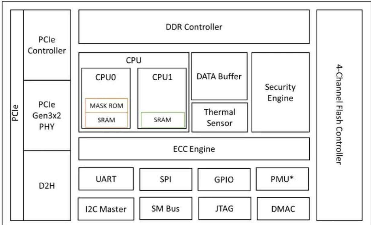
flowchart
graph TD
    A["PCIe"] --> B["PCIe Controller"]
    B --> C["DDR Controller"]
    C --> D["4-Channel Flash Controller"]
    D --> E["CPU"]
    E --> F["CPU0"]
    F --> G["MASK ROM"]
    F --> H["SRAM"]
    E --> I["CPU1"]
    I --> J["SRAM"]
    E --> K["DATA Buffer"]
    K --> L["Thermal Sensor"]
    K --> M["Security Engine"]
    E --> N["ECC Engine"]
    N --> O["UART"]
    O --> P["SPI"]
    P --> Q["GPIO"]
    Q --> R["PMU*"]
    N --> S["I2C Master"]
    S --> T["SM Bus"]
    T --> U["JTAG"]
    U --> V["DMAC"]
■ LBA value
| Density | LBA |
| 128 GB | 250,069,680 |
| 256 GB | 500,118,192 |
| 512 GB | 1,000,215,216 |
5. Pin Assignment and Description
Below table defines the signal assignment of the internal NGFF connector for SSD usage, described in the PCI Express M.2 Specification version 1.0 of the PCI-SIG.
| Pin No. | PCIe Pin | Description |
| 1 | GND | CONFIG 3 = Ground |
| 2 | 3.3V | 3.3V source |
| 3 | GND | Ground |
| 4 | 3.3V | 3.3V source |
| 5 | N/C | No connect |
| 6 | N/C | No connect |
| 7 | N/C | No connect |
| 8 | N/C | No connect |
| 9 | N/C | No connect |
| 10 | LED1# | Open drain, active low signal. These signals are used to allow the add-in card to provide status indicators via LED devices that will be provided by the system. |
| 11 | N/C | No connect |
| 12 | Module Key B | Module Key |
| 13 | Module Key B | |
| 14 | Module Key B | |
| 15 | Module Key B | |
| 16 | Module Key B | |
| 17 | Module Key B | |
| 18 | Module Key B | |
| 19 | Module Key B | |
| 20 | N/C | No connect |
| 21 | GND | Ground |
| 22 | N/C | No connect |
| 23 | N/C | No connect |
| 24 | N/C | No connect |
| 25 | N/C | No connect |
| 26 | N/C | No connect |
| 27 | GND | Ground |
| 28 | N/C | No connect |
| 29 | PETn1 | PCIe TX Differential signal defined by the PCI Express M.2 spec |
| 30 | N/C | No connect |
| 31 | PETp1 | PCIe TX Differential signal defined by the PCI Express M.2 spec |
| 32 | N/C | No connect |
| 33 | GND | Ground |
| 34 | N/C | No connect |
| 35 | PERn1 | PCIe TX Differential signal defined by the PCI Express M.2 spec |
| 36 | N/C | No connect |
| 37 | PERp1 | PCIe TX Differential signal defined by the PCI Express M.2 spec |
| 38 | N/C | No connect |
| 39 | GND | Ground |
| 40 | SMB_CLK (I/O)(0/1.8V) | SMBus Clock; Open Drain with pull-up on platform (Reserve) |
| 41 | PETn0 | PCIe TX Differential signal defined by the PCI Express M.2 spec |
| 42 | SMB_DATA (I/O)(0/1.8V) | SMBus Data; Open Drain with pull-up on platform (Reserve) |
| 43 | PETp0 | PCIe TX Differential signal defined by the PCIe 3.0 specification |
| 44 | ALERT#(O) (0/1.8V) | Alert notification to master; Open Drain with pull-up on platform; Active low |
| 45 | GND | Ground |
| 46 | N/C | No connect |
| 47 | PERn0 | PCIe RX Differential signal defined by the PCI Express M.2 spec |
| 48 | N/C | No connect |
| 49 | PERp0 | PCIe RX Differential signal defined by the PCI Express M.2 spec |
| 50 | PERST#(I)(0/3.3V) | PE-Reset is a functional reset to the card as defined by the PCIe Mini CEM specification. |
| 51 | GND | Ground |
| 52 | CLKREQ#(I/O)(0/3.3V) | Clock Request is a reference clock request signal as defined by the PCIe Mini CEM specification; Also used by L1 PM Substates. |
| 53 | REFCLKn | PCIe Reference Clock signals (100 MHz) defined by the PCI Express M.2 spec. |
| 54 | PEWAKE#(I/O)(0/3.3V) | PCIe PME Wake.Open Drain with pull up on platform; Active Low. |
| 55 | REFCLKp | PCIe Reference Clock signals (100 MHz) defined by the PCI Express M.2 spec. |
| 56 | Reserved for MFG DATA | Manufacturing Data line. Used for SSD manufacturing only.Not used in normal operation.Pins should be left N/C in platform Socket. |
| 57 | GND | Ground |
| 58 | Reserved for MFG CLOCK | Manufacturing Clock line. Used for SSD manufacturing only.Not used in normal operation.Pins should be left N/C in platform Socket. |
| 59 | Module Key | Module Key |
| 60 | Module Key | |
| 61 | Module Key | |
| 62 | Module Key | |
| 63 | Module Key | |
| 64 | Module Key | |
| 65 | Module Key | |
| 66 | Module Key | |
| 67 | N/C | No connect |
| 68 | N/C | No connect |
| 69 | NC | CONFIG_1 = No connect |
| 70 | 3.3V | 3.3V source |
| 71 | GND | Ground |
| 72 | 3.3V | 3.3V source |
| 73 | GND | Ground |
| 74 | 3.3V | 3.3V source |
| 75 | GND | CONFIG_2 = Ground |
6. NVMe Command List
■ Admin commands
| Opcode | Command Description |
| 00h | Delete I/O Submission Queue |
| 01h | Create I/O Submission Queue |
| 02h | Get Log Page |
| 04h | Delete I/O Completion Queue |
| 05h | Create I/O Completion Queue |
| 06h | Identify |
| 08h | Abort |
| 09h | Set Features |
| 0Ah | Get Features |
| 0Ch | Asynchronous Event Request |
| 10h | Firmware Activate |
| 11h | Firmware Image Download |
| NVM Command Set Specific | |
| 80h | Format NVM |
| 81h | Security Send |
| 82h | Security Receive |
■ NVM commands
| Opcode | Command Description |
| 00h | Flush |
| 01h | Write |
| 02h | Read |
| 04h | Write Uncorrectable |
| 08h | Write Zeroes |
| 09h | Dataset Management |
7. Identify Device Data
The Identity Device Data enables Host to receive parameter information from the device. The parameter words in the buffer have the arrangement and meanings defined in below table. All reserve bits or words are zero
■ Identify Controller Data Structure
| Bytes | O/M | Description | Default Value |
| 01:00 | M | PCI Vendor ID (VID) | 0x1987 |
| 03:02 | M | PCI Subsystem Vendor ID (SSVID) | 0x1987 |
| 23:04 | M | Serial Number (SN) | SN |
| 63:24 | M | Model Number (MN) | Model Number |
| 71:64 | M | Firmware Revision (FR) | FW Name |
| 72 | M | Recommended Arbitration Burst (RAB) | 0x01 |
| 75:73 | M | IEEE OUI Identifier (IEEE) | 0 |
| 76 | O | Controller Multi-Path I/O and Namespace Sharing Capabilities (CMIC) | 0x00 |
| 77 | M | Maximum Data Transfer Size (MDTS) | 0x09 |
| 79:78 | M | Controller ID (CNTLID) | 0x0000 |
| 83:80 | M | Version (VER) | 0x00010200 |
| 87:84 | M | RTD3 Resume Latency (RTD3R) | 0x00124F80 |
| 91:88 | M | RTD3 Entry Latency (RTD3E) | 0x0016E360 |
| 95:92 | M | Optional Asynchronous Events Supported (OAES) | 0 |
| 239:96 | - | Reserved | 0 |
| 255:240 | - | Refer to the NVMe Management Interface Specification for definition | 0 |
| 257:256 | M | Optional Admin Command Support (OACS) | 0x0007 |
| 258 | M | Abort Command Limit (ACL) | 0x03 |
| 259 | M | Asynchronous Event Request Limit (AERL) | 0x03 |
| 260 | M | Firmware Updates (FRMW) | 0x02 |
| 261 | M | Log Page Attributes (LPA) | 0x03 |
| 262 | M | Error Log Page Entries (ELPE) | 0x3F |
| 263 | M | Number of Power States Support (NPSS) | 0x04 |
| 264 | M | Admin Vendor Specific Command Configuration (AVSCC) | 0x01 |
| 265 | O | Autonomous Power State Transition Attributes (APSTA) | 0x01 |
| 267:266 | M | Warning Composite Temperature Threshold (WCTEMP) | 0x0157 |
| 269:268 | M | Critical Composite Temperature Threshold (CCTEMP) | 0x0193 |
| 271:270 | O | Maximum Time for Firmware Activation (MTFA) | 0x0000 |
| 275:272 | O | Host Memory Buffer Preferred Size (HMPRE) | 0 |
| 279:276 | O | Host Memory Buffer Minimum Size (HMMIN) | 0 |
| 295:280 | O | Total NVM Capacity (TNVMCAP) | 0 |
| 311:296 | O | Unallocated NVM Capacity (UNVMCAP) | 0 |
| 315:312 | O | Replay Protected Memory Block Support (RPMBS) | 0 |
| 511:316 | - | Reserved | 0 |
| NVM Command Set Attributes | |||
| 512 | M | Submission Queue Entry Size (SQES) | 0x66 |
| 513 | M | Completion Queue Entry Size (CQES) | 0x44 |
| 515:514 | - | Reserved | 0 |
| 519:516 | M | Number of Namespaces (NN) | 0x01 |
| 521:520 | M | Optional NVM Command Support (ONCS) | 0x001E |
| 523:522 | M | Fused Operation Support (FUSES) | 0 |
| 524 | M | Format NVM Attributes (FNA) | 0 |
| 525 | M | Volatile Write Cache (VWC) | 0x01 |
| 527:526 | M | Atomic Write Unit Normal (AWUN) | 0x00FF |
| 529:528 | M | Atomic Write Unit Power Fail (AWUPF) | 0x00 |
| 530 | M | NVM Vendor Specific Command Configuration (NVSCC) | 0x01 |
| 531 | M | Reserved | 0 |
Specifications subject to change without notice, contact your sales representatives for the most update information.
| 533:532 | O | Atomic Compare & Write Unit (ACWU) | 0x00 |
| 535:534 | M | Reserved | 0 |
| 539:536 | O | SGL Support (SGLS) | 0x00 |
| 703:540 | M | Reserved | 0 |
| IO Command Set Attributes | |||
| 2047:704 | M | Reserved | 0 |
| 2048:2079 | M | Power State 0 Descriptor | PSD0 |
| 2111:2080 | O | Power State 1 Descriptor | PSD1 |
| 2143:2112 | O | Power State 2 Descriptor | PSD2 |
| 2175:2144 | O | Power State 3 Descriptor | PSD3 |
| 2207:2176 | O | Power State 4 Descriptor | PSD4 |
| ... | - | (N/A) | 0 |
| 3071:3040 | O | Power State 31 Descriptor | PSD31 |
| Vendor Specific | |||
| 4095:3072 | O | Vendor Specific (VS) | Phison Reserved |
■ Identify Namespace Data Structure & NVM Command Set Specific
| Bytes | Description |
| 7:0 | Namespace Size (NSZE) |
| 15:8 | Namespace Capacity (NCAP) |
| 23:16 | Namespace Utilization (NUSE) |
| 24 | Namespace Features (NSFEAT) |
| 25 | Number of LBA Formats (NLBAF) |
| 26 | Formatted LBA Size (FLBAS) |
| 27 | Metadata Capabilities (MC) |
| 28 | End-to-end Data Protection Capabilities (DPC) |
| 29 | End-to-end Data Protection Type Settings (DPS) |
| 30 | Namespace Multi-path I/O and Namespace Sharing Capabilities (NMIC) |
| 31 | Reservation Capabilities (RESCAP) |
| 119:32 | Reserved |
| 127:120 | IEEE Extended Unique Identifier (EUI64) |
| 131:128 | LBA Format 0 Support (LBAF0) |
| 135:132 | LBA Format 1 Support (LBAF1) |
| 139:136 | LBA Format 2 Support (LBAF2) |
| 143:140 | LBA Format 3 Support (LBAF3) |
| 147:144 | LBA Format 4 Support (LBAF4) |
| 151:148 | LBA Format 5 Support (LBAF5) |
| 155:152 | LBA Format 6 Support (LBAF6) |
| 159:156 | LBA Format 7 Support (LBAF7) |
| 163:160 | LBA Format 8 Support (LBAF8) |
| 167:164 | LBA Format 9 Support (LBAF9) |
| 171:168 | LBA Format 10 Support (LBAF10) |
| 175:172 | LBA Format 11 Support (LBAF11) |
| 179:176 | LBA Format 12 Support (LBAF12) |
| 183:180 | LBA Format 13 Support (LBAF13) |
| 187:184 | LBA Format 14 Support (LBAF14) |
| 191:188 | LBA Format 15 Support (LBAF15) |
| 383:192 | Reserved |
| 4095:384 | Vendor Specific (VS) |
■ List of Device Identification for Each Capacity
| Capacity | Byte[7:0]:Namespace Size (NSZE) |
| 128 GB | EE7C2B0 |
| 256 GB | 1DCF32B0 |
| 512 GB | 3B9E12B0 |
- SMART Attributes
| Bytes Index | Bytes | Description |
| [0] | 1 | Critical Warning |
| [2:1] | 2 | Composite Temperature |
| [3] | 1 | Available Spare |
| [4] | 1 | Available Spare Threshold |
| [5] | 1 | Percentage Used |
| [31:6] | 26 | Reserved |
| [47:32] | 16 | Data Units Read |
| [63:48] | 16 | Data Units Written |
| [79:64] | 16 | Host Read Commands |
| [95:80] | 16 | Host Write Commands |
| [111:96] | 16 | Controller Busy Time |
| [127:112] | 16 | Power Cycles |
| [143:128] | 16 | Power On Hours |
| [159:144] | 16 | Unsafe Shutdowns |
| [175:160] | 16 | Media and Data Integrity Errors |
| [191:176] | 16 | Number of Error Information Log Entries |
| [195:192] | 4 | Warning Composite Temperature Time |
| [199:196] | 4 | Critical Composite Temperature Time |
| [201:200] | 2 | Temperature Sensor 1 |
| [203:202] | 2 | Temperature Sensor 2 |
| [205:204] | 2 | Temperature Sensor 3 |
| [207:206] | 2 | Temperature Sensor 4 |
9. System Power Consumption
■ Supply Voltage
| Parameter | Rating |
| Operating Voltage | 3.3V |
■ Power Consumption
| mW | Read | Write | Idle | |
| BiCS33D TLC | 128 GB | 2,734 | 2,223 | 35 |
| 256 GB | 3,249 | 2,776 | 40 | |
| 512 GB | 3,346 | 2,913 | 45 | |
- The average value of power consumption is achieved based on 100% conversion efficiency.
- Sample is measured under ambient temperature.
- Power Consumption may differ according to flash configuration and platform.
- Power consumption is measured during the sequential read and writes operations performed by CrystalDiskMark with the conditions described in 1(A).
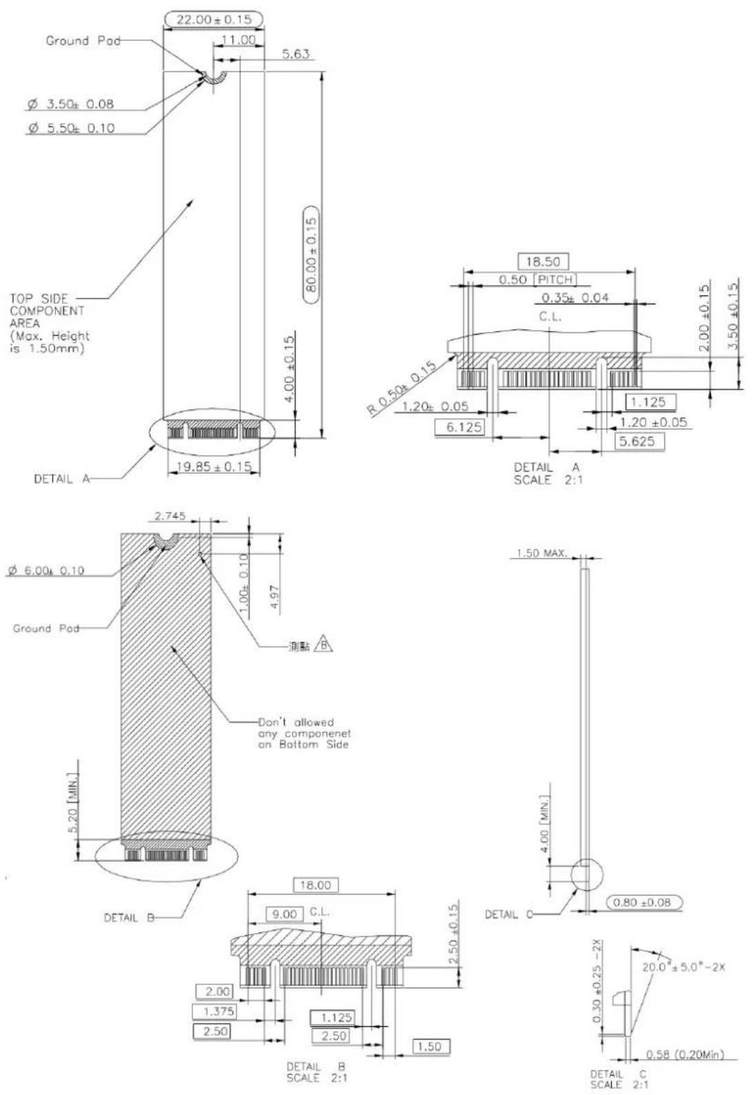
10. Physical Dimension
M.2 2280 (B+M key) PCIe/NVMe SSD (Unit: mm)
Appendix: Part Number Table
BiCS3 3D TLC
| Product | Advantech PN |
| SQF 710 PCIe/NVMe M.2 2280 128G 3D TLC (BiCS3) (0~70°C) | SQF-CM8V2-128G-E8C |
| SQF 710 PCIe/NVMe M.2 2280 256G 3D TLC (BiCS3) (0~70°C) | SQF-CM8V4-256G-E8C |
| SQF 710 PCIe/NVMe M.2 2280 512G 3D TLC (BiCS3) (0~70°C) | SQF-CM8V4-512G-E8C |
| SQF 710 PCIe/NVMe M.2 2280 128G 3D TLC (BiCS3) (-40~85°C) | SQF-CM8V2-128G-E8E |
| SQF 710 PCIe/NVMe M.2 2280 256G 3D TLC (BiCS3) (-40~85°C) | SQF-CM8V4-256G-E8E |
| SQF 710 PCIe/NVMe M.2 2280 512G 3D TLC (BiCS3) (-40~85°C) | SQF-CM8V4-512G-E8E |