
SQF-SM8V4-240G-SCE - SSD Advantech - Free user manual and instructions
Find the device manual for free SQF-SM8V4-240G-SCE Advantech in PDF.


| Product Type | Solid State Drive (SSD) |
| Form Factor | M.2 2280 (B+M Key) |
| Interface | SATA III (6.0 Gbps) backward compatible with SATA 1.5/3.0 Gbps |
| Capacity | 240 GB |
| NAND Flash Type | Toshiba 64-layer 3D NAND (BiCS3) |
| Sequential Read Speed | Up to 561.2 MB/s |
| Sequential Write Speed | Up to 536.9 MB/s |
| Random Read (4K) | Up to 98,069 IOPS |
| Random Write (4K) | Up to 88,349 IOPS |
| Operating Voltage | 3.3V |
| Power Consumption (Read/Write/Idle) | 3.0 W / 2.5 W / 1.5 W |
| Operating Temperature | -40°C to 85°C (Industrial) |
| Storage Temperature | -40°C to 85°C |
| Shock Resistance | 1,500 G / 0.5 ms |
| Vibration Resistance | 20 G / 80-2,000 Hz |
| Humidity | 5% to 95% under 55°C |
| Data Retention | 10 years |
| Endurance (TBW) | 389 TB |
| Security Features | AES 256-bit encryption, TCG-OPAL 2.0, Secure Erase, Flash Vault |
| Error Correction | LDPC with RAID ECC |
| Additional Features | TRIM, AHCI, SMART, Over-Provision, Thermal Throttling, Power Loss Protection (Flush Manager, Voltage Stabilizer) |
| Certifications | RoHS, WHQL, CE, FCC |
| Dimensions (W x L x H) | 80.8 mm x 22.0 mm x 3.8 mm |
Frequently Asked Questions - SQF-SM8V4-240G-SCE Advantech
User questions about SQF-SM8V4-240G-SCE Advantech
0 question about this device. Answer the ones you know or ask your own.
Ask a new question about this device
Download the instructions for your SSD in PDF format for free! Find your manual SQF-SM8V4-240G-SCE - Advantech and take your electronic device back in hand. On this page are published all the documents necessary for the use of your device. SQF-SM8V4-240G-SCE by Advantech.
USER MANUAL SQF-SM8V4-240G-SCE Advantech
- Overview ...... 4
- Features .... 5
- Specification Table....6
- General Description 8
- Security Features .... 11
- Pin Assignment and Description ...... 12
- Identify Device Data 15
- ATA Command Set .... 18
- System Power Consumption 25
9.1 Supply Voltage 25
9.2 Power Consumption 25
- Physical Dimension......26
Appendix: Part Number Table 27
Revision History
| Rev. | Date | History |
| 0.1 | 2018/5/18 | 1. Preliminary |
| 0.2 | 2018/8/22 | 1. Update PN information |
| 0.3 | 2019/7/15 | 1. Update produce information |
Advantech reserves the right to make changes without further notice to any products or data herein to improve reliability, function, or design. Information furnished by Advantech is believed to be accurate and reliable. However, Advantech does not assure any liability arising out of the application or use of this information, nor the application or use of any product or circuit described herein, neither does it convey any license under its patent rights nor the rights of others.
Copyright © 1983-2019 Advantech Co., Ltd. All rights reserved.
1. Overview
Advantech SQFlash 840 series M.2 2280 SATA-SSD (SQF-SM8 840) delivers all the advantages of Flash Disk technology with the Serial ATA III (6.0Gb) interface, fully compliant with standard Next Generation Form Factor (NGFF) M.2 2280 (B+M Key) form factor. The SATA SSD is designed to operate at a maximum operating frequency of 300MHz with 30MHz external crystal. Its capacity could provide a wide range up to 2TB. Moreover, it can reach up to 550MB/s read and 530MB/s write high performance based on Toshiba 64-layer 3D NAND Flash.
2. Features
■ Standard SATA interface
– Support SATA 1.5/3.0/6.0 Gbps interface
– SATA Revision 3.2 compliant
■ Operating Voltage : 3.3V
■ Support LDPC with RAID ECC
■ TRIM、AHCI、AES256 and OPAL supported
■ Hardware Quick Erase supported (optional)
■ Voltage Stabilizer supported (optional)
■ Temperature Ranges
- Commercial Temperature ^1
- 0^ C to 70^ C for operating
- -40°C to 85°C for storage
- Industrial Temperature ^1
- -40°C to 85°C for operating
- -40°C to 85°C for storage
Note: 1. Based on SMART Attribute C2h, which measured by thermal sensor
■ Mechanical Specification
- Shock : 1,500G / 0.5ms
- Vibration : 20G / 80\~2,000Hz
■ Humidity
- Humidity: 5% \~ 95% under 55°C
■ Data Retention
- 10 years
■ Acquired RoHS、WHQL、CE、FCC Certificate
■ Acoustic : 0 dB
■ Dimension : 80.8 mm x 22.0 mm x 3.8 mm
3. Specification Table
■ Performance
| Sequential Performance (MB/sec) | Random Performance (IOPS @4K) | ||||
| Read | Write | Read | Write | ||
| 3D NAND (BiCS3) | 240 GB | 561.2 | 536.9 | 98,069 | 88,349 |
| 480 GB | 560.7 | 542.1 | 95,735 | 89,009 | |
| 960 GB | 561.0 | 542.6 | 98,899 | 85,469 | |
| 1920 GB | 560.7 | 541.7 | 98,466 | 88,317 | |
* Subject to change based on firmware migration
■ Endurance
JEDEC defined an endurance rating TBW (TeraByte Written), following by the equation below, for indicating the number of terabytes a SSD can be written which is a measurement of SSDs' expected lifespan, represents the amount of data written to the device.
TBW = [(NAND Endurance) x (SSD Capacity)] / WAF
• NAND Endurance: Program / Erase cycle of a NAND flash.
- SLC: 100,000 cycles
- Ultra MLC: 30,000 cycles
- MLC: 3,000 cycles
- 3D NAND (BiCS3): 3,000 cycles
- SSD Capacity: SSD physical capacity in total of a SSD.
- WAF: Write Amplification Factor (WAF), as the equation shown below, is a numerical value representing the ratio between the amount of data that a SSD controller needs to write and the amount of data that the host's flash controller writes. A better WAF, which is near to 1, guarantees better endurance and lower frequency of data written to flash memory.
WAF = (Lifetime write to flash) / (Lifetime write to host)
Endurance measurement is based on New JEDEC 218/219 Client Workload and verified with following workload conditions,
- PreCond%full = 100%
- Trim commands enabled
- Random data pattern.
SQFlash 840 M.2 2280 SSD TBW
| WAF | TBW | |
| 3D NAND (BiCS3) | ||
| 240 GB | 1.85 | 389 |
| 480 GB | 1.85 | 778 |
| 960 GB | 1.85 | 1556 |
| 1920 GB | 1.85 | 3113 |
* Subject to change based on firmware migration
4. General Description
■ Error Correction Code (ECC)
Flash memory cells will deteriorate with use, which might generate random bit errors in the stored data. Thus, SQFlash 840 series SSD applies the LDPC with RAID ECC algorithm, which can detect and correct errors occur during read process, ensure data been read correctly, as well as protect data from corruption.
■ Wear Leveling
NAND flash devices can only undergo a limited number of program/erase cycles, and in most cases, the flash media are not used evenly. If some areas get updated more frequently than others, the lifetime of the device would be reduced significantly. Thus, Wear Leveling is applied to extend the lifespan of NAND Flash by evenly distributing write and erase cycles across the media.
SQFlash provides advanced Wear Leveling algorithm, which can efficiently spread out the flash usage through the whole flash media area. Moreover, by implementing both dynamic and static Wear Leveling algorithms, the life expectancy of the NAND flash is greatly improved.
■ Bad Block Management
Bad blocks are blocks that include one or more invalid bits, and their reliability is not guaranteed. Blocks that are identified and marked as bad by the manufacturer are referred to as "Initial Bad Blocks". Bad blocks that are developed during the lifespan of the flash are named "Later Bad Blocks". SQFlash implements an efficient bad block management algorithm to detect the factory-produced bad blocks and manages any bad blocks that appear with use. This practice further prevents data being stored into bad blocks and improves the data reliability.
■ Power Loss Protection
- Flush Manager
Power Loss Protection is a mechanism to prevent data loss during unexpected power failure. DRAM is a volatile memory and frequently used as temporary cache or buffer between the controller and the NAND flash to improve the SSD performance. However, one major concern of the DRAM is that it is not able to keep data during power failure. Accordingly, SQFlash SSD applies the Flush Manager technology, only when the data is fully committed to the NAND flash will the controller send acknowledgement (ACK) to the host. Such implementation can prevent false-positive performance and the risk of power cycling issues. In addition, it is critical for a controller to shorten the time the in-flight data stays in the controller internal cache. Thus, SQFlash applies an algorithm to reduce the amount of data resides in the cache to provide a better performance. With Flush Manager, incoming data would only have a “pit stop” in the cache and then move to NAND flash directly. Also, the onboard DDR will be treated as an “organizer” to consolidate incoming data into groups before written into the flash to improve write amplification.
- Voltage Stabilizer
While the built-in voltage detector detects an unstable power input (< 3.135 V or > 3.465 V), the controller will issue a power failure interrupt and force a Flush CMD first. At the same time, the whole internal power supply will be switched to Voltage Stabilizer immediately to ensure stable power is supplied throughout the whole drive. This ensures the Flash IC and DDR IC will not operate with unstable power which could lead to data errors or bad data integrity.
TRIM
TRIM is a feature which helps improve the read/write performance and speed of solid-state drives (SSD). Unlike hard disk drives (HDD), SSDs are not able to overwrite existing data, so the available space gradually becomes smaller with each use. With the TRIM command, the operating system can inform the SSD which blocks of data are no longer in use and can be removed permanently. Thus, the SSD will perform the erase action, which prevents unused data from occupying blocks all the time.
■ SMART
SMART, an acronym for Self-Monitoring, Analysis and Reporting Technology, is an open standard that allows a hard disk drive to automatically detect its health and report potential failures. When a failure is recorded by SMART, users can choose to replace the drive to prevent unexpected outage or data loss. Moreover, SMART can inform users of impending failures while there is still time to perform proactive actions, such as copy data to another device.
■ Over-Provision
Over Provisioning refers to the inclusion of extra NAND capacity in a SSD, which is not visible and cannot be used by users. With Over Provisioning, the performance and IOPS (Input/Output Operations per Second) are improved by providing the controller additional space to manage P/E cycles, which enhances the reliability and endurance as well. Moreover, the write amplification of the SSD becomes lower when the controller writes data to the flash.
■ Thermal Throttling
Thermal Throttling function is for protecting the drive and reducing the possibility of read / write error due to overheat. The temperature is monitored by the thermal sensor. As the operating temperature continues to increase to threshold temperature, the Thermal Throttling mechanism is activated. At this time, the performance of the drive will be significantly decreased to avoid continuous heating. When the operating temperature falls below threshold temperature, the drive can resume to normal operation.
■ Block Diagram
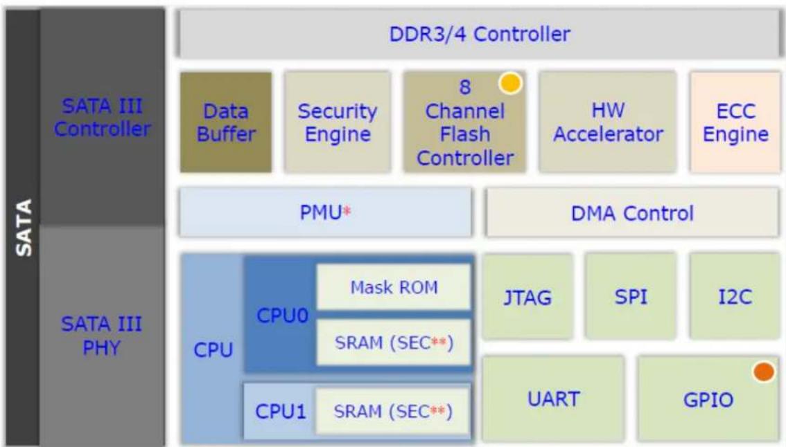
flowchart
graph TD
    A["SATA III Controller"] --> B["Data Buffer"]
    A --> C["Security Engine"]
    A --> D["8 Channel Flash Controller"]
    A --> E["HW Accelerator"]
    A --> F["ECC Engine"]
    G["SATA III PHY"] --> H["CPU"]
    G --> I["CPU0"]
    I --> J["Mask ROM"]
    I --> K["SRAM (SEC**)"]
    G --> L["CPU1"]
    L --> M["SRAM (SEC**)"]
    N["DDR3/4 Controller"] --> O["DMA Control"]
    P["PMU*"] --> Q["JTAG"]
    P --> R["SPI"]
    P --> S["I2C"]
    T["UART"] --> U["GPIO"]
■ LBA value
| Density | LBA |
| 240 GB | 468,862,128 |
| 480 GB | 937,703,088 |
| 960 GB | 1,875,385,008 |
| 1920 GB | 3,750,748,848 |
5. Security Features
■ Advanced Encryption Standard (AES)
An AES 256-bit encryption key is generated in the drive's security controller before the data got stored on the NAND flash. When the controller or firmware fails, the data that is securely stored in the encryption key becomes inaccessible through the NAND flash.
■ Secure / Quick Erase (optional)
SQFlash 840 series supports standard SATA command secure erase. Also, with internal AES encryption support, the erase process will start with resetting AES key. By doing so, existing data will be scrambled within 10ms and cannot be recovered anymore. Moreover, erase flag is set when erase function is triggered, which will ensure the whole erase process can be 100% completed. Even there's power interrupt, after power resume, erase operation will be resume right away as well.
■ TCG-OPAL 2.0 Compliance
TCG-OPAL compliance SED (Self-encryption Drive) supports a built-in shadow MBR to process user authentication to SSD before booting to normal MRR area and OS. SQFlash 840 series supports such feature with 100% TCG-OPAL compliance. Further, with SQFlash Flash Lock function, the user authentication process in shadow MBR can be done automatically by bonding with motherboard unique ID such as UUID in BIOS / MAC address / TPM unique code. So with Flash Lock enabled, only designated motherboard can have access to the SSD.
■ Flash Vault
Flash Vault is to lock Read and Write command by SSD firmware setting and make the SSD need password to verify and only operate with the corresponding platform. User can use Flash Vault to prevent data being stolen by reading the SQFlash SSD with other computers and unauthorized person.
- Pin Assignment and Description
| Pin # | SATA Pin | Description |
| 1 | CONFIG_3 = GND | Ground |
| 2 | 3.3V | Supply pin |
| 3 | GND | Ground |
| 4 | 3.3V | Supply pin |
| 5 | N/C | No Connect |
| 6 | N/C | No Connect |
| 7 | N/C | No Connect |
| 8 | N/C | No Connect |
| 9 | N/C or GND Note | No Connect or Ground |
| 10 | DAS/DSS# (O) (OD) | Status indicators via LED devices that will be provided by the system Active Low. A pulled-up LED with series current limiting resistor should allow for 9mA when On. |
| 11 | N/C | No Connect |
| 12 | Module Key | |
| 13 | Module Key | |
| 14 | Module Key | |
| 15 | Module Key | |
| 16 | Module Key | |
| 17 | Module Key | |
| 18 | Module Key | |
| 19 | Module Key | |
| 20 | N/C | No Connect |
| 21 | CONFIG_0 = GND | Ground |
| 22 | N/C | No Connect |
| 23 | N/C | No Connect |
| 24 | N/C | No Connect |
| 25 | N/C | No Connect |
| 26 | N/C | No Connect |
| 27 | GND | Ground |
| 28 | N/C | No Connect |
| 29 | N/C | No Connect |
| 30 | N/C | No Connect |
| 31 | N/C | No Connect |
| 32 | N/C | No Connect |
| 33 | GND | Ground |
| 34 | N/C | No Connect |
| 35 | N/C | No Connect |
| 36 | N/C | No Connect |
Specifications subject to change without notice, contact your sales representatives for the most update information.
| 37 | N/C | No Connect |
| 38 | DEVSLP (I) (0/3.3V) | Device Sleep, Input.When driven high the host is informing the SSD to enter a low power state (default NC, DEVSLP disable) |
| 39 | GND | Ground |
| 40 | N/C | No Connect |
| 41 | SATA-B+ | SATA differential signals in the SATA specification |
| 42 | N/C | No Connect |
| 43 | SATA-B- | SATA differential signals in the SATA specification |
| 44 | N/C | No Connect |
| 45 | GND | Ground |
| 46 | N/C | No Connect |
| 47 | SATA-A- | SATA differential signals in the SATA specification |
| 48 | N/C | No Connect |
| 49 | SATA-A+ | SATA differential signals in the SATA specification |
| 50 | N/C | No Connect |
| 51 | GND | Ground |
| 52 | N/C | No Connect |
| 53 | N/C | No Connect |
| 54 | N/C | No Connect |
| 55 | N/C | No Connect |
| 56 | Reserved for MFG Data | Manufacturing Data line. Used for SSD manufacturing only.Not used in normal operation. Pins should be left N/C in platform Socket. |
| 57 | GND | Ground |
| 58 | Reserved for MFG Clock | Manufacturing Clock line. Used for SSD manufacturing only.Not used in normal operation. Pins should be left N/C in platform Socket |
| 59 | Module Key | |
| 60 | Module Key | |
| 61 | Module Key | |
| 62 | Module Key | |
| 63 | Module Key | |
| 64 | Module Key | |
| 65 | Module Key | |
| 66 | Module Key | |
| 67 | N/C | No Connect |
| 68 | SUSCLK (I) (0/3.3V) | 32 kHz clock supply input that is provided by PCH to reduce power and cost for the module. (default NC) |
| 69 | CONFIG_1 = GND | Defines module type |
| 70 | 3.3V | Supply pin |
| 71 | GND | Ground |
| 72 | 3.3V | Supply pin |
Specifications subject to change without notice, contact your sales representatives for the most update information.
| 73 | GND | Ground |
| 74 | 3.3V | Supply pin |
| 75 | CONFIG_2 = GND | Ground |
NOTE: N/C for Socket 2, and GND for Socket 3.
7. Identify Device Data
The Identity Device Data enables Host to receive parameter information from the device. The parameter words in the buffer have the arrangement and meanings defined in below table. All reserve bits or words are zero
| Word | ATA Identify Parameter | Value |
| 0 | General configuration | 0040h |
| 1 | Number of cylinders in the default CHS translation | 3FFFh |
| 2 | Specific configuration | C837h |
| 3 | Number of heads in the default CHS translation | 0010h |
| 4-5 | Retired | 0000h |
| 6 | Number of sectors per track in the default CHS translation | 003Fh |
| 7-8 | Reserved for the CFA | 0000h |
| 9 | Obsolete | 0000h |
| 10-19 | Serial number | ASCII |
| 20 | Retired | 0000h |
| 21 | Retired | 0000h |
| 22 | Obsolete | 0000h |
| 23-26 | Firmware revision | ASCII |
| 27-46 | Model number | ASCII |
| 47 | READ/WRITE MULTIPLE commands function | 8010h |
| 48 | Trusted Computing feature set options | 4000h |
| 49 | Capabilities | 2F00h |
| 50 | Capabilities | 4000h |
| 51-52 | Obsolete | 0000h |
| 53 | field validity | 0007h |
| 54 | Number of cylinders in the current CHS translation | 3FFFh |
| 55 | Number of heads in the current CHS translation | 0010h |
| 56 | Number of sectors per track in the current CHS translation | 003Fh |
| 57-58 | Current capacity in sectors | 00FBFC10h |
| 59 | Multiple sector setting | 0110h |
| 60-61 | Total number of user addressable logical sectors for 28-bit commands | *3 |
| 62 | Obsolete | 0000h |
| 63 | Multiword DMA modes | 0407h |
| 64 | PIO mode supported | 0003h |
| 65 | Minimum Multiword DMA transfer cycle time per word | 0078h |
| 66 | Manufacturer's recommended Multiword DMA transfer cycle time | 0078h |
| 67 | Minimum PIO transfer cycle time without flow control | 0078h |
| 68 | Minimum PIO transfer cycle time with IORDY flow control | 0078h |
| 69 | Additional Supported | 5F20h |
| 70-73 | Reserved | 0000h |
| 74 | Reserved | 0000h |
| 75 | Queue depth | 001Fh |
| 76 | Serial ATA Capabilities | E70Eh |
| 77 | Supported Serial ATA Phy speed | 0006/0004/0002h |
| 78 | Serial ATA features supported | 054Ch |
| 79 | Serial ATA features enabled | 0040h |
| 80 | Major version number | 03F8h |
| 81 | Minor version number | 0000h |
| 82 | Commands and feature sets supported | 746Bh |
| 83 | Commands and feature sets supported | 7D09h |
| 84 | Commands and feature sets supported | 4163h |
| 85 | Commands and feature sets supported or enabled | 7469h |
| 86 | Commands and feature sets supported or enabled | BC09h |
| 87 | Commands and feature sets supported or enabled | 4163h |
| 88 | Ultra DMA modes | 007Fh |
| 89 | Time required for Normal Erase mode SECURITY ERASE UNIT command | 0001h |
| 90 | Time required for an Enhanced Erase mode SECURITY ERASE UNIT command | 0001h |
| 91 | Current APM level value | 00FEh |
| 92 | Master Password Identifier | FFFEh |
| 93 | Hardware reset result | 0000h |
| 94 | Current AAM value | 0000h |
| 95 | Stream Minimum Request Size | 0000h |
| 96 | Streaming Transfer Time - DMA | 0000h |
| 97 | Streaming Access Latency -DMA and PIO | 0000h |
| 98-99 | Streaming Performance Granularity | 0000h |
| 100-103 | Total Number of User Addressable Logical Sectors for 48-bit commands | *4 |
| 104 | Streaming Transfer Time - PIO | 0000h |
| 105 | Maximum number of 512-byte blocks of LBA Range Entries per DATA SET MANAGEMENT command | 0008h |
| 106 | Physical sector size / logical sector size | 4000h |
| 107 | Inter-seek delay for ISO 7999 standard acoustic testing | 0000h |
| 108-111 | World wide name | Vender Specific |
| 112-115 | Reserved | 0000h |
| 116 | Reserved for TLC | 0000h |
| 117-118 | Logical sector size | 0000h |
| 119 | Commands and feature sets supported | 401Ch |
| 120 | Commands and feature sets supported or enabled | 401Ch |
| 121-124 | Reserved for expanded supported and enabled settings | 0000h |
| 125-126 | Reserved for expanded supported and enabled settings | 0000h |
| 127 | Obsolete | 0000h |
| 128 | Security status | 0021h |
| 129-159 | Vendor specific | 0000h |
| 160 | CFA power mode | 0000h |
| 161-164 | Reserved for the CFA | 0000h |
| 165-167 | Reserved for the CFA | 0000h |
| 168 | Device Nominal Form Factor | 0003h |
| 169 | DATA SET MANAGEMENT is supported | 0001h |
| 170-173 | Additional Product Identifier | 0000h |
| 174-175 | Reserved | 0000h |
| 176-205 | Current media serial number | 0000h |
| 206 | SCT Command Transport | 0039h |
Specifications subject to change without notice, contact your sales representatives for the most update information.
| 207-208 | Reserved for CE-ATA | 0000h |
| 209 | Alignment of logical blocks within a physical block | 4000h |
| 210-211 | Write-Read-Verify Sector Count Mode 3 | 0000h |
| 212-213 | Write-Read-Verify Sector Count Mode 2 | 0000h |
| 214 | NV Cache Capabilities | 0000h |
| 215-216 | NV Cache Size in Logical Blocks | 0000h |
| 217 | Nominal media rotation rate | 0001h |
| 218 | Reserved | 0000h |
| 219 | NV Cache Options | 0000h |
| 220 | Current mode of the Write-Read-Verify feature set | 0000h |
| 221 | Reserved | 0000h |
| 222 | Transport major version number | 107Fh |
| 223 | Transport minor version number | 0000h |
| 224-227 | Reversed for CE-ATA | 0000h |
| 228-229 | Reversed for CE-ATA | 0000h |
| 230-233 | Extend Number of User Addressable Sectors | 0000h |
| 234 | Minimum number of 512-byte data blocks per DOWNLOAD MICROCODE command for mode 03h | 0001h |
| 235 | Maximum number of 512-byte data blocks per DOWNLOADMICROCODE command for mode 03h | FFFFh |
| 236-239 | Reserved | 0000h |
| 240-242 | Reserved | 0000h |
| 243 | Security feature4000 : Self Encrypting Drive | 4000h |
| 244-247 | Reserved | 0000h |
| 248-251 | Reserved | 0000h |
| 252-254 | Reserved | 0000h |
| 255 | Integrity word | xxA5h |
| Capacity(GB) | *1(Word 1/Word 54) | *2(Word 57 – 58) | *3(Word 60 – 61) | *4(Word 100 – 103) |
| 240 | 3FFFh | FBFC10h | FFFFFFh | 1BF244B0h |
| 480 | 3FFFh | FBFC10h | FFFFFFh | 37E436B0h |
| 960 | 3FFFh | FBFC10h | FFFFFFh | 6FC81AB0h |
| 1920 | 3FFFh | FBFC10h | FFFFFFh | DF8FE2B0h |
8. ATA Command Set
[Command Set List]
| Op-Code | Command Description | Op-Code | Command Description | |||
| 00h | NOP | 60h | Read FPDMA Queued | |||
| 06h | Data Set Management | 61h | Write FPDMA Queued | |||
| 10h | Recalibrate | 70h | Seek | |||
| 20h | Read Sectors | 90h | Execute Device Diagnostic | |||
| 21h | Read Sectors without Retry | 91h | Initialize Device Parameters | |||
| 24h | Read Sectors EXT | 92h | Download Microcode | |||
| 25h | Read DMA EXT | 93h | Download Microcode DMA | |||
| 27h | Read Native Max Address EXT | B0h | SMART | |||
| 29h | Read Multiple EXT | B0h | D0h | SMART READ DATA | ||
| 2Fh | Read Log EXT | B0h | D1h | SMART READ DATA ATTRIBUTE THRESHOLD | ||
| 30h | Write Sectors | B0h | D2h | SMART ENABLE/DISABLE ATTRIBUTE AUTOSAVE | ||
| 31h | Write Sectors without Retry | B0h | D3h | SMART SAVE ATTRIBUTE VALUES | ||
| 34h | Write Sectors EXT | B0h | D4h | SMART EXECUTE OFF-LINE IMMEDIATE | ||
| 35h | Write DMA EXT | B0h | D5h | SMART READ LOG | ||
| 37h | Set Native Max Address EXT | B0h | D6h | SMART WRITE LOG | ||
| 39h | Write Multiple EXT | B0h | D8h | SMART ENABLE OPERATIONS | ||
| 3Dh | Write DMA FUA EXT | B0h | D9h | SMART DISABLE OPERATIONS | ||
| 3Fh | Write Long EXT | B0h | DAh | SMART RETURN STATUS | ||
| 40h | Read Verify Sectors | B0h | DBh | SMART ENABLE/DISABLE AUTOMATIC OFF-LINE | ||
| 41h | Read Verify Sectors without Retry | B1h | DEVICE CONFIGURATION OVERLAY | |||
| 42h | Read Verify Sectors EXT | B1h | C0h | DEVICE CONFIGURATION RESTORE | ||
| 45h | Write Uncorrectable EXT | B1h | C1h | DEVICE CONFIGURATION FREEZE LOCK | ||
| 47h | Read Log DMA EXT | B1h | C2h | DEVICE CONFIGURATION IDENTIFY | ||
| 57h | Write Log DMA EXT | B1h | C3h | DEVICE CONFIGURATION SET | ||
| B1h | C4h | DEVICE CONFIGURATION IDENTIFY DMA | ECh | Identify Device | ||
| B1h | C5h | DEVICE CONFIGURATION SET DMA | EFh | Set Features | ||
| C4h | Read Multiple | EFh | 02h | Enable 8-bit PIO transfer mode | ||
Specifications subject to change without notice, contact your sales representatives for the most update information.
| C5h | Write Multiple | EFh | 03h | Set transfer mode based on value in Count field | |
| C6h | Set Multiple Mode | EFh | 05h | Enable advanced power management | |
| C8h | Read DMA | EFh | 10h | Enable use of Serial ATA feature | |
| C9h | Read DMA without Retry | EFh | 10h | 02h | Enable DMA Setup FIS Auto-Activate optimization |
| CAh | Write DMA | EFh | 10h | 03h | Enable Device-initiated interface power state (DIPM) transitions |
| CBh | Write DMA without Retry | EFh | 10h | 06h | Enable Software Settings Preservation (SSP) |
| CEh | Write Multiple FUA EXT | EFh | 10h | 07h | Enable Device Automatic Partial to Slumber transitions |
| E0h | Standby Immediate | EFh | 10h | 09h | Enable Device Sleep |
| E1h | Idle Immediate | EFh | 55h | Disable read look-ahead feature | |
| E2h | Standby | EFh | 66h | Disable reverting to power-on defaults | |
| E3h | Idle | EFh | 82h | Disable write cache | |
| E4h | Read Buffer | EFh | 85h | Disable advanced power management | |
| E5h | Check Power Mode | EFh | 90h | Disable use of Serial ATA feature set | |
| E6h | Sleep | EFh | 90h | 02h | Disable DMA Setup FIS Auto-Activate optimization |
| E7h | Flush Cache | EFh | 90h | 03h | Disable Device-initiated interface power state (DIPM) transitions |
| E8h | Write Buffer | EFh | 90h | 06h | Disable Software Settings Preservation (SSP) |
| E9h | Read Buffer DMA | EFh | 90h | 07h | Disable Device Automatic Partial to Slumber transitions |
| EAh | Flush Cache EXT | EFh | 90h | 09h | Disable Device Sleep |
| EBh | Write Buffer DMA | EFh | AAh | Enable read look-ahead feature | |
| EFh | CCh | Enable reverting to power-on defaults | F4h | Security Erase Unit | |
| F1h | Security Set Password | F5h | Security Freeze Lock | ||
| F2h | Security Unlock | F6h | Security Disable Password | ||
| F3h | Security Erase Prepare | F8h | Read Native Max Address | ||
Note: ND = Non-Data Command PI = PIO Data-In Command PO = PIO Data-Out Command DM = DMA Command DD = Execute Diagnostic Command
[Command Set Descriptions]
1. CHECK POWER MODE (code: E5h);
This command allows host to determine the current power mode of the device.
2. DOWNLOAD MICROCODE (code: 92h);
This command enables the host to alter the device's microcode. The data transferred using the DOWNLOAD MICROCODE command is vendor specific.
All transfers shall be an integer multiple of the sector size. The size of the data transfer is determined by the content of the LBA Low register and the Sector Count register.
This allows transfer sizes from 0 bytes to 33,553,920 bytes, in 512bytes increments.
3. EXECUTE DEVICE DIAGNOSTIC (code: 90h);
This command performs the internal diagnostic tests implemented by the module.
4. FLUSH CACHE (code: E7h);
This command used by the host to request the device to flush the write cache.
5. FLUSH CACHE EXT (code: EAh);
This command is used by the host to request the device to flush the write cache. If there is data in the write cache, that data shall be written to the media.
6. IDENTIFY DEVICE (code: ECh);
The IDENTIFY DEVICE command enables the host to receive parameter information from the module.
7. IDLE (code: 97h or E3h);
This command allows the host to place the module in the IDLE mode and also set the Standby timer. INTRQ may be asserted even through the module may not have fully transitioned to IDLE mode. If the Sector Count register is non-"0", then the Standby timer shall be enabled. The value in the Sector Count register shall be used to determine the time programmed into the Standby timer. If the Sector Count register is "0" then the Standby timer is disabled.
8. IDLE IMMEDIATE (code: E1h);
This command causes the module to set BSY, enter the Idle (Read) mode, clear BSY and generate an interrupt.
9. INITIALIZE DEVICE PARAMETERS (code: 91h);
This command enables the host to set the number of sectors per track and the number of heads per cylinder.
10. NOP (code: 00h);
If this command is issued, the module respond with command aborted.
11. READ BUFFER (code: E4h);
This command enables the host to read the current contents of the module's sector buffer.
12. READ DMA (code: C8h or C9h);
This command reads from "1" to "256" sectors as specified in the Sector Count register using the DMA
Specifications subject to change without notice, contact your sales representatives for the most update information.
data transfer protocol. A sector count of "0" requests "256" sectors transfer. The transfer begins at the sector specified in the Sector Number register.
13. READ DMA Ext (code: 25h);
This command allows the host to read data using the DMA data transfer protocol.
14. READ MULTIPLE (code: C4h);
This command performs similarly to the READ SECTORS command. Interrupts are not generated on each sector, but on the transfer of a block which contains the number of sector per block is defined by the content of word 59 in the IDENTIFY DEVICE response.
15. READ MULTIPLE EXT (code: 29h);
This command performs similarly to the READ SECTORS command. The number of sectors per block is defined by a successful SET MULTIPLE command. If no successful SET MULTIPLE command has been issued, the block is defined by the device's default value for number of sectors per block as defined in bits (7:0) in word 47 in the IDENTIFY DEVICE information.
16. READ NATIVE MAX ADDRESS (code: F8h);
This command returns the native maximum address. The native maximum address is the highest address accepted by the device in the factory default condition.
17. READ NATIVE MAX ADDRESS EXT (code: 27h);
This command returns the native maximum address.
18. READ SECTOR(S) (code: 20h or 21h);
This command reads from "1" to "256" sectors as specified in the Sector Count register. A sector count of "0" requests "256" sectors transfer. The transfer begins at the sector specified in the Sector Number register.
19. READ SECTOR(S) EXT (code: 24h);
This command reads from "1" to "65536" sectors as specified in the Sector Count register. A sector count of "0" requests "65536" sectors transfer. The transfer begins at the sector specified in the Sector Number register.
20. READ VERIFY SECTOR(S) (code: 40h or 41h);
This command is identical to the READ SECTORS command, except that DRQ is never set and no data is transferred to the host.
21. READ VERIFY SECTOR(S) EXT (code: 42h);
This command is identical to the READ SECTORS command, except that DRQ is never set and no data is transferred to the host.
22. RECALIBRATE (code: 1Xh);
This command return value is select address mode by the host request.
23. SECURITY DISABLE PASSWORD (code: F6h);
This command transfers 512 bytes of data from the host. Table defines the content of this information. If the password selected by word 0 match the password previously saved by the device, the device shall disable the Lock mode. This command shall not change the Master password. The Master password shall be reactivated when a User password is set.
24. SECURITY ERASE PREPARE (code: F3h);
This command shall be issued immediately before the SECURITY ERASE UNIT command to enable device erasing and unlocking.
Specifications subject to change without notice, contact your sales representatives for the most update information.
25. SECURITY ERASE UNIT (code: F4h);
This command transfers 512 bytes of data from the host. Table## defines the content of this information. If the password does not match the password previously saved by the device, the device shall reject the command with command aborted.
The SECURITY ERASE PREPARE command shall be completed immediately prior to the SECURITY ERASE UNIT command.
26. SECURITY FREEZE LOCK (code: F5h);
This command shall set the device to frozen mode. After command completion any other commands that update the device Lock mode shall be command aborted. Frozen shall be disabled by power-off or hardware reset.
If SECURITY FREEZE LOCK is issued when the drive is in frozen mode, the drive executes the command and remains in frozen mode.
27. SECURITY SET PASSWORD (code: F1h);
This command transfers 512 bytes of data from the host. Table defines the content of this information. The data transferred controls the function of this command. Table defines the interaction of the identifier and security level bits.
28. SECURITY UNLOCK (code: F2h);
This command transfers 512 bytes of data from the host. Table (as Disable Password) defines the content of this information.
If the Identifier bit is set to Master and the device is in high security level, then the password supplied shall be compared with the stored Master password. If the device is in maximum security level then the unlock shall be rejected.
If the identifier bit is set to user then the device shall compare the supplied password with the stored User password.
If the password compare fails then the device shall return command aborted to the host and decrements the unlock counter. This counter shall be initially set to five and shall be decremented for each password mismatch when SECURITY UNLOCK is issued and the device is locked. When this counter reaches zero then SECURITY UNLOCK and SECURITY ERASE UNIT command shall be aborted until a power-on or a hardware reset.
29. SEEK (code: 7Xh);
This command performs address range check.
30. SET MAX ADDRESS (code: F9h);
After successful command completion, all read and write access attempts to address greater than specified by the successful SET MAX ADDRESS command shall be rejected with an IDNF error. IDENTIFY DEVICE response words (61:60) shall reflect the maximum address set with this command.
31. SET MAX ADDRESS EXT (code: 37h);
After successful command completion, all read and write access attempts to address greater than specified by the successful SET MAX ADDRESS command shall be rejected with an IDNF error. IDENTIFY DEVICE response words (61:60) shall reflect the maximum address set with this command.
32. SET FEATURE (code: EFh);
This command is used by the host to establish parameters that affect the execution of certain device features.
33. SET MULTIPLE MODE (code: C6h);
This command enables the device to perform READ and Write Multiple operations and establishes the block count for these commands.
34. SLEEP (code: 99h or E6h);
This command causes the module to set BSY, enter the Sleep mode, clear BSY and generate an interrupt.
- SMART READ DATA (code: B0h with Feature register value of D0h);
This command returns the Device SMART data structure to the host.
- SMART ENABLE/DISABLE AUTO SAVE (code: B0h with Feature register value of D2h);
This command enables and disables the optional attribute auto-save feature of the device.
- SMART EXECUTE OFF_LINE (code: B0h with Feature register value of D4h);
This command causes the device to immediately initiate the optional set of activities that collect SMART data in an off-line mode and then save this data to the device's non-volatile memory, or execute a self-diagnostic test routine in either captive or off-line mode.
- SMART READ LOG (code: B0h with Feature register value of D5h);
This command returns the specified log data to the host.
- SMART ENABLE OPERATION (code: B0h with Feature register value of D8h);
This command enables access to all SMART capabilities within the device. Prior to receipt of this command SMART data are neither monitored nor saved by the device.
- SMART DISABLE OPERATION (code: B0h with Feature register value of D9h);
This command disables all SMART capabilities within the device including any and all timer and event count functions related exclusively to this feature. After command acceptance the device shall disable all SMART operations.
After receipt of this command by the device, all other SMART commands including SMART DISABLE OPERATION commands, with exception of SMART ENABLE OPERATIONS, are disabled and invalid and shall be command aborted by the device.
- SMART RETURN STATUS (code: B0h with Feature register value of DAh);
This command causes the device to communicate the reliability status of the device to the host.
- STANDBY (code: E2h);
This command causes the module to set BSY, enter the Standby mode, clear BSY and return the interrupt immediately.
- STANDBY IMMEDIATE (code: E0h);
This command causes the module to set BSY, enter the Standby mode, clear BSY and return the interrupt immediately.
- WRITE BUFFER (code: E8h);
This command enables the host to overwrite contents of the module's sector buffer with any data pattern desired.
- WRITR DMA (code: CAh or CBh);
This command writes from "1" to "256" sectors as specified in the Sector Count register using the DMA data transfer protocol. A sector count of "0" requests "256" sectors transfer. The transfer begins at the sector specified in the Sector Number register.
- WRITR DMA EXT (code: 35h);
This command writes from "1" to "65536" sectors as specified in the Sector Count register using the DMA data transfer protocol. A sector count of "0" requests "65536" sectors transfer. The transfer begins at the sector specified in the Sector Number register.
- WRITE MULTIPLE (code: C5h);
This command is similar to the WRITE SECTORS command. Interrupts are not presented on each sector,
Specifications subject to change without notice, contact your sales representatives for the most update information.
but on the transfer of a block which contains the number of sectors defined by Set Multiple command.
48. WRITE MULTIPLE EXT (code: 39h);
This command is similar to the WRITE SECTORS command. Interrupts are not presented on each sector, but on the transfer of a block which contains the number of sectors defined by Set Multiple command.
49. WRITE SECTOR(S) (code: 30h);
This command writes from "1" to "256" sectors as specified in the Sector Count register. A sector count of "0" requests "256" sectors transfer. The transfer begins at the sector specified in the Sector Number register.
50. WRITE SECTOR(S) EXT (code: 34h);
This command writes from "1" to "65536" sectors as specified in the Sector Count register. A sector count of "0" requests "65536" sectors transfer. The transfer begins at the sector specified in the Sector Number register.
51. WRITE SECTOR(S) W/O ERASE (code: 38h);
This command writes from "1" to "256" sectors as specified in the Sector Count register. A sector count of "0" requests "256" sectors transfer. The transfer begins at the sector specified in the Sector Number register.
52. WRITE VERIFY (code: 3Ch);
This command is similar to the WRITE SECTOR(S) command, except that each sector is verified before the command is completed.
9. System Power Consumption
9.1 Supply Voltage
| Parameter | Rating |
| Operating Voltage | 3.3V |
9.2 Power Consumption
| (Unit: W) | Read | Write | Idle | |
| 3D NAND (BiCS3) | 240 GB | 3.0 | 2.5 | 1.5 |
| 480 GB | 3.0 | 2.5 | 1.5 | |
| 960 GB | 3.5 | 3.0 | 1.5 | |
| 1920 GB | 3.5 | 3.2 | 1.5 | |
10. Physical Dimension
M.2 2280 SATA SSD (Unit: mm)
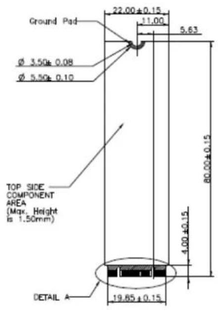
![1.50 MAX. 1.50 MAX. 4.00 [MIN.] 5.20 [MIN.] 0.80 ±0.08 DETAIL](/content/2026/06/1193632/images/0b1f4d734262c61a902ecd1943af01c9606e86f019073d2a5a68a2d859c64ef4.jpg)
![Ø 6.00 ± 0.10 Ground Pad Bottom Side Component Area (Max. Height is 1.50mm) 5.20 [MIN] DETAIL B](/content/2026/06/1193632/images/6068fd23b7939c19266a439b46e2ff7ed5777348dc6b091aa10f98819f99054a.jpg)
![18.50 0.50 [PITCH] 0.35± 0.04 C.L. 2.00 ±0.15 3.50 ±0.15 R 0.50± 0.15 1.20± 0.05 6.125 1.125 1.20 ±0.05 5.625](/content/2026/06/1193632/images/5c1694556c37cc36398b5b82eafd43dafe2171ec43210ed6a96ab2ccdddfd07d.jpg)
DETAIL A SCALE 2:1
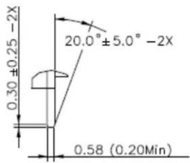
DETAIL C SCALE 2:1
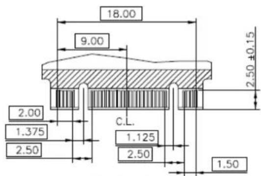
DETAIL B SCALE 2:1
Appendix: Part Number Table
| Product | Advantech PN |
| SQF M.2 2280 SATA SSD 840 (OPAL) 240G 3D NAND (0~70°C) | SQF-SM8V4-240G-SCC |
| SQF M.2 2280 SATA SSD 840 (OPAL) 480G 3D NAND (0~70°C) | SQF-SM8V4-480G-SCC |
| SQF M.2 2280 SATA SSD 840 (OPAL) 960G 3D NAND (0~70°C) | SQF-SM8V4-960G-SCC |
| SQF M.2 2280 SATA SSD 840 (OPAL) 1920G 3D NAND (0~70°C) | SQF-SM8V4-1K9G-SCC |
| SQF M.2 2280 SATA SSD 840 (OPAL) 240G 3D NAND (-40~85°C) | SQF-SM8V4-240G-SCE |
| SQF M.2 2280 SATA SSD 840 (OPAL) 480G 3D NAND (-40~85°C) | SQF-SM8V4-480G-SCE |
| SQF M.2 2280 SATA SSD 840 (OPAL) 960G 3D NAND (-40~85°C) | SQF-SM8V4-960G-SCE |
| SQF M.2 2280 SATA SSD 840 (OPAL) 1920G 3D NAND (-40~85°C) | SQF-SM8V4-1K9G-SCE |
- Overview
- Features
- ■ Standard SATA interface
- ■ Operating Voltage : 3.3V
- ■ Support LDPC with RAID ECC
- ■ TRIM、AHCI、AES256 and OPAL supported
- ■ Hardware Quick Erase supported (optional)
- ■ Voltage Stabilizer supported (optional)
- ■ Temperature Ranges
- ■ Mechanical Specification
- ■ Humidity
- ■ Data Retention
- ■ Acquired RoHS、WHQL、CE、FCC Certificate
- ■ Acoustic : 0 dB
- ■ Dimension : 80.8 mm x 22.0 mm x 3.8 mm
- Specification Table
- ■ Endurance
- TBW = [(NAND Endurance) x (SSD Capacity)] / WAF
- WAF = (Lifetime write to flash) / (Lifetime write to host)
- General Description
- ■ Error Correction Code (ECC)
- ■ Wear Leveling
- ■ Bad Block Management
- ■ Power Loss Protection
- - Flush Manager
- - Voltage Stabilizer
- TRIM
- ■ SMART
- ■ Over-Provision
- ■ Thermal Throttling
- Security Features
- ■ Advanced Encryption Standard (AES)
- ■ Secure / Quick Erase (optional)
- ■ TCG-OPAL 2.0 Compliance
- ■ Flash Vault
- Identify Device Data
- ATA Command Set
- [Command Set List]
- [Command Set Descriptions]
- CHECK POWER MODE (code: E5h);
- DOWNLOAD MICROCODE (code: 92h);
- EXECUTE DEVICE DIAGNOSTIC (code: 90h);
- FLUSH CACHE (code: E7h);
- FLUSH CACHE EXT (code: EAh);
- IDENTIFY DEVICE (code: ECh);
- IDLE (code: 97h or E3h);
- IDLE IMMEDIATE (code: E1h);
- INITIALIZE DEVICE PARAMETERS (code: 91h);
- NOP (code: 00h);
- READ BUFFER (code: E4h);
- READ DMA (code: C8h or C9h);
- READ DMA Ext (code: 25h);
- READ MULTIPLE (code: C4h);
- READ MULTIPLE EXT (code: 29h);
- READ NATIVE MAX ADDRESS (code: F8h);
- READ NATIVE MAX ADDRESS EXT (code: 27h);
- READ SECTOR(S) (code: 20h or 21h);
- READ SECTOR(S) EXT (code: 24h);
- READ VERIFY SECTOR(S) (code: 40h or 41h);
- READ VERIFY SECTOR(S) EXT (code: 42h);
- RECALIBRATE (code: 1Xh);
- SECURITY DISABLE PASSWORD (code: F6h);
- SECURITY ERASE PREPARE (code: F3h);
- SECURITY ERASE UNIT (code: F4h);
- SECURITY FREEZE LOCK (code: F5h);
- SECURITY SET PASSWORD (code: F1h);
- SECURITY UNLOCK (code: F2h);
- SEEK (code: 7Xh);
- SET MAX ADDRESS (code: F9h);
- SET MAX ADDRESS EXT (code: 37h);
- SET FEATURE (code: EFh);
- SET MULTIPLE MODE (code: C6h);
- SLEEP (code: 99h or E6h);
- WRITE MULTIPLE EXT (code: 39h);
- WRITE SECTOR(S) (code: 30h);
- WRITE SECTOR(S) EXT (code: 34h);
- WRITE SECTOR(S) W/O ERASE (code: 38h);
- WRITE VERIFY (code: 3Ch);
- System Power Consumption
- Supply Voltage
- Power Consumption
- Physical Dimension
Brand : Advantech
Model : SQF-SM8V4-240G-SCE
Category : SSD