SR1690WB - Computer Case INTEL - Free user manual and instructions
Find the device manual for free SR1690WB INTEL in PDF.

| Product Type | Computer Case |
| Brand | Intel |
| Model | SR1690WB |
| Form Factor | 1U Rackmount |
| Dimensions (W x H x D) | 17.2 x 1.7 x 20.1 inches (437 x 43 x 511 mm) |
| Weight | Approximately 15 lbs (6.8 kg) |
| Power Supply | Redundant 750W (optional) |
| Supported Motherboard | SSI CEB or proprietary Intel server board |
| Drive Bays | 2x 3.5" hot-swap SATA/SAS |
| Expansion Slots | 1x low-profile PCIe |
| Cooling | 4x 40mm dual-rotor fans |
| Front I/O | 2x USB 2.0 |
| Materials | Steel chassis, aluminum front bezel |
| Security | Lockable front door, chassis intrusion switch |
| Maintenance | Tool-less drive installation, hot-swap fans |
| Cleaning | Use dry compressed air; avoid liquids |
| Repairability | Spare parts available via Intel authorized distributors |
Frequently Asked Questions - SR1690WB INTEL
User questions about SR1690WB INTEL
0 question about this device. Answer the ones you know or ask your own.
Ask a new question about this device
Download the instructions for your Computer Case in PDF format for free! Find your manual SR1690WB - INTEL and take your electronic device back in hand. On this page are published all the documents necessary for the use of your device. SR1690WB by INTEL.
USER MANUAL SR1690WB INTEL
Intel® Server Board S5500WB
Technical Product Specification
Intel order number E53971-004
Revision 1.3
August 2009
Enterprise Platforms and Services Division
Revision History
| Date Revision Number | Modifications | |
| 03/30/2009 | 1.0 | Initial Release |
| 04/29/2009 | 1.1 | Formatting corrections |
| 05/20/2009 | 1.2 | Updated heatsink installation stepsCorrected processor fault tableAdded jumper location figure |
| 08/03/2009 1.3 | Updated memory supportCorrected PCIe slot speedRemoved S4 support | |
Disclaimers
Information in this document is provided in connection with Intel ^® products. No license, express or implied, by estoppel or otherwise, to any intellectual property rights is granted by this document. Except as provided in Intel's Terms and Conditions of Sale for such products, Intel assumes no liability whatsoever, and Intel disclaims any express or implied warranty, relating to sale and/or use of Intel products including liability or warranties relating to fitness for a particular purpose, merchantability, or infringement of any patent, copyright or other intellectual property right. Intel products are not intended for use in medical, life saving, or life sustaining applications. Intel may make changes to specifications and product descriptions at any time, without notice.
Designers must not rely on the absence or characteristics of any features or instructions marked "reserved" or "undefined." Intel reserves these for future definition and shall have no responsibility whatsoever for conflicts or incompatibilities arising from future changes to them.
This document contains information on products in the design phase of development. Do not finalize a design with this information. Revised information will be published when the product is available. Verify with your local sales office that you have the latest datasheet before finalizing a design.
This document may contain design defects or errors known as errata which may cause the product to deviate from published specifications. Current characterized errata are available on request.
This document and the software described in it are furnished under license and may only be used or copied in accordance with the terms of the license. The information in this manual is furnished for informational use only, is subject to change without notice, and should not be construed as a commitment by Intel Corporation. Intel Corporation assumes no responsibility or liability for any errors or inaccuracies that may appear in this document or any software that may be provided in association with this document.
Except as permitted by such license, no part of this document may be reproduced, stored in a retrieval system, or transmitted in any form or by any means without the express written consent of Intel Corporation.
Intel and Xeon are trademarks or registered trademarks of Intel Corporation.
*Other brands and names may be claimed as the property of others.
Copyright © Intel Corporation 2009
Table of Contents
1. Introduction ...... 1
1.1 Section Outline .... 1
1.2 Server Board Use Disclaimer .... 1
2. Server Board Overview....2
2.1 Intel ^® Server Board S5500WB Server Board....4
2.2 Server Board Connector and Component Layout....6
2.2.1 Board Rear Connector Placement....8
2.2.2 Server Board Mechanical Drawings 8
3. Functional Architecture....13
3.1 High Level Product Features 13
3.2 Functional Block Diagram....14
3.3 Intel ^® Xeon ^® 5500 Series....15
3.3.1 Processor Support....15
3.3.2 Processor Population Rules 15
3.3.3 Installing or Replacing the Processor 17
3.3.4 Intel ^ QuickPath Interconnect (Intel ^ QPI).... 20
3.4 Intel ^® QuickPath Memory Controller 21
3.4.1 Supported Memory 21
3.4.2 Memory Subsystem Nomenclature....22
3.4.3 ECC Support....23
3.4.4 Memory Reservation for Memory-mapped Functions....23
3.4.5 High-Memory Reclaim 23
3.4.6 Memory Population Rules....23
3.4.7 Installing and Removing Memory 24
3.4.8 Channel-Independent Mode 25
3.4.9 Memory RAS 25
3.4.10 Memory Error LED 26
3.5 Intel ^® 5500 Chipset IOH....26
3.5.1 IOH24D PCI Express* 27
3.6 Management Engine....28
3.7 Intel ^® 82801Jx I/O Controller Hub (ICH10R)....28
3.7.1 Serial ATA Support 29
3.7.2 USB 2.0 Support....29
3.8 Network Interface Controller (NIC) 30
3.8.1 MAC Address Definition....30
3.8.2 LAN Connector Ordering 31
3.9 Integrated Baseboard Management Controller....31
3.9.1 Integrated BMC Embedded LAN Channel 33
3.9.2 RMM3 Advanced Management Board: 33
3.10 Serial Ports 33
3.11 Wake-up Control 34
3.12 Integrated Video Support....34
3.12.1 Video Modes....34
3.12.2 Dual Video 34
3.12.3 Front Panel Video 35
3.13 I/O Slots 35
3.13.1 X16 Riser Slot Definition 35
3.13.2 PE WIDTH Strapping....35
3.13.3 Slot 1 PCI Express* x8 Connector....36
3.13.4 I/O Module Connector....36
-
Intel ^® I/O Expansion Modules....37
-
Platform Management Features....39
5.1 BIOS Feature Overview....39
5.1.1 EFI Support....39
5.1.2 Intel ^® Rapid Boot Toolkit....39
5.1.3 BIOS Recovery 39
5.2 BMC Feature Overview....39
5.2.1 Server Engines Pilot II Controller....40
5.2.2 BMC Firmware....40
5.2.3 BMC Basic Features....41
5.2.4 BMC Advanced Features....41
5.3 Management Engine (ME)....42
5.3.1 Overview....42
5.3.2 BMC - Management Engine Interaction....42
5.4 Data Center Manageability Interface 42
5.5 Other Platform Management 42
Table of Contents Intel® Server Board S5500WB TPS
5.5.1 Wake On LAN (WOL) 42
5.5.2 PCI Express* Power management 43
5.5.3 PMBus* 43
5.6 SMBUS Architecture Block 43
5.6.1 SMBUS Device Addresses 43
6. Configuration Jumpers....45
6.1.1 Force IBMC Update (J1B5) 46
6.1.2 Password Clear (J1C2)....47
6.1.3 BIOS Recovery Mode (J1C3) 48
6.1.4 Reset BIOS Configuration (J1B4)....49
6.1.5 Video Master (J6A3)....49
6.1.6 ME Firmware Force Update (J7A2)....50
6.1.7 Serial Interface (J6A2)....50
7. Connector / Header Locations and Pin-out....51
7.1 Power Connectors 51
7.2 System Management Headers 53
7.2.1 Intel ^ Remote Management Module 3 (Intel ^ RMM3) Connector....53
7.2.2 BMC Power Cycle Header (12V Only)....53
7.2.3 Hard Drive Activity (Input) LED Header 54
7.2.4 IPMB Header 54
7.2.5 SGPIO Header....54
7.3 SSI Control Panel Connector....54
7.3.1 Power Button 55
7.3.2 Reset Button....55
7.3.3 NMI Button....55
7.3.4 Chassis Identify Button....56
7.3.5 Power LED....56
7.3.6 System Status LED....56
7.3.7 Chassis ID LED 58
7.4 I/O Connectors....59
7.4.1 PCI Express* Connectors 59
7.4.2 VGA Connectors....61
7.4.3 NIC Connectors 62
7.4.4 SATA Connectors....63
7.4.5 Intel ^ I/O Expansion Module Connector 63
7.4.6 Serial Port Connectors....65
7.4.7 USB Connectors 65
7.5 Fan Headers....66
8. Intel Light-Guided Diagnostics....67
8.1 5-V Standby LED....67
8.2 Fan Fault LEDs....68
8.3 System Status LED....68
8.4 DIMM Fault LEDs 72
8.5 POST Code Diagnostic LEDs....73
8.6 Front Panel Support....74
9. Design and Environmental Specifications....75
9.1 Fan Speed Control Thermal Management 75
9.2 Thermal Sensors 77
9.2.1 Processor PECI Temperature Sensor 77
9.2.2 Memory Temperature Sensor....78
9.2.3 Board Temperature Sensor 78
9.2.4 Thermals Sensor Placement 78
9.3 Heatsinks....79
9.3.1 Unified Retention System Support....80
9.4 Errors....81
9.4.1 PROCHOT# 81
9.4.2 THERMTRIP#....81
9.4.3 CATERR# 81
10. Power Subsystem 82
10.1 Server Board Power Distribution 82
10.2 Power Supply Compatibility 82
10.3 Power Sequencing and Reset Distribution 83
11. Regulatory and Certification Information....84
11.1 Product Regulation Requirements....84
11.1.1 Product Safety Compliance 84
11.1.2 Product EMC Compliance – Class A Compliance 84
11.1.3 Certifications / Registrations / Declarations 84
11.2 Product Regulatory Compliance Markings 85
11.3 Electromagnetic Compatibility Notices 85
11.3.1 FCC Verification Statement (USA) 85
Table of Contents Intel® Server Board S5500WB TPS
11.3.2 ICES-003 (Canada) 86
11.3.3 Europe (CE Declaration of Conformity) 87
11.3.4 BSMI (Taiwan) 87
11.3.5 KCC (Korea) 87
Appendix A: POST Code LED Decoder....88
Appendix B: Video POST Code Errors....95
Glossary....99
Reference Documents....102
List of Figures
Figure 1. Intel ^® Server Board S5500WB 12V....4
Figure 2. Intel Server Board S5500WB SSI....5
Figure 3. Intel ^® Server Board S5500WB Components (both SKUs are shown) ......6
Figure 4. Rear Panel Connector Placement: 8
Figure 5. Baseboard and Mounting holes....9
Figure 6. Connector Locations....10
Figure 7. Primary Side Height Restrictions....11
Figure 8. Secondary Side Height Restrictions ...... 12
Figure 9. Intel ^® Server Board S5500WB Functional Block Diagram....14
Figure 10. Lifting the load lever of ILM cover....17
Figure 11. Removing the socket cover .... 18
Figure 12. Installing processor....18
Figure 13. Package Installation/Remove Feature....19
Figure 14. Installing/Removing Heatsink ....20
Figure 15. Intel ^® QPI Link....21
Figure 16. Memory Channel Population ......23
Figure 17. Installing Memory....24
Figure 18. Mirroring Memory Configuration ......26
Figure 19. Integrated BMC Hardware 33
Figure 20. S5500WB SMBUS Block Diagram ....43
Figure 21: Jumper Blocks (J1B5, J1C2, J1C3, J1B4, J6A3, J6A2, J7A2)....45
Figure 22: 5-V Standby Status LED Location 67
Figure 23. Fan Fault LED Locations ....68
Figure 24. System Status LED Location....69
Figure 25. DIMM Fault LEDs Locations....72
Figure 26. Rear Panel Diagnostic LEDs ....73
Figure 27: Thermal Zones....75
Figure 28: Location of Fan Connectors....76
Figure 29. Fans and Sensors Block Diagram ....77
Figure 30: Temp Sensor Location....79
Figure 31. Unified Retention System and Unified Backplate Assembly....80
List of Figures Intel® Server Board S5500WB TPS
Figure 32. Power Distribution Diagram....82
Figure 33. Diagnostic LED Placement Diagram 88
List of Tables
Table 1. Intel ^® Server Board S5500WB Feature Set ....2
Table 2. Intel ^® Server Board S5500WB System Interconnects....7
Table 3. Intel ^® Server Board S5500WB Features....13
Table 4. Mixed Processor Configurations....16
Table 5. DIMM Nomenclature....22
Table 6. IOH24D PCI Express* Bus Segments ......27
Table 7. NIC Status LED....30
Table 8. RMM3 Features ...... 33
Table 9. Supported Video Modes ...... 34
Table 10. Dual Video Options....35
Table 11. PEWIDTH Strapping Bits....35
Table 12. Intel ^® I/O Expansion Module Bus PEWIDTH Bits 36
Table 13. Intel ^® I/O Expansion Module Product Codes ...... 37
Table 14. Advanced Features....41
Table 15. SMBus Device Address Assignment ....43
Table 16: Server Board Jumpers (J1B5, J1C2, J1C3, J1B4, J6A3, J6A2)....46
Table 17. Force IBMC Update Jumper ...... 46
Table 18. Password Clear Jumper....47
Table 19. BIOS Recovery Mode Jumper ....48
Table 20. Reset BIOS Jumper....49
Table 21. Video Master Jumper....49
Table 22. SSI SKU 24-pin 2x12 Connector (J9B1)....51
Table 23. CPU 12V Power 2x4 Connector (J5K1)....51
Table 24. SSI Power Control (J9D1)....51
Table 25. 12-V only 2x4 Connector (replaces EPSD12V 2x12 connector) (J9D2)....51
Table 26. 12-V Only Power Control (replaces the 1x5 power control) (J9D1) (FOXCONN ELECTRONICS INC HF1107V-P1 or TYCO ELECTRONICS CORPORATION 5-104809-6)....52
Table 27. Peripheral Power (Only for 12-V only SKU) (J8K2) (iPN: C22293-003 MOLEX CONNECTOR CORPORATION 43045-0627)....52
Table 28. Intel ^® RMM3 Connector Pin-out (J5B1) 53
Table 29. BMC Power Cycle Header (J1D2)....53
Table 30. IPMB Header 4-pin (J1B2)....54
Table 31. SGPIO Header (J1B1)....54
Table 32. Front Panel SSI Standard 24-pin Connector Pin-out (J1E1) .....54
Table 33. Power LED Indicator States....56
Table 34. System Status LED....57
Table 35. Chassis ID LED Indicator States....58
Table 36. Slot 6 Riser Connector (J4B1)....59
Table 37. Slot 1 PCI Express* x8 Connector (J1B3) ......60
Table 38. VGA External Video Connector (J6A1)....61
Table 39. VGA Internal Video Connector (J1D1)....61
Table 40. RJ-45 10/100/1000 NIC Connector Pin-out (J8A2, J9A1) ......62
Table 41. SATA Connectors ......63
Table 42. 50-pin Intel ^® I/O Expansion Module Connector Pin-out (J2B1, J3B1) ...... 64
Table 43. External RJ-45 Serial Port A (COM1) (J7A1)....65
Table 44. Internal 9-pin Serial B (COM2) (J1A2)....65
Table 45. External USB Connector (J8A1, J9A1)....65
Table 46. Internal USB Connector (J1C1 and J9A2)....65
Table 47. Low-Profile Internal USB Connector (J1E2) ......66
Table 48. SSI 4-pin Fan Connector (J2K2, J2K3, J3K1, J7K1, J8K4, J8K5)....66
Table 49. 8-pin Fan Connector (J2K1 & J8K3) (MOLEX CONNECTOR CORPORATION 53398-0890 or 53398-0871)....66
Table 50. System Status LED....69
Table 51. Standard Front Panel Functionality....74
Table 52. Fan Connector Location & Detail....76
Table 53. Fan Connector Location & Detail....77
Table 54: Product Regulatory Compliance Markings....85
Table 55. POST Progress Code LED Example 89
Table 56. Diagnostic LED POST Code Decoder 90
Table 57. POST Error Messages and Handling....95
Table 58: Glossary....99
Intel® Server Board S5500WB TPS List of Tables
(This page intentionally left blank.)
1. Introduction
The Intel ^® Server Board S5500WB is a dual socket server using the Intel ^® Xeon ^® Processor 5500 series processor, in combination with the IOH and ICH10R to provide a balanced feature set between technology leadership and cost.
1.1 Section Outline
This document is divided into the following chapters:
• Section 1 – Introduction
• Section 2 – Server Board Overview
• Section 3 – Functional Architecture
• Section 4 – I/O Expansion Modules
• Section 5 – Platform Management Features
• Section 6 – Configuration Jumpers
• Section 7 – Connector and Header Location and Pin-out
• Section 8 – Intel ^® Light-Guided Diagnostics
• Section 9 – Design and Environmental Specifications
• Section 10 – Power Subsystem
• Section 11 - Regulatory and Certification Information
- Appendix A – POST Code LED Decoder
- Appendix B – Video POST Code Errors
1.2 Server Board Use Disclaimer
Intel Corporation server boards contain a number of high-density VLSI and power delivery components that need adequate airflow to cool. Intel ensures through its own chassis development and testing that when Intel server building blocks are used together, the fully integrated system will meet the intended thermal requirements of these components. It is the responsibility of the system integrator who chooses not to use Intel developed server building blocks to consult vendor datasheets and operating parameters to determine the amount of air flow required for their specific application and environmental conditions. Intel Corporation cannot be held responsible if components fail or the server board does not operate correctly when used outside any of their published operating or non-operating limits.
2. Server Board Overview
The Intel ^® Server Board S5500WB is a monolithic printed circuit board (PCB) with features designed to support the Internet Portal Data Center markets. The following table provides a high-level product feature list.
Table 1. Intel ^® Server Board S5500WB Feature Set
| Feature Description | |
| Processors Support for one or two Intel ^® Xeon ^® Processor 5500 series processors in FC-LGA1366 Socket B package with up to 95 W Thermal Design Power (TDP)Supports future processor compatibility guidelines4.8 GT/s, 5.86 GT/s, and 6.4 GT/s Intel ^® QuickPath Interconnect (Intel ^® QPI)Meets EVRD11.1 | |
| Memory Support for 800/1066/1333 MT/s ECC registered (RDIMM) or unbuffered (UDIMM)DDR3 memory.8 DIMMs total across six memory channels (three channels per processor in a 2:1:1 configuration)VRD optimized to support QR x8 DIMMsNo support for QR x4 DIMMs | |
| Chipset | Intel ^® 5500 Chipset IOHIntel ^® 82801Jx I/O Controller Hub (ICH10R) |
| I/O Control External connections:DB-15 Video connectorsRJ-45 serial Port A connectorRJ-45 connector for 10/100/1000 LANOne 2x USB 2.0 connectorsOne RJ-45 over USB for 10/100/1000 LANInternal connections:Two USB 2x5 pin header, supporting four USB 2.0 portsOne low-profile USB 2x5 pinOne DH-10 Serial Port B headerOne 2x8 pin VGA header with presence detection to switch from rear I/O video connectorSix SATA II connectorsIntel ^® I/O Expansion Module Dual ConnectorsOne RMM3 connector to support optional Intel ^® Remote Management Module 3SATA SW RAID 5 Activation Key ConnectorOne SSI-EEB compliant front panel header | |
| Power Connections | SSI SKUOne SSI-EEB compliant 24-pin main power connector (SSI only SKU)One SSI compliant 8-pin CPU power connectorOne SSI compliant 5-pin power control Connector (SSI only SKU)12-V Only SKUOne 8-pin power connectorOne 6-pin Aux power connector for 3.3 V and 5VOne 7-pin power control connector |
| System Fan Support | Two 8-pin fan headers for double rotor memory fans and six 4-pin fan headers supporting two processor zones and two memory zones in a redundant fashion |
| Add-in Adapter Support | One riser slot supporting both full-height and low-profile 1U and 2U MD2 PCI Express* x16 riser cards PCI gen2 Express* x8 w/ x16 connector.One riser slot supporting PCI Express* x8 riser cards PCI gen2 Express* x4 w/ x8 connector.Two Intel ^ I/O Expansion Module card connectors supporting double- and single-wide I/O modules. |
| Video Onboard ServerEngines* LLC Pilot II ControllerMatrox* G200 2D Video Graphics controllerUses 8 MB of the BMC 32 MB DDR2 Memory | |
| Hard Drive Support for six ICH10R SATA II portsOptional support for SW RAID 5 with activation key | |
| LAN Two 10/100/1000 ports provided by Intel ^ 82576 | |
| Server Management Onboard ServerEngines* LLC Pilot II Controller.Integrated Baseboard Management Controller (Integrated BMC), IPMI 2.0 compliantBasicBMC Controller: ARC 926E-S microcontrollerSuper IO: Serial Port logic, legacy interfaces, LPC interface, Port80Hardware Monitoring: Fan speed control and voltage monitoringAdvancedVideo and USB compression and redirectionNC-SI port, a high-speed sideband management interfaceIntegrated Super I/O on LPC interface | |
2.1 Intel ^® Server Board S5500WB Server Board
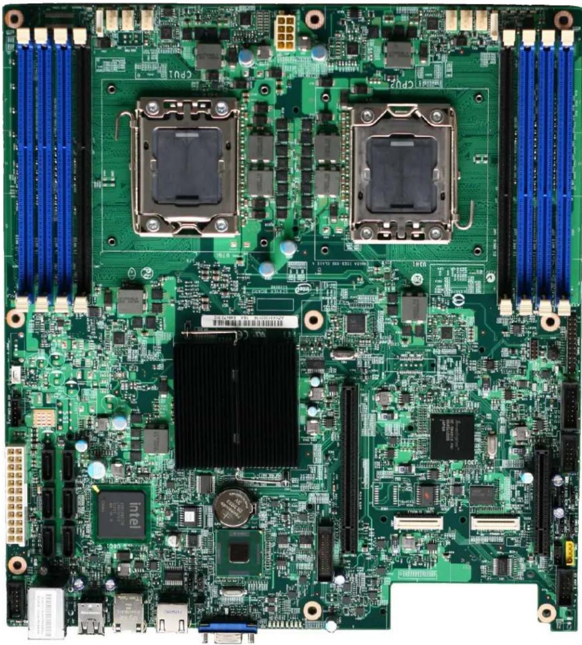
The Intel ^® Server Board S5500WB has two board SKUs. An SSI-compliant and a 12-V only SKU. The board layouts of the SKUs are shown.
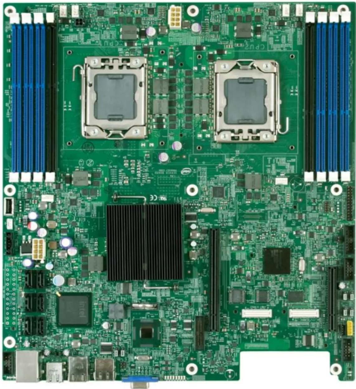
natural_image
Green printed circuit board with multiple CPU monitors and various connectors (no readable text or symbols)Figure 1. Intel® Server Board S5500WB 12V
natural_image
Close-up of a green computer motherboard with multiple CPU monitors and connectors (no readable text or symbols)Figure 2. Intel Server Board S5500WB SSI
2.2 Server Board Connector and Component Layout
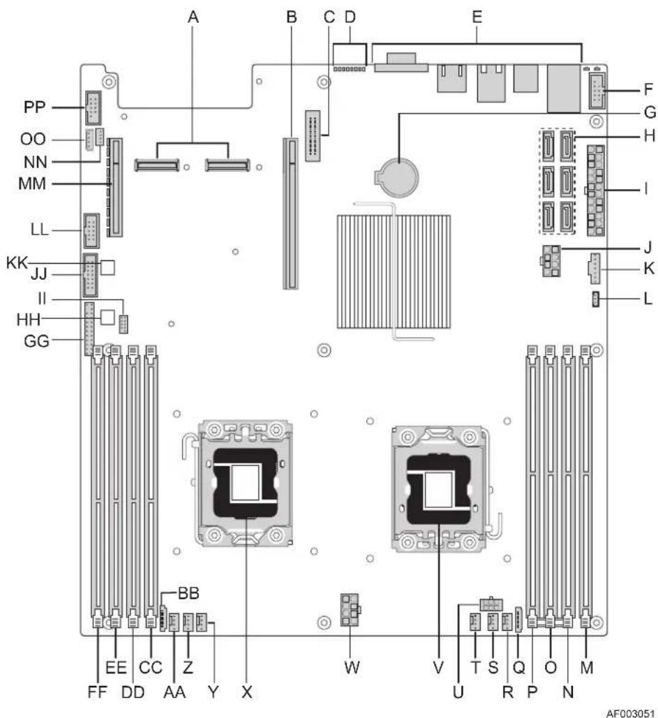
Figure 3. Intel ^® Server Board S5500WB Components (both SKUs are shown)
Table 2. Intel ^® Server Board S5500WB System Interconnects
| Description Description | |||
| A | Dual InNO Expansion Module Connectors | V Processor Socket 1 | |
| B PCI Express x16 Gen2 W 8 Pin CPU Connector | |||
| C Remote Management Module 3 X Processor Socket 2 | |||
| D POST Code LEDs Y 4-pin Fan Connector (CPU2) | |||
| E External I/O Z 4-pin Fan Connector (CPU2A) | |||
| F USB Connector | AA | 4-pin Fan Connector (MEM2) | |
| G Battery | BB | 8-pin Fan Connector (MEM2R) | |
| H SATA Connectors | CC | DIMM Slot D2 | |
| I 24 Pin Connector (SSI only) | DD | DIMM Slot D1 | |
| J 8 Pin Connector (12V only) | EE | DIMM Slot E1 | |
| K Aux Power (5-pin or 7-pin) | FF | DIMM Slot F1 | |
| L RAID Key | GG | Front Panel Connector | |
| M DIMM Slot C1 | HH | HDD LED Header | |
| N DIMM Slot B1 | II | Low-Profile USB Connector | |
| O DIMM Slot A1 | JJ | Internal VGA Connector | |
| P DIMM Slot A2 | KK | BMC Power Cycle Header (12V Only) | |
| Q 8-pin Fan Connector (MEM1R) | LL | USB Connector | |
| R 4-pin Fan Connector (MEM1) | MM | Slot 1 PCI Express x8 Gen2 | |
| S 4-pin Fan Connector (CPU1A) | NN | SGPIO Connector | |
| T 4-pin Fan Connector (CPU1) | OO | IMPB Connector | |
| U HDD Power Connector (12V only) | PP | Serial Port B | |
2.2.1 Board Rear Connector Placement
The Intel ^® Server Board S5500WB has the following board rear connector placement:
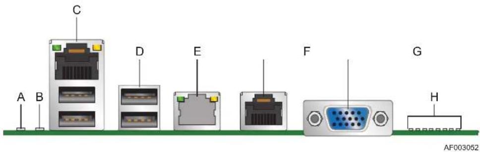
Figure 4. Rear Panel Connector Placement:
| Description Description | ||
| A ID LED E RJ-45 GbE LAN connector | ||
| B Status LED F RJ-45 Serial port connector | ||
| C RJ-45 GbE/Dual USB connector G | DB15 Video | |
| D Dual USB connector H | Diagnostic LEDs | |
2.2.2 Server Board Mechanical Drawings
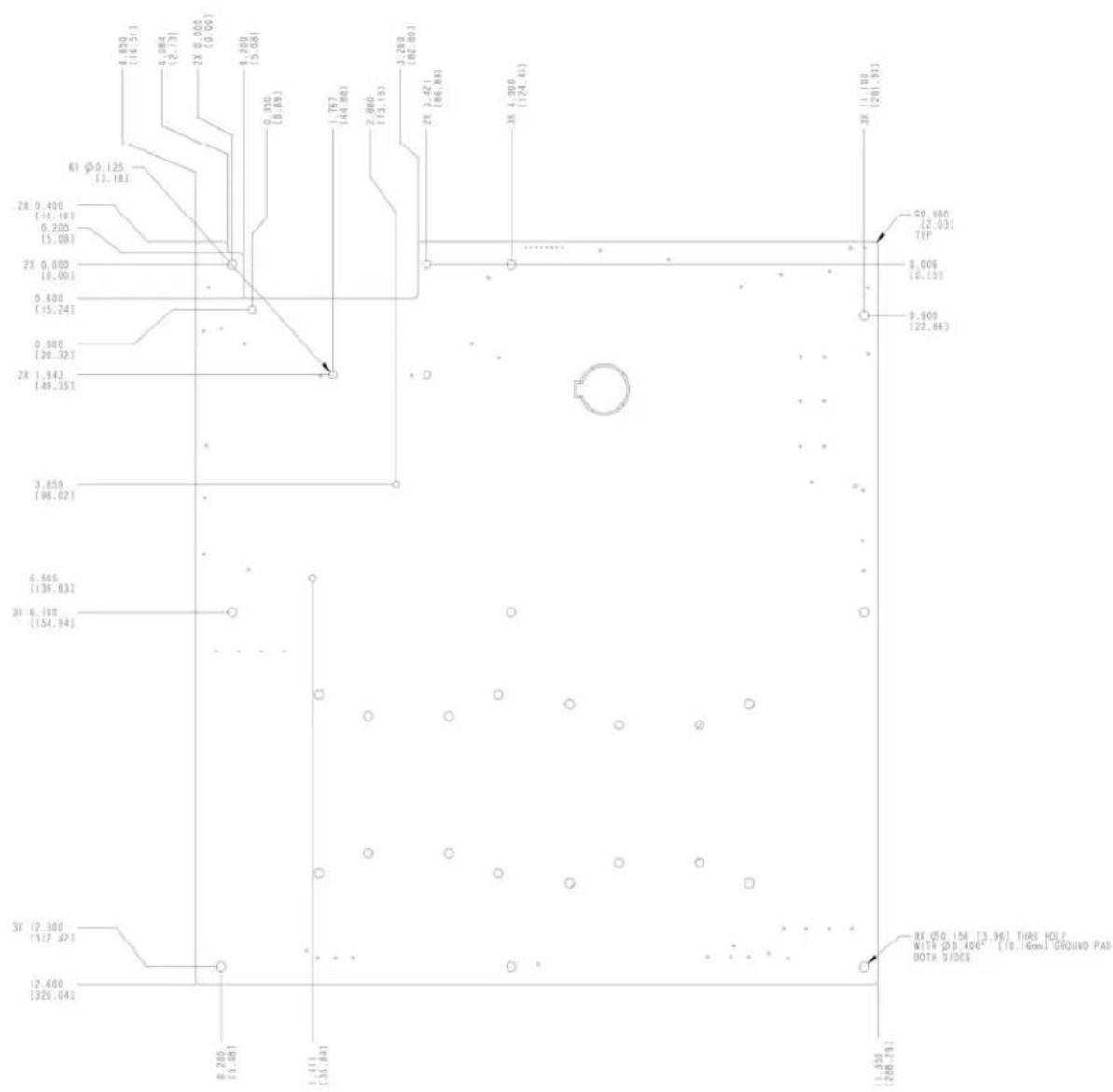
The following figures are mechanical drawings for the Intel ^® Server Board S5500WB.
other
| Dimension | Value | | --------- | ----- | | 0.800 [16.5] | 0.894 | | 0.200 [2.13] | 0.200 | | 0.800 [5.08] | 0.335 | | 1.767 [44.88] | 1.767 | | 2.880 [73.13] | 2.880 | | 3.263 [82.80] | 3.263 | | 2X 2.421 [86.88] | 2X 2.421 | | 3X 4.900 [174.41] | 3X 4.900 | | 3X 11.180 [291.91] | 3X 11.180 | | 5X 980 [2.03] TFP | 5X 980 | | 8.006 [6.15] | 8.006 | | 9.900 [22.98] | 9.900 | | 3X 6.100 [154.94] | 3X 6.100 | | 6.666 [138.63] | 6.666 | | 3X 6.100 [154.94] | 3X 6.100 | | 2X 1.94 [49.35] | 2X 1.94 | | 3X (2.300) [117.97] | 3X (2.300) | | 2X (2.600) [326.04] | 2X (2.600) | | 8.285 [5.08] | 8.285 | | 1.411 [35.84] | 1.411 | | HTB HOLT WITH DOTS SIDE OF ZENZHEN (286,73) | HTB HOLT WITH DOTS SIDE OF ZENZHEN (286,73) |Figure 5. Baseboard and Mounting holes
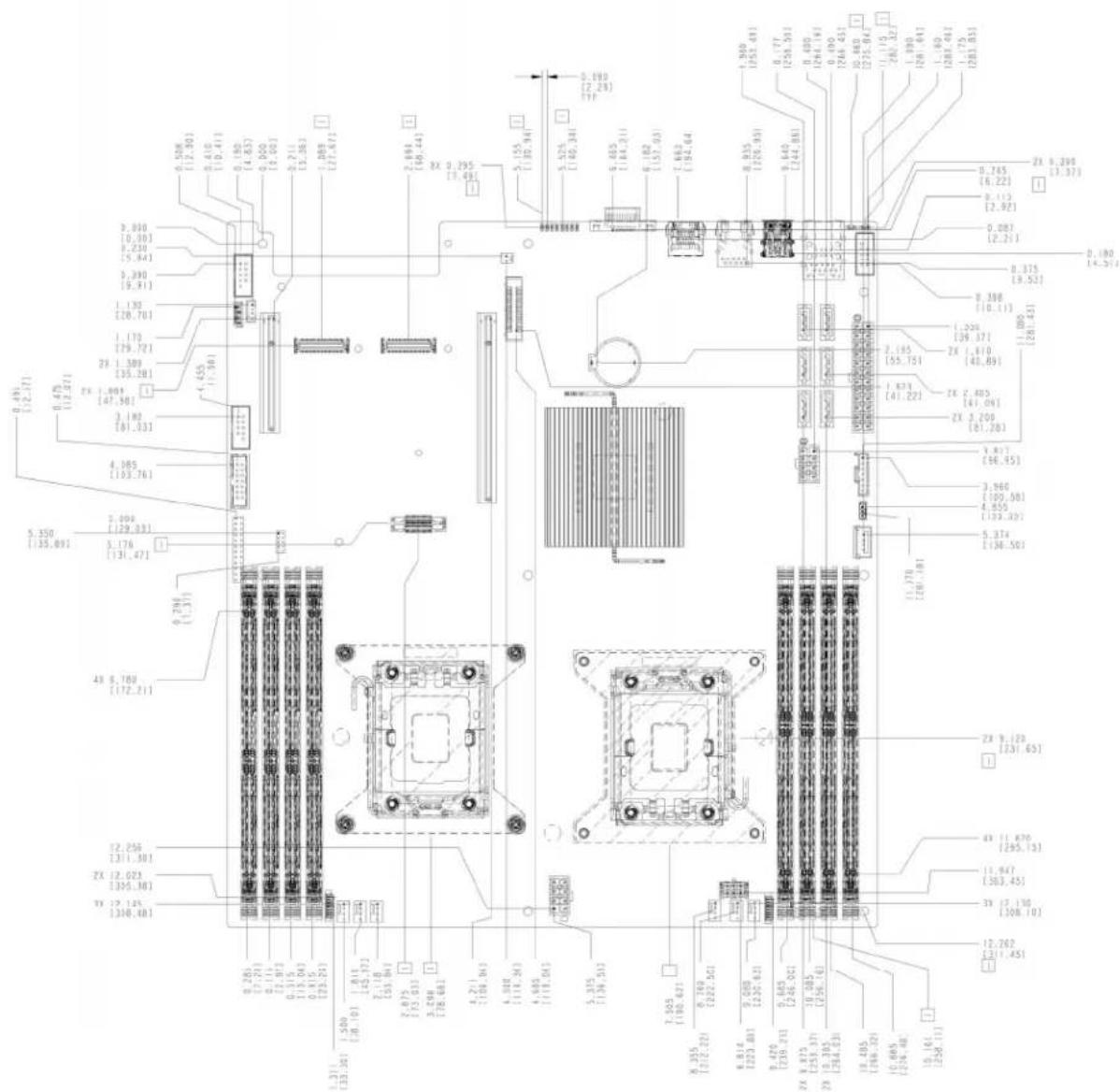
Figure 6. Connector Locations
![MAX COMPONENT HEIGHT UNDER SAS MODULE IS .138" [3.5mm] MAX COMPONENT HEIGHT UNDER SAS MODULE IS .138" [3.5mm] MAX COMPONENT HIHT ON PCI-1 CARD IS .300" [7.62mm] MAX COMPONENT HEIGHT UNDER RMM3 MODULE IS .102" [2.60mm] MAX COMPONENT ALLOWED UNDER RMM3 CONNECTOR IS .138" [3.5mm] MAX COMPONENT HEIGHT FOR PCI LOCK TAB IS .250" [6.35mm] 2 PLACES 0.250 [8.35] 0.600 [15.24] 2X 0.871 [22.12] 1.900 [40.24] 2X 0.400 [10.29] 4.430 [112.52] 4.781 [121.44] 5.649 [142.48] TILERSBURG HEATSINE KEEPOUTS SHOWN FOR REFERENCE ONLY MAX COMPONENT HEIGHT UNDER PCI CARD ZONE IS .0.600" [15.2mm] MAX COMPONENT HEIGHT UNDER PCI CARD ZONE IS .0.600" [15.2mm] MAX COMPONENT HEIGHT UNDER PCI CARD ZONE IS .0.600" [15.2mm] MAX COMPONENT HEIGHT UNDER CPU HEATSINN .293" [7.45mm] 2 PLACES](/content/2026/06/1185871/images/0520e43d29e8e80be425996c59c4b915629505bf57eeb4292ff071b16c703d2b.jpg)
Figure 7. Primary Side Height Restrictions
![MAX COMPONENT HEIGHT ALLOWED IN THIS ZONE IS .050" [1.23mm] 0.250 [234,91] 7.400 [187,91] 5.731 [145,971] 7.550 [135,89] 1.450 [36,83] [1,325] [33,467] 0.000 [0,80] 0.000 [0,80] 0.600 TYP [15,241] 0.800 TYP [20,323] 0.200 TYP [5,583] 7.510 [190,751] 0.160 [29,48] TYP 2X 7.340 [189,633] SUNPER TARGET- E PLACES 10.850 [235,591] 0.100 [241,14] Ø2.000 [50,80] TYP BACKING PLATE ZONE NO COMPONENTS ALLOWED SHOWN FOR REFERENCE ONLY](/content/2026/06/1185871/images/98621118015bbd07e3e45a1fbe6a018bbe49948eebf0d19f27ea4af4d5a04cd2.jpg)
Figure 8. Secondary Side Height Restrictions
3. Functional Architecture
The Intel ^® Server Board S5500WB is a purpose build, power-optimized server used in a 1U rack. Memory and processor socket placement is made to minimize the amount of fan power required to cool these components. Voltage Regulators (VRDs) are optimized for a particular range of memory and CPU power that suits the target Internet Portal Datacenter (IPDC) segment of the market. The VRDs are also designed to be highly power-efficient, balancing the needs of being small in size and also cost-effective. There are two SKUs: a 12-V only SKU and an SSI-compliant SKU.
3.1 High Level Product Features
Table 3. Intel ^® Server Board S5500WB Features
| Board S5500WB 12V S5500WB SSI | ||
| Form Factor EATX 12" x 13" EATX 12" x 13" | ||
| CPU Socket B B | ||
| Chipset | Intel® 5500 Chipset IOHIntel® 82801Jx I/O Controller Hub (ICH10R) | Intel® 5500 Chipset IOHIntel® 82801Jx I/O Controller Hub (ICH10R) |
| Memory 8 RDIMMs or | 8 UDIMMs DDR3 8 RDIMMs or 8 UDIMMs D | DR3 |
| Slots | 1 PCI Express* x8 w/ x16 connector1 PCI Express* x4 w/ x8 connector | 1 PCI Express* x8 w/ x16 connector1 PCI Express* x4 w/ x8 connector |
| Ethernet Dual GbE, Intel | ® 82576 Gigabit Ethernet Dual | GbE, Intel ® 82576 Gigabit Ethernet |
| Storage Six SATA II ports (3Gb/s) | Six SATA II ports (3Gb/s) | |
| SAS | One (1) 4-port SAS module on IOM connector (optional) | One (1) 4-port SAS module on IOM connector (optional) |
| I/O Module | Yes, single- and double-wide | Yes, single- and double-wide |
| SW RAID | LSI SW RAID 0,1,5,10 | LSI SW RAID 0,1,5,10 |
| Processor Support | 95 W, optimized for 80 W | 95 W, optimized for 80 W |
| Video | Integrated in BMC | Integrated in BMC |
| ISM | iBMC w/ IPMI 2.0 support | iBMC w/ IPMI 2.0 support |
| Chassis* | Reference | Reference |
| Power Supply | 12 V and 5 VS/B PMBus* | 12 V, 5 V, 3.3 V, 5 VSB, PMBus* |
*Referenced Chassis: Chenbro RM13204 Chassis and Intel® Server System SR1690WB
3.2 Functional Block Diagram
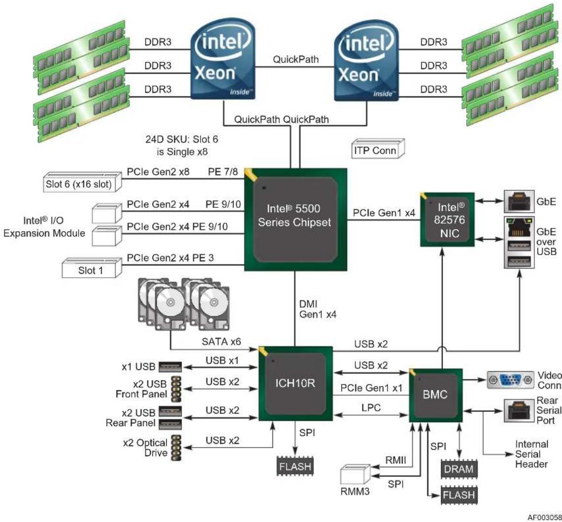
flowchart
graph TD
    subgraph Intel®_I/O_Expansion["Intel® I/O Expansion Module"]
        A["DDR3"] --> B["intel Xeon inside"]
        C["DDR3"] --> D["intel Xeon inside"]
        B --> E["QuickPath"]
        D --> E
        E --> F["24D SKU: Slot 6 is Single x8"]
        G["Slot 1"] --> H["PCIe Gen2 x4 PE 9/10"]
        H --> I["PCIe Gen2 x4 PE 3"]
        J["PCIe Gen2 x8 PE 7/8"] --> K["Intel® 5500 Series Chipset"]
    end

    subgraph ICH10R
        L["SATA x6"] --> M["ICH10R"]
        N["x1 USB"] --> O["USB x1"]
        P["x2 USB Front Panel"] --> Q["USB x2"]
        R["x2 USB Rear Panel"] --> S["USB x2"]
        T["x2 Optical Drive"] --> U["USB x2"]
    end

    subgraph BMC
        V["DRAM"] --> W["Internal Serial Header"]
        X["RMM3"] --> Y["SPI"]
        Z["RF"] --> AA["RF"]
        AB["RF"] --> AC["RF"]
        AD["RF"] --> AE["RF"]
        AF["RF"] --> AG["RF"]
        AH["RF"] --> AI["RF"]
        AJ["RF"] --> AK["RF"]
        AL["RF"] --> AM["RF"]
        AN["RF"] --> AO["RF"]
        AP["RF"] --> AQ["RF"]
        AR["RF"] --> AS["RF"]
        AT["RF"] --> AU["RF"]
        AV["RF"] --> AW["RF"]
        AX["RF"] --> AY["RF"]
        AZ["RF"] --> BA["RF"]
        BB["RF"] --> BC["RF"]
        BD["RF"] --> BE["RF"]
        BF["RF"] --> BG["RF"]
        BH["RF"] --> BI["RF"]
        BJ["RF"] --> BK["RF"]
        BL["RF"] --> BM["RF"]
    end

    subgraph BMC
        BN["PCIe Gen1 x4"] --> BO["Intel® 82576 NIC"]
        BP["PCIe Gen1 x1"] --> BMC
        BMC --> BR["BMC"]
    end

    subgraph ICH10R
        BS["SPI"] --> BT["FLASH"]
    end

    subgraph BMC
        BU["USB x2"] --> BV["PCIe Gen1 x1"]
        BW["LPC"] --> BX["PCIe Gen1 x1"]
    end

    subgraph ICH10R
        BY["SPI"] --> BMC
    end

    subgraph BMC
        BMC --> BC["GbE over USB"]
        BC --> BD
    end

    subgraph ICH10R
        BD --> BD
    end

    subgraph BMC
        BD --> BD
    end

    subgraph ICH10R
        BMC --> BD
    end

    subgraph BMC
        BMC --> DC["GbE over USB"]
        DC --> DB
    end

    subgraph ICH10R
        BMC --> DC
    end

    subgraph BMC
        BMC --> DC
    end

    subgraph ICH10R
        BMC --> DC
    end

    subgraph BMC
        BMC --> DC
    end

    subgraph ICH10R
        BMC --> DC
    end

    subgraph BMC
        BMC --> DC
    end

    subgraph ICH10R
        BMC --> DC
    end

    subgraph BMC
        BMC --> DC
    end
Figure 9. Intel ^® Server Board S5500WB Functional Block Diagram
3.3 Intel ^® Xeon ^® 5500 Series
The Intel ^® 5500 series processors are the first-generation server/workstation processor to implement the following key new technologies:
- Intel® QuickPath Memory Controller
- Point-to-point link interface based on the Intel ^ QuickPath Interconnect (Intel ^ QPI), which was formerly known as the Common System Interface (CSI).
The Intel ^® 5500 series processor is a series of multi-core processors based on the 45 nm process technology. Processor features vary by SKU and include up to two Intel ^® QPI point-to-point links capable of up to 6.4 GT/s, up to 8 MB of shared cache, and an integrated memory controller.
The processor family supports Streaming SIMD Extensions 2 (SSE2), Streaming SIMD Extensions 3 (SSE3), and Streaming SIMD Extensions 4 (SSE4). It also supports the following advanced technologies: Execute Disable Bit, Intel ^® 64 Technology, Enhanced Intel ^® SpeedStep ^® Technology, Intel ^® Virtualization Technology (Intel ^® VT), and Intel ^® Hyper threading.
3.3.1 Processor Support
The server board supports the following processors:
- One or two Intel ^ 5500 series processor(s) in FC-LGA 1366 socket B package with 4.8 GT/s, 5.86 GT/s, or 6.4 GT/s Intel ^ QPI.
- Up to 95 W Thermal Design Power (TDP)
- 80-W Processor only supports Intel ^ QPI up to 5.86 GT/s and DDR3 at 1067 MHz or lower
• Supports Low Voltage (LV) processors
The server board does not support previous generations of the Intel® Xeon® Processors.
3.3.2 Processor Population Rules
For optimum performance, when two processors are installed, both must be the identical revision and have the same core voltage and Intel ^® QPI/core speed. When only one processor is installed, it must be in the socket labeled CPU1. The other socket must be empty. You must populate processors in sequential order. Therefore, you must populate processor socket 1 (CPU1) before processor socket 2 (CPU2).
When a single processor is installed, no terminator is required in the second processor socket.
3.3.2.1 Mixed Processor Configurations
The following table describes mixed processor conditions and recommended actions for all Intel ^® server boards and systems that use the Intel ^® 5500 Chipset. The errors fall into one of the following two categories:
- Fatal: If the system can boot, it goes directly to the error manager, regardless of whether the Post Error Pause setup option is enabled or disabled.
- Major: If the Post Error Pause setup option is enabled, the system goes directly to the error manager. Otherwise, the system continues to boot and no prompt is given for the error. The error is logged to the error manager.
Table 4. Mixed Processor Configurations
| Error Severity System Action | ||
| Processor family not identical | Fatal | The BIOS detects the error condition and responds as follows:Logs the error into the system event log (SEL).Alerts the Integrated BMC of the configuration error with an IPMI command.Does not disable the processor.Displays “0194: Processor family mismatch detected” message in the error manager.Halts the system. |
| Processor cache not identical | Fatal The BIOS detects the error condition and responds as follows:Logs the error into the SEL.Alerts the Integrated BMC of the configuration error with an IPMI command.Does not disable the processor.Displays “0192: Cache size mismatch detected” message in the error manager.Halts the system. | |
| Processor frequency (speed) not identical | Major The BIOS detects the error condition and responds as follows:Adjusts all processor frequencies to the lowest common denominator.Continues to boot the system successfully.If the frequencies for all processors cannot be adjusted to be the same, then the BIOS:Logs the error into the SEL.Displays “0197: Processor speeds mismatched” message in the error manager.Halts the system. | |
| Processor microcode missing | Minor The BIOS detects the error condition and responds as follows:Logs the error into the SEL.Does not disable the processor.Displays “816x: Processor 0x unable to apply microcode update” message in the error manager.The system continues to boot in a degraded state, regardless of the setting of POST Error Pause in the Setup. | |
| Processor Intel® QuickPath Interconnect speeds not identical | Halt | The BIOS detects the error condition and responds as follows:Adjusts all processor interconnect frequencies to lowest common denominator.Logs the error into the SEL.Alerts the Integrated BMC about the configuration error.Does not disable the processor.Displays “0195: Processor 0x Intel(R) QPI speed mismatch” message in the Error Manager.If POST Error Pause is disabled in the Setup, continues to boot in a degraded state.If POST Error Pause is enabled in the Setup, pauses the system, but can continue to boot if operator directs. |
3.3.3 Installing or Replacing the Processor
3.3.3.1 Installing the Processor
To install a processor, follow these instructions:
- Turn off all peripheral devices connected to the server.
- Turn off the server.
- Disconnect the AC power cord from the server.
- Remove the server's cover. See the document that came with your server chassis for instructions on removing the server's cover.
- Locate the processor socket and raise the raise the load lever of the ILM cover completely. (see letter "A" in the figure below)
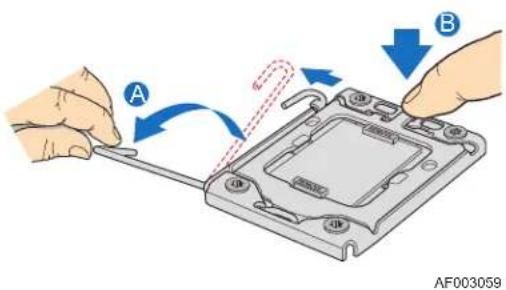
Figure 10. Lifting the load lever of ILM cover
- Open the load plate (see letter "B" in Figure 10 and letter "C" in Figure 11).
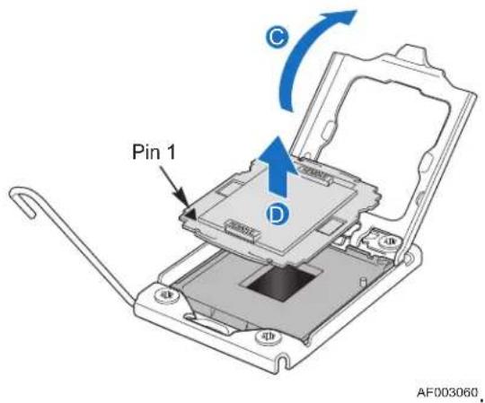
Figure 11. Removing the socket cover
- Remove the protective socket cover. (See letter "D" in Figure 11)
- Align the pins of the processor with the socket and insert the processor into the socket.
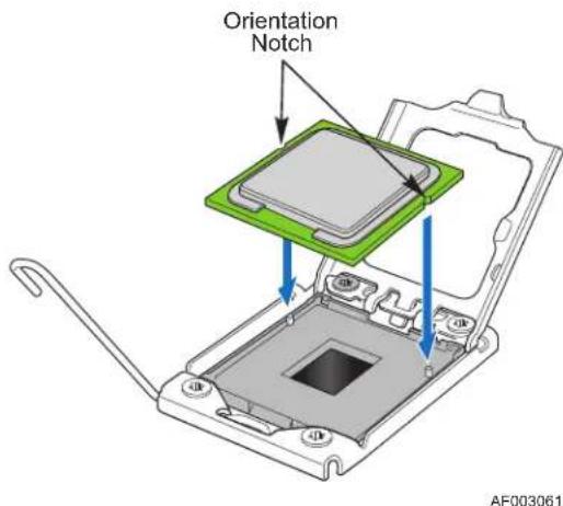
Figure 12. Installing processor
- Lower the load plate and load lever of the ILM cover completely.
NOTE:
Make sure the alignment triangle mark and the alignment triangle cutout align correctly. To assist in package orientation and alignment with the socket:
A. The package Pin1 triangle and the socket Pin1 chamfer provide a visual reference for proper orientation.
B. The package substrate has orientation notches along two opposing edges of the package offset from the centerline. The socket has two corresponding orientation
posts to physically prevent mis-orientation of the package. These orientation features also provide an initial rough alignment of the package to the socket.
C. The socket has alignment walls at the four corners to provide final alignment of the package.
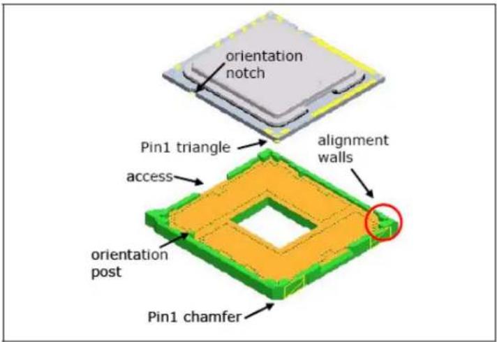
Figure 13. Package Installation/Remove Feature
3.3.3.2 Installing the Processor Heatsink(s)
CAUTION: The heatsink has Thermal Interface Material (TIM) located on the bottom of it. Use caution when you unpack the heatsink so you do not damage the TIM
To install the heatsink, follow these steps:
- Remove the protective film on the TIM if present.
- Orient the heatsink over the processor as shown in Figure 15. The heatsink fins must be positioned as shown to provide correct airflow through the system.
- Set the heatsink over the processor, lining up the four captive screws with the four posts surrounding the processor.
- Loosely screw in the captive screws on the heatsink corners in a diagonal manner according to the numbers shown in as follows:
a) Starting with the screw at location 1, engage the screw threads by giving it two rotations in the clockwise direction and stop. (IMPORTANT: Do not fully tighten.)
b) Proceed to the screw at location 2 and engage the screw threads by giving it two rotations and stop.
c) Engage screws at locations 3 and 4 by giving each screw two rotations and then stop.
d) Repeat steps 4a through 4c by giving each screw two rotations each time until all screws are lightly tightened up to a maximum of 8 inch-lbs torque.
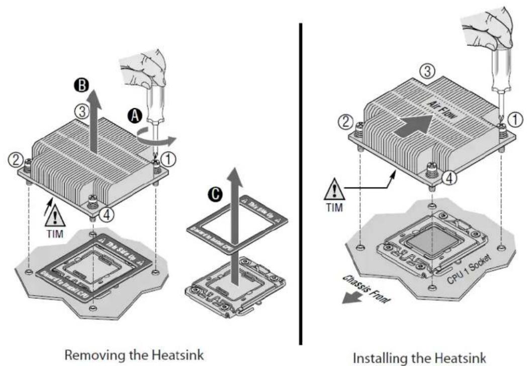
Figure 14. Installing/Removing Heatsink
3.3.3.3 Removing the Processor Heatsink
To remove the heatsink, follow these steps:
- Loosen the four captive screws on the heatsink corners in a diagonal manner according to the numbers shown in Figure 1 as follows:
a) Starting with the screw at location 1, loosen it by giving it two rotations in the anticlockwise direction and stop. (IMPORTANT: Do not fully loosen.)
b) Proceed to the screw at location 2 and loosen it by giving it two rotations and stop.
c) Loosen screws at locations 3 and 4 by giving each screw two rotations and then stop.
d) Repeat steps 1a through 1c by giving each screw two rotations each time until all screws are loosened.
- Lift the heatsink from the board.
3.3.4 Intel ^® QuickPath Interconnect (Intel ^® QPI)
Intel ^® QPI is a cache-coherent, link-based interconnect specification for processor, chipset, and I/O bridge components. You can use it in a wide variety of desktop, mobile, and server platforms spanning IA-32 and Intel ^® Itanium ^® architectures. Intel ^® QPI also provides support for high-performance I/O transfer between I/O nodes. It allows connection to standard I/O buses such as
PCI Express*, PCI-X*, PCI (including peer-to-peer communication support), AGP (Accelerated Graphics Port), and so forth, through the appropriate bridges.
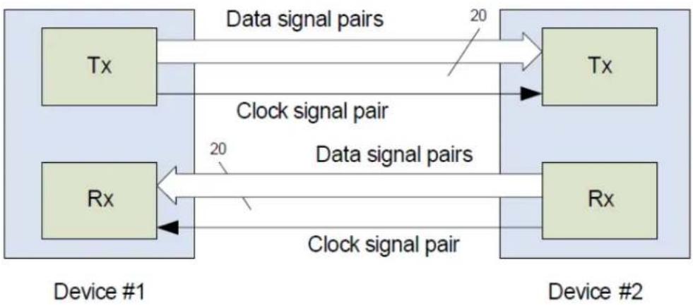
Each Intel ^® QPI link consists of 20 pairs of uni-directional differential lanes for the transmitter and receiver plus a differential forwarded clock. A full-width Intel ^® QPI link pair consists of 84 signals (20 differential pairs in each direction) plus a forwarded differential clock in each direction. Each Intel ^® 5500 series processor supports two Intel ^® QPI links, one going to the second processor and one going to the Intel ^® 5500 chipset IOH.
flowchart
graph LR
    A["Tx"] -->|Data signal pairs| B["Tx"]
    C["Rx"] -->|Clock signal pair| D["Rx"]
    B -->|20s Delay| B
    D -->|Clock signal pair| D
    style A fill:#d4edda,stroke:#333
    style C fill:#d4edda,stroke:#333
    style B fill:#d4edda,stroke:#333
    style D fill:#d4edda,stroke:#333
Figure 15. Intel® QPI Link
In the current implementation, Intel ^® QPI ports are capable of operating at transfer rates of up to 6.4 GT/s. Intel ^® QPI ports operate at multiple lane widths (full - 20 lanes, half - 10 lanes, and quarter - 5 lanes) independently in each direction between a pair of devices communicating via the Intel ^® QPI. The server boards support full-width communication only.
For more information see the Intel® QPI Overview Rev 1.04 (Document#: 380531)
3.4 Intel ^® QuickPath Memory Controller
The Intel ^® 5500 series processor has an integrated memory controller on its package. Each Intel ^® 5500 Series processor produces up to three channels of DDR3 memory. The Intel ^® QPI Memory Controller supports DDR3 800, DDR3 1066, and DDR3 1333 memory technologies. The memory controller supports both Registered DIMMs (RDIMMs) and Unbuffered DIMMs (UDIMMs).
Mixing of RDIMMs and UDIMMs is not supported.
3.4.1 Supported Memory
The Intel ^® Server Board S5500WB supports six DDR3 memory channels (three per processor socket) with two DIMMs on the first channel and one DIMM on the second and third channels of each processor. Therefore, the server board supports up to 8 DIMMs with dual-processor sockets with a maximum memory capacity of 64 GB.
The server board supports DDR3 800, DDR3 1067, and DDR3 1333 memory technologies. Memory modules of mixed speed are supported by automatic selection of the highest common frequency of all memory modules.
The following configurations are not supported, validated or recommended:
- Mixing of RDIMMs and UDIMMs is not supported
- Mixing of memory type, size, speed and/or rank has not been validated and is not supported
- Mixing memory vendors has not been validated and is not recommended
• Non-ECC memory has not been validated and is not supported in a server environment
NOTE: Mixed memory is not tested or supported. Non-ECC memory is not tested and is not recommended for use in a server environment
The Intel ^® Server Board S5500WB uses a 2:1:1 memory DIMM layout. A 2:1:1 layout was chosen for its lowest power for a particular bandwidth and because it allows the maximum possible bandwidth when a 1:1:1 memory population is used.
3.4.2 Memory Subsystem Nomenclature
DIMMs are organized into physical slots on DDR3 memory channels that belong to processor sockets.
The memory channels from socket 1 are identified as Channels A, B, and C. The memory channels from socket 2 are identified as Channels D, E, and F.
The DIMM identifiers on the silkscreen on the board provide information about the channel, and, therefore the processor, to which they belong. For example, DIMM_A1 is the first slot on Channel A on processor 1; DIMM_D1 is the first DIMM socket on Channel D on processor 2.
Table 5. DIMM Nomenclature
| Processor Socket 1 Processor Socket 2 | |||||||
| Channel A | Channel B Channel C Channel D Channel E Channel F | ||||||
| A1 | A2 | B1 | C1 | D1 | D2 | E1 | F1 |
If the socket is not populated, the memory slots associated with a processor socket are unavailable.
You can install a processor without populating the associated memory slots provided a second processor is installed with associated memory. In this case, the memory is shared by the processors. However, the platform suffers performance degradation and latency due to the remote memory.
Sockets are self-contained and autonomous. However, all configurations in the BIOS setup such as RAS, Error Management, and so forth, are applied commonly across sockets.
3.4.3 ECC Support
If at least one non-ECC DIMM is present in the system, the system reverts to non-ECC mode. UDIMMs can be ECC or non-ECC; RDIMMs are always ECC enabled. Non-ECC DIMMs are not validated and not recommended for server use.
3.4.4 Memory Reservation for Memory-mapped Functions
A region of size 40 MB of memory below 4 GB is always reserved for mapping chipset, processor, and BIOS (flash) memory-mapped I/O regions. This region displays as a loss of memory to the operating system. In addition to this loss, the BIOS creates another reserved region for memory-mapped PCI Express* functions, including a standard 64 MB or 256 MB of standard PCI Express* Memory Mapped I/O (MMIO) configuration space. This is based on the setup selection using the MAX_BUS_NUMBER feature offered by Intel® Tylersburg IOH chipset and a variably sized MMIO region for the PCI Express* functions.
All these reserved regions are reclaimed by the operating system if Physical Address Extension (PAE) is turned on in the operating system.
3.4.5 High-Memory Reclaim
When 4 GB or more of physical memory is installed (physical memory is the memory installed as DDR3 DIMMs), the reserved memory is lost. However, the Intel ^® 5500 Series Chipset provides a feature called high-memory reclaim, which allows the BIOS and operating system to remap the lost physical memory into system memory above 4 GB (the system memory is the memory that can be seen by the processor).
The BIOS will always enable high-memory reclaim if it discovers installed physical memory equal to or greater than 4 GB. For the operating system, the reclaimed memory is recoverable only when it supports and enables the PAE feature in the processor. Most operating systems support this feature. For details, see the relevant operating system manuals.
3.4.6 Memory Population Rules
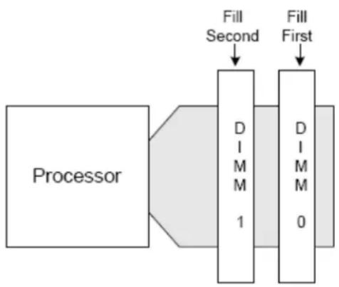
You should populate the memory slots of DDR3 channels furthest from the Intel ^® 5500 series processor first. Therefore, if A1 is empty, you cannot populate/use A2.
flowchart
graph LR
    A["Processor"] --> B["DIMM 1"]
    B --> C["DIMM 0"]
    D["Fill First"] --> C
    E["Fill Second"] --> B
Figure 16. Memory Channel Population
3.4.7 Installing and Removing Memory
The silkscreen on the board next to CPU1 displays: DIMM_A2, DIMM_A1, DIMM_B1, DIMM_C1, and next to CPU2 display: DIMM_D2, DIMM_D1, DIMM_E1, DIMM_F1 starting from the inside of the board. DIMM_A1 is the blue socket closest to the CPU 1 socket. For memory channel A, the server board requires DDR3 DIMMs within a channel to be populated starting with the DIMM farthest from the processor. The DIMM farthest from the processor per channel is blue on the board.
3.4.7.1 Installing DIMMs
To install DIMMs, follow these steps:
- Turn off the server.
- Disconnect the AC power cord from the server.
- Remove the server's cover and locate the DIMM sockets (see "Installing Memory").
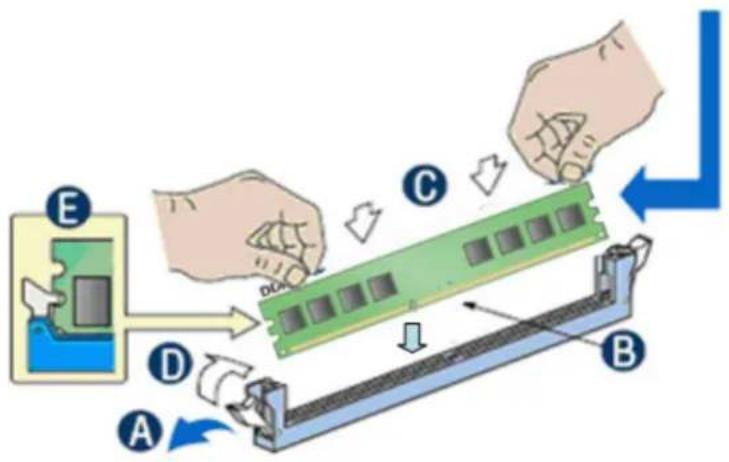
Figure 17. Installing Memory
- Make sure the clips at either end of the DIMM socket(s) are pushed outward to the open position (see letter "A" in the figure above).
- Holding the DIMM by the edges, remove it from its anti-static package.
- Position the DIMM above the socket. Align the two small notches in the bottom edge of the DIMM with the keys in the socket (letter "B" in Figure 16).
- Insert the bottom edge of the DIMM into the socket (letter "C" in Figure 16).
- When the DIMM is inserted, push down on the top edge of the DIMM until the retaining clips snap into place (letter "D" in Figure 16). Make sure the clips are firmly in place (letter "E" in Figure 16).
- Replace the server's cover and reconnect the AC power cord.
3.4.7.2 Removing DIMMs
To remove a DIMM, follow these steps:
- Turn off all peripheral devices connected to the server.
- Turn off the server.
- Remove the AC power cord from the server.
- Remove the server's cover.
- Gently spread the retaining clips at each end of the socket. The DIMM lifts from the socket.
- Holding the DIMM by the edges, lift it from the socket and store it in an anti-static package.
- Reinstall and reconnect any parts you removed or disconnected to reach the DIMM sockets.
- Replace the server's cover and reconnect the AC power cord.
3.4.8 Channel-Independent Mode
In the Independent Channel mode, you can populate multiple channels in any order (for example, you can populate channels B and C while channel A is empty). Also, DIMMs on adjacent channels do not need to have identical parameters. Therefore, all DIMMs are enabled and used in the Independent Channel mode.
Adjacent slots on channels A and D do not need matching size and organization. However, the speed of the channel is configured to the maximum common speed of the DIMMs.
The single channel mode is established using the independent channel mode by populating DIMM slots from channel A only.
3.4.9 Memory RAS
The memory RAS offered by the Intel ^® 5500 series processor is performed at channel level (for example, during mirroring, channel B mirrors channel A). All DIMM matching requirements are on a slot-to-slot basis on adjacent channels. For example, to enable mirroring, corresponding slots on channels A and B must have DIMMS of identical parameters.
If one socket fails, the population requirements for RAS, the BIOS sets all six channels to the Independent Channel mode. One exception to this rule is when all DIMM slots from a socket are empty (for example, when only DIMM slots A1, B1, and C1 are populated, mirroring is possible on the platform).
3.4.9.1 Memory Population for Channel Mirroring Mode
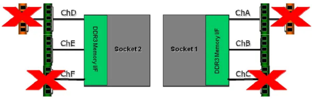
The mirrored configuration is a redundant image of the memory, and can continue to operate despite the presence of sporadic uncorrectable errors.
Channel mirroring is a RAS feature in which two identical images of memory data are maintained, thus providing maximum redundancy. On the Intel ^® 5500 series based Intel server boards, mirroring is achieved across channels. Active channels hold the primary image and the
other channels hold the secondary image of the system memory. The integrated memory controller in the Intel ^® 5500 series alternates between both channels for read transactions. Under normal circumstances, write transactions are issued to both channels.
Mirroring is only supported between Channels A & B and Channels D & E. The presence of a DIMM on Channel C or F causes the BIOS to disable Mirroring and revert to the Independent Channel mode.
flowchart
graph LR
    A["Router 1"] -->|ChA| B["Router 2"]
    B -->|ChB| A
    A -->|ChC| C["Router 3"]
    C -->|ChD| D["Router 4"]
    D -->|ChE| A
    A -->|ChF| E["Router 5"]
    E -->|ChF| A
    style A fill:#f9f,stroke:#333
    style B fill:#ccf,stroke:#333
    style C fill:#cfc,stroke:#333
    style D fill:#fcc,stroke:#333
    style E fill:#cff,stroke:#333
Figure 18. Mirroring Memory Configuration
3.4.10 Memory Error LED
Each DIMM is allocated an LED that, when lit, indicates a memory DIMM failure. It is the function of the BIOS to identify bad DIMMs during the boot process. The BIOS sends a message to the BMC to indicate which DIMM LED needs turn on.
3.5 Intel ^® 5500 Chipset IOH
The Intel ^® 5500 Chipset component is an I/O Hub (IOH). The Intel ^® 5500 Chipset provides a connection point between various I/O components and Intel processors using the Intel ^® QPI interface.
The Intel ^® 5500 Chipset IOH is capable of interfacing with up to 24 PCI Express* lanes, which can be configured in various combinations of x4, x8, x16 and limited x2 and x1 devices.
The Intel ^® 5500 Chipset IOH is responsible for providing a path to the legacy bridge. In addition, the Intel ^® 5500 Chipset supports a x4 DMI (Direct Media Interface) link interface for the legacy bridge and interfaces with other devices through SMBus, Controller Link, and RMII (Reduced Media Independent Interface) manageability interfaces. The Intel ^® 5500 Chipset supports the following features and technologies:
- Intel® QuickPath Interconnect (Intel® QPI)
- PCI Express* Gen2
- Intel® Virtualization Technology (Intel® VT) for Directed I/O 2 (Intel® VT-D2)
- Manageability Engine (ME) subsystem
3.5.1 IOH24D PCI Express\*
PCI Express* Gen1 and Gen2 are dual-simplex, point-to point serial differential low-voltage interconnects. The signaling bit rate is 2.5 Gb/s one direction per lane for Gen1 and 5.0 Gb/s one direction per lane for Gen2. Each port consists of a transmitter and receiver pair. A link between the ports of two devices is a collection of lanes (x1, x2, x4, x8, x16, and so forth). All lanes within a port must transmit data using the same frequency. The following table lists the usage of the IOH24D PCI Express* bus segments.
Table 6. IOH24D PCI Express* Bus Segments
| PCI Bus Segment | Width | Speed | Type | PCI I/O Card Slots |
| Port 0ICH10R | x4 10 Gb/s | PCI Express*Gen1 | x4 PCI Express* Gen1 throughput to the ICH10R southbridge | |
| PE1, PE2Intel®5500 Chipset IOH PCI Express* | x4 10 Gb/s | PCI Express*Gen1 | x4 PCI Express* Gen1 throughput to an onboard NIC. | |
| PE3, Intel®5500 Chipset IOH PCI Express* | X4 20 Gb/S | PCI Express*Gen2 | X4 PCI Express* Gen2 throughput to slot 1. | |
| PE7, PE8Intel®5500 Chipset IOH PCI Express* | x8 40 Gb/S | PCI Express*Gen2 | x8 PCI Express* Gen2 throughput to the slot 6 riser . | |
| PE9, PE10 Intel®5500 Chipset IOH PCI Express* | x8 40 Gb/S | PCI Express*Gen2 | x4 PCI Express* Gen2 throughput to each of the two Intel®I/O Expansion Module connectors. |
3.5.1.1 Direct Cache Access (DCA)
The DCA mechanism is a system-level protocol in a multi-processor system to improve I/O network performance by providing higher system performance. It is designed to minimize cache misses when a demand read is executed. This is accomplished by placing the data from the I/O devices directly into the CPU cache through hints to the processor to perform a data pre-fetch and install it in its local caches. The Intel ^® 5500 series processor supports Direct Cache Access (DCA). You enable or disable DCA in the BIOS processor setup menu.
3.5.1.2 Intel ^ Virtualization Technology for Directed I/O (Intel ^ VT-d)
The Intel ^® Virtualization Technology is designed to support multiple software environments sharing the same hardware resources. Each software environment may consist of an operating system and applications. You can enable or disable the Intel ^® Virtualization Technology in the BIOS setup. The default behavior is disabled.
Note: If the setup options are changed to enable or disable the Virtualization Technology setting in the processor, the user must perform an AC power cycle for the changes to take effect.
The Intel ^® 5500 Chipset IOH supports DMA remapping from inbound PCI Express* memory Guest Physical Address (GPA) to Host Physical Address (HPA). PCI Express* devices are directly assigned to a virtual machine leading to a robust and efficient virtualization.
3.6 Management Engine
The Management Engine (ME) is an embedded ARC controller within the IOH. The IOH ME performs manageability functions called Intel ^® Server Platform Services (SPS) for the discrete Baseboard Management Controller (BMC).
The functionality provided by the SPS firmware is different from Intel ^® Active Management Technology (Intel ^® AMT or AT) provided by the ME on client platforms.
Server Platform Services are value-added platform management options that enhance the value of Intel platforms and their component ingredients (CPUs, chipsets, and I/O components). Each service is designed to function independently wherever possible, or grouped together with one or more features in flexible combinations to allow OEMs (Original Equipment Manufacturers) to differentiate platforms. The following is a high-level view of the Intel ^® Server Board S5500WB SPS functions.
- Node Management Features:
• NPTM Policy Manager
• Power Supply Monitoring Service
- Inlet Temperature Monitoring Service
• CPU Power Limiting Service
- Provide Access to ICH10R Devices: The ME has control of ICH10R platform instrumentation. SPS provides a mechanism for the BMC to access this instrumentation through IPMI OEM commands. Use of this capability on Intel servers is platform-/SKU-specific.
- ICH10 temperature monitoring
- PECI 2.0 Proxy: SPS offers a means for a BMC without a PECI 2.0 interface to use the ME as a PECI proxy. The BMC on Intel servers already has a PECI 2.0 interface, so this SPS capability is not used.
3.7 Intel °82801Jx I/O Controller Hub (ICH10R)
The Intel ^® 82801Jx I/O Controller Hub (ICH10R) provides extensive I/O support and supports the following features and specifications:
- PCI Express* Base Specification, Revision 1.1 support
• ACPI Power Management Logic Support, Revision 3.0a - Enhanced DMA controller, interrupt controller, and timer functions
- Integrated Serial ATA host controllers with independent DMA operation on up to six ports and AHCI support
-
USB host interface with support for up to 12 USB ports; six UHCI host controllers; and two EHCI high-speed USB 2.0 host controllers
-
System Management Bus (SMBus) Specification, Version 2.0 with additional support for I²C devices
- Low Pin Count (LPC) interface support
- Serial Peripheral Interface (SPI) support
3.7.1 Serial ATA Support
The ICH10R has an integrated Serial ATA (SATA) controller that supports independent DMA operation on six ports and data transfer rates of up to 3.0 Gb/s. The six SATA ports on the server board are numbered SATA-1 through SATA-6. You can enable or disable the SATA ports and/or configure them by accessing the BIOS setup utility during POST.
3.7.1.1 Intel \*Embedded Server RAID Technology II
The onboard storage capability of these server boards includes support for Intel ^® Embedded Server RAID Technology II (Intel ^® ESRTII), which provides three standard software RAID levels: data stripping (RAID Level 0), data mirroring (RAID Level 1), and data stripping with mirroring (RAID Level 10). For higher performance, you can use data stripping to alleviate disk bottlenecks by taking advantage of the dual independent DMA engines that each SATA port offers. Data mirroring is used for data security. If a disk fails, a mirrored copy of the failed disk is brought online. There is no loss of either PCI resources (request/grant pair) or add-in card slots.
With the addition of an optional Intel ^® RAID Activation Key, Intel ^® ESRTII is also capable of providing fault tolerant data stripping (software RAID Level 5), such that if a SATA hard drive fails, you can restore the lost data on a replacement drive from the other drives that make up the RAID 5 pack.
Intel ^® Embedded Server RAID Technology functionality requires the following items:
- ICH10R IO Controller Hub
- Software RAID option is selected on BIOS menu for SATA controller
- Intel® Embedded Server RAID Technology II Option ROM
- Intel ^ Embedded Server RAID Technology II drivers, most recent revision
- At least two SATA hard disk drives
3.7.1.2 Intel \*Embedded Server RAID Technology II Option ROM
The Intel ^® Embedded Server RAID Technology II for SATA Option ROM provides a pre-operating system user interface for the Intel ^® Embedded Server RAID Technology II implementation and provides the ability to use an Intel ^® Embedded Server RAID Technology II volume as a boot disk as well as to detect any faults in the Intel ^® Embedded Server RAID Technology II volume(s).
3.7.2 USB 2.0 Support
The USB controller functionality integrated into ICH10R provides the server board with an interface for up to 12 USB 2.0 ports. All ports are high-speed, full-speed, and low-speed capable.
- Four external connectors are located on the back edge of the server board.
- Two internal 2x5 headers are provided, capable of supporting two optional USB 2.0 ports each, typically, one header supports Front panel USB and one supports an internal third party management card.
- One internal low-profile 2x5 header is provided
- One Internal Type A USB vertical connector is provided for attaching standard peripherals
- The BMC consumes 2 ports, for a total of 12 Ports
3.8 Network Interface Controller (NIC)
Network interface support is provided from the onboard Intel ^® 82576 NIC, which is a single, compact component with two fully integrated GbE Media Access Control (MAC) and Physical Layer (PHY) ports. The Intel ^® 82576 NIC provides the server board with support for dual LAN ports designed for 10/100/1000 Mbps operation. Refer to the Intel ^® 82576 Gigabit Ethernet Controller Datasheet (Document#: 82576) for full details of the NIC feature set.
The NIC device provides a standard IEEE 802.3 Ethernet interface for 1000BASE-T, 100BASE-TX, and 10BASE-T applications (802.3, 802.3u, and 802.3ab) and is capable of transmitting and receiving data at rates of 1000 Mbps, 100 Mbps, or 10 Mbps.
The Intel ^® 82576 NIC is powered off the main standby voltage rail via DC to DC Voltage regulators for efficiency purposes. It is on standby power so the BMC can send out-of-band management traffic over the RMII bus to the network during sleep state S5.
The NIC supports the normal RJ-45 LINK/Activity speed LEDs as well as the Proset ID function. These LEDs are powered from a Standby voltage rail.
The link / activity LED (at the right of the connector) indicates network connection when on, and transmit / receive activity when blinking. The speed LED (at the left of the connector) indicates 1000-Mbps operation when amber, 100-Mbps operation when green, and 10-Mbps when off. The following table provides an overview of the LEDs.
Table 7. NIC Status LED
| LED Color LED State | NIC State | |
| Green/Amber (Right) | Off 10 Mbps | |
| Green 100 Mbps | ||
| Amber | 1000 Mbps | |
| Green (Left) | On Active Connection | |
| Blinking Transmit / Receive activity | ||
3.8.1 MAC Address Definition
The Intel ^® Server Board S5500WB has the following four MAC addresses assigned to it at the Intel factory.
- NIC 1 MAC address
- NIC 2 MAC address – Assigned the NIC 1 MAC address +1
- Integrated BMC LAN Channel MAC address – Assigned the NIC 1 MAC address +2
- Intel® Remote Management Module 3 (Intel® RMM3) MAC address – Assigned the NIC 1 MAC address +3
The Intel ^® Server Board S5500WB has a white MAC address sticker included with the board. The sticker displays the NIC 1 MAC address in both bar code and alphanumeric formats.
3.8.2 LAN Connector Ordering
The Intel ^® 82576 NIC is connected to a stacked RJ-45 over USB mag-jack for NIC 1 and a RJ-45 mag-jack for the second connection (NIC 2).
3.9 Integrated Baseboard Management Controller
The ServerEngines* LLC Pilot II Integrated BMC is provided by an embedded ARM9 controller and associated peripheral functionality that is required for IPMI-based server management. Firmware usage of these hardware features is platform-dependant.
The following is a summary of the Integrated BMC management hardware features used by the ServerEngines* LLC Pilot II Integrated BMC:
- IPMI 2.0 Compliant
- Integrated 250 MHz 32-bit ARM9 processor
- Six ^2 C SMBus modules with Master-Slave support
- Two independent 10/100 Ethernet Controllers with RMII support
- Six ^2 C interface
• Memory Management Unit (MMU)
• DDR2 16-bit up to 667 MHz memory interface - Up to 16 direct and 64 Serial GPIO ports
• 12 10-bit Analog to Digital Converters
• Eight Fan Tachometers Inputs
• Four Pulse Width Modulators (PWM) - Chassis Intrusion Logic with battery-backed general purpose register
- JTAG Master interface
- Watchdog timer
Additionally, the ServerEngines* Pilot II part integrates a super I/O module with the following features:
- Keyboard Style/BT Interface
- Two 16C550 compatible serial ports
- Serial IRQ support
• 16 GPIO ports (shared with Integrated BMC)
• LPC to SPI Bridge for system BIOS support
• SMI and PME support
- ACPI compliant
- Wake-up control
The Pilot II contains an integrated KVMS subsystem and graphics controller with the following features:
• USB 2.0 for keyboard, mouse, and storage devices
- Hardware Video Compression for text and graphics
- Hardware encryption
• 2D Graphics Acceleration
• DDR2 graphics memory interface
- Matrox 2000 Graphics core with PCI Express* x1 host interface
- Up to 1600x1200 pixel resolution
flowchart
graph TD
    subgraph BMC and KVMS Subsystem
        A["ARM926E-S 16K D and I Cache"] --> B["Interrupt Controller"]
        B --> C["RTC and General Purpose Timers (3)"]
        C --> D["UART (3)"]
        D --> E["I2C (6)"]
        E --> F["Ethernet MAC with RMII Interface (2)"]
        F --> G["Crypto and Video Accelerator"]
        G --> H["LPC Master, JTAG Master, and SPI Flash"]
        H --> I["DDR-II 16-bit Memory Controller"]
        I --> J["Graphics Controller"]
    end

    subgraph Super I/O Subsystem
        K["LPC Interface"] --> L["UART (2)"]
        L --> M["GPIO and SGPIO"]
        M --> N["LPC to SPI Flash Bridge"]
        N --> O["Watchdog Timer"]
        O --> P["Real Time clock interface (requires external RTC)"]
        P --> Q["SPI Memory"]
        Q --> R["Super I/O Subsystem"]
        S["GPS"] --> T["SPI Memory"]
    end

    U["USB interface to Host"] --> H
    V["Code Memory"] --> H
    W["JTAG Master"] --> H
    X["DDR-II (up to 667 MHz)"] --> I
    Y["1x PCI Express* interface to Host"] --> Z["Graphics Subsystem"]
    style BMC and KVMS Subsystem fill:#f9f9f9,stroke:#333
    style Super I/O Subsystem fill:#e0e0e0,stroke:#333
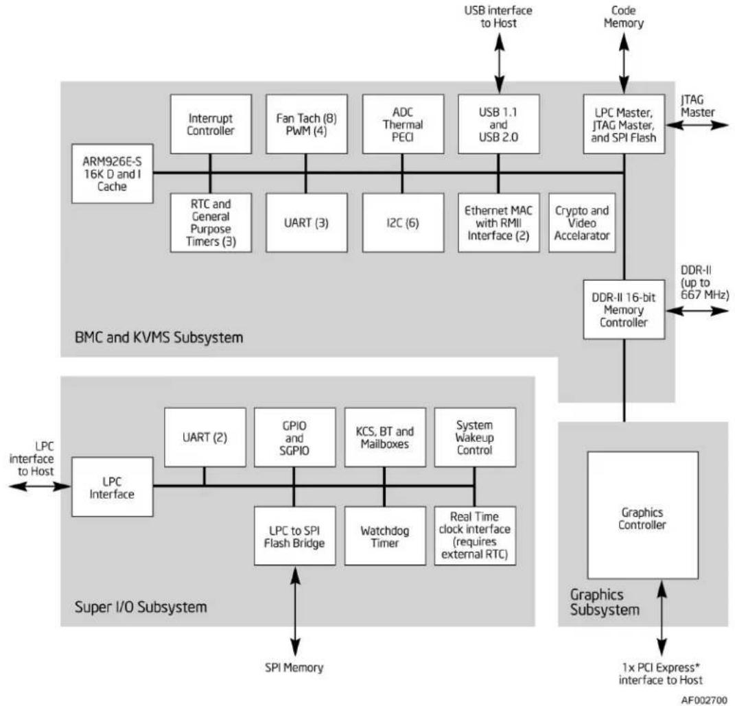
Figure 19. Integrated BMC Hardware
3.9.1 Integrated BMC Embedded LAN Channel
The Integrated BMC hardware includes two dedicated 10/100 network interfaces. These interfaces are not shared with the host system. At any time, you can enable only one dedicated interface for management traffic. The default active interface is the NIC 1 port.
For these channels, you can enable support for IPMI-over-LAN and DHCP.
For security reasons, embedded LAN channels have the following default settings:
■ IP Address: Static
- All users disabled.
3.9.2 RMM3 Advanced Management Board:
The RMM3 advanced management board serves two purposes. The first is to give the customer the option to add a dedicated management 100-Mbit LAN interface to the product. The second is to give additional flash space, enabling the Advanced Management functions to support WS-MAN and CIMOM. The RMM3 comes with a third 10/100GbE NIC that connects to the board. RMM3 management traffic can use the third NIC or NIC 1.
Table 8. RMM3 Features
| Manageability features Description | |
| Embedded Web U | Remote Power on\off, sensor status, system info, System Event log, and OEM customization |
| KVM Redirection High performance and multiple concurrent sessions | |
| USB 2.0 Media Redirection Boot over remote media | |
| Security SSL, SSH support | |
| WS- MAN | |
| Dedicated NIC | |
| Shared NIC (Onboard NICs) | |
| LDAP Support | |
3.10 Serial Ports
The server board provides two serial ports: an external RJ-45 serial port and an internal serial header.
The rear RJ-45 serial A port is a fully-functional serial port that can support any standard serial device.
The serial B port is an optional port that is accessed through a 9-pin internal DH-10 header. You can use a standard DH-10 to DB9 cable to direct serial A port to the rear of a chassis. Appendix A defines the serial B interface.
3.11 Wake-up Control
Wake from S1 is supported on LAN, USB, Serial port, and PCI Express* slots.
3.12 Integrated Video Support
The SVGA subsystem supports a variety of modes, up to 1600 x 1200 resolution in 8 / 16 / 32 bpp modes under 2D. It also supports both CRT and LCD monitors up to a 200 Hz vertical refresh rate.
The video is accessed using a standard 15-pin VGA connector found in the I/O panel area of the server board. You can disable the onboard video controller using the BIOS Setup utility or when an add-in video card is detected. The system BIOS provides the option for dual-video operation when an add-in video card is configured in the system.
3.12.1 Video Modes
The integrated video controller supports all standard VGA modes. The following table shows the 2D modes supported for both CRT and LCD.
Table 9. Supported Video Modes
| 2D Video Mode Support 2D Mode Refresh Rate (Hz) | ||||
| 8 bpp 16 bpp 32 bpp | ||||
| 640x480 60, 72, | 75, 85, 90,100, 120, 160, 200 | Supported | Supported | Supported |
| 800x600 60, 70, | 72, 75, 85,90, 100, 120,160 | Supported | Supported | Supported |
| 1024x768 60, 70, | 72,75,85,90,100 | Supported | Supported | Supported |
| 1152x864 | 43,47,60,70,75,80,85 | Supported | Supported | Supported |
| 1280x1024 | 60,70,74,75 | Supported | Supported | Supported |
| 1600x1200 | 52 Supported Supported Supported Supported | |||
3.12.2 Dual Video
The BIOS supports both single-video and dual-video modes. The dual-video mode is enabled by default in the BIOS.
In the single mode (dual monitor video = disabled), the onboard video controller is disabled when an add-in video card is detected.
In the dual mode (onboard video = enabled, dual monitor video = enabled), the onboard video controller is enabled and is the primary video device. The external video card is allocated resources and is considered the secondary video device. The BIOS Setup utility provides options to configure the feature as follows.
Table 10. Dual Video Options
| Onboard Video | EnabledDisabled | |
| Dual Monitor Video | EnabledDisabled | Shaded if onboard video is set to "Disabled" |
3.12.3 Front Panel Video
The Intel ^® Server Board S5500WB provides a mechanism to support video to the front panel via the use of an internal header. When a monitor is plugged into the front panel video connector, the rear panel video stream is disconnected.
There is a jumper option to change this default action. When the internal header is used by a third-party Management card to do KVM over LAN and then when a monitor is plugged into the rear panel video connector, the video stream to the internal header is cut off.
3.13 I/O Slots
3.13.1 X16 Riser Slot Definition
Slot 6 was defined to support riser cards. Slot 6 has a x16 physical connector with a PCI Express* Gen II x8 electrical interface. Two clocks are provided so the bus can be bifurcated into two x4 connectors.
Because of CPU placement, a 1U system supports only PCI Express* adapters that meet the PCI SIG half card definition. Full-length boards are supported in a 2U system by using a taller riser and extending the board over the 1U CPU heatsinks or if CPU2 is unpopulated.
Appendix A documents the pin assignments for this connector.
3.13.2 PE WIDTH Strapping
On the Intel ^® Server Board S5500WB, the IOH needs to be informed of the PCI Express* bus width during power on. This is accomplished using the PEWIDTH input straps. The mechanism used is the PEWIDTH bits, one bit is used to signify the width and number of PCI Express* buses used by the riser. For slot 6, the PEWIDTH bit used is 0.
Table 11. PEWIDTH Strapping Bits
| Riser Description | PEWIDTH0 pin A50 | |
| 1U one x8 1 x8 | PCI Express* Slot 0 | |
| 2U two x4 2 X4 | PCI Express* Slots 1 | |
By using this mechanism for selecting PCI Express* port width, you can avoid a BIOS rediscover and reboot.
The PEWIDTH is pulled up to 3.3 V Aux on the baseboard and grounded, if necessary, by the riser. The baseboard provides an inverter and voltage level translator before passing this signal to the IOH.
3.13.3 Slot 1 PCI Express\* x8 Connector
Slot 1 provides a PCI Express* x4 bus on an x8 connector, if provided, for use in a 2U chassis that uses LP boards without risers. Although it is feasible to use the IOM at the same time, it would require 2U chassis back panel changes.
3.13.4 I/O Module Connector
Mezanine connectors are provided to support the various I/O modules, both the older Gen 1 I/O modules supported by Intel ^® Server Board S5000PAL and newer, double-wide Gen 2 I/O modules supported by the Intel ^® Server Board S5520UR are supported on the Intel ^® Server Board S5500WB.
The Intel ^® I/O Expansion Module is also required to inform the IOH of the Intel ^® I/O Expansion Module Bus usage, PEWIDTH bit 1 is to be used for this.
Table 12. Intel ^® I/O Expansion Module Bus PEWIDTH Bits
| Intel® I/O Expansion Module | Description PEWIDTH1 - Pin 2 | |
| one x8 | 1 x8 PCI Express* target device | 0 |
| two x4 2 x4 | target devices 1 | |
4. Intel ^® I/O Expansion Modules
The Intel ^® Server Board S5500WB supports a variety of I/O Module options using 2x4 PCI Express* Gen2 Intel ^® I/O Expansion Module connectors on the rear of the server board. Each Intel ^® I/O Expansion Module connector is a 50-pin, surface mount, 0.8mm pitch, header. The Intel ^® Server Board S5500WB accommodates both the double-wide I/O expansion modules and the PCI Express* Gen 1 I/O modules (used on the S5000PAL rack server).
The Legacy modules are:
• Dual Port GbE I/O Module
• External 4 Port SAS I/O Module
The new modules consist of:
- Internal 4-port Intel 82576EB GbE*
• Dual Port Intel 10GbE I/O Module - Internal 4-port LSI* 1064e SAS I/O Module
- Internal 4-port LSI* 1078e SAS I/O Module
- Infiniband* I/O Expansion Module Single Port QDR
The second x4 Intel ^® I/O Expansion Module controller does not support a single-wide module; it is only used to support a double-wide module. You must mount single-wide modules on connector (J3B1) closest to Slot 6, marked Legacy Intel ^® I/O Expansion Module on the silkscreen. When double-wide Intel ^® I/O Expansion Modules are installed, there might be interference with some adapters installed in Slot 1.
The following table shows the product codes for each module.
Table 13. Intel ^® I/O Expansion Module Product Codes
| Product Code Description | |
| AXX4SASMOD | Intel® SAS Entry RAID I/O Expansion Module: Provides 4-port pass through SAS, entry-level RAID 0/1/1E, and optional host RAID (4 internal ports). |
| AXXGBIOMOD Dual Gigabit Ethernet I/O | Expansion Module |
| AXXROMBSASMR | Intel® Integrated RAID I/O Expansion Module: Provides four internal ports, full-featured SAS / SATA RAID 0,1,5,6 and striping capability for spans 10, 50, 60. You must order the optional backup battery AXXRSBBU3 separately. |
| AXXSASIOMOD External 4-port SAS I/O | Expansion Module. |
| AXX10GBIOMOD | Dual-port 10 Gigabit Ethernet I/O Expansion Module with CX4 connectors. |
| AXX4GBIOMOD2 | Quad port Gigabit Ethernet I/O Expansion Module based on the Intel® 82576EB Gigabit Ethernet Controller. |
| AXXIBQDRMOD InfiniBand* I/O Expansion Module Single Port QDR. | |
For more information, refer to the I/O modules in the Intel ^® I/O Expansion Modules Hardware Specification.
5. Platform Management Features
This section explains BIOS and firmware (FW) requirements that drive specific hardware implementations of the platform. To a large extent, this is background information.
5.1 BIOS Feature Overview
The Intel ^® Server Board S5500WB product uses the AMI Aptio v3.x code base.
5.1.1 EFI Support
The platform BIOS is compiled to support the 64-bit EFI environment, natively. This allows operating systems that are EFI-aware to take advantage of the EFI-boot process in a native 64-bit environment. It is expected this will reduce the time required to boot the platform to those operating systems. Additionally, any utilities that make use of the EFI environment provided by the platform BIOS need to support either the native 64-bit environment or make use of the EFI byte code (EBC). Of course, to maintain compatibility with legacy operating environments, a legacy boot option is provided.
5.1.2 Intel \* Rapid Boot Toolkit
The BIOS supports the Intel ^® Rapid Boot Toolkit on this platform. The toolkit allows users to develop payloads that may co-exist with the platform BIOS in the Flash component attached to the south bridge. The BIOS supports boots to the user-defined payload when this mechanism is enabled. To enable a variety of payloads, a larger Flash component is required to maintain both the platform BIOS and a useful payload. An 8 MB Flash should be sufficient to support a payload of approximately 5 MB. A significant part of this payload is the 4.5 MB used by the Intel ^® Rapid Boot Toolkit.
5.1.3 BIOS Recovery
The platform BIOS supports a BIOS Recovery Mode Jumper. The BIOS samples this jumper during POST through a GPIO and, if set, defaults to a recovery mode of operation that allows restoration of the BIOS Flash to a full operational state.
The platform BIOS supports a Reset BIOS Configuration Jumper. The BIOS samples this jumper during POST through a GPIO and, if set, resets its configuration information stored in Flash memory.
5.2 BMC Feature Overview
The server management subsystem consists of multiple components including several interconnected microcontrollers. The subsystem monitors platform sensors (temperatures, voltages, fans, hard drives, and so forth); implements platform acoustics, power, and thermal management policies; provides an intelligent LCD front-panel; and provides facilities for remote and local management.
The server management subsystem is available when the system is connected to wall power but not fully operational (S5 state); when the system is in a S1 sleep state or when the system is fully operational (S0 state).
5.2.1 Server Engines Pilot II Controller
The center of the server management subsystem is the Server Engines Pilot II integrated Baseboard Management Controller. This device provides support for many platform functions including system video capabilities, legacy Super I/O functions, and also provides an ARM 926-EJ microcontroller to host the embedded server management firmware stack.
The Server Engines Pilot II baseboard management controller across Intel's server product line with two different management feature set configurations: Basic and Advanced. The Intel® Server Board S5500WB supports both.
Basic features include IPMI 2.0 support, remote management, hardware monitoring, event management, event alerting, system event log, asset inventory, console redirection, web interface, and SMASH CLP (basic feature set).
Advanced features include the Basic features plus KVM redirection, USB Media redirection, SMASH CLP (Advanced feature set), and WS-MAN. To enable the Advanced features, you must install the Remote Management Module 3.
NOTE: The BMC consumes two USB ports; one runs at USB1.1 for keyboard mouse redirection and one runs at USB2.0 for media redirection.
5.2.2 BMC Firmware
The BMC supports a Fast Firmware Update mode in addition to the standard KCS (Keyboard Controller Style) SMS interface. This is a special AMI ^® proprietary protocol that goes over the USB connection between the host and the BMC. Called “IPMI over USB”, it is implemented in the LIBIPMI library on both host and BMC sides to transfer large blocks of data (up to 32 K) much faster than KCS can. IPMI commands are embedded in data written/read to a virtual CD-ROM device.
The embedded server management firmware stack is based on a core stack from American Megatrends Incorporated (AMI). The stack runs on an embedded version of the Linux operating system and provides support for current industry standard management interfaces (IPMI 2.0) and emerging industry standard advanced management interfaces (SMASH-CLP and WS-MAN). The stack also includes support for keyboard, video, mouse (KVM), and USB media redirection.
The server management subsystem provides remote connectivity through a single GbE NIC with NC-SI support (RMII).
NPTM support is required; you must use the ME function in the IOH to accomplish this.
5.2.3 BMC Basic Features
| Feature Description | |
| IPMI 2.0 Compliance to IPMI 2.0 specification | |
| Remote Management Out-of-band access via either LAN or serial port for numerous features | |
| Hardware Monitor Monitor of fans, voltages, temperatures, chassis intrusions, memory errors, power supplies, hard drives, and so forth | |
| Event Management System event filtering | |
| Event Alerting System events delivered via SNMP traps or email | |
| System Event Log Dedicated persistent storage for system events | |
| Asset Inventory Field replaceable unit (FRU) information | |
| Console Redirection Text-based console redirection via serial-over-LAN | |
| SMASH CLP (Basic) Command line SSH interface for basic server management operations | |
| Node Manager | Power management by using P-state\C-State cycling method Requires PMBus* power supply. |
5.2.4 BMC Advanced Features
The Intel ^® Server Board S5500WB product includes support for an upgrade module to support the advanced server management functionality. The Remote Management Module 3 supports an 8 MB SPI Flash, which connects to the integrated BMC SPI interface. This is in addition to the local integrated BMC 8 MB SPI flash connected to the PILOT II IBMC down on the board. The total 16 MB of Flash space is required to support advanced management features as defined in the following table. The RMM3 advanced management board has a PHY device that which interfaces with the secondary NC-SI port out of the Server Engines PILOT II integrated BMC to offer a dedicated management Ethernet port.
Table 14. Advanced Features
| Manageability features Description | |
| Embedded Web UI | Remote Power on\off, sensor status, system info, System Event log, OEM customization |
| KVM Redirection | high performance, multiple concurrent sessions |
| USB 2.0 Media Redirection | boot over remote media |
| Security | SSL, SSH support |
| WS- MAN | |
| Dedicated NIC | |
| Shared NIC (Onboard NICs) | |
| LDAP support |
5.3 Management Engine (ME)
5.3.1 Overview
The Intel ^® Server Platform Services (SPS) is a set of manageability services provided by the firmware executing on an embedded ARC controller within the IOH. This management controller is also commonly referred to as the Management Engine (ME). The functionality provided by the SPS firmware is different from Intel ^® Active Management Technology (Intel ^® AMT or AT) provided by the ME on client platforms.
Server Platform Services (SPS) are value-added platform management options that enhance the value of Intel platforms and their component ingredients (CPUs, chipsets, and I/O components). Each service is designed to function independently wherever possible, or grouped together with one or more features in flexible combinations to allow OEMs to differentiate platforms.
5.3.2 BMC - Management Engine Interaction
Management Engine-Integrated BMC interactions include the following:
- Integrated BMC stores sensor data records for ME-owned sensors.
- Integrated BMC participates in ME firmware update.
- Integrated BMC initializes ME-owned sensors based on SDRs.
- Integrated BMC receives platform event messages sent by the ME.
- Integrated BMC notifies ME of POST completion.
5.4 Data Center Manageability Interface
The DCMI specifications are derived from Intelligent Platform Management Interface (IPMI) 2.0. The DCMI specifications define a uniform set of monitoring, control features and interfaces that target the common and fundamental hardware management needs of server systems that are used in large deployments within data centers, such as Internet Portal data centers. This includes capabilities such as secure power and reset control, temperature monitoring, event logging, and others. For more information refer to www.intel.com/go/dcmi.
5.5 Other Platform Management
The platform supports the following sleep states, S1 and S5. Within S0, the platform supports additional lower power states, such as C1e and C6, for the CPU.
5.5.1 Wake On LAN (WOL)
- Wake On LAN (WOL) is supported on both LAN ports and IOM LAN modules for all supported Sleep states.
- Wake on Ring is supported on the external Serial port only for all supported Sleep states.
- Wake on USB is supported on the rear and front panel USB ports for S1 only.
- Wake on RTC is supported for all supported Sleep states.
Intel® Server Board S5500WB TPS Platform Management Features
- Wake IPMI command is supported (BMC function no additional hardware requirement) for all supported Sleep states.
5.5.2 PCI Express\* Power management
L0 and L3 power management states are supported on all PCI Express* slots and embedded end points.
5.5.3 PMBus\*
Power supplies that have PMBus* 1.1 are supported and required to support Intel® Dynamic Power Node Manager. Intel® Server Board S5500WB supports the features of Intel® Dynamic Power Node Manager version 1.5 except the inlet temperature sensor.
5.6 SMBUS Architecture Block
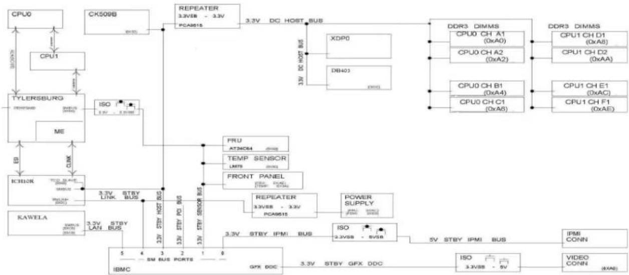
flowchart
graph TD
    CPU0 --> CPU1
    CPU1 --> TYLERSBURG
    TYLERSBURG --> ME
    ME --> ICHOR
    ICHOR --> KAWELA
    KAWELA --> IBMC
    IBMC --> 3.3V STBY LAN BUS
    IBMC --> 3.3V STBY PORTS
    IBMC --> 5 V STBY IPMI BUS
    IBMC --> 3.3V STBY GFX DDC
    IBMC --> 3.3V STBY GFX DDC
    3.3V STBY PC BUS --> FRU AT24C64
    3.3V STBY Sensor BUS --> TEMP SENSOR LMT9
    3.3V STBY Sensor BUS --> FRONT PANEL
    3.3V STBY Host BUS --> REPEATER 3.3VSB - 3.3V PCA9515
    3.3V STBY Sensor BUS --> REPEATER 3.3VSB - 3.3V PCA9515
    3.3V STBY Host BUS --> XDP0
    3.3V STBY Sensor BUS --> DB401
    3.3V STBY Sensor BUS --> DDR3 DIMMS
    DDR3 DIMMS --> CPU0 CH A1 (0xA0)
    DDR3 DIMMS --> CPU0 CH A2 (0xA2)
    DDR3 DIMMS --> CPU0 CH B1 (0xA4)
    DDR3 DIMMS --> CPU0 CH C1 (0xA6)
    DDR3 DIMMS --> CPU1 CH D1 (0xA8)
    DDR3 DIMMS --> CPU1 CH D2 (0xAA)
    DDR3 DIMMS --> CPU1 CH E1 (0xAC)
    DDR3 DIMMS --> CPU1 CH F1 (0xAE)
    CPU0 CH A1 --> DDR3 DIMMS
    CPU0 CH A2 --> DDR3 DIMMS
    CPU0 CH B1 --> DDR3 DIMMS
    CPU0 CH C1 --> DDR3 DIMMS
    CPU1 CH D1 --> DDR3 DIMMS
    CPU1 CH D2 --> DDR3 DIMMS
    CPU1 CH E1 --> DDR3 DIMMS
    CPU1 CH F1 --> DDR3 DIMMS
    CPU0 CH B2 --> DDR3 DIMMS
    CPU0 CH C1 --> DDR3 DIMMS
    CPU1 CH E2 --> DDR3 DIMMS
    CPU1 CH F2 --> DDR3 DIMMS
    CPU0 CH B3 --> DDR3 DIMMS
    CPU0 CH C2 --> DDR3 DIMMS
    CPU1 CH E3 --> DDR3 DIMMS
    CPU1 CH F4 --> DDR3 DIMMS
    CPU0 CH B4 --> DDR3 DIMMS
    CPU0 CH C4 --> DDR3 DIMMS
    CPU1 CH E5 --> DDR3 DIMMS
    CPU1 CH F6 --> DDR3 DIMMS
    CPU0 CH B6 --> DDR3 DIMMS
    CPU0 CH C6 --> DDR3 DIMMS
    CPU1 CH E7 --> DDR3 DIMMS
    CPU1 CH F8 --> DDR3 DIMMS
    CPU0 CH B9 --> DDR3 DIMMS
    CPU0 CH C9 --> DDR3 DIMMS
    CPU1 CH E9 --> DDR3 DIMMS
    CPU1 CH F9 --> DDR3 DIMMS
    CPU0 CH B10 --> DDR3 DIMMS
    CPU0 CH C10 --> DDR3 DIMMS
    CPU1 CH E10 --> DDR3 DIMMS
    CPU1 CH F10 --> DDR3 DIMMS
Figure 20. S5500WB SMBUS Block Diagram
5.6.1 SMBUS Device Addresses
Table 21 lists the SMBus addresses of various devices by bus.
Table 15. SMBus Device Address Assignment
| Main Bus | Power Rail | Sub Bus | Power Rail | Device SMBus | Address | Note |
| Host | 3V3SB | NA | NA | IBMC SMBus 3 No | Connect | |
| ICH10R SMBus 0x88 | ||||||
| CK509B | 0xD2 | |||||
| DB403 | 0xDC | |||||
| Host | 3V3 | XDP | ||||
| DB803 | 0xDC | |||||
| CPU0 DIMM 1A 0xA0 | ||||||
| CPU0 DIMM 2A 0xA2 | ||||||
| CPU0 DIMM 1B 0xA4 | ||||||
| CPU0 DIMM 1C 0xA6 | ||||||
| CPU0 DIMM 1D 0xA8 | ||||||
| CPU0 DIMM 2D 0xA | ||||||
| CPU0 DIMM 1E | 0xAC | |||||
| CPU0 DIMM 1F | 0xAE | |||||
| Sensor | 3V3SB | NA | NA | IBMC SMBus 1 | ||
| Temp Sensor 0x9E | ||||||
| FP Temp Sensor 0x9A | ||||||
| FP FRU 0xAE | ||||||
| Baseboard FRU 0xA8 | ||||||
| CPU IOH | 0xE0 | |||||
| IPMI | 3V3SB | NA | NA | IBMC SMBus 0 | ||
| IPMI | 5VSB | IPMI Connector | ||||
| IPMI | 5V | HSBP A | 0xC0 | |||
| LAN | 3V3SB | NA | NA | IBMC SMBus 5 | ||
| NIC LAN | ||||||
| Link | 3V3SB | NA | NA | IBMC SMBus 4 | ||
| ICH10R SMLINK | 0x88 | |||||
| PWR | 5V | PS FRU | 0xAC | |||
| PS PSMI | 0xB0 | |||||
| Spare | 3V3SB | NA | NA | IBMCSMBus 2 | ||
| DDC | 3V3SB | DDC | 5V | IBMC GFX DDC | ||
| Video Monitor | 0xA0 |
6. Configuration Jumpers
The following table provides a summary and description of configuration, test, and debug jumpers on the Intel ^® Server Board S5500WB. The server board has several 3-pin jumper blocks that can be used.
Pin 1 on each jumper block can be identified by the following symbol on the silkscreen: ▼
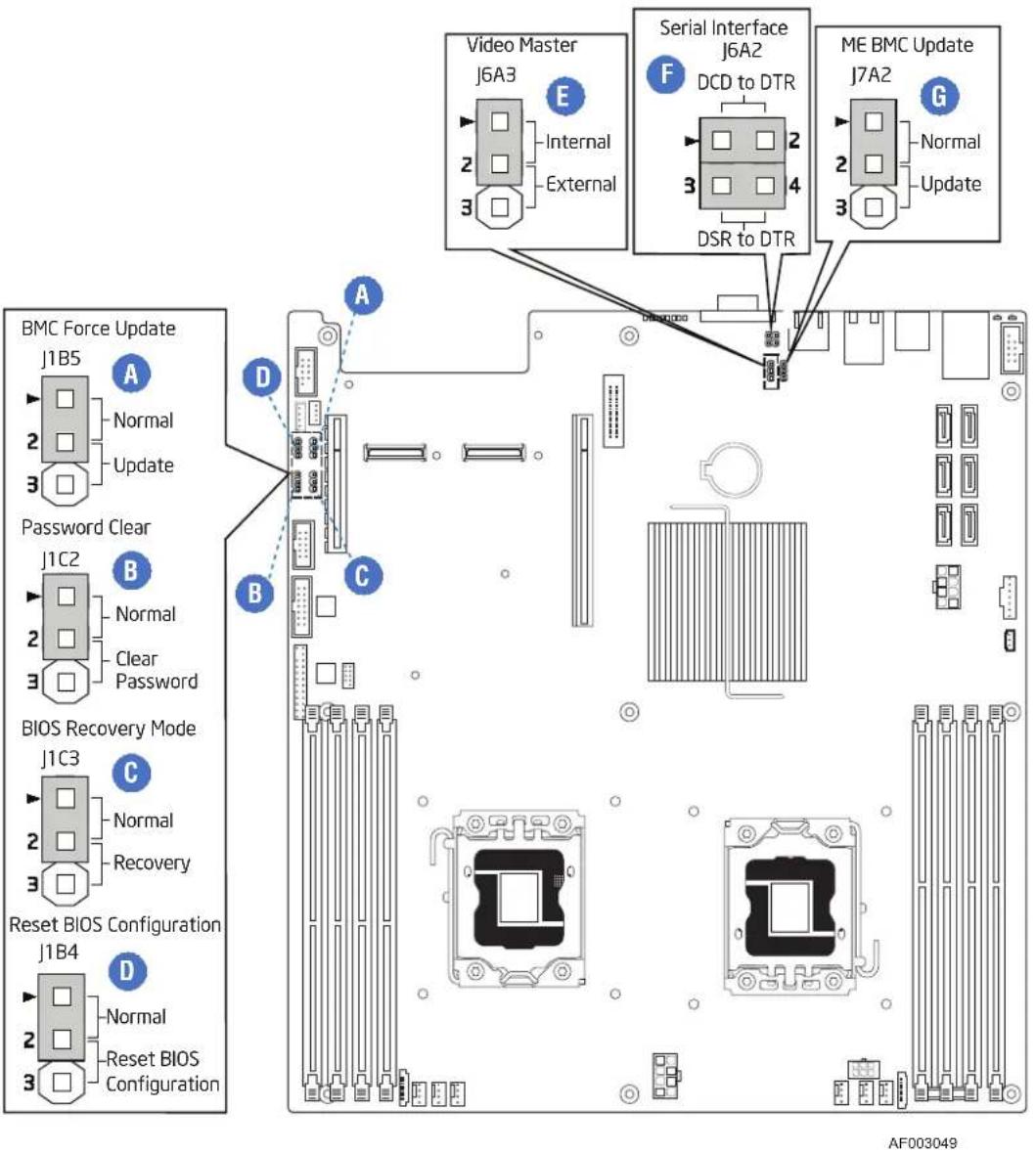
Figure 21: Jumper Blocks (J1B5, J1C2, J1C3, J1B4, J6A3, J6A2, J7A2)
Table 16: Server Board Jumpers (J1B5, J1C2, J1C3, J1B4, J6A3, J6A2)
| Jumper Name Jumper Position | Mode of Operation | Note | |
| Update jumper | 1-2 Normal IBMC | GPIO[1] is pulled H | HIGH. Default position. J1B5: BMC Force |
| 2-3 Update IBMC | GPIO[1] is pulled L | OW. | |
| J1C2: Password Clear | 1-2 Normal ICH1 | DR INTRUDER# pin | is pulled HIGH. Default position. |
| 2-3 Clear Password | ICH10R INTRUDER# pin is pulled LOW. | ||
| J1C3: BIOS Recovery Mode | 1-2 Normal ICH1 | DR GPIO [55] is pulled | HIGH. Default position. |
| 2-3 Recovery ICH1 | H10R GPIO [55] is pulled LOW. | ||
| J1B4: CMOS Clear | 1-2 Normal ICH1 | DR RTCRST# pin is | pulled HIGH. Default position. |
| 2-3 | Clear Settings | ICEMRSRTCRST# pin is pulled LOW. | |
| J6A3: Video Master | 1-2 Internal Internal connector will override if both connectors are used. | ||
| 2-3 External External connector will override if both connectors are used. | |||
| Force Update | 1-2 | Disabled | Default J7A2: ME Firmware |
| 2-3 | Enabled | ||
| J6A2: Serial Interface | 1 - 2 | DCD to DTR | Data Carrier Detect |
| 3 - 4 | DSR to DTR | Data Set Ready | |
6.1.1 Force IBMC Update (J1B5)
When performing a standard BMC firmware update procedure, the update utility places the BMC into an update mode, allowing the firmware to load safely onto the flash device. In the unlikely event the BMC firmware update process fails due to the BMC not being in the proper update state, the server board provides a BMC Force Update jumper (J1B5) which will force the BMC into the proper update state. The following procedure should be followed in the event the standard BMC firmware update process fails.
Table 17. Force IBMC Update Jumper
| Jumper Position | Mode of Operation | Note |
| 1-2 | Normal | IBMC GPIO[1] is pulled HIGH. Default position. |
| 2-3 | Update | IBMC GPIO[1] is pulled LOW. |
- Power down and remove the AC power cord.
- Open the server chassis. See your server chassis documentation for instructions.
-
Move jumper from the default operating position, covering pins1 and 2, to the enabled position, covering pins 2 and 3.
-
Close the server chassis.
- Reconnect the AC cord and power up the server.
- Perform the BMC firmware update procedure as documented in the README.TXT file included in the given BMC firmware update package. After successful completion of the firmware update process, the firmware update utility may generate an error stating the BMC is still in update mode.
- Power down and remove the AC power cord.
- Open the server chassis.
- Move the jumper from the enabled position, covering pins 2 and 3 to the disabled position, covering pins 1 and 2.
- Close the server chassis.
- Reconnect the AC cord and power up the server.
Note: Normal BMC functionality is disabled with the Force BMC Update jumper is set to the enabled position. You should never run the server with the BMC Force Update jumper set in this position. You should only use this jumper setting when the standard firmware update process fails. This jumper should remain in the default / disabled position when the server is running normally.
The server board has several 3-pin jumper blocks that can be used to configure, protect, or recover specific features of the server board.
6.1.2 Password Clear (J1C2)
The user sets this 3-pin jumper to clear the password.
Table 18. Password Clear Jumper
| Jumper Position Mode of Operation Note | ||
| 1-2 Normal ICH10R INTR | UDER# pin is pulled HIGH. Default position. | |
| 2-3 Clear Password ICH10R | INTRUDER# pin is pulled LOW. | |
6.1.2.1 Clearing the Password
- Power down server. Do not unplug the power cord.
- Open the chassis. For instructions, see your server chassis documentation.
- Move jumper (J1B6) from the default operating position, covering pins 1 and 2, to the password clear position, covering pins 2 and 3.
- Close the server chassis.
- Power up the server, wait 10 seconds or POST completes.
- Power down the server.
- Open the chassis and move the jumper back to default position, covering pins 1 and 2.
- Close the server chassis.
- Power up the server.
The password is now cleared and you can reset it by going into the BIOS setup.
6.1.3 BIOS Recovery Mode (J1C3)
The Intel ^® Server Board S5500WB uses BIOS recovery to repair the system BIOS from flash corruption in the main BIOS and Boot Block. This 3-pin jumper is used to reload the BIOS when the image is suspected to be corrupted. For directions on how to recover the BIOS, refer to the specific BIOS release notes.
Table 19. BIOS Recovery Mode Jumper
| Jumper Position | Mode of Operation Note | |
| 1-2 Normal ICH10R GPIO [55] is pulled HIGH. Default position. | ||
| 2-3 Recovery ICH10R GPIO [55] is pulled LOW. | ||
You can accomplish a BIOS recovery from the SATA CD and USB Mass Storage device. Please note that this platform does not support recovery from a USB floppy.
The recovery media must contain the following files under the root directory:
- FVMAIN.FV
- UEFI iFlash32 2.6 Build 9
- *Rec.CAP
- Startup.nsh (update accordingly to use proper *Rec.CAP file)
The BIOS starts the recovery process by first loading and booting to the recovery image file (FVMAIN.FV) on the root directory of the recovery media (SATA CD or USB disk). This process takes place before any video or console is available. Once the system boots to this recovery image file (FVMAIN.FV), it boots automatically into the EFI Shell to invoke the Startup.nsh script and start the flash update application (IFlash32.efi). IFlash32.efi requires the supporting BIOS Capsule image file (*Rec.CAP). After the update is complete, a message displays, stating the "BIOS has been updated successfully". This indicates the recovery process is finished. The user should then switch the recovery jumper back to normal operation and restart the system by performing a power cycle.
The following steps demonstrate this recovery process:
- Power OFF the system.
- Insert recovery media.
- Switch the recovery jumper. Details regarding the jumper ID and location can be obtained from the Board EPS for that Platform.
- Power ON the system.
- The BIOS POST screen will appear displaying the progress, and the system automatically boots to the EFI SHELL.
- The Startup.nsh file executes, and initiates the flash update (IFlash32.efi) with a new capsule file (*Rec.CAP). The regular IFlash message displays at the end of the process—once the flash update succeeds.
- Power OFF the system, and revert the recovery jumper position to "normal operation".
- Power ON the system.
- Do NOT interrupt the BIOS POST during the first boot.
6.1.4 Reset BIOS Configuration (J1B4)
This jumper used to be the CMOS Clear jumper. Since the previous generation, the BIOS has moved CMOS data to the NVRAM region of the BIOS flash. The BIOS checks during boot to determine if the data in the NVRAM needs to be set to default.
Table 20. Reset BIOS Jumper
| Jumper Position Mode of Operation Note | ||
| 1-2 Normal | ICH10R RTCRST# pin is | pulled HIGH. Default position. |
| 2-3 | Reset Configuration | IBIDSR RTCRST# pin is pulled LOW. |
6.1.4.1 Clearing the CMOS
- Power down server. Do not unplug the power cord.
- Open the server chassis. For instructions, see your server chassis documentation.
- Move jumper (J1B4) from the default operating position, covering pins 1 and 2, to the reset / clear position, covering pins 2 and 3.
- Wait five seconds.
- Remove AC power.
- Move the jumper back to default position, covering pins 1 and 2.
- Close the server chassis.
- Power up the server.
The CMOS is now cleared and you can reset it by going into the BIOS setup.
Note: Removing AC Power before performing the CMOS Clear operation causes the system to automatically power up and immediately power down, after the procedure is followed and AC power is re-applied. If this happens, remove the AC power cord again, wait 30 seconds, and re-install the AC power cord. Power-up the system and proceed to the
6.1.5 Video Master (J6A3)
Table 21. Video Master Jumper
| Jumper Position | Mode of Operation Notes |
| 1-2 Internal | Internal connector will override if both connectors are used. |
| 2-3 External | External connector will override if both connectors are used. |
This jumper determines which video is the primary.
J6A3, 1-2 jumpered: Internal video connector is primary, but video can come out of external video connector if you connect to it.
J6A3, 2-3 jumpered: External video connector is primary, but video can come out of internal video connector if you connect to it.
6.1.6 ME Firmware Force Update (J7A2)
| Pins ME Firmware Update Mode | ||
| 1-2 | Disabled | (Default) |
| 2-3 | Enabled | |
The ME firmware consists of two operational images and a recovery image. During boot, the recovery loader is started first and it tries to load the active firmware image by running the loader of this image. If it fails to boot, it tries to boot the other operational image. If both fail, the recovery loader starts in recovery mode. The recovery mode can also be forced setting the MGPIOx jumper on the board. Boot image verification and boot failure
6.1.7 Serial Interface (J6A2)
| Pins Mode Description | ||
| 1 – 2 DCD to DTR Data Carrier Detect | ||
| 3 – 4 DSR to DTR Data Set Ready | ||
7. Connector / Header Locations and Pin-out
7.1 Power Connectors
Table 22. SSI SKU 24-pin 2x12 Connector (J9B1)
| Pin Signal Name Pin Signal Name | |||
| 1 | +3.3V | 13 | +3.3V |
| 2 | +3.3V | 14 | -12V |
| 3 | GND | 15 | GND |
| 4 | +5V | 16 | PS_ON |
| 5 | GND | 17 | GND |
| 6 | +5V | 18 | GND |
| 7 | GND | 19 | GND |
| 8 | PWR_GD | 20 | NC |
| 9 | SB5V | 21 | +5V |
| 10 | +12V | 22 | +5V |
| 11 | +12V | 23 | +5V |
| 12 | +3.3V | 24 | GND |
Table 23. CPU 12V Power 2x4 Connector (J5K1)
| Pin Signal Name | |
| 1 | GND |
| 2 | GND |
| 3 | GND |
| 4 | GND |
| 5 | +12V |
| 6 | +12V |
| 7 | +12V |
| 8 | +12V |
Table 24. SSI Power Control (J9D1)
| Pin Signal Name | |
| 1 | SMB_PWR_CLK |
| 2 | SMB_PWR_DAT |
| 3 | SMB_PWR_ALRT |
| 4 | GND |
| 5 | 3.3V Remote Sense |
Table 25. 12-V only 2x4 Connector (replaces EPSD12V 2x12 connector) (J9D2)
| Pin Signal Name | |
| 1 | GND |
| 2 | GND |
| 3 | GND |
| 4 | GND |
| 5 | +12V |
| 6 | +12V |
| 7 | +12V |
| 8 | +12V |
Table 26. 12-V Only Power Control (replaces the 1x5 power control) (J9D1)
(FOXCONN ELECTRONICS INC HF1107V-P1 or TYCO ELECTRONICS CORPORATION 5-104809-6)
| Pin Signal Name | |
| 1 | SMB_PWR_CLK |
| 2 | SMB_PWR_DAT |
| 3 | SMB_PWR_ALRT |
| 4 | Remote Sense Return |
| 5 | 12V Remote Sense |
| 6 | PS_ON |
| 7 | 5V S/B |
Table 27. Peripheral Power (Only for 12-V only SKU) (J8K2)
(iPN: C22293-003 MOLEX CONNECTOR CORPORATION 43045-0627)
Note: This connector is for output power only. The 5V is limited to 6.5A and the 3.3V is limited to 2A. Pin 4 is a 3.3V output Power Good signal if needed for a backplane
| Pin Signal Name | |
| 1 | 5V |
| 2 | 5V |
| 3 | GND |
| 4 | Powergood |
| 5 | 3.3V |
| 6 | GND |
7.2 System Management Headers
7.2.1 Intel ^ Remote Management Module 3 (Intel ^ RMM3) Connector
A 34-pin Intel ^® RMM 3 connector (J5B1) is included on the server board to support the optional Intel ^® Remote Management Module 3. There is no support for third-party management cards on this server board.
Note: This connector is not compatible with the Intel ^® Remote Management Module (Intel ^® RMM) or the Intel ^® Remote Management Module 2 (Intel ^® RMM2).
Table 28. Intel® RMM3 Connector Pin-out (J5B1)
| Pin | Signal Name | Pin | Signal Name |
| 1 | 3V3_AUX | 2 | RMII_MDIO |
| 3 | 3V3_AUX | 4 | RMII_MDC |
| 5 | GND | 6 | RMII_RXD1 |
| 7 | GND | 8 | RMII_RXD0 |
| 9 | GND | 10 | RMII_RX_DV |
| 11 | GND | 12 | RMII_REF_CLK |
| 13 | GND | 14 | RMII_RX_ER |
| 15 | GND | 16 | RMII_TX_EN |
| 17 | GND | 18 | KEY (pin removed) |
| 19 | GND | 20 | RMII_TXD0 |
| 21 | GND | 22 | RMII_TXD1 |
| 23 | 3V3_AUX | 24 | SPI_CS_N |
| 25 | 3V3_AUX | 26 | NC (spare) |
| 27 | 3V3_AUX | 28 | SPI_DO |
| 29 | GND | 30 | SPI_CLK |
| 31 | GND | 32 | SPI_DI |
| 33 | GND | 34 | RMM3_Present_N (pulled high on baseboard and shorted to ground on the plug in module) |
7.2.2 BMC Power Cycle Header (12V Only)
A header is provided so you can use an external switch to remove power from the BMC. In effect, it causes a BMC Power on reset to occur.
Table 29. BMC Power Cycle Header (J1D2)
| Pin Description Note | ||
| 1 RST_BMC_PWR_CYC When power is removed from the BMC. | ||
| 2 | GND | |
Connector / Header Locations and Pin-out Intel® Server Board S5500WB TPS
If this switch is used while the system power is still applied, then the main power rail regulators is disabled first, then the main 3.3V S/B regulator is disabled, removing power from the BMC.
The usage of this header is to recover a non-responsive board, possibly caused by a hung BMC.
7.2.3 Hard Drive Activity (Input) LED Header
Table 47. SATA HDD Activity (Input) LED Header (J1E3)
| Pin Description | |
| 1 | LED_HD_ACTIVE_L |
| 2 | NC |
7.2.4 IPMB Header
Table 30. IPMB Header 4-pin (J1B2)
| Pin | Signal Name Description | |
| 1 | SMB_IPMB_5VSB_DAT | BMC IPMB 5V standby data line |
| 2 | GND | Ground |
| 3 | SMB_IPMB_5VSB_CLK | BMC IPMB 5V standby clock line |
| 4 | P5V_STBY | +5V standby power |
7.2.5 SGPIO Header
Table 31. SGPIO Header (J1B1)
| Pin Signal Name Description | ||
| 1 | SCLOCK | SGPIO Clock Signal |
| 2 | SLOAD | SGPIO Load Signal |
| 3 | SDOUT0 | SGPIO Data Out |
| 4 | SDOUT1 | SGPIO Data In |
7.3 SSI Control Panel Connector
The server board provides a 24-pin SSI front panel connector (J1D3) for use with SSI compliant third-party chassis. The following table provides the pin-out for this connector.
Table 32. Front Panel SSI Standard 24-pin Connector Pin-out (J1E1)
| Pin Signal Name Pin Signal Name | |||
| 1 P3V3_STBY (Power LED Anode) 2 P3V3_STBY (Front Panel Power) | |||
| 3 Key | 4 P5V_STBY (ID LED Anode) | ||
| 5 | FP_PWR_LED_N | 6 | FP_ID_LED_BUF_N |
| 7 P3V3 (HDD Activity LED Anode) | 8 FP_LED_STATUS_GREEN_N | ||
| 9 | LED_HDD_ACTIVITY_N | 10 | FP_LED_STATUS_AMBER_N |
| Pin Signal Name Pin Signal Name | |||||
| 11 | FP_PWR_BTN_N | 12 | NIC1_ACT | LED_N | |
| 13 GND (Power Button GND) | 14 | NIC1_LINK_LED_N | |||
| 15 | BMC_RST_BTN_N | 16 | $MB_SENSOR_3V3STB | DATA | |
| 17 GND (Reset GND) | 18 SMB_SENSOR_3V3STB | CLK | |||
| 19 | FP_ID_BTN_N | 20 | FP_CHASSIS | INTRU | |
| 21 | NC | 22 | NIC2_ACT_LED_N | ||
| 23 | FP_NMI_BTN_N | 24 | NIC2_LINK | LED_N | |
Combined system BIOS and the Integrated BMC support provide the functionality of the various supported control panel buttons and LEDs. The following sections describe the supported functionality of each control panel feature.
7.3.1 Power Button
The BIOS supports a front control panel power button. Pressing the power button initiates a request that the Integrated BMC forwards to the ACPI power state machines in the chipset. It is monitored by the Integrated BMC and does not directly control power on the power supply.
■ Power Button — Off to On
The Integrated BMC monitors the power button and the wake-up event signals from the chipset. A transition from either source results in the Integrated BMC starting the power-up sequence. Since the processors are not executing, the BIOS does not participate in this sequence. The hardware receives the power good and reset signals from the Integrated BMC and then transitions to an ON state.
■ Power Button — On to Off (operating system absent)
The System Control Interrupt (SCI) is masked. The BIOS sets up the power button event to generate an SMI and checks the power button status bit in the ACPI hardware registers when an SMI occurs. If the status bit is set, the BIOS sets the ACPI power state of the machine in the chipset to the OFF state. The Integrated BMC monitors power state signals from the chipset and de-asserts PS_PWR_ON to the power supply. As a safety mechanism, if the BIOS fails to service the request, the Integrated BMC automatically powers off the system in four to five seconds.
■ Power Button — On to Off (operating system present)
If an ACPI operating system is running, pressing the power button switch generates a request via SCI to the operating system to shut down the system. The operating system retains control of the system and the operating system policy determines the sleep state into which the system transitions, if any. Otherwise, the BIOS turns off the system.
7.3.2 Reset Button
The platform supports a front control panel reset button. Pressing the reset button initiates a request forwarded by the Integrated BMC to the chipset. The BIOS does not affect the behavior of the reset button.
7.3.3 NMI Button
The BIOS supports a front control panel NMI button. The NMI button may not be provided on all front panel designs. Pressing the NMI button initiates a request that causes the Integrated BMC
to generate an NMI (non-maskable interrupt). The NMI is captured by the BIOS during boot services time and by the operating system during runtime. During boot services time, the BIOS halts the system upon detection of the NMI.
7.3.4 Chassis Identify Button
The front panel Chassis Identify button toggles the state of the chassis ID LED. If the LED is off, pushing the ID button lights the LED. It remains lit until the button is pushed again or until a Chassis Identify or a Chassis Identify LED command is received to change the state of the LED.
7.3.5 Power LED
The green power LED is active when the system DC power is on. The power LED is controlled by the BIOS. The power LED reflects a combination of the state of system (DC) power and the system ACPI state. The following table identifies the different states that the power LED can assume.
Table 33. Power LED Indicator States
| State ACPI | Power LED | ||
| Power off | No | Off | |
| Power on | No | Solid on | |
| S5 | Yes | Off | |
| S1 Sleep Yes | ~1 Hz blink | ||
| S0 | Yes | Solid | |
on
7.3.6 System Status LED
Note: The system status LED state shows the state for the current, most severe fault. For example, if there was a critical fault due to one source and a non-critical fault due to another source, the system status LED state would be solid on (the critical fault state).
The system status LED is a bicolor LED. Green (status) shows a normal operation state or a degraded operation. Amber (fault) shows the system hardware state and overrides the green status.
The Integrated BMC-detected state and the state from the other controllers, such as the SCSI / SATA hot-swap controller state, are included in the LED state. For fault states monitored by the Integrated BMC sensors, the contribution to the LED state follows the associated sensor state, with the priority going to the most critical state currently asserted.
When the server is powered down (transitions to the DC-off state or S5), the Integrated BMC is still on standby power and retains the sensor and front panel status LED state established prior to the power-down event.
The following table maps the system state to the LED state.
Table 34. System Status LED
| Color State System Status Description | |||
| Green | Solid on Ok | System ready | |
| Green | ~1 Hz blink | Degraded | BIOS detected1. Unable to use all of the installed memory (more than one DIMM installed). ^1 2. In a mirrored configuration, when memory mirroring takes place and system loses memory redundancy. This is not covered by (2). ^1 3. PCI Express* correctable link errors.Integrated BMC detected1. Redundancy loss such as a power supply or fan.Applies only if the associated platform subsystem has redundancy capabilities.2. CPU disabled – if there are two CPUs and one CPU is disabled.3. Fan alarm – Fan failure. Number of operational fans should be more than minimum number needed to cool the system.4. Non-critical threshold crossed – Temperature, voltage, power nozzle, power gauge, and PROCHOT2 (Therm Ctrl) sensors.5. Battery failure.6. Predictive failure when the system has redundant power supplies. |
| Amber | ~1 Hz blink | Non-Fatal Non-fatal alarm – system is likely to fail:BIOS Detected1. In non-mirroring mode, if the threshold of ten correctable errors is crossed within the window. ^1 2. PCI Express* uncorrectable link errors.Integrated BMC Detected3. Critical threshold crossed – Voltage, temperature, power nozzle, power gauge, and PROCHOT (therm Ctrl) sensors.4. VRD Hot asserted.5. Minimum number of fans to cool the system is not present or have failed. | |
| Amber | Solid on Fatal Fatal alarm – system has failed or shut down: | ||
| Integrated BMC Detected | |||
| CPU CATERR signal asserted. | |||
| CPU 1 is missing. | |||
| CPU THERMTRIP. | |||
| No power good – power fault. | |||
| Power Unit Redundancy sensor – Insufficient resources offset (indicates not enough power supplies are present). | |||
| Off N/A | Not ready | Main power off | |
Notes:
- The BIOS detects these conditions and sends a Set Fault Indication command to the Integrated BMC to provide the contribution to the system status LED.
7.3.7 Chassis ID LED
The chassis ID LED provides a visual indication of a system being serviced. The state of the chassis ID LED is affected by the following:
- Toggled by the chassis ID button
■ Controlled by the Chassis Identify command (IPMI)
■ Controlled by the Chassis Identify LED command (OEM)
Table 35. Chassis ID LED Indicator States
| State LED State | |
| Identify active via button | Solid on |
| Identify active via command | ~1 Hz blink |
| Off | Off |
There is no precedence or lock-out mechanism for the control sources. When a new request arrives, all previous requests are terminated. For example, if the chassis ID LED is blinking and the chassis ID button is pressed, then the chassis ID LED changes to solid on. If the button is pressed again with no intervening commands, the chassis ID LED turns off.
7.4 I/O Connectors
7.4.1 PCI Express\* Connectors
The Intel ^® Server Board S5500WB has two PCI Express slots. The pin-outs for the slots are shown in the following tables.
Table 36. Slot 6 Riser Connector (J4B1)
| Pin Side B PCI | Express* Signal PCI Express* Signal | Pin Side A | |
| 1 | 12V | PRSNT1# | |
| 2 | 12V | 12V | |
| 3 | RSVD | 12V | |
| 4 | GND | GND | |
| 5 | SMCLK | JTAG2 | |
| 6 | SMDATA | JTAG3 | |
| 7 | GND | JTAG4 | |
| 8 | 3.3V | JTAG5 | |
| 9 | JTAG1 | 3.3V | 9 |
| 10 | 3.3VAUX | 3.3V | 10 |
| 11 | WAKE# | PERST# | 11 |
| KEY | KEY | KEY | |
| KEY | KEY | KEY | |
| 12 | RSVD | GND | 12 |
| 13 | GND | REFCLK+ | 13 |
| 14 | PETxP0 | REFCLK- | 14 |
| 15 | PETxN0 | GND | 15 |
| 16 | GND | PERxP0 | 16 |
| 17 | PRSNT2# | PERxN0 | 17 |
| 18 | GND | GND | |
| 19 | PETxP1 | RSVD | 19 |
| 20 | PETxN1 | GND | 20 |
| 21 | GND | PERxP1 | 21 |
| 22 | GND | PERxN1 | 22 |
| 23 | PETxP2 | GND | 23 |
| 24 | PETxN2 | GND | 24 |
| 25 | GND | PERxP2 | 25 |
| 26 | GND | PERxN2 | 26 |
| 27 | PETxP3 | GND | 27 |
| 28 | PETxN3 | GND | 28 |
| 29 | GND | PERxP3 | 29 |
| 30 | RSVD | PERxN3 | 30 |
| 31 | PRSNT2# | GND | 31 |
| 32 | GND | RSVD | 32 |
| 33 | PETxP4 | RSVD | 33 |
5 6
| Pin Side B PCI Express* Signal PCI Express* Signal | Pin Side A | ||
| 41 | PETxP6 | GND | 41 |
| 42 | 2 PETxN6 | GND | 42 |
| 43 | 3 GND | PERxP6 | 43 |
| 44^4 | GND | PERxN6 | 44 |
| 45 | PETxP7 | GND | 45 |
| 46 | PETxN7 | GND | 46 |
| 47 | GND | PERxP7 | 47 |
| 48 | PRSNT2# | PERxN7 | 48 |
| 49 | GND | GND | 49 |
| 50 | PETxP8 | RSVD | 50 |
| 51 | PETxN8 | GND | 51 |
| KEY52 | GND | PERxP8 | 52 |
| KEY53 | GND | PERxN8 | 53 |
| 54 | PETxP9 | GND | 54 |
| 55 | PETxN9 | GND | 55 |
| 56 | GND | PERxP9 | 56 |
| 57 | GND | PERxN9 | 57 |
| 58 | PETxP10 | GND | 58 |
| 59 | PETxN10 | GND | 59 |
| 60 | GND | PERxP10 | 60 |
| 61 | GND | PERxN10 | 61 |
| 62 | PETxP11 | GND | 62 |
| 63 | PETxN11 | GND | 63 |
| 64 | GND | PERxP11 | 64 |
| 65 | GND | PERxN11 | 65 |
| 66 | PETxP12 | GND | 66 |
| 67 | PETxN12 | GND | 67 |
| 68 | GND | PERxP12 | 68 |
| 69 | GND | PERxN12 | 69 |
| 70 | PETxP13 | GND | 70 |
| 71 | PETxN13 | GND | 71 |
| 72 | GND | PERxP13 | 72 |
| 73 | GND | PERxN13 | 73 |
| 74 | PETxP14 | GND | 74 |
| 75 | PETxN14 | GND | 75 |
| Pin Side B PCI | Express* Signal PCI Express* Signal | Pin Side A | |
| 34 | PETxN4 | GND | |
| 35 | GND | PERxP4 | 35 |
| 36 | GND | PERxN4 | 36 |
| 37 | PETxP5 | GND | 37 |
| 38 | PETxN5 | GND | 38 |
| 39 | GND | PERxP5 | 39 |
| 40 | GND | PERxN5 | 40 |
| Pin Side B PCI Express* Signal PCI Express* Signal | Pin Side A | ||
| 34 | 76 | GND | |
| 77 | GND | PERxN14 | 77 |
| 78 | PETxP15 | GND | 78 |
| 79 | PETxN15 | GND | 79 |
| 80 | GND | PERxP15 | 80 |
| 81 | PRSNT2# | PERxN15 | 81 |
| 82 | RSVD | GND | 82 |
Table 37. Slot 1 PCI Express* x8 Connector (J1B3)
| Pin-Side B | PCI Express* Spec Signal | Description | Pin-Side A | PCI Express* Spec Signal | Description |
| 1 | 12V | 1 | Reserved | ||
| 2 | 12V | 2 | 12V | ||
| 3 | Reserved | 3 | 12V | ||
| 4 | GND | 4 | GND | ||
| 5 | SMCLK | 5 | JTAG-TCK | ||
| 6 | SMDATA | 6 | JTAG-TDI | ||
| 7 | GND | 7 | JTAG-TDO | ||
| 8 | 3.3V | 8 | JTAG-TMS | ||
| 9 | JTAG-TRST# | 9 | 3.3V | ||
| 10 | 3.3VAux | 10 | 3.3V | ||
| 11 | Wake# | 11 | PERST# | ||
| KEY | KEY | KEY | KEY | ||
| KEY | KEY | KEY | KEY | ||
| 12 | Reserved | 12 | GND | ||
| 13 | GND | 13 | REFCLK1+ | ||
| 14 | PETp(0) | 14 | REFCLK1+ | ||
| 15 | PETn(0) | 15 | GND | ||
| 16 | GND | 16 | PERp(0) | ||
| 17 | Reserved | 17 | PERn(0) | ||
| 18 | GND | 1X end | 18 | GND | |
| 19 | PETp(1) | 19 | Reserved | ||
| 20 | PETn(1) | 20 | GND | ||
| 21 | GND | 21 | PERp(1) | ||
| 22 | GND | 22 | PERn(1) | ||
| 23 | PETp(2) | 23 | GND | ||
| 24 | PETn(2) | 24 | GND | ||
| 25 | GND | 25 | PERp(2) | ||
| 26 | GND | 26 | PERn(2) | ||
| 27 | PETp(3) | 27 | GND | ||
| 28 | PETn(3) | 28 | GND | ||
| 29 | GND | 29 | PERp(3) | ||
| 30 | Reserved | 30 | PERn(3) | ||
| 31 | PRSNT2# | 31 | GND | ||
| 32 | GND | 4X end | 32 | Reserved | |
| 33 | 33 | Reserved | |||
| 34 | 34 | GND | |||
| 35 | GND | 35 | |||
| 36 | GND | 36 | |||
| 37 | 37 | GND | |||
| 38 | 38 | GND | |||
| 39 | GND 39 | ||||
| 40 | GND 40 | ||||
| 41 | 41 GND | ||||
| 42 | 42 GND | ||||
| 43 | GND 43 | ||||
| 44 | GND 44 | ||||
| 45 | 45 GND | ||||
| 46 | 46 GND | ||||
| 47 | GND 47 | ||||
| 48 | PRSNT2# | 48 | |||
| 49 | GND | 8X end | 49 | GND |
7.4.2 VGA Connectors
The following table details the pin-out definition of the external VGA connector (J6A1).
Table 38. VGA External Video Connector (J6A1)
| Pin Signal Name Description | ||
| 1 | V_IO_R_CONN | Red (analog color signal R) |
| 2 | V_IO_G_CONN | Green (analog color signal G) |
| 3 | V_IO_B_CONN | Blue (analog color signal B) |
| 4 | TP_VID_CONN_B4 | No connection |
| 5 | GND | Ground |
| 6 | GND | Ground |
| 7 | GND | Ground |
| 8 | GND | Ground |
| 9 | TP_VID_CONN_B9 | No connection |
| 10 | GND | Ground |
| 11 | TP_VID_CONN_B11 | No connection |
| 12 | V_IO_DDCDAT | DDCDAT |
| 13 | V_IO_HSYNC_CONN | HSYNC (horizontal sync) |
| 14 | V_IO_VSYNC_CONN | VSYNC (vertical sync) |
| 15 | V_IO_DDCCLK | DDCCLK |
The following table details the pin-out definition of the internal VGA connector (J1D1).
Table 39. VGA Internal Video Connector (J1D1)
| Pin | Signal Name | Pin | Signal Name |
| 1 | Red | 2 | R_RTN(Red Return) |
| 3 | Green | 4 | G_RTN(Green Return) |
| 5 | Blue | 6 | B_RTN(Blue Return) |
| Pin Signal Name Pin Signal Name | |||
| 7 | Vsync | 8 | GND |
| 9 | Hsync | GND | |
| 11 | KEY | 12 | VIDEO_IN_USE signal |
| 13 | DDC_SDA | 14 | GND |
| 15 | DDC_SCL | 16 | +5V |
7.4.3 NIC Connectors
The server board provides two stacked RJ-45 / 2xUSB connectors side-by-side on the back edge of the board (J8A2, J9A1). The pin-out for NIC connectors are identical and are defined in the following table.
Table 40. RJ-45 10/100/1000 NIC Connector Pin-out (J8A2, J9A1)
| Pin | Signal Name |
| 1 | GND |
| 2 | P1V8_NIC |
| 3 | NIC_A_MDI3P |
| 4 | NIC_A_MDI3N |
| 5 | NIC_A_MDI2P |
| 6 | NIC_A_MDI2N |
| 7 | NIC_A_MDI1P |
| 8 | NIC_A_MDI1N |
| 9 | NIC_A_MDI0P |
| 10 | NIC_A_MDI0N |
| 11 (D1) | NIC_LINKA_1000_N (LED |
| 12 (D2) | NIC_LINKA_100_N (LED) |
| 13 (D3) | NIC_ACT_LED_N |
| 14 | NIC_LINK_LED_N |
| 15 | GND |
| 16 | GND |
7.4.4 SATA Connectors
The server board provides up to six SATA / SAS connectors:
- SATA-0 (J9B2)
- SATA-1 (J9B3)
- SATA-2 (J9C1)
- SATA-3 (J9C2)
- SATA-4 (J9B5)
- SATA-5 (J9B4)
The pin configuration for each connector is identical and defined in the following table.
Table 41. SATA Connectors
| Pin Signal Name Description | ||
| 1 | GND | Ground |
| 2 | SATA_TX_P | Positive side of transmit differential pair |
| 3 | SATA_TX_N | Negative side of transmit differential pair |
| 4 | GND | Ground |
| 5 | SATA_RX_N | Negative side of receive differential pair |
| 6 | SATA_RX_P | Positive side of receive differential pair |
| 7 | GND | Ground |
7.4.5 Intel ^ I/O Expansion Module Connector
The server board provides 2x internal 50-pin Intel ^® I/O Expansion Module style connector (J2B1, J3B1) to accommodate proprietary form factor Intel ^® I/O Expansion Modules, which expand the I/O capabilities of the server board without sacrificing an add-in slot from the riser cards. There are multiple Intel ^® I/O Expansion Modules for use on this server board. For more information on the supported Intel ^® I/O Expansion Modules, refer to the Intel ^® Server Board IO Module Hardware Specification. The following table details the pin-out of the Intel ^® I/O Expansion Module connectors.
Table 42. 50-pin Intel ^® I/O Expansion Module Connector Pin-out (J2B1, J3B1)
| Pin | Signal Name | Pin | Signal Name |
| 1 | P3V3_AUX | 2 | P3V3_AUX |
| 3 | PE_RST_IO_MODULE_N | 4 | GND |
| 5 | GND | 6 | PE2_ESB_RXP_C<0> |
| 7 | GND | 8 | PE2_ESB_RXN_C<0> |
| 9 | PE2_ESB_TXP_C<0> | 10 | GND |
| 11 | PE2_ESB_TXN_C<0> | 12 | GND |
| 13 | GND | 14 | PE2_ESB_RXP_C<1> |
| 15 | GND | 16 | PE2_ESB_RXN_C<1> |
| 17 | PE2_ESB_TXP_C<1> | 18 | GND |
| 19 | PE2_ESB_TXN_C<1> | 20 | GND |
| 21 | GND | 22 | PE2_ESB_RXP_C<2> |
| 22 | GND | 24 | PE2_ESB_RXN_C<2> |
| 25 | PE2_ESB_TXP_C<2> | 26 | GND |
| 27 | PE2_ESB_TXN_C<2> | 28 | GND |
| 29 | GND | 30 | PE2_ESB_RXP_C<3> |
| 31 | GND | 32 | PE2_ESB_RXN_C<3> |
| 33 | PE2_ESB_TXP_C<3> | 34 | GND |
| 35 | PE2_ESB_TXN_C<3> | 36 | GND |
| 37 | GND | 38 | CLK_100M_LP_PCIE_SLOT3_P |
| 39 | GND | 40 | CLK_100M_LP_PCIE_SLOT3_N |
| 41 | PE_WAKE_N | 42 | GND |
| 43 | P3V3 | 44 | P3V3 |
| 45 | P3V3 | 46 | P3V3 |
| 47 | P3V3 | 48 | P3V3 |
| 49 | P3V3 | 50 | P3V3 |
7.4.6 Serial Port Connectors
The server board provides one external RJ-45 Serial A port (J7A1) and one internal 9-pin serial B header (J1A2). The following tables define the pin-outs.
Table 43. External RJ-45 Serial Port A (COM1) (J7A1)
| Pin Signal Name Pin Signal | |||
| 1 | SPA_RTS | 5 | SPA_RI |
| 2 | SPA_DTR | 6 | SPA_SIN |
| 3 | SPA_SOUT_N | SPA_DSR | |
| 4 | GND 8 | SPA_CTS | |
Table 44. Internal 9-pin Serial B (COM2) (J1A2)
| Pin Signal Name Pin Signal Name | |||
| 1 | SPB_DCD | 2 | SPB_DSR |
| 3 | SPB_SIN_N | 4 | SPB_RTS |
| 5 | SPB_SOUT_N | 6 | SPB_CTS |
| 7 | SPB_DTR | 8 | SPB_RI |
| 9 | GND | ||
7.4.7 USB Connectors
The following table details the pin-out of the external USB connectors (J7A1, J7A2) found on the back edge of the server board and the internal connector (J9D3) centered on the right side of the board.
Table 45. External USB Connector (J8A1, J9A1))
| Pin | Signal Name | Description |
| 1 | +5V | USB Power |
| 2 | USB_N | Differential data line paired with DATAH0 |
| 3 | USB_P | Differential date line paired with DATAL0 |
| 4 | GND | Ground |
Two 2x5 connectors on the server board provide an option to support an additional four USB ports. The pin-out is the same for both of the connectors and is detailed in the following table.
Table 46. Internal USB Connector (J1C1 and J9A2)
| Pin | Signal Name | Pin | Signal Name |
| 1 | NC | 2 | Key Pin |
| 3 | GND | 4 | GND |
| 5 | USB_P | 6 | USB_P |
| 7 | USB_N | 8 | USB_N |
| 9 | +5V | 10 | +5V |
One low-profile 2x5 connectors (J1D4) on the server board provides an option to support low-profile USB based embedded flash devices. The pin-out of the connector is detailed in the following table.
Table 47. Low-Profile Internal USB Connector (J1E2)
| Pin Signal Name Pin Signal Name | ||||
| 1 | +5V | 2 | NC | |
| 3 | USB_N 4 NC | |||
| 5 | USB_P | 6 | NC | |
| 7 | GND | 8 | NC | |
| 9 | Key Pin | 10 | LED# | |
7.5 Fan Headers
The server board provides six SSI-compliant 4-pin fan headers and two 8-pin fan headers to be used for CPU, and IO cooling. The pin configuration for each of the 4-pin fan headers is identical and defined in the following tables.
Table 48. SSI 4-pin Fan Connector (J2K2, J2K3, J3K1, J7K1, J8K4, J8K5)
| Pin Signal Name | Description | |
| 1 | GND | Ground |
| 2 | 12V | Power Supply 12V |
| 3 | TACH IN | FAN_TACH signal is connected to the BMC to monitor the fan speed |
| 4 | PWM OUT | FAN_PWM signal to control fan speed |
Table 49. 8-pin Fan Connector (J2K1 & J8K3)
(MOLEX CONNECTOR CORPORATION 53398-0890 or 53398-0871)
| Pin | Signal Name |
| 1 | GND |
| 2 | 12V |
| 3 | Tach0 |
| 4 | PWM0 |
| 5 | GND |
| 6 | 12V |
| 7 | Tach1 |
| 8 | PWM1 |
8. Intel® Light-Guided Diagnostics
The server boards have several onboard diagnostic LEDs to assist in troubleshooting board-level issues. This section provides a description the location and function of each LED on the server board.
8.1 5-V Standby LED
Several server management features of this server board require a 5-V stand-by voltage is supplied from the power supply. Some of the features and components that require this voltage must be present when the system is "Off" include the Integrated BMC, onboard NICs, and optional RMM3 connector with Intel® RMM3 installed.
The LED is located in the lower-left corner of the server board and is labeled "5VSB_LED" is illuminated when AC power is applied to the platform and 5-V standby voltage is supplied to the server board by the power supply.
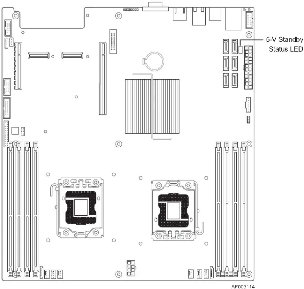
Figure 22: 5-V Standby Status LED Location
8.2 Fan Fault LEDs
Fan fault LEDs are present for the six fans and are located near each CPU fan header.
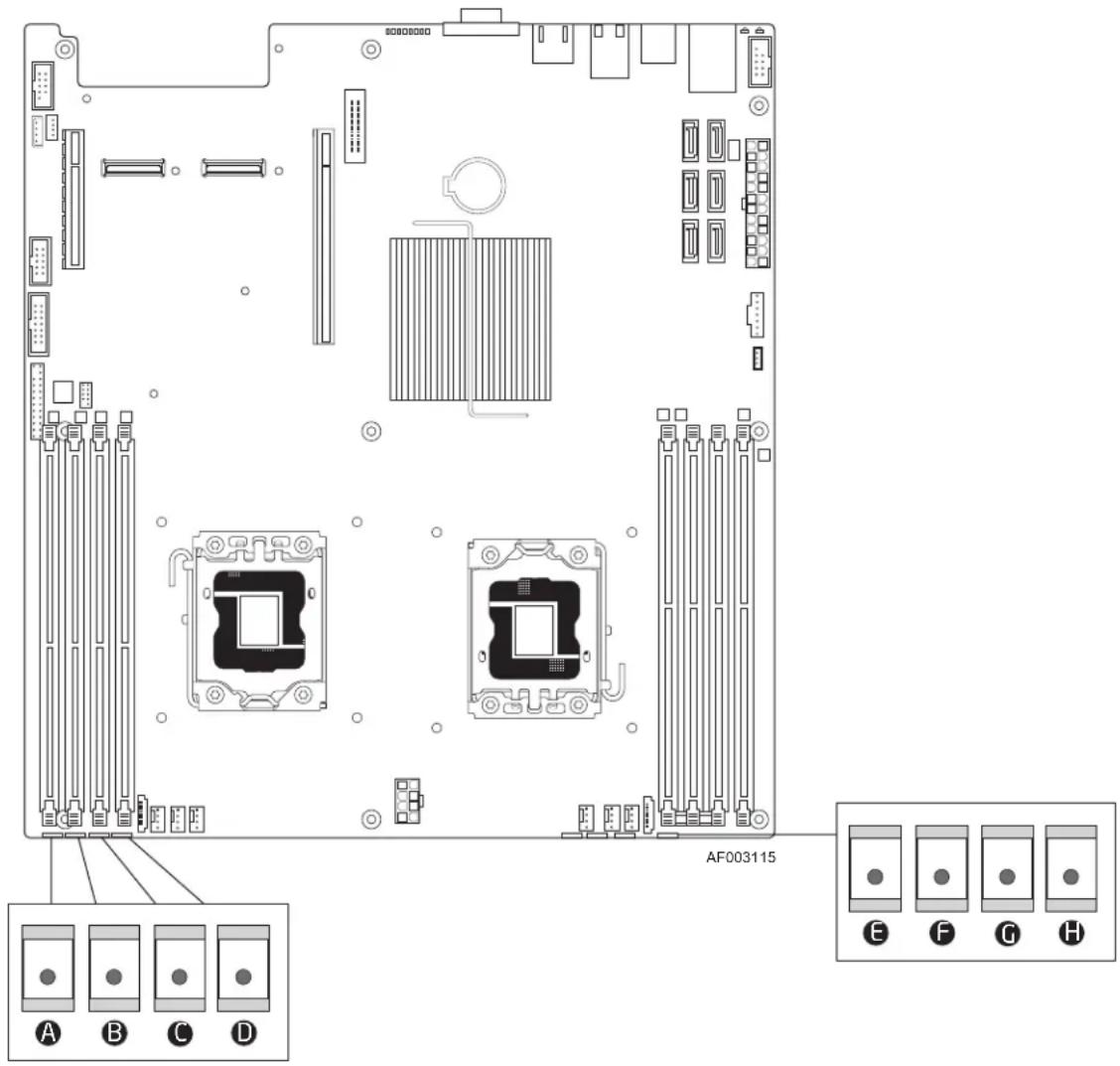
Figure 23. Fan Fault LED Locations
| A | FLTMEM2R | E | FLTCPU1 |
| B | FLTMEM2 | F | FLTCPU1A |
| C | FLTCPU2A | G | FLTMEM1 |
| D | FLTCPU2 | H | FLTMEM1R |
8.3 System Status LED
The server board provides LED for system status. The following figure shows the LED location.
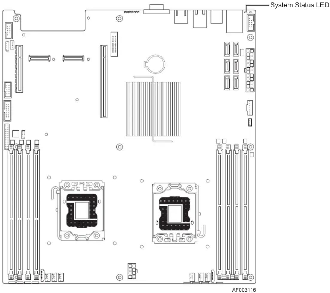
Figure 24. System Status LED Location
The bi-color System Status LED operates as follows:
Table 50. System Status LED
| Color State System Status Description | |||
| Green Solid on Ok | System ready | ||
| Green | ~1 Hz blink | Degraded | System degraded:BIOS detected1. Unable to use all of the installed memory (more than one DIMM installed). ^1 2. In a mirrored configuration, when memory mirroring takes place and system loses memory redundancy. This is not covered by (2). ^1 3. PCI Express* correctable link errors.Integrated BMC detected1. Redundancy loss such as a power supply or fan. Applies only if the associated platform subsystem has redundancy capabilities.2. CPU disabled – if there are two CPUs and one CPU is disabled.3. Fan alarm – Fan failure. Number of operational fans should be more than minimum number needed to cool the system.4. Non-critical threshold crossed – Temperature, voltage, power nozzle, power gauge, and PROCHOT2 (Therm Ctrl) sensors.5. Battery failure.6. Predictive failure when the system has redundant power supplies. |
| Amber | ~1 Hz blink | Non-Fatal | Non-fatal alarm – system is likely to fail:BIOS Detected1. In non-mirroring mode, if the threshold of ten correctable errors is crossed within the window. ^1 2. PCI Express* uncorrectable link errors.Integrated BMC Detected1. Critical threshold crossed – Voltage, temperature, power nozzle, power gauge, and PROCHOT (therm Ctrl) sensors.2. VRD Hot asserted.3. The minimum number of fans required to cool the system are not present or have failed. |
| Amber | Solid on | Fatal | Fatal alarm – system has failed or shut down:BIOS Detected1. DIMM failure when there is one DIMM present and no good memory is present. ^1 2. Run-time memory uncorrectable error in non-redundant mode. ^1 3. CPU configuration error (for instance, processor stepping mismatch).Integrated BMC Detected1. CPU IERR signal asserted.2. CPU 1 is missing.3. CPU THERMTRIP.4. No power good – power fault.5. Power Unit Redundancy sensor – Insufficient resources offset (indicates not enough power supplies are present). |
| Off N/A | Not ready | AC power off | |
Notes:
- The BIOS detects these conditions and sends a Set Fault Indication command to the Integrated BMC to provide the contribution to the system status LED.
- Support for an upper, non-critical threshold limit is not provided in default SDR configuration. However if a user does enable this threshold in the SDR, then the system status LED should behave as described.
8.4 DIMM Fault LEDs
Each DIMM slot has a DIMM Fault LED near the DIMM slot.
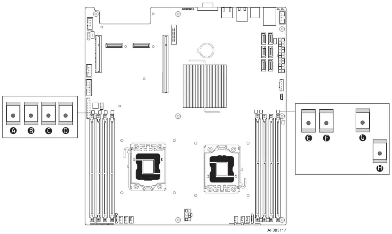
Figure 25. DIMM Fault LEDs Locations
| A | FLT_F | E | FLT_A2 |
| B | FLT_E | F | FLT_A1 |
| C | FLT_D1 | G | FLT_B |
| D | FLT_D2 | H | FLT_C |
8.5 POST Code Diagnostic LEDs
Eight amber POST code diagnostic LEDs are located on the back edge of the server board in the rear I/O area of the server board by the VGA connector.
During the system boot process, the BIOS executes a number of platform configuration processes, each of which is assigned a specific hex POST code number. As each configuration routine is started, the BIOS displays the given POST code to the POST code diagnostic LEDs on the back edge of the server board. To assist in troubleshooting a system hang during the POST process, you can use the Diagnostic LEDs to identify the last POST process executed. For a complete description of how these LEDs are read and a list of all supported POST codes, refer to Appendix A.
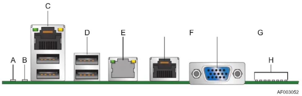
Figure 26. Rear Panel Diagnostic LEDs
| Description Description | |||
| A | ID LED E | RJ-45 GbE LAN connector | |
| B | Status LED F | RJ-45 Serial port connector | |
| C | RJ-45 GbE/Dual USB connector | G | DB15 Video |
| D | Dual USB connector | H | Diagnostic LEDs |
8.6 Front Panel Support
The Intel ^® Server Board S5500WB supports SSI standard front panel boards. The front panel support is provided by a SSI compatible 2x12-pin signal connector. The front panel connector supports the following diagnostic LEDs.
Table 51. Standard Front Panel Functionality
| LED Color Condition What It Means | |||
| Power/Sleep | Green On Power on or S0 sleep | ||
| Green Blink S1 sleep | |||
| Off Off (also sleep $5 modes) | |||
| Status | Green On System ready/No alarm | ||
| Green | Blink | System ready, but degraded: redundancy lost such as power supply or fan failure; non-critical temp/voltage threshold; battery failure; or predictive PS failure. | |
| Amber | On | Critical alarm: Voltage, thermal, or power fault; CPU1 missing; insufficient power unit redundancy resource offset asserted | |
| Amber | Blink | Non-Critical failure: Critical temp/voltage threshold; VDR hot asserted; min number fans not present or failed | |
| Off | AC power off: System unpluggedAC power on: System powered off and in standby, no prior degraded\non-critical\critical state | ||
| HDD | Green | Blink | HDD access |
| Amber | Not Supported | HDD fault | |
| Amber | Not Supported | Predictive failure, rebuild, identify | |
| Off No access | |||
| LAN #1 - Activity | Green On LAN link/ no access | ||
| Green | Blink | LAN access | |
| Off | Idle | ||
| LAN #2 - Activity | Green On LAN link/ no access | ||
| Green | Blink | LAN access | |
| Off | Idle | ||
| Identification | Blue On Front panel chassis ID button pressed | ||
| Blue Blink Unit selected for identification via software | |||
| Off | No identification | ||
9. Design and Environmental Specifications
9.1 Fan Speed Control Thermal Management
Fan speed control supports the following thermal sensors:
- Discrete board level digital thermal sensor TMP75
- Front panel Temp Sensor (if present)
- CPU PECI DTS
• DDR3 RDIMM TSOD
Eight front system fan headers for four individual thermal zones
- Zone 4 (mem2 fans) responds to memory2 and CPU2 temperatures.
- Zone 3 (CPU2 and MEM2 fans) responds to CPU2 and IOH temperatures.
- Zone 2 (CPU1 and MEM1 fans) responds to CPU1 and IOH temperatures.
• Zone 1 (mem1 fans) responds to memory1 and CPU1 temperatures.
Figure 27: Thermal Zones
The following tables show a basic location of the fan connectors on the board. The first line is the silk screen name of the connector; the second is the PWM signal name; the third is the Tach #; and the forth is the reference description. The last is the signal name associated with the fault LED signal.
flowchart
graph TD
    subgraph IBMC
        A["PWM 1"] --> B["4-Wire Fan headers"]
        C["TACH 1"] --> B
        D["TACH 5"] --> B
        E["PWM 2"] --> B
        F["TACH 2"] --> B
        G["TACH 6"] --> B
        H["PWM 3"] --> I["4-Wire Fan headers"]
        J["TACH 3"] --> I
        K["TACH 7"] --> I
        L["PWM 4"] --> M["4-Wire Fan headers"]
        N["TACH 4"] --> M
        O["TACH 8"] --> M
    end
    subgraph Double Rotor 1
        P["CPU_1a Fan"] --> Q["4-Wire Fan headers"]
        R["CPU_1 Fan (Active H/S)"] --> Q
    end
    subgraph Double Rotor 3
        S["Mem_1 Redundant Fan"] --> T["Combo header"]
        U["Mem_2 Redundant Fan"] --> T
        V["Combo header"] --> T
    end
    style IBMC fill:#f9f,stroke:#333
    style Double Rotor 1 fill:#bbf,stroke:#333
    style Double Rotor 3 fill:#bbf,stroke:#333
Figure 28: Location of Fan Connectors
Table 52. Fan Connector Location & Detail
| CPU 1 Memory 1 | |||
| FAN_CPU1 | FAN_CPU1A | FAN_MEM1 | FAN_MEM1R |
| PWM_CPU1 | PWM_CPU1 | PWM_MEM1 | PWM_MEM1 |
| Tach 1 Tach 5 Tach 2 | Tach 2 & 6 | ||
| J8E1 | J8J4 | J8J3 | |
| LED_Fan_Fault_CPU1 | LED_Fan_Fault_CPU1A | LED_Fan_Fault_MEM1 | LED_Fan_Fault_MEM1R |
J9E
Table 53. Fan Connector Location & Detail
| CPU 2 Memory 2 | |||
| FAN_CPU2 | FAN_CPU2A | FAN_MEM2 | FAN_MEM2R |
| PWM_CPU0 | PWM_CPU0 | PWM_MEM0 | PWM_MEM0 |
| Tach 3 Tach 7 Tach 4 | Tach 4 & 8 | ||
| J3E1 | J2J2 | J2J1 | |
| LED_Fan_Fault_CPU0 | LED_Fan_Fault_CPU0A | LED_Fan_Fault_MEM0 | LED_Fan_Fault_MEM0R |
J1[
flowchart
graph TD
    A["CPU0 NEHALEM"] -->|QUICKPATH| B["CPU1 NEHALEM"]
    B --> C["TYLERSBURG PEHPSMB"]
    C --> D["ME"]
    D --> E["ICH10R"]
    E --> F["SMBUS (DX44)"]
    F --> G["NOT USED"]
    H["TEMP LM75 (DXSE)"] --> I["FRU AT24C01 (DXAB)"]
    I --> J["FRONT PANEL CONN."]
    J --> K["REPEATER 3.3VSB - 3.3V PCA9515"]
    K --> L["DEPOP"]
    L --> M["GPIO SENSORS 08 FP_NMI_BTN_N 09 FP_ID_BTN 10 IRQ_IOH_ICH_SMI_TTL_N 16 DDR3_CPU0_THERMAL2 17 DDR3_CPU1_THERMAL2 18 SMB_PWR_ALERT_N 19 IOH_THERMALERT_N 20 IOH_THERMTRIP_N 21 CPU_PROCHOT_N 23 CATERR_N"]
    M --> N["SGPI SENSORS 0 CPU0_SKTOCC 1 CPU1_SKTOCC 2 CPU0_RDIMM_EVENT_N 3 CPU1_RDIMM_EVENT_N 4 CPU0_THERMTRIP_N 5 CPU1_THERMTRIP_N 6 CPU0_VRHOT 7 CPU1_VRHOT"]
    N --> O["THERMAL SENSORS 0 NOT USED 1 NOT USED 2 BASEBOARD"]
    O --> P["ISO 5VSB - 5V"]
    P --> Q["5V STBY IPMI BUS"]
    R["VOLTAGE SENSORS 0 - P12V 6 - PV_VCCP_CPU0 1 - P5V 7 - PV_VCCP_CPU1 2 - P3V3 8 - P1V5_DDR3_CPU0 3 - P5V_STBY 9 - P1V5_DDR3_CPU1 4 - P3V3_STBY 10 - P1V1_ICH 5 - P1V5_ICH 11 - P1V8_AUX_NIC"] --> S["BATTERY SENSOR MOSFET ISOLATION"]
    S --> T["SM BUS IBMC"]
    U["INTRUDER SWITCH"] --> V["HSBP CONN A (DXCO)"]
    V --> W["HSBP CONN B (DXC2)"]
    X["IPMI CONN"] --> Y["IPMI BUS"]
Figure 29. Fans and Sensors Block Diagram
9.2 Thermal Sensors
9.2.1 Processor PECI Temperature Sensor
The processor thermal control uses a CPU PECI thermal sensor, which is a relative temperature off PROCHOT# trip point (a -20C reading means 20C below PROCHOT# trip point temperature). The BMC can get the Intel® 5500 series processor PECI Tcontrol values for each CPU installed to use/follow the clamped algorithm for component thermal sensor. The following sample SDR settings could be used:
- Use Tcontrol (byte 8, bit 0 = 1): Tcontrol value is provided by BIOS via the Set CPU TControl command for the indicated CPU is used.
• Tcontrol offset Temperature = -2°C
- Pos_hyst = 0° C
- Neg_hyst = 3°C
Those parameters in turn set the following:
• Upper = - CPU PECI Tcontrol + Tcontrol offset
- Lower = - CPU PECI Tcontrol + Tcontrol offset - 3C
9.2.2 Memory Temperature Sensor
DDR3 cooling requires thermal throttling to protect memory from overheating. The Intel ^® Server Board S5500WB supports both DDR3 UDIMM and DDR3 RDIMM. SPD temperature sensor on DIMM is anticipated to be available on all DDR3 RDIMM but not for non-ECC UDIMM, so open loop thermal throttling and closed loop thermal throttling are supported.
- Static open loop thermal throttling: The system does not change any of the control registers in the processor during runtime. OLTT control registers are configured by BIOS MRC and remain fixed after post.
- Static closed loop thermal throttling: The system does not change the control registers for a closed loop in the processor during runtime. CLTT control registers are configured by BIOS MRC.
For advanced implementation with dynamic OLTT and CLTT, refer to the VR_Hot Sensor in VR11.1.
9.2.3 Board Temperature Sensor
For rack-based systems or those systems that do not have a front panel temp sensor, the board is enabled to use a board-mounted, industry standard "TMP75" type temp sensor. This part is on the IBMC two-wire serial SENSOR bus. The use of digital parts removes calibration and placement location issues imposed by the alternate analog type sensors.
9.2.4 Thermals Sensor Placement
The SMBUS based temp sensors are placed such that the ambient air temp can be measured. Placement near hot components and or downstream of hot components (including chassis-based hot spots) is avoided. The following figure shows the sensor placement on the Intel ^® Server Board S5500WB.
natural_image
Top-down schematic of a computer motherboard showing CPU socket, RAM slots, and drive bays (no text or labels)AF003062
Figure 30: Temp Sensor Location
| Location Description | |
| A U4K3 Temp Sensor - TMP75 |
9.3 Heatsinks
The Intel ^® Server Board S5500WB system cooling solutions rely on heatsinks for CPU cooling.
Chipset and or voltage regulator heatsinks are compatible with the 1U usage.
Note: The Intel® Thermal Solution STS100P – Passive 1U/2U heatsink was tested for processors up to and including 95-W TDP (Thermal Design Power). Product order code: BXSTS100P
9.3.1 Unified Retention System Support
The server board complies with the Intel ^® Unified Retention System (URS) and the Unified Backplate Assembly. The server board ships with a made-up assembly of Independent Loading Mechanism (ILM) and Unified Backplate at each processor socket.
The URS retention transfers load to the server board via the unified backplate assembly. The URS spring, captive in the heatsink, provides the necessary compressive load for the thermal interface material. All components of the URS heatsink solution are captive to the heatsink and only require a Philips* screwdriver to attach to the unified backplate assembly. See the following figure for the stacking order of the URS components.
The ILM and unified backplate are removable, allowing for the use of non-Intel heatsink retention solutions.
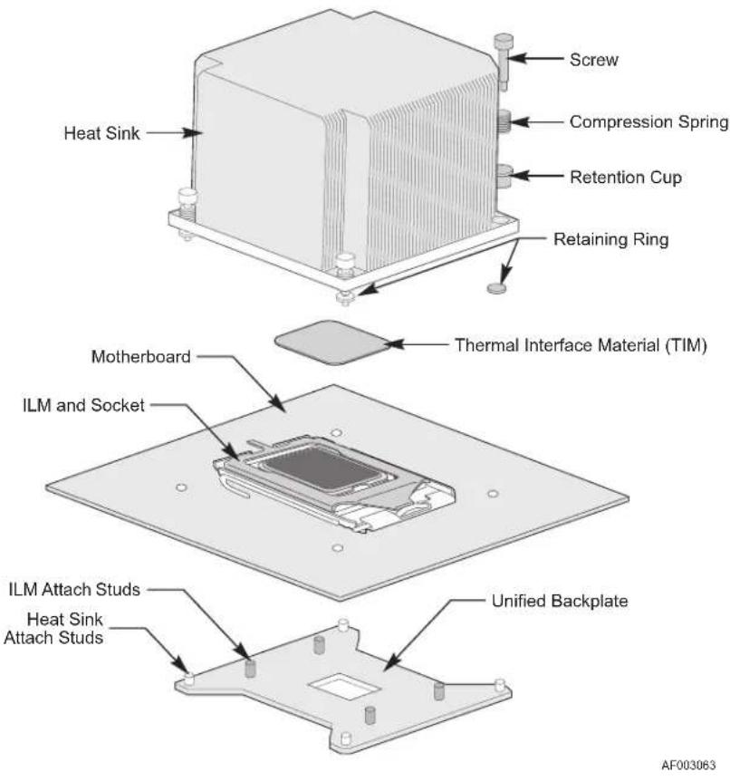
Figure 31. Unified Retention System and Unified Backplate Assembly
9.4 Errors
This section outlines how errors are routed in the hardware to ensure appropriate FW action (logging, fan control, system management, and so forth) is taken when an event occurs.
9.4.1 PROCHOT#
PROCHOT# is a bi-directional signal. The CPU toggles PROCHOT# when it goes into throttling mode. The duty cycle of PROCHOT# toggling indicates the amount of throttling initiated by the CPU. FW does not monitor PROCHOT# to determine CPU throttling percentage. Instead, it obtains outbound CPU throttling data via PECI. The path between the CPU's and IBMC (TTL_CPU_PROCHOT#) is there as a backup.
An external source can also toggle PROCHOT# to force the CPU to go into throttling mode. This usually happens when the system reaches a certain thermal threshold. VRHOT is an output of the CPU VR controller, which is capable of throttling the CPU via PROCHOT#. Some simple masking circuitry is required to prevent the VRHOT from asserting the PROCHOT# to the CPUs at the time of CPU_RST#. This keeps the VRHOT from unintentionally causing the CPU to disable. FW monitors VRHOT and creates a SEL event if VRHOT is asserted. There is no fan action as a result of the BMC seeing VRHOT.
9.4.2 THERMTRIP#
THERMTRIP# comes from the CPU. The THERMTRIP# signal is tied to a unique GPI on IBMC for FW to monitor. The combined THERMTRIP#'s from both CPUs is also tied to the ICH10R THERMTRIP input to cause an automatic Power Off condition when activated.
9.4.3 CATERR#
The CATERR# signal from the CPU signals a catastrophic error occurred. CATERR# may signal two types of issues. One type is a warning and is indicated by a pulse on the signal. The other is the static critical error, which is indicated by a continuously asserted level on the signal. The BMC only logs the static Critical Error events and ignores the warnings indicated by the pulse. An error on the CPU is immediately communicated to the ICH10R for notification.
10. Power Subsystem
10.1 Server Board Power Distribution
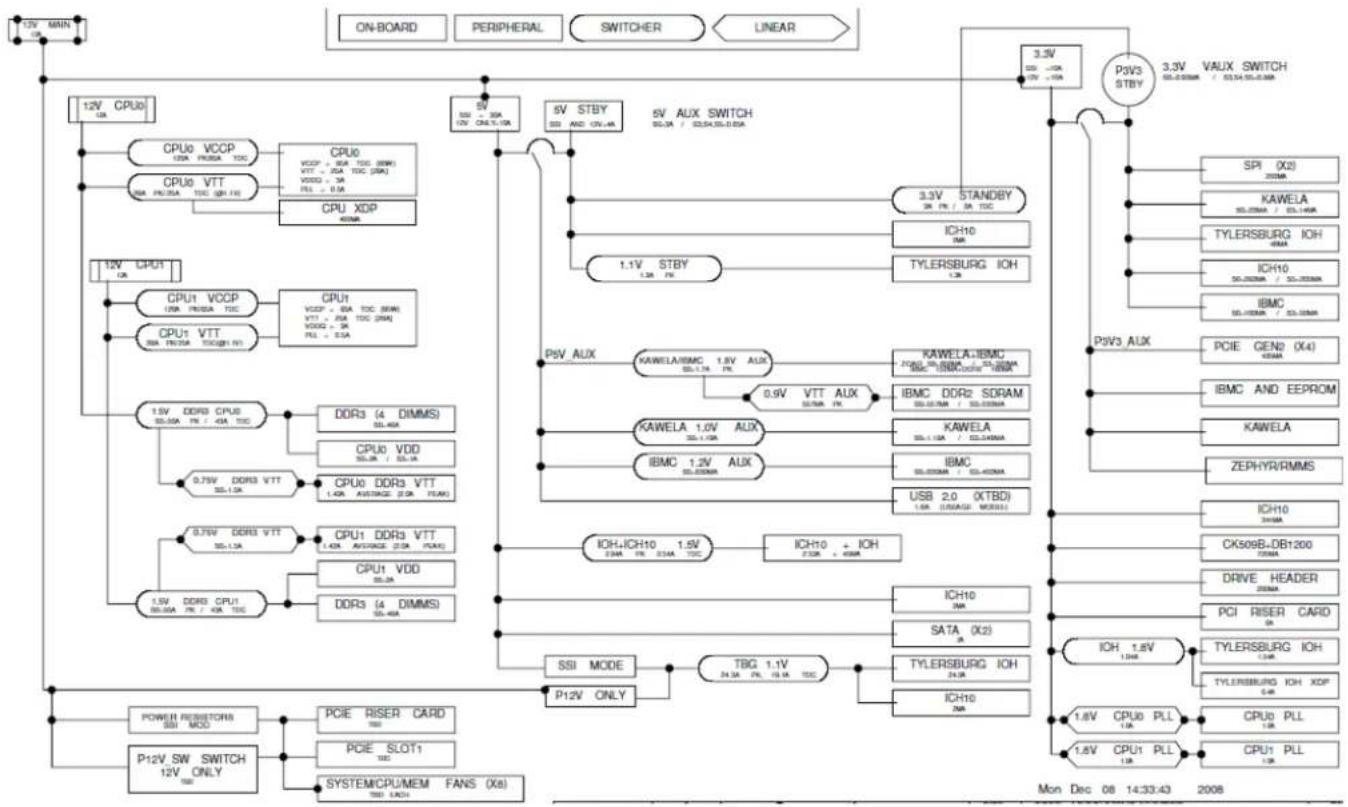
flowchart
graph TD
    A["12V MAIN"] --> B["ON-BOARD"]
    A --> C["PERIPHERAL"]
    A --> D["SWITCHER"]
    A --> E["LINEAR"]
    B --> F["12V CPU0 1CA"]
    C --> G["CPU0 VCCP 10A FROSA TDC"]
    C --> H["CPU0 VTT 80A FROSA TDC (DR) F1"]
    C --> I["CPU XDP 400A"]
    F --> J["12V CPU1 UK"]
    G --> K["CPU1 VCCP 10A FROSA TDC"]
    G --> L["CPU1 VTT 80A FROSA TDC(DR) F1"]
    H --> M["1.5V DDR3 CPU0 50.00A F1 / 40A TDC"]
    H --> N["DDR3 (4 DIMMS) 50.46K"]
    H --> O["CPU0 VDD 50.3A / 50.1A"]
    H --> P["0.75V DDR3 VTT 30.13K"]
    H --> Q["0.75V DDR3 VTT 30.13K"]
    H --> R["1.5V DDR3 CPU1 50.00A F1 / 40A TDC"]
    I --> S["5V STBY 32D AND CN-4K"]
    I --> T["5V AUX SWITCH 50.3A / 50.3A-50.0A"]
    T --> U["3.3V STANDBY 3K F1 / 3K TDC"]
    U --> V["ICH10 8M"]
    U --> W["TYLERSBURG IOH 1.3K"]
    V --> X["P9V3 STBY"]
    W --> Y["P9V3 AUX"]
    X --> Z["SPI (X2) 200MA"]
    X --> AA["KAWELA 50.20MA / 50.14MA"]
    X --> AB["TYLERSBURG IOH 40MA"]
    X --> AC["ICH10 50.20MA / 50.20MA"]
    X --> AD["IBMC 50.20MA / 50.20MA"]
    Y --> AE["PCE CEN2 (X4) 40MA"]
    Y --> AF["IBMC AND EEPROM"]
    Y --> AG["KAWELA"]
    Y --> AH["ZEPHYR/RMMS"]
    Z --> AI["ICH10 34MA"]
    AA --> AJ["CK509B-DB1200 72MA"]
    AB --> AK["DRIVE HEADER 20MA"]
    AC --> AL["PCI RISER CARD 8A"]
    AD --> AM["TYLERSBURG IOH 1.3M"]
    AD --> AN["TYLERSBURG IOH XOP 64M"]
    AE --> AO["ICH10 3M"]
    AE --> AP["SATA (X2) 8A"]
    AF --> AQ["ICH10 7M"]
    AG --> AR["ICH10 2.0 (XTBD) 1.6M (USBAGE MODE)"]
    AH --> AS["ICH10 PLL 1.6M"]
    AI --> AT["POWER RESISTORS SSI MDD"]
    AJ --> AU["P12V_SW SWITCH 12V ONLY 18B"]
    AK --> AV["PCIE RISER CARD 78B"]
    AL --> AW["PCIE SLOT1 TDC"]
    AM --> AX["SYSTEM/CPU/MEM FANS (X8) 78D EACH"]
    AN --> AY["P12V ONLY"]
    AO --> AZ["P12V ONLY"]
    AU --> BA["TSI MODE"]
    AV --> BB["P12V ONLY"]
    AW --> BC["P12V ONLY"]
Figure 32. Power Distribution Diagram
10.2 Power Supply Compatibility
The Intel ^® Server Board S5500WB is offered in two models:
- SSI SKU: This version of the server board is designed to work with an “off-the-shelf” multi-rail power supply that adheres to the SSI power specification: “Power Supply Design Guideline for 2008 Dual-Socket Servers and Workstations”. You can view SSI specifications at the following website: http://ssiforum.org
- 12V SKU: This version of the server board is designed to work with specially-designed "single rail" power supplies that provide 12V and 5V standby current. The server board has integrated, high-efficiency voltage regulators that produce other voltages required (for example, 3.3 V, 5 V, and so forth) and can also supply 5 V power required by hard drives.
The SSI uses the standard 24-pin and 8-pin power headers along with the 5pin Control connector. The 12-V only uses two 8-pin power headers, a 7-pin control header and a 6 pin HDD power connector. For maximum rack server efficiency, a DC 12-V only power supply is recommended. Appendix A shows connector pin outs.
10.3 Power Sequencing and Reset Distribution
The IBMC device is integrated into the power control and reset logic of the system. This design reduces the discrete logic requirements of previous generations and at the same time permits FW to manage certain features related to the power on/off control and the reset logic.
11. Regulatory and Certification Information
11.1 Product Regulation Requirements
Intended Application – This product was evaluated as Information Technology Equipment (ITE), which may be installed in offices, schools, computer rooms, and similar commercial type locations. The suitability of this product for other product categories and environments (such as: medical, industrial, telecommunications, NEBS, residential, alarm systems, test equipment), other than an ITE application, may require further evaluation. This is an FCC Class A device. Integration of it into a Class B chassis does not result in a Class B device.
11.1.1 Product Safety Compliance
The Intel ^® Server Board S5520UR complies with the following safety requirements:
- UL60950 – CSA 60950(USA / Canada)
■ EN60950 (Europe)
■ IEC60950 (International) - CB Certificate & Report, IEC60950 (report to include all country national deviations)
- GOST R 50377-92 – Listed on one System Certification (Russia)
- Belarus Certification – Listed on System Certification (Belarus)
■ CE - Low Voltage Directive 73/23/EEE (Europe) - IRAM Certification (Argentina)
11.1.2 Product EMC Compliance - Class A Compliance
- FCC /ICES-003 - Emissions (USA/Canada) Verification
- CISPR 22 – Emissions (International)
■ EN55022 - Emissions (Europe)
■ EN55024 - Immunity (Europe) - CE – EMC Directive 89/336/EEC (Europe)
- AS/NZS 3548 Emissions (Australia / New Zealand)
- VCCI Emissions (Japan)
■ BSMI CNS13438 Emissions (Taiwan) - GOST R 29216-91 Emissions - Listed on one System Certification (Russia)
- GOST R 50628-95 Immunity –Listed on one System Certification (Russia)
- Belarus Certification – Listed on one System Certification (Belarus)
■ KCC (EMI) (Korea)
11.1.3 Certifications / Registrations / Declarations
■ NRTL Certification (US/Canada)
■ CE Declaration of Conformity (CENELEC Europe)
■ FCC/ICES-003 Class A Attestation (USA/Canada)
■ C-Tick Declaration of Conformity (Australia)
■ MED Declaration of Conformity (New Zealand)
■ BSMI Certification (Taiwan)
Intel® Server Board S5500WB TPS Regulatory and Certification Information
- GOST – Listed on one System Certification (Russia)
- Belarus – Listed on one System Certification (Belarus)
■ KCC Certification (Korea)
■ Ecology Declaration (International)
11.2 Product Regulatory Compliance Markings
This Intel Server Board bears the following regulatory marks:
Table 54: Product Regulatory Compliance Markings
| Regulatory Compliance Country Marking | |
| UL Mark USA/Canada | |
| CE Mark Europe | |
| FCC Marking (Class A) USA | |
| EMC Marking (Class A) Canada CANADA ICES-003 CLASS A | |
| BSMI Marking (Class A) Taiwan | |
| KCC Mark Korea |
11.3 Electromagnetic Compatibility Notices
11.3.1 FCC Verification Statement (USA)
This device complies with Part 15 of the FCC Rules. Operation is subject to the following two conditions: (1) this device may not cause harmful interference, and (2) this device must accept any interference received, including interference that may cause undesired operation.
For questions related to the EMC performance of this product, contact:
Intel Corporation 5200 N.E. Elam Young Parkway Hillsboro, OR 97124-6497 1-800-628-8686
This equipment has been tested and found to comply with the limits for a Class A digital device, pursuant to Part 15 of the FCC Rules. These limits are designed to provide reasonable protection against harmful interference in a residential installation. This equipment generates, uses, and can radiate radio frequency energy and, if not installed and used in accordance with the instructions, may cause harmful interference to radio communications. However, there is no guarantee that interference will not occur in a particular installation. If this equipment does cause harmful interference to radio or television reception, which can be determined by turning the equipment off and on, the user is encouraged to try to correct the interference by one or more of the following measures:
- Reorient or relocate the receiving antenna.
- Increase the separation between the equipment and the receiver.
- Connect the equipment into an outlet on a circuit different from that to which the receiver is connected.
- Consult the dealer or an experienced radio/TV technician for help.
Any changes or modifications not expressly approved by the grantee of this device could void the user's authority to operate the equipment. The customer is responsible for ensuring compliance of the modified product.
Only peripherals (computer input/output devices, terminals, printers, etc.) that comply with FCC Class A or B limits may be attached to this computer product. Operation with noncompliant peripherals is likely to result in interference to radio and TV reception.
All cables used to connect to peripherals must be shielded and grounded. Operation with cables, connected to peripherals that are not shielded and grounded may result in interference to radio and TV reception.
11.3.2 ICES-003 (Canada)
English translation of the notice above:
This digital apparatus does not exceed the Class A limits for radio noise emissions from digital apparatus set out in the interference-causing equipment standard entitled “Digital Apparatus,” ICES-003 of the Canadian Department of Communications.
11.3.3 Europe (CE Declaration of Conformity)
This product has been tested in accordance too, and complies with the Low Voltage Directive (73/23/EEC) and EMC Directive (89/336/EEC). The product has been marked with the CE Mark to illustrate its compliance.
11.3.4 BSMI (Taiwan)
The BSMI Certification Marking and EMC warning is located on the outside rear area of the product.
警告使用者:
Following is the KCC certification information for Korea.

English translation of the notice above:
- Type of Equipment (Model Name): On Certification and Product
- Certification No.: On KCC certificate. Obtain certificate from local Intel representative
- Name of Certification Recipient: Intel Corporation
- Date of Manufacturer: Refer to date code on product
- Manufacturer/Nation: Intel Corporation/Refer to country of origin marked on product
Appendix A: POST Code LED Decoder
During the system boot process, the BIOS executes several platform configuration processes, each of which is assigned a specific hex POST code number. As each configuration routine is started, the BIOS displays the POST code on the POST code diagnostic LEDs found on the back edge of the server board. To assist in troubleshooting a system hang during the POST process, the diagnostic LEDs can be used to identify the last POST process to be executed.
Each POST code is represented by the eight amber diagnostic LEDs. The POST codes are divided into two nibbles, an upper nibble and a lower nibble. The upper nibble bits are represented by diagnostic LEDs #4, #5, #6, and #7. The lower nibble bits are represented by diagnostics LEDs #0, #1, #2, and #3. If the bit is set in the upper and lower nibbles, then the corresponding LED is lit. If the bit is clear, then the corresponding LED is off.
The diagnostic LED #7 is labeled as "MSB" (Most Significant Bit), and the diagnostic LED #0 is labeled as "LSB" (Least Significant Bit).
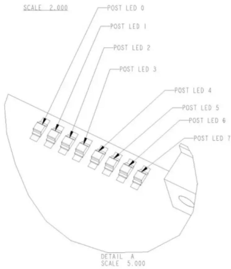
Figure 33. Diagnostic LED Placement Diagram
In the following example, the BIOS sends a value of ACh to the diagnostic LED decoder. The LEDs are decoded as follows:
Table 55. POST Progress Code LED Example
| LEDs | Upper Nibble LEDs Lower Nibble LEDs | ||||||||
| MSB | LSB | ||||||||
| LED #7 | LED #6 | LED #5 | LED #4 | LED #3 | LED #2 | LED #1 | LED #0 | ||
| 8h | 4h | 2h | 1h | 8h | 4h | 2h | 1h | ||
| Status | ON | OFF | ON | OFF | ON | ON | OFF | OFF | |
| Results | 1 | 0 | 1 | 0 | 1 1 | 0 | 0 | ||
| Ah | Ch | ||||||||
Upper nibble bits = 1010b = Ah; Lower nibble bits = 1100b = Ch; the two are concatenated as ACh.
Table 56. Diagnostic LED POST Code Decoder
| Checkpoint | Diagnostic LED Decoder | L S B Description | |||||||
| 1 = On, 0=Off | |||||||||
| Upper Nibble Lower Nibble | |||||||||
| M | S | B | |||||||
| 8h | 4h | 2h | 1h | 8h | 4h | 2h | 1h | ||
| LED | #7 | #6 | #5 | #4 | #3 | #2 | #1 | #0 | |
| Host Processor | |||||||||
| 0x10h | 0 | 0 | 0 | 1 | 0 | 0 | 0 | Power-on initialization of the host processor (bootstrap processor) | |
| 0x11h | 0 | 0 | 0 | 1 | 0 | 0 | 0 | 1 | Host processor cache initialization (including AP) |
| 0x12h | 0 | 0 | 0 | 1 | 0 | 0 | 1 | 0 | Starting application processor initialization |
| 0x13h | 0 | 0 | 0 | 1 | 0 | 0 | 1 | 1 | SMM initialization |
| 0x14h | 0 | 0 | 0 | 1 | 0 | 1 | 0 | 0 | Selection of Processor with least features to be used as Boot Strap Processor |
| 0x15h | 0 | 0 | 0 | 1 | 0 | 1 | 0 | 1 | Switch an AP processor to become the new Boot Strap Processor |
| Chipset | |||||||||
| 0x21h | 0 | 0 | 1 | 0 | 0 | 0 | 0 | 1 | Initializing a chipset component |
| Memory | |||||||||
| 0x22h | 0 | 0 | 1 | 0 | 0 | 0 | 1 | 0 | Reading configuration data from memory (SPD on FBDIMM) |
| 0x23h | 0 | 0 | 1 | 0 | 0 | 0 | 1 | 1 | Detecting presence of memory |
| 0x24h | 0 | 0 | 1 | 0 | 0 | 1 | 0 | 0 | Programming timing parameters in the memory controller |
| 0x25h | 0 | 0 | 1 | 0 | 0 | 1 | 0 | 1 | Configuring memory parameters in the memory controller |
| 0x26h | 0 | 0 | 1 | 0 | 0 | 1 | 1 | 0 | Optimizing memory controller settings |
| 0x27h | 0 | 0 | 1 | 0 | 0 | 1 | 1 | 1 | Initializing memory, such as ECC init |
| 0x28h | 0 | 0 | 1 | 0 | 1 | 0 | 0 | 0 | Testing memory |
| 0xE4h | 1 | 1 | 1 | 0 | 1 | 0 | 0 | BIOS cannot communicate with DIMM (serial channel hardware failure) | |
| 0xE6h | 1 | 1 | 1 | 0 | 1 | 1 | 0 | DIMM(s) failed Memory iBIST or Memory Link Training failure | |
| 0xE8h | 1 | 1 | 1 | 0 | 1 | 0 | 0 | No memory available (system halted) | |
| 0xE9h | 1 | 1 | 1 | 0 | 1 | 0 | 1 | Unsupported or invalid DIMM configuration (system halted) | |
| 0xEAh | 1 | 1 | 1 | 0 | 1 | 0 | 1 | DIMM training sequence failed (system halted) | |
| 0xEBh | 1 | 1 | 1 | 0 | 1 | 0 | 1 | Memory test failed (system halted) | |
| 0xECh | 1 | 1 | 1 | 0 | 1 | 1 | 0 | Unsupported or invalid DIMM configuration (system halted) | |
| 0xEDh | 1 | 1 | 1 | 0 | 1 | 1 | 0 | Unsupported or invalid DIMM configuration (system halted) | |
| 0xEBh | 1 | 1 | 1 | 0 | 1 | 0 | 1 | DIMM with corrupted SPD data detected (system halted) | |
| QuickPath Interconnect (QPI) | |||||||||
| 0xA0h | 1 | 0 | 1 | 0 | 0 | 0 | 0 | 0 | QPI Initialization |
| 0xA1h | 1 | 0 | 1 | 0 | 0 | 0 | 0 | 1 | QPI Initialization |
| 0xA2h | 1 | 0 | 1 | 0 | 0 | 0 | 1 | 0 | QPI Initialization |
| 0xA3h | 1 | 0 | 1 | 0 | 0 | 0 | 1 | 1 | QPI Initialization |
| 0xA4h | 1 | 0 | 1 | 0 | 0 | 1 | 0 | 0 | QPI Initialization |
| 0xA5h | 1 | 0 | 1 | 0 | 0 | 1 | 0 | 1 | QPI Initialization |
| 0xA6h | 1 | 0 | 1 | 0 | 0 | 1 | 1 | 0 | QPI Initialization |
| 0xA7h | 1 | 0 | 1 | 0 | 0 | 1 | 1 | 1 | QPI Initialization |
| 0xA8h | 1 | 0 | 1 | 0 | 1 | 0 | 0 | 0 | QPI Initialization |
| 0xA9h | 1 | 0 | 1 | 0 | 1 | 0 | 0 | 1 | QPI Initialization |
| 0xAAh | 1 | 0 | 1 | 0 | 1 | 0 | 1 | 0 | QPI Initialization |
| 0xABh | 1 | 0 | 1 | 0 | 1 | 0 | 1 | 1 | QPI Initialization |
| 0xACh | 1 | 0 | 1 | 0 | 1 | 1 | 0 | 0 | QPI Initialization |
| 0xADh | 1 | 0 | 1 | 0 | 1 | 1 | 0 | 1 | QPI Initialization |
| 0xAEh | 1 | 0 | 1 | 0 | 1 | 1 | 1 | 0 | QPI Initialization |
| 0xAFh | 1 | 0 | 1 | 0 | 1 | 1 | 1 | 1 | QPI Initialization |
| Integrated Memory Controller (IMC) | |||||||||
| 0xB0h | 1 | 0 | 1 | 1 | 0 | 0 | 0 | 0 | Memory Initialization of Integrated Memory Controller |
| 0xB1h | 1 | 0 | 1 | 1 | 0 | 0 | 0 | 1 | Memory Initialization of Integrated Memory Controller |
| 0xB2h | 1 | 0 | 1 | 1 | 0 | 0 | 1 | 0 | Memory Initialization of Integrated Memory Controller |
| 0xB3h | 1 | 0 | 1 | 1 | 0 | 0 | 1 | 1 | Memory Initialization of Integrated Memory Controller |
| 0xB4h | 1 | 0 | 1 | 1 | 0 | 1 | 0 | 0 | Memory Initialization of Integrated Memory Controller |
| 0xB5h | 1 | 0 | 1 | 1 | 0 | 1 | 0 | 1 | Memory Initialization of Integrated Memory Controller |
| 0xB6h | 1 | 0 | 1 | 1 | 0 | 1 | 1 | 0 | Memory Initialization of Integrated Memory Controller |
| 0xB7h | 1 | 0 | 1 | 1 | 0 | 1 | 1 | 1 | Memory Initialization of Integrated Memory Controller |
| 0xB8h | 1 | 0 | 1 | 1 | 1 | 0 | 0 | 0 | Memory Initialization of Integrated Memory Controller |
| 0xB9h | 1 | 0 | 1 | 1 | 1 | 0 | 0 | 1 | Memory Initialization of Integrated Memory Controller |
| 0xBAh | 1 | 0 | 1 | 1 | 1 | 0 | 1 | 0 | Memory Initialization of Integrated Memory Controller |
| 0xBBh | 1 | 0 | 1 | 1 | 1 | 0 | 1 | 1 | Memory Initialization of Integrated Memory Controller |
| 0xBCh | 1 | 0 | 1 | 1 | 1 | 1 | 0 | 0 | Memory Initialization of Integrated Memory Controller |
| 0xBDh | 1 | 0 | 1 | 1 | 1 | 1 | 0 | 1 | Memory Initialization of Integrated Memory Controller |
| 0xBEh | 1 | 0 | 1 | 1 | 1 | 1 | 1 | 0 | Memory Initialization of Integrated Memory Controller |
| 0xBFh | 1 | 0 | 1 | 1 | 1 | 1 | 1 | 1 | Memory Initialization of Integrated Memory Controller |
| PCI Bus | |||||||||
| 0x50h | 0 | 1 | 0 | 1 | 0 | 0 | 0 | 0 | Enumerating PCI buses |
| 0x51h | 0 | 1 | 0 | 1 | 0 | 0 | 0 | 1 | Allocating resources to PCI buses |
| 0x52h | 0 | 1 | 0 | 1 | 0 | 0 | 1 | 0 | Hot Plug PCI controller initialization |
| 0x53h | 0 | 1 | 0 | 1 | 0 | 0 | 1 | 1 | Reserved for PCI bus |
| 0x54h | 0 | 1 | 0 | 1 | 0 | 1 | 0 | 0 | Reserved for PCI bus |
| 0x55h | 0 | 1 | 0 | 1 | 0 | 1 | 0 | 1 | Reserved for PCI bus |
| USB | |||||||||
| 0x56h | 0 | 1 | 0 | 1 | 0 | 1 | 1 | 0 | Initializing USB host controllers |
| 0x57h | 0 | 1 | 0 | 1 | 0 | 1 | 1 | Detecting USB devices | |
| 0x58h | 0 | 1 | 0 | 1 | 1 | 0 | 0 | 0 | Resetting USB bus |
| 0x59h | 0 | 1 | 0 | 1 | 1 | 0 | 0 | 1 | Reserved for USB devices |
| ATA/ATAPI/SATA | |||||||||
| 0x5Ah | 0 | 1 | 0 | 1 | 1 | 0 | 1 | 0 | Resetting SATA bus and all devices |
| 0x5Bh | 0 | 1 | 0 | 1 | 1 | 0 | 1 | 1 | Detecting the presence of ATA device |
| 0x5Ch | 0 | 1 | 0 | 1 | 1 | 0 | 0 | Enable SMART if supported by ATA device | |
| 0x5Dh | 0 | 1 | 0 | 1 | 1 | 0 | 1 | Reserved for ATA | |
| SMBUS | |||||||||
| 0x5Eh | 0 | 1 | 0 | 1 | 1 | 1 | 0 | Resetting SMBUS | |
| 0x5Fh | 0 | 1 | 0 | 1 | 1 | 1 | 1 | 1 | Reserved for SMBUS |
| I/O Controller Hub | |||||||||
| 0x61h | 0 | 1 | 1 | 0 | 0 | 0 | 0 | 1 | Initializing I/O Controller Hub |
| Super I/O | |||||||||
| 0x63h | 0 | 1 | 1 | 0 | 0 | 0 | 1 | 1 | Initializing Super I/O |
| Local Console | |||||||||
| 0x70h | 0 | 1 | 1 | 1 | 0 | 0 | 0 | Resetting the video controller (VGA) | |
| 0x71h | 0 | 1 | 1 | 1 | 0 | 0 | 0 | 1 | Disabling the video controller (VGA) |
| 0x72h | 0 | 1 | 1 | 1 | 0 | 0 | 1 | 0 | Enabling the video controller (VGA) |
| 0x73h | 0 | 1 | 1 | 1 | 0 | 0 | 1 | 1 | Reserved for video controller (VGA) |
| Remote Console | |||||||||
| 0x78h | 0 | 1 | 1 | 1 | 1 | 0 | 0 | 0 | Resetting the console controller |
| 0x79h | 0 | 1 | 1 | 1 | 1 | 0 | 0 | 1 | Disabling the console controller |
| 0x7Ah | 0 | 1 | 1 | 1 | 1 | 0 | 1 | 0 | Enabling the console controller |
| 0x7Bh | 0 | 1 | 1 | 1 | 1 | 0 | 1 | 1 | Reserved for console controller |
| Keyboard (only USB) | |||||||||
| 0x90h | 1 | 0 | 0 | 1 | 0 | 0 | 0 | Resetting the keyboard | |
| 0x91h | 1 | 0 | 0 | 1 | 0 | 0 | 0 | 1 | Disabling the keyboard |
| 0x92h | 1 | 0 | 0 | 1 | 0 | 0 | 1 | 0 | Detecting the presence of the keyboard |
| 0x93h | 1 | 0 | 0 | 1 | 0 | 0 | 1 | 1 | Enabling the keyboard |
| 0x94h | 1 | 0 | 0 | 1 | 0 | 1 | 0 | 0 | Clearing keyboard input buffer |
| 0x96h | 1 | 0 | 0 | 1 | 0 | 1 | 1 | 0 | Reserved for keyboard |
| Mouse (only USB) | |||||||||
| 0x98h | 1 | 0 | 0 | 1 | 0 | 0 | 1 | 0 | Resetting the mouse |
| 0x99h | 1 | 0 | 0 | 1 | 0 | 0 | 1 | 1 | Detecting the mouse |
| 0x9Ah | 1 | 0 | 0 | 1 | 0 | 1 | 1 | 0 | Detecting the presence of mouse |
| 0x9Bh | 1 | 0 | 0 | 1 | 0 | 1 | 1 | 1 | Enabling the mouse |
| 0x9Ch | 1 | 0 | 0 | 1 | 0 | 0 | 1 | 0 | Reserved for mouse |
| Serial Port | |||||||||
| 0xA8h | 1 | 0 | 1 | 0 | 1 | 0 | 0 | 0 | Resetting the serial port |
| 0xA9h | 1 | 0 | 1 | 0 | 1 | 0 | 0 | 1 | Disabling the serial port |
| 0xAAh | 1 | 0 | 1 | 0 | 1 | 0 | 1 | 0 | Detecting the presence of the serial port |
| 0xABh | 1 | 0 | 1 | 0 | 1 | 0 | 1 | 1 | Clearing serial port buffer |
| 0xACh | 1 | 0 | 1 | 0 | 1 | 1 | 0 | 0 | Enabling serial port |
| 0xADh | 1 | 0 | 1 | 0 | 1 | 1 | 0 | 1 | Reserved for serial port |
| Fixed Media | |||||||||
| 0xB0h | 1 | 0 | 1 | 1 | 0 | 0 | 0 | 0 | Resetting fixed media device |
| 0xB1h | 1 | 0 | 1 | 1 | 0 | 0 | 0 | 1 | Disabling fixed media device |
| 0xB2h | 1 | 0 | 1 | 1 | 0 | 0 | 1 | 0 | Detecting presence of a fixed media device (SATA hard drive detection, and so forth) |
| 0xB3h | 1 | 0 | 1 | 1 | 0 | 0 | 1 | 1 | Enabling / configuring a fixed media device |
| 0xB4h | 1 | 0 | 1 | 1 | 0 | 1 | 0 | 0 | Reserved for fixed media |
| Removable Media | |||||||||
| 0xB8h | 1 | 0 | 1 | 1 | 0 | 0 | 0 | Resetting removable media device | |
| 0xB9h | 1 | 0 | 1 | 1 | 0 | 0 | 0 | 1 | Disabling removable media device |
| 0xBAH | 1 | 0 | 1 | 1 | 0 | 1 | 0 | 0 | Detecting presence of a removable media device (SATA CDROM detection, and so forth) |
| 0xBCh | 1 | 0 | 1 | 1 | 0 | 0 | 0 | Enabling / configuring a removable media device | |
| 0xBDh | 1 | 0 | 1 | 1 | 0 | 0 | 1 | 0 | Reserved for removable media device |
| Boot Device Selection (BDS) | |||||||||
| 0xD0 | 1 | 1 | 0 | 1 | 0 | 0 | 0 | 0 | Entered the Boot Device Selection phase (BDS) |
| 0xD1 | 1 | 1 | 0 | 1 | 0 | 0 | 0 | 1 | Return to last good boot device |
| 0xD2 | 1 | 1 | 0 | 1 | 0 | 0 | 1 | 0 | Setup boot device selection policy |
| 0xD3 | 1 | 1 | 0 | 1 | 0 | 0 | 1 | 1 | Connect boot device controller |
| 0xD4 | 1 | 1 | 0 | 1 | 0 | 1 | 0 | 0 | Attempt flash update boot mode |
| 0xD5 | 1 | 1 | 0 | 1 | 0 | 1 | 0 | 1 | Transfer control to EFI boot |
| 0xD6 | 1 | 1 | 0 | 1 | 0 | 1 | 1 | 0 | Trying to boot device selection |
| 0xDF | 1 | 1 | 0 | 1 | 1 | 1 | 1 | 1 | Reserved for boot device selection |
| Pre-EFI Initialization (PEI) Core | |||||||||
| 0xE0h | 1 | 1 | 1 | 0 | 0 | 0 | 0 | 0 | Entered Pre-EFI Initialization phase (PEI) |
| 0xE1h | 1 | 1 | 1 | 0 | 0 | 0 | 0 | 1 | Started dispatching early initialization modules (PEIM) |
| 0xE2h | 1 | 1 | 1 | 0 | 0 | 0 | 1 | 0 | Initial memory found, configured, and installed correctly |
| 0xE3h | 1 | 1 | 1 | 0 | 0 | 0 | 1 | 1 | Transfer control to the DXE Core |
| PEI Modules | |||||||||
| 0xF0h | 1 | 1 | 1 | 1 | 0 | 0 | 0 | 0 | Install PEIM for Platform Status Codes |
| 0xF1h | 1 | 1 | 1 | 1 | 0 | 0 | 0 | 1 | Detecting Platform Type |
| 0xF2h | 1 | 1 | 1 | 1 | 0 | 0 | 1 | 0 | Early Platform Initialization |
| 0xF3h | 1 | 1 | 1 | 1 | 0 | 0 | 1 | 1 | PEI Modules initialized |
| Driver eXecution Environment (DXE) Core | |||||||||
| 0xE4h | 1 | 1 | 1 | 0 | 0 | 1 | 0 | 0 | Entered EFI driver execution phase (DXE) |
| 0xE5h | 1 | 1 | 1 | 0 | 0 | 1 | 0 | 1 | Started dispatching drivers |
| 0xE6h | 1 | 1 | 1 | 0 | 0 | 1 | 1 | 0 | Started connecting drivers |
| DXE Drivers | |||||||||
| 0xE7h | 1 | 1 | 1 | 0 | 1 | 1 | 0 | 1 | Waiting for user input |
| 0xE8h | 1 | 1 | 1 | 0 | 1 | 0 | 0 | 0 | Checking password |
| 0xE9h | 1 | 1 | 1 | 0 | 1 | 0 | 0 | 1 | Entering BIOS setup |
| 0xEAh | 1 | 1 | 1 | 0 | 1 | 1 | 0 | 0 | Flash Update |
| 0xEBh | 1 | 1 | 1 | 0 | 1 | 1 | 0 | 1 | Legacy Option ROM initialization |
| 0xECh | 1 | 1 | 1 | 0 | 1 | 0 | 0 | 0 | DXE Drivers initialized |
| 0xEDh | 1 | 1 | 1 | 0 | 1 | 0 | 0 | 1 | Transfer control to Boot Device Selection (BDS) |
| 0xEEh | 1 | 1 | 1 | 0 | 1 | 1 | 0 | 0 | Calling Int 19. One beep unless silent boot is enabled. |
| 0xEFh | 1 | 1 | 1 | 0 | 1 | 1 | 0 | 1 | Unrecoverable boot failure |
| Pre-EFI Initialization Module (PEIM) / Recovery | |||||||||
| 0x30h | 0 | 0 | 1 | 1 | 0 | 0 | 0 | 0 | Crisis recovery initiated because of a user request |
| 0x31h | 0 | 0 | 1 | 1 | 0 | 0 | 0 | 1 | Crisis recovery initiated by software (corrupt flash) |
| 0x34h | 0 | 0 | 1 | 1 | 0 | 1 | 0 | 0 | Loading crisis recovery capsule |
| 0x35h | 0 | 0 | 1 | 1 | 0 | 1 | 0 | 1 | Handing off control to the crisis recovery capsule |
| 0x36h | 0 | 0 | 1 | 1 | 0 | 1 | 1 | 0 | Begin crisis recovery |
| 0x3Eh | 0 | 0 | 1 | 1 | 1 | 1 | 1 | 0 | No crisis recovery capsule detected |
| 0x3Fh | 0 | 0 | 1 | 1 | 1 | 1 | 1 | 1 | Crisis recovery capsule failed integrity check of capsule descriptors |
Appendix B: Video POST Code Errors
Whenever possible, the BIOS outputs the current boot progress codes on the video screen. Progress codes are 32-bit quantities plus optional data. The 32-bit numbers include class, subclass, and operation information. The class and subclass fields point to the type of hardware being initialized. The operation field represents the specific initialization activity. Based on the data bit availability to display progress codes, a progress code can be customized to fit the data width. The higher the data bit, the higher the granularity of information that can be sent on the progress port. The progress codes may be reported by the system BIOS or option ROMs.
The Response section in the following table is divided into three types:
- No Pause: The message is displayed on the local Vidoe screen during POSTor in the Error Manager. The system continues booting with a degraded state. The user may want to replace the erroneous unit. The setup POST error Pause setting does not have any effect with this error.
- Pause: The message is displayed on the Error Manager screen, and an error is logged to the SEL. The setup POST error Pause setting determines whether the system pauses to the Error Manager for this type of error, where the user can take immediate corrective action or choose to continue booting.
- Halt: The message is displayed on the Error Manager screen, an error is logged to the SEL, and the system cannot boot unless the error is resolved. The user needs to replace the faulty part and restart the system. The setup POST error Pause setting does not have any effect with this error.
Table 57. POST Error Messages and Handling
| Error Code | Error Message Response | |
| 0012 | CMOS date / time not set Major | |
| 0048 | Password check failed Major | |
| 0108 | Keyboard component encountered a locked error. Minor | |
| 0109 | Keyboard component encountered a stuck key error. Minor | |
| 0113 | Fixed Media The SAS RAID firmware can not run properly. The user should attempt to reflash the firmware. | Major |
| 0140 | PCI component encountered a PERR error. Major | |
| 0141 | PCI resource conflict Major | |
| 0146 | PCI out of resources error Major | |
| 0192 | Processor 0x cache size mismatch detected. Fatal | |
| 0193 | Processor 0x stepping mismatch. Minor | |
| 0194 | Processor 0x family mismatch detected. Fatal | |
| 0195 | Processor 0x Intel(R) QPI speed mismatch. Major | |
| 0196 | Processor 0x model mismatch. Fatal | |
| 0197 | Processor 0x speeds mismatched. Fatal | |
| 0198 | Processor 0x family is not supported. Fatal | |
| 019F | Processor and chipset stepping configuration is unsupported. | Major |
| 5220 | CMOS/NVRAM Configuration Cleared Major | |
| 5221 | Passwords cleared by jumper Major | |
| 5224 | Password clear Jumper is Set. Major | |
| 8160 | Processor 01 unable to apply microcode update Major | |
| 8161 | Processor 02 unable to apply microcode update Major | |
| 8180 | Processor 0x microcode update not found. Minor | |
| 8190 | Watchdog timer failed on last boot Major | |
| 8198 | OS boot watchdog timer failure. Major | |
| 8300 | Baseboard management controller failed self-test Major | |
| 84F2 | Baseboard management controller failed to respond Major | |
| 84F3 | Baseboard management controller in update mode Major | |
| 84F4 | Sensor data record empty Major | |
| 84FF | System event log full Minor | |
| 8500 | Memory component could not be configured in the selected RAS mode. Major | |
| 8501 | DIMM Population Error. Major | |
| 8502 | CLTT Configuration Failure Error. Major | |
| 8520 | DIMM_A1 failed Self Test (BIST). Major | |
| 8521 | DIMM_A2 failed Self Test (BIST). Major | |
| 8522 | DIMM_B1 failed Self Test (BIST). Major | |
| 8523 | DIMM_B2 failed Self Test (BIST). Major | |
| 8524 | DIMM_C1 failed Self Test (BIST). Major | |
| 8525 | DIMM_C2 failed Self Test (BIST). Major | |
| 8526 | DIMM_D1 failed Self Test (BIST). Major | |
| 8527 | DIMM_D2 failed Self Test (BIST). Major | |
| 8528 | DIMM_E1 failed Self Test (BIST). Major | |
| 8529 | DIMM_E2 failed Self Test (BIST). Major | |
| 852A | DIMM_F1 failed Self Test (BIST). Major | |
| 852B | DIMM_F2 failed Self Test (BIST). Major | |
| 8540 | DIMM_A1 Disabled. Major | |
| 8541 | DIMM_A2 Disabled. Major | |
| 8542 | DIMM_B1 Disabled. Major | |
| 8543 | DIMM_B2 Disabled. | Major |
| 8544 | DIMM_C1 Disabled. | Major |
| 8545 | DIMM_C2 Disabled. | Major |
| 8546 | DIMM_D1 Disabled. Major | |
| 8547 | DIMM_D2 Disabled. Major | |
| 8548 | DIMM_E1 Disabled. Major | |
| 8549 | DIMM_E2 Disabled. | Major |
| 854A | DIMM_F1 Disabled. Major | |
| 854B | DIMM_F2 Disabled. | Major |
| 8560 | DIMM_A1 Component encountered a Serial Presence Detection (SPD) fail error. | Major |
| 8561 | DIMM_A2 Component encountered a Serial Presence Detection (SPD) fail error. | Major |
| 8562 | DIMM_B1 Component encountered a Serial Presence Detection (SPD) fail error. | Major |
| 8563 | DIMM_B2 Component encountered a Serial Presence Detection (SPD) fail error. | Major |
| 8564 | DIMM_C1 Component encountered a Serial Presence Detection (SPD) fail error. | Major |
| 8565 | DIMM_C2 Component encountered a Serial Presence Detection (SPD) fail error. | Major |
| 8566 | DIMM_D1 Component encountered a Serial Presence Detection (SPD) fail error. Major | |
| 8567 | DIMM_D2 Component encountered a Serial Presence Detection (SPD) fail error. Major | |
| 8568 | DIMM_E1 Component encountered a Serial Presence Detection (SPD) fail error. Major | |
| 8569 | DIMM_E2 Component encountered a Serial Presence Detection (SPD) fail error. Major | |
| 856A | DIMM_F1 Component encountered a Serial Presence Detection (SPD) fail error. Major | |
| 856B | DIMM_F2 Component encountered a Serial Presence Detection (SPD) fail error. Major | |
| 85A0 | DIMM_A1 Uncorrectable ECC error encountered. Major | |
| 85A1 | DIMM_A2 Uncorrectable ECC error encountered. Major | |
| 85A2 | DIMM_B1 Uncorrectable ECC error encountered. Major | |
| 85A3 | DIMM_B2 Uncorrectable ECC error encountered. Major | |
| 85A4 | DIMM_C1 Uncorrectable ECC error encountered. Major | |
| 85A5 | DIMM_C2 Uncorrectable ECC error encountered. Major | |
| 85A6 | DIMM_D1 Uncorrectable ECC error encountered. Major | |
| 85A7 | DIMM_D2 Uncorrectable ECC error encountered. Major | |
| 85A8 | DIMM_E1 Uncorrectable ECC error encountered. Major | |
| 85A9 | DIMM_E2 Uncorrectable ECC error encountered. Major | |
| 85AA | DIMM_F1 Uncorrectable ECC error encountered. Major | |
| 85AB | DIMM_F2 Uncorrectable ECC error encountered. Major | |
| 8604 | Chipset Reclaim of non critical variables complete. Minor | |
| 9000 | Unspecified processor component has encountered a non specific error. | Major |
| 9223 | Keyboard component was not detected. | Minor |
| 9226 | Keyboard component encountered a controller error. Minor | |
| 9243 | Mouse component was not detected. Minor | |
| 9246 | Mouse component encountered a controller error. Minor | |
| 9266 | Local Console component encountered a controller error. | Minor |
| 9268 | Local Console component encountered an output error. | Minor |
| 9269 | Local Console component encountered a resource conflict error. | Minor |
| 9286 | Remote Console component encountered a controller error. | Minor |
| 9287 | Remote Console component encountered an input error. | Minor |
| 9288 | Remote Console component encountered an output error. | Minor |
| 92A3 | Serial port component was not detected | Major |
| 92A9 | Serial port component encountered a resource conflict error | Major |
| 92C6 | Serial Port controller error | Minor |
| 92C7 | Serial Port component encountered an input error. | Minor |
| 92C8 | Serial Port component encountered an output error. | Minor |
| 94C6 | LPC component encountered a controller error. | Minor |
| 94C9 | LPC component encountered a resource conflict error. | Major |
| 9506 | ATA/ATPI component encountered a controller error. Minor | |
| 95A6 | PCI component encountered a controller error. Minor | |
| 95A7 | PCI component encountered a read error. Minor | |
| 95A8 | PCI component encountered a write error. Minor | |
| 9609 | Unspecified software component encountered a start error. | Minor |
| 9641 | PEI Core component encountered a load error. Minor | |
| 9667 | PEI module component encountered a illegal software state error. | Fatal |
| 9687 DXE core component encountered a illegal software state error. Fatal | ||
| 96A7 | DXE boot services driver component encountered a illegal software state error. | Fatal |
| 96AB | DXE boot services driver component encountered invalid configuration. | Minor |
| 96E7 SMM driver component encountered a illegal software state error. Fatal | ||
| 0xA000 TPM device not detected. Minor | ||
| 0xA001 TPM device missing or not responding. Minor | ||
| 0xA002 TPM device failure. Minor | ||
| 0xA003 TPM device failed self test. Minor | ||
| 0xA022 | Processor component encountered a mismatch error. | Major |
| 0xA027 Processor component encountered a low voltage error. | Minor | |
| 0xA028 | Processor component encountered a high voltage error. | Minor |
| 0xA421 PCI component encountered a SERR error. | Fatal | |
| 0xA500 | ATA/ATPI ATA bus SMART not supported. | Minor |
| 0xA501 ATA/ATPI ATA SMART is disabled. | Minor | |
| 0xA5A0 | PCI Express component encountered a PERR error. | Minor |
| 0xA5A1 | PCI Express component encountered a SERR error. | Fatal |
| 0xA5A4 | PCI Express IBIST error. | Major |
| 0xA6A0 | DXE boot services driver Not enough memory available to shadow a legacy option ROM. | Minor |
| 0xB6A3 | DXE boot services driver Unrecognized. | Major |
Glossary
This appendix contains important terms used in the preceding chapters. For ease of use, numeric entries are listed first (for example, "82460GX") with alpha entries following (for example, "AGP 4x"). Acronyms are then entered in their respective place, with non-acronyms following.
Table 58: Glossary
| Term Definition | |
| ACPI | Advanced Configuration and Power Interface |
| AP | Application Processor |
| APIC Advanced Programmable Interrupt Control | |
| ARP Address | Resolution Protocol |
| ASIC | Application Specific Integrated Circuit |
| BIOS Basic Input / Output System | |
| BIST Built-In Self Test | |
| BMC Baseboard Management Controller | |
| Bridge | Circuitry connecting one computer bus to another, allowing an agent on one to access the other |
| BSP | Bootstrap Processor |
| Byte | 8-bit quantity. |
| CATERR | On a catastrophic hardware event the core signals CATERR to the uncore. The core enters a halted state that can only be exited by a reset. |
| CBC | Chassis Bridge Controller (A microcontroller connected to one or more other CBCs, together they bridge the IPMB buses of multiple chassis.) |
| CEK Common | Enabling Kit |
| CHAP Challenge Handshake Authentication Protocol | |
| CMOS | In terms of this specification, this describes the PC-AT compatible region of battery-backed 128 bytes of memory, which normally resides on the server board. |
| DCMI | Data Center Management Interface |
| DHCP | Dynamic Host Configuration Protocol |
| DPC Direct Platform Control | |
| EEPROM | Electrically Erasable Programmable Read-Only Memory |
| EHCI Enhanced Host Controller Interface | |
| EMP | Emergency Management Port |
| EPS | External Product Specification |
| FBD | Fully Buffered DIMM |
| F MB Flexible | Mother Board |
| FRB | Fault Resilient Booting |
| FRU Field Replaceable Unit | |
| FSB | Front Side Bus |
| GB | 1024 MB |
| GPIO | General Purpose I/O |
| GTL | Gunning Transceiver Logic |
| GPA Guest Physical Address | |
| HSC | Hot-Swap Controller |
| HPA Host Physical Address | |
| Hz Hertz (1 cycle / second) | |
| I2C Inter-Integrated Circuit Bus | |
| IA | Intel ^ Architecture |
| IBF | Input Buffer |
| ICH I/O Controller Hub | |
| IC MB Intelligent Chassis Management Bus | |
| IFB I/O and Firmware Bridge | |
| ILM Independent Loading Mechanism | |
| IMC Integrated Memory Controller | |
| INTR | Interrupt |
| IP | Internet Protocol |
| IPMB Intelligent Platform Management Bus | |
| IPMI Intelligent Platform Management Interface | |
| IR | Infrared |
| ITP | In-Target Probe |
| KB | 1024 bytes |
| KCS Keyboard Controller Style | |
| LAN Local Area Network | |
| LCD | Liquid Crystal Display |
| LED Light Emitting Diode | |
| LPC Low Pin Count | |
| LUN | Logical Unit Number |
| MAC | Media Access Control |
| MB | 1024KB |
| ME | Management Engine |
| MD2 | Message Digest 2 – Hashing Algorithm |
| MD5 | Message Digest 5 – Hashing Algorithm – Higher Security |
| ms | Milliseconds |
| MTTR Memory Type Range Register | |
| Mux | Multiplexor |
| NIC Network Interface Controller | |
| NMI | Nonmaskable Interrupt |
| OBF | Output Buffer |
| OEM | Original Equipment Manufacturer |
| Ohm | Unit of electrical resistance |
| PECI | Platform Environment Control Interface |
| PEF Platform Event Filtering | |
| PEP | Platform Event Paging |
| PIA | Platform Information Area (This feature configures the firmware for the platform hardware) |
| PLD Programmable Logic Device | |
| PMI | Platform Management Interrupt |
| POST | Power-On Self Test |
| Term Definition | ||
| PSMI Power Supply Management Interface | ||
| PWM | Pulse-Width Modulation | |
| QPI | QuickPath Interconnect | |
| RAM Random Access Memory | ||
| RASUM Reliability, Availability, Serviceability, Usability, and Manageability | ||
| RISC Reduced Instruction Set Computing | ||
| ROM Read Only Memory | ||
| RTC Real-Time Clock (Component of ICH peripheral chip on the server board) | ||
| RMM3 Remote Management Module 3 | ||
| SDR Sensor Data Record | ||
| SECC Single Edge Connector Cartridge | ||
| SEEPROM | Serial Electrically Erasable Programmable Read-Only Memory | |
| SEL | System Event Log | |
| SIO | Server Input / Output | |
| SMBUS | System Management BUS | |
| SMI | Server Management Interrupt (SMI is the highest priority nonmaskable interrupt) | |
| SMM Server Management Mode | ||
| SMS | Server Management Software | |
| SNMP | Simple Network Management Protocol | |
| TBD | To Be Determined | |
| TDP | Thermal Design Power | |
| TIM | Thermal Interface Material | |
| UART | Universal Asynchronous Receiver / Transmitter | |
| UDP User Datagram Protocol | ||
| UHCI Universal Host Controller Interface | ||
| URS Unified Retention System | ||
| UTC Universal time coordinare | ||
| UUID Universally Unique Identifier | ||
| VID | Voltage Identification | |
| VRD Voltage Regulator Down | ||
| VT | Virtualization Technology | |
| Word | 16-bit quantity | |
| ZIF | Zero Insertion Force | |
Reference Documents
• ACPI 3.0: http://www.acpi.info/spec.htm
- IPMI 2.0
- Data Center Management Interface Specification v1.0, May 1, 2008.: www.intel.com/go/dcmi
• PCI Bus Power Management Interface Specification 1.1: http://www.pcisig.com/
• PCI Express* Base Specification Rev 2.0 Dec06: http://www.pcisig.com/
• PCI Express* Card Electromechanical Specification Rev 2.0: http://www.pcisig.com/
- PMBus*: http://pmbus.org
• SATA 2.6: http://www.sata-io.org/
- SMBIOS 2.4
• SSI-EEB 3.0: http://www.ssiforum.org
• USB 1.1: http://www.usb.org
• USB 2.0: http://www.usb.org
- Windows Logo/SDG 3.0
Intel ^® Dynamic PowerTechnology Node Manager 1.5 External Interface Specification using IPMI, 2007. Intel Corporation.
- Node Power and Thermal Management Architecture Specification v1.5, rev.0.79. 2007. Intel Corporation.
Intel ^® Server System Integrated Baseboard Management Controller Core External Product Specification, 2007. Intel Corporation.
Intel ^® Thurley Server Platform Services IPMI Commands Specification, 2007. Intel Corporation.
-
Intelligent Platform Management Bus Communications Protocol Specification, Version 1.0, 1998. Intel Corporation, Hewlett-Packard Company, NEC Corporation, Dell Computer Corporation.
-
Platform Environmental Control Interface (PECI) Specification, Version 2.0. Intel Corporation
-
Platform Management FRU Information Storage Definition, Version 1.0, Revision 1.2, 2002. Intel Corporation, Hewlett-Packard Company, NEC Corporation, Dell Computer Corporation. http://developer.intel.com/design/servers/ipmi/spec.htm