H2216XXKR - Computer Case INTEL - Free user manual and instructions
Find the device manual for free H2216XXKR INTEL in PDF.

User questions about H2216XXKR INTEL
0 question about this device. Answer the ones you know or ask your own.
Ask a new question about this device
Download the instructions for your Computer Case in PDF format for free! Find your manual H2216XXKR - INTEL and take your electronic device back in hand. On this page are published all the documents necessary for the use of your device. H2216XXKR by INTEL.
USER MANUAL H2216XXKR INTEL
Intel® Server Chassis H2000 Family
Technical Product Specification
Intel order number: G59059-005
Revision 1.4
July, 2013
Enterprise Platforms and Services Division
Revision History
| Date | Revision Number | Modifications |
| February, 2012 | 1.0 | Initial release. |
| July, 2012 | 1.1 | Updated safety notice for rail kit. |
| August, 2012 | 1.2 | Updated power redundancy mode. |
| November, 2012 | 1.3 | ▪ Updated link to Rail Specification.▪ Updated warning message on PSU configuration. |
| July, 2013 | 1.4 | Updated chassis usage model. |
Disclaimers
INFORMATION IN THIS DOCUMENT IS PROVIDED IN CONNECTION WITH INTEL® PRODUCTS. NO LICENSE, EXPRESS OR IMPLIED, BY ESTOPPEL OR OTHERWISE, TO ANY INTELLECTUAL PROPERTY RIGHTS IS GRANTED BY THIS DOCUMENT. EXCEPT AS PROVIDED IN INTEL®S TERMS AND CONDITIONS OF SALE FOR SUCH PRODUCTS, INTEL® ASSUMES NO LIABILITY WHATSOEVER AND INTEL® DISCLAIMS ANY EXPRESS OR IMPLIED WARRANTY, RELATING TO SALE AND/OR USE OF INTEL® PRODUCTS INCLUDING LIABILITY OR WARRANTIES RELATING TO FITNESS FOR A PARTICULAR PURPOSE, MERCHANTABILITY, OR INFRINGEMENT OF ANY PATENT, COPYRIGHT OR OTHER INTELLECTUAL PROPERTY RIGHT.
A "Mission Critical Application" is any application in which failure of the Intel® Product could result, directly or indirectly, in personal injury or death. SHOULD YOU PURCHASE OR USE INTEL®'S PRODUCTS FOR ANY SUCH MISSION CRITICAL APPLICATION, YOU SHALL INDEMNIFY AND HOLD INTEL® AND ITS SUBSIDIARIES, SUBCONTRACTORS AND AFFILIATES, AND THE DIRECTORS, OFFICERS, AND EMPLOYEES OF EACH, HARMLESS AGAINST ALL CLAIMS COSTS, DAMAGES, AND EXPENSES AND REASONABLE ATTORNEYS' FEES ARISING OUT OF, DIRECTLY OR INDIRECTLY, ANY CLAIM OF PRODUCT LIABILITY, PERSONAL INJURY, OR DEATH ARISING IN ANY WAY OUT OF SUCH MISSION CRITICAL APPLICATION, WHETHER OR NOT INTEL® OR ITS SUBCONTRACTOR WAS NEGLIGENT IN THE DESIGN, MANUFACTURE, OR WARNING OF THE INTEL® PRODUCT OR ANY OF ITS PARTS.
Intel ^® may make changes to specifications and product descriptions at any time, without notice. Designers must not rely on the absence or characteristics of any features or instructions marked "reserved" or "undefined". Intel ^® reserves these for future definition and shall have no responsibility whatsoever for conflicts or incompatibilities arising from future changes to them. The information here is subject to change without notice. Do not finalize a design with this information.
The products described in this document may contain design defects or errors known as errata which may cause the product to deviate from published specifications. Current characterized errata are available on request.
Contact your local Intel sales office or your distributor to obtain the latest specifications and before placing your product order.
Copies of documents which have an order number and are referenced in this document, or other Intel® literature, may be obtained by calling 1-800-548-4725, or go to: http://www.intel.com/design/literature.
Table of Contents
1. Introduction .... 1
1.1 Chapter Outline....1
1.2 Server Board Use Disclaimer 2
2. Product Overview....3
2.1 Chassis Views 4
2.2 Chassis Dimensions 5
2.3 System Level Environmental Limits 5
2.4 Chassis Parts....6
2.5 Hard Drive and Peripheral Bays 7
2.6 Front Bezel Support....8
2.7 Rack and Cabinet Mounting Options 8
3. Power Sub-System....9
3.1 Mechanical Overview....9
3.1.1 AC Power Supply Unit Dimension Overview 9
3.1.2 AC Power Supply Unit General Data 10
3.1.3 AC input connector 10
3.1.4 AC Power Cord Specification Requirements 10
3.1.5 Power Supply Unit DC Output Connector....10
3.1.6 Handle Retention....11
3.1.7 LED Marking and Identification....11
3.1.8 Power Cage with Power Distribution Board.... 11
3.1.9 Power Cage Output Pin Assignment 12
3.2 AC Input Specification 14
3.2.1 Input Voltage And Frequency 14
3.2.2 AC input Power Factor....14
3.2.3 Efficiency 14
3.2.4 AC Line Fuse 15
3.2.5 AC Line Inrush 15
3.2.6 AC Line Dropout/Holdup 15
3.2.7 AC Line Fast Transient (EFT) Specification 15
3.2.8 Hot Plug 16
3.2.9 Susceptability Requirements 16
3.2.10 Electrostatic Discharge Susceptibility 16
3.2.11 Fast Transient/Burst 16
3.2.12 Radiated Immunity 16
3.2.13 Surge Immunity....16
3.2.14 AC Line Transient Specification....16
3.2.15 Power Recovery 17
3.2.16 Voltage Interruptions....17
3.2.17 AC Line Isolation....17
3.2.18 AC Power Inlet....17
3.3 DC Output Specification 18
3.3.1 Output Power/Currents 18
3.3.2 Standby Output....18
3.3.3 Voltage Regulation 18
3.3.4 Dynamic Loading 19
3.3.5 Capacitive Loading 19
3.3.6 Ripple/Noise 19
3.3.7 Grounding 20
3.3.8 Closed Loop Stability 20
3.3.9 Residual Voltage Immunity in Standby Mode 20
3.3.10 Common Mode Noise 20
3.3.11 Soft Starting 20
3.3.12 Zero Load Stability Requirement 20
3.3.13 Hot Swap Requirement....20
3.3.14 Forced Load Sharing 21
3.3.15 Timing Requirement 21
3.4 Power Supply Cold Redundancy Support 22
3.4.1 1200W CRPS Cold Redundancy 23
3.4.2 1600W CRPS Cold Redundancy 23
3.5 Control And Indicator Functions 23
3.5.1 PSON# Input Signal....23
3.5.2 PWOK(power good) Output Signal 24
3.5.3 SMBAlert# Signal....24
3.6 Protection circuits 25
3.6.1 Current Limit (OCP) 25
3.6.2 Over Voltage Protection (OVP) 25
3.6.3 Over Thermal protection 25
3.7 PMBus* 26
3.7.1 PSU Address Lines A0 26
3.7.2 Accuracy 27
3.8 Power Management Policy 27
- Cooling Sub-System 29
4.1 Power Supply Fan 29
4.2 Drive Bay Population Requirement....29
- Hard Disk Drive Support....30
5.1 Hard Disk Drive Bays Scheme 30
5.2 Hard Drive Carrier....31
5.3 Hot-Swap Hard Drive Support 31
5.3.1 Backplane Feature set: 32
5.3.2 Backplane Block Diagram....33
5.3.3 3.5" Hot Swap Backplane Connector scheme....33
5.3.4 2.5" Hot Swap Backplane Connector scheme....34
5.3.5 Backplane LED Support 36
5.3.6 Backplane Connector Definition 37
6. Front Panel Control and Indicators 40
6.1 Control Panel Button....41
6.2 Control Panel LED Indicators 41
6.2.1 Power/Sleep LED 42
6.2.2 System Status LED....42
6.2.3 System Status LED – BMC Initialization 43
Appendix A: Integration and Usage Tips....44
Glossary....45
Reference Documents 48
List of Figures
Figure 1. Chassis Overview (H2312xx SKU)....4
Figure 2. Power Supply Scheme (Rear View)....4
Figure 3. Dummy Tray Cover....4
Figure 4. Major Chassis Parts....7
Figure 5. Intel ^® Server Chassis H2312xx Drive Bay Front View ....7
Figure 6. Intel ^® Server Chassis H2216xx Drive Bay Front View ....7
Figure 7. Chassis Bezel Front View....8
Figure 8. AC Power Supply Unit Dimension Overview ......9
Figure 9. Power Cage Overview ...... 12
Figure 10. Power distribution board .... 13
Figure 11. AC Power Cord Specification....18
Figure 12. Turn On/Off Timing (Power Supply Signals) 22
Figure 13. Power Supply Device Address....26
Figure 14. PMBus Monitoring Accuracy....27
Figure 15. HDD Scheme for H2312xx .... 30
Figure 16. HDD Scheme for H2216xx ....30
Figure 17. 3.5" HDD Assembly Overview .... 31
Figure 18.2.5" HDD Assembly Overview ....31
Figure 19. Passive Backplane Block Diagram (for one node) ...... 33
Figure 20. 3.5" Backplane Component and Connectors (Front View) ...... 33
Figure 21. 3.5" Backplane Component and Connectors (Back View)....34
Figure 22. 2.5" Backplane Component and Connectors (Front View) ......35
Figure 23. 2.5" Backplane Component and Connectors (Back View)....35
Figure 24. Hard Drive Carrier LED....36
Figure 25. Front Control Panel....40
List of Tables
Table 1. Chassis Feature Set....3
Table 2. Chassis SKU Matrix ....3
Table 3. Chassis Dimension (SKU: H2312xxJR/KR) 5
Table 4. Chassis Dimension (SKU: H2216xxJR/KR) ....5
Table 5. System Environmental Limits Summary....5
Table 6. Specification Data for AC Power Supply Unit .... 10
Table 7. AC power cord specification....10
Table 8. DC Output Power Connector....10
Table 9. Power Supply Status LED ...... 11
Table 10. Pin assignment of power output connector .... 13
Table 11. Pin assignment of control signal connector....13
Table 12. AC input rating....14
Table 13. Typical power factor....14
Table 14. Platinum Efficiency Requirement....15
Table 15. AC Power Holdup Reuqirement .... 15
Table 16. Performance Criteria ...... 16
Table 17. AC Line Sag Transient Performance ...... 17
Table 18. AC Line Surge Transient Performance....17
Table 19. Load Ratings for single power supply unit.... 18
Table 20. Voltage Regulation Limits....19
Table 21. Transient Load Requirements ...... 19
Table 22. Capacitive Loading Conditions....19
Table 23. Ripple and Noise ...... 19
Table 24. Timing Requirement ...... 21
Table 25. 1200W CRPS Cold Redundancy Threshold....23
Table 26. 1600W CRPS Cold Redundancy Threshold....23
Table 27. PSON# Signal Characteristics. 23
Table 28. PWOK Signal Characteristics....24
Table 29. SMBAlert# Signal Characteristics ...... 24
Table 30. Over Current Protection ......25
Table 31. Over Voltage Protection (OVP) Limits ...... 25
Table 32. PSU addressing ....26
Table 33. PMBus Accuracy ......27
Table 34. Power Management Policy....28
Table 35. Hard Drive Carrier Status LED Functions....36
Table 36. Hard Drive Carrier Activity LED Functions .... 36
Table 37. Backplane Input Power Connector Pin-out ....37
Table 38. 2-Blade Compute Node Power Connector Pin-out....37
Table 39. 2x40 Pin Connector Pin-out for Node Bridge Board....38
Table 40. Front Panel Connector Pin-out....39
Table 41. Power Supply Control Connector Pin-out....39
Table 42. Front Control Button Function ...... 41
Table 43. Front LED Indicator Functions....41
Table 44. Power LED Operation ...... 42
Table 45. System Status LED Operation....42
(This page is intentionally left blank.)
1. Introduction
This Technical Product Specification (TPS) provides system specific information detailing the features, functionality, and high-level architecture of the Intel ^® Server Chassis H2000 family. You should also reference the Intel ^® Server System H2000JF, H2000WP, H2000LP Family Technical Product Specification to obtain greater detail of functionality and architecture of the server board integrated in this server system.
In addition, you can obtain design-level information for specific sub-systems by ordering the External Product Specifications (EPS) or External Design Specifications (EDS) for a given subsystem. EPS and EDS documents are not publicly available. They are only made available under NDA with Intel® and must be ordered through your local Intel® representative. For a complete list of available documents, refer to the Reference Documents section at the end of this document.
The Intel ^® Server Chassis H2000 may contain design defects or errors known as errata which may cause the product to deviate from published specifications. Refer to the Intel ^® Server Board S2600JF/Intel ^® Server System H2000JF Specification Update for published errata.
1.1 Chapter Outline
This document is divided into the following chapters:
■ Chapter 1 – Introduction
■ Chapter 2 – Product Overview
■ Chapter 3 – Power Sub-System
■ Chapter 4 – Cooling Sub-System
■ Chapter 5 – Hard Disk Drive Support
■ Chapter 6 – Front Panel Control and Indicators
- Appendix A – Integration and Usage Tips
- Glossary
■ Reference Documents
1.2 Server Board Use Disclaimer
Intel Corporation server boards support add-in peripherals and contain a number of high-density VLSI and power delivery components that need adequate airflow to cool. Intel ^® ensures through its own chassis development and testing that when Intel ^® server building blocks are used together, the fully integrated system will meet the intended thermal requirements of these components. It is the responsibility of the system integrator who chooses not to use Intel ^® developed server building blocks to consult vendor datasheets and operating parameters to determine the amount of air flow required for their specific application and environmental conditions. Intel Corporation cannot be held responsible if components fail or the server board does not operate correctly when used outside any of their published operating or non-operating limits.
2. Product Overview
The Intel ^® Server Chassis H2000 family includes two major SKUs: H2312xxJR/KR and H2216xxJR/KR, which are supporting rack mount 2U 4-node server systems, purpose-built for high-density and lowest total cost of ownership in dense computing applications, such as HPC and IPDC. The chassis can be used to integrate with four units of node trays which are built with Intel ^® Server Board S2600JF, S2600WP or S2400LP, supports up to twelve 3.5" or sixteen 2.5" hot-swap SAS or SATA hard drives, with 1200 Watts or 1600 Watts Common Redundant Power Supply(CRPS) capability.
This chapter provides a high-level overview of the chassis features. The following chapters provide greater detail for each major chassis component or feature.
Table 1. Chassis Feature Set
| Feature | Description |
| Hard Disk Drive Supported | 12x 3.5-inch SATA/SAS HDD bays or 16x 2.5-inch SATA/SAS HDD bays. |
| System Power | 1200w AC Common Redundant Power Supply (CRPS), 80 plus Platinum with PFC, supporting CRPS configuration, or1600w AC Common Redundant Power Supply (CRPS), 80 plus Platinum with PFC, supporting CRPS configuration. Chassis. |
Table 2. Chassis SKU Matrix
| Chassis SKU | 3.5" HDD support | 2.5" HDD support |
| 1200W CRPS | H2312xxJR | H2216xxJR |
| 1600W CRPS | H2312xxKR | H2216xxKR |
Caution: Installing two Power Supply Units with different wattage ratings on a system is not supported. This will not provide Power Supply Redundancy and causes the system to log multiple errors.
The Intel ^® Server Chassis H2000 family supports node trays which are built with Intel ^® Server Board S2600JF, S2600WP, or S2400LP.
The Intel ^® Server Chassis H2000 family also supports different node quantity in the same chassis. The compute node quantity can be at least 1, and up to 4 in one chassis.
Caution: The chassis doesn't support mixed node configuration, for example, compute nodes based on different Intel® Server Board S2600JF, S2600WP, or S2400LP cannot be installed in the same chassis.
2.1 Chassis Views
natural_image
3D technical illustration of a server rack unit with two internal compartments and ventilation slots (no text or symbols)Figure 1. Chassis Overview (H2312xx SKU)
Figure 2. Power Supply Scheme (Rear View)
natural_image
3D technical drawing of a mechanical component with a green handle and mounting bracket (no text or symbols)Figure 3. Dummy Tray Cover
2.2 Chassis Dimensions
Table 3. Chassis Dimension (SKU: H2312xxJR/KR)
| Height | 87.9 mm | 3.46" |
| Width | 438 mm | 17.24" |
| Depth | 771 mm | 30.35" |
Table 4. Chassis Dimension (SKU: H2216xxJR/KR)
| Height | 87.9 mm | 3.46" |
| Width | 438 mm | 17.24" |
| Depth | 733 mm | 28.86" |
2.3 System Level Environmental Limits
The following table defines the system level operating and non-operating environmental limits.
Table 5. System Environmental Limits Summary
| Parameter | Limits | |
| Temperature | ||
| Operating | 10^ C to 35^ C ( 50^ F to 95^ F) with the maximum rate of change not to exceed 10^ per hour | |
| Non-Operating | -40^ C to 70^ C ( -40^ F to 149^ F) | |
| Humidity | ||
| Non-Operating | 50% to 90%, non-condensing with a maximum wet bulb of 28^ C (at temperatures from 25^ C to 35^ C) | |
| Shock | ||
| Operating | Half sine, 2g , 11 mSec | |
| Unpackaged | Trapezoidal, 25g , velocity change is based on packaged weight | |
| Packaged | Product Weight: ≥ 40 to < 80Non-palletized Free Fall Height = 18 inchesPalletized (single product) Free Fall Height = NA | |
| Vibration | ||
| Unpackaged | 5 Hz to 500 Hz 2.20 g RMS random | |
| Packaged | 5 Hz to 500 Hz 1.09 g RMS random | |
| AC-DC | ||
| Voltage | 90 V to 132 V and 180 V to 264 V | |
| Frequency | 47 Hz to 63 Hz | |
| Source Interrupt | No loss of data for power line drop-out of 12 mSec | |
| Surge Non-operating and operating | Unidirectional | |
| Line to earth Only | AC Leads 2.0 kVI/O Leads 1.0 kVDC Leads 0.5 kV | |
| ESD | ||
| Air Discharged | 12.0 kV | |
| Contact Discharge | 8.0 kV | |
| Altitude | ||
| Operating | -16 to 3048 m (-50 to 10,000 ft.) Note: For altitudes above 2950 feet, the maximum operating temperature is de-rated 1° F/550 ft. | |
| Storage | -16 to 10,600 m (-50 to 35,000 ft.) | |
Disclaimer Note: Intel® ensures the unpackaged server board and system meet the shock requirement mentioned above through its own chassis development and system configuration. It is the responsibility of the system integrator to determine the proper shock level of the board and system if the system integrator chooses different system configuration or different chassis. Intel Corporation cannot be held responsible, if components fail or the server board does not operate correctly when used outside any of its published operating or non-operating limits.
2.4 Chassis Parts
| A | Front Control Panel |
| B | HDD bays |
| C | Upper and Lower Power Distribution Boards |
| D | Common Redundant Power Supply |
| E | Hot Swap Back Plane |
Note: Not shown - Rack slide rail, and top cover.
Figure 4. Major Chassis Parts
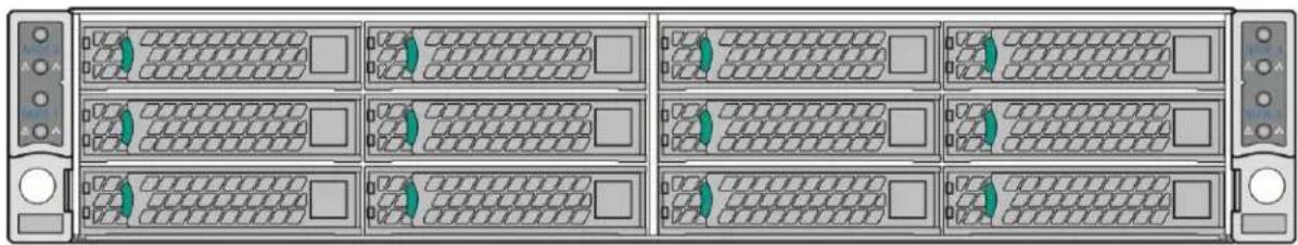
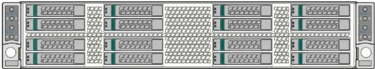
2.5 Hard Drive and Peripheral Bays
| Intel® Server System H2312xx | Intel® Server System H2216xx | |
| Slim-line SATA Optical Drive | Not Supported | Not Supported |
| Internal USB Floppy Drive | Not Supported | Not Supported |
| SATA/SAS Hard Disk Drives (3.5-inch) | Up to Twelve | Not Supported |
| SATA/SAS Hard Disk Drives (2.5-inch) | Not Supported | Up to Sixteen |
natural_image
Front view of a rack-mounted server rack with multiple drive bays and ports (no visible text or labels)AF004635
Figure 5. Intel ^® Server Chassis H2312xx Drive Bay Front View
natural_image
Front view of a rack-mounted server rack with multiple drive bays and indicator lights (no visible text or labels)AF004037
Figure 6. Intel ^® Server Chassis H2216xx Drive Bay Front View
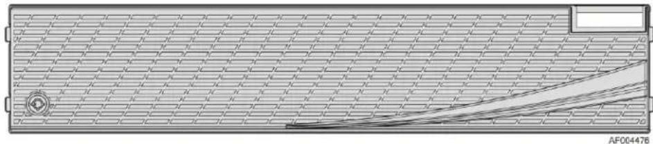
2.6 Front Bezel Support
Intel® Server Chassis H2000 family provides front panel bezel. The bezel provides protection to system HDD bays with a lock to chassis. The front view of the bezel is as below.
natural_image
Technical diagram of a mechanical component with grid pattern and curved cutouts (no text or symbols)Figure 7. Chassis Bezel Front View
2.7 Rack and Cabinet Mounting Options
The chassis was designed to support 19 inches wide by up to 30 inches deep server cabinets. The system bundles with the following Intel ^® rack mount option:
- A basic slide rail kit (Product order code – AXXELVRAIL) is designed to mount the chassis into a standard (19 inches by up to 30 inches deep) EIA-310D compatible server cabinet.
Caution: THE MAXIMUM RECOMMENDED SERVER WEIGHT FOR THE RACK RAILS CAN BE FOUND at http://www.intel.com/support/motherboards/server/sb/CS-033655.htm. EXCEEDING THE MAXIMUM RECOMMENDED WEIGHT OR MISALIGNMENT OF THE SERVER MAY RESULT IN FAILURE OF THE RACK RAILS HOLDING THE SERVER. Use of a mechanical assist to install and align server into the rack rails is recommended.
Advisory Note: The AXXELVRAIL value rack mount rail kit is not designed to support shipment of the server system while installed in a rack.
3. Power Sub-System
The system supports AC 1+1 hot swap power supply module and two power distribution board which can support 2U rack high density server system. Two different power supply units are supported: 1200W and 1600W. The single power supply module has Platinum level energy efficiency, demonstrating climate saver with silver rating.
3.1 Mechanical Overview
The power supply module has a simple retention mechanism to retain the module self once it is inserted. This mechanism shall withstand the specified mechanical shock and vibration requirements. The power distribution board will be fixed in the chassis with screws. This specification defines a 1+1 hot swap redundancy power supply that supports 2U server system. Using existing power supply module provided by vendor with updated PMBus* and custom-made power connector board to support four computing nodes. The power supply shall have two outputs: 12V and 12VSB. The input shall be auto ranging and power factor corrected. The PMBus* features included in this specification are requirements for AC silver rated box power supply for use in server systems based on Intel® Server Chassis H2000 Family. This specification is based on the PMBus* Specifications part I and II, revision 1.1.
3.1.1 AC Power Supply Unit Dimension Overview
The casing dimension is W 73.5mm x L 265.0mm x H 39/40mm. The power supply contains a single 40mm fan. The power supply has a card edge output that interfaces with a 2x25 card edge connector in the system. The AC plugs directly into the external face of the power supply.
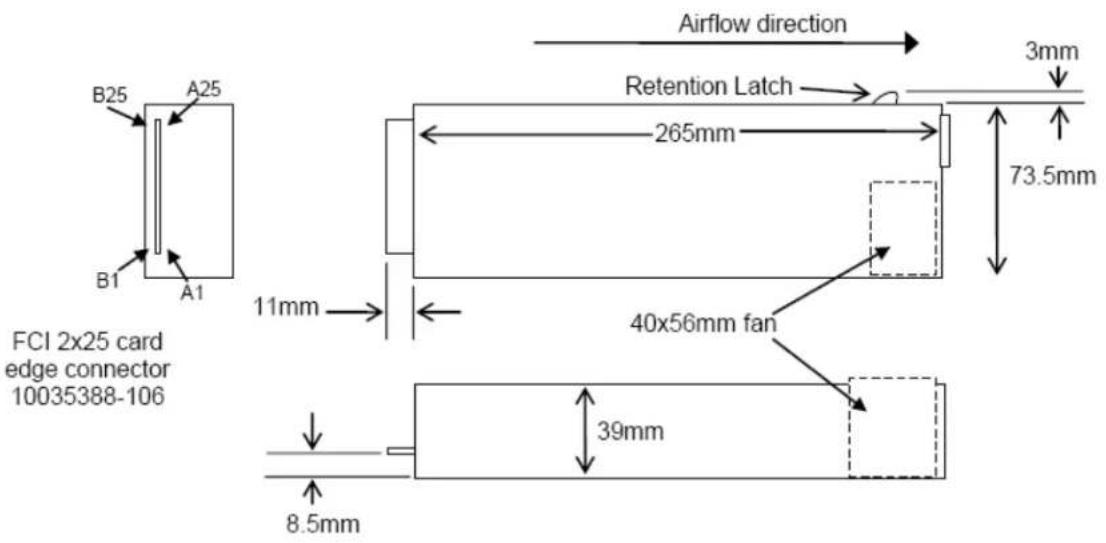
Figure 8. AC Power Supply Unit Dimension Overview
3.1.2 AC Power Supply Unit General Data
Below is general specification data for AC Power Supply Unit.
Table 6. Specification Data for AC Power Supply Unit
| Wattage | 1200W/1600W (Energy Smart) |
| Voltage | 90 – 264 VAC, auto-ranging, 47 Hz-63 Hz |
| Heat Dissipation | 2560 BTU/hr |
| Maximum Inrush Current | Under typical line conditions and over the entire system ambient operating range, the inrush current may reach 65 A per power supply for 5 ms |
| 80 Plus rating | Platinum |
| Climate Saver (CS) rating | Platinum |
3.1.3 AC input connector
The power supply has an internal IEC320 C14 power inlet. The inlet is rated for a minimum of 10A at 250VAC.
3.1.4 AC Power Cord Specification Requirements
The AC power cord used must meet the following specification requirements:
Table 7. AC power cord specification
| Cable Type | SJT |
| Wire Size | 16 AWG |
| Temperature Rating | 105^ C |
| Amperage Rating | 13A |
| Cable Type | SJT |
3.1.5 Power Supply Unit DC Output Connector
The DC output connector pin-out is defined as follows:
Table 8. DC Output Power Connector
| PSU Output Connector | |||
| A1 | GND | B1 | GND |
| A2 | GND | B2 | GND |
| A3 | GND | B3 | GND |
| A4 | GND | B4 | GND |
| A5 | GND | B5 | GND |
| A6 | GND | B6 | GND |
| A7 | GND | B7 | GND |
| A8 | GND | B8 | GND |
| A9 | GND | B9 | GND |
| A10 | +12V | B10 | +12V |
| A11 | +12V | B11 | +12V |
| A12 | +12V | B12 | +12V |
| A13 | +12V | B13 | +12V |
| A14 | +12V | B14 | +12V |
| A15 | +12V | B15 | +12V |
| A16 | +12V | B16 | +12V |
| A17 | +12V | B17 | +12V |
| A18 | +12V | B18 | +12V |
| A19 | PMBus SDA* | B19 | A0* (SMBus address) |
| A20 | PMBus SCL* | B20 | A1* (SMBus address) |
| A21 | PSON | B21 | 12V STBY |
| A22 | SMBAAlert# | B22 | Cold Redundancy Bus* |
| A23 | Return Sense | B23 | 12V load share bus |
| A24 | +12V Remote Sense | B24 | No Connect |
| A25 | PWOK | B25 | CRPS Compatibility Check pin* |
*: Refer to the spec of CRPS Common Requirements Specification.
3.1.6 Handle Retention
The power supply has a handle to assist extraction. The module is able to be inserted and extracted without the assistance of tools. The power supply also has a latch which retains the power supply into the system and prevents the power supply from being inserted or extracted from the system when the AC power cord is pulled into the power supply.
The handle protects the operator from any burn hazard through the use of industrial designed plastic handle or equivalent material.
3.1.7 LED Marking and Identification
The power supply is using a bi-color LED: Amber and Green for status indication. Below are table showing the LED states for each power supply operating state.
Table 9. Power Supply Status LED
| Power Supply Condition | LED State |
| Output ON and OK | Solid GREEN |
| No AC power to all power supplies | OFF |
| AC present/Only 12VSB on (PS off) or PS in Cold redundant state | 1Hz Blink GREEN |
| AC cord unplugged or AC power lost; with a second power supply in parallel still with AC input power. | Solid AMBER |
| Power supply warning events where the power supply continues to operate; high temp, high power, high current, slow fan. | 1Hz Blink Amber |
| Power supply critical event causing a shutdown; failure, OCP, OVP, Fan Fail | Solid AMBER |
| Power supply FW updating | 2Hz Blink GREEN |
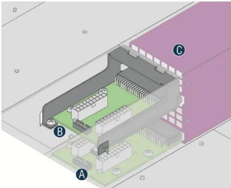
3.1.8 Power Cage with Power Distribution Board
The power cage is at the middle of the chassis, consists of two Power Distribution Boards (PDB) to support Common Redundant Power Supplies (CRPS).
Caution: Installing two Power Supply Units with different wattage ratings on a system is not supported. This will not provide Power Supply Redundancy and causes the system to log multiple errors.
Following is the power system overview:
AF004696
| A | Power Distribution Board 1 |
| B | Power Distribution Board 2 |
| C | Power Supply Unit #2(upper) and #1(lower) |
Figure 9. Power Cage Overview
3.1.9 Power Cage Output Pin Assignment
The power cage provides +12V and +12V _STB output to the system. Each PDB has two 2x9 power output cable to system backplane, together with one 2x8 signal control cable for power management. Refer to below table for PDB pin assignment.
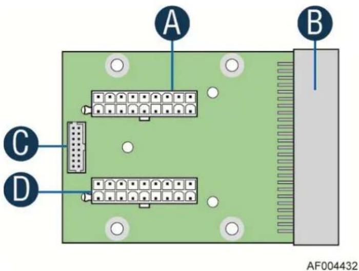
| A | Main Power Output Connector P1 |
| B | Power Supply Unit Connector |
| C | Control Signal Connector |
| D | Main Power Output Connector P2 |
Figure 10. Power distribution board
Table 10. Pin assignment of power output connector
| Pin | Description | Pin | Description |
| 1 | GND | 2 | +12V |
| 3 | GND | 4 | +12V |
| 5 | GND | 6 | +12V |
| 7 | GND | 8 | +12V |
| 9 | GND | 10 | +12V |
| 11 | GND | 12 | +12V |
| 13 | GND | 14 | +12V |
| 15 | GND | 16 | +12V |
| 17 | GND | 18 | +12V |
Table 11. Pin assignment of control signal connector
| Pin | Description | Pin | Description |
| 1 | PMBus SDA | 2 | A0 (SMBus Address) |
| 3 | PMBus SCL | 4 | A1 (SMBus Address) |
| 5 | PSON# | 6 | 12V Load Share Bus |
| 7 | SMBAlert# | 8 | Cold Redundancy Bus |
| 9 | Return Sense | 10 | PWOK |
| 11 | +12V Remote Sense | 12 | Compatibility Bus |
| 13 | Reserved | 14 | +12VSB |
| 15 | +12VSB | 16 | Key Pin (removed) |
3.2 AC Input Specification
3.2.1 Input Voltage And Frequency
The power supply must operate within all specified limits over the following input voltage range. Harmonic distortion of up to 10% THD must not cause the power supply to go out of specific limits. The power supply shall be capable of start-up (power-on) with full rated power load, at line voltage as low as 90VAC.
Table 12. AC input rating
| Parameter | Min | Rated | Max | Start up VAC | Power Off VAC |
| 110V_AC | 90 V_rms | 100-127 V_rms | 140 V_rms | 85 V_AC ± 4V_AC | 70V_AC ± 5V_AC |
| 220V_AC | 180 V_rms | 200-240 V_rms | 264 V_rms | ||
| Frequency | 47 Hz | 50/60 Hz | 63 Hz |
Note:
-
Maximum input current at low input voltage range shall be measured at 90VAC, at max load.
-
Maximum input current at high input voltage range shall be measured at 180VAC, at max load.
-
This requirement is not to be used for determining agency input current markings.
3.2.2 AC input Power Factor
The power supply must meet the power factor requirements stated in the Energy Star ^® Program Requirements for Computer Servers. These requirements are stated below.
Table 13. Typical power factor
| Output power | 10% load | 20% load | 50% load | 100% load |
| Power factor | >0.80 | >0.90 | >0.90 | >0.95 |
Note: Tested at 230Vac, 50Hz and 60Hz and 115VAC, 60Hz. Tested according to Generalized Internal Power Supply Efficiency Testing Protocol, Rev 6.4.3. This is posted at http://efficientpowersupplies.epri.com/methods.asp.
3.2.3 Efficiency
The following table provides the required minimum efficiency level at various loading conditions. These are provided at three different load levels; 100%, 50%, 20%, and 10%. Output shall be load according to the proportional loading method defined by 80 Plus in Generalized Internal Power Supply Efficiency Testing Protocol, Rev 6.4.3. This is posted at: http://efficientpowersupplies.epri.com/methods.asp.
Table 14. Platinum Efficiency Requirement
| Loading | 100% of maximum | 50% of maximum | 20% of maximum | 10% of maximum |
| Minimum Efficiency | 91% | 94% | 90% | 82% |
The power supply must pass with enough margins to make sure in production all power supplies meet these efficiency requirements.
3.2.4 AC Line Fuse
The power supply shall have one line fused in the single line fuse on the line (Hot) wire of the AC input. The line fusing shall be acceptable for all safety agency requirements. The input fuse shall be a slow blow type. AC inrush current shall not cause the AC line fuse to blow under any conditions. All protection circuits in the power supply shall not cause the AC fuse to blow unless a component in the power supply has failed. This includes DC output load short conditions.
3.2.5 AC Line Inrush
AC line inrush current shall not exceed 65A peak, for up to one-quarter of the AC cycle, after which, the input current should be no more than the specified maximum input current. The peak inrush current shall be less than the ratings of its critical components (including input fuse, bulk rectifiers, and surge limiting device).
The power supply must meet the inrush requirements for any rated AC voltage, during turn on at any phase of AC voltage, during a single cycle AC dropout condition as well as upon recovery after AC dropout of any duration, and over the specified temperature range ( T_op ).
3.2.6 AC Line Dropout/Holdup
An AC line dropout is defined to be when the AC input drops to 0VAC at any phase of the AC line for any length of time. During an AC dropout the power supply must meet dynamic voltage regulation requirements. An AC line dropout of any duration shall not cause tripping of control signals or protection circuits. If the AC dropout lasts longer than the holdup time the power supply should recover and meet all turn on requirements. The power supply shall meet the AC dropout requirement over rated AC voltages and frequencies. A dropout of the AC line for any duration shall not cause damage to the power supply.
Table 15. AC Power Holdup Reuqirement
| Loading | Holdup time |
| 70% | 10.6msec |
The 12V_STB output voltage should stay in regulation under its full load (static or dynamic) during an AC dropout of 70ms min (=12VSB holdup time) whether the power supply is in ON or OFF state (PSON asserted or de-asserted).
3.2.7 AC Line Fast Transient (EFT) Specification
The power supply shall meet the EN61000-4-5 directive and any additional requirements in IEC1000-4-5: 1995 and the Level 3 requirements for surge-withstand capability, with the following conditions and exceptions:
- These input transients must not cause any out-of-regulation conditions, such as overshoot and undershoot, nor must it cause any nuisance trips of any of the power supply protection circuits.
- The surge-withstand test must not produce damage to the power supply.
The supply must meet surge-withstand test conditions under maximum and minimum DC-output load conditions.
3.2.8 Hot Plug
Power supply shall be designed to allow connection into and removal from the system without removing power to the system. During any phase of insertion, start-up, shutdown, or removal, the power supply shall not cause any other like modules in the system to deviate outside of their specifications. When AC power is applied, the auxiliary supply shall turn on providing bias power internal to the supply and the 5VSB standby output.
3.2.9 Susceptability Requirements
The power supply shall meet the following electrical immunity requirements when connected to a cage with an external EMI filter, which meets the criteria, defined in the SSI document EPS Power Supply Specification. For further information on customer standards please request a copy of the customer Environmental Standards Handbook.
Table 16. Performance Criteria
| Level | Description |
| A | The apparatus shall continue to operate as intended. No degradation of performance. |
| B | The apparatus shall continue to operate as intended. No degradation of performance beyond spec limits. |
| C | Temporary loss of function is allowed provided the function is self-recoverable or can be restored by the operation of the controls. |
3.2.10 Electrostatic Discharge Susceptibility
The power supply shall comply with the limits defined in EN 55024: 1998 using the IEC 61000-4-2:1995 test standard and performance criteria B defined in Annex B of CISPR 24.
3.2.11 Fast Transient/Burst
The power supply shall comply with the limits defined in EN55024: 1998 using the IEC 61000-4-4:1995 test standard and performance criteria B defined in Annex B of CISPR 24.
3.2.12 Radiated Immunity
The power supply shall comply with the limits defined in EN55024: 1998 using the IEC 61000-4-3:1995 test standard and performance criteria A defined in Annex B of CISPR 24.
3.2.13 Surge Immunity
The power supply shall be tested with the system for immunity to AC Ring wave and AC Unidirectional wave, both up to 2kV, per EN 55024:1998, EN 61000-4-5:1995 and ANSI C62.45:1992.
The pass criteria include the following:
- No unsafe operation is allowed under any condition
- All power supply output voltage levels to stay within proper spec levels
- No change in operating state or loss of data during and after the test profile
- No component damage under any condition
The power supply shall comply with the limits defined in EN55024: 1998 using the IEC 61000-4-5:1995 test standard and performance criteria B defined in Annex B of CISPR 24.
3.2.14 AC Line Transient Specification
AC line transient conditions shall be defined as “sag” and “surge” conditions. “Sag” conditions are also commonly referred to as “brownout”; these conditions will be defined as the AC line voltage
dropping below nominal voltage conditions. "Surge" will be defined to refer to conditions when the AC line voltage rises above nominal voltage.
The power supply shall meet the requirements under the following AC line sag and surge conditions.
Table 17. AC Line Sag Transient Performance
| AC Line Sag (10 sec interval between each sagging) | ||||
| Duration | Sag | Operating AC Voltage | Line Frequency | Performance Criteria. |
| 0 to 1/2 AC cycle | 95% | Nominal AC Voltage ranges | 50/60Hz | No loss of function or performance. |
| >1 AC cycle | >30% | Nominal AC Voltage ranges | 50/60Hz | Loss of function acceptable, self-recoverable. |
Table 18. AC Line Surge Transient Performance
| AC Line Surge | ||||
| Duration | Surge | Operating AC Voltage | Line Frequency | Performance Criteria |
| Continuous | 10% | Nominal AC Voltages | 50/60Hz | No loss of function or performance |
| 0 to 1⁄2 AC cycle | 30% | Mid-point of nominal AC Voltages | 50/60Hz | No loss of function or performance |
3.2.15 Power Recovery
The power supply shall recover automatically after an AC power failure. AC power failure is defined to be any loss of AC power that exceeds the dropout criteria.
3.2.16 Voltage Interruptions
The power supply shall comply with the limits defined in EN55024: 1998/A1: 2001/A2: 2003 using the IEC 61000-4-11: Second Edition: 2004-03 test standard and performance criteria C defined in Annex B of CISPR 24.
3.2.17 AC Line Isolation
The power supply shall meet all safety agency requirements for dielectric strength. Transformers' isolation between primary and secondary windings must comply with the 3000Vac (4242Vdc) dielectric strength criteria. If the working voltage between primary and secondary dictates a higher dielectric strength test voltage the highest test voltage should be used. In addition the insulation system must comply with reinforced insulation per safety standard IEC 950. Separation between the primary and secondary circuits, and primary to ground circuits, must comply with the IEC 950 spacing requirements.
3.2.18 AC Power Inlet
The AC input connector should be an IEC 320 C-14 power inlet. This inlet is rated for 10A/250 VAC.
The AC power cord must meet the following specification requirements:
| Cable Type | SJT |
| Wire Size | 16 AWG |
| Temperature Rating | 105°C |
| Amperage Rating | 13 A |
| Voltage Rating | 125 V |
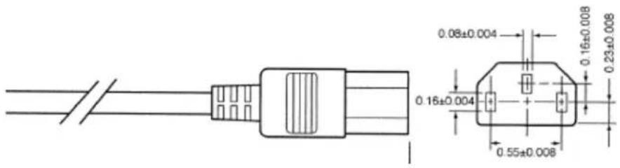
Figure 11. AC Power Cord Specification
3.3 DC Output Specification
3.3.1 Output Power/Currents
The following table defines the minimum power and current ratings. The power supply must meet both static and dynamic voltage regulation requirements for all conditions.
Table 19. Load Ratings for single power supply unit
| Parameter | Min | Max | Peak^23 | Unit | ||
| PSU SKU | 1200W | 1600W | 1200W | 1600W | ||
| +12V main (200-240VAC) | 0.0 | 100 | 133 | 133 | 175 | A |
| +12V main (100-127VAC) | 0.0 | 83 | 83 | 110 | 110 | A |
| +12V_STB^1 | 0.0 | 3.0 | 3.5 | 3.5 | 2.4 | A |
Notes:
- 12V STB must provide 4.0A with two power supplies in parallel. The power supply fan is allowed to run in standby mode for loads > 1.5A.
- Peak combined power for all outputs shall not exceed 1600W (for 1200W PSU) and 2100W (for 1600W PSU)
- Length of time peak power can be supported is based on thermal sensor and assertion of the SMBAlert# signal. Minimum peak power duration shall be 20 seconds without asserting the SMBAlert# signal.
3.3.2 Standby Output
The 12VSB output shall be present when an AC input greater than the power supply turn on voltage is applied.
3.3.3 Voltage Regulation
The power supply output voltages must stay within the following voltage limits when operating at steady state and dynamic loading conditions. These limits include the peak-peak ripple/noise. These shall be measured at the output connectors.
Table 20. Voltage Regulation Limits
| Parameter | Min | Nom | Max | Unit | Tolerance |
| +12V_STB | +11.40V | +12.000V | +12.60V | Vrms | ±5% |
| +12V | +11.40V | +12.000V | +12.60V | Vrms | ±5% |
The combined output continuous power of all outputs shall not exceed 3200W (1600W from each power supply unit). Each output has a maximum and minimum current rating shown in below table. The power supply shall meet both static and dynamic voltage regulation requirements for the minimum dynamic loading conditions. The power supply shall meet only the static load voltage regulation requirements for the minimum static load conditions.
3.3.4 Dynamic Loading
The output voltages shall remain within limits specified for the step loading and capacitive loading specified in the table below. The load transient repetition rate shall be tested between 50Hz and 5kHz at duty cycles ranging from 10%-90%. The load transient repetition rate is only a test specification. The step load may occur anywhere within the MIN load to the MAX load conditions.
Table 21. Transient Load Requirements
| Output | Step Load Size | Load Slew Rate | Test capacitive Load |
| +12V_STB | 1.0A | 0.25 A/ sec | 20 F |
| +12V | 60% of max load | 0.25 A/ sec | 2000 F |
Note: For dynamic condition +12V min loading is 1A.
3.3.5 Capacitive Loading
The power supply must be stable and meet all requirements, with the following capacitive loading conditions.
Table 22. Capacitive Loading Conditions
| Output | Min | Max | Units |
| +12V | 500 | 25,000 | F |
| +12V _STB | 20 | 3100 | F |
3.3.6 Ripple/Noise
The maximum allowed ripple/noise output of the power supply is defined in below table. This is measured over a bandwidth of 10Hz to 20MHz at the power supply output connectors. A 10 F tantalum capacitor in parallel with a 0.1 F ceramic capacitor is placed at the point of measurement.
Table 23. Ripple and Noise
| +12V | +12VSTB |
| 120mVp-p | 120mVp-p |
3.3.7 Grounding
The output ground of the pins of the power supply provides the output power return path. The output connector ground pins shall be connected to the safety ground (power supply enclosure). This grounding should be well designed to ensure passing the max allowed Common Mode Noise levels.
The power supply shall be provided with a reliable protective earth ground. All secondary circuits shall be connected to protective earth ground. Resistance of the ground returns to chassis shall not exceed 1.0 mΩ. This path may be used to carry DC current.
3.3.8 Closed Loop Stability
The power supply shall be unconditionally stable under all line/load/transient load conditions including capacitive load ranges specified in section 3.3.5. A minimum of: 45 degrees phase margin and -10dB-gain margin is required. The power supply manufacturer shall provide proof of the unit's closed-loop stability with local sensing through the submission of Bode plots. Closed-loop stability must be ensured at the maximum and minimum loads as applicable.
3.3.9 Residual Voltage Immunity in Standby Mode
The power supply should be immune to any residual voltage placed on its outputs (typically a leakage voltage through the system from standby output) up to 500mV. There shall be no additional heat generated, nor stressing of any internal components with this voltage applied to any individual or all outputs simultaneously. It also should not trip the protection circuits during turn on.
The residual voltage at the power supply outputs for no load condition shall not exceed 100mV when AC voltage is applied and the PSON# signal is de-asserted.
3.3.10 Common Mode Noise
The Common Mode noise on any output shall not exceed 350mVp-p over the frequency band of 10Hz to 20MHz.
- The measurement shall be made across a 100 resistor between each of DC outputs, including ground at the DC power connector and chassis ground (power subsystem enclosure).
- The test set-up shall use a FET probe such as Tektronix model P6046 or equivalent.
3.3.11 Soft Starting
The Power Supply shall contain control circuit which provides monotonic soft start for its outputs without overstress of the AC line or any power supply components at any specified AC line or load conditions.
3.3.12 Zero Load Stability Requirement
When the power subsystem operates in a no load condition, it does not need to meet the output regulation specification, but it must operate without any tripping of over-voltage or other fault circuitry. When the power subsystem is subsequently loaded, it must begin to regulate and source current without fault.
3.3.13 Hot Swap Requirement
Hot swapping a power supply is the process of inserting and extracting a power supply from an operating power system. During this process the output voltages shall remain within the limits with the capacitive load specified. The hot swap test must be conducted when the system is operating under static, dynamic, and zero loading conditions. The power supply shall use a latching
mechanism to prevent insertion and extraction of the power supply when the AC power cord is inserted into the power supply.
3.3.14 Forced Load Sharing
The +12V output will have active load sharing. The output will share within 10% at full load. The failure of a power supply should not affect the load sharing or output voltages of the other supplies still operating. The supplies must be able to load share in parallel and operate in a hot-swap/redundant 1+1 configurations. The 12VSBoutput is not required to actively share current between power supplies (passive sharing). The 12VSBoutput of the power supplies are connected together in the system so that a failure or hot swap of a redundant power supply does not cause these outputs to go out of regulation in the system.
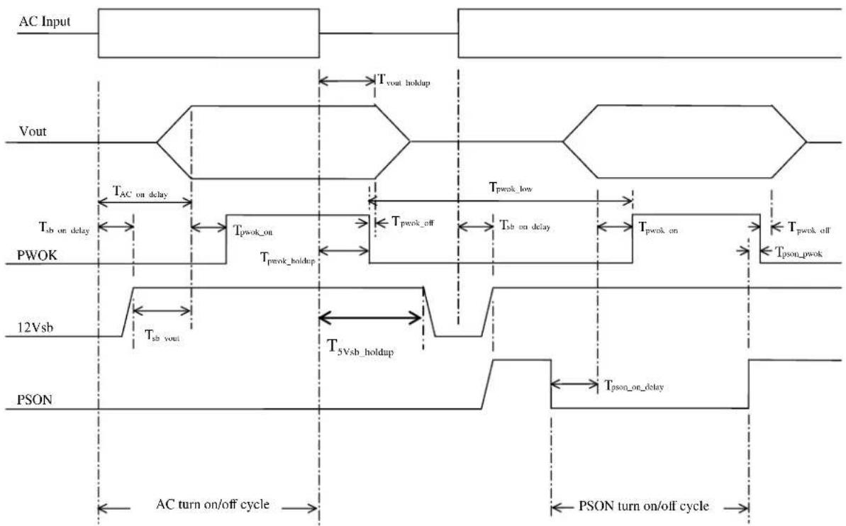
3.3.15 Timing Requirement
These are the timing requirements for the power supply operation. The output voltages must rise from 10% to within regulation limits ( T_vout_rise ) within 5 to 70ms. For 12VSB, it is allowed to rise from 1.0 to 25ms. All outputs must rise monotonically. Table below shows the timing requirements for the power supply being turned on and off through the AC input, with PSON held low and the PSON signal, with the AC input applied.
Table 24. Timing Requirement
| Item | Description | Min. | Max. | Units |
| T_vout\_rise | Output voltage rise time | 5.0 * | 70 * | ms |
| T_sb\_on\_delay | Delay from AC being applied to 12VSBbeing within regulation. | 1500 | ms | |
| T_ac\_on\_delay | Delay from AC being applied to all output voltages being within regulation. | 3000 | ms | |
| T_vout\_holdup | Time 12VI output voltage stay within regulation after loss of AC. | 13 | ms | |
| T_pwok\_holdup | Delay from loss of AC to de-assertion of PWOK | 10.6 | ms | |
| T_pson\_on\_delay | Delay from PSON# active to output voltages within regulation limits. | 5 | 400 | ms |
| T_pson\_pwok | Delay from PSON# deactivate to PWOK being de-asserted. | 5 | ms | |
| T_pwok\_on | Delay from output voltages within regulation limits to PWOK asserted at turn on. | 100 | 500 | ms |
| T_pwok\_off | Delay from PWOK de-asserted to output voltages dropping out of regulation limits. | 1 | ms | |
| T_pwok\_low | Duration of PWOK being in the de-asserted state during an off/on cycle using AC or the PSON signal. | 100 | ms | |
| T_sb\_vout | Delay from 12VSBbeing in regulation to O/Ps being in regulation at AC turn on. | 50 | 1000 | ms |
| T_12VSB\_holdup | Time the 12VSBoutput voltage stays within regulation after loss of AC. | 70 | ms |
Note: * The 12V_STB output voltage rise time shall be from 1.0ms to 25ms.
flowchart
graph TD
    A["AC Input"] --> B["Timing Diagram"]
    B --> C["Vout"]
    C --> D["Timing Diagram"]
    D --> E["PWOK"]
    E --> F["Timing Diagram"]
    F --> G["12Vsb"]
    G --> H["Timing Diagram"]
    H --> I["PSON"]

    subgraph Inputs
        J["AC turn on/off cycle"] --> K["AC turn on/off cycle"]
    end

    subgraph Outputs
        L["Tvout_holdup"] --> M["Tpwok_off"]
        N["Tpwok_low"] --> O["Tpwok_on"]
        P["Tpson_pwok"] --> Q["Tpson_on_delay"]
    end

    style Inputs fill:#f9f,stroke:#333
    style Outputs fill:#ccf,stroke:#333
Figure 12. Turn On/Off Timing (Power Supply Signals)
3.4 Power Supply Cold Redundancy Support
Power supplies that support cold redundancy can be enabled to go into a low-power state (that is, cold redundant state) in order to provide increased power usage efficiency when system loads are such that both power supplies are not needed. When the power subsystem is in Cold Redundant mode, only the needed power supply to support the best power delivery efficiency is ON. Any additional power supplies; including the redundant power supply, is in Cold Standby state.
Each power supply has an additional signal that is dedicated to supporting Cold Redundancy; CR_BUS. This signal is a common bus between all power supplies in the system. CR_BUS is asserted when there is a fault in any power supply OR the power supplies output voltage falls below the Vfault threshold. Asserting the CR_BUS signal causes all power supplies in Cold Standby state to power ON.
Enabling power supplies to maintain best efficiency is achieved by looking at the Load Share bus voltage and comparing it to a programmed voltage level through a PMBus command.
Whenever there is no active power supply on the Cold Redundancy bus driving a HIGH level on the bus all power supplies are ON no matter their defined Cold Redundant roll (active or Cold Standby). This guarantees that incorrect programming of the Cold Redundancy states of the power supply will never cause the power subsystem to shut down or become over loaded. The default state of the power subsystem is all power supplies ON. There needs to be at least one power supply in Cold Redundant Active state or Standard Redundant state to allow the Cold Standby state power supplies to go into Cold Standby state.
Caution: Installing two Power Supply Units with different wattage ratings on a system is not supported. This will not provide Power Supply Redundancy and causes the system to log multiple errors.
3.4.1 1200W CRPS Cold Redundancy
If the output power is less than 480W (40%). the Cold redundant function will be enable. Thus you will see one PSU working normal. The second PSU will be CR mode. The Power Supply LED is green blinking.
Table 25. 1200W CRPS Cold Redundancy Threshold.
| Enable (V) | percent | power (W) | Disable (V) | percent | power (W) | |
| Cold Standby 1 (02h) | 3.2 | 40.00% | 480(±5%) | 1.44 | 18.00% | 432(±5%) |
3.4.2 1600W CRPS Cold Redundancy
If the output power is less than 640W (40%). the Cold redundant function will be enable. Thus you will see one PSU working normal. The second PSU will be CR mode. The Power Supply LED is green blinking.
Table 26. 1600W CRPS Cold Redundancy Threshold.
| Enable (V) | percent | power (W) | Disable (V) | percent | power (W) | |
| Cold Standby 1 (02h) | 3.2 | 40.00% | 640(±5%) | 1.44 | 18.00% | 576(±5%) |
3.5 Control And Indicator Functions
The following sections define the input and output signals from the power supply. Signals that can be defined as low true use the following convention: Signal^# = low true .
3.5.1 PSON# Input Signal
The PSON ^# signal is required to remotely turn on/off the power supply. PSON ^# is an active low signal that turns on the +12V power rail. When this signal is not pulled low by the system, or left open, the outputs (except the +12VSB) turn off. This signal is pulled to a standby voltage by a pull-up resistor internal to the power supply. Refer to below table for the timing diagram.
Table 27. PSON# Signal Characteristics.
| Signal Type | Accepts an open collector/drain input from the system. Pull-up to VSB located in power supply. | |
| PSON# = Low | ON | |
| PSON# = High or Open | OFF | |
| MIN | MAX | |
| Logic level low (power supply ON) | 0V | 1.0V |
| Logic level high (power supply OFF) | 2.0V | 3.46V |
| Source current, Vpson = low | 4mA | |
| Power up delay: Tpson_on_delay | 5msec | 400msec |
| PWOK delay: Tpson_pwok | 50msec | |
3.5.2 PWOK(power good) Output Signal
PWOK is a power OK signal and will be pulled HIGH by the power supply to indicate that all the outputs are within the regulation limits of the power supply. When any output voltage falls below regulation limits or when AC power has been removed for a time sufficiently long so that power supply operation is no longer guaranteed, PWOK will be de-asserted to a LOW state. See the table below for a representation of the timing characteristics of PWOK. The start of the PWOK delay time shall inhibited as long as any power supply output is in current limit.
Table 28. PWOK Signal Characteristics
| Signal Type | ||
| PWOK = High | Power OK | |
| PWOK = Low | Power Not OK | |
| MIN | MAX | |
| Logic level low voltage, Isink=400uA | 0V | 0.4V |
| Logic level high voltage, Isource=200μA | 2.4V | 3.46V |
| Sink current, PWOK = low | 400uA | |
| Source current, PWOK = high | 2mA | |
| PWOK delay: Tpwok_on | 100ms | 1000ms |
| PWOK rise and fall time | 100μsec | |
| Power down delay: T pwok_off | 1ms | 200msec |
3.5.3 SMBAlert# Signal
This signal indicates that the power supply is experiencing a problem that the user should investigate. This shall be asserted due to Critical events or Warning events. The signal shall activate in the case of critical component temperature reached a warning threshold, general failure, over-current, over-voltage, under-voltage, failed fan. This signal may also indicate the power supply is reaching its end of life or is operating in an environment exceeding the specified limits.
This signal is to be asserted in parallel with LED turning solid Amber or blink Amber.
Table 29. SMBAlert# Signal Characteristics
| Signal Type (Active Low) | Open collector/drain output from power supply. Pull-up to VSB located in system. | |
| Alert# = High | OK | |
| Alert# = Low | Power Alert to system | |
| MIN | MAX | |
| Logic level low voltage, Isink=4 mA | 0 V | 0.4 V |
| Logic level high voltage, Isink=50 μA | 3.46 V | |
| Sink current, Alert# = low | 4 mA | |
| Sink current, Alert# = high | 50 μA | |
| Alert# rise and fall time | 100 μs | |
3.6 Protection circuits
Protection circuits inside the power supply shall cause only the power supply's main outputs to shut down. If the power supply latches off due to a protection circuit tripping, an AC cycle OFF for 15sec and a PSON# cycle HIGH for 1sec shall be able to reset the power supply.
3.6.1 Current Limit (OCP)
The power supply shall have current limit to prevent the outputs from exceeding the values shown in table below. If the current limits are exceeded the power supply shall shutdown and latch off. The latch will be cleared by toggling the PSON ^# signal or by an AC power interruption. The power supply shall not be damaged from repeated power cycling in this condition. 12VSB will be auto-recovered after removing OCP limit.
Table 30. Over Current Protection
| Output VOLTAGE | Input voltage range | OVER CURRENT LIMITS | |
| PSU SKU | 1200W | 1600W | |
| +12V | 90 – 264VAC | 140A min; 170A max | 180A min; 200A max |
| +12V_STB | 90 – 264VAC | 2.5A min; 3A max | 2.5A min; 3A max |
3.6.2 Over Voltage Protection (OVP)
The power supply over voltage protection shall be locally sensed. The power supply shall shutdown and latch off after an over voltage condition occurs. This latch shall be cleared by toggling the PSON ^# signal or by an AC power interruption. The values are measured at the output of the power supply's connectors. The voltage shall never exceed the maximum levels when measured at the power connectors of the power supply connector during any single point of fail. The voltage shall never trip any lower than the minimum levels when measured at the power connector. 12VSB will be auto-recovered after removing OVP limit.
Table 31. Over Voltage Protection (OVP) Limits
| Output Voltage | MIN (V) | MAX (V) |
| +12V | 13.3 | 14.5 |
| +12VSB | 13.3 | 14.5 |
3.6.3 Over Thermal protection
The power supply will be protected against over temperature conditions caused by loss of fan cooling or excessive ambient temperature. In an OTP condition the PSU will shut down. When the power supply temperature drops to within specified limits, the power supply shall restore power automatically, while the 12VSB remains always on. The OTP circuit must have built in margin such that the power supply will not oscillate on and off due to temperature recovering condition. The OTP trip level shall have a minimum of 4^ C of ambient temperature margin.
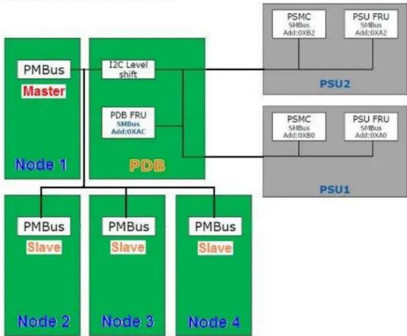
3.7 PMBus\*
The PMBus* features are requirements for power supply unit for use in server systems. This specification is based on the PMBus* specifications part I and II, revision 1.1. The power supply device address locations are shown below:
flowchart
graph TD
    A["Node 1"] --> B["PMBus Master"]
    A --> C["PDB"]
    C --> D["I2C Level shift"]
    C --> E["PDB FRU SMBus Add:0XAC"]
    E --> F["PSU2"]
    C --> G["PSU1"]
    H["Node 2"] --> I["PMBus Slave"]
    H --> J["PMBus Slave"]
    H --> K["PMBus Slave"]
    L["Node 3"] --> M["PSMC SMBus Add:0XB0"]
    L --> N["PSU FRU SMBus Add:0XA0"]
    O["Node 4"] --> P["PSMC SMBus Add:0XB2"]
    O --> Q["PSU FRU SMBus Add:0XA2"]
Figure 13. Power Supply Device Address
The PMBus* from PDB is connected to BMC of all four nodes. Only one board BMC is assigned to be the master BMC and communicate with PSU as single point. Other board BMCs receive PSU data from the master BMC. In case the master BMC is down, one of the slave board BMC will be promoted automatically as master BMC and maintain the communication.
3.7.1 PSU Address Lines A0
Address pins A0 is used by end use system to allocate unit address to a power supply in particular slot position.
For redundant systems there are two signals to set the address location of the power supply once it is installed in the system; Address0 and Address1. For non-redundant systems the power supply device address locations should align with the Address0/Address1 location of 0/0.
Table 32. PSU addressing
| PDB addressing Address0 | 0 | 1 |
| Power supply PMBus* device | B0h | B2h |
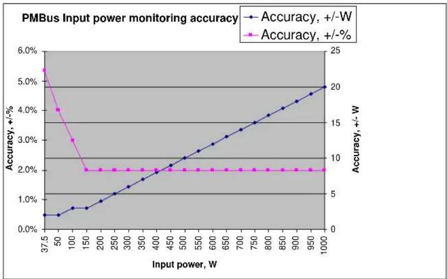
3.7.2 Accuracy
The sensor commands shall meet the following accuracy requirements. The accuracies shall be met over the specified ambient temperature and the full range of rated input voltage.
Table 33. PMBus Accuracy
| Output Loading | 10% - 20% | >20% - 50% | >50% - 100% |
| READ_PIN and READ_EIN | See graphs below | ||
| READ_FAN | +/-500 RPM | ||
| READ_IOUT | +/-5% | +/-2% | +/-2% |
| READ_TEMPERATURE | +/-3°C | ||
line
| Input power, W | Accuracy, +/-W | Accuracy, +/-% | | -------------- | -------------- | -------------- | | 37.5 | 0.5% | 5.5% | | 50 | 0.6% | 4.0% | | 100 | 0.8% | 3.0% | | 150 | 1.0% | 2.0% | | 200 | 1.2% | 2.0% | | 250 | 1.4% | 2.0% | | 300 | 1.6% | 2.0% | | 350 | 1.8% | 2.0% | | 400 | 2.0% | 2.0% | | 450 | 2.2% | 2.0% | | 500 | 2.4% | 2.0% | | 550 | 2.6% | 2.0% | | 600 | 2.8% | 2.0% | | 650 | 3.0% | 2.0% | | 700 | 3.2% | 2.0% | | 750 | 3.4% | 2.0% | | 800 | 3.6% | 2.0% | | 850 | 3.8% | 2.0% | | 900 | 4.0% | 2.0% | | 950 | 4.2% | 2.0% | | 1000 | 4.5% | 2.0% |Figure 14. PMBus Monitoring Accuracy
3.8 Power Management Policy
When working with Intel ^® Server Board S2600JF, the BMC on each node will monitor its fans and temperature for critical failures. When there is a fan failure and a critical temperature event at the same time the node will be powered down. When this occurs the node will need to be manually powered back on.
Additionally on Intel ^® Server Board S2600JF/S2600WP/S2400LP, the BMC on node 3 and node 4 will monitor for a power supply over current condition or power supply over temperature condition. If either of these occur and the Shutdown Policy has been enabled then the node will be powered down. When this occurs the node will need to be manually powered back on but if the over current or over temperature event is detected again the node will be powered back off.
The following table shows the scheme of system power redundancy mode with node behavior:
Table 34. Power Management Policy
| Intel® Server System H2000Load with 2x 1200Wsupplies | Intel® Server System H2000Load with 2x 1600Wsupplies | System Power RedundancyMode | System behavior with one PSU AC lost orfailed |
| System Power Load | |||
| <1200W | <1600W | UnconstrainedRedundant Mode | No system throttling. All 4 nodes worknormally. |
| 1200W< current load <1800W | 1600W< current load <2160W | Optimal RedundantMode | With BIOS setting “servermanagement - shutdown policy” setto “disable” all nodes in the systemmay be throttled to maintain power.This may cause lower performance.With BIOS “ server management--shutdown policy” set to “enable”,Nodes 3 and 4 will shut down whileNodes 1 and 2 keep running withoutthrottling. Node 1 and Node 2 willhave no performance loss. |
| >1800W | >2160W | Non Redundant Mode | All nodes in the system mayshutdown |
The Shutdown Policy setting is only shown on Node 3 and Node 4, and is disabled by default but can be enabled or disabled in the BIOS setup Server Management page or by using the Set Shutdown Policy command.
4. Cooling Sub-System
The chassis cooling system contains the fan cooling sub-system of each node tray and common fan cooling in the power supply units. Both node fans and PSU fans work together as thermal solution to the chassis.
For each node, several components and configuration requirements make up the cooling sub-system. These include processors, chipsets, VR heatsinks, system fan module, CPU air-duct, and drive bay population. All are necessary to provide and regulate the air flow and air pressure needed to maintain the system's thermals when operating at or below the maximum specified thermal limits.
In order to maintain the necessary airflow within the system, you must properly install the air-duct, HDD dummy carrier, PSU dummy filler and the top cover.
Each node uses a variable fan speed control engine to provide adequate cooling for the node and whole system at various ambient temperature conditions, under various server workloads, and with the least amount of acoustic noise possible. The fans operate at the lowest speed for any given condition to minimize acoustics.
Note: The server system does not support redundant cooling fans. If any of the node fans fail, you must power down the respective node as soon as possible to replace the fan.
4.1 Power Supply Fan
Each power supply module supports one non-redundant dual rotor 40 mm fan. The fans control the cooling of the power supply and some drive bays. These fans are not replaceable. Therefore, if a power supply fan fails, you must replace the power supply module.
4.2 Drive Bay Population Requirement
In order to maintain system thermal requirements, you must fully populate all hard drive bays. Hard drive trays used for hot-swap drives must either have a hard drive installed or not have a hard drive installed.
If only one power supply unit is used, a PSU dummy filler must be used to match the airflow requirement.
IMPORTANT: If the drive bay is missing or not fully populated, the system will not meet the thermal cooling requirements of the processor, which will most likely result in degraded performance as a result of throttling or thermal shutdown of the system. It is recommended to keep/apply the dummy plastic blocker(as shipped with HDD carrier) on any blank HDD carrier.
5. Hard Disk Drive Support
The server system provides two SKUs to support different types of Hard Disk Drives (HDD):
■ H2312xx: Supports 12x 3.5" HDD
■ H2216xx: Supports 16x 2.5" HDD
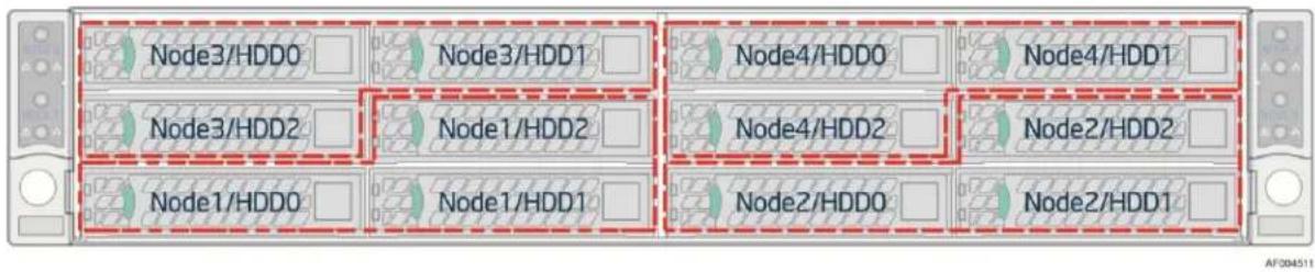
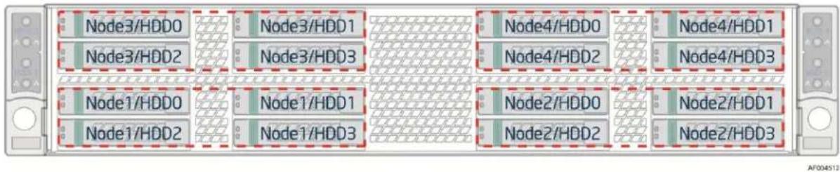
5.1 Hard Disk Drive Bays Scheme
The server system H2000 chassis can support up to twelve carrier-mounted SATA/SAS 3.5-inch hard disk drives, or sixteen carrier-mounted SATA/SAS 2.5" hard disk drives. The drives may be "electrically" hot-swapped while the system power is applied, but you must take caution before hot-swapping while the system is functioning under operating system/application control or data may be lost.
Below are hard disk drive distribution schemes on different SKUs of H2000 chassis family.
flowchart
graph LR
    subgraph Top
        A["Node3/HDD0"] --> B["Node3/HDD1"]
        C["Node3/HDD2"] --> D["Node1/HDD2"]
        E["Node1/HDD0"] --> F["Node1/HDD1"]
    end
    subgraph Middle
        G["Node4/HDD0"] --> H["Node4/HDD1"]
        I["Node4/HDD2"] --> J["Node2/HDD2"]
        K["Node2/HDD0"] --> L["Node2/HDD1"]
    end
    subgraph Bottom
        M["Node1/HDD0"] --> N["Node1/HDD1"]
        O["Node1/HDD2"] --> P["Node2/HDD2"]
        Q["Node2/HDD0"] --> R["Node2/HDD1"]
    end
Figure 15. HDD Scheme for H2312xx
flowchart
graph LR
    subgraph Row1
        A["Node3/HDD0"] --> B["Node3/HDD1"]
        C["Node3/HDD2"] --> D["Node3/HDD3"]
        E["Node1/HDD0"] --> F["Node1/HDD1"]
        G["Node1/HDD2"] --> H["Node1/HDD3"]
    end
    subgraph Row2
        I["Node4/HDD0"] --> J["Node4/HDD2"]
        K["Node4/HDD3"] --> L["Node4/HDD1"]
        M["Node2/HDD0"] --> N["Node2/HDD2"]
        O["Node2/HDD1"] --> P["Node2/HDD3"]
    end
    style Row1 fill:#f9f,stroke:#333
    style Row2 fill:#f9f,stroke:#333
    style Row3 fill:#ccf,stroke:#333
    style Row4 fill:#ccf,stroke:#333
    style Row5 fill:#cfc,stroke:#333
Figure 16. HDD Scheme for H2216xx
Note: Replace the faulty drive only with one from the same manufacturer with the same model and capacity.
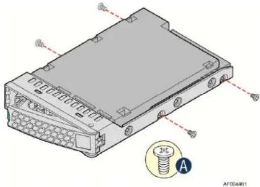
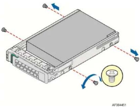
5.2 Hard Drive Carrier
There are two types of HDD carriers for two chassis SKUs respectively:
natural_image
Technical line drawing of an electronic device housing with screw and mounting holes (no text or symbols)Figure 17. 3.5" HDD Assembly Overview
natural_image
Diagram of an electronic device with a screw and indicator lights, showing no text or symbols on the main body.Figure 18. 2.5" HDD Assembly Overview
Hot-swap drive carriers make insertion and extraction of the drive from the system very simple. Each type of drive carrier has its own latching mechanism, which is used to both insert and extract drives from the chassis and lock the carrier in place. Each type of drive carrier supports two light pipes to direct light from the drive status LEDs on the backplane to the carrier's face allowing it to be viewable from the front of the system.
5.3 Hot-Swap Hard Drive Support
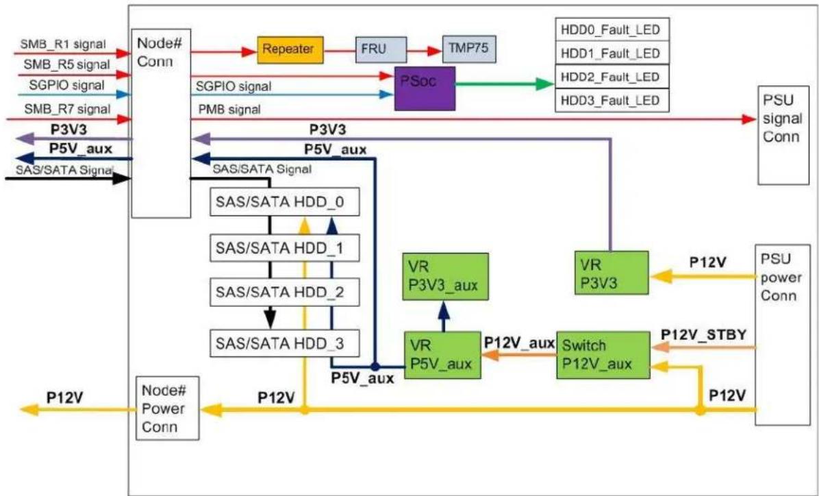
Both the Intel® Server Chassis H2312xx and H2216xx can support hot-swap SATA/SAS hard drives. Hard drives interface with the passive backplane through a blind mate connection when drives are installed into a hard drive bay using hot-swap drive carriers.
Each compute node in the system has dedicated Hot Swap Controller (HSC) to manage three or four HDDs. There are totally four sets of independent Programmable System On Chip (PSOC) on the backplane, to function as HSC respectively to four compute nodes.
The following sections describe the feature and connections between the backplane and server board.
5.3.1 Backplane Feature set:
- Common HSBP Microcontroller Cypress* PSoC 1 part
- H2312xxJR/KR: 12x SAS/SATA 3.5" HDDs at 6Gb/s SAS/SATA or slower speeds, divided into four groups of three hot swap hard drives. Each HDD group is associated with one of the four compute nodes respectively in the 2U chassis.
- H2216xx/JR/KR: 16x SAS/SATA 2.5" HDDs at 6Gb/s SAS/SATA or slower speeds, divided into 4 groups of four hot swap hard drives. Each HDD group is associated with one of the four compute nodes respectively in the 2U chassis.
- One SGPIO SFF-8485 interface per compute node, total of four SGPIO on the backplane.
-
Three SMB interfaces supported on the HSBP:
-
SMBUS R1 - For chassis temp sensor and chassis FRU EEPROM device.
-
SMBUS R5 - Connectivity to up to two HSBP controllers and one shared 12V current monitoring device.
o SMBUS R7 - Connectivity to up to two common redundant power supply (CRPS) module PMBus. -
Integrated front panel control connectors
- Status LED and Activity LED for each hard disk drive.
- 5V_AUX switcher regulator (from 12V and 12VSB) for HDD power and for compute nodes.
- Each grouping of HDD slots has switches for 5V and 12V power, only when corresponding compute node is plugged in and operating will power be provided to the HDDs.
- 3.3V switcher regulator (from 12V) to power microcontroller, SAS/SATA re-drivers on the bridge board and various other components.
- 3.3V_AUX linear regulator (from 5V_AUX) for temp sensor, and chassis FRU EEPROM located on the HSBP.
- Four 80-pin bridge board connectors, one per compute node.
- Four compute node main power connectors, one per compute node.
- Four 2x9pin power cable connections and one 2x9pin power control cable connections. These cables are routing to two power distribution boards (PDB).
- Shared speaker for all compute nodes.
5.3.2 Backplane Block Diagram
flowchart
graph TD
    A["Node# Conn"] --> B["Repeater"]
    B --> C["FRU"]
    C --> D["TMP75"]
    D --> E["PSoc"]
    E --> F["HDD0_Fault_LED"]
    E --> G["HDD1_Fault_LED"]
    E --> H["HDD2_Fault_LED"]
    E --> I["HDD3_Fault_LED"]
    A --> J["Repeater"]
    J --> K["FRU"]
    K --> L["TMP75"]
    L --> M["PSoc"]
    M --> N["PSU signal Conn"]
    A --> O["Repeater"]
    O --> P["FRU"]
    P --> Q["TMP75"]
    Q --> R["HDD0_Fault_LED"]
    Q --> S["HDD1_Fault_LED"]
    Q --> T["HDD2_Fault_LED"]
    Q --> U["HDD3_Fault_LED"]
    A --> V["Repeater"]
    V --> W["FRU"]
    W --> X["TMP75"]
    X --> Y["HDD0_Fault_LED"]
    X --> Z["HDD1_Fault_LED"]
    X --> AA["HDD2_Fault_LED"]
    X --> AB["HDD3_Fault_LED"]
    A --> AC["Repeater"]
    AC --> AD["FRU"]
    AD --> AE["TMP75"]
    AE --> AF["HDD0_Fault_LED"]
    AE --> AG["HDD1_Fault_LED"]
    AE --> AH["HDD2_Fault_LED"]
    AE --> AI["HDD3_Fault_LED"]
    A --> AJ["Repeater"]
    AJ --> AK["FRU"]
    AK --> AL["TMP75"]
    AL --> AM["HDD0_Fault_LED"]
    AL --> AN["HDD1_Fault_LED"]
    AL --> AO["HDD2_Fault_LED"]
    AL --> AP["HDD3_Fault_LED"]
    A --> AQ["Repeater"]
    AQ --> AR["FRU"]
    AR --> AS["TMP75"]
    AS --> AT["HDD0_Fault_LED"]
    AS --> AU["HDD1_Fault_LED"]
    AS --> AV["HDD2_Fault_LED"]
    AS --> AW["HDD3_Fault_LED"]
    A --> AX["Repeater"]
    AX --> AY["FRU"]
    AY --> AZ["TMP75"]
    AZ --> BA["HDD0_Fault_LED"]
    AZ --> BB["HDD1_Fault_LED"]
    AZ --> BC["HDD2_Fault_LED"]
    AZ --> BD["HDD3_Fault_LED"]
    A --> BE["Repeater"]
    BE --> BF["FRU"]
    BF --> BG["TMP75"]
    BG --> BH["HDD0_Fault_LED"]
    BG --> BI["HDD1_Fault_LED"]
    BG --> BJ["HDD2_Fault_LED"]
    BG --> BK["HDD3_Fault_LED"]
    A --> BL["Repeater"]
    BL --> BM["FRU"]
    BM --> BN["TMP75"]
    BN --> BO["HDD0_Fault_LED"]
    BN --> BP["HDD1_Fault_LED"]
    BN --> BQ["HDD2_Fault_LED"]
    BN --> BR["HDD3_Fault_LED"]
    A --> BS["Repeater"]
    BS --> BT["FRU"]
    BT --> BU["TMP75"]
    BU --> BV["HDD0_Fault_LED"]
    BU --> BW["HDD1_Fault_LED"]
    BU --> BX["HDD2_Fault_LED"]
    BU --> BY["HDD3_Fault_LED"]
    A --> BQ
    BQ --> CA["Repeater"]
    CA --> CB["FRU"]
    CB --> CC["TMP75"]
    CC --> CD["HDD0_Fault_LED"]
    CC --> DD["HDD1_Fault_LED"]
    CC --> DE["HDD2_Fault_LED"]
    CC --> DF["HDD3_Fault_LED"]
    A --> DG["Repeater"]
    DG --> DH["FRU"]
    DH --> DI["TMP75"]
    DI --> DJ["HDD0_Fault_LED"]
    DI --> DK["HDD1_Fault_LED"]
    DI --> DL["HDD2_Fault_LED"]
    DI --> DM["HDD3_Fault_LED"]
    A --> DN["Repeater"]
    DN --> DO
    DO --> DP["TMP75"]
    DP --> DP0["Fault Power Conn"]
    DP0 --> PSU PowerConn
    DP0 --> PSU PowerConn
    DP0 --> PSU PowerConn
    DP0 --> PSU PowerConn
    DP0 --> PSU PowerConn
Figure 19. Passive Backplane Block Diagram (for one node)
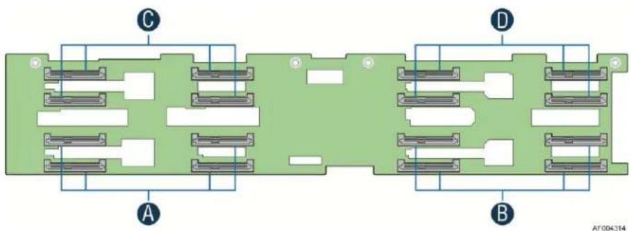
5.3.3 3.5" Hot Swap Backplane Connector scheme
The following diagrams show the layout of major components and connectors for 3.5" Hot Swap backplane.
| A | SATA/SAS connectors for Node 1 |
| B | SATA/SAS connectors for Node 2 |
| C | SATA/SAS connectors for Node 3 |
| D | SATA/SAS connectors for Node 4 |
Figure 20. 3.5" Backplane Component and Connectors (Front View)
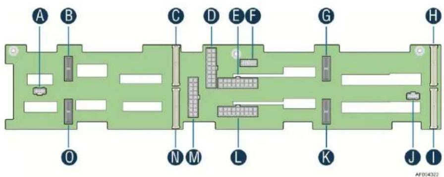
| A | 20-pin Front Panel cable connector for Node 2, 4 |
| B | 2Blade Compute Node Power connector for Node 4 |
| C | 2x40 pin Bridge Board connector for Node 4 |
| D | 2x9 pin Power supply input connector |
| E | 2x9 pin Power supply input connector |
| F | 2x7 pin Power Control cable connector |
| G | 2Blade Compute Node Power connector for Node 3 |
| H | 2x40 pin Bridge Board connector for Node 3 |
| I | 2x40 pin Bridge Board connector for Node 1 |
| J | 20-pin Front Panel cable connector for Node 1, 3 |
| K | 2Blade Compute Node Power connector for Node 1 |
| L | 2x9 pin Power supply input connector |
| M | 2x9 pin Power supply input connector |
| N | 2x40 pin Bridge Board connector for Node 2 |
| O | 2Blade Compute Node Power connector for Node 2 |
Figure 21. 3.5" Backplane Component and Connectors (Back View)
5.3.4 2.5" Hot Swap Backplane Connector scheme
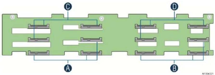
The following diagrams show the layout of major components and connectors for 2.5" Hot Swap backplane.
natural_image
Green circuit board diagram with labeled components A, B, C, D and no readable text or symbols| A | SATA/SAS connectors for Node 1 |
| B | SATA/SAS connectors for Node 2 |
| C | SATA/SAS connectors for Node 3 |
| D | SATA/SAS connectors for Node 4 |
Figure 22. 2.5" Backplane Component and Connectors (Front View)
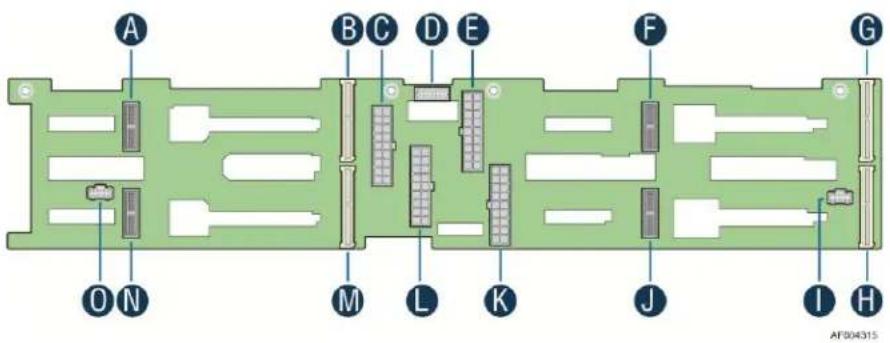
| A | 2Blade Compute Node Power connector for Node 4 |
| B | 2x40 pin Bridge Board connector for Node 4 |
| C | 2x9 pin Power supply input connector |
| D | 2x7 pin Power Control cable connector |
| E | 2x9 pin Power supply input connector |
| F | 2Blade Compute Node Power connector for Node 3 |
| G | 2x40 pin Bridge Board connector for Node 3 |
| H | 2x40 pin Bridge Board connector for Node 1 |
| I | 20-pin Front Panel cable connector for Node 1, 3 |
| J | 2Blade Compute Node Power connector for Node 1 |
| K | 2x9 pin Power supply input connector |
| L | 2x9 pin Power supply input connector |
| M | 2x40 pin Bridge Board connector for Node 2 |
| N | 2Blade Compute Node Power connector for Node 2 |
| O | 20-pin Front Panel cable connector for Node 2, 4 |
Figure 23. 2.5" Backplane Component and Connectors (Back View)
5.3.5 Backplane LED Support
The backplanes support both HDD online and activity/fault LEDs for each of the hard drive connectors. A light duct in HDD tray is used to conduct LED light to front panel. The following lists LED functionality.
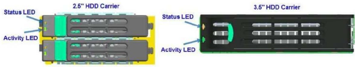
Figure 24. Hard Drive Carrier LED
General HDD LED functionality is displayed below:
Table 35. Hard Drive Carrier Status LED Functions
| Amber | Off | No access and no fault |
| Solid On | Hard Drive Fault has occurred | |
| Blink | Raid rebuild in progress (1hz) Identify (2hz) |
Table 36. Hard Drive Carrier Activity LED Functions
| Green | Condition | Drive Type | Behavior |
| Power on with no drive activity. | SAS | LED stays on | |
| SATA | LED stays off | ||
| Power on with drive activity. | SAS | LED blinks off when processing a command | |
| SATA | LED blinks off when processing a command | ||
| Power on and drive spun down. | SAS | LED stays off | |
| SATA | LED stays off | ||
| Power on and drive spinning up. | SAS | LED blinks | |
| SATA | LED stays off |
5.3.6 Backplane Connector Definition
The backplanes include several different connectors. This section defines the purpose and pin out associated with each.
1. 2x9 Pin Power Input Connector
The backplane is powered by +12V and +12V _STB from PDB of CRPS. The input power is distributed by backplane to all four nodes.
Table 37. Backplane Input Power Connector Pin-out
| Pin | Signal Description | Pin | Signal Description |
| 2 | P12V | 1 | GND |
| 4 | P12V | 3 | GND |
| 6 | P12V | 5 | GND |
| 8 | P12V | 7 | GND |
| 10 | P12V | 9 | GND |
| 12 | P12V | 11 | GND |
| 14 | P12V | 13 | GND |
| 16 | P12V | 15 | GND |
| 18 | P12V | 17 | GND |
2. 2-Blade Compute Node Power Connector
The backplane provides main power to compute node through 2-Blade power connector.
Table 38. 2-Blade Compute Node Power Connector Pin-out
| Pin | Signal Description | Pin | Signal Description |
| Lower Blade (Circuit 1) | |||
| 1 | GND | 2 | GND |
| 3 | GND | 4 | GND |
| 5 | GND | 6 | GND |
| 7 | GND | 8 | GND |
| Upper Blade (Circuit 2) | |||
| 9 | P12V | 10 | P12V |
| 11 | P12V | 12 | P12V |
| 13 | P12V | 14 | P12V |
| 15 | P12V | 16 | P12V |
3. 2x40 Pin Bridge Board Connector
The Compute Node provides four SATA/SAS ports (in SCU0) to backplane, together with front panel control signals and SMBus.
Table 39. 2x40 Pin Connector Pin-out for Node Bridge Board
| Pin | Signal Description | Pin | Signal Description |
| 1 | 5V_AUX | 2 | 5V_AUX |
| 3 | SATA0_TXN | 4 | USB2_OC |
| 5 | SATA0_TXP | 6 | GND |
| 7 | GND | 8 | SATA0_RXN |
| 9 | NODE_Present_N (GND) | 10 | SATA0_RXP |
| 11 | ALL_NODE_OFF | 12 | GND |
| 13 | spare | 14 | USB2_P0P |
| 15 | GND | 16 | USB2_P0N |
| 17 | IPMB-Data | 18 | GND |
| 19 | IPMB-Clk | 20 | FP HDD_ACT_LED_N |
| 21 | GND | 22 | FP Activity LED_N |
| 23 | SMBUS_R1_DATA | 24 | FP Health LEDA_N |
| 25 | SMBUS_R1_CLK | 26 | FP Health LEDG_N |
| 27 | GND | 28 | FP PWR LED_N |
| 29 | SMBUS_R5_DATA | 30 | FP ID LED_N |
| 31 | SMBUS_R5_CLK | 32 | FP ID BTN_N |
| 33 | GND | 34 | FP RST BTN_N |
| 35 | SMBUS_R7_DATA | 36 | FP PWR BTN_N |
| 37 | SMBUS_R7_CLK | 38 | FP NMI BTN_N |
| 39 | GND | 40 | SPA_SOUT_N |
| 41 | PMBUS Alert_N | 42 | SPA_SIN_N |
| 43 | NODEx_ON_N | 44 | ID3 |
| 45 | SGPIO_DATA_IN | 46 | ID2 |
| 47 | SGPIO Data Out | 48 | ID1 |
| 49 | SGPIO LD | 50 | ID0 |
| 51 | SPKR | 52 | SGPIO CLK |
| 53 | GND | 54 | GND |
| 55 | SAS3_RX | 56 | SAS3_TX |
| 57 | SAS3_RX | 58 | SAS3_TX |
| 59 | GND | 60 | GND |
| 61 | SAS2_TX | 62 | SAS2_RX |
| 63 | SAS2_TX | 64 | SAS2_RX |
| 65 | GND | 66 | GND |
| 67 | SAS1_RX | 68 | SAS1_TX |
| 69 | SAS1_RX | 70 | SAS1_TX |
| 71 | GND | 72 | GND |
| 73 | SAS0_TX | 74 | SAS0_RX |
| 75 | SAS0_TX | 76 | SAS0_RX |
| 77 | GND | 78 | GND |
| 79 | 3.3V | 80 | 3.3V |
4. 20-Pin Front Panel Connector
The backplanes provide connectors for front panel control signals. Each connector integrates the control signals of two compute nodes.
Table 40. Front Panel Connector Pin-out
| Pin | Signal Description |
| 1 | GND |
| 2 | FP1_PWR_BTN_N |
| 3 | FP1_RST_BTN_N |
| 4 | FP1_ID_BTN_N |
| 5 | P5VSB |
| 6 | FP1_PWR_LED_N |
| 7 | FP1_HEALTH_LEDG_N |
| 8 | FP1_HEALTH_LEDA_N |
| 9 | FP1_ACTIVITY_LED_N |
| 10 | FP1_ID_LED_N |
| 11 | GND |
| 12 | FP2_PWR_BTN_N |
| 13 | FP2_RST_BTN_N |
| 14 | FP2_ID_BTN_N |
| 15 | P3V3SB |
| 16 | FP2_PWR_LED_N |
| 17 | FP2_HEALTH_LEDG_N |
| 18 | FP2_HEALTH_LEDA_N |
| 19 | FP2_ACTIVITY_LED_N |
| 20 | FP2_ID_LED_N |
5. 2x7 Pin Power Supply Control Signal Connector
The backplanes provide power supply control signals, together with PMBus functionality integrated.
Table 41. Power Supply Control Connector Pin-out
| Pin | Signal Description | Pin | Signal Description |
| 1 | SMBUS_R7_DATA | 2 | A0 |
| 3 | SMBUS_R7_CLK | 4 | PSON_N |
| 5 | PMBUS_ALERT_N | 6 | 12V RS_RTN |
| 7 | PWROK | 8 | 12V RS |
| 9 | Reserved | 10 | PDU1-12VSB |
| 11 | PDU1-12VSB | 12 | PDU2-12VSB |
| 13 | PDU2-12VSB | 14 | Reserved |
6. Front Panel Control and Indicators
The Intel ^® Server Chassis H2000 family Front Control Panel is integrated with rack handles at the both sides of the chassis. Each control panel contains two sets of node control buttons and status LEDs. The control panel assembly is pre-assembled and fixed with the rack handles.
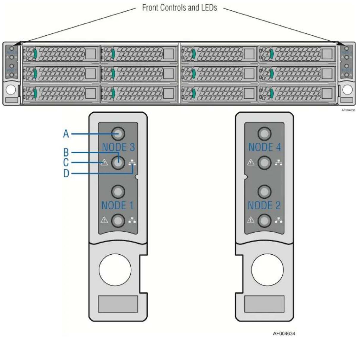
| A | System Power Button with LED |
| B | System ID LED Button |
| C | System Status LED |
| D | Network Link/Activity LED |
Figure 25. Front Control Panel
6.1 Control Panel Button
The following table lists the control panel features and functions. The control panels features a system power button.
Table 42. Front Control Button Function
| Feature | Function |
| Power Button with Power LED | Toggles the system power on/off. This button also integrates the power LED. |
| System ID Button with ID LED | Toggles between ID LED on and off |
6.2 Control Panel LED Indicators
The control panel houses independent two LEDs and two button integrated LEDs for each node, which are viewable to display the system's operating status. The following table identifies each LED and describes their functionality.
Table 43. Front LED Indicator Functions
| LED Indicator | Color | Condition | What it describes |
| Power | Green | On | Power On/ACPI S0 state |
| Green | Blink | Sleep/ACPI S1 state | |
| - | Off | Power Off /ACPI S5 state | |
| LAN (i350 Dual NIC) | Green | On | LAN Link no Access |
| Green | Blink | LAN Activity | |
| - | Off | No Link | |
| System Status | Green | On | System Ready/No Alarm |
| Green | Blink | System ready, but degraded: redundancy lost such as the power supply or fan failure; non-critical temp/voltage threshold; battery failure; or predictive power supply failure. | |
| Amber | On | Critical Alarm: Critical power modules failure, critical fans failure, voltage (power supply), critical temperature and voltage | |
| Amber | Blink | Non-Critical Alarm: Redundant fan failure, redundant power module failure, non-critical temperature and voltage | |
| - | Off | Power off: System unpluggedPower on: System powered off and in standby, no prior degraded\non-critical\critical state |
Notes:
- Blink rate is \~1 Hz at 50% duty cycle.
- It is also off when the system is powered off (S5) or in a sleep state (S1).
- The power LED sleep indication is maintained on standby by the chipset. If the system is powered down without going through the BIOS, the LED state in effect at the time of power off is restored when the system is powered on until the BIOS clear it.
- If the system is not powered down normally, it is possible the Power LED will blink at the same time the system status LED is off due to a failure or configuration change that prevents the BIOS from running.
6.2.1 Power/Sleep LED
Table 44. Power LED Operation
| State | Power Mode | LED | Description |
| Power Off | Non-ACPI | Off | System power is off and the BIOS has not initialized the chipset. |
| Power On | Non-ACPI | Solid On | System power is on but the BIOS has not yet initialized the chipset. |
| S5 | ACPI | Off | Mechanical is off and the operating system has not saved any context to the hard disk. |
| S1 Sleep | ACPI | Blink | DC power is still on. The operating system has saved context and gone into a level of low-power state. |
| S0 | ACPI | Solid On | System and the operating system are up and running. |
Note: Blink rate is \~ 1Hz at 50% duty cycle.
6.2.2 System Status LED
Table 45. System Status LED Operation
| Color | State | Criticality | Description |
| Off | N/A | Not ready | Power off or BMC initialization completes if no degraded, non-critical, critical, or non-recoverable conditions exist after power cable plug in. |
| Green/Amber | Both Solid On | Not ready | Pre DC Power On – 15-20 second BMC Initialization when AC is applied to the server. The system will not POST until BMC initialization completes. |
| Green | Solid on | Ok | System ready |
| Green | Blink | Degraded | BIOS detected1. Unable to use all of the installed memory (more than one DIMM installed). ^1 2. In a mirrored configuration, when memory mirroring takes place and system loses memory redundancy. This is not covered by (2). ^1 3. PCI Express* correctable link errors.4. Integrated BMC detected5. One of redundant power supplies not present.6. CPU disabled – if there are two CPUs and one CPU is disabled.7. Fan alarm – Fan failure. Number of operational fans should be more than minimum number needed to cool the system.8. Non-critical threshold crossed – Temperature, voltage, power nozzle, power gauge, and PROCHOT2 (Therm Ctrl) sensors.9. Battery failure.10. Predictive failure when the system has redundant power supplies. |
| Amber | Blink | Non-critical | Non-fatal alarm – system is likely to failBIOS Detected1. In non-mirroring mode, if the threshold of ten correctable errors is crossed within the window. ^1 2. PCI Express* uncorrectable link errors.Integrated BMC Detected1. Critical threshold crossed – Voltage, temperature, power nozzle, power gauge, and PROCHOT (Therm Ctrl) sensors.2. VRD Hot asserted.3. One of the redundant power supplies failed.4. Minimum number of fans to cool the system are not present or have failed. |
| Amber | Solid on | Critical, non-recoverable | Fatal alarm – system has failed or shutdownBIOS Detected1. DIMM failure when there is one DIMM present and no good memory is present. ^1 2. Run-time memory uncorrectable error in non-redundant mode. ^1 3. CPU configuration error (for instance, processor stepping mismatch).Integrated BMC Detected11. CPU CATERR signal asserted.12. CPU 1 is missing.13. CPU THERMTRIP.14. System cooling fan failure.15. No power good – redundant power fault.• Power Unit Redundancy sensor – Insufficient resources offset (indicates not enough power supplies are present). |
Notes:
1. The BIOS detects these conditions and sends a Set Fault Indication command to the Integrated BMC to provide the contribution to the system status LED.
2. Blink rate is \~ 1Hz at 50% duty cycle.
6.2.3 System Status LED - BMC Initialization
When power is first applied to the system and 5V-STBY is present, the BMC controller on the server board requires 15-20 seconds to initialize. During this time, the system status LED will be solid on, both amber and green. Once BMC initialization has completed, the status LED will stay green solid on. If power button is pressed before BMC initialization completes, the system will not boot to POST.
Appendix A: Integration and Usage Tips
Before attempting to integrate and configure your system, you should reference this section, which provides a list of useful information.
- Remove dummy tray cover before install node tray.
- Install dummy tray cover when respective node tray is plugged out.
- System fans in node trays are not hot-swappable.
- You must use the CPU/memory air-duct to maintain system thermals.
- To maintain system thermals, you must populate all hard drive bays with either a hard drive or drive blank.
- You must remove AC power from the system prior to opening the chassis for service
You can download the latest system documentation, drivers, and system software from the Intel Support website at http://www.intel.com/p/en_US/support/highlights/server/H2000JF.
Glossary
| Term | Definition |
| ACPI | Advanced Configuration and Power Interface |
| AP | Application Processor |
| APIC | Advanced Programmable Interrupt Control |
| ASIC | Application Specific Integrated Circuit |
| ASMI | Advanced Server Management Interface |
| BIOS | Basic Input/Output System |
| BIST | Built-In Self Test |
| BMC | Baseboard Management Controller |
| Bridge | Circuitry connecting one computer bus to another, allowing an agent on one to access the other |
| BSP | Bootstrap Processor |
| Byte | 8-bit quantity. |
| CBC | Chassis Bridge Controller (A microcontroller connected to one or more other CBCs, together they bridge the IPMB buses of multiple chassis.) |
| CEK | Common Enabling Kit |
| CHAP | Challenge Handshake Authentication Protocol |
| CMOS | In terms of this specification, this describes the PC-AT compatible region of battery-backed 128 bytes of memory, which normally resides on the server board |
| DPC | Direct Platform Control |
| EEPROM | Electrically Erasable Programmable Read-Only Memory |
| EHCI | Enhanced Host Controller Interface |
| EMP | Emergency Management Port |
| EPS | External Product Specification |
| ESB2-E | Enterprise South Bridge 2 |
| FBD | Fully Buffered DIMM |
| FMB | Flexible Mother Board |
| FRB | Fault Resilient Booting |
| FRU | Field Replaceable Unit |
| FSB | Front Side Bus |
| GB | 1024MB |
| GPIO | General Purpose I/O |
| GTL | Gunning Transceiver Logic |
| HSC | Hot-Swap Controller |
| Hz | Hertz (1 cycle/second) |
| I2C | Inter-Integrated Circuit Bus |
| IA | Intel®Architecture |
| IBF | Input Buffer |
| ICH | I/O Controller Hub |
| ICMB | Intelligent Chassis Management Bus |
| IERR | Internal Error |
| IFB | I/O and Firmware Bridge |
| INTR | Interrupt |
| IP | Internet Protocol |
| IPMB | Intelligent Platform Management Bus |
| IPMI | Intelligent Platform Management Interface |
| IR | Infrared |
| ITP | In-Target Probe |
| KB | 1024 bytes |
| KCS | Keyboard Controller Style |
| LAN | Local Area Network |
| LCD | Liquid Crystal Display |
| LED | Light Emitting Diode |
| LPC | Low Pin Count |
| LUN | Logical Unit Number |
| MAC | Media Access Control |
| MB | 1024KB |
| MCH | Memory Controller Hub |
| MD2 | Message Digest 2 – Hashing Algorithm |
| MD5 | Message Digest 5 – Hashing Algorithm – Higher Security |
| ms | milliseconds |
| MTTR | Memory Type Range Register |
| Mux | Multiplexor |
| NIC | Network Interface Controller |
| NMI | Non-maskable Interrupt |
| OBF | Output Buffer |
| OEM | Original Equipment Manufacturer |
| Ohm | Unit of electrical resistance |
| PEF | Platform Event Filtering |
| PEP | Platform Event Paging |
| PIA | Platform Information Area (This feature configures the firmware for the platform hardware.) |
| PLD | Programmable Logic Device |
| PMI | Platform Management Interrupt |
| POST | Power-On Self Test |
| PSMI | Power Supply Management Interface |
| PWM | Pulse-Width Modulation |
| RAM | Random Access Memory |
| RASUM | Reliability, Availability, Serviceability, Usability, and Manageability |
| RISC | Reduced Instruction Set Computing |
| RMM3 | Remote Management Module – 3^rd generation |
| RMM3 NIC | Remote Management Module – 3^rd generation dedicated management NIC |
| ROM | Read Only Memory |
| RTC | Real-Time Clock (Component of ICH peripheral chip on the server board.) |
| SDR | Sensor Data Record |
| SECC | Single Edge Connector Cartridge |
| SEEPROM | Serial Electrically Erasable Programmable Read-Only Memory |
| SEL | System Event Log |
| SIO | Server Input/Output |
| SMI | Server Management Interrupt (SMI is the highest priority non-maskable interrupt.) |
| SMM | Server Management Mode |
| SMS | Server Management Software |
| SNMP | Simple Network Management Protocol |
| SSI | Server System Infrastructure |
| TBD | To Be Determined |
| TIM | Thermal Interface Material |
| UART | Universal Asynchronous Receiver/Transmitter |
| UDP | User Datagram Protocol |
| UHCI | Universal Host Controller Interface |
| UTC | Universal time coordinate |
| VID | Voltage Identification |
| VRD | Voltage Regulator Down |
| Word | 16-bit quantity |
| ZIF | Zero Insertion Force |
Reference Documents
Refer to the following documents for additional information:
Intel ^® Server Board S2600JF Technical Product Specification (Intel ^® Order Code: G31608)
Intel ^® Server System H2000JF Technical Product Specification (Intel ^® Order Code: G39462)
Intel ^® Server Board S2600WP Technical Product Specification (Intel ^® Order Code: G44057)
Intel ^® Server System S2000WP Technical Product Specification (Intel ^® Order Code: 52418)
Intel ^® Server Board S2400LP Technical Product Specification (Intel ^® Order Code: G52803)
Intel ^® Server System S2400LP Technical Product Specification (Intel ^® Order Code: G59328)
■ ACPI 3.0: http://www.acpi.info/spec.htm
IPMI 2.0
Data Center Management Interface Specification v1.0, May 1, 2008: www.intel.com/go/dcmi
■ PCI Bus Power Management Interface Specification 1.1: http://www.pcisig.com/
■ PCI Express* Base Specification Rev 2.0 Dec 06: http://www.pcisig.com/
■ PCI Express* Card Electromechanical Specification Rev 2.0: http://www.pcisig.com/
■ PMBus*: http://pmbus.org
■ SATA 2.6: http://www.sata-io.org/
■ SMBIOS 2.4
■ SSI-EEB 3.0: http://www.ssiforum.org
■ USB 1.1: http://www.usb.org
■ USB 2.0: http://www.usb.org
- Windows Logo/SDG 3.0
Intel ^® Dynamic Power Technology Node Manager 1.5 External Interface Specification using IPMI, 2007. Intel Corporation.
- Node Power and Thermal Management Architecture Specification v1.5, rev.0.79. 2007, Intel Corporation.
Intel ^® Server System Integrated Baseboard Management Controller Core External Product Specification, 2007 Intel Corporation.
Intel ^® Thurley Server Platform Services IPMI Commands Specification, 2007. Intel Corporation.
Intel ^® Server Safety and Regulatory, 2011. Intel Corporation. (Intel Order Code: G23122)
- Intelligent Platform Management Bus Communications Protocol Specification, Version 1.0, 1998. Intel Corporation, Hewlett-Packard* Company, NEC* Corporation, Dell* Computer Corporation.
- Platform Environmental Control Interface (PECI) Specification, Version 2.0. Intel Corporation.
- Platform Management FRU Information Storage Definition, Version 1.0, Revision 1.2, 2002. Intel Corporation, Hewlett-Packard* Company, NEC* Corporation, Dell* Computer Corporation: http://developer.intel.com/design/servers/ipmi/spec.htm.