MCP1661 - Uncategorized Microchip - Free user manual and instructions
Find the device manual for free MCP1661 Microchip in PDF.

User questions about MCP1661 Microchip
0 question about this device. Answer the ones you know or ask your own.
Ask a new question about this device
Download the instructions for your Uncategorized in PDF format for free! Find your manual MCP1661 - Microchip and take your electronic device back in hand. On this page are published all the documents necessary for the use of your device. MCP1661 by Microchip.
USER MANUAL MCP1661 Microchip
High-Voltage Integrated Switch PWM Boost Regulator with UVLO
Features
• 3 6 V, 8 0 0 m Ω Integrated Switch
- Up to 92% Efficiency
• High Output Voltage Range: up to 32V
• 1.3A Peak Input Current Limit:
- I_OUT > 200 mA @ 5.0V V_IN , 12V V_OUT
- I_OUT > 125 mA @ 3.3V V_IN , 12V V_OUT
- I_OUT > 100 mA @ 4.2V V_IN , 24V V_OUT
- Input Voltage Range: 2.4V to 5.5V
- Undervoltage Lockout (UVLO):
- U V L O _IN @RisMng: 2.3V, typical
- U V L O _IN @Faving: 1.85V, typical
• No Load Input Current: 250 μA, typical
- Sleep mode with 200 nA Typical Quiescent Current
- PWM Operation with Skip mode: 500 kHz
- Feedback Voltage Reference: V_FB = 1.227V
• Cycle-by-Cycle Current Limiting
- Internal Compensation
- Inrush Current Limiting and Internal Soft Start
- Output Overvoltage Protection (OVP) in the event of:
- Feedback pin shorted to GND
- Disconnected feedback divider
• Overtemperature Protection
- Easily Configurable for SEPIC or Flyback Topologies
• Available Packages:
- 5-Lead SOT-23
- 8-Lead 2x3 TDFN
Applications
- Two and Three-Cell Alkaline, Lithium Ultimate and NiMH/NiCd Portable Products
- Single-Cell Li-Ion to 5V, 12V or 24V Converters
• LCD Bias Supply for Portable Applications - Camera Phone Flash
- Portable Medical Equipment
• Hand-Held Instruments - Single-Cell Li-Ion to 3.0V or 3.3V SEPIC Applications (see Figure 6-3)
General Description
The MCP1661 device is a compact, high-efficiency, fixed-frequency, non-synchronous step-up DC-DC converter which integrates a 36V, 800 mΩ NMOS switch. It provides a space-efficient high-voltage step-up power supply solution for applications powered by either two-cell or three-cell alkaline, Ultimate Lithium, NiCd, NiMH, one-cell Li-Ion or Li-Polymer batteries.
The integrated switch is protected by the 1.3A cycle-by-cycle inductor peak current limit operation. There is an output overvoltage protection which turns off switching in case the feedback resistors are accidentally disconnected or the feedback pin is short-circuited to GND.
Low-voltage technology allows the regulator to start-up without high inrush current or output voltage overshoot from a low-voltage input. The device features a UVLO which avoids start-up and operation with low inputs or discharged batteries for two cell-powered applications.
For standby applications (EN = GND), the device stops switching, enters Sleep mode and consumes 200 nA (typical) of input current.
MCP1661 is easy to use and allows creating classic boost, SEPIC or flyback DC-DC converters within a small Printed Circuit Board (PCB) area. All compensation and protection circuitry is integrated to minimize the number of external components. Ceramic input and output capacitors are used.
Package Types
MCP1661
SOT-23
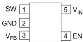
text_image
SW 1 GND 2 VFB 3 5 VIN 4 ENMCP1661
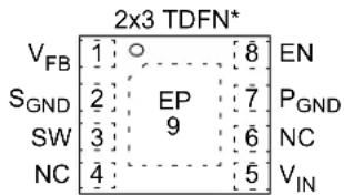
text_image
2x3 TDFN* V_FB 1 ○ 8 EN S_GND 2 EP 7 P_GND SW 3 9 6 NC NC 4 5 V_IN* Includes Exposed Thermal Pad (EP); see Table3-1.
Typical Applications
1.0 ELECTRICAL CHARACTERISTICS
Absolute Maximum Ratings †
V_SW - GND +36V
EN, V_IN - GND....+6.0V
V_FB +1.3V
Power Dissipation ..... Internally Limited
Storage Temperature ....-65°C to +150°C
Ambient Temperature with Power Applied .... -40°C to +125°C
Operating Junction Temperature.... -40°C to +150°C
ESD Protection On All Pins:
HBM....4 kV
MM....300V
† Notice: Stresses above those listed under “Maximum Ratings” may cause permanent damage to the device. This is a stress rating only and functional operation of the device at those or any other conditions above those indicated in the operational sections of this specification is not intended. Exposure to maximum rating conditions for extended periods may affect device reliability.
DC AND AC CHARACTERISTICS
| Electrical Specifications: Unless otherwise specified, all limits apply for typical values at ambient temperature T_A = +25°C_IN 3.3V , I_OUT = 20mA , I_OUT = 12V , I_IN = C_OUT = 10μF , X7R ceramic, L = 4.7 μH.Boldface specifications apply over the controlled T_A range of -40°C to +125°C. | ||||||
| Parameters Sym. Min. Typ. Max. Units | Conditions | |||||
| Input Voltage Range | V_IN | 2.4 | — | 5.5 | V | Note 1 |
| Undervoltage Lockout (UVLO) | UVLO_START | — | 2.3 | — | V | V_IN rising, I_OUT = 1mA resistive load |
| UVLO_STOP | — | 1.85 | — | V | V_IN falling, I_OUT = 1mA resistive load | |
| Output Voltage Adjust Range | V_OUT | — | — | 32 | V | Note 1 |
| Maximum Output Current | I_OUT | — | 125 | — | mA | 3.3V V_IN , 12V V_OUT |
| 200 | — | mA | 5.0V V_IN , 12V V_OUT | |||
| 100 | — | mA | 4.2V V_IN , 24V V_OUT | |||
| Feedback Voltage | V_FB | 1.190 | 1.227 | 1.264 | V | |
| V_FB Accuracy | -3 | — | 3 | % | ||
| Feedback Input Bias Current | I_VFB | — | 0.005 | — | μA | |
| No Load Input Current | I_IN0 | — | 250 | — | μA | Device switching, no load,3.3V V_IN , 12V V_OUT (Note 2) |
| Shutdown Quiescent Current | I_QSHDN | — | 200 | — | nA | EN = GND,feedback divider current notincluded (Note 3) |
| Peak Switch Current Limit | I_N(MAX) | — | 1.3 | — | A | Note 4 |
| NMOS Switch Leakage | I_NLK | — | 0.4 | — | μA | V_IN = V_SW = 5V; J_OUT = 5.5V V_EN = V_FB = GND |
| NMOS Switch ON Resistance | R_DS(ON) | — | 0.8 | — | Ω | V_IN = 5V, J_OUT = 12V , I_OUT = 100mA (Note 4) |
Note 1: Minimum input voltage in the range of V_IN ( V_IN < 5.5 V < V_OUT ) depends on the maximum duty cycle ( DC_MAX ) and on the output voltage ( V_OUT ), according to the boost converter equation: V_INmin = V_OUT × (1 - D G_MAX) .
2: I_IN0 varies with input and output voltage (Figure 2-8). I_IN0 is measured on the V_IN pin when the device is switching (EN = V_IN ), at no load, with R_TOP = 120 k and R_BOT = 1.05 M .
3: I_QSHDN is measured on the V_IN pin when the device is not switching (EN = GND), at no load, with the feedback resistors ( R_TOP + R_BOT ) disconnected from V_OUT .
4: Determined by characterization, not production tested.
DC AND AC CHARACTERISTICS (CONTINUED)
| Electrical Specifications: Unless otherwise specified, all limits apply for typical values at ambient temperature T_A = +25°C_IN 3.3V , I_OUT = 20mA , V_UT = 12V , I_N = C_OUT = 10μF , X7R ceramic, L = 4.7 μH.Boldface specifications apply over the controlled T_A range of -40°C to +125°C. | ||||||
| Parameters | Sym. | Min. | Typ. | Max. | Units | Conditions |
| Line Regulation |(ΔV) | /V_FB/ V_IN | — 0.0 | 5 0.5 %/V | V | IN= 3V to 5V, I_OUT = 20mA , V_UT = 12.0V | |
| Load Regulation |ΔV | /V_FB | — | 0 | . | 5 | 1OUT= 20 mA to 100 m%, V_IN = 3.3V , V_OUT = 12.0V |
| Overvoltage Reference | OVP_REF | — | 80 | — | mV | V_FB to GND transition (Note 4) |
| Maximum Duty Cycle | DC_MAX | 88 | 90 | — | % | Note 4 |
| Switching Frequency | f_SW | 425 | 500 | 575 | kHz | ±15% |
| EN Input Logic High | V_IH | 85 | — | — | % of V_IN | I_OUT = 1mA |
| EN Input Logic Low | V_IL | — | — | 7.5 | % of V_IN | I_OUT = 1mA |
| EN Input Leakage Current | I_ENLK | — | 0.025 | — | μA | V_EN = 5V |
| Soft-Start Time | t_SS | — | 3 | — | ms | T_A , EN Low-to-High, 90% of V_OUT |
| Thermal Shutdown Die Temperature | T_SD | — | 150 | — | °C | |
| Die Temperature Hysteresis | T_SDHYS | — | 15 | — | °C | |
Note 1: Minimum input voltage in the range of V_IN ( V_IN < 5.5V < V_OUT ) depends on the maximum duty cycle ( DC_MAX ) and on the output voltage ( V_OUT ), according to the boost converter equation: V_INmin = V_OUT × (1 - D C_MAX) .
2: I_IN0 varies with input and output voltage (Figure 2-8). I_IN0 is measured on the V_IN pin when the device is switching (EN = V_IN ), at no load, with R_TOP = 120 k and R_BOT = 1.05 M .
3: I_QSHDN is measured on the V_IN pin when the device is not switching (EN = GND), at no load, with the feedback resistors ( R_TOP + R_BOT ) disconnected from V_OUT .
4: Determined by characterization, not production tested.
TEMPERATURE SPECIFICATIONS
| Electrical Specifications: Unless otherwise specified, all limits apply for typical values at ambient temperature T_A = +25°C_IN 3.3V , I_OUT = 20mA , O_UT = 12V , I_N = C_OUT = 10μF , X7R ceramic, L = 4.7 μH and 5-lead SOT-23 package.Boldface specifications apply over the controlled T_A range of -40°C to +125°C. | ||||||
| Parameters | Sym. | Min. | Typ. | Max. | Units | Conditions |
| Temperature Ranges | ||||||
| Operating Junction Temperature Range | T_J | -40 | — | +125 | °C | Steady State |
| Storage Temperature Range | T_A | -65 | — | +150 | °C | |
| Maximum Junction Temperature | T_J | — | — | +150 | °C | Transient |
| Package Thermal Resistances | ||||||
| Thermal Resistance, 5LD-SOT-23 | _JA | — | 201.0 | — | °C/W | |
| Thermal Resistance, 8LD-2x3 TDFN | _JA | — | 52.5 | — | °C/W | |
2.0 TYPICAL PERFORMANCE CURVES
Note: The graphs and tables provided following this note are a statistical summary based on a limited number of samples and are provided for informational purposes only. The performance characteristics listed herein are not tested or guaranteed. In some graphs or tables, the data presented may be outside the specified operating range (e.g., outside specified power supply range) and therefore outside the warranted range.
Note: Unless otherwise indicated, V_IN = 3.3 V_OUT = 20 mA , V_OUT = 12 V , C_OUT = 10 F , X7R ceramic, L = 4.7 H_A 25^ , 5-lead SOT-23 package.
line
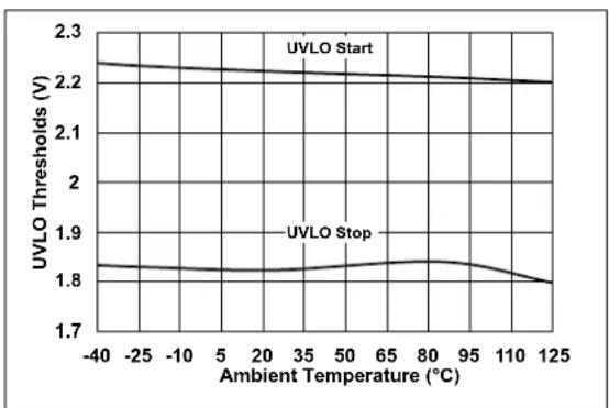
| Ambient Temperature (°C) | UVLO Thresholds (V) | | ------------------------ | ------------------- | | -40 | 2.2 | | -25 | 2.2 | | -10 | 2.2 | | 5 | 2.2 | | 20 | 2.2 | | 35 | 2.2 | | 50 | 2.2 | | 65 | 2.2 | | 80 | 2.2 | | 95 | 2.2 | | 110 | 2.2 | | 125 | 1.8 |FIGURE 2-1: Undervoltage Lockout (UVLO) vs. Ambient Temperature.
line
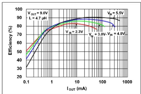
| I_OUT (mA) | Efficiency (%) at V_IN = 2.3V | Efficiency (%) at V_IN = 3.0V | Efficiency (%) at V_IN = 4.0V | Efficiency (%) at V_OUT = 5.5V | | ---------- | ----------------------------- | ----------------------------- | ----------------------------- | ------------------------------ | | 0.1 | ~50 | ~50 | ~50 | ~50 | | 1 | ~80 | ~80 | ~80 | ~80 | | 10 | ~85 | ~85 | ~85 | ~85 | | 100 | ~80 | ~80 | ~80 | ~80 | | 1000 | ~75 | ~75 | ~75 | ~75 |FIGURE 2-4: 9.0V V OUT Efficiency vs. IOUT.
line
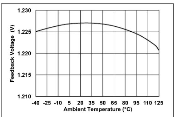
| Ambient Temperature (°C) | Feedback Voltage (V) | | ------------------------ | -------------------- | | -40 | 1.225 | | -25 | 1.226 | | -10 | 1.227 | | 5 | 1.228 | | 20 | 1.228 | | 35 | 1.228 | | 50 | 1.227 | | 65 | 1.226 | | 80 | 1.225 | | 95 | 1.223 | | 110 | 1.221 | | 125 | 1.220 |FIGURE 2-2: V FB Voltage vs. Ambient Temperature and VIN .
line
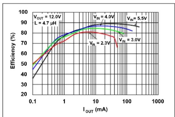
| I_OUT (mA) | Efficiency (%) at V_IN = 2.3V | Efficiency (%) at V_IN = 3.0V | Efficiency (%) at V_IN = 4.0V | Efficiency (%) at V_IN = 5.5V | | ---------- | ----------------------------- | ----------------------------- | ----------------------------- | ----------------------------- | | 0.1 | ~50 | ~50 | ~50 | ~50 | | 1 | ~75 | ~75 | ~80 | ~80 | | 10 | ~80 | ~80 | ~85 | ~85 | | 100 | ~75 | ~75 | ~80 | ~80 | | 1000 | ~70 | ~70 | ~75 | ~75 |FIGURE 2-5: 12.0V V OUT Efficiency vs. IOUT
line
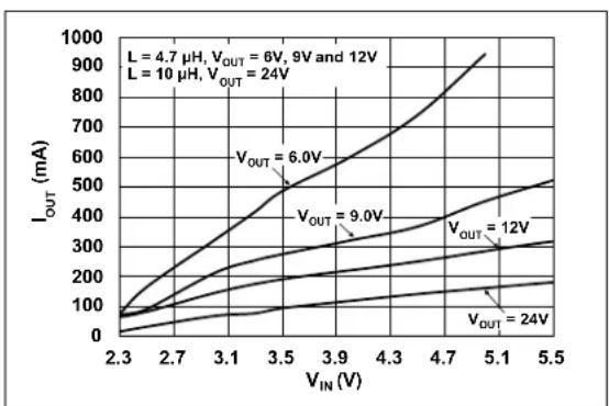
| V_IN (V) | I_OUT (mA) for V_OUT = 6.0V | I_OUT (mA) for V_OUT = 9.0V | I_OUT (mA) for V_OUT = 12V | I_OUT (mA) for V_OUT = 24V | | -------- | ---------------------------- | ---------------------------- | --------------------------- | --------------------------- | | 2.3 | ~50 | ~50 | ~50 | ~50 | | 2.7 | ~150 | ~150 | ~150 | ~150 | | 3.1 | ~300 | ~250 | ~200 | ~150 | | 3.5 | ~500 | ~350 | ~250 | ~150 | | 3.9 | ~700 | ~450 | ~300 | ~150 | | 4.3 | ~850 | ~550 | ~350 | ~150 | | 4.7 | ~950 | ~650 | ~400 | ~150 | | 5.1 | ~1000 | ~750 | ~450 | ~150 | | 5.5 | ~1000 | ~850 | ~500 | ~150 |FIGURE 2-3: Maximum Output Current vs. V_IN .
line
| I_OUT (mA) | Efficiency (%) for V_IN = 3.0V | Efficiency (%) for V_IN = 4.0V | | ---------- | ------------------------------ | ------------------------------ | | 0.1 | ~20 | ~20 | | 1 | ~60 | ~60 | | 10 | ~80 | ~80 | | 100 | ~85 | ~85 | | 1000 | ~80 | ~80 |FIGURE 2-6: 24.0V V OUT Efficiency vs. IOUT.
Note: Unless otherwise indicated, V_IN = 3.3 V_OUT = 20 mA , V_OUT = 12 V_IN = C_OUT = 10 F , X7R ceramic, L = 4.7 H_A 25^ , 5-lead SOT-23 package.
line
| Ambient Temperature (°C) | Inductor Peak Current (A) | | ------------------------ | ------------------------- | | -40 | 1.3 | | -25 | 1.3 | | -10 | 1.3 | | 5 | 1.3 | | 20 | 1.3 | | 35 | 1.3 | | 50 | 1.3 | | 65 | 1.3 | | 80 | 1.3 | | 95 | 1.25 | | 110 | 1.2 | | 125 | 1.15 |FIGURE 2-7: Inductor Peak Current Limit vs. Ambient Temperature.
line
| Ambient Temperature (°C) | I_IN^0 No Load Input Current (μA) for V_IN = 2.3V | I_IN^0 No Load Input Current (μA) for V_IN = 3.0V | I_IN^0 No Load Input Current (μA) for V_IN = 5.5V | | ------------------------ | ----------------------------------------------- | ----------------------------------------------- | ----------------------------------------------- | | -40 | ~200 | ~200 | ~200 | | -25 | ~200 | ~200 | ~200 | | -10 | ~200 | ~200 | ~200 | | 5 | ~200 | ~200 | ~200 | | 20 | ~200 | ~200 | ~200 | | 35 | ~200 | ~200 | ~200 | | 50 | ~200 | ~200 | ~200 | | 65 | ~200 | ~200 | ~200 | | 80 | ~400 | ~400 | ~400 | | 95 | ~800 | ~800 | ~600 | | 110 | ~1200 | ~1200 | ~800 | | 125 | ~1800 | ~1400 | ~600 |FIGURE 2-10: No Load Input Current, I_INO vs. Ambient Temperature.
line
| Input Voltage (V) | I_INO No Load Input Current (μA) | | ----------------- | -------------------------------- | | 2.3 | 250 | | 3.1 | 240 | | 3.9 | 230 | | 4.3 | 240 | | 4.7 | 250 | | 5.1 | 260 | | 5.5 | 270 |FIGURE 2-8: No Load Input Current, I INO vs. V_IN ( EN = V_IN ).
line
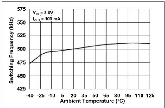
| Ambient Temperature (°C) | Switching Frequency (kHz) | | ------------------------ | ------------------------- | | -40 | 475 | | -25 | 490 | | -10 | 495 | | 0 | 500 | | 20 | 502 | | 35 | 504 | | 50 | 506 | | 65 | 508 | | 80 | 510 | | 95 | 512 | | 110 | 513 | | 125 | 514 |FIGURE 2-11: f SW vs. Ambient Temperature.
line
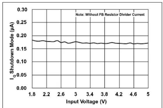
| Input Voltage (V) | I_G Shutdown Mode (µA) | | ----------------- | ---------------------- | | 1.8 | 0.18 | | 2.2 | 0.18 | | 2.6 | 0.17 | | 3.0 | 0.17 | | 3.4 | 0.17 | | 3.8 | 0.17 | | 4.2 | 0.17 | | 4.6 | 0.17 | | 5.0 | 0.17 |FIGURE 2-9: Shutdown Quiescent Current, I_QSHDN vs. V_IN (EN = GND).
line
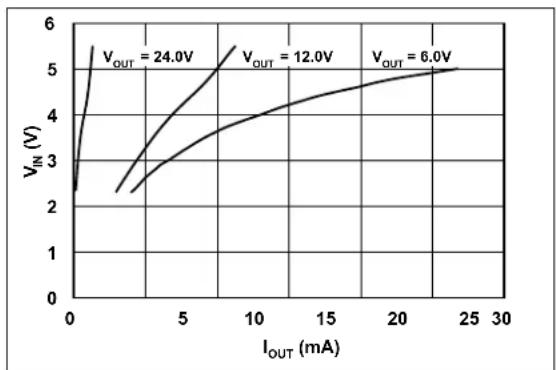
| IOUT (mA) | VIN (V) at VOUT = 24.0V | VIN (V) at VOUT = 12.0V | VIN (V) at VOUT = 6.0V | | --------- | ------------------------ | ------------------------ | ----------------------- | | 0 | 2.5 | 2.5 | 2.5 | | 5 | 4.5 | 3.5 | 3.0 | | 10 | 5.5 | 4.5 | 4.0 | | 15 | - | - | 4.5 | | 20 | - | - | 5.0 | | 25 | - | - | 5.0 | | 30 | - | - | 5.0 |FIGURE 2-12: PWM Pulse Skipping Mode Threshold.
Note: Unless otherwise indicated, V_IN = 3.3V_OUT = 20mA , V_OUT = 12V , C_OUT = 10 F , X7R ceramic, L = 4.7 H_A 25^ C , 5-lead SOT-23 package.
line
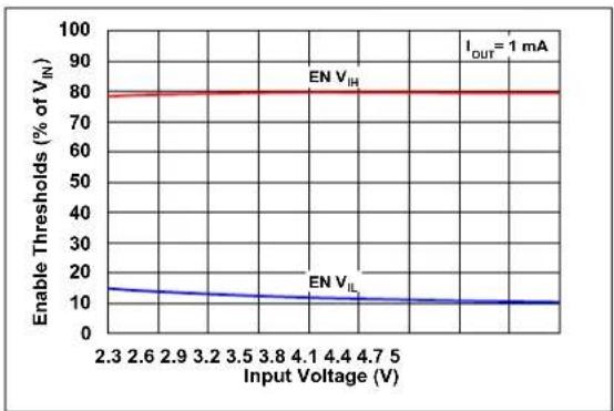
| Input Voltage (V) | EN V_IH | EN V_IL | | ----------------- | ------- | ------- | | 2.3 | 78 | 15 | | 2.6 | 78 | 14 | | 2.9 | 78 | 13 | | 3.2 | 78 | 12 | | 3.5 | 78 | 11 | | 3.8 | 78 | 10 | | 4.1 | 78 | 10 | | 4.4 | 78 | 10 | | 4.7 | 78 | 10 | | 5.0 | 78 | 10 |FIGURE 2-13: Enable Threshold vs. Input Voltage.
line
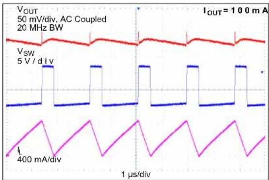
| Time (μs) | VOUT (mA) | VSW (V/div) | I (mA) | |-----------|----------|------------|--------| | 0 | 100 | 50 | 400 | | 1 | 100 | 50 | 400 | | 2 | 100 | 50 | 400 | | 3 | 100 | 50 | 400 | | 4 | 100 | 50 | 400 | | 5 | 100 | 50 | 400 | | 6 | 100 | 50 | 400 | | 7 | 100 | 50 | 400 | | 8 | 100 | 50 | 400 | | 9 | 100 | 50 | 400 | | 10 | 100 | 50 | 400 | | 11 | 100 | 50 | 400 | | 12 | 100 | 50 | 400 | | 13 | 100 | 50 | 400 | | 14 | 100 | 50 | 400 | | 15 | 100 | 50 | 400 | | 16 | 100 | 50 | 400 | | 17 | 100 | 50 | 400 | | 18 | 100 | 50 | 400 | | 19 | 100 | 50 | 400 | | 20 | 100 | 50 | 400 | | 21 | 100 | 50 | 400 | | 22 | 100 | 50 | 400 | | 23 | 100 | 50 | 400 | | 24 | 100 | 50 | 400 | | 25 | 100 | 50 | 400 | | 26 | 100 | 50 | 400 | | 27 | 100 | 50 | 400 | | 28 | 100 | 50 | 400 | | 29 | 100 | 50 | 400 | | 30 | 100 | 50 | 400 | | 31 | 100 | 50 | 400 | | 32 | 100 | 50 | 400 | | 33 | 100 | 50 | 400 | | 34 | 100 | 50 | 400 | | 35 | 100 | 50 | 400 | | 36 | 100 | 50 | 400 | | 37 | 100 | 50 | 400 | | 38 | 100 | 50 | 400 | | 39 | 100 | 50 | 400 | | 40 | 100 | 50 | 400 | | 41 | 100 | 50 | 400 | | 42 | 100 | 50 | 400 | | 43 | 100 | 50 | 400 | | 44 | 100 | 50 | 400 | | 45 | 100 | 50 | 400 | | 46 | 100 | 50 | 400 | | 47 | 100 | 50 | 400 | | 48 | 100 | 50 | 400 | | 49 | 100 | 50 | 400 | | 50 | 10 | | | | Peak | | | | | Final | | | | | Current | IOUT | - | - | | Current (approx.) from peak to final value: VOUT = -; AC Coupled; AC Coupled; AC Coupled; AC Coupled; AC Coupled; AC Coupled; AC Coupled; AC Coupled; AC Coupled; AC Coupled; AC Coupled; AC Coupled; AC Coupled; AC Coupled; AC Coupled; AC Coupled; AC Coupled; AC Coupled; AC Coupled; AC Coupled; AC Coupled; AC Coupled; AC Coupled; AC Coupled; AC Coupled; AC Cououred; AC Cououred; AC Cououred; AC Cououred; AC Cououred; AC Cououred; AC Cououred; AC Cououred; AC Cououred; AC Cououred; AC Cououred; AC Cououred; AC Cououred; AC Cououred; AC Cououred; AC Cououred; AC Cououred; AC Cououred; AC Cououred; AC Cououred; AC Cououred; AC Cououred; AC Cououred; AC Cououred; AC Cououred; AC Couured; AC Cououred; AC Cououred; AC Cououred; AC Cououred; AC Cououred; AC Cououred; AC Cououred; AC Cououred; AC Cououred; AC Cououred; AC Cououred; AC Cououred; AC Cououred; AC Cououred; AC Cououred; AC Cououred; AC Cououred; AC Cououred; AC Cououred; AC Cououred; AC Cououred; AC Cououred; AC Cououred; AC Cououred; AC Couruled; AC Couruled; AC Couruled; AC Couruled; AC Couruled; AC Couruled; AC Couruled; AC Couruled; AC Couruled; AC Couruled; AC Couruled; AC Couruled; AC Couruled; AC Couruled; AC Couruled; AC Couruled; AC Couruled; AC Couruled; AC Couruled; AC Couruled; AC Courued; AC Courued; AC Courued; AC Courued; AC Courued; AC Courued; AC Courued; AC Courued; AC Courued; AC Courued; AC Courued; AC Courued; AC Courued; AC Courued; AC Courued; AC Courued; AC Courued, AC Courued, AC Courued, AC Courued, AC Correlated, DC Correlated, DC Correlated, DC Correlated, DC Correlated, DC Correlated, DC Correlated, DC Correlated, DC Correlated, DC Correlated, DC Correlated, DC Correlated, DC Correlated, DC Correlated, DC Correlated, DC Correlated, DC Correlated, DC Correlated, DC Correlated, DC Correlated, DC Correlated, DC Correlated, DC Correlated, DC Correlated, DC Correlated, DC Correlated, DFIGURE 2-16: High Load PWM Mode Waveforms.
line
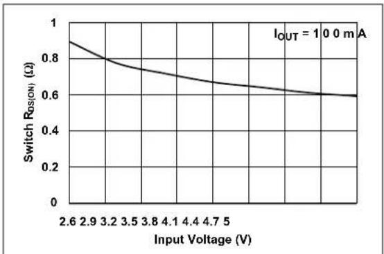
| Input Voltage (V) | Switch R_G(ON) (Ω) | | ----------------- | ------------------ | | 2.6 | 0.9 | | 2.9 | 0.8 | | 3.2 | 0.75 | | 3.5 | 0.7 | | 3.8 | 0.65 | | 4.1 | 0.6 | | 4.4 | 0.55 | | 4.7 | 0.5 | | 5.0 | 0.45 |FIGURE 2-14: N-Channel Switch R vs. V_IN . DSON
line
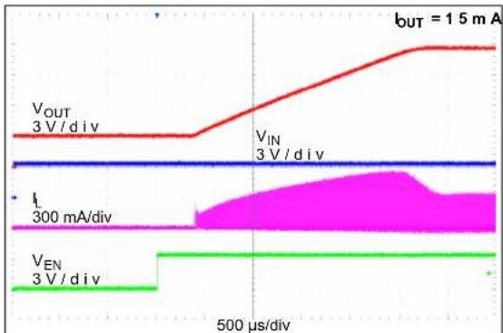
| Time (μs) | VOUT (3 V/div) | VIN (3 V/div) | I (300 mA/div) | VEN (3 V/div) | |-----------|----------------|---------------|----------------|---------------| | 0 | 0 | 0 | 0 | 0 | | 500 | ~0.5 | ~0.5 | ~0.2 | ~0.1 | | 1000 | ~1.0 | ~1.0 | ~0.8 | ~0.3 | | 1500 | ~1.5 | ~1.5 | ~1.0 | ~0.4 | | 2000 | ~2.0 | ~2.0 | ~1.2 | ~0.5 | | 2500 | ~2.5 | ~2.5 | ~1.4 | ~0.6 | | 3000 | ~3.0 | ~3.0 | ~1.6 | ~0.7 | | 3500 | ~3.5 | ~3.5 | ~1.8 | ~0.8 | | 4000 | ~4.0 | ~4.0 | ~2.0 | ~0.9 | | 4500 | ~4.5 | ~4.5 | ~2.2 | ~1.0 | | 500 | 15 | 15 | 15 | 15 |FIGURE 2-17: 12.0V Start-Up by Enable.
line
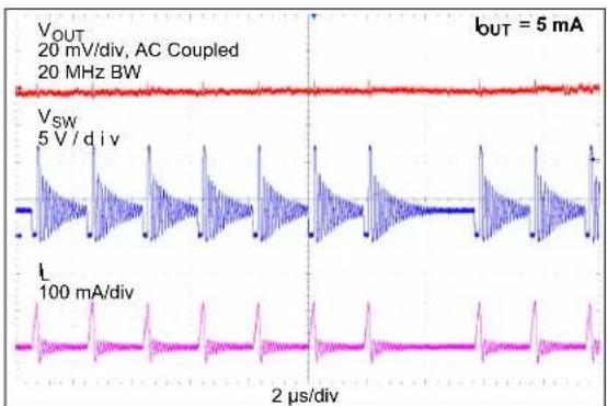
| Waveform | Description | |----------|--------------------------------| | VOUT | 20 mV/div, AC Coupled, 20 MHz BW | | VSW | 5 V/div | | L | 100 mA/div |FIGURE 2-15: 12.0V V OUT Light Load PWM Mode Waveforms.
line
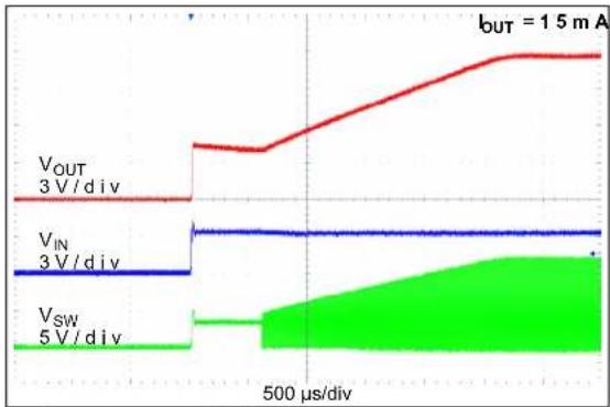
| Time (μs) | VOUT (3 V/div) | VIN (3 V/div) | VSW (5 V/div) | |-----------|----------------|---------------|---------------| | 0 | 0 | 0 | 0 | | 500 | ~0.8 | ~0.2 | ~0.1 |FIGURE 2-18: 12.0V Start-Up ( V_IN = V_ENABLE ).
Note: Unless otherwise indicated, V_IN = 3.3V_OUT = 20mA , V_OUT = 12V , C_OUT = 10 F , X7R ceramic, L = 4.7 H_A 25^ C , 5-lead SOT-23 package.
line
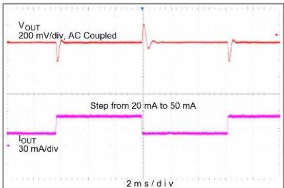
| Step | VOUT (mV/div) | IOUT (mA/div) | |------|---------------|---------------| | 20 | 200 | 30 |FIGURE 2-19: 12.0V V OUT Load Transient Waveforms.
line
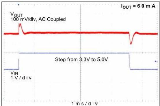
| Step from 1 ms/div | VOUT (mA) | VIN (A) | | ----------------- | --------- | ------- | | 3.3 | 60 | 1 | | 5.0 | 60 | 1 |FIGURE 2-20: 12.0V V OUT Line Transient Waveforms.
3.0 PIN DESCRIPTIONS
The descriptions of the pins are listed in Table3-1.
TABLE 3-1: PIN FUNCTION TABLE
| MCP1661SOT-23 | MCP16612x3 TDFN | Symbol | Description |
| 3 | 1 | V_FB | Feedback Voltage Pin |
| — | 2 | S_GND | Signal Ground Pin (TDFN only) |
| 1 3 | SW Switch Node, Boost Inductor Input Pin | ||
| — | 4, 6 | NC | Not Connected |
| 5 | 5 | V_IN | Input Voltage Pin |
| — | 7 | P_GND | Power Ground Pin (TDFN only) |
| 4 8 | EN Enable Control Input Pin | ||
| — | 9 | EP Exposed Thermal Pad (EP); must be connected to Ground.(TDFN only) | |
| 2 | — | GND | Ground Pin (SOT-23 only) |
3.1 Feedback Voltage Pin (V FB)
The V_FB pin is used to provide output voltage regulation by using a resistor divider. The V_FB voltage is 1.227V typical.
3.2 Signal Ground Pin (S GND)
The signal ground pin is used as a return for the integrated reference voltage and error amplifier. The signal ground and power ground must be connected externally in one point.
3.3 Switch Node Pin (SW)
Connect the inductor from the input voltage to the SW pin. The SW pin carries inductor current, which can be as high as 1.3A peak. The integrated N-Channel switch drain is internally connected to the SW node.
3.4 Not Connected (NC)
This is an unconnected pin.
3.5 Power Supply Input Voltage Pin ( V_IN )
Connect the input voltage source to V_IN . The input source must be decoupled from GND with a 4.7 F minimum capacitor.
3.6 Power Ground Pin (P GND)
The power ground pin is used as a return for the high-current N-Channel switch. The signal ground and power ground must be connected externally in one point.
3.7 Enable Pin (EN)
The EN pin is a logic-level input used to enable or disable device switching and lower quiescent current while disabled. A logic high ( >85% of V_IN ) will enable the regulator output. A logic low ( <7.5% of V_IN ) will ensure that the regulator is disabled.
3.8 Exposed Thermal Pad (EP)
There is no internal electrical connection between the Exposed Thermal Pad (EP) and the S_GND and P_GND pins. They must be connected to the same potential on the PCB.
3.9 Ground Pin (GND)
The ground or return pin is used for circuit ground connection. The length of the trace from the input cap return, the output cap return and the GND pin must be as short as possible to minimize noise on the GND pin. The 5-lead SOT-23 package uses a single ground pin.
NOTES:
4.0 DETAILED DESCRIPTION
4.1 Device Overview
MCP1661 is a constant frequency PWM boost (step-up) converter, based on a peak current mode architecture which delivers high efficiency over a wide load range from two-cell and three-cell Alkaline, Ultimate Lithium, NiMH, NiCd and single-cell Li-Ion battery inputs. A high level of integration lowers total system cost, eases implementation and reduces board area.
The device features controlled start-up voltage (UVLO), adjustable output voltage, 500 kHz PWM operation with Skipping mode, 36V integrated switch, internal compensation, inrush current limit, soft start, and overvoltage protection in case the V_FB connection is lost.
The 800 mΩ, 36V integrated switch is protected by the 1.3A cycle-by-cycle inductor peak current operation. When the Enable pin is pulled to ground (EN = GND), the device stops switching, enters in Shutdown mode and consumes approximately 200 nA of input current (the feedback current is not included).
MCP1661 can be used to build classic boost, SEPIC or flyback DC-DC converters.
4.2 Functional Description
The MCP1661 device is a compact, high-efficiency, fixed-frequency, step-up DC-DC converter that provides an easy-to-use high-output power supply solution for applications powered by either two-cell or three-cell alkaline or Lithium Energizer, three-cell NiCd or NiMH or one-cell Li-Ion or Li-Polymer batteries.
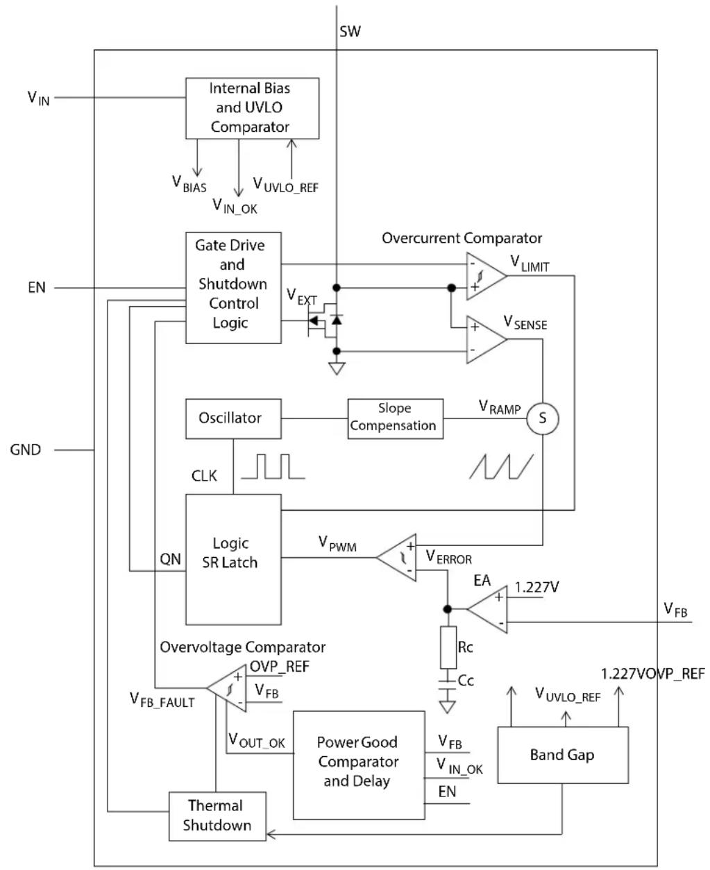
Figure 4-1 depicts the functional block diagram of the MCP1661 device. It incorporates a current mode control scheme, in which the PWM ramp signal is derived from the NMOS power switch current ( V_SENSE ). This ramp signal adds slope ramp compensation signal ( V_RAMP ) and is compared to the output of the error amplifier ( V_ERROR ) to control the on-time of the power switch. A proper slope rate will be designed to improve circuit stability.
flowchart
graph TD
    A["V_IN"] --> B["Internal Bias and UVLO Comparator"]
    B --> C["V_BIAS"]
    C --> D["V_UVLO_REF"]
    D --> E["V_IN_OK"]
    E --> F["Gate Drive and Shutdown Control Logic"]
    F --> G["V_EXT"]
    G --> H["Overcurrent Comparator"]
    H --> I["V_LIMIT"]
    I --> J["S"]
    J --> K["V_RAMP"]
    K --> L["S"]
    L --> M["Slope Compensation"]
    M --> N["Oscillator"]
    N --> O["CLK"]
    O --> P["QN"]
    P --> Q["Logic SR Latch"]
    Q --> R["V_PWM"]
    R --> S["V_ERROR"]
    S --> T["EA 1.227V"]
    T --> U["V_FB"]
    U --> V["Band Gap"]
    V --> W["V_UVLO_REF"]
    W --> X["1.227VOVP_REF"]
    X --> Y["V_FB_FAULT"]
    Y --> Z["Overvoltage Comparator"]
    Z --> AA["V_FB_FAULT"]
    AA --> AB["Power Good Comparator and Delay"]
    AB --> AC["V_FB"]
    AC --> AD["V_IN_OK"]
    AD --> AE["EN"]
    AE --> AF["Thermal Shutdown"]
    AF --> AG["GND"]
    AG --> AH["EN"]
    AH --> AI["SW"]
FIGURE 4-1: MCP1661 Simplified Block Diagram.
4.2.1 INTERNAL BIAS
The MCP1661 device gets its bias from V_IN . The V_IN bias is used to power the device and drive circuits over the entire operating range.
4.2.2 START-UP VOLTAGE AND SOFT START
The MCP1661 device starts at input voltages that are higher than or equal to a predefined set UVLO value. MCP1661 starts switching at approximately 2.3V for 12.0V output and 1 mA resistive load. Once started, the device will continue to operate under normal load conditions down to 1.85V typical. There is a soft start feature which provides a way to limit the inrush current drawn from the input (batteries) during start-up. The soft start has an important role in applications where the switch will reach 32V. During start-up, excessively high switch current, together with the presence of high voltage, can overstress the NMOS switch.
When the device is powered (EN = V_IN and V_IN rises from zero to its nominal value), the output capacitor charges to a value close to the input voltage (or V_IN minus a Schottky diode voltage drop). The overshoot on output is limited by slowly increasing the reference of the error amplifier. There is an internal reference voltage which charges an internal capacitor with a weak current source. The voltage on this capacitor slowly ramps the reference voltage. The soft-start capacitor is completely discharged in the event of a commanded shutdown or a thermal shutdown.
Due to the direct path from input to output, in the case of start-up by enable (EN voltage switches from low-to-high), the output capacitor is already charged and the output starts from a value close to the input voltage.
The internal oscillator has a delayed start to let the output capacitor be completely charged to the input voltage value.
4.2.3 UNDERVOLTAGE LOCKOUT (UVLO)
MCP1661 features an UVLO which prevents fault operation below 1.85V, which corresponds to the typical value of two discharged batteries. The device starts its normal operation at 2.3V input. The upper limit is set to avoid any input transients (temporary V_IN drop), which might trigger the lower UVLO threshold and restart the device. Usually, these voltage transients (overshoots and undershoots) have up to a few hundred mV.
MCP1661 is a non-synchronous boost regulator. Due to this fact, there is a direct path from V_IN to V_OUT through the inductor and the diode. This means that, while the device is not switching ( V_IN below UVLO STOP threshold), VOUT is not zero but equal to V_IN-V_F (where V_F is the voltage drop on the rectifier diode).
When the input voltage is below the 2.3V UVLO start threshold, the device is operating with limited specification.
MCP1661 operates as a fixed-frequency, non-synchronous converter. The switching frequency is maintained at 500 kHz with a precision oscillator.
Lossless current sensing converts the peak current signal to a voltage ( V_SENSE ) and adds it to the internal slope compensation ( V_RAMP ). This summed signal is compared to the voltage error amplifier output ( V_ERROR ) to provide a peak current control signal ( V_PWM ) for the PWM control block. The slope compensation signal depends on the input voltage. Therefore, the converter provides the proper amount of slope compensation to ensure stability. The peak current is set to 1.3A.
The MCP1661 device will operate in PWM even during periods of light load operation by skipping pulses. By operating in PWM mode, the output ripple is low and the frequency is constant.
The MCP1661 output voltage is adjustable with a resistor divider over the V_OUT range. High resistors are recommended to minimize power loss and keep efficiency high at light loads. The device integrates a transconductance-type error amplifier and the values of the feedback resistors do not influence the stability of the system.
value
4.2.6 MINIMUM INPUT VOLTAGE AND MAXIMUM OUTPUT CURRENT
The maximum output current for which the device can supply the load is dependent upon the input and output voltage. The minimum input voltage necessary to reach the value of the desired output depends on the maximum duty cycle (approximately 90%) in accordance with the mathematical relation V_OUT = V_INmin/(1 - D_MAX) . As there is a 1.3A inductor peak current limit, V_OUT can go out of regulation before reaching the maximum duty cycle. (For boost converters, the average inductor current is equal to the input current.)
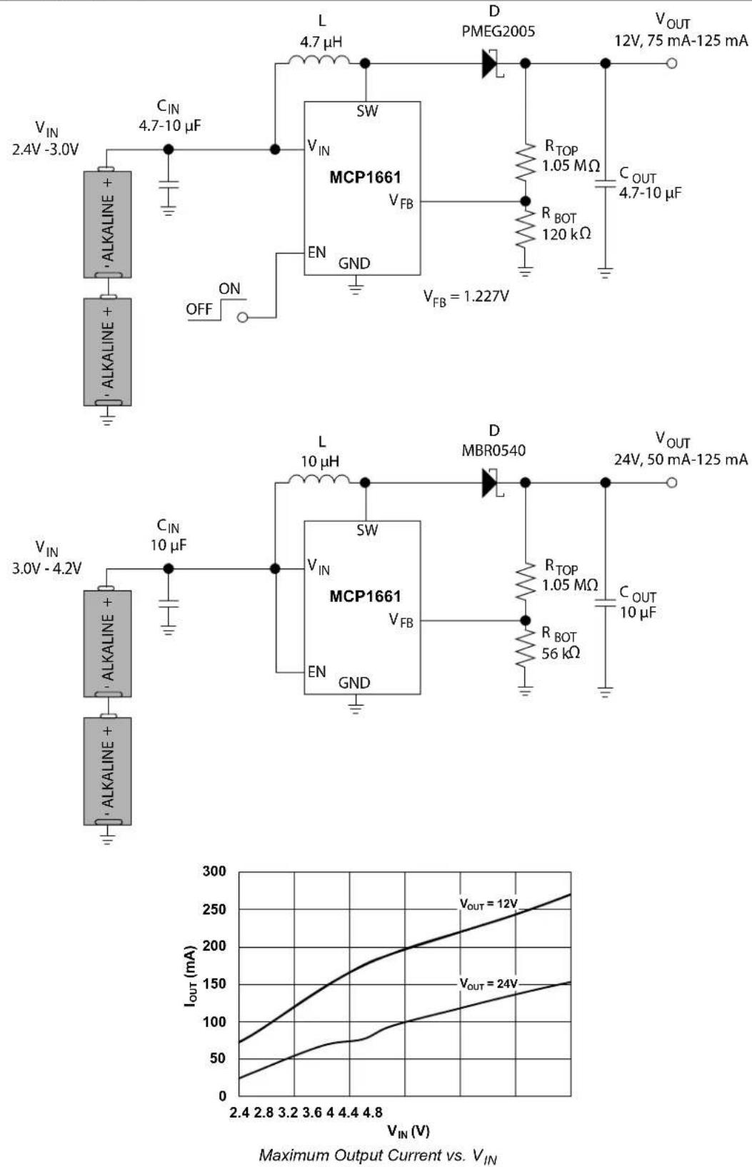
For example, to ensure a 100 mA load current for V_OUT = 12.0V , a minimum of 2.8V input voltage is necessary. If an application is powered by one Li-Ion battery ( V_IN from 3.3V to 4.2V), the minimum load current the MCP1661 device can deliver is close to 50 mA at 24.0V output (see Figure 2-3).
4.2.7 ENABLE PIN
The MCP1661 device is enabled when the EN pin is set high. The device is put into Shutdown mode when the EN pin is set low. To enable the boost converter, the EN voltage level must be greater than 85% of the V_IN voltage. To disable the boost converter, the EN voltage must be less than 7.5% of the V_IN voltage.
In Shutdown mode, the MCP1661 device stops switching and all internal control circuitry is switched off. On boost configuration, the input voltage will be bypassed to output through the inductor and the Schottky diode. In the SEPIC converter, Shutdown mode acts as output disconnect.
4.2.8 INTERNAL COMPENSATION
The error amplifier, with its associated compensation network, completes the closed-loop system by comparing the output voltage to a reference at the input of the error amplifier and by feeding the amplified and inverted error voltage to the control input of the inner current loop. The compensation network provides phase leads and lags at appropriate frequencies to cancel excessive phase lags and leads of the power circuit. All necessary compensation components and slope compensation are integrated.
4.2.9 OUTPUT OVERVOLTAGE PROTECTION (OVP)
An internal V_FB fault signal turns off the PWM signal ( V_EXT ) and prevents the output from going out of regulation in the event of:
- short circuit of the feedback pin to GND
- disconnection of the feedback divider from V_OUT
In any of the above events, for a regular integrated boost circuit (IC) without any protection implemented, if the V_FB voltage drops to ground potential, its N-channel transistor will be forced to switch at full duty cycle and V_OUT rises. This Fault event may cause the SW pin to exceed its maximum voltage rating and may damage the boost regulator IC, the external components and the load. To avoid all these, MCP1661 has implemented an overvoltage protection (OVP) which turns off PWM switching when an overvoltage condition is detected. There is an overvoltage comparator with 80 mV reference which monitors the V_FB voltage.
The OVP comparator is disabled during start-up sequences and thermal shutdown.
If OVP occurs with the input voltage below the UVLO START threshold and VFB remains under 80 mV due to a low input voltage or overload condition, the device latches its output and resumes after restart.
4.2.10 OVERCURRENT LIMIT
The MCP1661 device uses a 1.3A cycle-by-cycle inductor peak current limit to protect the N-channel switch. There is an overcurrent comparator which resets the drive latch when the peak of the inductor current reaches the limit. In current limitation, the output voltage starts dropping.
4.2.11 OUTPUT SHORT CIRCUIT CONDITION
Like all non-synchronous boost converters, the MCP1661 inductor current will increase excessively during a short circuit on the converter's output. Short circuit on the output will cause the diode rectifier to fail and the inductor's temperature to rise. When the diode fails, the SW pin becomes a high-impedance node, it remains connected only to the inductor and the excessive resulted ringing will damage the MCP1661 device.
4.2.12 OVERTEMPERATURE PROTECTION
Overtemperature protection circuitry is integrated into the MCP1661 device. This circuitry monitors the device junction temperature and shuts the device off if the junction temperature exceeds the typical +150°C threshold. If this threshold is exceeded, the device will automatically restart when the junction temperature drops by 15°C. The output overvoltage protection (OVP) is reset during an overtemperature condition.
5.0 APPLICATION INFORMATION
5.1 Typical Applications
The MCP1661 nonsynchronous boost regulator operates over a wide output voltage range up to 32V. The input voltage ranges from 2.4V to 5.5V. The device operates down to 1.85V input with limited specification. The UVLO thresholds are set to 2.3V when V_IN is ramping and to 1.85V when V_IN is falling. The power efficiency conversion is high for several decades of load range. Output current capability increases with the input voltage and decreases with the increasing output voltage. The maximum output current is based on the N-channel switch peak current limit, set to 1.3A, and on a maximum duty cycle of 90%. Typical characterization curves in this data sheet are presented to display the typical output current capability.
5.2 Adjustable Output Voltage Calculations
To calculate the resistor divider values for the MCP1661, the following equation can be used. Where R_TOP is connected to V_OUT , R_BOT is connected to GND and both are connected to the V_FB input pin.
EQUATION 5-1:
$$ R _ {T O P} = R _ {B O T} \times \left(\frac {V _ {O U T}}{V _ {F B}}\right) $$
EXAMPLE 5-1:
$$ V _ {\text { OUT }} = 1 2. 0 \mathrm{V} $$
$$ V _ {F B} = 1. 2 2 7 V $$
$$ R _ {B O T} = 1 2 0 k \Omega $$
$$ \begin{array}{r l} R _ {T O P} & = 1 0 5 3. 6 \mathrm{k} \Omega (\mathrm{V} _ {\text { OUT }} = 1 1. 9 6 \mathrm{V} \text { with a standard } \ & \text { value of } 1 0 5 0 \mathrm{k} \Omega) \end{array} $$
EXAMPLE 5-2:
$$ V _ {O U T} = 2 4. 0 \mathrm{V} $$
$$ V _ {F B} = 1. 2 2 7 V $$
$$ R _ {B O T} = 5 3 k \Omega $$
$$ \begin{array}{r l} R _ {T O P} & = 9 8 3. 6 7 \mathrm{k} \Omega (\mathrm{V} _ {\text { OUT }} = 2 3. 8 2 \mathrm{V} \text { with a standard } \ & \text { value of } 9 7 6 \mathrm{k} \Omega) \end{array} $$
The values of the two resistors, R_TOP and R_BOT , affect the no load input current and quiescent current. In Shutdown mode (EN = GND), the device consumes approximately 0.2 A. With 24V output and 1 M feedback divider, the current which this divider drains from input is 2.4 A. This value is much higher than what the device consumes. Keeping R_TOP and R_BOT high will optimize efficiency conversion at very light loads. There are some potential issues with higher value resistors, as in the case of small surface mount resistors; environment contamination can create leakage paths on the PCB that significantly change the resistor divider and may affect the output voltage tolerance.
5.2.1 OVERVOLTAGE PROTECTION
The MCP1661 features an output overvoltage protection (OVP) in case R_TOP is disconnected from the V_OUT line. A typical 80 mV OVP reference is compared to V_FB voltage. If voltage on the V_FB pin drops below the reference value, the device stops switching and prevents V_OUT from rising up to a dangerous value.
OVP is not enabled during start-up and thermal shutdown events.
5.3 Input Capacitor Selection
The boost input current is smoothened by the boost inductor, reducing the amount of filtering necessary at the input. Some capacitance is recommended to provide decoupling from the input source. Because MCP1661 is rated to work up to 125^ C, low ESR X7R ceramic capacitors are well suited, since they have a low temperature coefficient and are small-sized. For limited temperature range use at up to 85^ C, a X5R ceramic capacitor can be used. For light load applications, 4.7 F of capacitance is sufficient at the input. For high-power applications that have high source impedance or long leads, using a 20-30 F input capacitor is recommended to sustain high input boost currents. Additional input capacitance can be added to provide a stable input voltage.
Table 5-1 contains the recommended range for the input capacitor value.
5.4 Output Capacitor Selection
The output capacitor helps provide a stable output voltage during sudden load transients and reduces the output voltage ripple. As with the input capacitor, X7R ceramic capacitor is recommended for this application. Using other capacitor types (aluminum or tantalum) with large ESR has impact on the converter's efficiency (see AN1337), maximum output power and stability. For limited temperature range (up to 85°C), X5R ceramic capacitors can be used. The DC rating of the output capacitor should be greater than the V_OUT value. Generally, ceramic capacitors lose up to 50% of their capacity when the voltage applied is close to the maximum DC rating. Choosing a capacitor with a safe higher DC rating or placing two capacitors in parallel assure enough capacity to correctly filter the output voltage.
The MCP1661 device is internally compensated so output capacitance range is limited. See Table 5-1 for the recommended output capacitor range.
An output capacitance higher than 10 F adds a better load step response and high-frequency noise attenuation, especially while stepping from light to heavy current loads. In addition, 2 x 10 F output capacitors ensure a better recovery of the output after a short period of overloading.
While the N-Channel switch is on, the output current is supplied by the output capacitor C_OUT . The amount of output capacitance and equivalent series resistance will have a significant effect on the output ripple voltage. While C_OUT provides load current, a voltage drop also appears across its internal ESR that results in ripple voltage.
Peak-to-peak output ripple voltage also depends on the equivalent series inductance (ESL) of the output capacitor. There are ceramic capacitors with special
internal architecture which minimize the ESL. Consult the ceramic capacitor's manufacturer portfolio for more information.
Table5-1 contains the recommended range for the input and output capacitor value.
TABLE 5-1: CAPACITOR VALUE RANGE
| C_IN | C_OUT | |
| Minimum 4.7 μF | 10 μF | |
| Maximum — 47 μF | ||
5.5 Inductor Selection
The MCP1661 device is designed to be used with small surface mount inductors; the inductance value can range from 4.7 H to 10 H. An inductance value of 4.7 H is recommended for output voltages below 15V. For higher output voltages, up to 32V, an inductance value of 10 H is optimum. While the device operates at low inputs, below 3.0V, a low value inductor (2.2 H or 3.3 H) ensures better stability but limited output power capability. Usually, this is a good trade-off as boost converters powered from two-cell batteries are low-power applications.
TABLE 5-2: MCP1661 RECOMMENDED INDUCTORS FOR BOOST CONVERTERS
| Part Number | Value (μH) | DCR Ω (typ.) | ISAT(A) | Size WxLxH (mm) |
| Coilcraft | ||||
| MSS5131-472 4.7 0.038 1 | 42 5.1x | 5.1x3.1 | ||
| XFL4020-472 4.7 0.057 2.7 | 4.2x4.2 | x2.1 | ||
| LPS5015-562 | 5.6 0. | 175 1.6 5 | 0x5.0x1 | 5 |
| LPS6235-103 | 10 | 0.065 1 | 5 6.2x6 | 2x3.5 |
| XAL4040-103 | 10 | 0.092 | 1.9 4.3x4 | 4.3x4.1 |
| Würth Elektronik | ||||
| 744025004 WE-TPC | 4.7 | 0.1 | 1.7 | 2.8x2.8x2.8 |
| 744043004 WE-TPC | 4.7 | 0.05 | 1.7 | 4.8x4.8x2.8 |
| 744773112 WE-PD2 | 10 | 0.156 1 | 6 4.0x4 | 5x3.2 |
| 74408943100 WE-SPC 10 | 0.08 | 2 2.1 4.8x | 4.8x3.8 | |
| TDK Corporation | ||||
| B82462G4472 4.7 0.04 | 1.8 | 6.3x6.3x | 3.0 | |
| B82462G4103 | 10 | 0.062 1 | 3 6.3x6 | 3x3.0 |
| VLCF4024T-4R7 | 4.7 0. | 087 1.43 | 4.0x4.0x | 2.4 |
Several parameters are used to select the correct inductor: maximum rated current, saturation current and copper resistance (DCR). For boost converters, the inductor current is much higher than the output current. The average inductor current is equal to the input current. The inductor's peak current is 30-40% higher than the average. The lower the inductor DCR, the higher the efficiency of the converter: a common trade-off in size versus efficiency.
The saturation current typically specifies a point at which the inductance has rolled off a percentage of the rated value. This can range from a 20% to 40% reduction in inductance. As inductance rolls off, the inductor ripple current increases, as does the peak switch current. It is important to keep the inductance from rolling off too much, causing switch current to reach the peak limit.
5.6 Rectifier Diode Selection
Schottky diodes are used to reduce losses. The diode's current rating has to be equal or higher than the maximum output current. The diode's reverse breakdown voltage must be higher than the internal switch rating voltage of 36V.
The converter's efficiency will be improved if the voltage drop across the diode is lower. The forward voltage rating is forward-current dependent, which is equal in particular to the load current.
For high currents and high ambient temperatures, use a diode with good thermal characteristics.
TABLE 5-3: RECOMMENDED SCHOTTKY DIODES
| Type | V_OUTmax | T_A |
| PMEG2005 | 18V < 85°C | |
| PMEG4005 | 36V < 85°C | |
| MBR0520 | 18V < 125°C | |
| MBR0540 | 36V < 125°C |
5.7 SEPIC Converter Considerations
One of the advantages of using MCP1661 in SEPIC topology is the usage of an output disconnect feature.
Also, the output voltage may be lower or higher than the input voltage, resulting in buck or boost operation. Input voltage is limited to the 2.4-5.5V range.
One major advantage is that the SEPIC converter allows 3.0V or 3.3V buck-boost application from a Li-Ion battery with load disconnect. Also, SEPIC is recommended for higher output voltages where an input-to-output isolation is necessary (due to the coupling capacitor). An application example is shown in Figure 6-3.
The maximum output voltage, V_OUTmax , must be limited to the sum of (V_IN + V_OUT) < 36V , which is the maximum internal switch DC rating. V_IN must be ≤ 5.5V .
Some extra aspects need to be taken into account when choosing the external components:
- the DC voltage rating of the coupling capacitor should be at least equal to the maximum input voltage
- the average current rating of the rectifier diode's is equal to the output load current
- the peak current of the rectifier diode is the same as the internal switch current, I_SW = I_IN + I_OUT .
See the notes on Figure 6-3 in Section 6.0 "Typical Application Circuits" for some recommended 1:1 coupled inductors.
5.8 Thermal Calculations
The MCP1661 device is available in two different packages (5-lead SOT-23 and 8-lead 2x3 TDFN). By calculating the power dissipation and applying the package thermal resistance ( _JA ), the junction temperature is estimated. The maximum continuous junction temperature rating for the MCP1661 device is +125°C.
To quickly estimate the internal power dissipation for the switching boost regulator, an empirical calculation using measured efficiency can be used. Given the measured efficiency, the internal power dissipation is estimated by Equation 5-2.
EQUATION 5-2:
$$ \left(\frac {V _ {O U T} \times I _ {O U T}}{E f f i c i e n c y}\right) V _ {O U T} \times (I _ {O U T} = D i s) $$
The difference between the first term, input power, and the second term, power delivered, is the power dissipated when using the MCP1661 device. This is an estimate, assuming that most of the power lost is internal to the MCP1661 and not C_IN , C_OUT , the diode and the inductor. There is some percentage of power lost in the boost inductor and rectifier diode, with very little loss in the input and output capacitors. For a more accurate estimation of the internal power dissipation, subtract the I_INRMS^2 × L_DCR and I_OUT × V_F power dissipation (where I_NRMS is the average input current, L_DCR is the inductor series resistance and V_F is the diode voltage drop).
5.9 PCB Layout Information
Good printed circuit board layout techniques are important to any switching circuitry, and switching power supplies are no different. When wiring the switching high-current paths, short and wide traces should be used. Therefore, it is important that the input and output capacitors be placed as close as possible to the MCP1661 to minimize the loop area.
The feedback resistors and feedback signal should be routed away from the switching node and the switching current loop. When possible, ground planes and traces should be used to help shield the feedback signal and minimize noise and magnetic interference.
text_image
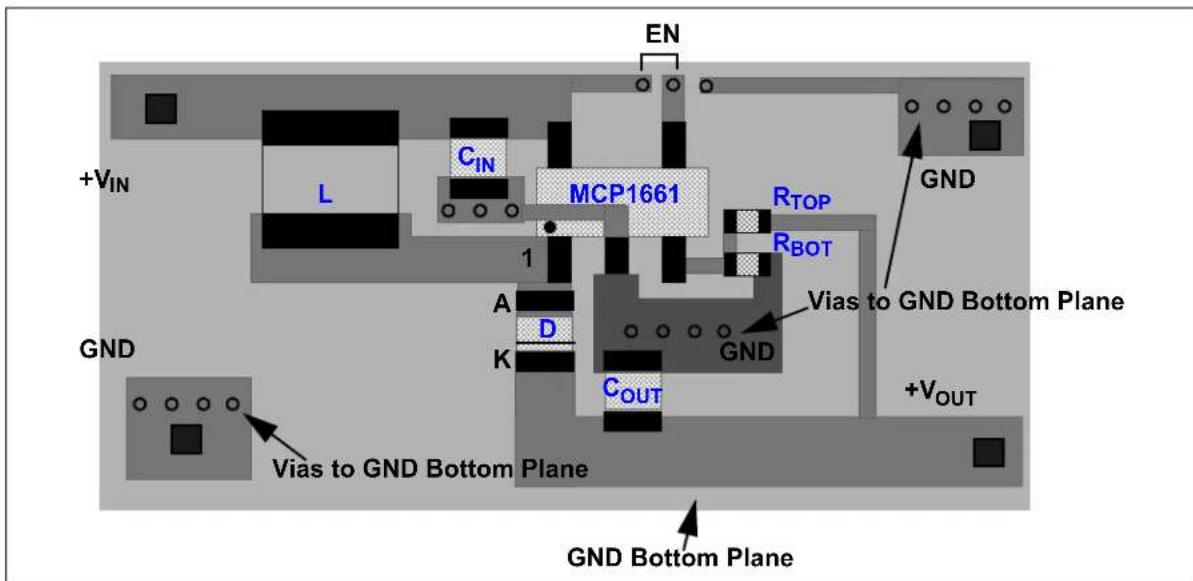
EN +VIN L CIN MCP1661 RTOP GND 1 A D K GND Vias to GND Bottom Plane COUT GND +VOUT GND Bottom Plane Vias to GND Bottom PlaneFIGURE 5-1: 5-Lead SOT-23 Recommended Layout.
text_image
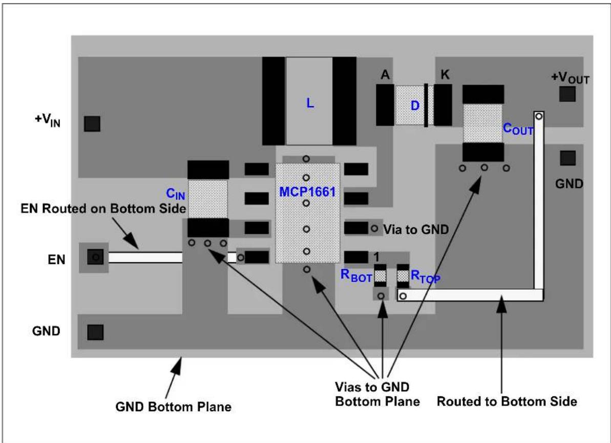
+V_IN C_IN EN Routed on Bottom Side MCP1661 Via to GND R_BOT 1 R_TOP GND GND Bottom Plane Vias to GND Bottom Plane Routed to Bottom Side A D K C_OUT +V_OUT GNDFIGURE 5-2: 8-Lead TDFN Recommended Layout.
6.0 TYPICAL APPLICATION CIRCUITS
text_image
VIN 2.4V-3.0V ALKALINE+ ALKALINE+ CIN 10 μF SW VIN MCP1661 VFB EN GND ON OFF L 4.7 μH D Schottky RTOP 1.05 MΩ RBOT 120 kΩ COUT 10 μF VOUT 12V, 75 mA| Component | Value | Manufacturer Part Number | Comment | |
| C_IN | 10 μF T | DK Corporation C201 | 2X7R1A106K125AC Cap. | ceramic 10 μF 10V 10% X7R 0805 |
| C_OUT | 10 μF T | DK Corporation C321 | 6X7R1C106K160AC Cap. | ceramic 10 μF 16V 10% X7R 1206 |
| L 4.7 μH Coilcraft | XFL4020-472MEB Inductor Power 4.7 μH 2A SMD | |||
| R_TOP | 1.05 MΩ | Yageo Corporation | RC0805FR-071M05L | Res. 1.05 MΩ 1/8W 1% 0805 SMD |
| R_BOT | 120 kΩ | Yageo Corporation | RC0805FR-07120KL | Res. 120 kΩ 1/8W 1% 0805 SMD |
| D | — | NXP Semiconductor | PMEG2005EH,115 | Diode Schottky 20V 0.5A SOD123F |
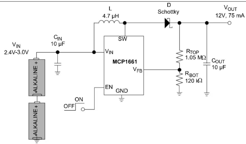
FIGURE 6-1: Two Alkaline Cells to 12V Boost Converter.
text_image
VIN 3.0V-4.2V + NION - CIN 10 μF L 10 μH D Schottky VOUT 24V, 50 mA SW VIN MCP1661 VFB EN GND RTOP 1.05 MΩ RBOT 56 kΩ COUT 10 μF| Component | Value Manufacturer Part Number | Comment | ||
| C_IN | 10 μF | TDK Corporation | C2012X7R1A106K125AC | Cap. ceramic 10 μF 10V 10% X7R 0805 |
| C_OUT | 10 μF | TDK Corporation | C3216X7R1V106K160AC | Cap. ceramic 10 μF 35V 10% X7R 1206 |
| L | 10 μH | EPCOS AG | B82462G4103M000 | Inductor Power 10 μH 1.5A SMD |
| R_TOP | 1.05 MΩ | Yageo Corporation | RC0805FR-071M05L | Res. 1.05 MΩ 1/8W 1% 0805 SMD |
| R_BOT | 56 kΩ | Yageo Corporation | RC0805FR-0756KL | Res. 56 kΩ 1/8W 1% 0805 SMD |
| D | — | Micro Commercial Components | MBR0540-TP | Diode Schottky 40V 0.5A SOD123 |
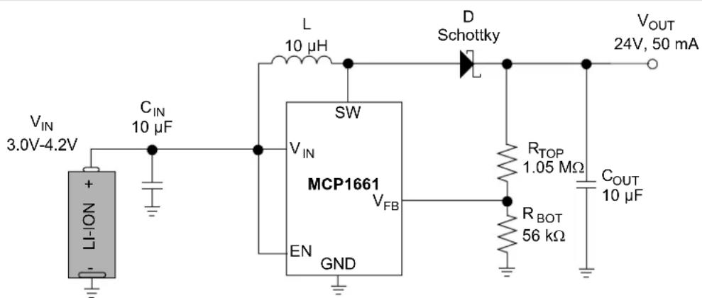
FIGURE 6-2: Single Li-Ion Cell to 24V Output Boost Converter.
text_image
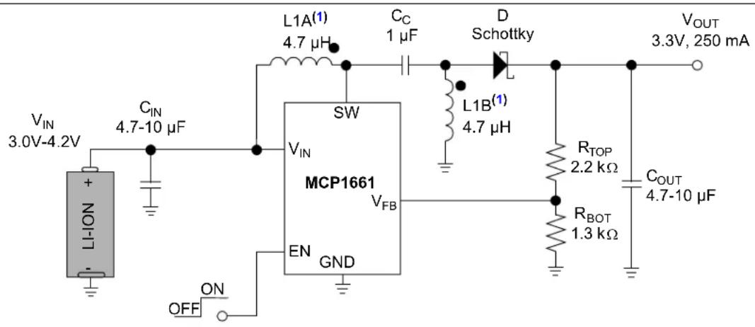
VIN 3.0V-4.2V + - LION CIN 4.7-10 μF SW VIN MCP1661 VFB EN GND ON OFF L1A(1) 4.7 μH CC 1 μF D Schottky L1B(1) 4.7 μH ROTOP 2.2 kΩ RBOT 1.3 kΩ COUT 4.7-10 μF VOUT 3.3V, 250 mANote 1: Recommended 1:1 coupled inductors.
| Component | Value M | Manufacturer Part Number | Comment | |
| C_IN | 10 μF | TDK Corporation | C2012X7R1A106K125AC | Cap. ceramic 10 μF 10V 10% X7R 0805 |
| C_OUT | 10 μF | TDK Corporation | C3216X7R1V106K160AC | Cap. ceramic 10 μF 35V 10% X7R 1206 |
| C_C | 1 μF | TDK Corporation | C2012X7R1E105K125AB | Cap. ceramic 1 μF 25V 10% X7R 0805 |
| L | 4.7 μH | Würth Elektronik | 744878004 | Inductor Array 2 Coil 4.7 μH SMD |
| R_TOP | 2.2 kΩ | Yageo Corporation | RC0805FR-072K2L | Res. 2.2 kΩ 1/8W 1% 0805 SMD |
| R_BOT | 1.3 kΩ | Yageo Corporation | RC0805FR-071K3L | Res. 1.3 kΩ 1/8W 1% 0805 SMD |
| D | — | NXP Semiconductors | PMEG2020AEA,115 | Diode Schottky 20V 2A SOD323 |
FIGURE 6-3: Single Li-Ion Cell to 3.3V Output Buck-Boost (SEPIC) Converter with 1:1 Coupled Inductors and Load Disconnect.
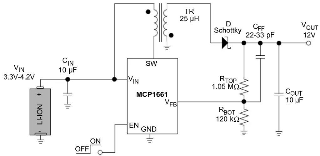
text_image
V_IN 3.3V-4.2V + - LION C_IN 10 μF SW V_IN MCP1661 V_FB EN GND OFF ON ON TR 25 μH D Schottky C_FF 22-33 pF V_OUT 12V R_TOP 1.05 MΩ R_BOT 120 kΩ C_OUT 10 μF| Component | Value Manufacturer Part Number Comment | |||
| C_IN | 10 μF | TDK Corporation | C2012X7R1A106K125AC | Cap. ceramic 10 μF 10V 10% X7R 0805 |
| C_OUT | 10 μF | TDK Corporation | C3216X7R1V106K160AC | Cap. ceramic 10 μF 35V 10% X7R 1206 |
| C_FF | 27 pF | TDK Corporation | C1608NP02A270J080AA | Cap. ceramic 27 pF 100V 5% NP0 0603 |
| TR 25 μH Würth Elektronik 750310799 | Trans. Flyback LT3573 25 μH SMD | |||
| R_TOP | 1.05 MΩ | Yageo Corporation | RC0805FR-071M05L | Res. 1.05 MΩ 1/8W 1% 0805 SMD |
| R_BOT | 120 kΩ | Yageo Corporation | RC0805FR-07120KL | Res. 120 kΩ 1/8W 1% 0805 SMD |
| D | — | Micro Commercial Components | MBR0540-TP | Diode Schottky 40V 0.5A SOD123 |
FIGURE 6-4: Single Li-Ion Cell to 12V Flyback Converter for Low Load Currents Application Example.
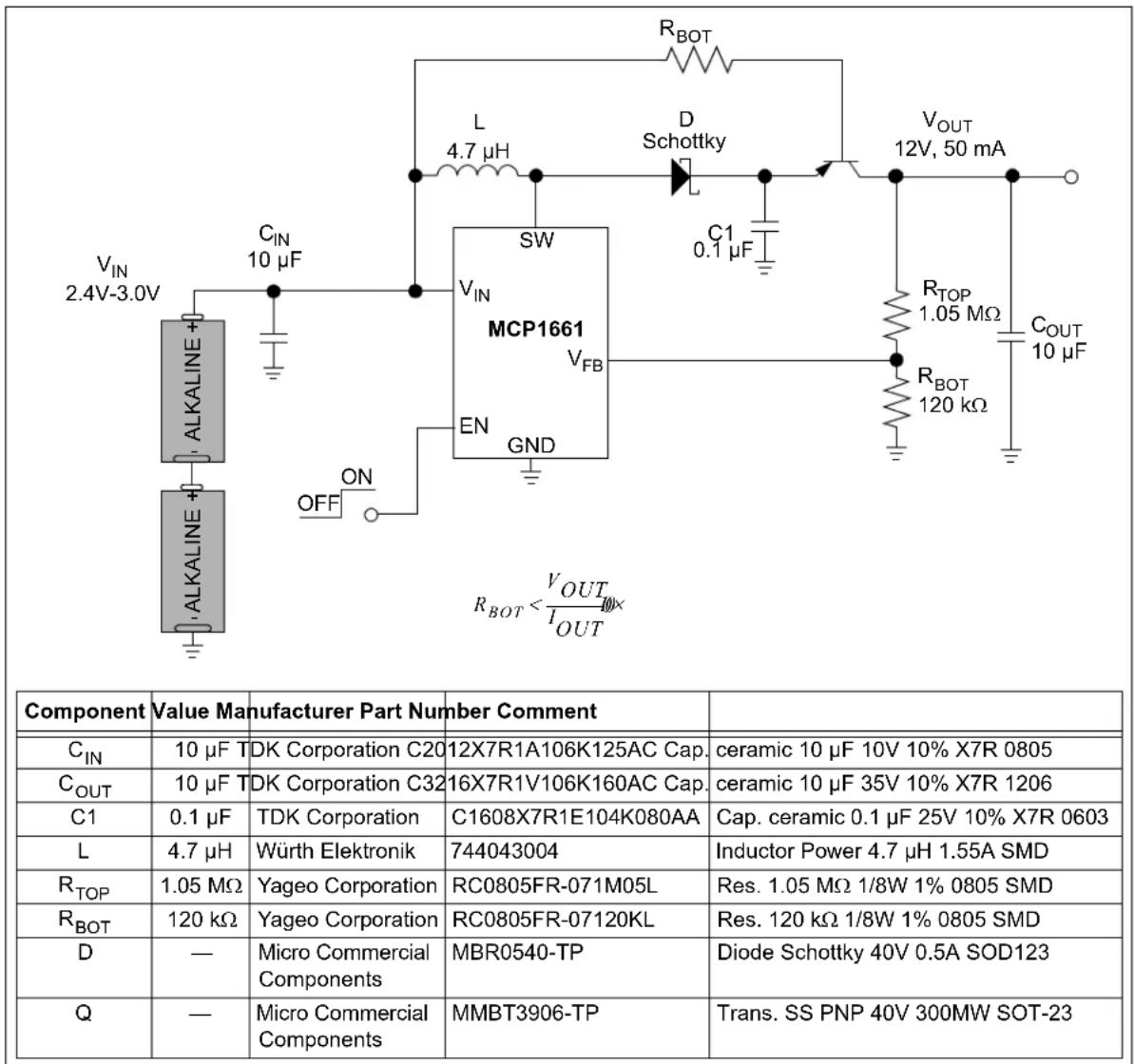
other
Component Value Manufacturer Part Number Comment | Component | Value Manufacturer Part NumberFIGURE 6-5: Two Alkaline Cells to 12V Boost Converter with Load Disconnect Application Example.
7.0 PACKAGING INFORMATION
7.1 Package Marking Information
5-Lead SOT-23 Example
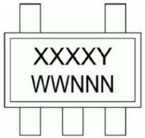
text_image
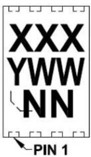
XXXXY WWNNN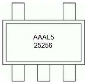
text_image
AAAL5 252568-Lead TDFN (2x3x0.75 mm) Example
text_image
XXX YWW NN PIN 1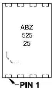
text_image
ABZ 525 25 PIN 1Legend: XX...X Customer-specific information
Y Year code (last digit of calendar year)
YY Year code (last 2 digits of calendar year)
WW Week code (week of January 1 is week '01')
NNN Alphanumeric traceability code
eBb-free JEDEC ^® designator for Matte Tin (Sn)
* This package is Pb-free. The Pb-free JEDEC designator ( )
can be found on the outer packaging for this package.
e3
Note: In the event the full Microchip part number cannot be marked on one line, it will be carried over to the next line, thus limiting the number of available characters for customer-specific information.
5-Lead Plastic Small Outline Transistor (OT) [SOT-23]
Note: For the most current package drawings, please see the Microchip Packaging Specification located at http://www.microchip.com/packaging
![Microchip MCP1661 - 5-Lead Plastic Small Outline Transistor (OT) [SOT-23] - 1](/content/2026/06/1182130/images/7ee585d6c7f45a8d4076e0118d6db9c600f8591e91f0d39492774ebfe5290897.jpg)
| Units | MILLIMETERS | |||
| Dimension Limitss | MINsNOMsMAX | |||
| Number of Pins | Ns | 5 | ||
| Lead Pitchses0.95 BSC | ||||
| Outside Lead Pitchse1s1.90 BSC | ||||
| Overall HeightsA 0.90 - | 1.45 | |||
| Molded Package Thickness | A2 | 0.89 | - | 1.30 |
| Standoff | A1 | 0.00 | - | 0.15 |
| Overall Width | E | 2.20 | - | 3.20 |
| Molded Package Width | E1 | 1.30 | - | 1.80 |
| Overall Length | D | 2.70 | - | 3.10 |
| Foot Length | L | 0.10 | - | 0.60 |
| Footprint | L1 | 0.35 | - | 0.80 |
| Foot Angle | 0° | - | 30° | |
| Lead Thickness | c | 0.08 | - | 0.26 |
| Lead Width | b | 0.20 | - | 0.51 |
Notes:
- Dimensions D and E1 do not include mold flash or protrusions. Mold flash or protrusions shall not exceed 0.127 mm per side.
2.sDimensioning and tolerancing per ASME Y14.5M.
BSC:sBasic Dimension. Theoretically exact value shown without tolerances.
Microchip Technology Drawing C04-091B
5-Lead Plastic Small Outline Transistor (OT) [SOT-23]
Note: For the most current package drawings, please see the Microchip Packaging Specification located at http://www.microchip.com/packaging
![Microchip MCP1661 - 5-Lead Plastic Small Outline Transistor (OT) [SOT-23] - 1](/content/2026/06/1182130/images/1dcf3e38104c974a6207a07577233d4d37585c719e3b5cd9c4ce18a761b304a3.jpg)
text_image
X Y Z C G SILK SCREEN E GXRECOMMENDED LAND PATTERN
| Units | MILLIMETERS | |||
| Dimension Limits | MIN | NOM | MAX | |
| Contact Pitch | E | 0.95 BSC | ||
| Contact Pad Spacing | C | 2.80 | ||
| Contact Pad Width (X5) | X | 0.60 | ||
| Contact Pad Length (X5) | Y | 1.10 | ||
| Distance Between Pads | G | 1.70 | ||
| Distance Between Pads | GX | 0.35 | ||
| Overall Width | Z | 3.90 | ||
Notes:
- Dimensioning and tolerancing per ASME Y14.5M
BSC: Basic Dimension. Theoretically exact value shown without tolerances.
Microchip Technology Drawing No. C04-2091A
8-Lead Plastic Dual Flat, No Lead Package (MN) - 2x3x0.75mm Body [TDFN]
Note: For the most current package drawings, please see the Microchip Packaging Specification located at http://www.microchip.com/packaging
![Microchip MCP1661 - 8-Lead Plastic Dual Flat, No Lead Package (MN) - 2x3x0.75mm Body [TDFN] - 1](/content/2026/06/1182130/images/3a4fa026ab92b8d82d98ce878bf43d49bdf5ac21d5803b8fd2639de8582ccba1.jpg)
BOTTOM VIEW
Microchip Technology Drawing No. C04-129C Sheet 1 of 2
8-Lead Plastic Dual Flat, No Lead Package (MN) - 2x3x0.75mm Body [TDFN]
Note: For the most current package drawings, please see the Microchip Packaging Specification located at http://www.microchip.com/packaging
![Microchip MCP1661 - 8-Lead Plastic Dual Flat, No Lead Package (MN) - 2x3x0.75mm Body [TDFN] - 1](/content/2026/06/1182130/images/6aa8ad549a0ab2ea96caca14b2221531e0e2aa5959496b1c182fd1c2728829bb.jpg)
natural_image
Isometric line drawing of a rectangular electronic component with labeled pins and an arrow pointing to its base (no text or symbols beyond label)| Units | MILLIMETERS | |||
| Dimension Limits | MIN | NOM | MAX | |
| Number of Pins | N | 8 | ||
| Pitch | e | 0.50 BSC | ||
| Overall Height | A | 0.70 | 0.75 | 0.80 |
| Standoff | A1 | 0.00 | 0.02 | 0.05 |
| Contact Thickness | A3 | 0.20 REF | ||
| Overall Length | D | 2.00 BSC | ||
| Overall Width | E | 3.00 BSC | ||
| Exposed Pad Length | D2 | 1.20 | - | 1.60 |
| Exposed Pad Width | E2 | 1.20 | - | 1.60 |
| Contact Width | b | 0.20 | 0.25 | 0.30 |
| Contact Length | L | 0.25 | 0.30 | 0.45 |
| Contact-to-Exposed Pad | K | 0.20 | - | - |
Notes:
- Pin 1 visual index feature may vary, but must be located within the hatched area.
- Package may have one or more exposed tie bars at ends.
- Package is saw singulated
- Dimensioning and tolerancing per ASME Y14.5M
BSC: Basic Dimension. Theoretically exact value shown without tolerances.
REF: Reference Dimension, usually without tolerance, for information purposes only.
Microchip Technology Drawing No. C04-129C Sheet 2 of 2
8-Lead Plastic Dual Flat, No Lead Package (MN) - 2x3x0.75 mm Body [TDFN]
Note: For the most current package drawings, please see the Microchip Packaging Specification located at http://www.microchip.com/packaging
![Microchip MCP1661 - 8-Lead Plastic Dual Flat, No Lead Package (MN) - 2x3x0.75 mm Body [TDFN] - 1](/content/2026/06/1182130/images/04af65178c08425b0efddee9e2f9c83f370363d2f97b0b1856ef7dac3f736bd4.jpg)
text_image
W2 G SILK SCREEN C1 T2 Y1 E X1RECOMMENDED LAND PATTERN
| Units | MILLIMETERS | |||
| Dimension Limits | MIN | NOM | MAX | |
| Contact Pitch | E | 0.50 BSC | ||
| Optional Center Pad Width | W2 | 1.46 | ||
| Optional Center Pad Length | T2 | 1.36 | ||
| Contact Pad Spacing | C1 | 3.00 | ||
| Contact Pad Width (X8) | X1 | 0.30 | ||
| Contact Pad Length (X8) | Y1 | 0.75 | ||
| Distance Between Pads | G | 0.20 | ||
Notes:
1. Dimensioning and tolerancing per ASME Y14.5M
BSC: Basic Dimension. Theoretically exact value shown without tolerances.
Microchip Technology Drawing No. C04-2129A
APPENDIX A: REVISION HISTORY
Revision B (February 2015)
The following is the list of modifications:
- Updated Section 6.0 "Typical Application Circuits".
- Added legend tables for Figures 6-3 to 6-5.
- Minor typographical corrections.
Revision A (June 2014)
• Original Release of this Document.
PRODUCT IDENTIFICATION SYSTEM
To order or obtain information, e.g., on pricing or delivery, refer to the factory or the listed sales office.
text_image
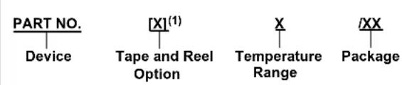
PART NO. Device [X](1) Tape and Reel Option X Temperature Range /XX PackageDevice: MCP1661: High-Voltage Step-Up LED Driver with UVLO and OLP
Tape and Reel T = Tape and Reel (1) Option:
Temperature E = -40°C to +125°C (Extended) Range:
Package: MN* = Plastic Dual Flat, No Lead - 2x3x0.75 mm Body (TDFN) OT = Plastic Small Outline Transistor (SOT-23) *Y = Nickel palladium gold manufacturing designator. Only available on the TDFN package.
Examples:
a) MCP1661T-E/MNY: Tape and Reel,
Extended temperature, 8LD TFDN package
b) MCP1661T-E/OT: Tape and Reel,
Extended temperature, 5LD SOT-23 package
Note 1: Tape and Reel identifier only appears in the catalog part number description. This identifier is used for ordering purposes and is not printed on the device package. Check with your Microchip Sales Office for package availability with the Tape and Reel option.
Note the following details of the code protection feature on Microchip devices:
• Microchip products meet the specification contained in their particular Microchip Data Sheet.
- Microchip believes that its family of products is one of the most secure families of its kind on the market today, when used in the intended manner and under normal conditions.
- There are dishonest and possibly illegal methods used to breach the code protection feature. All of these methods, to our knowledge, require using the Microchip products in a manner outside the operating specifications contained in Microchip's Data Sheets. Most likely, the person doing so is engaged in theft of intellectual property.
- Microchip is willing to work with the customer who is concerned about the integrity of their code.
- Neither Microchip nor any other semiconductor manufacturer can guarantee the security of their code. Code protection does not mean that we are guaranteeing the product as "unbreakable."
Code protection is constantly evolving. We at Microchip are committed to continuously improving the code protection features of our products. Attempts to break Microchip's code protection feature may be a violation of the Digital Millennium Copyright Act. If such acts allow unauthorized access to your software or other copyrighted work, you may have a right to sue for relief under that Act.
Information contained in this publication regarding device applications and the like is provided only for your convenience and may be superseded by updates. It is your responsibility to ensure that your application meets with your specifications. MICROCHIP MAKES NO REPRESENTATIONS OR WARRANTIES OF ANY KIND WHETHER EXPRESS OR IMPLIED, WRITTEN OR ORAL, STATUTORY OR OTHERWISE, RELATED TO THE INFORMATION, INCLUDING BUT NOT LIMITED TO ITS CONDITION, QUALITY, PERFORMANCE, MERCHANTABILITY OR FITNESS FOR PURPOSE. Microchip disclaims all liability arising from this information and its use. Use of Microchip devices in life support and/or safety applications is entirely at the buyer's risk, and the buyer agrees to defend, indemnify and hold harmless Microchip from any and all damages, claims, suits, or expenses resulting from such use. No licenses are conveyed, implicitly or otherwise, under any Microchip intellectual property rights.
QUALITY MANAGEMENT SYSTEM CERTIFIED BY DNV = ISO/TS 16949=
Trademarks
The Microchip name and logo, the Microchip logo, dsPIC, FlashFlex, flexPWR, JukeBlox, KEELOQ, KEELOQ logo, Kleer, LANCheck, MediaLB, MOST, MOST logo, MPLAB, OptoLyzer, PIC, PICSTART, PIC ^32 logo, RightTouch, SpyNIC, SST, SST Logo, SuperFlash and UNI/O are registered trademarks of Microchip Technology Incorporated in the U.S.A. and other countries.
The Embedded Control Solutions Company and mTouch are registered trademarks of Microchip Technology Incorporated in the U.S.A.
Analog-for-the-Digital Age, BodyCom, chipKIT, chipKIT logo, CodeGuard, dsPICDEM, dsPICDEM.net, ECAN, In-Circuit Serial Programming, ICSP, Inter-Chip Connectivity, KleerNet, KleerNet logo, MiWi, MPASM, MPF, MPLAB Certified logo, MPLIB, MPLINK, MultiTRAK, NetDetach, Omniscient Code Generation, PICDEM, PICDEM.net, PICkit, PICtail, RightTouch logo, REAL ICE, SQL, Serial Quad I/O, Total Endurance, TSHARC, USBCheck, VariSense, ViewSpan, WiperLock, Wireless DNA, and ZENA are trademarks of Microchip Technology Incorporated in the U.S.A. and other countries.
SQTP is a service mark of Microchip Technology Incorporated in the U.S.A.
Silicon Storage Technology is a registered trademark of Microchip Technology Inc. in other countries.
GestIC is a registered trademarks of Microchip Technology Germany II GmbH & Co. KG, a subsidiary of Microchip Technology Inc., in other countries.
All other trademarks mentioned herein are property of their respective companies.
© 2014-2015, Microchip Technology Incorporated, Printed in the U.S.A., All Rights Reserved.
Microchip received ISO/TS-16949:2009 certification for its worldwide headquarters, design and wafer fabrication facilities in Chandler and Tempe, Arizona; Gresham, Oregon and design centers in California and India. The Company's quality system processes and procedures are for its PIC® MCUs and dsPIC® DSCs, KEELOQ® code hopping devices, Serial EEPROMs, microperipherals, nonvolatile memory and analog products. In addition, Microchip's quality system for the design and manufacture of development systems is ISO 9001:2000 certified.
Worldwide Sales and Service
AMERICAS
Corporate Office
2355 West Chandler Blvd.
Chandler, AZ 85224-6199
Tel: 480-792-7200
Fax: 480-792-7277
Technical Support:
http://www.microchip.com/
support
Web Address:
www.microchip.com
Atlanta
Duluth, GA
Tel: 678-957-9614
Fax: 678-957-1455
Austin, TX
Tel: 512-257-3370
Boston
Westborough, MA
Tel: 774-760-0087
Fax: 774-760-0088
Chicago
Itasca, IL
Tel: 630-285-0071
Fax: 630-285-0075
Cleveland
Independence, OH
Tel: 216-447-0464
Fax: 216-447-0643
Dallas
Addison, TX
Tel: 972-818-7423
Fax: 972-818-2924
Detroit
Novi, M
Tel: 248-848-4000
Houston, TX
Tel: 281-894-5983
Indiana
Noblesville, IN
Tel: 317-773-8323
Fax: 317-773-5453
Los Angeles
Mission Viejo, CA
Tel: 949-462-9523
Fax: 949-462-9608
New York, NY
Tel: 631-435-6000
San Jose, CA
Tel: 408-735-9110
Canada - Toronto
Tel: 905-673-0699
Fax: 905-673-6509
ASIA/PACIFIC
Asia Pacific Office
Suites 3707-14, 37th Floor
Tower 6, The Gateway
Harbour City, Kowloon
Hong Kong
Tel: 852-2943-5100
Fax: 852-2401-3431
Australia - Sydney
Tel: 61-2-9868-6733
Fax: 61-2-9868-6755
China - Beijing
Tel: 86-10-8569-7000
Fax: 86-10-8528-2104
China - Chengdu
Tel: 86-28-8665-5511
Fax: 86-28-8665-7889
China - Chongqing
Tel: 86-23-8980-9588
Fax: 86-23-8980-9500
China - Dongguan
Tel: 86-769-8702-9880
China - Hangzhou
Tel: 86-571-8792-8115
Fax: 86-571-8792-8116
China - Hong Kong SAR
Tel: 852-2943-5100
Fax: 852-2401-3431
China - Nanjing
Tel: 86-25-8473-2460
Fax: 86-25-8473-2470
China - Qingdao
Tel: 86-532-8502-7355
Fax: 86-532-8502-7205
China - Shanghai
Tel: 86-21-5407-5533
Fax: 86-21-5407-5066
China - Shenyang
Tel: 86-24-2334-2829
Fax: 86-24-2334-2393
China - Shenzhen
Tel: 86-755-8864-2200
Fax: 86-755-8203-1760
China - Wuhan
Tel: 86-27-5980-5300
Fax: 86-27-5980-5118
China - Xian
Tel: 86-29-8833-7252
Fax: 86-29-8833-7256
ASIA/PACIFIC
China - Xiamen
Tel: 86-592-2388138
Fax: 86-592-2388130
China - Zhuhai
Tel: 86-756-3210040
Fax: 86-756-3210049
India - Bangalore
Tel: 91-80-3090-4444
Fax: 91-80-3090-4123
India - New Delhi
Tel: 91-11-4160-8631
Fax: 91-11-4160-8632
India - Pune
Tel: 91-20-3019-1500
Japan - Osaka
Tel: 81-6-6152-7160
Fax: 81-6-6152-9310
Japan - Tokyo
Tel: 81-3-6880-3770
Fax: 81-3-6880-3771
Korea - Daegu
Tel: 82-53-744-4301
Fax: 82-53-744-4302
Korea - Seoul
Tel: 82-2-554-7200
Fax: 82-2-558-5932 or
82-2-558-5934
Malaysia - Kuala Lumpur
Tel: 60-3-6201-9857
Fax: 60-3-6201-9859
Malaysia - Penang
Tel: 60-4-227-8870
Fax: 60-4-227-4068
Philippines - Manila
Tel: 63-2-634-9065
Fax: 63-2-634-9069
Singapore
Tel: 65-6334-8870
Fax: 65-6334-8850
Taiwan - Hsin Chu
Tel: 886-3-5778-366
Fax: 886-3-5770-955
Taiwan - Kaohsiung
Tel: 886-7-213-7828
Taiwan - Taipei
Tel: 886-2-2508-8600
Fax: 886-2-2508-0102
Thailand - Bangkok
Tel: 66-2-694-1351
Fax: 66-2-694-1350
EUROPE
Austria - Wels
Tel: 43-7242-2244-39
Fax: 43-7242-2244-393
Denmark - Copenhagen
Tel: 45-4450-2828
Fax: 45-4485-2829
France - Paris
Tel: 33-1-69-53-63-20
Fax: 33-1-69-30-90-79
Germany - Dusseldorf
Tel: 49-2129-3766400
Germany - Munich
Tel: 49-89-627-144-0
Fax: 49-89-627-144-44
Germany - Pforzheim
Tel: 49-7231-424750
Italy - Milan
Tel: 39-0331-742611
Fax: 39-0331-466781
Italy - Venice
Tel: 39-049-7625286
Netherlands - Drunen
Tel: 31-416-690399
Fax: 31-416-690340
Poland - Warsaw
Tel: 48-22-3325737
Spain - Madrid
Tel: 34-91-708-08-90
Fax: 34-91-708-08-91
Sweden - Stockholm
Tel: 46-8-5090-4654
UK - Wokingham
Tel: 44-118-921-5800
Fax: 44-118-921-5820