SY58030U - Uncategorized Microchip - Free user manual and instructions
Find the device manual for free SY58030U Microchip in PDF.

| Product Type | Differential Fanout Buffer |
| Brand | Microchip |
| Model | SY58030U |
| Category | Clock and Timing |
| Package Type | 32-pin QFN (5x5 mm) |
| Number of Pins | 32 |
| Supply Voltage | 2.5 V or 3.3 V |
| Operating Temperature Range | -40°C to +85°C |
| Maximum Data Rate | 3.2 Gbps |
| Fanout | 1:10 |
| Output Logic Type | LVPECL |
| Input Logic Type | CML, LVPECL, LVDS, HSTL |
| Output Skew (typical) | 10 ps |
| Propagation Delay (typical) | 350 ps |
| Power Dissipation (typical) | 500 mW |
| Dimensions | 5 mm x 5 mm x 0.9 mm |
| Weight | 0.1 g |
| RoHS Compliant | Yes |
| ESD Protection | 2 kV HBM |
| Application | High-speed clock distribution, data communication |
| Features | Low jitter, low skew, failsafe input, internal termination |
| Maintenance | None required; handle with ESD precautions |
| Safety | ESD sensitive device; use proper grounding |
| Spare Parts | Not applicable (integrated circuit) |
| Repairability | Not repairable; replace component if faulty |
Frequently Asked Questions - SY58030U Microchip
User questions about SY58030U Microchip
0 question about this device. Answer the ones you know or ask your own.
Ask a new question about this device
Download the instructions for your Uncategorized in PDF format for free! Find your manual SY58030U - Microchip and take your electronic device back in hand. On this page are published all the documents necessary for the use of your device. SY58030U by Microchip.
USER MANUAL SY58030U Microchip
■ Unique patented input design minimizes crosstalk
■ Accepts an input signal as low as 100mV
■ Unique patented input termination and V_T pin accepts DC-coupled and AC-coupled inputs (CML, LVPECL, LVDS)
■ 400mV 100k LVPECL output swing
■ Power supply 2.5V ±5% or 3.3V ±10%
■ -40^ to +85^ temperature range
■ Available in 32-pin (5mm × 5mm) MLF® package
APPLICATIONS
■ Redundant clock and/or data distribution
■ All SONET/SDH clock/data distribution
■ Loopback
■ All Fibre Channel distribution
■ All Gigabit Ethernet clock and/or data distribution
TYPICAL PERFORMANCE
line
| Time (100ps/div.) | Output Swing (100mV/div.) | | ----------------- | ------------------------- | | 0 | 0 | | 1 | 0 | | 2 | 0 | | 3 | 0 | | 4 | 0 | | 5 | 0 | | 6 | 0 | | 7 | 0 | | 8 | 0 | | 9 | 0 | | 10 | 0 | | 11 | 0 | | 12 | 0 | | 13 | 0 | | 14 | 0 | | 15 | 0 | | 16 | 0 | | 17 | 0 | | 18 | 0 | | 19 | 0 | | 20 | 0 | | 21 | 0 | | 22 | 0 | | 23 | 0 | | 24 | 0 | | 25 | 0 | | 26 | 0 | | 27 | 0 | | 28 | 0 | | 29 | 0 | | 30 | 0 | | 31 | 0 | | 32 | 0 | | 33 | 0 | | 34 | 0 | | 35 | 0 | | 36 | 0 | | 37 | 0 | | 38 | 0 | | 39 | 0 | | 40 | 0 | | 41 | 0 | | 42 | 0 | | 43 | 0 | | 44 | 0 | | 45 | 0 | | 46 | 0 | | 47 | 0 | | 48 | 0 | | 49 | 0 | | 50 | 0 | | 51 | 0 | | 52 | 0 | | 53 | 0 | | 54 | 0 | | 55 | 0 | | 56 | 0 | | 57 | 0 | | 58 | 0 | | 59 | 0 | | 60 | 0 | | 61 | 0 | | 62 | 0 | | 63 | 0 | | 64 | 0 | | 65 | 0 | | 66 | 0 | | 67 | 0 | | 68 | 0 | | 69 | 0 | | 70 | 0 | | 71 | 0 | | 72 | 0 | | 73 | 0 | | 74 | 0 | | 75 | 0 | | 76 | 0 | | 77 | 0 | | 78 | 0 | | 79 | 0 | | 80 | 0 | | 81 | 0 | | 82 | 0 | | 83 | 0 | | 84 | 0 | | 85 | 0 | | 86 | 0 | | 87 | 0 | | 88 | 0 | | 89 | 0 | | 90 | 0 | | 91 | 0 | | 92 | 0 | | 93 | 0 | | 94 | 0 | | 95 | 0 | | 96 | 0 | | 97 | 0 | | 98 | 0 | | 99 | 0 | | Note: The actual output values are not provided in the code. The code generates a random sample of two values from a normal distribution with a mean of zero. There is no label for the output data series. The output values are estimated based on the given code format. [Unlabeled] above the code format is not explicitly provided in the original image.Precision Edge is a registered trademark of Micrel, Inc.
MicroLeadFrame and MLF are registered trademarks of Amkor Technology, Inc.
Precision Edge is a registered trademark of Micrel, Inc. MicroLeadFrame and MLF are registered trademarks of Amkor Technology, Inc.

Precision Edge®
DESCRIPTION
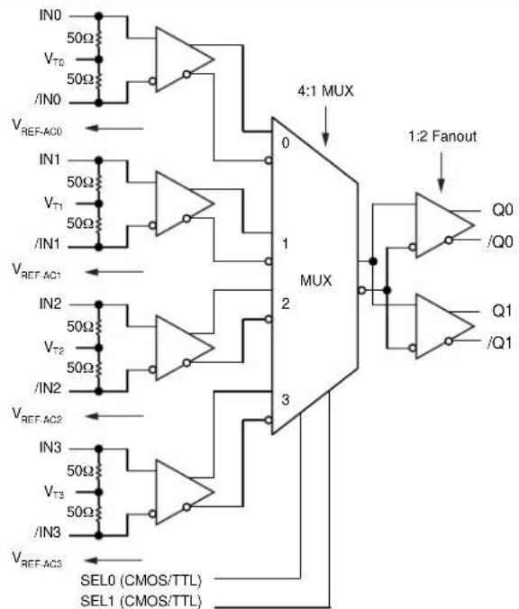
The SY58030U is a 2.5V/3.3V precision, high-speed, 4:1 differential multiplexer with 400mV LVPECL outputs, capable of handling clocks up to 7GHz and data streams up to 10.7Gbps. In addition, a 1:2 fanout buffer provides two copies of the selected input.
The differential input includes Micrel's unique, 3-pin input termination architecture that allows customers to interface to any differential signal (AC- or DC-coupled) as small as 100mV without any level shifting or termination resistor networks in the signal path. The result is a clean, stub-free, low-jitter interface solution. The outputs are 400mV LVPECL (100K temperature compensated) with extremely fast rise/fall times guaranteed to be less than 80ps.
The SY58030U operates from a 2.5V ±5% supply or a 3.3V ±10% supply and is guaranteed over the full industrial temperature range of -40°C to +85°C. For applications that require CML outputs, consider the SY58028U. For 800mV LVPECL outputs, consider the SY58029U. The SY58030U is part of Micrel's high-speed, Precision Edge® product line.
All support documentation can be found on Micrel's web site at www.micrel.com.
FUNCTIONAL BLOCK DIAGRAM
flowchart
graph TD
    subgraph Inputs
        IN0["IN0"] --> VREFAC0["50Ω"]
        VREFAC0 --> VREFAC1["50Ω"]
        VREFAC1 --> VREFAC2["50Ω"]
        VREFAC2 --> VREFAC3["50Ω"]
        VREFAC3 --> SEL0["SEL0 (CMOS/TTL)"]
        VREFAC3 --> SEL1["SEL1 (CMOS/TTL)"]
    end

    subgraph Outputs
        IN1["IN1"] --> VREFAC1["50Ω"]
        VREFAC1 --> VREFAC2["50Ω"]
        VREFAC2 --> VREFAC3["50Ω"]
        VREFAC3 --> SEL0
        VREFAC3 --> SEL1
    end

    subgraph Outputs
        IN2["IN2"] --> VREFAC2["50Ω"]
        VREFAC2 --> VREFAC3["50Ω"]
        VREFAC3 --> SEL0
        VREFAC3 --> SEL1
    end

    subgraph Outputs
        IN3["IN3"] --> VREFAC3["50Ω"]
        VREFAC3 --> SEL0
        VREFAC3 --> SEL1
    end

    subgraph Outputs
        IN1 --> 4:1 MUX
        IN2 --> 4:1 MUX
        IN3 --> 4:1 MUX
    end

    style Inputs fill:#f9f,stroke:#333
    style Outputs fill:#ccf,stroke:#333
PACKAGE/ORDERING INFORMATION
text_image
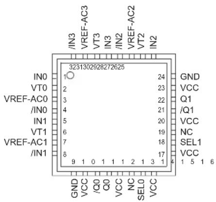
3231302928272625 IN0 1○ 24 VT0 2 23 VREF-AC0 3 22 /IN0 4 21 IN1 5 20 VT1 6 19 VREF-AC1 7 18 /IN1 8 17 GND VCC Q1 /Q1 VCC NC SEL1 VCC GND VCC /Q0 Q0 VCC NC SEL0 VCC IN3 VREF-AC3 VT3 IN3 /IN2 VREF-AC2 VT2 IN232-Pin MLF ^® (MLF-32)
Ordering Information ^(1)
| Part Number | Package Type Range | Operating | Package Marking | Finish |
| SY58030UMI | MLF-32 | Industrial | SY58030U | Sn-Pb |
| SY58030UMITR(2) | MLF-32 | Industrial | SY58030U | Sn-Pb |
| SY58030UMG(3) | MLF-32 | Industrial | SY58030U with Pb-Free Pb-Free bar-line indicator | NiPdAu |
| SY58030UMGTR(2, 3) | MLF-32 | Industrial | SY58030U with Pb-Free Pb-Free bar-line indicator | NiPdAu |
Notes:
- Contact factory for die availability. Dice are guaranteed at T_A = 25^ , DC electricals only.
- Tape and Reel.
- Pb-Free package recommended for new designs.
PIN DESCRIPTION
| Pin Number Pin | Name Pin Function | |
| 1, 4 IN0, /IN0 | Differential Input: Each pair accepts AC- or DC-coupled signals as small as 100mV.5, 8 IN1, /IN1 | Each pin of a pair internally terminates to a VT _T pin through 50Ω. Note that these 25, 28 IN2, /IN2 inputs will default to an indeterminate state if left open. If an input is not used, connect one 29, 32 IN3, /IN3 end of the differential pair to ground through a 1kΩ resistor, and leave the other end to V _CC through a 825Ω resistor. Unused VT _T and V _REF-AC pins may also be left floating. Please refer to the “Input Interface Applications” section for more details. |
| 2, 6, 26, 30 | VT0, VT1VT2, VT3 | Input Termination Center-Tap: Each side of the differential input pair terminates to a VTpin. The VT _T pins provide a center-tap to the termination network for maximum interface flexibility. See “Input Interface Applications” section for more details. |
| 15, 18 | SEL0, SEL1 | This Single-Ended TTL/CMOS compatible input selects the inputs to the multiplexer. Note that this input is internally connected to a 25kΩ pull-up resistor and will default to a logic HIGH state if left open. Input logic threshold is V _CC /2. See “Truth Table” for select control. |
| 14, 19 | NC | No Connect. |
| 10, 13, 1617, 20, 23 | VCC | Positive Power Supply: Bypass with 0.1μF||0.01μF low ESR capacitors. |
| 11, 1221, 22 | /Q0, Q0/Q1, Q1 | Differential Outputs: These 100k compatible (internally temperature compensated)LVPECL output pairs are copies of the selected input. Unused output pairs may be left floating. See “Output Interface” for termination guidelines. |
| 9, 24 | GND, Exposed Pad | Ground. Ground pin and exposed pad must be connected to the same ground plane. |
| 3, 7, 27, 31 | VREF-AC0VREF-AC1VREF-AC2VREF-AC3 | Reference Voltage: This reference output is equivalent to V _CC -1.4V. It is used for AC-coupled inputs. When interfacing to AC input signals, connect V _REF-AC directly to the VT _T pin and bypass with a 0.01μF low ESR capacitor to V _CC . See “Input Interface Applications” section. Maximum current sink/source is 0.5mA. |
TRUTH TABLE
| SEL0 | SEL1 | |
| 0 | 0 | IN0 Input Selected |
| 0 | 1 | IN2 Input Selected |
| 1 | 0 | IN1 Input Selected |
| 1 | 1 | IN3 Input Selected |
Absolute Maximum Ratings ^(1)
Power Supply Voltage ( V_CC ) ..... -0.5V to +4.0V
Input Voltage ( V_IN ) -0.5V to V_CC
LVPECL Output Current ( I_OUT )
Continuous 50mA
Surge....100mA
Termination Current ^(3)
Source or sink current on V_T pin ....±100mA
Input Current
Source or sink current on IN, /IN pin ....±50mA
Lead Temperature (soldering, 20 sec.) 260°C
Storage Temperature Range ( T_S ) ..... -65°C to +150°C
Operating Ratings ^(2)
Power Supply Voltage ( V_CC ) ..... +2.375V to +2.625V ..... +3.0V to +3.6V
Ambient Temperature Range ( T_A ) ..... -40°C to +85°C
Package Thermal Resistance ^(4)
MLF ^ ( _JA ) Still-Air 35°C/W
MLF ^ ( _JB ) Junction-to-Board ....2°C/W
DC ELECTRICAL CHARACTERISTICS ^(5)
T_A=-40^ to 85^ , unless otherwise stated.
| Symbol Parameter Condition Min Typ Max Units | ||||||
| V_CC | Power Supply Voltage V | _CC = 2.5V 2.375 2.5 2.625 V V_CC = 3.3V 3.0 3.3 3.6 V | ||||
| I_CC | Power Supply Current | No load, max. V_CC | 120 | 150 mA | ||
| R_DIFF\_IN | Differential Input Resistance (IN-to-/IN) | 80 | 100 | 120 | Ω | |
| R_IN | Input Resistance (IN-to- V_T , /IN-to- V_T ) | 40 50 | 60 Ω | |||
| V_IH | Input HIGH Voltage (IN-to-/IN) | Note 6 | V_CC-1.6 | V_CC | V | |
| V_IL | Input LOW Voltage (IN-to-/IN) | 0 | V_IH-0.1 | V | ||
| V_IN | Input Voltage Swing (IN-to-/IN) | See Figure 1a. | 0.1 | 1.7 | V | |
| V_DIFF\_IN | Differential Input Voltage Swing (IN-to-/IN) | See Figure 1b. | 0.2 | V | ||
| V_T IN | Max Input Voltage (IN-to- V_T ) | 1.28 | V | |||
| V_REF-AC | Reference Voltage | V_CC-1.3 | V_CC-1.2 | V_CC-1.1 | V | |
Notes:
- Permanent device damage may occur if ratings in the "Absolute Maximum Ratings" section are exceeded. This is a stress rating only and functional operation is not implied at conditions other than those detailed in the operational sections of this data sheet. Exposure to absolute maximum ratings conditions for extended periods may affect device reliability.
- The data sheet limits are not guaranteed if the device is operated beyond the operating ratings.
- Due to the limited drive capability, use for input of the same package only.
- Thermal performance assumes exposed pad is soldered (or equivalent) to the device's most negative potential (GND) on the PCB. _JB uses 4-layer _JA in still air number unless otherwise stated.
- The circuit is designed to meet the DC specifications shown in the above table after thermal equilibrium has been established.
- V_IH (min) not lower than 1.2V.
LVPECL OUTPUT DC ELECTRICAL CHARACTERISTICS ^(7)
V_CC = 2.5V ± 5% or 3.3V ± 10% ; T_A = -40^ C to +85^ C ; R_L = 50 to V_CC-2V , unless otherwise stated.
| Symbol Parameter Condition Min Typ Max Units | |||||
| V_OH | Output HIGH Voltage V | _CC-1.145 V | _CC-0.895 V | ||
| V_OL | Output LOW Voltage V | _CC-1.545 V | _CC-1.295 V | ||
| V_OUT | Output Voltage Swing See Figure 1a. 150 400 mV | ||||
| V_DIFF\_OUT | Differential Output Voltage Swing See Figure 1b. 300 800 mV | ||||
LVTTL/CMOS DC ELECTRICAL CHARACTERISTICS ^(7)
V_CC = 2.5V ± 5% or 3.3V ± 10% ; T_A = -40^ C to +85^ C , unless otherwise stated.
| Symbol | Parameter | Condition | Min | Typ | Max | Units |
| V_IH | Input HIGH Voltage | SEL0, SEL1 | 2.0 | V | ||
| V_IL | Input LOW Voltage | SEL0, SEL1 | 0.8 | V | ||
| I_IH | Input High Current | 40 | μA | |||
| I_IL | Input Low Current | -300 | μA |
Note:
- The circuit is designed to meet the DC specifications shown in the above table after thermal equilibrium has been established.
AC ELECTRICAL CHARACTERISTICS ^(8)
V_CC = 2.5V ± 5% or 3.3V ± 10% ; R_L = 50 to V_CC - 2V ; T_A = -40^ to +85^ , V_IN ≥ 100mV , unless otherwise stated.
| Symbol Parameter Condition Min Typ Max Units | ||||||
| f_MAX | Maximum Operating Frequency NRZ | Data 10.7 Gbps | ||||
| V_OUT ≥ 200mV Clock 7 GHz | ||||||
| t_pd | Propagation Delay (Diff) (IN to Q) V (SEL to Q) | ≥ 100mV\ | 170100 | 260 | 340500 | psps |
| t_pd Tempco | Differential Propagation Delay Temperature Coefficient | 115 | fs/°C | |||
| t_SKEW | Output-to-Output Skew | Note 9 | 7 | 20 | ps | |
| Part-to-Part Skew | Note 10 | 50 | ps | |||
| t_JITTER | Data Random Jitter | Note 11 2.5Gbps to 3.2Gbps | 1 | ps_PP | ||
| Deterministic Jitter | Note 12 2.5Gbps to 3.2Gbps | 10 | ps_PP | |||
| Clock Cycle-to-Cycle Jitter | Note 13 | 1 | ps_RMS | |||
| Total Jitter | Note 14 | 10 | ps_PP | |||
| Crosstalk Induced Jitter (Adjacent Channel) | Note 15 | 0.7 | ps_RMS | |||
| t_r, t_f | Output Rise/Fall Time | 20% to 80%, Full output swing | 20 | 55 | 80 | ps |
Notes:
- High frequency AC electricals are guaranteed by design and characterization.
- Output-to-output skew is measured between outputs under identical input conditions.
- Part-to-part skew is defined for two parts with identical power supply voltages at the same temperature and with no skew of the edges at the respective inputs.
- Random jitter is measured with a K28.7 comma detect character pattern, measured at 2.5Gbps to 3.2Gbps.
- Deterministic jitter is measured at 2.5Gpbs to 3.2Gbps with both K28.5 and 2^23-1 PRBS pattern.
- Cycle-to-cycle jitter definition: the variation of periods between adjacent cycles, T_n - T_n - 1 , where T is the time between rising edges of the output signal.
- Total jitter definition: with an ideal clock input of frequency ≤ f_MAX , no more than one output edge in 10^12 output edges will deviate by more than the specified peak-to-peak jitter value.
- Crosstalk is measured at the output while applying two similar clock frequencies that are asynchronous with respect to each other at the inputs.
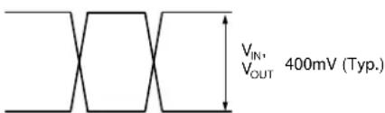
SINGLE-ENDED AND DIFFERENTIAL SWINGS
text_image
V_{IN}, \nV_{OUT} 400mV (Typ.)Figure 1a. Single-Ended Voltage Swing
text_image
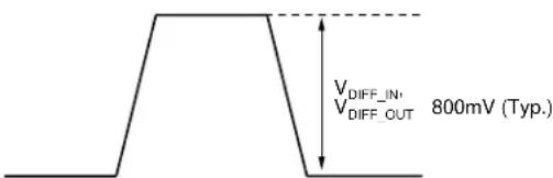
VDIFF_IN VDIFF_OUT 800mV (Typ.)Figure 1b. Differential Voltage Swing
TIMING DIAGRAMS
text_image
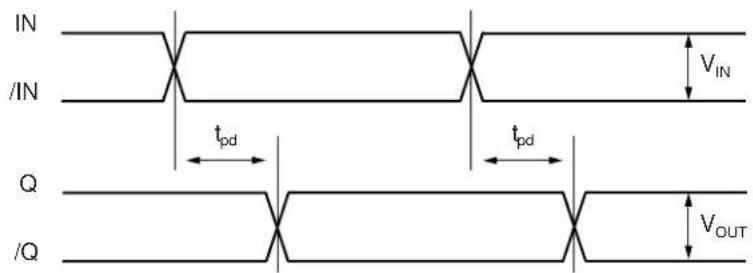
IN /IN tpd tpd Q /Q VIN VOUTFigure 2a. IN-to-Q Timing Diagram
text_image
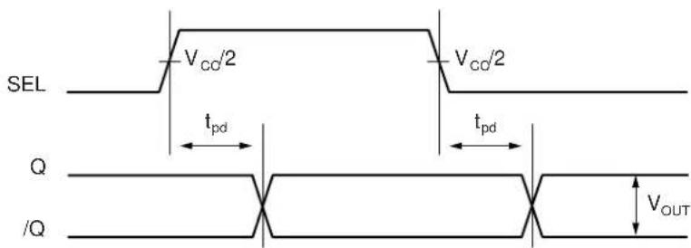
SEL Vcc/2 Vcc/2 tpd tpd Q /Q VOUTFigure 2b. SEL-to-Q Timing Diagram
SEL0 Q: SEL1 = LOW; IN0, /IN1 = LOW; /IN0, IN1 = HIGH or: SEL1 = HIGH; IN2, /IN3 = LOW; /IN2, IN3 = HIGH SEL1 Q: SEL0 = LOW; IN0, /IN2 = LOW; /IN0, IN2 = HIGH or: SEL0 = HIGH; IN1, /IN3 = LOW; /IN1, IN3 = HIGH
TYPICAL OPERATING CHARACTERISTICS
V_CC = 2.5V , GND = 0, V_IN = 100mV , T_A = 25^ C , unless otherwise stated.
line
| TIME (600ps/div.) | Output Swing (100mV/div.) | | ----------------- | ------------------------- | | 0 | 0 | | 600 | 0 | | 1200 | 0 | | 1800 | 0 | | 2400 | 0 | | 3000 | 0 | | 3600 | 0 | | 4200 | 0 | | 4800 | 0 | | 5400 | 0 | | 600 | 0 | | 660 | 0 | | 720 | 0 | | 780 | 0 | | 840 | 0 | | 900 | 0 | | 960 | 0 | | 1020 | 0 | | 1080 | 0 | | 1140 | 0 | | 1200 | 0 | | 1260 | 0 | | 1320 | 0 | | 1380 | 0 | | 1440 | 0 | | 1500 | 0 | | 1560 | 0 | | 1620 | 0 | | 1680 | 0 | | 1740 | 0 | | 1800 | 0 | | 1860 | 0 | | 1920 | 0 | | 1980 | 0 | | 2040 | 0 | | 2100 | 0 | | 2160 | 0 | | 2220 | 0 | | 2280 | 0 | | 2340 | 0 | | 2400 | 0 | | 2460 | 0 | | 2520 | 0 | | 2580 | 0 | | 2640 | 0 | | 2700 | 0 | | 2760 | 0 | | 2820 | 0 | | 2880 | 0 | | 2940 | 0 | | 3000 | 0 | | 3060 | 0 | | 3120 | 0 | | 3180 | 0 | | 3240 | 0 | | 3300 | 0 | | 3360 | 0 | | 3420 | 0 | | 3480 | 0 | | 3540 | 0 | | 3600 | 0 | | 3660 | 0 | | 3720 | 0 | | 3780 | 0 | | 3840 | 0 | | 3900 | 0 | | 3960 | 0 | | 4020 | 0 | | 4080 | 0 | | 4140 | 0 | | 4200 | 0 | | 4260 | 0 | | 4320 | 0 | | 4380 | 0 | | 4440 | 0 | | 4500 | 0 | | 4560 | 0 | | 4620 | 0 | | 4680 | 0 | | 4740 | 0 | | 4800 | 0 | | 4860 | 0 | | 4920 | 0 | | 4980 | 0 | | | |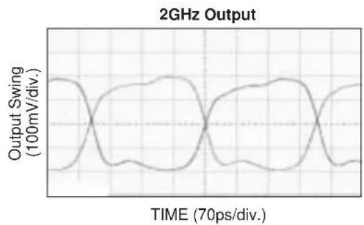
line
| TIME (70ps/div.) | Output Swing (100mV/div.) | | ---------------- | ------------------------- | | 0 | 0 | | 10 | 100 | | 20 | 0 | | 30 | -100 | | 40 | 0 | | 50 | 100 | | 60 | 0 | | 70 | -100 | | 80 | 0 | | 90 | 100 | | 100 | 0 | | 110 | -100 | | 120 | 0 | | 130 | 100 | | 140 | 0 | | 150 | -100 | | 160 | 0 | | 170 | 100 | | 180 | 0 | | 190 | -100 | | 200 | 0 |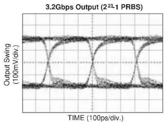
line
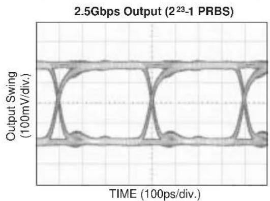
| TIME (100ps/div.) | Output Swing (100mV/div.) | | ----------------- | ------------------------- | | 0 | 0 | | 1 | 0.5 | | 2 | 1 | | 3 | 0.5 | | 4 | 0 | | 5 | 0.5 | | 6 | 1 | | 7 | 0.5 | | 8 | 0 | | 9 | 0.5 | | 10 | 1 | | 11 | 0.5 | | 12 | 0 | | 13 | 0.5 | | 14 | 1 | | 15 | 0.5 | | 16 | 0 | | 17 | 0.5 | | 18 | 1 | | 19 | 0.5 | | 20 | 0 | | 21 | 0.5 | | 22 | 1 | | 23 | 0.5 | | 24 | 0 | | 25 | 0.5 | | 26 | 1 | | 27 | 0.5 | | 28 | 0 | | 29 | 0.5 | | 30 | 1 | | 31 | 0.5 | | 32 | 0 | | 33 | 0.5 | | 34 | 1 | | 35 | 0.5 | | 36 | 0 | | 37 | 0.5 | | 38 | 1 | | 39 | 0.5 | | 40 | 0 | | 41 | 0.5 | | 42 | 1 | | 43 | 0.5 | | 44 | 0 | | 45 | 0.5 | | 46 | 1 | | 47 | 0.5 | | 48 | 0 | | 49 | 0.5 | | 50 | 1 | | 51 | 0.5 | | 52 | 0 | | 53 | 0.5 | | 54 | 1 | | 55 | 0.5 | | 56 | 0 | | 57 | 0.5 | | 58 | 1 | | 59 | 0.5 | | 60 | 0 | | 61 | 0.5 | | 62 | 1 | | 63 | 0.5 | | 64 | 0 | | 65 | 0.5 | | 66 | 1 | | 67 | 0.5 | | 68 | 0 | | 69 | 0.5 | | 70 | 1 | | 71 | 0.5 | | 72 | 0 | | 73 | 0.5 | | 74 | 1 | | 75 | 0.5 | | 76 | 0 | | 77 | 0.5 | | 78 | 1 | | 79 | 0.5 | | 80 | 0 | | 81 | 0.5 | | 82 | 1 | | 83 | 0.5 | | 84 | 0 | | 85 | 0.5 | | 86 | 1 | | 87 | 0.5 | | 88 | 0 | | 89 | 0.5 | | 90 | 1 | | 91 | 0.5 | | 92 | 0 | | 93 | 0.5 | | 94 | 1 | | 95 | 0.5 | | 96 | 0 | | 97 | 0.5 | | 98 | 1 | | 99 | 0.5 | | Note: The data is in a grid format with 'TIME' as the index of the grid from '2²³⁻¹ PRBS'. The output values are estimated based on the given code.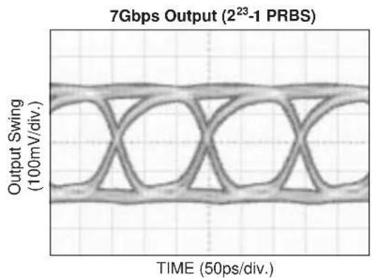
text_image
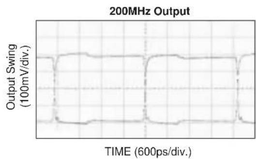
7Gbps Output (2²³-1 PRBS) Output Swing (100mV/div.) TIME (50ps/div.)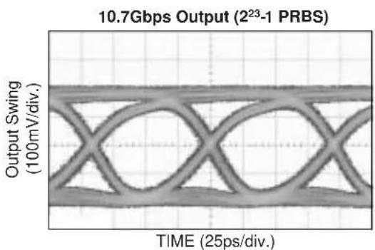
text_image
10.7Gbps Output (2²³-1 PRBS) Output Swing (100mV/div.) TIME (25ps/div.)TYPICAL OPERATING CHARACTERISTICS
V_CC = 2.5V, GND = 0, V_IN = 100mV, T_A = 25^, unless otherwise stated.
Propagation Delay. Input Voltage Swi
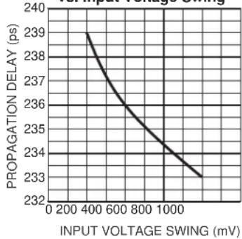
line
| INPUT VOLTAGE SWING (mV) | PROPAGATION DELAY (ps) | | ------------------------ | ---------------------- | | 0 | 239 | | 400 | 238 | | 600 | 237 | | 800 | 236 | | 1000 | 235 | | 1200 | 234 | | 1400 | 233 |Output-to-Output Skew vs. Temperature
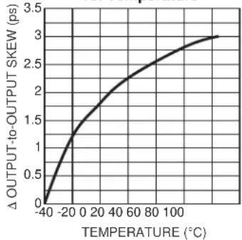
line
| TEMPERATURE (°C) | Δ OUTPUT-to-OUTPUT SKEW (ps) | | ---------------- | ---------------------------- | | -40 | 0 | | -20 | 1 | | 0 | 1.5 | | 20 | 2 | | 40 | 2.2 | | 60 | 2.5 | | 80 | 2.7 | | 100 | 2.9 | | 120 | 3 |Propagation Delay vs. Temperature
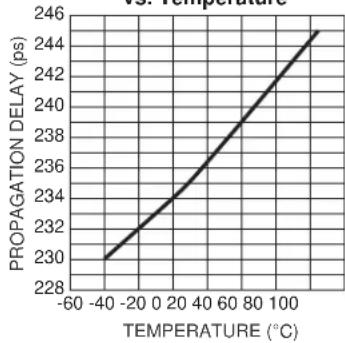
line
| TEMPERATURE (°C) | PROPAGATION DELAY (ps) | | ---------------- | --------------------- | | -60 | 230 | | -40 | 232 | | -20 | 234 | | 0 | 236 | | 20 | 238 | | 40 | 240 | | 60 | 242 | | 80 | 244 | | 100 | 246 |Output Amplitude vs. Frequency
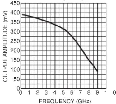
line
| FREQUENCY (GHz) | OUTPUT AMPLITUDE (mV) | | --------------- | --------------------- | | 0 | 400 | | 1 | 390 | | 2 | 370 | | 3 | 350 | | 4 | 330 | | 5 | 310 | | 6 | 280 | | 7 | 240 | | 8 | 180 | | 9 | 100 |INPUT STAGE
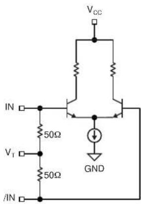
text_image
VCC IN 50Ω VT 50Ω /IN GNDFigure 3. Simplified Differential Input Stage
INPUT INTERFACE APPLICATIONS
text_image
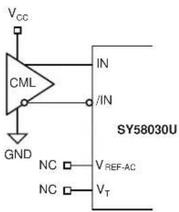
VCC CML GND IN /IN SY58030U NC □ VREF-AC NC □ VTFigure 4a. CML Interface (DC-Coupled)
Option: May connect V_T to V_CC
text_image
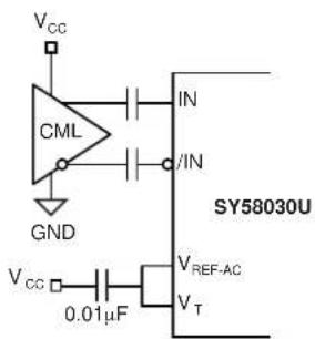
VCC CML GND IN /IN SY58030U VCC 0.01μF VREF-AC VTFigure 4b. CML Interface (AC-Coupled)
text_image
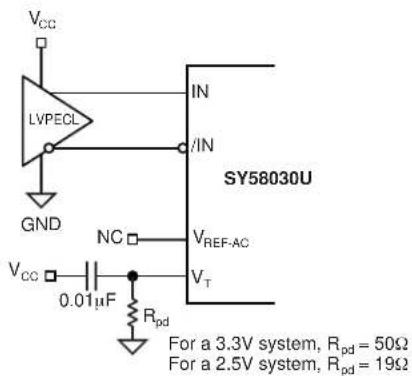
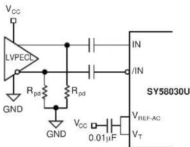
VCC LVPECL GND IN IN SY58030U NC VREF-AC VCC 0.01μF Rpd VT For a 3.3V system, Rpd = 50Ω For a 2.5V system, Rpd = 19ΩFigure 4c. PECL Interface (DC-Coupled)
text_image
VCC LVPECL IN Rpd Rpd GND GND VCC 0.01μF IN SY58030U VREF-AC VTFor a 3.3V system, R_pd = 100 For a 2.5V system, R_pd = 50
Figure 4d. LVPECL Interface (AC-Coupled)
text_image
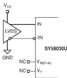
Vcc LVDS GND IN /IN SY58030U NC □ VREF-AC NC □ VTFigure 4e. LVDS Interface
OUTPUT INTERFACE APPLICATIONS
text_image
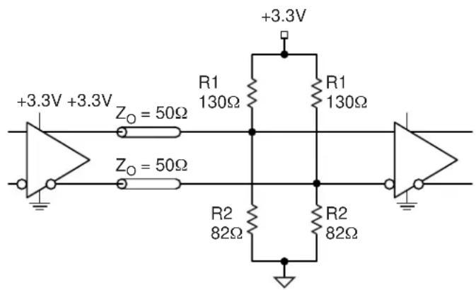
+3.3V +3.3V Z₀ = 50Ω +3.3V R1 130Ω R1 130Ω Z₀ = 50Ω R2 82Ω R2 82ΩFigure 5a. Parallel Thevenin-Equivalent Termination
text_image
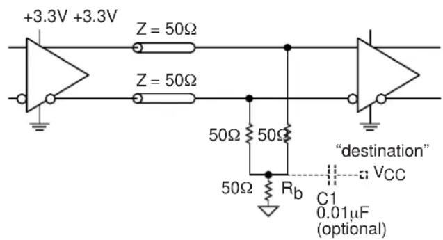
+3.3V +3.3V Z = 50Ω Z = 50Ω 50Ω 50Ω "destination" VCC 50Ω Rb C1 0.01μF (optional)Figure 5b. Parallel Termination (3-Resistor)
Note:
- For a 2.5V system, R1 = 250Ω, R2 = 62.5Ω.
For a 3.3V system, R1 = 130Ω, R2 = 82Ω.
Note:
- For a 2.5V system, Rb = 19Ω.
For a 3.3V system, Rb = 150Ω.
RELATED MICREL PRODUCTS AND SUPPORT DOCUMENTATION
| Part Number Function Data Sheet Link | ||
| SY58028U Ultra | Precision Differential CML 4:1 MUX http://www.micrel.com/product-info/products/sy58028u.shtmlwith 1:2 Fanout and Internal I/O Termination | |
| SY58029U | Ultra Precision Differential LVPECL 4:1 MUX with 1:2 Fanout and Internal Termination | http://www.micrel.com/product-info/products/sy58029u.shtml |
| SY58030U Ultra | Precision, 400mV Differential LVPECL 4:1 http://www.micrel.com/product-info/products/sy58030u.shtmlMUX with 1:2 Fanout and Internal Termination | |
| MLF® Application Note www.amkor.com/products/notes_papers/MLF_AppNote_0902.pdf | ||
| HBW Solutions | New Products and Applications www.micrel.com/product-info/products/solutions.shtml | |
32-PIN MicroLeadFrame® (MLF-32)
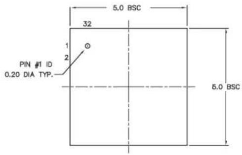
text_image
5.0 BSC 32 1 2 PIN #1 ID 0.20 DIA TYP. 5.0 BSCTOP VIEW
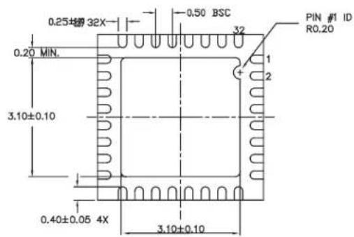
text_image
0.25±0.05 32X 0.20 MIN. 3.10±0.10 0.40±0.05 4X 0.50 BSC 32 1 2 PIN #1 ID R0.20BOTTOM VIEW
NOTE:
- ALL DIMENSIONS ARE IN MILLIMETERS.
- MAX. PACKAGE WARPAGE IS 0.05 mm.
- MAXIMUM ALLOWABE BURRS IS 0.076 mm IN ALL DIRECTIONS.
- PIN #1 ID ON TOP WILL BE LASER/INK MARKED.
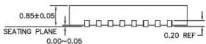
SIDE VIEW
text_image
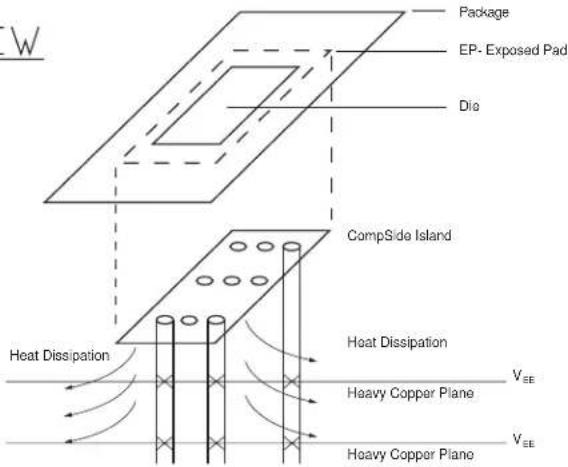
Package EP- Exposed Pad Dia CompSide Island Heat Dissipation Heat Dissipation Heavy Copper Plane Heavy Copper Plane VEE VEEPCB Thermal Consideration for 32-Pin MLF® Package (Always solder, or equivalent, the exposed pad to the PCB)
Package Notes:
- Package meets Level 2 qualification.
- All parts are dry-packaged before shipment.
- Exposed pads must be soldered to a ground for proper thermal management.
MICREL, INC. 2180 FORTUNE DRIVE SAN JOSE, CA 95131 USA
TEL + 1 (408) 944-0800 FAX + 1 (408) 474-1000 WEB http://www.micrel.com
The information furnished by Micrel in this data sheet is believed to be accurate and reliable. However, no responsibility is assumed by Micrel for its use. Micrel reserves the right to change circuitry and specifications at any time without notification to the customer.
Micrel Products are not designed or authorized for use as components in life support appliances, devices or systems where malfunction of a product can reasonably be expected to result in personal injury. Life support devices or systems are devices or systems that (a) are intended for surgical implant into the body or (b) support or sustain life, and whose failure to perform can be reasonably expected to result in a significant injury to the user. A Purchaser's use or sale of Micrel Products for use in life support appliances, devices or systems is at Purchaser's own risk and Purchaser agrees to fully indemnify
Micrel for any damages resulting from such use or sale.
© 2005 Micrel, Incorporated.