
AT91SAM9X35 - Uncategorized Microchip - Free user manual and instructions
Find the device manual for free AT91SAM9X35 Microchip in PDF.


| Product Type | ARM-based Embedded Microprocessor (MPU) |
| Core | ARM926EJ-S, 400 MHz (PCK), 133 MHz (MCK) |
| Package | 217-ball BGA (BGA217) |
| Memory Interfaces | DDR2 SDRAM, NAND Flash, SPI Serial Flash, EEPROM (I2C), 1-Wire |
| Ethernet | 10/100 Mbps EMAC (MII/RMII) with PHY |
| USB | 2x USB 2.0 Host, 1x USB 2.0 Host/Device (High Speed) |
| Serial Interfaces | UART (DBGU, USART0/3), SPI, TWI (I2C), CAN 2.0 |
| Audio | I2S interface for external codec |
| Display | 24-bit LCD controller (up to 800x480), touch screen support |
| Image Sensor Interface | ISI (up to 12-bit) |
| SD/MMC | 2x High-Speed MultiMedia Card Interface (MCI0/1) |
| Supply Voltage | 3.3V (I/O), 1.8V (DDR I/O), 1.0V (Core) |
| Operating Temperature | -10°C to +50°C (board level); chip: -40°C to +85°C (storage) |
| Dimensions (Chip) | Approximately 14x14 mm (BGA217) |
| RoHS | Compliant |
Frequently Asked Questions - AT91SAM9X35 Microchip
User questions about AT91SAM9X35 Microchip
0 question about this device. Answer the ones you know or ask your own.
Ask a new question about this device
Download the instructions for your Uncategorized in PDF format for free! Find your manual AT91SAM9X35 - Microchip and take your electronic device back in hand. On this page are published all the documents necessary for the use of your device. AT91SAM9X35 by Microchip.
USER MANUAL AT91SAM9X35 Microchip
This User Guide introduces the Evaluation Kit and describes the development and debugging capabilities running on Atmel ^® | SMART SAM9 ARM ^® -based Embedded MPUs as listed below:
SAM9G15
SAM9G25
SAM9X25
SAM9G35
SAM9X35
The User Guide pertains to the following Evaluation Kit references:
SAM9G15-EK
SAM9G25-EK
SAM9X25-EK
SAM9G35-EK
SAM9X35-EK
Contents
- Board
One EK board
— One of the five available CPU modules (CM)
SAM9G15-CM
SAM9G35-CM
SAM9X35-CM
SAM9G25-CM
SAM9X25-CM
— One optional DM board featured in SAM9G15, SAM9G35, SAM9X35 kits only.
Power supply
– Universal input AC/DC power supply with US, Europe and UK plug adapters
— One 3V Lithium Battery type CR1225
Cables
— One serial RS232 cable
— One micro A/B-type USB cable
— One RJ45 crossed cable
A Welcome Letter
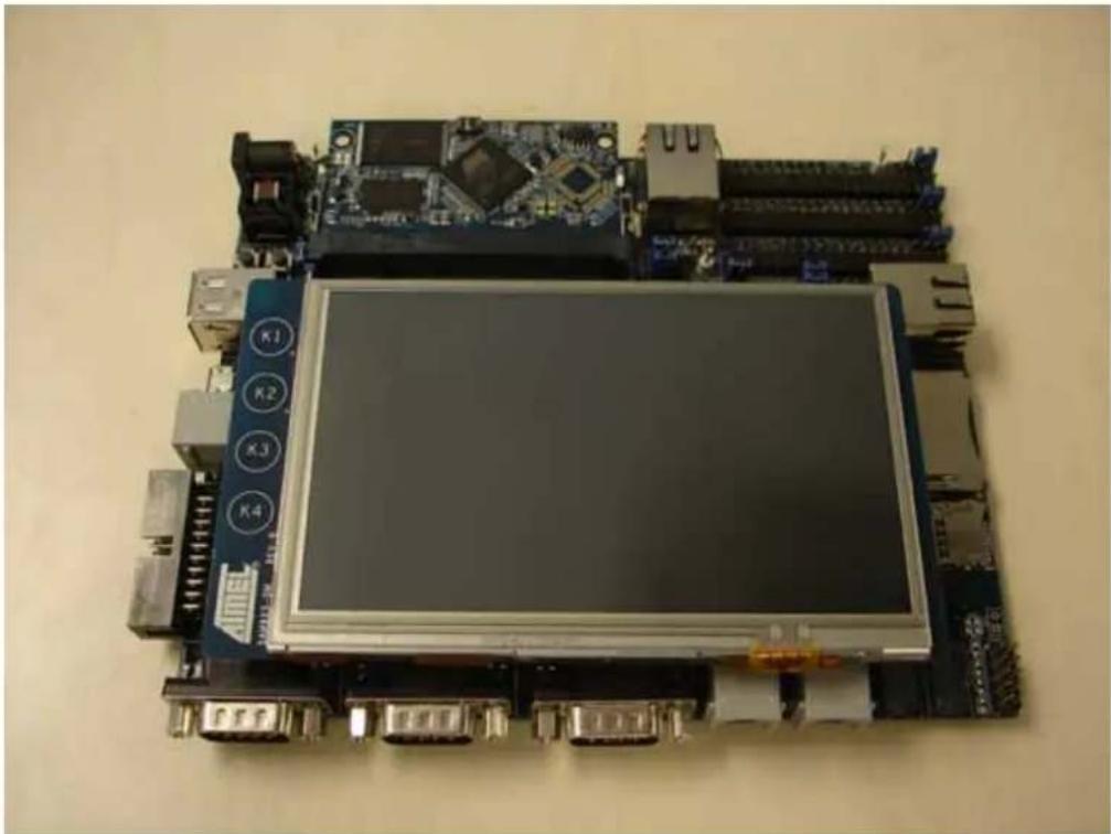
Board Photo (Display module is optional)
natural_image
Electronic circuit board with a central display and surrounding components (no visible text or symbols)Related Documents
| Title Reference Comment | ||
| SAM9G15 Datasheet | Atmel lit° 11052 | These documents provide technical support for each of the Atmel ARM-based Embedded MPU products supported by these Evaluation Kits. |
| SAM9G25 Datasheet | Atmel lit° 11032 | |
| SAM9X25 Datasheet | Atmel lit° 11054 | |
| SAM9G35 Datasheet | Atmel lit° 11053 | |
| SAM9X35 Datasheet | Atmel lit° 11055 | |
The datasheets can be found on www.atmel.com at the SAM9G MPU and SAM9X MPU product sections.
Table of Contents
Introduction....1
Contents 2
Related Documents 3
Table of Contents 4
- Specifications 5
1.1 Kit Specifications....5
1.2 Board Specifications 5
- Power Up 6
2.1 Power Up the Board 6
2.2 Sample Code and Technical Support 6
2.3 Recovery Procedure 7
- Hardware Overview 8
3.1 Introduction....8
3.2 Computer Module (CM)....10
3.3 EK Board Description 28
3.4 Optional Display Module (DM) Board Hardware 82
- Revision History 87
1. Specifications
1.1 Kit Specifications
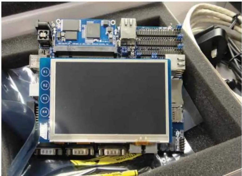
Unpack and inspect the kit carefully. Contact your local Atmel distributor, should there be issues concerning the contents of the kit.
Figure 1-1. Unpacked Evaluation Kit
natural_image
Close-up of an electronic circuit board with a central display and surrounding components (no visible text or symbols)1.2 Board Specifications
| Characteristics Specifications | |
| Clock speed 400 MHz PCK, 133 MHz MCK | |
| Ports Ethernet, USB, RS232, DBGU, JTAG, CAN, Audio, SD Card | |
| Board supply voltage 5 VDC from connector | |
| Temperature- operating- storage | -10° to +50°C-40° to +85°C |
| Relative humidity 0 to 90% (non condensing) | |
| DimensionsEK (Evaluation Kit)CM (Computer Module)DM (Display Module) | 165 mm x 135 mm67.6 mm x 35 mm135 mm x 80 mm |
| RoHS status Compliant | |
Table 1-1. Evaluation Kit Specifications
2. Power Up
2.1 Power Up the Board
Unpack the board taking care to avoid electrostatic discharge. Unpack the power supply, select the right power plug adapter corresponding to that of your country, and insert it in the power supply.
Connect the power supply DC connector to the board and plug the power supply to an AC power plug.
For SAM9G15, SAM9G35, SAM9X35 kits which contain LCD, the screen should light up and display the welcome page of a graphic demo. Click or touch icons displayed on the screen and enjoy the demo.
For SAM9G25 and SAM9X25 which do not contain LCD, before power up, connect DBGU port J11 on the EK board (refer to Section 3.3.3.4 for details) to RS232 port on your computer through the RS232 cable provided with the kit. It is recommended to open a communication session under HyperTerminal. After power up, a command-line based demo runs that can be monitored on HyperTerminal window.
2.2 Sample Code and Technical Support
After boot up, designers can run sample code or their own application, on the development kit. Users can download sample code and get technical support from the Atmel web site:
http://www.atmel.com/products/at91/default.asp?category_id=163&family_id=605&source=global_nav
Figure 2-1. Atmel Web Site
Note: Different interfaces on the EK boards share the same connections to the CPU module. Therefore the actual usage depends on the CPU module featured in the evaluation kit.
2.3 Recovery Procedure
All EK boards have passed strict test procedures before shipment. These test procedures are contained in the SPI serial Flash in case users need to examine the boards again at any time.
If the contents of the SPI serial Flash have been deleted, follow the instructions below to recover the state as it was when shipped by Atmel.
- Go to the page on atmel.com for the EK being used.
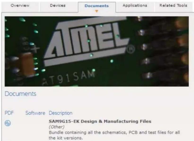
- Locate the EK Design & Manufacturing Files as shown in Figure 2-2.
- Find the xxx-EK_test_12_public.zip, which is the file for Flash content burning.
- Follow the step-by-step instructions in the file SAM9X5_EK_Test_Software to recover the content and to test each section of the boards.
Figure 2-2. EK Design & Manufacturing Files
Home > Microcontrollers > Atmel ARM-based Solutions > Atmel SAM9G > SAM9G15-EK
SAM9G15-EK
3. Hardware Overview
3.1 Introduction
The Evaluation Kit is a fully-featured evaluation platform for the Atmel MPU. The Evaluation Kit enables users to extensively evaluate, prototype and create application-specific designs.
The Evaluation Kit is a new platform architecture based on a Main Board (MB), a CPU Module (CM) equipped with one of the five processors and an optional Display Module (DM).
The Evaluation Kit consists of three boards:
- The CPU Module (CM) board, is a single-board computer that integrates all the core components and is mounted onto an application-specific carrier board (EK board). The CPU Module has specified pinouts based on the SODIMM200 connector. It provides the functional requirements for an embedded application. These functions include, but are not limited to, graphics, audio, mass storage, network and multiple serial and USB ports. A single SODIMM200 connector provides an interface for the carrier board to carry all the I/O signals to and from the CPU Module.
- The Evaluation Kit board (EK Main Board) provides all the interface connectors required to attach the system to the application specific peripherals. This versatility allows the designer to create a densely packed solution, which results in a more reliable product while simplifying system integration.
- The optional Display Module (DM) board integrates LCD, TouchScreen and QTouch ^® technology.
Table 3-1 lists the features provided on the Evaluation Kit:
Table 3-1. Evaluation Kit Features
| Supported Modules Product Name | |||||||
| Expansion Slot SO-DIMM200 | |||||||
| Processor Options SAM9G15 SAM9G25 SAM9G35 SAM9X25 SAM9X35 | X35 | ||||||
| LAN | MII/RMII Ethernet 10/100 w/PHY and three Led status | ETH0 - X X X X | |||||
| RMII Ethernet 10/100 w/PHY and three Led status | ETH1 - -- X - | ||||||
| USART/UART | RS232 four wires/RS485 Shared interface | COM0 X X X X | |||||
| RS232 four wires COM3 | - X - X - | ||||||
| RS232 two wires | DBGU X X X X | ||||||
| CAN | CAN interface Shared interface | CAN0 | -- - X X | ||||
| CAN1 | -- - X X | ||||||
| USB | 2 * USB 2.0 Host | - | X X X X X | ||||
| 1 * USB 2.0 Host/Device | - | X X X X X | |||||
| SMD | Software Modem Device | - | X X X X X | ||||
| Memory Card Support | μSD Card Slot Onboard | HSMCI0 | X X X X X | ||||
| MMC/MMC+/SD/SDIO/CE-ATA | HSMCI1 | X X X X X | |||||
| ISI | - | - | - X -- - | ||||
| LCD + Touch Screen | 24-bit Output Mode | - | X - X - X | ||||
| ZigBee® | - | - | X | X | X | X | X |
| SPI | - | - | X | X | X | X | X |
| TWI | - | - | X X X X X | ||||
| DEBUG | JTAG Test Access Port | - | X | X | X | X | X |
3.2 Computer Module (CM)
3.2.1 CM Board Overview
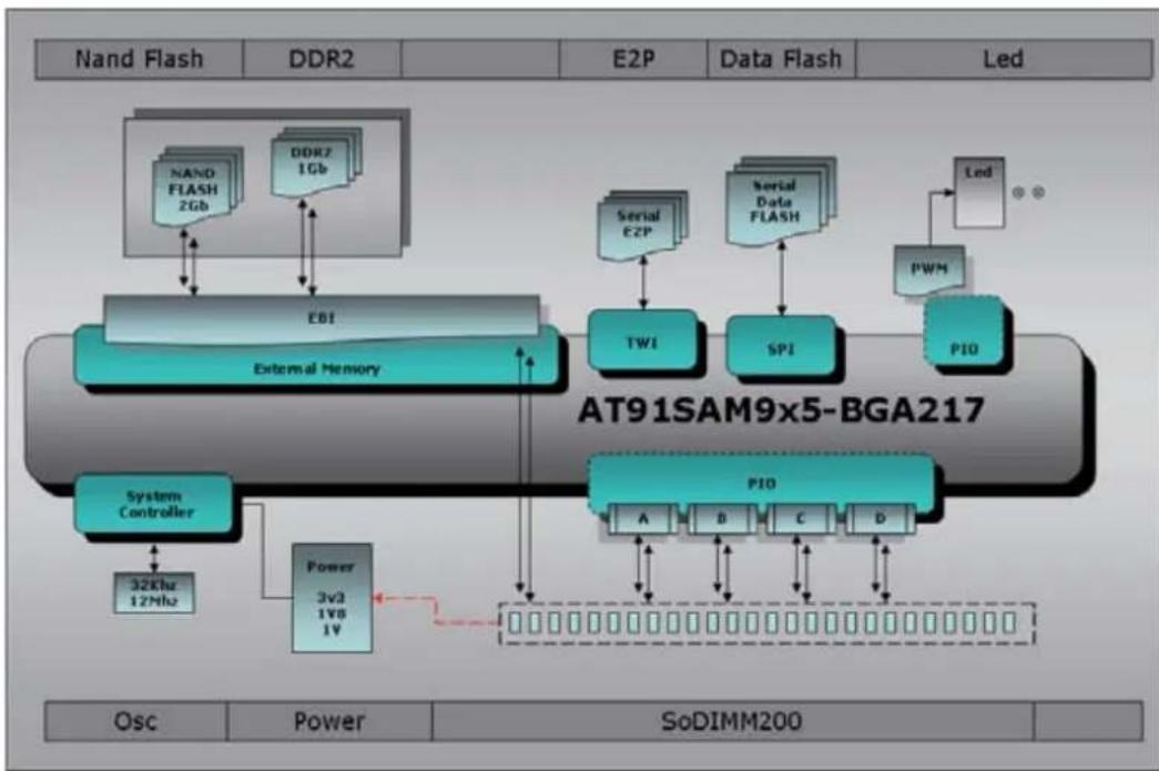
The CM board is the CPU module at the heart of the system. It connects to the EK board through a SO-DIMM200 interface. It carries the processor and external memories. The CM board serves as a minimal CPU sub-system. All five processors: SAM9G15, SAM9G25, SAM9X25, SAM9G35 and SAM9X35 share the same CM circuitry with minor configuration settings.
Note: There are three CM boards from three different manufacturers. The five processors are implemented as shown in Table 3-2 below:
Table 3-2. CM Board Implementation
| Manufacturer & Module kind SAM | M9G15-CM SAM9 | G25-CM SAM9G3 | 5-CM SAM9X25-CM | CM SAM9X35-CM | |
| mfg 1 x - x - - | |||||
| m | f | g | 2 | - | - |
| mfg 3 | x | x | x | x | x |
The three CM boards share the same circuitry design but with different designator information and PCB layouts. The circuitry reference in this guide, for common design parts, refers to schematics from SAM9G25-CM (mfg 3). All the other schematics are provided in Section 3.2.6 "Schematics".
Figure 3-1. Board Architecture
flowchart
graph TD
    subgraph Nand Flash
        A["NAND FLASH 2Gb"] --> B["External Memory"]
        C["DDR2 1Gb"] --> B
        D["NAND FLASH"] --> B
        E["External Memory"] --> F["EBI"]
        G["System Controller"] --> H["32KHz 12MHz"]
        I["Power 3v3 1V8 1V"] --> J["Power"]
    end

    subgraph DDR2
        K["NAND FLASH 2Gb"] --> L["External Memory"]
        M["DDR2 1Gb"] --> L
        N["External Memory"] --> O["External Memory"]
        P["External Memory"] --> Q["External Memory"]
        R["External Memory"] --> S["External Memory"]
        T["External Memory"] --> U["External Memory"]
        V["External Memory"] --> W["External Memory"]
    end

    subgraph E2P
        X["Serial E2P"] --> Y["TWI"]
        Z["Serial Data FLASH"] --> AA["SPI"]
        AB["Led"] --> AC["PWM"]
        AD["PWM"] --> AE["LED"]

    subgraph Data Flash
        AF["External Memory"] --> AG["TWI"]
        AH["External Memory"] --> AI["SPI"]
        AJ["Led"] --> AK["PWM"]
        AL["LED"] --> AM["PWM"]
    end

    subgraph Led
        AN["External Memory"] --> AO["TWI"]
        AP["External Memory"] --> AQ["SPI"]
        AR["Led"] --> AS["PWM"]
        AT["AT91SAM9x5-BGA217"] --> AU["Power"]
    end

    subgraph Power
        AV["Osc"] --> AW["SoDIMM200"]
    end
3.2.2 Equipment List
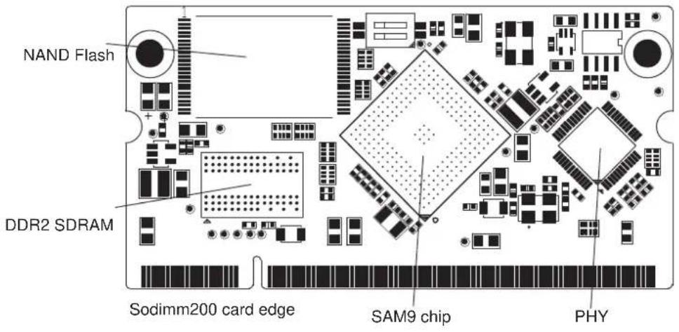
The CM board is built around the integration of an ARM926-based microcontroller (BGA217 package) with external memory and optional Ethernet PHYSical Layer Transceiver.
3.2.2.1 Devices
Following is the list of the CM board components:
One SAM9 Embedded MPU from the list below
- SAM9G15
- SAM9G25
SAM9G35
- SAM9X25
SAM9X35
12 MHz crystal
32.768 KHz crystal
• 1 Gbit DDR2 memory
2 Gits NAND Flash memory with Chip Selection control switch
32 Mbits SPI Serial Flash with Chip Selection control switch
512 Kbits EEPROM
• 1 Kbyte 1-Wire EEPROM
- On-board power regulation
- Two user LEDs
- Optional PHY
3.2.2.2 Interface Connection
• SODIMM200 card edge interface
3.2.2.3 Configuration Items
Dual ON/OFF switch for NAND Flash and SPI serial Flash Chip Select connection
Figure 3-2. CM Board Layout Commented
3.2.3 Function Blocks
3.2.3.1 Processor
The CM Board is equipped with an Atmel ARM-based embedded MPU, as listed below, in a 217-ball BGA package. The five devices share an identical footprint. All five share the same CM Board PCB with minor configuration differences.
The five devices are:
SAM9G15
SAM9G25
SAM9G35
SAM9X25
SAM9X35
As different interfaces can be defined using the same pins, it depends on the actual configuration of the CPU as to which functions are in fact available to the EK board.
Refer to Section 3.2.4.1 "Chip Identification" for details. The processor runs at a nominal frequency of 400 MHz for the core and 133 MHz for the system bus.
The peripheral configuration possibilities and implementation requirements of the CM are dependent on the module's chipset. Two configuration resistors are implemented on board in order to select the mode of configuration.
3.2.3.2 Clock Circuitry
The CM includes 3 clock sources:
- Two are alternatives for the processor main clock
• One crystal and one crystal oscillator are used for the Ethernet MII/RMII chip
Table 3-3. Main Components Associated with the Clock Systems
| Quantity Description Component assignment | ||
| 1 Crystal | for Internal Clock, 12 MHz Y1 | |
| 1 Crystal | for RTC Clock, 32.768 kHz Y2 | |
| 1 Oscillator for Ethernet Clock RMII, 50 MHz Y3 | ||
3.2.3.3 Reset Circuitry
The reset sources for the CM board are:
Power on reset
- Push button reset (Push button is equipped on EK board)
- JTAG reset from an in-circuit emulator (JTAG interface is equipped on EK board)
3.2.3.4 Power Supplies
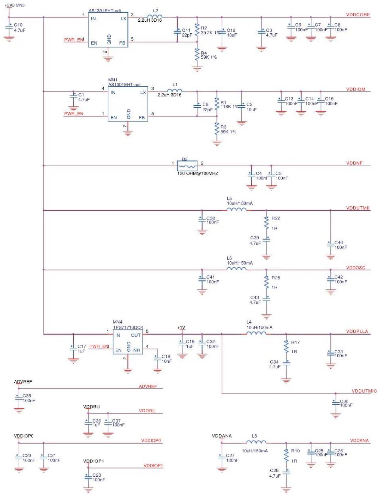
The CM Board is driven by +3V3 input power rail from the EK board through the SODIMM200 connector. The CM Board embeds all the necessary power rails required for the micro processor.
When additional voltages are required, for example VDDCORE, they are generated on board from the 3.3V supply. The detailed power supply requirements for any given module are specified within the corresponding product documentation. The following table summarizes the power specifications.
Table 3-4. Power Rails Associated with the Systems
| Nominal Name | Powers Component | ||
| 3.3v VDDNF | the NAND Flash I/O and control, D16-D32 and multiplexed SMC lines | From SODIMM200 connector | |
| 3.3v VDDIOP0 | Partial Peripheral I/O lines From SODIMM200 connector | ||
| 3.3v VDDIOP1 | Partial Peripheral I/O lines From SODIMM200 connector | ||
| 3.0v VDDBU | the Slow Clock oscillator, the internal 32 kHz RC, the internal 12 MHz RC and a part of the System Controller | From SODIMM200 connector | |
| 3.3v VDDUTMII the USB device and host UTMI+ interface From SODIMM200 connector | |||
| 3.3v VDDOSC the Main Oscillator cells From SODIMM200 connector | |||
| 3.3v | VDDANA | the Analog to Digital Converter | From SODIMM200 connector |
| 1.8v | VDDIOM | the External Memory Interface I/O lines | on-board |
| 1.0v | VDDUTMIC | DC Supply UDPHS and UHPHS UTMI+ Core | on-board |
| 3.3v | VDDPLLUTMI | DC Supply UDPHS and UHPHS UTMI+ Interface | From SODIMM200 connector |
| 1.0v | VDDPLLA | the PLLA cell | on-board |
| 1.0v | VDDCORE | the core, including the processor, the embedded memories and the peripherals | on-board |
| 3.0V or 3.3V configurable | ADVREF | ADC Reference voltage | From SODIMM200 connector |
Figure 3-3. CM Power Supply
3.2.3.5 Memory
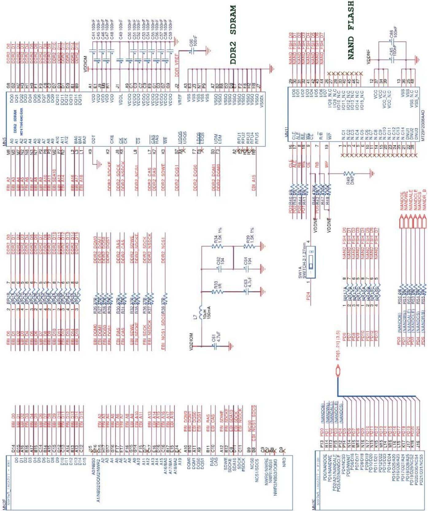
The Device serial processor features a DDR/SDR memory interface and an External Bus Interface (EBI) to enable interfacing to a wide range of external memories and to almost any kind of parallel peripheral.
The External Bus Interface (EBI) is connected to two kinds of memory devices:
• One 1 Gbyte DDR2 SDRAM
• One 2 Gbytes (or 4 Gbytes depending on supplier) NAND Flash
Figure 3-4. CM Board External Memory
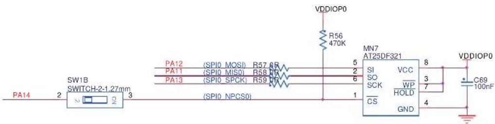
3.2.3.6 Serial Peripheral Interface (SPI) Controller
The serial processor provides two high-speed Serial Peripheral Interface (SPI) controllers. One port is used to interface with the on-board serial Flash.
Figure 3-5. SPI
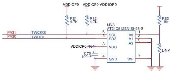
3.2.3.7 Two Wire Interface (TWI)
The serial processor has a full speed (400 kHz) master/slave TWI Serial Controller. The controller is mostly compatible with industry standard I2C and SMBus Interfaces. This port is used to interface with the on-board Serial EEPROM, ISI, QTouch device and audio codec interface.
Figure 3-6. TWI
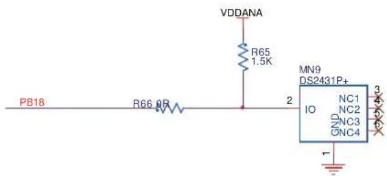
3.2.3.8 1-Wire EEPROM
The Evaluation Kit uses a 1-Wire device as "firmware label" to store the information such as chip type, manufacturer's name, production date etc.
Figure 3-7. 1-Wire Device
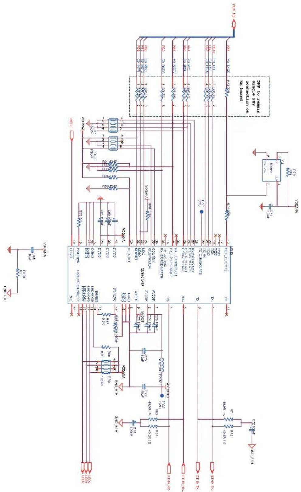
3.2.3.9 Optional PHY
Some of the device modules provide a location for a 10/100 Ethernet MAC/PHY interface.
For more information about the Ethernet controller device, refer to the Davicom DM9161 controller manufacturer's datasheet.
Figure 3-8. Ethernet
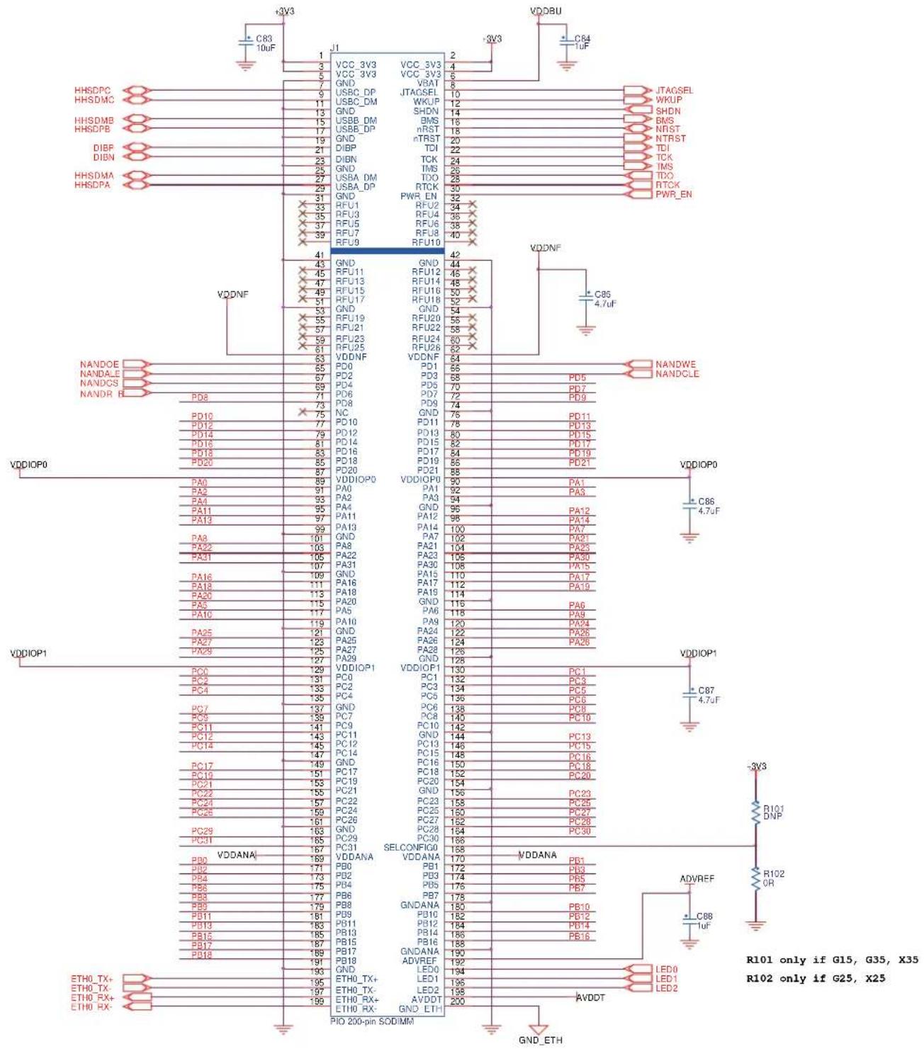
3.2.3.10 SODIMM200 Interface
The CM board uses SODIMM200 card edge connector to interface with the EK board.
Figure 3-9. SODIMM200 Interface on CM Board
3.2.4 Configuration
3.2.4.1 Chip Identification
The CM board may be equipped with any of the five processors, all sharing an identical BGA217 footprint. There are two resistors on the CM board for the purpose of identifying which of the five is the one actually mounted.
The tables below show in detail how the CM board, relative to different processors, determines the dedicated "SELCONFIG" logic.
Table 3-5. Resistor Identification
| Resistor SAM9G15 SAM9G25 SAM9G35 SAM9X25 SAM9X35 | |||||
| R49 --- Populated Not Populated | |||||
| R50 --- Not Populated Populated | |||||
| R87 Populated - Populated | -- | ||||
| R88 | Not Populated - | Not Populated -- | |||
| R101 Populated Not Populated | Populated Not Populated Populated | ||||
| R102 Not Populated Populated | Not Populated Populated Not Populated | ||||
Table 3-6. Module Configuration Identification
| SAM9G15 module | SAM9G35 module | SAM9X35 module | SAM9G25 module | SAM9X25 module | ||
| CM Setting | R101 | Populated | Populated | Populated | Not Populated | Not Populated |
| R102 | Not Populated | Not Populated | Not Populated | Populated | Populated | |
| SELCONFIG (SODIMM200 pin 166) | High High | High | Low | Low | ||
| EK Setting | USART3 | Not Selected | Not Selected | Not Selected | Selected | Selected |
| ETH1 | Not Selected | Not Selected | Not Selected | Not Selected | Selected | |
| DM Setting | LCD | Selected | Selected | Selected | Not Selected | Not Selected |
3.2.4.2 Boot Configuration
In order to use the SAM-BA boot, users must ensure that JP9 (BMS configuration) on the board is open, so that the embedded ROM code runs and searches for a bootable device. For more details, refer to the product datasheet. To make the processor boot from SAM-BA, the external memory devices cannot be bootable.
All three CM boards from different vendors feature a de-select function of the Chip Select signal on NAND and SPI serial Flash.
To boot from software, users may erase the bootable content within NAND and SPI serial Flash to launch a SAM-BA boot. A hardware disconnection of the Chip Select signal is not necessary.
Table 3-7. Boot Configuration
| Board Vendor Designation Default Setting Feature | |||
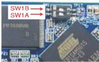
| Embest CM | SW1A (1,4) ON | 1. Default ON to select NAND Flash2. Set to OFF to deselect the NAND Flash | |
| SW1B (2,3) ON | 1. Default ON to select SPI serial Flash2. Set to OFF to deselect the SPI serial Flash | ||
| Ronetix CM | J1R17 | J1 DNPR17 populated | 1. Default select NAND Flash always2. Users need to dismount R17, mount J1 as 2.54mm jumper to ease frequent changes3. Close J1 to select NAND FlashOpen J1 to deselect NAND Flash |
| J2R24 | J2 DNPR24 populated | 1. Default select SPI serial Flash always2. Users need to dismount R24, mount J2 as 2.54mm jumper to ease frequent changes3. Close J2 to select SPI serial FlashOpen J2 to deselect SPI serial Flash | |
| Cogent CM | P2R90 | P2 normal closeR90 DNP | 1. By default, P2 is closed to select NAND Flash2. Open P2 to deselect NAND Flash3. Mounting R90 as 0-ohm always selects NAND Flash |
| R15 R15 populated | 1. Default select SPI serial Flash always2. Dismount R15 to deselect SPI serial Flash | ||
Figure 3-10. SW1A and SW1B Position on Embest Modules
3.2.5 Connectors
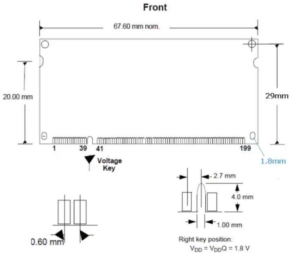
Figure 3-11. CM Board Dimensions
3.2.6 Schematics
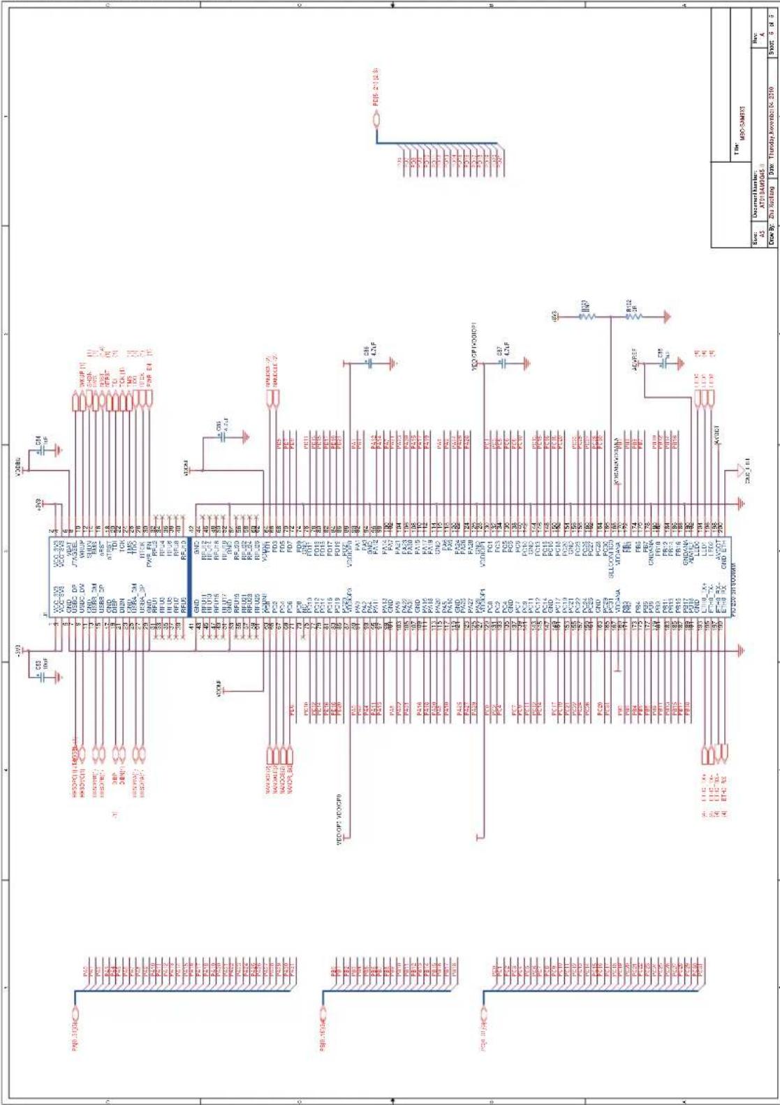
Figure 3-12. CM Board Schematics - 1 of 5
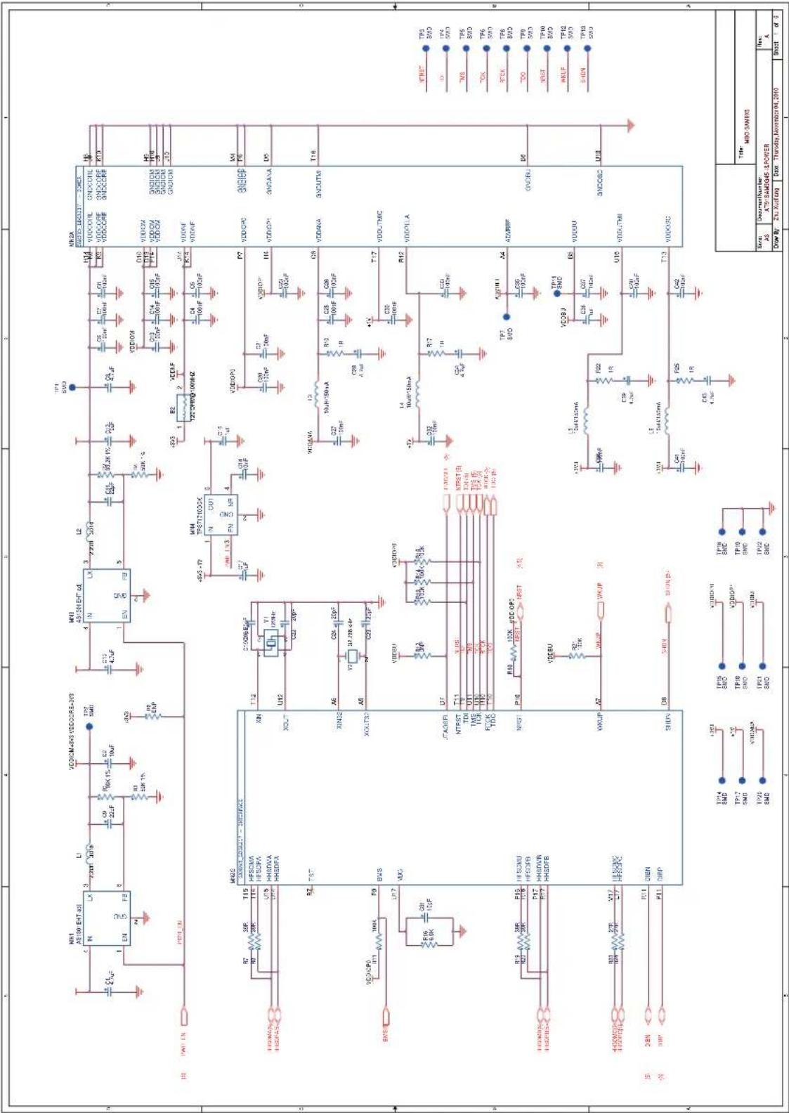
Figure 3-13. CM Board Schematics - 2 of 5
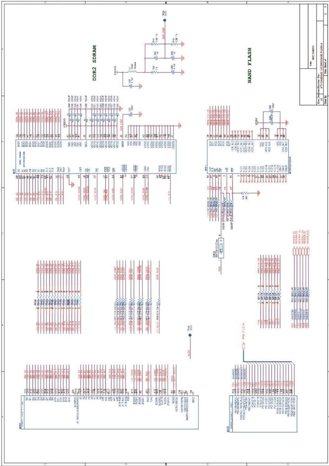
Figure 3-14. CM Board Schematics - 3 of 5
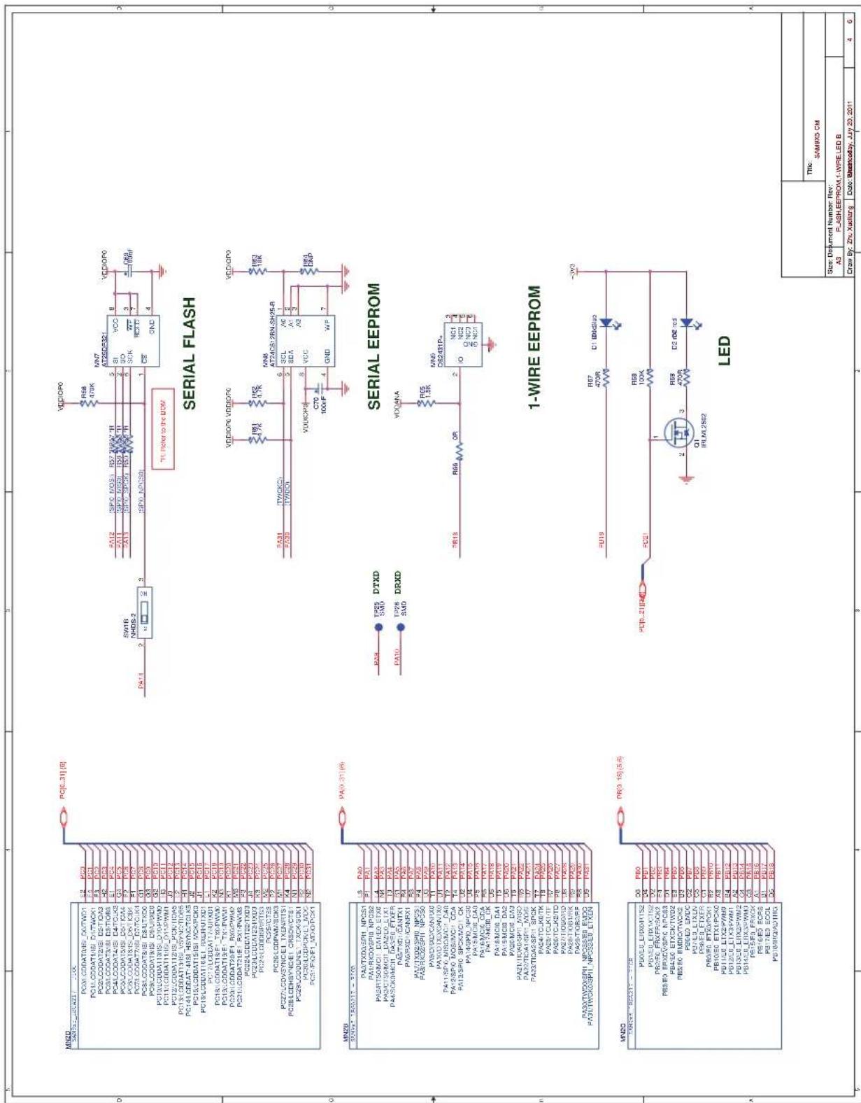
Figure 3-15. CM Board Schematics - 4 of 5
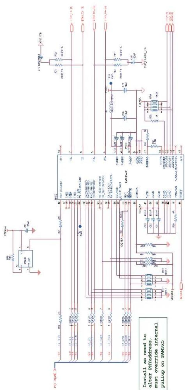
ETHERNET
Figure 3-16. CM Board Schematics - 5 of 5
3.3 EK Board Description
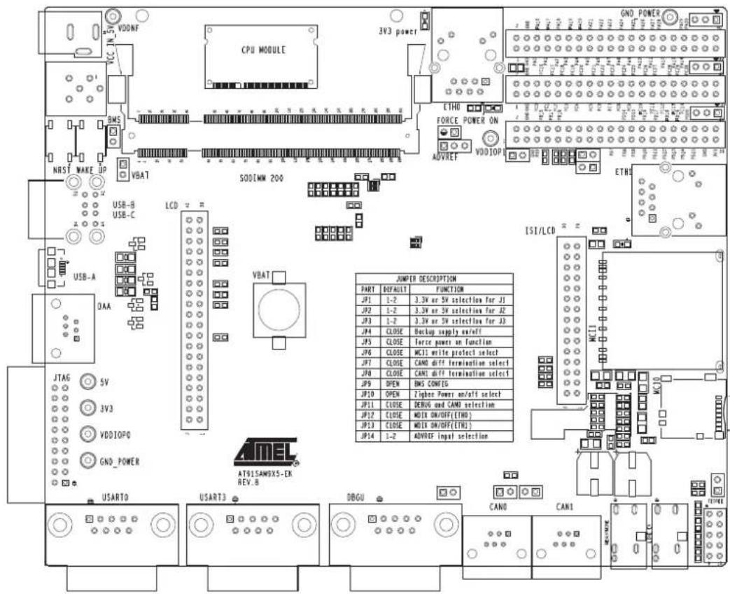
3.3.1 EK Board Overview
The EK board serves as the main board that carries the CPU module. It features all necessary peripherals and interfaces for processor evaluation.
Figure 3-17. Commented EK Board Layout
3.3.2 Equipment List
Based on the processor installed on the CM board, the EK board is equipped with the following interfaces or peripherals:
3.3.2.1 Devices
List of the EK board peripherals:
- Two EMAC PHY
One Audio codec
• Two high speed MCI Card interfaces
• Two CAN transceivers
• Three RS232 ports with level translator features: DBGU, USART0 and USART3
One Smart DAA port - Two USB host ports
• One USB host/device port
• On-board power regulation
• LCD/ISI extension interface
- ZigBee interface
One-wire device
3.3.2.2 Board Interface Connection
• Main power supply (J4)
• One SODIMM200 socket (CON1)
USB A Host/Device, support USB host/device using a type micro AB connector (J20)
USB B Host, support USB host using a type A connector (J19, upper)
- USB C Host, support USB host using a type A connector (J19, lower)
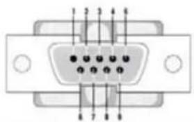
- DBGU (RX and TX only) connected to a 9-way male RS232 connector (J11)
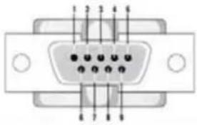
- USART1 (RX, TX, RTS, CTS) connected to a 9-way male RS232 connector (J8)
- USART3 (RX, TX, RTS, CTS) connected to a 9-way male RS232 connector (J12)
• JTAG, 20 pin IDC connector (J9)
- MicroSD connector (J6)
SD/MMC connector (J7)
• Headphone (J15), line-in (J13)
• Image sensor connector (J21)
DM board connection for QTouch and TFT LCD display with Touch Screen and backlight (J21, J22)
• DAA connector RJ11 6P4C type (J16)
• CAN bus connectors RJ12 6P6C type (CON2, CON3)
• ZigBee connector (J10)
• Three IO expansion ports (J1, J2, J3)
- Test points, various test points are located throughout the board
3.3.2.3 Push Button Switches
- Reset, board reset (BP1)
- Wake up, push button to bring the processor out of low power mode (BP2)
3.3.3 Function Blocks
3.3.3.1 Processor
The Evaluation Kit board may be used with any of the Core Modules:
SAM9G15
SAM9G25
SAM9G35
SAM9X25
SAM9X35
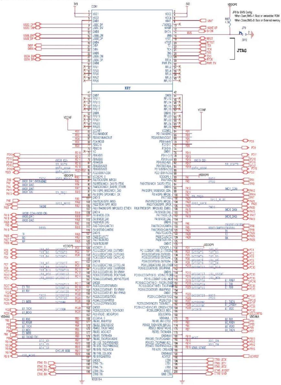
Figure 3-18. SODIMM Interface on EK Board
other
Pin 1: USB DP Pin 2: USB DM Pin 3: USB DP Pin 4: USB DP Pin 5: USB DP Pin 6: USB DP Pin 7: USB DP Pin 8: USB DP Pin 9: USB DP Pin 10: USB DP Pin 11: USB DP Pin 12: USB DP Pin 13: USB DP Pin 14: USB DP Pin 15: USB DP Pin 16: USB DP Pin 17: USB DP Pin 18: USB DP Pin 19: USB DP Pin 20: USB DP Pin 21: USB DP Pin 22: USB DP Pin 23: USB DP Pin 24: USB DP Pin 25: USB DP Pin 26: USB DP Pin 27: USB DP Pin 28: USB DP Pin 29: USB DP Pin 30: USB DP Pin 31: USB DP Pin 32: USB DP Pin 33: USB DP Pin 34: USB DP Pin 35: USB DP Pin 36: USB DP Pin 37: USB DP Pin 38: USB DP Pin 39: USB DP Pin 40: USB DP Pin 41: USB DP Pin 42: USB DP Pin 43: USB DP Pin 44: USB DP Pin 45: USB DP Pin 46: USB DP Pin 47: USB DP Pin 48: USB DP Pin 49: USB DP Pin 50: USB DP Pin 51: USB DP Pin 52: USB DP Pin 53: USB DP Pin 54: USB DP Pin 55: USB DP Pin 56: USB DP Pin 57: USB DP Pin 58: USB DP Pin 59: USB DP Pin 60: USB DP Pin 61: USB DP Pin 62: USB DP Pin 63: USB DP Pin 64: USB DP Pin 65: USB DP Pin 66: USB DP Pin 67: USB DP Pin 68: USB DP Pin 69: USB DP Pin 70: USB DP Pin 71: USB DP Pin 72: USB DP Pin 73: USB DP Pin 74: USB DP Pin 75: USB DP Pin 76: USB DP Pin 77: USB DP Pin 78: USB DP Pin 79: USB DP Pin 80: USB DP Pin 81: USB DP Pin 82: USB DP Pin 83: USB DP Pin 84: USB DP Pin 85: USB DP Pin 86: USB DP Pin 87: USB DP Pin 88: USB DP Pin 89: USB DP Pin 90: USB DP Pin 91: USB DP Pin 92: USB DP Pin 93: USB DP Pin 94: USB DP Pin 95: USB DP Pin 96: USB DP Pin 97: USB DP Pin 98: USB DP Pin 99: USB DP Pin100: USB DP Pin101: USB DP Pin102: USB DP Pin103: USB DP Pin104: USB DP Pin105: USB DP Pin106: USB DP Pin107: USB DP Pin108: USB DP Pin109: USB DP Pin110: USB DP Pin111: USB DP Pin112: USB DP Pin113: USB DP Pin114: USB DP Pin115: USB DP Pin116: USB DP Pin117: USB DP Pin118: USB DP Pin119: USB DP Pin120: USB DP Pin121: USB DP Pin122: USB DP Pin123: USB DP Pin124: USB DP Pin125: USB DP Pin126: USB DP Pin127: USB DP Pin128: USB DP Pin129: USB DP Pin130: USB DP Pin131: USB DP Pin132: USB DP Pin133: USB DP Pin134: USB DP Pin135: USB DP Pin136: USB DP Pin137: USB DP Pin138: USB DP Pin139: USB DP Pin140: USB DP Pin141: USB DP Pin142: USB DP Pin143: USB DP Pin144: USB DP Pin145: USB DP Pin146: USB DP Pin147: USB DP Pin148: USB DP Pin149: USB DP Pin150 :USBDPDPIA P00 :USBDPDPIA P01 :USBDPDPIA P02 :USBDPDPIA P03 :USBDPDPIA P04 :USBDPDPIA P05 :USBDPDPIA P06 :USBDPDPIA P07 :USBDPDPIA P08 :USBDPDPIA P09 :USBDPDPIA P10 :USBDPDPIA P11 :USBDPDPIA P12 :USBDPDPIA P13 :USBDPDPIA P14 :USBDPDPIA P15 :USBDPDPIA P16 :USBDPDPIA P17 :USBDPDPIA P18 :USBDPDPIA P19 :USBDPDPIA P20 :USBDPDPIA P21 :USBDPDPIA P22 :USBDPDPIA P23 :USBDPDPIA P24 :USBDPDPIA P25 :USBDPDPIA P26 :USBDPDPIA P27 :USBDPDPIA P28 :USBDPDPIA P29 :USBDPDPIA P30 :USBDPDPIA P31 :USBDPDPIA P32 :USBDPDPIA P33 :USBDPDPIA P34 :USBDPDPIA P35 :USBDPDPIA P36 :USBDPDPIA P37 :USBDPDPIA P38 :USBDPDPIA P39 :USBDPDPIA P40 :USBDPDPIA P41 :USBDPDPIA P42 :USBDPDPIA P43 :USBDPDPIA P44 :USBDPDPIA P45 :USBDPDPIA P46 :USBDPDPIA P47 :USBDPDPIA P48 :USBDPDPIA P49 :USBDPDPIA P50 :USBDPDPIA P51 :USBDPDPIA P52 :USBDPDPIA P53 :USBDPDPIA P54 :USBDPDPIA P55 :USBDPDPIA P56 :USBDPDPIA P57 :USBDPDPIA P58 :USBDPDPIA P59 :USBDPDPIA P60 :USBDPDPIA P61 :USBDPDPIA P62 :USBDPDPIA P63 :USBDPDPIA P64 :USBDPDPIA P65 :USBDPDPIA P66 :USBDPDPIA P67 :USBDPDPIA P68 :USBDPDPIA P69 :USBDPDPIA P70 :USBDPDPIA P71 :USBDPDPIA P72 :USBDPDPIA P73 :USBDPDPIA P74 :USBDPDPIA P75 :USBDPDPIA P76 :USBDPDPIA P77 :USBDPDPIA P78 :USBDPDPIA P79 :USBDPDPIA P80 :USBDPDPIA P81 :USBDPDPIA P82 :USBDPDPIA P83 :USBDPDPIA P84 :USBDPDPIA P85 :USBDPDPIA P86 :USBDPDPIA P87 :USBDPDPIA P88 :USBDPDPIA P89 :USBDPDPIA P90 :USBDPDPIA P91 :USBDPDPIA P92 :USBDPDPIA P93 :USBDPDPIA P94 :USBDPDPIA P95 :USBDPDPIA P96 :USBDPDPIA P97 :USBDPDPIA P98 :USBDPDPIA P99 :USBDPDPIA KEY KEY KEY KEY KEY KEY KEY KEY KEY KEY KEY KEY KEY KEY KEY KEY KEY KEY KEY KEY KEY KEY KEY KEY KEY KEY KEY KEY KEY KEY KEY KEY KEY KEY KEY KEY KEY KEY KEY KEY KEY KEY KEY KEY KEY KEY KEY KEY KEY KEY Key Key Key Key Key Key Key Key Key Key Key Key Key Key Key Key Key Key Key Key Key Key Key Key Key Key Key Key Key Key Key Key Key Key Key Key Key Key Key Key Key Key Key Key Key Key Key Key Key Key KDDI KDDI KDDI KDDI KDDI KDDI KDDI KDDI KDDI KDDI KDDI KDDI KDDI KDDI KDDI KDDI KDDI KDDI KDDI KDDI KDDI KDDI KDDI KDDI KDDI KDDI3.3.3.2 Power Supplies
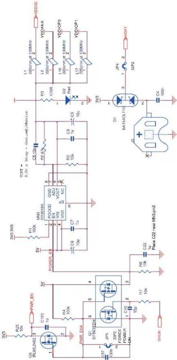
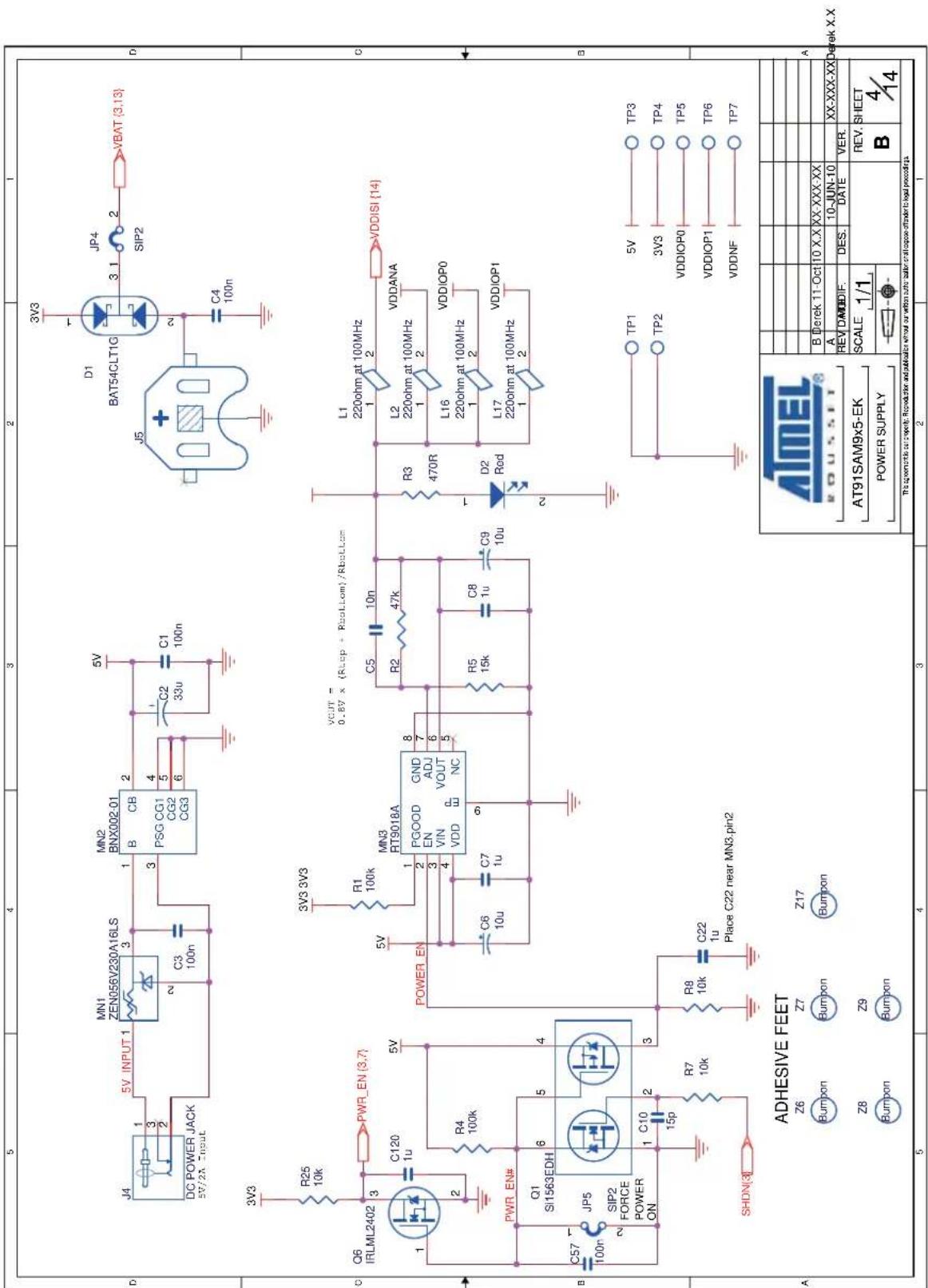
The EK Board features one adjustable LDO. It accepts DC 5V power input and outputs a regulated +3.3V to most other circuits on the board through four 3.3V rails.
VDDPIO0
VDDPIO1
VDDANA
VDDISI
This LDO is enabled through a dual FET scheme. The processor can assert SHDN (which is a VDDBU-powered I/O) to shut down the LDO to enter the so-called backup mode. The regulator on CM board is also shut down by the action of the SHDN signal.
If the 3V battery is mounted on J5, both CM and EK boards can be woken up by action on the BP2 button, which drives the WKUP signal (also a VDDBU-powered I/O).
Figure 3-19. EK Board Power Management
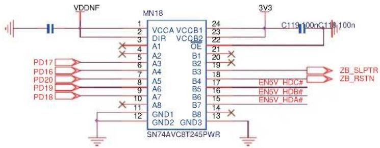
There is another 3.3V rail, VDDNF, supplied from the CM board. VDDNF is set to 3.3V in the current CM design. The processors also support a 1.8V NAND Flash device, in which case VDDNF is set to 1.8V. In order to avoid potential voltage conflict on user-defined applications, a level shifter is inserted between the PIO lines on VDDNF rail and the 3.3V application.
Figure 3-20. Level Shifter For VDDNF Rail
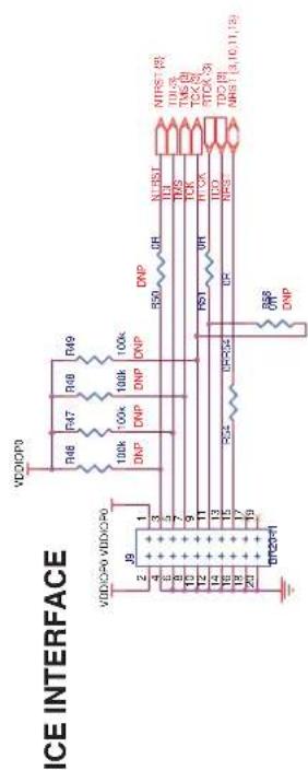
3.3.3.3 JTAG/ICE
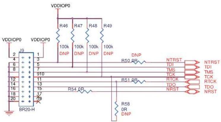
Software debug is accessed by a standard 20-pin JTAG connection. This allows connection to a standard USB-to-JTAG in-circuit emulator such as SAM-ICE ^™ .
Figure 3-21. JTAG Interface
3.3.3.4 DBGU
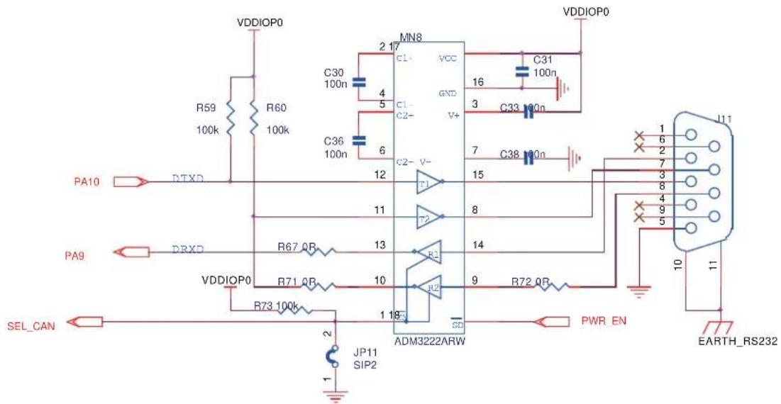
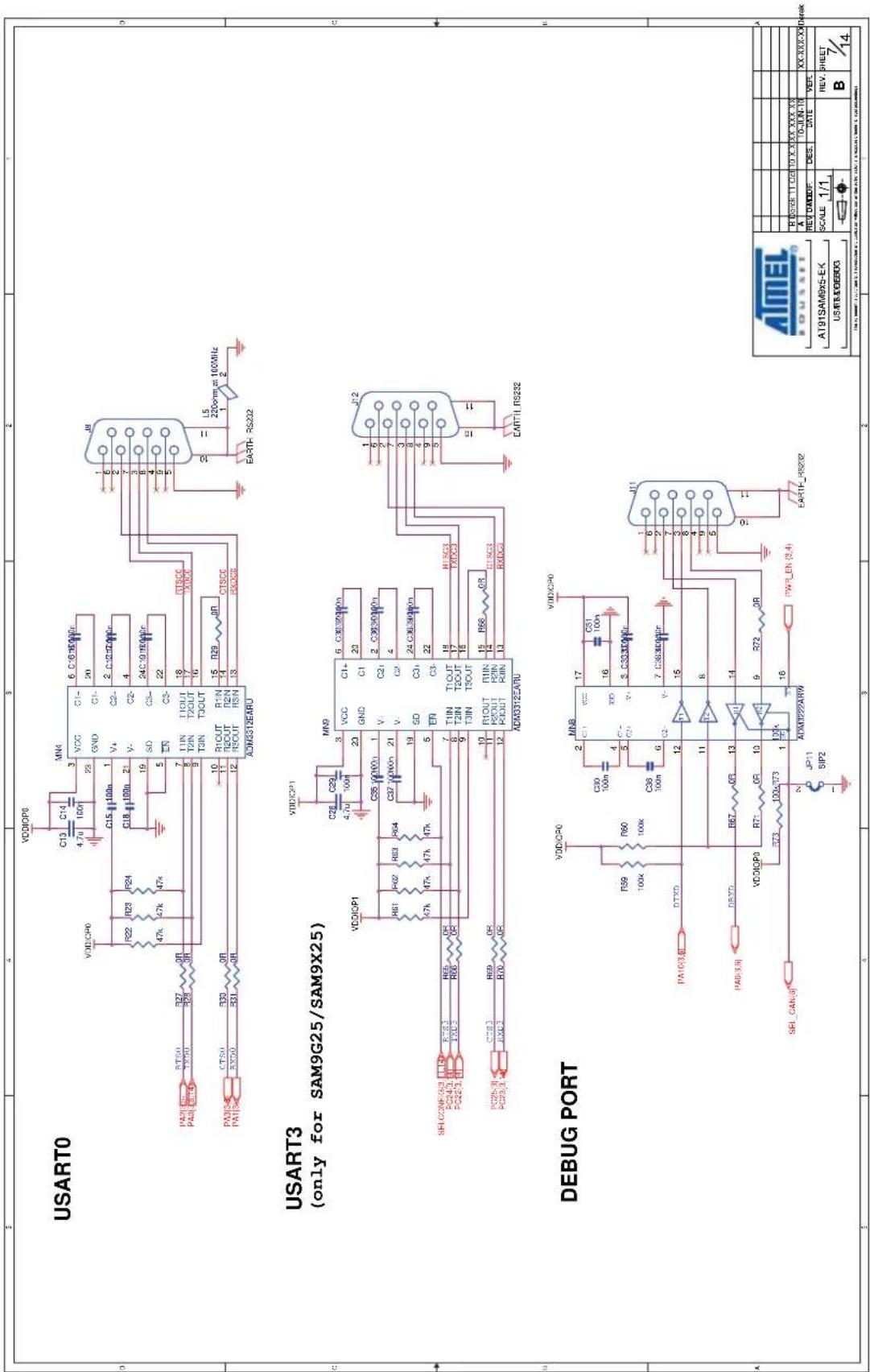
The UART is connected to the DB-9 male socket through an RS-232 Transceiver (TXD and RXD only). A jumper, JP11, is used to select DBGU or CAN0 between IO (PA9, PA10) sharing scheme. Close JP11 to select DBGU.
Figure 3-22. DBGU Com Port
3.3.3.5 USART
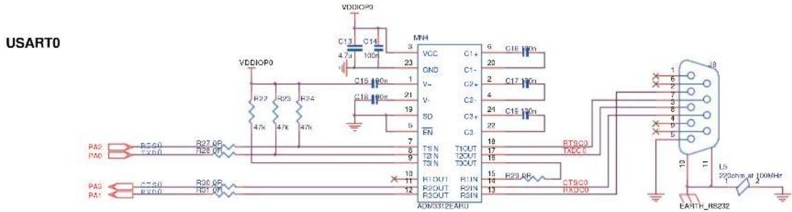
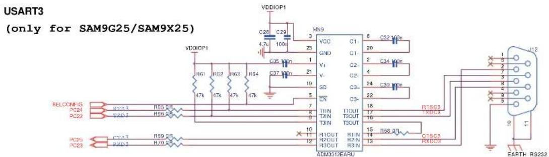
The USART0 and USART3 are used as serial communication ports. Both USARTs are buffered with an RS-232 Transceiver (TXD, RXD and handshake CTS/RTS control) and connected to the DB-9 male socket. The software must assign the appropriate PIO pins to enable the USART function.
The USART3 is only supported by SAM9G25 and SAM9X25 processors. The RS-232 Transceiver for USART3 is enabled by the signal SELCONFIG comprised of a pull down resistor on CM board. Ref to Section 3.4.1 "DM Board Overview" for details.
Figure 3-23. USART Com Port
3.3.3.6 USB Ports
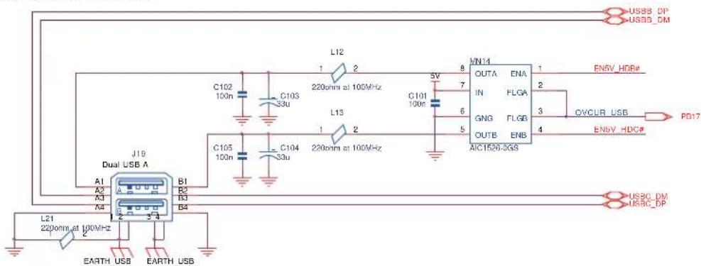
The Evaluation Kit features three USB communication ports:
Port A Host High Speed (EHCI) and Full Speed (OHCI) multiplexed with USB Device High speed Micro AB connector, J20
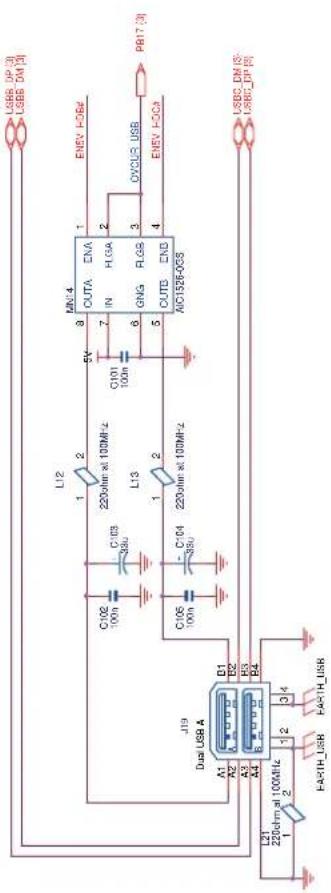
Port B Host High Speed (EHCI) and Full Speed (OHCI) standard type A connector, J19 upper port
Port C Host Full speed OHCI only standard type A connector, J19 lower port
All three USB Host ports are equipped with 500 mA high-side power switch for self-powered and bus-powered applications. The USB device port features VBUS insert detection function through the resistor ladder R138 and R139.
Refer to the embedded MPU product datasheet for detailed programming information. For datasheet reference numbers and titles, see "Related Documents".
Figure 3-24. USB Port (A)
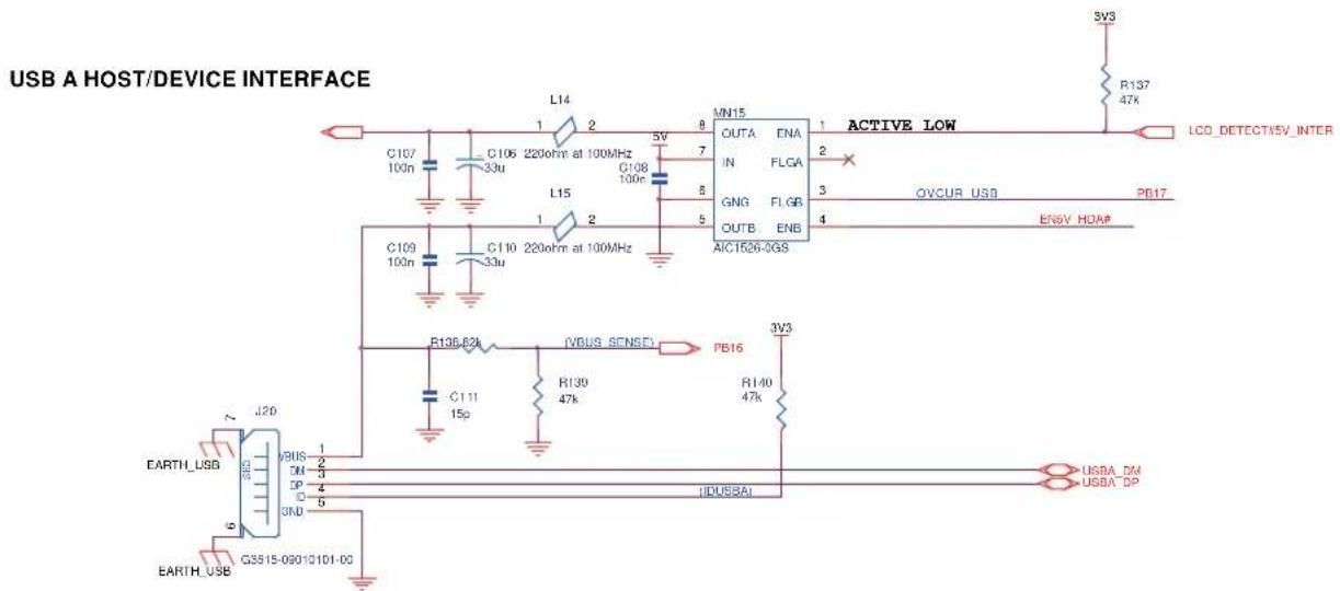
Figure 3-25. USB Port (B & C)
USB HOST B&C INTERFACE
3.3.3.7 Ethernet 10/100 (EMAC) Port
Except for SAM9G15, the processor has two 10/100 Mbps Ethernet Mac Controllers.
| SAM9G15 SAM9G35 SAM9X35 SAM9G25 SAM9X25 | |||||
| EMAC – RMII RMII MII MII – RMII | |||||
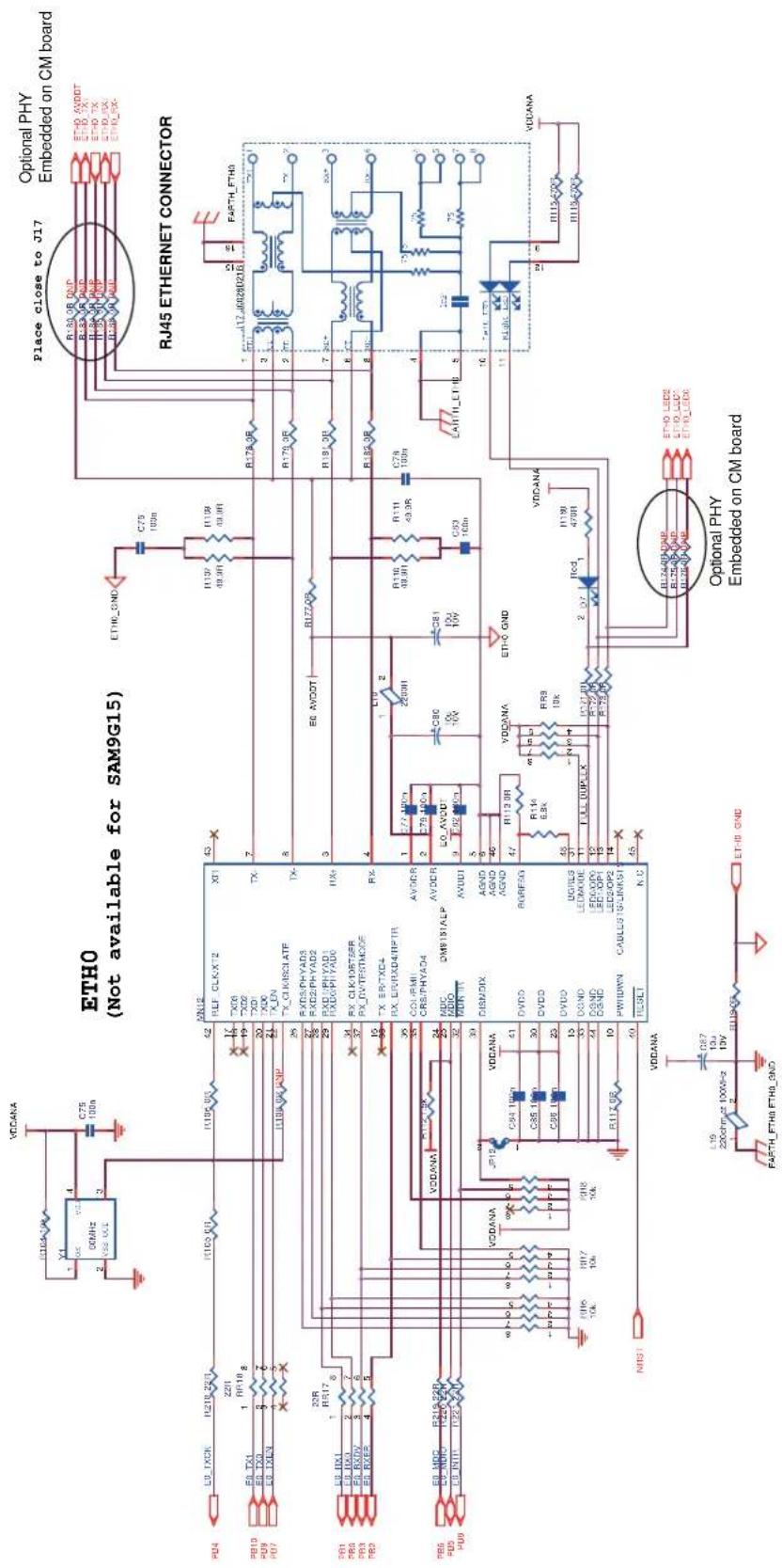
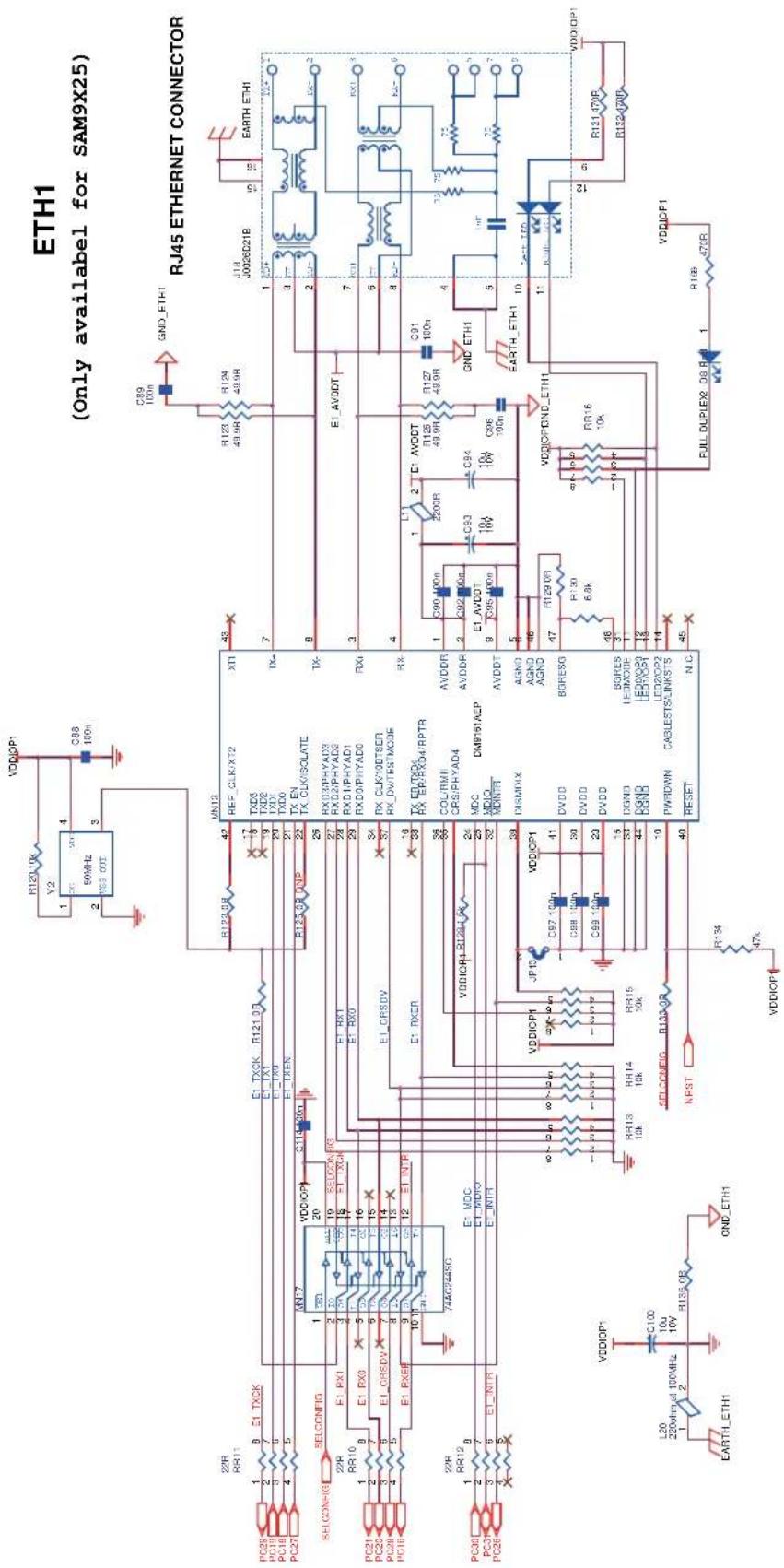
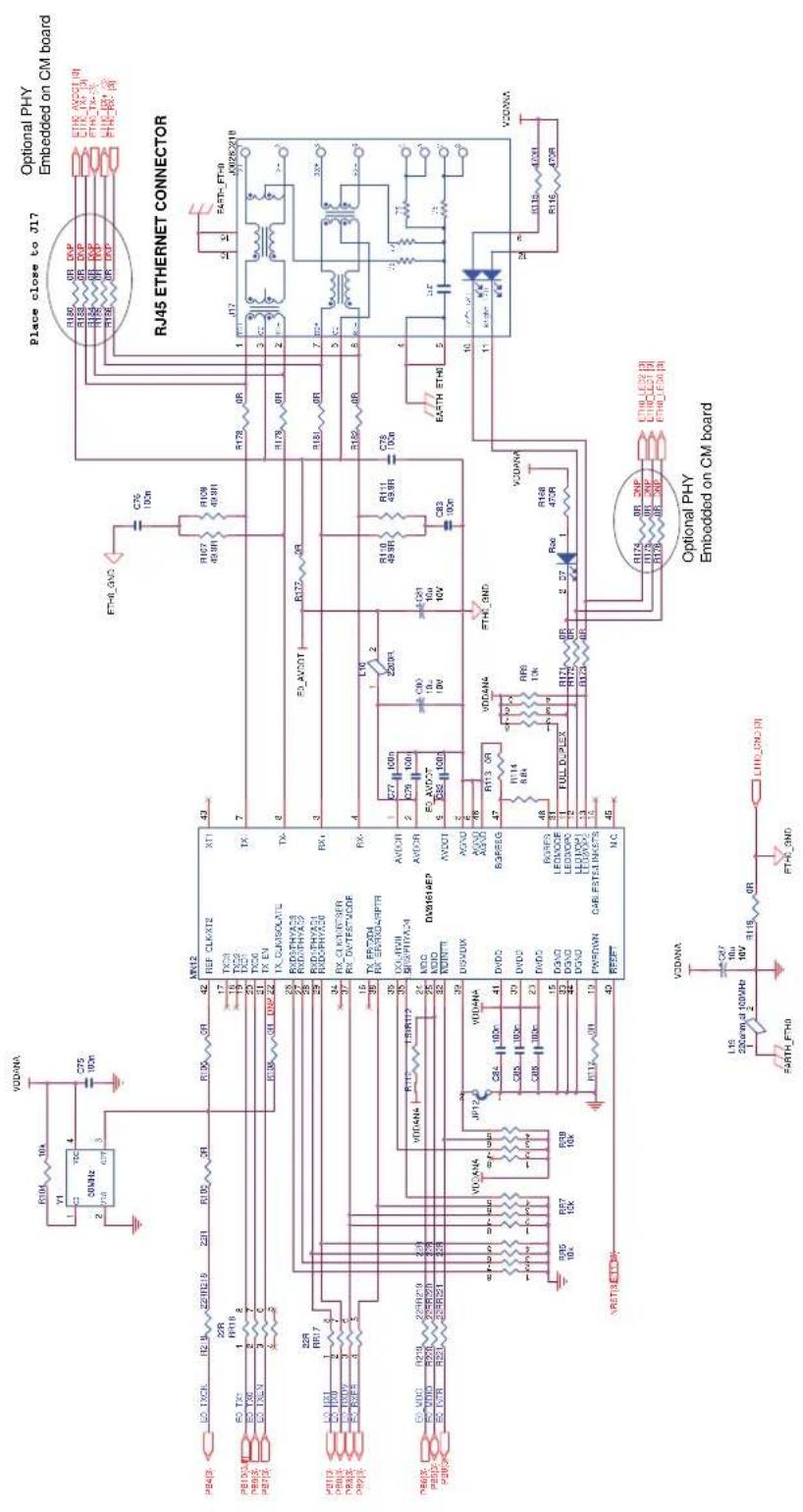
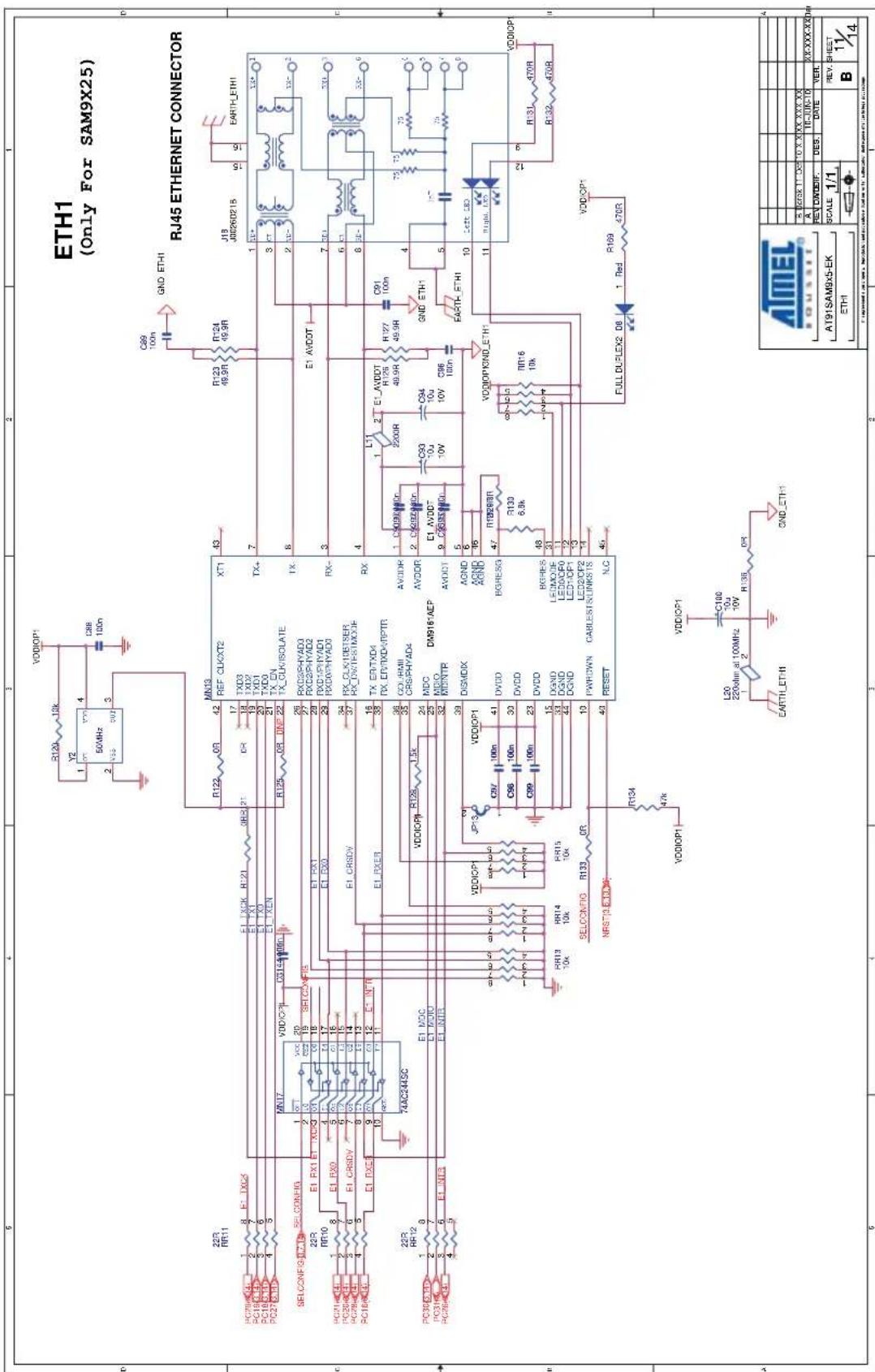
The EK board is equipped with two Davicom DM9161AEP PHYs for each Ethernet port. Both PHY Transceivers are configured as RMII mode. Both PHY transceivers have an RJ45 port with embedded transformer and three-status LEDs.
By default, the ETH0 interface is implemented on the EK board. Additionally, for monitoring and control purposes, an LED functionality is carried on the RJ45 connectors to indicate activity, link, and speed status information for the respective ports.
Figure 3-26. ETH0 Port
Ethernet 1 is only available for SAM9X25. The PHY on Ethernet 1 is enabled by the SELCONFIG signal from a pull-down resistor on the CM board. Refer to Section 3.4.1 "DM Board Overview" for detail.
Some pins (PC16, PC20, PC21, PC28, PC26 and PC29) are configured as Ethernet 1 input from PHY for SAM9X25, whereas they are configured as LCD data pins on other processors. An IO buffer MN17 is inserted in series with these signals to prevent the LCD from being disturbed by unknown status of the PHY device.
Figure 3-27. ETH1 Port
3.3.3.8 Audio
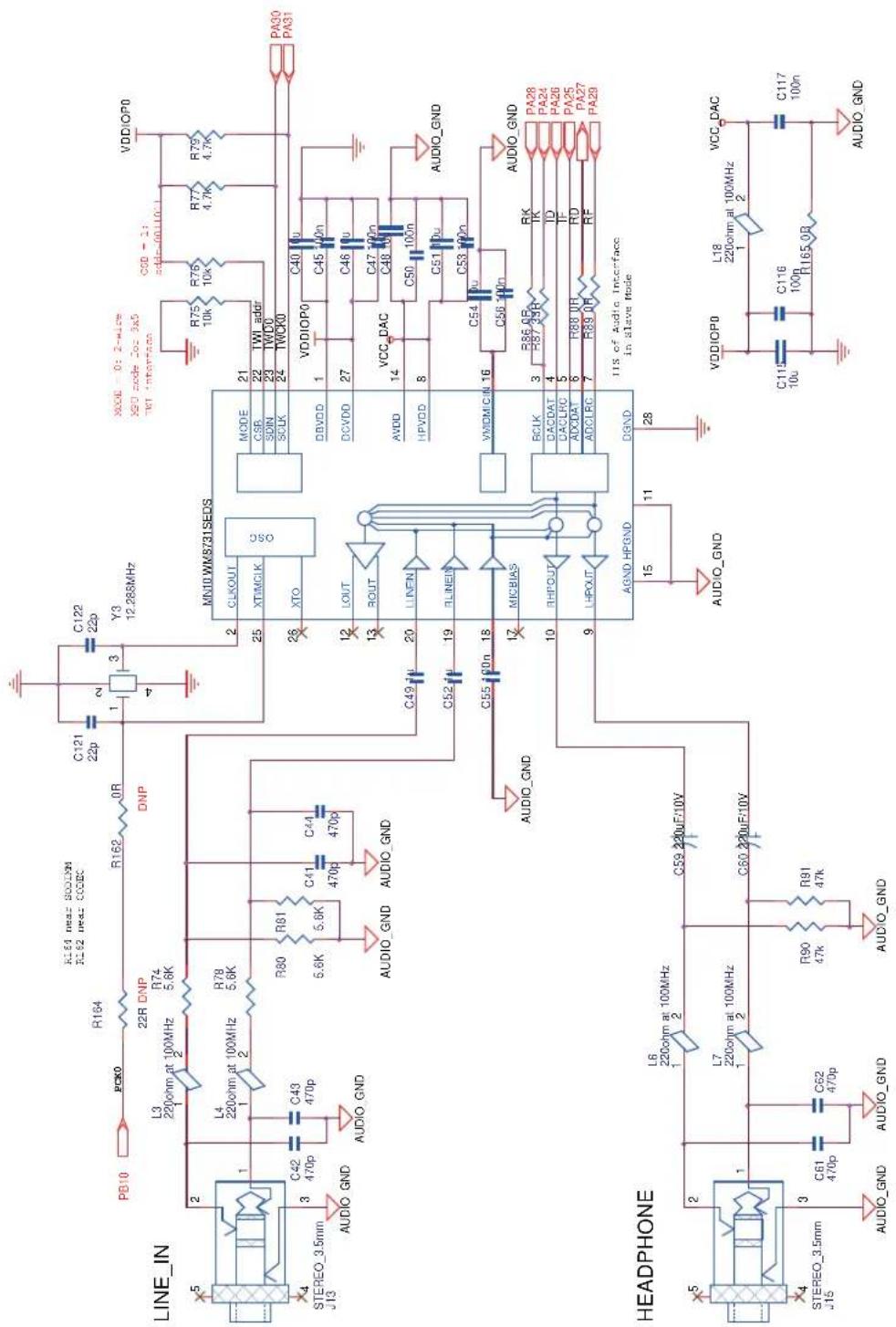
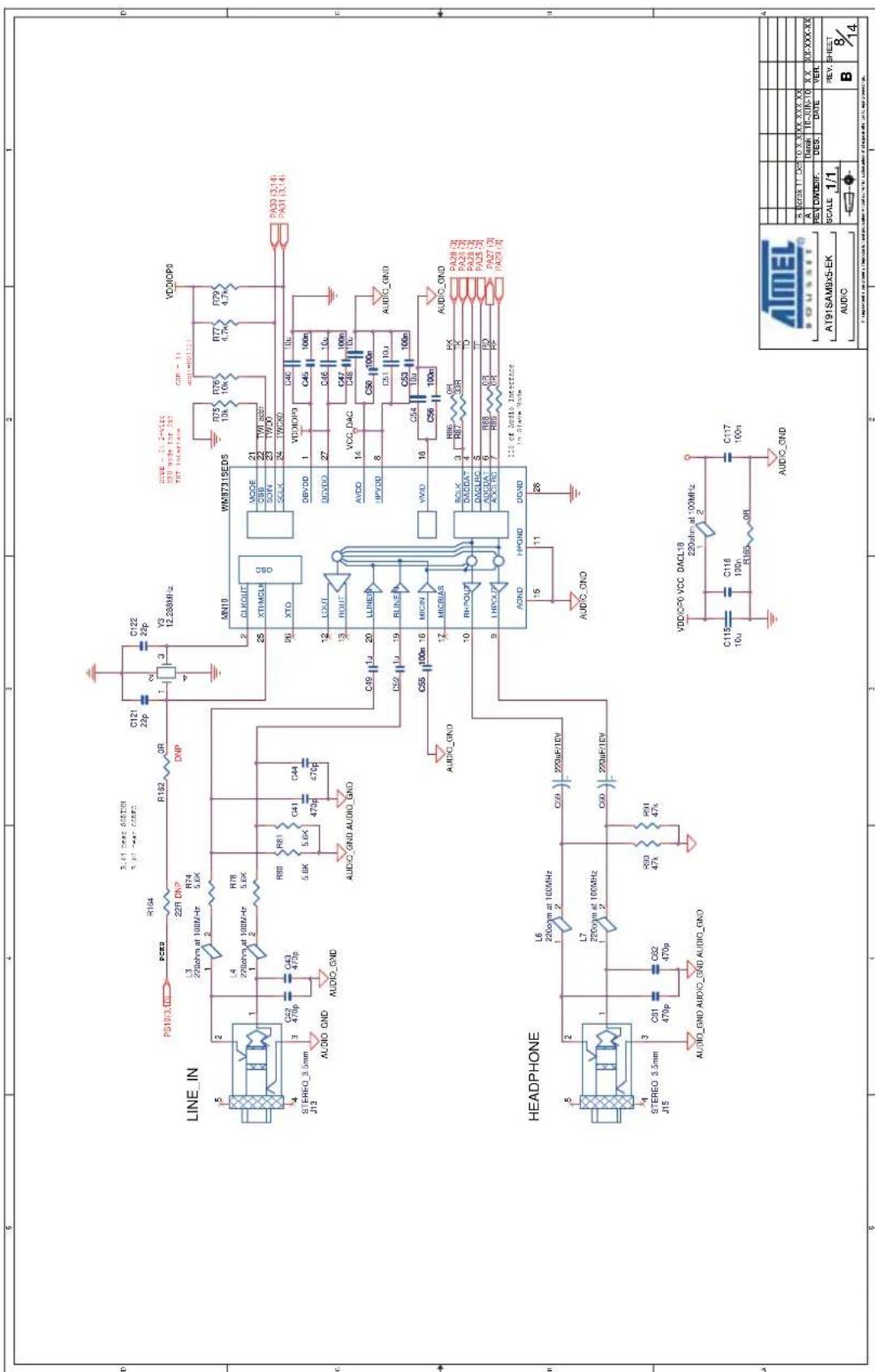
The Evaluation Kit includes a WM8731 CODEC for digital sound input and output. This interface includes audio jacks for line audio input (J13) and headphone line output (J15).
The SAM9 processor is configured in IIS slave mode to interface with the WM8731 Codec. The IIS master mode is also possible for evaluation by populating R162/R164 and removing the crystal Y3.
Figure 3-28. Audio Interface
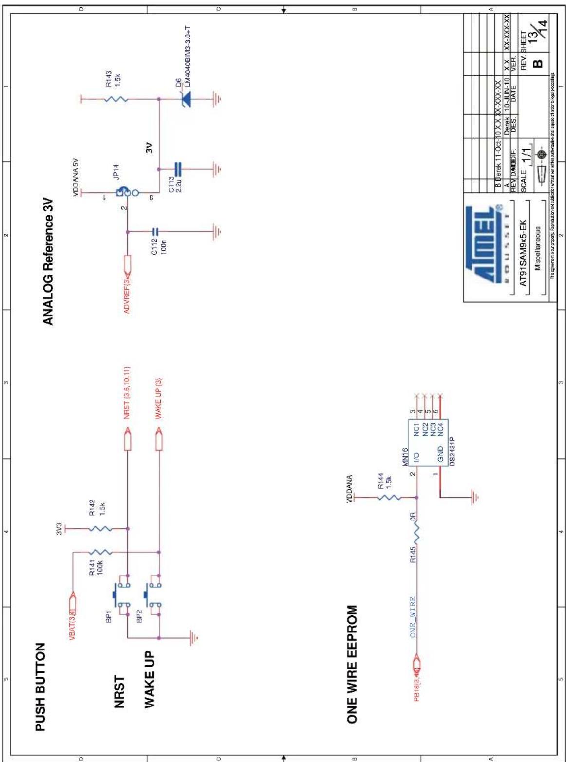
3.3.3.9 1-Wire EEPROM
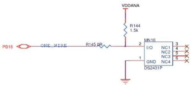
The EK board also features a 1-Wire device acting as a "firmware label" to store information like chip type, manufacturer's name, production date etc.
Figure 3-29. 1-Wire on EK
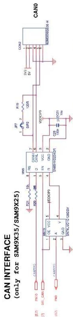
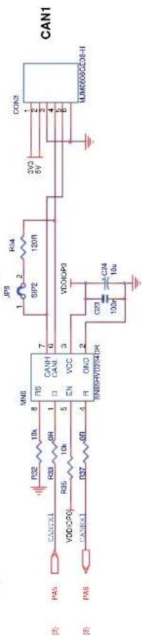
3.3.3.10 CAN Bus
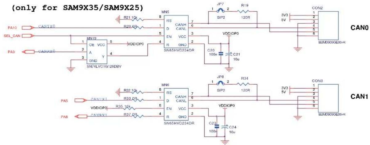
Two boards, the SAM9X35-EK and SAM9X25-EK, feature two Controller Area Network (CAN) ports with transceiver.
CAN0 uses the same IOs (PA9, PA10) as the DBGU. A jumper, JP11, is used to select either of the interfaces.
- Open JP11 to select the CAN function.
- Close JP11 to select the DBGU function.
A 3-state output buffer, MN19 is inserted in series with the output channels of the CAN transceiver, which share IOs with the DBGU. This is necessary because the CAN transceiver does not feature 3-state outputs.
Figure 3-30. CAN on EK
3.3.3.11 Telephone Interface
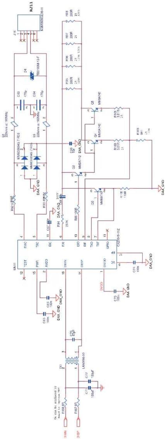
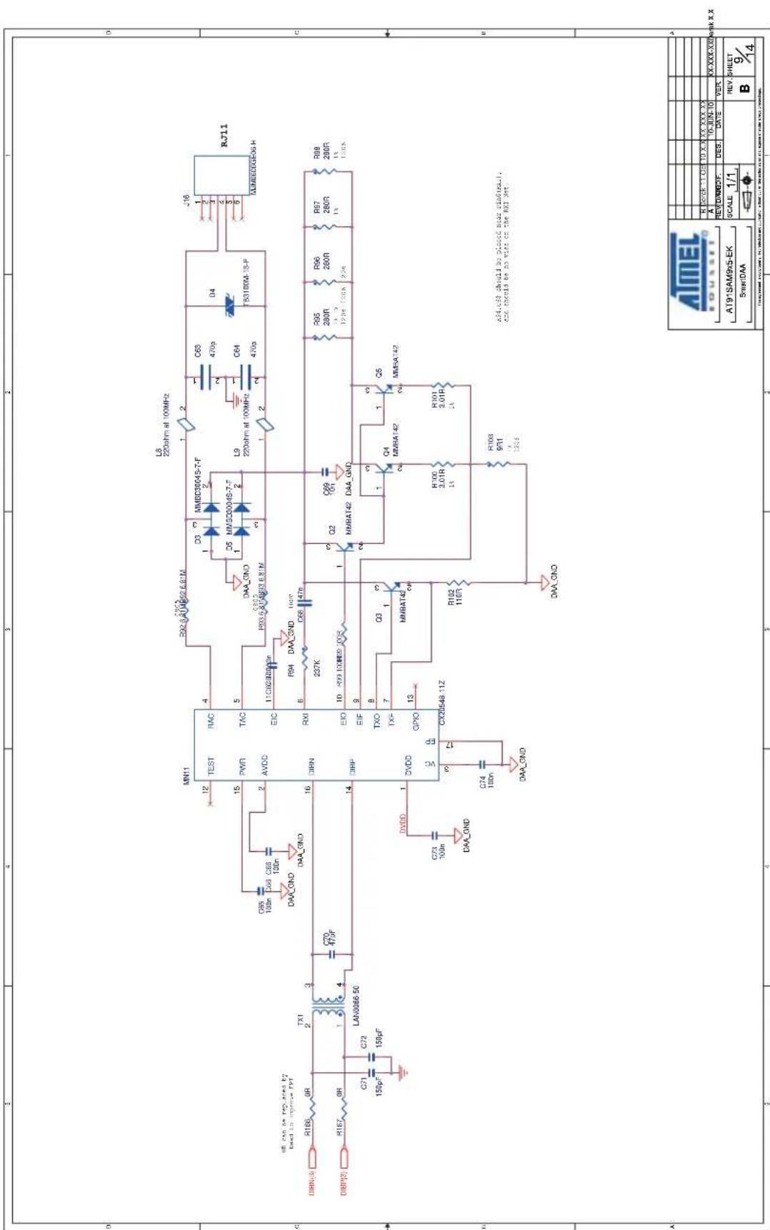
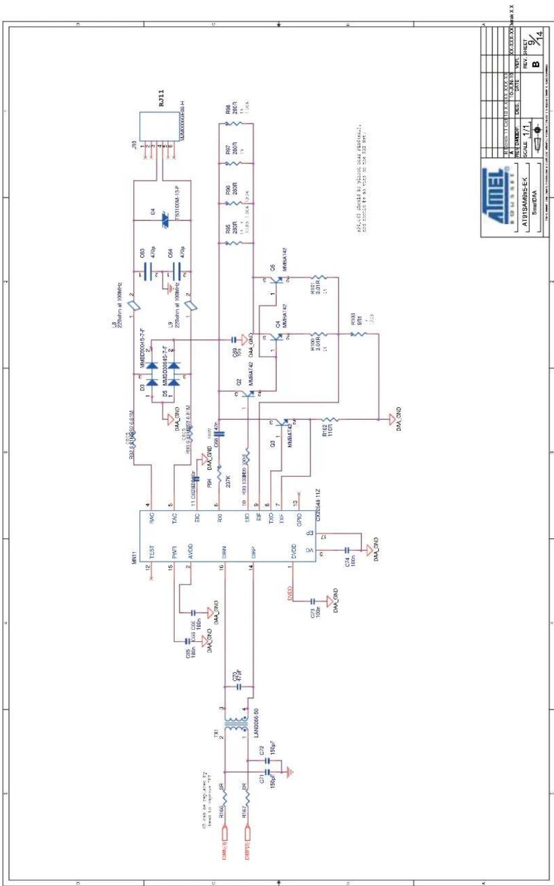
The Evaluation Kit features a smart DAA (Data Access Arrangement) chip to drive an analog telephone line on RJ11 6P4C port (J16).
Figure 3-31. Telephone Interface
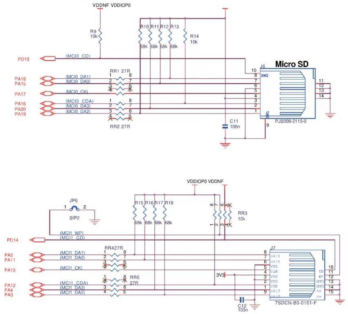
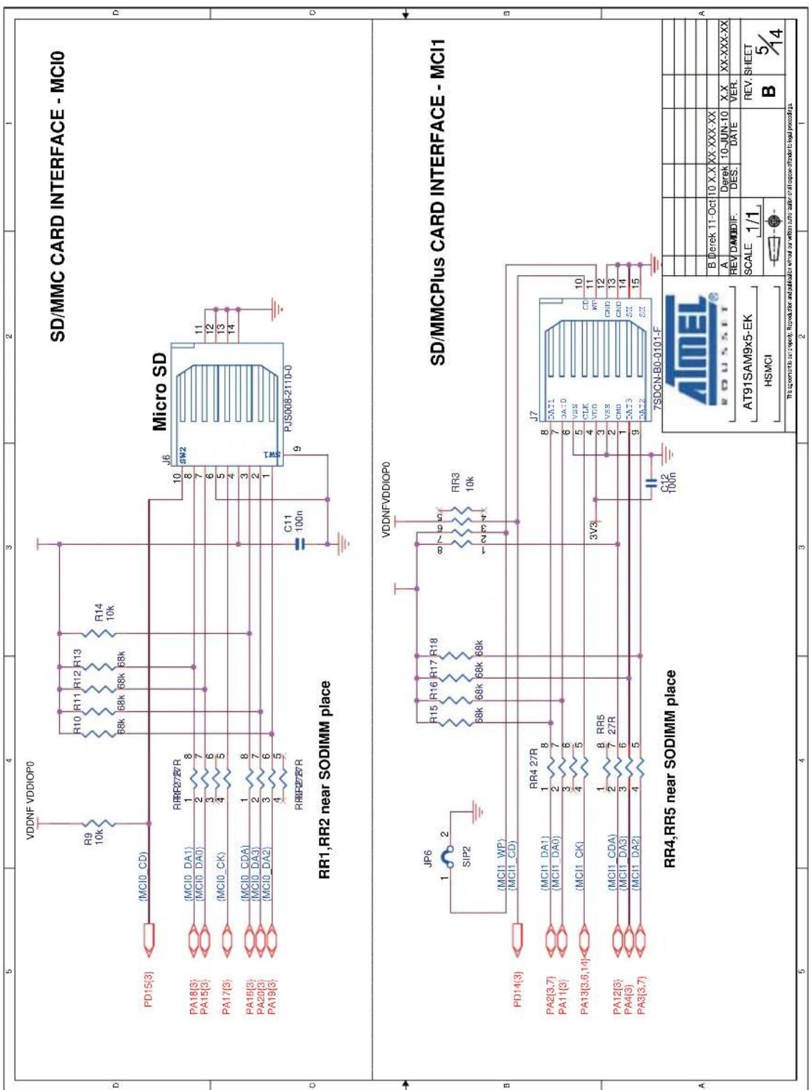
The EK board has two high-speed MultiMedia Card Interfaces (MCI). The first interface is used as a 4-bit interface (MCI0), connected to a MicroSD card slot. The second interface is used as a 4-bit interface (MCI1), connected to an SD/MMC card slot.
The memory card is not included in the Evaluation Kit.
Please note that the power is connected to VCC, which is 3.3 volts.
Figure 3-32. SD/MMC Interface
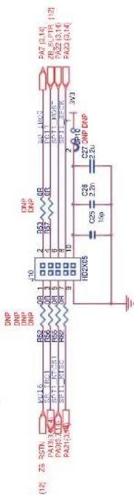
3.3.3.13 ZigBee
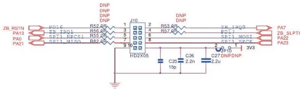
The EK board has a 10-pin male connector for the Atmel RZ600 ZigBee module.
DNP 0 Ohm resistors have been implemented in series with the PIO lines that are used elsewhere in the design. Thereby, enable their individual disconnections, should a conflict occur in user application.
Figure 3-33. ZigBee Interface
3.3.3.14 LED Indicators
The EK board has three LED indicators for purposes shown below:
Table 3-8. LED Indicators
| Reference Color Function | |
| D2 Red 3v3 Power indicator | |
| D7 Red ETH0 Full Duplex | |
| D8 Red ETH1 Full Duplex |
Refer to Section 3.3.3.2 "Power Supplies" and Section 3.3.3.7 "Ethernet 10/100 (EMAC) Port" for details.
3.3.3.15 Expansion Ports
Most GPIOs are routed to expansion ports J1, J2, J3.
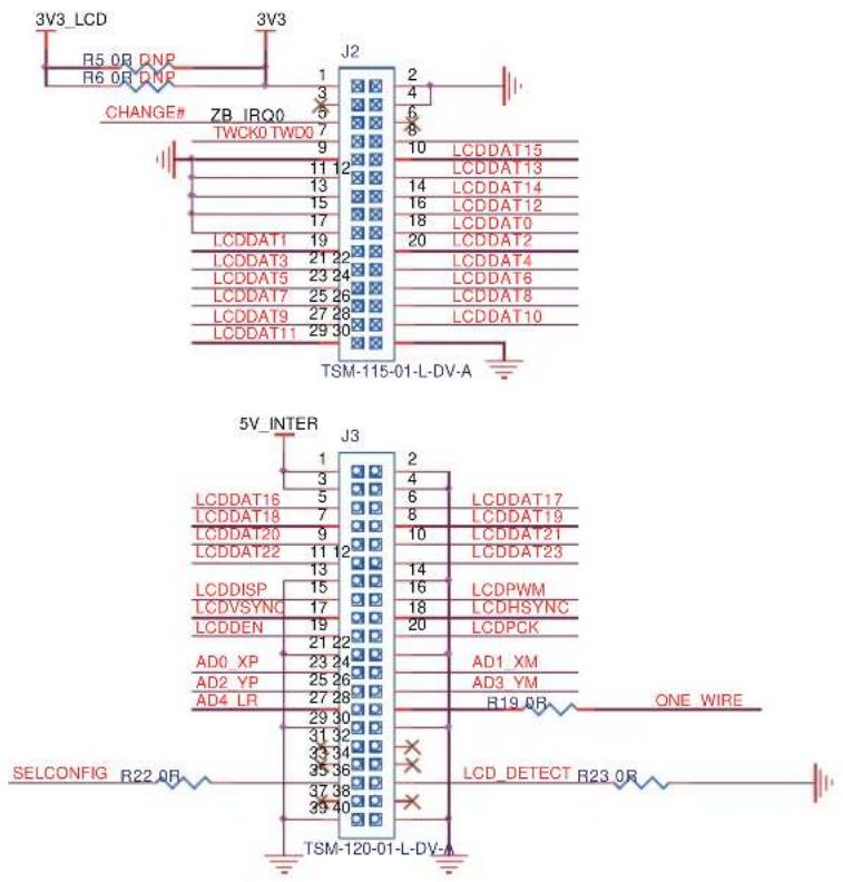
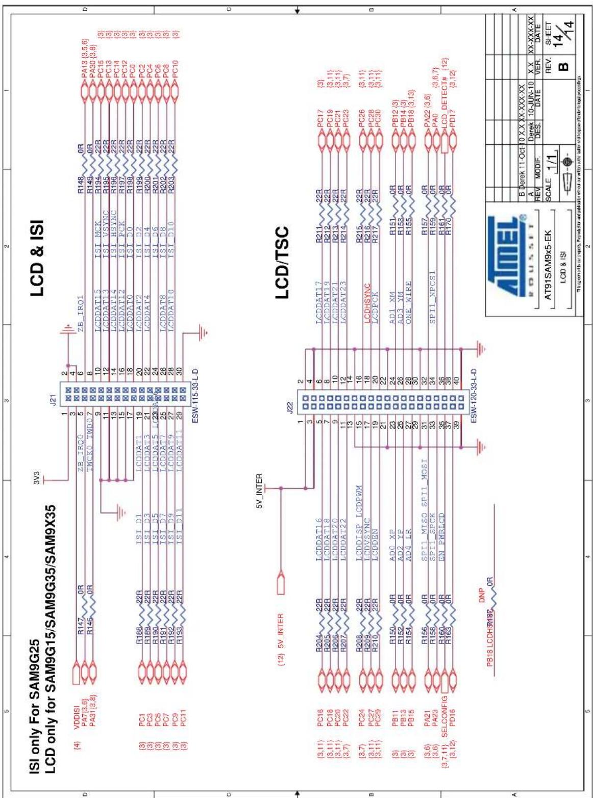
All I/Os of the MPU Image Sensor Interface (ISI) are routed to connectors J21.
The LCD and touch screen interfaces are routed to connectors J21, J22.
Figure 3-34. I/O Expansion
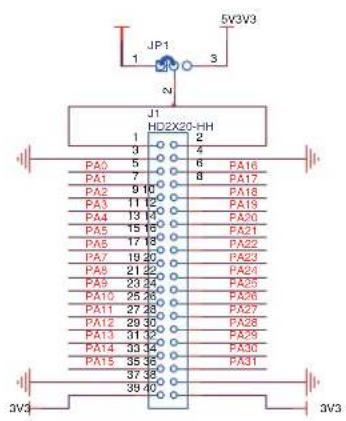
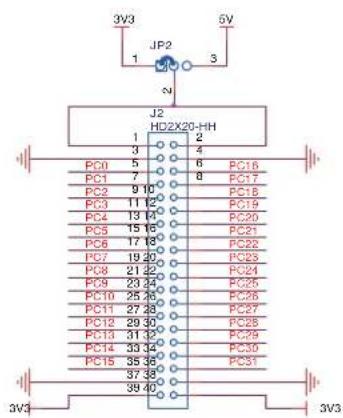
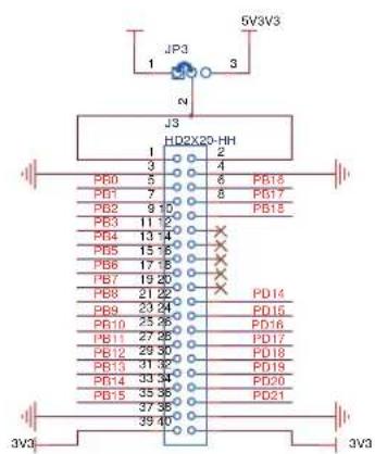
Figure 3-35. LCD and ISI Expansion
3.3.4 Configuration
This section describes the PIO usage, the jumpers, the test points and the solder drops of the EK board.
3.3.4.1 JTAG/ICE Configuration
Table 3-9. JTAG/ICE
| Designation Default Setting Feature | ||
| R50 Not Populated | Disables the ICE NTRST input | |
| R51 | Populated | Enables the ICE RTCK return. R94 must be opened |
| R54 | Populated | Enables the ICE NRST input |
| R58 Not Populated | Disables TCK <-> RTCK local loop | |
3.3.4.2 Boot Mode Select Configuration
Table 3-10. BMS
| Designation Default Setting | Feature | |
| JP9 | Open | Default to boot on embedded ROMClose to boot on external memory |
3.3.4.3 Force Power ON Configuration
Table 3-11. Force Power ON
| Designation Default Setting Feature | ||
| JP5 Close | Keep on-board regulator always on Open to feature SHDN function | |
3.3.4.4 White Protection Configuration on MCI1
Table 3-12. Write Protection on MCI1
| Designation Default Setting Feature | ||
| JP6 Close | MCI1 write protect selectedOpen to disable protection | |
3.3.4.5 Selection between DBGU and CAN
Table 3-13. Select DBGU or CAN
| Designation Default Setting Feature | ||
| JP11 Close | Default to select DBGUOpen to select CAN0 | |
3.3.4.6 Codec IIS Configuration
Table 3-14. Codec IIS
| Designation Default Setting Feature | ||
| R162, R164 Not Populated | IIS master mode, clock the codec by PCK0 | |
| C121, C122, Y3 Populated | IIS slaver mode, clock the codec by external crystal | |
3.3.4.7 ETH0 Configuration
Table 3-15. ETH0
| Designation Default Setting Feature | ||
| R180, R183, R184,R185, R185, R186,R174, R175, R176 | Not Populated | Populated to select the PHY channel on CM. Channel on EK must be cut if select the PHY on CM. |
| R177, R178, R179,R181, R182, R218,R171, R172, R173 | Populated Selection of PHY channel on EK | |
3.3.4.8 PIO Usage
Table 3-16. PIO A Pin Assignment and Signal Description
| Signal Alternate Periph A Periph B Periph C Module CM EK | ||||||
| PA0 - TXD0 SPI1_NPCS1 - TXD0/ ZigBee USART0 shared with ZigBee | ||||||
| PA1 - RXD0 | SPI0_NPCS2 - | RXD0 | USART0 | |||
| PA2 | - | RTS0 | MCI1_DA1 | E0_ETX0 | RTS0/ MCI1 | USART0 shared with MCI1 |
| PA3 | - | CTS0 | MCI1_DA2 | E0_ETX1 | CTS0/ MCI1 | USART0 shared with MCI1 |
| PA4 | - | SCK0 | MCI1_DA3 | E0_ETXER | MCI1 | - |
| PA5 - TXD1 | CANTX1 - | CAN1 | - | |||
| PA6 | - | RXD1 | CANRX1 | - | CAN1 | - |
| PA7 - TXD2 SPI0_NPCS1 - | - | ZB_IRQ0 | ||||
| PA8 - RXD2 | SPI1_NPCS0 - | - | Serial Flash | |||
| PA9 | - | - | CANRX0 | - | DBGU+CAN0 | DBGU shared with CAN0 |
| PA10 | - | - | CANTX0 | - | DBGU+CAN0 | DBGU shared with CAN0 |
| PA11 | - | SPI0_MISO | MCI1_DA0 | - | MCI1 | - |
| PA12 | - | SPI0_MOSI | MCI1_CDA | - | MCI1 | - |
| PA13 | - | SPI0_SPCK | MCI1_CK | - | MCI1 | ZB_IRQ1 |
| PA14 | - | SPI0_NPCS0 | - | - | - | MCI0 |
| PA15 | - | MCI0_DA0 | - | - | - | MCI0 |
| PA16 | - | MCI0_CDA | - | - | - | MCI0 |
| PA17 | - | MCI0_CK | - | - | - | MCI0 |
| PA18 | - | MCI0_DA1 | - | - | - | MCI0 |
| PA19 | - | MCI0_DA2 | - | - | - | MCI0 |
| PA20 | - | MCI0_DA3 | - | - | - | Serial Flash |
| PA21 | - | TIOA0 | SPI1_MISO | - | ZigBee | Serial Flash |
| PA22 | - | TIOA1 | SPI1_MOSI | - | ZigBee | Serial Flash |
| PA23 | - | TIOA2 | SPI1_SPCK | - | ZigBee | SSC |
| PA24 | - | TCLK0 | TK | - | - | SSC |
| PA25 | - | TCLK1 | TF | - | - | SSC |
| PA26 | - | TCLK2 | TD | - | - | SSC |
| PA27 | - | TIOB0 | RD | - | - | SSC |
| PA28 | - | TIOB1 | RK | - | - | SSC |
| PA29 | - | TIOB2 | RF | - | - | SSC |
| PA30 | - | TWD0 | SPI1_NPCS3 | E0_EMDC | - | TWD0 |
| PA31 | - | TWCK0 | SPI1_NPCS2 | E0_ETXEN | - | TWCK0 |
Table 3-17. PIO B Pin Assignment and Signal Description
| Signal Alternate Periph A Periph B Periph C Module CM EK | ||||||
| PB0 – E0_RX0 RTS2 – ETH0 – | ||||||
| PB1 – E0_RX1 CTS2 – ETH0 – | ||||||
| PB2 – E0_RXER SCK2 – ETH0 – | ||||||
| PB3 – E0_RXDV | SPI0_NPCS3 | – ETH0 – | ||||
| PB4 – | E0_TXCK | TWD2 | – ETH0 – | |||
| PB5 – | E0_MDIO | TWCK2 | – ETH0 – | |||
| PB6 | AD7 E0_MDC | – – ETH0 – | ||||
| PB7 | AD8 | E0_TXEN | – | – | ETH0 | – |
| PB8 | AD9 | E0_TXER | – | – | ETH0_INTR | – |
| PB9 | AD10 | E0_TX0 | PCK1 – ETH0 – | |||
| PB10 | AD11 | E0_TX1 | PCK0 – ETH0 – | |||
| PB11 | AD0xp | E0_TX2 | PWM0 | – | – | TSC |
| PB12 | AD1xm | E0_TX3 | PWM1 | – | – | TSC |
| PB13 | AD2yp | E0_RX2 | PWM2 | – | – | TSC |
| PB14 | AD3ym | E0_RX3 | PWM3 | – | – | TSC |
| PB15 | AD4lr | E0_RXCK | – | – | – | TSC |
| PB16 | AD5 | E0_CRS | – | – | – | VBUS_SENSE (USB) |
| PB17 | AD6 | E0_COL | – | – | – | OVCUR_USB (Open drain) |
| PB18 | IRQ | ADTRG | – | USER_LED1# | ONE_WIRE | |
Table 3-18. PIO C Pin Assignment and Signal Description
| Signal Alternate Periph A Periph B Periph C Module CM EK f (LCD) EK f (ISI+IO) | |||||||
| PC0 - LCDDAT0 ISI_D0 TWD1 - LCDDAT0 ISI_D0 | |||||||
| PC1 - LCDDAT1 ISI_D1 TWCK1 - LCDDAT1 ISI_D1 | |||||||
| PC2 - LCDDAT2 ISI_D2 TIOA3 - LCDDAT2 ISI_D2 | |||||||
| PC3 - LCDDAT3 ISI_D3 TIOB3 - LCDDAT3 ISI_D3 | |||||||
| PC4 - LCDDAT4 ISI_D4 TCLK3 - LCDDAT4 ISI_D4 | |||||||
| PC5 - LCDDAT5 ISI_D5 TIOA4 - LCDDAT5 ISI_D5 | |||||||
| PC6 - LCDDAT6 ISI_D6 TIOB4 - LCDDAT6 ISI_D6 | |||||||
| PC7 - LCDDAT7 ISI_D7 TCLK4 - LCDDAT7 ISI_D7 | |||||||
| PC8 - LCDDAT8 ISI_D8 UTXD0 - LCDDAT8 ISI_D8 | |||||||
| PC9 - LCDDAT9 ISI_D9 URXD0 - LCDDAT9 ISI_D9 | |||||||
| PC10 | - | LCDDAT10 | ISI_D10 | PWM0 | - | LCDDAT10 | ISI_D10 |
| PC11 | - | LCDDAT11 | ISI_D11 | PWM1 | - | LCDDAT11 | ISI_D11 |
| PC12 | - | LCDDAT12 | ISI_PCK | TIOA5 | - | LCDDAT12 | ISI_PCK |
| PC13 | - | LCDDAT13 | ISI_VSYNC | TIOB5 | - | LCDDAT13 | ISI_VSYNC |
| PC14 | - | LCDDAT14 | ISI_HSYNC | TCLK5 | - | LCDDAT14 | ISI_HSYNC |
| PC15 | - | LCDDAT15 | ISI_MCK | PCK0 | SSC | LCDDAT15 | ISI_MCK/PCK0 |
| PC16 | - | LCDDAT16 | E1_RXER | UTXD1 | - | LCDDAT16 | E1_RXER |
| PC17 | - | LCDDAT17 | - | URXD1 | - | LCDDAT17 | - |
| PC18 | - | LCDDAT18 | E1_TX0 | PWM0 | - | LCDDAT18 | E1_TX0 |
| PC19 | - | LCDDAT19 | E1_TX1 | PWM1 | - | LCDDAT19 | E1_TX1 |
| PC20 | - | LCDDAT20 | E1_RX0 | PWM2 | - | LCDDAT20 | E1_RX0 |
| PC21 | - | LCDDAT21 | E1_RX1 | PWM3 | - | LCDDAT21 | E1_RX1 |
| PC22 | - | LCDDAT22 | TXD3 | - | - | LCDDAT22 | TXD3 |
| PC23 | - | LCDDAT23 | RXD3 | - | - | LCDDAT23 | RXD3 |
| PC24 | - | LCDDISP | RTS3 | - | - | LCDDISP | RTS3 |
| PC25 | - | - | CTS3 | - | - | - | CTS3 |
| PC26 | - | LCDPWM | SCK3 | - | Eth1_Intr1 | LCDPWM | - |
| PC27 | - | LCDVSYNC | E1_TXEN | RTS1 | - | LCDVSYNC | E1_TXEN |
| PC28 | - | LCDHSYNC | E1_CRSDV | CTS1 | - | LCDHSYNC | E1_CRSDV |
| PC29 | - | LCDDEN | E1_TXCK | SCK1 | - | LCDDEN | E1_TXCK |
| PC30 | - | LCDPCK | E1_MDC | - | - | LCDPCK | E1_MDC |
| PC31 | - | FIQ | E1_MDIO | PCK1 | - | - | E1_MDIO |
Table 3-19. PIO D Pin Assignment and Signal Description
| Signal Alternate Periph A Periph B Periph C Module CM EK | ||||||
| PD0 – N | ANDOE – – | Nand Flash – | ||||
| PD1 – N | ANDWE | – – Nand | Flash – | |||
| PD2 – | A21/N | ANDALE | – – Nand Flash – | |||
| PD3 – | A22/N | ANDCLE | – – Nand Flash – | |||
| PD4 | – | NCS3 | – | – | CS NAND Flash | – |
| PD5 | – | NWAIT | – | – | NAND_RD/BY | – |
| PD6 – | D16 | – – Nand Flash – | ||||
| PD7 – | D17 | – – Nand Flash – | ||||
| PD8 – | D18 | – – Nand Flash – | ||||
| PD9 – | D19 | – – Nand Flash – | ||||
| PD10 | – | D20 | – | – | Nand Flash | MCI0_CD (switch) |
| PD11 | – | D21 | – | – | Nand Flash | MCI1_CD (switch) |
| PD12 | – | D22 | – | – | Nand Flash | ZB_RSTN |
| PD13 | – | D23 | – | – | Nand Flash | ZB_SLPTR |
| PD14 | – | D24 | – | – | – | EN5V_HDA# |
| PD15 | – | D25 | A20 | – | – | EN5V_HDB# |
| PD16 | – | D26 | A23 | – | – | EN5V_HDC# |
| PD17 | – | D27 | A24 | – | – | – |
| PD18 | – | D28 | A25 | – | – | – |
| PD19 | – | D29 | NCS2 | – | – | – |
| PD20 | – | D30 | NCS4 | – | – | – |
| PD21 | – | D31 | NCS5 | – | POWR_LED | – |
3.3.5 Connectors
3.3.5.1 Power Supply
Figure 3-36. Power Supply Connector J4
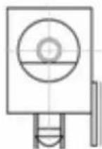
Table 3-20. Power Supply Connector J2 Signal Description
| Pin Mnemonic Signal description | ||
| 1 Center +5V | ||
| 2 - | G | N |
| 3 - Floating | ||
D
3.3.5.2 SODIMM Card Edge Socket
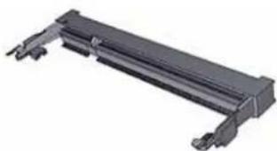
The Evaluation Kit uses a SODIMM200 standard connector for CM board interfacing.
Please note that this is not an industry standard pin-out and that it is unlikely to be compatible with off-the-shelf SODIMM cards.
Figure 3-37. SODIMM200 Socket CON1
natural_image
Mechanical component with flanged ends and a central rod (no visible text or symbols)Table 3-21. SODIMM200 CON1 Signal Descriptions
| Function | Type | x5 pad name | SODIMM 200 | x5 pad name | Type | Function | ||
| Front Side | A | - | B | Back Side | ||||
| VCC 3V3 | - | POWER OUTPUT | 1 | - | 2 | POWER OUTPUT | - | VCC 3V3 |
| VCC 3V3 | - | POWER OUTPUT | 3 | - | 4 | POWER OUTPUT | - | VCC 3V3 |
| GND | - | - | 5 | - | 6 | POWER OUTPUT | VBAT | - |
| USBC_DP | I/O | USB Data Positive | 7 | - | 8 | - | SYSC | JTAGSEL |
| USBC_DM | I/O | USB Data Negative | 9 | - | 10 | - | SYSC | WKUP |
| GND | - | - | 11 | - | 12 | - | SYSC | SHDN |
| USBB_DM | I/O | USB Data Negative | 13 | - | 14 | - | SYSC | BMS |
| USBB_DP | I/O | USB Data Positive | 15 | - | 16 | - | SYSC | nRST |
| GND--17 | -18-SYSC nTRST | |||||||
| DIBP I/O- | 19-20-RSTJTAG TDI | |||||||
| DIBN I/O- | 21-22-RSTJTAG TCK | |||||||
| GND--23 | -24-RSTJTAG TMS | |||||||
| USBA_DM I/O | USB Data Negative 25-26-RSTJTAG TDO | |||||||
| USBA_DP | I/O USB Data Positive | 27 | - | 28 | - | RSTJTAG | RTCK | |
| GND--29 | -30- | - | PWR_EN | |||||
| RFU | - | RFU | 31 | - | 32 | RFU | - | RFU |
| RFU | - | RFU | 33 | - | 34 | RFU | - | RFU |
| RFU | - | RFU | 35 | - | 36 | RFU | - | RFU |
| RFU | - | RFU | 37 | - | 38 | RFU | - | RFU |
| RFU | - | RFU | 39 | - | 40 | RFU | - | RFU |
| KEY | ||||||||
| GND--41 | -42- | - | GND | |||||
| RFU | - | RFU | 43 | - | 44 | RFU | - | RFU |
| RFU | - | RFU | 45 | - | 46 | RFU | - | RFU |
| RFU | - | RFU | 47 | - | 48 | RFU | - | RFU |
| RFU | - | RFU | 49 | - | 50 | RFU | - | RFU |
| GND--51 | -52- | - | GND | |||||
| RFU | - | RFU | 53 | - | 54 | RFU | - | RFU |
| RFU | - | RFU | 55 | - | 56 | RFU | - | RFU |
| RFU | - | RFU | 57 | - | 58 | RFU | - | RFU |
| RFU | - | RFU | 59 | - | 60 | RFU | - | RFU |
| VDDNF | POWER DOMAIN FROM CM | 61 | - | 62 | POWER DOMAIN FROM CM | VDDNF | ||
| PD0 | GPIO D | NANDOE | 63 | - | 64 | NANDWE | GPIO D | PD1 |
| PD2 | GPIO D | A21/NANDALE | 65 | - | 66 | A22/NANDCLE | GPIO D | PD3 |
| PD4 | GPIO D | NCS3 | 67 | - | 68 | NWAIT | GPIO D | PD5 |
| PD6 | GPIO D | D16 | 69 | - | 70 | D17 | GPIO D | PD7 |
| PD8 | GPIO D | D18 | 71 | - | 72 | D19 | GPIO D | PD9 |
| GND--73 | -74- | - | GND | |||||
| PD10 | GPIO D | D20 | 75 | - | 76 | D21 | GPIO D | PD11 |
| PD12 | GPIO D | D22 | 77 | - | 78 | D23 | GPIO D | PD13 |
| PD14 | GPIO D | D24 | 79 | - | 80 | D25/A20 | GPIO D | PD15 |
| PD16 | GPIO D | D26/A23 | 81 | - | 82 | D27/A24 | GPIO D | PD17 |
| PD18 | GPIO D | D28/A25 | 83 | - | 84 | D29/NCS2 | GPIO D | PD19 |
| PD20 | GPIO D | D30/NCS4 | 85 | - | 86 | D31/NCS5 | GPIO D | PD21 |
| VDDIOP0 | POWER OUTPUT | 87 | - | 88 | POWER OUTPUT | VDDIOP0 | ||
| PA0 GPIO | A TXD0/SPI1-NPCS1 89 - 90 RXD0/SPI0-NPCS2 GPIO A PA1 | |||||||
| PA2 GPIO | A MCI1_DA1/E0_ETX0 91 - 92 | CTS0/MCI1_DA2/E0_ETX1 | GPIO A PA3 | |||||
| PA4 GPIO | A | SCK0/MCI1_DA3/E0_ETXER | 93 - 94 -- GND | |||||
| PA11 GPIO | A | SPI0_MISO/MCI1_DA0 | 95 - 96 | SPI0_MOSI/MCI1_CDA | GPIO A PA12 | |||
| PA13 GPIO | A | SPI0_SPCK/MCI1_CK | 97 - 98 | SPI0_NPCSO GPIO A PA14 | ||||
| GND | - | - | 99 | - | 100 | TXD2/SPI0_NPCS1 | GPIO A PA7 | |
| PA8 | GPIO A | RXD2/SPI1_NPCS0 | 101 | - | 102 | TIOA0 /SPI1_MISO | GPIO A | PA21 |
| PA22 | GPIO A | TIOA1/SPI1_MOS1 | 103 | - | 104 | TIOA2/SPI1_SPCK | GPIO A PA23 | |
| PA31 GPIO | A | TWCK0/SPI1_NPCS2/E0_ETXEN | 105 | - | 106 | TWD0/SPI1_NPCS3/E0_EMDC | GPIO A PA30 | |
| GND | - | - | 107 | - | 108 | MCI0_DA0 | GPIO A | PA15 |
| PA16 | GPIO A | MCI0_CDA | 109 | - | 110 | MCI0_CK | GPIO A | PA17 |
| PA18 | GPIO A | MCI0_DA1 | 111 | - | 112 | MCI0_DA2 | GPIO A | PA19 |
| PA20 | GPIO A | MCI0_DA3 | 113 | - | 114 | - | - | GND |
| PA5 | GPIO A | TXD1/CANTX1 | 115 | - | 116 | RXD1/CANRX1 | GPIO A | PA6 |
| PA10 | GPIO A | DTXD/CANTX0 | 117 | - | 118 | DRXD/CANRX0 | GPIO A | PA9 |
| GND | - | - | 119 | - | 120 | TCLK0/TK | GPIO A | PA24 |
| PA25 | GPIO A | TCLK1/TF | 121 | - | 122 | TCLK2/TD | GPIO A | PA26 |
| PA27 | GPIO A | TIOB0/RD | 123 | - | 124 | TIOB1/RK | GPIO A | PA28 |
| PA29 | GPIO A | TIOB2/RF | 125 | - | 126 | - | - | GND |
| VDDIOP1 | POWER OUTPUT | 127 | - | 128 | POWER OUTPUT | VDDIOP1 | ||
| PC0 | GPIO C | LCDDAT0/ISI_D0 | 129 | - | 130 | LCDDAT1 | GPIO C | PC1 |
| PC2 | GPIO C | LCDDAT2/ISI_D2 | 131 | - | 132 | LCDDAT3 | GPIO C | PC3 |
| PC4 | GPIO C | LCDDAT4 | 133 | - | 134 | LCDDAT5 | GPIO C | PC5 |
| GND | - | - | 135 | - | 136 | LCDDAT6 | GPIO C | PC6 |
| PC7 | GPIO C | LCDDAT7 | 137 | - | 138 | LCDDAT8 | GPIO C | PC8 |
| PC9 | GPIO C | LCDDAT9 | 139 | - | 140 | LCDDAT10 | GPIO C | PC10 |
| PC11 | GPIO C | LCDDAT11 | 141 | - | 142 | - | - | GND |
| PC12 | GPIO C | LCDDAT12 | 143 | - | 144 | LCDDAT13 | GPIO C | PC13 |
| PC14 | GPIO C | LCDDAT14 | 145 | - | 146 | LCDDAT15 | GPIO C | PC15 |
| GND | - | - | 147 | - | 148 | LCDDAT16 | GPIO C | PC16 |
| PC17 | GPIO C | LCDDAT17 | 149 | - | 150 | LCDDAT18 | GPIO C | PC18 |
| PC19PC21 GPIO | GPIO CC LCDDAT | LCDDAT1921 153 – 154 – GND | 151 | - | 152 | LCDDAT20 | GPIO C | PC20 |
| PC22 GPIO | C LCDDAT | 22 155 – 156 LCDDAT | 23 GPIO | C PC23 | ||||
| PC24 GPIO | C LCDDISP | 157 – 158 – GPIO C | PC25 | |||||
| PC26 | GPIO C | LCDPWM | 159 | - | 160 | LCDVSYNC | GPIO C | PC27 |
| GND | - | - | 161 | - | 162 | LCDHSYNC | GPIO C | PC28 |
| PC29 GPIO | C LCDDEN | 163 – 164 | E1_MDC | GPIO C | PC30 | |||
| PC31 GPIO | C E1_MDIO | 165 – 166 – - | SELCONFIG | |||||
| VDDANA | POWER OUTPUT | 167 | - | 168 | POWER OUTPUT | VDDANA | ||
| PB0 | GPIO B | E0_RX0 | 169 | - | 170 | E0_RX1 | GPIO B | PB1 |
| PB2 | GPIO B | E0_RXER | 171 | - | 172 | E0_RXDV | GPIO B | PB3 |
| PB4 | GPIO B | E0_TXCK | 173 | - | 174 | E0_MDIO | GPIO B | PB5 |
| PB6 | GPIO B | E0_MDC | 175 | - | 176 | E0_TXEN | GPIO B | PB7 |
| PB8 | GPIO B | E0_TXER | 177 | - | 178 | GNDANA | - | - |
| PB9 | GPIO B | E0_TX0 | 179 | - | 180 | E0_TX1 | GPIO B | PB10 |
| PB11 | GPIO B | E0_TX2 | 181 | - | 182 | E0_TX3 | GPIO B | PB12 |
| PB13 | GPIO B | E0_RX2 | 183 | - | 184 | E0_RX3 | GPIO B | PB14 |
| PB15 | GPIO B | E0_RXCK | 185 | - | 186 | E0_CRS | GPIO B | PB16 |
| PB17 | GPIO B | E0_COL | 187 | - | 188 | GNDANA | - | - |
| PB18 | GPIO B | IRQ | 189 | - | 190 | POWER OUTPUT | POWR_REF | |
| GND | - | - | 191 | - | 192 | - | ETH | LED0 |
| ETH0_TX+ | ETH | - | 193 | - | 194 | - | ETH | LED1 |
| ETH0_TX- | ETH | - | 195 | - | 196 | - | ETH | LED2 |
| ETH0_RX+ | ETH | - | 197 | - | 198 | - | ETH | AVDDT |
| ETH0_RX- | ETH | - | 199 | - | 200 | - | - | GND_ETH |
3.3.5.3 JTAG/ICE Connector
Figure 3-38. JTAG J9
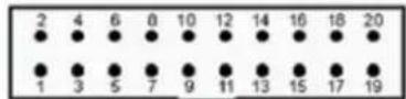
Table 3-22. JTAG/ICE Connector J13 Signal Descriptions
| Pin Mnemonic Description | ||
| 1 VTref. 3.3V power | This is the target reference voltage. It is used to check if the target has power, to create the logic-level reference for the input comparators, and to control the output logic levels to the target. It is normally fed from VDD on the target board and must not have a series resistor. | |
| 2 Vsupply. 3.3V power | This pin is not connected in SAM-ICE. It is reserved for compatibility with other equipment. Connect to VDD or leave open in target system. | |
| 3 | nTRST TARGET RESET - Active-low output signal that resets the target | JTAG Reset. Output from SAM-ICE to the Reset signal on the target JTAG port. Typically connected to nTRST on the target CPU. This pin is normally pulled HIGH on the target to avoid unintentional resets when there is no connection. |
| 4 GND Common ground | ||
| 5 | TDI TEST DATA INPUT - Serial data output line, sampled on the rising edge of the TCK signal. | JTAG data input of target CPU. It is recommended that this pin is pulled to a defined state on the target board. Typically connected to TDI on target CPU. |
| 6 GND Common ground | ||
| 7 TMS TEST MODE SELECT | JTAG mode set input of target CPU. This pin should be pulled up on the target. Typically connected to TMS on target CPU. Output signal that sequences the target's JTAG state machine, sampled on the rising edge of the TCK signal. | |
| 8 GND Common ground | ||
| 9 | TCK TEST CLOCK - Output timing signal, for synchronizing test logic and control register access. | JTAG clock signal to target CPU. It is recommended that this pin is pulled to a defined state on the target board. Typically connected to TCK on target CPU. |
| 10 GND Common ground | ||
| 11 | RTCK - Input Return test clock signal from the target. | Some targets must synchronize the JTAG inputs to internal clocks. To assist in meeting this requirement, a returned and retimed TCK can be used to dynamically control the TCK rate. SAM-ICE supports adaptive clocking which waits for TCK changes to be echoed correctly before making further changes. Connect to RTCK if available, otherwise to GND. |
| 12 GND Common ground | ||
| 13 | TDO JTAG TEST DATA OUTPUT - Serial data input from the target. | JTAG data output from target CPU. Typically connected to TDO on target CPU. |
| 14 GND Common ground | ||
| 15 | nSRST RESET | Active-low reset signal. Target CPU reset signal. |
| 16 GND Common ground | ||
| 17 | RFU | This pin is not connected in SAM-ICE. |
Table 3-22. JTAG/ICE Connector J13 Signal Descriptions (Continued)
| Pin Mnemonic Description | |
| 18 GND Common ground | |
| 19 RFU This pin is not connected in SAM-ICE. | |
| 20 GND Common ground |
3.3.5.4 USB Type A Dual Port
Figure 3-39. USB Type A Dual Port J19
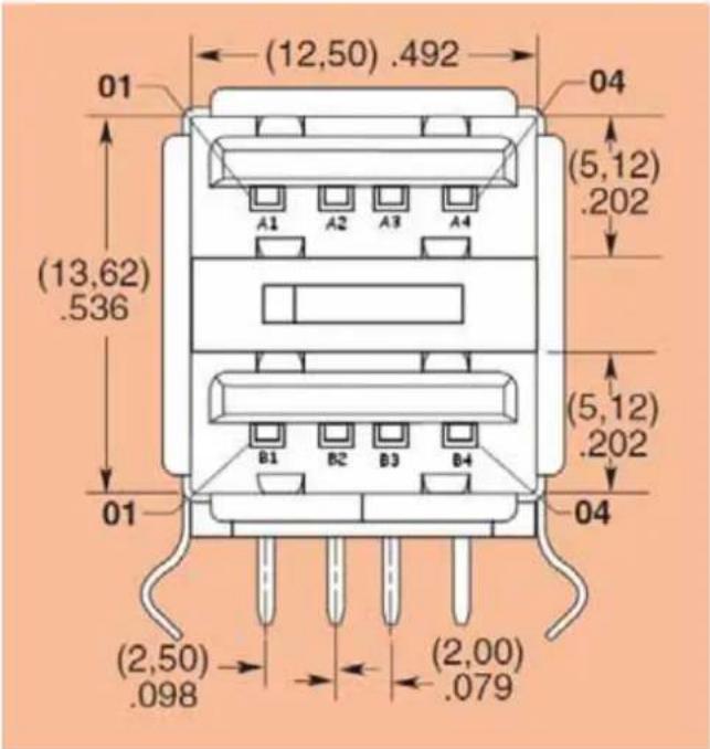
Table 3-23. USB Type A Dual Port J19 Signal Descriptions
| Pin Mnemonic Description | ||
| A1 Vbus – USB_A 5V power | ||
| A2 | DM – USB_A | Data minus |
| A3 | DP – USB_A | Data plus |
| A4 | GND | Common ground |
| B1 Vbus – USB_A 5V power | ||
| B2 | DM – USB_A | Data minus |
| B3 | DP – USB_A | Data plus |
| B4 | GND | Common ground |
| Mechanical pins | Shield | |
3.3.5.5 USB Micro AB
Figure 3-40. USB USB Host/Device Micro AB Connector J20
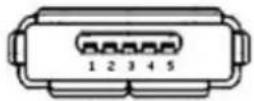
Table 3-24. USB USB Host/Device Micro AB Connector J20 Signal Descriptions
| Pin Mnemonic Description | ||
| 1 Vbus 5v power | ||
| 2 DM Data minus | ||
| 3 DP Data plus | ||
| 4 ID On the Go Identification | ||
| 5 | GND | Common ground |
3.3.5.6 DBGU
Figure 3-41. DBGU Connector J11
natural_image
Diagram of a 16-pin VGA connector with pin numbering (no text or symbols)Table 3-25. DBGU Connector J11 Signal Descriptions
| Pin | Mnemonic Description | |
| 1, 4, 6, 9 | - | NO CONNECTION |
| 2 | RXD (RECEIVED DATA) | RS232 serial data output signal |
| 3 | TXD (TRANSMITTED Data) | RS232 serial data input signal |
| 5 | GND | Common ground |
| 7 | RTS (REQUEST TO SEND) | NO USED |
| 8 | CTS (CLEAR TO SEND) | NO USED |
| Mechanical pins - | Shield |
3.3.5.7 RS232 Connector with RTS/CTS Handshake Support
Figure 3-42. USART Connector J12, J13
natural_image
Diagram of a 16-pin D-sub connector with pin numbering (no text or symbols)Table 3-26. USART Connector J12 Signal Descriptions
| Pin Mnemonic PIO Description | |||
| 1, 4, 6, 9 -- NO CONNECTION | |||
| 2 RXD (RECEIVED DATA) PA1 RS232 serial data output signal | |||
| 3 TXD (TRANSMITTED Data) PA0 | RS232 serial data input signal | ||
| 5 | GND | - | Common ground |
| 7 | RTS (REQUEST TO SEND) | PA2 | Active-positive RS232 input signal |
| 8 CTS (CLEAR TO SEND) PA3 | Active-positive RS232 output signal | ||
| Mechanical pins | -- | Shield | |
Table 3-27. USART Connector J13 Signal Descriptions
| Pin Mnemonic PIO Description | |||
| 1, 4, 6, 9 -- NO CONNECTION | |||
| 2 RXD (RECEIVED DATA) | PC23 | RS232 serial data output signal | |
| 3 TXD (TRANSMITTED Data) | PC22 | RS232 serial data input signal | |
| 5 | GND | - | Common ground |
| 7 | RTS (REQUEST TO SEND) | PC24 | Active-positive RS232 input signal |
| 8 | CTS (CLEAR TO SEND) | PC25 | Active-positive RS232 output signal |
| Mechanical pins | -- | Shield | |
3.3.5.8 DAA RJ11 Socket (6P4C)
Figure 3-43. DAA RJ11 Socket J16
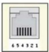
Table 3-28. DAA RJ11 Socket J16 Signal Descriptions
| Pin Mnemonic Description | |
| 1, 2, 5, 6 – NO CONNECTION | |
| 3 RAC RING side of ordinary telephone line | |
| 4 TAC TIP side of ordinary telephone line |
3.3.5.9 CAN RJ12 Socket (6P6C)
Figure 3-44. CAN RJ12 Socket CON2, CON3
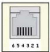
Table 3-29. DAA RJ11 Socket J16 Signal Descriptions
| Pin Mnemonic Description | ||
| 1 3V3 POWER PIN | ||
| 2 5V | POWER PIN | |
| 4 | CANL | CAN bus differential pair |
| 5 | CANH | CAN bus differential pair |
| 4, 6 | GND | Common ground |
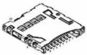
3.3.5.10 MicroSD MCI0
Figure 3-45. MicroSD Socket J6
natural_image
Isometric line drawing of a mechanical component with no visible text or symbolsTable 3-30. MicroSD Socket J6 Signal Descriptions
| Pin Mnemonic Description | ||
| 1 DAT2 Data Bit 2 | ||
| 2 CD/DAT3 Card Detect/Data Bit 3 | ||
| 3 CMD Command Line | ||
| 4 VCC | Supply Voltage 3.3V | |
| 5 | CLK | Command Line |
| 6 | VSS | Common ground |
| 7 DAT0 Data Bit 0 | ||
| 8 DAT1 Data Bit 1 | ||
| 9 | SW1 | No use, grounded |
| 10 | CARD DETECT CARD DETECT | |
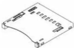
3.3.5.11 SD/MMC MCI1
Figure 3-46. SD/MMC Socket J7
natural_image
Isometric line drawing of a rectangular electronic component with mounting holes and slots (no text or symbols)Table 3-31. SD Socket J7 Signal Descriptions
| Pin | Mnemonic | PIO | Signal | ||
| MMC Card | SD Card | ||||
| 1-Bit Mode | 4-Bit Mode | ||||
| 1 | MCI1_DA2 | PA3 | Not Used | Read Wait (RW) | Data Line DAT2 or Read Wait (RW) |
| 2 | MCI1_DA3 | PA4 | Reserved | Not Used | Data Line DAT3 |
| 3 | MCI1_CDA | PA12 | Command/Response | ||
| 4 | VDDIOP0 | Supply Voltage (3.3-volts) VDDIOP0 | |||
| 5 | MCI1_CK | PA13 | Clock | ||
| 6 | GND | Ground | |||
| 7 MCI | 1_DA0 PA11 Data Line DAT0 | ||||
| 8 MC1 | DA1 PA2 Not Used Interrupt (IRQ) Data Line DAT1 or Interrupt (IRQ) | ||||
| 9 GND Ground | |||||
| 10 MC1 | CD PD14 Card Detect, configured as GPIO, Power domain VDDNF | ||||
| 11 | WP | Write Protect Detect, connects to jumper JP6 | |||
| 12 | GND Ground | ||||
| 13 | GND Ground | ||||
| 14 | GND Ground | ||||
| 15 | GND Ground | ||||
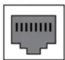
3.3.5.12 Ethernet RJ45 Socket J17, J18
Figure 3-47. Ethernet RJ45 Socket J17, J18
12345678
RJ-45
Table 3-32. DAA RJ11 Socket J16 Signal Descriptions
| Pin | Mnemonic | Description |
| 1 | TX+ | DIFFERENTIAL OUTPUT PLUS |
| 2 | TX- | DIFFERENTIAL OUTPUT MINUS |
| 3 | RX+ | DIFFERENTIAL INPUT PLUS |
| 4 | Reserved | - |
| 5 | Reserved | DIFFERENTIAL INPUT MINUS |
| 6 | RX- | - |
| 7 | Reserved | - |
| 8 | Reserved | - |
3.3.5.13 ZigBee Socket J10
Figure 3-48. ZigBee Socket J10
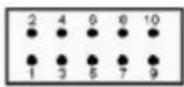
Table 3-33. ZigBee Socket J10 Signal Descriptions
| Function | Signal Name Port Pin Pin | Port | Signal Name Function | Option on misc. port set by OR or solder shunts | ||
| Reset /RST - 1 2 - Misc. - | • EEprom for MAC address, cap array settings and serial number• TST: test mode activation• CLKM: RF chip clock output | |||||
| Interrupt Request | IRQ | -34 - SLP_TR | SLP_TR | - | ||
| SPI chip select | /SEL | - | 5 | 6 | - | MOSI |
| SPI MISO | MISO | - | 7 | 8 | - | SCLK |
| Power Supply | GND | GND | 9 | 10 | VCC | VCC |
3.3.5.14 LCD/ISI Socket J21
Figure 3-49. LCD/ISI Socket J21

Table 3-34. LCD/ISI Socket J21 Signal Descriptions
| LCD | ISI | Pin Num | Pin Num | ISI | LCD |
| 3V3 | 3V3 | 1 | 2 | GND | GND |
| VDDISI | VDDISI | 3 | 4 | GND | GND |
| ZB_IRQ0 | ZB_IRQ0 | 5 | 6 | - | ZB_IRQ1 |
| TWCK0 | TWCK0 | 7 | 8 | - | TWD0 |
| GND | GND | 9 | 10 | ISI_MCK | LCDDAT15 |
| GND | GND | 11 | 12 | ISI_VSYNC | LCDDAT13 |
| GND | GND | 13 | 14 | ISI_HSYNC | LCDDAT14 |
| GND | GND | 15 | 16 | ISI_PCK | LCDDAT12 |
| GND | GND | 17 | 18 | ISI_D0 | LCDDAT0 |
| LCD ISI Pin | Num Pin Num ISI | LCD | |||
| LCDDAT1 ISI_D1 19 20 ISI_D2 LCDDAT2 | |||||
| LCDDAT3 ISI_D3 21 22 ISI_D4 LCDDAT4 | |||||
| LCDDAT5 ISI_D5 23 24 ISI_D6 LCDDAT6 | |||||
| LCDDAT7 ISI_D7 25 26 ISI_D8 LCDDAT8 | |||||
| LCDDAT9 ISI_D9 27 28 ISI_D10 LCDDAT10 | |||||
| LCDDAT11 ISI_D11 29 30 GND GND | |||||
3.3.5.15 LCD/TSC Socket J22
Figure 3-50. LCD/TSC Socket J22

Table 3-35. LCD/TSC Socket J22 Signal Descriptions
| LCD Pin Num Pin Num | LCD | |||
| 5V | 5V_INTER | 1 | 2 | GND |
| 5V | 5V_INTER | 3 | 4 | GND |
| LCDDAT16 | - | 5 | 6 | - |
| LCDDAT18 | - | 7 | 8 | - |
| LCDDAT20 | - | 9 | 10 | - |
| LCDDAT22 | - | 11 | 12 | - |
| GND | GND | 13 | 14 | GND |
| LCDDISP | - | 15 | 16 | - |
| LCDCSYNC | - | 17 | 18 | - |
| LCDDEN | - | 19 | 20 | - |
| GND | GND | 21 | 22 | GND |
| AD0_XP | TSC 23 | 24 TSC AD1_XM | ||
| AD2_YP | TSC 25 | 26 TSC AD3_YM | ||
| AD4_LR | TSC | 27 | 28 | - |
| GND | GND | 29 | 30 | GND |
| SPI1_MISO | - | 31 | 32 | - |
| SPI1_SPCK | - | 33 | 34 | - |
| EN_PWRLCD | SELCONFIG | 35 | 36 | LCD_DETECT |
| PD16 | - | 37 | 38 | - |
| GND | GND | 39 | 40 | GND |
3.3.5.16 IO Expansion Port J1
Figure 3-51. IO Expansion Socket J1

Table 3-36. Expansion Socket J1 Signal Descriptions
| PIO Power | Pin Num Pin Num | Power PIO | |||
| -3V3, or 5V 1 2 3V3, or 5V - | |||||
| - | G | N | D | 3 | 4 |
| PA0-56- | PA16 | ||||
| PA1-78- | PA17 | ||||
| PA2 | - | 9 | 10 | - | PA18 |
| PA3 | - | 11 | 12 | - | PA19 |
| PA4 | - | 13 | 14 | - | PA20 |
| PA5 | - | 15 | 16 | - | PA21 |
| PA6 | - | 17 | 18 | - | PA22 |
| PA7 | - | 19 | 20 | - | PA23 |
| PA8 | - | 21 | 22 | - | PA24 |
| PA9 | - | 23 | 24 | - | PA25 |
| PA10 | - | 25 | 26 | - | PA26 |
| PA11 | - | 27 | 28 | - | PA27 |
| PA12 | - | 29 | 30 | - | PA28 |
| PA13 | - | 31 | 32 | - | PA29 |
| PA14 | - | 33 | 34 | - | PA30 |
| PA15 | - | 35 | 36 | - | PA31 |
| - | GND | 37 | 38 | GND | - |
| - | 3V3 | 39 | 40 | 3V3 | - |
3.3.5.17 IO Expansion Port J2
Figure 3-52. IO Expansion Socket J2

Table 3-37. Expansion Socket J1 Signal Descriptions
| PIO Power | Pin Num Pin Num | Power PIO | |||
| -3V3, or 5V 1 2 3V3, or 5V - | |||||
| - | G | N | D | 3 | 4 |
| PC0 - 5 6 - | PC16 | ||||
| PC1 - 7 8 - | PC17 | ||||
| PC2 | - | 9 | 10 | - | PC18 |
| PC3 - | 11 | 12 | - PC19 | ||
| PC4 - | 13 | 14 | - PC20 | ||
| PC5 - | 15 | 16 | - PC21 | ||
| PC6 - | 17 | 18 | - PC22 | ||
| PC7 - | 19 | 20 | - PC23 | ||
| PC8 - | 21 | 22 | - PC24 | ||
| PC9 - | 23 | 24 | - PC25 | ||
| PC10 | - | 25 | 26 | - | PC26 |
| PC11 | - | 27 | 28 | - | PC27 |
| PC12 | - | 29 | 30 | - | PC28 |
| PC13 | - | 31 | 32 | - | PC29 |
| PC14 | - | 33 | 34 | - | PC30 |
| PC15 | - | 35 | 36 | - | PC31 |
| - | GND | 37 | 38 | GND | - |
| - | 3V3 | 39 | 40 | 3V3 | - |
3.3.5.18 IO Expansion Port J3
Figure 3-53. IO Expansion Socket J3

Table 3-38. Expansion Socket J1 Signal Descriptions
| PIO Power | Pin Num Pin Num | Power PIO | |||
| -3V3, or 5V 1 2 3V3, or 5V - | |||||
| - | G | N | D | 3 | 4 |
| PB0 - 5 6 - | PB16 | ||||
| PB1 - 7 8 - | PB17 | ||||
| PB2 | - | 9 | 10 | - | PB18 |
| PB3 - | 11 | 12 | -- | ||
| PB4 - | 13 | 14 | -- | ||
| PB5 - | 15 | 16 | -- | ||
| PB6 - | 17 | 18 | -- | ||
| PB7 - | 19 | 20 | -- | ||
| PB8 - | 21 | 22 | -PD14 | ||
| PB9 - | 23 | 24 | -PD15 | ||
| PB10 - | 25 | 26 | -PD16 | ||
| PB11 | - | 27 | 28 | - | PD17 |
| PB12 - | 29 | 30 | -PD18 | ||
| PB13 - | 31 | 32 | -PD19 | ||
| PB14 - | 33 | 34 | -PD20 | ||
| PB15 - | 35 | 36 | -PD21 | ||
| - | GND | 37 | 38 | GND | - |
| - | 3V3 | 39 | 40 | 3V3 | - |
3.3.6 Schematics
Figure 3-54. EK Board Schematics
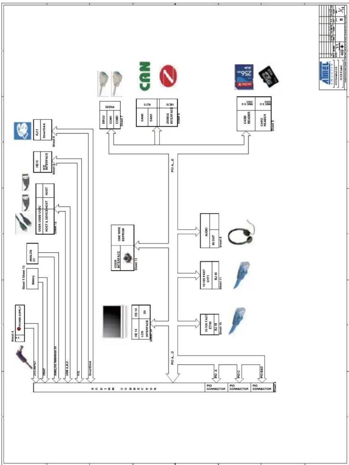
flowchart
graph TD
    A["Power Supply"] --> B["3V INPUT"]
    B --> C["USB 4 Sheet 13"]
    C --> D["SI/O"]
    D --> E["Microcontroller"]
    E --> F["Microcontroller"]
    F --> G["Microcontroller"]
    G --> H["S10273"]

    I["SmartDAA"] --> J["JB11"]
    J --> K["SmartDAA"]
    K --> L["Sheet 9"]
    L --> M["User Interface"]
    M --> N["One Wire EEPROM"]
    N --> O["Audio"]
    O --> P["In Out"]
    P --> Q["10/100 FAST EHT1"]
    Q --> R["10/100 FAST ETH0"]
    R --> S["Sheet 10"]

    T["USB 4 Interface"] --> U["USBA USB U5/C"]
    U --> V["HOST & DEVICE/HOST"]
    V --> W["HOST"]
    W --> X["Sheet 12"]

    Y["ICF"] --> Z["HE10"]
    Z --> AA["ICE INTERFACE"]
    AA --> AB["Sheet 5"]

    AC["SunDAA"] --> AD["USB A.R.C"]
    AD --> AE["TCE"]
    AE --> AF["SunDAA"]

    AG["RSC22"] --> AH["DB/GU"]
    AH --> AI["COM1"]
    AH --> AJ["CONS"]
    AH --> AK["Sheet 7"]

    AL["CAND"] --> AM["L1T"]
    AM --> AN["CAN1"]
    AN --> AO["ZIGBEE INTERFACE"]
    AO --> AP["SIGHTS"]

    AQ["CARD READER"] --> AR["CHSD D S ONN"]
    AR --> AS["CHSD D S ONW"]
    AS --> AT["SHEET 5"]

    AU["USER INTERFACE"] --> AV["ONE WIRE EEPROM"]
    AV --> AW["Sheet 13"]

    AX["VIDEO INTERFACE"] --> AY["LED INTERFACE"]
    AY --> AZ["ISI"]

    BA["AUDIO"] --> BB["IN OUT"]
    BB --> BC["Sheet 8"]

    BD["RJ46"] --> BE["10/100 FAST ETH1"]
    BE --> BF["Sheet 11"]

    BG["RJ15"] --> BH["10/100 FAST ETH0"]
    BH --> BI["Sheet 10"]

    BJ["PIO A...D"] --> BK["PIO CONNECTOR"]
    BK --> BL["PIO CONNECTOR"]
    BL --> BM["PIO CONNECTOR"]

    BN["PIO A"] --> BO["PIO CONNECTOR"]
    BO --> BP["PIO CONNECTOR"]
    BP --> BQ["PIO BAO"]
| REVISION HISTORY | TEST POINT | SCHEMATICS CONVENTIONS | ||||||||||||
| REV DATA | NOTE | PAGE | REFERENCE FUNCTION | (1) Resistance Limit: "K is 'Kanm', "P is 'Ohm" | ||||||||||
| 4 | TP1, TP2 | GND | ||||||||||||
| 4 | TP3 | 5V | ||||||||||||
| 4 | TP4 | 3VS | ||||||||||||
| 4 | TP5 | VDDIOP0 | ||||||||||||
| 4 | TP6 | VDDIOP1 | ||||||||||||
| 4 | TP7 | VDDNF | ||||||||||||
| JUMPER and SOLDERDROP | SAM9x5 Config | |||||||||||||
| PAGE | REFERENCE FUNCTION | ONDEFAULT | SAM9G12 | SAM9G35 | SAM9X35 | SAM9G25 | SAM9X25 | |||||||
| 3 JP1JP2JP3JP4JP5 | 1-21-21-2OPENCLOSECLOSECLOSECLOSECLOSECLOSECLOSECLOSECLOSECLOSECLOSECLOSECLOSECLOSECLOSECLOSECLOSECLOSECLOSECLOSECLOSECLOSECLOSECLOSECLOSECLOSECLOSECLOSECLOSECLOSECLOSECLOSECLOSECLOSECLOSECLOSECLOSECLOSECLOSECLOSECLOSECLOSECLOSECLOSECLOSECLOSECLOSECLOSECLOSECLOSECLOSECLOSECLOSECLOSECLOSECLOSECLOSECLOSECLOSECLOSECLOSECLOSECLOSECLOSECLOSECLOSECLOSECLOSECLOSECLOSECLOSECLOSECLOSECLOSECLOSECLOSECLOSECLOSECLOSECLOSECLOSECLOSECLOSECLOSECLOSECLOSECLOSECLOSECLOSECLOSECLOSECLOSECLOSECLOSECLOSECLOSECLOSECLOSECLOSECLOSECODE | 3.3V or 5V selection for J13.3V or 5V selection for J23.3V or 5V selection for J3Default boot on embedded ROM Glass base on external memory | ||||||||||||
| 4 | JP5 Backup supplyonCLOSEJP5 | Force power on function | ||||||||||||
| 5 MC1 white protocol select | CLOSE | |||||||||||||
| 6 | JP7 | CLOSE | CAN0 diff termination select | |||||||||||
| JP8 | CLOSE | CAN1 diff termination select | ||||||||||||
| JP10 Zigbee PoweronORISNet | CLOSE | |||||||||||||
| 7 | JP11 | CLOSE | DEBUG and CAM selection | |||||||||||
| 10 | JP12 | CLOSE | MDIX ON/OFF(ETH0) | |||||||||||
| 11 | JP13 | CLOSE | MDIX ON/OFF(ETH1) | |||||||||||
| 13 | JP14 | 1-2 | AOVREF input selection | |||||||||||
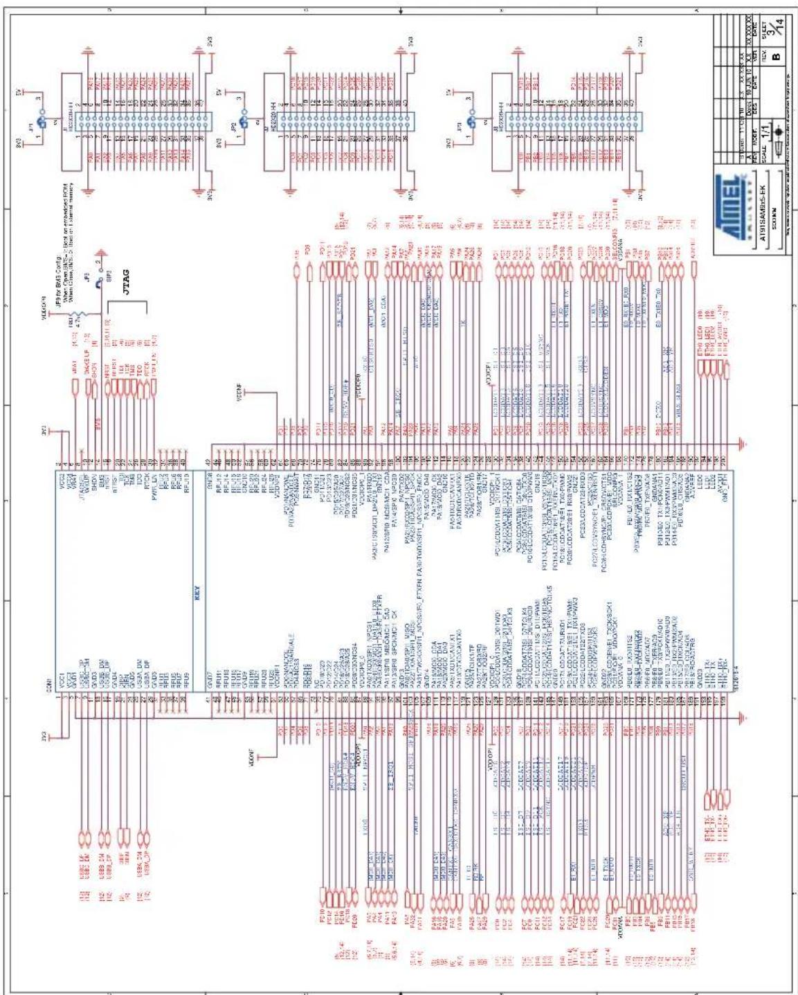
ZIGBEE INTERFACE
| ATMEL ROUSET | |||||||
| R D###k 11 C## | 10 X.XX | XX XXX XX | |||||
| AT91SAM9x5-EK CAN & ICE & ZIGSEE | A | D###k | 10-JUN-18 | X.X | XX-XXX-XX | ||
| REV | MODIF. | DES. | DATE | VER. | DATE | ||
| SCALE | 1/1 | REV. | SHEET | ||||
| B | 6/14 | ||||||
ETHO
(Only For SAM9G35/SAM9X35/SAM9G25/SAM9X25)
| B | M08X 1T C2F 0 | XX XX XXX XX | |||
| A | O4R6 | 10 JUN 10 | XX | XX XXX XX | |
| PEV | MOUF | DES | DATE | VER | DATE |
| SCALE | 1/1 | REV | SHEET | ||
| ETHO | B | 10/4 | |||
USB HOST B&C INTERFACE
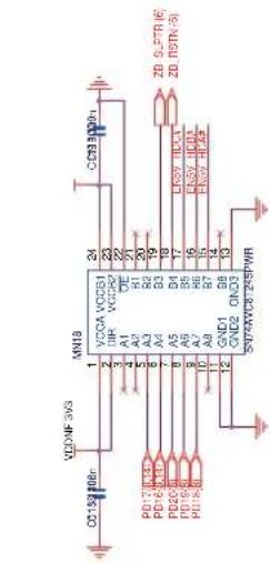
USB A HOST/DEVICE INTERFACE
![DEVICE INTERFACE LCD_DETECT# [140V_INTER-14] L14 MN15 CUTA ENA IN FLCA GNG FLGB OUTB CNB AIC1326-005 ACTIVE LOW R137 47k P517 EREV-HDA# LCD_DETECT# [140V_INTER-14] C107 100n C106 98u 220ohm at 100Mhz C106 100n L15 C109 100n C110 98u 220ohm at 100Mhz R138 82k (VBUS SENSE) C111 15p R139 47k PB16-3 R140 47k J20 EARTH_USS JDS DP 3 3D 3D JDSA DM (3) JDSA_DP (3) EARTH_USB G3515-080/101-03](/content/2026/06/1177958/images/129be02dcfe08d0fb7ecb98703a6c3acb9ce2c783e77c507298d953cee6afb47.jpg)
| D | Verisk 11-Oct-10 X.X | XX-XXX-XX | |||
| A | DISK | 10-JUN-10 | X.X | XX-XXX-XX | |
| REV | CANEXF. | DES. | DATE | VER. | |
| SCALE 1/1 | REV B | SHEET 1/4 | |||
3.4 Optional Display Module (DM) Board Hardware
3.4.1 DM Board Overview
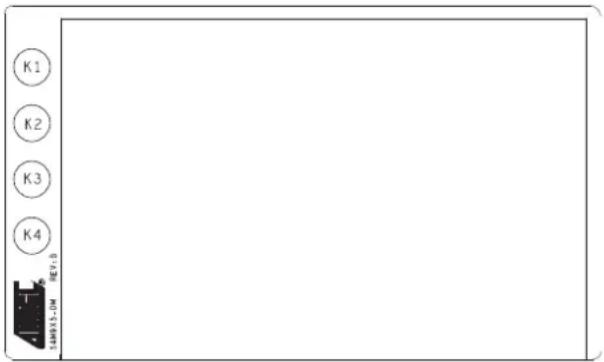
The optional DM board carries a 5.0" TFT LCD module with touch screen. The DM board also carries four QTouch pads.
Figure 3-55. DM Board Layout
3.4.2 Equipment List
The list of the DM board components follows:
• One 5.0" TFT LCD module
- LCD Back light driver
3.3V regulator
- QTouch device
1-Wire device
3.4.3 Function Blocks
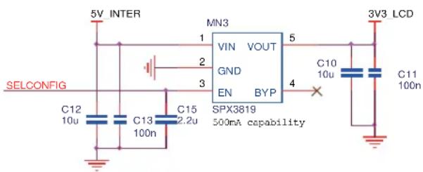
3.4.3.1 3.3V Regulator
The DM Board features its own LDO for local power regulation. It accepts DC 5V power from a 500 mA high-side power switch on the EK and outputs a regulated +3.3 V to most other circuits on the board.
Figure 3-56. DM Board Power Supply
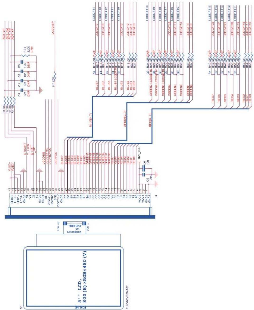
3.4.3.2 TFT LCD with Touch Panel
A 5" 800x480 LCD provides the DM with a low power display feature, back light unit and a touch panel, similar to that used on commercial PDAs.
Graphics and text can be displayed on the dot matrix panel with up to 16 million colors by supplying 24-bit data signals (8bit x RGB by default) or 16-bit data signals (5+6+5bit x RGB in option). This allows the user to develop graphical user interfaces for a wide variety of end applications.
Warning: Never connect/disconnect the LCD display from the board while the power supply is on. Doing so may damage both units.
Figure 3-57. LCD with Touch Panel
3.4.3.3 Back Light
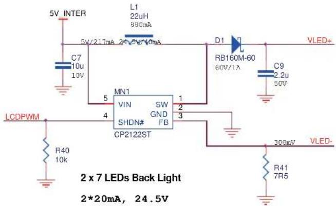
The back light voltage is generated from a CP2122ST boost converter. It is powered directly by the DC 5V from the EK board. The back light level is controlled by a PWM signal generated from the MPU Device processor.
Figure 3-58. Back Light Control
3.4.3.4 QTouch
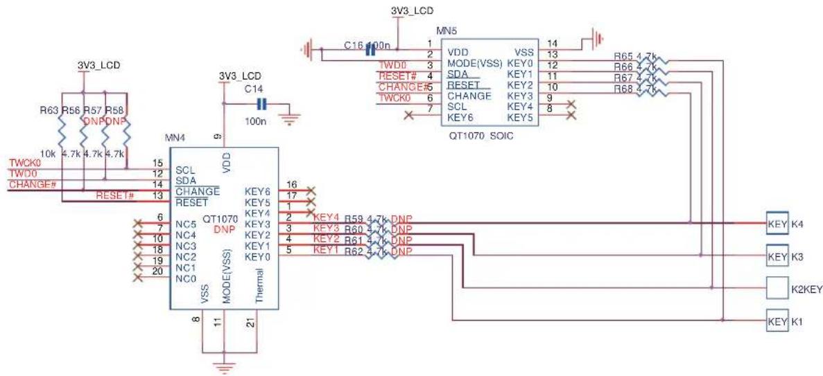
The DM board carries a QTouch device piloted through a TWI interface. It manages four capacitive touch buttons directly printed on the PCB.
There are dual footprints for the QTouch device, and SOIC is the default mounted one.
Figure 3-59. QTouch
3.4.3.5 1-Wire
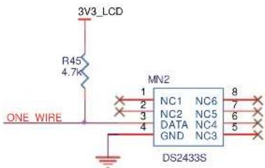
The DM board also uses a 1-Wire device as "firmware label" to store the information such as chip type, manufacturer's name, production date etc.
Figure 3-60. 1-Wire on DM
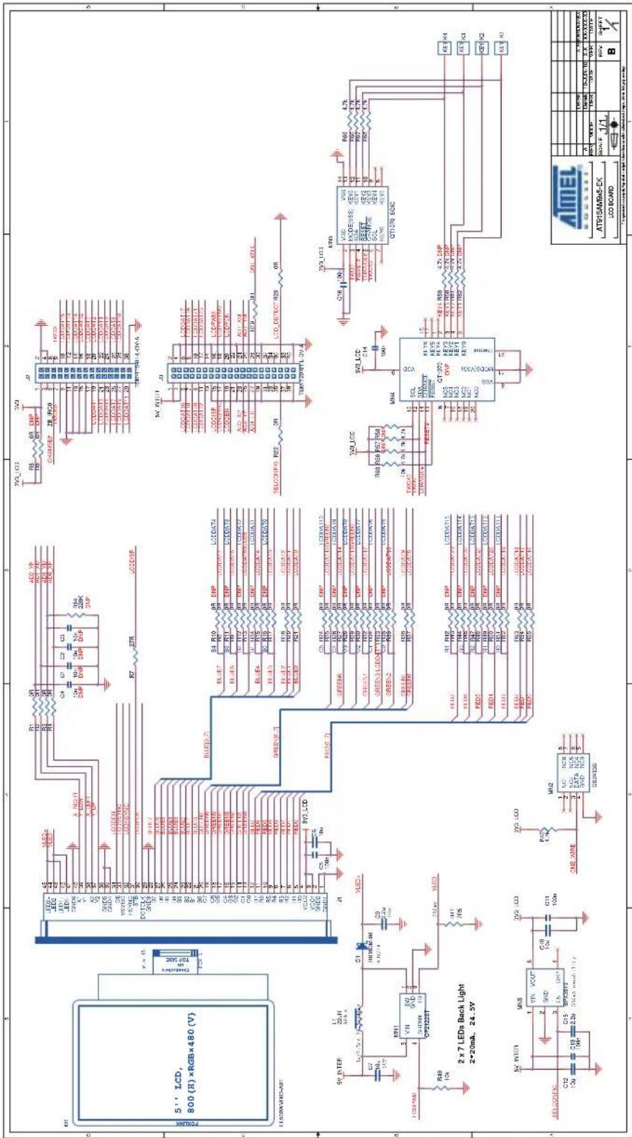
3.4.4 Schematics
Figure 3-61. DM Board Schematics
4. Revision History
Table 4-1. Revision History
| Document Comments | |
| 11115B | Replaced all occurrences of “DataFlash” with “serial Flash”.Updated Section 2.1 "Power Up the Board" and Section 2.3 "Recovery Procedure".Deleted section “DevStart”.Updated Table 3-7 "Boot Configuration". Added Figure 3-10, "SW1A and SW1B Position on Embest Modules”.Updated Figure 3-14, "CM Board Schematics – 3 of 5". |
| 11115A First issue. | |
Atmel
Enabling Unlimited Possibilities®

Atmel Corporation
1600 Technology Drive, San Jose, CA 95110 USA
T: (+1)(408) 441.0311
F: (+1)(408) 436.4200
www.atmel.com
© 2016 Atmel Corporation. / Rev.: Atmel-11115B-ATARM-SAM9G15-SAM9G25-SAM9G35-SAMX25-SAM9X35-User-Guide_05-Feb-16.
Atmel ^® , Atmel logo and combinations thereof, Enabling Unlimited Possibilities ^® , and others are registered trademarks or trademarks of Atmel Corporation in U.S. and other countries. ARM ^® , ARM Connected ^® logo, and others are the registered trademarks or trademarks of ARM Ltd. Other terms and product names may be trademarks of others.
DISCLAIMER: The information in this document is provided in connection with Atmel products. No license, express or implied, by estoppel or otherwise, to any intellectual property right is granted by this document or in connection with the sale of Atmel products. EXCEPT AS SET FORTH IN THE ATMEL TERMS AND CONDITIONS OF SALES LOCATED ON THE ATMEL WEBSITE, ATMEL ASSUMES NO LIABILITY WHATSOEVER AND DISCLAIMS ANY EXPRESS, IMPLIED OR STATUTORY WARRANTY RELATING TO ITS PRODUCTS INCLUDING, BUT NOT LIMITED TO, THE IMPLIED WARRANTY OF MERCHANTABILITY, FITNESS FOR A PARTICULAR PURPOSE, OR NON-INFRINGEMENT. IN NO EVENT SHALL ATMEL BE LIABLE FOR ANY DIRECT, INDIRECT, CONSEQUENTIAL, PUNITIVE, SPECIAL OR INCIDENTAL DAMAGES (INCLUDING, WITHOUT LIMITATION, DAMAGES FOR LOSS AND PROFITS, BUSINESS INTERRUPTION, OR LOSS OF INFORMATION) ARISING OUT OF THE USE OR INABILITY TO USE THIS DOCUMENT, EVEN IF ATMEL HAS BEEN ADVISED OF THE POSSIBILITY OF SUCH DAMAGES. Atmel makes no representations or warranties with respect to the accuracy or completeness of the contents of this document and reserves the right to make changes to specifications and products descriptions at any time without notice. Atmel does not make any commitment to update the information contained herein. Unless specifically provided otherwise, Atmel products are not suitable for, and shall not be used in, automotive applications. Atmel products are not intended, authorized, or warranted for use as components in applications intended to support or sustain life.
SAFETY-CRITICAL, MILITARY, AND AUTOMOTIVE APPLICATIONS DISCLAIMER: Atmel products are not designed for and will not be used in connection with any applications where the failure of such products would reasonably be expected to result in significant personal injury or death ("Safety-Critical Applications") without an Atmel officer's specific written consent. Safety-Critical Applications include, without limitation, life support devices and systems, equipment or systems for the operation of nuclear facilities and weapons systems. Atmel products are not designed nor intended for use in military or aerospace applications or environments unless specifically designated by Atmel as military-grade. Atmel products are not designed nor intended for use in automotive applications unless specifically designated by Atmel as automotive-grade.
- Contents
- - Board
- Power supply
- Cables
- A Welcome Letter
- Related Documents
- Table of Contents
- Specifications
- Kit Specifications
- Board Specifications
- Power Up
- Power Up the Board
- Sample Code and Technical Support
- Recovery Procedure
- Hardware Overview
- Introduction
- Computer Module (CM)
- CM Board Overview
- Equipment List
- Devices
- Interface Connection
- Configuration Items
- Function Blocks
- Processor
- Clock Circuitry
- Reset Circuitry
- Power Supplies
- Memory
- Serial Peripheral Interface (SPI) Controller
- Two Wire Interface (TWI)
- 1-Wire EEPROM
- Optional PHY
- SODIMM200 Interface
- Configuration
- Chip Identification
- Boot Configuration
- Connectors
- Schematics
- EK Board Description
- EK Board Overview
- Equipment List
- Devices
- Board Interface Connection
- Push Button Switches
- Function Blocks
- Processor
- Power Supplies
- JTAG/ICE
- DBGU
- USART
- USB Ports
- Ethernet 10/100 (EMAC) Port
- Audio
- 1-Wire EEPROM
- CAN Bus
- Telephone Interface
- ZigBee
- LED Indicators
- Expansion Ports
- Configuration
- JTAG/ICE Configuration
- Boot Mode Select Configuration
- Force Power ON Configuration
- White Protection Configuration on MCI1
- Selection between DBGU and CAN
- Codec IIS Configuration
- ETH0 Configuration
- PIO Usage
- Connectors
- Power Supply
- SODIMM Card Edge Socket
- JTAG/ICE Connector
- USB Type A Dual Port
- USB Micro AB
- DBGU
- RS232 Connector with RTS/CTS Handshake Support
- DAA RJ11 Socket (6P4C)
- CAN RJ12 Socket (6P6C)
- MicroSD MCI0
- SD/MMC MCI1
- Ethernet RJ45 Socket J17, J18
- ZigBee Socket J10
- LCD/ISI Socket J21
- LCD/TSC Socket J22
- IO Expansion Port J1
- IO Expansion Port J2
- IO Expansion Port J3
- Schematics
- Optional Display Module (DM) Board Hardware
- DM Board Overview
- Equipment List
- Function Blocks
- 3.3V Regulator
- TFT LCD with Touch Panel
- Back Light
- QTouch
- 1-Wire
- Schematics
- Revision History
- Atmel
- Enabling Unlimited Possibilities®
Brand : Microchip
Model : AT91SAM9X35
Category : Uncategorized