
MIC2877 - Uncategorized Microchip - Free user manual and instructions
Find the device manual for free MIC2877 Microchip in PDF.


| Product Type | USB Type-C Power Bank Reference Design |
| Brand | Microchip |
| Model | MIC2877 (ARD00916) |
| Category | Uncategorized |
| Power Supply | Two 18650 Li-Ion battery cells (not included) |
| Output Voltage | 5 V |
| Output Current | 2 A to 4 A (battery voltage dependent) |
| Charging Current | 1 A (default) or 2 A (fast charge, temperature dependent) |
| Ports | USB 2.0 (output), USB Type-C (dual role: input/output) |
| Key Components | MIC2877 boost regulator, PIC16F15344 MCU, MCP73843 charger, UCS2114 power switch, AT30TS74 temp sensor |
| Switching Frequency | 2 MHz |
| Efficiency | Up to 95% |
| Battery Protection | Overvoltage, undervoltage, overcurrent, thermal shutdown, temperature monitoring |
| Input Voltage Range | 2.5 V to 5.5 V (boost regulator) |
| Standby Current | Less than 2 μA (shutdown), 750 μA (idle) |
| User Interface | Push button, 4 green LEDs (battery level), 1 red LED (charging) |
| Firmware | Programmable via PICkit 3 (J2 connector), includes source code |
| Operating Temperature | -40°C to +85°C (board), -40°C to +105°C (UCS2114) |
| Maintenance | None required; firmware customizable |
| Safety Certifications | UL recognized, EN/IEC 60950-1 (CB) for UCS2114 |
Frequently Asked Questions - MIC2877 Microchip
User questions about MIC2877 Microchip
0 question about this device. Answer the ones you know or ask your own.
Ask a new question about this device
Download the instructions for your Uncategorized in PDF format for free! Find your manual MIC2877 - Microchip and take your electronic device back in hand. On this page are published all the documents necessary for the use of your device. MIC2877 by Microchip.
USER MANUAL MIC2877 Microchip
Power Bank with Dual Role Port Reference Design User's Guide
Note the following details of the code protection feature on Microchip devices:
• Microchip products meet the specifications contained in their particular Microchip Data Sheet.
• Microchip believes that its family of products is secure when used in the intended manner and under normal conditions.
- There are dishonest and possibly illegal methods being used in attempts to breach the code protection features of the Microchip devices. We believe that these methods require using the Microchip products in a manner outside the operating specifications contained in Microchip's Data Sheets. Attempts to breach these code protection features, most likely, cannot be accomplished without violating Microchip's intellectual property rights.
• Microchip is willing to work with any customer who is concerned about the integrity of its code.
- Neither Microchip nor any other semiconductor manufacturer can guarantee the security of its code. Code protection does not mean that we are guaranteeing the product is "unbreakable." Code protection is constantly evolving. We at Microchip are committed to continuously improving the code protection features of our products. Attempts to break Microchip's code protection feature may be a violation of the Digital Millennium Copyright Act. If such acts allow unauthorized access to your software or other copyrighted work, you may have a right to sue for relief under that Act.
Information contained in this publication is provided for the sole purpose of designing with and using Microchip products. Information regarding device applications and the like is provided only for your convenience and may be superseded by updates. It is your responsibility to ensure that your application meets with your specifications.
THIS INFORMATION IS PROVIDED BY MICROCHIP "AS IS". MICROCHIP MAKES NO REPRESENTATIONS OR WARRANTIES OF ANY KIND WHETHER EXPRESS OR IMPLIED, WRITTEN OR ORAL, STATUTORY OR OTHERWISE, RELATED TO THE INFORMATION INCLUDING BUT NOT LIMITED TO ANY IMPLIED WARRANTIES OF NON-INFRINGEMENT, MERCHANTABILITY, AND FITNESS FOR A PARTICULAR PURPOSE OR WARRANTIES RELATED TO ITS CONDITION, QUALITY, OR PERFORMANCE.
IN NO EVENT WILL MICROCHIP BE LIABLE FOR ANY INDIRECT, SPECIAL, PUNITIVE, INCIDENTAL OR CONSEQUENTIAL LOSS, DAMAGE, COST OR EXPENSE OF ANY KIND WHATSOEVER RELATED TO THE INFORMATION OR ITS USE, HOWEVER CAUSED, EVEN IF MICROCHIP HAS BEEN ADVISED OF THE POSSIBILITY OR THE DAMAGES ARE FORESEEABLE. TO THE FULLEST EXTENT ALLOWED BY LAW, MICROCHIP'S TOTAL LIABILITY ON ALL CLAIMS IN ANY WAY RELATED TO THE INFORMATION OR ITS USE WILL NOT EXCEED THE AMOUNT OF FEES, IF ANY, THAT YOU HAVE PAID DIRECTLY TO MICROCHIP FOR THE INFORMATION. Use of Microchip devices in life support and/or safety applications is entirely at the buyer's risk, and the buyer agrees to defend, indemnify and hold harmless Microchip from any and all damages, claims, suits, or expenses resulting from such use. No licenses are conveyed, implicitly or otherwise, under any Microchip intellectual property rights unless otherwise stated.
Trademarks
The Microchip name and logo, the Microchip logo, Adaptec, AnyRate, AVR, AVR logo, AVR Freaks, BesTime, BitCloud, chipKIT, chipKIT logo, CryptoMemory, CryptoRF, dsPIC, FlashFlex, flexPWR, HELDO, IGLOO, JukeBlox, KeeLoq, Kleer, LANCheck, LinkMD, maXStylus, maXTouch, MediaLB, megaAVR, Microsemi, Microsemi logo, MOST, MOST logo, MPLAB, OptoLyzer, PackeTime, PIC, picoPower, PICSTART, PIC32 logo, PolarFire, Prochip Designer, QTouch, SAM-BA, SenGenuity, SpyNIC, SST, SST Logo, SuperFlash, Symmetricom, SyncServer, Tachyon, TimeSource, tinyAVR, UNI/O, Vectron, and XMEGA are registered trademarks of Microchip Technology Incorporated in the U.S.A. and other countries.
AgileSwitch, APT, ClockWorks, The Embedded Control Solutions Company, EtherSynch, FlashTec, Hyper Speed Control, HyperLight Load, IntelliMOS, Libero, motorBench, mTouch, Powermite 3, Precision Edge, ProASIC, ProASIC Plus, ProASIC Plus logo, Quiet-Wire, SmartFusion, SyncWorld, Temux, TimeCesium, TimeHub, TimePictra, TimeProvider, WinPath, and ZL are registered trademarks of Microchip Technology Incorporated in the U.S.A.
Adjacent Key Suppression, AKS, Analog-for-the-Digital Age, Any Capacitor, AnyIn, AnyOut, Augmented Switching, BlueSky, BodyCom, CodeGuard, CryptoAuthentication, CryptoAutomotive, CryptoCompanion, CryptoController, dsPICDEM, dsPICDEM.net, Dynamic Average Matching, DAM, ECAN, Espresso T1S, EtherGREEN, IdealBridge, In-Circuit Serial Programming, ICSP, INICnet, Intelligent Paralleling, Inter-Chip Connectivity, JitterBlocker, maxCrypto, maxView, memBrain, Mindi, MiWi, MPASM, MPF, MPLAB Certified logo, MPLIB, MPLINK, MultiTRAK, NetDetach, Omniscient Code Generation, PICDEM, PICDEM.net, PICkit, PICtail, PowerSmart, PureSilicon, QMatrix, REAL ICE, Ripple Blocker, RTAX, RTG4, SAM-ICE, Serial Quad I/O, simpleMAP, SimpliPHY, SmartBuffer, SMART-I.S., storClad, SQI, SuperSwitcher, SuperSwitcher II, Switchtec, SynchroPHY, Total Endurance, TSHARC, USBCheck, VariSense, VectorBlox, VeriPHY, ViewSpan, WiperLock, XpressConnect, and ZENA are trademarks of Microchip Technology Incorporated in the U.S.A. and other countries.
SQTP is a service mark of Microchip Technology Incorporated in the U.S.A.
The Adaptec logo, Frequency on Demand, Silicon Storage Technology, and Symmcom are registered trademarks of Microchip Technology Inc. in other countries.
GestIC is a registered trademark of Microchip Technology Germany II GmbH & Co. KG, a subsidiary of Microchip Technology Inc., in other countries.
All other trademarks mentioned herein are property of their respective companies.
© 2021, Microchip Technology Incorporated, All Rights Reserved.
ISBN: 978-1-5224-7297-1
For information regarding Microchip's Quality Management Systems, please visit www.microchip.com/quality.
Table of Contents
Preface 5
Introduction......5
Document Layout 5
Conventions Used in this Guide 6
Recommended Reading....7
REFERENCES....7
The Microchip Web Site 7
Customer Support 8
Document Revision History 8
Chapter 1. Product Overview
1.1 Introduction ...... 9
1.2 Core Components Short Overview 9
1.3 Functional Description ...... 13
1.4 What is the MIC2877 USB Type-C Power Bank with Dual Role Port Reference Design? 19
1.5 What does the MIC2877 USB Type-C Power Bank with Dual Role Port Reference Design Kit Include? 19
Chapter 2. Installation and Operation
2.1 Overview 21
2.2 Getting Started 23
2.3 Programming the PIC16F15344 Microcontroller 24
Appendix A. Schematic and Layouts
A.1 Introduction 27
A.2 Board – Schematic 28
A.3 Board – Top Silk 29
A.4 Board – Top Copper and Silk 29
A.5 Board – Top Copper 30
A.6 Board – Signal Layer 1 ...... 30
A.7 Board – Signal Layer 2 ...... 31
A.8 Board – Bottom Copper 31
A.9 Board – Bottom Copper and Silk 32
A.10 Board – Bottom Silk 32
Appendix B. Bill of Materials (BOM)
Appendix C. Firmware Flowchart
C.1 Firmware Flowchart 37
Worldwide Sales and Service 39
Preface
NOTICE TO CUSTOMERS
All documentation becomes dated, and this manual is no exception. Microchip tools and documentation are constantly evolving to meet customer needs, so some actual dialogs and/or tool descriptions may differ from those in this document. Please refer to our web site (www.microchip.com) to obtain the latest documentation available.
Documents are identified with a "DS" number. This number is located on the bottom of each page, in front of the page number. The numbering convention for the DS number is "DSXXXXXXXXA", where "XXXXXXXXX" is the document number and "A" is the revision level of the document.
For the most up-to-date information on development tools, see the MPLAB ^® IDE online help. Select the Help menu, and then Topics to open a list of available online help files.
INTRODUCTION
This chapter contains general information that will be useful to know before using the MIC2877 USB Type-C Power Bank with Dual Role Port Reference Design. Items discussed in this chapter include:
- Document Layout
- Conventions Used in this Guide
- Recommended Reading
• The Microchip Web Site - Customer Support
• Document Revision History
DOCUMENT LAYOUT
This document describes how to use the MIC2877 USB Type-C Power Bank with Dual Role Port Reference Design as a development tool. The manual layout is as follows:
- Chapter 1. “Product Overview” – Provides important information about the MIC2877 USB Type-C Power Bank with Dual Role Port Reference Design.
- Chapter 2. “Installation and Operation” – Includes instructions on how to get started with this user’s guide and a description of each function.
- Appendix A. “Schematic and Layouts” – Shows the schematic and layout diagrams for the MIC2877 USB Type-C Power Bank with Dual Role Port Reference Design.
- Appendix B. "Bill of Materials (BOM)" – Lists the parts used to build the MIC2877 USB Type-C Power Bank with Dual Role Port Reference Design.
- Appendix C. "Firmware Flowchart" – Shows MIC2877 USB Type-C Power Bank with Dual Role Port Reference Design flowchart.
CONVENTIONS USED IN THIS GUIDE
This manual uses the following documentation conventions:
DOCUMENTATION CONVENTIONS
| Description Represents Examples | ||
| Arial font: | ||
| Italic characters Referenced books | oks MPLAB | ^ IDE User's Guide |
| Emphasized text ...is the only compiler... | ||
| Initial caps A window the Output | window | |
| A dialog the Settings dialog | ||
| A menu selection select Enable | Programmer | |
| Quotes A field name in a window or dialog | "Save project before build" | |
| Underlined, italic text with right angle bracket | A menu path File>Save | —— |
| Bold characters A dialog button | Click OK | |
| A tab | Click the Power tab | |
| N'Rnnnn | A number in verilog format, where N is the total number of digits, R is the radix and n is a digit. | 4'b0010, 2'hF1 |
| Text in angle brackets <> | A key on the keyboard | Press,, |
| Courier New font: | ||
| Plain Courier New | Sample source code | #define START |
| Filenames | autoexec.bat | |
| File paths | c:\mcc18\h | |
| Keywords | _asm, _endasm, static | |
| Command-line options | -Opa+, -Opa- | |
| Bit values | 0, 1 | |
| Constants | 0xFF, 'A' | |
| Italic Courier New | A variable argument | file.o, where file can be any valid filename |
| Square brackets [] | Optional arguments | mccl8 [options] file [options] |
| Curly brackets and pipe character: { | } | Choice of mutually exclusive arguments; an OR selection | errorlevel {0|1} |
| Ellipses... | Replaces repeated text | var_name [, var_name...] |
| Represents code supplied by user | void main (void) { ... } | |
RECOMMENDED READING
This user's guide describes how to use the MIC2877 USB Type-C Power Bank with Dual Role Port Reference Design. The following Microchip documents are available and recommended as a supplemental reference resource:
- MIC2877 Data Sheet – “2 MHz Synchronous Low Voltage Step-Up Regulator with 6.5A Switch and Bidirectional Load Disconnect” (DS20005873)
- PIC16(L)F15324/44 Data sheet - "Full-Featured 14/16/20-Pin Microcontrollers"
• UCS2114 Data Sheet – “USB Dual-Port Power Switch and Current Monitor” (DS20005743) - MCP73841/2/3/4 Data Sheet – “Advanced Single or Dual Cell Lithium-Ion/Lithium-Polymer Charge Management Controllers”
- AT30TS74 Data Sheet – “9- to 12-bit Selectable, ±1.0°C Accurate Digital Temperature Sensor” (DTS-AT30TS74-Datasheet_022017)
- AN1953 – Introduction to USB Type-C™ Application Note
In this document, fair-use reference may be made to other companies and their products. Their copyrights, patents and trademarks belong to them. No relationship between them and Microchip is expressed or implied.
Microchip's patents, along with other intellectual property rights on certain concepts are described here as well.
REFERENCES
This document is an introduction to USB Type-C ^™ and is not intended to be a replacement to the official specification.
Consult the following specifications for technical details not described in this document.
- USB Type-C™ Specification
- USB 2.0 Specification
- USB 3.0 Specification
- USB 3.1 Specification
• USB Battery Charging BC1.2
Microchip provides online support via our web site at www.microchip.com. This web site is used as a means to make files and information easily available to customers. Accessible by using your favorite Internet browser, the web site contains the following information:
- Product Support – Data sheets and errata, application notes and sample programs, design resources, user's guides and hardware support documents, latest software releases and archived software
- General Technical Support – Frequently Asked Questions (FAQs), technical support requests, online discussion groups, Microchip consultant program member listing
- Business of Microchip – Product selector and ordering guides, latest Microchip press releases, listing of seminars and events, listings of Microchip sales offices, distributors and factory representatives
CUSTOMER SUPPORT
Users of Microchip products can receive assistance through several channels:
• Distributor or Representative
- Local Sales Office
• Field Application Engineer (FAE)
- Technical Support
Customers should contact their distributor, representative or field application engineer (FAE) for support. Local sales offices are also available to help customers. A listing of sales offices and locations is included in the back of this document.
Technical support is available through the web site at:
http://www.microchip.com/support.
DOCUMENT REVISION HISTORY
Revision A (March 2021)
- Initial release of this document.
Chapter 1. Product Overview
1.1 INTRODUCTION
The MIC2877 USB Type-C Power Bank with Dual Role Port Reference Design is a fully functional Total System Solution (TSS) USB Type-C Power Bank, compatible with a large variety of portable devices and wall chargers.
This design has two ports: a USB 2.0, which is an output port and a USB Type-C, which can be configured either as an input or as an output port. The board can deliver between 2A and 4A, at 5V output voltage, depending on the battery voltage.
The battery protection is performed by the PIC16F15344 microcontroller, which always monitors the battery status, in order to prevent discharging below its cut-off voltage. On the other hand, the battery's temperature is measured, in order to apply the optimal charging/discharging current or shutdown the device, if the temperature has reached the critical value. The batteries can be charged with 1A or 2A, depending on the battery's temperature or the charger's capability. The algorithm implemented in the PIC microcontroller also monitors the output voltage, charging state and output current for each port. Based on all these parameters, it applies the most appropriate operating mode, in order to save the battery life.
The key feature of this board is the Dual Role Port, which means the capability to use a single USB Type-C connector either as an input (sink) port or as an output (source) port, depending on the type of connection that is detected and the fast charging mode, which can considerably reduce the charging time.
The board can be powered from two 18650 Cylindrical Li-Ion battery cells.
This chapter provides an overview of the MIC2877 USB Type-C Power Bank with Dual Role Port Reference Design and covers the following topics:
- Core Components Short Overview
• Functional Description - What is the MIC2877 USB Type-C Power Bank with Dual Role Port Reference Design?
- What does the MIC2877 USB Type-C Power Bank with Dual Role Port Reference Design Kit Include?
1.2 CORE COMPONENTS SHORT OVERVIEW
The MIC2877 USB Type-C Power Bank with Dual Role Port Reference Design consists of the main following devices:
- MIC2877 – 2 MHz Synchronous Low Voltage Step-Up Regulator with 6.5A Switch and Bidirectional Load Disconnect
- PIC16F15344 – Full-Featured 8-Bit 20-Pin Microcontroller
- MCP73843 – Advanced Single Cell Lithium-Ion/Lithium-Polymer Charge Management Controller
• UCS2114 – USB Dual-Port Power Switch and Current Monitor - AT30TS74 – 9 to 12-bit Selectable, ±1.0°C Accurate Digital Temperature Sensor
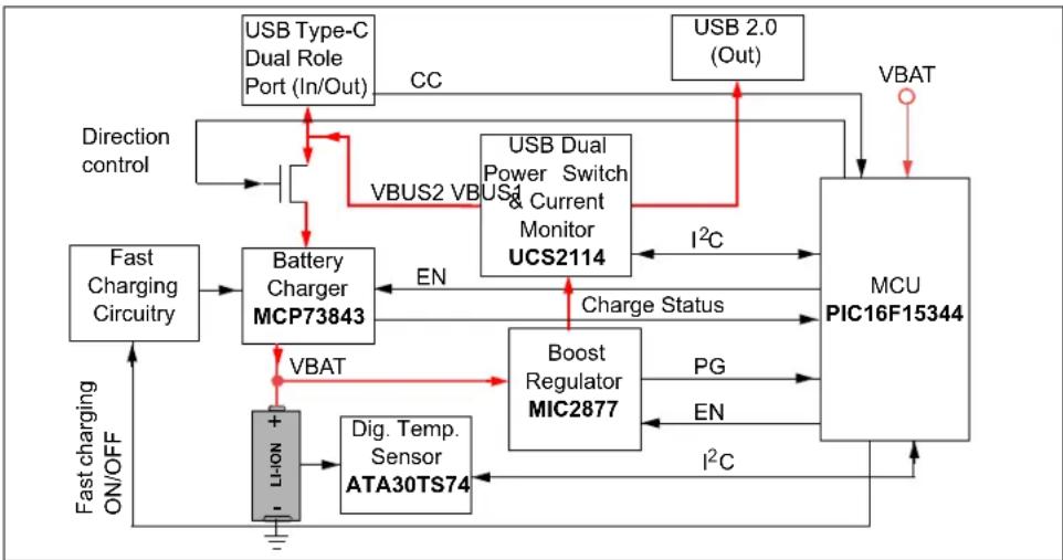
Figure 1-1 represents the block diagram of the MIC2877 USB Type-C Power Bank with Dual Role Port Reference Design.
1.2.1 MIC2877 Device Overview
The MIC2877 is a compact and highly efficient 2 MHz synchronous boost regulator with a 6.5A (typical) switch current limit. It features a bidirectional true load disconnect function that prevents any leakage current between the input and output, when the device is disabled (EN = GND), protecting the input supply and improving the start-up performance.
The MIC2877 has the input voltage range between 2.5V and 5.5V and provides 2A output continuous current for V_IN = 3V and V_OUT = 5V . Fixed output and adjustable output versions are available.
The converter operates in Automatic Input to Output Bypass Mode when the input voltage is higher or equal to the target output voltage. At light loads, the boost converter runs into Pulse Frequency Modulation (PFM) mode, to improve the efficiency. In shutdown mode, the regulator typically consumes less than 2 A.
The MIC2877 also features an integrated anti-ringing switch to minimize EMI, overvoltage and overcurrent protection, Undervoltage Lockout (UVLO) and thermal shutdown. The MIC2877 is available in an 8-pin FTQFN 2 mm x 2 mm package.
1.2.1.1 MIC2877 DEVICE FEATURES:
• Typical 6.5A Input Peak Current Limit
- Up to 95% Efficiency
- Fully Integrated, High Efficiency, 2 MHz Switching Frequency
- Bidirectional True Load Disconnect, Overvoltage Protection (OVP) and Undervoltage Lockout (UVLO)
- Controlled Pre-Charge Current Limit at Start-Up
- Ultra-Fast Transient Response
- Input Voltage Range from 2.5V to 5.5V
• Maximum Output Current:
- 1.5 A in a 2.5V and VOUT = 5V
- 2 A, a_N 3V and V_OUT = 5V
- Output Voltage Range:
- Adjustable
- Fixed Versions: 4.75V, 5V, 5.25V, 5.5V
- Integrated Anti-Ringing Switch for EMI Reduction
• Typically less than 2 μA Shutdown Current - Internal Compensation
• Automatic Input to Output Bypass Mode for V_IN ≥ V_OUT
• Power Good (PG) Output
• Overcurrent Protection and Thermal Shutdown
• Available Package: 8-pin FTQFN 2 mm x 2 mm
1.2.2 MCP7384X Device Overview
The MCP7384X family of devices are highly advanced linear charge management controllers for use in space-limited, cost-sensitive applications. The MCP73841 and MCP73842 combine high accuracy, constant-voltage, constant-current regulation, cell preconditioning, cell temperature monitoring, advanced safety timers, automatic charge termination and charge status indication in space-saving, 10-pin MSOP packages. The MCP73841 and MCP73842 provide complete, fully-functional, stand-alone charge management solutions.
The MCP73843 and MCP73844 employ all the features of the MCP73841 and MCP73842, with the exception of the cell temperature monitor. The MCP73843 and MCP73844 are offered in 8-pin MSOP packages.
The MCP73841 and MCP73843 are designed for applications which utilize single-cell Lithium-Ion or Lithium-Polymer battery packs. Two preset voltage regulation options are available (4.1V and 4.2V) for use with either coke or graphite anodes. The MCP73841 and MCP73843 operate with an input voltage range of 4.5V to 12V.
The MCP73842 and MCP73844 are designed for applications which utilize dual series connected cells Lithium-Ion or Lithium-Polymer battery packs. Two preset voltage regulation options are available (8.2V and 8.4V). The MCP73842 and MCP73844 operate with an input voltage range of 8.7V to 12V.
The MCP7384X family of devices are fully specified over the ambient temperature range of -40^ to +85^ .
1.2.2.1 MCP7384X DEVICE FEATURES
• Linear Charge Management Controllers
- High-Accuracy Preset Voltage Regulation: - ±10.5% (maximum)
- Four Preset Voltage Regulation Options:
- 4.1V: MCP73841-4.1, MCP73843-4.1
- 4.2V: MCP73841-4.2, MCP73843-4.2
- 8.2V: MCP73842-8.2, MCP73844-8.2
- 8.4V: MCP73842-8.4, MCP73844-8.4
• Programmable Charge Current
• Programmable Safety Charge Timers
• Preconditioning of Deeply Depleted Cells
• Automatic End-of-Charge Control
- Optional Continuous Cell Temperature Monitoring (MCP73841 and MCP73842)
- Charge Status Output for Direct LED Drive
• Automatic Power-Down when Input Power Removed
• Temperature Range: -40°C to 85°C
- Packaging:
- MSOP-10: MCP73841, MCP73842
- MSOP-8: MCP73843, MCP73844
1.2.3 UCS2114 Device Overview
The UCS2114 is a dual USB port power switch configuration which can provide 3.0A continuous current (3.4A maximum) per VBUS port with precision overcurrent limiting (OCL), port power switch enables, auto-recovery fault handling, undervoltage and overvoltage lockout, as well as back-drive, back-voltage and thermal protection.
The UCS2114 is well suited for both stand-alone and applications having SMBus/I²C communications. For applications with SMBus, the UCS2114 provides per-port current monitoring and eight programmable current limits per switch, ranging from 0.53A to 3.0A continuous current (3.4A maximum). Per-port charge rationing is also provided, ranging from 3.8 mAh to 246.3 mAh. In stand-alone mode, the UCS2114 provides eight current limits for both switches, ranging from 0.53A + 0.53A to 3A + 3A total continuous current.
Both power switches include an independent VBUS discharge function and constant current mode current limiting for BC1.2 applications.
The UCS2114 is available in a 3 mm x 3 mm 20-pin QFN package.
1.2.3.1 UCS2114 DEVICE FEATURES
- Dual-Port Power Switches:
- 2.9V to 5.5V source voltage range
- 3.0A continuous current per VBUS port, with 18 mΩ resistance per switch
- Independent port power switch enable pins
- Dual fault ALERT# active drain output pins
- Constant Current or Trip mode current limiting behaviors
- Undervoltage and overvoltage lockout
- Back-drive, back-voltage protection
- Auto-recovery fault handling with low test current
- BOOST# logic output to increase DC-DC converter output under large load conditions
- SMBus 2.0/I ^2 C ^TM Mode Features:
- Eight programmable current limits assignable to each power switch
- Other SMBus addresses available upon request
- Block read and block write
- Self-Contained Current Monitoring (No External Sense Resistor Required)
- Fully Programmable Per-Port Charge Rationing and Behaviors
- Configurable Per-Port BC1.2 VBUS Discharge Function
- -40°C to +105°C Operating Temperature Range
• Available in a 20-pin QFN 3 mm x 3 mm
• UL recognized and EN/IEC 60950-1 (CB) Certified
1.2.4 AT30TS74 Device Overview
Microchip's AT30TS74 temperature sensor is capable of measuring and converting temperatures from -55^ to +125^ to a digital word and provides a typical accuracy of ±1.0^ over the operating temperature range of -20^ to +100^ . The device is factory calibrated and requires no external components to help provide a cost effective solution. To reduce current consumption and save power, the AT30TS74 features a shutdown mode which turns off all internal circuitry, except for the internal power-on reset and serial interface circuits. In addition, the device features a power saving one-shot mode that allows the device to make a temperature measurement and update the temperature register and then return to shutdown mode. The AT30TS74 is based on the industry standard "LM75-type" compatible temperature sensor and is a precision temperature monitoring device designed for use in a variety of applications. The device combines a highly accurate digital temperature sensor with programmable high and low temperature alarms, user-selectable resolution up to 12 bits, and an I ^2 C/SMBus ^™ compatible serial interface available in compact packages.
1.2.4.1 AT30TS74 DEVICE FEATURES:
• 2-wire I ^2 C/SMBus Compatible Interface
• Single 1.7V to 5.5V Supply
- I ^2 C High-Speed (HS) Mode Compatible – 3.4 MHz Maximum Clock Frequency
- User Selectable 9 to 12-Bit Resolution
• ±1°C Accuracy from -20°C to +100°C
- Low Operating Current: 130 μA (typical)
- Shutdown Mode: 0.6 A (typical)
- Power Saving One-Shot Temperature Conversion Measurement
• Space Saving SOIC, DFN, MSOP and Wafer level CSP Packages available
1.2.5 PIC16F15344 Device Overview
PIC16(L)F153XX 8-bit product family features essential peripherals, such as Intelligent Analog, Core Independent Peripherals (CIPs) and communication combined with eXtreme Low-Power (XLP) for a wide range of low-power applications. The family features PWMs, multiple communication, temperature sensor and memory features, like Memory Access Partition (MAP) and Device Information Area (DIA). The products are offered in a broad range of pin counts from 8 to 48-pins, to support customers in various applications.
1.2.5.1 PIC16F15344 DEVICE FEATURES:
- Enhanced Mid-range Core with 49-Instruction, 16-Stack Levels
- Flash Program Memory with self read/write capability
• eXtreme Low Power (XLP)
• IDLE and DOZE low power modes
• Peripheral Module Disable (PMD)
• Peripheral Pin Select (PPS) - 4x 10-bit PWMs
• 2x Capture, Compare, PWM (CCP)
• Complementary Waveform Generator (CWG)
• Numerically Controlled Oscillator (NCO) - 4x Configurable Logic Controller (CLC)
• 17 Channel 10-bit ADC with Voltage Reference - 5-bit Digital to Analog Converter (DAC)
- 2x Comparators
- 1x 8-bit Timer (TMR2)
• 2x 16-bit Timers (TMR0/TMR1)
• Window Watchdog Timer (WWDT)
• Enhanced Power-On/Off-Reset - Low-Power Brown-Out Reset (LPBOR)
- Programmable Brown-Out Reset (BOR)
• In Circuit Serial Programming (ICSP) - Operating Voltage Range from 2.3V to 5.5V
1.3 FUNCTIONAL DESCRIPTION
The MIC2877 USB Type-C Power Bank with Dual Role Port Reference Design is a fully functional USB Type-C Power Bank solution, compatible with a large variety of portable devices and wall chargers.
This design has two ports: a USB2.0 port, which is an output port and a USB Type-C port, which is a reversible port that is set automatically by the PIC microcontroller, as an input or as an output port, according to the connection type detected (wall charger or portable device).
The MIC2877 boost converter used in this design can deliver from 2A to 4A at 5V output (which is the sum of the currents flowing though both USB2.0 and USB Type-C ports), depending on the battery voltage. The output current delivery is performed by the "USB Dual-Port Power Switch and Current Monitor" (UCS2114), which can switch on/off and monitor the output current for each USB port, that is controlled by the PIC16F15344 microcontroller through I²C communication.
The battery protection is performed by the PIC16F15344 microcontroller, which always measures several parameters, such as: the battery voltage, in order to prevent discharging below its cut-off voltage, as well as the battery temperature (through the AT30TS74 "9 to 12-bit Selectable, ±1.0°C Accurate Digital Temperature Sensor"), in order to apply the optimal charging/discharging current or shutdown the device if the temperature reaches the critical value. The battery charging mechanism is implemented by the MCP73843 "Advanced Single Cell Lithium-Ion/ Lithium-Polymer Charge Management Controller", together with a fast charging circuitry, which can double the charging current if the battery temperature is less than 40°C.
The algorithm implemented in the PIC16F15344 microcontroller monitors the battery voltage, battery temperature, output voltage, charge state and output current; based on all these parameters, it applies the most appropriate operating mode, in order to extend the battery life.
Figure 1-1 shows a simplified block diagram of the MIC2877 USB Type-C Power Bank with Dual Role Port Reference Design.
flowchart
graph TD
    A["Fast Charging Circuitry"] --> B["Battery Charger MCP73843"]
    B --> C["Boost Regulator MIC2877"]
    C --> D["MCU PIC16F15344"]
    D --> E["USB 2.0 (Out)"]
    D --> F["VBAT"]
    B --> G["VBUS2 VBUS1"]
    B --> H["VBAT"]
    B --> I["EN"]
    B --> J["I²C"]
    B --> K["Direction control"]
    B --> L["Fast charging ON/OFF"]
    B --> M["Dig. Temp. Sensor ATA30TS74"]
    M --> N["+ -<br>L-I ON"]
    N --> B
    C --> O["PG"]
    C --> P["EN"]
    C --> Q["I²C"]
    style A fill:#f9f,stroke:#333
    style D fill:#ccf,stroke:#333
FIGURE 1-1: MIC2877 USB Type-C Power Bank with Dual Role Port Reference Design Block Diagram.
1.3.1 Configuration Channel (CC) Pins
The Configuration Channels (CCs) CC1 and CC2 pins are critical for basic USB Type-C operation. Resistors are attached to the CC pins in various configurations, depending on whether the application is a source, a sink, or an electronically marked/active cable.
All USB host and hub ports advertise via the CC pins the level of current that is presently available. The USB device port is required to manage its load, in order to stay within the current level offered by the host or hub, including dynamically scaling back the load if the host or hub port changes its advertisement to a lower level, as indicated over the CC pins.
CC pins are used for port-to-port connections and shall be supported on all USB Type-C connections on the hub.
The CC1 and CC2 pins must be constantly monitored by the port, to perform the following functions:
- Cable attach and removal detection
- Basic USB Type-C current capability advertisement
TABLE 1-1: VALID SOURCE R PULL-UP RESISTOR VALUES
| Source Current Capability | Resistor Pull-up to 4.75V-5.5V | Resistor Pull-up to 3.3V ± 5% | Current Source to 1.7V-5.5V |
| Default USB Power (500 mA for USB2.0, 900 mA for USB3.0) | 56 kΩ ± 20% | 36 kΩ ± 20% | 80 μA ± 20% |
| 1.5A @ 5V 22 k | Ω ± 5% | 12 kΩ ± 5% | 180 μA ± 8% |
| 3.0A @ 5V 10 k | Ω ± 5% | 4.7 kΩ ± 5% | 330 μA ± 8% |
Table 1-1 shows the valid R_P pull-up resistor values, according to the current source capabilities, when a valid connection is established. A resistive divider consisting of R_P (from a source) and R_D (from a sink) is created, the current source capabilities depending on the voltage across the sink's R_D .
TABLE 1-2: USB TYPE-C™ - PORT TYPE COMPATIBILITY
| Port Type | DRP (Dual Role Port) | Source Only | Sink Only |
| DRP (Dual Role Port) | Supported* | Supported | Supported |
| Source Only Supported | Not | Supported | Supported |
| Sink Only | Supported | Supported | Not Supported |
*DRP toggles between source and sink advertisement by alternating between enabling R_P current sources and R_D pull-downs.
TABLE 1-3: CC STATES
| DRP Mode | CC1 CC2 | State | |
| Source mode | V_BUS | V_BUS | Nothing attached or source attached |
| Source mode | R_D | V_BUS | Sink attached |
| Source mode | V_BUS | R_D | Sink attached |
| Sink mode | GND GND | Nothing | attached or sink attached |
| Sink mode | R_P | GND | Source attached |
| Sink mode | GND | R_P | Source attached |
1.3.1.1 SOURCE MODE OPERATION
When operating as a source, the device connects the R_P pull-up resistors on both CC lines and waits for a sink connection; the R_P pull-up resistors values depend on the output current capability. The CC pins are read by the ADC of the PIC microcontroller, in order to determine if a valid portable device (sink) is connected. Refer to Table 1-1 for more information about R_P pull-up resistors.
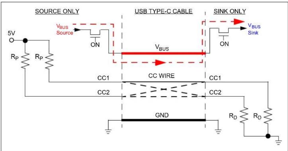
FIGURE 1-2: Source to Sink.
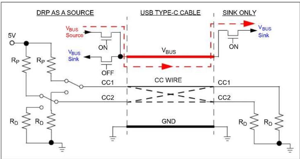
FIGURE 1-3: Dual Role Port (DRP) as a Source Connected to Sink.
1.3.1.2 SINK MODE OPERATION
When operating as a sink, the device connects the R_D pull-down resistors on both CC lines and waits for a source connection from the assertion of V_BUS . The CC pins are read by the ADC of the PIC microcontroller, in order to determine the advertised current charger capabilities supported by the source.
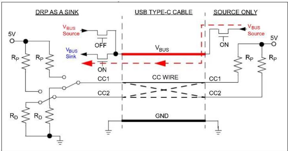
FIGURE 1-4: Dual Role Port (DRP) as a Sink Connected to Source.
1.3.2 Charging and Fast Charging Circuitry
For implementing the battery charge control on this board, the MCP73843 has been used. The MCP73843 is a highly advanced linear charge management controller, which combines high accuracy, constant-voltage, constant-current regulation, cell preconditioning, advanced safety timer, automatic charge termination and charge status indication.
Charge current is sensed via the voltage drop across an external precision sense resistor ( R_SHUNT ). The resistive divider consisting of R_1 and R_2 , together with the switch S_1 , provide the option to set a second charging current (Fast Charging Current) that is higher than the default one (Charging Current). The transition from the default charging current to the fast charging current is done by the switch S_1 . The charging current and fast charging current can be calculated by using Equation 1-1 and Equation 1-2.
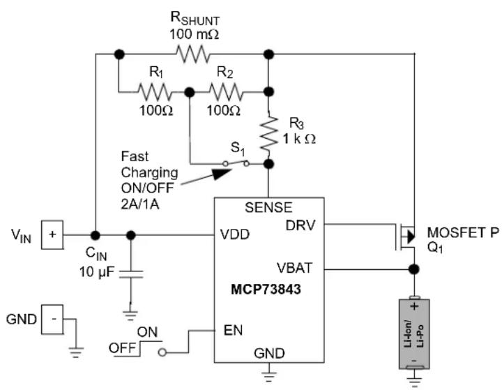
FIGURE 1-5: Fast Charging Circuitry.
EQUATION 1-1:
$$ I _ {C h i n g a r g} = \frac {V _ {F C S}}{R _ {S H U N T}} $$
Where: V_FCS = V_DD - V_SENSE = 100 mV
R_SHUNT = 100 m
EQUATION 1-2:
$$ I _ {F a s t C h i n g a r g} = I _ {C h i n g a r g} \times \frac {R _ {1} + R _ {2}}{R _ {1}} $$
Note 1: R 1 + R 2 should not exceed 500Ω.
2: I Charging and I_FastCharging should not exceed the maximum current that can be provided by the wall charger or 1C x 2 cell (1C is battery's capacity in mAh — refer to the battery manufacturer recommendation).
1.4 WHAT IS THE MIC2877 USB TYPE-C POWER BANK WITH DUAL ROLE PORT REFERENCE DESIGN?
The MIC2877 USB Type-C Power Bank with Dual Role Port Reference Design is used to evaluate and demonstrate Microchip Technology's MIC2877, PIC16F15344, MCP73843, UCS2114 and AT30TS74 products.
The MIC2877 USB Type-C Power Bank with Dual Role Port Reference Design was developed to help engineers reduce the product design cycle time.
1.5 WHAT DOES THE MIC2877 USB TYPE-C POWER BANK WITH DUAL ROLE PORT REFERENCE DESIGN KIT INCLUDE?
This MIC2877 USB Type-C Power Bank with Dual Role Port Reference Design kit includes:
- MIC2877 USB Type-C Power Bank with Dual Role Port Reference Design (ARD00916)
- Important Information Sheet
NOTES:
Chapter 2. Installation and Operation
2.1 OVERVIEW
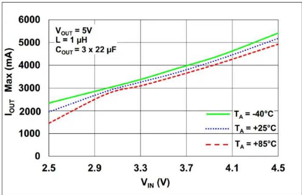
The MIC2877 USB Type-C Power Bank with Dual Role Port Reference Design was developed as a TSS (Total System Solution) for applications where a positive regulated 5V output voltage is needed from one or more parallel-connected Li-Ion cells. Refer to Figure 2-2 for the maximum output current that can be delivered for different input voltages.
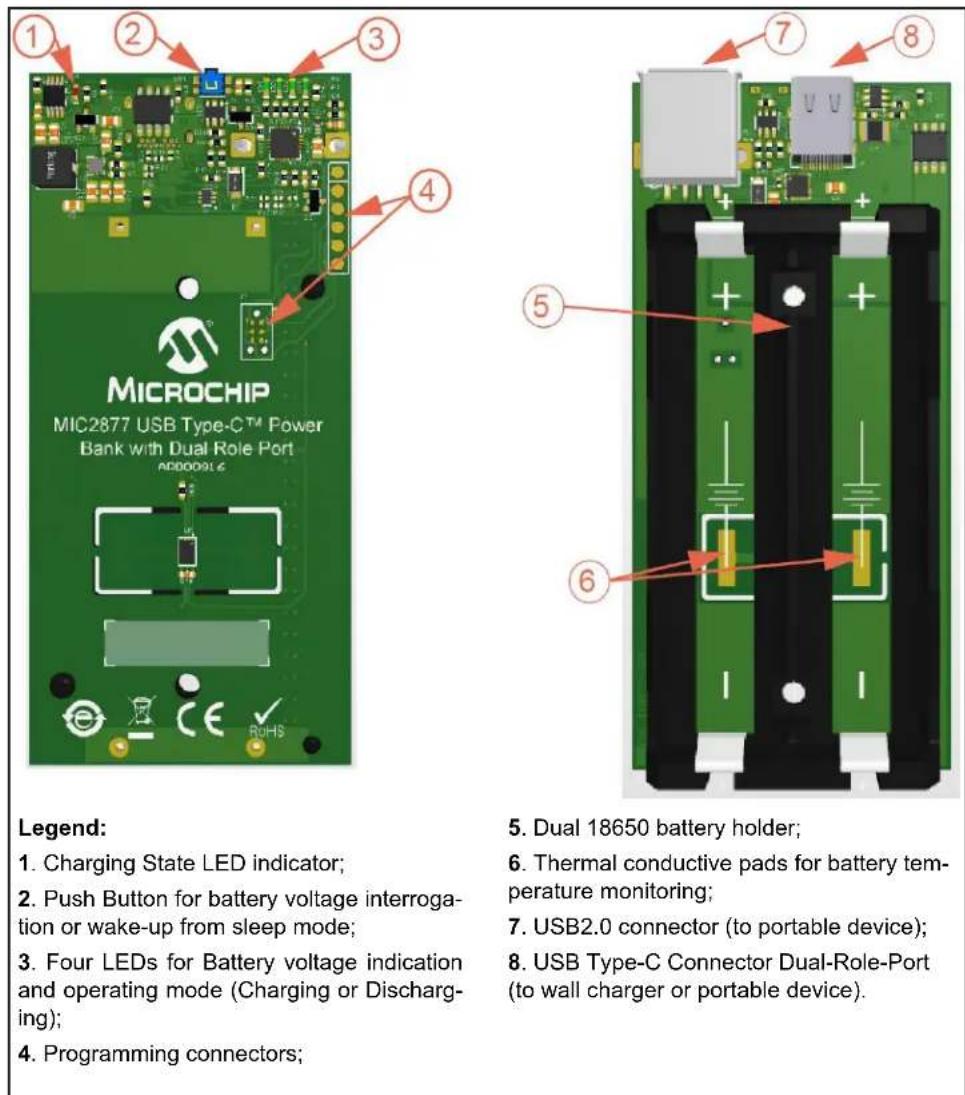
Legend:
- Charging State LED indicator;
- Push Button for battery voltage interrogation or wake-up from sleep mode;
- Four LEDs for Battery voltage indication and operating mode (Charging or Discharging);
-
Programming connectors;
-
Dual 18650 battery holder;
- Thermal conductive pads for battery temperature monitoring;
- USB2.0 connector (to portable device);
- USB Type-C Connector Dual-Role-Port (to wall charger or portable device).
FIGURE 2-1: MIC2877 USB Type-C Power Bank with Dual Role Port Reference Design — Top and Bottom View.
line
| VIN (V) | TA = -40°C | TA = +25°C | TA = +85°C | | ------- | ---------- | ---------- | ---------- | | 2.5 | ~2300 | ~2000 | ~1500 | | 2.9 | ~2800 | ~2600 | ~2200 | | 3.3 | ~3300 | ~3100 | ~2800 | | 3.7 | ~3800 | ~3600 | ~3300 | | 4.1 | ~4300 | ~4100 | ~3800 | | 4.5 | ~4800 | ~4600 | ~4300 |FIGURE 2-2: MIC2877 5V V OUT Maximum IOUT vs. VIN vs. Temperature.
2.1.1 Board Features
The MIC2877 USB Type-C Power Bank with Dual Role Port Reference Design has the following features:
- Battery temperature monitoring during both Charging and Discharging mode
- Battery voltage monitoring
• VBUS (Type-C Connector) voltage monitoring - Output Current monitoring on each output port
-
Adaptive Charging mode according to battery temperature (firmware customizable):
-
Default Charging Current: 1A, if battery temperature < 45°C
- Fast Charging Current: 2A, if battery temperature < 40°C
-
Charging off (automatic disable), if battery temperature > 45°C
-
Auto shutdown/enter sleep mode, if I_OUT < 40 mA or battery temperature > 55^ C
- Automatic/manual wake-up from sleep mode by using either WD Timer or Push button
- Battery status and operating mode LED indicators
-
Battery voltage interrogation by pressing the Push button
• Output characteristics: -
2 x Output ports: USB2.0 and USB Type-C (reversible)
- Output Current: 2A up to 4A (battery voltage dependent)
- Output voltage: 5V
- Start-up voltage (UVLO Start): 3.2V (programmable by MCU)
- Shutdown voltage (UVLO Stop): 3.0V (programmable by MCU)
- Input Idle current: 750 μA
2.2 GETTING STARTED
The MIC2877 USB Type-C Power Bank with Dual Role Port Reference Design is fully assembled, programmed and tested to evaluate and demonstrate the Microchip products used in this Reference Design. This board requires two 18650 Li-Ion battery cells (not provided with the board).
2.2.1 Power Input and Output Connections
2.2.1.1 POWERING THE MIC2877 USB TYPE-C POWER BANK WITH DUAL ROLE PORT REFERENCE DESIGN
The MIC2877 USB Type-C Power Bank with Dual Role Port Reference Design is powered from two 18650 Li-Ion batteries (the holder is available on the board). The switch peak current limit will provide a safe value for the input current. The maximum output current for the MIC2877 switching regulator will vary with the input and output voltages (see Figure 2-2).
For the onboard connectors, please refer to Figure 2-1 and Figure 2-3.
Soldered test points are available to connect a PIC programmer (please refer to Figure 2-4).
2.2.1.2 BOARD POWER-UP PROCEDURE
- Insert two 18650 Li-ion batteries into the holder (observing the polarity), as shown in Figure 2-3.
- Press the Push button once. The 4 LEDs will indicate the level of the battery (state of charge); each LED indicates 25%.
- Connect the wall charger (source) to the Type-C connector. The LD5 (red) indicates that the charging is in progress. Moreover, the LD1-LD4 LEDs will show the animated charging process, as well as the battery level.
Note 1: The value of the charging current changes automatically (1A or 2A), depending on the charger's type (being detected via CC pins on the USB Type-C connector) and the battery temperature.
2: Chargers with output current capabilities less than 1A are not recommended to be used with this Reference Design.
- Connect a portable device (sink) to the USB Type-C or the USB2.0 connectors. The LD1-LD4 LEDs will show the animated discharging process.
Note 1: USB2.0: This port will stay powered as long as the output current is higher than 40 mA.
2: If no device has been detected, the board will enter Sleep mode and periodically wakes up every 4 seconds (approximately).
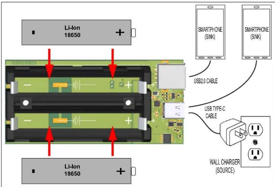
FIGURE 2-3: MIC2877 USB Type-C Power Bank with Dual Role Port Reference Design Setup.
2.3 PROGRAMMING THE PIC16F15344 MICROCONTROLLER
The firmware package provides the source and .hex files for this Reference Design.
The board is factory programmed with the Power Bank firmware. UVLO, temperature thresholds and the wake-up period can be modified. The source code includes comprehensive comments which help the user to define the board.
This firmware was developed using MPLAB ^® X Integrated Development Environment, in combination with the PIC10/12/16 MCU Family.
Connector J2 provides in-system circuit programming.
If custom functionality is needed, follow the next steps to reprogram the MCU:
-
Connect the PICkit™ 3 or other programming tool to the USB port.
-
Connect the programming tool to the board at J2 Tag-Connect or test points (see Figure 2-4).
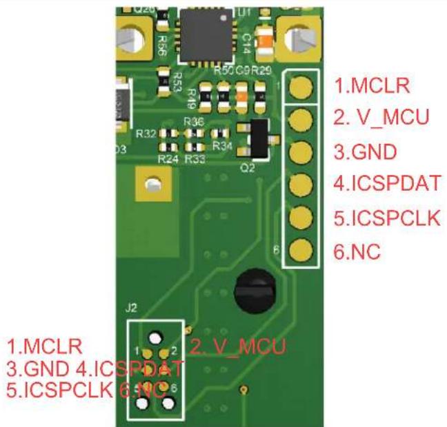
FIGURE 2-4: Programming Connectors Pinout.
- Open the Type_C_PWR_BNK.prj file using MPLAB® X Integrated Development Environment.
- Select the programming tool: File > Project Properties > Hardware Tools and choose your programming tool from the submenu list.
- Return to the Programmer menu and click the Power tab from the Option Categories window. Set the voltage to 5V and select the "Power target circuit from PICkit 3" check box. Click on the Apply button.
- Click the OK button on the warning message.
- Click the Make and Program Device toolbar button. Check the Output window to see if the programming was performed without errors.
The board is now ready to operate.
NOTES:
Appendix A. Schematic and Layouts
A.1 INTRODUCTION
This appendix contains the following schematics and layouts for the MIC2877 USB Type-C Power Bank with Dual Role Port Reference Design:
- Board – Schematic
- Board – Top Silk
- Board – Top Copper and Silk
- Board – Top Copper
- Board – Signal Layer 1
- Board – Signal Layer 2
- Board – Bottom Copper
- Board – Bottom Copper and Silk
- Board – Bottom Silk
A.2 BOARD - SCHEMATIC
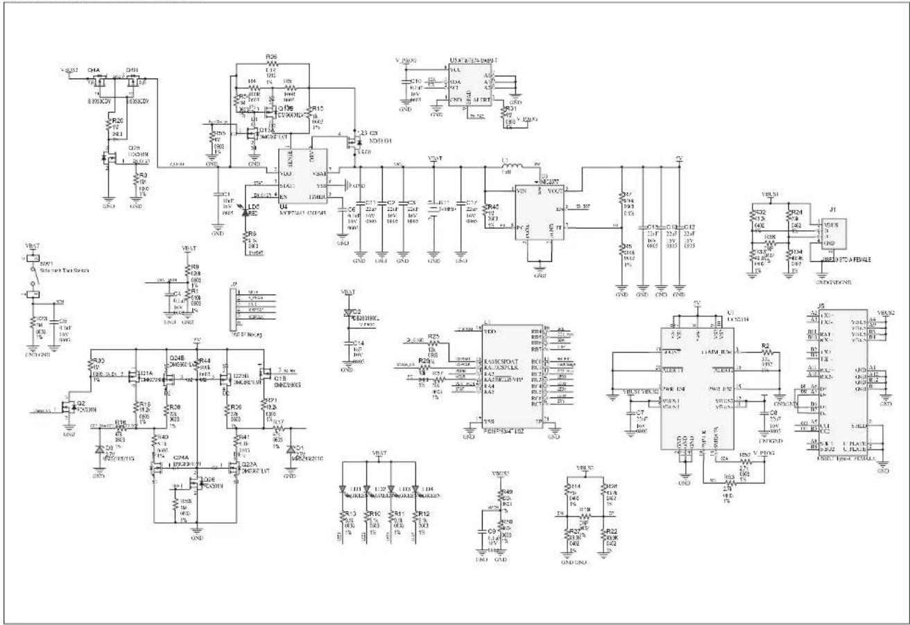
A.3 BOARD - TOP SILK
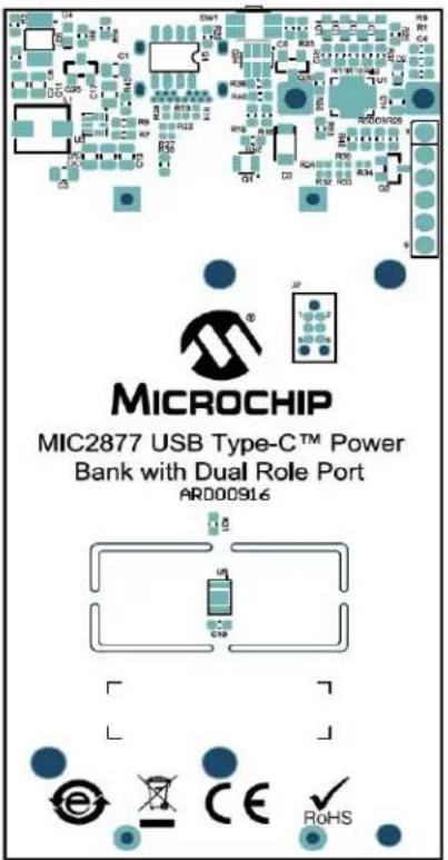
A.4 BOARD - TOP COPPER AND SILK
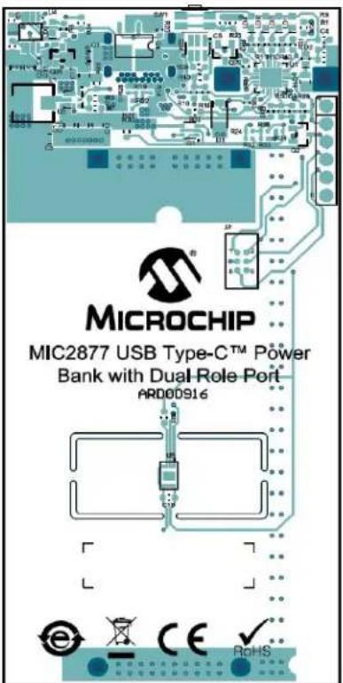
A.5 BOARD - TOP COPPER
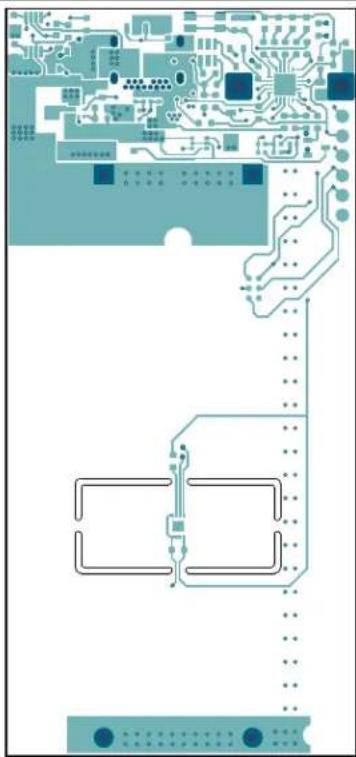
natural_image
Pure electrical circuit lines without any symbolsA.6 BOARD – SIGNAL LAYER 1
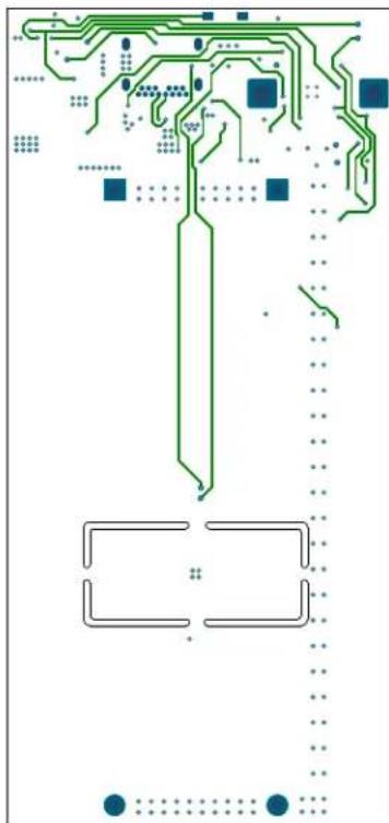
natural_image
Pure electrical circuit lines without any symbolsA.7 BOARD – SIGNAL LAYER 2
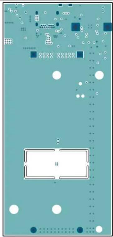
natural_image
Abstract geometric pattern with scattered circles, squares, and dots on a teal background (no text or symbols)A.8 BOARD - BOTTOM COPPER
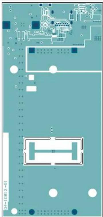
natural_image
Top-down view of a printed circuit board with traces, pads, and components (no readable text or symbols)A.9 BOARD - BOTTOM COPPER AND SILK
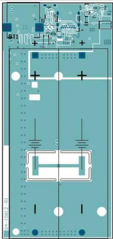
natural_image
Pure electrical circuit lines without any symbolsA.10 BOARD - BOTTOM SILK
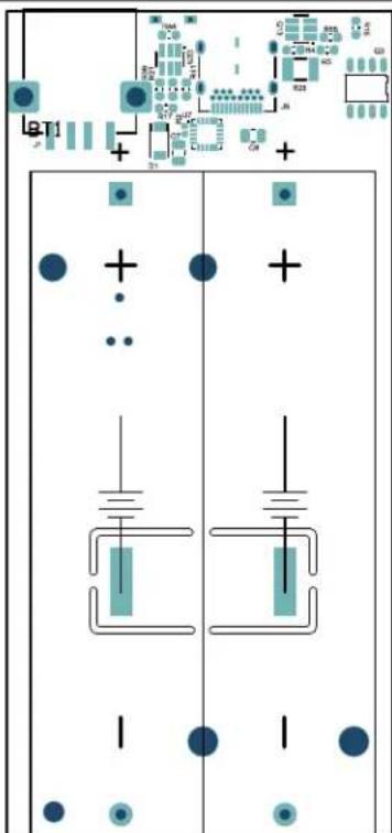
Appendix B. Bill of Materials (BOM)
TABLE B-1: BILL OF MATERIALS (BOM)
| Qty. | Reference | Description Manufacturer Part Number | ||
| 1 BT | Battery Holder | 1 TH, 2x 18650 Keystone Electronics 1049 | ||
| 1 C1 | Capacitor, Ceramic, 10 μF, 16V, 10%, X5R, SMD, 0805 | Wurth Electronik 885012 | 107014 | |
| 9 C2 | C3, C7, C8, C11, C12, C13, C15, C17 | Capacitor, Ceramic, 22 μF, 16V, 10%, X5R, SMD, 0805 | TDK Corporation C2012 | X5R1C226K |
| 5 C4 | C5, C6, C9, C10 | Capacitor, Ceramic, 0.1 μF, 16V, 10%, X7R, SMD, 0603 | Wurth Electronik 885012 | 206046 |
| 1 C14 | Capacitor, Ceramic, 1 μF, 10V, 10%, X5R, SMD, 0805 | Murata GRM219R61A10 | 5KC01D | |
| 2 D1 | D3 Diode, Zener, MMSZ4682, 2.7V, 500 mW, SMD, SOD-123 | ON Semiconductor® | MMSZ4682T1G | |
| 1 D2 | Diode, Schottky, 30V, 100 mA, DB2S31600L, SOD523 | Panasonic® - ECG | DB2S31600L | |
| 1 J1 | Connector, USB2.0, STD-A, Female, SMD, R/A | ASSMANN Electronics Inc. | AU-Y1006-2 | |
| 1 | J2 | Connector, TAG, 6P, No-Leg, SMD, Vertical | Tag-Connect | TC2030-MCP-NL |
| 1 J5 | Connector, USB3.1, TYPE-C, Female, TH, R/A | Wurth Electronik 632723 | 300011 | |
| 1 L1 | Inductor, 1 μH, 11.5A, 20%, SMD, L5.9W5.6H4.3 | Wurth Electronik 744316 | 100 | |
| 4 | LD1, LD2, LD3, LD4 | Diode, LED, Green, 2V, 30 mA, 35 mcd, Clear, SMD, 0603 | Lite-On®, Inc. | LTST-C190KGKT |
| 1 LD5 | Diode, LED | Red, 1.9V, 20 mA, 40 mcd, Clear, SMD, 0603 | Para Light Corp. | L-C191KRCT-U1 |
| 1 PCB1 | Printed Circuit Board | Microchip Technology Inc. | 04-10812-R1 | |
| 1 Q1 | Transistor, FET, Dual, P+P, CMKDM8005, 20V, 650 mA, .360R, 0.350W, SOT-363 | CentralTM Semiconductor Corp. | CMKDM8005 TR | |
| 3 | Q2, Q25, Q26 | Transistor, FET, N-CH, FDV301N, 25V, 220 mA, 350 mW, SOT-23-3 | Fairchild Semiconductor® | FDV301N |
| 1 Q3 | Transistor, FET, P-CH, NDS8434, 20V, 6.5A, 2.5W, SOIC-8 | ON Semiconductor® | NDS8434 | |
| 1 Q4 | Transistor, FET, Dual, P+P, SI9933CDY-T1-GE3, -20V, -4A, 0.094R, 3.1W, SO-8 | Vishay Siliconix | SI9933CDY-T1-GE3 | |
| 3 Q13 | Q23, Q24 | Transistor, FET, Dual, N+P, 30V, -30V, 3.8A, -2.5A, 0.055R, 0.11R, 0.85W, TSOT-26 | Diodes Incorporated® | DMG6601LVT-7 |
| Qty. | Reference | Description | Manufacturer | Part Number |
| 1 R1 | Resistor, Thick Film, 510k, 1%, 1/10W, SMD, 0603 | Panasonic ERJ-3EKF51 | 03V | |
| 1 R2 | Resistor, Thick Film, 33k, 1%, 1/16W, SMD, 0402 | Yageo AC0402FR-0733 | KL | |
| 9 R3 | R20, R23, R30, R31, R45, R54, R55, R56 | Resistor, Thick Film, 1M, 1%, 1/10W, SMD 0603 | Panasonic ERJ-3EKF10 | 04V |
| 2 R4 | R5 Resistor, | Thick Film, 100R, 1%, 1/10W, SMD, 0603 | Panasonic ERJ-3EKF10 | 00V |
| 5 R6 | R10, R11, R12, R13 | Resistor, Thick Film, 9.1k, 1%, 1/10W, SMD, 0603 | Yageo Corporation RC0 | 603FR-079K1L |
| 1 R7 | Resistor, Thin Film, 910k, 0.1%, 1/16W, SMD, 0603 | TE Connectivity Passive Product | CPF0603B910KE1 | |
| 1 R8 | Resistor, Thick Film, 200k, 1%, 1/10W, SMD, 0603 | Vishay CRCW0603200K | FKEA | |
| 2 R9 | R49 Resistor, | Thick Film, 620k, 1%, 1/10W, SMD, 0603 | Vishay Dale CRCW0603 | 620KFKEA |
| 2 R14 | R24 Resistor, | Thick Film, 75k, 1%, 1/10W, SMD, 0402 | Panasonic® - ECG ERJ- | 2RKF7502X |
| 1 R15 | Resistor, Thick Film, 1k, 1%, 1/10W, SMD, 0603 | Panasonic ERJ-3EKF10 | 01V | |
| 2 R16 | R17 Resistor, | Thick Film, 47k, 1%, 1/10W, SMD, 0603 | Panasonic ERJ-3EKF47 | 02V |
| 2 R18 | R21 Resistor, | Thick Film, 18.2k, 1%, 1/10W, SMD, 0603 | Panasonic ERJ-3EKF18 | 22V |
| 4 R22 | R27, R33, R34 | Resistor, Thick Film, 49.9k, 1%, 1/16W, SMD, 0402 | Yageo RC0402FR-0749 | K9L |
| 3 R25 | R29, R37 | Resistor, Thin Film, 10k, 1%, 1/16W, SMD, 0603 | TE Connectivity | 5-1879337-9 |
| 1 R26 | Resistor, Thick Film, 0.1R, 1%, 1W, SMD, 1210 | Vishay Dale RCWE1210 | R100FKEA | |
| 2 R28 | R32 Resistor, | Thick Film, 43.2k, 1%, 1/16W, SMD, 0402 | Yageo Corporation RC0 | 402FR-0743K2L |
| 2 R38 | R39 Resistor, | Thick Film, 22k, 1%, 1/10W, SMD, 0603 | Panasonic ERJ-3EKF22 | 02V |
| 2 R40 | R41 Resistor, | Thick Film, 5.1k, 1%, 1/10W, SMD, 0603 | Panasonic ERJ-3EKF51 | 01V |
| 1 R44 | Resistor, Thin Film, 100k, 1%, 1/8W, SMD, 0603 | Vishay MCT06030C1003 | FP500 | |
| 1 R50 | Resistor, Thick Film, 360k, 1%, 1/10W, SMD, 0603 | Yageo Corporation RC0 | 603FR-07360KL | |
| 2 R52 | R53 Resistor, | Thick Film, 2.7k, 1%, 1/10W, SMD, 0603 | Panasonic ERJ-3EKF27 | 01V |
| 1 | SW1 | Switch, Side Push, TACT, SPST-NO, 12V, 0.05A, 434331013822, SMD | Wurth Electronik | 434331013822 |
Note: The components listed in this Bill of Materials are representative for the PCB assembly. The released BOM used in manufacturing uses all RoHS-compliant components.
TABLE B-1: BILL OF MATERIALS (BOM) (CONTINUED)
| Qty. | Reference Description Manufacturer Part Number | ||
| 1 U1 | Microchip MCU, 8-BIT, 32 MHz, 7 KB,PIC16F15344T-I/GZ, UQFN-20 | Microchip Technology Inc. | PIC16F15344T-I/GZ |
| 1 U3 | Microchip Analog Switcher Boost, 3V to 5.5V, MIC2877-AYFT-TR, FTQFN-8 | Microchip Technology Inc. | MIC2877-AYFT-TR |
| 1 U4 | Microchip Analog Battery Charger,MCP73843-4.2, MSOP-8 | Microchip Technology Inc. | MCP73843-420I/MS |
| 1 U5 | Microchip Analog Temperature Sensor, ± 1^ , AT30TS74-MA8M-T, MSOP-8 | Microchip Technology Inc. | AT30TS74-MA8M-T |
| 1 U7 | Microchip Interface USB Power Controller,UCS2114, QFN-20 | Microchip Technology Inc. | UCS2114-1-V/LX |
Note: The components listed in this Bill of Materials are representative for the PCB assembly. The released BOM used in manufacturing uses all RoHS-compliant components.
NOTES:
Appendix C. Firmware Flowchart
C.1 FIRMWARE FLOWCHART
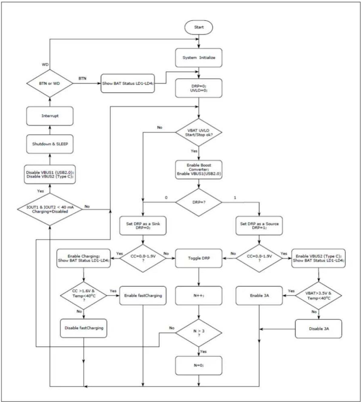
flowchart
graph TD
    A["Start"] --> B["System Initialize"]
    B --> C{BTN or WD}
    C -->|WT| D["Show BAT Status LD1-LD4;"]
    D --> E["DRP=0; UVLO=0;"]
    E --> F{VBAT UVLO Start/Stop ok?}
    F -->|No| G["Set DRP as a Sink DRP=0;"]
    F -->|Yes| H["Enable Boost Converter; Enable VBUS1(USB2.0)"]
    H --> I{DRP=?}
    I -->|0| J["Set DRP as a Sink DRP=0;"]
    I -->|1| K["Set DRP as a Source DRP=1;"]
    J --> L{CC=0.8-1.9V ?}
    K --> M{CC=0.8-1.9V ?}
    L -->|Yes| N["Enable Charging; Show BAT Status LD1-LD4;"]
    L -->|No| O["Enable fastCharging"]
    M --> P["Enable VBUS2 (Type C); Show BAT Status LD1-LD4;"]
    N --> Q{CC >1.6V & Temp<40°C ?}
    O --> R{N++;}
    P --> S{VBAT>3.5V & Temp<40°C ?}
    Q --> T{N >3 ?}
    R --> U["Enable 3A"]
    S --> V["Disable 3A"]
    T --> W["N=0;"]
    U --> X["Disable fastCharging"]
    V --> Y["Disable 3A"]
    W --> Z["Disable fastCharging"]
    X --> AA["Disable 3A"]
    Y --> AB["Disable fastCharging"]
    Z --> AC["Disable Fast Charging"]
    AA --> AD["Disable Fast Charging"]
    AB --> AE["Disable Fast Charging"]
    AC --> AF["Disable Fast Charging"]
    AD --> AG["Disable Fast Charging"]
    AE --> AH["Disable Fast Charging"]
    AF --> AI["Disable Fast Charging"]
NOTES:
Worldwide Sales and Service
AMERICAS
Corporate Office
2355 West Chandler Blvd.
Chandler, AZ 85224-6199
Tel: 480-792-7200
Fax: 480-792-7277
Technical Support:
http://www.microchip.com/
support
Web Address:
www.microchip.com
Atlanta
Duluth, GA
Tel: 678-957-9614
Fax: 678-957-1455
Austin, TX
Tel: 512-257-3370
Boston
Westborough, MA
Tel: 774-760-0087
Fax: 774-760-0088
Chicago
Itasca, IL
Tel: 630-285-0071
Fax: 630-285-0075
Dallas
Addison, TX
Tel: 972-818-7423
Fax: 972-818-2924
Detroit
Novi, MI
Tel: 248-848-4000
Houston, TX
Tel: 281-894-5983
Indianapolis
Noblesville, IN
Tel: 317-773-8323
Fax: 317-773-5453
Tel: 317-536-2380
Los Angeles
Mission Viejo, CA
Tel: 949-462-9523
Fax: 949-462-9608
Tel: 951-273-7800
Raleigh, NC
Tel: 919-844-7510
New York, NY
Tel: 631-435-6000
San Jose, CA
Tel: 408-735-9110
Tel: 408-436-4270
Canada - Toronto
Tel: 905-695-1980
ASIA/PACIFIC
Australia - Sydney
Tel: 61-2-9868-6733
China - Beijing
Tel: 86-10-8569-7000
China - Chengdu
Tel: 86-28-8665-5511
China - Chongqing
Tel: 86-23-8980-9588
China - Dongguan
Tel: 86-769-8702-9880
China - Guangzhou
Tel: 86-20-8755-8029
China - Hangzhou
Tel: 86-571-8792-8115
China - Hong Kong SAR
Tel: 852-2943-5100
China - Nanjing
Tel: 86-25-8473-2460
China - Qingdao
Tel: 86-532-8502-7355
China - Shanghai
Tel: 86-21-3326-8000
China - Shenyang
Tel: 86-24-2334-2829
China - Shenzhen
Tel: 86-755-8864-2200
China - Suzhou
Tel: 86-186-6233-1526
China - Wuhan
Tel: 86-27-5980-5300
China - Xian
Tel: 86-29-8833-7252
China - Xiamen
Tel: 86-592-2388138
China - Zhuhai
Tel: 86-756-3210040
ASIA/PACIFIC
India - Bangalore
Tel: 91-80-3090-4444
India - New Delhi
Tel: 91-11-4160-8631
India - Pune
Tel: 91-20-4121-0141
Japan - Osaka
Tel: 81-6-6152-7160
Japan - Tokyo
Tel: 81-3-6880-3770
Korea - Daegu
Tel: 82-53-744-4301
Korea - Seoul
Tel: 82-2-554-7200
Malaysia - Kuala Lumpur
Tel: 60-3-7651-7906
Malaysia - Penang
Tel: 60-4-227-8870
Philippines - Manila
Tel: 63-2-634-9065
Singapore
Tel: 65-6334-8870
Taiwan - Hsin Chu
Tel: 886-3-577-8366
Taiwan - Kaohsiung
Tel: 886-7-213-7830
Taiwan - Taipei
Tel: 886-2-2508-8600
Thailand - Bangkok
Tel: 66-2-694-1351
Tel: 43-7242-2244-39
Fax: 43-7242-2244-393
Denmark - Copenhagen
Tel: 45-4485-5910
Fax: 45-4485-2829
Finland - Espoo
Tel: 358-9-4520-820
France - Paris
Tel: 33-1-69-53-63-20
Fax: 33-1-69-30-90-79
Germany - Garching
Tel: 49-8931-9700
Germany - Haan
Tel: 49-2129-3766400
Germany - Heilbronn
Tel: 49-7131-72400
Germany - Karlsruhe
Tel: 49-721-625370
Germany - Munich
Tel: 49-89-627-144-0
Fax: 49-89-627-144-44
Germany - Rosenheim
Tel: 49-8031-354-560
Israel - Ra'anana
Tel: 972-9-744-7705
Italy - Milan
Tel: 39-0331-742611
Fax: 39-0331-466781
Italy - Padova
Tel: 39-049-7625286
Netherlands - Drunen
Tel: 31-416-690399
Fax: 31-416-690340
Norway - Trondheim
Tel: 47-7288-4388
Poland - Warsaw
Tel: 48-22-3325737
Romania - Bucharest
Tel: 40-21-407-87-50
Spain - Madrid
Tel: 34-91-708-08-90
Fax: 34-91-708-08-91
Sweden - Gothenberg
Tel: 46-31-704-60-40
Sweden - Stockholm
Tel: 46-8-5090-4654
UK - Wokingham
Tel: 44-118-921-5800
Fax: 44-118-921-5820
- Power Bank with Dual Role Port Reference Design User's Guide
- Note the following details of the code protection feature on Microchip devices:
- Trademarks
- Table of Contents
- Preface 5
- Chapter 1. Product Overview
- Chapter 2. Installation and Operation
- Appendix A. Schematic and Layouts
- Appendix B. Bill of Materials (BOM)
- Appendix C. Firmware Flowchart
- Worldwide Sales and Service 39
- Preface
- NOTICE TO CUSTOMERS
- INTRODUCTION
- DOCUMENT LAYOUT
- CONVENTIONS USED IN THIS GUIDE
- RECOMMENDED READING
- REFERENCES
- CUSTOMER SUPPORT
- DOCUMENT REVISION HISTORY
- Revision A (March 2021)
- INTRODUCTION
- CORE COMPONENTS SHORT OVERVIEW
- MIC2877 Device Overview
- MIC2877 DEVICE FEATURES:
- MCP7384X Device Overview
- MCP7384X DEVICE FEATURES
- UCS2114 Device Overview
- UCS2114 DEVICE FEATURES
- AT30TS74 Device Overview
- AT30TS74 DEVICE FEATURES:
- PIC16F15344 Device Overview
- PIC16F15344 DEVICE FEATURES:
- FUNCTIONAL DESCRIPTION
- Configuration Channel (CC) Pins
- SOURCE MODE OPERATION
- SINK MODE OPERATION
- Charging and Fast Charging Circuitry
- EQUATION 1-1:
- EQUATION 1-2:
- WHAT IS THE MIC2877 USB TYPE-C POWER BANK WITH DUAL ROLE PORT REFERENCE DESIGN?
- WHAT DOES THE MIC2877 USB TYPE-C POWER BANK WITH DUAL ROLE PORT REFERENCE DESIGN KIT INCLUDE?
- OVERVIEW
- Legend:
- Board Features
- GETTING STARTED
- Power Input and Output Connections
- POWERING THE MIC2877 USB TYPE-C POWER BANK WITH DUAL ROLE PORT REFERENCE DESIGN
- BOARD POWER-UP PROCEDURE
- PROGRAMMING THE PIC16F15344 MICROCONTROLLER
- A.1 INTRODUCTION
- A.3 BOARD - TOP SILK
- A.4 BOARD - TOP COPPER AND SILK
- A.5 BOARD - TOP COPPER
- A.6 BOARD – SIGNAL LAYER 1
- A.7 BOARD – SIGNAL LAYER 2
- A.8 BOARD - BOTTOM COPPER
- A.9 BOARD - BOTTOM COPPER AND SILK
- A.10 BOARD - BOTTOM SILK
- C.1 FIRMWARE FLOWCHART
- Worldwide Sales and Service
- AMERICAS
- ASIA/PACIFIC
Brand : Microchip
Model : MIC2877
Category : Uncategorized