
MCP19116 - Uncategorized Microchip - Free user manual and instructions
Find the device manual for free MCP19116 Microchip in PDF.


| Product Type | Digitally Enhanced Power Analog Synchronous Low-Side PWM Controller with Microcontroller Core |
| Dimensions (Package) | 4 x 4 x 0.9 mm (24-pin QFN) |
| Weight | Approx. 0.1 g |
| Input Voltage Range | +4.5V to +42V (absolute max 44V, transient 48V for 500 ms) |
| Gate Drive Output | Low-side, programmable 5V/0.5A or 10V/1A sink/source |
| Program Memory | 8192 words (8k) on-chip Flash, high endurance (100,000 write cycles) |
| ADC | 10-bit resolution, 5 external channels (up to 8 on MCP19117) |
| Communications | I²C (7-bit address masking), AUSART (asynchronous/synchronous) |
| Operating Temperature Range | -40°C to +125°C (junction) |
| Key Features | Peak current mode control, configurable topologies (Flyback, Ćuk, Boost, SEPIC), quasi-resonant or fixed-frequency operation, programmable slope compensation, leading edge blanking, dead time, UVLO/OVLO, output overvoltage protection, thermal shutdown |
| Maintenance and Cleaning | No user maintenance required. Handle with ESD precautions. Clean with isopropyl alcohol if needed. |
| Safety | AEC-Q100 qualified, thermal shutdown at 150°C (hysteresis 20°C), input UVLO/OVLO, output OV protection |
| Spare Parts and Repairability | Not repairable; replace the IC if faulty. No user-serviceable parts. |
| General Information | Manufacturer: Microchip Technology. For full specifications and programming details, refer to the official datasheet (e.g., DS20006162A). |
Frequently Asked Questions - MCP19116 Microchip
User questions about MCP19116 Microchip
0 question about this device. Answer the ones you know or ask your own.
Ask a new question about this device
Download the instructions for your Uncategorized in PDF format for free! Find your manual MCP19116 - Microchip and take your electronic device back in hand. On this page are published all the documents necessary for the use of your device. MCP19116 by Microchip.
USER MANUAL MCP19116 Microchip
Digitally Enhanced Power Analog Synchronous Low-Side PWM Controller with Improved 8k Word Core
Features
- Input Voltage: +4.5V to +42V
- Can be configured with multiple topologies including but not limited to:
- Fly back
- Ćuk
- Boost
- SEPIC (Single-Ended Primary-Inductor Converter)
- Capable of Quasi-Resonant or Fixed-Frequency Operation
- Low Quiescent Current: 5 mA Typical
- Low Sleep Current: 50~ A Typical
- Low-Side Gate Drivers:
- +5V gate drive with 0.5A sink/source current
- +10V gate drive with 1A sink/source current
• Peak Current Mode Control
• Differential Remote Output Sense - Multiple Output Systems:
- Master or Slave
• AEC-Q100 Qualified - Configurable Parameters:
- V_REF , Precision I_OUT/V_OUT Set Point (DAC)
- ADC Reference Switch (V_DD or AV_DD)
- Input Undervoltage Lockout (UVLO)
- Input Overvoltage Lockout (OVLO)
- Detection and protection
- Primary current leading edge blanking (0 ns, 50 ns, 100 ns and 200 ns)
- Gate drive dead time (16 ns to 256 ns)
- Fixed switching frequency range: 31.25 kHz to 2.0 MHz
- Slope compensation
- Quasi-Resonant configuration with built-in comparator and programmable offset voltage adjustment
- Primary current offset adjustment
- GPIO pin options
- Integrated Low-Side Differential Current-Sense Amplifier
• Better than 5% Current Regulation - Thermal Shutdown
Microcontroller Features
- Precision 8 MHz Internal Oscillator Block:
- Factory-calibrated to ±1%, typical
- Interrupt-Capable:
- Firmware
-
Interrupt-on-change pins
-
Only 35 Instructions to Learn
• 8192 Words On-Chip Program Memory
• High-Endurance Flash: -
100,000 write Flash endurance
-
Flash retention: > 40 years
-
Watchdog Timer (WDT) with Independent Oscillator for Reliable Operation
- Programmable Code Protection
- In-Circuit Serial Programming™ (ICSP™) via Two Pins
• Eight I/O Pins and One Input-Only Pin:
- Two open-drain pins
• Analog-to-Digital Converter (ADC):
- 10-bit resolution
- Five external channels
- Timer0: 8-bit Timer/Counter with 8-bit Prescaler
- Enhanced Timer1:
- 16-bit timer with prescaler
- Two selectable clock sources
- Timer2: 8-Bit Timer with Prescaler:
- 8-bit period register
- I²C Communication:
- 7-bit address masking
- Two dedicated address registers
- Addressable Universal Synchronous Receiver Transmitter (AUSART) Modes
- Asynchronous (Full Duplex)
- Synchronous - Master (Half Duplex)
- Synchronous - Slave (Half Duplex)
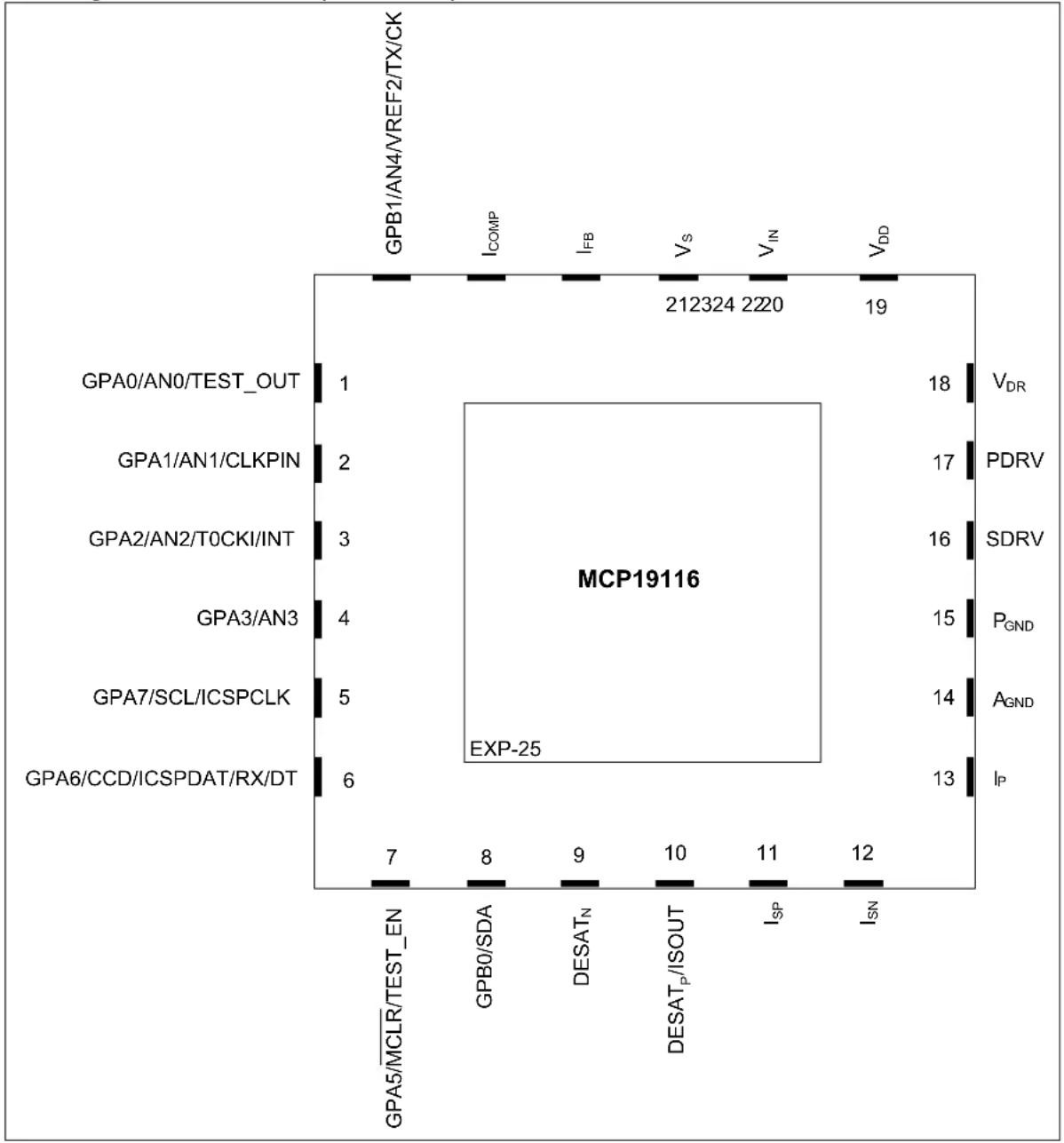
Pin Diagram - 24-Pin QFN (MCP19116)
other
| Pin | Label | Value | | --- | --- | --- | | GPB1/AN4/VREF2/TX/CK | | 18 | | GPB0/SDA | | 17 | | DESATN | | 16 | | DESATp/ISOUT | | 15 | | Isp | | 14 | | ISN | | 13 | | GPB0/SDA | | 8 | | DESATN | | 9 | | DESATp/ISOUT | | 10 | | Isp | | 11 | | ISN | | 12 | | GPB0/SDA | | 7 | | DESATN | | 12 | | DESATp/ISOUT | | 13 | | Isp | | 14 | | ISN | | 15 | | GPB0/SDA | | 16 | | DESATN | | 17 | | DESATp/ISOUT | | 18 | | Isp | | 19 | | IP | | 13 | | PDRV | | 17 | | SDRV | | 16 | | VDR | | 18 | | MCP19116 EXP-25TABLE 1: 24-PIN QFN (MCP19116) SUMMARY
| I/O | 24-Pin QFN | ANSEL | A/D | Timers | MSSP/AUSART | Interrupt | Pull-Up | Basic Additional | |
| GPA0 1 | Y AN0 | — — | IOC Y — | Analog/Digital Debug Output (1) | |||||
| GPA1 2 | Y AN1 | — — | IOC Y — | Sync Signal In/Out (2) | |||||
| GPA2 3 | Y AN2 | T0CKI | — IOC | INT | Y — | — | |||
| GPA3 | 4 | Y | AN3 | — | — | IOC | Y | — | — |
| GPA5 7 N | — | — — | IOC (3) | Y (4) | Test Enable Input | ||||
| GPA6 | 6 | N | — | — | RX/DT | IOC | Y | ICSPDAT | Dual Capture Input / Single Compare 1 Output |
| GPA7 | 5 | N | — | — | SCL | IOC | N | ICSPCLK | — |
| GPB0 | 8 | N | — | — | SDA | IOC | N | — | — |
| GPB1 | 24 | Y | AN4 | — | TX/CK | IOC | Y | — | V_REF2^(5) |
| DESATN | 9 | N | — | — | — | — | — | — | DESAT Negative Input |
| DESATP/ ISOUT | 10 | N | — | — | — | — | — | — | DESATP Input or ISOUTOutput (6) |
| ISP | 11 | N | — | — | — | — | Y | — | Current Sense Amplifier Positive Input |
| ISN | 12 | N | — | — | — | — | — | — | Current Sense Amplifier Negative Input |
| IP | 13 | N | — | — | — | — | — | — | Primary Input Current Sense |
| AGND | 14 | N | — | — | — | — | — | AGND | Small Signal Ground |
| PGND | 15 | N | — | — | — | — | — | PGND | Large Signal Ground |
| SDRV | 16 | N | — | — | — | — | — | — | Secondary LS Gate Drive Output |
| PDRV | 17 | N | — | — | — | — | — | — | Primary LS Gate Drive Output |
| VDR | 18 | N | — | — | — | — | — | VDR | Gate Drive Supply Voltage |
| VDD | 19 | N | — | — | — | — | — | VDD | VDD Output |
| VIN | 20 | N | — | — | — | — | — | VIN | Input Supply Voltage |
| VS | 21 | N | — | — | — | — | — | — | Output Voltage Sense |
| IFB | 22 | N | — | — | — | — | — | — | Error Amplifier Feedback Input |
| ICOMP | 23 | N | — | — | — | — | — | — | Error Amplifier Output |
Note 1: The Analog/Digital Debug Output is selected through the control of the ABECON register.
2: Selected when functioning as master or slave by proper configuration of the MSC<1:0> bits in the MODECON register.
3: The IOC is disabled when MCLR is enabled.
4: Weak pull-up always enabled when is enabled, otherwise the pull-up is under user control.
5: V_REF2 output selected when configured as master by proper configuration of the MSC<1:0> bits in the MODECON register.
6: When RFB of MODECON<5> = 0, the internal feedback resistor and DESAT P input are enabled. When RFB = 1, I SOUT is enabled.
Pin Diagram - 28-Pin QFN (MCP19117)
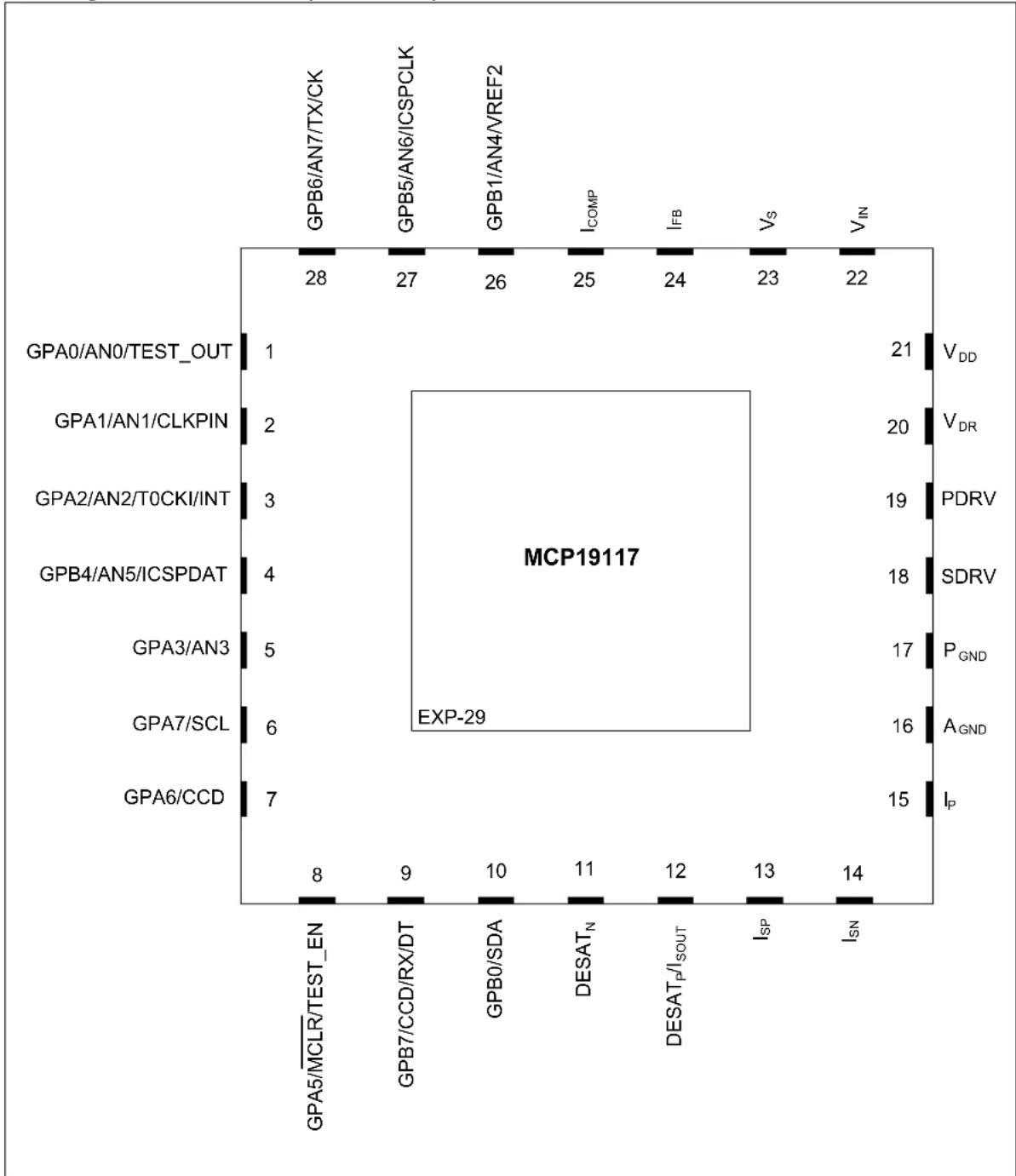
TABLE 2: 28-PIN QFN (MCP19117) SUMMARY
| I/O | 28-Pin QFN | ANSEL | A/D | Timers | MSSP/AUSART | Interrupt | Pull-Up | Basic Additional | |
| GPA0 1 | Y ANO | — — | IOC Y — | Analog/Digital Debug Output (1) | |||||
| GPA1 2 | Y AN1 | — — | IOC Y — | Sync Signal In/Out(2) | |||||
| GPA2 | 3 | Y | AN2 | T0CKI | — | IOC INT | Y — | — | |
| GPA3 | 5 | Y | AN3 | — | — | IOC | Y | — | — |
| GPA5 8 | N — | — — | IOC (3) | Y (4) | Test Enable Input | ||||
| GPA6 | 7 | N | — | — | — | IOC | Y | — | Dual Capture Input / Single Compare 1 Output |
| GPA7 | 6 | N | — | — | SCL | IOC | N | — | — |
| GPB0 | 10 | N | — | — | SDA | IOC | N | — | — |
| GPB1 | 26 | Y | AN4 | — | — | IOC | Y | — | V_REF2^(5) |
| GPB4 | 4 | Y | AN5 | — | — | IOC | Y | ICSPDAT | — |
| GPB5 | 27 | Y | AN6 | — | — | IOC | Y | ICSPCLK | — |
| GPB6 | 28 | Y | AN7 | — | TX/CK | IOC | Y | — | — |
| GPB7 | 9 | Y | — | — | RX/DT | IOC | Y | — | Single Compare 2 Output |
| DESATp/Isout | 12 | N | — | — | — | — | — | — | DESATp Input or IsOUTOutput (6) |
| DESATN | 11 | N | — | — | — | — | — | — | DESAT Negative Input |
| ISP | 13 | N | — | — | — | — | Y | — | Current Sense Amplifier Non-inverting Input |
| ISN | 14 | N | — | — | — | — | — | — | Current Sense Amplifier Inverting Input |
| IP | 15 | N | — | — | — | — | — | — | Primary Input Current Sense |
| AGND | 16 | N | — | — | — | — | — | AGND | Small Signal Ground |
| PGND | 17 | N | — | — | — | — | — | PGND | Large Signal Ground |
| SDRV | 18 | N | — | — | — | — | — | — | Secondary LS Gate Drive Output |
| PDRV | 19 | N | — | — | — | — | — | — | Primary LS Gate Drive Output |
| VDR | 20 | N | — | — | — | — | — | VDR | Gate Drive Supply Voltage |
| VDD | 21 | N | — | — | — | — | — | VDD | VDD Output |
| VIN | 22 | N | — | — | — | — | — | VIN | Input Supply Voltage |
| VS | 23 | N | — | — | — | — | — | — | Output Voltage Sense |
| IFB | 24 | N | — | — | — | — | — | — | Error Amplifier Feedback input |
| ICOMP | 25 | N | — | — | — | — | — | — | Error Amplifier Output |
Note 1: The Analog/Digital Debug Output is selected through the control of the ABECON register.
2: Selected when functioning as master or slave by proper configuration of the MSC<1:0> bits in the MODECON register.
3: The IOC is disabled when MCLR is enabled.
4: Weak pull-up always enabled when is enabled, otherwise the pull-up is under user control.
5: V_REF2 output selected when configured as master by proper configuration of the MSC<1:0> bits in the MODECON register.
6: When RFB of MODECON<6> = 0, the internal feedback resistor is enabled allow with DESAT P input. When RFB = 1, I SOUT is enabled.
Table of Contents
Features 1
1.0 Device Overview 9
2.0 Pin Description 13
3.0 Functional Description....19
4.0 Electrical Characteristics 22
5.0 Digital Electrical Characteristics....31
5.0 Digital Electrical Characteristics....39
6.0 Configuring the MCP19116/7 39
7.0 Typical Performance Curves 53
8.0 System Bench Testing 57
9.0 Device Calibration....59
10.0 Addressable USART Module 69
11.0 Memory Organization 81
12.0 Device Configuration....93
13.0 Oscillator Modes 95
14.0 Resets 97
15.0 Interrupts 105
16.0 Power-Down Mode (Sleep) 115
17.0 Watchdog Timer (WDT)....117
18.0 Flash Program Memory Control 119
19.0 I/O Ports 125
20.0 Interrupt-On-Change 133
21.0 Internal Temperature Indicator Module 137
22.0 Analog-to-Digital Converter (ADC) Module 139
23.0 Timer0 Module 149
24.0 Timer1 Module 15
25.0 Timer2 Module 155
26.0 Enhanced PWM Module 157
28.0 Dual Capture/Compare (CCD) Module 163
27.0 PWM Control Logic 161
29.0 Master Synchronous Serial Port (MSSP) Module 167
30.0 Instruction Set Summary 211
31.0 In-Circuit Serial Programming™ (ICSP™) 221
32.0 Development Support 223
33.0 Packaging Information 227
Appendix A: Revision History 233
INDEX 235
The Microchip Web Site 241
Customer Change Notification Service 241
Customer Support 241
Product Identification System 243
Trademarks 245
Worldwide Sales and Service 246
TO OUR VALUED CUSTOMERS
It is our intention to provide our valued customers with the best documentation possible to ensure successful use of your Microchip products. To this end, we will continue to improve our publications to better suit your needs. Our publications will be refined and enhanced as new volumes and updates are introduced.
If you have any questions or comments regarding this publication, please contact the Marketing Communications Department via E-mail at docerrors@microchip.com. We welcome your feedback.
Most Current Data Sheet
To obtain the most up-to-date version of this data sheet, please register at our Worldwide Web site at:
http://www.microchip.com
You can determine the version of a data sheet by examining its literature number found on the bottom outside corner of any page. The last character of the literature number is the version number, (e.g., DS30000000A is version A of document DS30000000).
Errata
An errata sheet, describing minor operational differences from the data sheet and recommended workarounds, may exist for current devices. As device/documentation issues become known to us, we will publish an errata sheet. The errata will specify the revision of silicon and revision of document to which it applies.
To determine if an errata sheet exists for a particular device, please check with one of the following:
- Microchip's Worldwide Web site; http://www.microchip.com
- Your local Microchip sales office (see last page)
When contacting a sales office, please specify which device, revision of silicon and data sheet (include literature number) you are using.
Customer Notification System
Register on our web site at www.microchip.com to receive the most current information on all of our products.
NOTES:
1.0 DEVICE OVERVIEW
The MCP19116/7 devices are highly integrated, mixed-signal low-side synchronous controllers that operate from +4.5V to +42V. The family features an analog PWM controller with an integrated microcontroller core used for LED lighting systems, battery chargers and other low-side switch PWM applications. The MCP19116/7 devices are derived from the MCP19114/5, which share the same features and characteristics except for the addition of larger program memory (8k words vs. 4k words) and several design enhancements. These enhancements were added to the MCP19116/7 devices to improve calibration, increase accuracy and provide greater flexibility. The devices feature an analog internal PWM controller similar to the MCP1631, and a standard PIC ^® microcontroller similar to the PIC12F617.
Complete customization of device operating parameters, start-up or shutdown profiles, protection levels and fault handling procedures are accomplished by setting digital registers using Microchip's MPLAB® X Integrated Development Environment software and one of Microchip's many in-circuit debugger and device programmers.
The MCP19116/7 mixed-signal low-side synchronous controllers feature integrated programmable input UVLO/OVLO, programmable output overvoltage (OV), two low-side gate drive outputs with independent programmable dead time, programmable leading edge blanking (four steps), programmable 6-bit slope compensation and an integrated internal programmable oscillator for fixed-frequency applications.
An integrated 8-bit reference voltage ( V_REF ) is used for setting output current or voltage. An internal comparator supports quasi-resonant applications. Additional Capture and Compare modules are integrated for increased control, including enhanced dimming capability.
The MCP19116/7 devices contain two internal LDOs. A 5V LDO ( V_DD ) is used to power the internal processor and provide 5V externally. A 4V LDO ( AV_DD ) is used to power the internal analog circuitry. Either V_DD or AV_DD can be connected internally to the 10-bit Analog-to-Digital Converter reference input. The 5V external output can be used to supply the gate drive. An analog filter between the V_DD output and the V_DR input is recommended when implementing a 5V gate drive supplied from V_DD . Two 4.7 F capacitors are recommended with one placed as close as possible to V_DD and one as close as possible to V_DR , separated by a 10 isolation resistor. DO NOT exceed 10 F on the V_DD . An external supply is required to implement higher gate drive voltages.
By utilizing a Microchip Technology Incorporated TC1240A voltage doubler supplied from V_DD to provide V_DR , a 10V gate drive can be achieved.
A 4V LDO is used to power the internal analog circuitry. The two low-side drivers can be used to operate the power converter in bidirectional mode, enabling the "shaping" of LED dimming current in LED applications or developing bidirectional power converters for battery-powered applications.
The MCP19116 is packaged in a 24-lead 4 mm x 4 mm QFN. The MCP19117 is packaged in a 28-lead 5 mm x 5 mm QFN.
The ability for system designers to configure application-specific features allows users of the MCP19116/7 devices to save costly board real estate and additional component costs.
The General Purpose Input/Output (GPIO) of the MCP19116/7 can be configured to offer a status output:
- a device enable, to control an external switch
- a switching frequency synchronization output or input
• and even a device status or "heartbeat" indicator
With integrated features like output current adjustment and dynamic output voltage positioning, the MCP19116/7 family has the best in-class performance and highest integration level currently available.
Power trains supported by this architecture include but are not limited to boost, flyback, quasi-resonant flyback, SEPIC, Ćuk, etc.
Two low-side gate drivers are capable of sinking and sourcing 1A at 10V V_DR . With a 5V gate drive, the driver is capable of 0.5A sink and source. The user has the option to allow the V_IN UVLO to shut down the drivers by setting the UVLOEN bit. When this bit is not set, the device drivers will ride through the UVLO condition and continue to operate until V_DR reaches the gate drive UVLO value. This value is selectable at 2.7V or 5.4V and is always enabled. An internal reset for the microcontroller core is set to 2.0V. An internal comparator module is used to sense the desaturation of the flyback transformer to synchronize switching for quasi-resonant applications.
The operating input voltage for normal device operation ranges from +4.5V to +42V with an absolute maximum of 44V. The maximum transient voltage is 48V for 500 ms. An ^2 serial bus is used for device communications from the PWM controller to the system.
FIGURE 1-1: MCP19116/7 FLYBACK SYNCHRONOUS QUASI-RESONANT BLOCK DIAGRAM
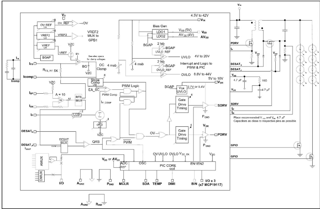
FIGURE 1-2: MCP19116 ĆUK SYNCHRONOUS POSITIVE OUTPUT APPLICATION DIAGRAM
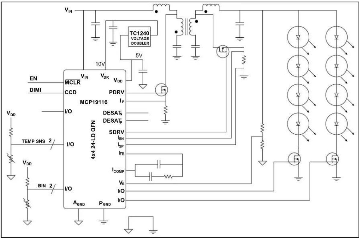
FIGURE 1-3: MCP19116 BOOST QUASI-RESONANT APPLICATION DIAGRAM
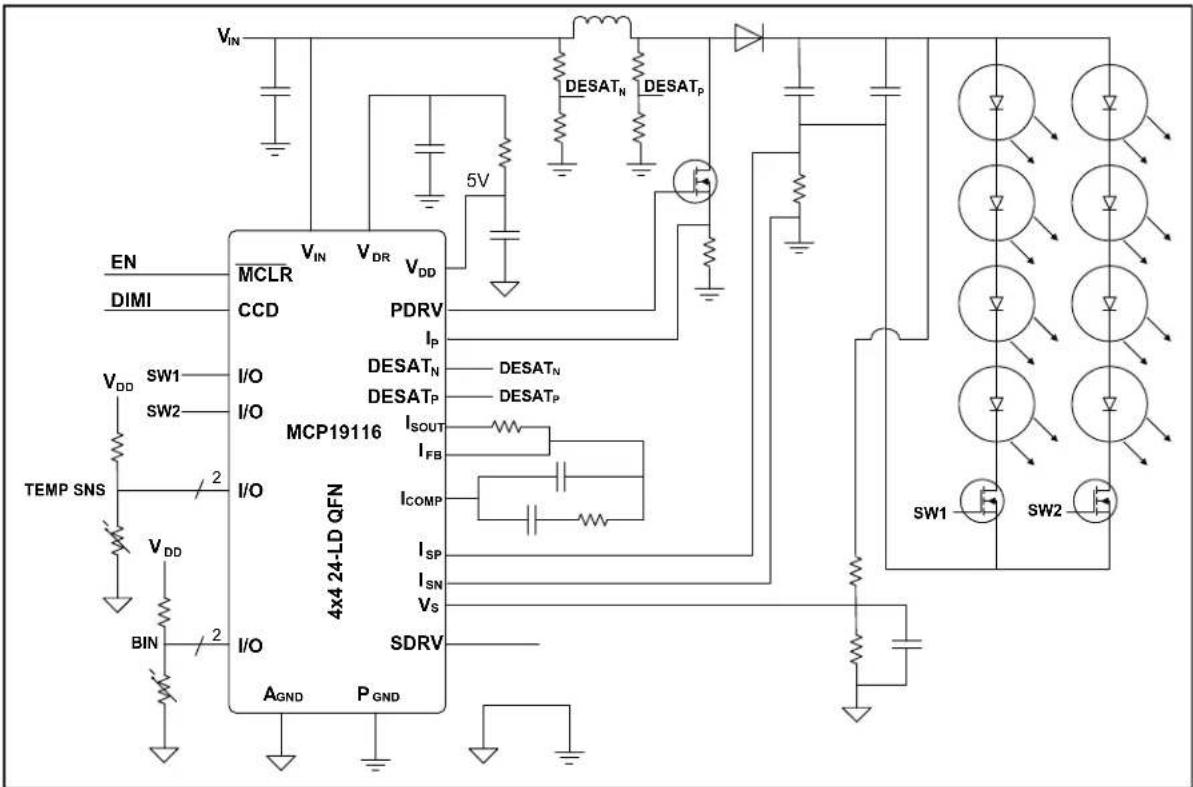
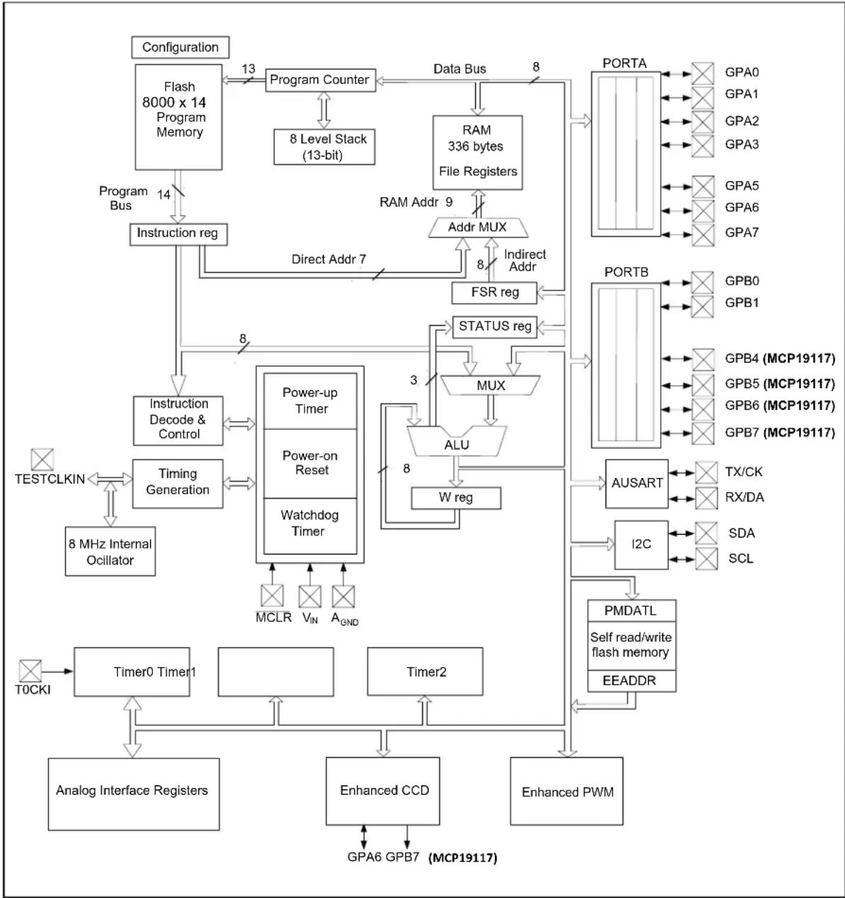
FIGURE 1-4: MICROCONTROLLER CORE BLOCK DIAGRAM
flowchart
graph TD
    A["Configuration"] --> B["Flash 8000 x 14 Program Memory"]
    B --> C["Program Bus"]
    C --> D["Instruction reg"]
    D --> E["Instruction Decode & Control"]
    E --> F["Timing Generation"]
    F --> G["8 MHz Internal Oscillator"]
    G --> H["T0CKI"]
    H --> I["Timer0 Timer1"]
    I --> J["Analog Interface Registers"]
    I --> K["Timer2"]
    K --> L["Enhanced CCD"]
    L --> M["GPA6 GPB7 (MCP19117)"]
    L --> N["Enhanced PWM"]
    O["Program Counter"] --> P["8 Level Stack (13-bit)"]
    P --> Q["RAM 336 bytes File Registers"]
    Q --> R["Addr MUX"]
    R --> S["FSR reg"]
    S --> T["STATUS reg"]
    T --> U["MUX"]
    U --> V["ALU"]
    V --> W["W reg"]
    W --> X["MCLR VIN AGND"]
    Y["Data Bus"] --> Z["RAM Addr 9"]
    Z --> AA["Indirect Addr"]
    AA --> AB["PORTA"]
    AB --> AC["GPA0 GPA1 GPA2 GPA3"]
    AB --> AD["GPA5 GPA6 GPA7"]
    AE["PORTB"] --> AF["GPB0 GPB1"]
    AF --> AG["GPB4 (MCP19117)"]
    AF --> AH["GPB5 (MCP19117)"]
    AF --> AI["GPB6 (MCP19117)"]
    AF --> AJ["GPB7 (MCP19117)"]
    AK["AUSART"] --> AL["TX/CK RX/DA"]
    AK --> AM["SDA SCL"]
    AN["I2C"] --> AO["PMDATL Self read/write flash memory EEADDR"]
    AP["Instruction reg"] --> AQ["Direct Addr 7"]
    AQ --> AR["Power-up Timer"]
    AR --> AS["Power-on Reset"]
    AS --> AT["Watchdog Timer"]
    AT --> AU["MCLR VIN AGND"]
2.0 PIN DESCRIPTION
The 24-lead MCP19116 and 28-lead MCP19117 devices feature pins that have multiple functions associated with each pin. Table2-1 provides a description of the different functions. Refer to Section 2.1 "Detailed Pin Functional Description" for detailed information.
TABLE 2-1: MCP19116/7 PINOUT DESCRIPTION
| Name Function | Input Type | Output Type | Description | |
| GPA0/AN0/TEST_OUT GPA0 | TTL CMOS General purpose I/O | |||
| AN0 | AN | — | A/D Channel 0 input | |
| TEST_OUT | — | — | Internal analog/digital signal multiplexer output^(1) | |
| GPA1/AN1/CLKPIN GPA1 TTL CMOS General purpose I/O | ||||
| AN1 | AN | — | A/D Channel 1 input | |
| CLKPIN | ST | CMOS | Switching-frequency clock input or output^(2) | |
| GPA2/AN2/T0CKI/INT | GPA2 | ST | CMOS | General purpose I/O |
| AN2 | AN | — | A/D Channel 2 input | |
| T0CKI | ST | — | Timer0 clock input | |
| INT | ST | — | External interrupt | |
| GPA3/AN3 | GPA3 TTL CMOS General purpose I/O | |||
| AN3 | AN | — | A/D Channel 3 input | |
| GPA5/MCLR | GPA5 TTL — General purpose input only | |||
| MCLR | ST | — | Master Clear with internal pull-up | |
| GPA6/CCD/ICSPDAT/RX/DT ICSPDAT/RX/DT (MCP19116 Only) | GPA6 | ST | CMOS | General purpose I/O |
| ICSPDAT | ST | CMOS | Serial Programming Data I/O (MCP19116 only) | |
| CCD | ST | CMOS | Dual Capture Input. CCD1 Single Compare output | |
| RX | ST | — | USART asynchronous serial receive (MCP19116 only) | |
| DT | ST | CMOS | USART synchronous serial data (MCP19116 only) | |
| GPA7/SCL/ICSPCLK ICSPCLK (MCP19116 only) | GPA7 | ST | OD | General purpose open drain I/O |
| SCL | I^2C | OD | I^2C clock | |
| ICSPCLK | ST | — | Serial Programming Clock (MCP19116 only) | |
| GPB0/SDA | GPB0 | TTL | OD | General purpose I/O |
| SDA | I^2C | OD | I^2C data input/output | |
| GPB1/AN4/VREF2/TX/CK TX/CK (MCP19116 Only) | GPB1 | TTL CMOS General-purpose I/O | ||
| AN4 | AN | — | A/D Channel 4 input | |
| VREF2 | — | AN | VREF2 DAC Output^(3) | |
| TX | — | CMOS | USART asynchronous serial transmit (MCP19116 only) | |
| CK | ST | CMOS | USART synchronous serial clock (MCP19116 only) | |
Legend: AN = Analog input or output CMOS = CMOS compatible input or output OD = Open-Drain TTL = TTL compatible input ST = Schmitt Trigger input with CMOS levels I²C = Schmitt Trigger input with I²C
Note 1: The Analog/Digital Debug Output is selected through the control of the ABECON register.
2: Selected when functioning as master or slave by proper configuration of the MSC<1:0> bits in the MODECON register.
3: VREF2 output selected when configured as master by proper configuration of the MSC<1:0> bits in the MODECON register.
TABLE 2-1: MCP19116/7 PINOUT DESCRIPTION (CONTINUED)
| Name | Function | Input Type | Output Type | Description |
| GPB4/AN5/ICSPDAT (MCP19117 Only) | GPB4 TTL | CMOS | General purpose I/O | |
| AN5 AN — | A/D Channel 5 input | |||
| ICSPDAT ST | CMOS | Primary Serial Programming Data I/O | ||
| GPB5/AN6/ICSPCLK (MCP19117 Only) | GPB5 TTL | CMOS | General purpose I/O | |
| AN6 AN — | A/D Channel 6 input | |||
| ISCPCLK ST | — Primary Serial | Programming Clock | ||
| GPB6/AN7/TX/CK (MCP19117 Only) | GPB6 TTL | CMOS | General purpose I/O | |
| AN7 AN — | A/D Channel 7 input | |||
| TX — | CMOS | USART asynchronous serial transmit | ||
| CK | ST CMOS | USART synchronous serial clock | ||
| GPB7/CCD/RX/DT (MCP19117 Only) | GPB7 TTL | CMOS | General purpose I/O | |
| CCD | ST CMOS | CCD2 Single Compare output. | ||
| RX | ST | — | USART asynchronous serial receive | |
| DT | ST CMOS | USART synchronous serial data | ||
| V_IN | V_IN | — | — Device input supply voltage | |
| V_DD | V_DD | — | — Internal +5V LDO output pin | |
| V_DR | V_DR | — | — Gate drive supply voltage | |
| A_GND | A_GND | — | — Small signal quiet ground | |
| P_GND | P_GND | — | — Large signal power ground | |
| PDRV | PDRV | — | — | Primary low-side MOSFET gate drive |
| SDRV | SDRV | — | — | Secondary low-side MOSFET gate drive |
| I_P | I_P | — | — Primary input current sense | |
| I_SN | I_SN | — | — Secondary-current sense-amplifier negative input | |
| I_SP | I_SP | — | — Secondary-current sense-amplifier positive input | |
| V_S | V_S | — | — Sense voltage compared to overvoltage DAC | |
| I_FB | I_FB | — | — Error amplifier feedback input | |
| I_COMP | I_COMP | — | — Error amplifier output | |
| DESAT_P/ISOUT | DESAT_P/ISOUT | — | — | DESAT_P: DESAT detect comparator positive input I_SOUT: Secondary-current sense-amplifier output |
| DESAT_N | DESAT_N | — | — | DESAT_N: DESAT detect comparator negative input |
Legend: AN = Analog input or output CMOS = CMOS compatible input or output OD = Open-Drain TTL = TTL compatible input ST = Schmitt Trigger input with CMOS levels I^2C = Schmitt Trigger input with I^2C
Note 1: The Analog/Digital Debug Output is selected through the control of the ABECON register.
2: Selected when functioning as master or slave by proper configuration of the MSC<1:0> bits in the MODECON register.
3: VREF2 output selected when configured as master by proper configuration of the MSC<1:0> bits in the MODECON register.
2.1 Detailed Pin Functional Description
2.1.1 GPA0 PIN
GPA0 is a general-purpose TTL input or CMOS output pin whose data direction is controlled in TRISGPA. An internal weak pull-up and interrupt-on-change are also available.
AN0 is an input to the A/D. To configure this pin to be read by the A/D on channel 0, bits TRISA0 and ANSA0 must be set.
The ABECON register can be configured to set this pin to the TEST_OUT function. It is a buffered output of the internal analog or digital signal multiplexers. Analog signals present on this pin are controlled by the ADCON0 register. Digital signals present on this pin are controlled by the ABECON register.
2.1.2 GPA1 PIN
GPA1 is a general-purpose TTL input or CMOS output pin whose data direction is controlled in TRISGPA. An internal weak pull-up and interrupt-on-change are also available.
AN1 is an input to the A/D. To configure this pin to be read by the A/D on channel 1, bits TRISA1 and ANSA1 must be set.
When the MCP19116/7 are configured as a master or slave, this pin is configured to be the switching-frequency synchronization input or output (CLKPIN).
2.1.3 GPA2 PIN
GPA2 is a general-purpose ST input or CMOS output pin whose data direction is controlled in TRISGPA. An internal weak pull-up and interrupt-on-change are also available.
AN2 is an input to the A/D. To configure this pin to be read by the A/D on channel 2, bits TRISA2 and ANSA2 must be set.
When bit T0CS is set in the OPTION_REG register, the T0CKI function is enabled. Refer to Section 23.0 "Timer0 Module" for more information.
GPA2 can also be configured as an external interrupt by setting the INTE bit. Refer to Section 15.2 "GPA2/INT Interrupt" for more information.
2.1.4 GPA3 PIN
GPA3 is a general purpose TTL input or CMOS output pin whose data direction is controlled in TRISGPA. An internal weak pull-up and interrupt-on-change are also available.
AN3 is an input to the A/D. To configure this pin to be read by the A/D on channel 3, bits TRISA3 and ANSA3 must be set.
2.1.5 GPA5 PIN
GPA5 is a general purpose TTL input only pin. An internal weak pull-up and interrupt-on-change are also available.
For programming purposes, this pin is to be connected to the MCLR pin of the serial programmer. Refer to Section 31.0 "In-Circuit Serial Programming™ (ICSP™)" for more information.
This pin is MCLR when the MCLRE bit is set in the CONFIG register.
2.1.6 GPA6 PIN
GPA6 is a general-purpose CMOS output ST input pin whose data direction is controlled in TRISGPA.
ICSPDAT is a serial programming data I/O function. This can be used in conjunction with ICSPCLK to serial-program the device.
MCP19116 Only: RX is the USART Asynchronous serial receive.
MCP19116 Only: DT is the USART Synchronous serial clock.
GPA6 is the Dual Capture input and CCD1 output compare. For more information, refer to Section 28.0 "Dual Capture/Compare (CCD) Module".
2.1.7 GPA7 PIN
GPA7 is a true open-drain general purpose pin whose data direction is controlled in TRISGPA. There is no internal connection between this pin and device V_DD . This pin does not have a weak pull-up, but interrupt-on-change is available.
This pin is the primary ICSPCLK input. This can be used in conjunction with ICSPDAT to serial program the device.
When the MCP19116/7 is configured for I^2C communication, GPA7 functions as the I^2C clock (SCL). This pin must be configured as an input to allow proper operation. For more information, refer to Section 29.2 “ I^2C Mode Overview”
2.1.8 GPB0 PIN
GPB0 is a true open-drain general-purpose pin whose data direction is controlled in TRISGPB. There is no internal connection between this pin and device V_DD . This pin does not have a weak pull-up, but interrupt-on-change is available. When the MCP19116/7 are configured for communication, GPB0 functions as the I^2C data (SDA). This pin must be configured as an input to allow proper operation. For more information, refer to Section 29.2 "IC Mode Overview".
2.1.9 GPB1 PIN
GPB1 is a general-purpose TTL input or CMOS output pin whose data direction is controlled in TRISGPB. An internal weak pull-up and interrupt-on-change are also available.
AN4 is an input to the A/D. To configure this pin to be read by the A/D on channel 4, bits TRISB1 and ANSB1 must be set.
MCP19116 Only: TX is the USART Asynchronous serial transmit.
MCP19116 Only: CK is the USART Synchronous serial clock.
When the MCP19116/7 are configured as a master, this pin is configured to be the V_REF2 DAC output.
2.1.10 GPB4 PIN (MCP19117 ONLY)
GPB4 is a general-purpose TTL input or CMOS output pin whose data direction is controlled in TRISGPB. An internal weak pull-up and interrupt-on-change are also available.
AN5 is an input to the A/D. To configure this pin to be read by the A/D on channel 5, bits TRISB4 and ANSB4 must be set.
ICSPDAT is the primary serial-programming data I/O function. This is used in conjunction with ICSPCLK to serial program the device.
2.1.11 GPB5 PIN (MCP19117 ONLY)
GPB5 is a general-purpose TTL input or CMOS output pin whose data direction is controlled in TRISGPB. An internal weak pull-up and interrupt-on-change are also available.
AN6 is an input to the A/D. To configure this pin to be read by the A/D on channel 6, bits TRISB5 and ANSB5 must be set.
ICSPCLK is the primary serial-programming clock function. This is used in conjunction with ICSPDAT to serial program the device.
2.1.12 GPB6 PIN (MCP19117 ONLY)
GPB6 is a general-purpose TTL input or CMOS output pin whose data direction is controlled in TRISGPB. An internal weak pull-up and interrupt-on-change are also available.
AN7 is an input to the A/D. To configure this pin to be read by the A/D on channel 7, bits TRISB6 and ANSB6 must be set.
MCP19117 Only: TX is the USART Asynchronous serial transmit.
MCP19117 Only: CK is the USART Synchronous serial clock.
2.1.13 GPB7 PIN (MCP19117 ONLY)
GPB7 is a general purpose TTL input or CMOS output pin whose data direction is controlled in TRISGPB. An internal weak pull-up and interrupt-on-change are also available.
RX is the USART Asynchronous serial receive.
DT is the USART Synchronous serial clock.
For more information, refer to Section 10.0 "Addressable USART Module"
GPB7 is the CCD2 output Compare. For more information, refer to Section 28.0 "Dual Capture/Compare (CCD) Module".
2.1.14 DESAT N PIN
Internal comparator inverting input. Used during Quasi-Resonant operation for desaturation detection.
2.1.15 DESAT P/ISOUT PIN
When using the internal comparator for desaturation detection during Quasi-Resonant operation, this pin connects to the comparator's noninverting input. The output of the remote sense current-sense amplifier gets configured to utilize the 5 kΩ internal feedback resistor. When not utilizing the internal comparator and not configured to use the 5 kΩ internal feedback resistor, the current sense amplifier gets connected to this pin and is I_SOUT .
2.1.16 I SP PIN
The noninverting input to internal current-sense amplifier, typically used to differentially remote-sense secondary current. This pin can be internally pulled-up to V_DD by setting the
2.1.17 I SN PIN
The inverting input to internal current-sense amplifier, typically used to differentially remote-sense secondary current.
2.1.18 I P PIN
Primary input current-sense for current mode control and peak current limit. For voltage mode control, this pin can be connected to an artificial ramp.
2.1.19 A GND PIN
A_GND is the small signal ground connection pin. This pin should be connected to the exposed pad on the bottom of the package.
2.1.20 P GND PIN
Connect all large-signal level ground returns to P_GND . These large-signal level ground traces should have a small loop area and minimal length to prevent coupling of switching noise to sensitive traces.
2.1.21 SDRV PIN
The gate of the low-side secondary MOSFET is connected to SDRV. The PCB trace connecting SDRV to the gate must be of minimal length and appropriate width to handle the high-peak drive current and fast voltage transitions.
2.1.22 PDRV PIN
The gate of the low-side primary MOSFET is connected to PDRV. The PCB tracing connecting PDRV to the gate must be of minimal length and appropriate width to handle the high-peak drive currents and fast voltage transitions.
2.1.23 V DR PIN
The supply for the low-side drivers is connected to this pin and has an absolute maximum rating of +13.5V. This pin can be connected by an RC filter to the V_DD pin.
2.1.24 V DD PIN
The output of the internal +5.0V regulator is connected to this pin. It is recommended that a 1.0 F minimum/10 F maximum bypass capacitor be connected between this pin and the GND pin of the device. The bypass capacitor should be physically placed close to the device.
2.1.25 V IN PIN
Input power connection pin of the device. It is recommended that capacitance be placed between this pin and the GND pin of the device.
2.1.26 V s PIN
Analog input connected to the non-inverting input of the overvoltage comparator. Typically used as output-voltage overvoltage protection. The inverting input of the overvoltage comparator is controlled by the OV REF DAC.
2.1.27 I FB PIN
Error-amplifier inverting feedback connection.
2.1.28 I COMP PIN
Error-amplifier output signal.
2.1.29 EXPOSED PAD (EP)
It is recommended to connect the exposed pad to A_GND .
NOTES:
3.0 FUNCTIONAL DESCRIPTION
3.1 Linear Regulators
The operating input voltage for the MCP19116/7 ranges from +4.5V to +42V. There are two internal Low Dropout (LDO) voltage regulators. A 5V LDO is used to power the internal processor and provide a 5V output for external usage. A second LDO (AV DD ) is a 4V regulator and is used to power the remaining analog internal circuitry. AV DD is factory calibrated and is the default ADC reference voltage. The ADC reference is switchable between AV DD and V DD . Using an LDO to power the MCP19116/7, the input voltage is monitored using a resistor divider. The MCP19116/7 also incorporate brown-out protection. Refer to Section 14.3 “Brown-Out Reset (BOR)” for details. The PIC core will reset at 2.0V V _DD .
3.2 Output Drive Circuitry
The MCP19116/7 integrate two low-side drivers used to drive the external low-side N-Channel power MOSFETs for synchronous applications, such as synchronous flyback and synchronous Ćuk converters. Both converter types can be configured for non-synchronous control by replacing the synchronous FET with a diode. The flyback is also capable of quasi-resonant operation. The MCP19116/7 can also be configured as a Boost or SEPIC switch-mode power supply (SMPS). In Boost mode, nonsynchronous fixed-frequency or nonsynchronous quasi-resonant control can be utilized. This device can also be used as a SEPIC SMPS in fixed-frequency nonsynchronous mode. The low-side drive is capable of switching the MOSFET at high frequency in typical SMPS applications. The gate drive ( V_DR ) can be supplied from 5V to 10V. The drive strength is capable of up to 1A sink/source with 10V gate drive and down to 0.5A sink/source with 5V gate drive. A programmable delay is used to set the gate turn-on dead time. This prevents overlap and shoot-through currents that can decrease the converter efficiency. Each driver has its own EN input controlled by the microcontroller core.
3.3 Current Sense
The output current is differentially sensed by the MCP19116/7. In low-current applications, this helps maintain high system efficiency by minimizing power dissipation in current-sense resistors. Differential current sensing also minimizes external ground-shift errors. The internal differential amplifier has a typical gain of 10 V/V and is factory trimmed.
3.4 Peak Current Mode
The MCP19116/7 is a peak current mode controlled device with the current-sensing element in series with the primary side MOSFET. Programmable leading edge blanking can be implemented to blank current spikes resulting from turn on. The blank time is controlled from the ICLEBCON register.
Primary-input current-offset adjust is also available via user programmability, thus limiting peak primary input current. This offset adjustment is controlled by the ICO-ACON register.
3.5 Magnetic Desaturation Detection
An internal comparator module is used to detect power train magnetic desaturation for quasi-resonant applications. The comparator output is used as a signal to synchronize the start of the next switching cycle. This operation differs from the traditional fixed-frequency application. The DESAT comparator output can be enabled and routed into the PWM circuitry or disabled for fixed-frequency applications. During Quasi-Resonant (QR) operation, the DESAT comparator output is enabled and combined with a pair of one-shot timers and a flip-flop to sustain PWM operation. Timer2 (TMR2) must be initialized and set to run at a frequency lower than the minimum QR operating frequency. When the CDSWDE bit is set in the DESATCON register, TMR2 serves as a watchdog.
An example of the order of events for a Flyback SMPS in synchronous QR operation is as follows:
• the primary gate drive (PDRV) goes high
• the output of the DESAT comparator is high
- the primary current increases until I_P reaches the level of the Error Amp and causes PWM comparator output to go low
- the PDRV goes low and the secondary gate drive (SDRV) goes high (after programmed dead time). This triggers the first one-shot to send a 200 ns pulse that resets the flip-flop and TMR2 (WDM_RESET)
- the 200 ns one-shot pulse design is implemented to mask any spurious transitions at the DESAT comparator output caused by switching noise
- the SDRV stays high until the secondary winding completely runs out of energy, at which time the output capacitance begins to source current back through the winding and secondary MOSFET
- the DESAT comparator detects this and its output goes low. This sets the flip-flop and triggers the second one-shot to send a 33 ns pulse to the control logic, causing the SDRV to go low and the PDRV to go high (after programmed dead time)
- the cycle then repeats. If, for any reason, the reset one-shot does not fire, the WDM_RESET signal stays low and TMR2 is allowed to run until the PWM signal kicks off a new cycle
The desaturation comparator module is controlled by the DESATCON register.
3.6 Start-Up
To control the output current during start-up, the MCP19116/7 devices have the capability to monotonically increase system current at the user's discretion. This is accomplished through the control of the reference voltage DAC ( V_REF ). Users also have firmware control over the switching frequency through Timer2 and the PR2 register. Maximum duty-cycle control is established through the PWMRL register. Refer to Section 26.0, Enhanced PWM Module for details. The entire start-up profile is under user control via software.
3.7 Driver Control Circuitry
The internal driver control circuitry of the MCP19116/7 is comprised of an error amplifier (EA), a high-speed comparator and a latch similar to the MCP1631.
The error amplifier generates the control voltage used by the high-speed PWM comparator. There is an internally generated reference voltage, V_REF . The difference or error between this internal reference voltage and the actual feedback voltage is the control voltage. Some applications will implement parked times where the gate drives are not active. For example, when changing between LED strings and after voltage repositioning, the user can disable the gate drives and park the error amplifier output low. During the time when the EA is parked, its output will be clamped low (1 * BG) such that it is in a known state when reactivated. Before the output switches are re-enabled, it may be necessary to re-enable the EA some time prior to enabling the output drivers. This prior-EA enable time will allow the EA to slew towards the intended target and prevent the secondary switch from turning on for an extensive period of time, unintentionally discharging the output capacitance and pulling the output voltage down. External compensation is used to stabilize the control system.
Since the MCP19116/7 devices are peak current mode controlled, the comparator compares the primary peak current waveform ( I_P ) that is based upon the current flowing in the primary side with the error amplifier control output voltage. This error amplifier control output voltage also has user-programmable slope compensation subtracted from it. In fixed-frequency applications, the slope compensation signal is generated to be greater than 1/2 the down slope of the inductor current waveform and is controlled by the SLPCRCON register. Offset adjust ability is also available to set the peak current limit of the primary switch for overcurrent protection. The range of the slope compensation ramp is specified. When the current sense signal reaches the level of the control voltage minus slope compensation, the ON cycle is terminated and the external PDRV switch is latched off until the beginning of the next cycle which begins at the next clock cycle.
To improve current regulation at low levels, a pedestal voltage (VZC) set to the BG (1.23V) is implemented. This virtual ground serves as the reference for the error amplifier (A1), slope compensation, current sense amplifier (A2) and the I_P offset adjustment.
An S-R latch (Set-Rest-Flip-Flop) is used to prevent the PWM circuitry from turning the external switch on until the beginning of the next clock cycle.
3.8 Fixed PWM Frequency
The switching frequency of the MCP19116/7 while not controlled by the DESAT comparator output is generated by using a single edge of the 8 MHz internal clock. The user sets the MCP19116/7 switching frequency by configuring the PR2 register. The maximum allowable PDRV duty cycle is adjustable and is controlled by the PWMRL register. The programmable range of the switching frequency will be 31.25 kHz to 2 MHz. The available switching frequency below 2 MHz is defined as F_SW = 8 MHz/N, where N is a whole number between 4 ≤ N ≤ 256 . Refer to Section 26.0 “Enhanced PWM Module” for details.
3.9 V REF
This reference is used to generate the voltage connected to the noninverting input of the error amplifier. The entire analog control loop is raised to a virtual ground pedestal equal to the Band Gap voltage (1.23V).
3.10 OV REF
This reference is used to set the output overvoltage set point. It is compared to the V_S input pin, which is typically proportional to the output voltage based on a resistor divider. OV protection, when enabled, can be set to a value for the protection of system circuitry, or it can be used to “ripple” regulate the converter output voltage for repositioning purposes. For details, refer to Register 6-4.
3.11 Independent Gate Drive with Programmable Delay
Two independent low-side gate drives are integrated for synchronous applications. Programmable delay has been implemented to improve efficiency and prevent shoot-through currents. Each gate drive has an independent enable input controlled by the PE1 register and programmable dead time controlled by the DEADCON register.
3.12 Temperature Management
3.12.1 THERMAL SHUTDOWN
To protect the MCP19116/7 from overtemperature conditions, a 150°C junction temperature thermal shutdown has been implemented. When the junction temperature reaches this limit, the device disables the output drivers. In Shutdown mode, both PDRV and SDRV outputs are disabled and the overtemperature flag (OTIF) is set in the PIR2 register. When the junction temperature is reduced by 20°C to 130°C, the MCP19116/7 can resume normal output drive switching.
3.12.2 TEMPERATURE REPORTING
The MCP19116/7 devices have a second on-chip temperature monitoring circuit that can be read by the ADC through the analog test MUX. Refer to Section 21.0 “Internal Temperature Indicator Module” for details on this internal temperature monitoring circuit.
4.0 ELECTRICAL CHARACTERISTICS
4.1 ABSOLUTE MAXIMUM RATINGS †
| V_IN - V_GND (DC) | -0.3V to +44V |
| V_IN (transient < 500 ms) | +48V |
| PDRV | (GND - 0.3V) to ( V_DR + 0.3V ) |
| SDRV | (GND - 0.3V) to ( V_DR + 0.3V ) |
| V_DD Internally Generated | +6.5V |
| V_DR Externally Generated | +13.5V |
| Voltage on with respect to GND | -0.3V to +13.5V |
| Maximum voltage: any other pin | + (V_GND - 0.3V) to ( V_DD + 0.3V ) |
| Maximum output current sunk by any single I/O pin | 25 mA |
| Maximum output current sourced by any single I/O pin | 25 mA |
| Maximum current sunk by all GPIO | 90 mA |
| Maximum current sourced by all GPIO | 35 mA |
| Storage Temperature | -65°C to +150°C |
| Maximum Junction Temperature | +150°C |
| Operating Junction Temperature | -40°C to +125°C |
| ESD protection on all pins (HBM) | 1.0 kV |
| CDM protection on corner pins | +/-750V |
| CDM protection on other pins | +/-500V |
† Notice: Stresses above those listed under “Maximum Ratings” may cause permanent damage to the device. This is a stress rating only and functional operation of the device at those or any other conditions above those indicated in the operational listings of this specification is not implied. Exposure to maximum rating conditions for extended periods may affect device reliability.
4.2 Electrical Characteristics
| Electrical Specifications: Unless otherwise noted, V_IN = 12V , F_SW = 150kHz_A T+25°C. Boldface specifications apply over the T_A range of -40°C to +125°C. | ||||||
| Parameters Sym. | Min. Typ. | Max. Units | Conditions | |||
| Input | ||||||
| Input Voltage | V_IN | 4.5 | — | 42 | V | |
| Input Quiescent Current | I_Q | — | 6 | 7.5 | mA | V_IN = 12V , Not switching |
| — | 6 | 7.5 | V_IN = 20V , Not switching | |||
| Shutdown Current | I_SHDN | — | 50 | 80 | μA | V_IN = 12V (Note 1) |
| Linear Regulator V_DD | ||||||
| Internal Circuitry Bias Voltage | V_DD | 4.75 | 5.1 | 5.5 | V | V_IN = 6.0V to 42V |
| Maximum External V_DD Output Current | I_DD\_OUT | 35 | — | — | mA | V_IN = 6.0V to 42V(Note 2) |
| Internal Circuitry Bias Voltage during SLEEP | V_DD\_SLEEP | 2.4 | — | 4 | V | V_IN = 4.5V to 42 V_DD\_OUT = 1mA |
| Maximum Available External V_DD Output Current During SLEEP | I_DD\_OUT\_SLEEP | 1 | — | — | mA | V_IN = 6.0V to 42 V_DD = V_DD\_SLEEP |
Note 1: Refer to Section 16.0, Power-Down Mode (Sleep).
2: V_DD is the voltage present at the V_DD pin.
3: Dropout voltage is defined as the input-to-output voltage differential at which the output voltage drops 2% below its nominal value measured at a 1V differential between V_IN and V_DD .
4: Ensured by design, not production tested.
5: These parameters are characterized, but not production tested.
6: The V_DD LDO will limit the total source current to a maximum of 35 mA. Individually each pin can source a maximum of 15 mA.
4.2 Electrical Characteristics (Continued)
| Electrical Specifications: Unless otherwise noted, V_IN = 12V , F_SW = 150kHz_AF +25°C . Boldface specifications apply over the T_A range of -40°C to +125°C. | ||||||
| Parameters | Sym. | Min. | Typ. | Max. | Units | Conditions |
| Line Regulation ΔV | _DD-OUT/_(V_DD-OUT * V_IN) | -0.1 0.00 | 2 0.1 %/V (V | _DD + 1.0V ≤N ≤ 20V (Note 2) | ||
| Load Regulation ΔV | _DD-OUT/_V_DD-OUT | -1.0 0.1 | 1.0 % | I | _DD\_OUT = 1mA to 20mA (Note 2) | |
| Output Short-Circuit Current | I_DD\_SC | — | 50 | — | mA | V_IN = (V_DD + 1.0V) (Note 2) |
| Dropout Voltage | V_IN - V_DD | — | 0.3 | 0.5 | V | I_DD\_OUT = 20mA (Notes 2 and 3) |
| Power Supply Rejection Ratio | PSRR_LDO | — | 60 | — | dB | f ≤ 1000 Hz I_DD\_OUT = 25mA C_IN = 0μF , C_DD = 1μF |
| Linear Regulator AV _DD | ||||||
| Internal Analog Supply Voltage | AV _DD | — | 4.096 | — | V | |
| AV _DD Tolerance | AV _DD\_TOL | -2.5 | ±0.5 | 2.5 | % | Trimmed at 25°C, 0°C to 125°C |
| -3.3 | — | 3.3 | % | -40°C to 0°C | ||
| Band Gap Voltage | BG | — | 1.23 | — | V | Trimmed at 1.0% tolerance |
| Band Gap Tolerance | BG _TOL | -2.5 | — | 2.5 | % | |
| Input UVLO Voltage | ||||||
| UVLO Range | UVLO _ON | 4 | — | 20 | V | V_IN Falling |
| UVLO _ON Trip Tolerance | UVLO _TOL | -14 | — | 14 | % | V_IN FallingUVLO trip set to 9VVINUVLO = 0x21h |
| UVLO Hysteresis | UVLO _HYS | 1 | 4 | 8 | % | Hysteresis is based upon the UVLO _ON settingUVLO trip set to 9VVINUVLO = 0x21h |
| Resolution | nbits | — | 6 | — | bits | Logarithmic Steps |
| UVLO Comparator | ||||||
| Input-to-Output Delay | TD | — | 5 | — | μs | 100 ns rise time to 1V overdrive on V_IN V_IN > UVLO to flag set |
| Input OVLO Voltage | ||||||
| OVLO Range | OVLO _ON | 8.8 | — | 44 | V | V_IN Rising |
| OVLO _ON Trip Tolerance | OVLO _TOL | -14 | — | 14 | % | V_IN RisingOVLO trip set to 18VVINOVLO = 0x1Fh |
Note 1: Refer to Section 16.0, Power-Down Mode (Sleep).
2: V_DD is the voltage present at the V_DD pin.
3: Dropout voltage is defined as the input-to-output voltage differential at which the output voltage drops 2% below its nominal value measured at a 1V differential between V_IN and V_DD .
4: Ensured by design, not production tested.
5: These parameters are characterized, but not production tested.
6: The V_DD LDO will limit the total source current to a maximum of 35 mA. Individually each pin can source a maximum of 15 mA.
4.2 Electrical Characteristics (Continued)
| Electrical Specifications: Unless otherwise noted, V_IN = 12V , F_SW = 150 kHz , T_A = +25°C . Boldface specifications apply over the T_A range of -40°C to +125°C . | ||||||
| Parameters | Sym. | Min. | Typ. | Max. | Units | Conditions |
| OVLO Hysteresis OVLO | HYS | 158% | Hysteresis | is based upon | the OVLO_ON setting OVLO trip set to 18V VINOVLO = 0x1Fh | |
| Resolution nbits — 6 — | bits Logarithmic Steps | |||||
| OVLO Comparator | ||||||
| Input-to-Output Delay | TD | — | 5 | — | μs | 100 ns rise time to 1V overdrive on V_IN V_IN > OVLO to flag set |
| Output OV DAC | ||||||
| Resolution nbits — 8 — | bits Linear DAC | |||||
| Full-Scale Range | FSR | 0 | — | 2 * BG | V | |
| Tolerance | OVREF_TOL | -2.0 | ±0.3 | 2.0 | % | Trimmed @ code = 0xCC at 25°C,0°C to 125°C |
| -3.3 | — 3.3 | % —40°C to 0°C | ||||
| Output OV Comparator | ||||||
| OV Hysteresis | OV_HYS | — | 50 | — | mV | |
| Input Bias Current | I_BIAS | — | ±1 | — | μA | |
| Common-Mode Input Voltage Range | V_CMR | 0 | — | 3.0 | V | Note 4 |
| Input-to-Output Delay | TD | — | 200 | — | ns | 100 ns rise time to 1V overdrive on V_S V_S > OV to flag set (Note 4) |
| Voltage Reference DAC ( V_REF ) | ||||||
| Resolution nbits — 8 — | bits Linear DAC | |||||
| Full-Scale Range | FSR | BG | — | 2 * BG | V | Pedestal set to BG |
| Tolerance | V_REF\_TOL | -2.0 | ±0.2 | 2.0 | % | Trimmed @ code = 0xCC at 25°C,0°C to 125°C |
| -3.3 | — 3.3 | % —40°C to 0°C | ||||
Note 1: Refer to Section 16.0, Power-Down Mode (Sleep).
2: V_DD is the voltage present at the V_DD pin.
3: Dropout voltage is defined as the input-to-output voltage differential at which the output voltage drops 2% below its nominal value measured at a 1V differential between V_N and V_DD .
4: Ensured by design, not production tested.
5: These parameters are characterized, but not production tested.
6: The V_DD LDO will limit the total source current to a maximum of 35 mA. Individually each pin can source a maximum of 15 mA.
4.2 Electrical Characteristics (Continued)
| Electrical Specifications: Unless otherwise noted, V_IN = 12V , F_SW = 150 kHz , T_A = +25°C . Boldface specifications apply over the T_A range of -40°C to +125°C . | ||||||
| Parameters | Sym. | Min. | Typ. | Max. | Units | Conditions |
| Voltage Reference DAC ( V_REF2 ) | ||||||
| Resolution nbits — 8 — bits Linear DAC | ||||||
| Full-Scale Range FSR 0 — BG V | ||||||
| Tolerance | V_REF2\_TOL | -2.2 | ±0.2 | 2.2 | % | Trimmed @ code = 0xCC at 25°C, 0°C to 125°C |
| -3.3 | — 3.3 | % | -40°C to 0°C | |||
| Sink Current | I_SINK | -3.0 — | — | mA | V | _REF2 = 0x29 I_SINK = 3 mA V_REF2 < 60 mV |
| Source Current | I_SOURCE | 3.0 | — | — | mA | V_REF2 = 0xFF I_SOURCE = 3 mA V_REF2 < 60mV |
| Current Sense Amplifier (A2) | ||||||
| Input Offset Voltage V | OS | — | 2 | — | mV | Trimmed |
| Amplifier PSRR | PSRR | — | 65 | — | dB | V_CM = 2 * BG |
| Closed-Loop Voltage Gain | A2_VCL | — | 10 | — | V/V | R_L = 5 kΩ to 2.048V, 100 mV < A2 < AV_DD - 100 mV , V_CM = BG |
| Closed Loop Voltage Gain Tolerance | A2_VCL\_TOL | -2.0 | 0.5 | 2.0 | % | Trimmed |
| Low-Level Output V | OL | — | 300 | — | mV | R_L = 5 kΩ to 2.048V |
| Gain-Bandwidth Product | GBWP | — | 10 | — | MHz | AV_DD = 4V |
| Input Impedance | R_IN | — | 10 | — | kΩ | |
| Sink Current | I_SINK | -3.0 — | — | mA | I | _SP = I_SN = GND R_L = 300Ω to 2 * BG |
| Source Current | I_SOURCE | 3.0 | — | — | mA | I_SP = I_SN = GND R_L = 300Ω to GND |
| Common-Mode Range | V_CMR | GND-0.3 | — | V_BG+0.3 | V | Note 4 |
| Common-Mode Rejection Ratio | CMRR | — | 70 | — | dB | |
| Internal Feedback Resistor | R_FB\_INT | — | 5 | — | kΩ | |
| Internal Feedback Resistor Tolerance | R_FB\_INT\_TOL | — | 2 | — | % | Trimmed |
Note 1: Refer to Section 16.0, Power-Down Mode (Sleep).
2: V_DD is the voltage present at the V_DD pin.
3: Dropout voltage is defined as the input-to-output voltage differential at which the output voltage drops 2% below its nominal value measured at a 1V differential between V_IN and V_DD .
4: Ensured by design, not production tested.
5: These parameters are characterized, but not production tested.
6: The V_DD LDO will limit the total source current to a maximum of 35 mA. Individually each pin can source a maximum of 15 mA.
4.2 Electrical Characteristics (Continued)
| Electrical Specifications: Unless otherwise noted, V_IN = 12V , F_SW = 150 kHz , T_A = +25°C . Boldface specifications apply over the T_A range of -40°C to +125°C . | ||||||
| Parameters | Sym. | Min. | Typ. | Max. | Units | Conditions |
| Pedestal Voltage | ||||||
| Pedestal Voltage Level | VZC — V | BG | — | V | ||
| Error Amplifier (EA) | ||||||
| Input Offset Voltage V | OS | — | 2 | — | m | V T |
| Common-Mode Rejection Ratio | CMRR — 65 | — dB | V | CM = 0V to BG | ||
| Open-Loop Voltage Gain | A_VOL | — | 70 | — | dB | Note 4 |
| Low-Level Clamp Value | V_OL | BG – 0.35 | BG - 0.22 | BG – 0.1 | V | R_L = 5 kΩ to 2.048V |
| Gain-Bandwidth Product | GBWP | — | 3.5 | — | MHz | |
| Error Amplifier Sink Current | I_SINK | -3 — | — | mA | V | REF = BG, I_FB = I_COMP R_L = 150Ω to 1.5 * BG |
| Error Amplifier Source Current | I_SOURCE | 3 — | — | mA | V | REF = 2 * BG I_FB = I_COMP R_L = 150Ω to 1.5 * BG |
| Maximum Error Amplifier Output High-Level Clamp | V_EA\_MAX | — | 2 x BG | — | V | EA Output clamped to 2 x BG Voltage |
| Peak Current Sense Input | ||||||
| Maximum Primary Current Sense Signal Voltage | V_IP\_MAX | — | BG | 1.5 | V | Note 4 |
| PWM Comparator | ||||||
| Input-to-Output Delay | TD | — | 11 | 20 | ns | Note 4 |
| Peak Current Leading Edge Blanking | ||||||
| Resolution | LEB | — 2 — | bits | |||
| Blanking Time Adjustable Range | LEB_RANGE | 0 — | 256 | ns | 4-Step ProgrammableRange: 0, 50,100, and 200 ns(Note 4) | |
| Offset Adjustment ( I_P Sense) | ||||||
| Resolution | OS_ADJ | — | 4 | — | b | i t |
| Offset Adjustment Range | OS_ADJ\_RANGE | 0 — | 750 | mV | ||
| Offset Adjustment Step Size | OS_ADJ\_STEP | — 50 — | mV | Linear Steps | ||
Note 1: Refer to Section 16.0, Power-Down Mode (Sleep).
2: V_DD is the voltage present at the V_DD pin.
3: Dropout voltage is defined as the input-to-output voltage differential at which the output voltage drops 2% below its nominal value measured at a 1V differential between V_N and V_DD .
4: Ensured by design, not production tested.
5: These parameters are characterized, but not production tested.
6: The V_DD LDO will limit the total source current to a maximum of 35 mA. Individually each pin can source a maximum of 15 mA.
4.2 Electrical Characteristics (Continued)
| Electrical Specifications: Unless otherwise noted, V_IN = 12V , F_SW = 150 kHz , T_A = +25°C . Boldface specifications apply over the T_A range of -40°C to +125°C. | ||||||
| Parameters | Sym. | Min. | Typ. | Max. | Units | Conditions |
| Adjustable Slope Compensation | ||||||
| Resolution SC | RES | — 6 — bits Log Steps | ||||
| Slope m 3.14 — 432.5 | mV/μs | |||||
| Slope Step Size SC | STEP | — | 8 | — | % | Log Steps |
| Ramp Set Point Tolerance | m_TOL | — | ±1 | ±30 % | Code | 16d at 15.4mV/usCode 32d at 52.8mV/us |
| Desaturation Detection Comparator | ||||||
| Input Offset Voltage V | OS | — | ±1 | — | mV | Trimmed, 5-bits adjustable |
| Input Bias Current | I_BIAS | — | ±1 | — | μA | Internal Circuit Dependent |
| Common-Mode Input Voltage Range | V_CMR | GND – 0.3V | — | 2.7 | V | Note 4 |
| Input-to-Output Delay | TD | — | 20 | — | ns | |
| V_DR\_UVLO | ||||||
| V_DR\_Resistance | V_DR\_RIN | — | 220 | — | kΩ | |
| V_DR\_UVLO (2.7V V_DR\_Falling ) | V_DR\_UVLO\_2.7\_F | 2.45 — | 2.9 | V | ||
| V_DR\_UVLO (2.7 V_DR\_Rising ) | V_DR\_UVLO\_2.7\_R | 2.68 — | 3.23 V | |||
| V_DR\_UVLO (2.7V Hysteresis) | V_DR\_UVLO\_2.7 HYS | 190 | — | 415 | mV | |
| V_DR\_UVLO (5.4V V_DR\_Falling ) | V_DR\_UVLO\_5.4\_F | 4.7 | — | 5.96 V | ||
| V_DR\_UVLO (5.4V V_DR\_Rising ) | V_DR\_UVLO\_5.4\_R | 5.15 — | 6.56 V | |||
| V_DR\_UVLO (5.4V Hysteresis) | V_DR\_UVLO\_5.4 HYS | 380 | — | 830 | mV | |
| Output Driver (PDRV and SDRV) | ||||||
| PDRV/SDRV Gate Drive Source Resistance | R_DR-SRC | — | — | 13.5 | Ω | V_DR = 4.5V (Note 4) |
| PDRV/SDRV Gate Drive Sink Resistance | R_DR-SINK | — | — | 12 | Ω | V_DR = 4.5V (Note 4) |
| PDRV/SDRV Gate Drive Source Current | I_DR-SRC | — | 0.5 | — | A | V_DR = 5V V_DR = 10V (Note 4) |
| — | 1.0 | — | ||||
| PDRV/SDRV Gate Drive Sink Current | I_DR-SINK | — | 0.5 | — | A | V_DR = 5V V_DR = 10V (Note 4) |
| — | 1.0 | — | ||||
Note 1: Refer to Section 16.0, Power-Down Mode (Sleep).
2: V_DD is the voltage present at the V_DD pin.
3: Dropout voltage is defined as the input-to-output voltage differential at which the output voltage drops 2% below its nominal value measured at a 1V differential between V_N and V_DD .
4: Ensured by design, not production tested.
5: These parameters are characterized, but not production tested.
6: The V_DD LDO will limit the total source current to a maximum of 35 mA. Individually each pin can source a maximum of 15 mA.
4.2 Electrical Characteristics (Continued)
| Electrical Specifications: Unless otherwise noted, V_IN = 12V , F_SW = 150 kHz , T_A = +25°C . Boldface specifications apply over the T_A range of -40°C to +125°C . | ||||||
| Parameters | Sym. | Min. | Typ. | Max. | Units | Conditions |
| Dead-Time Adjustment | ||||||
| Resolution DT | RES | — | 4 | — | b | i t |
| Dead-Time Adjustable Range | DTRANGE | 16 — 25 | 6 ns | |||
| Dead-Time Step Size DT | STEP | — 16 — | ns Linear Steps | |||
| Dead-Time Tolerance DT | TOL | — | ±8 | — | ns | |
| Oscillator/PWM | ||||||
| Internal Oscillator Frequency | F_OSC | 7.60 | 8.00 | 8.40 | MHz | |
| Switching Frequency | F_SW | — | F_OSC/N | — | MHz | |
| Switching Frequency Range Select | N | 4 | — 255 | — F | MAX = 2 MHz | |
| A/D Converter (ADC) Characteristics | ||||||
| Resolution | N_R | — | — | 10 | bits | |
| Integral Error | E_IL | — | — | ±1 | LSb | V_REF\_ADC = AV_DD V_REF\_ADC = V_DD |
| Differential Error | E_DL | — | — | ±1 | LSb | No missing code in 10 bits V_REF\_ADC = AV_DD V_REF\_ADC = V_DD (Note 5) |
| Offset Error | E_OFF | — | +3.0 | +7 | LSb | V_REF\_ADC = AV_DD V_REF\_ADC = V_DD |
| Gain Error | E_GN | — | ±2 | ±6 | LSb | V_REF\_ADC = AV_DD V_REF\_ADC = V_DD |
| Selectable ADC Reference Voltage | V_REF\_ADC | — | AV_DD | — | V | _DD AV= 4VADCON1 |
| V_DD | — | V | V_DD = 5V ADCON1 | |||
| Full-Scale Range | FSR_A/D | GND | — | AV_DD | V | AV_DD selected as ADC Reference |
| GND | — V | _DD | V | V_DD selected as ADC Reference | ||
Note 1: Refer to Section 16.0, Power-Down Mode (Sleep).
2: V_DD is the voltage present at the V_DD pin.
3: Dropout voltage is defined as the input-to-output voltage differential at which the output voltage drops 2% below its nominal value measured at a 1V differential between V_N and V_DD .
4: Ensured by design, not production tested.
5: These parameters are characterized, but not production tested.
6: The V_DD LDO will limit the total source current to a maximum of 35 mA. Individually each pin can source a maximum of 15 mA.
4.2 Electrical Characteristics (Continued)
| Electrical Specifications: Unless otherwise noted, V_IN = 12V , F_SW = 150 kHz , T_A = +25°C . Boldface specifications apply over the T_A range of -40°C to +125°C . | ||||||
| Parameters | Sym. | Min. | Typ. | Max. | Units | Conditions |
| GPIO Pins | ||||||
| Maximum GPIO Sink Current | I_SINK\_GPIO | — | — | 9 | 0 | mA |
| Maximum GPIO Source Current | I_SOURCE\_GPIO | — | — | 3 | 5 | mA |
| GPIO Weak Pull-Up Current | I_PULL-UP\_GPIO | 50 250 | 400 μA | |||
| GPIO Input Low Voltage | V_GPIO\_IL | GND | — | 0.8 | V | I/O Port with TTL buffer V_DD = 5V |
| GND — | 0.2 V | DD | V | I/O Port with Schmitt Trigger buffer, V_DD = 5V | ||
| GND — | 0.2 V_DD | V | MCLR | |||
| GPIO Input High Voltage | V_GPIO\_IH | 2.0 | — | V_DD | V | I/O Port with TTL buffer, V_DD = 5V |
| 0.8 V_DD | — | V_DD | V | I/O Port with Schmitt Trigger buffer, V_DD = 5V | ||
| 0.8 V_DD | — | V_DD | V | MCLR | ||
| GPIO Output Low Voltage | V_GPIO\_OL | — | — | 0.12 V_DD | V | I_OL = 7 mA , V_DD = 5V |
| GPIO Output High Voltage | V_GPIO\_OH | V_DD - 0.7 | —— | V | I | _OH = 2.5 mA V_DD = 5V |
| GPIO Input Leakage Current | GPIO\_I_IL | — | ±0.1 | ±1 | μA | Negative current is defined as current sourced by the pin. |
| POR | ||||||
| Power-on Reset Voltage | V_POR | — | 2.13 | — | V | V_DD Rising |
| Power-on Reset Voltage Hysteresis | V_POR\_HYS | — | 100 | — | mV | |
| Thermal Shutdown | ||||||
| Thermal Shutdown | T_SHD | — | 150 | — | °C | |
| Thermal Shutdown Hysteresis | T_SHD\_HYS | — | 20 | — | °C | |
Note 1: Refer to Section 16.0, Power-Down Mode (Sleep).
2: V_DD is the voltage present at the V_DD pin.
3: Dropout voltage is defined as the input-to-output voltage differential at which the output voltage drops 2% below its nominal value measured at a 1V differential between V_N and V_DD .
4: Ensured by design, not production tested.
5: These parameters are characterized, but not production tested.
6: The V_DD LDO will limit the total source current to a maximum of 35 mA. Individually each pin can source a maximum of 15 mA.
4.3 Thermal Specifications
| Parameters Sym. Min. Typ. Max. Units | |||||
| Temperature Ranges | |||||
| Specified Temperature Range T | _A | -40 — + | 125 °C | ||
| Operating Junction Temperature Range T | _J | -40 — + | 125 °C | ||
| Maximum Junction Temperature | T_J | — | — | +150 | °C |
| Storage Temperature Range | T_A | -65 — + | 150 °C | ||
| Thermal Package Resistances | |||||
| Thermal Resistance, 24L-QFN 4x4 | _JA | — | 42 | — | °C/W |
| Thermal Resistance, 28L-QFN 5x5 | _JA | — | 35.3 | — °C/W | |
5.0 DIGITAL ELECTRICAL CHARACTERISTICS
5.1 Timing Parameter Symbology
The timing parameter symbols have been created with one of the following formats:
| 1. TppS2ppS | 3. T_CC:ST | (I ^2 C specifications only) |
| 2. TppS | 4. Ts (I | ^2 C specifications only) |
| TF Frequency T Time |
Lowercase letters (pp) and their meanings:
| pp | |||
| cc CCP1 osc OSC1 | |||
| ck CLKOUT rd RD | — | ||
| cs CS rw | — | RD or WR | — — |
| di | SDI | sc SCK | — |
| do | SDO | ss SS | |
| dt | Data in | t0 | T0CKI |
| io | I/O port | wr | WR |
| mc | MCLR | ||
Uppercase letters and their meanings:
| S | |||
| F | Fall | P | Period |
| H | High | R | Rise |
| I | Invalid (high-impedance) | V | Valid |
| L | Low | Z | High-Impedance |
| I^2C only | |||
| AA | Output Access | High | High |
| BUF | Bus Free | Low | Low |
T_CC:ST ( I^2C specifications only)
| CC | |||
| HD | Hold | SU | Setup |
| ST | |||
| DAT | DATA Input Hold | STO | STOP Condition |
| STA | START Condition | ||
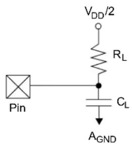
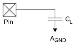
FIGURE 5-1: LOAD CONDITIONS
Load Condition 1
chemical
Circuit diagram showing pin connections to a voltage regulator with load resistor and capacitor$$ R _ {L} = 4 6 4 \Omega $$
$$ C _ {L} = 5 0 \mathrm{pF} \text { for all GPIO pins } $$
Load Condition 2
5.2 AC Characteristics: MCP19116 (Industrial, Extended)
FIGURE 5-2: EXTERNAL CLOCK TIMING

TABLE 5-1: EXTERNAL CLOCK TIMING REQUIREMENTS
| Param. No. | Sym. Characteristic Min. Typ. | Max. Units Conditions | |||||
| 1 | F_osc | Oscillator Frequency ^(1) | — | 8 | — | MHz | |
| 2 | T_osc | Oscillator Period ^(1) | — | 250 | — | ns | |
| 3 | T_CY | Instruction Cycle Time ^(1, 2) | — | T_CY | ns | T_CY = 4 * T_OSC | |
* These parameters are characterized but not tested.
† Data in "Typ." column is at V_IN = 12V ( V_DD = 5V ), 25^ unless otherwise stated. These parameters are for design guidance only and are not tested.
Note 1: All specified values are based on characterization data for that particular oscillator type under standard operating conditions with the device executing code.
2: Instruction cycle period (T CY) equals four times the input oscillator time base period.
FIGURE 5-3: I/O TIMING
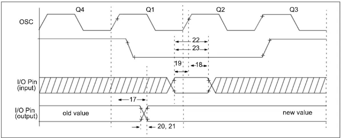
other
| Signal | Value | |-----------------|-------| | OSC | Q4 | | I/O Pin (input) | 17 | | I/O Pin (output) | 20, 21 |TABLE 5-2: I/O TIMING REQUIREMENTS
| Param. No. | Sym. Characteristic Min. Typ. | Max. Units Conditions | |||||
| 17 TosH2ioV OSC1 (Q1 cycle) to Port out valid | — | 5 | 0 | 7 | 0 | ||
| 18 | TosH2iol | OSC1 (Q2 cycle) to Port input invalid(I/O in hold time) | 50 | — | — | ns | |
| 19 TioV2osH Port input | valid to OSC1 (I/O in setup time) | 20 | — | — | ns | ||
| 20 | TioR | Port output rise time | — | 32 | 40 | ns | |
| 21 | TioF | Port output fall time | — | 15 | 30 | ns | |
| 22* | Tinp | INT pin high or low time | 25 | — | — | ns | |
| 23* | T_RABP | GPIOinterrupt-on-changenew input level time | T_CY | — | — | ns | |
^ Data in “Typ” column is at V_IN = 12V (V_DD = 5V) , 25^ unless otherwise stated.
* These parameters are characterized but not tested.
FIGURE 5-4: RESET, WATCHDOG TIMER, OSCILLATOR START-UP TIMER AND POWER-UP TIMER TIMING
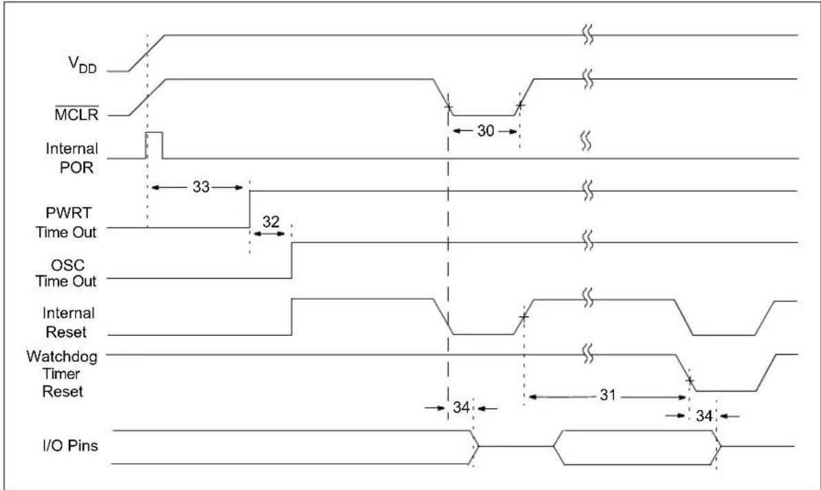
FIGURE 5-5: BROWN-OUT RESET TIMING AND CHARACTERISTICS
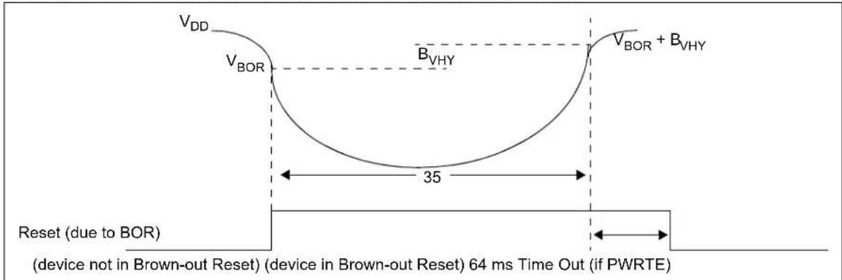
line
| Parameter | Value | | ------------------- | ----- | | V_DD | V_DD | | V_BOR | V_BOR | | B_VHY | B_VHY | | B_VHY + V_BOR | V_BOR + B_VHY | | Reset (due to BOR) | 35 | | Device not in Brown-out Reset (device in Brown-out Reset) 64 ms Time Out (if PWRTE) | 64 ms Time Out |TABLE 5-3: RESET, WATCHDOG TIMER, OSCILLATOR START-UP TIMER AND POWER-UP TIMER REQUIREMENTS
| Param. No. | Sym. Ch | Characteristic Min. Typ. | Max. Units Conditions | ||||
| 30 | T_MCL | Pulse Width (low) | 2 | — | — | μs | V_DD = 5V -40^ to +85^ |
| 31 | T_WDT | Watchdog Timer Time-Out Period (No Prescaler) | 7 | 18 | 33 | ms | V_DD = 5V -40^ to +85^ |
| 32 | T_OST | Oscillation Start-Up Timer Period | — | 1024T_OSC | — | — | T_OSC = OSC1 period |
| 33* | T_PWRT | Power-up Timer Period ( 4 × T_WDT ) | 28 72 | 132 | ms V | _DD = 5V -40^ to +85^ | |
| 34 | T_IOZ | I/O high impedance from MCLR Low or Watchdog Timer Reset | — | — | 2.0 | μs | |
| V_BOR | Brown-Out Reset voltage | — | 2.7 | — | V | ||
| B_VHY | Brown-Out Hysteresis | — | 100 | — | mV | ||
| 35 | T_BCR | Brown-Out Reset pulse width | 100* | — | — | μs | V_DD ≤ V_BOR (D005) |
| 48 | TCKEZ_TMR | Delay from clock edge to timer increment | 2T_OSC | — | 7T_OSC | ||
* These parameters are characterized but not tested.
Data in "Typ." column is at V_IN = 12V ( V_DD = 5V , AV_DD = 4V ), 25^ unless otherwise stated. These parameters are for design guidance only and are not tested.
FIGURE 5-6: TIMER0 AND TIMER1 EXTERNAL CLOCK TIMING
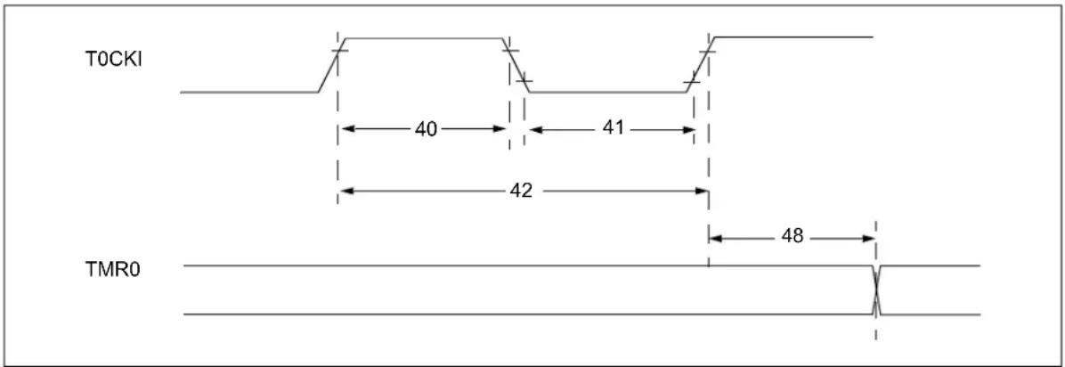
TABLE 5-4: TIMER0 EXTERNAL CLOCK REQUIREMENTS
| Param. No. | Sym . | Characteristic Min. Typ. | Max. | Units Conditions | ||||
| 40* Tt0 | H T0C | KI High Pulse Width No Prescaler 0.5T | _CY + 2 0 | — | — | n s | ||
| With Prescaler | 10 | —— | ns | |||||
| 41* | Tt0L | T0CKI Low Pulse Width No | Prescaler 0.5T | _CY + 2 0 | — | — | n s | |
| With Prescaler | 10 | — | — | ns | ||||
| 42* Tt0P | T0CKI Period | Greater of:20 or _CY + 40N | — | — | ns | N = prescale value(2, 4, ..., 256) | ||
* These parameters are characterized but not tested.
† Data in “Typ.” column is at V_IN = 12V , 25^ unless otherwise stated. These parameters are for design guidance only and are not tested.
FIGURE 5-7: PWM TIMINGS
PWM (CLKPIN)
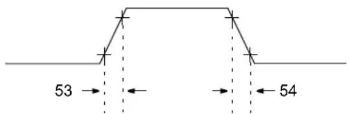
Note: Refer to Figure 5-1 for load conditions.
TABLE 5-5: PWM REQUIREMENTS
| Param. No. | Sym. | Characteristic | Min. Typ. | ^ | Max. | Units | Conditions |
| 53* | TccR | PWM (CLKPIN) output rise time | — | 10 | 25 | ns | |
| 54* | TccF | PWM (CLKPIN) output fall time | — | 10 | 25 | ns |
* These parameters are characterized but not tested.
Data in "Typ" column is at V_IN = 12V ( A_V_DD = 4V ), 25^ unless otherwise stated. Parameters are for design guidance only and are not tested.
TABLE 5-6: MCP19116/7 A/D CONVERTER (ADC) CHARACTERISTICS (1)
| Electrical Specifications: Unless otherwise noted, operating temperature = -40°C ≤ TA ≤ +125°C | |||||||
| Param. No. | Sym. | Characteristic Min. Typ. | † | Max. Units Conditions | |||
| AD01 N | R | Resolution — — 10 bits bit | |||||
| AD02 E | IL | Integral Error (2) | — | — | ±1 | LSb | V_REF\_ADC = AV_DD V_REF\_ADC = V_DD |
| AD03 | EDL | Differential Error (2) | — | — | ±1 | LSb | No missing codes to 10 bits (3) V_REF\_ADC = AV_DD V_REF\_ADC = V_DD |
| AD04 | EOFF | Offset Error (2) | — | +3.0 | +7 | LSb | V_REF\_ADC = AV_DD V_REF\_ADC = V_DD |
| AD07 | EGN | Gain Error (2) | — | ±2 | ±6 | LSb | V_REF\_ADC = AV_DD V_REF\_ADC = V_DD |
| AD07 | V_AIN | Full-Scale Range | A_GND | — | AV_DD | V | AV_DD selected as ADC reference |
| A_GND | — | V_DD | V | V_DD selected as ADC reference | |||
| AD08 | Z_AIN | Recommended Impedance of Analog Voltage Source | — | — | 10 | kΩ | |
* These parameters are characterized but not tested.
† Data in 'Typ.' column is at V_IN = 12V ( V_DD = 5V , AV_DD = 4V ), 25°C unless otherwise stated. These parameters are for design guidance only and are not tested.
Note 1: When ADC is off, it will not consume any current other than leakage current. The power-down current specification includes any such leakage from the ADC module. To minimize Sleep current, the ADC reference must be set to the default AV_DD .
2: Total Absolute Error includes integral, differential, offset and gain errors.
3: The A/D conversion result never decreases with an increase in the input voltage and has no missing codes.
TABLE 5-7: MCP19116/7 A/D CONVERSION REQUIREMENTS
| Electrical Specifications: Unless otherwise noted, operating temperature = -40°C ≤ TA ≤ +125°C | |||||||
| Param. No. | Sym. | Characteristic | Min. | Typ.† | Max. | Units | Conditions |
| AD130* | T_AD | A/D Clock Period | 1.6 | — | 9.0 | μs | T_OSC -based |
| A/D Internal RC Oscillator Period | 1.6 | 4.0 | 6.0 | μs | ADCS<1:0> = 11 (ADRC mode) | ||
| AD131 | T_CNV | Conversion Time (not including Acquisition Time)(1) | — | 11 | — | T_AD | Set GO/DONE bit to new data in A/D Result registers |
| AD132* | T_ACQ | Acquisition Time | — | 1.5 — μs | |||
| AD133* | T_AMP | Amplifier Settling Time | — | — | 5 | μs | |
| AD134 | T_GO | Q4 to A/D Clock Start | — | T_OSC/2 | — | — | |
^ Data in ‘Typ.’ column is at V_IN = 12V ( V_DD = 5V , AV_DD = 4V ), 25^ unless otherwise stated. These parameters are for design guidance only and are not tested.
* These parameters are characterized but not tested.
Note 1: ADRESH and ADRESL registers may be read on the following T_CY cycle.
FIGURE 5-8: A/D CONVERSION TIMING
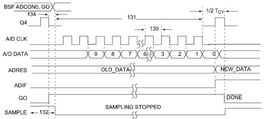
Note 1: If the A/D clock source is selected as RC, a time of T_CY is added before the A/D clock starts. This allows the SLEEP instruction to be executed.
6.0 CONFIGURING THE MCP19116/7
The MCP19116/7 devices are analog controllers with a digital peripheral. This means that device configuration is handled through register settings instead of adding external components. There are several internal configurable comparator modules used to interface analog circuits to digital processing that are very similar to a standard comparator module found in many PIC processors today (i.e., PIC16F1824/1828). The following sections detail how to set the analog control registers for all the configurable parameters.
6.1 Input Undervoltage and Overvoltage Lockout (UVLO and OVLO)
VINCON is the comparator control register for both the VINUVLO and VINOVLO registers. It contains the enable bits, the polarity edge detection bits and the status output bits for both protection circuits. The interrupt flags
The VINUVLO register contains the digital value that sets the input undervoltage lockout. UVLO has a range of 4V to 20V. For V_IN values below this range and above processor come-alive ( V_DD = 2V ), the UVLO comparator and the UVLOOUT Status bit will indicate an undervoltage condition. If using UVLO to determine power-up V_IN , it is recommended to poll the UVLOOUT bit for status. When the input voltage on the V_IN pin to the MCP19116/7 is below this programmed level and the
The VINOVLO register contains the digital value that sets the input overvoltage lockout. OVLO has a range of 8.8V to 44V. When the input voltage on the V_IN pin to the MCP19116/7 is above this programmed level and the
Note: The UVLOIF and OVLOIF interrupt flag bits are set when an interrupt condition occurs, regardless of the state of its corresponding enable bit or the Global Enable bit (GIE) in the INTCON register.
REGISTER 6-1: VINCON: UVLO AND OVLO COMPARATOR CONTROL REGISTER
| R/W-0 R-0 R/W-0 R/W-0 R/W-0 R-0 R/W-0 R/W-0 | |||||||
| UVLOEN | UVLOOUT | UVLOINTP | UVLOINTN | OVLOEN | OVLOOUT | OVLOINTP | OVLOINTN |
| bit 7 bit 0 | |||||||
Legend:
| R = Readable bit | W = Writable bit | U = Unimplemented bit, read as '0' |
| u = Bit is unchanged | x = Bit is unknown -n = Value at POR | |
| ‘1’ = Bit is set | ‘0’ = Bit is cleared | |
bit 7 UVLOEN: UVLO Comparator Module Logic Enable bit
1 = UVLO Comparator Module Logic enabled
0 = UVLO Comparator Module Logic disabled
bit 6 UVLOOUT: Undervoltage Lockout Status Output
1 = UVLO event has occurred
0 = No UVLO event has occurred
bit 5 UVLOINTP: UVLO Comparator Interrupt on Positive Going Edge Enable bit
1 = The UVLOIF interrupt flag will be set upon a positive going edge of the UVLO
0 = No UVLOIF interrupt flag will be set upon a positive going edge of the UVLO
bit 4 UVLOINTN: UVLO Comparator Interrupt on Negative Going Edge Enable bit
1 = The UVLOIF interrupt flag will be set upon a negative going edge of the UVLO
0 = No UVLOIF interrupt flag will be set upon a negative going edge of the UVLO
REGISTER 6-1: VINCON: UVLO AND OVLO COMPARATOR CONTROL REGISTER (CONTINUED)
bit 3 OVLOEN: OVLO Comparator Module Logic enable bit
1 = OVLO Comparator Module Logic enabled
0 = OVLO Comparator Module Logic disabled
bit 2 OVLOOUT: Overvoltage Lockout Status Output bit
1 = OVLO event has occurred
0 = No OVLO event has occurred
bit 1 OVLOINTP: OVLO Comparator Interrupt on Positive Going Edge Enable bit
1 = The OVLOIF interrupt flag will be set upon a positive going edge of the OVLO
0 = No OVLOIF interrupt flag will be set upon a positive going edge of the OVLO
bit 0 OVLOINTN: OVLO Comparator Interrupt on Negative Going Edge Enable bit
1 = The OVLOIF interrupt flag will be set upon a negative going edge of the OVLO
0 = No OVLOIF interrupt flag will be set upon a negative going edge of the OVLO
REGISTER 6-2: VINUVLO: INPUT UNDERVOLTAGE LOCKOUT REGISTER
| U-0 U-0 R/W-x R/W-x R/W-x R/W-x R/W-x R/W-x | |||||||
| — | — | UVLO5 | UVLO4 | UVLO3 | UVLO2 | UVLO1 | UVLO0 |
| bit 7 bit 0 | |||||||
Legend:
| R = Readable bit | W = Writable bit | U = Unimplemented bit, read as '0' |
| u = Bit is unchanged x = Bit is unknown | -n = Value at POR | |
| '1' = Bit is set | '0' = Bit is cleared | |
bit 7-6 Unimplemented: Read as '0'
bit 5-0 UVLO<5:0>: Undervoltage Lockout Configuration bits
UVLO(V) = 3.5472 * (1.0285 ^N ) where N = the decimal value written to the VINUVLO Register from 0 to 63
REGISTER 6-3: VINOVLO: INPUT OVERVOLTAGE LOCKOUT REGISTER
| U-0 U-0 R/W-x R/W-x R/W-x R/W-x R/W-x R/W-x | |||||||
| — | — | OVLO5 | OVLO4 | OVLO3 | OVLO2 | OVLO1 | OVLO0 |
| bit 7 bit 0 | |||||||
Legend:
| R = Readable bit | W = Writable bit | U = Unimplemented bit, read as ‘0’ |
| u = Bit is unchanged x = Bit is unknown | -n = Value at POR | |
| ‘1’ = Bit is set | ‘0’ = Bit is cleared | |
bit 7-6 Unimplemented: Read as '0'
bit 5-0 OVLO<5:0>: Overvoltage Lockout Configuration bits
OVLO(V) = 7.4847 * (1.0286 ^N ) where N = the decimal value written to the VINOVLO Register from 0 to 63
6.2 Output Overvoltage Protection
The MCP19116/7 devices feature output overvoltage protection. This feature also utilizes a comparator module similar to the standard PIC comparator module. This is used to prevent the power system from being damaged when the load is disconnected. The OVREFCON register contains the digital value that sets the analog DAC voltage at the inverting input of the comparator. By comparing the divided down power train output voltage connected to the noninverting input ( V_S ) of the comparator with the OVREF reference voltage, the user can determine when an overvoltage event has occurred and can automatically take action.
The OVCON register contains the interrupt flag polarity and OV enable bits along with the Output Status bit just as VINCON does for the input voltage UVLO and OVLO. When
| Note: The OVIF Interrupt Flag bit is set when an interrupt condition occurs, regardless of the state of its corresponding enable bit or the Global Enable bit (GIE) in the INTCON register. |
REGISTER 6-4: OVCON: OUTPUT OVERVOLTAGE COMPARATOR CONTROL REGISTER
| U-0 U-0 U-0 U-0 R/W-0 R-0 R/W-0 R/W-0 | |||||||
| — | — | — | — | OVEN | OVOUT | OVINTP | OVINTN |
| bit 7 bit 0 | |||||||
Legend:
| R = Readable bit | W = Writable bit | U = Unimplemented bit, read as '0' |
| u = Bit is unchanged | x = Bit is unknown | -n = Value at POR |
| ‘1’ = Bit is set | ‘0’ = Bit is cleared |
bit 7-4 Unimplemented: Read as '0'
bit 3 OVEN: OV Comparator Output Enable bit
1 = OV Comparator output is enabled
0 = OV Comparator output is not enabled
bit 2 OVOUT: Output Overvoltage Status Output bit
1 = Output Overvoltage has occurred
0 = No Output Overvoltage has occurred
bit 1 OVINTP: OV Comparator Interrupt on Positive Going Edge Enable bit
1 = The OVIF interrupt flag will be set upon a positive going edge of the OV
0 = No OVIF interrupt flag will be set upon a positive going edge of the OV
bit 0 OVINTN: OV Comparator Interrupt on Negative Going Edge Enable bit
1 = The OVIF interrupt flag will be set upon a negative going edge of the OV
0 = No OVIF interrupt flag will be set upon a negative going edge of the OV
REGISTER 6-5: OVREFCON: OUTPUT OVERVOLTAGE DETECT LEVEL REGISTER
| R/W-x R/W-x R/W-x R/W-x R/W-x R/W-x R/W-x R/W-x | |||
| OOV7 OOV6 OOV5 OOV4 OOV3 OOV2 OOV1 OOV0 | |||
| bit 7 bit 0 | |||
Legend:
| R = Readable bit W = Writable bit | U = Unimplemented bit, read as '0' | |
| u = Bit is unchanged | x = Bit is unknown | -n = Value at POR |
| '1' = Bit is set | '0' = Bit is cleared | |
bit 7-0 OOV<7:0>: Output Overvoltage Detect Level Configuration bits
V_OV_REF(V) = 2 * V_BG * N/255 where N is the decimal value written to the OVREFCON Register
6.3 Desaturation Detection for Quasi-Resonant Operation
The MCP19116/7 have been designed with a built-in desaturation detection comparator module custom made for quasi-resonant topologies. This is especially useful for LED-type applications. Through the use of the MCP19116/7, both synchronous and asynchronous quasi-resonant topologies can be implemented. The DESAT comparator module has the same features as the UVLO/OVLO and OV comparator modules, except that it includes some additional programmable parameters.
The DESATCON register holds the setup control bits for this module. Common control bits are the polarity edge trigger for the interrupt flag
REGISTER 6-6: DESATCON: DESATURATION COMPARATOR CONTROL REGISTER
| R/W-0 R/W-0 R/W-0 R/W-0 R/W-0 R/W-0 R/W-0 | |||||||
| CDSMUX | CDSWDE | Reserved | CDSPOL | CDSOE | CDSOUT | CDSINTP | CDSINTN |
| bit 7 bit 0 | |||||||
| Legend: | ||
| R = Readable bit | W = Writable bit | U = Unimplemented bit, read as ‘0’ |
| u = Bit is unchanged | x = Bit is unknown | -n = Value at POR |
| ‘1’ = Bit is set | ‘0’ = Bit is cleared | |
bit 7 CDSMUX: DESAT Comparator Module Multiplexer Channel Selection bit
1 = BG Selected
0 = DESAT_P Selected (Default)
bit 6 CDSWDE: DESAT Comparator Watch Dog Enable bit
1 = Watch Dog signal enables PWM Reset
0 = Watch Dog signal does not allow PWM reset
bit 5 Reserved
bit 4 CDSPOL: DESAT Comparator Polarity Select bit
1 = DESAT Comparator output is inverted
0 = DESAT Comparator output is not inverted
bit 3 CDSOE: DESAT Comparator output enable bit
1 = DESAT Comparator output PWM is enabled
0 = DESAT Comparator output PWM is not enabled
bit 2 CDSOUT: DESAT Comparator Output Status bit
If CDSPOL = 1 (inverted polarity)
1 = CDSVP < CDSVN (DESAT detected)
0 = CDSVP > CDSVN (DESAT not detected)
If CDSPOL = 0 (non-inverted polarity)
1 = CDSVP > CDSVN (DESAT not detected)
0 = CDSVP < CDSVN (DESAT detected)
bit 1 CDSINTP: CDSIF Comparator Interrupt on Positive Going Edge Enable bit
1 = The CDSIF interrupt flag will be set upon a positive going edge
0 = No CDSIF interrupt flag will be set upon a positive going edge
bit 0 CDSINTN: CDSIF Comparator Interrupt on Negative Going Edge Enable bit
1 = The CDSIF interrupt flag will be set upon a negative going edge
0 = No CDSIF interrupt flag will be set upon a negative going edge
6.4 Primary Input Current Offset Adjust
Primary input current offset adjust provides the ability to add offset to the primary input current signal, thus setting a peak primary current limit. This offset adjust is controlled by means of the four bits in the ICOACON register.
REGISTER 6-7: ICOACON: INPUT CURRENT OFFSET ADJUST CONTROL REGISTER
| U-0 U-0 U-0 U-0 R/W-x R/W-x R/W-x R/W-x | |||||||
| — | — | — | — | ICOAC3 | ICOAC2 | ICOAC1 | ICOAC0 |
| bit 7 bit 0 | |||||||
Legend:
| R = Readable bit | W = Writable bit | U = Unimplemented bit, read as '0' |
| u = Bit is unchanged | x = Bit is unknown | -n = Value at POR |
| '1' = Bit is set | '0' = Bit is cleared |
bit 7-4 Unimplemented: Read as '0'
bit 3-0 ICOAC<3:0>: Input Current Offset Adjustment Configuration bits
0000 = 0 mV
0001 = 50 mV
0010 = 100 mV
0011 = 150 mV
0100 = 200 mV
0101 = 250 mV
0110 = 300 mV
0111 = 350 mV
1000 = 400 mV
1001 = 450 mV
1010 = 500 mV
1011 = 550 mV
1100 = 600 mV
1101 = 650 mV
1110 = 700 mV
1111 = 750 mV
6.5 Leading Edge Blanking
The adjustable Leading Edge Blanking (LEB) is used to blank primary current spikes resulting from primary switch turn-on. Implementing adjustable LEB allows the system to ignore turn-on noise to best suit the application without primary current sense distortion from RC filtering. There are four settings available for LEB, including zero. These settings are controlled via two bits in the ICLEBCON register.
REGISTER 6-8: ICLEBCON: INPUT CURRENT LEADING EDGE BLANKING CONTROL REGISTER
| U-0 U-0 U-0 U-0 U-0 R/W-x R/W-x | |||||||
| — | — | — | — | — | — | ICLEBC1 | ICLEBC0 |
| bit 7 bit 0 | |||||||
Legend:
| R = Readable bit | W = Writable bit | U = Unimplemented bit, read as '0' |
| u = Bit is unchanged | x = Bit is unknown -n = Value at POR | |
| ‘1’ = Bit is set | ‘0’ = Bit is cleared | |
bit 7-2 Unimplemented: Read as '0'
bit 1-0 ICLEBC<1:0>: Input current Leading Edge Blanking Configuration bits
00 = 0 ns
01 = 50 ns
10 = 100 ns
11 = 200 ns
6.6 Slope Compensation
A negative voltage slope is added to the output of the error amplifier. This is done to prevent subharmonic instability when:
- the operating duty cycle is greater than 50%
- wide changes in duty cycle occur
The amount of negative slope added to the error amplifier output is controlled by the slope compensation slew rate control bits.
The slope compensation is enabled by clearing the SLPBY bit in the SLPCRCON register.
REGISTER 6-9: SLPCRCON: SLOPE COMPENSATION RAMP CONTROL REGISTER
| U-0 R/W-0 R/W-x R/W-x R/W-x R/W-x R/W-x R/W-x | |||||||
| — | SLPBY | SLPS5 | SLPS4 | SLPS3 | SLPS2 | SLPS1 | SLPS0 |
| bit 7 bit 0 | |||||||
Legend:
| R = Readable bit | W = Writable bit | U = Unimplemented bit, read as '0' |
| u = Bit is unchanged | x = Bit is unknown -n = Value at POR | |
| '1' = Bit is set | '0' = Bit is cleared | |
bit 7 Unimplemented: Read as '0'
bit 6 SLPBY: Slope Compensation Bypass Control bit
1 = Slope compensation is bypassed
0 = Slope compensation is not bypassed (Default)
bit 5-0 SLPS<5:0>: Slope Compensation Slew Rate Control bits
SLPS (mV/μs) = 4.5 * 1.08 ^N where N is the decimal value written to the SLPCRCON Register
6.7 MOSFET Driver Programmable Dead Time
The turn-on dead time of both PDRV and SDRV low-side drive signals can be configured independently to allow different MOSFETs and circuit board layouts to be used to construct an optimized system (refer to Figure 6-1).
Clearing the PDRVBY and SDRVBY bits in the PE1 register enables the PDRV and SDRV low-side dead timers, respectively. The amount of dead time added is controlled in the DEADCON register.
FIGURE 6-1: MOSFET DRIVER DEAD TIME
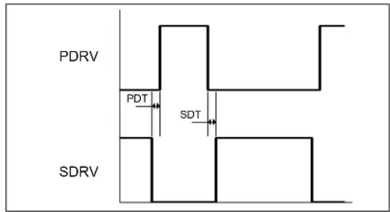
REGISTER 6-10: DEADCON: DRIVER DEAD TIME CONTROL REGISTER
| R/W-x R/W-x R/W-x R/W-x R/W-x R/W-x R/W-x | |||||||
| PDRVDT3 | PDRVDT2 | PDRVDT1 | PDRVDT0 | SDRVDT3 | SDRVDT2 | SDRVDT1 | SDRVDT0 |
| bit 7 bit 0 | |||||||
| Legend: | ||
| R = Readable bit | W = Writable bit | U = Unimplemented bit, read as ‘0’ |
| u = Bit is unchanged | x = Bit is unknown | -n = Value at POR |
| ‘1’ = Bit is set | ‘0’ = Bit is cleared | |
bit 7-4 PDRVDT<3:0>: PDRV Dead Time Configuration bits ( t_TD_1 )
0000 = 16 ns delay
0001 = 32 ns delay
0010 = 48 ns delay
0011 = 64 ns delay
0100 = 80 ns delay
0101 = 96 ns delay
0110 = 112 ns delay
0111 = 128 ns delay
1000 = 144 ns delay
1001 = 160 ns delay
1010 = 176 ns delay
1011 = 192 ns delay
1100 = 208 ns delay
1101 = 224 ns delay
1110 = 240 ns delay
1111 = 256 ns delay
REGISTER 6-10: DEADCON: DRIVER DEAD TIME CONTROL REGISTER (CONTINUED)
bit 3-0 SDRVDT<3:0>: SDRV Dead Time Configuration bits ( t_TD_2 )
0000 = 16 ns delay
0001 = 32 ns delay
0010 = 48 ns delay
0011 = 64 ns delay
0100 = 80 ns delay
0101 = 96 ns delay
0110 = 112 ns delay
0111 = 128 ns delay
1000 = 144 ns delay
1001 = 160 ns delay
1010 = 176 ns delay
1011 = 192 ns delay
1100 = 208 ns delay
1101 = 224 ns delay
1110 = 240 ns delay
1111 = 256 ns delay
6.8 Output Regulation Reference Voltage Configuration
The VREFCON register controls the error amplifier reference voltage. This reference is used to set the current or voltage regulation set point. VREFCON holds the digital value used by an 8-bit linear DAC, setting the analog equivalent that gets summed with the pedestal voltage (VZC) at the noninverting node of the error amplifier. VZC is equal to the band gap voltage (1.23V). The output of the current sense amplifier A2 is also raised on the pedestal voltage, effectively canceling its effect on the input. The pedestal is implemented throughout the analog control loop to improve accuracy at low levels. The V_REF DAC can be adjusted in 255 steps of 4.8 mV/step.
REGISTER 6-11: VREFCON: CURRENT/VOLTAGE REGULATION SET POINT CONTROL REGISTER
| R/W-0 R/W-0 R/W-0 R/W-0 R/W-0 R/W-0 R/W-0 | |||||||
| VREF7 | VREF6 | VREF5 | VREF4 | VREF3 | VREF2 | VREF1 | VREF0 |
| bit 7 bit 0 | |||||||
Legend:
| R = Readable bit | W = Writable bit | U = Unimplemented bit, read as '0' |
| u = Bit is unchanged | x = Bit is unknown | -n = Value at POR |
| '1' = Bit is set | '0' = Bit is cleared |
bit 7-0 VREF<7:0>: Voltage-Controlling Current Regulation Set Point bits
V_REF(V) = V_BG * N/255 where N is the decimal value written to the VREFCON Register
6.9 V REF2 Voltage Reference
The VREF2CON register controls a second reference DAC that can be used externally. For example, it can be sent off-chip and used to set the current regulation set point for a MCP1631 Pulse-Width Modulator. The MCP19116/7 must be configured in Master Mode with bits MSC<0:1> = 01 in the MODECON register to
connect V_REF2 to GPB1. In Stand-Alone mode, V_REF2 is not accessible. VREFCON2 holds the digital value used to set the VREF2 DAC. Since this reference is intended to go off-chip, there is no pedestal offset associated with it and it is referenced to GND. It is an 8-bit linear DAC and has a range from 0V to 1.23V (BG) equating to 255 steps at 4.8 mV/step.
REGISTER 6-12: VREF2CON: V REF2 VOLTAGE SET POINT REGISTER
| R/W-0 | R/W-0 | R/W-0 | R/W-0 | R/W-0 | R/W-0 | R/W-0 | R/W-0 |
| VREF27 | VREF26 | VREF25 | VREF24 | VREF23 | VREF22 | VREF21 | VREF20 |
| bit 7 bit 0 | |||||||
Legend:
| R = Readable bit | W = Writable bit | U = Unimplemented bit, read as '0' |
| u = Bit is unchanged | x = Bit is unknown | -n = Value at POR |
| '1' = Bit is set | '0' = Bit is cleared |
bit 7-0 VREF2<7:0>: Voltage Controlling Current Regulation Set Point bits
V_REF2(V) = V_BG^* N/255 where N is the decimal value written to the VREF2CON Register
6.10 Analog Peripheral Control
The MCP19116/7 devices have several analog peripherals, such as the PDRV and SDRV peripherals, and a weak pull-up on the I_SP input.
PDRV and SDRV peripherals are enabled using single bits, PDRVEN and SDRVEN. The weak pull-up on the I_SP input is enabled using the ISPUEN bit.
These peripherals can be configured to allow customizable operation. Refer to Register 6-13 for more information.
6.10.1 MOSFET GATE DRIVER ENABLES
The MCP19116/7 can enable and/or disable the MOSFET gate driver outputs for the primary drive (PDRV) and the secondary drive (SDRV) independently. Setting the
6.10.2 MOSFET DRIVER DEAD TIME
The MOSFET drive dead time can be adjusted as described in Section 6.7 "MOSFET Driver Programmable Dead Time". The dead time can be set independently for each driver from 16 ns to 256 ns in increments of 16 ns using the DEADCON register. Dead time can also be disabled for each driver independently by setting the bypass bits
6.10.3 SECONDARY CURRENT POSITIVE SENSE PULL-UP
A high-impedance pull-up on the I_SP pin can be configured by setting the
6.10.4 PWM STEERING
The MCP19116/7 devices have additional control circuitry to allow open-loop repositioning of the output. The PWMSTR_PEN bit enables a primary-only PWM signal of fixed frequency and duty cycle to reposition the output voltage up. The PWMSTR_SEN bit enables a secondary-only PWM signal of fixed frequency and duty cycle to reposition the output voltage down. When repositioning output voltage down, the output overvoltage protection must be active along with PWMSTR_SEN for the PWM to pulse the SDRV. Frequency and duty cycle are controlled through TMR2 registers PR2 and TMR1L. PWMSTPR_PEN and PWMSTR_SEN should never be active at the same time, therefore PWMSTPR_PEN is the dominant bit. For quasi-resonant operation during open-loop repositioning, the DESAT comparator output should be disabled with the
REGISTER 6-13: PE1: ANALOG PERIPHERAL ENABLE1 CONTROL REGISTER
| R/W-0 R/W-0 R/W-0 R/W-0 U-0 R/W-0 | R/W-0 | R/W-0 | |||||
| PDRVEN | SDRVEN | PDRVBY | SDRVBY | — | ISPUEN | PWMSTR_PEN | PWMSTR_SEN |
| bit 7 bit 0 | |||||||
Legend:
| R = Readable bit | W = Writable bit | U = Unimplemented bit, read as '0' |
| u = Bit is unchanged | x = Bit is unknown | -n = Value at POR |
| '1' = Bit is set | '0' = Bit is cleared |
bit 7 PDRVEN: PDRV Gate Drive Enable bit
1 = PDRV gate drive is enabled
0 = PDRV gate drive is disabled
bit 6 SDRVEN: SDRV Gate Drive Enable bit
1 = SDRV gate drive is enabled
0 = SDRV gate drive is disabled
bit 5 PDRVBY: PDRV Dead Time Bypass bit
1 = PDRV dead time is bypassed
0 = PDRV dead time is not bypassed
bit 4 SDRVBY: SDRV Dead Time Bypass bit
1 = SDRV dead time is bypassed
0 = SDRV dead time is not bypassed.
bit 3 Unimplemented: Read as '0'
bit 2 ISPUEN: I_SP Weak Pull-Up Enable bit
1 = I_SP weak pull-up is enabled
0 = I_SP weak pull-up is disabled
bit 1 PWMSTR_PEN: PDRV PWM Steering bit
1 = Enables open-loop PWM control to the PDRV
0 = Disables open-loop PWM control to the PDRV
bit 0 PWMSTR_SEN: SDRV PWM Steering bit
1 = Enables open-loop PWM control to the SDRV
0 = Disables open-loop PWM control to the SDRV
6.11 Analog and Digital Test Signal Enable and Control
Various analog and digital test signals can be enabled or disabled, as shown in Register 6-14. These signals can be configured to GPA0. Setting the
6.11.1 MOSFET DRIVER UNDERVOLTAGE LOCKOUT SELECTION
The MOSFET gate drivers have internal undervoltage protection that is controlled by the
6.11.2 ERROR AMPLIFIER DISABLE
The error amplifier can be disabled such that its output is parked to a known state. The
REGISTER 6-14: ABECON: ANALOG BLOCK ENABLE CONTROL REGISTER
| R/W-0 R/W-0 R/W-0 R/W-0 R/W-0 U-0 R/W-0 R/W-0 | |||||||
| DIGOEN | DSEL2 | DSEL1 | DSEL0 | DRUVSEL | — | EADIS | ANAOEN |
| bit 7 bit 0 | |||||||
Legend:
| R = Readable bit | W = Writable bit | U = Unimplemented bit, read as '0' |
| u = Bit is unchanged | x = Bit is unknown | -n = Value at POR |
| '1' = Bit is set | '0' = Bit is cleared |
bit 7 DIGOEN: DIG Test MUX to GPA0 connection control
1 = DIG Test MUX output is connected to external pin GPA0 0 = DIG Test MUX output is not connected to external pin GPA0
bit 6-4 DSEL<2:0> Digital Test Signals
000 = QRS (output of DESAT comparator) 001 = PWM_L (PWM output after monostable) 010 = PWM (oscillator output from the microcontroller) 011 = TMR2EQ (when TMR2 equals PR2) 100 = OV (overvoltage comparator output) 101 = SWFRQ (switching frequency output) 110 = SDRV_ON_ONESHOT (200 ns one-shot signal to reset WDM logic) 111 = Unimplemented
bit 3 DRUVSEL: Selects gate drive undervoltage lockout level
1 = Gate Drive UVLO set to 5.4V
0 = Gate Drive UVLO set to 2.7V
bit 2 Unimplemented: Read as '0'
bit 1 EADIS: Error Amplifier Disable bit
1 = Disables the error amplifier (Output parked low, clamped to 1 * BG) 0 = Enables the error amplifier (Normal operation)
bit 0 ANAOEN: Analog MUX Output Control bit
1 = Analog MUX output is connected to external pin GPA0 0 = Analog MUX output is not connected to external pin GPA0
6.12 Mode and RFB MUX Control
The MODECON register controls the Master/Slave configuration and the internal resistor feedback MUX for the current sense amplifier while in quasi-resonant mode.
In Master mode, it allows the V_REF2 signal of the Master MCP19116/7 device to be buffered and connected to a GPIO pin. This output signal can be connected to a Slave PWM driver (MCP1631) at the V_REF input to regulate current via the Slave PWM Controller. In Master mode, the CLKOUT sync signal is routed to GPA1. In Semi-Master Mode, users have the option to implement V_REF2 and CLKOUT independently. In Stand-Alone mode, the V_REF2 unity gain buffer and CLKOUT signals are not connected to GPIO Pins.
The RFB MUX selects the output of A2 current sense amplifier to be connected to the internal 5 kΩ feedback resistor or to the I_SOUT pin.
REGISTER 6-15: MODECON: MASTER/SLAVE AND RFB MUX CONTROL REGISTER
| R/W-0 R/W-0 R/W-0 U-0 R/W-0 U-0 U-0 U-0 | |||||||
| MSC1 | MSC0 | RFB | — | MSC2 | — | — | — |
| bit 7 bit 0 | |||||||
Legend:
| R = Readable bit | W = Writable bit | U = Unimplemented bit, read as '0' |
| u = Bit is unchanged | x = Bit is unknown -n = Value at POR | |
| '1' = Bit is set | '0' = Bit is cleared | |
bit 7-6 MSC<1:0>: Master/Slave Configuration bits
00 = Device set as stand-alone unit (VREF2 disabled, Switching frequency internally generated)
01 = Device set as MASTER (VREF2 to GPB1, CLKOUT sync to GPA1)
10 = Device set as SLAVE MODE (CLKIN switching frequency sync signal to GPA1)
11 = Device set to SEMI-MASTER MODE
bit 5 RFB: Current Sense Amplifier (A2) Output Resistor Feedback MUX Configuration bit
0 = R_FB_INT 5 k
1 = I _SOUT
bit 4 Unimplemented: Read as '0'
bit 3 MSC<2>: Semi-Master mode options
0 = GPB1 is VREF2 Output, GPA1 is general purpose I/O
1 = GPB1 is general purpose output, GPA1 is CLKOUT
bit 2-0 Unimplemented: Read as '0'
7.0 TYPICAL PERFORMANCE CURVES
Note: The graphs and tables provided following this note are a statistical summary based on a limited number of samples and are provided for informational purposes only. The performance characteristics listed herein are not tested or guaranteed. In some graphs or tables, the data presented may be outside the specified operating range (e.g., outside specified power supply range) and therefore, outside the warranted range.
Note: Unless otherwise indicated, V_IN = 12V · S W = 150 kHz , T_A = +25^ .
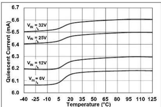
line
| Temperature (°C) | V_IN = 32V | V_IN = 25V | V_IN = 12V | V_IN = 6V | | ---------------- | ---------- | ---------- | ---------- | --------- | | -40 | 6.5 | 6.4 | 6.2 | 6.1 | | -25 | 6.5 | 6.4 | 6.2 | 6.1 | | -10 | 6.5 | 6.4 | 6.2 | 6.1 | | 5 | 6.5 | 6.4 | 6.2 | 6.1 | | 20 | 6.5 | 6.4 | 6.2 | 6.1 | | 35 | 6.5 | 6.4 | 6.2 | 6.1 | | 50 | 6.5 | 6.4 | 6.2 | 6.1 | | 65 | 6.5 | 6.4 | 6.2 | 6.1 | | 80 | 6.5 | 6.4 | 6.2 | 6.1 | | 95 | 6.5 | 6.4 | 6.2 | 6.1 | | 110 | 6.5 | 6.4 | 6.2 | 6.1 | | 125 | 6.5 | 6.4 | 6.2 | 6.1 |FIGURE 7-1: I Q vs. Temperature.
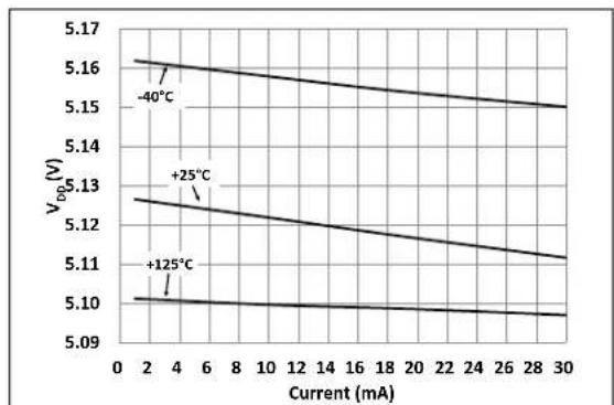
line
| Current (mA) | VDD (V) at -40°C | VDD (V) at +25°C | VDD (V) at +125°C | | ------------ | ---------------- | ---------------- | ----------------- | | 0 | 5.16 | 5.13 | 5.10 | | 2 | 5.16 | 5.13 | 5.10 | | 4 | 5.16 | 5.13 | 5.10 | | 6 | 5.16 | 5.13 | 5.10 | | 8 | 5.16 | 5.13 | 5.10 | | 10 | 5.16 | 5.13 | 5.10 | | 12 | 5.16 | 5.13 | 5.10 | | 14 | 5.16 | 5.13 | 5.10 | | 16 | 5.16 | 5.13 | 5.10 | | 18 | 5.16 | 5.13 | 5.10 | | 20 | 5.16 | 5.13 | 5.10 | | 22 | 5.16 | 5.13 | 5.10 | | 24 | 5.16 | 5.13 | 5.10 | | 26 | 5.16 | 5.13 | 5.10 | | 28 | 5.16 | 5.13 | 5.10 | | 30 | 5.16 | 5.13 | 5.10 |FIGURE 7-4: Load Regulation.
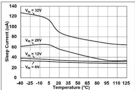
line
| Temperature (°C) | Sleep Current (uA) at V_IN = 6V | Sleep Current (uA) at V_IN = 12V | Sleep Current (uA) at V_IN = 20V | Sleep Current (uA) at V_IN = 32V | | ---------------- | ------------------------------ | ------------------------------- | ------------------------------- | ------------------------------- | | -40 | ~35 | ~60 | ~120 | ~125 | | -25 | ~35 | ~60 | ~115 | ~120 | | -10 | ~35 | ~60 | ~110 | ~115 | | 0 | ~35 | ~60 | ~105 | ~110 | | 5 | ~35 | ~60 | ~95 | ~100 | | 20 | ~35 | ~55 | ~85 | ~90 | | 35 | ~35 | ~50 | ~75 | ~80 | | 50 | ~35 | ~45 | ~70 | ~75 | | 65 | ~35 | ~40 | ~65 | ~70 | | 80 | ~35 | ~35 | ~60 | ~65 | | 95 | ~35 | ~35 | ~55 | ~60 | | 110 | ~35 | ~35 | ~50 | ~55 | | 125 | ~35 | ~35 | ~45 | ~50 |FIGURE 7-2: IQ vs. Temperature in Sleep Mode.
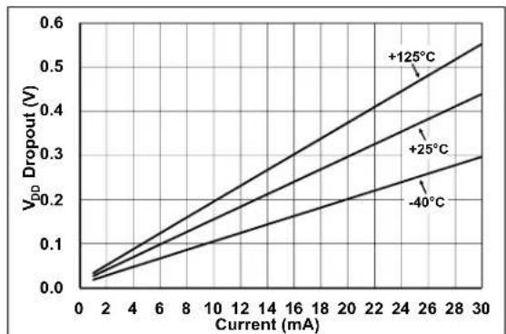
line
| Current (mA) | +125°C | +25°C | -40°C | | ------------ | ------ | ----- | ----- | | 0 | 0.0 | 0.0 | 0.0 | | 2 | 0.05 | 0.03 | 0.02 | | 4 | 0.1 | 0.06 | 0.04 | | 6 | 0.15 | 0.09 | 0.06 | | 8 | 0.2 | 0.12 | 0.08 | | 10 | 0.25 | 0.15 | 0.1 | | 12 | 0.3 | 0.18 | 0.12 | | 14 | 0.35 | 0.21 | 0.14 | | 16 | 0.4 | 0.24 | 0.16 | | 18 | 0.45 | 0.27 | 0.18 | | 20 | 0.5 | 0.3 | 0.2 | | 22 | 0.55 | 0.33 | 0.22 | | 24 | 0.6 | 0.36 | 0.24 | | 26 | 0.65 | 0.39 | 0.26 | | 28 | 0.7 | 0.42 | 0.28 | | 30 | 0.75 | 0.45 | 0.3 |FIGURE 7-5: V _DD Dropout Voltage vs. Output Current (mA).
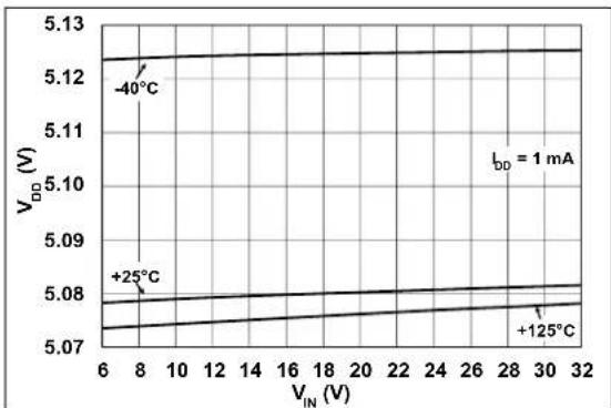
line
| V_IN (V) | V_DD (V) | | -------- | -------- | | 8 | 5.08 | | 30 | 5.08 |FIGURE 7-3: Line Regulation.
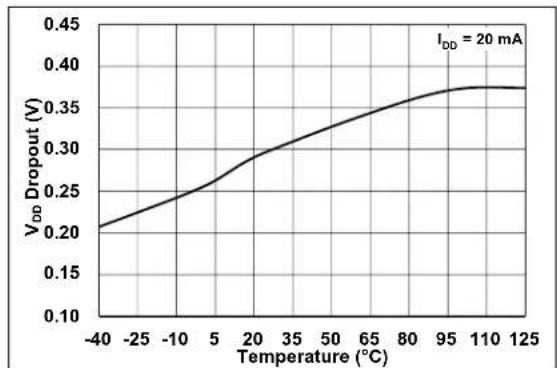
line
| Temperature (°C) | V_DD Dropout (V) | | ---------------- | ---------------- | | -40 | 0.20 | | -25 | 0.22 | | -10 | 0.24 | | 5 | 0.26 | | 20 | 0.29 | | 35 | 0.31 | | 50 | 0.33 | | 65 | 0.35 | | 80 | 0.36 | | 95 | 0.37 | | 110 | 0.37 | | 125 | 0.37 |FIGURE 7-6: V _DD Dropout Voltage vs. Temperature.
Note: Unless otherwise indicated, V_IN = 12V_SWF = 150kHz , T_A = +25^ .
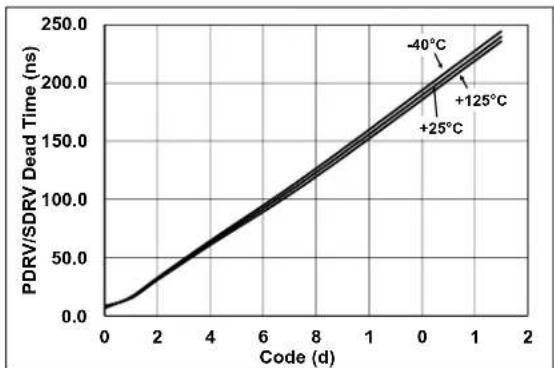
line
| Code (d) | PDRV/SDRV Dead Time (ns) | | -------- | ------------------------ | | 0 | 0.0 | | 2 | ~30.0 | | 4 | ~70.0 | | 6 | ~110.0 | | 8 | ~150.0 | | 10 | ~190.0 | | 12 | ~220.0 | | 14 | ~240.0 |FIGURE 7-7: Output Driver Dead Time vs. Code and Temperature.
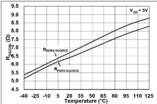
line
| Temperature (°C) | R_pS(CN) (Ω) - R_SDRV-SOURCE | R_pS(CN) (Ω) - R_PDRV-SOURCE | | ---------------- | ----------------------------- | ----------------------------- | | -40 | 5.0 | 5.0 | | -25 | 5.5 | 5.5 | | -10 | 6.0 | 6.0 | | 0 | 6.5 | 6.5 | | 20 | 7.0 | 7.0 | | 35 | 7.5 | 7.5 | | 50 | 8.0 | 8.0 | | 65 | 8.5 | 8.5 | | 80 | 9.0 | 9.0 | | 95 | 9.5 | 9.5 | | 110 | 10.0 | 10.0 | | 125 | 10.5 | 10.5 |FIGURE 7-10: Sourcing Output Driver R_DS(ON) vs. Temperature.
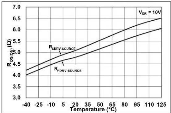
line
| Temperature (°C) | R_DS(ON) (Ω) for R_SDRV-SOURCE | R_DS(ON) (Ω) for R_PDRV-SOURCE | | ---------------- | -------------------------------- | -------------------------------- | | -40 | 4.0 | 4.0 | | -25 | 4.3 | 4.2 | | -10 | 4.6 | 4.5 | | 5 | 4.9 | 4.8 | | 20 | 5.2 | 5.0 | | 35 | 5.5 | 5.3 | | 50 | 5.8 | 5.6 | | 65 | 6.1 | 5.9 | | 80 | 6.4 | 6.2 | | 95 | 6.7 | 6.5 | | 110 | 7.0 | 6.8 | | 125 | 7.3 | 7.1 |FIGURE 7-8: Sourcing Output Driver R_DS(ON) vs. Temperature.
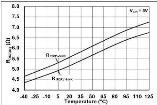
line
| Temperature (°C) | R_DS(ON) (Ω) for R_PDRV-SINK | R_DS(ON) (Ω) for R_SDRV-SINK | | ---------------- | ----------------------------- | ----------------------------- | | -40 | 4.5 | 4.3 | | 0 | 5.0 | 4.8 | | 5 | 5.5 | 5.2 | | 10 | 6.0 | 5.7 | | 15 | 6.5 | 6.2 | | 20 | 7.0 | 6.7 | | 25 | 7.5 | 7.2 | | 30 | 8.0 | 7.7 | | 35 | 8.5 | 8.2 | | 40 | 9.0 | 8.7 | | 45 | 9.5 | 9.2 | | 50 | 10.0 | 9.7 | | 55 | 10.5 | 10.2 | | 60 | 11.0 | 10.7 | | 65 | 11.5 | 11.2 | | 70 | 12.0 | 11.7 | | 75 | 12.5 | 12.2 | | 80 | 13.0 | 12.7 | | 85 | 13.5 | 13.2 | | 90 | 14.0 | 13.7 | | 95 | 14.5 | 14.2 | | 100 | 15.0 | 14.7 | | 105 | 15.5 | 15.2 | | 110 | 16.0 | 15.7 | | 115 | 16.5 | 16.2 | | 120 | 17.0 | 16.7 | | 125 | 17.5 | 17.2 |FIGURE 7-11: Sinking Output Driver R_DS(ON) vs. Temperature.
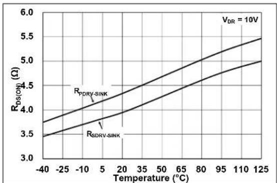
line
| Temperature (°C) | R_DS(ON) (Ω) - R_PDRV-SINK | R_DS(ON) (Ω) - R_SDRV-SINK | | ---------------- | --------------------------- | --------------------------- | | -40 | 3.5 | 3.5 | | -25 | 3.7 | 3.6 | | -10 | 3.9 | 3.8 | | 0 | 4.1 | 4.0 | | 20 | 4.3 | 4.2 | | 35 | 4.5 | 4.4 | | 50 | 4.7 | 4.6 | | 65 | 4.9 | 4.8 | | 80 | 5.1 | 5.0 | | 95 | 5.3 | 5.2 | | 110 | 5.5 | 5.4 | | 125 | 5.7 | 5.6 |FIGURE 7-9: Sinking Output Driver R_DS(ON) vs. Temperature.
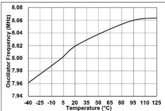
line
| Temperature (°C) | Oscillator Frequency (MHz) | | ---------------- | --------------------------- | | -40 | 7.96 | | -25 | 7.98 | | -10 | 8.00 | | 5 | 8.02 | | 20 | 8.03 | | 35 | 8.04 | | 50 | 8.05 | | 65 | 8.06 | | 80 | 8.06 | | 95 | 8.06 | | 110 | 8.06 | | 125 | 8.06 |FIGURE 7-12: Oscillator Frequency vs. Temperature.
Note: Unless otherwise indicated, V_IN = 12V_SW = 150kHz , T_A = +25^ .
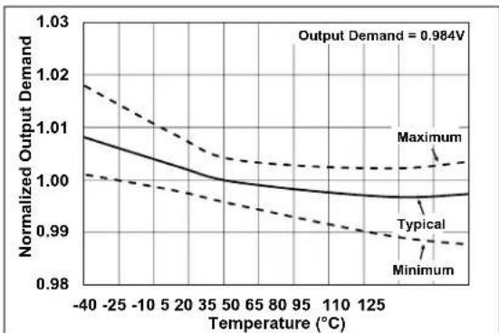
line
| Temperature (°C) | Maximum | Typical | Minimum | | ---------------- | ------- | ------- | ------- | | -40 | 1.02 | 1.01 | 1.00 | | -25 | 1.015 | 1.005 | 0.995 | | -10 | 1.01 | 1.00 | 0.99 | | 5 | 1.005 | 0.995 | 0.985 | | 20 | 1.00 | 0.99 | 0.98 | | 35 | 0.995 | 0.985 | 0.975 | | 50 | 0.99 | 0.98 | 0.97 | | 65 | 0.985 | 0.975 | 0.965 | | 80 | 0.98 | 0.97 | 0.96 | | 95 | 0.975 | 0.965 | 0.955 | | 110 | 0.97 | 0.96 | 0.95 | | 125 | 0.965 | 0.955 | 0.945 |FIGURE 7-13: Normalized Output Demand vs. Temperature.
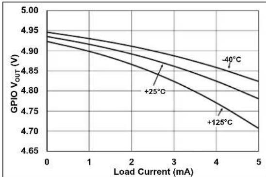
line
| Load Current (mA) | -40°C | +25°C | +125°C | | ----------------- | ----- | ----- | ------ | | 0 | 4.95 | 4.93 | 4.91 | | 2 | 4.88 | 4.85 | 4.82 | | 4 | 4.80 | 4.75 | 4.70 | | 5 | 4.78 | 4.72 | 4.68 |FIGURE 7-16: Average GPIO Output Voltage vs. Current.
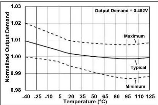
line
| Temperature (°C) | Maximum | Typical | Minimum | | ---------------- | ------- | ------- | ------- | | -40 | 1.02 | 1.01 | 1.00 | | 125 | 1.01 | 1.00 | 0.99 |FIGURE 7-14: Normalized Output Demand vs. Temperature.
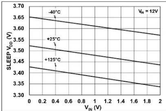
line
| VIN (V) | SLEEP VDD (V) at -40°C | SLEEP VDD (V) at +25°C | SLEEP VDD (V) at +125°C | | ------- | ---------------------- | ---------------------- | ----------------------- | | 0.0 | 3.65 | 3.52 | 3.43 | | 0.4 | 3.63 | 3.50 | 3.41 | | 1.0 | 3.61 | 3.48 | 3.39 | | 1.6 | 3.59 | 3.46 | 3.37 | | 2.0 | 3.57 | 3.44 | 3.35 |FIGURE 7-17: Average SLEEP V _DD Output Voltage vs. Current.
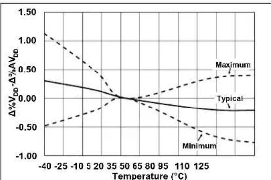
line
| Temperature (°C) | Δ%V_DD - Δ%AV_DD | | ---------------- | ---------------- | | -40 | 1.2 | | -25 | 0.8 | | -10 | 0.4 | | 5 | 0.0 | | 20 | -0.4 | | 35 | -0.6 | | 50 | -0.8 | | 65 | -0.9 | | 80 | -0.95 | | 95 | -0.98 | | 110 | -0.99 | | 125 | -1.0 |FIGURE 7-15: V DD vs. AVDD Temperature Drift Tracking.
NOTES:
To allow for easier system design and bench testing, the MCP19116/7 devices feature a multiplexer used to output various internal analog signals. These signals can be measured on the GPA0 pin through a unity gain buffer. The configuration control of the GPA0 pin is found in the ABECON register (Register 6-14).
Control of the signals present at the output of the unity gain analog buffer is found in the ADCON0 register (Register 8-1).
REGISTER 8-1: ADCON0: ANALOG-TO-DIGITAL CONTROL REGISTER
| U-0 R/W-0 R/W-0 R/W-0 R/W-0 R/W-0 R/W-0 R/W-0 | |||||||
| — | CHS4 | CHS3 | CHS2 | CHS1 | CHS0 | GO/DONE | ADON |
| bit 7 bit 0 | |||||||
Legend:
| R = Readable bit | W = Writable bit | U = Unimplemented bit, read as '0' |
| u = Bit is unchanged | x = Bit is unknown -n = Value at POR | |
| '1' = Bit is set | '0' = Bit is cleared | |
bit 7 Unimplemented: Read as '0'
bit 6-2 CHS<4:0>: Analog Channel Select bits
00000 = VIN/n analog voltage measurement (VIN/15.5)
00001 = VREF + VZC (DAC reference voltage + VZC pedestal setting current regulation level)
00010 = OV_REF (reference for overvoltage comparator)
00011 = V _BGR (band gap reference)
00100 = V S (voltage proportional to V OUT )
00101 = EA_SC (error amplifier after slope compensation output)
00110 = A2 (secondary current sense amplifier output at R_FB_INT connection)
00111 = Pedestal (Pedestal Voltage)
01000 = Reserved
01001 = Reserved
01010 = IP_ADJ (IP after Pedestal and Offset Adjust (at PWM Comparator))
01011 = IP_OFF_REF (IP Offset Reference)
01100 = V DR /n (V DR /n analog driver voltage measurement = 0.23V/V * V _DR )
01101 = TEMP_SNS (analog voltage representing internal temperature)
01110 = DLL_VCON (Delay Locked Loop Voltage Reference - control voltage for dead time)
01111 = SLPCMP_REF (slope compensation reference)
10000 = Unimplemented
10001 = Unimplemented
10010 = Unimplemented
10011 = Unimplemented
10100 = Unimplemented
10101 = Unimplemented
10110 = Unimplemented
10111 = Unimplemented
11000 = GPA0/AN0
11001 = GPA1/AN1
11010 = GPA2/AN2
11011 = GPA3/AN3
11100 = GPB1/AN4
11101 = GPB4/AN5 (MCP19117 only)
11110 = GPB5/AN6 (MCP19117 only)
11111 = GPB6/AN7 (MCP19117 only)
REGISTER 8-1: ADCON0: ANALOG-TO-DIGITAL CONTROL REGISTER (CONTINUED)
bit 1
GO/DONE: A/D Conversion Status bit
1 = A/D conversion cycle in progress. Setting this bit starts an A/D conversion cycle. This bit is automatically cleared by hardware when the A/D conversion has completed. 0 = A/D conversion completed/not in progress
bit 0 ADON: A/D Conversion Enable bit
1 = A/D converter module is operating 0 = A/D converter is shut off and consumes no operating current
9.0 DEVICE CALIBRATION
Read-only memory locations 2080h through 208Fh contain factory calibration data. Refer to Section 18.0 "Flash Program Memory Control" for information on how to read from these memory locations.
9.1 Calibration Word 1
Calibration Word 1 is at memory location 2080h. The DCSRFB<6:0> bits set the offset calibration for the current sense differential amplifier (A2) when configured using the internal feedback resistor. A calibration range of ±30 mV is provided with 20h and 00h being midscale (no offset). The MSB is polarity only. Firmware must read these values and copy them into the DCSCAL Special Function Register located in Bank 3 at 199h.
REGISTER 9-1: CALWD1: CALIBRATION WORD 1 REGISTER
| U-0 | R/P-1 | R/P-1 | R/P-1 | R/P-1 | R/P-1 | R/P-1 | R/P-1 |
| — | DCSRFB6 | DCSRFB5 | DCSRFB4 | DCSRFB3 | DCSRFB2 | DCSRFB1 | DCSRFB0 |
| bit 7 bit 0 | |||||||
Legend:
| R = Readable bit | P = Programmable bit | U = Unused bit, read as '0' | |
| -n = Value at POR | '1' = Bit is set | '0' = Bit is cleared | x = Bit is unknown |
bit 13-7 Unimplemented: Read as '0'
bit 6-0 DCSRFB<6:0>: Input Differential Current Sense Calibration bits when configured using internal feedback resistor
9.2 Calibration Word 2
Calibration Word 2 is at memory location 2081h. It contains the calibration bits for the desaturation comparator current measurement input offset voltage. Firmware must read these values and write them into the DSTCAL register to implement the factory offset calibration. The factory offset calibration will minimize offset voltage. The desaturation comparator is one of the few examples where the user may want to implement their own offset voltage values. Writing user-defined values to the DSTCAL register provides this flexibility. Firmware must read these values and copy into the DSTCAL Special Function Register located in Bank 3 at 196h.
This register also contains the trim bits needed to trim the internal 5 kΩ feedback resistor to within 2% using the
REGISTER 9-2: CALWD2: CALIBRATION WORD 2 REGISTER
| U-0 R/P-1 R/P-1 R/P-1 R/P-1 R/P-1 | |||||
| — DST4 | DST3 DST2 | DST1 DST0 | |||
| bit 13 bit 8 | |||||
| U-0 U-0 R/P-1 R/P-1 R/P-1 R/P-1 R/P-1 | |||||||
| — | — | RFBT5 | RFBT4 | RFBT3 | RFBT2 | RFBT1 | RFBT0 |
| bit 7 bit 0 | |||||||
Legend:
| R = Readable bit | P = Programmable bit | U = Unused bit, read as '0' | |
| -n = Value at POR | '1' = Bit is set | '0' = Bit is cleared | x = Bit is unknown |
bit 13 Unimplemented: Read as '0'
bit 12-8 DST<4:0>: Desaturation Comparator Current Measure Offset calibration bits
11111 = Maximum negative offset calibration (-30 mV)
•
.
[Non-Text]
•
10000 = Mid scale (0 mV)
00000 = Mid scale (0 mV)
.
。
-
•
01111 = Maximum positive offset calibration (+30 mV)
bit 7-6 Unimplemented: Read as '0'
bit 5-0 RFBT<5:0>: Internal Feedback Resistor Trim bits
9.3 Calibration Word 3
The BGR<4:0> bits at memory location 2082h calibrate the band gap reference. Firmware must read these values and copy them into the BGRCAL Special Function Register located in Bank 3 at 19Bh.
REGISTER 9-3: CALWD3: CALIBRATION WORD 3 REGISTER
| U-0 | U-0 | U-0 | R/P-1 | R/P-1 | R/P-1 | R/P-1 | R/P-1 |
| — | — | — | BGR4 | BGR3 | BGR2 | BGR1 | BGR0 |
| bit 7 bit 0 | |||||||
Legend:
| R = Readable bit | P = Programmable bit | U = Unused bit, read as ‘0’ | |
| -n = Value at POR | ‘1’ = Bit is set | ‘0’ = Bit is cleared | x = Bit is unknown |
bit 13-5 Unused: Read as '0'
bit 4-0 BGR<4:0>: Band Gap Reference Calibration bits
9.4 Calibration Word 4
The TTA<3:0> bits at memory location 2083h contain the calibration bits for the factory-set overtemperature threshold. Firmware must read these values and copy them into the TTACAL Special Function Register located in Bank 3 at 19Ah.
REGISTER 9-4: CALWD4: CALIBRATION WORD 4 REGISTER
| R = Readable bit | P = Programmable bit | U = Unused bit, read as '0' | |
| -n = Value at POR | '1' = Bit is set | '0' = Bit is cleared | x = Bit is unknown |
bit 13-4 Unimplemented: Read as '0'
bit 3-0 TTA<3:0>: Over-Temperature Threshold Calibration bits
9.5 Calibration Word 5
The TANA<9:0> bits at memory location 2084h contain the ADC reading from the internal temperature sensor when the silicon temperature is at 30°C. This 10-bit reading can be used to calibrate the ADC reading at any temperature. The temperature coefficient of the internal temperature sensor is 14.0 mV/°C.
REGISTER 9-5: CALWD5: CALIBRATION WORD 5 REGISTER
| U-0 U-0 U-0 U-0 R/P-1 R/P-1 | |||||
| — — — | + TANA9 | TANA8 | |||
| bit 13 bit 8 | |||||
| R/P-1 | R/P-1 | R/P-1 | R/P-1 | R/P-1 | R/P-1 | R/P-1 | R/P-1 |
| TANA7 | TANA6 | TANA5 | TANA4 | TANA3 | TANA2 | TANA1 | TANA0 |
| bit 7 bit 0 | |||||||
Legend:
| R = Readable bit | P = Programmable bit | U = Unused bit, read as '0' | |
| -n = Value at POR | '1' = Bit is set | '0' = Bit is cleared | x = Bit is unknown |
bit 13-10 Unimplemented: Read as '0'
bit 9-0 TANA<9:0>: ADC reading of internal silicon temperature at 30°C Calibration bits
9.6 Calibration Word 6
The FCAL<6:0> bits at memory location 2085h set the internal oscillator calibration. Firmware must read these values and copy them into the OSCCAL Special Function Register located in Bank 3 at 198h.
REGISTER 9-6: CALWD6: CALIBRATION WORD 6 REGISTER
| U-0 U-0 U-0 U-0 | U-0 | U-0 | ||
| — — — | + | — | + | |
| bit 13 bit 8 | ||||
| U-0 | R/P-1 | R/P-1 | R/P-1 | R/P-1 | R/P-1 | R/P-1 | R/P-1 |
| — | FCAL6 | FCAL5 | FCAL4 | FCAL3 | FCAL2 | FCAL1 | FCAL0 |
| bit 7 bit 0 | |||||||
Legend:
| R = Readable bit | P = Programmable bit | U = Unused bit, read as '0' | |
| -n = Value at POR | '1' = Bit is set | '0' = Bit is cleared | x = Bit is unknown |
bit 13-7 Unimplemented: Read as '0'
bit 6-0 FCAL<6:0>: Internal Oscillator Calibration bits
9.7 Calibration Word 7
The DCS<6:0> bits at memory location 2086h store the factory-set offset calibration for the current sense differential amplifier (A2) when configured using I_SOUT . Firmware must read these values and copy them into the DCSCAL Special Function Register located in Bank 3 at 199h. If using the internal feedback resistor, refer to Register 9-1.
REGISTER 9-7: CALWD7: CALIBRATION WORD 7 REGISTER
| U-0 U-0 U-0 U-0 U-0 U-0 | ||||
| ——— | + | + | + | |
| bit 13 bit 8 | ||||
| U-0 | R/P-1 | R/P-1 | R/P-1 | R/P-1 | R/P-1 | R/P-1 | R/P-1 |
| — | DCS6 | DCS5 | DCS4 | DCS3 | DCS2 | DCS1 | DCS0 |
| bit 7 bit 0 | |||||||
Legend:
| R = Readable bit | P = Programmable bit | U = Unimplemented bit, read as '0' |
| -n = Value at POR | '1' = Bit is set | '0' = Bit is cleared x = Bit is unknown |
bit 13-7 Unimplemented: Read as '0'
bit 6-0 DCS<6:0>: Differential Current Sense Amplifier Calibration bits when used with I_SOUT .
9.8 Calibration Word 8
Calibration Word 8 is at memory location 2087h and contains the calibration bits for the Error Amplifier Offset Voltage EAOFFCAL<4:0> and for the Current Sense Amplifier (A2) Gain while configured using the Internal Feedback Resistor A2GRFBCAL<3:0>. A2 Gain calibration trim bits set the 10V/V gain of the current sense amplifier (A2). If the user has configured the device using the internal Feedback Resistor, the A2GRFBCAL<3:0> calibration value must be read via firmware and copied into the A2GCAL Special Function Register located in Bank 3 at 19Eh. Firmware must also read the EAOFFCAL<4:0> values and copy them into the EAOFFCAL Special Function Register located in Bank 3 at 19Ch.
REGISTER 9-8: CALWD8: CALIBRATION WORD 8 REGISTER
| U-0 U-0 R/P-1 R/P-1 R/P-1 R/P-1 | |||||
| — — | A | 2 G CAL3 | A2GRFB-CAL2 | A2GRFB-CAL1 | B A2GRFB-CAL0 |
| bit 13 bit 8 | |||||
| U-0 U-0 U-0 R/P-1 R/P-1 R/P-1 R/P-1 R/P-1 | |||||||
| — | — | — | EAOFFCAL4 | EAOFFCAL3 | EAOFFCAL2 | EAOFFCAL1 | EAOFFCAL0 |
| bit 7 bit 0 | |||||||
Legend:
| R = Readable bit | P = Programmable bit | U = Unimplemented bit, read as '0' |
| -n = Value at POR | '1' = Bit is set | '0' = Bit is cleared x = Bit is unknown |
bit 13-12 Unimplemented: Read as '0'
bit 11-8 A2GRFBCAL<3:0>: A2 Current Sense Amplifier Gain Calibration bits
bit 7-5 Unimplemented: Read as '0'
bit 4-0 EAOFFCAL<4:0>: Error Amplifier Offset Voltage Calibration bits
9.9 Calibration Word 9
Calibration Word 9 is at memory location 2088h and contains the calibration bits for the OVREF DAC span trim OVRSPCAL<4:0> and the Current Sense Amplifier while configured using I_SOUT A2GCAL<3:0>. The OVRSPCAL<4:0> is an individual adjustment specific to calibrating the OVREF DAC span. Firmware must read these values and copy them into the OVRSPCAL Special Function Register located in Bank 3 at 19Fh.
If the user has configured the device using the external feedback path utilizing I_SOUT , the A2GCAL<3:0> value must be read via firmware and copied into the A2GCAL Special Function Register located in Bank 3 at 19Eh.
REGISTER 9-9: CALWD9: CALIBRATION WORD 9 REGISTER
| U-0 R/P-1 R/P-1 R/P-1 R/P-1 R/P-1 | |||||
| — OVRSP-CAL4 | OVRSP-CAL3 | OVRSP-CAL2 | OVRSP-CAL1 | OVRSP-CAL0 | |
| bit 13 bit 8 | |||||
| U-0 U-0 U-0 | U-0 | R/P-1 | R/P-1 R/P-1 R/P-1 | |||||
| — | — | — | — | A2GCAL3 | A2GCAL2 | A2GCAL1 | A2GCAL0 | |
| bit 7 bit 0 | ||||||||
| Legend: | |||
| R = Readable bit | P = Programmable bit | U = Unimplemented bit, read as ‘0’ | |
| -n = Value at POR | ‘1’ = Bit is set | ‘0’ = Bit is cleared | x = Bit is unknown |
bit 13 Unimplemented: Read as '0'
bit 12-8 OVRSPCAL<4:0>: OVREF Span Adjustment bits
bit 7-4 Unimplemented: Read as '0'
bit 3-0 A2GCAL<3:0>: A2 Current Sense Amplifier Gain Calibration bits
9.10 Calibration Word 10
Calibration word 10 at memory location 2089h contains the calibration bits for VREF2 DAC span trim VR2SPCAL<4:0> and the VREF DAC span trim VRSPCAL<4:0>. The VR2SPCAL<4:0> is an individual adjustment specific to calibrating the VREF2
DAC span. Firmware must read these values and copy them into the VR2SPCAL Special Function Register located in Bank 2 at 11Ah.
The VRSPCAL<4:0> is an individual adjustment specific to calibrating the VREF DAC span. Firmware must read these values and copy them into the VRSPCAL Special Function Register located in Bank 2 at 119h.
REGISTER 9-10: CALWD10: CALIBRATION WORD 10 REGISTER
| U-0 R/P-1 | R/P-1 | R/P-1 | R/P-1 | |||
| — VR2S | PCAL4 | VR2S | PCAL3 | VR2SP | CAL2 | VR2SPC |
| bit 13 bit 8 | ||||||
| U-0 U-0 U-0 R/P-1 R/P-1 | R/P-1 R/P-1 R/P-1 | ||||||
| — | — | — | VRSPCAL4 | VRSPCAL3 | VRSPCAL2 | VRSPCAL1 | VRSPCAL0 |
| bit 7 bit 0 | |||||||
Legend:
| R = Readable bit | P = Programmable bit | U = Unimplemented bit, read as '0' |
| -n = Value at POR | '1' = Bit is set | '0' = Bit is cleared x = Bit is unknown |
bit 13 Unimplemented: Read as '0'
bit 12-8 VR2SPCAL<4:0>: VREF2 Span Adjustment bits
bit 7-5 Unimplemented: Read as '0'
bit 4-0 VRSPCAL<4:0>: VREF Span Adjustment bits
9.11 Calibration Word 11
Calibration word 11 at memory location 208Ah contains the calibration bits for the 4V LDO (AVDD) trim AVDDCAL<3:0> and the offset voltage of the analog test buffer BUFF<7:0>. AVDD supplies the internal analog circuitry and is the default ADC Reference voltage. Firmware must read these values and copy them into the AVDDCAL Special Function Register located in Bank 3 at 19Dh.
Also stored at address 208Ah is the Analog test MUX buffer offset value. This is an 8-bit, two's complement word that represents the buffer's offset voltage in units of mV. This value can be used to correct for buffer offset of the analog test signal measurements. See Section 8.0, System Bench Testing for test signal details.
REGISTER 9-11: CALWD11: CALIBRATION WORD 11 REGISTER
| U-0 U-0 R/P-1 R/P-1 R/P-1 R/P-1 | |||||
| — | — | AVDDCAL3 | AVDDCAL2 | AVDDCAL1 | AVDDCAL0 |
| bit 13 bit 8 | |||||
| R/P-1 | R/P-1 | R/P-1 | R/P-1 | R/P-1 | R/P-1 | R/P-1 | R/P-1 |
| BUFF7 | BUFF6 | BUFF5 | BUFF4 | BUFF3 | BUFF2 | BUFF1 | BUFF0 |
| bit 7 bit 0 | |||||||
Legend:
| R = Readable bit | P = Programmable bit | U = Unimplemented bit, read as '0' |
| -n = Value at POR | '1' = Bit is set | '0' = Bit is cleared x = Bit is unknown |
bit 13-12 Unimplemented: Read as '0'
bit 11-8 AVDDCAL<3:0>: AV _DD 4.096V LDO Trim bits
bit 7-0 BUFF<7:0>: Analog Test MUX Buffer Offset bits
11111111 = Mid scale (-1mV)
.
.
10000000 = Largest negative offset (-128 mV)
01111111 = Largest positive offset (+128 mV)
•
•
00000000 = Mid scale (0 mV)
9.12 Calibration Word 12
The ADCCAL<13:0> bits at memory location 208Bh contain the calibration bits for the A/D Converter. Calibration Word 12 (ADCCAL<13:0>) contains the factory measurement of the full-scale ADC Reference. The value represents the number of A/D converter counts per volt. ADCC<4:0> bits represent the fraction of an A/D converter count, which can provide additional precision when oversampling the ADC for enhanced resolution. This calibration word can be used to calibrate signals read by the Analog-to-Digital Converter.
REGISTER 9-12: CALWD12: CALIBRATION WORD 12 REGISTER
| R/P-1 R/P-1 R/P-1 R/P-1 R/P-1 R/P-1 | |||||
| ADCC13 | ADCC12 | ADCC | 11 ADCC10 | ADCC9 | ADCC8 |
| bit 13 bit 8 | |||||
| R/P-1 R/P-1 R/P-1 R/P-1 R/P-1 R/P-1 R/P-1 | |||||||
| ADCC7 | ADCC6 | ADCC5 | ADCC4 | ADCC3 | ADCC2 | ADCC1 | ADCC0 |
| bit 7 bit 0 | |||||||
Legend:
| R = Readable bit | P = Programmable bit | U = Unimplemented bit, read as '0' |
| -n = Value at POR | '1' = Bit is set | '0' = Bit is cleared x = Bit is unknown |
bit 13-5 ADCC<13:5>: Whole number of A/D converter count
111111111 = 511
•
.
.
000000000 = 0
bit 4-0 ADCC<4:0>: Fraction number of A/D converter count
11111 = 0.96875
•
.
.
00001 = 0.03125
00000 = 0.00000
10.0 ADDRESSABLE USART MODULE
The Addressable USART module described in this document is designed into the PIC16F91x.
The features of that module include:
- Asynchronous and Synchronous modes:
- Asynchronous (full duplex)
- Synchronous - Master (half duplex)
- Synchronous - Slave (half duplex)
• 8- and 9-bit data operations
- Single and Continuous Receive modes
- Address detect
- Two-byte FIFOs for Transmit and Receive operations
• Majority bit detection in Asynchronous mode
- 8-bit Baud Rate generator with speed selection
- Fosc/16 or Fosc/64 for Asynchronous mode
- Fosc/4 for Synchronous mode
- Status bits for
- Framing Error
- Overrun Error
- Transmit Shift Register Status
In addition, the existing USART features are altered. These features are changed as previous modules did not exhibit the desired behavior. These alterations include:
- Holding all USART state machines in Reset while SPEN (RCSTA<7>) = 0
- Clarification on the TRMT (TXSTA<1>) status bit
10.1 Module Reset
When the SPEN (RCSTA<7>) is cleared, all USART state machines are held in Reset. This allows for software re-initialization of the module by toggling the SPEN bit. This also causes all status bits to be reset. All other R/W bits are available to the user, which allows them to pre-configure the module prior to setting the SPEN bit.
10.2 Pin Placement and Port Interaction
The bidirectional TX/CK pin is located on GPB6. The bidirectional RX/DT pin is located on GPB7. If TRISC<6> and TRISC<7> are configured as inputs ('1'), the USART control will automatically reconfigure the pin from input to output as needed.
10.3 USART Asynchronous mode
In this mode, the USART uses standard non-return-to-zero (NRZ) format (one Start bit, eight or nine data bits, and one Stop bit). The BRG is used to derive the baud rate frequencies from the system clock. The USART transmits and receives the LSB first. The transmitter and receiver are functionally independent, but use the same data format and baud rate. The BRG produces a clock, either x4, x16 or x64 of the bit shift rate, depending on its configuration (see
Section 10.3.2, Asynchronous Receive Mode). Parity is not supported by the hardware, but can be implemented in software using the ninth data bit option. Asynchronous mode is stopped during Sleep. Asynchronous mode is selected by clearing the SYNC (TXSTA<4>) bit.
10.3.1 ASYNCHRONOUS TRANSMIT MODE
The USART transmitter block diagram is shown in Figure 10-1. The heart of the transmitter is the transmit (serial) shift register (TSR). The shift register obtains its data from the read/write transmit buffer, TXREG. The TXREG register is loaded with data via software. The TSR register is not loaded until the Stop bit has been transmitted from the previous load. As soon as the Stop bit is transmitted, TSR is loaded with new data from the TXREG register (if available). The transmit register (TXREG) is double buffered. As the user writes to TXREG, the data is transferred from the buffer to the transmit shift register (TSR), thus freeing up the buffer register.
The interrupt flag TXIF is set as long as the TXEN (TXSTA<5>) bit is set and TXREG is empty, indicating that the transmit buffer register (TXREG) is enabled and free to accept another word. Flag bit TXIF (Transmit Buffer Empty) is read-only and will be set, regardless of the state of the TXIE bit, and cannot be cleared in software. It will be reset only when new data is loaded into TXREG.
Transmission is enabled by setting the enable bit TXEN. The actual transmission will not occur until the TXREG register has been loaded with data and the BRG has produced a shift clock (Figure 10-2). The transmission can also be started by first loading TXREG and then setting the enable bit TXEN. Normally, when transmission is first started, TSR is empty. At that point, transfer to TXREG will result in an immediate transfer to TSR, resulting in an empty TXREG. A back-to-back transfer is thus possible (Figure 10-3). Clearing the enable bit TXEN during a transmission will cause the transmission to be aborted and will reset the transmitter. As a result, the GPB6/TX/CK/AN7 pin will revert to hi-impedance.
If 9-bit transmission is desired, set the TX9 control bit. A set ninth data bit will indicate that the eight Least Significant data bits are an address when the receiver is set for address detection.
While TXIF indicates the status of the transmit buffer register, the TRMT (TXSTA<1>) bit indicates the status of the transmit operation. The TRMT bit is cleared automatically upon a byte transfer from TXREG to the Shift register, and is set at the end of a stop bit. A '1' value in the TRMT bit signifies that the transmit state machine is idle. The TRMT bit is read-only and is valid for both Asynchronous and Synchronous transmissions. No interrupt is associated with the TRMT bit.
When setting up an Asynchronous Transmission, follow these steps:
- Initialize the SPBRG register for the appropriate
baud rate. If a high-speed baud rate is desired, set bit BRGH.
- Enable the asynchronous serial port by clearing bit SYNC and setting bit SPEN.
- If interrupts are desired, then set enable bit TXIE.
- If 9-bit transmission is desired, then set transmit bit TX9.
- Enable the transmission by setting bit TXEN, which will also set bit TXIF.
- If 9-bit transmission is selected, the ninth bit should be loaded in bit TX9D.
- Load data to the TXREG register (starts transmission).
- If using interrupts, set GIE (INTCON<7>) and PEIE (INTCON<6>) bits.
FIGURE 10-1: USART TRANSMIT BLOCK DIAGRAM
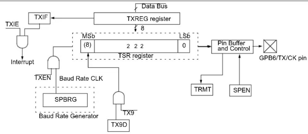
flowchart
graph TD
    A["TXIE"] --> B["Interrupt"]
    B --> C["TXIF"]
    C --> D["TXREG register"]
    D --> E["Data Bus"]
    E --> C
    C --> F["TSR register"]
    F --> G["MSb (8)"]
    F --> H["LSb 0"]
    F --> I["Baud Rate CLK"]
    I --> J["SPBRG"]
    I --> K["Baud Rate Generator"]
    K --> L["TX9D"]
    L --> M["TXEN"]
    M --> N["Interrupt"]
    N --> C
    F --> O["Pin Buffer and Control"]
    O --> P["GPB6/TX/CK pin"]
    O --> Q["TRMT"]
    O --> R["SPEN"]
FIGURE 10-2: ASYNCHRONOUS MASTER TRANSMISSION
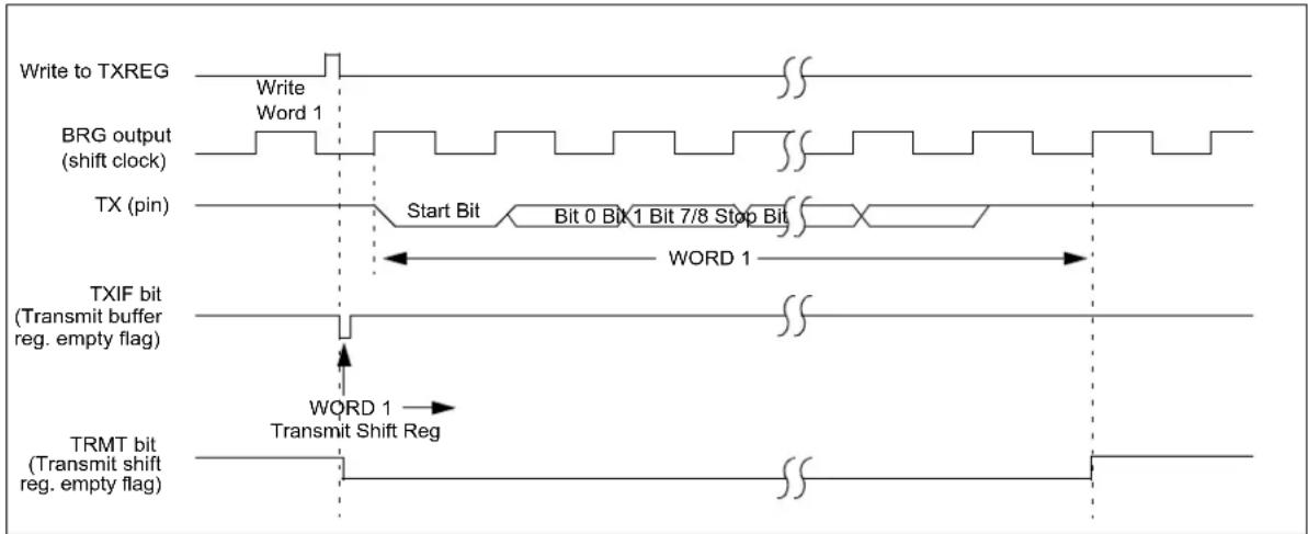
FIGURE 10-3: ASYNCHRONOUS TRANSMISSION (BACK TO BACK)
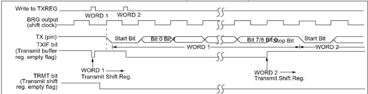
flowchart
graph TD
    A["Write to TXREG"] --> B["BRG output (shift clock)"]
    B --> C["TX (pin)"]
    C --> D["TXIF bit (Transmit buffer reg. empty flag)"]
    D --> E["TRMT bit (Transmit shift reg. empty flag)"]

    subgraph Signal Lines
        F["WORD 1"] --> G["Start Bit"]
        H["WORD 2"] --> I["Bit 0 Bit"]
        J["WORD 1"] --> K["Stop Bit"]
        L["WORD 2"] --> M["Stop Bit"]
    end

    style A fill:#f9f,stroke:#333
    style B fill:#f9f,stroke:#333
    style C fill:#ccf,stroke:#333
    style D fill:#ccf,stroke:#333
    style E fill:#cfc,stroke:#333
    style F fill:#ffc,stroke:#333
    style G fill:#ffc,stroke:#333
    style H fill:#ffc,stroke:#333
    style I fill:#ffc,stroke:#333
    style J fill:#ffc,stroke:#333
    style K fill:#ffc,stroke:#333
    style L fill:#ffc,stroke:#333
    style M fill:#ffc,stroke:#333
    style N fill:#ffc,stroke:#333
Note: This timing diagram shows two consecutive transmissions.
10.3.2 ASYNCHRONOUS RECEIVE MODE
The receiver block diagram is shown in Figure 10-4. The data is received on the GPB7/RX/DT/CCD pin and drives the data recovery block. The data recovery block is a shifter operating at x64, x16 or x4 times the baud rate. The main receive serial shifter operates at the bit rate or at Fosc. Once asynchronous mode is selected, reception is enabled by setting the CREN (RCSTA<4>) bit.
The heart of the receiver is the receive (serial) shift register (RSR). After sampling the Stop bit, the received data in the RSR is transferred to RCREG (if empty). If the transfer is complete, flag bit RCIF (PIR1<6>) is set. The interrupt can be enabled by setting the RCIE (PIE1<6>) bit. Flag bit RCIF is read-only and cleared by hardware. It is cleared when RCREG has been read and is empty. RCREG is double buffered (two deep FIFO). It is possible for two bytes of data to be received and transferred to the RCREG FIFO and a third byte to begin shifting to the RSR. On detection of the Stop bit of the third byte, if RCREG is full, the overrun error bit OERR (RCSTA<1>) will be set. The word in RSR will be lost. RCREG can be read twice to retrieve the two bytes in the FIFO. Overrun bit OERR has to be cleared in software. This is done by resetting the receive logic (CREN is cleared and then set). If bit OERR is set, transfers from the RSR register to RCREG are inhibited, and no further data will be received. The OERR bit can then be cleared in software. Framing error bit FERR (RCSTA<2>) is set if a Stop bit is detected as clear. The FERR bit and the ninth receive bit are buffered the same way as the receive data. Reading the RCREG will load bits RX9D and FERR with new values. The user will need to read the RCSTA register before reading RCREG in order to not lose the old FERR and RX9D data.
The USART module has a special provision for multi-processor communication. When the RX9 bit is set in the RCSTA register, nine bits are received and the ninth bit is placed in the RX9D status bit of the RSTA register. The port can be programmed such that when the Stop bit is received, the serial port interrupt will only activate if the RX9D bit is set. This feature is enabled by setting the ADDEN bit in the RCSTA register and can be used in a multi-processor system as indicated in this section.
To transmit a block of data in a multi-processor system, the master processor must first send an address byte that identifies the target slave. An address byte is identified by the RX9D bit being a '1' (instead of a '0' for a data byte). If the ADDEN bit is set in the slave's RCSTA register, all data bytes will be ignored. However, if the ninth received bit is equal to a '1', indicating that the received byte is an address, the slave will be interrupted and the contents of the Receive Shift Register (RSR) will be transferred into the receive buffer. This allows the slave to be interrupted only by addresses, so that the slave can examine the received byte to see if it is addressed. The addressed slave will then clear its ADDEN bit and prepare to receive data bytes from the master.
When the ADDEN bit is set, all data bytes are ignored. Following the Stop bit, the data will not be loaded into the receive buffer and no interrupt will occur. If another byte is shifted into the RSR, the previous data byte will be lost.
The ADDEN bit will only take affect when the receiver is configured in 9-bit mode.
To indicate that a reception is in progress, the RCIDL bit (BAUDCTL<6>) reflects the current state of the receive operation. This bit is cleared ('0') on the leading edge of a start bit and set ('1') upon the end of a Stop bit. A '1' value in the RCIDL bit signifies that the receive state machine is idle. The RCIDL bit is read-only and is valid for both Asynchronous and Synchronous receptions. No interrupt is associated with the RCIDL bit. See Figures 10-5, 10-6 and 10-7 for timing details of the RCIDL signal.
When setting up an Asynchronous Reception, follow these steps:
- Initialize the SPBRG register for the appropriate baud rate. If a high speed baud rate is desired, set bit BRGH.
- Enable the asynchronous serial port by clearing bit SYNC and setting bit SPEN.
- If interrupts are desired, then set enable bit RCIE.
- If 9-bit reception is desired, then set bit RX9.
- Set ADDEN if address detect is needed.
- Enable the reception by setting bit CREN.
-
Flag bit RCIF will be set when reception is complete and an interrupt will be generated if enable bit RCIE is set.
-
Read the RCSTA register to get the ninth bit (if enabled) and determine if any error occurred during reception.
- Read the 8-bit received data by reading the RCREG register.
- If any error occurred, clear the error by clearing enable bit CREN.
- If using interrupts, set GIE (INTCON<7>) and PEIE (INTCON<6>) bits.
FIGURE 10-4: USART RECEIVE BLOCK DIAGRAM
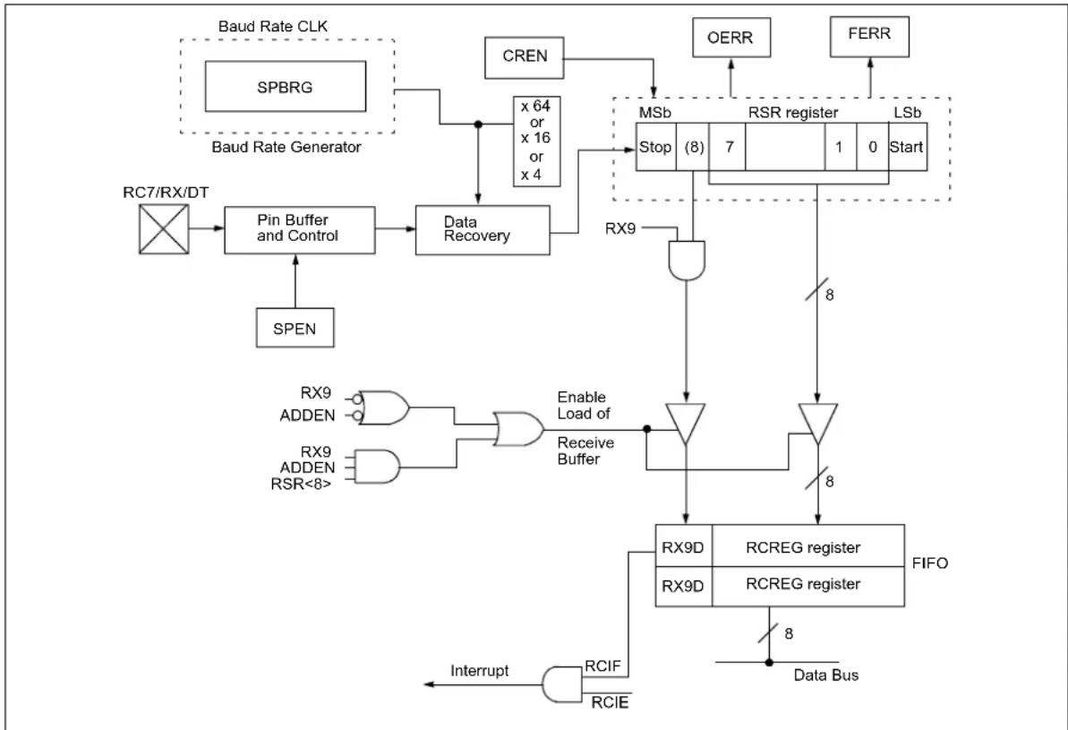
flowchart
graph TD
    A["Baud Rate CLK"] --> B["SPBRG"]
    B --> C["Baud Rate Generator"]
    C --> D["RC7/RX/DT"]
    D --> E["Pin Buffer and Control"]
    E --> F["Data Recovery"]
    F --> G["CREN"]
    G --> H["MSb"]
    H --> I["Stop (8)"]
    I --> J["RSR register"]
    J --> K["LSb"]
    K --> L["OERR"]
    L --> M["FERR"]
    M --> N["FS"]
    O["SPEN"] --> E
    P["RX9 ADDEN"] --> Q["AND Gate"]
    R["RX9 ADDEN RSR<8>"] --> Q
    Q --> S["Enable Load of Receive Buffer"]
    T["RX9D"] --> U["RCREG register"]
    V["RX9D"] --> W["RCREG register"]
    X["Interrupt"] --> Y["RCIF RCIE"]
    Y --> Z["FIFO Data Bus"]
    style A fill:#f9f,stroke:#333
    style B fill:#f9f,stroke:#333
    style C fill:#f9f,stroke:#333
    style D fill:#ccf,stroke:#333
    style E fill:#ccf,stroke:#333
    style F fill:#ccf,stroke:#333
    style G fill:#cfc,stroke:#333
    style H fill:#fcc,stroke:#333
    style I fill:#cff,stroke:#333
    style J fill:#ffc,stroke:#333
    style K fill:#ffc,stroke:#333
    style L fill:#ffc,stroke:#333
    style M fill:#ffc,stroke:#333
    style N fill:#ffc,stroke:#333
    style O fill:#ffc,stroke:#333
    style P fill:#ffc,stroke:#333
    style Q fill:#ffc,stroke:#333
    style R fill:#ffc,stroke:#333
    style S fill:#ffc,stroke:#333
    style T fill:#ffc,stroke:#333
    style U fill:#ffc,stroke:#333
    style V fill:#ffc,stroke:#333
    style W fill:#ffc,stroke:#333
    style X fill:#ffc,stroke:#333
FIGURE 10-5: ASYNCHRONOUS RECEPTION
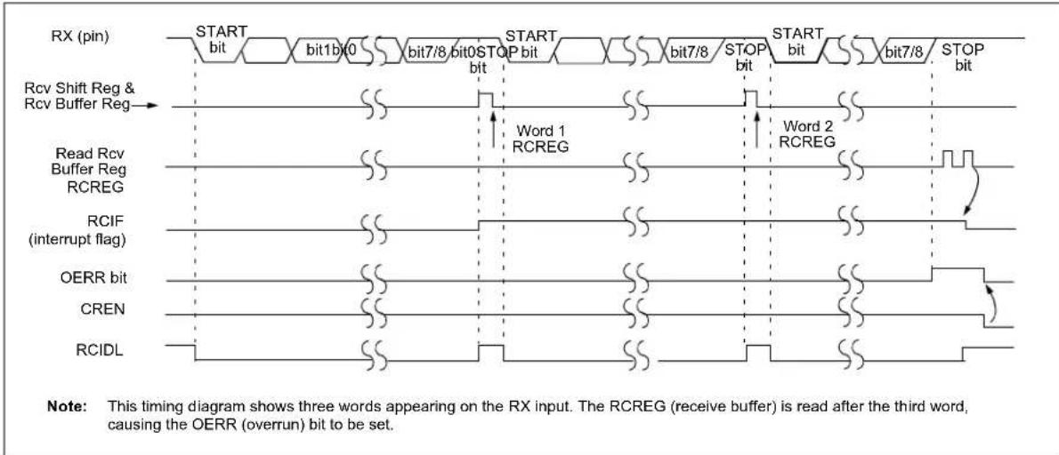
FIGURE 10-6: ASYNCHRONOUS RECEPTION WITH ADDRESS DETECT
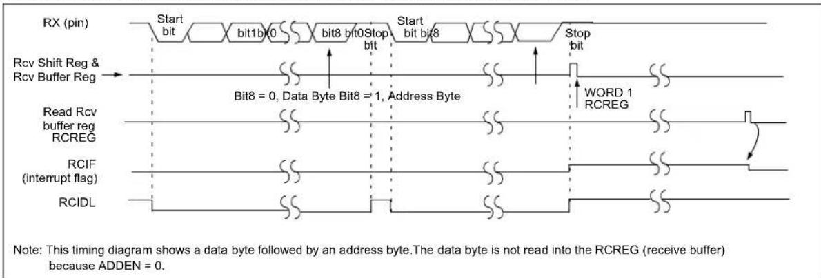
flowchart
graph TD
    A["RX (pin)"] --> B["Start bit"]
    B --> C["bit1b0"]
    C --> D["bit8 bit0"]
    D --> E["Stop bit"]
    E --> F["Start bit bit8"]
    F --> G["Stop bit"]
    G --> H["WORD 1 RCREG"]
    I["Rcv Shift Reg & Rcv Buffer Reg"] --> J["SS"]
    J --> K["Bit8 = 0, Data Byte Bit8 = 1, Address Byte"]
    L["Read Rcv buffer reg RCREG"] --> M["SS"]
    M --> N["SS"]
    N --> O["SS"]
    O --> P["RCIF (interrupt flag)"]
    Q["RCIDL"] --> R["SS"]
    R --> S["SS"]
    S --> T["SS"]
    T --> U["Word 1 RCREG"]
    V["Note: This timing diagram shows a data byte followed by an address byte. The data byte is not read into the RCREG (receive buffer) because ADDEN = 0."]
FIGURE 10-7: ASYNCHRONOUS RECEPTION WITH ADDRESS BYTE FIRST
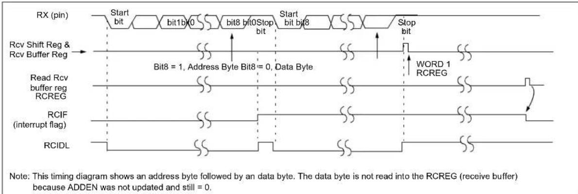
flowchart
graph TD
    A["RX (pin)"] --> B["Start bit"]
    B --> C["bit1b 0"]
    C --> D["bit8 bit0"]
    D --> E["Stop bit"]
    E --> F["Start bit bit8"]
    F --> G["Stop bit"]
    G --> H["Word 1 RCREG"]
    I["Rcv Shift Reg & Rcv Buffer Reg"] --> J["Bit8 = 1, Address Byte Bit8 = 0, Data Byte"]
    K["Read Rcv buffer reg RCREG"] --> L["SS"]
    M["RCIF (interrupt flag)"] --> N["SS"]
    O["RCIDL"] --> P["SS"]
    Q["Note: This timing diagram shows an address byte followed by an data byte. The data byte is not read into the RCREG (receive buffer) because ADDEN was not updated and still = 0."]
10.4 USART Synchronous Master Mode
In Synchronous Master mode, the data is transmitted in a half-duplex manner (i.e., transmission and reception do not occur at the same time). When transmitting data, the reception is inhibited and vice versa. Synchronous mode is entered by setting bit SYNC (TXSTA<4>). In addition, enable bit SPEN (RCSTA<7>) is set in order to configure the GPB6/TX/CK/AN7 and the GPB7/RX/DT/CCD I/O pins to CK (clock) and DT (data) lines, respectively. The Master mode indicates that the processor transmits the master clock on the CK line. The Master mode is entered by setting bit CSRC (TXSTA<7>).
10.4.1 SYNCHRONOUS MASTER TRANSMIT MODE
Synchronous Master Transmit mode works similarly to Asynchronous Transmit mode, see Section 10.3.1 "Asynchronous Transmit Mode". In Synchronous Transmit mode, the first data byte is shifted out on the next available rising edge of the CK line. Data out is stable relative to the falling edge of the synchronous clock.
Clearing enable bit TXEN (TXSTA<5>) during a transmission causes the transmission to be aborted and resets the transmitter. The DT and CK pins revert to high-impedance. If either bit CREN (RCSTA<4>) or bit SREN (RCSTA<5>) is set during a transmission, the transmission is aborted and the DT pin reverts to a hi-impedance state (for a reception). The CK pin remains an output if bit CSRC (TXSTA<7>) is set (internal clock).
The transmitter logic, however, is not reset, although it is disconnected from the pins. In order to reset the transmitter, the user has to clear bit TXEN. If bit SREN is set (to interrupt an on-going transmission and receive a single word), then after the single word is received, bit SREN is cleared and the serial port reverts back to transmitting, since bit TXEN is still set. The DT line immediately switches from high-impedance Receive mode to transmit and start driving. To avoid this, it is recommended that the bit TXEN be cleared.
Steps to follow when setting up a Synchronous Master Transmission:
- Initialize the SPBRG register for the appropriate baud rate.
- Enable the synchronous master serial port by setting bits SYNC, SPEN and CSRC.
- If interrupts are desired, set enable bit TXIE.
- If 9-bit transmission is desired, set bit TX9.
- Enable the transmission by setting bit TXEN.
- If 9-bit transmission is selected, the ninth bit should be loaded in bit TX9D.
- Start transmission by loading data to the TXREG register.
- If using interrupts, ensure that GIE and PEIE (bits 7 and 6) of the INT-CON register are set.
FIGURE 10-1: SYNCHRONOUS TRANSMISSION
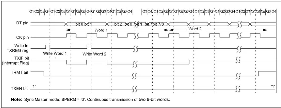
FIGURE 10-2: SYNCHRONOUS TRANSMISSION (THROUGH TXEN)
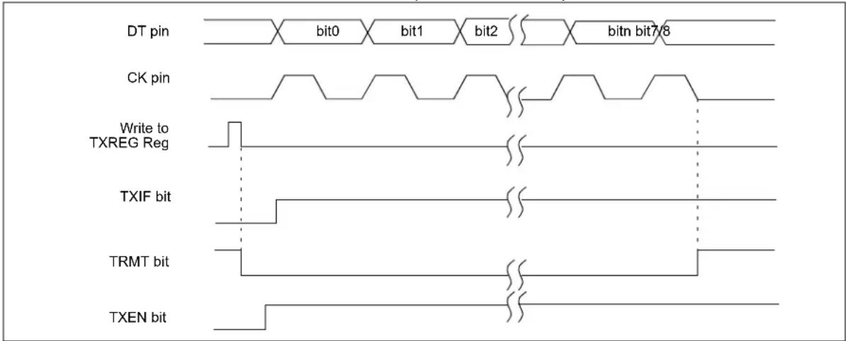
10.4.2 SYNCHRONOUS MASTER RECEIVE MODE
Synchronous Master Receive mode works similarly to Asynchronous Receive mode; see Section 10.3.2 "Asynchronous Receive Mode". In Synchronous Receive mode, reception is enabled by setting either enable bit SREN (RCSTA<5>) or enable bit CREN (RCSTA<4>). Data is sampled on the GPB7/RX/DT/CCD pin on the falling edge of the clock. If enable bit SREN is set, then only a single word is received. If enable bit CREN is set, the reception is continuous until CREN is cleared. If both bits are set, CREN takes precedence.
When setting up a Synchronous Master Reception:
- Initialize the SPBRG register for the appropriate baud rate.
- Enable the synchronous master serial port by setting bits SYNC, SPEN and CSRC.
- CREN and SREN bits are clear.
- If interrupts are desired, then set enable bit RCIE.
- If 9-bit reception is desired, then set bit RX9.
- If a single reception is required, set bit SREN. For continuous reception, set bit CREN.
- Interrupt flag bit RCIF is set when reception is complete and an interrupt is generated if enable bit RCIE was set.
- Read the RCSTA register to get the ninth bit (if enabled) and determine if any error occurred during reception.
- Read the 8-bit received data by reading the RCREG register.
- If any error occurred, clear the error by clearing bit CREN.
- If using interrupts, ensure that GIE and PEIE (bits 7 and 6) of the INTCON register are set.
FIGURE 10-3: SYNCHRONOUS RECEPTION (MASTER MODE, SREN)
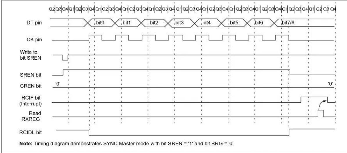
other
| Signal | Bit0 | Bit1 | Bit2 | Bit3 | Bit4 | Bit5 | Bit6 | Bit7/8 | |-----------------|------|------|------|------|------|------|------|--------| | DT pin | | | | | | | | | | CK pin | | | | | | | | | | Write to bit SREN| | | | | | | | | | SREN bit | | | | | | | | | | CREN bit | '0' | | | | | | | | | RCIF bit (Interrupt) | | | | | | | | | | Read RXREG | | | | | | | | | | RCIDL bit | | | | | | | | |10.5 USART Synchronous Slave Mode
Synchronous Slave mode differs from the Master mode in the fact that the shift clock is supplied externally at the GPB6/TX/CK/AN7 pin (instead of being supplied internally in Master mode). This allows the device to transfer or receive data while in Sleep mode. Slave mode is entered by clearing bit CSRC (TXSTA<7>).
10.5.1 SYNCHRONOUS SLAVE TRANSMIT MODE
The operation of the Synchronous Master and Slave modes is identical, except in the case of the Sleep mode.
If two words are written to the TXREG and then the SLEEP instruction is executed, the following occurs:
a) The first word immediately transfers to the TSR register and transmits.
b) The second word remains in TXREG register.
c) Flag bit TXIF is not set.
d) When the first word has been shifted out of TSR, the TXREG register transfers the second word to the TSR and flag bit TXIF is not set.
e) If enable bit TXIE is set, the interrupt wakes the chip from Sleep and if the global interrupt is enabled, the program branches to the interrupt vector (0004h).
When setting up a Synchronous Slave Transmission, follow these steps:
- Enable the synchronous slave serial port by setting bits SYNC and SPEN and clearing bit CSRC.
- Clear bits CREN and SREN.
- If interrupts are desired, then set enable bit TXIE.
- If 9-bit transmission is desired, then set bit TX9.
- Enable the transmission by setting enable bit TXEN.
- If 9-bit transmission is selected, the ninth bit should be loaded in bit TX9D.
- Start transmission by loading data to the TXREG register.
- If using interrupts, ensure that GIE and PEIE (bits 7 and 6) of the INTCON register are set.
10.5.2 SYNCHRONOUS SLAVE RECEIVE MODE
The operation of the Synchronous Master and Slave modes is identical, except in the case of the Sleep mode. Bit SREN is a "don't care" in Slave mode.
If receive is enabled by setting bit CREN prior to the SLEEP instruction, then a word may be received during Sleep. On completely receiving the word, the RSR register will transfer the data to the RCREG register and if enable bit RCIE bit is set, the interrupt generated will wake the chip from Sleep. If the global interrupt is enabled, the program will branch to the interrupt vector (0004h).
When setting up a Synchronous Slave Reception, follow these steps:
- Enable the synchronous master serial port by setting bits SYNC and SPEN and clearing bit CSRC.
- If interrupts are desired, set enable bit RCIE.
- If 9-bit reception is desired, set bit RX9.
- To enable reception, set enable bit CREN.
- Flag bit RCIF will be set when reception is complete and an interrupt will be generated, if enable bit RCIE was set.
- Read the RCSTA register to get the ninth bit (if enabled) and determine if any error occurred during reception.
- Read the 8-bit received data by reading the RCREG register.
- If any error occurred, clear the error by clearing bit CREN.
- If using interrupts, ensure that GIE and PEIE (bits 7 and 6) of the INTCON register are set.
REGISTER 10-1: RCSTA – RECEIVE STATUS AND CONTROL REGISTER
| R/W-0 R/W-0 R/W-0 R/W-0 R/W-0 R-0 R-0 R-x | |||||||
| SPEN | RX9 | SREN | CREN | ADDEN | FERR | OERR | RX9D |
| bit 7 bit 0 | |||||||
Legend:
| R = Readable bit | W = Writable bit | U = Unimplemented bit, read as '0' |
| -n = Value at POR | '1' = Bit is set | '0' = Bit is cleared x = Bit is unknown |
bit 7 SPEN ^(1) : Serial Port Enable bit
1 = Serial port enabled - configures GPB7/RX/DT/CCD and GPB6/TX/CK/AN7 pins as serial port pins 0 = Serial port disabled - module and its state machines held in Reset
bit 6 RX9: 9-bit Receive Enable bit
1 = Selects 9-bit reception 0 = Selects 8-bit reception
bit 5 SREN: Single Receive Enable bit
Asynchronous mode:
Unused in this mode - value ignored
Synchronous mode - master:
1 = Enables single receive 0 = Disables single receive This bit is cleared after reception is complete. Synchronous mode - slave: Unused in this mode - value ignored
bit 4 CREN: Continuous Receive Enable bit
Asynchronous mode:
1 = Enables continuous receive until enable bit CREN is cleared 0 = Disables continuous receive
Synchronous mode:
1 = Enables continuous receive until enable bit CREN is cleared (CREN overrides SREN) 0 = Disables continuous receive
bit 3 ADDEN: Address Detect Enable bit
RX9 = 1:
1 = Enables address detection - enable interrupt and load of the receive buffer when the ninth bit in the receive buffer is set 0 = Disables address detection - all bytes are received, and ninth bit can be used as parity bit RX9 = 0: Unused in this mode
bit 2 FERR: Framing Error bit
1 = Framing error (can be updated by reading RCREG register and receive next valid byte) 0 = No framing error
bit 1 OERR: Overrun Error bit
1 = Overrun error (can be cleared by clearing bit CREN) 0 = No overrun error
bit 0 RX9D: 9th bit of received data (can be parity bit)
Note 1: The USART module automatically changes the pin from tri-state to drive as needed. Configure TRISC<5> = 1 and TRISC<4> = 1.
REGISTER 10-2: TXSTA – TRANSMIT STATUS AND CONTROL REGISTER
| R/W-0 R/W-0 R/W-0 R/W-0 U-0 R/W-0 R-1 R/W-0 | |||||||
| CSRC TX9 TXEN | SYNC | — BRGH | TRMT | TX9D | |||
| bit 7 | bit 0 | ||||||
Legend:
| R = Readable bit | W = Writable bit | U = Unimplemented bit, read as '0' |
| -n = Value at POR | '1' = Bit is set | '0' = Bit is cleared x = Bit is unknown |
bit 7 CSRC: Clock Source Select bit
Asynchronous mode:
Unused in this mode - value ignored
Synchronous mode:
1 = Master mode - Clock generated internally from BRG
0 = Slave mode - Clock from external source
bit 6 TX9: 9-bit Transmit Enable bit
1 = Selects 9-bit transmission
0 = Selects 8-bit transmission
bit 5 TXEN ^(1) : Transmit Enable bit
1 = Transmit enabled
0 = Transmit disabled
bit 4 SYNC: USART Mode Select bit
1 = Synchronous mode
0 = Asynchronous mode
bit 3 Unimplemented: Read as '0'
bit 2 BRGH: High Baud Rate Select bit
Asynchronous mode:
1 = High speed
0 = Low speed
Synchronous mode:
Unused in this mode - value ignored
bit 1 TRMT: Transmit Operation Idle Status bit
1 = Transmit Operation Idle
0 = Transmit Operation Active
bit 0 TX9D: 9th bit of transmit data; can be used as parity bit
Note 1: SREN/CREN overrides TXEN in Synchronous mode.
NOTES:
11.0 MEMORY ORGANIZATION
There are two types of memory in the MCP19116/7:
- Program Memory
- Data Memory
- Special Function Registers (SFRs)
- General Purpose RAM
11.1 Program Memory Organization
The MCP19116/7 devices have a 13-bit program counter capable of addressing an 8000 x 14 program memory space. The Reset vector is at 0000h and the Interrupt vector is at 0004h (refer to Figure 11-1). The width of the program memory bus (instruction word) is 14 bits. Since all instructions are a single word, the MCP19116/7 devices have space for 8000 instructions.
FIGURE 11-1: PROGRAM MEMORY MAP AND STACK FOR MCP19116/7
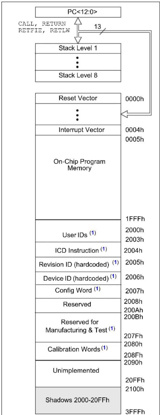
flowchart
graph TD
    A["PC<12:0>"] --> B["Stack Level 1"]
    B --> C["Stack Level 8"]
    B --> D["Reset Vector"]
    D --> E["Interrupt Vector"]
    E --> F["On-Chip Program Memory"]
    F --> G["User IDs (1)"]
    G --> H["ICD Instruction (1)"]
    H --> I["Revision ID (hardcoded) (1)"]
    I --> J["Device ID (hardcoded) (1)"]
    J --> K["Config Word (1)"]
    K --> L["Reserved"]
    L --> M["Reserved for Manufacturing & Test (1)"]
    M --> N["Calibration Words (1)"]
    N --> O["Unimplemented"]
    O --> P["Shadows 2000-20FFh"]
    P --> Q["3FFFh"]
    B --> R["13"]
    R --> S["0000h"]
    R --> T["0004h"]
    R --> U["0005h"]
    R --> V["1FFFh"]
    R --> W["2000h"]
    R --> X["2003h"]
    R --> Y["2004h"]
    R --> Z["2005h"]
    R --> AA["2006h"]
    R --> AB["2007h"]
    R --> AC["2008h"]
    R --> AD["200Ah"]
    R --> AE["200Bh"]
    R --> AF["207Fh"]
    R --> AG["2080h"]
    R --> AH["208Fh"]
    R --> AI["2090h"]
    R --> AJ["20FFh"]
    R --> AK["2100h"]
Note 1: Not code-protected.
11.1.1 READING PROGRAM MEMORY AS DATA
There are two methods of accessing constants in program memory:
• using tables of RETLW instructions.
- setting a Files Select Register (FSR) to point to the program memory.
11.1.1.1 RETLW Instruction
The RETLW instruction can be used to provide access to the tables of constants. The recommended way to create such tables is shown in Example 11-1.
EXAMPLE 11-1: RETLW INSTRUCTION
constants
    BRW ;Add Index in W to
    ;program counter to
    ;select data
    RETLW DATA0 ;Index0 data
    RETLW DATA1 ;Index1 data
    RETLW DATA2
    RETLW DATA3

my_function
    ;... LOTS OF CODE...
    MOVLW DATA_INDEX
    call constants
    ;... THE CONSTANT IS IN W
The BRW instruction makes this type of table very simple to implement. If your code must remain portable with previous generations of microcontrollers, then the BRW instruction is not available, so the older table-read method must be used.
11.2 Data Memory Organization
The data memory (refer to Figure 11-1) is partitioned into four banks, which contain the General Purpose Registers (GPR) and the Special Function Registers (SFR). The Special Function Registers are located in the first 32 locations of each bank. Register locations 20h-7Fh in Bank 0, A0h-EFh in Bank 1, 120h-16Fh in Bank 2 and 1A0h-1EFh in Bank 3 are General Purpose Registers, implemented as static RAM. All other RAM is unimplemented and returns '0' when read. The RP<1:0> bits in the STATUS register are the bank select bits.
EXAMPLE 11-2: BANK SELECT
RP1 RP0
0 0 → Bank 0 is selected
0 1 → Bank 1 is selected
1 0 → Bank 2 is selected
1 1 → Bank 3 is selected
To move values from one register to another register, the value must pass through the W register. This means that for all register-to-register moves, two instruction cycles are required.
The entire data memory can be accessed either directly or indirectly. Direct addressing may require the use of the RP<1:0> bits. Indirect addressing requires the use of the FSR. Indirect addressing uses the Indirect Register Pointer (IRP) bit in the STATUS register for access to the Bank0/Bank1 or the Bank2/Bank3 areas of data memory.
11.2.1 GENERAL PURPOSE REGISTER FILE
The register file is organized as 64 x 8 in the MCP19116/7. Each register is accessed, either directly or indirectly, through the FSR (refer to Section 11.5 "Indirect Addressing, INDF and FSR Registers").
11.2.2 CORE REGISTERS
The core registers contain the registers that directly affect the basic operation. The core registers can be addressed from any bank. These registers are listed in Table 11-1. For detailed information, refer to Table 11-2.
TABLE 11-1: CORE REGISTERS
| Addresses BANKx | |
| x00h, x80h, x100h, or x180h | INDF |
| x02h, x82h, x102h, or x182h | PCL |
| x03h, x83h, x103h, or x183h | STATUS |
| x04h, x84h, x104h, or x184h | FSR |
| x0Ah, x8Ah, x10Ah, or x18Ah | PCLATH |
| x0Bh, x8Bh, x10Bh, or x18Bh | INTCON |
11.2.2.1 STATUS Register
The STATUS register contains:
• the arithmetic status of the ALU
- the Reset status
• the bank select bits for data memory (RAM)
The STATUS register can be the destination for any instruction, like any other register. If the STATUS register is the destination for an instruction that affects the Z, DC or C bits, the Write to these three bits is disabled. These bits are set or cleared according to the device logic. Furthermore, the TO and PD bits are not writable. Therefore, the result of an instruction with the STATUS register as destination may be different than intended.
For example, CLRF STATUS will clear the upper three bits and set the Z bit. This leaves the STATUS register as '000u u1uu' (where u = unchanged).
It is recommended, therefore, that only BCF, BSF, SWAPF and MOVWF instructions be used to alter the STATUS register, because these instructions do not affect any Status bits.
Note: The C and DC bits operate as Borrow and Digit Borrow out bits, respectively, in subtraction.
REGISTER 11-1: STATUS: STATUS REGISTER
| R/W-0 | R/W-0 | R/W-0 | R-1 | R-1 | R/W-x | R/W-x | R/W-x |
| IRP | RP1 | RP0 | Z | DC(1) | C(1) | ||
| bit 7 bit 0 | |||||||
Legend:
| R = Readable bit | W = Writable bit | U = Unimplemented bit, read as '0' |
| -n = Value at POR | x = Bit is unknown | '0' = Bit is cleared |
| '1' = Bit is set |
bit 7 IRP: Register Bank Select bit (used for Indirect addressing)
1 = Bank 2 & 3 (100h - 1FFh)
0 = Bank 0 & 1 (00h - FFh)
bit 6-5 RP<1:0>: Register Bank Select bits (used for Direct addressing)
00 = Bank 0 (00h - 7Fh)
01 = Bank 1 (80h - FFh)
10 = Bank 2 (100h - 17Fh)
11 = Bank 3 (180h - 1FFh)
bit 4 TO: Time-Out bit
1 = After power-up, CLRWDT instruction or SLEEP instruction
0 = A WDT time out occurred
Note 1: For Borrow, the polarity is reversed. A subtraction is executed by adding the two's complement of the second operand. For rotate (RRF, RLF) instructions, this bit is loaded with either the high-order or low-order bit in the source register.
REGISTER 11-1: STATUS: STATUS REGISTER (CONTINUED)
bit 3 PD : Power-Down bit
1 = After power-up or by the CLRWDT instruction
0 = By execution of the SLEEP instruction
bit 2 Z: Zero bit
1 = The result of an arithmetic or logic operation is zero 0 = The result of an arithmetic or logic operation is not zero
bit 1 DC: Digit Carry/Digit Borrow bit (1) (ADDWF, ADDLW, SUBLW, SUBWF instructions) 1 = A carry-out from the 4 ^th low-order bit of the result occurred 0 = No carry-out from the 4 ^th low-order bit of the result
bit 0 C: Carry/Borrow bit (1) (ADDWF, ADDLW, SUBLW, SUBWF instructions) (1) 1 = A carry-out from the Most Significant bit of the result occurred 0 = No carry-out from the Most Significant bit of the result occurred
Note 1: For Borrow, the polarity is reversed. A subtraction is executed by adding the two's complement of the second operand. For rotate (RRF, RLF) instructions, this bit is loaded with either the high-order or low-order bit in the source register.
11.2.3 SPECIAL FUNCTION REGISTERS
The Special Function Registers are registers used by the CPU and peripheral functions for controlling the desired operation of the device (refer to Figure 11-2). These registers are static RAM.
The special registers can be classified into two sets:
- core
• peripheral
The Special Function Registers associated with the microcontroller core are described in this section. Those related to the operation of the peripheral features are described in the associated section for that peripheral feature.
11.3 DATA MEMORY
FIGURE 11-2: MCP19116/7 DATA MEMORY MAP
| File Address | File Address | File Address | File Address | ||||
| Indirect addr.(1) | 00h Indirect addr. (1) | 80h Indirect addr. (1) | 100h Indirect addr. (1) | 180h | |||
| TMR0 01h OPTION_REG 81h TMR0 10 | 1h OPTION_REG 181h | ||||||
| PCL | 02h | PCL | 82h | PCL | 102h | PCL | 182h |
| STATUS | 03h | STATUS | 83h | STATUS | 103h | STATUS | 183h |
| FSR | 04h | FSR | 84h | FSR | 104h | FSR | 184h |
| PORTGPA | 05h | TRISGPA | 85h | WPUGPA | 105h | IOCA | 185h |
| PORTGPB | 06h | TRISGPB | 86h | WPUGPB | 106h | IOCB | 186h |
| PIR1 | 07h | PIE1 | 87h | PE1 | 107h | ANSELA | 187h |
| PIR2 | 08h | PIE2 | 88h | MODECON | 108h | ANSELB | 188h |
| PCON | 09h | 89h | ABECON | 109h | 189h | ||
| PCLATH | 0Ah | PCLATH | 8Ah | PCLATH | 10Ah | PCLATH | 18Ah |
| INTCON | 0Bh | INTCON | 8Bh | INTCON | 10Bh | INTCON | 18Bh |
| TMR1L 0Ch | 8Ch | Reserved | 10Ch | PORTICD (2) | 18Ch | ||
| TMR1H | 0Dh | 8Dh | 10Dh | TRISICD (2) | 18Dh | ||
| T1CON | 0Eh | 8Eh | 10Eh | ICKBUG (2) | 18Eh | ||
| TMR2 0Fh | 8Fh | 10Fh | BIGBUG (2) | 18Fh | |||
| T2CON | 10h | VINUVLO | 90h | SSPADD | 110h | PMCON1 | 190h |
| PR2 | 11h | VINOVLO | 91h | SSPBUF | 111h | PMCON2 | 191h |
| 12h | VINCON | 92h | SSPCON1 | 112h | PMADRL | 192h | |
| PWMPHL | 13h | CC1RL | 93h | SSPCON2 | 113h | PMADRH | 193h |
| PWMPHH | 14h | CC1RH | 94h | SSPCON3 | 114h | PMDATL | 194h |
| PWMRL | 15h | CC2RL | 95h | SSPMSK1 | 115h | PMDATH | 195h |
| PWMRH | 16h | CC2RH | 96h | SSPSTAT | 116h | DSTCAL | 196h |
| 17h | CCDCON | 97h | SSPADD2 | 117h | RFBTCAL | 197h | |
| 18h | DESATCON | 98h | SSPMSK2 | 118h | OSCCAL | 198h | |
| VREFCON | 19h | OVCON | 99h | VRSPCAL | 119h | DCSCAL | 199h |
| VREF2CON | 1Ah | OVREFCON | 9Ah | VR2SPCAL | 11Ah | TTACAL | 19Ah |
| OSCTUNE | 1Bh | DEADCON | 9Bh | SPBRG | 11Bh | BGRCAL | 19Bh |
| ADRESL | 1Ch | SLPCRCON | 9Ch | RCREG | 11Ch | EAOFFCAL | 19Ch |
| ADRESH | 1Dh | ICOACON | 9Dh | TXREG | 11Dh | AVDDCAL | 19Dh |
| ADCON0 | 1Eh | ICLEBCON | 9Eh | TXSTA | 11Eh | A2GCAL | 19Eh |
| ADCON1 | 1Fh | 9Fh | RCSTA 11Fh | OVRSPCAL 19Fh | |||
| General Purpose Register | 20h | General Purpose Register | General Purpose Register | General Purpose Register | |||
| 96 Bytes | 80 Bytes | 80 bytes | 80 bytes | ||||
| EFh | 16F | 1EF | |||||
| Accesses Bank 0 | F0h | Accesses Bank 0 | Accesses Bank 0 | ||||
| 7Fh | FFh | 17Fh | 1FFh | ||||
| Bank 0 | Bank 1 | Bank2 | Bank3 | ||||
TABLE 11-2: MCP19116/7 SPECIAL REGISTERS SUMMARY BANK 0
| Addr. | Name Bit 7 Bit | 6 Bit 5 Bit 4 Bit 3 | Bit 2 Bit 1 | Bit 0 Value on | POR Reset Value on all other resets | (1) | |||||
| Bank 0 | |||||||||||
| 00h | INDF | Addressing this location uses contents of FSR to address data memory (not a physical register) | xxxx xxxx | xxxx xxxx | |||||||
| 01h | TMR0 | Timer0 Module's Register | xxxx xxxx | xxxx | |||||||
| 02h | PCL | Program Counter's (PC) Least Significant byte | 0000 0000 | 0000 0000 | |||||||
| 03h | STATUS | IRP | RP1 | RP0 | TO | PD | Z | DC | C | 000' 1xxx | 000q qucc |
| 04h | FSR | Indirect data memory address pointer | xxxx xxxx | xxxx | |||||||
| 05h | PORTGPA | GPA7 | GPA6 | GPA5 | — | GPA3 | GPA2 | GPA1 | GPA0 | xxxx- xxxx | xxxx- xxx |
| 06h | PORTGPB | GPB7 | GPB6 | GPB5 | GPB4 | — | — | GPB1 | GPB0 | xxxx --xx | xxxx --uu |
| 07h | PIR1 | TXIF | RCIF | BCLIF | SSPIF | CC2IF | CC1IF | TMR2IF | TMR1IF | 0000 0000 | 0000 0000 |
| 08h | PIR2 | CDSIF | ADIF | — | OTIF | OVIF | DRUVIF | OVLOIF | UVLOIF | 00-0 0000 | 00-0 0000 |
| 09h | PCON | ADC_REFR | — | — | — | VDDFLAG | VDDOK | POR | BOR | 0--- 10qq | 0--- 10uu |
| 0Ah | PCLATH | — | — | — | Write buffer for upper 5 bits of program counter | ---0 0000 | ---0 0000 | ||||
| 0Bh | INTCON | GIE | PEIE | TOIE | INTE | IOCE | TOIF | INTF | IOCF (2) | 0000 000x | 0000 000u |
| 0Ch | TMR1L | Holding register for the Least Significant byte of the 16-bit TMR1 | xxxx xxxx | xxxx | |||||||
| 0Dh | TMR1H | Holding register for the Most Significant byte of the 16-bit TMR1 | xxxx xxxx | xxxx | |||||||
| 0Eh | T1CON | — | — | T1CKPS1 | T1CKPS0 | — | — | TMR1CS | TMR1ON | --00 --00 | --00 --00 |
| 0Fh | TMR2 | Timer2 Module Register | 0000 0000 | xxxx | |||||||
| 10h | T2CON | — | — | — | — | — | TMR2ON | T2CKPS1 | T2CKPS0 | ---- -000 | ---- -000 |
| 11h | PR2 | Timer2 Module Period Register | 1111 1111 | 1111 1111 | |||||||
| 12h | — | Unimplemented | — | — | |||||||
| 13h | PWMPHL | SLAVE Phase Shift Register | xxxx xxxx | xxxx | |||||||
| 14h | PWMPHH | SLAVE Phase Shift Register | xxxx xxxx | xxxx | |||||||
| 15h | PWMRL | PWM Register Low Byte | xxxx xxxx | xxxx | |||||||
| 16h | PWMRH | PWM Register High Byte | xxxx xxxx | xxxx | |||||||
| 17h | — | Unimplemented | — | — | |||||||
| 18h | — | Unimplemented | — | — | |||||||
| 19h | VREFCON | VREF7 | VREF6 | VREF5 | VREF4 | VREF3 | VREF2 | VREF1 | VREF0 | 0000 0000 | 0000 0000 |
| 1Ah | VREF2CON | VREF27 | VREF26 | VREF25 | VREF24 | VREF23 | VREF22 | VREF21 | VREF20 | 0000 0000 | 0000 0000 |
| 1Bh | OSCTUNE | — | — | — | TUN4 | TUN3 | TUN2 | TUN1 | TUN0 | ---0 0000 | ---0 0000 |
| 1Ch | ADRESL | Least significant 8 bits of the A/D result | xxxx xxxx | xxxx | |||||||
| 1Dh | ADRESH | Most significant 2 bits of the A/D result | 0000 00xx | 0000 00xx | |||||||
| 1Eh | ADCON0 | — | CHS4 | CHS3 | CHS2 | CHS1 | CHS0 | GO/DONE | ADON | -000 0000 | -000 0000 |
| 1Fh | ADCON1 | — | ADCS2 | ADCS1 | ADCS0 | — | — | — | VCFG | -000 ---0 | -000 ---0 |
Legend: — = Unimplemented locations read as '0', u = unchanged, x = unknown, q = value depends on condition, shaded = unimplemented
Note 1: Other (non power-up) resets include MCLR Reset and Watchdog Timer Reset during normal operation.
2: MCLR and WDT reset does not affect the previous value data latch. The IOCF bit will be cleared upon reset but will be set again if the mismatch exists.
TABLE 11-3: MCP19116/7 SPECIAL REGISTERS SUMMARY BANK 1
| Addr. | Name Bit 7 Bit 6 Bit 5 Bit 4 Bit 3 | Bit 2 Bit 1 Bit 0 Value on POR | Reset Values | on all other resets | (1) | ||||||
| Bank 1 | |||||||||||
| 80h | INDF | Addressing this location uses contents of FSR to address data memory (not a physical register) | xxxx xxxx | xxxx xxx | |||||||
| 81h | OPTION_REG | RAPU | INTEDG | T0CS | T0SE | PSA | PS2 | PS1 | PS0 | 1111 1111 | 1111 1111 |
| 82h | PCL | Program Counter's (PC) Least Significant byte | 0000 0000 | 0000 0000 | |||||||
| 83h | STATUS | IRP | RP1 | RP0 | TO | PD | Z | DC | C | 0001 1xxx | 000g quuu |
| 84h | FSR | Indirect data memory address pointer | xxxx xxxx | xxxx xxx | |||||||
| 85h | TRISGPA | TRISA7 | TRISA6 TRISA5 | — | TRISA3 | TRISA2 | TRISA1 | TRISA0 | 1110 1111 | 1110 1111 | |
| 86h | TRISGPB | TRISB7 | TRISB6 TRISB5 TRISB4 | — | — | TRISB1 | TRISB0 | 1111 0011 | 1111 0011 | ||
| 87h | PIE1 | TXIE | RCIE | BCLIE | SSPIE | CC2IE | CC1IE | TMR2IE | TMR1IE | 0000 0000 | 0000 0000 |
| 88h | PIE2 | CDSIE | ADIE | — | OTIE | OVIE | DRUVIE | OVLOIE | UVLOIE | 00-0 0000 | 00-0 0000 |
| 89h | — | Unimplemented | — | — | |||||||
| 8Ah | PCLATH | — | — | — | Write buffer for upper 5 bits of program counter | ---0 0000 | ---0 0000 | ||||
| 8Bh | INTCON | GIE | PEIE | TOIE | INTE | IOCE | T0IF | INTF | IOCF (2) | 0000 000x | 0000 000u |
| 8Ch | — | Unimplemented | — | — | |||||||
| 8Dh | — | Unimplemented | — | — | |||||||
| 8Eh | — | Unimplemented | — | — | |||||||
| 8Fh | — | Unimplemented | — | — | |||||||
| 90h | VINUVLO | — | — | UVLO5 | UVLO4 | UVLO3 | UVLO2 | UVLO1 | UVLO0 | ---xx xxxx | ---xx xxx |
| 91h | VINOVLO | — | — | OVLO5 | OVLO4 | OVLO3 | OVLO2 | OVLO1 | OVLO0 | ---xx xxxx | ---xx xxx |
| 92h | VINCON | UVLOEN | UVLOCUT | UVLOINTP | UVLOINTN | OVLOEN | OVLOOUT | OVLOINTP | OVLOINTN | 0x00 0x00 | 0x00 0x00 |
| 93h | CC1RL | Capture1/Compare1 Register1 x Low Byte (LSB) | xxxx xxxx | xxxx xxx | |||||||
| 94h | CC1RH | Capture1/Compare1 Register2 x High Byte (MSB) | xxxx xxxx | xxxx xxx | |||||||
| 95h | CC2RL | Capture2/Compare2 Register1 x Low Byte (LSB) | xxxx xxxx | xxxx xxx | |||||||
| 96h | CC2RH | Capture2/Compare2 Register2 x High Byte (MSB) | xxxx xxxx | xxxx xxx | |||||||
| 97h | CCDCON | CC2M<3:0> | CC1M<3:0> | xxxx xxxx | xxxx xxx | ||||||
| 98h | DESATCON | CDSMUX | CDSWDE | Reserved | CDSPOL | CDSOE | CDSOUT | CDSINTP | CDSINTN | 0000 0x00 | 0000 0x00 |
| 99h | OVCON | — | — | — | — | OVEN | OVOUT | OVINTP | OVINTN | ---- 0x00 | ---- 0x00 |
| 9Ah | OVREFCON | OOV7 | OOV6 | OOV5 | OOV4 | OOV3 | OOV2 | OOV1 | OOV0 | xxxx xxxx | xxxx xxx |
| 9Bh | DEADCON | PDRVDT3 | PDRVDT2 | PDRVDT1 | PDRVDT0 | SDRVDT3 | SDRVDT2 | SDRVDT1 | SDRVDT0 | xxxx xxxx | xxxx xxx |
| 9Ch | SLPCRCON | — | SLPBY | SLPS5 | SLPS4 | SLPS3 | SLPS2 | SLPS1 | SLPS0 | ---xx xxxx | ---xx xxx |
| 9Dh | ICOACON | — | — | — | — | ICOAC3 | ICOAC2 | ICOAC1 | ICOAC0 | ---- xxxx | ---- xxx |
| 9Ef | ICLEBCON | — | — | — | — | — | — | ICLEBC1 | ICLEBC0 | ---- --xx | ---- --xx |
| 9Fh | — | Unimplemented | — | — | |||||||
Legend: — = Unimplemented locations read as '0', u = unchanged, x = unknown, q = value depends on condition, shaded = unimplemented
Note 1: Other (non power-up) resets include MCLR Reset and Watchdog Timer Reset during normal operation
2: MCLR and WDT reset does not affect the previous value data latch. The IOCF bit will be cleared upon reset but will be set again if the mismatch exists.
TABLE 11-4: MCP19116/7 SPECIAL REGISTERS SUMMARY BANK 2
| Addr. | Name Bit 7 Bit 6 | Bit 5 Bit 4 Bit 3 Bit 2 Bit 1 | Bit 0 Value on | POR Reset Value on all other resets | (1) | ||||||
| Bank 2 | |||||||||||
| 100h | INDF | Addressing this location uses contents of FSR to address data memory (not a physical register) | xxxx xxxx | xxxx xxxx | |||||||
| 101h | TMR0 | Timer0 Module's Register | xxxx xxxx | xxxx xxx | |||||||
| 102h | PCL | Program Counter's (PC) Least Significant byte | 0000 0000 | 0000 0000 | |||||||
| 103h | STATUS | IRP | RP1 | RP0 | TO | PD | Z | DC | C | 0001 1xxx | 0000 qxxx |
| 104h | FSR | Indirect data memory address pointer | xxxx xxxx | xxxx xxx | |||||||
| 105h | WPUGPA | — | — | WPUA5 | — | WPUA3 | WPUA2 | WPUA1 | WPUA0 | --1- 1111 | --u- xxx |
| 106h | WPUGPB | WPUB7 | WPUB6 | WPUB5 | WPUB4 | — | — | WPUB1 | — | 1111 --1- | xxx ---u- |
| 107h | PE1 | PDRVEN | SDRVEN | PDRVBY | SDRVBY | — | ISPUEN | PWMSTR_PEN | PWMSTR_SEN | 0000 -100 | 0000 -100 |
| 108h | MODECON | MSC1 | MSC0 | RFB | — | MSC2 | — | — | — | 001- 0--- | 001- 0--- |
| 109h | ABECON | DIGOEN | DSEL2 | DSEL1 | DSEL0 | DRUVSEL | — | EADIS | ANAOEN | 0000 0-00 | 0000 0-00 |
| 10Ah | PCLATH | — | — | — | Write buffer for upper 5 bits of program counter | ---0 0000 | ---0 0000 | ||||
| 10Bh | INTCON | GIE | PEIE | TOIE | INTE | IOCE | TOIF | INTF | IOCF (2) | 0000 000x | 0000 000u |
| 10Ch | — | Reserved | — | — | |||||||
| 10Dh | — | Unimplemented | — | — | |||||||
| 10Eh | — | Unimplemented | — | — | |||||||
| 10Fh | — | Unimplemented | — | — | |||||||
| 110h | SSPADD | ADD<7:0> | 0000 0000 | 0000 0000 | |||||||
| 111h | SSPBUF | Synchronous Serial Port Receive Buffer/Transmit Register | xxxx xxxx | xxxx xxx | |||||||
| 112h | SSPCON1 | WCOL | SSPOV | SSPEN | CKP | SSPM<3:0> | 0000 0000 | 0000 0000 | |||
| 113h | SSPCON2 | GCEN | ACKSTAT | ACKDT | ACKEN | RCEN | PEN | RSEN | SEN | 0000 0000 | 0000 0000 |
| 114h | SSPCON3 | ACKTIM | PCIE | SCIE | BOEN | SDAHT | SBCDE | AHEN | DHEN | 0000 0000 | 0000 0000 |
| 115h | SSPMSK1 | MSK<7:0> | 1111 1111 | 1111 1111 | |||||||
| 116h | SSPSTAT SMP CKE | D/A | — | P | S | R/W | UA | BF | — | — | — |
| 117h | SSPADD2 | ADD2<7:0> | 0000 0000 | 0000 0000 | |||||||
| 118h | SSPMSK2 | MSK2<7:0> | 1111 1111 | 1111 1111 | |||||||
| 119h | VRSPCAL | — | — | — | VRSPCAL4 | VRSPCAL3 | VRSPCAL2 | VRSPCAL1 | VRSPCAL0 | ---x xxx | ---u xxx |
| 11Ah | VR2SPCAL | — | — | — | VR2SPCAL4 | VR2SPCAL3 | VR2SPCAL2 | VR2SPCAL1 | VR2SPCAL0 | ---x xxx | ---u xxx |
| 11Bh | SPBRG | SPBRG7 | SPBRG6 | SPBRG5 | SPBRG4 | SPBRG3 | SPBRG2 | SPBRG1 | SPBRG0 | 0000 0000 | 0000 0000 |
| 11Ch | RCREG | USART Receive Data Register | 0000 0000 | 0000 0000 | |||||||
| 11Dh | TXREG | USART Transmit Data Register | 0000 0000 | 0000 0000 | |||||||
| 11Eh | TXSTA | CSRC | TX9 | TXEN | SYNC | — | BRGH | TRMT | TX9D | 0000 0000 | 0000 0000 |
| 11Fh | RCSTA | SPEN | RX9 | SREN | CREN | ADDEN | FERR | OERR | RX9D | 0000 0000 | 0000 0000 |
Legend: — = Unimplemented locations read as '0', u = unchanged, x = unknown, q = value depends on condition, shaded = unimplemented
Note 1: Other (non power-up) resets include MCLR Reset and Watchdog Timer Reset during normal operation.
2: MCLR and WDT reset does not affect the previous value data latch. The IOCF bit will be cleared upon reset but will be set again if the mismatch exists.
TABLE 11-5: MCP19116/7 SPECIAL REGISTERS SUMMARY BANK 3
| Addr. | Name | Bit 7 | Bit 6 | Bit 5 | Bit 4 | Bit 3 | Bit 2 | Bit 1 | Bit 0 | Value on POR Reset | Values on all other resets (1) |
| Bank 3 | |||||||||||
| 180h | INDF | Addressing this location uses contents of FSR to address data memory (not a physical register) | xxxx xxxx | xxxx quuu | |||||||
| 181h | OPTION_REG RAPU — | INTEDG | T0CS | T0SE | PSA | PS2 | PS1 | PS0 | 1111 1111 | 1111 1111 | |
| 182h | PCL | Program Counter's (PC) Least Significant byte | 0000 0000 | 0000 0000 | |||||||
| 183h | STATUS | IRP RP1 | RP0 TO | — | PD | Z | DC | C | 0001 xxx | 000g quuu | |
| 184h | FSR | Indirect data memory address pointer | xxxx xxxx | xxxx quuu | |||||||
| 185h | IOCA | IOCA7 | IOCA6 | IOCA5 | — | IOCA3 | IOCA2 | IOCA1 | IOCA0 | 000- 0000 | 0000 0000 |
| 186h | IOCB | IOCB7 | IOCB6 | IOCB5 | IOCB4 | — | — | IOCB1 | IOCB0 | 0000 --00 | 0000 --00 |
| 187h | ANSELA | — | — | — | — | ANSA3 | ANSA2 | ANSA1 | ANSA0 | ---- 1111 | ---- 1111 |
| 188h | ANSELB | — | ANSB6 | ANSB5 | ANSB4 | — | — | ANSB1 | — | -111 --1- | -111 --1- |
| 189h | — | Unimplemented | — | — | |||||||
| 18Ah | PCLATH | — | — | — | Write buffer for upper 5 bits of program counter | ---0 0000 | ---0 0000 | ||||
| 18Bh | INTCON | GIE | PEIE | T0IE | INTE | IOCE | TOIF | INTF | IOCF (2) | 0000 000x | 0000 000u |
| 18Ch | PORTICD (3) | In-Circuit Debug Port Register | xxx --xx | xxxx --ux | |||||||
| 18Dh | TRISICD (3) | In-Circuit Debug TRIS Register | 1111 0011 | 1111 0011 | |||||||
| 18Eh | ICKBUG (3) | In-Circuit Debug Register | 0000 0000 | 000u quuu | |||||||
| 18Fh | BIGBUG (3) | In-Circuit Debug Breakpoint Register | 0000 0000 | 000u quuu | |||||||
| 190h | PMCON1 | — | CALSEL | — | — | — | WREN | WR | RD | -0-- -000 | -0-- -000 |
| 191h | PMCON2 | Program Memory Control Register 2 (not a physical register) | ---- ---- | ---- ---- | |||||||
| 192h | PMADRL | PMADRL7 | PMADRL6 | PMADRL5 | PMADRL4 | PMADRL3 | PMADRL2 | PMADRL1 | PMADRL0 | 0000 0000 | 0000 0000 |
| 193h | PMADRH | — | — | — | — | PMADRH3 | PMADRH2 | PMADRH1 | PMADRHO | ---- -000 | ---- -000 |
| 194h | PMDATL | PMDATL7 | PMDATL6 | PMDATL5 | PMDATL4 | PMDATL3 | PMDATL2 | PMDATL1 | PMDATL0 | 0000 0000 | 0000 0000 |
| 195h | PMDATH | — | — | PMDATH5 | PMDATH4 | PMDATH3 | PMDATH2 | PMDATH1 | PMDATH0 | --00 0000 | --00 0000 |
| 196h | DSTCAL | — | — | — | DSTCAL4 | DSTCAL3 | DSTCAL2 | DSTCAL1 | DSTCAL0 | ----x xxx | ----u uuu |
| 197h | RFBTCAL | — | — | RFBCAL5 | RFBCAL4 | RFBCAL3 | RFBCAL2 | RFBCAL1 | RFBCAL0 | --xx xxx | --xx uuu |
| 198h | OSCCAL | — | FCALT6 | FCALT5 | FCALT4 | FCALT3 | FCALT2 | FCALT1 | FCALT0 | -xxx xxx | -uxu uuu |
| 199h | DCSCAL | — | DCSCAL6 | DCSCAL5 | DCSCAL4 | DCSCAL3 | DCSCAL2 | DCSCAL1 | DCSCAL0 | -xxx xxx | -uxu uuu |
| 19Ah | TTACAL | — | — | — | — | TTA3 | TTA2 | TTA1 | TTA0 | ---- xxx | ---- uuu |
| 19Bh | BGRCAL | — | — | — | BGRT4 | BGRT3 | BGRT2 | BGRT1 | BGRT0 | ----x xxx | ----u uuu |
| 19Ch | EAOFFCAL | — | — | — | EAOFFCAL4 | EAOFFCAL3 | EAOFFCAL2 | EAOFFCAL1 | EAOFFCAL0 | ----x xxx | ----u uuu |
| 19Dh | AVDDCAL | — | — | — | — | AVDDCAL3 | AVDDCAL2 | AVDDCAL1 | AVDDCAL0 | ---- xxx | ---- uuu |
| 19Eh | A2GCAL | — | — | — | — | A2GCAL3 | A2GCAL2 | A2GCAL1 | A2GCAL0 | ---- xxx | ---- uuu |
| 19Fh | OVRSPCAL | — | — | — | OVRSPCAL4 | OVRSPCAL3 | OVRSPCAL2 | OVRSPCAL1 | OVRSPCAL0 | ----x xxx | ----u uuu |
Legend: — = Unimplemented locations read as '0', u = unchanged, x = unknown, q = value depends on condition, shaded = unimplemented
Note 1: Other (non power-up) resets include MCLR Reset and Watchdog Timer Reset during normal operation.
2: MCLR and WDT reset does not affect the previous value data latch. The IOCF bit will be cleared upon reset but will be set again if the mismatch exists.
3: Only accessible when DBGEN = 0 and ICKBUG
The OPTION_REG register is a readable and writable register, which contains various control bits to configure:
- Timer0/WDT prescaler
• External GPA2/INT interrupt - Timer 0
- Weak pull-ups on PORTGPA and PORTGPB
Note: To achieve a 1:1 prescaler assignment for Timer0, assign the prescaler to the WDT by setting PSA bit to '1' in the OPTION_REG register. Refer to Section 23.1.3 "Software Programmable Prescaler".
REGISTER 11-2: OPTION_REG: OPTION REGISTER
| R/W-1 | R/W-1 | R/W-1 | R/W-1 | R/W-1 | R/W-1 | R/W-1 | R/W-1 |
| INTEDG | T0CS | T0SE | PSA | PS2 | PS1 | PS0 | |
| bit 7 bit 0 | |||||||
Legend:
| R = Readable bit | W = Writable bit | U = Unimplemented bit, read as '0' |
| -n = Value at POR | x = Bit is unknown | '0' = Bit is cleared |
| '1' = Bit is set |
bit 7 RAPU: Port GPx Pull-Up Enable bit (1)
1 = Port GPx pull-ups are disabled
0 = Port GPx pull-ups are enabled
bit 6 INTEDG: Interrupt Edge Select bit
1 = Interrupt on rising edge of INT pin
0 = Interrupt on falling edge of INT pin
bit 5 T0CS: TMR0 Clock Source Select bit
1 = Transition on T0CKI pin
0 = Internal instruction cycle clock
bit 4 TOSE: TMR0 Source Edge Select bit
1 = Increment on high-to-low transition on T0CKI pin
0 = Increment on low-to-high transition on T0CKI pin
bit 3 PSA: Prescaler Assignment bit
1 = Prescaler is assigned to WDT
0 = Prescaler is assigned to the Timer0 module
bit 2-0 PS<2:0>: Prescaler Rate Select bits
| Bit Value | TMR0 Rate | WDT Rate |
| 000 | 1: 2 | 1: 1 |
| 001 | 1: 4 | 1: 2 |
| 010 | 1: 8 | 1: 4 |
| 011 | 1: 16 | 1: 8 |
| 100 | 1: 32 1: 16 | |
| 101 | 1: 64 1: 32 | |
| 110 1: 128 | 1: 64 | |
| 111 1: 256 | 1: 128 |
Note 1: Individual WPUx bit must also be enabled.
11.4 PCL and PCLATH
The Program Counter (PC) is 13 bits wide. The low byte comes from the PCL register, which is a readable and writable register. The high byte (PC<12:8>) is not directly readable or writable and comes from PCLATH. On any reset, the PC is cleared. Figure 11-3 shows the two situations for loading the PC:
- the upper example shows how the PC is loaded on a write to PCL (PCLATH <4:0> → PCH)
- the lower example shows how the PC is loaded during a CALL or GOTO instruction (PCLATH<4:3> → PCH).
FIGURE 11-3: PROGRAM COUNTER
(PC) LOADING IN
DIFFERENT SITUATIONS
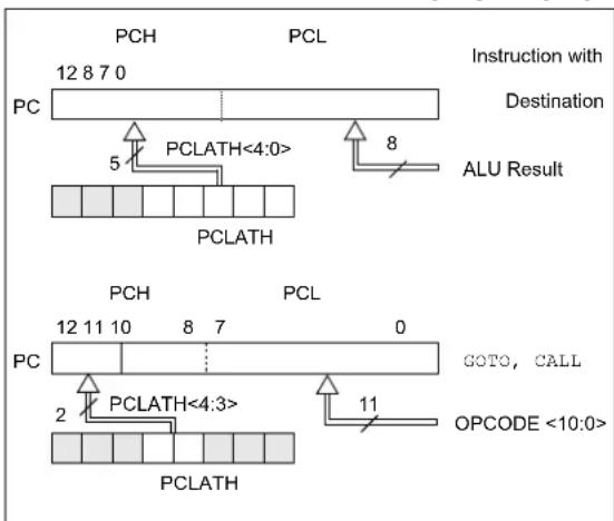
11.4.1 MODIFYING PCL REGISTER
Executing any instruction with the PCL register as the destination simultaneously causes the Program Counter PC<12:8> bits (PCH) to be replaced by the contents of the PCLATH register. This allows the entire contents of the program counter to be changed by writing the desired upper five bits to the PCLATH register. When the lower eight bits are written to the PCL register, all 13 bits of the program counter will change to the values contained in the PCLATH register and those being written to the PCL register.
11.4.2 COMPUTED GOTO
A computed GOTO is accomplished by adding an offset to the program counter (ADDWF PCL). Care should be exercised when jumping into a look-up table or program branch table (computed GOTO) by modifying the PCL register. Assuming that PCLATH is set to the table start address, if the table length is greater than 255 instructions or if the lower eight bits of the memory address roll over from 0xFFh to 0X00h in the middle of the table, then PCLATH must be incremented for each address rollover that occurs between the table beginning and the table location within the table.
For more information, refer to Application Note AN556, "Implementing a Table Read" (DS00000556).
11.4.3 COMPUTED FUNCTION CALLS
A computed function CALL allows programs to maintain tables of functions and provide another way to execute state machines or look-up tables. When performing a table-read using a computed function CALL, care should be exercised if the table location crosses a PCL memory boundary (each 256-byte block).
If using the CALL instruction, the PCH<2:0> and PCL registers are loaded with the operand of the CALL instruction. PCH<4:3> is loaded with PCLATH<4:3>.
11.4.4 STACK
The MCP19116/7 devices have an 8-level x 13-bit wide hardware stack (refer to Figure 11-1). The stack space is not part of either program or data space and the Stack Pointer is not readable or writable. The PC is PUSHed onto the stack when a CALL instruction is executed or an interrupt causes a branch. The stack is POPed in the event of a RETURN, RETLW or a RETFIE instruction execution. PCLATH is not affected by a PUSH or POP operation.
The stack operates as a circular buffer. This means that after the stack has been PUSHed eight times, the 9^th push overwrites the value that was stored from the first push. The tenth push overwrites the second push (and so on).
Note 1: There are no Status bits to indicate Stack Overflow or Stack Underflow conditions.
2: There are no instructions/mnemonics called PUSH or POP. These are actions that occur from the execution of the CALL, RETURN, RETLW and RETFIE instructions or the vectoring to an interrupt address.
11.5 Indirect Addressing, INDF and FSR Registers
The INDF register is not a physical register. Addressing the INDF register will cause indirect addressing.
Indirect addressing is possible by using the INDF register (see Table 11-1). Any instruction using the INDF register actually accesses data pointed to by the File Select Register (FSR). Reading INDF itself indirectly will produce 00h. Writing to the INDF register directly results in a NO OPERATION (NOP) (although Status bits may be affected). An effective 9-bit address is obtained by concatenating the 8-bit FSR and the IRP bit in the STATUS register, as shown in Figure 11-4.
A simple program to clear RAM location 40h-7Fh using indirect addressing is shown in Example 11-3.
EXAMPLE 11-3: INDIRECT ADDRESSING
MOVLW 0x40 ;initialize pointer
MOVWF FSR ;to RAM
NEXT CLRF INDF ;clear INDF register
INCF FSR ;inc pointer
BTFSS FSR,7 ;all done?
GOTO NEXT ;no clear next
CONTINUE ;yes continue
FIGURE 11-4: DIRECT/INDIRECT ADDRESSING
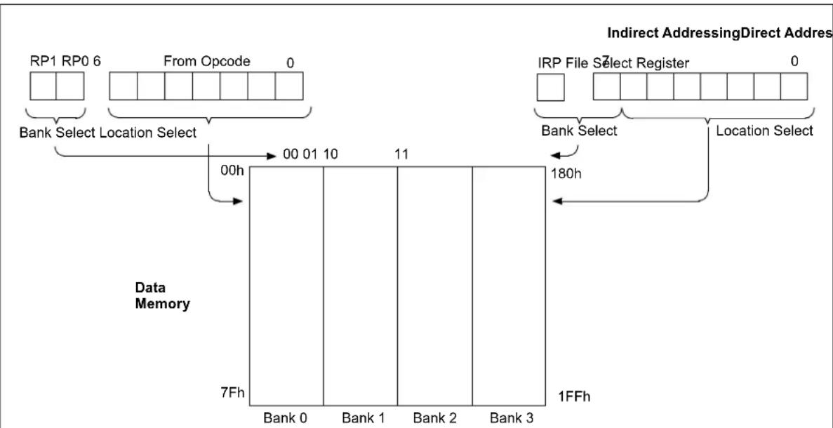
flowchart
graph TD
    A["RP1 RP0 6"] --> B["Bank Select Location Select"]
    C["From Opcode 0"] --> B
    B --> D["00h"]
    D --> E["00 01 10"]
    E --> F["11"]
    F --> G["180h"]
    G --> H["Location Select"]
    I["IRP File Select Register 0"] --> J["Bank Select"]
    K["Data Memory"] --> L["7Fh"]
    L --> M["Bank 0"]
    L --> N["Bank 1"]
    L --> O["Bank 2"]
    L --> P["Bank 3"]
    Q["Indirect AddressingDirect Address"] --> R["1FFh"]
For memory map detail, refer to Figure 11-2.
12.0 DEVICE CONFIGURATION
Device Configuration consists of Configuration Word, Code Protection and Device ID.
12.1 Configuration Word
There are several Configuration Word bits that allow different timers to be enabled and memory protection options. These are implemented as Configuration Word at 2007h.
Note: The DBGEN bit in Configuration Word is managed automatically by device development tools, including debuggers and programmers. For normal device operation, this bit should be maintained as a '1'. Debug is available only on the MCP19117.
REGISTER 12-1: CONFIG: CONFIGURATION WORD
| R/P-1 U-1 R/P-1 R/P-1 U-1 R/P-1 | |||||
| DBGEN | — | WRT1 | WRT0 | — | BOREN (1) |
| bit 13 bit 8 | |||||
| U-1 | R/P-1 | R/P-1 | R/P-1 | R/P-1 | U-1 | U-1 | U-1 |
| — | MCLRE | ^(1) | WDTE — | — | — | ||
| bit 7 bit 0 | |||||||
Legend:
| R = Readable bit | W = Writable bit | U = Unimplemented bit, read as '1' |
| -n = Value at POR | '1' = Bit is set | '0' = Bit is cleared x = Bit is unknown |
bit 13 DBGEN: ICD Debug bit
1 = ICD debug mode disabled
0 = ICD debug mode enabled
bit 12 Unimplemented: Read as '0'
bit 11-10 WRT<1:0>: Flash Program Memory Self-Write Enable bit
11 = Write protection off
10 = 000h to 7FFh write protected, 800h to 1FFFh may be modified by PMCON1 control
01 = 000h to FFFh write protected, 1000h to 1FFFh may be modified by PMCON1 control
00 = 000h to 1FFFh write protected, entire program memory is write protected.
bit 9 Unimplemented: Read as '1'
bit 8 BOREN: Brown-out Reset Enable bit (1)
1 = BOR disabled during Sleep and Enabled during operation
0 = BOR disabled
bit 7 Unimplemented: Read as '1'
bit 6 CP: Code Protection
1 = Program memory is not code protected
0 = Program memory is external read and write protected
bit 5 MCLRE: MCLR Pin Function Select
1 = MCLR pin is MCLR function and weak internal pull-up is enabled
0 = MCLR pin is alternate function, MCLR function is internally disabled
bit 4 PWRTE: Power-Up Timer Enable bit ^(1)
1 = PWRT disabled
0 = PWRT enabled
bit 3 WDTE: Watchdog Timer Enable bit
1 = WDT enabled
0 = WDT disabled
bit 2-0 Unimplemented: Read as '1'
Note 1: Enabling Brown-out Reset does not automatically enable the Power-up Timer.
12.2 Code Protection
Code protection allows the device to be protected from unauthorized access. Internal access to the program memory is unaffected by any code protection setting.
12.2.1 PROGRAM MEMORY PROTECTION
The entire program memory space is protected from external reads and writes by the CP bit in the Configuration Word. When = 0 , external reads and writes of program memory are inhibited and a read will return all '0's. The CPU can continue to read program memory, regardless of the protection bit settings. Writing the program memory is dependent upon the write protection setting. Refer to Section 12.3 "Write Protection" for more information.
12.3 Write Protection
Write protection allows the device to be protected from unintended self-writes. Applications, such as boot loader software, can be protected while allowing other regions of the program memory to be modified.
The WRT<1:0> bits in the Configuration Word define the size of the program memory block that is protected.
12.4 ID Locations
Four memory locations (2000h-2003h) are designated as ID locations where the user can store checksum or other code identification numbers. These locations are not accessible during normal execution but are readable and writable during Program/Verify mode. Only the Least Significant 7 bits of the ID locations are reported when using MPLAB Integrated Development Environment (IDE).
13.0 OSCILLATOR MODES
The MCP19116/7 devices have one oscillator configuration which is an 8 MHz internal oscillator.
13.1 Internal Oscillator (INTOSC)
The Internal Oscillator module provides a system clock source of 8 MHz. The frequency of the internal oscillator can be trimmed with a calibration value in the OSCTUNE register.
13.2 Oscillator Calibration
The 8 MHz internal oscillator is factory-calibrated. The factory calibration values reside in the read-only CALWD6 register. These values must be read from the CALWD6 register and stored in the OSCCAL register. Refer to Section 18.0 "Flash Program Memory Control" for the procedure on reading the program memory.
Note: The FCAL<6:0> bits in the CALWD6 register must be written into the OSCCAL register to calibrate the internal oscillator.
13.3 Frequency Tuning in User Mode
In addition to the factory calibration, the base frequency can be tuned in the user's application. This frequency tuning capability allows the user to deviate from the factory-calibrated frequency. The user can tune the frequency by writing to the OSCTUNE register (refer to Register 13-1).
REGISTER 13-1: OSCTUNE: OSCILLATOR TUNING REGISTER
| U-0 | U-0 | U-0 | R/W-0 | R/W-0 | R/W-0 | R/W-0 |
| — | — | — | TUN4 | TUN3 | TUN2 | TUN1 |
| bit 7 bit 0 | ||||||
R/W-0
| Legend: | |||
| R = Readable bit | W = Writable bit | U = Unimplemented bit, read as ‘0’ | |
| -n = Value at POR | ‘1’ = Bit is set | ‘0’ = Bit is cleared | x = Bit is unknown |
bit 7-5 Unimplemented: Read as '0'
bit 4-0 TUN<4:0>: Frequency Tuning bits
01111 = Maximum frequency
01110 = Maximum frequency
.
.
.
00001 =
00000 = Center frequency. Oscillator Module is running at the calibrated frequency.
11111 =
.
.
•
10000 = Minimum frequency
13.3.1 OSCILLATOR DELAY UPON
POWER-UP, WAKE-UP AND BASE FREQUENCY CHANGE
In applications where the OSCTUNE register is used to shift the frequency of the internal oscillator, it is recommended that the application does not expect the frequency of the internal oscillator to stabilize immediately. In this case, the frequency may shift gradually toward the new value. The time for this frequency shift is less than eight cycles of the base frequency.
On power-up, the device is held in reset by the power-up time if the power-up timer is enabled.
Following a wake-up from Sleep mode or POR, an internal delay of 10 s is invoked to allow the memory bias to stabilize before program execution can begin.
TABLE 13-1: SUMMARY OF REGISTERS ASSOCIATED WITH CLOCK SOURCES
| Name Bit | 7 Bit 6 Bit | 5 Bit 4 Bit | 3 Bit 2 Bit | 1 Bit 0 | Register on page | ||||
| OSCTUNE | — | — | — | TUN4 | TUN3 | TUN2 | TUN1 | TUN0 | 95 |
Legend: — = Unimplemented locations, read as '0'. Shaded cells are not used by clock sources.
TABLE 13-2: SUMMARY OF CONFIGURATION WORD ASSOCIATED WITH CLOCK SOURCES
| Name | Bits | Bit -/7 | Bit -/6 | Bit 13/5 | Bit 12/4 | Bit 11/3 | Bit 10/2 | Bit 9/1 | Bit 8/0 | Register on page |
| CONFIG6 | 13:8 | — | — | — | — | — | — | — | — | 62 |
| 7:0 | — | FCAL6 | FCAL5 | FCAL4 | FCAL3 | FCAL2 | FCAL1 | FCAL0 |
Legend: — = Unimplemented locations, read as '0'. Shaded cells are not used by clock sources.
14.0 RESETS
The reset logic is used to place the MCP19116/7 into a known state. The source of the reset can be determined by using the device status bits.
There are multiple ways to reset the MCP19116/7 devices:
• Power-on Reset (POR)
• Overtemperature Reset (OT)
• M C IRet
• WDT Reset
- Brown-out Reset (BOR)
To a low w_DD to stabilize, an optional power-up timer can be enabled to extend the Reset time after a POR event.
Some registers are not affected in any Reset condition; their status is unknown on POR and unchanged in any other Reset. Most other registers are reset to a "Reset state" on:
- Power-on Reset
• M C IRet
• M C L R Reset during Sleep - WDT Reset
- Brown-out Reset
WDT (Watchdog Timer) wake-up does not cause register resets in the same manner as a WDT Reset, since wake-up is viewed as the resumption of normal operation.
TO and PD bits are set or cleared differently in different Reset situations, as indicated in Table 14-1. The software can use these bits to determine the nature of the Reset. Refer to Table 14-2 for a full description of Reset states of all registers.
A simplified block diagram of the On-Chip Reset Circuit is shown in Figure 14-1.
The MCLR Reset path has a noise filter to detect and ignore small pulses. Refer to Section 5.0 “Digital Electrical Characteristics” for pulse-width specifications.
FIGURE 14-1: SIMPLIFIED BLOCK DIAGRAM OF ON-CHIP RESET CIRCUIT
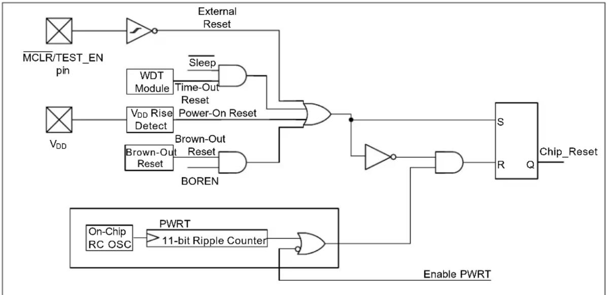
flowchart
graph TD
    A["MCLR/TEST_EN pin"] --> B["NOT"]
    B --> C["External Reset"]
    D["V_DD"] --> E["WDT Module"]
    E --> F["Time-Out Reset"]
    F --> G["Power-On Reset"]
    G --> H["AND Gate"]
    I["V_DD Rise Detect"] --> J["Brown-Out Reset"]
    J --> K["Reset"]
    L["BOREN"] --> M["AND Gate"]
    M --> N["OR Gate"]
    O["On-Chip RC OSC"] --> P["PWRT 11-bit Ripple Counter"]
    P --> Q["AND Gate"]
    R["Enable PWRT"] --> S["AND Gate"]
    T["External Reset"] --> U["AND Gate"]
    V["Sleep"] --> W["AND Gate"]
    X["Power-On Reset"] --> Y["AND Gate"]
    Z["Reset"] --> AA["AND Gate"]
    AB["S Chip_Reset"] --> AC["R Q"]
    AD["Enable PWRT"] --> AE["AND Gate"]
TABLE 14-1: TIME-OUT IN VARIOUS SITUATIONS
| Power-Up | Wake-Up from Sleep | |
| = 0 | = 1 | |
| T_PWRT | — | — |
TABLE 14-2: STATUS/PCON BITS AND THEIR SIGNIFICANCE
| Condition | ||||
| 0 | x | 1 | 1 | Power-on Reset |
| u | 0 | 1 | 1 | Brown-out Reset |
| u | u | 0 | u | WDT Reset |
| u | u | 0 | 0 | WDT Wake-Up |
| u | u | u | u | MORset during normal operation |
| u | u | 1 | 0 | MORset during Sleep |
Legend: u = unchanged, x = unknown
14.1 Power-on Reset (POR)
The on-chip POR circuit holds the chip in Reset until V_DD has reached a high enough level for proper operation. To take advantage of the POR, simply connect the MCLR pin through a resistor to V_DD . This will eliminate external RC components usually needed to create Power-on Reset.
When the device starts normal operation (exits the Reset condition), device operating parameters (i.e., voltage, frequency, temperature, etc.) must be met to ensure proper operation. If these conditions are not met, the device must be held in Reset until the operating conditions are met.
14.2 MCLR
MCP19116/7 devices have a noise filter in the MCLR Reset path. The filter will detect and ignore small pulses.
It should be noted that a WDT Reset does not drive MCLR pin low.
Voltages applied to the MCLR pin that exceed its specification can result in both MCLR Resets and excessive current beyond the device specification during the ESD event. For this reason, Microchip recommends that the MCLR pin no longer be tied directly to V_DD . The use of a Resistor-Capacitor (RC) network, as shown in Figure 14-2, is recommended.
An internal option is enabled by clearing the MCLRE bit in the CONFIG register. When MCLRE = 0, the Reset signal to the chip is generated internally. When MCLRE = 1, the pin becomes an external Reset input. In this mode, the pin has a weak pull-up to V_DD .
FIGURE 14-2: RECOMMENDED MCLR CIRCUIT
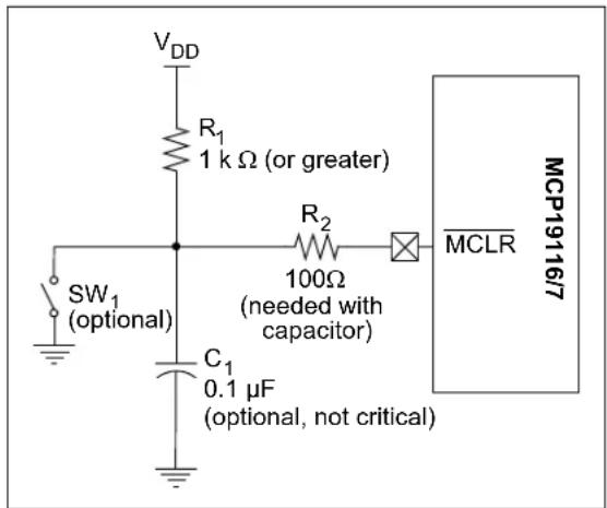
14.3 Brown-Out Reset (BOR)
The BOREN bit <8> in the CONFIG register enables or disables the BOR mode, as defined in the CONFIG register. A brown-out occurs when V_DD falls below V_BOR for greater than 100 s minimum. On any Reset (Power-on, Brown-out, Watchdog Timer, etc.), the chip will remain in Reset until V_DD rises above V_BOR (refer to Figure 14-3). If enabled, the Power-Up Timer will be invoked by the Reset and will keep the chip in Reset for an additional 64 ms. During power-up, it is recommended that the BOR configuration bit is enabled holding the MCU in Reset (OSC turned off and no code execution) until V_DD exceeds the V_BOR threshold. Users have the option of adding an additional 64 ms delay by clearing the PWRTE bit. At this time, the V_DD voltage level is high enough to operate the MCU functions only; all other device functionality is not operational. This is independent of the value of V_IN , which is typically V_DD + V_DROPOUT . During power-down with BOR enabled, the MCU operation will be held in Reset when V_DD falls below the V_BOR threshold. With BOR disabled or while operating in Sleep mode, the POR will hold the part in Reset when V_DD falls below the V_POR threshold.
Note: The Power-Up Timer is enabled by the PWRTE bit in the CONFIG register. If V_DD drops below V_BOR while the Power-Up Timer is running, the chip will go back into a Brown-out Reset and the Power-Up Timer will be re-initialized. Once the V_DD rises above V_BOR , the Power-Up Timer will execute a 64 ms reset.
FIGURE 14-3: BROWN-OUT SITUATIONS
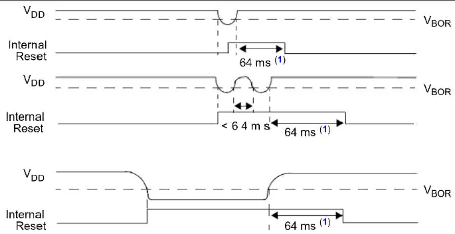
Note 1: 64 ms delay only if PWRTE bit is programmed to '0'.
14.4 Power-Up Timer (PWRT)
The Power-Up Timer provides a fixed 64 ms (nominal) time-out on power-up only, from POR Reset. The Power-Up Timer operates from an internal RC oscillator. The chip is kept in Reset as long as PWRT is active. The PWRT delay allows the V_DD to rise to an acceptable level. A bit (PWRTE) in the CONFIG register can disable (if set) or enable (if cleared or programmed) the Power-Up Timer.
The Power-Up Timer delay varies from chip to chip due to:
- V_DD variation
• Temperature variation - Process variation
Note: Voltage spikes below A GND at the MCLR pin, inducing currents greater than 80 mA, may cause latch-up. Thus, a series resistor of 50-100Ω should be used when applying a "low" level to the MCLR pin, rather than pulling this pin directly to A GND .
The Power-Up Timer optionally delays device execution after a POR event. This timer is typically used to allow V_DD to stabilize before allowing the device to start running.
The Power-Up Timer is controlled by the PWRTE bit in the CONFIG register.
14.5 Watchdog Timer (WDT) Reset
The Watchdog Timer generates a Reset if the firmware does not issue a CLRWDT instruction within the time-out period. The TO and PD bits in the STATUS register are changed to indicate the WDT Reset. Refer to Section 17.0 "Watchdog Timer (WDT)" for more information.
14.6 Start-Up Sequence
Upon the release of a POR, the following must occur before the device begins executing:
- Power-Up Timer runs to completion (if enabled)
- Oscillator start-up timer runs to completion
• M C ImuRst be released (if enabled)
The total time out will vary based on PWRTE bit status. For example, with PWRTE bit erased (PWRT disabled), there will be no time out at all. Figures 14-4, 14-5 and 14-6 represent time-out sequences.
Since the time-outs occur from the POR pulse, if MCLR is kept low long enough, the time-outs will expire. Then, bringing MCLR high begins execution immediately (refer to Figure 14-5). This is useful for testing purposes or to synchronize more than one MCP19116/7 device operating in parallel.
14.6.1 POWER CONTROL (PCON) REGISTER
The Power Control (PCON) register (address 8Eh) has two Status bits to indicate what type of Reset occurred last.
FIGURE 14-4: TIME-OUT SEQUENCE ON POWER-UP (DELAYED MCLR): CASE 1
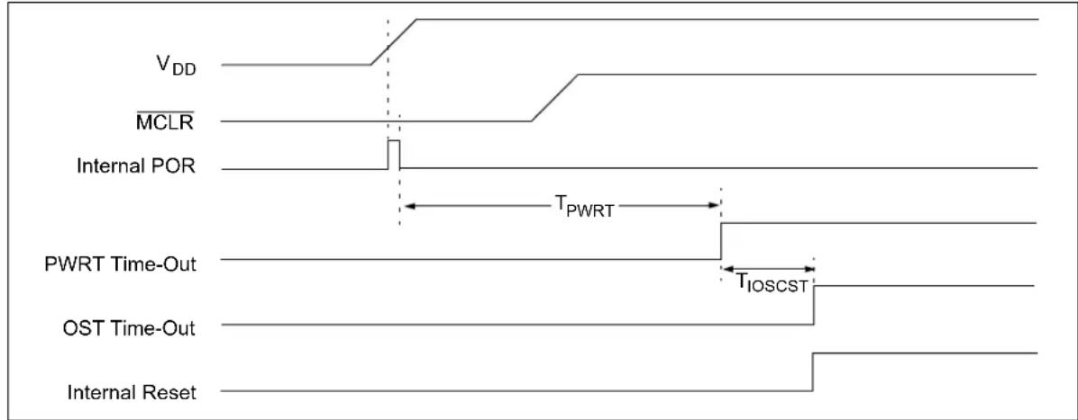
FIGURE 14-5: TIME-OUT SEQUENCE ON POWER-UP (DELAYED MCLR): CASE 2
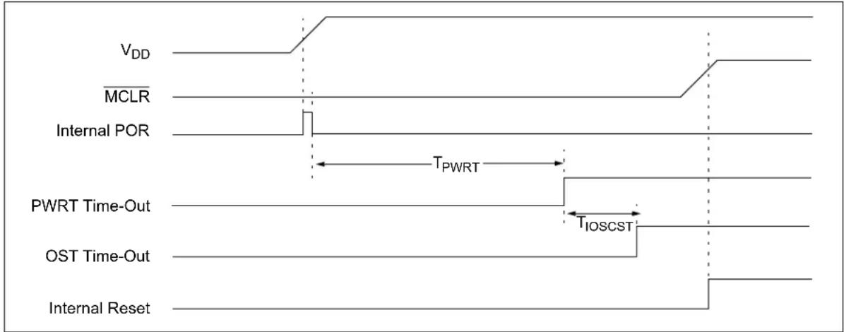
FIGURE 14-6: TIME-OUT SEQUENCE ON POWER-UP (MCLR WITH V _DD )
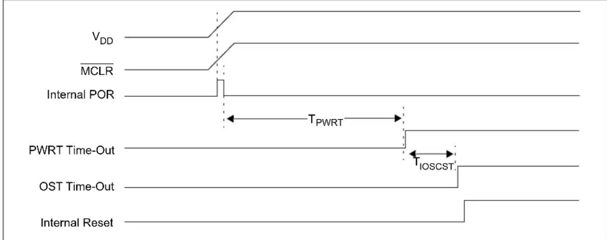
14.7 Determining the Cause of a Reset
Upon any Reset, multiple bits in the STATUS and PCON register are updated to indicate the cause of the Reset. Tables 14-3 and 14-4 show the Reset conditions of these registers.
TABLE 14-3: RESET STATUS BITS AND THEIR SIGNIFICANCE
| Condition | ||||
| 0 | x | 1 | 1 | Power-on Reset |
| u | 0 | 1 | 1 | Brown-out Reset |
| u | u | 0 | u | WDT Reset |
| u | u | 0 | 0 | WDT Wake-Up from Sleep |
| u | u | 1 | 0 | Interrupt Wake-Up from Sleep |
| u | u | u | u | during normal operation |
| u | u | 1 | 0 | during Sleep |
| 0 | u | 0 | x | Not allowed. is set on POR. |
| 0 | u | x | 0 | Not allowed. is set on POR. |
TABLE 14-4: RESET CONDITION FOR SPECIAL REGISTERS
(1)
| Condition | Program Counter | STATUS Register | PCON Register |
| Power-on Reset 0000h 0001 1xxx ---- --0u | |||
| Brown-out Reset 0000 0001 1xxx ---- --u0 | |||
| Reset during normal operation | 0000h | 000u uuuu | ---- --uu |
| Reset during Sleep 0000h 0001 0uuu ---- --uu | |||
| WDT Reset 0000h 0000 uuuu ---- --uu | |||
| WDT Wake-Up from Sleep | PC + 1 | uuu0 0uuu | ---- --uu |
| Interrupt Wake-Up from Sleep | PC + 1^(2) | uuu1 0uuu ---- --uu | |
Legend: u = unchanged, x = unknown, - = unimplemented bit, reads as '0'.
Note 1: If a Status bit is not implemented, that bit will be read as '0'.
2: When the wake-up is due to an interrupt and Global Enable bit (GIE) is set, the return address is pushed on the stack and PC is loaded with the interrupt vector (0004h) after execution of PC + 1.
14.8 Power Control (PCON) Register
The Power Control (PCON) register contains flag bits to differentiate between a:
• Power-on Reset (POR)
- Brown-out Reset (BOR)
The PCON register bits are shown in Register 14-1.
REGISTER 14-1: PCON: POWER CONTROL REGISTER
| R-0 | U-0 | U-0 | U-0 | R/W-0 | R-0 | R/W-0 | R/W-0 |
| ADC_REFR | — | — | — | VDDOK | |||
| bit 7 bit 0 | |||||||
| Legend: | |||
| R = Readable bit | W = Writable bit | U = Unimplemented bit, read as '0' | |
| -n = Value at POR | '1' = Bit is set | '0' = Bit is cleared | x = Bit is unknown |
bit 7 ADC_REFR: V_DD > AV_DD Status bit that shows if the ADC Reference is present at the ADC
1 = V_DD is greater than AV_DD and the ADC Reference is present at the ADC
0 = V_DD is not greater than AV_DD and the ADC Reference is not present at the ADC
bit 6-4 Unimplemented: Read as '0'
bit 3 VDDFLAG: VDDOK history status bit
1 = V_DD LDO has not dropped out of regulation (VDDOK has not gone low since this bit was last set)
0 = V_DD LDO has dropped out of regulation at some time since this bit was last set. Must be set by firmware when VDDOK=1
bit 2 VDDOK: V_DD Status bit
1 = V_DD is in regulation
0 = V_DD is not in regulation
bit 1 POR: Power-on Reset Status bit
1 = No Power-on Reset occurred
0 = A Power-on Reset occurred (must be set in software after a Power-on Reset occurs)
bit 0 BOR: Brown-out Reset
1 = No Brown-out Reset occurred
0 = A Brown-out Reset occurred (must be set in software after a Brown-out Reset occurs)
TABLE 14-5: SUMMARY OF REGISTERS ASSOCIATED WITH RESETS
| Name Bit | 7 Bit 6 Bit | 5 Bit 4 Bit | 3 Bit 2 Bit 1 | Bit 0 | Register on page | ||||
| PCON | — — — | — — — — | P | O | R | BOR 102 | — | — | |
| STATUS IPR | RP1 | RP0 | TO | — | Z | DC | C | 83 |
Legend: — = unimplemented bit, read as '0'. Shaded cells are not used by Resets.
Note: Other (non power-up) Resets include MCLR Reset and Watchdog Timer Reset during normal operation.
NOTES:
15.0 INTERRUPTS
The MCP19116/7 devices have multiple sources of interrupt:
• External Interrupt (INT pin)
- Interrupt-on-Change (IOC) Interrupts
- Timer0 Overflow Interrupt
- Timer1 Overflow Interrupt
- Timer2 Match Interrupt
- ADC Interrupt
- System Input Undervoltage Error
- System Input Overvoltage Error
• SSP
• BCL
- USART TX Interrupt
- USART RC Interrupt
• Desaturation Detection
- Gate Drive UVLO
- Capture/Compare 1
- Capture/Compare 2
- Overtemperature
The Interrupt Control (INTCON) register and the Peripheral Interrupt Request (PIRx) registers record individual interrupt requests in flag bits. The INTCON register also has individual and global interrupt enable bits.
The Global Interrupt Enable bit (GIE) in the INTCON register enables (if set) all unmasked interrupts or disables (if cleared) all interrupts. Individual interrupts can be disabled through their corresponding enable bits in the INTCON register and PIEx registers. GIE is cleared on Reset.
When an interrupt is serviced, the following actions occur automatically:
- The GIE is cleared to disable any further interrupt
- The return address is pushed onto the stack
• The PC is loaded with 0004h
The firmware within the Interrupt Service Routine (ISR) should determine the source of the interrupt by polling the interrupt flag bits. The interrupt flag bits must be cleared before exiting the ISR to avoid repeated interrupts. Because the GIE bit is cleared, any interrupt that occurs while executing the ISR is recorded through its interrupt flag but does not cause the processor to redirect to the interrupt vector.
Note 1: Individual interrupt flag bits are set, regardless of the status of their corresponding mask bit or the GIE bit.
2: When an instruction that clears the GIE bit is executed, any interrupts that were pending for execution in the next cycle are ignored. The interrupts which were ignored are still pending to be serviced when the GIE bit is set again.
The RETFIE instruction exits the ISR by popping the previous address from the stack, restoring the saved context from the shadow registers and setting the GIE bit.
For additional information on a specific interrupt operation, refer to its peripheral chapter.
15.1 Interrupt Latency
For external interrupt events, such as the INT pin or PORTGPx change interrupt, the interrupt latency will be three or four instruction cycles. The exact latency depends upon when the interrupt event occurs (refer to Figure 15-2). The latency is the same for one- or two-cycle instructions.
15.2 GPA2/INT Interrupt
The external interrupt on the GPA2/INT pin is edge-triggered, either on the rising edge if the INTEDG bit in the OPTION_REG register is set, or the falling edge if the INTEDG bit is clear. When a valid edge appears on the GPA2/INT pin, the INTF bit in the INTCON register is set. This interrupt can be disabled by clearing the INTE control bit in the INTCON register. The INTF bit must be cleared by software in the Interrupt Service Routine before re-enabling this interrupt. The GPA2/INT interrupt can wake up the processor from Sleep, if the INTE bit was set prior to going into Sleep. Refer to Section 16.0, Power-Down Mode (Sleep) for details on Sleep and Section 16.1 "Wake-Up from Sleep" for timing of wake-up from Sleep through GPA2/INT interrupt.
Note: The ANSEL register must be initialized to configure an analog channel as a digital input. Pins configured as analog inputs will read '0' and cannot generate an interrupt.
FIGURE 15-1: INTERRUPT LOGIC
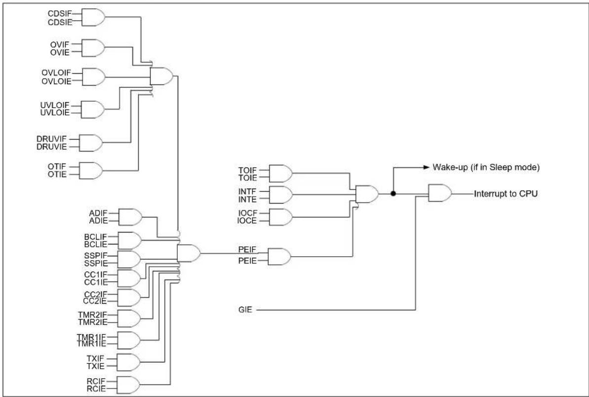
flowchart
graph TD
    A["CDSIF"] --> B["AND"]
    C["CDSIE"] --> B
    D["OVIF"] --> E["OR"]
    F["OVIE"] --> E
    G["OVLOIF"] --> H["AND"]
    I["OVLOIE"] --> H
    J["UVLOIF"] --> K["OR"]
    L["UVLOIE"] --> K
    M["DRUVIF"] --> N["AND"]
    O["DRUVIE"] --> N
    P["OTIF"] --> Q["AND"]
    R["OTIE"] --> Q
    S["ADIF"] --> T["OR"]
    U["ADIE"] --> T
    V["BCLIF"] --> W["AND"]
    X["BCLIE"] --> W
    Y["SSPIF"] --> Z["AND"]
    AA["SSPIE"] --> Z
    AB["CC1IF"] --> AC["AND"]
    AD["CC1IE"] --> AC
    AE["CC2IF"] --> AF["AND"]
    AG["CC2IE"] --> AF
    AH["TMR2IF"] --> AI["AND"]
    AJ["TMR2IE"] --> AI
    AK["TMR1IE"] --> AL["AND"]
    AM["TXIF"] --> AN["AND"]
    AO["TXIE"] --> AP["AND"]
    AQ["RCIF"] --> AR["AND"]
    AS["GIE"] --> AT["OR"]
    AU["PEIF"] --> AV["AND"]
    AW["PEIE"] --> AV
    AX["Wake-up (if in Sleep mode)"] --> AY["AND"]
    AZ["Interrupt to CPU"] --> AY
    AY --> BA["OK"]
    BA --> BB["AND"]
    BC["Wake-up (if in Sleep mode)"] --> BB
    BB --> BD["Interrupt to CPU"]
FIGURE 15-2: INT PIN INTERRUPT TIMING
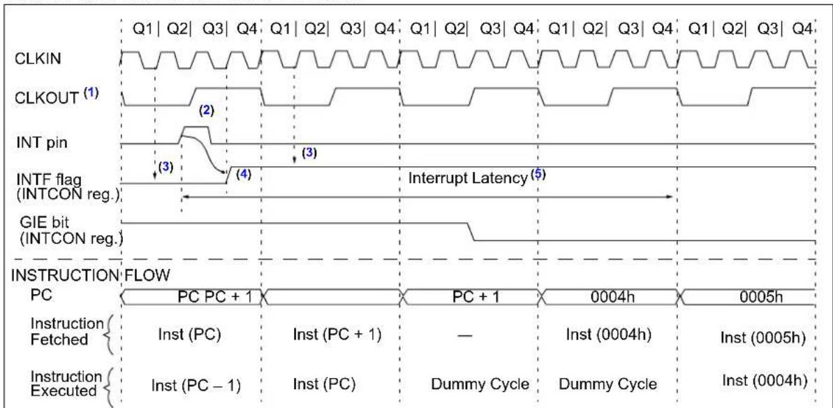
other
| Signal | Q1 | Q2 | Q3 | Q4 | Q1 | Q2 | Q3 | Q4 | Q1 | Q2 | Q3 | Q4 | |-----------------|------|------|------|------|------|------|------|------|------|------|------|------| | CLKIN | | | | | | | | | | | | | | CLKOUT (1) | | | | | | | | | | | | | | INT pin | | | | | | | | | | | | | | INTF flag (INTCON reg.) | | | | | | | | | | | | | | GIE bit (INTCON reg.) | | | | | | | | | | | | | | INTUCTION FLOW | | | | | | | | | | | | | | PC | PC | PC + 1 | | | PC + 1 | | | | 0004h | | | 0005h | | Instruction Fetched ( ) | Inst (PC) | | | Inst (PC + 1) | — | | | | Inst (0004h) | | | Inst (0005h) | | Instruction Executed ( ) | Inst (PC - 1) | | | Inst (PC) | Dummy Cycle | | | | Dummy Cycle | | | Inst (0004h) | | Instr (PC + 1) Instr (PC + 1) Instr (PC) Dummy Cycle Dummy Cycle Inst (0004h) Instr (0005h) Instr (0004h) Instr (0004h) Instr (0004h) Instr (0004h) Instr (0004h) Instr (0004h) Instr (0004h) Instr (0004h) Instr (0004h) Instr (0004h) Instr (0005h) Instr (0005h) Instr (0005h) Instr (0005h) Instr (0005h) Instr (0005h) Instr (0005h) Instr (0005h) Instr (0005h) Instr (001h) Instr (PC - 1) Inst (PC) Dummy Cycle Dummy Cycle Inst (PC) Dummy Cycle Dummy Cycle Inst (PC) Dummy Cycle Dummy Cycle Inst (PC) Dummy Cycle Dummy Cycle Inst (PC) Dummy Cycle Dummy Cycle Inst (PC) Dummy Cycle Dummy Cycle Inst (PC) Dummy Cycle Dummy Cycle Inst (PC) Dummy Cycle Dummy Cycle Inst (PC) Dummy Cycle Dummy Cycle Inst (PC) Dummy Cycle Dummy Cycle Ins(PC - 1) Inst(PC) Dummy Cycle Dummy Cycle Dummy Cycle Dummy Cycle Dummy Cycle Dummy Cycle Dummy Cycle Dummy Cycle Dummy Cycle Dummy Cycle Dummy Cycle Dummy Cycle Dummy Cycle Dummy Cycle Dummy Cycle Dummy Cycle Dummy Cycle Dummy Cycle Dummy Cycle Dummy Cycle Dummy Cycle Dummy Cycle Dummy Cycle Dummy Cycle Dummy Cycle Dummy CycleNote 1: CLKOUT is available only in INTOSC and RC Oscillator modes.
2: For minimum width of INT pulse, refer to AC specifications in Section 5.0, Digital Electrical Characteristics.
3: INTF flag is sampled here (every Q1).
4: INTF is enabled to be set any time during the Q4-Q1 cycles.
5: Asynchronous interrupt latency = 3-4 T_CY . Synchronous latency = 3 T_CY , where T_CY = instruction cycle time. Latency is the same whether Inst (PC) is a single-cycle or a two-cycle instruction.
15.3 Interrupt Control Registers
15.3.1 INTCON REGISTER
The INTCON register is a readable and writable register that contains the various enable and flag bits for the TMR0 register overflow, interrupt-on-change and external INT pin interrupts.
Note: Interrupt flag bits are set when an interrupt condition occurs, regardless of the state of its corresponding enable bit or the Global Enable bit (GIE) in the INTCON register. The user's software should ensure the appropriate interrupt flag bits are clear prior to enabling an interrupt.
REGISTER 15-1: INTCON: INTERRUPT CONTROL REGISTER
| R/W-0 R/W-0 R/W-0 R/W-0 R/W-0 R/W-0 R/W-x | |||||||
| GIE | PEIE | T0IE | INTE | IOCE | T0IF | INTF | IOCF |
| bit 7 bit 0 | |||||||
Legend:
| R = Readable bit | W = Writable bit | U = Unimplemented bit, read as '0' |
| -n = Value at POR | '1' = Bit is set | '0' = Bit is cleared x = Bit is unknown |
bit 7 GIE: Global Interrupt Enable bit
1 = Enables all unmasked interrupts
0 = Disables all interrupts
bit 6 PEIE: Peripheral Interrupt Enable bit
1 = Enables all unmasked peripheral interrupts
0 = Disables all peripheral interrupts
bit 5 T0IE: TMR0 Overflow Interrupt Enable bit
1 = Enables the TMR0 interrupt
0 = Disables the TMR0 interrupt
bit 4 INTE: INT External Interrupt Enable bit
1 = Enables the INT external interrupt
0 = Disables the INT external interrupt
bit 3 IOCE: Interrupt-on-Change Enable bit (1)
1 = Enables the interrupt-on-change
0 = Disables the interrupt-on-change
bit 2 T0IF: TMR0 Overflow Interrupt Flag bit ^(2)
1 = TMR0 register overflowed (must be cleared in software)
0 = TMR0 register did not overflow
bit 1 INTF: External Interrupt Flag bit
1 = The external interrupt occurred (must be cleared in software)
0 = The external interrupt did not occur
bit 0 IOCF: Interrupt-on-Change Interrupt Flag bit
1 = When at least one of the interrupt-on-change pins changed state
0 = None of the interrupt-on-change pins changed state
Note 1: IOCx registers must also be enabled.
2: T0IF bit is set when TMR0 rolls over. TMR0 is unchanged on Reset and should be initialized before clearing T0IF bit.
The PIE1 register contains the Peripheral Interrupt
Enable bits, as shown in Register 15-2.
Note 1: Bit PEIE in the INTCON register must be set to enable any peripheral interrupt.
REGISTER 15-2: PIE1: PERIPHERAL INTERRUPT ENABLE REGISTER 1
| R/W-0 R/W-0 R/W-0 R/W-0 R/W-0 R/W-0 R/W-0 | |||||||
| TXIE | RCIE | BCLIE | SSPIE | CC2IE | CC1IE | TMR2IE | TMR1IE |
| bit 7 bit 0 | |||||||
Legend:
| R = Readable bit | W = Writable bit | U = Unimplemented bit, read as '0' |
| -n = Value at POR | '1' = Bit is set | '0' = Bit is cleared x = Bit is unknown |
bit 7
TXIE: USART Transmit Interrupt Enable bit
1 = Enables the USART transmit interrupt
0 = Disables the USART transmit interrupt
bit 6
RCIE: USART Receive Interrupt Enable bit
1 = Enables the USART receive interrupt
0 = Disables the USART receive interrupt
bit 5
BCLIE: MSSP Bus Collision Interrupt Enable bit
1 = Enables the MSSP Bus Collision Interrupt
0 = Disables the MSSP Bus Collision Interrupt
bit 4
SSPIE: Synchronous Serial Port (MSSP) Interrupt Enable bit
1 = Enables the MSSP interrupt
0 = Disables the MSSP interrupt
bit 3
CC2IE: Capture2/Compare2 Interrupt Enable bit
1 = Enables the Capture2/Compare2 interrupt
0 = Disables the Capture2/Compare2 interrupt
bit 2
CC1IE: Capture1/Compare1 Interrupt Enable bit
1 = Enables the Capture1/Compare1 interrupt
0 = Disables the Capture1/Compare1 interrupt
bit 1
TMR2IE: Timer2 Interrupt Enable
1 = Enables the Timer2 interrupt
0 = Disables the Timer2 interrupt
bit 0
TMR1IE: Timer1 Interrupt Enable
1 = Enables the Timer1 interrupt
0 = Disables the Timer1 interrupt
The PIE2 register contains the Peripheral Interrupt
Enable bits, as shown in Register 15-3.
Note 1: Bit PEIE in the INTCON register must be set to enable any peripheral interrupt.
REGISTER 15-3: PIE2: PERIPHERAL INTERRUPT ENABLE REGISTER 2
| R/W-0 R/W | -0 U-0 R/W-0 R/W-0 R/W-0 R/W-0 R/W-0 | ||||||
| CDSIE ADIE | — | OTIE | OVIE | DRUVIE | OVLOIE | UVLOIE | |
| bit 7 bit 0 | |||||||
Legend:
| R = Readable bit | W = Writable bit | U = Unimplemented bit, read as '0' |
| -n = Value at POR | '1' = Bit is set | '0' = Bit is cleared x = Bit is unknown |
bit 7 CDSIE: Desaturation Detection Interrupt Enable bit
1 = Enables the DESAT Detect interrupt
0 = Disables the DESAT Detect interrupt
bit 6 ADIE: ADC Interrupt Enable bit
1 = Enables the ADC interrupt
0 = Disables the ADC interrupt
bit 5 Unimplemented: Read as '0'
bit 4 OTIE: Overtemperature Interrupt Enable bit
1 = Enables overtemperature interrupt
0 = Disables overtemperature interrupt
bit 3 OVIE: V_OUT Overvoltage Interrupt Enable bit
1 = Enables the OV interrupt
0 = Disables the OV interrupt
bit 2 DRUVIE: Gate Drive Undervoltage Lockout Interrupt Enable bit
1 = Enables Gate Drive UVLO interrupt
0 = Disables Gate Drive UVLO interrupt
bit 1 OVLOIE: V_IN Overvoltage Lockout Interrupt Enable bit
1 = Enables OVLO interrupt
0 = Disables OVLO interrupt
bit 0 UVLOIE: V_IN Undervoltage Lockout Interrupt Enable bit
1 = Enables UVLO interrupt
0 = Disables UVLO interrupt
15.3.1.3 PIR1 Register
The PIR1 register contains the Peripheral Interrupt Flag bits, as shown in Register 15-4.
Note 1: Interrupt flag bits are set when an interrupt condition occurs, regardless of the state of its corresponding enable bit or the Global Enable bit (GIE) in the INTCON register. The user's software should ensure the appropriate interrupt flag bits are clear prior to enabling an interrupt.
REGISTER 15-4: PIR1: PERIPHERAL INTERRUPT FLAG REGISTER 1
| R/W-0 R/W-0 R/W-0 R/W-0 R/W-0 R/W-0 R/W-0 | |||||||
| TXIF | RCIF | BCLIF | SSPIF | CC2IF | CC1IF | TMR2IF | TMR1IF |
| bit 7 bit 0 | |||||||
| Legend: | |||
| R = Readable bit | W = Writable bit | U = Unimplemented bit, read as ‘0’ | |
| -n = Value at POR | ‘1’ = Bit is set | ‘0’ = Bit is cleared | x = Bit is unknown |
bit 7 TXIF: USART Transmit Interrupt Flag bit
1 = The USART transmit buffer is empty (cleared by writing to TXREG)
0 = The USART receive buffer is not full
bit 6 RCIF: USART Receive Interrupt Flag bit
1 = The USART receive buffer is full (cleared by reading RCREG)
0 = The USART receive buffer is not full
bit 5 BCLIF: MSSP Bus Collision Interrupt Flag bit
1 = Interrupt is pending
0 = Interrupt is not pending
bit 4 SSPIF: Synchronous Serial Port (MSSP) Interrupt Flag bit
1 = Interrupt is pending
0 = Interrupt is not pending
bit 3 CC2IF: Capture2/Compare2 Interrupt Flag bit
1 = Capture or Compare has occurred
0 = Capture or Compare has not occurred
bit 2 CC1IF: Capture1/Compare1 Interrupt Flag bit
1 = Capture or Compare has occurred
0 = Capture or Compare has not occurred
bit 1 TMR2IF: Timer2 to PR2 Match Interrupt Flag
1 = Timer2 to PR2 match occurred (must be cleared in software)
0 = Timer2 to PR2 match did not occur
bit 0 TMR1IF: Timer1 Interrupt Flag
1 = Timer1 rolled over (must be cleared in software)
0 = Timer1 did not roll over
15.3.1.4 PIR2 Register
The PIR2 register contains the Peripheral Interrupt Flag bits, as shown in Register 15-5.
Note 1: Interrupt flag bits are set when an interrupt condition occurs, regardless of the state of its corresponding enable bit or the Global Enable bit (GIE) in the INTCON register. The user's software should ensure the appropriate interrupt flag bits are clear prior to enabling an interrupt.
REGISTER 15-5: PIR2: PERIPHERAL INTERRUPT FLAG REGISTER 2
| R/W-0 R/W-0 U-0 R/W-0 R/W-0 R/W-0 R/W-0 R/W-0 | |||||||
| CDSIF | ADIF | — | OTIF | OVIF | DRUVIF | OVLOIF | UVLOIF |
| bit 7 | bit 0 | ||||||
Legend:
| R = Readable bit | W = Writable bit | U = Unimplemented bit, read as '0' |
| -n = Value at POR | '1' = Bit is set | '0' = Bit is cleared x = Bit is unknown |
bit 7 CDSIF: DESAT Detect comparator module interrupt flag bit
1 = An interrupt is pending
0 = An interrupt is not pending
bit 6 ADIF: ADC Interrupt Flag bit
1 = ADC conversion complete
0 = ADC conversion has not completed or has not been started
bit 5 Unimplemented: Read as '0'
bit 4 OTIF: Overtemperature Interrupt Flag bit
1 = Overtemperature event has occurred
0 = Overtemperature event has not occurred
bit 3 OVIF: Overvoltage Interrupt Flag bit
With OVINTP bit set:
1 = A V_OUT Not Overvoltage-to-Overvoltage edge has been detected
0 = A V_OUT Not Overvoltage-to-Overvoltage edge has not been detected With OVINTN bit set:
1 = A V_OUT Overvoltage-to-Not Overvoltage edge has been detected
0 = A V_OUT Overvoltage-to-Not Overvoltage edge has not been detected
bit 2 DRUVIF: Gate Drive Undervoltage Lockout Interrupt Flag bit
1 = Gate Drive Undervoltage Lockout has occurred
0 = Gate Drive Undervoltage Lockout has not occurred
bit 1 OVLOIF: V_IN Overvoltage Lockout Interrupt Flag bit
With OVLOINTP bit set
1 = A V_IN Not Overvoltage-to- V_IN Overvoltage edge has been detected
0 = A V_IN Not Overvoltage-to- V_IN Overvoltage edge has not been detected With OVLOINTN bit set
1 = A V_IN Overvoltage-to- V_IN Not Overvoltage edge has been detected
0 = A V_IN Overvoltage-to-V_IN Not Overvoltage edge has not been detected
bit 0 UVLOIF: V_IN Undervoltage Lockout Interrupt Flag bit
With UVLOINTP bit set:
1 = A V_IN Not Undervoltage-to- V_IN Undervoltage edge has been detected
0 = A V_IN Not Undervoltage-to- V_IN Undervoltage edge has not been detected With UVLOINTN bit set:
1 = A V_IN Undervoltage-to- V_IN Not Undervoltage edge has been detected
0 = A V_IN Undervoltage-to-V_IN Not Undervoltage edge has not been detected
TABLE 15-1: SUMMARY OF REGISTERS ASSOCIATED WITH INTERRUPTS
| Name Bit 7 | Bit 6 Bit 5 | Bit 4 Bit 3 | Bit 2 Bit 1 | Bit 0 | Register on page | ||||
| INTCON | GIE | PEIE | T0IE | INTE | IOCE | T0IF | INTF | IOCF | 107 |
| OPTION_REG | INTEDG | T0CS | T0SE | PSA | PS2 | PS1 | PS0 | 90 | |
| PIE1 | TXIE | RCIE | BCLIE | SSPIE | CC2IE | CC1IE | TMR2IE | TMR1IE | 108 |
| PIE2 | CDSIE | ADIE | — | OTIE | OVIE | DRUVIE | OVLOIE | UVLOIE | 109 |
| PIR1 | TXIF RCIF | BCLIF | SSPIF | — | — | TMR2IF | TMR1IF | 110 | |
| PIR2 | CDSIF | ADIF | — | OTIF | OVIF | DRUVIF | OVLOIF | UVLOIF | 111 |
Legend: — = unimplemented locations, read as '0'. Shaded cells are not used by interrupts.
15.4 Context Saving During Interrupts
During an interrupt, only the return PC value is saved on the stack. Typically, users may wish to save key registers during an interrupt (e.g., W and STATUS registers). This must be implemented in software.
Temporary holding registers W_TEMP and STATUS_TEMP should be placed in the last 16 bytes of GPR. These 16 locations are common to all banks and do not require banking. This makes context save and restore operations simpler. The code shown in Example 15-1 can be used to:
- Store the W register
- Store the STATUS register
- Execute the ISR code
- Restore the Status (and Bank Select Bit) register
- Restore the W register
Note: The MCP19116/7 devices do not require saving the PCLATH. However, if computed GOTOS are used in both the ISR and the main code, the PCLATH must be saved and restored in the ISR.
EXAMPLE 15-1: SAVING STATUS AND W REGISTERS IN RAM
MOVWF W_TEMP ;Copy W to TEMP register
SWAPF STATUS,W ;Swap status to be saved into W
;Swaps are used because they do not affect the status bits
MOVWF STATUS_TEMP ;Save status to bank zero STATUS_TEMP register
:
:(ISR) ;Insert user code here
:
SWAPF STATUS_TEMP,W ;Swap STATUS_TEMP register into W
;(sets bank to original state)
MOVWF STATUS ;Move W into STATUS register
SWAPF W_TEMP,F ;Swap W_TEMP
SWAPF W_TEMP,W ;Swap W_TEMP into W
NOTES:
16.0 POWER-DOWN MODE (SLEEP)
The Power-Down mode is entered by executing a SLEEP instruction.
Upon entering Sleep mode, the following conditions occur:
- WDT is cleared but keeps running, if enabled for operation during Sleep.
- PD bit in the STATUS register is cleared.
- TO bit in the STATUS register is set.
- CPU clock is disabled.
- The ADC is inoperable due to the absence of the 4V LDO power (AV DD ) when the ADC reference is set to AV DD .
- I/O ports maintain the status they had before SLEEP was executed (driving high, low or high-impedance).
- Resets other than WDT and BOR are not affected by Sleep mode.
- Analog Circuit power (AV DD) is removed during Sleep mode.
- To minimize sleep current the ADC Reference must be set to AV_DD (default).
Refer to individual chapters for more details on peripheral operation during Sleep.
To minimize current consumption, the following conditions should be considered:
• I/O pins should not be floating (1)
- External circuitry sinking current from I/O pins
- Internal circuitry sourcing current from I/O pins
- Current draw from pins with internal weak pull-ups
- Modules using Timer1 oscillator
- ADC Reference should be set to the default condition (AV_DD) .
- V_DR will draw a small amount of current from V_DD if V_DD is connected to V_DR externally. To achieve minimum Sleep current, disconnect V_DR from V_DD during Sleep.
Note 1: It is recommended that the I/O pins that are high-impedance inputs be pulled to V_DD or GND externally to avoid switching currents caused by floating inputs.
The SLEEP instruction removes power from the analog circuitry. AV_DD is shut down to minimize current draw in Sleep mode and to maintain a shutdown current of 50 A typical. The 5V LDO ( V_DD ) voltage drops to 2.9V minimum in Sleep mode. External current draw from the 5V LDO ( V_DD ) should be limited to less than 1 mA. Loads drawing more than 1 mA externally during Sleep mode risk loading down the V_DD voltage and tripping POR. A POR event during Sleep mode will wake the device from Sleep. The enable state of the analog circuitry does not change with the execution of the SLEEP instruction.
16.1 Wake-Up from Sleep
The device can wake up from Sleep through one of the following events:
- External Reset input on MCLR pin, if enabled
- POR Reset
- Watchdog Timer, if enabled
- Any external interrupt
- Interrupts by peripherals capable of running during Sleep (see individual peripheral for more information)
The first two events will cause a device reset. The last three events are considered a continuation of program execution. To determine whether a device reset or wake-up event occurred, refer to Section 14.7 "Determining the Cause of a Reset".
The following peripheral interrupts can wake the device from Sleep:
- Interrupt-on-change
- External Interrupt from INT pin
When the SLEEP instruction is being executed, the next instruction (PC + 1) is prefetched. For the device to wake up through an interrupt event, the corresponding interrupt enable bit must be enabled. Wake-up will occur regardless of the state of the GIE bit. If the GIE bit is disabled, the device continues execution at the instruction after the SLEEP instruction. If the GIE bit is enabled, the device executes the instruction after the SLEEP instruction and will then call the Interrupt Service Routine. In cases where the execution of the instruction following SLEEP is not desirable, the user should have a NO OPERATION (NOP) after the SLEEP instruction.
The WDT is cleared when the device wakes up from Sleep, regardless of the source of wake-up.
16.1.1 WAKE-UP USING INTERRUPTS
When global interrupts are disabled (GIE cleared) and any interrupt source has both its interrupt enable bit and interrupt flag bit set, one of the following will occur:
- If the interrupt occurs before the execution of a SLEEP instruction:
- SLEEP instruction will execute as a NOP
- WDT and WDT prescaler are not cleared
- TO bit in the STATUS register are not set
- PD bit in the STATUS register are not cleared
- If the interrupt occurs during or after the execution of a SLEEP instruction:
- SLEEP instruction is completely executed
- Device immediately wakes up from Sleep
- WDT and WDT prescaler are cleared
- TO bit in the STATUS register is set
- D bit in the STATUS register is cleared
Even if the flag bits were checked before executing a SLEEP instruction, it may be possible for flag bits to become set before the SLEEP instruction completes. To determine whether a SLEEP instruction executed, test the bit. If the bit is set, the SLEEP instruction was executed as a NOP.
FIGURE 16-1: WAKE-UP FROM SLEEP THROUGH INTERRUPT
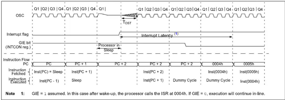
TABLE 16-1: SUMMARY OF REGISTERS ASSOCIATED WITH POWER-DOWN MODE
| Name Bit | 7 Bit 6 Bit | 5 Bit 4 Bit | 3 Bit 2 Bit | 1 Bit 0 | Register on page | ||||
| INTCON | GIE | PEIE | T0IE | INTE | IOCE | T0IF | INTF | IOCF | 107 |
| IOCA | IOCA7 | IOCA6 | IOCA5 | — | IOCA3 | IOCA2 | IOCA1 | IOCA0 | 134 |
| IOCB | IOCB7 | IOCB6 | IOCB5 | IOCB4 | — | — | IOCB1 | IOCB0 | 134 |
| PIE1 | TXIE | RCIE | BCLIE | SSPIE | CC2IE | CC1IE | TMR2IE | TMR1IE | 108 |
| PIE2 | CDSIE | ADIE | — | OTIE | OVIE | DRUVIE | OVLOIE | UVLOIE | 109 |
| PIR1 | TXIF | RCIF | BCLIF | SSPIF | CC2IF | CC1IF | TMR2IF | TMR1IF | 110 |
| PIR2 | CDSIF | ADIF | — | OTIF | OVIF | DRUVIF | OVLOIF | UVLOIF | 111 |
| STATUS | IRP | RP1 | RP0 | Z | DC | C | 83 |
Legend: — = unimplemented, read as '0'. Shaded cells are not used in Power-Down mode.
17.0 WATCHDOG TIMER (WDT)
The Watchdog Timer is a free running timer. The WDT is enabled by setting the WDTE bit in the CONFIG register (default setting).
During normal operation, a WDT time out generates a device reset. If the device is in Sleep mode, a WDT time out causes the device to wake up and continue with normal operation.
The WDT can be permanently disabled by clearing the WDTE bit in the CONFIG register. Refer to Section 12.1 "Configuration Word" for more information.
17.1 Watchdog Timer (WDT) Operation
During normal operation, a WDT time out generates a device reset. If the device is in Sleep mode, a WDT time out causes the device to wake-up and continue with normal operation; this is known as a WDT wake-up. The WDT can be permanently disabled by clearing the WDTE configuration bit.
The postscaler assignment is fully under software control and can be changed during program execution.
17.2 WDT Period
The WDT has a nominal time-out period of 18 ms (with no prescaler). The time-out periods vary with temperature, V_DD and process variations from part to part (refer to Table 5-3). If longer time-out periods are desired, a prescaler with a division ratio of up to 1:128 can be assigned to the WDT under software control by writing to the OPTION_REG register. Thus, time-out periods up to 2.3 seconds can be realized.
The CLRWDT and SLEEP instructions clear the WDT and the prescaler, if assigned to the WDT, and prevent it from timing out and generating a device reset.
The TO bit in the STATUS register will be cleared upon a Watchdog Timer time out.
17.3 WDT Programming Considerations
Under worst-case conditions (i.e., V_DD = Minimum, Temperature = Maximum, Maximum WDT prescaler), it may take several seconds before a WDT time out occurs.
FIGURE 17-1: WATCHDOG TIMER WITH SHARED PRESCALE BLOCK DIAGRAM
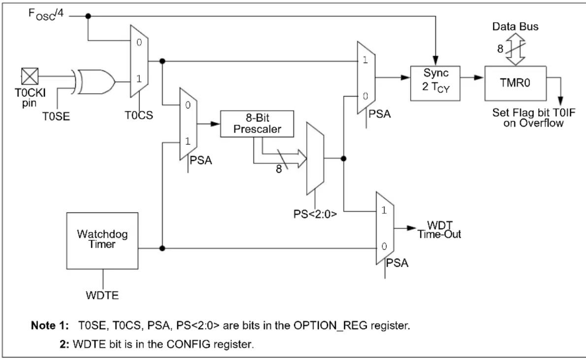
flowchart
graph TD
    A["T0CKI pin"] --> B["AND"]
    B --> C["0/1 T0CS"]
    C --> D["0/1 PSA"]
    D --> E["8-Bit Prescaler"]
    E --> F["PSA"]
    F --> G["1/0 PSA"]
    G --> H["Sync 2 TCY"]
    H --> I["TMR0"]
    I --> J["Set Flag bit T0IF on Overflow"]
    K["Watchdog Timer"] --> L["WDTE"]
    M["Fosc/4"] --> N["0"]
    O["Data Bus"] --> P["8"]
    Q["PSA"] --> R["8 Bit Prescaler"]
    S["PSA"] --> T["PS<2:0>"]
    U["WDT Time-Out"] --> V["1/0 PSA"]
    W["Note 1: T0SE, T0CS, PSA, PS<2:0> are bits in the OPTION_REG register."]
    X["Note 2: WDTE bit is in the CONFIG register."]
TABLE 17-1: WDT STATUS
| Conditions WDT | |
| WDTE = 0 | Cleared |
| CLRWDT Command | |
| Exit Sleep |
TABLE 17-2: SUMMARY OF REGISTERS ASSOCIATED WITH WATCHDOG TIMER
| N a | m | e B | i | t 7 | B | i t | 6 | B i | Register on page 5 |
| OPTION_REG | INTEDG | T0CS | T0SE | PSA | PS2 | PS1 | PS0 | 90 |
Legend: Shaded cells are not used by the Watchdog Timer.
Note 1: Refer to Register 12-1 for operation of all the bits in the CONFIG register.
TABLE 17-3: SUMMARY OF CONFIGURATION WORD ASSOCIATED WITH WATCHDOG TIMER
| Name | Bits | Bit -/7 | Bit -/6 | Bit 13/5 | Bit 12/4 | Bit 11/3 | Bit 10/2 | Bit 9/1 | Bit 8/0 | Register on page |
| CONFIG | 13:8 | — | — | DBGEN | — | WRT1 | WRT0 | — | BOREN | 93 |
| 7:0 | — | MCLRE | WDTE | — | — | — |
Legend: — = unimplemented location, read as '1'. Shaded cells are not used by Watchdog Timer.
18.0 FLASH PROGRAM MEMORY CONTROL
The Flash program memory is readable and writable during normal operation (full V_IN range). This memory is not directly mapped in the register file space. Instead, it is indirectly addressed through the Special Function Registers (refer to Registers 18-1 to 18-5). There are six SFRs used to read and write this memory:
• P M C O N 1
• P M C O N 2
• P M D A T L
• P M D A T H
• PMADRL
• PMADRH
When interfacing the program memory block, the PMDATL and PMDATH registers form a two-byte word which holds the 14-bit data for read/write, while the PMADRL and PMADRH registers form a two-byte word, which holds the 13-bit address of the FLASH location being accessed. These devices have 8000 words of program Flash with an address range from 0000h to 1FFFh.
The program memory allows single-word read and a four-word write. A four-word write automatically erases the row of the location and writes the new data (erase before write).
The write time is controlled by an on-chip timer. The write/erase voltages are generated by an on-chip charge pump rated to operate over the voltage range of the device for byte or word operations.
When the device is code-protected, the CPU may continue to read and write the Flash program memory.
Depending on the settings of the Flash Program Memory Enable (WRT<1:0>) bits, the device may or may not be able to write certain blocks of the program memory; however, reads of the program memory are allowed.
When the Flash Program Memory Code Protection ( ) bit is enabled, the program memory is code-protected and the device programmer (ICSP) cannot access data or program memory.
18.1 PMADRH and PMADRL Registers
The PMADRH and PMADRL registers can address up to a maximum of 8000 words of program memory.
When selecting a program address value, the Most Significant Byte (MSB) of the address is written to the PMADRH register and the Least Significant Byte (LSB) is written to the PMADRL register.
18.2 PMCON1 and PMCON2 Registers
The PMCON1 register is the control register for the data program memory accesses.
Control bits RD and WR initiate read and write, respectively. In software, these bits can only be set, not cleared. They are cleared in hardware at completion of the read or write operation. The inability to clear the WR bit in software prevents the accidental premature termination of a write operation.
The WREN bit, when set, will allow a write operation. On power-up, the WREN bit is clear.
The CALSEL bit allows the user to read locations in test memory in case there are calibration bits stored in the calibration word locations that need to be transferred to SFR trim registers. The CALSEL bit is only for reads. If a write operation is attempted with CALSEL = 1, no write occurs.
PMCON2 is not a physical register. Reading PMCON2 will read all '0's. The PMCON2 register is used exclusively in the flash memory write sequence.
18.3 Flash Program Memory Control Registers
REGISTER 18-1: PMDATL: PROGRAM MEMORY DATA LOW BYTE REGISTER
| R/W-0 R/W-0 R/W-0 R/W-0 R/W-0 R/W-0 R/W-0 R/W-0 |
| PMDATL<7:0> |
| bit 7 bit 0 |
| Legend: | |||
| R = Readable bit W = Writable bit | U = Unimplemented bit, read as ‘0’ | ||
| -n = Value at POR | ‘1’ = Bit is set | ‘0’ = Bit is cleared | x = Bit is unknown |
bit 7-0 PMDATL<7:0>: 8 Least Significant Data bits to write or read from program memory
REGISTER 18-2: PMADRL: PROGRAM MEMORY ADDRESS LOW BYTE REGISTER
| R/W-0 R/W-0 R/W-0 R/W-0 R/W-0 R/W-0 R/W-0 R/W-0 |
| PMADRL<7:0> |
| bit 7 bit 0 |
| Legend: | |||
| R = Readable bit W = Writable bit | U = Unimplemented bit, read as ‘0’ | ||
| -n = Value at POR | ‘1’ = Bit is set | ‘0’ = Bit is cleared | x = Bit is unknown |
bit 7-0 PMADRL<7:0>: 8 Least Significant Address bits for Program Memory Read/Write Operation
REGISTER 18-3: PMDATH: PROGRAM MEMORY DATA HIGH BYTE REGISTER
| U-0 | U-0 | R/W-0 R/W-0 R/W-0 R/W-0 R/W-0 R/W-0 |
| — | — | PMDATH<5:0> |
| bit 7 bit 0 | ||
| Legend: | |||
| R = Readable bit W = Writable bit | U = Unimplemented bit, read as ‘0’ | ||
| -n = Value at POR | ‘1’ = Bit is set | ‘0’ = Bit is cleared | x = Bit is unknown |
bit 7-6 Unimplemented: Read as '0'
bit 5-0 PMDATH<5:0>: 6 Most Significant Data bits from program memory
REGISTER 18-4: PMADRH: PROGRAM MEMORY ADDRESS HIGH BYTE REGISTER
| U-0 U-0 U-0 U-0 R/W-0 R/W-0 R/W-0 R/W-0 | |||
| — — — | — | PMADRH<3:0> | |
| bit 7 bit 0 | |||
Legend:
| R = Readable bit | W = Writable bit | U = Unimplemented bit, read as '0' |
| -n = Value at POR | '1' = Bit is set | '0' = Bit is cleared x = Bit is unknown |
bit 7-4 Unimplemented: Read as '0'
bit 3-0 PMADRH<3:0>: 4 Most Significant Address bits or High bits for program memory reads
REGISTER 18-5: PMCON1: PROGRAM MEMORY CONTROL REGISTER 1
| U-1 | R/W-0 | U-0 | U-0 | U-0 | R/W-0 | R/S-0 | R/S-0 |
| — | CALSEL | — | — | — | WREN | WR | RD |
| bit 7 bit 0 | |||||||
Legend:
| R = Readable bit | W = Writable bit | U = Unimplemented bit, read as '0' |
| -n = Value at POR | '1' = Bit is set | '0' = Bit is cleared x = Bit is unknown |
| S = Bit can only be set |
bit 7 Unimplemented: Read as '1'
bit 6 CALSEL: Program Memory calibration space select bit
1 = Select test memory area for reads only (for loading calibration trim registers)
0 = Select user area for reads
bit 5-3 Unimplemented: Read as '0'
bit 2 WREN: Program Memory Write Enable bit
1 = Allows write cycles
0 = Inhibits write to the EEPROM
bit 1 WR: Write Control bit
1 = Initiates a write cycle to program memory. (The bit is cleared by hardware when write is complete. The WR bit can only be set (not cleared) in software.)
0 = Write cycle to the Flash memory is complete
bit 0 RD: Read Control bit
1 = Initiates a program memory read. (The read takes one cycle. The RD is cleared in hardware; the RD bit can only be set (not cleared) in software.)
0 = Does not initiate a Flash memory read
18.3.1 READING THE FLASH PROGRAM MEMORY
To read a program memory location, the user must write two bytes of the address to the PMADRL and PMADRH registers, and then set control bit RD (bit 0 in the PMCON1register). Once the read control bit is set, the Program Memory Flash controller will use the second instruction cycle to read the data. This causes the second instruction immediately following the BSF PMCON1, RD instruction to be ignored. The data is available, in the very next cycle, in the PMDATL and PMDATH registers; it can be read as two bytes in the following instructions. PMDATL and PMDATH registers will hold this value until another read or until it is written to by the user (during a write operation).
EXAMPLE 18-1: FLASH PROGRAM READ
BANKSELPM_ADR; Change STATUS bits RP1:0 to select bank with PMADR
MOVLWMS_PROG_PM_ADDR;
MOVWFPMADRH; MS Byte of Program Address to read
MOVLWLS_PROG_PM_ADDR;
MOVWFPMADRL; LS Byte of Program Address to read
BANKSELPMCON1; Bank to containing PMCON1
BSF PMCON1, RD; EE Read

NOP ; First instruction after BSF PMCON1, RD executes normally

NOP ; Any instructions here are ignored as program
    ; memory is read in second cycle after BSF PMCON1, RD
    ;
BANKSELPMDATL; Bank to containing PMADRL
MOVFPMDATL, W; W = LS Byte of Program PMDATL
MOVFPMDATH, W; W = MS Byte of Program PMDATL
FIGURE 18-1: FLASH PROGRAM MEMORY READ CYCLE EXECUTION – NORMAL MODE
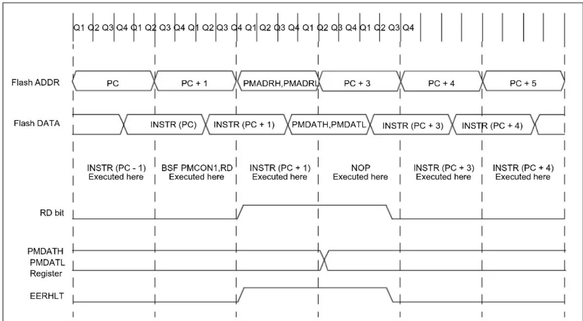
flowchart
graph TD
    subgraph Flash_ADDR
        A["PC"] --> B["PC + 1"]
        B --> C["PMADRH,PMADRL"]
        C --> D["PC + 3"]
        D --> E["PC + 4"]
        E --> F["PC + 5"]
    end
    subgraph Flash_DATA
        G["INSTR (PC)"] --> H["INSTR (PC + 1)"]
        H --> I["PMDATH,PMDATL"]
        I --> J["INSTR (PC + 3)"]
        J --> K["INSTR (PC + 4)"]
    end
    subgraph RD_bit
        L["INSTR (PC - 1) Executed here"] --> M["BSF PMCON1,RD Executed here"] --> N["INSTR (PC + 1) Executed here"] --> O["NOP Executed here"] --> P["INSTR (PC + 3) Executed here"] --> Q["INSTR (PC + 4) Executed here"]
    end
    subgraph PMDATH
        R["Instr"] --> S["Instr (PC + 1)"]
        T["Instr (PC + 1)"]
        U["Instr (PC + 1)"]
        V["Instr (PC + 1)"]
        W["Instr (PC + 1)"]
        X["Instr (PC + 1)"]
        Y["Instr (PC + 1)"]
        Z["Instr (PC + 1)"]
        AA["Instr (PC + 1)"]
        AB["Instr (PC + 1)"]
    end
    subgraph EERHLT
        AC["Instr"] --> AD["Instr (PC + 1)"]
        AE["Instr (PC + 1)"]
        AF["Instr (PC + 1)"]
        AG["Instr (PC + 1)"]
        AH["Instr (PC + 1)"]
        AI["Instr (PC + 1)"]
        AJ["Instr (PC + 1)"]
        AK["Instr (PC + 1)"]
    end
18.3.2 WRITING TO THE FLASH PROGRAM MEMORY
A word of the Flash program memory may only be written to if the word is in an unprotected segment of memory, as defined in Section 12.1 "Configuration Word" (bits
Note: The write-protect bits are used to protect the user's program from modification by the user's code. They have no effect when programming is performed by ICSP. The code-protect bits, when programmed for code protection, will prevent the program memory from being written via the ICSP interface.
Flash program memory must be written in eight-word blocks. Refer to Figures 18-2 and 18-3 for more details.
A block consists of eight words with sequential addresses, with a lower boundary defined by an address, where PMADRL<1:0>=00. All block writes to program memory are done as 16-word erase by eight-word write operations. The write operation is edge-aligned and cannot occur across boundaries.
To write program data, the WREN bit must first be loaded into the buffer registers (refer to Figure 18-2). This is accomplished by first writing the destination address to PMADRL and PMADR H and then writing the data to PMDATL and PMDATH. After the address and data have been set, the following sequence of events must be executed:
-
Write 55h, then AAh, to PMCON2 (Flash programming sequence)
-
Set the WR control bit in the PMCON1 register
All eight buffer register locations should be written to with correct data. If less than eight words are being written to in the block of eight words, a read from the program memory location(s) not being written to must be performed. This takes the data from the program location(s) not being written and loads it into the PMDATL and PMDATH registers. Then the sequence of events to transfer data to the buffer registers must be executed.
To transfer data from the buffer registers to the program memory, the PMADRL and PMADRH must point to the last location in the eight-word block (PMADRL<2:0> = 111). Then the following sequence of events must be executed:
- Write 55h, then AAh, to PMCON2 (Flash programming sequence).
- Set control bit WR in the PMCON1 register to begin the write operation.
The user must follow the same specific sequence to initiate the write for each word in the program block, writing each program word in sequence (000, 001, 010, 011). When the write is performed on the last word (PMADRL<2:0> = 111), a block of sixteen words is automatically erased and the content of the eight-word buffer registers are written into the program memory.
After the BSF PMCON1, WR instruction, the processor requires two cycles to set up the erase/write operation. The user must place two NOP instructions after the WR bit is set. Since data is being written to buffer registers, the writing of the first three words of the block appears to occur immediately. The processor will halt internal operations for the typical 4 ms only during the cycle in which the erase takes place (i.e., the last word of the sixteen-word block erase). This is not Sleep mode, as the clocks and peripherals will continue to run. After the four-word write cycle, the processor will resume operation with the third instruction after the PMCON1 write instruction. The above sequence must be repeated for the higher 12 words.
Note: An erase is only initiated for the write of four words just after a row boundary; or PMCON1
Refer to Figure 18-2 for a block diagram of the buffer registers and the control signals for test mode.
18.3.3 PROTECTION AGAINST SPURIOUS WRITE
There are conditions when the device should not write to the program memory. To protect against spurious writes, various mechanisms have been built in. On power-up, WREN is cleared. Also, the Power-Up Timer (72 ms duration) prevents program memory writes.
The write initiate sequence and the WREN bit help prevent an accidental write during a power glitch or software malfunction.
18.3.4 OPERATION DURING CODE PROTECT
When the device is code-protected, the CPU is able to read and write unscrambled data to the program memory. The test mode access is disabled.
18.3.5 OPERATION DURING WRITE PROTECT
When the program memory is write-protected, the CPU can read and execute from the program memory. The portions of program memory that are write-protected cannot be modified by the CPU using the PMCON registers. The write protection has no effect in ICSP mode.
FIGURE 18-2: BLOCK WRITES TO 8000 FLASH PROGRAM MEMORY
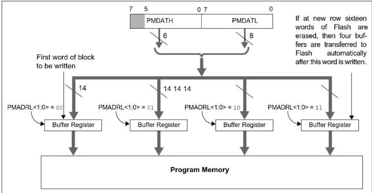
flowchart
graph TD
    A["7 5 0 7 0"] --> B["6"]
    C["PMDATH"] --> D["8"]
    E["PMDATL"] --> D
    D --> F["14"]
    F --> G["Buffer Register"]
    F --> H["Buffer Register"]
    F --> I["Buffer Register"]
    F --> J["Buffer Register"]
    G --> K["Program Memory"]
    H --> K
    I --> K
    J --> K
    K --> L["14 14 14"]
    L --> M["First word of block to be written"]
    M --> N["PMADRL<1:0>=00"]
    M --> O["PMADRL<1:0>=01"]
    M --> P["PMADRL<1:0>=10"]
    M --> Q["PMADRL<1:0>=11"]
    N --> R["Program Memory"]
    O --> R
    P --> R
    Q --> R
FIGURE 18-3: FLASH PROGRAM MEMORY LONG WRITE CYCLE EXECUTION
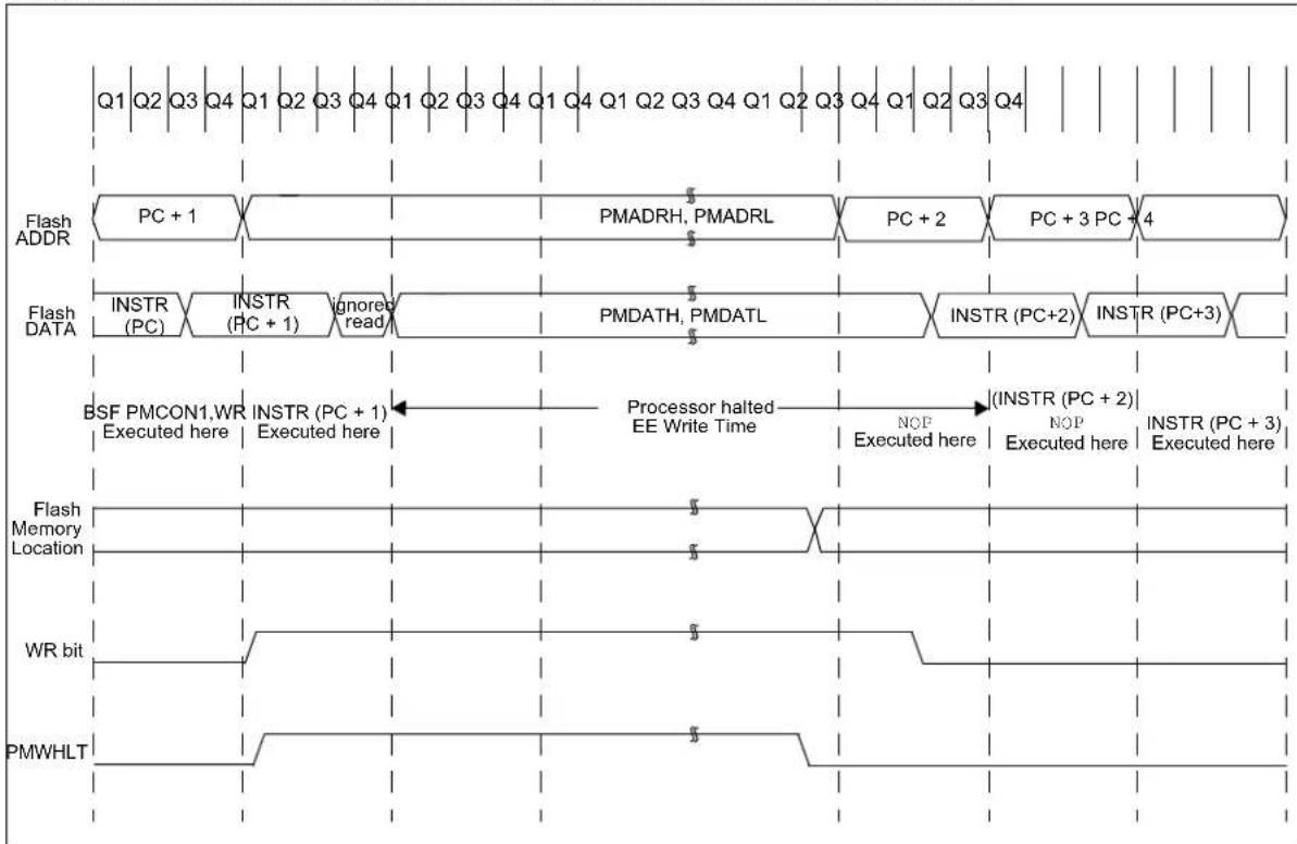
flowchart
graph TD
    A["Flash ADDR"] --> B["PC + 1"]
    B --> C["PMADR H, PMADRL"]
    C --> D["PC + 2"]
    D --> E["PC + 3 PC + 4"]
    F["Flash DATA"] --> G["INSTR (PC)"]
    G --> H["INSTR (PC + 1)"]
    H --> I["ignored read"]
    I --> J["PSMDATH, PMDATL"]
    J --> K["INSTR (PC+2)"]
    K --> L["INSTR (PC+3)"]
    M["BSF PMCON1,WR"] --> N["Executed here"]
    O["INSTR (PC + 1)"] --> P["Executed here"]
    Q["Processor halted EE Write Time"] --> R["NOP Executed here"]
    S["(INSTR (PC + 2)"]] --> T["NOP Executed here"]
    U["INSTR (PC + 3) Executed here"] --> V["Executed here"]
    W["Flash Memory Location"] --> X["5"]
    Y["WR bit"] --> Z["5"]
    AA["PMWHLT"] --> AB["5"]
19.0 I/O PORTS
In general, when a peripheral is enabled, that pin may not be used as a general purpose I/O pin.
Each port has the registers for its operation. These registers are:
• TRISGPx registers (data direction register)
- PORTGPx registers (read the levels on the pins of the device)
Some ports may have one or more of the following additional registers. These registers are:
• ANSELx (analog select)
• WPUGPx (weak pull-up)
Ports with analog functions also have an ANSELx register, which can disable the digital input and save power. A simplified model of a generic I/O port, without the interfaces to other peripherals, is shown in Figure 19-1.
FIGURE 19-1: GENERIC I/O PORTGPX OPERATION
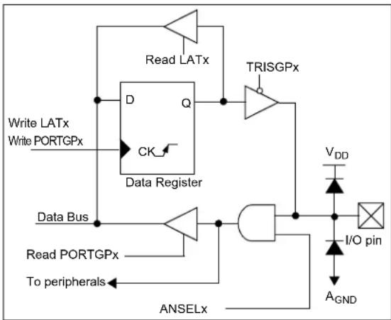
flowchart
graph TD
    A["Write LATx"] --> B["Data Register"]
    C["Write PORTGPx"] --> B
    B --> D["TRISGPx"]
    D --> E["I/O pin"]
    E --> F["AGND"]
    G["Data Bus"] --> H["AND Gate"]
    H --> I["AND Gate"]
    I --> J["AND Gate"]
    J --> K["AND Gate"]
    L["Read PORTGPx"] --> M["AND Gate"]
    M --> N["AND Gate"]
    O["ANSELx"] --> P["AND Gate"]
    P --> Q["AND Gate"]
    R["TRISGPx"] --> S["AND Gate"]
    S --> T["AND Gate"]
    U["TRISGPx"] --> V["AND Gate"]
    W["TRISGPx"] --> X["AND Gate"]
    Y["TRISGPx"] --> Z["AND Gate"]
    AA["TRISGPx"] --> AB["AND Gate"]
    AC["TRISGPx"] --> AD["AND Gate"]
EXAMPLE 19-1: INITIALIZING PORTGPA
; This code example illustrates
; initializing the PORTGPA register. The
; other ports are initialized in the same
; manner.

BANKSEL PORTGPA;
CLRF PORTGPA; Init PORTA
BANKSEL ANSELA;
CLRF ANSELA; digital I/O
BANKSEL TRISGPA;
MOVLW B'00011111'; Set GPA<3:0> as
; inputs
MOVWF TRISGPA; and set GPA<7:5> as
; outputs
19.1 PORTGPA and TRISGPA Registers
PORTGPA is an 8-bit-wide, bidirectional port consisting of five CMOS I/Os, one open-drain I/O and one open-drain input-only pin (GPA4 is not available). The corresponding data direction register is TRISGPA. Setting a TRISGPA bit to 1 makes the corresponding PORTGPA pin an input (i.e., disable the output driver). Clearing a TRISGPA bit set to 0 makes the corresponding PORTGPA pin an output (i.e., enables output driver). The exception is GPA5, which is input only and its TRISGPA bit always reads as '1'. Example 19-1 shows how to initialize an I/O port.
Reading the PORTGPA register reads the status of the pins, whereas writing to it writes to the PORT latch. All write operations are read-modify-write operations.
The TRISGPA register controls the PORTGPA pin output drivers, even when they are being used as analog inputs. The user must ensure the bits in the TRISGPA register are maintained set when using them as analog inputs. I/O pins configured as analog input always read '0'. If the pin is configured for a digital output (either port or alternate function), the TRISGPA bit must be cleared in order for the pin to drive the signal, and a read reflects the state of the pin.
19.1.1 INTERRUPT-ON-CHANGE
Each PORTGPA pin is individually configurable as an interrupt-on-change pin. Control bits IOCB<7:4> and IOCB<2:0> enable or disable the interrupt function for each pin. The interrupt-on-change feature is disabled on a Power-on Reset. Reference Section 20.0 "Interrupt-On-Change" for more information.
19.1.2 WEAK PULL-UPS
PORTGPA <3:0> and PORTGPA5 have an internal weak pull-up. PORTGPA<7:6> do not have internal weak pull-ups. Individual control bits can enable or disable the internal weak pull-ups (refer to Register 19-3). The weak pull-up is automatically turned off when the port pin is configured as an output or as an alternate function. It is also automatically disabled on a Power-on Reset where the RAPU bit is set by default. The weak pull-up on GPA5 is automatically enabled when the pin is configured as MCLR and there is no software control in this case. However, when the pin is configured as an I/O there is software control of the weak pull-up just like all of the other pins.
19.1.3 ANSELA REGISTER
The ANSELA register is used to configure the input mode of an I/O pin to analog. Setting the appropriate ANSELA bit high causes all digital reads on the pin to be read as '0' and allow analog functions on the pin to operate correctly.
The state of the ANSELA bits has no effect on digital output functions. A pin with TRISGPA cleared and ANSELx set still operates as a digital output, but the input mode is analog. This can cause unexpected behavior when executing read-modify-write instructions on the affected port.
Note: The ANSELA bits default to the Analog mode after Reset. To use any pins as digital general purpose or peripheral inputs, the corresponding ANSEL bits must be initialized to '0' by the user's software.
19.1.4 PORTGPA FUNCTIONS ALAND OUTPUT PRIORITIES
Each PORTGPA pin is multiplexed with other functions. The pins, their combined functions and their output priorities are shown in Table 19-1. For additional information, refer to the appropriate section in this data sheet.
Pin GPA7 in the PORTGPA register is a true open-drain pin with no connection back to V_DD .
When multiple outputs are enabled, the actual pin control goes to the peripheral with the highest priority.
Analog input functions, such as ADC, are not shown in the priority lists. These inputs are active when the I/O pin is set for Analog mode using the ANSELA register. Digital output functions may control the pin when it is in Analog mode with the priority shown in Table 19-1.
TABLE 19-1: PORTGPA OUTPUT PRIORITY
| Pin Name Function Priority (1) | |
| GPA0 GPA0 | |
| GPA1 GPA1 | |
| CLKPIN | |
| GPA2 GPA2 | |
| T0CKI | |
| INT | |
| GPA3 GPA3 | |
| GPA5 GPA5 (open-drain, input only) | |
| MCLR | |
| TEST_EN | |
| GPA6 GPA6 | |
| CCD | |
| ICSPDAT | |
| GPA7 GPA7 (open-drain output, ST input) | |
| SCL |
Note 1: Output function priority listed from lowest to highest.
REGISTER 19-1: PORTGPA: PORTGPA REGISTER
| R/W-x R/W-x R-x U-0 R/W-x R/W-x R/W-x R/W-x | |||||||
| GPA7 | GPA6 | GPA5 | — | GPA3 | GPA2 | GPA1 | GPA0 |
| bit 7 bit 0 | |||||||
| Legend: | ||
| R = Readable bit | W = Writable bit | U = Unimplemented bit, read as ‘0’ |
| u = Bit is unchanged | x = Bit is unknown | -n = Value at POR |
| ‘1’ = Bit is set | ‘0’ = Bit is cleared | |
bit 7 GPA7: General Purpose Open-Drain I/O pin
1 = Port pin is > V _IH
0 = Port pin is < VIL
bit 6 GPA6: General Purpose I/O pin
1 = Port pin is > V _IH
0 = Port pin is < V _IL
bit 5 GPA5/MCLR/TEST_EN5: General Purpose Open-Drain input pin
bit 4 Unimplemented: Read as '0'
bit 3-0 GPA<3:0>: General Purpose I/O pin
1 = Port pin is > VIH
0 = Port pin is < V _IL
REGISTER 19-2: TRISGPA: PORTGPA TRI-STATE REGISTER
| R/W-1 | R/W-1 | R-1 | U-0 | R/W-1 | R/W-1 | R/W-1 | R/W-1 |
| TRISA7 | TRISA6 | TRISA5 | — TRISA3 | TRISA2 | TRISA1 | TRISA0 | |
| bit 7 | bit 0 | ||||||
| Legend: | ||
| R = Readable bit | W = Writable bit | U = Unimplemented bit, read as ‘0’ |
| u = Bit is unchanged | x = Bit is unknown | -n = Value at POR |
| ‘1’ = Bit is set | ‘0’ = Bit is cleared | |
bit 7-6 TRISA<7:6>: PORTGPA Tri-State Control bits
1 = PORTGPA pin configured as an input (tri-stated)
0 = PORTGPA pin configured as an output
bit 5 TRISA5: GPA5 Port Tri-State Control bit
This bit is always '1' as GPA5 is an input only
bit 4 Unimplemented: Read as '0'
bit 3-0 TRISA<3:0>: PORTGPA Tri-State Control bits
1 = PORTGPA pin configured as an input (tri-stated)
0 = PORTGPA pin configured as an output
REGISTER 19-3: WPUGPA: WEAK PULL-UP PORTGPA REGISTER (1)
| U-0 U-0 R/W-1 U-0 R/W-1 R/W-1 R/W-1 R/W-1 | ||||||
| — — WPUA5 | (2) | — WPUA3 WPUA2 WPUA1 | WPUA0 | |||
| bit 7 bit 0 | ||||||
| Legend: | ||
| R = Readable bit | W = Writable bit | U = Unimplemented bit, read as ‘0’ |
| u = Bit is unchanged | x = Bit is unknown | -n = Value at POR |
| ‘1’ = Bit is set | ‘0’ = Bit is cleared | |
bit 7-6 Unimplemented: Read as '0'
bit 5 WPUA5: Weak Pull-Up Register bit
1 = Pull-up enabled
0 = Pull-up disabled
bit 4 Unimplemented: Read as '0'
bit 3-0 WPUA<3:0>: Weak Pull-Up Register bits
1 = Pull-up enabled
0 = Pull-up disabled
Note 1: The weak pull-up device is enabled only when the global RAPU bit is enabled, the pin is in input mode (TRISGPA = 1) and the individual WPUA bit is enabled (WPUA = 1), and the pin is not configured as an analog input.
2: GPA5 weak pull-up is also enabled when the pin is configured as MCLR in the CONFIG register.
REGISTER 19-4: ANSELA: ANALOG SELECT GPA REGISTER
| U-0 U-0 | U-0 | U-0 R/W-1 R/W-1 R/W-1 R/W-1 | |||||
| — | — | — | — | ANSA3 | ANSA2 | ANSA1 | ANSA0 |
| bit 7 bit 0 | |||||||
| Legend: | ||
| R = Readable bit | W = Writable bit | U = Unimplemented bit, read as ‘0’ |
| u = Bit is unchanged | x = Bit is unknown | -n = Value at POR |
| ‘1’ = Bit is set | ‘0’ = Bit is cleared | |
bit 7-4 Unimplemented: Read as '0'
bit 3-0 ANSA<3:0>: Analog Select GPA Register bits
1 = Analog input. Pin is assigned as analog input ^(1)
0 = Digital I/O. Pin is assigned to port or special function
Note 1: Setting a pin to an analog input automatically disables the digital input circuitry, weak pull-ups and interrupt-on-change if available. The corresponding TRISA bit must be set to Input mode in order to allow external control of the voltage on the pin.
TABLE 19-2: SUMMARY OF REGISTERS ASSOCIATED WITH PORTGPA
| Name Bit 7 | Bit 6 Bit 5 | Bit 4 Bit 3 | Bit 2 Bit 1 | Bit 0 | Register on page | ||||
| ANSELA | — | — | — | — | ANSA3 | ANSA2 | ANSA1 | ANSA0 | 128 |
| OPTION_REG | RAPU | INTEDG | T0CS | T0SE | PSA | PS2 | PS1 | PS0 | 90 |
| PORTGPA | GPA7 | GPA6 | GPA5 | — | GPA3 | GPA2 | GPA1 | GPA0 | 127 |
| TRISGPA | TRISA7 | TRISA6 | TRISA5 | — | TRISA3 | TRISA2 | TRISA1 | TRISA0 | 127 |
| WPUGPA | — | — | WPUA5 | — | WPUA3 | WPUA2 | WPUA1 | WPUA0 | 128 |
Legend: — = unimplemented locations read as '0'. Shaded cells are not used by PORTGPA.
19.2 PORTGPB and TRISGPB Registers
Due to special function pin requirements, a limited number of the PORTGPB I/Os are utilized.
On the 24-pin QFN MCP19116, GPB0 and GPB1 are implemented. GPB0 is an open-drain general purpose I/O and SDA pin. GPB1 is a general purpose I/O, analog input and VREF2 DAC output.
The 28-pin QFN MCP19116 has four additional general purpose PORTGPB I/O pins. The corresponding data direction register is TRISGPB. Setting a TRISGPB bit to 1 will make the corresponding PORTGPB pin an input (i.e., disable the output driver). Clearing a TRISGPB bit to 0 will make the corresponding PORTGPB pin an output (i.e., enable the output driver).
Example 19-1 shows how to initialize an I/O port.
Some pins for PORTGPB are multiplexed with an alternate function for the peripheral or a clock function. In general, when a peripheral or clock function is enabled, that pin may not be used as a general purpose I/O pin.
Reading the PORTGPB register reads the status of the pins, whereas writing to it writes to the PORT latch. All write operations are read-modify-write operations.
The TRISGPB register controls the PORTGPB pin output drivers, even when they are being used as analog inputs. It is recommended that the user ensures the bits in the TRISGPB register are maintained set when using them as analog inputs. I/O pins configured as analog input always read '0'. If the pin is configured for a digital output (either port or alternate function), the TRISGPB bit must be cleared in order for the pin to drive the signal and a read will reflect the state of the pin.
19.2.1 INTERRUPT-ON-CHANGE
Each PORTGPB pin is individually configurable as an interrupt-on-change pin. Control bits IOCB<7:4> and IOCB<2:0> enable or disable the interrupt function for each pin. The interrupt-on-change feature is disabled on a Power-on Reset. Reference Section 20.0 "Interrupt-On-Change" for more information.
19.2.2 WEAK PULL-UPS
Each of the PORTGPB pins has an individually configurable internal weak pull-up. Control bits WPUB<7:4> and WPUB<1> enable or disable each pull-up (refer to Register 19-7). Each weak pull-up is automatically turned off when the port pin is configured as an output. All pull-ups are disabled on a Power-on Reset by the RAPU bit in the OPTION_REG register.
19.2.3 ANSELB REGISTER
The ANSELB register is used to configure the input mode of an I/O pin to analog. Setting the appropriate ANSELB bit high will cause all digital reads on the pin to be read as '0' and allow analog functions on the pin to operate correctly.
The state of the ANSELB bits has no effect on the digital output functions. A pin with TRISGPB clear and ANSELB set will still operate as a digital output, but the input mode will be analog. This can cause unexpected behavior when executing read-modify-write instructions on the affected port.
The TRISGPB register controls the PORTGPB pin output drivers, even when they are being used as analog inputs. The user should ensure the bits in the TRISGPB register are maintained set when using them as analog inputs. I/O pins configured as analog input always read '0'.
Note: The ANSELB bits default to the Analog mode after Reset. To use any pins as digital general purpose or peripheral inputs, the corresponding ANSELB bits must be initialized to '0' by the user's software.
19.2.4 PORTGPB FUNCTIONS AND OUTPUT PRIORITIES
Each PORTGPB pin is multiplexed with other functions. The pins, their combined functions and their output priorities are shown in Table 19-3. For additional information, refer to the appropriate section in this data sheet.
GPB0 pin in the PORTGPB register is a true open-drain pin with no connection back to V_DD .
When multiple outputs are enabled, the actual pin control goes to the peripheral with the highest priority.
Analog input functions, such as ADC, and some digital input functions are not included in Table 19-3. These inputs are active when the I/O pin is set for Analog mode using the ANSELB register. Digital output functions may control the pin when it is in Analog mode, with the priority shown in Table 19-3.
TABLE 19-3: PORTGPB OUTPUT PRIORITY
| Pin Name Function | Priority (1) |
| GPB0 GPB0 | (open-drain input/output) |
| SDA | |
| GPB1 GPB1 | |
| VREF2 | |
| GPB4 GPB4 | (MCP19117) |
| ICSPDAT | |
| GPB5 GPB5 | (MCP19117) |
| GPB6 GPB6 | (MCP19117) |
| GPB7 GPB7 | (MCP19117) |
| CCD2 |
Note 1: Output function priority listed from lowest to highest.
REGISTER 19-5: PORTGPB: PORTGPB REGISTER
| R/W-x | R/W-x | R/W-x | R/W-x | U-0 | U-0 | R/W-x | R/W-x |
| GPB7^(1) | GPB6^(1) | GPB5^(1) | GPB4^(1) | — | — | GPB1 | GPB0 |
| bit 7 bit 0 | |||||||
Legend:
| R = Readable bit | W = Writable bit | U = Unimplemented bit, read as '0' |
| u = bit is unchanged | x = Bit is unknown | -n = Value at POR |
| '1' = Bit is set | '0' = Bit is cleared |
bit 7-4 GPB<7:4>: General Purpose I/O Pin bits
1 = Port pin is > V _IH
0 = Port pin is < V _IL
bit 3-2 Unimplemented: Read as '0'
bit 1-0 GPB<1:0>: General Purpose I/O Pin bits
1 = Port pin is > V _IH
0 = Port pin is < V _IL
Note 1: MCP19117 only.
REGISTER 19-6: TRISGPB: PORTGPB TRI-STATE REGISTER
| R/W-1 R/W-1 R/W-1 R/W-1 U-0 U-0 R/W-1 R/W-1 | |||||||
| TRISB7 (1) | TRISB6 (1) | TRISB5 (1) | TRISB4 (1) | — | — | TRISB1 TRISB0 | |
| bit 7 bit 0 | |||||||
Legend:
| R = Readable bit | W = Writable bit | U = Unimplemented bit, read as '0' |
| u = Bit is unchanged | x = Bit is unknown | -n = Value at POR |
| ‘1’ = Bit is set | ‘0’ = Bit is cleared |
bit 7-4 TRISB<7:4>: PORTGPB Tri-State Control bits (1)
1 = PORTGPB pin configured as an input (tri-stated)
0 = PORTGPB pin configured as an output
bit 3-2 Unimplemented: Read as '0'
bit 1-0 TRISB<1:0>: PORTGPB Tri-State Control bits
1 = PORTGPB pin configured as an input (tri-stated)
0 = PORTGPB pin configured as an output
Note 1: MCP19117 only.
REGISTER 19-7: WPUGPB: WEAK PULL-UP PORTGPB REGISTER ^(1)
| R/W-1 R/W-1 R/W-1 R/W-1 U-0 U-0 R/W-1 U-0 | |||||||
| WPUB7(2) | WPUB6(2) | WPUB5(2) | WPUB4(2) | — | — | WPUB1 | — |
| bit 7 bit 0 | |||||||
Legend:
| R = Readable bit | W = Writable bit | U = Unimplemented bit, read as '0' |
| u = Bit is unchanged | x = Bit is unknown | -n = Value at POR |
| '1' = Bit is set | '0' = Bit is cleared |
bit 7-4 WPUB<7:4>: Weak Pull-up Register bits (2)
1 = Pull-up enabled
0 = Pull-up disabled
bit 3-2 Unimplemented: Read as '0'
bit 1 WPUB<1>: Weak Pull-up Register bit
1 = Pull-up enabled
0 = Pull-up disabled
bit 0 Unimplemented: Read as '0'
Note 1: The weak pull-up device is enabled only when the global bit is enabled, the pin is in input mode (TRISGPA = 1) and the individual WPUB bit is enabled (WPUB = 1), and the pin is not configured as an analog input.
2: MCP19117 only.
REGISTER 19-8: ANSELB: ANALOG SELECT GPB REGISTER
| U-0 R/W-1 R/W-1 R/W-1 U-0 U-0 R/W-1 U-0 | |||||||
| — | ANSB6 (1) | ANSB5 (1) | ANSB4 (1) | — | — | ANSB1 | — |
| bit 7 bit 0 | |||||||
Legend:
| R = Readable bit W = Writable bit U = Unimplemented bit, read as '0' | |
| u = Bit is unchanged | x = Bit is unknown -n = Value at POR |
| '1' = Bit is set | '0' = Bit is cleared |
bit 7 Unimplemented: Read as '0'
bit 6-4 ANSB<6:4>: Analog Select GPA Register bits
1 = Analog input. Pin is assigned as analog input ^(2)
0 = Digital I/O. Pin is assigned to port or special function
bit 3-2 Unimplemented: Read as '0'
bit 1 ANSB<1>: Analog Select GPA Register bits
1 = Analog input. Pin is assigned as analog input ^(2)
0 = Digital I/O. Pin is assigned to port or special function
bit 0 Unimplemented: Read as '0'
Note 1: MCP19117 only.
2: Setting a pin to an analog input automatically disables the digital input circuitry, weak pull-ups and interrupt-on-change if available. The corresponding TRIS bit must be set to Input mode in order to allow external control of the voltage on the pin.
TABLE 19-4: SUMMARY OF REGISTERS ASSOCIATED WITH PORTGPB
| Name | Bit 7 | Bit 6 | Bit 5 | Bit 4 | Bit 3 | Bit 2 | Bit 1 | Bit 0 | Register on page |
| ANSELB | — | ANSB6 (1) | ANSB5 (1) | ANSB4 (1) | — | — | ANSB1 | — | 132 |
| OPTION_REG | INTEDG | T0CS | T0SE | PSA | PS2 | PS1 | PS0 | 90 | |
| PORTGPB | GPB7 (1) | GPB6 (1) | GPB5 (1) | GPB4 (1) | — | — | GPB1 | GPB0 | 130 |
| TRISGPB | TRISB7 (1) | TRISB6 (1) | TRISB5(1) | TRISB4 (1) | — | — | TRISB1 | TRISB0 | 131 |
| WPUGPB | WPUB7 (1) | WPUB6(1) | WPUB5 (1) | WPUB4(1) | — | — | WPUB1 | — | 131 |
Legend: — = unimplemented locations, read as '0'. Shaded cells are not used by the PORTGPB register.
Note 1: MCP19117 only.
20.0 INTERRUPT-ON-CHANGE
Each PORTGPA and PORTGPB pin is individually configurable as an interrupt-on-change pin. Control bits IOCA and IOCB enable or disable the interrupt function for each pin. Refer to Registers 20-1 and 20-2. The interrupt-on-change is disabled on a Power-on Reset.
The interrupt-on-change on GPA5 is disabled when configured as MCLR pin in the CONFIG register.
For enabled interrupt-on-change pins, the values are compared with the old value latched on the last read of PORTGPA or PORTGPB. The mismatched outputs of the last read of all the PORTGPA and PORTGPB pins are OR'ed together to set the Interrupt-on-Change Interrupt Flag (IOCF) bit in the INTCON register.
20.1 Enabling the Module
To allow individual port pins to generate an interrupt, the IOCE bit in the INTCON register must be set. If the IOCE bit is disabled, the edge detection on the pin will still occur, but an interrupt will not be generated.
20.2 Individual Pin Configuration
To enable a pin to detect an interrupt-on-change, the associated IOCAx or IOCBx bit in the IOCA or IOCB registers is set.
20.3 Clearing Interrupt Flags
The user, in the Interrupt Service Routine, clears the interrupt by:
a) Any read of PORTGPA or PORTGPB AND Clear flag bit IOCF. This ends the mismatch condition. OR
b) Any write of PORTGPA or PORTGPB AND Clear flag bit IOCF. This ends the mismatch condition.
A mismatch condition continues to set flag bit IOCF. Reading PORTGPA or PORTGPB ends the mismatch condition and allows flag bit IOCF to be cleared. The latch holding the last read value is not affected by a MCLR Reset. After this Reset, the IOCF flag continues to be set if a mismatch is present.
Note: If a change on the I/O pin occurs when any PORTGPA or PORTGPB operation is being executed, the IOCF interrupt flag may not get set.
20.4 Operation in Sleep
The interrupt-on-change interrupt sequence wakes the device from Sleep mode, if the IOCE bit is set.
20.5 Interrupt-On-Change Registers
REGISTER 20-1: IOCA: INTERRUPT-ON-CHANGE PORTGPA REGISTER
| R/W-0 R/W-0 R/W-0 U-0 R/W-0 R/W-0 R/W-0 R/W-0 | |||||||
| IOCA7 IOCA6 IOCA5 | — | IOCA3 IOCA2 IOCA1 | IOCA0 | ||||
| bit 7 bit 0 | |||||||
Legend:
| R = Readable bit | W = Writable bit | U = Unimplemented bit, read as '0' |
| u = Bit is unchanged | x = Bit is unknown | -n = Value at POR |
| '1' = Bit is set | '0' = Bit is cleared |
bit 7-6 IOCA<7:6>: Interrupt-on-Change PORTGPA register bits
1 = Interrupt-on-change enabled on the pin
0 = Interrupt-on-change disabled on the pin
bit 5 IOCA<5>: Interrupt-on-Change PORTGPA register bit (1)
1 = Interrupt-on-change enabled on the pin
0 = Interrupt-on-change disabled on the pin
bit 4 Unimplemented: Read as '0'
bit 3-0 IOCA<3:0>: Interrupt-on-Change PORTGPA register bits
1 = Interrupt-on-change enabled on the pin
0 = Interrupt-on-change disabled on the pin
Note 1: The Interrupt-on-Change on GPA5 is disabled if GPA5 is configured as MCLR.
REGISTER 20-2: IOCB: INTERRUPT-ON-CHANGE PORTGPB REGISTER
| R/W-0 | R/W-0 | R/W-0 | R/W-0 | U-0 | U-0 | R/W-0 | R/W-0 |
| IOCB7^(1) | IOCB6^(1) | IOCB5^(1) | IOCB4^(1) | — | — | IOCB1 | IOCB0 |
| bit 7 bit 0 | |||||||
Legend:
| R = Readable bit | W = Writable bit | U = Unimplemented bit, read as '0' |
| u = Bit is unchanged | x = Bit is unknown | -n = Value at POR |
| '1' = Bit is set | '0' = Bit is cleared |
bit 7-4 IOCB<7:4>: Interrupt-on-Change PORTGPB register bits
1 = Interrupt-on-change enabled on the pin
0 = Interrupt-on-change disabled on the pin
bit 3-2 Unimplemented: Read as '0'
bit 1-0 IOCB<1:0>: Interrupt-on-Change PORTGPB register bits
1 = Interrupt-on-change enabled on the pin
0 = Interrupt-on-change disabled on the pin
Note 1: MCP19117 only.
TABLE 20-1: SUMMARY OF REGISTERS ASSOCIATED WITH INTERRUPT-ON-CHANGE
| Name Bit | 7 Bit 6 Bit | 5 Bit 4 Bit 3 | Bit 2 Bit 1 Bit | 0 | Register on page | ||||
| ANSELA | — | — | — | — | ANSA3 | ANSA2 | ANSA1 | ANSA0 | 128 |
| ANSELB | — | ANSB6^(1) | ANSB5^(1) | ANSB4^(1) | — | — | ANSB1 | — | 132 |
| INTCON | GIE | PEIE | T0IE | INTE | IOCE | T0IF | INTF | IOCF | 107 |
| IOCA | IOCA7 | IOCA6 IOCA5 | — | IOCA3 | IOCA2 | IOCA1 | IOCA0 | 134 | |
| IOCB | IOCB7^(1) | IOCB6^(1) | IOCB5^(1) | IOCB4^(1) | — | — | IOCB1 | IOCB0 | 134 |
| TRISGPA | TRISA7 | TRISA6 | TRISA5 | — | TRISA3 | TRISA2 | TRISA1 | TRISA0 | 127 |
| TRISGPB | TRISB7^(1) | TRISB6^(1) | TRISB5^(1) | TRISB4^(1) | — — | TRISB1 | TRISB0 | 131 | |
Legend: — = unimplemented locations, read as '0'. Shaded cells are not used by interrupt-on-change.
Note 1: MCP19117 only.
NOTES:
21.0 INTERNAL TEMPERATURE INDICATOR MODULE
The MCP19116/7 devices are equipped with a temperature circuit designed to measure the operating temperature of the silicon die. The circuit's range of operating temperature falls between -40^ and +125^ . The output is a voltage that is proportional to the device temperature. The output of the temperature indicator is internally connected to the device ADC.
21.1 Circuit Operation
This internal temperature measurement circuit is always enabled.
FIGURE 21-1: TEMPERATURE CIRCUIT DIAGRAM
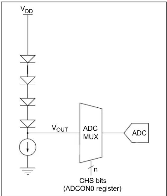
21.2 Temperature Output
The output of the circuit is measured using the internal analog-to-digital converter. Channel 13 is reserved for the temperature circuit output. Refer to Section 22.0, Analog-to-Digital Converter (ADC) Module for detailed information.
The temperature of the silicon die can be calculated by the ADC measurement by using Equation 21-1. A factory-stored 10-bit ADC value for 30°C is located at address 2084h. The temperature coefficient for this circuit is 14.0 mV/°C from -40°C to +125°C. Other temperature readings can be calculated from the 30°C mark.
Note: ADC temperature numbers represented are with ADC_REF = AV_DD
EQUATION 21-1: SILICON DIE TEMPERATURE
$$ T E M P _ D I E (\mathrm{C}) = \frac {A D C _ R E A D I N G (c o u n t s) A D C _ 3 0 ^ {\circ} \mathrm{C} _ R E A D I N G (c o u n t s -)}{3 . 5 (c o u n t s / ^ {\circ} \mathrm{C})} + 3 0 ^ {\circ} \mathrm{C} $$
NOTES:
22.0 ANALOG-TO-DIGITAL CONVERTER (ADC) MODULE
The Analog-to-Digital Converter (ADC) allows conversion of an analog input signal to a 10-bit binary representation of that signal. This device uses analog inputs that are multiplexed into a single sample-and-hold circuit. The output of the sample-and-hold is connected to the input of the converter. The converter generates a 10-bit binary result via successive approximation and stores the right-justified conversion result into the ADC result registers (ADRESH:ADRESL register pair). Figure 22-1 shows the block diagram of the ADC.
The internal band gap supplies the voltage reference to the ADC.
Note: Once V_IN is greater than AV_DD + V_DROPOUT , AV_DD is in regulation, allowing A/D readings to be accurate. Once V_IN is greater than V_DD + V_DROPOUT , V_DD is in regulation, allowing accurate ratiometric measurements.
FIGURE 22-1: ADC BLOCK DIAGRAM
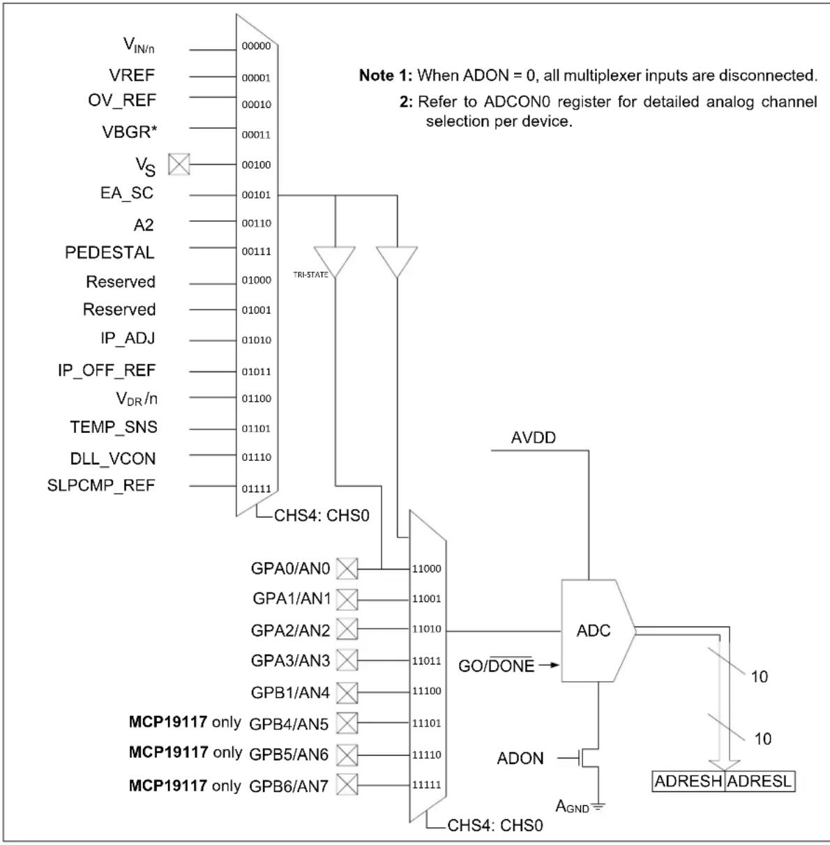
flowchart
graph TD
    A["V_IN/n"] --> B["00000"]
    C["VREF"] --> D["00001"]
    E["OV_REF"] --> F["00010"]
    G["VBGR*"] --> H["00011"]
    I["V_S"] --> J["00100"]
    K["EA_SC"] --> L["00101"]
    M["A2"] --> N["00110"]
    O["PEDESTAL"] --> P["00111"]
    Q["Reserved"] --> R["01000"]
    S["Reserved"] --> T["01001"]
    U["IP_ADJ"] --> V["01010"]
    W["IP_OFF_REF"] --> X["01011"]
    Y["V_DR/n"] --> Z["01100"]
    AA["TEMP_SNS"] --> AB["01101"]
    AC["DLL_VCON"] --> AD["01110"]
    AE["SLPCMP_REF"] --> AF["01111"]
    B --> G
    D --> G
    F --> G
    H --> G
    J --> G
    L --> G
    N --> G
    P --> G
    Q --> G
    R --> G
    S --> G
    T --> G
    U --> G
    V --> G
    X --> G
    Y --> G
    Z --> G
    AA --> G
    AB --> G
    AC --> G
    AD --> G
    AE --> G
    F --> H
    H --> I
    I --> J
    J --> K
    K --> L
    L --> M
    M --> N
    N --> O
    O --> P
    P --> Q
    Q --> R
    R --> S
    S --> T
    T --> U
    U --> V
    V --> W
    W --> X
    X --> Y
22.1 ADC Configuration
When configuring and using the ADC, the following functions must be considered:
- Port configuration
- Channel selection
• ADC conversion clock source - Interrupt control
- Result formatting
22.1.1 PORT CONFIGURATION
The ADC is used to convert analog signals into a corresponding digital representation. When converting analog signals, the I/O pin should be configured for analog by setting the associated TRIS and ANSEL bits. Refer to Section 19.0, I/O Ports for more information.
Note: Analog voltages on any pin that is defined as a digital input may cause the input buffer to conduct excess current.
22.1.2 CHANNEL SELECTION
There are up to 21 channel selections available for the MCP19116 and 24 channels for the MCP19117:
- AN<4:0> pins
• AN<7:5> pins (MCP19117 only)
• V_IN : 1/15.53 of the input voltage ( V_IN ) - V_REF : voltage reference for regulation set point
- OV_REF: reference for OV comparator
- V_BGR : band gap reference
- V_S : voltage proportional to V_OUT
- EA_SC: error amplifier output after slope compensation
• A2: secondary current sense amplifier output - Pedestal
- Reserved
- Reserved
- IP_ADJ: I_P after pedestal and offset adjust
- IP_OFF_REF: I_P offset reference
• V_DR : V_DR * 0.229V/V - TEMP_SNS: analog voltage representing internal temperature (refer to Equation 21-1)
- DLL_VCON: delay locked loop voltage reference
- SLPCMP_REF: slope compensation reference
The CHS<4:0> bits in the ADCON0 register determine which channel is connected to the sample and hold circuit.
When changing channels, a delay is required before starting the next conversion. Refer to Section 22.2 "ADC Operation" for more information.
22.1.3 ADC CONVERSION CLOCK
The source of the conversion clock is software selectable via the ADCS bits in the ADCON1 register. There are five possible clock options:
- F_OSC / 8
- F_OSC / 16
- F_OSC / 32
- F_OSC / 64
- F_RC (clock derived from internal oscillator with a divisor of 16)
The time to complete one-bit conversion is defined as T_AD . One full 10-bit conversion requires 11 T_AD periods, as shown in Figure 22-2.
For a correct conversion, the appropriate T_AD specification must be met. Refer to the A/D conversion requirements in Section 4.0 “Electrical
Characteristics" for more information. Table 22-1 gives examples of appropriate ADC clock selections.
Note: Unless using the F_RC , any changes in the system clock frequency will change the ADC clock frequency, which may adversely affect the ADC result.
TABLE 22-1: ADC CLOCK PERIOD (T AD) vs. DEVICE OPERATING FREQUENCIES
| ADC Clock Period (TAD) | Device Frequency (Fosc) | |
| ADCClockSource | ADCS<2:0> | 8 MHz |
| FOSC/8 | 001 | 1.0 μs(1) |
| FOSC/16 | 101 | 2.0 μs |
| FOSC/32 | 010 | 4.0 μs |
| FOSC/64 | 110 | 8.0 μs(2) |
| FRC | x11 | 2.0 – 6.0 μs(3, 4) |
Legend: Shaded cells are outside of recommended range.
Note 1: These values violate the minimum required T_AD time.
2: For faster conversion times, the selection of another clock source is recommended.
3: The F_RC source has a typical T_AD time of 4 s for V_DD > 3.0V .
4: The F_RC clock source is only recommended if the conversion will be performed during Sleep.
FIGURE 22-2: ANALOG-TO-DIGITAL CONVERSION T AD CYCLES
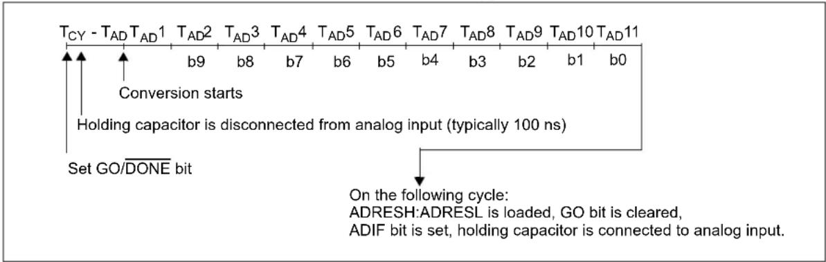
flowchart
graph TD
    A["T_CY - T_AD 1"] --> B["Conversion starts"]
    B --> C["Setting GO/DONE bit"]
    C --> D["On the following cycle: ADRESH:ADRESL is loaded, GO bit is cleared, ADIF bit is set, holding capacitor is connected to analog input."]
    style A fill:#f9f,stroke:#333
    style B fill:#ccf,stroke:#333
    style C fill:#cfc,stroke:#333
    style D fill:#fcc,stroke:#333
22.1.4 INTERRUPTS
The ADC module allows for the ability to generate an interrupt upon completion of an analog-to-digital conversion. The ADC Interrupt Flag is the ADIF bit in the PIR1 register. The ADC Interrupt Enable is the ADIE bit in the PIE1 register. The ADIF bit must be cleared in software.
Note 1: The ADIF bit is set at the completion of every conversion, regardless of whether or not the ADC interrupt is enabled.
This interrupt can be generated while the device is operating or while in Sleep. If the device is in Sleep, the interrupt wakes the device up. Upon waking from
Sleep, the next instruction following the SLEEP instruction is always executed. If the user is attempting to wake up from Sleep and resume in-line code execution, the GIE and PEIE bits in the INTCON register must be disabled. If the GIE and PEIE bits in the INTCON register are enabled, execution will switch to the Interrupt Service Routine.
22.1.5 RESULT FORMATTING
The 10-bit A/D conversion result is supplied in right-justified format only.
Figure 22-3 shows the output format.
FIGURE 22-3: 10-BIT A/D RESULT FORMAT

22.2 ADC Operation
22.2.1 ADC REFERENCE SWITCH
Users have the option of connecting the 5V LDO ( V_DD ) or the 4.096V LDO ( AV_DD ) as the reference to the Analog-to-Digital Converter. This control bit (VCFG) is located in the ADCON1 register bit 0 (see Register 22-2). Default configuration connects the AV_DD to the ADC reference.
22.2.2 STARTING A CONVERSION
To enable the ADC module, the ADON bit in the ADCON0 register must be set to a '1'. Setting the GO/DONE bit in the ADCON0 register to a '1' starts the analog-to-digital conversion.
Note: The GO/DONE bit should not be set in the same instruction that turns on the ADC.
Refer to Section 22.2.6 "A/D Conversion Procedure".
22.2.3 COMPLETION OF A CONVERSION
When the conversion is complete, the ADC module:
- Clears the GO/DONE bit
- Sets the ADIF Interrupt Flag bit
- Updates the ADRESH:ADRESL registers with new conversion result
22.2.4 TERMINATING A CONVERSION
If a conversion must be terminated before completion, the GO/DONE bit can be cleared in software. The ADRESH:ADRESL registers are not updated with the partially complete analog-to-digital conversion sample. Instead, the ADRESH:ADRESL register pair retains the value of the previous conversion. Additionally, two ADC clock cycles are required before another acquisition can be initiated. Following the delay, an input acquisition is automatically started on the selected channel.
Note: A device reset forces all registers to their Reset state. Thus, the ADC module is turned off and any pending conversion is terminated.
22.2.5 ADC OPERATION DURING SLEEP
The ADC is not operational during Sleep mode. The AV_DD 4V reference has been removed to minimize Sleep current.
22.2.6 A/D CONVERSION PROCEDURE
This is an example procedure for using the ADC to perform an analog-to-digital conversion:
-
Configure Port:
-
Disable pin output driver (refer to the TRISGPx registers)
-
Configure pin as analog (refer to the ANSELx registers)
-
Configure the ADC module:
-
Select ADC conversion clock
- Select ADC input channel
-
Turn on ADC module
-
Configure ADC interrupt (optional):
-
Clear ADC interrupt flag
- Enable ADC interrupt
- Enable peripheral interrupt
-
Enable global interrupt (1)
-
Wait the required acquisition time (2).
-
Start conversion by setting the GO/DONE bit.
-
Wait for ADC conversion to complete by one of the following:
-
Polling the GO/DONE bit
-
Waiting for the ADC interrupt (interrupts enabled)
-
Read ADC Result.
-
Clear the ADC interrupt flag (required if interrupt is enabled).
Note 1: The global interrupt can be disabled if the user is attempting to wake up from Sleep and resume in-line code execution.
2: Refer to Section 22.4 "A/D Acquisition Requirements".
EXAMPLE 22-1: A/D CONVERSION
;This code block configures the ADC
;for polling, Frc clock and ANO input.
;
;Conversion start & polling for completion ;
are included.
;
BANKSELADCON1;
MOVLWB'01110000';Frc clock
MOVWFADCON1;
BANKSELTRISGPA;
BSF TRISGPA,0;Set GPA0 to input
BANKSELANSELA;
BSF ANSELA,0;Set GPA0 to analog
BANKSELADCON0;
MOVLWB'01100001';Select channel ANO
MOVWFADCON0;Turn ADC On
CALLSampleTime;Acquisiton delay
BSF ADCON0,1;Start conversion
BTFSCADCON0,1;Is conversion done?
GOTO$-1 ;No, test again
BANKSELADRESH;
MOVPADRESH,W;Read upper 2 bits
MOVWFRESULTHI;store in GPR space
BANKSELADRESL;
MOVPADRESL,W;Read lower 8 bits
MOVWFRESULTLO;Store in GPR space
22.3 ADC Register Definitions
The following registers are used to control the operation of the ADC:
REGISTER 22-1: ADCON0: A/D CONTROL REGISTER 0
| U-0 R/W-0 R/W-0 R/W-0 R/W-0 R/W-0 R/W-0 R/W-0 | |||||||
| — | CHS4 | CHS3 | CHS2 | CHS1 | CHS0 | GO/DONE | ADON |
| bit 7 bit 0 | |||||||
Legend:
| R = Readable bit | W = Writable bit | U = Unimplemented bit, read as '0' |
| u = Bit is unchanged | x = Bit is unknown -n = Value at POR | |
| '1' = Bit is set | '0' = Bit is cleared | |
bit 7 Unimplemented: Read as '0'
bit 6-2 CHS<4:0>: Analog Channel Select bits
00000 = VIN/n analog voltage measurement (VIN/n = VIN/15.5328)
00001 = VREF (DAC reference voltage setting current regulation level)
00010 = OV_REF (reference for overvoltage comparator)
00011 = VBGR (band gap reference)
00100 = V S (Voltage proportional to V OUT )
00101 = EA_SC (Error Amplifier after Slope Compensation output)
00110 = A2 (Secondary Current Sense Amplifier output)
00111 = Pedestal (Pedestal Voltage)
01000 = Reserved
01001 = Reserved
01010 = IP_ADJ (IP after Pedestal and Offset Adjust (at PWM Comparator))
01011 = IP_OFF_REF (IP Offset Reference)
01100 = V DR /n (V DR /n analog driver voltage measurement = 0.229V/V * V _DR )
01101 = TEMP_SNS (analog voltage representing internal temperature)
01110 = DLL_VCON (Delay Locked-Loop Voltage Reference - Control voltage for dead time)
01111 = SLPCMP_REF (Slope compensation reference)
10000 = Unimplemented
10001 = Unimplemented
10010 = Unimplemented
10011 = Unimplemented
10100 = Unimplemented
10101 = Unimplemented
10110 = Unimplemented
10111 = Unimplemented
11000 = GPA0/AN0
11001 = GPA1/AN1
11010 = GPA2/AN2
11011 = GPA3/AN3
11100 = GPB1/AN4
11101 = GPB4/AN5 (MCP19117 only)
11110 = GPB5/AN6 (MCP19117 only)
11111 = GPB6/AN7 (MCP19117 only)
bit 1 GO/DONE: A/D Conversion Status bit
1 = A/D conversion cycle in progress. Setting this bit starts an A/D conversion cycle
This bit is automatically cleared by hardware when the A/D conversion has completed
0 = A/D conversion completed/not in progress
bit 0 ADON: ADC Enable bit
1 = ADC is enabled
0 = ADC is disabled and consumes no operating current
REGISTER 22-2: ADCON1: A/D CONTROL REGISTER 1
| U-0 R/W-0 R/W-0 R/W-0 U-0 U-0 U-0 R/W-0 | |||||||
| — | ADCS2 | ADCS1 | ADCS0 | — | — | — | VCFG |
| bit 7 bit 0 | |||||||
| Legend: | ||
| R = Readable bit | W = Writable bit | U = Unimplemented bit, read as '0' |
| u = Bit is unchanged | x = Bit is unknown | -n = Value at POR |
| ‘1’ = Bit is set | ‘0’ = Bit is cleared | |
bit 7 Unimplemented: Read as '0'
bit 6-4 ADCS<2:0>: A/D Conversion Clock Select bits
000 = Reserved
001 = F _OSC /8
010 = F _OSC /32
x11 = F_RC (clock derived from internal oscillator with a divisor of 16)
100 = Reserved
101 = Fosc/16
110 = F _OSC /64
bit 3-1 Unimplemented: Read as '0'
bit 0 VCFG: ADC Reference Voltage Configuration
0 = AV_DD
1 = V_DD
REGISTER 22-3: ADRESH: ADC RESULT REGISTER HIGH
| Legend: | ||
| R = Readable bit | W = Writable bit | U = Unimplemented bit, read as '0' |
| u = Bit is unchanged | x = Bit is unknown | -n = Value at POR |
| '1' = Bit is set | '0' = Bit is cleared | |
bit 7-2 Unimplemented: Read as '0'
bit 1-0 ADRES<9:8>: Most Significant A/D Results
REGISTER 22-4: ADRESL: ADC RESULT REGISTER LOW
| R-x | R-x | R-x | R-x | R-x | R-x | R-x | R-x |
| ADRES7 | ADRES6 | ADRES5 | ADRES4 | ADRES3 | ADRES2 | ADRES1 | ADRES0 |
| bit 7 bit 0 | |||||||
| Legend: | ||
| R = Readable bit | W = Writable bit | U = Unimplemented bit, read as ‘0’ |
| u = Bit is unchanged | x = Bit is unknown | -n = Value at POR |
| ‘1’ = Bit is set | ‘0’ = Bit is cleared | |
bit 7-0 ADRES<7:0>: Least Significant A/D results
22.4 A/D Acquisition Requirements
For the ADC to meet its specified accuracy, the charge holding capacitor ( C_HOLD ) must be allowed to fully charge to the input channel voltage level. The Analog Input model is shown in Figure 22-4. The source impedance ( R_S ) and the internal sampling switch ( R_SS ) impedance directly affect the time required to charge the capacitor C_HOLD . The sampling switch ( R_SS ) impedance varies over the device voltage ( V_DD ), refer to Figure 22-4. The maximum recommended impedance for analog sources is 10 kΩ.
As the source impedance is decreased, the acquisition time may be decreased. After the analog input channel is selected (or changed), an A/D acquisition must be done before the conversion can be started. To calculate the minimum acquisition time, Equation 22-1 may be used. This equation assumes that 1/2 LSb error is used (1,024 steps for the ADC). The 1/2 LSb error is the maximum error allowed for the ADC to meet its specified resolution.
EQUATION 22-1: ACQUISITION TIME EXAMPLE
Assumptions: Temperature = +50°C and external impedance of 10 k Ω 5.0V V _DD
$$ T _ {A C Q} = \text { Amplifier Settling Time } + \text { Hold Capacitor Charging Time } + \text { Temperature Coefficient } $$
$$ T _ {A M P} + T _ {C} + T _ {C \bar {O} F F} $$
$$ 2 \text {—} \mu s T + _ {C} + [ (T e m p e r a t u r e - 2 5 ^ {\circ} C) (0. 0 5 \mu s / ^ {\circ} C) ] $$
The value for T_C can be approximated with the following equations:
$$ V _ {A P P L I E D} \left(1 - \frac {I}{\left(2 ^ {n + 1}\right) - 1}\right) = V _ {C H O L D} $$
;[1] V_CHOLD charged to within 1/2 lsb
$$ V _ {A P P L I E D} \left(1 - e ^ {\frac {- T C}{R C}}\right) = V _ {C H O L D} $$
;[2] V_CHOLD charge response to V_APPLIED
$$ V _ {A P P L I E D} \left(1 - e ^ {\frac {- T _ {C}}{R C}}\right) = V _ {A P P L I E D} \left(1 - \frac {1}{\left(2 ^ {n + 1}\right) - 1}\right) $$
;combining [1] and [2]
Note: Where n = number of bits of the ADC.
Solving for T_C :
$$ \begin{array}{l} T _ {C} = - C _ {H O L D} \left(R _ {I C} + R _ {S S} + R _ {S}\right) \ln (1 / 2 0 4 7) \ = - 1 0 p F (1 k \Omega + 7 k \Omega + 1 0 k \Omega) \ln (0. 0 0 0 4 8 8 5) \ = 1. 3 7 \mu s \ \end{array} $$
Therefore:
$$ T _ {A C Q} = 2 \mu s + 1. 3 7 \mu s + [ (5 0 ^ {\circ} C - 2 5 ^ {\circ} C) (0. 0 5 \mu s / ^ {\circ} C) ] $$
$$ = 4. 6 7 \mu s $$
Note 1: The charge holding capacitor ( C_HOLD ) is not discharged after each conversion.
2: The maximum recommended impedance for analog sources is 10 kΩ. This is required to meet the pin leakage specification.
FIGURE 22-4: ANALOG INPUT MODEL
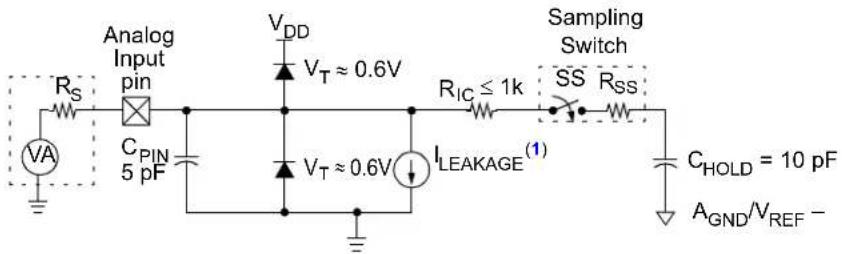
Legend:
C_HOLD = Sample/Hold Capacitance
C_PIN = Input Capacitance
I_LEAKAGE = Leakage current at the pin due to various junctions
R_IC = Interconnect Resistance
R_ss = Resistance of Sampling Switch
SS = Sampling Switch
V_T = Threshold Voltage
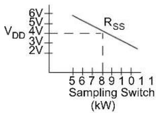
line
| Sampling Switch (kW) | V_DD | | --------------------- | ---- | | 5 | 6V | | 6 | 5V | | 7 | 4V | | 8 | 3V | | 9 | 2V | | 10 | 1V | | 11 | 0.5V |Note 1: Refer to Section 4.0 "Electrical Characteristics".
FIGURE 22-5: ADC TRANSFER FUNCTION
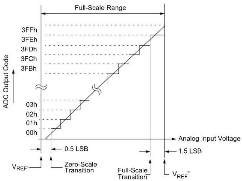
line
| Time | ADC Output Code | |------|-----------------| | 00h | 0 | | 01h | 0.5 LSB | | 02h | 0.5 LSB | | 03h | 0.5 LSB | | 0FDh | 0.5 LSB | | 3FEh | 0.5 LSB | | 3FFh | 0.5 LSB |TABLE 22-2: SUMMARY OF REGISTERS ASSOCIATED WITH ADC
| Name Bit | 7 Bit 6 Bit | 5 Bit 4 Bit | 3 Bit 2 Bit | 1 Bit 0 | Register on page | ||||
| ADCON0 | — | CHS4 CH | HS3 CHS2 | CHS1 CHS0 | GO/DONE | ADON 143 | —— | ||
| ADCON1 | — | ADCS2 | ADCS1 | ADCS0 | — | — | — | — | 144 |
| ADRESH | — | — | — | — | — | — | ADRES9 | ADRES8 | 144 |
| ADRESL | ADRES7 | ADRES6 | ADRES5 | ADRES4 | ADRES3 | ADRES2 | ADRES1 | ADRES0 | 144 |
| ANSELA | — | — | — | — | ANSA3 | ANSA2 | ANSA1 | ANSA0 | 128 |
| ANSELB | — | ANSB6 | ANSB5 | ANSB4 | — | — | ANSB1 | — | 132 |
| INTCON | GIE | PEIE | T0IE | INTE | IOCE | T0IF | INTF | IOCF | 107 |
| PIE2 | CDSIE | ADIE | — | OTIE | OVIE | DRUVIE | OVLOIE | UVLOIE | 109 |
| PIR2 | CDSIF | ADIF | — | OTIF | OVIF | DRUVIF | OVLOIF | UVLOIF | 111 |
| TRISGPA | TRISA7 | TRISA6 | TRISA5 | — | TRISA3 | TRISA2 | TRISA1 | TRISA0 | 127 |
| TRISGPB | TRISB7 | TRISB6 | TRISB5 | TRISB4 | — | — | TRISB1 | TRISB0 | 131 |
Legend: — = unimplemented, read as '0'. Shaded cells are not used for ADC module.
NOTES:
23.0 TIMER0 MODULE
The Timer0 module is an 8-bit timer/counter with the following features:
• 8-bit timer/counter register (TMR0)
- 8-bit prescaler
- Programmable internal or external clock source
- Programmable external clock edge selection
- Interrupt on overflow
Figure 23-1 is a block diagram of the Timer0 module.
FIGURE 23-1: TIMER0 BLOCK DIAGRAM
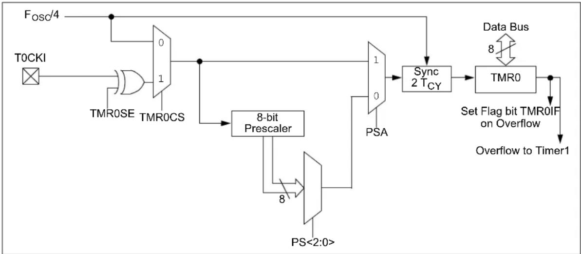
flowchart
graph TD
    A["T0CKI"] --> B["AND Gate"]
    B --> C["0/1 TMR0CS"]
    C --> D["8-bit Prescaler"]
    D --> E["PS<2:0>"]
    E --> F["0/1 TMR0"]
    F --> G["Sync 2 TCY"]
    G --> H["TMR0"]
    H --> I["Set Flag bit TMR0IF on Overflow"]
    I --> J["Data Bus"]
    J --> K["Overflow to Timer1"]
    C --> L["F_OSC/4"]
    D --> M["8-bit Prescaler"]
    M --> N["8"]
    N --> O["PS<2:0>"]
23.1 Timer0 Operation
The Timer0 module can be used as either an 8-bit timer or an 8-bit counter.
23.1.1 8-BIT TIMER MODE
The Timer0 module will increment every instruction cycle, if used without a prescaler. 8-Bit Timer mode is selected by clearing the T0CS bit in the OPTION_REG register.
When TMR0 is written, the increment is inhibited for two instruction cycles immediately following the write.
Note: The value written to the TMR0 register can be adjusted, in order to account for the two-instruction cycle delay when TMR0 is written.
23.1.2 8-BIT COUNTER MODE
In 8-Bit Counter mode, the Timer0 module increments on every rising or falling edge of the T0CKI pin. The incrementing edge is determined by the T0SE bit in the OPTION_REG register.
8-Bit Counter mode using the T0CKI pin is selected by setting the T0SE bit in the OPTION_REG register to '1'.
23.1.3 SOFTWARE PROGRAMMABLE PRESCALER
A single software programmable prescaler is available for use with either Timer0 or the Watchdog Timer (WDT), but not both simultaneously. The prescaler assignment is controlled by the PSA bit in the OPTION_REG register. To assign the prescaler to Timer0, the PSA bit must be cleared to '0'.
There are eight prescaler options for the Timer0 module ranging from 1:2 to 1:256. The prescale values are selectable via the PS<2:0> bits in the OPTION_REG register. In order to have a 1:1 prescaler value for the Timer0 module, the prescaler must be disabled by setting the PSA bit in the OPTION_REG register.
The prescaler is not readable or writable. When assigned to the Timer0 module, all instructions writing to the TMR0 register will clear the prescaler.
23.1.4 SWITCHING PRESCALER
BETWEEN TIMER0 AND WDT MODULES
As a result of having the prescaler assigned to either Timer0 or the WDT, it is possible to generate an unintended device reset when switching prescaler values. When changing the prescaler assignment from Timer0 to the WDT module, the instruction sequence shown in Example 23-1 must be executed.
EXAMPLE 23-1: CHANGING PRESCALER
(TIMER0 → WDT)
BANKSELTMR0;
CLRWDT ;Clear WDT
CLRFTMR0;Clear TMR0 and
;prescaler
BANKSELOPTION_REG;
BSF OPTION_REG,PSA;Select WDT
CLRWDT ;
;
MOVLWb'11111000';Mask prescaler
ANDWFOPTION_REG,W;bits
IORLWb'00000101';Set WDT prescaler
MOVWFOPTION_REG;to 1:32
When changing the prescaler assignment from the WDT to the Timer0 module, the following instruction sequence must be executed (refer to Example 23-2).
EXAMPLE 23-2: CHANGING PRESCALER
(WDT → TIMER0)
CLRWDT ;Clear WDT and
;prescaler
BANKSELOPTION_REG;
MOVLWb'11110000';Mask TMRO select and
ANDWFOPTION_REG,W;prescaler bits
IORLWb'00000011';Set prescale to 1:16
MOVWFOPTION_REG;
23.1.5 TIMER0 INTERRUPT
Timer0 will generate an interrupt when the TMR0 register overflows from FFh to 00h. The TOIF interrupt flag bit in the INTCON register is set every time the TMR0 register overflows, regardless of whether or not the Timer0 interrupt is enabled. The TOIF bit can only be cleared in software. The Timer0 interrupt enable is the TOIE bit in the INTCON register.
Note: The Timer0 interrupt cannot wake the processor from Sleep since the timer is frozen during Sleep.
23.1.6 USING TIMER0 WITH AN
EXTERNAL CLOCK
When Timer0 is in Counter mode, the synchronization of the T0CKI input and the Timer0 register is accomplished by sampling the prescaler output on the Q2 and Q4 cycles of the internal phase clocks. Therefore, the high and low periods of the external clock source must meet the timing requirements as shown in Section 4.0 "Electrical Characteristics".
23.1.7 OPERATION DURING SLEEP
Timer0 cannot operate while the processor is in Sleep mode. The contents of the TMR0 register will remain unchanged while the processor is in Sleep mode.
TABLE 23-1: SUMMARY OF REGISTERS ASSOCIATED WITH TIMER0
| Name | Bit 7 | Bit 6 | Bit 5 | Bit 4 | Bit 3 | Bit 2 | Bit 1 | Bit 0 | Register on page |
| INTCON | GIE | PEIE | T0IE | INTE | IOCIE | T0IF | INTF | IOCIF | 107 |
| OPTION_REG | INTEDG | T0CS | T0SE | PSA | PS2 | PS1 | PS0 | 90 | |
| TMR0 | Timer0 Module Register | 149* | |||||||
| TRISGPA | TRISA7 | TRISA6 | TRISA5 | TRISA4 | TRISA3 | TRISA2 | TRISA1 | TRISA0 | 127 |
Legend: — = Unimplemented locations, read as '0'. Shaded cells are not used by the Timer0 module.
*Page provides register information.
24.0 TIMER1 MODULE
The Timer1 module is a 16-bit timer with the following features:
• 16-bit timer register pair (TMR1H:TMR1L)
- Readable and writable (both registers)
- Selectable internal clock source
- 2-bit prescaler
- Interrupt on overflow
Figure 24-1 is a block diagram of the Timer1 module.
FIGURE 24-1: TIMER1 BLOCK DIAGRAM
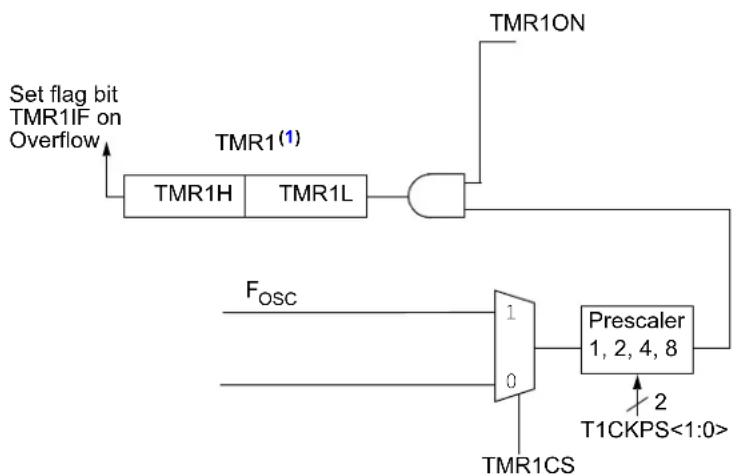
flowchart
graph TD
    A["Set flag bit TMR1IF on Overflow"] --> B["TMR1H"]
    B --> C["TMR1L"]
    C --> D["AND"]
    D --> E["TMR1ON"]
    F["F_OSC"] --> G["1"]
    G --> H["0"]
    H --> I["TMR1CS"]
    I --> J["Prescaler 1, 2, 4, 8"]
    J --> K["T1CKPS<1:0>"]
    L["TMR1(1)"] --> M["TMR1H"]
    L --> N["TMR1L"]
Note 1: TMR1 register increments on rising edge.
24.1 Timer1 Operation
The Timer1 module is a 16-bit incrementing timer which is accessed through the TMR1H:TMR1L register pair. Writes to TMR1H or TMR1L directly update the counter. The timer is incremented on every instruction cycle.
Timer1 is enabled by configuring the TMR1ON bit in the T1CON register. Table 24-1 displays the Timer1 enable selections.
24.2 Clock Source Selection
The TMR1CS bit in the T1CON register is used to select the clock source for Timer1. Table 24-1 displays the clock source selections.
24.2.1 INTERNAL CLOCK SOURCE
The TMR1H:TMR1L register pair will increment on multiples of F_OSC or F_OSC/4 as determined by the Timer1 prescaler.
As an example, when the F_OSC internal clock source is selected, the Timer1 register value will increment by four counts every instruction clock cycle.
TABLE 24-1: CLOCK SOURCE SELECTIONS
| TMR1CS Clock Source | |
| 1 8 MHz system clock (F | osc) |
| 0 2 MHz instruction clock (F | osc/4) |
24.3 Timer1 Prescaler
Timer1 has four prescaler options, allowing 1, 2, 4 or 8 divisions of the clock input. The T1CKPS bits in the T1CON register control the prescale counter. The prescale counter is not directly readable or writable; however, the prescaler counter is cleared upon a write to TMR1H or TMR1L.
24.4 Timer1 Interrupt
The Timer1 register pair (TMR1H:TMR1L) increments to FFFFh and rolls over to 0000h. When Timer1 rolls over, the Timer1 interrupt flag bit in the PIR1 register is set. To enable the interrupt on rollover, these bits must be set:
• TMR1ON bit in the T1CON register
• TMR1IE bit in the PIE1 register
• PEIE bit in the INTCON register
• GIE bit in the INTCON register
The interrupt is cleared by clearing the TMR1IF bit in the Interrupt Service Routine.
Note: The TMR1H:TMR1L register pair and the TMR1IF bit should be cleared before enabling interrupts.
24.5 Timer1 in Sleep
Unlike other standard mid-range Timer1 modules, the MCP19116/7 Timer1 module only clocks from an internal system clock, and thus cannot run during Sleep mode, nor can it be used to wake the device from this mode.
24.6 Timer1 Control Register
The Timer1 Control (T1CON) register, shown in Register 24-1, is used to control Timer1 and select the various features of the Timer1 module.
REGISTER 24-1: T1CON: TIMER1 CONTROL REGISTER
| U-0 U-0 R/W-0 R/W-0 U-0 U-0 R/W-0/ R/W-0 | |||||||
| — | — | T1CKPS1 | T1CKPS0 | — | — | TMR1CS | TMR1ON |
| bit 7 bit 0 | |||||||
Legend:
| R = Readable bit | W = Writable bit | U = Unimplemented bit, read as '0' |
| u = Bit is unchanged x = Bit is unknown | -n = Value at POR | |
| '1' = Bit is set | '0' = Bit is cleared | |
bit 7-6 Unimplemented: Read as '0'
bit 5-4 T1CKPS<1:0>: Timer1 Input Clock Prescale Select bits
11 = 1:8 Prescale value
10 = 1:4 Prescale value
01 = 1:2 Prescale value
00 = 1:1 Prescale value
bit 3-2 Unimplemented: Read as '0'
bit 1 TMR1CS: Timer1 Clock Source Control bit
1 = 8 MHz system clock (FOSC)
0 = 2 MHz instruction clock (FOSC/4)
bit 0 TMR1ON: Timer1 On bit
1 = Enables Timer1
0 = Stops Timer1, Clears Timer1 gate flip-flop
TABLE 24-2: SUMMARY OF REGISTERS ASSOCIATED WITH TIMER1
| Name Bit | 7 Bit 6 Bit | 5 Bit 4 Bit 3 | Bit 2 Bit 1 | Bit 0 | Register on page | ||||
| INTCON GIE | PEIE | T0IE | INTE | IOCE | T0IF | INTF | IOCF | 107 | |
| PIE1 | TXIE | RCIE | BCLIE | SSPIE | CC2IE | CC1IE | TMR2IE | TMR1IE | 108 |
| PIR1 | TXIF | RCIF | BCLIF | SSPIF | CC2IF | CC1IF | TMR2IF | TMR1IF | 110 |
| TMR1H | Holding Register for the Most Significant Byte of the 16-bit TMR1 Register | 151* | |||||||
| TMR1L | Holding Register for the Least Significant Byte of the 16-bit TMR1 Register | 151* | |||||||
| T1CON | — | — | T1CKPS1 | T1CKPS0 | — | — | TMR1CS | TMR1ON | 152 |
Legend: — = unimplemented, read as '0'. Shaded cells are not used by the Timer1 module.
* Page provides register information.
NOTES:
25.0 TIMER2 MODULE
The Timer2 module is an 8-bit timer with the following features:
• 8-bit timer register (TMR2)
• 8-bit period register (PR2)
- Interrupt on TMR2 match with PR2
- Software programmable prescaler (1:1, 1:4, 1:16)
Refer to Figure 25-1 for a block diagram of Timer2.
25.1 Timer2 Operation
The clock input to the Timer2 module is the system clock ( F_OSC ). The clock is fed into the Timer2 prescaler, which has prescale options of 1:1, 1:4 or 1:16. The output of the prescaler is then used to increment the TMR2 register.
The values of TMR2 and PR2 are constantly compared to determine when they match. TMR2 increments from 00h until it matches the value in PR2. When a match occurs, TMR2 is reset to 00h on the next increment cycle.
The match output of the Timer2/PR2 comparator is used to set the TMR2IF interrupt flag bit in the PIR1 register.
The TMR2 and PR2 registers are both fully readable and writable. On any Reset, the TMR2 register is set to 00h and the PR2 register is set to FFh.
Timer2 is turned on by setting the TMR2ON bit in the T2CON register to a '1'. Timer2 is turned off by clearing the TMR2ON bit to a '0'.
The Timer2 prescaler is controlled by the T2CKPS bits in the T2CON register. The prescaler counter is cleared when:
• A write to TMR2 occurs
• A write to T2CON occurs
- Any device reset occurs (Power-on Reset, MCLR Reset, Watchdog Timer Reset or Brown-out Reset)
Note: TMR2 is not cleared when T2CON is written.
FIGURE 25-1: TIMER2 BLOCK DIAGRAM
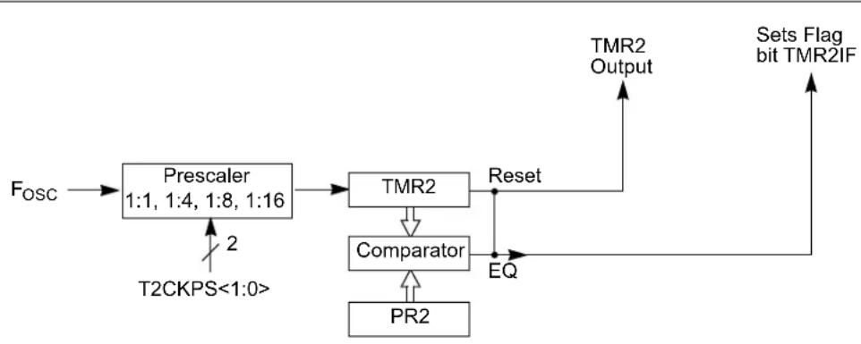
flowchart
graph TD
    A["Fosc"] --> B["Prescaler 1:1, 1:4, 1:8, 1:16"]
    B --> C["TMR2"]
    C --> D["Comparator"]
    D --> E["PR2"]
    F["T2CKPS<1:0>"] --> B
    G["Reset"] --> C
    H["TMR2 Output"] --> I["Sets Flag bit TMR2IF"]
    J["EQ"] --> D
    K["2"] --> B
25.2 Timer2 Control Register
REGISTER 25-1: T2CON: TIMER2 CONTROL REGISTER
| U-0 U-0 U-0 U-0 U-0 R/W-0 R/W-0 R/W-0 | |||||||
| — | — | — | — | — | TMR2ON | T2CKPS1 | T2CKPS0 |
| bit 7 bit 0 | |||||||
Legend:
| R = Readable bit | W = Writable bit | U = Unimplemented bit, read as '0' |
| u = Bit is unchanged x = Bit is unknown -n = Value at POR | ||
| '1' = Bit is set | '0' = Bit is cleared | |
bit 7-3 Unimplemented: Read as '0'
bit 2 TMR2ON: Timer2 On bit
1 = Timer2 is ON
0 = Timer2 is OFF
bit 1-0 T2CKPS<1:0>: Timer2 Clock Prescale Select bits
00 = Prescaler is 1
01 = Prescaler is 4
10 = Prescaler is 8
11 = Prescaler is 16
TABLE 25-1: SUMMARY OF REGISTERS ASSOCIATED WITH TIMER2
| Name | Bit 7 | Bit 6 | Bit 5 | Bit 4 | Bit 3 | Bit 2 | Bit 1 | Bit 0 | Register on page |
| INTCON | GIE | PEIE | T0IE | INTE | IOCE | T0IF | INTF | IOCF | 107 |
| PIE1 | TXIE | RCIE | BCLIE | SSPIE | CC2IE | CC1IE | TMR2IE | TMR1IE | 108 |
| PIR1 | TXIF | RCIF | BCLIF | SSPIF | CC2IF | CC1IF | TMR2IF | TMR1IF | 110 |
| PR2 | Timer2 Module Period Register | 155* | |||||||
| T2CON | — | — | — | — | — | TMR2ON | T2CKPS1 | T2CKPS0 | 156 |
| TMR2 | Holding Register for the 8-bit TMR2 Time Base | 155* | |||||||
Legend: — = unimplemented, read as '0'. Shaded cells are not used for Timer2 module.
* Page provides register information.
26.0 ENHANCED PWM MODULE
The PWM module implemented on the MCP19116/7 is a scaled-down version of the Capture/Compare/PWM (CCP) module found in standard mid-range microcontrollers. The module only features the PWM module, which is slightly modified from standard mid-range microcontrollers. In the MCP19116/7, the PWM module is used to generate the system clock or system oscillator. This system clock can control the MCP19116/7 switching frequency, as well as set the maximum allowable duty cycle. The PWM module does not continuously adjust the duty cycle to control the output voltage. This is accomplished by the analog control loop and associated circuitry.
26.1 Standard Pulse-Width Modulation Mode
The CCP will only function in PWM mode. The PWM signal is used to set the operating frequency and maximum allowable duty cycle of the MCP19116/7. Figure 26-1 is a snippet of the MCP19116/7 block diagram showing the PWM signal from the CCP module.
FIGURE 26-1: MCP19116/7 SNIPPET
SHOWING SYSTEM
CLOCK FROM PWM
MODULE
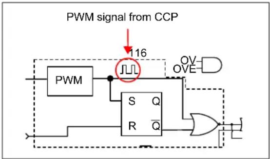
flowchart
graph TD
    A["PWM"] --> B["JLL"]
    B --> C["S R Q"]
    C --> D["OR"]
    D --> E["Output Logic"]
    F["PWM signal from CCP"] --> G["116"]
    G --> H["OVE"]
    H --> I["AND Gate"]
    I --> D
There are two modes of operation that concern the system clock PWM signal. These modes are Stand-Alone (non-frequency synchronization) and Frequency Synchronization.
26.1.1 STAND-ALONE (NON-FREQUENCY SYNCHRONIZATION) MODE
When the MCP19116/7 is running stand-alone, the PWM signal functions as the system clock. It is operating at the programmed switching frequency with a programmed maximum duty cycle ( D_CLOCK ). The programmed maximum duty cycle is not adjusted on a cycle-by-cycle basis to control the MCP19116/7 system output. The required duty cycle ( D_PDRVON ) to control the output is adjusted by the MCP19116/7 analog control loop and associated circuitry. D_CLOCK does however set the maximum allowable D_PDRVON .
EQUATION 26-1:
$$ D _ {P D R V O N} < 1 - D _ {C L O C K} $$
26.1.2 SWITCHING FREQUENCY SYNCHRONIZATION MODE
The MCP19116/7 can be programmed to be switching frequency MASTER or SLAVE devices. The MASTER device functions as described in Section 26.1.1 "Stand-Alone (Non-Frequency Synchronization) Mode" with the exception of the system clock also being applied to GPA1.
A SLAVE device will receive the MASTER system clock on GPA1. This MASTER system clock will be OR'ed with the output of the TIMER2 module. This OR'ed signal will latch PWMRL into PWMRH and PWMPHL into PWMPHH.
Figure 26-2 shows a simplified block diagram of the CCP module in PWM mode.
The PWMPHL register allows for a phase shift to be added to the SLAVE system clock.
It is desired to have the MCP19116/7 SLAVE device's system clock start point shifted by a programmed amount from the MASTER system clock. This SLAVE phase shift is specified by writing to the PWMPHL register. The SLAVE phase shift can be calculated by using the following equation.
EQUATION 26-2:
$$ \left| \begin{array}{c} S L A V E _ {P H A S E S H I F T} = P W M P H L \mathcal {T} _ {O S C} \times (T 2 _ {P R E S C A L E V A L U E}) \end{array} \right. $$
FIGURE 26-2: SIMPLIFIED PWM BLOCK DIAGRAM
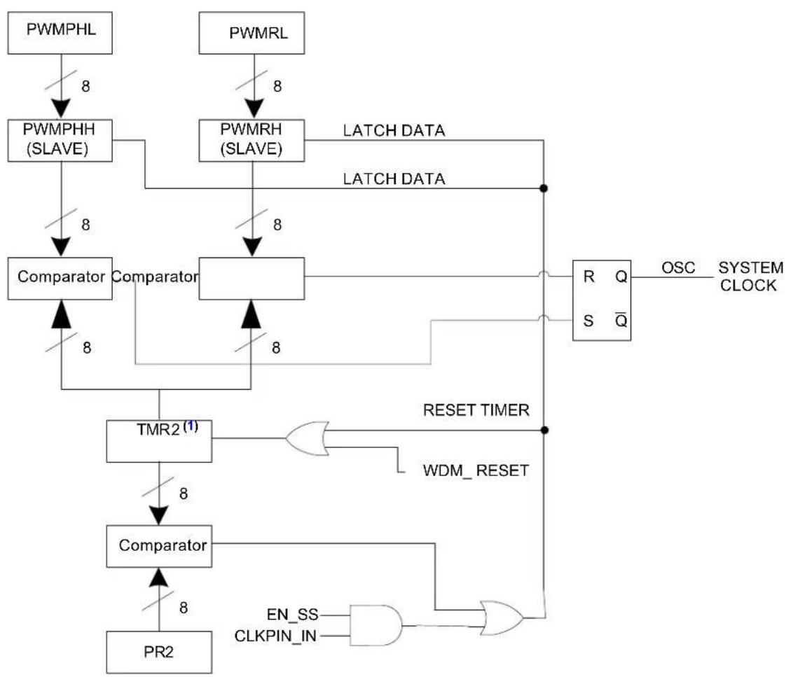
flowchart
graph TD
    A["PWMPHL"] -->|8| B["PWMPHH (SLAVE)"]
    C["PWMRL"] -->|8| D["PWMRH (SLAVE)"]
    B -->|8| E["Comparator"]
    D -->|8| F["Comparator"]
    E --> G["TMR2(1)"]
    F --> H["Comparator"]
    G --> I["RESET TIMER"]
    H --> J["EN_SS CLKPIN_IN"]
    I --> K["AND Gate"]
    J --> L["OR Gate"]
    K --> M["OSC SYSTEM CLOCK"]
    L --> N["Q̅ S"]
    M --> O["Q̅ Q̅"]
    N --> P["Q̅ S"]
    O --> Q["Q̅ S"]
    P --> R["Q̅ S"]
    Q --> S["Q̅ S"]
    R --> T["Q̅ S"]
    S --> U["Q̅ S"]
    T --> V["Q̅ S"]
    U --> W["Q̅ S"]
    V --> X["Q̅ S"]
    W --> Y["Q̅ S"]
    X --> Z["Q̅ S"]
    Y --> AA["Q̅ S"]
    Z --> AB["Q̅ S"]
Note 1: TIMER 2 should be clocked by F_OSC (8 MHz).
A PWM output (Figure 26-2) has a time base (period) and a time that the output stays high (duty cycle). The frequency of the PWM is the inverse of the period (1/period).
FIGURE 26-3: PWM OUTPUT
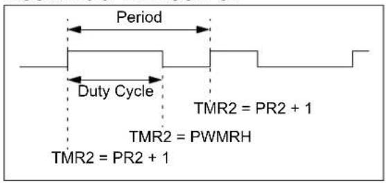
26.1.3 PWM PERIOD
The PWM period is specified by writing to the PR2 register. The PWM period can be calculated using the following equation.
EQUATION 26-1:
$$ P W M _ {P E R I O D} = [ (P R 2) + I ] \times T _ {O S C} \times (T 2 _ {P R E S C A L E V A L U E}) $$
When TMR2 is equal to PR2, the following two events occur on the next increment cycle:
• TMR2 is cleared
- The PWM duty cycle is latched from PWMRL into PWMRH
26.1.4 PWM DUTY CYCLE (D CLOCK)
The PWM duty cycle ( D_CLOCK ) is specified by writing to the PWMRL register. Up to 8-bit resolution is available. The following equation is used to calculate the PWM duty cycle ( D_CLOCK ).
EQUATION 26-2:
$$ P W M _ {D U T Y C Y C L E} = P W M R L \mathcal {T} O S C ^ {\times (T 2} P R E S C A L E V A L U E) $$
The PWMRL bits can be written to at any time, but the duty cycle value is not latched into PWMRH until after a match between PR2 and TMR2 occurs.
26.2 Operation During Sleep
When the device is placed in Sleep, the allocated timer will not increment and the state of the module will not change. If the CLKPIN pin is driving a value, it will continue to drive that value. When the device wakes up, it will continue from this state.
TABLE 26-1: SUMMARY OF REGISTERS ASSOCIATED WITH PWM MODULE
| Name Bit | 7 Bit 6 Bit | 5 Bit 4 Bit 3 | Bit 2 Bit 1 | Bit 0 | Register on page | ||||
| MODECON | MSC1 | MSC0 | RFB | — | MSC2 | — | — | — | 52 |
| T2CON | — | — | — | — | — | TMR2ON | T2CKPS1 | T2CKPS0 | 156 |
| PR2 | Timer2 Module Period Register | 157 | |||||||
| PWMRL | PWM Register Low Byte | 157* | |||||||
| PWMPHL | Phase Shift Low Byte | 157* | |||||||
Legend: — = Unimplemented locations, read as '0'. Shaded cells are not used by PWM mode.
* Page provides register information.
NOTES:
27.0 PWM CONTROL LOGIC
The PWM Control Logic implements standard comparator modules to identify events such as input undervoltage, input overvoltage and desaturation detection. The control logic takes action in hardware to appropriately enable/disable the output drive (PDRV/SDRV), as well as to set corresponding interrupt flags to be read by software. This control logic also defines normal PWM operation. For definition of individual bits within the control logic, refer to the Special Function Register (SFR) sections.
FIGURE 27-1: PWM CONTROL LOGIC
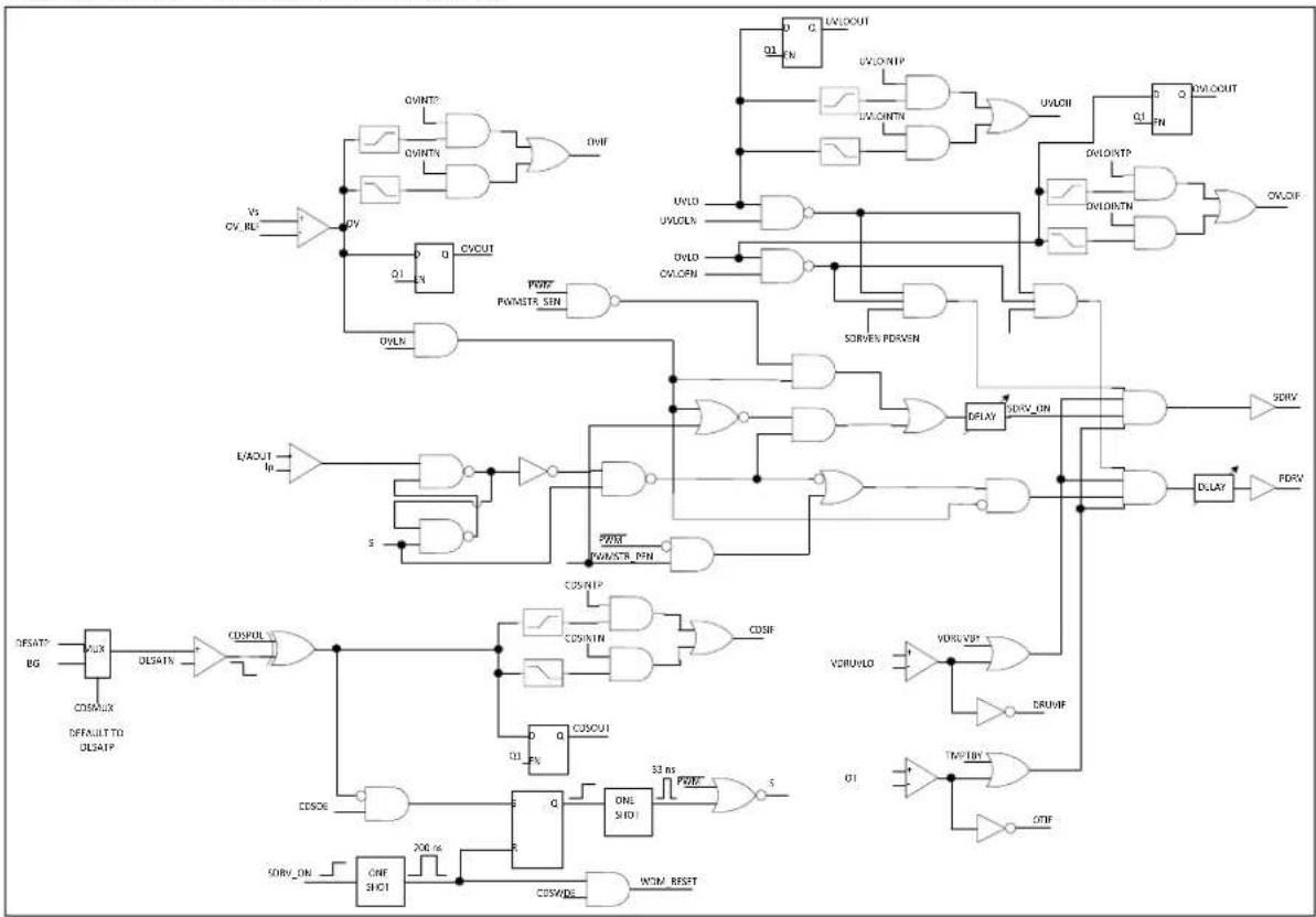
flowchart
graph TD
    subgraph FlipFlop1
        A["QVINTP"] --> B["OR"]
        C["QVINTN"] --> B
        D["QVOUT"] --> E["OR"]
        F["QVOUT"] --> G["OR"]
        H["QVOUT"] --> I["OR"]
        J["QVOUT"] --> K["OR"]
        L["QVOUT"] --> M["OR"]
        N["QVOUT"] --> O["OR"]
        P["QVOUT"] --> Q["OR"]
        R["QVOUT"] --> S["OR"]
        T["QVOUT"] --> U["OR"]
        V["QVOUT"] --> W["OR"]
        X["QVOUT"] --> Y["OR"]
        Z["QVOUT"] --> AA["OR"]
    end

    subgraph FlipFlop2
        AB["QVOUT"] --> AC["OR"]
        AD["QVOUTNP"] --> AE["OR"]
        AF["QVOUTN"] --> AG["OR"]
        AH["QVOUT"] --> AI["OR"]
        AJ["QVOUTNP"] --> AK["OR"]
        AL["QVOUTN"] --> AM["OR"]
        AN["QVOUT"] --> AO["OR"]
        AP["QVOUTNP"] --> AQ["OR"]
        AR["QVOUTN"] --> AS["OR"]
        AT["QVOUT"] --> AU["OR"]
        AV["QVOUTNP"] --> AW["OR"]
        AX["QVOUTN"] --> AY["OR"]
        AZ["QVOUT"] --> BA["OR"]
        BB["QVOUTNP"] --> BC["OR"]
        BD["QVOUTN"] --> BE["OR"]
        BF["QVOUT"] --> BG["OR"]
        BH["QVOUTNP"] --> BI["OR"]
        BJ["QVOUTN"] --> BK["OR"]
        BL["QVOUT"] --> BM["OR"]
        BN["QVOUTNP"] --> BO["OR"]
        BP["QVOUTN"] --> BP["OR"]
        BQ["QVOUT"] --> BR["OR"]
        BW["QVOUTNP"] --> BX["OR"]
        BY["QVOUTN"] --> BYB["OR"]
        BZ["QVOUT"] --> CA["OR"]
        CB["QVOUTNP"] --> CC["OR"]
        DD["QVOUTN"] --> DDY["OR"]
        DB["QVOUT"] --> DBY["OR"]
    end

    subgraph FlipFlop3
        DC["VOUT"] --> DDY
        DDY --> DVAY
        DVAY --> DRLAY
        DRLAY --> FDRIV
    end

    subgraph FlipFlop4
        DG["VOUT"] --> DVAY
        DVAY --> DVAYND
        DVAYND --> DVAYND
        DVAYND --> DVAYND
    end

    subgraph FlipFlop5
        DH["VDRUVO"] --> DVAVSP
        DVAVSP --> DVAVSPND
        DVAVSPND --> DVAVSPND
        DVAVSPND --> DVAVSPND
    end

    subgraph FlipFlop6
        DI["VTRIBY"] --> DVAVSPND
        DVAVSPND --> DVAVSPNDND
        DVAVSPNDNDNDNDNDNDNDNDNDNDNDNDNDNDNDNDNDNDNDNDNDNDNDNDNDNDNDNDNDNDNDNDNDNDNDNDNDNDNDNDNDNDNDNDNDNDNDNDNDNDNDNDNDNDNDNDNDNDNDNDNDNDNDNDNDNDNDNDNDNDNDNDNDNDNDNDNDNDNDNDNDNDNDNDNDNDNDNDNDNDNDNDNDNDNDNDNDNDNDNDN
    end

    subgraph FlipFlop7
        ON["VOUT"] --> DN["VOUTNP"]
        DN --> DN0
        DN0 --> DN00
        DN00 --> DN000
        DN000 --> DN0000
        DN0000 --> DN00000
    end

    subgraph FlipFlop8
        O["VOUT"] --> ON0
        ON0 --> DN0
        DN0 --> DN00
        DN00 --> DN000
        DN000 --> DN0000
        DN0000 --> DN00000
    end

    subgraph FlipFlop9
        P["VOUT"] --> O0
        O0 --> DN0
        DN0 --> DN00
        DN00 --> DN000
        DN000 --> DN0000
    end

    subgraph FlipFlop10
        Q["VOUT"] --> P0
        P0 --> DN1
        P0 --> DN10
        P0 --> DN11
        P0 --> DN12
        P0 --> DN13
        P0 --> DN14
    end

    subgraph FlipFlop11
        R["VOUT"] --> Q1
        Q1 --> DN2
        Q1 --> DN21
        Q1 --> DN22
        Q1 --> DN23
        Q1 --> DN24
    end

    subgraph FlipFlop12
        S["VOUT"] --> R1
        R1 --> DN3
        R1 --> DN31
        R1 --> DN32
    end

    subgraph FlipFlop13
        T["VOUT"] --> S2
        S2 --> DN4
        S2 --> DN41
        S2 --> DN42
    end

    subgraph FlipFlop14
        U["VOUT"] --> T3
        T3 --> DN5
        T3 --> DN51
        T3 --> DN52
    end

    subgraph FlipFlop15
        V["VOUT"] --> U4
        U4 --> DN6
        U4 --> DN61
        U4 --> DN62
    end

    subgraph FlipFlop16
        W["VOUT"] --> U5
        U5 --> DN7
        U5 --> DN71
        U5 --> DN72
    end

    subgraph FlipFlop17
        X["VOUT"] --> U6
        U6 --> DN8
        U6 --> DN81
    end

    subgraph FlipFlop18
        Y["VOUT"] --> U7
        U7 --> DN9
        U7 --> DN91
    end

    subgraph FlipFlop19
        Z["VOUT"] --> U8
        U8 --> DN10
        U8 --> DN101
    end

    subgraph FlipFlop20
        AA["VOUT"] --> U9
        U9 --> DN11
        U9 --> DN111
    end

    subgraph FlipFlop21
        AB["VOUT"] --> U10
        U10 --> DN12
        U10 --> DN121
    end

    subgraph FlipFlop22
        AC["VOUT"] --> U11
        U11 --> DN13
        U11 --> DN131
    end

    subgraph FlipFlop23
        AD["VOUT"] --> U12
        U12 --> DN14
        U12 --> DN141
    end

    subgraph FlipFlop24
        AE["VOUT"] --> U13
        U13 --> DN15
        U13 --> DN151
    end

    subgraph FlipFlop25
        AF["VOUT"] --> U14
        U14 --> DN16
        U14 --> DN161
    end

    subgraph FlipFlop26
        AG["VOUT"] --> U15
        U15 --> DN17
        U15 --> DN171
    end

    subgraph FlipFlop27
        AH["VOUT"] --> U16
        U16 --> DN18
        U16 --> DN181
    end

    subgraph FlipFlop28
        AI["VOUT"] --> U17
        U17 --> DN19
        U17 --> DN191
    end

    subgraph FlipFlop29
        AJ["VOUT"] --> U20
        U20 --> DN20
        U20 --> DN201
    end

    subgraph FlipFlop30
        AK["VOUT"] --> U21
        U21 --> DN21
        U21 --> DN211
    end

    subgraph FlipFlop31
        AL["VOUT"] --> U22
        U22 --> DN22
        U22 --> DN221
NOTES:
28.0 DUAL CAPTURE/COMPARE (CCD) MODULE
The CCD module is implemented on the MCP19116/7. This module is a new module based on the standard CCP module. It has two capture and compare-only register sets with no PWM function.
28.1 Capture Mode
In Capture mode, the CCxRH:CCxRL register set captures the 16-bit value of the TMR1 register when an event occurs on the DIMI pin. An event is defined as one of the following:
- Every falling edge
- Every rising edge
- E v e ^th rising edge
- E v e r ^th yising@edge
The type of event is configured by control bits CCxM3:CCxM0 (CCDCON<3:0> for register set 1 or CCDCON<7:4> for register set 2). When a capture is made, the interrupt request flag bit, CCxIF (PIR1<2> for register set 1 or PIR1<3> for register set 2), is set. The interrupt flag must be cleared in software. If another capture occurs before the value in the register set is read, the old captured value is overwritten by the new value.
28.1.1 CCX PIN CONFIGURATION
In Capture mode, the DIMI pin should be configured as an input by setting the TRIS bit for that pin.
Note: If the CCD pin is configured as an output, a write to the port can cause a capture condition.
FIGURE 28-1: CAPTURE MODE OPERATION BLOCK DIAGRAM
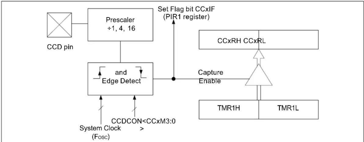
flowchart
graph TD
    A["CCD pin"] --> B["Prescaler ÷1, 4, 16"]
    B --> C["and Edge Detect"]
    C --> D["CCDCON<CCxM3:0 >"]
    D --> E["CCxRH CCxRL"]
    E --> F["TMR1H"]
    E --> G["TMR1L"]
    C --> H["Set Flag bit CCxIF (PIR1 register)"]
    C --> I["Capture Enable"]
    I --> E
    style A fill:#f9f,stroke:#333
    style B fill:#ccf,stroke:#333
    style C fill:#cfc,stroke:#333
    style D fill:#fcc,stroke:#333
    style E fill:#ffc,stroke:#333
    style F fill:#cff,stroke:#333
    style G fill:#ffc,stroke:#333
    style H fill:#cfc,stroke:#333
    style I fill:#ffc,stroke:#333
28.1.2 TIMER1 MODE SELECTION
Timer1 must be running off of the instruction clock for the CCD module to use the capture feature. If Timer1 is running off of the 8 MHz clock, the capture feature may not function correctly.
28.1.3 SOFTWARE INTERRUPT
When the Capture mode is changed, a false capture interrupt may be generated. The user should keep the enable for the capture interrupt clear in order to avoid false interrupts and should clear the flag bit, CCxIF, following any such change in the operating mode.
28.1.4 CCD PRESCALER
There are four prescaler settings, specified by bits CCxM3:CCxM0. Whenever the CCD register set is disabled or not set to Capture mode, the prescaler counter is cleared. Any reset will clear the prescaler counter.
Switching from one capture prescaler to another may generate an interrupt. Also, the prescaler counter will not be cleared, therefore, the first capture may be from a non-zero prescaler. It is recommended to disable the register set (CCxM3:0 = 00xx) prior to changing the prescaler value.
28.2 Compare Mode
In Compare mode, the 16-bit CCDRx register value is constantly compared against the TMR1 register pair value. When a match occurs, the CMPx pin:
- Is driven high
• Is driven low - Toggles
- Remains unchanged
The action on the pin is based on the value of the control bits, CCxM3:CCxM0. At the same time, interrupt flag bit, CCP1IF, is set.
FIGURE 28-2: COMPARE MODE OPERATION BLOCK DIAGRAM
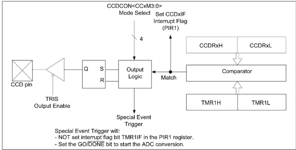
flowchart
graph TD
    A["CCD pin"] --> B["TRIS Output Enable"]
    B --> C["Q S R"]
    C --> D["Output Logic"]
    D --> E["Match"]
    F["CCDCON<CCxM3:0> Mode Select"] --> G["4"]
    H["Set CCDxIF Interrupt Flag (PIR1)"] --> D
    I["CCDRxH"] --> J["Comparator"]
    K["CCDRxL"] --> J
    J --> L["TMR1H"] --> M["TMR1L"]
    N["Special Event Trigger will: NOT set interrupt flag bit TMR1IF in the PIR1 register. Set the GO/DONE bit to start the ADC conversion."] --> D
28.2.1 CMPX PIN CONFIGURATION
The user must configure the CMPx pin as an output by clearing the TRIS bit for that pin.
Clearing the CCxM<3:0> bits will set the CMPx compare output latch to the default state. This is not the GPIO pin data latch. The default state for set-on-match or toggle-on-match is 0 but the default state for clear-on-match is 1.
28.2.2 TIMER1 MODE SELECTION
Timer1 must be running off of the instruction clock for the CCD module to use the compare feature. If Timer1 is running off of the 8 MHz clock, the compare feature may not function correctly.
28.2.3 SOFTWARE INTERRUPT MODE
When Generate Software Interrupt mode is chosen, the CCP1 pin is not affected. The CCP1IF bit is set, causing a CCx interrupt (if enabled).
28.2.4 SPECIAL EVENT TRIGGER
In this mode, an internal hardware trigger is generated, which may be used to initiate an action. The Special Event Trigger output of CCD does not reset the TMR1 register pair and starts an A/D conversion (if the A/D module is enabled).
Note: The Special Event Trigger from the CCD module does not set the interrupt flag bit TMR1IF (bit 0 in the PIR1 register).
28.3 Dual Capture/Compare Register
The Dual Capture/Compare Module is a new module based on the standard CCP. It has no PWM function.
REGISTER 28-1: CCDCON: DUAL CAPTURE/COMPARE CONTROL MODULE
| R/W-0 R/W-0 R/W-0 R/W-0 R/W-0 R/W-0 R/W-0 | |||||||
| CC2M3 | CC2M2 | CC2M1 | CC2M0 | CC1M3 | CC1M2 | CC1M1 | CC1M0 |
| bit 7 bit 0 | |||||||
Legend:
| R = Readable bit | W = Writable bit | U = Unimplemented bit, read as '0' |
| u = Bit is unchanged | x = Bit is unknown | -n = Value at POR |
| '1' = Bit is set | '0' = Bit is cleared |
bit 7-4 CC2M<3:0>: CC Register Set 2 Mode Select bits
00xx = Capture/Compare off (resets the module)
0100 = Capture mode, every falling edge
0101 = Capture mode, every rising edge
0110 = Capture mode, every 4^th rising edge
0111 = Capture mode, every 16 ^th rising edge
1000 = Compare mode, set output on match (CC2IF bit is set)
1001 = Compare mode, clear output on match (CC2IF bit is set)
1010 = Compare mode, toggle output on match (CC2IF bit is set)
1011 = Reserved
11xx = Compare mode, generate software interrupt on match (CC2IF bit is set, CMP2 pin is unaffected and configured as an I/O)
1111 = Compare mode, trigger special event (CC2IF bit is set; CC2 does not reset TMR1 ^(1) and starts an A/D conversion, if the A/D module is enabled. CMP2 pin is unaffected and configured as an I/O port)
bit 3-0 CC1M<3:0>: CC Register Set 1 Mode Select bits
00xx = Capture/Compare off (resets the module)
0100 = Capture mode, every falling edge
0101 = Capture mode, every rising edge
0110 = Capture mode, every 4^th rising edge
0111 = Capture mode, every 16^th rising edge
1000 = Compare mode, set output on match (CC1IF bit is set)
1001 = Compare mode, clear output on match (CC1IF bit is set)
1010 = Compare mode, toggle output on match (CC1IF bit is set)
1011 = Reserved
11xx = Compare mode, generate software interrupt on match (CC1IF bit is set, CMP1 pin is unaffected and configured as an I/O)
1111 = Compare mode, trigger special event (CC1IF bit is set; CC1 resets TMR1 and starts an A/D conversion, if the A/D module is enabled. CMP1 pin is unaffected and configured as an I/O port).
Note 1: When the Compare interrupt is set, a PIC will typically reset TMR1. This module does NOT reset TMR1.
NOTES:
29.0 MASTER SYNCHRONOUS SERIAL PORT (MSSP) MODULE
29.1 MSSP Module Overview
The Master Synchronous Serial Port (MSSP) module is a serial interface useful for communicating with other peripheral or microcontroller devices. These peripheral devices may be Serial EEPROMs, shift registers, display drivers, A/D converters, etc. The MSSP module in the MCP19116/7 only operates in Inter-Integrated Circuit (I²C) mode.
The I ^2 C interface supports the following modes and features:
- Master mode
- Slave mode
- Byte NACKing (Slave mode)
• Limited Multi-Master support - 7-bit and 10-bit addressing
- Start and Stop interrupts
- Interrupt masking
- Clock stretching
- Bus collision detection
- General call address matching
- Dual Address masking
- Address Hold and Data Hold modes
- Selectable SDA hold times
Figure 29-1 is a block diagram of the ^2C interface module in Master mode. Figure 29-2 is a diagram of the ^2C interface module in Slave mode.
FIGURE 29-1: MSSP BLOCK DIAGRAM (I ^2 C MASTER MODE)
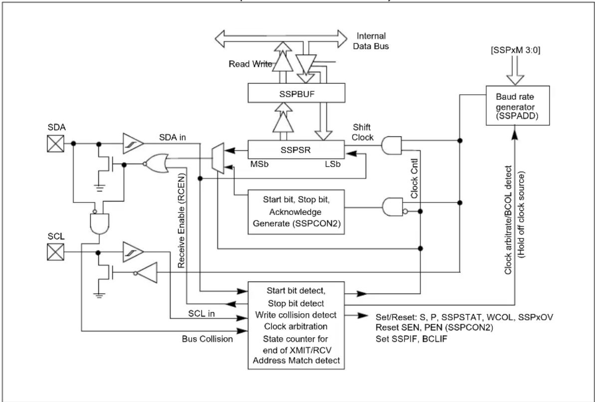
flowchart
graph TD
    A["SDA"] --> B["SDA in"]
    C["SCL"] --> D["Receive Enable (RCEN)"]
    B --> E["SSBUF"]
    D --> F["SSPSR"]
    E --> G["Shift Clock"]
    F --> H["MSb"]
    F --> I["LSb"]
    H --> J["Clock Cntl"]
    I --> K["Start bit, Stop bit, Acknowledge Generate (SSPCON2)"]
    J --> L["Clock arbitrate/BCOL detect (Hold off clock source)"]
    K --> M["Start bit detect, Stop bit detect"]
    L --> N["Set/Reset: S, P, SSPSTAT, WCOL, SSPxOV"]
    M --> O["Write collision detect"]
    N --> P["Reset SEN, PEN (SSPCON2)"]
    O --> Q["State counter for end of XMIT/RCV Address Match detect"]
    P --> R["Set SSPIF, BCLIF"]
    Q --> S["Bus Collision"]
    R --> T["BU"]
    S --> U["BU"]
    T --> V["BU"]
    U --> W["BU"]
    V --> X["BU"]
    W --> Y["BU"]
    X --> Z["BU"]
    Y --> AA["BU"]
    Z --> AB["BU"]
    AA --> AC["BU"]
    AB --> AD["BU"]
    AC --> AE["BU"]
    AD --> AF["BU"]
    AE --> AG["BU"]
    AF --> AH["BU"]
    AG --> AI["BU"]
    AH --> AJ["BU"]
    AI --> AK["BU"]
    AJ --> AL["BU"]
    AK --> AM["BU"]
    AL --> AN["BU"]
    AM --> AO["BU"]
    AN --> AP["BU"]
    AO --> AQ["BU"]
    AP --> AR["BU"]
    AQ --> AS["BU"]
    AR --> AT["BU"]
    AS --> AU["BU"]
    AT --> AV["BU"]
    AU --> AW["BU"]
    AV --> AX["BU"]
    AW --> AY["BU"]
FIGURE 29-2: MSSP BLOCK DIAGRAM (I²C SLAVE MODE)
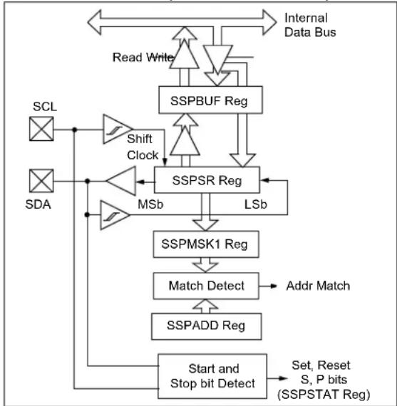
flowchart
graph TD
    A["SCL"] --> B["Shift Clock"]
    C["SDA"] --> D["MSb"]
    B --> E["SSPSR Reg"]
    D --> E
    E --> F["SSPBUF Reg"]
    F --> G["LSb"]
    G --> H["SSPMSK1 Reg"]
    H --> I["Match Detect"]
    I --> J["Addr Match"]
    J --> K["SSPADD Reg"]
    K --> L["Start and Stop bit Detect"]
    L --> M["Set, Reset S, P bits (SSPSTAT Reg)"]
    N["Internal Data Bus"] --> F
    O["Read Write"] --> F
29.2 I ^2 C MODE OVERVIEW
The Inter-Integrated Circuit Bus (I ^2 C) is a multi-master serial data communication bus. Devices communicate in a master/slave environment, where the master devices initiate the communication. A Slave device is controlled through addressing.
The I ^2 C bus specifies two signal connections:
- Serial Clock (SCL)
- Serial Data (SDA)
Both the SCL and SDA connections are bidirectional open-drain lines, each requiring pull-up resistors for the supply voltage. Pulling the line to ground is considered a logical zero; letting the line float is considered a logical one.
Figure 29-3 shows a typical connection between two devices configured as master and slave.
The I ^2 C bus can operate with one or more master devices and one or more slave devices.
There are four potential modes of operation for a given device:
- Master Transmit mode (master is transmitting data to a slave)
- Master Receive mode (master is receiving data from a slave)
- Slave Transmit mode (slave is transmitting data to a master)
- Slave Receive mode (slave is receiving data from a master)
To begin communication, a master device starts out in Master Transmit mode. The master device sends out a Start bit followed by the address byte of the slave it intends to communicate with. This is followed by a single Read/Write bit, which determines whether the master intends to transmit to or receive data from the slave device.
If the requested slave exists on the bus, it will respond with an Acknowledge bit, otherwise known as an ACK. The master then continues in either Transmit mode or Receive mode and the slave continues in the complement, either in Receive mode or Transmit mode, respectively.
A Start bit is indicated by a high-to-low transition of the SDA line while the SCL line is held high. Address and data bytes are sent out Most Significant bit (MSb) first. The Read/Write bit is sent out as a logical one when the master intends to read data from the slave, and is sent out as a logical zero when it intends to write data to the slave.
FIGURE 29-3: I ^2 C MASTER/
SLAVE CONNECTION
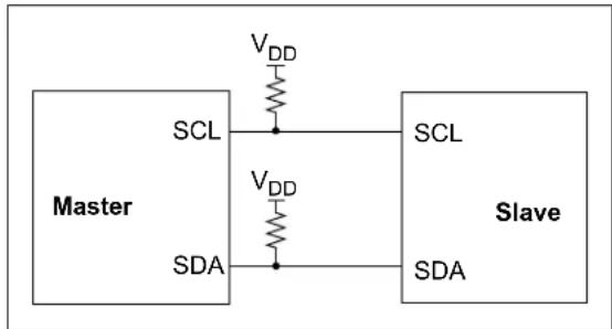
flowchart
graph TD
    A["Master"] -->|V_DD| B["Slave"]
    C["SCL"] --> D["V_DD"]
    E["SDA"] --> F["V_DD"]
    G["SCL"] --> H["Slave"]
    I["SDA"] --> J["Slave"]
The Acknowledge bit (ACK) is an active-low signal which holds the SDA line low to indicate to the transmitter that the slave device has received the transmitted data and is ready to receive more.
The transition of a data bit is always performed while the SCL line is held low. Transitions that occur while the SCL line is held high are used to indicate Start and Stop bits.
If the master intends to write to the slave, it repeatedly sends out a byte of data, with the slave responding after each byte with an ACK bit. In this example, the master device is in Master Transmit mode and the slave is in Slave Receive mode.
If the master intends to read from the slave, it repeatedly receives a byte of data from the slave and responds after each byte with an ACK bit. In this example, the master device is in Master Receive mode and the slave is Slave Transmit mode.
On the last byte of data communicated, the master device may end the transmission by sending a Stop bit. If the master device is in Receive mode, it sends the Stop bit in place of the last ACK bit. A Stop bit is indicated by a low-to-high transition of the SDA line while the SCL line is held high.
In some cases, the master may want to maintain control of the bus and re-initiate another transmission. If so, the master device may send another Start bit in place of the Stop bit or last ACK bit when it is in Receive mode.
The I ^2 C bus specifies three message protocols:
- Single message where a master writes data to a slave
- Single message where a master reads data from a slave
- Combined message where a master initiates a minimum of two writes, or two reads, or a combination of writes and reads, to one or more slaves
When one device is transmitting a logical one or letting the line float and a second device is transmitting a logical zero or holding the line low, the first device can detect that the line is not a logical one. This detection, when used on the SCL line, is called clock stretching. Clock stretching gives slave devices a mechanism to control the flow of data. When this detection is used on the SDA line, it is called arbitration. Arbitration ensures that there is only one master device communicating at any single time.
29.2.1 CLOCK STRETCHING
When a slave device has not completed processing data, it can delay the transfer of more data through the process of Clock Stretching. An addressed slave device may hold the SCL clock line low after receiving or sending a bit, indicating that it is not yet ready to continue. The master that is communicating with the slave will attempt to raise the SCL line in order to transfer the next bit, but will detect that the clock line has not yet been released. Because the SCL connection is open-drain, the slave has the ability to hold that line low until it is ready to continue communicating.
Clock stretching allows receivers that cannot keep up with a transmitter to control the flow of incoming data.
29.2.2 ARBITRATION
Each master device must monitor the bus for Start and Stop bits. If the device detects that the bus is busy, it cannot begin a new message until the bus returns to an idle state.
However, two master devices may try to initiate a transmission at or about the same time. When this occurs, the process of arbitration begins. Each transmitter checks the level of the SDA data line and compares it to the level that it expects to find. The first transmitter to observe that the two levels don't match loses arbitration and must stop transmitting on the SDA line.
For example, if one transmitter holds the SDA line to a logical one (lets it float) and a second transmitter holds it to a logical zero (pulls it low), the result is that the SDA line will be low. The first transmitter then observes that the level of the line is different than expected and concludes that another transmitter is communicating.
The first transmitter to notice this difference is the one that loses arbitration and must stop driving the SDA line. If this transmitter is also a master device, it must also stop driving the SCL line. It then can monitor the lines for a Stop condition before trying to reissue its transmission. In the meantime, the other device that has not noticed any difference between the expected and actual levels on the SDA line continues with its original transmission. It can do so without any complications, because so far the transmission appears exactly as expected, with no other transmitter disturbing the message.
Slave Transmit mode can also be arbitrated, when a master addresses multiple slaves, but this is less common.
If two master devices are sending a message to two different slave devices at the address stage, the master sending the lower slave address always wins arbitration. When two master devices send messages to the same slave address, and addresses can sometimes refer to multiple slaves, the arbitration process must continue into the data stage.
Arbitration usually occurs very rarely, but it is a necessary process for proper multi-master support.
29.3 I ^2 C MODE OPERATION
All MSSP I ^2 C communication is byte-oriented and shifted out MSb first. Six SFR registers and two interrupt flags interface the module with the PIC microcontroller and with the user's software. Two pins, SDA and SCL, are exercised by the module to communicate with other external I ^2 C devices.
29.3.1 BYTE FORMAT
All communication in I^2C is done in 9-bit segments. A byte is sent from a Master to a Slave or vice versa, followed by an Acknowledge bit sent back. After the 8^th falling edge of the SCL line, the device outputting data on the SDA changes that pin to an input and reads in an acknowledge value on the next clock pulse.
The clock signal, SCL, is provided by the master. Data is valid to change while the SCL signal is low, and sampled on the rising edge of the clock. Changes on the SDA line while the SCL line is high define special conditions on the bus, explained in the following sections.
29.3.2 DEFINITION OF I ^2 C TERMINOLOGY
There is language and terminology in the description of I^2C communication that have definitions specific to I^2C . Such word usage is defined in Table 29-1 and may be used in the rest of this document without explanation. The information in this table was adapted from the Philips I^2C specification.
29.3.3 SDA AND SCL PINS
Selecting any I^2C mode with the SSPEN bit set forces the SCL and SDA pins to be open-drain. These pins should be set by the user to inputs by setting the appropriate TRIS bits.
Note: Data is tied to output zero when an I ^2 C mode is enabled.
29.3.4 SDA HOLD TIME
The hold time of the SDA pin is selected by the SDAHT bit in the SSPCON3 register. Hold time is the time SDA is held valid after the falling edge of SCL. Setting the SDAHT bit selects a longer 300 ns minimum hold time and may help on buses with large capacitance.
TABLE 29-1: I ^2 C BUS TERMS
| Term Description | |
| Transmitter The device that shifts data out onto the bus | |
| Receiver The device that shifts data in from the bus | |
| Master The device that initiates a transfer, generates clock signals and terminates a transfer | |
| Slave The device addressed by the master | |
| Multi-Master | A bus with more than one device that can initiate data transfers |
| Arbitration | Procedure to ensure that only one master at a time controls the bus. Winning arbitration ensures that the message is not corrupted. |
| Synchronization | Procedure to synchronize the clocks of two or more devices on the bus |
| Idle | No master is controlling the bus and both SDA and SCL lines are high |
| Active | Any time one or more master devices are controlling the bus |
| Addressed Slave | Slave device that has received a matching address and is actively being clocked by a master |
| Matching Address | Address byte that is clocked into a slave that matches the value stored in SSPADDx |
| Write Request | Slave receives a matching address with R/Wbit clear and is ready to clock in data |
| Read Request | Master sends an address byte with the R/W bit set, indicating that it wishes to clock data out of the Slave. The data that follows is read by the Master. A data transfer is terminated by a Stop condition which is generated by the Master. The Master could also generate a repeated START condition is applicable. |
| Clock Stretching | When a device on the bus holds SCL low to stall communication |
| Bus Collision | Any time the SDA line is sampled low by the module while it is outputting and expected high state |
29.3.5 START CONDITION
The I^2C specification defines a Start condition as a transition of SDA from a high state to a low state, while SCL line is high. A Start condition is always generated by the master and signifies the transition of the bus from an Idle to an Active state. Figure 29-4 shows the wave forms for Start and Stop conditions.
A bus collision can occur on a Start condition if the module samples the SDA line low before asserting it low. This does not conform to the ^2 C Specification that states no bus collision can occur on a Start.
29.3.6 STOP CONDITION
A Stop condition is a transition of the SDA line from low-to-high state while the SCL line is high.
Note: At least one SCL low time must appear before a Stop is valid. Therefore, if the SDA line goes low then high again while the SCL line stays high, only the Start condition is detected.
29.3.7 RESTART CONDITION
A Restart is valid any time that a Stop is valid. A master can issue a Restart if it wishes to hold the bus after terminating the current transfer. A Restart has the same effect on the slave that a Start would, resetting all slave logic and preparing it to clock in an address. The master may want to address the same or another slave.
In 10-bit Addressing Slave mode, a Restart is required for the master to clock data out of the addressed slave. Once a slave has been fully addressed, matching both high and low address bytes, the master can issue a Restart and the high address byte with the R/W bit set. The slave logic will then hold the clock and prepare to clock out data.
After a full match with R/W clear in 10-bit mode, a prior match flag is set and maintained until a Stop condition, a high address with R/W clear or a high address match fails.
29.3.8 START/STOP CONDITION INTERRUPT MASKING
The SCIE and PCIE bits in the SSPCON3 register can enable the generation of an interrupt in Slave modes that do not typically support this function. These bits will have no effect on slave modes where interrupt on Start and Stop detect are already enabled.
FIGURE 29-4: I ^2 C START AND STOP CONDITIONS
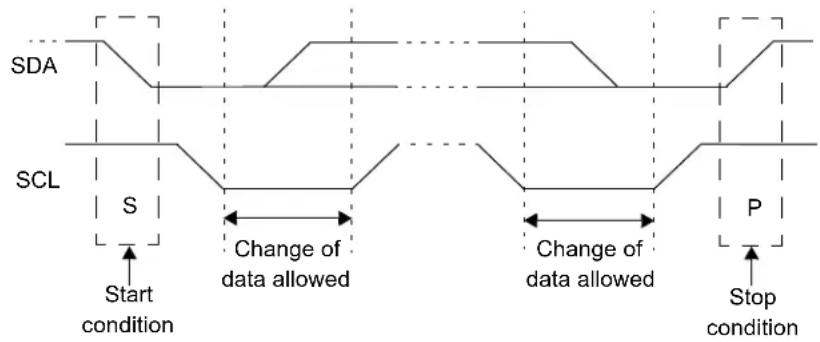
FIGURE 29-5: I ^2 C RESTART CONDITION
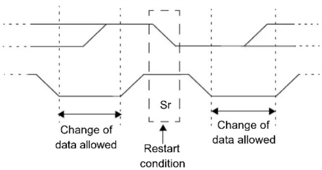
The 9^th SCL pulse for any transferred byte in I^2C is dedicated as an Acknowledge. It allows receiving devices to respond back to the transmitter by pulling the SDA line low. The transmitter must release control of the line during this time to shift in the response. The Acknowledge (ACK) is an active-low signal, pulling the SDA line low, indicating to the transmitter that the device has received the transmitted data and is ready to receive more.
The result of an ACK is placed in the ACKSTAT bit in the SSPCON2 register.
Slave software, when the AHEN and DHEN bits are set, allows the user to set the ACK value sent back to the transmitter. The ACKDT bit in the SSPCON2 register is set/cleared to determine the response.
Slave hardware will generate an ACK response if the AHEN and DHEN bits in the SSPCON3 register are clear.
There are certain conditions where an ACK will not be sent by the slave. If the BF bit in the SSPSTAT register or the SSPOV bit in the SSPCON1 register are set when a byte is received, the ACK will not be sent.
When the module is addressed, after the 8^th falling edge of SCL on the bus, the ACKTIM bit in the SSPCON3 register is set. The ACKTIM bit indicates the acknowledge time of the active bus. The ACKTIM status bit is only active when the AHEN or DHEN bits are enabled.
29.4 I ^2 C SLAVE MODE OPERATION
The MSSP Slave mode operates in one of the four modes selected in the SSPM bits in SSPCON1 register. The modes can be divided into 7-bit and 10-bit Addressing mode. 10-bit Addressing mode operates the same as 7-bit, with some additional overhead for handling the larger addresses.
Modes with Start and Stop bit interrupts operate the same as the other modes, with SSPIF additionally getting set upon detection of a Start, Restart or Stop condition.
The SSPADD register contains the Slave mode address. The first byte received after a Start or Restart condition is compared against the value stored in this register. If the byte matches, the value is loaded into the SSPBUF register and an interrupt is generated. If the value does not match, the module goes idle and no indication is given to the software that anything happened.
The SSPMSK1 register affects the address matching process. Refer to Section 29.4.10 "SSPMSK1 Register" for more information.
29.4.2 SECOND SLAVE MODE ADDRESS
The SSPADD2 register contains a second 7-bit Slave mode address. The first byte received after a Start or Restart condition is compared against the value stored in this register. If the byte matches, the value is loaded into the SSPBUF register and an interrupt is generated. If the value does not match, the module goes idle and no indication is given to the software that anything happened.
The SSPMSK2 register affects the address matching process. Refer to Section 29.4.10 “SSPMSK1 Register” for more information.
29.4.2.1 I ^2 C Slave 7-Bit Addressing Mode
In 7-bit Addressing mode, the LSb of the received data byte is ignored when determining if there is an address match.
29.4.2.2 I ^2 C Slave 10-Bit Addressing Mode
In 10-bit Addressing mode, the first received byte is compared to the binary value of '1 1 1 1 0 A 9 A 8 0'. A9 and A8 are the two MSb of the 10-bit address and are stored in bits 2 and 1 in the SSPADD register.
After the high byte has been acknowledged, the UA bit is set and SCL is held low until the user updates SSPADD with the low address. The low-address byte is clocked in, and all 8 bits are compared to the low-address value in SSPADD. Even if there is no address match, SSPIF and UA are set and SCL is held low until SSPADD is updated to receive a high byte again. When SSPADD is updated, the UA bit is cleared. This ensures the module is ready to receive the high-address byte on the next communication.
A high- and low-address match as a write request is required at the start of all 10-bit addressing communication. A transmission can be initiated by issuing a Restart once the slave is addressed, and clocking in the high address with the R/W bit set. The slave hardware then acknowledges the read request and prepares to clock out data. This is only valid for a slave after it has received a complete high and low address-byte match.
29.4.3 SLAVE RECEPTION
When the R/ bit of a matching received address byte is clear, the R/ bit in the SSPSTAT register is cleared. The received address is loaded into the SSPBUF register and acknowledged.
When an overflow condition exists for a received address, then Not Acknowledge is given. An overflow condition is defined as either bit BF in the SSPSTAT register is set, or bit SSPOV in the SSPCON1 register is set. The BOEN bit in the SSPCON3 register modifies this operation. For more information, refer to Register 29-4.
A MSSP interrupt is generated for each transferred data byte. Flag bit SSPIF must be cleared by software.
When the SEN bit in the SSPCON2 register is set, SCL will be held low (clock stretch) following each received byte. The clock must be released by setting the CKP bit in the SSPCON1 register, except sometimes in 10-bit mode.
29.4.3.1 7-Bit Addressing Reception
This section describes a standard sequence of events for the MSSP module configured as an I^2C Slave in 7-bit Addressing mode, including all decisions made by hardware or software and their effect on reception. Figures 29-5 and 29-6 are used as a visual reference for this description.
This is a step-by-step process of what typically must be done to accomplish I^2C communication.
- Start bit detected.
- S bit in the SSPSTAT register is set; SSPIF is set if interrupt-on-Start detect is enabled.
-
Matching address with R/W bit clear is received.
-
The slave pulls SDA low, sending an ACK to the master, and sets SSPIF bit.
-
Software clears the SSPIF bit.
-
Software reads received address from SSPBUF clearing the BF flag.
-
If SEN = 1, Slave software sets CKP bit to release the SCL line.
-
The master clocks out a data byte.
-
Slave drives SDA low sending an ACK to the master, and sets SSPIF bit.
-
Software clears SSPIF.
-
Software reads the received byte from SSPBUF clearing BF.
-
Steps 8-12 are repeated for all received bytes from the Master.
-
Master sends Stop condition, setting P bit in the SSPSTAT register, and the bus goes idle.
29.4.3.2 7-Bit Reception with AHEN and DHEN
Slave device reception with AHEN and DHEN set operates the same as without these options with extra interrupts and clock stretching added after the 8^th falling edge of SCL. These additional interrupts allow the slave software to decide whether it wants the ACK to receive address or data byte, rather than the hardware.
This list describes the steps that need to be taken by slave software to use these options for I^2C communication. Figure 29-7 displays a module using both address and data holding. Figure 29-8 includes the operation with the SEN bit in the SSPCON2 register set.
- S bit in the SSPSTAT register is set; SSPIF is set if interrupt-on-Start detect is enabled.
- Matching address with R/W ^- bit clear is clocked in. SSPIF is set and CKP cleared after the 8 ^th falling edge of SCL.
- Slave clears the SSPIF.
- Slave can look at the ACKTIM bit in the SSPCON3 register to determine if the SSPIF was after or before the ACK.
- Slave reads the address value from SSPBUF, clearing the BF flag.
- Slave sets ACK value clocked out to the master by setting ACKDT.
- Slave releases the clock by setting CKP.
- SSPxIF is set after an ACK, not after a NACK.
- If SEN = 1 the slave hardware will stretch the clock after the ACK.
- Slave clears SSPIF.
Note: SSPIF is still set after the 9^th falling edge of SCL even if there is no clock stretching and BF has been cleared. The SSPIF is not set only when NACK is sent to Master.
- SSPIF set and CKP cleared after 8^th falling edge of SCL for a received data byte.
- Slave looks at ACKTIM bit in the SSPCON3 register to determine the source of the interrupt.
- Slave reads the received data from SSPBUF clearing BF.
- Steps 7-14 are the same for each received data byte.
- Communication is ended by either the slave sending an ACK = 1 or the master sending a Stop condition. If a Stop is sent and Interrupt-on-Stop Detect is disabled, the slave will only know by polling the P bit in the SSPSTAT register.
FIGURE 29-6: I ^2 C SLAVE, 7-BIT ADDRESS, RECEPTION (SEN = 0, AHEN = 0, DHEN = 0)
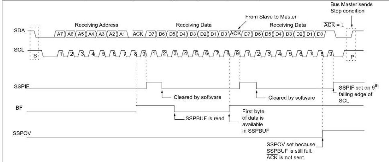
flowchart
graph TD
    A["Receiving Address"] --> B["Receiving Data"]
    B --> C["From Slave to Master"]
    C --> D["Receiving Data"]
    D --> E["ACK = 1"]
    F["SDA"] --> G["A7 A6 A5 A4 A3 A2 A1 ACK D7 D6 D5 D4 D3 D2 D1 D0 ACK D7 D6 D5 D4 D3 D2 D1 D0"]
    H["SCL"] --> I["S 1 2 3 4 5 6 7 8 9 1 2 3 4 5 6 7 8 9 1 2 3 4 5 6 7 8 9 1 2 3 4 5 6 7 8 9"]
    J["SSPIF"] --> K["Cleared by software"]
    L["BF"] --> M["First byte of data is available in SSPBUF"]
    N["SSPOV"] --> O["SSPOV set because SSPBUF is still full. ACK is not sent."]
    P["Bus Master sends Stop condition"] --> Q["ACK = 1"]
FIGURE 29-7: I ^2 C SLAVE, 7-BIT ADDRESS, RECEPTION (SEN = 1, AHEN = 0, DHEN = 0)
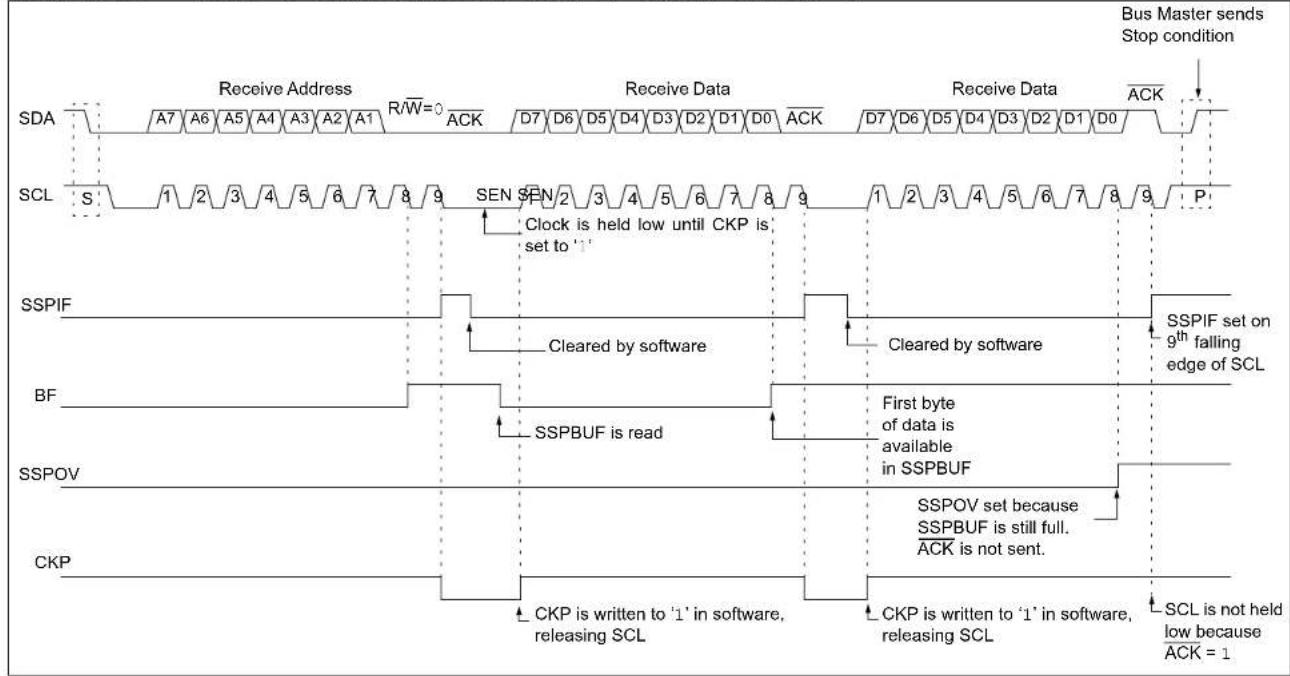
flowchart
graph TD
    A["Receive Address"] --> B["SDA"]
    B --> C["SCL"]
    C --> D["SSPIF"]
    D --> E["BF"]
    E --> F["SSPOV"]
    F --> G["CKP"]

    subgraph SDA
        H["A7"] --> I["A6"] --> J["A5"] --> K["A4"] --> L["A3"] --> M["A2"] --> N["A1"] --> O["R/W=0"] --> P["ACK"]
    end

    subgraph SCL
        Q["S"] --> R["S1"] --> S["S2"] --> T["S3"] --> U["S4"] --> V["S5"] --> W["S6"] --> X["S7"] --> Y["S8"] --> Z["S9"] --> AA["SEN"]
    end

    subgraph SSPIF
        AB["Cleared by software"] --> AC["Cleared by software"]
        AD["First byte of data is available in SSPBUF"] --> AE["SSPOV set because SSPBUF is still full. ACK is not sent."]
    end

    subgraph BF
        AF["SSPBUF is read"] --> AG["SSPOV set because SSPBUF is still full. ACK is not sent."]
    end

    subgraph SSPOV
        AH["CKP is written to '1' in software, releasing SCL"] --> AI["CKP is written to '1' in software, releasing SCL"]
        AJ["CKP is not held low because ACK = 1"] --> AK["SCL is not held low because ACK = 1"]
    end

    subgraph CKP
        AL["Cleared by software"] --> AM["Clock is held low until CKP is set to '1'"]
    end

    subgraph_BusMaster["{Bus Master sends Stop condition}<br>        AN[D7"] --> AO["D6"] --> AP["D5"] --> AQ["D4"] --> AR["D3"] --> AS["D2"] --> AT["D1"] --> AU["D0"] --> AV["ACK"]
    end
FIGURE 29-8: I ^2 C SLAVE, 7-BIT ADDRESS, RECEPTION (SEN = 0, AHEN = 1, DHEN = 1)
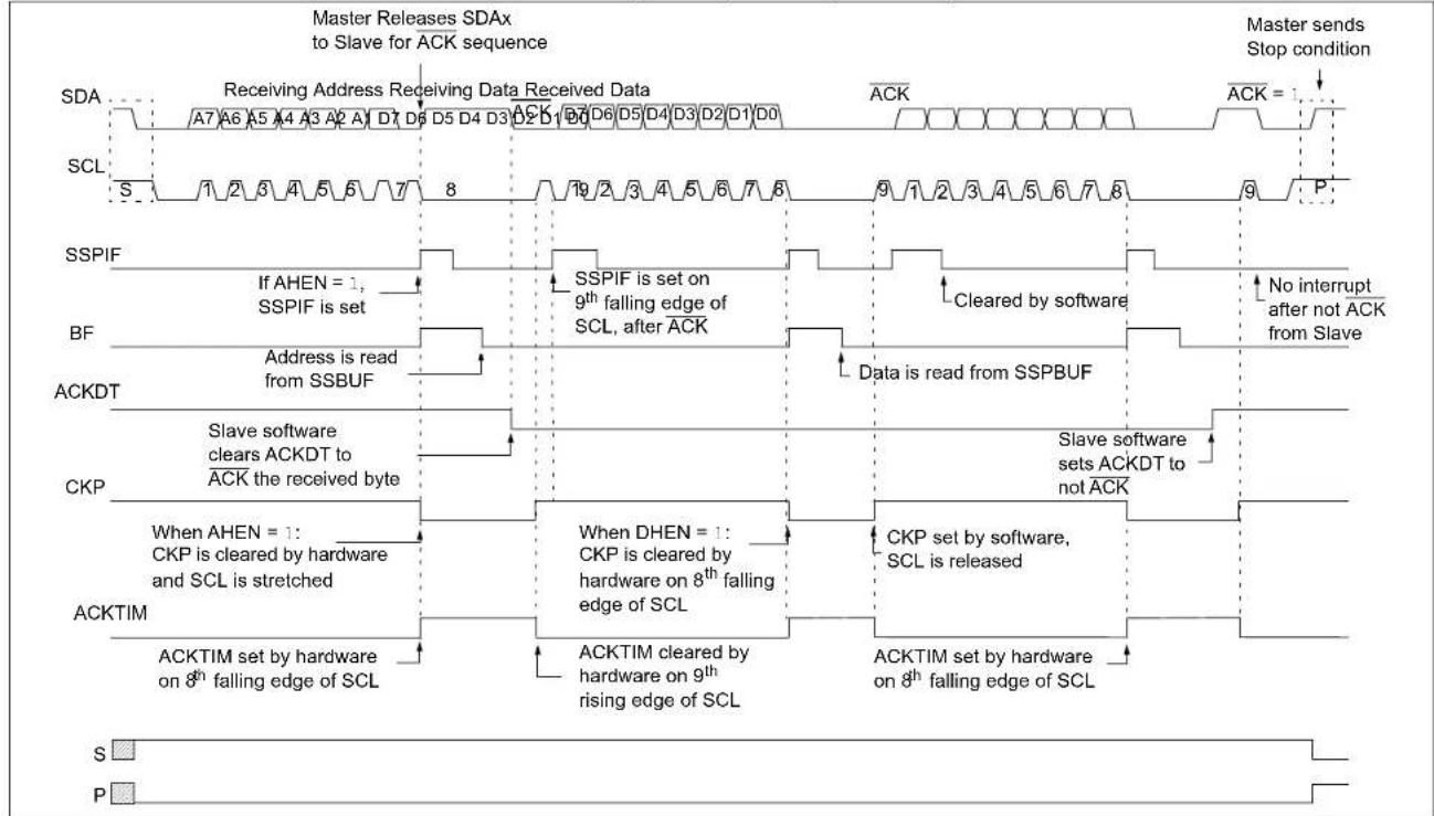
flowchart
graph TD
    A["Master Releases SDAx to Slave for ACK sequence"] --> B["SDA"]
    B --> C["Receiving Address Receiving Data Received Data"]
    C --> D["SCL"]
    D --> E["ACK"]
    E --> F["ACK = 1"]
    F --> G["Master sends Stop condition"]
    H["SSPIF"] --> I["If AHEN = 1, SSPIF is set"]
    I --> J["Address is read from SSBUF"]
    J --> K["SSPIF is set on 9th falling edge of SCL, after ACK"]
    K --> L["Cleared by software"]
    L --> M["No interrupt after not ACK from Slave"]
    N["BF"] --> O["Address is read from SSBUF"]
    O --> P["Data is read from SSPBUF"]
    P --> Q["ACKDT"]
    Q --> R["Slave software clears ACKDT to ACK the received byte"]
    R --> S["CKP"]
    S --> T["When AHEN = 1: CKP is cleared by hardware and SCL is stretched"]
    T --> U["ACKTIM"]
    U --> V["ACKTIM set by hardware on 8th falling edge of SCL"]
    V --> W["ACKTIM cleared by hardware on 9th rising edge of SCL"]
    W --> X["ACKPT"]
    X --> Y["ACKPT set by software, SCL is released"]
    Y --> Z["ACKTIM set by hardware on 8th falling edge of SCL"]
    Z --> AA["S"]
    Z --> AB["P"]
FIGURE 29-9: I ^2 C SLAVE, 7-BIT ADDRESS, RECEPTION (SEN = 1, AHEN = 1, DHEN = 1)
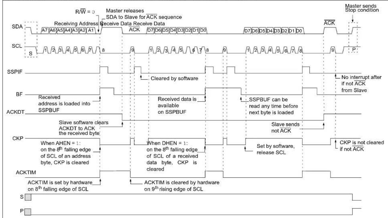
flowchart
graph TD
    A["Receiving Address"] --> B["SDA to Slave for ACK sequence"]
    B --> C["Receive Data Receive Data"]
    C --> D["ACK"]
    D --> E["D7 D6 D5 D4 D3 D2 D1 D0"]
    E --> F["D7 D6 D5 D4 D3 D2 D1 D0"]
    F --> G["ACK"]
    G --> H["Master sends Stop condition"]

    I["Received address is loaded into SSPBUF"] --> J["SLAVE SOFTWARE CLEAR"]
    J --> K["ACKDT to ACK the received byte"]
    K --> L["SLAVE SOFTWARE IS cleared"]
    L --> M["ACKDT to ACK the received byte"]
    M --> N["SLAVE SOFTWARE IS cleared by hardware on 8th falling edge of SCL"]

    O["SLAVE DATA is available on SSPBUF"] --> P["SLAVE DATA IS cleared by software"]
    P --> Q["SLAVE DATA IS cleared by software"]
    Q --> R["SLAVE DATA IS cleared by software"]
    R --> S["SLAVE DATA IS cleared by software"]

    T["SLAVE DATA is cleared by hardware on 9th rising edge of SCL"] --> U["SLAVE DATA IS cleared by software"]
    U --> V["SLAVE DATA IS cleared by software"]
    V --> W["SLAVE DATA IS cleared by software"]

    X["SLAVE DATA is cleared by software"] --> Y["SLAVE DATA IS cleared by software"]
    Y --> Z["SLAVE DATA IS cleared by software"]
    Z --> AA["SLAVE DATA IS cleared by software"]

    AB["SLAVE DATA is cleared by software"] --> AC["SLAVE DATA IS cleared by software"]
    AC --> AD["SLAVE DATA IS cleared by software"]
    AD --> AE["SLAVE DATA IS cleared by software"]

    AF["SLAVE DATA is cleared by software"] --> AG["SLAVE DATA IS cleared by software"]
    AG --> AH["SLAVE DATA IS cleared by software"]
    AH --> AI["SLAVE DATA IS cleared by software"]

    AJ["SLAVE DATA is cleared by software"] --> AK["SLAVE DATA IS cleared by software"]
    AK --> AL["SLAVE DATA IS cleared by software"]
    AL --> AM["SLAVE DATA IS cleared by software"]

    AN["SLAVE DATA is cleared by software"] --> AO["SLAVE DATA IS cleared by software"]
    AO --> AP["SLAVE DATA IS cleared by software"]
    AP --> AQ["SLAVE DATA IS cleared by software"]

    AR["SLAVE DATA is cleared by software"] --> AS["SLAVE DATA IS cleared by software"]
    AS --> AT["SLAVE DATA IS cleared by software"]
    AT --> AU["SLAVE DATA IS cleared by software"]

    AV["SLAVE DATA is cleared by software"] --> AW["SLAVE DATA IS cleared by software"]
    AW --> AX["SLAVE DATA IS cleared by software"]
    AX --> AY["SLAVE DATA IS cleared by software"]

    AZ["SLAVE DATA is cleared by software"] --> BA["SLAVE DATA IS cleared by software"]
    BA --> BB["SLAVE DATA IS cleared by software"]
    BB --> BC["SLAVE DATA IS cleared by software"]

    BD["SLAVE DATA is cleared by software"] --> BE["SLAVE DATA IS cleared by software"]
    BE --> BF["SLAVE DATA IS cleared by software"]
    BF --> BG["SLAVE DATA IS cleared by software"]

    BH["SLAVE DATA is cleared by software"] --> BI["SLAVE DATA IS cleared by software"]
    BI --> BJ["SLAVE DATA IS cleared by software"]
    BJ --> BK["SLAVE DATA IS cleared by software"]

    BL["SLAVE DATA is cleared by software"] --> BM["SLAVE DATA IS cleared by software"]
    BM --> BN["SLAVE DATA IS cleared by software"]

    BO["SLAVE DATA is cleared by software"] --> BP["SLAVE DATA IS cleared by software"]
    BP --> BQ["SLAVE DATA IS cleared by software"]

    BR["SLAVE DATA is cleared by software"] --> BS["SLAVE DATA IS cleared by software"]
    BS --> BT["SLAVE DATA IS cleared by software"]

    BU["SLAVE DATA is cleared by software"] --> BV["SLAVE DATA IS cleared by software"]
    BV --> BW["SLAVE DATA IS cleared by software"]

    BX["SLAVE DATA is cleared by software"] --> BY["SLAVE DATA IS cleared by software"]
    BY --> BZ["SLAVE DATA IS cleared by software"]

    CA["SLAVE DATA is cleared by software"] --> CB["SLAVE DATA IS cleared by software"]
    CB --> CC["SLAVE DATA IS cleared by software"]

    DA["SLAVE Data is cleared by Software"] --> DB["A7 A6 A5 A4 A3 A2 A1"]

    DC["CCKP"] --> DD["When AHEN = 1: on the 8th falling edge of SCL of an address byte, CKP is cleared"]

    EE["ACKTIM"] --> EEA["ACKTIM is set by hardware on 8th falling edge of SCL"]

    EF["S"] --> EF
    EF --> EF
    EF --> EF

    GF["P"] --> GF

    GH["CSPIF"] --> GH
    GH --> GH
    GH --> GH

    ID["BF"] --> ID
    ID --> ID
    ID --> ID
    ID --> ID

    IJ["ACKDT"] --> IJ
    IJ --> IJ

    JX["CPP"] --> JX
    JX --> JX

    KX["CKP"] --> KX
    KX --> KX

    LX["CSPBUF"] --> LX
    LX --> LX

    MZ["CSPBUF can be read any time before next byte is loaded"]
29.4.4 SLAVE TRANSMISSION
When the R/W bit of the incoming address byte is set and an address match occurs, the R/W bit in the SSPSTAT register is set. The received address is loaded into the SSPBUF register and an ACK pulse is sent by the slave on the 9^th bit.
Following the ACK, slave hardware clears the CKP bit and the SCL pin is held low. Refer to Section 29.4.7, Clock Stretching for more details. By stretching the clock, the master will be unable to assert another clock pulse until the slave is done preparing the transmit data.
The transmit data must be loaded into the SSPBUF register, which also loads the SSPSR register. Then the SCL pin should be released by setting the CKP bit in the SSPCON1 register. The eight data bits are shifted out on the falling edge of the SCL input. This ensures that the SDA signal is valid during the SCL high time.
The ACK pulse from the master-receiver is latched on the rising edge of the 9 ^th SCL input pulse. This ACK value is copied to the ACKSTAT bit in the SSPCON2 register. If ACKSTAT is set (not ACK), the data transfer is complete. In this case, when the not ACK is latched by the slave, the slave goes idle and waits for another occurrence of the Start bit. If the SDA line was low (ACK), the next transmit data must be loaded into the SSPBUF register. Again, the SCL pin must be released by setting bit CKP.
An MSSP interrupt is generated for each data transfer byte. The SSPIF bit must be cleared by software, and the SSPSTAT register is used to determine the status of the byte. The SSPIF bit is set on the falling edge of the 9^th clock pulse.
29.4.4.1 Slave Mode Bus Collision
A slave receives a read request and begins shifting data out on the SDA line. If a bus collision is detected and the SBCDE bit in the SSPCON3 register is set, the BCLIF bit in the PIR register is set. Once a bus collision is detected, the slave goes idle and waits to be addressed again. The user's software can use the BCLIF bit to handle a slave bus collision.
29.4.4.2 7-Bit Transmission
A master device can transmit a read request to a slave, and then it clocks data out of the slave. The list below outlines what slave software does in order to accomplish a standard transmission. Figure 29-10 can be used as a reference to this list.
- Master sends a Start condition on SDA and SCL.
- S bit in the SSPSTAT register is set; SSPIF is set if interrupt-on-Start detect is enabled.
- Matching address with R/W bit set is received by the Slave setting SSPIF bit.
- Slave hardware generates an ACK and sets SSPIF.
- SSPIF bit is cleared by user.
- Software reads the received address from SSPBUF, clearing BF.
- R/W ^- is set so CKP was automatically cleared after the ACK.
- The slave software loads the transmit data into SSPBUF.
- CKP bit is set releasing SCL, allowing the master to clock the data out of the slave.
- SSPIF is set after the ACK response from the master is loaded into the ACKSTAT register.
- SSPIF bit is cleared.
- The slave software checks the ACKSTAT bit to see if the master wants to clock out more data.
Note 1: If the master ACK s, the clock will be stretched.
2: ACKSTAT is the only bit updated on the rising edge of SCL ( 9^th ) rather than on the falling edge.
- Steps 9-13 are repeated for each transmitted byte.
- If the master sends a not ACK, the clock is not held but SSPIF is still set.
- The master sends a Restart condition or a Stop
- The slave is no longer addressed.
FIGURE 29-10: I ^2 C SLAVE, 7-BIT ADDRESS, TRANSMISSION (AHEN = 0)
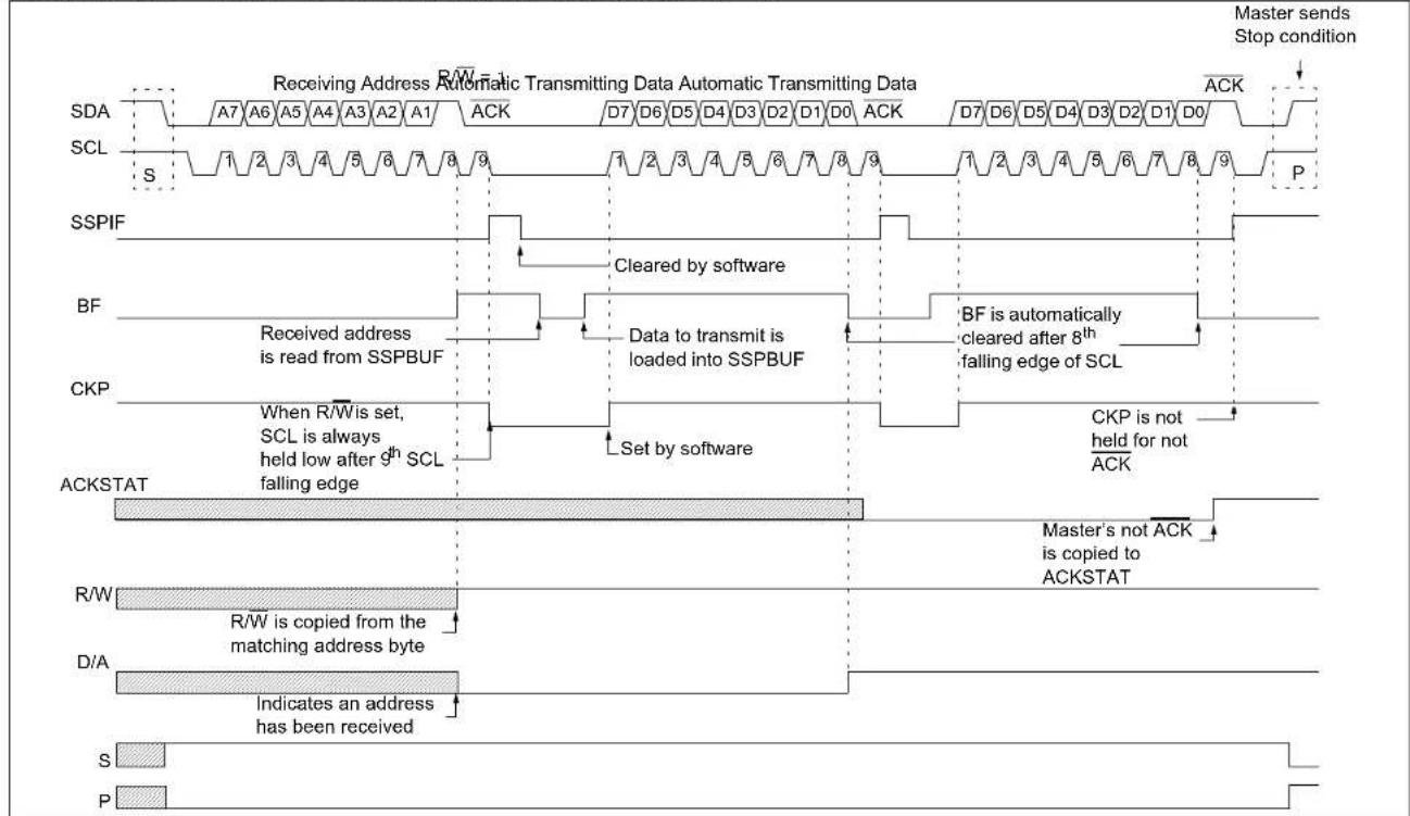
flowchart
graph TD
    A["Receiving Address"] --> B["Automatic Transmitting Data"]
    B --> C["SDA"]
    B --> D["SCL"]
    B --> E["SSPIF"]
    B --> F["BF"]
    B --> G["CKP"]
    B --> H["ACKSTAT"]
    B --> I["R/W"]
    B --> J["D/A"]
    B --> K["S"]
    B --> L["P"]

    subgraph Data
        M["A7"] --> N["A6"] --> O["A5"] --> P["A4"] --> Q["A3"] --> R["A2"] --> S["A1"] --> T["ACK"]
        U["D7"] --> V["D6"] --> W["D5"] --> X["D4"] --> Y["D3"] --> Z["D2"] --> AA["D1"] --> AB["D0"] --> AC["ACK"]
        AD["D7"] --> AE["D6"] --> AF["D5"] --> AG["D4"] --> AH["D3"] --> AI["D2"] --> AJ["D1"] --> AK["D0"]
        AL["1"] --> AM["2"] --> AN["3"] --> AO["4"] --> AP["5"] --> AQ["6"] --> AR["7"] --> AS["8"] --> AT["9"]
        AU["1"] --> AV["2"] --> AW["3"] --> AX["4"] --> AY["5"] --> AZ["6"] --> BA["7"] --> BB["8"] --> BC["9"]
        BD["1"] --> BE["2"] --> BF["3"] --> BG["4"] --> BH["5"] --> BI["6"] --> BJ["7"] --> BK["8"] --> BL["9"]
        BM["1"] --> BN["2"] --> BO["3"] --> BP["4"] --> BQ["5"] --> BR["6"] --> BS["7"] --> BT["8"] --> BU["9"]
        BV["1"] --> BW["2"] --> BX["3"] --> BY["4"] --> BZ["5"] --> CA["6"] --> CB["7"] --> CC["8"]
        CD["P"] --> CE["P"]
    end

    subgraph Software
        CF["Cleared by software"]
        GF["Data to transmit is loaded into SSPBUF"]
        GH["CF is automatically cleared after 8th falling edge of SCL"]
        IJ["Set by software"]
        KJ["CKP is not held for not ACK"]
    end

    subgraph Data
        L["Cleared by software"]
        M["Cleared by software"]
        GF["Cleared by software"]
        IJ["Cleared by software"]
        KJ["Cleared by software"]
        M["Cleared by software"]
    end

    subgraph Software
        N["Cleared by software"]
        O["Cleared by software"]
        P["Cleared by software"]
        Q["Cleared by software"]
        R["Cleared by software"]
        S["Cleared by software"]
    end

    subgraph Data
        S["Cleared by software"]
        T["Cleared by software"]
        U["Cleared by software"]
        V["Cleared by software"]
        W["Cleared by software"]
        X["Cleared by software"]
        Y["Cleared by software"]
        Z["Cleared by software"]
    end

    subgraph Data
        W["Cleared by software"]
        X["Cleared by software"]
        Y["Cleared by software"]
        Z["Cleared by software"]
        AA["Cleared by software"]
        AB["Cleared by software"]
        AC["Cleared by software"]
        AD["Cleared by software"]
        AE["Cleared by software"]
        AF["Cleared by software"]
        AG["Cleared by software"]
    end

    subgraph Software
        AH["Cleared by software"]
        AI["Cleared by software"]
        AJ["Cleared by software"]
        AK["Cleared by software"]
        AL["Cleared by software"]
        AM["Cleared by software"]
        AN["Cleared by software"]
        AO["Cleared by software"]
        AP["Cleared by software"]
    end

    subgraph Data
        AQ["Cleared by software"]
        AR["Cleared by software"]
        AS["Cleared by software"]
        AT["Cleared by software"]
        AU["Cleared by software"]
        AV["Cleared by software"]
        AW["Cleared by software"]
        AX["Cleared by software"]
        AY["Cleared by software"]
    end

    subgraph Software
        AZ["Cleared by software"]
        BA["Cleared by software"]
        BB["Cleared by software"]
        BC["Cleared by software"]
        DA["Cleared by software"]
        DB["Cleared by software"]
        DC["Cleared by software"]
    end

    subgraph Data
        DD["Cleared by software"]
        DE["Cleared by software"]
        EF["Cleared by software"]
        GF["Cleared by software"]
        GH["Cleared by software"]
        IDC["Cleared by software"]
    end

    subgraph Software
        IJ["Cleared by software"]
        JI["Cleared by software"]
        AKI["Cleared by software"]
        ALK["Indicates an address has been received"]
    end

    subgraph Data
        MA["Cleared by software"]
        ANC["Cleared by software"]
        AOCC["S"] --> APCC["P"]
    end

    subgraph Software
        AQ["S-DA"] & AQ["S-DA"] & AQ["S-DA"] & AQ["S-DA"] & AQ["S-DA"] & AQ["S-DA"] & AQ["S-DA"] & AQ["S-DA"] & AQ["S-DA"] & AQ["S-DA"] & AQ["S-DA"] & AQ["S-DA"] & AQ["S-DA"] & AQ["S-DA"] & AQ["S-DA"] & AQ["S-DA"] & AQ["S-DA"] & AQ["S-DaS-DaS-DaS-DaS-DaS-DaS-DaS-DaS-DaS-DaS-DaS-DaS-DaS-DaS-DaS-DaS-DaS-DaS-DaS-DaS-DaS-DaS-DaS-DaS-DaS-DaS-DaS-DaS-DaS-DaS-DaS-DaS-DaS-DaS-Sd<br>    end<br>    <br>    subgraph Data<br>    AA[S-A"] & AA["S-B"] & AA["S-C"] & AA["S-D"] & AA["S-E"] & AA["S-F"] & AA["S-G"] & AA["S-H"] & AA["S-I"] & AA["S-J"] & AA["S-K"] & AA["S-L"] & AA["S-M"] & AA["S-N"]
29.4.4.3 7-Bit Transmission with Address Hold Enabled
Setting the AHEN bit in the SSPCON3 register enables additional clock stretching and interrupt generation after the 8^th falling edge of a received matching address. Once a matching address has been clocked in, CKP is cleared and the SSPIF interrupt is set.
Figure 29-11 displays a standard waveform of a 7-bit Address Slave Transmission with AHEN enabled.
- Bus starts idle.
- Master sends Start condition; the S bit in the SSPSTAT register is set; SSPIF is set if interrupt-on-Start detect is enabled.
- Master sends matching address with R/W bit set. After the 8^th falling edge of the SCL line, the CKP bit is cleared and SSPIF interrupt is generated.
- Slave software clears SSPIF.
- Slave software reads ACKTIM bit in the SSPCON3 register and R/W and D/A bits in the SSPSTAT register to determine the source of the interrupt.
- Slave reads the address value from the SSPBUF register, clearing the BF bit.
- Slave software decides from this information if it wishes to ACK or not ACK, and sets ACKDT bit in the SSPCON2 register accordingly.
- Slave sets the CKP bit releasing SCL.
- Master clocks in the ACK value from the slave.
- Slave hardware automatically clears the CKP bit and sets SSPIF after the ACK if the R/W bit is set.
- Slave software clears SSPIF.
- Slave loads value to transmit to the master into SSPBUF setting the BF bit.
Note: SSPBUF cannot be loaded until after the ACK.
- Slave sets CKP bit releasing the clock.
- Master clocks out the data from the slave and sends an ACK value on the 9 ^th SCL pulse.
- Slave hardware copies the ACK value into the ACKSTAT bit in the SSPCON2 register.
- Steps 10-15 are repeated for each byte transmitted to the master from the slave.
- If the master sends a not ACK, the slave releases the bus, allowing the master to send a Stop and end the communication.
Note: Master must send a not ACK on the last byte to ensure that the slave releases the SCL line to receive a Stop.
FIGURE 29-11: I ^2 C SLAVE, 7-BIT ADDRESS, TRANSMISSION (AHEN = 1)
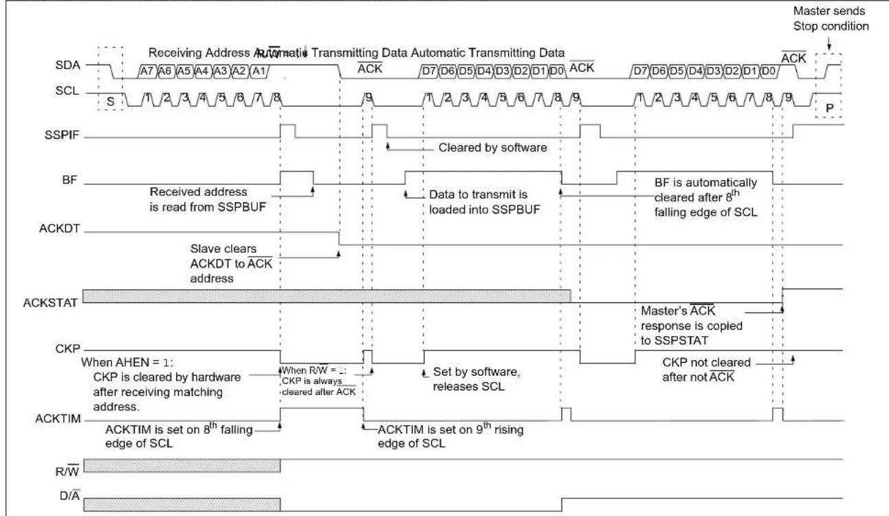
flowchart
graph TD
    A["Receiving Address Automatic Transmitting Data"] --> B["SDA"]
    B --> C["SCL"]
    C --> D["SSPIF"]
    D --> E["BF"]
    E --> F["ACKDT"]
    F --> G["ACKSTAT"]
    G --> H["CKP"]
    H --> I["ACKTIM"]
    I --> J["R/W"]
    J --> K["D/A"]

    subgraph Data_Circuit
        L["ACK"] --> M["ACKD"]
        N["ACKT"] --> O["ACKTIM"]
    end

    subgraph Software_Circuit
        P["Cleared by software"] --> Q["Data to transmit is loaded into SSPBUF"]
        R["Master sends Stop condition"] --> S["Master's ACK response is copied to SSPSTAT"]
        T["CFPS"] --> U["CFPS is cleared by hardware after receiving matching address."]
        V["ACK"] --> W["ACKTIM is set on 8th falling edge of SCL"]
        X["ACK"] --> Y["ACKTIM is set on 9th rising edge of SCL"]
    end

    style A fill:#f9f,stroke:#333
    style B fill:#ccf,stroke:#333
    style C fill:#cfc,stroke:#333
    style D fill:#fcc,stroke:#333
    style E fill:#ffc,stroke:#333
    style F fill:#fcc,stroke:#333
    style G fill:#ffc,stroke:#333
    style H fill:#fcc,stroke:#333
    style I fill:#fcc,stroke:#333
    style J fill:#fff,stroke:#333
    style K fill:#fff,stroke:#333
    style L fill:#fff,stroke:#333
    style M fill:#fff,stroke:#333
    style N fill:#fff,stroke:#333
    style O fill:#fff,stroke:#333
    style P fill:#fff,stroke:#333
    style Q fill:#fff,stroke:#333
    style R fill:#fff,stroke:#333
    style S fill:#fff,stroke:#333
    style T fill:#fff,stroke:#333
    style U fill:#fff,stroke:#333
    style V fill:#fff,stroke:#333
    style W fill:#fff,stroke:#333
    style X fill:#fff,stroke:#333
29.4.5 SLAVE MODE 10-BIT ADDRESS RECEPTION
This section describes a standard sequence of events for the MSSP module configured as an Slave in 10-bit Addressing mode.
Figure 29-12 is used as a visual reference for this description.
This is a step-by-step process of what must be done by slave software to accomplish I ^2 C communication:
- Bus starts idle.
- Master sends Start condition; S bit in the SSPSTAT register is set; SSPIF is set if interrupt-on-Start detect is enabled.
- Master sends matching high address with R/W bit clear; UA bit in the SSPSTAT register is set.
- Slave sends ACK and SSPIF is set.
- Software clears the SSPIF bit.
- Software reads received address from SSPBUF, clearing the BF flag.
- Slave loads low address into SSPADD, releasing SCL.
- Master sends matching low-address byte to the Slave; UA bit is set.
Note: Updates to the SSPADD register are not allowed until after the ACK sequence.
- Slave sends ACK and SSPIF is set.
Note: If the low address does not match, SSPIF and UA are still set so that the slave software can set SSPADD back to the high address. BF is not set because there is no match. CKP is unaffected.
- Slave clears SSPIF.
- Slave reads the received matching address from SSPBUF, clearing BF.
- Slave loads high address into SSPADD.
- Master clocks a data byte to the slave and clocks out the slave's ACK on the 9^th SCL pulse; SSPIF is set.
- If SEN bit in the SSPCON2 register is set, CKP is cleared by hardware and the clock is stretched.
- Slave clears SSPIF.
- Slave reads the received byte from SSPBUF, clearing BF.
- If SEN is set, the slave sets CKP to release the SCL.
- Steps 13-17 are repeated for each received byte.
- Master sends Stop to end the transmission.
29.4.6 10-BIT ADDRESSING WITH ADDRESS OR DATA HOLD
Reception using 10-bit addressing with AHEN or DHEN set is the same as with 7-bit modes. The only difference is the need to update the SSPADD register using the UA bit. All functionality, specifically when the CKP bit is cleared and the SCL line is held low, is the same. Figure 29-13 can be used as a reference of a slave in 10-bit addressing with AHEN set.
Figure 29-14 shows a standard waveform for a slave transmitter in 10-bit Addressing mode.
FIGURE 29-12: I ^2 C SLAVE, 10-BIT ADDRESS, RECEPTION (SEN = 1, AHEN = 0, DHEN = 0)
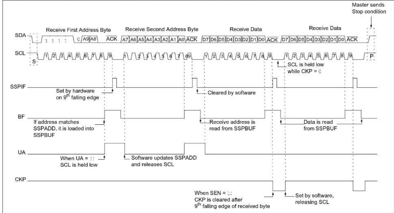
flowchart
graph TD
    A["Master sends Stop condition"] --> B["SDA"]
    B --> C["Receive First Address Byte"]
    C --> D["ACK"]
    D --> E["A7"]
    E --> F["A6"]
    F --> G["A5"]
    G --> H["A4"]
    H --> I["A3"]
    I --> J["A2"]
    J --> K["A1"]
    K --> L["A0"]
    L --> M["ACK"]
    M --> N["D7"]
    N --> O["D6"]
    O --> P["D5"]
    P --> Q["D4"]
    Q --> R["D3"]
    R --> S["D2"]
    S --> T["D1"]
    T --> U["D0"]
    U --> V["ACK"]
    V --> W["D7"]
    W --> X["D6"]
    X --> Y["D5"]
    Y --> Z["D4"]
    Z --> AA["D3"]
    AA --> AB["D2"]
    AB --> AC["D1"]
    AC --> AD["ACK"]
    AD --> AE["P"]

    subgraph SDA
        B
        C
        D
        E
        F
        G
        H
        I
        J
        K
        L
        M
        N
        O
        P
        Q
        R
        S
        T
        U
        V
        W
        X
        Y
        Z
        AA
        AB
        AC
        AD
        AE
        AF
        AG
        AH
        AI
    end

    subgraph SCL
        B
        C
        D
        E
        F
        G
        H
        I
        J
        K
        L
        M
        N
        O
        P
        Q
        S
        T
        U
        V
        W
        X
        Y
        Z
        AA
        AB
        AC
        AD
        AE
    end

    subgraph SSPIF
        B
        C
        D
        E
        F
        G
        H
        I
        J
        K
        L
        M
        N
        O
        P
        Q
        S
    end

    subgraph BF
        B
        C
        D
        E
        F
        G
        H
        I
        J
        K
        L
        M
        N
        O
        P
    end

    subgraph UA
        B
        C
        D
        E
        F
        G
        H
        I
        J
        K
    end

    subgraph CKP
        B
        C
        D
        E
        F
        G
        H
        I
        J
    end

    subgraph BF:
        B -->|Set by hardware on 9th falling edge| C

    subgraph UA:
            B -->|When UA = 1: SCL is held low| C

    subgraph CKP:
            C -->|Software updates SSPADD and releases SCL| D

    end

    subgraph BF:
            B -->|Cleared by software| E

    subgraph UA:
            B -->|Software updates SSPADD and releases SCL| F

    subgraph CKP:
            F -->|Software updates SSPADD and releases SCL| G

    end

    subgraph BF:
            B -->|Data is read from SSPBUF| H

    subgraph UA:
            B -->|Data is read from SSPBUF| I

    end

    subgraph CKP:
            C -->|Set by software, releasing SCL| D

    subgraph BF:
            C -->|Cleared by software| E

    end

    subgraph UA:
            C -->|Software updates SSPADD and releases SCL| F

    subgraph CKP:
            F -->|Software updates SSPADD and releases SCL| G

    end

    subgraph BF:
            B -->|Cleared by software| H

    subgraph UA:
            B -->|Software updates SSPADD and releases SCL| I

    end

    subgraph CKP:
            C -->|Cleared by software| D

    end

    style SDA fill:#f9f,stroke:#333,stroke-width:2px;
    style SCL fill:#f9f,stroke:#333,stroke-width:2px;
    style SSPIF fill:#ccf,stroke:#333,stroke-width:2px;
    style BF fill:#cfc,stroke:#333,stroke-width:2px;
    style UA fill:#fcc,stroke:#333,stroke-width:2px;
FIGURE 29-13: I ^2 C SLAVE, 10-BIT ADDRESS, RECEPTION (SEN = 0, AHEN = 1, DHEN = 0)
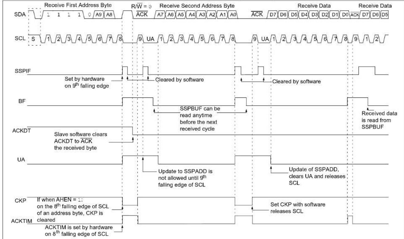
FIGURE 29-14: I ^2 C SLAVE, 10-BIT ADDRESS, TRANSMISSION (SEN = 0, AHEN = 0, DHEN = 0)
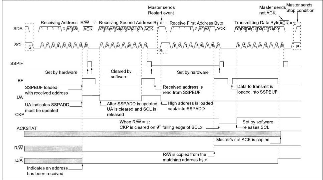
flowchart
graph TD
    subgraph SDA
        A1["Receiving Address"] --> A2["ACK"]
        A3["Receiving Second Address Byte"] --> A4["A7"]
        A5["Receiving First Address Byte"] --> A6["A9"]
        A7["Transmitting Data Byte"] --> A8["ACK"]
        A9["Master sends not ACK"] --> A10["D7"]
        A11["Master sends Stop condition"] --> A12["D5"]
        A13["Master sends not ACK"] --> A14["D4"]
        A15["Master sends not ACK"] --> A16["D3"]
        A17["Master sends not ACK"] --> A18["D2"]
        A19["Master sends not ACK"] --> A20["D1"]
        A21["Master sends not ACK"] --> A22["D0"]
    end

    subgraph SCL
        S["S"] --> S1["S"]
        S1 --> S2["S"]
        S2 --> S3["S"]
        S3 --> S4["S"]
        S4 --> S5["S"]
        S5 --> S6["S"]
        S6 --> S7["S"]
        S7 --> S8["S"]
        S8 --> S9["S"]
        S9 --> S10["S"]
        S10 --> S11["S"]
        S11 --> S12["S"]
        S12 --> S13["S"]
        S13 --> S14["S"]
        S14 --> S15["S"]
        S15 --> S16["S"]
        S16 --> S17["S"]
        S17 --> S18["S"]
        S18 --> S19["S"]
        S20["S"] --> S10["S"]
        S10 --> S11["S"]
        S11 --> S12["S"]
        S12 --> S13["S"]
        S13 --> S14["S"]
        S14 --> S15["S"]
        S15 --> S16["S"]
        S16 --> S17["S"]
        S17 --> S18["S"]
        S18 --> S19["S"]
    end

    subgraph SSPIF
        B["BF"] --> B1["Set by hardware"]
        B1 --> B2["Cleared by software"]
        B2 --> B3["Set by hardware"]
        B3 --> B4["Received address is read from SSPBUF"]
        B4 --> B5["Data to transmit is loaded into SSPBUF"]
        B5 --> B6["After SSPADD is updated. UA is cleared and SCL is released"]
        B6 --> B7["High address is loaded back into SSPADD"]
    end

    subgraph BF
        C["SSPBUF loaded with received address"] --> C1["After SSPADD is updated. UA is cleared and SCL is released"]
        C1 --> C2["Received address is read from SSPBUF"]
        C2 --> C3["Data to transmit is loaded into SSPBUF"]
    end

    subgraph UA
        D["UA indicates SSPADD must be updated"] --> D1["After SSPADD is updated. UA is cleared and SCL is released"]
        D1 --> D2["High address is loaded back into SSPADD"]
    end

    subgraph CKP
        E["ACKSTAT"] --> E1["When R/W = 1: CKP is cleared on 9th falling edge of SCLx"]
        E1 --> E2["Set by software releases SCL"]
        E2 --> E3["Master's not ACK is copied"]
    end

    subgraph ACKSTAT
        F["R/W"] --> F1["R/W is copied from the matching address byte"]
        F --> F2["Indicates an address has been received"]
    end

    subgraph D/A
        G["D/A"] --> G1["End"]
    end
29.4.7 CLOCK STRETCHING
Clock stretching occurs when a device on the bus holds the SCL line low, effectively pausing communication. The slave may stretch the clock to allow more time to handle data or prepare a response for the master device. A master device is not concerned with stretching, as it is stretching anytime it is active on the bus and not transferring data. Any stretching done by a slave is invisible to the master software and handled by the hardware that generates SCL.
The CKP bit in the SSPCON1 register is used to control stretching in software. Any time the CKP bit is cleared, the module will wait for the SCL line to go low and then hold it. Setting CKP will release SCL and allow more communication.
29.4.7.1 Normal Clock Stretching
Following an ACK, if the R/W bit in the SSPSTAT register is set, causing a read request, the slave hardware will clear CKP. This allows the slave time to update SSPBUF with data to transfer to the master. If the SEN bit in the SSPCON2 register is set, the slave hardware will always stretch the clock after the ACK sequence. Once the slave is ready, CKP is set by software and communication resumes.
Note 1: The BF bit has no effect on whether the clock will be stretched or not. This is different than previous versions of the module that would not stretch the clock or clear CKP if SSPBUF was read before the 9^th falling edge of SCL.
2: Previous versions of the module did not stretch the clock for a transmission if SSPBUF was loaded before the 9^th falling edge of SCL. It is now always cleared for read requests.
29.4.7.2 10-Bit Addressing Mode
In 10-bit Addressing mode, when the UA bit is set, the clock is always stretched. This is the only time the SCL is stretched without CKP being cleared. SCL is released immediately after a write to SSPADD.
Note: Previous versions of the module did not stretch the clock if the second address byte did not match.
When AHEN bit in the SSPCON3 register is set, CKP is cleared by hardware after the 8^th falling edge of SCL for a received matching address byte. When DHEN bit in the SSPCON3 register is set, CKP is cleared after the 8^th falling edge of SCL for received data.
Stretching after the 8^th falling edge of SCL allows the slave to look at the received address or data and decide if it wants to ACK the received data.
29.4.8 CLOCK SYNCHRONIZATION AND THE CKP BIT
Any time the CKP bit is cleared, the module will wait for the SCL line to go low and then hold it. However, clearing the CKP bit will not assert the SCL output low until the SCL output is already sampled low. Therefore, the CKP bit will not assert the SCL line until an external I²C master device has already asserted the SCL line. The SCL output will remain low until the CKP bit is set and all other devices on the I²C bus have released SCL. This ensures that a write to the CKP bit will not violate the minimum high-time requirement for SCL (refer to Figure 29-16).
FIGURE 29-15: CLOCK SYNCHRONIZATION TIMING
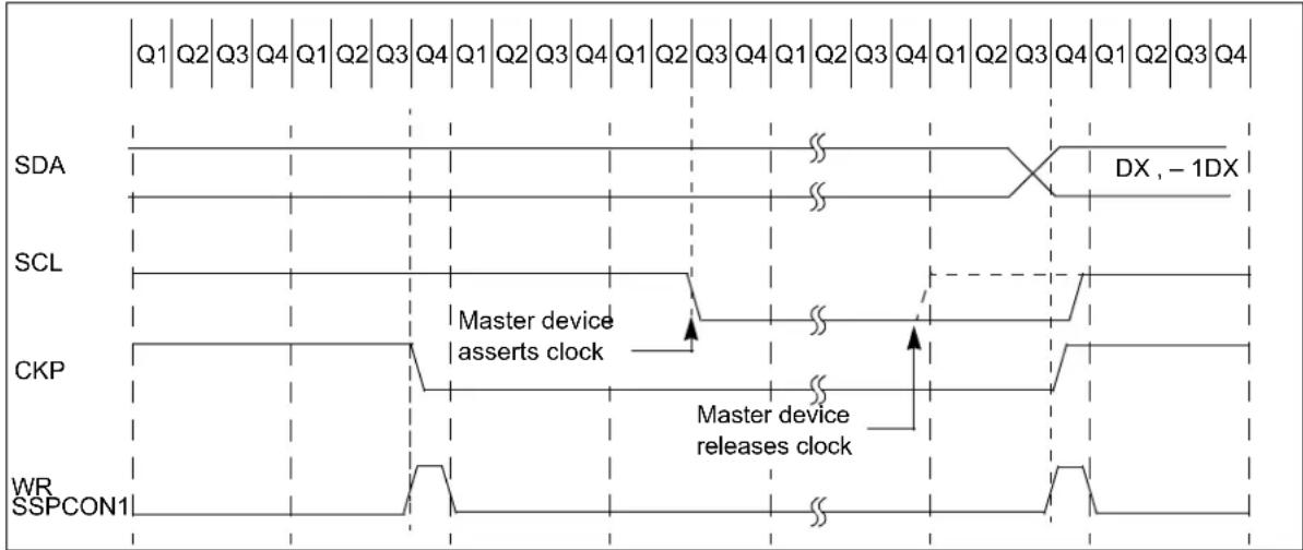
29.4.9 GENERAL CALL ADDRESS SUPPORT
The addressing procedure for the ^2C bus is such that the first byte after the Start condition usually determines which device is the slave addressed by the master device. The exception is the general call address which can address all devices. When this address is used, all devices should, in theory, respond with an acknowledge.
The general call address is a reserved address in the I²C protocol, defined as address 0x00. When the GCEN bit in the SSPCON2 register is set, the slave module will automatically ACK the reception of this address regardless of the value stored in SSPADD. After the slave clocks in an address of all zeros with the R/W bit clear, an interrupt is generated and slave software can read SSPBUF and respond. Figure 29-7 shows a general call reception sequence.
In 10-bit Address mode, the UA bit will not be set on the reception of the general call address. The slave will prepare to receive the second byte as data, just as it would in 7-bit mode.
If the AHEN bit in the SSPCON3 register is set, just as with any other address reception, the slave hardware will stretch the clock after the 8^th falling edge of SCL. The slave must then set its ACKDT value and release the clock with communication progressing as it would normally.
FIGURE 29-16: SLAVE MODE GENERAL CALL ADDRESS SEQUENCE
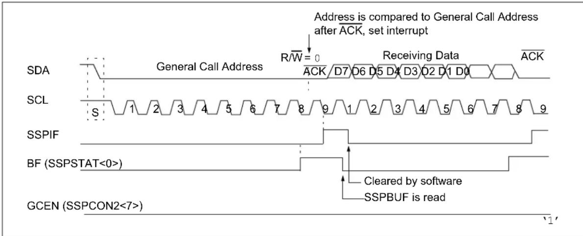
29.4.10 SSPMSK1 REGISTER
An SSP Mask (SSPMSK1) register is available in I²C Slave mode as a mask for the value held in the SSPSR register during an address comparison operation. A zero ('0') bit in the SSPMSK1 register has the effect of making the corresponding bit of the received address a "don't care".
This register is reset to all '1's upon any Reset condition and, therefore, has no effect on standard SSP operation until written with a mask value.
The SSPMSK1 register is active during:
- 7-bit Address mode: address compare of A<7:1>
- 10-bit Address mode: address compare of A<7:0> only. The SSP mask has no effect during the reception of the first (high) byte of the address
29.5 I ^2 C MASTER MODE
Master mode is enabled by setting and clearing the appropriate SSPM bits in the SSPCON1 register and by setting the SSPEN bit. In Master mode, the SDA and SCK pins must be configured as inputs. The MSSP peripheral hardware will override the output driver TRIS controls when necessary, to drive the pins low.
The Master mode of operation is supported by interrupt generation on the detection of the Start and Stop conditions. The Stop (P) and Start (S) bits are cleared from a Reset or when the MSSP module is disabled. Control of the I²C bus may be taken when the P bit is set or the bus is idle.
In Firmware-Controlled Master mode, user code conducts all I^2C bus operations based on Start and Stop bit condition detection. Start and Stop condition detection is the only active circuitry in this mode. All other communication is done by the user's software directly manipulating the SDA and SCL lines.
The following events will cause the SSP Interrupt Flag bit (SSPIF) to be set (SSP interrupt, if enabled):
- Start condition detected
- Stop condition detected
• Data-transfer byte transmitted/received - Acknowledge transmitted/received
• Repeated Start generated
Note 1: The MSSP module, when configured in I²C Master mode, does not allow queuing of events. For instance, the user is not allowed to initiate a Start condition and immediately write the SSPBUF register to initiate transmission before the Start condition is complete. In this case, the SSPBUF will not be written to and the WCOL bit will be set, indicating that a write to the SSPBUF did not occur.
2: When in Master mode, Start/Stop detection is masked and an interrupt is generated when the SEN/PEN bit is cleared and the generation is complete.
29.5.1 I ^2 C MASTER MODE OPERATION
The master device generates all of the serial clock pulses and the Start and Stop conditions. A transfer is ended with a Stop condition or with a Repeated Start condition. Since the Repeated Start condition is also the beginning of the next serial transfer, the bus is not released.
In Master Transmit mode, serial data is output through SDA while SCL outputs the serial clock. The first byte transmitted contains the slave address of the receiving device (7 bits) and the Read/Write (R/W) bit. In this case, the R/W bit is logic '0'. Serial data is transmitted eight bits at a time. After each byte is transmitted, an Acknowledge bit is received. Start and Stop conditions are output to indicate the beginning and the end of a serial transfer.
In Master Receive mode, the first byte transmitted contains the slave address of the transmitting device (7 bits) and the R/W bit. In this case, the R/W bit is logic '1'. Thus, the first byte transmitted is a 7-bit slave address followed by a '1' to indicate the receive bit. Serial data is received via SDA, while SCL outputs the serial clock. Serial data is received eight bits at a time. After each byte is received, an Acknowledge bit is transmitted. Start and Stop conditions indicate the beginning and end of transmission.
A Baud Rate Generator is used to set the clock frequency output on SCL. Refer to Section 29.6 "Baud Rate Generator" for more details.
Clock arbitration occurs when the master, during any Receive, Transmit or Repeated Start/Stop condition, releases the SCL pin (SCL allowed to float high). When the SCL pin is allowed to float high, the Baud Rate Generator (BRG) is suspended from counting until the SCL pin is actually sampled high. When the SCL pin is sampled high, the Baud Rate Generator is reloaded with the contents of SSPADD<7:0> and begins counting. This ensures that the SCL high time will always be at least one BRG rollover count in the event that the clock is held low by an external device (Figure 29-17).
FIGURE 29-17: BAUD RATE GENERATOR TIMING WITH CLOCK ARBITRATION
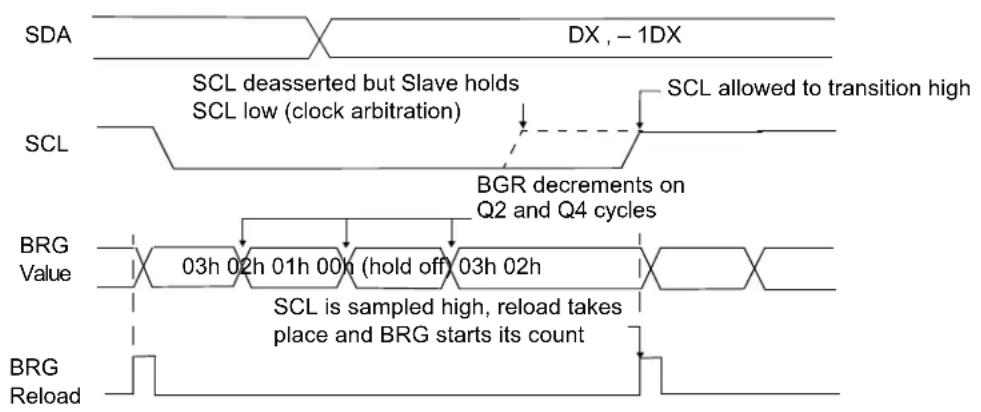
flowchart
graph TD
    A["SDA"] --> B["SCL deasserted but Slave holds"]
    B --> C["SCL low (clock arbitration)"]
    C --> D["SCL allowed to transition high"]
    D --> E["BGR decrements on Q2 and Q4 cycles"]
    E --> F["BRG Value: 03h 02h 01h 00h (hold off) 03h 02h"]
    F --> G["SCL is sampled high, reload takes place and BRG starts its count"]
    G --> H["BRG Reload"]
29.5.3 WCOL STATUS FLAG
If the user writes the SSPBUF when a Start, Restart, Stop, Receive or Transmit sequence is in progress, the WCOL is set and the contents of the buffer are unchanged (the write does not occur). Any time the WCOL bit is set, it indicates that an action on SSPBUF was attempted while the module was not idle.
Note: Because queuing of events is not allowed, writing to the lower five bits in the SSPCON2 register is disabled until the Start condition is complete.
29.5.4 I ^2 C MASTER MODE START CONDITION TIMING
To initiate a Start condition, the user sets the Start Enable bit, SEN, in the SSPCON2 register. If the SDA and SCL pins are sampled high, the Baud Rate Generator is reloaded with the contents of SSPADD<7:0> and starts its count. If SCL and SDA are both sampled high when the Baud Rate Generator times out ( T_BRG ), the SDA pin is driven low. The action
of the SDA being driven low while SCL is high is the Start condition, and causes the S bit in the SSPSTAT1 register to be set. Following this, the Baud Rate Generator is reloaded with the contents of SSPADD<7:0> and resumes its count. When the Baud Rate Generator times out ( T_BRG ), the SEN bit in the SSPCON2 register will be automatically cleared by hardware; the Baud Rate Generator is suspended, leaving the SDA line held low and the Start condition is complete.
Note 1: If, at the beginning of the Start condition, the SDA and SCL pins are already sampled low, or if, during the Start condition, the SCL line is sampled low before the SDA line is driven low, a bus collision occurs, the Bus Collision Interrupt Flag (BCLIF) is set, the Start condition is aborted and the module is reset into its idle state.
2: The Philips I ^2 C Specification states that a bus collision cannot occur on a Start.
FIGURE 29-18: FIRST START BIT TIMING
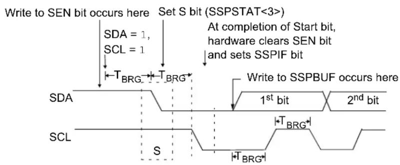
29.5.5 I ^2 C MASTER MODE REPEATED START CONDITION TIMING
A Repeated Start condition occurs when the RSEN bit in the SSPCON2 register is programmed high and the master state machine is no longer active. When the RSEN bit is set, the SCL pin is asserted low. When the SCL pin is sampled low, the Baud Rate Generator is loaded and begins counting. The SDA pin is released (brought high) for one Baud Rate Generator count ( T_BRG ). When the Baud Rate Generator times out, if SDA is sampled high, the SCL pin will be deasserted (brought high). When SCL is sampled high, the Baud Rate Generator is reloaded and begins counting. SDA and SCL must be sampled high for one T_BRG . This action is then followed by assertion of the SDA pin (SDA = 0) for one T_BRG while SCL is high. SCL is asserted low. Following this, the RSEN bit in the SSPCON2 register will be automatically cleared and the Baud Rate Generator will not be reloaded, leaving the SDA pin held low. As soon as a Start condition is detected on the SDA and SCL pins, the S bit in the SSPSTAT register is set. The SSPIF bit will not be set until the Baud Rate Generator has timed out.
Note 1: If RSEN is programmed while any other event is in progress, it does not take effect.
2: A bus collision during the Repeated Start condition occurs if:
- SDA is sampled low when SCL goes from low to high
- SCL goes low before SDA is asserted low. This may indicate that another master is attempting to transmit a data '1'
FIGURE 29-19: REPEAT START CONDITION WAVEFORM
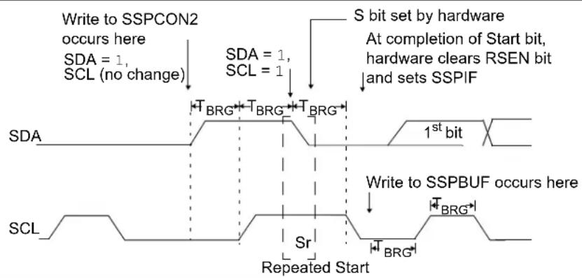
29.5.6 I ^2 C MASTER MODE TRANSMISSION
Transmission of a data byte, a 7-bit address or the other half of a 10-bit address is accomplished by simply writing a value to the SSPBUF register. This action sets the Buffer Full (BF) flag bit and allows the Baud Rate Generator to begin counting and start the next transmission. Each bit of address/data is shifted out onto the SDA pin after the falling edge of SCL is asserted. SCL is held low for one Baud Rate Generator rollover count ( T_BRG ). Data should be valid before SCL is released high. When the SCL pin is released high, it is held that way for T_BRG . The data on the SDA pin must remain stable for that duration and some hold time after the next falling edge of SCL. After the 8^th bit is shifted out (the falling edge of the 8^th clock), the BF flag is cleared and the master releases the SDA. This allows the slave device being addressed to respond with an ACK bit during the 9^th bit time if an address match occurred or if data was received properly. The status of ACK is written into the ACKSTAT bit on the rising edge of the 9^th clock. If the master receives an Acknowledge, the Acknowledge Status bit (ACKSTAT) is cleared. If not, the bit is set. After the 9^th clock, the SSPIF bit is set and the master clock (Baud Rate Generator) is suspended until the next data byte is loaded into the SSPBUF, leaving SCL low and SDA unchanged (Figure 29-20).
After the write to the SSPBUF, each bit of the address will be shifted out on the falling edge of SCL until all seven address bits and the R/W bit are completed. On the falling edge of the 8^th clock, the master releases the SDA pin, allowing the slave to respond with an Acknowledge. On the falling edge of the 9^th clock, the master samples the SDA pin to see if the address was recognized by a slave. The status of the ACK bit is loaded into the ACKSTAT status bit in the SSPCON2 register. Following the falling edge of the 9^th clock transmission of the address, the SSPIF is set, the BF flag is cleared and the Baud Rate Generator is turned off until another write to the SSPBUF takes place, holding SCL low and allowing SDA to float.
29.5.6.1 BF Status Flag
In Transmit mode, the BF bit in the SSPSTAT register is set when the CPU writes to SSPBUF and is cleared when all eight bits are shifted out.
29.5.6.2 WCOL Status Flag
If the user writes the SSPBUF when a Transmit is already in progress (i.e., SSPSR is still shifting out a data byte), the WCOL is set and the contents of the buffer are unchanged (the write does not occur).
WCOL must be cleared by software before the next transmission.
29.5.6.3 ACKSTAT Status Flag
In Transmit mode, the ACKSTAT bit in the SSPCON2 register is cleared when the slave has sent an Acknowledge (ACK = 0) and is set when the slave does not Acknowledge (ACK = 1). A slave sends an Acknowledge when it has recognized its address (including a general call) or when the slave has properly received its data.
29.5.6.4 Typical Transmit Sequence
- The user generates a Start condition by setting the SEN bit in the SSPCON2 register.
- SSPIF is set by hardware on completion of the Start.
- SSPIF is cleared by software.
- The MSSP module waits the required start time before any other operation takes place.
- The user loads the SSPBUF with the slave address to transmit.
- Address is shifted out the SDA pin until all eight bits are transmitted. Transmission begins as soon as SSPBUF is written to.
- The MSSP module shifts in the ACK bit from the slave device and writes its value into the ACKSTAT bit in the SSPCON2 register.
- The MSSP module generates an interrupt at the end of the 9^th clock cycle by setting the SSPIF bit.
- The user loads the SSPBUF with eight bits of data
- Data is shifted out the SDA pin until all eight bits are transmitted.
- The MSSP module shifts in the ACK bit from the slave device and writes its value into the ACKSTAT bit in the SSPCON2 register.
- Steps 8-11 are repeated for all transmitted data bytes.
- The user generates a Stop or Restart condition by setting the PEN or RSEN bits in the SSPCON2 register. Interrupt is generated once the Stop/Restart condition is complete.
FIGURE 29-20: I ^2 C MASTER MODE WAVEFORM (TRANSMISSION, 7 OR 10-BIT ADDRESS)
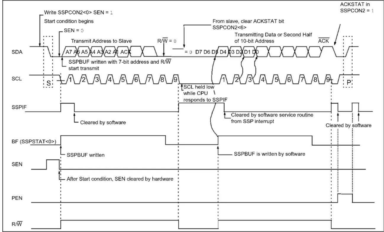
flowchart
graph TD
    A["Write SSPCON2<0> SEN = 1"] --> B["Start condition begins"]
    B --> C["SEN = 0"]
    C --> D["Transmit Address to Slave"]
    D --> E["R/W = 0"]
    E --> F["= 0 D7 D6 D5 D4 D3 D2 D1 D0"]
    F --> G["From slave, clear ACKSTAT bit SSPCON2<6>"]
    G --> H["Transmitting Data or Second Half of 10-bit Address"]
    H --> I["ACK"]
    I --> J["ACKSTAT in SSPCON2 = 1"]

    K["SDA"] --> L["A7 A6 A5 A4 A3 A2 A1 AC"]
    L --> M["SSPBUF written with 7-bit address and R/W start transmit"]
    M --> N["SCL held low while CPU responds to SSPIF"]
    N --> O["Cleared by software service routine from SSP interrupt"]
    O --> P["Cleared by software"]

    Q["SCL"] --> R["S"]
    R --> S["1 2 3 4 5 6 7 8 9"]
    S --> T["SSPIF"]
    T --> U["Cleared by software"]

    V["BF (SSPSTAT<0>)"] --> W["SSPBUF written"]
    W --> X["After Start condition, SEN cleared by hardware"]
    X --> Y["SSPBUF is written by software"]

    Z["SEN"] --> AA["After Start condition, SEN cleared by hardware"]

    AB["PEN"] --> AC["After Start condition, SEN cleared by hardware"]

    AD["R/W"] --> AE["After Start condition, SEN cleared by hardware"]
29.5.7 I ^2 C MASTER MODE RECEPTION
Master mode reception is enabled by programming the Receive Enable (RCEN) bit in the SSPCON2 register.
Note: The MSSP module must be in an idle state before the RCEN bit is set or the RCEN bit will be disregarded.
The Baud Rate Generator begins counting and, upon each rollover, the state of the SCL pin changes (high-to-low/low-to-high) and data is shifted into the SSPSR. After the falling edge of the 8^th clock, the receive enable flag is automatically cleared, the contents of the SSPSR are loaded into the SSPBUF, the BF flag bit is set, the SSPIF flag bit is set and the Baud Rate Generator is suspended from counting, holding SCL low. The MSSP is now in idle state awaiting the next command. When the buffer is read by the CPU, the BF flag bit is automatically cleared. The user can then send an Acknowledge bit at the end of reception by setting the Acknowledge Sequence Enable (ACKEN) bit in the SSPCON2 register.
29.5.7.1 BF Status Flag
In receive operation, the BF bit is set when an address or data byte is loaded into SSPBUF from SSPSR. It is cleared when the SSPBUF register is read.
29.5.7.2 SSPOV Status Flag
In receive operation, the SSPOV bit is set when 8 bits are received into the SSPSR and the BF flag bit is already set from a previous reception.
29.5.7.3 WCOL Status Flag
If the user writes the SSPBUF when a receive is already in progress (i.e., SSPSR is still shifting in a data byte), the WCOL bit is set and the contents of the buffer are unchanged (the write does not occur).
29.5.7.4 Typical Receive Sequence
- The user generates a Start condition by setting the SEN bit in the SSPCON2 register.
- SSPIF is set by hardware on completion of the Start.
- SSPIF is cleared by software
- User writes SSPBUF with the slave address to transmit and the R/W bit set.
- Address is shifted out the SDA pin until all eight bits are transmitted. Transmission begins as soon as SSPBUF is written to.
- The MSSP module shifts in the ACK bit from the slave device and writes its value into the ACKSTAT bit in the SSPCON2 register.
- The MSSP module generates an interrupt at the end of the 9^th clock cycle by setting the SSPIF bit.
- User sets the RCEN bit in the SSPCON2 register and the Master clocks in a byte from the slave.
- After the 8 ^th falling edge of SCL, SSPIF and BF are set.
- Master clears SSPIF and reads the received byte from SSPUF, then clears BF.
- Master sets ACK value sent to slave in ACKDT bit in the SSPCON2 register and initiates the ACK by setting the ACKEN bit.
- Masters ACK is clocked out to the slave and SSPIF is set.
- The user clears SSPIF.
- Steps 8-13 are repeated for each received byte from the slave.
- Master sends a not ACK or Stop to end communication.
FIGURE 29-21: I ^2 C MASTER MODE WAVEFORM (RECEPTION, 7-BIT ADDRESS)
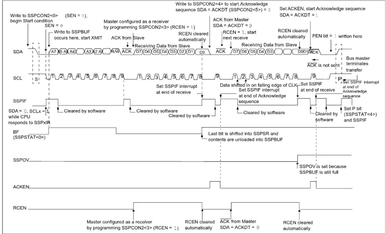
flowchart
graph TD
    A["Write to SSPCON2<0> (SEN = 1), begin Start condition"] --> B["Write to SSPBUF occurs here, start XMIT"]
    B --> C["Master configured as a receiver by programming SSPCON2<3> (RCEN = 1)"]
    C --> D["ACK from Slave"]
    D --> E["Receiving Data from Slave"]
    E --> F["ACK from Master SDA = ACKDT = 0"]
    F --> G["RCEN cleared automatically"]
    G --> H["ACK from master SDA = ACKDT = 0"]
    H --> I["RCEN cleared automatically"]
    I --> J["PEN bit = 1 written here"]
    K["SDA"] --> L["A7 A6 A4 A3 A2 A1 R/W ACK D7 D6 D5 D4 D3 D2 D1 D0"]
    L --> M["ACK D7 D6 D5 D4 D3"]
    M --> N["Receiving Data from Slave"]
    N --> O["D0D1 ACK"]
    P["SCL"] --> Q["1 2 3 4 5 6 7 8 9"]
    Q --> R["Set SSPIF interrupt at end of receive"]
    R --> S["Data shifted in on falling edge of CLK"]
    S --> T["Set SSPIF interrupt at end of Acknowledge sequence"]
    T --> U["Set SSPIF at end of receive"]
    U --> V["Set P bit (SSPSTAT<4>) and SSPIF"]
    W["SSPIF"] --> X["SDA = 0, SCLx = 1, while CPU responds to SSPxIR"]
    X --> Y["Cleared by software"]
    Y --> Z["Cleared by software"]
    Z --> AA["Cleared by software"]
    AA --> AB["Last bit is shifted into SSPSR and contents are unloaded into SSPBUF"]
    AC["BF (SSPSTAT<0>"] --> AD["Last bit is shifted into SSPSR and contents are unloaded into SSPBUF"]
    AE["SSPOV"] --> AF["SSPOV is set because SSPBUF is still full"]
    AG["ACKEN"] --> AH["Master configured as a receiver by programming SSPCON2<3> (RCEN = 1)"]
    AH --> AI["RCEN cleared automatically"]
    AI --> AJ["ACK from Master SDA = ACKDT = 0"]
    AJ --> AK["RCEN cleared automatically"]
29.5.8 ACKNOWLEDGE SEQUENCE TIMING
An Acknowledge sequence is enabled by setting the Acknowledge Sequence Enable (ACKEN) bit in the SSPCON2 register. When this bit is set, the SCL pin is pulled low and the contents of the Acknowledge data bit are presented on the SDA pin. If the user wishes to generate an Acknowledge, then the ACKDT bit should be cleared. If not, the user should set the ACKDT bit before starting an Acknowledge sequence. The Baud Rate Generator then counts for one rollover period ( T_BRG ) and the SCL pin is deasserted (pulled high). When the SCL pin is sampled high (clock arbitration), the Baud Rate Generator counts for T_BRG . The SCL pin is then pulled low. Following this, the ACKEN bit is automatically cleared, the Baud Rate Generator is turned off and the MSSP module then goes into Idle mode (Figure 29-22).
29.5.8.1 WCOL Status Flag
If the user writes the SSPBUF when an Acknowledge sequence is in progress, WCOL is set and the contents of the buffer are unchanged (the write does not occur).
29.5.9 STOP CONDITION TIMING
A Stop bit is asserted on the SDA pin at the end of a receive/transmit by setting the Stop Sequence Enable bit (PEN) in the SSPCON2 register. At the end of a receive/transmit, the SCL line is held low after the falling edge of the 9^th clock. When the PEN bit is set, the master will assert the SDA line low. When the SDA line is sampled low, the Baud Rate Generator is reloaded and counts down to '0'. When the Baud Rate Generator times out, the SCL pin will be brought high and then, one T_BRG (Baud Rate Generator rollover count) later, the SDA pin is deasserted. When the SDA pin is sampled high while SCL is high, the P bit in the SSPSTAT register, is set. A T_BRG later, the PEN bit is cleared and the SSPIF bit is set (Figure 29-23).
29.5.9.1 WCOL Status Flag
If the user writes the SSPBUF when a Stop sequence is in progress, the WCOL bit is set and the contents of the buffer are unchanged (the write does not occur).
FIGURE 29-23: STOP CONDITION RECEIVE OR TRANSMIT MODE
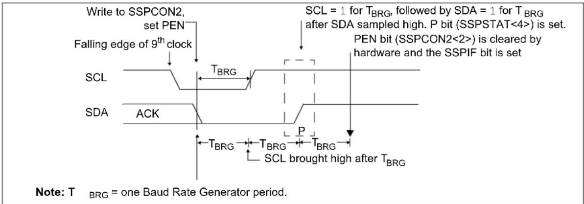
While in Sleep mode, the I^2C slave module can receive addresses or data and, when an address match or complete byte transfer occurs, wake the processor from Sleep (if the MSSP interrupt is enabled).
29.5.11 EFFECTS OF A RESET
A Reset disables the MSSP module and terminates the current transfer.
29.5.12 MULTI-MASTER MODE
In Multi-Master mode, the interrupt generation on the detection of the Start and Stop conditions allows the determination of when the bus is free. The Stop (P) and Start (S) bits are cleared from a Reset or when the MSSPx module is disabled. Control of the I²C bus may be taken when the P bit in the SSPSTAT register is set or the bus is idle, with both the S and P bits clear. When the bus is busy, enabling the SSP interrupt generates the interrupt when the Stop condition occurs.
In multi-master operation, the SDA line must be monitored for arbitration to see if the signal level is the expected output level. This check is performed by hardware with the result placed in the BCLIF bit.
The states where arbitration can be lost are:
- Address Transfer
- Data Transfer
- a Start Condition
• a Repeated Start Condition
• an Acknowledge Condition
29.5.13 MULTI -MASTER COMMUNICATION, BUS COLLISION AND BUS ARBITRATION
Multi-Master mode support is achieved by bus arbitration. When the master outputs address/data bits onto the SDA pin, arbitration takes place when the master outputs a '1' on SDA by letting SDA float high, and another master asserts a '0'. When the SCL pin floats high, data should be stable. If the expected data on SDA is a '1' and the data sampled on the SDA pin is '0', a bus collision has taken place. The master sets the Bus Collision Interrupt Flag (BCLIF) and resets the PC port to its Idle state (Figure 29-24).
If a transmit was in progress when the bus collision occurred, the transmission is halted, the BF flag is cleared, the SDA and SCL lines are deasserted and the SSPBUF can be written to. When the user services the bus collision Interrupt Service Routine and if the I^2C bus is free, the user can resume communication by asserting a Start condition.
If a Start, Repeated Start, Stop or Acknowledge condition was in progress when the bus collision occurred, the condition is aborted, the SDA and SCL lines are deasserted and the respective control bits in the SSPCON2 register are cleared. When the user services the bus collision Interrupt Service Routine and if the I²C bus is free, the user can resume communication by asserting a Start condition.
The master continues to monitor the SDA and SCL pins. If a Stop condition occurs, the SSPIF bit is set.
A write to the SSPBUF starts the transmission of data at the first data bit, regardless of where the transmitter left off when the bus collision occurred.
In Multi-Master mode, the interrupt generation on the detection of Start and Stop conditions allows the determination of when the bus is free. Control of the I^2C bus can be taken when the P bit is set in the SSPSTAT register, or the bus is idle and the S and P bits are cleared.
FIGURE 29-24: BUS COLLISION TIMING FOR TRANSMIT AND ACKNOWLEDGE
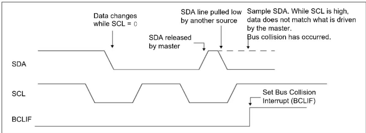
flowchart
graph TD
    A["Data changes while SCL = 0"] --> B["SDA released by master"]
    B --> C["SDA line pulled low by another source"]
    C --> D["Sample SDA. While SCL is high, data does not match what is driven by the master. Bus collision has occurred."]
    E["SCL"] --> F["Set Bus Collision Interrupt (BCLIF)"]
    G["BCLIF"] --> H["End"]
29.5.13.1 Bus Collision During a Start Condition
During a Start condition, a bus collision occurs if:
a) SDA or SCL are sampled low at the beginning of the Start condition (Figure 29-25)
b) SCL is sampled low before SDA is asserted low (Figure 29-26)
During a Start condition, both the SDA and the SCL pins are monitored.
If the SDA pin is already low or the SCL pin is already low, all of the following occur:
• the Start condition is aborted
- the BCLIF flag is set
- the MSSP module is reset to its Idle state (Figure 29-25)
The Start condition begins with the SDA and SCL pins deasserted. When the SDA pin is sampled high, the Baud Rate Generator is loaded and counts down. If the SCL pin is sampled low while SDA is high, a bus collision occurs because it is assumed that another master is attempting to drive a data '1' during the Start condition.
If the SDA pin is sampled low during this count, the BRG is reset and the SDA line is asserted early (Figure 29-27). If, however, a '1' is sampled on the SDA pin, the SDA pin is asserted low at the end of the BRG count. The Baud Rate Generator is then reloaded and counts down to zero; if the SCL pin is sampled as '0' during this time, a bus collision does not occur. At the end of the BRG count, the SCL pin is asserted low.
Note: The reason for which bus collision is not a factor during a Start condition is that no two bus masters can assert a Start condition at the exact same time. Therefore, one master will always assert SDA before the other. This condition does not cause a bus collision because the two masters must be allowed to arbitrate the first address following the Start condition. If the address is the same, arbitration must be allowed to continue into the data portion, Repeated Start or Stop conditions.
FIGURE 29-25: BUS COLLISION DURING A START CONDITION (SDA ONLY)
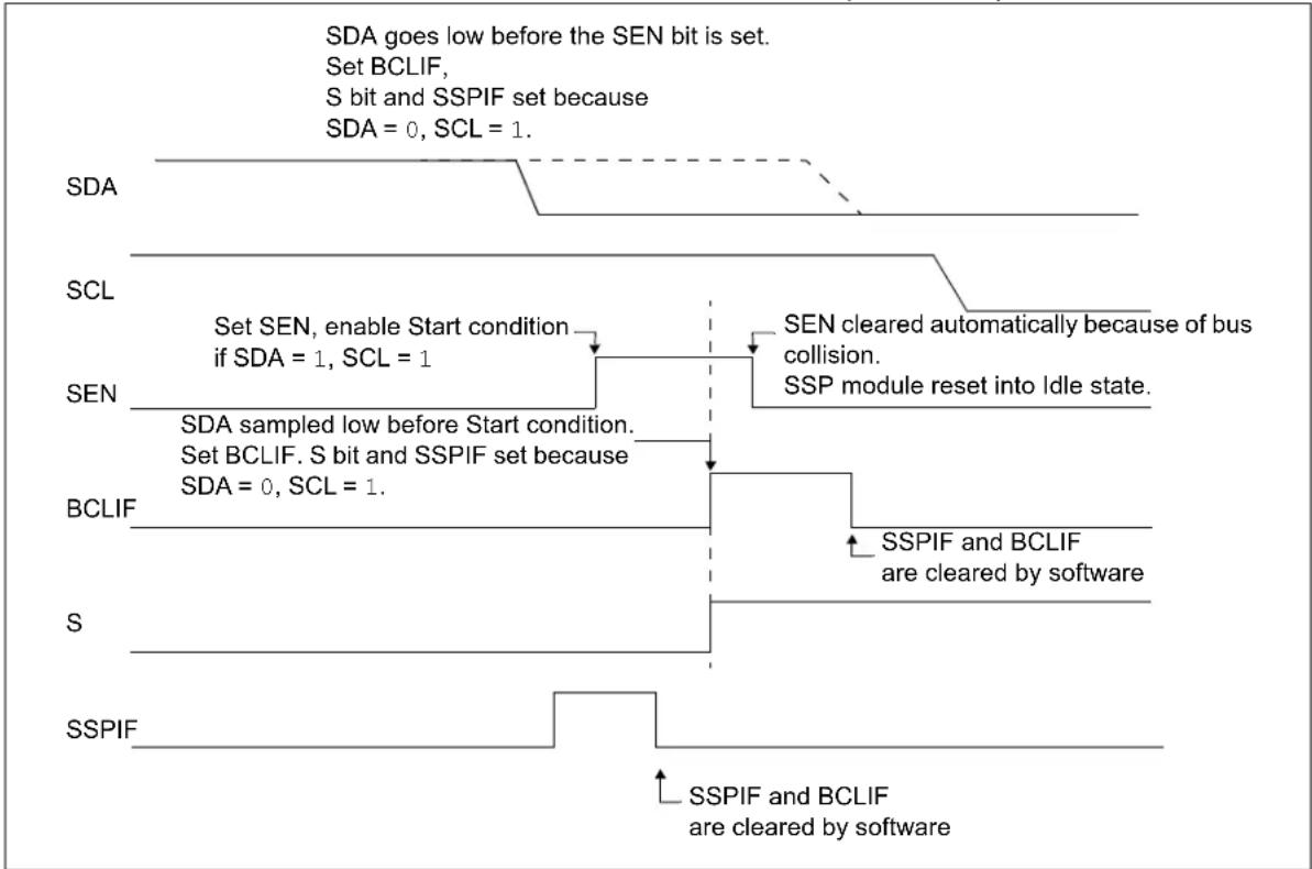
flowchart
graph TD
    A["SDA"] --> B["SDA goes low before the SEN bit is set."]
    B --> C["Set BCLIF, S bit and SSPIF set because SDA = 0, SCL = 1."]
    C --> D["SCL"]
    D --> E["Set SEN, enable Start condition if SDA = 1, SCL = 1"]
    E --> F["SEN cleared automatically because of bus collision. SSP module reset into Idle state."]
    F --> G["SEN sampled low before Start condition."]
    G --> H["Set BCLIF, S bit and SSPIF set because SDA = 0, SCL = 1."]
    H --> I["BCLIF"]
    I --> J["SSPIF and BCLIF are cleared by software"]
    J --> K["S"]
    K --> L["SSPIF"]
    L --> M["SSPIF and BCLIF are cleared by software"]
FIGURE 29-26: BUS COLLISION DURING A START CONDITION (SCL = 0)
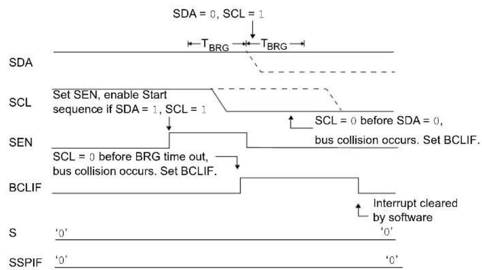
flowchart
graph TD
    A["SDA = 0, SCL = 1"] --> B["T_BRG"]
    B --> C["T_BRG"]
    D["SCL"] --> E["Set SEN, enable Start sequence if SDA = 1, SCL = 1"]
    E --> F["SCL = 0 before BRG time out, bus collision occurs. Set BCLIF"]
    G["SEN"] --> H["SCL = 0 before BRG time out, bus collision occurs. Set BCLIF"]
    H --> I["Interrupt cleared by software"]
    J["BCLIF"] --> K["'0'"]
    L["S"] --> M["'0'"]
    N["SSPIF"] --> O["'0'"]
FIGURE 29-27: BRG RESET DUE TO SDA ARBITRATION DURING START CONDITION
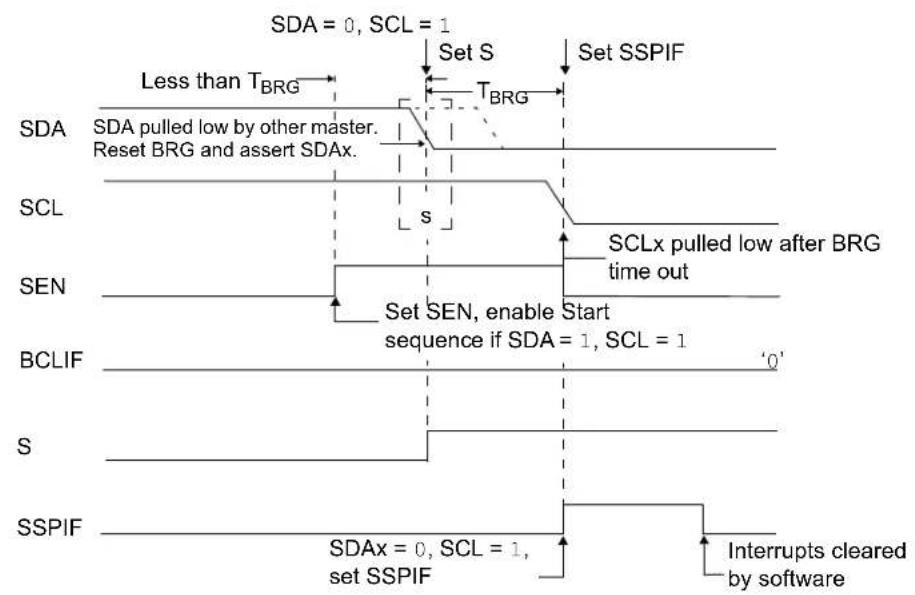
flowchart
graph TD
    A["SDA"] --> B["SDA pulled low by other master. Reset BRG and assert SDAx."]
    B --> C["Less than T_BRG"]
    C --> D["Set S"]
    D --> E["Set SSPIF"]
    F["SCL"] --> G["SCLx pulled low after BRG time out"]
    H["SEN"] --> I["Set SEN, enable Start sequence if SDA = 1, SCL = 1"]
    J["BCLIF"] --> K["'0'"]
    L["S"] --> M["Set SSPIF"]
    N["SSPIF"] --> O["SDAx = 0, SCL = 1, set SSPIF"]
    P["Interrupts cleared by software"] --> Q["Set SSPIF"]
29.5.13.2 Bus Collision during a Repeated Start Condition
During a Repeated Start condition, a bus collision occurs if:
a) a low level is sampled on SDA when SCL goes from low level to high level
b) SCL goes low before SDA is asserted low, indicating that another master is attempting to transmit a data '1'
When the user releases SDA and the pin is allowed to float high, the BRG is loaded with SSPADD and counts down to zero. The SCL pin is then deasserted and, when sampled high, the SDA pin is sampled.
If SDA is low, a bus collision has occurred (i.e., another master is attempting to transmit a data '0', Figure 29-28). If SDA is sampled high, the BRG is reloaded and begins counting. If SDA goes from high to low before the BRG times out, no bus collision occurs because no two masters can assert SDA at exactly the same time.
If SCL goes from high to low before the BRG times out and SDA has not already been asserted, a bus collision occurs. In this case, another master is attempting to transmit a data '1' during the Repeated Start condition (refer to Figure 29-29).
If, at the end of the BRG time out, both SCL and SDA are still high, the SDA pin is driven low and the BRG is reloaded and begins counting. At the end of the count, regardless of the status of the SCL pin, the SCL pin is driven low and the Repeated Start condition is complete.
FIGURE 29-28: BUS COLLISION DURING A REPEATED START CONDITION (CASE 1)
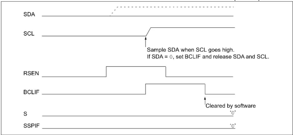
FIGURE 29-29: BUS COLLISION DURING A REPEATED START CONDITION (CASE 2)
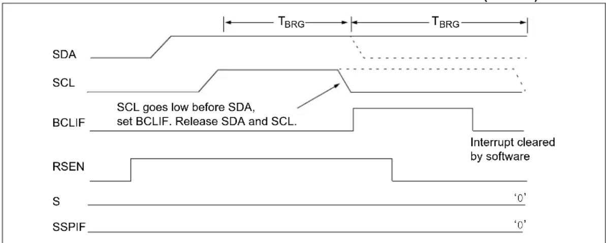
29.5.13.3 Bus Collision During a Stop Condition
Bus collision occurs during a Stop condition if:
a) after the SDA pin has been deasserted and allowed to float high, SDA is sampled low after the BRG has timed out
b) after the SCL pin is deasserted, SCL is sampled low before SDA goes high
The Stop condition begins with SDA asserted low. When SDA is sampled low, the SCL pin is allowed to float. When the pin is sampled high (clock arbitration), the Baud Rate Generator is loaded with SSPADD and counts down to 0. After the BRG times out, SDA is sampled. If SDA is sampled low, a bus collision has occurred. This is due to another master attempting to drive a data '0' (Figure 29-30). If the SCL pin is sampled low before SDA is allowed to float high, a bus collision occurs. This is another case of another master attempting to drive a data '0' (Figure 29-31).
FIGURE 29-30: BUS COLLISION DURING A STOP CONDITION (CASE 1)
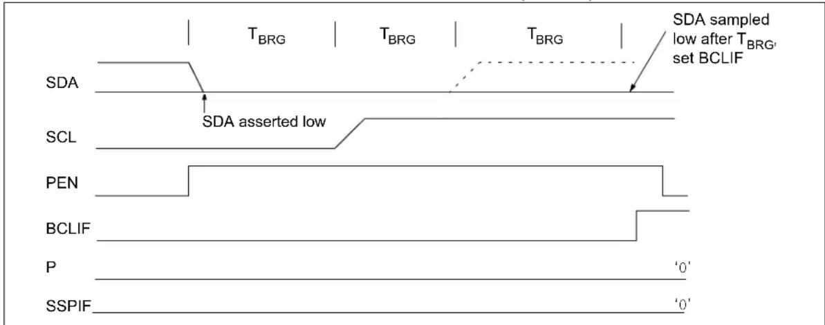
other
| Signal | Time Interval | Label | |--------|---------------|---------------------------| | SDA | Low | SDA asserted low | | SCL | Low | SDA asserted low | | PEN | Low | SDA asserted low | | BCLIF | Low | SDA sampled low after T_BRG' | | P | '0' | SDA sampled low after T_BRG' | | SSPIF | '0' | SDA sampled low after T_BRG' | | SDA | High | SDA sampled low after T_BRG' | | SCL | High | SDA sampled low after T_BRG' | | PEN | High | SDA sampled low after T_BRG' | | BCLIF | High | SDA sampled low after T_BRG' | | P | '0' | SDA sampled low after T_BRG' | | SSPIF | '0' | SDA sampled low after T_BRG' |FIGURE 29-31: BUS COLLISION DURING A STOP CONDITION (CASE 2)
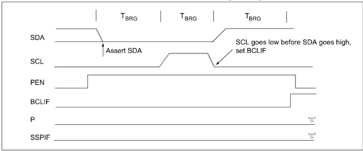
TABLE 29-2: SUMMARY OF REGISTERS ASSOCIATED WITH I ^2 C OPERATION
| Name Bit | 7 Bit 6 Bit | 5 Bit 4 Bit 3 | Bit 2 Bit 1 | Bit 0 | Reset Values on Page: | ||||
| INTCON GIE | E PEIE | T0IE | INTE | IOCE | T0IF | INTF | IOCF | 107 | |
| PIE1 | TXIE | RCIE | BCLIE | SSPIE | CC2IE | CC1IE | TMR2IE | TMR1IE | 108 |
| PIR1 | TXIF | RCIF | BCLIF | SSPIF | CC2IF | CC1IF | TMR2IF | TMR1IF | 110 |
| TRISGPA | TRISA7 | TRISA6 | TRISA5 | — | TRISA3 | TRISA2 | TRISA1 | TRISA0 | 127 |
| TRISGPB | TRISB7 | TRISB6 | TRISB5 | TRISB4 | — | — | TRISB1 | TRISB0 | 131 |
| SSPADD | ADD7 | ADD6 | ADD5 | ADD4 | ADD3 | ADD2 | ADD1 | ADD0 | 208 |
| SSPBUF | Synchronous Serial Port Receive Buffer/Transmit Register | 167* | |||||||
| SSPCON1 | WCOL | SSPOV | SSPEN | CKP | SSPM3 | SSPM2 | SSPM1 | SSPM0 | 204 |
| SSPCON2 | GCEN | ACKSTAT | ACKDT | ACKEN | RCEN | PEN | RSEN | SEN | 206 |
| SSPCON3 | ACKTIM | PCIE | SCIE | BOEN | SDAHT | SBCDE | AHEN | DHEN | 207 |
| SSPMSK1 | MSK7 | MSK6 | MSK5 | MSK4 | MSK3 | MSK2 | MSK1 | MSK0 | 208 |
| SSPSTAT | SMP CKE | D/A | — | P | S | R/W | UA | BF | 203 |
| SSPMSK2 | MSK27 | MSK26 | MSK25 | MSK24 | MSK23 | MSK22 | MSK21 | MSK20 | 209 |
| SSPADD2 | ADD27 | ADD26 | ADD25 | ADD24 | ADD23 | ADD22 | ADD21 | ADD20 | 209 |
Legend: — = unimplemented, read as '0'. Shaded cells are not used by the MSSP module in I²C mode.
* Page provides register information.
29.6 Baud Rate Generator
The MSSP module has a Baud Rate Generator available for clock generation in the ^2C Master mode. The Baud Rate Generator (BRG) reload value is placed in the SSPADD register. When a write occurs to SSPBUF, the Baud Rate Generator will automatically begin counting down.
Once the given operation is complete, the internal clock automatically stops counting and the clock pin remains in its last state.
An internal signal "Reload" in Figure 29-32 triggers the value from SSPADD to be loaded into the BRG counter. This occurs twice for each oscillation of the module clock line. The logic dictating when the reload signal is asserted depends on the mode the MSSP is being operated in.
Table 29-3 demonstrates clock rates based on instruction cycles and the BRG value loaded into SSPADD.
EQUATION 29-1:
$$ F _ {C L O C K} \quad \frac {F _ {O S C}}{(S S P A D D + 1) (4)} $$
FIGURE 29-32: BAUD RATE GENERATOR BLOCK DIAGRAM
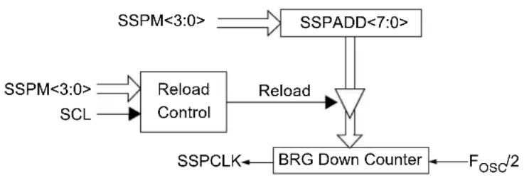
flowchart
graph TD
    A["SSPM<3:0>"] --> B["SSPADD<7:0>"]
    C["SSPM<3:0>"] --> D["Reload Control"]
    E["SCL"] --> D
    D --> F["Reload"]
    F --> G["M"]
    G --> H["BRG Down Counter"]
    H --> I["SSPCLK"]
    H --> J["Fosc/2"]
Note: Values of 0x00, 0x01 and 0x02 are not valid for SSPADD when used as a Baud Rate Generator for ^2 C. This is an implementation limitation.
TABLE 29-3: MSSP CLOCK RATE W/BRG
| F_osc | F_CY | BRG Value | F_CLOCK (2 rollovers of BRG) |
| 8 MHz | 2 MHz | 04h | 400 kHz (1) |
| 8 MHz | 2 MHz | 0Bh | 166 kHz |
| 8 MHz | 2 MHz | 13h | 100 kHz |
Note 1: The I ^2 C interface does not conform to the 400 kHz I ^2 C specification (which applies to rates greater than 100 kHz) in all details, but may be used with care where higher rates are required by the application.
REGISTER 29-1: SSPSTAT: SSP STATUS REGISTER
| R/W-0 R/W-0 R-0 R-0 R-0 R-0 R-0 | |||||||
| SMP | CKE | D/ | P | S | R/ | UA | BF |
| bit 7 bit 0 | |||||||
Legend:
| R = Readable bit | W = Writable bit | U = Unimplemented bit, read as '0' |
| u = Bit is unchanged | x = Bit is unknown -n = Value at POR | |
| ‘1’ = Bit is set | ‘0’ = Bit is cleared | |
bit 7 SMP: Data Input Sample bit
1 = Slew rate control disabled for standard-speed mode (100 kHz and 1 MHz)
0 = Slew rate control enabled for high-speed mode (400 kHz)
bit 6 CKE: Clock Edge Select bit
1 = Enable input logic so that thresholds are compliant with SM bus specification
0 = Disable SM bus specific inputs
: Data/Address bit
1 = Indicates that the last byte received or transmitted was data
0 = Indicates that the last byte received or transmitted was address
bit 5 D/A
bit 4 P: Stop bit
(This bit is cleared when the MSSP module is disabled, SSPEN is cleared.)
1 = Indicates that a Stop bit has been detected last (this bit is '0' on Reset)
0 = Stop bit was not detected last
bit 3 S: Start bit
(This bit is cleared when the MSSP module is disabled, SSPEN is cleared.)
1 = Indicates that a Start bit has been detected last (this bit is '0' on Reset)
0 = Start bit was not detected last
: Read/Write bit information
bit 2 R/W
This bit holds the R/W bit information following the last address match. This bit is only valid from the address match to the next Start bit, Stop bit, or not ACKbit
In I^2 C Slave mode:
1 = Read
0 = Write
In I² C Master mode:
1 = Transmit is in progress
0 = Transmit is not in progress
OR-ing this bit with SEN, RSEN, PEN, RCEN or ACKEN will indicate if the MSSP is in Idle mode
bit 1 UA: Update Address bit (10-bit I
^2 C mode only)
1 = Indicates that the user needs to update the address in the SSPADD register
0 = Address does not need to be updated
bit 0 BF: Buffer Full status bit
Receive:
1 = Receive complete, SSPBUF is full
0 = Receive not complete, SSPBUF is empty
Transmit:
1 = Data transmit in progress (does not include the ACK and Stop bits), SSPBUF is full
0 = Data transmit complete (does not include the ACK and Stop bits), SSPBUF is empty
REGISTER 29-2: SSPCON1:SSP CONTROL REGISTER 1
| R/C/HS-0 R/C/HS-0 R/W-0 R/W-0 R/W-0 R/W-0 R/W-0 R/W-0 | |||
| WCOL SSPOV SSPEN C | KP SSPM<3:0> | ||
| bit 7 bit 0 | |||
Legend:
| R = Readable bit | W = Writable bit | U = Unimplemented bit, read as '0' |
| u = Bit is unchanged | x = Bit is unknown | -n = Value at POR |
| '1' = Bit is set | '0' = Bit is cleared | HS = Bit is set by hardware C = User cleared |
bit 7 WCOL: Write Collision Detect bit
Master mode:
1 = A write to the SSPBUF register was attempted while the I²C conditions were not valid for a transmission to be started
0 = No collision
Slave mode:
1 = The SSPBUF register is written while it is still transmitting the previous word (must be cleared in software)
0 = No collision
bit 6 SSPOV: Receive Overflow Indicator bit (1)
1 = A byte is received while the SSPBUF register is still holding the previous byte. SSPOV is a "don't care" in Transmit mode (must be cleared in software)
0 = No overflow
bit 5 SSPEN: Synchronous Serial Port Enable bit
In both modes, when enabled, these pins must be properly configured as input or output
1 = Enables the serial port and configures the SDA and SCL pins as the source of the serial port pins ^(2)
0 = Disables serial port and configures these pins as I/O port pins
bit 4 CKP: Clock Polarity Select bit
In I^2 C Slave mode:
SCL release control
1 = Enable clock
0 = Holds clock low (clock stretch). (Used to ensure data setup time)
In I^2 C Master mode:
Unused in this mode
Note 1: In Master mode, the overflow bit is not set since each new reception (and transmission) is initiated by writing to the SSPBUF register.
2: When enabled, the SDA and SCL pins must be configured as inputs.
3: SSPADD values of 0, 1 or 2 are not supported for C mode.
REGISTER 29-2: SSPCON1:SSP CONTROL REGISTER 1 (CONTINUED)
bit 3-0
SSPM<3:0>: Synchronous Serial Port Mode Select bits
0000 = Reserved
0001 = Reserved
0010 = Reserved
0011 = Reserved
0100 = Reserved
0101 = Reserved
0110 = I²C Slave mode, 7-bit address
0111 = I²C Slave mode, 10-bit address
1000 = I²C Master mode, clock = F_OSC/(4 * (SSPADD+1)) ^(3)
1001 = Reserved
1010 = Reserved
1011 = I²C Firmware-Controlled Master mode (Slave idle)
1100 = Reserved
1101 = Reserved
1110 = I²C Slave mode, 7-bit address with Start and Stop bit interrupts enabled
1111 = I²C Slave mode, 10-bit address with Start and Stop bit interrupts enabled
Note 1: In Master mode, the overflow bit is not set since each new reception (and transmission) is initiated by writing to the SSPBUF register.
2: When enabled, the SDA and SCL pins must be configured as inputs.
3: SSPADD values of 0, 1 or 2 are not supported for I ^2 C mode.
REGISTER 29-3: SSPCON2: SSP CONTROL REGISTER 2
| R/W-0/0 R-0/0 R/W-0/0 R/S/HS-0/0 R/S/HS-0/0 R/S/HS-0/0 R/S/HS-0/0 R/W/HS-0/0 | |||||||
| GCEN ACK | STAT ACKDT | ACKEN | (1) | RCEN (1) | PEN (1) | RSEN (1) | SEN (1) |
| bit 7 bit 0 | |||||||
Legend:
| R = Readable bit | W = Writable bit | U = Unimplemented bit, read as '0' |
| u = Bit is unchanged | x = Bit is unknown | -n/n = Value at POR and BOR/Value at all other Resets |
| ‘1’ = Bit is set | ‘0’ = Bit is cleared | HS = Bit is set by hardware S = User set |
bit 7 GCEN: General Call Enable bit (in I²C Slave mode only)
1 = Enable interrupt when a general call address (0x00 or 00h) is received in the SSPSR register
0 = General call address disabled
bit 6 ACKSTAT: Acknowledge Status bit (in I²C mode only)
1 = Acknowledge was not received
0 = Acknowledge was received
bit 5 ACKDT: Acknowledge Data bit (in I²C mode only)
In Receive mode:
Value transmitted when the user initiates an Acknowledge sequence at the end of a receive
1 = Not Acknowledge
0 = Acknowledge
bit 4 ACKEN: Acknowledge Sequence Enable bit (in I²C Master mode only)
In Master Receive mode:
1 = Initiate Acknowledge sequence on SDA and SCL pins and transmit ACKDT data bit. Automatically cleared by hardware
0 = Acknowledge sequence idle
bit 3 RCEN: Receive Enable bit (in I²C Master mode only)
1 = Enables Receive mode for I^2C
0 = Receive idle
bit 2 PEN: Stop Condition Enable bit (in I ^2 C Master mode only)
SCK Release Control:
1 = Initiate Stop condition on SDA and SCL pins. Automatically cleared by hardware
0 = Stop condition idle
bit 1 RSEN: Repeated Start Condition Enabled bit (in I²C Master mode only)
1 = Initiate Repeated Start condition on SDA and SCL pins. Automatically cleared by hardware
0 = Repeated Start condition idle
bit 0 SEN: Start Condition Enabled bit (in I²C Master mode only)
In Master mode:
1 = Initiate Start condition on SDA and SCL pins. Automatically cleared by hardware
0 = Start condition idle
In Slave mode:
1 = Clock stretching is enabled for both Slave Transmit and Slave Receive (stretch enabled)
0 = Clock stretching is disabled
Note 1: If the I²C module is not in Idle mode, this bit may not be set (no spooling) and the SSPBUF may not be written (or writes to the SSPBUF are disabled).
REGISTER 29-4: SSPCON3: SSP CONTROL REGISTER 3
| R-0/0 R/W-0/0 R/W-0/0 R/W-0/0 R/W-0/0 R/W-0/0 R/W-0/0 R/W-0/0 | |||||||
| ACKTIM PC | IE SCIE BOEN | SDAHT SBCDE | AHEN | DHEN | |||
| bit 7 bit 0 | |||||||
| Legend: | ||
| R = Readable bit | W = Writable bit | U = Unimplemented bit, read as ‘0’ |
| u = Bit is unchanged | x = Bit is unknown | -n/n = Value at POR and BOR/Value at all other Resets |
| ‘1’ = Bit is set | ‘0’ = Bit is cleared | |
| bit 7 | ACKTIM: Acknowledge Time status bit (I2C mode only) (1) |
| 1 = Indicates the I2C bus is in an Acknowledge sequence, set on 8thfalling edge of SCL clock | |
| 0 = Not an Acknowledge sequence, cleared on 9thrising edge of SCL clock | |
| bit 6 | PCIE: Stop Condition Interrupt Enable bit (I2C mode only) |
| 1 = Enable interrupt on detection of Stop condition | |
| 0 = Stop detection interrupts are disabled (2) | |
| bit 5 | SCIE: Start Condition Interrupt Enable bit (I2C mode only) |
| 1 = Enable interrupt on detection of Start or Restart conditions | |
| 0 = Start detection interrupts are disabled (2) | |
| bit 4 | BOEN: Buffer Overwrite Enable bit |
| In I2C Master mode: | |
| This bit is ignored. | |
| In I2C Slave mode: | |
| 1 = SSPBUF is updated and ACK is generated for a received address/data byte, ignoring the state of the SSPOV bit only if the BF bit = 0. | |
| 0 = SSPBUF is only updated when SSPOV is clear. | |
| bit 3 | SDAHT: SDA Hold Time Selection bit |
| 1 = Minimum of 300 ns hold time on SDA after the falling edge of SCL | |
| 0 = Minimum of 100 ns hold time on SDA after the falling edge of SCL | |
| bit 2 | SBCDE: Slave Mode Bus Collision Detect Enable bit (I2C Slave mode only) |
| If, on the rising edge of SCL, SDA is sampled low when the module outputs a high state, the BCLIF bit in the PIR1 register is set and bus goes idle. | |
| 1 = Enable slave bus collision interrupts | |
| 0 = Slave bus collision interrupts are disabled | |
| bit 1 | AHEN: Address Hold Enable bit (I2C Slave mode only) |
| 1 = Following the 8thfalling edge of SCL for a matching received address byte; CKP bit in the SSPCON1 register is cleared and the SCL is held low | |
| 0 = Address holding is disabled | |
| bit 0 | DHEN: Data Hold Enable bit (I2C Slave mode only) |
| 1 = Following the 8thfalling edge of SCL for a received data byte; slave hardware clears the CKP bit in the SSPCON1 register and SCL is held low | |
| 0 = Data holding is disabled |
Note 1: The ACKTIM status bit is only active when the AHEN bit or DHEN bit is set.
2: This bit has no effect in Slave modes where Start and Stop condition detection is explicitly listed as enabled.
REGISTER 29-5: SSPMSK1: SSP MASK REGISTER 1
| R/W-1 R/W-1 R/W-1 R/W-1 R/W-1 R/W-1 R/W-1 R/W-1 | |
| MSK<7:1> | MSK<0> |
| bit 7 bit 0 | |
Legend:
| R = Readable bit W = Writable bit U = Unimplemented bit, read as '0' | |
| u = Bit is unchanged x = Bit is unknown | -n = Value at POR |
| '1' = Bit is set | '0' = Bit is cleared |
bit 7-1 MSK<7:1>: Mask bits
1 = The received address bit n is compared to SSPADD
0 = The received address bit n is not used to detect I^2C address match
bit 0 MSK<0>: Mask bit for I²C Slave mode, 10-bit Address
I^2C Slave mode, 10-bit address (SSPM<3:0> = 0111 or 1111):
1 = The received address bit 0 is compared to SSPADD<0> to detect I²C address match
0 = The received address bit 0 is not used to detect I²C address match I²C Slave mode, 7-bit address, the bit is ignored
REGISTER 29-6: SSPADD: MSSP ADDRESS AND BAUD RATE REGISTER 1
| R/W-0 R/W-0 R/W-0 R/W-0 R/W-0 R/W-0 R/W-0 R/W-0 |
| ADD<7:0> |
| bit 7 bit 0 |
Legend:
| R = Readable bit W = Writable bit U = Unimplemented bit, read as '0' | |
| u = Bit is unchanged x = Bit is unknown | -n = Value at POR |
| '1' = Bit is set | '0' = Bit is cleared |
Master mode:
| bit 7-0 | ADD<7:0>: Baud Rate Clock Divider bitsSCL pin clock period = ((ADD<7:0> + 1) * 4)/ F_OSC |
10-Bit Slave mode — Most Significant Address byte:
| bit 7-3 | Not used: Unused for Most Significant Address byte. Bit state of this register is a “don’t care”. Bit pattern sent by master is fixed by I^2C specification and must be equal to ‘11110’. However, those bits are compared by hardware and are not affected by the value in this register |
| bit 2-1 | ADD<2:1>: Two Most Significant bits of 10-bit address. |
| bit 0 | Not used: Unused in this mode. Bit state is a “don’t care” |
10-Bit Slave mode — Least Significant Address byte:
| bit 7-0 | ADD<7:0>: Eight Least Significant bits of 10-bit address |
7-Bit Slave mode:
| bit 7-1 | ADD<7:1>: 7-bit address |
| bit 0 | Not used: Unused in this mode. Bit state is a “don’t care” |
REGISTER 29-7: SSPMSK2: SSP MASK REGISTER 2
| R/W-1 R/W-1 R/W-1 R/W-1 R/W-1 R/W-1 R/W-1 R/W-1 | |
| MSK2<7:1> | MSK2<0> |
| bit 7 bit 0 | |
Legend:
| R = Readable bit W = Writable bit U = Unimplemented bit, read as '0' | ||
| u = Bit is unchanged | x = Bit is unknown | -n = Value at POR |
| ‘1’ = Bit is set | ‘0’ = Bit is cleared | |
bit 7-1
MSK2<7:1>: Mask bits
1 = The received address bit n is compared to SSPADD2
0 = The received address bit n is not used to detect I^2C address match
bit 0
MSK2<0>: Mask bit for I²C Slave mode, 10-bit Address
I^2C Slave mode, 10-bit address (SSPM<3:0>=0111 or 1111):
1 = The received address bit 0 is compared to SSPADD2<0> to detect I²C address match
0 = The received address bit 0 is not used to detect I²C address match I²C Slave mode, 7-bit address, the bit is ignored
REGISTER 29-8: SSPADD2: MSSP ADDRESS 2
| R/W-0 R/W-0 R/W-0 R/W-0 R/W-0 R/W-0 R/W-0 R/W-0 |
| ADD2<7:0> |
| bit 7 bit 0 |
Legend:
| R = Readable bit W = Writable bit U = Unimplemented bit, read as '0' | ||
| u = Bit is unchanged | x = Bit is unknown | -n = Value at POR |
| '1' = Bit is set | '0' = Bit is cleared | |
Master mode:
bit 7-0
ADD2<7:0>: Baud Rate Clock Divider bits
SCL pin clock period = ((ADD<7:0> + 1) * 4)/FOSC
10-Bit Slave mode — Most Significant Address byte:
bit 7-3 Not used: Unused for Most Significant Address byte. Bit state of this register is a "don't care". Bit pattern sent by master is fixed by I^2C specification and must be equal to '11110'. However, those bits are compared by hardware and are not affected by the value in this register
bit 2-1 ADD2<2:1>: Two Most Significant bits of 10-bit address
bit 0 Not used: Unused in this mode. Bit state is a "don't care"
10-Bit Slave mode — Least Significant Address byte:
bit 7-0 ADD2<7:0>: Eight Least Significant bits of 10-bit address
7-Bit Slave mode:
bit 7-1
ADD2<7:1>: 7-bit address
bit 0
Not used: Unused in this mode. Bit state is a "don't care"
NOTES:
30.0 INSTRUCTION SET SUMMARY
The MCP19116/7 instruction set is highly orthogonal and is comprised of three basic categories:
- Byte-oriented operations
- Bit-oriented operations
• Literal and control operations
Each instruction is a 14-bit word divided into:
- a n opcode, which specifies the instruction type
- one or more operands, which further specify the operation of the instruction.
The formats for each of the categories is presented in Figure 30-1, while the various opcode fields are summarized in Table 30-1.
Table 30-2 lists the instructions recognized by the MPASM™ assembler.
For byte-oriented instructions, 'f' represents a file register designator and 'd' represents a destination designator. The file register designator specifies which file register is to be used by the instruction.
The destination designator specifies where the result of the operation is to be placed. If 'd' is 0, the result is placed in the W register. If 'd' is 1, the result is placed in the file register specified in the instruction.
For bit-oriented instructions, 'b' represents a bit field designator, which selects the bit affected by the operation, while 'f' represents the address of the file in which the bit is located.
For literal and control operations, 'k' represents an 8-bit or 11-bit constant, or literal value.
One instruction cycle consists of four oscillator periods; for an oscillator frequency of 4 MHz, this gives a normal instruction execution time of 1 s. All instructions are executed within a single instruction cycle, unless a conditional test is true or the program counter is changed as a result of an instruction. When this occurs, the execution takes two instruction cycles, with the second cycle executed as a NOP.
All instruction examples use the format '0xhh' to represent a hexadecimal number, where 'h' signifies a hexadecimal digit.
30.1 Read-Modify-Write Operations
Any instruction that specifies a file register as part of the instruction performs a Read-Modify-Write (RMW) operation. The register is read, the data is modified, and the result is stored according to either the instruction or the destination designator 'd'. A read operation is performed on a register even if the instruction writes to that register.
For example, a CLRF PORTA instruction will read PORTGPA, clear all the data bits, then write the result back to PORTGPA. This example would have the unintended consequence of clearing the condition that sets the IOCIF flag.
TABLE 30-1: OPCODE FIELD DESCRIPTIONS
| Field | Description |
| f | Register file address (0x00 to 0x7F) |
| W Working register (accumulator) | |
| b | Bit address within an 8-bit file register |
| k Literal field, constant data or label | |
| x | Don't care location (= 0 or 1).The assembler will generate code with x = 0.It is the recommended form of use for compatibility with all Microchip Technology Inc. software tools. |
| d | Destination select; d = 0: store result in W,d = 1: store result in file register f.Default is d = 1 . |
| PC | Program Counter |
| TO | Time-Out bit |
| C Carry bit | |
| DC | Digit carry bit |
| Z | Zero bit |
| Power-down bit | |
FIGURE 30-1: GENERAL FORMAT FOR INSTRUCTIONS
| Byte-oriented file register operations | ||
| 13 | 8 7 6 | 0 |
| OPCODE | d | f (FILE #) |
| d = 0 for destination W | ||
| d = 1 for destination f | ||
| f = 7-bit file register address | ||
| Bit-oriented file register operations | ||
| 13 | 10 9 7 6 | 0 |
| OPCODE | b (BIT #) | f (FILE #) |
| b = 3-bit address | ||
| f = 7-bit file register address | ||
| Literal and control operations | ||
| General | ||
| 13 | 8 7 | 0 |
| OPCODE | k (literal) | |
| k = 8-bit immediate value | ||
| CALL and GOTO instructions only | ||
| 13 | 11 10 | 0 |
| OPCODE | k (literal) | |
| k = 11-bit immediate value | ||
Byte-oriented file register operations
d = 0 for destination W
d = 1 for destination f
f = 7-bit file register address
Bit-oriented file register operations
b = 3-bit address
f = 7-bit file register address
Literal and control operations
General
| 13 | 8 | 7 | 0 |
| OPCODE | k (literal) | ||
k = 8-bit immediate value
CALL and GOTO instructions only
| 13 | 11 | 10 | 0 |
| OPCODE | k (literal) | ||
k = 11-bit immediate value
TABLE 30-2: MCP19116/7 INSTRUCTION SET
| Mnemonic, Operands | Description Cycles | 14-Bit Opcode | Status affected | Notes | |||||
| MSb LSb | |||||||||
| BYTE-ORIENTED FILE REGISTER OPERATIONS | |||||||||
| ADDWF | f, d | Add W and f | 1 | 00 | 0111 | dfff | ffff | C, DC, Z | 1, 2 |
| ANDWF | f, d | AND W with f | 1 | 00 | 0101 | dfff | ffff | Z | 1, 2 |
| CLRF | f | Clear f | 1 | 00 | 0001 | lfff | ffff | Z | 2 |
| CLRW | - | Clear W | 1 | 00 | 0001 | 0xxx | xxxx | Z | |
| COMF | f, d | Complement f | 1 | 00 | 1001 | dfff | ffff | Z | 1, 2 |
| DECF | f, d | Decrement f | 1 | 00 | 0011 | dfff | ffff | Z | 1, 2 |
| DECFSZ | f, d | Decrement f, Skip if 0 | 1(2) | 00 | 1011 | dfff | ffff | 1, 2, 3 | |
| INCF | f, d | Increment f | 1 | 00 | 1010 | dfff | ffff | Z | 1, 2 |
| INCFSZ | f, d | Increment f, Skip if 0 | 1(2) | 00 | 1111 | dfff | ffff | 1, 2, 3 | |
| IORWF | f, d | Inclusive OR W with f | 1 | 00 | 0100 | dfff | ffff | Z | 1, 2 |
| MOVF | f, d | Move f | 1 | 00 | 1000 | dfff | ffff | Z | 1, 2 |
| MOVWF | f | Move W to f | 1 | 00 | 0000 | lfff | ffff | ||
| NOP | - | No Operation | 1 | 00 | 0000 | 0xx0 | 0000 | ||
| RLF | f, d | Rotate Left f through Carry | 1 | 00 | 1101 | dfff | ffff | C | 1, 2 |
| RRF | f, d | Rotate Right f through Carry | 1 | 00 | 1100 | dfff | ffff | C | 1, 2 |
| SUBWF | f, d | Subtract W from f | 1 | 00 | 0010 | dfff | ffff | C, DC, Z | 1, 2 |
| SWAPF | f, d | Swap nibbles in f | 1 | 00 | 1110 | dfff | ffff | 1, 2 | |
| XORWF | f, d | Exclusive OR W with f | 1 | 00 | 0110 | dfff | ffff | Z | 1, 2 |
| BIT-ORIENTED FILE REGISTER OPERATIONS | |||||||||
| BCF | f, b | Bit Clear f | 1 | 01 | 00bb | bfff | ffff | 1, 2 | |
| BSF | f, b | Bit Set f | 1 | 01 | 01bb | bfff | ffff | 1, 2 | |
| BTFSC | f, b | Bit Test f, Skip if Clear | 1 (2) | 01 | 10bb | bfff | ffff | 3 | |
| BTFSS | f, b | Bit Test f, Skip if Set | 1 (2) | 01 | 11bb | bfff | ffff | 3 | |
| LITERAL AND CONTROL OPERATIONS | |||||||||
| ADDLW | k | Add literal and W | 1 | 11 | 111x | kkkk | kkkk | C, DC, Z | |
| ANDLW | k | AND literal with W | 1 | 11 | 1001 | kkkk | kkkk | Z | |
| CALL | k | Call Subroutine | 2 | 10 | 0kkk | kkkk | kkkk | ||
| CLRWDT | - | Clear Watchdog Timer | 1 | 00 | 0000 | 0110 | 0100 | TO, PD | |
| GOTO | k | Go to address | 2 | 10 | 1kkk | kkkk | kkkk | ||
| IORLW | k | Inclusive OR literal with W | 1 | 11 | 1000 | kkkk | kkkk | Z | |
| MOVLW | k | Move literal to W | 1 | 11 | 00xx | kkkk | kkkk | ||
| RETFIE | - | Return from interrupt | 2 | 00 | 0000 | 0000 | 1001 | ||
| RETLW | k | Return with literal in W | 2 | 11 | 01xx | kkkk | kkkk | ||
| RETURN | - | Return from Subroutine | 2 | 00 | 0000 | 0000 | 1000 | ||
| SLEEP | - | Go into Standby mode | 1 | 00 | 0000 | 0110 | 0011 | TO, PD | |
| SUBLW | k | Subtract W from literal | 1 | 11 | 110x | kkkk | kkkk | C, DC, Z | |
| XORLW | k | Exclusive OR literal with W | 1 | 11 | 1010 | kkkk | kkkk | Z | |
Note 1: When an I/O register is modified as a function of itself (e.g., MOVF PORTA, 1), the value used will be that value present on the pins themselves. For example, if the data latch is '1' for a pin configured as input and is driven low by an external device, the data will be written back with a '0'.
2: If this instruction is executed on the TMR0 register (and where applicable, d = 1), the prescaler will be cleared if assigned to the Timer0 module.
3: If the Program Counter (PC) is modified, or a conditional test is true, the instruction requires two cycles. The second cycle is executed as a NOP.
30.2 Instruction Descriptions
ADDLW Add literal and W
| Syntax: [label] ADDLW k | |
| Operands: | 0 ≤ k ≤ 255 |
| Operation: | (W) + k → (W) |
| Status Affected: C, DC, Z | |
| Description: The contents of the W register are added to the 8-bit literal 'k' and the result is placed in the W register. | |
ADDWF Add W and f
| Syntax: [label] ADDWF f,d | |
| Operands: | 0 ≤ f ≤ 127d ∈ [0,1] |
| Operation: | (W) + (f) → (destination) |
| Status Affected: | C, DC, Z |
| Description: | Add the contents of the W register with register 'f'. If 'd' is '0', the result is stored in the W register. If 'd' is '1', the result is stored back in register 'f'. |
ANDLW AND literal with W
| Syntax: [label] ANDLW k | |
| Operands: 0 ≤ k ≤ 255 | |
| Operation: (W) .AND. (k) → (W) | |
| Status Affected: Z | |
| Description: The contents of W register are AND'ed with the 8-bit literal 'k'. The result is placed in the W register. |
ANDWF AND W with f
| Syntax: [label] ANDWF f,d | |
| Operands: | 0 ≤ f ≤ 127d ∈ [0,1] |
| Operation: | (W) .AND. (f) → (destination) |
| Status Affected: | Z |
| Description: | AND the W register with register ‘f’. If ‘d’ is ‘0’, the result is stored in the W register. If ‘d’ is ‘1’, the result is stored back in register ‘f’. |
BCF Bit Clear f
| Syntax: [label] BCF f,b | |
| Operands: 0 ≤ f ≤ 1270 ≤ b ≤ 7 | |
| Operation: 0 → (f) | |
| Status Affected: None | |
| Description: Bit 'b' in register 'f' is cleared. |
BSF Bit Set f
| Syntax: [label] BSF f,b | |
| Operands: 0 ≤ f ≤ 1270 ≤ b ≤ 7 | |
| Operation: 1 → (f) | |
| Status Affected: None | |
| Description: Bit 'b' in register 'f' is set. |
BTFSC Bit Test f, Skip if Clear
| Syntax: | [ label ] BTFSC f,b |
| Operands: | 0 ≤ f ≤ 1270 ≤ b ≤ 7 |
| Operation: | skip if (f) = 0 |
| Status Affected: | None |
| Description: | If bit ‘b’ in register ‘f’ is ‘1’, the next instruction is executed.If bit ‘b’ in register ‘f’ is ‘0’, the next instruction is discarded, and a NOP is executed instead, making this a two-cycle instruction. |
BTFSS Bit Test f, Skip if Set
| Syntax: [label] BTFSS f,b | |
| Operands: 0 ≤ f ≤ 1270 ≤ b < 7 | |
| Operation: skip if (f<b>) = 1 | |
| Status Affected: None | |
| Description: If bit 'b' in register 'f' is '0', the next instruction is executed.If bit 'b' is '1', the next instruction is discarded and a NOP is executed instead, making this a two-cycle instruction. |
CALL Call Subroutine
| Syntax: [label] CALL k | |
| Operands: 0 ≤ k ≤ 2047 | |
| Operation: (PC)+ 1→ TOS,k → PC<10:0>,(PCLATH<4:3>) → PC<12:11> | |
| Status Affected: None | |
| Description: Call Subroutine. First, return address (PC + 1) is pushed onto the stack. The 11-bit immediate address is loaded into PC bits <10:0>. The upper bits of the PC are loaded from PCLATH. CALL is a two-cycle instruction. |
CLRF Clear f
| Syntax: | [ label ] CLRF f |
| Operands: | 0 ≤ f ≤ 127 |
| Operation: | 00h → (f)1 → Z |
| Status Affected: | Z |
| Description: | The contents of register ‘f’ are cleared and the Z bit is set. |
CLRW Clear W
| Syntax: [ label ] | CLRW |
| Operands: | None |
| Operation: | 00h → (W)1 → Z |
| Status Affected: | Z |
| Description: | W register is cleared. Zero (Z) bit is set. |
CLRWDT Clear Watchdog Timer
| Syntax: [label] | CLRWDT |
| Operands: | None |
| Operation: | 00h → WDT0 →WDT prescaler,1 →TO1 →PD |
| Status Affected: | TO, PD |
| Description: | CLRWDT instruction resets the Watchdog Timer. It also resets the prescaler of the WDT.Bits TO and PD in the STATUS register are set. |
COMF Complement f
| Syntax: | [ label] COMF f,d |
| Operands: | 0 ≤ f ≤ 127d ∈ [0,1] |
| Operation: | (f) → (destination) |
| Status Affected: | Z |
| Description: | The contents of register 'f' are complemented. If 'd' is '0', the result is stored in W. If 'd' is '1', the result is stored back in register 'f'. |
DECF Decrement f
| Syntax: | [ label ] DECF f,d |
| Operands: | 0 ≤ f ≤ 127d ∈ [0,1] |
| Operation: (f) - 1 → (destination) | |
| Status Affected: | Z |
| Description: | Decrement register ‘f’. If ‘d’ is ‘0’, the result is stored in the W register. If ‘d’ is ‘1’, the result is stored back in register ‘f’. |
DECFSZ Decrement f, Skip if 0
| Syntax: [label] | DECFSZ f,d |
| Operands: | 0 ≤ f ≤ 127d ∈ [0,1] |
| Operation: | (f) - 1 → (destination);skip if result = 0 |
| Status Affected: None | |
| Description: The contents of register ‘f’ are decremented. If ‘d’ is ‘0’, the result is placed in the W register. If ‘d’ is ‘1’, the result is placed back in register ‘f’.If the result is ‘1’, the next instruction is executed. If the result is ‘0’, a NOP is executed instead, making it a two-cycle instruction. | |
GOTO Unconditional Branch
| Syntax: [label] | GOTO k |
| Operands: | 0 ≤ k ≤ 2047 |
| Operation: k → PC<10:0> PCLATH<4:3> → PC<12:11> | |
| Status Affected: None | |
| Description: | GOTO is an unconditional branch. The 11-bit immediate value is loaded into PC bits <10:0>. The upper bits of PC are loaded from PCLATH<4:3>. GOTO is a two-cycle instruction. |
| INCF | Increment f |
| Syntax: | [ label ] INCF f,d |
| Operands: | 0 ≤ f ≤ 127d ∈ [0,1] |
| Operation: | (f) + 1 → (destination) |
| Status Affected: | Z |
| Description: | The contents of register ‘f’ are incremented. If ‘d’ is ‘0’, the result is placed in the W register. If ‘d’ is ‘1’, the result is placed back in register ‘f’. |
INCFSZ Increment f, Skip if 0
| Syntax: [label] | INCFSZ f,d |
| Operands: | 0 ≤ f ≤ 127d ∈ [0,1] |
| Operation: | (f) + 1 → (destination),skip if result = 0 |
| Status Affected: None | |
| Description: The contents of register ‘f’ are incremented. If ‘d’ is ‘0’, the result is placed in the W register. If ‘d’ is ‘1’, the result is placed back in register ‘f’.If the result is ‘1’, the next instruction is executed. If the result is ‘0’, a NOP is executed instead, making it a two-cycle instruction. | |
IORLW Inclusive OR literal with W
| Syntax: | [ label ] IORLW k |
| Operands: | 0 ≤ k ≤ 255 |
| Operation: | (W) .OR. k → (W) |
| Status Affected: | Z |
| Description: | The contents of the W register are OR'ed with the 8-bit literal 'k'. The result is placed in the W register. |
| IORWF | Inclusive OR W with f |
| Syntax: | [ label ] IORWF f,d |
| Operands: | 0 ≤ f ≤ 127d ∈ [0,1] |
| Operation: | (W) .OR. (f) → (destination) |
| Status Affected: | Z |
| Description: | Inclusive OR the W register with register ‘f’. If ‘d’ is ‘0’, the result is placed in the W register. If ‘d’ is ‘1’, the result is placed back in register ‘f’. |
MOVF Move f
| Syntax: [label] | MOVF f,d |
| Operands: | 0 ≤ f ≤ 127d ∈ [0,1] |
| Operation: (f) → (dest) | |
| Status Affected: Z | |
| Description: The contents of register 'f' are moved to a destination dependent upon the status of 'd'. If d = 0, the destination is W register. If d = 1, the destination is file register 'f' itself. d = 1 is useful to test a file register since STATUS flag Z is affected. | |
| Words: 1 | |
| Cycles: 1 | |
| Example: MOVF FSR, 0 | |
| After InstructionW = value in FSRregisterZ = 1 | |
MOVWF Move W to f
| Syntax: [label] MOVWF f | |
| Operands: 0 ≤ f ≤ 127 | |
| Operation: (W) → (f) | |
| Status Affected: None | |
| Description: Move data from W register to register 'f'. | |
| Words: 1 | |
| Cycles: 1 | |
| Example: MOVW OPTION | |
| F | |
| Before Instruction | |
| OPTION = 0xFF | |
| W = 0x4F | |
| After Instruction | |
| OPTION = 0x4F | |
| W = 0x4F |
MOVLW Move literal to W
| Syntax: | [ label ] MOVLW k |
| Operands: | 0 ≤ k ≤ 255 |
| Operation: | k (W) |
| Status | None |
| Affected: | |
| Description: | The 8-bit literal ‘k’ is loaded into W register. The “don’t cares” will assemble as ‘0’s. |
| Words: | 1 |
| Cycles: | 1 |
| Example: | MOVLW 0x5A |
| After InstructionW = 0x5A |
NOP No Operation
| Syntax: [label] NOP |
| Operands: None |
| Operation: No operation |
| Status Affected: None |
| Description: No operation. |
| Words: 1 |
| Cycles: 1 |
| Example: NOP |
RETFIE Return from Interrupt
| Syntax: [label] RETFIE |
| Operands: None |
| Operation: TOS → PC,1 → GIE |
| Status Affected: None |
| Description: Return from Interrupt. Stack is POPed and Top-of-Stack (TOS)is loaded in the PC. Interrupts are enabled by setting Global Interrupt Enable bit, GIE(INTCON<7>). This is a two-cycle instruction. |
| Words: 1 |
| Cycles: 2 |
| Example: RETFIE |
| After InterruptPC = TOSGIE = 1 |
RETURN Return from Subroutine
| Syntax: [label] | RETURN |
| Operands: | None |
| Operation: | TOS → PC |
| Status Affected: | None |
| Description: | Return from subroutine. The stack is POPed and the Top-of-Stack (TOS) is loaded into the program counter. This is a two-cycle instruction. |
RETLW Return with literal in W
| Syntax: | [ label] RETLW k |
| Operands: | 0 ≤ k ≤ 255 |
| Operation: k → (W);TOS → PC | |
| Status Affected: None | |
| Description: The W register is loaded with the 8-bit literal 'k'. The program counter is loaded from the Top-of-Stack (the return address). This is a two-cycle instruction. | |
| Words: 1 | |
| Cycles: 2 | |
| Example: | CALL TABLE;W contains ;table offset ;valueGOTO DONE |
| TABLE | ••ADDWF PC ;W = offsetRETLW k1 ;Begin tableRETLW k2 ;•••RETLW kn ;End of table |
| DONE | |
| Before InstructionW = 0x07After InstructionW = value of k8 | |
RLF Rotate Left f through Carry
| Syntax: | [label RLF f,d] |
| Operands: | 0 ≤ f ≤ 127d ∈ [0,1] |
| Operation: | See description below |
| Status Affected: | C |
| Description: | The contents of register 'f' are rotated one bit to the left through the Carry flag. If 'd' is '0', the result is placed in the W register. If 'd' is '1', the result is stored back in register 'f'.[IMAGE] |
| Words: 1 | |
| Cycles: | 1 |
| Example: | RLF REG1, 0Before InstructionREG1 = 1110 0110C = 0After InstructionREG1 = 1110 0110W = 1100 1100C = 1 |
RRF Rotate Right f through Carry
| Syntax: [label] | RRF f,d |
| Operands: | 0≤f≤127d∈[0,1] |
| Operation: See description below | |
| Status Affected: C | |
| Description: The contents of register 'f' are rotated one bit to the right through the Carry flag. If 'd' is '0', the result is placed in the W register. If 'd' is '1', the result is placed back in register 'f'. | |
SLEEP Enter Sleep mode
| Syntax: [label] SLEEP | |
| Operands: None | |
| Operation: 00h → WDT,0 → WDT prescaler,1 → TO,0 → PD | |
| Status Affected: TO,PD — | |
| Description: | The power-down STATUS bit,PD, is cleared. Time-OutSTATUS bit (TO) is set.Watchdog Timer and its prescaler are cleared.The processor is put into Sleep mode with the oscillator stopped. |
SUBLW Subtract W from literal
| Syntax: | [ label ] SUBLW k |
| Operands: | 0 ≤ k ≤ 255 |
| Operation: | k - (W) → (W) |
| Status Affected: | C, DC, Z |
| Description: | The W register is subtracted (two's complement method) from the 8-bit literal 'k'. The result is placed in the W register. |
| Result | Condition |
| C = 0 | W > k |
| C = 1 | W ≤ k |
| DC = 0 | W<3:0> > k<3:0> |
| DC = 1 | W<3:0> ≤ k<3:0> |
SUBWF Subtract W from f
| Syntax: | [ label ] SUBWF f,d | |
| Operands: | 0 ≤ f ≤ 127d ∈ [0,1] | |
| Operation: | (f) - (W) → (destination) | |
| Status Affected: | C, DC, Z | |
| Description: | Subtract (two's complement method) W register from register 'f'.If 'd' is '0', the result is stored in the W register. If 'd' is '1', the result is stored back in register 'f'. | |
| C = 0 | W > f | |
| C = 1 | W ≤ f | |
| DC = 0 | W<3:0> > f<3:0> | |
| DC = 1 | W<3:0> ≤ f<3:0> | |
SWAPF Swap Nibbles in f
| Syntax: [label] | SWAPF f,d |
| Operands: | 0 ≤ f ≤ 127d ∈ [0,1] |
| Operation: (f<3:0>) → (destination<7:4>), (f<7:4>) → (destination<3:0>) | |
| Status Affected: None | |
| Description: | The upper and lower nibbles of register ‘f’ are exchanged. If ‘d’ is ‘0’, the result is placed in the W register. If ‘d’ is ‘1’, the result is placed in register ‘f’. |
XORLW Exclusive OR literal with W
| Syntax: [label] XORLW k | |
| Operands: | 0 ≤ k ≤ 255 |
| Operation: (W) .XOR. k → (W) | |
| Status Affected: Z | |
| Description: | The contents of the W register are XOR'ed with the 8-bit literal 'k'. The result is placed in the W register. |
XORWF Exclusive OR W with f
Syntax: [label] XORWF f,d
Operands: 0 ≤ f ≤ 127
d ∈ [0,1]
Operation: (W). XOR. (f) → (destination)
Status Affected: Z
Description: Exclusive OR the contents of the
W register with register 'f'. If 'd' is '0', the result is stored in the W register. If 'd' is '1', the result is stored back in register 'f'.
NOTES:
31.0 IN-CIRCUIT SERIAL PROGRAMMING™ (ICSP™)
ICSP allows customers to manufacture circuit boards with unprogrammed devices. Programming can be done after the assembly process, allowing the device to be programmed with the most recent firmware or a custom firmware. Five pins are needed for ICSP programming:
- ICSPCLK
• ICSPDAT
• MCLR
• V_DD - A_GND
In Program/Verify mode, the Program Memory, User IDs and the Configuration Words are programmed through serial communications. The ICSPDAT pin is a bidirectional I/O used for transferring the serial data and the ICSPCLK pin is the clock input. The device is placed into a Program/Verify mode by holding the ICSPDAT and ICSPCLK pins low while raising the MCLR pin from V_IL to V_IHH .
31.1 Common Programming Interfaces
Connection to a target device is typically done through an ICSP header. A commonly found connector on development tools is the RJ-11 in the 6P6C (6-pin, 6-connector) configuration. Refer to Figure 31-1.
FIGURE 31-1: ICD RJ-11 STYLE
CONNECTOR INTERFACE
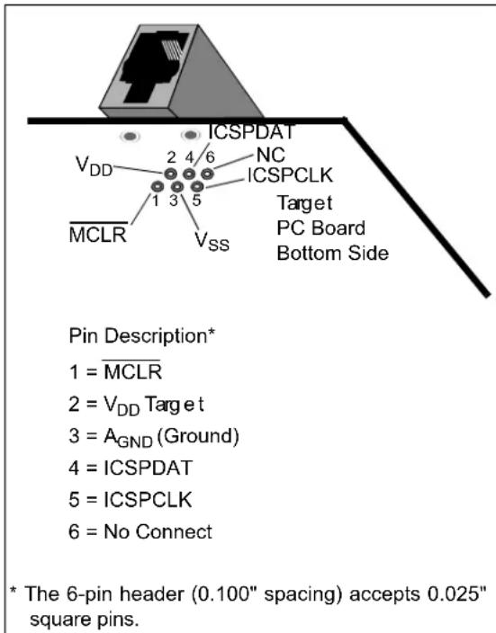
Another connector often found in use with the PICkit™ programmers is a standard 6-pin header with 0.1 inch spacing. Refer to Figure 31-2.
FIGURE 31-2: PICkit™ STYLE CONNECTOR INTERFACE
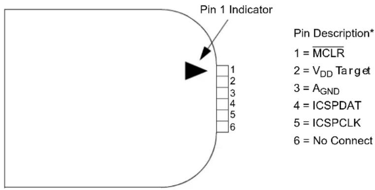
* The 6-pin header (0.100" spacing) accepts 0.025" square pins.
For additional interface recommendations, refer to your specific device programmer manual prior to PCB design.
It is recommended that isolation devices be used to separate the programming pins from other circuitry. The type of isolation is highly dependent on the specific application and may include devices such as resistors, diodes or even jumpers. Refer to Figure 31-3 for more information.
FIGURE 31-3: TYPICAL CONNECTION FOR ICSP™ PROGRAMMING
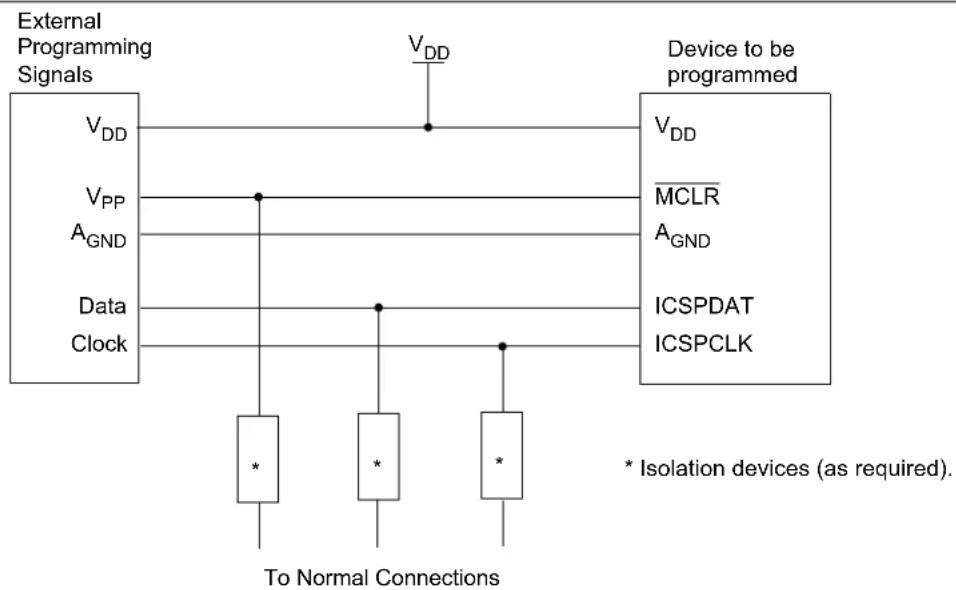
flowchart
graph TD
    A["External Programming Signals"] --> B["V_DD"]
    A --> C["V_PP"]
    A --> D["A_GND"]
    A --> E["Data"]
    A --> F["Clock"]
    G["Device to be programmed"] --> H["V_DD"]
    G --> I["MCLR"]
    G --> J["A_GND"]
    G --> K["ICSPDAT"]
    G --> L["ICSPCLK"]
    M["* Isolation devices (as required.)"] --> N["To Normal Connections"]
    N --> O["*"]
    N --> P["*"]
    N --> Q["*"]
Note: If powering via back feeding V DD , V DD must be tied to V _IN .
32.0 DEVELOPMENT SUPPORT
The PIC ^® microcontrollers (MCU) and dsPIC ^® digital signal controllers (DSC) are supported with a full range of software and hardware development tools:
- Integrated Development Environment - MPLAB ^® X IDE Software
- Compilers/Assemblers/Linkers
- MPLAB XC Compiler
- MPASM ^TM Assembler
- M P L ^TM Object Linker/MPLIB ^TM Object Librarian
- MPLAB Assembler/Linker/Librarian for Various Device Families
- Simulators
- MPLAB X SIM Software Simulator
- Emulators
- MPLAB REAL ICE™ In-Circuit Emulator
• In-Circuit Debuggers/Programmers
- MPLAB ICD 3
- PICkit™ 3
• Device Programmers
- MPLAB PM3 Device Programmer
- Low-Cost Demonstration/Development Boards, Evaluation Kits and Starter Kits
• Third-party development tools
32.1 MPLAB X Integrated Development Environment Software
The MPLAB X IDE is a single, unified graphical user interface for Microchip and third-party software, and hardware development tool that runs on Windows ^® , Linux and Mac OS ^® X. Based on the NetBeans IDE, MPLAB X IDE is an entirely new IDE with a host of free software components and plug-ins for high-performance application development and debugging. Moving between tools and upgrading from software simulators to hardware debugging and programming tools is simple with the seamless user interface.
With complete project management, visual call graphs, a configurable watch window and a feature-rich editor that includes code completion and context menus, MPLAB X IDE is flexible and friendly enough for new users. With the ability to support multiple tools on multiple projects with simultaneous debugging, MPLAB X IDE is also suitable for the needs of experienced users.
Feature-Rich Editor:
• Color syntax highlighting
- Smart code completion makes suggestions and provides hints as you type
• Automatic code formatting based on user-defined rules
• Live parsing
User-Friendly, Customizable Interface:
- Fully customizable interface: toolbars, toolbar buttons, windows, window placement, etc.
- Call graph window
Project-Based Workspaces:
- Multiple projects
- Multiple tools
- Multiple configurations
- Simultaneous debugging sessions
File History and Bug Tracking:
- Local file history feature
• Built-in support for Bugzilla issue tracker
32.2 MPLAB XC Compilers
The MPLAB XC Compilers are complete ANSI C compilers for all of Microchip's 8-, 16- and 32-bit MCU and DSC devices. These compilers provide powerful integration capabilities, superior code optimization and ease of use. MPLAB XC Compilers run on Windows, Linux or MAC OS X.
For easy source level debugging, the compilers provide debug information that is optimized to the MPLAB X IDE.
The free MPLAB XC Compiler editions support all devices and commands, with no time or memory restrictions, and offer sufficient code optimization for most applications.
MPLAB XC Compilers include an assembler, linker and utilities. The assembler generates relocatable object files that can then be archived or linked with other relocatable object files and archives to create an executable file. MPLAB XC Compiler uses the assembler to produce its object file. Notable features of the assembler include:
- Support for the entire device instruction set
- Support for fixed-point and floating-point data
- Command-line interface
- Rich directive set
- Flexible macro language
- MPLAB X IDE compatibility
32.3 MPASM Assembler
The MPASM Assembler is a full-featured, universal macro assembler for PIC10/12/16/18 MCUs.
The MPASM Assembler generates relocatable object files for the MPLINK Object Linker, Intel® standard HEX files, MAP files to detail memory usage and symbol reference, absolute LST files that contain source lines and generated machine code, and COFF files for debugging.
The MPASM Assembler features include:
• Integration into MPLAB X IDE projects
- User-defined macros to streamline assembly code
- Conditional assembly for multipurpose source files
- Directives that allow complete control over the assembly process
32.4 MPLINK Object Linker/MPLIB Object Librarian
The MPLINK Object Linker combines relocatable objects created by the MPASM Assembler. It can link relocatable objects from precompiled libraries, using directives from a linker script.
The MPLIB Object Librarian manages the creation and modification of library files of precompiled code. When a routine from a library is called from a source file, only the modules that contain that routine will be linked in with the application. This allows large libraries to be used efficiently in many different applications.
The object linker/library features include:
- Efficient linking of single libraries instead of many smaller files
- Enhanced code maintainability by grouping related modules together
- Flexible creation of libraries with easy module listing, replacement, deletion and extraction
32.5 MPLAB Assembler, Linker and Librarian for Various Device Families
MPLAB Assembler produces relocatable machine code from symbolic assembly language for PIC24, PIC32 and dsPIC DSC devices. MPLAB XC Compiler uses the assembler to produce its object file. The assembler generates relocatable object files that can then be archived or linked with other relocatable object files and archives to create an executable file. Notable features of the assembler include:
- Support for the entire device instruction set
- Support for fixed-point and floating-point data
- Command-line interface
- Rich directive set
- Flexible macro language
- MPLAB X IDE compatibility
32.6 MPLAB X SIM Software Simulator
The MPLAB X SIM Software Simulator allows code development in a PC-hosted environment by simulating the PIC MCUs and dsPIC DSCs on an instruction level. On any given instruction, the data areas can be examined or modified and stimuli can be applied from a comprehensive stimulus controller. Registers can be logged to files for further run-time analysis. The trace buffer and logic analyzer display extend the power of the simulator to record and track program execution, actions on I/O, most peripherals and internal registers.
The MPLAB X SIM Software Simulator fully supports symbolic debugging using the MPLAB XC Compilers, and the MPASM and MPLAB Assemblers. The software simulator offers the flexibility to develop and debug code outside of the hardware laboratory environment, making it an excellent, economical software development tool.
32.7 MPLAB REAL ICE In-Circuit Emulator System
The MPLAB REAL ICE In-Circuit Emulator System is Microchip's next generation high-speed emulator for Microchip Flash DSC and MCU devices. It debugs and programs all 8, 16 and 32-bit MCU, and DSC devices with the easy-to-use, powerful graphical user interface of the MPLAB X IDE.
The emulator is connected to the design engineer's PC using a high-speed USB 2.0 interface and is connected to the target with either a connector compatible with in-circuit debugger systems (RJ-11) or with the new high-speed, noise tolerant, Low-Voltage Differential Signal (LVDS) interconnection (CAT5).
The emulator is field upgradeable through future firmware downloads in MPLAB X IDE. MPLAB REAL ICE offers significant advantages over competitive emulators including full-speed emulation, run-time variable watches, trace analysis, complex breakpoints, logic probes, a ruggedized probe interface and long (up to three meters) interconnection cables.
32.8 MPLAB ICD 3 In-Circuit Debugger System
The MPLAB ICD 3 In-Circuit Debugger System is Microchip's most cost-effective, high-speed hardware debugger/programmer for Microchip Flash DSC and MCU devices. It debugs and programs PIC Flash microcontrollers and dsPIC DSCs with the powerful, yet easy-to-use graphical user interface of the MPLAB IDE.
The MPLAB ICD 3 In-Circuit Debugger probe is connected to the design engineer's PC using a high-speed USB 2.0 interface and is connected to the target with a connector compatible with the MPLAB ICD 2 or MPLAB REAL ICE systems (RJ-11). MPLAB ICD 3 supports all MPLAB ICD 2 headers.
32.9 PICkit 3 In-Circuit Debugger/Programmer
The MPLAB PICkit 3 allows debugging and programming of PIC and dsPIC Flash microcontrollers at a most affordable price point using the powerful graphical user interface of the MPLAB IDE. The MPLAB PICkit 3 is connected to the design engineer's PC using a full-speed USB interface and can be connected to the target via a Microchip debug (RJ-11) connector (compatible with MPLAB ICD 3 and MPLAB REAL ICE). The connector uses two device I/O pins and the Reset line to implement in-circuit debugging and In-Circuit Serial Programming™ (ICSP™).
32.10 MPLAB PM3 Device Programmer
The MPLAB PM3 Device Programmer is a universal, CE compliant device programmer with programmable voltage verification at VDDMIN and VDDMAX for maximum reliability. It features a large LCD display (128 x 64) for menus and error messages, and a modular, detachable socket assembly to support various package types. The ICSP cable assembly is included as a standard item. In Stand-Alone mode, the MPLAB PM3 Device Programmer can read, verify and program PIC devices without a PC connection. It can also set code protection in this mode. The MPLAB PM3 connects to the host PC via an RS-232 or USB cable. The MPLAB PM3 has high-speed communications and optimized algorithms for quick programming of large memory devices, and incorporates an MMC card for file storage and data applications.
32.11 Demonstration/Development Boards, Evaluation Kits, and Starter Kits
A wide variety of demonstration, development and evaluation boards for various PIC MCUs and dsPIC DSCs allows quick application development on fully functional systems. Most boards include prototyping areas for adding custom circuitry and provide application firmware and source code for examination and modification.
The boards support a variety of features, including LEDs, temperature sensors, switches, speakers, RS-232 interfaces, LCD displays, potentiometers and additional EEPROM memory.
The demonstration and development boards can be used in teaching environments, for prototyping custom circuits and for learning about various microcontroller applications.
In addition to the PICDEM ^™ and dsPICDEM ^™ demonstration/development board series of circuits, Microchip has a line of evaluation kits and demonstration software for analog filter design, KEELoQ ^® security ICs, CAN, IrDA ^® , PowerSmart battery management, SEEVAL ^® evaluation system, Sigma-Delta ADC, flow rate sensing, plus many more.
Also available are starter kits that contain everything needed to experience the specified device. This usually includes a single application and debug capability, all on one board.
Check the Microchip web page (www.microchip.com) for the complete list of demonstration, development and evaluation kits.
32.12 Third-Party Development Tools
Microchip also offers a great collection of tools from third-party vendors. These tools are carefully selected to offer good value and unique functionality.
• Device Programmers and Gang Programmers from companies, such as SoftLog and CCS
- Software Tools from companies, such as Gimpel and Trace Systems
- Protocol Analyzers from companies, such as Saleae and Total Phase
- Demonstration Boards from companies, such as MikroElektronika, Digilent® and Olimex
- Embedded Ethernet Solutions from companies, such as EZ Web Lynx, WIZnet and IPLogika®
33.0 PACKAGING INFORMATION
33.1 Package Marking Information
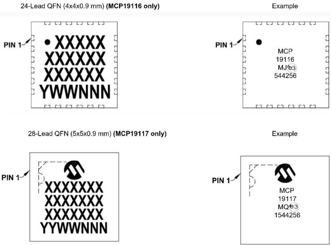
Legend: XX...X Customer-specific information
Y Year code (last digit of calendar year)
YY Year code (last 2 digits of calendar year)
WW Week code (week of January 1 is week '01')
NNN Alphanumeric traceability code
epb-free JEDEC
® designator for Matte Tin (Sn)
* This package is Pb-free. The Pb-free JEDEC designator (e3) can be found on the outer packaging for this package.
Note: In the event the full Microchip part number cannot be marked on one line, it will be carried over to the next line, thus limiting the number of available characters for customer-specific information.
24-Lead Plastic Quad Flat, No Lead Package (MJ) - 4x4x0.9 mm Body [QFN]
Note: For the most current package drawings, please see the Microchip Packaging Specification located at http://www.microchip.com/packaging
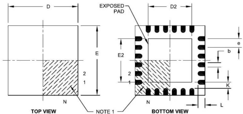
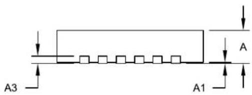
![Microchip MCP19116 - 24-Lead Plastic Quad Flat, No Lead Package (MJ) - 4x4x0.9 mm Body [QFN] - 3](/content/2026/06/1177924/images/9cfe126a1e9a798a64fe713d15bd4f3026ae6ccf03e1a42f169532e19c4f8ea2.jpg)
natural_image
Isometric line drawing of a rectangular electronic component with square holes on both sides (no text or symbols)| Units | MILLIMETERS | |||
| Dimension Limits | MIN | NOM | MAX | |
| Number of Pins | N | 24 | ||
| Pitch | e | 0.50 BSC | ||
| Overall Height | A | 0.80 | 0.85 | 0.90 |
| Standoff | A1 | 0.00 | 0.02 | 0.05 |
| Contact Thickness | A3 | 0.20 REF | ||
| Overall Width | E | 4.00 BSC | ||
| Exposed Pad Width | E2 | 2.40 | 2.50 | 2.60 |
| Overall Length | D | 4.00 BSC | ||
| Exposed Pad Length | D2 | 2.40 | 2.50 | 2.60 |
| Contact Width | b | 0.20 | 0.25 | 0.30 |
| Contact Length | L | 0.30 | 0.40 | 0.50 |
| Contact-to-Exposed Pad | K | 0.20 | - | - |
Notes:
- Pin 1 visual index feature may vary, but must be located within the hatched area.
- Package is saw singulated.
- Dimensioning and tolerancing per ASME Y14.5M. BSC: Basic Dimension. Theoretically exact value shown without tolerances. REF: Reference Dimension, usually without tolerance, for information purposes only.
Microchip Technology Drawing C04-143A
24-Lead Plastic Quad Flat, No Lead Package (MJ) - 4x4 mm Body [QFN]
Note: For the most current package drawings, please see the Microchip Packaging Specification located at http://www.microchip.com/packaging
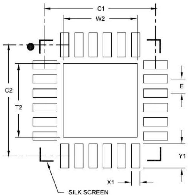
RECOMMENDED LAND PATTERN
| Units | MILLIMETERS | |||
| Dimension Limits | MIN | NOM | MAX | |
| Contact Pitch | E | 0.50 BSC | ||
| Optional Center Pad Width | W2 | 2.60 | ||
| Optional Center Pad Length | T2 | 2.60 | ||
| Contact Pad Spacing | C1 | 3.90 | ||
| Contact Pad Spacing | C2 | 3.90 | ||
| Contact Pad Width | X1 | 0.30 | ||
| Contact Pad Length | Y1 | 0.85 | ||
Notes:
- Dimensioning and tolerancing per ASME Y14.5M
BSC: Basic Dimension. Theoretically exact value shown without tolerances.
Microchip Technology Drawing No. C04-2143B
28-Lead Plastic Quad Flat, No Lead Package (MQ) - 5x5x0.9 mm Body [QFN]
Note: For the most current package drawings, please see the Microchip Packaging Specification located at http://www.microchip.com/packaging
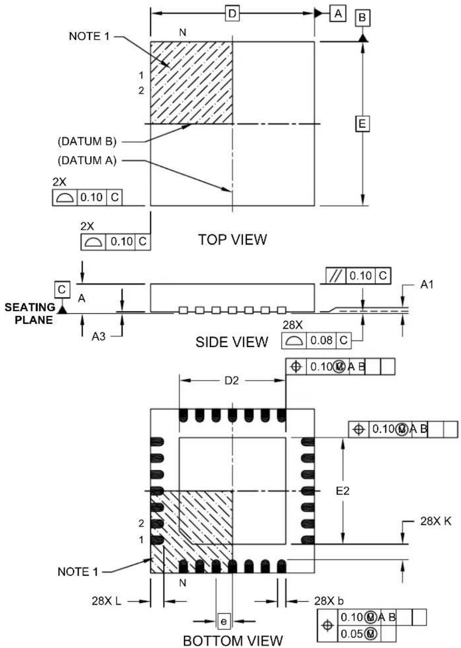
Microchip Technology Drawing C04-140C Sheet 1 of 2
28-Lead Plastic Quad Flat, No Lead Package (MQ) - 5x5x0.9 mm Body [QFN]
Note: For the most current package drawings, please see the Microchip Packaging Specification located at http://www.microchip.com/packaging
![Microchip MCP19116 - 28-Lead Plastic Quad Flat, No Lead Package (MQ) - 5x5x0.9 mm Body [QFN] - 1](/content/2026/06/1177924/images/d41bf46607ea423a3c0d155d735e42367798e705f82b4df13f62d297e1945eca.jpg)
natural_image
Two isometric line drawings of an integrated circuit chip with square and rectangular components (no text or symbols)| Units | MILLIMETERS | |||
| Dimension Limits | MIN | NOM | MAX | |
| Number of Pins N | 2 | 8 | ||
| Pitch | e | 0.50 BSC | ||
| Overall Height A 0.90 | 0.80 | 1.00 | ||
| Standoff A1 0.02 | 0.00 | 0.05 | ||
| Contact Thickness | A3 | 0.20 REF | ||
| Overall Width | E | 5.00 BSC | ||
| Exposed Pad Width | E2 | 3.15 | 3.25 | 3.35 |
| Overall Length | D | 5.00 BSC | ||
| Exposed Pad Length | D2 | 3.15 | 3.25 | 3.35 |
| Contact Width | b | 0.18 | 0.25 | 0.30 |
| Contact Length | L | 0.35 | 0.40 | 0.45 |
| KContact-to-Exposed Pad 0.20 | - | |||
Notes:
- Pin 1 visual index feature may vary, but must be located within the hatched area.
- Package is saw singulated.
- Dimensioning and tolerancing per ASME Y14.5M. BSC: Basic Dimension. Theoretically exact value shown without tolerances. REF: Reference Dimension, usually without tolerance, for information purposes only.
Microchip Technology Drawing C04-140C Sheet 2 of 2
28-Lead Plastic Quad Flat, No Lead Package (MQ) - 5x5 mm Body [QFN] Land Pattern With 0.55 mm Contact Length
Note: For the most current package drawings, please see the Microchip Packaging Specification located at http://www.microchip.com/packaging
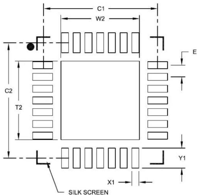
RECOMMENDED LAND PATTERN
| Units | MILLIMETERS | |||
| Dimension Limits | MIN | NOM | MAX | |
| Contact Pitch | E | 0.50 BSC | ||
| Optional Center Pad Width | W2 | 3.35 | ||
| Optional Center Pad Length | T2 | 3.35 | ||
| Contact Pad Spacing | C1 | 4.90 | ||
| Contact Pad Spacing | C2 | 4.90 | ||
| Contact Pad Width (X28) | X1 | 0.30 | ||
| Contact Pad Length (X28) | Y1 | 0.85 | ||
Notes:
1. Dimensioning and tolerancing per ASME Y14.5M
BSC: Basic Dimension. Theoretically exact value shown without tolerances.
Microchip Technology Drawing C04-2140A
APPENDIX A: REVISION HISTORY
Revision D (June 2020)
- Updated Section 4.1, Absolute Maximum Ratings †
- Updated Section 8.0, System Bench Testing.
- Updated Section 19.1.2, Weak Pull-Ups.
- Updated Section 21.2, Temperature Output.
- Updated Section 23.1.2, 8-Bit Counter Mode.
- Updated Equation 26-1 in Section 26.1, Standard Pulse-Width Modulation Mode.
- Minor editorial changes.
Revision C (January 2018)
- Updated Table 1 and Table 2.
- Updated Section 4.2, Electrical Characteristics.
- Updated Section 5.0, Digital Electrical Characteristics with minor changes to Table 5-3.
- Minor editorial changes
Revision B (March 2016)
- Updated Section 4.2, Electrical Characteristics with tolerances across multiple temperature ranges.
• Minor typographical changes.
Revision A (December 2015)
• Original Release of this Document.
NOTES:
INDEX
A
A/D
Specifications.... 3, 5, 37
A/D Conversion. See ADC
ABECON Register 51
Absolute Maximum Ratings 22
AC Characteristics 32
ACKSTAT
Status Flag.... 191
ADC
10-Bit Result Format 141
Acquisition Requirements 145
Associated Registers 147
Block Diagram.... 139
Calculating Acquisition Time.... 145
Channel Selection.... 140
Configuration.... 140
Configuring Interrupt 142
Conversion Clock.... 140
Conversion Procedure 142
Internal Sampling Switch (R SS) Impedance.... 145
Interrupts.... 141
Operation 142
Operation During Sleep 142
Port Configuration 140
Register Definitions.... 143
Requirements.... 37
Source Impedance (R S).... 145
Timing Diagram.... 38
ADCON0 Register.... 57, 143
ADCON1 Register.... 144
ADRESH Register.... 144
ADRESL Register 144
Analog Blocks Enable Control 50
Error Amplifier Disable 51
Analog Peripheral Control.... 49
PWM Steering....49
Secondary Current Positive Sense Pull-Up 49
Analog-to-Digital Converter. See ADC....139
ANSELA Register 128
ANSELB Register 132
Application Diagrams
MCP19116 Boost Quasi-Resonant.... 11
MCP19116 Cuk' Synchronous Positive Output ..... 11
Assembler
MPASM Assembler.... 224
B
Bench Testing
System 57
BF 193
Status Flag.... 191
BF Status Flag 193
Block Diagrams
ADC 139
ADC Transfer Function 146
Analog Input Model 146
Baud Rate Generator.... 202
Capture Mode Operation 161
Compare Mode Operation 162
Interrupt Logic 106
MCP19116/7 Flyback Synchronous Quasi-Resonant. 10
Microcontroller Core.... 12
MSSP (I ^2 C Master Mode) 167
MSSP (I ^2 C Slave Mode).... 168
On-Chip Reset Circuit.... 97
Pulse-Width Modulation (PWM) 158
Recommended MCLR Circuit....98
Timer0 149
Timer1 151
Timer2 155
USART Receive 72
USART Transmit 70
Watchdog Timer with Shared Prescale 117
Brown-Out Reset (BOR).... 99
C
C Compilers
MPLAB XC 224
Calibration Word Registers
CALWD1 (Calibration Word 1) 59
CALWD10 (Calibration Word 10) 66
CALWD11 (Calibration Word 11) 68
CALWD2 (Calibration Word 2) 60
CALWD3 (Calibration Word 3) 61
CALWD4 (Calibration Word 4) 61
CALWD5 (Calibration Word 5) 62
CALWD6 (Calibration Word 6) 62
CALWD7 (Calibration Word 7) 63
CALWD8 (Calibration Word 8) 64
CALWD9 (Calibration Word 9) 65
Capture Mode
Block Diagram 161
Capture/Compare (CCD) Module
Capture Mode 161
CCP1IF.... 161
CCX Pin Configuration 161
Prescaler 161
Software Interrupt 161
Timer1 Mode Selection.... 161
Compare Mode
CCP1IF.... 162
CMPX Pin Configuration.... 162
Software Interrupt 162
Special Event Trigger 162
Timer1 Mode Selection.... 162
Register 163
CCDCON Register.... 163
Clock Switching 96
Code Example
Indirect Addressing 92
Code Examples
A/D Conversion 142
Assigning Prescaler to Timer0.... 150
Assigning Prescaler to WDT.... 150
Initializing PORTGPA 125
Saving Status and W Registers in RAM 113
Compare Mode
Block Diagram 162
Computed Function Calls 91
Computed GOTO....91
Configuration Word....93
Registers Associated with Clock Sources 96
with Watchdog Timer.... 118
Current Sense 19
Customer Change Notification Service.... 241
Customer Support.... 241
D
Data Memory
Core Registers 83
STATUS Register 83
General Purpose Registers....82
Map 85
Organization....82
Special Function Registers 82, 84
DC and AC Characteristics
Graphs and Tables 53
DEADCON Register.
ATCON Register....43
Desaturation Detection
elopment Support 223
Device Calibration
CALWD1 (Calibration Word 1)....59
CALWD10 (Calibration Word 10)......66
CALWD11 (Calibration Word 11)......68
CALWD2 (Calibration Word 2)....60
CALWD3 (Calibration Word 3)....61
CALWD4 (Calibration Word 4)....61
CALWD5 (Calibration Word 5)....62
CALWD6 (Calibration Word 6)....62
CALWD7 (Calibration Word 7)......63
CALWD8 (Calibration Word 8)....64
CALWD9 (Calibration Word 9)......65
Device Configuration.... 39, 93
Code Protection 94
Configuration Word 93
ID Locations 94
Write Protection 94
Device Overview
Digital Electrical Characteristics
Direct Addressing
Driver Control Circuitry.... 20
E
Electrical Characteristics....22
Errata
External Clock
Timing 32
Timing Requirements 32
F
Features.... 1
Microcontroller 1
Timer0 Module 149
Timer1 Module 151
File Select Register. See FSR
Firmware Instructions....211
Flash Program Memory
Control 119
Operation During Code Protect 123
Operation During Write Protect.... 123
Protection Against Spurious Write 123
Registers....120
Reading.... 122
Writing to....123
FSR
Register....91
G
General Purpose Register. See GPR
GPR
Register....82
|
I/Q Ports 125
I²C Mode (MSSP)
Acknowledge Sequence 172
Acknowledge Sequence Timing 195
Associated Registers 201
Bus Collision
During a Repeated Start Condition.... 199
During a Start Condition 197
During a Stop Condition 200
Effects of a Reset 196
I^2C Clock Rate w/BRG.... 202
Master Mode.... 188
Clock Arbitration 188
Operation.... 188
Reception 193
Repeated Start Condition Timing 190
Start Condition Timing 189
Transmission 191
Multi-Master Communication, Bus Collision and Arbitra-
tion 196
Multi-Master Mode.... 196
Operation.... 170
Overview.... 168
Read/Write Bit Information (R/W Bit) 172
Slave Mode
10-bit Address Reception 182
Bus Collision.... 178
Clock Stretching 186
Clock Synchronization 186
General Call Address Support.... 187
Operation.... 172
SSPMSK1 Register 208
Transmission 178
Sleep Operation.... 196
Stop Condition Timing 195
ICLEBCON Register 45
ICOACON Register.... 44
In-Circuit Serial Programming (ICSP)
Common Programming Interfaces.... 221
INDF
Register 91
Indirect Addressing 91, 92
Input 22
Overvoltage Lockout.... 39
Type....13
Undervoltage Lockout 39
Instruction Format.... 211
Instruction Set.... 211
ADDLW 213
ADDWF 213
ANDLW 213
ANDWF 213
BCF 213
BSF 213
BTFSC 213
BTFSS 214
CALL 214
CLRF 214
CLRW 214
CLRWDT 214
COMF 214
DECF 214
DECFSZ 215
GOTO 215
INCF....215
INCFSZ 215
IORLW 215
IORWF 215
MOVF....216
MOVLW 216
MOVWF 216
NOP 216
RETFIE 217
RETLW 217
RETURN 217
RLF 217
RRF 218
SLEEP 218
SUBLW 218
SUBWF 218
Summary Table.... 212
SWAPF 218
XORLW....218
XORWF 219
INTCON Register.... 107
Internal Sampling Switch (Rss) Impedance.... 145
Internet Address 241
Interrupt-on-Change.... 133
Associated Registers 135
Clearing Interrupt Flags 133
Enabling the Module 133
Individual Pin Configuration 133
Operation in Sleep 133
Registers.... 134
Interrupts
ADC 142
Associated Registers 112
Configuration Word w/ Clock Sources 96
Context Saving.... 113
Control Registers 107
GPA2/INT....105
Timer0.... 150
Timer1.... 152
IOCA Register.... 134
IOCB Register.... 134
L
Linear Regulators.... 19
M
Magnetic Desaturation Detection 19
Master Synchronous Serial Port. See MSSP.... 167
MCLR 98
Internal 98
Memory Organization.... 69, 81
Data 82
Program 81
Microchip Internet Web Site 241
Mode and RFB MUX Control 52
MODECON Register....52
MOSFET 17
Driver
Dead Time 49
Programmable Dead Time.... 47
Undervoltage Lockout Selection 50
Gate Driver Enables.... 49
MPLAB Assembler, Linker, Librarian 224
MPLAB ICD 3 In-Circuit Debugger System 225
MPLAB Integrated Development Environment Software .. 223
MPLAB PM3 Device Programmer 225
MPLAB REAL ICE In-Circuit Emulator System 225
MPLAB X SIM Software Simulator 225
MPLINK Object Linker/MPLIB Object Librarian 224
MSSP
Arbitration 169
Baud Rate Generator 202
Block Diagram (I²C Master Mode).... 167
Block Diagram (I²C Slave Mode).... 168
Clock Stretching 169
I^2C Bus Terms 170
I²C Master Mode 188
I^2C Mode 168
I^2C Mode Operation.... 170
I^2C Slave Mode Operation.... 172
Overview.... 167
0
OPCODE Field Descriptions.... 211
OPTION_REG Register....90
Oscillator....95
Associated Registers....96
Calibration 95
Delay Upon Base Frequency Change 96
Delay Upon Power-Up.... 96
Delay Upon Wake-Up....96
Frequency Tuning....95
Internal....95
OSCTUNE Register....95
Output
Drive Circuitry 19
Overvoltage 41
OVCON Register 41
OVREFCON Register 42
Protection 41
Type.... 13
Output Regulation Reference Voltage Configuration...... 48
OVCON Register 41
Overvoltage Lockout
Input.... 39
OVREFCON Register 42
P
Package Marking Information 227
PCL....91
Modifying 91
PCLATH 91
PCON Register.... 100, 102
PE1 Register 50
Peak Current Mode.... 19
PICkit 3 In-Circuit Debugger/Programmer.... 225
PIE1 Register 108
PIE2 Register 109
Pin Diagram
24-Pin QFN (MCP19116) 2
28-Pin QFN (MCP19117) 4
Pinout Description
Summary 3,5
Table.... 13
PIR1 Register 110
PIR2 Register 111
PMADRH Register.... 119, 121
PMADRL Register 119, 120
PMCON1 Register.... 119, 121
PMCON2 Register 119
PMDATH Register 120
PMDATL Register 120
PORTGPA.... 125, 133
ANSELA Register 126
Associated Registers 129
Functions and Output Priorities.... 126
Interrupt-on-Change.... 125
Output Priority 126
Register.... 125, 127
Weak Pull-Ups 125
PORTGPB....129, 133
ANSELB Register 129
Associated Registers 132
Functions and Output Priorities.... 130
Interrupt-on-Change.... 129
Output Priority 130
Register.... 129, 130
Weak Pull-Ups 129
Power-Down Mode (Sleep) 115
Associated Registers 116
Power-On Reset (POR) 98
Power-Up Timer (PWRT) 100
Primary Input Current Offset Adjust 44
Program Memory
Organization....81
Protection....94
Programming, Device Instructions 211
Pulse-Width Modulation
Control Logic.... 165
Pulse-Width Modulation. See PWM
PWM 36
Associated Registers 159
Control Logic.... 165
Duty Cycle.... 159
Enhanced Module 157
Fixed Frequency 20
Operation During Sleep 159
Output 158
Period....158
Requirements.... 36
Simplified Diagram.... 158
Stand-Alone Mode 157
Standard Mode 157
Steering....49
Switching Frequency Synchronization Mode 157
Timing Diagram....36
R
Read-Modify-Write Operations.... 211
Registers
ABECON (Analog Block Enable Control).... 51
ADCON0 (A/D Control 0) 143
ADCON0 (Analog-to-Digital Control) 57
ADCON1 (A/D Control 1) 144
ADRESH (ADC Result High) 144
ADRESL (ADC Result Low).... 144
ANSELA (Analog Select GPA).... 128
ANSELB (Analog Select GPB).... 132
CALWD1 (Calibration Word 1)....59
CALWD10 (Calibration Word 10)....66
CALWD11 (Calibration Word 11)....68
CALWD2 (Calibration Word 2)....60
CALWD3 (Calibration Word 3)....61
CALWD4 (Calibration Word 4)....61
CALWD5 (Calibration Word 5)....62
CALWD6 (Calibration Word 6)....62
CALWD7 (Calibration Word 7)....63
CALWD8 (Calibration Word 8)....64
CALWD9 (Calibration Word 9)....65
CCDCON (Dual Capture/Compare Control Module) 163
CONFIG (Configuration Word) 93
DEADCON (Driver Dead Time Control).... 47
DESATCON (Desaturation Comparator Control) ..... 43
FSR (File Select Register).... 9'
General Purpose Register 82
ICLEBCON (Input Current Leading Edge Blanking Control) 45
ICOACON (Input Current Offset Adjust Control) ..... 44
INDF 91
INTCON (Interrupt Control).... 107
IOCA (Interrupt-on-Change PORTGPA).... 134
IOCB (Interrupt-on-Change PORTGPB).... 134
MODECON (Master/Slave and RFB MUX Control).... 52
OSCTUNE (Oscillator Tuning)....95
OVCON (Output Overvoltage Comparator Control) ... 41
OVREFCON (Output Overvoltage Detect Level)..... 42
PCON (Power Control) 100, 102
PE1 (Analog Peripheral Enable1 Control) 50
PIE1 (Peripheral Interrupt Enable 1).... 108
PIE2 (Peripheral Interrupt Enable 2).... 109
PIR1 (Peripheral Interrupt Flag 1).... 110
PIR2 (Peripheral Interrupt Flag 2).... 111
PMADRH (Program Memory Address High) .... 119, 121
PMADRL (Program Memory Address Low)..... 119, 120
PMCON1 (Program Memory Control 1)...... 119, 121
PMCON2 (Program Memory Control 2).... 119
PMDATH (Program Memory Data High) 120
PMDATL (Program Memory Data Low).... 120
PORTGPA 125, 127
PORTGPB 129, 130
SLPCRCON (Slope Compensation Ramp Control).... 46
Special Function 82
Special Registers Summary
Bank 0 86
Bank 1 87
Bank 2 88
Bank 3 89
SSPADD (MSSP Address and Baud Rate 1) ...... 208
SSPCON1 (SSP Control 1) 204
SSPCON2 (SSP Control 2) 206
SSPCON3 (SSP Control 3) 207
SSPMSK1 (SSP Mask 1)....208
SSPMSK2 (SSP Mask 2).... 209
SSPSTAT (SSP Status).... 203
STATUS 83
T1CON (Timer1 Control) 152
T2CON (Timer2 Control) 156
TRISGPA (PORTGPA Tri-State) 125, 127
TRISGPB (PORTGPB Tri-State) 129, 131
VINCON (UVLO and OVLO Comparator Control) ..... 39
VINOVLO (Input Overvoltage Lockout) 40
VINUVLO (Input Undervoltage Lockout).... 40
VREF2CON (V _REF2 Voltage Set Point) 49
VREFCON (Current/Voltage Regulation Set Point Control) 48
WPUGPA (Weak Pull-Up PORTGPA).... 128
WPUGPB (Weak Pull-Up PORTGPB).... 131
Requirements
A/D Acquisition 145
A/D Conversion.... 37
External Clock, Timing.... 32
I/O, Timing 33
PWM 36
Reset, Watchdog Timer, Oscillator Start-Up Timer and Power-Up Timer.... 35
Timer0 External Clock.... 36
Resets....97
Associated Registers 103
Brown-Out....99
Determining Causes 101
Power-On....98
Watchdog Timer.... 100
s
Sleep
Wake-Up from.... 115
Wake-Up Using Interrupts.... 116
Slope Compensation.... 46
SLPCRCON Register 46
Software Simulator (MPLAB X SIM) 225
Special Event Trigger Capture/Compare Module.... 162
Special Function Registers (SFR) 82
SSPADD Register....208
SSPCON1 Register 204
SSPCON2 Register 206
SSPCON3 Register 207
SSPMSK1 Register....208
SSPMSK2 Register.... 209
SSPOV....193
SSPOV Status Flag 193
SSPSTAT Register 203
R/W Bit.... 172
Stack 91
Start-Up....20
Start-Up Sequence 100
STATUS Register 83
System Bench Testing 57
T
T1CON Register 152
T2CON Register 156
Temperature Indicator Module 137
Circuit Operation 137
Temperature Output.... 137
Thermal Specifications.... 30
Timer0....149
8-bit Counter Mode 149
8-bit Timer Mode.... 149
Associated Registers 150
Block Diagram.... 149
External Clock.... 150
Requirements 36
Timing 35
Interrupt.... 150
Module 149
Features.... 149
Operation 149
During Sleep 150
Software Programmable Prescaler.... 149
Switching Prescaler 150
T0CKI.... 150
TMR0 Register.... 149
Timer1.... 151
Associated Registers 153
Block Diagram.... 151
Clock Source Selection 151
Control Register.... 152
External Clock Timing.... 35
Interrupt 152
Module Features .... 151
Operation.... 151
During Sleep.... 152
Prescaler 152
TMR1H Register.... 151
TMR1L Register 151
Timer2 Associated Registers.... 156
Block Diagram 155
Control Register.... 156
Module.... 155
Features 155
Operation.... 155
Timers Timer1 (T1CON).... 152 Timer2 (T2CON).... 156
Timing Diagrams
A/D Conversion 38
Acknowledge Sequence 195
Asynchronous Reception.... 73
Baud Rate Generator Timing with Clock Arbitration. 189
BRG Reset Due to SDA Arbitration During Start Condition.... 198
Bus Collision During a Repeated Start Condition (Case 1)....199
Bus Collision During a Repeated Start Condition (Case 2)....199
Bus Collision During a Start Condition (SCL = 0)..... 198
Bus Collision During a Start Condition (SDA Only) .. 197
Bus Collision During a Stop Condition (Case 1)..... 200
Bus Collision During a Stop Condition (Case 2)..... 200
Bus Collision for Transmit and Acknowledge ..... 196
Clock Synchronization 186
First Start Bit.... 189
I/O....33
I²C Master Mode (7 or 10-Bit Transmission) ..... 192
I²C Master Mode (7-Bit Reception) 194
INT Pin Interrupt 106
Power-Up Timer 34
Pulse-Width Modulation 36
Repeat Start Condition 190
Reset 34
Start-Up Timer 34
Stop Condition Receive or Transmit Mode.... 195
Synchronous Reception (Master Mode, SREN) ..... 76
Synchronous Transmission 74
Synchronous Transmission (through TXEN) 75
Time-Out Sequence
Case 1 .... 100
Case 2 101
Case 3 101
Timer0, External Clock 35
Timer1, External Clock 35
USART, Asynchronous Reception 73
Wake-up from Interrupt.... 116
Watchdog Timer 34
Timing Parameter Symbology 31
TRISGPA....125
Register 125, 127
TRISGPB 129
MCP19116/7
Register.... 129, 131
Typical Performance Curves.... 53
U
Undervoltage Lockout
Input 39
Selection for MOSFET Driver 50
Universal Synchronous Asynchronous Receiver Transmitter (USART)
Asynchronous Receiver Timing Diagram....73
USART
Asynchronous Reception 72
Synchronous Slave Mode 76
Synchronous Slave Transmit 76, 77
Transmit Block Diagram.... 70
v
VINCON Register 39
VINOVLO Register....40
VINUVLO Register.... 40
V_REF2 Voltage Reference.... 49
VREF2CON Register 49
VREFCON Register 48
W
Watchdog Timer. See WDT
WCOL 195
Status Flag 189, 191, 193, 195
WCOL Status Flag 195
WDT 117
Associated Registers 118
Block Diagram.... 117
Configuration Word w/ Watchdog Timer 118
Operation 117
Period....117
Programming Considerations 117
Reset....100
Switching Prescaler 150
WPUGPA Register.... 128
WPUGPB Register.... 131
WWW Address 241
WWW, On-Line Support....7
Microchip provides online support via our web site at www.microchip.com. This web site is used as a means to make files and information easily available to customers. Accessible by using your favorite Internet browser, the web site contains the following information:
- Product Support – Data sheets and errata, application notes and sample programs, design resources, user's guides and hardware support documents, latest software releases and archived software
- General Technical Support – Frequently Asked Questions (FAQ), technical support requests, online discussion groups, Microchip consultant program member listing
- Business of Microchip – Product selector and ordering guides, latest Microchip press releases, listing of seminars and events, listings of Microchip sales offices, distributors and factory representatives
CUSTOMER CHANGE NOTIFICATION SERVICE
Microchip's customer notification service helps keep customers current on Microchip products. Subscribers will receive e-mail notification whenever there are changes, updates, revisions or errata related to a specified product family or development tool of interest.
To register, access the Microchip web site at www.microchip.com. Under "Support", click on "Customer Change Notification" and follow the registration instructions.
CUSTOMER SUPPORT
Users of Microchip products can receive assistance through several channels:
• Distributor or Representative
- Local Sales Office
• Field Application Engineer (FAE)
- Technical Support
Customers should contact their distributor, representative or Field Application Engineer (FAE) for support. Local sales offices are also available to help customers. A listing of sales offices and locations is included in the back of this document.
Technical support is available through the web site at: http://microchip.com/support
NOTES:
PRODUCT IDENTIFICATION SYSTEM
To order or obtain information, e.g., on pricing or delivery, refer to the factory or the listed sales office.
Device
Tape and Reel Option

Range


PatternPac
Device: MCP19116: Digitally Enhanced PWM Power Analog
High-Speed Controller
MCP19117: Digitally Enhanced PWM Power Analog High-Speed Controller
Tape and Reel
MJ = 24-Lead Plastic Quad Flat, No Lead Package - 4x4x0.9 mm Body [QFN]
MQ = 28-Lead Plastic Quad Flat, No Lead Package - 5x5x0.9 mm Body [QFN]
Examples:
a) MCP19116-E/MJ: Extended temperature, kageTemperature 24LD QFN 4x4 package
b) MCP19116T-E/MJ: Tape and Reel, Extended Temperature, 24LD QFN 4x4 package
a) MCP19117-E/MQ: Extended temperature, 28LD 5x5 QFN package
b) MCP19117T-E/MQ: Tape and Reel, Extended temperature, 28LD 5x5 QFN package
Note 1: Tape and Reel identifier only appears in the catalog part number description. This identifier is used for ordering purposes and is not printed on the device package. Check with your Microchip Sales Office for package availability with the Tape and Reel option.
NOTES:
Note the following details of the code protection feature on Microchip devices:
• Microchip products meet the specification contained in their particular Microchip Data Sheet.
- Microchip believes that its family of products is one of the most secure families of its kind on the market today, when used in the intended manner and under normal conditions.
- There are dishonest and possibly illegal methods used to breach the code protection feature. All of these methods, to our knowledge, require using the Microchip products in a manner outside the operating specifications contained in Microchip's Data Sheets. Most likely, the person doing so is engaged in theft of intellectual property.
- Microchip is willing to work with the customer who is concerned about the integrity of their code.
- Neither Microchip nor any other semiconductor manufacturer can guarantee the security of their code. Code protection does not mean that we are guaranteeing the product as "unbreakable."
Code protection is constantly evolving. We at Microchip are committed to continuously improving the code protection features of our products. Attempts to break Microchip's code protection feature may be a violation of the Digital Millennium Copyright Act. If such acts allow unauthorized access to your software or other copyrighted work, you may have a right to sue for relief under that Act.
Information contained in this publication regarding device applications and the like is provided only for your convenience and may be superseded by updates. It is your responsibility to ensure that your application meets with your specifications. MICROCHIP MAKES NO REPRESENTATIONS OR WARRANTIES OF ANY KIND WHETHER EXPRESS OR IMPLIED, WRITTEN OR ORAL, STATUTORY OR OTHERWISE, RELATED TO THE INFORMATION, INCLUDING BUT NOT LIMITED TO ITS CONDITION, QUALITY, PERFORMANCE, MERCHANTABILITY OR FITNESS FOR PURPOSE. Microchip disclaims all liability arising from this information and its use. Use of Microchip devices in life support and/or safety applications is entirely at the buyer's risk, and the buyer agrees to defend, indemnify and hold harmless Microchip from any and all damages, claims, suits, or expenses resulting from such use. No licenses are conveyed, implicitly or otherwise, under any Microchip intellectual property rights unless otherwise stated.
Trademarks
The Microchip name and logo, the Microchip logo, Adaptec, AnyRate, AVR, AVR logo, AVR Freaks, BesTime, BitCloud, chipKIT, chipKIT logo, CryptoMemory, CryptoRF, dsPIC, FlashFlex, flexPWR, HELDO, IGLOO, JukeBlox, KeeLoq, Kleer, LANCheck, LinkMD, maXStylus, maXTouch, MediaLB, megaAVR, Microsemi, Microsemi logo, MOST, MOST logo, MPLAB, OptoLyzer, PackeTime, PIC, picoPower, PICSTART, PIC32 logo, PolarFire, Prochip Designer, QTouch, SAM-BA, SenGenuity, SpyNIC, SST, SST Logo, SuperFlash, Symmetricom, SyncServer, Tachyon, TempTrackr, TimeSource, tinyAVR, UNI/O, Vectron, and XMEGA are registered trademarks of Microchip Technology Incorporated in the U.S.A. and other countries.
APT, ClockWorks, The Embedded Control Solutions Company, EtherSynch, FlashTec, Hyper Speed Control, HyperLight Load, IntelliMOS, Libero, motorBench, mTouch, Powermite 3, Precision Edge, ProASIC, ProASIC Plus, ProASIC Plus logo, Quiet-Wire, SmartFusion, SyncWorld, Temux, TimeCesium, TimeHub, TimePictra, TimeProvider, Vite, WinPath, and ZL are registered trademarks of Microchip Technology Incorporated in the U.S.A.
Adjacent Key Suppression, AKS, Analog-for-the-Digital Age, Any Capacitor, AnyIn, AnyOut, BlueSky, BodyCom, CodeGuard, CryptoAuthentication, CryptoAutomotive, CryptoCompanion, CryptoController, dsPICDEM, dsPICDEM.net, Dynamic Average Matching, DAM, ECAN, EtherGREEN, In-Circuit Serial Programming, ICSP, INICnet, Inter-Chip Connectivity, JitterBlocker, KleerNet, KleerNet logo, memBrain, Mindi, MiWi, MPASM, MPF, MPLAB Certified logo, MPLIB, MPLINK, MultiTRAK, NetDetach, Omniscient Code Generation, PICDEM, PICDEM.net, PICkit, PICtail, PowerSmart, PureSilicon, QMatrix, REAL ICE, Ripple Blocker, SAM-ICE, Serial Quad I/O, SMART-I.S., SQI, SuperSwitcher, SuperSwitcher II, Total Endurance, TSHARC, USBCheck, VariSense, ViewSpan, WiperLock, Wireless DNA, and ZENA are trademarks of Microchip Technology Incorporated in the U.S.A. and other countries.
SQTP is a service mark of Microchip Technology Incorporated in the U.S.A.
The Adaptec logo, Frequency on Demand, Silicon Storage Technology, and Symmcom are registered trademarks of Microchip Technology Inc. in other countries.
GestIC is a registered trademark of Microchip Technology Germany II GmbH & Co. KG, a subsidiary of Microchip Technology Inc., in other countries.
All other trademarks mentioned herein are property of their respective companies.
© 2020, Microchip Technology Incorporated, All Rights Reserved.
ISBN: 978-1-5224-6249-1
For information regarding Microchip's Quality Management Systems, please visit www.microchip.com/quality.
Worldwide Sales and Service
AMERICAS
Corporate Office
2355 West Chandler Blvd.
Chandler, AZ 85224-6199
Tel: 480-792-7200
Fax: 480-792-7277
Technical Support:
http://www.microchip.com/
support
Web Address:
www.microchip.com
Atlanta
Duluth, GA
Tel: 678-957-9614
Fax: 678-957-1455
Austin, TX
Tel: 512-257-3370
Boston
Westborough, MA
Tel: 774-760-0087
Fax: 774-760-0088
Chicago
Itasca, IL
Tel: 630-285-0071
Fax: 630-285-0075
Dallas
Addison, TX
Tel: 972-818-7423
Fax: 972-818-2924
Detroit
Novi, MI
Tel: 248-848-4000
Houston, TX
Tel: 281-894-5983
Indianapolis
Noblesville, IN
Tel: 317-773-8323
Fax: 317-773-5453
Tel: 317-536-2380
Los Angeles
Mission Viejo, CA
Tel: 949-462-9523
Fax: 949-462-9608
Tel: 951-273-7800
Raleigh, NC
Tel: 919-844-7510
New York, NY
Tel: 631-435-6000
San Jose, CA
Tel: 408-735-9110
Tel: 408-436-4270
Canada - Toronto
Tel: 905-695-1980
Fax: 905-695-2078
ASIA/PACIFIC
Australia - Sydney
Tel: 61-2-9868-6733
China - Beijing
Tel: 86-10-8569-7000
China - Chengdu
Tel: 86-28-8665-5511
China - Chongqing
Tel: 86-23-8980-9588
China - Dongguan
Tel: 86-769-8702-9880
China - Guangzhou
Tel: 86-20-8755-8029
China - Hangzhou
Tel: 86-571-8792-8115
China - Hong Kong SAR
Tel: 852-2943-5100
China - Nanjing
Tel: 86-25-8473-2460
China - Qingdao
Tel: 86-532-8502-7355
China - Shanghai
Tel: 86-21-3326-8000
China - Shenyang
Tel: 86-24-2334-2829
China - Shenzhen
Tel: 86-755-8864-2200
China - Suzhou
Tel: 86-186-6233-1526
China - Wuhan
Tel: 86-27-5980-5300
China - Xian
Tel: 86-29-8833-7252
China - Xiamen
Tel: 86-592-2388138
China - Zhuhai
Tel: 86-756-3210040
ASIA/PACIFIC
India - Bangalore
Tel: 91-80-3090-4444
India - New Delhi
Tel: 91-11-4160-8631
India - Pune
Tel: 91-20-4121-0141
Japan - Osaka
Tel: 81-6-6152-7160
Japan - Tokyo
Tel: 81-3-6880-3770
Korea - Daegu
Tel: 82-53-744-4301
Korea - Seoul
Tel: 82-2-554-7200
Malaysia - Kuala Lumpur
Tel: 60-3-7651-7906
Malaysia - Penang
Tel: 60-4-227-8870
Philippines - Manila
Tel: 63-2-634-9065
Singapore
Tel: 65-6334-8870
Taiwan - Hsin Chu
Tel: 886-3-577-8366
Taiwan - Kaohsiung
Tel: 886-7-213-7830
Taiwan - Taipei
Tel: 886-2-2508-8600
Thailand - Bangkok
Tel: 66-2-694-1351
Tel: 43-7242-2244-39
Fax: 43-7242-2244-393
Denmark - Copenhagen
Tel: 45-4485-5910
Fax: 45-4485-2829
Finland - Espoo
Tel: 358-9-4520-820
France - Paris
Tel: 33-1-69-53-63-20
Fax: 33-1-69-30-90-79
Germany - Garching
Tel: 49-8931-9700
Germany - Haan
Tel: 49-2129-3766400
Germany - Heilbronn
Tel: 49-7131-72400
Germany - Karlsruhe
Tel: 49-721-625370
Germany - Munich
Tel: 49-89-627-144-0
Fax: 49-89-627-144-44
Germany - Rosenheim
Tel: 49-8031-354-560
Israel - Ra'anana
Tel: 972-9-744-7705
Italy - Milan
Tel: 39-0331-742611
Fax: 39-0331-466781
Italy - Padova
Tel: 39-049-7625286
Netherlands - Drunen
Tel: 31-416-690399
Fax: 31-416-690340
Norway - Trondheim
Tel: 47-7288-4388
Poland - Warsaw
Tel: 48-22-3325737
Romania - Bucharest
Tel: 40-21-407-87-50
Spain - Madrid
Tel: 34-91-708-08-90
Fax: 34-91-708-08-91
Sweden - Gothenberg
Tel: 46-31-704-60-40
Sweden - Stockholm
Tel: 46-8-5090-4654
UK - Wokingham
Tel: 44-118-921-5800
Fax: 44-118-921-5820
- Digitally Enhanced Power Analog Synchronous Low-Side PWM Controller with Improved 8k Word Core
- Features
- Microcontroller Features
- Table of Contents
- TO OUR VALUED CUSTOMERS
- Most Current Data Sheet
- Errata
- Customer Notification System
- DEVICE OVERVIEW
- PIN DESCRIPTION
- Detailed Pin Functional Description
- GPA0 PIN
- GPA1 PIN
- GPA2 PIN
- GPA3 PIN
- GPA5 PIN
- GPA6 PIN
- GPA7 PIN
- GPB0 PIN
- GPB1 PIN
- GPB4 PIN (MCP19117 ONLY)
- GPB5 PIN (MCP19117 ONLY)
- GPB6 PIN (MCP19117 ONLY)
- GPB7 PIN (MCP19117 ONLY)
- DESAT N PIN
- DESAT P/ISOUT PIN
- I SP PIN
- I SN PIN
- I P PIN
- A GND PIN
- P GND PIN
- SDRV PIN
- PDRV PIN
- V DR PIN
- V DD PIN
- V IN PIN
- V s PIN
- I FB PIN
- I COMP PIN
- EXPOSED PAD (EP)
- FUNCTIONAL DESCRIPTION
- Linear Regulators
- Output Drive Circuitry
- Current Sense
- Peak Current Mode
- Magnetic Desaturation Detection
- Start-Up
- Driver Control Circuitry
- Fixed PWM Frequency
- V REF
- OV REF
- Independent Gate Drive with Programmable Delay
- Temperature Management
- THERMAL SHUTDOWN
- TEMPERATURE REPORTING
- ELECTRICAL CHARACTERISTICS
- ABSOLUTE MAXIMUM RATINGS †
- Electrical Characteristics
- Electrical Characteristics (Continued)
- DIGITAL ELECTRICAL CHARACTERISTICS
- Timing Parameter Symbology
- AC Characteristics: MCP19116 (Industrial, Extended)
- CONFIGURING THE MCP19116/7
- Input Undervoltage and Overvoltage Lockout (UVLO and OVLO)
- REGISTER 6-1: VINCON: UVLO AND OVLO COMPARATOR CONTROL REGISTER (CONTINUED)
- REGISTER 6-2: VINUVLO: INPUT UNDERVOLTAGE LOCKOUT REGISTER
- REGISTER 6-3: VINOVLO: INPUT OVERVOLTAGE LOCKOUT REGISTER
- Output Overvoltage Protection
- REGISTER 6-4: OVCON: OUTPUT OVERVOLTAGE COMPARATOR CONTROL REGISTER
- Desaturation Detection for Quasi-Resonant Operation
- Primary Input Current Offset Adjust
- Leading Edge Blanking
- Slope Compensation
- MOSFET Driver Programmable Dead Time
- REGISTER 6-10: DEADCON: DRIVER DEAD TIME CONTROL REGISTER
- REGISTER 6-10: DEADCON: DRIVER DEAD TIME CONTROL REGISTER (CONTINUED)
- Output Regulation Reference Voltage Configuration
- REGISTER 6-11: VREFCON: CURRENT/VOLTAGE REGULATION SET POINT CONTROL REGISTER
- V REF2 Voltage Reference
- Analog Peripheral Control
- MOSFET GATE DRIVER ENABLES
- MOSFET DRIVER DEAD TIME
- SECONDARY CURRENT POSITIVE SENSE PULL-UP
- PWM STEERING
- Analog and Digital Test Signal Enable and Control
- MOSFET DRIVER UNDERVOLTAGE LOCKOUT SELECTION
- ERROR AMPLIFIER DISABLE
- Mode and RFB MUX Control
- TYPICAL PERFORMANCE CURVES
- REGISTER 8-1: ADCON0: ANALOG-TO-DIGITAL CONTROL REGISTER (CONTINUED)
- DEVICE CALIBRATION
- Calibration Word 1
- Calibration Word 2
- Calibration Word 3
- Calibration Word 4
- Calibration Word 5
- Calibration Word 6
- Calibration Word 7
- Calibration Word 8
- Calibration Word 9
- Calibration Word 10
- Calibration Word 11
- Calibration Word 12
- ADDRESSABLE USART MODULE
- Module Reset
- Pin Placement and Port Interaction
- USART Asynchronous mode
- ASYNCHRONOUS TRANSMIT MODE
- ASYNCHRONOUS RECEIVE MODE
- USART Synchronous Master Mode
- SYNCHRONOUS MASTER TRANSMIT MODE
- SYNCHRONOUS MASTER RECEIVE MODE
- USART Synchronous Slave Mode
- SYNCHRONOUS SLAVE TRANSMIT MODE
- SYNCHRONOUS SLAVE RECEIVE MODE
- MEMORY ORGANIZATION
- Program Memory Organization
- READING PROGRAM MEMORY AS DATA
- RETLW Instruction
- Data Memory Organization
- GENERAL PURPOSE REGISTER FILE
- CORE REGISTERS
- STATUS Register
- REGISTER 11-1: STATUS: STATUS REGISTER (CONTINUED)
- SPECIAL FUNCTION REGISTERS
- DATA MEMORY
- PCL and PCLATH
- MODIFYING PCL REGISTER
- COMPUTED GOTO
- COMPUTED FUNCTION CALLS
- STACK
- Indirect Addressing, INDF and FSR Registers
- EXAMPLE 11-3: INDIRECT ADDRESSING
- DEVICE CONFIGURATION
- Configuration Word
- Code Protection
- PROGRAM MEMORY PROTECTION
- Write Protection
- ID Locations
- OSCILLATOR MODES
- Internal Oscillator (INTOSC)
- Oscillator Calibration
- Frequency Tuning in User Mode
- OSCILLATOR DELAY UPON
- POWER-UP, WAKE-UP AND BASE FREQUENCY CHANGE
- RESETS
- Power-on Reset (POR)
- MCLR
- Brown-Out Reset (BOR)
- Power-Up Timer (PWRT)
- Watchdog Timer (WDT) Reset
- Start-Up Sequence
- POWER CONTROL (PCON) REGISTER
- Determining the Cause of a Reset
- Power Control (PCON) Register
- INTERRUPTS
- Interrupt Latency
- GPA2/INT Interrupt
- Interrupt Control Registers
- INTCON REGISTER
- PIR1 Register
- PIR2 Register
- Context Saving During Interrupts
- POWER-DOWN MODE (SLEEP)
- Wake-Up from Sleep
- WAKE-UP USING INTERRUPTS
- WATCHDOG TIMER (WDT)
- Watchdog Timer (WDT) Operation
- WDT Period
- WDT Programming Considerations
- FLASH PROGRAM MEMORY CONTROL
- PMADRH and PMADRL Registers
- PMCON1 and PMCON2 Registers
- Flash Program Memory Control Registers
- REGISTER 18-1: PMDATL: PROGRAM MEMORY DATA LOW BYTE REGISTER
- REGISTER 18-2: PMADRL: PROGRAM MEMORY ADDRESS LOW BYTE REGISTER
- REGISTER 18-3: PMDATH: PROGRAM MEMORY DATA HIGH BYTE REGISTER
- READING THE FLASH PROGRAM MEMORY
- WRITING TO THE FLASH PROGRAM MEMORY
- PROTECTION AGAINST SPURIOUS WRITE
- OPERATION DURING CODE PROTECT
- OPERATION DURING WRITE PROTECT
- I/O PORTS
- PORTGPA and TRISGPA Registers
- INTERRUPT-ON-CHANGE
- WEAK PULL-UPS
- ANSELA REGISTER
- PORTGPA FUNCTIONS ALAND OUTPUT PRIORITIES
- PORTGPB and TRISGPB Registers
- INTERRUPT-ON-CHANGE
- WEAK PULL-UPS
- ANSELB REGISTER
- PORTGPB FUNCTIONS AND OUTPUT PRIORITIES
- INTERRUPT-ON-CHANGE
- Enabling the Module
- Individual Pin Configuration
- Clearing Interrupt Flags
- Operation in Sleep
- Interrupt-On-Change Registers
- INTERNAL TEMPERATURE INDICATOR MODULE
- Circuit Operation
- Temperature Output
- ANALOG-TO-DIGITAL CONVERTER (ADC) MODULE
- ADC Configuration
- PORT CONFIGURATION
- CHANNEL SELECTION
- ADC CONVERSION CLOCK
- INTERRUPTS
- RESULT FORMATTING
- ADC Operation
- ADC REFERENCE SWITCH
- STARTING A CONVERSION
- COMPLETION OF A CONVERSION
- TERMINATING A CONVERSION
- ADC OPERATION DURING SLEEP
- A/D CONVERSION PROCEDURE
- ADC Register Definitions
- A/D Acquisition Requirements
- EQUATION 22-1: ACQUISITION TIME EXAMPLE
- TIMER0 MODULE
- Timer0 Operation
- 8-BIT TIMER MODE
- 8-BIT COUNTER MODE
- SOFTWARE PROGRAMMABLE PRESCALER
- SWITCHING PRESCALER
- BETWEEN TIMER0 AND WDT MODULES
- TIMER0 INTERRUPT
- USING TIMER0 WITH AN
- EXTERNAL CLOCK
- OPERATION DURING SLEEP
- TIMER1 MODULE
- Timer1 Operation
- Clock Source Selection
- INTERNAL CLOCK SOURCE
- Timer1 Prescaler
- Timer1 Interrupt
- Timer1 in Sleep
- Timer1 Control Register
- TIMER2 MODULE
- Timer2 Operation
- Timer2 Control Register
- ENHANCED PWM MODULE
- Standard Pulse-Width Modulation Mode
- STAND-ALONE (NON-FREQUENCY SYNCHRONIZATION) MODE
- EQUATION 26-1:
- SWITCHING FREQUENCY SYNCHRONIZATION MODE
- EQUATION 26-2:
- PWM PERIOD
- PWM DUTY CYCLE (D CLOCK)
- Operation During Sleep
- PWM CONTROL LOGIC
- DUAL CAPTURE/COMPARE (CCD) MODULE
- Capture Mode
- CCX PIN CONFIGURATION
- TIMER1 MODE SELECTION
- SOFTWARE INTERRUPT
- CCD PRESCALER
- Compare Mode
- CMPX PIN CONFIGURATION
- TIMER1 MODE SELECTION
- SOFTWARE INTERRUPT MODE
- SPECIAL EVENT TRIGGER
- Dual Capture/Compare Register
- MASTER SYNCHRONOUS SERIAL PORT (MSSP) MODULE
- MSSP Module Overview
- I 2 C MODE OVERVIEW
- CLOCK STRETCHING
- ARBITRATION
- I 2 C MODE OPERATION
- BYTE FORMAT
- DEFINITION OF I 2 C TERMINOLOGY
- SDA AND SCL PINS
- SDA HOLD TIME
- START CONDITION
- STOP CONDITION
- RESTART CONDITION
- START/STOP CONDITION INTERRUPT MASKING
- I 2 C SLAVE MODE OPERATION
- SECOND SLAVE MODE ADDRESS
- I 2 C Slave 7-Bit Addressing Mode
- I 2 C Slave 10-Bit Addressing Mode
- SLAVE RECEPTION
- 7-Bit Addressing Reception
- 7-Bit Reception with AHEN and DHEN
- SLAVE TRANSMISSION
- Slave Mode Bus Collision
- 7-Bit Transmission
- 7-Bit Transmission with Address Hold Enabled
- SLAVE MODE 10-BIT ADDRESS RECEPTION
- 10-BIT ADDRESSING WITH ADDRESS OR DATA HOLD
- CLOCK STRETCHING
- Normal Clock Stretching
- 10-Bit Addressing Mode
- CLOCK SYNCHRONIZATION AND THE CKP BIT
- GENERAL CALL ADDRESS SUPPORT
- SSPMSK1 REGISTER
- I 2 C MASTER MODE
- I 2 C MASTER MODE OPERATION
- WCOL STATUS FLAG
- I 2 C MASTER MODE START CONDITION TIMING
- I 2 C MASTER MODE REPEATED START CONDITION TIMING
- I 2 C MASTER MODE TRANSMISSION
- BF Status Flag
- WCOL Status Flag
- ACKSTAT Status Flag
- Typical Transmit Sequence
- I 2 C MASTER MODE RECEPTION
- BF Status Flag
- SSPOV Status Flag
- WCOL Status Flag
- Typical Receive Sequence
- ACKNOWLEDGE SEQUENCE TIMING
- WCOL Status Flag
- STOP CONDITION TIMING
- WCOL Status Flag
- EFFECTS OF A RESET
- MULTI-MASTER MODE
- MULTI -MASTER COMMUNICATION, BUS COLLISION AND BUS ARBITRATION
- Bus Collision During a Start Condition
- Bus Collision during a Repeated Start Condition
- Bus Collision During a Stop Condition
- Baud Rate Generator
- EQUATION 29-1:
- FIGURE 29-32: BAUD RATE GENERATOR BLOCK DIAGRAM
- REGISTER 29-2: SSPCON1:SSP CONTROL REGISTER 1 (CONTINUED)
- Master mode:
- 10-Bit Slave mode — Most Significant Address byte:
- 10-Bit Slave mode — Least Significant Address byte:
- 7-Bit Slave mode:
- INSTRUCTION SET SUMMARY
- Read-Modify-Write Operations
- Instruction Descriptions
- XORWF Exclusive OR W with f
- IN-CIRCUIT SERIAL PROGRAMMING™ (ICSP™)
- Common Programming Interfaces
- DEVELOPMENT SUPPORT
- MPLAB X Integrated Development Environment Software
- Feature-Rich Editor:
- MPLAB XC Compilers
- MPASM Assembler
- MPLINK Object Linker/MPLIB Object Librarian
- MPLAB Assembler, Linker and Librarian for Various Device Families
- MPLAB X SIM Software Simulator
- MPLAB REAL ICE In-Circuit Emulator System
- MPLAB ICD 3 In-Circuit Debugger System
- PICkit 3 In-Circuit Debugger/Programmer
- MPLAB PM3 Device Programmer
- Demonstration/Development Boards, Evaluation Kits, and Starter Kits
- Third-Party Development Tools
- PACKAGING INFORMATION
- Package Marking Information
- 24-Lead Plastic Quad Flat, No Lead Package (MJ) - 4x4x0.9 mm Body [QFN]
- Notes:
- 24-Lead Plastic Quad Flat, No Lead Package (MJ) - 4x4 mm Body [QFN]
- 28-Lead Plastic Quad Flat, No Lead Package (MQ) - 5x5x0.9 mm Body [QFN]
- 28-Lead Plastic Quad Flat, No Lead Package (MQ) - 5x5 mm Body [QFN] Land Pattern With 0.55 mm Contact Length
- APPENDIX A: REVISION HISTORY
- Revision D (June 2020)
- Revision C (January 2018)
- Revision B (March 2016)
- Revision A (December 2015)
- INDEX
- A
- B
- C
- D
- E
- F
- G
- |
- L
- M
- 0
- P
- R
- s
- T
- MCP19116/7
- U
- USART
- v
- W
- CUSTOMER CHANGE NOTIFICATION SERVICE
- CUSTOMER SUPPORT
- PRODUCT IDENTIFICATION SYSTEM
- Examples:
- Note the following details of the code protection feature on Microchip devices:
- Trademarks
- Worldwide Sales and Service
- AMERICAS
- ASIA/PACIFIC
Brand : Microchip
Model : MCP19116
Category : Uncategorized