DPD-F1 - Measuring device PCE Instruments - Free user manual and instructions
Find the device manual for free DPD-F1 PCE Instruments in PDF.

User questions about DPD-F1 PCE Instruments
0 question about this device. Answer the ones you know or ask your own.
Ask a new question about this device
Download the instructions for your Measuring device in PDF format for free! Find your manual DPD-F1 - PCE Instruments and take your electronic device back in hand. On this page are published all the documents necessary for the use of your device. DPD-F1 by PCE Instruments.
USER MANUAL DPD-F1 PCE Instruments
Output and control options
DIGITAL PANEL METERS
PANEL METERS. OUTPUT AND CONTROL OPTIONS
Modular output and control options for panel meters from series PCE-DPD (except PCE-DPD-U). Relay outputs, transistor outputs, SSR control outputs, analog outputs, Modbus RTU communications, RS-485 and RS-232 communications.
www.pce-instruments.com
Index
1.1 Read this first 2
1.2 Modular architecture. 2
1.3 Installation and start-up 2
1.4 To open the housing 3
1.5 Internal modules 3
1. Options PCE-DPD/R, PCE-DPD/T and PCE-DPD/SSR ..... 4
2. Option PCE-DPD/AV 5
2.1 Configuration menu 6
2.2 Error codes 6
3. Option PCE-DPD/MB 7
3.1 Accessible registers. 7
3.2 Configuration menu 8
3.3 Exception codes. 8
3.4 Description and example of registers ..... 9
4. Option PCE-DPD/485. 10
4.1 Accessible registers.....10
4.2 Configuration menu 11
4.3 Frame types....12
4.4 Frame structure.....12
4.5 Error codes .....12
4.7 Frame examples 13
4.7.1 Frames 'RD' (36) and 'ANS' (37) ..... 13
4.7.2 Frames 'ERR' (38) ..... 13
4.7.3 Frames 'PING' (32) and 'PONG' (33). . . . . . . . . 13
4.6 CRC calculation .....13
5. Option PCE-DPD/232. 14
1.1 Read this first
All modules mentioned in this document are compatible with digital panel meters PCE-DPD series (except multiinput panel meter PCE-DPD-U). Different series differ in the number of digits, the digit height and the number of output and control options they can accept.
The output and control modules mentioned in this document, are covered by the warranty of the instrument where they are installed. Check the user's manual of the instrument for more information related to warranty.

The user's manual of the instrument where the module is installed, has important information related to installation that applies also to the output and control modules mentioned in this document. Check the user's manual of the content for more information related to installation precautions.

The output and control modules mentioned in this document are covered by the 'CE declaration of conformity' of the instrument where they are installed. Check the user's manual of the instrument for more information related to declaration of conformity.
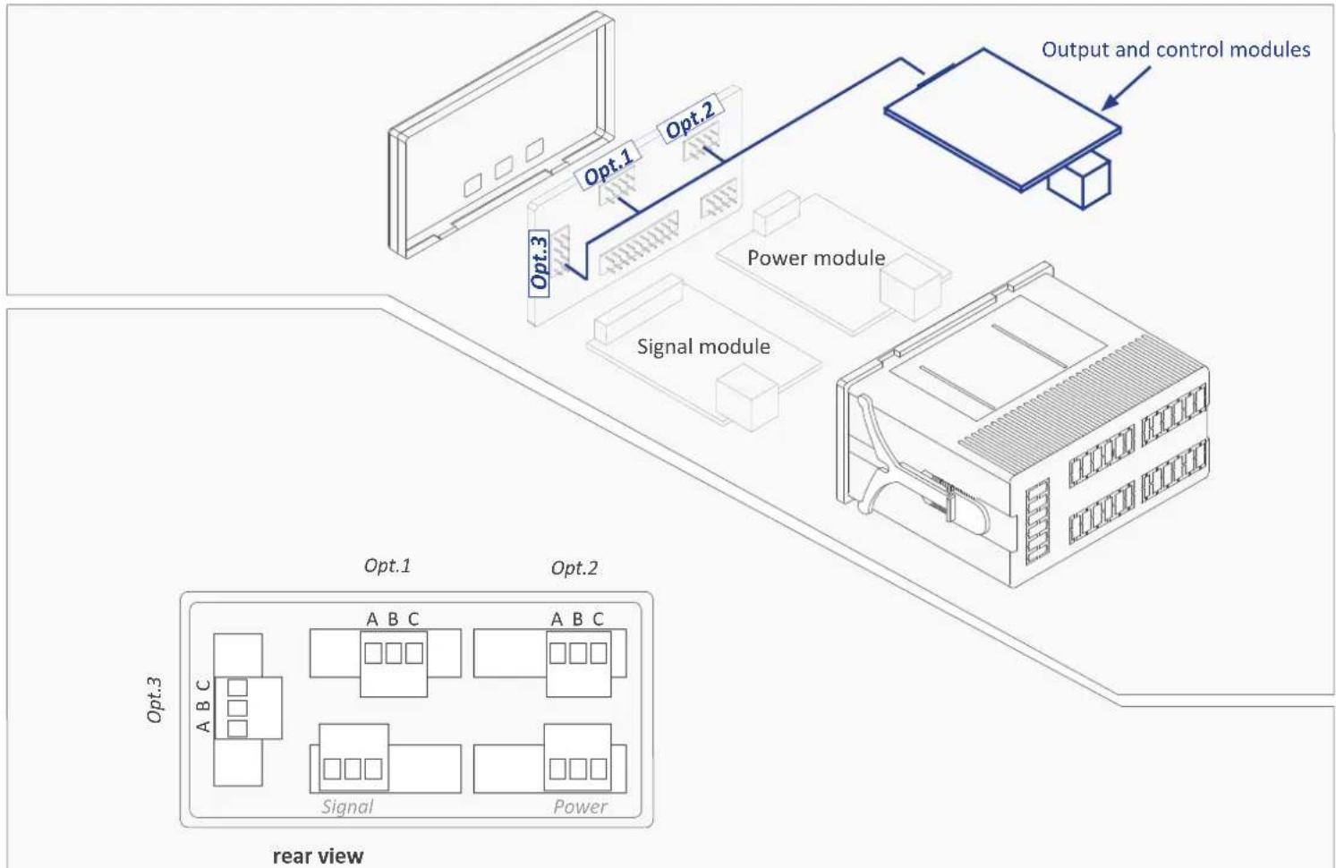
1.2 Modular architecture
Digital panel meters from series M, K and S are designed following a modular architecture that allows the operator to install any od the output and control modules mentioned in this document.
1.3 Installation and start-up
To install an optional output and control module into a digital panel meter from series PCE-DPD:
- open the housing of the instrument (see section 1.4)
- install the module at slot Opt.1', 'Opt.2' or 'Opt.3' as preferred and close the instrument
- close the housing of the instrument (see section 1.4)
- if needed, configure the appropriate jumpers at the module
-
connect the signal output terminals
-
configure the parameters at the 'Configuration menu'.
-
modules PCE-DPD/R, T1 and SSR are configured from the alarms menu of the instrument where the module has been installed
- other modules are configured from its own configuration menu, accessible from menu entries 'Opt.1', 'Opt.2' or 'Opt.3', depending on the slot where the module has been installed.
1.4 To open the housing
To open the housing and access the internal circuits, use a flat screwdriver to unlock clips 'D', 'C', 'B' and 'A', in this order. Remove the front filter. Let the inside of the instrument slide out of the housing.
To reinsert the instrument make sure that all modules are correctly connected to the pins on the display module. Place all the set into the housing, assuring that the modules correctly fit into the internal guiding slides of the housing. Once introduced, place again the front filter at cover 'X', and then insert clips 'A', 'B', 'C' and 'D', in this order.

Risk of electric shock. Removing the front cover will grant access to the internal circuits. Disconnect the power and the input signal to prevent electric shock to the operator. Operation must be performed by qualified personnel only. Observe precautions for handling ESD (electrostatic discharge) sensitive devices

text_image
Technical diagram of a computer rack with labeled components A, B, C, and D, showing internal structure and mounting points.1.5 Internal modules
flowchart
graph TD
    A["Input Module"] --> B["Power module"]
    B --> C["Control module"]
    C --> D["Output and control modules"]
    subgraph Power module
        E["Signal module"]
        F["Power module"]
    end
    subgraph Signal module
        G["Signal module"]
        H["Signal module"]
    end
    I["Output and control modules"] --> J["Output and control modules"]
    style A fill:#f9f,stroke:#333
    style B fill:#ccf,stroke:#333
    style C fill:#cfc,stroke:#333
    style D fill:#fcc,stroke:#333
    style E fill:#ffc,stroke:#333
    style F fill:#fcc,stroke:#333
    style G fill:#ffc,stroke:#333
    style H fill:#fcc,stroke:#333
    style I fill:#fff,stroke:#333
    style J fill:#fff,stroke:#333
    subgraph Power module
        K["Power module"]
        L["Power module"]
    end
    subgraph Signal module
        M["Signal module"]
        N["Signal module"]
        O["Signal module"]
        P["Signal module"]
    end
    subgraph Power module
        Q["Power module"]
        R["Power module"]
        S["Power module"]
    end
    subgraph Signal module
        T["Signal module"]
        U["Signal module"]
        V["Signal module"]
        W["Signal module"]
        X["Signal module"]
    end
    subgraph Power module
        Y["Power module"]
        Z["Power module"]
        AA["Power module"]
    end
    subgraph Signal module
        AB["Signal module"]
        AC["Signal module"]
        AD["Signal module"]
        AE["Signal module"]
        AF["Signal module"]
    end
1. Options PCE-DPD/R, PCE-DPD/T and PCE-DPD/SSR
Modules PCE-DPD/ALr1, PCE-DPD/T and PCE-DPD/SSR provide 1 digital 'on/off' output. The output is configured from the alarms configuration menu ('ALr.1', 'ALr.2' or 'ALr.3') of the instrument where the module is installed.
The menu allows to configure the setpoint, hysteresis, independent activation and deactivation delays, and a second setpoint to create
Option PCE-DPD/R
Output type relay
Relay type
3 contact relay (NC, NO, common)
Maximum current 8 A (resistive load)
Maximum voltage 250 Vac continuous
Isolation 3500 Veff
Type of terminal plug-in screw terminal pitch 5.08 mm
Installation allowed at 'Opt.1', 'Opt.2', 'Opt.3'
Option PCE-DPD/T
Output type transistor
Maximum voltage 35 Vdc
Maximum current 50 mA
Isolation 3500 Veff
Type of terminal plug-in screw terminal pitch 5.08 mm
Installation allowed at 'Opt.1', 'Opt.2', 'Opt.3'
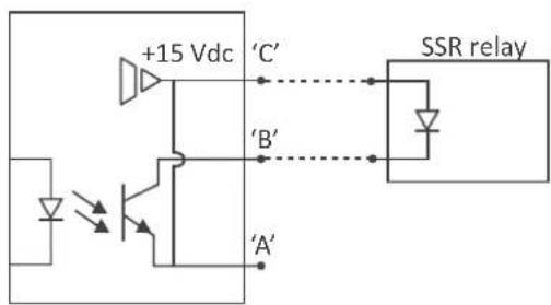
Option PCE-DPD/SSR
Output type to control a SSR relay
Output voltage +15 Vdc
Maximum current 45 mA
Isolation 1000 Vdc
Type of terminal plug-in screw terminal pitch 5.08 mm
Installation allowed at 'Opt.1', 'Opt.2', 'Opt.3'
alarm windows.
Modules PCE-DPD/R, PCE-DPD/T and PCE-DPD/SSR are isolated against all other instrument circuits, and isolated between them.
Note : for more than three relays per instrument or higher relay density per module, see special modules R2, R4 and R6.

text_image
'com' ('A') 'NC' ('C') 'NO' ('B')Module PCE-DPD/R output schematics

text_image
Electrical circuit diagram with diode and transistor symbols labeled A', B'Module PCE-DPD/T output schematics
text_image
+15 Vdc 'C' SSR relay 'B' 'A'Module PCE-DPD/SSR output schematics
flowchart
graph TD
    subgraph Opt.1
        A["Component A"] --> B["Component B"]
        C["Component C"] --> D["Component D"]
        E["Component E"] --> F["Component F"]
    end
    subgraph Opt.2
        G["Component A"] --> H["Component B"]
        I["Component B"] --> J["Component C"]
        K["Component C"] --> L["Component D"]
        M["Component D"] --> N["Component E"]
    end
    subgraph Signal
        O["Signal Block"] --> P["Component P"]
        Q["Component Q"] --> R["Component R"]
        S["Component S"] --> T["Component T"]
    end
    subgraph Power
        U["Power Block"] --> V["Component V"]
        W["Component W"] --> X["Component X"]
        Y["Component Y"] --> Z["Component Z"]
    end
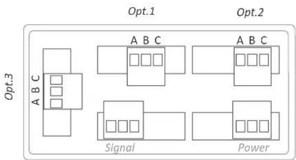
Rear view
2. Option PCE-DPD/AV
Module PCE-DPD/AV provides 1 analog output configurable as 4/20 mA or 0/10 Vdc. The output is configured from the options configuration menu ('Opt.1', 'Opt.2' or 'Opt.3') of the instrument where the module is installed.
The output signal is proportional to the reading and it can be configured for direct (positive) and inverted (negative) slopes. It accepts connection for active and passive current loops.
Modules AO are isolated against all other instrument circuits.
Option PCE-DPD/AV
Output type analog output
Output signals 4/20 mA active
4/20 mA passive
0/10 Vdc
Max. signal output 22 mA, 10.5 Vdc
Min. signal output 0 mA, -50 mVdc
Scaling related to the instruments reading direct or inverse slope
Vexc (terminal A) +13.8 Vdc ± 0.4 Vdc (max. 25 mA) protected against short circuit
Load impedances ≤350 Ohms (in 4/20 mA active) ≤800 Ohms (in 4/20 mA passive) (with a 24 Vdc external Vexc) (maximum 27 Vdc between terminals 'B' and 'C') ≥10 KOhms (in 0/10 Vdc)
Accuracy (at 25 °C) <0.1 % FS
Thermal stability 60 ppm/°C in mA mode 50 ppm/°C in Vdc mode
Step response <75 mSeconds + meter step response (0% to 99% signal)
Isolation 1000 Vdc
Warm-up 15 minutes
Type of terminal pitch 5.08 mm plug-in screw terminal
Factory configuration 'Mode mA' 'Scaling 0/9999 = 4/20 mA'
'On error to high level('to_h')'
Installation allowed at 'Opt.1', 'Opt.2', 'Opt.3'
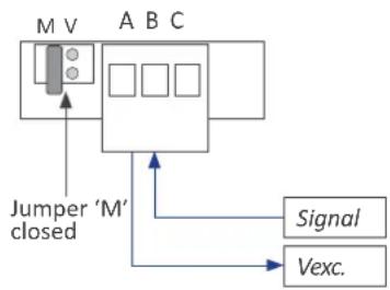
- Mode 4/20 mA active
The current loop is powered from the 'PCE-DPD/AV' module
flowchart
graph TD
    A["Block A"] --> B["Block B"]
    B --> C["Block C"]
    D["Jumper 'M' closed"] --> A
    E["Signal"] --> B
    F["Vexc."] --> B
- Mode 4/20 mA passive
The current loop is powered from an external equipment

flowchart
graph TD
    A["Jumper 'M' closed"] --> B["Signal-"]
    A --> C["Signal+"]
    B --> D[Box 1 Box 2 Box 3 Box 4 Box 5 Box 6 Box 7 Box 8 Box 9 Box 10 Box 11 Box 12 Box 13 Box 14 Box 15 Box 16 Box 17 Box 18 Box 19 Box 20 Box 21 Box 22 Box 23 Box 24 Box 25 Box 26 Box 27 Box 28 Box 29 Box 30 Box 31 Box 32 Box 33 Box 34 Box 35 Box 36 Box 37 Box 38 Box 39 Box 40 Box 41 Box 42 Box 43 Box 44 Box 45 Box 46 Box 47 Box 48 Box 49 Box 50 Box 51 Box 52 Box 53 Box 54 Box 55 Box 56 Box 57 Box 58 Box 59 Box 60 Box 61 Box 62 Box 63 Box 64 Box 65 Box 66 Box 67 Box 68 Box 69 Box 70 Box 71 Box 72 Box 73 Box 74 Box 75 Box 76 Box 77 Box 78 Box 79 Box 80 Box 81 Box 82 Box 83 Box 84 Box 85 Box 86 Box 87 Box 88 Box 89 Box 90 Box 91 Box 92 Box 93 Box 94 Box 95 Box 96 Box 97 Box 98 Box 99
- Mode 0/10 Vdc

flowchart
graph TD
    A["M V"] --> B["Com."]
    A --> C["Signal"]
    D["Jumper 'V' closed"] --> B
    B --> E["Output"]
    style A fill:#f9f,stroke:#333
    style D fill:#ccf,stroke:#333
    style E fill:#cfc,stroke:#333
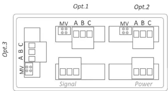
Terminal A Vexc
Terminal B Signal (mA or Vdc)
Terminal C GND
Jumper M closed for 'mA'
Jumper V closed for 'Vdc'
flowchart
graph TD
    subgraph Opt.1
        A["MV A B C"] --> B["Square"]
        C["MV A B C"] --> D["Square"]
        E["MV A B C"] --> F["Square"]
    end
    subgraph Opt.2
        G["MV A B C"] --> H["Square"]
        I["MV A B C"] --> J["Square"]
        K["MV A B C"] --> L["Square"]
    end
    M["Opt.3"] --> N["Signal"]
    O["Opt.3"] --> P["Power"]
Rear view
2.1 Configuration menu
Configure at menu 'Mode' ('ModE') the output signal range to '4/20 mA' ('mA') or '0/10 Vdc' ('Vdc'). Position for jumpers 'V' and 'M' must be according to the range selected.
At menu 'Scaling' ('ScAL') configure the values that define the two points ('high' and 'low') of the 'signal-reading' slope:
- the lower slope point, defined by 'Display low' ('d.Lo') and 'Output low' ('Ao.Lo')
- the higher slope point, defined by 'Display high' ('d.hI') and 'Output high' ('Ao.hI')
Analog output values are shown with 'XX.XX' format, acceptable values are '0.00' to '10.00' Vdc for voltage, and '0.00' to '20.00' mA for current.

line
| Analog output | Reading | | :--- | :--- | | 20 mA | 100.0 | | 4 mA | -50.0 | | d.Lo' = -50.0 | -50.0 | | Ao.Lo' = '4.00' | -40.0 | | Ao.hI' = '20.00' | -30.0 | Example: analog output in 4/20 mA, associated to a reading of -50.0 to 100.0.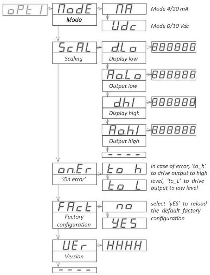
flowchart
graph TD
    A["opt1"] --> B["Node"]
    B --> C["NA"]
    C --> D["Mode 4/20 mA"]
    C --> E["Udc"]
    E --> F["Scaling"]
    F --> G["dLo"]
    G --> H["Display low"]
    H --> I["RoLo"]
    I --> J["Output low"]
    J --> K["dhi"]
    K --> L["Display high"]
    L --> M["Rohl"]
    M --> N["Output high"]
    N --> O["----"]
    O --> P["on.Er"]
    P --> Q["'On error'"]
    Q --> R["FACT"]
    R --> S["Factory configuration"]
    S --> T["UEr"]
    T --> U["HHHH"]
    U --> V["Version"]
    style A fill:#f9f,stroke:#333
    style V fill:#ccf,stroke:#333
2.2 Error codes
'Er.34' output signal configured to value lower than 0 Vdc or 0 mA 'Er.35' output signal configured to a value higher than 10 Vdc or 20 mA
'Er.36' configured slope points are not acceptable, such as: 'd.Hi'='d.Lo'
'Ao.Hi'='Ao.Lo' ('Ao.Hi'-'Ao.Lo')>'(d.Hi'-d.Lo')
3. Option PCE-DPD/MB
Module PCE-DPD/MB provides 1 Modbus RTU communications port. Using protocol function '4' ('Read Input Registers') the instrument registers are accessible (reading value, alarm status, memory of maximum and minimum, setpoint values, ...)
The protocol parameters are configured from the options configura-
Option PCE-DPD/MB
Output type Modbus RTU communication port
Function implemented 4 (Read_Input_Registers)
Addresses 01 to 247
Exception codes see section 3.3
Registers* see section 3.1
*available registers can vary for different models
Bus RS-485
speed 57.6 Kbps to 600 bps
Data format 8n1 (standard), 8o1, 8n2, 8e1
bus terminator not included
Isolation 1000 Vdc
Configuration 3 button front keypad
Temperature operation from 0 to 50 °C
storage from -20 to +70 °C
Factory configuration 'Address 1'
'Speed 19.2 Kbps'
'Format 8n1'
'Decimal point Auto'
Installation allowed at 'Opt.1', 'Opt.2', 'Opt.3'
tion menu ('Opt.1', 'Opt.2' or 'Opt.3') of the instrument where the module is installed.
Modules are isolated against all other instrument circuits.
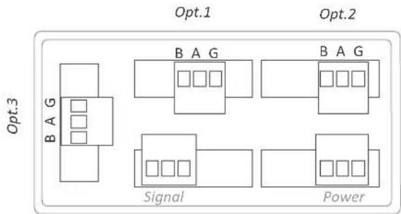
Terminal B RS-485 bus 'B' signal
Terminal A RS-485 bus 'A' signal
Terminal G GND

flowchart
graph TD
    subgraph Opt.1
        A["Block B"] --> B["Component 1"]
        C["Block B"] --> D["Component 2"]
        E["Block B"] --> F["Component 3"]
    end
    subgraph Opt.2
        G["Block B"] --> H["Component 1"]
        I["Block B"] --> J["Component 2"]
        K["Block B"] --> L["Component 3"]
    end
    subgraph Opt.3
        M["Block B"] --> N["Component 1"]
        O["Block B"] --> P["Component 2"]
        Q["Block B"] --> R["Component 3"]
    end
    A --> M
    C --> O
    E --> K
    G --> M
    I --> N
    K --> P
    M --> Q
    N --> Q
    style Opt.1 fill:#f9f,stroke:#333
    style Opt.2 fill:#f9f,stroke:#333
    style Opt.3 fill:#ccf,stroke:#333
Rear view
3.1 Accessible registers
| Register | Name | Description | Size | Refresh | Value : Series M | Value : Series K and S |
| 0 | DISPLAY1_L | Display value | 16 bits | same as display | 999999 to -199999 | 9999 to -1999 |
| 1 | DISPLAY1_H | 16 bits | ||||
| 2 | DECIMALS1 | Decimals on display | 16 bits | 0 to 6 | 0 to 4 | |
| 3 | MAXMEM_L | Memory of maximum | 16 bits | every 30 seconds | 999999 to -199999 | 9999 to -1999 |
| 4 | MAXMEM_H | 16 bits | ||||
| 5 | MINMEM_L | Memory of minimum | 16 bits | 999999 to -199999 | 9999 to -1999 | |
| 6 | MINMEM_H | 16 bits | ||||
| 7 | SETPOINT1_L | Setpoint 1 value | 16 bits | every 2 seconds | 999999 to -199999 | 9999 to -1999 |
| 8 | SETPOINT1_H | 16 bits | ||||
| 9 | SETPOINT2_L | Setpoint 2 value | 16 bits | 999999 to -199999 | 9999 to -1999 | |
| 10 | SETPOINT2_H | 16 bits | ||||
| 11 | SETPOINT3_L | Setpoint 3 value | 16 bits | 999999 to -199999 | 9999 to -1999* | |
| 12 | SETPOINT3_H | 16 bits | ||||
| 13 | STATUS | Alarm status Instrument status | 16 bits | same as display | bit 0...7 alarm status bit 8...16 instrument status | |
| 14 a 16 | Reserved | Reserved | 16 x 3 bits | Not accessible | Not accessible | |
Table 1 - Registers accessible via MODBUS-RTU
All registers codified as binary numbers. Negative values are codified in two's complement. Available registers can vary for different models. Register 11 is not accessible to instruments from series S (limited to 2 output and control option modules)
3.2 Configuration menu

flowchart
graph TD
    A["opt1"] --> B["rtu Configuration"]
    B --> C["Addr Address"]
    C --> D["6Aud Speed (kbps)"]
    D --> E["57.6 1 to 247"]
    D --> F["38.4 57.6 Kbps ... to 600 bps"]
    D --> G["19.2"]
    G --> H["9.6"]
    H --> I["4.8"]
    I --> J["2.4"]
    J --> K["1.2"]
    K --> L["0.6"]
    L --> M["---"]
    D --> N["bits Format"]
    N --> O["8n1 8 bits, no parity, 1 stop"]
    N --> P["8E1 8 bits, even parity, 1 stop"]
    N --> Q["8o1 8 bits, odd parity, 1 stop"]
    N --> R["8n2 8 bits, no parity, 2 stop"]
    N --> S["---"]
    T["tools"] --> U["dP"]
    U --> V["Auto AutomaticDecimal point"]
    V --> W["7Anl Manual 8.8.8.8.8 Move with LE"]
    U --> X["FACT Factory configuration"]
    X --> Y["no YES"]
    Y --> Z["UEr Version HHHH"]
    Z --> AA["---"]
Configure at menu 'Configuration' ('rtu'), the address value between '1' and '247' at parameter 'Address' ('Addr'), bus speed in kbps at parameter 'Speed' ('bAud') and data format at parameter 'Format' ('bltS').
Special tools are grouped inside the 'Tools' ('TooL') menu.
- the 'Decimal point' ('dP') menu is provided for compatibility with ancient hardware that does not support decimal point retransmission. By default, select 'Automatic' ('Auto'). If your instrument does nos transmit the decimal point position, select 'Manual' ('MAnL') and fix the position of the decimal point manually.
- at the 'Factory reset' ('FAct') menu, select 'yes' to load the default factory configuration for the instrument.
the 'Version' ('VEr') menu informs of the current firmware version installed in the module.
3.3 Exception codes
The Modbus RTU protocol defines the following scenarios when a 'Master' is sending a frame to a 'Slave':
- the 'Slave' device receives the frame correctly and replies with the requested data
- the 'Slave' devices detects a CRC error, parity error, or other. and discards the frame without generating a reply frame. The 'Master' will detect a 'TIMEOUT' condition due to the absence of reply.
- the 'Slave' device receives the frame correctly, but replies with an 'EXCEPTION_CODE' as it can not process the function or register requested.
The 'EXCEPTION_CODES' configured in the RTU module are :
| Exception code | Name Description | |
| 0 ILLEGAL_FUNCTION | Requested function is not supported | |
| 1 ILLEGAL_DATA_ADDRESS | Requested register is not supported | |
| Table 2 - Exception codes | ||
3.4 Description and example of registers
Register R0 and R1 (DISPLAY1\_L and DISPLAY1\_H)
Contains the display value of the instrument, codified in two registers of 16 bits each. Possible values are from 999999 to -199999. Decimal point position is codified on register R2.
$$ \text { Example } R 0 = F B F 1 (\text { hex }) \text { and } R 1 = 0 0 0 9 (\text { hex }) $$
$$ \text { Register value } = 0 0 0 9 \text { FBF1 (hex) } $$
$$ \text { Reading value } = 6 5 4 3 2 1 $$
Register R2 (DECIMALS1)
Contains the number of decimals of the display, codified in a single register of 16 bits. Possible values are from 0 to 6.
$$ \text { Example } R 2 = 0 0 0 2 (\text { hex }) $$
$$ \text { Number of decimals } = 2 = 6 5 4 3. 2 1 $$
Register R3 and R4 (MAXMEM\_L and MAXMEM\_H)
Contains the memory of maximum reading of the instrument, codified in two registers of 16 bits each. Possible values are from 999999 to -199999. Decimal point position is codified on register R2.
Example - same example as in R0 and R1 but accessing to R3 and R4.
Register R5 and R6 (MINMEM\_L and MINMEM\_H)
Contains the memory of minimum reading of the instrument, codified in two registers of 16 bits each. Possible values are from 999999 to -199999. Decimal point position is codified on register R2.
Example - same example as in R0 and R1 but accessing to R5 and R6.
Register R7 and R8 (SETPOINT1\_L and SETPOINT1\_H)
Contains the setpoint value of alarm 1, codified in two registers of 16 bits each. Possible values are from 999999 to -199999. Decimal point position is codified on register R2.
Example - same example as in R0 and R1 but accessing to R7 and
R8.
Register R9 and R10 (SETPOINT2\_L and SETPOINT2\_H)
Contains the setpoint value of alarm 2, codified in two registers of 16 bits each. Possible values are from 999999 to -199999. Decimal point position is codified on register R2.
Example - same example as in R0 and R1 but accessing to R9 and R10.
Register R11 and R12 (SETPOINT3\_L and SETPOINT3\_H)
Contains the setpoint value of alarm 3, codified in two registers of 16 bits each. Possible values are from 999999 to -199999. Decimal point position is codified on register R2.
Example - same example as in R0 and R1 but accessing to R11 and R12.
Register R13 (STATUS)
Information bit-by-bit, for the alarm status (on / off) and instrument status. See below for a description.
Bit 0 Alarm 1 status (0 = inactive, 1 = active)
Bit 1 Alarm 2 status (0 = inactive, 1 = active)
Bit 2 Alarm 3 status (0 = inactive, 1 = active)
Bit 3 a 7 Reserved
Bit 8 Display overrange
Bit 9 Display underrange
Bit 10 Lost communication with the main processor
Bit 11 to 15 Reserved
Registers R14, R15 and R16
Reserved
4. Option PCE-DPD/485
Module PCE-DPD/485 provides 1 RS-485 ASCII communications port. Protocol with 'master' - 'slave' architecture, addressable up to 31 modules. Frames codified in representable ASCII characters (codes 32 to 255), which are visible using 'hyperterminal' or similar programs.
Instrument registers are accessible through the RS-485 ASCII port (reading value, alarm status, memory of maximum and minimum, set-
Option PCE-DPD/485
Output type RS-485 ASCII communication port
Bus RS-485
Speed 57.6 Kbps to 600 bps
Data format 8n1 (standard), 8o1, 8n2, 8e1
Protocol ASCII
Architecture 'master-slave'
Addresses 01 to 31
'Broadcast' address 128
Registers* see section 4.1
*available registers can vary for different models
Isolation 1000 Vdc
Configuration 3 button front keypad
Temperature operation from 0 to 50 °C
storage from -20 to +70 °C
| Factory configuration‘Address | ‘Mode1’ | Slave’ |
| ‘Speed‘Format | 19.2 Kbps’8n1’ | |
| ‘Decimal pointconfiguration ‘Master’‘Frequencytools | Auto’‘Destination address0.5 seconds’ | 31’ |
| ‘Decimal point‘Legacy | Auto’Off’ | |
| ‘Answer delayInstallation allowed at | 0 mSeconds’‘Opt.1’, ‘Opt.2’, ‘Opt.3’ |
point values, ...)
The protocol parameters are configured from the options configuration menu ('Opt.1', 'Opt.2' or 'Opt.3') of the instrument where the module is installed.
Modules PCE-DPD/485 are isolated against all other instrument circuits.
Terminal B RS-485 bus 'B' signal
Terminal A RS-485 bus 'A' signal
Terminal G GND
flowchart
graph TD
    subgraph Opt.1
        A["Block 1"] --> B["B A G"]
        C["Block 2"] --> D["Block 3"]
        E["Block 4"] --> F["Block 5"]
    end
    subgraph Opt.2
        G["Block 1"] --> H["B A G"]
        I["Block 2"] --> J["Block 3"]
        K["Block 4"] --> L["Block 5"]
    end
    subgraph Signal
        M["Block 1"] --> N["Block 2"]
        O["Block 3"] --> P["Block 4"]
        Q["Block 5"] --> R["Block 6"]
    end
    subgraph Power
        S["Block 1"] --> T["Block 2"]
        U["Block 3"] --> V["Block 4"]
        W["Block 5"] --> X["Block 6"]
    end
Rear view
4.1 Accessible registers
Display values (DISPLAY1, MAXMEM, MINMEM, AL1, AL2, AL3) are codified with a minimum of 6 digits (left zeros are added if necessary), polarity and decimal point.
| Register | Name | Description |
| 0 | DISPLAY1 | Display1 value |
| 1 | MAXMEM | Memory of maximum |
| 2 | MINMEM | Memory of minimum |
| 3 | AL1 | Setpoint 1 value |
| 4 | AL2 | Setpoint 2 value |
| 5 | AL3 | Setpoint 3 value |
| 6 | STATUS | Alarm status |
| Table 3 - Accessible registers for ASCII protocol. | ||
Register 0 - DISPLAY1
Contains the display value of the instrument, in ASCII code, including polarity (positive / negative) and decimal point.
Example 1 RO=+'0'6'5'4'3'2'
Display value = 6543.2
Example 2 RO='-'0'0'0'0'4'.'5'2'
Display value = -4.52
Register 1 - MAXMEM
Contains the value for memory of maximum, in ASCII code, including polarity (positive / negative) and decimal point.
Register 2 - MINMEM
Contains the value for memory of minimum, in ASCII code, including polarity (positive / negative) and decimal point.
Register 3 - AL1
Contains the value for alarm 1 setpoint, in ASCII code, including polarity (positive / negative) and decimal point.
Register 4 - AL2
Contains the value for alarm 2 setpoint, in ASCII code, including polarity (positive / negative) and decimal point.
Register 5 - AL3
Contains the value for alarm 3 setpoint, in ASCII code, including polarity (positive / negative) and decimal point.
Register 6 - STATUS
Contains the alarm status (on/off).
Bit 0 Alarm 1 status (0 = inactive, 1 = active)
Bit 1 Alarm 2 status (0 = inactive, 1 = active)
Bit 2 Alarm 3 status (0 = inactive, 1 = active)
Bit 3 to 15 Reserved
4.2 Configuration menu

flowchart
graph TD
    A["PCI"] --> B["Configuration ASCII"]
    B --> C["Node Mode"]
    C --> D["Addr Address"]
    D --> E["6Aud Speed (kbps)"]
    E --> F["6bits Format"]
    F --> G["cnF.0 Configuration 'Master'"]
    G --> H["Tool Tools"]
    H --> I["dp Decimal point"]
    I --> J["LEG Legacy mode"]
    J --> K["AnS.d Answer delay"]
    K --> L["FACT Factory configuration"]
    L --> M["UE Version"]

    N["Slave' mode"] --> O["'Master' mode"]
    O --> P["8 bits, no parity, 1 stop"]
    O --> Q["8 bits, even parity, 1 stop"]
    O --> R["8 bits, odd parity, 1 stop"]
    O --> S["8 bits, no parity, 2 stop"]

    T["Fre9 Frequency"] --> U["0.1"]
    U --> V["60"]

    W["Automatic"] --> X["Manual"]
    X --> Y["0.1 seconds\n0.5 seconds\n1 seconds\n5 seconds\n15 seconds\n60 seconds"]

    Z["Auto"] --> AA["on/loFF"]
    AA --> AB["0.8.8.8.8\nuse key 'LE' to select"]
    AC["dP"] --> AD["Answer delay"]
    AD --> AE["0.88.8.88"]
    AF["Factory"] --> AG["no"]
    AG --> AH["YES"]
    AI["HHH"] --> AJ["HHHH"]
At menu 'Configuration ASCII' ('AScl'), configure the instrument at parameter 'Mode' ('ModE') to work as 'slave' or 'master', at parameter 'Address' ('Addr') set the address value from '1' to '31', set the bus speed in kbps at parameter 'Speed' ('bAud') and set the data format at parameter 'Format' ('bltS').
When working as 'master', the instrument continuously transmits the display value data frame. The local module address is '0'. Configure at menu 'Configuration Master' ('cnF.M') the 'Destination address' ('d.Add') parameter from '1' to '31' or use value '128' for a broadcast message. At parameter 'Frequency' ('FrEq') select the how often the frame with the reading value will be transmitted.
Special tools are grouped inside the 'Tools' ('TooL') menu.
- the 'Decimal point' ('dP') menu is provided for compatibility with ancient hardware that does not support decimal point retransmission. By default, select 'Automatic' ('Auto'). If your instrument does nos transmit the decimal point position, select 'Manual' ('MAnL') and fix the position of the decimal point manually.
- the 'Legacy mode' ('LEG') parameter is provided to maintain compatibility with instruments with older communication protocols. Select 'on' to activate this mode.
- the 'Answer delay' ('AnS.d') parameter applies only to 'Slave' mode. The local module delays the answer frame. Configure for applications where the 'Master' needs additional time to switch between 'transmit' and 'receive' modes. Enter a numeric value between '0' and '1000' mSeconds.
- at the 'Factory reset' ('FAct') menu, select 'yes' to load the default factory configuration for the instrument.
the 'Version' ('VEr') menu informs of the current firmware version installed in the module.
4.3 Frame types
The ASCII protocol defines the following frames:
- Frame 'read' ('RD'). Id code 36. Request data frame. The requested register is indicated into the 'REG' byte ('Header' section).
-
Frame 'answer' ('ANS'). Id code 37. Response frame to a request data frame. The requested register is indicated into the 'REG' byte ('Header' section). Data of the requested register is indicated into data bytes 'DO' to 'Dn' ('Data' section).
-
Frame 'error' ('ERR'). Id code 38. Response frame to a request data frame. Indicates that an error has occurred. Error code is codified into the 'REG' byte ('Header' section).
- Frame 'ping' ('PING'). Id code 32. Used to confirm the existence of the remote instrument.
- Frame 'pong' ('PONG'). Id code 33. Response to a 'ping' frame. It confirms the existence of the remote instrument.
4.4 Frame structure
| Header Data Trail | |||||||||||||
| STX | ID | RSV | FROM | TO | REG | RSV | LONG | D0 | D1 | ... | Dn | CRC | ETX |
| 2 | x | 32 | x | x | x | 32 | n+1 | [data] | x | 3 | |||
| 0 | 1 | 2 | 3 | 4 | 5 | 6 | 7 | 8 | 9 | ... | n+7 | n+8 | n+9 |
Protocol frames have a structure made of 'Header', 'Data' and 'Trail'.
Section 'Header'
Contains the start byte ('STX'), the frame identifier ('ID'), the origin address ('FROM') and the destination address ('TO'), the register id ('REG') and the length ('LONG') of the 'Data' section.
Section 'Data'
Contains data for the requested register ('REG').
Section 'Trail'
Contains the 'CRC' code and the end of frame byte ('ETX').
'Real value' and 'Frame value'
To use representable ASCII values, the real values are codified before being sent into the frame. The following definitions apply :
- 'real value' is the value of the field without codification
- 'frame value' is the value of the field, codified
| Field | Description | Size | Position | Real value | Frame value |
| STX | Start of frame | 1 byte | 0 | does not apply | 2 |
| ID | Frame type | 1 byte | 1 | (see section 4.3) | real_value |
| RSV | Reserved | 1 byte | 2 | 0 | 32 |
| FROM | Origin address | 1 byte | 3 | 0 ('Master') / 1 to 31 ('Slave') | 32 + real_value |
| TO | Destination address | 1 byte | 4 | 0 ('Master') / 1 to 31 ('Slave')128 ('broadcast') | 32 + real_value |
| REG | Register identification | 1 byte | 5 | (see section 4.1) | 32 + real_value |
| RSV | Reserved | 1 byte | 6 | 0 | 32 |
| LONG | Length of 'Data' section | 1 byte | 7 | n (between 0 and 32) | 32 + real_value |
| DO ... Dn | Data | n bytes | 8 to n+7 | number 0 to 9decimal pointpolarity (+/-) | ASCII code of the number (48 to 57)ASCII code of decimal point (46)ASCII code of '+' (43)ASCII code of '-' (45) |
| CRC | CRC calculation | 1 byte | n+8 | does not apply | (see section 4.6) |
| ETX | End of frame | 1 byte | n+9 | does not apply | 3 |
Table 4 - Description of the bytes for the ASCII frame
4.5 Error codes
Frames 'ERR' contain within the 'REG' field, the error code. Available error codes are :
error 1 unknown register
error 2 display overrange
error 3 display underrange
error 4 CRC error
error 5 internal error
4.7 Frame examples
4.7.1 Frames 'RD' (36) and 'ANS' (37)
Example - 'Master' (address '0') requests the value of register '0' (display value) to the 'Slave' at address '28' ('RD' frame) and the 'Slave' replies to the 'Master' with a reply frame ('ANS' frame) containing the requested data (765.43).
*Instruments with 4 digits also send reading values formatted with 6 digits : value -321.5 is transmitted as -00321.5
| Header | Trail | ||||||||
| STX | ID | RSV | FROM | TO | REG | RSV | LONG | CRC | ETX |
| 2 | 36 | 32 | 32 | 60 | 32 | 32 | 32 | 58 | 3 |
| Start | RD | --- | 0 | 28 | 0 | --- | 0 | CRC | Stop |
| Header | Data | Trail | |||||||||||||||
| STX | ID | RSV | FROM | TO | REG | RSV | LONG | D0 | D1 | D2 | D3 | D4 | D5 | D6 | D7 | CRC | ETX |
| 2 | 37 | 32 | 60 | 32 | 32 | 32 | 40 | 43 | 48 | 55 | 54 | 53 | 46 | 52 | 51 | 15 | 3 |
| Start | ANS | --- | 28 | 0 | 0 | --- | 8 | +0765.43 | CRC | Stop | |||||||
4.7.2 Frames 'ERR' (38)
Example - 'Slave' at address '11' replies to the 'Master' (address '0') with an error frame ('ERR' frame) indicating that the requested register number is unknown ('UNKNOWN_REGISTER', error code '1'). The
error code is codified into the 'REG' byte. For a list of error code see section 4.5.
| Header | Trail | ||||||||
| STX | ID | RSV | FROM | TO | REG | RSV | LONG | CRC | ETX |
| 2 | 38 | 32 | 43 | 32 | 33 | 32 | 32 | 46 | 3 |
| Start | ERR | --- | 11 | 0 | 1 | --- | 0 | CRC | Stop |
4.7.3 Frames 'PING' (32) and 'PONG' (33)
Example - 'Master' (address '0') requests confirmation of existence to the 'Slave' at address '22' ('PING' frame) and the 'Slave' replies to the 'Master' with a 'PONG' frame.
| Header Trail | |||||||||
| STX | ID | RSV | FROM | TO | REG | RSV | LONG | CRC | ETX |
| 2 | 32 | 32 | 32 | 54 | 32 | 32 | 32 | 52 | 3 |
| Start | Ping | --- | 0 | 22 | 0 | --- | 0 | CRC | Stop |
| Header Trail | |||||||||
| STX | ID | RSV | FROM | TO | REG | RSV | LONG | CRC | ETX |
| 2 | 33 | 32 | 54 | 32 | 32 | 32 | 32 | 53 | 3 |
| Start | Pong | --- | 22 | 0 | 0 | --- | 0 | CRC | Stop |
4.6 CRC calculation
The 'frame value' for the CRC byte is calculated applying a XOR function to the 'frame value' (see section 4.4) of all bytes in sections 'Header' and 'Data', from byte '0' ('STX') to the last data byte ('Dn').
- if the calculated CRC value is lower than '32', it is normalized by applying the 'one's complement' function.
CRC0=STX ^ ID ^ RSV ^ FROM ^ TO ^ REG ^ RSV ^ LONG ^ DO ^...^ Dn
- if (CRC0<32) -> CRC=!CRC0 (one's complement function)
- if (CRC0>31) -> CRC=CRC0
//example of CRC calculation in C language
int8 Calculate_CRC(int8 CRC_Position)
{
int8 i, CRC=0;
for(i=0;c<CRC_Position;c++)
1
crc=crc ^ frame[i];
}
if(crc<32) CRC=\~CRC;
return(CRC);
}
5. Option PCE-DPD/232
Module PCE-DPD/232 provides 1 RS-232 ASCII communications port. Protocol specifications are the same as with module PCE-DPD/485 (see section 4), with only difference that the physical bus is RS-232 instead of RS-485.
PCE-DPD/232 modules allow for point-to-point communication over RS-232 and also allow for multinode communication over RS-232 using a 'Daisy-Chain' type of connection.
Terminals RX1 and TX1 are for connection to the RS-232 bus. Terminals RX2 and TX2 are for RS-232 multinode connection. Frames received on RX1 with destination address different than the local instrument's address, will be retransmitted over the TX2 terminal. In a similar way, frames received from RX2 with destination address
Option PCE-DPD/232
Output type RS-232 ASCII communication port
Bus RS-232
Speed 57.6 Kbps to 600 bps
Data format 8n1 (standard), 8o1, 8n2, 8e1
Protocol
ASCII
Architecture 'master-slave'
Addresses 01 to 31
'Broadcast' address 128
Registers* see section 4.1
*available registers can vary for different models
Isolation 1000 Vdc
Configuration 3 button front keypad
Temperature operation from 0 to 50 °C
storage from -20 to +70 °C
Installation allowed at 'Opt.1', 'Opt.2', 'Opt.3'
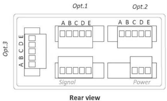
Terminal E
GND
Terminal B
Rx2
Terminal D
Rx1
Terminal A
Tx2
Terminal C
Tx1
text_image
Opt.1 Opt.2 A B C D E A B C D E A B C D E Signal Power Rear viewNotes
PCE Instruments
GERMANY
www.pce-instruments.com/dutch
USA
PCE Americas Inc.
711 Commerce Way suite 8
Jupiter / Palm Beach
33458 FL
USA
Tel: +1 (561) 320-9162
Fax: +1 (561) 320-9176
info@pce-americas.com
www.pce-instruments.com/us
FRANCE
PCE Instruments France EURL
Units 11 Southpoint Business Park
Ensign Way, Southampton
Hampshire
United Kingdom, SO31 4RF
Tel: +44 (0) 2380 98703 0
Fax: +44 (0) 2380 98703 9
info@industrial-needs.com
www.pce-instruments.com/english
CHILE
PCE Instruments Chile S.A.
RUT: 76.154.057-2
Calle Santos Dumont N° 738, Local 4
Comuna de Recoleta, Santiago
Tel.: +56 2 24053238
Fax: +56 2 2873 3777
info@pce-instruments.cl
www.pce-instruments.com/chile
TURKEY
Pehlivan Sok. No.6/C
www.pce-instruments.com/turkish
SPAIN
PCE Ibérica S.L.
Calle Mayor, 53
02500 Tobarra (Albacete)
España
Tel.:+34 967 543 548
Fax: +34 967 543 542
info@pce-iberica.es
www.pce-instruments.com/espanol
ITALY
PCE Italia s.r.l.
Via Pesciatina 878 / B-Interno 6
55010 Loc. Gragnano
Capannori (Lucca)
Italia
PCE (Beijing) Technology Co., Limited
1519 Room, 4 Building
Men Tou Gou Xin Cheng
Men Tou Gou District
102300 Beijing
China
Tel: +86 (10) 8893 9660
info@pce-instruments.cn
www.pce-instruments.cn