QU-DR-791 - Memory card reader QUIO - Free user manual and instructions
Find the device manual for free QU-DR-791 QUIO in PDF.

User questions about QU-DR-791 QUIO
0 question about this device. Answer the ones you know or ask your own.
Ask a new question about this device
Download the instructions for your Memory card reader in PDF format for free! Find your manual QU-DR-791 - QUIO and take your electronic device back in hand. On this page are published all the documents necessary for the use of your device. QU-DR-791 by QUIO.
USER MANUAL QU-DR-791 QUIO
Standard PC/SC Series IC Card Reader
General Technical Manual
(Revision 2.63)
Please read this manual carefully before using. If any problem, please feel free to contact us, we will offer satisfied answer ASAP.
Contents
Document update records....4
1 Introduction....5
2 Driver Installation and System Identification....5
2.1 Contactless Reader 5
2.2 SAM Reader 5
2.3 Device Controller 6
3 PC Software 7
4 PICC Interface Description....8
4.1 ATRGeneration....8
4.2 ATR format for ISO 14443 Part 3 PICCs....8
4.3 ATR format for ISO 14443 Part 4 PICCs 9
5 Contactless ReaderCommands....10
5.1 Operation Prepare....10
5.2 Get Data....10
5.3 ISO14443-4 CPU Card Command....10
5.4 Direct RF Transaction....10
5.5 MIFARE ClassicCards Commands (T=CLEmulation) 11
5.5.1 Load Keys 11
5.5.2 Authentication....12
5.5.3 ReadBinaryBlocks....13
5.5.4 UpdateBinaryBlocks 13
5.5.5 ValueBlockOperation 13
5.5.6 ReadValueBlock....14
5.5.7 RestoreValueBlock....14
5.6 Contactless Smart Card Operation Loop....15
5.6.1 ISO14443-4Card Operation....15
5.6.2 MIFARE 1K/4KCard Operation....15
5.6.3 MIFAREUltra Light Card Operation....16
6 SAM Readers Commands....17
7 Device Controller Commands....18
7.1 Switch Current Operating Smart Card....18
7.2 Reset SAM Card....18
7.3 Set PPSS of SAM Card....19
7.4 Automatically Set SAM Baud Rate (Set PPS) 20
7.5 Set SAM Baud Rate after Reset....20
7.6 Read Default Baud Rate of SAM Card....21
7.7 Set Card Operation Mode....22
7.8 RTC Time Initialize 23
7.9 RTC Time Read 23
7.10 RTC TimeDisplay on LCD Format Set 24
7.11 RTC DateDisplay on LCD Format Set 24
7.12 Set The Date Display Format 25
7.13 Set Non-English Font Display....25
7.14 Read Non-English Font Display Setting....26
7.15 Set Display Font Pixel 26
7.16 LCD Display Text on LCD 27
7.17 LCD Display Character String at Any Point....28
7.18 LCD Display Picture (Directly send picture data)....29
7.19 Delete Row on LCD 30
7.20 Delete Row on LCD 30
7.21 Set Boot Screen on LCD 30
7.22 Set Standby Screen on LCD 34
7.23 LCD Backlight Control 35
7.24 LCD Display a Screen Stored in FLASH....35
7.25 Read Data from FLASH....36
7.26 Write Data to FLASH....37
7.27 Get Device SNR 37
7.28 Get Hardware and Firmware Version 38
7.29 Set LED 38
7.30 Set Buzzer....39
7.31 Set Card Encryption Mode 40
7.32 Reader Reset to Factory Default (Repower on)....40
7.33 Reader Reboot 40
7.34 Set Fast Boot....41
7.35 Get Setting of Fast Boot 41
7.36 Get Setting of Buzzer and LED Indicator Parameter 41
7.37 Set Buzzer and LED Indicator Parameter 42
Document update records
| Date Revision | Update information | |
| June 14, 2016 | R2.30 | Update device controller part and modify sample code. |
| July 1, 2016 | R2.32 | Add comments |
| August 18, 2017 | R2.35 | Fix spell errors. |
| April 22, 2018 | R2.37 | Add chapter 7.21 and 7.22 |
| May 5, 2018 | R2.38 | Add chapter 5.3 and 5.5 |
| May 8, 2018 | R2.39 | Fix spelling errorsFix chapter 5.5 7.7 and 7.22 |
| July 26,2018 | R2.40 | Add MR881 commentsFix chapter 5.4 |
| Aug 1,2018 R2.50 | Fix spelling errorsFix command description | |
| October 10, 2018 | R2.52 | Add fast boot function and set method |
| February 20, 2021 R2.63 | Add Sam card instruction introductionFix spell errors |
1 Introduction
This document is suitable for MR791, MR7911, MR801, MR811, MR8111 and MR881 and so on.
The above mentioned RFID Readers are designed according to USB PC/SC standard. It uses the Microsoft CCID driver and standard operation method, so you could refer to other standard PC/SC documents too.
2 Driver Installation and System Identification
If your PC systemis no CCID driver, it will remind you to install the driver when the PC/SC Reader connects with your PC via USB interface at the first time. But no worry, we can offer you the CCID driver, you can get it from our website or we will send it to you by mail.
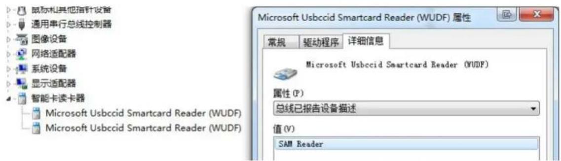
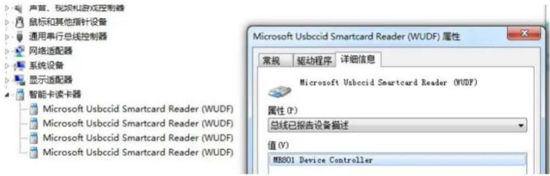
After installation successfully, it will show you two Smart Card Readers-- "Microsoft Usbecid Smartcard Reader (WUDF)" in your PC Device Manager, like the following picture.
2.1 Contactless Reader
The Reader can Read/Write the Contactless Smart Card and Memory Card within the Antenna fields.
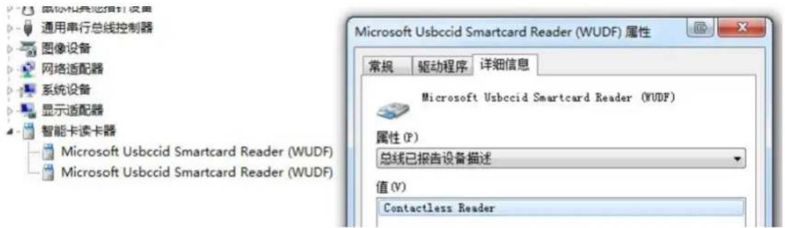
Also it can operate ISO7816 SAM cards in the Reader internal SAM slots.
Device controller is the way to operate miscellany. Like LCD, buzzer and etc.
text_image
声首、视频机游戏控制器 鼠标和其他指针设备 通用串行总线控制器 网络适配器 系统设备 显示适配器 智能卡读卡器 Microsoft Usbccid Smartcard Reader (WUDF) Microsoft Usbccid Smartcard Reader (WUDF) Microsoft Usbccid Smartcard Reader (WUDF) Microsoft Usbccid Smartcard Reader (WUDF) Microsoft Usbccid Smartcard Reader (WUDF) Microsoft Usbccid Smartcard Reader (WUDF) Microsoft Usbccid Smartcard Reader (WUDF) Microsoft Usbccid Smartcard Reader (WUDF) Microsoft Usbccid Smartcard Reader Microsoft Usbccid Smartcard Reader (WUDF) Microsoft Usbccid Smartcard Reader (WUDF) Microsoft Usbccid Smartcard Reader (WUDF) Microsoft Usbccid Smartcard Reader (WUDF) Microsoft Usbccid Smartcard Reader (WUDF) Microsoft Usbccid Smartcard Reader (WUDF) Microsoft Usbccid Smartcard Reader (WUDF) Microsoft Usbccid SmartcardReader (WUDF) Microsoft Usbccid Smartcard Reader (WUDF) Microsoft Usbccid Smartcard Reader (WUDF) Microsoft Usbccid Smartcard Reader (WUDF) Microsoft Usbccid Smartcard Reader (WUDF) Microsoft Usbccid Smartcard Reader (WUDF) Microsoft Usbccid Smartcard Reader (WUDF) Microsoft Usbccid Smartcard Reader (WUDF) Microsoft UsbcccSmartCard Reader (WUDF) Microsoft Usbccid Smartcard Reader (WUDF) Microsoft Usbccid Smartcard Reader (WUDF) Microsoft Usbccid Smartcard Reader (WUDF) Microsoft Usbccid Smartcard Reader (WUDF) Microsoft Usbccid Smartcard Reader (WUDF) Microsoft Usbccid Smartcard Reader (WUDF) Microsoft Usbccid Smartcard Reader (WUDF) Microsoft UsbcaccSmartCard Reader (WUDF) Microsoft UsbcaccSmartCard Reader (WUDF) Microsoft UsbcaccSmartCard Reader (WUDF) Microsoft UsbcaccSmartCard Reader (WUDF) Microsoft UsbcaccSmartCard Reader (WUDF) Microsoft UsbcaccSmartCard Reader (WUDF) Microsoft UsbcaccSmartCard Reader (WUDF) Microsoft UsbcaccSmartCard Reader (WUDF) Microsoft UsbcaccSmartCard Reader (Wudf) Microsoft UsbcaccSmartCard Reader (Wudf) Microsoft UsbcaccSmartCard Reader (Wudf) Microsoft UsbcaccSmartCard Reader (Wudf) Microsoft UsbcaccSmartCard Reader (Wudf) Microsoft UsbcaccSmartCard Reader (Wudf) Microsoft UsbcaccSmartCard Reader (Wudf) Microsoft UsbcaccSmartCard Reader (Wudf) Microsoft UsbcaccSmartCard Reader (Wudf) Microsoft UsbccidSmartCard Reader (Wudf) Microsoft UsbcccSmartCard Reader (Wudf) Microsoft UsbcccSmartCard Reader (Wudf) Microsoft UsbcccSmartCard Reader (Wudf) Microsoft UsbcccSmartCard Reader (Wudf) Microsoft UsbcccSmartCard Reader (Wudf) Microsoft UsbcccSmartCard Reader (Wudf) Microsoft UsbcccSmartCard Reader (Wudf) Microsoft UsbcccSmartCard Reader (Wudf) Microsoft UsbcccSmartCard Reader MS801 Device Controller3 PC Software
First opening "PC/SC Communication Tool", then to click "Initialize" button, there are several Readers will be shown like the following picture.

text_image
PCSC Communication Tool Jinmuyu MR801 Device Controller 0 Jinmuyu MR801 Contactless Reader 0 Jinmuyu MR801 Device Controller 0 Jinmuyu MR801 SAM1 Reader 0 Jinmuyu MR801 SAM2 Reader 0 Initialize Connect Clear APDU Command (HEX) Send History: SendThese 4 devices explain below:
QU-DR-801Contactless Reader 0: MR801 IC card reader contactless channel
QU-DR-801Device Controller 0: MR801 IC device control channel
QU-DR-801SAM1 Reader 0: MR801 IC card reader SAM1 channel
QU-DR-801SAM2 Reader 0: MR801 ICcard reader SAM2 channel
4 PICC Interface Description
4.1 ATRGeneration
If the reader detects a PICC, an ATR will be sent to the PCSC driver for identifying the PICC. Because these readers are standard PC/SC device, you could refer to other standard documents too.
4.2 ATR format for ISO 14443 Part 3 PICCs
| Byte No. | Value(Hex) | Designation Description | |
| 0 | 3B | Initial Header | |
| 1 | 8N | T0 | Higher nibble 8 means no TA1, TB1, and TC1 only TD1 is following. Lower nibble n is the number of historical bytes (HistByte 0 to HistByte n-1). |
| 2 | 80 | TD1 | Higher nibble 8 means no TA2, TB2, and TC2 only TD2 is following. Lower nibble 0 means T = 0. |
| 3 | 01 | TD2 | Higher nibble 0 means no TA3, TB3, TC3, TD3 following. Lower nibble 1 means T = 1. |
| 4 to 3+N | 80 | T1 | Category indicator byte, 80 means A status indicator may be present in an optional COMPACT-TLV data object. |
| 4F | Registered application provider | Application identifier Presence indicator | |
| 0C | Length | ||
| RID Tk Registered application provider identifier:(RID) # A0 00 00 03 06h | |||
| SS | Byte for Standard | ||
| C0...C1 | Bytes for Card Name | ||
| 00000000h | RFU | RFU # 00 00 00 00h | |
| 4+N | UU | TCK | XOR of all the bytes T0 to Tk |
4.3 ATR format for ISO 14443 Part 4 PICCs
| Byte Nr | Value(Hex) | Designation Description | |
| 0 | 3B | Initial Header | |
| 1 8N T0 | Higher nibble 8 means no TA1, TB1, and TC1 only TD1 is following. Lower nibble n is the number of historical bytes (HistByte 0 to HistByte n-1). | ||
| 2 | 80 | TD1 | Higher nibble 8 means no TA2, TB2, and TC2 only TD2 is following. Lower nibble 0 means T = 0. |
| 3 | 01 | TD2 | Higher nibble 0 means no TA3, TB3, TC3, TD3 following. Lower nibble 1 means T = 1. |
| 4 to 3+N ISO | XX T1 | Historical bytes:ISO14443A:The historical bytes from ATS response. Refer to the ISO14443-4 specification. | |
| XX14443B:xxXX | Tk | The higher layer response from the ATTRIB response. Refer to the ISO14443-3 specification. | |
| 4+N | UU | TCK | XOR of bytes T0 to Tk |
5 Contactless Reader Commands
5.1 Operation Prepare
Please to confirm that the card could be support by the reader before you operate the card.
Connect the reader to PC and wait the reader startup. Place the card on the reader and the reader will prompt by LED and Buzzer. Startup the PC/SC operation software (PCSC Communication Tools) supplied by QUIO-RFID. Select the proper channel and click “Connect” button. If connect successful, you can operate the card by input APDU now.
5.2 Get Data
This command will retrieve the SNR or ATS of the present card.
APDU Format:
| Command | CLA | INS | P1 P2 | Lc | |
| GetData | FF | CA | 00/01 | 00 | 00 |
Answer:
Response Format (UID + 2 Bytes) if P1 = 00
| Response | Data | ||||
| Result | UID(LSB) -- UID(MSB) SW1 | SW2 | |||
Get ATS of a ISO 14443 A card (ATS + 2 Bytes) if P1 = 01
| Response | Data | ||
| Result | ATS | SW1 | SW2 |
Response State:
| Result | SW1 SW2 | Meaning |
| Success | 90 00 | The operation is completed successfully. |
| Error | 63 00 | The operation is failed. |
| Error | 6A 81 | No such function |
5.3 ISO14443-4 CPU Card Command
Input APDU and send will implement the operation of the card.
5.4 Direct RF Transaction
Send data stream over RF interface to card and receive thedata.
APDU format 1:
| Command CLA | INS | P1 | P2 | Lc Data | |
| Transaction LEN RF DataF | 00 | 00 | 00 |
LEN: the length of RF Data
RF Data: the data will send over RF interface
| Response Data Out | |||
| Result Data SW2 | SW1 | ||
APDU format 2:
| Command CLA | INS | P1 | P2 | Lc | CMD | TMO | Data | |
| Transaction | FF | 00 | FF | FF | LEN | CMD | FWI | RF Data |
LEN: the length of Data
CMD: 0: Send commands and receive data.
1: Send only.
TMO: Timeout parameter. Operate the M1 card, FWI = 4. When CMD=1, this byte is meaningless
RF Data: the data will send over RF interface
Answer:
| Response | Data Out | ||
| Result | Data SW2 | SW1 | |
5.5 MIFARE ClassicCards Commands (T=CLEmulation)
These parts describe the operation of MIFARE/Ultralight. PC sends APDU to reader. Reader analyzes and executes the APDU and sends back the result. The APDU is not same to smart card.
5.5.1 Load Keys
This command will load the keys into the reader. The key will be of two different types; the reader key and the card key. This command can be used for all kinds of contactless cards.
Reader Key: 16 bytes, use for encrypt application data. The encryption is 3DES. Max. 1 key.
Card Key: 16 bytes, this is the card key. It could be authenticating the memory card. Max. 32 keys.
APDU Format:
| Command | CLA | INS | P1 | P2 | Lc Data | |
| Load Keys | FF | 82 | Key Structure | Key Index | Key length | KeyData |
Key Structure: 1byte
| b7 | b6 | b5 | b4 | b3 | b2 | b1 | b0 | Description | ||
| X 0: Card Key; 1 Reader Key | ||||||||||
| X 0: Plain Transmission, 1: Secured Transmission | ||||||||||
| X | 0: Keys are loaded into volatile memory1: Keys are loaded into non-volatile memory. | |||||||||
| 0 | 0 | 0 | 0 | 0 | RFU | |||||
The non-volatile Key, which is stored in the Flash of the Reader, has write cycle limitation. Users need pay more attention to it.
Key Index:1byte
0x00 \~ 0x31 when loading card key
0x00, the Reader can store 1Reader Key.
Key Length:1byte
When loading the Reader Key, the length of the Key must be 16bytes, or the Reader will return fail.
When loading the Card Key by way of plaintext, the Reader no any restriction for the Key length.
When loading the Card Key by way of ciphertext, the Key length must be 8bytes or 16bytes.
Key:N byte
Answer:
| Response | Data Out | |
| Result | SW1 SW2 | |
5.5.2 Authentication
The application specific the key used for the MIFARE 1K/4K card authentication. The specific key must be already in the reader. Two typeauthentication keys: KEY_A and KEY_B.
APDU Format:
| Command | CLA | INS | P1 | P2 | Lc | Data |
| Authentication | FF | 86 | 00 | 00 | 05 | Data |
Data:
| Byte1 Byte2 | Byte3 Byte4 | Byte5 | ||
| Version (0x01) | 00 | Block Number | KeyType | Key Index |
Block Number: 1 Byte. This is the memory block number to be authenticated.
Key Type: 1 Byte
0x60 = Key is used as a KEY_A key for authentication.
0x61 = Key is used as a KEY_B key for authentication.
Key Index: 1 Byte
0x00 \~ 0x1F = Key Index.
Answer:
| Response | Data Out | |
| Result | SW1 SW2 | |
5.5.3 ReadBinaryBlocks
This command is used for retrieving “data blocks” from the PICC. The data block/trailer block must be authenticated first.
APDU Format:
| Command CLA | INS | P1 | P2 Le | ||
| Read Blocks Block Number Len | B0 | 00 | |||
Block Number: 1Byte. The block to be accessed
Len: 1Byte. An integer multiple of 16 bytes
Answer:
| Response | Data Out | ||
| Result | Data SW2 | SW1 | |
5.5.4 UpdateBinaryBlocks
This command is used for writing “data blocks” into the PICC. The data block/trailer block must be authenticated.
Update Binary APDU Format (4 or 16 + 5 Bytes)
| Command CLA | INS | P1 | P2 Lc | Data | ||
| Update Blocks | FF | D6 | 00 | Block Number Len | Data | |
Block Number: 1Byte. The starting block to be updated.
Len: 1Byte.
16*n(n>0) bytes for MIFARE 1K/4K.
4*n(n>0) bytes for MIFARE Ultra light.
Block Data: The data will be written into the binary block/blocks.
5.5.5 ValueBlockOperation
These commands increment/decrement the value of a purse block.
APDU Format:
| Command CLA | INS | P1 | P2 Lc | Data | ||
| Value Operation | FF | D7 | 00 | Block Number | 05 | Data |
Block Number: 1 Byte, The value block to be manipulated.
0x00 = Store the VB_Value into the block. The block will then be converted to a value block.
0x01 = Increment the value of the value block by the VB_Value.
This command is only valid for value block.
0x02 = Decrement the value of the value block by the VB_Value.
This command is only valid for value block.
VB_Value: The value used for value manipulation. The value is a signed long integer with LSB first.
Answer:
| Response | Data Out | |
| Result | SW1 SW2 | |
5.5.6 ReadValueBlock
This command is used for retrieving the value from the value block. This command is only valid for value block.
APDU Format:
| Command | CLA | INS | P1 | P2 Lc | |
| ReadValueBlock Block Number | B1 | 00 | 04 | ||
Block Number:1 Byte,the value block to be accessed.
Answer:
| Response | Data Out | ||
| Result | Value SW2 | SW1 | |
Value: 4Bytes. The value returned from the card. The value is a signed long integer.
5.5.7 RestoreValueBlock
This command is used to copy a value from a value block to another value block.
APDU Format:
| Command | CLA | INS | P1 | P2 Lc | Data | ||
| Restore | FF | D7 | 00 | SourceBlock 03 | Target Block | ||
Source Block: 1 Byte, the value of the source value block will be copied to the target value block.
Target Block: 1 Byte, the value block to be restored. The source and target value blocks must be in the same sector.
Answer:
| Response | Data Out | |
| Result | SW1 SW2 | |
5.6 Contactless Smart Card Operation Loop
5.6.1 ISO14443-4Card Operation
Basic Operation Loop:
Step 1 PuttheCPU card into ContactlessReader antenna field
Step 2 Connect Contactless Reader
Step 3 SendAPDU command
Example:
Get 8bytes Random
Send: 0xFF 00 FB 00 08 07 DA 04 0C 0C 01 00 01
Receive: 0x90 00
5.6.2 MIFARE 1K/4KCard Operation
Basic Operation Loop:
Step 1 Put theMIFARE 1K/4K card into Contactless Reader antenna field
Step 2 Connect Contactless Reader
Step 3 SendMIFARE 1K/4K card operation commands
Example:
Loading Reader Key
Send: 0xFF 82 A0 00 10 00 11 22 33 44 55 66 77 88 99 AA BB CC DD EE FF
Receive: 0x90 00
Loading Card Key, Number 00h
Send: 0xFF 82 00 00 06 FF FF FF FF FF
Receive: 0x90 00
Ciphertext Load Card Key, Number 01h, The key plaintext is {FF FF FF FF FF FF}
Send: 0xFF 82 60 01 08 C0 D6 1E B0 84 F9 43 57
Receive: 0x90 00
Get Data
Send: 0xFF CA 00 00 00
Receive: 0x03 12 94 DD 90 00
Authenticate 04 Block Via Type A Key Which Is Stored In 00 Position.
Send: 0xFF 86 00 00 05 01 00 04 60 00
Receive: 0x90 00
Write Data Into 04 Block
Send: 0xFF D6 00 04 10 01 02 03 04 05 06 07 08 09 0A 0B 0C 0D 0E 0F 00
Receive: 0x90 00
Read Data From 04/05 Block
Send: 0xFF B0 00 04 20
Receive: 0x01 02 03 04 05 06 07 08 09 0A 0B 0C 0D 0E 0F 00 FF FF FF FF FF FF FF FF FF FF FF FF FF FF FF FF FF FF FF FF FF FF FF FF FF FF FF FF FF FF FF
Purse Initialization
Send: 0xFF D7 00 04 05 00 00000000
Receive: 0x90 00
Purse Increment
Send: FF D7 00 04 05 01 05000000
Receive: 0x90 00
Purse Decrement
Send: FF D7 00 04 05 02 0A000000
Receive: 0x90 00
Purse Copy
Send: 0xFF D7 00 04 02 03 05
Receive: 0x90 00
Read Purse Value
Send: 0xFF B1 00 05 04
Receive: 0xF6 FF FF FF 90 00
5.6.3 MIFAREUltra Light Card Operation
BasicOperation Loop:
Step 1 Put the MIFARE Ultra Lightcard into Contactless Reader antenna field
Step 2 Connect Contactless Reader
Step 3 Send MIFARE Ultra Light card operation commands
Example:
Loading Card Key, Number 05h
Send: 0xFF 82 20 05 10 49 45 4D 4B 41 45 52 42 21 4E 41 43 55 4F 59 46
Receive: 0x90 00
Get Data
Send: 0xFF CA 00 00 00
Receive: 0x04 0E 8B 8A 7C 3B 80 90 00
Mifare Ultralight C certification
Send: 0xFF 86 00 00 05 01 00 00 00 05
Receive: 0x90 00
Write data into 4 block
Send: 0xFF D6 00 04 04 00 01 02 03
Receive: 0x90 00
Write data into 5\~7 block
Send: 0xFF D6 00 05 0C 04 05 06 07 08 09 0A 0B 0C 0D 0E 0F
Receive: 0x90 00
Read data from 4\~12 block
Send: 0xFF B0 00 04 20
Receive: 0x00 01 02 03 04 05 06 07 08 09 0A 0B 0C 0D 0E 0F 00 00 00 00 00 00 00 00 00 00 00 00 00 00 00 00 00 00 00 00 90 00
6 SAM Readers Commands
IMPORTANT: SAM(s) need to install before the reader power up. After connect to SAM readers, users could send APDU to SAM directly.
For the MR881 card reader, the operation of SAM card requires the DEVICE Controller to be connected, and the default automatically selects the SAM1 card.
7 Device Controller Commands
This part of APDU is about the operation of "DEVICE" controller.
The “DEVICE” controller is included these components: LCD, RTC, FLASH MEMORY, LED, and BUZZER.
7.1 Switch Current Operating Smart Card
This function is aim to switch SAM card.
Note: Format 1 is only supported by MR88x, and Format 2 is supported by MR88x, MR79xx.
APDU Format 1:
| Command Class | INS | P1 P2 | Lc | Data | ||
| SwitchCard FA | CurSmaFtCard | 00 | 00 | 01 |
APDU Format 2:
| Command | Class | INS | P1 | P2 | Lc | Data |
| SwitchCard | FF | 00 | 61 | 00 | 01 | CurSmartCard |
CurSmartCard:
0x00 - StandardCPUCard
0x01 - SAM1Card
0x02 - SAM2Card
0x03 - SAM3Card
0x04 - SAM4Card
Answer:
| Response | Data Out | |
| Result | SW1 | SW2 |
7.2 Reset SAM Card
Reset SAM card manually.
Note: Format 1 is only supported by MR88x, and Format 2 is supported by MR88x, MR79xx.
APDU Format 1:
| Command | Class | INS | P1 | P2 | Lc | Data |
| RstCard | FF | 00 | 60 | 00 | 01 | SAMNo |
APDU Format 2:
| Command | Class | INS | P1 | P2 | Lc | Data |
| RstCard | FF | 00 | 60 | 00 | 03 | Parameter |
Parameter: SAMNO(1Byte) + RSTBOUND(1Byte) + SAMPPS(1Byte)
SAMNO:
0x00 - StandardCPUCard
0x01 - SAM1Card
0x02 - SAM2Card
0x03 - SAM3Card
0x04 - SAM4Card
RSTBOUND: Reset Baud Rate
SAMPPS: Communication Baud Rate
0x00 - 9600
0x01 - 19200
0x02 - 38400
0x03 - 55800
0x04 - 57600
0x05 - 115200
0x06 - 230400
Answer:
| Response | Data Out | ||
| Result | ATR SW2 | SW1 | |
7.3 Set PPSS of SAM Card
Note: This command only supported by MR801/MR811/MR8111/MR881.
This is the PPS command of ISO7816. It is need to be the 1^st APDU of the SAM card after reset.
APDU Format:
| Command Class | INS | P1 | P2 | Lc | Data | |
| SetSamBaud SAMn+Ba#Rate | 00 | 60 | 10 | 02 |
SAMn:
0x00 - StandardCPUCard
0x01 - SAM1Card
0x02 - SAM2Card
0x03 - SAM3Card
0x04 - SAM4Card
Baudrate:
0x00 - 9600(Default)
0x01 - 19200
0x02 - 38400
0x03 - 55800
0x04 - 57600
0x05 - 115200
0x06 - 230400
Answer:
| Response | Data Out | |
| Result | SW1 SW2 | |
7.4 Automatically Set SAM Baud Rate (Set PPS)
Note: This command only supported by MR801/MR811/MR8111/MR881.
This function is aim to according to SAM Reset Information (ATR) parameters in the automatic set of SAM baudrate. Default is not enable. This parameter is set to save when power is off.
APDU Format:
| Command Class | INS | P1 | P2 | Lc | Data | |
| AutoSetBaud Status | FF | 00 | 60 | 14 | 01 |
Status:
0x00: disenable
0x01: enable
Answer:
| Response | Data Out | |
| Result | SW1 SW2 | |
7.5 Set SAM Baud Rate after Reset
Note: This command only supported by MR801/MR811/MR8111/MR881.
This function is aim to set SAM Baud Rate after Reset. The SAM card slots which can be supported by each Reader are different. (MR800 has 2 SAM slots). Usually, the default SAM Baud Rate after Reset is 9600bps. Before sending GetData APDU to Reset SAM card, if you want to modify the SAM Baud Rate after Reset, you can use this APDU command to set the new Baud Rate Value. (Note: this SAM card must support the Baud Rate to be set). This parameter is set to save when power is off.
APDU Format:
| Command | Class | INS | P1 | P2 | Lc | Data | |
| SetRstSamBaud | FF | 00 | 60 | 11 | 02 | SAMn | Baudrate |
SAMn:
0x00 - StandardCPUCard
0x01 - SAM1Card
0x02 - SAM2Card
0x03 - SAM3Card
0x04 - SAM4Card
Baudrate:
0x00 - 9600(Default)
0x01 - 19200
0x02 - 38400
0x03 - 55800
0x04 - 57600
0x05 - 115200
0x06 - 230400
Answer:
| Response | Data Out | |
| Result | SW1 SW2 | |
7.6 Read Default Baud Rate of SAM Card
Note: This command only supported by MR801/MR811/MR8111/MR881.
APDU Format:
| Command Class | INS | P1 | P2 | Lc | Data | |
| ReadRstBaud SAMn | FF | 00 | 60 | 12 | 01 |
SAMn:
0x00 - StandardCPUCard
0x01 - SAM1Card
0x02 - SAM2Card
0x03 - SAM3Card
0x04 - SAM4Card
Answer:
| Response | Data Out | ||
| Result | RstBaud SW1 | SW2 | |
RstBaud:
0x00 - 9600(Default)
0x01 - 19200
0x02 - 38400
0x03 - 55800
0x04 - 57600
0x05 - 115200
0x06 - 230400
Example:
Reset SAM1
Send: 0xFF 00 60 00 01 01
Receive: 0x3B 6C 00 02 43 21 86 38 07 54 42 00 16 0E 62 3B 90 00
Set PPS 38400
Send: 0xFF 00 60 10 02 01 02
Receive: 0x90 00
Get Random
Send: 0x00 84 00 00 08
Receive: 0xF9 B5 69 7A CC 39 D0 DE 90 00
Set SAM2 Reset Baud Rate 38400
Send: 0xFF 00 60 11 02 02 02
Receive: 0x90 00
Read Default Baud Rate Of SAM2
Send: 0xFF 00 60 12 01 02
Receive: 02 90 00
Reset SAM2
Send: 0xFF 00 60 00 01 02
Receive: 0x3B 69 00 00 44 01 9F 92 D9 29 47 25 20 90 00
Get Random
Send: 0x00 84 00 00 08
Receive: 0x15 1EA3 53 C4 BC 73 34 90 00
7.7 Set Card Operation Mode
Some ISO14443-4 card combined with a MIFARE 1 card. The SAK will indicate it is a ISO14443-4 card. This command is used for set the reader to operate the card by mothed of MIFARE 1.
APDU Format:
| Command | CLA | INS | P1 | P2 | Lc | Data |
| Set Mode | FF | 00 | FF | 10 | 01 | SETTING |
SETTING:
0x00: Operate the card use ISO14443-4 mothed
0x01: Operate the card use MIFARE 1 mothed
Note: remove card is needed after this command.
Answer:
| Response | Data Out | |
| Result | SW1 SW2 | |
Example:
Get Random
Send: 0xFF 00 FF 10 01 01
Receive: 0x90 00
7.8 RTC Time Initialize
Initialize theInternal Clock of the Reader.
APDU Format:
| Command | Class | INS | P1 P2 | Le | Data | |
| InitialRTC | FF | 00 | FB | 00 | 08 | Time |
Time:
Year (High Byte) + Year(Low Byte) + Month + Date + Hour + Minute + Second + Week
Example:
2010 - 4 - 12 12:01:00 Monday : Time in hex = 0x07 DA 04 0C 0C 01 00 01
Answer:
| Response | Data Out | |
| Result | SW1 SW2 | |
7.9 RTC Time Read
Read time from RTC of reader.
APDU Format:
| Command | Class | INS | P1 P2 | Lc | |
| ReadRTC | FF | 00 | FB | 01 | 08 |
Answer:
| Response | Data Out | ||
| Result | Time SW2 | SW1 | |
Time:
Year (High Byte) + Year(Low Byte) + Month + Date + Hour + Minute + Second + Week
Example:
2010 - 4 - 12 12:01:00 Monday : Time in hex = 0x07 DA 04 0C 0C 01 00 01
Set and Read Time
Send: 0xFF 00 FB 00 08 07 DA 04 0C 0C 01 00 01
Receive: 0x90 00
Send: 0xFF 00 FB 01 08
Receive: 0x07 DA 04 0C 0C 03 15 01 90 00
7.10 RTC TimeDisplay on LCD Format Set
Set the time display format on LCD.
APDU Format:
| Command | Class | INS | P1 P2 | Lc | Data | |
| DisTime | FF | 00 | FB | 02 | 03 | Data |
Data: EnableFag(1Byte) + Line(1Byte) + Column(1Byte)
Line: The start display line (0\~7 or 0\~12) (LCD resolution: 128*64 or 240*128)
Column: The start display column (0\~127 or 0\~239) (Same as above)
Answer:
| Response | Data Out | |
| Result | SW1 SW2 | |
Example:
Time Display OFF
Send: 0xFF 00 FB 02 03 00 00 00
Receive: 0x90 00
Time Display ON
Send: 0xFF 00 FB 02 03 01 03 05
Receive: 0x90 00
7.11 RTC DateDisplay on LCD Format Set
Set the date display format on LCD.
APDU Format:
| Command | Class | INS | P1 P2 | Lc | Data | |
| DisDate | FF | 00 | FB | 03 | 03 | Data |
Data: EnableFag(1Byte) + Line(1Byte) + Column(1Byte)
EnableFag: Date display enable (0-Disable, 1-Enable)
Line: The start display line (0\~7 or 0\~12) (LCD resolution: 128*64 or 240*128)
Column: The start display column (0\~127 or 0\~239) (Same as above)
Answer:
| Response | Data Out | |
| Result | SW1 SW2 | |
Example:
Date Display OFF
Send: 0xFF 00 FB 03 03 00 00 00
Receive: 0x90 00
Date Display ON
Send: 0xFF 00 FB 03 03 01 03 05
Receive: 0x90 00
7.12 Set The Date Display Format
MR88x special instruction.
APDU Format:
| Command Class | INS | P1 P2 | Lc | Data | ||
| DateFormat FB | USdate6fmat | 00 | 04 | 01 |
Usdateformat:
0x00 : YYYY-MM-DD(Default)
0x01 : MM-DD-YYYY
Answer:
| Response | Data Out | |
| Result | SW1 SW2 | |
7.13 Set Non-English Font Display
Switch none-English font display method. (Any Language could be support, contact us please)
APDU Format:
| Command Class | INS | P1 P2 | Lc | Data | ||
| Display Font FC | FontTypeF | 00 | 00 | 01 |
FontType:
0x01: Simplify Chinese
0x02: Traditional Chinese
0x03: Russian
Answer:
| Response | Data Out | |
| Result | SW1 SW2 | |
Example:
Send: 0xFF 00 FC 00 01 01
Receive: 0x90 00
7.14 Read Non-English Font Display Setting
Read the setting of none-English font display.
APDU Format:
| Command | Class | INS | P1 P2 | Le | |
| Read Font | FF | 00 | FC | 01 | 01 |
Answer:
| Response | Data Out | ||
| Result | CharacterSet SW2 | SW1 | |
Example:
Send: 0xFF 00 FC 00 01 02
Receive: 0x90 00
Send: 0xFF 00 FC 01 01
Receive: 0x02 90 00
7.15 Set Display Font Pixel
MR88x special instruction.
MR881 support 16, 24 and 32 pixel display fonts. This instruction could switch the display font pixel.
APDU Format:
| Command Class | INS | P1 P2 Lc | Data | ||
| SetFontPixel FC 0A FonFFlexl | 00 | 01 |
FontPiexl:
$$ 0 x 0 0 = 1 6 \text { pixel } $$
$$ 0 \mathrm{x} 0 1 = 2 4 \text { pixel } $$
0x02 = 32pixel (system default, not save after repower)
Answer:
| Response | Data Out | |
| Result | SW1 SW2 | |
Remark: Russian support 32 pixel only.
Example:
Send: FF 00 FC 0A 01 00
Receive: 90 00
7.16 LCD Display Text on LCD
Display Text on LCD.
One Chinese font - 2Byte; One English font - 1Byte; One Russian font - 1Byte.
APDU Format:
| Command Class | INS | P1 P2 | Lc Data | |||
| DisplayText FC | nByte FF | 00 | 02 | Data |
Data: Configure(1Byte) + Row(1Byte) + Column(1Byte) + DisplayData(nBytes)
Configure:
| Bit | Value Instructions | |
| B0 | 0 | Positive Display |
| 1 | Negative Display | |
| B2~B1 | 00 | Before showing new information on the screen, no any delete the old ones |
| 01 | Before showing new information on the screen, only to clear the row of the showed screen | |
| 10 | Before showing new information on the screen, delete the all old ones | |
| B3 | 0 | BackLight off |
| 1 | BackLight on | |
| B7~b4 | RFU | RFU |
Row:
| Value Instructions | |
| 0~7 | LCD resolution 128*64(1Row = 16 dot High) |
| 0~7 | LCD resolution 240*128 32 pixel font (1Row = 32 dot High) |
| 0~0x09 | LCD resolution 240*128 24 pixel font (1Row = 24 dot High) |
| 0~0x0F | LCD resolution 240*128 16 pixel font (1Row = 16 dot High) |
Column: (0\~7 or 0\~12) (LCD resolution: 128*64 or 240*128)
Display Data: One Chinese font - 2Byte, One ASCII or Russian font - 1Byte.
Answer:
| Response | Data Out | |
| Result | SW1 SW2 | |
Example:
Showing "QUIO-RFID" on the top left corner of LCD displayer with "Positive Display", "Before showing new information on the screen, no any delete the old ones" and "BackLight off".
Send: 0xFF 00 FC 02 09 00 00 00 BD F0 C4 BE D3 EA
Receive: 0x90 00
7.17 LCD Display Character String at Any Point
MR88x special instruction.
This function is aim to set the specified number of characterson LCD at ANY POINT.
APDU Format:
| Command Class | INS | P1 P2 | Lc Data | |||
| DisplayText FC | nByte FF | 00 | 09 | Data |
Data: Configure(1Byte) + Row(1Byte) + Column(1Byte) + DisplayData(nBytes)
Configure:
| Bit | Value | Instructions |
| B0 | 0 | Positive Display |
| 1 | Negative Display | |
| B1 | RFU | RFU |
| B2 | 0 | keep screen |
| 1 | clear screen | |
| B3 | 0 | BackLight off |
| 1 | BackLight on | |
| B5~B4 | 01 | display character with 16 pixel font |
| 10 | display character with 24 pixel font | |
| 11 | display character with 32 pixel font | |
| B7~b6 | RFU | RFU |
Row: 0 \~ 127 dot
Column: 0 \~ 239 dot
Display Data: One Chinese font - 2Byte, One ASCII or Russian font - 1Byte.
Answer:
| Response | Data Out | |
| Result | SW1 SW2 | |
Example:
Showing "QUIO-RFID" on the top left corner of LCD displayer with "Positive Display", "Before showing new information on the screen, no any delete the old ones" and "BackLight off".
Send: 0xFF 00 FC 02 09 00 00 00 BD F0 C4 BE D3 EA
Receive: 0x90 00
7.18 LCD Display Picture (Directly send picture data)
This function is aim to display the specified size picture. If the showing picture is large, it needs several times to be displayed.
APDU Format:
| Command | Class | INS | P1 P2 | Lc Data | ||
| DisPicture | FF | 00 | FC nByte | 03 | Data |
Data: Configure(1Byte) + Row(1Byte) + Column(1Byte) + PictureWidth(1Byte) +
PictureHigh(1Byte) + DisplayData(nBytes)
Configure:
| Bit Value | Instructions | |
| B0 | 0 | Positive Display |
| 1 | Negative Display | |
| B2~B1 | 00 | Before showing new information on the screen, no any delete the old ones |
| 01 | Before showing new information on the screen, only to clear the row of the showed screen | |
| 10 | Before showing new information on the screen, delete the all old ones | |
| B3 | 0 | BackLight off |
| 1 | BackLight on | |
| B7~b4 | RFU | RFU |
Row (1Row = 8 dot High) : 0\~7 or 0\~15(LCD resolution:128*64 or 240*128)
Column:0 \~ 127 or 0\~239 (Same as above)
PictureWidth: 1\~128 or 0\~240, Width of the picture(Same as above)
PictureHigh: 1\~8 or 0\~16, Picture height(Same as above)
DisplayData: Picture data to be displayed (Bytes = Width*Height)
Answer:
| Response | Data Out | |
| Result | SW1 SW2 | |
7.19 Delete Row on LCD
MR80x special instruction.
For the convenience of the screen to be cleared, the user can remove fonts or picture according to each row.
APDU Format:
| Command | Class | INS | P1 P2 | Lc | Data | |
| EraseLCD | FF | 00 | FC | 04 | 01 | Row |
Row (1Row = 8 dot High) : "Bit0 \~ Bit7" means 0 to 7 rows. (0-keep, 1-delete)
Answer:
| Response | Data Out | |
| Result | SW1 SW2 | |
Example:
Delete the whole rows on the LCD
Send: 0xFF 00 FC 04 01 FF
Receive: 0x90 00
7.20 Delete Row on LCD
MR88x special instruction.
For the convenience of the screen to be cleared, the user can remove fonts or picture according to each row.
APDU Format:
| Command | Class | INS | P1 P2 | Lc | Data | |
| EraseLCD | FF | 00 | FC | 04 | 02 | Row |
Row (1Row = 8 dot High) : "Bit0 \~ Bit15" means 0 to 15 rows. (0-keep, 1-delete)
Answer:
| Response | Data Out | |
| Result | SW1 SW2 | |
Example:
Delete the whole rows on the LCD
Send: 0xFF 00 FC 04 02 FFFF
Receive: 0x90 00
7.21 Set Boot Screen on LCD
This function is aim to set the boot screen on LCD when power on. If no setting, it will show the default screen. All of the screen pictures will be stored in Flash AT45DB321.
APDU Format:
| Command | Class | INS | P1 P2 | Lc | Data | |
| PowerOnPIC | FF | 00 | FC | 05 | 08 | Data |
SaveAddr: Save the Boot Screen in the Flash; Address LSB first
Width: Width of the image (1\~128 or 1\~240) (LCD resolution: 128*64 or 240*128)
High: Image height (1\~8 or 1\~16) (Same as above)
StartLine: Displaystart line (0\~7 or 1\~15) (Same as above)
StartColumn: Display start column (0\~127 or 1\~239) (Same as above)
Time: To set the time of the Boot Screen (Unit: S)
Answer:
| Response | Data Out | |
| Result | SW1 SW2 | |
Note:
If the Boot Screen OFF, the following parameters are meaningless.
The Boot Screen stored in external FLASH of the reader. Thefonts stored totally in the 1303(0\~1302) Blocks with MR801, 10360(0 \~ 10359) blocks with MR881, the user can not erase or set the above Blocks. Forusers' use the block number is 1303 \~ 8191 of MR801, forusers' use the block number is 10360\~ 16383 of MR881, each block size is 512 bytes.
Before the Boot Screen Enable, the Screen picture data need be written into the Flash "SaveAddr" via "FlashWrite APDU" command. If the picture is larger than 512 bytes, the extra bytes will be written into the following block.
The image dimension = Width*High
Example:
Set a Boot Screen picture, the picture is 128*64. (The picture data need be written into the FLASH)
Send:
FF 00 FD 01 84 05 17 00 00
00 00 00 00 00 00 00 00 00 00 00 00 00 00 00
00 00 00 00 00 00 00 00 00 00 01 07 3F 3F 3F
1F 07 01 00 00 00 00 00 00 00 00 00 00 00 00
00 00 00 00 00 00 00 00 00 00 00 00 00 00 00
00 00 00 00 00 00 00 00 00 00 00 00 00 00 00
00 00 00 00 00 00 00 00 00 00 00 00 00 00 00
00 00 00 00 00 00 00 00 00 00 00 00 00 00 00
00 00 00 00 00 00 00 00 00 00 00 00 00 00 00
Receive: 90 00
Send:
| FF 00 FD 01 84 05 17 00 80 |
| 00 00 00 00 00 00 00 00 00 7C 7F 7F7F 3F 3F |
| 3F 3F 1F 1F1F 0F 0F 07 07 03 7F FF FF FF FF |
| FF FFFF 7D 03 07 07 0F 0F 1F 1F1F 3F 3F 3F |
| 7F 7F7F 78 00 00 00 00 00 00 00 00 00 00 |
| 00 00 00 00 00 00 01 03 03 0D 39 71 31 0D 07 07 |
| 03 03 01 00 00 04 04 04 04 05 07 7F 27 05 04 04 |
| 0C 0C 00 00 30 37 37 37 35 34 3F 3F 37 35 34 37 |
| 37 30 00 00 00 00 00 00 00 00 00 00 00 00 |
Receive: 90 00
Send:
| FF 00 FD 01 84 05 17 01 00 |
| 00 00 00 00 00 00 00 00 00 00 C0 F0 FC FF FF |
| FF FF FF FF FF FF FF FF FF FF FF FF FF FF FF FF |
| BF 7F FF FF FF FF FF FF FF FF FF FF FF FF FF FF |
| FC F0 80 00 00 00 00 00 00 00 00 00 00 00 |
| 00 00 00 00 00 83 A2 32 3A 2E 26 FE FE 26 3E 3A |
| 62 22 02 00 04 0C 18 30 60 C0 00 FF 00 C0 60 30 |
| 18 18 08 00 00 FF FE 20 B8 90 FE FE 20 BA 03 FF |
| FC 00 00 00 00 00 00 00 00 00 00 00 00 00 |
Receive: 90 00
Send:
| FF 00 FD 01 84 05 17 01 80 |
| 00 00 00 06 0F 0F 1F 1F 3F 3F 7F 7F7F7F7F BF |
| FF EF FF FF FF FF FF FF FF FF FF FF FF FF FF FF |
| FF FF FF FF FF FF FF FF FF FF FF FF FF FF FF FF FF |
| 7F 7F 7F 7F 3F 3F 1F 1F 0F 0F 07 00 00 00 00 00 |
| 00 00 00 00 00 00 00 00 00 00 00 00 00 00 00 |
| 00 00 00 00 00 00 00 00 00 00 00 00 00 00 00 |
| 00 00 00 00 00 00 00 00 00 00 00 01 00 00 00 00 00 00 |
| 00 00 00 00 00 00 00 00 00 00 00 00 00 00 00 00 |
Receive: 90 00
Send:
| FF 00 FD 01 84 05 18 00 00 |
| 00 00 00 00 00 00 80 80 C0 C0 E0 E0E0 E3 EF DF |
| FF 7F FF FF FF FF FF FF FF FF FF FF FF FF FF |
| FF FF FF FF FF FF FF FF FF FF FF FF FF FF EF |
| E3 E0 E0 E0 C0 C0 80 80 00 00 00 00 00 00 00 |
| 00 00 00 00 00 00 08 0E 06 01 05 05 05 1F 1D 05 |
| 05 05 01 00 00 02 0E 0C 09 0B 08 08 08 08 0B |
| 0F 0C 00 00 00 00 0F 0F 09 0F 0F 00 0F 09 09 0F |
| 0F 00 00 00 00 00 00 00 00 00 00 00 00 00 |
Receive: 90 00
Send:
| FF 00 FD 01 84 05 18 00 80 |
| 00 00 00 00 00 00 00 00 00 03 1F FF FF FF FF |
| FF FF FF FF FF FF FE FE FC FF FF FF FF FF |
| FF EF FF FB FC FE FE FF FF FF FF FF FF FF FF |
| FF FF 1F 01 00 00 00 00 00 00 00 00 00 00 |
| 00 00 00 00 00 C0 C0 FF FF 87 36 5C 6C 27 7F 7D |
| 05 C4 8C 00 00 04 06 06 F6 D6 96 96 96 96 96 |
| BF B8 00 00 44 64 EF EF 5C F7 EF E0 EF B4 DC 6F |
| 6F 6C 28 00 00 00 00 00 00 00 00 00 00 00 |
Receive: 90 00
Send:
| FF 00 FD 01 84 05 18 01 00 |
| 00 00 00 00 00 00 00 00 00 E0 E0E0E0E0 C0 |
| C0 C0 80 80 80 00 00 00 00 00 F0 FC FE FF FF FF |
| FF FE F8 E0 00 00 00 00 00 80 80 80 C0 C0C0 E0 |
| E0 E0 E0 E0 00 00 00 00 00 00 00 00 00 00 00 |
| 00 00 00 00 00 00 80 80 40 40 C0 80 80 00 00 |
| 80 C0 40 00 00 00 00 00 00 00 00 80 80 C0 C0 |
| 80 00 00 00 00 00 C0 C0 80 C0 80 00 C0 80 80 C0 |
| 80 00 00 00 00 00 00 00 00 00 00 00 00 |
Receive: 90 00
Send:
| FF 00 FD 01 84 05 18 01 80 |
| 00 00 00 00 00 00 00 00 00 00 00 00 00 00 |
| 00 00 00 00 00 00 00 00 00 00 00 00 C0 C0C0 |
| 80 00 00 00 00 00 00 00 00 00 00 00 00 00 |
| 00 00 00 00 00 00 00 00 00 00 00 00 00 00 |
| 00 00 00 00 00 00 00 00 00 00 00 00 00 00 |
00 00 00 00 00 00 00 00 00 00 00 00 00 00 00
00 00 00 00 00 00 00 00 00 00 00 00 00 00 00
00 00 00 00 00 00 00 00 00 00 00 00 00 00 00
Receive: 90 00
Send: FF 00 FC 05 08 01 17 05 80 08 00 00 05
Receive: 90 00
7.22 Set Standby Screen on LCD
This function is aim to set the standby screen. If no setting, after finished the User's interface display, it won't return to the standby screen. All pictures will be stored in FLASH.
APDU Format:
| Command | Class | INS | P1 P2 | Lc | Data | |
| IdlePIC | FF | 00 | FC | 06 | 08 | Data |
| Bit Value Instructions | ||
| B0 | 0 | Enable Standby Screen |
| 1 | Disable Standby Screen | |
| B2~B1 | 00 | Before showing new information on the screen, no any delete the old ones |
| 01 | Before showing new information on the screen, only to clear the row of the showed screen | |
| 10 | Before showing new information on the screen, delete the all old ones | |
| B3 | 0 | BackLight off |
| 1 | BackLight on | |
| B7~b4 RFU | RFU | |
SaveAddr: Save the Boot Screen in the Flash; Address LSB first
Width: Width of the image (1\~128 or 1\~240) (LCD resolution: 128*64 or 240*128)
High: Image height (1\~8 or 1\~16) (Same as above)
StartLine: Displaystart line (0\~7 or 1\~15) (Same as above)
StartColumn: Display start column (0\~127 or 1\~239) (Same as above)
Time: Set operation interval time, if no further operation, then the LCD screen enter into the standby screen (Unit: S).
Answer:
| Response | Data Out | |
| Result | SW1 SW2 | |
Note:
If the standby Screen OFF, the following parameters are meaningless.
The standby Screen stored in external FLASH of the reader. Thefonts stored totally in the 1303(0\~1302) Blocks with MR801, 10360(0 \~ 10359) blocks with MR881, the user can not erase or set the above Blocks. Forusers' use the block number is 1303 \~ 8191 of MR801, forusers' use the block number is 10360\~ 16383 of MR881, each block size is 512 bytes.
Before the StandbyScreen Enable, the Screen picture data need be written into the Flash SaveAddr via "FlashWrite APDU" command. If the picture is larger than 512 bytes, the extra bytes will be written into the following block.
The image dimension = Width*High
As to how to operate, please refer to the SDK for "Set Boot Screen on LCD", but notice the storage address in FLASH.
7.23 LCD Backlight Control
APDU Format:
| Command | Class | INS | P1 | P2 | Lc | Data |
| LCDBackLight | FF | 00 | FC | 07 | 02 | Mode + Time |
Mode:
00 - OFF
01 - ON
02 - Specified time on (Time data is valid)
Time: Only in "Mode=2" are valid (Unit:S)
Answer:
| Response | Data Out | |
| Result | SW1 SW2 | |
Example:
LCD BackLight is on and last 15s
Send: 0xFF 00 FC 07 02 02 0F
Receive: 0x90 00
7.24 LCD Display a Screen Stored in FLASH
APDU Format:
| Command | Class | INS | P1 | P2 | Lc | Data |
| DisplayPIC | FF | 00 | FC | 08 | 09 | Data |
| Bit | Value | Instructions |
| B0 | RFU | RFU |
| B2~B1 | 00 | Before showing new information on the screen, no any delete the old ones |
| 01 | Before showing new information on the screen, only to clear the row of the showed screen | |
| 10 | Before showing new information on the screen, delete the all old ones | |
| B3 | 0 | BackLight off |
| 1 | BackLight on | |
| B7~B4 RFU | RFU | |
DisAddr: the saveAddress in the Flash; LSB first.
Width: Width of the image (1\~128 or 1\~240) (LCD resolution: 128*64 or 240*128)
High: Image height (1\~8 or 1\~16) (Same as above)
StartLine: Displaystart line (0\~7 or 1\~15) (Same as above)
StartColumn: Display start column (0\~127 or 1\~239) (Same as above)
Answer:
| Response | Data Out | |
| Result | SW1 SW2 | |
Example:
Display the Screen Picture from Address1303 in FLASH
Send: 0xFF 00 FC 08 09 0C 17 05 80 08 00 00
Receive: 0x90 00
7.25 Read Data from FLASH
The Flash on MR801/MR811 is AT45DB321 (MR881 isAT45DB641).From address0 to address1302, these are used to store the fonts (MR881 is address0 to address10359), so please don't read or write them. For users' use the block number is 1303 \~ 8191 of MR801/MR811, for users' use the block number is 10360\~ 16383 of MR881, each block size is 512 bytes.
APDU Format:
| Command | Class | INS | P1 P2 | Lc | Data | |
| ReadFlash | FF | 00 | FD | 00 | 06 | Data |
BlockAddr: Block Address (MSB first)
ByteAddr: The start byte address in Block (MSB first)
Len : The length of Byte to be read (MSB first), Len 256
Answer:
| Response | Data Out | ||
| Result | Flash Data SW2 | SW1 | |
Example:
Read 2bytes from Block2 in Flash, the start address is 0002
Send: 0xFF 00 FD 00 06 00 02 00 02 00 02
Receive: 0x18 08 90 00
7.26 Write Data to FLASH
The Flash on MR801/MR811 is AT45DB321 (MR881 isAT45DB641).From address0 to address1302, these are used to store the fonts (MR881 is address0 to address10359), so please don't read or write them. For users' use the block number is 1303 \~ 8191 of MR801/MR811, for users' use the block number is 10360\~ 16383 of MR881, each block size is 512 bytes.
APDU Format:
| Command | Class | INS | P1 P2 | Lc Data | ||
| WriteFlash | FF | 00 | FD 04+n | 01 | Data |
Data: BlockAddr (2Byte) + ByteAddr(2Byte) + nData (nBytes)
BlockAddr: Block Address (MSB first)
ByteAddr: The start byte address in Block (MSB first)
nData:Data to be written
Answer:
| Response | Data Out | |
| Result | SW1 | SW2 |
Example:
Write 1bytes into Block0616 in Flash, the start address is 0002
Send: 0xFF 00 FD 01 05 06 16 00 02 01
Receive: 0x90 00
7.27 Get Device SNR
APDU Format:
| Command | Class | INS | P1 | P2 | Lc |
| GetSNR | FF | 00 | FF | 00 | 0A |
Answer:
| Response | Data Out | ||
| Result | Product SNR SW2 | SW1 | |
Example:
Send: 0xFF 00 FF 00 0A
Receive: 0x01 05 07 09 09 04 03 08 06 09 90 00
7.28 Get Hardware and Firmware Version
APDU Format:
| Command | Class | INS | P1 | P2 | Le |
| GetVer | FF | 00 | FF | 01 | 04 |
Answer:
| Response | Data Out | ||
| Result | HandwareVer (2Byte) + Software Ver (2Byte) | SW1 SW2 | |
Example:
Send: 0xFF 00 FF 01 04
Receive: 0x01 00 02 02 90 00
7.29 Set LED
APDU Format:
| Command | Class | INS | P1 | P2 | Lc | Data |
| LEDCtr | FF | 00 | FF | 02 | 05 | Data |
$$ \text { BIT0 } = \text { Red light final state (1 - ON, 0 - OFF) } $$
$$ \text { BIT1 } = \text { Green light final state (1 - ON, 0 - OFF) } $$
$$ \text { BIT2 } = \text { Blue light final state(1 - ON,0 - OFF) } $$
$$ \text { BIT3 } = \text { Yellow light final state(1 - ON,0 - OFF) } $$
$$ \text { BIT4 } = \text { Red light flashing in the initial state (1 - ON, 0 - OFF) } $$
$$ \text { BIT5 } = \text { Green light flashing in the initial state (1 - ON, 0 - OFF) } $$
$$ \text { BIT6 } = \text { Blue light flashing in the initial state(1 - ON,0 - OFF) } $$
$$ \text { BIT7 } = \text { Yellow light flashing in the initial state(1 - ON,0 - OFF) } $$
StateMask:
$$ \text { BIT0 } = \text { Red state update mask(1 - Update,0 - Maintenance) } $$
$$ \text { BIT1 } = \text { Green state update mask(1 - Update,0 - Maintenance) } $$
$$ \text { BIT2 } = \text { Blue state update mask(1 - Update,0 - Maintenance)} $$
BIT3 = Yellow state update mask (1 - Update, 0 - Maintenance)
BIT4\~7: RFU
T1/T2: T1, T2 time (Unit: 100ms), T = T1 + T2
Number: Times
Answer:
| Response | Data Out | |
| Result | SW1 SW2 | |
Example:
Four kinds of lights twinkle two times. And then all of them are OFF
Send: 0xFF 00 FF 02 05 F0 0F 0F0F 02
Receive: 0x90 00
Red twinkles two times. And then light ON
Send: 0xFF 00 FF 02 05 11 01 0F 0F 02
Receive: 0x90 00
Yellow twinkles, and then Red is ON. This state will be executed two times.
Send: 0xFF 00 FF 02 05 81 09 0F 0F 02
Receive: 0x90 00
7.30 Set Buzzer
APDU Format:
| Command | Class | INS | P1 | P2 | Lc | Data |
| BuzzerCtr | FF | 00 | FF | 03 | 05 | Data |
BIT0 = BEEP final state (1 - ON, 0 - OFF)
BIT4 = BEEP initial state (1 - ON, 0 - OFF)
StatusMask:
BIT0 = Buzzer status update mask (1 - Update, 0 - Maintenance)
BIT4\~7 RFU
T1/T2: T1, T2 time (Unit: 100ms), T = T1 + T2
Number: Times
Answer:
| Response | Data Out | |
| Result | SW1 SW2 | |
Example:
Buzzer beeps two times with status update mask. This state will be executed two times.
Send: 0xFF 00 FF 03 05 08 01 0F 0F 02
Receive: 0x90 00
7.31 Set Card Encryption Mode
APDU Format:
| Command | Class | INS | P1 | P2 | Lc | Data |
| EncrMode | FF | 00 | FF | 05 | 01 | EncryptMode |
EncryptMode:
0x00-Philips
0x01-Shanghai Standard
Answer:
| Response | Data Out | |
| Result | SW1 SW2 | |
Example:
Set Shanghai Encryption Mode
Send: 0xFF 00 FF 05 01 01
Receive: 0x90 00
7.32 Reader Reset to Factory Default (Repower on)
APDU Format:
| Command | Class | INS | P1 | P2 | Le |
| FactoryDefault | FF | 00 | FF | 06 | 00 |
Answer:
| Response | Data Out | |
| Result | SW1 SW2 | |
Example:
Send: 0xFF 00 FF 06 00
Receive: 0x90 00
7.33 Reader Reboot
APDU Format:
| Command | Class | INS | P1 | P2 | Lc |
| Reboot | FF | 00 | FF | 07 | 00 |
Answer:
| Response | Data Out | |
| Result | SW1 SW2 | |
Example:
Send: 0xFF 00 FF 07 00
Receive: 0x90 00
7.34 Set Fast Boot
The reader could be set Fast Boot. It could be quickly to ready.
APDU Format:
| Command Class | INS | P1 | P2 | Le | Data | |
| SetFastBoot | FF | 00 | FF | 08 | 01 | Para |
Para: 0: normal boot; 1: fast boot
Answer:
| Response | Data Out | |
| Result | SW1 SW2 | |
Example:
Send: 0xFF 00 FF 08 01 01
Receive: 0x90 00
7.35 Get Setting of Fast Boot
Get the setting of Fast Boot.
APDU Format:
| Command | Class | INS | P1 | P2 | Le |
| GetPara | FF | 00 | FF | 08 | 00 |
Answer:
| Response | Data Out | ||
| Result | Setting SW2 | SW1 | |
Setting: 0: normal boot; 1: fast boot
Example:
Send: 0xFF 00 FF 08 00
Receive: 0x00 90 00
7.36 Get Setting of Buzzer and LED Indicator Parameter
Get the setting of buzzer and LED working mode when card in and out RF field.
APDU Format:
| Command | Class | INS | P1 | P2 | Le |
| GetParameter | FF | 00 | FF | 21 | 00 |
Answer:
| Response | Data Out | ||
| Result | Parameter SW2 | SW1 | |
Example:
Send: 0xFF 00 FF 21 00
Receive: 0x03 90 00 (parameter default 0x03)
7.37 Set Buzzer and LED Indicator Parameter
Set buzzer and LED indicator working mode when card in and out of the RF filed.
APDU Format:
| Command Class | INS | P1 | P2 | Le | Data |
| SetParameter Parameter FF | 00 | FF | 21 | 01 |
Answer:
| Response | Data Out | |
| Result | SW1 SW2 | |
Example:
Send: 0xFF 00 FF 21 01 03
Receive: 0x90 00
| bit | parameter description option | ||
| B7~B2 | 0 RFU 0 | ||
| B1 | LED | Set buzzer and LED indicator enable or disable | 1 = enable0 = disable |
| B0 | buzzer | 1 = enable0 = disable | |
---- End of file ----