
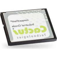
240S - Flash Memory Cactus - Free user manual and instructions
Find the device manual for free 240S Cactus in PDF.


| Product Type | USB Flash Drive |
| Brand | Cactus |
| Model | 240S |
| Capacity | 64 GB |
| Interface | USB 3.0 |
| Read Speed | Up to 100 MB/s |
| Write Speed | Up to 30 MB/s |
| Dimensions (L x W x H) | 60 mm x 20 mm x 10 mm |
| Weight | 10 g |
| Power Supply | USB bus-powered |
| Compatibility | Windows, macOS, Linux |
| File System | FAT32 (exFAT support) |
| Operating Temperature | 0°C to 60°C |
| Storage Temperature | -20°C to 85°C |
| Key Features | Plug and play, shockproof, LED indicator |
| Maintenance | Keep dry, avoid magnetic fields |
| Safety | No data loss when used properly |
| Spare Parts / Repairability | Not repairable; replace if faulty |
Frequently Asked Questions - 240S Cactus
User questions about 240S Cactus
0 question about this device. Answer the ones you know or ask your own.
Ask a new question about this device
Download the instructions for your Flash Memory in PDF format for free! Find your manual 240S - Cactus and take your electronic device back in hand. On this page are published all the documents necessary for the use of your device. 240S by Cactus.
USER MANUAL 240S Cactus
Industrial MLC -240S series CFast Card
Product Manual
June 7, 2023
www.cactus-tech.com
The information in this manual is preliminary and is subject to change without notice. Cactus Technologies ^® , Limited shall not be liable for technical or editorial errors or omissions contained herein; nor for incidental or consequential damages resulting from the furnishing, performance, or use of this material.
Cactus Technologies ^® makes no warranty, representation or guarantee regarding the suitability of its products for any particular purpose, nor does Cactus Technologies ^® assume any liability arising out of the application or use of its products, and specifically disclaims any and all liability, including without limitation consequential or incidental damages.
Cactus Technologies ^® products are not designed, intended or authorized for use as components in systems intended for surgical implant into the body or in other applications intended to support or sustain life or for any application where the failure of a Cactus Technologies ^® product can result in personal injury or death. Users of Cactus Technologies ^® products for such unintended and unauthorized applications shall assume all risk of such use and shall indemnify and hold Cactus Technologies ^® and its officers, employees, subsidiaries, affiliates and distributors harmless against all claims, costs, damages, expenses and attorney fees arising out of, directly or indirectly, any claim of personal injury or death associated with such unintended and unauthorized use, even if such claim alleges that Cactus Technologies ^® was negligent regarding the design or manufacture of the part.
All parts of the Cactus Technologies ^® documentation are protected by copyright law and all rights are reserved. This documentation may not, in whole or in part, be copied, photocopied, reproduced, translated, or reduced to any electronic medium or machine-readable form without prior consent, in writing, from Cactus Technologies ^® , Limited.
© 2005-2023 Cactus Technologies ^® Limited. All rights reserved.
Table of Contents
- Introduction to Cactus Technologies® Industrial MLC -240S Series CFast Products ....5
1.1.Supported Standards....6
1.2.Product Features....6
1.2.1.Host and Technology Independence....6
1.2.2.Defect and Error Management....6
1.2.3.Power Supply Requirements....7
2.Product Specifications....7
2.1.System Environmental Specifications....7
2.2.System Power Requirements....7
2.3.System Performance....8
2.4.System Reliability....8
2.5.Physical Specifications....8
2.5.1.CFast Card Physical Specifications....8
3.Capacities....11
4.Interface Description....12
4.1.CFast Pin Assignments and Pin Type....12
4.2.Electrical Specifications....13
4.2.1. Absolute Maximum Ratings....13
4.2.2.DC Characteristics....13
4.2.3.AC Characteristics....13
- ATA Drive Register Set Definition and Protocol....13
5.1.ATA Task File Definitions....14
5.1.1.Data Register....14
5.1.2.Error Register....14
5.1.3.Feature Register....14
5.1.4.Sector Count Register....14
5.1.5.Sector Number (LBA 7-0) Register....14
5.1.6.Cylinder Low (LBA 15-8) Register....15
5.1.7.Cylinder High (LBA 23-16) Register....15
5.1.8.Drive/Head (LBA 27-24) Register....15
5.1.9.Status Registers....15
5.1.10.Device Control Register....16
5.1.11.Drive Address Register....16
- ATA Command Description....17
6.1.ATA Command Set....17
6.1.1.Identify Drive—ECH....18
- S.M.A.R.T. Feature Set....20
7.1.S.M.A.R.T Data Structure....20
7.2.S.M.A.R.T Attributes....21
- Write Protect Feature....22
Appendix A. Ordering Information....23
Cactus Technologies, Limited
Appendix B. Technical Support Services....24
Appendix C.Cactus Technologies® Worldwide Sales Offices....25
Appendix D. Limited Warranty....26
1. Introduction to Cactus Technologies® Industrial MLC -240S Series CFast Products
Features:
- Solid state design with no moving parts
- Industry standard CFast Type I form factor
•Capacities from 8GB to 128GB - Compliant with Serial ATA 3.1 specifications
- ATA-8 compatible and CFast 2.0 compliant
•Supports Serial ATA Generation I/II/III transfer rate of 1.5/3.0/6.0 Gbps
•Support ATA SMART Feature Set
•Support ATA Security Feature Set
•Supports TRIM commands
•Supports NCQ, max. queue depth of 32 - ECC capable of correcting up to 66 bit errors per 1KB
- Enhanced error correction, < 1 error in 10 ^14 bits read
•SATA partial and slumber modes supported - Optional Write Protect feature
•Voltage support: 3.3V±5%
Cactus Technologies ^® CFast card is a high capacity solid-state flash memory product that complies with the Serial ATA 3.1 standard and is functionally compatible with a SATA hard disk drive. Cactus Technologies ^® CFast cards provide up to 128GB of formatted storage capacity.
Cactus Technologies® CFast product uses high quality Industrial Grade MLC NAND flash memory from Kioxia Corporation. In addition, it includes an on-drive intelligent controller that manages interface protocols, data storage and retrieval as well as ECC, defect handling and diagnostics, power management, and clock control. The controller's firmware is upgradeable, thus allowing feature enhancements and firmware updates while keeping the BOM stable.
1.1. Supported Standards
Cactus Technologies® CFast card is fully compatible with the following specification:
•ATA 8 Specification published by ANSI
- Serial ATA 3.1 Specification published by the Serial ATA International Organization
•CFast 2.0 Specification published by CFA
1.2. Product Features
Cactus Technologies ^® Industrial MLC CFast card contains a high level, intelligent controller. This intelligent controller provides many capabilities including the following:
- Standard ATA register and command set (same as found on most magnetic disk drives).
- Manages details of erasing and programming flash memory independent of the host system
- Sophisticated defect managing capabilities (similar to magnetic disk drives).
- Sophisticated system for error recovery using powerful error correction code (ECC).
- Intelligent power management for low power operation.
1.2.1. Host and Technology Independence
Cactus Technologies® Industrial MLC CFast card appears as a standard SATA disk drive to the host system. The drive utilizes a 512-byte sector which is the same as that in an IDE magnetic disk drive. To write or read a sector (or multiple sectors), the host computer software simply issues an ATA Read or Write command to the drive as per the SATA protocol. The host software then waits for the command to complete. The host system does not get involved in the details of how the flash memory is erased, programmed or read as this is all managed by the built-in controller in the drive. Also, with the intelligent on-board controller, the host system software will not require changing as new flash memory evolves. Thus, systems that support the Cactus Technologies® Industrial MLC CFast products today will continue to work with future Cactus Technologies® Industrial MLC CFast cards built with new flash technology without having to update or change host software.
1.2.2. Defect and Error Management
Cactus Technologies® Industrial MLC CFast card contains a sophisticated defect and error management system similar to those found in magnetic disk drives. The defect management is completely transparent to the host and does not consume any user data space.
The soft error rate for Cactus Technologies ^® Industrial MLC CFast card is much lower than that of magnetic disk drives. In the extremely rare case where a read error does occur, the drive has sophisticated ECC to recover the data.
These defect and error management systems, coupled with the solid-state construction, give Cactus Technologies® Industrial MLC CFast cards unparalleled reliability.
1.2.3. Power Supply Requirements
Cactus Technologies® Industrial MLC CFast card operates at a voltage range of 3.3 volts ± 5%.
2.Product Specifications
For all the following specifications, values are defined at ambient temperature and nominal supply voltage unless otherwise stated.
2.1. System Environmental Specifications
Table 2-1. Environmental Specifications
| Cactus Technologies®Industrial MLC CFast | ||
| Temperature Operating: 0°C to +70°C (Standard) | -40°C to 85°C (Extended) | |
| Humidity Operating & Non-Operating: | 8% to 95%, non-condensing | |
| Vibration Operating & Non-Operating: | 20G, MIL-STD-883G Method 2005.2, Condition A | |
| Shock Operating & Non-Operating: | 3,000 G, MIL-STD-883G Method 2002.4, Condition C | |
| Altitude (relative to sea level) | Operating & Non-Operating: | 100,000 feet maximum |
2.2. System Power Requirements
Table 2-2. Power Requirements
| Cactus Technologies® Industrial MLC CFast | ||
| DC Input Voltage (VCC)100 mV max. ripple (p-p) | 3.3V ±5% | |
| (Maximum Average Value)See Notes. | Idle:Reading:Writing: | 90 mA410 mA530 mA |
NOTES: All values quoted are typical at ambient temperature and nominal supply voltage unless otherwise stated.
Sleep mode is specified under the condition that all drive inputs are static CMOS levels and in a "Not Busy" operating state.
2.3. System Performance
All performance timings assume the drive controller is in the default (i.e., fastest) mode.
Table 2-3. Performance
| Read Transfer Rate 8GB | Up to 140MBytes/sec | |
| 16GB | Up to 280MBytes/sec | |
| 32GB | Up to 280MBytes/sec | |
| 64GB | Up to 350MBytes/sec | |
| 128GB | Up to 350MBytes/sec | |
| Write Transfer Rate 8GB | Up to 25 Mbytes/sec | |
| 16GB | Up to 50 Mbytes/sec | |
| 32GB | Up to 45 Mbytes/sec | |
| 64GB | Up to 90 Mbytes/sec | |
| 128GB | Up to 180MBytes/sec |
2.4. System Reliability
Table 2-4. Reliability
| Data Reliability | < 1 non-recoverable error in 10^14 bits READ |
| Endurance (estimated TBW): | Up to 3TB/GB: |
| 8GB | 24TB |
| 16GB | 48TB |
| 32GB | 96TB |
| 64GB | 192TB |
| 128GB | 384TB |
Note: estimated TBW assumes a workload of large block, sequential writes; endurance can be significantly reduced if the workload consists of mostly random, small block write.
2.5. Physical Specifications
The following sections provide the physical specifications for Cactus Technologies® Industrial MLC CFast products.
2.5.1. CFast Card Physical Specifications
Table 1: Type I CFast Card Physical Specifications
| Length: | 36.4 ± 0.15 mm (1.433 ±.006 in.) |
| Width: | 42.80 ± 0.10 mm (1.685 ±.004 in.) |
| Thickness Including Label Area: | 3.6 mm maximum (.1418 in maximum). |
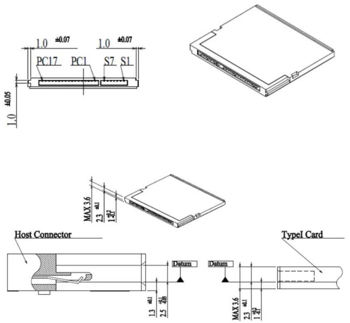
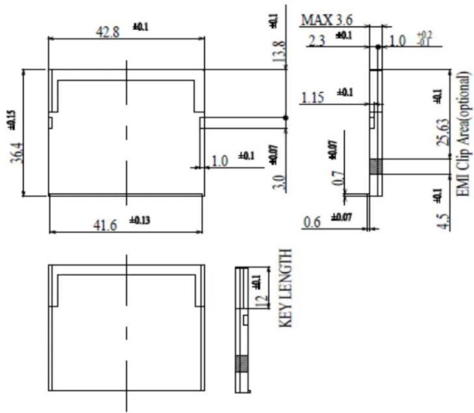
Figure 2-1. Type I CFast Card Dimensions
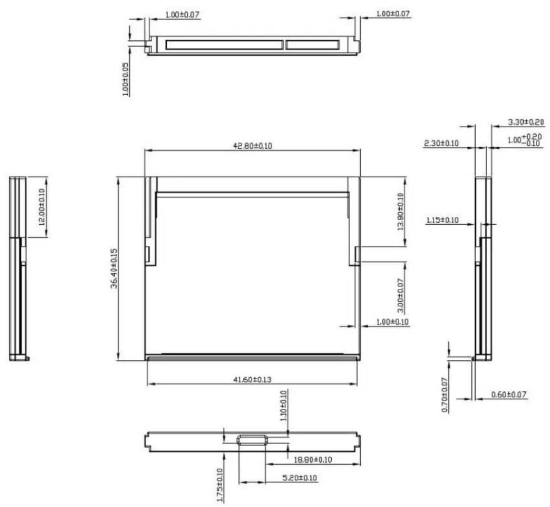
Figure 2-2. Type I CFast Card Write Protect Switch Dimensions
3.Capacities
Cactus Technologies® Industrial MLC CFast cards are available in the following capacities:
Std. Temp. 8GB 16GB 32GB 64GB 128GB
Ext. Temp. 16GB 32GB 64GB 128GB
4. Interface Description
The following sections provide detailed information on the Cactus Technologies® Industrial MLC CFast card interface.
4.1. CFast Pin Assignments and Pin Type
Cactus Technologies® CFast signal pinout conforms to CFA specifications. The signal/pin assignments and descriptions are listed in Table 3-5.
| Number | Segment | Name | Type | Description | Mating Sequence |
| S1 | SATA | SGND | Signal GND | Ground for signal integrity | 1^st |
| S2 | SATA | A+ | SATA Differential | Signal Pair A | 2^nd |
| S3 | SATA | A- | SATA Differential | 2^nd | |
| S4 | SATA | SGND | Signal GND | Ground for signal integrity | 1^st |
| S5 | SATA | B- | SATA Differential | Signal Pair B | 2^nd |
| S6 | SATA | B+ | SATA Differential | 2^nd | |
| S7 | SATA | SGND | Signal GND | Ground for signal integrity | 1^st |
| Key | |||||
| Key | |||||
| PC1 | PWR/CTL | CDI | Input | Card Detect In | 3^rd |
| PC2 | PWR/CTL | PGND | Device GND | 1^st | |
| PC3 | PWR/CTL | DEVSLP | DEVSLP Card Input | DevSleep Power State Enable No Connect | 2^nd |
| PC4 | PWR/CTL | Reserved ^1 | 2^nd | ||
| PC5 | PWR/CTL | Reserved ^1 | 2^nd | ||
| PC6 | PWR/CTL | Reserved ^1 | 2^nd | ||
| PC7 | PWR/CTL | PGND | Device GND | 1^st | |
| PC8 | PWR/CTL | LED1 | LED Output | LED Output ^1 | 2^nd |
| PC9 | PWR/CTL | LED2 | LED Output | LED Output ^1 | 2^nd |
| PC10 | PWR/CTL | Reserved ^1 | 2^nd | ||
| PC11 | PWR/CTL | Reserved | 2^nd | ||
| PC12 | PWR/CTL | IFDet | GND | Card output, connect to PGND on card ^2 | 2^nd |
| PC13 | PWR/CTL | PWR | 3.3V | Device Power (3.3V) | 2^nd |
| PC14 | PWR/CTL | PWR | 3.3V | Device Power (3.3V) | 2^nd |
| PC15 | PWR/CTL | PGND | Device GND | Device Ground | 1^st |
| PC16 | PWR/CTL | PGND | Device GND | Device Ground | 1^st |
| PC17 | PWR/CTL | CDO | Output | Card Detect Out | 3^rd 3 |
Table 3-5. CFast Pin Assignments and Pin Type
- These signals are provided for backwards compatibility with CFast v1.1; these signals may be used for different purposes in the future.
- IFDet shall be connected to GND on Cfast v2.0 compliant devices.
- DEVSLP feature is not supported, pin PC3 shall be No Connect.
4.2. Electrical Specifications
The following table defines all D.C. Characteristics for the CFast products. Unless otherwise stated, conditions are:
$$ \begin{array}{l} \mathrm{Vcc} = 3.3 \mathrm{V} \pm 5 \% \ \mathrm{Ta} = - 4 0 ^ {\circ} \mathrm{C} \text { to } 8 5 ^ {\circ} \mathrm{C} \ \end{array} $$
4.2.1. Absolute Maximum Ratings
| Parameter Symbol MIN | MAX Units | |||
| Storage Temperature Ts -55 +100 | °C | |||
| Operating Temperature T | A | -40 +85 | °C | |
| Vcc with respect to GND Vcc -0.3 3.6 V | ||||
4.2.2. DC Characteristics
| Parameter Symbol MIN | MAX Units | |||
| Input Voltage Vin -0.5 | V_cc + 0.5 V | |||
| Output Voltage | Vout | -0.3 | V_cc + 0.3 | V |
| Input Leakage Current | I_U | -10 | 10 | uA |
| Output Leakage Current | I_LO | -10 | 10 | uA |
| Input/Output Capacitance C | /C_o | 10 | pF | |
| Operating Current | I_CC | mA | ||
| Idle | 105 | |||
| Active | 535 |
4.2.3. AC Characteristics
Cactus Technologies ^® CFast products conforms to all AC timing requirements as specified in the CFA specifications. Please refer to that document for details of AC timing for all operation modes of the device.
5. ATA Drive Register Set Definition and Protocol
The communication to or from the CFast card is done using FIS. Legacy ATA protocol is supported by using the legacy mode defined in the SATA specifications. In this mode, the FIS has defined fields which provide all the necessary ATA task file registers for control and status information. The Serial ATA interface does not support Primary/Secondary or Master/Slave configurations. Each SATA channel supports only one SATA device, with the register selection as defined by the ATA standard.
5.1. ATA Task File Definitions
The following sections describes the usage of the ATA task file registers. Note that the Alternate Status Register of legacy ATA is not defined for SATA drives.
5.1.1. Data Register
The Data Register is a 16-bit register, and it is used to transfer data blocks between the SSD data buffer and the Host.
5.1.2. Error Register
This register contains additional information about the source of an error when an error is indicated in bit 0 of the Status register. The bits are defined as follows:
| D7 D6 D5 D4 D3 D2 D1 D0 | ||||
| BBK UNC 0 IDNF 0 ABRT 0 AMNF |
Bit 7 (BBK) This bit is set when a Bad Block is detected.
Bit 6 (UNC) This bit is set when an Uncorrectable Error is encountered.
Bit 5 This bit is 0.
Bit 4 (IDNF) The requested sector ID is in error or cannot be found.
Bit 3 This bit is 0.
Bit 2 (Abort) This bit is set if the command has been aborted because of a status condition: (Not Ready, Write Fault, etc.) or when an invalid command has been issued.
Bit 1 This bit is 0.
Bit 0 (AMNF) This bit is set in case of a general error.
5.1.3. Feature Register
This register provides information regarding features of the SSD that the host can utilize.
5.1.4. Sector Count Register
This register contains the number of sectors of data requested to be transferred on a read or write operation between the host and the SSD. If the value in this register is zero, a count of 256 sectors is specified. If the command was successful, this register is zero at command completion. If not successfully completed, the register contains the number of sectors that need to be transferred in order to complete the request.
5.1.5. Sector Number (LBA 7-0) Register
This register contains the starting sector number or bits 7-0 of the Logical Block Address (LBA) for any SSD data access for the subsequent command.
5.1.6. Cylinder Low (LBA 15-8) Register
This register contains the low order 8 bits of the starting cylinder address or bits 15-8 of the Logical Block Address.
5.1.7. Cylinder High (LBA 23-16) Register
This register contains the high order bits of the starting cylinder address or bits 23-16 of the Logical Block Address.
5.1.8. Drive/Head (LBA 27-24) Register
The Drive/Head register is used to select the drive and head. It is also used to select LBA addressing instead of cylinder/head/sector addressing. The bits are defined as follows:
Bit 7 This bit is set to 1.
Bit 6 LBA is a flag to select either Cylinder/Head/Sector (CHS) or Logical Block Address Mode (LBA). When LBA=0, Cylinder/Head/Sector mode is selected. When LBA=1, Logical Block Address is selected. In Logical Block Mode, the Logical Block Address is interpreted as follows:
LBA07-LBA00: Sector Number Register D7-D0.
LBA15-LBA08: Cylinder Low Register D7-D0.
LBA23-LBA16: Cylinder High Register D7-D0.
LBA27-LBA24: Drive/Head Register bits HS3-HS0.
Bit 5 This bit is set to 1.
Bit 4 (DRV) DRV is the drive number. This should always be set to 0.
Bit 3 (HS3) When operating in the Cylinder, Head, Sector mode, this is bit 3 of the head number. It is Bit 27 in the Logical Block Address mode.
Bit 2 (HS2) When operating in the Cylinder, Head, Sector mode, this is bit 2 of the head number. It is Bit 26 in the Logical Block Address mode.
Bit 1 (HS1) When operating in the Cylinder, Head, Sector mode, this is bit 1 of the head number. It is Bit 25 in the Logical Block Address mode.
Bit 0 (HSO) When operating in the Cylinder, Head, Sector mode, this is bit 0 of the head number. It is Bit 24 in the Logical Block Address mode.
5.1.9. Status Registers
These registers return the status when read by the host. Reading the Status register does clear a pending interrupt while reading the Auxiliary Status register does not. The meaning of the status bits are described as follows:
| D7 D6 D5 D4 D3 D2 D1 D0 | |||||
| BUSY RDY DWF DSC DRQ CORR | 0 | ERR | |||
Bit 7 (BUSY) The busy bit is set when the device has access to the command buffer and registers and the host is locked out from accessing the command register and buffer. No other bits in this register are valid when this bit is set to a 1.
Bit 6 (RDY) RDY indicates whether the device is capable of performing operations requested by the host. This bit is cleared at power up and remains cleared until the device is ready to accept a command.
Bit 5 (DWF) This bit, if set, indicates a write fault has occurred.
Bit 4 (DSC) This bit is set when the device is ready.
Bit 3 (DRQ) The Data Request is set when the device requires that information be transferred either to or from the host through the Data register.
Bit 2 (CORR) This bit is set when a Correctable data error has been encountered and the data has been corrected. This condition does not terminate a multi-sector read operation.
Bit 1 (IDX) This bit is always set to 0.
Bit 0 (ERR) This bit is set when the previous command has ended in some type of error. The bits in the Error register contain additional information describing the error.
5.1.10. Device Control Register
This register is used to control the drive interrupt request and to issue an ATA soft reset to the drive. The bits are defined as follows:
Bit 7 This bit is used in 48-bit addressing mode. When cleared, the host can read the most recently written values of the Sector Count,Drive/Head and LBA registers. When set, the host will read the previous written values of these registers. A write to any Command block register will clear this bit.
Bit 6 This bit is an X (Do not care).
Bit 5 This bit is an X (Do not care).
Bit 4 This bit is an X (Do not care).
Bit 3 This bit is ignored by the drive.
Bit 2 (SW Rst) This bit is set to 1 in order to force the drive to perform an AT Disk controller Soft Reset operation. The drive remains in Reset until this bit is reset to '0'.
Bit 1 (-IEn) The Interrupt Enable bit enables interrupts when the bit is 0. When the bit is 1, interrupts from the drive are disabled. This bit is set to 0 at power on and Reset.
Bit 0 This bit is ignored by the drive.
5.1.11. Drive Address Register
This register is provided for compatibility with the AT disk drive interface. It is recommended that this register not be mapped into the host's I/O space because of potential conflicts on Bit 7. The bits are defined as follows:
Bit 7 This bit is unknown. Implementation Note:
Conflicts may occur on the host data bus when this bit is provided by a Floppy Disk Controller operating at the same addresses as the SSD. Following are some possible solutions to this problem:
-
Locate the SSD at a non-conflicting address (i.e., Secondary address (377) when a Floppy Disk Controller is located at the Primary addresses).
-
Do not install a Floppy and a SSD in the system at the same time.
-
Implement a socket adapter that can be programmed to (conditionally) tri-state D7 of I/O address 3F7/377 when a SSD product is installed and conversely to tri-state D6-D0 of I/O address 3F7/377 when a floppy controller is installed.
-
Do not use the SSD's Drive Address register. This may be accomplished by either a) If possible, program the host adapter to enable only I/O addresses 1F0-1F7, 3F6 (or 170-177, 176) to the SSD or b) if provided use an additional Primary/Secondary configuration in the SSD that does not respond to accesses to I/O locations 3F7 and 377. With either of these implementations, the host software must not attempt to use information in the Drive Address Register.
Bit 6 (-WTG) This bit is 0 when a write operation is in progress, otherwise, it is 1.
Bit 5 (-HS3) This bit is the negation of bit 3 in the Drive/Head register.
Bit 4 (-HS2) This bit is the negation of bit 2 in the Drive/Head register.
Bit 3 (-HS1) This bit is the negation of bit 1 in the Drive/Head register.
Bit 2 (-HS0) This bit is the negation of bit 0 in the Drive/Head register.
Bit 1 (-nDS1) This bit is 0 when drive 1 is active and selected.
Bit 0 (-nDS0) This bit is 0 when the drive 0 is active and selected.
6. ATA Command Description
This section defines the ATA command set supported by the Cactus Technologies® CFast card.
6.1. ATA Command Set
Table 5-6 summarizes the supported ATA command set.
Table 5-6. ATA Command Set
| COMMAND Code | |
| Check Power Mode E5h, 98h | |
| Data Set Management 06h | |
| Execute Drive Diagnostic 90h | |
| Flush Cache E7h | |
| Flush Cache Ext EAh | |
| Identify Drive ECh | |
| Idle E3h, 97h | |
| Idle Immediate E1h, 95h | |
| Initialize Drive Parameters 91h | |
| NOP | 00h |
| Read Buffer | E4h |
| Read DMA | C8h |
| Read DMA Ext 25h | |
| Read Multiple | C4h |
| Read Multiple Ext | 29h |
| Read FPDMA Queued 60h | |
| Read Native Max Address | F8h |
| Read Native Max Address Ext | 27h |
| Read Sector(s) | 20h, 21h |
| Read Sector(s) Ext 24h | |
| Read Verify Sector(s) 40h, 41h | |
| Read Verify Sector(s) Ext 42h | |
| Security Disable Password F6h | |
| Security Erase Prepare F3h | |
| Security Erase Unit F4h | |
| Security Freeze Lock F5h | |
| Security Set Password F1h | |
| Security Unlock F2h | |
| Seek 70h | |
| Set Features EFh | |
| Set Max Address F9h | |
| Set Max Address Ext 37h | |
| Set Max Freeze Lock | F9h |
| Set Max Lock | F9h |
| Set Max Unlock | F9h |
| Set Multiple Mode | C6h |
| Sleep | E6h, 99h |
| SMART | B0h |
| Stand By | E2h, 96h |
| Stand By Immediate | E0h, 94h |
| Write Buffer | E8h |
| Write DMA | Cah, CBh |
| Write DMA Ext | 35h |
| Write FPDMA Queued | 61h |
| Write Multiple | C5h |
| Write Multiple Ext | 39h |
| Write Sector(s) | 30h, 31h |
| Write Sector(s) Ext 34h | |
6.1.1. Identify Drive—ECH
The Identify Drive command enables the host to receive parameter information from the drive. This command has the same protocol as the Read Sector(s) command. The parameter words in the buffer have the arrangement and meanings defined in Table 5-7. All reserved bits or words are zero. Table 5-7 is the definition for each field in the Identify Drive Information.
Table 5-7. Identify Drive Information
| Word Address | Default Value | Data Field Type Information |
| 0 | 044AH | General configuration bit-significant information. |
| 1 | XXXXH | Default number of cylinders; capacity dependent. |
| 2 | 0000H | Reserved. |
| 3 | 00XXH | Default number of heads; capacity dependent. |
| 4 | 0000H | Number of unformatted bytes per track. |
| 5 | 0240H | Number of unformatted bytes per sector. |
| 6 | XXXXH | Default number of sectors per track; capacity dependent. |
| 7-8 | XXXXH,XXXXH | Number of sectors per drive (Word 7 = MSW, Word 8 = LSW); capacity dependent. |
| 9 | 0000H | Reserved. |
| 10-19 | aaaa | Serial number in ASCII (Right Justified). |
| 20 | 0002H | Buffer type (dual ported multi-sector) |
| Word Address | Default Value Data Field Type Information | |
| 21 0002H Buffer size in 512 bytes increments | ||
| 22 0000H # of ECC bytes passed in R/W Long commands | ||
| 23-26 aaaa Firmware revision in ASCII . Big Endian Byte Order in Word. | ||
| 27-46 aaaa Model number in ASCII (Left Justified) Big Endian Byte Order in Word. | ||
| 47 8001H Maximum number of sectors on Read/Write Multiple command: 1 | ||
| 48 0000H Double Word not supported. | ||
| 49 0F00H Capabilities: DMA, LBA, IORDY supported | ||
| 50 4000H Capabilities: device specific standby timer minimum | ||
| 51 0200H PIO data transfer cycle timing mode 2 | ||
| 52 0000H Single Word DMA data transfer cycle timing mode (not supported). | ||
| 53 0007H Data fields 54-58,64-70 and 88 are valid. | ||
| 54 XXXX Current numbers of cylinders. | ||
| 55 XXXX Current numbers of heads. | ||
| 56 XXXX Current sectors per track. | ||
| 57-58 XXXX Current capacity in sectors (LBAs) (Word 57 = LSW, Word 58 = MSW). | ||
| 59 0100H Multiple sector setting is valid; low byte is capacity dependent. | ||
| 60-61 XXXX Total number of sectors addressable in LBA Mode. | ||
| 62 0000H Single Word DMA transfer not implemented | ||
| Multiword DMA modes 0-2 are supported; upper byte reflects currently selected MWDMA mode. | ||
| 63 0207H | ||
| 64 0003H Advanced PIO modes supported (modes 3 and 4) | ||
| 65 0078H Minimum MWDMA cycle time per word is 120ns. | ||
| 66 0078H Recommended MWDMA cycle time is 120ns. | ||
| 67 0078H Minimum PIO cycle time without IORDY flow control is 120ns. | ||
| 68 0078H Minimum PIO cycle time with IORDY flow control is 120ns. | ||
| 69 4000H CFast specification supported | ||
| 70-74 0000H Reserved | ||
| 75 001FH Queue depth of 32 for NCQ | ||
| 76 070EH Supports Gen 1, Gen2 signaling rates, host initiated power management requests | ||
| 77 0080H Supports DEVSLP | ||
| 78 0148H Device supports initiating interface power management | ||
| 79 0040H Reserved | ||
| 80 03F0H Major version number | ||
| 81 0000H No minor revision reported. | ||
| 742BH | Command set: NOP, READ BUFFER, WRITE BUFFER, HPA, volatile write cache, power management feature set, Security Mode feature set, SMART feature set | |
| 82 | ||
| 7500H 48-bit mode supported; Flush Cache/Flush Cache Ext, LAB48, microcode download supported. | ||
| 83 | ||
| 84 4023H World wide name, general purpose logging supported | ||
| 85 74XXH Feature status | ||
| 86 B401H Feature status | ||
| 87 4120H Feature status | ||
| 88 XX7FH UDMA Modes 0-6 supported. | ||
| 89 0003H Time for Security Erase Unit | ||
| 90 0001H Time for Enhanced Security Erase Unit not specified. | ||
| 91 0000H Reserved | ||
| 92 | XXXXH Master password revision code | |
| 93-99 0000H Reserved | ||
| 100-103 | XXXXH Maximum user LBA for 48-bit addressing mode. | |
| 104 | 0000H Reserved | |
| 105 | 0100H Max. number of 512byte blocks per TRIM command | |
| 106-127 | 0000H Reserved | |
| 128 | 0XXXH Security status | |
| 129-159 | XXXXH Vendor specific | |
| 160 | 0000H CFA Power mode | |
| Word Address | Default Value Data Field Type Information |
| 161 0000H CFast specific support | |
| 162 0000H CPRM not supported | |
| 163 0000H CFA Advanced modes: not relevant for CFast | |
| 164-168 0000H Reserved | |
| 169 0001H Data Set Management supported | |
| 170-216 0000H Reserved | |
| 217 0001H Solid State Device | |
| 218-221 0000H Reserved | |
| 222 107FH Transport major revision | |
| 223-254 0000H Reserved | |
| 255 XXXXH checksum | |
7. S.M.A.R.T. Feature Set
Cactus Technologies ^® -240 Series CFast card supports S.M.A.R.T. attribute reporting. This following subcommands are supported when programmed into the Feature Register:
| Value Command | Value | Command |
| D0h Read Data D5h Reserved | ||
| D1h Read Attribute Threshold D6h Reserved | ||
| D2h Enable/Disable Autosave D8h Enable SMART operations | ||
| D3h Save Attribute Values D9h Disable SMART operations | ||
| D4h Execute OFF-LINE Immediate DAh Return Status |
7.1. S.M.A.R.T Data Structure
The Read Data commands returns 512 bytes of data in the following structure:
| Byte | Description |
| 0-1 | Revision code |
| 2-361 | Vendor specific |
| 362 | Off-line data collection status |
| 363 | Self-test execution status byte |
| 364-365 | Total time in seconds to complete off-line data collection activities |
| 366 | Vendor specific |
| 367 | Off-line data collection capabilities |
| 368-369 | SMART capabilities |
| 370 | Error loading capabilities: bit[7:1] – reserved: bit[0]: 1=device error loading supported |
| Bvte | Description |
| 371 | Vendor specific |
| 372 | Short self-test routine recommended pollina time (in minutes) |
| 373 | Extended self-test routine recommended pollina time (in minutes) |
| 374 | Conveyance self-test routine recommended pollina time (in minutes) |
| 375-385 | Reserved |
| 386-395 | Firmware Version/Date Code |
| 396-397 | Reserved |
| 398-399 | Reserved |
| 400-405 | 'SMI2246' |
| 406-510 | Vendor specific |
| 511 | Data structure checksum |
7.2. S.M.A.R.T Attributes
The following table lists the attributes returned in bytes 2-361 of the 512-byte SMART data. Each attribute has 12 bytes, byte 0 is Attribute ID, bytes 1-2 are status flags, bytes 3-4 are reserved flags, the table below shows the definition of bytes 5-11:
| Attribute ID | Attribute values Attribute Name | ||
| 01h MSB 00 00 00 00 00 00 Read error rate | |||
| 05h LSB MSB 00 00 00 00 00 Reallocated sectors count | |||
| 09h LSB MSB 00 00 00 Power on hours | |||
| 0Ch LSB MSB 00 00 00 Power cycle count | |||
| A0h LSB MSB 00 00 00 Uncorrectable sector count when read/write | |||
| A1h LSB MSB 00 00 00 00 00 Number of valid spare block | |||
| A3h LSB MSB 00 00 00 00 00 Number of initial invalid block | |||
| A4h LSB MSB 00 00 00 Total erase count | |||
| A5h LSB MSB 00 00 00 Max. Erase count | |||
| A6h LSB MSB 00 00 00 Min. Erase count | |||
| A7h LSB MSB 00 00 00 Average erase count | |||
| A8h LSB MSB 00 00 00 Max. erase count spec. | |||
| A9h LSB MSB 00 00 00 Percent remaining life | |||
| AFh LSB MSB 00 00 00 Program fail count in worst die | |||
| B0h LSB MSB 00 00 00 00 00 Erase fail count in worst die | |||
| B1h LSB MSB 00 00 00 Total wear level count | |||
| B2h LSB MSB 00 00 00 00 00 Runtime invalid block count | |||
| B5h LSB MSB 00 00 00 Total program fail count | |||
| B6h LSB MSB 00 00 00 00 00 Total erase fail count | |||
| BBh LSB MSB 00 00 00 Uncorrectable error count | |||
| C0h LSB MSB 00 00 00 Power-off retract count | |||
| C2h MSB 00 00 00 00 00 00 Temperature | |||
| C3h LSB MSB 00 00 00 Hardware ECC recovered | |||
| C4h LSB MSB 00 00 00 Reallocation event count | |||
| C6h LSB MSB 00 00 00 Uncorrectable error count | |||
| C7h LSB MSB 00 00 00 00 UltraDMA CRC error count | |||
| E1h LSB MSB Total LBAs written (in units of 32MB) | |||
| E8h LSB MSB 00 00 00 00 00 Available reserve space | |||
| F1h LSB MSB Total LBAs written (in units of 32MB) | |||
| F2h LSB MSB Total LBAs read (in units of 32MB) | |||
8. Write Protect Feature
Cactus Technologies® -240 Series CFast card supports optional Write Protect function using a physical write protect switch. When the switch is toggled to the WP position, the card is write protected. The setting of the switch is sensed only during power up time, changing the setting of this switch after power up will not alter the write protect behavior. However, to avoid any unintended side effects, it is recommended that this switch not be toggled when power is applied to the card.
When the write protect function is enabled, all data write commands to the card will be accepted but the write data will be silently discarded. The card will follow all the data transfer handshake and will return successful status to the host. This method of handling write protection provides the best compatibility to host systems as simply rejecting write commands and returning error status may cause some operating systems to hang.
Appendix A. Ordering Information
Model KCXFY-240S-WP1
Where: X is drive capacities:
8G 8GB
16G 16GB
32G ---- 32GB
64G 64GB
128G 128GB
Where: Y is temperature grade:
blank ---- standard temp.
I---- extended temp.
Where: WP1 is optional Write Protect feature:
blank ---- standard
WP1 ---- w/ Write Protect switch
Example:
(1) 8GB CFast KC8GF-240S
(2) 16GB extended temp. CFast ---- KC16GFI-240S
(3) 8GB CFast w/ Write Protect ---- KC8GF-240S-WP1
Appendix B. Technical Support Services
B.1.Direct Cactus Technologies® Technical Support
Email: tech@cactus-tech.com
Cactus Technologies, Limited
Appendix C.Cactus Technologies® Worldwide Sales Offices
Email: sales@cactus-tech.com
Email: americas@cactus-tech.com
Appendix D. Limited Warranty
I. WARRANTY STATEMENT
Cactus Technologies® warrants its Industrial MLC Grade products only to be free of any defects in materials or workmanship that would prevent them from functioning properly for two years from the date of purchase or when estimated TBW is reached, whichever occurs first. This express warranty is extended by Cactus Technologies® Limited to customers of our products.
II. GENERAL PROVISIONS
This warranty sets forth the full extent of Cactus Technologies® responsibilities regarding the Cactus Technologies® Industrial MLC Grade Flash Storage Products. Cactus Technologies®, at its sole option, will repair, replace or refund the purchase price of the defective product. Cactus Technologies® guarantees our products meet all specifications detailed in our product manuals. Although Cactus Technologies® products are designed to withstand harsh environments and have the highest specifications in the industry, they are not warranted to never have failure and Cactus Technologies® does not warranty against incidental or consequential damages. Accordingly, in any use of products in life support systems or other applications where failure could cause injury or loss of life, the products should only be incorporated in systems designed with appropriate redundancy, fault tolerant or backup features.
III. WHAT THIS WARRANTY COVERS
For products found to be defective within two years of purchase, Cactus Technologies ^® will have the option of repairing, replacing or refunding the purchase price the defective product, if the following conditions are met:
A. The defective product is returned to Cactus Technologies ^® for failure analysis as soon as possible after the failure occurs.
B. An incident card filled out by the user, explaining the conditions of usage and the nature of the failure, accompanies each returned defective product.
C. No evidence is found of abuse or operation of products not in accordance with the published specifications, or of exceeding maximum ratings or operating conditions.
All failing products returned to Cactus Technologies® under the provisions of this limited warranty shall be tested to the product's functional and performance specifications. Upon confirmation of failure, each product will be analyzed, by whatever means necessary, to determine the root cause of failure. If the root cause of failure is found to be not covered by the above provisions, then the product will be returned to the customer with a report indicating why the failure was not covered under the warranty.
This warranty does not cover defects, malfunctions, performance failures or damages to the unit resulting from use in other than its normal and customary manner, misuse, accident or neglect; or improper alterations or repairs. Cactus Technologies® Limited may repair or replace, at its discretion, any product returned by its customers, even if such product is not covered under warranty, but is under no obligation to do so.
IV. RECEIVING WARRANTY SERVICE
According to Cactus Technologies ^® warranty procedure, defective product should be returned only with prior authorization from Cactus Technologies ^® Limited. Please contact Cactus Technologies ^® Customer Service department (tech@cactus-tech.com) with the following information: product model number and description, nature of defect, conditions of use, proof of purchase and purchase date. If approved, Cactus Technologies ^® will issue a Return Material Authorization or Product Repair Authorization number with shipping instructions.
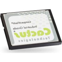
- Industrial MLC -240S series CFast Card
- Product Manual
- Table of Contents
- Cactus Technologies, Limited
- Introduction to Cactus Technologies® Industrial MLC -240S Series CFast Products
- Features:
- Supported Standards
- Product Features
- Host and Technology Independence
- Defect and Error Management
- Power Supply Requirements
- 2.Product Specifications
- System Environmental Specifications
- System Power Requirements
- System Performance
- System Reliability
- Physical Specifications
- CFast Card Physical Specifications
- 3.Capacities
- Interface Description
- CFast Pin Assignments and Pin Type
- Table 3-5. CFast Pin Assignments and Pin Type
- Electrical Specifications
- Absolute Maximum Ratings
- DC Characteristics
- AC Characteristics
- ATA Drive Register Set Definition and Protocol
- ATA Task File Definitions
- Data Register
- Error Register
- Feature Register
- Sector Count Register
- Sector Number (LBA 7-0) Register
- Cylinder Low (LBA 15-8) Register
- Cylinder High (LBA 23-16) Register
- Drive/Head (LBA 27-24) Register
- Status Registers
- Device Control Register
- Drive Address Register
- ATA Command Description
- ATA Command Set
- Identify Drive—ECH
- S.M.A.R.T. Feature Set
- S.M.A.R.T Data Structure
- S.M.A.R.T Attributes
- Write Protect Feature
- Appendix A. Ordering Information
- Example:
- Appendix B. Technical Support Services
- B.1.Direct Cactus Technologies® Technical Support
- Appendix C.Cactus Technologies® Worldwide Sales Offices
- Appendix D. Limited Warranty
- WARRANTY STATEMENT
- GENERAL PROVISIONS
- WHAT THIS WARRANTY COVERS
- RECEIVING WARRANTY SERVICE
Brand : Cactus
Model : 240S
Category : Flash Memory