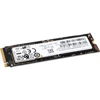
MZVL21T0HDLU - SSD SAMSUNG - Notice d'utilisation et mode d'emploi gratuit
Retrouvez gratuitement la notice de l'appareil MZVL21T0HDLU SAMSUNG au format PDF.


| Type de produit | SSD M.2 NVMe PCIe Gen4 |
| Capacité | 1 To (1024 Go) |
| Interface | PCI Express Gen4 x4, NVMe 1.3 |
| Format | M.2 2280 |
| Dimensions (L x l x H) | 80,00 x 22,00 x 2,38 mm (max) |
| Poids | 9,0 g (max) |
| Tension d'alimentation | 3,3 V ± 5% |
| Consommation active (lecture typique) | 5,8 W |
| Consommation active (écriture typique) | 5,6 W |
| Consommation au repos (idle) | 35 mW (avec L1.2 + APST) |
| Consommation en veille (sleep) | 5 mW (état PS4) |
| Lecture séquentielle (max) | 7 000 Mo/s |
| Écriture séquentielle (max) | 5 200 Mo/s |
| Lecture aléatoire (4K, QD32, max) | 1 000 000 IOPS |
| Écriture aléatoire (4K, QD32, max) | 850 000 IOPS |
| Endurance (TBW pour 1 To) | 600 To écrits |
| Fiabilité MTBF | 1,5 million d'heures |
| Taux d'erreur binaire (UBER) | < 1 secteur par 10^15 bits lus |
| Température de fonctionnement | 0 °C à 70 °C |
| Température de stockage | -40 °C à 85 °C |
| Résistance aux chocs (hors fonctionnement) | 1 500 G, 0,5 ms |
| Résistance aux vibrations (hors fonctionnement) | 20 G, 20-2000 Hz |
| Cryptage matériel | AES-XTS 256 bits (SED) |
| Technologies supportées | TurboWrite, APST, L1.2, TCG OPAL 2.0 |
| Normes de conformité | RoHS, CE, FCC, ICES-003, VCCI, BSMI |
FOIRE AUX QUESTIONS - MZVL21T0HDLU SAMSUNG
Questions des utilisateurs sur MZVL21T0HDLU SAMSUNG
0 question sur cet appareil. Repondez a celles que vous connaissez ou posez la votre.
Poser une nouvelle question sur cet appareil
Téléchargez la notice de votre SSD au format PDF gratuitement ! Retrouvez votre notice MZVL21T0HDLU - SAMSUNG et reprennez votre appareil électronique en main. Sur cette page sont publiés tous les documents nécessaires à l'utilisation de votre appareil MZVL21T0HDLU de la marque SAMSUNG.
MODE D'EMPLOI MZVL21T0HDLU SAMSUNG
M.2 NVMe PCIe SSD
specification
(PM9A1)
Datasheet
SAMSUNG ELECTRONICS RESERVES THE RIGHT TO CHANGE PRODUCTS, INFORMATION AND SPECIFICATIONS WITHOUT NOTICE.
Products and specifications discussed herein are for reference purposes only. All information discussed herein is provided on an "AS IS" basis, without warranties of any kind.
This document and all information discussed herein remain the sole and exclusive property of Samsung Electronics. No license of any patent, copyright, mask work, trademark or any other intellectual property right is granted by one party to the other party under this document, by implication, estoppel or otherwise.
Samsung products are not intended for use in life support, critical care, medical, safety equipment, or similar applications where product failure could result in loss of life or personal or physical harm, or any military or defense application, or any governmental procurement to which special terms or provisions may apply.
For updates or additional information about Samsung products, contact your nearest Samsung office.
All brand names, trademarks and registered trademarks belong to their respective owners.
© 2020 Samsung Electronics Co., Ltd. All rights reserved.
Revision History
| Revision No. | History | Draft Date | Remark | Created by | Review by |
| 1.0 1. initial version June.20, 2020 Final H.O Kim Y.B Jeon | |||||
| 1.1 1. Modify Performance and MTBF2. Modify Power and DTT information3. Modify minor typo | Sep.18, 2020 Revision Y.J.Kim | Y.B Jeon |
PM9A1 Series
| PART NUMBER | Capacity1) | LBA Count2) |
| MZVL2256HCHQ-0000/07 256GB 500,118,192 | ||
| MZVL2512HCJQ-0000/07 512GB 1,000,215,216 | ||
| MZVL21T0HCLR-0000/07 1024GB 2,000,409,264 | ||
| MZVL22T0HBLB-0000/07 2048GB 4,000,797,360 | ||
| Features Reliability Specifications | ||
| • PCIe Gen4 16Gb/s Interface, up to 4 Lanes | UBER | < 1 sector per 10^15 bits read |
| • Compliant with PCI Express Base Specification Rev. 4.0 | MTBF 1.5 Million Hours | |
| • Compliant with PCI Express M.2 Specification Rev. 1.1 | Environmental Specifications | |
| • Compliant with NVMe Express specification Rev. 1.3 | Temperature | |
| • Power Saving Modes: | Operating4) | 0°C to 70°C |
| - Supporting APST Non-operating | -40°C to 85°C | |
| - Supporting L1.2 Mode Humidity (non-condensing) | ||
| • Support Admin & NVM Command Set | Non-operating 5 ~ 95% | |
| • RoHS Compliant | Linear Shock | |
| • Hardware based AES-XTS 256-bit Encryption Engine for SED7) | Non-operating | 1,500 Gpeak(0.5ms duration with 1/2 sine wave) |
| • TCG OPAL (v2.1) Compliant for SED7) | Vibration | |
| Drive Configuration | Non-operating | 20 Gpeak(20 ~ 2,000 Hz, Sinusoidal) |
| Capacity | 256/512/1024/2048GB | Power Specifications |
| Form Factor | M.2 | Supply Voltage |
| Interface | PCI Express Gen4 x4 | Voltage Ripple/Noise(max.) |
| Bytes per Sector | 512Byte | Active5) (Typ., RMS) |
| Performance Specifications3) | - Read | 5.8W |
| Data Transfer Rate (128KB) | - Write | 5.6W |
| Sequential Read | (256GB) Up to 6,400 MB/s | Idle6) |
| (512GB) Up to 6,900 MB/s | Sleep6) | |
| (1024GB) Up to 7,000 MB/s | Physical Dimension | |
| (2048GB) Up to 7,000 MB/s | Width | |
| Length | ||
| Sequential Write | (256GB) Up to 2,700 MB/s | Height |
| (512GB) Up to 5,000 MB/s | - Single Side | |
| (1024GB) Up to 5,100 MB/s | Weight | |
| (2048GB) Up to 5,200 MB/s | ||
| Data I/O Speed (4KB) | ||
| Random Read | (256GB) Up to 500K IOPS | Note : Specifications are subject to change without notice. |
| (512GB) Up to 800K IOPS | 1) 1GB = 1,000,000,000 Bytes, Unformatted Capacity.User accessible capacity may vary depending on operating environment and formatting. | |
| (1024GB) Up to 1,000K IOPS | 2) 1 Sector = 512Bytes, Max. LBA represents the total user addressable sectors in LBA mode and calculated by IDEMA rule | |
| (2048GB) Up to 1,000K IOPS | 3) Actual performance may vary depending on use conditions and environment. Performance measurements based on TurboWrite technology. | |
| 4) Measured by SMART Temperature. Proper airflow recommended over 70°C | ||
| Random Write | (256GB) Up to 600K IOPS | 5) Active power is measured on sequential write and read. |
| (512GB) Up to 800K IOPS | 6) Idle Power is measured on PS3 (L1.2 Enable) and Sleep Power is measured on PS4 (L1.2 Enable). Actual measurements result may vary depend on use conditions and environment. | |
| (1024GB) Up to 850K IOPS | 7) SED is applied only for 07 buckets. | |
| (2048GB) Up to 850K IOPS | ||
Table Of Contents
1.0 INTRODUCTION ....5
1.1 General Description....5
1.2 Product List....5
1.3 Ordering Information....5
2.0 PRODUCT SPECIFICATION....6
2.1 Capacity....6
2.2 Performance....6
2.3 Power 6
2.4 Reliability 7
2.4.1 MTBF 7
2.4.2 UBER 7
2.4.3 TBW 7
2.5 Environmental Specification 7
3.0 MECHANICAL SPECIFICATION....8
3.1 Physical dimensions and Weight 8
3.2 Form Factor 8
4.0 INTERFACE SPECIFACION 9
4.1 Connector Dimension and Pin Location 9
4.2 Pin Assignments and Definitions 9
5.0 PCI and NVM Express registers 11
5.1 PCI Express Registers 11
5.1.1 PCI Register Summary 11
5.1.2 PCI Configuration Header Space Registers Detail 11
5.1.2.1 PCI Configuration Header Space Registers 11
5.1.3 PCI Capability Registers Detail 15
5.1.3.1 PCI Power Management Capability 15
5.1.3.2 Message Signaled Interrupt (MSI) Capability 16
5.1.3.3 PCI Express Capability 17
5.1.3.4 MSI-X Capability 21
5.1.4 PCI Extended Capability Details 22
5.1.4.1 Advanced Error Reporting Registers 22
5.1.4.2 Alternative Routing-ID(ARI) Capability 25
5.1.4.3 Secondary PCI Express Capability 26
5.1.4.4 Physical Layer 16.0 GT/s Capability 27
5.1.4.5 Margining Extended Capability 29
5.1.4.6 Latency Tolerance Reporting Capability Registers....31
5.1.4.7 L1 Substates Extended Capability 31
5.1.4.8 Data Link Feature Extended Capability 32
5.2 NVM Express Registers 34
5.2.1 Register Summary 34
5.2.2 Controller Registers 34
6.0 Supported Command Set 38
6.1 Admin Command Set 38
6.1.1 Identify Command 39
6.2 NVM Express I/O Command Set 45
6.3 SMART/Health Information....45
7.0 PRODUCT COMPLIANCE 46
7.1 Product regulatory compliance and Certifications 46
8.0 References....48
1.0 INTRODUCTION
1.1 General Description
This document describes the specifications of PM9A1 SSD which uses PCIe interface.
The PM9A1 is fully consist of semiconductor device and using NAND Flash Memory which has a high reliability and a high technology in a small form factor. It supports Peripheral Component Interconnect Express (PCIe) 4.0 interface standard up to 4 lanes and shows much faster performance than previous SATA SSDs.
The PM9A1 provides 256GB, 512GB, 1024GB and 2048GB capacities. It's sequential performance is up to 7,000MB/s for read operation and 5,200MB/s for write operation by 4 lanes. It's random performance is up to 1,000k IOPS for read and 850k IOPS for write operation.
1.2 Product List
[Table 1] Product Line-up
| Form Factor Capacity Part Number | ||
| M.2 | 256GB | MZVL2256HCHQ-00A00/07MZVL2256HCHQ-00B00/07 |
| 512GB | MZVL2512HCJQ-00A00/07MZVL2512HCJQ-00B00/07 | |
| 1024GB | MZVL21T0HCLR-00A00/07MZVL21T0HCLR-00B00/07 | |
| 2048GB | MZVL22T0HBLB-00A00/07MZVL22T0HBLB-00B00/07 | |
1.3 Ordering Information
| M | Z | X | X | X | X | X | X | X | X | X | X | X | - | X | X | X | X | X |
| 1 | 2 | 3 | 4 | 5 | 6 | 7 | 8 | 9 | 10 | 11 | 12 | 13 | 14 | 15 | 16 | 17 | 18 |
-
Memory (M)
-
Module Classification Z: SSD
-
Form Factor V: PCIe M.2 (22*80, PCIe x4)
-
Line-Up L: VNAND 3bit MLC
-
SSD Controller 2: Elpis
6\~8. SSD Density 256: 256GB 512: 512GB 1T0: 1024GB 2T0: 2048GB
-
NAND PKG + NAND Voltage H: BGA (LF,HF)
-
Flash Generation B: 2nd Generation C: 3rd Generation
11\~12. NAND Density HQ: 1T QDP 4CE JQ: 2T ODP 4CE LR: 4T HDP 4CE LB : 8T HDP 4CE
-
"-"
-
Default "0"
-
HW revision 0: No revision
-
Region Code A: Region A B: Region B
17\~18. Customer 00: World Wide (non-SED) 07 : World Wide (SED)
2.0 PRODUCT SPECIFICATION
2.1 Capacity
[Table 2] User Addressable Sectors
| Capacity^1) | LBA Count^2) |
| 256GB 500,118,192 | |
| 512GB 1,000,215,216 | |
| 1024GB 2,000,409,264 | |
| 2048GB 4,000,797,360 |
NOTE:
1) Gigabyte (GB) = 1,000,000,000 Bytes
2) Max. LBA shown in Table 1 represents the total user addressable sectors in LBA mode and calculated by IDEMA rule.(1 Sector = 512Bytes)
2.2 Performance ^1)
[Table 3] Drive Performance
| Parameter Unit | Queue Depth(QD) | 256GB 512GB | 1024GB 2048GB | |||
| Sequential Read^2) (Up to) | MB/s 32 | 6,400/4,900^5) | 6,900/6,300^5) | 7,000/6,600^5) | 7,000/6,600^5) | |
| Sequential Write^2) (Up to) | MB/s 32 | 2,700/500^5) | 5,000/1,050^5) | 5,100/1,900^5) | 5,200/2,000^5) | |
| Random Read(Up to) | IOPS^3) | 1 | 18K 18K 18K | 18K | ||
| IOPS^4) | 32 500K/300K 800K/500K | 1,000K/750K | 1,000K/750K | |||
| Random Write(Up to) | IOPS^3) | 1 | 53K 53K 53K | 53K | ||
| IOPS^4) | 32 | 600K/150K | 800K/250K | 850K/500K | 850K/500K | |
NOTE:
1) Actual performance may vary depending on use conditions and environment
2) Sequential performance is measured using IOMeter1.1.0 on Windows 10 64 bit. (128KB data size, QD=32 by Thread=1)
3) Queue Depth 1 Random performance is measured using CDM7.0.0 on Windows 10 64 bit. (QD=1 by Thread 1)
4) Queue Depth 32 Random performance is measured using IOMeter 1.1.0 on Windows 10 64bit
(4KB data size, QD=32 Random Read by Thread 16, QD32 Random Write by Thread 32)
5) Performance without TurboWrite technology
2.3 Power
[Table 4] Maximum Ratings
| Parameter | Specifications | |
| Supply Voltage | Allowable voltage | 3.3V ± 5% |
| Allowable noise/ripple | 100mV p-p or less | |
[Table 5] Power Consumption for M.2 (3.3V Supply)
| Parameter | Specifications | ||
| Power Consumption | Active^1) (Typical, RMS) | Read | 5.8W |
| Write | 5.6W | ||
| Idle^2) (Typical) | 35mW | ||
| Sleep^3) (Typical) | 5mW | ||
NOTE:
1) Active power is measured on sequential write and read.
2) Idle Power is measured on Idle status with L1.2+APST/ASPM on.
3) Sleep means PS4 (Lowest Power State). If Sleep time logging option is enabled, Sleep Power could be 5mW.
4) Actual measurements result may vary depending on use conditions and environment.
IF THERE IS ANY OTHER OPERATION TO IMPLEMENT IN ADDITION TO SPECIFICATION IN THE DATASHEET OR JEDEC STANDARD, PLEASE CONTACT EACH BRANCH OFFICE OR HEADQUARTERS OF SAMSUNG ELECTRONICS.
Rev. 1.1
CONFIDENTIAL
[Table 6] Power Management with Thermal Throttling
| Model PM9A1 | |||
| Dynamic Thermal Throttlingng Level | Smart (=NAND Tc ^1 ) | Power state | |
| Device Initiated Thermal Throttling | T0 | ~81°C | Full performance (PS0) |
| T1 83°C Light | Throttling (PS1) | ||
| T2 85°C Heavy | Throttling (PS2) | ||
| Thermal Protection T3 85°C | 1 | % | |
NOTE:
1) Tc is the maximum temperature on the surface of the package.
2.4 Reliability
This chapter provides the information for the SSD reliability features.
2.4.1 MTBF
MTBF(Mean Time Between Failures) is the predicted elapsed time between inherent failures of a system during operation. As same word, AFR (Annual Failure Ratio) is 0.4%. MTBF can be calculated as the arithmetic average time between failures of a system.
[Table 7] MTBFSpecifications
| Capacity MTBF | |
| 256GB | 1,500,000 Hours |
| 512GB | |
| 1024GB | |
| 2048GB |
2.4.2 UBER
UBER is Uncorrectable Bit Error Rate.
[Table 8] UBER Specifications
| Parameter Specification | |
| UBER | < 1 sector per 10^15 bits read |
2.4.3 TBW
TBW is Total Bytes Written.
[Table 9] TBW Specifications
| Parameter | Unit | 256GB | 512GB | 1024GB | 2048GB |
| TBW | TB | 150 300 600 | 1200 |
2.5 Environmental Specification
[Table 10] Temperature, Humidity, Shock, Vibration
| Parameter | Mode | Specification |
| Temperature | Operating^1) | 0°C to 70°C |
| Non-operating | -40°C to 85°C | |
| Humidity^2) | Non-operating | 5% to 95% |
| Shock | Non-operating | 1500G, duration : 0.5ms, 3 axis |
| Vibration | Non-operating | 20~2000Hz, 20G |
NOTE:
1) SMART Temperature, not Ambient Temperature. Performance throttling operates at 70 degrees or higher.
SSD Cooling is required to prevent performance throttling due to temperature increase higher than 70°C.
Operation over ambient 55°C is not recommended to satisfy the guaranteed temperature of each PKG in the SSD Product.
2) Humidity is measured in non-condensing
3.0 MECHANICAL SPECIFICATION
3.1 Physical dimensions and Weight
[Table 11] Physical dimensions and Weight
| Parameter Value | |
| Width 22.00 ± 0.15 mm | |
| Length 80.00 ± 0.15 mm | |
| Thickness Max. 2.38 mm | |
| Weight Max 9.0g |
3.2 Mechanical Information
The following figure shows the mechanical information for PM9A1. All dimensions are expressed in millimeters.
[Figure 1] PM9A1 Mechanical Information

4.0 INTERFACE SPECIFACION
4.1 Connector Dimension and Pin Location
![[TOP VIEW] Pin 1 Pin 75 Pin 74 [BOTTOM VIEW] Pin 2](/content/2026/04/721067/images/04785b81c258e98922067bfe5b6ae190cb0e6927fbc11918a93435448edaf671.jpg)
[Figure 2] M.2 Signal and Power pins
4.2 Pin Assignments and Definitions
[Table 12] Signal Assignments
| Pin# | Assignment | Description | Pin# | Assignment | Description |
| 1 GND Return current path 2 3.3V 3.3V source | |||||
| 3 GND Return current path 4 3.3V 3.3V source | |||||
| 5 | PETn3 | PCIe TX | 6 | N/C | N/C |
| 7 | PETp3 | PCIe TX | 8 | PLP_INIT# | PLP Control Signal |
| 9 | GND | Return current path | 10 | LED1# | Device Active Signal (Refer to [Table 13]) |
| 11 | PERn3 | PCIe Rx | 12 | 3.3V | 3.3V source |
| 13 | PERp3 | PCIe Rx | 14 | 3.3V | 3.3V source |
| 15 | GND | Return current path | 16 | 3.3V | 3.3V source |
| 17 | PETn2 | PCIe TX | 18 | 3.3V | 3.3V source |
| 19 | PETp2 | PCIe TX | 20 | N/C | N/C |
| 21 | GND | Return current path | 22 | N/C | N/C |
| 23 | PERn2 | PCIe Rx | 24 | N/C | N/C |
| 25 | PERp2 | PCIe Rx | 26 | N/C | N/C |
| 27 | GND | Return current path | 28 | N/C | N/C |
| 29 | PETn1 | PCIe TX | 30 | PLP_FBCK# | N/C |
| 31 | PETp1 | PCIe TX | 32 | N/C | N/C |
| 33 | GND | Return current path | 34 | N/C | N/C |
| 35 | PERn1 | PCIe Rx | 36 | N/C | N/C |
| 37 | PERp1 | PCIe Rx | 38 | N/C | N/C |
| 39 | GND Return current path 40 | SMB\_CLK (I/O)^1) | SMBUS Clock | ||
| 41 | PETn0 | PCIe TX | 42 | SMB\_DATA (I/O)^1) | SMBUS Data |
| 43 | PETp0 | PCIe TX | 44 | ALERT\# (O)^2) | DNU (Do Not Use) |
| 45 | GND | Return current path | 46 | N/C | N/C |
| 47 | PERn0 | PCIe Rx | 48 | N/C | N/C |
| 49 | PERp0 | PCIe Rx | 50 | PERST# | PCIe Reset |
| 51 | GND | Return current path | 52 | CLKREQ# | PCIe Device Clock Request |
| 53 | REFCLKN | PCIe Reference Clock | 54 | PEWake# | N/C |
| 55 | REFCLKP | PCIe Reference Clock | 56 | Reserved for MFG_Data | DNU (Do Not Use) |
| 57 | GND Return current path 58 | Reserved for MFG_CLOCK | DNU (Do Not Use) | ||
| 67 N/C | N/C 68 | SU$CLK DNU (Do Not Use) | |||
| 69 | PEDET | N/C | 70 | 3.3V | 3.3V source |
| 71 | GND | Return current path | 72 | 3.3V | 3.3V source |
| 73 | GND | Return current path | 74 | 3.3V | 3.3V source |
| 75 | GND | Return current path | |||
NOTE:
1) Support : Open-drain with pull-up on Host (1.8V)
2) Not support: Open-drain with pull-up on Host (1.8V). Active low.
[Table 13] Simple Indicator Protocol for SSD LED States (Optional)
| ASPM^1) | LED Status | |
| Active State (Host send CMD to SSD) | Blinking | |
| Idle Low Power standby OFF | ||
| State Deep Sleep Power savings OFF | ||
NOTE:
1) ASPM (Active State Power Management)
5.0 PCI and NVM Express registers
5.1 PCI Express Registers
5.1.1 PCI Register Summary
[Table 14] PCI Register Summary
| Start Address End Address Name Type | |||
| 00h 3Fh PCI | Header PCI Configuration Header Space | ||
| 40h 47h PCI | Power Management Capability PCI Capability | ||
| 50h 67h MSI | Capability PCI Capability | ||
| 70h | A3h | PCI Express Capability | PCI Capability |
| B0h | BBh | MSI-X Capability | PCI Capability |
| 100h | 12Bh | Advanced Error Reporting Capability | PCI Extended Capability |
| 168h | 16Fh | Alternative Routing-ID Capability | PCI Extended Capability |
| 178h | 18Bh | Secondary PCI Express Capability | PCI Extended Capability |
| 198h | 1BBh | Physical Layer 16.0 GT/s Capability | PCI Extended Capability |
| 1BCh | 1D3h | Margining Extended Capability | PCI Extended Capability |
| 214h | 21Bh | Latency Tolerance Reporting Capability | PCI Extended Capability |
| 21Ch | 22Bh | L1 Sub-states Capability | PCI Extended Capability |
| 3A0h | 3ABh | Data Link Feature Extended Capability | PCI Extended Capability |
5.1.2 PCI Configuration Header Space Registers Detail
5.1.2.1 PCI Configuration Header Space Registers
[Table 15] PCI Header Space Summary
| Start Address | End Address | Symbol | Description |
| 00h | 03h | IDTF | Identifiers |
| 04h | 05h | CMD | Command Register |
| 06h | 07h | STS | Status Register |
| 08h | 08h | REVID | Revision ID |
| 09h | 0Bh | CC | Class Codes |
| 0Ch | 0Ch | CLS | Cache Line Size |
| 0Dh | 0Dh | MLT | Master Latency Timer |
| 0Eh | 0Eh | HTYPE | Header Type |
| 0Fh | 0Fh | BIST | Built in Self Test |
| 10h | 13h | MLBAR (BAR0) | Memory Register Base Address (lower 32-bit) |
| 14h | 17h | MUBAR (BAR1) | Memory Register Base Address (upper 32-bit) |
| 18h | 1Bh | IDBAR (BAR2) | Reserved |
| 1Ch | 1Fh | BAR3 | Reserved |
| 20h | 23h | BAR4 | Reserved |
| 24h | 27h | BAR5 | Reserved |
| 28h | 2Bh | CCPTR | CardBus CIS Pointer |
| 2Ch | 2Fh | SS | Subsystem Identifiers |
| 30h | 33h | EXPROM | Expansion ROM Base Address |
| 34h | 34h | CAP | Capabilities Pointer |
| 35h 3Bh R Reserved | |||
| 3Ch 3Dh INTR Interrupt Information | |||
| 3Eh 3Eh MGN T Minimum Grant | |||
| 3Fh 3Fh | MLAT | Maximum Latency |
[Table 16] Identifier Register
| Bits | Type | Default Value | Description |
| 31:16 | RO | A80Ah | Device ID |
| 0:15 | RO | 144Dh | Vendor ID |
[Table 17] Command Register
| Bits | Type | Default Value | Description |
| 15:11 | RO | 0h | Reserved |
| 10 | RW | 0 | Interrupt Disable |
| 9 | RO | 0 | Fast Back-to-Back Enable (N/A) |
| 8 | RW | 0 | SERR# Enable |
| 7 | RO | 0 | IDSEL Stepping/Wait Cycle Control (N/A) |
| 6 | RW | 0 | Parity Error Response Enable |
| 5 | RO | 0 | VGA Palette Snooping Enable (N/A) |
| 4 | RO | 0 | Memory Write and Invalidate Enable (N/A) |
| 3 | RO | 0 | Special Cycle Enable (N/A) |
| 2 | RW | 0 | Bus Master Enable |
| 1 | RW | 0 | Memory Space Enable |
| 0 | RW | 0 | I/O Space Enable |
[Table 18] Status Register
| Bits | Type | Default Value | Description |
| 15 | RW1C | 0 | Detected Parity Error |
| 14 | RW1C | 0 | Signaled System Error |
| 13 | RW1C | 0 | Received Master Abort |
| 12 | RW1C | 0 | Received Target Abort |
| 11 | RW1C | 0 | Signaled Target Abort (N/A) |
| 10:9 | RO | 0h | DEVSEL Timing (N/A) |
| 8 | RW1C | 0 | Master Data Parity Error Detected |
| 7 | RO | 0 | Fast Back-to-Back Transaction Capable (N/A) |
| 6 | RO | 0 | Reserved |
| 5 | RO | 0 | 66MHz Capable (N/A) |
| 4 | RO | 1 | Capabilities List |
| 3 | RO | 0 | Interrupt Status |
| 2:1 RO | 0h | Reserved | |
| 0 | RO | 0 | Reserved |
[Table 19] Revision ID Register
| Bits | Type | Default Value | Description |
| 7:0 RO | 00h | Controller Hardware Revision ID | |
[Table 20] Class Code Register
| Bits Type Default Value Description | ||
| 23:16 RO 01h Base Class Code | ||
| 15:8 RO 08h Sub Class Code | ||
| 7:0 RO 02h Programming Interface |
[Table 21] Cache Line Size Register
| Bits Type Default Value | Description | ||
| 7:0 | RW | 0h | Cache Line Size (N/A) |
[Table 22] Master Latency Timer Register
| Bits | Type | Default Value | Description |
| 7:0 | RO | 0h | Master Latency Timer (N/A) |
[Table 23] Header Type Register
| Bits | Type Default Value Description | ||
| 7 RO | 0 | Multi-Function Device (N/A) | |
| 6:0 RO | 0h | Reserved | |
[Table 24] Built In Self Test Register
| Bits | Type | Default Value | Description |
| 7:0 | RO | 0h | Built In Self Test (N/A) |
[Table 25] Memory Register Base Address Lower 32-bits (BAR0) Register
| Bits | Type | Default Value | Description |
| 31:14 | RW | 0h | Base Address |
| 13:4 RO | 0h | Reserved | |
| 3 | RO | 0 | Pre-Fetchable |
| 2:1 | RO | 2h | Address Type (64-bit) |
| 0 | RO | 0 | Memory Space Indicator (MEMSI) |
[Table 26] Memory Register Base Address Upper 32-bits (BAR1)
| Bits | Type | Default Value | Description |
| 31:0 | RO | 0h | Base Address |
[Table 27] Index/Data Pair Register Base Address (BAR2) Register
| Bits | Type | Default Value | Description |
| 31:0 | RO | 0h | N/A |
[Table 28] BAR3 Register
| Bits | Type | Default Value | Description |
| 31:0 | RO | 0h | N/A |
[Table 29] Vendor Specific BAR4 Register
| Bits Type | Default Value | Description | |
| 31:0 | RO | 0h | N/A |
[Table 30] Vendor Specific BAR5 Register
| Bits Type Default Value Description | ||
| 31:0 RO 0h N/A |
[Table 31] Cardbus CIS Pointer Register
| Bits Type Default Value Description | ||
| 31:0 RO 0h N/A |
[Table 32] Subsystem Identifier Register
| Bits Type Default Value Description | ||
| 31:16 RO A801h Subsystem ID | ||
| 15:0 RO 144Dh Subsystem Vendor ID |
[Table 33] Expansion ROM Register
| Bits | Type | Default Value | Description |
| 31:11 | RW | 0h | Expansion ROM Base Address |
| 10:1 | RO | 0h | Reserved |
| 0 | RW | 0 | Expansion ROM Enable/Disable |
[Table 34] Capabilities Pointer Register
| Bits | Type | Default Value | Description |
| 7:0 | RO | 40h | Capability Pointer |
[Table 35] Interrupt Information Register
| Bits | Type | Default Value | Description |
| 15:8 | RO | 01h | Interrupt Pin |
| 7:0 | RW | FFh | Interrupt Line |
[Table 36] Minimum Grant Register
| Bits | Type | Default Value | Description |
| 7:0 | RO | 0h | Minimum Grant |
[Table 37] Maximum Latency Register
| Bits | Type | Default Value | Description |
| 7:0 | RO 0h Maximum Latency | ||
5.1.3 PCI Capability Registers Detail
5.1.3.1 PCI Power Management Capability
[Table 38] PCI Power Management Capability Summary
| Start Address End Address Symbol Description | |||
| 40h 40h PCIPM_ID PCI Power Management Capability ID | |||
| 41h 41h NEXTCAP Next Capability Pointer | |||
| 42h 43h PCIPM_CAP PCI Power Management Capabilities | |||
| 44h 45h PCIPM_CS PCI Power Management Control and Status | |||
| 46h 46h PCIPM_CSR_BSE | PMCSR_BSE Bridge Extensions | ||
| 47h 47h | PCIEPM_DATA Data | ||
[Table 39] PCI Power Management Capability ID Register
| Bits | Type | Default Value | Description |
| 15:8 | RO | 50h | Next Capability |
| 7:0 | RO | 1h | Capability ID |
[Table 40] PCI Power Management Capability Register
| Bits | Type | Default Value | Description |
| 15:11 | RO | 0h | PME Support (N/A) |
| 10 | RO | 0 | D2 Support (N/A) |
| 9 | RO | 0 | D1 Support (N/A) |
| 8:6 | RO | 0h | AUX Current (N/A) |
| 5 | RO | 0 | Device Specific Initialization (N/A) |
| 4 | RsvdP | 0 | Reserved |
| 3 | RO | 0 | PME Clock (N/A) |
| 2:0 | RO | 3h | Version (Support for PCI Bus Power Management Interface Spec R1.2) |
[Table 41] PCI Power Management Control and Status Register
| Bits | Type | Default Value | Description |
| 31:24 RsvdP | 0h | Data register (N/A) | |
| 23 | RO | 0 | Bus Power/Clock Enable (N/A) |
| 22 | RO | 0 | B2, B3 support (N/A) |
| 21:16 RsvdP | 0h | Reserved | |
| 15 | RO | 0 | PME_Status (N/A) |
| 14:13 | RO | 0h | Data Scale (N/A) |
| 12:9 | RO | 0h | Data Select (N/A) |
| 8 | RWS | 0 | PME enable (N/A) |
| 7:4 RsvdP | 0h | Reserved | |
| 3 | RO | 1 | No Soft Reset |
| 2 | RsvdP | 0 | Reserved |
| 1:0 | RW | 0h | Power State |
5.1.3.2 Message Signaled Interrupt (MSI) Capability
[Table 42] Message Signaled Interrupt Capability Summary
| Start Address | End Address | Symbol | Description |
| 50h 51h MSI_ID | Message Signaled Interrupt Capability ID | ||
| 52h 53h MSI_MC | Message Signaled Interrupt Message Control | ||
| 54h 57h MSI_MA | Message Signaled Interrupt Message Address | ||
| 58h 5Bh MSI_MUA | Message Signaled Interrupt Upper Address | ||
| 5Ch 5Dh | MSI_MDATA | Message Signaled Interrupt Message Data | |
| 60h 63h | MSI_MMASK | Message Signaled Interrupt Mask Bits | |
| 64h 67h | MSI_MPEND | Message Signaled Interrupt | Pending Bits |
[Table 43] Message Signaled Interrupt Capability ID Register
| Bits | Type | Default Value | Description |
| 15:8 RO | 70h | Next Capability | |
| 7:0 | RO | 05h | Capability ID |
[Table 44] Message Signaled Interrupt Control Register
| Bits | Type | Default Value | Description |
| 15:11 | RsvdP | 0h | Reserved |
| 10 | RO | 0h | Extended Message Data Enable |
| 9 | RO | 0h | Extended Message Data Capable |
| 8 | RO 0 | Per Vector Masking Capable (N/A) | |
| 7 | RO | 1h | 64-bit Address Capable |
| 6:4 | RW | 0h | Multiple Message Enable |
| 3:1 | RO | 5h | Multiple Message Capable |
| 0 | RW 0 | MSI Enable | |
[Table 45] Message Signaled Interrupt Address Register
| Bits | Type | Default Value | Description |
| 31:2 RW | 0h | Address | |
| 1:0 | RO | 0h | Reserved |
[Table 46] Message Signaled Interrupt Upper Address Register
| Bits | Type | Default Value | Description |
| 31:0 | RW | 0h | Upper Address |
[Table 47] Message Signaled Interrupt Message Data Register
| Bits | Type | Default Value | Description |
| 31:16 RW | 0h | Extended Message Data | |
| 0:15 RW | 0h | Data |
[Table 48] Message Signaled Interrupt Mask Bits Register
| Bits | Type | Default Value | Description |
| 31:0 | RW | 0h | Mask Bits (N/A) |
[Table 49] Message Signaled Interrupt Pending Bits Register
| Bits | Type | Default Value | Description |
| 31:0 RO | 0h | Pending Bits |
5.1.3.3 PCI Express Capability
[Table 50] PCI Express Capability Summary
| Start Address End | Address Symbol Description | ||
| 70h 71h PCIE_ID | PCI Express Capability ID | ||
| 72h 73h PCIE_CAP | PCI Express Capabilities | ||
| 74h 77h PCIE_DCAP | PCI Express Device Capabilities | ||
| 78h 79h PCIE_DC | PCI Express Device Control | ||
| 7Ah | 7Bh | PCIE_DS | PCI Express Device Status |
| 7Ch | 7Fh | PCIE_LCAP | PCI Express Link Capabilities |
| 80h 81h | PCIE_LC | PCI Express Link Control | |
| 82h 83h | PCIE_LS | PCI Express Link Status | |
| 94h 97h | PCIE_DCAP2 | PCI Express Device Capabilities 2 | |
| 98h 99h PCIE_DC2 | PCI Express Device Control 2 | ||
| 9Ah | 9Bh PCIE_DS2 | PCI Express Device Status 2 | |
| 9Ch | 9Fh | PCIE_LCAP2 PCI Express Link Capabilities 2 | |
| A0h | A1h | PCIE_LC2 PCI Express Link Control 2 | |
| A2h | A3h | PCIE_LS2 | PCI Express Link Status 2 |
[Table 51] PCI Express Capability ID Register
| Bits | Type | Default Value | Description |
| 15:8 | RO | B0h | Next Pointer |
| 7:0 | RO | 10h | Capability ID |
[Table 52] PCI Express Capabilities Register
| Bits | Type | Default Value | Description |
| 15:14 | RsvdP | 0h | Reserved |
| 13:9 | RO | 0h | Interrupt Message Number |
| 8 | HwInit | 0 | Slot Implementation (N/A) |
| 7:4 | RO | 0h | Device/Port Type |
| 3:0 | RO | 2h Capability Version | |
[Table 53] PCI Express Device Capabilities Register
| Bits | Type | Default Value | Description |
| 31:29 | RsvdP | 0h | Reserved |
| 28 | RO | 1 | Function Level Reset Capability |
| 27:26 | RO | 0h Captured Slot Power Limit Scale | |
| 25:18 | RO | 0h Captured Slot Power Limit Value | |
| 17 | RO | 0 | 10-Bit Tag Requester Supported |
| 16 | RO | 1 | 10-Bit Tag Completer Supported |
| 15 | RO | 1 | Role-based Error Reporting |
| 14:12 | RO | 0h | Reserved |
| 11:9 | RO | 7h | Endpoint L1 Acceptable Latency |
| 8:6 | RO | 7h | Endpoint L0 Acceptable Latency |
| 5 | RO | 1 | Extended Tag Field Supported |
| 4:3 | RO | 0h | Phantom Functions Supported |
| 2:0 | RO | 1h | Max Payload Size Supported |
[Table 54] PCI Express Device Control Register
| Bits Type Default Value Description | |||
| 15 RW 0 Initiate Function Level Reset | |||
| 14:12 RW 2h Max Read Request Size | |||
| 11 RW 1 Enable No Snoop | |||
| 10 RWS 0 Aux Power PM Enable (N/A) | |||
| 9 | RW 0 | Phantom Functions Enable (N/A) | |
| 8 | RW 1 | Extended Tag Enable | |
| 7:5 | RW 0h | Max Payload Size | |
| 4 | RW 1 Enable | Relaxed Ordering | |
| 3 | RW 0 | Unsupported Request Reporting Enable | |
| 2 | RW 0 | Fatal Error Reporting Enable | |
| 1 | RW 0 | Non-Fatal Error Reporting Enable | |
| 0 | RW | 0 | Correctable Error Reporting Enable |
[Table 55] PCI Express Device Status Register
| Bits | Type | Default Value | Description |
| 15:7 | RsvdZ | 0h | Reserved |
| 6 | RO | 0 | Emergency Power Reduction Detected (N/A) |
| 5 | RO | 0 | Transactions Pending |
| 4 | RO | 0 | Aux Power Detected |
| 3 | RW1C | 0 | Unsupported Request Detected |
| 2 | RW1C | 0 | Fatal Error Detected |
| 1 | RW1C | 0 | Non-Fatal Error Detected |
| 0 | RW1C | 0 | Correctable Error Detected |
[Table 56] PCI Express Link Capabilities Register
| Bits | Type | Default Value | Description |
| 31:24 | HwInit | 0h (Port 0) | Port Number |
| 23 | RsvdP | 0 | Reserved |
| 22 | HwInit | 1 | ASPM Optionality Compliance |
| 21 | RO | 0 | Link Bandwidth Notification Capability (N/A) |
| 20 | RO | 0 | Data Link Layer Link Active Reporting Capable (N/A) |
| 19 | RO | 0 | Surprise Down Error Reporting Capable (N/A) |
| 18 | RO | 1 Clock Power Management | |
| 17:15 | RO | 6h | L1 Exit Latency |
| 14:12 | RO | 7h | L0s Exit Latency |
| 11:10 RO | 2h | Active State Power Management Support | |
| 9:4 | RO | 4h (x4 link) | Maximum Link Width |
| 3:0 | RO | 4h | Max Link Speeds |
[Table 57] PCI Express Link Control Register
| Bits Type Default Value Description | |||
| 15:14 RW/RsvdP 0h DRS Signaling Control (N/A) | |||
| 13:12 RsvdP 0h Reserved | |||
| 11 RsvdP 0 | Link Autonomous Bandwidth Interrupt Enable (N/A) | ||
| 10 RsvdP 0 | Link Bandwidth Management Interrupt Enable (N/A) | ||
| 9 | RW | 0 | Hardware Autonomous Width Disable |
| 8 | RW | 0 | Enable Clock Power Management |
| 7 | RW | 0 | Extended Sync |
| 6 | RW | 0 | Common Clock Configuration |
| 5 | RsvdP 0 | Retrain Link (N/A) | |
| 4 | RsvdP 0 | Link Disable (N/A) | |
| 3 | RW | 0 | Read Completion Boundary (N/A) |
| 2 | RsvdP 0 | Reserved | |
| 1:0 | RW | 0h | Active State Power Management Control |
[Table 58] PCI Express Link Status Register
| Bits | Type | Default Value | Description |
| 15 | RW1C | 0h | Link Autonomous Bandwidth Status (N/A) |
| 14 | RW1C | 0 | Link Bandwidth Management Status (N/A) |
| 13 | RO | 0 | Data Link Layer Link Active |
| 12 | HwInit | 1 | Slot Clock Configuration |
| 11 | RO | 0 | Link Training (N/A) |
| 10 | RO | 0 | Reserved |
| 9:4 | RO | 1h | Negotiated Link Width |
| 3:0 | RO | 1h | Current Link Speed |
[Table 59] PCI Express Device Capabilities 2 Register
| Bits | Type | Default Value | Description |
| 31 | HwInit | 0 | FRS Supported |
| 30:27 | RsvdP | 0h | Reserved |
| 26 | RO | 0 | Emergency Power Reduction Initialization Required (N/A) |
| 25:24 | RO | 0 | Emergency Power Reduction Supported (N/A) |
| 23:22 | HwInit | 0h | Max End-End TLP Prefixes (N/A) |
| 21 | HwInit | 0 | End-End TLP Prefix Supported (N/A) |
| 20 | RO | 0 | Extended Format Field Supported (N/A) |
| 19:18 | HwInit | 0h | OBFF Supported (N/A) |
| 17:16 | RsvdP | 0h | Reserved |
| 15:14 | HwInit | 0h | LN System CLS (N/A) |
| 13:12 | RO | 0h | TPH Completer Supported (N/A) |
| 11 RO | 1 | Latency Tolerance Reporting Supported | |
| 10 | HwInit | 0 | No RO-enabled PR-PR Passing (N/A) |
| 9 | RO | 0 | 128-bit CAS Completer Supported |
| 8 | RO | 0 | 64-bit Atomic Op Completer Supported |
| 7 | RO | 0 | 32-bit Atomic Op Completer Supported |
| 6 | RO | 0 | Atomic Op Routing Supported (N/A) |
| 5 | RO | 0 | ARI Forwarding Supported (N/A) |
| 4 | RO | 1 | Completion Timeout Disable Supported |
| 3:0 HwInit | Fh | Completion Timeout Ranges Supported | |
[Table 60] PCI Express Device Control 2 Register
| Bits Type Default Value Description | |||
| 15 RsvdP 0 End-to-end TLP Prefix Blocking (N/A) | |||
| 14:13 RW/RsvdP 0h OBFF Enable (N/A) | |||
| 12 RW 0h | 10-Bit Tag Requester Enable | ||
| 11 | RO | 0 | Emergency Power Reduction Request (N/A) |
| 10 | RW | 0 | Latency Tolerance Reporting Mechanism Enable |
| 9 | RW | 0 | IDO Completion Enable (N/A) |
| 8 | RW | 0 | IDO Request Enable (N/A) |
| 7 | RW | 0 | AtomicOp Egress Blocking (N/A) |
| 6 | RW | 0 | AtomicOp Requester Enable (N/A) |
| 5 | RW | 0 | ARI Forwarding Enable (N/A) |
| 4 | RW | 0 | Completion Timeout Disable |
| 3:0 | RW 0h | Completion Timeout Value | |
[Table 61] PCI Express Device Status 2 Register
| Bits Type | Default Value Description | ||
| 15:0 RsvdZ | 0h | Reserved | |
[Table 62] PCI Express Link Capabilities 2 Register
| Bits | Type | Default Value | Description |
| 31 | RO | 0 | DRS supported |
| 30:25 | RsvdP | 0h | Reserved |
| 24 HWinit 1 | Two Retimers Presence Detect Supported | ||
| 23 HWinit 1 | Retimer Presence Detect Supported | ||
| 22:16 RO | 0h | Lower SKP OS Reception Supported Speed Vector (N/A) | |
| 15:9 | RO | 0h | Lower SKP OS Generation Supported Speed Vector (N/A) |
| 8 | RO | 0 | Cross-Link Supported (N/A) |
| 7:1 | RO | Fh | Supported Speeds Vector |
| 0 | RsvdP 0 | Reserved | |
[Table 63] PCI Express Link Control 2 Register
| Bits | Type | Default Value | Description |
| 15:12 | RWS/RsvdP | 0h | Compliance De-emphasis |
| 11 | RWS/RsvdP | 0 | Compliance SOS |
| 10 | RWS/RsvdP | 0 | Enter Modified Compliance |
| 9:7 | RWS/RsvdP | 0h | Transmit Margin |
| 6 | HwInit | 0 | Selectable De-Emphasis (N/A) |
| 5 | RWS/RsvdP | 0 | Hardware Autonomous Speed Disable |
| 4 | RWS/RsvdP | 0 | Enter Compliance |
| 3:0 | RWS/RsvdP | 4h | Target Link Speed |
[Table 64] PCI Express Link Status 2 Register
| Bits Type | Default Value | Description | |
| 15 RW | 1C 0 DRS Message Received | ||
| 14:12 RO | 0 Downstream Component Presence | ||
| 11:10 RsvdP | 0h Reserved | ||
| 9:8 RO | 1 | Crosslink Resolution | |
| 7 | ROS/RsvdZ | 0 | Two Retimers Presence Detected |
| 6 | ROS/RsvdZ | 0 | Retimer Presence Detected |
| 5 | RW1CS | 0 | Link Equalization Request 8.0GT/s |
| 4 | ROS | 0 | Equalization 8.0GT/s Phase 3 Successful |
| 3 | ROS | 0 | Equalization 8.0GT/s Phase 2 Successful |
| 2 | ROS | 0 | Equalization 8.0GT/s Phase 1 Successful |
| 1 | ROS | 0 | Equalization 8.0GT/s Complete |
| 0 | RO | 1 | Current De-Emphasis |
5.1.3.4 MSI-X Capability
[Table 65] MSI-X Capability Summary
| Start Address | End Address | Symbol | Description |
| B0h | B1h | MSIX_ID | MSI-X Capability ID |
| B2h | B3h | MSIX_CAP | MSI-X Message Control |
| B4h | B7h | MSIX_TBL | MSI-X Table Offset and Table BIR |
| B8h | BBh | MSIX_PBA | MSI-X PBA Offset and PBA BIR |
[Table 66] MSI-X Identifier Register
| Bits | Type | Default Value | Description |
| 15:8 | RO 00h | Next Capability | |
| 7:0 | RO | 11h Capability ID |
[Table 67] MSI-X Control Register
| Bits | Type | Default Value | Description |
| 15 | RW | 0 | MSI-X Enable |
| 14 | RW | 0 | Function Mask |
| 13:11 | RsvdP | 0h | Reserved |
| 10:0 | RO | 81h | Table Size |
[Table 68] MSI-X Table Offset Register
| Bits | Type | Default Value | Description |
| 31:3 | RO | 600h | Table Offset |
| 2:0 | RO | 0h | Table BIR |
[Table 69] MSI-X Pending Bit Array Offset Register
| Bits | Type | Default Value | Description |
| 31:3 | RO | 400h | Pending Bit Array Offset |
| 2:0 | RO | 0h | Pending Bit Array BIR |
5.1.4 PCI Extended Capability Details
5.1.4.1 Advanced Error Reporting Registers
[Table 70] Advanced Error Reporting Capability Summary
| Start Address | End Address | Symbol | Description |
| 100h 103h AER_ID AER Capability ID | |||
| 104h 107h AER_UCES AER Uncorrectable Error Status | |||
| 108h 10Bh AER_UCEM AER Uncorrectable Error Mask | |||
| 10Ch 10Fh AER_UCESEV | AER Uncorrectable Error Severity | ||
| 110h | 113h | AER_CES | AER Correctable Error Status |
| 114h | 117h | AER_CEM | AER Correctable Error Mask |
| 118h | 11Bh | AER_CC | AER Advanced Error Capabilities and Control |
| 11Ch | 12Bh | AER_HL | AER Header Log |
[Table 71] AER Capability ID Register
| Bits | Type | Default Value | Description |
| 31:20 | RO | 168h | Next Pointer(Points to Alternative Routing-ID Capability Header Offset) |
| 19:16 | RO | 2h Capability Version | |
| 15:0 | RO | 1h | Capability ID |
[Table 72] AER Uncorrectable Error Status Register
| Bits | Type | Default Value | Description |
| 31:27 | RsvdZ | 0h | Reserved |
| 26 | RW1CS | 0 | Poisoned TLP Egress Blocked Status (N/A) |
| 25 | RW1CS | 0 | TLP Prefix Blocked Error Status (N/A) |
| 24 | RW1CS | 0 | Atomic Op Egress Blocked Status (N/A) |
| 23 | RW1CS | 0 | MC Blocked TLP Status (N/A) |
| 22 | RW1CS | 0 | Uncorrectable Internal Error Status |
| 21 | RW1CS | 0 | ACS Violation Status (N/A) |
| 20 | RW1CS | 0 | Unsupported Request Error Status |
| 19 | RW1CS | 0 | ECRC Error Status |
| 18 | RW1CS | 0 | Malformed TLP Status |
| 17 | RW1CS | 0 | Receiver Overflow Status |
| 16 | RW1CS | 0 | Unexpected Completion Status |
| 15 | RW1CS | 0 | Completer Abort Status |
| 14 | RW1CS | 0 | Completion Timeout Status |
| 13 | RW1CS | 0 | Flow Control Protocol Error Status |
| 12 | RW1CS | 0 | Poisoned TLP Status |
| 11:6 | RsvdZ | 0h | Reserved |
| 5 | RW1CS | 0 Surprise Down Error Status (N/A) | |
| 4 | RW1CS | 0 | Data Link Protocol Error Status |
| 3:1 | RsvdZ | 0h | Reserved |
| 0 | Undefined | 0 | Undefined |
[Table 73] AER Uncorrectable Error Mask Register
| Bits Type Default Value Description | |||
| 31:26 RsvdZ 0h Reserved | |||
| 25 RWS 0 TLP Prefix Blocked Error Mask (N/A) | |||
| 24 RWS 0 Atomic Op Egress Blocked Mask (N/A) | |||
| 23 RWS 0 MC Blocked TLP Mask (N/A) | |||
| 22 RWS 1 Uncorrectable Internal Error Mask | |||
| 21 RWS 0 | ACS Violation Mask (N/A) | ||
| 20 RWS 0 | Unsupported Request Error Mask | ||
| 19 RWS 0 | ECRC Error Mask | ||
| 18 RWS 0 | Malformed TLP Mask | ||
| 17 RWS 0 | Receiver Overflow Mask | ||
| 16 RWS 0 | Unexpected Completion Mask | ||
| 15 RWS 0 | Completer Abort Mask | ||
| 14 RWS 0 | Completion Timeout Mask | ||
| 13 RWS 0 | Flow Control Protocol Error Mask | ||
| 12 RWS 0 | Poisoned TLP Mask | ||
| 11:6 | RsvdZ 0h Reserved | ||
| 5 | RWS 0 | Surprise Down Error Mask (N/A) | |
| 4 | RWS 0 | Data Link Protocol Error Mask | |
| 3:1 | RsvdZ 0h Reserved | ||
| 0 | Undefined | 0 | Undefined |
[Table 74] AER Uncorrectable Error Severity Register
| Bits | Type | Default Value | Description |
| 31:27 | RsvdP | 0h | Reserved |
| 26 | RWS | 0 | Poisoned TLP Egress Blocked Severity |
| 25 | RWS | 0 | TLP Prefix Blocked Error Severity |
| 24 | RWS | 0 | Atomic Op Egress Blocked Severity |
| 23 | RWS | 0 | MC Blocked TLP Severity |
| 22 | RWS | 1 | Uncorrectable Internal Error Severity |
| 21 | RWS | 0 | ACS Violation Severity |
| 20 | RWS | 0 | Unsupported Request Error Severity |
| 19 | RWS | 0 | ECRC Error Severity |
| 18 | RWS | 1 | Malformed TLP Severity |
| 17 | RWS | 1 | Receiver Overflow Severity |
| 16 | RWS | 0 | Unexpected Completion Severity |
| 15 | RWS | 0 | Completer Abort Severity |
| 14 | RWS | 0 | Completion Timeout Severity |
| 13 | RWS | 1 | Flow Control Protocol Error Severity |
| 12 | RWS | 0 | Poisoned TLP Severity |
| 11:6 | RsvdP | 0h | Reserved |
| 5 | RWS | 1 | Surprise Down Error Severity (N/A) |
| 4 | RWS | 1 | Data Link Protocol Error Severity |
| 3:1 | RsvdP | 0h | Reserved |
| 0 | Undefined | 0 | Undefined |
[Table 75] AER Correctable Error Status Register
| Bits Type Default Value Description | |||
| 31:16 RsvdZ 0h | Reserved | ||
| 15 RW1CS 0 | Header Log Overflow | Status | |
| 14 RW1CS 0 | Corrected Internal Error Status | ||
| 13 RW1CS 0 | Advisory Non-Fatal Error Status | ||
| 12 RW1CS 0 | Replay Timer Timeout Status | ||
| 11:9 RsvdZ 0h | Reserved | ||
| 8 RW1CS | 0 | Replay Number Rollover Status | |
| 7 RW1CS | 0 | Bad DLLP Status | |
| 6 RW1CS | 0 | Bad TLP Status | |
| 5:1 | RsvdZ 0h Reserved | ||
| 0 RW1CS | 0 | Received Error Status | |
[Table 76] AER Correctable Error Mask Register
| Bits | Type | Default Value | Description |
| 31:16 | RsvdP | 0h | Reserved |
| 15 | RWS | 1 | Header Log Overflow Mask |
| 14 | RWS | 1 | Corrected Internal Error Mask |
| 13 | RWS | 1 | Advisory Non-Fatal Error Mask |
| 12 | RWS | 0 | Replay Timer Timeout Mask |
| 11:9 | RsvdP | 0h | Reserved |
| 8 | RWS | 0 | Replay Number Rollover Mask |
| 7 | RWS | 0 | Bad DLLP Mask |
| 6 | RWS | 0 | Bad TLP Mask |
| 5:1 | RsvdP | 0h | Reserved |
| 0 | RWS | 0 | Received Error Mask |
[Table 77] AER Capabilities and Control Register
| Bits | Type | Default Value | Description |
| 31:11 | RsvdP | 0h | Reserved |
| 10 | RWS | 0 | Multiple Header Recording Enable |
| 9 | RO | 1 | Multiple Header Recording Capable |
| 8 | RWS | 0 | ECRC Check Enable |
| 7 | RO | 1 | ECRC Check Capable |
| 6 | RWS | 0 | ECRC Generation Enable |
| 5 | RO | 1 | ECRC Generation Capable |
| 4:0 | ROS | 0h | First Error Pointer |
[Table 78] AER Header Log Register
| Bits Type Default Value Description | ||
| 127:120 ROS 0h Header Byte 0 | ||
| 119:112 ROS 0h Header Byte 1 | ||
| 111:104 ROS 0h Header Byte 2 | ||
| 103:96 ROS 0h Header Byte 3 | ||
| 95:88 ROS 0h Header Byte 4 | ||
| 87:80 ROS 0h Header Byte 5 | ||
| 79:72 ROS 0h Header Byte 6 | ||
| 71:64 ROS 0h Header Byte 7 | ||
| 63:56 ROS 0h Header Byte 8 | ||
| 55:48 ROS 0h Header Byte 9 | ||
| 47:40 ROS 0h Header Byte 10 | ||
| 39:32 ROS 0h Header Byte 11 | ||
| 31:24 ROS 0h Header Byte 12 | ||
| 23:16 ROS 0h Header Byte 13 | ||
| 15:8 ROS 0h Header Byte 14 | ||
| 7:0 ROS 0h Header Byte 15 | ||
5.1.4.2 Alternative Routing-ID(ARI) Capability
[Table 79] Alternative Routing-ID(ARI) Capability Summary
| Start Address | End Address | Symbol | Description |
| 168h | 16Bh | ARI_ID | Alternative Routing-ID(ARI) Capability Header |
| 16Ch | 16Dh | ARI_CAP | ARI Capability Register |
| 16Eh | 16Fh | ARI_CON | ARI Control Register |
[Table 80] Alternative Routing-ID(ARI) Capability Header
| Bits | Type | Default Value | Description |
| 31:20 | RO | 178h | Next Capability Offset(Points to Secondary PCI Express Extended capability Header Offset) |
| 19:16 | HwInit | 1h | Capability Version |
| 15:0 | HwInit | Eh | PCI Express Extended Capability ID |
[Table 81] Alternative Routing-ID(ARI) Capability Register
| Bits | Type | Default Value | Description |
| 15:8 RO | 0 | Next Function Number | |
| 7:2 | RsvdP | 0 | Reserved |
| 1 | RO | 0 | ACS Function Groups Capability (A) |
| 0 | RO | 0 | MFVC Function Groups Capability (M) |
[Table 82] Serial Number Register Header (Upper DW)
| Bits | Type | Default Value | Description |
| 15:7 | RsvdP | 0 | Reserved |
| 6:4 | RO | 0 | Function Group |
| 3:2 | RsvdP | 0 | Reserved |
| 1 | RO | 0 | ACS Function Groups Enable (A) |
| 0 | RO | 0 | MFVC Function Groups Enable (M) |
5.1.4.3 Secondary PCI Express Capability
[Table 83] Secondary PCI Express Capability Summary
| Start Address | End Address | Symbol | Description |
| 178h 17Bh SPE_ID Secondary PCI Express Capability | |||
| 17Ch 17Fh PCIE_LC3 PCI Express Link Control 3 | |||
| 180h 183h PCIE_LE PCI Express Lane Error Status | |||
| 184h 185h | PCIE_L0EC | PCI Express Lane 0 Equalization Control | |
| 186h 187h | PCIE_L1EC | PCI Express Lane 1 Equalization Control | |
| 188h 189h | PCIE_L2EC | PCI Express Lane 2 Equalization Control | |
| 18Ah | 18Bh | PCIE_L3EC | PCI Express Lane 3 Equalization Control |
[Table 84] Secondary PCI Express Capability ID Register
| Bits | Type | Default Value | Description |
| 31:20 | RO | 198h | Next Pointer(Points to Physical Layer 16.0 GT/s Capability Header Offset) |
| 19:16 | RO | 1h | Capability Version |
| 15:0 | RO | 19h | Capability ID (Secondary PCI Express Extended capability) |
[Table 85] PCI Express Link Control 3 Register
| Bits | Type | Default Value | Description |
| 31:16 RsvdP | 0h | Reserved | |
| 15:9 | RW | 0h | Enable Lower SKP OS Generation Vector (N/A) |
| 8:2 | RsvdP | 0h | Reserved |
| 1 | RW | 0 | Link Equalization Request Interrupt Enable (N/A) |
| 0 | RW | 0 | Perform Equalization (N/A) |
[Table 86] PCI Express Lane Error Status Register
| Bits | Type | Default Value | Description |
| 31:4 | Rsvdp | 0h | Reserved |
| 3:0 RW1CS | 0h | Lane Error Status Bits |
[Table 87] Lane 0 Equalization Control Register
| Bits | Type | Default Value | Description |
| 15 | RsvdP | 0 | Reserved |
| 14:12 | HwInit/RO | 7h | Upstream Port 8.0T/s Receiver Preset Hint |
| 11:8 | HwInit/RO | Fh | Upstream Port 8.0T/s Transmitter Preset |
| 7 | RsvdP | 0 | Reserved |
| 6:4 | HwInit/RsvdP | 0h | Downstream Port 8.0T/s Receiver Preset Hint (N/A) |
| 3:0 | HwInit/RsvdP | 0h | Downstream Port 8.0T/s Transmitter Preset (N/A) |
[Table 88] Lane 1 Equalization Control Register
| Bits Type Default Value Description | |||
| 15 RsvdP 0 Reserved | |||
| 14:12 HwInit/RO | 7h Upstream Port | 8.0T/s Receiver Preset Hint | |
| 11:8 HwInit/RO | Fh Upstream Port | 8.0T/s Transmitter Preset | |
| 7 RsvdP 0 Reserved | |||
| 6:4 | HwInit/RsvdP | 0h | Downstream Port 8.0T/s Receiver Preset Hint (N/A) |
| 3:0 | HwInit/RsvdP | 0h | Downstream Port 8.0T/s Transmitter Preset (N/A) |
[Table 89] Lane 2 Equalization Control Register
| Bits | Type | Default Value | Description |
| 15 | RsvdP | 0 | Reserved |
| 14:12 | HwInit/RO | 7h | Upstream Port 8.0T/s Receiver Preset Hint |
| 11:8 | HwInit/RO | Fh | Upstream Port 8.0T/s Transmitter Preset |
| 7 | RsvdP | 0 | Reserved |
| 6:4 | HwInit/RsvdP | 0h | Downstream Port 8.0T/s Receiver Preset Hint (N/A) |
| 3:0 | HwInit/RsvdP | 0h | Downstream Port 8.0T/s Transmitter Preset (N/A) |
[Table 90] Lane 3 Equalization Control Register
| Bits | Type | Default Value | Description |
| 15 | RsvdP | 0 | Reserved |
| 14:12 | HwInit/RO 7h | Upstream Port 8.0T/s Receiver Preset Hint | |
| 11:8 | HwInit/RO Fh | Upstream Port 8.0T/s Transmitter Preset | |
| 7 | RsvdP | 0 | Reserved |
| 6:4 | HwInit/RsvdP | 0h | Downstream Port 8.0T/s Receiver Preset Hint (N/A) |
| 3:0 | HwInit/RsvdP | 0h | Downstream Port 8.0T/s Transmitter Preset (N/A) |
5.1.4.4 Physical Layer 16.0 GT/s Capability
[Table 91] Physical Layer 16.0 GT/s Capability Summary
| Start Address | End Address | Symbol | Description |
| 198h | 19Bh | PL16_ID | Physical Layer 16.0 GT/s Extended Capability Header |
| 19Ch | 19Fh | PL16_CAP | 16.0 GT/s Capabilities Register |
| 1A0h | 1A3h | PL16_CON | 16.0 GT/s Control Register |
| 1A4h | 1A7h | PL16_STA | 16.0 GT/s Status Register |
| 1A8h | 1ABh | PL16_LDP | 16.0 GT/s Local Data Parity Mismatch Status Register |
| 1ACh | 1AFh | PL16_FRDP | 16.0 GT/s First Retimer Data Parity Mismatch Status Register |
| 1B0h | 1B3h | PL16_SRDP | 16.0 GT/s Second Retimer Data Parity Mismatch Status Register |
| 1B4h 1B7h | Reserved | ||
| 1B8h | 1BBh | LTR_NSLR | 16.0 GT/s Control Register for Lane 0-3 |
[Table 92] Physical Layer 16.0 GT/s Extended Capability ID Register
| Bits | Type | Default Value | Description |
| 31:20 | RO | 1BCh | Next Pointer(Points to Margining Extended Capability Header Offset) |
| 19:16 | RO | 1h | Capability Version |
| 15:0 | RO | 26h | Capability ID (Physical Layer 16.0 GT/s Extended Capability) |
[Table 93] 16.0 GT/s Capabilities Register
| Bits Type Default Value Description | ||
| 31:0 RsvdP 0 Reserved |
[Table 94] 16.0 GT/s Control Register
| Bits Type Default Value Description | ||
| 31:0 RsvdP 0 Reserved |
[Table 95] 16.0 GT/s Status Register
| Bits Type Default Value Description | |||
| 31:5 RsvdZ 0 Reserved | |||
| 4 RW1CS 0 Link Equalization Request 16.0 GT/s | |||
| 3 ROS 0 | Equalization 16.0 | GT/s Phase 3 Successful | |
| 2 ROS 0 | Equalization 16.0 | GT/s Phase 2 Successful | |
| 1 ROS 0 | Equalization 16.0 | GT/s Phase 1 Successful | |
| 0 ROS 0 | Equalization | 16.0 GT/s Complete | |
[Table 96] 16.0 GT/s Local Data Parity Mismatch Status Register
| Bits Type Default Value Description | |||
| 31:4 RsvdP 0 Reserved | |||
| 3:0 | RW1CS 0 | Local Data Parity Mismatch Status | |
[Table 97] 16.0 GT/s First Retimer Data Parity Mismatch Status Register
| Bits Type Default Value Description | |||
| 31:4 RsvdP 0 Reserved | |||
| 3:0 | RW1CS 0 | First Retimer Data Parity Mismatch Status | |
[Table 98] 16.0 GT/s Second Retimer Data Parity Mismatch Status Register
| Bits Type Default Value Description | |||
| 31:4 RsvdP 0 | Reserved | ||
| 3:0 | RW1CS 0 | Second Retimer Data Parity Mismatch Status | |
[Table 99] Reserved
| Bits Type Default Value Description | ||
| 31:0 RsvdP 0 Reserved |
[Table 100] 16.0GT/s Control Register for Lane 0-3
| Bits Type Default Value Description | |||
| 31:28 | HwInit/RO | 4h | Upstream Port 16.0 GT/s Transmitter Preset Lane 3 |
| 27:24 | HwInit/RsvdP | 0h | Downstream Port 16.0 GT/s Transmitter Preset Lane 3 (N/A) |
| 23:20 | HwInit/RO | 4h | Upstream Port 16.0 GT/s Transmitter Preset Lane 2 |
| 19:16 | HwInit/RsvdP | 0h | Downstream Port 16.0 GT/s Transmitter Preset Lane 2 (N/A) |
| 15:12 | HwInit/RO | 4h | Upstream Port 16.0 GT/s Transmitter Preset Lane 1 |
| 11:8 | HwInit/RsvdP | 0h | Downstream Port 16.0 GT/s Transmitter Preset Lane 1 (N/A) |
| 7:4 | HwInit/RO | 4h | Upstream Port 16.0 GT/s Transmitter Preset Lane 0 |
| 3:0 | HwInit/RsvdP | 0h | Downstream Port 16.0 GT/s Transmitter Preset Lane 0 (N/A) |
5.1.4.5 Margining Extended Capability
[Table 101] Margining Extended Capability Summary
| Start Address End | Address Symbol Description | ||
| 1BCh | 1BFh | MAR_ID | Margining Extended Capability Header |
| 1C0h 1C1h MAR_CAP Margining Port | Capabilities Register | ||
| 1C2h 1C3h MAR_STA Margining Port | Status Register | ||
| 1C4h | 1C5h | MAR_LANE0_CON | Margining Lane Control Register (Lane 0) |
| 1C6h | 1C7h | MAR_LANE0_STA | Margining Lane Status Register (Lane 0) |
| 1C8h | 1C9h | MAR_LANE1_CON | Margining Lane Control Register (Lane 1) |
| 1CAh | 1CBh | MAR_LANE1_STA | Margining Lane Status Register (Lane 1) |
| 1CCh | 1CDh | MAR_LANE2_CON | Margining Lane Control Register (Lane 2) |
| 1CEh | 1CFh | MAR_LANE2_STA | Margining Lane Status Register (Lane 2) |
| 1D0h | 1D1h | MAR_LANE3_CON | Margining Lane Control Register (Lane 3) |
| 1D2h | 1D3h | MAR_LANE3_STA | Margining Lane Status Register (Lane 3) |
[Table 102] Margining Extended Capability ID Register
| Bits | Type | Default Value | Description |
| 31:20 | RO | 214h | Next Pointer(Points to Latency Tolerance Reporting Capability Header Offset) |
| 19:16 | RO | 1h | Capability Version |
| 15:0 | RO | 27h | Capability ID (Margining Extended Capability) |
[Table 103] Margining Port Capabilities Register
| Bits | Type | Default Value | Description |
| 15:1 | RsvdP | 0 | Reserved |
| 0 | HWInit | 0 | Margining uses Driver Software |
[Table 104] Margining Port Status Register
| Bits | Type | Default Value | Description |
| 15:2 | RsvdP | 0 | Reserved |
| 1 | RO | 0 | Margining Software Ready |
| 0 | RO | 0 | Margining Ready |
[Table 105] Margining Lane Control Register Lane 0
| Bits | Type | Default Value | Description |
| 15:8 | RW | 9Ch | Margin Payload |
| 7 | RsvdP | 0 | Reserved |
| 6 | RW 0 | Usage Model | |
| 5:3 | RW 7h | Margin Type | |
| 2:0 | RW 0 | Receiver Number |
[Table 106] Margining Lane Status Register Lane 0
| Bits | Type | Default Value | Description |
| 15:8 | RW 0 | Margin Payload Status | |
| 7 | RsvdP | 0 | Reserved |
| 6 | RW 0 | Usage Model Status | |
| 5:3 | RW 0 | Margin Type Status | |
| 2:0 | RW 0 | Receiver Number Status |
[Table 107] Margining Lane Control Register Lane 1
| Bits Type Default Value Description | |||
| 15:8 RW 9Ch Margin Payload | |||
| 7 RsvdP 0 Reserved | |||
| 6 RW 0 Usage Model | |||
| 5:3 RW | 7h | Margin Type | |
| 2:0 RW 0 | Receiver Number | ||
[Table 108] Margining Lane Status Register Lane 1
| Bits Type Default Value Description | |||
| 15:8 RW 0 | Margin | Payload Status | |
| 7 RsvdP 0 Reserved | |||
| 6 RW 0 | Usage | Model Status | |
| 5:3 RW 0 | Margin | Type Status | |
| 2:0 RW 0 | Receiver | Number Status | |
[Table 109] Margining Lane Control Register Lane 2
| Bits Type Default Value Description | |||
| 15:8 RW 9Ch Margin Payload | |||
| 7 RsvdP 0 Reserved | |||
| 6 RW 0 Usage Model | |||
| 5:3 RW | 7h | Margin Type | |
| 2:0 RW 0 | Receiver Number | ||
[Table 110] Margining Lane Status Register Lane 2
| Bits Type Default Value Description | ||
| 15:8 RW 0 | Margin | Payload Status |
| 7 RsvdP 0 Reserved | ||
| 6 RW 0 | Usage | Model Status |
| 5:3 RW 0 | Margin | Type Status |
| 2:0 RW 0 | Receiver | Number Status |
[Table 111] Margining Lane Control Register Lane 3
| Bits Type Default Value Description | |||
| 15:8 RW 9Ch Margin Payload | |||
| 7 RsvdP 0 Reserved | |||
| 6 RW 0 Usage Model | |||
| 5:3 RW | 7h | Margin Type | |
| 2:0 RW 0 | Receiver Number | ||
[Table 112] Margining Lane Status Register Lane 3
| Bits Type Default Value Description | |||
| 15:8 RW 0 | Margin | Payload Status | |
| 7 RsvdP 0 Reserved | |||
| 6 RW 0 | Usage | Model Status | |
| 5:3 RW 0 | Margin | Type Status | |
| 2:0 RW 0 | Receiver | Number Status | |
5.1.4.6 Latency Tolerance Reporting Capability Registers
[Table 113] Latency Tolerance Reporting Capability Summary
| Start Address End | Address Symbol Description | |
| 214h 217h LTR_ID Latency Tolerance | Reporting (LTR) Capability ID | |
| 218h 219h LTR_SLR LTR Max Snoop | Latency Register | |
| 21Ah | 21Bh | LTR_NSLR LTR Max No-Snoop Latency Register |
[Table 114] LTR Extended Capability Header
| Bits | Type | Default Value | Description |
| 31:20 | RO | 21Ch | Next Capability Offset(Points to L1 Substates Extended Capability Header Offset) |
| 19:16 | RO 1h | Capability Version | |
| 15:0 | RO | 18h | PCI Express Extended Capability ID (Latency Tolerance Reporting Capability) |
[Table 115] LTR Max Snoop latency Register
| Bits | Type | Default Value | Description |
| 15:13 | RsvdP | 0h | Reserved |
| 12:10 | RW | 0h | Max Snoop latency Scale |
| 9:0 | RW | 0h | Max Snoop latency Value |
[Table 116] LTR Max No Snoop latency Register
| Bits | Type | Default Value | Description |
| 15:13 | RsvdP | 0h | Reserved |
| 12:10 | RW | 0h | Max No Snoop Latency Scale |
| 9:0 | RW | 0h | Max No Snoop Latency Value |
5.1.4.7 L1 Substates Extended Capability
[Table 117] L1 Substate Capability Summary
| Start Address | End Address | Symbol | Description |
| 21Ch | 21Fh | L1S_CID | L1 Substate Capability ID |
| 220h | 223h | L1S_CR | L1 Substate Capability Register |
| 224h | 227h | L1S_C1R | L1 Substate Control 1 Register |
| 228h | 22Bh | L1S_C2R | L1 Substate Control 2 Register |
[Table 118] L1 Substates Extended Capability Header
| Bits | Type | Default Value | Description |
| 31:20 | RO 3A0h | Next Capability Offset(Points to Data Link Feature Extended Capability Header Offset) | |
| 19:16 | RO | 1h | Capability Version |
| 15:0 | RO | 1Eh | PCI Express Extended Capability ID ( L1 Substate Extended Capability ) |
[Table 119] L1 Substate Capability Register
| Bits Type | Default Value Description | ||
| 31:24 RsvdP | 0h Reserved | ||
| 23:19 HwInit | 5h Port Power on value | ||
| 18 RsvdP 0 | Reserved | ||
| 17:16 HwInit | 0h | Port T_Power_on scale | |
| 15:8 | HwInit | Ah | Port Common_mode_restore_time |
| 7:5 | RsvdP 0h Reserved | ||
| 4 | HwInit | 1 | L1 PM Substates Supported |
| 3 | HwInit | 1 | ASPM PM L1.1 Supported |
| 2 | HwInit | 1 | ASPM PM L1.2 Supported |
| 1 | HwInit | 1 | PCI PM L1.1 Supported |
| 0 | HwInit | 1 | PCI PM L1.2 Supported |
[Table 120] L1 Substate Control 1 Register
| Bits | Type | Default Value | Description |
| 31:29 | RW | 0h | LTR L1.2 Threshold Scale |
| 28:26 | RsvdP | 0h | Reserved |
| 25:16 | RW | 0h | LTR L1.2 Threshold value |
| 15:8 | RsvdP | 0h | Common_mode_restore_time (N/A) |
| 7:4 | RsvdP | 0h | Reserved |
| 3 | RW | 0 | ASPM PM L1.1 Enable |
| 2 | RW | 0 | ASPM PM L1.2 Enable |
| 1 | RW | 0 | PCI PM L1.1 Enable |
| 0 | RW | 0 | PCI PM L1.2 Enable |
[Table 121] L1 Substate Control 2 Register
| Bits | Type | Default Value | Description |
| 31:8 | RsvdP | 0h | Reserved |
| 7:3 RW | 5h | T_POWER_ON Value | |
| 2 | RsvdP | 0 | Reserved |
| 1:0 RW | 0h | T_POWER_ON Scale |
5.1.4.8 Data Link Feature Extended Capability
[Table 122] Data Link Feature Extended Capability Summary
| Start Address | End Address | Symbol | Description |
| 3A0h 3A3h DL_EXT_CAP | Data Link | Feature Extended Capability Header | |
| 3A4h 3A7h DL_FEA_CAP | Data Link | Link Feature Capabilities Register | |
| 3A8h | 3ABh DL_FEA_STA | Data Link Feature Status Register | |
[Table 123] Data Link Feature Extended Capability Header
| Bits | Type | Default Value | Description |
| 31:20 | RO | 0h | Next Capability Offset |
| 19:16 | RO | 1h | Capability Version |
| 15:0 | RO | 25h | PCI Express Extended Capability ID ( Data Link Feature Extended Capability ) |
[Table 124] Data Link Feature Capabilities Register
| Bits Type Default Value Description | |||
| 31 HwInit 1h Data Link Feature Exchange Enable | |||
| 30:23 RsvdP 0h Reserved | |||
| 22:1 RsvdP 0h Reserved | |||
| 0 HwInit 1h | Local Scaled Flow Control Supported | ||
[Table 125] Data Link Feature Status Register
| Bits Type Default Value Description | |||
| 31 RO | 0h | Remote Data Link Feature Supported Valid | |
| 30:23 RsvdP | 0h Reserved | ||
| 22:1 | RO | 0h | Undefined |
| 0 | RO | 0h | Remote Scaled Flow Control Supported |
5.2 NVM Express Registers
5.2.1 Register Summary
[Table 126] Register Summary
| Start Address End Address | Name Type | ||
| 00h 07h CAP Controller | Capabilities | ||
| 08h 0Bh VS Version | |||
| 0Ch 0Fh INTMS Interrupt Mask Set | |||
| 10h 13h INTMC | Interrupt Mask Clear | ||
| 14h 17h CC | Controller Configuration | ||
| 18h 1Bh | Reserved Reserved | ||
| 1Ch 1Fh | CSTS Controller Status | ||
| 20h 23h | NSSR NVM Subsystem Reset | ||
| 24h 27h AQA | Admin Queue Attributes | ||
| 28h 2Fh | ASQ Admin Submission Queue Base Address | ||
| 30h 37h | ACQ Admin Completion Queue Base Address | ||
| 38h 3Bh | CMBLOC Controller Memory Buffer Location (Optional) | ||
| 3Ch | 3Fh | CMBSZ | Controller Memory Buffer Size (Optional) |
| 40h | EFFh | Reserved | Reserved |
| F00h | FFFh | Reserved | Command Set Specific |
| 1000h | 1003h | SQ0TCBL | Submission Queue 0 Tail Doorbell (Admin) |
| 1000h + (1 * (4 << CAP.DSTRD)) | 1003h + (1 * (4 << CAP.DSTRD)) | CQ0HDBL | Completion Queue 0 Head Doorbell (Admin) |
| ... | |||
| 1000h+ (2y * (4 << CAP.DSTRD)) | 1003h + (2y * (4 << CAP.DSTRD)) | SQyTDVL | Submission Queue y Tail Doorbell |
| 1000h + ((2y + 1) * (4 << CAP.DSTRD)) | 1003h + ((2y + 1) * (4 << CAP.DSTRD)) | CQYHDBL | Completion Queue y Head Doorbell |
5.2.2 Controller Registers
[Table 127] Controller Capabilities
| Bits | Type | Name | Default Value | Description |
| 63:56 | RO | 0h | Reserved | |
| 55:52 | RO | MPSMAX | 0h | Memory Page Size Maximum (Maximum is 4KB) |
| 51:48 | RO | MPSMIN | 0 | Memory Page Size Minimum (Minimum is 4KB) |
| 47:45 | RO | 0 | Reserved | |
| 44:37 | RO | CSS | 1h | Command Sets Supported |
| 1h: NVM command set | ||||
| 36 | RO | NSSRS | 1h | NVM Subsystem Reset Supported |
| 35:32 | RO | DSTRD | 0 | Doorbell Stride |
| 0: Stride of 4 bytes | ||||
| 31:24 | RO | TO | 28h | Timeout |
| 28h : 20 seconds | ||||
| 23:19 | RO | 0 | Reserved | |
| 18:17 | RO | AMS | 1 | Arbitration Mechanism Supported |
| (Weighted Round Robin with Urgent supported) | ||||
| 16 | RO | CQR | 1 | Contiguous Queues Required |
| 15:0 | RO | MQES | 3FFFh | Maximum Queue Entries Supported |
| (16384 entries supported) |
[Table 128] Version
| Bits Type | Name | Default Value Description | ||
| 31:16 RO | MJR 1h | Major Version Number | ||
| 15:08 RO | MNR 3h | Minor Version Number | ||
| 7:00 RO | Reserved | 0 | Reserved | |
NOTE:
Note: The PM9A1 supports NVM Express version 1.3
[Table 129] Interrupt Mask Set
| Bits | Type | Name | Default Value | Description |
| 31:00 | RW1S | IVMS | 0 | Interrupt Vector Mask Set |
[Table 130] Interrupt Mask Clear
| Bits | Type | Name | Default Value | Description |
| 31:00 | RW1C | IVMC | 0 | Interrupt Vector Mask Clear |
[Table 131] Controller Configuration
| Bits | Type | Name | Default Value | Description |
| 31:24 | RO | - | 0 | Reserved |
| 23:20 | RW | IOCQES | 0 | I/O Completion Queue Entry Size (Configured as a power of 2) (Should be set to 4 for a 16 byte entry size) |
| 19:16 | RW | IOSQES | 0 | I/O Submission Queue Entry Size (Configured as a power of 2) (Should be set to 6 for a 64 byte entry size) |
| 15:14 | RW | SHN | 0 | Shutdown Notification0h: No notification1h: Normal shutdown notification2h: Abrupt shutdown notification3h: ReservedCSTS.SHST indicates shutdown status. |
| 13:11 | RW AMS | 0 | Arbitration Mechanism Selected0h: Round RobinNo other values supported. | |
| 10:7 | RW MPS | 0 | Memory Page SizeMPS is 2^A(12+MPS) Shall be within CAP.MPSMAX and CAP.MPSMIN ranges. | |
| 6:4 | RW | CSS | 0 | Command Set Selected0h: NVM Command SetNo other values supported |
| 3:1 | RO | - | 0 | Reserved |
| 0 | RW | EN | 0 | EnableWhen set to 1, controller shall process commands.When cleared to 0, controller shall not process commands.This field is subject to CSTS.RDY and CAP.TO restrictions. |
[Table 132] Controller Status
| Bits | Type | Name | Default Value | Description |
| 31:6 RO | - 0 Reserved | |||
| 5 RW PP 0 | Processing Paused | |||
| 4 | RW1C | NSSRO | 0 | NVM Subsystem Reset Occurred |
| 3:2 | RO | SHST | 0 | Shutdown Status0h: Normal operation, no shutdown requested1h: Shutdown processing occurring2h: Shutdown processing complete3h: Reserved |
| 1 | RO | CFS | 0 | Controller Fatal Status |
| 0 | RO | RDY | 0 | 1h: Controller ready to process commands0h: Controller shall not process commands. |
[Table 133] NVM Subsystem Reset
| Bits | Type | Name | Default Value | Description |
| 31:0 | RW | NSSRC | 0 | NVM Subsystem Reset Control |
[Table 134] Admin Queue Attributes
| Bits | Type | Name | Default Value | Description |
| 31:28 | RO - 0 | Reserved | ||
| 27:16 RW | ACQS | 0 | Admin Completion Queue SizeMax: 4096 (Value of 4095h - 0's based value) | |
| 15:12 | RO - 0 | Reserved | ||
| 11:0 | RW | ASQS | 0 | Admin Submission Queue SizeMax: 4096 (Value of 4095h - 0's based value) |
[Table 135] Admin Submission Queue Base Address
| Bits | Type | Name | Default Value | Description |
| 63:12 | RW | ASQB | 0 | Admin Submission Queue Base Address |
| 11:0 | RO - 0 | Reserved |
[Table 136] Admin Completion Queue Base Address
| Bits | Type | Name | Default Value | Description |
| 63:12 | RW | ACQB | 0 | Admin Completion Queue Base Address |
| 11:0 | RO | - | 0 | Reserved |
[Table 137] Controller Memory Buffer Location
| Bits | Type | Name | Default Value | Description |
| 31:12 | RO | OFST | 0 | Offset |
| 11:3 | RO | 0 | Reserved | |
| 2:0 | RO | BIR | 0 | Base Indicator Register |
[Table 138] Controller Memory Buffer Size
| Bits Type | Name | Default Value Description | ||
| 31:12 | RO | SZ | 0 | Size |
| 11:8 RO | SZU 0 Size | Units | ||
| 7:5 | RO | 0 | Reserved | |
| 4 | RO | WDS | 0 | Write Data Support |
| 3 | RO | RDS | 0 | Read Data Support |
| 2 | RO | LISTS | 0 | PRP SGL List Support |
| 1 | RO | CQS | 0 | Completion Queue Support |
| 0 | RO | SQS | 0 | Submission Queue Support |
[Table 139] Submission Queue Tail y Doorbell
| Bits | Type | Name | Default Value | Description |
| 31:16 | RO | 0 | Reserved | |
| 15:0 | RW SQT | 0 | Submission Queue Tail |
[Table 140] Completion Queue Head y Doorbell
| Bits | Type | Name | Default Value | Description |
| 31:16 | RO | 0 | Reserved | |
| 15:0 | RW | CQH | 0 | Completion Queue Head |
6.0 Supported Command Set
The Admin command sets and NVM I/O command sets of Samsung SSD PM9A1 are defined in compliant with NVM Express specification revision 1.3
6.1 Admin Command Set
The Admin command set is the commands that are submitted to the Admin Submission Queues. The detailed specifications are described in NVM Express specification document.
[Table 141] Opcode for Admin Commands
| Opcode (Hex) Command Name | |
| 00h Delete I/O Submission Queue | |
| 01h Create I/O Submission Queue | |
| 02h Get Log Page | |
| 04h Delete I/O Completion Queue | |
| 05h Create I/O Completion Queue | |
| 06h Identify | |
| 08h Abort | |
| 09h Set Feature | |
| 0Ah Get Feature | |
| 0Ch Asynchronous Event Request | |
| 10h Firmware Activate | |
| 11h Firmware Image Download | |
| 14h Device Self-test | |
| 80h | Format NVM |
| 81h Security Send | |
| 82h | Security Receive |
| 84h | Sanitize |
| C0h – FFh | Vendor Specific |
6.1.1 Identify Command
The Identify Command returns the data described below.
[Table 142] Identify Controller Data Structure
| Bytes O/M Default Value | Description | |
| 1:0 M 144Dh PCI Vendor | ID | |
| 3:2 M 144Dh PCI Subsystem Vendor ID | ||
| 23:4 M S#####N####### | Serial Number(ASCII), # :Variables | |
| 63:24 M | 256GB : MZVL2256HCHQ-0000/07512GB : MZVL2512HCJQ-0000/071024GB : MZVL21T0HCLR-0000/072048GB : MZVL22T0HBLB-0000/07 | |
| 71:64 M GX####### | Firmware Revision, #:Variables | |
| 72 | M | 2h |
| 75:73 M | 002538h | |
| 76 | O | 0 |
| 77 | M | 7h |
| 79:78 M | 6h | |
| 83:80 M | 00010300h | |
| 87:84 M | 0x30D40 RTD3 Resume Latency (RTD3R) | |
| 91:88 M | 00989680h | |
| 95:92 | M | 200h |
| 99:96 M | 10h | |
| 111:100 | - | 0h |
| 127:112 | O | 0h |
| 255:128 | - | 0h |
| 257:256 | M | 17h |
| 258 | M | 7h |
| 259 | M | 3h |
| 260 M 16h | Firmware UpdatesBits 7:5 - ReservedBit 4 - 1h Support firmware activation without a resetBits 3:1 - Number of firmware slotsBit 0 - 0h, "1" indicates Slot 1 is read only | ||
| 261 M Eh | Log Page AttributesBits 7:2 -> 7:5 - ReservedBit 4 : 0h - Support the Persistent Event logBit 3 : 1h - Support the Telemetry Host-Initiated and Telemetry Controller-Initiated log pages and sending Telemetry Log NoticesBit 2 : 1h - support extended data for the Get Log Page commandBit 1 : 1h - Support the command effects log pageBit 0: 0h SMART data is global for all namespaces | ||
| 262 M 3Fh | Error Log Page Entries(Number of Error Information log entries stored by controller)(0's based value) | ||
| 263 M 4h | Number of Power States Support(0's based value) | ||
| 264 M 1h | Admin Vendor Specific Command ConfigurationBits 7:1 - reservedBit 0 - Indicates Admin Vendor Specific Commands use the format defined in NVM Express 1.0c Figure 8. | ||
| 265 O 1h Autonomous Power State Transition Attributes (APSTA) | |||
| 267:266 M 0x15D Warning | Composite Temperature Threshold | ||
| 269:268 M 0x168 Critical Composite Temperature Threshold | |||
| 271:270 O 0h Maximum Time for Firmware Activation | |||
| 275:272 O 0h | Host Memory Buffer Preferred Size | ||
| 279:276 O 0h | Host Memory Buffer Minimum Size | ||
| 295:280 O | 2048GB: 1DCEEA56000h | Total NVM Capacity | |
| 1024GB: EE77A56000h | |||
| 512GB: 773C256000h | |||
| 256GB: 3B9E656000h | |||
| 311:296 O 0h | Unallocated NVM Capacity | ||
| 315:312 O 0h | Replay Protected Memory Block Support | ||
| 317:316 O | 23h Extended Device Self-Test Time | ||
| 318 O 0h | Device Self-Test Options | ||
| 319 | L0 | 0x0 | Firmware Update Granularity (FWUG): |
| 321:320 | L0 | 0x0 | Keep Alive Support (KAS): |
| 323:322 | O | 0x1 | Host Controlled Thermal Management Attributes (HCTMA): |
| 325:324 O | 0x13E Minimum Thermal Management Temperature (MNTMT): | ||
| 327:326 O | 0x164 | Maximum Thermal Management Temperature (MXTMT): | |
| 331:328 O | 0x03 | Sanitize Capabilities (SANICAP): | |
| 0x0 | Bits 31:3 | ||
| 0x0 Bit 2 the Overwrite sanitize operation supported | |||
| 0x1 | Bit 1 the Block Erase sanitize operation supported | ||
| Non-SED:0x0SED: 0x1 | Bit 0 the Crypto Erase sanitize operation supported | ||
| 511:332 | 0x0 | Reserved NVM Command Set Attributes | |
| 512 M 66h | Submission Queue Entry SizeBits 7:4 – 6h Max SQES (64 bytes)Bits 3:0 – 6h Required SQES (64 bytes) | ||
| 513 M 44h | Completion Queue Entry SizeBits 7:4 – 4h Max CQES (16 bytes)Bits 3:0 – 4h Required CQES (16 bytes) | ||
| 515:514 0 Reserved | |||
| 519:516 M 1h Number of Namespaces | |||
| 521:520 M 57h | Optional NVM Command SupportBits 15:6 – ReservedBit 5 – 1h Reservations Supported0h Not support ReservationsBit 4 – 1h Save field in Set Feature & Select field in Get Feature Supported0h Not support Save field in Set Feature & Select field in Get FeatureBit 3 – 1h Write Zeros Supported0h Not support Write ZerosBit 2 – 1h Dataset Management Supported0h Not support Dataset ManagementBit 1 – 1h Write Uncorrectable Supported0h Not support Write UncorrectableBit 0 – 1h Compare Supported0h Not support Compare | ||
| 523:522 M 0h | Fused Operation SupportBits 15:1 – ReservedBit 0 – 0h Compare/Write Fused Operation Not Supported | ||
| 524 M | 0h for Non-SED4h for SED | Format NVM AttributesBits 7:3 – ReservedBit 2 – 1h Cryptographic Erase is supprted0h Cryptographic Erase is not supprtedBit 1 – 0h Cryptographic erase and user data erase Per NamespaceBit 0 – 0h Format Per Namespace | |
| 525 M 7h | Volatile Write CacheBits 7:1 - ReservedBit 0 -1h Volatile write cache is present0h No Volatile Write Cache present | ||
| 527:526 M 3FFh | Atomic Write Unit Normal(0's based value) | ||
| 529:528 M 0h | Atomic Write Unit Power Fail(0's based value) | ||
| 530 M 1h | NVM Vendor Specific Command ConfigurationBits 7:1 – reservedBit 0 – Indicates NVM Vendor Specific Commands use the format defined in NVM Express | ||
| 531 M 0h Reserved | |||
| 533:532 O 0h ACWU | |||
| 534:533 M 0h Reserved | |||
| 539:536 O 0h | No SGL support | ||
| 703:540 | - | 0h Reserved | |
| I/O Command Set Attributes | |||
| 2047:704 - | 0h Reserved | ||
| Power State Descriptors | |||
| 2079:2048 M | refer to 'Identify Power State Descriptor Data Structure' | Power State 0 Descriptor | |
| 2111:2080 O | refer to 'Identify Power State Descriptor Data Structure' | Power State1 Descriptor | |
| 2143:2112 O | refer to 'Identify Power State Descriptor Data Structure' | Power State 2 Descriptor | |
| 2175:2144 O | refer to 'Identify Power State Descriptor Data Structure' | Power State 3 Descriptor | |
| 2207:2176 O | refer to 'Identify Power State Descriptor Data Structure' | Power State 4 Descriptor | |
| ... - 0h (N/A) | |||
| 3071:3040 O 0h Power | State | 31 Descriptor (N/A) | |
| Vendor Specific | |||
| 3278:3072 - Samsung | Specific Samsung Reserved | ||
| 3279 O | 5h for Non-SED7h for SED | Security Feature SetBit 2 – 1h TCG SupportedBit 1 – 1h SED SupportedBit 0 – 1h ATA Security Supported | |
| 4095:3280 - 0h Samsung | Reserved | ||
[Table 143] Identify Power State Descriptor Data Structure
| Bytes Description | Power State 0 Descriptor | Power State 1 Descriptor | Power State 2 Descriptor | Power State 3 Descriptor | Power State 4 Descriptor | |
| 255:184 | Reserved | |||||
| 183:182 | Active Power Scale(APS) | 0h | 0h | 0h | 0h | 0h |
| 181:179 | Reserved | |||||
| 178:176 | Active Power Workload(APW) | 0h | 0h | 0h | 0h | 0h |
| 175:160 | Active Power(ACTP) | 0h | 0h | 0h | 0h | 0h |
| 159:152 | Reserved | |||||
| 151:150 | Idle Power Scale(IPS) | 0h | 0h | 0h | 0h | 0h |
| 149:144 | Reserved | |||||
| 143:128 | Idle Power(IDLP) | 0h | 0h | 0h | 0h | 0h |
| 127:125 | Reserved | |||||
| 124:120 | Relative Write Latency | 0h | 1h | 2h | 3h | 4h |
| 119:117 | Reserved | |||||
| 116:112 | Relative Write Throughput | 0h | 1h | 2h | 3h | 4h |
| 111:109 | Reserved | |||||
| 108:104 | Relative Read Latency | 0h | 1h | 2h | 3h | 4h |
| 103:101 | Reserved | |||||
| 100:96 | Relative Read Throughput | 0h | 1h | 2h | 3h | 4h |
| 95:64 | Exit Latency | 0h | C8h | C8h | 4B0h | 1F40h |
| 63:32 | Entry Latency | 0h | 0h | 0h | 7D0h | 251h |
| 31:26 | Reserved | |||||
| 25 | Non-Operational State | 0h | 0h | 0h | 1h | 1h |
| 24 | Max Power Scale | 0h | 0h | 0h | 1h | 1h |
| 23:16 | Reserved | |||||
| 15:00 | Maximum Power | 345h | 345h | 345h | 1F4h | 32h |
[Table 144] Identify Namespace Data Structure
| Bytes O/M Default | Value Description | |||
| 7:0 M | 2048GB EE | 7752B0h | Namespace Size | |
| 1024GB 773 | BD2B0h | |||
| 512GB 3B9 | E12B0h | |||
| 256GB 1DCF | F32B0h | |||
| 15:8 M | 2048GB EE | 7752B0h | Namespace Capacity | |
| 1024GB 773 | BD2B0h | |||
| 512GB 3B9 | E12B0h | |||
| 256GB 1DCF | F32B0h | |||
| 23:16 M | 2048GB 0 | Namespace Utilization | ||
| 1024GB 0 | ||||
| 512GB 0 | ||||
| 256GB 0 | ||||
| 24 M | 0h | Namespace FeaturesBits 7:1 ReservedBit 0: 0h Thin provisioning not supported | ||
| 25 M | 0h Number of LBA Formats | |||
| 26 M | 0h | Formatted LBA SizeBits 7:5 – ReservedBit 4: Metadata interleaved or separate (based on LBA format)Bit 3:0 – Indicates LBA format | ||
| 27 M | 0h | Metadata CapabilitiesBits 7:2 – ReservedBit 1 – Supports Metadata as separate bufferBit 0 – Supports Metadata as extended LBA | ||
| 28 M | 0h | End-to-end Data Protection CapabilitiesBits 7:5 – ReservedBit 4 – Supports protection information as last 8 bytes of MetadataBit 3 – Supports protection information as first 8 bytes of metadataBit 2 – Supports Type 3 protection informationBit 1 – Supports Type 2 protection informationBit 0 – Supports Type 1 protection information | ||
| 29 M | 0h | End-to-End Data Protection Type SettingsBits 7:4 – ReservedBit 3 – 1: Protection information transferred as first 8 bytes of metadataBit 3 – 0: Protection information transferred as last 8 bytes of metadataBit 2:0 – 000b: Protection information disabledBit 2:0 – 1h: Protection type 1 enabledBit 2:0 – 2h: Protection type 2 enabledBit 2:0 – 3h: Protection type 3 enabled | ||
| 30 O | 0h | Namespace Multi-path I/O and Namespace sharing Capabilities (NMIC)Bits 7:1 - ReservedBit 0 - 1 : Accessible by two or more controllersBit 0 - 0 : Private namespace | ||
| 31 O 0h | Reservation Capabilities (RESCAP)Bits 7 - ReservedBits 6 - 1: Namespace supports the Exclusive Access (All Registrants reservation type)Bit 5 - 1: Namespace supports the Write Exclusive (All Registrants reservation type)Bit 4 - 1: Namespace supports the Exclusive Access (Registrants only reservation type)Bit 3 - 1: Namespace supports the Write Exclusive (Registrants only reservation type)Bit 2 - 1: Namespace supports the Exclusive Access Reservation typeBit 1 - 1: Namespace supports the Write Exclusive Reservation typeBit 0 - 1: Namespace supports the Persist Through Power Loss capability | |||
| 32 O 80h | Bit 7 - 1: Format Progress Indicator | |||
| 33 - Reserved | ||||
| 35:34 O 0h | Namespace Atomic Write Unit Normal | |||
| 37:36 O 0h | Namespace Atomic Write Unit Power Fail | |||
| 39:38 O 0h | Namespace Atomic Compare & Write Unit | |||
| 41:40 O 0h | Namespace Atomic Boundary Size Normal | |||
| 43:42 O 0h | Namespace Atomic Boundary Offset | |||
| 45:44 O 0h | Namespace Atomic Boundary Size Power Fail | |||
| 47:46 | - Reserved | |||
| 63:48 O | 2048GB | 1DCEEA56000h | NVM Capacity | |
| 1024GB | EE77A56000h | |||
| 512GB 773C256000h | ||||
| 256GB | 3B9E656000h | |||
| 103:64 | - Reserved | |||
| 119:104 | O 0h | Namespace Globally Unique Identifier (NGUID)#:Variables*NGUID specifies data in a big endian format. | ||
| 127:120 | O 002538#######h | IEEE Extended Unique Identifier(EUI64)#:Variables*EUI64 specifies data in a big endian format. | ||
| 131:128 | M | refer to 'LBA Format 0 Data Structure' | LBA Format 0 Support | |
| 135:132 | O 0h | LBA Format 1 Support | ||
| 139:136 | O 0h | LBA Format 2 Support | ||
| 143:140 | O 0h | LBA Format 3 Support | ||
| 147:144 | O 0h | LBA Format 4 Support (N/A) | ||
| ... | ||||
| 191:188 | O 0h | LBA Format 15 Support (N/A) | ||
| 383:192 | - | 0h | Reserved | |
| Vendor Specific | ||||
| 4095:384 | - | 0h | Samsung Reserved | |
[Table 145] LBA Format 0 Data Structure
| Bits | Name | Default Value | Description |
| 31:26 | - | 0 | Reserved |
| 25:24 | RP | 0 | Relative Performance |
| 23:16 | LBADS | 9h | LBA Data Size |
| 15:00 | MS | 0 | Meta data Size |
6.2 NVM Express I/O Command Set
[Table 146] Opcode for NVM Express I/O Commands
| Opcode (Hex) Command Name | |
| 00h Flush | |
| 01h Write | |
| 02h Read | |
| 04h Write Uncorrectable | |
| 05h Compare | |
| 08h Write Zeroes | |
| 09h Dataset Management |
NOTE:
1) Deallocate feature in Dataset Management command is only supported in the Samsung SSD PM9A1.
6.3 SMART/Health Information
[Table 147] SMART/Health Information Log
| Bytes Default Value Attribute Description | ||
| 0 | 0 | Critical WarningBit 7:5 – ReservedBit 4 – 1h: the volatile memory backup device has failed. (only valid if the controller has a volatile memory backup solution)Bit 3 – 1h: the media has been placed in read only modeBit 2 – 1h: the NVM subsystem reliability has been degraded due to significant media related errors or any internal error that degrades NVM subsystem reliabilityBit 1 – 1h: a temperature is above an over temperature threshold or below an under temperature thresholdBit 0 – 1h: the available spare space has fallen below the threshold |
| 2:1 current temp. Temperature | ||
| 3 | 100 | Available Spare |
| 4 | 10 | Available Spare Threshold |
| 5 | 0 | Percentage Used |
| 31:6 | - | Reserved |
| 47:32 | 0 | Data Units Read |
| 63:48 | 0 | Data Units Written |
| 79:64 | 0 | Host Read Commands |
| 95:80 | 0 | Host Write Commands |
| 111:96 | 0 | Controller Busy Time |
| 127:112 | 0 | Power Cycles |
| 143:128 | 0 | Power On Hours |
| 159:144 | 0 | Unsafe Shutdowns |
| 175:160 | 0 | Media and Data Integrity Errors |
| 191:176 | 0 | Number of Error Information Log Entries |
| 195:192 | 0 | Warning Composite Temperature Time |
| 199:196 | 0 | Critical Composite Temperature Time |
| 201:200 | current temp. | Temperature Sensor 1 |
| 203:202 | current temp. | Temperature Sensor 2 |
| 205:204 | 0 | Temperature Sensor 3 |
| 207:206 | 0 | Temperature Sensor 4 |
| 209:208 | 0 | Temperature Sensor 5 |
| 211:210 | 0 | Temperature Sensor 6 |
| 213:212 | 0 | Temperature Sensor 7 |
| 215:213 | 0 | Temperature Sensor 8 |
| 511:216 | - | Reserved |
7.0 PRODUCT COMPLIANCE
7.1 Product regulatory compliance and Certifications
[Table 148] Certifications and Declarations
| Category Certifications Region or Country Standard | |||
| EMC | CE E.U. (Europe) | EN55032:2012/AC:2013, Class BEN55024:2010EN55035:2017 | |
| FCC U.S. CFR 47 Part 15 subpart B, Class B | |||
| IC CANADA ICES-003, Issue 6 | |||
| RCM Australia & New Zealand AS/NZS CISPR 32:2015, Class B | |||
| Morocco Morocco | NM EN 55022NM EN 55024 | ||
| KC Korea | KN 32, KN 35 | ||
| VCCI Japan | VCCI-CISPR 32:2016, Class B | ||
| BSMI | Taiwan | CNS 13438 | |
| Safety | c-UL-us | America(U.S., CANADA) | UL/CSA 60950-1 |
| CE E.U. (Europe) | EN 60950-1:2006 | ||
| TUV-GS | - | EN 60950-1:2006 | |
| CB E.U. (Europe) | IEC 60950-1:2005 ( 2^nd Edition) | ||
| RoHS | CE E.U. (Europe) | EN50581:2012 | |
| BSMI | Taiwan | CNS 15663 | |
The three existing compliance marks (C-Tick, A-Tick and RCM) are consolidated into a single compliance mark - the RCM.
For more details are available at the following internet address:
www.samsung.com/semiconductor

MANUFACTURER'S DECLARATION FOR CE CERTIFICATION
Hereby, Samsung Electronics declares that the product above is in compliance with Directive 2014/30/EU, 2011/65/EU, 2014/35/EU.
EU Compliance Contact information
Samsung Service PO Box 12987, Dublin, Ireland

FEDERAL COMMUNICATION COMMISSION (FCC)
This device complies with Part 15 of the FCC Rules.
Operation is subject to the following two conditions:
(1) This device may not cause harmful interference, and
(2) this device must accept any interference received, including interference that may cause undesired operation.
Unique Identifier : Check the label on the product
Responsible Party : Samsung Electronics America QA Lab
19 Chapin Rd. Building D Pine Brook NJ 07058
Tel: 1-973-808-6362, Fax: 1-973-808-6361
Innovation, Science and Economic Development Canada ICES-003 Compliance Label
CAN ICES-3 (B)/NMB-3(B)
Taiwan RoHS (Restriction of Hazardous Substances Directive)
| 設備名稱:固態硬碟,型號(型式):請參考外箱標籤 | ||||||
| 單元Unit | 限用物質及其化學符號 | |||||
| 鉛Lead(Pb) | 汞Mercury(Hg) | 鎘Cadmium(Cd) | 六價鉻Hexavalent chromium( Cr^16 ) | 多溴聯苯Polybrominated biphenyls(PBB) | 多溴二苯醚Polybrominated diphenyl ethers(PBDE) | |
| 電子零組件 | ○ | ○ | ○ | ○ | ○ | ○ |
| 電路板 | ○ | ○ | ○ | ○ | ○ | ○ |
| 錫膏 | ○ | ○ | ○ | ○ | ○ | ○ |
| 主動及被動零組件 | - | ○ | ○ | ○ | ○ | ○ |
| 次要零組件 | ○ | ○ | ○ | ○ | ○ | ○ |
| 備考1. “○”係指該項限用物質之百分比含量未超出百分比含量基準值。備考2. “-”係指該項限用物質為排除項目。 | ||||||

Waste Electrical and Electronic Equipment
This symbol on the product or on its packaging indicates that this product must not be disposed of with your other household waste. Instead, it is your responsibility to dispose of your waste equipment by handing it over to a designated collection point for the recycling of waste electrical and electronic equipment. The separate collection and recycling of your waste equipment at the time of disposal will help to conserve natural resources and ensure that it is recycled in a manner that protects human health and the environment. For more information about where you can drop off your waste equipment for recycling, please contact your local city office, your household waste disposal service, or the shop where you purchased the product.
8.0 References
[Table 149] Standards References
| Item Website | |
| PCI Express Base Specification Revision 4.0 | http://www.pcisig.com/specifications/pciexpress/base3/ |
| PCI Express M.2 Specification Revision 1.1 http://pcisig.com/specifications | ____ |
| NVM Express Specification Rev. 1.3 http://www.nvmexpress.org/ | ____ |
| Solid-State Drive Requirements and Endurance Test Method (JESD218A) | http://www.jedec.org/standards-documents/docs/jesd218a |
| Solid-State Drive Requirements and Endurance Test Method (JESD219A) | http://www.jedec.org/standards-documents/docs/jesd219a |

- M.2 NVMe PCIe SSD
- specification
- Datasheet
- Table Of Contents
- INTRODUCTION
- General Description
- Product List
- Ordering Information
- PRODUCT SPECIFICATION
- Capacity
- Performance 1)
- Power
- Reliability
- MTBF
- UBER
- TBW
- Environmental Specification
- MECHANICAL SPECIFICATION
- Physical dimensions and Weight
- Mechanical Information
- INTERFACE SPECIFACION
- Connector Dimension and Pin Location
- Pin Assignments and Definitions
- PCI and NVM Express registers
- PCI Express Registers
- PCI Register Summary
- PCI Configuration Header Space Registers Detail
- PCI Configuration Header Space Registers
- PCI Capability Registers Detail
- PCI Power Management Capability
- Message Signaled Interrupt (MSI) Capability
- PCI Express Capability
- MSI-X Capability
- PCI Extended Capability Details
- Advanced Error Reporting Registers
- Alternative Routing-ID(ARI) Capability
- Secondary PCI Express Capability
- Physical Layer 16.0 GT/s Capability
- Margining Extended Capability
- Latency Tolerance Reporting Capability Registers
- L1 Substates Extended Capability
- Data Link Feature Extended Capability
- NVM Express Registers
- Register Summary
- Controller Registers
- Supported Command Set
- Admin Command Set
- Identify Command
- NVM Express I/O Command Set
- SMART/Health Information
- PRODUCT COMPLIANCE
- Product regulatory compliance and Certifications
- MANUFACTURER'S DECLARATION FOR CE CERTIFICATION
- FEDERAL COMMUNICATION COMMISSION (FCC)
- Innovation, Science and Economic Development Canada ICES-003 Compliance Label
- Waste Electrical and Electronic Equipment
- References
Marque : SAMSUNG
Modèle : MZVL21T0HDLU
Catégorie : SSD