
PCE3B12 - Carte électronique Advantech - Notice d'utilisation et mode d'emploi gratuit
Retrouvez gratuitement la notice de l'appareil PCE3B12 Advantech au format PDF.
| Caractéristiques Techniques | Détails |
|---|---|
| Type de produit | Non catégorisé |
| Dimensions | Non spécifiées |
| Poids | Non spécifié |
| Alimentation | Non spécifiée |
| Connectivité | Non spécifiée |
| Utilisation recommandée | Non spécifiée |
| Maintenance | Non spécifiée |
| Réparation | Non spécifiée |
| Consignes de sécurité | Non spécifiées |
| Informations générales | Non spécifiées |
FOIRE AUX QUESTIONS - PCE3B12 Advantech
Questions des utilisateurs sur PCE3B12 Advantech
0 question sur cet appareil. Repondez a celles que vous connaissez ou posez la votre.
Poser une nouvelle question sur cet appareil
Téléchargez la notice de votre Carte électronique au format PDF gratuitement ! Retrouvez votre notice PCE3B12 - Advantech et reprennez votre appareil électronique en main. Sur cette page sont publiés tous les documents nécessaires à l'utilisation de votre appareil PCE3B12 de la marque Advantech.
MODE D'EMPLOI PCE3B12 Advantech
ADVANTECH
PCE-3B12-08/PCE-4B13-08 Backplane: 12/13 Slot PICMG 1.3 Half-size BP for 14-slot Rackmount Chassis, 1 xPCIe x16 or 2x PCIe x8, 2x PCIex1, 8x 32bit/33MHz PCI
Before you begin installing your card, please make sure that the following items have been shipped:
• PCE-3B12-08/PCE-4B13-08 User
Manual 1st Ed.
p/n: 20023B1200
• 2-year quality warranty card
p/n: 2190000902
If any of these items are missing or damaged, please contact your distributor or sales representative immediately.
Specifications Packing List
Standard functions
- PICMG 1.3 slots:
- PCE-3B12-08 supports PICMG 1.3 half-size mainstream SHB (PCE-3XXX series)
- PCE-4B13-08 supports PICMG 1.3 half-size mainstream /server grade SHB (PCE-3XXX, PCE-4XXX series)
- PCIe slots:
- PCE-3B12-08 supports one PCIe x16 slot, two PCIe x1 slot
- PCE-4B13-08 supports two PCIe x8 slot, two PCIe x1 slot
- PCI slots:
- PCE-3B12-08 supports eight PCI slots
- PCE-4B13-08 supports eight PCI slots
Mechanical and Environment
• Dimensions: 315 x 185 mm
• Power supply voltage: +12 V, +5 V, -12 V, +3.3 V +5 VSB
• Power requirements: Refer to the CPU Board, add-on card & peripherals
• Operating temperature: 0 \~ 60 °C
• Weight: 0.2 kg (weight of board)
For more information on this and other Advantech products, please visit our website at:
http://www.advantech.com
http://www.advantech.com/eplatform
For technical support and service, please visit our support website at:
http://www.advantech.com.tw/support
This manual is for the PCE-3B12-08/PCE-4B13-08 series.
Part No. 20023B1200
1st Edition
Printed in China
September 2013
Connectors
| Connectors | |
| Label | Function |
| SHBA1 ~ SHBB1 | PICMG1.3 CPU board slot |
| PPCIE1 PCIe x8 | (PCE-4B13-08) |
| PPCIE2 | PCIe x8 slot (PCE-4B13-08)PCIe x16 slot (PCE-3B12-08) |
| PPCIE3, PPCIE4 PCIe x1 slot | |
| EATXPWR1 ATX2.0 24-pin power connector | |
| PWR1 Big 4 pin power connector | |
| VOLT1 Alarm board power connector | |
| ATX12V1 | ATX 12V Auxiliary 4-pin power connector |
| FAN1~FAN7 FAN connector | |
| FANDEC1 FAN detector connector | |
| SMBUS1, SMBUS2 | SMBus connector for chassis monitor |
| JFP1 | Power and Reset button connector |
Jumpers
| Jumpers | |
| Label | Function |
| PSON1 | ATX/AT Mode Selection |
| JFAN_CTRL1 System | Smart Fan Control |
| EATXPWR1 | |
| Pin Name | |
| 1 3.3 V | |
| 2 3.3 V | |
| 3 GND | |
| 4 5 V | |
| 5 GND | |
| 6 5 V | |
| 7 GND | |
| 8 Power OK | |
| 9 5 V SB | |
| 10 12 V | |
| 11 12 V | |
| 12 3.3 V | |
| 13 3.3 V | |
| 14 | -12 V |
| 15 GND | |
| 16 PSON# | |
| 17 GND | |
| 18 GND | |
| 19 GND | |
| 20 -5 V | |
| 21 5 V | |
| 22 5 V | |
| 23 5 V | |
| 24 | GND |
Jumpers
| ATX12V1 | |
| Pin Name | |
| 1 GND | |
| 2 GND | |
| 3 12 V | |
| 4 12 V | |
| PWR1 | |
| Pin Name | |
| 1 12 V | |
| 2 GND | |
| 3 GND | |
| 4 5 V | |
| VOLT1 | |
| Pin Name | |
| 1 5 VSB | |
| 2 GND | |
| 3 GND | |
| 4 -5 V | |
| 5 5 V | |
| 6 3.3 V | |
| 7 -12 V | |
| 8 12 V | |
| FAN1 ~ FAN7 | |
| Pin Name | |
| 1 GND | |
| 2 12 V | |
| 3 FANIO1~FANIO7 | |
| SMBUS1, SMBUS2 | |
| Pin Name | |
| 1 5 V | |
| 2 SMBCLK | |
| 3 SMBDAT | |
| 4 GND | |
Jumpers
| JFP1 | |
| Pin Name | |
| 1 PWRBTN# | |
| 2 GND | |
| 3 RESET# | |
| 4 GND | |
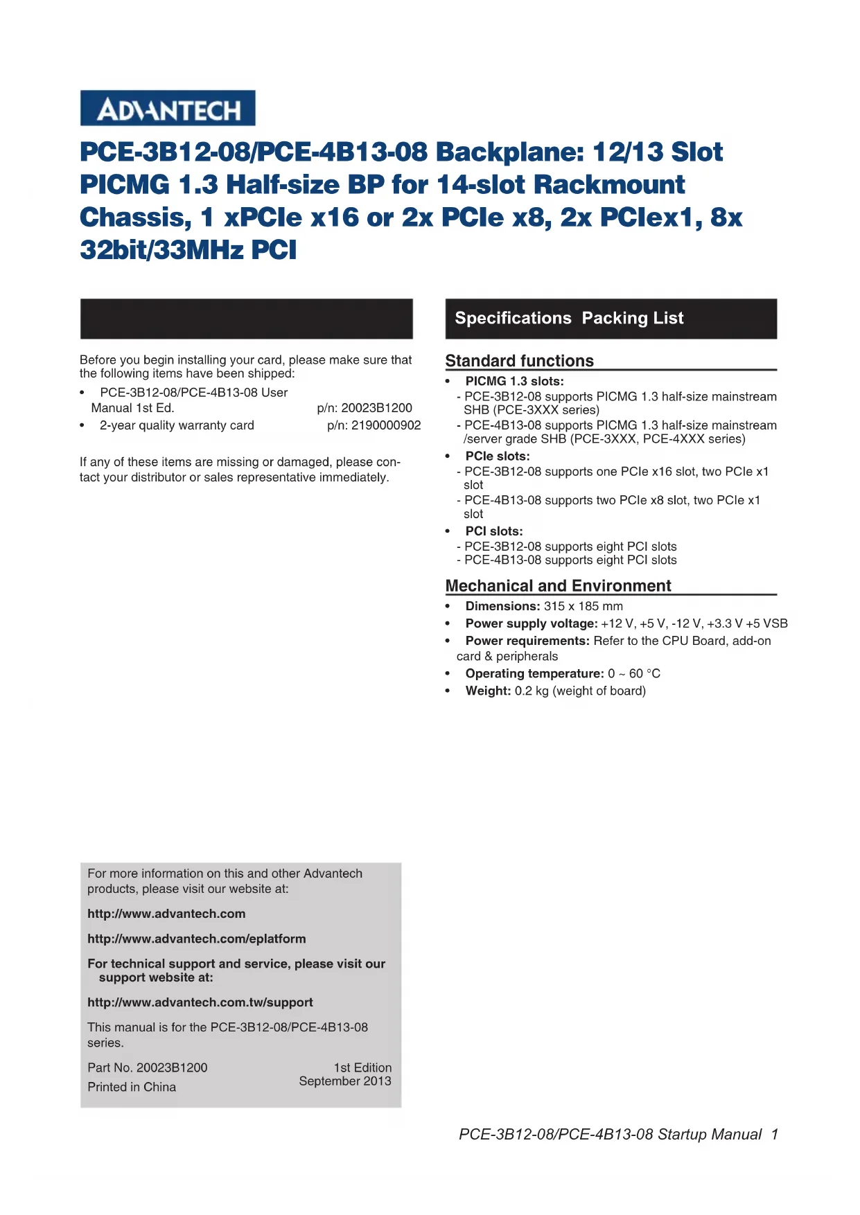
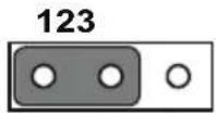
| PSON1: ATX/AT Mode Selection | |
| Jumper Setting Function | |
| 1-2 AT mode | |
| 2-3 (Default) ATX mode | |

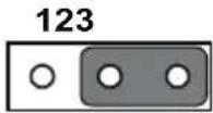
| JFAN_CTRL1: System Smart Fan Control | |
| Jumper Setting Function | |
| 1-2 (Default) Smart fan | |
| 2-3 Full speed fan | |
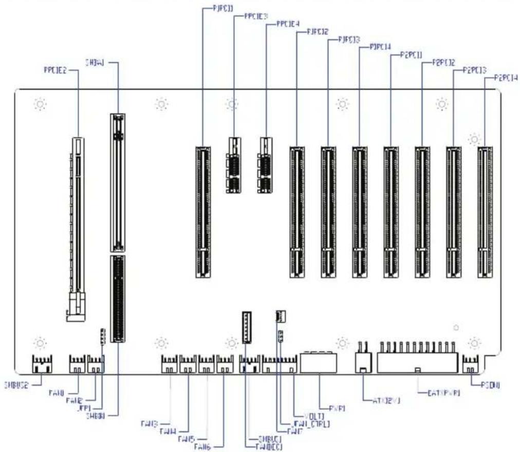
text_image
FPC1E2 [SHW] FPC1E3 FPC1E4 FPC1E2 FPC1E3 FPC1E4 FPC1E1 FPC1E2 FPC1E3 FPC1E4 SHW52 FA10 FA1E FF1 SHW8 FA13 FA14 FA15 FA16 [DLT] FA17[CTPL] SHW9 FA18[TCPL] FAN1 FAN2 FAN3 FAN4 FAN5 FAN6 AT102VJ BAT10PANJ PSDUFigure 1: PCE-3B12-08 connectors and jumpers
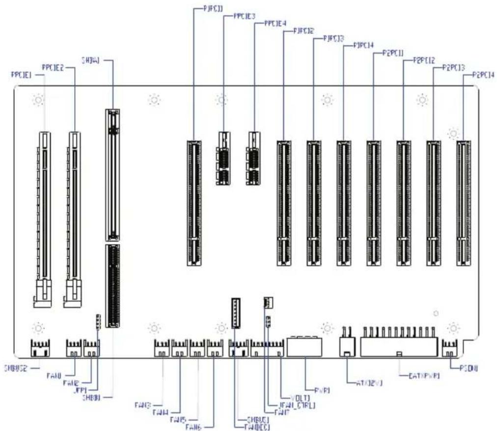
text_image
FPCJE1 FPCJE2 SHBU FPCJE3 FPCJE4 FPCJE2 FPCJE3 FPCJE4 FPCJE1 FPCJE2 FPCJE3 FPCJE4 FPCJE5 FPCJE6 FPCJE7 FPCJE8 FPCJE9 FPCJE10 FPCJE11 FPCJE12 FPCJE13 FPCJE14 FPCJE15 FPCJE16 FPCJE17 FPCJE18 FPCJE19 FPCJE20 FPCJE21 FPCJE22 FPCJE23 FPCJE24 FPCJE25 FPCJE26 FPCJE27 FPCJE28 FPCJE29 FPCJE30 FPCJE31 FPCJE32 FPCJE33 FPCJE34 FPCJE35 FPCJE36 FPCJE37 FPCJE38 FPCJE39 FPCJE40 FPCJE41 FPCJE42 FPCJE43 FPCJE44 FPCJE45 FPCJE46 FPCJE47 FPCJE48 FPCJE49 FPCJE50 FPCJE51 FPCJE52 FACU FAU0 FAU1E JFP1 SHBU0 FAU1E FAU2E FAU3E FAU4E FAU5E FAU6E VOLT1 FAU7_CFL1 FAU7_PNP1 SHBU0C1 TAWDEC1 ATJOZV1 CATJPNP1 PSDUFigure 2: PCE-4B13-08 connectors and jumpers
Board Dimensions
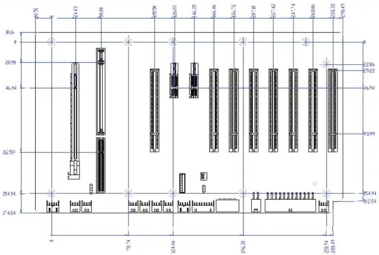
other
| Position | Value | |--------|--------| | 16.51 | 10.16 | | 24.43 | 20.90 | | 50.80 | 46.94 | | 105.50 | 112.59 | | 126.03 | 124.46 | | 146.35 | 196.30 | | 166.46 | 231.94 | | 186.73 | 238.49 | | 207.10 | 29.22 | | 227.42 | 33.99 | | 247.74 | 354.94 | | 268.06 | 362.84 | | 288.33 | 393.99 | | 328.49 | 46.94 |Figure 3: PCE-3B12-08 board dimensions
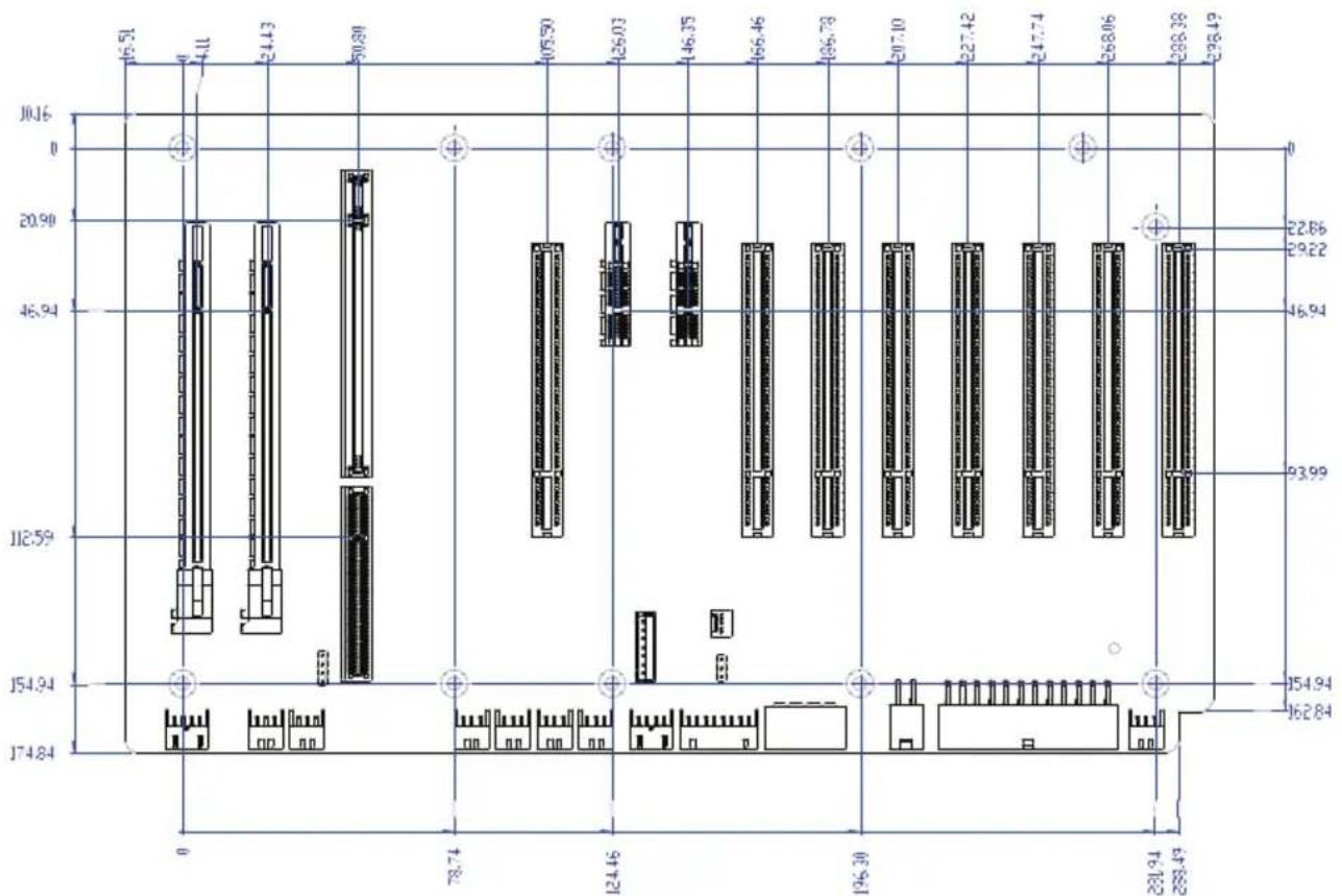
other
| Dimension | Value | | --------- | ------ | | 10.16 | 16.51 | | 20.90 | 24.43 | | 46.94 | 50.80 | | 112.59 | 105.50 | | 124.46 | 136.03 | | 136.30 | 146.35 | | 146.46 | 166.46 | | 156.73 | 186.73 | | 167.10 | 207.10 | | 177.42 | 227.42 | | 187.74 | 247.74 | | 198.06 | 268.06 | | 208.38 | 288.38 | | 228.49 | 328.49 | | 239.94 | 354.94 | | 250.94 | 362.84 | | 261.94 | 371.94 | | 272.84 | 380.84 | | 283.49 | 399.49 | | 293.99 | 408.94 | | 303.99 | 428.94 | | 313.99 | 448.94 | | 323.99 | 468.94 | | 333.99 | 488.94 | | 343.99 | 508.94 | | 353.99 | 528.94 | | 363.99 | 548.94 | | 373.99 | 568.94 | | 383.99 | 588.94 | | 393.99 | 608.94 | | 403.99 | 628.94 | | 413.99 | 648.94 | | 423.99 | 668.94 | | 433.99 | 688.94 | | 443.99 | 708.94 | | 453.99 | 728.94 | | 463.99 | 748.94 | | 473.99 | 768.94 | | 483.99 | 788.94 | | 493.99 | 808.94 | | 503.99 | 828.94 | | 513.99 | 848.94 | | 523.99 | 868.94 | | 533.99 | 888.94 | | 543.99 | 908.94 | | 553.99 | 928.94 | | 563.99 | 948.94 | | 573.99 | 968.94 | | 583.99 | 988.94 | | 593.99 | 1008.94| | 603.99 | 1028.94| | 613.99 | 1048.94| | 623.99 | 1068.94| | 633.99 | 1088.94| | 643.99 | 1108.94| | 653.99 | 1128.94| | 663.99 | 1148.94| | 673.99 | 1168.94| | 683.99 | 1188.94| | 693.99 | 1208.94| | 703.99 | 1228.94| | 713.99 | 1248.94| | 723.99 | 1268.94| | 733.99 | 1288.94| | 743.84 | 174.84 | | 753.84 | 175.84 | | 763.84 | 176.84 | | 773.84 | 177.84 | | 783.84 | 178.84 | | 793.84 | 179.84 | | 803.84 | 180.84 | | 813.84 | 181.84 | | 823.84 | 182.84 | | 833.84 | 183.84 | | 843.84 | 184.84 | | 853.84 | 185.84 | | 863.84 | 186.84 | | 873.84 | 187.84 | | 883.84 | 188.84 | | 893.84 | 189.84 | | 903.84 | - | The chart displays a schematic diagram of a device layout with labeled components and dimensions for each component.Figure 4: PCE-4B13-08 board dimensions
Board Diagram
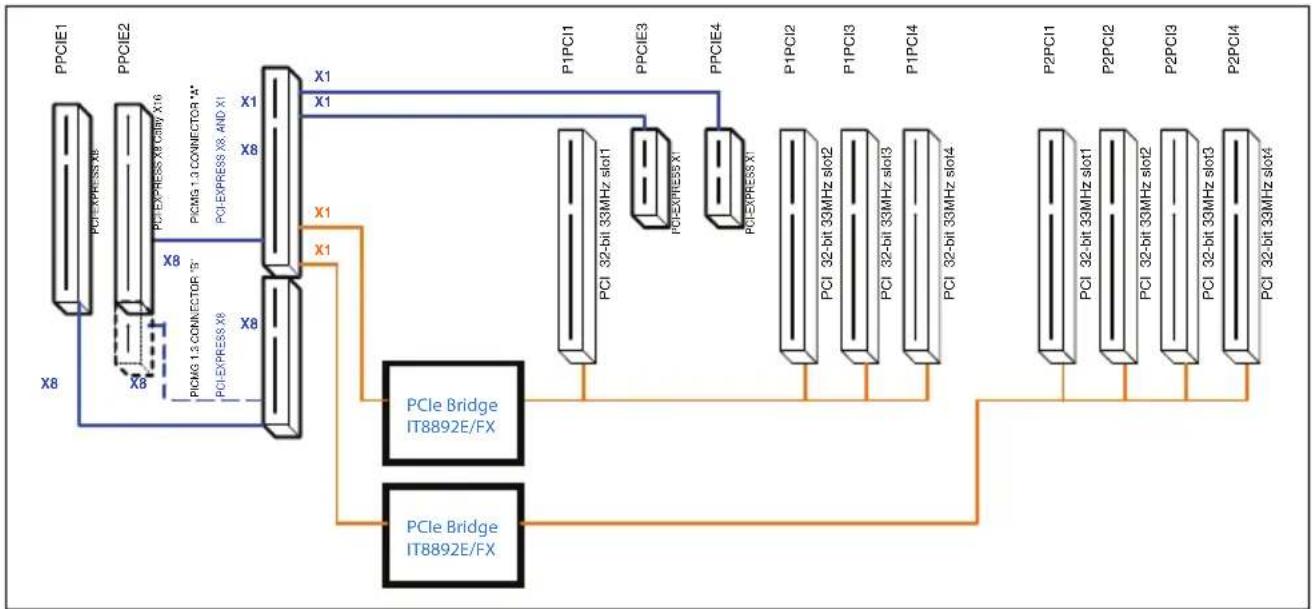
flowchart
graph TD
    A["PPCIE1"] -->|X8| B["PCIE EXPRESS X8"]
    C["PPCIE2"] -->|X8| D["PCIE EXPRESS X8 CIBY X16"]
    E["PCICM 1.3 CONNECTOR X7"] -->|X1| F["X1"]
    G["POI EXPRESS X8 AND X1"] -->|X1| H["X1"]
    I["POI EXPRESS X8"] -->|X8| J["X8"]
    K["PCI 32-bit 33MHz slot1"] --> L["P1PCI1"]
    K --> M["PPCIE3"]
    N["PCI 32-bit 33MHz slot4"] --> O["P1PCI2"]
    N --> P["PCI 32-bit 33MHz slot2"]
    Q["PCI 32-bit 33MHz slot3"] --> R["P1PCI3"]
    Q --> S["PCI 32-bit 33MHz slot4"]
    T["PCI 32-bit 33MHz slot1"] --> U["P2PCI1"]
    T --> V["PCI 32-bit 33MHz slot2"]
    W["PCI 32-bit 33MHz slot3"] --> X["P2PCI3"]
    W --> Y["PCI 32-bit 33MHz slot4"]
Figure 3: Board diagram