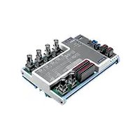
USB-5801-AE - Module d'acquisition de données Advantech - Free user manual and instructions
Find the device manual for free USB-5801-AE Advantech in PDF.


| Product Type | Dynamic Signal Acquisition USB 3.0 I/O Module |
| Model Number | USB-5801-AE |
| Analog Input Channels | 4, simultaneous sampling, 24-bit ADC, up to 192 kS/s |
| Analog Input Ranges | ±10 V, ±5 V, ±2 V, ±1 V (software selectable per channel) |
| Analog Input Coupling | AC or DC, software selectable per channel |
| Analog Input Configuration | Differential or Pseudo-differential (software selectable) |
| IEPE Excitation | 2 mA per channel, software enable/disable |
| Analog Output Channels | 2, 24-bit DAC, up to 192 kS/s update rate |
| Analog Output Ranges | ±10 V, ±1 V (software selectable per channel) |
| Digital I/O | 4 isolated inputs, 4 isolated outputs (2,500 VDC) |
| Counter/Timer | 2 channels, 32-bit, up to 50 MHz internal clock |
| Tachometer Inputs | 2, frequency measurement up to 5 kHz |
| Trigger | Analog (from any AI channel) and digital (external TRGIN) |
| Synchronization | Multiple modules daisy-chainable via TRGIN/TRGOUT |
| USB Interface | USB 3.0 SuperSpeed, type B upstream, type A downstream (daisy chain) |
| Power Requirements | External 10~30 VDC or USB bus power (5V); redundant power inputs |
| Power Consumption | 150 mA typ./200 mA max @ 24V external; 700 mA typ./860 mA max @ 5V bus |
| Dimensions (W x H x D) | 168 mm x 120 mm x 45 mm |
| Weight | 290 g |
| Operating Temperature | 0 to 60 °C (32 to 140 °F) |
| Storage Temperature | -40 to 70 °C (-40 to 158 °F) |
| Board ID Switch | DIP switch for addressing multiple modules |
| Warranty | 2 years |
| Certifications | CE (with shielded cables) |
Frequently Asked Questions - USB-5801-AE Advantech
User questions about USB-5801-AE Advantech
0 question about this device. Answer the ones you know or ask your own.
Ask a new question about this device
Download the instructions for your Module d'acquisition de données in PDF format for free! Find your manual USB-5801-AE - Advantech and take your electronic device back in hand. On this page are published all the documents necessary for the use of your device. USB-5801-AE by Advantech.
USER MANUAL USB-5801-AE Advantech
natural_image
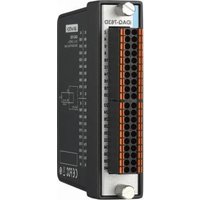
Illustration of a computer motherboard with two components, one showing internal circuitry and the other a rectangular electronic device (no text or symbols)USB-5801
4-CH, 24-Bit, 192 kS/s Dynamic Signal Acquisition USB 3.0 I/O Module with Analog Output and Tachometer
Copyright
This documentation and the software included with this product are copyrighted 2019 by Advantech Co., Ltd. All rights are reserved. Advantech Co., Ltd. reserves the right to improve the products described in this manual at any time without notice. No part of this manual may be reproduced, copied, translated, or transmitted in any form or by any means without the prior written permission of Advantech Co., Ltd. The information provided in this manual is intended to be accurate and reliable. However, Advantech Co., Ltd. assumes no responsibility for its use, nor for any infringements of the rights of third parties that may result from its use.
Acknowledgments
Intel and Pentium are trademarks of Intel Corporation.
Microsoft Windows and MS-DOS are registered trademarks of Microsoft Corp.
All other product names or trademarks are properties of their respective owners.
Product Warranty (2 years)
Advantech warrants the original purchaser that each of its products will be free from defects in materials and workmanship for two years from the date of purchase.
This warranty does not apply to any products that have been repaired or altered by persons other than repair personnel authorized by Advantech, or products that have been subject to misuse, abuse, accident, or improper installation. Advantech assumes no liability under the terms of this warranty as a consequence of such events.
Because of Advantech's high quality-control standards and rigorous testing, most customers never need to use our repair service. If an Advantech product is defective, it will be repaired or replaced free of charge during the warranty period. For out-of-warranty repairs, customers are billed according to the cost of replacement materials, service time, and freight. Consult your dealer for more details.
If you believe that your product is defective product, follow the steps outlined below.
-
Collect all information about the problem encountered. (For example, CPU speed, Advantech products used, other hardware and software used, etc.) Note anything abnormal and list any onscreen messages displayed when the problem occurs.
-
Call your dealer and describe the problem. Have your manual, product, and any helpful information readily available.
-
If your product is diagnosed as defective, obtain an return merchandise authorization (RMA) number from your dealer. This allows us to process your return more quickly.
-
Carefully pack the defective product, a completed Repair and Replacement Order Card, and a proof of purchase date (such as a photocopy of your sales receipt) into a shippable container. Products returned without a proof of purchase date are not eligible for warranty service.
-
Write the RMA number clearly on the outside of the package. Then ship the package prepaid to your dealer.
Part No. 2001580100 Edition 1
Printed in China August 2019
CE
This product has passed the CE test for environmental specifications when shielded cables are used for external wiring. We recommend the use of shielded cables. This type of cable is available from Advantech. Please contact your local supplier for ordering information.
Technical Support and Assistance
- Visit the Advantech website at http://support.advantech.com.tw/ to obtain the latest product information.
- Contact your distributor, sales representative, or Advantech's customer service center for technical support if you need additional assistance. Please have the following information ready before calling:
– Product name and serial number
– Description of your peripheral attachments
– Description of your software (operating system, version, application software, etc.)
– A complete description of the problem
– The exact wording of any error messages
Packing List
Before setting up the system, check that the items listed below are included and in good condition. If any item is missing or damaged, contact your dealer immediately.
1 x USB-5801 module
4 x terminal blocks
■ 1 x USB-5801 startup manual
■ 1 x USB 3.0 lockable cable (1 m)
Safety Precautions - Static Electricity
Follow these simple precautions to protect yourself from harm and the products from damage.
- To avoid electrical shock, always disconnect the power from the PC chassis before manual handling. Do not touch any components on the CPU card or other cards while the PC is powered on.
- Disconnect the power before implementing any configuration changes. The sudden rush of power after connecting a jumper or installing a card may damage sensitive electronic components.
Contents
Chapter 1 Introduction......1
1.1 Features ...... 2
1.2 Installation Guide .... 3
Figure 1.1 Installation Flowchart.... 4
1.3 Software Overview 5
1.4 DAQNavi Device Driver Programming Roadmap 5
1.5 Accessories....6
Chapter 2 Installation....7
2.1 Unpacking Instructions....8
2.2 Driver Installation 9
Figure 2.1 Advantech DAQnavi Installation Wizard ...... 9
Figure 2.2 Driver Installation Setup Screen 10
Figure 2.3 Driver Installation Path and Space Requirements.... 10
Figure 2.4 Driver Installation Process.... 11
Figure 2.5 Exit the Driver Installation Wizard.... 11
2.3 Hardware Installation 12
2.4 Device Setup and Configuration 13
Figure 2.6 USB-5801 Device Settings 13
Figure 2.7 Device Settings Page 14
Figure 2.8 USB-5801 Device Testing 14
Chapter 3 Signal Connections....15
3.1 Overview 16
3.2 Dimensions 16
3.3 Connector, Switch, and LED 17
3.4 Analog Input 20
3.4.1 Analog Input Overview.... 20
Figure 3.1 Analog Input Functional Block Diagram ...... 20
3.4.2 Analog Input Channel Types.... 20
Figure 3.2 Connecting a Floating Source 20
Figure 3.3 Connecting a Grounded Source 21
Table 3.1: Recommended Analog Input Channel Configuration21
3.4.3 Analog Input Coupling.... 21
3.4.4 Integrated Electronic Piezoelectric (IEPE) Excitation 22
Figure 3.4 Connecting an IEPE Sensor....22
Table 3.2: LED Status for IEPE Fault Detection....22
3.4.5 Analog Input Ranges 23
3.4.6 Sample Rate and Anti-Aliasing Filters 23
Figure 3.5 Anti-Aliasing Filters....23
3.4.7 Analog Input Measurement Types 24
Figure 3.6 Analog Input Measurement Types.... 24
g Output 24
3.5.1 Analog Output Overview....24
Figure 3.7 Analog Output Functional Block Diagram....24
3.5.2 Analog Output Channel Types 24
3.5.3 Analog Output Loads 25
3.5.4 Analog Output Generation Types .... 25
Figure 3.8 Analog Output Generation Types .... 25
er....26
3.6.1 Trigger Functions 26
Figure 3.9 Delayed Start and Stop Triggers ...... 26
3.6.2 Digital Triggers.... 26
Figure 3.10 Digital Trigger Signal Connection and Signals ..... 26
3.6.3 Analog Triggers 27
Figure 3.11 Analog Triggers 27
Figure 3.12 Analog Triggers with Hysteresis.... 27
3.7 Analog Calibration.... 28
3.7.1 Analog Calibration Overview 28
Figure 3.13Block Diagram of Analog Calibration Circuitry ..... 28
3.7.2 Voltage References Calibration 29
Figure 3.14 Voltage Reference Calibration ...... 29
3.7.3 Analog Input Calibration 30
Figure 3.15 Analog Input Calibration 30
3.7.4 Analog Output Calibration.... 30
Figure 3.16 Analog Output Calibration 30
3.7.5 Store Calibration Parameters to EEPROM.... 31
Figure 3.17 Store Calibration Parameters to EEPROM ...... 31
3.7.6 Load Default Calibration Parameters from EEPROM.... 32
Figure 3.18 Load Default Calibration Parameters from EEPROM .. 32
3.8 Digital Input/Output 33
3.8.1 Digital Inputs 33
Figure 3.19 Digital Input Functional Block Diagram .... 33
Figure 3.20Digital Input Interrupt 33
Figure 3.21 Digital Input Filter 34
3.8.2 Digital Outputs 35
Figure 3.22Digital Output Functional Block Diagram.... 35
3.9 Counter/Timer 35
Figure 3.23Counter/Timer Functional Block Diagram ...... 35
3.9.1 Event Counting 36
Figure 3.24Event Counting.... 36
3.9.2 Frequency Measurement (Tachometer) 36
Figure 3.25 Frequency Measurement 36
3.9.3 Phase Measurement for Analog Input Samples 37
Figure 3.26Phase Measurement for Analog Input Samples..... 37
3.10 Synchronization 38
Figure 3.27 Multiple Module Synchronization.... 38
Appendix A Specifications.... 39
A.1 Analog Input.... 40
A.1.1 Functions 40
A.1.2 ADC Modulator Oversample Rate 40
A.1.3 Maximum Operating Voltage 40
A.1.4 Input Overvoltage Protection 41
A.1.5 AC Coupled Measurement Accuracy.... 41
A.1.6 DC Coupled Measurement Accuracy 41
A.1.7 Input Impedance 41
A.1.8 Common-Mode Rejection Ratio (CMRR) 41
A.1.9 Frequency Response.... 42
A.1.10 AC Coupling.... 42
A.1.11 Idle Channel Noise 42
A.1.12 Dynamic Range (DR).... 42
A.1.13 Spurious Free Dynamic Range (SFDR) 42
A.1.14 Signal-to-Noise Ratio (SNR)...... 43
A.1.15 Total Harmonic Distortion (THD) 43
A.1.16 Total Harmonic Distortion Plus Noise (THD+N) 43
A.1.17 Crosstalk.... 43
A.1.18 Integrated Electronic Piezoelectric Excitation (IEPE) 44
A.2 Analog Output 44
A.2.1 Functions 44
A.2.2 Analog Output Accuracy 44
A.2.3 Output Noise 44
A.2.4 Spurious Free Dynamic Range (SFDR).... 45
A.2.5 Signal-to-Noise Ratio (SNR) 45
A.2.6 Total Harmonic Distortion (THD) 45
A.2.7 Total Harmonic Distortion Plus Noise (THD+N).... 45
A.3 Triggers 46
A.3.1 Analog Trigger Input 46
A.3.2 Digital Trigger Input....46
A.3.3 Digital Trigger Output 46
A.4 Tachometer 46
A.5 Digital I/O 47
A.5.1 Digital Input 47
A.5.2 Digital Output 47
A.6 General Specifications 48
A.6.1 Bus Interface.... 48
A.6.2 Power Requirements 48
A.6.3 Physical.... 48
A.6.4 Environmental 48
Chapter 1
Introduction
This chapter provides an introduction to USB-5801 and its typical applications.
Features
Applications
Installation Guide
■ Software Overview
Accessories
USB-5801 is a high accuracy dynamic signal acquisition USB 3.0 module specifically designed for vibration and acoustic measurements. It provides four simultaneously sampled, 24-bit, IEPE sensor inputs with up to 192 kS/s sample rate for high resolution measurements. It is also equipped with two 24-bit analog outputs with up to 192 kS/s update rate. In addition, it has two tachometer inputs whose data can be correlated to the sensor data. The built-in USB hub makes this module daisy chainable with other USB-5000 series products.
1.1 Features
USB 3.0 SuperSpeed and daisy chainable by built-in USB hub
■ 4 simultaneously sampled analog inputs, up to 192 kS/s
■ 24-bit resolution ADCs with -94 dB total harmonic distortion plus noise (THD+N)
■ Built-in anti-aliasing filter
■ 2 mA integrated electronic piezoelectric (IEPE) excitation currents
■ 2 analog outputs with update rate up to 192 kS/s
■ 24-bit resolution DACs with -90 dB total harmonic distortion plus noise (THD+N)
■ 2 tachometer inputs for period or frequency measurement
■ 4-ch isolated digital input and 4-ch isolated digital output
USB 3.0 SuperSpeed
The USB-5800 series modules support USB 3.0 SuperSpeed for an accelerated response time.
Easy Maintenance
The LED indicators, rotary switch, and terminal blocks are all front-facing for easy access and wiring. The European-type pluggable terminal blocks also simplify maintenance, reducing overall service time.
Compact Size
The compact design and high-density channel count improves space utilization, while the DIN-rail mounting kit ensures easy installation in cabinets.
Built-In USB Hub with Daisy Chaining Support
The USB-5800 module is equipped with a USB hub that supports daisy chain topologies. This feature frees up the IPC USB ports by enabling more than one USB-5800 module to be integrated into a single system.
Note! Because USB 3.0 can only provide a maximum current of 900 mA, if more than one module is connected via the hub, an external power supply unit (PSU) will be required.

Redundant Power
USB-5801 modules feature two power input terminals with an input power range of 10 30 V_DC and power redundancy support. For modules connected to two power input sources, if one source is inactive or interrupted, the other power source can immediately assume supply operations. Accordingly, USB-5801 modules can operate with a single power source. (The modules can also be powered via USB if there is no device connected to the downstream port.)
Board ID Switch
USB-5801 modules have a built-in DIP switch that is used to define the board ID for each module. When multiple modules are installed in the same system, the board ID switch can be used to identify each module's device number. Every module in the system should be assigned different device numbers. The default board ID value is 0.
1.2 Installation Guide
Before module installation, please ensure that you have the following necessary components:
1 x USB-5801 module
1 x USB-5801 user manual
■ Advantech DAQNavi driver software
1 x personal computer or workstation with a USB interface (equipped with Windows 10/8/7/XP operating system)
■ 1 x 10 \~ 30 V power supply (96PS-A40WDIN optional)
Other optional components are also available for enhanced operation:
■ DAQnavi, LabVIEW, and other third-party software
Once you have the necessary components and any additional accessories for enhanced operation, you can begin installing the USB-5801 module. Figure 1.1 is a flowchart that provides a broad overview of the software and hardware installation procedures.

flowchart
graph TD
    A["Install driver and turn off computer"] --> B["Install hardware and turn on computer"]
    B --> C["Use driver utility to configure hardware"]
    C --> D["Use test utility to test hardware"]
    D --> E["Read examples & driver manual"]
    E --> F["Start writing your own application"]
Figure 1.1 Installation Flowchart
1.3 Software Overview
Advantech offers a wide range of DLL drivers, third-party drivers, and application software for fully exploiting the functions of your USB-5801 module.
Device Drivers
■ Advantech DAQNavi
DAQNavi Software
Advantech's DAQNavi software includes device drivers and a software development kit (SDK), which features a comprehensive I/O function library to boost application performance. This software can be downloaded from the Advantech website (at www.advantech.com). The Advantech DAQNavi software for Windows XP/7/8/10 (desktop mode) works seamlessly with most major development tools, including Visual Studio.NET, Visual C++, Visual Basic, and Borland Delphi.
1.4 DAQnavi Device Driver Programming Roadmap
This section provides a roadmap for building an application from scratch using Advantech's DAQNavi Device Driver with a range of development tools such as Visual Studio.NET, Visual C++, Visual Basic, Delphi, and C++ Builder. Step-by-step instructions for application development using each tool are provided in the device driver manual. A large library of example source codes is also provided for reference.
Programming Tools
Programmers can develop application programs using their preferred development tools.
Visual Studio.NET
■ Visual C++ and Visual Basic
Delphi
C++ Builder
For instructions on programming using each development tool, Advantech offers a tutorial chapter in the DAQnavi SDK manual. Please refer to the corresponding sections in the DAQnavi SDK manual to begin programming. Users should also review the example source codes provided for each programming tool. The examples can help jump start a project.
The DAQNavi SDK manual can be downloaded from the Advantech website. Alternatively, if the device drivers are already installed on the computer, the DAQNavi SDK manual can be accessed via the Start button.
Start/Programs/Advantech Automation/DAQNavi/DAQNavi Manuals/DAQNavi SDK Manual
The example source codes can be found under the corresponding installation folder/default installation path.
\Advantech\DAQNavi\Examples
For information about using other function groups or development tools, refer to the chapter titled "Using DAQnavi SDK" in the DAQnavi SDK manual, or watch the video tutorials provided with the Advantech Navigator.
Programming with DAQnavi Device Drivers Function Library
Advantech offers a comprehensive function library for DAQNavi device drivers that can be utilized when developing various application programs. This function library comprises numerous APIs that support many development tools, such as Visual Studio.NET, Visual C++, Visual Basic, Delphi and C++ Builder.
These APIs can be categorized into several groups according to their function or purpose.
■ Analog Input Function Group
■ Analog Output Function Group
■ Digital Input/Output Function Group
Counter Function Group
■ Port Function Group (direct I/O)
■ Event Function Group
For the usage and parameters of each function, refer to the chapter titled "Using DAQnavi SDK" in the DAQnavi SDK manual.
Troubleshooting DAQnavi Device Drivers Error
Driver functions return a status code when called to perform a certain task for an application. When a function returns a code that is not zero, this means the driver has failed to perform the designated function. To troubleshoot device driver errors, check the error code and error description in the Error Control section for each function in the DAQnavi SDK manual.
1.5 Accessories
Advantech offers the following accessories to support the USB-5801 module:
Power supply unit
■ 96PSD-A40W24-MM 40 W, 24 V DIN-rail power supply
Chapter 2
Installation
This chapter includes a packing checklist, instructions for unpacking, and step-by-step procedures for both driver and card installation.
■ Unpacking Instructions
Driver Installation
Hardware Installation
■ Device Setup and Configuration
2.1 Unpacking Instructions
After receiving your USB-5801 module, inspect the package contents to ensure that the following items are present:
1 x USB-5801 module
4 x terminal blocks
■ 1 x USB-5801 startup manual
■ 1 x USB 3.0 lockable cable (1 m)
The USB-5801 module contains electronic components that are vulnerable to electrostatic discharge (ESD). ESD can easily damage the integrated circuits and components if preventive measures are not carefully implemented. Before removing the module from the antistatic plastic bag, take the following precautions to prevent possible ESD damage:
■ Touch the metal part of your computer chassis with your hand to discharge any static electricity accumulated in your body. Alternatively, wear a grounding strap.
■ Make contact between the antistatic bag and ground before opening. After removing the module from the packaging, first inspect the module for any signs of external damage (loose or damaged components, etc.). If the module is visibly damaged, notify our service department or your local sales representative immediately. Do not install or use a damaged module.
- Avoid contact with materials that may hold static electricity, such as plastic, vinyl, and styrofoam.
2.2 Driver Installation
We recommend installing the drivers before installing the USB-5801 module to guarantee a problem-free installation process.
The Advantech DAQNavi Device Drivers setup program can be downloaded from the Advantech website. Follow the steps outlined below to install the driver software.
- Execute the USB-5801 driver package.
- The Advantech DAQNavi driver installation wizard program should launch automatically. Figures 2.1 to 2.5 show the various pages of the installation wizard interface.
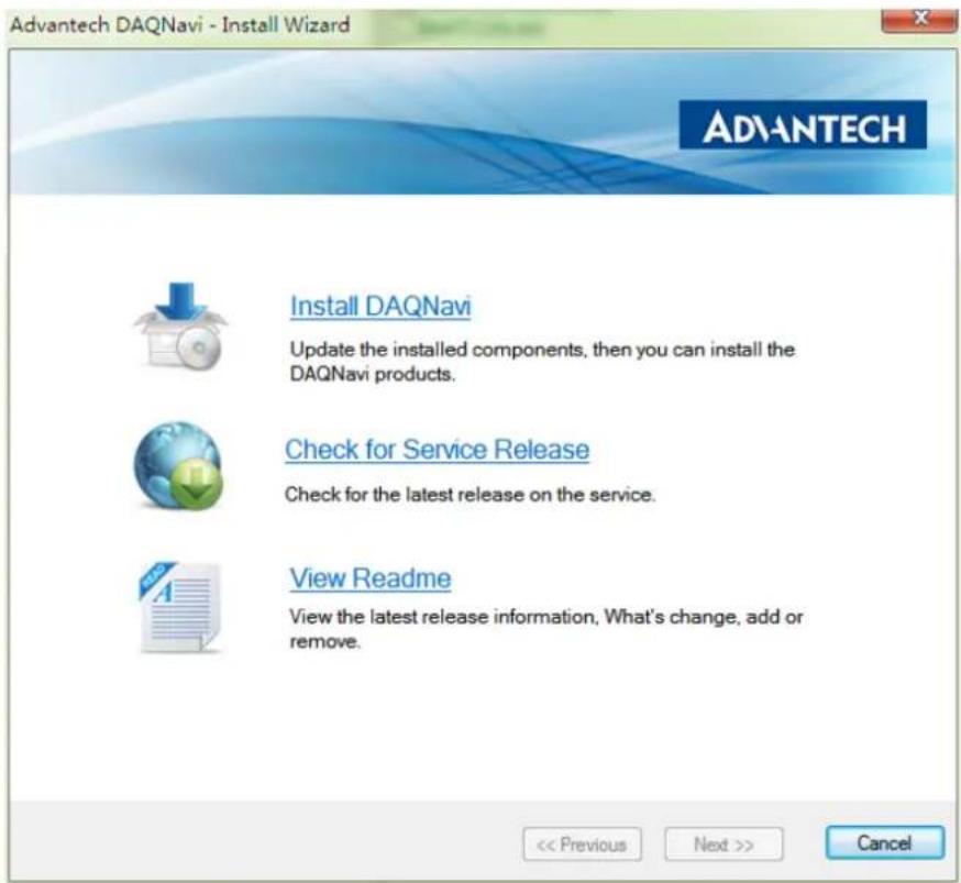
Figure 2.1 Advantech DAQnavi Installation Wizard
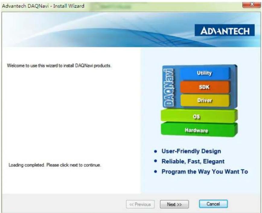
Figure 2.2 Driver Installation Setup Screen
- Once the DAQNavi driver installation wizard is launched, follow the instructions displayed in the interface to complete the driver installation.

Figure 2.3 Driver Installation Path and Space Requirements

Figure 2.4 Driver Installation Process
- After the driver is successfully installed, click the "Finish" button to exit the installation wizard.
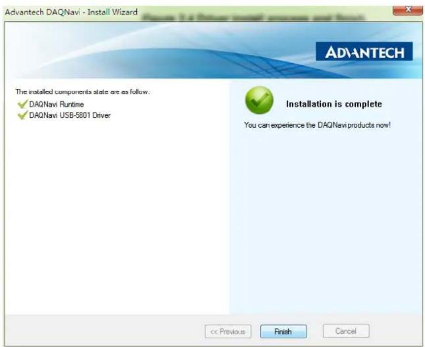
Figure 2.5 Exit the Driver Installation Wizard
2.3 Hardware Installation
Note! Ensure that the relevant driver is installed before installing the USB-5801 module. (Refer to Section 2.2 "Driver Installation" for more information.)

After the device drivers are installed, the USB-5801 module can be installed in your computer. We recommend referring to the computer user manual or related documentation if you have any concerns. Follow the steps outlined below to install the module.
- Touch any metal surface of your computer to discharge any static electricity that may have accumulated in your body.
- Plug the USB-5801 module into the selected USB port. To avoid damaging the module, do not use excessive force when inserting the module into the USB port.
After the module is installed, your device can be configured using the Advantech Navigator program automatically installed during driver installation. The complete device installation process should include device setup, configuration, and testing. The following sections provide information for guiding users through the device setup, configuration, and testing procedures.
2.4 Device Setup and Configuration
The Advantech Navigator program is a utility for setting up, configuring, and testing devices. The program also stores the system configuration settings in the system registry for subsequent reference. These settings are used when a device driver API is called. Figure 2.6 shows an example of the USB-5801 device settings.
Setting Up a Device
- To install an I/O device or module, first initialize the Advantech Navigator program (Start/Programs/Advantech Automation/Navigator for DN4).
- Users can view the device(s) already installed on the system (if any) by accessing the Installed Devices list. Once the software/hardware installation is complete, the USB-5801 module should be included in the Installed Devices list.
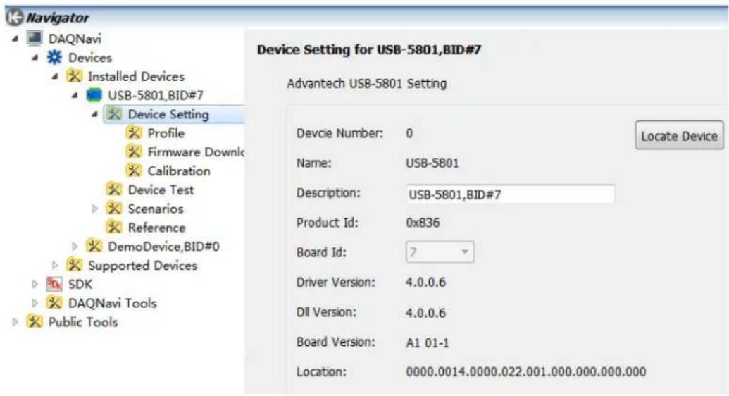
Figure 2.6 USB-5801 Device Settings
Configuring the Device
- Go to the Device Setting page to configure the device. The items in the page allow users to configure the USB-5801 modules' analog input.
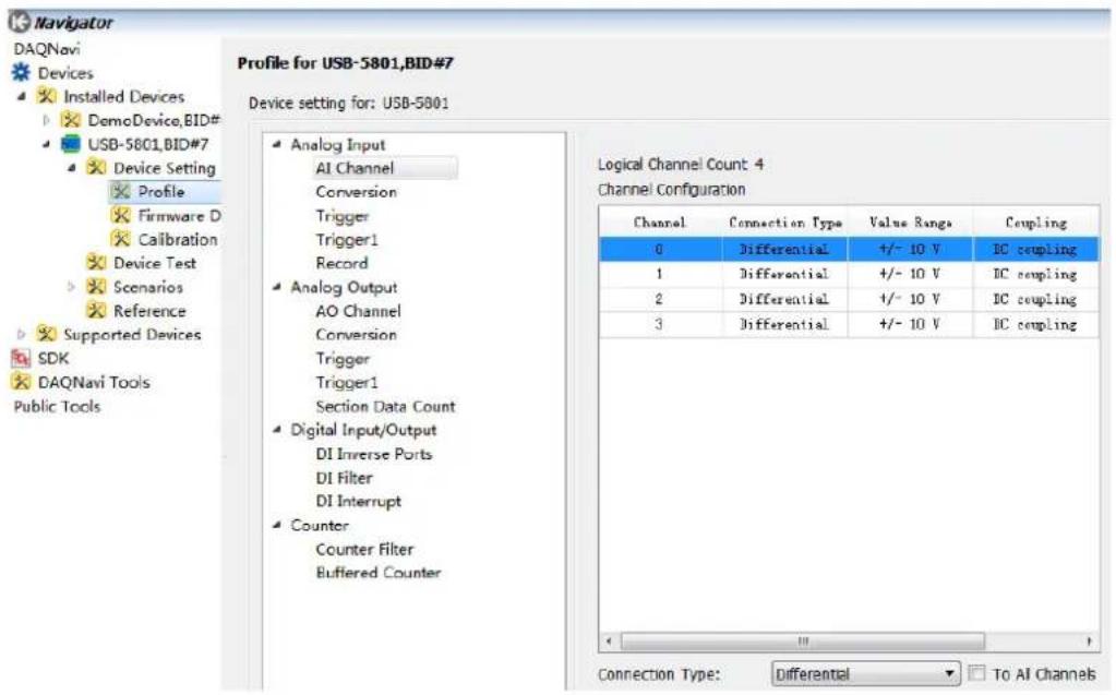
Figure 2.7 Device Settings Page
- After the module is installed and configured, access the Device Testing page to test the hardware using the test utility provided.
![Device Test for USB-5B01,BID#7 Buffered A1 Instant A1 Buffered A0 Static A0 Digital Input Digital Output Buffered Counter Counter 10 0 -10 10 0 -10 10 0 Channel 0 +/- 10 V +/- 5 V +/- 2 V +/- 1 V Channel 1 +/- 10 V +/- 5 V +/- 2 V +/- 1 V Channel 2 +/- 10 V +/- 5 V +/- 2 V +/- 1 V Start Extension Ext_DigCLK Ext_AnuCLK Convert Clock Rate: 1000 HZ (1000, 192000] Section Length: 504 Section Count: 10 Cycles: 10 Overrun Count: 0 Data Ready Count: 0 Record Count: 0 Overflow Count:](/content/2026/05/994588/images/8e995d5807bb2869747ac05d6f2b7bea594c9fa5ee97e983ae3784c3648b745f.jpg)
Figure 2.8 USB-5801 Device Testing
For more detailed information, please refer to the DAQNavi SDK manual or the Advantech Navigator user interface manual.
Chapter 3
Signal Connections
This chapter explains how to connect input and output signals to the USB-5801 module via the I/O connector.
Overview
Board ID Settings
Signal Connections
Field Wiring Considerations
3.1 Overview
Maintaining signal connections is one of the most important factors in ensuring that your application system is sending and receiving data correctly. A good signal connection can prevent unnecessary and costly damage to your PC and other hardware devices. This chapter provides information about connecting input and output signals to the USB-5800 module via the I/O connector.
3.2 Dimensions

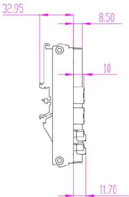
3.3 Connector, Switch, and LED
Switch Description
| SW1 | Board ID switch. Refer to the following table for board ID configuration. | ||||
| B | o | a | r | d | |
| 0↑ | ↑ | ↑ | ↑ | ||
| 1↑ | ↑ | ↑ | ↓ | ||
| 2↑ | ↑ | ↓ | ↑ | ||
| 3↑ | ↑ | ↓ | ↓ | ||
| 4↑ | ↓ | ↑ | ↑ | ||
| 5↑ | ↓ | ↑ | ↓ | ||
| 6↑ | ↓ | ↓ | ↑ | ||
| 7↑ | ↓ | ↓ | ↓ | ||
| 8↓ | ↑ | ↑ | ↑ | ||
| 9↓ | ↑ | ↑ | ↓ | ||
| 10↓ | ↑ | ↓ | ↑ | ||
| 11↓ | ↑ | ↓ | ↓ | ||
| 12↓ | ↓ | ↑ | ↑ | ||
| 13↓ | ↓ | ↑ | ↓ | ||
| 14↓ | ↓ | ↓ | ↑ | ||
| 15↓ | ↓ | ↓ | ↓ | ||
Connector Description
| CN1 | USB upstream port (USB 3.0 type-B connector with screw). Connect this port to the host or to the downstream port of the previous USB module. |
| CN2 | USB downstream port (USB 3.0 type-A connector with screw). Connect this port to the upstream port of the next USB module if any. |
Connector Pin Description
| CN4 | Center pin Positive terminal of analog input channel 0 | |
| Outer shield | Negative terminal of analog input channel 0 | |
| CN5 | Center pin Positive terminal of analog input channel 1 | |
| Outer shield | Negative terminal of analog input channel 1 | |
| CN6 | Center pin Positive terminal of analog input channel 2 | |
| Outer shield | Negative terminal of analog input channel 2 | |
| CN7 | Center pin Positive terminal of analog input channel 3 | |
| Outer shield | Negative terminal of analog input channel 3 | |
| CN8 | Center pin Positive terminal of analog output channel 0 | |
| Outer shield | Negative terminal of analog output channel 0 | |
| CN9 | Center pin Positive terminal of analog output channel 1 | |
| Outer shield | Negative terminal of analog output channel 1 | |
Connector Pin Description
| GND | C0CLK | C0SCK | TRGIN | GND | I0 | I1 | I2 | I3 | EC |
| GND | C1CLK | C1SCK | TRGOUT | GND | O0 | O1 | O2 | O3 | PC |
CN10 & CN11
| C<0...1>CLK Clock input for counter channel 0 and 1 |
| C<0...1>SCK Sample clock input for counter channel 0 and 1 |
| TRGIN Digital trigger input |
| TRGOUT Digital trigger output |
| I<0...3> Digital input channel 0 through 3 |
| O<0...3> Digital output channel 0 through 3 |
| EC Common point for digital input signals |
| PC Common point for digital output signals |
| GND Ground for digital signals |
Connector Pin Name Description

CN12 & CN13
| +VS | External 10 ~ 30 V_DC power supply |
| GND | Power ground |

Note! CN12 and CN13 are used for power redundancy. External power can be supplied from either of the connectors.

| LED | State | Description |
| LED2 | Off | Module is not powered on |
| Green | Module is powered on using either USB bus power or external power | |
| LED3 | Off | Initial state. Module has not been connected |
| Green | Upstream port is connected. Module is functioning normally | |
| Red | Upstream port is not connected or is disconnected. Module function is halted | |
| LED4 | Off | Downstream port is not connected |
| Blue | Downstream port is connected | |
| LED State Description | ||
| Near CN4 | Off | No sensor is connected to analog input channel 0 or sensor wire is broken |
| Green | Sensor is connected to analog input channel 0 and works normally | |
| Red | Sensor connected to analog input channel 0 is short circuited | |
| Near CN5 | Off | No sensor is connected to analog input channel 1 or sensor wire is broken |
| Green | Sensor is connected to analog input channel 1 and works normally | |
| Red | Sensor connected to analog input channel 1 is short circuited | |
| Near CN6 | Off | No sensor is connected to analog input channel 2 or sensor wire is broken |
| Green | Sensor is connected to analog input channel 2 and works normally | |
| Red | Sensor connected to analog input channel 2 is short circuited | |
| Near CN7 | Off | No sensor is connected to analog input channel 3 or sensor wire is broken |
| Green | Sensor is connected to analog input channel 3 and works normally | |
| Red | Sensor connected to analog input channel 3 is short circuited | |
Note! LEDs near CN4 \~ CN7 are functioning only when IEPE is enabled for the corresponding analog input channel.

3.4 Analog Input
3.4.1 Analog Input Overview
The USB-5801 provides 8 channels of analog input (AI) signal measurement. Figure 3.1 shows the functional block diagram of one analog input channel.

flowchart
graph LR
    A["IEPE Excitation"] --> B["BNC"]
    C["Pseudo-differential"] --> D["AC/DC Coupling"]
    D --> E["Programmable Gain Amplifier"]
    E --> F["Low-pass Filter"]
    F --> G["ADC"]
    H["Power Supply"] --> I["Switch"]
    I --> J["Ground"]
    K["Resistors"] --> L["Switch"]
    L --> M["Ground"]
    N["Resistors"] --> O["Switch"]
    O --> P["Ground"]
    Q["Resistors"] --> R["Switch"]
    R --> S["Ground"]
    T["Resistors"] --> U["Switch"]
    U --> V["Ground"]
    W["Resistors"] --> X["Switch"]
    X --> Y["Ground"]
Figure 3.1 Analog Input Functional Block Diagram
The analog input signal enters the USB-5801 through a BNC connector. The IEPE excitation, differential/pseudo-differential, AC/DC coupling, and input range can all be configured for each channel independently by software. A low-pass filter before the ADC removes unwanted out-of-band noise and alias components.
3.4.2 Analog Input Channel Types
The USB-5801 supports two types of terminal configuration for analog input: differential and pseudo-differential. The term "pseudo-differential" refers to a 50 Ω resistor between the outer shell of the BNC connector and the signal ground.
For a floating signal source, using the pseudo-differential configuration is recommended. The pseudo-differential configuration provides a ground reference between the floating source and the USB-5801 by connecting a 50 Ω resistor from the negative input to ground. This is shown in Figure 3.2. Without this, the floating source can drift outside of the input common-mode range of the USB-5801.

Figure 3.2 Connecting a Floating Source
For a grounded or ground referenced signal source, both the pseudo-differential and differential input configurations can be used. However, the differential input configuration is preferred, since using the pseudo-differential input configuration on a grounded signal source creates more than one ground-reference point, which results in a ground loop. The ground loop will introduce errors or noise into the measurement. The 50 Ω resistor between the negative input and ground is usually sufficient to reduce these errors to negligible levels, but results can vary depending on your system setup. This is shown in Figure 3.3.

Figure 3.3 Connecting a Grounded Source
Therefore, users should configure the channels based on the signal source type. Table 3.1 summarizes the recommended configurations for different signal source type. Each channel can be configured independently.
Table 3.1: Recommended Analog Input Channel Configuration
Source Type Channel Configuration
| Floating Pseudo-differential |
| Grounded Differential |
3.4.3 Analog Input Coupling
Each analog input channel can be individually configured as either AC or DC coupling. For DC coupling, any DC offset presented in the source signal is directly passed to the ADC. The DC coupling configuration can be used if the source signal has only small amounts of offset voltage or if the DC content of the signal is important. However, if the source has significant amounts of unwanted offset voltage, AC coupling should be used to take full advantage of the input dynamic range.
For AC coupling, a high-pass resistor-capacitor (RC) filter in the signal path is enabled. The filter time constant is 0.2 seconds. For a step input signal, it takes 1.06 seconds to settle to 0.5% accuracy, and 3.33 seconds to settle to 24-bit accuracy. The settling time also depends on the signal source impedance.
Due to the settling time described above, users should take care when switching the analog input channels from DC coupling to AC coupling. Users can either discard samples taken during the settling time, or force a delay before starting the measurement. There is no settling time issue when switching the analog input channels from AC coupling to DC coupling.
The high-pass RC filter for AC coupling will attenuate the low-frequency component of the input signal. The -3 dB cut-off frequency is 0.796 Hz.
3.4.4 Integrated Electronic Piezoelectric (IEPE) Excitation
The USB-5801 is equipped with a 2 mA constant current source of IEPE excitation for each analog input channel. When an IEPE sensor such as accelerometer or microphone is connected to the analog input terminals, the IEPE excitation for that channel must be enabled.
For those channels with IEPE excitation enabled, both pseudo-differential configuration and AC coupling must be selected. The pseudo-differential resistor provides a path for the IEPE excitation current to ground. The AC coupling removes the DC voltage offset generated by the IEPE excitation current through the sensor impedance. It also prevents overvoltage conditions. This is shown in Figure 3.4.
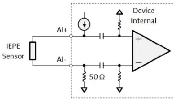
Figure 3.4 Connecting an IEPE Sensor
Users should note that when enabling IEPE excitation (and selecting AC coupling), the settling time phenomenon described in the previous section will occur. Please refer to the previous section for how to deal with this issue.
3.4.4.1 IEPE Fault Detection
Each analog input channel has LED indicators for IEPE fault detection. These indicators are effective only when IEPE excitation is enabled for the corresponding channels.
When the sensor is connected correctly, the green (normal) LED is on. If both two analog input terminals (positive and negative) are short, the red (short) LED is on. If the sensor wiring is broken or if there is no sensor connected, all LEDs are off. Table 3.2 shows the LED status for IEPE fault detection.
Table 3.2: LED Status for IEPE Fault Detection.
| LED Status Description |
| Green Normal |
| Red Sensor short |
| All off Sensor open or no sensor connected |
3.4.5 Analog Input Ranges
The USB-5801 supports 4 different analog input ranges: ±10 V, ±5 V, ±2 V, and ±1 V. Users should select the input range that is large enough for all possible voltage values of the input signal, and small enough to make full use of the input dynamic range.
For example, if the largest signal variation is ±3 V, input range of ±5 V is suggested. If the largest signal variation is ±1.5 V, input range of ±2 V is suggested.
If the range of the input signal is unknown, always select the maximum input range of ±10 V to prevent over-voltage and damage to the hardware.
3.4.6 Sample Rate and Anti-Aliasing Filters
In a sampling system, such as an ADC, the maximum bandwidth of the signal that can be measured is limited. Specifically, a sampling system with sample rate of fS can represent only signals with frequency lower than fS/2. This frequency is called the Nyquist frequency and the bandwidth from 0 Hz to the Nyquist frequency is called the Nyquist bandwidth.
However, frequency components above the Nyquist frequency, if any, will be modulated back to the Nyquist bandwidth when ADC is sampling, which introduces distortion to the measurement result. This undesirable effect is called aliasing. Unfortunately, one cannot tell whether aliasing occurs by just looking at the measured result. The only method to prevent aliasing is by low-pass filtering to remove frequency components above the Nyquist frequency. This low-pass filter is usually called anti-aliasing filter.
The delta-sigma ADCs on the USB-5801 contain an oversampled architecture and sharp roll-off digital filters with cut-off frequencies that track the sampling rate. The cut-off frequencies of the digital filters will be automatically adjusted to a little lower than the Nyquist frequency, which can be considered as excellent anti-aliasing filters.
Although the digital filter eliminates almost all out-of-band components, it is still susceptible to aliases from certain narrow frequency bands. These bands are located at sample rate multiplied by oversample factor, and the bandwidth is always one fs wide. To deal with these susceptible bands, the USB-5801 is also equipped with a fixed cut-off frequency, multiple-pole analog low-pass filter. The analog filter removes high-frequency components that are not covered by the digital filter in the ADCs in the analog signal path before they reach the ADC. This is shown in Figure 3.5.

line
| Frequency | ADC Digital Filter Amplitude | Fixed Frequency Analog Filter Amplitude | | --------- | ---------------------------- | -------------------------------------- | | fs/2 | High | High | | fs | Low | High | | N x fs | 0 | 0 |Figure 3.5 Anti-Aliasing Filters
3.4.7 Analog Input Measurement Types
The analog signal is converted to the digital sample by the ADC. After offset and gain correction, the samples are routed differently for different types of measurement as shown in Figure 3.6.
For buffered AI measurement, each sample acquired will be written into a first-in-first-out (FIFO) buffer and then uploaded to the host automatically. All samples acquired during the acquisition period are presented to the users and will not be lost. This measurement type is best for those who needs post data processing such as fast Fourier transform (FFT).
For instant AI measurement, samples will not be written into the FIFO. When the host requests to read the sample, only the latest sample acquired is returned. This type of measurement is suitable for static or low frequency voltage monitoring.

flowchart
graph LR
    A["ADC"] --> B["Offset/Gain Correction"]
    B --> C["FIFO"]
    C --> D["Buffered AI"]
    C --> E["Instant AI"]
    D --> F["USB 3.0 Interface"]
    E --> F
    F --> G["USB 3.0 bus"]
    G --> H["Host"]
Figure 3.6 Analog Input Measurement Types
3.5 Analog Output
3.5.1 Analog Output Overview
The USB-5801 provides 2 channels of analog output (AO) signal measurement. Figure 3.7 shows the functional block diagram of one analog input channel.

flowchart
graph LR
    DAC --> Buffer
    Buffer --> LowPassFilter
    LowPassFilter --> DeGlitchSwitches
    DeGlitchSwitches --> BNC
    BNC --> Pseudo-differential
Figure 3.7 Analog Output Functional Block Diagram
The DAC generates single-ended analog output signals. The single-ended signal is converted to differential signal by a buffer, and then goes through a low-pass interpolating filtered to a BNC connector. The de-glitch switches are opened when power-on, and automatically closed only after the power supplies are stable, preventing unexpected signal glitches at power-on. The output range can be configured for each channel independently by software.
3.5.2 Analog Output Channel Types
The USB-5801 supports pseudo-differential terminal configuration. The term "pseudo-differential" refers to a 50 Ω resistor between the outer shell of the BNC connector and the signal ground.
3.5.3 Analog Output Loads
Although the USB-5801 is specified to drive a minimal load of 600 Ω, the output signal distortion is minimized for high impedance load. Users can, for example, connect the analog outputs to external devices with larger input impedance such as 10 kΩ or 100 kΩ for optimal performance.
In addition, the output waveform will be attenuated for lower load impedance due to the small but non-zero output impedance of the analog output circuitry. The differential output impedance between the positive and negative terminals is approximately 20 Ω.
3.5.4 Analog Output Generation Types
After offset and gain correction, the digital samples are converted to the analog output signals by the DAC. There are two types of methods to generate the digital samples as shown in Figure 3.8.
For buffered AO generation, the pre-programmed samples are first written into a FIFO buffer. The samples are converted to the analog output signals by the DAC one by one at the specified update rate. Arbitrary waveform with specified frequency (or period) can be generated using buffered AO.
For static AO generation, the analog output voltage stays constant until new output value is written by the software. The samples are written to the DAC directly without passing through a FIFO buffer, thus the time at which the samples are actually converted to the analog output signals by the DAC is uncertain. This type of generation is suitable for DC voltage output or very low frequency waveform output.

flowchart
graph LR
    A["Host"] --> B["USB 3.0 bus"]
    B --> C["USB 3.0 Interface"]
    C --> D["Buffered AO"]
    C --> E["Static AO"]
    D --> F["FIFO"]
    E --> F
    F --> G["Offset/Gain Correction"]
    G --> H["DAC"]
Figure 3.8 Analog Output Generation Types
3.6 Trigger
3.6.1 Trigger Functions
Data acquisition or generation of the USB-5801 is controlled by the start trigger and the stop trigger. The returned data consists of samples acquired after the start trigger occurs and before the stop trigger occurs.
Both the start and stop triggers can be delayed by a predefined delay sample number. The trigger takes effect only when the number of samples acquired after the trigger occurs has reached the predefined delay sample number. This is shown in Figure 3.11.

flowchart
graph TD
    A["Acquired Sample"] --> B["Start Trigger (Delay Number = 3)"]
    B --> C["Stop Trigger (Delay Number = 5)"]
    C --> D["Returned Data"]
    style A fill:#f9f,stroke:#333
    style B fill:#ccf,stroke:#333
    style C fill:#cfc,stroke:#333
    style D fill:#ffc,stroke:#333
Figure 3.9 Delayed Start and Stop Triggers
The start and stop triggers can be configured independently, and routed from a variety of signal sources. In addition, triggers can be configured to occur at rising edge or falling edge of a signal. Since the start and stop triggers are configured independently, alternate edges of one signal can be used as different triggers.
3.6.2 Digital Triggers
The triggers can be routed from the external digital signal on TRGIN pin of the terminal block, located at the lower part of the module. This is called digital trigger. The triggers can be configured to occur at rising edge or falling edge of the signal. Figure 3.12 shows the digital trigger signal connection and a trigger example.
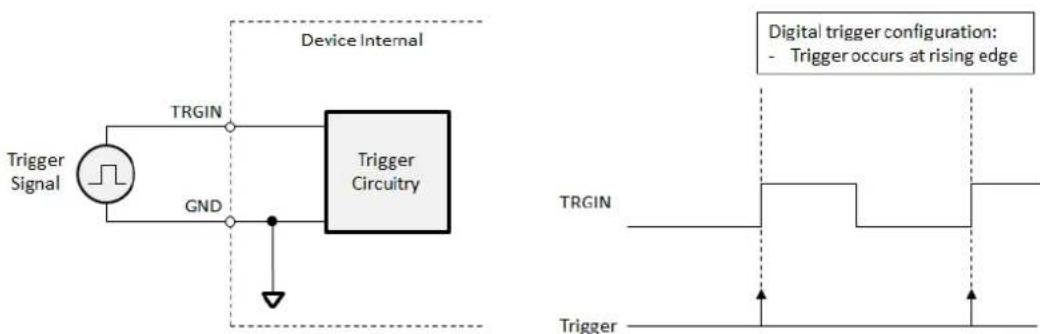
Figure 3.10 Digital Trigger Signal Connection and Signals
3.6.3 Analog Triggers
The triggers can also be routed from the measured results of the analog input channels. This is called analog trigger. Users need to select one of the analog input channels as trigger signal source, set the trigger voltage threshold, and configure whether trigger occurs at rising edge or falling edge of the signal.
After configuration, the internal analog trigger circuitry begins to monitor the acquired samples (voltage) of the selected analog input channel. A trigger will occur when the voltage crosses the trigger voltage threshold with the same edge as configured. This is shown in Figure 3.13.
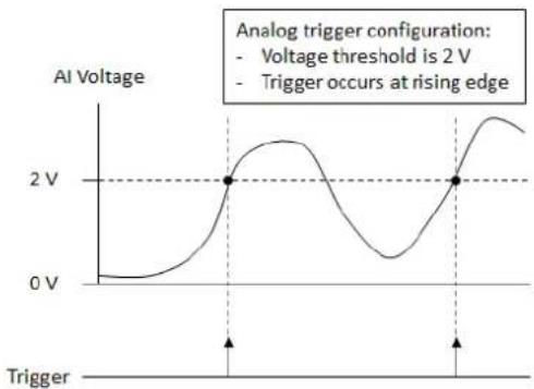
line
| Trigger | AI Voltage | | ------- | ---------- | | Threshold | 2 V | | Trigger | 2 V |Figure 3.11 Analog Triggers
To prevent false triggering due to noise or jitters in the signal, hysteresis can be added to the analog trigger. The hysteresis range is specified by percentage of the full-scale analog input range. For example, when selecting an analog input channel with ±10 V input range as analog trigger source, a 0.1% hysteresis range equals to 20 mV. Figure 3.14 shows examples of both rising edge and falling edge analog trigger with hysteresis.
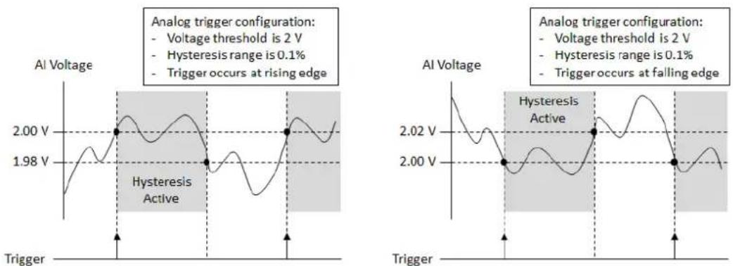
Figure 3.12 Analog Triggers with Hysteresis
3.7 Analog Calibration
3.7.1 Analog Calibration Overview
USB-5801 implements a specially designed circuitry for analog calibration. By selecting different calibration sources, each component of the analog functions can be calibrated individually. In addition, the calibration parameter is stored in an electrically-erasable programmable read-only memory (EEPROM). The block diagram is shown in Figure 3.15.

flowchart
graph TD
    A["ADC REF"] --> B["Calibration"]
    C["+10 V REF"] --> D["Calibration"]
    E["+5 V REF"] --> F["Calibration"]
    G["+2 V REF"] --> H["Calibration"]
    I["+1 V REF"] --> J["Calibration"]
    K["Calibration"] --> L["AO 0"]
    M["Calibration"] --> N["AO 1"]
    O["GND"] --> P["MUX"]
    Q["DMM"] --> R["Switch"]
    S["Test Points"] --> R
    T["GND"] --> R
    U["AI 0"] --> R
    V["AI 3"] --> R
    W["Calibration"] --> X["Calibration"]
    Y["EEPROM"] --> Z["Output"]
    style A fill:#f9f,stroke:#333
    style C fill:#f9f,stroke:#333
    style E fill:#f9f,stroke:#333
    style G fill:#f9f,stroke:#333
    style I fill:#f9f,stroke:#333
    style K fill:#f9f,stroke:#333
    style M fill:#f9f,stroke:#333
    style Q fill:#ccf,stroke:#333
    style S fill:#ccf,stroke:#333
    style T fill:#ccf,stroke:#333
    style U fill:#ccf,stroke:#333
    style V fill:#ccf,stroke:#333
    style W fill:#ccf,stroke:#333
Figure 3.13 Block Diagram of Analog Calibration Circuitry
The major calibration procedures are described as follows:
-
Voltage reference calibration*: Connect a digital multi-meter (DMM) to the test points, and route each of the voltage references (ADC REF, +10 V REF, +5 VREF, +2 V REF, and +1 V REF) to the test points through the analog multiplexer (MUX). Measure the voltage reference voltage values by the DMM and then calibrate.
-
Analog input calibration: Use the voltage references which is already calibrated as calibration source, route them to the analog input channels (Al n) through the MUX and switch and then calibrate. Use the corresponding voltage reference for each of the analog input range calibration.
-
Analog output calibration: Route the analog output channels to the analog input 0 which is already calibrated through the MUX and switch and then calibrate.
-
Store all calibration parameters to the EEPROM.
*Note: For users who do not have a high precision digital multi-meter (not less than 6.5 digits), voltage reference calibration can be skipped.
3.7.2 Voltage References Calibration
Voltage reference calibration steps:
- Connect a digital multi-meter (DMM) with precision not less than 6.5 digits to TP17 (positive terminal) and TP19 (negative terminal). Use DC voltage measurement mode.
- In the Navigator, choose one of the voltage references to calibrate. (+10 V, +5 V, +2 V, +1 V, or ADC)
- Observe the DMM reading and compare it to the "target voltage". Adjust the corresponding calibration parameter. If the reading is too small, increase the parameter; on the other hand, decrease the parameter. Repeat this step until the DMM reading is within the voltage range specified by "target voltage".
- Repeat steps 2 through 3 for all voltage references.
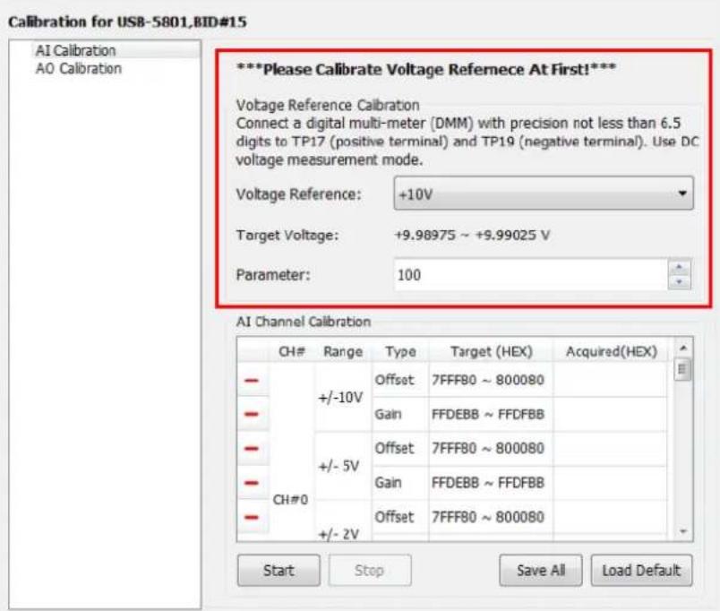
Figure 3.14 Voltage Reference Calibration
3.7.3 Analog Input Calibration
In the Navigator, select "AI Calibration", click "Start" button, and wait for calibration finished.

Figure 3.15 Analog Input Calibration
3.7.4 Analog Output Calibration
In the Navigator, select "AO Calibration", click "Start" button, and wait for calibration finished.

Figure 3.16 Analog Output Calibration
3.7.5 Store Calibration Parameters to EEPROM
After all calibration procedures are done, click "Save All" button to store calibration parameters into EEPROM. The parameters in the previous calibration procedures are temporarily stored in the on-board volatile memory. To prevent from losing those parameters after powering off, it is required to store them in a non-volatile memory such as an EEPROM.

Figure 3.17 Store Calibration Parameters to EEPROM
3.7.6 Load Default Calibration Parameters from EEPROM
Users can load the default (factory trimmed) calibration parameters from the EEPROM by clicking "Load Default" button if needed. Note that this operation only loads the parameters into the on-board volatile memory. To keep them permanently, it is required to store them into the EEPROM by clicking "Save All" button.

Figure 3.18 Load Default Calibration Parameters from EEPROM
3.8 Digital Input/Output
3.8.1 Digital Inputs
The USB-5801 provides 4 channels of digital input (DI) signal measurement with 2,500 V _DC galvanic isolation. Figure 3.21 shows the functional block diagram of one digital input channel.

Figure 3.19 Digital Input Functional Block Diagram
When an external voltage ( V_EX in Figure 3.21) is applied to the digital input between terminals I<0..3> and EC, the isolator output turns on. On the other hand, when the external voltage is removed, the isolator output turns off. Users will read logic high and logic low for these two circumstances in the software, respectively.
The value of the external voltage needs to be higher than the input high voltage (VIH) specification to turn on the isolator, and be lower than the input low voltage (VIL) specification to turn off the isolator. If the external voltage is between VIH and VIL, the reading in the software is uncertain and may be high or low.
The digital inputs accept both polarity of the external voltage.
3.8.1.1 Digital Input Interrupt
Users can use digital input signals to generate a software event (interrupt). The interrupt can occur at the rising edge, falling edge, or both edges of the digital input signal as shown in Figure 3.22. The interrupt function can be configured independently for each digital input channel.

Figure 3.20 Digital Input Interrupt
3.8.1.2 Digital Input Filter
To prevent false interrupts due to noise or bouncing in the signal, the digital input signals can be filtered. If digital input filter is enabled, transient signals with durations smaller than the filter duration will be considered as glitches and will not generate an interrupt. This is shown in Figure 3.23. Digital input filter can be enabled/disabled and filter duration can be configured independently for each channel.
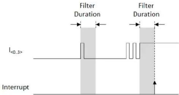
Figure 3.21 Digital Input Filter
3.8.2 Digital Outputs
The USB-5801 provides 4 channels of digital output (DO) signal generation with 2,500 V _DC galvanic isolation. Figure 3.24 shows the functional block diagram of one digital output channel.

Figure 3.22 Digital Output Functional Block Diagram
The load should be connected between the O<0..3> terminal and the positive terminal of the external source (VEX), and the ground of the external source should be connected to the ground of the USB-5801.
When the digital output is on, the MOSFET on the USB-5801 closes and provides a path for the load current flowing through to the ground. When the digital output is off, on the other hand, the MOSFET opens and blocks the path.
A flyback diode on the PC terminal provides a path for dissipating energy for inductive load when the digital output becomes off. This prevents the inductive load from generating a large back EMF which may damage the module.
3.9 Counter/Timer
The USB-5801 provides 2 channels of 32-bit counter/timer measurement with 2,500 V_DC galvanic isolation. Figure 3.25 shows the functional block diagram of one counter/timer channel.
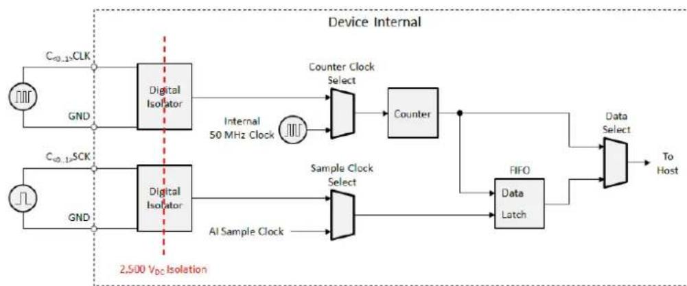
flowchart
graph LR
    A["Device Internal"] --> B["Digital Isolator"]
    B --> C["Counter Clock Select"]
    C --> D["Counter"]
    D --> E["FIFO Data Latch"]
    E --> F["Data Select"]
    F --> G["To Host"]
    H["Device Internal"] --> I["Digital Isolator"]
    I --> J["Sample Clock Select"]
    J --> K["AI Sample Clock"]
    K --> I
    style A fill:#f9f,stroke:#333
    style H fill:#f9f,stroke:#333
    style I fill:#f9f,stroke:#333
Figure 3.23 Counter/Timer Functional Block Diagram
Using different configurations, each counter/timer channel can support multiple functions. This is described in the following sections.
3.9.1 Event Counting
For event counting function, select external counter clock pin (C<0..1>CLK) as the counter clock. The counters can be configured to count (increase by one) when either the rising edge or the falling edge of the counter clock occurs. Software can read the latest counter value directly. This is shown in Figure 3.26.

Figure 3.24 Event Counting
3.9.2 Frequency Measurement (Tachometer)
For frequency measurement or tachometer function, select internal 50 MHz clock as the counter clock and external sample clock pin (C<0..1>SCK) as the sample clock. The signal to be measured should be connected to external sample clock pin.
The counter will count up at a rate of 50 MHz, which means one count is equal to 20 ns. Each time the signal to be measured rises (or falls according to the configuration), the counter value at that time will be stored in a FIFO. By subtracting consecutive two counter values (TCA and TCB), the period or the frequency of the signal can be calculated as shown in the following equations.
$$ \text { Period } = (T C _ {A} - T C _ {B}) \times 2 0 n s $$
$$ \text { Frequency } = 1 / \text { Period } $$
A frequency measurement example is shown in Figure 3.27.

flowchart
graph TD
    A["Frequency measurement configuration: - Sample at rising edge"] --> B["Counter Value"]
    B --> C["1000"]
    C --> D["2000"]
    D --> E["FIFO Values"]
    E --> F["1000"]
    F --> G["2000"]
    G --> H["Period of the signal: (2000 - 1000) × 20 ns = 20 μs\nFrequency of the signal: 1 / 20 μs = 50 kHz"]
Figure 3.25 Frequency Measurement
3.9.3 Phase Measurement for Analog Input Samples
When measuring a rotating device, users can use one counter as a tachometer to measure the speed of the rotation, and the other counter to measure the phase information of the acquired analog input samples. This is shown in Figure 3.28.

flowchart
graph TD
    A["Tachometer Pulse"] --> B["Al Sample Clock"]
    B --> C["Rotating Device"]
    D["Counter Value"] --> E["1000 1001 1005 2000"]
    E --> F["Tachometer Pulse"]
    F --> G["1000"]
    G --> H["Al Sample Clock"]
    H --> I["Phase Counter"]
    I --> J["0.3 V 1.5 V 1.5 V 0.3 V 1.5 V 0.4 V 0.7 V"]
    J --> K["1999 2004"]
    K --> L["1999 2000"]
    L --> M["1000 2000"]
    style A fill:#f9f,stroke:#333
    style B fill:#ccf,stroke:#333
    style D fill:#cfc,stroke:#333
    style E fill:#fcc,stroke:#333
    style F fill:#ffc,stroke:#333
    style G fill:#cfc,stroke:#333
    style H fill:#cfc,stroke:#333
    style I fill:#cfc,stroke:#333
    style J fill:#cfc,stroke:#333
    style K fill:#cfc,stroke:#333
    style L fill:#cfc,stroke:#333
    style M fill:#cfc,stroke:#333
    style_N["Al Samples"] --> O["0.4 V 0.4 V 0.7 V"]
Figure 3.26 Phase Measurement for Analog Input Samples
Connect tachometer signal to the external sample clock pin of counter 0 (C0SCK). Select internal 50 MHz clock as the counter clock for both counters, external sample clock pin as the sample clock for counter 0 (tachometer counter), and analog input sample clock as the sample clock for counter 1 (phase counter). Arm both counters at the same time, begin analog input acquisition, and then start the rotating device. All the information needed to calculate the rotating speed and phase of the AI samples will be collected automatically.
The rotating speed can be calculated as described in the previous section. To calculate the phase of the acquired analog input samples, users should first find the phase counter value related to the specified analog input sample (PC), and then find the tachometer counter values just above (TCA) and just below (TCB) the phase counter value. Finally, use the following equation to calculate the phase of the analog input sample. Note the position where the tachometer pulse occurs is set as a reference point (0 degree).
$$ \text { Phase (in degree) } = \frac {P C - T C _ {B}}{T C _ {A} - T C _ {B}} \times 3 6 0 ^ {\circ} $$
For example, to calculate the phase of the 1.5 V analog input sample (the second sample) in Figure 3.28, first find the corresponding PC, which is 1005. Then find the TCA and TCB, which are 1000 and 2000, respectively. Use the previous equation,
$$ \text { Phase (in degree) } = \frac {1 0 0 5 - 1 0 0 0}{2 0 0 0 - 1 0 0 0} \times 3 6 0 ^ {\circ} = 1. 8 ^ {\circ} $$
the phase of the 1.5 V analog input sample can be calculated as 1.8^ .
3.10 Synchronization
Multiple USB-5801 modules can be synchronized to support more acquisition channels.
Each module has one trigger input pin (TRGIN) and one trigger output pin (TRGOUT). To synchronize multiple modules, users must choose one of the modules to be the trigger master, and others as trigger slaves. Connect TRGOUT pin of the master to TRGIN pin of the first slave, and TRGOUT pin of the first slave to TRGIN pin of the second slave if present, and TRGOUT pin of the second slave to TRGIN pin of the third slave if present, and so on. This is shown in Figure 3.29.

flowchart
graph LR
    A["External Trigger Source (Optional)"] --> B["TRGIN<br>Master"]
    B --> C["TRGIN<br>TrgOUT"]
    C --> D["USB-5801 (Slave 1)"]
    D --> E["TRGIN<br>TrgOUT"]
    E --> F["USB-5801 (Slave 2)"]
    F --> G["..."]
Figure 3.27 Multiple Module Synchronization
Users can select one of the possible trigger sources for the master. However, all slaves must use external digital signal on TRGIN pin as the trigger source. When the master receives a trigger, the trigger signal level will present at TRGOUT pin immediately, which triggers the first slave. Then the TRGOUT pin of the first slaves immediately triggers the second slave, and so on.
Appendix A
Specifications
A.1 Analog Input
A.1.1 Functions
| Channels | 4, simultaneous sampling, can be enabled/disabled each channel independently by software |
| Input Configuration | Differential/Pseudo-differential (50 Ω between negative input and chassis ground), software selectable per channel |
| Input Coupling AC/DC, software selectable per channel | |
| Input Range ±10 V/±5 V/±2 V/ ±1 V, software selectable per channel | |
| A/D Converter (ADC) Resolution | 24 bits |
| A/D Converter (ADC) Type | Delta-sigma |
| Sample Rates ( f_s ) | |
| Range | 1 kS/s to 192 kS/s (AI sample rate setting must be the same as AO update rate) |
| Resolution | 68.21 μS/s (1 kS/s to 8 kS/s)136.42 μS/s (8 kS/s to 16 kS/s)272.84 μS/s (16 kS/s to 32 kS/s)545.69 μS/s (32 kS/s to 64 kS/s)1.09 mS/s (64 kS/s to 128 kS/s)2.18 mS/s (128 kS/s to 192 kS/s) |
| FIFO Buffer Size 4,096 samples | |
A.1.2 ADC Modulator Oversample Rate
| Sample Rate (fs) | Oversample Rate |
| 1 kS/s < fs < 8 kS/s 128 fs | |
| 8 kS/s < fs ≤ 16 kS/s 64 fs | |
| 16 kS/s < fs ≤ 32 kS/s 32 fs | |
| 32 kS/s < fs ≤ 64 kS/s 64 fs | |
| 64 kS/s < fs ≤ 192 kS/s 32 fs |
A.1.3 Maximum Operating Voltage
| IEPE | Input Coupling | Input Configuration | Positive Terminal (+)* | Negative Terminal (-)* |
| Disabled | AC | Differential | ±22 V | ±22 V |
| Disabled | AC | Pseudo-differential | ±19 V | ±9 V |
| Disabled | DC | Differential | ±12 V | ±12 V |
| Disabled | DC | Pseudo-differential | ±12 V | ±9 V |
| Enabled | AC | Pseudo-differential | 0 ~ +24 V | 0 ~ +1 V |
* Voltages with respect to chassis ground.
Note: Input coupling must be AC and input configuration must be pseudo-differential when IEPE is enabled.
A.1.4 Input Overvoltage Protection
Input Configuration Positive Terminal (+)* Negative Terminal (-)*
Differential ±24 V ±24 V
Pseudo-Differential ±24 V ±10 V
* Voltages with respect to chassis ground.
A.1.5 AC Coupled Measurement Accuracy
| Gain Error (fin=1 kHz) |
| Operating temperature within 5 °C of last auto-calibration temperature: < ±0.5 % |
| Over full operating temperature range: < ±2.5% |
| Offset Error |
| Operating temperature within 5 °C of last auto-calibration temperature: < ±1 mV |
| Over full operating temperature range: < ±5 mV |
A.1.6 DC Coupled Measurement Accuracy
| Gain Error |
| Operating temperature within 5 °C of last auto-calibration temperature: < ±0.02 % |
| Over full operating temperature range: < ±0.1 % |
| Offset Error |
| Operating temperature within 5 °C of last auto-calibration temperature: < ±0.2 mV |
| Over full operating temperature range: < ±0.5 mV |
A.1.7 Input Impedance
| Input Configuration | Between Positive Terminal (+) and Chassis Ground | Between Negative Terminal (-) and Chassis Ground |
| Differential | 200 kΩ | 200 kΩ |
| Pseudo-Differential 200 kΩ | 50 Ω |
A.1.8 Common-Mode Rejection Ratio (CMRR)
Input Frequency < 20 kHz: 60 dB
A.1.9 Frequency Response
| Pass-band ripple: ±0.005 dB |
| Pass-band |
| ±0.005 dB bandwidth: 0.4 × fs |
| -0.1 dB bandwidth: 0.409 × fs |
| -3 dB bandwidth: 0.433 × fs |
| Stop-band frequency: 0.499 × fs |
| Stop-band attenuation: >105 dB |
A.1.10 AC Coupling
| -3 dB cutoff frequency: 0.796 Hz |
| -0.1 dB cutoff frequency: 5.215 Hz |
A.1.11 Idle Channel Noise
| Input Range | f_s=32 kS/s f | s=128 kS/s f | s=192 kS/s | |||
| μVrms | ENOB | μVrms | ENOB | μVrms | ENOB | |
| ±10.0 V | 20.5 | 19.9 | 30.8 | 19.3 | 30.8 | 19.3 |
| ±5.0 V | 10.4 | 19.8 | 15.8 | 19.2 | 15.8 | 19.2 |
| ±2.0 V | 4.3 | 19.8 | 6.7 | 19.1 | 7.0 | 19.1 |
| ±1.0 V | 2.5 | 19.6 | 3.9 | 18.9 | 4.4 | 18.8 |
A.1.12 Dynamic Range (DR)
| Input Range | Dynamic Range (dB)* | ||
| f_s=32 kS/s | f_s=128 kS/s | f_s=192 kS/s | |
| ±10.0 V | 108 | 106 | 104 |
| ±5.0 V | 105 | 102 | 100 |
| ±2.0 V | 102 | 98 | 94 |
| ±1.0 V | 98 | 92 | 89 |
| * 1 kHz input tone, unweighted. Input amplitude is -60 dBFS. | |||
A.1.13 Spurious Free Dynamic Range (SFDR)
| Input Range | Spurious Free Dynamic Range (dBc)*,** | ||
| f_s=32 kS/s | f_s=128 kS/s | f_s=192 kS/s | |
| ±10.0 V | 106 | 107 | 100 |
| ±5.0 V | 107 | 107 | 103 |
| ±2.0 V | 108 | 108 | 96 |
| ±1.0 V | 101 | 104 | 91 |
| * 1 kHz input tone, input amplitude is -1 dBFS. ** Measurement includes all harmonics. | |||
A.1.14 Signal-to-Noise Ratio (SNR)
| Input Range | Signal-to-Noise Ratio (dB)* | ||
| f_s=32 kS/s f | s=128 kS/s f | s=192 kS/s | |
| ±10.0 V 105 103 100 | |||
| ±5.0 V 103 101 98 | |||
| ±2.0 V 98 96 92 | |||
| ±1.0 V 93 91 87 | |||
| * 1 kHz input tone, input amplitude is -1 dBFS. | |||
A.1.15 Total Harmonic Distortion (THD)
| Input Range | Total Harmonic Distortion (dB)* | ||
| f_s=32 kS/s f | s=128 kS/s f | s=192 kS/s | |
| ±10.0 V -103 | -104 | -97 | |
| ±5.0 V | -104 | -104 | -101 |
| ±2.0 V | -108 | -106 | -102 |
| ±1.0 V | -106 | -103 | -101 |
| * 1 kHz input tone, input amplitude is -1 dBFS. | |||
A.1.16 Total Harmonic Distortion Plus Noise (THD+N)
| Input Range | Total Harmonic Distortion Plus Noise (dB)* | ||
| f_s = 32 kS/s | f_s = 128 kS/s | f_s = 192 kS/s | |
| ±10.0 V | -101 | -101 | -95 |
| ±5.0 V | -100 | -99 | -96 |
| ±2.0 V | -98 | -96 | -92 |
| ±1.0 V | -93 | -91 | -86 |
| * 1 kHz input tone, input amplitude is -1 dBFS. | |||
A.1.17 Crosstalk
| Input Range | Crosstalk (dBc)* | |
| 32 kS/s f_in = 1 kHz | 192 kS/s f_in = 20 kHz | |
| ±10.0 V | -104 | -100 |
| ±5.0 V | -104 | -100 |
| ±2.0 V | -104 | -99 |
| ±1.0 V | -103 | -97 |
| * Input amplitude is -1 dBFS. | ||
A.1.18 Integrated Electronic Piezoelectric Excitation (IEPE)
Current: 0 or 2 mA ± 5%, each channel independently software selectable
Compliance: 24 V min.
Fault Detection
Threshold: < 1.5 V (short), > 19.5 V (open)
Indication: Software, per channel
A.2 Analog Output
A.2.1 Functions
| Channels | 2, can be enabled/disabled each channel independently by software |
| Output Configuration | Pseudo-differential (50 Ω between negative input and chassis ground) |
| Output Coupling DC | |
| Output Range ±10 V/ ±1 V, software selectable per channel | |
| D/A Converter (DAC) Resolution | 24 bits |
| D/A Converter (DAC) type Delta-sigma | |
| Update Rates (fs) | 1 kS/s to 192 kS/s (AO update rate setting must be the same as AI sample rate) |
| Output Load ≥ 1 kΩ | |
| FIFO Buffer Size 4,096 samples | |
A.2.2 Analog Output Accuracy
| Gain Error |
| Operating temperature within 5 °C of last auto-calibration temperature: < ±0.03 % |
| Over full operating temperature range: < ±0.15 % |
| Offset Error |
| Operating temperature within 5 °C of last auto-calibration temperature: < ±0.5 mV |
| Over full operating temperature range: < ±2.5 mV |
A.2.3 Output Noise
| Output Range | f_s = 32 kS/s f | s = 128 kS/s f | s = 192 kS/s |
| V_rms | V_rms | V_rms | |
| ±10.0 V/±1.0 V 70.7 70.2 60.7 | |||
A.2.4 Spurious Free Dynamic Range (SFDR)
| Output Range | Spurious Free Dynamic Range (dBc)*,** | ||
| f_s=32 kS/s f | s=128 kS/s f | s=192 kS/s | |
| ±10.0 V 88 91 93 | |||
| ±1.0 V 87 89 92 | |||
| * 1 kHz output tone, output amplitude is -1 dBFS.** Measurement includes all harmonics. | |||
A.2.5 Signal-to-Noise Ratio (SNR)
| Output Range | Signal-to-Noise Ratio (dB)* | ||
| f_s=32 kS/s f | s=128 kS/s f | s=192 kS/s | |
| ±10.0 V 86 90 96 | |||
| ±1.0 V 77 77 79 | |||
| * 1 kHz output tone, output amplitude is -1 dBFS. | |||
A.2.6 Total Harmonic Distortion (THD)
| Output Range | Total Harmonic Distortion (dB)* | ||
| f_s=32 kS/s f | s=128 kS/s f | s=192 kS/s | |
| ±10.0 V -90 -90 -92 | |||
| ±1.0 V -87 -85 -89 | |||
| * 1 kHz output tone, output amplitude is -1 dBFS. | |||
A.2.7 Total Harmonic Distortion Plus Noise (THD+N)
| Output Range | Total Harmonic Distortion Plus Noise (dB)* | ||
| f_s=32 kS/s f | s=128 kS/s f | s=192 kS/s | |
| ±10.0 V -85 -87 -91 | |||
| ±1.0 V -76 -76 -79 | |||
| * 1 kHz output tone, output amplitude is -1 dBFS. | |||
A.3 Triggers
Trigger Function Start trigger/stop trigger/index trigger
A.3.1 Analog Trigger Input
| Source Any analog input channel | |||
| Threshold Level Full scale of analog input range, software programmable | |||
| Resolution | 24 | bits | |
| Hysteresis | Programmable | ||
| Polarity | Rising | edge/falling | edge, software selectable |
A.3.2 Digital Trigger Input
| Source 1 external digital trigger input | |
| Input Voltage | |
| Logic 0 < +1.5 V (-0.5 V min.) | |
| Logic 1 > +3.5 V (+5.5 V max.) | |
| Pull-up Resistor 10 kΩ | |
| Polarity Rising edge/falling edge, software selectable | |
| Minimum Pulse Width 500 ns | |
| Isolation Protection 2,500 V_DC |
A.3.3 Digital Trigger Output
| Channels | 1 |
| Source | Analog trigger input/digital trigger input/software trigger, software selectable |
| Output Voltage | |
| Logic 0 | < +0.5 V |
| Logic 1 | > +4.5 V |
| Isolation Protection | 2,500 V_DC |
A.4 Tachometer
| Channels | 2 |
| Functions | Frequency (period) measurement |
| Input Voltage (referenced to GND pin) | |
| Logic 0 | < +3 V (-30 V min.) |
| Logic 1 | > +10 V (+30 V max.) |
| Input Frequency | 5 kHz max. |
| Digital Filter | 16 μs ~ 131 ms |
| Isolation Protection | 2,500 V_DC |
A.5 Digital I/O
A.5.1 Digital Input
| Channels 4 | |
| Input Voltage (referenced to ECOM pin) | |
| Logic 0 -3 V ~ +3 V | |
| Logic 1 > +10 V (+30 V max.) or < -10 V (-30 V min.) | |
| Opto-Isolator Response Time | 100 μs |
| Digital Filter 16 μs ~ 131 ms | |
| Isolation Protection | 2,500 V_DC |
A.5.2 Digital Output
| Channels 4 | |
| Load Voltage(referenced to GND pin) | 5 ~ 40 V_DC |
| Load Current 350 mA/ch (sink) | |
| Opto-Isolator Response Time | 100 μs |
| Isolation Protection | 2,500 V_DC |
A.6 General Specifications
A.6.1 Bus Interface
| Interface USB 3.0 |
| Data Transfer Rate 5 Gbps |
A.6.2 Power Requirements
| Power Consumption | 150 mA typ./200 mA max. @ 24 V external power |
| 700 mA typ./860 mA max. @ 5 V bus power |
A.6.3 Physical
| Dimensions 168 mm x 120 mm x 45 mm | |
| Weight | 290 g |
| I/O Connector | BNC x 6 (AI & AO)10-pin 3.81 mm terminal x 2 (tachometer & DI/O)3-pin 3.81 mm terminal x 2 (power)USB 3.0 type A (downstream port)USB 3.0 type B (upstream port) |
A.6.4 Environmental
| Operating Temperature 0 to 60 °C (32 to 140 °F) |
| Storage Temperature -40 to 70 °C (-40 to 158 °F) |
| Operating Humidity 10 to 90% RH, non-condensing |
| Storage Humidity 5 to 95% RH, non-condensing |
| Indoor Use Only. |
www.advantech.com
Please verify specifications before quoting. This guide is intended for reference purposes only.
All product specifications are subject to change without notice.
No part of this publication may be reproduced in any form or by any means, such as electronically, by photocopying, recording, or otherwise, without prior written permission from the publisher.
All brand and product names are trademarks or registered trademarks of their respective companies.
© Advantech Co., Ltd. 2019


- USB-5801
- Copyright
- Acknowledgments
- Product Warranty (2 years)
- CE
- Technical Support and Assistance
- Packing List
- Safety Precautions - Static Electricity
- Contents
- Chapter 1 Introduction......1
- Chapter 2 Installation....7
- Chapter 3 Signal Connections....15
- Appendix A Specifications.... 39
- Chapter 1
- Introduction
- Features
- USB 3.0 SuperSpeed
- Easy Maintenance
- Compact Size
- Built-In USB Hub with Daisy Chaining Support
- Redundant Power
- Board ID Switch
- Installation Guide
- Software Overview
- DAQNavi Software
- DAQnavi Device Driver Programming Roadmap
- Programming Tools
- Programming with DAQnavi Device Drivers Function Library
- Troubleshooting DAQnavi Device Drivers Error
- Accessories
- Chapter 2
- Installation
- Unpacking Instructions
- Driver Installation
- Hardware Installation
- Device Setup and Configuration
- Setting Up a Device
- Configuring the Device
- Chapter 3
- Signal Connections
- Overview
- Dimensions
- Connector, Switch, and LED
- Analog Input
- Analog Input Overview
- Analog Input Channel Types
- Analog Input Coupling
- Integrated Electronic Piezoelectric (IEPE) Excitation
- IEPE Fault Detection
- Analog Input Ranges
- Sample Rate and Anti-Aliasing Filters
- Analog Input Measurement Types
- Analog Output
- Analog Output Overview
- Analog Output Channel Types
- Analog Output Loads
- Analog Output Generation Types
- Trigger
- Trigger Functions
- Digital Triggers
- Analog Triggers
- Analog Calibration
- Analog Calibration Overview
- Voltage References Calibration
- Analog Input Calibration
- Analog Output Calibration
- Store Calibration Parameters to EEPROM
- Load Default Calibration Parameters from EEPROM
- Digital Input/Output
- Digital Inputs
- Digital Input Interrupt
- Digital Input Filter
- Digital Outputs
- Counter/Timer
- Event Counting
- Frequency Measurement (Tachometer)
- Phase Measurement for Analog Input Samples
- Synchronization
- Appendix A
- A.1 Analog Input
- A.1.1 Functions
- A.1.2 ADC Modulator Oversample Rate
- A.1.3 Maximum Operating Voltage
- A.1.4 Input Overvoltage Protection
- A.1.5 AC Coupled Measurement Accuracy
- A.1.6 DC Coupled Measurement Accuracy
- A.1.7 Input Impedance
- A.1.8 Common-Mode Rejection Ratio (CMRR)
- A.1.9 Frequency Response
- A.1.10 AC Coupling
- A.1.11 Idle Channel Noise
- A.1.12 Dynamic Range (DR)
- A.1.13 Spurious Free Dynamic Range (SFDR)
- A.1.14 Signal-to-Noise Ratio (SNR)
- A.1.15 Total Harmonic Distortion (THD)
- A.1.16 Total Harmonic Distortion Plus Noise (THD+N)
- A.1.17 Crosstalk
- A.1.18 Integrated Electronic Piezoelectric Excitation (IEPE)
- A.2 Analog Output
- A.2.1 Functions
- A.2.2 Analog Output Accuracy
- A.2.3 Output Noise
- A.2.4 Spurious Free Dynamic Range (SFDR)
- A.2.5 Signal-to-Noise Ratio (SNR)
- A.2.6 Total Harmonic Distortion (THD)
- A.2.7 Total Harmonic Distortion Plus Noise (THD+N)
- A.3 Triggers
- A.3.1 Analog Trigger Input
- A.3.2 Digital Trigger Input
- A.3.3 Digital Trigger Output
- A.4 Tachometer
- A.5 Digital I/O
- A.5.1 Digital Input
- A.5.2 Digital Output
- A.6 General Specifications
- A.6.1 Bus Interface
- A.6.2 Power Requirements
- A.6.3 Physical
- A.6.4 Environmental
- www.advantech.com
Brand : Advantech
Model : USB-5801-AE
Category : Module d'acquisition de données