
BG3 - SSD Drive TOSHIBA - Free user manual and instructions
Find the device manual for free BG3 TOSHIBA in PDF.


| Product Type | SSD Drive |
| Manufacturer | Toshiba (Kioxia) |
| Model Series | BG3 |
| Capacities | 128GB, 256GB, 512GB |
| Form Factors | M.2 1620 single package (20mm x 16mm x 1.3/1.5mm) and M.2 2230 single-sided module (30mm x 22mm x 2.18/2.38mm) |
| Interface | PCIe Gen3 x2, NVMe 1.2.1 |
| Memory Type | Toshiba 64-layer BiCS FLASH TLC |
| Sequential Read (Max) | Non-SED: up to 1,500 MB/s; SED: up to 1,300 MB/s |
| Sequential Write (Max) | Non-SED: up to 1,000 MB/s; SED: up to 950 MB/s |
| Power Consumption (Typical) | Read: 2.7-3.3W, Write: 2.1-3.2W, Idle PS3: 50mW, PS4: 5mW |
| Supply Voltage | 3.3V, 1.8V, 1.2V (1620); 3.3V (2230) |
| Operating Temperature | 0 to 80°C (package or component temperature) |
| Non-operating Temperature | -40 to 85°C |
| Shock Resistance | Operating: 1,500 G / 0.5ms; Non-operating: 100cm free drop |
| Vibration Resistance | Operating: 20 G peak, 10-2000 Hz |
| Reliability | MTTF: 1,500,000 hours; Product Life: ~5 years |
| Weight | M.2 1620: 0.85-1.00g; M.2 2230: 2.42-2.60g |
| Key Features | Host Memory Buffer (HMB), Host Controlled Thermal Management (HCTM), Device Self-test, Firmware Security, TCG OPAL 2.01 (SED models) |
| Compliance | UL, cUL, TÜV, KC, FCC, BSMI, CE, RCM, ISED, VCCI, Moroccan conformity (M.2 2230 only) |
| Maintenance | No user-serviceable parts. Use in clean, dry environment. |
| Safety Precautions | Use within specified voltage and temperature. Avoid physical shock. |
| Spare Parts and Repairability | Not repairable. Replacement required. Warranty coverage varies. |
Frequently Asked Questions - BG3 TOSHIBA
User questions about BG3 TOSHIBA
0 question about this device. Answer the ones you know or ask your own.
Ask a new question about this device
Download the instructions for your SSD Drive in PDF format for free! Find your manual BG3 - TOSHIBA and take your electronic device back in hand. On this page are published all the documents necessary for the use of your device. BG3 by TOSHIBA.
USER MANUAL BG3 TOSHIBA
The BG3 series leverages 64-layer, 3-bit-per-cell (TLC) BICS FLASH™ and features NVMe™ Revision 1.2.1. With Host Memory Buffer (HMB) technology, this SSD series retains high performance in a DRAM-less architecture, while enabling reduced power and a smaller footprint.
BG3 SSDs, as an innovative, next generation single-package ball grid array (BGA) SSD product line, harness the flexibility in system design that enables mobile computing and IoT embedded devices to be smaller, lighter, faster, and more power efficient. Also, these power-saving BG3 SSDs offer data center applications an alternative solution for server boot storage.
The BG3 series is available in 128GB, 256GB, and 512GB capacities. All three models are available in a surface-mount single package M.2 1620 or a removable module M.2 2230 form factor. BG3 SED models are also available.

> KEY FEATURES
• Toshiba 64-Layer BiCS FLASH™
• PCIe® Gen3*2L NVMe™
• Capacities up to 512GB
- M.2 1620 single package and M.2 2230 single-sided form factor
• TCG OPAL 2.01 Optional for SED
> APPLICATIONS
- Ultra-mobile PCs
• 2-in-1 notebook PCs
• IoT/embedded devices
• Server and storage array boot drives
> SPECIFICATIONS
| Standard Models | M.2 1620-S2Single Package | M.2 1620-S3Single Package | M.2 2230-S2Single-sided | M.2 2230-S3Single-sided | ||||
| Model Number | (Non-SED) | KBG30ZPZ128G | KBG30ZPZ256G | KBG30ZPZ512G | KBG30ZMS128G | KBG30ZMS256G | KBG30ZMS512G | |
| (SED) | KBG3AZPZ128G | KBG3AZPZ256G | KBG3AZP Z512G | KBG3AZMS128G | KBG3AZMS256G | KBG3AZMS512G | ||
| Memory | TLC (BiCS FLASHTM) | |||||||
| Interface | PCI Express® Base Specification Revision 3.1a (PCIe®) | |||||||
| Standard Models | M.2 1620-S2Single Package | M.2 1620-S3Single Package | M.2 2230-S2Single-sided | M.2 2230-S3Single-sided | |
| Size | 20.0 mm x16.0 mm x1.3 mm | 20.0 mm x16.0 mm x1.5 mm | 30.0 mm x22.0 mm x2.18 mm | 30.0 mm x22.0 mm x2.38 mm | |
| Weight | 0.85 g typ. | 1.00 g typ. | 2.42 g typ. | 2.60 g typ. | |
| Tempera-ture | Operating | 0 to 80 °C(Package Surface Temperature) | 0 to 80 °C(Components Temperature) | ||
| Non-operating | -40 to 85 °C | ||||
| Reliability3) | Mean Time to Failure (MTTF): 1,500,000 hoursProduct Life: Approximately 5 years | ||||
| More Features | ·Device Self-test is supported.·Host Controlled Thermal Management (HCTM) is supported.·The feature of Host Memory Buffer (HMB) is supported.·Firmware security feature (only digitally signed firmware can be installed) is supported. | ||||
| Compliance4) | UL, cUL, TÜV, KC, FCC, BSMI, CE, RCM, ISED, VCCI, Moroccan conformity mark | ||||
Note: 1) Definition of capacity: Toshiba Memory Corporation defines a megabyte (MB) as 1,000,000 bytes, a gigabyte (GB) as 1,000,000,000 bytes and a terabyte (TB) as 1,000,000,000,000 bytes. A computer operating system, however, reports storage capacity using powers of 2 for the definition of 1GB = 230 = 1,073,741,824 bytes and therefore shows less storage capacity. Available storage capacity (including examples of various media files) will vary based on file size, formatting, settings, software and operating system, such as Microsoft Operating System and/or pre-installed software applications, or media content. Actual formatted capacity may vary.
2) Read and write speed, tested on the state of "Host Memory Buffer (HMB) = On", may vary depending on the host device, read and write conditions, and file size. 1 MiB (mebibyte) = 220 bytes = 1,048,576 bytes, and 1 MB (megabyte) = 1,000,000 bytes.
3) MTTF (Mean Time to Failure) is not a guarantee or estimate of product life; it is a statistical value related to mean failure rates for a large number of products which may not accurately reflect actual operation. Actual operating life of the product may be different from the MTTF.
4) The Safety/EMI Standard is supported for KBG3xZMSxxxx only.
* PCIe and PCI Express are registered trademarks of PCI-SIG
* NVMe™ and NVM Express™ are trademarks of NVM Express, Inc.
* All other company names, product names, and service names mentioned herein may be trademarks of their respective companies.
* Availability of the SED model line-up may vary by region.
> ORDERING INFORMATION
| 1 | 2 | 3 | 4 | 5 | 6 | 7 | 8 |
- Product Name K: SSD product
- Prodct Category BG: BG Series
- Development Generation 3: Generation 3
- Option Code 1 0: Non-SED
A: SED
-
Option Code 2 Z: No-option
-
Connector Type M: M.2 (B-M Key)
P: M.2 BGA
- Form Factor S: M.2 2230 Single Sided
Z: M.2 1620 Single Package
- Capacity 128G / 256G / 512G
128G is 128 GB, 256G is 256 GB and 512G is 512 GB
(1 GB = 1,000,000,000 bytes)
PRODUCT LINE UP
| Model Number | Formatted Capacity | Form Factor/Connect Type | Function |
| Note | |||
| KBG30ZPZ128G | 128 GB | M.2 1620-S2 1) | Non-SED |
| KBG30ZPZ256G | 256 GB | ||
| KBG30ZPZ512G | 512 GB | M.2 1620-S3 2) | |
| KBG3AZPZ128G | 128 GB | M.2 1620-S2 1) | SED 3) |
| KBG3AZPZ256G | 256 GB | ||
| KBG3AZPZ512G | 512 GB | M.2 1620-S3 2) | |
| KBG30ZMS128G | 128 GB | M.2 2230-S2 1) -B-M | Non-SED |
| KBG30ZMS256G | 256 GB | ||
| KBG30ZMS512G | 512 GB | M.2 2230-S3 2) -B-M | |
| KBG3AZMS128G | 128 GB | M.2 2230-S2 1) -B-M | SED 3) |
| KBG3AZMS256G | 256 GB | ||
| KBG3AZMS512G | 512 GB | M.2 2230-S3 2) -B-M |
Note: 1) Single Sided/Top side 1.35mm Maximum Thickness
2) Single Sided/Top side 1.5 mm Maximum Thickness
3) Availability of the SED model line-up may vary by region.
CAPACITY
| Capacity | Total Number of User Addressable Sectors in LBA Mode | |
| 512 bytes sector | 4,096 bytes sector | |
| 128 GB1) | 250,069,680 | 31,258,710 |
| 256 GB1) | 500,118,192 | 62,514,774 |
| 512 GB1) | 1,000,215,216 | 125,026,902 |
Note: 1) 1 GB (Gigabyte) = 1,000,000,000 bytes
PERFORMANCE
| Standard Models | (Non-SED) | KBG30ZPZ128G KBG30ZMS128G | KBG30ZPZ256G KBG30ZMS256G | KBG30ZPZ512G KBG30ZMS512G |
| (SED) | KBG3AZPZ128G KBG3AZMS128G | KBG3AZPZ256G KBG3AZMS256G | KBG3AZPZ512G KBG3AZMS512G | |
| Interface Speed | 16 GT/s (Gen3x2 Lane), 8 GT/s (Gen3x1 Lane)10 GT/s (Gen2x2 Lane), 5 GT/s (Gen2x1 Lane)5 GT/s (Gen1x2 Lane), 2.5 GT/s (Gen1x1 Lane) | |||
| Sequential Read 1) (Up to) | (Non-SED) | 1,300 MB/s {1,240 MiB/s} | 1,400 MB/s {1,330 MiB/s} | 1,500 MB/s {1,430 MiB/s} |
| (SED) | 1,200 MB/s {1,140 MiB/s} | 1,250 MB/s {1,190 MiB/s} | 1,300 MB/s {1,240 MiB/s} | |
| Sequential Write 1) (Up to) | (Non-SED) | 600 MB/s {570 MiB/s} | 800 MB/s {760 MiB/s} | 1,000 MB/s {950 MiB/s} |
| (SED) | 550 MB/s {520 MiB/s} | 750 MB/s {710 MiB/s} | 950 MB/s {900 MiB/s} | |
Note: 1) Under the condition of measurement with 128 KiB unit sequential access and 4KiB align. Queue depth is 32, and access range is 16GiB. 1KiB (Kibibyte) = 210 bytes = 1024 bytes
Products and specicaons discussed herein are for reference purposes only and are subject to change without noce. All informaon discussed herein is provided on an "as is" basis, without warranes of any kind. Before creang and producing designs and using, customers must refer to and comply with the latest versions of the product specicaons.
SUPPLY VOLTAGE
| Standard Models | M.2 1620 Single Package | M.2 2280 Module |
| Allowable voltage | 3.3 V ±5 %1.8 V ±5 %1.2 V ±5 % | 3.3 V ±5 % |
| Allowable noise/ripple | 100 mV p-p, 0-10MHz | |
| Allowable supply rise time | Comply to the PCI-SIG specification of Power Up/Down Sequence | 2 –100 ms |
POWER CONSUMPTION
| Operation(Ta1)=25°C) | M.2 1620 Single Package | ||
| KBG30ZPZ128GKBG3AZPZ128G | KBG30ZPZ256GKBG3AZPZ256G | KBG30ZPZ512GKBG3AZPZ512G | |
| Read2) | 2.7 W typ. | 2.8 W typ. | 2.8 W typ. |
| Write2) | 2.1 W typ. | 2.4 W typ. | 2.8 W typ. |
| Power State33) | 50 mW typ. | ||
| Power State43) | 5 mW typ. | ||
| Operation(Ta1)=25°C) | M.2 2230 Module | ||
| KBG30ZMS128GKBG3AZMS128G | KBG30ZMS256GKBG3AZMS256G | KBG30ZMS512GKBG3AZMS512G | |
| Read2) | 3.2 W typ. | 3.3 W typ. | 3.3 W typ. |
| Write2) | 2.5 W typ. | 2.8 W typ. | 3.2 W typ. |
| Power State 33) | 50 mW typ. | ||
| Power State 43) | 5 mW typ. | ||
Note: 1) Ambient Temperature
2) The values are specified at the condition causing maximum power consumption and Power State 0.
3) PCIe Link state L1.2
Power consumption during the Admin command processing is excluded.
ENVIRONMENTAL CONDITIONS
> TEMPERATURE
| Condition | Range | Gradient | |
| M.2 1620 Single Package | M.2 2280 Module | ||
| Operating1) | 0 °C (Tc) – 80 °C (Tc)(Package Temperature) | 0 °C (Tc) – 80 °C (Tc)(Components Temperature) | 30 °C (Ta) / h maximum |
| Non-operating | -40 °C – 85 °C | 30 °C / h maximum | |
| Under Shipment 2) | -40 °C – 85 °C | 30 °C / h maximum | |
Note: 1) Ta: Ambient Temperature, Tc: Package Surface or Components Temperature
2) Packaged in Toshiba Memory Corporation's original shipping package.
HUMIDITY
| Condition | Range |
| Operating | 8 % – 90 % R.H. (No condensation) |
| Non-operating | 8 % – 95 % R.H. (No condensation) |
| Under Shipment1) | 5 % – 95 % R.H. |
| Max. wet bulb | 32.5 °C (Operating)40.0 °C (Non-operating / Shipping) |
Note: 1) Packaged in Toshiba Memory Corporation's original shipping package.
> SHOCK
| Condition | Range |
| Operating1) | 14.709 km/s 2 {1,500 G}, 0.5 ms half sine wave |
| Non-operating1) | |
| Under Shipment2) | 100 cm free drop |
Note: 1) Apply shocks in each direction of the drive's three mutually perpendicular axes, one axis at a time.
2) Packaged in Toshiba Memory Corporation's original shipping package.
VIBRATION
| Condition | Range |
| Operating | 196 m/s 2 {20 G} Peak, 10 - 2,000 Hz(20 minutes per axis) x 3 axis |
| Non-operating |
Products and specicaons discussed herein are for reference purposes only and are subject to change without noce. All informaon discussed herein is provided on an "as is" basis, without warranes of any kind. Before creang and producing designs and using, customers must refer to and comply with the latest versions of the product specicaons.
COMPLIANCE
SAFETY / EMI STANDARDS
| Title | Description | Region |
| UL1)(Underwriters Laboratories) | UL 60950-1 | USA2) |
| cUL1)(Underwriters Laboratories of Canada) | CSA-C22.2 No.60950-1-07 | Canada |
| TÜV1)(Technischer Überwachungs Verein) | EN 60950-1 | EURO |
| KC1) | KN32, KN35 | Korea |
| FCC1) | FCC part 15 Subpart B | USA |
| BSMI1)(Bureau of Standards, Metrology and Inspection) | CNS13438 (CISPR Pub. 22) | Taiwan |
| CE1) | EN 55032, EN 55024 | EURO |
| RCM1) | AS/NZS CISPR 32 | Australia, New Zealand |
| ISED1) | ICES-003 | Canada |
| Moroccan conformity mark1) | NM EN 55032, NM EN 22024 | Morocco |
| VCCI1) | VCCI-CISPR32 | Japan |
Note: 1) The Safety/EMI Standard is supported for KBG3xZMSxxxx only.
2) UL certification is basically on a voluntary basis.
RELIABILITY
| Parameter | Value |
| Mean Time to Failure | 1,500,000 hours |
| Product Life | Approximately 5 years |
MECHANICAL SPECIFICATIONS
M.2 1620 SINGLE PACKAGE
| Model Number | Weight | Width | Height | Length |
| KBG30ZPZ128G | 0.85 g typ. | 16.00 mm | 1.30 mm | 20.00 mm |
| KBG3AZPZ128G | ||||
| KBG30ZPZ256G | ||||
| KBG3AZPZ256G | ||||
| KBG30ZPZ512G | 1.00 g typ. | 1.50 mm | ||
| KBG3AZPZ512G |
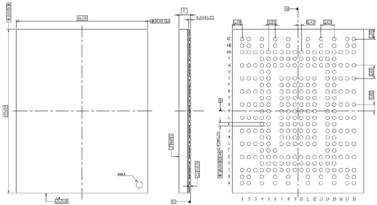
Unit:mm
| Dimension | Description | KBG30ZPZ128GKBG3AZPZ128GKBG30ZPZ256GKBG3AZPZ256G | KBG30ZPZ512GKBG3AZPZ512G |
| c | Thickness of BGA Package | 1.30 mm Max. | 1.50 mm Max. |
Figure 1: Dimensions of KBG3xZPZxxxx (Single Package)
Products and speciaons discussed herein are for reference purposes only and are subject to change without noce. All informaon discussed herein is provided on an “as is” basis, without warranes of any kind. Before creang and producing designs and using, customers must refer to and comply with the latest versions of the product speciaons.
M.2 2230 MODULE
| Model Number | Weight | Width | Height | Length |
| KBG30ZMS128GKBG3AZMS128G | 2.42 g typ. | 22.00 mm | 2.18 mm | 30.00 mm |
| KBG30ZMS256GKBG3AZMS256G | ||||
| KBG30ZMS512GKBG3AZMS512G | 2.60 g typ. | 2.38 mm |


Unit:mm
| Dimension | Description | KBG30ZMS128GKBG3AZMS128GKBG30ZMS256GKBG3AZMS256G | KBG30ZMS512GKBG3AZMS512G |
| A | Thickness of BGA Package (without label) | 1.30 mm Max. | 1.50 mm Max. |
Figure 2: Dimensions of KBG3xZMSxxxx (M.2 2230 Module)
Products and specicaons discussed herein are for reference purposes only and are subject to change without noce. All informaon discussed herein is provided on an "as is" basis, without warranes of any kind. Before creang and producing designs and using, customers must refer to and comply with the latest versions of the product specicaons.
INTERFACE CONNECTOR
M.2 1620 SINGLE PACKAGE
| 1 | 2 | 3 | 4 | 5 | 6 | 7 | 8 | 9 | 10 | 11 | 12 | 13 | 14 | 15 | 16 | 17 | 18 | |
| A | DNU | DNU | DNU | DNU | DNU | DNU | DNU | DNU | DNU | DNU | ||||||||
| B | DNU | DNU | DNU | NC | DNU | DNU | DNU | DNU | DNU | DNU | ||||||||
| C | GND | GND | GND | GND | GND | DNU | NC | NC | DNU | NC | DNU | DNU | RFU | RFU | GND | DNU | DNU | DNU |
| D | REFCLKP | REFCLKN | GND | PERST# | CLKREQ# | PWR1 | PWR1 | GND | DNU | DIAG1 | NC | RFU | ||||||
| E | GND | GND | GND | GND | GND | GND | GND | NC | PWR1 | PWR1 | GND | NC | DIAG0 | GND | GND | DNU | DNU | DNU |
| F | PERp0 | PERn0 | GND | PEDET | RFU | |||||||||||||
| G | GND | GND | GND | GND | GND | PWR3 | PWR3 | GND | GND | PWR3 | PWR3 | GND | GND | DNU | DNU | DNU | ||
| H | PETp0 | PETn0 | PWR3 | PWR3 | GND | GND | PWR3 | PWR3 | RFU | RFU | ||||||||
| J | GND | GND | GND | GND | GND | PWR3 | PWR3 | GND | GND | PWR3 | PWR3 | GND | GND | DNU | DNU | DNU | ||
| K | PERp1 | PERn1 | GND | GND | GND | GND | GND | GND | RFU | RFU | ||||||||
| L | GND | GND | GND | GND | GND | RFU | RFU | RFU | RFU | RFU | RFU | GND | GND | DNU | DNU | NC | ||
| M | PETp1 | PETn1 | RFU | RFU | GND | GND | RFU | RFU | RFU | RFU | ||||||||
| N | GND | GND | GND | GND | GND | RFU | RFU | RFU | RFU | RFU | RFU | GND | GND | DNU | NC | NC | ||
| P | NC | NC | GND | GND | GND | GND | GND | GND | RFU | RFU | ||||||||
| R | GND | GND | GND | GND | GND | PWR2 | PWR2 | GND | GND | PWR2 | PWR2 | GND | GND | DNU | NC | NC | ||
| T | NC | NC | PWR2 | PWR2 | GND | GND | PWR2 | PWR2 | RFU | RFU | ||||||||
| U | GND | GND | GND | GND | GND | PWR2 | PWR2 | GND | GND | PWR2 | PWR2 | GND | GND | DNU | NC | NC | ||
| V | NC | NC | RFU | RFU | ||||||||||||||
| W | GND | GND | GND | GND | GND | GND | LED1# | RFU | PWR1 | PWR1 | GND | RFU | RFU | GND | GND | DNU | DNU | NC |
| Y | NC | NC | GND | DNU | DNU | PWR1 | PWR1 | GND | DNU | GND | DNU | DNU | ||||||
| AA | GND | GND | GND | GND | GND | DNU | DNU | DNU | DNU | NC | DNU | DNU | DNU | GND | GND | DNU | DNU | DNU |
| AB | DNU | DNU | DNU | DNU | DNU | DNU | DNU | DNU | DNU | DNU | ||||||||
| AC | DNU | DNU | DNU | DNU | DNU | DNU | DNU | DNU | DNU | DNU |
Note: 1) The total ball number is 291.
2) The voltage powers must be supplied to each ball on all power rails.
3) NC is not used in KBG3xZPZxxxx. But NC ball function is assigned in PCI-SiG specification.
4) NC, DNU and RFU must be connected to independent OPEN land, and can't be connected between each other on host board.
5) DIAG0 and DIAG1 are engineering diagnosis balls. Toshiba Memory Corporation requests to enable access to DIAG0 and DIAG1 on host board.
Figure 3: Ball Map of KBG3xZPZxxxx (Single Package)
Products and speciaons discussed herein are for reference purposes only and are subject to change without noce. All informaon discussed herein is provided on an “as is” basis, without warranes of any kind. Before creang and producing designs and using, customers must refer to and comply with the latest versions of the product speciaons.
SINGLE PACKAGE INTERFACE SIGNALS
| Interface | Signal Name | Description | Location |
| Power and Grounds | PWR_1 | 3.3 V Source | D9, D10, E9, E10, W9, W10, Y9, Y10 |
| PWR_2 | 1.8 V Source | R7, R8, R11, R12, T7, T8, T11, T12, U7, U8, U11, U12 | |
| PWR_3 | 1.2 V Source | G7, G8, G11, G12, H7, H8, H11, H12, J7, J8, J11, J12 | |
| Power and Grounds | GND | GND | C1-C5, C15, D6, D11, E1-E7, E11, E14, E15, F6, G1-G5, G9, G10, G14, G15, H9, H10, J1-J5, J9, J10, J14, J15, K7-K12, L1-L5, L14, L15, M9, M10, N1-N5, N14, N15, P7-P12, R1-R5, R9, R10, R14, R15, T9, T10, U1-U5, U9, U10, U14, U15, W1-W6, W11, W14, W15, Y6, Y11, Y13, AA1-AA5, AA14, AA15 |
| PCIe | PERp0, PERn0 | PCIe 0Device Receiver | F4, F5 |
| PETp0, PETn0 | PCIe 0Device Transfer | H4, H5 | |
| PERp1, PERn1 | PCIe 1Device Receiver | K4, K5 | |
| PETp1, PETn1 | PCIe 1Device Transfer | M4, M5 | |
| REFCLKp, REFCLKn | PCIe Reference Clock | D4, D5 | |
| PERST# | PE-Reset | D7 | |
| CLKREQ# | Clock Request | D8 | |
| SSD Specific Signals | LED1# | Device Activity | W7 |
| PEDET | Host I/F Indication (PCIe:OPEN / SATA:GND) | F14 | |
| Optional Signals | DIAG0, DIAG1 | Diagnosis, option for engineering | D13, E13 |
Products and specicaons discussed herein are for reference purposes only and are subject to change without noce. All informaon discussed herein is provided on an "as is" basis, without warranes of any kind. Before creang and producing designs and using, customers must refer to and comply with the latest versions of the product specicaons.
| Interface | Signal Name | Description | Location |
| Other Signals | RFU | Reserved; OPEN | C13, C14, D15, F15, H14, H15, K14, K15, L7, L8, L9, L10, L11, L12, M7, M8, M11, M12, M14, M15, N7, N8, N9, N10, N11, N12, P14, P15, T14, T15, V14, V15, W8, W12, W13 |
| DNU | Manufacturing purpose only;OPEN | A1, A2, A4, A6, A8, A11, A13, A15, A17, A18, B1, B2, B4, B8, B11, B13, B15, B17, B18, C6, C9, C11, C12, C16-C18, D12, E16-E18, G16-G18, J16-J18, L16, L17, N16, R16, U16, W16, W17, Y7, Y8, Y12, Y14, Y15, AA6-AA9, AA11-AA13, AA16-AA18, AB1, AB2, AB4, AB6, AB8, AB11, AB13, AB15, AB17, AB18, AC1, AC2, AC4, AC6, AC8, AC11, AC13, AC15, AC17, AC18 | |
| NC | Not used; OPEN | B6, C7, C8, C10, D14, E8, E12, L18, N17, N18, P4, P5, R17, R18, T4, T5, U17, U18, V4, V5, W18, Y4, Y5, AA10 |
Products and specicaons discussed herein are for reference purposes only and are subject to change without noce. All informaon discussed herein is provided on an “as is” basis, without warranes of any kind. Before creang and producing designs and using, customers must refer to and comply with the latest versions of the product specicaons.
M.2 2230 MODULE

Unit:mm
Figure 4: Interface Dimensions of KBG3xZMSxxxx (M.2 2230 Module)
Products and specicaons discussed herein are for reference purposes only and are subject to change without noce. All informaon discussed herein is provided on an “as is” basis, without warranes of any kind. Before creang and producing designs and using, customers must refer to and comply with the latest versions of the product specicaons.
M.2 2230 MODULE CONNECTOR PIN ASSIGNMENT
| Pin # | Signal Name | Description |
| 1 | CONFIG_3 | GND |
| 3 | GND | GND |
| 5 | Reserved | NC |
| 7 | Reserved | NC |
| 9 | Reserved | NC |
| 11 | Reserved | NC |
| Notch | ||
| 21 | CONFIG_0 | GND |
| 23 | Reserved | NC |
| 25 | Reserved | NC |
| 27 | GND | GND |
| 29 | PETn1 | PCIe 1Device Transfer |
| 31 | PETp1 | |
| 33 | GND | GND |
| 35 | PERn1 | PCIe 1Device Receiver |
| 37 | PERp1 | |
| 39 | GND | GND |
| 41 | PETn0 | PCIe 0Device Transfer |
| 43 | PETp0 | |
| 45 | GND | GND |
| 47 | PERn0 | PCIe 0Device Receiver |
| 49 | PERp0 | |
| 51 | GND | GND |
| 53 | REFCLKn | PCIe Reference Clock |
| 55 | REFCLKp | PCIe Reference Clock |
| 57 | GND | GND |
| Notch | ||
| 67 | Reserved | NC |
| 69 | PEDET | Host I/F Indication (PCIe:OPEN / SATA:GND) |
| 71 | GND | GND |
| 73 | GND | GND |
| 75 | GND | GND |
| Pin # | Name | Description |
| 2 | +3.3V | 3.3 V Source |
| 4 | +3.3V | 3.3 V Source |
| 6 | Reserved | NC |
| 8 | Reserved | NC |
| 10 | LED1# | Device Activity |
| Notch | ||
| 20 | Reserved | NC |
| 22 | Reserved | NC |
| 24 | Reserved | NC |
| 26 | Reserved | NC |
| 28 | Reserved | NC |
| 30 | Reserved | NC |
| 32 | Reserved | NC |
| 34 | Reserved | NC |
| 36 | Reserved | NC |
| 38 | Reserved | NC |
| 40 | Reserved | NC |
| 42 | Reserved | NC |
| 44 | Reserved | NC |
| 46 | Reserved | NC |
| 48 | Reserved | NC |
| 50 | PERST# | PE-Reset |
| 52 | CLKREQ# | Clock Request |
| 54 | PEWAKE# | NC |
| 56 | MFG DATA | Manufacturing pin. Must NOT be connected on host board. |
| 58 | MFG CLOCK | |
| Notch | ||
| 68 | SUSCLK | NC |
| 70 | +3.3V | 3.3 V Source |
| 72 | +3.3V | 3.3 V Source |
| 74 | +3.3V | 3.3 V Source |
COMMAND TABLE
ADMIN Command set
| Op-Code | Command Name |
| 00h | Delete I/O Submission Queue |
| 01h | Create I/O Submission Queue |
| 02h | Get Log Page |
| 04h | Delete I/O Completion Queue |
| 05h | Create I/O Completion Queue |
| 06h | Identify |
| 08h | Abort |
| 09h | Set Features |
| 0Ah | Get Features |
| 0Ch | Asynchronous Event Request |
| 10h | Firmware Commit |
| 11h | Firmware Image Download |
| 14h | Device Self-Test (DST) |
| 80h | Format NVM |
| 81h | Security Send |
| 82h | Security Receive |
Set Features / Get Features Set
| Op-Code | Feature Name |
| 01h | Arbitration |
| 02h | Power Management |
| 04h | Temperature Threshold |
| 05h | Error Recovery |
| 06h | Volatile Write Cache |
| 07h | Number of Queues |
| 08h | Interrupt Coalescing |
| 09h | Interrupt Vector Configuration |
| 0Ah | Write Atomicity |
| 0Bh | Asynchronous Event Configuration |
| 0Ch | Autonomous Power State Transition |
| 0Dh | Host Memory Buffer (HMB) |
| 10h | Host Controlled Thermal Management (HCTM) |
Products and specicaons discussed herein are for reference purposes only and are subject to change without noce. All informaon discussed herein is provided on an "as is" basis, without warranes of any kind. Before creang and producing designs and using, customers must refer to and comply with the latest versions of the product specicaons.
NVMe Command Set
| Op-Code | Command Name |
| 00h | Flush |
| 01h | Write |
| 02h | Read |
| 04h | Write Uncorrectable |
| 05h | Compare |
| 09h | Dataset Management |
Products and specicaons discussed herein are for reference purposes only and are subject to change without noce. All informaon discussed herein is provided on an “as is” basis, without warranes of any kind. Before creang and producing designs and using, customers must refer to and comply with the latest versions of the product specicaons.
> RESTRICTIONS ON PRODUCT USE
Toshiba Corporation and its subsidiaries and affiliates are collectively referred to as "TOSHIBA".
Hardware, software and systems described in this document are collectively referred to as "Product".
- TOSHIBA reserves the right to make changes to the information in this document and related Product without notice.
- This document and any information herein may not be reproduced without prior written permission from TOSHIBA. Even with TOSHIBA's written permission, reproduction is permissible only if reproduction is without alteration/omission.
- Though TOSHIBA works continually to improve Product's quality and reliability, Product can malfunction or fail. Customers are responsible for complying with safety standards and for providing adequate designs and safeguards for their hardware, software and systems which minimize risk and avoid situations in which a malfunction or failure of Product could cause loss of human life, bodily injury or damage to property, including data loss or corruption. Before customers use the Product, create designs including the Product, or incorporate the Product into their own applications, customers must also refer to and comply with (a) the latest versions of all relevant TOSHIBA information, including without limitation, this document, the specifications, the data sheets and application notes for Product and the precautions and conditions set forth in the "TOSHIBA Semiconductor Reliability Handbook" and (b) the instructions for the application with which the Product will be used with or for. Customers are solely responsible for all aspects of their own product design or applications, including but not limited to (a) determining the appropriateness of the use of this Product in such design or applications; (b) evaluating and determining the applicability of any information contained in this document, or in charts, diagrams, programs, algorithms, sample application circuits, or any other referenced documents; and (c) validating all operating parameters for such designs and applications. TOSHIBA ASSUMES NO LIABILITY FOR CUSTOMERS' PRODUCT DESIGN OR APPLICATIONS.
- PRODUCT IS NEITHER INTENDED NOR WARRANTED FOR USE IN EQUIPMENTS OR SYSTEMS THAT REQUIRE EXTRAORDINARILY HIGH LEVELS OF QUALITY AND/OR RELIABILITY, AND/OR A MALFUNCTION OR FAILURE OF WHICH MAY CAUSE LOSS OF HUMAN LIFE, BODILY INJURY, SERIOUS PROPERTY DAMAGE AND/OR SERIOUS PUBLIC IMPACT ("UNINTENDED USE"). Except for specific applications as expressly stated in this document, Unintended Use includes, without limitation, equipment used in nuclear facilities, equipment used in the aerospace industry, medical equipment, equipment used for automobiles, trains, ships and other transportation, traffic signaling equipment, equipment used to control combustions or explosions, safety devices, elevators and escalators, devices related to electric power, and equipment used in finance-related fields. IF YOU USE PRODUCT FOR UNINTENDED USE, TOSHIBA ASSUMES NO LIABILITY FOR PRODUCT. For details, please contact your TOSHIBA sales representative.
- Do not disassemble, analyze, reverse-engineer, alter, modify, translate or copy Product, whether in whole or in part.
- Product shall not be used for or incorporated into any products or systems whose manufacture, use, or sale is prohibited under any applicable laws or regulations.
- The information contained herein is presented only as guidance for Product use. No responsibility is assumed by TOSHIBA for any infringement of patents or any other intellectual property rights of third parties that may result from the use of Product. No license to any intellectual property right is granted by this document, whether express or implied, by estoppel or otherwise.
- ABSENT A WRITTEN SIGNED AGREEMENT, EXCEPT AS PROVIDED IN THE RELEVANT TERMS AND CONDITIONS OF SALE FOR PRODUCT, AND TO THE MAXIMUM EXTENT ALLOWABLE BY LAW, TOSHIBA (1) ASSUMES NO LIABILITY WHATSOEVER, INCLUDING WITHOUT LIMITATION, INDIRECT, CONSEQUENTIAL, SPECIAL, OR INCIDENTAL DAMAGES OR LOSS, INCLUDING WITHOUT LIMITATION, LOSS OF PROFITS, LOSS OF OPPORTUNITIES, BUSINESS INTERRUPTION AND LOSS OF DATA, AND (2) DISCLAIMS ANY AND ALL EXPRESS OR IMPLIED WARRANTIES AND CONDITIONS RELATED TO SALE, USE OF PRODUCT, OR INFORMATION, INCLUDING WARRANTIES OR CONDITIONS OF MERCHANTABILITY, FITNESS FOR A PARTICULAR PURPOSE, ACCURACY OF INFORMATION, OR NONINFRINGEMENT.
- Do not use or otherwise make available Product or related software or technology for any military purposes, including without limitation, for the design, development, use, stockpiling or manufacturing of nuclear, chemical, or biological weapons or missile technology products (mass destruction weapons). Product and related software and technology may be controlled under the applicable export laws and regulations including, without limitation, the Japanese Foreign Exchange and Foreign Trade Law and the U.S. Export Administration Regulations. Export and re-export of Product or related software or technology are strictly prohibited except in compliance with all applicable export laws and regulations.
- Product may include products subject to foreign exchange and foreign trade control laws.
- Please contact your TOSHIBA sales representative for details as to environmental matters such as the RoHS compatibility of Product. Please use Product in compliance with all applicable laws and regulations that regulate the inclusion or use of controlled substances, including without limitation, the EU RoHS Directive. TOSHIBA ASSUMES NO LIABILITY FOR DAMAGES OR LOSSES OCCURRING AS A RESULT OF NONCOMPLIANCE WITH APPLICABLE LAWS AND REGULATIONS.
Brand : TOSHIBA
Model : BG3
Category : SSD Drive