
540s - SSD Drive INTEL - Free user manual and instructions
Find the device manual for free 540s INTEL in PDF.


| Product Type | Solid State Drive (SSD) |
| Brand | Intel |
| Model | 540s |
| Form Factor | 2.5-inch |
| Interface | SATA III 6Gb/s |
| Capacities Available | 120GB, 180GB, 240GB, 360GB, 480GB, 1TB |
| Sequential Read Speed | Up to 540 MB/s |
| Sequential Write Speed | Up to 480 MB/s |
| Random Read (IOPS) | Up to 78,000 |
| Random Write (IOPS) | Up to 85,000 |
| Dimensions (L x W x H) | 100.0 mm x 69.85 mm x 7.0 mm |
| Weight | Approximately 70g |
| Power Consumption (Active) | Up to 3.5W |
| Power Consumption (Idle) | Up to 0.5W |
| Operating Temperature | 0°C to 70°C |
| Storage Temperature | -40°C to 85°C |
| Shock Resistance | 1000 G/0.5 ms |
| Warranty | 5 years |
| Maintenance | No moving parts; firmware updates via Intel SSD Toolbox |
| Safety Certifications | UL, CE, FCC, VCCI, RCM |
| Spare Parts / Repairability | Non-repairable; replace entire unit if failed |
| General Information | Designed for reliable performance in laptops and desktops |
Frequently Asked Questions - 540s INTEL
User questions about 540s INTEL
0 question about this device. Answer the ones you know or ask your own.
Ask a new question about this device
Download the instructions for your SSD Drive in PDF format for free! Find your manual 540s - INTEL and take your electronic device back in hand. On this page are published all the documents necessary for the use of your device. 540s by INTEL.
USER MANUAL 540s INTEL
Intel® Solid State Drive 540s Series (M.2)
Product Specification
■ Capacities: 120, 180, 240, 360, 480, 1000 GB
Form Factors:
- 80mm (single-sided) 2280-S3-B-M
(120, 180, 240, 360, 480 GB)
- 80mm (double-sided) 2280-D3-B-M (1000 GB)
■ Thickness: S3 – up to 2.38 mm; D3 – up to 3.73mm
■ Weight: <7 grams
■ SATA 6Gb/s Bandwidth Performance ^1,2
(IOMeter* Queue Depth 32)
- Sequential Read: up to 560MB/s
- Sequential Write: up to 480MB/s
Read and Write IOPS ^1,2
(IOMeter Queue Depth 32)
– Random 4KB Reads: up to 78,000 IOPS
Random 4KB Writes: up to 85,000 IOPS
■ Additional Compatibility
- Intel® SSD Toolbox with Intel® SSD Optimizer
Intel® Data Migration Software - Intel® Rapid Storage Technology
- SATA Revision 3.2
- ACS-3 (ATA/ATAPI Command Set 3)
- SSD Enhanced SMART ATA feature set
AES 256-bit Encryption
Power Management
- 3.3 V SATA Supply Rail
- SATA Link Power Management (LPM)
- Device Sleep (DevSleep)
- Advanced Power Management (APM)
Power
- Active (BAPCo MobileMark* 2012 Workload): 80 mW
- Idle ^3 : 40 mW
- DevSleep: 3 mW
Temperature
- Operating 4: 0°C to 70°C
- Non-Operating: -55°C to 95°C
Reliability
- Uncorrectable Bit Error Rate (UBER):
<1 sector per 10^16 bits read - Mean Time Between Failure (MTBF):
1.6 million hours - Shock (non-operating):
1,000 G/0.5 ms
Vibration
- Operating: 2.17 GRMS (5-700Hz)
- Non-operating: 3.13 GRMS (5-800Hz)
■ Certifications and Declarations:
- UL*
- CE*
- RCM*
- BSMI*
- KCC*
- Microsoft* WHCK/WHLK
- VCCI*
- SATA-IO*
■ Product Ecological Compliance
- RoHS*
NOTES:
-
IOMeter Test and System Configurations: Intel® Core™ i7-4790 (8MB L3 Cache, 3.60GHz), ASUS® Deluxe Z97I-PLUS motherboard, Intel® HD Graphics 4600 driver 10.18.10.3920, BIOS: AMI® 2605 5/19/2015, Chipset: Intel® INF 10.0.16.0, Memory: 8GB (2X4GB) Kingston DDR3-1555, Intel® RST driver 13.5, Microsoft® Windows 7 Enterprise 64-bit with SP1.
-
Performance values vary by capacity.
- Non-DevSleep idle power with SATA Link Power Management (LPM) enabled.
- As measured by temperature sensor, SMART Attribute BEh. Active airflow is recommended within the system for maintaining proper device operating temperatures on heavier workloads.
Ordering Information
Contact your local Intel sales representative for ordering information.
Revision History
| Revision Number | Description | Revision Date |
| 001 | • Initial release | March 2016 |
Tests document performance of components on a particular test, in specific systems. Differences in hardware, software, or configuration will affect actual performance. Consult other sources of information to evaluate performance as you consider your purchase.
For more complete information about performance and benchmark results, visit http://www.intel.com/performance.
IOMeter Test and System Configurations: Intel® Core™ i7-4790 (8MB L3 Cache, 3.60GHz), ASUS* Deluxe Z97I-PLUS motherboard, Intel® HD Graphics 4600 driver 10.18.10.3920, BIOS: AMI* 2605 5/19/2015, Chipset: Intel® INF 10.0.16.0, Memory: 8GB (2X4GB) Kingston DDR3-1555, Intel® RST driver 13.5, Microsoft* Windows 7 Enterprise 64-bit with SP1.
All documented test results are obtained by Intel in compliance with JESD218 Standards; refer to individual sub-sections within this document for specific methodologies. See www.jedec.org for detailed definitions of JESD218 Standards.
Low Halogen applies only to brominated and chlorinated flame retardants (BFRs/CFRs) and PVC in the final product. Intel components as well as purchased components on the finished assembly meet JS-709 requirements, and the PCB/substrate meet IEC 61249-2-21 requirements. The replacement of halogenated flame retardants and/or PVC may not be better for the environment.
Intel disclaims all express and implied warranties, including without limitation, the implied warranties of merchantability, fitness for a particular purpose, and non-infringement, as well as any warranty arising from course of performance, course of dealing, or usage in trade.
The products described in this document may contain design defects or errors known as errata which may cause the product to deviate from published specifications. Current characterized errata are available on request.
Contact your local Intel sales office or your distributor to obtain the latest specifications and before placing your product order. This document contains information on products in the design phase of development.
Copies of documents which have an order number and are referenced in this document, or other Intel literature, may be obtained by calling 1-800-548-4725, or go to: http://www.intel.com/design/literature.htm
Intel, Intel Core i7-4790, Intel HD Graphics 4600 Driver, Intel INF, Intel RST and the Intel logo are trademarks of Intel Corporation in the U.S. and other countries.
*Other names and brands may be claimed as the property of others.
Copyright © 2016 Intel Corporation. All rights reserved.
Contents
1 Introduction....5
1.1 Terminology....5
1.2 Reference Documents 6
2 Product Specifications....7
2.1 Capacity....7
2.2 Performance....7
2.3 Electrical Characteristics 8
2.4 Environmental Conditions....9
2.4.1 Temperature, Shock, Vibration 9
2.4.2 Altitude....9
2.5 Product Regulatory Compliance 9
2.6 Reliability 10
3 Mechanical Information....11
4 Pin and Signal Descriptions....13
4.1 Pin Locations....13
4.2 Signal Descriptions 14
5 Supported Command and Feature Sets....16
5.1 Supported ATA General Feature Command Set....16
5.2 Security Features 18
5.2.1 Sanitization Methods....18
5.3 DevSleep....18
5.4 SMART Attributes 19
6 Certifications and Declarations....22
7 Appendix....23
7.1 Identify Device....23
7.2 Models....26
Tables
Table 1: Terminology....5
Table 2: Standard References....6
Table 3: User Addressable Sectors 7
Table 4: Burst Performance....7
Table 5: Sustained Performance....7
Table 6: Latency 8
Table 7: Operating Voltage and Power Consumption....8
Table 8: Temperature, Shock, Vibration....9
Table 9: Reliability Specifications....10
Table 10: M.2 Serial ATA Power Pin Definitions....14
Table 11: Supported ATA Commands and Feature Sets....16
Table 12: Supported Secure Erase Modes and Definitions....18
Table 13: Supported Sanitize Device Modes and Definitions....18
Table 15: DevSleep Control Parameters....19
Table 16: SMART Attributes....19
Table 17: SMART Attribute Status Flags ....21
Table 18: Device Certifications and Declarations....22
Table 19: Identify Device Returned Sector Data....23
Table 20: Available Models....26
Figures
Figure 1: Dimensions for 80 mm single-sided M.2 Form Factor Drives (2280-S3-B-M)....11
Figure 2: Dimensions for 80 mm double-sided M.2 Form Factor Drives (2280-D3-B-M)....12
Figure 3: Layout of Signal and Power Segment Pins....13
1 Introduction
This document describes the specifications and capabilities of the Intel® Solid State Drive 540s Series (Intel® SSD 540s Series).
1.1 Terminology
Table 1: Terminology
| Term | Description |
| AHCI* | Advanced Host Controller Interface |
| ATA | Advanced Technology Attachment |
| DAS | Device Activity Signal |
| DevSleep | Device Sleep |
| DIPM | Device Initiated Power Management |
| DMA | Direct Memory Access |
| DPTF | Dynamic Platform Thermal Framework |
| EXT | Extended |
| FPDMA | First Party Direct Memory Access |
| GB | Gigabyte (1,000,000,000 bytes)Note: The total usable capacity of the SSD may be less than the total physical capacity because a small portion of the capacity is used for NAND flash management and maintenance purposes. |
| HDD | Hard Disk Drive |
| HIPM | Host Initiated Power Management |
| I/O | Input/Output |
| IOPS | Input/Output Operations Per Second |
| KB | Kilobyte (1,024 bytes) |
| LBA | Logical Block Address |
| LPM | Link Power Management |
| MB | Megabyte (1,000,000 bytes) |
| MLC | Multi-level Cell |
| MTBF | Mean Time Between Failures |
| NCQ | Native Command Queuing |
| NOP | No Operation |
| PIO | Programmed Input/Output |
| RDT | Reliability Demonstration Test |
| RMS | Root Mean Squared |
| SLC | Single-level Cell |
| SATA | Serial Advanced Technology Attachment |
| SMART | Self-Monitoring, Analysis and Reporting Technology |
| SSD | Solid State Drive |
| TYP | Typical |
| UBER | Uncorrectable Bit Error Rate |
1.2 Reference Documents
Table 2: Standard References
| Date or Rev. # | Title | Location |
| Sept 2008 | IEC 55022 Information Technology Equipment — Radio disturbance Characteristics— Limits and methods of measurement CISPR22:2008 (Modified) | http://www.iec.ch/ |
| Dec 2008 | VCCI | http://www.vcci.jp/vcci_e/ |
| June 2009 | RoHS | http://qdms.intel.com/Click Search MDDS Database and search for material description datasheet |
| August 2010 | IEC 55024 Information Technology Equipment — Immunity characteristics— Limits and methods of measurement CISPR24:2010 | http://www.iec.ch/ |
| Sept 2010 | Solid State Drive (SSD) Requirements and Endurance Test Method (JESD218) | http://www.jedec.org/standards-documents/docs/jesd218/ |
| August 2013 | Serial ATA Revision 3.2 | http://www.sata-io.org/ |
| October 2013 | ACS-3 Specification | http://www.t13.org/ |
2 Product Specifications
2.1 Capacity
Table 3: User Addressable Sectors
| Capacity | Unformatted Capacity (Total User Addressable Sectors in LBA mode) |
| 120GB | 234,441,648 |
| 180GB | 351,651,888 |
| 240GB | 468,862,128 |
| 360GB | 703,282,608 |
| 480GB | 937,703,088 |
| 1000GB | 1,953,525,168 |
2.2 Performance
Table 4: Burst Performance
| Capacity | Random 4KB Read (up to) ^1 | Random 4KB Write (up to) ^1 | Sequential 128KB Read ^1 | Sequential 128KB Write ^2 |
| IOPS | IOPS | MB/s | MB/s | |
| 120GB | 60,000 | 50,000 | 560 | 400 |
| 180GB | 71,000 | 85,000 | 560 | 475 |
| 240GB | 74,000 | 85,000 | 560 | 480 |
| 360GB | 74,000 | 85,000 | 560 | 480 |
| 480GB | 78,000 | 85,000 | 560 | 480 |
| 1000GB | 78,000 | 85,000 | 560 | 480 |
Note:
- Performance measured within the SLC cache buffer using IOMeter* with Queue Depth 32.
Table 5: Sustained Performance
| Capacity | Specification | |||
| Random 4KB Read (up to) ^1 | Random 4KB Write (up to) ^1 | Sequential 128KB Read ^1 | Sequential 128KB Write ^1 | |
| IOPS | IOPS | MB/s | MB/s | |
| 120GB | 55,000 | 13,500 | 560 | 70 |
| 180GB | 65,000 | 22,000 | 560 | 90 |
| 240GB | 70,000 | 29,000 | 560 | 100 |
| 360GB | 70,000 | 29,000 | 560 | 100 |
| 480GB | 72,000 | 36,000 | 560 | 125 |
| 1000GB | 72,000 | 36,000 | 560 | 125 |
Note:
- Performance measured using IOMeter* with Queue Depth 32. Measurements are performed on 8GB of Logical Block Address (LBA) range on a full SSD.
Table 6: Latency
| Specification | Intel® SSD 540s Series Type 2280 |
| Read1 | 50 μs (TYP) |
| Write1 | 60 μs (TYP) |
| Power On To Ready2 | 500 ms (TYP) |
| Max Power On To Ready3 | < 10 sec |
NOTES:
- Based on sequential 4KB using IOMeter with Queue Depth 1 workload. Write Cache enabled.
- Power On To Ready time assumes safe shutdown
- Max Power On To Ready time assumes unsafe shutdown. Based on statistical measurement of 95% quality of service.
2.3 Electrical Characteristics
Table 7: Operating Voltage and Power Consumption
| Electrical Characteristics | Intel® SSD 540s Series Type 2280 | |||||
| 120GB | 180GB | 240GB | 360GB | 480GB | 1000GB | |
| Operating Voltage for 3.3 V (±5%) | ||||||
| Min | 3.14 V | |||||
| Max | 3.47 V | |||||
| Rise Time (Max/Min) | 100 ms / 0.1 ms | |||||
| Fall Time (Max/Min) | 5 s / 1 ms | |||||
| Noise Tolerance | 70 mV pp (10 Hz - 30 MHz) | |||||
| Min Off Time1 | 1 s | |||||
| Power Consumption (TYP) | ||||||
| Active2 | 80 mW | |||||
| Idle3 | 40 mW | |||||
| DevSleep4 | 3 mW | |||||
| Thermal Power5 | ||||||
| Regulator Power6 | ||||||
NOTES:
- Minimum time from when power removed from drive (Vcc < 100 mV) to when power can be reapplied to drive.
- Active power measured during execution of MobileMark* 2012 with SATA Link Power Management (LPM) enabled.
- Non-DevSleep idle power with SATA Link Power Management (LPM) enabled.
- Power consumption during DevSleep state.
- Power measured during 128kB sequential writes with Queue Depth 32 workload using 100 ms sample period. This represents power that would be thermal load on system during heavy workloads.
- Power measured during 128kB sequential writes with Queue Depth 32 workload using 500 us sample period. This represents power that system power supply would have to regulate for proper device operation.
2.4 Environmental Conditions
2.4.1 Temperature, Shock, Vibration
Table 8: Temperature, Shock, Vibration
| Electrical Characteristics | Range |
| Module Temperature | |
| Operating1 | 0°C – 70°C |
| Non-operating2 | -55°C – 95°C |
| Temperature Gradient3 | |
| Operating | 30 (TYP)°C/hr |
| Non-operating | 30 (TYP)°C/hr |
| Humidity | |
| Operating | 5 – 95 % |
| Non-operating | 5 – 95 % |
| Shock and Vibration | Range |
| Shock4 | |
| Non-operating | 1,000 G (Max) at 0.5 msec |
| Vibration5 | |
| Operating | 2.17 GRMS (5-700 Hz) Max |
| Non-operating | 3.13 GRMS (5-800 Hz) Max |
NOTES:
- As measured by temperature sensor, SMART Attribute BEh. Active airflow is recommended within the system for maintaining proper device operating temperature on heavier workloads.
- Please contact your Intel representative for details on the non-operating temperature range.
- Temperature gradient measured without condensation.
- Shock specifications assume SSD is mounted securely with the input vibration applied to the drive-mounting screws. Stimulus may be applied in the X, Y or Z axis. Shock specification is measured using peak acceleration and pulse width value.
- Vibration specifications assume the SSD is mounted securely with the input vibration applied to the drive-mounting screws. Stimulus may be applied in the X, Y or Z axis. Vibration specification is measured using G Root Mean Squared (GRMS) value.
2.4.2 Altitude
The drive is not sensitive to changes in atmospheric pressure because it has no moving parts. Drive tested under non-operational conditions to pressures representative of -1 K and +40 K feet.
2.5 Product Regulatory Compliance
The Intel SSD 540s Series meets or exceeds the regulatory or certification requirements as specified in the Intel SSD 540s Series Declaration of Conformity at http://www.intel.com/content/www/us/en/library/tech-docs.results.html?mTag=rresourcetype:technicaldocument/declarationofconformity
2.6 Reliability
The Intel SSD 540s Series meets or exceeds SSD endurance and data retention requirements as specified in the JESD218 specification.
Table 9: Reliability Specifications
| Parameter | Value |
| Uncorrectable Bit Error Rate (UBER)Uncorrectable bit error rate will not exceed one sector in the specified number of bits read. In the unlikely event of a non-recoverable read error, the SSD will report it as a read failure to the host; the sector in error is considered corrupt and is not returned to the host. | < 1 sector per 10^16 bits read |
| Mean Time Between Failures (MTBF)Mean Time Between Failures is estimated based on Telcordia* methodology and demonstrated through Reliability Demonstration Test (RDT). | ≥ 1.6 million hours |
| Minimum Useful Life/Endurance RatingThe SSD will have a minimum of five years of useful life under typical client workloads with up to 40 GB ^ of host writes per day. | 5 years |
| Insertion CyclesMaximum insertion/removal cycles on M.2 port | 250 insertion/removal cycles |
^† 120GB SSD qualified to 20 GB of host writes per day.
3 Mechanical Information
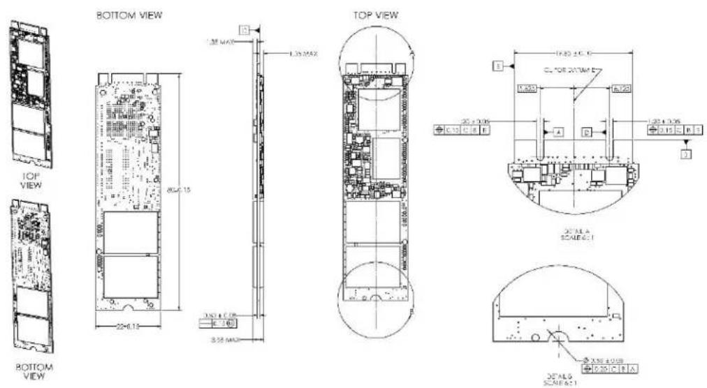
The following figures show the mechanical information for the single-sided, 80 mm height, M.2 Intel SSD 540s Series. All dimensions are in millimeters.
Figure 1: Dimensions for 80 mm single-sided M.2 Form Factor Drives (2280-S3-B-M)
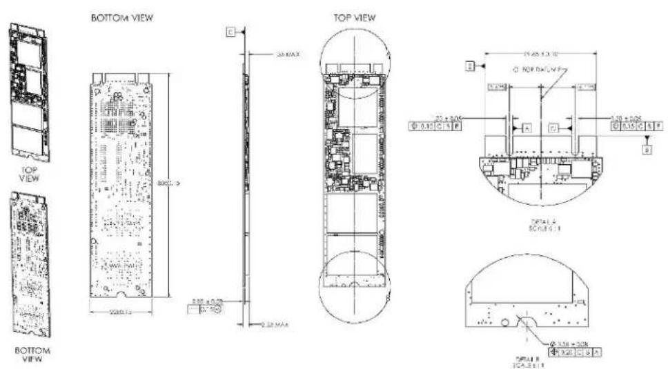
Figure 2: Dimensions for 80 mm double-sided M.2 Form Factor Drives (2280-D3-B-M)
4 Pin and Signal Descriptions
4.1 Pin Locations
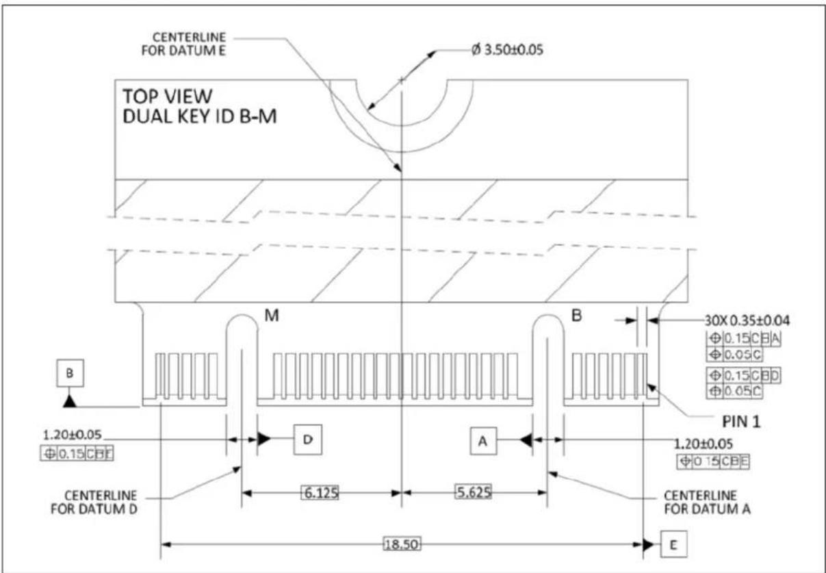
Figure 3: Layout of Signal and Power Segment Pins
4.2 Signal Descriptions
Table 10: M.2 Serial ATA Power Pin Definitions
| Pin | Function | Definition |
| P1 | CONFIG_3 | Ground |
| P2 | +3.3 V | 3.3 V Source |
| P3 | GND | Ground |
| P4 | +3.3 V | 3.3 V Source |
| P5 | Reserved | No Connect |
| P6 | Reserved | No Connect |
| P7 | Reserved | No Connect |
| P8 | Reserved | No Connect |
| P9 | Reserved | No Connect |
| P10 | DAS/DSS# | Device Activity Signal / Disable Staggered Spin-up |
| P11 | Reserved | No Connect |
| P12 | Notch | No Connect |
| P13 | Notch | No Connect |
| P14 | Notch | No Connect |
| P15 | Notch | No Connect |
| P16 | Notch | No Connect |
| P17 | Notch | No Connect |
| P18 | Notch | No Connect |
| P19 | Notch | No Connect |
| P20 | Reserved | No Connect |
| P21 | CONFIG_0 | Ground |
| P22 | Reserved | No Connect |
| P23 | Reserved | No Connect |
| P24 | Reserved | No Connect |
| P25 | Reserved | No Connect |
| P26 | Reserved | No Connect |
| P27 | GND | Ground |
| P28 | Reserved | No Connect |
| P29 | Reserved | No Connect |
| P30 | Reserved | No Connect |
| P31 | Reserved | No Connect |
| P32 | Reserved | No Connect |
| P33 | GND | Ground |
| P34 | Reserved | No Connect |
| P35 | Reserved | No Connect |
| P36 | Reserved | No Connect |
| P37 | Reserved | No Connect |
| P38 | DEVSLP | DevSleep Pin |
| P39 | GND | Ground |
| P40 | Reserved | No Connect |
| P41 | +B | Host Receiver Differential Signal Pair (This is an output of the SSD) |
| P42 | Reserved | No Connect |
| P43 | -B | Host Receiver Differential Signal Pair (This is an output of the SSD) |
| P44 | Reserved | No Connect |
| P45 | GND | Ground |
| P46 | Reserved | No Connect |
| P47 | -A | Host Transmitter Differential Signal Pair (This is an input of the SSD) |
| P48 | Reserved | No Connect |
| P49 | +A | Host Transmitter Differential Signal Pair (This is an input of the SSD) |
| P50 | Reserved | No Connect |
| P51 | GND | Ground |
| P52 | Reserved | No Connect |
| P53 | Reserved | No Connect |
| P54 | Reserved | No Connect |
| P55 | Reserved | No Connect |
| P56 | Two Wire Interface | Two Wire Interface Clock |
| P57 | GND | Ground |
| P58 | Two Wire Interface | Two Wire Interface Data |
| P59 | Notch | No Connect |
| P60 | Notch | No Connect |
| P61 | Notch | No Connect |
| P62 | Notch | No Connect |
| P63 | Notch | No Connect |
| P64 | Notch | No Connect |
| P65 | Notch | No Connect |
| P66 | Notch | No Connect |
| P67 | Reserved | No Connect |
| P68 | Reserved | No Connect |
| P69 | CONFIG_1 | Ground |
| P70 | +3.3 V | 3.3 V Source |
| P71 | GND | Ground |
| P72 | +3.3 V | 3.3 V Source |
| P73 | GND | Ground |
| P74 | +3.3 V | 3.3 V Source |
| P75 | CONFIG_2 | Ground |
5 Supported Command and Feature Sets
The Intel SSD 540s Series supports all mandatory Advanced Technology Attachment (ATA) and Serial ATA (SATA) commands defined in the ACS-3 and SATA Revision 3.2 specifications. The mandatory and optional commands are defined in this section.
5.1 Supported ATA General Feature Command Set
Below are mandatory and optional ATA feature sets supported by Intel SSD 540s Series.
- 48-Bit Address
- General
• General Purpose Logging (GPL)
• Native Command Queuing (NCQ)
• Power Management - Sanitize Device
- Security
- SMART
- Software Settings Preservation (SSP)
Below are mandatory and optional ATA commands supported by Intel SSD 540s Series.
Table 11: Supported ATA Commands and Feature Sets
| Commands | Feature Set |
| BLOCK ERASE EXT | Sanitize Device |
| CHECK POWER MODE | Power Management |
| CRYPTO SCRAMBLE EXT | Sanitize Device |
| DATA SET MANAGEMENT | ATA General Feature |
| DOWNLOAD MICROCODE | ATA General Feature |
| EXECUTE DEVICE DIAGNOSTIC | ATA General Feature |
| FLUSH CACHE | ATA General Feature |
| FLUSH CACHE EXT | 48-Bit Address |
| IDENTIFY DEVICE^1 | ATA General Feature |
| IDLE | Power Management |
| IDLE IMMEDIATE | Power Management |
| NOP | ATA General Feature |
| READ BUFFER | ATA General Feature |
| READ DMA | ATA General Feature |
| READ DMA EXT | 48-Bit Address |
| READ FPDMA QUEUED | Native Command Queuing |
| READ LOG DMA EXT | General Purpose Logging |
| READ LOG EXT | General Purpose Logging |
| READ MULTIPLE | ATA General Feature |
| READ MULTIPLE EXT | 48-Bit Address |
| READ NATIVE MAX ADDRESS | 48-Bit Address |
| READ NATIVE MAX ADDRESS EXT | 48-Bit Address |
| READ SECTOR(S) | ATA General Feature |
| READ SECTOR(S) EXT | 48-Bit Address |
| READ VERIFY SECTOR(S) | ATA General Feature |
| READ VERIFY SECTOR(S) EXT | 48-Bit Address |
| SANITIZE FREEZE LOCK EXT | Sanitize Device |
| SANITIZE STATUS EXT | Sanitize Device |
| SECURITY DISABLE PASSWORD | ATA Security |
| SECURITY ERASE PREPARE | ATA Security |
| SECURITY ERASE UNIT | ATA Security |
| SECURITY FREEZE LOCK | ATA Security |
| SECURITY SET PASSWORD | ATA Security |
| SECURITY UNLOCK | ATA Security |
| SEEK | ATA General Feature |
| SET FEATURES | ATA General Feature |
| SET MAX ADDRESS EXT | 48-Bit Address |
| SET MULTIPLE MODE | ATA General Feature |
| SLEEP | Power Management |
| SMART DISABLE OPERATIONS | SMART |
| SMART ENABLE OPERATIONS | SMART |
| SMART ENABLE/DISABLE ATTRIBUTE AUTOSAVE | SMART |
| SMART EXECUTE OFF-LINE IMMEDIATE | SMART |
| SMART READ DATA | SMART |
| SMART READ ATTRIBUTE THRESHOLDS | SMART |
| SMART READ LOG | SMART |
| SMART READ LOG SECTOR | SMART |
| SMART RETURN STATUS | SMART |
| SMART SAVE ATTRIBUTE VALUES | SMART |
| SMART WRITE LOG SECTOR | SMART |
| STANDBY | Power Management |
| STANDBY IMMEDIATE | Power Management |
| WRITE BUFFER | ATA General Feature |
| WRITE DMA | ATA General Feature |
| WRITE DMA EXT | 48-Bit Address |
| WRITE DMA FUA EXT | 48-Bit Address |
| WRITE FPDMA QUEUED | Native Command Queuing |
| WRITE LOG DMA EXT | General Purpose Logging |
| WRITE LOG EXT | General Purpose Logging |
| WRITE MULTIPLE | ATA General Feature |
| WRITE MULTIPLE EXT | 48-Bit Address |
| WRITE MULTIPLE FUA EXT | 48-Bit Address |
| WRITE SECTOR(S) | ATA General Feature |
| WRITE SECTOR(S) EXT | 48-Bit Address |
| WRITE UNCORRECTABLE EXT | ATA General Feature |
NOTES:
1. See the Appendix for details on the sector data returned after issuing an IDENTIFY DEVICE command.
5.2 Security Features
5.2.1 Sanitization Methods
Sanitization refers to a process that renders data inaccessible. Various sanitization methods are listed below.
5.2.1.1 Secure Erase
Secure Erase runs the SECURITY ERASE UNIT command
Table 12: Supported Secure Erase Modes and Definitions
| Secure Erase Mode | Definition |
| Normal Mode | Full NAND erase of user available space and spare area |
| Enhanced Mode | Cryptographically erase data |
5.2.1.2 Sanitize Device
Table 13: Supported Sanitize Device Modes and Definitions
| Mode | Definition |
| Block Erase | Block erase method, all user data areas including user data not currently allocated, irretrievable |
| Crypto Scramble Ext | Changes the internal encryption keys |
5.3 DevSleep
Intel ^® SSD 540s Series supports the DevSleep feature. DevSleep must be enabled on the device by the host system through the SET FEATURES command. If DevSleep is enabled by the host, the host must drive the DevSleep signal to proper assert/de-assert voltage levels according to the SATA specification. Entry into DevSleep must be preceded by LPM slumber entry by host and device. The Intel SSD 540s Series also supports
DevSleep_to_ReducedPwrState which allows the host to wake the drive using normal LPM COMWAKE out-of-band signaling.
For the Intel SSD 540s Series, the recommended total time to DevSleep for system active state is 6 sec. The AHCI* controller has 4 parameters used to define proper DevSleep operation between the host and drive. The following table provides those recommended values for the Intel SSD 540s Series.
Table 14: DevSleep Control Parameters
| Parameter | Definition | Control | Recommended Settings |
| DITO | DevSleep Idle Time Out – number of milliseconds prior to host asserting DevSleep | Set by Host | Active (lid-up): 375 |
| DM | DITO Multiplier – set once at boot-up | Set by Host | 15 |
| MDAT | Minimum DevSleep Assertion Time – minimum time in milliseconds for host to assert DevSleep | Reported by Drive | 10 |
| DETO | DevSleep Exit Time Out – max time in milliseconds from when DevSleep is negated to when device ready to detect OOB | Reported by Drive | 20 |
Total time to DevSleep entry = DITO * (DM+1)
5.4 SMART Attributes
The following two tables list the SMART attributes supported by the Intel SSD 540s Series, and the corresponding status flags and threshold settings.
Table 15: SMART Attributes
| ID | Attribute | Status Flags | Threshold | |||||
| SP | EC | ER | PE | OC | PW | |||
| 05h | Re-allocated Sector CountThe raw value of this attribute shows the number of retired blocks since leaving the factory (grown defect count). | 1 | 1 | 0 | 0 | 1 | 0 | 0 (none) |
| 09h | Power-On Hours CountThe raw value reports the cumulative number of power-on hours over the life of the device,The On/Off status of the Device Initiated Power Management (DIPM) and Devsleep features will affect the number of hours reported. If DIPM and/or Devsleep are turned On, the recorded value for power-on hours does not include the time that the device is in those states. | 1 | 1 | 0 | 0 | 1 | 0 | 0 (none) |
| 0Ch | Power Cycle CountThe raw value of this attribute reports the cumulative number of power cycle events over the life of the device. | 1 | 1 | 0 | 0 | 1 | 0 | 0 (none) |
| AAh | Available Reserved Space (See E8h Attribute) | 1 | 1 | 0 | 0 | 1 | 1 | 10 |
| ABh | Program Fail CountThe raw value of this attribute shows total count of program fails and the normalized value, beginning at 100, shows the percent remaining of allowable program fails. | 1 | 1 | 0 | 0 | 1 | 0 | 0 (none) |
| ACh | Erase Fail CountThe raw value of this attribute shows total count of erase fails and the normalized value, beginning at 100, shows the percent remaining of allowable erase fails. | 1 | 1 | 0 | 0 | 1 | 0 | 0 (none) |
| AEh | Unexpected Power LossThe raw value of this attribute reports the cumulative number of unsafe (unclean) shutdown events over the life of the device.An unsafe shutdown occurs whenever the device is powered off without STANDBY IMMEDIATE being the last command | 1 | 1 | 0 | 0 | 1 | 0 | 0 (none) |
| B7h | SATA Downshift CountThe raw value counts of the number of times SATA interface selected lower signaling rate due to error. | 1 | 1 | 0 | 0 | 1 | 0 | 0 |
| B8h | End-to-End Error Detection CountReports number of errors encountered during end-to-end error detection within the SSD data path. | 1 | 1 | 0 | 0 | 1 | 1 | 90 |
| BBh | Uncorrectable Error CountThe raw value shows the count of errors that could not be recovered using Error Correction Code (ECC) and XOR | 1 | 1 | 0 | 0 | 1 | 0 | 0 (none) |
| BEh | TemperatureReports real-time temperature of drive as measured by temperature sensor on drive PCB. The normalized value reports the current temperature value. The raw value shows current, lifetime highest and lifetime lowest temperatures. Byte 1:0 = current temp Celsius; Byte 3:2 = lifetime highest temp Celsius; Byte 5:4 = lifetime lowest temp Celsius. | 1 | 1 | 0 | 0 | 1 | 0 | 0 (none) |
| C0h | Power-Off Retract Count (Unsafe Shutdown Count)The raw value of this attribute reports the cumulative number of unsafe (unclean) shutdown events over the life of the device. An unsafe shutdown occurs whenever the device is powered off without STANDBY IMMEDIATE being the last command. | 1 | 1 | 0 | 0 | 1 | 0 | 0 (none) |
| C7h | CRC Error CountThe total number of encountered SATA interface cyclic redundancy check (CRC) errors. | 1 | 1 | 0 | 0 | 1 | 0 | 0 (none) |
| E1h | Host WritesThe raw value of this attribute reports the total number of sectors written by the host system. The raw value is increased by 1 for every 65,536 sectors (32MB) written by the host. | 1 | 1 | 0 | 0 | 1 | 0 | 0 (none) |
| E2h | Timed Workload Media WearMeasures the wear seen by the SSD (since reset of the workload timer, attribute E4h), as a percentage of the maximum rated cycles. Divide raw value by 1024 to get percentage of wear – accurate to 3 decimal places. | 1 | 1 | 0 | 0 | 1 | 0 | 0 (none) |
| E3h | Timed Workload Host Read/Write RatioThe raw value shows the percentage of I/O operations that are read operations (since reset of the workload timer, attribute E4h). | 1 | 1 | 0 | 0 | 1 | 0 | 0 (none) |
| E4h | Timed Workload TimerThe raw value measures the elapsed time (number of minutes since starting this workload timer). | 1 | 1 | 0 | 0 | 1 | 0 | 0 (none) |
| E8h | Available Reserved SpaceThis attribute reports the number of reserve blocks remaining. The normalized value begins at 100 (64h), which corresponds to 100 percent availability of the reserved space. The threshold value for this attribute is 10 percent availability. | 1 | 1 | 0 | 0 | 1 | 1 | 10 |
| E9h | Media Wearout IndicatorThis attribute reports the number of cycles the NAND media has undergone. The normalized value declines linearly from 100 to 1 as the average erase cycle count increases from 0 to the maximum rated cycles.Once the normalized value reaches 1, the number will not decrease, although it is likely that significant additional wear can be put on the device | 1 | 1 | 0 | 0 | 1 | 0 | 0 (none) |
| F1h | Total LBAs WrittenThe raw value of this attribute reports the total number of sectors written by the host system. The raw value is increased by 1 for every 65,536 sectors (32MB) written by the host. | 1 | 1 | 0 | 0 | 1 | 0 | 0 (none) |
| F2h | Total LBAs ReadThe raw value of this attribute reports the total number of sectors read by the host system. The raw value is increased by 1 for every 65,536 sectors (32MB) read by the host. | 1 | 1 | 0 | 0 | 1 | 0 | 0 (none) |
| F9h | Total NAND WritesRaw value reports the number of writes to NAND in 1 GB increments. | 1 | 1 | 0 | 0 | 1 | 0 | 0 (none) |
Table 16: SMART Attribute Status Flags
| Status Flag | Description | Value = 0 | Value = 1 |
| SP | Self-preserving attribute | Not a self-preserving attribute | Self-preserving attribute |
| EC | Event count attribute | Not an event count attribute | Event count attribute |
| ER | Error rate attribute | Not an error rate attribute | Error rate attribute |
| PE | Performance attribute | Not a performance attribute | Performance attribute |
| OC | Online collection attribute | Collected only during offline activity | Collected during both offline and online activity |
| PW | Pre-fail warranty attribute | Advisory | Pre-fail |
6 Certifications and Declarations
The following table describes the Device Certifications supported by the Intel SSD 540s Series.
Table 17: Device Certifications and Declarations
| Certification | Description |
| CE* Compliant | European Economic Area (EEA): Compliance with the essential requirements of EC Council Directives Low Voltage Directive (LVD) 2006/95/EC, EMC Directive 2004/108/EC and Directive 2011/65/EU. |
| UL* Certified | Certified Underwriters Laboratories, Inc. Bi-National Component Recognition; UL 60950-1, 2nd Edition, 2007-03-27 (Information Technology Equipment - Safety - Part 1: General Requirements)CSA C22.2 No. 60950-1-07, 2nd Edition, 2007-03 (Information Technology Equipment - Safety - Part 1: General Requirements) |
| RCM* Compliant | Compliance with the Australia/New Zealand Standard AS/NZS3548 and Electromagnetic Compatibility (EMC) Framework requirements of the Australian Communication Authority (ACA). |
| BSMI* Compliant | Compliance to the Taiwan EMC standard CNS 13438: Information technology equipment - Radio disturbance Characteristics - limits and methods of measurement, as amended on June 1, 2006, is harmonized with CISPR 22: 2005.04. |
| KCC* | Compliance with paragraph 1 of Article 11 of the Electromagnetic Compatibility Control Regulation and meets the Electromagnetic Compatibility (EMC) Framework requirements of the Radio Research Laboratory (RRL) Ministry of Information and Communication Republic of Korea. |
| Microsoft* WHCK/WHLK | Microsoft Windows Hardware Certification |
| RoHS* Compliant | Restriction of Hazardous Substance Directive |
| VCCI* | Voluntary Control Council for Interface to cope with disturbance problems caused by personal computers or facsimile. |
| SATA-IO* | Indicates certified logo program from Serial ATA International Organization. |
| Low Halogen | Applies only to brominated and chlorinated flame retardants (BFRs/CFRs) and PVC in the final product. Intel components as well as purchased components on the finished assembly meet JS-709 requirements, and the PCB/substrate meet IEC 61249-2-21 requirements. The replacement of halogenated flame retardants and/or PVC may not be better for the environment. |
7 Appendix
7.1 Identify Device
The following table describes the sector data returned from an identify device command.
Table 18: Identify Device Returned Sector Data
| Word | F = FixedV = VariableX = Both | Default Value | Description |
| 0 | F | 0040h | General configuration bit-significant information |
| 1 | X | 3FFFh | Obsolete - Number of logical cylinders (16,383) |
| 2 | V | C837h | Specific configuration |
| 3 | X | 0010h | Obsolete - Number of logical heads (16) |
| 4-5 | X | 0h | Retired |
| 6 | X | 003Fh | Obsolete - Number of logical sectors per logical track (63) |
| 7-8 | V | 0h | Reserved for assignment by the CompactFlash* Association (CFA) |
| 9 | X | 0h | Retired |
| 10-19 | F | varies | Serial number (20 ASCII characters) |
| 20-21 | X | 0h | Retired |
| 22 | X | 0h | Obsolete |
| 23-26 | F | varies | Firmware revision (8 ASCII characters) |
| 27-46 | F | varies | Model number (Intel* Solid State Drive) |
| 47 | F | 8010h | 7:0—Maximum number of sectors transferred per interrupt on multiple commands |
| 48 | F | 4000h | Reserved |
| 49 | F | 2F00h | Capabilities |
| 50 | F | 4000h | Capabilities |
| 51-52 | X | 0h | Obsolete |
| 53 | F | 0007h | Words 88 and 70:64 valid |
| 54 | X | 3FFFh | Obsolete - Number of logical cylinders (16,383) |
| 55 | X | 0010h | Obsolete - Number of logical heads (16) |
| 56 | X | 003Fh | Obsolete - Number of logical sectors per logical track (63) |
| 57-58 | X | 00FBFC10h | Obsolete |
| 59 | V | B110h | Sanitize/Multiple Sector settings |
| 60-61 | F | varies | Total number of user-addressable sectors |
| 62 | X | 0h | Obsolete |
| 63 | F | 0007h | Multi-word DMA modes supported/selected |
| 64 | F | 0003h | PIO modes supported |
| 65 | F | 0078h | Minimum multiword DMA transfer cycle time per word |
| 66 | F | 0078h | Manufacturer's recommended multiword DMA transfer cycle time |
| 67 | F | 0078h | Minimum PIO transfer cycle time without flow control |
| 68 | F | 0078h | Minimum PIO transfer cycle time with IORDY flow control |
| 69 | F | 4D10h | Additional Supported |
| 70 | F | 0h | Reserved |
| 71-74 | F | 0h | Reserved for IDENTIFY PACKET DEVICE command |
| 75 | F | 001Fh | Queue depth |
| 76 | F | 070Eh | Serial ATA capabilities |
| 77 | F | 0086h | Reserved for future Serial ATA definition |
| 78 | F | 014Ch | Serial ATA features supported |
| 79 | V | 0040h | Serial ATA features enabled |
| 80 | F | 07FCh | Major version number |
| 81 | F | FFFFh | Minor version number |
| 82 | F | 746Bh | Command set supported |
| 83 | F | 7409h | Command sets supported |
| 84 | F | 6163h | Command set/feature supported extension |
| 85 | V | 7469h | Command set/feature enabled |
| 86 | V | B409h | Command set/feature enabled |
| 87 | V | 6163h | Command set/feature default |
| 88 | V | 407Fh | Ultra DMA Modes |
| 89 | F | 0002h | Time required for security erase unit completion |
| 90 | F | 0001h | Time required for enhanced security erase completion |
| 91 | V | 00FEh | Current advanced power management value |
| 92 | V | FFFEh | Master Password Revision Code |
| 93 | F | 0h | Hardware reset result: the contents of bits (12:0) of this word shall change only during the execution of a hardware reset |
| 94 | V | 0h | Vendor's recommended and actual acoustic management value |
| 95 | F | 0h | Stream minimum request size |
| 96 | V | 0h | Streaming transfer time - DMA |
| 97 | V | 0h | Streaming access latency - DMA and PIO |
| 98-99 | F | 0h | Streaming performance granularity |
| 100-103 | V | varies | Maximum user LBA for 48-bit address feature set |
| 104 | V | 0h | Streaming transfer time - PIO |
| 105 | F | 0008h | Reserved |
| 106 | F | 4000h | Physical sector size / logical sector size |
| 107 | F | 0h | Inter-seek delay for ISO-7779 acoustic testing in microseconds |
| 108-111 | F | varies | Unique ID |
| 112-115 | F | 0h | Reserved for world wide name extension to 128 bits |
| 116 | V | 0h | Reserved for technical report |
| 117-118 | F | 0h | Words per logical sector |
| 119 | F | 401Ch | Supported settings |
| 120 | F | 401Ch | Command set/feature enabled/supported |
| 121-126 | F | 0h | Reserved |
| 127 | F | 0h | Removable Media Status Notification feature set support |
| 128 | V | 0021h | Security status |
| 129-159 | X | varies | Vendor-specific |
| 160 | F | 0h | CompactFlash Association (CFA) power mode 1 |
| 161-167 | X | 0h | Reserved for assignment by the CFA |
| 168 | F | 0007h (M.2) | Nominal Form Factor |
| 169 | X | 0001h | Data set management Trim attribute support |
| 170-173 | F | 0h | Additional Product Identifier |
| 174-175 | F | 0h | Reserved |
| 176-205 | V | 0h | Current media serial number |
| 206 | X | 0039h | SCT Command Transport |
| 207-208 | X | 0h | Reserved |
| 209 | X | 4000h | Alignment of logical blocks within a physical block |
| 210-211 | X | 0h | Write-Read-Verify Sector Count Mode 3 (DWord) |
| 212-213 | X | 0h | Write-Read-Verify Sector Count Mode 2 (DWord) |
| 214 | X | 0h | NV Cache Capabilities |
| 215-216 | X | 0h | NV Cache Size in Logical Blocks (DWord) |
| 217 | X | 0001h | Nominal media rotation rate |
| 218 | X | 0h | Reserved |
| 219 | X | 0h | NV Cache Options |
| 220 | X | 0h | Write-Read-Verify feature set |
| 221 | X | 0h | Reserved |
| 222 | X | 10FFh | Transport major version number |
| 223 | X | 0h | Transport minor version number |
| 224-229 | X | 0h | Reserved |
| 230-233 | X | 0h | Extended Number of User Addressable Sectors (QWord) |
| 234 | X | 0002h | Minimum number of 512-byte data blocks per DOWNLOAD MICROCODE command for mode 03h |
| 235 | X | 0080h | Maximum number of 512-byte data blocks per DOWNLOADMICROCODE command for mode 03h |
| 236-254 | X | 0h | Reserved |
| 255 | X | varies | Integrity word |
NOTES:
F = Fixed. The content of the word is fixed and does not change. For removable media devices, these values may change when media is removed or changed.
V = Variable. The state of at least one bit in a word is variable and may change depending on the state of the device or the commands executed by the device.
X = F or V. The content of the word may be fixed or variable.
7.2 Models
The following table lists the available M.2 single-sided models of the Intel ^® SSD 540s Series.
Table 19: Available Models
| Model String | Capacity |
| SSDSCKKW120H6 | 120GB |
| SSDSCKKW180H6 | 180GB |
| SSDSCKKW240H6 | 240GB |
| SSDSCKKW360H6 | 360GB |
| SSDSCKKW480H6 | 480GB |
| SSDSCKKW010X6 | 1000GB |
- Intel® Solid State Drive 540s Series (M.2)
- Product Specification
- NOTES:
- Ordering Information
- Contents
- Introduction....5
- Product Specifications....7
- Mechanical Information....11
- Pin and Signal Descriptions....13
- Supported Command and Feature Sets....16
- Certifications and Declarations....22
- Appendix....23
- Tables
- Figures
- Introduction
- Terminology
- Reference Documents
- Product Specifications
- Capacity
- Performance
- Note:
- Electrical Characteristics
- Environmental Conditions
- Temperature, Shock, Vibration
- Altitude
- Product Regulatory Compliance
- Reliability
- Mechanical Information
- Pin and Signal Descriptions
- Pin Locations
- Signal Descriptions
- Supported Command and Feature Sets
- Supported ATA General Feature Command Set
- Security Features
- Sanitization Methods
- Secure Erase
- Sanitize Device
- DevSleep
- SMART Attributes
- Certifications and Declarations
- Appendix
- Identify Device
- Models
Brand : INTEL
Model : 540s
Category : SSD Drive