
PCI-1750SO-AE - Expansion card Advantech - Free user manual and instructions
Find the device manual for free PCI-1750SO-AE Advantech in PDF.


| Product Type | Expansion Card |
| Model | PCI-1750SO-AE |
| Brand | Advantech |
| Bus Interface | PCI |
| I/O Channels | 32 (programmable as input or output) |
| Isolation Voltage | 2500 VDC |
| Input Voltage Range | 0 ~ 24 VDC |
| Output Voltage Range | 5 ~ 40 VDC |
| Power Consumption | Typical 5V @ 1A |
| Operating Temperature | 0°C ~ 60°C |
| Storage Temperature | -20°C ~ 85°C |
| Dimensions | 175 mm x 107 mm (standard PCI card) |
| Weight | Approximately 100 g |
| Main Functions | Digital input sensing, digital output control, isolated signal acquisition |
| Maintenance | Keep dry and clean. Avoid dust. No user-serviceable parts. |
| Safety | Install in a grounded chassis. Disconnect power before installation. |
| Spare Parts | Replacement cables (e.g., PCL-10168-1) are available from Advantech. |
| Repair | Contact Advantech RMA service for repairs; no on-site repair possible. |
| General Information | Industrial-grade digital I/O card with optical isolation for noise immunity. |
Frequently Asked Questions - PCI-1750SO-AE Advantech
User questions about PCI-1750SO-AE Advantech
0 question about this device. Answer the ones you know or ask your own.
Ask a new question about this device
Download the instructions for your Expansion card in PDF format for free! Find your manual PCI-1750SO-AE - Advantech and take your electronic device back in hand. On this page are published all the documents necessary for the use of your device. PCI-1750SO-AE by Advantech.
USER MANUAL PCI-1750SO-AE Advantech
natural_image
Illustration of an electronic circuit board with two components, one showing internal circuitry and the other a rectangular device (no text or symbols)PCI-1750/PCI-1750SO
32-ch Isolated Digital I/O PCI Card
Copyright
The documentation and the software included with this product are copyrighted 2016 by Advantech Co., Ltd. All rights are reserved. Advantech Co., Ltd. reserves the right to make improvements in the products described in this manual at any time without notice. No part of this manual may be reproduced, copied, translated or transmitted in any form or by any means without the prior written permission of Advantech Co., Ltd. Information provided in this manual is intended to be accurate and reliable. However, Advantech Co., Ltd. assumes no responsibility for its use, nor for any infringements of the rights of third parties, which may result from its use.
Acknowledgements
Intel and Pentium are trademarks of Intel Corporation.
Microsoft Windows and MS-DOS are registered trademarks of Microsoft Corp.
All other product names or trademarks are properties of their respective owners.
Product Warranty (2 years)
Advantech warrants to you, the original purchaser, that each of its products will be free from defects in materials and workmanship for two years from the date of purchase.
This warranty does not apply to any products which have been repaired or altered by persons other than repair personnel authorized by Advantech, or which have been subject to misuse, abuse, accident or improper installation. Advantech assumes no liability under the terms of this warranty as a consequence of such events.
Because of Advantech's high quality-control standards and rigorous testing, most of our customers never need to use our repair service. If an Advantech product is defective, it will be repaired or replaced at no charge during the warranty period. For out-of-warranty repairs, you will be billed according to the cost of replacement materials, service time and freight. Please consult your dealer for more details.
If you think you have a defective product, follow these steps:
-
Collect all the information about the problem encountered. (For example, CPU speed, Advantech products used, other hardware and software used, etc.) Note anything abnormal and list any on screen messages you get when the problem occurs.
-
Call your dealer and describe the problem. Please have your manual, product, and any helpful information readily available.
-
If your product is diagnosed as defective, obtain an RMA (return merchandise authorization) number from your dealer. This allows us to process your return more quickly.
-
Carefully pack the defective product, a fully-completed Repair and Replacement Order Card and a photocopy proof of purchase date (such as your sales receipt) in a shippable container. A product returned without proof of the purchase date is not eligible for warranty service.
-
Write the RMA number visibly on the outside of the package and ship it prepaid to your dealer.
Printed in Taiwan Edition4
Part No. 2003175030 June 2016
Declaration of Conformity
CE
This product has passed the CE test for environmental specifications when shielded cables are used for external wiring. We recommend the use of shielded cables. This kind of cable is available from Advantech. Please contact your local supplier for ordering information.
Technical Support and Assistance
- Visit the Advantech web site at www.advantech.com/support where you can find the latest information about the product.
- Contact your distributor, sales representative, or Advantech's customer service center for technical support if you need additional assistance. Please have the following information ready before you call:
– Product name and serial number
– Description of your peripheral attachments
– Description of your software (operating system, version, application software, etc.)
– A complete description of the problem
- The exact wording of any error messages
Warnings, Cautions and Notes
Warning! Warnings indicate conditions, which if not observed, can cause personal injury!

Caution! Cautions are included to help you avoid damaging hardware or losing data. e.g.

There is a danger of a new battery exploding if it is incorrectly installed. Do not attempt to recharge, force open, or heat the battery. Replace the battery only with the same or equivalent type recommended by the manufacturer. Discard used batteries according to the manufacturer's instructions.
Safety Instructions
- Read these safety instructions carefully.
- Keep this User Manual for later reference.
- Disconnect this equipment from any AC outlet before cleaning. Use a damp cloth. Do not use liquid or spray detergents for cleaning.
- For plug-in equipment, the power outlet socket must be located near the equipment and must be easily accessible.
- Keep this equipment away from humidity.
- Put this equipment on a reliable surface during installation. Dropping it or letting it fall may cause damage.
- The openings on the enclosure are for air convection. Protect the equipment from overheating. DO NOT COVER THE OPENINGS.
- Make sure the voltage of the power source is correct before connecting the equipment to the power outlet.
- Position the power cord so that people cannot step on it. Do not place anything over the power cord.
- All cautions and warnings on the equipment should be noted.
- If the equipment is not used for a long time, disconnect it from the power source to avoid damage by transient overvoltage.
- Never pour any liquid into an opening. This may cause fire or electrical shock.
- Never open the equipment. For safety reasons, the equipment should be opened only by qualified service personnel.
- If one of the following situations arises, get the equipment checked by service personnel:
- The power cord or plug is damaged.
- Liquid has penetrated into the equipment.
- The equipment has been exposed to moisture.
- The equipment does not work well, or you cannot get it to work according to the user's manual.
- The equipment has been dropped and damaged.
- The equipment has obvious signs of breakage.
- DO NOT LEAVE THIS EQUIPMENT IN AN ENVIRONMENT WHERE THE STORAGE TEMPERATURE MAY GO BELOW -20°C (-4°F) OR ABOVE 60°C (140°F). THIS COULD DAMAGE THE EQUIPMENT. THE EQUIPMENT SHOULD BE IN A CONTROLLED ENVIRONMENT.
- CAUTION: DANGER OF EXPLOSION IF BATTERY IS INCORRECTLY REPLACED. REPLACE ONLY WITH THE SAME OR EQUIVALENT TYPE RECOMMENDED BY THE MANUFACTURER, DISCARD USED BATTERIES ACCORDING TO THE MANUFACTURER'S INSTRUCTIONS.
- The sound pressure level at the operator's position according to IEC 704-1:1982 is no more than 70 dB (A).
Safety Precaution - Static Electricity
DISCLAIMER: This set of instructions is given according to IEC 704-1. Advantech disclaims all responsibility for the accuracy of any statements contained herein. Safety Precaution - Static Electricity
Follow these simple precautions to protect yourself from harm and the products from damage.
To avoid electrical shock, always disconnect the power from your PC chassis before you work on it. Don't touch any components on the CPU card or other cards while the PC is on.
■ Disconnect power before making any configuration changes. The sudden rush of power as you connect a jumper or install a card may damage sensitive electronic components.
Contents
Chapter 1 Overview......1
1.1 Introduction 2
1.2 Features 2
1.3 Applications.... 2
1.4 Specifications 2
Chapter 2 Installation....5
2.1 Initial inspection....6
2.2 Unpacking 6
2.3 Location of Connectors 7
Figure 2.1 Location of Jumper and DIP switch .... 7
Table 2.1: JP2 : Power on configuration after hot reset ...... 7
Table 2.2: Board ID Setting (SW1) 8
2.4 PCI-1750/PCI-1750SO Block Diagram 9
Figure 2.2 Block Diagram ...... 9
2.5 Connector Pin Assignments 10
2.6 Installation Instructions.... 12
Table 2.3: Signal Description of I/O Connectors ...... 10
Chapter 3 Operation....13
3.1 Operation 14
3.2 Isolated Digital I/O Ports 14
3.2.1 Introduction ...... 14
3.2.2 Interrupt function of the DIO signals 14
3.2.3 Power On Configuration.... 14
3.2.4 Isolated Inputs.... 15
Figure 3.1 PCI-1750 / PCI-1750SO isolated digital input connection....15
3.2.5 Isolated Outputs.... 16
Figure 3.2 PCI-1750 isolated digital output connection (sink type) 16
Figure 3.3 PCI-1750SO isolated digital output connection (source type)....16
3.3 Timer and Counter 17
3.3.1 Introduction ...... 17
Figure 3.4 Block diagram of timer/counter.... 17
3.3.2 Timer/Counter Frequency and Interrupt.... 17
3.3.3 One Shot and Interrupt 18
3.4 Interrupt Function 19
3.4.1 Introduction 19
3.4.2 IRQ Level 19
3.4.3 Interrupt Control Register [Base + 32(Dec)] 19
Table 3.1: Interrupt control register bit map.... 19
3.4.4 Interrupt Source Control.... 20
Figure 3.5 Interrupt source control.... 20
Table 3.2: Interrupt mode bit values ...... 20
3.4.5 Interrupt Triggering Edge Control 20
Table 3.3: Triggering edge control bit values ...... 20
3.4.6 Interrupt Flag Bit 21
Table 3.4: Interrupt flag bit values ...... 21
Appendix A Function of 8254 Counter Chip...... 23
A.1 The Intel 8254 ...... 24
A.1.1 Counter read/write and control registers.... 24
A.2 Counter operating modes 26
A.2.1 MODE 0 – Stop on terminal count ...... 26
A.2.2 MODE 1 – Programmable one-shot ...... 26
A.2.3 MODE 2 – Rate generator ...... 26
A.2.4 MODE 3 – Square wave generator.... 26
A.2.5 MODE 4 – software triggered strobe ..... 27
A.2.6 MODE 5 – Hardware triggered strobe ...... 27
A.3 Counter operations 27
A.3.1 Read/write operation.... 27
A.3.2 Counter read-back command 27
A.3.3 Counter latch operation 27
Appendix B Register Format of PCI-1750/PCI-1750SO29
B.1 Register Format of PCI-1750/PCI-1750SO.... 30
Chapter 1
Overview
1.1 Introduction
The PCI-1750/PCI-1750SO offers 16 isolated digital input channels, 16 isolated digital output channels, one isolated counter and one timer with PCI bus interface. With isolation protection of 2500 V_DC the PCI-1750/PCI-1750SO is ideal for industrial applications where high-voltage protection is required.
The card's 16 bits are divided into two 8-bit I/O ports. This makes the PCI-1750/PCI-1750SO very easy to program. This card also offers dual interrupt handling capability, providing the user more flexibility in using the counter, timer, digital inputs or a combination to generate interrupts to the PC. A user can easily configure the interrupts through software.
The PCI-1750/PCI-1750SO uses a PCI controller to interface the card to the PCI bus. The controller fully implements the PCI bus specification Rev 2.1. All bus relative configurations, such as base addresses and interrupt assignments, are automatically controlled by software.
1.2 Features
■ 16 isolated digital input and 16 isolated digital output channels.
■ High voltage isolation on all channels (2500 V DC )
- Driving current capability on isolated output channels (200 mA/Channel).
■ D-type 37-pin female connector.
■ Supports dry contact or 5 to 50 V DC isolated input.
■ Dual interrupt handling capability
■ Timer / Counter interrupt capability generates watchdog timer interrupts
1.3 Applications
Digital I/O control.
■ Industrial ON/OFF control.
■ Industrial and lab automation.
■ Switch status sensing
■ BCD interfacing.
1.4 Specifications
16 Optically-Isolated Inputs:
■ Input range: 5 to 50 V _DC or dry contact.
■ Isolation voltage: 2,500 V DC
■ Optical Isolator response time: 100us
16 Optically-Isolated Outputs:
■ Output range: Open collector 5 to 40 V _DC
■ Sink Current: 200mA max. / channel (PCI-1750)
■ Source Current: 200mA max. / channel (PCI-1750SO)
■ Isolation voltage: 2,500 V DC
■ Optical Isolator response time: 100us
■ Each PCOM Withstanding current: 1.6A max.
■ Over current ground: CN5 (wiring necessary when totally current over 1.6A)
One 16-bit Optically-Isolated Counter:
■ Shares Pin with isolated input 15.
■ Throughput: 1 MHz Max.
■ Isolation voltage: 2,500 V DC
One 32-bit Timer.
■ 10 MHz internal clock source
Interrupt Source
■ Interrupt Inputs: 2 (IDI0,IDI8) Dimensions: 175 mm x 100 mm (6.9" x 3.9")
Connectors: One DB-37 female connector One 2-pin terminal block for extended ground
Power consumption: 5 V @ 850 mA (Typical) 5 V @ 1.0 A (Max.)
Operating temperature: 0 \~ 70°C (32°F \~ 158°F)
Storage temperature: -20 \~ 80°C (-4°F \~ 176°F)
Humidity: 5% \~ 95% non-condensing
Chapter 2
Installation
2.1 Initial inspection
Before starting to install the PCI-1750/PCI-1750SO, make sure there is no visible damage on the card. We carefully inspected the card both mechanically and electrically before shipment. It should be free of marks and in perfect order on receipt.
As you unpack the PCI-1750/PCI-1750SO, check it for signs of shipping damage (damaged box, scratches, dents, etc.) If it is damaged or fails to meet specification, notify our service department or your local sales representative immediately. Also, call the carrier immediately and retain the shipping carton and packing materials for inspection by the carrier. We will then make arrangements to repair or replace the unit.
2.2 Unpacking
The PCI-1750/PCI-1750SO contains components that are sensitive and vulnerable to static electricity. Discharge any static electricity on your body to ground by touching the back of the system unit (grounded metal) before you touch the board.
Remove the PCI-1750/PCI-1750SO card from its protective packaging by grasping the rear panel. Handle the card only by its edges to avoid static discharge which could damage its integrated circuits. Keep the antistatic package. Whenever you remove the card from the PC, please store the card in this package for its protection.
You should also avoid contact with materials that hold static electricity such as plastic, vinyl and styrofoam.
Check the product contents inside the packing. There should be one card, one CD-ROM, and this manual. Make sure nothing is missing.
2.3 Location of Connectors
Figure 2.1 shows the names and locations of connectors on the board.
The PCI-1750/PCI-1750SO is a plug and play device. The PCI BIOS assigns the system resources automatically at system start-up. All functions can be set by software. One jumper and one switch are used on this card.
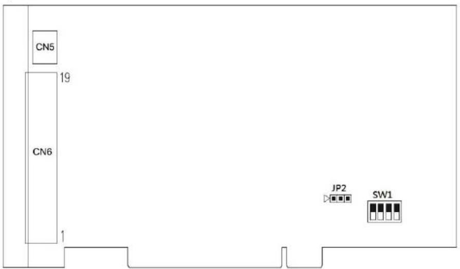
Figure 2.1 Location of Jumper and DIP switch
The default configuration after the power is switched on, and the hardware has been reset is to set all the isolated output channels to "open" (the current of the load can't be sinked) so that users do not have worry about damaging external devices during system startup or reset.
When the system is hot reset, then the status of the isolated digital output channels are selected by jumper JP2. Table 2-1 shows the configuration of jumper JP2.
Table 2.1: JP2 : Power on configuration after hot reset
| JP2 Power on configuration after hot reset | |
| Default Configuration (Load default after hot reset) | |
| Keep last status after hot reset | |
Board ID (SW1)
The PCI-1750/PCI-1750SO has a built-in DIP switch (SW1), which is used to define each cards board ID. When there are multiple cards on the same chassis, this board ID switch is useful for identifying each cards device number.
After setting each PCI-1750/PCI-1750SO, you can identify each card in system with different device numbers. The default value of board ID is 0 and if you need to adjust it to other value, please set the SW1 by referring to Table 2.2.
Table 2.2: Board ID Setting (SW1)
SW1 Position 1 Position 2 Position 3 Position 4
| BoardID ID3 ID2 ID1 ID0 | ||||||||
| 0* ON ON ON ON | ||||||||
| 1 | O | N | O | N | ||||
| 2 | O | N | O | N | O | F | F | |
| 3 | O | N | O | N | O | F | F | |
| 4 | O | N | O | F | F | O | N | |
| 5 | O | N | O | F | F | O | N | |
| 6 | O | N | O | F | F | O | F | |
| 7 | O | N | O | F | F | O | F | |
| 8 | OFF | ON ON ON | ||||||
| 9 | OFF | ON ON OFF | ||||||
| 10 | OFF | OFF | OFF | ON | ||||
| 11 | OFF | OFF | OFF | OFF | ||||
| 12 | OFF | OFF | ON ON | |||||
| 13 | OFF | OFF | ON OFF | |||||
| 14 | OFF | OFF | OFF | ON | ||||
| 15 | OFF | OFF | OFF | OFF | ||||
*Default setting is 0
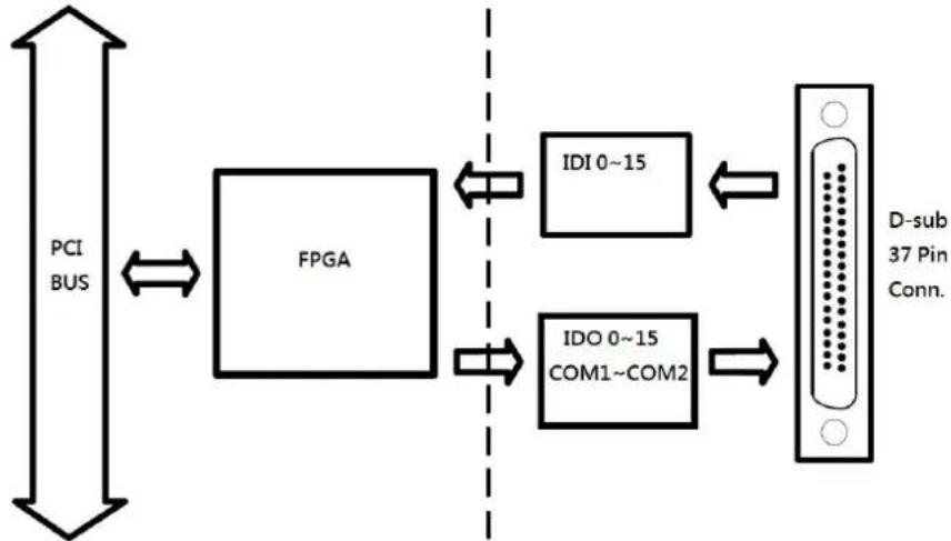
2.4 PCI-1750/PCI-1750SO Block Diagram
flowchart
graph LR
    A["PCI BUS"] <--> B["FPGA"]
    B <--> C["IDI 0~15"]
    B <--> D["IDO 0~15 COM1~COM2"]
    C <--> E["D-sub 37 Pin Conn."]
    D <--> E
Figure 2.2 Block Diagram
2.5 Connector Pin Assignments
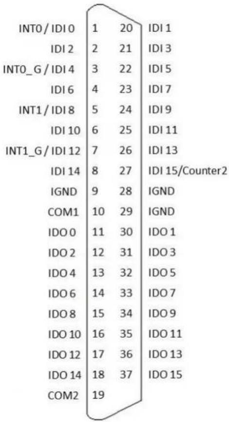
Table 2.3: Signal Description of I/O Connectors
| Signal Name Reference Direction Description | |||
| IDI <0~15> IGND Input Isolated digital input channels | |||
| IDO <0~7> IGND Output Isolated digital output of group 1 | |||
| IDO <8~15> IGND Output Isolated digital output of group 2 | |||
| COM 1 - Input | PCI-1750:Common pin for connecting inductive loads of IDO 0 ~ IDO 7 | ||
| PCI-1750SO:Common pin for connecting external voltage source to IDO 0 ~ IDO 7 | |||
| COM 2 - Input | PCI-1750:Common pin for connecting inductive loads of IDO 8 ~ IDO 15 | ||
| PCI-1750SO:Common pin for connecting external voltage source to IDO 8~ IDO 15 | |||
| IGND | - | - Isolated ground | |
| INT<0,1> | IGND | Input | Interrupt trigger sources (shared with IDI 0, IDI 8) |
| INT<0,1>_G IGND | - Gate for Interrupt pins (shared with IDI 4, IDI 12) | ||
| Counter2 | IGND Input Input pin of isolated counter (shared with IDI 15) | ||
Warning!

Be careful when wiring digital input lines. Never apply a negative voltage to the isolated input pins, as this may damage the PCI-1750/PCI-1750SO.
2.6 Installation Instructions
The PCI-1750/PCI-1750SO can be installed in any PCI slot in the computer. However,
refer to the computer user's manual to avoid any mistakes and
danger before you follow the installation procedure below:
- Turn off your computer and any accessories connected to the computer.
Warning!

TURN OFF your computer power supply whenever you install or remove any card, or connect and disconnect cables.
-
Disconnect the power cord and any other cables from the back of the computer
-
Remove the cover of the computer.
-
Select an empty 5 V PCI slot. Remove the screw that secures the expansion slot cover to the system unit. Save the screw to secure the interface card retaining bracket.
-
Carefully grasp the upper edge of the PCI-1750/PCI-1750SO. Align the hole in the retaining bracket with the hole on the expansion slot and align the gold striped edge connector with the expansion slot socket.
-
Press the card into the socket gently but firmly. Make sure the card fits the slot tightly.
-
Secure the PCI-1750/PCI-1750SO by screwing the mounting bracket to the back panel of computer.
-
Attach any accessories (cable, wiring terminal, etc.) to the card.
-
Replace the cover of your computer. Connect the cables you removed in step 2.
-
Turn the computer power on.
Chapter 3
Operation
3.1 Operation
Maintaining signal connections is one of the most important factors in ensuring that your application system is sending and receiving data correctly. A good signal connection can avoid unnecessary and costly damage to your PC and other hardware devices. This chapter provides useful information about how to connect input and output signals to the PCI-1750/PCI-1750SO via the I/O connector.
3.2 Isolated Digital I/O Ports
3.2.1 Introduction
The PCI-1750/PCI-1750SO has 16 isolated digital input channels designated IDI 0 \~ IDI 15, and 16 isolated digital output channels designated IDO 0 \~ IDO 15. Data can be read from or written to the card's channels.
3.2.2 Interrupt function of the DIO signals
Two I/O channels (IDI 0 and IDI 8) can be used to generate hard ware interrupts. A user can program the interrupt control register [Base + (32Dec)] to select the interrupt sources. Refer to Section "Interrupt Function" for details about interrupt control.
3.2.3 Power On Configuration
The default configuration after power on, hardware reset or software reset is to set all the isolated output channels to low so that users need not worry about damaging external devices during system start up or reset.
3.2.4 Isolated Inputs
Each of 16 isolated digital input channels accepts dry contacts or 5 \~ 50 V _DC voltage inputs. All sixteen input channels share 3 ground pins and one extended ground terminal block (CN5). Figure 3.1 shows how to connect an external input source to one of the card's isolated input channels.
Warning!

Be careful when wiring digital input cables. Never apply a negative voltage to an isolated input pin, as this may damage the PCI-1750/PCI-1750SO.
Note for wet contacts: A malfunction might occur in cases where the internal resistance of a voltage source under wet contacts is significant (>5 KΩ). It is advisable to connect a parallel 5 KΩ, 0.5 W resistor to avoid a voltage rise inside the voltage source.
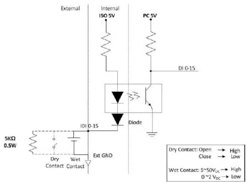
Figure 3.1 PCI-1750 / PCI-1750SO isolated digital input connection
3.2.5 Isolated Outputs
Each of isolated output channels comes equipped with a MOSFET, polyswitch (for current protection) and integral suppression diode for using with inductive loads.
Note! If the external voltage source (5\~40 V) is connected to each isolated output channel (IDO0 \~ IDO15) and its isolated digital output turns on (200 mA max./ch), the card's current will flow from the external voltage source. The current through IGND should not exceed 3.2 A. Use the extended ground connector CN5 to shunt the current to the external voltage source ground.
Figure 3.2 shows how to connect an external output load to the card's isolated outputs.
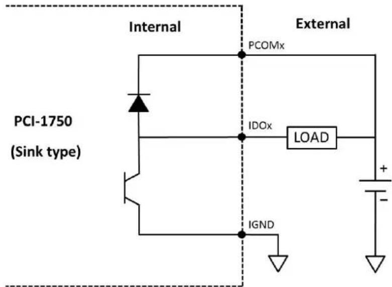
Figure 3.2 PCI-1750 isolated digital output connection (sink type)
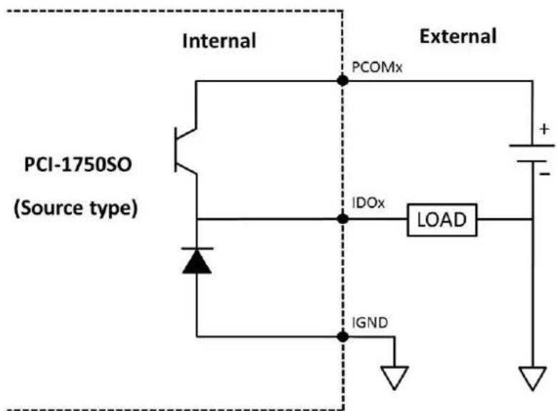
Figure 3.3 PCI-1750SO isolated digital output connection (source type)
3.3 Timer and Counter
3.3.1 Introduction
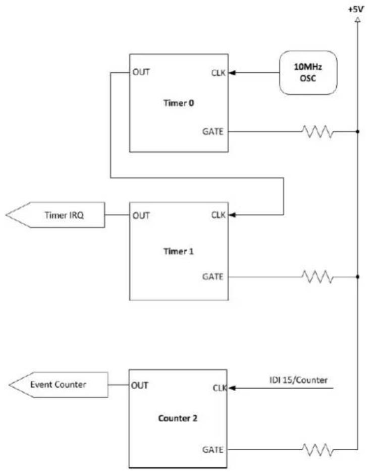
The PCL-1750 includes one 8254 compatible programmable timer/counter chip which provides two 16-bit timers and one counter, designated as Timer 0, Timer 1 and Counter 2. Timer 0 and Timer 1 are cascaded to be a 32-bit timer, with its input connected to a 10 MHz oscillator and its gate control pulled high (enabled). Counter 2 of the 8254 chip is a 16-bit high-speed (1 MHz) isolated event counter (it shares a pin with isolated IDI 15). The block diagram of the timer/counter system of PCI-1750/PCI-1750SO is shown in Figure 3.3. Timers 0 and 1 are usually set in mode 3 (square wave generator) to generate periodic watchdog interrupts. Counter 2 can be set in mode 0 (stop on terminal count) for measuring frequency, or in mode 3 (square wave generator) to generate periodic watchdog interrupts or to be used as an event counter. For more details on the operating modes of the 8254 counter chip, please refer to Appendix A.
flowchart
graph TD
    A["Timer 0"] -->|CLK| B["10MHz OSC"]
    A -->|GATE| C["+5V"]
    D["Timer IRQ"] --> E["OUT"]
    E --> F["Timer 1"]
    F --> G["GATE"]
    H["Event Counter"] --> I["OUT"]
    I --> J["Counter 2"]
    J --> K["GATE"]
    L["IDI 15/Counter"] --> M["Ground"]
    N["OUT"] --> O["OUT"]
    P["CLK"] --> Q["OUT"]
    R["CLK"] --> S["OUT"]
    T["CLK"] --> U["OUT"]
    V["CLK"] --> W["OUT"]
    X["CLK"] --> Y["OUT"]
    Z["CLK"] --> AA["OUT"]
Figure 3.4 Block diagram of timer/counter
3.3.2 Timer/Counter Frequency and Interrupt
The input clock frequency of the counter/timers is 10 MHz. The output of both Timer 1 and Counter 2 can generate interrupts to the system (refer to Section 3.3). The maximum and minimum timer interrupt frequency is (10 MHz)/(2x2)=(2.5 MHz) and (10 MHz)/(65535*65535)=0.002328 Hz, respectively.
The gates of the counter/timers are internally pulled to +5 V, keeping the gate control always enabled.
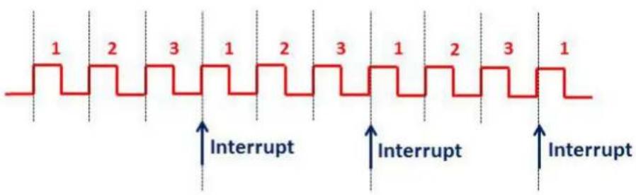
3.3.3 One Shot and Interrupt
The One-Shot, which is based on counting function to achieve and can be triggered by external signal level change.
For example as figure 3.5, the number of counting is set to 3 so that an interrupt will be generated after 3 cycles of external clock signal is received.
3.4 Interrupt Function
3.4.1 Introduction
Four input channels (IDI 0, IDI 4, IDI 8 and IDI 12) and the output of Timer 1 and Counter 2 are connected to the interrupt circuitry. The “Interrupt Control Register” of the PCI-1750/PCI-1750SO controls how the combination of the six signals generates an interrupt. Two interrupt request signals, designated “interrupt group 0” and “interrupt group 1”, can be generated at the same time, and then the software can service these two request signals by ISR. IDI 0, IDI 4 and Timer 1 are connected to interrupt port 0, IDI 8, IDI 12 and Counter 2 are connected to interrupt port 1. The dual interrupt sources provide the card with more capability and flexibility.
3.4.2 IRQ Level
The IRQ level is set automatically by the PCI plug and play BIOS and is saved in the PCI controller. There is no need for users to set the IRQ level. Only one IRQ level is used by this card, although it has two interrupt sources.
3.4.3 Interrupt Control Register [Base + 32(Dec)]
The “Interrupt Control Register” [Base + 32(Dec)] controls the interrupt signal source, edge and flag. Table 3.1 shows the bit map of the interrupt control register. The register is a readable/writable register. When writing to it, it is used as a control register, and when reading from it, it is use data status register.
Table 3.1: Interrupt control register bit map
| Interrupt Source # | Interrupt Group 1 Interrupt Group 0 | |||||||
| B i | t | # | D | 7 D | 6 | D | 5 | D |
| Abbreviation | F1 E1 M11 | M10 | F0 E0 M01 | M00 | ||||
M00 and M01: "mode bits" of interrupt Group 0
M10 and M11: "mode bits" of interrupt Group 1
E0,E1: triggering edge control bits
F0, F1: flag bits
3.4.4 Interrupt Source Control
The “mode bits” written into the interrupt control register determine the allowable sources of signals generating an interrupt. Bit 0 and bit 1 determine the interrupt source for interrupt group 0, and bit 4 and bit 5 determine the interrupt source for interrupt group 1, as indicated in Figure 3.4. Table 3.2 shows the relationship between an interrupt source and the values in the mode bits.
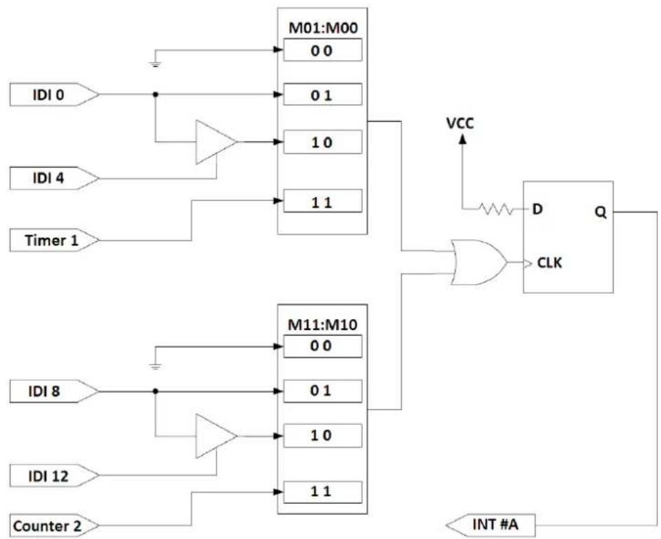
flowchart
graph TD
    subgraph_M01_M00["0 0"]
        IDI0["IDI 0"] --> NOT1["NOT"]
        NOT1 --> AND1["AND"]
        AND1 --> M01_M00
        M01_M00 --> DFF["D"]
        M01_M00 --> CLK["CLK"]
    end

    subgraph_M11_M10["0 0"]
        IDI8["IDI 8"] --> NOT2["NOT"]
        NOT2 --> AND2["AND"]
        AND2 --> M11_M10
        M11_M10 --> VCC["VCC"]
        M11_M10 --> CLK
    end

    M01_M00 --> DFF
    M11_M10 --> CLK
    DFF --> Q["Q"]
    CLK --> Q
    Counter2["Counter 2"] --> AND2
    Counter2 --> M11_M10
    CLK --> Q
    VCC --> DFF
    CLK --> CLK
    INT_A["INT #A"]
Figure 3.5 Interrupt source control
Table 3.2: Interrupt mode bit values
| Interrupt Group 1 Interrupt | Group 0 | ||||
| M11 | M10 | Description M01 M00 Description | |||
| 0 | 0 | Disable interrupt 0 | 0 Disable Interrupt | ||
| 0 | 1 | Source = | IDI 8 | 0 1 Source = IDI 0 | |
| 1 | 0 | Source = | IDI 8 & IDI 12 | 1 | 0 Source = IDI 0 & IDI 4 |
| 1 | 1 | Source= | Counter 2 | 1 | 1 Source = Timer 1 |
3.4.5 Interrupt Triggering Edge Control
The interrupt can be triggered by a rising edge or a falling edge of the interrupt signal, as determined by the value in the “triggering edge control” bit in the interrupt control register, as shown in Table 3.3.
Table 3.3: Triggering edge control bit values
| E0 or E1 | Triggering edge of interrupt signal |
| 1 | Rising edge trigger |
| 0 | Falling edge trigger |
3.4.6 Interrupt Flag Bit
The “interrupt flag” bit is a flag indicating the status of an interrupt. It is a readable and writable bit. Read the bit value to find the status of the interrupt, write “1” to this bit to clear the interrupt. This bit must be cleared in the ISR to service the next incoming interrupt.
| F0 & F1 Interrupt status | ||
| Read | 1 | Interrupt |
| 0 No Interrupt | ||
| Write 1 Clear Interrupt | ||
| 0 Don't Care | ||
Appendix A
Function of 8254 Counter Chip
A.1 The Intel 8254
The PCI-1750/PCI-1750SO uses one Intel 8254 compatible programmable interval timer/counter chip. The popular 8254 offers three independent 16-bit down counters. Each counter has a clock input, control gate and an output. You can program each counter for maximum count values from 2 to 65535.
The 8254 has a maximum input clock frequency of 10 MHz. The PCI-1750/PCI-1750SO provides 10 MHz input frequencies to the counter chip from an on-board crystal oscillator.
On the PCI-1750/PCI-1750SO, the 8254 chip's Timer 0 and Timer 1 are cascaded to be a 32-bit programmable timer.
A.1.1 Counter read/write and control registers
The 8254 programmable interval timer uses four registers at addresses BASE + 24(Dec), BASE + 25(Dec), BASE + 26(Dec) and BASE + 27(Dec) for read, write and control of counter functions.
Register functions appear below:
| Register Function |
| BASE + 24(Dec) Counter 0 read/write |
| BASE + 25(Dec) Counter 1 read/write |
| BASE + 26(Dec) Counter 2 read/write |
| BASE + 27(Dec) Counter control word |
Since the 8254 counter uses a 16-bit structure, each section of read/write data is split into a least significant byte (LSB) and most significant byte (MSB). To avoid errors it is important that you make read/write operations in pairs and keep track of the byte order.
The data format for the control register appears below:
| BASE+27(Dec) 8254 control, standard mode | |||||||||||
| B | i | t | D | 7 | D | 6 | D | 5 | D | 4 | D |
| Value | SC1 | SC0 | RW1 | RW0 | M2 | M1 | M0 | BCD | |||
3 D 2 D 1
A.1.1.1 Description
SC1 & SC0 Select counter
| Counter | SC1 | SC0 |
| 0 | 0 | 0 |
| 1 | 0 | 1 |
| 2 | 1 | 0 |
| Read-back command | 1 | 1 |
RW1 & RW0 Select Read/Write Operation
| Operation | RW1 | RW0 |
| Counter Latch | 0 | 0 |
| Read/Write LSB | 0 | 1 |
| Read/Write MSB | 1 | 0 |
| Read/Write LSB first then MSB | 1 | 1 |
M2, M1 & M0 Select Operating Mode
| M2 M1 M0 Mode |
| 0 0 0 0 Programmable one shot |
| 0 0 1 1 Programmable one shot |
| X 1 0 2 Rate generator |
| X 1 1 3 Square wave generator |
| 1 0 0 4 Software triggered strobe |
| 1 0 1 5 Hardware triggered strobe |
BCD Select Binary or BCD Counting
| BCD Type |
| 0 Binary counting 16-bits |
| 1 Binary coded decimal (BCD) counting |
If you set the module for binary counting, the count can be any number from 0 up to 65535. If you set it for BCD (Binary Coded Decimal) counting, the count can be any number from 0 to 9999.
If you set both SC1 and SC0 bits to 1, the counter control register is in read-back command mode. The control register data format then becomes:
BASE + 27(Dec) 8254 control, read-back mode
| B | i | t | D | 7 | D | 6 | D | 5 | D | 4 | D |
| Value | 1 | 1 | CNT | STA | C2 | C1 | C0 | X | |||
3 D 2 D 1 D 0
CNT = 0 Latch count of selected counter(s).
STA = 0 Latch status of selected counter(s).
C2, C1 & C0 Select counter for a read-back operation.
$$ C 2 = 1 \text { select Counter } 2 $$
$$ C 1 = 1 \text { select Counter } 1 $$
$$ \mathrm{C0} = 1 \text { select Counter } 0 $$
If you set both SC1 and SC0 to 1 and STA to 0, the register selected by C2 to C0 contains a byte which shows the status of the counter. The data format of the counter read/write register then becomes:
BASE+24/25/26(Dec) Status read-back mode
| Bit | D7 | D6 | D5 | D4 | D3 | D2 | D1 | D0 |
| Value | OUT | NC | RW1 | RW0 | M2 | M1 | M0 | BCD |
OUT Current state of counter output
NC Null count is 1 when the last count written to the counter register has been loaded into the counting element
A.2 Counter operating modes
A.2.1 MODE 0 – Stop on terminal count
The output will be initially low after you set this mode of operation. After you load the count into the selected count register, the output will remain low and the counter will count. When the counter reaches the terminal count, its output will go high and remain high until you reload it with the mode or a new count value. The counter continues to decrement after it reaches the terminal count. Rewriting a counter register during counting has the following results:
- Writing to the first byte stops the current counting.
- Writing to the second byte starts the new count.
A.2.2 MODE 1 – Programmable one-shot
The output is initially high. The output will go low on the count following the rising edge of the gate input. It will then go high on the terminal count. If you load a new count value while the output is low, the new value will not affect the duration of the one-shot pulse until the succeeding trigger. You can read the current count at any time without affecting the one-shot pulse. The one-shot is retriggerable, thus the output will remain low for the full count after any rising edge at the gate input.
A.2.3 MODE 2 – Rate generator
The output will be low for one period of the input clock. The period from one output pulse to the next equals the number of input counts in the counter register. If you reload the counter register between output pulses, the present period will not be affected, but the subsequent period will reflect the value.
The gate input, when low, will force the output high. When the gate input goes high, the counter will start from the initial count. You can thus use the gate input to synchronize the counter.
With this mode the output will remain high until you load the count register. You can also synchronize the output by software.
A.2.4 MODE 3 – Square wave generator
This mode is similar to Mode 2, except that the output will remain high until one half of the count has been completed (for even numbers), and will go low for the other half of the count. This is accomplished by decreasing the counter by two on the falling edge of each clock pulse. When the counter reaches the terminal count, the state of the output is changed, the counter is reloaded with the full count and the whole process is repeated.
If the count is odd and the output is high, the first clock pulse (after the count is loaded) decrements the count by 1. Subsequent clock pulses decrement the count by 2. After time out, the output goes low and the full count is reloaded. The first clock pulse (following the reload) decrements the counter by 3. Subsequent clock pulses decrement the count by two until time out, then the whole process is repeated. In this way, if the count is odd, the output will be high for (N+1)/2 counts and low for (N-1)/2 counts.
A.2.5 MODE 4 – software triggered strobe
After the mode is set, the output will be high. When the count is loaded, the counter will begin counting. On terminal count, the output will go low for one input clock period then go high again. If you reload the count register during counting, the new count will be loaded on the next CLK pulse. The count will be inhibited while the GATE input is low.
A.2.6 MODE 5 – Hardware triggered strobe
The counter will start counting after the rising edge of the trigger input and will go low for one clock period when the terminal count is reached. The counter is retriggerable.
A.3 Counter operations
A.3.1 Read/write operation
Before you write the initial count to each counter, you must first specify the read/write operation type, operating mode and counter type in the control byte and write the control byte to the control register [BASE + 27(Dec)].
Since the control byte register and all three counter read/write registers have separate addresses and each control byte specifies the counter it applies to (by SC1 and SC0), no instructions on the operating sequence are required. Any programming sequence following the 8254 convention is acceptable.
There are three types of counter operation: read/load LSB, read/load MSB and read/load LSB followed by MSB. It is important that you make your read/write operations in pairs and keep track of the byte order.
A.3.2 Counter read-back command
The 8254 counter read-back command lets you check the count value, programmed mode and current states of the OUT pin and Null Count flag of the selected counter(s). You write this command to the control word register. Format is as shown at the beginning of this section.
The read-back command can latch multiple counter output latches. Simply set the CNT bit to 0 and select the desired counter(s). This single command is functionally equivalent to multiple counter latch commands, one for each counter latched.
The read-back command can also latch status information for selected counter(s) by setting STA bit = 0. The status must be latched to be read; the status of a counter is accessed by a read from that counter. The counter status format appears at the beginning of the chapter.
A.3.3 Counter latch operation
Users often want to read the value of a counter without disturbing the count in progress. You do this by latching the count value for the specific counter then reading the value.
The 8254 supports the counter latch operation in two ways. The first way is to set bits RW1 and RW0 to 0. This latches the count of the selected counter in a 16-bit hold register. The second way is to perform a latch operation under the read-back command. Set bits SC1 and SC0 to 1 and CNT = 0. The second method has the advantage of operating several counters at the same time. A subsequent read operation on the selected counter will retrieve the latched value.
Appendix B
Register Format of PCI-1750/PCI-1750SO
B.1 Register Format of PCI-1750/PCI-1750SO
| Base Address + (Decimal) | Function | |
| Read Write | ||
| 0 IDI [7:0] | IDO [7:0] | |
| 1 IDI [15:8] | IDO [15:8] | |
| 2 IDO [7:0] | Read back Reserved | |
| 3 IDO [15:8] | Read back Reserved | |
| 4 BOID [3:0] | Reserved | |
| 5~23 Reserved | Reserved | |
| 24 8254 Counter 0 | 8254 Counter 0 | |
| 25 8254 Counter 1 | 8254 Counter 1 | |
| 26 8254 Counter 2 | 8254 Counter 2 | |
| 27 | Reserved | 8254 Control Register |
| 28~31 | Reserved Reserved | |
| 32 | Interrupt Status Register | Interrupt Status Register |
ADVANTECH
eAutomation
www.advantech.com
Please verify specifications before quoting. This guide is intended for reference purposes only.
All product specifications are subject to change without notice.
No part of this publication may be reproduced in any form or by any means, electronic, photocopying, recording or otherwise, without prior written permission of the publisher.
All brand and product names are trademarks or registered trademarks of their respective companies.
© Advantech Co., Ltd. 2016
- PCI-1750/PCI-1750SO
- Copyright
- Acknowledgements
- Product Warranty (2 years)
- Declaration of Conformity
- CE
- Technical Support and Assistance
- Warnings, Cautions and Notes
- Safety Instructions
- Safety Precaution - Static Electricity
- Contents
- Chapter 1 Overview......1
- Chapter 2 Installation....5
- Chapter 3 Operation....13
- Appendix A Function of 8254 Counter Chip...... 23
- Appendix B Register Format of PCI-1750/PCI-1750SO29
- Chapter 1
- Introduction
- Features
- Applications
- Specifications
- Optically-Isolated Inputs:
- Optically-Isolated Outputs:
- One 16-bit Optically-Isolated Counter:
- One 32-bit Timer.
- Interrupt Source
- Chapter 2
- Initial inspection
- Unpacking
- Location of Connectors
- Board ID (SW1)
- Connector Pin Assignments
- Installation Instructions
- Warning!
- Chapter 3
- Operation
- Isolated Digital I/O Ports
- Introduction
- Interrupt function of the DIO signals
- Power On Configuration
- Isolated Inputs
- Isolated Outputs
- Timer and Counter
- Introduction
- Timer/Counter Frequency and Interrupt
- One Shot and Interrupt
- Interrupt Function
- Introduction
- IRQ Level
- Interrupt Control Register [Base + 32(Dec)]
- Interrupt Source Control
- Interrupt Triggering Edge Control
- Interrupt Flag Bit
- Appendix A
- A.1 The Intel 8254
- A.1.1 Counter read/write and control registers
- A.1.1.1 Description
- A.2 Counter operating modes
- A.2.1 MODE 0 – Stop on terminal count
- A.2.2 MODE 1 – Programmable one-shot
- A.2.3 MODE 2 – Rate generator
- A.2.4 MODE 3 – Square wave generator
- A.2.5 MODE 4 – software triggered strobe
- A.2.6 MODE 5 – Hardware triggered strobe
- A.3 Counter operations
- A.3.1 Read/write operation
- A.3.2 Counter read-back command
- A.3.3 Counter latch operation
- Appendix B
- B.1 Register Format of PCI-1750/PCI-1750SO
- ADVANTECH
- eAutomation
- www.advantech.com
Brand : Advantech
Model : PCI-1750SO-AE
Category : Expansion card