
PCIE-1816-B - Expansion card Advantech - Free user manual and instructions
Find the device manual for free PCIE-1816-B Advantech in PDF.


| Product Type | Expansion Card (PCI Express Multifunction DA&C) |
| Model | PCIE-1816-B |
| Brand | Advantech |
| Dimensions (W x L) | 167 x 100 mm |
| Weight | Approx. 100 g |
| Power Consumption (Typical) | 3.3V @ 504 mA, 12V @ 152 mA |
| Power Consumption (Maximum) | 3.3V @ 2.49 A, 12V @ 408 mA |
| Operating Temperature | 0 to 60°C (32 to 140°F) |
| Storage Temperature | -40 to 70°C (-40 to 158°F) |
| Humidity (Operating) | 5 to 85% RH non-condensing |
| Analog Input Channels | 16 single-ended or 8 differential |
| Analog Input Resolution | 16-bit |
| Analog Input Sampling Rate (PCIE-1816) | 1 MS/s single-channel, 500 KS/s multi-channel |
| Analog Input Sampling Rate (PCIE-1816H) | 5 MS/s single-channel, 1 MS/s multi-channel |
| Analog Output Channels | 2 |
| Analog Output Resolution | 16-bit |
| Analog Output Update Rate | Up to 3 MS/s |
| Digital I/O | 24 channels, TTL compatible |
| Counter/Timer Channels | 2 independent 32-bit counters |
| Onboard Memory | 4K samples ring buffer (AI and AO) |
| Connector | 68-pin SCSI female |
| Certifications | CE, FCC |
| Warranty | 2 years |
| Included Accessories | Startup manual, companion DVD-ROM with DAQnavi drivers |
Frequently Asked Questions - PCIE-1816-B Advantech
User questions about PCIE-1816-B Advantech
0 question about this device. Answer the ones you know or ask your own.
Ask a new question about this device
Download the instructions for your Expansion card in PDF format for free! Find your manual PCIE-1816-B - Advantech and take your electronic device back in hand. On this page are published all the documents necessary for the use of your device. PCIE-1816-B by Advantech.
USER MANUAL PCIE-1816-B Advantech
natural_image
Illustration of a computer motherboard with two electronic components, one showing internal circuitry and the other a rectangular base (no text or symbols)PCIE-1816/1816H
16-bit Multi-function Card with PCI Express Bus
Copyright
This documentation and the software included with this product are copyrighted 2019 by Advantech Co., Ltd. All rights are reserved. Advantech Co., Ltd. reserves the right to make improvements in the products described in this manual at any time without notice.
No part of this manual may be reproduced, copied, translated or transmitted in any form or by any means without the prior written permission of Advantech Co., Ltd. Information provided in this manual is intended to be accurate and reliable. However, Advantech Co., Ltd. assumes no responsibility for its use, nor for any infringements of the rights of third parties which may result from its use.
Acknowledgments
Intel and Pentium are trademarks of Intel Corporation.
Microsoft Windows and MS-DOS are registered trademarks of Microsoft Corp.
All other product names or trademarks are properties of their respective owners.
Product Warranty (2 years)
Advantech warrants to you, the original purchaser, that each of its products will be free from defects in materials and workmanship for two years from the date of purchase.
This warranty does not apply to any products which have been repaired or altered by persons other than repair personnel authorized by Advantech, or which have been subject to misuse, abuse, accident or improper installation. Advantech assumes no liability under the terms of this warranty as a consequence of such events.
Because of Advantech's high quality-control standards and rigorous testing, most of our customers never need to use our repair service. If an Advantech product is defective, it will be repaired or replaced at no charge during the warranty period. For out-of-warranty repairs, you will be billed according to the cost of replacement materials, service time and freight. Consult your dealer for more details.
If you think you have a defective product, follow these steps:
-
Collect all the information about the problem encountered. (For example, CPU speed, Advantech products used, other hardware and software used, etc.) Note anything abnormal and list any onscreen messages you get when the problem occurs.
-
Call your dealer and describe the problem. Have your manual, product, and any helpful information readily available.
-
If your product is diagnosed as defective, obtain an RMA (return merchandise authorization) number from your dealer. This allows us to process your return more quickly.
-
Carefully pack the defective product, a fully-completed Repair and Replacement Order Card and a photocopy proof of purchase date (such as your sales receipt) in a shippable container. A product returned without proof of the purchase date is not eligible for warranty service.
-
Write the RMA number visibly on the outside of the package and ship it prepaid to your dealer.
Part No. 2001E18110 Edition 1
Printed in Taiwan Dec 2019
CE
This product has passed the CE test for environmental specifications when shielded cables are used for external wiring. We recommend the use of shielded cables. This kind of cable is available from Advantech. Please contact your local supplier for ordering information.
Technical Support and Assistance
- Visit the Advantech web site at http://support.advantech.com.tw/ where you can find the latest information about the product.
- Contact your distributor, sales representative, or Advantech's customer service center for technical support if you need additional assistance. Have the following information ready before you call:
– Product name and serial number
– Description of your peripheral attachments
– Description of your software (operating system, version, application software, etc.)
– A complete description of the problem
– The exact wording of any error messages
Packing List
Before setting up the system, check that the items listed below are included and in good condition. If any item does not accord with the table, Contact your dealer immediately.
■ PCIE-1816/1816H DA&C card
■ Startup or User Manual
■ Companion DVD-ROM with DAQnavi drivers included
Safety Precaution - Static Electricity
Follow these simple precautions to protect yourself from harm and the products from damage.
- To avoid electrical shock, always disconnect the power from your PC chassis before you work on it. Don't touch any components on the CPU card or other cards while the PC is on.
- Disconnect power before making any configuration changes. The sudden rush of power as you connect a jumper or install a card may damage sensitive electronic components.
Contents
Chapter 1 Introduction......1
1.1 Features 2
1.2 Applications....3
1.3 Installation Guide 3
Figure 1.1 Installation Flow Chart .... 4
1.4 Software Overview 5
1.5 DAQnavi Device Driver Programming Roadmap 5
1.6 Accessories....6
Chapter 2 Installation....7
2.1 Unpacking 8
2.2 Driver Installation 9
Figure 2.1 Setup Screen of Advantech Automation Software ..... 9
Figure 2.2 Different Options for Driver Setup 10
2.3 Hardware Installation 10
2.4 Device Setup & Configuration 11
Figure 2.3 The Device Setting of PCIE-1816/1816H ..... 1 1
Figure 2.4 The Device Setting page 12
Figure 2.5 The Device Testing of PCIE-1816/1816H ...... 12
Chapter 3 Signal Connections....13
3.1 Overview 14
3.2 Switch and Jumper Settings....14
Figure 3.1 Connector and Switch Locations .... 14
3.2.1 Board ID (SW1).... 15
Table 3.1: Board ID Setting (SW1) 15
3.2.2 Power On Configuration(JP1) 15
Table 3.2: Power on Configuration after Hot Reset (JP1) ..... 15
3.2.3 Jumper Settings to Set Ports as Software-configurable or Output ports....16
Table 3.3: Function Description.... 16
3.3 Signal Connections 17
Figure 3.2 68-pin I/O Connector Pin Assignments ..... 17
3.3.1 I/O Connector Signal Description.... 18
Table 3.4: I/O Connector Signal Descriptions ..... 18
3.3.2 Analog Input Connections....19
Figure 3.3 Single-ended input channel connections....19
Figure 3.4 Differential input channel connections.... 20
Figure 3.5 Differential input channel connection - floating signal source....21
Figure 3.6 External Clock Source Connection.... 23
Figure 3.7 External Digital Trigger Source Connection ...... 23
Figure 3.8 External Analog Trigger Source Connection ..... 24
Figure 3.9 Analog Output Connections.... 25
Figure 3.10 External Clock Source Connection.... 26
Figure 3.11 External Digital Trigger Source Connection ..... 26
Figure 3.12External Analog Trigger Source Connection ..... 27
3.3.3 Digital Signal Connections 27
Figure 3.13Wet and Dry contacts 27
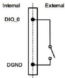
Figure 3.14Wet signal connection of digital input 28
Figure 3.15Dry signal connection of digital input 28
Figure 3.16 Digital Output Channel Connections ...... 28
3.4 Field Wiring Considerations 29
Appendix A Specifications.... 31
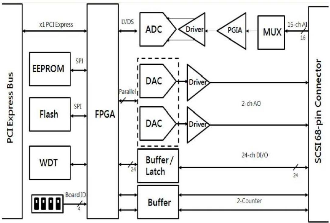
A.1 Function Block 32
A.2 Analog Input 33
A.3 Analog Output 34
A.4 Digital Input/Output 34
A.5 Counter/Timer 35
A.6 General 35
Appendix B Operation Theory 37
B.1 Analog Input Operation 38
B.1.1 AI Hardware Structure 38
B.1.2 Analog Input Ranges and Gains 39
Table B.1: Gains and Analog Input Range 39
B.1.3 Analog Input Acquisition Mode 39
B.1.4 AI Trigger Modes 43
B.1.5 AI SCAN/CONV Clock Source.... 46
B.1.6 AI Trigger Source.... 47
Table B.2: Analog Input Data Format 47
Table B.3: Full Scale Values for Input Voltage Ranges...... 48
B.2 PCIE-1816/1816H Analog Output Operation 48
B.2.1 Analog Output Ranges 48
B.2.2 Analog Output Operation Modes 49
B.2.3 AO Clock Sources 50
B.2.4 AO Trigger Sources 50
Table B.4: Analog Output Data Format 50
Table B.5: Full Scale Values for Output Voltage Ranges ..... 50
B.3 Digital Input/Output Operation 51
B.4 Counter Input and PWM Input/Output.... 51
Chapter 1
Introduction
This chapter introduces PCIE-1816/1816H and its typical applications.
Sections include:
Features
Applications
Installation Guide
Software Overview
Roadmap
■ Accessories
The PCIE-1816/1816H is a PCI Express multifunction card for IBM x86 or compatible computers. It offers the five most desired measurement and control functions:
■ 16-bit AI conversion
■ 16-bit AO conversion
Digital input
Digital output
Timer/counter.
A programmable-gain instrument amplifier lets you acquire different input signals without external signal conditioning. An onboard 4k word FIFO buffer provides high-speed data transfer and predictable performance under Windows. Automatic channel scanning circuitry and onboard SRAM lets you perform multiple-channel AI conversion and individual gains for each channel.
The following sections of this chapter will provide further information about features of the multifunction cards, together with some brief information on software and accessories for the PCIE-1816/1816H cards.
1.1 Features
■ 16 single-ended or 8 differential AI inputs, programmable
■ 16-bit AI converter, up to 1 MHz sampling rate for PCIE-1816
■ 16-bit AI converter, up to 5 MHz sampling rate for PCIE-1816H
■ Double-Clock acquisition operation for analog input
■ Start-, Delay to Start-, Delay to Stop-, Stop-event trigger capable
■ Programmable gain for each input channel, automatic channel/gain scanning
■ 4K onboard ring buffer for analog input and output
■ Two independent 16-bit analog output channels with continuous waveform output function of maximum 3 MHz throughput rate
■ Auto-Calibration for analog input and output channels
■ 24 digital Input or output channels, TTL compatible
■ Two 32-bit independent full function counters
BoardID switch
PCIE-1816/1816H offers the following main features:
PCIe-Bus Plug & Play
The PCIE-1816/1816H card uses a PCIe controller to interface the card to the PCI Express bus. The controller fully implements the PCI bus specification Rev 2.2. All configurations related to the bus, such as base address and interrupt assignment, are automatically controlled by software. No jumper or switch is required for user configuration.
Automatic Channel/Gain Scanning
The PCIE-1816/1816H features an automatic channel/gain scanning circuit. This circuit, instead of your software, controls multiplexer switching during sampling. On-board SRAM stores different gain values for each channel. This combination lets user perform multi-channel high-speed sampling for each channel.
Onboard Ring Buffer Memory
There are 4k sample ring buffers for AI and AO on PCIE-1816/1816H. This is an important feature for faster data transfer and more predictable performance under Windows.
Onboard Programmable Timer/Counter
The PCIE-1816/1816H features two 32-bit timer/counters to provide one shot output, PWM output, periodic interrupt output, time-delay output, and the measurement of frequency and pulse width.
BoardID Switch
The PCIE-1816/1816H has a built-in DIP switch that helps define each card's ID when multiple PCIE-1816/1816H cards have been installed on the same PC chassis. The BoardID setting function is very useful when building a system with multiple PCIE-1816/1816H cards. With the correct BoardID settings, you can easily identify and access each card during hardware configuration and software programming.
Note! For detailed specifications and operation of the PCIE-1816/1816H, please refer to Appendix A and B.

1.2 Applications
■ Transducer and sensor measurements
■ Waveform acquisition and analysis
■ Process control and monitoring
■ Vibration and transient analysis
1.3 Installation Guide
Before you install your PCIE-1816/1816H card, please make sure you have the following necessary components:
■ PCIE-1816/1816H DA&C card
■ PCIE-1816/1816H User Manual
Driver software Advantech DAQNavi software (included in the companion DVD-ROM)
■ Personal computer or workstation with a PCI Express interface (running Windows 8 (desktop mode), 7 and XP)
■ Shielded Cable PCL-10168 or Shielded Cable with Noise Rejecting PCL-10168H (optional)
■ Wiring Board ADAM-3968 (optional)
Other optional components are also available for enhanced operation:
■ DAQ Navi, LabView or other 3rd-party software
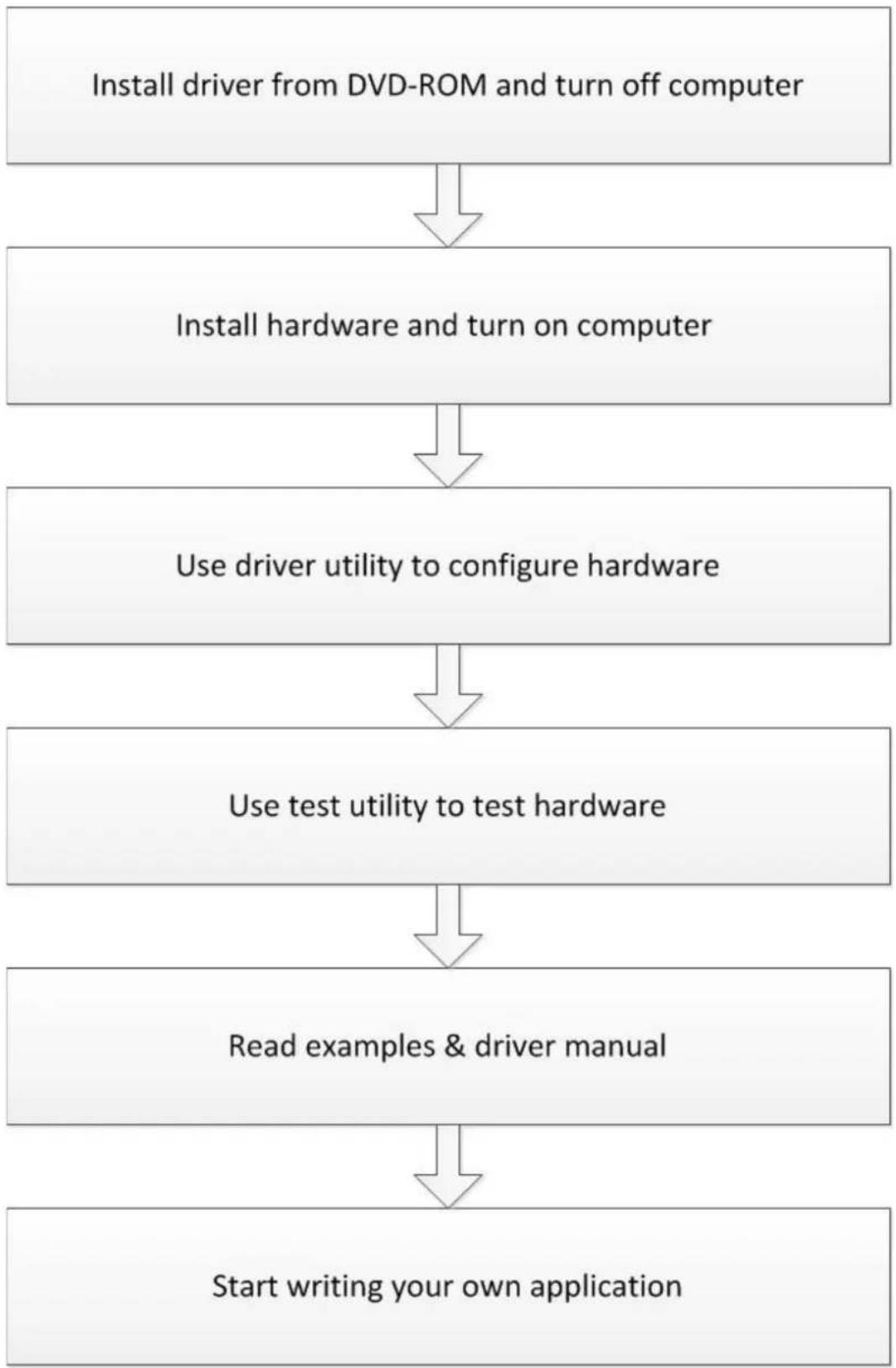
After you get the necessary components and maybe some of the accessories for enhanced operation of your multifunction card, you can then begin the installation procedure. Figure 1.1 on the next page provides a concise flow chart to give users a broad picture of the software and hardware installation procedures:
flowchart
graph TD
    A["Install driver from DVD-ROM and turn off computer"] --> B["Install hardware and turn on computer"]
    B --> C["Use driver utility to configure hardware"]
    C --> D["Use test utility to test hardware"]
    D --> E["Read examples & driver manual"]
    E --> F["Start writing your own application"]
Figure 1.1 Installation Flow Chart
1.4 Software Overview
Advantech offers a rich set of DLL drivers, third-party driver support and application software to help fully exploit the functions of your PCIE-1816/1816H card:
LabVIEW driver
■ Advantech DAQ NAVi
Data logger
■ Device Drivers (on the companion DVD-ROM)
Programming choices for DA&C cards
You may use Advantech application software such as Advantech Device Drivers. On the other hand, advanced users can use register-level programming, although this is not recommended due to its laborious and time-consuming nature.
DAQNavi Software
Advantech DAQNavi software includes device drivers and SDK which features a complete I/O function library to help boost your application performance. This software is included in the companion DVD-ROM at no extra charge and comes with all Advantech DA&C cards. The Advantech DAQNavi software for Windows XP/7/8 (desktop mode) works seamlessly with development tools such as Visual Studio .Net, Visual C++, Visual Basic and Borland Delphi.
1.5 DAQnavi Device Driver Programming Roadmap
This section will provide you a roadmap to demonstrate how to build an application from scratch using Advantech DAQNavi Device Driver with your favorite development tools such as Visual Studio .Net, Visual C++, Visual Basic, Delphi and C++ Builder. The step-by-step instructions on how to build your own applications using each development tool will be given in the Device Drivers Manual. Moreover, a set of example source code is also given for your reference.
Programming Tools
Programmers can develop application programs with their favorite development tools:
Visual Studio.Net
■ Visual C++ and Visual Basic
Delphi
C++ Builder
For instructions on how to begin programming works in each development tool, Advantech offers a Tutorial Chapter in the DAQNavi SDK Manual for your reference. Please refer to the corresponding sections in this chapter on the DAQNavi SDK Manual to begin your programming efforts. You can also look at the example source code provided for each programming tool to get you quickly oriented.
The DAQNavi SDK Manual can be found on the companion DVD-ROM. Alternatively, if you have already installed the Device Drivers on your system, The DAQNavi SDK Manual can be readily accessed through the Start button:
Start/Programs/Advantech Automation/DAQNavi/DAQNavi Manuals/DAQNavi SDK Manual
The example source code could be found under the corresponding installation folder such as the default installation path:
\Advantech\DAQNavi\Examples
For information about using other function groups or other development tools, please refer to the Using DAQNavi SDK chapter in the DAQNavi SDK Manual, or the video tutorials in the Advantech Navigator.
Programming with DAQnavi Device Drivers Function Library
Advantech DAQnavi Device Drivers offer a rich function library that can be utilized in various application programs. This function library consists of numerous APIs that support many development tools, such as Visual Studio .Net, Visual C++, Visual Basic, Delphi and C++ Builder.
According to their specific functions or services, APIs can be categorized into several function groups:
■ Analog Input Function Group
■ Analog Output Function Group
■ Digital Input/Output Function Group
Counter Function Group
■ Port Function Group (direct I/O)
■ Event Function Group
For the usage and parameters of each function, please refer to the Using DAQNavi SDK chapter in the DAQNavi SDK Manual.
Troubleshooting DAQnavi Device Drivers Error
Driver functions will return a status code when they are called to perform a certain task for the application. When a function returns a code that is not zero, it means the function has failed to perform its designated function. To troubleshoot the Device Drivers error, you can pass the error, you can check the error code and error description within the Error Control of each function in the DAQnavi SDK Manual.
1.6 Accessories
Advantech offers a complete set of accessory products to support the PCIE-1816/1816H card. These accessories include:
Wiring Cables
■ PCL-10168-1E 68-pin SCSI Shielded Cable, 1 m
■ PCL-10168-2E 68-pin SCSI Shielded Cable, 2 m
■ PCL-10168H-1E 68-pin SCSI Shielded Cable with Noise Rejecting, 1 m
■ PCL-10168H-2E 68-pin SCSI Shielded Cable with Noise Rejecting, 2 m
Wiring Boards
■ ADAM-3968 68-pin DIN-rail SCSI Wiring Board
Chapter 2
Installation
This chapter provides a packaged item checklist, proper instructions for unpacking and step-by-step procedures for both driver and card installation.
Sections include:
Unpacking
Driver Installation
Hardware Installation
■ Device Setup & Configuration
2.1 Unpacking
After receiving your PCIE-1816/1816H package, inspect the contents first. The package should include the following items:
■ PCIE-1816/1816H card
■ Companion DVD-ROM (Device Drivers included)
■ Startup Manual
The PCIE-1816/1816H card harbor certain electronic components vulnerable to electrostatic discharge (ESD). ESD can easily damage the integrated circuits and certain components if preventive measures are ignored.
Before removing the card from the antistatic plastic bag, you should take following precautions to ward off possible ESD damage:
- Touch the metal part of your computer chassis with your hand to discharge the static electricity accumulated on your body. Alternatively, one can also use a grounding strap.
■ Touch the anti-static bag to a metal part of your computer chassis before opening the bag.
Take hold of the card only by the metal bracket when removing it out of the bag.
After taking out the card, you should first:
Inspect the card for any possible signs of external damage (loose or damaged components, etc.). If the card is visibly damaged, please notify our service department or our local sales representative immediately. Do not install a damaged card into your system.
Also pay extra attention to the followings to ensure a proper installation:
- Avoid physical contact with materials that could hold static electricity such as plastic, vinyl and Styrofoam.
Whenever you handle the card, grasp it only by its edges. DO NOT TOUCH the exposed metal pins of the connector or the electronic components.
Note! Keep the anti-static bag for future use. You might need the original bag to store the card if you have to remove the card from a PC or transport it elsewhere.
2.2 Driver Installation
We recommend you to install the driver before you install the PCIE-1816/1816H card into your system, since this will guarantee a smooth installation process.
The Advantech DAQNavi Device Drivers Setup program for the PCIE-1816/1816H card is included in the companion DVD-ROM that is shipped with your DA&C card package. Please follow the steps below to install the driver software:
- Insert the companion DVD-ROM into your DVD-ROM drive.
- The Setup program will be launched automatically if you have the autoplay function enabled on your system. When the Setup Program is launched, you will see the following Setup Screen.
Note! If the autoplay function is not enabled on your computer, use Windows

Explorer or Windows Run command to execute autorun.exe on the companion DVD-ROM.
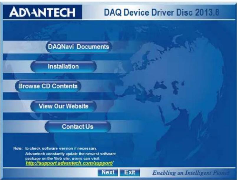
Figure 2.1 Setup Screen of Advantech Automation Software
- Select the Installation option.
- Select the Legacy SDK and Drivers option to install.
- Select the Individual Drivers option.
- Select the PCIE series and the specific device then follow the installation instructions step by step to complete your device driver installation and setup.
- Back and select the Windows SDK and Drivers install the Advantech Navigator.
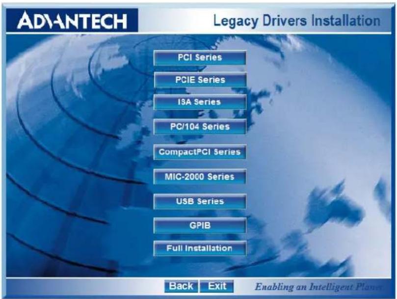
Figure 2.2 Different Options for Driver Setup
For further information on driver-related issues, an online version of the DAQNavi SDK Manual is available by accessing the following path:
Start/Programs/Advantech Automation/DAQNavi/DAQNavi Manuals/DAQNavi SDK Manual
2.3 Hardware Installation
Note! Make sure you have installed the driver first before you install the card (refer to 2.2 Driver Installation)

After the Device Drivers installation is completed you can install the PCIE-1816/1816H card on your computer. However, it is suggested that you refer to the computer's user manual or related documentation if you have any doubts. Please follow the steps below to install the card onto your system.
-
Turn off your computer and unplug the power cord and cables. TURN OFF your computer before installing or removing any components on the computer.
-
Remove the cover of your computer.
-
Remove the slot cover on the back panel of your computer.
-
Touch the metal part on the surface of your computer to neutralize the static electricity that might be on your body.
-
Insert the PCIE-1816/1816H card into the PCI Express interface. Hold the card only by its edges and carefully align it with the slot. Insert the card firmly into place. Use of excessive force must be avoided; otherwise, the card might be damaged.
-
Connect appropriate accessories (68-pin SCSI Shielded Cable, wiring terminals, etc. if necessary) to the card.
-
Replace the cover of your computer chassis. Re-connect the cables you removed in step 2.
-
Plug in the power cord and turn on the computer.
After your card is properly installed on your system, you can now configure your device using the Advantech Navigator Program that has itself already been installed on your system during driver setup. A complete device installation procedure should include device setup, configuration and testing. The following sections will guide you through the Setup, Configuration and Testing of your device.
2.4 Device Setup & Configuration
The Advantech Navigator program is a utility that allows you to set up, configure and test your device, and later stores your settings on the system registry. These settings will be used when you call the APIs of Advantech Device Drivers.
Setting Up the Device
-
To install the I/O device for your card, you must first run the Advantech Navigator program (by accessing Start/Programs/Advantech Automation/DAQNavi/Advantech Navigator).
-
You can then view the device(s) already installed on your system (if any) on the Installed Devices list box. If the software and hardware installation are completed, you will see PCIE-1816/1816H card in the Installed Devices list.
![Advantech Navigator Version 3.1 DAQnavi ADVANTECH Contents Welcome DAQnavi Devices Installed Devices DemoDevice,BID#0 PCIE-1810,BID#15 Device Setting Device Test Scenarios Reference PCIE-1810,BID#0 PCIE-1810,BID#0 Supported Devices SDKs DAQnavi User Interface Welcome to Advantck Video Tutorial Tools Multimeter Customer Feedback Device Setting Setting of PCIE-1810,BID#15 Device Analog Input AL Channel Conversion Sach Clock Trigger0 Trigger 1 Special Configuration Analog Input Calibration Analog Input Manual Calibra Analog Output AD Channel Conversion Trigger0 Trigger 1 Analog Output Calibration Analog Output Manual Calibra Digital Input/Output DIO Ports Direction DI Filter DI Interrupt DI Pattern Match Interrupt DI Status Change Interrupt DO Port Initial Status Counter Clock Filter Event Counter Frequency Measurement Device Number: 11 Name: PCIE-1810 Description: PCIE-1810,BID#15 Product Id: 0x8.10 Board Id: 0xF Driver Version: 3, 1, 0, i2 Dil Version: 3, 1, 0, i6 Board Version: 1.0.0.1 Location: PCI bus 1, device 0, function 0 Base Addresses: [0xF7D0B000,0xF7D0A000,0xF7D00000,0xF7D0B000] Interrupt: 0x10 Initialize device at driver loading: Yes No Update Device Update System Database Save](/content/2026/05/942939/images/0ab0715c8da7e880199d80d89c30bdbd4b983900392d3c36018c077f1a781cf0.jpg)
Figure 2.3 The Device Setting of PCIE-1816/1816H
Configuring the Device
- Please go to the Device Setting to configure your device. Here you can configure not only the Analog Input/Output of PCIE-1816/1816H but also Digital Input/Output.
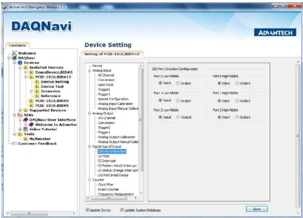
Figure 2.4 The Device Setting page
- After your card is properly installed and configured, you can go to the Device Test page to test your hardware by using the testing utility supplied.
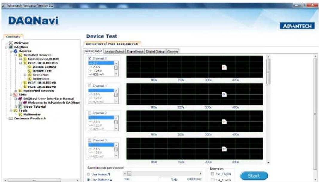
Figure 2.5 The Device Testing of PCIE-1816/1816H
For more detailed information, please refer to the DAQNavi SDK Manual or the User Interface Manual in the Advantech Navigator.
Chapter 3
Signal Connections
This chapter provides useful information about how to connect input and output signals to the PCIE-1816/1816H card via the I/O connector.
Sections include:
Overview
BoardID Settings
Signal Connections
Field Wiring Considerations
3.1 Overview
Maintaining signal connections is one of the most important factors in ensuring that your application system is sending and receiving data correctly. A good signal connection can avoid unnecessary and costly damage to your PC and other hardware devices. This chapter provides useful information about how to connect input and output signals to the PCIE-1816/1816H card via the I/O connector.
3.2 Switch and Jumper Settings
Please refer to Figure 3.1 for jumper and switch locations on PCIE-1816/1816H.
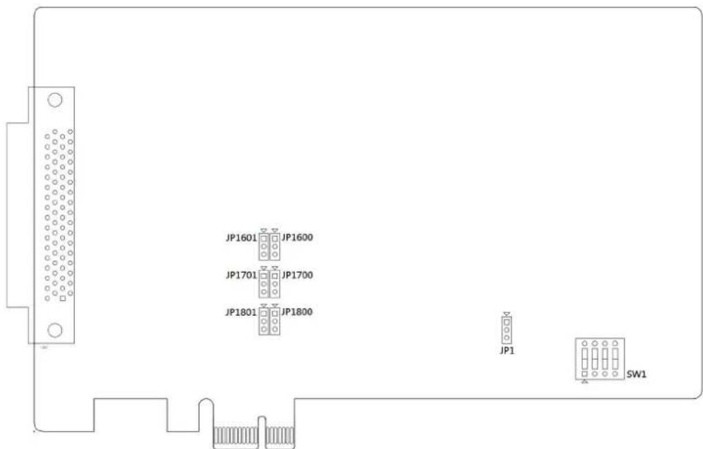
Figure 3.1 Connector and Switch Locations
3.2.1 Board ID (SW1)
The PCIE-1816/1816H has a built-in DIP switch (SW1), which is used to define each card's board ID. When there are multiple cards on the same chassis, this board ID switch is useful for identifying each card's device number.
After setting each PCIE-1816/1816H, you can identify each card in system with different device numbers. The default value of board ID is 0 and if you need to adjust it to other value, please set the SW1 by referring to Table 3.1.
Table 3.1: Board ID Setting (SW1)
| SW1 Position 1 Position 2 Position 3 Position 4 | |||||
| BoardID ID0 ID1 ID2 ID3 | |||||
| 0 | O | N | O | N | O |
| 1 OFF | ON | ON | ON | ||
| 2 ON | OFF ON | ON | |||
| 3 OFF | OFF ON | ON | |||
| 4 ON ON | OFF ON | ||||
| 5 OFF | ON | OFF ON | |||
| 6 ON | OFF OFF ON | ||||
| 7 OFF | OFF OFF ON | ||||
| 8 | O | N | O | N | O |
| 9 OFF | ON | ON | OFF | ||
| 10 | ON | OFF ON | OFF | ||
| 11 | OFF | OFF ON | OFF | ||
| 12 | ON | ON | OFF OFF | ||
| 13 | OFF | ON | OFF OFF | ||
| 14 | ON | OFF OFF OFF | |||
| 15 | OFF | OFF OFF OFF | |||
Default Setting is 0
3.2.2 Power On Configuration(JP1)
Default configuration after power on, and hardware reset is to set all the analog input and analog output channels to open status (the current of the load can't be sink) so that the external devices will not be damaged when the system starts or resets. When the system is hot reset, then the status of isolated digital output channels are selected by jumper JP1. Table 3.2 shows the configuration of jumper JP1.
Table 3.2: Power on Configuration after Hot Reset (JP1)
| JP1 | Power on configuration after hot reset |
1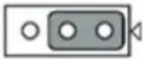 | Keep last status after hot reset |
1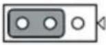 | Default configuration (Default setting) |
3.2.3 Jumper Settings to Set Ports as Software-configurable or Output ports
Table 3.3: Function Description
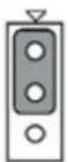
Set DIO channel as software-configurable input or output (default)
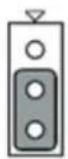
Set DIO channel as output
Jumper number Relative channels
| JP1600 DIO 0~3 |
| JP1601 DIO 4~7 |
| JP1700 DIO 8~11 |
| JP1701 DIO 12~15 |
| JP1800 DIO 16~19 |
| JP1801 DIO 20~23 |
3.3 Signal Connections
Pin Assignments
The I/O connector on the PCIE-1816/1816H is a 68-pin connector that enable you to connect to accessories with the PCL-10168-1 or PCL-10168H shielded cable.
Figure 3.2 shows the pin assignments for the 68-pin I/O connector on the PCIE-1816/1816H, and Table 3.3 shows its I/O connector signal description.
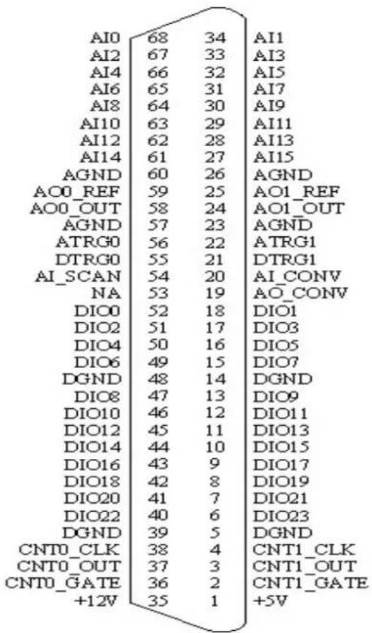
Figure 3.2 68-pin I/O Connector Pin Assignments
3.3.1 I/O Connector Signal Description
Table 3.4: I/O Connector Signal Descriptions
| Signal Name Reference Direction Pin description | |||
| AI[15:0] AGND Input AI Channels 0 to 15. Each channel pair, AI[i+1:i](i=0,2,4...14), can be configured as either two single-ended inputs or one differential input. | |||
| AGND | - | - | Analog Ground. These pins are the reference points for single-ended measurements and the bias current return point for differential measurement. The ground reference (AGND and DGND) are connected together on the PCIE-1816/1816H. |
| ATRG0ATRG1 | AGND Input Analog Threshold Trigger. These pins are the analog input threshold trigger input. | ||
| DTRG0DTRG1 | DGND | Input | Digital Trigger. These pins are the digital input. The left pins are used to start or stop a data acquisition.Analog Threshold Trigger and Digital Trigger are used to execute a specific data acquisition mode – an acquisition which consists of one or more scans. And then a data acquisition behavior needs a stop trigger signal while the pin is used to stop function. The active edge of the start and stop function could be programmed to be rising or falling. |
| AI_SCAN | DGND | Input | AI Scan Clock. This pin is used to initiate a set of data acquisition. The card samples the AI signals of every channel in the scan list once for every AI Scan Clock. |
| AI_CONV | DGND | Input | AI Conversion Clock. This pin is to initiate a single AI conversion on a single channel. A Scan (controlled by the AI Scan Clock) consists of one or more conversions. |
| AO0_REFAO1_REF | AGND Input AO Channel 0/1 External Reference. This is the external reference input for the analog output channel 0/1. | ||
| AO0_OUTAO1_OUT | AGND | Output | AO Channels 0/1. This pin supplies the voltage output of analog output channel 0/1. |
| AO_CONV | DGND | Input | AO Convert Clock. This pin is to initiate AO conversion. Each sample updates the output of all of the DACs. You can specify an internal or external source for AO Convert Clock. |
| DIO[23:0] | DGND | Input/Output | Digital Input/ Output Channel [23:0]. These pins are digital input/output which could be configured as general purpose digital inputs or outputs. |
| DGND | - | - | Digital Ground. This pin supplies the reference for the digital channels at the I/O connector as well as the +5V and +12V DC supply. The ground references (AGND and DGND) are connected together on the PCIE-1816/1816H. |
| CNT0_CLKCNT1_CLK | DGND | Input | Counter 0/1 External Clock Input. The clock input of counters can be either external (up to 10MHz) or internal (20MHz), as set by software. |
Table 3.4: I/O Connector Signal Descriptions
| CNT0_OUT | DGND Output Counter 0/1 Output. |
| CNT1_OUT | |
| CNT0_GATE | DGND Input Counter 0/1 Gate Control. |
| CNT1_GATE | |
| +12V DGND Output +12V DC Source. This pin is +12V DC power supply for external use. (0.1A maximum) | |
| +5V DGND Output +5V DC Source. This pin is +5V DC power supply for external use. (0.3A maximum) | |
3.3.2 Analog Input Connections
PCIE-1816/1816H supports either 16 single-ended or 8 differential analog inputs.
Single-ended Channel Connections
The single-ended input configuration has only one signal wire for each channel, and the measured voltage (Vm) is the voltage of the wire as referenced against the common ground.
A signal source without a local ground is also called a "floating source". It is fairly simple to connect a single-ended channel to a floating signal source. In this mode, the PCIE-1816/1816H provides a reference ground for external floating signal sources.
Figure 3-3 shows a single-ended channel connection between a floating signal source and an input channel.
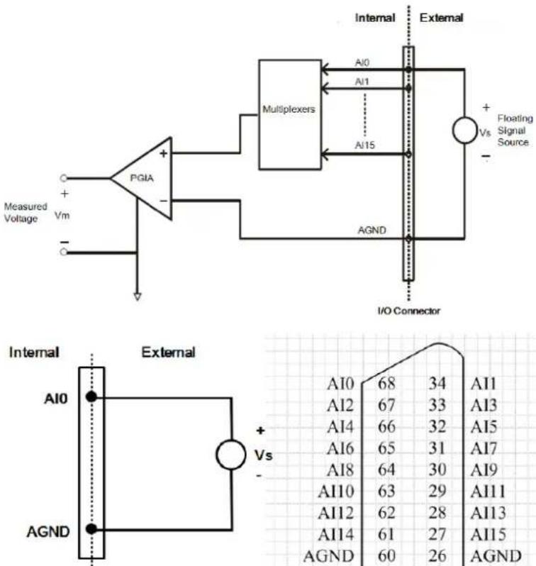
Figure 3.3 Single-ended input channel connections
When to Use Single-ended Channel Connections
Single-ended connections are only used for the following conditions:
All input signals that can share a common reference point, AGND.
The wire connecting the signal to the device are less than 3 m.
Differential Channel Connections
The differential input channels operate with two signal wires for each channel, and the voltage difference between both signal wires is measured. On PCIE-1816/1816H, when all channels are configured to differential input, up to 8 analog channels are available.
If one side of the signal source is connected to a local ground, the signal source is ground-referenced. Therefore, the ground of the signal source and the ground of the card will not be exactly of the same voltage. The difference between the ground voltages forms a common-mode voltage (Vcm).
To avoid the ground loop noise effect caused by common-mode voltages, you can connect the signal ground to the Low input. Figure 3-4 shows a differential channel connection between a ground reference signal source and an input channel on the PCIE-1816/1816H. With this connection, the PGIA rejects a common-mode voltage Vcm between the signal source and the PCIE-1816/1816H ground, shown as Vcm in Figure 3-4.
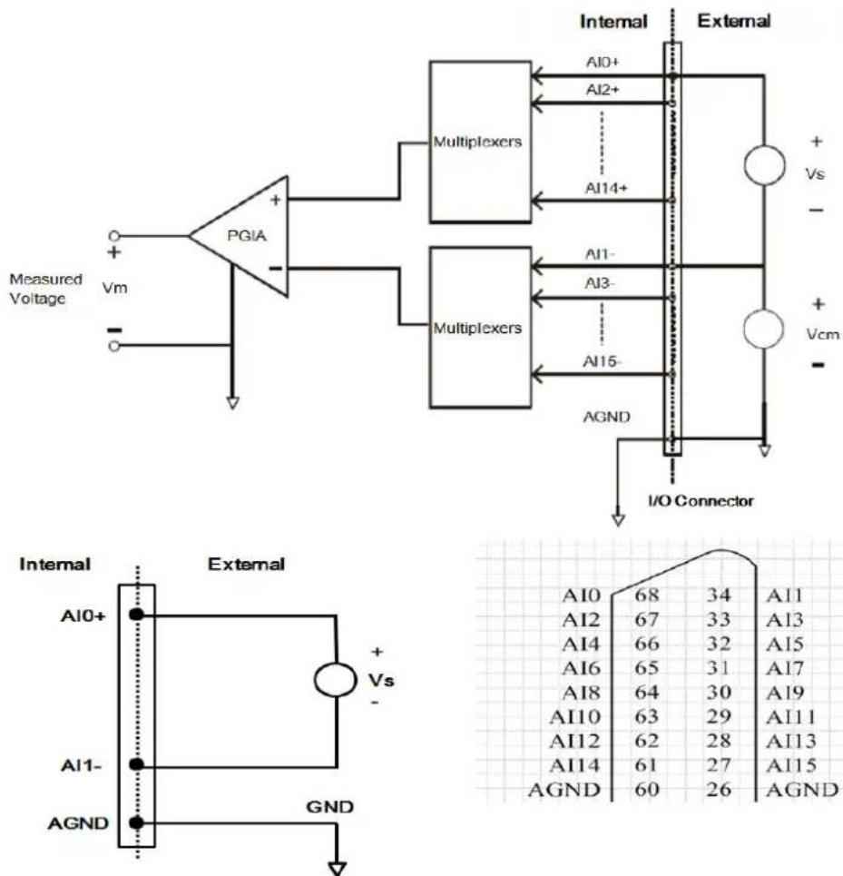
Figure 3.4 Differential input channel connections
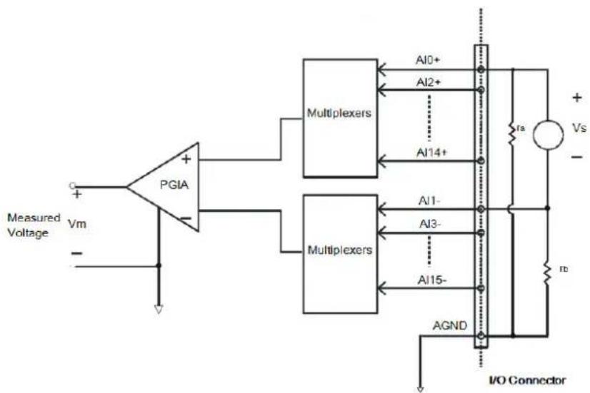
If a floating signal source is connected to the differential input channel, the signal source might exceed the common-mode signal range of the PGIA, and the PGIA will be saturated with erroneous voltage-readings. You must therefore reference the signal source against the AGND.
Figure 3-5 shows a differential channel connection between a floating signal source and an input channel on the PCI-1816/1816H. In this figure, each side of the floating signal source is connected through a resistor to the AGND. This connection can reject the common-mode voltage between the signal source and the PCI-1816/1816H ground.
flowchart
graph TD
    A["Measured Voltage"] --> B["PGIA"]
    B --> C["Multiplexers"]
    B --> D["Multiplexers"]
    C --> E["AI0+"]
    C --> F["AI2+"]
    C --> G["AI14+"]
    D --> H["AI1-"]
    D --> I["AI3-"]
    D --> J["AI15-"]
    E --> K["I/O Connector"]
    F --> K
    G --> K
    H --> K
    I --> K
    J --> K
    K --> L["Vs"]
    L --> M["+"]
    L --> N["-"]
    M --> O["I/O Connector"]
    N --> O
    O --> P["AGND"]
    P --> Q["Ground"]
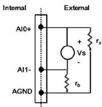
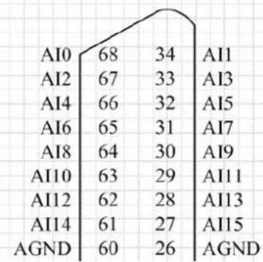
Figure 3.5 Differential input channel connection - floating signal source
However, this connection has the disadvantage of loading the source down with the series combination (sum) of the two resistors. For ra and rb, for example, if the input impedance rs is 1k Ohm, and each of the two resistors is 100k Ohm, then the resistors load down the signal source with 200 Ohm (100 Ohm+ 100 Ohm), resulting in a -0.5% gain error. The following gives a simplified representation of the circuit and calculating process.
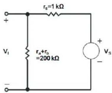
$$ \mathrm{V} _ {1} = \frac {\mathrm{r} _ {\mathrm{a}} + \mathrm{r} _ {\mathrm{b}}}{\mathrm{r} _ {\mathrm{a}} + \mathrm{r} _ {\mathrm{a}} + \mathrm{r} _ {\mathrm{b}}} \mathrm{V} _ {\mathrm{s}} = \frac {2 0 0}{1 + 2 0 0} \mathrm{V} _ {\mathrm{s}} = \frac {2 0 0}{2 0 1} \mathrm{V} _ {\mathrm{s}} $$
V_S : ideal signal source
V_i : measured signal source
r_g : output impedance of signal source
r_a, r_b : series-wound resistors
$$ \text{Gain error} = \frac {V _ {1} - V _ {8}}{V _ {s}} = - \frac {1}{2 0 1} = - 0.5 $$
AI Sample Clock Sources Connections
Internal AI Sample Clock
The internal AI sample clock uses a 100 MHz time base. Conversions start on the rising edge of the counter output. You can use software to specify the clock source as internal and the sampling frequency to pace the operation. The minimum frequency is 0.024 S/s, the maximum frequency is 500 KS/s. According to the sampling theory (Nyquist Theorem), you must specify a frequency that is at least twice as fast as the input's highest frequency component to achieve a valid sampling. For example, to accurately sample a 20 kHz signal, you have to specify a sampling frequency of at least 40 kHz. This consideration can avoid an error condition often know as aliasing, in which high frequency input components appear erroneously as lower frequencies when sampling.
External AI Sample Clock
The external AI sample clock is useful when you want to pace acquisitions at rates not available with the internal AI sample clock, or when you want to pace at uneven intervals. Connect an external AI sample clock to screw terminal AI_CLK on the screw terminal board. Conversions will start on the rising edge of the external AI sample clock input signal. You can use software to specify the clock source as external. The sampling frequency is always limited to a maximum of 10 MHz for the external AI sample clock input signal.
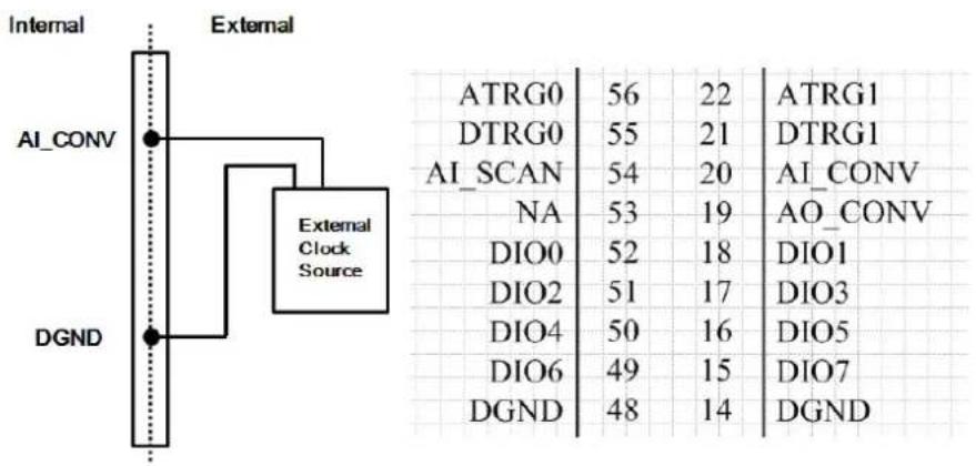
Figure 3.6 External Clock Source Connection
Trigger Sources Connections
External Digital (TTL) Trigger
For analog input operations, an external digital trigger event occurs when the PCIE-1816/ 1816H detects either a rising or falling edge on the External AI TTL trigger input signal from screw terminal DTRG0 and DTRG1 on the screw terminal board. The trigger signal is TTL-compatible.
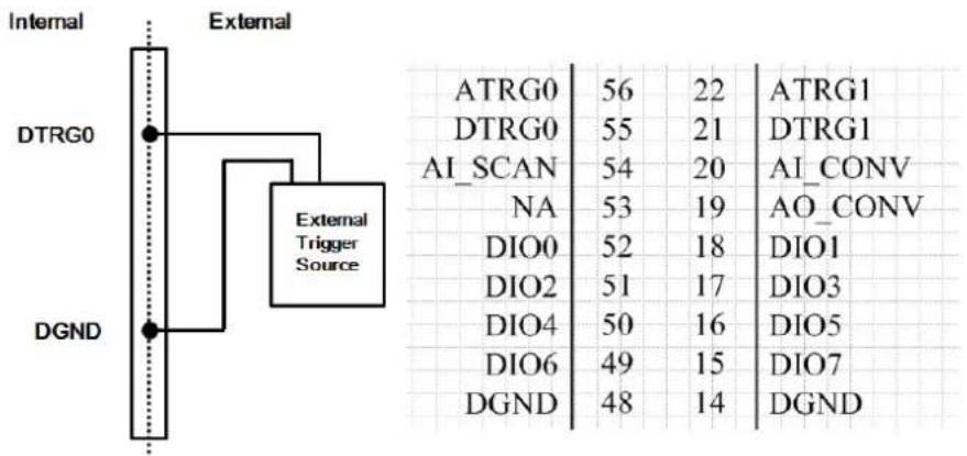
Figure 3.7 External Digital Trigger Source Connection
Analog Threshold Trigger
For analog input operations, an analog trigger event occurs when the PCIE-1816/1816H detects a transition from above a threshold level to below a threshold level (falling edge), or a transition from below a threshold level to above a threshold level (rising edge). User should connect analog signals from external device or analog output channel on board to external input signal ATRG0 and ATRG1. On the PCIE-1816/1816H, the threshold level is set using a dedicated 16-bit DAC. By software, you can program the threshold level by writing a voltage value to this DAC; this value can range from -10V to +10V.
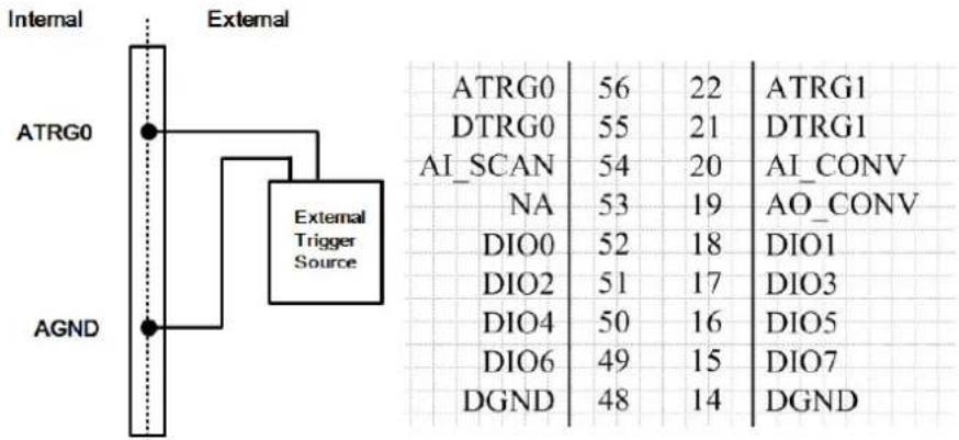
Figure 3.8 External Analog Trigger Source Connection
Analog Output Connection
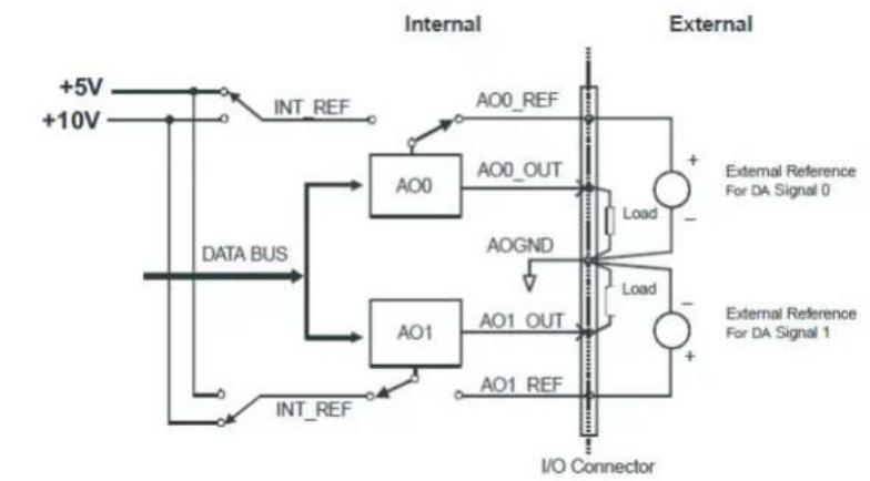
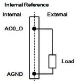
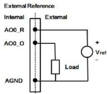
The PCIE-1816/1816H provides two AO output channels. You can use the internal precision -5 V or -10 V reference to generate 0 to +5 V or 0 to +10 V AO output. Use an external reference for other AO output ranges. The maximum reference input voltage is ±10 V and maximum output scaling is ±10 V. Loading current for AO outputs should not exceed 5 mA.
Fig. 3.9 shows how to make analog output and external reference input connections on the PCIE-1816/1816H.
flowchart
graph TD
    A["+5V"] --> B["INT_REF"]
    C["+10V"] --> D["DATA BUS"]
    B --> E["AO0"]
    D --> F["AO1"]
    E --> G["AO0_OUT"]
    F --> H["AO1_OUT"]
    G --> I["External Reference For DA Signal 0"]
    H --> J["External Reference For DA Signal 1"]
    I --> K["I/O Connector"]
    J --> L["I/O Connector"]
    M["IO REF"] --> N["AO0_REF"]
    O["IO REF"] --> P["AO1_REF"]
    Q["AOGND"] --> R["Load"]
    S["Ground"] --> T["Ground"]
| AO0_R | 59 | 25 | AO1_REF |
| AO0_O | 58 | 24 | AO1_OUT |
| AGND | 57 | 23 | AGND |
| AO0_R | 59 | 25 | AO1_REF |
| AO0_O | 58 | 24 | AO1_OUT |
| AGND | 57 | 23 | AGND |
Figure 3.9 Analog Output Connections
AO Sample Clock Sources Connections
Internal AO Output Clock
The internal AO output clock applies a 100MHz time base divided by a 32-bit counter. Conversions start on the rising edges of counter output. Through software, user can specify the clock source and clock frequency to pace the analog output operation. The maximum frequency is 3.030303MS/s.
External AO Output Clock
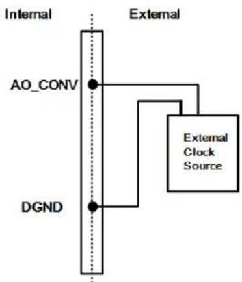
The external AO output clock is useful when you want to pace analog output operations at rates not available with the internal AO output clock, or when you want to pace at uneven intervals. Connect an external AO output clock to the pin and then the conversions will start on input signal's rising edge. You can use software to specify the clock source as external. The maximum input clock frequency is 3MS/s.
flowchart
graph TD
    A["External Clock Source"] --> B["AO_CONV"]
    B --> C["Internal"]
    B --> D["DGND"]
| ATRG0 | 56 | 22 | ATRG1 |
| DTRG0 | 55 | 21 | DTRG1 |
| AI_SCAN | 54 | 20 | AI_CONV |
| NA | 53 | 19 | AO_CONV |
| DIO0 | 52 | 18 | DIO1 |
| DIO2 | 51 | 17 | DIO3 |
| DIO4 | 50 | 16 | DIO5 |
| DIO6 | 49 | 15 | DIO7 |
| DGND | 48 | 14 | DGND |
Figure 3.10 External Clock Source Connection
Trigger Sources Connections
External Digital (TTL) Trigger
The PCIE-1816/ 1816H supports External digital (TTL) trigger to activate AO conversions for continuous output mode. An external digital trigger event occurs when the PCIE-1816/ 1816H detects either a rising or falling edge on the External AO TTL trigger input signal from the pin of connector. User can define the type of trigger source as rising-edge or falling-edge by software. The trigger signal is TTL-compatible.
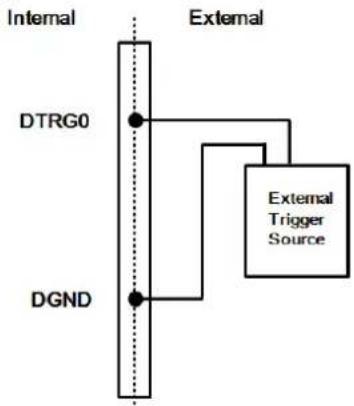
flowchart
graph TD
    A["Internal"] --> B["DTRG0"]
    B --> C["External Trigger Source"]
    B --> D["DGND"]
| ATRG0 | 56 | 22 | ATRG1 |
| DTRG0 | 55 | 21 | DTRG1 |
| AI_SCAN | 54 | 20 | AI_CONV |
| NA | 53 | 19 | AO_CONV |
| DIO0 | 52 | 18 | DIO1 |
| DIO2 | 51 | 17 | DIO3 |
| DIO4 | 50 | 16 | DIO5 |
| DIO6 | 49 | 15 | DIO7 |
| DGND | 48 | 14 | DGND |
Figure 3.11 External Digital Trigger Source Connection
Analog Threshold Trigger
For analog input operations, an analog trigger event occurs when the PCIE-1816/1816H detects a transition from above a threshold level to below a threshold level (falling edge), or a transition from below a threshold level to above a threshold level (rising edge). User should connect analog signals from external device or analog output channel on board to external input signal ATRG0 and ATRG1. On the PCIE-1816H, the threshold level is set using a dedicated 16-bit DAC. By software, you can program the threshold level by writing a voltage value to this DAC; this value can range from -10V to +10V.
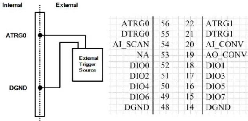
Figure 3.12 External Analog Trigger Source Connection
3.3.3 Digital Signal Connections
The PCIE-1816/1816H has 24 digital input/output channels and they can be configured as input or output channels. The digital I/O levels are TTL compatible.
Digital Input Connections
Each digital input channel accepts either dry contact or 0 \~ 5 V _DC wet contact inputs. Dry contact capability allows the channel to respond to change in external circuit when no voltage is existed.
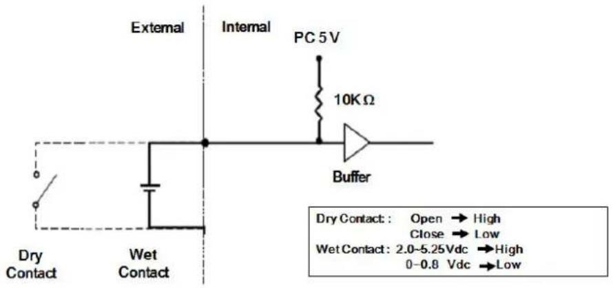
Figure 3.13 Wet and Dry contacts
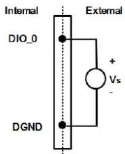
| DIO0 | 52 | 18 | DIO1 |
| DIO2 | 51 | 17 | DIO3 |
| DIO4 | 50 | 16 | DIO5 |
| DIO6 | 49 | 15 | DIO7 |
| DGND | 48 | 14 | DGND |
| DIO8 | 47 | 13 | DIO9 |
| DIO10 | 46 | 12 | DIO11 |
Figure 3.14 Wet signal connection of digital input
| DIO0 | 52 | 18 | DIO1 |
| DIO2 | 51 | 17 | DIO3 |
| DIO4 | 50 | 16 | DIO5 |
| DIO6 | 49 | 15 | DIO7 |
| DGND | 48 | 14 | DGND |
| DIO8 | 47 | 13 | DIO9 |
| DIO10 | 46 | 12 | DIO11 |
Figure 3.15 Dry signal connection of digital input
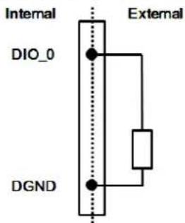
Digital Output Connections
PCIE-1816/ 1816H also has TTL digital output
| DIO0 | 52 | 18 | DIO1 |
| DIO2 | 51 | 17 | DIO3 |
| DIO4 | 50 | 16 | DIO5 |
| DIO6 | 49 | 15 | DIO7 |
| DGND | 48 | 14 | DGND |
| DIO8 | 47 | 13 | DIO9 |
| DIO10 | 46 | 12 | DIO11 |
Figure 3.16 Digital Output Channel Connections
3.4 Field Wiring Considerations
When you use PCIE-1816/1816H cards to acquire data from outside, noise in the environment might significantly affect the accuracy of your measurements if due cautions are not taken. The following measures will be helpful to reduce possible interference running signal wires between signal sources and the PCIE-1816/1816H card.
The signal cables must be kept away from strong electromagnetic sources such as power lines, large electric motors, circuit breakers or welding machines, since they may cause strong electromagnetic interference. Keep the analog signal cables away from any video monitor, since it can significantly affect a data acquisition system.
If the cable travels through an area with significant electromagnetic interference, you should adopt individually shielded, twisted-pair wires as the analog input cable. This type of cable has its signal wires twisted together and shielded with a metal mesh. The metal mesh should only be connected to one point at the signal source ground.
- Avoid running the signal cables through any conduit that might have power lines in it.
If you have to place your signal cable parallel to a power line that has a high voltage or high current running through it, try to keep a safe distance between them. Alternatively, you can place the signal cable at a right angle to the power line to minimize the undesirable effect.
The signals transmitted on the cable will be directly affected by the quality of the cable. In order to ensure better signal quality, we recommend that you use the PCL-10168 shielded cable.
Appendix
A
Specifications
A.1 Function Block
flowchart
graph LR
    A["PCI Express Bus"] -->|x1 PCI Express| B["FPGA"]
    B -->|LVDS| C["ADC"]
    B -->|Parallel| D["DAC"]
    B -->|24-ch AO| E["Buffer / Latch"]
    B -->|24-ch DI/O| F["Buffer"]
    B -->|2-Counter| G["24"]
    C --> H["Driver"]
    D --> I["Driver"]
    E --> J["Driver"]
    F --> K["Driver"]
    G --> L["Driver"]
    H --> M["PGIA"]
    I --> N["MUX"]
    J --> O["PGIA"]
    K --> P["PGIA"]
    L --> Q["PGIA"]
    M --> R["PGIA"]
    N --> S["PGIA"]
    O --> T["PGIA"]
    P --> U["PGIA"]
    Q --> V["PGIA"]
    R --> W["PGIA"]
    S --> X["PGIA"]
    T --> Y["PGIA"]
    U --> Z["PGIA"]
    V --> AA["PGIA"]
    W --> AB["PGIA"]
    X --> AC["PGIA"]
    Y --> AD["PGIA"]
    Z --> AE["PGIA"]
    AA --> AF["PGIA"]
    AB --> AG["PGIA"]
    AC --> AH["PGIA"]
    AD --> AI["PGIA"]
    AE --> AJ["PGIA"]
    AF --> AK["PGIA"]
    AG --> AL["PGIA"]
    AH --> AM["PGIA"]
    AI --> AN["PGIA"]
    AJ --> AO["PGIA"]
    AK --> AP["PGIA"]
    AL --> AQ["PGIA"]
    AM --> AR["PGIA"]
    AN --> AS["PGIA"]
    AO --> AT["PGIA"]
    AP --> AU["PGIA"]
    AQ --> AV["PGIA"]
    AR --> AW["PGIA"]
    AS --> AX["PGIA"]
    AT --> AY["PGIA"]
    AU --> AZ["PGIA"]
    AV --> BA["PGIA"]
    AW --> BB["PGIA"]
A.2 Analog Input
| Channels 16 single-ended / 8 differential | |||||||
| Resolution 16-bit | |||||||
| Built-in memory 4K samples | |||||||
| Sampling Rate | Model PCIE-1816 PCIE-1816H | ||||||
| Single-channel 1 MS/s 5 MS/s | |||||||
| Multi-channel 500 KS/s 1 MS/s | |||||||
| Unipolar/Bipolar Mixed | 100 KS/s 250 KS/s | ||||||
| Input Range and Gain List | G a i n | 0 . | 5 | 1 | |||
| Unipolar | NA | 0~10 | 0~5 | 0~2.5 | 0~1.25 | ||
| Bipolar | ±10 | ±5 | ±2.5 | ±1.25 | ±0.625 | ||
| Drift | Gain | 0.5 | 1 | 2 | 4 | 8 | |
| Zero | 25 ppm/°C | ||||||
| Span | 15 ppm/°C | ||||||
| Input Signal Band Width (-3dB) | G a i n | 0 . | 5 | 1 | |||
| BW (MHz) | 4.4 | 4.4 | 4.4 | 3.3 | 1.7 | ||
| Max. Input Voltage | ±15 V | ||||||
| Input Impedance | 1G Ω / 2pF | ||||||
| Clock Source | Software or external | ||||||
| Trigger Mode | Start trigger, Delay to Start trigger, Stop trigger, Delay to Stop trigger | ||||||
| Accuracy | DC | INLE: ±2 LSB (Under manual adjustment) | |||||
| DNLE: ±1 LSB (Under manual adjustment) | |||||||
| Offset error: Adjustable to zero | |||||||
| Gain | 0.5 | 1 | 2 | 4 | 8 | ||
| Gain Error (%FSR) | 0.007 | 0.007 | 0.007 | 0.008 | 0.008 | ||
| 5 | 5 | 5 | |||||
| Channel Type | Single-Ended / Differential | ||||||
| AC | SNR: 90 dB | ||||||
| ENOB : 15 bits | |||||||
| External Digital Trigger | Low: 0.8V max. ; High: 2.0V min. | ||||||
| Min. pulse width : 50 ns | |||||||
| External Analog Trigger | Range: -10V ~ +10V | ||||||
| Resolution: 16-bit (0.3mV/step) | |||||||
| Bipolar Range | Unipolar Range | ±1 LSB For Full Scale Step | |||||
| ±10V | NA | 1.04 us | |||||
| ±5V | 0 ~ 10V | 1.04 us | |||||
| ±2.5V | 0 ~ 5V | 1.04 us | |||||
| ±1.25V | 0 ~ 2.5V | 4 us | |||||
| ±0.625V | 0 ~ 1.25V | 5 us | |||||
A.3 Analog Output
| Channels 2 | |||
| Resolution 16-bit | |||
| Memory Size 4k samples | |||
| Update Rate 3 MS/s | |||
| Output Range | Internal Reference 0~5, 0~10, ±5, ±10 V | ||
| External Reference Unipolar Bipolar | Reference Input -10V ≤ x ≤ 10V | Maximum Range 0 ~ x V -x V ~ x V | |
| Accuracy Relative ±1 LSB | |||
| Slew Rate 20 V/μs | |||
| Gain Error Adjustable to zero (manual calibration) | |||
| Drift 30 ppm / °C | |||
| Driving Capability 5 mA | |||
| Update Mode | Static update, waveform | ||
| Output Impedance | max. 0.1 Ω | ||
| Capacitive | max. 500 pF | ||
A.4 Digital Input/Output
| Channels | 24 (shared), TTL compatible | |
| Input Voltage | Low | 0.8V max. |
| High | 2.0 V min. | |
| Output Voltage | Low | 0.8 V max.@ +15 mA (sink) |
| High | 2.0 V min.@ -15 mA (source) | |
A.5 Counter/Timer
| Channels 2 channels (independent) | |
| Resolution 32-bit | |
| Compatibility TTL level | |
| Clock Source Internal 20MHz or external clock (10 MHz max.).Selected by software | |
| Output Frequency Max. 10MHz | |
| Clock Input | Low 0.8 V max. |
| High 2.0 V min. | |
| Gate Input | Low 0.8 V max. |
| High 2.0 V min. | |
| Counter Output | Low 0.8 V max. @+15mA |
| High 2.0 V min. @-15mA | |
| Error in Advanced Functions | Frequency Measurement 0.1% when input signal frequency ≥ 40KHz |
| Pulse Width Measurement 0.1% when input signal frequency ≤ 40KHz | |
| Pulse Output within 2% when output frequency > 1MHz | |
| PWM Output within 2% when output frequency > 1MHz | |
Note! When performing advanced functions, like frequency measurement and pulse output, there will be errors. And the error will vary depending on the parameter selections and the OS performance.
A.6 General
| I/O Connector Type 68-pin SCSI female | ||
| Dimensions | 167 x 100 mm | |
| Power Consumption | Typical | 3.3 V @ 504 mA, 12 V @ 152 mA |
| Max. 3.3 V @ 2.49 A, 12 V @ 408 mA | ||
| Temperature | Operating | 0~60°C (32~140°F) |
| Storage | -40 ~ 70°C (-40 ~ 158°F) | |
| Relative Humidity | Operating | 5~85%RH non-condensing |
| Storage | 5~95%RH non-condensing | |
| Certifications | CE/FCC certified | |
Appendix B
Operation Theory
B.1 Analog Input Operation
This section describes the following features of analog input that can help you realize how to configure the functions and parameters to match various applications.
AI Hardware Structure
■ Analog input ranges and gains
■ Analog data acquisition mechanism
■ Analog input acquisition modes
AI SCAN/CONV clock source
AI trigger sources
■ Analog input data format
B.1.1 AI Hardware Structure
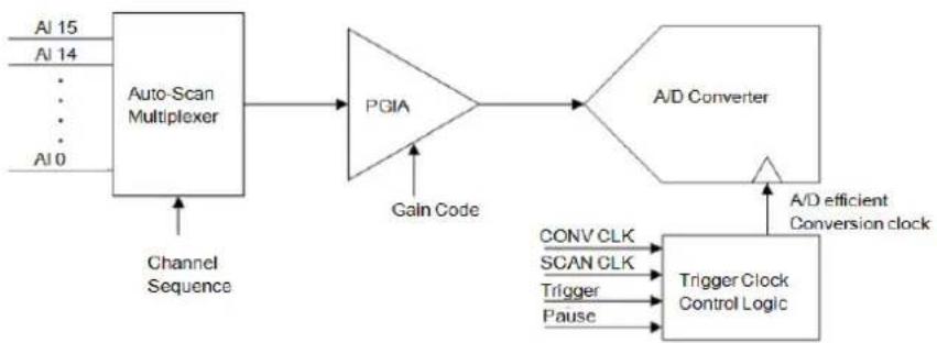
The AI conversion hardware structure includes four major parts:
■ Auto-scan multiplexer routes the analog input signals into AI converter channel by channel in a software-defined sequence.
PGIA (Programmable Gain Instrument Amplifier) rectifies the input range and amplify/alleviate input signal to match the input range of A/ D converter.
AI converter conceives the rectified voltage from PGIA and transfers it into the corresponding digital data format.
Trigger/Clock control logic enables/disables the whole process and determines acquisition timing interval.
flowchart
graph LR
    A["AI 15"] --> B["Auto-Scan Multiplexer"]
    C["AI 14"] --> B
    D["..."] --> B
    E["AI 0"] --> B
    B --> F["PGIA"]
    F --> G["A/D Converter"]
    G --> H["Trigger Clock Control Logic"]
    H --> I["CONV CLK"]
    H --> J["SCAN CLK"]
    H --> K["Trigger"]
    H --> L["Pause"]
    F --> M["Gain Code"]
    M --> N["Channel Sequence"]
    G --> O["A/D efficient Conversion clock"]
AI Conversion Hardware Structure
B.1.2 Analog Input Ranges and Gains
The PCIE-1816/1816H can measure both unipolar and bipolar analog input signals. A unipolar signal can range from 0 to 10 V FSR (Full Scale Range), while a bipolar signal extends within ±10 V FSR. The PCIE-1816/1816H provides various programmable gain levels and each channel is allowed to set its own input range individually. Table B.1 lists the effective ranges supported by the PCIE-1816/1816H with gains.
Table B.1: Gains and Analog Input Range
| Gain | Unipolar Analog Input Range | Bipolar Analog Input Range |
| 0.5 | N/A | ±10 V |
| 1 | 0 ~ 10 V | ±5 V |
| 2 | 0 ~ 5 V | ±2.5 V |
| 4 | 0 ~ 2.5 V | ±1.25 V |
| 8 | 0 ~ 1.25 V | ±0.625 V |
For each channel, choose the gain level providing the most optimal range that can accommodate the signal range you want to measure.
B.1.3 Analog Input Acquisition Mode
The PCIE-1816/1816H can acquire data in either single value or pacer mode.
■ Single Value Acquisition (Polling) Mode
The single value acquisition mode is the simplest way to acquire data. User can simply poll the data register of the desired channel to get the latest acquired value. Each analog input channel has its own dedicated data register (buffer) and in this mode the PCIE-1816/1816H updates each channel cyclically. The update rate is sampling rate/num. of active channels.
Buffer Mode
Adopt buffer mode to acquire data if you wanna accurately control the time interval between conversions. AI conversion clocks come from internal clock sources or external signals on connector. AI conversion starts when the clocks signal come in, and will not stop if the clocks are continuously sent. Conversion data is accumulated into the on-board AI buffer and waiting the transfer to PC memory. Further, you can specify Trigger to acquire the desired periods. We will discuss the detail in the next sections.
AI Data Acquisition Clock Timing
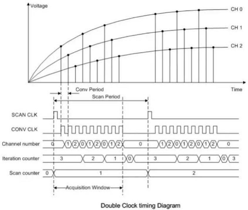
The PCIE-1816/1816H introduces a double-clock system, with SCAN clock and CONV clock, to generate efficient AI conversion clocks at dedicated timing. You can control acquisition timing interval precisely and just acquire the desired period. It can save the waste of PCI bandwidth with continuing acquisition and post data processing by filtering-out the redundant data beforehand. In this section, we will describe how it works and its timing reference in detail.
Double-Clock Procedure
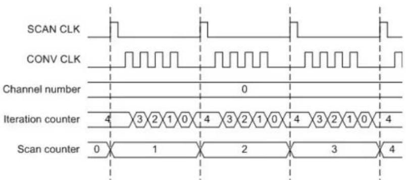
Double clock procedure is the fundamental AI conversion mechanism of the PCIE-1816/1816H, regardless of which mode selected. The incoming SCAN CLK launches an acquisition period called Acquisition Window. The arriving CONV CLKs within the Acquisition Window will become an efficient AI conversion clock to trigger AI converter. The number of efficient CONV CLK depends on the number of active scanning (multiplex) channels and software-programed iteration counters. One scanning iteration is defined as the time auto-scan multiplexer routes input channels from Start channel to Stop channel once. On the other words, all the active channels are sampled once in a single iteration. After the iteration counter counts down to zero, the Acquisition Window will be disable automatically and wait for the next incoming SCAN CLK. The end of Acquisition Window resets the iteration counter to its user-specified value. Users can specify the iteration counter by software and read back the number of incoming SCAN CLKs from SCAN CLK counter.
line
| Channel | Time Segment | Voltage | |---------|--------------|---------| | CH 0 | Start | 0 | | CH 0 | Mid | ~0.8 | | CH 0 | End | ~1.0 | | CH 1 | Start | 0 | | CH 1 | Mid | ~0.6 | | CH 1 | End | ~0.9 | | CH 2 | Start | 0 | | CH 2 | Mid | ~0.4 | | CH 2 | End | ~0.7 | | Scan Period | Time Segment | Voltage | |-------------|------------------|---------| | SCAN CLK | Start | 0 | | CONV CLK | Mid | ~0.5 | | Channel number | 0 | 0 | | Channel number | 1 | 0.5 | | Channel number | 2 | 0.7 | | Channel number | 3 | 0.8 | | Iteration counter | 0 | 0 | | Iteration counter | 1 | 0.5 | | Iteration counter | 2 | 0.7 | | Iteration counter | 3 | 0.8 | | Scan counter | End | 0 | | Scan counter | Mid | ~0.4 | | Scan counter | End | ~0.7 | | Acquisition Window | Mid | 0 | | Acquisition Window | End | ~0.5 | | Double Clock timing DiagramOnce the acquisition procedure inside Acquisition Windows is set, the incoming CLKs must fit in the user-specified acquisition sequence, or the CLKs may be gated off. Refer to the following figures for more details.
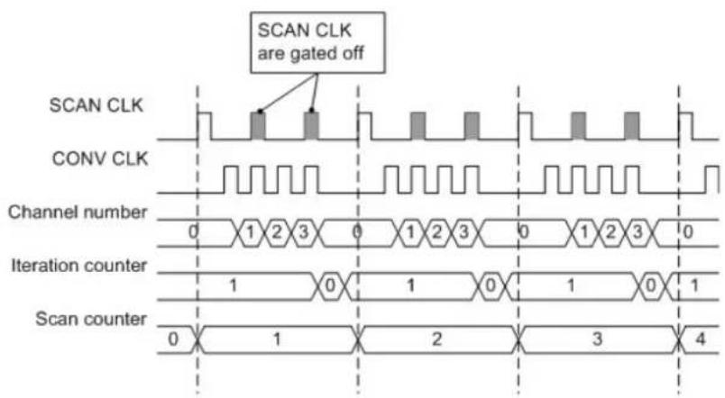
SCAN CLK is too fast
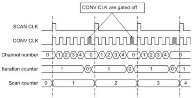
CONV CLK is too fast
Other scanning procedure applications timing diagram.
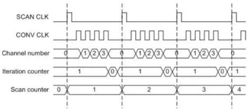
Single Iteration
Multiple Iteration timing with fixed channel
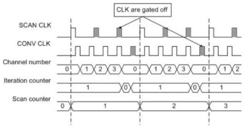
flowchart
graph TD
    A["SCAN CLK"] --> B["Channel number 0"]
    C["CONV CLK"] --> D["Channel number 1"]
    E["Scan counter"] --> F["Channel number 2"]
    G["CLK are gated off"] --> H["Channel number 3"]
    style A fill:#f9f,stroke:#333
    style C fill:#f9f,stroke:#333
    style E fill:#f9f,stroke:#333
    style G fill:#f9f,stroke:#333
    style B fill:#ccf,stroke:#333
    style D fill:#ccf,stroke:#333
    style F fill:#ccf,stroke:#333
    style H fill:#ccf,stroke:#333
Improperly matched SCAN CLK and CONV CLK
■ Single Clock Source Driving
Single clock source driving is a specific function well-suited for consecutive data acquisition while there is only one clock signal available. CONV CLKs will be internally routed as SCAN CLKs. And the external SCAN CLKs input will not be accepted. Figure describes how it works.
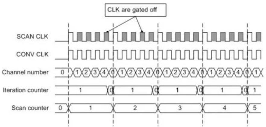
Single clock source driving both CLKs
B.1.4 AI Trigger Modes
The PCIE-1816/1816H supports four trigger modes and pause function. User can start or stop the operation by trigger mode selection. An extra 32-bit counter is dedicated to delay-trigger mode and about-trigger mode, and user can set it as the number of delay SCAN CLKs before trigger or the number of holding SCAN CLKs after trigger. Figure shows the four different trigger modes.
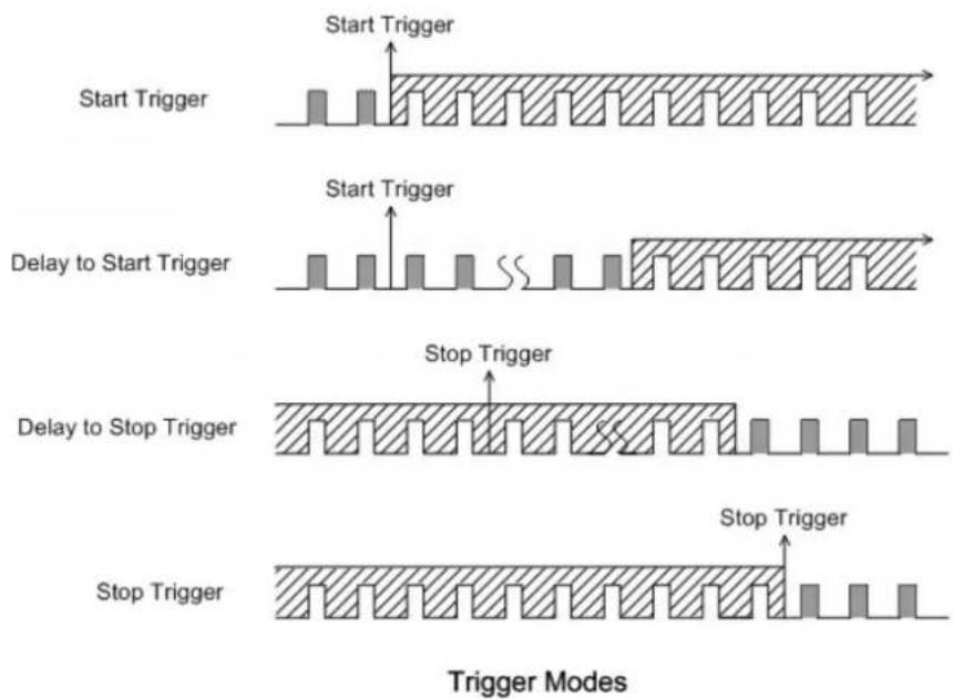
■ Start Trigger Acquisition Mode
Start trigger acquisition starts when the PCIE-1816/1816H detects the trigger event and stops when you stop the operation. The SCAN CLKs before Trigger will be blocked out. You can set post-trigger acquisition mode by software.
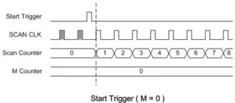
■ Delay to Start Trigger Acquisition Mode
In delay to start trigger mode, data acquisition will be activated after a preset delay number of SCAN CLKs has been taken after the trigger event. User can set the delay number of SCAN CLKs by a 32-bit counter. Delay to start trigger acquisition starts when the PCIE-1816/1816H detects the trigger event and stops when you stop the operation.
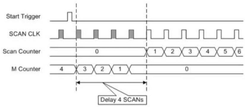
Delay to Start Trigger ( M = 4 )
■ Delay to Stop Trigger Acquisition Mode
When you want to acquire data both before and after a specific trigger event occurs, users should take advantage of the delay to stop trigger mode. First designate the size of the allocated memory and the amount of samples to be snatched after the trigger event happens. The trigger acquisition starts when the first SCAN CLK signal comes in. Once a trigger event happens, the on-going data acquisition will continue until the designated amount of SCAN CLKs have been reached. When the PCIE-1816/1816H detects the selected about-trigger event, the card keeps acquiring the preset number of samples, and keeps them in the buffer.
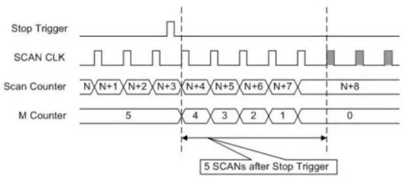
Delay to Stop Trigger ( M = 5 )
■ Stop Trigger Acquisition Mode
Stop trigger mode is a particular application of about-trigger mode. Use pre-trigger acquisition mode when you want to acquire data before a specific trigger event occurs. Stop-trigger acquisition starts when you start the operation and stops when the trigger event happens.
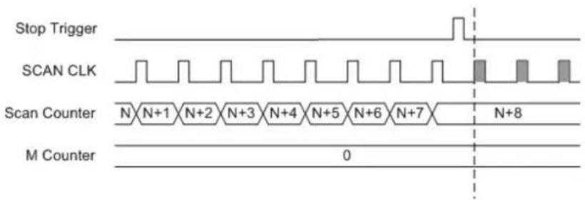
Stop Trigger ( M = 0 )
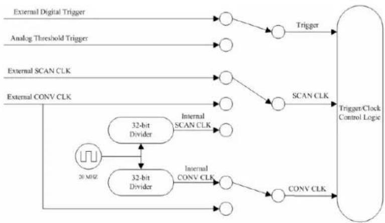
B.1.5 AI SCAN/CONV Clock Source
The PCIE-1816/1816H can adopt both internal and external clock sources to accomplish pacer acquisition. You can set the clock and trigger sources conveniently by software. The figure can help you understand the routing route of clock and trigger generation.
SCAN Clock
– Internal AI SCAN clock derived from 32-bit divider
– External AI SCAN clock from terminal board
– External AI CONV clock from terminal board
Internal AI SCAN Clock
The internal AI SCAN clock uses a 100 MHz time base divided by a 32-bit divider programmable by software. You can program SCAN clock source to internal and its frequency the clock source as internal and the frequency, 500 KS/s maximum for the PCIE-1816 multi-channel and 1 MS/s maximum for the PCIE-1816H multi-channel, to activate AI conversions. To ensure system stability, SCAN clock frequency should be less or equal to CONV clock.
■ External AI SCAN Clock
The external AI SCAN clock is useful when you want to execute acquisitions at rates not available from the internal AI SCAN clock, or when you want to pace at uneven intervals. Acquisitions will start the rising edge of the external AI SCAN clock input. And the frequency for PCIE-1816 and PCIE-1816H should be always limited under 500 KHz and 1 MHz. The exceeding frequency may result in data loss or unexpected data acquisition.
■ External AI CONV clock
This setting is useful when single external clock source is available. Instead of hard-wire, the internal routing can protect signals from different line transmission delay.
CONV Clock
- Internal AI CONV clock derived from 32-bit divider
– External AI CONV clock from terminal board
Internal AI CONV Clock
The same as internal SCAN clock, the internal AI CONV clock applies 100 MHz time base accompanied with 32-bit divider. The maximum frequency is 500 KS/s. According to the sampling theory (Nyquist Theorem), you must specify a frequency that is at least twice as fast as the input's highest frequency component to achieve a valid sampling. For example, to accurately sample a 20 kHz signal, you have to specify a sampling frequency of at least 40 kHz. This consideration can avoid an error condition often know as aliasing, in which high frequency input components appear erroneously as lower frequencies when sampling.
■ External AI CONV Clock
The external AI CONV Clock is convenient in uneven sampling internal. AI conversion will start by each arriving rising edge. The sampling frequency is always limited to a maximum of 500 KHz.
flowchart
graph TD
    A["External Digital Trigger"] --> B(( ))
    C["Analog Threshold Trigger"] --> D(( ))
    E["External SCAN CLK"] --> F(( ))
    G["External CONV CLK"] --> H(( ))
    B --> I(( ))
    D --> J(( ))
    F --> K(( ))
    H --> L(( ))
    I --> M["Trigger"]
    J --> N["SCAN CLK"]
    K --> O["Trigger/Clock Control Logic"]
    L --> P["32-bit Divider"]
    M --> Q["32-bit Divider"]
    N --> R["32-bit Divider"]
    O --> S["32-bit Divider"]
    P <--> T["Internal SCAN CLK"]
    Q <--> U["Internal CONV CLK"]
    R <--> V["CONV CLK"]
    S <--> W["CONV CLK"]
    T --> X["20 MHz"]
    U --> Y["20 MHz"]
Trigger/Clock Routing Diagram
B.1.6 AI Trigger Source
The PCIE-1816/1816H supports the following trigger sources for start, delay to start, delay to stop, stop trigger acquisition modes:
■ External digital (TTL) trigger
■ Analog threshold trigger
With PCIE-1816/1816H, user can also define the type of trigger source as rising-edge or falling-edge. These following sections describe these trigger sources in more detail.
■ External Digital (TTL) Trigger
For analog input operations, an external digital trigger event occurs when the PCIE-1816/1816H detects either a rising or falling edge on the External AI TTL trigger input. The trigger signal is TTL compatible.
■ Analog Threshold Trigger
For analog input operations, an analog trigger event occurs when the PCIE-1816/1816H detects a transition from above a threshold level to below a threshold level (falling edge), or a transition from below a threshold level to above a threshold level (rising edge). User should connect analog signals from external device or analog output channel on board to external input signal ATRG0/1. On the PCIE-1816/1816H, the threshold level is set using a dedicated 16-bit DAC. By software, you can program the threshold level by writing a voltage value to this DAC; this value can range from -10 V to +10 V.
Table B.2: Analog Input Data Format
| AI Code Mapping Voltage | |||
| Hex. Dec. | Unipolar | Bipolar | |
| 0000 h | 0 d | 0 | - FS/2 |
| 7FFF h | 32767 d | FS/2 - 1 LSB | - 1LSB |
| 8000 h | 32768 d | FS/2 | 0 |
| FFFF h | 65535 d | FS - 1 LSB | FS/2 - 1 LSB |
| 1 LSB | FS/65536 | FS/65536 | |
Table B.3: Full Scale Values for Input Voltage Ranges
| Gain | Unipolar Bipolar | |||
| Range FS Range FS | ||||
| 0.5 | N/A | N/A | ±10 V | 20 |
| 1 | 0~10 V | 10 | ±5 V | 10 |
| 2 | 0~5 V | 5 | ±2.5 V | 5 |
| 4 | 0~2.5 V | 2.5 | ±1.25 V | 2.5 |
| 8 | 0~1.25 V | 1.25 | ±0.625 V | 1.25 |
B.2 PCIE-1816/1816H Analog Output Operation
The PCIE-1816/1816H card provides two 16-bit multi-range analog output (D/A) channels. This section describes the following features:
■ Analog output ranges
■ Analog output operation modes
■ Synchronous Analog output waveform
■ AO clock sources
■ AO Trigger sources
■ Analog Output Data Format
B.2.1 Analog Output Ranges
The PCIE-1816/1816H provides two 16-bit analog output channels, both of which can be configured internally to be applicable within 0 \~ 5 V, 0 \~ 10 V, ± 5 V, ± 10 V output voltage range. Otherwise, users can use external reference voltage to apply 0 \~ x V or ± x V output range, where the value x is from -10 to +10. Users can configure the output range during driver installation or in software programming.
B.2.2 Analog Output Operation Modes
■ Single Value Operation Mode
The single value conversion mode is the simplest way for analog output operation. Users can set the mode of each channel individually. Then users just need to use software to write output data to specific register. The analog output channels will output the corresponding voltage immediately. In the single value operation mode, users need not set any clock source and trigger source, but only output voltage range.
Waveform Mode
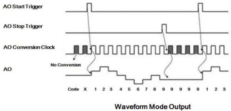
In waveform mode, all AO channels can change output voltage at the same time. Users can accurately control the update rate (up to 3 MS/s) between conversions of individual analog output channels, and takes full advantage of the PCIE-1816/1816H. In this mode you can specify a clock and trigger source and either of the two analog output channels to work in this mode.
Before operating in this mode, users need to set the clock and trigger source first, and then generate the output data stored in the memory buffers of host PC. The host computer then transfers that data to the DACs' buffers on PCIE-1816/1816H. When PCIE-1816/1816H detects a trigger, it outputs the values stored in its buffer. When the buffer's storage decreases, the card sends an interrupt request to the host PC which in turn sends samples to the buffer. This output operation will repeat until either all the data is sent from the buffers or until you stop the operation. If the two AO channels are both operating in continuous output mode, the data in buffer will be sent in an interlaced manner, i.e. the "Even Address" samples in the buffer are sent to AO channel 0, while the "Odd Address" samples to AO channel 1.
B.2.3 AO Clock Sources
The PCIE-1816/1816H can adopt both internal and external clock sources for pacing the analog output of each channel:
■ Internal AO output clock with 32-bit Divider
■ External AO output clock from connector
The internal and external AO output clocks are described in more detail as follows:
■ Internal AO Output Clock
The internal AO output clock applies a 100 MHz time base divided by a 32-bit counter. Conversions start on the rising edges of counter output. Through software, user can specify the clock source and clock frequency to pace the analog output operation. The maximum frequency is 3 MS/s.
■ External AO Output Clock
The external AO output clock is useful when you want to pace analog output operations at rates not available with the internal AO output clock, or when you want to pace at uneven intervals. Connect an external AO output clock to the pin and then the conversions will start on input signal's rising edge. You can use software to specify the clock source as external. The maximum input clock frequency is 3 MS/s.
B.2.4 AO Trigger Sources
The PCIE-1816/1816H supports External digital (TTL) trigger to activate AO conversions for waveform mode. An external digital trigger event occurs when the PCIE-1816/1816H detects either a rising or falling edge on the External AO TTL trigger input signal from the pin of connector. User can define the type of trigger source as rising-edge or falling-edge by software. The trigger signal is TTL-compatible.
Table B.4: Analog Output Data Format
| AO Code Mapping Voltage | |||
| Hex. Dec. Unipolar Bipolar | |||
| 0000 h 0 d 0 | - FS/2 | ||
| 7FFF h | 32767 d | FS/2 - 1 LSB | - 1LSB |
| 8000 h | 32768 d | FS/2 | 0 |
| FFFF h | 65535 d | FS - 1 LSB | FS/2 - 1 LSB |
| 1 LSB | FS/65536 | FS/65536 | |
Table B.5: Full Scale Values for Output Voltage Ranges
| Reference Source | Unipolar | Bipolar | ||
| Range | FS | Range | FS | |
| Internal | 0 ~ 5 V 5 | ± 5 V | 10 | 20 |
| 0 ~ 10 V | 10 | ± 10 V | ||
| External | 0 ~ x V | x | ± x V | 2x |
B.3 Digital Input/Output Operation
The PCIE-1816/1816H supports 24 digital I/O channels. You can use each byte as either an input port or an output port by configuring the corresponding parameter; and all four channels of the byte have the same configuration.
You do not need to specify the clock source or trigger source. To output the data, you just need to write it to the digital output channel directly. In the same way, you can directly read back data from digital input channel. The default configuration after reset sets all the digital I/O channels to logic-low so users don't need to worry about damaging external devices during system start up or reset.
B.4 Counter Input and PWM Input/Output
PCIE-1816/1816H offer two 32-bit counters inputs which can perform event counting, frequency measurement and pulse width measurement.
Counters on PCIE-1816/1816H have a counter value match interrupt function. When this interrupt function is enabled, an interrupt signal will be generated if the counter value reaches a pre-set counter match value. The counter will continue to count until an overflow occurs, then it will go back to its reset value zero and continue the counting process. A user can set each individual counter channel to count either falling edge (high-to-low) or rising edge (low-to-high) signals.
Except measurement functionality, counter input channels can combine with PWM output channels to generate single pulse, pulse train or PWM (pulse-width modulated) output signal. A pulse-width modulated waveform is created when the High and Low periods of a periodic rectangular signal are varied. Using PCIE-1816/1816H, user can individually set each PWM channel's High and Low periods for from 2 to (2^32 - 1) units (1 unit = 50 ns), depending on his needs.
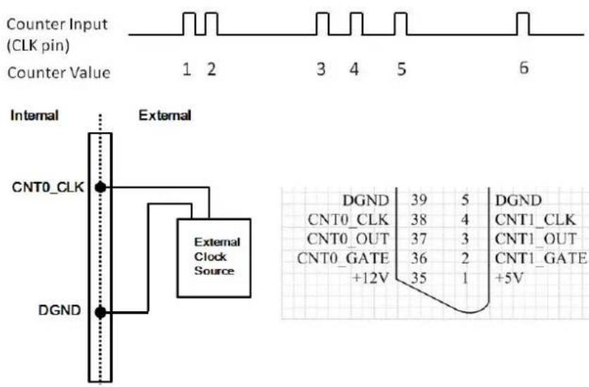
1. Event Counter Connection
PCIE-1816/ 1816H built-in counter can calculate how many pulse are sent into the input channel.
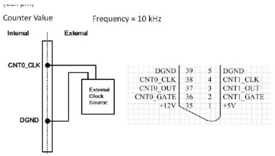
2. Frequency Measurement Connection
PCIE-1816/ 1816H built-in counter can measure the frequency value of the signal connected to counter input.
3. Pulse Width measurement Connection
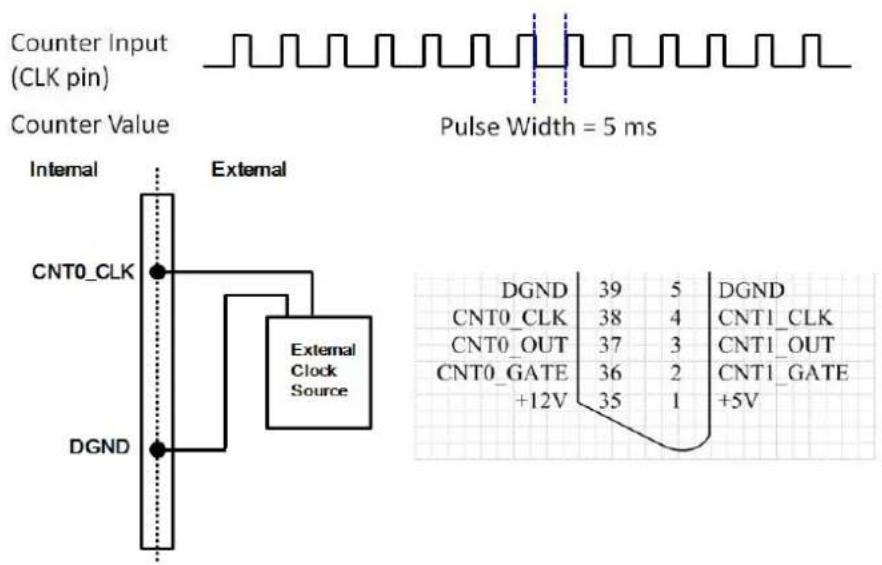
PCIE-1816/1816H built-in counter can measure the pulse width value of the signal connected to counter input. The measurable range is 50 ns to 107 seconds. You can measure both the logic high time and logic low time within the measurable range.
4. Pulse Output with Timer Interrupt
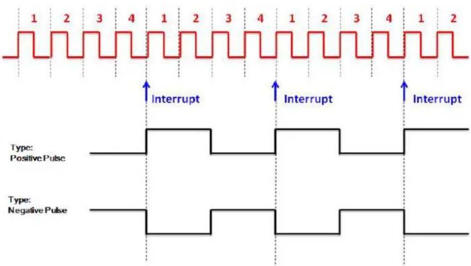
PCIE-1816/1816H counter has internal clock that you can produce periodic output signal with interrupt generated at the same time. PCIE-1816/1816H counter will use internal clock as time base, to fulfill the frequency you want to set. See the figure below as example, the desired frequency is 5 MHz. The internal clock is 20 MHz, so PCIE-1816/1816H will periodically generate output signal and interrupt every 4 pulses of the internal clock. (20 MHz / 5 MHz = 4). Available output frequency range is 0.005 Hz \~ 5 MHz.
5. Delay Pulse Generation
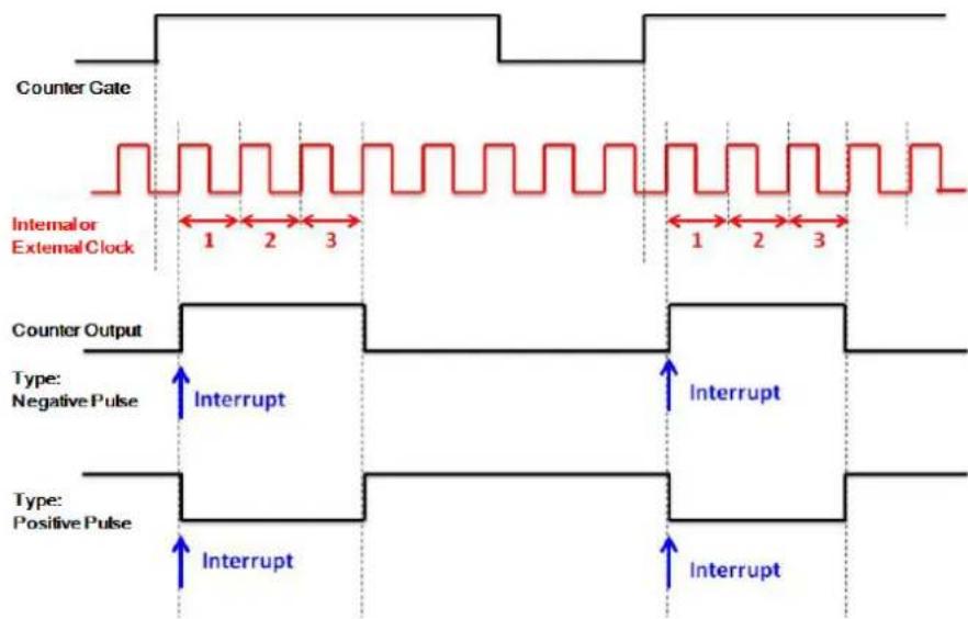
Using PCIE-1816/1816H internal clock, you can change the logic level within a specific period, starting from a trigger signal connecting to counter gate input. For example, if you define the count equals to 3 (as figure below), a counter output will change its status after 3 pulses of internal clock signals pass, after a trigger signal from counter gate becomes high.
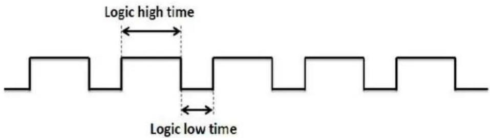
- PWM Output: PCIE-1816/1816H can generate PWM (pulse width modulation) signal which you can configure its logic high time and logic low time as figure below. The available period range for logic high time and logic low time is 100 ns \~ 214 second.
www.advantech.com
Please verify specifications before quoting. This guide is intended for reference purposes only.
All product specifications are subject to change without notice.
No part of this publication may be reproduced in any form or by any means, electronic, photocopying, recording or otherwise, without prior written permission of the publisher.
All brand and product names are trademarks or registered trademarks of their respective companies.
© Advantech Co., Ltd. 2019
- PCIE-1816/1816H
- 16-bit Multi-function Card with PCI Express Bus
- Copyright
- Acknowledgments
- Product Warranty (2 years)
- CE
- Technical Support and Assistance
- Packing List
- Safety Precaution - Static Electricity
- Contents
- Chapter 1 Introduction......1
- Chapter 2 Installation....7
- Chapter 3 Signal Connections....13
- Figure 3.16 Digital Output Channel Connections ...... 28
- Appendix A Specifications.... 31
- Appendix B Operation Theory 37
- Chapter 1
- Introduction
- Features
- PCIe-Bus Plug & Play
- Automatic Channel/Gain Scanning
- Onboard Ring Buffer Memory
- Onboard Programmable Timer/Counter
- BoardID Switch
- Applications
- Installation Guide
- Software Overview
- Programming choices for DA&C cards
- DAQNavi Software
- DAQnavi Device Driver Programming Roadmap
- Programming Tools
- Start/Programs/Advantech Automation/DAQNavi/DAQNavi Manuals/DAQNavi SDK Manual
- Programming with DAQnavi Device Drivers Function Library
- Troubleshooting DAQnavi Device Drivers Error
- Accessories
- Wiring Cables
- Wiring Boards
- Chapter 2
- Installation
- Unpacking
- Driver Installation
- Hardware Installation
- Device Setup & Configuration
- Setting Up the Device
- Configuring the Device
- Chapter 3
- Signal Connections
- Overview
- Switch and Jumper Settings
- Board ID (SW1)
- Power On Configuration(JP1)
- Jumper Settings to Set Ports as Software-configurable or Output ports
- Signal Connections
- Pin Assignments
- I/O Connector Signal Description
- Analog Input Connections
- Single-ended Channel Connections
- When to Use Single-ended Channel Connections
- Differential Channel Connections
- AI Sample Clock Sources Connections
- Internal AI Sample Clock
- External AI Sample Clock
- Trigger Sources Connections
- External Digital (TTL) Trigger
- Analog Threshold Trigger
- Analog Output Connection
- AO Sample Clock Sources Connections
- Internal AO Output Clock
- External AO Output Clock
- Digital Signal Connections
- Digital Input Connections
- Digital Output Connections
- Field Wiring Considerations
- Appendix
- A
- A.2 Analog Input
- A.3 Analog Output
- A.4 Digital Input/Output
- A.5 Counter/Timer
- A.6 General
- Appendix B
- B.1 Analog Input Operation
- B.1.1 AI Hardware Structure
- B.1.2 Analog Input Ranges and Gains
- B.1.3 Analog Input Acquisition Mode
- ■ Single Value Acquisition (Polling) Mode
- Buffer Mode
- AI Data Acquisition Clock Timing
- Double-Clock Procedure
- ■ Single Clock Source Driving
- B.1.4 AI Trigger Modes
- ■ Start Trigger Acquisition Mode
- ■ Delay to Start Trigger Acquisition Mode
- ■ Delay to Stop Trigger Acquisition Mode
- ■ Stop Trigger Acquisition Mode
- B.1.5 AI SCAN/CONV Clock Source
- SCAN Clock
- Internal AI SCAN Clock
- ■ External AI SCAN Clock
- ■ External AI CONV clock
- CONV Clock
- Internal AI CONV Clock
- B.1.6 AI Trigger Source
- B.2 PCIE-1816/1816H Analog Output Operation
- B.2.1 Analog Output Ranges
- B.2.2 Analog Output Operation Modes
- ■ Single Value Operation Mode
- Waveform Mode
- B.2.3 AO Clock Sources
- B.2.4 AO Trigger Sources
- B.3 Digital Input/Output Operation
- B.4 Counter Input and PWM Input/Output
- Event Counter Connection
- Frequency Measurement Connection
- Pulse Width measurement Connection
- Pulse Output with Timer Interrupt
- Delay Pulse Generation
- www.advantech.com
Brand : Advantech
Model : PCIE-1816-B
Category : Expansion card