
PIC32MZ1025W104132 - Uncategorized Microchip - Free user manual and instructions
Find the device manual for free PIC32MZ1025W104132 Microchip in PDF.


| Product Type | 32-bit Microcontroller with Wi-Fi and Hardware-Based Security Accelerator |
| Model | PIC32MZ1025W104132 (SoC) / WFI32E01PE, WFI32E01PC, WFI32E01UE, WFI32E01UC, WFI32E02UE, WFI32E02UC (Modules) |
| Core Processor | 200 MHz MIPS32 M-Class with 16 KB I-Cache, 16 KB D-Cache, DSP-enhanced core |
| Memory | 1 MB Flash, 64 KB Boot Flash, 256 KB SRAM, 64 KB Data Buffer (DBF) |
| Wireless | IEEE 802.11 b/g/n, 2.4 GHz ISM band, Infrastructure BSS STA, Soft-AP, WPA3/WPA2/WEP security |
| Security Accelerator | Hardware accelerated AES (ECB, CBC, CTR, CFB, OFB, GCM), 3DES, SHA, MD5, HMAC, TRNG, Public Key (ECC/ECDH/ECDSA up to 512-bit), Trust&GO (optional) |
| Power Supply (SoC) | 2.97V to 3.63V |
| Power Supply (Module) | 3.0V to 3.6V |
| Operating Temperature | -40°C to +85°C (Industrial) |
| Low Power Modes | Dream, Sleep, Deep Sleep (1.9 μA typical), Extreme Deep Sleep (0.71 μA typical) |
| Package (SoC) | 132-pin DQFN, 10 x 10 x 0.9 mm |
| Package (Modules) | WFI32E01: 54-pin SMD, 24.5 x 20.5 x 2.5 mm; WFI32E02: 87-pin dual-row SMD, 24.5 x 22.5 x 2.5 mm |
| Weight (Estimate) | Approximately 1-2 grams for SoC; 3-5 grams for modules |
| Peripheral Interfaces | USB 2.0 OTG FS, Ethernet MAC (10/100), CAN/CAN-FD, UART (3), SPI (2), I2C (2), SQI, ADC (12-bit, up to 20 ch), CVD touch, PTG |
| Care and Cleaning | No special maintenance required. Keep away from moisture and static discharge. Clean with soft dry cloth if needed. |
| Safety | Operate within specified voltage and temperature range. Use ESD protection during handling. Follow MCLR and power supply recommendations. |
| Spare Parts and Repairability | Not applicable. The device is sold as a single component. No user-serviceable parts. For support, contact Microchip. |
| Certifications (Module) | FCC, ISED, CE, UKCA, MIC, KCC, NCC, SRRC; RoHS and REACH compliant |
| Software Support | MPLAB Harmony v3 TCP/IP Stack, RTOS (FreeRTOS, ThreadX, etc.), OTA/OTH firmware update |
Frequently Asked Questions - PIC32MZ1025W104132 Microchip
User questions about PIC32MZ1025W104132 Microchip
0 question about this device. Answer the ones you know or ask your own.
Ask a new question about this device
Download the instructions for your Uncategorized in PDF format for free! Find your manual PIC32MZ1025W104132 - Microchip and take your electronic device back in hand. On this page are published all the documents necessary for the use of your device. PIC32MZ1025W104132 by Microchip.
USER MANUAL PIC32MZ1025W104132 Microchip
PIC32MZ W1 MCU and WFI32 Module with Wi-Fi® and Hardware-Based Security Accelerator Data Sheet
INTRODUCTION
The PIC32MZ W1 Family (PIC32MZ1025W104132 device) is a general purpose, low-cost, 32-bit Microcontroller (MCU) with the Wi-Fi and network connectivity, hardware-based security accelerator, transceiver and Power Management Unit (PMU). It supports interface to an External Front-End Module.
The WFI32 is a fully RF certified wireless Module that contains the PIC32MZ1025W104 SoC and an integrated Front-end Module (FEM) with following antenna options:
• PCB Antenna (WFI32E01PC/WFI32E01PE)
• U.FL Connector (WFI32E01UC/WFI32E01UE/WFI32E02UC/WFI32E02UE) for External Antenna
The WFI32 Module has the following variants:
• WFI32E01
• WFI32E02
The PIC32MZ W1 Family supports rich set of standard PIC32 peripherals, such as Wi-Fi, Ethernet MAC, USB, CAN, CAN-FD, SPI, I²C, SQL, UART, CVD, ADC and JTAG.
TCP/IP based connectivity protocols along with SSL support enables a low-cost, low complexity system to obtain full-featured Internet connectivity and reliable information exchange.
PIC32MZ W1 FAMILY FEATURES
The following section lists the PIC32MZ1025W104 related features.
Wireless Interfaces
• PHY :
- IEEE ^® 802.11 b/g/n WLAN link
- Single spatial stream of 20 MHz channel bandwidth
- External FEM support for Power Amplifier (PA), Low Noise Amplifier (LNA), Transmitter/Receiver (TX/RX) switch
- 2.4 GHz (2400 \~ 2483.5 MHz) ISM band
• M A C :
- Infrastructure BSS STA mode
- Soft-AP mode functionality
- Active and passive scanning
- Transmit power control support over temperature and voltage
- Security:
- WPA3 personal (SAE and PMF-802.11w)
- WPA2 personal, with options for WPA compatibility and PMF
- WEP
• Harmony Networking:
- Out of box support for MPLAB ^ Harmony v3 TCP/IP Stack
- TLS v1.2 with symmetric/asymmetric crypto acceleration
• Wi-Fi Power Save Modes:
- Wireless Sleep mode (WSM)
- Wireless Deep Sleep mode (WDS)
• Wi-Fi Timestamping Support
200 MHz, MIPS32 ^® M-Class Microprocessor Core
• 16 KB I-Cache, 16 KB D-Cache
- Fixed Mapping Translation (FMT) based MMU for Optimum Embedded OS Execution
- microMIPS™ Mode for Up to 35% Smaller Code Size
• DSP-enhanced Core:
- Four 64-bit accumulators
- Single-cycle MAC, saturating and fractional math
• Code-efficient (c and assembly) architecture
On-Chip Flash and SRAM
• 1 MB Flash Program Memory
• 64 KB Boot Program Flash
• 256 KB SRAM (Program and Data)
• 64 KB Data Buffer (DBF)
• Dedicated Buffer for Peripherals
Power Management and System Recovery
- Low-Power Modes (Dream, Sleep, Deep Sleep and Extreme Deep Sleep)
- 8 KB Context SRAM for Context Storage Under Low Power Modes
- Deep Sleep mode
- 32 Semaphore registers (32-bit wide) for context storage Current consumption: 1.9 μA (typical)
- Extreme Deep Sleep mode
-
32-bit Semaphore register for context storage. Current consumption: 0.71 μA (typical)
-
Integrated Power-on Reset (POR), Brown-out Reset (BOR), Zero-power BOR (ZPBOR) and Programmable Low Voltage Detect (PLVD)
• Secondary Oscillator and Fail Safe Clock - Fast Power-up and Brown-out Recovery
Security
- Hardware Accelerated Security Modes (with Built-in DMA Support)
- Crypto Engine with True Random Number Generator (TRNG) for Data Encryption/decryption and Authentication (AES, 3DES, SHA, MD5 and HMAC)
- AES Modes:
- Electronic Codebook (ECB)
- Cypher Block Chaining (CBC)
- Counter Mode (CTR)
- Cypher Feedback Mode (CFB)
- Output Feedback Mode (OFB)
- Galois/Counter Mode (GCM)
- Hardware Accelerated Public Key Cryptography with Support for:
- 16-DSP multipliers configuration
- 256-bit ECC/ECDH/ECDSA/Curve25519
- 256-bit Ed25519
- 512-bit ECC/ECDH/ECDSA generation
Clock Management
• 40 MHz Primary Oscillator (POSC)
• 32.768 kHz Secondary Oscillator (SOSC)
• Power-up Timer (PWRT) and Oscillator Start-up Timer (OST)
• Fail-Safe Clock Monitor (FSCM)
- On-chip Clock Sources:
- 8 MHz Fast RC (FRC) oscillator
- 32.768 kHz Low-Power RC (LPRC) oscillator
- Programmable PLLs and Oscillator Clock Sources
- Independent Watchdog Timer (WDT), Deadman Timer (DMT) and Independent Deep Sleep Watchdog Timer
- Fast Wake-up and Start-up
- Support for Precise Reference Clocks to External Devices
Direct Memory Access (DMA)
- Eight Channels with Automatic Data Size Detection
• Programmable 32-bit Cyclic Redundancy Check (CRC)
Advanced Analog
• 12-bit ADC Module:
- 2 MSPS with two Sample and Hold (S&H) circuits (one dedicated and one shared)
- Up to 20 analog input channels
- Sleep and Idle mode operations
- Multiple trigger sources
- Two digital comparators and two digital filters
- Supports self capacitance touch interface with a maximum of 18 touch buttons and one driven shield
Communication Interfaces
- Up to Two CAN Modules (CAN and CAN-FD)
- 2.0B Active with DeviceNet™ addressing support
- Up to Three UART Modules (Speed up to 10 Mbps):
- Supports RS-232, RS-485, LIN 2.1 and IrDA Protocols
- One Ethernet MAC Module (10/100 Mbps) with RMII Interface and Dedicated DMA:
- IEEE 1588 Precision Time Protocol (PTP)
- Time synchronization support between Wi-Fi and Ethernet
- Up to Two SPI (4-wire) Modules with Speed up to 40 MHz
- SQI Configurable as an Additional SPI Module (60 MHz)
• One Full-Speed USB 2.0 OTG Interface with Dedicated DMA
• T w ^2 6 (Up to 1M baud) with SMBus Support
Timers/Output Compare/Input Capture
- Seven 16-bit or up to Three 32-bit Timers/Counters
• Four Output Compare (OC) Modules
• Four Input Capture (IC) Modules - Low-power Precision Real-Time Clock and Calendar (RTCC)
Input/Output
• High Current Source/Sink (up to 25 mA) on All I/O Pins
- Configurable Open-Drain, Pull-up, Pull-down and Slew Rate Controls
• External interrupts on all I/O Pins
- Peripheral Pin Select (PPS) to Enable Function Remap
- Up to 62 GPIO Pins
Peripheral Trigger Generator (PTG)
- PTG with 8-bit User Command for Scheduling Complex Sequences
Qualification and Class B Support
• Class B Safety Library, IEC 60730
Debugger Development Support
• In-circuit and In-application Programming
• 4 - w i r®EnhancerPJTAG Interface
- Unlimited Software, 8 Instruction and 4 Data Complex Hardware Breakpoints
- IEEE 1149.2-Compatible (JTAG) Boundary Scan
- iFlowtrace functionality support:
- Off-chip Buffering of iFlowTrace Messages
Software and Tools Support
• C/C++ Compiler with Native DSP/fractional
- MPLAB ^® Harmony Integrated Software Framework:
- TCP/IP, USB, Graphics and mTouch™ Middleware
- MFi, Android™
- RTOS Kernels: Express Logic ThreadX, FreeRTOS™, OPENRTOS®, Micrium® μC/OS™ and SEGGER embOS®
• Supports Over-the-Air (OTA) and Over-the-Host (OTH) Firmware Update Modes
Package and Operating Conditions
- Package:
- 132-pin DQFN – Dual Row
- Size - 10 x 10 x 0.9 mm
- Operating conditions:
- 2.97V to 3.63V, -40°C to +85°C, DC to 200 MHz
WFI32 MODULE FEATURES
The following section lists the WFI32 Module related features, which complement SoC features.
Antenna Options
• PCB Antenna Variants:
- WFI32E01PC
- WFI32E01PE
- External Antenna Variants:
- WFI32E01UC
- WFI32E01UE
- WFI32E02UC
- WFI32E02UE
Wireless Feature
On-Board FEM/PA to Meet the TX Power Requirements:
• Maximum 20.5 dBm TX Power in 802.11b Mode
Security
• Integrated Trust&GO (Optional)
Clock Management
• Integrated 40 MHz POSC
Advanced Analog
• 12 Analog Channels for WFI32E01
• 20 Analog Channels for WFI32E02
Input/Output
• 37 GPIO Pins for WFI32E01
• 60 GPIO Pins for WFI32E02
Package and Operating Conditions
- WFI32E01 Package:
- 54-pin SMD package with Shield Can
- Size - 24.5 mm x 20.5 mm x 2.5 mm
- WFI32E02 Package:
- 87-pin dual-row SMD package with Shield Can
- Size - 24.5 mm x 22.5 mm x 2.5 mm
- Operating conditions:
- 3.0V to 3.6V, -40°C to +85°C, DC to 200 MHz
Regulations
• RoHS and REACH Compliant
Certifications
• WFI32 Module Certified to FCC, ISED, CE, UKCA, MIC, KCC, NCC and SRRC Radio
TABLE 1: PIC32MZ1025W104 SoC FEATURES
| SoC Name | Program Memory (KB) | Data Memory (KB) | Pins | Package | Boot Flash Memory (KB) | Wireless/RF Remappable Peripherals | Crypto | Asymmetric Crypto | Trust&GO | TRNG | DMA Channels (Programmable/Dedicated) | ADC Channels | CVD | ADC Enhanced CVD | PTG | USB 2.0 OTG FS | I^2C | SPI | UART | SQI | RTCC | Ethernet MAC | I/O Pins | ICSPTM | JTAG | Trace | ||||||||
| 802.11 b/g/n | Channel BW (MHz) | Remappable Pins | Timers/Capture/ Compare(1) | UART | SPI/2S | CAN-FD (1.0) | CAN (2.0 A/B) | |||||||||||||||||||||||||||
| PIC32MZ1025W104132 | 1024 | 256 | 132 | DQFN | 64 | 1x1 | 20 | 58 | 7/4/4 | 2 | 1 | 1 | 1 | Y | Y | N | Y | 8 | 20 | Y | Y | 1 | 1 | 2 | 1 | 1 | Y | Y | Y | 62 | Y | Y | Y | |
TABLE 2: WFI32 MODULE FEATURES
| Module Name | Program Memory (KB) | Data Memory (KB) | Pins | Package | Boot Flash Memory (KB) | Wireless/RF | Remappable Peripherals | Crypto | Asymmetric Crypto | Trust&GO | TRNG | DMA Channels (Programmable/Dedicated) | ADC Channels | CVD | ADC Enhanced CVD | PTG | USB 2.0 OTG FS | ^12C | SPI | UART | SQI | RTCC | Ethernet MAC | I/O Pins | ICSP | JTAG | Trace | Antenna Options | ||||||
| On-board FEM | 802.11 b/g/n | Channel BW (MHz) | Remappable Pins | Timers/Capture/Compare | UART | SPI/ I^2S | CAN-FD (1.0) | |||||||||||||||||||||||||||
| WFI32E01PE | 1024 | 256 | 54 | SMD | 64 | Y | 1x1 | 20 | 35 | 7/4/4 | 2 | 1 | 1 | 1 | Y | Y | N | Y | 8 | 12 | Y | Y | 1 | 1 | 1 | 1 | 1 | N | Y | Y | 37 | Y | Y | PCB |
| WFI32E01PC | 1024 | 256 | 54 | SMD | 64 | Y | 1x1 | 20 | 35 | 7/4/4 | 2 | 1 | 1 | 1 | Y | Y | Y | Y | 8 | 12 | Y | Y | 1 | 1 | 1 | 1 | 1 | N | Y | Y | 37 | Y | Y | PCB |
| WFI32E01UE | 1024 | 256 | 54 | SMD | 64 | Y | 1x1 | 20 | 35 | 7/4/4 | 2 | 1 | 1 | 1 | Y | Y | N | Y | 8 | 12 | Y | Y | 1 | 1 | 1 | 1 | 1 | N | Y | Y | 37 | Y | Y | U.FL |
| WFI32E01UC | 1024 | 256 | 54 | SMD | 64 | Y | 1x1 | 20 | 35 | 7/4/4 | 2 | 1 | 1 | 1 | Y | Y | Y | Y | 8 | 12 | Y | Y | 1 | 1 | 1 | 1 | 1 | N | Y | Y | 37 | Y | Y | U.FL |
| WFI32E02UE | 1024 | 256 | 87 | SMD | 64 | Y | 1x1 | 20 | 56 | 7/4/4 | 2 | 1 | 1 | 1 | Y | Y | N | Y | 8 | 20 | Y | Y | 1 | 1 | 2 | 1 | 1 | Y | Y | Y | 60 | Y | Y | U.FL |
| WFI32E02UC | 1024 | 256 | 87 | SMD | 64 | Y | 1x1 | 20 | 56 | 7/4/4 | 2 | 1 | 1 | 1 | Y | Y | Y | Y | 8 | 20 | Y | Y | 1 | 1 | 2 | 1 | 1 | Y | Y | Y | 60 | Y | Y | U.FL |
TABLE 3: PIN NAMES FOR 132-PIN PIC32MZ1025W104 SoC
132-PIN DQFN (TOP AND BOTTOM VIEW) 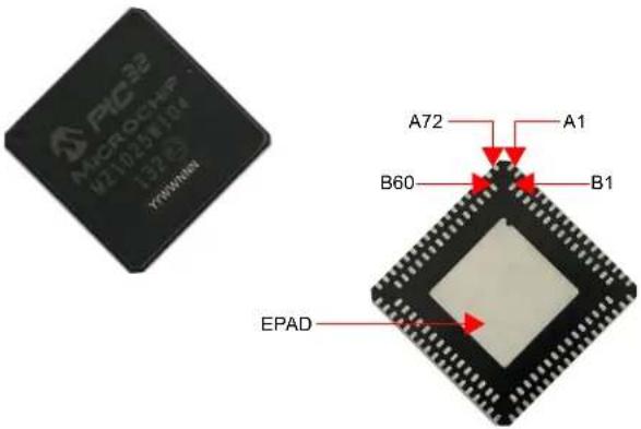 | ||||
| SoC Pin Number | SoC Pin Name(1,2) | V A64 D+ | SoC Pin Number | SoC Pin Name(1,2) |
| A1 | NC | A36 | NC | |
| A2 PMU_VSENSE A37 NC | ||||
| A3 | VDD33 | A38 | NC | |
| A4 | CVDT13/ETXD0/RPC15/IOCC15/RC15 | A39 | RXR_IN2 | |
| A5 | CVDT15/EMDIO/RPK13/IOCK13/RK13 | A40 | RXR_RIQ_VDD15 | |
| A6 | CVDT14/ERXDV/RPK12/IOCK12/RK12 | A41 | NC | |
| A7 | NC | A42 | TXR_UMX_VDD15 | |
| A8 VDD15 | A43 TXR_LPA_VOUT | |||
| A9 | SQICS1/CVDT18/RPC0/IOCC0/RC0 | A44 | RF_FE_3/RPK0/IOCK0/RK0 | |
| A10 | SQID2/CVDT20/RPC2/IOCC2/RC2 | A45 | RF_FE_1/AN19/CVD19/CVDR19/RPK2/IOCK2/RK2 | |
| A11 VDD33 | A46 VDD33 | |||
| A12 | SQICLK/CVDT23/RPC5/IOCC5/RC5 | A47 | SCK2/RPA11/IOCA11/RA11 | |
| A13 SDI1/RPC7/IOCC7/RC7 A48 AN15/ANN1/CVD15/CVDR15/RPA13/IOCA13/RA13 | ||||
| A14 | SS1/CS1/FSYNC1/RPA1/IOCA1/RA1 | A49 | TRD0/AN13/CVD13/CVDR13/RPA15/IOCA15/RA15 | |
| A15 | SCL2/RPA2/IOCA2/RA2 | A50 | TRD1/AN12/CVD12/CVDR12/RPB14/IOCB14/RB14 | |
| A16 | SCL1/RPA4/IOCA4/RA4 | A51 | TRD3/ANA0/RPB12/IOCB12/RB12 | |
| A17 NC A52 | AN10/CVD10/CVDR10/LVDIN/RPB10/IOCB10/RB10 | |||
| A18 NC A53 NC | ||||
| A19 NC A54 NC | ||||
| A20 NC A55 NC | ||||
| A21 | U1RTSn/U1BCLK/IOCA7/RA7 | A56 | TDI/PGED4/AN9/CVD9/CVDR9/RPB9/IOCB9/RB9 | |
| A22 | U1TX/IOCA9/RA9 | A57 | TDO/AN7/CVD7/CVDR7/CVDT0/RPB7/IOCB7/RB7 | |
| A23 | MCLR | A58 | SOSCO/PK15(4) | |
| A24 | BT_PRIO/RPK6/IOCK6/RK6 | A59 | SOSCI/PB15(4) | |
| A25 VDD33 | A60 VBAT | |||
| A26 | RF_FE_8/RPK9/IOCK9/RK9 | A61 | PGEC1/AN3/CVD3/CVDR3/CVDT4/USBOEN/RPB3/IOCB3/RB3 | |
| A27 | RF_FE_5/RPK11/IOCK11/RK11 | A62 | AN1/CVD1/CVDR1/CVDT6/ETH_EXCLK_OUT/VBUSON/RPB1/IOCB1/RB1 | |
| A 2 | 8 A F E _ | D | D 1 5 A 6 3 | |
| A29 XTAL_IN | ||||
Note
1: The RPn pins can be used by re-mappable peripherals. Refer to Section 13.4 "Peripheral Pin Select (PPS)" for details.
2: Every I/O port pin (RAx-RKx) can be used as a change notification pin (CNAx-CNKx). See Section 13.0 "I/O Ports" for more information.
3: Do not use BUCK/MLDO output to drive any other device.
4: A58 and A59 pins can be configured as GPI as an alternate function.
5: Exact connection for each pin is available in the reference design package. Contact the Microchip Sales/Support Team for the package.
6: Connect Exposed Die Pad to GND.
TABLE 3: PIN NAMES FOR 132-PIN PIC32MZ1025W104 SoC (CONTINUED)
Note
1: The RPn pins can be used by re-mappable peripherals. Refer to Section 13.4 "Peripheral Pin Select (PPS)" for details.
2: Every I/O port pin (RAx-RKx) can be used as a change notification pin (CNAx-CNKx). See Section 13.0 "I/O Ports" for more information.
3: Do not use BUCK/MLDO output to drive any other device.
4: A58 and A59 pins can be configured as GPI as an alternate function.
5: Exact connection for each pin is available in the reference design package. Contact the Microchip Sales/Support Team for the package.
6: Connect Exposed Die Pad to GND.
TABLE 3: PIN NAMES FOR 132-PIN PIC32MZ1025W104 SoC (CONTINUED)
132-PIN DQFN (TOP AND BOTTOM VIEW) 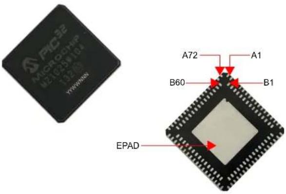 | ||||||
| SoC Pin Number | SoC Pin Name(1,2) | SoC Pin Number | SoC Pin Name(1,2) | |||
| B23 | SPI_VDD15 | B54 | VUSB3V3 | |||
| B 2 | 4 X T A L | - | V | D | D | 1 5 B 5 |
| B25 NC B56 NC | ||||||
| B26 | IOVDD_RF | B57 | CVDT8/ERXD1/RPC10/IOCC10/RC10 | |||
| B27 | IN_TSSI | B58 | CVDT10/ETH_CLK_OUT/ERXCLK/RPC12/IOCC12/RC12 | |||
| B28 SYN_PLL_VDD15 B59 BUK_MLDO_OUT | (3) | |||||
| B29 NC B60 VPMU_VDDP | ||||||
| — — EPAD Exposed Die Pad | (6) | |||||
Note
1: The RPn pins can be used by re-mappable peripherals. Refer to Section 13.4 "Peripheral Pin Select (PPS)" for details.
2: Every I/O port pin (RAx-RKx) can be used as a change notification pin (CNAx-CNKx). See Section 13.0 "I/O Ports" for more information.
3: Do not use BUCK/MLDO output to drive any other device.
4: A58 and A59 pins can be configured as GPI as an alternate function.
5: Exact connection for each pin is available in the reference design package. Contact the Microchip Sales/Support Team for the package.
6: Connect Exposed Die Pad to GND
Table of Contents
Introduction 1
1.0 Ordering Information 11
2.0 PIC32MZ1025W104 SoC Description 13
3.0 WFI32E01 Module Description 27
4.0 CPU 59
5.0 Flash Program Memory 71
6.0 Memory Organization 85
7.0 Resets 111
8.0 CPU Exceptions and Interrupt Controller 119
9.0 Prefetch Module 147
10.0 Direct Memory Access (DMA) Controller 155
11.0 Oscillator Configuration 179
12.0 Full-Speed USB On-The-Go (OTG) 201
13.0 I/O Ports 227
14.0 Peripheral Trigger Generator (PTG) 263
15.0 Timer1 283
16.0 Timer2/3, Timer4/5, and Timer6/7 287
17.0 Deadman Timer (DMT) 293
18.0 Watchdog Timer (WDT) 301
19.0 Input Capture 303
20.0 Output Compare 307
21.0 Serial Peripheral Interface (SPI) and Inter-IC Sound (I^2S) 311
22.0 Serial Quad Interface (SQI) 319
23.0 Inter-Integrated Circuit (I²C) 341
24.0 UART 351
25.0 Real-Time Clock and Calendar (RTCC) 359
26.0 Asymmetric Crypto Engine 369
27.0 Symmetric Crypto Engine 371
28.0 True Random Number Generator (TRNG) 395
29.0 12-bit High-Speed Successive Approximation Register (SAR) ADC 401
30.0 Controller Area Network (CAN) 445
31.0 Controller Area Network-Flexible Data-Rate (CAN-FD) Module 473
32.0 Wi-Fi Controller 523
33.0 Ethernet Controller 565
34.0 Enhanced Capacitive Voltage Divider (CVD) Touch Controller 565
35.0 Power Management Unit (PMU) 587
36.0 Power-Saving Features 599
37.0 Programmable Low Voltage Detect (PLVD) 617
38.0 Special Features 621
39.0 Instruction Set 641
40.0 Development Support 643
41.0 Electrical Specifications 647
42.0 Packaging Information 707
Appendix A: Regulatory Approvals 723
Appendix B: Document Revision History 735
TO OUR VALUED CUSTOMERS
It is our intention to provide our valued customers with the best documentation possible to ensure successful use of your Microchip products. To this end, we will continue to improve our publications to better suit your needs. Our publications will be refined and enhanced as new volumes and updates are introduced.
If you have any questions or comments regarding this publication, please contact the Marketing Communications Department via E-mail at docerrors@microchip.com. We welcome your feedback.
Most Current Data Sheet
To obtain the most up-to-date version of this data sheet, please register at our Worldwide Website at:
http://www.microchip.com
You can determine the version of a data sheet by examining its literature number found on the bottom outside corner of any page. The last character of the literature number is the version number, (e.g., DS30000000A is version A of document DS30000000).
Errata
An errata sheet, describing minor operational differences from the data sheet and recommended workarounds, may exist for current devices. As device/documentation issues become known to us, we will publish an errata sheet. The errata will specify the revision of silicon and revision of document to which it applies.
To determine if an errata sheet exists for a particular device, please check with one of the following:
- Microchip's Worldwide Website; http://www.microchip.com
- Your local Microchip sales office (see last page)
When contacting a sales office, please specify which device, revision of silicon and data sheet (include literature number) you are using.
Customer Notification System
Register on our website at www.microchip.com to receive the most current information on all of our products.
Referenced Sources
This device data sheet is based on the following individual sections of the "PIC32 Family Reference Manual" and "PIC32MZ W1 Family Reference Man-
ual". These documents must be considered as the general reference for the operation of a particular module or device feature.
Note: To access the following documents, browse the documentation section of the Microchip website (www.microchip.com).
• Section 5. “Flash Program Memory with Support for Live Update” (DS60001640)
• Section 6. "Memory Organization and Permissions" (DS60001641)
• Section 7. "Resets" (DS60001118)
• Section 8. "Interrupts" (DS60001108)
- Section 9. "Prefetch Module for Devices with L1 CPU Cache" (DS60001649)
• Section 9. "Watchdog, Deadman, and Power-up Timers" (DS60001114)
• Section 10. "Power-Saving Modes" (DS60001130)
• Section 12. "I/O Ports" (DS60001120)
• Section 14. "Timers" (DS60001105)
• Section 14. "Peripheral Trigger Generator (PTG)" (DS50003105)
• Section 15. "Input Capture" (DS60001122)
• Section 16. "Output Compare" (DS60001111)
• Section 21. "UART" (DS60001107)
- Section 22. "12-bit High-Speed Successive Approximation Register (SAR) Analog-to-Digital Converter (ADC)" (DS60001344)
• Section 23. "Serial Peripheral Interface (SPI)" (DS60001106)
• Section 24. "Inter-Integrated Circuit (I ^2 C)" (DS60001116)
• Section 26. "Asymmetric Crypto Engine" (DS60001695)
• Section 27. "USB On-The-Go (OTG)" (DS61126)
• Section 29. "Real-Time Clock and Calendar (RTCC)" (DS60001125)
• Section 31. "DMA Controller" (DS60001117)
• Section 32. "Configuration" (DS60001124)
• Section 33. "Programming and Diagnostics" (DS60001129)
• Section 34. "Controller Area Network (CAN)" (DS60001154)
• Section 34. "Enhanced Capacitive Voltage Divider (CVD) Controller" (DS60001684)
• Section 35. "Ethernet Controller" (DS60001155)
• Section 42. "Oscillators with Enhanced PLL" (DS60001250)
• Section 46. "Serial Quad Interface (SQL)" (DS60001244)
• Section 49. "Crypto Engine and Random Number Generator (RNG)" (DS60001246)
- Section 50. "CPU for Devices with MIPS32 ^ microAptiv ^TM and M-Class Cores" (DS60001192)
• Section 56. "Controller Area Network with Flexible Data-rate (CAN FD)" (DS60001549)
1.0 ORDERING INFORMATION
This chapter provides the ordering information of the PIC32MZ1025W104 SoC and the WFI32 Module.
1.1 PIC32MZ1025W104 SoC Ordering Information
The following table describes the ordering information of the PIC32MZ1025W104 SoC.
TABLE 1-1: PIC32MZ1025W104 SOC ORDERING DETAILS
| SoC Name Pin and Package Description Ordering Code | |||
| PIC32MZ1025W104 1 | 32-pin and DQFN (10 mm x10 mm x 0.9 mm) | 32-bit MCU Wi-Fi Connectivity and Security Accelerator | PIC32MZ1025W104132-I/NX |
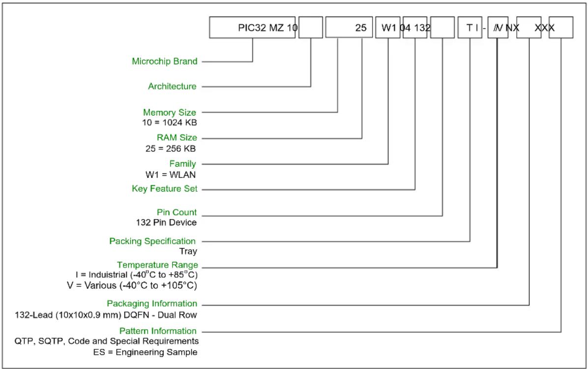
The following figure illustrates the details of PIC32MZ1025W104 SoC ordering information.
FIGURE 1-1: PIC32MZ1025W104 SOC ORDERING INFORMATION
flowchart
graph TD
    A["PIC32 MZ 10"] --> B["Microchip Brand"]
    A --> C["Architecture"]
    A --> D["Memory Size 10 = 1024 KB"]
    A --> E["RAM Size 25 = 256 KB"]
    A --> F["Family W1 = WLAN"]
    A --> G["Key Feature Set"]
    A --> H["Pin Count 132 Pin Device"]
    A --> I["Packing Specification Tray"]
    A --> J["Temperature Range I = Industrial (-40°C to +85°C) V = Various (-40°C to +105°C)"]
    A --> K["Packaging Information 132-Lead (10x10x0.9 mm) DQFN - Dual Row"]
    A --> L["Pattern Information QTP, SQTP, Code and Special Requirements ES = Engineering Sample"]
    A --> M["W1 04 132"]
    A --> N["T I - /N NX XXX"]
1.2 WFI32 Module Ordering Information
The following table describes the ordering information of the WFI32 Module.
TABLE 1-2: WFI32 MODULE ORDERING INFORMATION
| Model No. | Module SoC Description | Regulatory Certification | Ordering Code | |
| WFI32E01PE | PIC32MZ1025W104132-I/NX WFI32E01 Module with PCB antenna | I32E01 Module with PCB antenna FCC, ISED, CE, UKCA, MIC, KCC, NCC and SRRC | WFI32E01PE - I | |
| WFI32E01PC | enna and Trust&GO | FCC, ISED, CE, UKCA, MIC, KCC, NCC and SRRC | WFI32E01PC - I | |
| WFI32E01UE | WFI32E01 Module with U.FL connector | Connector for external antenna | FCC, ISED, CE, UKCA, MIC, KCC, NCC and SRRC | WFI32E01UE - I |
| WFI32E01UC | WFI32E01 Module with U.FL connector for external antenna and Trust&GO | FCC, ISED, CE, UKCA, MIC, KCC, NCC and SRRC | WFI32E01UC - I | |
| WFI32E02UC | WFI32E02 Module with U.FL connector for external antenna and Trust&GO | FCC, ISED, CE, UKCA, MIC, KCC, NCC and SRRC | WFI32E02UC - I | |
| WFI32E02UE | WFI32E02 Module with U.FL connector | Connector for external antenna | FCC, ISED, CE, UKCA, MIC, KCC, NCC and SRRC | WFI32E02UE - I |
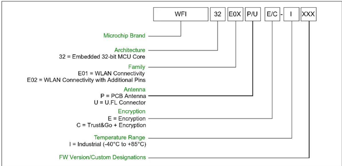
The following figure illustrates the details of the WFI32 Module ordering information.
FIGURE 1-2: WFI32 MODULE ORDERING INFORMATION
flowchart
graph TD
    A["WFI"] --> B["32"]
    B --> C["E0X"]
    C --> D["P/U"]
    D --> E["E/C"]
    E --> F["I"]
    F --> G["XXX"]
    H["Microchip Brand"] --> A
    I["Architecture\n32 = Embedded 32-bit MCU Core"] --> A
    J["Family\nE01 = WLAN Connectivity\nE02 = WLAN Connectivity with Additional Pins"] --> A
    K["Antenna\nP = PCB Antenna\nU = U.FL Connector"] --> A
    L["Encryption\nE = Encryption\nC = Trust&Go + Encryption"] --> A
    M["Temperature Range\nI = Industrial (-40°C to +85°C)"] --> A
    N["FW Version/Custom Designations"] --> A
2.0 PIC32MZ1025W104 SOC DESCRIPTION
Note: This data sheet summarizes the features of the PIC32MZ1025W104 SoC. It is not intended to be a comprehensive reference source. To complement the information in this data sheet, refer to the "PIC32 Family Reference Manual", which is available from the Microchip website (www.microchip.com/PIC32).
This chapter contains device-specific information for the PIC32MZ1025W104 SoC.
2.1 Block Diagram
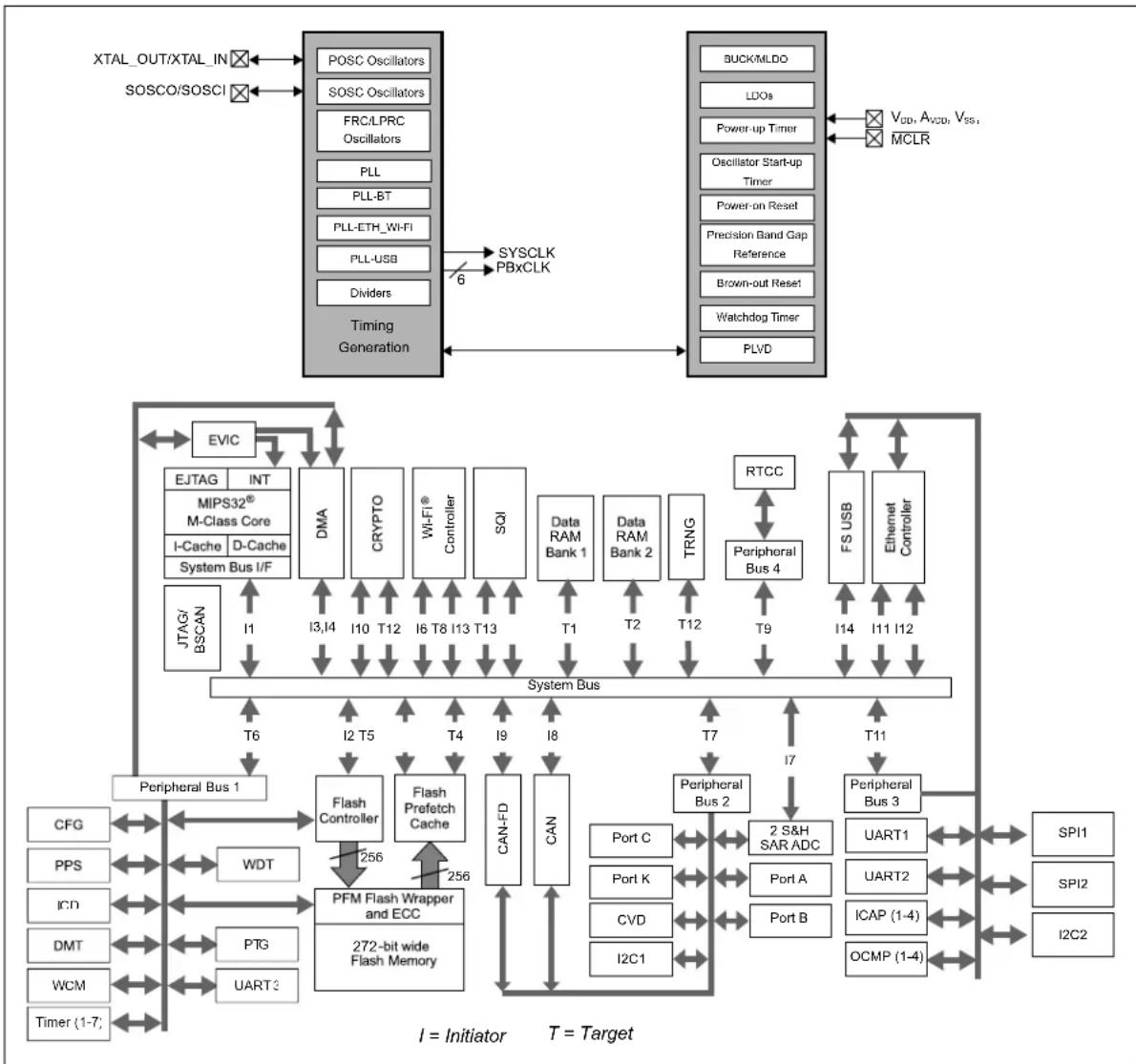
The following figure illustrates the block diagram of the core and peripheral modules in the PIC32MZ1025W104 SoC.
FIGURE 2-1: PIC32MZ1025W104 SoC BLOCK DIAGRAM
flowchart
graph TD
    subgraph_Timing_Generation["Timing Generation"]
        A["POS C Oscillators"] --> B["SOSC Oscillators"]
        B --> C["FRC/LPRC Oscillators"]
        C --> D["PLL"]
        D --> E["PLL-BT"]
        E --> F["PLL-ETH_WI-FI"]
        F --> G["PLL-USB"]
        G --> H["Dividers"]
        H --> I["SYSCLK PBxCLK"]
        I --> J["BUCK/MLDO"]
        J --> K["LDOs"]
        K --> L["Power-up Timer"]
        L --> M["Oscillator Start-up Timer"]
        M --> N["Power-on Reset"]
        N --> O["Precision Band Gap Reference"]
        O --> P["Brown-out Reset"]
        P --> Q["Watchdog Timer"]
        Q --> R["PLVD"]
        I --> S["V_DD, AWD, VSS, MCLR"]
    end

    subgraph_System_Bus["System Bus"]
        T["EVIC"] --> U["EJTAG INT MIPS32® M-Class Core I-Cache D-Cache System Bus I/F"]
        U --> V["JTAG/BSCAN"]
        V --> W["T6"]
        W --> X["I2 T5"]
        X --> Y["T4"]
        Y --> Z["I9"]
        Z --> AA["I8"]
        AA --> AB["T7"]
        AB --> AC["T11"]
        AC --> AD["Peripheral Bus 3"]
        AD --> AE["UART1"]
        AD --> AF["UART2"]
        AD --> AG["ICAP (1-4)"]
        AD --> AH["OCMP (1-4)"]
        AI["Peripheral Bus 1"] --> AJ["Flash Controller"]
        AJ --> AK["PFM Flash Wrapper and ECC 272-bit wide Flash Memory"]
        AK --> AL["CAN-FD"]
        AL --> AM["CAN"]
        AM --> AN["Peripheral Bus 2"]
        AN --> AO["2 S&H SAR ADC Port A"]
        AN --> AP["Port B"]
        AQ["Peripheral Bus 3"] --> AR["UART1"]
        AQ --> AS["UART2"]
        AQ --> AT["ICAP (1-4)"]
        AQ --> AU["OCMP (1-4)"]
    end

    subgraph I = Initiator["I = Initiator"]
        AV["CFG"] <--> AW["WDT"] <--> AX["PTG"] <--> AY["UART3"] <--> AZ["Timer (1-7)"]
        BA["PPS"] <--> BB["ICD"] <--> BC["DMT"] <--> BD["WCM"] <--> BE["Timer (1-7)"]
    end

    subgraph T = Target["T = Target"]
        BF["SPI1"] <--> BG["SPI2"] <--> BH["I2C2"]
    end
2.2 Function-wise Pinout Description
The following tables provide the function-wise pinout descriptions for the PIC32MZ1025W104 SoC and the WFI32 Module pins.
TABLE 2-1: ADC PINOUT DESCRIPTION
| PIC32MZ1025W104 WFI32E01 WFI32E02 | Pin Type | Buffer Type | Description | |||||
| Pin Name | Pin Number | Pin Name | Pin Number | Pin Name | Pin Number | |||
| AN0 | B52 | — | — | AN0 | B5 | I | Analog | A/D Analog Input Channels |
| AN1 A62 AN1 | 3 | AN1 B2 I | Analog | |||||
| AN2 B51 AN2 | 7 | AN2 A5 I | Analog | |||||
| AN3 A61 — | — AN3 B32 | I | Analog | |||||
| AN4 B50 AN4 | 2 | AN4 B4 I | Analog | |||||
| AN5 B49 AN5 | 52 | AN5 A4 I | Analog | |||||
| AN6 | B47 | AN6 | 46 | AN6 | A47 | I | Analog | |
| AN7 | A57 | AN7 | 49 | AN7 | A48 | I | Analog | |
| AN8 | B46 | AN8 | 47 | AN8 | B30 | I | Analog | |
| AN9 | A56 | AN9 | 48 | AN9 | B31 | I | Analog | |
| AN10 | A52 | — | — | AN10 | B27 | I | Analog | |
| AN11 | B43 | — | — | AN11 | B29 | I | Analog | |
| AN12 | A50 | — | — | AN12 | B26 | I | Analog | |
| AN13 | A49 | — | — | AN13 | A42 | I | Analog | |
| AN14 | B41 | AN14 | 44 | AN14 | A45 | I | Analog | |
| AN15 | A48 | AN15 | 42 | AN15 | B25 | I | Analog | |
| AN16 | B40 | — | — | AN16 | B28 | I | Analog | |
| AN17 | B39 | AN17 | 41 | AN17 | A44 | I | Analog | |
| AN18 | B38 | — | — | — | — | I | Analog | |
| AN19 | A45 | — | — | — | — | I | Analog | |
| ANA0 | A51 | ANA0 | 45 | ANA0 | A43 | I | Analog | |
| ANB0 | B44 | — | — | ANB0 | A46 | I | Analog | A/D Negative Analog Input Channels |
| ANN0 | B41 | ANN0 | 44 | ANN0 | A45 | I | Analog | |
| ANN1 | A48 | ANN1 | 42 | ANN1 | B25 | I | Analog | |
| Legend: Analog = Analog input I = Input | ||||||||
TABLE 2-2: OSCILLATOR PINOUT DESCRIPTION
| PIC32MZ1025W104 | WFI32E01 | WFI32E02 | Pin Type | Buffer Type | Description | |||
| Pin Name | Pin Number | Pin Name | Pin Number | Pin Name | Pin Number | |||
| XTAL_IN | A29 | — | — | — | — | I | — | 40 MHz Primary Oscillator Crystal Input |
| XTAL_OUT | A30 | — | — | — | — | O | — | 40 MHz Primary Oscillator Crystal Output |
| SOSCI | A59 | SOSCI | 53 | SOSCI | B34 | I | — | 32.768 kHz Secondary Oscillator Crystal Input |
| SOSCO | A58 | SOSCO | 54 | SOSCO | B33 | O | — | 32.768 kHz Secondary Oscillator Crystal Output |
| REFI | PPS | REFI | PPS | REFI | PPS | I | — | Reference Clock Generator Input |
| REFO1 | PPS | REFO1 | PPS | REFO1 | PPS | O | — | Reference Clock Generator Outputs 1-4 |
| REFO2 | PPS | REFO2 | PPS | REFO2 | PPS | O | — | |
| REFO3 | PPS | REFO3 | PPS | REFO3 | PPS | O | — | |
| REFO4 | PPS | REFO4 | PPS | REFO4 | PPS | O | — | |
| Legend: PPS = Peripheral Pin Select I = Input O = output | ||||||||
TABLE 2-3: IC1 THROUGH IC4 PINOUT DESCRIPTION
| PIC32MZ1025W104 WF | 32E01 WFI32E02 | Pin Type | Buffer Type | Description | ||||
| Pin Name | Pin Number | Pin Name | Pin Number | Pin Name | Pin Number | |||
| Input Capture | ||||||||
| IC1 PPS IC | 1 PPS IC1 P | PS I ST Input | Capture Inputs 1-4 | |||||
| IC2 PPS IC | 2 PPS IC2 P | PS I ST | ||||||
| IC3 PPS IC | 3 PPS IC3 P | PS I ST | ||||||
| IC4 PPS IC | 4 PPS IC4 P | PS I ST | ||||||
Legend: ST = Schmitt Trigger input with CMOS levels I = Input PPS = Peripheral Pin Select
TABLE 2-4: OC1 THROUGH OC4 PINOUT DESCRIPTION
| PIC32MZ1025W104 | WFI32E01 | WFI32E02 | Pin Type | Buffer Type | Description | |||
| Pin Name | Pin Number | Pin Name | Pin Number | Pin Name | Pin Number | |||
| Output Compare | ||||||||
| OC1 | PPS | OC1 | PPS | OC1 | PPS | O | — | Output Compare Outputs 1-4 |
| OC2 | PPS | OC2 | PPS | OC2 | PPS | O | — | |
| OC3 | PPS | OC3 | PPS | OC3 | PPS | O | — | |
| OC4 | PPS | OC4 | PPS | OC4 | PPS | O | — | |
| OCFA | PPS | OCFA | PPS | OCFA | PPS | I | ST | Output Compare Fault A Input |
| OCFB | PPS | OCFB | PPS | OCFB | PPS | I | ST | Output Compare Fault B Input |
| OCFC | PPS | OCFC | PPS | OCFC | PPS | I | ST | Output Compare Fault C Input |
| OCFD | PPS | OCFD | PPS | OCFD | PPS | I | ST | Output Compare Fault D Input |
Legend: ST = Schmitt Trigger input with CMOS levels O = Output I = Input PPS = Peripheral Pin Select
TABLE 2-5: EXTERNAL INTERRUPTS PINOUT DESCRIPTION
| PIC32MZ1025W104 | WFI32E01 | WFI32E02 | Pin Type | Buffer Type | Description | |||
| Pin Name | Pin Number | Pin Name | Pin Number | Pin Name | Pin Number | |||
| External Interrupts | ||||||||
| INT0 | B39 | INT0 | 41 | INT0 | A44 | I | ST | External Interrupt 0 |
| INT1 | PPS | INT1 | PPS | INT1 | PPS | I | ST | External Interrupt 1 |
| INT2 | PPS | INT2 | PPS | INT2 | PPS | I | ST | External Interrupt 2 |
| INT3 | PPS | INT3 | PPS | INT3 | PPS | I | ST | External Interrupt 3 |
| INT4 | PPS | INT4 | PPS | INT4 | PPS | I | ST | External Interrupt 4 |
Legend: ST = Schmitt Trigger input with CMOS levels I = Input PPS = Peripheral Pin Select
TABLE 2-6: PORTA THROUGH PORTC AND PORTK PINOUT DESCRIPTION
| PIC32MZ1025W104 W | FI32E01 WFI32E02 | Pin Type | Buffer Type | Description | ||||
| Pin Name | Pin Number | Pin Name | Pin Number | Pin Name | Pin Number | |||
| PORTA | ||||||||
| RA0 B6 — | — RA0 B12 | I/O DIG/ST | PORTA Digital I/O | |||||
| RA1 A14 | RA1 20 | RA1 A19 I/O | DIG/ST | |||||
| RA2 A15 | — — | RA2 B15 I/O | DIG/ST | |||||
| RA3 B14 | — — | RA3 B16 I/O | DIG/ST | |||||
| RA4 A16 | RA4 33 | RA4 B17 I/O | DIG/ST | |||||
| RA5 B15 | RA5 32 | RA5 B18 I/O | DIG/ST | |||||
| RA6 B16 | — — | RA6 B19 I/O | DIG/ST | |||||
| RA7 A21 | — — | RA7 B21 I/O | DIG/ST | |||||
| RA8 B17 | — — | RA8 B20 I/O | DIG/ST | |||||
| RA9 A22 | — — | RA9 B22 I/O | DIG/ST | |||||
| RA10 | B39 | RA10 | 41 | RA10 | A44 | I/O | DIG/ST | |
| RA11 | A47 | RA11 | 43 | RA11 | A41 | I/O | DIG/ST | |
| RA12 | B40 | — | — | RA12 | B28 | I/O | DIG/ST | |
| RA13 | A48 | RA13 | 42 | RA13 | B25 | I/O | DIG/ST | |
| RA14 | B41 | RA14 | 44 | RA14 | A45 | I/O | DIG/ST | |
| RA15 | A49 | — | — | RA15 | A42 | I/O | DIG/ST | |
| PORTB | ||||||||
| RB0 B52 | — — | RB0 B5 | I/O DIG/ST | PORTB Digital I/O | ||||
| RB1 A62 | RB1 3 | RB1 B2 | I/O DIG/ST | |||||
| RB2 B51 | RB2 7 | RB2 A5 | I/O DIG/ST | |||||
| RB3 A61 | — — | RB3 B32 I/O | DIG/ST | |||||
| RB4 B50 | RB4 2 | RB4 B4 | I/O DIG/ST | |||||
| RB5 B49 | RB5 52 | RB5 A4 | I/O DIG/ST | |||||
| RB6 B47 | RB6 46 | RB6 A47 I/O | DIG/ST | |||||
| RB7 A57 | RB7 49 | RB7 A48 I/O | DIG/ST | |||||
| RB8 B46 | RB8 47 | RB8 B30 I/O | DIG/ST | |||||
| RB9 A56 | RB9 48 | RB9 B31 I/O | DIG/ST | |||||
| RB10 | A52 | — — RB10 | B27 I/O DIG/ST | |||||
| RB11 | B44 | — — RB11 | A46 I/O DIG/ST | |||||
| RB12 | A51 | RB12 | 45 | RB12 | A43 | I/O | DIG/ST | |
| RB13 | B43 | — — RB13 | B29 I/O DIG/ST | |||||
| RB14 | A50 | — — RB14 | B26 I/O DIG/ST | |||||
| PB15 | A59 | PB15 | 53 | PB15 | B34 | I | DIG/ST | |
| PIC32MZ1025W104 | WFI32E01 | WFI32E02 | Pin Type | Buffer Type | Description | |||
| Pin Name | Pin Number | Pin Name | Pin Number | Pin Name | Pin Number | |||
| PORTC | ||||||||
| RC0 A9 — | — RC0 — | I/O DIG/ST | PORTC Digital I/O | |||||
| RC1 B8 — | — RC1 — | I/O DIG/ST | ||||||
| RC2 A10 — | — RC2 — | I/O DIG/ST | ||||||
| RC3 B9 — | — RC3 — | I/O DIG/ST | ||||||
| RC4 B10 — | — RC4 — | I/O DIG/ST | ||||||
| RC5 A12 — | — RC5 — | I/O DIG/ST | ||||||
| RC6 B11 RC6 21 RC6 | — I/O DIG/ST | |||||||
| RC7 A13 RC7 19 RC7 | — I/O DIG/ST | |||||||
| RC8 B12 RC8 23 RC8 | — I/O DIG/ST | |||||||
| RC9 B5 RC9 18 RC9 | — I/O DIG/ST | |||||||
| RC10 B57 RC10 10 RC10 — I/O DIG/ST | ||||||||
| RC11 | A68 | RC11 | 9 | RC11 | — | I/O | DIG/ST | |
| RC12 B58 RC12 12 RC12 — I/O DIG/ST | ||||||||
| RC13 A69 RC13 8 | RC13 | — I/O DIG/ST | ||||||
| RC14 B2 RC14 13 RC14 — I/O DIG/ST | ||||||||
| RC15 A4 RC15 14 RC15 — I/O DIG/ST | ||||||||
| PORTK | ||||||||
| RK0 | A44 — — RK0 | — I/O DIG/ST PORTK Digital I/O | ||||||
| RK1 | B37 RK1 | 34 RK1 | — I/O DIG/ST | |||||
| RK2 | A45 — — RK2 | — I/O DIG/ST | ||||||
| RK3 | B38 RK3 | 35 RK3 | — I/O DIG/ST | |||||
| RK4 | B18 RK4 | 24 RK4 | — I/O DIG/ST | |||||
| RK5 | B19 RK5 | 27 RK5 | — I/O DIG/ST | |||||
| RK6 | A24 RK6 | 25 RK6 | — I/O DIG/ST | |||||
| RK7 | B20 RK7 | 28 RK7 | — I/O DIG/ST | |||||
| RK8 | B21 — — RK8 | — I/O DIG/ST | ||||||
| RK9 | A26 — — RK9 | — I/O DIG/ST | ||||||
| RK10 | B22 | — — RK10 | — I/O DIG/ST | |||||
| RK11 | A27 | — | — | RK11 | — | I/O | DIG/ST | |
| RK12 | A6 RK12 | 15 RK12 | — I/O DIG/ST | |||||
| RK13 | A5 RK13 | 16 RK13 | — I/O DIG/ST | |||||
| RK14 | B4 RK14 | 17 RK14 | — I/O DIG/ST | |||||
| PK15 | A58 | PK15 | 54 | PK15 | — | I | DIG/ST | |
Legend: DIG = Digital input
ST = Schmitt Trigger input with CMOS levels
O = Output I = Input
TABLE 2-7: TIMER1 THROUGH TIMER7 AND RTCC PINOUT DESCRIPTION
| PIC32MZ1025W104 W | WFI32E01 WFI32E02 | Pin Type | Buffer Type | Description | ||||
| Pin Name | Pin Number | Pin Name | Pin Number | Pin Name | Pin Number | |||
| Timer1 through Timer7 | ||||||||
| T1CK PPS | T1CK PPS | T1CK PPS | I ST Timer | 1 External | Clock Input | |||
| T2CK PPS | T2CK PPS | T2CK PPS | I ST Timer | 2 External | Clock Input | |||
| T3CK PPS | T3CK PPS | T3CK PPS | I ST Timer | 3 External | Clock Input | |||
| T4CK PPS | T4CK PPS | T4CK PPS | I ST Timer | 4 External | Clock Input | |||
| T5CK PPS | T5CK PPS | T5CK PPS | I ST Timer | 5 External | Clock Input | |||
| T6CK PPS | T6CK PPS | T6CK PPS | I ST Timer | 6 External | Clock Input | |||
| T7CK PPS | T7CK PPS | T7CK PPS | I ST Timer | 7 External | Clock Input | |||
| Real-Time Clock and Calendar | ||||||||
| RTCC | B49 | RTCC | 52 | RTCC | 52 | O | — | RTCC Output Clock |
Legend: ST = Schmitt Trigger input with CMOS levels
O = Output I = Input
PPS = Peripheral Pin Select
TABLE 2-8: UART1 (DEDICATED) PINOUT DESCRIPTION
| PIC32MZ1025W104 | WFI32E01 | WFI32E02 | Pin Type | Buffer Type | Description | |||
| Pin Name | Pin Number | Pin Name | Pin Number | Pin Name | Pin Number | |||
| Universal Asynchronous Receiver Transmitter 1 | ||||||||
| U1CTSn | B16 | — | — | U1CTSn | B19 | I | ST | UART1 Clear to Send (CTS) Input |
| U1RTSn/U1BCLK | A21 | — | — | U1RTSn/U1BCLK | B21 | O DIG | UART1 Request to Send (RTS) Output/UART1 Baud Clock | |
| U1RX | B17 | U1RX | 30 | U1RX | B20 | I | ST | UART1 Receive |
| U1TX | A22 | U1TX | 29 | U1TX | B22 | O | DIG | UART1 Transmit |
Legend: DIG = Digital input
ST = Schmitt Trigger input with CMOS levels
O = Output I = Input
TABLE 2-9: UART1 THROUGH UART3 PINOUT DESCRIPTION
| PIC32MZ1025W104 | WFI32E01 | WFI32E02 | Pin Type | Buffer Type | Description | |||
| Pin Name | Pin Number | Pin Name | Pin Number | Pin Name | Pin Number | |||
| Universal Asynchronous Receiver Transmitter 1 | ||||||||
| U1CTSn | PPS | U1CTSn | PPS | U1CTSn | PPS | I | ST | UART1 CTS Input |
| U1RTSn/U1BCLK | PPS | U1RTSn | PPS | U1RTSn | PPS | O | DIG | UART1 RTS Output/UART1 Baud Clock |
| U1RX | PPS | U1RX | PPS | U1RX | PPS | I | ST | UART1 Receive |
| U1TX | PPS | U1TX | PPS | U1TX | PPS | O | DIG | UART1 Transmit |
| Universal Asynchronous Receiver Transmitter 2 | ||||||||
| U2CTSn | PPS | U2CTSn | PPS | U2CTSn | PPS | I | ST | UART2 CTS Input |
| U2RTSn/U2BCLK | PPS | U2RTSn | PPS | U2RTSn | PPS | O | DIG | UART2 RTS Output/UART2 Baud Clock |
| U2RX | PPS | U2RX | PPS | U2RX | PPS | I | ST | UART2 Receive |
| U2TX | PPS | U2TX | PPS | U2TX | PPS | O | DIG | UART2 Transmit |
| Universal Asynchronous Receiver Transmitter 3 | ||||||||
| U3CTSn | PPS | U3CTSn | PPS | U3CTSn | PPS | I | ST | UART3 CTS Input |
Legend: DIG = Digital input
ST = Schmitt Trigger input with CMOS levels
O = Output I = Input
PPS = Peripheral Pin Select
TABLE 2-9: UART1 THROUGH UART3 PINOUT DESCRIPTION (CONTINUED)
| PIC32MZ1025W104 | WFI32E01 | WFI32E02 | Pin Type | Buffer Type | Description | |||
| Pin Name | Pin Number | Pin Name | Pin Number | Pin Name | Pin Number | |||
| U3RTSn/U3BCLK | PPS U3RT | Sn PPS U3R | Sn PPS O | DIG UART3 | RTS Output | UART3 | Baud | Clock |
| U3RX PPS U3RX PPS U3RX PPS I ST | UART3 Re | ceive | ||||||
| U3TX PPS U3TX PPS U3TX PPS O DIG UART3 Transmit | ||||||||
Legend: DIG = Digital input ST = Schmitt Trigger input with CMOS levels O = Output I = Input PPS = Peripheral Pin Select
TABLE 2-10: SPI1 (DEDICATED) PINOUT DESCRIPTION
| PIC32MZ1025W104 | WFI32E01 | WFI32E02 | Pin Type | Buffer Type | Description | |||
| Pin Name | Pin Number | Pin Name | Pin Number | Pin Name | Pin Number | |||
| Serial Peripheral Interface 1 | ||||||||
| SCK1 B11 | CK1 21 SCK1 A20 | I/O | DIG/ST | SPI1 Synchronous Serial Clock Input/Output | ||||
| SDI1 | A13 | SDI1 | 19 | SDI1 | A18 | I | ST | SPI1 Data In |
| SDO1 | B12 | SDO1 | 23 | SDO1 | A21 | O | DIG | SPI1 Data Out |
| \overline{SS1}/\overline{CS1} | A14 | \overline{SS1}/\overline{CS1} | 20 | \overline{SS1}/\overline{CS1}$ | A19 | I/O | DIG/ST | SPI1 Client Select/Chip Select/Frame Sync (active-low) |
Legend: DIG = Digital input ST = Schmitt Trigger input with CMOS levels O = Output I = Input
TABLE 2-11: SPI1 THROUGH SPI 2 PINOUT DESCRIPTION
| PIC32MZ1025W104 | WFI32E01 | WFI32E02 | Pin Type | Buffer Type | Description | |||
| Pin Name | Pin Number | Pin Name | Pin Number | Pin Name | Pin Number | |||
| Serial Peripheral Interface 1 | ||||||||
| SCK1 | B11 | SCK1 | 21 | SCK1 | A20 | I/O | DIG/ST | SPI1 Synchronous Serial Clock Input/Output |
| SDI1 | PPS | SDI1 | PPS | SDI1 | PPS | I | ST | SPI1 Data In |
| SDO1 | PPS | SDO1 | PPS | SDO1 | PPS | O | DIG | SPI1 Data Out |
| 1/CS1 | PPS | 1/CS1 | PPS | 1/CS1 | PPS | I/O | DIG/ST | SPI1 Client Select/Chip Select/Frame Sync (active-low) |
| Serial Peripheral Interface 2 | ||||||||
| SCK2 | A47 | SCK2 | 43 | SCK2 | A41 | I/O | DIG/ST | SPI2 Synchronous Serial Clock Input/Output |
| SDI2 | PPS | SDI2 | PPS | SDI2 | PPS | I | ST | SPI2 Data In |
| SDO2 | PPS | SDO2 | PPS | SDO2 | PPS | O | DIG | SPI2 Data Out |
| 2/CS2 | PPS | 2/CS2 | PPS | 2/CS2 | PPS | I/O | DIG/ST | SPI2 Client Select/Chip Select/Frame Sync (active-low) |
Legend: DIG = Digital input ST = Schmitt Trigger input with CMOS levels O = Output I = Input PPS = Peripheral Pin Select
TABLE 2-12: I2C1 THROUGH I2C2 PINOUT DESCRIPTION
| PIC32MZ1025W104 WFI32E01 WFI32E02 | Pin Type | Buffer Type | Description | |||||
| Pin Name | Pin Number | Pin Name | Pin Number | Pin Name | Pin Number | |||
| Inter-Integrated Circuit 1 | ||||||||
| SCL1 A16 | SCL1 33 S | SCL1 B17 I/O | DIG/I2C/ | SMB | I2C1 Synchronous Serial Clock Input/Output | |||
| SDA1 B15 | SDA1 32 | SDA1 B18 I/O | DIG/I2C/ | SMB | I2C1 Data Input/Output | |||
| Inter-Integrated Circuit 2 | ||||||||
| SCL2 A15 | — — | SCL2 B15 | I/O DIG/I2C/ | SMB | I2C2 Synchronous Serial Clock Input/Output | |||
| SDA2 B14 | — — | SDA2 B16 | I/O DIG/I2C/ | SMB | I2C2 Data Input/Output | |||
Legend: DIG = Digital input O = Output I = Input
TABLE 2-13: USB PINOUT DESCRIPTION
| PIC32MZ1025W104 | WFI32E01 | WFI32E02 | Pin Type | Buffer Type | Description | |||
| Pin Name | Pin Number | Pin Name | Pin Number | Pin Name | Pin Number | |||
| V_BUS | A65 | V_BUS | 4 | V_BUS | A65 | I | — | USB V_BUS Input Signal (3.3V); can be left open when USB not in use(1). |
| VUSB3V3 | B54 | — | — | — | — | P | — | • USB Internal Transceiver Supply Voltage (3.3V).• This pin must be connected to the 3.3V even if USB is not used. |
| D+ | A64 | USB D+ | 6 | USB D+ | A64 | I/O | — | USB D+ |
| D- | A63 | USB D- | 5 | USB D- | A63 | I/O | — | USB D- |
| USBID | B51 | USBID | 7 | USBID | B51 | I | ST | USB OTG ID input |
| USBOEN | A61 | — | — | USBOEN | B32 | O | DIG | USB transceiver interface output enable state |
| VBUSON | A62 | VBUSON | 3 | VBUSON | A62 | O | DIG | USB ON signal for external VBUS source |
Legend: DIG = Digital input ST = Schmitt Trigger input with CMOS levels O = Output I = Input
P = Power
Note 1: The recommendation is to use a voltage divider on the V_BUS . For more details, refer to Section 3.2.6 "USB".
TABLE 2-14: CAN AND CAN-FD PINOUT DESCRIPTION
| PIC32MZ1025W104 | WFI32E01 | WFI32E02 | Pin Type | Buffer Type | Description | |||
| Pin Name | Pin Number | Pin Name | Pin Number | Pin Name | Pin Number | |||
| C1TX | PPS | C1TX | PPS | C1TX | PPS | O | — | CAN1 Bus Transmit Pin |
| C1RX | PPS | C1RX | PPS | C1RX | PPS | I | ST | CAN1 Bus Receive Pin |
| C2TX | PPS | C2TX | PPS | C2TX | PPS | O | — | CAN2 Bus Transmit Pin |
| C2RX | PPS | C2RX | PPS | C2RX | PPS | I | ST | CAN2 Bus Receive Pin |
Legend: ST = Schmitt Trigger input with CMOS levels O = Output I = Input
PPS = Peripheral Pin Select
Note: The CAN1 bus supports only the CAN interface, and the CAN2 bus supports both the CAN and CAN-FD interfaces.
TABLE 2-15: ETHERNET RMII PINOUT DESCRIPTION
| PIC32MZ1025W104 WF | 32E01 WFI32E02 | Pin Type | Buffer Type | Description | ||||
| Pin Name | Pin Number | Pin Name | Pin Number | Pin Name | Pin Number | |||
| Ethernet RMII Interface | ||||||||
| ERXD0 A68 ERXD0 9 ERXD0 A68 I ST Ethernet Receive Data 0 | ||||||||
| ERXD1 B57 ERXD1 10 | ERXD1 B57 I ST Ethernet Receive Data 1 | |||||||
| ERXERR | B5 | ERXERR | 18 | ERXERR | B5 | I | ST | Ethernet Receive Error |
| ERXDV | A6 | ERXDV | 15 | ERXDV | A6 | I | ST | Ethernet Receive Data Valid |
| ETHCLKOUT | B58 | ETH_CLK_OUT | 12 | ETH_CLK_OUT | B58 | O | ST | Ethernet Clock Output (50 MHz) |
| ETXD0 | A4 | ETXD0 | 14 | ETXD0 | A4 | O | DIG | Ethernet Transmit Data 0 |
| ETXD1 | B2 | ETXD1 | 13 | ETXD1 | B2 | O | DIG | Ethernet Transmit Data 1 |
| ETXEN A69 ETXEN 8 ETXEN A69 O | DIG | Ethernet Transmit Enable | ||||||
| EMDC | B4 | EMDC | 17 | EMDC | B4 | O | DIG | Ethernet Management Data Clock |
| EMDIO | A5 | EMDIO | 16 | EMDIO | A5 | I/O | ST/DIG | Ethernet Management Data |
Legend: DIG = Digital input ST = Schmitt Trigger input with CMOS levels O = Output I = Input
TABLE 2-16: SQI1 PINOUT Description
| PIC32MZ1025W104 | WFI32E01 | WFI32E02 | Pin Type | Buffer Type | Description | |||
| Pin Name | Pin Number | Pin Name | Pin Number | Pin Name | Pin Number | |||
| SQICLK | A12 | — | — | SQICLK | A12 | O | DIG/ST | SQI1 Clock |
| SQICS0 | B6 | — | — | SQICS0 | B6 | O | DIG | SQI Chip Select 0 |
| SQICS1 | A9 | — | — | SQICS1 | A9 | O | DIG | SQI Chip Select 1 |
| SQID0 | B10 | — | — | SQID0 | B10 | I/O | DIG/ST | SQI1 Data[0] |
| SQID1 | B9 | — | — | SQID1 | B9 | I/O | DIG/ST | SQI1 Data[1] |
| SQID2 | A10 | — | — | SQID2 | A10 | I/O | DIG/ST | SQI1 Data[2] |
| SQID3 | B8 | — | — | SQID3 | B8 | I/O | DIG/ST | SQI1 Data[3] |
Legend: DIG = Digital input ST = Schmitt Trigger input with CMOS levels O = Output I = Input
TABLE 2-17: POWER, GROUND AND VOLTAGE REFERENCE PINOUT DESCRIPTION
| PIC32MZ1025W104 WFI32E01 WFI32E02 | Pin Type | Buffer Type | Description | |||||
| Pin Name | Pin Number | Pin Name | Pin Number | Pin Name | Pin Number | |||
| Power and Ground | ||||||||
| VPMU_VDDP A70, B60 — — | — — P — | Input Supply Voltage (3.3V) to PMU | ||||||
| PMU_VDDIO/VPMU_VDDC | B1 — — | — — P | — | Input Supply Voltage (3.3V) to PMU Core | ||||
| VBAT | A60 | — — — — | P — | Backup Battery Voltage and must Be Connected to Input Supply Voltage (3.3V) | ||||
| BUK_MDLO_OUT | B59 | — — — — | P — | MLDO Output Voltage (1.5V), for Internal Usage only; Do Not Connect to Any External Circuit | ||||
| BUK_BK_LX | A71 | — — — — | P — | Buck Output to External LC Filter. | ||||
| PMU_VSENSE | A2 — — — | — P — | Feedback Voltage to PMU | |||||
| VDD33 | A3, A11, A25, A46, A67, B3, B13, B48 | 3V3_MOD | 51, 52 | VDD | A51, A52 | P | — | Input Supply Voltage (3.3V) |
| VUSB3V3 | B54 | — — — — | P — | USB Input Supply Voltage (3.3V) | ||||
| AVDD33 | B42 | 3V3_MOD | 51, 52 | AVDD | B35 | P | — | Analog Input Supply Voltage (3.3V) |
| AVss | B45 | — | — | — | — | P | — | Analog Ground |
| VDD15 | A66, A8 | — — — — | P — | Input Supply Voltage (1.5V) from PMU | ||||
| IOVDD_RF | A34, B26 — | — — — P — | ESD Input Voltage (3.3V) | |||||
| RXR_RIQ_VDD15 | A40 | — | — | — | — | P | — | RF Supply Voltage (1.5V) from PMU |
| RXR_FE1_VDD15 | B33 | — — — — | P — | |||||
| RXR_FE2_VDD15 | B32 | — — — — | P — | |||||
| SYN_PLL_VDD15 | B28 | — — — — | P — | |||||
| SYN_SD_VDD15 | A32 | — — — — | P — | |||||
| SYN_VCO_VDD15 | A33 | — — — — | P — | |||||
| XTAL_VDD15 | B24 | — — — — | P — | |||||
| TXR_LPA_VDD15 | B36 | — — — — | P — | |||||
| TXR_UMX_VDD15 | A42 | — — — — | P — | |||||
| SPI_VDD15 | B23 | — — — — | P — | |||||
| BB_VDD15 | B34 | — — — — | P — | |||||
| AFE_VDD15 | A28 | — — — — | P — | |||||
| Voltage Reference | ||||||||
| LVDIN | A52 | — | — | LVDIN | B27 | I | Analog | Programmable Low-Voltage Detect Input |
| GNDDB | GND | — — — — | P — | — | ||||
Legend: P = Power
Analog = Analog input
I = Input
TABLE 2-18: JTAG, TRACE AND PROGRAMMING/DEBUGGING PINOUT DESCRIPTION
| PIC32MZ1025W104 WFI3 | 2E01 WFI32E02 | Pin Type | Buffer Type | Description | ||||
| Pin Name | Pin Number | Pin Name | Pin Number | Pin Name | Pin Number | |||
| JTAG | ||||||||
| TCK B46 TCK 47 | TCK B30 I ST | JTAG Test Clock/Programming Clock Input | ||||||
| TDI | A56 TDI | 48 TDI | B31 I ST | JTAG Test Data/Programming Data Input | ||||
| TDO | A57 | TDO | 49 | TDO | A48 | O | DIG | JTAG Test Data Output |
| TMS | B47 | TMS | 46 | TMS | A47 | I | ST | JTAG Test Mode Select Input |
| Trace | ||||||||
| TRCLK | B41 | — | — | TRCLK | A45 | O | DIG | Trace Clock |
| TRD0 | A49 | — | — | TRD0 | A42 | O | DIG | Trace Data |
| TRD1 | A50 | — | — | TRD1 | B26 | O | DIG | |
| TRD2 | B43 | — | — | TRD2 | B29 | O | DIG | |
| TRD3 | A51 | — | — | TRD3 | A43 | O | DIG | |
| Programming/ Debugging | ||||||||
| MCLR | A23 | MCLR | 26 | MCLR | A27 | I | ST | Master Clear (Device Reset) Input(active-low) |
| PGC1/EMUC1 | A61 | — | — | PGC1/EMUC1 | B32 | I | ST | ICSP Programming Clock |
| PGC1ENTRY | A61 | — | — | — | — | I | ST | Test Mode Entry Clock |
| PGC2/EMUC2 | B50 | PGC2 | 2 | PGC2/EMUC2 | B4 | I | ST | ICSP Programming Clock |
| PGC2ENTRY | B50 | — | — | — | — | I | ST | Test Mode Entry Clock |
| PGC4/EMUC4 | B46 | PGC4 | 47 | PGC4/EMUC4 | B30 | I | ST | ICSP Programming Clock |
| PGC4ENTRY | B46 | — | — | — | — | I | ST | Test Mode Entry Clock |
| PGD1/EMUD1 | B51 | — | — | PGD1/EMUD1 | A5 | I/O | DIG/ST | ICSP Programming Data |
| PGD1ENTRY | B51 | — | — | — | — | I | ST | Test Mode Entry Data |
| PGD2/EMUD2 | B49 | PGD2 | 52 | PGD2/EMUD2 | A4 | I/O | DIG/ST | ICSP Programming Data |
| PGD2ENTRY | B49 | — | — | — | — | I | ST | Test Mode Entry Data |
| PGD4/EMUD4 | A56 | PGD4 | 48 | PGD4/EMUD4 | B31 | I/O | DIG/ST | ICSP Programming Data |
| PGD4ENTRY | A56 | — | — | — | — | I | ST | Test Mode Entry Data |
Legend: DIG = Digital input ST = Schmitt Trigger input with CMOS levels O = Output I = Input PPS = Peripheral Pin Select
TABLE 2-19: WI-FI INTERFACE PINOUT DESCRIPTION
| PIC32MZ1025W104 WFI32E01 | WFI32E02 | Pin Type | Buffer Type | Description | ||||
| Pin Name | Pin Number | Pin Name | Pin Number | Pin Name | Pin Number | |||
| RF_FE_1 A45 | (1) | — — — — | I/O DIG/ST | RF Front-End Control | ||||
| RF_FE_2 B38 RF_FE_2 35 | RF_FE_2 | A33 | I/O DIG/ST | |||||
| RF_FE_3 A44 | (1) | — | — | — | — | I/O | DIG/ST | |
| RF_FE_4 B37 RF_FE_4 34 | RF_FE_4 | A34 | I/O DIG/ST | |||||
| RF_FE_5 A27 — — | RF_FE_5 A29 | I/O | DIG/ST | |||||
| RF_FE_6 B22 — — | RF_FE_6 B23 | I/O | DIG/ST | |||||
| RF_FE_7 B21 — — | RF_FE_7 A30 | I/O | DIG/ST | |||||
| RF_FE_8 A26 — — | RF_FE_8 A28 | I/O | DIG/ST | |||||
| ANALOG_TEST A31 | — — — — | O — | Analog Test Output | |||||
| IN_TSSI | B27 — — | — — I | — | TSSI (Transmitter Signal Strength Indication) Input | ||||
| MBS_EXTRA_48K | B31 | — | — | — | — | O | — | DC Output (Band Gap Voltage) |
| RXR_IN | A39 — — | — — I | — | Receiver Input | ||||
| TXR_LPA_VOUT | A43 | — | — | — | — | O | — | Transmitter Output |
Legend: DIG = Digital input ST = Schmitt Trigger input with CMOS levels O = Output I = Input
Note 1: A44 and A45 pins are used for controlling the FEM on the WFI32 Module. Microchip recommends using these pins as described in the reference design package. Contact the Microchip Sales/Support Team for the reference package.
TABLE 2-20: WI-FI BLUETOOTH ^ COEXISTENCE ^(1)
| PIC32MZ1025W104 | WFI32E01 | WFI32E02 | Pin Type | Buffer Type | Description | |||
| Pin Name | Pin Number | Pin Name | Pin Number | Pin Name | Pin Number | |||
| BT_CLK_OUT | B18 | BT_CLK_OUT | 24 | BT_CLK_OUT | A23 | O | DIG | Bluetooth®Clock Out |
| PTA_BT_ACTIVE | B20 | PTA_BT_ACTIVE | 28 | PTA_BT_ACTIVE | A24 | I/O | DIG/ST | Packet Traffic Arbitration (PTA) three-wire interface for Wi-Fi and Bluetooth co-existence |
| PTA_BT_PRIO | A24 | PTA_BT_PRIO | 25 | PTA_BT_PRIO | A26 | I/O | DIG/ST | |
| PTA_WLAN_ACTIVE | B19 | PTA_WLAN_ACTIVE | 27 | PTA_WLAN_ACTIVE | A25 | I/O | DIG/ST | |
Legend: DIG = Digital input ST = Schmitt Trigger input with CMOS levels O = Output I = Input
Note 1: This feature is currently not supported and it is recommended that it not be used in an end-product design. Microchip plans to support this feature in the future.
TABLE 2-21: CVD PINOUT DESCRIPTION
| PIC32MZ1025W104 W | WFI32E01 WFI32E02 | Pin Type | Buffer Type Description | ||||
| Pin Name | Pin Number | Pin Name | Pin Number | Pin Name | Pin Number | ||
| CVD1 A62 | CVD1 3 CVD | D1 B2 O DIG | ADC CVD | Controller | Output | ||
| CVD2 B51 | CVD2 7 CVD | D2 A5 O DIG | |||||
| CVD3 | A61 | — | — | CVD3 | B32 | O | DIG |
| CVD4 B50 | CVD4 2 CVD | D4 B4 O DIG | |||||
| CVD5 B49 | CVD5 52 | CVD5 A4 | O DIG | ||||
| CVD6 B47 | CVD6 46 | CVD6 A47 | O DIG | ||||
| CVD7 A57 | CVD7 49 | CVD7 A48 | O DIG | ||||
| CVD8 B46 | CVD8 47 | CVD8 B30 | O DIG | ||||
| CVD9 A56 | CVD9 48 | CVD9 B31 | O DIG | ||||
| CVD10 | A52 | — | — | CVD10 | B27 | O | DIG |
| CVD11 | B43 | — | — | CVD11 | B29 | O | DIG |
| CVD12 | A50 | — | — | CVD12 | B26 | O | DIG |
| CVD13 | A49 | — | — | CVD13 | A42 | O | DIG |
| CVD14 | B41 | CVD14 | 44 | CVD14 | A45 | O | DIG |
| CVD15 | A48 | CVD15 | 42 | CVD15 | B25 | O | DIG |
| CVD16 | B40 | — | — | CVD16 | B28 | O | DIG |
| CVD17 | B39 | CVD17 | 41 | CVD17 | A44 | O | DIG |
| CVD18 | B38 | — | — | CVD18 | A33 | O | DIG |
| CVD19 | A45 | — | — | CVD19 | — | O | DIG |
Legend: DIG = Digital input O = Output
TABLE 2-22: ENHANCED CVD PINOUT DESCRIPTION
| PIC32MZ1025W104 W | WFI32E01 | WFI32E02 | Pin Type | Buffer Type | Description | |||
| Pin Name | Pin Number | Pin Name | Pin Number | Pin Name | Pin Number | |||
| CVDR1 | A62 | CVDR1 | 3 | CVDR1 | B2 | O | DIG | ADC CVD Controller RX Output |
| CVDR2 | B51 | CVDR2 | 7 | CVDR2 | A5 | O | DIG | |
| CVDR3 | A61 | — | — | CVDR3 | B32 | O | DIG | |
| CVDR4 | B50 | CVDR4 | 2 | CVDR4 | B4 | O | DIG | |
| CVDR5 | B49 | CVDR5 | 52 | CVDR5 | A4 | O | DIG | |
| CVDR6 | B47 | CVDR6 | 46 | CVDR6 | A47 | O | DIG | |
| CVDR7 | A57 | CVDR7 | 49 | CVDR7 | A48 | O | DIG | |
| CVDR8 | B46 | CVDR8 | 47 | CVDR8 | B30 | O | DIG | |
| CVDR9 | A56 | CVDR9 | 48 | CVDR9 | B31 | O | DIG | |
| CVDR10 | A52 | — | — | CVDR10 | B27 | O | DIG | |
| CVDR11 | B43 | — | — | CVDR11 | B29 | O | DIG | |
| CVDR12 | A50 | — | — | CVDR12 | B26 | O | DIG | |
| CVDR13 | A49 | — | — | CVDR13 | A42 | O | DIG | |
| CVDR14 | B41 | CVDR14 | 44 | CVDR14 | A45 | O | DIG | |
| CVDR15 | A48 | CVDR15 | 42 | CVDR15 | B25 | O | DIG | |
| CVDR16 | B40 | — | — | CVDR16 | B28 | O | DIG | |
| CVDR17 | B39 | CVDR17 | 41 | CVDR17 | A44 | O | DIG | |
| CVDR18 | B38 | — | — | CVDR18 | A33 | O | DIG | |
| CVDR19 | A45 | — | — | CVDR19 | — | O | DIG | |
| PIC32MZ1025W104 | WFI32E01 | WFI32E02 | Pin Type | Buffer Type | Description | |||
| Pin Name | Pin Number | Pin Name | Pin Number | Pin Name | Pin Number | |||
| CVDT0 A57 | CVDT0 49 | CVDT0 A48 | O DIG AD | C CVD Controller TX Output | ||||
| CVDT1 B47 | CVDT1 46 | CVDT1 A47 | O DIG | |||||
| CVDT2 B49 | CVDT2 52 | CVDT2 A4 | O DIG | |||||
| CVDT3 B50 | CVDT3 2 | CVDT3 B4 | O DIG | |||||
| CVDT4 A61 | — — CVD | T4 B32 | O DIG | |||||
| CVDT5 B51 | CVDT5 7 | CVDT5 A5 | O DIG | |||||
| CVDT6 A62 | CVDT6 3 | CVDT6 B2 | O DIG | |||||
| CVDT7 B5 | CVDT7 18 | CVDT7 B9 | O DIG | |||||
| CVDT8 B57 | CVDT8 10 | CVDT8 B7 | O DIG | |||||
| CVDT9 A68 | CVDT9 9 | CVDT9 B6 | O DIG | |||||
| CVDT10 B58 | CVDT10 | 12 CVDT10 | A8 O DIG | |||||
| CVDT11 | A69 | CVDT11 | 8 | CVDT11 | A7 | O | DIG | |
| CVDT12 B2 | CVDT12 | 13 CVDT12 | B8 O DIG | |||||
| CVDT13 A4 | CVDT13 | 14 CVDT13 | A10 O DIG | |||||
| CVDT14 A6 | CVDT14 | 15 CVDT14 | A11 | O DIG | ||||
| CVDT15 A5 | CVDT15 | 16 CVDT15 | B10 O DIG | |||||
| CVDT16 B4 | CVDT16 | 17 CVDT16 | A9 O DIG | |||||
| CVDT17 B6 | — — CVD | T17 B12 | O DIG | |||||
| CVDT18 A9 | — — CVD | T18 B13 | O DIG | |||||
| CVDT19 B8 | — — CVD | T19 A13 | O DIG | |||||
| CVDT20 A10 | — — CVD | T20 A14 | O DIG | |||||
| CVDT21 B9 | — — CVD | T21 A15 | O DIG | |||||
| CVDT22 B10 | — — CVD | T22 B14 | O DIG | |||||
| CVDT23 A12 | — — CVD | T23 A16 | O DIG | |||||
Legend: DIG = Digital input O = Output
TABLE 2-23: CTRT PINOUT DESCRIPTION
| PIC32MZ1025W104 | WFI32E01 | WFI32E02 | Pin Type | Buffer Type | Description | |||
| Pin Name | Pin Number | Pin Name | Pin Number | Pin Name | Pin Number | |||
| CTRTM0 | B39 | CTRTM0 | 41 | CTRTM0 | A44 | I | ST | CTR External Trigger |
| CTRTM1 | B40 | — | — | CTRTM1 | B28 | I | ST | |
Legend: ST = Schmitt Trigger input with CMOS levels I = Input
TABLE 2-24: PTG PINOUT DESCRIPTION
| PIC32MZ1025W104 | WFI32E01 | WFI32E02 | Pin Type | Buffer Type | Description | |||
| Pin Name | Pin Number | Pin Name | Pin Number | Pin Name | Pin Number | |||
| PTG28 | PPS | PTG28 | PPS | PTG28 | PPS | O | — | Peripheral Trigger Generator output buffer data |
| PTG29 PPS | S PTG29 | PPS | PTG29 PPS | O | — | |||
| PTG30 PPS | S PTG30 | PPS | PTG30 PPS | O | — | |||
| PTG31 PPS | S PTG31 | PPS | PTG31 PPS | O | — | |||
Legend: O = Output PPS = Peripheral Pin Select
Note: For more details on the designs using the PIC32MZ1025W104 SoC, refer to the PIC32MZ-W1_Reference_Design_Package on the product page.
3.0 WFI32 MODULE DESCRIPTION
The WFI32 is a fully-certified Module that contains the PIC32MZ1025W104 SoC, an integrated FEM and Trust&GO with following antenna options:
• PCB antenna (WFI32E01PC/WFI32E01PE)
• U.FL connector (WFI32E01UC/WFI32E01UE) for external antenna
- U.FL connector (WFI32E02UC/WFI32E02UE) for external antenna
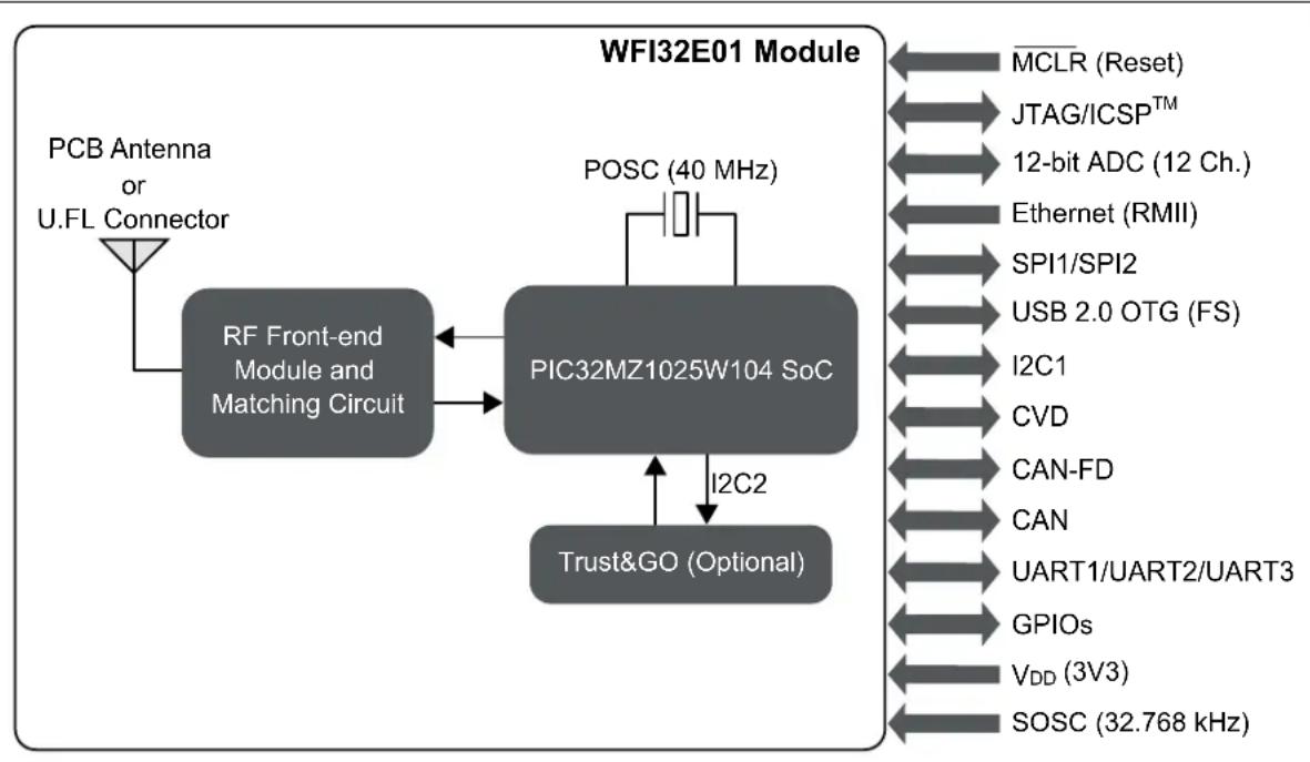
The Trust&GO is a pre-configured and pre-provisioned secure element of Microchip's family of security-focused devices. The Trust&Go is connected using I2C2 in the Module.
The WFI32 Module has the following variants:
- WFI32E01
- WFI32E02
The following figure illustrates the WFI32E01 Module block diagram.
FIGURE 3-1: WFI32E01 MODULE BLOCK DIAGRAM
flowchart
graph TD
    A["PCB Antenna or U.FL Connector"] --> B["RF Front-end Module and Matching Circuit"]
    B --> C["PIC32MZ1025W104 SoC"]
    C --> D["Trust&GO (Optional)"]
    D --> E["I2C2"]
    E --> C
    C --> F["POSC (40 MHz)"]
    F --> G["MCLR (Reset)"]
    F --> H["JTAG/ICSP™"]
    F --> I["12-bit ADC (12 Ch.)"]
    F --> J["Ethernet (RMII)"]
    F --> K["SPI1/SPI2"]
    F --> L["USB 2.0 OTG (FS)"]
    F --> M["I2C1"]
    F --> N["CVD"]
    F --> O["CAN-FD"]
    F --> P["CAN"]
    F --> Q["UART1/UART2/UART3"]
    F --> R["GPIOs"]
    F --> S["V_DD (3V3)"]
    F --> T["SOSC (32.768 kHz)"]
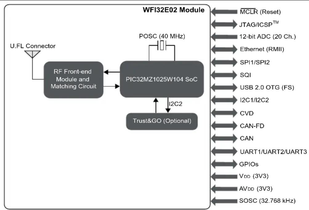
The following figure illustrates the WFI32E02 Module block diagram.
FIGURE 3-2: WFI32E02 MODULE BLOCK DIAGRAM
flowchart
graph TD
    A["U.FL Connector"] --> B["RF Front-end Module and Matching Circuit"]
    B --> C["PIC32MZ1025W104 SoC"]
    C --> D["Trust&GO (Optional)"]
    D --> E["I2C2"]
    E --> C
    F["MCLR (Reset)"] --> G["JTAG/ICSP™"]
    G --> H["12-bit ADC (20 Ch.)"]
    H --> I["Ethernet (RMII)"]
    I --> J["SPI1/SPI2"]
    J --> K["SQI"]
    K --> L["USB 2.0 OTG (FS)"]
    L --> M["I2C1/I2C2"]
    M --> N["CVD"]
    N --> O["CAN-FD"]
    O --> P["CAN"]
    P --> Q["UART1/UART2/UART3"]
    Q --> R["GPIOs"]
    R --> S["V_DD (3V3)"]
    S --> T["AV_DD (3V3)"]
    T --> U["SOSC (32.768 kHz)"]
    C --> V["POSC (40 MHz)"]
3.1 Pinout Details
3.1.1 WFI32E01 PINOUT DETAILS
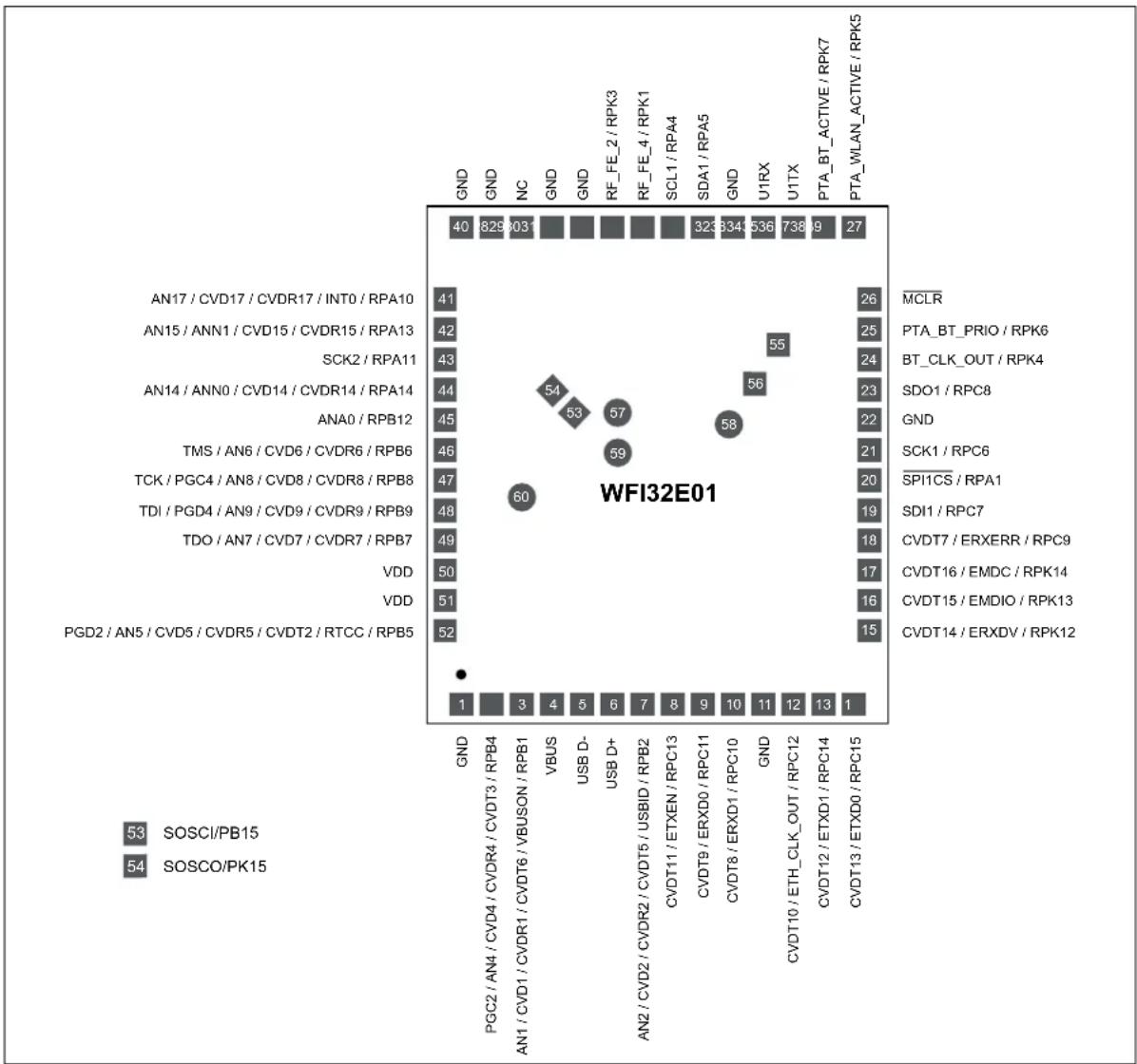
The following figure illustrates the WFI32E01 Module pinout diagram.
FIGURE 3-3: WFI32E01 MODULE PINOUT DIAGRAM
scatter
| Chip | Pin Number | Frequency | | :--- | :--- | :--- | | GND | 40 | 829 | | GND | 41 | 829 | | NC | 42 | 803 | | GND | 43 | 803 | | GND | 44 | 54 | | RF_FE_2 / RPK3 | 45 | 57 | | RF_FE_4 / RPK1 | 46 | 59 | | SCL1 / RPA4 | 47 | 60 | | SDA1 / RPA5 | 48 | 57 | WFI32E01 An17 / CVD17 / CVDR17 / INT0 / RPA10 An15 / ANN1 / CVD15 / CVDR15 / RPA13 SCK2 / RPA11 AN14 / ANN0 / CVD14 / CVDR14 / RPA14 ANA0 / RPB12 TMS / AN6 / CVD6 / CVDR6 / RPB6 TCK / PGC4 / AN8 / CVD8 / CVDR8 / RPB8 TDI / PGD4 / AN9 / CVD9 / CVDR9 / RPB9 TDO / AN7 / CVD7 / CVDR7 / RPB7 VDD VDD PGD2 / AN5 / CVD5 / CVDR5 / CVDT2 / RTCC / RPB5 GND PGC2 / AN4 / CVD4 / CVDR4 / CVDT3 / RPB4 AN1 / CVD1 / CVDR1 / CVDT6 / VBUSON / RPB1 VBUS USB D- USB D+ AN2 / CVD2 / CVDR2 / CVDT5 / USBID / RPB2 CVDT11 / ETXEN / RPC13 CVDT9 / ERXD0 / RPC11 CVDT8 / ERXD1 / RPC10 GND CVDT10 / ETH_CLK_OUT / RPC12 CVDT12 / ETXD1 / RPC14 CVDT13 / ETXD0 / RPC15 MCLR PTA_BT_PRIO / RPK6 BT_CLK_OUT / RPK4 SDO1 / RPC8 GND SCK1 / RPC6 SPI1CS / RPA1 SDI1 / RPC7 CVDT7 / ERXERR / RPC9 CVDT16 / EMDC / RPK14 CVDT15 / EMDIO / RPK13 CVDT14 / ERXDV / RPK12 SOSCI/PB15 SOSCO/PK15Note 1: For details on the exact pin placement and dimensions, refer to Section 42.0 "Packaging Information".
2: For pin descriptions, refer to Table 3-1.
3: Pins (61-63) are not indicated in the Figure 3-3. For more details, refer to the Section 42.0 "Packaging Information".
TABLE 3-1: WFI32E01 MODULE PIN DESCRIPTION
| Module Pin Number | SoC Pin Number | Pin Name | Pin Type(1) | Description |
| 1 — GND P Ground | ||||
| 2 B50 PGC2 I | In Circuit Serial | Programming^TM (ICSP) | programming clock | |
| AN4 I Analog input | ||||
| CVD4 O ADC CVD controller output | ||||
| CVDR4 | O ADC CVD controller RX | |||
| CVDT3 | O ADC CVD controller TX | |||
| RPB4 | I/O | Remappable peripheral (2) | ||
| RB4 I/O PORTB | digital I/O | |||
| 3 A62 AN1 I Analog input | ||||
| CVD1 O ADC CVD controller output | ||||
| CVDR1 | O ADC CVD controller RX | |||
| CVDT6 | O ADC CVD controller TX | |||
| VBUSON | O USB ON signal for external VBUS source | |||
| RPB1 | I/O | Remappable peripheral (2) | ||
| RB1 I/O PORTB | digital I/O | |||
| 4 A65 VBUS I | USB VBUS signal input (3.3V), can be left open when USB not in use | |||
| 5 A63 USB D- | I/O USB data - | |||
| 6 A64 USB D+ | I/O USB data + | |||
| 7 B51 AN2 I Analog input | ||||
| CVD2 O ADC CVD controller output | ||||
| CVDR2 | O ADC CVD controller RX | |||
| CVDT5 | O ADC CVD controller TX | |||
| USBID | I USB OTG ID input | |||
| RPB2 | I/O | Remappable peripheral (2) | ||
| RB2 I/O PORTB | digital I/O | |||
| 8 A69 CVDT11 | O ADC CVD controller TX | |||
| ETXEN | O Ethernet | transmit enable output | ||
| RPC13 | I/O | Remappable peripheral (2) | ||
| RC13 | I/O | PORTC digital I/O | ||
| 9 A68 CVDT9 | O ADC CVD controller TX | |||
| ERXD0 | I Ethernet | RMII receive data bit 0 | ||
| RPC11 | I/O | Remappable peripheral (2) | ||
| RC11 | I/O | PORTC digital I/O | ||
| 10 | B57 CVDT8 | O ADC CVD controller TX | ||
| ERXD1 | I Ethernet | RMII receive data bit 1 | ||
| RPC10 | I/O | Remappable peripheral (2) | ||
| RC10 | I/O | PORTC digital I/O | ||
| 11 | — GND P Ground | |||
| 12 | B58 CVDT10 | O ADC CVD controller TX | ||
| ETH_CLK_OUT | O | Ethernet RMII reference clock out (50 MHz), requires an external 33 Ω series termination resistor | ||
| RPC12 | I/O | Remappable peripheral (2) | ||
| RC12 | I/O | PORTC digital I/O | ||
| 13 | B2 | CVDT12 | O ADC CVD controller TX | |
| ETXD1 | O Ethernet | RMII transmit data bit 1 | ||
| RPC14 | I/O | Remappable peripheral (2) | ||
| RC14 | I/O | PORTC digital I/O | ||
| 14 A4 CVDT | 3 O ADC CVD | D controller TX | ||
| ETXD0 O Ethernet RMII receive data bit 0 | ||||
| RPC15 I/O Remappable peripheral (2) | ||||
| RC15 I/O PORTC digital I/O | ||||
| 15 A6 CVDT | 4 O ADC CVD | D controller TX | ||
| ERXDV I Ethernet RMII receive data valid | ||||
| RPK12 I/O Remappable peripheral (2) | ||||
| RK12 I/O PORTK digital I/O | ||||
| 16 A5 CVDT | 5 O ADC CVD | D controller TX | ||
| EMDIO I/O Ethernet management data IO | ||||
| RPK13 I/O Remappable peripheral (2) | ||||
| RK13 I/O PORTK digital I/O | ||||
| 17 B4 CVDT | 6 O ADC CVD | D controller TX | ||
| EMDC O Ethernet management data clock | ||||
| RPK14 I/O Remappable peripheral (2) | ||||
| RK14 I/O PORTK digital I/O | ||||
| 18 B5 CVDT | 7 O ADC CVD | D controller TX | ||
| ERXERR | I Ethernet RMII receive error | |||
| RPC9 | I/O Remappable peripheral (2) | |||
| RC9 | I/O PORTC digital I/O | |||
| 19 A13 | SDI1 | I SPI1 serial data in | ||
| RPC7 | I/O Remappable peripheral (2) | |||
| RC7 | I/O PORTC digital I/O | |||
| 20 A14 | SPI1CS | O SPI client select/chip select input (active-low) | ||
| RPA1 I/O Remappable peripheral (2) | ||||
| RA1 | I/O PORTA digital I/O | |||
| 21 B11 | SCK1 | I/O SPI1 serial clock | ||
| RPC6 | I/O Remappable peripheral (2) | |||
| RC6 | I/O PORTC digital I/O | |||
| 22 — | GND | P | Ground | |
| 23 B12 | SDO1 | O SPI1 serial data out | ||
| RPC8 | I/O Remappable peripheral (2) | |||
| RC8 | I/O PORTC digital I/O | |||
| 24 B18 | BT_CLK_OUT O Bluetooth | ®reference clock out (26 MHz)(6) | ||
| RPK4 | I/O Remappable peripheral (2) | |||
| RK4 | I/O PORTK digital I/O | |||
| 25 | A24 | PTA_BT_PRIO | I/O | Packet Traffic Arbitration (PTA) Bluetooth priority signal for Bluetooth and Wi-Fi® coexistence(6) |
| RPK6 | I/O Remappable peripheral (2) | |||
| RK6 | I/O PORTK digital I/O | |||
| 26(4) | A23 | MCLR | I | Reset signal, Active-low, requires external RC circuit |
| 27 | B19 | PTA_WLAN_ACTIVE | I/O | PTA Wi-Fi active signal for Bluetooth and Wi-Fi coexistence(6) |
| RPK5 | I/O Remappable peripheral (2) | |||
| RK5 | I/O PORTK digital I/O | |||
| 28 | B20 | PTA_BT_ACTIVE | I/O | PTA Bluetooth active signal for Bluetooth and Wi-Fi coexistence(6) |
| RPK7 | I/O Remappable peripheral (2) | |||
| RK7 | I/O PORTK digital I/O | |||
| 29 A22 | U1TX O UART1 transmit | |||
| 30 B17 U1RX | I UART1 receive | |||
| 31 — GND P | Ground | |||
| 32 | B15 | SDA1 | I/O | I2C data, requires an external pull-up resistor (1.8 kΩ) |
| RPA5 I/O Remappable peripheral (2) | ||||
| RA5 I/O PORTA digital I/O | ||||
| 33 | A16 | SCL1 | I/O | I2C clock, requires an external pull-up resistor (1.8 kΩ) |
| RPA4 I/O Remappable peripheral (2) | ||||
| RA4 I/O PORTA digital I/O | ||||
| 34 B37 RF_FE_4 | I/O RF front-end control | |||
| RPK1 I/O Remappable peripheral (2) | ||||
| RK1 I/O PORTK digital I/O | ||||
| 35 B38 RF_FE_2 | I/O RF front-end control | |||
| AN18 I/O Analog input | ||||
| CVD18 | I/O ADC CVD controller output | |||
| CVDR18 | I/O ADC CVD controller RX | |||
| RPK3 I/O Remappable peripheral (2) | ||||
| RK3 I/O PORTK digital I/O | ||||
| 36 — GND P | Ground | |||
| 37 — GND P | Ground | |||
| 38 — NC | — RF test pad (only for factory use) | |||
| 39 — GND P | Ground | |||
| 40 — GND P | Ground | |||
| 41 B39 AN17 | I Analog input | |||
| CVD17 | O | ADC CVD controller output | ||
| CVDR17 | O | ADC CVD controller RX output | ||
| INT0 | I External interrupt input 0 | |||
| RPA10 | I/O Remappable peripheral (2) | |||
| RA10 I/O PORTA digital I/O | ||||
| 42 A48 AN15 | I Analog input | |||
| ANN1 I Analog input | ||||
| CVD15 | O | ADC CVD controller output | ||
| CVDR15 | O | ADC CVD controller RX | ||
| RPA13 | I/O Remappable peripheral (2) | |||
| RA13 I/O PORTA digital I/O | ||||
| 43 A47 SCK2 | I/O SPI2 serial clock | |||
| RPA11 | I/O Remappable peripheral (2) | |||
| RA11 | I/O PORTA digital I/O | |||
| 44 B41 AN14 | I Analog input | |||
| ANN0 I Analog input | ||||
| CVD14 | O | ADC CVD controller output | ||
| CVDR14 | O | ADC CVD controller RX | ||
| RPA14 | I/O Remappable peripheral (2) | |||
| RA14 I/O PORTA digital I/O | ||||
| 45 A51 ANA0 | I Analog input | |||
| RPB12 | I/O Remappable peripheral (2) | |||
| RB12 I/O PORTB digital I/O | ||||
| 46 B47 TMS | I JTAG Test | mode select input | ||
| AN6 I Analog input | ||||
| CVD6 O ADC CVD controller output | ||||
| CVDR6 O ADC CVD controller RX | ||||
| CVDT1 O ADC CVD controller TX | ||||
| RPB6 | I/O | Remappable peripheral(2) | ||
| RB6 I/O PORTB digital I/O | ||||
| 47 B46 TCK | I JTAG test cock/programming clock input | |||
| PGC4 | I ICSP programming clock | |||
| AN8 I Analog input | ||||
| CVD8 O ADC CVD controller output | ||||
| CVDR8 O ADC CVD controller RX | ||||
| RPB8 | I/O | Remappable peripheral(2) | ||
| RB8 I/O PORTB digital I/O | ||||
| 48 A56 TDI | I JTAG test data/programming data input | |||
| PGD4 | I/O | ICSP programming data | ||
| AN9 I Analog input | ||||
| CVD9 O ADC CVD controller output | ||||
| CVDR9 O ADC CVD controller RX | ||||
| RPB9 | I/O | Remappable peripheral(2) | ||
| RB9 I/O PORTB digital I/O | ||||
| 49 A57 TDO | O JTAG test | data output | ||
| AN7 I Analog input | ||||
| CVD7 O ADC CVD controller output | ||||
| CVDR7 O ADC CVD controller RX | ||||
| CVDT0 O ADC CVD controller TX | ||||
| RPB7 | I/O | Remappable peripheral(2) | ||
| RB7 I/O PORTB digital I/O | ||||
| 50 | — | VDD | P | Input supply voltage (3V3) |
| 51 | — | VDD | P | Input supply voltage (3V3) |
| 52 B49 PGD2 | I/O ICSP programming data | |||
| AN5 I Analog input | ||||
| CVD5 O ADC CVD controller output | ||||
| CVDR5 O ADC CVD controller RX | ||||
| CVDT2 O ADC CVD controller TX | ||||
| RTCC | O RTCC output clock | |||
| RPB5 | I/O | Remappable peripheral(2) | ||
| RB5 I/O PORTB digital I/O | ||||
| 53 A59 SOSCI | I Secondary oscillator input | |||
| PB15 | I PORTB digital input | |||
| 54 A58 SOSCO | O Secondary oscillator output | |||
| PK15 | I PORTK digital input | |||
| 55-60^(5) | — | NC | — | Test pad (only for factory use, no pads on the host board) |
| 61-63^(5) | — | GND | P | Exposed GND pads, must be soldered on the host board |
Note 1: Legend:
- I = Input pin
- O = Output pin
- I/O = Input/Output pin
- P = Power pin
2: These pins can be configured for any of the supported peripheral functions based on the user's requirement. For more details, refer to Section 13.4 "Peripheral Pin Select (PPS)".
3: Every I/O port pin (RAx-RKx) can be used as a change notification pin (CNAx-CNKx). See Section 13.0 "I/O Ports" for more information.
4: Pins 26 through 30 are critical pins, and Microchip recommends adding series resistors in the host board. For more details on series resistor recommendations, see Figure 3-5.
5: For the placement of pins 55 through 63, refer to Section 42.2 "WFI32 Module Packaging Information".
6: The PTA features are currently not supported, and it is recommended that it not be used in an end-product design. Microchip plans to support this feature in the future.
Note: For module-related recommended operating values and electrical characteristics, refer to Section 41.2 "WFI32 Module Electrical Specifications".
3.1.2 WFI32E02 MODULE PINOUT DETAILS
The following figure illustrates the WFI32E02 Module pinout diagram.
FIGURE 3-4: WFI32E02 MODULE PINOUT DIAGRAM
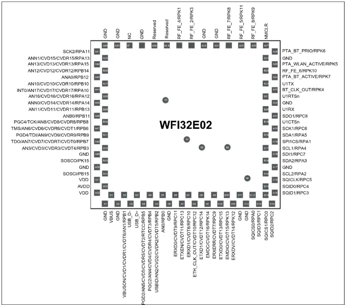
geo
WFI32E02 | Category | Pin Number | | :--- | :--- | | GND | A10 | | GND | A39 | | NC | S7 | | GND | A36 | | Reserved | A34 | | Reserved | S4 | | RF_FE_4/RPK1 | ■ | | RF_FE_2/RPK3 | ■ | | GND | A32 | | GND | A31 | | RF_FE_7/RPK8 | ■ | | RF_FE_5/RPK11 | ■ | | RF_FE_8/RPK9 | ■ | | NMCLR | A27 | | PTA_BT_PRIO/RPK6 | ■ | | GND | B21 | | PTA_WLAN_ACTIVE/RPK5 | ■ | | RF_FE_6/RPK10 | ■ | | PTA_BT_ACTIVE/RPK7 | ■ | | U1TX | B22 | | BT_CLK_OUT/RPK4 | ■ | | U1RTSn | B21 | | GND | A22 | | U1RX | B20 | | ANB0/RPB11 | A46 | | ANB0/RPB11 | A46 | | PGC4/TCK/AN8/CVD8/CVDR8/RPB8 | B30 | | TMS/AN6/CVD6/CVDR6/CVDT1/RPB6 | A47 | | PGD4/TDI/AN9/CVD9/CVDR9/RPB9 | B51 | | TDO/AN7/CVD7/CVDR7/CVDT0/RPB7 | A48 | | AN3/CVD3/CVDR3/CVDT4/RPB3 | B32 | | GND | A49 | | SOSCO/PK15 | B33 | | GND | A50 | | SOSCI/PB15 | B30 | | VDD | A51 | | AVDD | B39 | | VDD | A52 | | GND | A1 | | VBUS | A2 | | GND | A3 | | VBUSON/CVD1/CVDR1/CVDT6/AN1/RPB1 USB_D-USB_D+PGD2/AN5/CVD5/CVDR5/CVDT2/RTCC/RPB5 PGC2/AN4/CVD4/CVDR4/CVDT3/RPB4 USBID/AN2/CVD2/CVDR2/CVDT5/RPB2 ANO/RPB0 GND ERXD0/CVDT9/RPC11 ETXEN/CVDT11/RPC13 ERXD1/CVDT8/RPC10 ETH_CLK_OUT/CVDT10/RPC12 ETXD1/CVDT12/RPC14 EMDC/CVDT16/RPK14 ERXERR/CVDT7/RPC9 ETXD0/CVDT13/RPC15 EMDIO/CVDT15/RPK13 ERXD/CVDT14/RPK12 GND GND SQICSO/RPA0 SQID3/RPC1 SQICSI/RPC0 SQID2/RPC2 SQICCLK/RPC5 SQID0/RPC4 SQID1/RPC3 SQICCLK/RPC5 SQID2/RPC2 SQICCLK/RPC5 SQID3/RPC1 SQICCS0/RPA0 SQID3/RPC1 SQICCS0/RPA0 SQID3/RPC1 SQICCS0/RPA0 SQID3/RPC1 SQICCS0/RPA0 SQID3/RPC1 SQICCS0/RPA0 SQID3/RPC1 SQICCS0/RPA0 SQID3/RPC1 SQICCS0/RPA0 SQID3/RPC1 SQICCS0/RPA0 SQID3/RPC1 SQICSC0/RPA0 SQID3/RPC1 SQICCS0/RPA0 SQID3/RPC1 SQICCS0/RPA0 SQID3/RPC1 SQICCS0/RPA0 SQID3/RPC1 SQICCS0/RPA0 SQID3/RPC1 SQICCS0/RPA0 SQID3/RPC1 SQICCS0/RPA0 SQID3/RPC1 SQICCS0/RPA0 SQID3/RRCN RPLC (A) B ■ ■ ■ ■ ■ ■ ■ ■ ■ ■ ■ ■ ■ ■ ■ ■ ■ ■ ■ ■ ■ ■ ■ ■ ■ ■ ■ ■ ■ ■ ■ ■ ■ ■ ■ ■ ■ ■ ■ ■ ■ ■ ■ ■ ■ ■ ■ ■ ■ ■ ● S2 S2 S2 S2 S2 S2 S2 S2 S2 S2 S2 S2 S2 S2 S2 S2 S2 S2 S2 S2 S2 S2 S2 S2 S2 S2 S2 S2 S2 S2 S2 S2 S2 S2Note 1: For details on the exact pin placement and dimensions, refer to Section 42.0 "Packaging Information".
2: For pin descriptions, refer to Table 3-2.
3: Pins (93-102) are not indicated in Figure 3-4. For more details, refer to the Section 42.0 "Packaging Information".
TABLE 3-2: WFI32E02 MODULE PIN DESCRIPTION
| Module Pin Number | SoC Pin Number | Pin Name | Pin Type(1) | Description |
| A1 — GND P | Ground | |||
| B1 A65 VBUS | I USB VBUS | signal input (3.3V compliant and | needs a resistor divider on the host board), can be left open when USB not in use | |
| A2 — GND P | Ground | |||
| B2 A62 AN1 | Analog input | |||
| CVD1 O ADC CVD controller output | ||||
| CVDR1 | O ADC CVD controller RX | |||
| CVDT6 | O ADC CVD controller TX | |||
| VBUSON | O USB ON signal for external VBUS source | |||
| RPB1 | I/O | Remappable peripheral(2) | ||
| RB1 I/O PORTB digital I/O | ||||
| A3 A63 USB | D- | I/O USB data - | ||
| B3 A64 USB | D+ | I/O USB data + | ||
| A4 B49 PGD2 | I/O In Circuit Serial ProgrammingTM (ICSPTM) programming data | |||
TABLE 3-2: WFI32E02 MODULE PIN DESCRIPTION (CONTINUED)
| Module Pin Number | SoC Pin Number | Pin Name | Pin Type(1) | Description | |||
| B7 B57 CVD | T8 O ADC CV | D controller TX | |||||
| ERXD1 I Ethernet RM | I receive data bit 1 | ||||||
| RPC10 I/O Remappable peripheral (2) | |||||||
| RC10 I/O PORTC digital I/O | |||||||
| A8 B58 CVD | T10 O ADC CV | D controller TX | |||||
| ETH_CLK_OUT O Ethernet RMI | reference clock out (50 MHz), requires an external 33 series termination resistor | ||||||
| RPC12 I/O Remappable peripheral (2) | |||||||
| RC12 I/O PORTC digital I/O | |||||||
| B8 B2 CVDT | 12 O ADC CV | D controller TX | |||||
| ETXD1 O Ethernet RMI transmit | data bit 1 | ||||||
| RPC14 I/O Remappable peripheral (2) | |||||||
| RC14 I/O PORTC digital I/O | |||||||
| A9 B4 CVDT | 16 O ADC CV | D controller TX | |||||
| EMDC | O Ethernet management data clock | ||||||
| RPK14 | I/O Remappable peripheral (2) | ||||||
| RK14 | I/O PORTK digital I/O | ||||||
| B9 B5 CVDT | 7 O ADC CV | D controller TX | |||||
| ERXERR | I Ethernet RMII receive error | ||||||
| RPC9 | I/O Remappable peripheral (2) | ||||||
| RC9 | I/O PORTC digital I/O | ||||||
| A10 | A4 CVDT13 | O ADC CVD controller TX | |||||
| ETXD0 O Ethernet RMII receive data bit 0 | |||||||
| RPC15 I/O Remappable peripheral (2) | |||||||
| RC15 I/O PORTC digital I/O | |||||||
| B10 | A5 CVDT15 | O ADC CVD controller TX | |||||
| EMDIO I/O Ethernet management data IO | |||||||
| RPK13 | I/O Remappable peripheral (2) | ||||||
| RK13 | I/O PORTK digital I/O | ||||||
| A11 | A6 CVDT14 | O ADC CVD controller TX | |||||
| ERXDV | I Ethernet RMII receive data valid | ||||||
| RPK12 | I/O Remappable peripheral (2) | ||||||
| RK12 | I/O PORTK digital I/O | ||||||
| B11 | — | GND | P | Ground | |||
| A12 | — GND | P | Ground | ||||
| B12 | B6 SQICS0 | O SQI1 Chip Select | |||||
| CVDT17 O ADC CVD controller TX | |||||||
| RPA0 I/O Remappable peripheral (2) | |||||||
| RA0 | I/O PORTA digital I/O | ||||||
| A13 | B8 SQID3 | I/O SQI1 Data[3] | |||||
| CVDT19 O ADC CVD controller TX | |||||||
| RPC1 | I/O Remappable peripheral (2) | ||||||
| RC1 | I/O PORTC digital I/O | ||||||
| B13 | A9 SQICS1 | O SQI1 Chip Select | |||||
| CVDT18 O ADC CVD controller TX | |||||||
| RPC0 | I/O Remappable peripheral (2) | ||||||
| RC0 | I/O PORTC digital I/O | ||||||
| A14 A10 SQID2 I/O SQI1 | Data[2] | ||||||
| CVDT20 O ADC CVD | controller | TX | |||||
| RPC2 I/O Remappable peripheral | (2) | ||||||
| RC2 I/O PORTC digital I/O | |||||||
| A15 B9 SQID1 I/O SQI1 | Data[1] | ||||||
| CVDT21 O ADC CVD | controller | TX | |||||
| RPC3 I/O Remappable peripheral | (2) | ||||||
| RC3 I/O PORTC digital I/O | |||||||
| B14 B10 SQID0 I/O SQI1 | Data[0] | ||||||
| CVDT22 O ADC CVD | controller | TX | |||||
| RPC4 I/O Remappable peripheral | (2) | ||||||
| RC4 I/O PORTC digital I/O | |||||||
| A16 A12 SQICLK I/O SQI1 | Clock | ||||||
| CVDT23 O ADC CVD | controller | TX | |||||
| RPC5 I/O Remappable peripheral | (2) | ||||||
| RC5 I/O PORTC digital I/O | |||||||
| B15 A15 SCL2 I/O I2C1 Synchronous Serial Clock Input/Output | |||||||
| RPA2 I/O Remappable peripheral | (2) | ||||||
| RA2 I/O PORTA digital I/O | |||||||
| A17 — | GND | P | Ground | ||||
| B16 B14 SDA2 | I/O I2C2 Data Input/Output | ||||||
| RPA3 I/O Remappable peripheral | (2) | ||||||
| RA3 I/O PORTA digital I/O | |||||||
| A18 A13 SDI1 | I SPI1 serial data in | ||||||
| RPC7 I/O Remappable peripheral | (2) | ||||||
| RC7 I/O PORTC digital I/O | |||||||
| B17 | A16 | SCL1 | I/O | I2C clock, requires an external pull-up resistor (1.8 kΩ) | |||
| RPA4 I/O Remappable peripheral | (2) | ||||||
| RA4 I/O PORTA digital I/O | |||||||
| A19 A14 SPI1CS | —— | O SPI client select/chip select input (active-low) | |||||
| RPA1 I/O Remappable peripheral | (2) | ||||||
| RA1 I/O PORTA digital I/O | |||||||
| B18 | B15 | SDA1 | I/O | I2C data, requires an external pull-up resistor (1.8 kΩ) | |||
| RPA5 I/O Remappable peripheral | (2) | ||||||
| RA5 I/O PORTA digital I/O | |||||||
| A20 B11 | SCK1 | I/O SPI1 serial clock | |||||
| RPC6 I/O Remappable peripheral | (2) | ||||||
| RC6 I/O PORTC digital I/O | |||||||
| B19 B16 U1CTSn I | UART1 CTS Output | ||||||
| RA6 I/O PORTA digital I/O | |||||||
| A21 B12 SDO1 | O SPI1 serial data out | ||||||
| RPC8 I/O Remappable peripheral | (2) | ||||||
| RC8 I/O PORTC digital I/O | |||||||
| B20 B17 U1RX I | UART1 receive | ||||||
| A22 — | GND | P | Ground | ||||
| B21 A21 U1RTSn O | UART1 RTS Input | ||||||
| RA7 I/O PORTA digital I/O | |||||||
| A23 B18 BT | CLK_OUT O | Bluetooth | ^ reference clock out (26 MHz) | ||||
| RPK4 I/O Remappable peripheral | (2) | ||||||
| RK4 I/O PORTK digital I/O | |||||||
| B22 A22 U1TX O UART1 | transmit | ||||||
| A24 B20 PTA_BT_ACTIVE | I PTA Bluetooth active signal for Bluetooth and Wi-Fi ^ coexistence(6) | ||||||
| RPK7 I/O Remappable peripheral | (2) | ||||||
| RK7 I/O PORTK digital I/O | |||||||
| B23 B22 RF | FE_6 I/O RF | front-end control | |||||
| RPK10 I/O Remappable peripheral | (2) | ||||||
| RK10 | I/O PORTK digital I/O | ||||||
| A25 | B19 | PTA_WLAN_ACTIVE | O | PTA Wi-Fi active signal for Bluetooth and Wi-Fi coexistence(6) | |||
| RPK5 I/O Remappable peripheral | (2) | ||||||
| RK5 I/O PORTK digital I/O | |||||||
| B24 — | GND | P | Ground | ||||
| A26 | A24 | PTA_BT_PRIO | I | Packet Traffic Arbitration (PTA) Bluetooth priority signal for Bluetooth and Wi-Fi coexistence(6) | |||
| RPK6 I/O Remappable peripheral | (2) | ||||||
| RK6 I/O PORTK digital I/O | |||||||
| A27 A23 MCLR | I Reset signal, Active-low, requires external RC circuit | ||||||
| A28 A26 RF | FE_8 I/O RF | front-end control | |||||
| RPK9 I/O Remappable peripheral | (2) | ||||||
| RK9 I/O PORTK digital I/O | |||||||
| A29 A27 RF | FE_5 I/O RF | front-end control | |||||
| RPK11 | I/O Remappable peripheral | (2) | |||||
| RK11 | I/O PORTK digital I/O | ||||||
| A30 B21 RF | FE_7 I/O RF | front-end control | |||||
| RPK8 I/O Remappable peripheral | (2) | ||||||
| RK8 I/O PORTK digital I/O | |||||||
| A31 — | GND | P | Ground | ||||
| A32 — | GND | P | Ground | ||||
| A33 B38 RF | FE_2 I/O RF | front-end control | |||||
| AN18 | I/O Analog input | ||||||
| CVD18 | I/O ADC CVD controller output | ||||||
| CVDR18 | I/O ADC CVD controller RX | ||||||
| RPK3 I/O Remappable peripheral | (2) | ||||||
| RK3 I/O PORTK digital I/O | |||||||
| A34 B37 RF | FE_4 I/O RF | front-end control | |||||
| RPK1 I/O Remappable peripheral | (2) | ||||||
| RK1 I/O PORTK digital I/O | |||||||
| A35(7) | — | — | — | Reserved | |||
| A36(7) | — | — | — | Reserved | |||
| A37 — | GND | P | Ground | ||||
| A38 | — | NC | — | RF test pad (only for factory use) | |||
| A39 — | GND | P | Ground | ||||
| A40 — | GND | P | Ground | ||||
| A41 A47 SCK2 I/O SPI2 s | serial clock | ||||||
| RPA11 | I/O Remappable peripheral | (2) | |||||
| RA11 | I/O PORTA digital I/O | ||||||
| B25 A48 AN1 | 5 I Analog input | ||||||
| ANN1 I Analog input | |||||||
| CVD15 O ADC CVD controller output | |||||||
| CVDR15 O ADC CVD controller RX | |||||||
| RPA13 I/O Remappable peripheral (2) | |||||||
| RA13 I/O PORTA digital I/O | |||||||
| A42 A49 AN1 | 3 I Analog input | ||||||
| CVD13 O ADC CVD controller output | |||||||
| CVDR13 O ADC CVD controller RX | |||||||
| RPA15 I/O Remappable peripheral (2) | |||||||
| RA15 I/O PORTA digital I/O | |||||||
| B26 A50 AN1 | 2 I Analog input | ||||||
| CVD12 O ADC CVD controller output | |||||||
| CVDR12 O ADC CVD controller RX | |||||||
| RPB14 I/O Remappable peripheral (2) | |||||||
| RB14 I/O PORTB digital I/O | |||||||
| A43 A51 ANA0 | I Analog input | ||||||
| RPB12 I/O Remappable peripheral (2) | |||||||
| RB12 I/O PORTB digital I/O | |||||||
| B27 A52 AN1 | 10 I Analog input | ||||||
| CVD10 O ADC CVD controller output | |||||||
| CVDR10 O ADC CVD controller RX | |||||||
| RPB10 I/O Remappable peripheral (2) | |||||||
| RB10 I/O PORTB digital I/O | |||||||
| A44 B39 AN1 | 7 I Analog input | ||||||
| CVD17 O ADC CVD controller output | |||||||
| CVDR17 | O ADC CVD controller RX output | ||||||
| INT0 | I External interrupt input 0 | ||||||
| RPA10 I/O Remappable peripheral (2) | |||||||
| RA10 I/O PORTA digital I/O | |||||||
| B28 B40 AN1 | 16 I Analog input | ||||||
| CVD16 O ADC CVD controller output | |||||||
| CVDR16 | O ADC CVD controller RX output | ||||||
| RPA12 I/O Remappable peripheral (2) | |||||||
| RA12 I/O PORTA digital I/O | |||||||
| A45 B41 AN1 | 14 I Analog input | ||||||
| ANN0 I Analog Input | |||||||
| CVD14 O ADC CVD controller output | |||||||
| CVDR14 O ADC CVD controller RX | |||||||
| RPA14 I/O Remappable peripheral (2) | |||||||
| RA14 I/O PORTA digital I/O | |||||||
| B29 B43 AN1 | 1 | ||||||
| I Analog input | |||||||
| CVD11 | O ADC CVD controller output | ||||||
| CVDR11 | O ADC CVD controller RX output | ||||||
| RPB13 I/O Remappable peripheral (2) | |||||||
| RB13 I/O PORTB digital I/O | |||||||
| A46 B44 ANB0 I A/D Analog inputs | |||||||
| RPB11 I/O Remappable peripheral (2) | |||||||
| RB11 I/O PORTB digital I/O | |||||||
| B30 B46 TCK I JTAG test | cock/programming clock input | ||||||
| PGC4 I ICSP programming clock | |||||||
| AN8 | I Analog input | ||||||
| CVD8 | O | ADC CVD controller output | |||||
| CVDR8 | O | ADC CVD controller RX | |||||
| RPB8 I/O Remappable peripheral (2) | |||||||
| RB8 | I/O PORTB digital I/O | ||||||
| A47 B47 TMS | I JTAG Test mode select input | ||||||
| AN6 | I Analog input | ||||||
| CVD6 | O | ADC CVD controller output | |||||
| CVDR6 | O | ADC CVD controller RX | |||||
| CVDT1 | O | ADC CVD controller TX | |||||
| RPB6 I/O Remappable peripheral (2) | |||||||
| RB6 | I/O PORTB digital I/O | ||||||
| B31 A56 TDI | I JTAG test data/programming data input | ||||||
| PGD4 I/O ICSP programming data | |||||||
| AN9 | I Analog input | ||||||
| CVD9 | O | ADC CVD controller output | |||||
| CVDR9 | O | ADC CVD controller RX | |||||
| RPB9 I/O Remappable peripheral (2) | |||||||
| RB9 | I/O PORTB digital I/O | ||||||
| A48 A57 TDO | I JTAG test data output | ||||||
| AN7 | I Analog input | ||||||
| CVD7 | O | ADC CVD controller output | |||||
| CVDR7 | O | ADC CVD controller RX | |||||
| CVDT0 | O | ADC CVD controller TX | |||||
| RPB7 I/O Remappable peripheral (2) | |||||||
| RB7 | I/O PORTB digital I/O | ||||||
| B32 A61 AN3 | I Analog input | ||||||
| CVD3 | O | ADC CVD controller output | |||||
| CVDR3 | O | ADC CVD controller RX | |||||
| CVDT4 | O | ADC CVD controller TX | |||||
| RPB3 I/O Remappable peripheral (2) | |||||||
| RB3 | I/O PORTB digital I/O | ||||||
| A49 — | GND | P | Ground | ||||
| B33 A58 SOSCO | O Secondary oscillator output | ||||||
| A50 — | GND | P | Ground | ||||
| B34 A59 SOSCI I Secondary oscillator input | |||||||
| A51 — | VDD | P | Input supply voltage (3V3) | ||||
| B35 — | AVDD P | Input supply voltage (3V3) | |||||
| A52 — | VDD | P | Input supply voltage (3V3) | ||||
| 88-92^(5) | — | NC | — | Test pad (only for factory use, no pads on the host board) | |||
| 93-102^(5) | — | GND | P | Exposed GND pads, must be soldered on the host board | |||
Note 1: Legend:
- | = Input pin
- O = Output pin
• I/O = Input/Output pin - P = Power pin
2: These pins can be configured for any of the supported peripheral functions based on the user's requirement. For more details, refer to Section 13.4 "Peripheral Pin Select (PPS)".
3: Every I/O port pin (RAx-RKx) can be used as a change notification pin (CNAx-CNKx). See Section 13.0 "I/O Ports" for more information.
4: Microchip recommends adding series resistors in the host board. For more details on series resistor recommendations, see Figure 3-6.
5: For the placement of pins 88 through 102, refer to Section 42.2 "WFI32 Module Packaging Information".
6: The PTA features is currently not supported, and it is recommended that it not be used in an end-product design. Microchip plans to support this feature in the future.
7: The recommendation is to keep pins A35 and A36 as Reserved/Not Connected (NC) on the host board for future product upgrade. However, the pins A35 and A36 are connected to the GND on the EV89Y10A PIC32 WFI32 Curiosity HPC Board.
Note: For module-related recommended operating values and electrical characteristics, refer to Section 41.2 "WFI32 Module Electrical Specifications".
3.2 Basic Connection Requirement
The WFI32 Module requires attention to a minimal set of device pin connections before proceeding with development.
FIGURE 3-5: WFI32E01 MODULE BASIC CONNECTIONS
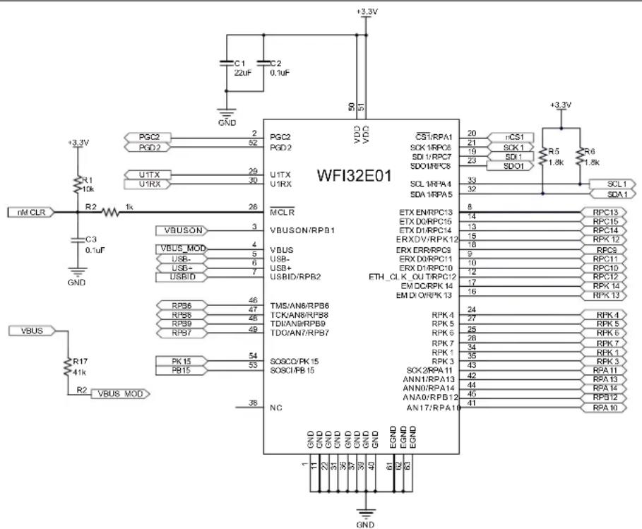
Note 1: The mentioned resistance values are only for the guidance. For details on the application schematics, refer to the PIC32 WFI32E Curiosity Board User's Guide (DS50003028).
FIGURE 3-6: WFI32E02 MODULE BASIC CONNECTIONS
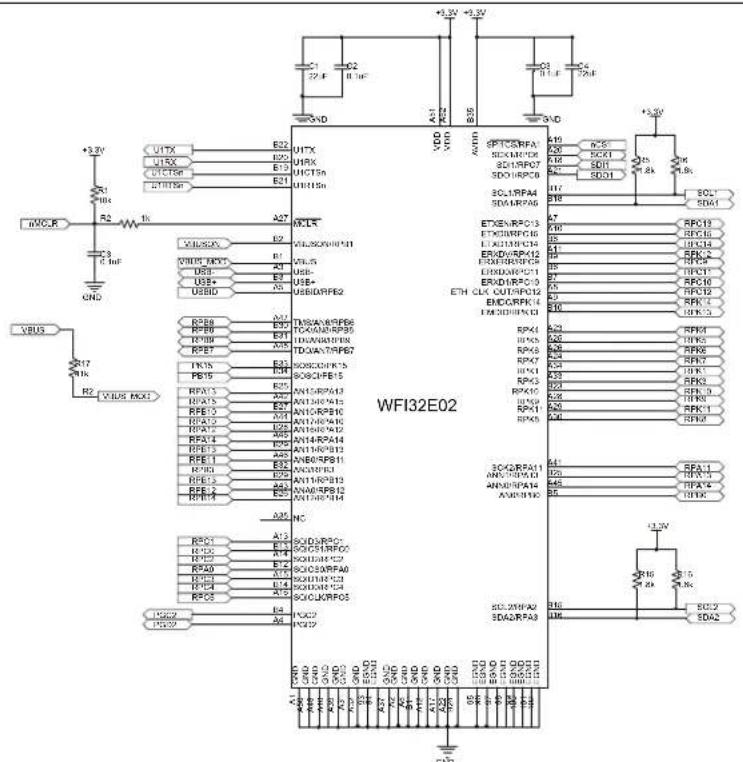
Note 1: The mentioned resistance values are only for the guidance. For details on the application schematics, refer to the EV89Y10A PIC32 WFI32 Curiosity HPC User's Guide (DS50003573).
3.2.1 POWER PINS
It is recommended that a bulk and a decoupling capacitor be added at the input supply pin (VDD, AVDD and GND pins) of the WFI32 Module.
FIGURE 3-7: WFI32E01
RECOMMENDED
MODULE POWER
SUPPLY CONNECTIONS
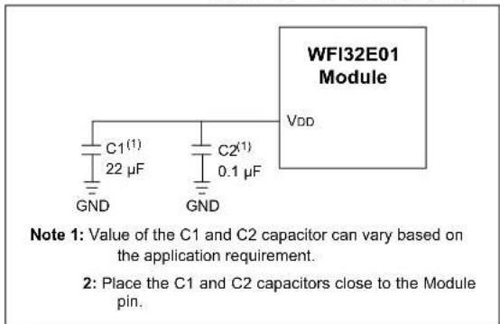
FIGURE 3-8: WFI32E02
RECOMMENDED
MODULE POWER
SUPPLY CONNECTIONS
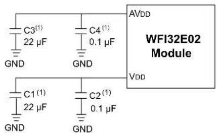
Note 1: Value of the C1, C2, C3 and C4 capacitor can vary based on the application requirement.
2: Place the C1, C2, C3 and C4 capacitors close to the module pin.
3: To achieve better ADC performance, the user can supply power to AVDD and VDD supply pins from separate power supply sources.
3.2.2 MASTER CLEAR (MCLR) PIN
The MCLR pin provides for two specific device functions:
- Device Reset
• Device programming and debugging
Pulling the MCLR pin low generates a device Reset. Figure 3-9 illustrates a typical MCLR circuit. During device programming and debugging, the resistance and capacitance that can be added to the pin must be considered. Device programmers and debuggers drive the MCLR pin. Consequently, specific voltage levels (VIH and VIL) and fast signal transitions must not be adversely affected. Therefore, specific values of R and C need to be adjusted based on the application and PCB requirements.
For example, as illustrated in Figure 3-9, it is recommended that capacitor C be isolated from the MCLR pin during programming and debugging operations.
Place the components illustrated in Figure 3-9 within one-quarter inch (6 mm) from the MCLR pin.
FIGURE 3-9: EXAMPLE OF MCLR PIN CONNECTIONS
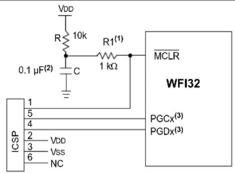
Note 1: 470 ≤ R1 ≤ 1 kΩ limits any current flowing into MCLR from the external capacitor C, in the event of MCLR pin breakdown, due to Electrostatic Discharge (ESD) or Electrical Overstress (EOS). Ensure that the MCLR pin VIH and VIL specifications are met without interfering with the Debug/Programmer tools.
2: The capacitor can be sized to prevent unintentional Resets from brief glitches or to extend the device Reset period during POR.
3: No pull-ups or bypass capacitors are allowed on active debug/program PGCx and PGDx pins.
3.2.3 ICSP PINS
The PGCx/PGECx and PGDx/PGEDx pins are used for ICSP and debugging purposes. It is recommended that PGC2 and PGD2 be used for the WFI32 Module as the default configuration.
Keep the trace length between the ICSP pins of the WFI32 Module and the ICSP header as short as possible. If the ICSP connector is expected to experience an ESD event, a series resistor is recommended with the value in the range of a few tens of s, not to exceed 100 .
Ensure that the Communication Channel Select (PGECx/PGEDx pins) programmed into the device matches the physical connections for the ICSP to MPLAB ICD 4/MPLAB ICD 5 or MPLAB REAL ICE™ in-circuit emulator.
For more information on MPLAB ICD 4/MPLAB ICD 5, and MPLAB REAL ICE in-circuit emulator connection requirements, refer to the following documents available from the Microchip website.
- "MPLAB® ICD 4 In-Circuit Debugger Quick Start
- Guide" (DS50002538)
- "MPLAB® ICD 4 In-Circuit Debugger User's
- Guide" (DS50002596)
- "MPLAB ^ ICD 5 In-Circuit Debugger Quick Start Guide" (DS50003438)
- "MPLAB ^ ICD 5 In-Circuit Debugger User's Guide" (DS50003529)
- "MPLAB® REAL ICE™ In-Circuit Debugger User's Guide" (DS50001616)
- "Using MPLAB ^ REAL ICE ^TM Emulator" (poster) (DS50001749)
3.2.4 JTAG
Note: This is an optional interface for the WFI32 Module. JTAG can be used based on the selection of the debugger and programing interface.
The TMS, TDO, TDI and TCK pins are used for programming and debugging according to the Joint Test Action Group (JTAG) standard. Pull-up resistors are recommended on these lines for JTAG functionality. For remappable functionality, the discrete component value needs to be considered based on application.
It is recommended to keep the trace length between the JTAG connector and the JTAG pins on the WFI32 Module as short as possible. If the JTAG connector is expected to experience an ESD event, a series resistor is recommended, with the value in the range of a few tens of s, not to exceed 100 .
Refer to the AC/DC characteristics and timing requirements in the respective device specification for information on capacitive loading limits and pin input voltage high (VIH) and input voltage low (VIL) requirements.
3.2.5 UNUSED I/O PINS
For low power modes, the user must not allow the unused I/O pins to float as inputs. The user can also configure them as outputs and drive them to a Logic-low state. As an alternative, the user can reserve the inputs by connecting the pin to VSS through a 1 kΩ to 10 kΩ resistor and configuring the pin as an input.
In general, the user needs to drive the I/O pins based on the application use case. Also, the user must know how a particular pin is wired before driving it to a particular state. For example, do not drive a pin to low, if it is wired to sink current, or drive high, if it is going to the source current.
3.2.5.1 GPIO Pins/PPS Functions
Most of the WFI32 Module pins can be configured as GPIOs pins or for PPS functionality. To find the functionality supported by each of these GPIOs, refer to Table 3-1 and Table 3-2.
It is recommended that a series resistor be added on the host board for all GPIOs. The value of the series resistor depends on the actual pin configuration. These resistors must be placed close to the module. Figure 3-16 and Figure 3-17 illustrate the placement of the series resistor.
3.2.6 USB
The external VBUS specified with 5V tolerance needs to be level converted interfacing with the WFI32 Module, which is a 3.3V-tolerant pin.
FIGURE 3-10: EXTERNAL 5V V BUS INTERFACING WITH WFI32 MODULE
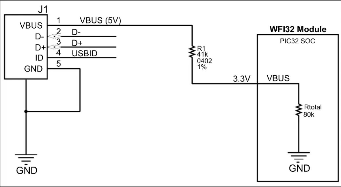
3.3 WFI32 Module Placement Guidelines
- For any Wi-Fi product, the antenna placement affects the performance of the whole system. The antenna requires free space to radiate RF signals and it must not be surrounded by the ground plane. Thus, for best PCB antenna performance, the WFI32E01PC/WFI32E01PE Module must be placed at the edge of the host board.
- The WFI32E01PC/WFI32E01PE Module ground outline edge must be aligned with the edge of the host board ground plane (see the following figure).
- A low-impedance ground plane for the WFI32 Module ensures the best radio performance (best range and lowest noise). The ground plane can be
extended beyond the minimum recommendation as required for the host board EMC and noise reduction.
- For best performance, keep metal structures and components (such as mechanical spacers, bump-on, and so on) at least 31.75 mm away from the PCB trace antenna as illustrated in the following figure.
- The antenna on the WFI32 Module must not be placed in direct contact with or close proximity to plastic casing or objects. Keep a minimum clearance of 10mm in all directions around the PCB antenna (see the following figure).
- Microchip uses the following module placement for EV36W50A.
FIGURE 3-11: WFI32E01PC/WFI32E01PE MODULE PLACEMENT RECOMMENDATION (TOP VIEW)
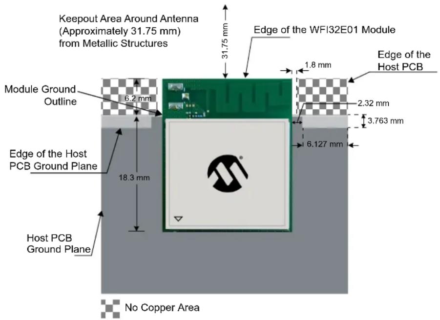
Note: For alternate module placement guidelines, refer to the Section Appendix B: "Alternate Module Placement Guidelines".
- The WFI32 Module must be flush mounted to the host board (see the following figure).
FIGURE 3-12: WFI32 MOUNTING GUIDELINES RECOMMENDATION (SIDE VIEW)

- The WFI32E01UC/WFI32E01UE Module on the host board can be placed aligned to each other (see Figure 3-13).
- Three Exposed GND pads (61-63) on the bottom of the WFI32E01 Module must be soldered to the host board (see Figure 42-7).
- A PCB cutout is required under RF test point (see Figure 42-7).
• Copper keepout areas are required on the top layer under voltage test points (55-60) (see Figure 42-7).
FIGURE 3-13: WFI32E01UC/WFI32E01UE MODULE PLACEMENT (TOP VIEW)
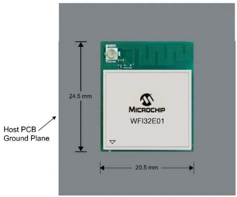
Note 1: The user can place the WFI32E01UC/WFI32E01UE variants anywhere on the host PCB.
FIGURE 3-14: WFI32E02UC/WFI32E02UE MODULE PLACEMENT (TOP VIEW)
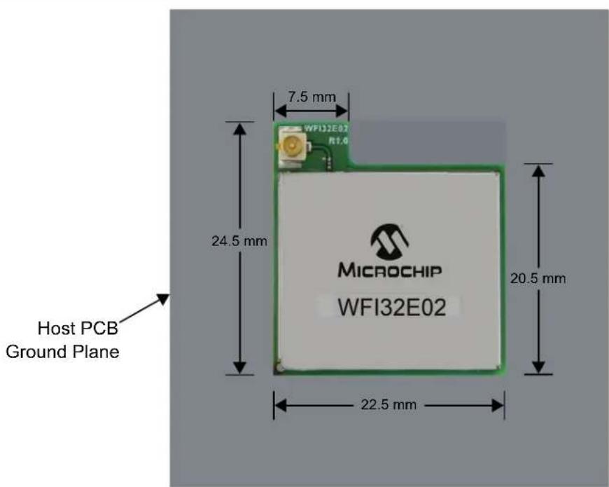
Note 1: The user can place the WFI32E02UC/WFI32E02UE variants anywhere on the host PCB.
The following figure illustrates the examples of WFI32E01PC/WFI32E01PE Module placement on a host board with a ground plane. Refer to Figure 3-11 for placement specific guidance.
FIGURE 3-15: EXAMPLES OF WFI32E01PC/WFI32E01PE MODULE PLACEMENTS ON THE HOST BOARD
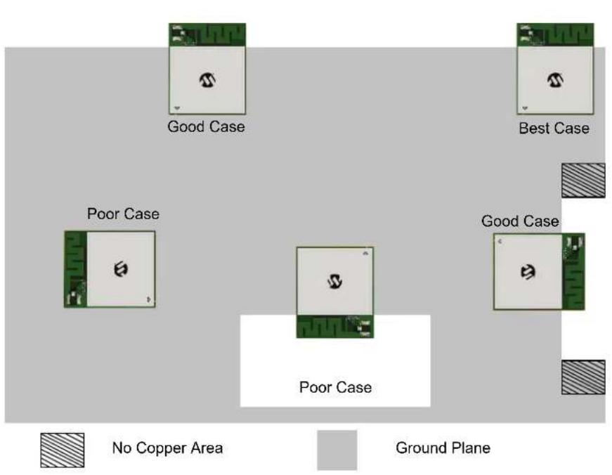
3.4 WFI32 Module Routing Guidelines
- Use the multi-layer host board for routing signals on the inner layer and the bottom layer.
-
The top layer (underneath the Module) of the host board must be ground with as many GND vias as possible.
-
For WFI32E01 Module, see Figure 3-16 and Figure 42-11.
- For WFI32E02 Module, see Figure 3-17 and Figure 42-12.
- Avoid fan-out of the signals under the Module or antenna area. Use a via to fan-out signals to the edge of the WFI32 Module.
- For better GND connection and thermal conductivity to the WFI32 Module, solder the exposed GND pads of the WFI32 Module on the host board.
- For the WFI32 Module GND pad, use a GND via of a minimum 10 mil (hole diameter) for good ground to all the layers and thermal conduction path.
- The recommendation is to have a series resistor on the host board for all GPIOs. Place these resistors close to the signal source. Refer to Figure 3-16 and Figure 3-17 for the placement of the series resistor.
-
The user must ensure length matching of the signal traces on the host PCB.
-
USB differential pair signals are 90 impedance controlled on the WF132 Module PCB and the same must be followed on the host board.
- SOSC crystal (32.768 kHz) on host board must be placed close to the WFI32 Module and follow the shortest trace routing length with the minimum number of vias (see Figure 3-16, Figure 3-17 and Figure 3-18).
FIGURE 3-16: WFI32E01 - EXAMPLE OF THE HOST BOARD TOP LAYER
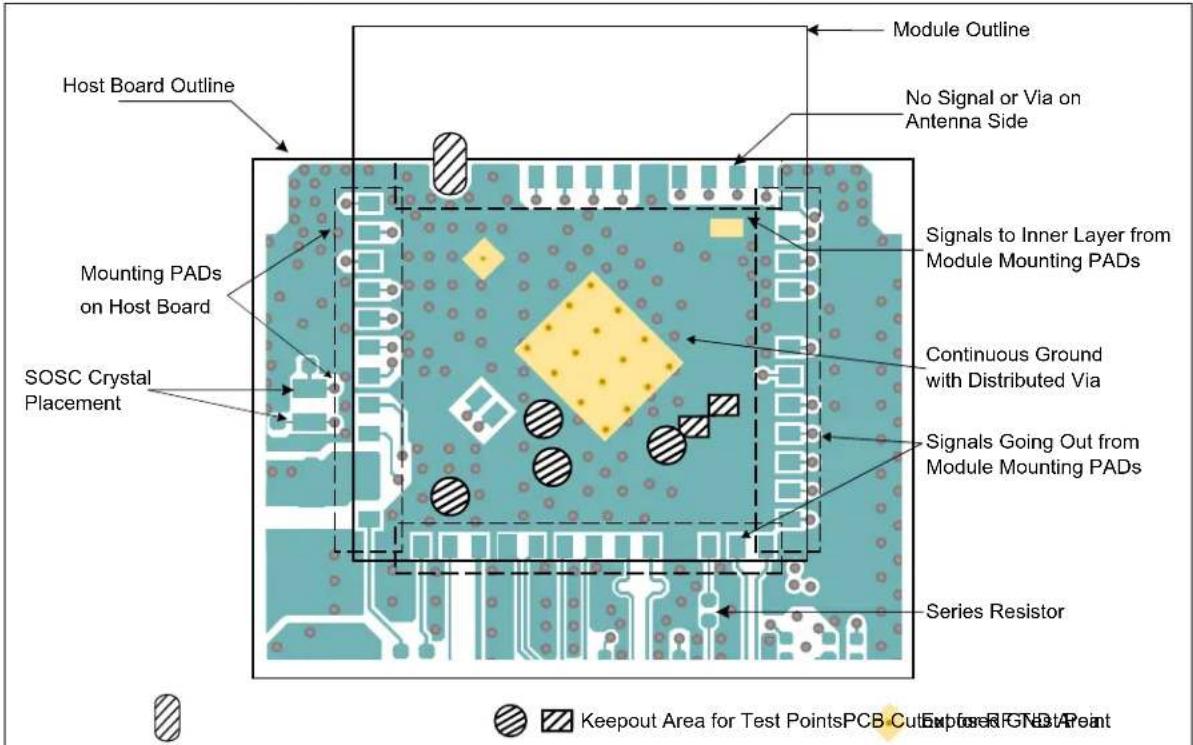
Note 1: The user can place the WFI32E01UC/WFI32E01UE Module anywhere on the host PCB (see Figure 3-13) and must provide continuous ground and tented ground vias underneath the module (see Figure 3-16).
FIGURE 3-17: WFI32E02 - EXAMPLE OF THE HOST BOARD TOP LAYER
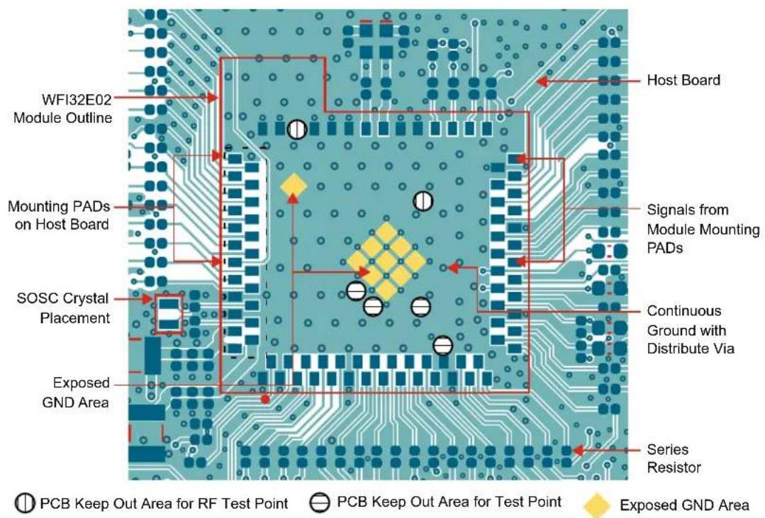
Note 1: The user can place the WFI32E02UC/WFI32E02UE Module anywhere on the host PCB (see Figure 3-14), and must provide continuous ground and tented ground vias underneath the module (see Figure 3-17).
FIGURE 3-18: PLACEMENT AND ROUTING OF SOSC CRYSTAL
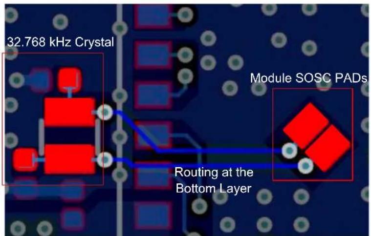
3.5 WFI32 Module RF Considerations
The overall performance of the system, RF and Wi-Fi is significantly affected by the product design, environment and application. The product designer must ensure system level shielding (if required) and verify the performance of the product features and applications.
Consider the following guidelines for optimal Wi-Fi performance:
- The WFI32 Module must be positioned in a noise-free RF environment and must be kept far away from high-frequency clock signals and any other sources of RF energy
- The antenna must not be shielded by any metal objects
• Power supply must be clean and noise-free - Make sure that the width of the traces routed to GND, VDD rails are sufficiently large for handling peak TX current consumption.
Note: The WFI32 Module includes RF shielding on top of the board as a standard feature.
3.6 WFI32 Module Antenna Considerations
3.6.1 WFI32E01 PCB ANTENNA
For the WFI32E01PC/WFI32E01PE Module, the PCB antenna is fabricated on the top copper layer and covered in solder mask. The layers below the antenna do not have copper trace. It is recommended that the module is mounted on the edge of the host board and to have no PCB material below the antenna structure of the module and no copper traces or planes on the host board in that area. It is recommended to verify that antenna tuning is maintained when the module is integrated onto a host board or end-product.
The following table lists the technical specification of the PCB antenna, which is tested with the WF132E01 module mounted on a Carrier/Evaluation Board of 0.8 mm PCB thickness.
TABLE 3-3: WFI32E01 PCB ANTENNA SPECIFICATIONS
| Parameter Specification | |
| Operating frequency 2400 ~ | 2500 MHz |
| Peak gain 2.51 dBi at 2450 | MHz |
| Efficiency (avg.) | 71% |
3.6.1.1 PCB Antenna Radiation Pattern
The following figures illustrate the module orientation and PCB antenna radiation pattern.
FIGURE 3-19: MODULE ORIENTATION FOR RADIATION PATTERN MEASUREMENT
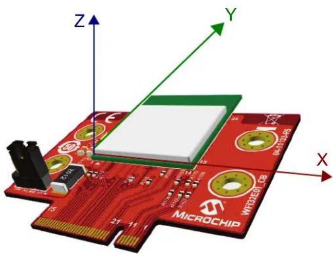
FIGURE 3-20: PHI = 0 DEGREE ANTENNA RADIATION PATTERN
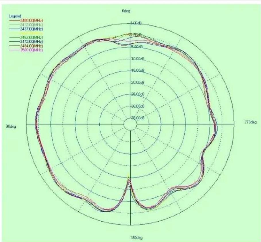
radar
| Frequency | Frequency (MHz) | |---|---| | 2400.00 | 5.0 | | 2412.00 | 5.0 | | 2437.00 | 5.0 | | 2462.00 | 5.0 | | 2472.00 | 5.0 | | 2484.00 | 5.0 | | 2500.00 | 5.0 |FIGURE 3-21: PHI = 90 DEGREE ANTENNA RADIATION PATTERN
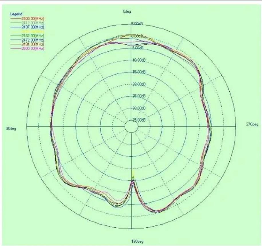
radar
| Frequency (MHz) | Angle (deg) | Value (dB) | | --------------- | ----------- | ---------- | | 2400.00 | 0 | ~5.0 | | 2400.00 | 30 | ~5.0 | | 2400.00 | 190 | ~5.0 | | 2400.00 | 270 | ~5.0 | | 2400.00 | 360 | ~5.0 | | 2412.00 | 0 | ~5.0 | | 2412.00 | 30 | ~5.0 | | 2412.00 | 190 | ~5.0 | | 2412.00 | 270 | ~5.0 | | 2412.00 | 360 | ~5.0 | | 2437.00 | 0 | ~5.0 | | 2437.00 | 30 | ~5.0 | | 2437.00 | 190 | ~5.0 | | 2437.00 | 270 | ~5.0 | | 2437.00 | 360 | ~5.0 | | 2462.00 | 0 | ~5.0 | | 2462.00 | 30 | ~5.0 | | 2462.00 | 190 | ~5.0 | | 2462.00 | 270 | ~5.0 | | 2462.00 | 360 | ~5.0 | | 2472.00 | 0 | ~5.0 | | 2472.00 | 30 | ~5.0 | | 2472.00 | 190 | ~5.0 | | 2472.00 | 270 | ~5.0 | | 2472.00 | 360 | ~5.0 | | 2484.00 | 0 | ~5.0 | | 2484.00 | 30 | ~5.0 | | 2484.00 | 190 | ~5.0 | | 2484.00 | 270 | ~5.0 | | 2484.00 | 360 | ~5.0 | | 2500.00 | 0 | ~5.0 | | 2500.00 | 30 | ~5.0 | | 2500.00 | 190 | ~5.0 | | 2500.00 | 270 | ~5.0 | | 2500.00 | 360 | ~5.0 |FIGURE 3-22: THETA = 90 DEGREE ANTENNA RADIATION PATTERN
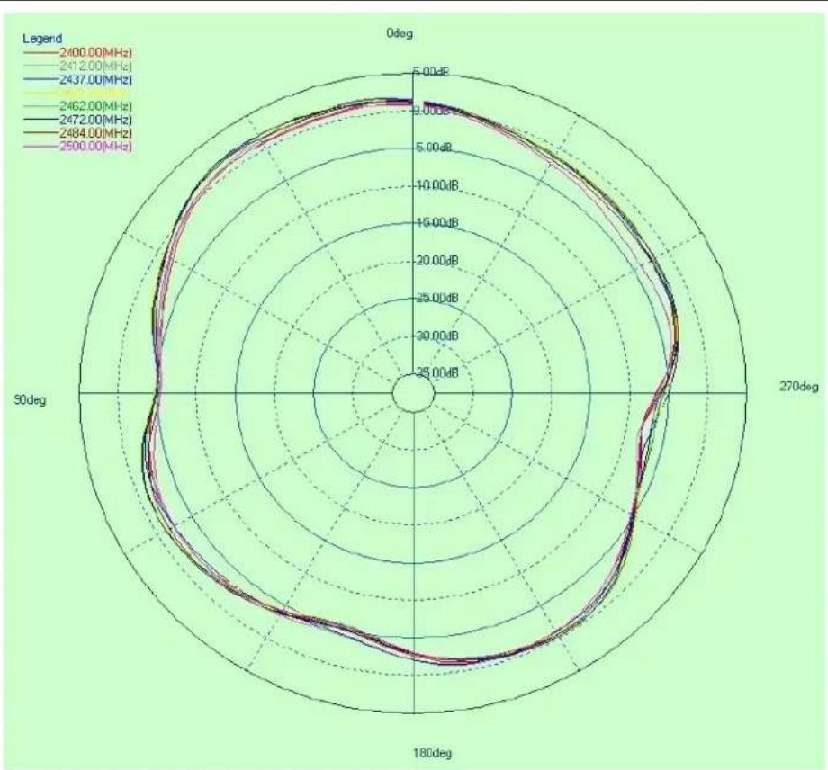
radar
| Frequency (MHz) | Angle (deg) | Value (dB) | | ---------------- | ----------- | ---------- | | 2400.00 | 0 | ~3.5 | | 2400.00 | 90 | ~3.5 | | 2412.00 | 0 | ~3.5 | | 2412.00 | 90 | ~3.5 | | 2437.00 | 0 | ~3.5 | | 2437.00 | 90 | ~3.5 | | 2462.00 | 0 | ~3.5 | | 2462.00 | 90 | ~3.5 | | 2472.00 | 0 | ~3.5 | | 2472.00 | 90 | ~3.5 | | 2484.00 | 0 | ~3.5 | | 2484.00 | 90 | ~3.5 | | 2500.00 | 0 | ~3.5 | | 2500.00 | 90 | ~3.5 |3.6.2 EXTERNAL ANTENNA PLACEMENT RECOMMENDATIONS
The following recommendations must be applied for the placement of the antenna and its cable:
- The antenna cable must not be routed over circuits generating electrical noise on the host board or alongside or underneath the module. It is preferred that the cable is routed straight out of the module.
- The antenna must not be placed in direct contact or in close proximity of the plastic casing/objects.
- Do not enclose the antenna within a metal shield.
- Keep any components which may radiate noise, signals or harmonics within the 2.4 GHz to 2.5 GHz frequency band away from the antenna and, if possible, shield those components. Any noise radiated from the host board in this frequency band degrades the sensitivity of the module.
- It is recommended that the antenna be placed preferably at a distance greater than 5 cm away from the module. The following figure shows the antenna keep out area indication where the antenna must not be placed.
These recommendations are based on an open-air measurement and does not take into account any metal shielding of the customer end-product. When a metal enclosure is used, the antenna can be located closer to the WFI32E01UC/WFI32E01UE/WFI32E02UC/WFI32E02UE Module.
Note: These are generic guidelines and it is recommended that customers check and fine-tune the antenna positioning in the final host product based on RF performance.
The following figure provides an indication on how the antenna cable must be routed depending on the location of the antenna with respect to the WFI32E01UC/WFI32E01UE/WFI32E02UC/WFI32E02UE Module PCB, there are two possible options for the optimum routing of the cable.
FIGURE 3-23: WFI32E01UC/WFI32E01UE/WFI32E02UC/WFI32E02UE Module ANTENNA PLACEMENT GUIDELINES
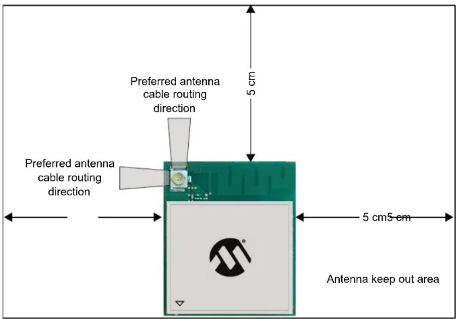
3.6.2.1 External Antennas
The WFI32E01UC/WFI32E01UE/WFI32E02UC/WFI32E02UE Modules have an ultra-small surface mount U.FL connector for an external antenna connection. The choice of antenna is limited to the antenna types for which the module is tested and approved.
The WFI32E01UC/WFI32E01UE/WFI32E02UC/WFI32E02UE Modules are approved to use with the antennas listed in Table 3-4.
It is permissible to use different antenna, provided the same antenna type, antenna gain (equal or less than), and similar in-band and out-of-band characteristics are present (refer to specification sheet for cutoff frequencies).
If other antenna types are used, the OEM installer must conduct the necessary assessments and authorize the antenna with respective regulatory agencies and ensure compliance.
TABLE 3-4: LIST OF APPROVED EXTERNAL ANTENNAS
| SI.No. | Part Number Manufacturer | Antenna Gain (dBi) | Antenna Type | Regulatory Authority(1) | Cable Length/Remarks | |||
| FCC(2)(3) | ISED CE | |||||||
| 1 | RFA-02-L2H1 | Alead/Aristotle | 2 | Dipole | x | x | x | 150 mm |
| 2 | RFA-02-C2H1-D034 | Alead/Aristotle | 2 | Dipole | x | x | x | 150 mm |
| 3 | RFA-02-D3 | Alead/Aristotle | 2 | Dipole | x | x | x | 150 mm |
| 4 | RFDPA870920IMLB301 | WALSIN | 1.84 | Dipole | x | x | x | 200 mm |
| 5 | RFDPA870920IMAB302 | WALSIN | 1.82 | Dipole | x | x | x | 200 mm/Black |
| 6 | RFDPA870920IMAB305 | WALSIN | 1.82 | Dipole | x | x | x | 200 mm/Grey |
| 7 | RFDPA870910IMAB308 | WALSIN | 2 | Dipole | x | x | x | 100 mm |
| 8 | RFA-02-C2M2 | Alead/Aristotle | 2 | Dipole | x | x | x | RP-SMA(2)(3) to U.FL cable length of 100 mm |
| 9 | RFA-02-C2M2-SMA-D034 | Alead/Aristotle | 2 | Dipole | — | — | x | SMA to U.FL cable length of 100 mm |
| 10 | RN-SMA-S-RP | Microchip | 0.56 | Dipole | x | x | x | RP-SMA(2)(3) to U.FL cable length of 100 mm |
| 11 | RN-SMA-S | Microchip | 0.56 | Dipole | — | — | x | SMA to U.FL cable length of 100 mm |
Note 1: 'x' denotes the antennas covered under the certification.
2: If the end-product using the module is designed to have an antenna port that is accessible to the end-user than a unique (non-standard) antenna connector (as permissible by FCC) must be used (e.g., RP (Reverse Polarity)-SMA socket).
3: If an RF coaxial cable is used between the module RF output and the enclosure, than a unique (non-standard) antenna connector must be used in the enclosure wall to interface with antenna.
4: Contact the antenna vendor for detailed antenna specifications to review its suitability to the end-product operating environment and to identify alternatives.
3.7 WFI32 Module Reflow Profile Information
The WFI32 Module was assembled using the IPC/JEDEC J-STD-020 Standard lead free reflow profile. The WFI32 Module can be soldered to the host board using standard leaded or lead free solder reflow profiles. To avoid damaging the module, adhere to the following recommendations:
- For Solder Reflow Recommendations, refer to the Solder Reflow Recommendation Application Note (AN233).
- Do not exceed a Peak Temperature (TP) of 250^ .
- Refer to the solder paste data sheet for specific reflow profile recommendations from the vendor.
-
Use no-clean flux solder paste.
-
Do not wash as moisture can be trapped under the shield.
- Use single reflow. If the PCB requires multiple iterations of reflow soldering, it is important to mount the WFI32 Module during the final reflow iteration.
3.7.1 CLEANING
The Exposed GND pad helps to self-align the module, avoiding pad misalignment. The use of no clean solder pastes is recommended. Full drying of no-clean paste fluxes as a result of the reflow process must be ensured. This may require longer reflow profiles and/or peak temperatures toward the high end of the process window as recommended by the solder paste vendor. The uncured flux residues may lead to corrosion and/or shorting in accelerated testing and possibly the field.
3.8 WFI32 Module Assembly Considerations
The WFI32 Module is assembled with an EMI shield to ensure compliance with EMI emission and immunity rules. The EMI shield is made of a tin-plated steel (SPTE) and is not hermetically sealed. Solutions such as IPA and similar solvents can be used to clean this module. Cleaning solutions containing acid must never be used on the module.
3.8.1 CONFORMAL COATING
The modules are not intended for use with a conformal coating and the customer assumes all risks (such as the module reliability, performance degradation and so on) if a conformal coating is applied to the modules.
4.0 CPU
Note 1: This data sheet summarizes the features of the PIC32MZ1025W104 family of devices. It is not intended to be a comprehensive reference source. To complement the information in this data sheet, refer to Section 50. "CPU for Devices with MIPS32® microAptiv™ and M-Class Cores" (DS60001192) of the "PIC32 Family Reference Manual", which is available from the Microchip website (www.microchip.com/PIC32).
2: The Series 5 Warrior M-class CPU core resources are available at: www.imgtec.com.
The MIPS32 ^® M-Class Microprocessor Core is the heart of the PIC32MZ1025W104. The CPU fetches instructions, decodes each instruction, fetches source operands, executes each instruction and writes the results of instruction execution to the proper destinations.
Key features include:
- 5-stage pipeline
• 32-bit address and data paths -
MIPS32 enhanced architecture (release 5):
-
Multiply-accumulate and multiply-subtract instructions
- Targeted multiply instruction
- Zero/onedetectinstructions
- WAIT instruction
- Conditional move instructions (MOVN, MOVZ)
- Vectored interrupts
- Programmable exception vector base
- Atomic interrupt enable/disable
- GPR shadow registers to minimize latency for interrupt handlers
- Bit field manipulation instructions
- Virtual memory support
- microMIPS™ compatible instruction set:
- Improves code size density over MIPS32, while maintaining MIPS32 performance.
- Supports all MIPS32 instructions (except branch- likely instructions)
- Fifteen additional 32-bit instructions and thirty-nine 16-bit instructions corresponding to commonly-used MIPS32 instructions
- Stack Pointer implicit in instruction
- MIPS32 assembly and Application Binary Interface (ABI) compatible
• MIPS32 ISA mode for legacy compatibility
• MCU ASE 1(Application Specific Extension 1):
- Increases the number of interrupt hardware inputs from 6 to 8 for Vectored Interrupt (VI) mode, and from 63 to 255 for External Interrupt Controller (EIC) mode.
- Separate priority and vector generation.
- 16-bit vector address is provided.
- Hardware assist combined with the use of shadow register sets to reduce interrupt latency during the prologue and epilogue of an interrupt.
- An interrupt return with automated interrupt epilogue handling instruction (IRET) improves interrupt latency.
- Supports optional interrupt chaining.
- Two memory-to-memory atomic read-modify-write instructions (ASET and ACLR) eases commonly used semaphore manipulation in MCU applications. Interrupts are automatically disabled during the operation to maintain coherency.
- MMU with simple FMT mechanism:
- FMT performs virtual-to-physical address translation
- Provides attributes for the different segments
- Separate L1 data and instruction caches:
- 16 Kbyte 4 way set associative instruction cache (I-Cache)
- 16 Kbyte 4 way set associative data cache (D-Cache)
• Autonomous Multiply/Divide Unit (MDU):
- Maximum issue rate of one 32x32 multiply per clock
- Early-in iterative divide. Minimum 12 and maximum 38 clock latency (dividend (rs) sign extension-dependent)
- Power control:
- Minimum frequency: 0 MHz
- Low-Power mode (triggered by WAIT instruction)
- Extensive use of local gated clocks
- EJTAG debug and instruction trace:
- Support for single stepping
- Virtual instruction and data address/value breakpoints
- Hardware breakpoint supports both address match and address range triggering.
- Eight instruction and four data complex breakpoints
- iFlowtrace ^ version 2.0 support:
- Real-time instruction program counter
- Special events trace capability
- Two performance counters with 34 user-selectable countable events
- Disabled if the processor enters Debug mode
- Program counter sampling
- Eight watch registers:
- Instruction, data read, data write options
- Address match masking options
- DSP ASE extension:
- Native fractional format data type operations
- Register Single Instruction Multiple Data (SIMD)
operations (add, subtract, multiply, and shift)
- GPR-based shift
- Bit manipulation
- Compare-pick
- DSP control access
- Indexed-load
-
Branch
-
Multiplication of complex operands
- Variable bit insertion and extraction
- Virtual circular buffers
- Arithmetic saturation and overflow handling
- Zero-cycle overhead saturation and rounding operations
A block diagram of the PIC32MZ1025W104 processor core is shown in the figure below.
FIGURE 4-1: PIC32MZ1025W104 MICROPROCESSOR CORE BLOCK DIAGRAM
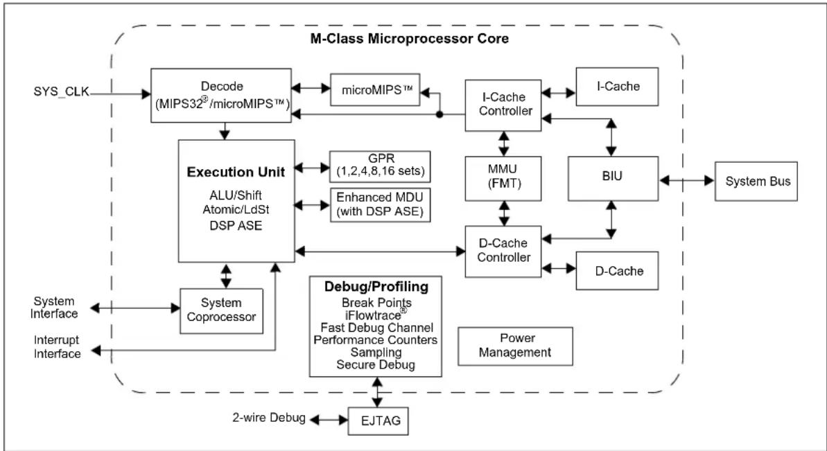
flowchart
graph TD
    A["SYS_CLK"] --> B["Decode (MIPS32®/microMIPS™)"]
    B --> C["Execution Unit ALU/Shift Atomic/LdSt DSP ASE"]
    C --> D["System Coprocessor"]
    D --> E["Debug/Profiling Break Points iFlowtrace® Fast Debug Channel Performance Counters Sampling Secure Debug"]
    E --> F["EJTAG"]
    F --> G["2-wire Debug"]
    G --> H["Power Management"]
    H --> I["D-Cache Controller"]
    I --> J["BIU"]
    J --> K["System Bus"]
    C --> L["GPR (1,2,4,8,16 sets)"]
    C --> M["Enhanced MDU (with DSP ASE)"]
    C --> N["microMIPS™"]
    C --> O["I-Cache Controller"]
    O --> P["I-Cache"]
    P --> Q["BIU"]
    Q --> R["System Bus"]
    style A fill:#f9f,stroke:#333
    style B fill:#ccf,stroke:#333
    style C fill:#cfc,stroke:#333
    style D fill:#fcc,stroke:#333
    style E fill:#cff,stroke:#333
    style F fill:#ffc,stroke:#333
    style G fill:#cfc,stroke:#333
    style H fill:#fcc,stroke:#333
    style I fill:#cfc,stroke:#333
    style J fill:#cfc,stroke:#333
    style K fill:#fcc,stroke:#333
    style L fill:#cfc,stroke:#333
    style M fill:#cfc,stroke:#333
    style N fill:#cfc,stroke:#333
    style O fill:#cfc,stroke:#333
    style P fill:#cfc,stroke:#333
    style Q fill:#cfc,stroke:#333
    style R fill:#fcc,stroke:#333
    style S fill:#fcc,stroke:#333
    style T fill:#fcc,stroke:#333
    style U fill:#fcc,stroke:#333
    style V fill:#fcc,stroke:#333
    style W fill:#fcc,stroke:#333
    style X fill:#fcc,stroke:#333
    style Y fill:#fcc,stroke:#333
    style Z fill:#fcc,stroke:#333
4.1 Architecture Overview
The MIPS32 M-Class Microprocessor Core in PIC32MZ1025W104 contains several logic blocks working together in parallel, providing an efficient high-performance computing engine. The following blocks are included with the core:
- Execution unit
- General Purpose Register (GPR)
- Multiply/Divide Unit (MDU)
- System control coprocessor (CP0)
• Memory Management Unit (MMU) - Instruction/data cache controllers
- Power management
- Instructions and data caches
- microMIPS support
• Enhanced JTAG (EJTAG) controller
4.1.1 EXECUTION UNIT
The processor core execution unit implements a load/store architecture with single-cycle Arithmetic Logic Unit (ALU) operations (logical, shift, add, subtract) and an autonomous multiply/divide unit. The core contains
thirty-two 32-bit GPRs used for integer operations and address calculation. Seven additional register file shadow sets (containing 32 registers) are added to minimize context switching overhead during interrupt/exception processing. The register file consists of two read ports and one write port and is fully bypassed to minimize operation latency in the pipeline.
The execution unit includes:
• 32-bit adder for calculating the data address
- Address unit for calculating the next instruction address
- Logic for branch determination and branch target address calculation
- Load aligner
- Trap condition comparator
- Bypass multiplexers for avoiding stalls when executing instruction streams where data producing instructions are followed closely by results
- Leading zero/one detect unit for implementing the CLZ and CLO instructions
- ALU for performing arithmetic and bitwise logical operations
- Shifter and store aligner
- DSP ALU and logic block for performing DSP instructions, such as arithmetic/shift/compare operations
4.1.2 MULTIPLY/DIVIDE UNIT
The processor core includes an MDU that contains a separate pipeline for multiply and divide operations, and DSP ASE multiply instructions. This pipeline operates in parallel with the Integer Unit (IU) pipeline and does not stall when the IU pipeline stalls. This allows MDU operations to be partially masked by system stalls and/or other integer unit instructions.
The high-performance MDU consists of a 32x32 booth recoded multiplier, four pairs of result/accumulation registers (HI and LO), a divide state machine, and the necessary multiplexers and control logic. The first num-
ber shown ('32' of 32x32) represents the rs operand. The second number ('32' of 32x32) represents the rt operand.
The MDU supports execution of one multiply or multiply-accumulate operation every clock cycle. Divide operations are implemented with a simple 1-bit-per-clock iterative algorithm. An early-in detection checks the sign extension of the dividend (rs) operand. If rs is 8 bits wide, 23 iterations are skipped. For a 16-bit wide rs, 15 iterations are skipped and for a 24-bit wide rs, 7 iterations are skipped. Any attempt to issue a subsequent MDU instruction while a divide is still active causes an IU pipeline stall until the divide operation is completed.
The table below lists the repeat rate (peak issue rate of cycles until the operation can be reissued) and latency (number of cycles until a result is available) for the processor core multiply and divide instructions. The approximate latency and repeat rates are listed in terms of pipeline clocks.
TABLE 4-1: MIPS32 ^ M-CLASS MICROPROCESSOR CORE HIGH-PERFORMANCE INTEGER MDU LATENCIES AND REPEAT RATES
| Opcode | Operand Size (mul rt) (div rs) | Latency | Repeat Rate |
| MULT/MULTU, MADD/MADDU,MSUB/MSUBU (HI/LO destination) | 16 bits 5 1 | ||
| 32 bits 5 1 | |||
| MUL (GPR destination) 16 bits 5 1 | |||
| 32 bits 5 1 | |||
| DIV/DIVU 8 bits | 12/14 | 12/14 | |
| 16 bits 20/22 | 20/22 | ||
| 24 bits 28/30 | 28/30 | ||
| 32 bits 36/38 | 36/38 |
The MIPS architecture defines that the result of a multiply or divide operation be placed in one of four pairs of HI and LO registers. Using the Move-From-HI (MFHI) and Move-From-LO (MFLO) instructions, these values can be transferred to the GPR.
In addition to the HI/LO targeted operations, the MIPS32 architecture also defines a Multiply instruction (MUL), which places the least significant results in the primary register file instead of the HI/LO register pair. By avoiding the explicit MFLO instruction required when using the LO register, and by supporting multiple destination registers, the throughput of multiply-intensive operations is increased.
Two other instructions, Multiply-Add (MADD) and Multiply-Subtract (MSUB), are used to perform the multiply-accumulate and multiply-subtract operations. The MADD instruction multiplies two numbers and then adds the product to the current contents of the HI and LO registers. Similarly, the MSUB instruction multiplies two operands and then subtracts the product from the HI and LO registers. The MADD and MSUB operations are commonly used in DSP algorithms.
The MDU also implements various shift instructions operating on the HI/LO register and multiply instructions as defined in the DSP ASE. The MDU supports all of the data types required for this purpose and includes three extra HI/LO registers as defined by the ASE.
The table below lists the latencies and repeat rates for the DSP multiply and dot-product operations. The approximate latencies and repeat rates are listed in terms of pipeline clocks.
TABLE 4-2: DSP-RELATED LATENCIES AND REPEAT RATES
| Opcode | Latency | Repeat Rate |
| Multiply and dot-product without saturation after accumulation | 5 | 1 |
| Multiply and dot-product with saturation after accumulation | 5 | 1 |
| Multiply without accumulation | 5 | 1 |
4.1.3 SYSTEM CONTROL
COPROCESSOR (CP0)
In the MIPS architecture, CP0 is responsible for the virtual-to-physical address translation and cache protocols, the exception control system, the processor's diagnostics capability, the operating modes (Kernel, User and Debug) and whether interrupts are enabled or
disabled. Configuration information, such as cache size and set associativity, and the presence of options like microMIPS is also available by accessing the CP0 registers, as listed in the table below. Refer to the Series 5 Warrior M-class CPU core resources which are available at: www.imgtec.com for more information.
TABLE 4-3: COPROCESSOR 0 REGISTERS
| Register Number | Register Name | Function | ||
| 0 Index | Index into the TLB array (MPU only). | |||
| 1 Random Randomly generated index into the TLB array (MPU only). | ||||
| 2 Entry | Lo0 Low-order portion of the TLB entry for even-numbered virtual pages (MPU only). | |||
| 3 Entry | Lo1 Low-order portion of the TLB entry for odd-numbered virtual pages (MPU only). | |||
| 4 Context/UserLocal | Pointer to the page table entry in memory (MPU only).User information that can be written by privileged software and read through the RDHWR instruction. | |||
| 5 Page | Mask/PageGrain | PageMask controls the variable page sizes in TLB entries. PageGrain enables support of 1 KB pages in the TLB (MPU only). | ||
| 6 Wired Controls the number of fixed (i.e., wired) TLB entries (MPU only). | ||||
| 7 | HWREna | Enables access through the RDHWR instruction to selected hardware registers in Non-privileged mode. | ||
| 8 Bad | VAddr Reports the address for the most recent address-related exception. | |||
| BadInstr Reports the instruction that caused the most recent exception. | ||||
| BadInstrP Reports the branch instruction if a delay slot caused the most recent exception. | ||||
| 9 Count | Processor cycle count. | |||
| 10 | EntryHi | High-order portion of the TLB entry (MPU only). | ||
| 11 | Compare | Core timer interrupt control. | ||
| 12 | Status | Processor status and control. | ||
| IntCtl | Interrupt control of vector spacing. | |||
| SRSCtl | Shadow register set control. | |||
| SRSMap Shadow register mapping control. | ||||
| View_IPL | Allows the Priority Level to be read/written without extracting or inserting that bit from/to the Status register. | |||
| SRSMAP2 | Contains two 4-bit fields that provide the mapping from a vector number to the shadow set number to use when servicing such an interrupt. | |||
| GuestCtl0 | Control of virtualized Guest OS | |||
| GTOffset | Guest Timer Offset | |||
| 13 | Cause | Describes the cause of the last exception. | ||
| NestedExc | Contains the error and exception level status bit values that existed prior to the current exception. | |||
| View_RIPL | Enables read access to the RIPL bit that is available in the Cause register. | |||
| 14 | EPC | Program counter at last exception. | ||
| NestedEPC | Contains the exception program counter that existed prior to the current exception. | |||
| 15 | PRID | Processor identification and revision | ||
| Ebase | Exception base address of exception vectors. | |||
| CDMMBase | Common device memory map base. | |||
| 16 | Config Configuration register. | |||
| Config1 Configuration register 1. | ||||
| Config2 Configuration register 2. | ||||
| Config3 Configuration register 3. | ||||
| Config4 Configuration register 4. | ||||
| Config5 Configuration register 5. | ||||
| Config7 Configuration register 7. | ||||
| 17 LAddr Load link address (MPU only). | ||||
| 18 WatchLo Low-order watchpoint address (MPU only). | ||||
| 19 WatchHi High-order watchpoint address (MPU only). | ||||
| 20-22 | Reserved Reserved in the PIC32 core. | |||
| 23 Debug EJTAG debug register. | ||||
| TraceControl | EJTAG trace control. | |||
| TraceControl2 | EJTAG trace control 2. | |||
| UserTraceData1 | EJTAG user trace data 1 register. | |||
| TraceBPC EJTAG trace breakpoint register. | ||||
| Debug2 | Debug control/exception status 1. | |||
| 24 DEPC Program counter at last debug exception. | ||||
| UserTraceData2 | EJTAG user trace data 2 register. | |||
| 25 PerfCtl0 Performance counter 0 control. | ||||
| PerfCnt0 | Performance counter 0. | |||
| PerfCtl1 | Performance counter 1 control. | |||
| PerfCnt1 | Performance counter 1. | |||
| 26 | ErrCtl | Software test enable of way-select and data RAM arrays for I-Cache and D-Cache (MPU only). | ||
| 27 | Reserved | Reserved in the PIC32 core. | ||
| 28 | TagLo/DataLo | Low-order portion of cache tag interface (MPU only). | ||
| 29 | Reserved | Reserved in the PIC32 core. | ||
| 30 ErrorEPC Program counter at last error exception. | ||||
| 31 DeSave Debug exception save. | ||||
| KScratchn | Scratch registers for Kernel mode | |||
4.2 Power Management
The processor core offers a number of power management features, including low-power design, active power management and power-down modes of operation. The core is a static design that supports slowing or halting the clocks, which reduces system power consumption during Idle periods.
4.2.1 INSTRUCTION-CONTROLLED POWER MANAGEMENT
The mechanism for invoking Power-Down mode is through execution of the WAIT/SLEEP instruction. For more information on power management, see Section 36.0 "Power-Saving Features".
The majority of the power consumed by the processor core is in the clock tree and clocking registers. The PIC32MZ1025W104 family makes extensive use of local gated-clocks to reduce this dynamic power consumption.
4.3 L1 Instruction and Data Caches
4.3.1 INSTRUCTION CACHE (I-CACHE)
The I-Cache is an on-core memory block of 16 Kbytes. As the I-Cache is virtually indexed, the virtual-to-physical address translation occurs in parallel with the cache access rather than having to wait for the physical address translation. The tag holds 22 bits of physical address, a valid bit, and a lock bit. The Least Recently Used (LRU) replacement bits are stored in a separate array.
The I-Cache block also contains and manages the instruction line fill buffer. Besides accumulating data to be written to the cache, instruction fetches that reference data in the line fill buffer are serviced either by a bypass of that data, or data coming from the external interface. The I-Cache control logic controls the bypass function.
The processor core supports I-Cache locking. Cache locking allows critical code or data segments to be locked into the cache on a per-line basis, enabling the system programmer to maximize the efficiency of the system cache.
The cache locking function is always available on all I-Cache entries. Entries can then be marked as locked or unlocked on a per entry basis using the CACHE instruction.
4.3.2 DATA CACHE (D-CACHE)
The D-Cache is an on-core memory block of 16 Kbytes. This virtually indexed, physically tagged cache is protected. As the D-Cache is virtually indexed, the virtual-to-physical address translation occurs in parallel with the cache access. The tag holds 22 bits of physical address, a valid bit, and a lock bit. There is an additional array holding dirty bits and LRU replacement algorithm bits for each set of the cache.
In addition to I-Cache locking, the processor core also supports a D-Cache locking mechanism identical to the I-Cache. Critical data segments are locked into the cache on a per-line basis. The locked contents can be updated on a store hit, but cannot be selected for replacement on a cache miss.
The D-Cache locking function is always available on all D-Cache entries. Entries can then be marked as locked or unlocked on a per-entry basis using the CACHE instruction.
4.3.3 ATTRIBUTES
The processor core I-Cache and D-Cache attributes are listed in the Configuration registers (see Register 4-1 through Register 4-4).
4.4 EJTAG Debug Support
The processor core provides for an Enhanced JTAG (EJTAG) interface for use in the software debug of application and kernel code. In addition to standard User mode and Kernel modes of operation, the processor core provides a Debug mode that is entered after a debug exception (derived from a hardware breakpoint, single-step exception, and so on) is taken and continues until a Debug Exception Return (DERET) instruction is executed. During this time, the processor executes the debug exception handler routine.
The EJTAG interface operates through the Test Access Port (TAP), a serial communication port used for transferring test data in and out of the core. In addition to the standard JTAG instructions, special instructions defined in the EJTAG specification specify which registers are selected and how they are used.
4.5 MIPS DSP ASE Extension
The MIPS DSP ASE Revision 2 is an extension to the MIPS32 architecture. This extension comprises new integer instructions and states that include new HI/LO accumulator register pairs and a DSP control register. This extension is crucial in a wide range of DSP, multimedia, and DSP-like algorithms covering audio and video processing applications. The extension supports native fractional format data type operations, register SIMD operations, such as add, subtract, multiply, and shift. In addition, the extension includes the following features that are essential in making DSP algorithms computationally efficient:
- Support for multiplication of complex operands
- Variable bit insertion and extraction
- Implementation and use of virtual circular buffers
- Arithmetic saturation and overflow handling support
- Zero cycle overhead saturation and rounding operations
4.6 microMIPS ISA
The processor core supports the microMIPS ISA, which contains all MIPS32 ISA instructions (except for branch-likely instructions) in a new 32-bit encoding scheme, with some of the commonly used instructions also available in 16-bit encoded format. This ISA improves code density through the additional 16-bit instructions while maintaining a performance similar to MIPS32 mode. In microMIPS mode, 16-bit or 32-bit instructions will be fetched and recoded to legacy MIPS32 instruction opcodes in the pipeline's I stage, so that the processor core can have the same microAptiv UP microarchitecture. The microMIPS instruction stream can be intermixed with 16-bit halfword or 32-bit word size instructions on halfword or word boundaries, additional logic is in place to address the word misalignment issues, thus minimizing performance loss.
4.7 M-Class Core Configuration
Register 4-1 through Register 4-4 show the default configuration of the M-Class core, which is included on the PIC32MZ1025W104.
REGISTER 4-1: CONFIG: CONFIGURATION REGISTER; CP0 REGISTER 16, SELECT 0
| Bit Range | Bit 31/23/15/7 | Bit 30/22/14/6 | Bit 29/21/13/5 | Bit 28/20/12/4 | Bit 27/19/11/3 | Bit 26/18/10/2 | Bit 25/17/9/1 | Bit 24/16/8/0 |
| 31:24 | R-1 U- | 0 | U-0 U-0 | U-0 U-0 U-0 R- | 0 | |||
| — — — | — — — | ISP | ||||||
| 23:16 | R-0 | R-0 | R-1 | R-0 U-0 R- | 1 | R-0 | R-0 | |
| DSP | UDI | SB | MDU | — | MM[1:0] | BM | ||
| 15:8 | R-0 | R-0 | R-0 R-0 | R-0 R- | 1 | R-0 R- | 0 | |
| BE | AT[1:0] | AR[2:0] | MT[2:1] | |||||
| 7:0 | R-1 | U-0 | U-0 U-0 | U-0 | R/W- | 0 | R/W-1 | R/W-0 |
| MT[0] | — — — | — | K0[2] | :0] | ||||
| Legend: | r = Reserved bit | ||
| R = Readable bit | W = Writable bit | U = Unimplemented bit, read as ‘0’ | |
| -n = Value at POR | ‘1’ = Bit is set | ‘0’ = Bit is cleared | x = Bit is unknown |
bit 31 Reserved: This bit is hardwired to '1' to indicate the presence of the Config1 register.
bit 30-25 Unimplemented: Read as '0'.
bit 24 ISP: Instruction Scratch Pad RAM bit 0 = Instruction scratch pad RAM is not implemented
bit 23 DSP: Data Scratch Pad RAM bit 0 = Data scratch pad RAM is not implemented
bit 22 UDI: User-defined bit 0 = CorExtend user-defined instructions are not implemented
bit 21 SB: SimpleBE bit 1 = Only simple byte enables are allowed on the internal bus interface
bit 20 MDU: Multiply/Divide Unit bit 0 = Fast, high-performance MDU 1 = Iterative, area-efficient MDU
bit 19 Unimplemented: Read as '0'
bit 18-17 MM[1:0]: Merge Mode bits 10 = Merging is allowed x1 = Reserved
bit 16 BM: Burst Mode bit 0 = Burst order is sequential
bit 15 BE: Endian Mode bit 0 = Little-endian
bit 14-13 AT[1:0]: Architecture Type bits 00 = MIPS32
bit 12-10 AR[2:0]: Architecture Revision Level bits 001 = MIPS32 release 2
bit 9-7 MT[2:0]: MMU Type bits 011 = Fixed Mapping
bit 6-3 Unimplemented: Read as '0'
REGISTER 4-1: CONFIG: CONFIGURATION REGISTER; CP0 REGISTER 16, SELECT 0
bit 2-0 K0[2:0]: Kseg0 Coherency Algorithm bits
011 = Cacheable, non-coherent, write-back, write allocate
010 = Uncached
001 = Cacheable, non-coherent, write-through, write allocate
000 = Cacheable, non-coherent, write-through, no write allocate
All other values are not used and mapped to other values. 100, 101, and 110 are mapped to 010. 111 is mapped to 010.
REGISTER 4-2: CONFIG1L: CONFIGURATION REGISTER 1
| Bit Range | Bit 31/23/15/7 | Bit 30/22/14/6 | Bit 29/21/13/5 | Bit 28/20/12/4 | Bit 27/19/11/3 | Bit 26/18/10/2 | Bit 25/17/9/1 | Bit 24/16/8/0 |
| 31:24 | R-1 R-0 R-0 R-0 R-0 R-0 | R-0 R-0 | ||||||
| — — — — — — — — | I | S | [ 2 ] | |||||
| 23:16 | R-1 R-0 R-0 R-1 R-1 R-0 | R-1 R-1 | ||||||
| IS[1:0] IL[2:0] | IA[2:0] | |||||||
| 15:8 | R-0 R-0 R-0 R-0 R-1 R-1 | R-0 R-1 | ||||||
| DS[2:0] | DL[2:0] | DA[2:0] | ||||||
| 7:0 | R-1 U-0 U-0 R-1 R-1 R-0 | R-1 R-0 | ||||||
| FCPRI | — | — | PC | WR | CA | EP | FP | |
| Legend: | r = Reserved bit | |
| R = Readable bit | W = Writable bit | U = Unimplemented bit, read as ‘0’ |
| -n = Value at POR | ‘1’ = Bit is set | ‘0’ = Bit is cleared x = Bit is unknown |
bit 31 Reserved: This bit is hardwired to a '1' to indicate the presence of the Config2 register.
bit 30-25 Unimplemented: Read as '0'
bit 24-22 IS[2:0]: Instruction Cache Sets bits
0x2: 256
0x5 - 0x7: Reserved
bit 21-19 IL[2:0]: Instruction-Cache Line bits
000 = No I-Cache present
011 = Contains instruction cache line size of 16 bytes
0x1, 0x2, 0x4 - 0x7: Reserved
bit 18-16 IA[2:0: Instruction-Cache Associativity bits
0x00 - 0x02: Reserved
0x3: 4-way
0x4 - 0x7: Reserved
bit 15-13 DS[2:0]: Data-Cache Sets bits
0x2: 256
0x5 - 0x7: Reserved
bit 12-10 DL[2:0]: Data-Cache Line bits
0x0: No D-Cache present
0x3: 16 bytes
0x1, 0x2, 0x4 - 0x7: Reserved
bit 9-7 DA[2:0]: Data-Cache Associativity bits
0x00 - 0x02: Reserved
0x3: 4-way
0x4 - 0x7: Reserved
bit 6-5 Unimplemented: Read as '0'
bit 4 PC: Performance Counter bit
1 = The processor core contains performance counters
bit 3 WR: Watch Register Presence bit
1 = No Watch registers are present
bit 2 CA: Code Compression Implemented bit
0 = No MIPS16e® present
bit 1 EP: EJTAG Present bit
1 = Core implements EJTAG
bit 0 FP: Floating Point Unit bit
0 = No FPU
REGISTER 4-3: CONFIG3: CONFIGURATION REGISTER 3; CP0 REGISTER 16, SELECT 3
| Bit Range | Bit 31/23/15/7 | Bit 30/22/14/6 | Bit 29/21/13/5 | Bit 28/20/12/4 | Bit 27/19/11/3 | Bit 26/18/10/2 | Bit 25/17/9/1 | Bit 24/16/8/0 |
| 31:24 | R-1 U-0 | U-0 U-0 U-0 U-0 | U-0 U-0 | |||||
| — — — | — — — — — | |||||||
| 23:16 | U-0 R-0 | R-1 R-0 R-0 R-0 | R-1 R/W-y | |||||
| — | IPLW[1:0] | MMAR[2:0] | MCU | ISAONEXC(1) | ||||
| 15:8 | R-y | R-y R-1 | R-1 R-1 R-1 U-0 | R-1 | ||||
| ISA[1:0]^(1) | ULRI | RXI | DSP2P | DSPP | — | ITL | ||
| 7:0 | R-0 R-1 | R-1 U-0 R-1 U-0 | U-0 R-1 | |||||
| LPA | VEIC | VINT | — | CDMM | — | — | TL | |
| Legend: | r = Reserved bit | y = Value set from Configuration bits on POR |
| R = Readable bit | W = Writable bit | U = Unimplemented bit, read as ‘0’ |
| -n = Value at POR | ‘1’ = Bit is set | ‘0’ = Bit is cleared x = Bit is unknown |
bit 31 Reserved: This bit is hardwired as '1' to indicate the presence of the Config4 register.
bit 30-23 Unimplemented: Read as '0'
bit 22-21 IPLW[1:0]: Width of the Status IPL and Cause RIPL bits
01 = IPL and RIPL bits are 8-bits in width
Others = Reserved
bit 20-18 MMAR[2:0]: microMIPS Architecture Revision Level bits
000 = Release 1
Others = Reserved
bit 17 MCU: MIPS® MCU™ ASE Implemented bit
0 = MCU ASE is not implemented
1 = MCU ASE is implemented
bit 16 ISAONEXC: ISA on Exception bit ^(1)
1 = microMIPS is used on entrance to an exception vector
0 = MIPS32 ISA is used on entrance to an exception vector
bit 15-14 ISA[1:0]: Instruction Set Availability bits ^(1)
00 = Only MIPS32 is implemented
01 = Only microMIPS is implemented
11 = Both MIPS32 and microMIPS are implemented; microMIPS is used when coming out of Reset
10 = Both MIPS32 and microMIPS are implemented; MIPS32 ISA used when coming out of Reset
bit 13 ULRI: UserLocal Register Implemented bit
1 = UserLocal Coprocessor 0 register is implemented
bit 12 RXI: RIE and XIE Implemented in PageGrain bit
0 = RIE and XIE bits are not implemented
1 = RIE and XIE bits are implemented
bit 11 DSP2P: MIPS DSP ASE Revision 2 Presence bit
1 = DSP revision 2 is present
bit 10 DSPP: MIPS DSP ASE Presence bit
1 = DSP is present
bit 9 Unimplemented: Read as '0'
bit 8 ITL: Indicates that iFlowtrace® hardware is present
1 = iFlowtrace® is implemented in the core
bit 7 LPA: Denotes the presence of support for large physical addresses on MIPS64 processors. Not used by MIPS32 processors and returns zero on read.
0 = Large physical address support is not implemented
Note 1: These bits are set based on the value of the BOOTISA Configuration bit (BCFG0[3]).
REGISTER 4-3: CONFIG3: CONFIGURATION REGISTER 3; CP0 REGISTER 16, SELECT 3 (CONTINUED)
bit 6 VEIC: External Vector Interrupt Controller bit
1 = Support for an external interrupt controller is implemented
bit 5 VINT: Vector Interrupt bit
1 = Vector interrupts are implemented
bit 4 Unimplemented: Read as '0'
bit 3 CDMM: Common Device Memory Map bit
0 = CDMM is not implemented
1 = CDMM is implemented
bit 2-1 Unimplemented: Read as '0'
bit 0 TL: Trace Logic bit
1 = Trace logic is implemented
Note 1: These bits are set based on the value of the BOOTISA Configuration bit (BCFG0[3]).
REGISTER 4-4: CONFIG5: CONFIGURATION REGISTER 5; CP0 REGISTER 16, SELECT 5
Legend: r = Reserved
| R = Readable bit | W = Writable bit | U = Unimplemented bit, read as '0' |
| -n = Value at POR | ‘1’ = Bit is set | ‘0’ = Bit is cleared x = Bit is unknown |
bit 31 M: This bit is reserved to indicate that a Config5 register is present. With the current architectural definition, this bit must always read as a '0'.
bit 30-1 Unimplemented: Read as '0'
bit 0 NF: Nested Fault bit
1 = Nested Fault feature is implemented
REGISTER 4-5: CONFIG7: CONFIGURATION REGISTER 7; CP0 REGISTER 16, SELECT 7
| R = Readable bit | W = Writable bit | U = Unimplemented bit, read as '0' |
| -n = Value at POR | ‘1’ = Bit is set | ‘0’ = Bit is cleared x = Bit is unknown |
bit 31 WII: Wait IE Ignore bit
1 = Indicates that this processor will allow an interrupt to unblock a WAIT instruction
bit 30-0 Unimplemented: Read as '0'
5.0 FLASH PROGRAM MEMORY
| Note: This data sheet summarizes the features of the PIC32MZ1025W104 family of devices. It is not intended to be a comprehensive reference source. To complement the information in this data sheet, refer to Section 5. “Flash Programming” (DS60001640) in the “PIC32MZ W1 Family Reference Manual”, which is available from the Microchip website (www.microchip.com/PIC32). |
The PIC32MZ1025W104 device contains an internal Flash program memory for executing user code, which includes the following features:
- Write protection for program and boot Flash
- Error-correction code (ECC) support
• Supports chip and page erase
• Supports Single Word, Quad Word and row program options - Flash page size is 4 Kbytes (1K Instruction Word (IW))
- Row size is 1 KB (256 IW)
The user can program this memory using the following methods:
• Run-Time Self-Programming (RTSP)
• Enhanced JTAG (EJTAG) programming
• In-Circuit Serial Programming (ICSP)
RTSP is performed by software, executing from either Flash or RAM memory. Information about RTSP techniques is available in Section 5. "Flash Programming" (DS60001640) in the "PIC32MZ W1 Family Reference Manual".
EJTAG is performed using the EJTAG port of the device and an EJTAG capable programmer.
ICSP is performed using a serial data connection to the device and allows much faster programming times than RTSP.
The EJTAG and ICSP methods are described in the "PIC32 Flash Programming Specification" (DS60001145), which is available for download from the Microchip website (www.microchip.com).
5.1 Flash Control Registers
TABLE 5-1: FLASH CONTROLLER REGISTER MAP
| Virtual Address(BF50_#) | Register Name | Bit Range | Bits | All Resets | |||||||||||||||
| 31/15 30/14 | 29/13 28/1 | 27/11 26 | 10 25/9 24 | 8 23/7 22/6 | 21/5 20/4 19 | 73 18/2 17/1 | 16/0 | ||||||||||||
| 600 | NVMCON (1) | 31:16 | — | — | — | — | — | — | — | — | — | — | — | — | — | — | — | — | 0000 |
| 15:00 | WR | WREN | WRERR | LVDERR | — | — | — | HTDPGM | — | — | — | — | NVMOP[3:0] | 50x0 | |||||
| 610 | NVMCON2 | 31:16 | ERS[3:0] | — | — | — | SLEEP | — | — | — | WS[4:0] | 011x | |||||||
| 15:00 | — | TEMP | CREAD1 | VREAD1 | — | — | RETRY[1:0] | — | — | — | — | — | — | — | — | x000 | |||
| 620 | NVMKEY | 31:16 | NVMKEY[31:0] | 0000 | |||||||||||||||
| 15:00 | 0000 | ||||||||||||||||||
| 630 | NVMADDR(1) | 31:16 | NVMADDR[31:0] | 0000 | |||||||||||||||
| 15:00 | 0000 | ||||||||||||||||||
| 640 | NVMDATA0 | 31:16 | NVMDATA0[31:0] | 0000 | |||||||||||||||
| 15:00 | 0000 | ||||||||||||||||||
| 650 | NVMDATA1 | 31:16 | NVMDATA1[31:0] | 0000 | |||||||||||||||
| 15:00 | 0000 | ||||||||||||||||||
| 660 | NVMDATA2 | 31:16 | NVMDATA2[31:0] | 0000 | |||||||||||||||
| 15:00 | 0000 | ||||||||||||||||||
| 670 | NVMDATA3 | 31:16 | NVMDATA3[31:0] | 0000 | |||||||||||||||
| 15:00 | 0000 | ||||||||||||||||||
| 680 | NVMDATA4 | 31:16 | NVMDATA4[31:0] | 0000 | |||||||||||||||
| 15:00 | 0000 | ||||||||||||||||||
| 690 | NVMDATA5 | 31:16 | NVMDATA5[31:0] | 0000 | |||||||||||||||
| 15:00 | 0000 | ||||||||||||||||||
| 6A0 | NVMDATA6 | 31:16 | NVMDATA6[31:0] | 0000 | |||||||||||||||
| 15:00 | 0000 | ||||||||||||||||||
| 6B0 | NVMDATA7 | 31:16 | NVMDATA7[31:0] | 0000 | |||||||||||||||
| 15:00 | 0000 | ||||||||||||||||||
| 6C0 | NVMSRC ADDR | 31:16 | NVMSRCADDR[31:0] | 0000 | |||||||||||||||
| 15:00 | 0000 | ||||||||||||||||||
| 6D0 | NVMPWPLT | 31:16 | ULOCK | — | — | — | — | — | — | — | — | PWPLT[23:16] | 8000 | ||||||
| 15:00 | PWPLT[15:0] | 0000 | |||||||||||||||||
| 6E0 | NVMPWPGTE | 31:16 | ULOCK | — | — | — | — | — | — | — | — | PGTE[23:16] | 80FF | ||||||
| 15:00 | PGTE[15:0] | F22F | |||||||||||||||||
| 6F0 | NVMLBWP(1) | 31:16 | ULOCK | — | — | — | — | — | — | LBWP23 | LBWP22 | LBWP21 | LBWP20 | LBWP19 | LBWP18 | LBWP17 | LBWP16 | 80FF | |
| 15:00 | LBWP15 | LBWP14 | LBWP13 | LBWP12 | LBWP11 | LBWP10 | LBWP9 | LBWP8 | LBWP7 | LBWP6 | LBWP5 | LBWP4 | LBWP3 | LBWP2 | LBWP1 | F22F | |||
| 700 | NVMUBWP(1) | 31:16 | ULOCK | — | — | — | — | — | — | UBWP23 | UBWP22 | LBWP21 | UBWP20 | UBWP19 | UBWP18 | UBWP17 | UBWP16 | 80FF | |
| 15:00 | UBWP15 | UBWP14 | UBWP13 | UBWP12 | UBWP11 | UBWP10 | UBWP9 | UBWP8 | UBWP7 | UBWP6 | UBWP5 | UBWP4 | UBWP3 | UBWP2 | UBWP1 | F22F | |||
Legend: x = unknown value on Reset; — = unimplemented, read as '0'. Reset values are shown in hexadecimal.
Note 1: This register has corresponding CLR, SET and INV registers at their virtual addresses, plus offsets of 0x4, 0x8 and 0xC, respectively. See Section 13.3 "CLR, SET and INV Registers" for more information.
REGISTER 5-1: NVMCON: PROGRAMMING CONTROL REGISTER
| Bit Range | Bit 31/23/15/7 | Bit 30/22/14/6 | Bit 29/21/13/5 | Bit 28/20/12/4 | Bit 27/19/11/3 | Bit 26/18/10/2 | Bit 25/17/9/1 | Bit 24/16/8/0 |
| 31:24 | U-0 U-0 | U-0 U-0 U-0 U-0 | U-0 U-0 | |||||
| — — — | — — — | — — | ||||||
| 23:16 | U-0 U-0 | U-0 U-0 U-0 U-0 | U-0 U-0 | |||||
| — — — | — — — | — — | ||||||
| 15:8 | R/HS/HC-0 | R/W-0 | R/HS/HC-0 | R/HS/HC-0 | U-0 | U-0 | U-0 | R/HS/HC-0 |
| WR(1) | WREN(1) | WRERR(1) | LVDERR(1) | — | — | — | HTDPGM | |
| 7:0 | U-0 U-0 | U-0 U-0 R/W-0 | R/W-0 | R/W-0 | R/W-0 | |||
| — — — | — | NVMOP[3:0] | ||||||
| Legend: | HC = Hardware Set HC = Hardware Cleared | ||
| R = Readable bit | W = Writable bit | U = Unimplemented bit, read as ‘0’ | |
| -n = Value at POR | ‘1’ = Bit is set | ‘0’ = Bit is cleared | x = Bit is unknown |
bit 31-16 Unimplemented: Read as '0'
bit 15 WR: Write Control Bit ^(1)
1 = Initiate a Flash operation. Hardware clears this bit when the operation completes.
0 = Flash operation complete or inactive.
Note: This field can only be modified when WREN = 1, TEMP = 1, and the NVMKEY unlock sequence is satisfied.
bit 14 WREN: Write Enable Bit ^(1)
1 = Enables writes to WR
0 = Disables writes to WR
bit 13 WRERR: Write Error Bit ^(1)
1 = Program or erase sequence does not complete successfully
0 = Program or erase sequence completed normally
Note: Cleared by setting NVMOP == 0000b and initiating a Flash operation (WR).
bit 12 LVDERR: Low-voltage Detect Error Bit ^(1)
The error is only captured for programming/erase operations (when WR = 1).
1 = Low-voltage is detected (possible data corruption if WRERR is set)
0 = Normal voltage is detected
Note: Cleared by setting NVMOP == 0000b and initiating a Flash operation (WR).
bit 11-9 Unimplemented: Read as '0'
bit 8 HTDPGM: High Temperature Detected during Program/Erase Operation bit
This status is only captured for programming/erase operations (when WR = 1).
1 = High temperature is detected (possible data corruption, verify operation)
0 = High temperature is not detected
Note: Cleared by setting NVMOP == 0000b and initiating a Flash operation (WR)
bit 7-4 Unimplemented: Read as '0'
Note 1: These bits are only reset by a POR and are not affected by other Reset sources.
2: This operation results in a No Operation (NOP) when the Dynamic Flash ECC Configuration bits = 00 (FECCCON[1:0] (CFGCON0[299:28])), which enables ECC at all times. For all other FECCCON[1:0] bit settings, this command will execute, but will not write the ECC bits for the Word and can cause DED errors if dynamic Flash ECC is enabled (FECCCON[1:0] = 01).
REGISTER 5-1: NVMCON: PROGRAMMING CONTROL REGISTER (CONTINUED)
bit 3-0 NVMOP[3:0]: NVM Operation bits
These bits are only writable when WREN = 0.
1111 = Reserved
.
.
.
1000 = Reserved
0111 = Program erase operation: erase all of program Flash memory (all pages must be unprotected)
0110 = Upper program Flash memory erase operation: erases only the upper mapped region of program Flash (all pages in that region must be unprotected)
0101 = Lower program Flash memory erase operation: erases only the lower mapped region of program Flash (all pages in that region must be unprotected)
0100 = Page erase operation: erases page selected by NVMADDR, if it is not write-protected
0011 = Row program operation: programs row selected by NVMADDR, if it is not write-protected
0010 = Quad Word (256-bit) program operation: programs the 256-bit Flash Word selected by NVMADDR, if it is not write-protected 0001 = Word program operation: programs Word selected by NVMADDR, if it is not write-protected ^(2) 0000 = No operation
Note 1: These bits are only reset by a POR and are not affected by other Reset sources.
2: This operation results in a No Operation (NOP) when the Dynamic Flash ECC Configuration bits = 00 (FECCCON[1:0] (CFGCON0[299:28])), which enables ECC at all times. For all other FECCCON[1:0] bit settings, this command will execute, but will not write the ECC bits for the Word and can cause DED errors if dynamic Flash ECC is enabled (FECCCON[1:0] = 01).
REGISTER 5-2: NVMCON2: PROGRAMMING CONTROL2 REGISTER
| Bit Range | Bit 31/23/15/7 | Bit 30/22/14/6 | Bit 29/21/13/5 | Bit 28/20/12/4 | Bit 27/19/11/3 | Bit 26/18/10/2 | Bit 25/17/9/1 | Bit 24/16/8/0 |
| 31:24 | R/W-0 R/W-0 R/W-0 R/W-0 U-0 U-0 U-0 R/W-1 | |||||||
| ERS[3:0] | — — — SLEEP | |||||||
| 23:16 | U-0 | U-0 | U-0 | R/W-1 | R/W-1 | R/W-1 | R/W-1 | R/W-1 |
| — | — | — | WS[4:0] | |||||
| 15:8 | U-0 | R/W-cfg | R/W-0 | R/W-0 | U-0 | U-0 | R/W-0 | R/W-0 |
| — | TEMP | CREAD1 | VREAD1 | — | — | RETRY[1:0] | ||
| 7:0 | U-0 U-0 | U-0 | U-0 | U-0 U-0 U-0 | U-0 | |||
| — | — | — | — | — | — | — | — | |
| Legend: | HC = Hardware Set HC = Hardware Cleared | ||
| R = Readable bit | W = Writable bit U = Unimplemented bit, read as ‘0’ | ||
| -n = Value at POR | ‘1’ = Bit is set | ‘0’ = Bit is cleared | x = Bit is unknown |
bit 31-28 ERS[3:0]: Erase Retry State
These bits are used by software to track the software state of the erase retry procedure in the event of a system Reset (MCLR) or brown out Reset event.
bit 27-25 Unimplemented: Read as '0'
bit 24 SLEEP: Power Down in Sleep bit
1 = Configures Flash for power down when the system is in Sleep mode
0 = Configures Flash for standby when the system is in Sleep mode
Note: This field can only be modified when the NVMKEY unlock sequence is satisfied.
bit 23-21 Unimplemented: Read as '0'
bit 20-16 WS[4:0]: Flash Access Wait State Control for VREAD1 = 1
11111 = 31 wait states (32 total system clocks)
11110 = 30 wait states (31 total system clocks)
+ + +
00010 = 2 wait states (3 total system clocks)
00001 = 1 wait state (2 total system clocks)
00000 = 0 wait state (1 total system clock)
Note 1: When VREAD1 = 1, WS[] only affects the panel containing NVMADDR[].
2: This field can only be modified when the NVMKEY unlock sequence is satisfied.
bit 15 Unimplemented: Read as '0'
bit 14 TEMP: Operating Temperature Control bit
1 = Configures Flash for standard temperature, low latency reads
0 = Configures Flash for high temperature, high latency reads
Note 1: When TEMP = 0, all NVMOP Operations are disabled because NVMWR cannot be written to '1'.
2: When TEMP = 0, firmware must adjust Flash wait state control at the system level.
3: This field can only be modified when NVMCON.WR == 0 and the NVMKEY unlock sequence is satisfied.
bit 13 CREAD1: Compare Read of Logic 1 bit
Compare read 1 causes all bits in a Flash Word (including ECC if it exists) to be evaluated during the read. If all bits are 1, the lowest Word in the Flash Word evaluates to 0x0000_0001, all other Words are 0x0001_0000. If any bit is 0, the read evaluates to 0x0000_0000 for all Words in the Flash Word.
1 = Compare read enabled, only if VREAD1 = 1
0 = Compare read disabled
Note 1: When using erase retry in an ECC Flash system, CREAD1 = 1 must be used.
2: This field can only be modified when the NVMKEY unlock sequence is satisfied.
REGISTER 5-2: NVMCON2: PROGRAMMING CONTROL2 REGISTER (CONTINUED)
bit 12 VREAD1: Verify Read of Logic 1 Control bit
1 = Selects erase retry procedure with verify read
0 = Selects single erase without verify read
Note 1: When VREAD1 = 1, Flash wait state control is from WS[] for the panel containing NVMADDR[].
2: Using erase retry and verify read procedure increase life of Flash panel(s).
3: This field can only be modified when NVMCON.WR == 0 and the NVMKEY unlock sequence is satisfied.
bit 11 Unimplemented: Read as '0'
bit 10 Unimplemented: Read as '0'
bit 9-8 RETRY[1:0]: Erase Retry Control bit, only used when VREAD1 = 1
11 = Erase strength for last retry cycle
10 = Erase strength for third retry cycle
01 = Erase strength for second retry cycle
00 = Erase strength for first retry cycle
Note: This field can only be modified when NVMCON.WR == 0.
bit 7-0 Unimplemented: Read as '0'
REGISTER 5-3: NVMKEY: PROGRAMMING UNLOCK REGISTER
| Bit Range | Bit 31/23/15/7 | Bit 30/22/14/6 | Bit 29/21/13/5 | Bit 28/20/12/4 | Bit 27/19/11/3 | Bit 26/18/10/2 | Bit 25/17/9/1 | Bit 24/16/8/0 |
| 31:24 | W-0 W-0 | W-0 W-0 W-0 | W-0 W-0 W-0 | |||||
| NVMKEY[31:24] | ||||||||
| 23:16 | W-0 W-0 | W-0 W-0 W-0 | W-0 W-0 W-0 | |||||
| NVMKEY[23:16] | ||||||||
| 15:8 | W-0 W-0 | W-0 W-0 W-0 | W-0 W-0 W-0 | |||||
| NVMKEY[15:8] | ||||||||
| 7:0 | W-0 W-0 | W-0 W-0 W-0 | W-0 W-0 W-0 | |||||
| NVMKEY[7:0] | ||||||||
Legend:
R = Readable bit W = Writable bit U = Unimplemented bit, read as '0' -n = Value at POR '1' = Bit is set '0' = Bit is cleared x = Bit is unknown
bit 31-0 NVMKEY[31:0]: Unlock Register bits
These bits are write only and read '0' on any read.
Note: This register is used as part of the unlock sequence to prevent inadvertent writes to the program Flash.
REGISTER 5-4: NVMADDR: FLASH ADDRESS REGISTER
| Bit Range | Bit 31/23/15/7 | Bit 30/22/14/6 | Bit 29/21/13/5 | Bit 28/20/12/4 | Bit 27/19/11/3 | Bit 26/18/10/2 | Bit 25/17/9/1 | Bit 24/16/8/0 |
| 31:24 | R/W-0 R/W | -0 R/W-0 R/W | -0 R/W-0 R/W-0 | R/W-0 R/W-0 | ||||
| NVMADDR[31:24] | ||||||||
| 23:16 | R/W-0 R/W | -0 R/W-0 R/W | -0 R/W-0 R/W-0 | R/W-0 R/W-0 | ||||
| NVMADDR[23:16] | ||||||||
| 15:8 | R/W-0 R/W | -0 R/W-0 R/W | -0 R/W-0 R/W-0 | R/W-0 R/W-0 | ||||
| NVMADDR[15:8] | ||||||||
| 7:0 | R/W-0 R/W | -0 R/W-0 R/W | -0 R/W-0 R/W-0 | R/W-0 R/W-0 | ||||
| NVMADDR[7:0] | ||||||||
Legend:
R = Readable bit W = Writable bit U = Unimplemented bit, read as '0' -n = Value at POR '1' = Bit is set '0' = Bit is cleared x = Bit is unknown
bit 31-0 NVMADDR[31:0]: Flash (Word) Address bits
| NVMOP[3:0] Selection | Flash Address Bits (NVMADDR[31:0]) |
| Page erase | Address identifies the page to erase. |
| Row program | Address identifies the row to program. |
| Double Word program Address | identifies the 64-bit DWord to program.NVMADDR[2:0] bits are ignored. |
| Quad Double Word program | Address identifies the 256-bit Quad DWord to program. NVMADDR[4:0] bits are ignored. |
Note 1: Hardware prevents writing to this register when NVMCON.WR = 1.
2: For all other NVMOP[3:0] bit settings, the Flash address is ignored. See the NVMCON register (Register 5-1) for additional information on these bits.
3: The bits in this register are only reset by a POR and are not affected by other Reset sources.
REGISTER 5-5: NVMDATAx: FLASH PROGRAM DATA REGISTER (x = 0-7)
| Bit Range | Bit 31/23/15/7 | Bit 30/22/14/6 | Bit 29/21/13/5 | Bit 28/20/12/4 | Bit 27/19/11/3 | Bit 26/18/10/2 | Bit 25/17/9/1 | Bit 24/16/8/0 |
| 31:24 | R/W-0 R/W | -0 R/W-0 R/W | -0 R/W-0 R/W-0 | R/W-0 R/W-0 | ||||
| NVMDATA[31:24] | ||||||||
| 23:16 | R/W-0 R/W | -0 R/W-0 R/W | -0 R/W-0 R/W-0 | R/W-0 R/W-0 | ||||
| NVMDATA[23:16] | ||||||||
| 15:8 | R/W-0 R/W | -0 R/W-0 R/W | -0 R/W-0 R/W-0 | R/W-0 R/W-0 | ||||
| NVMDATA[15:8] | ||||||||
| 7:0 | R/W-0 R/W | -0 R/W-0 R/W | -0 R/W-0 R/W-0 | R/W-0 R/W-0 | ||||
| NVMDATA[7:0] | ||||||||
Legend:
R = Readable bit W = Writable bit U = Unimplemented bit, read as '0'
-n = Value at POR '1' = Bit is set '0' = Bit is cleared x = Bit is unknown
bit 31-0 NVMDATAx[31:0]: Flash Programming Data bits
The value in this register is written to Flash when a program operation is commanded.
Single Double Word program (64-bit)
Writes NVMDATA1:NVMDATA0 to the target Flash address defined in NVMADDR.
Quad Double Word program (256-bit)
Writes NVMDATA7:NVMDATA6:NVMDATA5:NVMDATA4:NVMDATA3:NVMDATA2:NVMDATA1:NVMDATA0 to the target Flash address defined in NVMADDR. NVMDATA0 contains the Least Significant Instruction Word.
Note: Hardware prevents writing to this register when NVMCON.WR = 1.
REGISTER 5-6: NVMSRCADDR: SOURCE DATA ADDRESS REGISTER
| Bit Range | Bit 31/23/15/7 | Bit 30/22/14/6 | Bit 29/21/13/5 | Bit 28/20/12/4 | Bit 27/19/11/3 | Bit 26/18/10/2 | Bit 25/17/9/1 | Bit 24/16/8/0 |
| 31:24 | R/W-0 R/W | -0 R/W-0 R/W | -0 R/W-0 R/W-0 | R/W-0 R/W-0 | ||||
| NVMSRCADDR[31:24] | ||||||||
| 23:16 | R/W-0 R/W | -0 R/W-0 R/W | -0 R/W-0 R/W-0 | R/W-0 R/W-0 | ||||
| NVMSRCADDR[23:16] | ||||||||
| 15:8 | R/W-0 R/W | -0 R/W-0 R/W | -0 R/W-0 R/W-0 | R/W-0 R/W-0 | ||||
| NVMSRCADDR[15:8] | ||||||||
| 7:0 | R/W-0 R/W | -0 R/W-0 R/W | -0 R/W-0 R/W-0 | R/W-0 R/W-0 | ||||
| NVMSRCADDR[7:0] | ||||||||
Legend:
R = Readable bit W = Writable bit U = Unimplemented bit, read as '0' -n = Value at POR '1' = Bit is set '0' = Bit is cleared x = Bit is unknown
bit 31-0 NVMSRCADDR[31:0]: Source Data (Word) Address bits
This is the system physical Word address of the data (in DRM) to be programmed into the Flash when NVMCON.NVMOP is set to row programming.
Note: Hardware prevents writing to this register when NVMCON.WR = 1.
REGISTER 5-7: NVMPWPLT: FLASH PROGRAM WRITE PROTECT LOWER REGISTER
| Bit Range | Bit 31/23/15/7 | Bit 30/22/14/6 | Bit 29/21/13/5 | Bit 28/20/12/4 | Bit 27/19/11/3 | Bit 26/18/10/2 | Bit 25/17/9/1 | Bit 24/16/8/0 |
| 31:24 | R/C-1 U-0 U | U-0 U-0 U-0 | U-0 U-0 | |||||
| ULOCK | — — — | — — — | — | |||||
| 23:16 | R/W-0 | R/W-0 | R/W-0 | R/W-0 | R/W-0 | R/W-0 | R/W-0 | R/W-0 |
| PWPLT[23:16] | ||||||||
| 15:8 | R/W-0 | R/W-0 | R/W-0 | R/W-0 | R/W-0 | R/W-0 | R/W-0 | R/W-0 |
| PWPLT[15:8] | ||||||||
| 7:0 | R/W-0 | R/W-0 | R/W-0 | R/W-0 | R/W-0 | R/W-0 | R/W-0 | R/W-0 |
| PWPLT[7:0] | ||||||||
Legend:
| R = Readable bit | W = Writable bit U = Unimplemented bit, read as '0' |
| -n = Value at POR | '1' = Bit is set '0' = Bit is cleared x = Bit is unknown |
bit 31 ULOCK: NVMPWPLT Register Unlock bit
1 = NVMPWPLT register is not locked and can be modified
0 = NVMPWPLT register is locked and cannot be modified
Note 1: This field can only be modified when the NVMKEY unlock sequence is satisfied.
2: This field can be cleared at the same time as writing to PWPLT[23:0].
bit 30-24 Unimplemented: Read as '0'
bit 23-0 PWPLT[23:0]: Flash Program Write Protect Less Than Address
Pages at Flash addresses less than this value are write protected.
Note 1: This field can only be modified when the NVMKEY unlock sequence is satisfied, and ULOCK = 1.
2: This is a byte address force to align to page boundaries.
REGISTER 5-8: NVMPWPGTE: FLASH PROGRAM WRITE PROTECT GREATER REGISTER
| Bit Range | Bit 31/23/15/7 | Bit 30/22/14/6 | Bit 29/21/13/5 | Bit 28/20/12/4 | Bit 27/19/11/3 | Bit 26/18/10/2 | Bit 25/17/9/1 | Bit 24/16/8/0 |
| 31:24 | R/C-1 U-0 U-0 U-0 U-0 U-0 U-0 | |||||||
| ULOCK | — — — | — — — — | ||||||
| 23:16 | R/W-1 | R/W-1 | R/W-1 | R/W-1 | R/W-1 | R/W-1 | R/W-1 | R/W-1 |
| PWPGTE[23:16] | ||||||||
| 15:8 | R/W-1 | R/W-1 | R/W-1 | R/W-1 | R/W-1 | R/W-1 | R/W-1 | R/W-1 |
| PWPGTE[15:8] | ||||||||
| 7:0 | R/W-1 | R/W-1 | R/W-1 | R/W-1 | R/W-1 | R/W-1 | R/W-1 | R/W-1 |
| PWPGTE[7:0] | ||||||||
| Legend: | r = Reserved | ||
| R = Readable bit | W = Writable bit | U = Unimplemented bit, read as '0' | |
| -n = Value at POR | '1' = Bit is set | '0' = Bit is cleared | x = Bit is unknown |
bit 31 ULOCK: NVMPWPGTE Register Unlock bit
1 = NVMPWPGTE register is not locked and can be modified
0 = NVMPWPGTE register is locked and cannot be modified
Note 1: This field can only be modified when the NVMKEY unlock sequence is satisfied.
2: This field can be cleared at the same time as writing to PWPGTE[23:0].
bit 30-24 Unimplemented: Read as '0'
bit 23-0 PWPGTE[23:0]: Flash Program Write Protect Address bits
Pages at Flash addresses greater than or equal to this value are write protected.
Note 1: This field can only be modified when the NVMKEY unlock sequence is satisfied, and ULOCK = 1.
2: This is a byte address force to align to page boundaries.
REGISTER 5-9: NVMLBWP: FLASH LOWER BOOT WRITE PROTECT REGISTER
| Bit Range | Bit 31/23/15/7 | Bit 30/22/14/6 | Bit 29/21/13/5 | Bit 28/20/12/4 | Bit 27/19/11/3 | Bit 26/18/10/2 | Bit 25/17/9/1 | Bit 24/16/8/0 |
| 31:24 | R/C-1 U-0 U-0 U-0 U-0 U-0 U-0 | |||||||
| ULOCK | ——— | ——— | ||||||
| 23:16 | R/W-1 | R/W-1 | R/W-1 | R/W-1 | R/W-1 | R/W-1 | R/W-1 | R/W-1 |
| LBWP23 | LBWP22 | LBWP21 | LBWP20 | LBWP19 | LBWP18 | LBWP17 | LBWP16 | |
| 15:8 | R/W-1 | R/W-1 | R/W-1 | R/W-1 | R/W-1 | R/W-1 | R/W-1 | R/W-1 |
| LBWP15 | LBWP14 | LBWP13 | LBWP12 | LBWP11 | LBWP10 | LBWP9 | LBWP8 | |
| 7:0 | R/W-1 | R/W-1 | R/W-1 | R/W-1 | R/W-1 | R/W-1 | R/W-1 | R/W-1 |
| LBWP7 | LBWP6 | LBWP5 | LBWP4 | LBWP3 | LBWP2 | LBWP1 | LBWP0 | |
| Legend: | r = Reserved | ||
| R = Readable bit | W = Writable bit | U = Unimplemented bit, read as ‘0’ | |
| -n = Value at POR | ‘1’ = Bit is set | ‘0’ = Bit is cleared | x = Bit is unknown |
bit 31 ULOCK: Lower Boot Write Protect (LBWPn) Unlock bit
1 = LBWPn bits are not locked and can be modified
0 = LBWPn bits are locked and cannot be modified
Note 1: This field can only be modified when the NVMKEY unlock sequence is satisfied.
2: This field can be cleared at the same time as writing to LBWP[msb:lsb].
bit 30-24 Unimplemented: Read as '0'
bit 23-0 LBWP[23:0]: Lower Boot Pages Write Protect bits
LBWP[n] = 1: Erase and write protection for upper boot page n is enabled
LBWP[n] = 0: Erase and write protection for upper boot page n is disabled
Note: This field can only be modified when the NVMKEY unlock sequence is satisfied, and ULOCK = 1.
REGISTER 5-10: NVMUBWP: FLASH UPPER BOOT WRITE PROTECT REGISTER
| Bit Range | Bit 31/23/15/7 | Bit 30/22/14/6 | Bit 29/21/13/5 | Bit 28/20/12/4 | Bit 27/19/11/3 | Bit 26/18/10/2 | Bit 25/17/9/1 | Bit 24/16/8/0 |
| 31:24 | R/C-1 U-0 U-0 U-0 U-0 U-0 | |||||||
| ULOCK | ——— | ——— | ||||||
| 23:16 | R/W-1 | R/W-1 | R/W-1 | R/W-1 | R/W-1 | R/W-1 | R/W-1 | R/W-1 |
| UBWP23 | UBWP22 | UBWP21 | UBWP20 | UBWP19 | UBWP18 | UBWP17 | UBWP16 | |
| 15:8 | R/W-1 | R/W-1 | R/W-1 | R/W-1 | R/W-1 | R/W-1 | R/W-1 | R/W-1 |
| UBWP15 | UBWP14 | UBWP13 | UBWP12 | UBWP11 | UBWP10 | UBWP9 | UBWP8 | |
| 7:0 | R/W-1 | R/W-1 | R/W-1 | R/W-1 | R/W-1 | R/W-1 | R/W-1 | R/W-1 |
| UBWP7 | UBWP6 | UBWP5 | UBWP4 | UBWP3 | UBWP2 | UBWP1 | UBWP0 | |
| Legend: | r = Reserved | |
| R = Readable bit | W = Writable bit | U = Unimplemented bit, read as '0' |
| -n = Value at POR | '1' = Bit is set | '0' = Bit is cleared x = Bit is unknown |
bit 31 ULOCK: Upper Boot Write Protect (UBWPn) Register Unlock bit
1 = UBWPn bits are not locked and can be modified
0 = UBWPn bits are locked and cannot be modified
Note 1: This field can only be modified when the NVMKEY unlock sequence is satisfied.
2: This field can be cleared at the same time as writing to UBWP[msb:lsb].
bit 30-24 Unimplemented: Read as '0'
bit 23-0 UBWP[23:0]: Upper Boot Pages Write Protect bits
UBWP[n] = 1: Erase and write protection for upper boot page n is enabled
UBWP[n] = 0: Erase and write protection for upper boot page n is disabled
Note: This field can only be modified when the NVMKEY unlock sequence is satisfied, and ULOCK = 1.
6.0 MEMORY ORGANIZATION
Note: This data sheet summarizes the features of the PIC32MZ1025W104 family of devices. It is not intended to be a comprehensive reference source. For detailed information, refer to Section 6. "Memory Organization and Permissions" (DS60001641) in the "PIC32MZ W1 Family Reference Manual", which is available from the Microchip web site (www.microchip.com/PIC32).
PIC32MZ1025W104 MCUs provide 4 GB of unified virtual memory address space. All memory regions, including program, data memory, SFRs and Configuration registers, reside in this address space at their respective unique addresses. The program and data memories can be optionally partitioned into user and kernel memories. In addition, PIC32MZ1025W104 device allows execution from data memory.
Key features include:
• 32-bit native data width
- Separate User (KUSEG) and Kernel (KSEG0/KSEG1) mode address space
- Separate boot Flash memory for protected code
- Robust bus exception handling to intercept runaway code
- Cacheable (KSEG0) and non-cacheable (KSEG1) address regions
- Read/Write permission access to predefined memory regions
6.1 Memory Layout
PIC32MZ1025W104 MCUs implement two address schemes: virtual and physical. All hardware resources, such as program memory, data memory and peripherals, are located at their respective physical addresses. Virtual addresses are exclusively used by the CPU to fetch and execute instructions as well as access peripherals. Physical addresses are used by bus manager peripherals, such as DMA and the Flash controller, that access memory independently of the CPU.
The main memory maps for the PIC32MZ1025W104 device is illustrated in Figure 6-1, which provides memory map information for boot Flash and boot alias. Table 6-1 provides memory map information for Special Function Registers (SFRs).
FIGURE 6-1: MEMORY MAP FOR DEVICES WITH 1024 KBYTE OF PROGRAM MEMORY, 256 KBYTE RAM AND 64 KBYTE DATA BUFFER (DBF) ^(1,2)
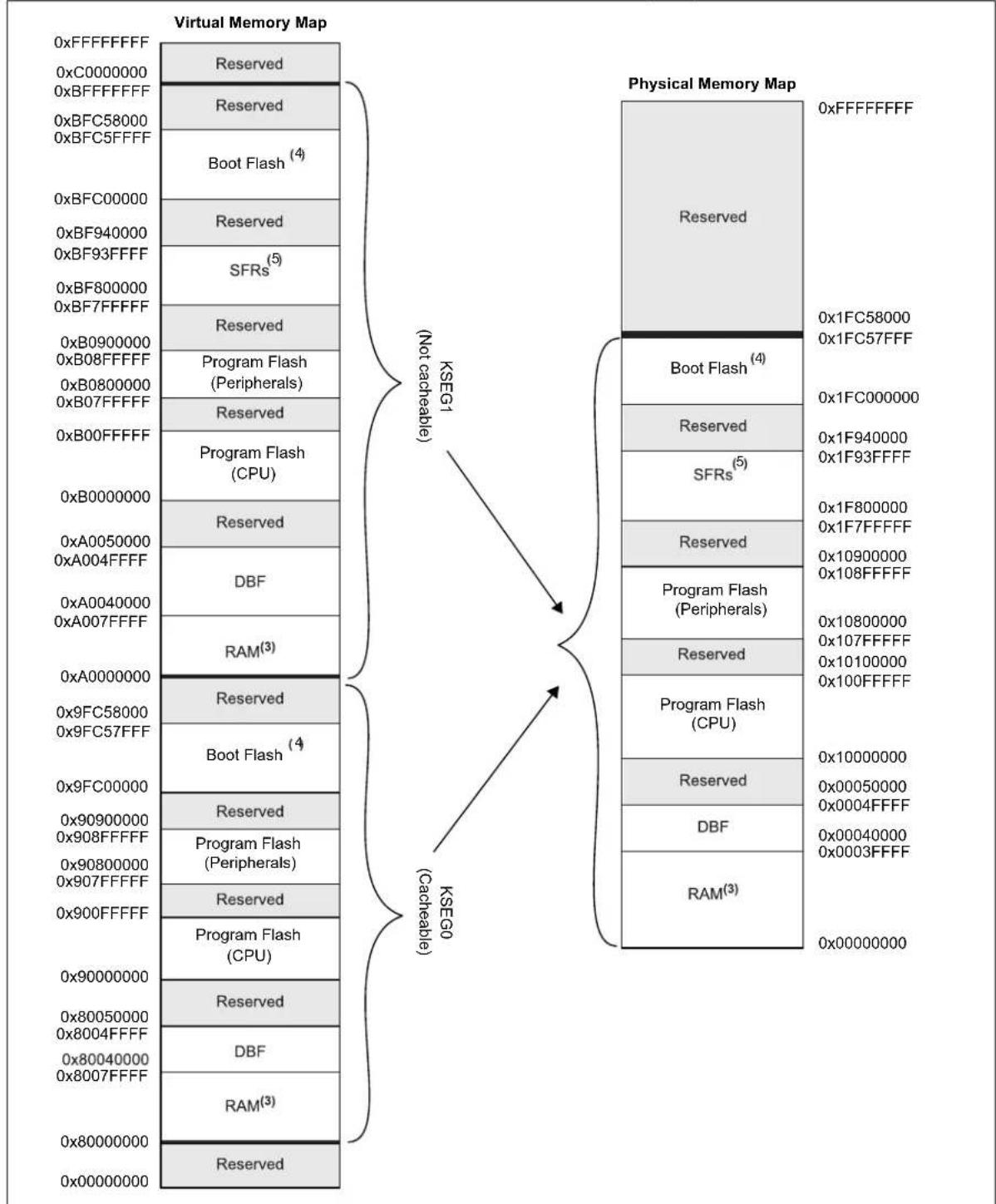
Note 1: Memory areas are not shown to scale.
2: The Cache and MMU (FMT) are initialized by compiler start-up code.
3: RAM memory is divided into two equal banks: RAM Bank 1 and RAM Bank 2 on a half boundary.
4: Refer to Figure 6-2.
5: Refer to Table 6-1.
FIGURE 6-2: BOOT AND ALIAS MEMORY MAP
| Physical Memory Map(1) | |
| Reserved | 0x1FC7FFFF |
| Calibration Area(2) | 0x1FC570000x1FC56FFF |
| 0x1FC560000x1FC55FFF | |
| Configuration Space(3, 4) | 0x1FC550000x1FC54FFF |
| Reserved | 0x1FC500000x1FC4FFFF |
| Upper Boot Alias | 0x1FC400000x1FC3FFFF |
| Reserved | 0x1FC100000x1FC0FFFF |
| Lower Boot Alias | 0x1FC00000 |
Note 1: Memory areas are not shown to scale.
2: This calibration area space cannot be modified by user.
3: Refer to Section 6.1.1 "Boot Flash And Configuration" for more information.
4: This configuration space cannot be used for executing code in the upper boot alias. These memory locations are used to initialize Configuration registers (see Section 38.2 "Special Features Registers".
TABLE 6-1: SFR MEMORY MAP
| Peripheral | Virtual Address | |
| Base | Offset Start | |
| Asymmetric Crypto | 0xBF900000 | 0x0000 |
| Sonics Register Target 0x030000 | ||
| Wi-Fi(2) | 0xBF8C0000 | 0x0000 |
| SQI 0x021000 | ||
| Crypto 0x024000 | ||
| RNG 0x025000 | ||
| RTCC 0xBF870000 0x0000 | ||
| DSCON 0x1000 | ||
| I2C2 | 0xBF840000 | 0x0400 |
| UART1-UART2 | 0x0600 | |
| SPI1-SPI2 | 0x0C00 | |
| IC1-IC4 | 0x1000 | |
| OC1-OC4 | 0x2000 | |
| Ethernet | 0x3000 | |
| USB | 0x4000 | |
| PORTA-PORTC | 0xBF820000 | 0x0000 |
| PORTK | 0x0300 | |
| I2C1 | 0x0400 | |
| ADC | 0x1000 | |
| CAN | 0x2000 | |
| CAN-FD | 0x3000 | |
| CVD | 0x4000 | |
| Interrupt controller | 0xBF810000 | 0x0000 |
| DMA 0x1000 | ||
| Prefetch | 0x2400 | |
| PMU 0x3E00 | ||
| PMU WCM | 0x4000 | |
Note 1: Refer to Section 6.3 "System Bus Arbitration" for important legal information.
2: This configuration space cannot be modified by the user.
TABLE 6-1: SFR MEMORY MAP (CONTINUED)
| Configuration | 0xBF800000 | 0x0000 |
| Flash Controller 0x0600 | ||
| Watchdog Timer 0x0800 | ||
| Deadman Timer 0x0A00 | ||
| CRU 0x1200 | ||
| UART3 0x1600 | ||
| PPS 0x1800 | ||
| PTG 0x1C00 | ||
| Timer1-Timer7 0x2000 | ||
| PFW 0xFE00 |
Note 1: Refer to Section 6.3 "System Bus Arbitration" for important legal information.
2: This configuration space cannot be modified by the user.
6.1.1 BOOT FLASH AND
CONFIGURATION
PIC32MZ W1 on device Reset, reads Boot Flash Configuration Word information before allowing system to boot.
Every time device Reset or NMI event occurs, the CFGPG.CPUPG[1:0] bits are reset to '0'. This helps the user to strictly control some regions. Boot code to use the CFGPG registers to define regions that are only accessible by group 0. Once the boot code is finished with data or code operations, it must set the CFGPG.CPUPG[1:0] to a value other than '0'.
6.2 Boot Flash Configuration Registers
TABLE 6-2: BOOT FLASH CONFIGURATION WORD SUMMARY
| Virtual Address (BFC5_#) | Register Name | Bit Range | Bits | All Resets | |||||||||||||||
| 31/15 30 | 14 29/13 28 | 12 27/11 26/10 | 25/9 24/8 | 23/7 22/6 21/5 20 | 4 19/3 | 18/2 17/1 16 | 0 | ||||||||||||
| 5F9C | BFDEVCFG0 | 31:16 | BINFOVAL-ID0 | — | — | — | — | — | — | — | — | — | — | — | — | — | — | — | xxxx |
| 15:00 | — | — | — | — | — | — | — | — | — | — | — | — | BOOT-ISA | — | PCSC-MODE | — | xxxx0 | ||
| 5F98 | BFDEVCFG1 | 31:16 | EPGMCLK | ETHTPSF | FECCCON[1:0] | ETHPLL-HWMD | BTPLL-HWMD | SPLL-HWMD | UPLL-HWMD | PCM | — | CANFDDIV | — | — | IC_ACLK | OC_ACLK | xxxxx | ||
| 15:00 | CFGLOCK[1:0] | IOLOCK | PMDLOCK | PGLOCK | PMULOCK | — | USBSSEN | EXLPRI | DMAPRI | FCPRI | — | JTAGEN | TROEN | — | TDOEN | xxxxx | |||
| 5F94 | BFDEVCFG2 | 31:16 | — | — | — | WDTPS[4:0] | USBDPTRIM[3:0] | USBDMTRIM[3:0] | xxxxx | ||||||||||
| 15:00 | HSUARTEN | SMCLR | HSSPIEN | VBUSIO | USBIDIO | CLASSB-DIS | ETHEX-EREF | FMIEN | — | — | TRCEN | ICESEL[1:0] | — | DEBUG[1:0] | xxxxx | ||||
| 5F90 | BFDEVCFG3 | 31:16 | DMTEN | DMTCNT[4:0] | WDTWINSZ[1:0] | WDTEN | WINDIS | WDTSPGM | WDTPS[4:0] | xxxxx | |||||||||
| 15:00 | FSCMEN | CKSWEN | WAKE2SPD | SOSCSEL | WDTRMCS[1:0] | POSCMOD[1:0] | — | — | DMTINTV[2:0] | — | — | — | xxxxx | ||||||
| 5F8C | BFDEVCFG4 | 31:16 | — | SOSCEN | — | DSEN | DSWDTEN | DSWD-TOSC | DSWDTPS[4:0] | DSZP-BOREN | VBZP-BOREN | — | — | — | xxxxx | ||||
| 15:00 | — | — | — | — | — | — | — | — | — | — | SOSCCFG[7-0] | xxxxx | |||||||
| 5F88 | BFDEVCFG5 | 31:16 | — | — | — | — | — | — | — | — | — | — | — | — | — | — | — | — | xxxxx |
| 15:00 | USERID[15:0] | xxxxx | |||||||||||||||||
Legend: x = unknown value on Reset; — = unimplemented, read as '0'. Reset values are shown in hexadecimal.
Note 1: The user configured setting of BFDEVCFG0 to BFDEVCFG5 loaded from boot Flash into following counterpart registers at system start-up.
• BFDEVCFG0 to BCFG0(L)
• BFDEVCFG1 to CFGCON0(L)
• BFDEVCFG2 to CFGCON1(L)
• BFDEVCFG3 to CFGCON2(L)
• BFDEVCFG4 to CFGCON4(L)
• BFDEVCFG5 to USERID
Definition of BCFG0, CFGCON0, CFGCON1, CFGCON2, CFGCON4 and USERID is available in Table 38-1.
TABLE 6-1: BOOT FLASH CODE PROTECTION REGISTER SUMMARY MAP
| Legend: | |||
| R = Readable bit | W = Writable bit | U = Unimplemented bit, read as ‘0’ | |
| -n = Value at POR | ‘1’ = Bit is set | ‘0’ = Bit is cleared | P = Programmable Bit |
bit 31-29 Unimplemented: Read as '0'
bit 28 CP: Code Protect bit
0 = Protection Disabled
1 = Protection Enabled
bit 27-0 Unimplemented: Read as '0'
TABLE 6-3: BOOT FLASH SIGN REGISTER SUMMARY MAP
| Legend: | |||
| R = Readable bit | W = Writable bit | U = Unimplemented bit, read as ‘0’ | |
| -n = Value at POR | ‘1’ = Bit is set | ‘0’ = Bit is cleared | P = Programmable Bit |
bit 31 SIGN: Flash SIGN bit
1 = Unsigned
0 = Signed
bit 30-0 Unimplemented: Read as '0'
6.3 System Bus Arbitration
| Note: The System Bus interconnect implements one or more instantiations of the SonicsSX® interconnect from Sonics, Inc. This document contains materials that are (c) 2003-2015 Sonics, Inc., and that constitute proprietary information of Sonics, Inc. SonicsSX is a registered trademark of Sonics, Inc. All such materials and trademarks are used under license from Sonics, Inc. |
As shown in the PIC32MZ1025W104 family block diagram (see Figure 2-1), there are multiple initiator modules (I1 through I13) in the system that can access various target modules (T1 through T13). Table 6-3 lists the initiator and its corresponding access target. The System Bus supports simultaneous access to targets by initiators, so long as the initiators are accessing different targets. The System Bus will perform arbitration if multiple initiators attempt to access the same target.
TABLE 6-3: INITIATORS TO TARGET ACCESS ASSOCIATION
| Target # | Initiator ID | 1 | 2 | 3 | 4 | 5 | 6 | 7 | 8 | 9 | 10 | 11 | 12 | 13 | 14 |
| Name | CPU | Flash Controller | DMA Read | DMA Write | ICD | WI-FI | ADC | CAN | CAN-FD | Crypto | Ethernet TX | Ethernet RX | SQI | USB | |
| 1 | RAM Bank 1 Memory | X | X | X | X | X | X | X | X | X | X | X | X | X | X |
| 2 | RAM Bank 2 Memory | X | X | X | X | X | X | X | X | X | X | X | X | X | X |
| 3 | Data Buffer Memory | X | X | X | X | X | X | X | X | X | X | X | X | X | X |
| 4 | Prefetch | X | X | X | X | X | X | X | X | X | X | X | |||
| 5 | Flash Memory Boot Flash | X | X | ||||||||||||
| 6 | Peripheral Set 1: Flash Controller, WDT, DMT, Clock Reset Unit, PTG, UART3, PPS, Timer 1-7 | X | X | X | X | X | |||||||||
| 7 | Peripheral Set 2: Port A, Port B, Port C, Port K, I2C1, ADC, CAN, CAN-FD, CVD Controller | X | X | X | X | X | |||||||||
| 8 | Wi-Fi | X | X | X | X | X | |||||||||
| 9 | Peripheral Set 4: RTCC, DSCON | X | X | X | X | ||||||||||
| 10 | SSX RT | X | X | X | X | X | |||||||||
| 11 | Peripheral Set 3: I2C, UART1-UART2, SPI1-SPI2, IC1-IC4, OC1-OC4, Ethernet Controller, USB | X | X | X | X | X | |||||||||
| 12 | AHB | X | X | X | X | X | |||||||||
| 13 | SQI | X | X | X | X | X |
Legend:
- X = Connection between initiator and target
- Shaded cells = No connection between initiator and target
The System Bus arbitration scheme implements a non-programmable, Least Recently Serviced (LRS) priority, which provides Quality Of Service (QOS) for most initiators. However, some initiators can use Fixed High Priority (HIGH) arbitration to guarantee their access to data.
The arbitration scheme for the available initiators is shown in Table 6-4.
TABLE 6-4: INITIATOR ID AND QOS
| Name ID QOS | ||
| CPU 1 LRS | (1) | |
| CPU 2 HIGH | (1,2) | |
| Flash Controller 3 LRS | (1) | |
| Flash Controller 4 HIGH | (1,2) | |
| DMA Read | 5 LRS | (1) |
| DMA Read | 6 HIGH | (1,2) |
| DMA Write | 7 LRS | (1) |
| DMA Write | 8 HIGH | (1,2) |
| ICD - JTAG | 9 | LRS |
| Wi-Fi | 10 | LRS |
| ADC | 11 | LRS |
| CAN | 12 | LRS |
| CAN-FD | 13 | LRS |
| Crypto Engine | 14 | LRS |
| Ethernet Write | 15 | LRS |
| Ethernet Read | 16 | LRS |
| SQI | 17 | LRS |
| USB | 18 | LRS |
Note 1: When accessing SRAM, the DMAPRI bit (CFGCON0[6]), the FCPRI bit (CFGCON0[5]), and the EXLPRI bit (CFGCON0[7]) provide arbitration control for the DMA, FC, and CPU (when servicing an interrupt (EXL = 1)), respectively, by selecting the use of LRS or HIGH. When using HIGH, the DMA, FC, and CPU get arbitration preference over all initiators using LRS.
2: Using HIGH arbitration can have serious negative effects on other initiators. Therefore, it is recommended to not enable this type of arbitration for an initiator that uses significant system bandwidth. HIGH arbitration is intended to be used for low bandwidth applications that require low latency, such as LCC graphics applications.
6.4 Permission Access and System Bus Registers
The System Bus on the PIC32MZ1025W104 family of MCUs provide access control capabilities for the transaction initiators on the System Bus.
The System Bus divides the entire memory space into 14 target regions and permits access to each target by initiators through permission groups. Four Permission Groups (0 through 3) can be assigned to each initiator. Each permission group is independent of the others and can have exclusive or shared access to a region.
Using the CFGPG register (see Register 38-6 in Section 38.0 "Special Features"), Boot firmware can assign a permission group to each initiator, which can make requests on the System Bus.
The available targets and their regions, as well as the associated control registers to assign protection, are described and listed in Table 6-5.
Register 6-5 through Register 6-12 are used for setting and controlling access permission groups and regions.
To change these registers, they must be unlocked in hardware. The register lock is controlled by the PGLOCK Configuration bit (CFGCON[11]). Setting PGLOCK prevents writes to the control registers; clearing PGLOCK allows writes.
To set or clear the PGLOCK bit, an unlock sequence must be executed. Refer to Oscillators with Enhanced PLL in the "PIC32 Family Reference Manual" for more details.
TABLE 6-5: SYSTEM BUS TARGETS AND ASSOCIATED PROTECTION REGISTERS
| Target Number | Target Description^(5) | SBTxREGy Register SBTxRDy Register SBTxWRy Register | ||||||||||
| Name | Region Base (BASE[21:0]) (2) | Physical Start Address | Region Size (SIZE[4:0]) (3) | Region Size | Priority (PRI) | Priority Level | Name | Read Permission (GROUP3, GROUP2, GROUP1, GROUP0) | Name | Write Permission (GROUP3, GROUP2, GROUP1, GROUP0) | ||
| 1 RAM | Bank 1 Memory | SBT1REG0 R | 0x00000000 R | (4) | 128 Kbyte | — | 0 SBT1RD0 R/W | (1) | SBT1WR0 R/W | |||
| SBT1REG1 R/W | R/W | R/W | R/W | — | 3 SBT1RD1 R/W | (1) | SBT1WR1 R/W | |||||
| SBT1REG2 | R/W | R/W | R/W | R/W | 0 | 1 | SBT1RD2 | R/W^(1) | SBT1WR2 R/W | |||
| 2 RAM | Bank 2 Memory | SBT2REG0 R | 0x00020000 R | (4) | 128 Kbyte | — | 0 SBT2RD0 R/W | (1) | SBT2WR0 R/W | |||
| SBT2REG1 R/W | R/W | R/W | R/W | — | 3 SBT2RD1 R/W | (1) | SBT2WR1 R/W | |||||
| SBT2REG2 | R/W | R/W | R/W | R/W | 0 | 1 | SBT2RD2 | R/W^(1) | SBT2WR2 R/W | |||
| 3 Data | Buffer Memory | SBT3REG0 R | 0x00040000 R | (4) | 64 Kbyte | — | 0 SBT3RD0 R/W | (1) | SBT3WR0 R/W | |||
| SBT3REG1 R/W | R/W | R/W | R/W | — | 3 SBT3RD1 R/W | (1) | SBT3WR1 R/W | |||||
| SBT3REG2 | R/W | R/W | R/W | R/W | 0 | 1 | SBT3RD2 | R/W^(1) | SBT3WR2 R/W | |||
| 4 Flash | Memory (Peripherals) | SBT4REG0 R | 0x10800000 | R | 1 Mbyte | — | 0 SBT4RD0 R/W | (1) | SBT4WR0 | 0, 0, 0, 0 | ||
| SBT4REG1 R/W | R/W | R/W | R/W | — | 3 SBT4RD1 R/W | (1) | SBT4WR1 | 0, 0, 0, 0 | ||||
| SBT4REG2 | R/W | R/W | R/W | R/W | 0 | 1 | SBT4RD2 | R/W^(1) | SBT4WR2 | 0, 0, 0, 0 | ||
| 5 | Flash Memory (CPU) | SBT5REG0 R | 0x10000000 R | (4) | 1 Mbyte | — | 0 SBT5RD0 R/W | (1) | SBT5WR0 | 0, 0, 0, 0 | ||
| SBT5REG2 | R/W | R/W | R/W | R/W | 0 | 1 | SBT5RD2 | R/W^(1) | SBT5WR2 | 0, 0, 0, 0 | ||
| SBT5REG3 | R/W | R/W | R/W | R/W | 0 | 1 | SBT5RD3 | R/W^(1) | SBT5WR3 | 0, 0, 0, 0 | ||
| SBT5REG4 | R | R | R | R | 1 | 2 | SBT5RD4 | 0, 0, 0, 1 | SBT5WR4 | 0, 0, 0, 0 | ||
| SBT5REG5 | R | R | R | R | 1 | 2 | SBT5RD5 | 0, 0, 0, 1 | SBT5WR5 | 0, 0, 0, 0 | ||
| SBT5REG6 | R | R | R | R | 1 | 2 | SBT5RD6 | 0, 0, 0, 1 | SBT5WR6 | 0, 0, 0, 0 | ||
| SBT5REG7 | R | R | R | R | 1 | 2 | SBT5RD7 | 1, 1, 1, 1 | SBT5WR7 | 0, 0, 0, 0 | ||
| SBT5REG8 | R | R | R | R | 1 | 2 | SBT5RD8 | 1, 1, 1, 1 | SBT5WR8 | 0, 0, 0, 0 | ||
| SBT5REG9 | R | R | R | R | 1 | 2 | SBT5RD9 | 0, 0, 0, 1 | SBT5WR9 | 0, 0, 0, 0 | ||
| SBT5REG10 | R | R | R | R | 1 | 2 | SBT5RD10 | 0, 0, 0, 1 | SBT5WR10 | 0, 0, 0, 0 | ||
| 6 | Peripheral Set 1: Flash Controller, DMT, WDT, Clock Reset Unit, UART3, PPS, PTG, Timer1-Timer7, DMA, ICD, PMU | SBT6REG0 R | 0x1F800000 | R | 128 Kbyte | — | 0 SBT6RD0 | R/W (1) | SBT6WR0 R/W | |||
| SBT6REG1 R/W | R/W | R/W | R/W | — | 3 SBT6RD1 | R/W (1) | SBT6WR1 R/W | |||||
Legend:
R = Read;
R/W =
'x' in a reg
'y' in a register name = 0-10.
Note
1: Reset values for these bits are ‘_’, ‘1’, ‘1’, ‘2’, respectively.
2: The BASE[21:0] bits must be set to the corresponding Physical Address and right shifted by 10 bits. For Read-only bits, this value is set by hardware on Reset.
3: The SIZE[4:0] bits must be set to the corresponding Region Size, based on the following formula: Region Size = 2^(SIZE-1) x 1024 bytes. For read-only bits, this value is set by hardware on Reset.
4: Refer to the Device Memory Maps (Figure 6-1 for specific device memory sizes and start addresses
5: See Table 6-1 for information on specific target memory size and start addresses.
6: The SBTxREG1 SFRs are reserved, and therefore, are not listed in this table for this target.
TABLE 6-5: SYSTEM BUS TARGETS AND ASSOCIATED PROTECTION REGISTERS (CONTINUED)
| Target Number | Target Description^(5) | SBTxREGy Register | SBTxRDy Register SBTxWRy Register | |||||||||
| Name | Region Base (BASE[21:0]) (2) | Physical Start Address | Region Size (SIZE[4:0]) (3) | Region Size | Priority (PRI) | Priority Level | Name | Read Permission (GROUP3, GROUP2, GROUP1, GROUP0) | Name | Write Permission (GROUP3, GROUP2, GROUP1, GROUP0) | ||
| 7 | Peripheral Set 2: Port A, Port B, Port C, Port K, I2C1, ADC, CAN, CAN-FD, CVD Controller | SBT7REG0 R | 0x1F820000 R 128 | Kbyte | — 0 | SBT7RD0 R/W | (1) | SBT7WR0 R/W | ||||
| 8 | Wi-Fi | SBT8REG0 R | 0x1F8C0000 R 128 | Kbyte | — 0 | SBT8RD0 R/W | (1) | SBT8WR0 R/W | ||||
| 9 | Peripheral Set 4: RTCC, DSCON | SBT9REG0 R | 0x1F870000 R 128 | Kbyte | — 0 | SBT9RD0 R/W | (1) | SBT9WR0 R/W | ||||
| 10 | SSX RT | SBT10REG0 R | 0X1F8F0000 R 64 | Kbyte | — 0 | SBT10RD0 0 | 0, 0, 1 | SBT10WR0 0 | 0, 0,1 | |||
| 11 | Peripheral Set 3: I2C, UART1-UART2, SPI1-SPI2, IC1-IC4, OC1-OC4, USB, Ethemet Controller | SBT11REG0 | R 0x1F840 | 0000 R 128 Kbyte | — 0 | SBT11RD0 | R/W | (1) | SBT11WR0 | R/W | ||
| 12 | AHB | SBT12REG0 R | 0x1F8E4000 R 256 | Kbyte | — 0 | SBT12RD0 | R/W | (1) | SBT12WR0 | R/W | ||
| SBT12REG1 | R/W | R/W | R/W R/W | — 3 | SBT12RD1 | R/W | (1) | SBT12WR1 | R/W | |||
| 13 | SQL | SBT13REG0 R | 0x1F8E1000 R 4 | Kbyte | — 0 | SBT13RD0 | R/W | (1) | SBT13WR0 | R/W | ||
Legend: R = Read; R/W = Read/Write; 'x' in a register name = 0-13; 'y' in a register name = 0-10.
Note 1: Reset values for these bits are ‘1’, ‘1’, ‘1’, ‘1’, respectively.
2: The BASE[21:0] bits must be set to the corresponding Physical Address and right shifted by 10 bits. For Read-only bits, this value is set by hardware on Reset.
3: The SIZE[4:0] bits must be set to the corresponding Region Size, based on the following formula: Region Size = 2 ^(SIZE-1) x 1024 bytes. For read-only bits, this value is set by hardware on Reset.
4: Refer to the Device Memory Maps (Figure 6-1 for specific device memory sizes and start addresses.
5: See Table 6-1 for information on specific target memory size and start addresses.
6: The SBTxREG1 SFRs are reserved, and therefore, are not listed in this table for this target.
TABLE 6-6: SYSTEM BUS TARGET x REGISTER MAP, x = 1, 2, 3, 4 (2)
Legend: x = unknown value on Reset; — = unimplemented, read as '0'. Reset values are shown in hexadecimal.
Note 1: Target virtual addresses are:
•Target 1 Virtual address = 0xBF93_1000
•Target 2 Virtual address = 0xBF93_2000
•Target 3 Virtual address = 0xBF93_3000
•Target 4 Virtual address = 0xBF93_4000
2: For Reset values listed as 'xxxx', refer to Table 6-5 for the actual Reset values.
TABLE 6-7: SYSTEM BUS TARGET 5 REGISTER MAP
Legend: x = unknown value on Reset; — = unimplemented, read as '0'. Reset values are shown in hexadecimal.
Note: For Reset values listed as 'xxxx', refer to Table 6-5 for the actual Reset values.
TABLE 6-7: SYSTEM BUS TARGET 5 REGISTER MAP (CONTINUED)
Legend: x = unknown value on Reset; — = unimplemented, read as '0'. Reset values are shown in hexadecimal.
Note: For Reset values listed as 'xxxx', refer to Table 6-5 for the actual Reset values.
TABLE 6-8: SYSTEM BUS TARGET x REGISTER MAP, x = 7, 8, 9, 11, 13
Legend: x = unknown value on Reset; — = unimplemented, read as '0'. Reset values are shown in hexadecimal.
Note 1: Target virtual addresses are:
•Target 7 Virtual address = 0xBF93 7000
•Target 8 Virtual address = 0xBF93 8000
•Target 9 Virtual address = 0xBF93 9000
•Target 11 Virtual address = 0xBF93 B000
•Target 13 Virtual address = 0xBF93 D000
2: For Reset values listed as 'xxxx', refer to Table 6-5 for the actual Reset values.
TABLE 6-9: SYSTEM BUS TARGET 10 REGISTER MAP
Legend: x = unknown value on Reset; — = unimplemented, read as '0'. Reset values are shown in hexadecimal.
Note: For Reset values listed as 'xxxx', refer to Table 6-5 for the actual Reset values.
TABLE 6-10: SYSTEM BUS TARGET x REGISTER MAP, WHERE x = 6, 12
Legend: x = unknown value on Reset; — = unimplemented, read as '0'. Reset values are shown in hexadecimal.
Note 1: Target virtual addresses are:
•Target 6 Virtual address = 0xBF93_6000
•Target 12 Virtual address = 0xBF93_C000
2: For Reset values listed as 'xxxx', refer to Table 6-5 for the actual Reset values.
REGISTER 6-5: SBTxELOG1: SYSTEM BUS TARGET 'x' ERROR LOG REGISTER 1 ('x' = 0-13)
| Bit Range | Bit 31/23/15/7 | Bit 30/22/14/6 | Bit 29/21/13/5 | Bit 28/20/12/4 | Bit 27/19/11/3 | Bit 26/18/10/2 | Bit 25/17/9/1 | Bit 24/16/8/0 |
| 31:24 | R/W-0, C U-0 | U-0 U-0 R/W-0, | C R/W-0, C R/W-0, C R/W-0, C | |||||
| MULTI — — — | C | O | D | |||||
| 23:16 | U-0 U-0 U-0 U-0 U-0 U-0 | |||||||
| — — — — | — — | — — | ||||||
| 15:8 | R-0 R-0 R-0 R-0 R-0 R-0 | |||||||
| INITID[7:0] | ||||||||
| 7:0 | R-0 R-0 R-0 R-0 U-0 R-0 R-0 | |||||||
| REGION[3:0] | — | CMD[2:0] | ||||||
| Legend: | C = Clearable bit | |
| R = Readable bit | W = Writable bit | U = Unimplemented bit, read as ‘0’ |
| -n = Value at POR | ‘1’ = Bit is set | ‘0’ = Bit is cleared |
bit 31 MULTI: Multiple Permission Violations Status bit
This bit is cleared by writing a '1'.
1 = Multiple errors have been detected
0 = No multiple errors have been detected
bit 30-28 Unimplemented: Read as '0'
bit 27-24 CODE[3:0]: Error Code bits
Indicates the type of error that was detected. These bits are cleared by writing a '1'.
1111 = Reserved
1101 = Reserved
•
•
0011 = Permission violation
0010 = Reserved
0001 = Reserved
0000 = No error
bit 23-16 Unimplemented: Read as '0'
Note: Refer to Table 6-5 for the list of available targets and their descriptions.
REGISTER 6-5: SBTxELOG1: SYSTEM BUS TARGET 'x' ERROR LOG REGISTER 1
('x' = 0-13) (CONTINUED)
bit 15-8 INITID[7:0]: Initiator ID of Requester bits
11111111 = Reserved
.
.
.
00010011 = Reserved
00010010 = USB
00010001 = SQL
00010000 = Ethernet Read
00001111 = Ethernet Write
00001110 = Crypto Engine
00001101 = CAN-FD
00001100 = CAN
00001011 = ADC
00001010 = Wi-Fi
00001001 = JTAG
00001000 = DMA Write (DMAPRI (CFGCON0[6]) = 1)
00000111 = DMA Write (DMAPRI (CFGCON0[6]) = 0)
00000110 = DMA Read (DMAPRI (CFGCON0[6]) = 1)
00000101 = DMA Read (DMAPRI (CFGCON0[6]) = 0)
00000100 = Flash Controller (FCPRI(CFGCON0[5]) = 0)
00000011 = Flash Controller (FCPRI(CFGCON0[5]) = 0)
00000010 = CPU (CPUPRI (CFGCON0[7]) = 1)
00000001 = CPU (CPUPRI (CFGCON0[7]) = 0)
00000000 = Reserved
bit 7-4 REGION[3:0]: Requested Region Number bits
1111 - 0000 = Target's region that reported a permission group violation
bit 3 Unimplemented: Read as '0'
bit CMD[2:0]: Transaction Command of the Requester bits
111 = Reserved
110 = Reserved
101 = Write (a non-posted write)
100 = Reserved
011 = Read (a locked read caused by a Read-Modify-Write transaction)
010 = Read
001 = Write
000 = Idle
Note: Refer to Table 6-5 for the list of available targets and their descriptions.
REGISTER 6-6: SBTxELOG2: SYSTEM BUS TARGET 'x' ERROR LOG REGISTER 2 ('x' = 0-13)
| R = Readable bit | W = Writable bit U = Unimplemented bit, read as '0' |
| -n = Value at POR | '1' = Bit is set '0' = Bit is cleared |
bit 31-3 Unimplemented: Read as '0'
bit 1-0 GROUP[1:0]: Requested Permissions Group bits
11 = Group 3
10 = Group 2
01 = Group 1
00 = Group 0
Note: Refer to Table 6-5 for the list of available targets and their descriptions.
REGISTER 6-7: SBTxECON: SYSTEM BUS TARGET 'x' ERROR CONTROL REGISTER
('x' = 0-13)
| Bit Range | Bit 31/23/15/7 | Bit 30/22/14/6 | Bit 29/21/13/5 | Bit 28/20/12/4 | Bit 27/19/11/3 | Bit 26/18/10/2 | Bit 25/17/9/1 | Bit 24/16/8/0 |
| 31:24 | U-0 U-0 U-0 U-0 U-0 U-0 | R/W-0 | ||||||
| —— — | —— — — | ERRP | ||||||
| 23:16 | U-0 U-0 U-0 U-0 U-0 U-0 | U-0 | ||||||
| —— — | —— — — — — | |||||||
| 15:8 | U-0 U-0 U-0 U-0 U-0 U-0 | U-0 | ||||||
| —— — | —— — — — — | |||||||
| 7:0 | U-0 U-0 U-0 U-0 U-0 U-0 | U-0 | ||||||
| —— — | —— — — — — | |||||||
Legend:
| R = Readable bit | W = Writable bit U = Unimplemented bit, read as '0' |
| -n = Value at POR | '1' = Bit is set '0' = Bit is cleared |
bit 31-25 Unimplemented: Read as '0'
bit 24 ERRP: Error Control bit
1 = Report protection group violation errors
0 = Do not report protection group violation errors
bit 23-0 Unimplemented: Read as '0'
Note: Refer to Table 6-5 for the list of available targets and their descriptions.
REGISTER 6-8: SBTxECLRS: SYSTEM BUS TARGET 'x' SINGLE ERROR CLEAR REGISTER ('x' = 0-13)
R = Readable bit W = Writable bit U = Unimplemented bit, read as '0'
-n = Value at POR '1' = Bit is set '0' = Bit is cleared
bit 31-1 Unimplemented: Read as '0'
bit 0 CLEAR: Clear Single Error on Read bit
A single error as reported via SBTxELOG1 and SBTxELOG2 is cleared by a read of this register.
Note: Refer to Table 6-5 for the list of available targets and their descriptions.
REGISTER 6-9: SBTxECLRM: SYSTEM BUS TARGET 'x' MULTIPLE ERROR CLEAR REGISTER ('x' = 0-13)
R = Readable bit W = Writable bit U = Unimplemented bit, read as '0'
-n = Value at POR '1' = Bit is set '0' = Bit is cleared
bit 31-1 Unimplemented: Read as '0'
bit 0 CLEAR: Clear Multiple Errors on Read bit
Multiple errors as reported via SBTxELOG1 and SBTxELOG2 is cleared by a read of this register.
Note: Refer to Table 6-5 for the list of available targets and their descriptions.
REGISTER 6-10: SBTxREGy: SYSTEM BUS TARGET 'x' REGION 'y' REGISTER
('x' = 0-13; 'y' = 0-10)
| Bit Range | Bit 31/23/15/7 | Bit 30/22/14/6 | Bit 29/21/13/5 | Bit 28/20/12/4 | Bit 27/19/11/3 | Bit 26/18/10/2 | Bit 25/17/9/1 | Bit 24/16/8/0 |
| 31:24 | R/W-0 R/W-0 R/W-0 R/W-0 R/W-0 R/W-0 | |||||||
| BASE[21:14] | ||||||||
| 23:16 | R/W-0 R/W-0 R/W-0 R/W-0 R/W-0 R/W-0 | |||||||
| BASE[13:6] | ||||||||
| 15:8 | R/W-0 R/W-0 R/W-0 R/W-0 R/W-0 R/W-0 R/W-0 | |||||||
| BASE[5:0] PRI — | ||||||||
| 7:0 | R/W-0 R/W-0 R/W-0 R/W-0 | U-0 | U-0 U-0 | |||||
| SIZE[4:0] | — | — | — | |||||
Legend:
| R = Readable bit | W = Writable bit | U = Unimplemented bit, read as '0' |
| -n = Value at POR | '1' = Bit is set | '0' = Bit is cleared |
bit 31-10 BASE[21:0]: Region Base Address bits
bit 9 PRI: Region Priority Level bit
1 = Level 2
0 = Level 1
bit 8 Unimplemented: Read as '0'
bit 7-3 SIZE[4:0]: Region Size bits
Permissions for a region are only active is the SIZE is non-zero.
11111 = Region size = 2(SIZE - 1) x 1024 (bytes)
•
.
•
00001 = Region size = 2(SIZE - 1) x 1024 (bytes)
00000 = Region is not present
bit 2-0 Unimplemented: Read as '0'
Note 1: Refer to Table 6-5 for the list of available targets and their descriptions.
2: For some target regions, certain bits in this register are read-only with preset values. See Table 6-5 for more information.
REGISTER 6-11: SBTxRDy: SYSTEM BUS TARGET 'x' REGION 'y' READ PERMISSIONS REGISTER ('x' = 0-13; 'y' = 0-10)
| R = Readable bit | W = Writable bit | U = Unimplemented bit, read as '0' |
| -n = Value at POR | '1' = Bit is set | '0' = Bit is cleared |
bit 31-4 Unimplemented: Read as '0'
bit 3 Group3: Group3 Read Permissions bits
1 = Privilege Group 3 has read permission
0 = Privilege Group 3 does not have read permission
bit 2 Group2: Group2 Read Permissions bits
1 = Privilege Group 2 has read permission
0 = Privilege Group 2 does not have read permission
bit 1 Group1: Group1 Read Permissions bits
1 = Privilege Group 1 has read permission
0 = Privilege Group 1 does not have read permission
bit 0 Group0: Group0 Read Permissions bits
1 = Privilege Group 0 has read permission
0 = Privilege Group 0 does not have read permission
Note 1: Refer to Table 6-5 for the list of available targets and their descriptions.
2: For some target regions, certain bits in this register are read-only with preset values. See Table 6-5 for more information.
REGISTER 6-12: SBTxWRy: SYSTEM BUS TARGET 'x' REGION 'y' WRITE PERMISSIONS REGISTER ('x' = 0-13; 'y' = 0-10)
| R = Readable bit | W = Writable bit U = Unimplemented bit, read as '0' |
| -n = Value at POR | '1' = Bit is set '0' = Bit is cleared |
bit 31-4 Unimplemented: Read as '0'
bit 3 Group3: Group 3 Write Permissions bits
1 = Privilege Group 3 has write permission
0 = Privilege Group 3 does not have write permission
bit 2 Group2: Group 2 Write Permissions bits
1 = Privilege Group 2 has write permission
0 = Privilege Group 2 does not have write permission
bit 1 Group1: Group 1 Write Permissions bits
1 = Privilege Group 1 has write permission
0 = Privilege Group 1 does not have write permission
bit 0 Group0: Group 0 Write Permissions bits
1 = Privilege Group 0 has write permission
0 = Privilege Group 0 does not have write permission
Note 1: Refer to Table 6-5 for the list of available targets and their descriptions.
2: For some target regions, certain bits in this register are read-only with preset values. See Table 6-5 for more information.
7.0 RESETS
Note: This data sheet summarizes the features of the PIC32MZ1025W104 family of devices. It is not intended to be a comprehensive reference source. To complement the information in this data sheet, refer to Section 7. "Resets" (DS60001118) in the "PIC32 Family Reference Manual", which is available from the Microchip website (www.microchip.com/PIC32).
The Reset module combines all Reset sources and controls the device host Reset signal, SYSRST.
The device Reset sources are as follows:
• Power-on Reset (POR)
• Master Clear Reset (MCLR)
- Software Reset (SWR)
- Watchdog Timer Reset (WDTR)
• Brown-out Reset (BOR)
- Configuration Mismatch Reset (CMR)
- Deadman Timer Reset (DMTR)
• Zero-power BOR (ZPBOR)
A simplified block diagram of the Reset module is illustrated in the figure below.
FIGURE 7-1: SYSTEM RESET BLOCK DIAGRAM
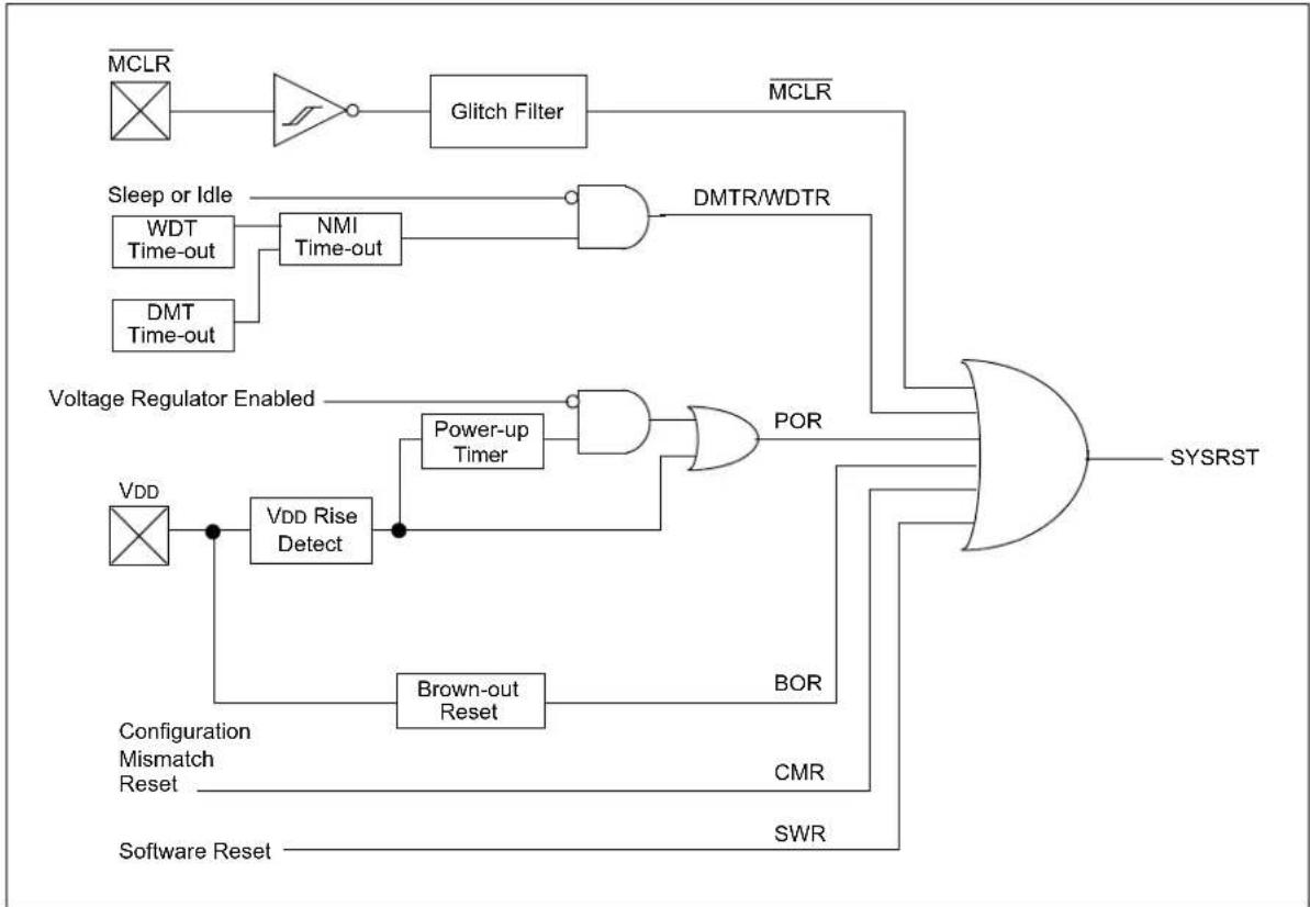
flowchart
graph TD
    A["MCLR"] --> B["Amplifier"]
    B --> C["Glitch Filter"]
    C --> D["MCLR"]
    E["Sleep or Idle"] --> F["WDT Time-out"]
    E --> G["DMT Time-out"]
    F --> H["NMI Time-out"]
    G --> H
    H --> I["AND"]
    I --> J["DMTR/WDTR"]
    K["Voltage Regulator Enabled"] --> L["Power-up Timer"]
    L --> M["AND"]
    M --> N["POR"]
    O["VDD"] --> P["VDD Rise Detect"]
    P --> Q["Brown-out Reset"]
    Q --> R["BOR"]
    R --> S["SYSRST"]
    T["Configuration Mismatch Reset"] --> U["CMR"]
    V["Software Reset"] --> W["SWR"]
7.1 Reset Control Registers
TABLE 7-1: RESETS REGISTER MAP
| Virtual Address (BF80_#) | Register Name | Bit Range | Bits | All Resets | |||||||||||||||
| 31/15 30 | 4/14 29/13 23 | 3/12 27/11 | 26/10 25/9 | 24/8 23/7 2 | 2/6 21/5 20/4 | 19/3 18/2 | 17/1 16/0 | ||||||||||||
| 1260 | RCON | 31:16 | PORIO PC | RCORE | — | — | BCFGERR | BCFGFAIL | NVMLTA | NVMEOL | — | — | — | — | — | — | VBPOR | VBAT | 0000 |
| 15:0 | — | — | — | — | — | DPSLP | CMR | — | EXTR | SWR | DMTO | WDTO | SLEEP | IDLE | BOR | POR | 0000 | ||
| 1270 | RSWRST | 31:16 | — | — | — | — | — | — | — | — | — | — | — | — | — | — | — | — | 0000 |
| 15:0 | — | — | — | — | — | — | — | — | — | — | — | — | — | — | — | SWRST | 0000 | ||
| 1280 | RNMON | 31:16 | — | — | — | — | — | — | DMTO | WDTR | SWNMI | — | — | — | GNMI | LVD | CF | WDTS | 0000 |
| 15:0 | NMICNT[15:0] | 0000 | |||||||||||||||||
Legend: x = unknown value on Reset; — = unimplemented, read as 'C'. Reset values are shown in hexadecimal.
Note 1: All registers have corresponding CLR, SET and INV registers at their virtual addresses, plus offsets of 0×4, 0×8 and 0×C, respectively. See Section 13.3 "CLR, SET and INV Registers" for more information.
REGISTER 7-1: RCON: RESET CONTROL REGISTER
| Bit Range | Bit 31/23/15/7 | Bit 30/22/14/6 | Bit 29/21/13/5 | Bit 28/20/12/4 | Bit 27/19/11/3 | Bit 26/18/10/2 | Bit 25/17/9/1 | Bit 24/16/8/0 |
| 31:24 | R/W/HS-0 R/W/HS-0 U-0 U-0 R/W-0, HS R/W-0, HS R/W/HS-0 R/W/HS-0 | |||||||
| PORIO^(1) | PORCORE^(1) | — — BCFGERR BCFGFAIL NVMLTA NVMEOL | ||||||
| 23:16 | U-0 | U-0 | U-0 | U-0 | U-0 | U-0 | R/W-0, HS | R/W-0, HS |
| — | — | — | — | — | — | VBPOR | VBAT | |
| 15:8 | U-0 | U-0 | U-0 | U-0 | U-0 | R/W-0, HS | R/W-0, HS | U-0 |
| — | — | — | — | — | DPSLP^(1) | CMR | — | |
| 7:0 | R/W-0, HS | R/W-0, HS | R/W-0, HS | R/W-0, HS | R/W-0, HS | R/W-0, HS | R/W-1, HS | R/W-1, HS |
| EXTR | SWR | DMTO | WDTO | SLEEP | IDLE | BOR^(1) | POR^(1) | |
| Legend: | HS = Hardware Set | HC = Hardware Cleared |
| R = Readable bit | W = Writable bit | U = Unimplemented bit, read as ‘0’ |
| -n = Value at POR | ‘1’ = Bit is set | ‘0’ = Bit is cleared x = Bit is unknown |
bit 31 PORIO: IO Voltage POR Flag bit ^(1)
1 = Power-up Reset occurs due to IO voltage
0 = Power-up Reset does not occur due to IO voltage
Set by hardware at detection of an IO POR event.
Note: User may write this bit to '1'. Does not cause a POR_IO.
bit 30 PORCORE: Core Voltage POR Flag bit ^(1)
1 = Power-up Reset occurs due to core voltage
0 = Power-up Reset does not occur due to core voltage
Set by hardware at detection of a core POR event.
Note: User may write this bit to '1'. Does not cause a POR_CORE.
bit 29-28 Unimplemented: Read as '0'
bit 27 BCFGERR: BCFG Error Flag bit
1 = BCFG error occurs
0 = BCFG error does not occur
A primary BCFG value had an error but the secondary BCFG value was valid and used.
bit 26 BCFGFAIL: BCFG Failure Flag bit
1 = BCFG failure occurs
0 = BCFG failure does not occur
bit 25 NVMLTA: NVM Life Time Alert Flag bit
1 = NVM LTA error occurs
0 = NVM LTA error does not occur
NVM Life Time Alert - due to charge leakage the NVM is nearing End of Life (EOL).
bit 24 NVMEOL: NVM EOL Flag bit
1 = NVM EOL failure occurs
0 = NVM EOL failure does not occur
NVM EOL - may not be visible since the part does not come out of Reset if the bit is asserted.
bit 23-18 Unimplemented: Read as '0'
bit 17 VBPOR: VBPOR Mode Flag bit
1 = VBAT domain POR occurs
0 = VBAT domain POR does not occur
Note: User may write this bit to '1'. Does not cause a VBPOR event.
bit 16 VBAT: VBAT Mode Flag bit
1 = POR exit from VBAT occurs. A true POR must be established with the valid VBAT voltage level on the VBAT pin.
0 = POR exit from VBAT does not occur
Note: User may write this bit to '1'. Does not cause a VBAT event.
bit 15-11 Unimplemented: Read as '0'
REGISTER 7-1: RCON: RESET CONTROL REGISTER (CONTINUED)
bit 10 DPSLP: Deep Sleep Mode Flag bit (1)
1 = Deep Sleep mode occurs
0 = Deep Sleep mode does not occur
Set by hardware at time of entry into Deep Sleep mode.
Note: User may write this bit to '1'. Does not cause a DPSLP event.
bit 9 CMR: Configuration Mismatch Reset Flag bit
1 = Configuration mismatch Reset event occurs
0 = Configuration mismatch Reset event does not occur
Note: User may write this bit to '1'. Does not cause a mismatch Reset.
bit 8 Unimplemented: Read as '0'
bit 7 EXTR: External Reset (MCLR) Pin Flag bit
1 = MCLR occurs
0 = MCLR does not occur
Note: User may write this bit to '1'. Does not cause a MCLR.
bit 6 SWR: Software Reset Flag bit
1 = SWR is executed
0 = SWR is not executed
Note: User may write this bit to '1'. Does not cause SWR.
bit 5 DMTO: Deadman Timer Time-Out Flag bit
1 = DMT time-out occurs and causes a Reset
0 = DMT time-out does not occur
Note: User may write this bit to '1'. Does not cause DMT Reset.
bit 4 WDTO: Watchdog Timer Time-Out Flag bit
1 = WDT time-out occurs and causes a Reset
0 = WDT time-out does not occur
bit 3 SLEEP: Wake from Sleep Flag bit
1 = Device is in Sleep mode
0 = Device is not in Sleep mode
Note: User may write this bit to '1'. Does not invoke Sleep mode.
bit 2 IDLE: Wake from Idle Flag bit
1 = Device in Idle mode
0 = Device in not in Idle mode
Note: User may write this bit to '1'. Does not invoke Idle mode.
bit 1 BOR: Brown-out Reset Flag bit (1)
1 = Brown-out Reset occurs
0 = Brown-out Reset does not occur
Set by hardware at detection of a BOR event.
Note: User may write this bit to '1'. Does not cause a BOR.
bit 0 POR: Power-On Reset Flag bit (1)
1 = Power-up Reset occurs
0 = Power-up Reset does not occur
Set by hardware at detection of a POR event.
Note: User may write this bit to '1'. Does not cause a POR.
Note 1: User software must clear this bit to view the next detection.
REGISTER 7-2: RSWRST: SOFTWARE RESET REGISTER
| Bit Range | Bit 31/23/15/7 | Bit 30/22/14/6 | Bit 29/21/13/5 | Bit 28/20/12/4 | Bit 27/19/11/3 | Bit 26/18/10/2 | Bit 25/17/9/1 | Bit 24/16/8/0 |
| 31:24 | U-0 U-0 | U-0 U-0 U-0 U-0 | U-0 U-0 | |||||
| — — — | — — — — | — | ||||||
| 23:16 | U-0 U-0 | U-0 U-0 U-0 U-0 | U-0 U-0 | |||||
| — — — | — — — — | — | ||||||
| 15:8 | U-0 U-0 | U-0 U-0 U-0 U-0 | U-0 U-0 | |||||
| — — — | — — — — | — | ||||||
| 7:0 | U-0 U-0 | U-0 U-0 U-0 U-0 | U-0 W-0, HC | |||||
| — | — | — | — | — | — | — | SWRST ^(1,2) |
| Legend: | HC = Hardware Cleared | ||
| R = Readable bit | W = Writable bit | U = Unimplemented bit, read as ‘0’ | |
| -n = Value at POR | ‘1’ = Bit is set | ‘0’ = Bit is cleared | x = Bit is unknown |
bit 31-1 Unimplemented: Read as '0'
bit 0 SWRST: Software Reset Trigger bit ^(1)
1 = Enable SWR event
0 = No effect
Note 1: The system unlock sequence must be performed before the SWRST bit can be written. Refer to Oscillators with Enhanced PLL in the "PIC32 Family Reference Manual" for details. Once this bit is set, any read of the RSWRST register triggers a Reset.
REGISTER 7-3: RNMICON: NON-MASKABLE INTERRUPT (NMI) CONTROL REGISTER
| Bit Range | Bit 31/23/15/7 | Bit 30/22/14/6 | Bit 29/21/13/5 | Bit 28/20/12/4 | Bit 27/19/11/3 | Bit 26/18/10/2 | Bit 25/17/9/1 | Bit 24/16/8/0 | |
| 31:24 | U-0 U-0 | U-0 U-0 U-0 U-0 | R/W-0 R/W-0 | ||||||
| — — — | — — — | D | M | T | O | W | D | T | |
| 23:16 | R/W-0 | U-0 U-0 | U-0 | R/W-0 | U-0 R/W-0 | R/W-0 | |||
| SWNMI | — | — | — | GNMI | LVD | CF | WDTS | ||
| 15:8 | R/W-0 | R/W-0 | R/W-0 | R/W-0 | R/W-0 | R/W-0 | R/W-0 | R/W-0 | |
| NMICNT[15:8] | |||||||||
| 7:0 | R/W-0 | R/W-0 | R/W-0 | R/W-0 | R/W-0 | R/W-0 | R/W-0 | R/W-0 | |
| NMICNT[7:0] | |||||||||
Legend:
| R = Readable bit | W = Writable bit | U = Unimplemented bit, read as ‘0’ |
| -n = Value at POR | ‘1’ = Bit is set | ‘0’ = Bit is cleared x = Bit is unknown |
bit 31-26 Unimplemented: Read as '0'
bit 25 DMTO: Deadman Timer Time-Out Flag bit
This causes a Reset when NMICNT expires.
1 = DMT time-out occurs and causes a NMI
0 = DMT time-out does not occur
Note: User may write this bit to '1'. Does cause a user initiated DMT NMI event and NMICNT start.
bit 24 WDTR: Watchdog Timer Time-Out in Run Flag bit
This may cause a Reset if NMICNT expires
1 = WDT time-out occurs and causes a NMI
0 = WDT time-out does not occur
Note: User may write this bit to '1'. Does cause a user initiated WDT NMI event and NMICNT start.
bit 23 SWNMI: Software NMI Trigger bit
1 = Writing a '1' to this bit causes an NMI to be generated
0 = Writing a '0' to this bit does not have any effect
bit 22-20 Unimplemented: Read as '0'
bit 19 GNMI: External/Generic NMI Event bit
1 = Generic NMI event is detected and causes an NMI
0 = Generic NMI event is not detected
Note: User may write this bit to '1'. Does cause a user initiated External/Generic NMI event.
bit 18 LVD: Low-voltage Detect Event bit
1 = LVD detects a Low-voltage condition and causes an NMI
0 = LVD does not detect a Low-voltage condition
Note: User may write this bit to '1'. Does cause a user initiated LVD NMI event.
bit 17 CF: Clock Fail Detect bit (read/clearable by application)
1 = FSCM detects clock failure and causes an NMI
0 = FSCM does not detect clock failure
Note 1: Writing a '1' to the CF bit causes a user initiated clock failure NMI event, but does not actually cause a clock switch.
2: Reset when a valid clock switching sequence is initiated by the clock switch state machine set when clock fail detected.
Note: The system unlock sequence must be performed before the SWRST bit can be written. Refer to Oscillators with Enhanced PLL in the "PIC32 Family Reference Manual" for details.
bit 16 WDTS: WDTS: Watch-Dog Timer Time-Out in Sleep Flag bit
1 = WDT time-out occurs during Sleep mode and causes a wake-up from sleep
0 = WDT time-out does not occur during Sleep mode
Note: User may write this bit to '1'. Does cause a user initiated WDT NMI event.
REGISTER 7-3: RNMICON: NON-MASKABLE INTERRUPT (NMI) CONTROL REGISTER (CONTINUED)
bit 15-0 NMICNT[15:0]: NMI Reset Counter bit
This bit field specifies the reload value used by the NMI Reset counter.
1111111111111111-0000000000000001 = Number of SYSCLK cycles before a device Reset occurs ^(2) .
If the NMI event is cleared before the counter reached zero, then device Reset is not asserted.
00000000000000000 = No delay between NMI assertion and device Reset event
Note 1: The system unlock sequence must be done before this register can be written.
2: When a WDT NMI event (when not in Sleep mode) or a DMT NMI event is triggered, the NMICNT starts decrementing. When NMICNT reaches zero, the device is Reset. This NMI Reset counter is only applicable to these two specific NMI events.
Note: The system unlock sequence must be performed before the SWRST bit can be written. Refer to Oscillators with Enhanced PLL in the "PIC32 Family Reference Manual" for details.
8.0 CPU EXCEPTIONS AND INTERRUPT CONTROLLER
Note: This data sheet summarizes the features of the PIC32MZ1025W104 family of devices. It is not intended to be a comprehensive reference source. To complement the information in this data sheet, refer to Section 8. "Interrupts" (DS60001108) and Section 50. "CPU for Devices with MIPS32® microAptiv™ and M-Class Cores" (DS60001192) of the "PIC32 Family Reference Manual", which is available from the Microchip website (www.microchip.com/PIC32).
The PIC32MZ1025W104 device generates interrupt requests in response to interrupt events from peripheral modules. The Interrupt Controller module exists outside of the CPU and prioritizes the interrupt events before presenting them to the CPU.
The CPU handles interrupt events as part of the exception handling mechanism, which is described in Section 8.1 "CPU Exceptions".
The Interrupt Controller module includes the following features:
- Up to 126 interrupt sources
- Seven user selectable priority levels with four sub-priority levels within a priority level
- Fixed priority within a specified user sub-priority level
- Unique interrupt offset for each source
- Single vector mode with interrupt number status "registerfwifi"
- Software can generate any peripheral interrupt
- Seven shadow register sets that can be used for any priority level, eliminating software context switch and reducing interrupt latency
- Five external interrupts with edge polarity control
The figure below shows the block diagram for the Interrupt Controller and CPU exceptions.
FIGURE 8-1: CPU EXCEPTIONS AND INTERRUPT CONTROLLER MODULE BLOCK DIAGRAM
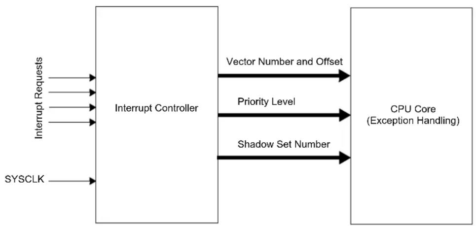
flowchart
graph LR
    A["Interrupt Requests"] --> B["Interrupt Controller"]
    C["SYSCLK"] --> B
    B --> D["Vector Number and Offset"]
    B --> E["Priority Level"]
    B --> F["Shadow Set Number"]
    D --> G["CPU Core (Exception Handling)"]
    E --> G
    F --> G
8.1 CPU Exceptions
CPU coprocessor 0 contains the logic for identifying and managing exceptions. Exceptions can be caused by a variety of sources, including boundary cases in data, external events or program errors. The table below lists the exception types in order of priority.
TABLE 8-1: MIPS32 ® M-CLASS MICROPROCESSOR CORE EXCEPTION TYPES
| Exception Type (In Order of Priority) | Description Branches to | Status Bits Set | Debug Bits Set | EXCCODE | XC32 Function Name | |
| Highest Priority | ||||||
| Reset | Assertion MCLR or a POR. | 0xBFC0_0000 | BEV, ERL | — | — | _on_reset |
| Soft Reset Assertion of a software Reset. | 0xBFC0_0000 BEV, SR, ERL | SR, ERL | — | — | — | _on_reset |
| DSS | EJTAG debug single step. | 0xBFC0_0480 | — | DSS | — | — |
| DINT | EJTAG debug interrupt. Caused by the assertion of the external EJ_DINT input or by setting the EjtagBrk bit in the ECR register. | 0xBFC0_0480 | — | DINT | — | — |
| NMI | Assertion of NMI signal. | 0xBFC0_0000 | BEV, NMI, ERL | — | — | _nmi_handler |
| Interrupt | Assertion of unmasked hardware or software interrupt signal. | See Table 8-2. | IPL[2:0] | — | 0x00 | See Table 8-2. |
| DIB | EJTAG debug hardware instruction break matched. | 0xBFC0_0480 | — | DIB | — | — |
| AdEL | Fetch address alignment error. Fetch reference to protected address. | 0xBFC0_0380 | EXL — 0x04 | general exception handler | ||
| IBE | Instruction fetch bus error. | 0xBFC0_0380 | EXL | — | 0x06 | general exception handler |
| Execute Exception | An instruction-based exception occurred: Integer overflow, trap, system call, breakpoint, floating point, or DSP ASE state disabled exception. | 0xBFC0_0380 | EXL — 0x08 | — | 0x0C | general exception handler |
| Tr | Execution of a trap (when trap condition is true). | 0xBFC0_0380 | EXL | — | 0x0D | general exception handler |
| DDBL/DDBS | EJTAG Data Address Break (address only) or EJTAG data value break on store (address + value). | 0xBFC0_0480 | — | DBL or DDBS | — | — |
| AdEL | Load address alignment error. User mode load reference to kernel address. | 0xBFC0_0380 | EXL — 0x04 | general exception handler | ||
| AdES | Store address alignment error. User mode store to kernel address. | 0xBFC0_0380 | EXL — 0x05 | general exception handler | ||
| Exception Type (In Order of Priority) | Description | Branches to | Status Bits Set | Debug Bits Set | EXCCODE | XC32 Function Name |
| DBE Load or store bus error. 0xBFC0_0380 EXL — 0x07_general_exception_han- | dler | |||||
| DDBL EJTAG data hardware breakpoint matched in load data compare. | 0xBFC0_0480 — DDBL — — | |||||
| CBrk EJTAG complex breakpoint. 0xBFC0_0480 — DIBIMPR, | DDBLIMPR and/or DDBSIMPR | — | — | |||
| Lowest Priority | ||||||
8.2 Interrupts
The PIC32MZ1025W104 uses variable offsets for vector spacing. This allows the interrupt vector spacing to be configured according to application needs. A unique interrupt vector offset can be set for each vector using its associated OFFx register.
For details on the variable offset feature, refer to 8.5.2 "Variable Offset" in Section 8. "Interrupt Controller" (DS60001108) of the "PIC32 Family Reference Manual".
The table below provides the interrupt IRQ, vector and bit location information.
TABLE 8-2: INTERRUPT IRQ, VECTOR AND BIT LOCATION
| Interrupt Source(1) | XC32 Vector Name IRQ # Vector # | Interrupt Bit Location | Persistent Interrupt | |||||
| Flag Enable Priority Sub-priority | ||||||||
| Highest Natural Order Priority | ||||||||
| Core Timer Interrupt | _CORE_TIMER_VECTOR | 0 | OFF000[17:1] | IFS0[0] | IEC0[0] | IPC0[4:2] | IPC0[1:0] | No |
| Core Software Interrupt 0 | _CORE_SOFTWARE_0_VECTOR | 1 | OFF001[17:1] | IFS0[1] | IEC0[1] | IPC0[12:10] | IPC0[9:8] | No |
| Core Software Interrupt 1 | _CORE_SOFTWARE_1_VECTOR | 2 | OFF002[17:1] | IFS0[2] | IEC0[2] | IPC0[20:18] | IPC0[17:16] | No |
| External Interrupt 0 | _EXTERNAL_0_VECTOR | 3 | OFF003[17:1] | IFS0[3] | IEC0[3] | IPC0[28:26] | IPC0[25:24] | No |
| Timer1 | _TIMER_1_VECTOR | 4 | OFF004[17:1] | IFS0[4] | IEC0[4] | IPC1[4:2] | IPC1[1:0] | No |
| Input Capture 1 Error | _INPUT_CAPTURE_1_ERROR_VECTOR | 5 | OFF005[17:1] | IFS0[5] | IEC0[5] | IPC1[12:10] | IPC1[9:8] | Yes |
| Input Capture 1 | _INPUT_CAPTURE_1_VECTOR | 6 | OFF006[17:1] | IFS0[6] | IEC0[6] | IPC1[20:18] | IPC1[17:16] | Yes |
| Output Compare 1 | _OUTPUT_COMPARE_1_VECTOR | 7 | OFF007[17:1] | IFS0[7] | IEC0[7] | IPC1[28:26] | IPC1[25:24] | No |
| External Interrupt 1 | _EXTERNAL_1_VECTOR | 8 | OFF008[17:1] | IFS0[8] | IEC0[8] | IPC2[4:2] | IPC2[1:0] | No |
| Timer2 | _TIMER_2_VECTOR | 9 | OFF009[17:1] | IFS0[9] | IEC0[9] | IPC2[12:10] | IPC2[9:8] | No |
| Input Capture 2 Error | _INPUT_CAPTURE_2_ERROR_VECTOR | 10 | OFF010[17:1] | IFS0[10] | IEC0[10] | IPC2[20:18] | IPC2[17:16] | Yes |
| Input Capture 2 | _INPUT_CAPTURE_2_VECTOR | 11 | OFF011[17:1] | IFS0[11] | IEC0[11] | IPC2[28:26] | IPC2[25:24] | Yes |
| Output Compare 2 | _OUTPUT_COMPARE_2_VECTOR | 12 | OFF012[17:1] | IFS0[12] | IEC0[12] | IPC3[4:2] | IPC3[1:0] | No |
| External Interrupt 2 | _EXTERNAL_2_VECTOR | 13 | OFF013[17:1] | IFS0[13] | IEC0[13] | IPC3[12:10] | IPC3[9:8] | No |
| Timer3 | _TIMER_3_VECTOR | 14 | OFF014[17:1] | IFS0[14] | IEC0[14] | IPC3[20:18] | IPC3[17:16] | No |
| Input Capture 3 Error | _INPUT_CAPTURE_3_ERROR_VECTOR | 15 | OFF015[17:1] | IFS0[15] | IEC0[15] | IPC3[28:26] | IPC3[25:24] | Yes |
| Input Capture 3 | INPUT_CAPTURE_3_VECTOR | 16 | OFF016[17:1] | IFS0[16] | IEC0[16] | IPC4[4:2] | IPC4[1:0] | Yes |
| Output Compare 3 | _OUTPUT_COMPARE_3_VECTOR | 17 | OFF017[17:1] | IFS0[17] | IEC0[17] | IPC4[12:10] | IPC4[9:8] | No |
| External Interrupt 3 | _EXTERNAL_3_VECTOR | 18 | OFF018[17:1] | IFS0[18] | IEC0[18] | IPC4[20:18] | IPC4[17:16] | No |
| Timer4 | _TIMER_4_VECTOR | 19 | OFF019[17:1] | IFS0[19] | IEC0[19] | IPC4[28:26] | IPC4[25:24] | No |
| Input Capture 4 Error | INPUT_CAPTURE_4_ERROR_VECTOR | 20 | OFF020[17:1] | IFS0[20] | IEC0[20] | IPC5[4:2] | IPC5[1:0] | Yes |
| Input Capture 4 | _INPUT_CAPTURE_4_VECTOR | 21 | OFF021[17:1] | IFS0[21] | IEC0[21] | IPC5[12:10] | IPC5[9:8] | Yes |
| Output Compare 4 | _OUTPUT_COMPARE_4_VECTOR | 22 | OFF022[17:1] | IFS0[22] | IEC0[22] | IPC5[20:18] | IPC5[17:16] | No |
| External Interrupt 4 | _EXTERNAL_4_VECTOR | 23 | OFF023[17:1] | IFS0[23] | IEC0[23] | IPC5[28:26] | IPC5[25:24] | No |
| Timer5 | _TIMER_5_VECTOR | 24 | OFF024[17:1] | IFS0[24] | IEC0[24] | IPC6[4:2] | IPC6[1:0] | No |
| FC Programming Event | FLASH_CONTROL_VECTOR | 30 | OFF030[17:1] | IFS0[30] | IEC0[30] | IPC7[20:18] | IPC7[17:16] | No |
| Interrupt Source(1) | XC32 Vector Name | IRQ # | Vector # | Interrupt Bit Location | Persistent Interrupt | |||
| Flag | Enable | Priority | Sub-priority | |||||
| Prefetch module Event_PREFETCH | VECTOR 31 OFF031[17:1] IFS0[31] IEC0[31] IPC7 | [28:26] IPC7[25:24] No | ||||||
| PFW CRC Event | _PFW_CRC_VECTOR | 32 | OFF032[17:1] | IFS1[0] | IEC1[0] | IPC8[4:2] | IPC8[1:0] | No |
| Real Time Clock | _RTCC_VECTOR | 33 | OFF033[17:1] | IFS1[1] | IEC1[1] | IPC8[12:10] | IPC8[9:8] | No |
| Combined Interrupt | _USB_VECTOR | 34 | OFF034[17:1] | IFS1[2] | IEC1[2] | IPC8[20:18] | IPC8[17:16] | Yes |
| SPI 1 Fault | _SPI1_FAULT_VECTOR | 35 | OFF035[17:1] | IFS1[3] | IEC1[3] | IPC8[28:26] | IPC8[25:24] | Yes |
| SPI 1 Receive Done | _SPI1_RX_VECTOR | 36 | OFF036[17:1] | IFS1[4] | IEC1[4] | IPC9[4:2] | IPC9[1:0] | Yes |
| SPI 1 Transfer Done | _SPI1_TX_VECTOR | 37 | OFF037[17:1] | IFS1[5] | IEC1[5] | IPC9[12:10] | IPC9[9:8] | Yes |
| UART1 Fault | _UART1_FAULT_VECTOR | 38 | OFF038[17:1] | IFS1[6] | IEC1[6] | IPC9[20:18] | IPC9[17:16] | Yes |
| UART1 Receive Done | _UART1_RX_VECTOR | 39 | OFF039[17:1] | IFS1[7] | IEC1[7] | IPC9[28:26] | IPC9[25:24] | Yes |
| UART1 Transfer Done | _UART1_TX_VECTOR | 40 | OFF040[17:1] | IFS1[8] | IEC1[8] | IPC10[4:2] | IPC10[1:0] | Yes |
| I2C 1 Bus Collision Event | _I2C1_BUS_VECTOR | 41 | OFF041[17:1] | IFS1[9] | IEC1[9] | IPC10[12:10] | IPC10[9:8] | Yes |
| I2C 1 Slave Event | _I2C1_SLAVE_VECTOR | 42 | OFF042[17:1] | IFS1[10] | IEC1[10] | IPC10[20:18] | IPC10[17:16] | Yes |
| I2C 1 Master Event | _I2C1_MASTER_VECTOR | 43 | OFF043[17:1] | IFS1[11] | IEC1[11] | IPC10[28:26] | IPC10[25:24] | Yes |
| PortA Input Change Interrupt | _CHANGE_NOTICE_A_VECTOR | 44 | OFF044[17:1] | IFS1[12] | IEC1[12] | IPC11[4:2] | IPC11[1:0] | Yes |
| PortB Input Change Interrupt | _CHANGE_NOTICE_B_VECTOR | 45 | OFF045[17:1] | IFS1[13] | IEC1[13] | IPC11[12:10] | IPC11[9:8] | Yes |
| PortC Input Change Interrupt | _CHANGE_NOTICE_C_VECTOR | 46 | OFF046[17:1] | IFS1[14] | IEC1[14] | IPC11[20:18] | IPC11[17:16] | Yes |
| PortK Input Change Interrupt | _CHANGE_NOTICE_K_VECTOR | 47 | OFF047[17:1] | IFS1[15] | IEC1[15] | IPC11[28:26] | IPC11[25:24] | Yes |
| SPI 2 Fault | _SPI2_FAULT_VECTOR | 53 | OFF053[17:1] | IFS1[21] | IEC1[21] | IPC13[12:10] | IPC13[9:8] | Yes |
| SPI 2 Receive Done | _SPI2_RX_VECTOR | 54 | OFF054[17:1] | IFS1[22] | IEC1[22] | IPC13[20:18] | IPC13[17:16] | Yes |
| SPI 2 Transfer Done | _SPI2_TX_VECTOR | 55 | OFF055[17:1] | IFS1[23] | IEC1[23] | IPC13[28:26] | IPC13[25:24] | Yes |
| UART 2 Error | _UART2_FAULT_VECTOR | 56 | OFF056[17:1] | IFS1[24] | IEC1[24] | IPC14[4:2] | IPC14[1:0] | Yes |
| UART 2 Receiver | _UART2_RX_VECTOR | 57 | OFF057[17:1] | IFS1[25] | IEC1[25] | IPC14[12:10] | IPC14[9:8] | Yes |
| UART 2 Transmitter | _UART2_TX_VECTOR | 58 | OFF058[17:1] | IFS1[26] | IEC1[26] | IPC14[20:18] | IPC14[17:16] | Yes |
| I2C 2 Bus Collision Event | _I2C2_BUS_VECTOR | 59 | OFF059[17:1] | IFS1[27] | IEC1[27] | IPC14[28:26] | IPC14[25:24] | Yes |
| I2C 2 Slave Event | _I2C2_SLAVE_VECTOR | 60 | OFF060[17:1] | IFS1[28] | IEC1[28] | IPC15[4:2] | IPC15[1:0] | Yes |
| I2C 2 Master Event | _I2C2_MASTER_VECTOR | 61 | OFF061[17:1] | IFS1[29] | IEC1[29] | IPC15[12:10] | IPC15[9:8] | Yes |
| UART 3 Error | _UART3_FAULT_VECTOR | 62 | OFF062[17:1] | IFS1[30] | IEC1[30] | IPC15[20:18] | IPC15[17:16] | Yes |
| UART 3 Receiver | _UART3_RX_VECTOR | 63 | OFF063[17:1] | IFS1[31] | IEC1[31] | IPC15[28:26] | IPC15[25:24] | No |
| UART 3 Transmitter | _UART3_TX_VECTOR | 64 | OFF064[17:1] | IFS2[0] | IEC2[0] | IPC16[4:2] | IPC16[1:0] | No |
| DMA Channel 0 | _DMA0_VECTOR | 68 | OFF068[17:1] | IFS2[4] | IEC2[4] | IPC17[4:2] | IPC17[1:0] | No |
| DMA Channel 1 | _DMA1_VECTOR | 69 | OFF069[17:1] | IFS2[5] | IEC2[5] | IPC17[12:10] | IPC17[9:8] | No |
| DMA Channel 2 | _DMA2_VECTOR | 70 | OFF070[17:1] | IFS2[6] | IEC2[6] | IPC17[20:18] | IPC17[17:16] | No |
| DMA Channel 3_DMA3_VECTOR 71 | OFF071[17:1] IFS2[7] IEC2[7] IPC17[28:26] | IPC17 | [25:24] No | |||||
| DMA Channel 4_DMA4_VECTOR 72 | OFF072[17:1] IFS2[8] IEC2[8] IPC18[4:2] IPC18[1:0] No | |||||||
| DMA Channel 5_DMA5_VECTOR 73 | OFF073[17:1] IFS2[9] IEC2[9] IPC18[12:10] IPC18[9:8] No | |||||||
| DMA Channel 6_DMA6_VECTOR 74 | OFF074[17:1] IFS2[10] IEC2[10] IPC18[20:18] IPC18[17:16] No | |||||||
| DMA Channel 7_DMA7_VECTOR 75 | OFF075[17:1] IFS2[11] IEC2[11] IPC18[28:26] IPC18[25:24] No | |||||||
| Timer 6 | _TIMER_6_VECTOR | 76 | OFF076[17:1] | IFS2[12] | IEC2[12] | IPC19[4:2] | IPC19[1:0] | No |
| Timer 7 | _TIMER_7_VECTOR | 80 | OFF080[17:1] | IFS2[16] | IEC2[16] | IPC20[4:2] | IPC20[1:0] | No |
| Wi-Fi SMC Event | _RFSMC_VECTOR | 83 | OFF083[17:1] | IFS2[19] | IEC2[19] | IPC20[28:26] | IPC20[25:24] | Yes |
| Wi-Fi MAC Event | _RFMAC_VECTOR | 84 | OFF084[17:1] | IFS2[20] | IEC2[20] | IPC21[4:2] | IPC21[1:0] | Yes |
| Cycle Time Register Event | _CTR1_EVENT_VECTOR | 85 | OFF085[17:1] | IFS2[21] | IEC2[21] | IPC21[12:10] | IPC21[9:8] | No |
| Wi-Fi Timer 0 Event | _RFTM0_VECTOR | 86 | OFF086[17:1] | IFS2[22] | IEC2[22] | IPC21[20:18] | IPC21[17:16] | Yes |
| Wi-Fi Timer 1 Event | _RFTM1_VECTOR | 87 | OFF087[17:1] | IFS2[23] | IEC2[23] | IPC21[28:26] | IPC21[25:24] | Yes |
| Wi-Fi Timer 2 Event | _RFTM2_VECTOR | 88 | OFF088[17:1] | IFS2[24] | IEC2[24] | IPC22[4:2] | IPC22[1:0] | Yes |
| Wi-Fi Timer 3 Event | _RFTM3_VECTOR | 89 | OFF089[17:1] | IFS2[25] | IEC2[25] | IPC22[12:10] | IPC22[9:8] | Yes |
| Cycle Time Reg Trig. Out Ev. | _CTR1_TRG_VECTOR | 90 | OFF090[17:1] | IFS2[26] | IEC2[26] | IPC22[20:18] | IPC22[17:16] | No |
| Wi-Fi WCOE Event | _RFWCOE_VECTOR | 91 | OFF091[17:1] | IFS2[27] | IEC2[27] | IPC22[28:26] | IPC22[25:24] | Yes |
| ADC global | _ADC_VECTOR | 92 | OFF092[17:1] | IFS2[28] | IEC2[28] | IPC23[4:2] | IPC23[1:0] | No |
| ADC Digital Comparator 1 | _ADC_DC1_VECTOR | 94 | OFF094[17:1] | IFS2[30] | IEC2[30] | IPC23[20:18] | IPC23[17:16] | No |
| ADC Digital Comparator 2 | _ADC_DC2_VECTOR | 95 | OFF095[17:1] | IFS2[31] | IEC2[31] | IPC23[28:26] | IPC23[25:24] | No |
| ADC Digital Filter 1 | _ADC_DF1_VECTOR | 96 | OFF096[17:1] | IFS3[0] | IEC3[0] | IPC24[4:2] | IPC24[1:0] | No |
| ADC Digital Filter 2 | _ADC_DF2_VECTOR | 97 | OFF097[17:1] | IFS3[1] | IEC3[1] | IPC24[12:10] | IPC24[9:8] | No |
| ADC Fault Interrupt | _ADC_FAULT_VECTOR | 100 | OFF100[17:1] | IFS3[4] | IEC3[4] | IPC25[4:2] | IPC25[1:0] | No |
| ADC EO Scan | _ADC_EOS_VECTOR | 101 | OFF101[17:1] | IFS3[5] | IEC3[5] | IPC25[12:10] | IPC25[9:8] | No |
| ADC Analog Ready | _ADCARDY_VECTOR | 102 | OFF102[17:1] | IFS3[6] | IEC3[6] | IPC25[20:18] | IPC25[17:16] | No |
| ADC Update Ready after Suspend | _ADC_URDY_VECTOR | 103 | OFF103[17:1] | IFS3[7] | IEC3[7] | IPC25[28:26] | IPC25[25:24] | No |
| ADC 1st Class Buffer Transfer | _ADC_DMA_VECTOR | 104 | OFF104[17:1] | IFS3[8] | IEC3[8] | IPC26[4:2] | IPC26[1:0] | No |
| ADC A Data #0 | _ADC_DATA0_VECTOR | 106 | OFF106[17:1] | IFS3[10] | IEC3[10] | IPC26[20:18] | IPC26[17:16] | No |
| ADC A Data #1 | _ADC_DATA1_VECTOR | 107 | OFF107[17:1] | IFS3[11] | IEC3[11] | IPC26[28:26] | IPC26[25:24] | No |
| ADC A Data #2 | _ADC_DATA2_VECTOR | 108 | OFF108[17:1] | IFS3[12] | IEC3[12] | IPC27[4:2] | IPC27[1:0] | No |
| ADC A Data #3 | _ADC_DATA3_VECTOR | 109 | OFF109[17:1] | IFS3[13] | IEC3[13] | IPC27[12:10] | IPC27[9:8] | No |
| ADC A Data #4 | _ADC_DATA4_VECTOR | 110 | OFF110[17:1] | IFS3[14] | IEC3[14] | IPC27[20:18] | IPC27[17:16] | No |
| ADC A Data #5 | _ADC_DATA5_VECTOR | 111 | OFF111[17:1] | IFS3[15] | IEC3[15] | IPC27[28:26] | IPC27[25:24] | No |
| ADC A Data #6_ADC_DATA6_VECTOR | TOR 112 OFF112[17:1] IFS3[16] IEC3[16] IPC28[4:2] | IPC28[1:0] No | ||||||
| ADC A Data #7 | _ADC_DATA7_VECTOR | 113 | OFF113[17:1] | IFS3[17] | IEC3[17] | IPC28[12:10] | IPC28[9:8] | No |
| ADC A Data #8 | _ADC_DATA8_VECTOR | 114 | OFF114[17:1] | IFS3[18] | IEC3[18] | IPC28[20:18] | IPC28[17:16] | No |
| ADC A Data #9 | _ADC_DATA9_VECTOR | 115 | OFF115[17:1] | IFS3[19] | IEC3[19] | IPC28[28:26] | IPC28[25:24] | No |
| ADC A Data #10_ADC_DATA10_VECTOR | 116 OFF116[17:1] IFS3[20] IEC3[20] IPC29[4:2] | IPC29[1:0] No | ||||||
| ADC A Data #11_ADC_DATA11_VECTOR | 117 OFF117[17:1] IFS3[21] IEC3[21] IPC29[12:10] | IPC29[9:8] No | ||||||
| ADC A Data #12 | _ADC_DATA12_VECTOR | 118 | OFF118[17:1] | IFS3[22] | IEC3[22] | IPC29[20:18] | IPC29[17:16] | No |
| ADC A Data #13 | _ADC_DATA13_VECTOR | 119 | OFF119[17:1] | IFS3[23] | IEC3[23] | IPC29[28:26] | IPC29[25:24] | No |
| ADC A Data #14_ADC_DATA14_VECTOR | 120 OFF120[17:1] IFS3[24] IEC3[24] IPC30[4:2] | IPC30[1:0] No | ||||||
| ADC A Data #15_ADC_DATA15_VECTOR | 121 OFF121[17:1] IFS3[25] IEC3[25] IPC30[12:10] | IPC30[9:8] No | ||||||
| ADC A Data #16 | _ADC_DATA16_VECTOR | 122 | OFF122[17:1] | IFS3[26] | IEC3[26] | IPC30[20:18] | IPC30[17:16] | No |
| ADC A Data #17 | _ADC_DATA17_VECTOR | 123 | OFF123[17:1] | IFS3[27] | IEC3[27] | IPC30[28:26] | IPC30[25:24] | No |
| ADC A Data #18_ADC_DATA18_VECTOR | 124 OFF124[17:1] IFS3[28] IEC3[28] IPC31[4:2] | IPC31[1:0] No | ||||||
| ADC A Data #19_ADC_DATA19_VECTOR | 125 OFF125[17:1] IFS3[29] IEC3[29] IPC31[12:10] | IPC31[9:8] No | ||||||
| ADC A Data #20 | _ADC_DATA20_VECTOR | 126 | OFF126[17:1] | IFS3[30] | IEC3[30] | IPC31[20:18] | IPC31[17:16] | No |
| ADC A Data #21 | _ADC_DATA21_VECTOR | 127 | OFF127[17:1] IFS3[31] IEC3[31] IPC31[28:26] IPC31[25:24] No | |||||
| ADC A Data #22 | _ADC_DATA22_VECTOR | 128 | OFF128[17:1] | IFS4[0] | IEC4[0] | IPC32[4:2] | IPC32[1:0] | No |
| ADC A Data #23 | _ADC_DATA23_VECTOR | 129 | OFF129[17:1] | IFS4[1] | IEC4[1] | IPC32[12:10] | IPC32[9:8] | No |
| CAN Combined Interrupt | _CAN1_VECTOR | 142 | OFF142[17:1] | IFS4[14] | IEC4[14] | IPC35[20:18] | IPC35[17:16] | Yes |
| CAN Combined Interrupt | _CAN2_RX_VECTOR | 143 | OFF143[17:1] | IFS4[15] | IEC4[15] | IPC35[28:26] | IPC35[25:24] | Yes |
| CAN Combined Interrupt | _CAN2_TX_VECTOR | 144 | OFF144[17:1] | IFS4[16] | IEC4[16] | IPC36[4:2] | IPC36[1:0] | Yes |
| CAN Combined Interrupt | _CAN2_MISC_VECTOR | 145 | OFF145[17:1] | IFS4[17] | IEC4[17] | IPC36[12:10] | IPC36[9:8] | Yes |
| SQI Event Completion | _SQI1_VECTOR | 150 | OFF150[17:1] | IFS4[22] | IEC4[22] | IPC37[20:18] | IPC37[17:16] | Yes |
| PTG Step Complete | _PTG0_STEP_VECTOR | 152 | OFF152[17:1] | IFS4[24] | IEC4[24] | IPC38[4:2] | IPC38[1:0] | No |
| PTG Watchdog Timeout | _PTG0_WDT_VECTOR | 153 | OFF153[17:1] | IFS4[25] | IEC4[25] | IPC38[12:10] | IPC38[9:8] | No |
| PTG Int. Trigger 0 | _PTG0_TRG0_VECTOR | 154 | OFF154[17:1] | IFS4[26] | IEC4[26] | IPC38[20:18] | IPC38[17:16] | No |
| PTG Int. Trigger 1 | _PTG0_TRG1_VECTOR | 155 | OFF155[17:1] | IFS4[27] | IEC4[27] | IPC38[28:26] | IPC38[25:24] | No |
| PTG Int. Trigger 2 | _PTG0_TRG2_VECTOR | 156 | OFF156[17:1] | IFS4[28] | IEC4[28] | IPC39[4:2] | IPC39[1:0] | No |
| PTG Int. Trigger 3 | _PTG0_TRG3_VECTOR | 157 | OFF157[17:1] | IFS4[29] | IEC4[29] | IPC39[12:10] | IPC39[9:8] | No |
| Core perform. counter event | _CORE_PERF_COUNT_VECTOR | 162 | OFF162[17:1] | IFS5[2] | IEC5[2] | IPC40[20:18] | IPC40[17:16] | Yes |
| Fast Debug Channel Event | _CORE_FAST_DEBUG_CHAN_VECTOR | 163 | OFF163[17:1] | IFS5[3] | IEC5[3] | IPC40[28:26] | IPC40[25:24] | Yes |
| Crypt Engine 1 Event | _CRYPTO_VECTOR | 164 | OFF164[17:1] | IFS5[4] | IEC5[4] | IPC41[4:2] | IPC41[1:0] | Yes |
| Interrupt Source^(1) | XC32 Vector Name | IRQ # | Vector # | Interrupt Bit Location | Persistent Interrupt | |||
| Flag | Enable | Priority Sub | -priority | |||||
| Ethernet network event | ETHERNET_VECTOR | 165 | OFF165[17:1] | IFS5[5] | IEC5[5] | IPC41[12:10] | IPC41[9:8] | Yes |
| IRQEnd _CRYPTO1_VECTOR 166 | OFF166[17:1] IFS5[6] IEC5[6] IPC41[20:18] IPC41[17:16] Yes | |||||||
| IRQErr | CRYPTO1_FAULT_VECTOR | 167 | OFF167[17:1] | IFS5[7] | IEC5[7] | IPC41[28:26] | IPC41[25:24] | Yes |
| CVD Event Interrupt | _CVD_EVENT_VECTOR | 168 | OFF168[17:1] | IFS5[8] | IEC5[8] | IPC42[4:2] | IPC42[1:0] | No |
| Lowest Natural Order Priority | ||||||||
8.3 Interrupt Control Registers
TABLE 8-3: INTERRUPT REGISTER MAP
| Virtual Address(BF81_#) | Register Name(1) | Bit Range | Bits | All Resets | ||||||||||||||||
| 31/15 30 | 14 29/13 28/ | 12 27/11 26/ | 10 25/9 24/ | 8 23/7 22/6 21/5 20/4 | 19/3 18/2 17/1 | 16/0 | ||||||||||||||
| 0000 | INTCON | 31:16 | NMIKEY[7:0] | — | — | — | — | — | — | — | — | — | 0000 | |||||||
| 15:0 | — | — | — | MVEC | — | IPC[2:0] | — | — | — | INT4EP | INT3EP | INT2EP | INT1EP | INT0EP | 0000 | |||||
| 0010 | PRISS | 31:16 | PRI7SS[3:0] | PRI6SS[3:0] | PRI5SS[3:0] | PRIWSS[3:0] | 0000 | |||||||||||||
| 15:0 | PRI3SS[3:0] | PRI2SS[3:0] | PRI1SS[3:0] | — | — | — | 550 | 0000 | ||||||||||||
| 0020 | INTSTAT | 31:16 | — | — | — | — | — | — | — | — | — | — | — | — | — | — | — | — | 0000 | |
| 15:0 | — | — | — | — | — | — | SRIPL[2:0] | SIRQ[7:0] | 0000 | |||||||||||
| 0030 | IPTMR | 31:16 | IPTMR[31:16] | 0000 | ||||||||||||||||
| 15:0 | IPTMR[15:0] | 0020 | ||||||||||||||||||
| 0040 | IFS0 | 31:16 | PREIF FO | CIF | — | — | — | — | — | T5IF | INT4IF | OC4IF | IC4IF | IC4EIF | T4IF | INT3IF | OC3IF | IC3IF | 0000 | |
| 15:0 | IC3EIF | T3IF | INT2IF | OC2IF | IC2IF | IC2EIF | T2IF | INT1IF | OC1IF | IC1IF | IC1EIF | T1IF | INT0IF | CS1IF | CS0IF | CTIF | 0020 | |||
| 0050 | IFS1 | 31:16 | U3RXIF | U3EIF | I2C2MIF | I2C2SIF | I2C2BIF | U2TXIF | U2RXIF | U2EIF | SPI2TXIF | SPI2RXIF | SPI2EIF | — | — | — | — | 0000 | ||
| 15:0 | CNKIF | CNCF | CNBIF | CNAIF | I2C1MIF | I2C1SIF | I2C1BIF | U1TXIF | U1RXIF | U1EIF | SPI1TXIF | SPI1RXIF | SPI1EIF | USBIF | RTCCIF | PFWCRCIF | 0030 | |||
| 0060 | IFS2 | 31:16 | ADCDC2IF | ADCDC1IF | — | ADCIF | RFWCOEIF | CTR1TRGIF | RFTM3IF | RFTM2IF | RFTM1IF | RFTM0IF | CTR1EVIF | RFMACIF | RFSMCIF | — | — | T7IF | 0003 | |
| 15:0 | — | — | — | T9IF | DMA7IF | DMA8IF | DMA5IF | DMA4IF | DMA3IF | DMA2IF | DMA1IF | DMA0IF | — | — | — | U3TXIF | 0003 | |||
| 0070 | IFS3 | 31:16 | ADCD21IF | ADCD20IF | ADCD19IF | ADCD18IF | ADCD17IF | ADCD16IF | ADCD15IF | ADCD14IF | ADCD13IF | ADCD12IF | ADCD11IF | ADCD10IF | ADCD9IF | ADCD8IF | ADCD7IF | ADCD8IF | 0003 | |
| 15:0 | ADDC5IF | ADCD4IF | ADCD3IF | ADCD2IF | ADCD1IF | ADCD0IF | — | ADCFCBTIF | ADCURDYIF | ADCARDYIF | ADCDEOSIF | ADCFLTIF | — | — | ADCDF2IF | ADCDF1IF | 0000 | |||
| 0080 | IFS4 | 31:16 | — | — | PTG0TR3IF | PTG0TR2IF | PTG0TR1IF | PTG0TR0IF | PTGWDTIF | PTGSTEP1IF | — | SQ1IF | — | — | — | — | CAN2IF | CAN2TXIF | 0000 | |
| 15:0 | CAN2RXIF | CAN1IF | — | — | — | — | — | — | — | — | — | — | — | — | ADCDD23IF | ADCDD22IF | 0000 | |||
| 0090 | IFS5 | 31:16 | — | — | — | — | — | — | — | — | — | — | — | — | — | — | — | — | 0000 | |
| 15:0 | — | — | — | — | — | — | — | — | CRPT1EIF | CRPT1IF | ETHIF | CRPTIF | FDCIF | MPUPCIF | — | — | 0000 | |||
| 00C0 | IEC0 | 31:16 | PREIE | FCEIE | — | — | — | — | — | T5IE | INT4IE | OC4IE | IC4IE | IC4EIE | T4IE | INT3IE | OC3IE | IC3IE | 0003 | |
| 15:0 | IC3EIE | T3IE | INT2IE | OC2IE | IC2IE | IC2EIE | T2IE | INT1IE | OC1IE | IC1IE | IC1EIE | T1IE | INT0IE | CS1IE | CS0IE | CTIE | 0000 | |||
| 00D0 | IEC1 | 31:16 | U3RXIE | U3EIE | I2C2MIE | I2C2SIE | I2C2BIE | U2TXIE | U2RXIE | U2EIE | SPI2TXIE | SPI2RXIE | SPI2EIE | — | — | — | — | — | 0000 | |
| 15:0 | CNKIE | CNCE | CNBIE | CNAIE | I2C1MIE | I2C1SIE | I2C1BIE | U1TXIE | U1RXIE | U1EIE | SPI1TXIE | SPI1RXIE | SPI1EIE | USBIE | RTCCIE | PFWCRCIE | 0020 | |||
| 00E0 | IEC2 | 31:16 | ADCDC2IE | ADCDC1IE | — | ADCIE | RFWCOEIF | CTRTRGIE | RFTM3IE | RFTM2IE | RFTM1IE | RFTM0IE | CTREVIE | RFMACIE | RFSMCIE | — | — | T7IE | 0030 | |
| 15:0 | — | — | — | T8IE | DMA7IE | DMA8IE | DMA5IE | DMA4IE | DMA3IE | DMA2IE | DMA1IE | DMA0IE | — | — | — | U3TXIE | 0000 | |||
| 00FD | IEC3 | 31:16 | ADCDC21IE | ADCDC20IE | ADCDC19IE | ADCDC18IE | ADCDC17IE | ADCDC16IE | ADCDC15IE | ADCDC14IE | ADCDC13IE | ADCDC12IE | ADCDC11IE | ADCDC10IE | ADCDC9IE | ADCDC8IE | ADCDD7IE | ADCDD8IE | 0030 | |
| 15:0 | ADCDSIE | ADCDS4IE | ADCDS3IE | ADCDS2IE | ADCDS1IE | ADCDS0IE | — | ADCFCBTIE | ADCUCRDYIE | ADCARDYIE | ADCDEOSIE | ADCFLTIE | — | — | ADCDCF2IE | ADCDCF1IE | 0000 | |||
| 0100 | IEC4 | 31:16 | — | — | PTG0TR3IE | PTG0TR2IE | PTG0TR1IE | PTG0TR0IE | PTGWDTIE | PTGSTEP1IE | — | SQIE | — | — | — | — | CAN2IE | CAN2TXIE | 0000 | |
| 15:0 | CAN2RXIE | CAN1IE | — | — | — | — | — | — | — | — | — | — | — | — | ADCDD23IE | ADCDD22IE | 0000 | |||
| 0110 | IEC5 | 31:16 | — | — | — | — | — | — | — | — | — | — | — | — | — | — | — | — | 0000 | |
| 15:0 | — | — | — | — | — | — | — | — | CRPT1EIE | CRPT1IE | ETHIE | CRPTIE | FDCIE | MPUPCIE | — | — | 0000 | |||
Legend: x = unknown value on Reset; — = unimplemented, read as '0'. Reset values are shown in hexadecimal.
Note 1: All registers in this table with the exception of the OFFx registers, have corresponding CLR, SET, and INV registers at their virtual addresses, plus offsets of 0x4, 0x8 and 0xC, respectively. See
Section 13.3 "CLR, SET and INV Registers" for more information
2: This bit or register is not available on devices without a CAN module.
3: This bit or register is not available on devices without a Crypto module.
TABLE 8-3: INTERRUPT REGISTER MAP (CONTINUED)
| Virtual Address(BF81_f9) | Register Name(1) | Bit Range | Bits | All Resets | |||||||||||||||
| 31/15 | 30/14 | 29/13 | 28/12 | 27/11 | 26/10 | 25/9 | 24/8 | 23/7 | 22/6 | 21/5 | 20/4 | 19/3 | 18/2 | 17/1 | 16/0 | ||||
| 0140 | IPC0 | 31:16 | — — INT0IP[2:0] INT0IS[1:0] — — — | CS1IP[2:0] CS1IS[1:0] 00:00 | |||||||||||||||
| 15:0 | — | — | — | CS0IP[2:0] | CS0IS[1:0] | — | — | — | CTIP[2:0] | CTIS[1:0] | 00:00 | ||||||||
| 0150 | IPC1 | 31:16 | — | — | — | OC1IP[2:0] | OC1IS[1:0] | — | — | — | IC1IP[2:0] | IC1IS[1:0] | 00:00 | ||||||
| 15:0 | — | — | — | IC1EP[2:0] | IC1EIS[1:0] | — | — | — | T1IP[2:0] | T1IS[1:0] | 00:00 | ||||||||
| 0160 | IPC2 | 31:16 | — | — | — | IC2IP[2:0] | IC2IS[1:0] | — | — | — | IC2EIP[2:0] | IC2EIS[1:0] | 00:00 | ||||||
| 15:0 | — | — | — | T2IP[2:0] | T2IS[1:0] | — | — | — | INT1IP[2:0] | INT1IS[1:0] | 00:00 | ||||||||
| 0170 | IPC3 | 31:16 | — | — | — | IC3EIP[2:0] | IC3EIS[1:0] | — | — | — | T3IP[2:0] | T3IS[1:0] | 00:00 | ||||||
| 15:0 | — | — | — | INT2IP[2:0] | INT2IS[1:0] | — | — | — | OC2IP[2:0] | OC2IS[1:0] | 00:00 | ||||||||
| 0160 | IPC4 | 31:16 | — | — | — | T4IP[2:0] | T4IS[1:0] | — | — | — | INT3IP[2:0] | INT3IS[1:0] | 00:00 | ||||||
| 15:0 | — | — | — | OC3IP[2:0] | OC3IS[1:0] | — | — | — | IC3IP[2:0] | IC3IS[1:0] | 00:00 | ||||||||
| 0190 | IPC5 | 31:16 | — | — | — | INT4IP[2:0] | INT4IS[1:0] | — | — | — | OC4IP[2:0] | OC4IS[1:0] | 00:00 | ||||||
| 16:0 | — | — | — | IC4IP[2:0] | IC4IS[1:0] | — | — | — | IC4EIP[2:0] | IC4EIS[1:0] | 00:00 | ||||||||
| 01A0 | IPC6 | 31:16 | — | — | — | — | — | — | — | — | — | — | 00:00 | ||||||
| 16:0 | — | — | — | — | — | — | — | — | T5IP[2:0] | T5IS[1:0] | 00:00 | ||||||||
| 01B0 | IPC7 | 31:16 | — | — | — | PREIP[2:0] | PREIS[1:0] | — | — | — | FCEIP[2:0] | FCEIS[1:0] | 00:00 | ||||||
| 15:0 | — | — | — | — | — | — | — | — | — | — | 00:00 | ||||||||
| 01C0 | IPC8 | 31:16 | — | — | — | SP11EIP[2:0] | SP11EIS[1:0] | — | — | — | USBIP[2:0] | USBIS[1:0] | 00:00 | ||||||
| 15:0 | — | — | — | RTCCIP[2:0] | RTCCIS[1:0] | — | — | — | PFWCRCIP[2:0] | PFWCRCIS[1:0] | 00:00 | ||||||||
| 01D0 | IPC9 | 31:16 | — | — | — | U1RXIP[2:0] | U1RXIS[1:0] | — | — | — | U1EIP[2:0] | U1EIS[1:0] | 00:00 | ||||||
| 15:0 | — | — | — | SP11TXIP[2:0] | SP11TXIS[1:0] | — | — | — | SP11RXIP[2:0] | SP11RXIS[1:0] | 00:00 | ||||||||
| 01E0 | IPC10 | 31:16 | — | — | — | I2C1MIP[2:0] | I2C1MIS[1:0] | — | — | — | I2C1SIP[2:0] | I2C1SIS[1:0] | 00:00 | ||||||
| 15:0 | — | — | — | I2C1BIP[2:0] | I2C1MIS[1:0] | — | — | — | U1TXIP[2:0] | U1TXIS[1:0] | 00:00 | ||||||||
| 01F0 | IPC11 | 31:16 | — | — | — | CNKIP[2:0] | CNKIS[1:0] | — | — | — | CNCIP[2:0] | CNCIS[1:0] | 00:00 | ||||||
| 15:0 | — | — | — | CNBIP[2:0] | CNBIS[1:0] | — | — | — | CNAIP[2:0] | CNAIS[1:0] | 00:00 | ||||||||
| 0210 | IPC13 | 31:16 | — | — | — | SP12TXIP[2:0] | SP12TXIS[1:0] | — | — | — | SP12RXIP[2:0] | SP12RXIS[1:0] | 00:00 | ||||||
| 15:0 | — | — | — | SP12EIP[2:0] | SP12EIS[1:0] | — | — | — | — | — | — | — | — | 00:00 | |||||
| 0220 | IPC14 | 31:16 | — | — | — | I2C2BIP[2:0] | I2C2BIS[1:0] | — | — | — | U2TXIP[2:0] | U2TXIS[1:0] | 00:00 | ||||||
| 16:0 | — | — | — | U2RXIP[2:0] | U2RXIS[1:0] | — | — | — | U2EIP[2:0] | U2EIS[1:0] | 00:00 | ||||||||
| 0230 | IPC15 | 31:16 | — | — | — | U3RXIP[2:0] | U3RXIS[1:0] | — | — | — | U3EIP[2:0] | U3EIS[1:0] | 00:00 | ||||||
| 15:0 | — | — | — | I2C2MIP[2:0] | I2C2MIS[1:0] | — | — | — | I2C2SIP[2:0] | I2C2SIS[1:0] | 00:00 | ||||||||
| 0240 | IPC16 | 31:16 | — | — | — | — | — | — | — | — | — | — | — | — | — | — | — | — | 00:00 |
| 15:0 | — | — | — | — | — | — | — | — | — | — | — | U3TXIP[2:0] | U3TXIS[1:0] | 00:00 | |||||
Legend: x = unknown value on Reset; — = unimplemented, read as '0'. Reset values are shown in hexadecimal.
Note 1: All registers in this table with the exception of the OFFx registers, have corresponding CLR, SET, and INV registers at their virtual addresses, plus offsets of 0x4, 0x8 and 0xC, respectively. See Section 13.3 "CLR, SET and INV Registers" for more information.
2: This bit or register is not available on devices without a CAN module.
3: This bit or register is not available on devices without a Crypto module.
TABLE 8-3: INTERRUPT REGISTER MAP (CONTINUED)
| Virtual Address(BF81_#) | Register Name(1) | Bit Range | Bits | All Resets | |||||||||||||||
| 31/15 | 30/14 | 29/13 | 28/12 | 27/11 | 26/10 | 25/9 | 24/8 | 23/7 | 22/6 | 21/5 | 20/4 | 19/3 | 18/2 | 17/1 | 16/0 | ||||
| C250 | IPC17 | 31:15 | — — | DMA3IP[2:0] DMA3IS[1:0] | — — | DMA2IP[2:0] DMA2IS[1:0] **** | |||||||||||||
| 15:0 | — — | DMA1IP[2:0] DMA1IS[1:0] | — — | DMA0IP[2:0] DMA0IS[1:0] **** | |||||||||||||||
| C260 | IPC18 | 31:16 | — | — | — | DMA7IP[2:0] | DMA7IS[1:0] | — | — | — | DMA6IP[2:0] | DMA8IS[1:0] | C000 | ||||||
| 15:0 | — | — | — | DMA5IP[2:0] | DMA5IS[1:0] | — | — | — | DMA4IP[2:0] | DMA4IS[1:0] | C000 | ||||||||
| C270 | IPC19 | 31:16 | — | — | — | — | — | — | — | — | — | — | — | — | — | — | — | — | C000 |
| 15:0 | — | — | — | — | — | — | — | — | — | — | — | T6IP[2:0] | T6IS[1:0] | C000 | |||||
| C280 | IPC20 | 31:16 | — | — | — | RFSMCIP[2:0] | RFSMCIS[1:0] | — | — | — | — | — | — | — | — | C000 | |||
| 15:0 | — | — | — | — | — | — | — | — | — | — | — | T7IP[2:0] | T7IS[1:0] | C000 | |||||
| C290 | IPC21 | 31:16 | — | — | — | RFTM1IP[2:0] | RFTM1IS[1:0] | — | — | — | RFTM0IP[2:0] | RFTM0IS[1:0] | C000 | ||||||
| 15:0 | — | — | — | CTREVIP[2:0] | CTREVIS[1:0] | — | — | — | RFMACIP[2:0] | RFMACIS[1:0] | C000 | ||||||||
| C2A0 | IPC22 | 31:16 | — | — | — | RFWCOEIP[2:0] | RFWCOEIS[1:0] | — | — | — | CTRTRGIP[2:0] | CTRTRGIS[1:0] | C000 | ||||||
| 15:0 | — | — | — | RFTM3IP[2:0] | RFTM3IS[1:0] | — | — | — | RFTM2IP[2:0] | RFTM2IS[1:0] | C000 | ||||||||
| C2B0 | IPC23 | 31:16 | — | — | — | AD1DC2IP[2:0] | AD1DC2IS[1:0] | — | — | — | AD1DC1IP[2:0] | AD1DC1IS[1:0] | C000 | ||||||
| 15:0 | — | — | — | — | — | — | — | — | — | — | — | AD1IF[2:0] | AD1IS[1:0] | C000 | |||||
| C2C0 | IPC24 | 31:16 | — | — | — | — | — | — | — | — | — | — | — | — | — | — | — | — | C000 |
| 15:0 | — | — | — | AD1DF2IP[2:0] | AD1DF2IS[1:0] | — | — | — | AD1DF1IP[2:0] | AD1DF1IS[1:0] | C000 | ||||||||
| C2D0 | IPC25 | 31:16 | — | — | — | AD1RSIP[2:0] | AD1RSIS[1:0] | — | — | — | AD1ARIP[2:0] | AD1ARIS[1:0] | C000 | ||||||
| 15:0 | — | — | — | AD1EOSIP[2:0] | AD1EOSIS[1:0] | — | — | — | AD1DFIP[2:0] | AD1DFIIS[1:0] | C000 | ||||||||
| C2E0 | IPC26 | 31:16 | — | — | — | AD1101IP[2:0] | AD1101IS[1:0] | — | — | — | AD1100IP[2:0] | AD1100IS[1:0] | C000 | ||||||
| 15:0 | — | — | — | — | — | — | — | — | — | — | — | AD1FCIP[2:0] | AD1FCIS[1:0] | C000 | |||||
| C2F0 | IPC27 | 31:16 | — | — | — | AD105IP[2:0] | AD105IS[1:0] | — | — | — | AD1104IP[2:0] | AD1104IS[1:0] | C000 | ||||||
| 15:0 | — | — | — | AD1103IP[2:0] | AD1103IS[1:0] | — | — | — | AD1102IP[2:0] | AD1102IS[1:0] | C000 | ||||||||
| C300 | IPC28 | 31:16 | — | — | — | AD1109IP[2:0] | AD1109IS[1:0] | — | — | — | AD1108IP[2:0] | AD1108IS[1:0] | C000 | ||||||
| 15:0 | — | — | — | AD1107IP[2:0] | AD1107IS[1:0] | — | — | — | AD1108IP[2:0] | AD1108IS[1:0] | C000 | ||||||||
| C310 | IPC29 | 31:16 | — | — | — | AD1113IP[2:0] | AD1113IS[1:0] | — | — | — | AD1112IP[2:0] | AD1112IS[1:0] | C000 | ||||||
| 15:0 | — | — | — | AD1111IP[2:0] | AD1111IS[1:0] | — | — | — | AD1110IP[2:0] | AD1110IS[1:0] | C000 | ||||||||
| C320 | IPC30 | 31:16 | — | — | — | AD1117IP[2:0] | AD1117IS[1:0] | — | — | — | AD1116IP[2:0] | AD1116IS[1:0] | C000 | ||||||
| 15:0 | — | — | — | AD1115IP[2:0] | AD1115IS[1:0] | — | — | — | AD1114IP[2:0] | AD1114IS[1:0] | C000 | ||||||||
| C330 | IPC31 | 31:16 | — | — | — | AD1121IP[2:0] | AD1121IS[1:0] | — | — | — | AD1120IP[2:0] | AD1120IS[1:0] | C000 | ||||||
| 15:0 | — | — | — | AD1119IP[2:0] | AD1119IS[1:0] | — | — | — | AD1118IP[2:0] | AD1118IS[1:0] | C000 | ||||||||
| C340 | IPC32 | 31:16 | — | — | — | — | — | — | — | — | — | — | — | — | — | — | — | — | C000 |
| 15:0 | — | — | — | AD1123IP[2:0] | AD1123IS[1:0] | — | — | — | AD1122IP[2:0] | AD1122IS[1:0] | C000 | ||||||||
Legend: x = unknown value on Reset; — = unimplemented, read as '0'. Reset values are shown in hexadecimal.
Note 1: All registers in this table with the exception of the OFFx registers, have corresponding CLR, SET, and INV registers at their virtual addresses, plus offsets of 0x4, 0x8 and 0xC, respectively. See Section 13.3 "CLR, SET and INV Registers" for more information.
2: This bit or register is not available on devices without a CAN module. 3: This bit or register is not available on devices without a Crypto module.
TABLE 8-3: INTERRUPT REGISTER MAP (CONTINUED)
Legend: x = unknown value on Reset; — = unimplemented, read as '0'. Reset values are shown in hexadecimal.
Note 1: All registers in this table with the exception of the OFFx registers, have corresponding CLR, SET, and INV registers at their virtual addresses, plus offsets of 0x4, 0x8 and 0xC, respectively. See Section 13.3 "CLR, SET and INV Registers" for more information.
2: This bit or register is not available on devices without a CAN module.
3: This bit or register is not available on devices without a Crypto module.
TABLE 8-3: INTERRUPT REGISTER MAP (CONTINUED)
Legend: x = unknown value on Reset; — = unimplemented, read as '0'. Reset values are shown in hexadecimal.
Note 1: All registers in this table with the exception of the OFFx registers, have corresponding CLR, SET, and INV registers at their virtual addresses, plus offsets of 0x4, 0x8 and 0xC, respectively. See Section 13.3 "CLR, SET and INV Registers" for more information.
2: This bit or register is not available on devices without a CAN module. 3: This bit or register is not available on devices without a Crypto module.
TABLE 8-3: INTERRUPT REGISTER MAP (CONTINUED)
Legend: x = unknown value on Reset; — = unimplemented, read as '0'. Reset values are shown in hexadecimal.
Note 1: All registers in this table with the exception of the OFFx registers, have corresponding CLR, SET, and INV registers at their virtual addresses, plus offsets of 0x4, 0x8 and 0xC, respectively. See Section 13.3 "CLR, SET and INV Registers" for more information.
2: This bit or register is not available on devices without a CAN module.
3: This bit or register is not available on devices without a Crypto module.
TABLE 8-3: INTERRUPT REGISTER MAP (CONTINUED)
| Virtual Address(BF81_#) | Register Name(1) | Bit Range | Bits | All Resets | |||||||||||||||
| 31/15 | 30/14 | 29/13 | 28/12 | 27/11 | 26/10 | 25/9 | 24/8 | 23/7 | 22/6 | 21/5 | 20/4 | 19/3 | 18/2 | 17/1 | 16/0 | ||||
| D5FB OFF046 | 31:16 | —— | —— | —— | —— | — VOFF[7:16] (C00) | |||||||||||||
| 15:0 VOFF[15:1] | — 2000 | ||||||||||||||||||
| D5FC OFF047 | 31:16 | —— | —— | —— | —— | — VOFF[7:16] (C00) | |||||||||||||
| 15:0 VOFF[15:1] | — 2000 | ||||||||||||||||||
| D614 OFF053 | 31:16 | —— | —— | —— | —— | — VOFF[7:16] (C00) | |||||||||||||
| 15:0 VOFF[15:1] | — 2000 | ||||||||||||||||||
| D618 OFF054 | 31:16 | —— | —— | —— | —— | — VOFF[7:16] (C00) | |||||||||||||
| 15:0 VOFF[15:1] | — 2000 | ||||||||||||||||||
| D61C OFF055 | 31:16 | —— | —— | —— | —— | — VOFF[7:16] (C00) | |||||||||||||
| 15:0 VOFF[15:1] | — 2000 | ||||||||||||||||||
| D620 OFF056 | 31:16 | —— | —— | —— | —— | — VOFF[7:16] (C00) | |||||||||||||
| 15:0 VOFF[15:1] | — 2000 | ||||||||||||||||||
| D624 OFF057 | 31:16 | —— | —— | —— | —— | — VOFF[7:16] (C00) | |||||||||||||
| 15:0 VOFF[15:1] | — 2000 | ||||||||||||||||||
| D628 OFF058 | 31:16 | —— | —— | —— | —— | — VOFF[7:16] (C00) | |||||||||||||
| 15:0 VOFF[15:1] | — 2000 | ||||||||||||||||||
| D62C OFF059 | 31:16 | —— | —— | —— | —— | — VOFF[7:16] (C00) | |||||||||||||
| 15:0 VOFF[15:1] | — 2000 | ||||||||||||||||||
| D630 OFF060 | 31:16 | —— | —— | —— | —— | — VOFF[7:16] (C00) | |||||||||||||
| 15:0 VOFF[15:1] | — 2000 | ||||||||||||||||||
| D634 OFF061 | 31:16 | —— | —— | —— | —— | — VOFF[7:16] (C00) | |||||||||||||
| 15:0 VOFF[15:1] | — 2000 | ||||||||||||||||||
| D638 OFF062 | 31:16 | —— | —— | —— | —— | — VOFF[7:16] (C00) | |||||||||||||
| 15:0 VOFF[15:1] | — 2000 | ||||||||||||||||||
| D63C OFF063 | 31:16 | —— | —— | —— | —— | — VOFF[7:16] (C00) | |||||||||||||
| 15:0 VOFF[15:1] | — 2000 | ||||||||||||||||||
| D640 OFF064 | 31:16 | —— | —— | —— | —— | — VOFF[7:16] (C00) | |||||||||||||
| 15:0 VOFF[15:1] | — 2000 | ||||||||||||||||||
| D650 OFF068 | 31:16 | —— | —— | —— | —— | — VOFF[7:16] (C00) | |||||||||||||
| 15:0 VOFF[15:1] | — 2000 | ||||||||||||||||||
| D654 OFF069 | 31:16 | —— | —— | —— | —— | — VOFF[7:16] (C00) | |||||||||||||
| 15:0 VOFF[15:1] | — 2000 | ||||||||||||||||||
| D658 OFF070 | 31:16 | —— | —— | —— | —— | — VOFF[7:16] (C00) | |||||||||||||
| 15:0 VOFF[15:1] | — 2000 | ||||||||||||||||||
| D65C OFF071 | 31:16 | —— | —— | —— | —— | — VOFF[7:16] (C00) | |||||||||||||
| 15:0 VOFF[15:1] | — 2000 | ||||||||||||||||||
Legend: x = unknown value on Reset; — = unimplemented, read as '0'. Reset values are shown in hexadecimal.
Note 1: All registers in this table with the exception of the OFFx registers, have corresponding CLR, SET, and INV registers at their virtual addresses, plus offsets of 0x4, 0xB and 0xC, respectively. See Section 13.3 "CLR, SET and INV Registers" for more information.
2: This bit or register is not available on devices without a CAN module.
3: This bit or register is not available on devices without a Crypto module.
TABLE 8-3: INTERRUPT REGISTER MAP (CONTINUED)
| Virtual Address (BF81_9) | Register Name(1) | Bit Range | Bits | All Resets | |||||||||||||||
| 31/15 | 30/14 | 29/13 | 28/12 | 27/11 | 26/10 | 25/9 | 24/8 | 23/7 | 22/6 | 21/5 | 20/4 | 19/3 | 18/2 | 17/1 | 16/0 | ||||
| D650 | OFF072 | 31:15 | —— | —— | —— | —— | —VOFF[7:16] (C00) | ||||||||||||
| 15:0 VOFF[15:1] | — 3000 | ||||||||||||||||||
| D664 | OFF073 | 31:15 | —— | —— | —— | —— | —VOFF[7:16] (C00) | ||||||||||||
| 15:0 VOFF[15:1] | — 3000 | ||||||||||||||||||
| D658 | OFF074 | 31:15 | —— | —— | —— | —— | —VOFF[7:16] (C00) | ||||||||||||
| 15:0 VOFF[15:1] | — 3000 | ||||||||||||||||||
| D65C | OFF075 | 31:15 | —— | —— | —— | —— | —VOFF[7:16] (C00) | ||||||||||||
| 15:0 VOFF[15:1] | — 3000 | ||||||||||||||||||
| D670 | OFF076 | 31:15 | —— | —— | —— | —— | —VOFF[7:16] (C00) | ||||||||||||
| 15:0 VOFF[15:1] | — 3000 | ||||||||||||||||||
| D650 | OFF080 | 31:15 | —— | —— | —— | —— | —VOFF[7:16] (C00) | ||||||||||||
| 15:0 VOFF[15:1] | — 3000 | ||||||||||||||||||
| D65C | OFF083 | 31:15 | —— | —— | —— | —— | —VOFF[7:16] (C00) | ||||||||||||
| 15:0 VOFF[15:1] | — 3000 | ||||||||||||||||||
| D690 | OFF084 | 31:15 | —— | —— | —— | —— | —VOFF[7:16] (C00) | ||||||||||||
| 15:0 VOFF[15:1] | — 3000 | ||||||||||||||||||
| D694 | OFF085 | 31:15 | —— | —— | —— | —— | —VOFF[7:16] (C00) | ||||||||||||
| 15:0 VOFF[15:1] | — 3000 | ||||||||||||||||||
| D698 | OFF086 | 31:15 | —— | —— | —— | —— | —VOFF[7:16] (C00) | ||||||||||||
| 15:0 VOFF[15:1] | — 3000 | ||||||||||||||||||
| D65C | OFF087 | 31:15 | —— | —— | —— | —— | —VOFF[7:16] (C00) | ||||||||||||
| 15:0 VOFF[15:1] | — 3000 | ||||||||||||||||||
| D6A0 | OFF088 | 31:15 | —— | —— | —— | —— | —VOFF[7:16] (C00) | ||||||||||||
| 15:0 VOFF[15:1] | — 3000 | ||||||||||||||||||
| D6A4 | OFF089 | 31:15 | —— | —— | —— | —— | —VOFF[7:16] (C00) | ||||||||||||
| 15:0 VOFF[15:1] | — 3000 | ||||||||||||||||||
| D6A8 | OFF090 | 31:15 | —— | —— | —— | —— | —VOFF[7:16] (C00) | ||||||||||||
| 15:0 VOFF[15:1] | — 3000 | ||||||||||||||||||
| D6AC | OFF091 | 31:15 | —— | —— | —— | —— | —VOFF[7:16] (C00) | ||||||||||||
| 15:0 VOFF[15:1] | — 3000 | ||||||||||||||||||
| D6B0 | OFF092 | 31:15 | —— | —— | —— | —— | —VOFF[7:16] (C00) | ||||||||||||
| 15:0 VOFF[15:1] | — 3000 | ||||||||||||||||||
| D6B8 | OFF094 | 31:15 | —— | —— | —— | —— | —VOFF[7:16] (C00) | ||||||||||||
| 15:0 VOFF[15:1] | — 3000 | ||||||||||||||||||
| D6BC | OFF095 | 31:15 | —— | —— | —— | —— | —VOFF[7:16] (C00) | ||||||||||||
| 15:0 VOFF[15:1] | — 3000 | ||||||||||||||||||
Legend: x = unknown value on Reset; — = unimplemented, read as '0'. Reset values are shown in hexadecimal.
Note 1: All registers in this table with the exception of the OFFx registers, have corresponding CLR, SET, and INV registers at their virtual addresses, plus offsets of 0x4, 0x8 and 0xC, respectively. See Section 13.3 "CLR, SET and INV Registers" for more information.
2: This bit or register is not available on devices without a CAN module.
3: This bit or register is not available on devices without a Crypto module.
TABLE 8-3: INTERRUPT REGISTER MAP (CONTINUED)
| Virtual Address(BF81_#) | Register Name(1) | Bit Range | Bits | All Resets | |||||||||||||||
| 31/15 | 30/14 | 29/13 | 28/12 | 27/11 | 26/10 | 25/9 | 24/8 | 23/7 | 22/6 | 21/5 | 20/4 | 19/3 | 18/2 | 17/1 | 16/0 | ||||
| D6C0 | OFF396 | 31:18 | —— | —— | —— | —— | —VOFF[7:18] (COO) | ||||||||||||
| 15:0 VOFF[15:1] | — 3000 | ||||||||||||||||||
| D6C4 | OFF397 | 31:18 | —— | —— | —— | —— | —VOFF[7:18] (COO) | ||||||||||||
| 15:0 VOFF[15:1] | — 3000 | ||||||||||||||||||
| D6D0 | OFF100 | 31:18 | —— | —— | —— | —— | —VOFF[7:18] (COO) | ||||||||||||
| 15:0 VOFF[15:1] | — 3000 | ||||||||||||||||||
| D6D4 | OFF101 | 31:18 | —— | —— | —— | —— | —VOFF[7:18] (COO) | ||||||||||||
| 15:0 VOFF[15:1] | — 3000 | ||||||||||||||||||
| D6DB | OFF102 | 31:18 | —— | —— | —— | —— | —VOFF[7:18] (COO) | ||||||||||||
| 15:0 VOFF[15:1] | — 3000 | ||||||||||||||||||
| D6DC | OFF103 | 31:18 | —— | —— | —— | —— | —VOFF[7:18] (COO) | ||||||||||||
| 15:0 VOFF[15:1] | — 3000 | ||||||||||||||||||
| D6E0 | OFF104 | 31:18 | —— | —— | —— | —— | —VOFF[7:18] (COO) | ||||||||||||
| 15:0 VOFF[15:1] | — 3000 | ||||||||||||||||||
| D6E8 | OFF106 | 31:18 | —— | —— | —— | —— | —VOFF[7:18] (COO) | ||||||||||||
| 15:0 VOFF[15:1] | — 3000 | ||||||||||||||||||
| D6EC | OFF107 | 31:18 | —— | —— | —— | —— | —VOFF[7:18] (COO) | ||||||||||||
| 15:0 VOFF[15:1] | — 3000 | ||||||||||||||||||
| D6F0 | OFF108 | 31:18 | —— | —— | —— | —— | —VOFF[7:18] (COO) | ||||||||||||
| 15:0 VOFF[15:1] | — 3000 | ||||||||||||||||||
| D6F4 | OFF109 | 31:18 | —— | —— | —— | —— | —VOFF[7:18] (COO) | ||||||||||||
| 15:0 VOFF[15:1] | — 3000 | ||||||||||||||||||
| D6F8 | OFF110 | 31:18 | —— | —— | —— | —— | —VOFF[7:18] (COO) | ||||||||||||
| 15:0 VOFF[15:1] | — 3000 | ||||||||||||||||||
| D6FC | OFF111 | 31:18 | —— | —— | —— | —— | —VOFF[7:18] (COO) | ||||||||||||
| 15:0 VOFF[15:1] | — 3000 | ||||||||||||||||||
| D700 | OFF112 | 31:18 | —— | —— | —— | —— | —VOFF[7:18] (COO) | ||||||||||||
| 15:0 VOFF[15:1] | — 3000 | ||||||||||||||||||
| D704 | OFF113 | 31:18 | —— | —— | —— | —— | —VOFF[7:18] (COO) | ||||||||||||
| 15:0 VOFF[15:1] | — 3000 | ||||||||||||||||||
| D708 | OFF114 | 31:18 | —— | —— | —— | —— | —VOFF[7:18] (COO) | ||||||||||||
| 15:0 VOFF[15:1] | — 3000 | ||||||||||||||||||
| D70C | OFF115 | 31:18 | —— | —— | —— | —— | —VOFF[7:18] (COO) | ||||||||||||
| 15:0 VOFF[15:1] | — 3000 | ||||||||||||||||||
| D710 | OFF116 | 31:18 | —— | —— | —— | —— | —VOFF[7:18] (COO) | ||||||||||||
| 15:0 VOFF[15:1] | — 3000 | ||||||||||||||||||
Legend: x = unknown value on Reset; — = unimplemented, read as '0'. Reset values are shown in hexadecimal.
Note 1: All registers in this table with the exception of the OFFx registers, have corresponding CLR, SET, and INV registers at their virtual addresses, plus offsets of 0x4, 0x8 and 0xC, respectively. See Section 13.3 "CLR, SET and INV Registers" for more information.
2: This bit or register is not available on devices without a CAN module.
3: This bit or register is not available on devices without a Crypto module.
TABLE 8-3: INTERRUPT REGISTER MAP (CONTINUED)
Legend: x = unknown value on Reset; — = unimplemented, read as '0'. Reset values are shown in hexadecimal.
Note 1: All registers in this table with the exception of the OFFx registers, have corresponding CLR, SET, and INV registers at their virtual addresses, plus offsets of 0x4, 0x8 and 0xC, respectively. See Section 13.3 "CLR, SET and INV Registers" for more information.
2: This bit or register is not available on devices without a CAN module.
3: This bit or register is not available on devices without a Crypto module.
TABLE 8-3: INTERRUPT REGISTER MAP (CONTINUED)
| Virtual Address(BF81_#) | Register Name(1) | Bit Range | Bits | All Resets | |||||||||||||||
| 31/15 | 30/14 | 29/13 | 28/12 | 27/11 | 26/10 | 25/9 | 24/8 | 23/7 | 22/6 | 21/5 | 20/4 | 19/3 | 18/2 | 17/1 | 16/0 | ||||
| 07A0 | OFF 152 | 31:16 | —— | —— | —— | —— | — VOFF[7:16] CC00 | ||||||||||||
| 15.0 V OFF[15:1] | — 3000 | ||||||||||||||||||
| 07A4 | OFF 153 | 31:16 | —— | —— | —— | —— | — VOFF[7:16] CC00 | ||||||||||||
| 15.0 V OFF[15:1] | — 3000 | ||||||||||||||||||
| 07A8 | OFF 154 | 31:16 | —— | —— | —— | —— | — VOFF[7:16] CC00 | ||||||||||||
| 15.0 V OFF[15:1] | — 3000 | ||||||||||||||||||
| 07AC | OFF 155 | 31:16 | —— | —— | —— | —— | — VOFF[7:16] CC00 | ||||||||||||
| 15.0 V OFF[15:1] | — 3000 | ||||||||||||||||||
| 07B0 | OFF 156 | 31:16 | —— | —— | —— | —— | — VOFF[7:16] CC00 | ||||||||||||
| 15.0 V OFF[15:1] | — 3000 | ||||||||||||||||||
| 07B4 | OFF 157 | 31:16 | —— | —— | —— | —— | — VOFF[7:16] CC00 | ||||||||||||
| 15.0 V OFF[15:1] | — 3000 | ||||||||||||||||||
| 07CB | OFF 162 | 31:16 | —— | —— | —— | —— | — VOFF[7:16] CC00 | ||||||||||||
| 15.0 V OFF[15:1] | — 3000 | ||||||||||||||||||
| 07CC | OFF 163 | 31:16 | —— | —— | —— | —— | — VOFF[7:16] CC00 | ||||||||||||
| 15.0 V OFF[15:1] | — 3000 | ||||||||||||||||||
| 07D0 | OFF 164(3) | 31:16 | — | — | — | — | — | — | — | — | — | — | — | — | — | — | VOFF[17:16] | 9000 | |
| 15.0 V OFF[15:1] | — 3000 | ||||||||||||||||||
| 07D4 | OFF 165 | 31:16 | —— | —— | —— | —— | — VOFF[7:16] CC00 | ||||||||||||
| 15.0 V OFF[15:1] | — 3000 | ||||||||||||||||||
| 07D8 | OFF 166(3) | 31:16 | — | — | — | — | — | — | — | — | — | — | — | — | — | — | VOFF[17:16] | 9000 | |
| 15.0 V OFF[15:1] | — 3000 | ||||||||||||||||||
| 07DC | OFF 167(3) | 31:16 | — | — | — | — | — | — | — | — | — | — | — | — | — | — | VOFF[17:16] | 9000 | |
| 15.0 V OFF[15:1] | — 3000 | ||||||||||||||||||
| 07E0 | OFF 168(3) | 31:16 | — | — | — | — | — | — | — | — | — | — | — | — | — | — | VOFF[17:16] | 9000 | |
| 15.0 V OFF[15:1] | — 3000 | ||||||||||||||||||
Legend: x = unknown value on Reset; — = unimplemented, read as '0'. Reset values are shown in hexadecimal.
Note 1: All registers in this table with the exception of the OFFx registers, have corresponding CLR, SET, and INV registers at their virtual addresses, plus offsets of 0x4, 0xB and 0xC, respectively. See Section 13.3 "CLR, SET and INV Registers" for more information.
2: This bit or register is not available on devices without a CAN module.
3: This bit or register is not available on devices without a Crypto module.
REGISTER 8-1: INTCON: INTERRUPT CONTROL REGISTER
| Bit Range | Bit 31/23/15/7 | Bit 30/22/14/6 | Bit 29/21/13/5 | Bit 28/20/12/4 | Bit 27/19/11/3 | Bit 26/18/10/2 | Bit 25/17/9/1 | Bit 24/16/8/0 |
| 31:24 | R/W-0 R/W | -0 R/W-0 R/W | -0 R/W-0 R/W-0 | R/W-0 R/W-0 | ||||
| NMIKEY[7:0] | ||||||||
| 23:16 | U-0 U-0 | U-0 U-0 U-0 | U-0 U-0 | |||||
| — — — | — | — | — | — | ||||
| 15:8 | U-0 U-0 | U-0 | R/W-0 | U-0 | R/W-0 R/W-0 R/W-0 | |||
| — | — | — | MVEC | — | TPC[2:0] | |||
| 7:0 | U-0 U-0 | U-0 | R/W-0 R/W-0 | R/W-0 R/W-0 R/W-0 | ||||
| — | — | — | INT4EP | INT3EP | INT2EP | INT1EP | INT0EP | |
Legend:
| R = Readable bit | W = Writable bit | U = Unimplemented bit, read as '0' |
| -n = Value at POR | '1' = Bit is set | '0' = Bit is cleared x = Bit is unknown |
bit 31-24 NMIKEY[7:0]: Non-maskable Interrupt Key bits
When the correct key (0x4E) is written, a software NMI is generated. The status is indicated by the GNMI bit (RNMICON[19]).
bit 23-13 Unimplemented: Read as '0'
bit 12 MVEC: Multi-vector Configuration bit
1 = Interrupt Controller configured for Multi-vector mode
0 = Interrupt Controller configured for Single Vector mode
bit 11 Unimplemented: Read as '0'
bit 10-8 TPC[2:0]: Interrupt Proximity Timer Control bits
111 = Interrupts of group priority 7 or lower start the interrupt proximity timer
110 = Interrupts of group priority 6 or lower start the interrupt proximity timer
101 = Interrupts of group priority 5 or lower start the interrupt proximity timer
100 = Interrupts of group priority 4 or lower start the interrupt proximity timer
011 = Interrupts of group priority 3 or lower start the interrupt proximity timer
010 = Interrupts of group priority 2 or lower start the interrupt proximity timer
001 = Interrupts of group priority 1 start the interrupt proximity timer
000 = Disables interrupt proximity timer
bit 7-5 Unimplemented: Read as '0'
bit 4 INT4EP: External Interrupt 4 Edge Polarity Control bit
1 = Rising edge
0 = Falling edge
bit 3 INT3EP: External Interrupt 3 Edge Polarity Control bit
1 = Rising edge
0 = Falling edge
bit 2 INT2EP: External Interrupt 2 Edge Polarity Control bit
1 = Rising edge
0 = Falling edge
bit 1 INT1EP: External Interrupt 1 Edge Polarity Control bit
1 = Rising edge
0 = Falling edge
bit 0 INTOEP: External Interrupt 0 Edge Polarity Control bit
1 = Rising edge
0 = Falling edge
REGISTER 8-2: PRISS: PRIORITY SHADOW SELECT REGISTER
| Bit Range | Bit 31/23/15/7 | Bit 30/22/14/6 | Bit 29/21/13/5 | Bit 28/20/12/4 | Bit 27/19/11/3 | Bit 26/18/10/2 | Bit 25/17/9/1 | Bit 24/16/8/0 |
| 31:24 | R/W-0 R/W-0 R/W-0 R/W-0 R/W-0 R/W-0 R/W-0 | |||||||
| PRI7SS[3:0](1) | PRI6SS[3:0](1) | |||||||
| 23:16 | R/W-0 R/W-0 R/W-0 R/W-0 R/W-0 R/W-0 R/W-0 | |||||||
| PRI5SS[3:0](1) | PRI4SS[3:0](1) | |||||||
| 15:8 | R/W-0 R/W-0 R/W-0 R/W-0 R/W-0 R/W-0 R/W-0 | |||||||
| PRI3SS[3:0] PRI2SS[3:0] | (1) | |||||||
| 7:0 | R/W-0 R/W-0 R/W-0 R/W-0 U-0 U-0 U-0 R/W-0 | |||||||
| PRI1SS[3:0](1) | — — | — | SS0 | |||||
Legend:
| R = Readable bit | W = Writable bit | U = Unimplemented bit, read as '0' |
| -n = Value at POR | ‘1’ = Bit is set | ‘0’ = Bit is cleared x = Bit is unknown |
bit 31-28 PRI7SS[3:0]: Interrupt with Priority Level 7 Shadow Set bits ^(1)
1xxx = Reserved (by default, an interrupt with a priority level of 7 uses Shadow Set 0)
0111 = Interrupt with a priority level of 7 uses Shadow Set 7
0110 = Interrupt with a priority level of 7 uses Shadow Set 6
•
•
.
0001 = Interrupt with a priority level of 7 uses Shadow Set 1
0000 = Interrupt with a priority level of 7 uses Shadow Set 0
bit 27-24 PRI6SS[3:0]: Interrupt with Priority Level 6 Shadow Set bits ^(1)
1xxx = Reserved (by default, an interrupt with a priority level of 6 uses Shadow Set 0)
0111 = Interrupt with a priority level of 6 uses Shadow Set 7
0110 = Interrupt with a priority level of 6 uses Shadow Set 6
■
.
.
0001 = Interrupt with a priority level of 6 uses Shadow Set 1
0000 = Interrupt with a priority level of 6 uses Shadow Set 0
bit 23-20 PRI5SS[3:0]: Interrupt with Priority Level 5 Shadow Set bits ^(1)
1xxx = Reserved (by default, an interrupt with a priority level of 5 uses Shadow Set 0)
0111 = Interrupt with a priority level of 5 uses Shadow Set 7
0110 = Interrupt with a priority level of 5 uses Shadow Set 6
•
.
•
0001 = Interrupt with a priority level of 5 uses Shadow Set 1
0000 = Interrupt with a priority level of 5 uses Shadow Set 0
bit 19-16 PRI4SS[3:0]: Interrupt with Priority Level 4 Shadow Set bits ^(1)
1xxx = Reserved (by default, an interrupt with a priority level of 4 uses Shadow Set 0)
0111 = Interrupt with a priority level of 4 uses Shadow Set 7
0110 = Interrupt with a priority level of 4 uses Shadow Set 6
■
•
.
0001 = Interrupt with a priority level of 4 uses Shadow Set 1
0000 = Interrupt with a priority level of 4 uses Shadow Set 0
Note 1: These bits are ignored if the MVEC bit (INTCON[12]) = 0.
REGISTER 8-2: PRISS: PRIORITY SHADOW SELECT REGISTER (CONTINUED)
bit 15-12 PRI3SS[3:0]: Interrupt with Priority Level 3 Shadow Set bits ^(1) 1xxx = Reserved (by default, an interrupt with a priority level of 3 uses Shadow Set 0)
0111 = Interrupt with a priority level of 3 uses Shadow Set 7
0110 = Interrupt with a priority level of 3 uses Shadow Set 6
:
:
0001 = Interrupt with a priority level of 3 uses Shadow Set 1
0000 = Interrupt with a priority level of 3 uses Shadow Set 0
bit 11-8 PRI2SS[3:0]: Interrupt with Priority Level 2 Shadow Set bits ^(1) 1xxx = Reserved (by default, an interrupt with a priority level of 2 uses Shadow Set 0) 0111 = Interrupt with a priority level of 2 uses Shadow Set 7 0110 = Interrupt with a priority level of 2 uses Shadow Set 6 : : 0001 = Interrupt with a priority level of 2 uses Shadow Set 1 0000 = Interrupt with a priority level of 2 uses Shadow Set 0
bit 7-4 PRI1SS[3:0]: Interrupt with Priority Level 1 Shadow Set bits ^(1) 1xxx = Reserved (by default, an interrupt with a priority level of 1 uses Shadow Set 0) 0111 = Interrupt with a priority level of 1 uses Shadow Set 7 0110 = Interrupt with a priority level of 1 uses Shadow Set 6 : : 0001 = Interrupt with a priority level of 1 uses Shadow Set 1 0000 = Interrupt with a priority level of 1 uses Shadow Set 0
bit 3-1 Unimplemented: Read as ‘0’
bit 0 SS0: Single Vector Shadow Register Set bit 1 = Single vector is presented with a shadow set 0 = Single vector is not presented with a shadow set
Note 1: These bits are ignored if the MVEC bit (INTCON[12]) = 0.
REGISTER 8-3: INTSTAT: INTERRUPT STATUS REGISTER
| Bit Range | Bit 31/23/15/7 | Bit 30/22/14/6 | Bit 29/21/13/5 | Bit 28/20/12/4 | Bit 27/19/11/3 | Bit 26/18/10/2 | Bit 25/17/9/1 | Bit 24/16/8/0 |
| 31:24 | U-0 U-0 | U-0 U-0 U-0 U-0 | U-0 U-0 | |||||
| — — — | — — — | — | — | |||||
| 23:16 | U-0 U-0 | U-0 U-0 U-0 U-0 | U-0 U-0 | |||||
| — — — | — — — | — | — | |||||
| 15:8 | U-0 U-0 | U-0 U-0 U-0 R-0 | R-0 R-0 | |||||
| — — — | — — | SRIPL[2:0] | (1) | |||||
| 7:0 | R-0 R-0 | R-0 R-0 R-0 R-0 | R-0 R-0 | |||||
| SIRQ[7:0] | ||||||||
Legend:
| R = Readable bit | W = Writable bit | U = Unimplemented bit, read as '0' |
| -n = Value at POR | '1' = Bit is set | '0' = Bit is cleared x = Bit is unknown |
bit 31-11 Unimplemented: Read as '0'
bit 10-8 SRIPL[2:0]: Requested Priority Level bits for Single Vector mode bits ^(1)
111-000 = The priority level of the latest interrupt presented to the CPU
bit 7-6 Unimplemented: Read as '0'
bit 7-0 SIRQ[7:0]: Last Interrupt Request Serviced Status bits
11111111-00000000 = The last interrupt request number serviced by the CPU
Note 1: This value must only be used when the Interrupt Controller is configured for Single Vector mode.
REGISTER 8-4: IPTMR: INTERRUPT PROXIMITY TIMER REGISTER
| Bit Range | Bit 31/23/15/7 | Bit 30/22/14/6 | Bit 29/21/13/5 | Bit 28/20/12/4 | Bit 27/19/11/3 | Bit 26/18/10/2 | Bit 25/17/9/1 | Bit 24/16/8/0 |
| 31:24 | R/W-0 | R/W-0 | R/W-0 | R/W-0 | R/W-0 | R/W-0 | R/W-0 | R/W-0 |
| IPTMR[31:24] | ||||||||
| 23:16 | R/W-0 | R/W-0 | R/W-0 | R/W-0 | R/W-0 | R/W-0 | R/W-0 | R/W-0 |
| IPTMR[23:16] | ||||||||
| 15:8 | R/W-0 | R/W-0 | R/W-0 | R/W-0 | R/W-0 | R/W-0 | R/W-0 | R/W-0 |
| IPTMR[15:8] | ||||||||
| 7:0 | R/W-0 | R/W-0 | R/W-0 | R/W-0 | R/W-0 | R/W-0 | R/W-0 | R/W-0 |
| IPTMR[7:0] | ||||||||
Legend:
| R = Readable bit | W = Writable bit | U = Unimplemented bit, read as '0' |
| -n = Value at POR | '1' = Bit is set | '0' = Bit is cleared x = Bit is unknown |
bit 31-0 IPTMR[31:0]: Interrupt Proximity Timer Reload bits
Used by the interrupt proximity timer as a reload value when the interrupt proximity timer is triggered by an interrupt event.
REGISTER 8-5: IFSx: INTERRUPT FLAG STATUS REGISTER
| Bit Range | Bit 31/23/15/7 | Bit 30/22/14/6 | Bit 29/21/13/5 | Bit 28/20/12/4 | Bit 27/19/11/3 | Bit 26/18/10/2 | Bit 25/17/9/1 | Bit 24/16/8/0 |
| 31:24 | R/W-0 R/W-0 R/W-0 R/W-0 R/W-0 R/W-0 R/W-0 | |||||||
| IFS31 IFS30 IFS29 IFS28 | IFS27 IFS26 IFS25 IFS24 | |||||||
| 23:16 | R/W-0 R/W-0 R/W-0 R/W-0 R/W-0 R/W-0 R/W-0 | |||||||
| IFS23 IFS22 IFS21 IFS20 | IFS19 IFS18 IFS17 IFS16 | |||||||
| 15:8 | R/W-0 R/W-0 R/W-0 R/W-0 R/W-0 R/W-0 R/W-0 | |||||||
| IFS15 IFS14 IFS13 IFS12 | IFS11 IFS10 IFS9 IFS8 | |||||||
| 7:0 | R/W-0 R/W-0 R/W-0 R/W-0 R/W-0 R/W-0 | |||||||
| IFS7 | IFS6 | IFS5 | IFS4 | IFS3 | IFS2 | IFS1 | IFS0 | |
Legend:
| R = Readable bit | W = Writable bit | U = Unimplemented bit, read as '0' |
| -n = Value at POR | '1' = Bit is set | '0' = Bit is cleared x = Bit is unknown |
bit 31-0 IFS31-IFS0: Interrupt Flag Status bits
1 = Interrupt request has occurred
0 = No interrupt request has occurred
Note: This register represents a generic definition of the IFSx register. Refer to Table 8-2 for the exact bit definitions.
REGISTER 8-6: IECx: INTERRUPT ENABLE CONTROL REGISTER
| Bit Range | Bit 31/23/15/7 | Bit 30/22/14/6 | Bit 29/21/13/5 | Bit 28/20/12/4 | Bit 27/19/11/3 | Bit 26/18/10/2 | Bit 25/17/9/1 | Bit 24/16/8/0 |
| 31:24 | R/W-0 | R/W-0 | R/W-0 | R/W-0 | R/W-0 | R/W-0 | R/W-0 | R/W-0 |
| IEC31 IEC | 30 IEC29 IEC28 | IEC27 IEC26 | IEC25 | IEC24 | ||||
| 23:16 | R/W-0 | R/W-0 | R/W-0 | R/W-0 | R/W-0 | R/W-0 | R/W-0 | R/W-0 |
| IEC23 IEC | 22 IEC21 IEC20 | IEC19 IEC18 | IEC17 | IEC16 | ||||
| 15:8 | R/W-0 | R/W-0 | R/W-0 | R/W-0 | R/W-0 | R/W-0 | R/W-0 | R/W-0 |
| IEC15 IEC | 14 IEC13 IEC12 | IEC11 IEC10 | IEC9 | EC8 | ||||
| 7:0 | R/W-0 | R/W-0 | R/W-0 | R/W-0 | R/W-0 | R/W-0 | R/W-0 | R/W-0 |
| IEC7 | IEC6 | IEC5 | IEC4 | IEC3 | IEC2 | IEC1 | IEC0 |
Legend:
| R = Readable bit | W = Writable bit | U = Unimplemented bit, read as '0' |
| -n = Value at POR | '1' = Bit is set | '0' = Bit is cleared x = Bit is unknown |
bit 31-0 IEC31-IEC0: Interrupt Enable bits
1 = Interrupt is enabled
0 = Interrupt is disabled
Note: This register represents a generic definition of the IFSx register. Refer to Table 8-2 for the exact bit definitions.
REGISTER 8-7: IPCx: INTERRUPT PRIORITY CONTROL REGISTER
| Bit Range | Bit 31/23/15/7 | Bit 30/22/14/6 | Bit 29/21/13/5 | Bit 28/20/12/4 | Bit 27/19/11/3 | Bit 26/18/10/2 | Bit 25/17/9/1 | Bit 24/16/8/0 |
| 31:24 | U-0 U-0 | U-0 R/W-0 R/W | 0 R/W-0 R/W-0 | R/W-0 | ||||
| — — — | IP3[2:0] IS3[1:0] | |||||||
| 23:16 | U-0 U-0 | U-0 R/W-0 R/W | 0 R/W-0 R/W-0 | R/W-0 | ||||
| — — — | IP2[2:0] IS2[1:0] | |||||||
| 15:8 | U-0 U-0 | U-0 R/W-0 R/W | 0 R/W-0 R/W-0 | R/W-0 | ||||
| — — — | IP1[2:0] IS1[1:0] | |||||||
| 7:0 | U-0 U-0 | U-0 R/W-0 R/W | 0 R/W-0 R/W-0 | R/W-0 | ||||
| — — — | IP0[2:0] ISO[1:0] | |||||||
Legend:
| R = Readable bit | W = Writable bit | U = Unimplemented bit, read as '0' |
| -n = Value at POR | '1' = Bit is set | '0' = Bit is cleared x = Bit is unknown |
bit 31-29 Unimplemented: Read as '0'
bit 28-26 IP3[2:0]: Interrupt Priority bits
111 = Interrupt priority is 7
•
•
•
010 = Interrupt priority is 2
001 = Interrupt priority is 1
000 = Interrupt is disabled
bit 25-24 IS3[1:0]: Interrupt Subpriority bits
11 = Interrupt subpriority is 3
10 = Interrupt subpriority is 2
01 = Interrupt subpriority is 1
00 = Interrupt subpriority is 0
bit 23-21 Unimplemented: Read as '0'
bit 20-18 IP2[2:0]: Interrupt Priority bits
111 = Interrupt priority is 7
•
•
010 = Interrupt priority is 2
001 = Interrupt priority is 1
000 = Interrupt is disabled
bit 17-16 IS2[1:0]: Interrupt Subpriority bits
11 = Interrupt subpriority is 3
10 = Interrupt subpriority is 2
01 = Interrupt subpriority is 1
00 = Interrupt subpriority is 0
bit 15-13 Unimplemented: Read as '0'
bit 12-10 IP1[2:0]: Interrupt Priority bits
111 = Interrupt priority is 7
•
•
:
010 - Interrupt priority is 2 001 - Interrupt priority is 1
001 - interrupt priority is 1 002 - interrupt is disabled
000 - interrupt is disabled
Note: This register represents a generic definition of the IPCx register. Refer to Table 8-2 for the exact bit definitions.
REGISTER 8-7: IPCx: INTERRUPT PRIORITY CONTROL REGISTER (CONTINUED)
bit 9-8 IS1[1:0]: Interrupt Subpriority bits
    11 = Interrupt subpriority is 3
    10 = Interrupt subpriority is 2
    01 = Interrupt subpriority is 1
    00 = Interrupt subpriority is 0
bit 7-5 Unimplemented: Read as '0'
bit 4-2 IP0[2:0]: Interrupt Priority bits
111 = Interrupt priority is 7
.
.
.
010 = Interrupt priority is 2
001 = Interrupt priority is 1
000 = Interrupt is disabled
bit 1-0 ISO[1:0]: Interrupt Subpriority bits
11 = Interrupt subpriority is 3
10 = Interrupt subpriority is 2
01 = Interrupt subpriority is 1
00 = Interrupt subpriority is 0
Note: This register represents a generic definition of the IPCx register. Refer to Table 8-2 for the exact bit definitions.
REGISTER 8-8: OFFx: INTERRUPT VECTOR ADDRESS OFFSET REGISTER (x = 0-168)
| Bit Range | Bit 31/23/15/7 | Bit 30/22/14/6 | Bit 29/21/13/5 | Bit 28/20/12/4 | Bit 27/19/11/3 | Bit 26/18/10/2 | Bit 25/17/9/1 | Bit 24/16/8/0 |
| 31:24 | U-0 U-0 | U-0 U-0 U-0 | U-0 U-0 | |||||
| —— — | —— — — | |||||||
| 23:16 | U-0 U-0 | U-0 U-0 U-0 | R/W-0 | R/W-0 | ||||
| —— — | —— — | VOFF[17:16] | ||||||
| 15:8 | R/W-0 | R/W-0 | R/W-0 | R/W-0 | R/W-0 | R/W-0 | R/W-0 | R/W-0 |
| VOFF[15:8] | ||||||||
| 7:0 | R/W-0 | R/W-0 | R/W-0 | R/W-0 | R/W-0 | R/W-0 | R/W-0 | U-0 |
| VOFF[7:1] | — | |||||||
Legend:
| R = Readable bit | W = Writable bit U = Unimplemented bit, read as '0' | ||
| -n = Value at POR | '1' = Bit is set | '0' = Bit is cleared | x = Bit is unknown |
bit 31-16 Unimplemented: Read as '0'
bit 17-1 VOFF[17:1]: Interrupt Vector 'x' Address Offset bits
bit 0 Unimplemented: Read as '0'
Note: x may not be continuous. Refer to Table 8-2 for available registers.
9.0 PREFETCH MODULE
Note: This data sheet summarizes the features of the PIC32MZ1025W104 family of devices. It is not intended to be a comprehensive reference source. To complement the information in this data sheet, refer to Section 9. "Prefetch Module for Devices with L1 CPU Cache" (DS60001649) in the "PIC32MZ W1 Family Reference Manual", which is available from the Microchip website (www.microchip.com/PIC32).
The prefetch module is a performance enhancing module that is included in the PIC32MZ1025W104 family of devices. When running at high-clock rates, Wait states must be inserted into Program Flash Memory (PFM) read transactions to meet the access time of the PFM. Wait states can be hidden to the core by prefetching and storing instructions in a temporary holding area that the CPU can access quickly. Although the data path to the CPU is 32 bits wide, the data path to the PFM is 256 bits wide. This wide data path provides the same bandwidth to the CPU as a 32-bit path running at eight times the frequency.
The prefetch module holds a subset of PFM in temporary holding spaces known as lines. Each line contains a tag and data field. Normally, the lines hold a copy of what is currently in memory to make instructions or data available to the CPU without Flash Wait states.
The following are key features of the prefetch module:
- 12x32 byte fully associative lines
• 4 lines for CPU instructions
• 4 lines for CPU data
• 4 lines for peripheral data
• 32 byte cache lines (256 bits) parallel memory fetch
• True/pseudo LRU replacement policy - Configurable predictive prefetch
- Flash ECC support
A simplified block diagram of the prefetch module is shown in the figure below.
FIGURE 9-1: PREFETCH MODULE BLOCK DIAGRAM
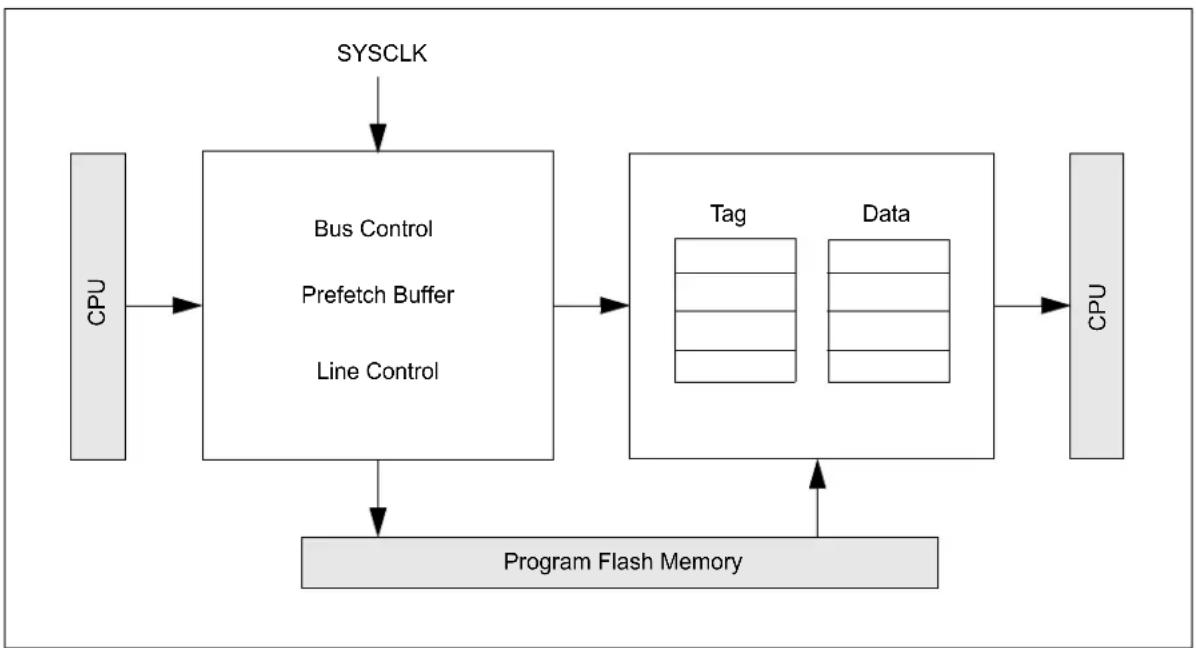
flowchart
graph TD
    CPU --> BusControl["Bus Control"]
    BusControl --> PrefetchBuffer["Prefetch Buffer"]
    PrefetchBuffer --> LineControl["Line Control"]
    BusControl --> Tag["Tag"]
    BusControl --> Data["Data"]
    BusControl --> CPU["CPU"]
    CPU --> ProgramFlashMemory["Program Flash Memory"]
    SysCLK --> BusControl
    BusControl --> Tag
    BusControl --> Data
9.1 Prefetch Control Registers
TABLE 9-1: PREFETCH REGISTER MAP
| Virtual Address(BF81_#) | Register Name(?) | Bit Range | Bits | All Resets | |||||||||||||||
| 31/15 | 30/14 | 29/13 | 28/12 | 27/11 | 26/10 | 25/9 | 24/8 | 23/7 | 22/6 | 21/5 | 20/4 | 19/3 | 18/2 | 17/1 | 16/0 | ||||
| 2400 | PRECON | 31:16 | — | — | — | — | — | PERCHEEN | DCHEEN | ICHEEN | — | PERCHEINV | DCHEINV | ICHEINV | — | PERCHECOH | DCHECOH | ICHECOH | 0000 |
| 15:00 | — | — | — | CHEPERFEN | — | — | — | PFMAWSEN | PFMSECEN | — | PREFEN[1:0] | PFMWS[3:0] | 0007 | ||||||
| 2410 | PRESTAT | 31:16 | — | — | — | — | PFMDED | PFMSEC | — | — | — | — | — | — | — | — | — | — | 0000 |
| 15:00 | — | — | — | — | — | — | — | — | — | PFMSECCNT[7:0] | 0000 | ||||||||
| 2420 | PREHIT | 31:16 | CHEHIT[31:16] | 0000 | |||||||||||||||
| 15:00 | CHEHIT[15:0] | 0000 | |||||||||||||||||
| 2430 | PREMIS | 31:16 | CHEMIS[31:16] | 0000 | |||||||||||||||
| 15:00 | CHEMIS[15:0] | 0000 | |||||||||||||||||
Legend: x = unknown value on Reset, — = unimplemented, read as '0'. Reset values are shown in hexadecimal.
Note 1: All registers in this table have corresponding CLR, SET and INV registers at its virtual address, plus an offset of 0x4, 0x8 and 0xC, respectively. See Section 13.3 "CLR, SET and INV Registers" for more information.
REGISTER 9-1: PRECON: PREFETCH MODULE CONTROL REGISTER
| Bit Range | Bit 31/23/15/7 | Bit 30/22/14/6 | Bit 29/21/13/5 | Bit 28/20/12/4 | Bit 27/19/11/3 | Bit 26/18/10/2 | Bit 25/17/9/1 | Bit 24/16/8/0 |
| 31:24 | U-0 U-0 | U-0 U-0 U-0 R/W-1 | R/W-1 R/W-1 R/W-1 | |||||
| — — — | — — PERCHEEN | DCHEEN ICHEEN | ||||||
| 23:16 | U-0 | R/S/HC-0 | R/S/HC-0 | R/S/HC-0 | U-0 | R/W-0 | R/W-0 | R/W-0 |
| — | PERCHEINV | DCHEINV | ICHEINV | — | PERCHECOH | DCHECOH | ICHECOH | |
| 15:8 | U-0 U-0 | U-0 | R/W-0 | U-0 U-0 U-0 | R/W-1 | |||
| — | — | — | CHEPERFEN | — | — | — | PFMAWSEN | |
| 7:0 | R/W-0 | U-0 | R/W-0 | R/W-0 | U-0 | R/W-1 | R/W-1 | R/W-1 |
| PFMSECEN | — | PREFEN[1:0] | PFMWS[3:0](1) | |||||
| Legend: | HC = Hardware Cleared | HS = Hardware Set | |
| R = Readable bit | W = Writable bit U = Unimplemented bit, read as ‘0’ | ||
| S = Settable bit | ‘1’ = Bit is set | ‘0’ = Bit is cleared | x = Bit is unknown |
bit 31-27 Unimplemented: Read as '0'
bit 26, PERCHEEN: Peripheral Data Cache Enable bit
1 = Caching enabled
0 = Caching disabled (and all lines invalidated)
bit 25 DCHEEN: Data Cache Enable bit
1 = Caching enabled
0 = Caching disabled (and all lines invalidated)
bit 24 ICHEEN: Instruction Cache Enable bit
1 = Caching enabled
0 = Caching disabled (and all lines invalidated)
bit 23 Unimplemented: Read as '0'
bit 22 PERCHEINV: Manual Invalidate Control for Peripheral Data Cache
1 = Force invalidate cache/invalidate busy
0 = Cache invalidation follows CHECOH/invalid complete
Note 1: PFB is included with iCache invalidate.
2: Hardware auto clears this bit when cache invalidate completes. Bits may clear at different times.
bit 21 DCHEINV: Manual Invalidate Control for Data Cache
1 = Force invalidate cache/invalidate busy
0 = Cache invalidation follows CHECOH/invalid complete
Note 1: PFB is included with iCache invalidate.
2: Hardware auto clears this bit when cache invalidate completes. Bits may clear at different times.
bit 20 ICHEINV: Manual Invalidate Control for Instruction Cache
1 = Force invalidate cache/invalidate busy
0 = Cache invalidation follows CHECOH/invalid complete
Note 1: PFB is included with iCache invalidate.
2: Hardware auto clears this bit when cache invalidate completes. Bits may clear at different times.
bit 19 Unimplemented: Read as '0'
Note 1: For the Wait states to SYSCLK relationship, refer to Section 41.0 "Electrical Specifications".
REGISTER 9-1: PRECON: PREFETCH MODULE CONTROL REGISTER (CONTINUED)
bit 18 PERCHECOH: Auto Cache Coherency Control for Peripheral Data Cache
1 = Auto invalidate cache on a programming event
0 = No auto invalidated cache on a programming event
Note: CHECOH must be stable before initiation of programming to ensure correct invalidation of data.
bit 17 DCHECOH: Auto Cache Coherency Control for Data Cache 1 = Auto invalidate cache on a programming event 0 = No auto invalidated cache on a programming event Note: CHECOH must be stable before initiation of programming to ensure correct invalidation of data.
bit 16 ICHECOH: Auto Cache Coherency Control for Instruction Cache 1 = Auto invalidate cache on a programming event 0 = No auto invalidated cache on a programming event Note: CHECOH must be stable before initiation of programming to ensure correct invalidation of data.
bit 15-13 Unimplemented: Read as '0'
bit 12 CHEPERFEN: Cache Performance Counters Enable 1 = Performance counters is enabled 0 = Performance counters is disabled Note: Performance counters are reset on 0 to 1 transition of this bit.
bit 11-9 Unimplemented: Read as '0'
bit 8 PFMAWSEN: Address Wait State Enable Total Flash wait states are ADRWS + PFMWS. 1 = Add 1 address Wait state - allowing for higher clock frequencies 0 = Add 0 address Wait states - allowing for higher performance at lower clock frequencies
bit 7 PFMSECEN: Flash Single-bit Error Corrected (SEC) Interrupt Enable bit 1 = Generate an interrupt when PFMSEC is set 0 = Do not generate an interrupt when PFMSEC is set
bit 6 Unimplemented: Read as '0'
bit 5-4 PREFEN[1:0]: Instruction Predictive Prefetch Enable 01 = Instruction predictive prefetch enabled for cacheable regions only 00 = Instruction predictive prefetch disabled Other values are unavailable.
bit 3-0 PFMWS[3:0]: PFM Access Time Defined in Terms of SYSCLK Wait States bits(1) Total Flash Wait states are ADRWS + PFMWS. 1111 = Fifteen Wait states 1110 = Fourteen Wait states ... 0001 = One Wait state 0000 = Zero Wait state Note: This is not the Wait state seen by the CPU.
Note 1: For the Wait states to SYSCLK relationship, refer to Section 41.0 "Electrical Specifications".
REGISTER 9-2: PRESTAT: PREFETCH MODULE STATUS REGISTER
| Bit Range | Bit 31/23/15/7 | Bit 30/22/14/6 | Bit 29/21/13/5 | Bit 28/20/12/4 | Bit 27/19/11/3 | Bit 26/18/10/2 | Bit 25/17/9/1 | Bit 24/16/8/0 |
| 31:24 | U-0 U-0 U-0 | U-0 HS/HC/R/W-0 | HS/HC/R/W-0 U-0 | U-0 | ||||
| —— — — — | PFMDED PFMSEC — — | |||||||
| 23:16 | U-0 U-0 U-0 | U-0 U-0 | U-0 | U-0 | U-0 | |||
| —— — — — | —— — — — | |||||||
| 15:8 | U-0 U-0 U-0 | U-0 U-0 | U-0 | U-0 | U-0 | |||
| —— — — — | —— — — — | |||||||
| 7:0 | HS/HC/R/W-0 | HS/HC/R/W-0 | HS/HC/R/W-0 | HS/HC/R/W-0 | HS/HC/R/W-0 | HS/HC/R/W-0 | HS/HC/R/W-0 | HS/HC/R/W-0 |
| PFMSECCNT[7:0] | ||||||||
| Legend: | HC = Hardware Cleared | HS = Hardware Set |
| R = Readable bit | W = Writable bit | U = Unimplemented bit, read as ‘0’ |
| S = Settable bit | ‘1’ = Bit is set | ‘0’ = Bit is cleared x = Bit is unknown |
bit 31-28 Unimplemented: Read as '0'
bit 27 PFMDED: Flash Double-bit Error Detected (DED) Status bit
1 = An error has occurred
0 = An error has not occurred
Note: DED errors are reported in-band with the data using the bus error protocol. When reported for CPU reads they are seen as bus exception errors by the CPU.
bit 26 PFMSEC: Flash Single-bit Error Corrected (SEC) Status bit
1 = A SEC error occurred when PFMSECCNT[7:0] was equal to zero
0 = A SEC error has not occurred
Note: The error event is reported to the CPU via using the prefetch module interrupt event.
bit 25-8 Unimplemented: Read as '0'
bit 7-0 PFMSECCNT[7:0]: Flash SEC Count bits
Decrements (by 1) its count value each time an SEC error occurs. Holds at zero. When an SEC error occurs when PFMSECCNT is zero, the PFMSEC status is set. If PFMSECEN is also set, a pCache interrupt event is generated.
Note: This field counts all SEC errors and is not limited to SEC errors on unique addresses.
REGISTER 9-3: PREHIT: PREFETCH MODULE HIT STATISTICS REGISTER
| Bit Range | Bit 31/23/15/7 | Bit 30/22/14/6 | Bit 29/21/13/5 | Bit 28/20/12/4 | Bit 27/19/11/3 | Bit 26/18/10/2 | Bit 25/17/9/1 | Bit 24/16/8/0 |
| 31:24 | R/H/C-0 R/H | H/C-0 R/H/C-0 | R/H/C-0 R/H/C-0 | R/H/C-0 R/H/C-0 | C-0 R/H/C-0 | |||
| CHEHIT[31:24] | ||||||||
| 23:16 | R/H/C-0 R/H | H/C-0 R/H/C-0 | R/H/C-0 R/H/C-0 | R/H/C-0 R/H/C-0 | C-0 R/H/C-0 | |||
| CHEHIT[23:16] | ||||||||
| 15:8 | R/H/C-0 R/H | H/C-0 R/H/C-0 | R/H/C-0 R/H/C-0 | R/H/C-0 R/H/C-0 | C-0 R/H/C-0 | |||
| CHEHIT[15:8] | ||||||||
| 7:0 | R/H/C-0 R/H | H/C-0 R/H/C-0 | R/H/C-0 R/H/C-0 | R/H/C-0 R/H/C-0 | C-0 R/H/C-0 | |||
| CHEHIT[7:0] | ||||||||
Legend: HC = Hardware Cleared HS = Hardware Set R = Readable bit W = Writable bit U = Unimplemented bit, read as '0' S = Settable bit '1' = Bit is set '0' = Bit is cleared x = Bit is unknown
bit 31-0 CHEHIT[31:0]: Instruction Cache Hit Count bits
When CHECON.CHEPERF = 1, CHEHIT increments once per iCache or PFB hit.
Note: CHEHIT is reset on '0' to '1' transition of CHECON.CHEPERF.
REGISTER 9-4: PREMIS: PREFETCH MODULE MISS STATISTICS REGISTER
| Bit Range | Bit 31/23/15/7 | Bit 30/22/14/6 | Bit 29/21/13/5 | Bit 28/20/12/4 | Bit 27/19/11/3 | Bit 26/18/10/2 | Bit 25/17/9/1 | Bit 24/16/8/0 |
| 31:24 | R/H/C-0 R/H/C-0 | R/C-0 R/H/C-0 | R/H/C-0 R/H/C-0 | R/H/C-0 R/H/C-0 | C-0 R/H/C-0 | |||
| CHEMIS[31:24] | ||||||||
| 23:16 | R/H/C-0 R/H/C-0 | R/C-0 R/H/C-0 | R/H/C-0 R/H/C-0 | R/H/C-0 R/H/C-0 | C-0 R/H/C-0 | |||
| CHEMIS[23:16] | ||||||||
| 15:8 | R/H/C-0 R/H/C-0 | R/C-0 R/H/C-0 | R/H/C-0 R/H/C-0 | R/H/C-0 R/H/C-0 | C-0 R/H/C-0 | |||
| CHEMIS[15:8] | ||||||||
| 7:0 | R/H/C-0 R/H/C-0 | R/C-0 R/H/C-0 | R/H/C-0 R/H/C-0 | R/H/C-0 R/H/C-0 | C-0 R/H/C-0 | |||
| CHEMIS[7:0] | ||||||||
Legend: HC = Hardware Cleared HS = Hardware Set R = Readable bit W = Writable bit U = Unimplemented bit, read as '0' S = Settable bit '1' = Bit is set '0' = Bit is cleared x = Bit is unknown
bit 31-0 CHEMIS[31:0]: Instruction Cache Miss Count bits
When CHECON.CHEPERF = 1, CHEMIS increments once per iCache or PFB miss.
Note: CHEMIS is reset on '0' to '1' transition of CHECON.CHEPERF.
10.0 DIRECT MEMORY ACCESS (DMA) CONTROLLER
Note: This data sheet summarizes the features of the PIC32MZ1025W104 device. It is not intended to be a comprehensive reference source. To complement the information in this data sheet, refer to Section 31. "Direct Memory Access (DMA) Controller" (DS60001117) in the "PIC32 Family Reference Manual", which is available from the Microchip website (www.microchip.com/PIC32).
The DMA Controller is a bus manager module useful for data transfers between different devices without CPU intervention. The source and destination of a DMA transfer can be any of the memory mapped modules existent in the device such as SPI, UART, and so on, or memory itself. Peripherals like SQI, ADC, and so on with dedicated DMA can also access the generic system DMA.
The following are key features of the DMA Controller:
• Eight identical channels:
- Auto-increment source and destination address registers
- Source and destination pointers
- Memory to memory and memory to peripheral transfers
• Automatic Word-size detection:
- Transfer granularity, down to byte level
- Bytes need not be word-aligned at source and destination
• Fixed priority channel arbitration
- Flexible DMA channel operating modes:
- Manual (software) or automatic (interrupt) DMA requests
- One-shot or Auto-repeat Block Transfer modes
- Channel-to-channel chaining
- Flexible DMA requests:
- A DMA request can be selected from any of the peripheral interrupt sources
- Each channel can select any (appropriate) observable interrupt as its DMA request source
- A DMA transfer abort can be selected from any of the peripheral interrupt sources
- Up to 2-byte pattern (data) match transfer termination
- Multiple DMA channel status interrupts:
- DMA channel block transfer complete
- Source empty or half empty
- Destination full or half full
- DMA transfer aborted due to an external event
- Invalid DMA address generated
• DMA debug support features:
- Most recent error address accessed by a DMA channel
- Most recent DMA channel to transfer data
- CRC generation module:
- CRC module can be assigned to any of the available channels
- CRC module is highly configurable
Note: The Program Flash is not accessible by DMA.
FIGURE 10-1: DMA BLOCK DIAGRAM
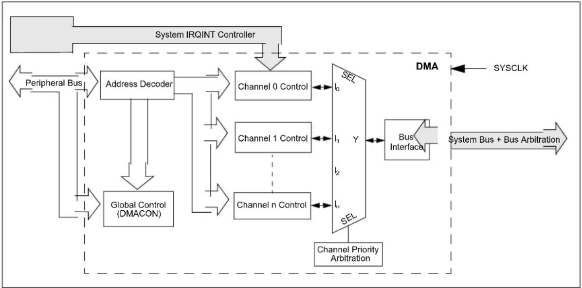
flowchart
graph TD
    A["System IRQINT Controller"] --> B["Address Decoder"]
    B --> C["Channel 0 Control"]
    C --> D["Channel 1 Control"]
    D --> E["Channel n Control"]
    E --> F["Channel Priority Arbitration"]
    F --> G["Bus Interface"]
    G --> H["System Bus + Bus Arbitration"]
    I["Peripheral Bus"] --> B
    J["Global Control (DMACON)"] --> B
    K["DMA"] --> L["SysCLK"]
    M["Channel 0 Control"] --> N["SEL"]
    O["Channel 1 Control"] --> P["Y"]
    Q["Channel n Control"] --> R["I1"]
    S["Channel Priority Arbitration"] --> T["I2"]
    U["Channel 0 Control"] --> V["I3"]
    W["Channel 1 Control"] --> X["I4"]
    Y["Channel n Control"] --> Z["I5"]
10.1 DMA Control Registers
TABLE 10-1: DMA GLOBAL REGISTER MAP
Legend: x = unknown value on Reset; — = unimplemented, read as '0'. Reset values are shown in hexadecimal.
Note 1: All registers in this table have corresponding CLR, SET and INV registers at its virtual address, plus an offset of 0x4, 0x8 and 0xC, respectively. Sea Section 13.3 "CLR, SET and INV Registers" for more information.
TABLE 10-2: DMA CRC REGISTER MAP
| Virtual Address (BF-B1_#) | RegisterName | Bit Range | Bits | All Resets | |||||||||||||||
| 31/15 | 30/14 | 29/13 | 28/12 | 27/11 | 26/10 | 25/9 | 24/8 | 23/7 | 22/6 | 21/5 | 20/4 | 19/3 | 18/2 | 17/1 | 16/0 | ||||
| 1030 | DCRCCON | 31:16 | — | — | BYTE[1:0] | WBO | — | — | BITO | — | — | — | — | — | — | — | — | 0000 | |
| 15:0 | — | — | — | PLEN[4:0] | CRCEN | CRCAPP | CRCTYP | — | — | CRCCH[2:0] | 0000 | ||||||||
| 1040 | DCRCDATA | 31:16 | DCRCDATA[31:16] | 0000 | |||||||||||||||
| 15:0 | DCRCDATA[15:0] | 0000 | |||||||||||||||||
| 1050 | DCRCXOR | 31:16 | DCRCXOR[31:16] | 0000 | |||||||||||||||
| 15:0 | DCRCXOR[15:0] | 0000 | |||||||||||||||||
Legend: x = unknown value on Reset; — = unimplemented, read as '0'. Reset values are shown in hexadecimal.
Note 1: All registers in this table have corresponding CLR, SET and INV registers at their virtual addresses, plus offsets of 0x4, 0x8 and 0xC, respectively. See Section 13.3 "CLR, SET and INV Registers" for more information.
TABLE 10-3: DMA CHANNEL 0 THROUGH CHANNEL 7 REGISTER MAP
Legend: x = unknown value on Reset; — = unimplemented, read as '0'. Reset values are shown in hexadecimal.
Note 1: All registers in this table have corresponding CLR, SET and INV registers at their virtual addresses. plus offsets of 0x4, 0x8 and 0xC, respectively. See Section 13.3 "CLR, SET and INV Registers" for more information.
TABLE 10-3: DMA CHANNEL 0 THROUGH CHANNEL 7 REGISTER MAP (CONTINUED)
Legend: x = unknown value on Reset; — = unimplemented, read as '0'. Reset values are shown in hexadecimal.
Note 1: All registers in this table have corresponding CLR, SET and INV registers at their virtual addresses, plus offsets of 0x4, 0x8 and 0xC, respectively. See Section 13.3 "CLR, SET and INV Registers" for more information.
TABLE 10-3: DMA CHANNEL 0 THROUGH CHANNEL 7 REGISTER MAP (CONTINUED)
Legend: x = unknown value on Reset; — = unimplemented, read as '0'. Reset values are shown in hexadecimal.
Note 1: All registers in this table have corresponding CLR, SET and INV registers at their virtual addresses, plus offsets of 0x4, 0x8 and 0xC, respectively. See Section 13.3 "CLR, SET and INV Registers" for more information.
TABLE 10-3: DMA CHANNEL 0 THROUGH CHANNEL 7 REGISTER MAP (CONTINUED)
Legend: x = unknown value on Reset; — = unimplemented, read as '0'. Reset values are shown in hexadecimal.
Note 1: All registers in this table have corresponding CLR, SET and INV registers at their virtual addresses, plus offsets of 0x4, 0x8 and 0xC, respectively. See Section 13.3 "CLR, SET and INV Registers" for more information.
TABLE 10-3: DMA CHANNEL 0 THROUGH CHANNEL 7 REGISTER MAP (CONTINUED)
| Virtual Address (BFB1,#) | Register Name | Bit Range | Bits | All Resets | ||||||||||||||||
| 31/15 | 30/14 | 29/13 | 28/12 | 27/11 | 26/10 | 25/9 | 24/8 | 23/7 | 22/6 | 21/5 | 20/4 | 19/3 | 18/2 | 17/1 | 16/0 | |||||
| 14A0 | DCH5DPTR | 31:16 | — | — | — | — | — | — | — | — | ||||||||||
| 15:0 CHDPTR[15:0] 0000 | ||||||||||||||||||||
| 14B0 | DCH5CSIZ | 31:16 | — | — | — | — | — | — | — | — | ||||||||||
| 15:0 CHCSIZ[15:0] 0000 | ||||||||||||||||||||
| 14C0 | DCH5CPTR | 31:16 | — | — | — | — | — | — | — | — | ||||||||||
| 15:0 CHCPTR[15:0] 0000 | ||||||||||||||||||||
| 14D0 | DCH5DAT | 31:16 | — | — | — | — | — | — | — | — | ||||||||||
| 15:0 CHPDAT[15:0] 0000 | ||||||||||||||||||||
| 14E0 | DCH6CON | 31:16 | CHPIGN[7:0] | — | — | — | — | — | ||||||||||||
| 15:0 CHBUSY | — | — | CHPIGNEN | — | CHPATLEN | — | — | CHCHNS | CHEN | CHAED | CHCHN | CHAEN | — | CHEDET | CHPRI[1:0] | 0000 | ||||
| 14F0 | DCH6ECON | 31:16 | — | — | — | — | — | — | — | — | — | — | — | CHAIRQ[7:0] | 0000 | |||||
| 15:0 | CHSIRQ[7:0] | CFORCE | CABORT | PATEN | SIRQEN | AIRQEN | — | — | — | — | 2200 | |||||||||
| 1500 | DCH6INT | 31:16 | — | — | — | — | — | — | — | — | CHSDIE | CHSHIE | CHDDIE | CHDHIE | CHBCIE | CHCCIE | CHTAIE | CHERIE | 0000 | |
| 15:0 | — | — | — | — | — | — | — | — | CHSDIF | CHSHIF | CHDDIF | CHDHIF | CHBCIF | CHCCIF | CHTAIF | CHERIF | 0000 | |||
| 1510 | DCH6SSA | 31:16 | CHSSA[31:16] 0000 | |||||||||||||||||
| 15:0 | CHSSA[15:0] | 0000 | ||||||||||||||||||
| 1520 | DCH6DSA | 31:16 | CHDSA[31:16] 0000 | |||||||||||||||||
| 15:0 | CHDSA[15:0] | 0000 | ||||||||||||||||||
| 1530 | DCH6SSIZ | 31:16 | — | — | — | — | — | — | — | — | ||||||||||
| 15:0 CHSSIZ[15:0] 0000 | 0000 | |||||||||||||||||||
| 1540 | DCH6DSIZ | 31:16 | — | — | — | — | — | — | — | — | ||||||||||
| 15:0 CHDSIZ[15:0] 0000 | ||||||||||||||||||||
| 1550 | DCH6SPTR | 31:16 | — | — | — | — | — | — | — | — | ||||||||||
| 15:0 CHSPTR[15:0] 0000 | ||||||||||||||||||||
| 1560 | DCH6DPTR | 31:16 | — | — | — | — | — | — | — | — | ||||||||||
| 15:0 CHDPTR[15:0] 0000 | ||||||||||||||||||||
| 1570 | DCH6CSIZ | 31:16 | — | — | — | — | — | — | — | — | ||||||||||
| 15:0 CHCSIZ[15:0] 0000 | ||||||||||||||||||||
| 1580 | DCH6CPTR | 31:16 | — | — | — | — | — | — | — | — | ||||||||||
| 15:0 CHCPTR[15:0] 0000 | ||||||||||||||||||||
| 1590 | DCH6DAT | 31:16 | — | — | — | — | — | — | — | — | ||||||||||
| 15:0 CHPDAT[15:0] 0000 | ||||||||||||||||||||
| 15A0 | DCH7CON | 31:16 | CHPIGN[7:0] | — | — | — | — | — | ||||||||||||
| 15:0 CHBUSY | — | — | CHPIGNEN | — | CHPATLEN | — | — | CHCHNS | CHEN | CHAED | CHCHN | CHAEN | — | CHEDET | CHPRI[1:0] 0000 | |||||
Legend: x = unknown value on Reset; — = unimplemented, read as '0'. Reset values are shown in hexadecimal.
Note 1: All registers in this table have corresponding CLR, SET and INV registers at their virtual addresses, plus offsets of 0x4, 0x8 and 0xC, respectively. See Section 13.3 "CLR, SET and INV Registers" for more information.
TABLE 10-3: DMA CHANNEL 0 THROUGH CHANNEL 7 REGISTER MAP (CONTINUED)
| Virtual Address (BF81_#) | Register Name(f) | Bit Range | Bits | All Resets | |||||||||||||||
| 31/15 | 30/14 | 29/13 | 28/12 | 27/11 | 26/10 | 25/9 | 24/8 | 23/7 | 22/6 | 21/5 | 20/4 | 19/3 | 18/2 | 17/1 | 16/0 | ||||
| 31:16 | —— | —— | —— | CHAIRQ[7:0] 00:FF | |||||||||||||||
| 15B0 | DCH7ECON | 15:0 | CHSIRQ[7:0] | CFORCE | CABORT | PATEN | SIRQEN | AIRQEN | — | — | — | FF00 | |||||||
| 15C0 | DCH7INT | 31:16 | — | — | — | — | — | — | — | — | CHSDIE | CHSHIE | CHDDIE | CHDHIE | CHBCIE | CHCCIE | CHTAIE | CHERIE | 0000 |
| 15:0 | — | — | — | — | — | — | — | — | CHSDIF | CHSHIF | CHDDIF | CHDHIF | CHBCIF | CHCCIF | CHTAIF | CHERIF | 0000 | ||
| 15D0 | DCH7SSA | 31:16 | CHSSA[31:16] | 0000 | |||||||||||||||
| 15:0 | CHSSA[15:0] | 0000 | |||||||||||||||||
| 15E0 | DCH7DSA | 31:16 | CHDSA[31:16] | 0000 | |||||||||||||||
| 15:0 | CHDSA[15:0] | 0000 | |||||||||||||||||
| 15F0 | DCH7SSIZ | 31:16 | —— | —— | —— | —— | —— | —— | —— | —— | —— | —— | —— | —— | —— | —— | —— | —— | |
| 15:0 | CHSSIZ[15:0] | 0000 | |||||||||||||||||
| 1600 | DCH7DSIZ | 31:16 | —— | —— | —— | —— | —— | —— | —— | —— | —— | —— | —— | —— | —— | —— | —— | ||
| 15:0 | CHDSIZ[15:0] | 0000 | |||||||||||||||||
| 1610 | DCH7SPTR | 31:16 | —— | —— | —— | —— | —— | —— | —— | —— | —— | —— | —— | —— | —— | —— | —— | ||
| 15:0 | CHSPTR[15:0] | 0000 | |||||||||||||||||
| 1620 | DCH7DPTR | 31:16 | —— | —— | —— | —— | —— | —— | —— | —— | —— | —— | —— | —— | —— | —— | —— | ||
| 15:0 | CHDPTR[15:0] | 0000 | |||||||||||||||||
| 1630 | DCH7CSIZ | 31:16 | —— | —— | —— | —— | —— | —— | —— | —— | —— | —— | —— | —— | —— | —— | —— | ||
| 15:0 | CHCSIZ[15:0] | 0000 | |||||||||||||||||
| 1640 | DCH7CPTR | 31:16 | —— | —— | —— | —— | —— | —— | —— | —— | —— | —— | —— | —— | —— | —— | —— | ||
| 15:0 | CHCPTR[15:0] | 0000 | |||||||||||||||||
| 1650 | DCH7DAT | 31:16 | —— | —— | —— | —— | —— | —— | —— | —— | —— | —— | —— | —— | —— | —— | —— | ||
| 15:0 | CHPDAT[15:0] | 0000 | |||||||||||||||||
Legend: x = unknown value on Reset; — = unimplemented, read as '0'. Reset values are shown in hexadecimal.
Note 1: All registers in this table have corresponding CLR, SET and INV registers at their virtual addresses, plus offsets of 0x4, 0x8 and 0xC, respectively. See Section 13.3 "CLR, SET and INV Registers" for more information.
REGISTER 10-1: DMACON: DMA CONTROLLER CONTROL REGISTER
| Bit Range | Bit 31/23/15/7 | Bit 30/22/14/6 | Bit 29/21/13/5 | Bit 28/20/12/4 | Bit 27/19/11/3 | Bit 26/18/10/2 | Bit 25/17/9/1 | Bit 24/16/8/0 |
| 31:24 | U-0 U-0 | U-0 U-0 U-0 U-0 | U-0 U-0 | |||||
| — — — | — — — — — | |||||||
| 23:16 | U-0 U-0 | U-0 U-0 U-0 U-0 | U-0 U-0 | |||||
| — — — | — — — — — | |||||||
| 15:8 | R/W-0 U-0 | U-0 R/W-0 R/W-0 | U-0 U-0 | U-0 | ||||
| ON | — | — | SUSPEND | DMABUSY | — | — | — | |
| 7:0 | U-0 U-0 | U-0 U-0 U-0 U-0 | U-0 | U-0 | ||||
| — — — | — — — — — | |||||||
Legend:
| R = Readable bit | W = Writable bit | U = Unimplemented bit, read as '0' |
| -n = Value at POR | '1' = Bit is set | '0' = Bit is cleared x = Bit is unknown |
bit 31-16 Unimplemented: Read as '0'
bit 15 ON: DMA On bit
1 = DMA module is enabled
0 = DMA module is disabled
bit 14-13 Unimplemented: Read as '0'
bit 12 SUSPEND: DMA Suspend bit
1 = DMA transfers are suspended to allow CPU uninterrupted access to data bus
0 = DMA operates normally
bit 11 DMABUSY: DMA Module Busy bit
1 = DMA module is active and is transferring data
0 = DMA module is disabled and not actively transferring data
bit 10-0 Unimplemented: Read as '0'
REGISTER 10-2: DMASTAT: DMA STATUS REGISTER
| Bit Range | Bit 31/23/15/7 | Bit 30/22/14/6 | Bit 29/21/13/5 | Bit 28/20/12/4 | Bit 27/19/11/3 | Bit 26/18/10/2 | Bit 25/17/9/1 | Bit 24/16/8/0 |
| 31:24 | R-0 U-0 U | -0 U-0 U-0 U-0 | U-0 U-0 | |||||
| RDWR | — — — | — — — — | ||||||
| 23:16 | U-0 U-0 U | -0 U-0 U-0 U-0 | U-0 U-0 | |||||
| — | — — — | — — — — | ||||||
| 15:8 | U-0 U-0 U | -0 U-0 U-0 U-0 | U-0 U-0 | |||||
| — | — — — | — — — — | ||||||
| 7:0 | U-0 U-0 U | -0 U-0 U-0 R-0 | R-0 R-0 | |||||
| — | — — — | — | DMACH[2:0] | |||||
Legend:
| R = Readable bit | W = Writable bit | U = Unimplemented bit, read as '0' |
| -n = Value at POR | '1' = Bit is set | '0' = Bit is cleared x = Bit is unknown |
bit 31 RDWR: Read/Write Status bit
1 = Last DMA bus access when an error was detected was a read
0 = Last DMA bus access when an error was detected was a write
bit 30-3 Unimplemented: Read as '0'
bit 2-0 DMACH[2:0]: DMA Channel bits
These bits contain the value of the most recent active DMA channel when an error is detected.
REGISTER 10-3: DMAADDR: DMA ADDRESS REGISTER
| Bit Range | Bit 31/23/15/7 | Bit 30/22/14/6 | Bit 29/21/13/5 | Bit 28/20/12/4 | Bit 27/19/11/3 | Bit 26/18/10/2 | Bit 25/17/9/1 | Bit 24/16/8/0 |
| 31:24 | R-0 R-0 R | -0 R-0 R-0 R-0 | R-0 R-0 | |||||
| DMAADDR[31:24] | ||||||||
| 23:16 | R-0 R-0 R | -0 R-0 R-0 R-0 | R-0 R-0 | |||||
| DMAADDR[23:16] | ||||||||
| 15:8 | R-0 R-0 R | -0 R-0 R-0 R-0 | R-0 R-0 | |||||
| DMAADDR[15:8] | ||||||||
| 7:0 | R-0 R-0 R | -0 R-0 R-0 R-0 | R-0 R-0 | |||||
| DMAADDR[7:0] | ||||||||
Legend:
| R = Readable bit | W = Writable bit | U = Unimplemented bit, read as '0' |
| -n = Value at POR | '1' = Bit is set | '0' = Bit is cleared x = Bit is unknown |
bit 31-0 DMAADDR[31:0]: DMA Module Address bits
These bits contain the address of the most recent DMA access when an error is detected.
Note: The DMAEADDR register will be cleared when its contents are read. If more than one error occurs at the same time, the read transaction will be recorded. Additional later transfers with an error will not update this register until it has been read or cleared.
REGISTER 10-4: DCRCCON: DMA CRC CONTROL REGISTER
| Bit Range | Bit 31/23/15/7 | Bit 30/22/14/6 | Bit 29/21/13/5 | Bit 28/20/12/4 | Bit 27/19/11/3 | Bit 26/18/10/2 | Bit 25/17/9/1 | Bit 24/16/8/0 |
| 31:24 | U-0 U-0 R/W-0 R/W-0 R/W-0 U-0 U-0 R/W-0 | |||||||
| — — BYTO[1:0] WBO | (1) | — — | B | I | ||||
| 23:16 | U-0 | U-0 | U-0 | U-0 | U-0 | U-0 | U-0 | U-0 |
| — | — | — | — | — | — | — | — | |
| 15:8 | U-0 | U-0 | U-0 | R/W-0 | R/W-0 | R/W-0 | R/W-0 | R/W-0 |
| — — | — | PLEN[4:0] | ||||||
| 7:0 | R/W-0 | R/W-0 | R/W-0 | U-0 | U-0 | R/W-0 | R/W-0 | R/W-0 |
| CRCEN | CRCAPP(1) | CRCTYP | — | — | CRCCH[2:0] | |||
Legend:
| R = Readable bit | W = Writable bit U = Unimplemented bit, read as '0' | ||
| -n = Value at POR | '1' = Bit is set | '0' = Bit is cleared | x = Bit is unknown |
bit 31-30 Unimplemented: Read as '0'
bit 29-28 BYTO[1:0]: CRC Byte Order Selection bits
11 = Endian byte swap on half-word boundaries (in other words, source half-word order with reverse source byte order per half-word)
10 = Swap half-words on word boundaries (in other words, reverse source half-word order with source byte order per half-word)
01 = Endian byte swap on word boundaries (in other words, reverse source byte order)
00 = No swapping (i.e., source byte order)
bit 27 WBO: CRC Write Byte Order Selection bit ^(1)
1 = Source data is written to the destination re-ordered as defined by BYTO[1:0]
0 = Source data is written to the destination unaltered
bit 26-25 Unimplemented: Read as '0'
bit 24 BITO: CRC Bit Order Selection bit
When CRCTYP (DCRCCON[5]) = 1 (CRC module is in IP Header mode):
1 = The IP header checksum is calculated Least Significant bit (LSb) first (in other words, reflected)
0 = The IP header checksum is calculated Most Significant bit (MSb) first (in other words, not reflected)
When CRCTYP (DCRCCON[5]) = 0 (CRC module is in LFSR mode):
1 = The LFSR CRC is calculated Least Significant bit first (in other words, reflected)
0 = The LFSR CRC is calculated Most Significant bit first (in other words, not reflected)
bit 23-13 Unimplemented: Read as '0'
bit 12-8 PLEN[4:0]: Polynomial Length bits ^(1)
When CRCTYP (DCRCCON[5]) = 1 (CRC module is in IP Header mode):
These bits are unused.
When CRCTYP (DCRCCON[5]) = 0 (CRC module is in LFSR mode):
Denotes the length of the polynomial - 1.
bit 7 CRCEN: CRC Enable bit
1 = CRC module is enabled and channel transfers are routed through the CRC module
0 = CRC module is disabled and channel transfers proceed normally
Note 1: When WBO = 1, unaligned transfers are not supported and the CRCAPP bit cannot be set.
REGISTER 10-4: DCRCCON: DMA CRC CONTROL REGISTER (CONTINUED)
bit 6 CRCAPP: CRC Append Mode bit (1)
1 = DMA transfers data from the source into the CRC but not to the destination. When a block transfer completes the DMA writes the calculated CRC value to the location given by CHxDSA.
0 = DMA transfers data from the source through the CRC obeying WBO as it writes the data to the destination.
bit 5 CRCTYP: CRC Type Selection bit
1 = The CRC module calculates an IP header checksum
0 = The CRC module calculates a LFSR CRC
bit 4-3 Unimplemented: Read as '0'
bit 2-0 CRCCH[2:0]: CRC Channel Select bits
111 = CRC is assigned to Channel 7
110 = CRC is assigned to Channel 6
101 = CRC is assigned to Channel 5
100 = CRC is assigned to Channel 4
011 = CRC is assigned to Channel 3
010 = CRC is assigned to Channel 2
001 = CRC is assigned to Channel 1
000 = CRC is assigned to Channel 0
Note 1: When WBO = 1, unaligned transfers are not supported and the CRCAPP bit cannot be set.
REGISTER 10-5: DCRCDATA: DMA CRC DATA REGISTER
| Bit Range | Bit 31/23/15/7 | Bit 30/22/14/6 | Bit 29/21/13/5 | Bit 28/20/12/4 | Bit 27/19/11/3 | Bit 26/18/10/2 | Bit 25/17/9/1 | Bit 24/16/8/0 |
| 31:24 | R/W-0 R/W | -0 R/W-0 R/W-0 | R/W-0 R/W-0 | R/W-0 R/W-0 | ||||
| DCRCDATA[31:24] | ||||||||
| 23:16 | R/W-0 R/W | -0 R/W-0 R/W-0 | R/W-0 R/W-0 | R/W-0 R/W-0 | ||||
| DCRCDATA[23:16] | ||||||||
| 15:8 | R/W-0 R/W | -0 R/W-0 R/W-0 | R/W-0 R/W-0 | R/W-0 R/W-0 | ||||
| DCRCDATA[15:8] | ||||||||
| 7:0 | R/W-0 R/W | -0 R/W-0 R/W-0 | R/W-0 R/W-0 | R/W-0 R/W-0 | ||||
| DCRCDATA[7:0] | ||||||||
Legend:
R = Readable bit W = Writable bit U = Unimplemented bit, read as '0' -n = Value at POR '1' = Bit is set '0' = Bit is cleared x = Bit is unknown
bit 31-0 DCRCDATA[31:0]: CRC Data Register bits
Writing to this register will seed the CRC generator. Reading from this register returns the current value of the CRC. Bits greater than PLEN will return '0' on any read.
When CRCTYP (DCRCCON[5]) = 1 (CRC module is in IP Header mode):
Only the lower 16 bits contain IP header checksum information. The upper 16 bits are always '0'. Data written to this register is converted and read back in 1's complement form (in other words, current IP header checksum value).
When CRCTYP (DCRCCON[5]) = 0 (CRC module is in LFSR mode):
Bits greater than PLEN returns '0' on any read.
REGISTER 10-6: DCRCXOR: DMA CRCXOR ENABLE REGISTER
| Bit Range | Bit 31/23/15/7 | Bit 30/22/14/6 | Bit 29/21/13/5 | Bit 28/20/12/4 | Bit 27/19/11/3 | Bit 26/18/10/2 | Bit 25/17/9/1 | Bit 24/16/8/0 |
| 31:24 | R/W-0 R/W | 0 R/W-0 R/W-0 | R/W-0 R/W-0 R/W-0 R/W-0 | |||||
| DCRCXOR[31:24] | ||||||||
| 23:16 | R/W-0 R/W | 0 R/W-0 R/W-0 | R/W-0 R/W-0 R/W-0 R/W-0 | |||||
| DCRCXOR[23:16] | ||||||||
| 15:8 | R/W-0 R/W | 0 R/W-0 R/W-0 | R/W-0 R/W-0 R/W-0 R/W-0 | |||||
| DCRCXOR[15:8] | ||||||||
| 7:0 | R/W-0 R/W | 0 R/W-0 R/W-0 | R/W-0 R/W-0 R/W-0 R/W-0 | |||||
| DCRCXOR[7:0] | ||||||||
Legend:
R = Readable bit W = Writable bit U = Unimplemented bit, read as '0'
-n = Value at POR '1' = Bit is set '0' = Bit is cleared x = Bit is unknown
bit 31-0 DCRCXOR[31:0]: CRC XOR Register bits
When CRCTYP (DCRCCON[5]) = 1 (CRC module is in IP Header mode):
This register is unused.
When CRCTYP (DCRCCON[5]) = 0 (CRC module is in LFSR mode):
1 = Enable the XOR input to the Shift register
0 = Disable the XOR input to the Shift register; data is shifted in directly from the previous stage in the register
REGISTER 10-7: DCHxCON: DMA CHANNEL x CONTROL REGISTER
| Bit Range | Bit 31/23/15/7 | Bit 30/22/14/6 | Bit 29/21/13/5 | Bit 28/20/12/4 | Bit 27/19/11/3 | Bit 26/18/10/2 | Bit 25/17/9/1 | Bit 24/16/8/0 |
| 31:24 | R/W-0 | R/W-0 | R/W-0 | R/W-0 | R/W-0 | R/W-0 | R/W-0 | R/W-0 |
| CHPIGN[7:0] | ||||||||
| 23:16 | U-0 | U-0 | U-0 | U-0 | U-0 | U-0 | U-0 | U-0 |
| — | — | — | — | — | — | — | — | |
| 15:8 | R/W-0 | U-0 | R/W-0 | U-0 | R/W-0 | U-0 | U-0 | R/W-0 |
| CHBUSY | — | CHIPGNEN | — | CHPATLEN | — | — | CHCHNS^(1) | |
| 7:0 | R/W-0 | R/W-0 | R/W-0 | R/W-0 | U-0 | R-0 | R/W-0 | R/W-0 |
| CHEN^(2) | CHAED | CHCHN | CHAEN | — | CHEDET | CHPRI[1:0] | ||
Legend:
| R = Readable bit | W = Writable bit | U = Unimplemented bit, read as '0' |
| -n = Value at POR | '1' = Bit is set | '0' = Bit is cleared x = Bit is unknown |
bit 31-24 CHPIGN[7:0]: Channel Register Data bits
Pattern Terminate mode:
Any byte matching these bits during a pattern match may be ignored during the pattern match determination when the CHPIGNEN bit is set. If a byte is read that is identical to this data byte, the pattern match logic will treat it as a "don't care" when the pattern matching logic is enabled and the CHPIGEN bit is set.
bit 23-16 Unimplemented: Read as '0'
Note 1: The chain selection bit takes effect when chaining is enabled (in other words, CHCHN = 1).
2: When the channel is suspended by clearing this bit, the user application must poll the CHBUSY bit (if available on the device variant) to see when the channel is suspended, as it may take some clock cycles to complete a current transaction before the channel is suspended.
REGISTER 10-7: DCHxCON: DMA CHANNEL x CONTROL REGISTER (CONTINUED)
bit 15 CHBUSY: Channel Busy bit
1 = Channel is active or enabled
0 = Channel is inactive or disabled
bit 14 Unimplemented: Read as '0'
bit 13 CHPIGNEN: Enable Pattern Ignore Byte bit
1 = Treat any byte that matches the CHPIGN[7:0] bits as a "don't care" when pattern matching is enabled
0 = Disable this feature
bit 12 Unimplemented: Read as '0'
bit 11 CHPATLEN: Pattern Length bit
1 = 2 byte length
0 = 1 byte length
bit 10-9 Unimplemented: Read as '0'
bit 8 CHCHNS: Chain Channel Selection bit (1)
1 = Chain to channel lower in natural priority (CH1 is enabled by CH2 transfer complete)
0 = Chain to channel higher in natural priority (CH1 is enabled by CH0 transfer complete)
bit 7 CHEN: Channel Enable bit (2)
1 = Channel is enabled
0 = Channel is disabled
bit 6 CHAED: Channel Allow Events If Disabled bit
1 = Channel start/abort events are registered, even if the channel is disabled
0 = Channel start/abort events are ignored if the channel is disabled
bit 5 CHCHN: Channel Chain Enable bit
1 = Allow channel to be chained
0 = Do not allow channel to be chained
bit 4 CHAEN: Channel Automatic Enable bit
1 = Channel is continuously enabled, and not automatically disabled after a block transfer is complete
0 = Channel is disabled on block transfer complete
bit 3 Unimplemented: Read as '0'
bit 2 CHEDET: Channel Event Detected bit
1 = An event has been detected
0 = No events have been detected
bit 1-0 CHPRI[1:0]: Channel Priority bits
11 = Channel has priority 3 (highest)
10 = Channel has priority 2
01 = Channel has priority 1
00 = Channel has priority 0
Note 1: The chain selection bit takes effect when chaining is enabled (in other words, CHCHN = 1).
2: When the channel is suspended by clearing this bit, the user application must poll the CHBUSY bit (if available on the device variant) to see when the channel is suspended, as it may take some clock cycles to complete a current transaction before the channel is suspended.
REGISTER 10-8: DCHxECON: DMA CHANNEL x EVENT CONTROL REGISTER
| Legend: | S = Settable bit | ||
| R = Readable bit | W = Writable bit U = Unimplemented bit, read as ‘0’ | ||
| -n = Value at POR | ‘1’ = Bit is set | ‘0’ = Bit is cleared | x = Bit is unknown |
bit 31-24 Unimplemented: Read as '0'
bit 23-16 CHAIRQ[7:0]: Channel Transfer Abort IRQ bits ^(1)
11111111 = Interrupt 255 aborts any transfers in progress and set CHAIF flag
00000001 = Interrupt 1 aborts any transfers in progress and set CHAIF flag
00000000 = Interrupt 0 aborts any transfers in progress and set CHAIF flag
bit 15-8 CHSIRQ[7:0]: Channel Transfer Start IRQ bits ^(1)
11111111 = Interrupt 255 initiates a DMA transfer
00000001 = Interrupt 1 initiates a DMA transfer
00000000 = Interrupt 0 initiates a DMA transfer
bit 7 CFORCE: DMA Forced Transfer bit
1 = A DMA transfer is forced to begin when this bit is written to a '1'
0 = This bit always reads '0'
bit 6 CABORT: DMAAbort Transfer bit
1 = A DMA transfer is aborted when this bit is written to a '1'
0 = This bit always reads '0'
bit 5 PATEN: Channel Pattern Match Abort Enable bit
1 = Abort transfer and clear CHEN on pattern match
0 = Pattern match is disabled
bit 4 SIRQEN: Channel Start IRQ Enable bit
1 = Start channel cell transfer if an interrupt matching CHSIRQ occurs
0 = Interrupt number CHSIRQ is ignored and does not start a transfer
bit 3 AIRQEN: Channel Abort IRQ Enable bit
1 = Channel transfer is aborted if an interrupt matching CHAIRQ occurs
0 = Interrupt number CHAIRQ is ignored and does not terminate a transfer
bit 2-0 Unimplemented: Read as '0'
Note 1: See Table 8-2 for the list of available interrupt IRQ sources.
REGISTER 10-9: DCHxINT: DMA CHANNEL x INTERRUPT CONTROL REGISTER
| Bit Range | Bit 31/23/15/7 | Bit 30/22/14/6 | Bit 29/21/13/5 | Bit 28/20/12/4 | Bit 27/19/11/3 | Bit 26/18/10/2 | Bit 25/17/9/1 | Bit 24/16/8/0 |
| 31:24 | U-0 U-0 U | -U-0 U-0 U-0 | U-0 U-0 | |||||
| ——— | ——— — | |||||||
| 23:16 | R/W-0 | R/W-0 | R/W-0 | R/W-0 | R/W-0 | R/W-0 | R/W-0 | R/W-0 |
| CHSDIE | CHSHIE | CHDDIE | CHDHIE | CHBCIE | CHCCIE | CHTAIE | CHERIE | |
| 15:8 | U-0 U-0 U | -U-0 U-0 U-0 | U-0 U-0 | |||||
| ——— | ——— — | |||||||
| 7:0 | R/W-0 | R/W-0 | R/W-0 | R/W-0 | R/W-0 | R/W-0 | R/W-0 | R/W-0 |
| CHSDIF | CHSHIF | CHDDIF | CHDHIF | CHBCIF | CHCCIF | CHTAIF | CHERIF |
Legend:
| R = Readable bit | W = Writable bit | U = Unimplemented bit, read as '0' |
| -n = Value at POR | ‘1’ = Bit is set | ‘0’ = Bit is cleared x = Bit is unknown |
bit 31-24 Unimplemented: Read as '0'
bit 23 CHSDIE: Channel Source Done Interrupt Enable bit
1 = Interrupt is enabled
0 = Interrupt is disabled
bit 22 CHSHIE: Channel Source Half Empty Interrupt Enable bit
1 = Interrupt is enabled
0 = Interrupt is disabled
bit 21 CHDDIE: Channel Destination Done Interrupt Enable bit
1 = Interrupt is enabled
0 = Interrupt is disabled
bit 20 CHDHIE: Channel Destination Half Full Interrupt Enable bit
1 = Interrupt is enabled
0 = Interrupt is disabled
bit 19 CHBCIE: Channel Block Transfer Complete Interrupt Enable bit
1 = Interrupt is enabled
0 = Interrupt is disabled
bit 18 CHCCIE: Channel Cell Transfer Complete Interrupt Enable bit
1 = Interrupt is enabled
0 = Interrupt is disabled
bit 17 CHTAIE: Channel Transfer Abort Interrupt Enable bit
1 = Interrupt is enabled
0 = Interrupt is disabled
bit 16 CHERIE: Channel Address Error Interrupt Enable bit
1 = Interrupt is enabled
0 = Interrupt is disabled
bit 15-8 Unimplemented: Read as '0'
bit 7 CHSDIF: Channel Source Done Interrupt Flag bit
1 = Channel Source Pointer has reached end of source (CHSPTR = CHSSIZ)
0 = No interrupt is pending
bit 6 CHSHIF: Channel Source Half Empty Interrupt Flag bit
1 = Channel Source Pointer has reached midpoint of source (CHSPTR = CHSSIZ/2)
0 = No interrupt is pending
bit 5 CHDDIF: Channel Destination Done Interrupt Flag bit
1 = Channel Destination Pointer has reached end of destination (CHDPTR = CHDSIZ)
0 = No interrupt is pending
REGISTER 10-9: DCHxINT: DMA CHANNEL x INTERRUPT CONTROL REGISTER (CONTINUED)
bit 4 CHDHIF: Channel Destination Half Full Interrupt Flag bit
1 = Channel Destination Pointer has reached midpoint of destination (CHDPTR = CHDSIZ/2)
0 = No interrupt is pending
bit 3 CHBCIF: Channel Block Transfer Complete Interrupt Flag bit
1 = A block transfer has been completed (the larger of CHSSIZ/CHDSIZ bytes has been transferred), or a pattern match event occurs
0 = No interrupt is pending
bit 2 CHCCIF: Channel Cell Transfer Complete Interrupt Flag bit
1 = A cell transfer has been completed (CHCSIZ bytes have been transferred)
0 = No interrupt is pending
bit 1 CHTAIF: Channel Transfer Abort Interrupt Flag bit
1 = An interrupt matching CHAIRQ has been detected and the DMA transfer has been aborted
0 = No interrupt is pending
bit 0 CHERIF: Channel Address Error Interrupt Flag bit
1 = A channel address error has been detected; either the source or the destination address is invalid
0 = No interrupt is pending
REGISTER 10-10: DCHxSSA: DMA CHANNEL x SOURCE START ADDRESS REGISTER
| Bit Range | Bit31/23/15/7 | Bit30/22/14/6 | Bit29/21/13/5 | Bit28/20/12/4 | Bit27/19/11/3 | Bit26/18/10/2 | Bit25/17/9/1 | Bit24/16/8/0 |
| 31:24 | R/W-0 R/W | -0 R/W-0 R/W-0 | R/W-0 R/W-0 | R/W-0 R/W-0 | ||||
| CHSSA[31:24] | ||||||||
| 23:16 | R/W-0 R/W | -0 R/W-0 R/W-0 | R/W-0 R/W-0 | R/W-0 R/W-0 | ||||
| CHSSA[23:16] | ||||||||
| 15:8 | R/W-0 R/W | -0 R/W-0 R/W-0 | R/W-0 R/W-0 | R/W-0 R/W-0 | ||||
| CHSSA[15:8] | ||||||||
| 7:0 | R/W-0 R/W | -0 R/W-0 R/W-0 | R/W-0 R/W-0 | R/W-0 R/W-0 | ||||
| CHSSA[7:0] | ||||||||
Legend:
R = Readable bit W = Writable bit U = Unimplemented bit, read as '0' -n = Value at POR '1' = Bit is set '0' = Bit is cleared x = Bit is unknown
bit 31-0
CHSSA[31:0] Channel Source Start Address bits
Note: This must be the physical address of the source.
REGISTER 10-11: DCHxDSA: DMA CHANNEL x DESTINATION START ADDRESS REGISTER
| Bit Range | Bit 31/23/15/7 | Bit 30/22/14/6 | Bit 29/21/13/5 | Bit 28/20/12/4 | Bit 27/19/11/3 | Bit 26/18/10/2 | Bit 25/17/9/1 | Bit 24/16/8/0 |
| 31:24 | R/W-0 | R/W-0 | R/W-0 | R/W-0 | R/W-0 | R/W-0 | R/W-0 | R/W-0 |
| CHDSA[31:24] | ||||||||
| 23:16 | R/W-0 | R/W-0 | R/W-0 | R/W-0 | R/W-0 | R/W-0 | R/W-0 | R/W-0 |
| CHDSA[23:16] | ||||||||
| 15:8 | R/W-0 | R/W-0 | R/W-0 | R/W-0 | R/W-0 | R/W-0 | R/W-0 | R/W-0 |
| CHDSA[15:8] | ||||||||
| 7:0 | R/W-0 | R/W-0 | R/W-0 | R/W-0 | R/W-0 | R/W-0 | R/W-0 | R/W-0 |
| CHDSA[7:0] | ||||||||
Legend:
R = Readable bit W = Writable bit U = Unimplemented bit, read as '0' -n = Value at POR '1' = Bit is set '0' = Bit is cleared x = Bit is unknown
bit 31-0 CHDSA[31:0]: Channel Destination Start Address bits
Note: This must be the physical address of the destination.
REGISTER 10-12: DCHxSSIZ: DMA CHANNEL x SOURCE SIZE REGISTER
| Bit Range | Bit 31/23/15/7 | Bit 30/22/14/6 | Bit 29/21/13/5 | Bit 28/20/12/4 | Bit 27/19/11/3 | Bit 26/18/10/2 | Bit 25/17/9/1 | Bit 24/16/8/0 |
| 31:24 | U-0 U-0 U-0 U-0 U-0 U-0 | U-0 U-0 | ||||||
| ——————— | ||||||||
| 23:16 | U-0 U-0 U-0 U-0 U-0 U-0 | U-0 U-0 | ||||||
| ——————— | ||||||||
| 15:8 | R/W-0 R/W-0 R/W-0 R/W-0 | R/W-0 | R/W-0 | R/W-0 R/W-0 | ||||
| CHSSIZ[15:8] | ||||||||
| 7:0 | R/W-0 R/W-0 R/W-0 R/W-0 | R/W-0 | R/W-0 | R/W-0 R/W-0 | ||||
| CHSSIZ[7:0] | ||||||||
Legend:
| R = Readable bit | W = Writable bit U = Unimplemented bit, read as '0' | ||
| -n = Value at POR | ‘1’ = Bit is set | ‘0’ = Bit is cleared | x = Bit is unknown |
bit 31-16 Unimplemented: Read as '0'
bit 15-0 CHSSIZ[15:0]: Channel Source Size bits
11111111111111111 = 65,535 byte source size
| . |
| . |
| . |
| 0000000000000010 = 2 byte source size |
| 000000000000001 = 1 byte source size |
| 000000000000000 = 65,536 byte source size |
REGISTER 10-13: DCHxDSIZ: DMA CHANNEL x DESTINATION SIZE REGISTER
| Bit Range | Bit 31/23/15/7 | Bit 30/22/14/6 | Bit 29/21/13/5 | Bit 28/20/12/4 | Bit 27/19/11/3 | Bit 26/18/10/2 | Bit 25/17/9/1 | Bit 24/16/8/0 |
| 31:24 | U-0 | U-0 | U-0 | U-0 | U-0 | U-0 | U-0 | U-0 |
| — | — | — | — | — | — | — | — | |
| 23:16 | U-0 | U-0 | U-0 | U-0 | U-0 | U-0 | U-0 | U-0 |
| — | — | — | — | — | — | — | — | |
| 15:8 | R/W-0 | R/W-0 | R/W-0 | R/W-0 | R/W-0 | R/W-0 | R/W-0 | R/W-0 |
| CHDSIZ[15:8] | ||||||||
| 7:0 | R/W-0 | R/W-0 | R/W-0 | R/W-0 | R/W-0 | R/W-0 | R/W-0 | R/W-0 |
| CHDSIZ[7:0] | ||||||||
Legend:
| R = Readable bit | W = Writable bit U = Unimplemented bit, read as '0' |
| -n = Value at POR | '1' = Bit is set '0' = Bit is cleared x = Bit is unknown |
bit 31-16 Unimplemented: Read as '0'
bit 15-0 CHDSIZ[15:0]: Channel Destination Size bits
| 1111111111111111 = 65,535 byte destination size |
| . |
| . |
| 0000000000000010 = 2 byte destination size |
| 0000000000000001 = 1 byte destination size |
| 0000000000000000 = 65,536 byte destination size |
REGISTER 10-14: DCHxSPTR: DMA CHANNEL x SOURCE POINTER REGISTER
R = Readable bit W = Writable bit U = Unimplemented bit, read as '0'
-n = Value at POR '1' = Bit is set '0' = Bit is cleared x = Bit is unknown
bit 31-16 Unimplemented: Read as '0'
bit 15-0 CHSPTR[15:0]: Channel Source Pointer bits
11111111111111111 = Points to byte 65,535 of the source
•
•
•
0000000000000001 = Points to byte 1 of the source
00000000000000000 = Points to byte 0 of the source
Note: When in Pattern Detect mode, this register is reset on a pattern detect.
REGISTER 10-15: DCHxDPTR: DMA CHANNEL x DESTINATION POINTER REGISTER
| Bit Range | Bit 31/23/15/7 | Bit 30/22/14/6 | Bit 29/21/13/5 | Bit 28/20/12/4 | Bit 27/19/11/3 | Bit 26/18/10/2 | Bit 25/17/9/1 | Bit 24/16/8/0 |
| 31:24 | U-0 | U-0 | U-0 | U-0 | U-0 | U-0 | U-0 | U-0 |
| — | — | — | — | — | — | — | — | |
| 23:16 | U-0 | U-0 | U-0 | U-0 | U-0 | U-0 | U-0 | U-0 |
| — | — | — | — | — | — | — | — | |
| 15:8 | R-0 | R-0 | R-0 | R-0 | R-0 | R-0 | R-0 | R-0 |
| CHDPTR[15:8] | ||||||||
| 7:0 | R-0 | R-0 | R-0 | R-0 | R-0 | R-0 | R-0 | R-0 |
| CHDPTR[7:0] | ||||||||
Legend:
| R = Readable bit W = Writable bit | U = Unimplemented bit, read as '0' | ||
| -n = Value at POR | '1' = Bit is set | '0' = Bit is cleared | x = Bit is unknown |
bit 31-16 Unimplemented: Read as '0'
bit 15-0 CHDPTR[15:0]: Channel Destination Pointer bits
11111111111111111 = Points to byte 65,535 of the destination
•
•
•
0000000000000001 = Points to byte 1 of the destination
00000000000000000 = Points to byte 0 of the destination
REGISTER 10-16: DCHxCSIZ: DMA CHANNEL x CELL-SIZE REGISTER
| Bit Range | Bit 31/23/15/7 | Bit 30/22/14/6 | Bit 29/21/13/5 | Bit 28/20/12/4 | Bit 27/19/11/3 | Bit 26/18/10/2 | Bit 25/17/9/1 | Bit 24/16/8/0 |
| 31:24 | U-0 U-0 U | -U-0 U-0 U-0 | U-0 U-0 | |||||
| —— ——— ——— ——— ——— ——— ——— ——— ——— ——— ——— ——— ——— ——— ——— ——— ——— ——— ——— ——— ——— ——— ——— ——— ——— ——— ——— ——— ——— ——— ——— ——— ——— ——— ——— ——— ——— ——— ——— ——— ——— ——— ——— ——— ——— ——— ——— ——— ——— ——— ——— | ||||||||
| 23:16 | U-0 U-0 U | -U-0 U-0 U-0 | U-0 U-0 | |||||
| —— ——— ——— ——— ——— ——— ——— ——— ——— ——— ——— ——— ——— ——— ——— ——— ——— ——— ——— ——— ——— ——— ——— ——— ——— ——— ——— ——— ——— ——— ——— ——— ——— | ||||||||
| 15:8 | R/W-0 | R/W-0 | R/W-0 | R/W-0 | R/W-0 | R/W-0 | R/W-0 | R/W-0 |
| CHCSIZ[15:8] | ||||||||
| 7:0 | R/W-0 | R/W-0 | R/W-0 | R/W-0 | R/W-0 | R/W-0 | R/W-0 | R/W-0 |
| CHCSIZ[7:0] | ||||||||
Legend:
| R = Readable bit | W = Writable bit U = Unimplemented bit, read as '0' | ||
| -n = Value at POR | ‘1’ = Bit is set | ‘0’ = Bit is cleared | x = Bit is unknown |
bit 31-16 Unimplemented: Read as '0'
bit 15-0 CHCSIZ[15:0]: Channel Cell-Size bits
11111111111111111 = 65,535 bytes transferred on an event
.
•
.
000000000000010 = 2 bytes transferred on an event
000000000000001 = 1 byte transferred on an event
00000000000000000 = 65,536 bytes transferred on an event
REGISTER 10-17: DCHxCPTR: DMA CHANNEL x CELL POINTER REGISTER
| Bit Range | Bit 31/23/15/7 | Bit 30/22/14/6 | Bit 29/21/13/5 | Bit 28/20/12/4 | Bit 27/19/11/3 | Bit 26/18/10/2 | Bit 25/17/9/1 | Bit 24/16/8/0 |
| 31:24 | U-0 U-0 U-0 | U-0 | U-0 U-0 U-0 U-0 | U-0 | ||||
| — — — | — — — — | |||||||
| 23:16 | U-0 U-0 U-0 | U-0 | U-0 U-0 U-0 U-0 | U-0 | ||||
| — — — | — — — — | |||||||
| 15:8 | R-0 R-0 R-0 | R-0 | R-0 R-0 R-0 R-0 | R-0 | ||||
| CHCPTR[15:8] | ||||||||
| 7:0 | R-0 R-0 R-0 | R-0 | R-0 R-0 R-0 R-0 | R-0 | ||||
| CHCPTR[7:0] | ||||||||
Legend:
| R = Readable bit | W = Writable bit | U = Unimplemented bit, read as '0' |
| -n = Value at POR | '1' = Bit is set | '0' = Bit is cleared x = Bit is unknown |
bit 31-16 Unimplemented: Read as '0'
bit 15-0 CHCPTR[15:0]: Channel Cell Progress Pointer bits
1111111111111111 = 65,535 bytes have been transferred since the last event
•
.
.
000000000000001 = 1 byte has been transferred since the last event
00000000000000000 = 0 bytes have been transferred since the last event
Note: When in Pattern Detect mode, this register is reset on a pattern detect.
REGISTER 10-18: DCHxDAT: DMA CHANNEL x PATTERN DATA REGISTER
| R = Readable bit | W = Writable bit | U = Unimplemented bit, read as '0' |
| -n = Value at POR | '1' = Bit is set | '0' = Bit is cleared x = Bit is unknown |
bit 31-16 Unimplemented: Read as '0'
bit 15-0 CHPDAT[15:0]: Channel Data Register bits
Pattern Terminate mode:
Data to be matched must be stored in this register to allow terminate on match.
All other modes:
Unused.
11.0 OSCILLATOR CONFIGURATION
Note: This data sheet summarizes the features of the PIC32MZ1025W104 family of devices. It is not intended to be a comprehensive reference source. To complement the information in this data sheet, refer to Section 42. “Oscillators with Enhanced PLL” (DS60001250) in the “PIC32 Family Reference Manual”, which is available from the Microchip website (www.microchip.com/PIC32).
The PIC32MZ1025W104 oscillator system has the following modules and features:
- Four external and internal oscillator options as clock sources
- Four on-chip PLLs with user-selectable input divider, multiplier and output divider to boost operating frequency on select internal and external oscillator sources
- On-chip user-selectable divisor postscaler on select oscillator sources
- Software-controllable switching between various clock sources
• Dedicated on-chip PLL for USB, Wi-Fi/Ethernet and Bluetooth modules - Flexible reference clock output
- Multiple clock branches for peripherals for better performance flexibility
- Clock switch/slew control with output divider
A block diagram of the oscillator system is shown in Figure 11-1. The clock distribution is provided in Table 11-1.
FIGURE 11-1: PIC32MZ1025W104 FAMILY OSCILLATOR DIAGRAM
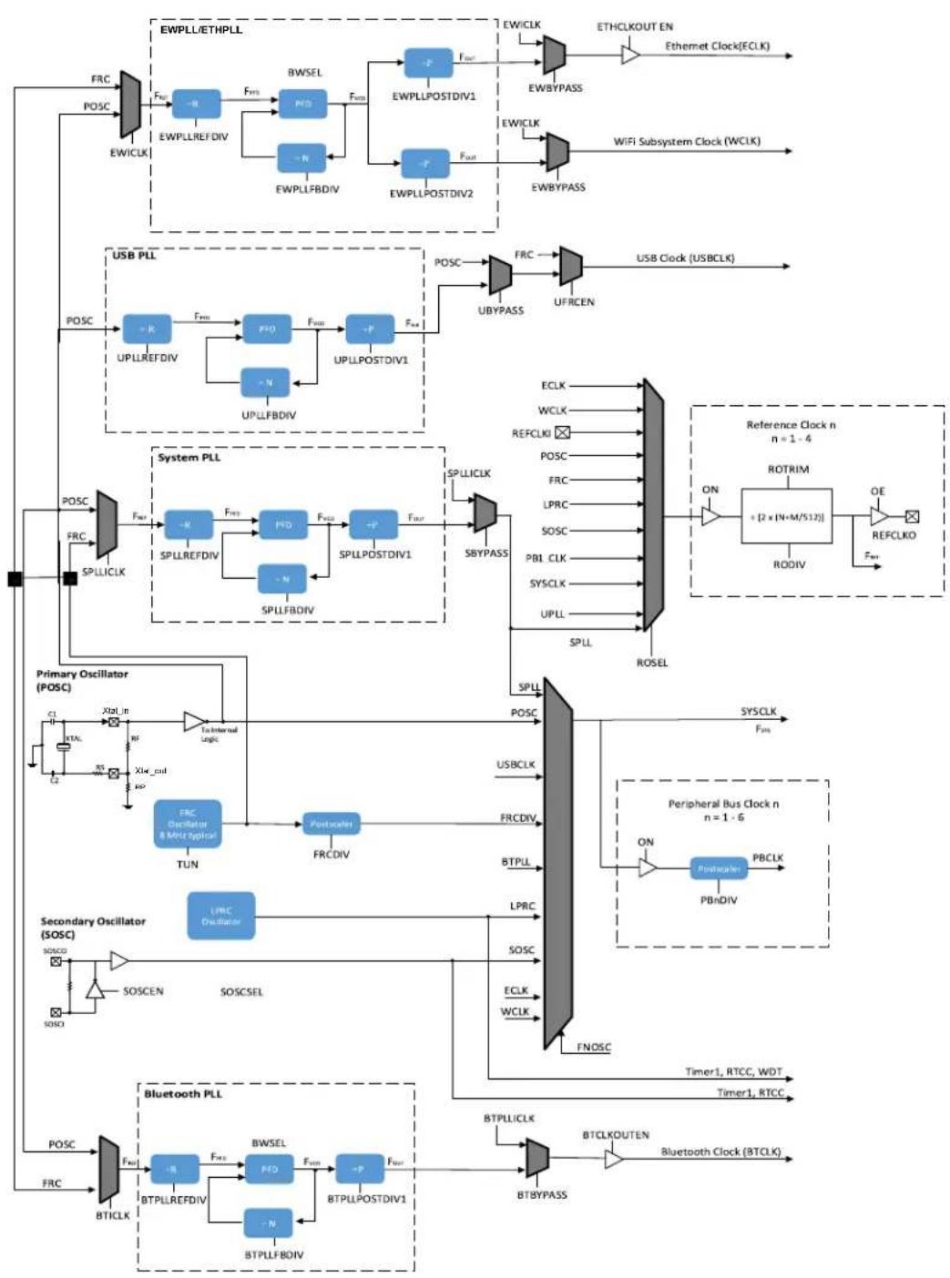
flowchart
graph TD
    subgraph Power Components
        A["POS C"] --> B["EWICLK"]
        B --> C["EWPLL/ETHPLL"]
        C --> D["FRC"]
        D --> E["POSC"]
        E --> F["USB PLL"]
        F --> G["POSC"]
        G --> H["SPILLCLK"]
        H --> I["Primary Oscillator (POSC)"]
        I --> J["C1"]
        J --> K["Xba_in"]
        J --> L["Xba_rml"]
        J --> M["SOSC"]
        J --> N["SOSC"]
        J --> O["SOSC"]
        J --> P["SOSC"]
        J --> Q["SOSC"]
        J --> R["SOSC"]
        J --> S["SOSC"]
        J --> T["SOSC"]
        J --> U["SOSC"]
        J --> V["SOSC"]
        J --> W["SOSC"]
        J --> X["SOSC"]
        J --> Y["SOSC"]
        J --> Z["SOSC"]
        J --> AA["SOSC"]
    end

    subgraph Power Components
        AB["FWEL"] --> AC["FWEL"]
        AC --> AD["FWELREFDIV"]
        AD --> AE["FWEL"]
        AE --> AF["FWELFBDIV"]
        AF --> AG["FWEL"]
        AG --> AH["FWELPOSTDIV1"]
        AH --> AI["FWELPOSTDIV2"]
        AI --> AJ["FWELPOSTDIV1"]
        AJ --> AK["FWELPOSTDIV1"]
        AK --> AL["FWELPOSTDIV1"]
        AL --> AM["FWELPOSTDIV1"]
        AM --> AN["FWELPOSTDIV1"]
    end

    subgraph Power Components
        AO["FWEL"] --> AP["FWEL"]
        AP --> AQ["FWEL"]
        AQ --> AR["FWEL"]
        AR --> AS["FWEL"]
        AS --> AT["FWEL"]
        AT --> AU["FWEL"]
        AU --> AV["FWEL"]
    end

    subgraph Power Components
        AW["FWEL"] --> AX["FWEL"]
        AX --> AY["FWEL"]
        AY --> AZ["FWEL"]
        AZ --> BA["FWEL"]
        BA --> BB["FWEL"]
        BB --> BC["FWEL"]
    end

    subgraph Power Components
        BD["FWEL"] --> BE["FWEL"]
        BE --> BF["FWEL"]
        BF --> BG["FWEL"]
        BG --> BH["FWEL"]
        BH --> BI["FWEL"]
    end

    subgraph Power Components
        BJ["FWEL"] --> BK["FWEL"]
        BK --> BL["FWEL"]
        BL --> BM["FWEL"]
        BM --> BN["FWEL"]
    end

    subgraph Power Components
        BO["FWEL"] --> BP["FWEL"]
        BP --> BQ["FWEL"]
        BQ --> BR["FWEL"]
        BR --> BS["FWEL"]
    end

    subgraph Power Components
        BT["FWEL"] --> BU["FWEL"]
        BU --> BV["FWEL"]
        BV --> BW["FWEL"]
    end

    subgraph Power Components
        BX["FWEL"] --> BY["FWEL"]
        BY --> BZ["FWEL"]
        BZ --> CA["FWEL"]
    end

    subgraph Power Components
        CB["FWEL"] --> CC["FWEL"]
        CC --> CD["FWEL"]
        CD --> CE["FWEL"]
    end

    subgraph Power Components
        CF["FWEL"] --> CG["FWEL"]
        CG --> CH["FWEL"]
        CH --> CI["FWEL"]
    end

    subgraph Power Components
        CJ["FWEL"] --> CK["FWEL"]
        CK --> CL["FWEL"]
        CL --> CM["FWEL"]
    end

    subgraph Power Components
        CN["FWEL"] --> CO["FWEL"]
        CO --> CP["FWEL"]
        CP --> CQ["FWEL"]
    end

    subgraph Power Components
        CR["FWEL"] --> CS["FWEL"]
        CS --> CT["FWEL"]
        CT --> CU["FWEL"]
    end

    subgraph Power Components
        DU["FWEL"] --> DV["FWEL"]
        DV --> DW["FWEL"]
    end

    subgraph Power Components
        DX["FWEL"] --> DXB["FWEL"]
        DXB --> DXC["FWEL"]
    end

    subgraph Power Components
        DXC --> DXD["FWEL"]

    subgraph Power Components
        DXD --> DXE["FWEL"]

    subgraph Power Components
        DXE --> DXF["FWEL"]

    subgraph Power Components
        DXF --> DXG["FWEL"]

    subgraph Power Components
        DXG --> DXH["FWEL"]

    subgraph Power Components
        DXH --> DXI["FWEL"]

    subgraph Power Components
        DXI --> DXJ["FWEL"]

    subgraph Power Components
        DXJ --> DXK["FWEL"]

    subgraph Power Components
        DXK --> DXL["FWEL"]

    subgraph Power Components
        DXL --> DXM["FWEL"]

    subgraph Power Components
        DXM --> DXN["FWEL"]

    subgraph Power Components
        DXN --> DXO["FWEL"]

    subgraph Power Components
        DXO --> DXP["FWEL"]

    subgraph Power Components
        DXP --> DXQ["FWEL"]

    subgraph Power Components
        DXQ --> DXR["FWEL"]

    subgraph Power Components
        DXR --> DXS["FWEL"]

    subgraph Power Components
        DXS --> DXT["FWEL"]

    subgraph Power Components
        DXT --> DXU["FWEL"]

    subgraph Power Components
        DXU --> DXV["FWEL"]

    subgraph Power Components
        DXV --> DXW["FWEL"]

    subgraph Power Components
        DXW --> DXX["FWEL"]

    subgraph Power Components
        DXX --> DXY["FWEL"]

    subgraph Power Components
        DXY --> DXZ["FWEL"]

    subgraph Power Components
        DXZ --> DXR

    subgraph Power Components
        DXR --> DXS

    end

    subgraph Power Components
        DXS --> DXT

    subgraph Power Components
        DXT --> DXU

    end

    subgraph Power Components
        DXU --> DXV

    subgraph Power Components
        DXV --> DXW

    subgraph Power Components
        DXW --> DXZ

    end

    subgraph Power Components
        DXZ --> DXT

    subgraph Power Components
        DXT --> DXU

    subgraph Power Components
        DXU --> DXV

    end

    subgraph Power Components
        DXV --> DXW

    subgraph Power Components
        DXW --> DXZ

    end

    subgraph Power Components
        DXZ --> DXT

    subgraph Power Components
        DXT --> DXU

    subgraph Power Components
        DXU --> DXV

    end

    subgraph Power Components
        DXV --> DXW

    subgraph Power Components
        DXW --> DXZ

    subgraph Power Components
        DXZ --> DXT

    end

    subgraph Power Components
        DXT <-->|Timer1, RTCC, WDT| LR
    end

    subgraph Power Components
        DXT <-->|Timer1, RTCC| LR

    end

    style Power Components fill:#f9f9f9,stroke:#333,stroke-width:2px
Notes: 1. A series resistor, Rs, may be required for AT strip cut crystals, or to eliminate clipping.
2. The internal feedback resistor, R F, is typically 1 MW.
3. Refer to Oscillators with Enhanced PLL (DS60001250) in the "PIC32 Family Reference Manual" for help in determining the best oscillator components.
4: Refer to Section 42.0 "Packaging Information" for frequency limitations.
5: A parallel resistor R P is added to adjust the oscillator gain and ensure start-up.
TABLE 11-1: SYSTEM AND PERIPHERAL CLOCK DISTRIBUTION (1)
| Peripheral | Clock Source | |||||||||||||||||
| BTPLL | ETHPLL | FRC | LPRC | PB1_CLK | PB2_CLK | PB3_CLK | PB4_CLK | PB5_CLK | PB6_CLK | POSC | REFO1 | REFO2 | REFO3 | REFO4 | SOSC | SYSCLK | UPLL | |
| ADC | XX | XX | ||||||||||||||||
| Asymmetric Crypto | X | |||||||||||||||||
| BOR | X | |||||||||||||||||
| BT-CLKOUT | X | |||||||||||||||||
| CAN | X | |||||||||||||||||
| CAN-FD | X | X | ||||||||||||||||
| CPU | X | |||||||||||||||||
| CVD | X | X | XX | |||||||||||||||
| DMA | X | |||||||||||||||||
| DMT | X | |||||||||||||||||
| DSCON | X | |||||||||||||||||
| DSWDT | X | X | ||||||||||||||||
| Ethernet | X | X | ||||||||||||||||
| EVIC | X | |||||||||||||||||
| Flash Controller | X | X | ||||||||||||||||
| I2C1 | X | |||||||||||||||||
| I2C2 | X | |||||||||||||||||
| ICAP1 | X | |||||||||||||||||
| ICAP2 | X | |||||||||||||||||
| ICAP3 | X | |||||||||||||||||
| ICAP4 | X | |||||||||||||||||
| ICD | X | |||||||||||||||||
| OCMP1 | X | |||||||||||||||||
| OCMP2 | X | |||||||||||||||||
| OCMP3 | X | |||||||||||||||||
| OCMP4 | X | |||||||||||||||||
| PMU | X | X | ||||||||||||||||
| PORT A | X | |||||||||||||||||
| PORT B | X | |||||||||||||||||
| PORT C | X | |||||||||||||||||
| PORT K | X | |||||||||||||||||
| PPS | X | |||||||||||||||||
| Prefetch Cache | X | |||||||||||||||||
| PTG | XX | XX | ||||||||||||||||
| RTCC | XX | X | ||||||||||||||||
| SPI1 | X | X | ||||||||||||||||
| SPI2 | X | X | ||||||||||||||||
| SQI | X | X | ||||||||||||||||
| Symmetric Crypto | X | |||||||||||||||||
| Timer 1 | X | X | X | |||||||||||||||
| Timer 2 | X | |||||||||||||||||
| Timer 3 | X | |||||||||||||||||
| Timer 4 | X | |||||||||||||||||
| Timer 5 | X | |||||||||||||||||
| Timer 6 | X | |||||||||||||||||
| Timer 7 | X | |||||||||||||||||
| UART1 | XX | XX | ||||||||||||||||
| UART2 | XX | XX | ||||||||||||||||
| UART3 | XX | XX | ||||||||||||||||
| USB | X | X | ||||||||||||||||
| WDT | X | X | ||||||||||||||||
| Wi-Fi | X | X | X | XX | X | |||||||||||||
| TRNG | X | |||||||||||||||||
Note 1: The timer clocks represented in this table are not the standard clock. Refer to the corresponding module chapters for the standard timer clock support.
11.1 Oscillator Control Registers
TABLE 11-2: OSCILLATOR CONFIGURATION REGISTER MAP
| Virtual Address(BF60_#) | RegistName | Bit Range | Bits | All Resets | |||||||||||||||
| 31/15 | 30/14 | 29/13 | 28/12 | 27/11 | 26/10 | 25/9 | 24/8 | 23/7 | 22/6 | 21/5 | 20/4 | 19/3 | 18/2 | 17/1 | 16/0 | ||||
| 1200 | OSCCON | 31:16 | — | — | — | — | — | FRCDIV[2:0] | DRMEN | — | WAKE2SPD | — | — | — | — | — | 2000 | ||
| 15:0 | COSC[3:0] | NOSC[3:0] | CLKLOCK | — | — | SLPEN | CF | UFRCEN | SOSCEN | OSWEN | 0000 | ||||||||
| 1210 | OSCTUN | 31:16 | — | — | — | — | — | — | — | — | — | — | — | — | — | — | — | — | 2000 |
| 15:0 | — | — | — | — | — | — | — | — | — | — | TUN[5:0] | 0000 | |||||||
| 1220 | SPLLCON | 31:16 | SPLL_BYP | SPLLICLK | — | — | SPLLREFDIV[5:0] | SPLLFBDIV[9:0] | 2000 | ||||||||||
| 15:0 | SPLLFBDIV[9:0] | SPLLRST | SPLL-FLOCK | SPLLPOSTDIV[5:0] | SPLLPWDN | SPLLBSWSEL[2:0] | 0000 | ||||||||||||
| 1230 | UPLLCON | 31:16 | UPLL_BYP | — | — | — | UPLLREFDIV[5:0] | UPLLFBDIV[9:0] | 2000 | ||||||||||
| 15:0 | UPLLFBDIV[9:0] | UPLLRST | UPLL-FLOCK | UPLLPOSTDIV[5:0] | UPLLPWDN | UPLLBSWSEL[2:0] | 0000 | ||||||||||||
| 1240 | BTPLLCON | 31:16 | BTPLL_BYP | BTPLLICLK | — | BTCLKOUTEN | BTPLLREFDIV[5:0] | BTPLLFBDIV[9:0] | 2000 | ||||||||||
| 15:0 | BTPLLFBDIV[9:0] | BTPLLRST | BTPLL-FLOCK | BTPLLPOSTDIV[5:0] | BTPLLPWDN | BTPLLBSWSEL[2:0] | 0000 | ||||||||||||
| 1250 | EWPLLCON | 31:16 | EWPLL_BYP | EWPLLICLK | — | ETHICLKOUTEN | EWPLLREFDIV[5:0] | EWPLLFBDIV[9:0] | 2000 | ||||||||||
| 15:0 | EWPLLFBDIV[9:0] | EWPLLRST | EWPLL-FLOCK | EWPLLPOSTDIV[5:0] | EWPLLPWDN | EWPLLBSWSEL[2:0] | 0000 | ||||||||||||
| 12A0 | REFO1CON | 31:16 | — | RODIV[14:0] | 2000 | ||||||||||||||
| 15:0 | ON | — | SIDL | OE | RSLP | — | DIVSWEN | ACTIVE | — | — | — | — | ROSEL[3:0] | 0000 | |||||
| 12B0 | REFO1TRIM | 31:16 | ROTRIM[8:0] | — | — | — | — | — | — | — | 2000 | ||||||||
| 15:0 | — | — | — | — | — | — | — | — | — | — | — | — | — | — | — | — | 0000 | ||
| 12C0 | REFO2CON | 31:16 | — | RODIV[14:0] | 2000 | ||||||||||||||
| 15:0 | ON | — | SIDL | OE | RSLP | — | DIVSWEN | ACTIVE | — | — | — | — | ROSEL[3:0] | 0000 | |||||
| 12D0 | REFO2TRIM | 31:16 | ROTRIM[8:0] | — | — | — | — | — | — | — | 2000 | ||||||||
| 15:0 | — | — | — | — | — | — | — | — | — | — | — | — | — | — | — | — | 0000 | ||
| 12E0 | REFO3CON | 31:16 | — | RODIV[14:0] | 2000 | ||||||||||||||
| 15:0 | ON | — | SIDL | OE | RSLP | — | DIVSWEN | ACTIVE | — | — | — | — | ROSEL[3:0] | 0000 | |||||
| 12F0 | REFO3TRIM | 31:16 | ROTRIM[8:0] | — | — | — | — | — | — | — | 2000 | ||||||||
| 15:0 | — | — | — | — | — | — | — | — | — | — | — | — | — | — | — | — | 0000 | ||
| 1300 | REFO4CON | 31:16 | — | RODIV[14:0] | 2000 | ||||||||||||||
| 15:0 | ON | — | SIDL | OE | RSLP | — | DIVSWEN | ACTIVE | — | — | — | — | ROSEL[3:0] | 0000 | |||||
| 1310 | REFO4TRIM | 31:16 | ROTRIM[8:0] | — | — | — | — | — | — | — | 2000 | ||||||||
| 15:0 | — | — | — | — | — | — | — | — | — | — | — | — | — | — | — | — | 0000 | ||
| 1320 | PB1DIV | 31:16 | — | — | — | — | — | — | — | — | — | — | — | — | — | — | — | — | 0000 |
| 15:0 | PB1DIVON | — | — | — | PBDIVRDY | — | — | — | — | PBDIV[0:0] | 0000 | ||||||||
Legend: x = unknown value on Reset; — = unimplemented, read as '0'. Reset values are shown in hexadecimal.
Note 1: All registers in this table have corresponding CLR, SET, and INV registers at their virtual addresses, plus offsets of 0x4, 0x8 and 0xC, respectively. See Section 13.3 "CLR, SET and INV Registers" for more
information.
2: Reset values are dependent on the CFGCONx Configuration bits and the type of Reset.
TABLE 11-2: OSCILLATOR CONFIGURATION REGISTER MAP (CONTINUED)
Legend: x = unknown value on Reset; — = unimplemented, read as '0'. Reset values are shown in hexadecimal.
Note 1: All registers in this table have corresponding CLR, SET, and INV registers at their virtual addresses, plus offsets of 0x4, 0x5 and 0xC, respectively. See Section 13.3 "CLR, SET and INV Registers" for more information.
2: Reset values are dependent on the CFGCONx Configuration bits and the type of Reset.
REGISTER 11-1: OSCCON: CRU OSCILLATOR CONTROL REGISTER
| Bit Range | Bit 31/23/15/7 | Bit 30/22/14/6 | Bit 29/21/13/5 | Bit 28/20/12/4 | Bit 27/19/11/3 | Bit 26/18/10/2 | Bit 25/17/9/1 | Bit 24/16/8/0 |
| 31:24 | U-0 U-0 | U-0 U-0 U-0 R | W/L-0 R/W/L-0 | R/W/L-0 | ||||
| — — — | — — FRCDIV[2:0] | |||||||
| 23:16 | R/W/L-0 | U-0 | R/W/L-1 | U-0 | U-0 | U-0 | U-0 | U-0 |
| DRMEN | — | 2SPDSLP | — | — | — | — | — | |
| 15:8 | R/W/L-0 | R/W/L-0 | R/W/L-0 | R/W/L-0 | R/W/L-0 | R/W/L-0 | R/W/L-0 | R/W/L-0 |
| COSC[3:0] | NOSC[3:0] | |||||||
| 7:0 | R/W/L-0 | U-0 | U-0 | R/W/L-0 | R/W/HS/L-0 | R/W/L-1 | R/W/L-1 | R/W/HC/L-1 |
| CLKLOCK | — | — | SLPEN | CF | UFRCEN | SOSCEN | OSWEN | |
Legend: HC = Hardware Cleared HS = Hardware Set
R = Readable bit W = Writable bit U = Unimplemented bit, read as '0' -n = Value at POR '1' = Bit is set '0' = Bit is cleared x = Bit is unknown
L = Value set from Configuration bits on POR
bit 31-27 Unimplemented: Read as '0'
bit 26-24 FRCDIV[2:0]: Fast RC Clock Divider bits
000 = FRC divided by 1 (default value)
001 = FRC divided by 2
010 = FRC divided by 4
011 = FRC divided by 8
100 = FRC divided by 16
101 = FRC divided by 32
110 = FRC divided by 64
111 = FRC divided by 256
bit 23 DRMEN: Enable Dream Mode bit
1 = When SLPEN = 1, DMA transfer complete causes Sleep mode to be entered
0 = DMA transfer has no effect
bit 22 Unimplemented: Read as '0'
bit 21 WAKE2SPD: 2-Speed startup enabled in Sleep mode bit
1 = When the device exits Sleep mode, the SYS_CLK is from FRC until the selected clock is ready
0 = When the device exits Sleep mode, the SYS_CLK is from the selected clock
bit 20-16 Unimplemented: Read as '0'
bit 15-12 COSC[3:0]: Current Oscillator Selection bits (Read-only)
0000 = Fast RC Oscillator (FRC) divided by OSCCON.FRCDIV (supports FRC/16 and FRC/1)
0001 = System PLL (SPLL module) (input clock and divider set by SPLLCON)
0010 = Primary Oscillator (POSC)
0011 = USB PLL (UPLL module) (input clock and divider set by UPLLCON)
0100 = Secondary Oscillator (SOSC)
0101 = Low-Power RC Oscillator (LPRC)
0110 = BT PLL (input clock and divider set by BTPLLCON)
0111 = EWPLL Ethernet clock (input clock and divider set by EWPLLCON)
1000 = EWPLL Wi-Fi clock (input clock and divider set by EWPLLCON)
Note 1: Loaded with NOSC[3:0] at the completion of a successful clock switch.
2: Set to FRC value (0000) when FSCM detects a failure and switches clock to FRC.
Note: The system unlock sequence must be done before this register can be written.
REGISTER 11-1: OSCCON: CRU OSCILLATOR CONTROL REGISTER (CONTINUED)
bit 11-8 NOSC[3:0]: New Oscillator Selection bits
0000 = FRC divided by OSCCON. FRCDIV (supports FRC/16 and FRC/1)
0001 = SPLL module (input clock and divider set by SPLLCON)
0010 = POSC
0011 = UPLL mode (input clock divider set by UPLLCON), was POSC with PLL
0100 = SOSC
0101 = LPRC
0110 = BT PLL (input clock and divider set by BTPLLCON)
0111 = EWPLL Ethernet clock (input clock and divider set by EWPLLCON)
1000 = EWPLL Wi-Fi clock (input clock and divider set by EWPLLCON)
bit 7 CLKLOCK: Clock Lock Enabled bit
1 = All clock and PLL configuration registers are locked. These include OSCCON, OSCTRIM, SPLLCON, UPLLCON, and PBxDIV.
0 = Clock and PLL selection registers are not locked, configurations may be modified
Note 1: Once set, this bit can only be cleared via a device Reset.
2: When active, this bit prevents writes to the following registers: NOSC[3:0], and OSWEN.
bit 6-5 Unimplemented: Read as '0'
bit 4 SLPEN: Enable Sleep Mode bit
1 = When a WAIT instruction is executed, device enters Sleep mode
0 = When a WAIT instruction is executed, device enters Idle mode
bit 3 CF: Clock Fail Detect bit (readable/writable/clearable by application)
1 = FSCM detects clock failure
0 = FSCM does not detect clock failure
Note 1: Writing a '1' to this bit causes a clock switching sequence to be initiated by the clock switch state machine.
2: Reset when a valid clock switching sequence is initiated by the clock switch state machine.
3: This bit is set when clock fail event detected.
bit 2 UFRCEN: USB FRC Clock Enable bit
1 = Enable FRC as the clock source for the USB clock source
0 = Use the primary oscillator or UPLL as the USB clock source
bit 1 SOSCEN: 32 kHz Secondary (LP) Oscillator Enable bit
1 = Enable SOSC
0 = Disable SOSC
bit 0 OSWEN: Oscillator Switch Enable bit
1 = Request oscillator switch to selection specified by NOSC[3:0] bits
0 = Oscillator switch is complete
Note 1: A Write of value '0' has no effect.
2: This bit is cleared by hardware after a successful clock switch; after redundant clock switch (NOSC = COSC) and when FSCM switches the oscillator to Fail-Safe Clock Source (FRC).
Note: The system unlock sequence must be done before this register can be written.
REGISTER 11-2: OSCTUN: FRC TUNING REGISTER
| Bit Range | Bit 31/23/15/7 | Bit 30/22/14/6 | Bit 29/21/13/5 | Bit 28/20/12/4 | Bit 27/19/11/3 | Bit 26/18/10/2 | Bit 25/17/9/1 | Bit 24/16/8/0 |
| 31:24 | U-0 U-0 | U-0 U-0 U-0 | U-0 U-0 U-0 | |||||
| — — — | — — | — | — — | |||||
| 23:16 | U-0 R-0 | U-0 U-0 U-0 | U-0 U-0 U-0 | |||||
| — — — | — — | — | — — | |||||
| 15:8 | U-0 R-0 | U-0 U-0 U-0 | U-0 U-0 U-0 | |||||
| — — — | — — | — | — — | |||||
| 7:0 | U-0 U-0 | R/W/L-0 | ||||||
| — — | TUN[5:0] | |||||||
| Legend: | L = Value set from Configuration bits on POR | ||
| R = Readable bit | W = Writable bit | U = Unimplemented bit, read as ‘0’ | |
| -n = Value at POR | ‘1’ = Bit is set | ‘0’ = Bit is cleared | x = Bit is unknown |
bit 31-6 Unimplemented: Read as '0'
bit 5-0 TUN[5:0]: Internal FRC Oscillator Tuning bits
This bit field specifies the user tuning capability for the internal FRC oscillator.
011111 = Center frequency +2%
011110 =
•
•
•
000001 =
000000 = Center frequency, oscillator is running at calibrated frequency (8MHz)
111111 =
111110 =
•
•
.
100001 =
100000 = Center frequency -2%
Note 1: The system unlock sequence must be done before this register can be written.
2: OSCTUN functionality has been provided to help customers compensate for temperature effects on the FRC frequency over a wide range of temperatures. The tuning step size is an approximation, and is neither characterized nor tested.
REGISTER 11-3: SPLLCON: SPLL CONTROL REGISTER
| Bit Range | Bit 31/23/15/7 | Bit 30/22/14/6 | Bit 29/21/13/5 | Bit 28/20/12/4 | Bit 27/19/11/3 | Bit 26/18/10/2 | Bit 25/17/9/1 | Bit 24/16/8/0 |
| 31:24 | R/W/L-1 R/W | W/L-1 U-0 U-0 | R/W-0 R/W/L-0 | R/W-0 R/W-0 | ||||
| SPLL_BYP S | SPLLICLK | — — SP | LLREFDIV[5:2] | |||||
| 23:16 | R/W/L-0 R/W | W/L-0 R/W/L-0 | R/W/L-0 R/W/L-0 | R/W/L-0 R/W/L-0 | W/L-0 R/W/L-0 | |||
| SPLLREFDIV[1:0] SPLL | FBDIV[9:4] | |||||||
| 15:8 | R/W/L-0 R/W | W/L-0 R/W/L-0 | R/W/L-0 R/W/L-0 | -1 R/W/L-0 R/W | W/L-0 R/W/L-0 | |||
| SPLLFBDIV[3:0] | SPLLRST | SPLLFLOCK | SPLLPOSTDIV1[5-4] | |||||
| 7:0 | R/W/L-0 R/W | W/L-0 R/W/L-0 | R/W/L-0 R/W/L-0 | -1 R/W/L-0 R/W | W/L-0 R/W/L-0 | |||
| SPLLPOSTDIV1[3:0] | SPLLPWDN | SPLLBSWSEL[2:0] | ||||||
| Legend: | L = Value set from Configuration bits on POR | ||
| R = Readable bit | W = Writable bit | U = Unimplemented bit, read as ‘0’ | |
| -n = Value at POR | ‘1’ = Bit is set | ‘0’ = Bit is cleared | x = Bit is unknown |
bit 31 SPLL_BYP: SPLL Bypass bit; when this bit is set, the input clock REF bypasses PLL to PLLOUTx.
Note: Recommendation is to setup SPLL first before setting up other PLLs especially when using SYS-PLL for generating main system clock. Reset value must be 1, because PLL needs setup in SW for generating desired frequency.
bit 30 SPLLICLK: Source Input Clock Selection bit:
0 = POSC is the SPLL input clock source
1 = FRC is the SPLL input clock source
Note: The Reset value must be 1, because the POSC is not available upon Reset.
bit 29-28 Unimplemented: Read as '0'
bit 27-22 SPLLREFDIV[5:0]: Reference Frequency Divide bit. The recommended value of SPLLREFDIV is 5 for deriving the system clock of 200 MHz.
bit 21-12 SPLLFBDIV[9:0]: PLL Feedback Divider bit. The recommended value of SPLLFBDIV is 0x96 for deriving system clock of 200 MHz.
bit 11 SPLLRST: System PLL Reset bit
1 = Assert the Reset to the SPLL
0 = De-assert the Reset to the SPLL
bit 10 SPLLFLOCK: System PLL Force Lock bit
1 = Force the SPLL lock signal to be asserted
0 = Do not force the SPLL lock signal to be asserted
bit 9-4 SPLLPOSTDIV1[5:0]: First Post Divide Value bit. The recommended value of SPLLPOSTDIV is 6 for deriving system clock of 200 MHz.
bit 3 SPLLPWDN: PLL Power Down Register bit
1 = PLL is powered down
0 = PLL is active
bit 2-0 SPLLBSWSEL[2:0]: PLL Bandwidth Select bit
Use the frequency range that matches the PLL closed loop bandwidth as based on the reference frequency divided by REFDIV to be set to allow the PLL loop filter to work with the post-reference divider frequency. The recommended value of SPLLBSWSEL is 1 for deriving system clock of 200 MHz.
Note 1: The system unlock sequence must be done before this register can be written.
2: Using unrecommended values for these register bits may result invalid behavior of the device.
3: To reduce the system clock frequency from 200 MHz, it is recommended to change only the SPLLPOST-DIV values
REGISTER 11-4: UPLLCON: UPLL CONTROL REGISTER
| Bit Range | Bit 31/23/15/7 | Bit 30/22/14/6 | Bit 29/21/13/5 | Bit 28/20/12/4 | Bit 27/19/11/3 | Bit 26/18/10/2 | Bit 25/17/9/1 | Bit 24/16/8/0 |
| 31:24 | R/W/L-1 U-0 | U-0 U-0 R/W | -0 R/W/L-0 | R/W-0 R/W-0 | ||||
| UPLL_BYP | — — — | UPLLREFDIV[5:2] | ||||||
| 23:16 | R/W/L-0 | R/W/L-0 | R/W/L-0 | R/W/L-0 | R/W/L-0 | R/W/L-0 | R/W/L-0 | R/W/L-0 |
| UPLLREFDIV[1:0] | UPLLFBDIV[9:4] | |||||||
| 15:8 | R/W/L-0 | R/W/L-0 | R/W/L-0 | R/W/L-0 | R/W/L-1 | R/W/L-0 | R/W/L-0 | R/W/L-0 |
| UPLLFBDIV[3:0] | UPLLRST | UPLLFLOCK | UPLLPOSTDIV1[5-4] | |||||
| 7:0 | R/W/L-0 | R/W/L-0 | R/W/L-0 | R/W/L-0 | R/W/L-1 | R/W/L-0 | R/W/L-0 | R/W/L-0 |
| UPLLPOSTDIV1[3:0] | USPLLPWDN | UPLLBSWSEL[2:0] | ||||||
| Legend: | L = Value set from Configuration bits on POR | ||
| R = Readable bit | W = Writable bit | U = Unimplemented bit, read as ‘0’ | |
| -n = Value at POR | ‘1’ = Bit is set | ‘0’ = Bit is cleared | x = Bit is unknown |
bit 31 UPLL_BYP: UPLL Bypass; when this bit is set, the input clock REF bypasses PLL to PLLOUTx.
Note: Recommendation is to setup SPLL first before setting up other PLLs especially when using SYS-PLL for generating main system clock. Reset value must be 1, because PLL needs setup in SW for generating desired frequency.
bit 30-28 Unimplemented: Read as '0'
bit 29-28 Unimplemented: Read as '0'
bit 27-22 UPLLREFDIV[5:0]: Reference Frequency Divide, 1 ≤ UPLLDIVR ≤ 63 , value of 0 is unused
bit 21-12 UPLLFBDIV[9:0]: PLL Feedback Divider, 16 ≤ UPLLFBDIV ≤ 1023, values of 0 to 15 are unused
bit 11 UPLLRST: USB PLL Reset
1 = Assert the reset to the UPLL
0 = De-assert the reset to the UPLL
bit 10 UPLLFLOCK: USB PLL Force Lock
1 = Force the UPLL lock signal to be asserted
0 = Do not force the UPLL lock signal to be asserted
bit 9-4 UPLLPOSTDIV1[5:0]: First Post Divide Value, 1 ≤ UPLLPOSTDIV1 ≤ 63 , value of 0 is unused
bit 3 UPLLPWDN: PLL Power Down Register bit
1 = PLL is powered down
0 = PLL is active
bit 2-0 UPLLBSWSEL[2:0]: PLL Bandwidth Select
Use the frequency range that matches the PLL closed loop bandwidth as based on the reference frequency divided by REFDIV to be set to allow the PLL loop filter to work with the post-reference divider frequency.
Note: The system unlock sequence must be done before this register can be written.
REGISTER 11-5: BTPLLCON: BTPLL CONTROL REGISTER
| Bit Range | Bit 31/23/15/7 | Bit 30/22/14/6 | Bit 29/21/13/5 | Bit 28/20/12/4 | Bit 27/19/11/3 | Bit 26/18/10/2 | Bit 25/17/9/1 | Bit 24/16/8/0 |
| 31:24 | R/W/L-1 R/ | W/L-1 U-0 R/W | W/L-0 R/W-0 R | W/L-0 R/W-0 R/W-0 | ||||
| BTPLL_BYP | BTPLLICLK | — BTCL | KOUTEN BTPLL | REFDIV[5:2] | ||||
| 23:16 | R/W/L-0 | R/W/L-0 | R/W/L-0 | R/W/L-0 | R/W/L-0 | R/W/L-0 | R/W/L-0 | R/W/L-0 |
| BTPLLREFDIV[1:0] | BTPLLFBDIV[9:4] | |||||||
| 15:8 | R/W/L-0 | R/W/L-0 | R/W/L-0 | R/W/L-0 | R/W/L-1 | R/W/L-0 | R/W/L-0 | R/W/L-0 |
| BTPLLFBDIV[3:0] | BTPLLRST | BTPLLFLOCK | BTPLLPOSTDIV[5-4] | |||||
| 7:0 | R/W/L-0 | R/W/L-0 | R/W/L-0 | R/W/L-0 | R/W/L-1 | R/W/L-0 | R/W/L-0 | R/W/L-0 |
| BTPLLPOSTDIV1[3:0] | BTPLLPWDN | BTPLLBSWSEL[2:0] | ||||||
| Legend: | L = Value set from Configuration bits on POR | ||
| R = Readable bit | W = Writable bit | U = Unimplemented bit, read as ‘0’ | |
| -n = Value at POR | ‘1’ = Bit is set | ‘0’ = Bit is cleared | x = Bit is unknown |
bit 31 BTPLL_BYP: BTPLL Bypass; when this bit is set, the input clock REF bypasses PLL to PLLOUTx.
Note: Recommendation is to setup SPLL first before setting up other PLLs especially when using SYS-PLL for generating main system clock. Reset value must be 1, because PLL needs setup in SW for generating desired frequency.
bit 30 BTPLLICLK: Source Input Clock Selection bit:
0 = POSC is the BTPLL input clock source
1 = FRC is the BTPLL input clock source
Note: The Reset value must be 1, because the POSC is not available upon Reset.
bit 29 Unimplemented: Read as '0'
bit 28 BTCLKOUTEN: BT Clock Out pin Enable bit
1 = BT_CLK_OUT Pin is enabled
0 = BT_CLK_OUT Pin is disabled
bit 27-22 BTPLLREFDIV[5:0]: Reference Frequency Divide, 1 ≤ BTPLLDIVR ≤ 63 , value of 0 is unused
bit 21-12 BTPLLFBDIV[9:0]: PLL Feedback Divider, 16 ≤ BTPLLFBDIV ≤ 1023, values of 0 to 15 are unused
bit 11 BTPLLRST: BT PLL Reset
1 = Assert the reset to the BTPLL
0 = De-assert the reset to the BTPLL
bit 10 BTPLLFLOCK: BT PLL Force Lock
1 = Force the BTPLL lock signal to be asserted
0 = Do not force the BTPLL lock signal to be asserted
bit 9-4 BTPLLPOSTDIV1[5:0]: First Post Divide Value, 1 ≤ BTPLLPOSTDIV1 ≤ 63, value of 0 is unused
bit 3 BTPLLPWDN: PLL Power Down Register bit
1 = PLL is powered down
0 = PLL is active
bit 2-0 BTPLLBSWSEL[2:0]: PLL Bandwidth Select
Use the frequency range that matches the PLL closed loop bandwidth as based on the reference frequency divided by REFDIV to be set to allow the PLL loop filter to work with the post-reference divider frequency.
Note: The system unlock sequence must be done before this register can be written.
REGISTER 11-6: EWPLLCON: EWPLL CONTROL REGISTER
| Bit Range | Bit 31/23/15/7 | Bit 30/22/14/6 | Bit 29/21/13/5 | Bit 28/20/12/4 | Bit 27/19/11/3 | Bit 26/18/10/2 | Bit 25/17/9/1 | Bit 24/16/8/0 |
| 31:24 | R/W/L-1 R/W | W/L-1 U-0 R/W | L-0 R/W-0 R/W | W/L-0 R/W-0 R/W-0 | 0 | |||
| EWPLL_BYP | EWPLLICLK | — ETHCLKOUTEN EWPLL | LREFDIV[5:2] | |||||
| 23:16 | R/W/L-0 R/W | W/L-0 R/W/L-0 | R/W/L-0 R/W/L-0 | R/W/L-0 R/W/L-0 | R/W/L-0 R/W/L-0 | |||
| EWPLLREFDIV[1:0] | EWPLLFBDIV[9:4] | |||||||
| 15:8 | R/W/L-0 R/W | W/L-0 R/W/L-0 | R/W/L-0 R/W/L-1 | R/W/L-0 R/W/L-0 | R/W/L-0 R/W/L-0 | |||
| EWPLLFBDIV[3:0] | EWPLLRST | EWPLLFLOCK | EWPLLPOSTDIV1[5-4] | |||||
| 7:0 | R/W/L-0 R/W | W/L-0 R/W/L-0 | R/W/L-0 R/W/L-1 | R/W/L-0 R/W/L-0 | R/W/L-0 R/W/L-0 | |||
| EWPLLPOSTDIV1[3:0] | EWPLLPWDN | EWPLLBSWSEL[2:0] | ||||||
| Legend: | L = Value set from Configuration bits on POR | ||
| R = Readable bit | W = Writable bit | U = Unimplemented bit, read as ‘0’ | |
| -n = Value at POR | ‘1’ = Bit is set | ‘0’ = Bit is cleared | x = Bit is unknown |
bit 31 EWPLL_BYP: EWPLL Bypass; when this bit is set, the input clock REF bypasses PLL to PLLOUTx.
Note: Set up the SPLL first before setting up other PLLs, especially when using the SYSPLL for generating the main system clock. The Reset value must be '1' because the PLL needs to be set up in SW for generating the desired frequency.
bit 30 EWPLLICLK: Source Input Clock Selection bit:
0 = POSC is the EWPLL input clock source
1 = FRC is the EWPLL input clock source
Note: The Reset value must be '1' because the POSC is not available upon Reset. For Wi-Fi operation, this bit must be set to '0'. For Ethernet, when providing the reference clock to the external PHY, this bit must be set to '0'.
bit 29 Unimplemented: Read as '0'
bit 28 ETHCLKOUTEN: Ethernet Clock Out pin Enable bit
1 = ETH_CLK_OUT pin is enabled
0 = ETH_CLK_OUT pin is disabled
bit 27-22 EWPLLREFDIV[5:0]: Reference Frequency Divide, 1 ≤ EWPLLDIVR ≤ 63, value of 0 is unused
bit 21-12 EWPLLFBDIV[9:0]: PLL Feedback Divider, 16 ≤ EWPLLFBDIV ≤ 1023 , values of 0 to 15 are unused
1 = Assert the reset to the EWPLL
0 = De-assert the reset to the EWPLL
1 = Force the EWPLL lock signal to be asserted
0 = Do not force the EWPLL lock signal to be asserted
bit 9-4 EWPLLPOSTDIV1[5:0]: First Post Divide Value, 1 ≤ EWPLLPOSTDIV1 ≤ 63 , value of 0 is unused
bit 3 EWPLLPWDN: PLL Power Down Register bit
1 = PLL is powered down
0 = PLL is active
bit 2-0 EWPLLBSWSEL[2:0]: PLL Bandwidth Select
Use the frequency range that matches the PLL closed loop bandwidth as based on the reference frequency divided by REFDIV to be set to allow the PLL loop filter to work with the post-reference divider frequency.
Note: The system unlock sequence must be done before this register can be written.
REGISTER 11-7: REFOxCON: REFERENCE OSCILLATOR 1 CONTROL REGISTER (x = 1-4)
| Bit Range | Bit 31/23/15/7 | Bit 30/22/14/6 | Bit 29/21/13/5 | Bit 28/20/12/4 | Bit 27/19/11/3 | Bit 26/18/10/2 | Bit 25/17/9/1 | Bit 24/16/8/0 | |
| 31:24 | U-0 R/W-0 R/W-0 R/W-0 R/W-0 R/W-0 R/W-0 | ||||||||
| — RODIV[14:8] | |||||||||
| 23:16 | R/W-0 R/W-0 R/W-0 R/W-0 R/W-0 R/W-0 R/W-0 | ||||||||
| RODIV[7:0] | |||||||||
| 15:8 | R/W-0 R/W-0 R/W-0 R/W-0 R/W-0 U-0 H C/ R/W-0 HS/H C/ R-0 | ||||||||
| ON | — | S | I | D | L | O | E | R | |
| 7:0 | U-0 | U-0 | U-0 | U-0 | R/W-0 | R/W-0 | R/W-0 | R/W-0 | |
| — | — | — | — | ROSEL[3:0] | |||||
| Legend: | HC = Hardware Cleared | HS = Hardware Set |
| R = Readable bit | W = Writable bit | U = Unimplemented bit, read as ‘0’ |
| -n = Value at POR | ‘1’ = Bit is set | ‘0’ = Bit is cleared x = Bit is unknown |
bit 31 Unimplemented: Read as '0'
Reserved for expansion of RODIV[15]
bit 30-16 RODIV[14:0] Reference Clock Divider bits
Specifies 1/2 period of reference clock in the source clocks.
1111111111111111 = REFO clock is base clock frequency divided by 65,534 (32,767 *2)
111111111111110 = REFO clock is base clock frequency divided by 65,532 (32,766 * 2)
000000000000011 = REFO clock is base clock frequency divided by 6 (3*2)
000000000000010 = REFO clock is base clock frequency divided by 4 (2*2)
000000000000001 = REFO clock is base clock frequency divided by 2 (1*2)
000000000000000 = REFO clock is same frequency as base clock (no divider)
Note: RODIV values (up to 0x1000) are used when trying to divide a highly loaded clock source.
bit 15 ON: Output Enable bit
1 = Reference oscillator module enabled
0 = Reference oscillator module disabled
bit 14 Unimplemented: Read as '0'
bit 13 SIDL: Peripheral Stop in Idle Mode bit
1 = Discontinue module operation when device enters Idle mode
0 = Continue module operation in Idle mode
bit 12 OE: Reference Clock Output Enable bit
1 = Reference clock is driven out on REFO pin
0 = Reference clock is not driven out on REFO pin
bit 11 RSLP: Reference Oscillator Run in Sleep bit
1 = Reference oscillator output continues to run in Sleep mode
0 = Reference oscillator output is disabled in Sleep mode
Note: This bit is ignored when ROSEL[3:0] = (0000 or 0001).
bit 10 Unimplemented: Read as '0'
bit 9 DIVSWEN: Clock RODIV/ROTRIM switch enabled
1 = Clock divider switching currently in progress
0 = Clock divider switching is completed
bit 8 ACTIVE: Reference Clock Request Status bit
1 = Reference clock request is active (user must not update this REFOCON register)
0 = Reference clock request is not active (user can update this REFOCON register)
bit 7-4 Unimplemented: Read as '0'
Note 1: REFOCON.ROSEL must not be written while the REFOCON.ACTIVE bit is '1' – Undefined behavior will result.
2: REFOCON must not be written when REFOCON[ON] != REFOCON[ACTIVE] – Undefined behavior will result.
REGISTER 11-7: REFOXCON: REFERENCE OSCILLATOR 1 CONTROL REGISTER (x = 1-4) (CONTINUED)
bit 3-0 ROSEL[3:0]: Reference Clock Source Select bits
Select one of various clock sources to be used as the reference clock.
1100 - 1111 = Reserved
1011 = RE F I P i n
1010 = BTPLL clock(2)
1001 = EWPLL Wi-Fi clock
1000 = EWPLL Ethernet clock
0111 = System PLL
0110 = USB PLL
0101 = SOSC
0100 = L P R C
0011 = F R C
0010 = POSC
0001 = Peripheral clock (reference clock reflects any peripheral clock switching)
0000 = System clock (reference clock reflects any device clock switching)
Note 1: REFOCON.ROSEL must not be written while the REFOCON.ACTIVE bit is '1' – Undefined behavior will result.
2: REFOCON must not be written when REFOCON[ON] != REFOCON[ACTIVE] - Undefined behavior will result..
REGISTER 11-8: REFOxTRIM: REFERENCE OSCILLATOR 1 TRIM REGISTER (x = 1-4)
| Bit Range | Bit 31/23/15/7 | Bit 30/22/14/6 | Bit 29/21/13/5 | Bit 28/20/12/4 | Bit 27/19/11/3 | Bit 26/18/10/2 | Bit 25/17/9/1 | Bit 24/16/8/0 |
| 31:24 | R/W-0 R/W-0 | R/W-0 R/W-0 | R/W-0 R/W-0 | R/W-0 R/W-0 | ||||
| ROTRIM[8:1] | ||||||||
| 23:16 | R/W-0 U-0 | U-0 U-0 U-0 | U-0 U-0 | |||||
| ROTRIM[0] | — — — | — — — | ||||||
| 15:8 | U-0 R-0 U-0 | U-0 U-0 | U-0 U-0 | |||||
| — | — — — | — — — | ||||||
| 7:0 | U-0 U-0 U-0 | U-0 U-0 | U-0 U-0 | |||||
| — | — — — | — — — | ||||||
Legend:
| R = Readable bit | W = Writable bit | U = Unimplemented bit, read as '0' |
| -n = Value at POR | '1' = Bit is set | '0' = Bit is cleared x = Bit is unknown |
bit 31-23 ROTRIM[8:0] Trim bits - Provides fractional additive to RODIV value for 1/2 period of REFO1 clock
0000_0000_0 = 0/512 (0.0) divisor added to RODIV value
0000_0000_1 = 1/512 (0.001953125) divisor added to RODIV value
0000_0001_0 = 2/512 (0.00390625) divisor added to RODIV value
100000000 = 256/512 (0.5000) divisor added to RODIV value
1111_1111_0 = 510/512 (0.99609375) divisor added to RODIV value
1111_1111_1 = 511/512 (0.998046875) divisor added to RODIV value
Note: ROTRIM values greater than zero are only valid when RODIV values are greater than 0.
bit 22-0 Unimplemented: Read as '0'
Note: REFOxTRIM must not be written when REFOxCON[ON] != REFOxCON[ACTIVE] - Undefined behavior will result.
REGISTER 11-9: PBxDIV: PERIPHERAL BUS 'x' CLOCK DIVISOR CONTROL REGISTER (x = 1-6)
| Bit Range | Bit 31/23/15/7 | Bit 30/22/14/6 | Bit 29/21/13/5 | Bit 28/20/12/4 | Bit 27/19/11/3 | Bit 26/18/10/2 | Bit 25/17/9/1 | Bit 24/16/8/0 |
| 31:24 | U-0 U-0 | U-0 U-0 U-0 U-0 | U-0 U-0 | |||||
| — — — | — — — — | |||||||
| 23:16 | U-0 U-0 | U-0 U-0 U-0 U-0 | U-0 U-0 | |||||
| — — — | — — — — | |||||||
| 15:8 | R-1 U-0 | U-0 U-0 R-1 U-0 | U-0 U-0 | |||||
| PBxDIVON | — — — | PBDIVRDY | — — | |||||
| 7:0 | U-0 | R/W-0 | R/W-0 | R/W-0 | R/W-0 | R/W-0 | R/W-0 | R/W-1 |
| — | PBDIV[6:0] | |||||||
Legend:
| R = Readable bit | W = Writable bit | U = Unimplemented bit, read as '0' |
| -n = Value at POR | '1' = Bit is set | '0' = Bit is cleared x = Bit is unknown |
bit 31-16 Unimplemented: Read as '0'
bit 15 PBxDIVON: Peripheral Bus 'x' Output Clock Enable bit
1 = Output clock is enabled
0 = Output clock is disabled
Note 1: PB1DIV[PB1DIVON] bit cannot be written to a '0', as this clock is used by CRU.
2: PB6DIV[PB6DIVON] bit cannot be written to a '0', as this clock is used by CPU.
3: PB3DIV[PB3DIVON] bit cannot be written to a '0', as this clock is used by Wi-Fi subsystem.
4: PB4DIV[PB4DIVON] bit cannot be written to a '0', as this clock is used by Deep Sleep Controller.
bit 14-12 Unimplemented: Read as '0'
bit 11 PBDIVRDY: Peripheral Bus 'x' Clock Divisor Ready bit
1 = Clock divisor logic is not switching divisors and the PBxDIV[6:0] bits may be written
0 = Clock divisor logic is currently switching values and the PBxDIV[6:0] bits cannot be written
bit 10-7 Unimplemented: Read as '0'
bit 6-0 PBDIV[6:0]: Peripheral Bus 'x' Clock Divisor Control bits
1111111 = PBCLKx is SYSCLK divided by 128
1111110 = PBCLKx is SYSCLK divided by 127
•
•
0000011 = PBCLKx is SYSCLK divided by 4
0000010 = PBCLKx is SYSCLK divided by 3
0000001 = PBCLKx is SYSCLK divided by 2
0000000 = PBCLKx is SYSCLK divided by 1
Note 1: The system unlock sequence must be done before this register can be written.
2: The PB4_CLK frequency must be less than 25 MHz for reliable device operation.
REGISTER 11-10: SLEWCON: SLEW RATE CONTROL FOR CLOCK SWITCHING REGISTER
| Bit Range | Bit 31/23/15/7 | Bit 30/22/14/6 | Bit 29/21/13/5 | Bit 28/20/12/4 | Bit 27/19/11/3 | Bit 26/18/10/2 | Bit 25/17/9/1 | Bit 24/16/8/0 |
| 31:24 | U-0 U-0 | U-0 U-0 R/W-cfg | R/W-cfg R/W | -cfg R/W-cfg | ||||
| — | — | — | — | SLWDLY[3:0] | ||||
| 23:16 | U-0 U-0 | U-0 U-0 R/W-cfg | R/W-cfg R/W | -cfg R/W-cfg | ||||
| — — — | — | SYSDIV[3:0] | ||||||
| 15:8 | U-0 U-0 | U-0 U-0 U-0 | R/W-cfg | R/W-cfg R/W-cfg | ||||
| — — — | — — | SLWDIV[2:0] | ||||||
| 7:0 | U-0 U-0 | U-0 U-0 U-0 | R/W-cfg | R/W-cfg R/W-cfg | ||||
| — | — | — | — | — | UPEN | DNEN | BUSY | |
| Legend: | cfg- Configurable at Reset | ||
| R = Readable bit | W = Writable bit | U = Unimplemented bit, read as ‘0’ | |
| -n = Value at POR | ‘1’ = Bit is set | ‘0’ = Bit is cleared | x = Bit is unknown |
bit 31-28 Unimplemented: Read as '0'
bit 27-24 SLWDLY[3:0]: Number of clocks generated at each slew step for a clock switch
0000 = 1 clock is generated at each slew step
0001 = 2 clocks is generated at each slew step
1111 = 16 clocks is generated at each slew step
bit 19-16 SYSDIV[3:0]: PBx Peripheral Clock Divisor Control bit
1111 = SYSCLK is divided by 16
1110 = SYSCLK is divided by 15
•
•
0010 = SYSCLK is divided by 3
0001 = SYSCLK is divided by 2
0000 = SYSCLK is not divided
bit 15-11 Unimplemented: Read as '0'.
bit 10-8 SLWDIV[2:0]: Slew Divisor Steps Control bits
These bits control the maximum division steps used when slewing during a frequency change.
111 = Steps are divided by 128, 64, 32, 16, 8, 4, 2, and then no divisor 110 = Steps are divided by 64, 32, 16, 8, 4, 2, and then no divisor
101 = Steps are divided by 32, 16, 8, 4, 2, and then no divisor
100 = Steps are divided by 16, 8, 4, 2, and then no divisor
011 = Steps are divided by 8, 4, 2, and then no divisor
010 = Steps are divided by 4, 2, and then no divisor
001 = Steps are divided by 2, and then no divisor
000 = No divisor is used during slewing
Note: Each divisor step lasts 4 clocks.
bit 7-3 Unimplemented: Read as '0'
Note 1: The system unlock sequence must be done before this register can be written.
2: Updates to this register do not take affect until OSCCON[OSWEN] is set.
REGISTER 11-10: SLEWCON: SLEW RATE CONTROL FOR CLOCK SWITCHING REGISTER (CONTINUED)
bit 2 UPEN: Upward Slew Enable bit
Enable clock slew for switching up to faster clocks
1 = Slewing enabled for switching to a higher frequency
0 = Slewing disabled for switching to a higher frequency
bit 1 DNEN: Downward Slew Enable bit
Enable clock slew for switching down to slower clocks
1 = Slewing enabled for switching to a lower frequency
0 = Slewing disabled for switching to a lower frequency
bit 0 BUSY: Clock Switch Slewing Active Status bit (Read-only)
0 = Clock switch has reached its final value
1 = Clock frequency is actively slewed
Note 1: The system unlock sequence must be done before this register can be written.
2: Updates to this register do not take affect until OSCCON[OSWEN] is set.
REGISTER 11-11: CLKSTAT: CLOCK STATUS REGISTER
| Bit Range | Bit 31/23/15/7 | Bit 30/22/14/6 | Bit 29/21/13/5 | Bit 28/20/12/4 | Bit 27/19/11/3 | Bit 26/18/10/2 | Bit 25/17/9/1 | Bit 24/16/8/0 |
| 31:24 | U-0 U-0 | U-0 U-0 | U-0 U-0 | U-0 U-0 | ||||
| — — — | — — — | — | — | |||||
| 23:16 | U-0 U-0 | U-0 U-0 | U-0 U-0 | U-0 U-0 | ||||
| — — — | — — — | — | — | |||||
| 15:8 | U-0 | U-0 | U-0 | U-0 | R/HS/HC-0 | R/HS/HC-0 | R/HS/HC-0 | R/HS/HC-0 |
| — | — | — | — | SYSCLKRDY | PB1CLKRDY | SPLLALTRDY | WIFICLKRDY | |
| 7:0 | R/HS/HC-0 | R/HS/HC-0 | R/HS/HC-0 | R/HS/HC-0 | R/HS/HC-0 | R/HS/HC-0 | R/HS/HC-0 | R/HS/HC-0 |
| ETHPLLRDY | BTPLLRDY | LPRCRDY | SOSCRDY | UPLLRDY | POSCRDY | SPLLRDY | FRCRDY |
| Legend: | HC = Hardware Set | HC = Hardware Cleared |
| R = Readable bit | W = Writable bit | U = Unimplemented bit, read as ‘0’ |
| -n = Value at POR | ‘1’ = Bit is set | ‘0’ = Bit is cleared x = Bit is unknown |
bit 31-12 Unimplemented: Read as '0'
bit 11 SYSCLKRDY: System Clock Ready Status bit
0 = SYSCLK is not stable and not ready
1 = SYSCLK is stable and ready
bit 10 PB1CLKRDY: PB1 Clock Ready Status bit
0 = PB1CLK is not stable and not ready
1 = PB1CLK is stable and ready
bit 9 SPLLALTRDY: System PLL Ready Status bit
0 = SPLL alternate output is not stable and not ready
1 = SPLL alternate output is stable and ready
bit 8 WIFICLKRDY: Wi-Fi Clock Ready Status bit
0 = WIFICCLK is not stable and not ready
1 = WIFICCLK is stable and ready
bit 7 ETHPLLRDY: ETHPLL Ready Status bit
0 = ETHPLL is not stable and not ready
1 = ETHPLL is stable and ready
bit 6 BTPLLRDY: Bluetooth PLL Ready Status bit
0 = BTPLL is not stable and not ready
1 = BTPLL is stable and ready
bit 5 LPRCRDY: LPRC Ready Status bit
0 = LPRC is not stable and not ready
1 = LPRC is stable and ready
bit 4 SOSCRDY: SOSC Ready Status bit
0 = SOSC is not stable and not ready
1 = SOSC is stable and ready
bit 3 UPLLRDY: USB PLL Ready Status bit
0 = UPLL is not stable and not ready
1 = UPLL is stable and ready
REGISTER 11-11: CLKSTAT: CLOCK STATUS REGISTER (CONTINUED)
bit 2 POSCRDY: Primary Oscillator Ready Status bit
0 = POSC is not stable and not ready
1 = POSC is stable and ready
bit 1 SPLLRDY: System PLL Ready Status bit
0 = SPLL Primary output is not stable and not ready
1 = SPLL Primary output is stable and ready
bit 0 FRCRDY: FRC Ready Status bit
0 = FRC is not stable and not ready
1 = FRC is stable and ready
REGISTER 11-12: CLKDIAG: USER CLOCK DIAGNOSTICS CONTROL REGISTER
| Bit Range | Bit 31/23/15/7 | Bit 30/22/14/6 | Bit 29/21/13/5 | Bit 28/20/12/4 | Bit 27/19/11/3 | Bit 26/18/10/2 | Bit 25/17/9/1 | Bit 24/16/8/0 |
| 31:24 | U-0 U-0 | U-0 U-0 U-0 U-0 | U-0 U-0 | |||||
| — — — | — — — — | — | ||||||
| 23:16 | U-0 U-0 | U-0 U-0 U-0 U-0 | U-0 U-0 | |||||
| — — — | — — — — | — | ||||||
| 15:8 | U-0 U-0 | U-0 U-0 U-0 U-0 | U-0 U-0 | |||||
| — — — | — — — — | — | ||||||
| 7:0 | U-0 | R/W-0 | R/W-0 | R/W-0 | R/W-0 | R/W-0 | R/W-0 | R/W-0 |
| — | ETHPLLSTOP | UPLLSTOP | SPLLSTOP | LPRCSTOP | FRCSTOP | SOSCSTOP | POSCSTOP |
Legend:
| R = Readable bit | W = Writable bit | U = Unimplemented bit, read as '0' |
| -n = Value at POR | '1' = Bit is set | '0' = Bit is cleared x = Bit is unknown |
bit 31-15 Unimplemented: Read as '0'
bit 6 ETHPLLSTOP: ETHPLL Clock Stop Control bit
0 = ETHPLL clock source runs as normal
1 = ETHPLL clock source is stopped
bit 5 UPLLSTOP: UPLL Clock Stop Control bit
0 = UPLL clock source runs as normal
1 = UPLL clock source is stopped
bit 4 SPLLSTOP: SPLL Clock Stop Control bit
0 = SPLL clock source runs as normal
1 = SPLL clock source is stopped
bit 3 LPRCSTOP: LPRC Clock Stop Control bit
0 = LPRC clock source runs as normal
1 = LPRC clock source is stopped
bit 2 FRCSTOP: FRC Clock Stop Control bit
0 = FRC clock source runs as normal
1 = FRC clock source is stopped
bit 1 SOSCSTOP: SOSC Clock Stop Control bit
0 = SOSC clock source runs as normal
1 = SOSC clock source is stopped
bit 0 POSCSTOP: POSC Clock Stop Control bit
0 = POSC clock source runs as normal
1 = POSC clock source is stopped
Note: The system unlock sequence must be done before this register can be written.
12.0 FULL-SPEED USB ON-THE-GO (OTG)
Note 1: This data sheet summarizes the features of the PIC32MZ W1 of family of devices. It is not intended to be a comprehensive reference source. To complement the information in this data sheet, refer to Section 27. "USB On-The-Go (OTG)" (DS61126) of the "PIC32 Family Reference Manual", which is available from the Microchip website (www.microchip.com/PIC32).
2: Some registers and associated bits described in this section may not be available on all devices. Refer to Section 6.0 "Memory Organization" in this data sheet for device-specific register and bit information.
The Universal Serial Bus (USB) module contains analog and digital components to provide a USB 2.0 full-speed and low-speed embedded host, full-speed device, and OTG implementation with minimum external components. This module in Host mode is intended for use as an embedded host and therefore does not implement a UHCI or OHCI controller.
The USB module consists of the following:
- Clock generator
• USB voltage comparators - Transceiver
- Serial Interface Engine (SIE)
- USB DMA controller
• Pull-up and pull-down resistors - Register interface
The interface diagram of the PIC32 USB OTG module is illustrated in Figure 12-1.
The clock generator provides the 48 MHz clock required for USB full-speed and low-speed communication. The voltage comparators monitor the voltage on the V_BUS pin to determine the state of the bus. The transceiver provides the analog translation between the USB bus and the digital logic. The SIE is a state machine that transfers data to and from the endpoint buffers, and generates the hardware protocol for data transfers. The USB DMA controller transfers data between the data buffers in RAM and the SIE. The integrated pull-up and pull-down resistors eliminate the need for external signaling components. The register interface allows the CPU to configure and communicate with the module.
The PIC32 USB module has the following features:
- USB full-speed support for host and device
- Low-speed host support
- USB OTG support
- Integrated signaling resistors
- Integrated analog comparators for VBUS monitoring
- Integrated USB transceiver
- Transaction handshaking performed by hardware
- Endpoint buffering anywhere in system RAM
- Integrated DMA to access system RAM and Flash
Note: The implementation and use of the USB specifications, as well as other third-party specifications or technologies, may require licensing; including, but not limited to, USB Implementers Forum, Inc. (USB-IF). The user is fully responsible for investigating and satisfying any applicable licensing obligations.
FIGURE 12-1: PIC32 USB INTERFACE DIAGRAM
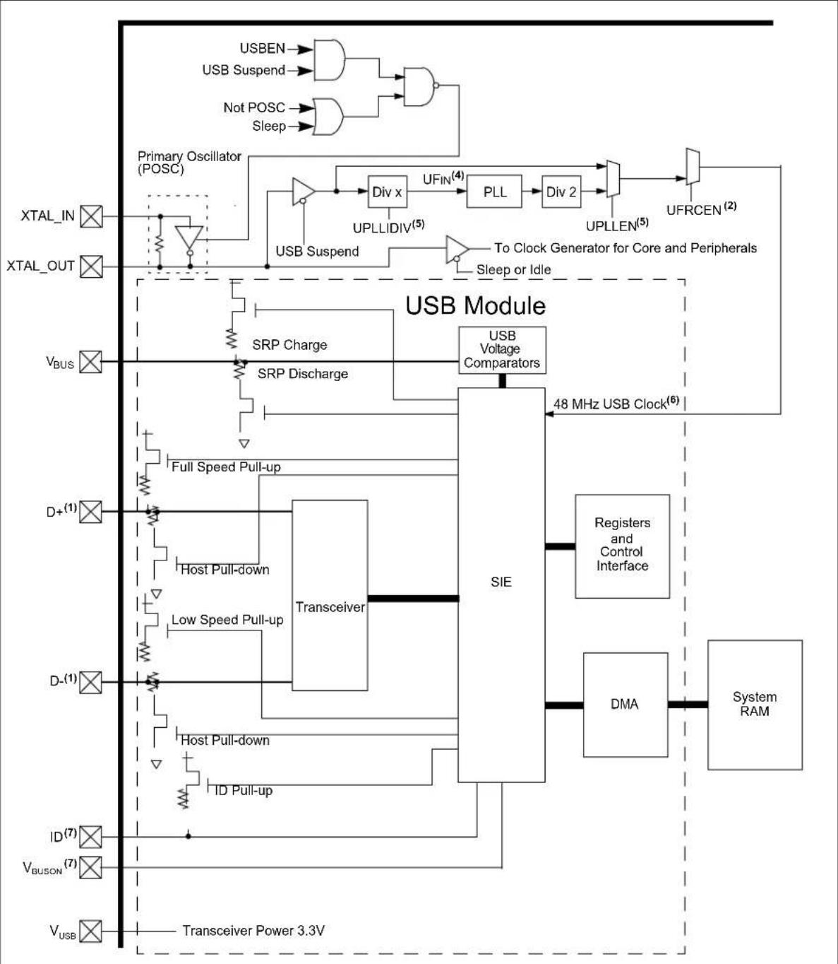
flowchart
graph TD
    subgraph Inputs
        A["XTAL_IN"] --> B["Primary Oscillator (POSC)"]
        C["XTAL_OUT"] --> D["SRP Charge"]
        E["V_BUS"] --> F["SRP Discharge"]
        G["D+(1)"] --> H["Host Pull-down"]
        I["D-(1)"] --> J["Host Pull-down"]
        K["ID(7)"] --> L["ID Pull-up"]
        M["V_BUSON(7)"] --> N["Transceiver"]
        O["V_USB"] --> P["Transceiver Power 3.3V"]
    end

    subgraph Outputs
        Q["USB Suspend"] --> R["USB VOLTAGE COMPARATORS"]
        S["Not POSC"] --> T["AND"]
        U["Sleep"] --> V["AND"]
        W["Div x"] --> X["UFIN(4)"]
        Y["UPLLIDIV(5)"] --> Z["PLL"]
        AA["Div 2"] --> AB["DIV"]
        AC["UPLLEN(5)"] --> AD["UPLENN(5)"]
        AE["UFRCEN(2)"] --> AF["UFRCEN(2)"]
    end

    subgraph Outputs
        AG["48 MHz USB Clock(6)"] --> AH["SIE"]
        AI["Registers and Control Interface"] --> AJ["DMA"]
        AK["System RAM"] --> AL["System RAM"]
    end

    A --> Q
    C --> Q
    D --> Q
    E --> Q
    F --> Q
    H --> Q
    J --> Q
    K --> Q
    L --> Q
    N --> Q
    P --> Q
    Q --> AH
    Q --> AI
    Q --> AK
    Q --> AL
Note 1: Pins can be used as digital inputs when USB is not enabled.
2: This bit field is contained in the OSCCON register.
3: This bit field is contained in the OSCTRM register.
4: USB PLL UF IN requirements: 4 MHz.
5: This bit field is contained in the CFGCON0 register.
6: A 48 MHz clock is required for proper USB operation.
7: Pins can be used as GPIO when the USB module is disabled.
12.1 USB OTG Control Registers
TABLE 12-1: USB REGISTERS MAP (1)
Legend: x = unknown value on Reset, — = unimplemented, read as '0'. Reset values are shown in hexadecimal.
Note 1: Except where noted, all registers in this table have corresponding CLR, SET and INV registers at their virtual addresses, plus offsets of 0x4, 0x8 and 0xC, respectively. See Section 13.3 "CLR, SET and INV
Registers" for more information.
2: This register does not have associated CLR, SET, and INV registers.
3: All bits in this register are read-only; therefore, CLR, SET, and INV registers are not supported.
4: The Reset value for this bit is undefined.
TABLE 12-1: USB REGISTERS MAP ^(1) (CONTINUED)
Legend: x = unknown value on Reset, — = unimplemented, read as '0'. Reset values are shown in hexadecimal.
Note 1: Except where noted, all registers in this table have corresponding CLR, SET and INV registers at their virtual addresses, plus offsets of 0x4, 0x8 and 0xC, respectively. See Section 13.3 "CLR, SET and INV
Registers" for more information.
2: This register does not have associated CLR, SET, and INV registers.
3: All bits in this register are read-only; therefore, CLR, SET, and INV registers are not supported.
4: The Reset value for this bit is undefined.
TABLE 12-1: USB REGISTERS MAP ^(1) (CONTINUED)
Legend: x = unknown value on Reset, — = unimplemented, read as '0'. Reset values are shown in hexadecimal.
Note 1: Except where noted, all registers in this table have corresponding CLR. SET and INV registers at their virtual addresses, plus offsets of 0x4. 0x8 and 0xC, respectively. See Section 13.3 "CLR, SET and INV Registers" for more information.
2: This register does not have associated CLR, SET, and INV registers.
3: All bits in this register are read-only; therefore, CLR, SET, and INV registers are not supported.
4: The Reset value for this bit is undefined.
REGISTER 12-1: U1OTGIR: USB OTG INTERRUPT STATUS REGISTER
| R = Readable bit | W = Writable bit | P = Programmable bit | r = Reserved bit |
| U = Unimplemented bit | K = Write '1' to clear | -n = Bit Value at POR: (0, 1, x = unknown) | |
bit 31-8 Unimplemented: Read as '0'
bit 7 IDIF: ID State Change Indicator bit
Write a '1' to this bit to clear the interrupt.
1 = Change in ID state detected
0 = No change in ID state detected
bit 6 T1MSECIF: 1 Millisecond Timer bit
Write a '1' to this bit to clear the interrupt.
1 = 1 millisecond timer has expired
0 = 1 millisecond timer has not expired
bit 5 LSTATEIF: Line State Stable Indicator bit
Write a '1' to this bit to clear the interrupt.
1 = USB line state is stable for 1 ms, but different from last time
0 = USB line state is not stable for 1 ms
bit 4 ACTVIF: Bus Activity Indicator bit
Write a '1' to this bit to clear the interrupt.
1 = Activity on the D+, D-, ID or V_BUS pins has caused the device to wake up
0 = Activity has not been detected
bit 3 SESVDIF: Session Valid Change Indicator bit
Write a '1' to this bit to clear the interrupt.
1 = V_BUS voltage has dropped below the session end level
0 = V_BUS voltage has not dropped below the session end level
bit 2 SESENDIF: B-Device V_BUS Change Indicator bit
Write a '1' to this bit to clear the interrupt.
1 = A change on the session end input was detected
0 = No change on the session end input was detected
bit 1 Unimplemented: Read as '0'
bit 0 VBUSVDIF: A-Device V_BUS Change Indicator bit
Write a '1' to this bit to clear the interrupt.
1 = Change on the session valid input detected
0 = No change on the session valid input detected
REGISTER 12-2: U1OTGIE: USB OTG INTERRUPT ENABLE REGISTER
| R = Readable bit | W = Writable bit | P = Programmable bit | r = Reserved bit |
| U = Unimplemented bit | -n = Bit Value at POR: ('0', '1', x = Unknown) | ||
bit 31-8 Unimplemented: Read as '0'
bit 7 IDIE: ID Interrupt Enable bit
1 = ID interrupt enabled
0 = ID interrupt disabled
bit 6 T1MSECIE: 1 Millisecond Timer Interrupt Enable bit
1 = 1 millisecond timer interrupt enabled
0 = 1 millisecond timer interrupt disabled
bit 5 LSTATEIE: Line State Interrupt Enable bit
1 = Line state interrupt enabled
0 = Line state interrupt disabled
bit 4 ACTVIE: Bus Activity Interrupt Enable bit
1 = Bus activity interrupt enabled
0 = Bus activity interrupt disabled
bit 3 SESVDIE: Session Valid Interrupt Enable bit
1 = Session valid interrupt enabled
0 = Session valid interrupt disabled
bit 2 SESENDIE: B-Session End Interrupt Enable bit
1 = B-session end interrupt enabled
0 = B-session end interrupt disabled
bit 1 Unimplemented: Read as '0'
bit 0 VBUSVDIE: A- V_BUS Valid Interrupt Enable bit
1 = A-V_BUS valid interrupt enabled
0 = A - V_BUS valid interrupt disabled
REGISTER 12-3: U1OTGSTAT: USB OTG STATUS REGISTER
| R = Readable bit | W = Writable bit | P = Programmable bit | r = Reserved bit |
| U = Unimplemented bit | -n = Bit Value at POR: ('0', '1', x = Unknown) | ||
bit 31-8 Unimplemented: Read as '0'
bit 7 ID: ID Pin State Indicator bit
1 = No cable is attached or a type B cable has been plugged into the USB receptacle 0 = A "type A" OTG cable has been plugged into the USB receptacle
bit 6 Unimplemented: Read as '0'
bit 5 LSTATE: Line State Stable Indicator bit
1 = USB line state (U1CON[SE0] and U1CON[JSTATE]) has been stable for the last 1 ms 0 = USB line state (U1CON[SE0] and U1CON[JSTATE]) has not been stable for the last 1 ms
bit 4 Unimplemented: Read as '0'
bit 3 SESVD: Session Valid Indicator bit
1 = V_BUS voltage is above Session Valid on the A or B device 0 = V_BUS voltage is below Session Valid on the A or B device
bit 2 SESEND: B-Session End Indicator bit
1 = V_BUS voltage is below Session Valid on the B device 0 = V_BUS voltage is above Session Valid on the B device
bit 1 Unimplemented: Read as '0'
bit 0 VBUSVD: A- V_BUS Valid Indicator bit
1 = V_BUS voltage is above Session Valid on the A device 0 = V_BUS voltage is below Session Valid on the A device
REGISTER 12-4: U1OTGCON: USB OTG STATUS REGISTER
| Bit Range | Bit 31/23/15/7 | Bit 30/22/14/6 | Bit 29/21/13/5 | Bit 28/20/12/4 | Bit 27/19/11/3 | Bit 26/18/10/2 | Bit 25/17/9/1 | Bit 24/16/8/0 |
| 31:24 | U-0 U-0 U-0 U-0 U-0 U-0 | U-0 U-0 | ||||||
| — | — | — | — | — | — | — | — | |
| 23:16 | U-0 U-0 U-0 U-0 U-0 U-0 | U-0 U-0 | ||||||
| — | — | — | — | — | — | — | — | |
| 15:8 | U-0 U-0 U-0 U-0 U-0 U-0 | U-0 U-0 | ||||||
| — | — | — | — | — | — | — | — | |
| 7:0 | R/W-0 | R/W-0 | R/W-0 | R/W-0 | R/W-0 | R/W-0 | R/W-0 | R/W-0 |
| DPPULUP | DMPULUP | DPPULDWN | DMPULDWN | VBUSON | OTGEN | VBUSCHG | VBUSDIS | |
Legend:
| R = Readable bit | W = Writable bit | P = Programmable bit | r = Reserved bit |
| U = Unimplemented bit | -n = Bit Value at POR: ('0', '1', x = Unknown) | ||
bit 31-8 Unimplemented: Read as '0'
bit 7 DPPULUP: D+ Pull-Up Enable bit
1 = D+ data line pull-up resistor is enabled
0 = D+ data line pull-up resistor is disabled
bit 6 DMPULUP: D- Pull-Up Enable bit
1 = D- data line pull-up resistor is enabled
0 = D- data line pull-up resistor is disabled
bit 5 DPPULDWN: D+ Pull-Down Enable bit
1 = D+ data line pull-down resistor is enabled
0 = D+ data line pull-down resistor is disabled
bit 4 DMPULDWN: D- Pull-Down Enable bit
1 = D- data line pull-down resistor is enabled
0 = D- data line pull-down resistor is disabled
bit 3 VBUSON: V_BUS Power-on bit
1 = V_BUS line is powered
0 = V_BUS line is not powered
bit 2 OTGEN: OTG Functionality Enable bit
1 = DPPULUP, DMPULUP, DPPULDWN and DMPULDWN bits are under software control
0 = DPPULUP, DMPULUP, DPPULDWN and DMPULDWN bits are under USB hardware control
bit 1 VBUSCHG: V_BUS Charge Enable bit
1 = V_BUS line is charged through a pull-up resistor
0 = V_BUS line is not charged through a resistor
bit 0 VBUSDIS: V_BUS Discharge Enable bit
1 = V_BUS line is discharged through a pull-down resistor
0 = V_BUS line is not discharged through a resistor
REGISTER 12-5: U1PWRC: USB POWER CONTROL REGISTER
| Bit Range | Bit 31/23/15/7 | Bit 30/22/14/6 | Bit 29/21/13/5 | Bit 28/20/12/4 | Bit 27/19/11/3 | Bit 26/18/10/2 | Bit 25/17/9/1 | Bit 24/16/8/0 |
| 31:24 | U-0 U-0 U-0 | U-0 U-0 U-0 | U-0 U-0 | |||||
| — — — — | — — — — | |||||||
| 23:16 | U-0 U-0 U-0 | U-0 U-0 U-0 | U-0 U-0 | |||||
| — — — — | — — — — | |||||||
| 15:8 | U-0 U-0 U-0 | U-0 U-0 U-0 | U-0 U-0 | |||||
| — — — — | — — — — | |||||||
| 7:0 | HS,HC-x U-0 | U-0 R/W-0 | R/W-0 | R/W-0 | R/W-0 | |||
| UACTPND | — — | USLPGRD | USBBUSY ^(1) | — | USUSPEND | USBPWR |
Legend:
| HC = Cleared by hardware | HS = Set by hardware | |
| R = Readable bit | W = Writable bit | P = Programmable bit r = Reserved bit |
| U = Unimplemented bit | K = Write '1' to clear | -n = Bit Value at POR: (0, 1, x = unknown) |
bit 31-8 Unimplemented: Read as '0'
bit 7 UACTPND: USB Activity Pending bit
1 = USB bus activity has been detected; but an interrupt is pending, it has not been generated yet
0 = An interrupt is not pending
bit 6-5 Unimplemented: Read as '0'
bit 4 USLPGRD: USB Sleep Entry Guard bit
1 = Sleep entry is blocked if USB bus activity is detected or if a notification is pending
0 = USB OTG module does not block Sleep entry
bit 3 USBBUSY: USB OTG module Busy bit ^(1)
1 = USB OTG module is active or disabled, but not ready to be enabled
0 = USB OTG module is not active and is ready to be enabled
Note: When USBPWR = 0 and USBBUSY = 1, status from all other registers is invalid and writes to all USB OTG module registers produce undefined results.
bit 2 Unimplemented: Read as '0'
bit 1 USUSPEND: USB Suspend Mode bit
1 = USB OTG module is placed in Suspend mode
(The 48 MHz USB clock is gated off. The transceiver is placed in a low-power state.)
0 = USB OTG module operates normally
bit 0 USBPWR: USB Operation Enable bit
1 = USB OTG module is turned on
0 = USB OTG module is disabled
(Outputs held inactive, device pins not used by USB, analog features are shut down to reduce power consumption.)
Note 1: This bit is not available on all devices. Refer to the specific device data sheet for details.
REGISTER 12-6: U1IR: USB INTERRUPT REGISTER
| R = Readable bit | W = Writable bit | P = Programmable bit | r = Reserved bit |
| U = Unimplemented bit | K = Write '1' to clear | -n = Bit Value at POR: (0, 1, x = unknown) | |
bit 31-8 Unimplemented: Read as '0'
bit 7 STALLIF: STALL Handshake Interrupt bit
Write a '1' to this bit to clear the interrupt.
1 = In Host mode, a STALL handshake was received during the handshake phase of the transaction. In Device mode, a STALL handshake was transmitted during the handshake phase of the transaction.
0 = STALL handshake has not been sent
bit 6 ATTACHIF: Peripheral Attach Interrupt bit ^(1)
Write a '1' to this bit to clear the interrupt.
1 = Peripheral attachment was detected by the USB OTG module
0 = Peripheral attachment was not detected
bit 5 RESUMEIF: Resume Interrupt bit ^(2)
Write a '1' to this bit to clear the interrupt.
1 = K-State is observed on the D+ or D- pin for 2.5 μs
0 = K-State is not observed
bit 4 IDLEIF: Idle Detect Interrupt bit
Write a '1' to this bit to clear the interrupt.
1 = Idle condition detected (constant Idle state of 3 ms or more)
0 = No Idle condition detected
bit 3 TRNIF: Token Processing Complete Interrupt bit ^(3)
Write a '1' to this bit to clear the interrupt.
1 = Processing of current token is complete; a read of the U1STAT register provides endpoint information
0 = Processing of current token not complete
bit 2 SOFIF: SOF Token Interrupt bit
Write a '1' to this bit to clear the interrupt.
1 = SOF token received by the peripheral or the SOF threshold reached by the host
0 = SOF token was not received nor threshold reached
Note 1: This bit is valid only if the HOSTEN bit is set (see Register 12-11), there is no activity on the USB for 2.5 s, and the current bus state is not SE0.
2: When not in Suspend mode, this interrupt must be disabled.
3: Clearing this bit will cause the STAT FIFO to advance.
4: Only error conditions enabled through the U1EIE register will set this bit.
5: Device mode.
6: Host mode.
REGISTER 12-6: U1IR: USB INTERRUPT REGISTER (CONTINUED)
bit 1 UERRIF: USB Error Condition Interrupt bit (4)
Write a '1' to this bit to clear the interrupt.
1 = Unmasked Error condition has occurred
0 = Unmasked Error condition has not occurred
bit 0 URSTIF: USB Reset Interrupt bit (Device mode) (5)
1 = Valid USB Reset has occurred
0 = No USB Reset has occurred
DETACHIF: USB Detach Interrupt bit (Host mode) ^(6)
1 = Peripheral detachment was detected by the USB OTG module
0 = Peripheral detachment was not detected
Note 1: This bit is valid only if the HOSTEN bit is set (see Register 12-11), there is no activity on the USB for 2.5 s, and the current bus state is not SE0.
2: When not in Suspend mode, this interrupt must be disabled.
3: Clearing this bit will cause the STAT FIFO to advance.
4: Only error conditions enabled through the U1EIE register will set this bit.
5: Device mode.
6: Host mode.
REGISTER 12-7: U1IE: USB INTERRUPT ENABLE REGISTER (1)
| R = Readable bit | W = Writable bit | P = Programmable bit | r = Reserved bit |
| U = Unimplemented bit | -n = Bit Value at POR: ('0', '1', x = Unknown) | ||
bit 31-8 Unimplemented: Read as '0'
bit 7 STALLIE: STALL Handshake Interrupt Enable bit
1 = STALL interrupt enabled
0 = STALL interrupt disabled
bit 6 ATTACHIE: ATTACH Interrupt Enable bit
1 = ATTACH interrupt enabled
0 = ATTACH interrupt disabled
bit 5 RESUMEIE: RESUME Interrupt Enable bit
1 = RESUME interrupt enabled
0 = RESUME interrupt disabled
bit 4 IDLEIE: Idle Detect Interrupt Enable bit
1 = Idle interrupt enabled
0 = Idle interrupt disabled
bit 3 TRNIE: Token Processing Complete Interrupt Enable bit
1 = TRNIF interrupt enabled
0 = TRNIF interrupt disabled
bit 2 SOFIE: SOF Token Interrupt Enable bit
1 = SOFIF interrupt enabled
0 = SOFIF interrupt disabled
bit 1 UERRIE: USB Error Interrupt Enable bit
1 = USB Error interrupt enabled
0 = USB Error interrupt disabled
bit 0 URSTIE: USB Reset Interrupt Enable bit ^(2)
1 = URSTIF interrupt enabled
0 = URSTIF interrupt disabled
DETACHIE: USB Detach Interrupt Enable bit(3)
1 = DATTCHIF interrupt enabled
0 = DATTCHIF interrupt disabled
Note 1: For an interrupt to propagate to the USBIF bit (IFS1[25]), the UERRIE bit (U1IE[1]) must be set.
2: Device mode.
3: Host mode.
REGISTER 12-8: U1EIR: USB ERROR INTERRUPT STATUS REGISTER
| Bit Range | Bit 31/23/15/7 | Bit 30/22/14/6 | Bit 29/21/13/5 | Bit 28/20/12/4 | Bit 27/19/11/3 | Bit 26/18/10/2 | Bit 25/17/9/1 | Bit 24/16/8/0 |
| 31:24 | U-0 U-0 | U-0 U-0 U-0 U-0 | U-0 U-0 | |||||
| ——— | ——— —— | |||||||
| 23:16 | U-0 U-0 | U-0 U-0 U-0 U-0 | U-0 U-0 | |||||
| ——— | ——— —— | |||||||
| 15:8 | U-0 U-0 | U-0 U-0 U-0 U-0 | U-0 U-0 | |||||
| ——— | ——— —— | |||||||
| 7:0 | R/K-0 | R/K-0 | R/K-0 | R/K-0 | R/K-0 | R/K-0 | R/K-0 | R/W-0 |
| BTSEF | BMXEF | DMAEF(1) | BTOEF(2) | DFN8EF | CRC16EF | CRC5EF(3,4) | PIDEF | |
| EOFEF(5) |
Legend:
| R = Readable bit | W = Writable bit | P = Programmable bit | r = Reserved bit |
| U = Unimplemented bit | K = Write '1' to clear | -n = Bit Value at POR: ('0', '1', x = unknown) | |
bit 31-8 Unimplemented: Read as '0'
bit 7 BTSEF: Bit Stuff Error Flag bit
Write a '1' to this bit to clear the interrupt.
1 = Packet rejected due to bit stuff error
0 = Packet accepted
bit 6 BMXEF: Bus Matrix Error Flag bit
Write a '1' to this bit to clear the interrupt.
1 = The base address of the BDT or the address of an individual buffer pointed to by a BDT entry, is invalid.
0 = No address error
bit 5 DMAEF: DMA Error Flag bit ^(1)
Write a '1' to this bit to clear the interrupt.
1 = USB DMA error condition detected
0 = No DMA error
bit 4 BTOEF: Bus Turnaround Time-Out Error Flag bit ^(2)
Write a '1' to this bit to clear the interrupt.
1 = Bus turnaround time-out has occurred
0 = No bus turnaround time-out
bit 3 DFN8EF: Data Field Size Error Flag bit
Write a '1' to this bit to clear the interrupt.
1 = Data field received is not an integral number of bytes
0 = Data field received is an integral number of bytes
Note 1: This type of error occurs when the module's request for the DMA bus is not granted in time to service the module's demand for memory, resulting in an overflow or underflow condition, and/or the allocated buffer size is not sufficient to store the received data packet causing it to be truncated.
2: This type of error occurs when more than 16-bit-times of Idle from the previous End-of-Packet (EOP) has elapsed.
3: This type of error occurs when the module is transmitting or receiving data and the SOF counter has reached zero.
4: Device mode.
5: Host mode.
REGISTER 12-8: U1EIR: USB ERROR INTERRUPT STATUS REGISTER (CONTINUED)
bit 2 CRC16EF: CRC16 Failure Flag bit
Write a '1' to this bit to clear the interrupt.
1 = Data packet rejected due to CRC16 error
0 = Data packet accepted
bit 1 CRC5EF: CRC5 Host Error Flag bit (3,4)
Write a '1' to this bit to clear the interrupt.
1 = Token packet rejected due to CRC5 error
0 = Token packet accepted
EOFEF: EOF Error Flag bit ^(5)
1 = EOF error condition detected
0 = No EOF error condition
bit 0 PIDEF: PID Check Failure Flag bit
1 = PID check failed
0 = PID check passed
Note 1: This type of error occurs when the module's request for the DMA bus is not granted in time to service the module's demand for memory, resulting in an overflow or underflow condition, and/or the allocated buffer size is not sufficient to store the received data packet causing it to be truncated.
2: This type of error occurs when more than 16-bit-times of Idle from the previous End-of-Packet (EOP) has elapsed.
3: This type of error occurs when the module is transmitting or receiving data and the SOF counter has reached zero.
4: Device mode.
5: Host mode.
REGISTER 12-9: U1EIE: USB ERROR INTERRUPT ENABLE REGISTER (1)
| Bit Range | Bit 31/23/15/7 | Bit 30/22/14/6 | Bit 29/21/13/5 | Bit 28/20/12/4 | Bit 27/19/11/3 | Bit 26/18/10/2 | Bit 25/17/9/1 | Bit 24/16/8/0 |
| 31:24 | U-0 U-0 | U-0 U-0 U-0 | U-0 U-0 | |||||
| — — — | — — — — | — | ||||||
| 23:16 | U-0 U-0 | U-0 U-0 U-0 | U-0 U-0 | |||||
| — — — | — — — — | — | ||||||
| 15:8 | U-0 U-0 | U-0 U-0 U-0 | U-0 U-0 | |||||
| — — — | — — — — | — | ||||||
| 7:0 | R/W-0 | R/W-0 | R/W-0 | R/W-0 | R/W-0 | R/W-0 | R/W-0 | R/W-0 |
| BTSEE | BMXEE | DMAEE | BTOEE | DFN8EE | CRC16EE | CRC5EE ^(2) | PIDEE | |
| EOFEE ^(3) |
Legend:
| R = Readable bit | W = Writable bit | P = Programmable bit | r = Reserved bit |
| U = Unimplemented bit | -n = Bit Value at POR: ('0', '1', x = Unknown) | ||
bit 31-8 Unimplemented: Read as '0'
bit 7 BTSEE: Bit Stuff Error Interrupt Enable bit
1 = BTSEF interrupt enabled
0 = BTSEF interrupt disabled
bit 6 BMXEE: Bus Matrix Error Interrupt Enable bit
1 = BMXEF interrupt enabled
0 = BMXEF interrupt disabled
bit 5 DMAEE: DMA Error Interrupt Enable bit
1 = DMAEF interrupt enabled
0 = DMAEF interrupt disabled
bit 4 BTOEE: Bus Turnaround Time-Out Error Interrupt Enable bit
1 = BTOEF interrupt enabled
0 = BTOEF interrupt disabled
bit 3 DFN8EE: Data Field Size Error Interrupt Enable bit
1 = DFN8EF interrupt enabled
0 = DFN8EF interrupt disabled
bit 2 CRC16EE: CRC16 Failure Interrupt Enable bit
1 = CRC16EF interrupt enabled
0 = CRC16EF interrupt disabled
bit 1 CRC5EE: CRC5 Host Error Interrupt Enable bit ^(2)
1 = CRC5EF interrupt enabled
0 = CRC5EF interrupt disabled
EOFEE: EOF Error Interrupt Enable bit ^(3)
1 = EOF interrupt enabled
0 = EOF interrupt disabled
Note 1: For an interrupt to propagate USBIF bit (IFS1[25]), the UERRIE bit (U1IE[1]) must be set.
2: Device mode.
3: Host mode.
REGISTER 12-9: U1EIE: USB ERROR INTERRUPT ENABLE REGISTER (1) (CONTINUED)
bit 0 PIDEE: PID Check Failure Interrupt Enable bit
1 = PIDEF interrupt enabled
0 = PIDEF interrupt disabled
Note 1: For an interrupt to propagate USBIF bit (IFS1[25]), the UERRIE bit (U1IE[1]) must be set.
2: Device mode.
3: Host mode.
REGISTER 12-10: U1STAT: USB STATUS REGISTER ^(1)
| Bit Range | Bit 31/23/15/7 | Bit 30/22/14/6 | Bit 29/21/13/5 | Bit 28/20/12/4 | Bit 27/19/11/3 | Bit 26/18/10/2 | Bit 25/17/9/1 | Bit 24/16/8/0 |
| 31:24 | U-0 U-0 U-0 U-0 U-0 U-0 | U-0 U-0 | ||||||
| — | — | — | — | — | — | — | — | |
| 23:16 | U-0 U-0 U-0 U-0 U-0 U-0 | U-0 U-0 | ||||||
| — | — | — | — | — | — | — | — | |
| 15:8 | U-0 U-0 U-0 U-0 U-0 U-0 | U-0 U-0 | ||||||
| — | — | — | — | — | — | — | — | |
| 7:0 | R-x | R-x | R-x | R-x | R-x | R-x | U-0 | U-0 |
| ENDPT[3:0] | DIR | PPBI | — | — | ||||
Legend:
| R = Readable bit | W = Writable bit | P = Programmable bit | r = Reserved bit |
| U = Unimplemented bit | -n = Bit Value at POR: ('0', '1', x = Unknown) | ||
bit 31-8 Unimplemented: Read as '0'
bit 7-4 ENDPT[3:0]: Encoded Number of Last Endpoint Activity bits (Represents the number of the BDT, updated by the last USB transfer.)
1111 = Endpoint 15
1110 = Endpoint 14
•
•
•
0001 = Endpoint 1
0000 = Endpoint 0
bit 3 DIR: Last BD Direction Indicator bit
1 = Last transaction was a TX
0 = Last transaction was a RX
bit 2 PPBI: Ping-pong BD Pointer Indicator bit
1 = Last transaction was to the ODD BD bank
0 = Last transaction was to the EVEN BD bank
bit 1-0 Unimplemented: Read as '0'
Note 1: The U1STAT register is a window into a 4 byte FIFO maintained by the USB OTG module. U1STAT value is only valid when the TRNIF bit (U1IR[3]) is active. Clearing the TRNIF bit (U1IR[3]) advances the FIFO. Data in register is invalid when the TRNIF bit (U1IR[3]) = 0.
REGISTER 12-11: U1CON: USB CONTROL REGISTER
| Bit Range | Bit 31/23/15/7 | Bit 30/22/14/6 | Bit 29/21/13/5 | Bit 28/20/12/4 | Bit 27/19/11/3 | Bit 26/18/10/2 | Bit 25/17/9/1 | Bit 24/16/8/0 |
| 31:24 | U-0 U-0 | U-0 U-0 U-0 U-0 | U-0 U-0 | |||||
| — — — | — — — — | — | ||||||
| 23:16 | U-0 U-0 | U-0 U-0 U-0 U-0 | U-0 U-0 | |||||
| — — — | — — — — | — | ||||||
| 15:8 | U-0 U-0 | U-0 U-0 U-0 U-0 | U-0 U-0 | |||||
| — — — | — — — — | — | ||||||
| 7:0 | R-x | R-x | R/W-0 | R/W-0 | R/W-0 | R/W-0 | R/W-0 | U-0 |
| JSTATE | SE0 | PKTDIS^(4) | USBRST | HOSTEN^(2) | RESUME^(3) | PPBRST | USBEN^(4) | |
| TOKBUSY^(1,5) | SOFEN^(5) |
Legend:
| R = Readable bit | W = Writable bit | P = Programmable bit | r = Reserved bit |
| U = Unimplemented bit | -n = Bit Value at POR: ('0', '1', x = Unknown) | ||
bit 31-8 Unimplemented: Read as '0'
bit 7 JSTATE: Live Differential Receiver JSTATE flag bit
1 = JSTATE detected on the USB
0 = No JSTATE detected
bit 6 SEO: Live Single-Ended Zero flag bit
1 = Single-Ended Zero detected on the USB
0 = No Single-Ended Zero detected
bit 5 PKTDIS: Packet Transfer Disable bit ^(4)
1 = Token and packet processing disabled (set upon SETUP token received)
0 = Token and packet processing enabled
TOKBUSY: Token Busy Indicator bit ^(1,5)
1 = Token being executed by the USB OTG module
0 = No token being executed
bit 4 USBRST: Module Reset bit ^(5)
1 = USB Reset generated
0 = USB Reset terminated
bit 3 HOSTEN: Host Mode Enable bit ^(2)
1 = USB host capability enabled
0 = USB host capability disabled
bit 2 RESUME: RESUME Signaling Enable bit ^(3)
1 = RESUME signaling activated
0 = RESUME signaling disabled
Note 1: Software is required to check this bit before issuing another token command to the U1TOK register, see Register 12-15.
2: All host control logic is reset any time that the value of this bit is toggled.
3: Software must set RESUME for 10 ms if the part is a function, or for 25 ms if the part is a host, and then clear it to enable remote wake-up. In Host mode, the USB OTG module will append a low-speed EOP to the RESUME signaling when this bit is cleared.
4: Device mode.
5: Host mode.
REGISTER 12-11: U1CON: USB CONTROL REGISTER (CONTINUED)
bit 1 PPBRST: Ping-Pong Buffers Reset bit
1 = Reset all Even/Odd buffer pointers to the EVEN BD banks
0 = Even/Odd buffer pointers not being Reset
bit 0 USBEN: USB OTG Module Enable bit (4)
1 = USB OTG module and supporting circuitry enabled
0 = USB OTG module and supporting circuitry disabled
SOFEN: SOF Enable bit ^(5)
1 = SOF token sent every 1 ms
0 = SOF token disabled
Note 1: Software is required to check this bit before issuing another token command to the U1TOK register, see Register 12-15.
2: All host control logic is reset any time that the value of this bit is toggled.
3: Software must set RESUME for 10 ms if the part is a function, or for 25 ms if the part is a host, and then clear it to enable remote wake-up. In Host mode, the USB OTG module will append a low-speed EOP to the RESUME signaling when this bit is cleared.
4: Device mode.
5: Host mode.
REGISTER 12-12: U1ADDR: USB ADDRESS REGISTER
| Bit Range | Bit 31/23/15/7 | Bit 30/22/14/6 | Bit 29/21/13/5 | Bit 28/20/12/4 | Bit 27/19/11/3 | Bit 26/18/10/2 | Bit 25/17/9/1 | Bit 24/16/8/0 |
| 31:24 | U-0 U-0 U-0 U-0 U-0 U-0 | |||||||
| — | — | — | — | — | — | — | — | |
| 23:16 | U-0 U-0 U-0 U-0 U-0 U-0 | |||||||
| — | — | — | — | — | — | — | — | |
| 15:8 | U-0 U-0 U-0 U-0 U-0 U-0 | |||||||
| — | — | — | — | — | — | — | — | |
| 7:0 | R/W-0 | R/W-0 | R/W-0 | R/W-0 | R/W-0 | R/W-0 | R/W-0 | R/W-0 |
| LSPDEN | DEVADDR[6:0] | |||||||
Legend:
R = Readable bit W = Writable bit P = Programmable bit r = Reserved bit
U = Unimplemented bit -n = Bit Value at POR: ('0', '1', x = Unknown)
bit 31-8 Unimplemented: Read as '0'
bit 7 LSPDEN: Low-Speed Enable Indicator bit
1 = Next token command to be executed at low-speed
0 = Next token command to be executed at full-speed
bit 6-0 DEVADDR[6:0]: 7-bit USB Device Address bits
REGISTER 12-13: U1FRML: USB FRAME NUMBER LOW REGISTER
| R = Readable bit | W = Writable bit | P = Programmable bit | r = Reserved bit |
| U = Unimplemented bit | -n = Bit Value at POR: (‘0’, ‘1’, x = Unknown) | ||
bit 31-8 Unimplemented: Read as '0'
bit 7-0 FRML[7:0]: 11-bit Frame Number Lower bits
The register bits are updated with the current frame number whenever a SOF TOKEN is received.
REGISTER 12-14: U1FRMH: USB FRAME NUMBER HIGH REGISTER
| Bit Range | Bit 31/23/15/7 | Bit 30/22/14/6 | Bit 29/21/13/5 | Bit 28/20/12/4 | Bit 27/19/11/3 | Bit 26/18/10/2 | Bit 25/17/9/1 | Bit 24/16/8/0 |
| 31:24 | U-0 | U-0 | U-0 | U-0 | U-0 | U-0 | U-0 | U-0 |
| — | — | — | — | — | — | — | — | |
| 23:16 | U-0 | U-0 | U-0 | U-0 | U-0 | U-0 | U-0 | U-0 |
| — | — | — | — | — | — | — | — | |
| 15:8 | U-0 | U-0 | U-0 | U-0 | U-0 | U-0 | U-0 | U-0 |
| — | — | — | — | — | — | — | — | |
| 7:0 | R/W-0 | R/W-0 | R/W-0 | R/W-0 | R/W-0 | R/W-0 | R/W-0 | R/W-0 |
| — | — | — | — | — | FRMH[2:0] | |||
Legend:
| R = Readable bit | W = Writable bit | P = Programmable bit | r = Reserved bit |
| U = Unimplemented bit | -n = Bit Value at POR: ('0', '1', x = Unknown) | ||
bit 31-3 Unimplemented: Read as '0'
bit 2-0 FRMH[2:0]: Upper 3 bits of the Frame Number bits
The register bits are updated with the current frame number whenever a SOF TOKEN is received.
REGISTER 12-15: U1TOK: USB TOKEN REGISTER
| Bit Range | Bit 31/23/15/7 | Bit 30/22/14/6 | Bit 29/21/13/5 | Bit 28/20/12/4 | Bit 27/19/11/3 | Bit 26/18/10/2 | Bit 25/17/9/1 | Bit 24/16/8/0 |
| 31:24 | U-0 U-0 | U-0 U-0 U-0 U-0 | U-0 U-0 | |||||
| — — — | — — — — | |||||||
| 23:16 | U-0 U-0 | U-0 U-0 U-0 U-0 | U-0 U-0 | |||||
| — — — | — — — — | |||||||
| 15:8 | U-0 U-0 | U-0 U-0 U-0 U-0 | U-0 U-0 | |||||
| — — — | — — — — | |||||||
| 7:0 | R/W-0 R/W | R/W-0 R/W-0 R/W-0 | R/W-0 R/W-0 | R/W-0 R/W-0 | ||||
| PID[3:0](1) | EP[3:0] | |||||||
Legend:
| R = Readable bit | W = Writable bit | P = Programmable bit | r = Reserved bit |
| U = Unimplemented bit | -n = Bit Value at POR: ('0', '1', x = Unknown) | ||
bit 31-8 Unimplemented: Read as '0'
bit 7-4 PID[3:0]: Token Type Indicator bits ^(1)
0001 = OUT (TX) token type transaction
1001 = IN (RX) token type transaction
1101 = SETUP (TX) token type transaction
Note: All other values are reserved and must not be used.
bit 3-0 EP[3:0]: Token Command Endpoint Address bits
The four bit value must specify a valid endpoint.
Note 1: All other values are reserved and must not be used.
REGISTER 12-16: U1SOF: USB SOF THRESHOLD REGISTER
| Bit Range | Bit 31/23/15/7 | Bit 30/22/14/6 | Bit 29/21/13/5 | Bit 28/20/12/4 | Bit 27/19/11/3 | Bit 26/18/10/2 | Bit 25/17/9/1 | Bit 24/16/8/0 |
| 31:24 | U-0 U-0 | U-0 U-0 U-0 U-0 | U-0 U-0 | |||||
| ——— | ——— —— —— | |||||||
| 23:16 | U-0 U-0 | U-0 U-0 U-0 U-0 | U-0 U-0 | |||||
| ——— | ——— —— —— | |||||||
| 15:8 | U-0 U-0 | U-0 U-0 U-0 U-0 | U-0 U-0 | |||||
| ——— | ——— —— —— | |||||||
| 7:0 | R/W-0 R/W | V-0 R/W-0 R/W | 0 R/W-0 R/W-0 | R/W-0 R/W-0 | ||||
| CNT[7:0] | ||||||||
Legend:
| R = Readable bit | W = Writable bit | P = Programmable bit | r = Reserved bit |
| U = Unimplemented bit | -n = Bit Value at POR: ('0', '1', x = Unknown) | ||
bit 31-8 Unimplemented: Read as '0'
bit 7-0 CNT[7:0]: SOF Threshold Value bits
Typical values of the threshold are:
0100 1010 = 64-byte packet
0010 1010 = 32-byte packet
0001 1010 = 16-byte packet
0001 0010 = 8-byte packet
REGISTER 12-17: U1BDTP1: USB BDT REGISTER
| Bit Range | Bit 31/23/15/7 | Bit 30/22/14/6 | Bit 29/21/13/5 | Bit 28/20/12/4 | Bit 27/19/11/3 | Bit 26/18/10/2 | Bit 25/17/9/1 | Bit 24/16/8/0 |
| 31:24 | U-0 U-0 | U-0 U-0 U-0 U-0 | U-0 U-0 | |||||
| — — — | — — — — — | |||||||
| 23:16 | U-0 U-0 | U-0 U-0 U-0 U-0 | U-0 U-0 | |||||
| — — — | — — — — — | |||||||
| 15:8 | U-0 U-0 | U-0 U-0 U-0 U-0 | U-0 U-0 | |||||
| — — — | — — — — — | |||||||
| 7:0 | R/W-0 R/W | R/W-0 R/W-0 R/W | R/W-0 R/W-0 | R/W-0 U-0 | ||||
| BDTPTRL[15:9] | — | |||||||
Legend:
| R = Readable bit | W = Writable bit | P = Programmable bit | r = Reserved bit |
| U = Unimplemented bit | -n = Bit Value at POR: ('0', '1', x = Unknown) | ||
bit 31-8 Unimplemented: Read as '0'
bit 7-1 BDTPTRL[15:9]: BDT Base Address Low bits
This 7-bit value provides address bits 15 through 9 of the BDT base address, which defines the BDT's starting location in the system memory.
The 32-bit BDT base address is 512 byte aligned.
bit 0 Unimplemented: Read as '0'
REGISTER 12-18: U1BDTP2: USB BDT PAGE 2 REGISTER
| Bit Range | Bit 31/23/15/7 | Bit 30/22/14/6 | Bit 29/21/13/5 | Bit 28/20/12/4 | Bit 27/19/11/3 | Bit 26/18/10/2 | Bit 25/17/9/1 | Bit 24/16/8/0 |
| 31:24 | U-0 U-0 | U-0 | U-0 U-0 U-0 U-0 | U-0 | ||||
| — — — | — — — | — — | ||||||
| 23:16 | U-0 U-0 | U-0 | U-0 U-0 U-0 U-0 | U-0 | ||||
| — — — | — — — | — — | ||||||
| 15:8 | U-0 U-0 | U-0 | U-0 U-0 U-0 U-0 | U-0 | ||||
| — — — | — — — | — — | ||||||
| 7:0 | R/W-0 | R/W-0 | R/W-0 | R/W-0 | R/W-0 | R/W-0 | R/W-0 | R/W-0 |
| BDTPTRH[23:16] | ||||||||
Legend:
| R = Readable bit | W = Writable bit | P = Programmable bit | r = Reserved bit |
| U = Unimplemented bit | -n = Bit Value at POR: ('0', '1', x = Unknown) | ||
bit 31-8 Unimplemented: Read as '0'
bit 7-0 BDTPTRH[23:16]: BDT Base Address High bits
This 8-bit value provides address bits 23 through 16 of the BDT base address, which defines the BDT's starting location in the system memory.
The 32-bit BDT base address is 512 byte aligned.
REGISTER 12-19: U1BDTP3: USB BDT PAGE 3 REGISTER
| Bit Range | Bit 31/23/15/7 | Bit 30/22/14/6 | Bit 29/21/13/5 | Bit 28/20/12/4 | Bit 27/19/11/3 | Bit 26/18/10/2 | Bit 25/17/9/1 | Bit 24/16/8/0 |
| 31:24 | U-0 U-0 | U-0 U-0 U-0 U-0 | U-0 U-0 | |||||
| —— — | —— — — — | |||||||
| 23:16 | U-0 U-0 | U-0 U-0 U-0 U-0 | U-0 U-0 | |||||
| —— — | —— — — — | |||||||
| 15:8 | U-0 U-0 | U-0 U-0 U-0 U-0 | U-0 U-0 | |||||
| —— — | —— — — — | |||||||
| 7:0 | R/W-0 R/W | R/W-0 R/W-0 | R/W-0 R/W-0 | R/W-0 R/W-0 | ||||
| BDTPTRU[31:24] | ||||||||
Legend:
| R = Readable bit | W = Writable bit | P = Programmable bit | r = Reserved bit |
| U = Unimplemented bit | -n = Bit Value at POR: ('0', '1', x = Unknown) | ||
bit 31-8 Unimplemented: Read as '0'
bit 7-0 BDTPTRU[31:24]: BDT Base Address Upper bits
This 8-bit value provides address bits 31 through 24 of the BDT base address, which defines the BDT's starting location in the system memory.
The 32-bit BDT base address is 512 byte aligned.
REGISTER 12-20: U1CNFG1: USB CONFIGURATION 1 REGISTER
| Bit Range | Bit 31/23/15/7 | Bit 30/22/14/6 | Bit 29/21/13/5 | Bit 28/20/12/4 | Bit 27/19/11/3 | Bit 26/18/10/2 | Bit 25/17/9/1 | Bit 24/16/8/0 |
| 31:24 | U-0 U-0 | U-0 U-0 U-0 U-0 | U-0 U-0 | |||||
| ——— | ——— —— | |||||||
| 23:16 | U-0 U-0 | U-0 U-0 U-0 U-0 | U-0 U-0 | |||||
| ——— | ——— —— | |||||||
| 15:8 | U-0 U-0 | U-0 U-0 U-0 U-0 | U-0 U-0 | |||||
| ——— | ——— —— | |||||||
| 7:0 | R/W-0 | R/W-0 | R/W-0 | R/W-0 | U-0 | U-0 | U-0 | R/W-0 |
| UTEYE | UOEMON | USBFRZ | USBSIDL | ——— | UAS | USPND |
Legend:
| R = Readable bit | W = Writable bit | P = Programmable bit | r = Reserved bit |
| U = Unimplemented bit | -n = Bit Value at POR: ('0', '1', x = Unknown) | ||
bit 31-8 Unimplemented: Read as '0'
bit 7 UTEYE: USB Eye-Pattern Test Enable bit
1 = Eye-Pattern test enabled
0 = Eye-Pattern test disabled
bit 6 UOEMON: USB OE Monitor Enable bit
1 = OE signal is active; it indicates intervals during which the D+/D- lines are driving
0 = OE signal is inactive
bit 5 USBFRZ: Freeze in Debug Mode bit
1 = When emulator is in Debug mode, module freezes operation
0 = When emulator is in Debug mode, module continues operation
bit 4 USBSIDL: Stop in Idle Mode bit
1 = Discontinue module operation when device enters Idle mode
0 = Continue module operation in Idle mode
bit 3-1 Unimplemented: Read as '0'
bit 0 UASUSPND: Automatic Suspend Enable bit
1 = USB OTG module automatically suspends upon entry to Sleep mode. See the USUSPEND bit (U1PWRC[1]) in Register 12-5.
0 = USB OTG module does not automatically suspend upon entry to Sleep mode. Software must use the USUSPEND bit (U1PWRC[1]) to suspend the module, including the USB 48 MHz clock
REGISTER 12-21: U1EP0-U1EP15: USB ENDPOINT CONTROL REGISTERS
| Bit Range | Bit 31/23/15/7 | Bit 30/22/14/6 | Bit 29/21/13/5 | Bit 28/20/12/4 | Bit 27/19/11/3 | Bit 26/18/10/2 | Bit 25/17/9/1 | Bit 24/16/8/0 |
| 31:24 | U | - | 0 U | - | 0 | U | - | 0 U |
| ——— | ——— | |||||||
| 23:16 | U | - | 0 U | - | 0 | U | - | 0 U |
| ——— | ——— | |||||||
| 15:8 | U | - | 0 U | - | 0 | U | - | 0 U |
| ——— | ——— | |||||||
| 7:0 | R/W-0 R/W-0 U-0 R/W-0 | R/W-0 R/W-0 R/W-0 R/W-0 | ||||||
| LSPD RETRYDIS | — EPCONDIS EPRXEN | EPTXEN | EPSTALL | EPHSHK | ||||
Legend:
| R = Readable bit | W = Writable bit | P = Programmable bit | r = Reserved bit |
| U = Unimplemented bit | -n = Bit Value at POR: ('0', '1', x = Unknown) | ||
bit 31-8 Unimplemented: Read as '0'
bit 7 LSPD: Low-Speed Direct Connection Enable bit (Host mode and U1EP0 only)
1 = Direct connection to a low-speed device enabled
0 = Direct connection to a low-speed device disabled; hub required with PRE_PID
bit 6 RETRYDIS: Retry Disable bit (Host mode and U1EP0 only)
1 = Retry NAK'd transactions disabled
0 = Retry NAK'd transactions enabled; retry done in hardware
bit 5 Unimplemented: Read as '0'
bit 4 EPCONDIS: Bidirectional Endpoint Control bit
If EPTXEN = 1 and EPRXEN = 1:
1 = Disable endpoint n for control transfers; only TX and RX transfers are allowed
0 = Enable endpoint n for control (SETUP) transfers; TX and RX transfers are also allowed
Otherwise, this bit is ignored.
bit 3 EPRXEN: Endpoint Receive Enable bit
1 = Endpoint n receive enabled
0 = Endpoint n receive disabled
bit 2 EPTXEN: Endpoint Transmit Enable bit
1 = Endpoint n transmit enabled
0 = Endpoint n transmit disabled
bit 1 EPSTALL: Endpoint Stall Status bit
1 = Endpoint n is stalled
0 = Endpoint n is not stalled
bit 0 EPHSHK: Endpoint Handshake Enable bit
1 = Endpoint handshake enabled
0 = Endpoint handshake disabled (typically used for isochronous endpoints)
13.0 I/O PORTS
| Note: This data sheet summarizes the features of the PIC32MZ1025W104 family of devices. It is not intended to be a comprehensive reference source. To complement the information in this data sheet, refer to Section 12. “I/O Ports” (DS60001120) in the “PIC32 Family Reference Manual”, which is available from the Microchip website (www.microchip.com/PIC32). |
General purpose I/O pins allow the PIC32MZ1025W104 family of devices to monitor and control other devices. To add flexibility and functionality, some pins are multiplexed with alternate function(s). These functions depend on which peripheral
features are on the device. In general, when a peripheral is functioning, that pin may not be used as a GPIO pin.
Some of the key features of the I/O ports are:
- Individual output pin open-drain enable/disable
- Individual input pin weak pull-up and pull-down
- Monitor selective inputs and generate interrupt when change in pin state is detected
• Operation during Sleep and Idle modes - Fast bit manipulation using CLR, SET and INV registers
The figure below illustrates a block diagram of a typical multiplexed I/O port.
FIGURE 13-1: BLOCK DIAGRAM OF A TYPICAL MULTIPLEXED PORT STRUCTURE
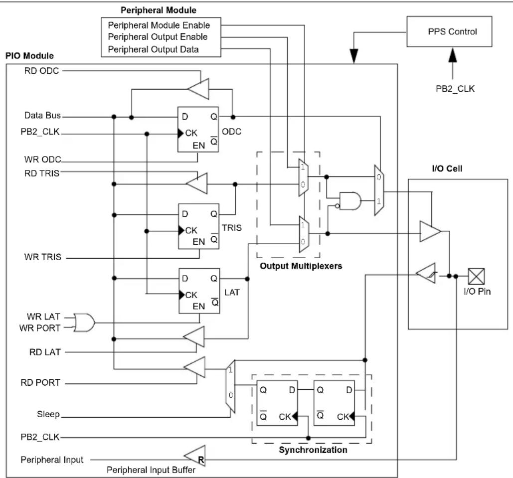
flowchart
graph TD
    A["Peripheral Module"] --> B["Peripheral Output Enable"]
    A --> C["Peripheral Output Data"]
    D["PIO Module"] --> E["RD ODC"]
    D --> F["Data Bus"]
    D --> G["PB2_CLK"]
    D --> H["WR ODC"]
    D --> I["RD TRIS"]
    J["PPS Control"] --> K["PB2_CLK"]
    L["I/O Cell"] --> M["I/O Pin"]
    N["Output Multiplexers"] --> O["0-1"]
    P["Synchronization"] --> Q["Q-D"]
    P --> R["Q-CK"]
    S["Peripheral Input"] --> T["Peripheral Input Buffer"]
    U["WR LAT"] --> V["WR PORT"]
    W["RD LAT"] --> X["RD PORT"]
    Y["Sleep"] --> Z["PB2_CLK"]
    AA["Peripheral Input"] --> AB["R"]
    AC["0"] --> AD["0"]
    AE["1"] --> AF["1"]
    AG["0"] --> AH["0"]
    AI["0"] --> AJ["0"]
    AK["0"] --> AL["0"]
    AM["0"] --> AN["0"]
    AO["0"] --> AP["0"]
    AQ["0"] --> AR["0"]
    AS["0"] --> AT["0"]
    AU["0"] --> AV["0"]
    AW["0"] --> AX["0"]
    AY["Peripheral Module Enable"] --> AZ["Peripheral Output Enable"]
    style A fill:#f9f,stroke:#333
    style D fill:#ccf,stroke:#333
    style J fill:#cfc,stroke:#333
    style L fill:#fcc,stroke:#333
Legend: R = Peripheral input buffer types may vary. Refer to Table 3 for peripheral details.
Note: This block diagram is a general representation of a shared port/peripheral structure for illustration purposes only. The actual structure for any specific port/peripheral combination may be different than it is shown here.
13.1 Parallel I/O (PIO) Ports
All port pins have up to 14 registers directly associated with their operation as digital I/O. The data direction register (TRISx) determines whether the pin is an input or an output. If the data direction bit is a '1', then the pin is an input. All port pins are defined as inputs after a Reset. Reads from the latch (LATx) read the latch. Writes to the latch write the latch. Reads from the port (PORTx) read the port pins, while writes to the port pins write the latch.
13.1.1 OPEN-DRAIN CONFIGURATION
In addition to the PORTx, LATx, and TRISx registers for data control, some port pins can also be individually configured for either digital or open-drain output. This is controlled by the Open-Drain Control register, ODCx, associated with each port. Setting any of the bits configures the corresponding pin to act as an open-drain output.
13.1.2 CONFIGURING ANALOG AND DIGITAL PORT PINS
The ANSELx register controls the operation of the analog port pins. The port pins that are to function as analog inputs must have their corresponding ANSEL and TRIS bits set. In order to use port pins for I/O functionality with digital modules, such as timers, UARTs, and so on, the corresponding ANSELx bit must be cleared.
The ANSELx register has a default value of 0xFFFF; therefore, all pins that share analog functions are analog (not digital) by default.
If the TRIS bit is cleared (output) while the ANSELx bit is set, the digital output level (VOH or VOL) is converted by an analog peripheral, such as the ADC module or Comparator module.
When the PORT register is read, all pins configured as analog input channels are read as cleared (a low level).
Pins configured as digital inputs do not convert an analog input. Analog levels on any pin defined as a digital input (including the ANx pins) can cause the input buffer to consume current that exceeds the device specifications.
13.1.3 I/O PORT WRITE/READ TIMING
One instruction cycle is required between a port direction change or port write operation and a read operation of the same port. Typically this instruction would be an NOP.
13.1.4 INPUT CHANGE NOTIFICATION
The input change notification function of the I/O ports allows the PIC32MZ1025W104 family of devices to generate interrupt requests to the processor in response to a change-of-state on selected input pins. This feature can detect input change-of-states even in Sleep mode, when the clocks are disabled. Every I/O port pin can be selected (enabled) for generating an interrupt request on a change-of-state.
Seven control registers are associated with the Change Notice (CN) functionality of each I/O port. The CNENx/CNNEx registers contain the CN interrupt enable control bits for each of the input pins. Setting any of these bits enables a CN interrupt for the corresponding pins. CNENx enables a mismatch CN interrupt condition when the EDGEDETECT bit (CNCONx[11]) is not set. When the EDGEDETECT bit is set, CNNEx controls the negative edge while CNENx controls the positive.
The CNSTATx/CNFx registers indicate the status of change notice based on the setting of the EDGEDETECT bit. If the EDGEDETECT bit is set to '0', the CNSTATx register indicates whether a change occurred on the corresponding pin since the last read of the PORTx bit. If the EDGEDETECT bit is set to '1', the CNFx register indicates whether a change has occurred and through the CNNEx/CNENx registers the edge type of the change that occurred is also indicated.
Each I/O pin also has a weak pull-up and a weak pull-down connected to it. The pull-ups act as a current source or sink source connected to the pin, and eliminate the need for external resistors when push-button or keypad devices are connected. The pull-ups and pull-downs are enabled separately using the CNPUx and the CNPDx registers, which contain the control bits for each of the pins. Setting any of the control bits enables the weak pull-ups and/or pull-downs for the corresponding pins.
Note: Pull-ups and pull-downs on change notification pins must always be disabled when the port pin is configured as a digital output.
An additional control register (CNCONx) is shown in Register 13-3.
13.2 Registers for Slew Rate Control
Some I/O pins can be configured for various types of slew rate control on its associated port. This is controlled by the Slew Rate Control bits in the SRCON1x and SRCON0x registers that are associated with each I/O port. The slew rate control is configured using the corresponding bit in each register, as shown in the table below.
As an example, writing 0x0001, 0x0000 to SRCON1A and SRCON0A, respectively, will enable slew rate control on the RA0 pin and sets the slew rate to the slow edge rate.
TABLE 13-1: SLEW RATE CONTROL BIT SETTINGS ^(1)
| SRCON1x | SRCON0x | Description |
| 1 | 1 | Slew rate control is enabled and is set to the slowest edge rate. |
| 1 | 0 | Slew rate control is enabled and is set to the slow edge rate. |
| 0 | 1 | Slew rate control is enabled and is set to the medium edge rate. |
| 0 | 0 | Slew rate control is disabled and is set to the fastest edge rate. |
Note 1: By default, all of the port pins are set to the fastest edge rate.
13.3 CLR, SET and INV Registers
Every I/O module register has a corresponding CLR (clear), SET (set) and INV (invert) register designed to provide fast atomic bit manipulations. As the name of the register implies, a value written to a SET, CLR or INV register effectively performs the implied operation, but only on the corresponding base register and only bits specified as '1' are modified. Bits specified as '0' are not modified.
Reading SET, CLR and INV registers return undefined values. To see the affects of a write operation to a SET, CLR or INV register, the base register must be read.
13.4 Peripheral Pin Select (PPS)
A major challenge in general purpose devices is providing the largest possible set of peripheral features while minimizing the conflict of features on I/O pins. The challenge is even greater on low pin-count devices. In an application where more than one peripheral needs to be assigned to a single pin, inconvenient workarounds in application code or a complete redesign may be the only option.
PPS configuration provides an alternative to these choices by enabling peripheral set selection and their placement on a wide range of I/O pins. By increasing the pinout options available on a particular device, users can better tailor the device to their entire application, rather than trimming the application to fit the device.
The PPS configuration feature operates over a fixed subset of digital I/O pins. Users may independently map the input and/or output of most digital peripherals to these I/O pins. PPS is performed in software and generally does not require the device to be reprogrammed. Hardware safeguards are included that prevent accidental or spurious changes to the peripheral mapping once it has been established.
13.4.1 AVAILABLE PINS
The number of available pins is dependent on the particular device and its pin count. Pins that support the PPS feature include the designation "RPn" in their full pin designation, where "RP" designates a remappable peripheral and "n" is the remappable port number.
13.4.2 AVAILABLE PERIPHERALS
The peripherals managed by the PPS are all digital-only peripherals. These include general serial communications (UART, SPI, and CAN), general purpose timer clock inputs, timer-related peripherals (input capture and output compare), interrupt-on-change inputs, and reference clocks (input and output).
In comparison, some digital-only peripheral modules are never included in the PPS feature. This is because the peripheral's function requires special I/O circuitry on a specific port and cannot be easily connected to multiple pins. These modules include I^2C among others. A similar requirement excludes all modules with analog inputs, such as the ADC.
A key difference between remappable and non-remappable peripherals is that remappable peripherals are not associated with a default I/O pin. The peripheral must always be assigned to a specific I/O pin before it can be used. In contrast, non-remappable peripherals are always available on a default pin, assuming that the peripheral is active and not conflicting with another peripheral.
When a remappable peripheral is active on a given I/O pin, it takes priority over all other digital I/O and digital communication peripherals associated with the pin. Priority is given regardless of the type of peripheral that is mapped. Remappable peripherals never take priority over any analog functions associated with the pin.
13.4.3 CONTROLLING PERIPHERAL PIN SELECT
PPS features are controlled through two sets of SFRs: one to map peripheral inputs, and one to map outputs. As they are separately controlled, a particular peripheral's input and output (if the peripheral has both) can be placed on any selectable function pin without constraint.
The association of a peripheral to a peripheral-selectable pin is handled in two different ways, depending on whether an input or output is being mapped.
13.4.4 INPUT MAPPING
The inputs of the PPS options are mapped on the basis of the peripheral. That is, a control register associated with a peripheral dictates the pin it will be mapped to. The [pin name]R registers, where [pin name] refers to the peripheral pins listed in Table 13-2, are used to configure peripheral input mapping (see Register 13-1). Each register contains set of 4-bit fields. Programming these bit fields with an appropriate value maps the RPn pin with the corresponding value to that peripheral. For any given device, the valid range of values for any bit field is shown in Table 13-2.
For example, the figure below illustrates the remappable pin selection for the U1RX input.
FIGURE 13-2: REMAPPABLE INPUT
EXAMPLE FOR U1RX
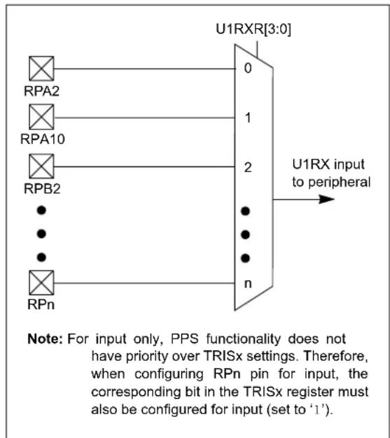
flowchart
graph TD
    A["RPA2"] --> B["U1RXR[3:0"]]
    C["RPA10"] --> B
    D["RPB2"] --> B
    E["RPn"] --> B
    B --> F["U1RX input to peripheral"]
    style B fill:#f9f,stroke:#333
    note right of B: Note: For input only, PPS functionality does not have priority over TRISx settings. Therefore, when configuring RPN pin for input, the corresponding bit in the TRISx register must also be configured for input (set to '1').
13.4.5 VIRTUAL INPUT PINS
Included in the input pin mappings are special inputs taken from nodes within the device. These nodes include outputs from built-in digital noise filters. These inputs may be used to filter a pin input before presenting that signal to another module like a ICAP or UART input.
This is accomplished by configuring a particular module to use PTG30 or PTG31 (which come from the PTG module) instead of a device pin, using the mapping.
TABLE 13-2: INPUT PIN SELECTION
| Peripheral Pin | [pin name]R SFR | [pin name]R bits | [pin name]R Value to RPn Pin Selection |
| INT4 INT4R INT4R[3:0] 4'b0000 = RPA0 | 4'b0001 = RPA44'b0010 = RPA124'b0011 = RPB04'b0100 = RPB44'b0101 = RPB84'b0110 = RPB124'b0111 = RPC04'b1000 = RPC44'b1001 = RPC94'b1010 = RPC134'b1011 = RPK04'b1100 = RPK44'b1100 = RPK84'b1101 = RPK124'b1111 = Reserved | ||
| INT0 INT0R INT0R[3:0] | |||
| T1CK T1CKR T1CKR[3:0] | |||
| T5CK T5CKR T5CKR[3:0] | |||
| IC4 IC4R IC4R[3:0] | |||
| U3RX | U3RXR | U3RXR[3:0] | |
| SDI1 | SDI1R | SDI1R[3:0] | |
| ECOL | ECOLR ECOLR[3:0] | ||
| ETXCLK | ETXCLKR | ETXCLKR[3:0] | |
| REFI | REFIR | REFIR[3:0] | |
| OCFD | OCFDR | OCFDR[3:0] | |
| INT3 INT3R INT3R[3:0] 4'b0000 = RPA1 | 4'b0001 = RPA54'b0010 = RPA134'b0011 = RPB14'b0100 = RPB54'b0101 = RPB94'b0110 = RPB134'b0111 = RPC14'b1000 = RPC54'b1001 = RPC104'b1010 = RPC144'b1011 = RPK14'b1100 = RPK54'b1100 = RPK94'b1101 = RPK134'b1111 = Reserved | ||
| T2CK T2CKR T2CKR[3:0] | |||
| T6CK T6CKR T6CKR[3:0] | |||
| IC3 IC3R IC3R[3:0] | |||
| U1CTS | U1CTSR | U1CTSR[3:0] | |
| U2RX | U2RXR | U2RXR[3:0] | |
| SDI2 | SDI2R | SDI2R[3:0] | |
| ERXD3 | ERXD3R | ERXD3R[3:0] | |
| OCFC | OCFCR | OCFCR[3:0] | |
| INT2 INT2R INT2R[3:0] 4'b0000 = RPA2 | 4'b0001 = RPA104'b0010 = RPA144'b0011 = RPB24'b0100 = RPB64'b0101 = RPB104'b0110 = RB144'b0111 = RPC24'b1000 = RPC64'b1001 = RPC114'b1010 = RPC154'b1011 = RPK24'b1100 = RPK64'b1100 = RPK104'b1101 = RPK144'b1111 = PTG30 | ||
| T3CK T3CKR T3CKR[3:0] | |||
| T7CK T7CKR T7CKR[3:0] | |||
| IC1 IC1R IC1R[3:0] | |||
| U1RX | U1RXR | U1RXR[3:0] | |
| U2CTSn | U2CTSnR | U2CTSnR[3:0] | |
| C1RX | C1RXR | C1RXR[3:0] | |
| ECRS | ECRSR | ECRSR[3:0] | |
| ERXD2 | ERXD2R | ERXD2R[3:0] | |
| SS1 | SS1R | SS1R[3:0] | |
| OCFB | OCFBR | OCFBR[3:0] | |
| INT1 INT1R INT1R[3:0] 4'b0000 = RPA3 | 4'b0001 = RPA114'b0010 = RPA154'b0011 = RPB34'b0100 = RPB74'b0101 = RPB114'b0110 = Reserved4'b0111 = RPC34'b1000 = RPC74'b1001 = RPC84'b1010 = RPC124'b1011 = RPK34'b1100 = RPK74'b1100 = RPK114'b1101 = Reserved4'b1111 = PTG31 | ||
| T4CK T4CKR T4CKR[3:0] | |||
| IC2 IC2R IC2R[3:0] | |||
| U3CTSn U3CTSnR U3CTSnR[3:0] | |||
| SS2 SS2R SS2R[3:0] | |||
| C2RX C2RXR | C2RXR[3:0] | ||
| OCFA | OCFAR | OCFAR[3:0] |
13.4.6 OUTPUT MAPPING
In contrast to inputs, the outputs of the PPS options are mapped on the basis of the pin. In this case, a control register associated with a particular pin dictates the peripheral output to be mapped. The RPnR registers (Register 13-2) are used to control output mapping. Like the [pin name]R registers, each register contains set of 4-bit fields. The value of the bit field corresponds to one of the peripherals, and that peripherals output is mapped to the pin (see Table 13-3 and the figure below).
A null output is associated with the output register Reset value of '0'. This is done to ensure that remappable outputs remain disconnected from all output pins by default.
13.4.7.1 Control Register Lock
Under normal operation, writes to the RPnR and [pin name]R registers are not allowed. Attempted writes appear to execute normally, but the contents of the registers remain unchanged. To change these registers, they must be unlocked in hardware. The register lock is controlled by the IOLOCK Configuration bit (CFGCON0[13]). Setting IOLOCK prevents writes to the control registers; clearing IOLOCK allows writes.
Note: To set or clear the IOLOCK bit, an unlock sequence must be executed. Refer to Section 42. "Oscillators with Enhanced PLL" in the "PIC32 Family Reference Manual" for details.
FIGURE 13-3: EXAMPLE OF
MULTIPLEXING OF
REMAPPABLE OUTPUT
FOR RPA0
![RPA0R[3:0] Default U1TX Output U2RTS Output Output Data REFCLKO1 14 15](/content/2026/05/935427/images/18f389f1eaef13c149742aa77b03503633d922011a625b87dc73117ae336023a.jpg)
13.4.7 CONTROLLING CONFIGURATION CHANGES
Some restrictions on peripheral remapping are needed to prevent accidental configuration changes as the peripheral remapping can be changed during run time. The PIC32MZ1025W104 family of devices include two features to prevent alterations to the peripheral map:
• Control register lock sequence
- Configuration bit select lock
TABLE 13-3: OUTPUT PIN SELECTION
| RPn Port Pin RPnR SFR RPnR bits RPnR Value to Peripheral Selection | |||
| RPA0 RPA0R RPA0R[4:0] 5'b00000 = No Connect | 5'b00001 = U1TX5'b00010 = U2RTS5'b00011 = SDO15'b00100 = SDO25'b00101 = OC15'b00110 = C1TX5'b10010 = REFO15'b10011 = PTG28 | ||
| RPA4 RPA4R RPA4R[4:0] | |||
| RPA12 RPA12R RPA12R[4:0] | |||
| RPB0 | RPB0R | RPB0R[4:0] | |
| RPB4 | RPB4R | RPB4R[4:0] | |
| RPB8 | RPB8R | RPB8R[4:0] | |
| RPB12 | RPB12R | RPB12R[4:0] | |
| RPC0 | RPC0R | RPC0R[4:0] | |
| RPC4 | RPC4R | RPC4R[4:0] | |
| RPK0 | RPK0R | RPK0R[4:0] | |
| RPK4 | RPK4R | RPK4R[4:0] | |
| RPK8 | RPK8R | RPK8R[4:0] | |
| RPK12 | RPK12R | RPK12R[4:0] | |
| RPC9 | RPC9R | RPC9R[4:0] | |
| RPC13 | RPC13R | RPC13R[4:0] | |
| RPA1 RPA1R RPA1R[4:0] 5'b00000 = No Connect | 5'b00001 = U3TX5'b00011 = SDO15'b00100 = SDO25'b00101 = OC25'b00110 = C2TX5'b10010 = REFO25'b10011 = PTG295'b10110 = ETXERR | ||
| RPA5 RPA5R RPA5R[4:0] | |||
| RPA13 RPA13R RPA13R[4:0] | |||
| RPB1 | RPB1R | RPB1R[4:0] | |
| RPB5 | RPB5R | RPB5R[4:0] | |
| RPB9 | RPB9R | RPB9R[4:0] | |
| RPB13 | RPB13R | RPB13R[4:0] | |
| RPC1 | RPC1R | RPC1R[4:0] | |
| RPC5 | RPC5R | RPC5R[4:0] | |
| RPK1 | RPK1R | RPK1R[4:0] | |
| RPK5 | RPK5R | RPK5R[4:0] | |
| RPK9 | RPK9R | RPK9R[4:0] | |
| RPK13 | RPK13R | RPK13R[4:0] | |
| RPC10 | RPC10R | RPC10R[4:0] | |
| RPC14 | RPC14R | RPC14R[4:0] | |
| RPn Port Pin | RPnR SFR | RPnR bits | RPnR Value to Peripheral Selection |
| RPA2 RPA2R RPA2 | R[4:0] 5'b00000 = No Connect | 5'b00010 = U3RTS5'b00011 = SS15'b00101 = OC35'b10010 = REFO35'b10011 = PTG305'b10110 = ETXD3 | |
| RPA10 RPA10R RPA10R | RPA10R[4:0] | ||
| RPA14 | RPA14R | RPA14R[4:0] | |
| RPB2 RPB2R RPB2 | R[4:0] | ||
| RPB6 RPB6R RPB6 | R[4:0] | ||
| RPB10 RPB10R RPB10R | R[4:0] | ||
| RPB14 RPB14R RPB14R | R[4:0] | ||
| RPC2 RPC2R RPC2 | R[4:0] | ||
| RPC6 RPC6R RPC6 | R[4:0] | ||
| RPK2 RPK2R RPK2 | R[4:0] | ||
| RPK6 RPK6R RPK6 | R[4:0] | ||
| RPK10 RPK10R RPK10R | R[4:0] | ||
| RPK14 RPK14R RPK14R | R[4:0] | ||
| RPC11 RPC11R RPC11R | R[4:0] | ||
| RPC15 | RPC15R | RPC15R[4:0] | |
| RPA3 RPA3R RPA3 | R[4:0] 5'b00000 = No Connect | 5'b00001 = U1RTS5'b00010 = U2TX5'b00100 = SS25'b00101 = OC45'b10010 = REFO45'b10011 = PTG315'b10110 = ETXD2 | |
| RPA11 | RPA11R | RPA11R[4:0] | |
| RPA15 | RPA15R | RPA15R[4:0] | |
| RPB3 RPB3R RPB3 | R[4:0] | ||
| RPB7 RPB7R RPB7 | R[4:0] | ||
| RPB11 RPB11R RPB11R | R[4:0] | ||
| RPC3 RPC3R RPC3 | R[4:0] | ||
| RPC7 RPC7R RPC7 | R[4:0] | ||
| RPC8 RPC8R RPC8 | R[4:0] | ||
| RPK3 RPK3R RPK3 | R[4:0] | ||
| RPK7 RPK7R RPK7 | R[4:0] | ||
| RPK11 | RPK11R | RPK11R[4:0] | |
| RPC12 | RPC12R | RPC12R[4:0] | |
13.5 Function Priority for Device Pins
Device pins have an associated priority order in which functionality is brought out on it. Availability of PPS functionality is impacted by this priority order. For example, if high-speed UART is enabled, pins PA6, PA7, PA8, and PA9 are given priority to be used as UART pins instead of PORT pins.
Refer to the following tables for the priority in which functions are brought out on each device pin.
Refer to Section 2.0 "PIC32MZ1025W104 SoC Description" for the mapping of device pin name to package pin numbers.
Note: Refer to the corresponding reference peripheral chapter for functionality details.
TABLE 13-4: PRIORITY FOR DEVICE PINS PA(N) (N = 0-15)
| Pin Name Functions in | Priority Order Reference Peripheral | |
| PA0 SQICS0 SQI | ||
| CVDT17 CVD | ||
| RPA0 PPS | ||
| IOCA0 Change Notification | ||
| RA0 Port I/O | ||
| PA1 RPA1 PPS | ||
| 1/CS1/FSYNC1 | SPI | |
| IOCA1 Change Notification | ||
| RA1 Port I/O | ||
| PA2 RPA2 PPS | ||
| SCL2 I2C | ||
| IOCA2 Change Notification | ||
| RA2 Port I/O | ||
| PA3 RPA3 PPS | ||
| SDA2 | I2C | |
| IOCA3 Change Notification | ||
| RA3 Port I/O | ||
| PA4 RPA4 PPS | ||
| SCL1 I2C | ||
| IOCA4 Change Notification | ||
| RA4 Port I/O | ||
| PA5 RPA5 PPS | ||
| SDA1 | I2C | |
| IOCA5 Change Notification | ||
| RA5 Port I/O | ||
| PA6 U1CTSn UART/USART | ||
| IOCA6 Change Notification | ||
| RA6 Port I/O | ||
| PA7 U1RTSn/U1BCLK | UART/USART | |
| IOCA7 Change Notification | ||
| RA7 Port I/O | ||
| PA8 U1RX | UART/USART | |
| IOCA8 Change Notification | ||
| RA8 Port I/O | ||
| Pin Name | Functions in Priority Order | Reference Peripheral |
| PA9 U1TX UART/USART | ||
| IOCA9 Change Notification | ||
| RA9 Port I/O | ||
| PA10 AN17 ADC | ||
| CVD17 CVD | ||
| CVDR17 CVD | ||
| RPA10 PPS | ||
| CTRTM0 Timer | ||
| INT0 Edge Interrupt | ||
| IOCA10 Change Notification | ||
| RA10 Port I/O | ||
| PA11 | RPA11 | PPS |
| SCK2 | SPI | |
| IOCA11 | Change Notification | |
| RA11 | Port I/O | |
| PA12 AN16 ADC | ||
| CVD16 CVD | ||
| CVDR16 CVD | ||
| RPA12 PPS | ||
| CTRTM1 Timer | ||
| IOCA12 Change Notification | ||
| RA12 Port I/O | ||
| PA13 AN15 ADC | ||
| ANN1 | ADC (Differential) | |
| CVD15 CVD | ||
| CVDR15 CVD | ||
| RPA13 PPS | ||
| IOCA13 Change Notification | ||
| RA13 Port I/O | ||
| PA14 AN14 ADC | ||
| ANN0 | ADC (Differential) | |
| CVD14 CVD | ||
| CVDR14 CVD | ||
| RPA14 PPS | ||
| IOCA14 Change Notification | ||
| RA14 Port I/O | ||
| PA15 AN13 ADC | ||
| CVD13 CVD | ||
| CVDR13 CVD | ||
| RPA15 PPS | ||
| IOCA15 Change Notification | ||
| RA15 Port I/O |
TABLE 13-5: PRIORITY FOR DEVICE PINS PB(N) (N = 0-15)
| Pin Name Functions in Priority Order Reference Peripheral | ||
| PB0 AN0 ADC | ||
| RPB0 PPS | ||
| IOCB0 Change Notification | ||
| RB0 Port I/O | ||
| PB1 AN1 ADC | ||
| CVD1 CVD | ||
| CVDR1 CVD | ||
| CVDT6 CVD | ||
| ETH_EXCLK_OUT Ethernet/Clock | ||
| RPB1 PPS | ||
| VBUSON USB | ||
| IOCB1 Change Notification | ||
| RB1 Port I/O | ||
| PB2 PGD1/EMUD1 | ICD | |
| AN2 ADC | ||
| CVD2 CVD | ||
| CVDR2 CVD | ||
| CVDT5 CVD | ||
| RPB2 PPS | ||
| USBID | USB | |
| IOCB2 Change Notification | ||
| RB2 Port I/O | ||
| PB3 PGC1/EMUC1 | ICD | |
| AN3 ADC | ||
| CVD3 CVD | ||
| CVDR3 CVD | ||
| CVDT4 CVD | ||
| RPB3 PPS | ||
| USBOEN | USB | |
| IOCB3 Change Notification | ||
| RB3 Port I/O | ||
| PB4 PGC2/EMUC2 | ICD | |
| AN4 ADC | ||
| CVD4 CVD | ||
| CVDR4 CVD | ||
| CVDT3 CVD | ||
| RPB4 PPS | ||
| IOCB4 Change Notification | ||
| RB4 Port I/O | ||
| Pin Name | Functions in Priority Order | Reference Peripheral |
| PB5 PGD2/EMUD2 ICD | ||
| AN5 ADC | ||
| CVD5 CVD | ||
| CVDR5 CVD | ||
| CVDT2 CVD | ||
| RTCC RTCC | ||
| RPB5 PPS | ||
| IOCB5 Change Notification | ||
| RB5 Port I/O | ||
| PB6 TMS JTAG | ||
| AN6 ADC | ||
| CVD6 CVD | ||
| CVDR6 CVD | ||
| CVDT1 CVD | ||
| RPB6 PPS | ||
| IOCB6 Change Notification | ||
| RB6 Port I/O | ||
| PB7 TDO JTAG | ||
| AN7 ADC | ||
| CVD7 CVD | ||
| CVDR7 CVD | ||
| CVDT0 CVD | ||
| RPB7 PPS | ||
| IOCB7 Change Notification | ||
| RB7 Port I/O | ||
| PB8 PGC4/EMUC4 ICD | ||
| TCK JTAG | ||
| AN8 ADC | ||
| CVD8 CVD | ||
| CVDR8 CVD | ||
| RPB8 PPS | ||
| IOCB8 Change Notification | ||
| RB8 Port I/O | ||
| PB9 PGD4/EMUD4 ICD/Test Entry | ||
| TDI | JTAG | |
| AN9 ADC | ||
| CVD9 CVD | ||
| CVDR9 CVD | ||
| RPB9 PPS | ||
| IOCB9 Change Notification | ||
| RB9 Port I/O | ||
| PB10 AN10 ADC | ||
| CVD10 CVD | ||
| CVDR10 CVD | ||
| LVDIN LVD Voltage Reference | ||
| RPB10 PPS | ||
| IOCB10 Change Notification | ||
| RB10 Port I/O | ||
| PB11 ANB0 ADC (Alternate) | ||
| RPB11 PPS | ||
| IOCB11 Change Notification | ||
| RB11 Port I/O | ||
| PB12 ANA0 ADC (Alternate) | ||
| RPB12 PPS | ||
| IOCB12 Change Notification | ||
| RB12 Port I/O | ||
| PB13 AN11 ADC | ||
| CVD11 CVD | ||
| CVDR11 CVD | ||
| RPB13 PPS | ||
| IOCB13 Change Notification | ||
| RB13 Port I/O | ||
| PB14 AN12 ADC | ||
| CVD12 CVD | ||
| CVDR12 CVD | ||
| RPB14 PPS | ||
| IOCB14 Change Notification | ||
| RB14 Port I/O | ||
| PB15 SOSCI Secondary Oscillator Input | ||
TABLE 13-6: PRIORITY FOR DEVICE PIN PC(N) (N = 0-15)
| Pin Name | Functions in Priority Order | Reference Peripheral |
| PC0 | SQICS1 | SQI |
| CVDT18 | CVD | |
| RPC0 | PPS | |
| IOCC0 | Change Notification | |
| RC0 | Port I/O |
TABLE 13-6: PRIORITY FOR DEVICE PIN PC(N) (N = 0-15)
| Pin Name | Functions in Priority Order | Reference Peripheral |
| PC1 SQID3 SQI | ||
| CVDT19 CVD | ||
| RPC1 PPS | ||
| IOCC1 Change Notification | ||
| RC1 Port I/O | ||
| PC2 SQID2 SQI | ||
| CVDT20 CVD | ||
| RPC2 PPS | ||
| IOCC2 Change Notification | ||
| RC2 Port I/O | ||
| PC3 SQID1 SQI | ||
| CVDT21 CVD | ||
| RPC3 PPS | ||
| IOCC3 Change Notification | ||
| RC3 Port I/O | ||
| PC4 SCLKI Secondary Oscillator - Digital | ||
| SQID0 SQI | ||
| CVDT22 CVD | ||
| RPC4 PPS | ||
| IOCC4 Change Notification | ||
| RC4 Port I/O | ||
| PC5 SQICLK SQI | ||
| CVDT23 CVD | ||
| RPC5 PPS | ||
| IOCC5 Change Notification | ||
| RC5 Port I/O | ||
| PC6 RPC6 PPS | ||
| SCK1 SPI | ||
| IOCC6 Change Notification | ||
| RC6 Port I/O | ||
| PC7 RPC7 PPS | ||
| SDI1 SPI | ||
| IOCC7 Change Notification | ||
| RC7 Port I/O | ||
| PC8 RPC8 PPS | ||
| SDO1 SPI | ||
| IOCC8 Change Notification | ||
| RC8 Port I/O | ||
TABLE 13-6: PRIORITY FOR DEVICE PIN PC(N) (N = 0-15)
| Pin Name | Functions in Priority Order | Reference Peripheral |
| PC9 CVDT7 CVD | ||
| ERXERR Ethernet | ||
| RPC9 PPS | ||
| IOCC9 Change Notification | ||
| RC9 Port I/O | ||
| PC10 CVDT8 CVD | ||
| ERXD1 Ethernet | ||
| RPC10 PPS | ||
| IOCC10 Change Notification | ||
| RC10 Port I/O | ||
| PC11 CVDT9 CVD | ||
| ERXD0 Ethernet | ||
| RPC11 | PPS | |
| IOCC11 | Change Notification | |
| RC11 | Port I/O | |
| PC12 CVDT10 | CVD | |
| ETH_CLK_OUT | Clock/Ethernet | |
| ERXCLK | Ethernet | |
| RPC12 PPS | ||
| IOCC12 Change Notification | ||
| RC12 Port I/O | ||
| PC13 CVDT11 | CVD | |
| ETXEN Ethernet | ||
| RPC13 PPS | ||
| IOCC13 Change Notification | ||
| RC13 Port I/O | ||
| PC14 CVDT12 | CVD | |
| ETXD1 | Ethernet | |
| RPC14 PPS | ||
| IOCC14 Change Notification | ||
| RC14 Port I/O | ||
| PC15 CVDT13 | CVD | |
| ETXD0 | Ethernet | |
| RPC15 PPS | ||
| IOCC15 Change Notification | ||
| RC15 Port I/O |
TABLE 13-7: PRIORITY FOR DEVICE PIN PK(N) (N = 0-15)
| Pin Name Functions in | Priority Order Reference Peripheral | |
| PK0 RF_FE_3 Wi-Fi | ||
| RPK0 PPS | ||
| IOCK0 Change Notification | ||
| RK0 Port I/O | ||
| PK1 RF_FE_4 Wi-Fi | ||
| RPK1 PPS | ||
| IOCK1 Change Notification | ||
| RK1 Port I/O | ||
| PK2 RF_FE_1 Wi-Fi | ||
| AN19 ADC | ||
| CVD19 CVD | ||
| CVDR19 CVD | ||
| RPK2 PPS | ||
| IOCK2 Change Notification | ||
| RK2 Port I/O | ||
| PK3 RF_FE_2 Wi-Fi | ||
| AN18 ADC | ||
| CVD18 CVD | ||
| CVDR18 CVD | ||
| RPK3 PPS | ||
| IOCK3 Change Notification | ||
| RK3 Port I/O | ||
| PK4 VREGCTRL0 | Wi-Fi | |
| BT_CLK_OUT | Oscillator | |
| SCANDIAG8 | ATPG Scan | |
| RPK4 PPS | ||
| IOCK4 Change Notification | ||
| RK4 Port I/O | ||
| PK5 VREGCTRL1 | Wi-Fi | |
| PTA_WLAN_ACTIVE | Wi-Fi | |
| RPK5 PPS | ||
| IOCK5 Change Notification | ||
| RK5 Port I/O | ||
| PK6 PTA_BT_PRIO | Wi-Fi | |
| RPK6 PPS | ||
| IOCK6 Change Notification | ||
| RK6 Port I/O | ||
| PK7 PTA_BT_ACTIVE | Wi-Fi | |
| RPK7 PPS | ||
| IOCK7 Change Notification | ||
| RK7 Port I/O | ||
| Pin Name | Functions in Priority Order | Reference Peripheral |
| PK8 RF_FE_7 Wi-Fi | ||
| RPK8 PPS | ||
| IOCK8 Change Notification | ||
| RK8 Port I/O | ||
| PK9 RF_FE_8 Wi-Fi | ||
| RPK9 PPS | ||
| IOCK9 Change Notification | ||
| RK9 Port I/O | ||
| PK10 RF_FE_6 Wi-Fi | ||
| RPK10 PPS | ||
| IOCK10 Change Notification | ||
| RK10 Port I/O | ||
| PK11 RF_FE_5 Wi-Fi | ||
| RPK11 PPS | ||
| IOCK11 Change Notification | ||
| RK11 Port I/O | ||
| PK12 CVDT14 | CVD | |
| ERXDV Ethernet | ||
| RPK12 PPS | ||
| IOCK12 Change Notification | ||
| RK12 Port I/O | ||
| PK13 CVDT15 | CVD | |
| EMDIO | Ethernet | |
| RPK13 PPS | ||
| IOCK13 Change Notification | ||
| RK13 Port I/O | ||
| PK14 CVDT16 | CVD | |
| EMDC | Ethernet | |
| RPK14 PPS | ||
| IOCK14 Change Notification | ||
| RK14 Port I/O | ||
| PK15 SOSCO | Secondary Oscillator Output | |
| RPK15 Port Input Only |
13.6 I/O Ports Control Registers
TABLE 13-8: PERIPHERAL PIN SELECT OUTPUT REGISTER MAP
Legend: x = Unknown value on Reset; — = Unimplemented, read as 'c'; Reset values are shown in hexadecimal.
TABLE 13-9: PERIPHERAL PIN SELECT INPUT REGISTER MAP
Legend: x = Unknown value on Reset; — = Unimplemented, read as '0'; Reset values are shown in hexadecimal.
TABLE 13-9: PERIPHERAL PIN SELECT INPUT REGISTER MAP (CONTINUED)
Legend: x = Unknown value on Reset; — = Unimplemented, read as '0'; Reset values are shown in hexadecimal.
TABLE 13-10: PORTA REGISTER MAP
| Virtual Address (BF82_#) | Register Name(1) | Bit Range | Bits | All Resets | ||||||||||||||||
| 31/15 30 | 14 29/13 28 | 12 27/11 26 | 10 25/9 24 | 8 23/7 22/6 | 21/5 20/4 19 | 3 18/2 17/1 | 16/0 | |||||||||||||
| 0000 | ANSELA | 31:16 | — | — | — | — | — | — | — | — | — | — | — | — | — | — | — | — | — | 0000 |
| 15:0 | ANSA15 | ANSA14 | ANSA13 | ANSA12 | — | ANSA10 | — | — | — | — | — | — | — | — | — | — | — | 0000 | ||
| 0010 | TRISA | 31:16 | — | — | — | — | — | — | — | — | — | — | — | — | — | — | — | — | — | 0000 |
| 15:0 | TRISA15 | TRISA14 | TRISA13 | TRISA12 | TRISA11 | TRISA10 | TRISA0 | TRISA8 | TRISA7 | TRISA6 | TRISA5 | TRISA4 | TRISA3 | TRISA2 | TRISA1 | TRISA0 | 0000 | |||
| 0020 | PORTA | 31:16 | — | — | — | — | — | — | — | — | — | — | — | — | — | — | — | — | — | 0000 |
| 15:0 | RA15 | RA14 | RA13 | RA12 | RA11 | RA10 | RA9 | RA8 | RA7 | RA6 | RA5 | RA4 | RA3 | RA2 | RA1 | RA0 | 2000 | |||
| 0030 | LATA | 31:16 | — | — | — | — | — | — | — | — | — | — | — | — | — | — | — | — | — | 0000 |
| 15:0 | LATA15 | LATA14 | LATA13 | LATA12 | LATA11 | LATA10 | LATA9 | LATA8 | LATA7 | LATA6 | LATA5 | LATA4 | LATA3 | LATA2 | LATA1 | LATA0 | 3000 | |||
| 0040 | ODCA | 31:16 | — | — | — | — | — | — | — | — | — | — | — | — | — | — | — | — | — | 0000 |
| 15:0 | ODCA15 | ODCA14 | ODCA13 | ODCA12 | ODCA11 | ODCA10 | ODCA9 | ODCA8 | ODCA7 | ODCA6 | ODCA5 | ODCA4 | ODCA3 | ODCA2 | ODCA1 | ODCA0 | 3000 | |||
| 0050 | CNPUA | 31:16 | — | — | — | — | — | — | — | — | — | — | — | — | — | — | — | — | — | 0000 |
| 15:0 | CNPUA15 | CNPUA14 | CNPUA13 | CNPUA12 | CNPUA11 | CNPUA10 | CNPUA9 | CNPUA8 | CNPUA7 | CNPUA6 | CNPUA5 | CNPUA4 | CNPUA3 | CNPUA2 | CNPUA1 | CNPUA0 | 3000 | |||
| 0060 | CNPDA | 31:16 | — | — | — | — | — | — | — | — | — | — | — | — | — | — | — | — | — | 0000 |
| 15:0 | CNPDA15 | CNPDA14 | CNPDA13 | CNPDA12 | CNPDA11 | CNPDA10 | CNPDA9 | CNPDA8 | CNPDA7 | CNPDA6 | CNPDA5 | CNPDA4 | CNPDA3 | CNPDA2 | CNPDA1 | CNPDA0 | 3000 | |||
| 0070 | CNCONA | 31:16 | — | — | — | — | — | — | — | — | — | — | — | — | — | — | — | — | — | 0000 |
| 15:0 ON | — | — | — | EDGEDE- TECT | — | — | — | — | — | — | — | — | — | — | — | — | 0000 | |||
| 0080 | CNENA | 31:16 | — | — | — | — | — | — | — | — | — | — | — | — | — | — | — | — | — | 2000 |
| 15:0 | CNIEA15 | CNIEA14 | CNIEA13 | CNIEA12 | CNIEA11 | CNIEA10 | CNIEA9 | CNIEA8 | CNIEA7 | CNIEA6 | CNIEA5 | CNIEA4 | CNIEA3 | CNIEA2 | CNIEA1 | CNIEA0 | 3000 | |||
| 0090 | CNSTATA | 31:16 | — | — | — | — | — | — | — | — | — | — | — | — | — | — | — | — | — | 2000 |
| 15:0 | CNSTA- TA15 | CNSTA- TA14 | CNSTATA13 | CNSTA- TA12 | CNSTA- TA11 | CNSTA- TA10 | CNSTA- TA9 | CNSTATA8 | CNSTATA7 | CNSTA- TA6 | CNSTA- TA5 | CNSTATA4 | CNSTA- TA3 | CNSTA- TA2 | CNSTA- TA1 | CNSTA- TA0 | 0000 | |||
| 00A0 | CNNEA | 31:16 | — | — | — | — | — | — | — | — | — | — | — | — | — | — | — | — | — | 2000 |
| 15:0 | CNNEA15 | CNNEA14 | CNNEA13 | CNNEA12 | CNNEA11 | CNNEA10 | CNNEA9 | CNNEA8 | CNNEA7 | CNNEA6 | CNNEA5 | CNNEA4 | CNNEA3 | CNNEA2 | CNNEA1 | CNNEA0 | 3000 | |||
Legend: x = Unknown value on Reset; — = Unimplemented, read as '0'; Reset values are shown in hexadecimal.
Note 1: All registers in this table have corresponding CLR, SET and INV registers at its virtual address, plus an offset of 0x4, 0x8 and 0xC, respectively. See Section 13.3 "CLR, SET and INV Registers" for more information.
TABLE 13-10: PORTA REGISTER MAP (CONTINUED)
| Virtual Address (BF82_#) | Register Name(1) | Bit Range | Bits | All Resets | |||||||||||||||
| 31/15 | 30/14 | 29/13 | 28/12 | 27/11 | 26/10 | 25/9 | 24/8 | 23/7 | 22/6 | 21/5 | 20/4 | 19/3 | 18/2 | 17/1 | 16/0 | ||||
| D0B0 | CNFA | 31:16 | —— | —— | —— | —— | 0.050 | ||||||||||||
| 15:0 | CNFA15 | CNFA14 | CNFA13 | CNFA12 | CNFA11 | CNFA10 | CNFA9 | CNFA8 | CNFA7 | CNFA6 | CNFA5 | CNFA4 | CNFA3 | CNFA2 | CNFA1 | CNFA0 | D0B0 | ||
| 00C0 | SRCON0A | 31:16 | —— | —— | —— | —— | 0.050 | ||||||||||||
| 15:0 | — | — | — | — | — | — | — | — | — | — | — | — | — | — | — | SR0A0 | D000 | ||
| 00D0 | SRCON1A | 31:16 | —— | —— | —— | —— | 0.050 | ||||||||||||
| 15:0 | — | — | — | — | — | — | — | — | — | — | — | — | — | — | — | SR1A0 | D000 | ||
Legend: x = Unknown value on Reset; — = Unimplemented, read as '0'; Reset values are shown in hexadecimal.
Note 1: All registers in this table have corresponding CLR, SET and INV registers at its virtual address, plus an offset of 0x4, 0x8 and 0xC, respectively. See Section 13.3 "CLR, SET and INV Registers" for more information.
TABLE 13-11: PORTB REGISTER MAP
| Virtual Address (BF82_#) | Register Name(1) | Bit Range | Bits | All Resets | |||||||||||||||
| 31/15 | 30/14 | 29/13 | 28/12 | 27/11 | 26/10 | 25/9 | 24/8 | 23/7 | 22/6 | 21/5 | 20/4 | 19/3 | 18/2 | 17/1 | 16/0 | ||||
| 0100 | ANSELB | 31:16 | — | — | — | — | — | — | — | — | — | — | — | — | — | — | — | — | 0000 |
| 15:0 | — | ANSB14 | ANSB13 | ANSB12 | ANSB11 | ANSB10 | ANSB9 | ANSB6 | ANSB7 | ANSB6 | ANSB5 | ANSB4 | ANSB3 | ANSB2 | ANSB1 | ANSB0 | 0000 | ||
| 0110 | TRISB | 31:16 | — | — | — | — | — | — | — | — | — | — | — | — | — | — | — | — | 0000 |
| 15:0 | TRISB15 | TRISB14 | TRISB13 | TRISB12 | TRISB11 | TRISB10 | TRISB9 | TRISB8 | TRISB7 | TRISB6 | TRISB5 | TRISB4 | TRISB3 | TRISB2 | TRISB1 | TRISB0 | 0000 | ||
| 0120 | PORTB | 31:16 | — | — | — | — | — | — | — | — | — | — | — | — | — | — | — | — | 0000 |
| 15:0 | RB15 | RB14 | RB13 | RB12 | RB11 | RB10 | RB9 | RB8 | RB7 | RB6 | RB5 | RB4 | RB3 | RB2 | RB1 | RB0 | 0000 | ||
| 0130 | LATB | 31:16 | — | — | — | — | — | — | — | — | — | — | — | — | — | — | — | — | 0000 |
| 15:0 | LATB15 | LATB14 | LATB13 | LATB12 | LATB11 | LATB10 | LATB9 | LATB5 | LATB7 | LATB5 | LATB5 | LATB4 | LATB3 | LATB2 | LATB1 | LATB0 | 0000 | ||
| 0140 | ODCB | 31:16 | — | — | — | — | — | — | — | — | — | — | — | — | — | — | — | — | 0000 |
| 15:0 | — | ODCB14 | ODCB13 | ODCB12 | ODCB11 | ODCB10 | ODCB9 | ODCB8 | ODCB7 | ODCB6 | ODCB5 | ODCB4 | ODCB3 | ODCB2 | ODCB1 | ODCB0 | 0000 | ||
Legend: x = Unknown value on Reset; — = Unimplemented, read as '0'; Reset values are shown in hexadecimal.
Note 1: All registers in this table have corresponding CLR, SET and INV registers at its virtual address, plus an offset of 0x4, 0x8 and 0xC, respectively. See Section 13.3 "CLR, SET and INV Registers" for more information.
TABLE 13-11: PORTB REGISTER MAP (CONTINUED)
| Virtual Address(BF82_#) | Register Name(1) | Bit Range | Bits | All Resets | |||||||||||||||
| 31/15 | 30/14 | 29/13 | 28/12 | 27/11 | 26/10 | 25/9 | 24/8 | 23/7 | 22/6 | 21/5 | 20/4 | 19/3 | 18/2 | 17/1 | 16/0 | ||||
| 0150 | CNPUB | 31:16 | —— | —— | —— | —— | 0300 | ||||||||||||
| 15:0 | — | CNPUB14 | CNPUB13 | CNPUB12 | CNPUB11 | CNPUB10 | CNPUB9 | CNPUB6 | CNPUB7 | CNPUB6 | CNPUB5 | CNPUB4 | CNPUB3 | CNPUB2 | CNPUB1 | CNPUB0 | 0000 | ||
| 0160 | CNPDB | 31:16 | —— | —— | —— | —— | 0300 | ||||||||||||
| 15:0 | — | CNPDB14 | CNPDB13 | CNPDB12 | CNPDB11 | CNPDB10 | CNPDB9 | CNPDB6 | CNPDB7 | CNPDB6 | CNPDB5 | CNPDB4 | CNPDB3 | CNPDB2 | CNPDB1 | CNPDB0 | 0000 | ||
| 0170 | CNCONB | 31:16 | —— | —— | —— | —— | 0300 | ||||||||||||
| 15:0 ON—— | EDGEDE-TECT | —— | —— | —— | 0300 | ||||||||||||||
| 0180 | CNENB | 31:16 | —— | —— | —— | —— | 0300 | ||||||||||||
| 15:0 | — | CNIEB14 | CNIEB13 | CNIEB12 | CNIEB11 | CNIEB10 | CNIEB9 | CNIEB8 | CNIEB7 | CNIEB6 | CNIEB5 | CNIEB4 | CNIEB3 | CNIEB2 | CNIEB1 | CNIEB0 | 0000 | ||
| 0190 | CNSTATB | 31:16 | —— | —— | —— | —— | 0300 | ||||||||||||
| 15:0 | — | CNSTATB14 | CNSTATB13 | CNSTATB12 | CNSTATB11 | CNSTATB10 | CNSTATB9 | CNSTATB8 | CNSTATB7 | CNSTATB6 | CNSTATB5 | CNSTATB4 | CNSTATB3 | CNSTATB2 | CNSTATB1 | CNSTATB0 | 0000 | ||
| 01A0 | CNNEB | 31:16 | —— | —— | —— | —— | 0300 | ||||||||||||
| 15:0 | — | CNNEB14 | CNNEB13 | CNNEB12 | CNNEB11 | CNNEB10 | CNNEB9 | CNNEB6 | CNNEB7 | CNNEB6 | CNNEB5 | CNNEB4 | CNNEB3 | CNNEB2 | CNNEB1 | CNNEB0 | 0000 | ||
| 01B0 | CNFB | 31:16 | —— | —— | —— | —— | 0300 | ||||||||||||
| 15:0 | — | CNFB14 | CNFB13 | CNFB12 | CNFB11 | CNFB10 | CNFB9 | CNFB8 | CNFB7 | CNFB6 | CNFB5 | CNFB4 | CNFB3 | CNFB2 | CNFB1 | CNFB0 | 0000 | ||
Legend: x = Unknown value on Reset; — = Unimplemented, read as '0'; Reset values are shown in hexadecimal.
Note 1: All registers in this table have corresponding CLR, SET and INV registers at its virtual address, plus an offset of 0x4, 0x8 and 0xC, respectively. See Section 13.3 "CLR, SET and INV Registers" for more information.
TABLE 13-12: PORTC REGISTER MAP
Legend: x = Unknown value on Reset; — = Unimplemented, read as 'c'; Reset values are shown in hexadecimal. Note 1: All registers in this table have corresponding CLR, SET and INV registers at its virtual address, plus an offset of 0x4, 0x8 and 0xC, respectively. See Section 13.3 "CLR, SET and INV Registers" for more information.
TABLE 13-12: PORTC REGISTER MAP (CONTINUED)
| Virtual Address (BF02,#) | Register Name | Bit Range | Bits | All Resets | |||||||||||||||
| 31/15 | 30/14 | 29/13 | 28/12 | 27/11 | 26/10 | 25/9 | 24/8 | 23/7 | 22/6 | 21/5 | 20/4 | 19/3 | 18/2 | 17/1 | 16/0 | ||||
| 02C0 | SRCONDC | 31:16 | —— | —— | —— | — | — | ||||||||||||
| 15:0 | SR0C15 | SR0C14 | SR0C13 | — | — | — | — | — | — | — | SR0C5 | SR0C4 | SR0C3 | SR0C2 | SR0C1 | SR0C0 | J000 | ||
| 02D0 | SRCON1C | 31:16 | —— | —— | —— | — | — | ||||||||||||
| 15:0 | SR1C15 | SR1C14 | SR1C13 | — | — | — | — | — | — | — | SR1C5 | SR1C4 | SR1C3 | SR1C2 | SR1C1 | SR1C0 | J000 | ||
Legend: x = Unknown value on Reset; — = Unimplemented, read as '0'; Reset values are shown in hexadecimal.
Note 1: All registers in this table have corresponding CLR, SET and INV registers at its virtual address, plus an offset of 0x4, 0x8 and 0xC, respectively. See Section 13.3 "CLR, SET and INV Registers" for more information.
TABLE 13-13: PORTK REGISTER MAP
Legend: x = Unknown value on Reset; — = Unimplemented, read as '0'; Reset values are shown in hexadecimal.
Note 1: All registers in this table have corresponding CLR, SET and INV registers at its virtual address, plus an offset of 0x4, 0x8 and 0xC, respectively. See Section 13.3 "CLR, SET and INV Registers" for more information.
TABLE 13-13: PORTK REGISTER MAP (CONTINUED)
| Virtual Address (BF82_#) | Register Name(1) | Bit Range | Bits | All Resets | ||||||||||||||||
| 31/15 | 30/14 | 29/13 | 28/12 | 27/11 | 26/10 | 25/9 | 24/8 | 23/7 | 22/6 | 21/5 | 20/4 | 19/3 | 18/2 | 17/1 | 16/0 | |||||
| 0350 | ONPUK | 31:16 | — | — | — | — | — | 3000 | ||||||||||||
| 15:0 | — | CNPUK14 | CNPUK13 | CNPUK12 | CNPUK11 | CNPUK10 | CNPUK9 | CNPUK8 | CNPUK7 | CNPUK6 | CNPUK5 | CNPUK4 | CNPUK3 | CNPUK2 | CNPUK1 | CNPUK0 | 0000 | |||
| 0360 | ONPDK | 31:16 | — | — | — | — | — | 3000 | ||||||||||||
| 15:0 | — | CNPDK14 | CNPDK13 | CNP-DK12 | CNPDK11 | CNPDK10 | CNPDK9 | CNPDK8 | CNPDK7 | CNPDK6 | CNPDK5 | CNPDK4 | CNPDK3 | CNP-DK2 | CNP-DK1 | CNP-DK0 | 0000 | |||
| 0370 | CNCONK | 31:16 | — | — | — | — | — | 3000 | ||||||||||||
| 15:0 ON | — | — | — | EDGEDE-TECT | — | — | — | — | 0000 | |||||||||||
| 0380 | CNENK | 31:16 | — | — | — | — | — | 3000 | ||||||||||||
| 15:0 | — | CNIEK14 | CNIEK13 | CNIEK12 | CNIEK11 | CNIEK10 | CNIEK9 | CNIEK8 | CNIEK7 | CNIEK6 | CNIEK5 | CNIEK4 | CNIEK3 | CNIEK2 | CNIEK1 | CNIEK0 | 0000 | |||
| 0390 | CNSTATK | 31:16 | — | — | — | — | — | 3000 | ||||||||||||
| 15:0 | — | CNSTATK14 | CNSTATK13 | CNSTATK12 | CNSTATK11 | CNSTATK10 | CNSTATK9 | CNSTATK8 | CNSTATK7 | CNSTATK5 | CNSTATK5 | CNSTATK4 | CNSTATK3 | CNSTATK2 | CNSTATK1 | CNSTATK0 | 0000 | |||
| 03A0 | CNNEK | 31:16 | — | — | — | — | — | 3000 | ||||||||||||
| 15:0 | — | CNNEK14 | CNNEK13 | CNNEK12 | CNNEK11 | CNNEK10 | CNNEK9 | CNNEK8 | CNNEK7 | CNNEK6 | CNNEK5 | CNNEK4 | CNNEK3 | CNNEK2 | CNNEK1 | CNNEK0 | 0000 | |||
| 03B0 | CNFK | 31:16 | — | — | — | — | — | 3000 | ||||||||||||
| 15:0 | — | CNFK14 | CNFK13 | CNFK12 | CNFK11 | CNFK10 | CNFK9 | CNFK8 | CNFK7 | CNFK5 | CNFK5 | CNFK4 | CNFK3 | CNFK2 | CNFK1 | CNFK0 | 3000 | |||
| 03C0 | SRCONOK | 31:16 | — | — | — | — | — | 3000 | ||||||||||||
| 15:0 | — | SROK14 | SROK13 | — | — | — | — | — | — | — | — | — | — | — | — | — | 0000 | |||
| 03D0 | SRCON1K | 31:16 | — | — | — | — | — | 3000 | ||||||||||||
| 15:0 | — | SR1K14 | SR1K13 | — | — | — | — | — | — | — | — | — | — | — | — | — | 0000 | |||
Legend: x = Unknown value on Reset; — = Unimplemented, read as '0'; Reset values are shown in hexadecimal.
Note 1: All registers in this table have corresponding CLR, SET and INV registers at its virtual address, plus an offset of 0x4, 0x8 and 0xC, respectively. See Section 13.3 "CLR, SET and INV Registers" for more information.
REGISTER 13-1: [pin name]R: PERIPHERAL PIN SELECT INPUT REGISTER
| Bit Range | Bit 31/23/15/7 | Bit 30/22/14/6 | Bit 29/21/13/5 | Bit 28/20/12/4 | Bit 27/19/11/3 | Bit 26/18/10/2 | Bit 25/17/9/1 | Bit 24/16/8/0 |
| 31:24 | U-0 U-0 | U-0 U-0 U-0 U-0 | U-0 U-0 | |||||
| — — — | — — — — — | |||||||
| 23:16 | U-0 U-0 | U-0 U-0 U-0 U-0 | U-0 U-0 | |||||
| — — — | — — — — — | |||||||
| 15:8 | U-0 U-0 | U-0 U-0 U-0 U-0 | U-0 U-0 | |||||
| — — — | — — — — — | |||||||
| 7:0 | U-0 U-0 | U-0 U-0 R/W-0 | R/W-0 | R/W-0 | R/W-0 | |||
| — | — | — | [pin name]R[4:0] | |||||
Legend:
| R = Readable bit | W = Writable bit | U = Unimplemented bit, read as '0' |
| -n = Value at POR | '1' = Bit is set | '0' = Bit is cleared x = Bit is unknown |
bit 31-4 Unimplemented: Read as '0'
bit 3-0 [pin name]R[4:0]: Peripheral Pin Select Input bits
Where [pin name] refers to the pins that are used to configure the peripheral input mapping. See Table 13-2 for the input pin selection values.
Note: Register values can only be changed if the IOLOCK Configuration bit (CFGCON[13]) = 0.
REGISTER 13-2: RPnR: PERIPHERAL PIN SELECT OUTPUT REGISTER
| Bit Range | Bit 31/23/15/7 | Bit 30/22/14/6 | Bit 29/21/13/5 | Bit 28/20/12/4 | Bit 27/19/11/3 | Bit 26/18/10/2 | Bit 25/17/9/1 | Bit 24/16/8/0 |
| 31:24 | U-0 U-0 | U-0 U-0 U-0 U-0 | U-0 U-0 | |||||
| — — — | — — — — — | |||||||
| 23:16 | U-0 U-0 | U-0 U-0 U-0 U-0 | U-0 U-0 | |||||
| — — — | — — — — — | |||||||
| 15:8 | U-0 U-0 | U-0 U-0 U-0 U-0 | U-0 U-0 | |||||
| — — — | — — — — — | |||||||
| 7:0 | U-0 | U-0 U-0 | U-0 W-0 | W-0 W-0 W-0 W-0 | ||||
| — — — | RPnR[4:0] | |||||||
Legend:
| R = Readable bit | W = Writable bit | U = Unimplemented bit, read as ‘0’ |
| -n = Value at POR | ‘1’ = Bit is set | ‘0’ = Bit is cleared x = Bit is unknown |
bit 31-4 Unimplemented: Read as '0'
bit 3-0 RPnR[4:0]: Peripheral Pin Select Output bits ^(1)
See Table 13-3 for output pin selection values.
Note: All remappable output configuration registers (RPA, RPB, RPC and RPK) are write-only registers and always read as '0'.
Note: Register values can only be changed if the IOLOCK Configuration bit (CFGCON[13]) = 0.
REGISTER 13-3: CNCONx: CHANGE NOTICE CONTROL FOR PORTx REGISTER (x = A/B/C/K)
| Bit Range | Bit 31/23/15/7 | Bit 30/22/14/6 | Bit 29/21/13/5 | Bit 28/20/12/4 | Bit 27/19/11/3 | Bit 26/18/10/2 | Bit 25/17/9/1 | Bit 24/16/8/0 |
| 31:24 | U-0 U-0 | U-0 U-0 U-0 U-0 | U-0 U-0 U-0 | |||||
| — — — | — — — — | — | ||||||
| 23:16 | U-0 U-0 | U-0 U-0 U-0 U-0 | U-0 U-0 U-0 | |||||
| — — — | — — — — | — | ||||||
| 15:8 | R/W-0 | U-0 U-0 | U-0 | R/W-0 U-0 U-0 | U-0 | |||
| ON | — | — | — | EDGEDETECT | — | — | — | |
| 7:0 | U-0 U-0 | U-0 U-0 U-0 U-0 | U-0 U-0 U-0 | |||||
| — — — | — — — — | — |
Legend:
| R = Readable bit | W = Writable bit | U = Unimplemented bit, read as '0' |
| -n = Value at POR | '1' = Bit is set | '0' = Bit is cleared x = Bit is unknown |
bit 31-16 Unimplemented: Read as '0'
bit 15 ON: CN Control ON bit
1 = CN is enabled
0 = CN is disabled
bit 14-12 Unimplemented: Read as '0'
bit 11 EDGEDETECT: Change Notification Style bit
1 = Edge style. Detect edge transitions (CNFx used for CN event).
0 = Mismatch style. Detect change from last PORTx read (CNSTATx used for CN event).
bit 10-0 Unimplemented: Read as '0'
14.0 PERIPHERAL TRIGGER GENERATOR (PTG)
The PTG provides a means to schedule complex high-speed peripheral operations that would be difficult to achieve using software. The PIC32MZ W1 device has single PTG module. The PTG module uses thirty-two 8-bit commands, called as step, that the user writes to the PTG Queue registers (PTGQUE0-PTGQUE7). Each 8-bit step is made up of a four bit command code and a four bit parameter field. The commands perform operations such as wait for an input trigger signal, generate an output trigger signal, and wait for the timer.
PTG does not synchronize its clock sources. Use the same clock source for coordinated operation of PTG with another module (for example, ADC).
PTG module has the following key features:
- Multiple clock sources
• Four 16-bit general purpose timers - Two 16-bit general limit counters
- Configurable for rising or falling edge triggering
-
PTG generated processor interrupts include:
-
Four configurable processor interrupts
- Interrupt on a step event in Single Step Ping mode
- Interrupt on a PTG WDT time-out
- Receives trigger signals from following peripherals:
- ADC
- I C A P
- O CMP
- Generates trigger or synchronize to following peripherals:
- ADC
- I C A P
- O CMP
FIGURE 14-1: PTG BLOCK DIAGRAM
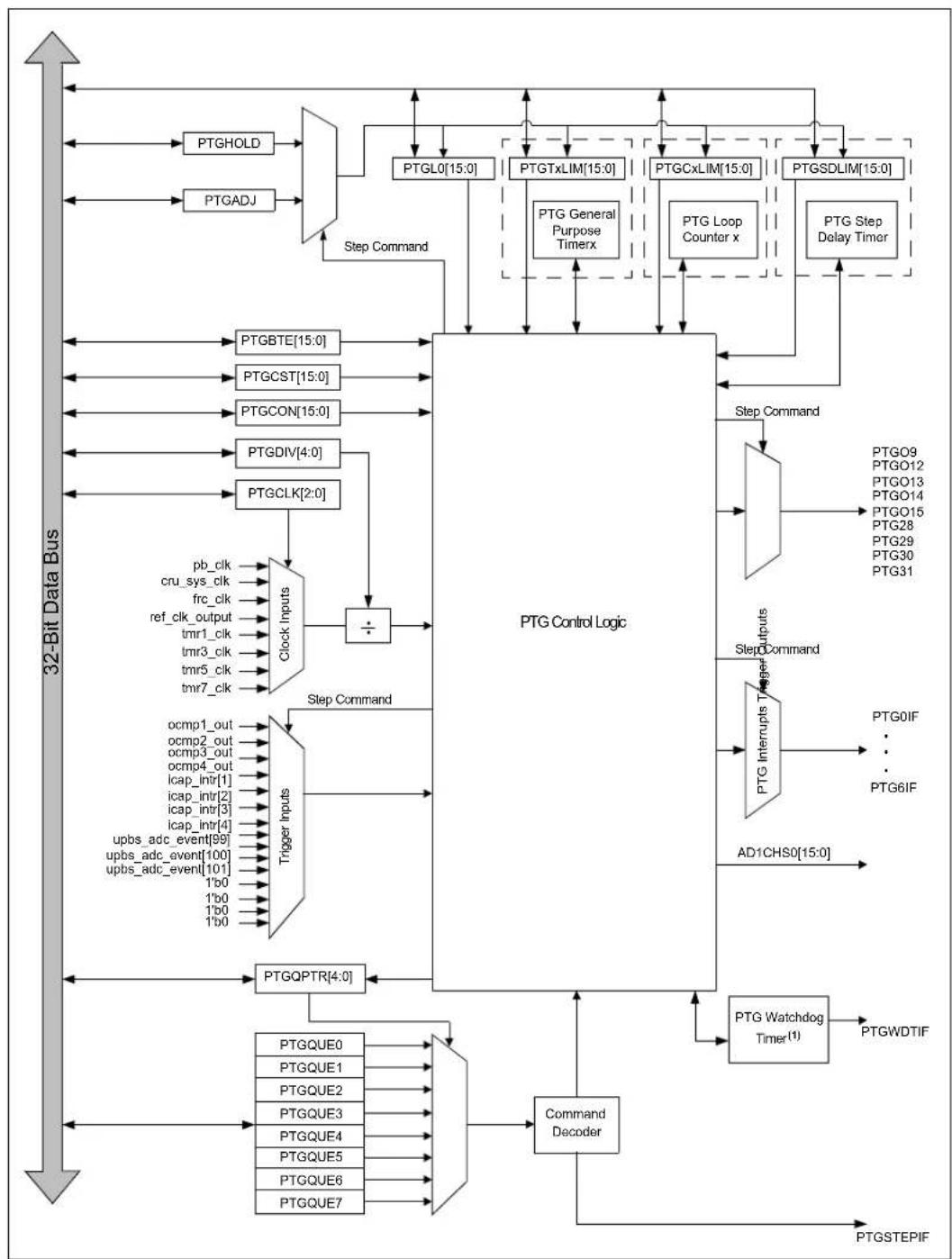
flowchart
graph TD
    A["PTGHOLD"] --> B["PTGADJ"]
    B --> C["PTGBTE[15:0"]]
    C --> D["PTGCST[15:0"]]
    D --> E["PTGCON[15:0"]]
    E --> F["PTGDIV[4:0"]]
    F --> G["PTGCLK[2:0"]]
    G --> H["Clock Inputs"]
    H --> I["PTGControl Logic"]
    I --> J["PTGLO[15:0"]]
    I --> K["PTGTxLIM[15:0"]]
    I --> L["PTGCxLIM[15:0"]]
    I --> M["PTGSDLIM[15:0"]]
    I --> N["PTGGeneral Purpose Timerx"]
    I --> O["PTGLoop Counter x"]
    I --> P["PTGStep Delay Timer"]
    I --> Q["PTGOP9 PTGO12 PTGO13 PTGO14 PTGO15 PTG28 PTG29 PTG30 PTG31"]
    Q --> R["PTGOP9 PTGO12 PTGO13 PTGO14 PTGO15 PTG28 PTG29 PTG30 PTG31"]
    I --> S["PTGOP9 PTGO12 PTGO13 PTGO14 PTGO15 PTG28 PTG29 PTG30 PTG31"]
    S --> T["PTGOP9 PTGO12 PTGO13 PTGO14 PTGO15 PTG28 PTG29 PTG30 PTG31"]
    U["ptg_clk"] --> V["Clock Inputs"]
    W["cru_sys_clk"] --> V
    X["frc_clk"] --> V
    Yeref_clk_output] --> V
    Z["tmr1_clk"] --> V
    AA["tmr3_clk"] --> V
    AB["tmr5_clk"] --> V
    AC["tmr7_clk"] --> V
    AD["pb_clk"] --> V
    AE["ocmp1_out"] --> AF["Trigger Inputs"]
    AG["ocmp2_out"] --> AF
    AH["ocmp3_out"] --> AF
    AI["ocmp4_out"] --> AF
    AJ["icap_intr[1"]] --> AF
    AK["icap_intr[2"]] --> AF
    AL["icap_intr[3"]] --> AF
    AM["icap_intr[4"]] --> AF
    AN["upbs_adc_event[99"]] --> AF
    AO["upbs_adc_event[100"]] --> AF
    AP["upbs_adc_event[101"]] --> AF
    AQ["1'b0"] --> AF
    AR["1'b0"] --> AF
    AS["1'b0"] --> AF
    AT["PTGQPTR[4:0"]] --> AF
    AU["PTGQUE0"] --> AV["Command Decoder"]
    AW["PTGQUE1"] --> AV
    AX["PTGQUE2"] --> AV
    AY["PTGQUE3"] --> AV
    AZ["PTGQUE4"] --> AV
    BA["PTGQUE5"] --> AV
    BB["PTGQUE6"] --> AV
    BC["PTGQUE7"] --> AV
    AD --> AD
    AE --> AD
    AF --> AD
    AG --> AD
    AH --> AD
    AI --> AD
    AJ --> AD
    AK --> AD
    AL --> AD
    AM --> AD
    AN --> AD
    AU --> AD
    AV --> AD
    AV --> AD
    AD --> AD_Steps_Output
    AD_Steps_Output --> AD_Steps_Days_Output
    AD_Steps_Days_Output --> AD_Steps_Peak_Output
    AD_Steps_Peak_Output --> AD_Steps_Rate_Output
    AD_Steps_Rate_Output --> AD_Steps_Terap_Output
    AD_Steps_Terap_Output --> AD_Steps_Ur/Yr_Output
    AD_Steps_Ur/Yr_Output --> AD_Steps_Terap_Terap_Output
    AD_Steps_Terap_Terap_Output --> AD_Steps_Rate_Terap_Terap_Output
    AD_Steps_Rate_Terap_Terap_Output --> AD_Steps_Terap_Terap_Terap_Output
    AD_Steps_Terap_Terap_Terap_Output --> AD_Steps_Rate_Terap_Terap_Terap_Output
    AD_Steps_Rate_Terap_Terap_Terap_Output --> AD_Steps_Rate_Terap_Terap_Terap_Output
    AD_Steps_Rate_Terap_Terap_Terap_Output --> AD_Steps_Rate_Terap_Terap_Terap_Output
    AD_Steps_Rate_Terap_Terap_Terap_Output --> AD_Steps_Rate_Terap_Terap_Terap_Output
Note 1: This is a dedicated WDT for the PTG module and is independent of the device WDT.
14.1 PTG Control Registers
TABLE 14-1: PTG CONTROL REGISTER MAP
| Virtual Address (BF80 #) | Register Name | Bit Range | Bits | All Resets | |||||||||||||||||||
| 31/15 | 30/14 | 29/13 | 28/12 | 27/1 | 11 | 26/10 | 25/9 | 24/8 | 23/7 | 22/6 | 21/5 | 20/4 | 19/3 | 18/2 | 17/1 | 16/0 | |||||||
| 1C00 | PTGCON | 31:16 | PTGCLK[2:0] | PTGDIV[4:0] | PTGPWD[3:0] | — | PTGWDT[2:0] | 0000 | |||||||||||||||
| 15:0 | PTGON | — | PTGSIDL | PTGTOGL | — | PTGSWT | PTGSSEN | PTGIVIS | PTGSTRT | PTGWDTO | PTGBUSY | — | — | — | PTGITM[1:0] | 0000 | |||||||
| 1C10 | PTGBTE | 31:16 | PTGBTE[31:16] | 0000 | |||||||||||||||||||
| 15:0 | PTGBTE[15:0] | 0000 | |||||||||||||||||||||
| 1C20 | PTGHOLD | 31:16 | — | — | — | — | — | — | — | — | — | — | — | — | — | 0000 | |||||||
| 15:0 | PTGHOLD[15:0] | 0000 | |||||||||||||||||||||
| 1C30 | PTGTOLIM | 31:16 | — | — | — | — | — | — | — | — | — | — | — | — | — | 0000 | |||||||
| 15:0 | PTGTOLIM[15:0] | 0000 | |||||||||||||||||||||
| 1C40 | PTGT1LIM | 31:16 | — | — | — | — | — | — | — | — | — | — | — | — | — | 0000 | |||||||
| 15:0 | PTGT1LIM[15:0] | 0000 | |||||||||||||||||||||
| 1C50 | PTGSDLIM | 31:16 | — | — | — | — | — | — | — | — | — | — | — | — | — | 0000 | |||||||
| 15:0 | PTGSDLIM[15:0] | 0000 | |||||||||||||||||||||
| 1C60 | PTGCOLIM | 31:16 | — | — | — | — | — | — | — | — | — | — | — | — | — | 0000 | |||||||
| 15:0 | PTGCOLIM[15:0] | 0000 | |||||||||||||||||||||
| 1C70 | PTGC1LIM | 31:16 | — | — | — | — | — | — | — | — | — | — | — | — | — | 0000 | |||||||
| 15:0 | PTGC1LIM[15:0] | 0000 | |||||||||||||||||||||
| 1C80 | PTGADJ | 31:16 | — | — | — | — | — | — | — | — | — | — | — | — | — | 0000 | |||||||
| 15:0 | PTGADJ[15:0] | 0000 | |||||||||||||||||||||
| 1C90 | PTGL0 | 31:16 | — | — | — | — | — | — | — | — | — | — | — | — | — | 0000 | |||||||
| 15:0 | PTGL0[15:0] | 0000 | |||||||||||||||||||||
| 1CA0 | PTGQPTR | 31:16 | — | — | — | — | — | — | — | — | — | — | — | — | — | 0000 | |||||||
| 15:0 | — | — | — | — | — | — | — | — | — | PTGQPTR[5:0] | 0000 | ||||||||||||
| 1CC0 | PTGQUE0 | 31:16 | STEP3[7:0] | STEP2[7:0] | 0000 | ||||||||||||||||||
| 15:0 | STEP1[7:0] | STEP0[7:0] | 0000 | ||||||||||||||||||||
| 1CD0 | PTGQUE1 | 31:16 | STEP7[7:0] | STEP6[7:0] | 0000 | ||||||||||||||||||
| 15:0 | STEP5[7:0] | STEP4[7:0] | 0000 | ||||||||||||||||||||
| 1CE0 | PTGQUE2 | 31:16 | STEP11[7:0] | STEP10[7:0] | 0000 | ||||||||||||||||||
| 15:0 | STEP9[7:0] | STEP8[7:0] | 0000 | ||||||||||||||||||||
| 1CFO | PTGQUE3 | 31:16 | STEP16[7:0] | STEP14[7:0] | 0000 | ||||||||||||||||||
| 15:0 | STEP13[7:0] | STEP12[7:0] | 0000 | ||||||||||||||||||||
| 1D00 | PTGQUE4 | 31:16 | STEP19[7:0] | STEP18[7:0] | 0000 | ||||||||||||||||||
| 15:0 | STEP17[7:0] | STEP16[7:0] | 0000 | ||||||||||||||||||||
Legend: x = unknown value on Reset; — = unimplemented, read as '0'. Reset values are shown in hexadecimal.
Note 1: All registers have corresponding CLR, SET and INV registers at its virtual address, plus an offset of 0x4, 0x8, and 0xC, respectively. See Section 13.3 "CLR, SET and INV Registers" for more information.
TABLE 14-1: PTG CONTROL REGISTER MAP (CONTINUED)
| Virtual Address (BF80_#) | Register Name | Bit Range | Bits | All Resets | |||||||||||||||
| 31/15 | 30/14 | 29/13 | 28/12 | 27/11 | 26/10 | 25/9 | 24/8 | 23/7 | 22/6 | 21/5 | 20/4 | 19/3 | 18/2 | 17/1 | 16/0 | ||||
| 1D10 | PTGQUE5 | 31:16 | STEP23[7:0] | STEP22[7:0] | 0000 | ||||||||||||||
| 15:0 | TEP21[7:0] | STEP20[7:0] | 0000 | ||||||||||||||||
| 1D20 | PTGQUE6 | 31:16 | STEP27[7:0] | STEP26[7:0] | 0000 | ||||||||||||||
| 15:0 | TEP25[7:0] | STEP24[7:0] | 0000 | ||||||||||||||||
| 1D30 | PTGQUE7 | 31:16 | STEP31[7:0] | STEP30[7:0] | 0000 | ||||||||||||||
| 15:0 | $TEP29[7:0] | STEP28[7:0] | 0000 | ||||||||||||||||
Legend: x = unknown value on Reset; — = unimplemented, read as '0'. Reset values are shown in hexadecimal.
Note 1: All registers have corresponding CLR, SET and INV registers at its virtual address, plus an offset of 0x4, 0x8, and 0xC, respectively. See Section 13.3 "CLR, SET and INV Registers" for more information.
REGISTER 14-1: PTGCON: PTG CONTROL REGISTER
| Bit Range | Bit 31/23/15/7 | Bit 30/22/14/6 | Bit 29/21/13/5 | Bit 28/20/12/4 | Bit 27/19/11/3 | Bit 26/18/10/2 | Bit 25/17/9/1 | Bit 24/16/8/0 |
| 31:24 | R/W-0 R/W | W-0 R/W-0 R/W | 0 R/W-0 R/W-0 | R/W-0 R/W-0 | ||||
| PTGCLK[2:0](1) | PTGDIV[4:0](1) | |||||||
| 23:16 | R/W-0 R/W | W-0 R/W-0 R/W | 0 U-0 R/W-0 R | R/W-0 R/W-0 | ||||
| PTGPWD[3:0](1) | — PTGWDT[2:0] (1) | |||||||
| 15:8 | R/W-0 R/W | W-0 R/W-0 R/W | 0 U-0 R/W-0, | HC R/W-0 R/W-0 | ||||
| PTGON | — | PTGSIDL | PTGTOGL(1) | RSVD | PTGSWT | PTGSSEN(3) | PTGIVIS(1) | |
| 7:0 | R/W-0, HC | PTGWDTO(1) | R-0, HS/HC | U-0 | U-0 | U-0 | R-0 | R-0 |
| PTGSTRT | PTGBUSY | — | — | — | PTGITM[1:0](1) | |||
| Legend: | HC = Hardware Cleared | HS = Hardware Set | |
| R = Readable bit | W = Writable bit | U = Unimplemented bit, read as ‘0’ | |
| -n = Value at POR | ‘1’ = Bit is set | ‘0’ = Bit is cleared | x = Bit is unknown |
bit 31-29 PTGCLK[2:0]: PTG Module Clock Source Select bits ^(1)
111 = PTG module clock source will be REF_CLK
110 = PTG module clock source will be TMR7_CLK
101 = PTG module clock source will be TMR5_CLK
100 = PTG module clock source will be TMR3_CLK
011 = PTG module clock source will be TMR1_CLK
010 = PTG module clock source will be FRC_CLK
001 = PTG module clock source will be SYS_CLK
000 = PTG module clock source will be PB1_CLK
bit 28-24 PTGDIV[4:0]: PTG Module Clock Prescaler (Divider) bits ^(1)
11111 = Divide by 32
11110 = Divide by 31
•
•
•
00001 = Divide by 2
00000 = Divide by 1
bit 23-20 PTGPWD[3:0]: PTG Trigger Output Pulse Width bits ^(1)
1111 = All trigger outputs are 16 PTG clock cycles wide
1110 = All trigger outputs are 15 PTG clock cycles wide
•
•
•
0001 = All trigger outputs are 2 PTG clock cycles wide
0000 = All trigger outputs are 1 PTG clock cycle wide
bit 19 Unimplemented: Read as '0'
Note 1: These bits are read only when the module is executing step command (PTGSTRT = 1).
2: The PTGSSEN bit may only be written when in Debug mode, and will otherwise always read '0'. The PTGSSEN bit (internal) value is preserved independent of Debug mode.
REGISTER 14-1: PTGCON: PTG CONTROL REGISTER (CONTINUED)
bit 18-16 PTGWDT[2:0]: PTG Watchdog Time-Out Count Value Select bits ^(1)
111 = Watchdog will timeout after 512 PTG clocks
110 = Watchdog will timeout after 256 PTG clocks
101 = Watchdog will timeout after 128 PTG clocks
100 = Watchdog will timeout after 64 PTG clocks
011 = Watchdog will timeout after 32 PTG clocks
010 = Watchdog will timeout after 16 PTG clocks
001 = Watchdog will timeout after 8 PTG clocks
000 = Watchdog disabled
bit 15 PTGON: Module Enable bit
1 = PTG module is enabled
0 = PTG module is disabled
bit 14 Unimplemented: Read as '0'
bit 13 PTGSIDL: Stop in Idle Mode bit
1 = Discontinue module operation when device enters Idle mode (act as if in Sleep mode)
0 = Continue module operation when device enters Idle mode
bit 12 PTGTOGL: TRIG Output Toggle Mode bit (1)
1 = Toggle state of the PTGOx for each execution of the PTGTRIG command
0 = Each execution of the PTGTRIG command will generate a single PTGOx pulse determined by the value in the PTGPWDx bits
bit 11 Unimplemented: Read as '0'
bit 10 PTGSWT: Software Trigger bit
This control bit enables the application software to interact with the PTG module via the "Wait for software trigger" step commands (PTGCTRL SWTRGE or PTGCTRL SWTRGL). The PTGCTRL SWTRGE command is only sensitive to a 0 to 1 transition of the PTGSWT bit that occurs during execution of the command. The PTGCTRL SWTRGL command is sensitive to a logic 1 state of the PTGSWT bit that is present prior to and during, or occurs during, execution of the command.
1 = If the PTG state machine is executing the PTGCTRL SWTRGE command and PTGSWT = 0 prior to the bit set operation, the command will complete and execution will continue. If PTGSWT = 1 prior to the bit set operation, no action.
If the PTG state machine is executing the PTGCTRL SWTRGL command, the command will complete and execution will continue irrespective of when the bit set operation occurred. 0 = No action other than to clear the bit ^(2) .
Note 1: Software may write '1' to the PTGSWT bit to initiate the software trigger. Writing '0' (at any time) will have no effect.
2: PTGSWT is automatically cleared by hardware when the PTGCTRL SWTRGE command completes after the associated step delay, if any (when the subsequent command starts). PTGSWT is not automatically cleared by hardware when the PTGCTRL SWTRGL command completes.
3: PTGSWT is cleared when PTGON = 0.
4: If executing the SWTRGE command consecutively, the hardware does not clear the PTGSWT bit. The user application must use any other command or NOP command in between two SWTRGE commands.
bit 9 PTGSSEN: Enable Single Step bit (2)
If in Debug mode:
1 = Enable command Single Step mode
0 = Disable command Single Step mode
Otherwise, the PTGSSEN bit will have no effect.
Note: The PTGSSEN bit may only be written when in Debug mode, and will otherwise always read '0'.
REGISTER 14-1: PTGCON: PTG CONTROL REGISTER (CONTINUED)
Note 1: These bits are read only when the module is executing step command (PTGSTRT = 1).
2: The PTGSSEN bit may only be written when in Debug mode, and will otherwise always read '0'. The PTGSSEN bit (internal) value is preserved independent of Debug mode.
bit 8 PTGIVIS: Counter/Timer Internal Visibility Control bit ^(1)
1 = SFR read of the PTGSDLIM, PTGCnLIM or PTGTnLIM registers will yield the contents of the corresponding internal timer/counter (PTGSD, PTGCn or PTGTn, respectively)
0 = SFR read of the PTGSDLIM, PTGCnLIM or PTGTnLIM registers will yield the contents of the associated SFR register, and represents the value previously written to the target register.
The register read will be either the UPB or internal register as determined by the PTGSTART bit.
Note 1: The PTGIVIS bit enables the user to "debug" the setup and operation of the PTG module in an application.
bit 7 PTGSTRT: Start PTG Sequencer bit
If not in Single Step mode:
1 = Start PTG sequencer and sequentially execute commands (Continuous mode)
0 = Stop PTG sequencer and place in Halt state
If in Single Step mode:
1 = Start PTG sequencer and execute one step command, and then halt
Note: Single step enable must be set (PTGSSEN = 1) prior to the bit set operation of PTGSTRT.
0 = Stop PTG sequencer and place in HALT state
Note 1: In Single Step mode (PTGSSEN = 1), PTGSTRT is automatically cleared by hardware when the target command completes after the associated step delay, if any (when the subsequent command starts).
2: The PTGSTRT bit is not hardware cleared when the PTGON bit is disabled. The user must ensure to clear PTGSTRT bit before clearing (disable) the PTGON bit. Not following the above sequence to clear these register bits can cause the device to behave incorrectly when the PTG is re-enabled.
3: This bit can be hardware clearable by the PTG WDT.
bit 6 PTGWDTO: PTG State Machine Watchdog Timeout Status bit ^(1)
1 = PTG state machine watchdog has timed out
0 = PTG state machine watchdog has not timed out
Note: PTGWDTO is automatically set by hardware but must be cleared by the user or by disabling the module (PTGON = 0).
bit 5 PTGBUSY: PTG State Machine Busy bit
1 = PTG state machine is running on the selected PTG clock source instructions - No SFR writes are allowed to PTGCLK and PTBDIV bit fields.
0 = PTG state machine is NOT running.
Note: PTGBUSY is asserted when PTGON = 1 to indicate PTG is busy running, it will be cleared by HW once sequencer has completed all the tasks when PTGON is cleared.
bit 4-2 Unimplemented: Read as '0'
bit 1-0 PTGITM[1:0]: Selects PTG Input Trigger Command Operating Mode bits ^(1)
11 = Test input state once per step delay, exit when (level) true and complete command without step delay.
10 = Test input state once per step delay, exit when (level) true to step delay prior to command completion.
01 = Test input state continuously, exit when valid edge detected (during execution) and complete command without step delay.
00 = Test input state continuously, exit to step delay when valid edge detected (during execution), prior to command completion.
Note 1: These bits are read only when the module is executing step command (PTGSTRT = 1).
2: The PTGSSEN bit may only be written when in Debug mode, and will otherwise always read '0'. The PTGSSEN bit (internal) value is preserved independent of Debug mode.
REGISTER 14-2: PTGBTE: PTG BROADCAST TRIGGER ENABLE REGISTER
| Bit Range | Bit 31/23/15/7 | Bit 30/22/14/6 | Bit 29/21/13/5 | Bit 28/20/12/4 | Bit 27/19/11/3 | Bit 26/18/10/2 | Bit 25/17/9/1 | Bit 24/16/8/0 |
| 31:24 | R/W-0 R/W | -0 R/W-0 R/W | -0 R/W-0 R/W-0 | R/W-0 R/W-0 | ||||
| PTGBTE[31:24](1) | ||||||||
| 23:16 | R/W-0 R/W | -0 R/W-0 R/W | -0 R/W-0 R/W-0 | R/W-0 R/W-0 | ||||
| PTGBTE[23:16](1) | ||||||||
| 15:8 | R/W-0 R/W | -0 R/W-0 R/W | -0 R/W-0 R/W-0 | R/W-0 R/W-0 | ||||
| PTGBTE[15:8](1) | ||||||||
| 7:0 | R/W-0 R/W | -0 R/W-0 R/W | -0 R/W-0 R/W-0 | R/W-0 R/W-0 | ||||
| PTGBTE[7:0](1) | ||||||||
Legend:
R = Readable bit W = Writable bit U = Unimplemented bit, read as '0'
-n = Value at POR '1' = Bit is set '0' = Bit is cleared x = Bit is unknown
bit 31-0 PTGBTE[31:0]: Broadcast Trigger Enable Register bits ^(1)
Each bit corresponds to a individual trigger output. If a bit is set in the PTGBTE register, the corresponding individual trigger output will be generated if a step broadcast command is executed.
Note 1: These bits are read only when the module is executing step commands (PTGSTRT = 1).
REGISTER 14-3: PTGHOLD: PTG HOLD REGISTER
| Bit Range | Bit 31/23/15/7 | Bit 30/22/14/6 | Bit 29/21/13/5 | Bit 28/20/12/4 | Bit 27/19/11/3 | Bit 26/18/10/2 | Bit 25/17/9/1 | Bit 24/16/8/0 |
| 31:24 | U-0 U-0 U | -U-0 U-0 U-0 | U-0 U-0 | |||||
| ——— | ——— | |||||||
| 23:16 | U-0 U-0 U | -U-0 U-0 U-0 | U-0 U-0 | |||||
| ——— | ——— | |||||||
| 15:8 | R/W-0 | R/W-0 | R/W-0 | R/W-0 | R/W-0 | R/W-0 | R/W-0 | R/W-0 |
| PTGHOLD[15:8](1) | ||||||||
| 7:0 | R/W-0 | R/W-0 | R/W-0 | R/W-0 | R/W-0 | R/W-0 | R/W-0 | R/W-0 |
| PTGHOLD[7:0](1) | ||||||||
| Legend: | |||
| R = Readable bit | W = Writable bit | U = Unimplemented bit, read as ‘0’ | |
| -n = Value at POR | ‘1’ = Bit is set | ‘0’ = Bit is cleared | x = Bit is unknown |
bit 31-16 Unimplemented: Read as '0'
bit 15-0 PTGHOLD[15:0]: General Purpose Hold Register bits ^(1)
Preserves a copy of user supplied data for re-initializing one of the following registers, PTGT0LIM, PTGT1LIM, PTGC0LIM, PTGC1LIM, PTGSDLIM, and PTGL0 via a step command.
Note 1: These bits are read only when the module is executing step commands (PTGSTRT = 1).
REGISTER 14-4: PTGT0LIM: PTG TIMER0 LIMIT REGISTER
| Bit Range | Bit 31/23/15/7 | Bit 30/22/14/6 | Bit 29/21/13/5 | Bit 28/20/12/4 | Bit 27/19/11/3 | Bit 26/18/10/2 | Bit 25/17/9/1 | Bit 24/16/8/0 |
| 31:24 | U-0 U-0 U | -U-0 U-0 U-0 | U-0 U-0 | |||||
| ——— | ——— — | |||||||
| 23:16 | U-0 U-0 U | -U-0 U-0 U-0 | U-0 U-0 | |||||
| ——— | ——— — | |||||||
| 15:8 | R/W-1 | R/W-1 | R/W-1 | R/W-1 | R/W-1 | R/W-1 | R/W-1 | R/W-1 |
| PTGTOLIM[15:8](1) | ||||||||
| 7:0 | R/W-1 | R/W-1 | R/W-1 | R/W-1 | R/W-1 | R/W-1 | R/W-1 | R/W-1 |
| PTGTOLIM[7:0](1) | ||||||||
Legend:
| R = Readable bit | W = Writable bit | U = Unimplemented bit, read as '0' |
| -n = Value at POR | '1' = Bit is set | '0' = Bit is cleared x = Bit is unknown |
bit 31-16 Unimplemented: Read as '0'
bit 15-0 PTGTOLIM[15:0]: PTG (GP) Timer0 Limit Register bits ^(1)
General Purpose Timer0 Limit register (effective only with a "Wait for GP Timer0" step command).
Note 1: These bits are read only when the module is executing step commands (PTGSTRT = 1).
REGISTER 14-5: PTGT1LIM: PTG TIMER1 LIMIT REGISTER
| Bit Range | Bit 31/23/15/7 | Bit 30/22/14/6 | Bit 29/21/13/5 | Bit 28/20/12/4 | Bit 27/19/11/3 | Bit 26/18/10/2 | Bit 25/17/9/1 | Bit 24/16/8/0 |
| 31:24 | U-0 U-0 U | -U-0 U-0 U-0 | U-0 U-0 | |||||
| ——— | ——— | |||||||
| 23:16 | U-0 U-0 U | -U-0 U-0 U-0 | U-0 U-0 | |||||
| ——— | ——— | |||||||
| 15:8 | R/W-0 | R/W-0 | R/W-0 | R/W-0 | R/W-0 | R/W-0 | R/W-0 | R/W-0 |
| PTGT1LIM[15:8](1) | ||||||||
| 7:0 | R/W-0 | R/W-0 | R/W-0 | R/W-0 | R/W-0 | R/W-0 | R/W-0 | R/W-0 |
| PTGT1LIM[7:0](1) | ||||||||
| Legend: | |||
| R = Readable bit | W = Writable bit | U = Unimplemented bit, read as ‘0’ | |
| -n = Value at POR | ‘1’ = Bit is set | ‘0’ = Bit is cleared | x = Bit is unknown |
bit 31-16 Unimplemented: Read as '0'
bit 31-0 PTGT1LIM[15:0]: PTG (GP) Timer1Limit Register bits ^(1)
General Purpose Timer1 Limit register (effective only with a "Wait for GP Timer1" step command).
Note 1: These bits are read only when the module is executing step commands (PTGSTRT = 1).
REGISTER 14-6: PTGSDLIM: PTG STEP DELAY LIMIT REGISTER
| Bit Range | Bit 31/23/15/7 | Bit 30/22/14/6 | Bit 29/21/13/5 | Bit 28/20/12/4 | Bit 27/19/11/3 | Bit 26/18/10/2 | Bit 25/17/9/1 | Bit 24/16/8/0 |
| 31:24 | U-0 U-0 U | -U-0 U-0 U-0 | U-0 U-0 | |||||
| ——— | ——— | |||||||
| 23:16 | U-0 U-0 U | -U-0 U-0 U-0 | U-0 U-0 | |||||
| ——— | ——— | |||||||
| 15:8 | R/W-0 | R/W-0 | R/W-0 | R/W-0 | R/W-0 | R/W-0 | R/W-0 | R/W-0 |
| PTGSDLIM[15:8](1) | ||||||||
| 7:0 | R/W-0 | R/W-0 | R/W-0 | R/W-0 | R/W-0 | R/W-0 | R/W-0 | R/W-0 |
| PTGSDLIM[7:0](1) | ||||||||
Legend:
| R = Readable bit | W = Writable bit | U = Unimplemented bit, read as '0' |
| -n = Value at POR | '1' = Bit is set | '0' = Bit is cleared x = Bit is unknown |
bit 31-6 Unimplemented: Read as '0'
bit 15-0 PTGSDLIM[15:0]: PTG Step Delay Limit Register bits ^(1)
Holds a PTG step delay value representing the number of additional PTG clocks between the start of a step command, and the completion of the step command.
A base delay of a command is one PTG clock period, and the PTG step delay value is added to this minimum command delay to create the total step command duration. That is, if PTGSDLIM = 0x0006, the resultant step command duration will be 7 PTG clocks.
Note 1: These bits are read only when the module is executing step commands (PTGSTRT = 1).
REGISTER 14-7: PTGC0LIM: PTG COUNTER '0' LIMIT REGISTER
| Bit Range | Bit 31/23/15/7 | Bit 30/22/14/6 | Bit 29/21/13/5 | Bit 28/20/12/4 | Bit 27/19/11/3 | Bit 26/18/10/2 | Bit 25/17/9/1 | Bit 24/16/8/0 |
| 31:24 | U-0 U-0 U | -U-0 U-0 U-0 | U-0 U-0 | |||||
| ——— | ——— | |||||||
| 23:16 | U-0 U-0 U | -U-0 U-0 U-0 | U-0 U-0 | |||||
| ——— | ——— | |||||||
| 15:8 | R/W-0 | R/W-0 | R/W-0 | R/W-0 | R/W-0 | R/W-0 | R/W-0 | R/W-0 |
| PTGCOLIM[15:8](1) | ||||||||
| 7:0 | R/W-0 | R/W-0 | R/W-0 | R/W-0 | R/W-0 | R/W-0 | R/W-0 | R/W-0 |
| PTGCOLIM[7:0](1) | ||||||||
| Legend: | |||
| R = Readable bit | W = Writable bit | U = Unimplemented bit, read as ‘0’ | |
| -n = Value at POR | ‘1’ = Bit is set | ‘0’ = Bit is cleared | x = Bit is unknown |
bit 31-16 Unimplemented: Read as '0'
bit 15-0 PTGC0LIM[15:0]: PTG Counter '0' Limit Register bits ^(1)
These bits can be used to specify the loop count for the PTGJMPC0 step command, or as a general purpose counter limit register.
Note 1: These bits are read only when the module is executing step commands (PTGSTRT = 1).
REGISTER 14-8: PTGC1LIM: PTG COUNTER '1' LIMIT REGISTER
| R = Readable bit | W = Writable bit | U = Unimplemented bit, read as '0' |
| -n = Value at POR | '1' = Bit is set | '0' = Bit is cleared x = Bit is unknown |
bit 31-16 Unimplemented: Read as '0'
bit 31-0 PTGC1LIM[31:0]: PTG Counter '1' Limit Register bits ^(1)
These bits can be used to specify the loop count for the PTGJMPC1 step command, or as a general purpose counter limit register.
Note 1: These bits are read only when the module is executing step commands (PTGSTRT = 1).
REGISTER 14-9: PTGADJ: PTG ADJUST REGISTER
| Bit Range | Bit 31/23/15/7 | Bit 30/22/14/6 | Bit 29/21/13/5 | Bit 28/20/12/4 | Bit 27/19/11/3 | Bit 26/18/10/2 | Bit 25/17/9/1 | Bit 24/16/8/0 |
| 31:24 | U-0 U-0 U | -0 U-0 U-0 U-0 | U-0 U-0 | |||||
| ——— | ——— | |||||||
| 23:16 | U-0 U-0 U | -0 U-0 U-0 U-0 | U-0 U-0 | |||||
| ——— | ——— | |||||||
| 15:8 | R/W-0 | R/W-0 | R/W-0 | R/W-0 | R/W-0 | R/W-0 | R/W-0 | R/W-0 |
| PTGADJ[15:8](1) | ||||||||
| 7:0 | R/W-0 | R/W-0 | R/W-0 | R/W-0 | R/W-0 | R/W-0 | R/W-0 | R/W-0 |
| PTGADJ[7:0](1) | ||||||||
Legend:
| R = Readable bit | W = Writable bit | U = Unimplemented bit, read as '0' |
| -n = Value at POR | '1' = Bit is set | '0' = Bit is cleared x = Bit is unknown |
bit 31-16 Unimplemented: Read as '0'
bit 15-0 PTGADJ[15:0]: PTG Adjust Register bits ^(1)
A register that is used by the PTGADD step command to adjust the contents of one of the following registers, PTGT0LIM, PTGT1LIM, PTGC0LIM, PTGC1LIM, PTGSDLIM, and PTGL0. The PTGADD step command adds the contents of the PTGADJ[15:0] register to the target register, and then writes it back to the target register.
Note 1: These bits are read only when the module is executing step commands (PTGSTRT = 1).
REGISTER 14-10: PTGL0: PTG LITERAL REGISTER
| Bit Range | Bit 31/23/15/7 | Bit 30/22/14/6 | Bit 29/21/13/5 | Bit 28/20/12/4 | Bit 27/19/11/3 | Bit 26/18/10/2 | Bit 25/17/9/1 | Bit 24/16/8/0 |
| 31:24 | U-0 U-0 U | -U-0 U-0 U-0 | U-0 U-0 | |||||
| ——— | ——— | |||||||
| 23:16 | U-0 U-0 U | -U-0 U-0 U-0 | U-0 U-0 | |||||
| ——— | ——— | |||||||
| 15:8 | R/W-0 | R/W-0 | R/W-0 | R/W-0 | R/W-0 | R/W-0 | R/W-0 | R/W-0 |
| PTGL0[15:8](1) | ||||||||
| 7:0 | R/W-0 | R/W-0 | R/W-0 | R/W-0 | R/W-0 | R/W-0 | R/W-0 | R/W-0 |
| PTGL0[7:0](1) | ||||||||
Legend:
| R = Readable bit | W = Writable bit | U = Unimplemented bit, read as '0' |
| -n = Value at POR | '1' = Bit is set | '0' = Bit is cleared x = Bit is unknown |
bit 31-16 Unimplemented: Read as '0'
bit 15-0 PTGL0[15:0]: PTG Literal Register bits ^(1)
This register holds the 16-bit literal value that is strobed when the PTGCTRL STRBL0 command is executed.
Note 1: These bits are read only when the module is executing step commands (PTGSTRT = 1).
REGISTER 14-11: PTGQPTR: PTG STEP QUEUE POINTER REGISTER
| Bit Range | Bit 31/23/15/7 | Bit 30/22/14/6 | Bit 29/21/13/5 | Bit 28/20/12/4 | Bit 27/19/11/3 | Bit 26/18/10/2 | Bit 25/17/9/1 | Bit 24/16/8/0 |
| 31:24 | U-0 U-0 U | -0 U-0 U-0 U-0 | U-0 U-0 | |||||
| —— — | —— — — | |||||||
| 23:16 | U-0 U-0 U | -0 U-0 U-0 U-0 | U-0 U-0 | |||||
| —— — | —— — — | |||||||
| 15:8 | U-0 U-0 U | -0 U-0 U-0 U-0 | U-0 U-0 | |||||
| —— — | —— — — | |||||||
| 7:0 | U-0 U-0 U | -0 R/W-0 R/W-0 | R/W-0 R/W-0 | R/W-0 | ||||
| —— — | PTGQPTR[4:0] (1) | |||||||
Legend:
| R = Readable bit | W = Writable bit | U = Unimplemented bit, read as '0' |
| -n = Value at POR | '1' = Bit is set | '0' = Bit is cleared x = Bit is unknown |
bit 31-5 Unimplemented: Read as '0'
bit 4-0 PTGQPTR[4:0]: PTG Step Queue Pointer Register bits ^(1)
This register points to the currently active step command in the step queue.
Note 1: These bits are read only when the module is executing step commands (PTGSTRT = 1).
REGISTER 14-12: PTGQUEn: PTG STEP QUEUE 'n' REGISTER ('n' = 0-7)
| Bit Range | Bit 31/23/15/7 | Bit 30/22/14/6 | Bit 29/21/13/5 | Bit 28/20/12/4 | Bit 27/19/11/3 | Bit 26/18/10/2 | Bit 25/17/9/1 | Bit 24/16/8/0 |
| 31:24 | R/W-0 R/W | -0 R/W-0 R/W-0 | R/W-0 R/W-0 | R/W-0 R/W-0 | ||||
| STEP3[15:8]^(1) | ||||||||
| 23:16 | R/W-0 R/W | -0 R/W-0 R/W-0 | R/W-0 R/W-0 | R/W-0 R/W-0 | ||||
| STEP2[7:0]^(1) | ||||||||
| 15:8 | R/W-0 R/W | -0 R/W-0 R/W-0 | R/W-0 R/W-0 | R/W-0 R/W-0 | ||||
| STEP1[15:8]^(1) | ||||||||
| 7:0 | R/W-0 R/W | -0 R/W-0 R/W-0 | R/W-0 R/W-0 | R/W-0 R/W-0 | ||||
| STEP0[7:0]^(1) | ||||||||
Legend:
| R = Readable bit W = Writable bit U = Unimplemented bit, read as '0' | ||
| -n = Value at POR | '1' = Bit is set | '0' = Bit is cleared x = Bit is unknown |
bit 31-24 STEP[4n+3][7:0]: STEP[4n+3] Command Byte bits ^(1)
A queue location for storage of the STEP[4n+3] command byte.
bit 23-16 STEP[4n+2][7:0]: STEP[4n+2] Command Byte bits ^(1)
A queue location for storage of the STEP[4n+2] command byte.
bit 15-8 STEP[4n+1][7:0]: STEP[4n+1] Command Byte bits ^(1)
A queue location for storage of the STEP[4n+1] command byte.
bit 7-0 STEP[4n][7:0]: STEP[4n] Command Byte bits ^(1)
A queue location for storage of the STEP command byte.
Note 1: These bits are read only when the module is executing step commands (PTGSTRT = 1).
TABLE 14-2: PTG OUTPUT DESCRIPTION
| PTG Output Number PTG Output Description | |
| PTGO0 Reserved | |
| PTGO1 Reserved | |
| PTGO2 Reserved | |
| PTGO3 Reserved | |
| PTGO4 Reserved | |
| PTGO5 Reserved | |
| PTGO6 Reserved | |
| PTGO7 Reserved | |
| PTGO8 Reserved | |
| PTGO9 To CVD | |
| PTGO10 Reserved | |
| PTGO11 Reserved | |
| PTGO12 Sample Trigger for ADC | |
| PTGO13 Sample Trigger for ADC | |
| PTGO14 Sample Trigger for ADC | |
| PTGO15 Sample Trigger for ADC | |
| PTGO16 Reserved | |
| PTGO17 Reserved | |
| PTGO18 Reserved | |
| PTGO19 Reserved | |
| PTGO20 Reserved | |
| PTGO21 Reserved | |
| PTGO22 Reserved | |
| PTGO23 Reserved | |
| PTGO24 Reserved | |
| PTGO25 Reserved | |
| PTGO26 Reserved | |
| PTGO27 Reserved | |
| PTGO28 Output Buffer Data | |
| PTGO29 Output Buffer Data | |
| PTGO30 Output Buffer Data | |
| PTGO31 Output Buffer Data | |
Note: PTGO28 to PTGO31 are available on PPS. Refer to Table 13-3.
15.0 TIMER1
| Note: This data sheet summarizes the features of the PIC32MZ1025W104 family of devices. It is not intended to be a comprehensive reference source. To complement the information in this data sheet, refer to Section 14. “Timers” (DS60001105) in the “PIC32 Family Reference Manual”, which is available from the Microchip website (www.microchip.com/PIC32). |
The PIC32MZ1025W104 device features one synchronous/asynchronous 16-bit timer that can operate as a free-running interval timer for various timing applications and counting external events. This timer can also be used with the low-power SOSC for real-time clock applications.
The following modes are supported by Timer1:
- Synchronous Internal Timer mode
- Synchronous Internal Gated Timer mode
- Synchronous External Timer mode
- Asynchronous External Timer mode
Timer1 has the following key features:
- Selectable clock prescaler
- Timer operation during Sleep and Idle modes
- Fast bit manipulation using CLR, SET and INV registers
- Asynchronous mode can be used with the SOSC to function as a real-time clock
- ADC (CVD) event trigger
- Timer1 can be used as a wake up source from the Sleep mode
FIGURE 15-1: TIMER1 BLOCK DIAGRAM
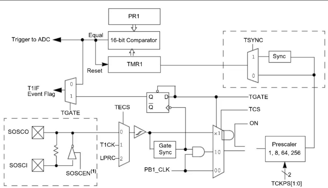
flowchart
graph TD
    A["Trigger to ADC"] --> B["0 1"]
    C["Equal"] --> D["16-bit Comparator"]
    D --> E["TMR1"]
    F["T1IF Event Flag"] --> G["TGATE"]
    G --> H["TECS"]
    H --> I["Q/Q"]
    I --> J["Gate Sync"]
    J --> K["×1"]
    K --> L["Transistor"]
    M["TSYNC"] --> N["1 0"]
    O["Sync"] --> P["0"]
    Q["SOSCO"] --> R["SOSCEN(1)"]
    S["SOSCI"] --> T["SOSCEN(1)"]
    U["TGATE"] --> V["Q/Q"]
    W["TECS"] --> X["0 1"]
    Y["Gate Sync"] --> Z["×1"]
    AA["PB1_CLK"] --> AB["0 0"]
    AC["PR1"] --> AD["16-bit Comparator"]
    AE["Reset"] --> AF["TMR1"]
    AG["TSYNCS"] --> AH["1 0"]
    AI["TGATE"] --> AJ["0 1"]
    AK["TCS"] --> AL["ON"]
    AM["Prescaler 1,8,64,256"] --> AN["2 TCKPS[1:0"]]
Note 1: The default state of the SOSCEN bit (OSCCON[1]) during a device Reset is controlled by the SOSCEN bit in Configuration Word and CFGCON4.
15.1 Timer1 Control Register
TABLE 15-1: TIMER1 REGISTER MAP
| Virtual Address(BF80_#) | Register Name 1 | Bit Range | Bits | All Resets | ||||||||||||||||
| 31/15 30 | 14 29/13 | 28/12 27/11 | 26/10 25/9 | 24/8 23/7 | 22/6 21/5 | 20 | 4 19/3 18/2 | 17/1 16/0 | ||||||||||||
| 2000 | T1CON | 31:16 | — — | — — | — — | — — | — C000 | |||||||||||||
| 15:0 ON | — | SIDL | TWDIS | TWIP | — | TECS[1:0] | TGATE | — | TCKPS[1:0] | — | TSYNC | TCS | — | 0000 | ||||||
| 2010 | TMR1 | 31:16 | TMR1[31:16] | 0000 | ||||||||||||||||
| 15:0 | TMR1[15:0] | 0000 | ||||||||||||||||||
| 2020 | PR1 | 31:16 | PR1[31:16] | 0000 | ||||||||||||||||
| 15:0 | PR1[15:0] | FFFF | ||||||||||||||||||
Legend: x = unknown value on Reset; — = unimplemented, read as '0'. Reset values are shown in hexadecimal.
Note 1: All registers in this table have corresponding CLR, SET and INV registers at their virtual addresses, plus offsets of 0x4, 0x8 and 0xC, respectively. See Section 13.3 "CLR, SET and INV Registers" for more information.
2: Continuous CPU write operations to the TMR1 register within 4 PBCLK cycles are restricted.
REGISTER 15-1: T1CON: TYPE A TIMER CONTROL REGISTER
| R = Readable bit | W = Writable bit U = Unimplemented bit, read as '0' | ||
| -n = Value at POR | ‘1’ = Bit is set | ‘0’ = Bit is cleared | x = Bit is unknown |
bit 31-16 Unimplemented: Read as '0'
bit 15 ON: TMR1 bit
1 = TMR1 is enabled
0 = TMR1 is disabled
bit 14 Unimplemented: Read as '0'
bit 13 SIDL: Stop in Idle Mode bit
1 = Discontinue operation when device enters Idle mode
0 = Continue operation even in Idle mode
bit 12 TWDIS: Asynchronous Timer Write Disable bit
1 = Writes to TMR1 are ignored until pending write operation completes
0 = Back-to-back writes are enabled (legacy asynchronous timer functionality)
bit 11 TWIP: Asynchronous Timer Write in Progress bit
In Asynchronous Timer mode:
1 = Asynchronous write to TMR1 register in progress
0 = Asynchronous write to TMR1 register complete
In Synchronous Timer mode:
This bit is read as '0'.
bit 10 Unimplemented: Read as '0'
bit 9-8 TECS[1:0]: TMR1 Extended Clock Select bits
11= Reserved
10=LPRC
01=T1CK pin
00=SOSC
bit 7 TGATE: Timer Gated Time Accumulation Enable bit
When TCS = 1:
This bit is ignored.
When TCS = 0:
1 = Gated time accumulation is enabled
0 = Gated time accumulation is disabled
bit 6 Unimplemented: Read as '0'
REGISTER 15-1: T1CON: TYPE A TIMER CONTROL REGISTER (CONTINUED)
bit 5-4 TCKPS[1:0]: Timer Input Clock Prescale Select bits
11 = 1:256 prescale value
10 = 1:64 prescale value
01 = 1:8 prescale value
00 = 1:1 prescale value
bit 3 Unimplemented: Read as '0'
bit 2 TSYNC: Timer External Clock Input Synchronization Selection bit
When TCS = 1:
1 = External clock input is synchronized
0 = External clock input is not synchronized
When TCS = 0:
This bit is ignored.
bit 1 TCS: Timer Clock Source Select bit
1 = External clock from TECS
0 = Internal peripheral clock
bit 0 Unimplemented: Read as '0'
16.0 TIMER2/3, TIMER4/5, AND TIMER6/7
Note: This data sheet summarizes the features of the PIC32MZ1025W104 family of devices. It is not intended to be a comprehensive reference source. To complement the information in this data sheet, refer to Section 14. "Timers" (DS60001105) of the "PIC32 Family Reference Manual", which is available from the Microchip website (www.microchip.com/PIC32).
The PIC32MZ1025W104 family of devices features six synchronous 16-bit timers (default) that can operate as a free-running interval timer for various timing applications and counting external events.
The following modes are supported:
- Synchronous Internal 16-bit Timer mode
- Synchronous Internal 16-bit Gated Timer mode
- Synchronous External 16-bit Timer mode
Three 32-bit synchronous timers are available by combining Timer2 with Timer3, Timer4 with Timer5, Timer6 with Timer7.
The 32-bit timers can operate in one of three modes:
- Synchronous Internal 32-bit Timer mode
- Synchronous Internal 32-bit Gated Timer mode
- Synchronous External 32-bit Timer mode
These timers have the following key features:
- Selectable clock prescaler
- Timers operational during CPU Idle mode
- Time base for input capture and output compare modules (Timer2 Through Timer7 only)
- ADC event trigger (Timer3 and Timer5 only)
- Fast bit manipulation using CLR, SET, and INV registers
FIGURE 16-1: TIMER2 THROUGH TIMER7 BLOCK DIAGRAM (16-BIT)
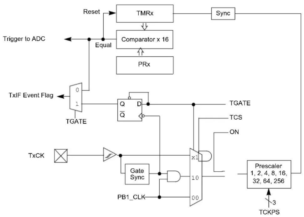
flowchart
graph TD
    A["Trigger to ADC"] --> B["Equal"]
    B --> C["TMRx"]
    C --> D["Comparator x 16"]
    D --> E["PRx"]
    E --> F["TGATE"]
    F --> G["Gate Sync"]
    G --> H["x1"]
    H --> I["ON"]
    I --> J["TCS"]
    J --> K["ON"]
    K --> L["Prescaler 1, 2, 4, 8, 16, 32, 64, 256"]
    L --> M["TCKPS"]
    N["TxIF Event Flag"] --> O["0/1 TGATE"]
    O --> P["Q/Q̅"]
    P --> Q["TGATE"]
    R["TxCK"] --> S["NOT"]
    S --> T["AND Gate"]
    T --> U["Gate Sync"]
    U --> V["AND Gate"]
    V --> W["AND Gate"]
    W --> X["AND Gate"]
    X --> Y["AND Gate"]
    Y --> Z["AND Gate"]
    Z --> AA["AND Gate"]
    AA --> AB["AND Gate"]
    AB --> AC["AND Gate"]
    AC --> AD["AND Gate"]
    AD --> AE["AND Gate"]
    AE --> AF["AND Gate"]
    AF --> AG["AND Gate"]
    AG --> AH["AND Gate"]
    AH --> AI["AND Gate"]
    AI --> AJ["AND Gate"]
    AJ --> AK["AND Gate"]
    AK --> AL["AND Gate"]
    AL --> AM["AND Gate"]
    AM --> AN["AND Gate"]
    AN --> AO["AND Gate"]
    AO --> AP["AND Gate"]
    AP --> AQ["AND Gate"]
    AQ --> AR["AND Gate"]
    AR --> AS["AND Gate"]
    AS --> AT["AND Gate"]
    AT --> AU["AND Gate"]
    AU --> AV["AND Gate"]
    AV --> AW["AND Gate"]
    AW --> AX["AND Gate"]
    AX --> AY["AND Gate"]
    AY --> AZ["AND Gate"]
    AZ --> BA["AND Gate"]
    BA --> BB["AND Gate"]
    BB --> BC["AND Gate"]
    BC --> BD["AND Gate"]
    BD --> BE["AND Gate"]
    BE --> BF["AND Gate"]
    BF --> BG["AND Gate"]
    BG --> BH["AND Gate"]
    BH --> BI["AND Gate"]
    BI --> BJ["AND Gate"]
    BJ --> BK["AND Gate"]
    BK --> BL["AND Gate"]
    BL --> BM["AND Gate"]
    BM --> BN["AND Gate"]
    BN --> BO["AND Gate"]
    BO --> BP["AND Gate"]
    BP --> BQ["TXCKP"]
FIGURE 16-2: TIMER2/3, TIMER4/5, AND TIMER6/7, BLOCK DIAGRAM (32-BIT)
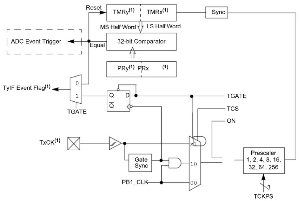
flowchart
graph TD
    A["ADC Event Trigger"] --> B["0"]
    B --> C["TGATE"]
    C --> D["Q"]
    D --> E["Q̅"]
    E --> F["Gate Sync"]
    F --> G["PB1_CLK"]
    G --> H["10"]
    H --> I["×1"]
    I --> J["TXCK(1)"]
    J --> K["TCKPS"]
    K --> L["Prescaler 1, 2, 4, 8, 16, 32, 64, 256"]
    L --> M["TGATE"]
    M --> N["TCS"]
    N --> O["ON"]
    O --> P["3"]
    P --> Q["TCKPS"]
    Q --> R["Reset"]
    R --> S["TMRy(1)"]
    S --> T["TMRx(1)"]
    T --> U["Sync"]
    U --> V["32-bit Comparator"]
    V --> W["Equal"]
    W --> X["MS Half Word"]
    X --> Y["LS Half Word"]
    Y --> Z["PRy(1)"]
    Z --> AA["PRx (1)"]
    AA --> AB["TyIF Event Flag(1)"]
Note 1: In this diagram, 'x' represents Timer2, 4, or 6, and 'y' represents Timer3, 5, or 7.
16.1 Timer2-Timer7 Control Registers
TABLE 16-1: TIMER2 THROUGH TIMER7 REGISTER MAP
Legend: x = unknown value on Reset; — = unimplemented, read as '0'. Reset values are shown in hexadecimal.
Note 1: All registers in this table have corresponding CLR, SET and INV registers at their virtual addresses, plus offsets of 0x4, 0x8 and 0xC, respectively. See Section 13.3 "CLR, SET and INV Registers" for more information.
TABLE 16-1: TIMER2 THROUGH TIMER7 REGISTER MAP (CONTINUED)
Legend: x = unknown value on Reset; — = unimplemented, read as '0'. Reset values are shown in hexadecimal.
Note 1: All registers in this table have corresponding CLR, SET and INV registers at their virtual addresses, plus offsets of 0x4, 0x8 and 0xC, respectively. See Section 13.3 "CLR, SET and INV Registers" for more information.
REGISTER 16-1: TxCON: TYPE B TIMER CONTROL REGISTER (x = 2-7)
| Bit Range | Bit 31/23/15/7 | Bit 30/22/14/6 | Bit 29/21/13/5 | Bit 28/20/12/4 | Bit 27/19/11/3 | Bit 26/18/10/2 | Bit 25/17/9/1 | Bit 24/16/8/0 |
| 31:24 | U-0 U-0 | U-0 U-0 U-0 | U-0 U-0 | |||||
| — — — | — — — — | |||||||
| 23:16 | U-0 U-0 | U-0 U-0 U-0 | U-0 U-0 | |||||
| — — — | — — — — | |||||||
| 15:8 | R/W-0 U-0 | R/W-0 U-0 | U-0 U-0 U-0 | |||||
| ON^(1) | — | SIDL^(2) | — — — | — — | ||||
| 7:0 | R/W-0 | R/W-0 | R/W-0 | R/W-0 | R/W-0 | U-0 | R/W-0 | U-0 |
| TGATE^(1) | TCKPS[2:0]^(1) | T32^(3) | — | TCS^(1) | — | |||
Legend:
| R = Readable bit | W = Writable bit | U = Unimplemented bit, read as '0' |
| -n = Value at POR | '1' = Bit is set | '0' = Bit is cleared x = Bit is unknown |
bit 31-16 Unimplemented: Read as '0'
bit 15 ON: Timer On bit(1)
1 = Module is enabled
0 = Module is disabled
bit 14 Unimplemented: Read as '0'
bit 13 SIDL: Stop in Idle Mode bit ^(2)
1 = Discontinue operation when device enters Idle mode
0 = Continue operation even in Idle mode
bit 12-8 Unimplemented: Read as '0'
bit 7 TGATE: Timer Gated Time Accumulation Enable bit ^(1)
When TCS = 1:
This bit is ignored and is read as '0'.
When TCS = 0:
1 = Gated time accumulation is enabled
0 = Gated time accumulation is disabled
bit 6-4 TCKPS[2:0]: Timer Input Clock Prescale Select bits ^(1)
111 = 1:256 prescale value
110 = 1:64 prescale value
101 = 1:32 prescale value
100 = 1:16 prescale value
011 = 1:8 prescale value
010 = 1:4 prescale value
001 = 1:2 prescale value
000 = 1:1 prescale value
bit 3 T32: 32-Bit Timer Mode Select bit ^(3)
1 = Odd numbered and even numbered timers form a 32-bit timer
0 = Odd numbered and even numbered timers form separate 16-bit timers
bit 2 Unimplemented: Read as '0'
Note 1: While operating in 32-bit mode, this bit has no effect for odd numbered timers (Timer1, Timer3, Timer5, and Timer7). All timer functions are set through the even numbered timers.
2: While operating in 32-bit mode, this bit must be cleared on odd numbered timers to enable the 32-bit timer in Idle mode.
3: This bit is available only on even numbered timers (Timer2, Timer4, and Timer6).
REGISTER 16-1: TxCON: TYPE B TIMER CONTROL REGISTER (x = 2-7) (CONTINUED)
bit 1 TCS: Timer Clock Source Select bit (1)
1 = External clock from TxCK pin
0 = Internal peripheral clock
bit 0 Unimplemented: Read as '0'
Note 1: While operating in 32-bit mode, this bit has no effect for odd numbered timers (Timer1, Timer3, Timer5, and Timer7). All timer functions are set through the even numbered timers.
2: While operating in 32-bit mode, this bit must be cleared on odd numbered timers to enable the 32-bit timer in Idle mode.
3: This bit is available only on even numbered timers (Timer2, Timer4, and Timer6).
17.0 DEADMAN TIMER (DMT)
Note: This data sheet summarizes the features of the PIC32MZ1025W104 family of devices. It is not intended to be a comprehensive reference source. To complement the information in this data sheet, refer to Section 9. "Watchdog, Deadman, and Power-up Timers" (DS60001114) in the "PIC32 Family Reference Manual", which is available from the Microchip website (www.microchip.com/PIC32).
The primary function of DMT is to reset the processor in the event of a software malfunction. The DMT is a free-running instruction fetch timer, which is clocked whenever an instruction fetch occurs until a count match occurs. Instructions are not fetched when the processor is in Sleep mode.
The DMT consists of a 32-bit counter with a time-out count match value as specified by the DMTCNT[4:0] bits in the CFGCON2 Configuration register.
The DMT is typically used in mission critical and safety critical applications, where any single failure of the software functionality and sequencing must be detected.
The DMT is enabled by setting the CFGCON2.DMTEN Configuration register bit or DMTCON.ON register bit. A device Reset is required to disable the DMT.
DMT has the following key features:
- 32-bit configurable count-limit based upon counting instructions fetched
• Hardware and software enabled - Two instruction sequence to clear timer
• 32-bit configurable window to clear timer
FIGURE 17-1: DMT BLOCK DIAGRAM
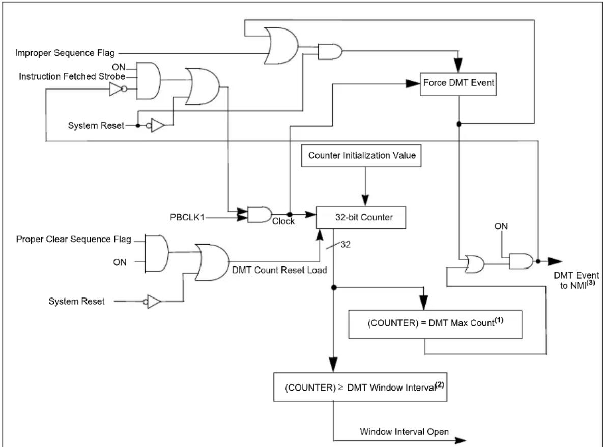
flowchart
graph TD
    A["Improper Sequence Flag"] --> B["AND"]
    C["Instruction Fetched Strobe"] --> D["NOT"]
    E["System Reset"] --> F["NOT"]
    B --> G["OR"]
    D --> G
    F --> G
    G --> H["Force DMT Event"]
    H --> I["Counter Initialization Value"]
    I --> J["32-bit Counter"]
    J --> K["(COUNTER) = DMT Max Count^(1)"]
    K --> L["(COUNTER) ≥ DMT Window Interval^(2)"]
    L --> M["Window Interval Open"]
    N["Proper Clear Sequence Flag"] --> O["AND"]
    P["System Reset"] --> Q["NOT"]
    O --> R["DMT Count Reset Load"]
    Q --> R
    R --> S["32"]
    S --> J
    T["ON"] --> U["AND"]
    V["ON"] --> W["AND"]
    X["ON"] --> Y["AND"]
    Z["ON"] --> AA["AND"]
    AB["ON"] --> AC["AND"]
    AD["ON"] --> AE["AND"]
    AF["ON"] --> AG["AND"]
    AH["ON"] --> AI["AND"]
    AJ["ON"] --> AK["AND"]
    AL["ON"] --> AM["AND"]
    AN["ON"] --> AO["AND"]
    AP["DMT Event to NMI^(3)"] --> AQ["OR"]
    AQ --> AR["32-bit Counter"]
    AR --> S
Note 1: DMT Max Count is controlled by the DMTCNT[4:0] bits in the CFGCON2 Configuration register.
2: DMT Window Interval is controlled by the DMTINTV[2:0] bits in the CFGCON2 Configuration register.
3: Refer to Section 7.0 "Resets" for more information.
17.1 DMT Control Registers
TABLE 17-1: DMT REGISTER MAP
Legend: x = unknown value on Reset; — = unimplemented, read as '0'. Reset values are shown in hexadecimal.
REGISTER 17-1: DMTCON: DEADMAN TIMER CONTROL REGISTER
| Bit Range | Bit31/23/15/7 | Bit30/22/14/6 | Bit29/21/13/5 | Bit28/20/12/4 | Bit27/19/11/3 | Bit26/18/10/2 | Bit25/17/9/1 | Bit24/16/8/0 |
| 31:24 | U-0 U-0 | U-0 U-0 U-0 U-0 | U-0 U-0 | |||||
| — — — | — — — — | |||||||
| 23:16 | U-0 U-0 | U-0 U-0 U-0 U-0 | U-0 U-0 | |||||
| — — — | — — — — | |||||||
| 15:8 | R/W-y U-0 | U-0 U-0 U-0 U-0 | U-0 U-0 | |||||
| ON ^(1) | — — — | — — — | ||||||
| 7:0 | U-0 U-0 | U-0 U-0 U-0 U-0 | U-0 U-0 | |||||
| — — — | — — — — |
| Legend: y = Value set from Configuration bits on POR | |||
| R = Readable bit | W = Writable bit | U = Unimplemented bit, read as '0' | |
| -n = Value at POR | '1' = Bit is set | '0' = Bit is cleared | x = Bit is unknown |
bit 31-16 Unimplemented: Read as '0'
bit 15 ON: DMT Module Enable bit ^(1)
1 = DMT module is enabled
0 = DMT module is disabled
The Reset value of this bit is determined by the setting of the DMTEN bit (CFGCON2[3]).
bit 13-0 Unimplemented: Read as '0'
Note 1: This bit only has control when DMTEN (CFGCON2[3]) = 0.
REGISTER 17-2: DMTPRECLR: DEADMAN TIMER PRECLEAR REGISTER
| Bit Range | Bit31/23/15/7 | Bit30/22/14/6 | Bit29/21/13/5 | Bit28/20/12/4 | Bit27/19/11/3 | Bit26/18/10/2 | Bit25/17/9/1 | Bit24/16/8/0 |
| 31:24 | U-0 U-0 | U-0 U-0 | U-0 U-0 | |||||
| — — — | — — — — | |||||||
| 23:16 | U-0 U-0 | U-0 U-0 | U-0 U-0 | |||||
| — — — | — — — — | |||||||
| 15:8 | R/W-0 | R/W-0 | R/W-0 | R/W-0 | R/W-0 | R/W-0 | R/W-0 | R/W-0 |
| STEP1[7:0] | ||||||||
| 7:0 | U-0 U-0 | U-0 U-0 | U-0 U-0 | |||||
| — — — | — — — — | |||||||
| Legend: | |||
| R = Readable bit | W = Writable bit | U = Unimplemented bit, read as ‘0’ | |
| -n = Value at POR | ‘1’ = Bit is set | ‘0’ = Bit is cleared | x = Bit is unknown |
bit 31-16 Unimplemented: Read as '0'
bit 15-8 STEP1[7:0]: Preclear Enable bits
01000000 = Enables the DMT preclear (Step 1)
All other write patterns = Set BAD1 flag.
These bits are cleared when a DMT Reset event occurs. STEP1[7:0] is also cleared if the STEP2[7:0] bits are loaded with the correct value in the correct sequence.
bit 7-0 Unimplemented: Read as '0'
REGISTER 17-3: DMTCLR: DEADMAN TIMER CLEAR REGISTER
| R = Readable bit | W = Writable bit | U = Unimplemented bit, read as '0' |
| -n = Value at POR | '1' = Bit is set | '0' = Bit is cleared x = Bit is unknown |
bit 31-8
Unimplemented: Read as '0'
bit 7-0
STEP2[7:0]: Clear Timer bits
00001000 = Clears STEP1[7:0], STEP2[7:0] and the DMT if, and only if, preceded by correct loading of STEP1[7:0] bits in the correct sequence. The write to these bits may be verified by reading DMTCNT and observing the counter being reset.
All other write patterns = Set BAD2 bit, the value of STEP1[7:0] will remain unchanged, and the new value being written STEP2[7:0] will be captured. These bits are also cleared when a DMT Reset event occurs.
If the STEP2[7:0] bits are written without preceding with a correct loading of STEP1[7:0] bits, the BAD1 bit is set.
REGISTER 17-4: DMTSTAT: DEADMAN TIMER STATUS REGISTER
| Bit Range | Bit31/23/15/7 | Bit30/22/14/6 | Bit29/21/13/5 | Bit28/20/12/4 | Bit27/19/11/3 | Bit26/18/10/2 | Bit25/17/9/1 | Bit24/16/8/0 |
| 31:24 | U-0 U-0 | U-0 U-0 U-0 | U-0 U-0 | |||||
| — — — | — | — — — | ||||||
| 23:16 | U-0 U-0 | U-0 U-0 U-0 | U-0 U-0 | |||||
| — — — | — | — — — | ||||||
| 15:8 | U-0 U-0 | U-0 U-0 U-0 | U-0 U-0 | |||||
| — — — | — | — — — | ||||||
| 7:0 | R-0, HC, HS | R-0, HC, HS | R-0, HC, HS | U-0 | U-0 | U-0 | U-0 | R-0, HC, HS |
| BAD1 | BAD2 | DMTEVENT | — | — | — | — | WINOPN |
| Legend: | HC = Hardware Cleared HS = Hardware Set | ||
| R = Readable bit | W = Writable bit U = Unimplemented bit, read as ‘0’ | ||
| -n = Value at POR | ‘1’ = Bit is set | ‘0’ = Bit is cleared | x = Bit is unknown |
bit 31-8 Unimplemented: Read as '0'
bit 7 BAD1: Bad STEP1[7:0] Value Detect bit
1 = Incorrect STEP1[7:0] value or out of sequence write to STEP2[7:0] is detected
0 = Incorrect STEP1[7:0] value is not detected
bit 6 BAD2: Bad STEP2[7:0] Value Detect bit
1 = Incorrect STEP2[7:0] value is detected
0 = Incorrect STEP2[7:0] value is not detected
bit 5 DMTEVENT: DMT Event bit
1 = DMT event is detected (counter expired or bad STEP1[7:0] or STEP2[7:0] value is entered prior to counter increment)
0 = DMT even is not detected
bit 4-1 Unimplemented: Read as '0'
bit 0 WINOPN: DMT Clear Window bit
1 = DMT clear window is open
0 = DMT clear window is not open
REGISTER 17-5: DMTCNT: DEADMAN TIMER COUNT REGISTER
| Bit Range | Bit31/23/15/7 | Bit30/22/14/6 | Bit29/21/13/5 | Bit28/20/12/4 | Bit27/19/11/3 | Bit26/18/10/2 | Bit25/17/9/1 | Bit24/16/8/0 |
| 31:24 | R-0 R-0 R-0 R-0 R-0 R-0 | |||||||
| COUNTER[31:24] | ||||||||
| 23:16 | R-0 R-0 R-0 R-0 R-0 R-0 | |||||||
| COUNTER[23:16] | ||||||||
| 15:8 | R-0 R-0 R-0 R-0 R-0 R-0 | |||||||
| COUNTER[15:8] | ||||||||
| 7:0 | R-0 R-0 R-0 R-0 R-0 R-0 | |||||||
| COUNTER[7:0] | ||||||||
Legend:
R = Readable bit W = Writable bit U = Unimplemented bit, read as '0' -n = Value at POR '1' = Bit is set '0' = Bit is cleared x = Bit is unknown
bit 31-0 COUNTER[31:0]: Read current contents of DMT counter
REGISTER 17-6: DMTPSCNT: POST STATUS CONFIGURE DMT COUNT STATUS REGISTER
| Bit Range | Bit31/23/15/7 | Bit30/22/14/6 | Bit29/21/13/5 | Bit28/20/12/4 | Bit27/19/11/3 | Bit26/18/10/2 | Bit25/17/9/1 | Bit24/16/8/0 |
| 31:24 | R-0 R-0 | R-0 R-0 | R-0 R-0 | |||||
| PSCNT[31:24] | ||||||||
| 23:16 | R-0 R-0 | R-0 R-0 | R-0 R-0 | |||||
| PSCNT[23:16] | ||||||||
| 15:8 | R-0 R-0 | R-0 R-0 | R-0 R-0 | |||||
| PSCNT[15:8] | ||||||||
| 7:0 | R-0 R-0 | R-0 R-y | R-y R-y | R-y | ||||
| PSCNT[7:0] | ||||||||
Legend:
R = Readable bit W = Writable bit U = Unimplemented bit, read as '0' -n = Value at POR '1' = Bit is set '0' = Bit is cleared x = Bit is unknown
bit 31-0 PSCNT[31:0]: DMT Instruction Count Value Configuration Status bits
This is always the value of the DMTCNT[4:0] bits in the CFGCON2 Configuration register.
REGISTER 17-7: DMTPSINTV: POST STATUS CONFIGURE DMT INTERVAL STATUS REGISTER
| Bit Range | Bit31/23/15/7 | Bit30/22/14/6 | Bit29/21/13/5 | Bit28/20/12/4 | Bit27/19/11/3 | Bit26/18/10/2 | Bit25/17/9/1 | Bit24/16/8/0 |
| 31:24 | R-0 R-0 R-0 R-0 R-0 R-0 | |||||||
| PSINTV[31:24] | ||||||||
| 23:16 | R-0 R-0 R-0 R-0 R-0 R-0 | |||||||
| PSINTV[23:16] | ||||||||
| 15:8 | R-0 R-0 R-0 R-0 R-0 R-0 | |||||||
| PSINTV[15:8] | ||||||||
| 7:0 | R-0 R-0 R-0 R-0 R-0 R-y | |||||||
| PSINTV[7:0] | ||||||||
| Legend: y = Value set from Configuration bits on POR | |||
| R = Readable bit W = Writable bit U = Unimplemented bit, read as '0' | |||
| -n = Value at POR | '1' = Bit is set | '0' = Bit is cleared | x = Bit is unknown |
bit 31-0
PSINTV[31:0]: DMT Window Interval Configuration Status bits
This is always the value of the DMTINTV[2:0] bits in the CFGCON2 Configuration register.
18.0 WATCHDOG TIMER (WDT)
Note: This data sheet summarizes the features of the PIC32MZ1025W104 family of devices. It is not intended to be a comprehensive reference source. To complement the information in this data sheet, refer to Section 9. "Watchdog, Deadman, and Power-up Timers" (DS60001114) in the "PIC32 Family Reference Manual", which is available from the Microchip website (www.microchip.com/PIC32).
When enabled, the WDT operates from the internal LPRC clock source and can be used to detect system software malfunctions by resetting the device if the WDT is not clear. Sed periodically in software. Various WDT time-out periods can be selected using the WDT postscaler. The WDT can also be used to wake the device from Sleep or Idle mode.
The key features of the WDT module are:
- Configuration or software controlled
- Up to 32 configurable time-out periods
- Can wake the device from Sleep or Idle mode
- Independent Run and Sleep mode counters
- WDT may use alternate clock source and postscaler for Run mode counter
- Independent 5-bit postscalers for Run and Sleep mode counters
• Hardware and software enabled
- Two clock sources
- Windowed WDT
Note: When the CPU is running on the same clock or clock frequency as the WDT (LPRC), the lowest pre-scale values may not allow the CPU to have enough time to reset the WDT before it expires.
FIGURE 18-1: WDT BLOCK DIAGRAM
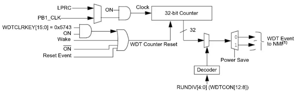
flowchart
graph TD
    A["LPRC"] --> B["AND"]
    C["PB1_CLK"] --> B
    B --> D["ON"]
    D --> E["AND"]
    F["WDTCLRKEY[15:0"] = 0x5743] --> G["AND"]
    H["ON"] --> G
    I["Wake"] --> G
    J["ON"] --> G
    K["Reset Event"] --> G
    G --> L["WDT Counter Reset"]
    L --> M["32-bit Counter"]
    M --> N["32"]
    N --> O["Decoder"]
    O --> P["0"]
    O --> Q["1"]
    P --> R["WDT Event to NMI(1)"]
    Q --> S["Power Save"]
    S --> T["RUNDIV[4:0"] (WDTCON["12:8"])]
    T --> U["Reset Event"]
Note 1: Refer to Section 7.0 "Resets" for more information.
18.1 WDT Configuration
The WDT is configured using the following config register bits/fields:
- Window size (CFGCON2.FWINSZ[1:0])
- Windowing disable (CFGCON2.WINDIS)
• Post-scaler selection (CFGCON2.WDTPS[4:0])
18.2 WDT Control Registers
TABLE 18-1: WDT REGISTER MAP
| Virtual Address (BF80_#) | Register Name | Bit Range | Bits | All Resets | ||||||||||||||||||
| 31/15 | 30/14 | 29/13 | 28/12 | 27/11 | 26/10 | 25/9 | 24/8 | 23/7 | 22/6 | 21/5 | 20/4 | 19/3 | 18/2 | 17/1 | 16/0 | |||||||
| 0800 | WDTCON(1) | 31:16 | WDTCLRKEY[15:0] | 0000 | ||||||||||||||||||
| 15:0 | ON | — | — | RUNDIV[4:0] | — | — | — | — | — | — | — | — | — | WDTWINEN | xx00 | |||||||
Legend: x = unknown value on Reset; — = unimplemented, read as '0'. Reset values are shown in hexadecimal.
Note 1: This register has corresponding CLR, SET and INV registers at its virtual address, plus an offset of 0x4, 0x8 and 0xC, respectively. See Section 13.0 "I/O Ports" for more information.
REGISTER 18-1: WDTCON: WATCHDOG TIMER CONTROL REGISTER
| Bit Range | Bit 31/23/15/7 | Bit 30/22/14/6 | Bit 29/21/13/5 | Bit 28/20/12/4 | Bit 27/19/11/3 | Bit 26/18/10/2 | Bit 25/17/9/1 | Bit 24/16/8/0 |
| 31:24 | W-0 | W-0 | W-0 | W-0 | W-0 | W-0 | W-0 | W-0 |
| WDTCLRKEY[15:8] | ||||||||
| 23:16 | W-0 | W-0 | W-0 | W-0 | W-0 | W-0 | W-0 | W-0 |
| WDTCLRKEY[7:0] | ||||||||
| 15:8 | R/W-y | U-0 | U-0 | R-y | R-y | R-y | R-y | R-y |
| ON(1) | — | — | RUNDIV[4:0] | |||||
| 7:0 | U-0 | U-0 | U-0 | U-0 | U-0 | U-0 | U-0 | R/W-0 |
| — | — | — | — | — | — | — | WDTWINEN | |
| Legend: | y = Values set from Configuration bits on POR | ||
| R = Readable bit | W = Writable bit | U = Unimplemented bit, read as ‘0’ | |
| -n = Value at POR | ‘1’ = Bit is set | ‘0’ = Bit is cleared | x = Bit is unknown |
bit 31-16 WDTCLRKEY[16:0]: Watchdog Timer Clear Key bits
To clear the WDT to prevent a time-out, software must write the value 0x5743 to this location using a single 16-bit write.
bit 15 ON: Watchdog Timer Enable bit ^(1)
1 = WDT is enabled
0 = WDT is disabled
bit 14-13 Unimplemented: Read as '0'
bit 12-8 RUNDIV[4:0]: Watchdog Timer Postscaler Value bits
On Reset, these bits are set to the values of the WDTPS[4:0] Configuration bits in CFGCON2.
bit 7-1 Unimplemented: Read as '0'
bit 0 WDTWINEN: Watchdog Timer Window Enable bit
1 = Enable windowed WDT
0 = Disable windowed WDT
Note 1: This bit only has control when the WDTEN bit (CFGCON2[23]) = 0.
19.0 INPUT CAPTURE
Note: This data sheet summarizes the features of the PIC32MZ1025W104 family of devices. It is not intended to be a comprehensive reference source. To complement the information in this data sheet, refer to Section 15. "Input Capture" (DS60001122) of the "PIC32 Family Reference Manual", which is available from the Microchip website (www.microchip.com/PIC32).
The input capture module is useful in applications requiring frequency (period) and pulse measurement.
This module captures the 16-bit value of the selected Time Base registers when an event occurs at the ICx pin.
The input capture module has the following features:
• Capture every rising and falling edge
• Capture every 4 ^th and 16 ^th rising edge
- Capture timer values based on internal or external clocks
• TMR2 or TMR3 time-based selection
- Device wakes up from capture pin during Sleep and Idle modes
- Interrupt on input capture event
- 4-word FIFO buffer for capture values; interrupt optionally generated after 1, 2, 3, or 4 buffer locations are filled
- Input capture can also be used to provide additional sources of external interrupts
- Capability to trigger PTG
FIGURE 19-1: INPUT CAPTURE BLOCK DIAGRAM
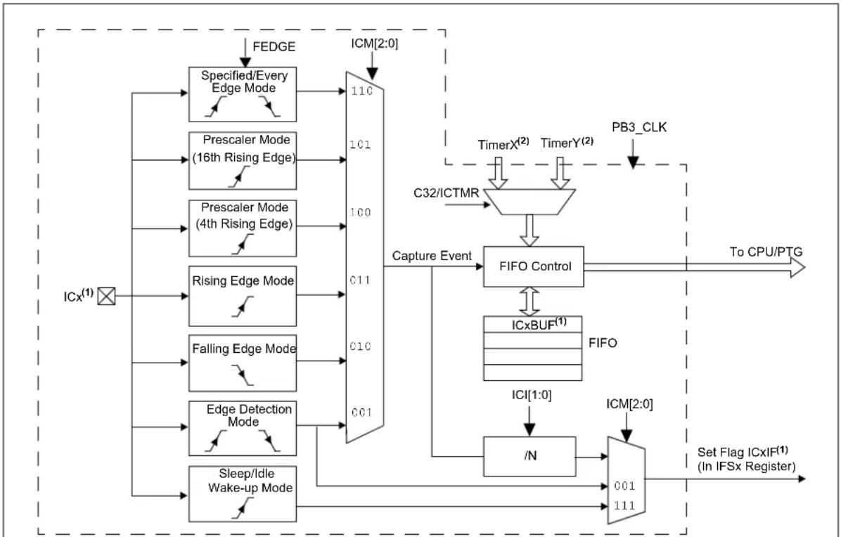
flowchart
graph TD
    A["FEDGE"] --> B["Specified/Every Edge Mode"]
    B --> C["Prescaler Mode (16th Rising Edge)"]
    C --> D["Prescaler Mode (4th Rising Edge)"]
    D --> E["Rising Edge Mode"]
    E --> F["Falling Edge Mode"]
    F --> G["Edge Detection Mode"]
    G --> H["Sleep/Idle Wake-up Mode"]
    H --> I["ICx(1)"]
    I --> J["ICM[2:0"]]
    J --> K["ICXBUF(1)"]
    K --> L["ICI[1:0"]]
    L --> M["/N"]
    M --> N["001 111"]
    N --> O["Set Flag ICxIF(1) (In IFSx Register)"]
    P["TimerX(2)"] --> Q["FIFO Control"]
    R["TimerY(2)"] --> Q
    Q --> S["To CPU/PTG"]
    T["PB3_CLK"] --> U["PB3_CLK"]
    V["C32/ICTMR"] --> Q
    W["Capture Event"] --> Q
Note 1: An 'x' in a signal, register or bit name denotes the number of the capture channel.
2: See Table 19-1 for TimerX and TimerY selections.
The timer source for each input capture module depends on the setting of the IC_ACLK bit in the CFGCON0 register. The available configurations are shown in the table below.
When IC_ACLK = 0, all ICAP may choose between the same 2 timer sources. When IC_ACLK = 1, groups of ICAP may choose between a variation of timer sources.
TABLE 19-1: ICAP CLOCK SOURCES
| IC_ACLK ICAP instance | X (MSB) clock/data | Y (MSB) clock/data | |
| 0 ICAP1-4 TMR3 TMR2 | |||
| 1 ICAP1-2 TMR5 TMR4 | |||
| ICAP3-4 TMR7 TMR6 | |||
19.1 Input Capture Control Registers
TABLE 19-2: INPUT CAPTURE 1 THROUGH INPUT CAPTURE 9 REGISTER MAP
| Virtual Address (BF84,#) | Register Name | Bit Range | Bits | All Resets | ||||||||||||||||
| 31/15 30 | 14 29/13 | 28/12 27/11 | 26/10 25/9 | 24/8 23/7 | 22/6 21/5 20 | 14 19/3 18/2 | 17/1 16/0 | |||||||||||||
| 1000 | C1CON (1) | 31:16 | — | — | — | — | — | — | — | — | — | — | — | — | — | — | — | — | — | 0000 |
| 15:0 | ON | — | SIDL | — | — | — | FEDGE | C32 | ICTMR | ICI[1:0] | ICOV | ICBNE | ICM[2:0] | 0000 | ||||||
| 1010 | IC1BUF | 31:16 | IC1BUF[31:16] | xxxxx | ||||||||||||||||
| 15:0 | IC1BUF[16:0] | xxxxx | ||||||||||||||||||
| 1200 | C2CON (1) | 31:16 | — | — | — | — | — | — | — | — | — | — | — | — | — | — | — | — | — | 0000 |
| 15:0 | ON | — | SIDL | — | — | — | FEDGE | C32 | ICTMR | ICI[1:0] | ICOV | ICBNE | ICM [2:0] | 0000 | ||||||
| 1210 | IC2BUF | 31:16 | IC2BUF[31:16] | xxxxx | ||||||||||||||||
| 15:0 | IC2BUF[16:0] | xxxxx | ||||||||||||||||||
| 1400 | C3CON (1) | 31:16 | — | — | — | — | — | — | — | — | — | — | — | — | — | — | — | — | — | 0000 |
| 15:0 | ON | — | SIDL | — | — | — | FEDGE | C32 | ICTMR | ICI[1:0] | ICOV | ICBNE | ICM(2:0] | 0000 | ||||||
| 1410 | IC3BUF | 31:16 | IC3BUF[31:16] | xxxxx | ||||||||||||||||
| 15:0 | IC3BUF[16:0] | xxxxx | ||||||||||||||||||
| 1600 | C4CON (1) | 31:16 | — | — | — | — | — | — | — | — | — | — | — | — | — | — | — | — | — | 0000 |
| 15:0 | ON | — | SIDL | — | — | — | FEDGE | C32 | ICTMR | ICI[1:0] | ICOV | ICBNE | ICM 2 : 0 | 0000 | ||||||
| 1610 | IC4BUF | 31:16 | IC4BUF[31:16] | xxxxx | ||||||||||||||||
| 15:0 | IC4BUF[16:0] | xxxxx | ||||||||||||||||||
Legend: x = unknown value on Reset; — = unimplemented, read as '0'. Reset values are shown in hexadecimal.
Note 1: This register has corresponding CLR, SET and INV registers at its virtual address, plus an offset of 0x4, 0x8 and 0xC, respectively. See Section 13.3 "CLR, SET and INV Registers" for more information.
REGISTER 19-1: ICxCON: INPUT CAPTURE x CONTROL REGISTER
| R = Readable bit | W = Writable bit | U = Unimplemented bit |
| -n = Bit Value at POR: ('0', '1', x = unknown) | P = Programmable bit r = Reserved bit | |
bit 31-16 Unimplemented: Read as '0'
bit 15 ON: Input Capture Module Enable bit
1 = Module is enabled
0 = Disable and Reset module, disable clocks, disable interrupt generation and allow SFR modifications
bit 14 Unimplemented: Read as '0'
bit 13 SIDL: Stop in Idle Control bit
1 = Halt in CPU Idle mode
0 = Continue to operate in CPU Idle mode
bit 12-10 Unimplemented: Read as '0'
bit 9 FEDGE: First Capture Edge Select bit (only used in mode 6, ICM[2:0] = 110)
1 = Capture rising edge first
0 = Capture falling edge first
bit 8 C32: 32-bit Capture Select bit
1 = 32-bit timer resource capture
0 = 16-bit timer resource capture
bit 7 ICTMR: Timer Select bit (Does not affect timer selection when C32 (ICxCON[8]) is '1') ^(1)
0 = Timery is the counter source for capture
1 = Timerx is the counter source for capture
bit 6-5 ICI[1:0]: Interrupt Control bits
11 = Interrupt on every fourth capture event
10 = Interrupt on every third capture event
01 = Interrupt on every second capture event
00 = Interrupt on every capture event
bit 4 ICOV: Input Capture Overflow Status Flag bit (read-only)
1 = Input capture overflow is occurred
0 = No input capture overflow is occurred
bit 3 ICBNE: Input Capture Buffer Not Empty Status bit (read-only)
1 = Input capture buffer is not empty; at least one more capture value can be read
0 = Input capture buffer is empty
bit 2-0 ICM[2:0]: Input Capture Mode Select bits
111 = Interrupt-Only mode (only supported while in Sleep mode or Idle mode)
110 = Simple Capture Event mode - every edge, specified edge first and every edge thereafter
101 = Prescaled Capture Event mode - every sixteenth rising edge
100 = Prescaled Capture Event mode - every fourth rising edge
011 = Simple Capture Event mode - every rising edge
010 = Simple Capture Event mode - every falling edge
001 = Edge Detect mode - every edge (rising and falling)
000 = Input Capture module is disabled
Note 1: Refer to Table 19-1 for TimerX and TimerY selections.
20.0 OUTPUT COMPARE
Note: This data sheet summarizes the features of the PIC32MZ1025W104 device. It is not intended to be a comprehensive reference source. To complement the information in this data sheet, refer to Section 16. "Output Compare" (DS60001111) in the "PIC32 Family Reference Manual", which is available from the Microchip website (www.microchip.com/PIC32).
The output compare module is used to generate a single pulse or a train of pulses in response to selected time base events.
For all modes of operation, the output compare module compares the values stored in the OCxR and/or the OCxRS registers to the value in the selected timer. When a match occurs, the output compare module generates an event based on the selected mode of operation.
The output compare module has the following features:
- Multiple output compare modules in a device
- Programmable interrupt generation on compare event
- Single and Dual Compare modes
- Single and continuous output pulse generation
- Glitchless Pulse Width Modulation (PWM) mode
- with fault protection input
-
without fault protection input
-
Interrupt on output compare/PWM event
- Interrupt on PWM fault detect condition
- Programmable selection of 16-bit or 32-bit time bases
- Can operate from either of two available 16-bit time bases or a single 32-bit time base
- ADC event trigger
- Capability to trigger PTG
Operating modes are determined by setting the OCxM bits. Note that the OCxM bits must be switched through the OCxM = 000, before the next mode is selected.
FIGURE 20-1: OUTPUT COMPARE MODULE BLOCK DIAGRAM
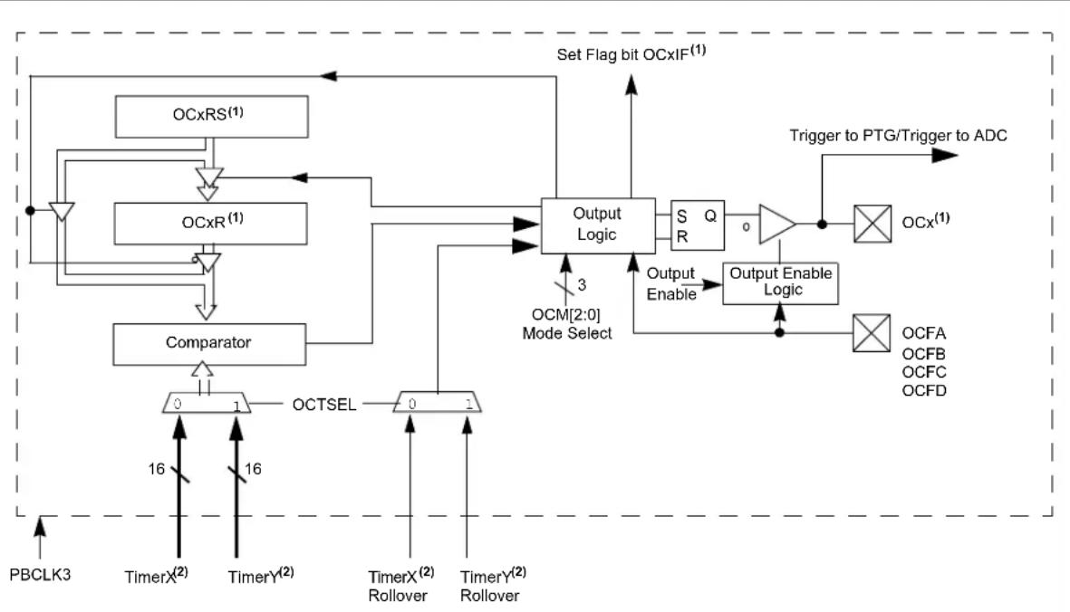
flowchart
graph TD
    A["OCxRS(1)"] --> B["Comparator"]
    C["OCxR(1)"] --> B
    D["TimerX(2)"] --> E["OCTSEL"]
    F["TimerY(2)"] --> E
    G["TimerX(2) Rollover"] --> H["0 1"]
    I["TimerY(2) Rollover"] --> J["0 1"]
    K["Set Flag bit OCxIF(1)"] --> L["Output Logic"]
    M["Trigger to PTG/Trigger to ADC"] --> N["OCx(1)"]
    O["OCFA OCFB OCFC OCFD"] --> P["Output Enable Logic"]
    Q["OCXRS(1)"] --> R["Comparator"]
    S["OCXR(1)"] --> R
    T["OCM[2:0"] Mode Select] --> U["0 1"]
    V["3"] --> W["Output Enable Logic"]
    X["16"] --> Y["TimerX(2)"]
    X --> Z["TimerY(2)"]
Note 1: Where 'x' is shown, reference is made to the registers associated with the respective output compare channels, 1 through 4.
2: Refer to Table 20-1 for TimerX and TimerY selections.
The timer source for each output compare module depends on the setting of the OC_ACLK bit in the CFGCON0 register. The available configurations are shown in the table below.
When OC_ACLK = 0, all OCMP may choose between the same 2 timer sources. When OC_ACLK = 1, groups of OCMP may choose between a variation of timer sources.
TABLE 20-1: OCMP CLOCK SOURCES
| OC_ACLK OCMP | Instance | X (MSB)Clock/Data | Y (MSB)Clock/Data |
| 0 OCMP1-4 TMR3 TMR2 | |||
| 1 OCMP1-2 TMR5 TMR4 | |||
| OCMP3-4 TMR7 TMR6 |
20.1 Output Compare Control Registers
TABLE 20-2: OUTPUT COMPARE 1 THROUGH OUTPUT COMPARE 4 REGISTER MAP
| Virtual Address(BFB4_#) | RegistrarName | Bit Range | Bits | All Resets | |||||||||||||||||
| 31/15 30 | /14 29/13 | 28/12 27/11 | 26/10 25/9 | 24/8 23/7 | 22/6 21/5 20 | /4 19/3 18/2 | 17/1 16/0 | ||||||||||||||
| 2000 | OC1CON | 31:16 | —— | —— | —— | —— | —— | —— | 2000 | ||||||||||||
| 15:0 ON | — | SIDL | — | — | — | — | — | — | — | — | OC32 | OCFLT | OCTSEL | OCM[2:0] | 0000 | ||||||
| 2010 | OC1R | 31:16 | OC1R[31:16] | xxxxx | |||||||||||||||||
| 15:0 | OC1R[15:0] | xxxxx | |||||||||||||||||||
| 2020 | OC1RS | 31:16 | OC1RS[31:16] | xxxxx | |||||||||||||||||
| 15:0 | OC1RS[15:0] | xxxxx | |||||||||||||||||||
| 2200 | OC2CON | 31:16 | —— | —— | —— | —— | —— | —— | 2000 | ||||||||||||
| 15:0 ON | — | SIDL | — | — | — | — | — | — | — | — | OC32 | OCFLT | OCTSEL | OCM[2:0] | 0000 | ||||||
| 2210 | OC2R | 31:16 | OC2R[31:16] | xxxxx | |||||||||||||||||
| 15:0 | OC2R[15:0] | xxxxx | |||||||||||||||||||
| 2220 | OC2RS | 31:16 | OC2RS[31:16] | xxxxx | |||||||||||||||||
| 15:0 | OC2RS[15:0] | xxxxx | |||||||||||||||||||
| 2400 | OC3CON | 31:16 | —— | —— | —— | —— | —— | —— | 2000 | ||||||||||||
| 15:0 ON | — | SIDL | — | — | — | — | — | — | — | — | OC32 | OCFLT | OCTSEL | OCM[2:0] | 0000 | ||||||
| 2410 | OC3R | 31:16 | OC3R[31:16] | xxxxx | |||||||||||||||||
| 15:0 | OC3R[15:0] | xxxxx | |||||||||||||||||||
| 2420 | OC3RS | 31:16 | OC3RS[31:16] | xxxxx | |||||||||||||||||
| 15:0 | OC3RS[15:0] | xxxxx | |||||||||||||||||||
| 2600 | OC4CON | 31:16 | —— | —— | —— | —— | —— | —— | 2000 | ||||||||||||
| 15:0 ON | — | SIDL | — | — | — | — | — | — | — | — | OC32 | OCFLT | OCTSEL | OCM[2:0] | 0000 | ||||||
| 2610 | OC4R | 31:16 | OC4R[31:16] | xxxxx | |||||||||||||||||
| 15:0 | OC4R[15:0] | xxxxx | |||||||||||||||||||
| 2620 | OC4RS | 31:16 | OC4RS[31:16] | xxxxx | |||||||||||||||||
| 15:0 | OC4RS[15:0] | xxxxx | |||||||||||||||||||
Legend: x = unknown value on Reset; — = unimplemented, read as '0'. Reset values are shown in hexadecimal.
Note 1: All registers in this table have corresponding CLR, SET and INV registers at their virtual addresses, plus offsets of 0x4, 0x8 and 0xC, respectively. See Section 13.3 "CLR, SET and INV Registers" for more information.
REGISTER 20-1: OCxCON: OUTPUT COMPARE 'x' CONTROL REGISTER (x=1-4)
| Bit Range | Bit 31/23/15/7 | Bit 30/22/14/6 | Bit 29/21/13/5 | Bit 28/20/12/4 | Bit 27/19/11/3 | Bit 26/18/10/2 | Bit 25/17/9/1 | Bit 24/16/8/0 |
| 31:24 | U-0 U-0 U-0 U-0 U-0 U-0 | U-0 U-0 | ||||||
| — — — | — — — — | |||||||
| 23:16 | U-0 U-0 U-0 U-0 U-0 U-0 | U-0 U-0 | ||||||
| — — — | — — — — | |||||||
| 15:8 | R/W-0 U-0 | R/W-0 | U-0 U-0 U-0 U-0 | U-0 | U-0 | |||
| ON | — | SIDL | — — — | — — | ||||
| 7:0 | U-0 | U-0 | R/W-0 | R-0 | R/W-0 | R/W-0 | R/W-0 | R/W-0 |
| — | — | OC32 | OCFLT^(1) | OCTSEL^(2) | OCM[2:0] | |||
Legend:
| R = Readable bit | W = Writable bit | U = Unimplemented bit, read as '0' |
| -n = Value at POR | '1' = Bit is set | '0' = Bit is cleared x = Bit is unknown |
bit 31-16 Unimplemented: Read as '0'
bit 15 ON: Output Compare Peripheral On bit
1 = Output compare peripheral is enabled
0 = Output compare peripheral is disabled
bit 14 Unimplemented: Read as '0'
bit 13 SIDL: Stop in Idle Mode bit
1 = Discontinue operation when CPU enters Idle mode
0 = Continue operation in Idle mode
bit 12-6 Unimplemented: Read as '0'
bit 5 OC32: 32-bit Compare Mode bit
1 = OCxR[31:0] and/or OCxRS[31:0] are used for comparisons to the 32-bit timer source
0 = OCxR[15:0] and OCxRS[15:0] are used for comparisons to the 16-bit timer source
bit 4 OCFLT: PWM Fault Condition Status bit ^(1)
1 = PWM Fault condition has occurred (cleared in hardware only)
0 = No PWM Fault condition has occurred
bit 3 OCTSEL: Output Compare Timer Select bit ^(2)
1 = TimerX is the clock source for this output compare module
0 = TimerY is the clock source for this output compare module
bit 2-0 OCM[2:0]: Output Compare Mode Select bits
111 = PWM mode on OCx; fault pin is enabled
110 = PWM mode on OCx; fault pin is disabled
101 = Initialize OCx pin low; generate continuous output pulses on OCx pin
100 = Initialize OCx pin low; generate single output pulse on OCx pin
011 = Compare event toggles OCx pin
010 = Initialize OCx pin high; compare event forces OCx pin low
001 = Initialize OCx pin low; compare event forces OCx pin high
000 = Output compare peripheral is disabled but continues to draw current
Note 1: This bit is only used when OCM[2:0] = '111'. It is read as '0' in all other modes.
2: Refer to Table 20-1 for TimerX and TimerY selections.
21.0 SERIAL PERIPHERAL INTERFACE (SPI) AND INTER-IC SOUND (I²S)
Note: This data sheet summarizes the features of the PIC32MZ1025W104 device. It is not intended to be a comprehensive reference source. To complement the information in this data sheet, refer to Section 23. "Serial Peripheral Interface (SPI)" (DS60001106) in the "PIC32 Family Reference Manual", which is available from the Microchip website (www.microchip.com/PIC32).
SPI/I ^2 S module is a synchronous serial interface that is useful for communicating with external peripherals and other MCU devices, as well as digital audio devices. These peripheral devices may be Serial EEPROMs, Shift registers, display drivers, ADCs, and so on.
SPI1 has two paths to device pins. One using PPS (slower operation) and another using dedicated pins (faster operation). The dedicated pins can operate at a maximum of 40 MHz whereas PPS pins (slower SPI) can operate up to 20 MHz. SPI2 supports single path to device pins using PPS.
The following are key features of the SPI module:
- Native 32-bit peripheral bus architecture, scalable to 16-bit and 8-bit access
- Host and Client mode support
• Full-duplex operation with 8/16/32-bit communication - Status bit to indicate activity of SPI
- Four different clock formats
- Interrupt event on every byte/half-word/word received
- Separate transmit and receive buffer events
- Framed SPI protocol support
- DMA support
- SDO pin disable option
• 16 byte deep enhanced buffer operation - Persistent Interrupt events based on internal status bits
• Enhanced FSYNC operation
• Audio CODEC support - I²S protocol
- Left justified
- Right justified
- PCM
- I²S protocol
- Left justified
- Right justified
- PCM
Note: Set the CFGCON1.HSSPIEN register bit to enable the High-speed mode on SPI1.
FIGURE 21-1: SPI/I ^2 S MODULE BLOCK DIAGRAM
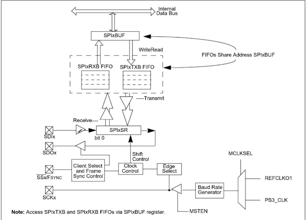
flowchart
graph TD
    A["SPIxBUF"] -->|WriteRead| B["FIFOs Share Address SPIxBUF"]
    B --> C["SPIxRSR"]
    C -->|bit 0| D["Client Select and Frame Sync Control"]
    C --> E["Clock Control"]
    C --> F["Edge Select"]
    F --> G["Baud Rate Generator"]
    G --> H["MCLKSEL"]
    H --> I["REFCLKO1"]
    H --> J["PB3_CLK"]
    K["SCKx"] --> C
    L["SSx/FSYNC"] --> C
    M["SDIx"] --> C
    N["SDOx"] --> C
    O["SDIx"] --> C
    P["Transmit"] --> C
    Q["Client Select and Frame Sync Control"] --> C
    R["Shift Control"] --> C
    S["WriteRead"] --> T["SPIxRXB FIFO"]
    U["SPIxTXB FIFO"] --> T
    V["Send Data Bus"] <--> W["Internal Data Bus"]
21.1 SPI Control Registers
TABLE 21-1: SPI1 AND SPI2 REGISTER MAP
| Virtual Address(BF84.#) | Register Name[1] | Bit Range | Bits | All Resets | ||||||||||||||||
| 31/15 30 | 14 29/13 28 | 12 27/11 | 26/10 25/9 2 | 24/8 23/7 22/6 | 21/5 20/4 | 19/3 18/2 | 17/1 16/0 | |||||||||||||
| OC00 | SPI1CON | 31:16 | FRMEN | FRMSYNC | FRMPOL | MSSEN | FRMSYPW | FRMCNT[2:0] | MCLKSEL | — | — | — | — | — | SPIFE | ENHBUF | C000 | |||
| 15:0 | ON | — | SIDL | DISSDO | MODE32 | MODE16 | SMP | CKE | SSEN | CKP | MSTEN | DISSDI | STXISEL[1:0] | SRXISEL[1:0] | 0000 | |||||
| OC10 | SPI1STAT | 31:16 | — | — | — | RXBUFELM[4:0] | — | — | — | TXBUFELM[4:0] | 0000 | |||||||||
| 15:0 | — | — | — | FRMERR | SPIBUSY | — | — | SPITUR | SRMT | SPIROV | SPIRBE | — | SPITBE | — | SPITBF | SPIRBF | 0000 | |||
| OC20 | SPI1BUF | 31:16 | DATA[31:16] | C000 | ||||||||||||||||
| 15:0 | DATA[15:0] | C000 | ||||||||||||||||||
| OC30 | SPI1BRG | 31:16 | — | — | — | — | — | — | — | — | — | — | — | — | — | — | — | — | 0000 | |
| 15:0 | — | — | — | BRG[12:0] | 0000 | |||||||||||||||
| OC40 | SPI1CON2 | 31:16 | — | — | — | — | — | — | — | — | — | — | — | — | — | — | — | — | 0000 | |
| 15:0 | SPISGNEXT | — | — | FRMERREN | SPIROVEN | SPITUREN | IGNROV | IGNTUR | AUDEN | — | — | — | AUDMONO | — | AUDMOD[1:0] | 0000 | ||||
| OE00 | SPI2CON | 31:16 | FRMEN | FRMSYNC | FRMPOL | MSSEN | FRMSYPW | FRMCNT[2:0] | MCLKSEL | — | — | — | — | — | SPIFE | ENHBUF | C000 | |||
| 15:0 | ON | — | SIDL | DISSDO | MODE32 | MODE16 | SMP | CKE | SSEN | CKP | MSTEN | DISSDI | STXISEL[1:0] | SRXISEL[1:0] | 0000 | |||||
| OE10 | SPI2STAT | 31:16 | — | — | — | RXBUFELM[4:0] | — | — | — | TXBUFELM[4:0] | 0000 | |||||||||
| 15:0 | — | — | — | FRMERR | SPIBUSY | — | — | SPITUR | SRMT | SPIROV | SPIRBE | — | SPATBE | — | SPITBF | SPIRBF | 0000 | |||
| OE20 | SPI2BUF | 31:16 | DATA[31:0] | 0000 | ||||||||||||||||
| 15:0 | C000 | |||||||||||||||||||
| OE30 | SPI2BRG | 31:16 | — | — | — | — | — | — | — | — | — | — | — | — | — | — | — | — | 0000 | |
| 15:0 | — | — | — | — | — | — | — | BRG[8:0] | 0000 | |||||||||||
| OE40 | SPI2CON2 | 31:16 | — | — | — | — | — | — | — | — | — | — | — | — | — | — | — | — | 0000 | |
| 15:0 | SPISGNEXT | — | — | FRMERREN | SPIROVEN | SPITUREN | IGNROV | IGNTUR | AUDEN | — | — | — | AUDMONO | - | AUDMOD[1:0] | 0000 | ||||
Legend: x = unknown value on Reset; — = unimplemented, read as '0'. Reset values are shown in hexadecimal.
Note 1: All registers in this table except SPIxBUF have corresponding CLR, SET and INV registers at their virtual addresses, plus offsets of 0x4, 0x8 and 0xC, respectively. See Section 13.3 "CLR, SET and INV Registers" for more information.
REGISTER 21-1: SPIxCON: SPI CONTROL REGISTER
| Bit Range | Bit 31/23/15/7 | Bit 30/22/14/6 | Bit 29/21/13/5 | Bit 28/20/12/4 | Bit 27/19/11/3 | Bit 26/18/10/2 | Bit 25/17/9/1 | Bit 24/16/8/0 |
| 31:24 | R/W-0 R/W-0 R/W-0 R/W-0 R/W-0 R/W-0 | |||||||
| FRMEN FRMSYNC FRMPOL MSSEN FRMSYPW FRMCNT[2:0] | ||||||||
| 23:16 | R/W-0 | U-0 | U-0 | U-0 | U-0 | U-0 | R/W-0 | R/W-0 |
| MCLKSEL^(1) | — | — | — | — | — | SPIFE | ENHBUF^(1) | |
| 15:8 | R/W-0 U-0 | R/W-0 | R/W-0 R/W-0 | R/W-0 R/W-0 | R/W-0 | |||
| ON | — | SIDL | DISSDO^(4) | MODE32 MODE16 | MP CKE | (2) | ||
| 7:0 | R/W-0 R/W-0 R/W-0 R/W-0 R/W-0 R/W-0 | |||||||
| SSEN CKP | (3) | MSTEN | DISSDI^{(4)}$ | STXISEL[1:0] | SRXISEL[1:0] | |||
Legend:
| R = Readable bit | W = Writable bit | U = Unimplemented bit, read as '0' |
| -n = Value at POR | '1' = Bit is set | '0' = Bit is cleared x = Bit is unknown |
bit 31 FRMEN: Framed SPI Support bit
1 = Framed SPI support is enabled (SSx pin used as FSYNC input/output)
0 = Framed SPI support is disabled
bit 30 FRMSYNC: Frame Sync Pulse Direction Control on pin bit (Framed SPI mode only)
1 = Frame sync pulse input (Client mode)
0 = Frame sync pulse output (Host mode)
bit 29 FRMPOL: Frame Sync/Client Select Polarity bit (Framed SPI or Host Transmit modes only)
1 = Frame pulse or SSx pin is active-high
0 = Frame pulse or SSx is active-low
bit 28 MSSEN: Host Mode Client Select Enable bit
1 = Client select SPI support is enabled. The pin is automatically driven during transmission in Host mode. Polarity is determined by the FRMPOL bit.
0 = Client select SPI support is disabled.
bit 27 FRMSYPW: Frame Sync Pulse Width bit
1 = Frame sync pulse is one character wide
0 = Frame sync pulse is one clock wide
bit 26-24 FRMCNT[2:0]: Frame Sync Pulse Counter bits. Controls the number of data characters transmitted per pulse. This bit is only valid in Framed mode.
111 = Reserved
110 = Reserved
101 = Generates a frame sync pulse on every 32 data characters
100 = Generates a frame sync pulse on every 16 data characters
011 = Generates a frame sync pulse on every 8 data characters
010 = Generates a frame sync pulse on every 4 data characters
001 = Generates a frame sync pulse on every 2 data characters
000 = Generates a frame sync pulse on every data character
bit 23 MCLKSEL: Host Clock Enable bit ^(1)
1 = REFCLKO1 is used by the Baud Rate Generator
0 = PBCLK3 is used by the Baud Rate Generator
bit 22-18 Unimplemented: Read as '0'
Note 1: This bit can only be written when the ON bit = 0. Refer to Section 41.0 “Electrical Specifications” for maximum clock frequency requirements.
2: This bit is not used in the Framed SPI mode. The user must program this bit to '0' for the Framed SPI mode (FRMEN = 1).
3: When AUDEN = 1, the SPI/I²S module functions as if the CKP bit is equal to '1', regardless of the actual value of the CKP bit.
4: This bit present for legacy compatibility and is superseded by PPS functionality on these devices (see Section 13.4 "Peripheral Pin Select (PPS)" for more information).
REGISTER 21-1: SPIxCON: SPI CONTROL REGISTER (CONTINUED)
bit 17 SPIFE: Frame Sync Pulse Edge Select bit (Framed SPI mode only)
1 = Frame synchronization pulse coincides with the first bit clock
0 = Frame synchronization pulse precedes the first bit clock
bit 16 ENHBUF: Enhanced Buffer Enable bit (1)
1 = Enhanced Buffer mode is enabled
0 = Enhanced Buffer mode is disabled
bit 15 ON: SPI/I ^2 S Module On bit
1 = SPI/I 2S module is enabled
0 = SPI/I 2S module is disabled
bit 14 Unimplemented: Read as '0'
bit 13 SIDL: Stop in Idle Mode bit
1 = Discontinue operation when CPU enters in Idle mode
0 = Continue operation in Idle mode
bit 12 DISSDO: Disable SDOx pin bit (4)
1 = SDOx pin is not used by the module. Pin is controlled by associated PORT register.
0 = SDOx pin is controlled by the module
bit 11-10 MODE[32,16]: 32/16-Bit Communication Select bits
When AUDEN = 1:
MODE32 MODE16 Communication
| 1 | 1 | 24-bit Data, 32-bit FIFO, 32-bit Channel/64-bit Frame |
| 1 | 0 | 32-bit Data, 32-bit FIFO, 32-bit Channel/64-bit Frame |
| 0 | 1 | 16-bit Data, 16-bit FIFO, 32-bit Channel/64-bit Frame |
| 0 | 0 | 16-bit Data, 16-bit FIFO, 16-bit Channel/32-bit Frame |
When AUDEN = 0:
MODE32 MODE16 Communication
| 1 | x | 32-bit |
| 0 | 1 | 16-bit |
| 0 | 0 | 8-bit |
bit 9 SMP: SPI Data Input Sample Phase bit
Host mode (MSTEN = 1):
1 = Input data sampled at end of data output time
0 = Input data sampled at middle of data output time
Client mode (MSTEN = 0):
SMP value is ignored when SPI is used in Client mode. The module always uses SMP = 0.
bit 8 CKE: SPI Clock Edge Select bit (2)
1 = Serial output data changes on transition from active clock state to Idle clock state (see CKP bit)
0 = Serial output data changes on transition from Idle clock state to active clock state (see CKP bit)
bit 7 SSEN: Client Select Enable (Client mode) bit
1 = SSx pin is used for Client mode
0 = pin is not used for Client mode, pin is controlled by the port function.
bit 6 CKP: Clock Polarity Select bit (3)
1 = Idle state for clock is a high level; active state is a low level
0 = Idle state for clock is a low level; active state is a high level
bit 5 MSTEN: Host Mode Enable bit
1 = Host mode
0 = Client mode
Note 1: This bit can only be written when the ON bit = 0. Refer to Section 41.0 “Electrical Specifications” for maximum clock frequency requirements.
2: This bit is not used in the Framed SPI mode. The user must program this bit to '0' for the Framed SPI mode (FRMEN = 1).
3: When AUDEN = 1, the SPI/I²S module functions as if the CKP bit is equal to '1', regardless of the actual value of the CKP bit.
4: This bit present for legacy compatibility and is superseded by PPS functionality on these devices (see Section 13.4 "Peripheral Pin Select (PPS)" for more information).
REGISTER 21-1: SPIxCON: SPI CONTROL REGISTER (CONTINUED)
bit 4 DISSDI: Disable SDI bit (4)
1 = SDI pin is not used by the SPI module (pin is controlled by PORT function)
0 = SDI pin is controlled by the SPI module
bit 3-2 STXISEL[1:0]: SPI Transmit Buffer Empty Interrupt Mode bits
11 = Interrupt is generated when the buffer is not full (has one or more empty elements)
10 = Interrupt is generated when the buffer is empty by one-half or more
01 = Interrupt is generated when the buffer is completely empty
0.0 = Interrupt is generated when the last transfer is shifted out of SPISR and transmit operations are complete
bit 1-0 SRXISEL[1:0]: SPI Receive Buffer Full Interrupt Mode bits
11 = Interrupt is generated when the buffer is full
10 = Interrupt is generated when the buffer is full by one-half or more
01 = Interrupt is generated when the buffer is not empty
00 = Interrupt is generated when the last word in the receive buffer is read (in other words buffer is empty)
Note 1: This bit can only be written when the ON bit = 0. Refer to Section 41.0 "Electrical Specifications" for maximum clock frequency requirements.
2: This bit is not used in the Framed SPI mode. The user must program this bit to '0' for the Framed SPI mode (FRMEN = 1).
3: When AUDEN = 1, the SPI/I²S module functions as if the CKP bit is equal to '1', regardless of the actual value of the CKP bit.
4: This bit present for legacy compatibility and is superseded by PPS functionality on these devices (see Section 13.4 "Peripheral Pin Select (PPS)" for more information).
REGISTER 21-2: SPIxCON2: SPI CONTROL REGISTER 2
| R = Readable bit | W = Writable bit | U = Unimplemented bit, read as ‘0’ |
| -n = Value at POR | ‘1’ = Bit is set | ‘0’ = Bit is cleared x = Bit is unknown |
bit 31-16 Unimplemented: Read as '0'
bit 15 SPISGNEXT: Sign Extend Read Data from the RX FIFO bit
1 = Data from RX FIFO is sign extended
0 = Data from RX FIFO is not sign extended
bit 14-13 Unimplemented: Read as '0'
bit 12 FRMERREN: Enable Interrupt Events via FRMERR bit
1 = Frame error overflow generates error events
0 = Frame error does not generate error events
bit 11 SPIROVEN: Enable Interrupt Events via SPIROV bit
1 = Receive overflow generates error events
0 = Receive overflow does not generate error events
bit 10 SPITUREN: Enable Interrupt Events via SPITUR bit
1 = Transmit underrun generates error events
0 = Transmit underrun does not generate error events
bit 9 IGNROV: Ignore Receive Overflow bit (for audio data transmissions)
1 = A ROV is not a critical error; during ROV data in the FIFO is not overwritten by receive data
0 = A ROV is a critical error which stop SPI operation
bit 8 IGNTUR: Ignore Transmit Underrun bit (for audio data transmissions)
1 = A TUR is not a critical error and zeros are transmitted until the SPIxTXB is not empty
0 = A TUR is a critical error which stop SPI operation
bit 7 AUDEN: Enable Audio CODEC Support bit ^(1)
1 = Audio protocol is enabled
0 = Audio protocol is disabled
bit 6-5 Unimplemented: Read as '0'
bit 3 AUDMONO: Transmit Audio Data Format bit ^(1,2)
1 = Audio data is mono (each data word is transmitted on both left and right channels)
0 = Audio data is stereo
bit 2 Unimplemented: Read as '0'
bit 1-0 AUDMOD[1:0]: Audio Protocol Mode bit ^(1,2)
11 = PCM/DSP mode
10 = Right Justified mode
01 = Left Justified mode
00 = I²S mode
Note 1: This bit can only be written when the ON bit = 0.
2: This bit is only valid for AUDEN = 1.
| Legend: | C = Clearable bit HS = Set in hardware | ||
| R = Readable bit | W = Writable bit | U = Unimplemented bit, read as ‘0’ | |
| -n = Value at POR | ‘1’ = Bit is set | ‘0’ = Bit is cleared | x = Bit is unknown |
bit 31-29 Unimplemented: Read as '0'
bit 28-24 RXBUFELM[4:0]: Receive Buffer Element Count bits (valid only when ENHBUF = 1)
bit 23-21 Unimplemented: Read as '0'
bit 20-16 TXBUFELM[4:0]: Transmit Buffer Element Count bits (valid only when ENHBUF = 1)
bit 15-13 Unimplemented: Read as '0'
bit 12 FRMERR: SPI Frame Error status bit
1 = Frame error is detected
0 = No Frame error is detected
This bit is only valid when FRMEN = 1.
bit 11 SPIBUSY: SPI Activity Status bit
1 = SPI peripheral is currently busy with some transactions
0 = SPI peripheral is currently idle
bit 10-9 Unimplemented: Read as '0'
bit 8 SPITUR: Transmit Under Run bit
1 = Transmit buffer has encountered an Underrun condition
0 = Transmit buffer has no Underrun condition
This bit is only valid in Framed Sync mode; the Underrun condition must be cleared by disabling/re-enabling the module.
bit 7 SRMT: Shift Register Empty bit (valid only when ENHBUF = 1)
1 = When SPI module shift register is empty
0 = When SPI module shift register is not empty
bit 6 SPIROV: Receive Overflow Flag bit
1 = A new data is completely received and discarded. The user software has not read the previous data in the SPIxBUF register.
0 = No overflow has occurred
This bit is set in hardware; can only be cleared (= 0) in software.
bit 5 SPIRBE: RX FIFO Empty bit (valid only when ENHBUF = 1)
1 = RX FIFO is empty (CRPTR = SWPTR)
0 = RX FIFO is not empty (CRPTR ≠ SWPTR)
bit 4 Unimplemented: Read as '0'
REGISTER 21-3: SPIxSTAT: SPI STATUS REGISTER (CONTINUED)
bit 3 SPITBE: SPI Transmit Buffer Empty Status bit
1 = Transmit buffer, SPIxTXB is empty
0 = Transmit buffer, SPIxTXB is not empty
Automatically set in hardware when SPI transfers data from SPIxTXB to SPIxSR.
Automatically cleared in hardware when SPIxBUF is written to, loading SPIxTXB.
bit 2 Unimplemented: Read as '0'
bit 1 SPITBF: SPI Transmit Buffer Full Status bit
1 = Transmit is not yet started, SPITXB is full
0 = Transmit buffer is not full
Standard Buffer mode:
Automatically set in hardware when the core writes to the SPIBUF location, loading SPITXB.
Automatically cleared in hardware when the SPI module transfers data from SPITXB to SPISR.
Enhanced Buffer mode:
Set when CWPTR + 1 = SRPTR; cleared otherwise
bit 0 SPIRBF: SPI Receive Buffer Full Status bit
1 = Receive buffer, SPIxRXB is full
0 = Receive buffer, SPIxRXB is not full
Standard Buffer mode:
Automatically set in hardware when the SPI module transfers data from SPIxSR to SPIxRXB.
Automatically cleared in hardware when SPIxBUF is read from, reading SPIxRXB.
Enhanced Buffer mode:
Set when SWPTR + 1 = CRPTR; cleared otherwise
22.0 SERIAL QUAD INTERFACE (SQI)
Note: This data sheet summarizes the features of the PIC32MZ1025W104 device. It is not intended to be a comprehensive reference source. To complement the information in this data sheet, refer to Section 46. "Serial Quad Interface (SQI)" (DS60001244) in the "PIC32 Family Reference Manual", which is available from the Microchip website (www.microchip.com/PIC32).
The SQI module is a synchronous serial interface that provides access to serial Flash memories and other serial devices. The SQI module supports Single Lane (identical to SPI), Dual Lane, and Quad Lane modes.
The following are key features of the SQI module:
• Supports Single, Dual, and Quad Lane modes
• Supports Single Data Rate (SDR) mode
- Programmable command sequence
- Does not support Execute-in-Place (XIP) over SQL interface
- Data transfer:
- Programmed I/O mode (PIO)
- Buffer descriptor DMA
• Supports SPI Mode 0 and Mode 3
- Programmable Clock Polarity (CPOL) and Clock Phase (CPHA) bits
• Supports up to two chip selects
• Supports up to four bytes of Flash address
- Programmable interrupt thresholds
• 32-byte transmit data buffer
• 32-byte receive data buffer
• 4-word controller buffer
FIGURE 22-1: SQI MODULE BLOCK DIAGRAM
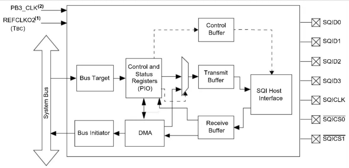
flowchart
graph TD
    A["PB3_CLK(2)"] --> B["REFCLKO2(1) (Tbc)"]
    B --> C["Bus Target"]
    C --> D["Control and Status Registers (PIO)"]
    D --> E["Transmit Buffer"]
    E --> F["SQI Host Interface"]
    F --> G["Control Buffer"]
    G --> H["SQID0"]
    F --> I["SQID1"]
    F --> J["SQID2"]
    F --> K["SQID3"]
    F --> L["SQICLK"]
    F --> M["SQICS0"]
    F --> N["SQICS1"]
    O["Bus Initiator"] --> P["DMA"]
    P --> Q["Receive Buffer"]
    Q --> F
    R["System Bus"] --> S["Up arrow"]
    S --> A
Note 1: When configuring the REFCLKO2 clock source, a value of '0' for the ROTRIM[8:0] bits must be selected. The user need to configure CFGCON3.SPLLPOSTDIV2 when SPLL is selected as clock source for REFCLKO2 (as REFCLKO2 is connected to the auxiliary second PLL clock).
2: This clock source is only used for SQI Special Function Register (SFR) access.
22.1 SQI Control Registers
Note 1: After a Reset, the first access to the SQI SFRs must be a write.
2: The REFCLKO2 must be enabled before reading the registers from the SQI peripheral.
TABLE 22-1: SERIAL QUADRATURE INTERFACE (SQI) REGISTER MAP
| Virtual Address (BFBE_#) | Register Name | Bit Range | Bits | All Resets | ||||||||||||||||
| 31/15 30 | 14 29/13 28 | 12 27/11 26 | 10 25/9 24 | 8 23/7 22/6 | 21/5 20/4 19 | 3 18/2 17/1 | 16/0 | |||||||||||||
| 1008 | SQI1CFG | 31:16 | — | — | — | — | — | — | CSEN[1:0] | SQIEN | — | DATAEN[1:0] | CONBU-FRST | RXBU-FRST | TXBU-FRST | RESET | 0000 | |||
| 15:0 | — | — | — | BURSTEN | — | HOLD | WP | — | — | — | LSBF | CPOL | CPHA | MODE[2:0] | 0000 | |||||
| 100C | SQI1CON | 31:16 | — | — | — | — | — | — | — | SCHECK | — | DASSERT | DEVSEL[1:0] | LANEMODE[1:0] | CMDINIT[1:0] | 0000 | ||||
| 15:0 | TXRXCOUNT[15:0] | 0000 | ||||||||||||||||||
| 1010 | SQI1 CLKCON | 31:16 | — | — | — | — | — | — | — | — | — | — | — | — | — | CLKDIV[10:8] | 0000 | |||
| 15:0 | CLKDIV[7:0] | — | — | — | — | — | — | STABLE | EN | 0000 | ||||||||||
| 1014 | SQI1 CMDTHR | 31:16 | — | — | — | — | — | — | — | — | — | — | — | — | — | — | — | — | 0000 | |
| 15:0 | TXCMDTHR[7:0] | RXCMDTHR[7:0] | 0000 | |||||||||||||||||
| 1018 | SQI1 INTTHR | 31:16 | — | — | — | — | — | — | — | — | — | — | — | — | — | — | — | — | 0000 | |
| 15:0 | TXINTTHR[7:0] | RXINTTHR[7:0] | 0000 | |||||||||||||||||
| 101C | SQI1 INTEN | 31:16 | — | — | — | — | — | — | — | — | — | — | — | — | — | — | — | — | 0000 | |
| 15:0 | DMAEIE | PKT COMPIE | BD DONEIE | CON THRIE | CON EMPTYIE | CON FULLIE | RX THRIE | RX FULLIE | RX EMPTYIE | TX THRIE | TX FULLIE | TX EMPTYIE | TX THRIE | TX FULLIE | TX FULLIE | TX EMPTYIE | 0000 | |||
| 1020 | SQI1 INTSTAT | 31:16 | — | — | — | — | — | — | — | — | — | — | — | — | — | — | — | — | 0000 | |
| 15:0 | DMAEIF | PKT COMPIF | BD DONEIF | CON THRIF | CON EMPTYIF | CON FULLIF | RX THRIF | RX FULLIF | RX EMPTYIF | TX THRIF | TX FULLIF | TX EMPTYIF | TX THRIF | TX FULLIF | TX FULLIF | TX EMPTYIF | 0000 | |||
| 1024 | SQI1 TXDATA | 31:16 | TXDATA[31:16] | 0000 | ||||||||||||||||
| 15:0 | TXDATA[15:0] | 0000 | ||||||||||||||||||
| 1028 | SQI1 RXDATA | 31:16 | RXDATA[31:16] | 0000 | ||||||||||||||||
| 15:0 | RXDATA[15:0] | 0000 | ||||||||||||||||||
| 102C | SQI1 STAT1 | 31:16 | — | — | — | — | — | — | — | — | — | — | TXFIFOFREE[7:0] | 0000 | ||||||
| 15:0 | — | — | — | — | — | — | — | — | — | — | RXFIFOCNT[7:0] | 0000 | ||||||||
| 1030 | SQI1 STAT2 | 31:16 | — | — | — | — | — | — | — | — | — | — | — | — | — | — | CMDSTAT[1:0] | 0000 | ||
| 15:0 | — | — | — | — | CONAVAIL[4:0] | SDID3 | SDID2 | SDID1 | SDID0 | — | RXUN | TXOV | 0000 | |||||||
| 1034 | SQI1 BDCON | 31:16 | — | — | — | — | — | — | — | — | — | — | — | — | — | — | — | — | 0000 | |
| 15:0 | — | — | — | — | — | — | — | — | — | — | — | — | — | START | POLLEN | DMAEN | 0000 | |||
| 1038 | SQI1BD CURADD | 31:16 | BDCURRADDR[31:16] | 0000 | ||||||||||||||||
| 15:0 | BDCURRADDR[15:0] | 0000 | ||||||||||||||||||
| 1040 | SQI1BD BASEADD | 31:16 | BDADDR[31:16] | 0000 | ||||||||||||||||
| 15:0 | BDADDR[15:0] | 0000 | ||||||||||||||||||
| Virtual Address (BF8E_#) | Register Name | Bit Range | Bits | All Resets | ||||||||||||||||
| 31/15 | 30/14 | 29/13 | 28/12 | 27/11 | 26/10 | 25/9 | 24/8 | 23/7 | 22/6 | 21/5 | 20/4 | 19/3 | 18/2 | 17/1 | 16/0 | |||||
| 1044 | SQI1BD STAT | 31:16 | — — | — — — | — — — BD | STATE[3:0] | DMA START | DMAACTV | 0000 | |||||||||||
| 15:0 | BDCON[15:0] 00:00 | |||||||||||||||||||
| 1048 | SQI1BD POLLCON | 31:16 | — — | — — — | — — — | — — — | C000 | |||||||||||||
| 15:0 | POLLCON[15:0] 00:00 | |||||||||||||||||||
| 104C | SQI1BD TXDSTAT | 31:16 | — | — | — | TXSTATE[3:0] | — | — | — | — | TXBUFCNT[4:0] | 0000 | ||||||||
| 15:0 | — — | — — — | — TXCURBUFLEN[7:0] | 0000 | ||||||||||||||||
| 1050 | SQI1BD RXDSTAT | 31:16 | — | — | — | RXSTATE[3:0] | — | — | — | — | RXCURBUFLEN[7:0] | 0000 | ||||||||
| 15:0 | — | — | — | — | — | — | — | — | — | |||||||||||
| 1054 | SQI1THR | 31:16 | — — | — — — | — — — | C000 | ||||||||||||||
| 15:0 | — | — | — | — | — | — | — | — | — | — | — | THRES[4:0] | 0000 | |||||||
| 1058 | SQI1INT SIGEN | 31:16 | — — | — — — | — — — | C000 | ||||||||||||||
| 15:0 | — | — | — | DMAFISE | PKT DONEISE | BD DONEISE | CON THRISE | CON EMPTYISE | CON FULLISE | RX THRISE | RX FULLISE | RX EMPTYISE | TX THRISE | TX FULLISE | TX EMPTYISE | TX EMPTYISE | 0000 | |||
| 105C | SQI1 TAPCON | 31:16 | — — | — — — | — — — | C000 | ||||||||||||||
| 15:0 | — | — | CLKINDLY[5:0] | DATAOUTDLY[3:0] | CLKOUTDLY[3:0] | 0000 | ||||||||||||||
| 1060 | SQI1 MEMSTAT | 31:16 | — | — | — | — | — | — | — | — | — | — | — | STATPOS | TYPESTAT[1:0] | STATBYTES[1:0] | 0000 | |||
| 15:0 | STATDATA[15:0] | 0000 | ||||||||||||||||||
REGISTER 22-1: SQI1CFG: SQI CONFIGURATION REGISTER (1)
| Bit Range | Bit 31/23/15/7 | Bit 30/22/14/6 | Bit 29/21/13/5 | Bit 28/20/12/4 | Bit 27/19/11/3 | Bit 26/18/10/2 | Bit 25/17/9/1 | Bit 24/16/8/0 |
| 31:24 | U-0 U-0 | U-0 U-0 U-0 U-0 | R/W-0 R/W-0 | |||||
| — — — | — — — | CSEN[1:0] | ||||||
| 23:16 | R/W-0 | U-0 | R/W-0 | R/W-0 | R/W-0, HC | R/W-0, HC | R/W-0, HC | R/W-0, HC |
| SQIEN | — | DATAEN[1:0] | CONBUFRST | RXBUFRST | TXBUFRST | RESET | ||
| 15:8 | U-0 | r-0 | r-0 | R/W-0 | r-0 | R/W-0 | R/W-0 | U-0 |
| — — — | BURSTEN | (1) | — | HOLD | WP | — | ||
| 7:0 | U-0 | U-0 | R/W-0 | R/W-0 | R/W-0 | R/W-0 | R/W-0 | R/W-0 |
| — | — | LSBF | CPOL | CPHA | MODE[2:0] | |||
| Legend: | HC = Hardware Cleared | r = Reserved | |
| R = Readable bit | W = Writable bit | U = Unimplemented bit, read as ‘0’ | |
| -n = Value at POR | ‘1’ = Bit is set | ‘0’ = Bit is cleared | x = Bit is unknown |
bit 31-26 Unimplemented: Read as '0'
bit 25-24 CSEN[1:0]: Chip Select Output Enable bits
11 = Chip Select 0 and Chip Select 1 are used
10 = Chip Select 1 is used (Chip Select 0 is not used)
01 = Chip Select 0 is used (Chip Select 1 is not used)
00 = Chip Select 0 and Chip Select 1 are not used
bit 23 SQIEN: SQI Enable bit
1 = SQI module is enabled
0 = SQI module is disabled
Note: Do not use the SQI1CFGbits.SQIEN = 0 instruction to enable the SQI. Instead, use the SQI1CFGCLR = _SQICFG_SQIEN_MASK instruction.
bit 22 Unimplemented: Read as '0'
bit 21-20 DATAEN[1:0]: Data Output Enable bits
11 = Reserved
10 = SQID3-SQID0 outputs are enabled
01 = SQID1 and SQID0 data outputs are enabled
00 = SQID0 data output is enabled
bit 19 CONFIFORST: Control FIFO Reset bit
1 = A reset pulse is generated clearing the control FIFO
0 = A reset pulse is not generated
bit 18 RXFIFORST: Receive FIFO Reset bit
1 = A reset pulse is generated clearing the receive FIFO
0 = A reset pulse is not generated
bit 17 TXFIFORST: Transmit FIFO Reset bit
1 = A reset pulse is generated clearing the transmit FIFO
0 = A reset pulse is not generated
bit 16 RESET: Software Reset Select bit
This bit is automatically cleared by the SQI module. All of the internal state machines and FIFO pointers are reset by this reset pulse.
1 = A reset pulse is generated
0 = A reset pulse is not generated
bit 15 Unimplemented: Read as '0'
Note 1: The SQI1CFG register must be programmed to 2'b01 (CPU mode) in the peripheral initialization code if the SQI peripheral is used.
REGISTER 22-1: SQI1CFG: SQI CONFIGURATION REGISTER (1) (CONTINUED)
bit 14-13 Reserved: Must be programmed as '0'
bit 12 BURSTEN: Burst Configuration bit (1)
1 = Burst is enabled
0 = Burst is not enabled
Note 1: This bit must be programmed as '1'.
bit 11 Reserved: Must be programmed as '0'
bit 10 HOLD: Hold bit
In Single Lane or Dual Lane mode, this bit is used to drive the SQID3 pin, which can be used for devices with a HOLD input pin. The meaning of the values for this bit will depend on the device to which SQID3 is connected.
bit 9 WP: Write Protect bit
In Single Lane or Dual Lane mode, this bit is used to drive the SQID2 pin, which can be used with devices with a write-protect pin. The meaning of the values for this bit will depend on the device to which SQID2 is connected.
bit 8-6 Unimplemented: Read as '0'
bit 5 LSBF: Data Format Select bit
1 = LSB is sent or received first
0 = MSB is sent or received first
bit 4 CPOL: Clock Polarity Select bit
1 = Active-low SQICLK (SQICLK high is the Idle state)
0 = Active-high SQICLK (SQICLK low is the Idle state)
bit 3 CPHA: Clock Phase Select bit
1 = SQICLK starts toggling at the start of the first data bit
0 = SQICLK starts toggling at the middle of the first data bit
bit 2-0 MODE[2:0]: Mode Select bits
111 = Reserved
-
•
100 = Reserved
011 = Reserved
010 = DMA mode is selected
001 = CPU mode is selected (the module is controlled by the CPU in PIO mode.
000 = Reserved
Note 1: The SQI1CFG register must be programmed to 2'b01 (CPU mode) in the peripheral initialization code if the SQI peripheral is used.
REGISTER 22-2: SQI1CON: SQI CONTROL REGISTER
| Bit Range | Bit 31/23/15/7 | Bit 30/22/14/6 | Bit 29/21/13/5 | Bit 28/20/12/4 | Bit 27/19/11/3 | Bit 26/18/10/2 | Bit 25/17/9/1 | Bit 24/16/8/0 |
| 31:24 | U-0 U-0 | U-0 U-0 U-0 U-0 | r-0 R/W-0 | |||||
| — — — | — — — — | SCHECK | ||||||
| 23:16 | U-0 | R/W-0 | R/W-0 | R/W-0 | R/W-0 | R/W-0 | R/W-0 | R/W-0 |
| — | DASSERT | DEVSEL[1:0] | LANEMODE[1:0] | CMDINIT[1:0] | ||||
| 15:8 | R/W-0 | R/W-0 | R/W-0 | R/W-0 | R/W-0 | R/W-0 | R/W-0 | R/W-0 |
| TXRXCOUNT[15:8] | ||||||||
| 7:0 | R/W-0 | R/W-0 | R/W-0 | R/W-0 | R/W-0 | R/W-0 | R/W-0 | R/W-0 |
| TXRXCOUNT[7:0] | ||||||||
| Legend: | r = Reserved | ||
| R = Readable bit | W = Writable bit | U = Unimplemented bit, read as ‘0’ | |
| -n = Value at POR | ‘1’ = Bit is set | ‘0’ = Bit is cleared | x = Bit is unknown |
bit 31-26 Unimplemented: Read as '0'
bit 25 Reserved: Must be programmed as '0'
bit 24 SCHECK: Flash Status Check bit
1 = Check the status of the Flash
0 = Do not check the status of the Flash
bit 23 Unimplemented: Read as '0'
bit 22 DASSERT: Chip Select Assert bit
1 = Chip Select is deasserted after transmission or reception of the specified number of bytes
0 = Chip Select is not deasserted after transmission or reception of the specified number of bytes
bit 21-20 DEVSEL[1:0]: SQL Device Select bits
11 = Reserved
10 = Reserved
01 = Select Device 1
00 = Select Device 0
bit 19-18 LANEMODE[1:0]: SQI Lane Mode Select bits
11 = Reserved
10 = Quad Lane mode
01 = Dual Lane mode
00 = Single Lane mode
bit 17-16 CMDINIT[1:0]: Command Initiation Mode Select bits
If it is Transmit, commands are initiated based on a write to the transmit register or the contents of TX FIFO. If CMDINIT is Receive, commands are initiated based on reads to the read register or RX FIFO availability.
11 = Reserved
10 = Receive
01 = Transmit
00 = Idle
bit 15-0 TXRXCOUNT[15:0]: Transmit/Receive Count bits
These bits specify the total number of bytes to transmit or receive (based on CMDINIT).
REGISTER 22-3: SQI1CLKCON: SQI CLOCK CONTROL REGISTER
| Bit Range | Bit 31/23/15/7 | Bit 30/22/14/6 | Bit 29/21/13/5 | Bit 28/20/12/4 | Bit 27/19/11/3 | Bit 26/18/10/2 | Bit 25/17/9/1 | Bit 24/16/8/0 |
| 31:24 | U-0 U-0 U | -0 U-0 U-0 U-0 | U-0 U-0 | |||||
| — — — | — — — — | |||||||
| 23:16 | U-0 U-0 U | -0 U-0 U-0 R/W | -0 R/W-0 | R/W-0 | ||||
| — — — | — — | CLKDIV[10:8] | (1) | |||||
| 15:8 | R/W-0 | R/W-0 | R/W-0 | R/W-0 | R/W-0 | R/W-0 | R/W-0 | R/W-0 |
| CLKDIV[7:0](1) | ||||||||
| 7:0 | U-0 U-0 U | -0 U-0 U-0 U-0 | R-0 | R/W-0 | ||||
| — | — | — | — | — | — | STABLE | EN | |
Legend:
| R = Readable bit | W = Writable bit | U = Unimplemented bit, read as '0' |
| -n = Value at POR | '1' = Bit is set | '0' = Bit is cleared x = Bit is unknown |
bit 31-19 Unimplemented: Read as '0'
bit 18-8 CLKDIV[10:0]: SQI Clock Tsq Frequency Select bit ^(1)
10000000000 = Base clock TBC is divided by 2048
01000000000 = Base clock TBC is divided by 1024
00100000000 = Base clock TBC is divided by 512
00010000000 = Base clock TBC is divided by 256
00001000000 = Base clock TBC is divided by 128
00000100000 = Base clock TBC is divided by 64
00000010000 = Base clock TBC is divided by 32
00000001000 = Base clock TBC is divided by 16
00000000100 = Base clock TBC is divided by 8
00000000010 = Base clock TBC is divided by 4
00000000001 = Base clock TBC is divided by 2
00000000000 = Base clock TBC
Setting these bits to '00000000000' specifies the highest frequency of the SQI clock.
bit 7-2 Unimplemented: Read as '0'
bit 1 STABLE: T_{SQI} Clock Stable Select bit
This bit is set to '1' when the SQI clock, Tsqi, is stable after writing a '1' to the EN bit.
1 = Tsq clock is stable
0 = Tsq clock is not stable
bit 0 EN: TSQI Clock Enable Select bit
When clock oscillation is stable, the SQI module will set the STABLE bit to '1'.
1 = Enable the SQI clock (TsqI) (when clock oscillation is stable, the SQI module sets the STABLE bit to '1')
0 = Disable the SQI clock (TsqI) (the SQI module must stop its clock to enter a low power state); SFRs can still be accessed, as they use PB3_CLK
Note 1: Refer to 41.0 "Electrical Specifications" for the maximum clock frequency specifications.
REGISTER 22-4: SQI1CMDTHR: SQI COMMAND THRESHOLD REGISTER
| Bit Range | Bit 31/23/15/7 | Bit 30/22/14/6 | Bit 29/21/13/5 | Bit 28/20/12/4 | Bit 27/19/11/3 | Bit 26/18/10/2 | Bit 25/17/9/1 | Bit 24/16/8/0 |
| 31:24 | U-0 U-0 U | -0 U-0 U-0 U-0 | U-0 U-0 | |||||
| —— — | —— — — | |||||||
| 23:16 | U-0 U-0 U | -0 U-0 U-0 U-0 | U-0 U-0 | |||||
| —— — | —— — — | |||||||
| 15:8 | U-0 U-0 U | -0 R/W-0 R/W-0 | R/W-0 R/W-0 | R/W-0 | ||||
| TXCMDTHR[7:0] | ||||||||
| 7:0 | U-0 U-0 U | -0 R/W-0 R/W-0 | R/W-0 R/W-0 | R/W-0 | ||||
| RXCMDTHR[7:0]^(1) | ||||||||
Legend:
| R = Readable bit | W = Writable bit | U = Unimplemented bit, read as '0' |
| -n = Value at POR | '1' = Bit is set | '0' = Bit is cleared x = Bit is unknown |
bit 31-13 Unimplemented: Read as '0'
bit 15-8 TXCMDTHR[7:0]: Transmit Command Threshold bits
In transmit initiation mode, the SQI module performs a transmit operation when transmit command threshold bytes are present in the TX FIFO. These bits must usually be set to '1' for normal Flash commands and set to a higher value for page programming. For 16-bit mode, the value must be a multiple of 2.
bit 7-0 RXCMDTHR[7:0]: Receive Command Threshold bits ^(1)
In receive initiation mode, the SQI module attempts to perform receive operations to fetch the receive command threshold number of bytes in the receive buffer. If space for these bytes is not present in the FIFO, the SQI will not initiate a transfer. For 16-bit mode, the value must be a multiple of 2.
If software performs any reads, thereby reducing the FIFO count, hardware would initiate a receive transfer to make the FIFO count equal to the value in these bits. If software would not like any more words latched into the FIFO, command initiation mode needs to be changed to Idle before any FIFO reads by software.
Note 1: These bits must only be programmed when a receive is not active (i.e., during Idle mode or a transmit).
REGISTER 22-5: SQI1INTTHR: SQI INTERRUPT THRESHOLD REGISTER
| Bit Range | Bit 31/23/15/7 | Bit 30/22/14/6 | Bit 29/21/13/5 | Bit 28/20/12/4 | Bit 27/19/11/3 | Bit 26/18/10/2 | Bit 25/17/9/1 | Bit 24/16/8/0 |
| 31:24 | U-0 U-0 U | -0 U-0 U-0 U-0 | U-0 U-0 | |||||
| — — — | — — — — | |||||||
| 23:16 | U-0 U-0 U | -0 U-0 U-0 U-0 | U-0 U-0 | |||||
| — — — | — — — — | |||||||
| 15:8 | U-0 U-0 U | -0 R/W-0 R/W-0 | R/W-0 R/W-0 | R/W-0 | ||||
| TXINTTHR[7:0] | ||||||||
| 7:0 | U-0 U-0 U | -0 R/W-0 R/W-0 | R/W-0 R/W-0 | R/W-0 | ||||
| RXINTTHR[7:0] | ||||||||
Legend:
| R = Readable bit | W = Writable bit | U = Unimplemented bit, read as '0' |
| -n = Value at POR | '1' = Bit is set | '0' = Bit is cleared x = Bit is unknown |
bit 31-13 Unimplemented: Read as '0'
bit 15-8 TXINTTHR[7:0]: Transmit Interrupt Threshold bits
A transmit interrupt is set when the transmit FIFO has more space than the set number of bytes. For 16-bit mode, the value must be a multiple of 2.
bit 7-0 RXINTTHR[7:0]: Receive Interrupt Threshold bits
A receive interrupt is set when the receive FIFO count is larger than or equal to the set number of bytes. For 16-bit mode, the value must be multiple of 2.
REGISTER 22-6: SQI1INTEN: SQI INTERRUPT ENABLE REGISTER
| Bit Range | Bit 31/23/15/7 | Bit 30/22/14/6 | Bit 29/21/13/5 | Bit 28/20/12/4 | Bit 27/19/11/3 | Bit 26/18/10/2 | Bit 25/17/9/1 | Bit 24/16/8/0 |
| 31:24 | U-0 U-0 U-0 | U-0 U-0 U-0 | U-0 U-0 | |||||
| — — — — | — — — — — | |||||||
| 23:16 | U-0 U-0 U-0 | U-0 U-0 U-0 | U-0 U-0 | |||||
| — — — — | — — — — — | |||||||
| 15:8 | U-0 | U-0 | U-0 | U-0 | R/W-0 | R/W-0 | R/W-0 | R/W-0 |
| — — — — — | DMAEIE | PKTCOMPIE | BDDONEIE | CONTHRIE | ||||
| 7:0 | R/W-0 | R/W-0 | R/W-0 | R/W-0 | R/W-0 | R/W-0 | R/W-0 | R/W-0 |
| CONEMPTYIE | CONFULLIE | RXTHRIE | RXFULLIE | RXEMPTYIE | TXTHRIE | TXFULLIE | TXEMPTYIE |
| Legend: | HS = Hardware Set | ||
| R = Readable bit | W = Writable bit | U = Unimplemented bit, read as ‘0’ | |
| -n = Value at POR | ‘1’ = Bit is set | ‘0’ = Bit is cleared | x = Bit is unknown |
bit 31-12 Unimplemented: Read as '0'
bit 11 DMAEIE: DMA Bus Error Interrupt Enable bit
1 = Interrupt is enabled
0 = Interrupt is disabled
bit 10 PKTCOMPIE: DMA Buffer Descriptor Packet Complete Interrupt Enable bit
1 = Interrupt is enabled
0 = Interrupt is disabled
bit 9 BDDONEIE: DMA Buffer Descriptor Done Interrupt Enable bit
1 = Interrupt is enabled
0 = Interrupt is disabled
bit 8 CONTHRIE: Control Buffer Threshold Interrupt Enable bit
1 = Interrupt is enabled
0 = Interrupt is disabled
bit 7 CONEMPTYIE: Control Buffer Empty Interrupt Enable bit
1 = Interrupt is enabled
0 = Interrupt is disabled
bit 6 CONFULLIE: Control Buffer Full Interrupt Enable bit
This bit enables an interrupt when the receive FIFO buffer is full.
1 = Interrupt is enabled
0 = Interrupt is disabled
bit 5 RXTHRIE:Receive Buffer Threshold Interrupt Enable bit
1 = Interrupt is enabled
0 = Interrupt is disabled
bit 4 RXFULLIE: Receive Buffer Full Interrupt Enable bit
1 = Interrupt is enabled
0 = Interrupt is disabled
bit 3 RXEMPTYIE: Receive Buffer Empty Interrupt Enable bit
1 = Interrupt is enabled
0 = Interrupt is disabled
bit 2 TXTHRIE: Transmit Threshold Interrupt Enable bit
1 = Interrupt is enabled
0 = Interrupt is disabled
bit 1 TXFULLIE: Transmit Buffer Full Interrupt Enable bit
1 = Interrupt is enabled
0 = Interrupt is disabled
bit 0 TXEMPTYIE: Transmit Buffer Empty Interrupt Enable bit
1 = Interrupt is enabled
0 = Interrupt is disabled
REGISTER 22-7: SQI1INTSTAT: SQI INTERRUPT STATUS REGISTER
| Legend: | HS = Hardware Set | ||
| R = Readable bit | W = Writable bit U = Unimplemented bit, read as ‘0’ | ||
| -n = Value at POR | ‘1’ = Bit is set | ‘0’ = Bit is cleared | x = Bit is unknown |
bit 31- Unimplemented: Read as '0'
12
bit 11 DMAEIF: DMA Bus Error Interrupt Flag bit
1 = DMA bus error has occurred
0 = DMA bus error has not occurred
bit 10 PKTCOMPIF: DMA Buffer Descriptor Processor Packet Completion Interrupt Flag bit
1 = DMA BD packet is complete
0 = DMA BD packet is in progress
bit 9 BDDONEIF: DMA Buffer Descriptor Done Interrupt Flag bit
1 = DMA BD process is done
0 = DMA BD process is in progress
bit 8 CONTHRIF: Control Buffer Threshold Interrupt Flag bit
1 = The control buffer has more than THRES words of space available
0 = The control buffer has less than THRES words of space available
bit 7 CONEMPTYIF: Control Buffer Empty Interrupt Flag bit
1 = Control buffer is empty
0 = Control buffer is not empty
bit 6 CONFULLIF: Control Buffer Full Interrupt Flag bit
1 = Control buffer is full
0 = Control buffer is not full
bit 5 RXTHRIF: Receive Buffer Threshold Interrupt Flag bit ^(1)
1 = Receive buffer has more than RXINTTHR words of space available
0 = Receive buffer has less than RXINTTHR words of space available
bit 4 RXFULLIF: Receive Buffer Full Interrupt Flag bit
1 = Receive buffer is full
0 = Receive buffer is not full
bit 3 RXEMPTYIF: Receive Buffer Empty Interrupt Flag bit
1 = Receive buffer is empty
0 = Receive buffer is not empty
Note 1: This bit will be set to a '1', immediately after a POR until a read request on the System Bus is received.
2: The bits in the register are cleared by writing a '1' to the corresponding bit position.
REGISTER 22-7: SQI1INTSTAT: SQI INTERRUPT STATUS REGISTER (CONTINUED)
bit 2 TXTHRIF: Transmit Buffer Threshold Interrupt Flag bit
1 = Transmit buffer has more than TXINTTHR words of space available
0 = Transmit buffer has less than TXINTTHR words of space available
bit 1 TXFULLIF: Transmit Buffer Full Interrupt Flag bit
1 = The transmit buffer is full
0 = The transmit buffer is not full
bit 0 TXEMPTYIF: Transmit Buffer Empty Interrupt Flag bit
1 = The transmit buffer is empty
0 = The transmit buffer has content
Note 1: This bit will be set to a '1', immediately after a POR until a read request on the System Bus is received.
2: The bits in the register are cleared by writing a '1' to the corresponding bit position.
REGISTER 22-8: SQI1TXDATA: SQI TRANSMIT DATA BUFFER REGISTER
| Bit Range | Bit 31/23/15/7 | Bit 30/22/14/6 | Bit 29/21/13/5 | Bit 28/20/12/4 | Bit 27/19/11/3 | Bit 26/18/10/2 | Bit 25/17/9/1 | Bit 24/16/8/0 |
| 31:24 | R/W-0 R/W | -0 R/W-0 R/W-0 | R/W-0 R/W-0 | R/W-0 R/W-0 | ||||
| TXDATA[31:24] | ||||||||
| 23:16 | R/W-0 R/W | -0 R/W-0 R/W-0 | R/W-0 R/W-0 | R/W-0 R/W-0 | ||||
| TXDATA[23:16] | ||||||||
| 15:8 | R/W-0 R/W | -0 R/W-0 R/W-0 | R/W-0 R/W-0 | R/W-0 R/W-0 | ||||
| TXDATA[15:8] | ||||||||
| 7:0 | R/W-0 R/W | -0 R/W-0 R/W-0 | R/W-0 R/W-0 | R/W-0 R/W-0 | ||||
| TXDATA[7:0] | ||||||||
Legend:
R = Readable bit W = Writable bit U = Unimplemented bit, read as '0'
-n = Value at POR '1' = Bit is set '0' = Bit is cleared x = Bit is unknown
bit 31-0 TXDATA[31:0]: Transmit Command Data bits
Data is loaded into this register before being transmitted. Prior to the data transfer, the data in TXDATA is loaded into the shift register (SFDR).
Multiple writes to TXDATA can occur while a transfer is in progress. There can be a maximum of eight commands that can be queued.
REGISTER 22-9: SQI1RXDATA: SQI RECEIVE DATA BUFFER REGISTER
| Bit Range | Bit 31/23/15/7 | Bit 30/22/14/6 | Bit 29/21/13/5 | Bit 28/20/12/4 | Bit 27/19/11/3 | Bit 26/18/10/2 | Bit 25/17/9/1 | Bit 24/16/8/0 |
| 31:24 | R-0 | R-0 | R-0 | R-0 | R-0 | R-0 | R-0 | R-0 |
| RXDATA[31:24] | ||||||||
| 23:16 | R-0 | R-0 | R-0 | R-0 | R-0 | R-0 | R-0 | R-0 |
| RXDATA[23:16] | ||||||||
| 15:8 | R-0 | R-0 | R-0 | R-0 | R-0 | R-0 | R-0 | R-0 |
| RXDATA[15:8] | ||||||||
| 7:0 | R-0 | R-0 | R-0 | R-0 | R-0 | R-0 | R-0 | R-0 |
| RXDATA[7:0] | ||||||||
Legend:
R = Readable bit W = Writable bit U = Unimplemented bit, read as '0'
-n = Value at POR '1' = Bit is set '0' = Bit is cleared x = Bit is unknown
bit 31-0 RXDATA[31:0]: Receive Data Buffer bits
At the end of a data transfer, the data in the shift register is loaded into the RXDATA register. This register works like a FIFO. The depth of the receive buffer is eight words.
REGISTER 22-10: SQI1STAT1: SQI STATUS REGISTER 1
| R = Readable bit | W = Writable bit | U = Unimplemented bit, read as '0' |
| -n = Value at POR | '1' = Bit is set | '0' = Bit is cleared x = Bit is unknown |
bit 31-22 Unimplemented: Read as '0'
bit 21-16 TXFIFOFREE[5:0]: Transmit FIFO Available Word Space bits
bit 15-6 Unimplemented: Read as '0'
bit 5-0 RXFIFOCNT[5:0]: Number of words of read data in the FIFO
REGISTER 22-11: SQI1STAT2: SQI STATUS REGISTER 2
| Bit Range | Bit 31/23/15/7 | Bit 30/22/14/6 | Bit 29/21/13/5 | Bit 28/20/12/4 | Bit 27/19/11/3 | Bit 26/18/10/2 | Bit 25/17/9/1 | Bit 24/16/8/0 |
| 31:24 | U-0 U-0 U-0 | U-0 U-0 U-0 | U-0 U-0 | |||||
| — — — — | — — — — | |||||||
| 23:16 | U-0 U-0 U-0 | U-0 U-0 U-0 | R-0 R-0 | |||||
| — — — — | — — CMDST | AT[1:0] | ||||||
| 15:8 | U-0 U-0 U-0 | U-0 R-0 R-0 | R-0 R-0 | |||||
| — — — — | CONAVAIL[4:1] | |||||||
| 7:0 | R-0 R-0 R-0 | R-0 R-0 U-0 | R-0 R-0 | |||||
| CONAVAIL[0] | SQID3 | SQID2 | SQID1 | SQID0 | — | RXUN | TXOV | |
Legend:
| R = Readable bit | W = Writable bit | U = Unimplemented bit, read as '0' |
| -n = Value at POR | '1' = Bit is set | '0' = Bit is cleared x = Bit is unknown |
bit 31-18 Unimplemented: Read as '0'
bit 17-16 CMDSTAT[1:0]: Current Command Status bits
These bits indicate the current command status.
11 = Reserved
10 = Receive
01 = Transmit
00 = Idle
bit 15-12 Unimplemented: Read as '0'
bit 11-7 CONAVAIL[4:0]: Control FIFO Space Available bits
These bits indicate the available control Word space.
11111 = 32 bytes are available
11110 = 31 bytes are available
-
-
•
00001 = 1 byte is available
00000 = No bytes are available
bit 6 SQID3: SQID3 Status bit
1 = Data is present on SQID3
0 = Data is not present on SQID3
bit 5 SQID2: SQID2 Status bit
1 = Data is present on SQID2
0 = Data is not present on SQID2
bit 4 SQID1: SQID1 Status bit
1 = Data is present on SQID1
0 = Data is not present on SQID1
bit 3 SQID0: SQID0 Status bit
1 = Data is present on SQID0
0 = Data is not present on SQID0
bit 2 Unimplemented: Read as '0'
bit 1 RXUN: Receive FIFO Underflow Status bit
1 = Receive FIFO Underflow has occurred
0 = Receive FIFO underflow has not occurred
bit 0 TXOV: Transmit FIFO Overflow Status bit
1 = Transmit FIFO overflow has occurred
0 = Transmit FIFO overflow has not occurred
REGISTER 22-12: SQI1BDCON: SQI BUFFER DESCRIPTOR CONTROL REGISTER
| R = Readable bit | W = Writable bit | U = Unimplemented bit, read as '0' |
| -n = Value at POR | '1' = Bit is set | '0' = Bit is cleared x = Bit is unknown |
bit 31-3 Unimplemented: Read as '0'
bit 2 START: Buffer Descriptor Processor Start bit
1 = Start the buffer descriptor processor
0 = Disable the buffer descriptor processor
bit 1 POLLEN: Buffer Descriptor Poll Enable bit
1 = BDP poll is enabled
0 = BDP poll is not enabled
bit 0 DMAEN: DMA Enable bit
1 = DMA is enabled
0 = DMA is disabled
REGISTER 22-13: SQI1BDCURADD: SQI BUFFER DESCRIPTOR CURRENT ADDRESS REGISTER
| Bit Range | Bit 31/23/15/7 | Bit 30/22/14/6 | Bit 29/21/13/5 | Bit 28/20/12/4 | Bit 27/19/11/3 | Bit 26/18/10/2 | Bit 25/17/9/1 | Bit 24/16/8/0 |
| 31:24 | R-0 R-0 R-0 R-0 | R-0 R-0 | R-0 R-0 | |||||
| BDCURRADDR[31:24] | ||||||||
| 23:16 | R-0 R-0 R-0 R-0 | R-0 R-0 | R-0 R-0 | |||||
| BDCURRADDR[23:16] | ||||||||
| 15:8 | R-0 R-0 R-0 R-0 | R-0 R-0 | R-0 R-0 | |||||
| BDCURRADDR[15:8] | ||||||||
| 7:0 | R-0 R-0 R-0 R-0 | R-0 R-0 | R-0 R-0 | |||||
| BDCURRADDR[7:0] | ||||||||
Legend:
| R = Readable bit | W = Writable bit | U = Unimplemented bit, read as '0' |
| -n = Value at POR | '1' = Bit is set | '0' = Bit is cleared x = Bit is unknown |
bit 31-0 BDCURRADDR[31:0]: Current Buffer Descriptor Address bits
These bits contain the address of the current descriptor being processed by the Buffer Descriptor Processor.
REGISTER 22-14: SQI1BDBASEADD: SQI BUFFER DESCRIPTOR BASE ADDRESS REGISTER
| Bit Range | Bit 31/23/15/7 | Bit 30/22/14/6 | Bit 29/21/13/5 | Bit 28/20/12/4 | Bit 27/19/11/3 | Bit 26/18/10/2 | Bit 25/17/9/1 | Bit 24/16/8/0 |
| 31:24 | R/W-0 R/W-0 R/W-0 R/W-0 R/W-0 | R/W-0 R/W-0 | R/W-0 R/W-0 | |||||
| BDADDR[31:24] | ||||||||
| 23:16 | R/W-0 R/W-0 R/W-0 R/W-0 R/W-0 | R/W-0 R/W-0 | R/W-0 R/W-0 | |||||
| BDADDR[23:16] | ||||||||
| 15:8 | R/W-0 R/W-0 R/W-0 R/W-0 R/W-0 | R/W-0 R/W-0 | R/W-0 R/W-0 | |||||
| BDADDR[15:8] | ||||||||
| 7:0 | R/W-0 R/W-0 R/W-0 R/W-0 R/W-0 | R/W-0 R/W-0 | R/W-0 R/W-0 | |||||
| BDADDR[7:0] | ||||||||
Legend:
R = Readable bit W = Writable bit U = Unimplemented bit, read as '0'
-n = Value at POR '1' = Bit is set '0' = Bit is cleared x = Bit is unknown
bit 31-0 BDADDR[31:0]: DMA Base Address bits
These bits contain the physical address of the root buffer descriptor. This register must be updated only when the DMA is idle.
REGISTER 22-15: SQI1BDSTAT: SQI BUFFER DESCRIPTOR STATUS REGISTER
| Bit Range | Bit 31/23/15/7 | Bit 30/22/14/6 | Bit 29/21/13/5 | Bit 28/20/12/4 | Bit 27/19/11/3 | Bit 26/18/10/2 | Bit 25/17/9/1 | Bit 24/16/8/0 |
| 31:24 | U-0 | U-0 | U-0 | U-0 | U-0 | U-0 | U-0 | U-0 |
| — | — | — | — | — | — | — | — | |
| 23:16 | U-0 | U-0 | R-x | R-x | R-x | R-x | R-x | R-x |
| — | — | BDSTATE[3:0] | DMASTART | DMAACTV | ||||
| 15:8 | R-x | R-x | R-x | R-x | R-x | R-x | R-x | R-x |
| BDCON[15:8] | ||||||||
| 7:0 | R-x | R-x | R-x | R-x | R-x | R-x | R-x | R-x |
| BDCON[7:0] | ||||||||
Legend:
| R = Readable bit | W = Writable bit | U = Unimplemented bit, read as '0' |
| -n = Value at POR | '1' = Bit is set | '0' = Bit is cleared x = Bit is unknown |
bit 31-22 Unimplemented: Read as '0'
bit 21-18 BDSTATE[3:0]: DMA Buffer Descriptor Processor State Status bits
These bits return the current state of the buffer descriptor processor:
5 = Fetched buffer descriptor is disabled
4 = Descriptor is done
3 = Data phase
2 = Buffer descriptor is loading
1 = Descriptor fetch request is pending
0 = Idle
bit 17 DMASTART: DMA Buffer Descriptor Processor Start Status bit
1 = DMA has started
0 = DMA has not started
bit 16 DMAACTV: DMA Buffer Descriptor Processor Active Status bit
1 = Buffer Descriptor Processor is active
0 = Buffer Descriptor Processor is idle
bit 15-0 BDCON[15:0]: DMA Buffer Descriptor Control Word bits
These bits contain the current buffer descriptor control word.
REGISTER 22-16: SQI1BDPOLLCON: SQI BUFFER DESCRIPTOR POLL CONTROL REGISTER
| Bit Range | Bit 31/23/15/7 | Bit 30/22/14/6 | Bit 29/21/13/5 | Bit 28/20/12/4 | Bit 27/19/11/3 | Bit 26/18/10/2 | Bit 25/17/9/1 | Bit 24/16/8/0 |
| 31:24 | U-0 U-0 U | -0 U-0 U-0 U-0 | U-0 U-0 | |||||
| —— — | —— — — | |||||||
| 23:16 | U-0 U-0 U | -0 U-0 U-0 U-0 | U-0 U-0 | |||||
| —— — | —— — — | |||||||
| 15:8 | R/W-0 | R/W-0 | R/W-0 | R/W-0 | R/W-0 | R/W-0 | R/W-0 | R/W-0 |
| POLLCON[15:8] | ||||||||
| 7:0 | R/W-0 | R/W-0 | R/W-0 | R/W-0 | R/W-0 | R/W-0 | R/W-0 | R/W-0 |
| POLLCON[7:0] | ||||||||
Legend:
| R = Readable bit | W = Writable bit | U = Unimplemented bit, read as '0' |
| -n = Value at POR | '1' = Bit is set | '0' = Bit is cleared x = Bit is unknown |
bit 31-16 Unimplemented: Read as '0'
bit 15-0 POLLCON[15:0]: Buffer Descriptor Processor Poll Status bits
These bits indicate the number of cycles the BDP would wait before refetching the descriptor control word if the previous descriptor fetched was disabled.
REGISTER 22-17: SQI1BDTXDSTAT: SQI BUFFER DESCRIPTOR DMA TRANSMIT STATUS REGISTER
| R = Readable bit | W = Writable bit | U = Unimplemented bit, read as '0' |
| -n = Value at POR | '1' = Bit is set | '0' = Bit is cleared x = Bit is unknown |
bit 31-29 Unimplemented: Read as '0'
bit 28-25 TXSTATE[3:0]: Current DMA Transmit State Status bits
These bits provide information on the current DMA receive states.
bit 24-21 Unimplemented: Read as '0'
bit 20-16 TXBUFCNT[4:0]: DMA Buffer Byte Count Status bits
These bits provide information on the internal FIFO space.
bit 15-8 Unimplemented: Read as '0'
bit 7-0 TXCURBUFLEN[7:0]: Current DMA Transmit Buffer Length Status bits
These bits provide the length of the current DMA transmit buffer.
REGISTER 22-18: SQI1BDRXDSTAT: SQI BUFFER DESCRIPTOR DMA RECEIVE STATUS REGISTER
| Bit Range | Bit 31/23/15/7 | Bit 30/22/14/6 | Bit 29/21/13/5 | Bit 28/20/12/4 | Bit 27/19/11/3 | Bit 26/18/10/2 | Bit 25/17/9/1 | Bit 24/16/8/0 |
| 31:24 | U-0 U-0 U-0 R-x R-x R-x | R-x U-0 | ||||||
| — — — RXSTATE[3:0] — | ||||||||
| 23:16 | U-0 U-0 U-0 R-x R-x R-x | R-x R-x | ||||||
| — — — RXBUFCNT[4:0] | ||||||||
| 15:8 | U-0 U-0 U-0 U-0 U-0 | U-0 | U-0 | |||||
| — | — | — | — | — | — | — | — | |
| 7:0 | R-x | R-x | R-x R-x R-x R-x R-x | |||||
| RXCURBUFLEN[7:0] | ||||||||
Legend:
| R = Readable bit | W = Writable bit | U = Unimplemented bit, read as '0' |
| -n = Value at POR | '1' = Bit is set | '0' = Bit is cleared x = Bit is unknown |
bit 31-29 Unimplemented: Read as '0'
bit 28-25 RXSTATE[3:0]: Current DMA Receive State Status bits
These bits provide information on the current DMA receive states.
bit 24-21 Unimplemented: Read as '0'
bit 20-16 RXBUFCNT[4:0]: DMA Buffer Byte Count Status bits
These bits provide information on the internal FIFO space.
bit 15-8 Unimplemented: Read as '0'
bit 7-0 RXCURBUFLEN[7:0]: Current DMA Receive Buffer Length Status bits
These bits provide the length of the current DMA receive buffer.
REGISTER 22-19: SQI1THR: SQI THRESHOLD CONTROL REGISTER
| Bit Range | Bit 31/23/15/7 | Bit 30/22/14/6 | Bit 29/21/13/5 | Bit 28/20/12/4 | Bit 27/19/11/3 | Bit 26/18/10/2 | Bit 25/17/9/1 | Bit 24/16/8/0 |
| 31:24 | U-0 U-0 U | -0 U-0 U-0 U-0 | U-0 | U-0 | ||||
| — | — | — | — | — | — | — | — | |
| 23:16 | U-0 U-0 U | -0 U-0 U-0 U-0 | U-0 | U-0 | ||||
| — | — | — | — | — | — | — | — | |
| 15:8 | U-0 U-0 U | -0 U-0 U-0 U-0 | U-0 | U-0 | ||||
| — | — | — | — | — | — | — | — | |
| 7:0 | U-0 | U-0 | U-0 | R/W-0 | R/W-0 | R/W-0 | R/W-0 | R/W-0 |
| — — — | THRES[4:0] | |||||||
Legend:
| R = Readable bit | W = Writable bit | U = Unimplemented bit, read as '0' |
| -n = Value at POR | '1' = Bit is set | '0' = Bit is cleared x = Bit is unknown |
bit 31-5 Unimplemented: Read as '0'
bit 4-0 THRES[4:0]: SQI Control Threshold Value bits
The SQI control threshold interrupt is asserted when the amount of space indicated by THRES[4:0] is available in the SQI control buffer.
REGISTER 22-20: SQI1INTSIGEN: SQI INTERRUPT SIGNAL ENABLE REGISTER
| Bit Range | Bit 31/23/15/7 | Bit 30/22/14/6 | Bit 29/21/13/5 | Bit 28/20/12/4 | Bit 27/19/11/3 | Bit 26/18/10/2 | Bit 25/17/9/1 | Bit 24/16/8/0 |
| 31:24 | U-0 U-0 U-0 U-0 U-0 | U-0 U-0 | ||||||
| —— — | —— — — | |||||||
| 23:16 | U-0 U-0 U-0 U-0 U-0 | U-0 U-0 | ||||||
| —— — | —— — — | |||||||
| 15:8 | U-0 | U-0 | U-0 | U-0 | R/W-0 | R/W-0 | R/W-0 | R/W-0 |
| —— — | DMAEISE | PKT DONEISE | BD DONEISE | CON THRISE | ||||
| 7:0 | R/W-0 | R/W-0 | R/W-0 | R/W-0 | R/W-0 | R/W-0 | R/W-0 | R/W-0 |
| CON EMPTYISE | CON FULLISE | RX THRISE | RX FULLISE | RX EMPTYISE | TX THRISE | TX FULLISE | TX EMPTYISE | |
Legend:
| R = Readable bit | W = Writable bit | U = Unimplemented bit, read as '0' |
| -n = Value at POR | '1' = Bit is set | '0' = Bit is cleared x = Bit is unknown |
bit 31-12 Unimplemented: Read as '0'
bit 11 DMAEISE: DMA Bus Error Interrupt Signal Enable bit
1 = Interrupt signal is enabled
0 = Interrupt signal is disabled
bit 10 PKTDONEISE: Receive Error Interrupt Signal Enable bit
1 = Interrupt signal is enabled
0 = Interrupt signal is disabled
bit 9 BDDONEISE: Transmit Error Interrupt Signal Enable bit
1 = Interrupt signal is enabled
0 = Interrupt signal is disabled
bit 8 CONTHRISE: Control Buffer Threshold Interrupt Signal Enable bit
1 = Interrupt signal is enabled
0 = Interrupt signal is disabled
bit 7 CONEMPTYISE: Control Buffer Empty Interrupt Signal Enable bit
1 = Interrupt signal is enabled
0 = Interrupt signal is disabled
bit 6 CONFULLISE: Control Buffer Full Interrupt Signal Enable bit
1 = Interrupt signal is enabled
0 = Interrupt signal is disabled
bit 5 RXTHRISE: Receive Buffer Threshold Interrupt Signal Enable bit
1 = Interrupt signal is enabled
0 = Interrupt signal is disabled
bit 4 RXFULLISE: Receive Buffer Full Interrupt Signal Enable bit
1 = Interrupt signal is enabled
0 = Interrupt signal is disabled
bit 3 RXEMPTYISE: Receive Buffer Empty Interrupt Signal Enable bit
1 = Interrupt signal is enabled
0 = Interrupt signal is disabled
bit 2 TXTHRISE: Transmit Buffer Threshold Interrupt Signal Enable bit
1 = Interrupt signal is enabled
0 = Interrupt signal is disabled
bit 1 TXFULLISE: Transmit Buffer Full Interrupt Signal Enable bit
1 = Interrupt signal is enabled
0 = Interrupt signal is disabled
bit 0 TXEMPTYISE: Transmit Buffer Empty Interrupt Signal Enable bit
1 = Interrupt signal is enabled
0 = Interrupt signal is disabled
REGISTER 22-21: SQI1TAPCON: SQI TAP CONTROL REGISTER
| Bit Range | Bit 31/23/15/7 | Bit 30/22/14/6 | Bit 29/21/13/5 | Bit 28/20/12/4 | Bit 27/19/11/3 | Bit 26/18/10/2 | Bit 25/17/9/1 | Bit 24/16/8/0 |
| 31:24 | U-0 U-0 U | -U-0 U-0 U-0 | U-0 U-0 | |||||
| ——— | ——— — | |||||||
| 23:16 | U-0 U-0 U | -U-0 U-0 U-0 | U-0 U-0 | |||||
| ——— | ——— — | |||||||
| 15:8 | U-0 | U-0 | R/W-0 | R/W-0 | R/W-0 | R/W-0 | R/W-0 | R/W-0 |
| —— | CLKINDLY[5:0] | |||||||
| 7:0 | R/W-0 | R/W-0 | R/W-0 | R/W-0 | R/W-0 | R/W-0 | R/W-0 | R/W-0 |
| DATAOUTDLY[3:0] | CLKOUTDLY[3:0] | |||||||
Legend:
| R = Readable bit | W = Writable bit | U = Unimplemented bit, read as '0' |
| -n = Value at POR | '1' = Bit is set | '0' = Bit is cleared x = Bit is unknown |
bit 31-14 Unimplemented: Read as '0'
bit 13-8 CLKINDLY[5:0]: SQI Clock Input Delay bits
These bits are used to add fractional delays to SQI Clock Input while sampling the incoming data.
111111 = 64 taps added on clock input
111110 = 63 taps added on clock input
•
•
•
000001 = 2 taps added on clock input
000000 = 1 tap added on clock input
bit 7-4 DATAOUTDLY[3:0]: SQI Data Output Delay bits
These bits are used to add fractional delays to SQI Data Output while writing the data to the Flash.
1111 = 16 taps added on clock output
1110 = 15 taps added on clock output
•
•
•
0001 = 2 taps added on clock output
0000 = 1 tap added on clock output
bit 3-0 CLKOUTDLY[3:0]: SQI Clock Output Delay bits
These bits are used to add fractional delays to SQI Clock Output while writing the data to the Flash.
1111 = 16 taps added on clock output
1110 = 15 taps added on clock output
•
•
•
0001 = 2 taps added on clock output
0000 = 1 tap added on clock output
REGISTER 22-22: SQI1MEMSTAT: SQI MEMORY STATUS REGISTER
| R = Readable bit | W = Writable bit | U = Unimplemented bit, read as '0' |
| -n = Value at POR | '1' = Bit is set | '0' = Bit is cleared x = Bit is unknown |
bit 31-21 Unimplemented: Read as '0'
bit 20 STATPOS: Status Bit Position in Flash bit
Indicates the BUSY bit position in the Flash Status register. This bit is added to support all Flash types (with BUSY bit at 0 and at 7).
1 = BUSY bit position is bit 7 in status register
0 = BUSY bit position is bit 0 in status register
bit 19-18 STATTYPE[1:0]: Status Command/Read Lane Mode bits
11 = Reserved
10 = Status command and read are executed in Quad Lane mode
01 = Status command and read are executed in Dual Lane mode
00 = Status command and read are executed in Single Lane mode
bit 17-16 STATBYTES[1:0]: Number of Status Bytes bits
11 = Reserved
10 = Status command/read is 2 bytes long
01 = Status command/read is 1 byte long
00 = Reserved
bit 15-8 STATDATA[7:0]: Status Data bits
These bits contain the status value of the Flash device
bit 7-0 STATCMD[7:0]: Status Command bits
The status check command is written into these bits
23.0 INTER-INTEGRATED CIRCUIT (I²C)
| Note: This data sheet summarizes the features of the PIC32MZ1025W104 family of devices. It is not intended to be a comprehensive reference source. To complement the information in this data sheet, refer to Section 24. “Inter-Integrated Circuit (I2C)” (DS60001116) in the “PIC32 Family Reference Manual”, which is available from the Microchip website (www.microchip.com/PIC32). |
The I^2C module provides complete hardware support for both Client and Multi-Host modes of the I^2C serial communication standard.
Each I²C module has a 2-pin interface:
- SCLx pin is clock
- SDAx pin is data
Each I^2C module offers the following key features:
- I ^2 C interface supporting both host and client operation
- I ^2 C Client mode supports 7-bit and 10-bit addressing
- I ^2 C Host mode supports 7-bit and 10-bit addressing
- I ^2 C port allows bidirectional transfers between host and clients
- Serial clock synchronization for the I ^2 C Port can be used as a handshake mechanism to Suspend and Resume Serial Transfer (SCLREL control)
- I ^2 C supports multi-host operation; detects bus collision and arbitrates accordingly
- Provides support for Client mode address bit masking
- SMbus support
• Supports up to 1 MHz operation
TABLE 23-1: I ^2 C PB CLOCK MAPPING
| I2C Instance PB Clock | |
| I2C1 PB2_CLK | |
| I2C2 PB3_CLK | |
Figure 23-1 illustrates the I^2C module connection diagram.
FIGURE 23-1: I ^2 C CONNECTION DIAGRAM
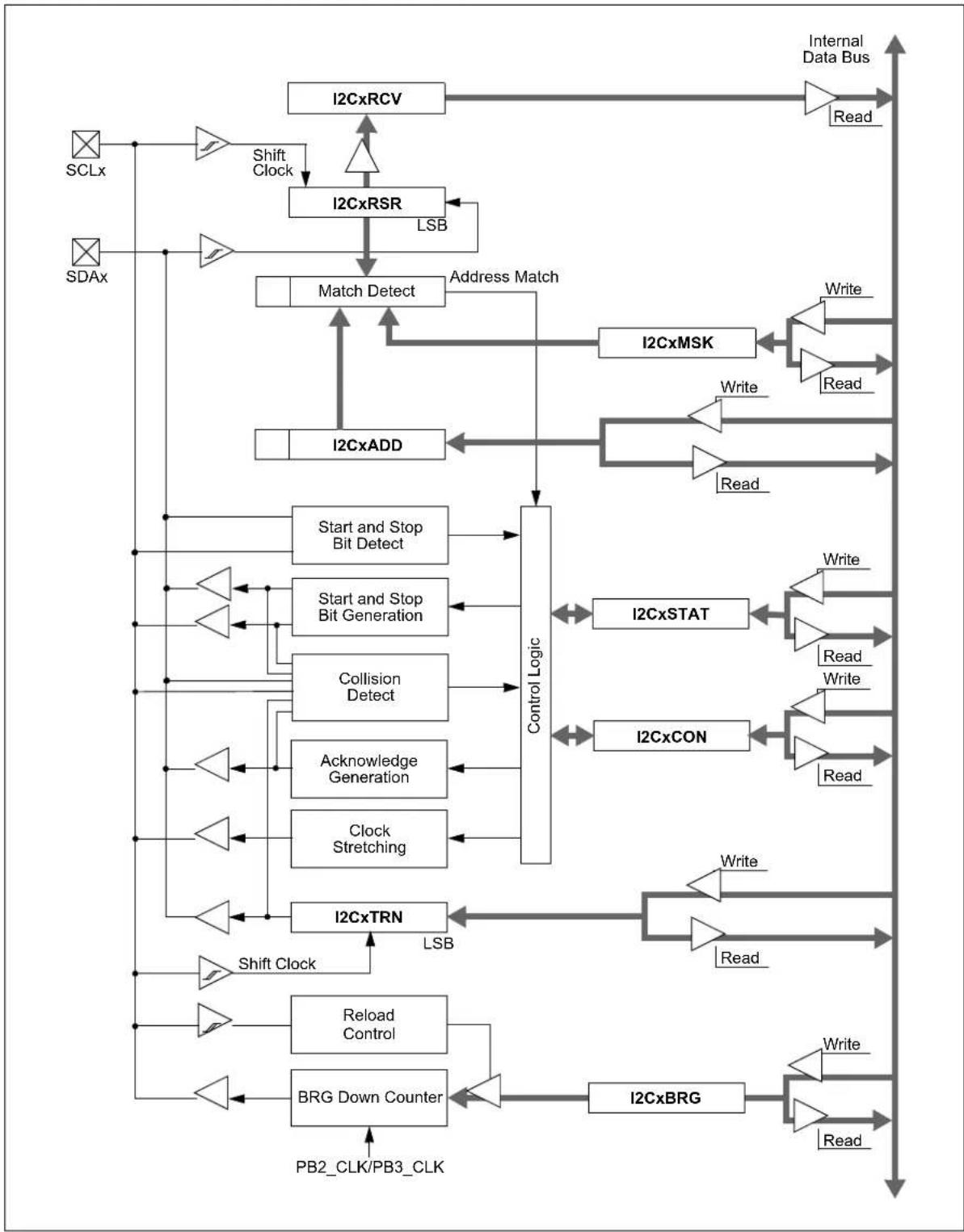
flowchart
graph TD
    A["I2CxRCV"] --> B["Shift Clock"]
    C["I2CxRSR"] --> D["Match Detect"]
    D --> E["Address Match"]
    E --> F["I2CxMSK"]
    F --> G["Write"]
    F --> H["Read"]
    I["SCLx"] --> J["Shift Clock"]
    K["SDAx"] --> L["Match Detect"]
    L --> M["I2CxADD"]
    M --> N["Start and Stop Bit Detect"]
    N --> O["Start and Stop Bit Generation"]
    O --> P["Collision Detect"]
    P --> Q["Acknowledge Generation"]
    Q --> R["Clock Stretching"]
    R --> S["I2CxTRN"]
    S --> T["Shift Clock"]
    U["Reload Control"] --> V["BRG Down Counter"]
    W["PB2_CLK/PB3_CLK"] --> X["PB2_CLK/PB3_CLK"]
    Y["I2CxSTAT"] --> Z["Write"]
    Y --> AA["Read"]
    AB["I2CXCON"] --> AC["Write"]
    AB --> AD["Read"]
    AE["I2CBrG"] --> AF["Write"]
    AE --> AG["Read"]
    AH["Internal Data Bus"] --> AI["Read"]
    AJ["LSB"] --> AK["Address Match"]
    AL["LSB"] --> AM["Address Match"]
    AN["LSB"] --> AO["Address Match"]
    AP["LSB"] --> AQ["Address Match"]
    AR["LSB"] --> AS["Address Match"]
    AT["LSB"] --> AU["Address Match"]
    AV["LSB"] --> AW["Address Match"]
    AX["LSB"] --> AY["Address Match"]
    AZ["LSB"] --> BA["Address Match"]
    BB["LSB"] --> BC["Address Match"]
    BD["I2CxADD"] --> BE["Control Logic"]
    BF["I2CxSTAT"] --> BG["Control Logic"]
    BH["I2CxCON"] --> BI["Control Logic"]
    BJ["I2CxBRG"] --> BK["Control Logic"]
23.1 I ^2 C Control Registers
TABLE 23-2: I ^2 C1 REGISTER MAP
Legend: x = unknown value on Reset; — = unimplemented, read as '0'. Reset values are shown in hexadecimal.
Note 1: All registers in this table except I2CxRCV have corresponding CLR, SET and INV registers at their virtual addresses, plus offsets of 0x4, 0x8 and 0xC, respectively. See Section 13.3 "CLR, SET and INV Registers" for more information.
TABLE 23-3: I ^2 C2 REGISTER MAP
| Virtual Address (BF84_#) | Register Name | Bit Range | Bits | All Resets | |||||||||||||||
| 31/15 | 30/14 | 29/13 | 28/12 | 27/11 | 26/10 | 25/9 | 24/8 | 23/7 | 22/6 | 21/5 | 20/4 | 19/3 | 18/2 | 17/1 | 16/0 | ||||
| 0400 | I2C2CON | 31:16 | — | — | — | — | — | — | — | — | — | PCIE | SCIE | BOEN | SDAHT | SBCDE | AHEN | DHEN | 0000 |
| 15:0 CN | — | SIDL | SCLREL | STRICT | A10M | DISSLW | SMEN | GCEN | STREN | ACKDT | ACKEN | RCEN | PEN | RSEN | SEN | 1000 | |||
| 0410 | I2C2STAT | 31:16 | — | — | — | — | — | — | — | — | — | — | — | — | — | — | — | — | 0000 |
| 15:0 ACKSTAT | TRSTAT | ACKTIM | — | — | — | BCL | GCSTAT | ADD10 | IWCOL | I2COV | D/A | P | S | R/W | RBF | TBF | 0000 | ||
| 0420 | I2C2ADD | 31:16 | — | — | — | — | — | — | — | — | — | — | — | — | — | — | — | — | 0000 |
| 15:0 | — | — | — | — | — | — | — | — | — | I2CADD (Address Register) | 0000 | ||||||||
Legend: x = unknown value on Reset; — = unimplemented, read as '0'. Reset values are shown in hexadecimal.
Note 1: All registers in this table except I2CxRCV have corresponding CLR, SET and INV registers at their virtual addresses, plus offsets of 0x4, 0x8 and 0xC, respectively. See Section 13.3 "CLR, SET and INV Registers" for more information.
TABLE 23-3: I²C2 REGISTER MAP (CONTINUED)
Legend: x = unknown value on Reset; — = unimplemented, read as '0'. Reset values are shown in hexadecimal.
Note 1: All registers in this table except I2CxRCV have corresponding CLR, SET and INV registers at their virtual addresses, plus offsets of 0x4, 0x8 and 0xC, respectively. See Section 13.3 "CLR, SET and INV Registers" for more information.
REGISTER 23-1: I2CxCON: I ^2 C CONTROL REGISTER
| Legend: | HC = Hardware Cleared | ||
| R = Readable bit | W = Writable bit U = Unimplemented bit, read as ‘0’ | ||
| -n = Value at POR | ‘1’ = Bit is set | ‘0’ = Bit is cleared | x = Bit is unknown |
bit 31-23 Unimplemented: Read as '0'
bit 22 PCIE: Stop Condition Interrupt Enable bit (I²C Client mode only)
1 = Enable interrupt on detection of Stop condition
0 = Stop detection interrupts are disabled
bit 21 SCIE: Start Condition Interrupt Enable bit ( I^2C Client mode only)
1 = Enable interrupt on detection of Start or Restart conditions
0 = Start detection interrupts are disabled
bit 20 BOEN: Buffer Overwrite Enable bit (I²C Client mode only)
1 = I2CxRCV is updated and ACK is generated for a received address/data byte, ignoring the state of the I2COV bit (I2CxSTAT[6]) only if the RBF bit (I2CxSTAT[2]) = 0
0 = I2CxRCV is only updated when the I2COV bit (I2CxSTAT[6]) is clear
bit 19 SDAHT: SDA Hold Time Selection bit
1 = Minimum of 300 ns hold time on SDA after the falling edge of SCL
0 = Minimum of 100 ns hold time on SDA after the falling edge of SCL
Note: This bit is not supported for 1 MHz.
bit 18 SBCDE: Client Mode Bus Collision Detect Enable bit (I²C Client mode only)
1 = Enable client bus collision interrupts
0 = Client bus collision interrupts are disabled
bit 17 AHEN: Address Hold Enable bit (Client mode only)
1 = Following the 8th falling edge of SCL for a matching received address byte; SCKREL bit will be cleared and the SCL will be held low.
0 = Address holding is disabled
bit 16 DHEN: Data Hold Enable bit (I²C Client mode only)
1 = Following the 8th falling edge of SCL for a received data byte; client hardware clears the SCKREL bit and SCL is held low
0 = Data holding is disabled
bit 15 ON: I²C Enable bit
1 = Enables the I²C module and configures the SDA and SCL pins as serial port pins
0 = Disables the I²C module; all I²C pins are controlled by PORT functions
bit 14 Unimplemented: Read as '0'
bit 13 SIDL: Stop in Idle Mode bit
1 = Discontinue module operation when device enters Idle mode
0 = Continue module operation in Idle mode
REGISTER 23-1: I2CxCON: I ^2 C CONTROL REGISTER (CONTINUED)
bit 12 SCLREL: SCLx Release Control bit (when operating as I²C client)
In I2C Client mode only; module reset and (ON = 0) sets SCLREL = 1.
If STREN = 0:
1 = Release clock
0 = Force clock low (clock stretch)
Bit is automatically cleared to '0' at beginning of client transmission.
If STREN = 1:
1 = Release clock
0 = Holds clock low (clock stretch)
User may program this bit to '0' to force a clock stretch at the next SCLx low. Bit is automatically cleared to '0' at beginning of client transmission; automatically cleared to '0' at end of client reception.
bit 11 STRICT: Strict I ²C Reserved Address Rule Enable bit 1 = Strict reserved addressing is enforced. Device does not respond to reserved address space or generate addresses in reserved address space. 0 = Strict I²C reserved address rule is not enabled
bit 10 A10M: 10-bit Client Address bit 1 = I2CxADD is a 10-bit client address 0 = I2CxADD is a 7-bit client address
bit 9 DISSLW: Disable Slew Rate Control bit 1 = Slew rate control is disabled 0 = Slew rate control is enabled
bit 8 SMEN: SMBus Input Levels bit 1 = Enable I/O pin thresholds compliant with SMBus specification 0 = Disable SMBus input thresholds
bit 7 GCEN: General Call Enable bit (when operating as I ²C client) 1 = Enable interrupt when a general call address is received in the I2CxRSR (module is enabled for reception) 0 = General call address is disabled
bit 6 STREN: SCLx Clock Stretch Enable bit (when operating as I²C client) Used in conjunction with SCLREL bit. 1 = Enable software or receive clock stretching 0 = Disable software or receive clock stretching
bit 5 ACKDT: Acknowledge Data bit (when operating as I²C host, applicable during host receive) Value that is transmitted when the software initiates an Acknowledge sequence. 1 = Send NACK during acknowledge 0 = Send ACK during acknowledge
bit 4 ACKEN: Acknowledge Sequence Enable bit (when operating as I²C host, applicable during host receive) 1 = Initiate Acknowledge sequence on SDAx and SCLx pins and transmit ACKDT data bit. Hardware cleared at end of host Acknowledge sequence. 0 = Acknowledge sequence not in progress
bit 3 RCEN: Receive Enable bit (when operating as I ²C host) 1 = Enables Receive mode for I²C. Hardware cleared at end of eighth bit of host receive data byte. 0 = Receive sequence not in progress
bit 2 PEN: Stop Condition Enable bit (when operating as I²C host) 1 = Initiate Stop condition on SDAx and SCLx pins. Hardware clear at end of host Stop sequence. 0 = Stop condition not in progress
bit 1 RSEN: Repeated Start Condition Enable bit (when operating as I²C host) 1 = Initiate repeated Start condition on SDAx and SCLx pins. Hardware cleared at end of host repeated Start sequence. 0 = Repeated Start condition not in progress
bit 0 SEN: Start Condition Enable bit (when operating as I²C host) 1 = Initiate Start condition on SDAx and SCLx pins. Hardware cleared at end of host Start sequence. 0 = Start condition not in progress
REGISTER 23-2: I2CxSTAT: I ^2 C STATUS REGISTER
| Bit Range | Bit 31/23/15/7 | Bit 30/22/14/6 | Bit 29/21/13/5 | Bit 28/20/12/4 | Bit 27/19/11/3 | Bit 26/18/10/2 | Bit 25/17/9/1 | Bit 24/16/8/0 |
| 31:24 | U-0 U-0 U-0 | U-0 U-0 U-0 U-0 | U-0 | |||||
| — — — — | — — — — | |||||||
| 23:16 | U-0 U-0 U-0 | U-0 U-0 U-0 U-0 | U-0 | |||||
| — — — — | — — — — | |||||||
| 15:8 | R-0, HS, HC R-0, HS, HC | R/C-0, HS, HC | U-0 U-0 R | C-0, HS | R-0, HS, HC R-0, HS, HC | |||
| ACKSTAT | TRSTAT | ACKTIM | — | — | BCL | GCSTAT | ADD10 | |
| 7:0 | R/C-0, HS, SC | R/C-0, HS, SC | R-0, HS, HC | R/C-0, HS, HC | R/C-0, HS, HC | R-0, HS, HC | R-0, HS, HC | R-0, HS, HC |
| IWCOL | I2COV | D_A | P | S | R_W | RBF | TBF | |
| Legend: | HS = Hardware Set | HC = Hardware Cleared | SC = Software Cleared |
| R = Readable bit | W = Writable bit | U = Unimplemented bit, read as ‘0’ | |
| -n = Value at POR | ‘1’ = Bit is set | ‘0’ = Bit is cleared | C = Clearable bit |
bit 31-16 Unimplemented: Read as '0'
bit 15 ACKSTAT: Acknowledge Status bit
(when operating as I^2C host, applicable to host transmit operation)
1 = NACK received from client
0 = ACK received from client
Hardware set or cleared at the end of client acknowledge.
bit 14 TRSTAT: Transmit Status bit (when operating as I²C host, applicable to host transmit operation)
1 = Host transmit is in progress (8 bits + ACK)
0 = Host transmit is not in progress
Hardware set at the beginning of host transmission. Hardware cleared at the end of client acknowledge.
bit 13 ACKTIM: Acknowledge Time Status bit (Valid in I²C Client mode only)
1 = I^2C bus is in an Acknowledge sequence, set on the eight falling edge of SCL clock
0 = Not an Acknowledge sequence, cleared on 9th rising edge of SCL clock
bit 12-11 Unimplemented: Read as '0'
bit 10 BCL: Host Bus Collision Detect bit
1 = A bus collision is detected during a host operation
0 = No collision
Hardware set at detection of bus collision.
bit 9 GCSTAT: General Call Status bit
1 = General call address is received
0 = General call address is not received
Hardware set when address matches general call address. Hardware cleared at stop detection.
bit 8 ADD10: 10-bit Address Status bit
1 = 10-bit address is matched
0 = 10-bit address is not matched
Hardware set at match of 2nd byte of matched 10-bit address. Hardware cleared at stop detection.
bit 7 IWCOL: Write Collision Detect bit
1 = An attempt to write the I2CxTRN register failed because the I²C module is busy
0 = No collision
Hardware set at occurrence of write to I2CxTRN while busy (cleared by software).
bit 6 I2COV: Receive Overflow Flag bit
1 = A byte is received while the I2CxRCV register is still holding the previous byte
0 = No overflow
Hardware set at attempt to transfer I2CxRSR to I2CxRCV (cleared by software).
REGISTER 23-2: I2CxSTAT: I ^2 C STATUS REGISTER (CONTINUED)
bit 5 D_A: Data/Address bit (when operating as I ^2 C client)
1 = Indicates that the last byte received is data
0 = Indicates that the last byte received is device address
Hardware cleared at device address match. Hardware set by reception of client byte.
bit 4 P: Stop bit
1 = Indicates that a Stop bit is detected last
0 = Stop bit is not detected last
Hardware set or cleared when start, repeated start or stop detected.
bit 3 S: Start bit
1 = Indicates that a start (or repeated start) bit is detected last
0 = Start bit is not detected last
Hardware set or cleared when start, repeated start or stop detected.
bit 2 R_W: Read/Write Information bit (when operating as I ^2 C client)
1 = Read - Indicates data transfer is output from client
0 = Write - Indicates data transfer is input to client
Hardware set or cleared after reception of I ^2 C device address byte.
bit 1 RBF: Receive Buffer Full Status bit
1 = Receive complete, I2CxRCV is full
0 = Receive not complete, I2CxRCV is empty
Hardware set when I2CxRCV is written with received byte. Hardware cleared when software reads I2CxRCV.
bit 0 TBF: Transmit Buffer Full Status bit
1 = Transmit in progress, l2CxTRN is full
0 = Transmit complete, I2CxTRN is empty
Hardware set when software writes I2CxTRN. Hardware cleared at completion of data transmission.
To compute the Baud Rate Generator (BRG) reload value, use the formula in the equation below:
EQUATION 23-1: BRG RELOAD VALUE CALCULATION
$$ I 2 C x B R G = \left[ \left(\frac {1}{(2 . F _ {S C K})} - T _ {P G D}\right) \cdot P B C L K \right] - 2 $$
TABLE 23-4: I ^2 C CLOCK RATE WITH BRG
| PBCLK (MHz) | I2CxBRG | PGD(1)(ns) | Approximate F_SCK (two rollovers of BFG) (kHz) |
| 50 0x037 | 104 400 | ||
| 50 0x0F3 | 104 100 | ||
| 40 0X02C | 104 400 | ||
| 40 0X0C2 | 104 100 | ||
| 30 0X020 | 104 400 | ||
| 30 0X091 | 104 100 | ||
| 20 0X015 | 104 400 | ||
| 20 0X060 | 104 100 | ||
| 10 0X009 | 104 400 | ||
| 10 0X02F | 104 100 | ||
| Note 1: The typical value of the Pulse Gobbler Delay (PGD) is 104 ns. Refer to the I2Cx Bus Data Timing Requirements in Table 41-31 and Table 41-32 for more information. | |||
Note: Equation 23-1 and Table 23-4 are provided as design guidelines. Due to system-dependent parameters, the actual baud rate may differ slightly. Testing is required to confirm that the actual baud rate meets the system requirements. Otherwise, the value of the I2Cx-BRG register may need to be adjusted.
24.0 UART
Note: This data sheet summarizes the features of the PIC32MZ1025W104 family of devices. It is not intended to be a comprehensive reference source. To complement the information in this data sheet, refer to Section 21. "UART" (DS60001107) in the "PIC32 Family Reference Manual", which is available from the Microchip website (www.microchip.com/PIC32).
The Universal Asynchronous Receiver Transmitter (UART) module is one of the serial I/O modules available in the PIC32MZ1025W104 family of devices. The UART is a full-duplex, asynchronous communication channel that communicates with peripheral devices and personal computers through protocols, such as RS-232, RS-485, LIN, and IrDA ^® . The module also supports the hardware flow control option, with UxCTS and UxRTS pins, and also includes an IrDA encoder and decoder.
The device has three UART modules (UART1-3). UART1 supports high-speed operation up to 10 Mbps on non-PPS pins. On PPS pins UART (1-3) speed is limited to 5 Mbps. All three UARTs are capable of 2-pin (UxTX, UxRX) or 4-pin (UxRX, UxTX, UxRTS, UxCTS) operation.
To enable High-speed mode on UART1, the CFGCON1.HSUARTEN register bit needs to be set. This enables UART1 on non-PPS pins. To enable UART1 on PPS pins, CFGCON1.HSUARTEN must be set to '0'. UART2 and UART3 are only available through PPS pads (I/O remap), thus, can achieve up to 5 Mbps speed.
The primary features of the UART module are:
• Full-duplex, 8-bit or 9-bit data transmission
• Even, odd or no parity options (for 8-bit data)
- One or two stop bits
- Hardware flow control option with and pins
- Fully integrated baud rate generator with 16-bit prescaler
• Supports Up to 10 Mbps
Note: Baud clock of 160 MHz is required to obtain 10 Mbps speed.
- Four clock source inputs, asynchronous clocking
- 8-character deep transmit data buffer
• 8-character deep receive data buffer - Parity, framing and buffer overrun error detection
- IrDA encoder and decoder logic
• 16x baud clock output for IrDA support - Support for interrupt on address detect (when 9th bit = 1)
• TX/RX polarity control - Separate transmit and receive interrupts
- loopback mode for diagnostic support
- hardware auto-baud support
Note 1: The FRC clock must be used as the baud clock source to use the UART2 and UART3 in high baud rate (5 Mbps) with the PPS feature.
The figure below illustrates a simplified block diagram of the UART module.
FIGURE 24-1: UART SIMPLIFIED BLOCK DIAGRAM
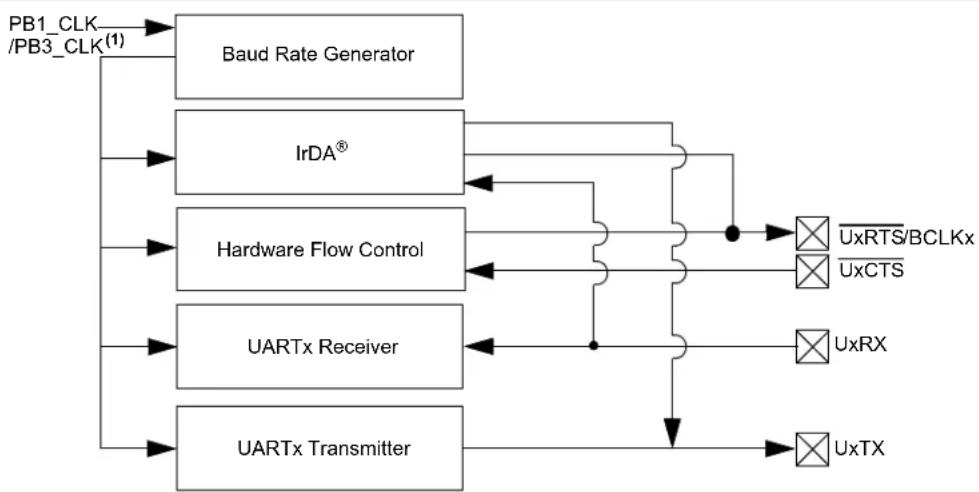
flowchart
graph TD
    A["PB1_CLK /PB3_CLK(1)"] --> B["Baud Rate Generator"]
    A --> C["IrDA®"]
    A --> D["Hardware Flow Control"]
    A --> E["UARTx Receiver"]
    A --> F["UARTx Transmitter"]
    B --> G["× UxRTS/BCLKx"]
    B --> H["× UxCTS"]
    C --> G
    C --> H
    D --> I["× UxRX"]
    E --> J["× UxTX"]
    F --> K["× UxTX"]
Note 1: The PB clock PB1_CLK is used by UART3. The PB clock PB3_CLK is used by UART1 and UART2.
24.1 UART Control Registers
TABLE 24-1: UART1 THROUGH UART3 REGISTER MAP
| Virtual Address(BF84.#) | Register Name | Bit Range | Bits | All Resets | ||||||||||||||||
| 31/15 30 | /14 29/13 | 28/12 27/11 | 26/10 25/9 | 24/8 23/7 | 22/6 21/5 | 20/4 19/3 18 | 2 17/1 16/0 | |||||||||||||
| 0600 | U1MODE (1) | 31:16 | —— — | —— — | SLPEN ACTIVE | —— — | CLK_SEL[1:0] OVFDIS | 0000 | ||||||||||||
| 15:0 | ON | — | SIDL | IREN | RTSMD | — | UEN[1:0] | WAKE | LPBACK | ABAUD | RXINV | BRGH | PDSEL[1:0] | STSEL | 0000 | |||||
| 0610 | U1STA(1) | 31:16 | MASK[7:0] | ADDR[7:0] | 0000 | |||||||||||||||
| 15:0 | UTXISEL[1:0] | UTXINV | URXEN | UTXBRK | UTXEN | UTXBF | TRMT | URXISEL[1:0] | ADDEN | RIDLE | PERR | FERR | OERR | URXDA | 01:0 | |||||
| 0620 | U1TXREG | 31:16 | —— — | —— — | —— — | —— — | —— — | 0000 | ||||||||||||
| 15:0 | — | — | — | — | — | — | — | U1TXREG[7:0] | 0000 | |||||||||||
| 0630 | U1RXREG | 31:16 | —— — | —— — | —— — | —— — | —— — | 0000 | ||||||||||||
| 15:0 | — | — | — | — | — | — | — | U1RXREG[7:0] | 0000 | |||||||||||
| 0640 | U1BRG | 31:16 | — | — | — | — | — | — | — | — | — | — | — | — | U1BRG[19:16] | 0000 | ||||
| 15:0 | U1BRG[15:0] | 0000 | ||||||||||||||||||
| 0800 | U2MODE (1) | 31:16 | —— — | —— — | — | SLPEN ACTIVE | —— — | CLK_SEL[1:0] OVFDIS | 0000 | |||||||||||
| 15:0 | ON | — | SIDL | IREN | RTSMD | — | UEN[1:0] | WAKE | LPBACK | ABAUD | RXINV | BRGH | PDSEL[1:0] | STSEL | 0000 | |||||
| 0810 | U2STA(1) | 31:16 | MASK[7:0] | ADDR[7:0] | 0000 | |||||||||||||||
| 15:0 | UTXISEL[1:0] | UTXINV | URXEN | UTXBRK | UTXEN | UTXBF | TRMT | URXISEL[1:0] | ADDEN | RIDLE | PERR | FERR | OERR | URXDA | 01:0 | |||||
| 0820 | U2TXREG | 31:16 | —— — | —— — | —— — | —— — | —— — | 0000 | ||||||||||||
| 15:0 | — | — | — | — | — | — | — | U2TXREG[7:0] | 0000 | |||||||||||
| 0830 | U2RXREG | 31:16 | —— — | —— — | —— — | —— — | —— — | 0000 | ||||||||||||
| 15:0 | — | — | — | — | — | — | — | U2RXREG[7:0] | 0000 | |||||||||||
| 0840 | U2BRG | 31:16 | — | — | — | — | — | — | — | — | — | — | — | — | U2BRG[19:16] | 0000 | ||||
| 15:0 | U2BRG[15:0] | 0000 | ||||||||||||||||||
| 1600 | U3MODE (1) | 31:16 | —— — | —— — | SLPEN ACTIVE | —— — | CLK_SEL[1:0] OVFDIS | 0000 | ||||||||||||
| 15:0 | ON | — | SIDL | IREN | RTSMD | — | UEN[1:0] | WAKE | LPBACK | ABAUD | RXINV | BGRH | PDSEL[1:0] | STSEL | 0000 | |||||
| 1610 | U3STA(1) | 31:16 | MASK[7:0] | ADDR[7:0] | 0000 | |||||||||||||||
| 15:0 | UTXISEL[1:0] | UTXINV | URXEN | UTXBRK | UTXEN | UTXBF | TRMT | URXISEL[1:0] | ADDEN | RIDLE | PERR | FERR | OERR | URXDA | 01:0 | |||||
| 1620 | U3TXREG | 31:16 | —— — | —— — | —— — | —— — | —— — | 0000 | ||||||||||||
| 15:0 | — | — | — | — | — | — | — | U3TXREG[7:0] | 0000 | |||||||||||
| 1630 | U3RXREG | 31:16 | —— — | —— — | —— — | —— — | —— — | 0000 | ||||||||||||
| 15:0 | — | — | — | — | — | — | — | U3RXREG[7:0] | 0000 | |||||||||||
| 1640 | U3BRG | 31:16 | — | — | — | — | — | — | — | — | — | — | — | — | U3BRG[19:16] | 0000 | ||||
| 15:0 | U3BRG[15:0] | 0000 | ||||||||||||||||||
Legend: x = unknown value on Reset; — = unimplemented, read as '0'. Reset values are shown in hexadecimal.
Note 1: This register has corresponding CLR, SET and INV registers at its virtual address, plus an offset of 0x4, 0x8 and 0xC, respectively. See Section 13.3 "CLR, SET and INV Registers" for more information.
REGISTER 24-1: UxMODE: UARTx MODE REGISTER
| Bit Range | Bit 31/23/15/7 | Bit 30/22/14/6 | Bit 29/21/13/5 | Bit 28/20/12/4 | Bit 27/19/11/3 | Bit 26/18/10/2 | Bit 25/17/9/1 | Bit 24/16/8/0 |
| 31:24 | U-0 U-0 | U-0 U-0 U-0 U | -U-0 U-0 U-0 | |||||
| — — — | — — — — — | |||||||
| 23:16 | R/W-0 R-0 | HS/HC | U-0 U-0 U-0 | U-0 U-0 | R/W-0 | |||
| SLPEN | ACTIVE | — — — | CLK_SEL[1:0] OVFDIS | |||||
| 15:8 | R/W-0 | U-0 | R/W-0 | R/W-0 | R/W-0 | U-0 | R/W-0 | R/W-0 |
| ON | — | SIDL | IREN | RTSMD | — | UEN[1:0](1) | ||
| 7:0 | R/W-0 HC | R/W-0 | R/W-0 HC | R/W-0 | R/W-0 | R/W-0 | R/W-0 | R/W-0 |
| WAKE | LPBACK | ABAUD | RXINV | BRGH | PDSEL[1:0] | STSEL | ||
Legend:
| R = Readable bit | W = Writable bit U = Unimplemented bit, read as '0' |
| -n = Value at POR | '1' = Bit is set at Reset '0' = Bit is cleared at Reset |
| HC = Hardware Cleared | HS = Hardware Set x = Bit is unknown at Reset |
Example: R/W - 0 indicates the bit is both readable and writable, and reads '0' after a Reset.
bit 31-24 Unimplemented: Read as '0'
bit 23 SLPEN: Run during Sleep Enable bit
1 = UART BRG clock runs during Sleep mode
0 = UART BRG clock is turned off during Sleep mode
Note: This assumes that the UART is not driven by system clock that is turned off during sleep.
bit 22 ACTIVE: UART Running Status bit
1 = UART clock request is active
0 = UART clock request is not active
bit 21-19 Unimplemented: Read as '0'
bit 18-17 CLK_SEL: UARTx Baud Clock Selection bits
11 = UART BRG clock is the external REFO1 clock.
10 = UART BRG clock is the external FRC clock.
01 = UART BRG clock is the external SYS clock.
00 = UART BRG clock is the internal UPBM clock
Note 1: These bits can only be changed when UxMODE.ON = 0.
2: A clock frequency of 160 MHz is required for obtaining 10 Mbps speed.
bit 16 OVFDIS: Run during Overflow Condition Mode bit
1 = When OERR is detected, shift register continues to run to remain synchronized
0 = When OERR is detected, shift register stops accepting new data
bit 15 ON: UARTx Enable bit
1 = UARTx is enabled; UARTx pins are controlled by UARTx as defined by UEN[1:0] and UTXEN control bits.
0 = UARTx is disabled; all UARTx pins are controlled by corresponding bits in the control bits PORTx, TRISx and LATx registers; UARTx power consumption is minimal.
bit 14 Unimplemented: Read as '0'
bit 13 SIDL: Stop in Idle Mode bit
1 = Discontinue module operation when device enters Idle mode
0 = Continue module operation in Idle mode
Note 1: These bits are present for legacy compatibility, and are superseded by PPS functionality on these devices. For additional information, see Section 13.4 "Peripheral Pin Select (PPS)".
REGISTER 24-1: UxMODE: UARTx MODE REGISTER (CONTINUED)
bit 12 IREN: IrDA Encoder and Decoder Enable bit
1 = IrDA enabled
0 = IrDA disabled
Note: This feature is only available for Standard mode (UxMODE.BRGH = '0').
bit 11 RTSMD: Mode Selection for UxRTS Pin bit
1 = UxRTS pin in Simplex mode
0 = UxRTS pin in Flow Control mode
bit 10 Unimplemented: Read as '0'
bit 9-8 UEN[1:0]: UARTx Enable bits (1)
11 = UxTX, UxRX and UxBCLK pins are enabled and used; UxCTS pin is controlled by corresponding bits in the PORTx register
10 = UxTX, UxRX, UxCTS and UxRTS pins are enabled and used
01 = UxTX, UxRX and UxRTS pins are enabled and used; UxCTS pin is controlled by corresponding bits in the PORTx register
0.0 = UxTX and UxRX pins are enabled and used; UxCTS and UxRTS/UxBCLK pins are controlled by corresponding bits in the PORTx register
bit 7 WAKE: Enable Wake-up on Start bit Detect During Sleep Mode bit
1 = Wake-up is enabled
0 = Wake-up is disabled
Note: Hardware clear has priority over software.
bit 6 LPBACK: UARTx Loopback Mode Enable bit
1 = Enabled
0 = Disabled
bit 5 ABAUD: Auto Baud Enable bit
1 = Enable baud rate measurement on the next character – requires reception of a SYNCH field (55h); cleared in hardware upon completion
0 = Baud rate measurement disabled or completed
bit 4 RXINV: Receive Polarity Inversion bit
1 = RX Idle state is '0'
0 = RX Idle state is '1'
bit 3 BRGH: High Baud Rate Enable bit
1 = UxBRG generates 4 shift clocks per bit period (4x baud clock, High-speed mode)
0 = UxBRG generates 16 shift clocks per bit period (16x baud clock, Standard mode)
Note: The user configurations must not exceed the maximum supported baud rate.
bit 2-1 PDSEL[1:0]: Parity and Data Selection bits
11 = 9-bit data, no parity
10 = 8-bit data, odd parity
01 = 8-bit data, even parity
00 = 8-bit data, no parity
bit 0 STSEL: Stop Selection bit
1 = 2 Stop bits
0 = 1 Stop bit
Note 1: These bits are present for legacy compatibility, and are superseded by PPS functionality on these devices.
For additional information, see Section 13.4 "Peripheral Pin Select (PPS)".
REGISTER 24-2: UxSTA: UARTx STATUS AND CONTROL REGISTER
| Bit Range | Bit 31/23/15/7 | Bit 30/22/14/6 | Bit 29/21/13/5 | Bit 28/20/12/4 | Bit 27/19/11/3 | Bit 26/18/10/2 | Bit 25/17/9/1 | Bit 24/16/8/0 |
| 31:24 | R/W-0 R/W | W-0 R/W-0 R/W | W-0 R/W-0 R/W | W-0 R/W-0 R/W | W-0 | |||
| MASK[7:0] | ||||||||
| 23:16 | R/W-0 R/W | W-0 R/W-0 R/W | W-0 R/W-0 R/W | W-0 R/W-0 R/W | W-0 | |||
| ADDR[7:0] | ||||||||
| 15:8 | R/W-0 R/W | W-0 R/W-0 R/W | W-0 R/W-0 HC | R/W-0 R-0 R-1 | ||||
| UTXISEL[1:0] UTXIN V URXEN | (1) | UTXBRK U TXEN UTXBF TRMT | ||||||
| 7:0 | R/W-0 R/W | W-0 R/W-0 | R-1 | R-0 R-0 | R/C-0 R-0 | |||
| URXISEL[1:0] | ADDEN | RIDLE | PERR | FERR | OERR | URXDA | ||
Legend:
R = Readable bit W = Writable bit U = Unimplemented bit, read as '0'
-n = Value at POR '1' = Bit is set at Reset '0' = Bit is cleared at Reset
HC = Hardware Cleared HS = Hardware Set x = Bit is unknown at Reset
Example: R/W - 0 indicates the bit is both readable and writable, and reads '0' after a Reset.
bit 31-24 MASK[7:0]: Address Match Mask bits
Used to mask the UxSTAT.ADM_ADDR[7:0] bits.
For ADM_MASK[n]:
1 = ADM_ADDR[n] is used to detect the address match
0 = ADM_ADDR[n] is not used to detect the address match
bit 23-16 ADDR[7:0]: Address Detect Task Offload bits
Used with UxSTAT.ADM_EN to offload the task of detecting the address character from the processor during Address Detect mode.
bit 15-14 UTXISEL[1:0]: Transmission Interrupt Mode Selection bits
11 = Reserved, do not use
10 = Interrupt is persistent when the transmit buffer is empty
(The Transmit Shift register may or may not be empty.)
01 = Interrupt is persistent when both the transmit buffer and Transmit Shift register are empty
(This indicates that all characters have been transmitted).
00 = Interrupt is persistent when the transmit buffer is not full
(This means there is space for at least one character in the transmit buffer).
bit 13 UTXINV: Transmit Polarity Inversion bit
If UxMODE.IREN = 0:
1 = TX Idle state is '0'
0 = TX Idle state is '1'
If UxMODE.IREN = 1:
1 = IrDA encoded TX Idle state is '1'
0 = IrDA encoded TX Idle state is '0'
bit 12 URXEN: Receive Enable bit ^(1)
1 = Receive enabled, characters seen on the RX pin and captured by the UARTx
0 = Receive disabled, the RX pin is ignored by the UARTx. RX pin is controlled by PORT.
bit 11 UTXBRK: Transmit Break bit
1 = Send SYNCH BREAK on next transmission – Start bit, followed by twelve '0' bits, followed by Stop bit; cleared by hardware upon completion
0 = SYNCH BREAK transmission disabled or completed
bit 10 UTXEN: Transmit Enable bit
1 = UARTx transmitter is enabled. UxTX pin is controlled by UARTx (if ON = 1)
0 = UARTx transmitter is disabled. Any pending transmission is aborted and buffer is reset
REGISTER 24-2: UxSTA: UARTx STATUS AND CONTROL REGISTER (CONTINUED)
bit 9 UTXBF: Transmit Buffer Full Status bit
1 = Transmit buffer is full
0 = Transmit buffer is not full, at least one more character can be written
bit 8 TRMT: Transmit Shift Register Empty bit
1 = Transmit shift register is empty and transmit buffer is empty (The last transmission has completed)
0 = Transmit shift register is not empty, a transmission is in progress or queued
bit 7-6 URXISEL[1:0]: Receive Interrupt Mode Selection bit
11 = Reserved, do not use
10 = Interrupt is persistent when the receive buffer has 6 or more data characters
01 = Interrupt is persistent when the receive buffer has 4 or more data characters
00 = Interrupt is persistent when the receive buffer has 1 or more data characters (in other words, not empty)
bit 5 ADDEN: Address Character Detect bit (Bit 8 of received data = 1)
1 = Address Detect mode is enabled. If 9-bit mode is not selected, this control bit has no effect.
0 = Address Detect mode is disabled
bit 4 RIDLE: Receiver Idle bit
1 = Receiver is idle
0 = Receiver is active
bit 3 PERR: Parity Error Status bit
1 = Parity error has been detected for the current character (Character at the top of the receive FIFO)
0 = Parity error has not been detected
bit 2 FERR: Framing Error Status bit
1 = Framing error has been detected for the current character (Character at the top of the receive FIFO)
0 = Framing error has not been detected
bit 1 OERR: Receive Buffer Overrun Error Status bit
1 = Receive buffer has overflowed
0 = Receive buffer has not overflowed
Note 1: When RUNOVF = 0, clearing a previously set OERR bit ('1' to '0' transition) resets the receiver buffer and the RSR to the empty state.
2: When RUNOVF = 1, clearing a previously set OERR bit ('1' to '0' transition) does not reset the receive buffer or RSR.
bit 0 URXDA: Receive Buffer Data Available bit
1 = Receive buffer has data, at least one more character can be read
0 = Receive buffer is empty
Note 1: Clearing UxSTAT.RXEN will not reset the receive buffer. Clearing UxMODE.ON will reset the receive buffer.
24.2 Receive and Transmit Timing for UART Module
The figures below illustrate the typical receive and transmit timing for the UART module.
FIGURE 24-2: UART RECEPTION
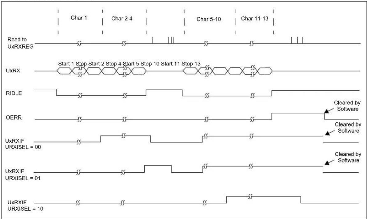
flowchart
graph TD
    A["Read to UxRXREG"] --> B["Char 1"]
    B --> C["Char 2-4"]
    C --> D["Char 5-10"]
    D --> E["Char 11-13"]

    F["UxRX"] --> G["Start 1 Stop Start 2 Stop 4 Start 5 Stop 10 Start 11 Stop 13"]

    H["RIDLE"] --> I["SS SS SS SS SS SS"]

    J["OERR"] --> K["SS SS SS SS SS"]

    L["UxRXIF URXISEL = 00"] --> M["SS SS SS SS SS"]

    N["UxRXIF URXISEL = 01"] --> O["SS SS SS SS SS"]

    P["UxRXIF URXISEL = 10"] --> Q["SS SS SS SS SS"]
FIGURE 24-3: UART TRANSMISSION (8-BIT OR 9-BIT DATA)
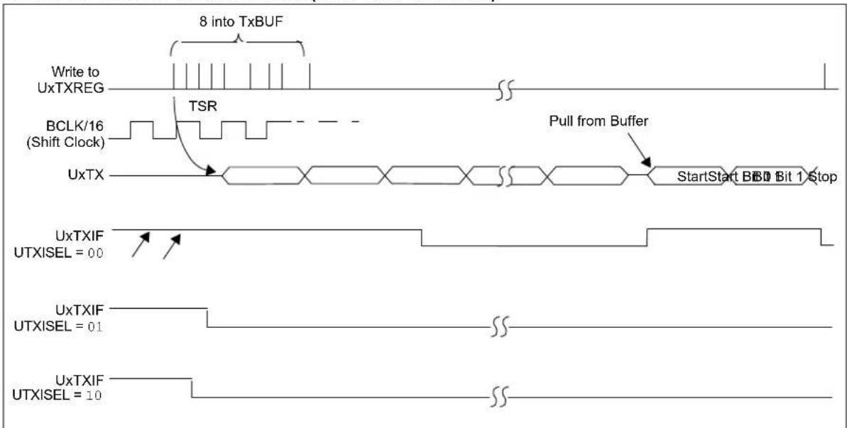
flowchart
graph TD
    A["Write to UxTXREG"] --> B["8 into TxBUF"]
    B --> C["TSR"]
    C --> D["BCLK/16 (Shift Clock)"]
    D --> E["UxTX"]
    E --> F["Pull from Buffer"]
    F --> G["StartStart BBD Bit 1 Stop"]
    G --> H["UxTXIF UTXISEL = 00"]
    H --> I["UxTXIF UTXISEL = 01"]
    I --> J["UxTXIF UTXISEL = 10"]
    J --> K["SS"]
    style A fill:#f9f,stroke:#333
    style B fill:#ccf,stroke:#333
    style C fill:#cfc,stroke:#333
    style D fill:#fcc,stroke:#333
    style E fill:#cff,stroke:#333
    style F fill:#ffc,stroke:#333
    style G fill:#cfc,stroke:#333
    style H fill:#fcc,stroke:#333
    style I fill:#ffc,stroke:#333
    style J fill:#fcc,stroke:#333
    style K fill:#ffc,stroke:#333
25.0 REAL-TIME CLOCK AND CALENDAR (RTCC)
Note: This data sheet summarizes the features of the PIC32MZ1025W104 family of devices. It is not intended to be a comprehensive reference source. To complement the information in this data sheet, refer to Section 29. "Real-Time Clock and Calendar (RTCC)" (DS60001125) in the "PIC32 Family Reference Manual", which is available from the Microchip website (www.microchip.com/PIC32).
The RTCC module is intended for applications in which accurate time must be maintained for extended periods of time with minimal or no CPU intervention. Low-power optimization provides extended battery lifetime while keeping track of time.
The following are key features of the RTCC module:
• Time: hours, minutes, and seconds
• 24-hour format (military time)
- Visibility of one-half second period
- Provides calendar: weekday, date, month, and year
- Alarm intervals are configurable for half of a second, one second, 10 seconds, one minute, 10 minutes, one hour, one day, one week, one month and one year.
- Alarm repeat with decrementing counter
- Alarm with indefinite repeat: Chime
• Year range: 2000-2099 - Leap year correction
• BCD format for smaller firmware overhead - Optimized for long-term battery operation
• Fractional second synchronization - User calibration of the clock frequency with periodic auto-adjust
- Calibration within ± 2.64 seconds error per month
- Calibrates up to 260 ppm of crystal error
- Uses external 32.768 kHz crystal or 32.768 kHz internal oscillator
- Alarm pulse or seconds clock output on RTCC pin
The RTCC reference clock is obtained from either the SOSC or LPRC oscillator. The user is responsible to enable the oscillator using the OSCCON[SOSCEN] bit if the SOSC is used.
FIGURE 25-1: RTCC BLOCK DIAGRAM
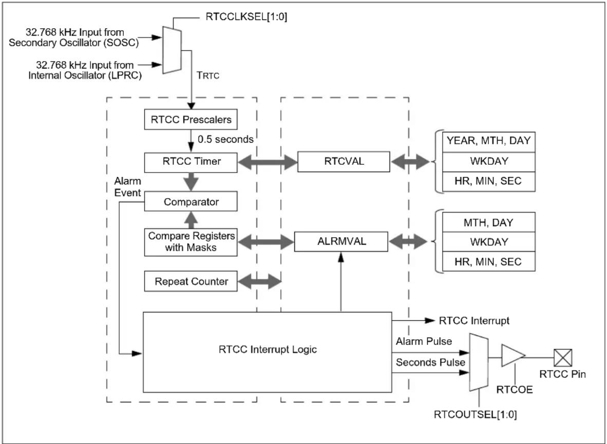
flowchart
graph TD
    A["32.768 kHz Input from Secondary Oscillator (SOSC)"] --> B["RTCC Prescalers"]
    C["32.768 kHz Input from Internal Oscillator (LPRC)"] --> B
    B --> D["0.5 seconds"]
    D --> E["RTCC Timer"]
    E <--> F["RTCVAL"]
    F <--> G["YEAR, MTH, DAY"]
    F --> H["WKDAY"]
    F --> I["HR, MIN, SEC"]
    E --> J["Comparator"]
    J --> K["Compare Registers with Masks"]
    K --> L["ALRMVAL"]
    L <--> M["MTH, DAY"]
    L --> N["WKDAY"]
    L --> O["HR, MIN, SEC"]
    J --> P["Repeat Counter"]
    P --> Q["RTCC Interrupt Logic"]
    Q --> R["RTCC Interrupt"]
    R --> S["Alarm Pulse"]
    R --> T["Seconds Pulse"]
    S --> U["RTCOE"]
    T --> V["RTCC Pin"]
    U --> W["RTCOUTSEL[1:0"]]
    V --> X["RTCC Pin"]
25.1 RTCC Control Registers
TABLE 25-1: RTCC REGISTER MAP
| Virtual Address(BF87_#) | Register Name() | Bit Range | Bits | All Resets | |||||||||||||||||
| 31/15 30 | /14 29/13 | 28/12 27/11 | 26/10 25/9 | 24/8 23/7 | 22/6 21/5 20 | 20/4 19/3 18 | 1/2 17/1 16 | 0 | |||||||||||||
| 0000 | RTCCON | 31:16 | — | — | — | — | — | — | CAL[9:0] | 0000 | |||||||||||
| 15:0 | ON | — | SIDL | — | — | RTCCLKSEL[1:0] | RTCOUTSEL[1:0] | RTCCLKON | — | — | RTCWREN | RTCSYNC | HALFSEC | RTCOE | 0000 | ||||||
| 0010 | RTCALRM | 31:16 | — | — | — | — | — | — | — | — | — | — | — | — | — | — | — | 0000 | |||
| 15:0 | ALRMEN | CHIME | PIV | ALRMSYNC | AMASK[3:0] | ARPT[7:0] | 0000 | ||||||||||||||
| 0020 | RTCTIME | 31:16 | HR10[3:0] | HR01[3:0] | MIN10[3:0] | MIN01[3:0] | ×××× | ||||||||||||||
| 15:0 | SEC10[3:0] | SEC01[3:0] | — | — | — | — | — | — | — | — | xx×0 | ||||||||||
| 0030 | RTCDATE | 31:16 | YEAR10[3:0] | YEAR01[3:0] | MONTH10[3:0] | MONTH01[3:0] | ×××× | ||||||||||||||
| 15:0 | DAY10[3:0] | DAY01[3:0] | — | — | — | — | WDAY01[3:0] | xx×0 | |||||||||||||
| 0040 | ALRMTIME | 31:16 | HR10[3:0] | HR01[3:0] | MIN10[3:0] | MIN01[3:0] | ×××× | ||||||||||||||
| 15:0 | SEC10[3:0] | SEC01[3:0] | — | — | — | — | — | — | — | xx×0 | |||||||||||
| 0050 | ALRMDATE | 31:16 | — | — | — | — | — | — | — | — | MONTH10[3:0] | MONTH01[3:0] | 0Cxx | ||||||||
| 15:0 | DAY10[3:0] | DAY01[3:0] | — | — | — | — | WDAY01[3:0] | xx×0 | |||||||||||||
Legend: x = unknown value on Reset; — = unimplemented, read as '0'. Reset values are shown in hexadecimal.
Note 1: All registers in this table have corresponding CLR, SET and INV registers at its virtual address, plus an offset of 0x4, 0x8 and 0xC, respectively. See Section 13.3 "CLR, SET and INV Registers" for more information.
REGISTER 25-1: RTCCON: REAL-TIME CLOCK AND CALENDAR CONTROL REGISTER
| Bit Range | Bit 31/23/15/7 | Bit 30/22/14/6 | Bit 29/21/13/5 | Bit 28/20/12/4 | Bit 27/19/11/3 | Bit 26/18/10/2 | Bit 25/17/9/1 | Bit 24/16/8/0 |
| 31:24 | U-0 U-0 U-0 | U-0 U-0 U-0 R/W | R/W-0 | R/W-0 | ||||
| —— — — | — — | C | A | L | [ 9 | |||
| 23:16 | R/W-0 | R/W-0 | R/W-0 | R/W-0 | R/W-0 | R/W-0 | R/W-0 | R/W-0 |
| CAL[7:0] | ||||||||
| 15:8 | R/W-0 | U-0 | R/W-0 | U-0 | U-0 | R/W-0 | R/W-0 | R/W-0 |
| ON(1) | — | SIDL | — | — | RTCCLKSEL[1:0] | RTCOUTSEL[1](2) | ||
| 7:0 | R/W-0 | R-0 U-0 U-0 | R/W-0 | R/W-0 | R-0 R-0 R/W-0 | |||
| RTCOUTSEL[0](2) | RTCCLKON(5) | — | — | RTCWREN(3) | RTCSYNC | HALFSEC(4) | RTCOE | |
Legend:
| R = Readable bit | W = Writable bit | U = Unimplemented bit, read as '0' |
| -n = Value at POR | '1' = Bit is set | '0' = Bit is cleared x = Bit is unknown |
bit 31-26 Unimplemented: Read as '0'
bit 25-16 CAL[9:0]: Real-Time Clock Drift Calibration bits, which contain a signed 10-bit integer value
0111111111 = Maximum positive adjustment, adds 511 real-time clock pulses every one minute
•
•
•
0000000001 = Minimum positive adjustment, adds 1 real-time clock pulse every one minute
0000000000 = No adjustment
1111111111 = Minimum negative adjustment, subtracts 1 real-time clock pulse every one minute
•
•
•
1000000000 = Maximum negative adjustment, subtracts 512 real-time clock pulses every one minute
bit 15 ON: RTCC On bit ^(1)
1 = RTCC module is enabled
0 = RTCC module is disabled
bit 14 Unimplemented: Read as '0'
bit 13 SIDL: Stop in Idle Mode bit
1 = Disables RTCC operation when CPU enters Idle mode
0 = Continue normal operation when CPU enters Idle mode
bit 12-11 Unimplemented: Read as '0'
bit 10-9 RTCCLKSEL[1:0]: RTCC Clock Select bits
When a new value is written to these bits, the Seconds Value register must also be written to properly reset the clock prescalers in the RTCC.
11 = Reserved
10 = Reserved
01 = RTCC uses the external 32.768 kHz SOSC
00 = RTCC uses the internal 32.768 kHz LPRC
Note 1: The ON bit is only writable when RTCWREN = 1.
2: Requires RTCOE = 1 (RTCCON[0]) for the output to be active.
3: The RTCWREN bit can be set only when the Write sequence is enabled.
4: This bit is read-only. It is cleared to '0' on a write to the seconds bit fields (RTCTIME[14:8]).
5: This bit is undefined when RTCCLKSEL[1:0] = 0.0 (LPRC is the clock source).
6: This register is reset only on a POR.
REGISTER 25-1: RTCCON: REAL-TIME CLOCK AND CALENDAR CONTROL REGISTER (CONTINUED)
bit 8-7 RTCOUTSEL[1:0]: RTCC Output Data Select bits (2)
11 = Reserved
10 = Reserved
01 = Seconds Clock is presented on the RTCC pin
00 = Alarm Pulse is presented on the RTCC pin when the alarm interrupt is triggered
bit 6 RTCCLKON: RTCC Clock Enable Status bit (5)
1 = RTCC Clock is actively running
0 = RTCC Clock is not running
bit 5-4 Unimplemented: Read as '0'
bit 3 RTCWREN: Real-Time Clock Value Registers Write Enable bit ^(3)
1 = Real-Time Clock Value registers can be written to by the user
0 = Real-Time Clock Value registers are locked out from being written to by the user
bit 2 RTCSYNC: Real-Time Clock Value Registers Read Synchronization bit
1 = Real-time clock value registers can change while reading (due to a rollover ripple that results in an invalid data read). If the register is read twice and results in the same data, the data can be assumed to be valid.
0 = Real-time clock value registers can be read without concern about a rollover ripple
bit 1 HALFSEC: Half-Second Status bit (4)
1 = Second half period of a second
0 = First half period of a second
bit 0 RTCOE: RTCC Output Enable bit
1 = RTCC output is enabled
0 = RTCC output is disabled
Note 1: The ON bit is only writable when RTCWREN = 1.
2: Requires RTCOE = 1 (RTCCON[0]) for the output to be active.
3: The RTCWREN bit can be set only when the Write sequence is enabled.
4: This bit is read-only. It is cleared to '0' on a write to the seconds bit fields (RTCTIME[14:8]).
5: This bit is undefined when RTCCLKSEL[1:0] = 0.0 (LPRC is the clock source).
6: This register is reset only on a POR.
REGISTER 25-2: RTCALRM: REAL-TIME CLOCK ALARM CONTROL REGISTER
| Legend: | |||
| R = Readable bit | W = Writable bit | U = Unimplemented bit, read as ‘0’ | |
| -n = Value at POR | ‘1’ = Bit is set | ‘0’ = Bit is cleared | x = Bit is unknown |
bit 31-16 Unimplemented: Read as '0'
bit 15 ALRMEN: Alarm Enable bit ^(1,2)
1 = Alarm is enabled
0 = Alarm is disabled
bit 14 CHIME: Chime Enable bit ^(2)
1 = Chime is enabled - ARPT[7:0] is allowed to rollover from 0x00 to 0xFF
0 = Chime is disabled - ARPT[7:0] stops once it reaches 0x00
bit 13 PIV: Alarm Pulse Initial Value bit ^(2)
When ALRMEN = 0, PIV is writable and determines the initial value of the Alarm Pulse.
When ALRMEN = 1, PIV is read-only and returns the state of the Alarm Pulse.
bit 12 ALRMSYNC: Alarm Sync bit
1 = ARPT[7:0] and ALRMEN may change as a result of a half second rollover during a read. The ARPT must be read repeatedly until the same value is read twice. This must be done since multiple bits may be changing.
0 = ARPT[7:0] and ALRMEN can be read without concerns of rollover because the prescaler is more than 32 real-time clocks away from a half-second rollover
bit 11-8 AMASK[3:0]: Alarm Mask Configuration bits ^(2)
0000 = Every half-second
0001 = Every second
0010 = Every 10 seconds
0011 = Every minute
0100 = Every 10 minutes
0101 = Every hour
0110 = Once a day
0111 = Once a week
1000 = Once a month
1001 = Once a year (except when configured for February 29, once every four years)
1010 = Reserved
1011 = Reserved
11xx = Reserved
Note 1: Hardware clears the ALRMEN bit anytime the alarm event occurs, when ARPT[7:0] = 0.0 and CHIME = 0.
2: This field must not be written when the RTCC ON bit = 1 (RTCCON[15]) and ALRMSYNC = 1.
3: This register is reset only on a POR.
REGISTER 25-2: RTCALRM: REAL-TIME CLOCK ALARM CONTROL REGISTER (CONTINUED)
bit 7-0 ARPT[7:0]: Alarm Repeat Counter Value bits (2)
11111111 = Alarm will trigger 256 times
•
•
00000000 = Alarm will trigger one time
The counter decrements on any alarm event. The counter only rolls over from 0x00 to 0xFF if CHIME = 1.
Note 1: Hardware clears the ALRMEN bit anytime the alarm event occurs, when ARPT[7:0] = 0.0 and CHIME = 0.
2: This field must not be written when the RTCC ON bit = 1 (RTCCON[15]) and ALRMSYNC = 1.
3: This register is reset only on a POR.
REGISTER 25-3: RTCTIME: REAL-TIME CLOCK TIME VALUE REGISTER
| Bit Range | Bit 31/23/15/7 | Bit 30/22/14/6 | Bit 29/21/13/5 | Bit 28/20/12/4 | Bit 27/19/11/3 | Bit 26/18/10/2 | Bit 25/17/9/1 | Bit 24/16/8/0 |
| 31:24 | R/W-x R/W-x R/W-x R/W-x | R/W-x R/W-x | R/W-x R/W-x | |||||
| HR10[3:0] HR01[3:0] | ||||||||
| 23:16 | R/W-x R/W-x R/W-x R/W-x | R/W-x R/W-x | R/W-x R/W-x | |||||
| MIN10[3:0] MIN01[3:0] | ||||||||
| 15:8 | R/W-x R/W-x R/W-x | R/W-x R/W-x | R/W-x R/W-x | |||||
| SEC10[3:0] SEC01[3:0] | ||||||||
| 7:0 | U-0 | U-0 | U-0 | U-0 | U-0 | U-0 | U-0 | U-0 |
| — | — | — | — | — | — | — | — | |
| Legend: | |||
| R = Readable bit | W = Writable bit | U = Unimplemented bit, read as '0' | |
| -n = Value at POR | '1' = Bit is set | '0' = Bit is cleared | x = Bit is unknown |
bit 31-28 HR10[3:0]: Binary-Coded Decimal Value of Hours bits, 10 digits; contains a value from 0 to 2
bit 27-24 HR01[3:0]: Binary-Coded Decimal Value of Hours bits, 1 digit; contains a value from 0 to 9
bit 23-20 MIN10[3:0]: Binary-Coded Decimal Value of Minutes bits, 10 digits; contains a value from 0 to 5
bit 19-16 MIN01[3:0]: Binary-Coded Decimal Value of Minutes bits, 1 digit; contains a value from 0 to 9
bit 15-12 SEC10[3:0]: Binary-Coded Decimal Value of Seconds bits, 10 digits; contains a value from 0 to 5
bit 11-8 SEC01[3:0]: Binary-Coded Decimal Value of Seconds bits, 1 digit; contains a value from 0 to 9
bit 7-0 Unimplemented: Read as '0'
Note: This register is only writable when RTCWREN = 1 (RTCCON[3]).
REGISTER 25-4: RTCDATE: REAL-TIME CLOCK DATE VALUE REGISTER
| Bit Range | Bit 31/23/15/7 | Bit 30/22/14/6 | Bit 29/21/13/5 | Bit 28/20/12/4 | Bit 27/19/11/3 | Bit 26/18/10/2 | Bit 25/17/9/1 | Bit 24/16/8/0 |
| 31:24 | R/W-x R/W-x R/W-x R/W-x R/W-x R/W-x | |||||||
| YEAR10[3:0] YEAR01[3:0] | ||||||||
| 23:16 | R/W-x R/W-x R/W-x R/W-x R/W-x R/W-x | |||||||
| MONTH10[3:0] MONTH01[3:0] | ||||||||
| 15:8 | R/W-x R/W-x R/W-x R/W-x R/W-x R/W-x | |||||||
| DAY10[3:0] DAY01[3:0] | ||||||||
| 7:0 | U-0 U-0 U-0 U-0 | R/W-x R/W-x R/W-x R/W-x R/W-x | ||||||
| — | — | — | — | WDAY01[3:0] | ||||
| Legend:R = Readable bit W = Writable bit U = Unimplemented bit, read as '0'-n = Value at POR '1' = Bit is set '0' = Bit is cleared x = Bit is unknown | ||||||||
bit 31-28 YEAR10[3:0]: Binary-Coded Decimal Value of Years bits, 10 digits
bit 27-24 YEAR01[3:0]: Binary-Coded Decimal Value of Years bits, 1 digit
bit 23-20 MONTH10[3:0]: Binary-Coded Decimal Value of Months bits, 10 digits; contains a value from 0 to 1
bit 19-16 MONTH01[3:0]: Binary-Coded Decimal Value of Months bits, 1 digit; contains a value from 0 to 9
bit 15-12 DAY10[3:0]: Binary-Coded Decimal Value of Days bits, 10 digits; contains a value from 0 to 3
bit 11-8 DAY01[3:0]: Binary-Coded Decimal Value of Days bits, 1 digit; contains a value from 0 to 9
bit 7-4 Unimplemented: Read as '0'
bit 3-0 WDAY01[3:0]: Binary-Coded Decimal Value of Weekdays bits, 1 digit; contains a value from 0 to 6
Note: This register is only writable when RTCWREN = 1 (RTCCON[3]).
REGISTER 25-5: ALRMTIME: ALARM TIME VALUE REGISTER
| Bit Range | Bit 31/23/15/7 | Bit 30/22/14/6 | Bit 29/21/13/5 | Bit 28/20/12/4 | Bit 27/19/11/3 | Bit 26/18/10/2 | Bit 25/17/9/1 | Bit 24/16/8/0 |
| 31:24 | R/W-x R/W-x R/W-x R/W-x | R/W-x R/W-x | R/W-x R/W-x | |||||
| HR10[3:0] HR01[3:0] | ||||||||
| 23:16 | R/W-x R/W-x R/W-x R/W-x | R/W-x R/W-x | R/W-x R/W-x | |||||
| MIN10[3:0] MIN01[3:0] | ||||||||
| 15:8 | R/W-x R/W-x R/W-x | R/W-x R/W-x | R/W-x R/W-x | |||||
| SEC10[3:0] SEC01[3:0] | ||||||||
| 7:0 | U-0 | U-0 | U-0 | U-0 | U-0 | U-0 | U-0 | U-0 |
| — | — | — | — | — | — | — | — | |
| Legend: | |||
| R = Readable bit | W = Writable bit | U = Unimplemented bit, read as '0' | |
| -n = Value at POR | '1' = Bit is set | '0' = Bit is cleared | x = Bit is unknown |
bit 31-28 HR10[3:0]: Binary Coded Decimal value of hours bits, 10 digits; contains a value from 0 to 2
bit 27-24 HR01[3:0]: Binary Coded Decimal value of hours bits, 1 digit; contains a value from 0 to 9
bit 23-20 MIN10[3:0]: Binary Coded Decimal value of minutes bits, 10 digits; contains a value from 0 to 5
bit 19-16 MIN01[3:0]: Binary Coded Decimal value of minutes bits, 1 digit; contains a value from 0 to 9
bit 15-12 SEC10[3:0]: Binary Coded Decimal value of seconds bits, 10 digits; contains a value from 0 to 5
bit 11-8 SEC01[3:0]: Binary Coded Decimal value of seconds bits, 1 digit; contains a value from 0 to 9
bit 7-0 Unimplemented: Read as '0'
REGISTER 25-6: ALRMDATE: ALARM DATE VALUE REGISTER
| Bit Range | Bit 31/23/15/7 | Bit 30/22/14/6 | Bit 29/21/13/5 | Bit 28/20/12/4 | Bit 27/19/11/3 | Bit 26/18/10/2 | Bit 25/17/9/1 | Bit 24/16/8/0 |
| 31:24 | U-0 U-0 | U-0 U-0 U-0 | U-0 U-0 | |||||
| — — — | — — — — | — | ||||||
| 23:16 | R/W-x | R/W-x | R/W-x | R/W-x | R/W-x | R/W-x | R/W-x | R/W-x |
| MONTH10[3:0] | MONTH01[3:0] | |||||||
| 15:8 | R/W-x | R/W-x | R/W-x | R/W-x | R/W-x | R/W-x | R/W-x | R/W-x |
| DAY10[1:0] | DAY01[3:0] | |||||||
| 7:0 | U-0 | U-0 | U-0 | U-0 | R/W-x | R/W-x | R/W-x | R/W-x |
| — — — — | WDAY01[3:0] | |||||||
Legend:
| R = Readable bit | W = Writable bit | U = Unimplemented bit, read as '0' |
| -n = Value at POR | '1' = Bit is set | '0' = Bit is cleared x = Bit is unknown |
bit 31-24 Unimplemented: Read as '0'
bit 23-20 MONTH10[3:0]: Binary Coded Decimal value of months bits, 10 digits; contains a value from 0 to 1
bit 19-16 MONTH01[3:0]: Binary Coded Decimal value of months bits, 1 digit; contains a value from 0 to 9
bit 15-12 DAY10[3:0]: Binary Coded Decimal value of days bits, 10 digits; contains a value from 0 to 3
bit 11-8 DAY01[3:0]: Binary Coded Decimal value of days bits, 1 digit; contains a value from 0 to 9
bit 7-4 Unimplemented: Read as '0'
bit 3-0 WDAY01[3:0]: Binary Coded Decimal value of weekdays bits, 1 digit; contains a value from 0 to 6
26.0 ASYMMETRIC CRYPTO ENGINE
The Asymmetric Crypto Engine provides hardware acceleration to support Public Key (PK) cryptography functions, needed during authentication and key negotiation sessions. The PK Crypto Engine is based on a scalable array of dual-field processing elements that can be used to execute all operations and algorithms required for PK crypto-systems.
The Asymmetric Crypto Engine supports the following:
- Algorithms
- 256/512-bit crypto engines
• Elliptic-curve cryptography (ECC) - Elliptic-curve Diffie–Hellman (ECDH)
• Elliptic Curve Digital Signature Algorithm (ECDSA)
- 256-bit Ed25519
- Applications:
- Digital signature applications
- Digital right management
- Key exchange protocol
- IPSec - Internet Key Exchange (IKE)
- Transport Layer Security/Secure Sockets Layer (TLS/SSL) gateways
The following are key features of the Asymmetric Crypto Engine:
• Supports microcode based sequence
• Dedicated DMA for write back from crypto memory to shared memory
- Flexible microcode update using the crypto engine SRAM
The asymmetric crypto module interfaces with three memory modules as shown in the table below.
TABLE 26-1: ASYMMETRIC CRYPTO MEMORIES
| Memory Size | |
| Shared Crypto RAM (SCM) | 304 (Words) x 64 (Bits) |
| Microcode memory 1440 (Words) x 18 (Bits) | |
FIGURE 26-1: ASYMMETRIC CRYPTO ENGINE BLOCK DIAGRAM
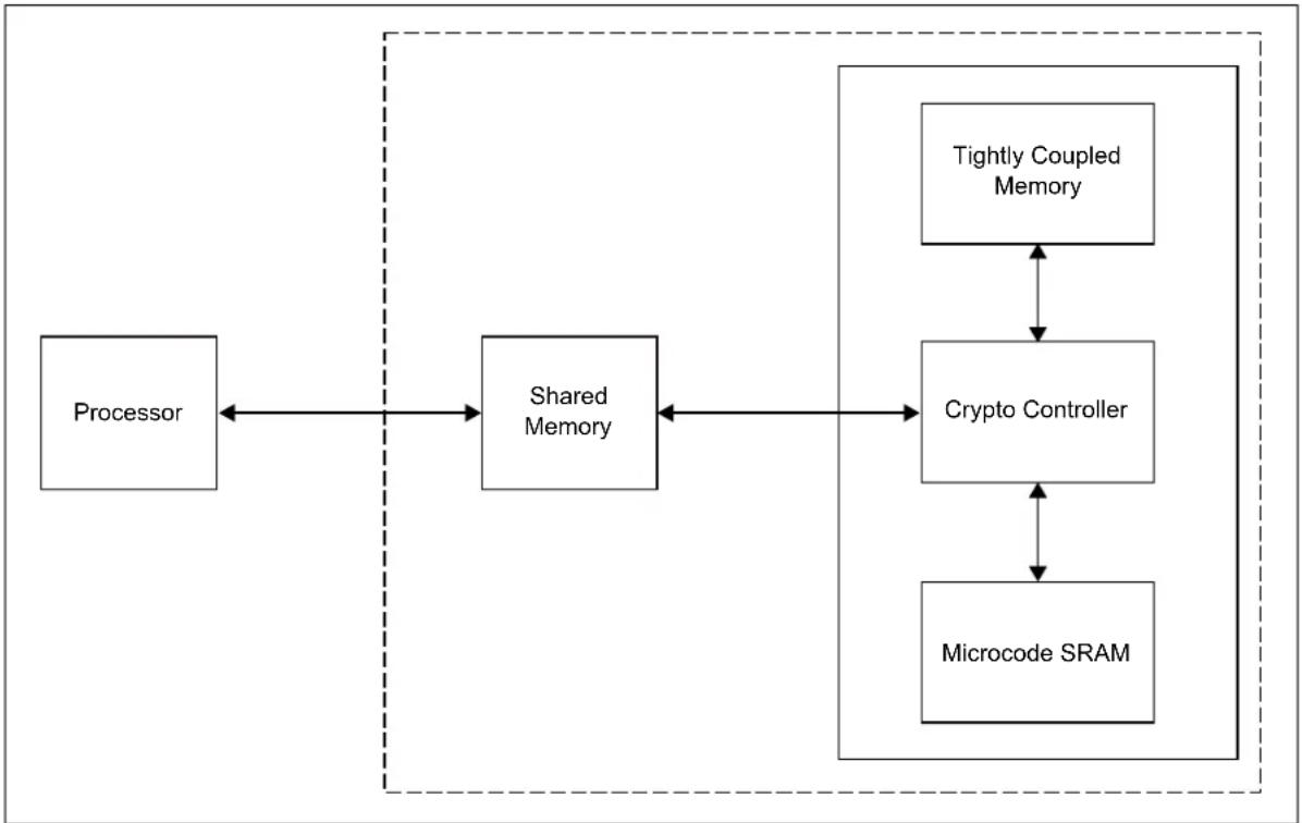
flowchart
graph TD
    A["Processor"] <--> B["Shared Memory"]
    B <--> C["Crypto Controller"]
    C <--> D["Tightly Coupled Memory"]
    C <--> E["Microcode SRAM"]
27.0 SYMMETRIC CRYPTO ENGINE
| Note: This data sheet summarizes the features of the PIC32MZ1025W104 family of devices. It is not intended to be a comprehensive reference source. To complement the information in this data sheet, refer to Section 49. “Crypto Engine (CE) and Random Number Generator (RNG)” (DS60001246) in the “PIC32 Family Reference Manual”, which is available from the Microchip website (www.microchip.com/PIC32). |
The Symmetric Crypto Engine is intended to accelerate applications that need cryptographic functions. By executing these functions in the hardware module, software overhead is reduced and actions, such as encryption, decryption, and authentication can execute much more quickly.
The Symmetric Crypto Engine uses an internal descriptor-based DMA for efficient programming of the Security Association (SA) data and packet pointers (allowing scatter/gather data fetching). An intelligent state machine schedules the Symmetric Crypto Engines based on the protocol selection and packet boundaries. The hardware engines can perform the encryption and authentication in sequence or in parallel.
The following are key features of the Symmetric Crypto Engine:
- Bulk ciphers and hash engines
- Integrated CRDMA to off-load processing:
- Buffer Descriptor (BD)-based
- Secure association per buffer descriptor
- Some functions can execute in parallel
Bulk ciphers that are handled by the Symmetric Crypto Engine include:
• AES:
- 128-bit, 192-bit and 256-bit key sizes
- CBC, ECB, CTR, CFB and OFB modes
• DES/TDES:
- CBC, ECB, CFB and OFB modes
Authentication engines that are available through the Symmetric Crypto Engine include:
• S H A - 1
• SHA-256
• M D - 5
• AES-GCM
- AES-CBC
- HMAC operation (for all authentication engines)
• SFR interface:
- 32-bit Read/Write only
- No 8-bit or 16-bit access
The Symmetric Crypto Engine processes the data rate on the basis of the following factors:
- Which algorithm/engine is in use
- Whether the algorithms/engines are used in parallel or in series
- Demand on source and destination memories by other parts of the system (CPU, DMA, and so on.)
- The speed of PB5_CLK, which drives the Symmetric Crypto Engine
The table below shows typical performance for various engines.
TABLE 27-1: SYMMETRIC CRYPTO ENGINE PERFORMANCE
| Engine/ Algorithm | Performance Factor (Mbps/MHz) | Maximum Mbps (PB5_CLK = 100 MHz) |
| DES 14.4 1440 | ||
| TDES 6.6 | 660 | |
| AES-128 9.0 | 900 | |
| AES-192 7.9 | 790 | |
| AES-256 7.2 | 720 | |
| MD5 | 15.6 1560 | |
| SHA-1 | 13.2 1320 | |
| SHA-256 9.3 | 930 | |
Note: When using the engines sequentially, the throughput degrades. Throughput is also negatively affected by other bus activity, specifically if the CPU and/or peripherals have high activity to the same SRAM target as the CRDMA.
Note 1: A cryptographic operation cannot be interrupted with another. A hash is always processed completely.
2: Using the crypto DMA on an empty hash string will cause the peripheral to time out and not return a valid hash. The expectation is that it will use the fixed/known hash of the empty string.
FIGURE 27-1: SYMMETRIC CRYPTO ENGINE BLOCK DIAGRAM
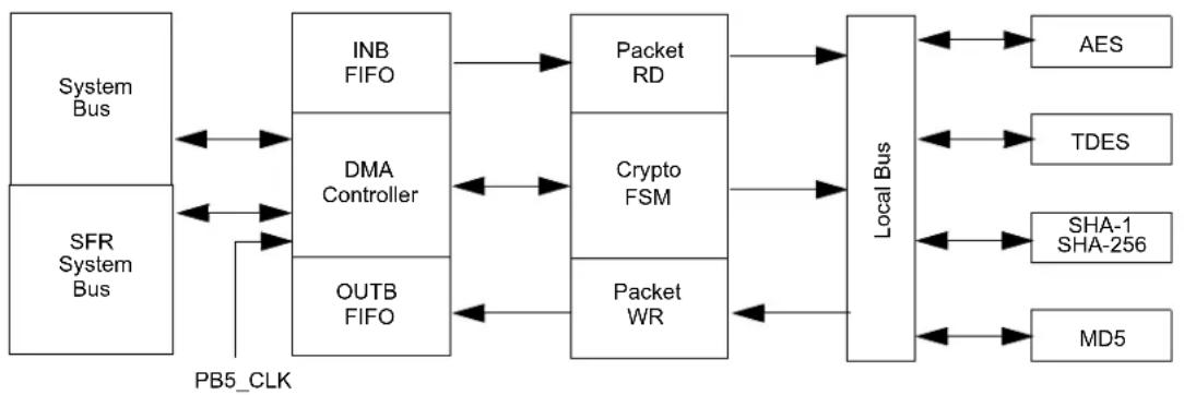
flowchart
graph LR
    A["System Bus"] -->|PB5_CLK| B["INB FIFO"]
    A -->|PB5_CLK| C["DMA Controller"]
    A -->|PB5_CLK| D["OUTB FIFO"]
    B --> E["Packet RD"]
    C --> F["Crypto FSM"]
    D --> G["Packet WR"]
    E --> H["Local Bus"]
    F --> H
    G --> H
    H --> I["AES"]
    H --> J["TDES"]
    H --> K["SHA-1 SHA-256"]
    H --> L["MD5"]
27.1 Symmetric Crypto Engine Control Registers
TABLE 27-2: SYMMETRIC CRYPTO ENGINE REGISTER MAP
Legend: x = unknown value on Reset; — = unimplemented, read as '0'. Reset values are shown in hexadecimal.
REGISTER 27-1: CEVER: CRYPTO ENGINE REVISION, VERSION, AND ID REGISTER
| Bit Range | Bit 31/23/15/7 | Bit 30/22/14/6 | Bit 29/21/13/5 | Bit 28/20/12/4 | Bit 27/19/11/3 | Bit 26/18/10/2 | Bit 25/17/9/1 | Bit 24/16/8/0 |
| 31:24 | R-0 R-0 R-0 R-0 R-0 R-0 | |||||||
| REVISION[7:0] | ||||||||
| 23:16 | R-0 R-0 R-0 R-0 R-0 R-0 | |||||||
| VERSION[7:0] | ||||||||
| 15:8 | R-0 R-0 R-0 R-0 R-0 R-0 | |||||||
| ID[15:8] | ||||||||
| 7:0 | R-0 R-0 R-0 R-0 R-0 R-0 | |||||||
| ID[7:0] | ||||||||
Legend:
R = Readable bit W = Writable bit U = Unimplemented bit, read as '0'
-n = Value at POR '1' = Bit is set '0' = Bit is cleared x = Bit is unknown
bit 31-24 REVISION[7:0]: Crypto Engine Revision bits
bit 23-16 VERSION[7:0]: Crypto Engine Version bits
bit 15-0 ID[15:0]: Crypto Engine Identification bits
REGISTER 27-2: CECON: CRYPTO ENGINE CONTROL REGISTER
| Bit Range | Bit 31/23/15/7 | Bit 30/22/14/6 | Bit 29/21/13/5 | Bit 28/20/12/4 | Bit 27/19/11/3 | Bit 26/18/10/2 | Bit 25/17/9/1 | Bit 24/16/8/0 |
| 31:24 | U-0 U-0 | U-0 U-0 U-0 U-0 | U-0 U-0 | |||||
| — — — | — — — — — | |||||||
| 23:16 | U-0 U-0 | U-0 U-0 U-0 U-0 | U-0 U-0 | |||||
| — — — | — — — — — | |||||||
| 15:8 | U-0 U-0 | U-0 U-0 U-0 U-0 | U-0 U-0 | |||||
| — — — | — — — — — | |||||||
| 7:0 | R/W-0 | R/W-0, HC | R/W-0 | U-0 | U-0 | R/W-0 | R/W-0 | R/W-0 |
| SWAPOEN | SWRST | SWAPEN | — | — | BDPCHST | BDPPLEN | DMAEN |
| Legend: | HC = Hardware Cleared | |
| R = Readable bit | W = Writable bit | U = Unimplemented bit, read as ‘0’ |
| -n = Value at POR | ‘1’ = Bit is set | ‘0’ = Bit is cleared x = Bit is unknown |
bit 31-8 Unimplemented: Read as '0'
bit 7 SWAPOEN: Swap Output Data Enable bit
1 = Output data is byte swapped when written by dedicated DMA
0 = Output data is not byte swapped when written by dedicated DMA
bit 6 SWRST: Software Reset bit
1 = Initiate a software reset of the Crypto Engine
0 = Normal operation
bit 5 SWAPEN: Input Data Swap Enable bit
1 = Input data is byte swapped when read by dedicated DMA
0 = Input data is not byte swapped when read by dedicated DMA
bit 4-3 Unimplemented: Read as '0'
bit 2 BDPCHST: Buffer Descriptor Processor (BDP) Fetch Enable bit
This bit must be enabled only after all DMA descriptor programming is completed.
1 = BDP descriptor fetch is enabled
0 = BDP descriptor fetch is disabled
bit 1 BDPPLEN: Buffer Descriptor Processor Poll Enable bit
This bit must be enabled only after all DMA descriptor programming is completed.
1 = Poll for descriptor until valid bit is set
0 = Do not poll
bit 0 DMAEN: DMA Enable bit
1 = Crypto Engine DMA is enabled
0 = Crypto Engine DMA is disabled
REGISTER 27-3: CEBDADDR: CRYPTO ENGINE BUFFER DESCRIPTOR REGISTER
| Bit Range | Bit 31/23/15/7 | Bit 30/22/14/6 | Bit 29/21/13/5 | Bit 28/20/12/4 | Bit 27/19/11/3 | Bit 26/18/10/2 | Bit 25/17/9/1 | Bit 24/16/8/0 |
| 31:24 | R-0 R-0 R | -0 R-0 R-0 R-0 | R-0 R-0 | |||||
| BDPADDR[31:24] | ||||||||
| 23:16 | R-0 R-0 R | -0 R-0 R-0 R-0 | R-0 R-0 | |||||
| BDPADDR[23:16] | ||||||||
| 15:8 | R-0 R-0 R | -0 R-0 R-0 R-0 | R-0 R-0 | |||||
| BDPADDR[15:8] | ||||||||
| 7:0 | R-0 R-0 R | -0 R-0 R-0 R-0 | R-0 R-0 | |||||
| BDPADDR[7:0] | ||||||||
Legend:
R = Readable bit W = Writable bit U = Unimplemented bit, read as '0' -n = Value at POR '1' = Bit is set '0' = Bit is cleared x = Bit is unknown
bit 31-0 BDPADDR[31:0]: Current Buffer Descriptor Process Address Status bits
These bits contain the current descriptor address that is being processed by the BDP.
REGISTER 27-4: CEBDPADDR: CRYPTO ENGINE BUFFER DESCRIPTOR PROCESSOR REGISTER
| Bit Range | Bit 31/23/15/7 | Bit 30/22/14/6 | Bit 29/21/13/5 | Bit 28/20/12/4 | Bit 27/19/11/3 | Bit 26/18/10/2 | Bit 25/17/9/1 | Bit 24/16/8/0 |
| 31:24 | R/W-0 | R/W-0 | R/W-0 | R/W-0 | R/W-0 | R/W-0 | R/W-0 | R/W-0 |
| BASEADDR[31:24] | ||||||||
| 23:16 | R/W-0 | R/W-0 | R/W-0 | R/W-0 | R/W-0 | R/W-0 | R/W-0 | R/W-0 |
| BASEADDR[23:16] | ||||||||
| 15:8 | R/W-0 | R/W-0 | R/W-0 | R/W-0 | R/W-0 | R/W-0 | R/W-0 | R/W-0 |
| BASEADDR[15:8] | ||||||||
| 7:0 | R/W-0 | R/W-0 | R/W-0 | R/W-0 | R/W-0 | R/W-0 | R/W-0 | R/W-0 |
| BASEADDR[7:0] | ||||||||
Legend:
R = Readable bit W = Writable bit U = Unimplemented bit, read as '0' -n = Value at POR '1' = Bit is set '0' = Bit is cleared x = Bit is unknown
bit 31-0 BASEADDR[31:0]: Buffer Descriptor Base Address bits
These bits contain the physical address of the first buffer descriptor in the buffer descriptor chain. When enabled, the Crypto DMA begins fetching buffer descriptors from this address.
REGISTER 27-5: CESTAT: CRYPTO ENGINE STATUS REGISTER
| Bit Range | Bit 31/23/15/7 | Bit 30/22/14/6 | Bit 29/21/13/5 | Bit 28/20/12/4 | Bit 27/19/11/3 | Bit 26/18/10/2 | Bit 25/17/9/1 | Bit 24/16/8/0 |
| 31:24 | R-0 R-0 R-0 R-0 R-0 R-0 | R-0 R-0 | ||||||
| ERRMODE[2:0] | ERROP[2:0] ERRPHASE[1:0] | |||||||
| 23:16 | U-0 U-0 R-0 R-0 R-0 R-0 | R-0 R-0 | ||||||
| — — BDSTATE[3:0] | START ACTIVE | |||||||
| 15:8 | R-0 R-0 R-0 R-0 R-0 R-0 | R-0 R-0 | ||||||
| BDCTRL[15:8] | ||||||||
| 7:0 | R-0 R-0 R-0 R-0 R-0 R-0 | R-0 R-0 | ||||||
| BDCTRL[7:0] | ||||||||
Legend:
| R = Readable bit | W = Writable bit | U = Unimplemented bit, read as '0' |
| -n = Value at POR | '1' = Bit is set | '0' = Bit is cleared x = Bit is unknown |
bit 31-29 ERRMODE[2:0]: Internal Error Mode Status bits
111 = Reserved
110 = Reserved
101 = Reserved
100 = Reserved
011 = CEK operation
010 = KEK operation
001 = Preboot authentication
000 = Normal operation
bit 28-26 ERROP[2:0]: Internal Error Operation Status bits
111 = Reserved
110 = Reserved
101 = Reserved
100 = Authentication
011 = Reserved
010 = Decryption
001 = Encryption
000 = Reserved
bit 25-24 ERRPHASE[1:0]: Internal Error Phase of DMA Status bits
11 = Destination data
10 = Source data
01 = Security Association (SA) access
00 = Buffer Descriptor (BD) access
bit 23-22 Unimplemented: Read as '0'
bit 21-18 BDSTATE[3:0]: Buffer Descriptor Processor State Status bits
The current state of the BDP:
1111 = Reserved
•
•
0111 = Reserved
0110 = SA fetch
0101 = Fetch BDP is disabled
0100 = Descriptor is done
0011 = Data phase
0010 = BDP is loading
0001 = Descriptor fetch request is pending
0000 = BDP is idle
bit 17 START: DMA Start Status bit
1 = DMA start has occurred
0 = DMA start has not occurred
REGISTER 27-5: CESTAT: CRYPTO ENGINE STATUS REGISTER (CONTINUED)
bit 16 ACTIVE: Buffer Descriptor Processor Status bit
1 = BDP is active
0 = BDP is idle
bit 15-0 BDCTRL[15:0]: Descriptor Control Word Status bits
These bits contain the Control Word for the current BD.
REGISTER 27-6: CEINTSRC: CRYPTO ENGINE INTERRUPT SOURCE REGISTER
| Bit Range | Bit 31/23/15/7 | Bit 30/22/14/6 | Bit 29/21/13/5 | Bit 28/20/12/4 | Bit 27/19/11/3 | Bit 26/18/10/2 | Bit 25/17/9/1 | Bit 24/16/8/0 |
| 31:24 | U-0 U-0 U | -U-0 U-0 U-0 U-0 | U-0 U-0 | |||||
| ——— | ——— —— | |||||||
| 23:16 | U-0 U-0 U | -U-0 U-0 U-0 U-0 | U-0 U-0 | |||||
| ——— | ——— —— | |||||||
| 15:8 | U-0 U-0 U | -U-0 U-0 U-0 U-0 | U-0 U-0 | |||||
| ——— | ——— —— | |||||||
| 7:0 | U-0 U-0 U | -U-0 U-0 R-0 R-0 | R-0 R-0 | |||||
| ——— | — AREIF PKTIF | CBDIF PENDIF |
Legend:
| R = Readable bit | W = Writable bit | U = Unimplemented bit, read as '0' |
| -n = Value at POR | '1' = Bit is set | '0' = Bit is cleared x = Bit is unknown |
bit 31-4 Unimplemented: Read as '0'
bit 3 AREIF: Access Response Error Interrupt bit
1 = Error occurred trying to access memory outside the Crypto Engine
0 = No error has occurred
bit 2 PKTIF: DMA Packet Completion Interrupt Status bit
1 = DMA packet was completed
0 = DMA packet was not completed
bit 1 CBDIF: BD Transmit Status bit
1 = Last BD transmit was processed
0 = Last BD transmit has not been processed
bit 0 PENDIF: Crypto Engine Interrupt Pending Status bit
1 = Crypto Engine interrupt is pending (this value is the result of an OR of all interrupts in the Crypto Engine)
0 = Crypto Engine interrupt is not pending
REGISTER 27-7: CEINTEN: CRYPTO ENGINE INTERRUPT ENABLE REGISTER
| Bit Range | Bit 31/23/15/7 | Bit 30/22/14/6 | Bit 29/21/13/5 | Bit 28/20/12/4 | Bit 27/19/11/3 | Bit 26/18/10/2 | Bit 25/17/9/1 | Bit 24/16/8/0 |
| 31:24 | U-0 U-0 U | -U-0 U-0 U-0 | U-0 U-0 | |||||
| ——— | ——— — | |||||||
| 23:16 | U-0 U-0 U | -U-0 U-0 U-0 | U-0 U-0 | |||||
| ——— | ——— — | |||||||
| 15:8 | U-0 U-0 U | -U-0 U-0 U-0 | U-0 U-0 | |||||
| ——— | ——— — | |||||||
| 7:0 | U-0 U-0 U | -U-0 R/W-0 R/W-0 | R/W-0 | R/W-0 | ||||
| — | — | — | — | AREIE | PKTIE | BDPIE | PENDIE^(1) |
Legend:
| R = Readable bit | W = Writable bit | U = Unimplemented bit, read as '0' |
| -n = Value at POR | '1' = Bit is set | '0' = Bit is cleared x = Bit is unknown |
bit 31-4 Unimplemented: Read as '0'
bit 3 AREIE: Access Response Error Interrupt Enable bit 1 = Access response error interrupts are enabled 0 = Access response error interrupts are not enabled
bit 2 PKTIE: DMA Packet Completion Interrupt Enable bit 1 = DMA packet completion interrupts are enabled 0 = DMA packet completion interrupts are not enabled
bit 1 BDPIE: DMA Buffer Descriptor Processor Interrupt Enable bit 1 = BDP interrupts are enabled 0 = BDP interrupts are not enabled
bit 0 PENDIE: Primary Interrupt Enable bit ^(1) 1 = Crypto Engine interrupts are enabled 0 = Crypto Engine interrupts are not enabled
Note 1: The PENDIE bit is a global enable bit and must be enabled together with the other interrupts desired.
REGISTER 27-8: CEPOLLCON: CRYPTO ENGINE POLL CONTROL REGISTER
| Bit Range | Bit 31/23/15/7 | Bit 30/22/14/6 | Bit 29/21/13/5 | Bit 28/20/12/4 | Bit 27/19/11/3 | Bit 26/18/10/2 | Bit 25/17/9/1 | Bit 24/16/8/0 |
| 31:24 | U-0 U-0 U | -U-0 U-0 U-0 | U-0 U-0 | |||||
| ——— | ——— —— | |||||||
| 23:16 | U-0 U-0 U | -U-0 U-0 U-0 | U-0 U-0 | |||||
| ——— | ——— —— | |||||||
| 15:8 | R/W-0 | R/W-0 | R/W-0 | R/W-0 | R/W-0 | R/W-0 | R/W-0 | R/W-0 |
| BDPPLCON[15:8] | ||||||||
| 7:0 | R/W-0 | R/W-0 | R/W-0 | R/W-0 | R/W-0 | R/W-0 | R/W-0 | R/W-0 |
| BDPPLCON[7:0] | ||||||||
Legend:
| R = Readable bit | W = Writable bit | U = Unimplemented bit, read as '0' |
| -n = Value at POR | '1' = Bit is set | '0' = Bit is cleared x = Bit is unknown |
bit 31-16 Unimplemented: Read as '0'
bit 15-0 BDPPLCON[15:0]: Buffer Descriptor Processor Poll Control bits
These bits determine the number of SYSCLK cycles that the crypto DMA would wait before refetching the descriptor control word if the BD fetched was disabled.
REGISTER 27-9: CEHDLEN: CRYPTO ENGINE HEADER LENGTH REGISTER
| Bit Range | Bit 31/23/15/7 | Bit 30/22/14/6 | Bit 29/21/13/5 | Bit 28/20/12/4 | Bit 27/19/11/3 | Bit 26/18/10/2 | Bit 25/17/9/1 | Bit 24/16/8/0 |
| 31:24 | U-0 U-0 U | -U-0 U-0 U-0 | U-0 U-0 | |||||
| ——— | ——— | |||||||
| 23:16 | U-0 U-0 U | -U-0 U-0 U-0 | U-0 U-0 | |||||
| ——— | ——— | |||||||
| 15:8 | U-0 U-0 U | -U-0 U-0 U-0 | U-0 U-0 | |||||
| ——— | ——— | |||||||
| 7:0 | R/W-0 | R/W-0 | R/W-0 | R/W-0 | R/W-0 | R/W-0 | R/W-0 | R/W-0 |
| HDRLEN[7:0] | ||||||||
| Legend: | |||
| R = Readable bit | W = Writable bit | U = Unimplemented bit, read as ‘0’ | |
| -n = Value at POR | ‘1’ = Bit is set | ‘0’ = Bit is cleared | x = Bit is unknown |
bit 31-8 Unimplemented: Read as '0'
bit 7-0 HDRLEN[7:0]: DMA Header Length bits
For every packet, skip this length of locations and start filling the data.
REGISTER 27-10: CETRLLEN: CRYPTO ENGINE TRAILER LENGTH REGISTER
| Bit Range | Bit 31/23/15/7 | Bit 30/22/14/6 | Bit 29/21/13/5 | Bit 28/20/12/4 | Bit 27/19/11/3 | Bit 26/18/10/2 | Bit 25/17/9/1 | Bit 24/16/8/0 |
| 31:24 | U-0 U-0 U | -U-0 U-0 U-0 | U-0 U-0 | |||||
| ——— | ——— — | |||||||
| 23:16 | U-0 U-0 U | -U-0 U-0 U-0 | U-0 U-0 | |||||
| ——— | ——— — | |||||||
| 15:8 | U-0 U-0 U | -U-0 U-0 U-0 | U-0 U-0 | |||||
| ——— | ——— — | |||||||
| 7:0 | R/W-0 | R/W-0 | R/W-0 | R/W-0 | R/W-0 | R/W-0 | R/W-0 | R/W-0 |
| TRLRLEN[7:0] | ||||||||
| Legend: | |||
| R = Readable bit | W = Writable bit | U = Unimplemented bit, read as ‘0’ | |
| -n = Value at POR | ‘1’ = Bit is set | ‘0’ = Bit is cleared | x = Bit is unknown |
bit 31-8 Unimplemented: Read as '0'
bit 7-0 TRLRLEN[7:0]: DMA Trailer Length bits
For every packet, skip this length of locations at the end of the current packet and start putting the next packet.
27.2 Crypto Engine Buffer Descriptors
Host software creates a linked list of BDs and the hardware updates them. The table below provides a list of the Crypto Engine BDs, followed by format descriptions of each BD (see Figure 27-2 to Figure 27-9).
TABLE 27-3: CRYPTO ENGINE BUFFER DESCRIPTORS
| Name (see Note 1) | Bit31/2315/7 | Bit30/22/14/6 | Bit29/21/13/5 | Bit28/20/12/4 | Bit27/19/11/3 | Bit26/18/10/2 | Bit25/17/9/1 | Bit24/16/8/0 | |
| BD_CTRL 31:24 | DESC_EN | — CRY_MODE[2:0] — — | |||||||
| 23:16 | — | SA_FETCH_EN | — | — | LAST_BD | LIFM | PKT_INT_EN | CBD_INT_EN | |
| 15:8 | BD_BUFLEN[15:8] | ||||||||
| 7:0 | BD_BUFLEN[7:0] | ||||||||
| BD_SA_ADDR | 31:24 | BD_SAADDR[31:24] | |||||||
| 23:16 | BD_SAADDR[23:16] | ||||||||
| 15:8 | BD_SAADDR[15:8] | ||||||||
| 7:0 | BD_SAADR[7:0] | ||||||||
| BD_SRCADDR | 31:24 | BD_SRCADDR[31:24] | |||||||
| 23:16 | BD_SRCADDR[23:16] | ||||||||
| 15:8 | BD_SRCADDR[15:8] | ||||||||
| 7:0 | BD_SRCADDR[7:0] | ||||||||
| BD_DSTADDR | 31:24 | BD_DSTADDR[31:24] | |||||||
| 23:16 | BD_DSTADDR[23:16] | ||||||||
| 15:8 | BD_DSTADDR[15:8] | ||||||||
| 7:0 | BD_DSTADDR[7:0] | ||||||||
| BD_NXTPTR | 31:24 | BD_NXTADDR[31:24] | |||||||
| 23:16 | BD_NXTADDR[23:16] | ||||||||
| 15:8 | BD_NXTADDR[15:8] | ||||||||
| 7:0 | BD_NXTADDR[7:0] | ||||||||
| BD_UPDPTR | 31:24 | BD_UPDADDR[31:24] | |||||||
| 23:16 | BD_UPDADDR[23:16] | ||||||||
| 15:8 | BD_UPDADDR[15:8] | ||||||||
| 7:0 | BD_UPDADDR[7:0] | ||||||||
| BD_MSG_LEN | 31:24 | MSG_LENGTH[31:24] | |||||||
| 23:16 | MSG_LENGTH[23:16] | ||||||||
| 15:8 | MSG_LENGTH[15:8] | ||||||||
| 7:0 | MSG_LENGTH[7:0] | ||||||||
| BD_ENC_OFF | 31:24 | ENCR_OFFSET[31:24] | |||||||
| 23:16 | ENCR_OFFSET[23:16] | ||||||||
| 15:8 | ENCR_OFFSET[15:8] | ||||||||
| 7:0 | ENCR_OFFSET[7:0] | ||||||||
Note 1: The BD must be allocated in memory on a 64-bit boundary.
FIGURE 27-2: FORMAT OF BD_CTRL
| Bit Range | Bit 31/23/15/7 | Bit 30/22/14/6 | Bit 29/21/13/5 | Bit 28/20/12/4 | Bit 27/19/11/3 | Bit 26/18/10/2 | Bit 25/17/9/1 | Bit 24/16/8/0 |
| 31-24 DESC_EN — C | RY_MODE[2:0] | — — — | ||||||
| 23-16 | — | SA_FETCH_EN | — — LA | ST_BD LIFM | PKT_INT_EN | CBD_INT_EN | ||
| 15-8 | BD_BUFLEN[15:8] | |||||||
| 7-0 | BD_BUFLEN[7:0] | |||||||
bit 31 DESC_EN: Descriptor Enable
1 = The descriptor is owned by hardware. After processing the BD, hardware resets this bit to '0'.
0 = The descriptor is owned by software
bit 30 Unimplemented: Must be written as '0'
bit 29-27 CRY_MODE[2:0]: Crypto Mode
111 = Reserved
110 = Reserved
101 = Reserved
100 = Reserved
011 = CEK operation
010 = KEK operation
001 = Preboot authentication
000 = Normal operation
bit 22 SA_FETCH_EN: Fetch Security Association From External Memory
1 = Fetch SA from the SA pointer. This bit needs to be set to '1' for every new packet.
0 = Use current fetched SA or the internal SA
bit 21-20 Unimplemented: Must be written as '0'
bit 19 LAST_BD: Last Buffer Descriptors
1 = Last BD in the chain
0 = More BDs in the chain
After the last BD, the CEBDADDR goes to the base address in CEBDPADDR.
bit 18 LIFM: Last In Frame
In case of Receive Packets (from H/W-> Host), this field is filled by the Hardware to indicate whether the packet goes across multiple BDs. In case of transmit packets (from Host -> H/W), this field indicates whether this BD is the last in the frame.
bit 17 PKT_INT_EN: Packet Interrupt Enable
Generate an interrupt after processing the current BD, if it is the end of the packet.
bit 16 CBD_INT_EN: CBD Interrupt Enable
Generate an interrupt after processing the current BD.
bit 15-0 BD_BUFLEN[15:0]: Buffer Descriptor Length
This field contains the length of the buffer and is updated with the actual length filled by the receiver.
FIGURE 27-3: FORMAT OF BD_SADDR
| Bit Range | Bit 31/23/15/7 | Bit 30/22/14/6 | Bit 29/21/13/5 | Bit 28/20/12/4 | Bit 27/19/11/3 | Bit 26/18/10/2 | Bit 25/17/9/1 | Bit 24/16/8/0 |
| 31-24 BD_SAADDR[31:24] | ||||||||
| 23-16 BD_SAADDR[23:16] | ||||||||
| 15-8 BD_SAADDR[15:8] | ||||||||
| 7-0 BD_SAADDR[7:0] | ||||||||
bit 31-0 BD_SAADDR[31:0]: Security Association IP Session Address The sessions' SA pointer has the keys and IV values.
FIGURE 27-4: FORMAT OF BD_SRCADDR
| Bit Range | Bit 31/23/15/7 | Bit 30/22/14/6 | Bit 29/21/13/5 | Bit 28/20/12/4 | Bit 27/19/11/3 | Bit 26/18/10/2 | Bit 25/17/9/1 | Bit 24/16/8/0 |
| 31-24 BD_SRCADDR[31:24] | ||||||||
| 23-16 BD_SRCADDR[23:16] | ||||||||
| 15-8 BD_SRCADDR[15:8] | ||||||||
| 7-0 BD SRCADDR[7:0] | ||||||||
bit 31-0 BD_SRCADDR: Buffer Source Address
The source address of the buffer that needs to be passed through the PE-CRDMA for encryption or authentication. This address must be on a 32-bit boundary.
FIGURE 27-5: FORMAT OF BD_DSTADDR
| Bit Range | Bit 31/23/15/7 | Bit 30/22/14/6 | Bit 29/21/13/5 | Bit 28/20/12/4 | Bit 27/19/11/3 | Bit 26/18/10/2 | Bit 25/17/9/1 | Bit 24/16/8/0 |
| 31-24 BD_DSTADDR[31:24] | ||||||||
| 23-16 BD_DSTADDR[23:16] | ||||||||
| 15-8 BD_DSTADDR[15:8] | ||||||||
| 7-0 BD_DSTADDR[7:0] | ||||||||
bit 31-0 BD_DSTADDR: Buffer Destination Address
The destination address of the buffer that needs to be passed through the PE-CRDMA for encryption or authentication. This address must be on a 32-bit boundary.
FIGURE 27-6: FORMAT OF BD_NXTADDR
| Bit Range | Bit 31/23/15/7 | Bit 30/22/14/6 | Bit 29/21/13/5 | Bit 28/20/12/4 | Bit 27/19/11/3 | Bit 26/18/10/2 | Bit 25/17/9/1 | Bit 24/16/8/0 |
| 31-24 BD_NXTADDR[31:24] | ||||||||
| 23-16 BD_NXTADDR[23:16] | ||||||||
| 15-8 BD_NXTADDR[15:8] | ||||||||
| 7-0 BD_NXTADDR[7:0] | ||||||||
bit 31-0 BD_NXTADDR: Next BD Pointer Address Has Next Buffer Descriptor
The next buffer can be a next segment of the previous buffer or a new packet. This address must be on a 64-bit boundary.
FIGURE 27-7: FORMAT OF BD_UPDPTR
| Bit Range | Bit 31/23/15/7 | Bit 30/22/14/6 | Bit 29/21/13/5 | Bit 28/20/12/4 | Bit 27/19/11/3 | Bit 26/18/10/2 | Bit 25/17/9/1 | Bit 24/16/8/0 |
| 31-24 BD_UPDADDR[31:24] | ||||||||
| 23-16 BD_UPDADDR[23:16] | ||||||||
| 15-8 BD_UPDADDR[15:8] | ||||||||
| 7-0 BD_UPDADDR[7:0] | ||||||||
bit 31-0 BD_UPDADDR: UPD Address Location
The update address has the location where the CRDMA results are posted. The updated results are the ICV values, key output values as needed.
FIGURE 27-8: FORMAT OF BD_MSG_LEN
| Bit Range | Bit 31/23/15/7 | Bit 30/22/14/6 | Bit 29/21/13/5 | Bit 28/20/12/4 | Bit 27/19/11/3 | Bit 26/18/10/2 | Bit 25/17/9/1 | Bit 24/16/8/0 |
| 31-24 MSG_LENGTH[31:24] | ||||||||
| 23-16 MSG_LENGTH[23:16] | ||||||||
| 15-8 MSG_LENGTH[15:8] | ||||||||
| 7-0 MSG_LENGTH[7:0] | ||||||||
bit 31-0 MSG_LENGTH: Total Message Length
Total message length for the hash and HMAC algorithms in bytes. Total number of crypto bytes in case of GCM algorithm (LEN-C).
FIGURE 27-9: FORMAT OF BD_ENC_OFF
| Bit Range | Bit 31/23/15/7 | Bit 30/22/14/6 | Bit 29/21/13/5 | Bit 28/20/12/4 | Bit 27/19/11/3 | Bit 26/18/10/2 | Bit 25/17/9/1 | Bit 24/16/8/0 |
| 31-24 ENCR_OFFSET[31:24] | ||||||||
| 23-16 ENCR_OFFSET[23:16] | ||||||||
| 15-8 ENCR_OFFSET[15:8] | ||||||||
| 7-0 ENCR_OFFSET[7:0] | ||||||||
bit 31-0 ENCR_OFFSET: Encryption Offset
Encryption offset for the multi-task test cases (both encryption and authentication). The number of AAD bytes in the case of GCM algorithm (LEN-A).
27.3 Security Association Structure
Table 27-4 shows the SA structure. The Crypto Engine uses the SA to determine the settings for processing a BDP. The SA contains:
• Which algorithm to use
- Whether to use engines in parallel (for both authentication and encryption/decryption)
- The size of the key
- Authentication key
- Encryption/decryption key
- Authentication Initialization Vector (IV)
- Encryption IV
TABLE 27-4: CRYPTO ENGINE SA STRUCTURE
| Name | Bit31/23/15/7 | Bit30/22/14/6 | Bit29/21/13/5 | Bit28/20/12/4 | Bit27/19/11/3 | Bit26/18/10/2 | Bit25/17/9/1 | Bit24/16/8/0 | |
| SA_CTRL 31:24 | — — | V | E R | I | F | Y | — NO_RX OR_EN ICVONLY | ||
| 23:16 | LNC LOADIV FB | FLAGS | — | — | — | ALGO[6] | |||
| 15:8 | ALGO[5:0] | ENCTYPE | KEYSIZE[1] | ||||||
| 7:0 | KEYSIZE[0] | MULTITASK[2:0] | CRYPTOALGO[3:0] | ||||||
| SA_AUTHKEY1 | 31:24 | AUTHKEY[31:24] | |||||||
| 23:16 | AUTHKEY[23:16] | ||||||||
| 15:8 | AUTHKEY[15:8] | ||||||||
| 7:0 | AUTHKEY[7:0] | ||||||||
| SA_AUTHKEY2 | 31:24 | AUTHKEY[31:24] | |||||||
| 23:16 | AUTHKEY[23:16] | ||||||||
| 15:8 | AUTHKEY[15:8] | ||||||||
| 7:0 | AUTHKEY[7:0] | ||||||||
| SA AUTHKEY3 | 31:24 | AUTHKEY[31:24] | |||||||
| 23:16 | AUTHKEY[23:16] | ||||||||
| 15:8 | AUTHKEY[15:8] | ||||||||
| 7:0 | AUTHKEY[7:0] | ||||||||
| SA AUTHORKEY4 | 31:24 | AUTHKEY[31:24] | |||||||
| 23:16 | AUTHKEY[23:16] | ||||||||
| 15:8 | AUTHKEY[15:8] | ||||||||
| 7:0 | AUTHKEY[7:0] | ||||||||
| SA AuthorKEY5 | 31:24 | AUTHKEY[31:24] | |||||||
| 23:16 | AUTHKEY[23:16] | ||||||||
| 15:8 | AUTHKEY[15:8] | ||||||||
| 7:0 | AUTHKEY[7:0] | ||||||||
| SA _AUTHKEY6 | 31:24 | AUTHKEY[31:24] | |||||||
| 23:16 | AUTHKEY[23:16] | ||||||||
| 15:8 | AUTHKEY[15:8] | ||||||||
| 7:0 | AUTHKEY[7:0] | ||||||||
| SA_AuthKEY7 | 31:24 | AUTHKEY[31:24] | |||||||
| 23:16 | AUTHKEY[23:16] | ||||||||
| 15:8 | AUTHKEY[15:8] | ||||||||
| 7:0 | AUTHKEY[7:0] | ||||||||
| SA_AUTHKEY8 | 31:24 | AUTHKEY[31:24] | |||||||
| 23:16 | AUTHKEY[23:16] | ||||||||
| 15:8 | AUTHKEY[15:8] | ||||||||
| 7:0 | AUTHKEY[7:0] | ||||||||
| SA_ENCKEY1 | 31:24 | ENCKEY[31:24] | |||||||
| 23:16 | ENCKEY[23:16] | ||||||||
| 15:8 | ENCKEY[15:8] | ||||||||
| 7:0 | ENCKEY[7:0] | ||||||||
| SA ENCKEY2 | 31:24 | ENCKEY[31:24] | |||||||
| 23:16 | ENCKEY[23:16] | ||||||||
| 15:8 | ENCKEY[15:8] | ||||||||
| 7:0 | ENCKEY[7:0] | ||||||||
| SA_ENCKEY3 | 31:24 | ENCKEY[31:24] | |||||||
| 23:16 | ENCKEY[23:16] | ||||||||
| 15:8 | ENCKEY[15:8] | ||||||||
| 7:0 | ENCKEY[7:0] | ||||||||
| SA_ENCKEY4 | 31:24 | ENCKEY[31:24] | |||||||
| 23:16 | ENCKEY[23:16] | ||||||||
| 15:8 | ENCKEY[15:8] | ||||||||
| 7:0 | ENCKEY[7:0] | ENCKEY[7:0] | |||||||
| SA_ENCKEY5 | 31:24 | ENCKEY[31:24] | |||||||
| 23:16 | ENCKEY[23:16] | ||||||||
| 15:8 | ENCKEY[15:8] | ||||||||
| 7:0 | ENCKEY[7:0] | ||||||||
| SA_ENCKEY6 | 31:24 | ENCKEY[31:24] | |||||||
| 23:16 | ENCKEY[23:16] | ||||||||
| 15:8 | ENCKEY[15:8] | ||||||||
| 7:0 | ENCKEY[7:0] | ||||||||
TABLE 27-4: CRYPTO ENGINE SA STRUCTURE (CONTINUED)
| Name | Bit31/23/15/7 | Bit30/22/14/6 | Bit29/21/13/5 | Bit28/20/12/4 | Bit27/19/11/3 | Bit26/18/10/2 | Bit25/17/9/1 | Bit24/16/8/0 | ||||||||||
| SA_ENCKEY7 31 | 1:24 ENCKEY[31:24] | |||||||||||||||||
| 23:16 ENCKEY[23:16] | ||||||||||||||||||
| 15:8 ENCKEY[15:8] | ||||||||||||||||||
| 7:0 ENCKEY[7:0] | ||||||||||||||||||
| SA_ENCKEY8 31 | 1:24 ENCKEY[31:24] | |||||||||||||||||
| 23:16 ENCKEY[23:16] | ||||||||||||||||||
| 15:8 ENCKEY[15:8] | ||||||||||||||||||
| 7:0 ENCKEY[7:0] | ||||||||||||||||||
| SA_AUTHIV1 31 | 24 AUTHIV[31:24] | |||||||||||||||||
| 23:16 AUTHIV[23:16] | ||||||||||||||||||
| 15:8 AUTHIV[15:8] | ||||||||||||||||||
| 7:0 AUTHIV[7:0] | ||||||||||||||||||
| SA_AUTHIV2 31 | 24 AUTHIV[31:24] | |||||||||||||||||
| 23:16 AUTHIV[23:16] | ||||||||||||||||||
| 15:8 AUTHIV[15:8] | ||||||||||||||||||
| 7:0 AUTHIV[7:0] | ||||||||||||||||||
| SAAUTHIV3 31 | 24 AUTHIV[31:24] | |||||||||||||||||
| 23:16 AUTHIV[23:16] | ||||||||||||||||||
| 15:8 AUTHIV[15:8] | ||||||||||||||||||
| 7:0 AUTHIV[7:0] | ||||||||||||||||||
| SA AUTHIV4 31 | 24 AUTHIV[31:24] | |||||||||||||||||
| 23:16 AUTHIV[23:16] | ||||||||||||||||||
| 15:8 AUTHIV[15:8] | ||||||||||||||||||
| 7:0 AUTHIV[7:0] | ||||||||||||||||||
| SA AUTHORV5 31 | 24 AUTHIV[31:24] | |||||||||||||||||
| 23:16 AUTHIV[23:16] | ||||||||||||||||||
| 15:8 AUTHIV[15:8] | ||||||||||||||||||
| 7:0 AUTHIV[7:0] | ||||||||||||||||||
| SA AuthorHV6 31 | 24 AUTHIV[31:24] | |||||||||||||||||
| 23:16 AUTHIV[23:16] | ||||||||||||||||||
| 15:8 AUTHIV[15:8] | ||||||||||||||||||
| 7:0 AUTHIV[7:0] | ||||||||||||||||||
| SA _ AUTHIV7 31 | 24 AUTHIV[31:24] | |||||||||||||||||
| 23:16 AUTHIV[23:16] | ||||||||||||||||||
| 15:8 AUTHIV[15:8] | ||||||||||||||||||
| 7:0 AUTHIV[7:0] | ||||||||||||||||||
| SA_ AUTHIV8 31 | 24 AUTHIV[31:24] | |||||||||||||||||
| 23:16 AUTHIV[23:16] | ||||||||||||||||||
| 15:8 AUTHIV[15:8] | ||||||||||||||||||
| 7:0 AUTHIV[7:0] | ||||||||||||||||||
| SA_ENCIV1 31:24 ENCIV[31:24] | ||||||||||||||||||
| 23:16 | ENCIV[23:16] | |||||||||||||||||
| 15:8 | ENCIV[15:8] | |||||||||||||||||
| 7:0 | ENCIV[7:0] | |||||||||||||||||
| SA_ENCIV2 31:24 ENCIV[31:24] | ||||||||||||||||||
| 23:16 | ENCIV[23:16] | |||||||||||||||||
| 15:8 | ENCIV[15:8] | |||||||||||||||||
| 7:0 | ENCIV[7:0] | |||||||||||||||||
| SA_ENCIV3 31:24 ENCIV[31:24] | ||||||||||||||||||
| 23:16 | ENCIV[23:16] | |||||||||||||||||
| 15:8 | ENCIV[15:8] | |||||||||||||||||
| 7:0 | ENCIV[7:0] | |||||||||||||||||
| GA_ENCIV4 31:24 ENCIV[31:24] | ||||||||||||||||||
| 23:16 | ENCIV[23:16] | |||||||||||||||||
| 15:8 | ENCIV[15:8] | |||||||||||||||||
| 7:0 | ENCIV[7:0] | |||||||||||||||||
The figure below shows the SA control word structure.
The Crypto Engine fetches different structures for different flows and ensures that hardware fetches minimum words from SA required for processing. The structure is ready for hardware optimal data fetches.
FIGURE 27-10: FORMAT OF SA_CTRL
| Bit Range | Bit 31/23/15/7 | Bit 30/22/14/6 | Bit 29/21/13/5 | Bit 28/20/12/4 | Bit 27/19/11/3 | Bit 26/18/10/2 | Bit 25/17/9/1 | Bit 24/16/8/0 |
| 31-24 | — | — | VERIFY | — | NO_RX | OR_EN | ICVONLY | IRFLAG |
| 23-16 LNC LOADIV FB | FLAGS | —— | — | ALGO[6] | ||||
| 15-8 | ALGO[5:0] | ENC | KEYSIZE[1] | |||||
| 7-0 KEYSIZE[0] | MULTITASK[2:0] | CRYPTOALGO[3:0] | ||||||
bit 31-30 Reserved: Initialize to zero.
bit 29 VERIFY: NIST Procedure Verification Setting
1 = NIST procedures are to be used
0 = Do not use NIST procedures
Note: The bit value shall be zero for the device.
bit 28 Reserved: Initialize to zero.
bit 27 NO_RX: Receive DMA Control Setting
1 = Only calculate ICV for authentication calculations
0 = Normal processing
bit 26 OR_EN: OR Register Bits Enable Setting
1 = OR the register bits with the internal value of the CSR register
0 = Normal processing
bit 25 ICVONLY: Incomplete Check Value Only Flag
This affects the SHA-1 algorithm only. It has no effect on the AES algorithm.
1 = Only three words of the HMAC result are available
0 = All results from the HMAC result are available
bit 24 IRFLAG: Immediate Result of Hash Setting
This bit is set when the immediate result for hashing is requested.
1 = Save the immediate result for hashing
0 = Do not save the immediate result
bit 23 LNC: Load New Keys Setting
1 = Load a new set of keys for encryption and authentication
0 = Do not load new keys
bit 22 LOADIV: Load IV Setting
1 = Load the IV from this SA
0 = Use the next IV
bit 21 FB: First Block Setting
This bit indicates that this is the first block of data to feed the IV value.
1 = Indicates this is the first block of data
0 = Indicates this is not the first block of data
bit 20 FLAGS: Incoming/Outgoing Flow Setting
1 = SA is associated with an outgoing flow
0 = SA is associated with an incoming flow
bit 19-17 Reserved: Initialize to zero.
Figure 27-10: FORMAT OF SA_CTRL (CONTINUED)
bit 16-10 ALGO[6:0]: Type of Algorithm to Use
1xxxxxxxx = HMAC 1
x1xxxxxx = SHA-256
xx1xxxx = SHA1
xxxx1xxx = MD5
xxxx1xx = AES
xxxxxx1x = TDES
xxxxxx1 = DES
bit 9 ENC: Type of Encryption Setting 1 = Encryption 0 = Decryption
bit 8-7 KEYSIZE[1:0]: Size of Keys in SA_AUTHKEYx or SA_ENCKEYx 11 = Reserved; do not use 10 = 256 bits 01 = 192 bits 00 = 128 bits(1)
bit 6-4 MULTITASK[2:0]: How to Combine Parallel Operations in the Crypto Engine 111 = Parallel pass (decrypt and authenticate incoming data in parallel) 101 = Pipe pass (encrypt the incoming data, and then perform authentication on the encrypted data) 011 = Reserved 010 = Reserved 001 = Reserved 000 = Encryption or authentication or decryption (no pass)
bit 3-0 CRYPTOALGO[3:0]: Mode of operation for the Crypto Algorithm 1111 = Reserved 1110 = AES_GCM (for AES processing) 1101 = RCTR (for AES processing) 1100 = RCBC_MAC (for AES processing) 1011 = ROFB (for AES processing) 1010 = RCFB (for AES processing) 1001 = RCBC (for AES processing) 1000 = RECB (for AES processing) 0111 = TOFB (for Triple-DES processing) 0110 = TCFB (for Triple-DES processing) 0101 = TCBC (for Triple-DES processing) 0100 = TECB (for Triple-DES processing) 0011 = OFB (for DES processing) 0010 = CFB (for DES processing) 0001 = CBC (for DES processing) 0000 = ECB (for DES processing)
Note 1: This setting does not alter the size of SA_AUTHKEYx or SA_ENCKEYx in the SA, only the number of bits of SA_AUTHKEYx and SA_ENCKEYx that are used.
Note 1: IV size for AES GCM is restricted to 96 bits.
2: Supports 32-bit counter mode only.
3: IV value is expected in big endian format.
Example: 12 byte IV Value: with SA_PTR = 0x00002000
- IV value desired = 0x11223344 55667788 99aabbcc
- In the SA Structure IV will be starting at (32-bit) word offset [25]
SYSTEM ADDR: DATA:
0x00002064: 0x11223344
0x00002068: 0x55667788
0x0000206C: 0x99aabbcc
4: Hash results are posted in big endian format as below.
Example: 16 byte hash result with UPD_PTR (BD[5]) = 0x00003000
Hash actual result: 0x00010203_04050607_08090a0b_0c0d0e0f
SYSTEM ADDR: DATA
0x00003000: 0x00010203
0x00003004: 0x04050607
0x00003008: 0x08090a0b
0x0000300C: 0x0c0d0e0f
28.0 TRUE RANDOM NUMBER GENERATOR (TRNG)
Note: This data sheet summarizes the features of the PIC32MZ1025W104 family of devices. It is not intended to be a comprehensive reference source. To complement the information in this data sheet, refer to Section 49. “Crypto Engine (CE) and Random Number Generator (RNG)” (DS60001246) in the “PIC32 Family Reference Manual”, which is available from the Microchip website (www.microchip.com/PIC32).
The Random Number Generator (RNG) core implements a thermal noise-based, TRNG and a cryptographically secure Pseudo-Random Number Generator (PRNG).
The TRNG uses multiple ring oscillators and the inherent thermal noise of integrated circuits to generate true random numbers that can initialize the PRNG.
The PRNG is a flexible Linear-Feedback Shift Register (LFSR), which is capable of displaying a maximal length LFSR of up to 64-bits.
The key features of the RNG are:
• TRNG :
- Up to 50 Mbps of random bits
- Multi-ring oscillator-based design
- Built-in bias corrector
- PRNG:
- LFSR-based
- Up to 64-bit polynomial length
- Programmable polynomial
- TRNG can be seed value
To start using the PRNG, it is necessary to set the initial seed value, the length of the polynomial, and the polynomial equation.
The initial seed value is set by writing to the RNGNUMGEN1 and RNGNUMGEN2 registers, which are also the registers where the random value is read. The initial seed value can also be loaded from the TRNG by writing a '1' to the LOAD bit (RNGCON[12]). This action transfers the current value in the RNGSEEDx registers to the corresponding RNGNUMGENx registers. The polynomial length for the LFSR is set by writing the length (in bits) to the PLEN[7:0] bits (RNGCON[7:0])
RNGPOLY1 and RNGPOLY2 control the feedback taps of the polynomial. The PRNG uses a reverse shift LFSR to reverse the bit positions, and largest tap of the polynomial is assigned to bit 0. The length (PLEN[7:0] in RNGCON) defines the feedback position.
To select a 42-bit (in this case maximal length) LFSR, it is described by:
$$ x 4 2 + x 4 1 + x 2 0 + x 1 9 + 1 $$
SFR settings:
• RNGNUMGEN1 = SEED-Low
• RNGNUMGEN2 = SEED-High
• RNGPOLY1 = 0x00C0_0003
• RNGPOLY2 = 0x0000_0000
• RNGCON = 0x0000_062A
The RNG's bus clock is gated when the RNG Peripheral Module Disable (PMD) bit is set. When the PMD is set, the RNG cannot be read or written.
TABLE 28-1: RNG BLOCK DIAGRAM
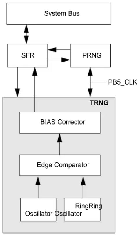
flowchart
graph TD
    A["System Bus"] --> B["SFR"]
    A --> C["PRNG"]
    B --> D["TRNG"]
    C --> D
    D --> E["BIAS Corrector"]
    E --> F["Edge Comparator"]
    F --> G["Oscillator"]
    F --> H["RingRing"]
    G --> I["Oscillator"]
    H --> J["RingRing"]
    B <--> C
    C <--> D
    D <--> E
    E <--> F
    F <--> G
    G <--> H
    H <--> I
    I <--> J
    J <--> K["PB5_CLK"]
28.1 RNG Control Registers
TABLE 28-2: RNG REGISTER MAP
| Virtual Address (BF8E_#) | Register Name | Bit Range | Bits | All Resets | ||||||||||||||||
| 31/15 30 | 14 29/13 | 28/12 27/1 | 1 26/10 25 | 9 24/8 23/7 | 22/6 21/5 20 | 14 19/3 18 | 2 17/1 16/0 | |||||||||||||
| 5000 | RNGVER | 31:16 | ID[15:0] ×××× | |||||||||||||||||
| 15:0 | VERSION[7:0] | REVISION[7:0] | ×××× | |||||||||||||||||
| 5004 | RNGCON | 31:16 | — | — | — | — | — | — | — | — | — | — | — | — | — | — | — | — | — | 0000 |
| 15:0 | — | — | — | LOAD | TRNGMODE | CONT | PRNGEN | TRNGEN | PLEN[7:0] | 0064 | ||||||||||
| 5008 | RNGPOLY1 | 31:16 | POLY[31:16] | PCCC | ||||||||||||||||
| 15:0 | POLY[15:0] | 0000 | ||||||||||||||||||
| 500C | RNGPOLY2 | 31:16 | POLY[31:16] | PCCC | ||||||||||||||||
| 15:0 | POLY[15:0] | 0000 | ||||||||||||||||||
| 5010 | RNGNUMGEN1 | 31:16 | RNG[31:16] | PCCC | ||||||||||||||||
| 15:0 | RNG[15:0] | 0000 | ||||||||||||||||||
| 5014 | RNGNUMGEN2 | 31:16 | RNG[31:16] | PCCC | ||||||||||||||||
| 15:0 | RNG[15:0] | 0000 | ||||||||||||||||||
| 5018 | RNGSEED1 | 31:16 | SEED[31:16] | 0000 | ||||||||||||||||
| 15:0 | SEED[15:0] | 0000 | ||||||||||||||||||
| 501C | RNGSEED2 | 31:16 | SEED[31:16] | 0000 | ||||||||||||||||
| 15:0 | SEED[15:0] | 0000 | ||||||||||||||||||
| 5020 | RNGCNT | 31:16 | — | — | — | — | — | — | — | — | — | — | — | — | — | — | — | — | — | 0000 |
| 15:0 | — | — | — | — | — | — | — | — | — | — | RCNT[6:0] | 0000 | ||||||||
Legend: x = unknown value on Reset; — = unimplemented, read as '0'. Reset values are shown in hexadecimal.
REGISTER 28-1: RNGVER: RANDOM NUMBER GENERATOR VERSION REGISTER
| Bit Range | Bit 31/23/15/7 | Bit 30/22/14/6 | Bit 29/21/13/5 | Bit 28/20/12/4 | Bit 27/19/11/3 | Bit 26/18/10/2 | Bit 25/17/9/1 | Bit 24/16/8/0 |
| 31:24 | R-0 R-0 R-0 R-0 R-0 R-0 | |||||||
| ID[15:8] | ||||||||
| 23:16 | R-0 R-0 R-0 R-0 R-0 R-0 | |||||||
| ID[7:0] | ||||||||
| 15:8 | R-0 R-0 R-0 R-0 R-0 R-0 | |||||||
| VERSION[7:0] | ||||||||
| 7:0 | R-0 R-0 R-0 R-0 R-0 R-0 | |||||||
| Revision[7:0] | ||||||||
Legend:
R = Readable bit W = Writable bit U = Unimplemented bit, read as '0'
-n = Value at POR '1' = Bit is set '0' = Bit is cleared x = Bit is unknown
bit 31-16 ID[15:0]: Block Identification bits
bit 15-8 VERSION[7:0]: Block Version bits
bit 7-0 REVISION[7:0]: Block Revision bits
REGISTER 28-2: RNGCON: RANDOM NUMBER GENERATOR CONTROL REGISTER
| Bit Range | Bit 31/23/15/7 | Bit 30/22/14/6 | Bit 29/21/13/5 | Bit 28/20/12/4 | Bit 27/19/11/3 | Bit 26/18/10/2 | Bit 25/17/9/1 | Bit 24/16/8/0 |
| 31:24 | U-0 U-0 | U-0 U-0 U-0 U-0 | U-0 U-0 | |||||
| — — — | — — — — — | |||||||
| 23:16 | U-0 U-0 | U-0 U-0 U-0 U-0 | U-0 U-0 | |||||
| — — — | — — — — — | |||||||
| 15:8 | U-0 U-0 | U-0 R/W-0 R/W-0 | R/W-0 R/W-0 | R/W-0 | ||||
| — — — | LOAD TRNGM | ODE CONT | PRNGEN | TRNGEN | ||||
| 7:0 | R/W-0 | R/W-1 | R/W-1 | R/W-0 | R/W-0 | R/W-1 | R/W-0 | R/W-0 |
| PLEN[7:0] | ||||||||
Legend:
| R = Readable bit | W = Writable bit U = Unimplemented bit, read as '0' | ||
| -n = Value at POR | '1' = Bit is set | '0' = Bit is cleared | x = Bit is unknown |
bit 31-13 Unimplemented: Read as '0'
bit 12 LOAD: Device Select bit
This bit is self-clearing and is used to load the seed from the TRNG (random value) as a seed to the PRNG.
bit 11 TRNGMODE: TRNG Mode Selection bit
1 = Use ring oscillators with bias corrector
0 = Use ring oscillators with XOR tree
Note: Enabling this bit will generate numbers with a more even distribution of randomness.
bit 10 CONT: PRNG Number Shift Enable bit
1 = PRNG random number is shifted every cycle
0 = PRNG random number is shifted when the previous value is removed
bit 9 PRNGEN: PRNG Operation Enable bit
1 = PRNG operation is enabled
0 = PRNG operation is not enabled
bit 8 TRNGEN: TRNG Operation Enable bit
1 = TRNG operation is enabled
0 = TRNG operation is not enabled
bit 7-0 PLEN[7:0]: PRNG Polynomial Length bits
These bits contain the length of the polynomial used for the PRNG.
REGISTER 28-3: RNGPOLYx: RANDOM NUMBER GENERATOR POLYNOMIAL REGISTER 'x' ('x' = 1 or 2)
| Bit Range | Bit 31/23/15/7 | Bit 30/22/14/6 | Bit 29/21/13/5 | Bit 28/20/12/4 | Bit 27/19/11/3 | Bit 26/18/10/2 | Bit 25/17/9/1 | Bit 24/16/8/0 |
| 31:24 | R/W-1 R/W | -1 R/W-1 R/W-1 | R/W-1 R/W-1 | R/W-1 R/W-1 | ||||
| POLY[31:24] | ||||||||
| 23:16 | R/W-1 R/W | -1 R/W-1 R/W-1 | R/W-1 R/W-1 | R/W-1 R/W-1 | ||||
| POLY[23:16] | ||||||||
| 15:8 | R/W-0 R/W | -0 R/W-0 R/W-0 | R/W-0 R/W-0 | R/W-0 R/W-0 | ||||
| POLY[15:8] | ||||||||
| 7:0 | R/W-0 R/W | -0 R/W-0 R/W-0 | R/W-0 R/W-0 | R/W-0 R/W-0 | ||||
| POLY[7:0] | ||||||||
| Legend: | |||
| R = Readable bit W = Writable bit U = Unimplemented bit, read as '0' | |||
| -n = Value at POR | '1' = Bit is set | '0' = Bit is cleared | x = Bit is unknown |
bit 31-0 POLY[31:0]: PRNG LFSR Polynomial MSB/LSB bits (RNGPOLY1 = LSB, RNGPOLY2 = MSB)
REGISTER 28-4: RNGNUMGENx: RANDOM NUMBER GENERATOR REGISTER 'x' ('x' = 1 or 2)
| Bit Range | Bit 31/23/15/7 | Bit 30/22/14/6 | Bit 29/21/13/5 | Bit 28/20/12/4 | Bit 27/19/11/3 | Bit 26/18/10/2 | Bit 25/17/9/1 | Bit 24/16/8/0 |
| 31:24 | R/W-1 R/W | -1 R/W-1 R/W-1 | R/W-1 R/W-1 | R/W-1 R/W-1 | ||||
| RNG[31:24] | ||||||||
| 23:16 | R/W-1 R/W | -1 R/W-1 R/W-1 | R/W-1 R/W-1 | R/W-1 R/W-1 | ||||
| RNG[23:16] | ||||||||
| 15:8 | R/W-1 R/W | -1 R/W-1 R/W-1 | R/W-1 R/W-1 | R/W-1 R/W-1 | ||||
| RNG[15:8] | ||||||||
| 7:0 | R/W-1 R/W | -1 R/W-1 R/W-1 | R/W-1 R/W-1 | R/W-1 R/W-1 | ||||
| RNG[7:0] | ||||||||
| Legend: | |||
| R = Readable bit W = Writable bit U = Unimplemented bit, read as '0' | |||
| -n = Value at POR | '1' = Bit is set | '0' = Bit is cleared | x = Bit is unknown |
bit 31-0 RNG[31:0]: Current PRNG MSB/LSB Value bits (RNGNUMGEN1 = LSB, RNGNUMGEN2 = MSB)
REGISTER 28-5: RNGSEEDx: TRUE RANDOM NUMBER GENERATOR SEED REGISTER 'x' ('x' = 1 or 2)
| Bit Range | Bit 31/23/15/7 | Bit 30/22/14/6 | Bit 29/21/13/5 | Bit 28/20/12/4 | Bit 27/19/11/3 | Bit 26/18/10/2 | Bit 25/17/9/1 | Bit 24/16/8/0 |
| 31:24 | R-0 R-0 R-0 R-0 R-0 R-0 | |||||||
| SEED[31:24] | ||||||||
| 23:16 | R-0 R-0 R-0 R-0 R-0 R-0 | |||||||
| SEED[23:16] | ||||||||
| 15:8 | R-0 R-0 R-0 R-0 R-0 R-0 | |||||||
| SEED[15:8] | ||||||||
| 7:0 | R-0 R-0 R-0 R-0 R-0 R-0 | |||||||
| SEED[7:0] | ||||||||
Legend:
R = Readable bit W = Writable bit U = Unimplemented bit, read as '0' -n = Value at POR '1' = Bit is set '0' = Bit is cleared x = Bit is unknown
bit 31-0 SEED[31:0]: TRNG MSB/LSB Value bits (RNGSEED1 = LSB, RNGSEED2 = MSB)
REGISTER 28-6: RNGCNT: TRUE RANDOM NUMBER GENERATOR COUNT REGISTER
| Bit Range | Bit 31/23/15/7 | Bit 30/22/14/6 | Bit 29/21/13/5 | Bit 28/20/12/4 | Bit 27/19/11/3 | Bit 26/18/10/2 | Bit 25/17/9/1 | Bit 24/16/8/0 |
| 31:24 | U-0 U-0 U | -0 U-0 U-0 U-0 | U-0 U-0 | |||||
| — | — | — | — | — | — | — | — | |
| 23:16 | U-0 U-0 U | -0 U-0 U-0 U-0 | U-0 U-0 | |||||
| — | — | — | — | — | — | — | — | |
| 15:8 | U-0 U-0 U | -0 U-0 U-0 U-0 | U-0 U-0 | |||||
| — | — | — | — | — | — | — | — | |
| 7:0 | U-0 | R/W-0 | R/W-0 | R/W-0 | R/W-0 | R/W-0 | R/W-0 | R/W-0 |
| — | RCNT[6:0] | |||||||
Legend:
R = Readable bit W = Writable bit U = Unimplemented bit, read as '0' -n = Value at POR '1' = Bit is set '0' = Bit is cleared x = Bit is unknown
bit 31-7 Unimplemented: Read as '0'
bit 6-0 RCNT[6:0]: Number of Valid TRNG MSB 32 bits
29.0 12-BIT HIGH-SPEED SUCCESSIVE APPROXIMATION REGISTER (SAR) ADC
Note: This data sheet summarizes the features of the PIC32MZ1025W104 family of devices. It is not intended to be a comprehensive reference source. To complement the information in this data sheet, refer to Section 22. “12-bit High-Speed Successive Approximation Register (SAR) ADC” (DS60001344) in the “PIC32 Family Reference Manual”, which is available from the Microchip website (www.microchip.com/PIC32).
The ADC is designed to support power conversion, and general use applications. The PIC32MZ W1 supports two 12-bit ADC modules, one dedicated ADC SARCORE and one shared ADC SARCORE.
SAR ADC includes the following key features:
- 12-bit resolution
- Two ADC modules with dedicated sample and hold (S&H) circuits
- Single-ended and/or differential inputs
- Can operate during Sleep mode
• Supports touch sense applications - Two digital comparators
- Two digital filters supporting two modes:
- Oversampling mode
- Averaging mode
- Designed for general purpose applications
Note: The ADC's accuracy depends on the reference voltage ( V_REF = V_DD ), therefore, it is the designer's responsibility to implement a power supply system, where a constant reference voltage can be maintained for the ADC to achieve accurate results.
The 12-bit HS SAR ADC has one dedicated ADC module (ADC1) and one shared ADC module (ADC2). The dedicated ADC module uses a single input and is intended for high-speed and precise sampling of time-sensitive or transient inputs. The shared ADC module incorporates a multiplexer on the input to facilitate a larger group of inputs, with slower sampling, and provides flexible automated scanning option through the input scan logic.
For each ADC module, the analog inputs are connected to the S&H capacitor. The clock, sampling time, and output data resolution for each ADC module can be set independently. The ADC module performs the conversion of the input analog signal based on the configurations set in the registers. When conversion is complete, the final result is stored in the result buffer for the specific analog
input and is passed to the digital filter and digital comparator if configured to use data from this particular sample.
Basic CVD provides a touch interface based on self-capacitance touch sensing. The ADC module supports CVD feature by using the shared ADC core to perform a modified scan of all second and third class channels. The feature can be used to make single-ended or differential measurement of external capacitors. Thus the basic CVD feature provides an analog front-end for capacitive touch screen application.
The module enables the digital comparator to set its interrupt flag if the capacitance drop detected is greater than a threshold value to decide if a touch event is happening or not on pad. Then, the interrupt can wake up the CPU during idle or sleep or to signal the running software to branch to a different routine because of the touch event on the pad.
29.1 Activation Sequence
Step 1: Write all the essential ADC configuration SFRs including the ADC control clock and all ADC core clocks setup as given below:
- ADCCON1, keeping the ON bit = 0
- ADCCON2, especially paying attention to ADCDIV[6:0] and SAMC[9:0]
- ADCANCON, keeping all analog enables ANENx bit = 0, WKUPCLKCNT bit = 0xA
- ADCCON3, keeping all DIGEN5x = 0, especially paying attention to ADCSEL[1:0], and CONCLKDIV [5:0]
- ADCxTIME, ADCDIVx[6:0], and SAMCx[9:0]
- ADCTRGMODE, ADCIMCONx, ADCTRGSNS, ADCCSSx, ADCGIRQENx, ADCTRGx, ADCBASE
Step 2: Set the ON bit to '1', which enables the ADC control clock.
Step 3: Wait for the interrupt or polls the status bit BGVRRDY = 1, which signals that the device analog environment (band gap) is ready.
Step 4: Set the ANENx bit to '1' for each of the ADC SAR cores to be used.
Step 5: Wait for the interrupt or polls the warm-up ready bits WKRDYx = 1, which signals that the respective ADC SAR cores are ready to operate.
Step 6: Set the DIGENx bit to '1', which enables the digital circuitry to immediately begin processing incoming triggers to perform data conversions.
The throughput rate is calculated, as shown in Equation 29-1. Refer to Section 41.0 “Electrical Specifications” for more information.
EQUATION 29-1: ADC THROUGHPUT RATE
$$ F T P = \frac {T _ {A D}}{T _ {S A M P} + (T _ {C O N V})} $$
Where,
T_AD = the frequency of the individual ADC module
FIGURE 29-1: ADC BLOCK DIAGRAM
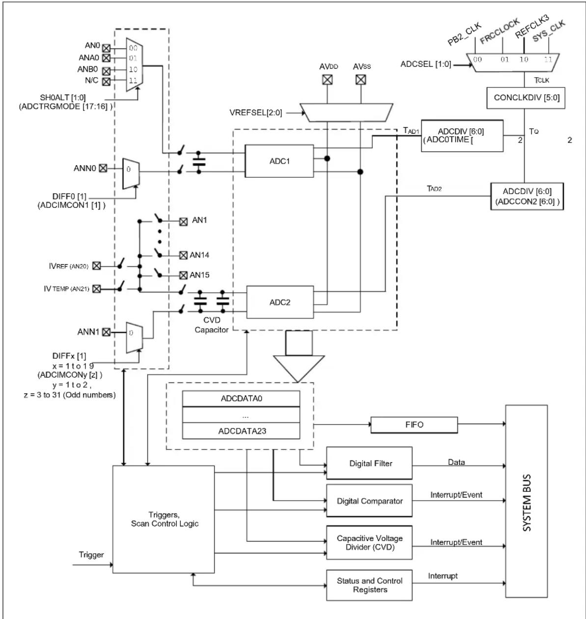
flowchart
graph TD
    A["Trigger"] --> B["Triggers, Scan Control Logic"]
    B --> C["ADC0A0"]
    B --> D["ADC0A23"]
    C --> E["FIFO"]
    D --> E
    E --> F["SYSTEM BUS"]
    G["ANN0"] --> H["0"]
    I["ANN1"] --> J["0"]
    K["ANN2"] --> L["0"]
    M["ANN3"] --> N["0"]
    O["AN0"] --> P["0.0"]
    Q["ANA0"] --> R["0.1"]
    S["ANB0"] --> T["1.0"]
    U["N/C"] --> V["1.1"]
    W["SHOALT [1:0"] (ADCTRGMODE["17:16"]) ] --> X["VREFSEL[2:0"]]
    Y["AVDD"] --> Z["ADC1"]
    AA["AVss"] --> AB["ADC2"]
    AC["TAD1"] --> AD["ADCDIV [6:0"] (ADC0TIME)]
    AE["TAD2"] --> AF["ADCDIV [6:0"] (ADCCON2["6:0"]) ]
    AG["PB2_CLK"] --> AH["00 01 10 11"]
    AI["FRCCLOCK"] --> AJ["CONCLKDIV [5:0"]]
    AK["REFCLK3"] --> AL["TCLK"]
    AM["SYS_CLK"] --> AN["TQ"]
    AO["TCLK"] --> AP["TAD1"]
    AQ["ADCSEL [1:0"]] --> AR["ADC2"]
    AS["ADC0TIME"] --> AT["CVD Capacitor"]
    AU["ADC1"] --> AV["ADC2"]
    AW["ADC2"] --> AX["CVD Capacitor"]
    AY["DIFF0 [1"] (ADCIMCON1["1"]) ] --> AZ["AN1"]
    BA["AN14"] --> BB["AN15"]
    BC["AN1"] --> BD["AN14"]
    BE["AN15"] --> BF["AN15"]
    BG["DIFFx [1"] x=1 to 19 (ADCIMCONy["z"]) y=1 to 2, z=3 to 31 (Odd numbers)] --> BH["CVD Capacitor"]
    BI["DICOLI [ADC0"] --> BJ["Digital Filter"]
    BK["DICOLI [ADC1"] --> BL["Digital Comparator"]
    BM["DICOLI [ADC2"] --> BN["Duplexing Capacitive Voltage Divider (CVD)"]
    BO["DICOLI [ADC3"] --> BP["Status and Control Registers"]
    BQ["DIFLO"] --> BR["FIFO"]
    BS["FIFO"] --> BT["System BUS"]
    BU["FIFO"] --> BV["FIFO"]
    BW["FIFO"] --> BX["FIFO"]
    BY["FIFO"] --> BZ["FIFO"]
FIGURE 29-2: S&H BLOCK DIAGRAM
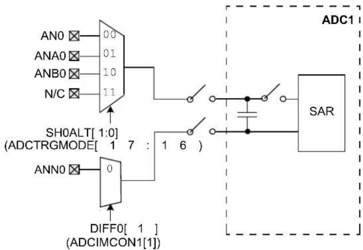
flowchart
graph TD
    A["AN0"] --> B["00"]
    C["ANA0"] --> D["01"]
    E["ANB0"] --> F["10"]
    G["N/C"] --> H["11"]
    I["SHOALT[1:0"](ADCTRGMODE["1 7 : 1 6"])] --> J["SAR"]
    K["ANN0"] --> L["0"]
    M["DIFF0[1"](ADCIMCON1["1"])] --> L
    B --> J
    D --> J
    F --> J
    H --> J
    J --> S["ADC1"]
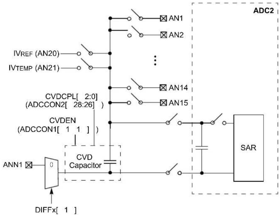
flowchart
graph TD
    A["ANN1"] --> B["0"]
    B --> C["CVD Capacitor"]
    C --> D["SAR"]
    D --> E["ADC2"]
    F["IVREF (AN20)"] --> G["AND"]
    H["IVTEMP (AN21)"] --> I["AND"]
    J["CVDCPL 2:0 (ADCCON2 28:26)"] --> K["AND"]
    L["CVDEN (ADCCON1 1 1)"] --> M["AND"]
    N["DIFFx 1"] --> O["AND"]
    P["AN1"] --> Q["AND"]
    R["AN2"] --> S["AND"]
    T["AN14"] --> U["AND"]
    V["AN15"] --> W["AND"]
    X["Ground"] --> Y["SAR"]
FIGURE 29-3: FIFO BLOCK DIAGRAM
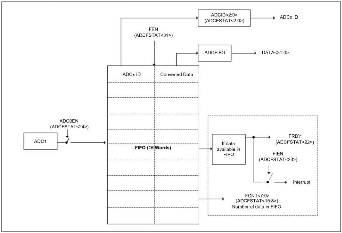
flowchart
graph TD
    A["ADC1"] --> B["ADC0EN (ADCFSTAT<24>)"]
    B --> C["FIFO (16 Words)"]
    C --> D["Converted Data"]
    D --> E["ADCx ID"]
    E --> F["ADCID<2:0> (ADCFSTAT<2:0>)"]
    F --> G["ADCx ID"]
    D --> H["ADCFIFO"]
    H --> I["DATA<31:0>"]
    D --> J["If data available in FIFO"]
    J --> K["FRDY (ADCFSTAT<22>)"]
    J --> L["FIEN (ADCFSTAT<23>)"]
    L --> M["Interrupt"]
    J --> N["FCNT<7:0> (ADCFSTAT<15:8>) Number of data in FIFO"]
    D --> O["FEN (ADCFSTAT<31>)"]
29.2 ADC Control Registers
TABLE 29-1: ADC REGISTER MAP
| Virtual Address(1F82_F) | Register Name | Bit Range | Bits | All Resets | ||||||||||||||||
| 31/15 30/ | 14 29/13 28/1 | 12 27/11 26/10 | 25/9 24/8 23 | 7 22/6 21/5 | 20/4 19/3 18/2 | 17/1 16/0 | ||||||||||||||
| 1000 | ADCCON1 | 31:16 | — | — | — | — | — | — | — | — | FRACT | SELRES[1:0] | STRGSRC[4:0] | 10:00 | ||||||
| 15:0 | ON | — | SIDL | — | CVDEN | FSYDMA | FSYUPB | SCANEN | — | IRQVS[2:0] | STROVL | DMABL[2:0] | 10:00 | |||||||
| 1010 | ADCCON2 | 31:16 | BGVRRDY | REFFLT | EOSRDY | CVDCL[2:0] | SAMC[9:0] | 10:00 | ||||||||||||
| 15:0 | BGVRIEN | REFLTIEN | EOSIEN | — | ENXCN-VRT | — | — | — | — | — | — | ADCDIV[6:0] | 10:00 | |||||||
| 1020 | ADCCON3 | 31:16 | ADCSEL[1:0] | CONCLKDIV[5:0] | DIGEN7 | — | — | — | — | — | — | — | DIGENO | 10:00 | ||||||
| 15:0 | VREFSEL[2:0] | TRGSUSP | UPDIEN | UPDRDY | SAMP | RQCNVRT | GLSWTRG | GSWTRG | ADINSEL[5:0] | 10:00 | ||||||||||
| 1030 | ADCTRGMODE | 31:16 | — | — | — | — | — | — | — | — | — | — | — | — | — | — | — | SH0ALT[1:0] | 10:00 | |
| 15:0 | — | — | — | — | — | — | — | STRGEN1 | — | — | — | — | — | — | — | — | SSAMPENU | 10:00 | ||
| 1040 | ADCIMCON1 | 31:16 | DIFF15 | SIGN15 | DIFF14 | SIGN14 | DIFF13 | SIGN13 | DIFF12 | SIGN12 | DIFF11 | SIGN11 | DIFF10 | SIGN10 | DIFF9 | SIGN9 | DIFF8 | SIGN8 | 10:00 | |
| 15:0 | DIFF7 | SIGN7 | DIFF5 | SIGN5 | DIFF5 | SIGN5 | DIFF4 | SIGN4 | DIFF3 | SIGN3 | DIFF2 | SIGN2 | DIFF1 | SIGN1 | DIFF0 | SIGN0 | 10:00 | |||
| 1050 | ADCIMCON2 | 31:16 | — | — | — | — | — | — | — | — | — | — | — | — | — | — | — | — | 10:00 | |
| 15:0 | — | — | — | — | — | — | — | — | DIFF19 | SIGN19 | DIFF18 | SIGN18 | DIFF17 | SIGN17 | DIFF16 | SIGN16 | 10:00 | |||
| 1080 | ADCGIRGEN1 | 31:16 | — | — | — | — | — | — | — | — | — | — | — | — | AGIEN19 | AGIEN18 | AGIEN17 | AGIEN16 | 10:00 | |
| 15:0 | AGIEN15 | AGIEN14 | AGIEN13 | AGIEN12 | AGIEN11 | AGIEN10 | AGIEN9 | AGIEN8 | AGIEN7 | AGIEN6 | AGIEN5 | AGIEN4 | AGIEN3 | AGIEN2 | AGIEN1 | AGIEN0 | 10:00 | |||
| 10A0 | ADCCSS1 | 31:16 | — | — | — | — | — | — | — | — | — | — | — | — | CSS19 | CSS18 | CSS17 | CSS16 | 10:00 | |
| 15:0 | CSS15 | CSS14 | CSS13 | CSS12 | CSS11 | CSS10 | CSS9 | CSS8 | CSS7 | CSS6 | CSS5 | CSS4 | CSS3 | CSS2 | CSS1 | CSS0 | 10:00 | |||
| 10C0 | ADCDSTAT1 | 31:16 | — | — | — | — | — | — | — | — | — | — | — | — | ARDY19 | ARDY18 | ARDY17 | ARDY16 | 10:00 | |
| 15:0 | ARDY15 | ARDY14 | ARDY13 | ARDY12 | ARDY11 | ARDY10 | ARDY9 | ARDY8 | ARDY7 | ARDY6 | ARDY5 | ARDY4 | ARDY3 | ARDY2 | ARDY1 | ARDY0 | 10:00 | |||
| 10E0 | ADCCMPEN1 | 31:16 | — | — | — | — | — | — | — | — | — | — | — | — | CMPE19 | CMPE18 | CMPE17 | CMPE16 | 10:00 | |
| 15:0 | CMPE15 | CMPE14 | CMPE13 | CMPE12 | CMPE11 | CMPE10 | CMPE9 | CMPE8 | CMPE7 | CMPE5 | CMPE5 | CMPE4 | CMPE3 | CMPE2 | CMPE1 | CMPE0 | 10:00 | |||
| 10F0 | ADCCMP1 | 31:16 | DCMPHI[15:0] | 10:00 | ||||||||||||||||
| 15:0 | DCMPLO[15:0] | 10:00 | ||||||||||||||||||
| 1100 | ADCCMPEN2 | 31:16 | — | — | — | — | — | — | — | — | — | — | — | — | CMPE19 | CMPE18 | CMPE17 | CMPE16 | 10:00 | |
| 15:0 | CMPE15 | CMPE14 | CMPE13 | CMPE12 | CMPE11 | CMPE10 | CMPE8 | CMPE8 | CMPE7 | CMPE5 | CMPE5 | CMPE4 | CMPE3 | CMPE2 | CMPE1 | CMPE0 | 10:00 | |||
| 1110 | ADCCMP2 | 31:16 | DCMPHI[15:0] | 10:00 | ||||||||||||||||
| 15:0 | DCMPLO[15:0] | 10:00 | ||||||||||||||||||
| 11A0 | ADCFLTR1 | 31:16 | AFEN | DATA16EN | DFMODE | OVRSAM[2:0] | AFGIEN | AFRDY | — | — | — | — | CHNLID[4:0] | 10:00 | ||||||
| 15:0 | FLTRDATA[15:0] | 10:00 | ||||||||||||||||||
| 11B0 | ADCFLTR2 | 31:16 | AFEN | DATA16EN | DFMODE | OVRSAM[2:0] | AFGIEN | AFRDY | — | — | — | — | CHNLID[4:0] | 10:00 | ||||||
| 15:0 | FLTRDATA[15:0] | 20:00 | ||||||||||||||||||
| 1200 | ADCTRG1 | 31:16 | — | — | — | TRGSRC3[4:0] | — | — | — | — | TRGSRC2[4:0] | 10:00 | ||||||||
| 15:0 | — | — | — | TRGSRC1[4:0] | — | — | — | — | TRGSRC0[4:0] | 10:00 | ||||||||||
| 1210 | ADCTRG2 | 31:16 | — | — | — | TRGSRC7[4:0] | — | — | — | — | TRGSRC6[4:0] | 10:00 | ||||||||
| 15:0 | — | — | — | TRGSRC5[4:0] | — | — | — | — | TRGSRC4[4:0] | 10:00 | ||||||||||
| 1280 | ADCCMPCON1 | 31:16 | CVDDATA[15:0] | 10:00 | ||||||||||||||||
| 15:0 | — | — | AIND[5:0] | ENDCMP | DCMPGIEN | DCMPED | IEBTWN | IEHIHI | IEHILO | IELOHI | IELOLO | 10:00 | ||||||||
| Virtual Address (1R2_#) | Register Name | Bit Range | Bits | All Resets | ||||||||||||||||
| 31/15 | 30/14 | 29/13 | 28/12 | 27/11 | 26/10 | 25/9 | 24/8 | 23/7 | 22/6 | 21/5 | 20/4 | 19/3 | 18/2 | 17/1 | 16/0 | |||||
| 1290 | ADCCMPCON2 | 31:16 | — — — — | — — — — | — — — — | — 2000 | ||||||||||||||
| 15:0 | — | — | — | AINID[4:0] | ENDCMP | DCMPGIEN | DCMPED | IEBTWN | IEHIHI | IEHILO | IELOHI | IELOLO | 0000 | |||||||
| 12E0 | ADCFSTAT | 31:16 | FEN | — | — | — | — | — | — | — | ADC0EN | FIEN | FRDY | FWROVERR | — | — | — | — | — | 0000 |
| 15:0 | FCNT[7:0] | FSIGN | — | — | — | — | ADCID[2:0] | 0000 | ||||||||||||
| 12F0 | ADCFIFO | 31:16 | DATA[31:16] | 0000 | ||||||||||||||||
| 15:0 | DATA[15:0] | 0000 | ||||||||||||||||||
| 1300 | ADCBASE | 31:16 | — — — — | — — — — | — 2000 | |||||||||||||||
| 15:0 | ADCBASE[15:0] | 0000 | ||||||||||||||||||
| 1310 | ADCDMAST | 31:16 | DMAEN | — | — | — | — | — | — | — | RBFOIEN | WROVRERR | — | — | — | — | — | — | RBF0 | 0000 |
| 15:0 | DMACNTEN | — | — | — | — | — | — | — | RAFOIEN | — | — | — | — | — | — | — | RAFO | 0000 | ||
| 1320 | ADCCNTB | 31:16 | ADCCNTB[31:16] | 0000 | ||||||||||||||||
| 15:0 | ADCCNTB[15:0] | 0000 | ||||||||||||||||||
| 1330 | ADCDMA8 | 31:16 | ADDMAB[31:16] | 0000 | ||||||||||||||||
| 15:0 | ADDMAB[15:0] | 0000 | ||||||||||||||||||
| 1340 | ADCTRGSNS | 31:16 | — — — — | — — — — | — 2000 | |||||||||||||||
| 15:0 | — | — | — | — | — | — | — | — | LVL7 | LVL6 | LVL5 | LVL4 | LVL3 | LVL2 | LVL1 | LVL0 | 0000 | |||
| 1350 | ADCOTIME | 31:16 | — | — | — | — | — | — | SELRES[1:0] | BCHEN0 | ADCDIV[6:0] | 0000 | ||||||||
| 15:0 | — | — | — | — | — | — | 0000 | |||||||||||||
| 1400 | ADCANCON | 31:16 | — | — | — | — | WKUPCLKCNT[3:0] | WKIEN7 | — | — | — | — | — | — | — | WKIEN0 | 0000 | |||
| 15:0 | WKRDY7 | — | — | — | — | — | — | WKRDYO | ANEN7 | — | — | — | — | — | — | — | ANENO | 0000 | ||
| 1700 | ADCSYSCFG0 | 31:16 | — | — | — | — | — | — | — | — | — | — | — | — | AN19 | AN16 | AN17 | AN16 | 0000 | |
| 15:0 | AN15 | AN14 | AN13 | AN12 | AN11 | AN10 | AN9 | AN8 | AN7 | AN6 | AN5 | AN4 | AN3 | AN2 | AN1 | AN0 | 0000 | |||
| 1A00 | ADCDATA0 | 31:16 | DATA[31:16] | 0000 | ||||||||||||||||
| 15:0 | DATA[15:0] | 0000 | ||||||||||||||||||
| 1A10 | ADCDATA1 | 31:16 | DATA[31:16] | 0000 | ||||||||||||||||
| 15:0 | DATA[15:0] | 0000 | ||||||||||||||||||
| 1A20 | ADCDATA2 | 31:16 | DATA[31:16] | 0000 | ||||||||||||||||
| 15:0 | DATA[15:0] | 0000 | ||||||||||||||||||
| 1A30 | ADCDATA3 | 31:16 | DATA[31:16] | 0000 | ||||||||||||||||
| 15:0 | DATA[15:0] | 0000 | ||||||||||||||||||
| 1A40 | ADCDATA4 | 31:16 | DATA[31:16] | 0000 | ||||||||||||||||
| 15:0 | DATA[15:0] | 0000 | ||||||||||||||||||
| 1A50 | ADCDATA5 | 31:16 | DATA[31:16] | 0000 | ||||||||||||||||
| 15:0 | DATA[15:0] | 0000 | ||||||||||||||||||
| 1A60 | ADCDATA6 | 31:16 | DATA[31:16] | 0000 | ||||||||||||||||
| 15:0 | DATA[15:0] | 0000 | ||||||||||||||||||
| 1A70 | ADCDATA7 | 31:16 | DATA[31:16] | 0000 | ||||||||||||||||
| 15:0 | DATA[15:0] | 0000 | ||||||||||||||||||
| Virtual Address (IF82_F) | Register Name | Bit Range | Bits | All Resets | ||||||||||||||||
| 31/15 | 30/14 | 29/13 | 28/12 | 27/11 | 26/10 | 25/9 | 24/8 | 23/7 | 22/6 | 21/5 | 20/4 | 19/3 | 18/2 | 17/1 | 16/0 | |||||
| 1A80 | ADCDATA8 | 31:16 | DATA[31:16] 0003 | |||||||||||||||||
| 15:0 | DATA[15:0] 0000 | |||||||||||||||||||
| 1A90 | ADCDATA9 | 31:16 | DATA[31:16] 0003 | |||||||||||||||||
| 15:0 | DATA[15:0] 0000 | |||||||||||||||||||
| 1AA0 | ADCDATA10 | 31:16 | DATA[31:16] 0003 | |||||||||||||||||
| 15:0 | DATA[15:0] 0000 | |||||||||||||||||||
| 1AB0 | ADCDATA11 | 31:16 | DATA[31:16] 0003 | |||||||||||||||||
| 15:0 | DATA[15:0] 0000 | |||||||||||||||||||
| 1AC0 | ADCDATA12 | 31:16 | DATA[31:16] 0003 | |||||||||||||||||
| 15:0 | DATA[15:0] 0000 | |||||||||||||||||||
| 1AD0 | ADCDATA13 | 31:16 | DATA[31:16] 0003 | |||||||||||||||||
| 15:0 | DATA[15:0] 0000 | |||||||||||||||||||
| 1AE0 | ADCDATA14 | 31:16 | DATA[31:16] 0003 | |||||||||||||||||
| 15:0 | DATA[15:0] 0000 | |||||||||||||||||||
| 1AF0 | ADCDATA15 | 31:16 | DATA[31:16] 0003 | |||||||||||||||||
| 15:0 | DATA[15:0] 0000 | |||||||||||||||||||
| 1B00 | ADCDATA16 | 31:16 | DATA[31:16] 0003 | |||||||||||||||||
| 15:0 | DATA[15:0] 0000 | |||||||||||||||||||
| 1B10 | ADCDATA17 | 31:16 | DATA[31:16] 0003 | |||||||||||||||||
| 15:0 | DATA[15:0] 0000 | |||||||||||||||||||
| 1B20 | ADCDATA18 | 31:16 | DATA[31:16] 0003 | |||||||||||||||||
| 15:0 | DATA[15:0] 0000 | |||||||||||||||||||
| 1B30 | ADCDATA19 | 31:16 | DATA[31:16] 0003 | |||||||||||||||||
| 15:0 | DATA[15:0] 0000 | |||||||||||||||||||
| 1B40 | ADCDATA20 | 31:16 | DATA[31:16] 0003 | |||||||||||||||||
| 15:0 | DATA[15:0] 0000 | |||||||||||||||||||
| 1B50 | ADCDATA21 | 31:16 | DATA[31:16] 0003 | |||||||||||||||||
| 15:0 | DATA[15:0] 0000 | |||||||||||||||||||
| 1B60 | ADCDATA22 | 31:16 | DATA[31:16] 0003 | |||||||||||||||||
| 15:0 | DATA[15:0] 0000 | |||||||||||||||||||
| 1B70 | ADCDATA23 | 31:16 | DATA[31:16] 0003 | |||||||||||||||||
| 15:0 | DATA[15:0] 0000 | |||||||||||||||||||
Note 1: All registers in this table (with the exception of ADCDATAx) have corresponding CLR, SET and INV registers at their virtual addresses, plus offsets of 0x4, 0x8 and 0xC, respectively.
REGISTER 29-1: ADCCON1: ADC CONTROL REGISTER 1
| Bit Range | Bit 31/23/15/7 | Bit 30/22/14/6 | Bit 29/21/13/5 | Bit 28/20/12/4 | Bit 27/19/11/3 | Bit 26/18/10/2 | Bit 25/17/9/1 | Bit 24/16/8/0 |
| 31:24 | U-0 U-0 | U-0 U-0 U-0 U-0 | U-0 U-0 | |||||
| — — — | — — — — — | |||||||
| 23:16 | R/W-0 | R/W-1 | R/W-1 | R/W-0 | R/W-0 | R/W-0 | R/W-0 | R/W-0 |
| FRACT | SELRES[1:0] | STRGSRC[4:0] | ||||||
| 15:8 | R/W-0 | U-0 | R/W-0 | U-0 | R/W-0 | R/W-0 | R/W-0 | R/W-0 |
| ON | — | SIDL | — | CVDEN | FSYDMA | FSYUPB | SCANEN | |
| 7:0 | U-0 | R/W-0 | R/W-0 | R/W-0 | R/W-0 | U-0 | U-0 | |
| — | IRQVS[2:0] | STRGLVL | DMABL[2:0] | |||||
| Legend: | HS = Hardware Set | HC = Hardware Cleared |
| R = Readable bit | W = Writable bit | U = Unimplemented bit, read as ‘0’ |
| -n = Value at POR | ‘1’ = Bit is set | ‘0’ = Bit is cleared x = Bit is unknown |
bit 31-24 Unimplemented: Read as '0'
bit 23 FRACT: Fractional Data Output Format bit
1 = Fractional
0 = Integer
bit 22-21 SELRES[1:0]: Shared ADC (ADC2) Resolution bits
11 = 12 bits (default)
10 = 10 bits
01 = 8 bits
00 = 6 bits
Note: Changing the resolution of the ADC does not shift the result in the corresponding ADCDATAx register. The result will still occupy 12 bits, with the corresponding lower unused bits set to '0'. For example, a resolution of 6 bits will result in ADCDATAx[5:0] being set to '0', and ADCDATAx[11:6] holding the result.
bit 20-16 STRGSRC[4:0]: Scan Trigger Source Select bits
11111 = Reserved
.
•
•
01101 = Reserved
01100 = Comparator 2 (COUT)
01011 = Comparator 1 (COUT)
01010 = OCMP5
01001 = OCMP3
01000 = OCMP1
00111 = TMR5 match
00110 = TMR3 match
00101 = TMR1 match
00100 = INTO External interrupt
00011 = Reserved
00010 = Global level software trigger (GLSWTRG)
00001 = Global software edge trigger (GSWTRG)
00000 = No Trigger
Note 1: The STRGSRC[4:0] bits trigger source repetition rate must be greater than (sample + conversion) the sum of all ANx inputs defined in the ADCCSS1 registers. Otherwise, there is a chance that the scan list conversions defined in the ADCCSS1 register will restart without finishing the current scan list and do not generate an EOSRDY bit (ADCCON2[29]) end of scan interrupt status if a new trigger event from the STRGSRC[4:0] bits (ADCCON1[20:16]) trigger source occurs before the scan list completion on the shared ADC2 core.
REGISTER 29-1: ADCCON1: ADC CONTROL REGISTER 1 (CONTINUED)
bit 15 ON: ADC Module Enable bit
1 = ADC module is enabled
0 = ADC module is disabled
Note: The ON bit must be set only after the ADC module is configured.
bit 14 Unimplemented: Read as '0'
bit 13 SIDL: Stop in Idle Mode bit
1 = Discontinue module operation when device enters Idle mode
0 = Continue module operation in Idle mode
bit 12 Unimplemented: Read as '0'
bit 11 CVDEN: Capacitive Voltage Division Enable bit
1 = CVD operation is enabled
0 = CVD operation is disabled
bit 10 FSYDMA: Fast Synchronous DMA System Clock bit
1 = Fast synchronous DMA system clock is enabled
0 = Fast synchronous DMA system clock is disabled
bit 9 FSYUPB: Fast Synchronous UPB Clock bit
1 = Fast synchronous UPB clock is enabled
0 = Fast synchronous UPB clock is disabled
bit 8-7 Unimplemented: Read as '0'
bit 6-4 IRQVS[2:0]: Interrupt Vector Shift bits
To determine interrupt vector address, this bit specifies the amount of left shift done to the ARDYx status bits in the ADCDSTAT1 and ADCDSTAT2 registers, prior to adding with the ADCBASE register.
Interrupt Vector Address = Read Value of ADCBASE and Read Value of ADCBASE = Value written to ADCBASE + x << IRQVS[2:0], where 'x' is the smallest active input ID from the ADCDSTAT1 or ADCDSTAT2 registers (which has highest priority).
111 = Shift x left 7 bit position
110 = Shift x left 6 bit position
101 = Shift x left 5 bit position
100 = Shift x left 4 bit position
011 = Shift x left 3 bit position
010 = Shift x left 2 bit position
001 = Shift x left 1 bit position
000 = Shift x left 0 bit position
bit 3 STRGLVL: Scan Trigger High Level/Positive Edge Sensitivity bit
1 = Scan trigger is high level sensitive. Once STRIG mode is selected (TRGSRCx[4:0] in the ADCTRGx register), the scan trigger will continue for all selected analog inputs, until the STRIG option is removed.
0 = Scan trigger is positive edge sensitive. Once STRIG mode is selected (TRGSRCx[4:0] in the ADCTRGx register), only a single scan trigger will be generated, which will complete the scan of all selected analog inputs.
bit 2-0 DMABL[2:0]: DMA to System RAM Buffer Length Size
Defines the number of locations in system memory allocated per analog input for DMA interface use.
As each output data is 16-bit wide, one location consists of 2 bytes. Therefore the actual size reserved in the system RAM follows the formula:
RAM Buffer Length in bytes = 2(DMABL+1)
REGISTER 29-2: ADCCON2: ADC CONTROL REGISTER 2
| Bit Range | Bit31/23/15/7 | Bit30/22/14/6 | Bit29/21/13/5 | Bit28/20/12/4 | Bit27/19/11/3 | Bit26/18/10/2 | Bit25/17/9/1 | Bit24/16/8/0 |
| 31:24 | R-0, HS, HC | R-0, HS, HC R-0, | HS, HC R/W-0 | R/W-0 R/W-0 | R/W-0 R/W-0 | |||
| BGVRRDY REFFLT EOSRDY | CVDCPL[2:0] | SAMC[9:8] | ||||||
| 23:16 | R/W-0 R/W-0 | R/W-0 | R/W-0 | R/W-0 R/W-0 | R/W-0 R/W-0 | |||
| SAMC[7:0] | ||||||||
| 15:8 | R/W-0 | R/W-0 | R/W-0 | U-0 | R/W-0 | U-0 | U-0 | U-0 |
| BGVRIEN | REFFLTIEN | EOSIEN | — | ENXCNVRT | — | — | — | |
| 7:0 | U-0 | R/W-0 | R/W-0 | R/W-0 | R/W-0 | R/W-0 | R/W-0 | R/W-0 |
| — | ADCDIV[6:0] | |||||||
| Legend: | HS = Hardware Set | HC = Hardware Cleared | r = Reserved |
| R = Readable bit | W = Writable bit | U = Unimplemented bit, read as ‘0’ | |
| -n = Value at POR | ‘1’ = Bit is set | ‘0’ = Bit is cleared | x = Bit is unknown |
bit 31 BGVRRDY: Band Gap Voltage/ADC Reference Voltage Status bit
1 = Both band gap voltage and ADC reference voltages (VREF) are ready
0 = Either or both band gap voltage and ADC reference voltages (VREF) are not ready
Data processing is valid only after BGVRRDY is set by hardware, so the application code must check that the BGVRRDY bit is set to ensure data validity. This bit set to '0' when ON (ADCCON1[15]) = 0.
bit 30 REFFLT: Band Gap/VREF/AVDD BOR Fault Status bit
1 = Fault in band gap or the VREF voltage while the ON bit (ADCCON1[15]) was set. Most likely a band gap or VREF fault will be caused by a BOR of the analog VDD supply.
0 = Band gap and VREF voltage are working properly
This bit is cleared when the ON bit (ADCCON1[15]) = 0 and the BGVRRDY bit = 1.
bit 29 EOSRDY: End of Scan Interrupt Status bit
1 = All analog inputs considered for scanning through the scan trigger (all analog inputs specified in the ADCCSS1 register) completed scanning
0 = Scanning has not completed
This bit is cleared when ADCCON2[31:24] are read in software.
bit 28-26 CVDCPL[2:0]: Capacitor Voltage Divider (CVD) Setting bits
111 = 7 * 2.5 pF = 17.5 pF
110 = 6 * 2.5 pF = 15 pF
101 = 5 * 2.5 pF = 12.5 pF
100 = 4 * 2.5 pF = 10 pF
011 = 3 * 2.5 pF = 7.5 pF
010 = 2 * 2.5 pF = 5 pF
001 = 1 * 2.5 pF = 2.5 pF
000 = 0 * 2.5 pF = 0 pF
bit 25-16 SAMC[9:0]: Sample Time for the Shared ADC (ADC2) bits
1111111111 = 1025 TAD7
•
•
•
0000000001 = 3 TAD7
0000000000 = 2 TAD7
Where TAD7 = period of the ADC conversion clock for the Shared ADC (ADC2) controlled by the ADCDIV[6:0] bits.
bit 15 BGVRIEN: Band Gap/VREF Voltage Ready Interrupt Enable bit
1 = Interrupt will be generated when the BGVRDDY bit is set
0 = No interrupt is generated when the BGVRRDY bit is set
REGISTER 29-2: ADCCON2: ADC CONTROL REGISTER 2 (CONTINUED)
bit 14 REFFLTEN: Band Gap/VREF Voltage Fault Interrupt Enable bit
1 = Interrupt will be generated when the REFFLT bit is set
0 = No interrupt is generated when the REFFLT bit is set
bit 13 EOSIEN: End of Scan Interrupt Enable bit
1 = Interrupt will be generated when EOSRDY bit is set
0 = No interrupt is generated when the EOSRDY bit is set
bit 12 Unimplemented: Read as '0'
bit 11 ENXCNVRT: Enable External Conversion Request Interface
Setting this bit will enable another module (such as the PTG) to specify and request conversion of an ADC input.
Note: The external module (such as the PTG) is responsible for asserted only the proper trigger signals. This ADC module has no method to block specific trigger requests from the external module.
bit 10-7 Unimplemented: Read as '0'
bit 6-0 ADCDIV[6:0]: Division Ratio for the Shared SAR ADC Core Clock bits
1111111 = 254 * TQ = TAD2
•
•
0000011 = 6 * TQ = TAD2
0000010 = 4 * TQ = TAD2
0000001 = 2 * TQ = TAD2
0000000 = Reserved
The ADCDIV[6:0] bits divide the ADC control clock ( T_Q ) to generate the clock for the shared SAR ADC.
REGISTER 29-3: ADCCON3: ADC CONTROL REGISTER 3
| Bit Range | Bit 31/23/15/7 | Bit 30/22/14/6 | Bit 29/21/13/5 | Bit 28/20/12/4 | Bit 27/19/11/3 | Bit 26/18/10/2 | Bit 25/17/9/1 | Bit 24/16/8/0 |
| 31:24 | R/W-0 R/W | R/W-0 R/W-0 R/W | R/W-0 R/W-0 R/W | R/W-0 R/W-0 R/W-0 | ||||
| ADCSEL[1:0] CONCLKDIV[5:0] | ||||||||
| 23:16 | R/W-0 U-0 | U-0 U-0 U-0 | U-0 U-0 R/W-0 | |||||
| DIGEN7 | — | — | — | — | — | — | DIGEN0 | |
| 15:8 | R/W-0 | R/W-0 | R/W-0 | R/W-0 | R/W-0 | R-0, HS, HC | R/W-0 | R-0, HS, HC |
| VREFSEL[2:0] | TRGSUSP | UPDIEN | UPDRDY | SAMP(1,2,3,4) | RQCNVRT | |||
| 7:0 | R/W-0 | R/W-0, HC | R/W-0 | R/W-0 | R/W-0 | R/W-0 | R/W-0 | R/W-0 |
| GLSWTRG | GSWTRG | ADINSEL[5:0] | ||||||
| Legend: | HS = Hardware Set | HC = Hardware Cleared r = Reserved |
| R = Readable bit | W = Writable bit | U = Unimplemented bit, read as ‘0’ |
| -n = Value at POR | ‘1’ = Bit is set | ‘0’ = Bit is cleared x = Bit is unknown |
bit 31-30 ADCSEL[1:0]: Analog-to-Digital Clock Source ( T_CLK ) bits
00 = Peripheral Bus Clock
01 = FRC Clock
10 = REFO3 Clock Output
11 = System Clock (SYS_CLK)
bit 29-24 CONCLKDIV[5:0]: Analog-to-Digital Control Clock ( T_Q ) Divider bits
111111 = 64 * TCLK = TQ
•
•
000011 = 4 * TCLK = TQ
000010 = 3 * TCLK = TQ
000001 = 2 * TCLK = TQ
000000 = TCLK = TQ
bit 23 DIGEN7: Shared ADC (ADC2) Digital Enable bit
1 = ADC2 is digital enabled
0 = ADC2 is digital disabled
bit 22-17 Unimplemented: Read as '0'
bit 16 DIGEN0: ADC1 Digital Enable bit
1 = ADC1 is digital enabled
0 = ADC1 is digital disabled
bit 15-13 VREFSEL[2:0]: Voltage Reference (VREF) Input Selection bits
| VREFSEL[2:0] | ADREF+ | ADREF- |
| 000 | AVDD | AVss |
| 001-111 | RESERVED FOR FUTURE USE | |
bit 12 TRGSUSP: Trigger Suspend bit
1 = Triggers are blocked from starting a new analog-to-digital conversion, but the ADC module is not disabled
0 = Triggers are not blocked
bit 11 UPDIEN: Update Ready Interrupt Enable bit
1 = Interrupt will be generated when the UPDRDY bit is set by hardware
0 = No interrupt is generated
bit 10 UPDRDY: ADC Update Ready Status bit
1 = ADC SFRs can be updated
0 = ADC SFRs cannot be updated
Note: This bit is only active while the TRGSUSP bit is set and there are no more running conversions of any ADC modules.
REGISTER 29-3: ADCCON3: ADC CONTROL REGISTER 3 (CONTINUED)
bit 9 SAMP: Class 2 and Class 3 Analog Input Sampling Enable bit ^(1,2,3,4)
1 = ADC S&H amplifier is sampling
0 = ADC S&H amplifier is holding
Note 1: The SAMP bit has the highest priority and setting this bit will keep the S&H circuit in Sample mode until the bit is cleared. Also, usage of the SAMP bit will cause settings of SAMC[9:0] bits (ADCCON2[25:16]) to be ignored.
2: The SAMP bit only connects Class 2 and Class 3 analog inputs to the shared ADC. All Class 1 analog inputs are not affected by the SAMP bit.
3: The SAMP bit is not a self-clearing bit and it is the responsibility of application software to first clear this bit and only after setting the RQCNVRT bit to start the analog-to-digital conversion.
4: Normally, when the SAMP and RQCNVRT bits are used by software routines, all TRGSRCx[4:0] bits and STRGSRC[4:0] bits must be set to '00000' to disable all external hardware triggers and prevent them from interfering with the software-controlled sampling command signal SAMP and with the software-controlled trigger RQCNVRT.
bit 8 RQCNVRT: Individual ADC Input Conversion Request bit
This bit and its associated ADINSEL[5:0] bits enable the user to individually request an analog-to-digital conversion of an analog input through software.
1 = Trigger the conversion of the selected ADC input as specified by the ADINSEL[5:0] bits
0 = Do not trigger the conversion
Note: This bit is automatically cleared in the next ADC clock cycle.
bit 7 GLSWTRG: Global Level Software Trigger bit
1 = Trigger conversion for ADC inputs that have selected the GLSWTRG bit as the trigger signal, either through the associated TRGSRC[4:0] bits in the ADCTRGx registers or through the STRGSRC[4:0] bits in the ADCCON1 register
0 = Do not trigger an analog-to-digital conversion
bit 6 GSWTRG: Global Software Trigger bit
1 = Trigger conversion for ADC inputs that have selected the GSWTRG bit as the trigger signal, either through the associated TRGSRC[4:0] bits in the ADCTRGx registers or through the STRGSRC[4:0] bits in the ADCCON1 register
0 = Do not trigger an analog-to-digital conversion
Note: This bit is automatically cleared in the next ADC clock cycle.
bit 5-0 ADINSEL[5:0]: Analog Input Select bits
These bits select the analog input to be converted when the RQCNVRT bit is set. As a general rule:
111111 = Reserved
•
-
101101 = Reserved
101100 = MAX AN INPUT + 2 = IVTEMP
101011 = MAX AN INPUT + 1 = IVREF
101010 = MAX_AN_INPUT = AN[MAX_AN_INPUT]
•
•
000001 = AN1
000000 = AN0
REGISTER 29-4: ADCTRGMODE: ADC TRIGGERING MODE FOR DEDICATED ADC REGISTER
| Bit Range | Bit 31/23/15/7 | Bit 30/22/14/6 | Bit 29/21/13/5 | Bit 28/20/12/4 | Bit 27/19/11/3 | Bit 26/18/10/2 | Bit 25/17/9/1 | Bit 24/16/8/0 |
| 31:24 | U-0 U-0 | U-0 U-0 U-0 U-0 | U-0 U-0 | |||||
| —— — | —— — — — | |||||||
| 23:16 | U-0 U-0 | U-0 U-0 U-0 U-0 | R/W-0 R/W-0 | |||||
| —— — | —— — — SH0ALT[1:0] | |||||||
| 15:8 | U-0 U-0 | U-0 U-0 U-0 U-0 | U-0 R/W-0 | |||||
| —— — | —— — — — | S | T R | G | E N | 0 | ||
| 7:0 | U-0 U-0 | U-0 U-0 U-0 U-0 | U-0 R/W-0 | |||||
| —— — | —— — — — SS | AMPEN0 | ||||||
Legend:
| R = Readable bit W = Writable bit U = Unimplemented bit, read as '0' | |||
| -n = Value at POR | ‘1’ = Bit is set | ‘0’ = Bit is cleared | x = Bit is unknown |
bit 31-26 Unimplemented: Read as '0'
bit 17-16 SH0ALT[1:0]: ADC1 Analog Input Select bits
11 = Reserved
10 = Reserved
01 = AN45
00 = AN0
bit 15-9 Unimplemented: Read as '0'
bit 8 STRGEN0: ADC1 Presynchronized Triggers bit
1 = ADC1 uses presynchronized triggers
0 = ADC1 does not use presynchronized triggers
bit 7-1 Unimplemented: Read as '0'
bit 0 SSAMPENO: ADC1 Synchronous Sampling bit
1 = ADC1 uses synchronous sampling for the first sample after being idle or disabled
0 = ADC1 does not use synchronous sampling
REGISTER 29-5: ADCIMCON1: ADC INPUT MODE CONTROL REGISTER 1
| Bit Range | Bit31/23/15/7 | Bit30/22/14/6 | Bit29/21/13/5 | Bit28/20/12/4 | Bit27/19/11/3 | Bit26/18/10/2 | Bit25/17/9/1 | Bit24/16/8/0 |
| 31:24 | R/W-0 R/W-0 R/W-0 R/W-0 R/W-0 R/W-0 R/W-0 | |||||||
| DIFF15 SIGN15 DIFF14 SIGN14 DIFF13 SIGN13 DIFF12 SIGN12 | ||||||||
| 23:16 | R/W-0 R/W-0 R/W-0 R/W-0 R/W-0 R/W-0 R/W-0 | |||||||
| DIFF11 SIGN11 DIFF10 SIGN10 DIFF9 SIGN9 DIFF8 SIGN8 | ||||||||
| 15:8 | R/W-0 R/W-0 R/W-0 R/W-0 R/W-0 R/W-0 | |||||||
| DIFF7 SIGN7 DIFF6 SIGN6 DIFF5 SIGN5 DIFF4 SIGN4 | ||||||||
| 7:0 | R/W-0 R/W-0 R/W-0 R/W-0 R/W-0 R/W-0 | |||||||
| DIFF3 SIGN3 DIFF2 SIGN2 DIFF1 SIGN1 DIFF0 SIGN0 | ||||||||
Legend:
| R = Readable bit W = Writable bit | U = Unimplemented bit, read as '0' |
| -n = Value at POR '1' = Bit is set | '0' = Bit is cleared x = Bit is unknown |
bit 31 DIFF15: AN15 Mode bit
1 = AN15 is using Differential mode
0 = AN15 is using Single-ended mode
bit 30 SIGN:15 AN15 Signed Data Mode bit
1 = AN15 is using Signed Data mode
0 = AN15 is using Unsigned Data mode
bit 29 DIFF14: AN14 Mode bit
1 = AN14 is using Differential mode
0 = AN14 is using Single-ended mode
bit 28 SIGN14: AN14 Signed Data Mode bit
1 = AN14 is using Signed Data mode
0 = AN14 is using Unsigned Data mode
bit 27 DIFF13: AN13 Mode bit
1 = AN13 is using Differential mode
0 = AN13 is using Single-ended mode
bit 26 SIGN13: AN13 Signed Data Mode bit
1 = AN13 is using Signed Data mode
0 = AN13 is using Unsigned Data mode
bit 25 DIFF12: AN12 Mode bit
1 = AN12 is using Differential mode
0 = AN12 is using Single-ended mode
bit 24 SIGN12: AN12 Signed Data Mode bit
1 = AN12 is using Signed Data mode
0 = AN12 is using Unsigned Data mode
bit 23 DIFF11: AN11 Mode bit
1 = AN11 is using Differential mode
0 = AN11 is using Single-ended mode
bit 22 SIGN11: AN11 Signed Data Mode bit
1 = AN11 is using Signed Data mode
0 = AN11 is using Unsigned Data mode
bit 21 DIFF10: AN10 Mode bit
1 = AN10 is using Differential mode
0 = AN10 is using Single-ended mode
REGISTER 29-5: ADCIMCON1: ADC INPUT MODE CONTROL REGISTER 1 (CONTINUED)
bit 20 SIGN10: AN10 Signed Data Mode bit
1 = AN10 is using Signed Data mode
0 = AN10 is using Unsigned Data mode
bit 19 DIFF9: AN9 Mode bit
1 = AN9 is using Differential mode
0 = AN9 is using Single-ended mode
bit 18 SIGN9: AN9 Signed Data Mode bit
1 = AN9 is using Signed Data mode
0 = AN9 is using Unsigned Data mode
bit 17 DIFF8: AN 8 Mode bit
1 = AN8 is using Differential mode
0 = AN8 is using Single-ended mode
bit 16 SIGN8: AN8 Signed Data Mode bit
1 = AN8 is using Signed Data mode
0 = AN8 is using Unsigned Data mode
bit 15 DIFF7: AN7 Mode bit
1 = AN7 is using Differential mode
0 = AN7 is using Single-ended mode
bit 14 SIGN7: AN7 Signed Data Mode bit
1 = AN7 is using Signed Data mode
0 = AN7 is using Unsigned Data mode
bit 13 DIFF6: AN6 Mode bit
1 = AN6 is using Differential mode
0 = AN6 is using Single-ended mode
bit 12 SIGN6: AN6 Signed Data Mode bit
1 = AN6 is using Signed Data mode
0 = AN6 is using Unsigned Data mode
bit 11 DIFF5: AN5 Mode bit
1 = AN5 is using Differential mode
0 = AN5 is using Single-ended mode
bit 10 SIGN5: AN5 Signed Data Mode bit
1 = AN5 is using Signed Data mode
0 = AN5 is using Unsigned Data mode
bit 9 DIFF4: AN4 Mode bit
1 = AN4 is using Differential mode
0 = AN4 is using Single-ended mode
bit 8 SIGN4: AN4 Signed Data Mode bit
1 = AN4 is using Signed Data mode
0 = AN4 is using Unsigned Data mode
bit 7 DIFF3: AN3 Mode bit
1 = AN3 is using Differential mode
0 = AN3 is using Single-ended mode
bit 6 SIGN3: AN3 Signed Data Mode bit
1 = AN3 is using Signed Data mode
0 = AN3 is using Unsigned Data mode
bit 5 DIFF2: AN2 Mode bit
1 = AN2 is using Differential mode
0 = AN2 is using Single-ended mode
REGISTER 29-5: ADCIMCON1: ADC INPUT MODE CONTROL REGISTER 1 (CONTINUED)
bit 4 SIGN2: AN2 Signed Data Mode bit
1 = AN2 is using Signed Data mode
0 = AN2 is using Unsigned Data mode
bit 3 DIFF1: AN1 Mode bit
1 = AN1 is using Differential mode
0 = AN1 is using Single-ended mode
bit 2 SIGN1: AN1 Signed Data Mode bit
1 = AN1 is using Signed Data mode
0 = AN1 is using Unsigned Data mode
bit 1 DIFF0: AN0 Mode bit
1 = AN0 is using Differential mode
0 = AN0 is using Single-ended mode
bit 0 SIGN0: AN0 Signed Data Mode bit
1 = AN0 is using Signed Data mode
0 = AN0 is using Unsigned Data mode
REGISTER 29-6: ADCIMCON2: ADC INPUT MODE CONTROL REGISTER 2
| Bit Range | Bit31/23/15/7 | Bit30/22/14/6 | Bit29/21/13/5 | Bit28/20/12/4 | Bit27/19/11/3 | Bit26/18/10/2 | Bit25/17/9/1 | Bit24/16/8/0 |
| 31:24 | U-0 U-0 | U-0 U-0 U-0 U-0 | U-0 U-0 | |||||
| — — — | — — — — — | |||||||
| 23:16 | U-0 U-0 | U-0 U-0 U-0 U-0 | U-0 U-0 | |||||
| — — — | — — — — — | |||||||
| 15:8 | U-0 U-0 | U-0 U-0 U-0 U-0 | U-0 U-0 | |||||
| — — — | — — — — — | |||||||
| 7:0 | R/W-0 R/W | R/W-0 R/W-0 R/W | R/W-0 R/W-0 R/W | R/W-0 R/W-0 R/W-0 | ||||
| DIFF19 | SIGN19 | DIFF18 | SIGN18 | DIFF17 | SIGN17 | DIFF16 | SIGN16 |
Legend:
| R = Readable bit | W = Writable bit | U = Unimplemented bit, read as '0' |
| -n = Value at POR | '1' = Bit is set | '0' = Bit is cleared x = Bit is unknown |
bit 31-8 Unimplemented: Read as '0'
bit 7 DIFF19: AN19 Mode bit
1 = AN19 is using Differential mode
0 = AN19 is using Single-ended mode
bit 6 SIGN19: AN19 Signed Data Mode bit
1 = AN19 is using Signed Data mode
0 = AN19 is using Unsigned Data mode
bit 5 DIFF18: AN18 Mode bit
1 = AN18 is using Differential mode
0 = AN18 is using Single-ended mode
bit 4 SIGN18: AN18 Signed Data Mode bit
1 = AN18 is using Signed Data mode
0 = AN18 is using Unsigned Data mode
bit 3 DIFF17: AN17 Mode bit
1 = AN17 is using Differential mode
0 = AN17 is using Single-ended mode
bit 2 SIGN17: AN17 Signed Data Mode bit
1 = AN17 is using Signed Data mode
0 = AN17 is using Unsigned Data mode
bit 1 DIFF16: AN16 Mode bit
1 = AN16 is using Differential mode
0 = AN16 is using Single-ended mode
bit 0 SIGN16: AN16 Signed Data Mode bit
1 = AN16 is using Signed Data mode
0 = AN16 is using Unsigned Data mode
REGISTER 29-7: ADCGIRQEN1: ADC GLOBAL INTERRUPT ENABLE REGISTER 1
| Bit Range | Bit 31/23/15/7 | Bit 30/22/14/6 | Bit 29/21/13/5 | Bit 28/20/12/4 | Bit 27/19/11/3 | Bit 26/18/10/2 | Bit 25/17/9/1 | Bit 24/16/8/0 |
| 31:24 | U-0 U-0 | U-0 U-0 U-0 U-0 | U-0 U-0 | |||||
| — — — | — — — — — | |||||||
| 23:16 | U-0 U-0 | U-0 U-0 U-0 U-0 | U-0 U-0 | |||||
| — — — | — AGIEN19 | AGIEN18 AGIEN17 | AGIEN16 | |||||
| 15:8 | R/W-0 R/W-0 | R/W-0 R/W-0 | R/W-0 R/W-0 | R/W-0 R/W-0 | ||||
| AGIEN15 | AGIEN14 AGIEN13 | AGIEN12 AGIEN11 | AGIEN10 | AGIEN9 AGIEN8 | ||||
| 7:0 | R/W-0 R/W-0 | R/W-0 R/W-0 | R/W-0 R/W-0 | R/W-0 R/W-0 | ||||
| AGIEN7 | AGIEN6 AGIEN5 | AGIEN4 AGIEN3 | AGIEN2 AGIEN1 | AGIEN0 |
Legend:
R = Readable bit W = Writable bit U = Unimplemented bit, read as '0'
-n = Value at POR '1' = Bit is set '0' = Bit is cleared x = Bit is unknown
bit 31-16 Unimplemented: Read as '0'
bit 15-0 AGIEN[19:0]: ADC Global Interrupt Enable bits
1 = Interrupts are enabled for the selected analog input. The interrupt is generated after the converted data is ready (indicated by the ARDYx bit ('x' = 31-0) of the ADCDSTAT1 register)
0 = Interrupts are disabled
REGISTER 29-8: ADCCSS1: ADC COMMON SCAN SELECT REGISTER 1
| Bit Range | Bit31/23/15/7 | Bit30/22/14/6 | Bit29/21/13/5 | Bit28/20/12/4 | Bit27/19/11/3 | Bit26/18/10/2 | Bit25/17/9/1 | Bit24/16/8/0 |
| 31:24 | U-0 U-0 | U-0 U-0 U-0 U-0 | U-0 U-0 | |||||
| — — — | — — — — — | |||||||
| 23:16 | U-0 U-0 | U-0 U-0 R/W-0 | R/W-0 R/W-0 | R/W-0 | ||||
| — — — | — CSS19 | (1) | CSS18 | CSS17 | CSS16 | |||
| 15:8 | R/W-0 R/W-0 | R/W-0 R/W-0 R/W-0 | R/W-0 R/W-0 | R/W-0 | ||||
| CSS15 | CSS14 | CSS13 | CSS12 | CSS11 | CSS10 | CSS9 | CSS8 | |
| 7:0 | R/W-0 R/W-0 | R/W-0 R/W-0 R/W-0 | R/W-0 R/W-0 | R/W-0 | ||||
| CSS7 | CSS6 | CSS5 | CSS4 | CSS3 | CSS2 | CSS1 | CSS0 | |
Legend:
| R = Readable bit | W = Writable bit | U = Unimplemented bit, read as '0' |
| -n = Value at POR | '1' = Bit is set | '0' = Bit is cleared x = Bit is unknown |
bit 31-20 Unimplemented: Read as '0'
bit 19-0 CSS[19:0]: Analog Common Scan Select bits ^(1,2)
1 = Select ANx for input scan
0 = Skip ANx for input scan
Note 1: In addition to setting the appropriate bits in this register, Class 1 and Class 2 analog inputs must select the STRIG input as the trigger source if they are to be scanned through the CSSx bits. Refer to the bit descriptions in the ADCTRGx registers for selecting the STRIG option.
2: If a Class 1 or Class 2 input is included in the scan by setting the CSSx bit to '1' and by setting the TRGS-RCx[4:0] bits to STRIG mode ('0b11), the user application must ensure that no other triggers are generated for that input using the RQCNVRT bit in the ADCCON3 register or the hardware input or any digital filter. Otherwise, the scan behavior is unpredictable.
REGISTER 29-9: ADCDSTAT1: ADC DATA READY STATUS REGISTER 1
| Bit Range | Bit 31/23/15/7 | Bit 30/22/14/6 | Bit 29/21/13/5 | Bit 28/20/12/4 | Bit 27/19/11/3 | Bit 26/18/10/2 | Bit 25/17/9/1 | Bit 24/16/8/0 |
| 31:24 | U | - | 0 U | - | 0 | U | - | 0 U |
| ——— | ——— — | |||||||
| 23:16 | U-0 U-0 | U-0 U-0 R-0, HS, | HC R-0, HS, | HC R-0, HS, HC | R-0, HS, HC | |||
| ——— | — ARDY19 AR | DY18 ARDY17 | ARDY16 | |||||
| 15:8 | R-0, HS, HC | R-0, HS, HC R-0, | HS, HC R-0, | S, HC R-0, HS, | HC R-0, HS, HC | R-0, HS, HC | ||
| ARDY15 AR | RDY14 ARDY13 | ARDY12 ARD | Y11 ARDY10 ARDY9 | ARDY8 | ||||
| 7:0 | R-0, HS, HC | R-0, HS, HC R-0, | HS, HC R-0, | S, HC R-0, HS, | HC R-0, HS, HC | R-0, HS, HC | ||
| ARDY7 | ARDY6 | ARDY5 | ARDY4 | ARDY3 | ARDY2 | ARDY1 | ARDY0 |
| Legend: | HS = Hardware Set | HC = Hardware Cleared |
| R = Readable bit | W = Writable bit | U = Unimplemented bit, read as ‘0’ |
| -n = Value at POR | ‘1’ = Bit is set | ‘0’ = Bit is cleared x = Bit is unknown |
bit 31-20 Unimplemented: Read as '0'
bit 19-0 ARDY[19:0]: Conversion Data Ready for Corresponding Analog Input Ready bits
1 = This bit is set when converted data is ready in the data register
0 = This bit is cleared when the associated data register is read
REGISTER 29-10: ADCCMPENx: ADC DIGITAL COMPARATOR 'x' ENABLE REGISTER ('x' = 1 OR 2)
| Bit Range | Bit 31/23/15/7 | Bit 30/22/14/6 | Bit 29/21/13/5 | Bit 28/20/12/4 | Bit 27/19/11/3 | Bit 26/18/10/2 | Bit 25/17/9/1 | Bit 24/16/8/0 |
| 31:24 | U-0 U-0 | U-0 U-0 U-0 U-0 | U-0 U-0 | |||||
| — — — | — — — — | |||||||
| 23:16 | U-0 U-0 | U-0 U-0 R/W-0 | R/W-0 R/W-0 R/W-0 | |||||
| — — — | — CMPE19 | (1) | CMPE18 | CMPE17 | CMPE16 | |||
| 15:8 | R/W-0 R/W | R/W-0 R/W-0 R/W-0 | R/W-0 R/W-0 | R/W-0 R/W-0 | ||||
| CMPE15 | CMPE14 | CMPE13 | CMPE12 | CMPE11 | CMPE10 | CMPE9 | CMPE8 | |
| 7:0 | R/W-0 R/W | R/W-0 R/W-0 R/W-0 | R/W-0 R/W-0 | R/W-0 R/W-0 | ||||
| CMPE7 | CMPE6 | CMPE5 | CMPE4 | CMPE3 | CMPE2 | CMPE1 | CMPE0 |
Legend:
| R = Readable bit | W = Writable bit | U = Unimplemented bit, read as '0' |
| -n = Value at POR | ‘1’ = Bit is set | ‘0’ = Bit is cleared x = Bit is unknown |
bit 31-20 Unimplemented: Read as '0'
bit 31-0 CMPE[19:0]: ADC Digital Comparator 'x' Enable bits ^(1,2)
These bits enable conversion results corresponding to the analog input to be processed by the digital comparator. CMPE0 enables AN0, CMPE1 enables AN1, and so on.
Note 1: CMPEx = ANx, where 'x' = 0-19 (Digital Comparator inputs are limited to AN0 through AN19).
2: Changing the bits in this register while the Digital Comparator is enabled (ENDCMP = 1), can result in unpredictable behavior.
REGISTER 29-11: ADCCMPx: ADC DIGITAL COMPARATOR 'x' LIMIT VALUE REGISTER ('x' = 1 OR 2)
| Bit Range | Bit31/23/15/7 | Bit30/22/14/6 | Bit29/21/13/5 | Bit28/20/12/4 | Bit27/19/11/3 | Bit26/18/10/2 | Bit25/17/9/1 | Bit24/16/8/0 |
| 31:24 | R/W-0 R/W | R/W-0 R/W-0 R/W | R/W-0 R/W-0 R/W-0 | R/W-0 R/W-0 | ||||
| DCMPHI[15:8](1,2,3) | ||||||||
| 23:16 | R/W-0 R/W | R/W-0 R/W-0 R/W | R/W-0 R/W-0 | R/W-0 R/W-0 | ||||
| DCMPHI[7:0](1,2,3) | ||||||||
| 15:8 | R/W-0 R/W | R/W-0 R/W-0 R/W | R/W-0 R/W-0 | R/W-0 R/W-0 | ||||
| DCMPLO[15:8](1,2,3) | ||||||||
| 7:0 | R/W-0 R/W | R/W-0 R/W-0 | R/W-0 R/W-0 | R/W-0 R/W-0 | ||||
| DCMPLO[7:0](1,2,3) | ||||||||
Legend:
R = Readable bit W = Writable bit U = Unimplemented bit, read as '0'
-n = Value at POR '1' = Bit is set '0' = Bit is cleared x = Bit is unknown
bit 31-16 DCMPHI[15:0]: Digital Comparator 'x' High Limit Value bits ^(1,2,3)
These bits store the high limit value, which is used by digital comparator for comparisons with ADC converted data.
bit 15-0 DCMPLO[15:0]: Digital Comparator 'x' Low Limit Value bits ^(1,2,3)
These bits store the low limit value, which is used by digital comparator for comparisons with ADC converted data.
Note 1: Changing theses bits while the Digital Comparator is enabled (ENDCMP = 1) can result in unpredictable behavior.
2: The format of the limit values must match the format of the ADC converted value in terms of sign and fractional settings.
3: For Digital Comparator 0 used in CVD mode, the DCMPHI[15:0] and DCMPLO[15:0] bits must always be specified in signed format, as the CVD output data is differential and is always signed.
REGISTER 29-12: ADCFLTRx: ADC DIGITAL FILTER 'x' REGISTER ('x' = 1 OR 2)
| Bit Range | Bit 31/23/15/7 | Bit 30/22/14/6 | Bit 29/21/13/5 | Bit 28/20/12/4 | Bit 27/19/11/3 | Bit 26/18/10/2 | Bit 25/17/9/1 | Bit 24/16/8/0 |
| 31:24 | R/W-0 R/W-0 R/W-0 R/W-0 R/W-0 R/W-0 R/W-0 R/W-0 R/W-0 R/W-0 R/W-0 R/W-0 R/W-0 | |||||||
| AFEN DATA16EN DFMODE OVRSAM[2:0] AFGIEN AFRDY | ||||||||
| 23:16 | U-0 | U-0 | U-0 | R/W-0 | R/W-0 | R/W-0 | R/W-0 | R/W-0 |
| — | — | — | CHNLID[4:0] | |||||
| 15:8 | R-0, HS, HC | R-0, HS, HC | R-0, HS, HC | R-0, HS, HC | R-0, HS, HC | R-0, HS, HC | R-0, HS, HC | R-0, HS, HC |
| FLTRDATA[15:8] | ||||||||
| 7:0 | R-0, HS, HC | R-0, HS, HC | R-0, HS, HC | R-0, HS, HC | R-0, HS, HC | R-0, HS, HC | R-0, HS, HC | R-0, HS, HC |
| FLTRDATA[7:0] | ||||||||
| Legend: | HS = Hardware Set | HC = Hardware Cleared |
| R = Readable bit | W = Writable bit | U = Unimplemented bit, read as ‘0’ |
| -n = Value at POR | ‘1’ = Bit is set | ‘0’ = Bit is cleared x = Bit is unknown |
bit 31 AFEN: Digital Filter 'x' Enable bit
1 = Digital filter is enabled
0 = Digital filter is disabled and the AFRDY status bit is cleared
bit 30 DATA16EN: Filter Significant Data Length bit
1 = All 16 bits of the filter output data are significant
0 = Only the first 12 bits are significant, followed by four zeros
Note: This bit is significant only if DFMODE = 1 (Averaging mode) and FRACT (ADCCON1[23]) = 1 (Fractional Output mode).
bit DFMODE: ADC Filter Mode bit
1 = Filter 'x' works in Averaging mode
0 = Filter 'x' works in Oversampling Filter mode (default)
bit 28-26 OVRSAM[2:0]: Oversampling Filter Ratio bits
If DFMODE is '0':
111 = 128 samples (shift sum 3 bits to right, output data is in 15.1 format)
110 = 32 samples (shift sum 2 bits to right, output data is in 14.1 format)
101 = 8 samples (shift sum 1 bit to right, output data is in 13.1 format)
100 = 2 samples (shift sum 0 bits to right, output data is in 12.1 format)
011 = 256 samples (shift sum 4 bits to right, output data is 16 bits)
010 = 64 samples (shift sum 3 bits to right, output data is 15 bits)
001 = 16 samples (shift sum 2 bits to right, output data is 14 bits)
000 = 4 samples (shift sum 1 bit to right, output data is 13 bits)
If DFMODE is '1':
111 = 256 samples (256 samples to be averaged)
110 = 128 samples (128 samples to be averaged)
101 = 64 samples (64 samples to be averaged)
100 = 32 samples (32 samples to be averaged)
011 = 16 samples (16 samples to be averaged)
010 = 8 samples (8 samples to be averaged)
001 = 4 samples (4 samples to be averaged)
000 = 2 samples (2 samples to be averaged)
bit 25 AFGIEN: Digital Filter 'x' Interrupt Enable bit
1 = Digital filter interrupt is enabled and is generated by the AFRDY status bit
0 = Digital filter is disabled
REGISTER 29-12: ADCFLTRx: ADC DIGITAL FILTER 'x' REGISTER ('x' = 1 OR 2) (CONTINUED)
bit 24 AFRDY: Digital Filter 'x' Data Ready Status bit
1 = Data is ready in the FLTRDATA[15:0] bits
0 = Data is not ready
Note: This bit is cleared by reading the FLTRDATA[15:0] bits or by disabling the Digital Filter module (by setting AFEN to '0').
bit 23-21 Unimplemented: Read as '0'
bit 20-16 CHNLID[4:0]: Digital Filter Analog Input Selection bits
These bits specify the analog input to be used as the oversampling filter data source.
11111 = Reserved
.
.
01100 = Reserved
01011 = AN11
.
.
00010 = AN2
00001 = AN1
00000 = AN0
Note: Only the first 12 analog inputs, Class 1 (AN0-AN11) and Class 2 (AN5-AN11), can use a digital filter.
bit 15-0 FLTRDATA[15:0]: Digital Filter 'x' Data Output Value bits
The filter output data is as per the fractional format set in the FRACT bit (ADCCON1[23]). The FRACT bit must not be changed while the filter is enabled. Changing the state of the FRACT bit after the operation of the filter ended will not update the value of the FLTRDATA[15:0] bits to reflect the new format.
REGISTER 29-13: ADCTRG1: ADC TRIGGER SOURCE 1 REGISTER
| Bit Range | Bit 31/23/15/7 | Bit 30/22/14/6 | Bit 29/21/13/5 | Bit 28/20/12/4 | Bit 27/19/11/3 | Bit 26/18/10/2 | Bit 25/17/9/1 | Bit 24/16/8/0 |
| 31:24 | U-0 U-0 | U-0 R/W-0 R/W-0 | R/W-0 R/W-0 | R/W-0 | ||||
| — — — | TRGSRC3[4:0] | |||||||
| 23:16 | U-0 U-0 | U-0 R/W-0 R/W-0 | R/W-0 R/W-0 | R/W-0 | ||||
| — — — | TRGSRC2[4:0] | |||||||
| 15:8 | U-0 U-0 | U-0 R/W-0 R/W-0 | R/W-0 R/W-0 | R/W-0 | ||||
| — — — | TRGSRC1[4:0] | |||||||
| 7:0 | U-0 U-0 | U-0 R/W-0 R/W-0 | R/W-0 R/W-0 | R/W-0 | ||||
| — — — | TRGSRC0[4:0] | |||||||
Legend:
R = Readable bit W = Writable bit U = Unimplemented bit, read as '0'
-n = Value at POR '1' = Bit is set '0' = Bit is cleared x = Bit is unknown
bit 31-29 Unimplemented: Read as '0'
bit 28-24 TRGSRC3[4:0]: Trigger Source for Conversion of Analog Input AN3 Select bits
11111 = Reserved
•
•
01101 = Reserved
01100 = Comparator 2 (COUT)
01011 = Comparator 1 (COUT)
01010 = OCMP5
01001 = OCMP3
01000 = OCMP1
00111 = TMR5 match
00110 = TMR3 match
00101 = TMR1 match
00100 = INTO External interrupt
00011 = STRIG
00010 = Global level software trigger (GLSWTRG)
00001 = Global software edge Trigger (GSWTRG)
00000 = No Trigger
For STRIG, in addition to setting the trigger, it also requires programming of the STRGSRC[4:0] bits (ADCCON1[20:16]) to select the trigger source, and requires the appropriate CSS bits to be set in the ADCCSSx registers.
bit 23-21 Unimplemented: Read as '0'
bit 20-16 TRGSRC2[4:0]: Trigger Source for Conversion of Analog Input AN2 Select bits See bits 28-24 for bit value definitions.
bit 15-13 Unimplemented: Read as '0'
bit 12-8 TRGSRC1[4:0]: Trigger Source for Conversion of Analog Input AN1 Select bits See bits 28-24 for bit value definitions.
bit 7-5 Unimplemented: Read as '0'
bit 4-0 TRGSRC0[4:0]: Trigger Source for Conversion of Analog Input AN0 Select bits See bits 28-24 for bit value definitions.
REGISTER 29-14: ADCTRG2: ADC TRIGGER SOURCE 2 REGISTER
| Bit Range | Bit 31/23/15/7 | Bit 30/22/14/6 | Bit 29/21/13/5 | Bit 28/20/12/4 | Bit 27/19/11/3 | Bit 26/18/10/2 | Bit 25/17/9/1 | Bit 24/16/8/0 |
| 31:24 | U-0 U-0 | U-0 R/W-0 R/W-0 | R/W-0 R/W-0 | R/W-0 | ||||
| — — — | TRGSRC7[4:0] | |||||||
| 23:16 | U-0 U-0 | U-0 R/W-0 R/W-0 | R/W-0 R/W-0 | R/W-0 | ||||
| — — — | TRGSRC6[4:0] | |||||||
| 15:8 | U-0 U-0 | U-0 R/W-0 R/W-0 | R/W-0 R/W-0 | R/W-0 | ||||
| — — — | TRGSRC5[4:0] | |||||||
| 7:0 | U-0 U-0 | U-0 R/W-0 R/W-0 | R/W-0 R/W-0 | R/W-0 | ||||
| — — — | TRGSRC4[4:0] | |||||||
Legend:
R = Readable bit W = Writable bit U = Unimplemented bit, read as '0'
-n = Value at POR '1' = Bit is set '0' = Bit is cleared x = Bit is unknown
bit 31-29 Unimplemented: Read as '0'
bit 28-24 TRGSRC7[4:0]: Trigger Source for Conversion of Analog Input AN7 Select bits
11111 = Reserved
•
•
01101 = Reserved
01100 = Comparator 2 (COUT)
01011 = Comparator 1 (COUT)
01010 = OCMP5
01001 = OCMP3
01000 = OCMP1
00111 = TMR5 match
00110 = TMR3 match
00101 = TMR1 match
00100 = INTO External interrupt
00011 = STRIG
00010 = Global level software trigger (GLSWTRG)
00001 = Global software edge Trigger (GSWTRG)
00000 = No Trigger
For STRIG, in addition to setting the trigger, it also requires programming of the STRGSRC[4:0] bits (ADCCON1[20:16]) to select the trigger source, and requires the appropriate CSS bits to be set in the ADCCSSx registers.
bit 23-21 Unimplemented: Read as '0'
bit 20-16 TRGSRC6[4:0]: Trigger Source for Conversion of Analog Input AN6 Select bits See bits 28-24 for bit value definitions.
bit 15-13 Unimplemented: Read as '0'
bit 12-8 TRGSRC5[4:0]: Trigger Source for Conversion of Analog Input AN5 Select bits See bits 28-24 for bit value definitions.
bit 7-5 Unimplemented: Read as '0'
bit 4-0 TRGSRC4[4:0]: Trigger Source for Conversion of Analog Input AN4 Select bits See bits 28-24 for bit value definitions.
REGISTER 29-15: ADCCMPCON1: ADC DIGITAL COMPARATOR 1 CONTROL REGISTER
| Bit Range | Bit 31/23/15/7 | Bit 30/22/14/6 | Bit 29/21/13/5 | Bit 28/20/12/4 | Bit 27/19/11/3 | Bit 26/18/10/2 | Bit 25/17/9/1 | Bit 24/16/8/0 |
| 31:24 | R-0, HS, HC | R-0, HS, HC R-0, | HS, HC R-0, | HS, HC R-0, | HS, HC R-0, HS, | HC R-0, HS, | HC R-0, HS, HC | |
| CVDDATA[15:8] | ||||||||
| 23:16 | R-0, HS, HC | R-0, HS, HC R-0, | HS, HC R-0, | HS, HC R-0, | HS, HC R-0, HS, | HC R-0, HS, | HC R-0, HS, HC | |
| CVDDATA[7:0] | ||||||||
| 15:8 | U-0 U-0 | R-0, HS, HC R-0, | HS, HC R-0, | HS, HC R-0, | HS, HC R-0, HS, | HC R-0, HS, | HC | |
| — — AINID[5:0] | ||||||||
| 7:0 | R/W-0 R/W-0 R-0, HS, HC | R/W-0 R/W-0 | R/W-0 R/W-0 | R/W-0 | ||||
| ENDCMP | DCMPGIEN | DCMPED | IEBTWN | IEHIHI | IEHILO | IELOHI | IELOLO | |
| Legend: | HS = Hardware Set | HC = Hardware Cleared |
| R = Readable bit | W = Writable bit | U = Unimplemented bit, read as ‘0’ |
| -n = Value at POR | ‘1’ = Bit is set | ‘0’ = Bit is cleared x = Bit is unknown |
bit 31-16 CVDDATA[15:0]: CVD Data Status bits
In CVD mode, these bits obtain the CVD differential output data (subtraction of CVD positive and negative measurement), whenever a digital comparator interrupt is generated. The value in these bits is compliant with the FRACT bit (ADCCON1[23]) and is always signed.
bit 15-14 Unimplemented: Read as '0'
bit 13-8 AINID[5:0]: Digital Comparator 0 Analog Input Identification (ID) bits
When a digital comparator event occurs (DCMPED = 1), these bits identify the analog input being monitored by digital comparator 0.
Note: In normal ADC mode, only analog inputs [31:0] can be processed by the digital comparator 0. The digital comparator 0 also supports the CVD mode, in which all Class 2 and Class 3 analog inputs may be stored in the AINID[5:0] bits.
111111 = Reserved
.
.
.
101101 = Reserved
101100 = AN44 is being monitored
101011 = AN43 is being monitored
.
.
.
000001 = AN1 is being monitored
000000 = AN0 is being monitored
bit 7 ENDCMP: Digital Comparator 0 Enable bit
1 = Digital comparator 0 is enabled
0 = Digital comparator 0 is not enabled, and the DCMPED status bit (ADCCMP0CON[5]) is cleared
bit 6 DCMPGIEN: Digital Comparator 0 Global Interrupt Enable bit
1 = A Digital comparator 0 interrupt is generated when the DCMPED status bit (ADCCMP0CON[5]) is set
0 = A Digital comparator 0 interrupt is disabled
bit 5 DCMPED: Digital Comparator 0 "Output True" Event Status bit
The logical conditions under which the digital comparator gets "True" are defined by the IEBTWN, IEHIHI, IEHILO, IELOHI, and IELOLO bits.
Note: This bit is cleared by reading the AINID[5:0] bits or by disabling the Digital Comparator module (by setting ENDCMP to '0').
1 = Digital comparator 0 output true event has occurred (output of comparator is '1')
0 = Digital comparator 0 output is false (output of comparator is '0')
bit 4 IEBTWN: Between Low/High Digital Comparator 0 Event bit
1 = Generate a digital comparator event when DCMPO[15:0] bits ≤ DATA[31:0] bits < DCMPHI[15:0] bits
0 = Do not generate a digital comparator event
REGISTER 29-15: ADCCMPCON1: ADC DIGITAL COMPARATOR 1 CONTROL REGISTER (CONTINUED)
bit 3 IEHIHI: High/High Digital Comparator 0 Event bit
1 = Generate a digital comparator 0 event when DCMPHI[15:0] bits are less than or equal to DATA[31:0] bits
0 = Do not generate an event
bit 2 IEHILO: High/Low Digital Comparator 0 Event bit
1 = Generate a digital comparator 0 event when DATA[31:0] bits are less than DCMPHI[15:0] bits
0 = Do not generate an event
bit 1 IELOHI: Low/High Digital Comparator 0 Event bit
1 = Generate a digital comparator 0 event when DCMPLO[15:0] bits are less than or equal to DATA[31:0] bits
0 = Do not generate an event
bit 0 IELOLO: Low/Low Digital Comparator 0 Event bit
1 = Generate a digital comparator 0 event when DATA[31:0] bits are less than DCMPLO[15:0] bits
0 = Do not generate an event
REGISTER 29-16: ADCCMPCON2: ADC DIGITAL COMPARATOR 2 CONTROL REGISTER
| Bit Range | Bit 31/23/15/7 | Bit 30/22/14/6 | Bit 29/21/13/5 | Bit 28/20/12/4 | Bit 27/19/11/3 | Bit 26/18/10/2 | Bit 25/17/9/1 | Bit 24/16/8/0 |
| 31:24 | U-0 U-0 | U-0 U-0 U-0 U-0 | U-0 U-0 | |||||
| — — — | — — — — — | |||||||
| 23:16 | U-0 U-0 | U-0 U-0 U-0 U-0 | U-0 U-0 | |||||
| — — — | — — — — — | |||||||
| 15:8 | U-0 U-0 | U-0 R-0, HS, HC | R-0, HS, HC | R-0, HS, HC R-0, HS, HC R-0, | HS, HC | |||
| — — — | AINID[4:0] | |||||||
| 7:0 | R/W-0 R/W | R-0 R-0, HS, HC | R/W-0 R/W-0 | R/W-0 R/W-0 | R/W-0 | |||
| ENDCMP | DCMPGIEN | DCMPED | IEBTWN | IEHIHI | IEHILO | IELOHI | IELOLO | |
| Legend: | HS = Hardware Set | HC = Hardware Cleared |
| R = Readable bit | W = Writable bit | U = Unimplemented bit, read as ‘0’ |
| -n = Value at POR | ‘1’ = Bit is set | ‘0’ = Bit is cleared x = Bit is unknown |
bit 31-13 Unimplemented: Read as '0'
bit 12-8 AINID[4:0]: Digital Comparator 1 Analog Input Identification (ID) bits
When a digital comparator event occurs (DCMPED = 1), these bits identify the analog input being monitored by the digital comparator.
Note: Only analog inputs [31:0] can be processed by the Digital Comparator 1
11111 = Reserved
11110 = Reserved
•
•
0001 0011 = AN19 is being monitored
00001 = AN1 is being monitored
00000 = AN0 is being monitored
bit 7 ENDCMP: Digital Comparator 1 Enable bit
1 = Digital comparator 1 is enabled
0 = Digital comparator 1 is not enabled, and the DCMPED status bit (ADCCMPxCON[5]) is cleared
bit 6 DCMPGIEN: Digital Comparator 1 Global Interrupt Enable bit
1 = A Digital comparator 1 interrupt is generated when the DCMPED status bit (ADCCMPxCON[5]) is set
0 = A Digital comparator 1 interrupt is disabled
bit 5 DCMPED: Digital Comparator 1 "Output True" Event Status bit
The logical conditions under which the digital comparator gets “True” are defined by the IEBTWN, IEHIHI, IEHILO, IELOHI and IELOLO bits.
Note: This bit is cleared by reading the AINID[5:0] bits (ADCCMP0CON[13:8]) or by disabling the Digital Comparator module (by setting ENDCMP to '0').
1 = Digital comparator 1 output true event has occurred (output of comparator is '1')
0 = Digital comparator 1 output is false (output of comparator is '0')
bit 4 IEBTWN: Between Low/High Digital Comparator 1 Event bit
1 = Generate a digital comparator event when the DCMPLO[15:0] bits ≤ DATA[31:0] bits < DCMPHI[15:0] bits
0 = Do not generate a digital comparator event
bit 3 IEHIHI: High/High Digital Comparator 1 Event bit
1 = Generate a digital comparator 1 event when the DCMPHI[15:0] bits are less than or equal to DATA[31:0] bits
0 = Do not generate an event
REGISTER 29-16: ADCCMPCON2: ADC DIGITAL COMPARATOR 2 CONTROL REGISTER (CONTINUED)
bit 2 IEHILO: High/Low Digital Comparator 1 Event bit
1 = Generate a digital comparator 1 event when the DATA[31:0] bits are less than DCMPHI[15:0] bits
0 = Do not generate an event
bit 1 IELOHI: Low/High Digital Comparator 1 Event bit
1 = Generate a digital comparator 1 event when the DCMPLO[15:0] bits are less than or equal to DATA[31:0] bits
0 = Do not generate an event
bit 0 IELOLO: Low/Low Digital Comparator 1 Event bit
1 = Generate a digital comparator 1 event when the DATA[31:0] bits are less than DCMPO[15:0] bits
0 = Do not generate an event
REGISTER 29-17: ADCFSTAT: ADC FIFO STATUS REGISTER
| Bit Range | Bit 31/23/15/7 | Bit 30/22/14/6 | Bit 29/21/13/5 | Bit 28/20/12/4 | Bit 27/19/11/3 | Bit 26/18/10/2 | Bit 25/17/9/1 | Bit 24/16/8/0 |
| 31:24 | R/W-0 U-0 | U-0 U-0 U-0 | U-0 U-0 R/W-0 | |||||
| FEN | — — — | — — | — ADC0EN | |||||
| 23:16 | R/W-0 | R-0, HS, HC | R-0, HS, HC | U-0 | U-0 | U-0 | U-0 | U-0 |
| FIEN | FRDY | FWROVERR | — — — | — | — | |||
| 15:8 | R-0 | R-0 R-0 | R-0 R-0 R-0 | R-0 | R-0 | |||
| FCNT[7:0] | ||||||||
| 7:0 | R-0 | U-0 U-0 | U-0 U-0 R-0 | R-0 | R-0 | |||
| FSIGN | — — — | — | ADCID[2:0] | |||||
| Legend: | HS = Hardware Set HC = Hardware Cleared | ||
| R = Readable bit | W = Writable bit | U = Unimplemented bit, read as ‘0’ | |
| -n = Value at POR | ‘1’ = Bit is set | ‘0’ = Bit is cleared | x = Bit is unknown |
bit 31 FEN: FIFO Enable bit
1 = FIFO is enabled
0 = FIFO is disabled; no data is being saved into the FIFO
bit 30-25 Unimplemented: Read as '0'
bit 24 ADC0EN: First class channel (0) Enable bit
1 = Converted output data of first class channel (0) is stored in the FIFO
0 = Converted output data of first class channel (0) is not stored in the FIFO
Note: While using FIFO, the output data is additionally stored in the respective output data register (ADCDATA0).
bit 23 FIEN: FIFO Interrupt Enable bit
1 = FIFO interrupts are enabled; an interrupt is generated once the FRDY bit is set
0 = FIFO interrupts are disabled
bit 22 FRDY: FIFO Data Ready Interrupt Status bit
1 = FIFO has data to be read
0 = No data is available in the FIFO
Note: This bit is cleared when the FIFO output data in ADCFIFO has been read and there is no additional data ready in the FIFO (that is, the FIFO is empty).
bit 21 FWROVERR: FIFO Write Overflow Error Status bit
1 = A write overflow error in the FIFO has occurred (circular FIFO)
0 = A write overflow error in the FIFO has not occurred
Note: This bit is cleared after ADCFSTAT[23:16] are read by software.
bit 15-8 FCNT[7:0]: FIFO Data Entry Count Status bits
The value in these bits indicates the number of data entries in the FIFO.
bit 7 FSIGN: FIFO Sign Setting bit
This bit reflects the sign of data stored in the ADCFIFO register.
bit 6-3 Unimplemented: Read as '0'
bit 2-0 ADCID[2:0]: First class channel (0) Identifier bits
These bits specify the first class channel whose data is stored in the FIFO.
111 = Reserved
110 = Reserved
101 = Reserved
100 = Reserved
•
•
000 = Converted data of first class channel (0) is stored in FIFO
REGISTER 29-18: ADCFIFO: ADC FIFO DATA REGISTER
| Bit Range | Bit 31/23/15/7 | Bit 30/22/14/6 | Bit 29/21/13/5 | Bit 28/20/12/4 | Bit 27/19/11/3 | Bit 26/18/10/2 | Bit 25/17/9/1 | Bit 24/16/8/0 |
| 31:24 | R-0 R-0 | R-0 R-0 R-0 R-0 | R-0 R-0 | |||||
| DATA[31:24]^(1,2) | ||||||||
| 23:16 | R-0 R-0 | R-0 R-0 R-0 R-0 | R-0 R-0 | |||||
| DATA[23:16]^(1,2) | ||||||||
| 15:8 | R-0 R-0 | R-0 R-0 R-0 R-0 | R-0 R-0 | |||||
| DATA[15:8]^(1,2) | ||||||||
| 7:0 | R-0 R-0 | R-0 R-0 R-0 R-0 | R-0 R-0 | |||||
| DATA[7:0]^(1,2) | ||||||||
Legend:
R = Readable bit W = Writable bit U = Unimplemented bit, read as '0'
-n = Value at POR '1' = Bit is set '0' = Bit is cleared x = Bit is unknown
bit 31-0 DATA[31:0]: FIFO Data Output Value bits (1,2)
Note 1: When an alternate input is used as the input source for a dedicated ADC module, the data output is still read from the Primary input Data Output register.
2: Reading the ADCDATAx register value after changing the FRACT bit converts the data into the format specified by FRACT bit.
Note: When an alternate input is used as the input source for a dedicated ADC module, the data output is still read from the Primary Input Data Output register.
REGISTER 29-19: ADCBASE: ADC BASE REGISTER
| Bit Range | Bit 31/23/15/7 | Bit 30/22/14/6 | Bit 29/21/13/5 | Bit 28/20/12/4 | Bit 27/19/11/3 | Bit 26/18/10/2 | Bit 25/17/9/1 | Bit 24/16/8/0 |
| 31:24 | U-0 U-0 | U-0 U-0 U-0 U-0 | U-0 U-0 | |||||
| ——— | ——— —— | |||||||
| 23:16 | U-0 U-0 | U-0 U-0 U-0 U-0 | U-0 U-0 | |||||
| ——— | ——— —— | |||||||
| 15:8 | R/W-0 | R/W-0 | R/W-0 | R/W-0 | R/W-0 | R/W-0 | R/W-0 | R/W-0 |
| ADCBASE[15:8] | ||||||||
| 7:0 | R/W-0 | R/W-0 | R/W-0 | R/W-0 | R/W-0 | R/W-0 | R/W-0 | R/W-0 |
| ADCBASE[7:0] | ||||||||
Legend:
| R = Readable bit | W = Writable bit | U = Unimplemented bit, read as '0' |
| -n = Value at POR | '1' = Bit is set | '0' = Bit is cleared x = Bit is unknown |
bit 31-0 Unimplemented: Read as '0'
bit 15-0 ADCBASE[15:0]: ADC ISR Base Address bits
This register, when read, contains the base address of the user's ADC ISR jump table. The interrupt vector address is determined by the IRQVS[2:0] bits of the ADCCON1 register specifying the amount of left shift done to the ARDYx status bits in the ADCDSTAT1 register, prior to adding with ADCBASE register.
Interrupt vector address = Read value of ADCBASE
Read value of ADCBASE = Value written to ADCBASE + x << IRQVS[2:0], where 'x' is the smallest active analog input ID from the ADCDSTAT1 register (which has highest priority).
REGISTER 29-20: ADCDMAST: ADC DMA STATUS REGISTER
| Bit Range | Bit 31/23/15/7 | Bit 30/22/14/6 | Bit 29/21/13/5 | Bit 28/20/12/4 | Bit 27/19/11/3 | Bit 26/18/10/2 | Bit 25/17/9/1 | Bit 24/16/8/0 |
| 31:24 | R/W-0 U-0 | U-0 U-0 U-0 U-0 | U-0 R/W-0 | |||||
| DMAEN | — — — | — | — — | RBF0IEN | ||||
| 23:16 | R/HS/HC-0 | U-0 U-0 U-0 | U-0 U-0 U-0 | R/HS/C-0 | ||||
| WROVRERR | — | — | — | — | — | — | RBF0 | |
| 15:8 | R/W-0 U-0 | U-0 U-0 U-0 | U-0 R/W-0 | |||||
| DMACNTEN | — — — | — | — — | RAF0IEN | ||||
| 7:0 | U-0 | U-0 U-0 | U-0 U-0 U-0 | R/HS/C-0 | ||||
| — | — | — | — | — | — | — | RAF0 |
Legend:
| R = Readable bit | W = Writable bit U = Unimplemented bit, read as '0' |
| -n = Value at POR | '1' = Bit is set '0' = Bit is cleared x = Bit is unknown |
bit 31 DMAEN: DMA Interface Enable bit
1 = DMA interface is enabled
0 = DMA interface is disabled
When DMAEN == 0, no data is being saved into the DMA FIFO, no SRAM writes occur and the DMA interface logic is being kept in Reset state.
bit 30-25 Unimplemented: Read as '0'
bit 24 RBF0IEN: RAM Buffer B FULL Interrupt Enable for channel 0.
1 = Interrupts are enabled and generated when the RBFx Status bit is set
0 = Interrupts are disabled
bit 23 WROVRERR: Write Overflow Error in the DMA FIFO; set by hardware, cleared by hardware after a software read of the ADDMAST register.
Note: The write always occurs and the old data is being replaced with new data because the software missed reading the old data on time.
bit 22-17 Unimplemented: Read as '0'
bit 16 RBF0: RAM Buffer B FULL status bit for channel 0. This bit is self-clearing upon being read by software.
bit 15 DMACNTEN: DMA Buffer Sample Count Enable bit
The DMA interface will save the current sample count for each buffer in the table starting at the ADCCNTB address after each sample write into the corresponding buffer in the SRAM.
bit 14-9 Unimplemented: Read as '0'
bit 8 RAF0IEN: RAM Buffer A FULL Interrupt Enable for channel 0.
1 = Interrupts are enabled and generated when the RAFx Status bit is set
0 = Interrupts are disabled
bit 7-1 Unimplemented: Read as '0'
bit 0 RAF0: RAM Buffer A FULL status bit for channel 0. This bit is self-clearing upon being read by software.
REGISTER 29-21: ADCCNTB: ADC CHANNEL SAMPLE COUNT BASE ADDRESS REGISTER
| Bit Range | Bit 31/23/15/7 | Bit 30/22/14/6 | Bit 29/21/13/5 | Bit 28/20/12/4 | Bit 27/19/11/3 | Bit 26/18/10/2 | Bit 25/17/9/1 | Bit 24/16/8/0 |
| 31:24 | R-0 R-0 R | 0 R-0 R-0 R-0 | R-0 R-0 | |||||
| ADCCNTB[31:24] | ||||||||
| 23:16 | R-0 R-0 R | 0 R-0 R-0 R-0 | R-0 R-0 | |||||
| ADCCNTB[23:16] | ||||||||
| 15:8 | R-0 R-0 R | 0 R-0 R-0 R-0 | R-0 R-0 | |||||
| ADCCNTB[15:8] | ||||||||
| 7:0 | R-0 R-0 R | 0 R-0 R-0 R-0 | R-0 R-0 | |||||
| ADCCNTB[7:0] | ||||||||
Legend:
R = Readable bit W = Writable bit U = Unimplemented bit, read as '0'
-n = Value at POR '1' = Bit is set '0' = Bit is cleared x = Bit is unknown
bit 31-0 ADCCNTB[31:0]: ADC Channel Count Base Address: SRAM address for the DMA interface at which to save the first class channel buffer A sample count values into the System RAM. If first class channel x, x = 0...6, is ready with a new available sample data, and the DMA interface is currently saving data for channel x to RAM Buffer z (where z == 0 means Buffer A and z == 1 means Buffer B, z depending on x), then the DMA interface will increment (+1) the 1 byte count value stored at System RAM address (ADCCNTB + 2*x + z). ADCCNTB works in conjunction with ADDMAB. The DMA interface will use ADCCNTB to save the buffer sample counts only if ADDMAST.DMA_CNT_EN is set to 1.
REGISTER 29-22: ADCDMAB: ADC DMA BASE ADDRESS REGISTER
| Bit Range | Bit 31/23/15/7 | Bit 30/22/14/6 | Bit 29/21/13/5 | Bit 28/20/12/4 | Bit 27/19/11/3 | Bit 26/18/10/2 | Bit 25/17/9/1 | Bit 24/16/8/0 |
| 31:24 | R-0 R-0 R | -0 R-0 R-0 R-0 | R-0 R-0 | |||||
| ADDMAB[31:24] | ||||||||
| 23:16 | R-0 R-0 R | -0 R-0 R-0 R-0 | R-0 R-0 | |||||
| ADDMAB[23:16] | ||||||||
| 15:8 | R-0 R-0 R | -0 R-0 R-0 R-0 | R-0 R-0 | |||||
| ADDMAB[15:8] | ||||||||
| 7:0 | R-0 R-0 R | -0 R-0 R-0 R-0 | R-0 R-0 | |||||
| ADDMAB[7:0] | ||||||||
Legend:
R = Readable bit W = Writable bit U = Unimplemented bit, read as '0' -n = Value at POR '1' = Bit is set '0' = Bit is cleared x = Bit is unknown
bit 31-0 ADDMAB[31:0]: BASE ADDRESS for the DMA interface at which to save first class channels data into the System RAM. If first class channel x, x = 0...6, is ready with a new available sample data, and the DMAI interface is currently saving data for channel x to RAM Buffer z (where z == 0 means Buffer A and z == 1 means Buffer B, z depending on x), and the current DMA x-counter value is y (y depending on x), then the DMA interface will store the 2-byte output data value at System RAM address (ADDMAB + (2*x + z)*2 ^(DMABL+1) + 2*y. Also, if ADDMAST.DMA_CNT_EN is set to 1, the DMA interface will store without delay the value y itself at the System RAM address (ADCCNTB + 2*x + z).
REGISTER 29-23: ADCTRGSNS: ADC TRIGGER LEVEL/EDGE SENSITIVITY REGISTER
| Bit Range | Bit31/23/15/7 | Bit30/22/14/6 | Bit29/21/13/5 | Bit28/20/12/4 | Bit27/19/11/3 | Bit26/18/10/2 | Bit25/17/9/1 | Bit24/16/8/0 |
| 31:24 | U-0 U-0 | U-0 U-0 U-0 U-0 | U-0 U-0 | |||||
| ——— | ——— —— —— | |||||||
| 23:16 | U-0 U-0 | U-0 U-0 U-0 U-0 | U-0 U-0 | |||||
| ——— | —— —— —— | |||||||
| 15:8 | U-0 U-0 | U-0 U-0 U-0 U-0 | U-0 U-0 | |||||
| ——— | —— —— —— | |||||||
| 7:0 | R/W-0 R/W | W-0 R/W-0 R/W | W-0 R/W-0 | R/W-0 R/W-0 | R/W-0 | |||
| LVL7 | LVL6 | LVL5 | LVL4 | LVL3 | LVL2 | LVL1 | LVL0 |
Legend:
| R = Readable bit | W = Writable bit | U = Unimplemented bit, read as '0' |
| -n = Value at POR | '1' = Bit is set | '0' = Bit is cleared x = Bit is unknown |
bit 31-8 Unimplemented: Read as '0'
bit 17-0 LVL[7:0]: Trigger Level and Edge Sensitivity bits
1 = Analog input is sensitive to the high level of its trigger (level sensitivity implies retriggering as long as the trigger signal remains high)
0 = Analog input is sensitive to the positive edge of its trigger (this is the value after a Reset)
Note 1: When an alternate input is used as the input source for a dedicated ADC module, the data output is still read from the Primary input Data Output register.
2: Reading the ADCDATAx register value after changing the FRACT bit converts the data into the format specified by FRACT bit.
REGISTER 29-24: ADC0TIME: DEDICATED ADC1 TIMING REGISTER
| Bit Range | Bit31/23/15/7 | Bit30/22/14/6 | Bit29/21/13/5 | Bit28/20/12/4 | Bit27/19/11/3 | Bit26/18/10/2 | Bit25/17/9/1 | Bit24/16/8/0 |
| 31:24 | U-0 U-0 | U-0 U-0 U-0 U-0 | R/W-1 R/W-1 | |||||
| — — — | — — — SELRES[1:0] | |||||||
| 23:16 | R/W-0 | R/W-0 | R/W-0 | R/W-0 | R/W-0 | R/W-0 | R/W-0 | R/W-0 |
| BCHEN0 | ADCDIV[6:0] | |||||||
| 15:8 | U-0 U-0 | U-0 U-0 U-0 U-0 | R/W-0 R/W-0 | |||||
| — — — | — — — | SAMC[9:8] | ||||||
| 7:0 | R/W-0 | R/W-0 | R/W-0 | R/W-0 | R/W-0 | R/W-0 | R/W-0 | R/W-0 |
| SAMC[7:0] | ||||||||
Legend:
| R = Readable bit | W = Writable bit U = Unimplemented bit, read as '0' |
| -n = Value at POR | '1' = Bit is set '0' = Bit is cleared x = Bit is unknown |
bit 31-26 Unimplemented: Read as '0'
bit 25-24 SELRES[1:0]: ADC1 Resolution Select bits
11 = 12 bits
10 = 10 bits
01 = 8 bits
00 = 6 bits
Note: Changing the resolution of the ADC does not shift the result in the corresponding ADCDATAx register. The result will still occupy 12 bits, with the corresponding lower unused bits set to '0'. For example, a resolution of 6 bits will result in ADCDATAx[5:0] being set to '0', and ADCDATAx[11:6] holding the result.
bit 23 BCHENO: If set to 1 and if ADDMAST.DMAEN == 1, the output data of first class channel 0, will be saved by the DMA interface to the System RAM. If set to 0, this first class channel output data can be retrieved only via ADC SFRs.
bit 22-16 ADCDIV[6:0]: ADC1 Clock Divisor bits
These bits divide the ADC control clock with period T_Q to generate the clock for ADC1 ( T_AD1 ).
1111111 = 254 * TQ = T _AD1
•
•
0000011 = 6 * TQ = TAD1
0000010 = 4 * TQ = TAD1
0000001 = 2 * TQ = TAD1
0000000 = Reserved
bit 15-10 Unimplemented: Read as '0'
bit 9-0 SAMC[9:0]: ADC1 Sample Time bits
Where T_AD0 = period of the ADC conversion clock for the dedicated ADC controlled by the ADCDIV[6:0] bits.
1111111111 = 1025 T _AD1
•
•
0000000001 = 3 T _AD1
0000000000 = 2 T _AD1
REGISTER 29-25: ADCANCON: ADC ANALOG WARM-UP CONTROL REGISTER
| Bit Range | Bit31/23/15/7 | Bit30/22/14/6 | Bit29/21/13/5 | Bit28/20/12/4 | Bit27/19/11/3 | Bit26/18/10/2 | Bit25/17/9/1 | Bit24/16/8/0 |
| 31:24 | U-0 U-0U-0 U-0 R/W-0R/W-0 R/W-0 R/W-0 | |||||||
| — — — —WKUPCLKCNT[3:0] | ||||||||
| 23:16 | R/W-0 U-0 | U-0 U-0 | U-0 | U-0 U-0 | R/W-0 | |||
| WKIEN7 | — | — | — | — | — | — | WKIEN0 | |
| 15:8 | R-0, HS, HC | U-0 | U-0 | U-0 | U-0 | U-0 | U-0 | R-0, HS, HC |
| WKRDY7 | — | — | — | — | — | — | WKRDY0 | |
| 7:0 | R/W-0 U-0 | U-0 U-0 | U-0 | U-0 U-0 | R/W-0 | |||
| ANEN7 | — | — | — | — | — | — | ANEN0 | |
| Legend: HS = Hardware Set HC = Hardware Cleared | |||
| R = Readable bit | W = Writable bit | U = Unimplemented bit, read as ‘0’ | |
| -n = Value at POR | ‘1’ = Bit is set | ‘0’ = Bit is cleared | x = Bit is unknown |
bit 31-28 Unimplemented: Read as '0'
bit 27-24 WKUPCLKCNT[3:0]: Wake-up Clock Count bits
These bits represent the number of ADC clocks required to warm-up the ADC module before it can perform conversion. Although the clocks are specific to each ADC, the WKUPCLKCNT bit is common to all ADC modules.
1111 = 2 ^15 = 32,768 clocks
•
•
•
0110 = 2 ^6 = 64 clocks
0101 = 2 ^5 = 32 clocks
0100 = 2 ^4 = 16 clocks
0011 = 2 ^4 = 16 clocks
0010 = 2^4 = 16 clocks
0001 = 2^4 = 16 clocks
0000 = 2^4 = 16 clocks
bit 23 WKIEN7: Shared ADC (ADC2) Wake-up Interrupt Enable bit
1 = Enable interrupt and generate interrupt when the WKRDY2 status bit is set
0 = Disable interrupt
bit 22-17 Unimplemented: Read as '0'
bit 16 WKIEN0: ADC1 Wake-up Interrupt Enable bit
1 = Enable interrupt and generate interrupt when the WKRDYx status bit is set
0 = Disable interrupt
bit 15 WKRDY7: Shared ADC (ADC2) Wake-up Status bit
1 = ADC2 Analog and bias circuitry ready after the wake-up count number 2^WKUPEXP clocks after setting ANEN2 to '1'
0 = ADC2 Analog and bias circuitry is not ready
Note: This bit is cleared by hardware when the ANEN2 bit is cleared.
bit 14-9 Unimplemented: Read as '0'
bit 8 WKRDY0: ADC1 Wake-up Status bit
1 = ADC1 Analog and bias circuitry ready after the wake-up count number 2^WKUPEXP clocks after setting ANEN1 to '1'
0 = ADC1 Analog and bias circuitry is not ready
Note: These bits are cleared by hardware when the ANENx bit is cleared.
REGISTER 29-25: ADCANCON: ADC ANALOG WARM-UP CONTROL REGISTER (CONTINUED)
bit 7 ANEN7: Shared ADC (ADC2) Analog and Bias Circuitry Enable bit
1 = Analog and bias circuitry enabled. Once the analog and bias circuit is enabled, the ADC module needs a warm-up time, as defined by the WKUPCLKCNT[3:0] bits.
0 = Analog and bias circuitry disabled
bit 6-1 Unimplemented: Read as '0'
bit 0 ANENO: ADC1 Analog and Bias Circuitry Enable bits
1 = Analog and bias circuitry enabled. Once the analog and bias circuit is enabled, the ADC module needs a warm-up time, as defined by the WKUPCLKCNT[3:0] bits.
0 = Analog and bias circuitry disabled
REGISTER 29-26: ADCSYSCFG0: ADC SYSTEM CONFIGURATION REGISTER 0
| Bit Range | Bit31/23/15/7 | Bit30/22/14/6 | Bit29/21/13/5 | Bit28/20/12/4 | Bit27/19/11/3 | Bit26/18/10/2 | Bit25/17/9/1 | Bit24/16/8/0 |
| 31:24 U-0 | U-0 U-0 U-0 | U-0 U-0 U-0 U-0 | ||||||
| — — — | — — — — | |||||||
| 23:16 U-0 | U-0 U-0 U-0 | R-y R-1 R-1 R-1 | ||||||
| — | — | — | — | AN19 | AN-18 | AN-17 | AN-16 | |
| 15:8 | R-1 R-1 | R-1 R-1 R-1 R-1 | R-1 R-1 | |||||
| AN15 | AN14 | AN13 | AN12 | AN11 | AN10 | AN9 | AN8 | |
| 7:0 R-1 | R-1 R-1 | R-1 R-1 R-1 | R-1 R-1 | |||||
| AN7 | AN6 | AN5 | AN4 | AN3 | AN2 | AN1 | AN0 |
| Legend: | y = POR value is determined by the specific device | ||
| R = Readable bit | W = Writable bit U = Unimplemented bit, read as ‘0’ | ||
| -n = Value at POR | ‘1’ = Bit is set | ‘0’ = Bit is cleared | x = Bit is unknown |
bit 31-20 Unimplemented: Read as '0'
bit 19-0 AN[19:0]: ADC Analog Input bits
These bits reflect the system configuration and are updated during boot-up time. By reading these read-only bits, the user application can determine whether or not an analog input in the device is available.
REGISTER 29-27: ADCDATAx: ADC OUTPUT DATA REGISTER ('x' = 0 TO 23)
| Bit Range | Bit 31/23/15/7 | Bit 30/22/14/6 | Bit 29/21/13/5 | Bit 28/20/12/4 | Bit 27/19/11/3 | Bit 26/18/10/2 | Bit 25/17/9/1 | Bit 24/16/8/0 |
| 31:24 | R-0 R-0 | R-0 R-0 R-0 R-0 | R-0 R-0 | |||||
| DATA[31:24] | ||||||||
| 23:16 | R-0 R-0 | R-0 R-0 R-0 R-0 | R-0 R-0 | |||||
| DATA[23:16] | ||||||||
| 15:8 | R-0 R-0 | R-0 R-0 R-0 R-0 | R-0 R-0 | |||||
| DATA[15:8] | ||||||||
| 7:0 | R-0 R-0 | R-0 R-0 R-0 R-0 | R-0 R-0 | |||||
| DATA[7:0] | ||||||||
Legend:
R = Readable bit W = Writable bit U = Unimplemented bit, read as '0' -n = Value at POR '1' = Bit is set '0' = Bit is cleared x = Bit is unknown
bit 31-0 DATA[31:0]: ADC Converted Data Output bits
Note 1: When an alternate input is used as the input source for a dedicated ADC module, the data output is still read from the Primary input Data Output register.
2: Reading the ADCDATAx register value after changing the FRACT bit converts the data into the format specified by FRACT bit.
30.0 CONTROLLER AREA NETWORK (CAN)
Note: This data sheet summarizes the features of the PIC32MZ1025W104 family of devices. It is not intended to be a comprehensive reference source. To complement the information in this data sheet, refer to Section 34. "Controller Area Network (CAN)" (DS60001154) in the "PIC32 Family Reference Manual", which is available from the Microchip website (www.microchip.com/PIC32).
The PIC32MZ W1 device supports one CAN module. The CAN module has the following key features:
- Standards compliance:
- Full CAN 2.0B compliance
- Programmable bit rate up to 1 Mbps
- Message reception and transmission:
- 16 message FIFOs
- Each FIFO can have up to 32 messages for a total of 512 messages
- FIFO can be a transmit message FIFO or a
receive message FIFO
- User-defined priority levels for message FIFOs used for transmission
- 16 acceptance filters for message filtering
- Three acceptance filter mask registers for message filtering
- Automatic response to remote transmit request
- DeviceNet™ addressing support
• Additional features:
- Loopback, Listen All Messages and Listen Only modes for self-test, system diagnostics and bus monitoring
- Low-Power Operating modes
- CAN module is a bus manager on the PIC32 System Bus
- Buffers stored in volatile memory (SRAM)
- Dedicated time-stamp timer
- Data-only Message Reception mode
- Low pulse filter on receive lines for noise immunity
The figure below illustrates the general structure of the CAN module.
FIGURE 30-1: CAN MODULE BLOCK DIAGRAM
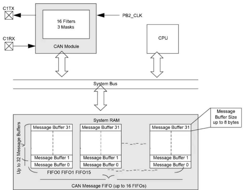
flowchart
graph TD
    subgraph CAN Module
        A["16 Filters 3 Masks"] --> B["C1TX"]
        C["C1RX"] --> D["CAN Module"]
        D --> E["CPU"]
    end

    subgraph System RAM
        F["Message Buffer 31"] --> G["FIFO0 FIFO1 FIFO15"]
        H["Message Buffer 31"] --> I["FIFO0 FIFO1 FIFO15"]
        J["Message Buffer 31"] --> K["FIFO0 FIFO1 FIFO15"]
        L["Message Buffer 0"] --> M["FIFO0 FIFO1 FIFO15"]
        N["Message Buffer 0"] --> O["FIFO0 FIFO1 FIFO15"]
        P["Message Buffer 1"] --> Q["FIFO0 FIFO1 FIFO15"]
        R["Message Buffer 1"] --> S["FIFO0 FIFO1 FIFO15"]
        T["Message Buffer 0"] --> U["FIFO0 FIFO1 FIFO15"]
    end

    subgraph CPU
        V["PB2_CLK"] --> W["Data Bus"]
    end

    subgraph System Bus
        X["Up to 32 Message Buffers"] --> Y["CAN Message FIFO (up to 16 FIFOs)"]
    end

    style CAN Module fill:#f9f,stroke:#333
    style System RAM fill:#ccf,stroke:#333
30.1 CAN Control Registers
TABLE 30-1: CAN1 REGISTER SUMMARY
| Virtual Address(BF82.#) | Register Name ( 1 \ ) | Bit Range | Bits | All Resets | ||||||||||||||||
| 31/15 30 | 14 29/13 | 28/12 27/11 | 26/10 25/9 | 24/8 23/7 | 22/6 21/5 20 | 14 19/3 18 | 2 17/1 16/0 | |||||||||||||
| 2000 | C1CON | 31:16 | — | — | — | — | ABAT | REQOP[2:0] | OPMOD[2:0] | CANCAP | — | — | — | — | 0400 | |||||
| 15:0 | ON | — | SIDLE | — | CANBUSY | — | — | — | — | — | — | — | DNCNT[4:0] | 0000 | ||||||
| 2010 | C1CFG | 31:16 | — | — | — | — | — | — | — | — | — | WAKFIL | — | — | — | SEG2PH[2:0] | 0000 | |||
| 15:0 | SEG2PHTS | SAM | SEG1PH[2:0] | PRSEG[2:0] | SJW[1:0] | BRP[5:0] | 0000 | |||||||||||||
| 2020 | C1INT | 31:16 | IVRIE | WAKIE | CERRIE | SERRIE | RBOVIE | — | — | — | — | — | — | — | MODIE | CTMRIE | RBIE | TBIE | 0000 | |
| 15:0 | IVRIF | WAKIF | CERRIF | SERRIF | RBOVIF | — | — | — | — | — | — | — | MODIF | CTMRIF | RBIF | TBIF | 0000 | |||
| 2030 | C1VEC | 31:16 | — | — | — | — | — | — | — | — | — | — | — | — | — | — | — | — | 0000 | |
| 15:0 | — | — | — | — | FILHIT[4:0] | — | ICODE[6:0] | 0040 | ||||||||||||
| 2040 | C1TREC | 31:16 | — | — | — | — | — | — | — | — | — | — | TXBO | TXBP | RXBP | TXWARN | RXWARN | EWARN | 0000 | |
| 15:0 | TERRCNT[7:0] | RERRCNT[7:0] | 0000 | |||||||||||||||||
| 2050 | C1FSTAT | 31:16 | FIFOIP31 | FIFOIP30 | FIFOIP29 | FIFOIP28 | FIFOIP27 | FIFOIP26 | FIFOIP25 | FIFOIP24 | FIFOIP23 | FIFOIP22 | FIFOIP21 | FIFOIP20 | FIFOIP19 | FIFOIP18 | FIFOIP17 | FIFOIP16 | 0000 | |
| 15:0 | FIFOIP15 | FIFOIP14 | FIFOIP13 | FIFOIP12 | FIFOIP11 | FIFOIP10 | FIFOIP9 | FIFOIP8 | FIFOIP7 | FIFOIP6 | FIFOIP5 | FIFOIP4 | FIFOIP3 | FIFOIP2 | FIFOIP1 | FIFOIP0 | 0000 | |||
| 2060 | C1RXOVF | 31:16 | RXOVF31 | RXOVF30 | RXOVF29 | RXOVF28 | RXOVF27 | RXOVF26 | RXOVF25 | RXOVF24 | RXOVF23 | RXOVF22 | RXOVF21 | RXOVF20 | RXOVF19 | RXOVF18 | RXOVF17 | RXOVF16 | 0000 | |
| 15:0 | RXOVF15 | RXOVF14 | RXOVF13 | RXOVF12 | RXOVF11 | RXOVF10 | RXOVF9 | RXOVF8 | RXOVF7 | RXOVF6 | RXOVF5 | RXOVF4 | RXOVF3 | RXOVF2 | RXOVF1 | RXOVF0 | 0000 | |||
| 2070 | C1TMR | 31:16 | CANTS[15:0] | 0000 | ||||||||||||||||
| 15:0 | CANTSPRE[15:0] | 0000 | ||||||||||||||||||
| 2080 | C1RXM0 | 31:16 | SID[10:0] | — | MIDE | — | EID[17:16] | xxxxx | ||||||||||||
| 15:0 | EID[15:0] | xxxxx | ||||||||||||||||||
| 2090 | C1RXM1 | 31:16 | SID[10:0] | — | MIDE | — | EID[17:16] | xxxxx | ||||||||||||
| 15:0 | EID[15:0] | xxxxx | ||||||||||||||||||
| 20A0 | C1RXM2 | 31:16 | SID[10:0] | — | MIDE | — | EID[17:16] | xxxxx | ||||||||||||
| 15:0 | EID[15:0] | xxxxx | ||||||||||||||||||
| 20C0 | C1FLTCONO | 31:16 | FLTEN3 | MSEL3[1:0] | FSEL3[4:0] | FLTEN2 | MSEL2[1:0] | FSEL2[4:0] | 0000 | |||||||||||
| 15:0 | FLTEN1 | MSEL1[1:0] | FSEL1[4:0] | FLTEN0 | MSEL0[1:0] | FSEL0[4:0] | 0000 | |||||||||||||
| 20D0 | C1FLTCON1 | 31:16 | FLTEN7 | MSEL7[1:0] | FSEL7[4:0] | FLTEN6 | MSEL6[1:0] | FSEL6[4:0] | 0000 | |||||||||||
| 15:0 | FLTEN5 | MSEL5[1:0] | FSEL5[4:0] | FLTEN4 | MSEL4[1:0] | FSEL4[4:0] | 0000 | |||||||||||||
| 20E0 | C1FLTCON2 | 31:16 | FLTEN11 | MSEL11[1:0] | FSEL11[4:0] | FLTEN10 | MSEL10[1:0] | FSEL10[4:0] | 0000 | |||||||||||
| 15:0 | FLTEN9 | MSEL9[1:0] | FSEL9[4:0] | FLTEN8 | MSEL8[1:0] | FSEL8[4:0] | 0000 | |||||||||||||
| 20F0 | C1FLTCON3 | 31:16 | FLTEN15 | MSEL15[1:0] | FSEL15[4:0] | FLTEN14 | MSEL14[1:0] | FSEL14[4:0] | 0000 | |||||||||||
| 15:0 | FLTEN13 | MSEL13[1:0] | FSEL13[4:0] | FLTEN12 | MSEL12[1:0] | FSEL12[4:0] | 0000 | |||||||||||||
| 2140-2330 | C1RXFn(n = 0-15) | 31:16 | SID[10:0] | — EXID — EID[17:16] | xxxxx | |||||||||||||||
| 15:0 | EID[15:0] | xxxxx | ||||||||||||||||||
| 2340 | C1FIFOBA | 31:16 | C1FIFOBA[29:14] | 0000 | ||||||||||||||||
| 15:0 | C1FIFOBA[13:0] | — | — | 0000 | ||||||||||||||||
Legend: x = unknown value on Reset; — = unimplemented, read as '0'. Reset values are shown in hexadecimal. Note 1: All registers in this table have corresponding CLR, SET and INV registers at their virtual addresses, plus offsets of 0x4, 0x8 and 0xC, respectively. See Section 13.3 "CLR, SET and INV Registers" for more information.
TABLE 30-1: CAN1 REGISTER SUMMARY (CONTINUED)
| Virtual Address (BFB2_#) | Register Name | Bit Range | Bits | All Resets | |||||||||||||||
| 31/15 | 30/14 | 29/13 | 28/12 | 27/11 | 26/10 | 25/9 | 24/8 | 23/7 | 22/6 | 21/5 | 20/4 | 19/3 | 18/2 | 17/1 | 16/0 | ||||
| 2350 | C1FIFOCONn(n = 0) | 3 | 1 | : | 1 | 6 | — | — | — | — | — | — | — | — | — | — | — | — | |
| 15:0 | — | FRESET | UINC | DONLY | — | — | — | — | TXEN | TXABAT | TXLARB | TXERR | TXREQ | RTREN | TXPRI[1:0] | 0000 | |||
| 2360 | C1FIFOINTn(n = 0) | 31:16 | — | — | — | — | — | TXNFULLIE | TXHALFIE | TXEMPTYIE | — | — | — | — | RXOVFLIE | RXFULLIE | RXHALFIE | RXN EMPTYIE | 0000 |
| 15:0 | — | — | — | — | — | TXNFULLIF | TXHALFIF | TXEMPTYIF | — | — | — | — | RXOVFLIF | RXFULLIF | RXHALFIF | RXN EMPTYIF | 0000 | ||
| 2370 | C1FIFOUAn(n = 0) | 31:16 | C1FIFOUA[15:0] | 0000 | |||||||||||||||
| 15:0 | C1FIFOUA[13:0] | — | — | 0000 | |||||||||||||||
| 2380 | C1FIFOCIn(n = 0) | 31:16 | — | — | — | — | — | — | — | — | — | — | — | — | — | — | — | — | 0000 |
| 15:0 | — | — | — | — | — | — | — | — | — | — | — | — | C1FIFOCI[4:0] | 0000 | |||||
| 2390-2740 | C1FIFOCONnC1FIFOINTnC1FIFOUAnC1FIFOCIn(n = 1-15) | 31:16 | — | — | — | — | — | — | — | — | — | — | — | FSIZE[4:0] | 0000 | ||||
| 15:0 | — | FRESET | UINC | DONLY | — | — | — | — | TXEN | TXABAT | TXLARB | TXERR | TXREQ | RTREN | TXPRI[1:0] | 0000 | |||
| 31:16 | — | — | — | — | — | TXNFULLIE | TXHALFIE | TXEMPTYIE | — | — | — | — | RXOVFLIE | RXFULLIE | RXHALFIE | RXN EMPTYIE | 0000 | ||
| 15:0 | — | — | — | — | — | TXNFULLIF | TXHALFIF | TXEMPTYIF | — | — | — | RXOVFLIF | RXFULLIF | RXHALFIF | RXN EMPTYIF | 0000 | |||
| 31:16 | C1FIFOUA[15:0] | 0000 | |||||||||||||||||
| 15:0 | C1FIFOUA[13:0] | — | — | 0000 | |||||||||||||||
| 31:16 | — | — | — | — | — | — | — | — | — | — | — | — | — | — | — | — | 0000 | ||
| 15:0 | — | — | — | — | — | — | — | — | — | — | — | C1FIFOCI[4:0] | 0000 | ||||||
Legend: x = unknown value on Reset; — = unimplemented, read as '0'. Reset values are shown in hexadecimal.
Note 1: All registers in this table have corresponding CLR, SET and INV registers at their virtual addresses, plus offsets of 0x4, 0xB and 0xC, respectively. See Section 13.3 "CLR, SET and INV Registers" for more information.
REGISTER 30-1: C1CON: CAN MODULE CONTROL REGISTER
| Bit Range | Bit 31/23/15/7 | Bit 30/22/14/6 | Bit 29/21/13/5 | Bit 28/20/12/4 | Bit 27/19/11/3 | Bit 26/18/10/2 | Bit 25/17/9/1 | Bit 24/16/8/0 |
| 31:24 | U-0 U-0 U-0 U-0 S/HC-0 R/W-1 R/W-0 R/W-0 | |||||||
| — — — | ABAT REQOP[2:0] | |||||||
| 23:16 | R-1 R-0 R-0 R/W-0 U-0 U-0 U-0 | |||||||
| OPMOD[2:0] | CANCAP | — | — — | — | ||||
| 15:8 | R/W-0 | U-0 | R/W-0 | U-0 | R-0 | U-0 | U-0 | U-0 |
| ON(1) | — | SIDLE | — | CANBUSY | — | — | — | |
| 7:0 | U-0 U-0 U-0 R/W-0 R/W-0 R/W-0 R/W-0 | |||||||
| — — — | DNCNT[4:0] | |||||||
| Legend: HC = Hardware Cleared S = Settable bitR = Readable bit W = Writable bit P = Programmable bit r = Reserved bitU = Unimplemented bit -n = Bit Value at POR: ('0', '1', x = Unknown) |
bit 31-28 Unimplemented: Read as '0'
bit 27 ABAT: Abort All Pending Transmissions bit
1 = Signal all transmit buffers to abort transmission
0 = Module will clear this bit when all transmissions aborted
bit 26-24 REQOP[2:0]: Request Operation Mode bits
111 = Set Listen All Messages mode
110 = Reserved - Do not use
101 = Reserved - Do not use
100 = Set Configuration mode
011 = Set Listen Only mode
010 = Set Loopback mode
001 = Set Disable mode
000 = Set Normal Operation mode
bit 23-21 OPMOD[2:0]: Operation Mode Status bits
111 = Module is in Listen All Messages mode
110 = Reserved
101 = Reserved
100 = Module is in Configuration mode
011 = Module is in Listen Only mode
010 = Module is in Loopback mode
001 = Module is in Disable mode
000 = Module is in Normal Operation mode
bit 20 CANCAP: CAN Message Receive Time Stamp Timer Capture Enable bit
1 = CANTMR value is stored on valid message reception and is stored with the message
0 = Disable CAN message receive time stamp timer capture and stop CANTMR to conserve power
bit 19-16 Unimplemented: Read as '0'
bit 15 ON: CAN On bit ^(1)
1 = CAN module is enabled
0 = CAN module is disabled
bit 14 Unimplemented: Read as '0'
Note 1: If the user application clears the ON bit, it may take a number of cycles before the CAN module completes the current transaction and responds to the request. The user application must poll the CANBUSY bit to verify that the request was honored.
REGISTER 30-1: C1CON: CAN MODULE CONTROL REGISTER (CONTINUED)
bit 13 SIDLE: CAN Stop in Idle bit
1 = CAN Stops operation when system enters Idle mode
0 = CAN continues operation when system enters Idle mode
bit 12 Unimplemented: Read as '0'
bit 11 CANBUSY: CAN Module is Busy bit
1 = The CAN module is active
0 = The CAN module is completely disabled
bit 10-5 Unimplemented: Read as '0'
bit 4-0 DNCNT[4:0]: Device Net Filter Bit Number bits
10011-11111 = Invalid Selection (compare up to 18-bits of data with EID)
10010 = Compare up to data byte 2 bit 6 with EID17 (CiRXFn[17])
.
.
00001 = Compare up to data byte 0 bit 7 with EID0 (CiRXFn[0])
00000 = Do not compare data bytes
Note 1: If the user application clears the ON bit, it may take a number of cycles before the CAN module completes the current transaction and responds to the request. The user application must poll the CANBUSY bit to verify that the request was honored.
REGISTER 30-2: C1CFG: CAN BAUD RATE CONFIGURATION REGISTER
| Bit Range | Bit 31/23/15/7 | Bit 30/22/14/6 | Bit 29/21/13/5 | Bit 28/20/12/4 | Bit 27/19/11/3 | Bit 26/18/10/2 | Bit 25/17/9/1 | Bit 24/16/8/0 |
| 31:24 | U-0 U-0 U-0 U-0 U-0 U-0 U-0 | |||||||
| — — — — | — — — — | |||||||
| 23:16 | U-0 R/W-0 U-0 U-0 U-0 R/W-0 R/W-0 R/W-0 | |||||||
| — | WAKFIL | — | — | — | SEG2PH[2:0]^(1,4) | |||
| 15:8 | R/W-0 | R/W-0 | R/W-0 | R/W-0 | R/W-0 | R/W-0 | R/W-0 | R/W-0 |
| SEG2PHTS^(1) | SAM^(2) | SEG1PH[2:0] | PRSEG[2:0] | |||||
| 7:0 | R/W-0 | R/W-0 | R/W-0 | R/W-0 | R/W-0 | R/W-0 | R/W-0 | R/W-0 |
| SJW[1:0]^(3) | BRP[5:0] | |||||||
| Legend: | HC = Hardware Clear | S = Settable bit | |
| R = Readable bit | W = Writable bit | P = Programmable bit | r = Reserved bit |
| U = Unimplemented bit | -n = Bit Value at POR: ('0', '1', x = Unknown) | ||
bit 31-23 Unimplemented: Read as '0'
bit 22 WAKFIL: CAN Bus Line Filter Enable bit
1 = Use CAN bus line filter for wake-up
0 = CAN bus line filter is not used for wake-up
bit 21-19 Unimplemented: Read as '0'
bit 18-16 SEG2PH[2:0]: Phase Buffer Segment 2 bits ^(1,4)
111 = Length is 8 x Tq
•
•
000 = Length is 1 x Tq
bit 15 SEG2PHTS: Phase Segment 2 Time Select bit ^(1)
1 = Freely programmable
0 = Maximum of SEG1PH or Information Processing Time, whichever is greater
bit 14 SAM: Sample of the CAN Bus Line bit ^(2)
1 = Bus line is sampled three times at the sample point
0 = Bus line is sampled once at the sample point
bit 13-11 SEG1PH[2:0]: Phase Buffer Segment 1 bits ^(4)
111 = Length is 8 x To
•
•
000 = Length is 1 x TQ
Note 1: SEG2PH ≤ SEG1PH. If SEG2PHTS is clear, SEG2PH will be set automatically.
2: 3 Time bit sampling is not allowed for BRP < 2.
3: SJW ≤ SEG2PH.
4: The Time Quanta per bit must be greater than 7 (that is, TQBIT > 7).
5: This register can only be modified when the CAN module is in Configuration mode (OPMOD[2:0] (C1CON[23:21]) = 100).
REGISTER 30-2: C1CFG: CAN BAUD RATE CONFIGURATION REGISTER (CONTINUED)
bit 10-8 PRSEG[2:0]: Propagation Time Segment bits (4)
111 = Length is 8 x Tq
•
•
•
000 = Length is 1 x Tq
bit 7-6 SJW[1:0]: Synchronization Jump Width bits (3)
11 = Length is 4 x Tq
10 = Length is 3 x Tq
01 = Length is 2 x Tq
00 = Length is 1 x Tq
bit 5-0 BRP[5:0]: Baud Rate Prescaler bits
111111 = TQ = (2 x 64)/TPB2_CLK
111110 = TQ = (2 x 63)/TPB2_CLK
.
.
.
.
000001 = TQ = (2 x 2)/TPB2_CLK
000000 = TQ = (2 x 1)/TPB2_CLK
Note 1: SEG2PH ≤ SEG1PH. If SEG2PHTS is clear, SEG2PH will be set automatically.
2: 3 Time bit sampling is not allowed for BRP < 2.
3: SJW ≤ SEG2PH.
4: The Time Quanta per bit must be greater than 7 (that is, T QBIT > 7).
5: This register can only be modified when the CAN module is in Configuration mode (OPMOD[2:0] (C1CON[23:21]) = 100).
REGISTER 30-3: C1INT: CAN INTERRUPT REGISTER
| Bit Range | Bit 31/23/15/7 | Bit 30/22/14/6 | Bit 29/21/13/5 | Bit 28/20/12/4 | Bit 27/19/11/3 | Bit 26/18/10/2 | Bit 25/17/9/1 | Bit 24/16/8/0 |
| 31:24 | R/W-0 R/W-0 R/W-0 R/W-0 R/W-0 U-0 U-0 U-0 | |||||||
| IVRIE WAKIE CERRIE SERRIE RBOVIE | — — — | |||||||
| 23:16 | U-0 U-0 U-0 U-0 R/W-0 R/W-0 R/W-0 R/W-0 | |||||||
| — — — — MODIE CTMIRIE RBIE TBIE | ||||||||
| 15:8 | R/W-0 R/W-0 R/W-0 R/W-0 R/W-0 U-0 U-0 U-0 | |||||||
| IVRIF WAKIF CERRIF SERRIF (1) | RBOVIF | — — — | ||||||
| 7:0 | U-0 U-0 U-0 U-0 R/W-0 R/W-0 R/W-0 R/W-0 | |||||||
| — — — — MODIF CTMRIF RBIF TBIF | ||||||||
Legend:
| R = Readable bit | W = Writable bit | U = Unimplemented bit, read as '0' |
| -n = Value at POR | ‘1’ = Bit is set | ‘0’ = Bit is cleared x = Bit is unknown |
bit 31 IVRIE: Invalid Message Received Interrupt Enable bit
1 = Interrupt request is enabled
0 = Interrupt request is not enabled
bit 30 WAKIE: CAN Bus Activity Wake-up Interrupt Enable bit
1 = Interrupt request is enabled
0 = Interrupt request is not enabled
bit 29 CERRIE: CAN Bus Error Interrupt Enable bit
1 = Interrupt request is enabled
0 = Interrupt request is not enabled
bit 28 SERRIE: System Error Interrupt Enable bit
1 = Interrupt request is enabled
0 = Interrupt request is not enabled
bit 27 RBOVIE: Receive Buffer Overflow Interrupt Enable bit
1 = Interrupt request is enabled
0 = Interrupt request is not enabled
bit 26-20 Unimplemented: Read as '0'
bit 19 MODIE: Mode Change Interrupt Enable bit
1 = Interrupt request is enabled
0 = Interrupt request is not enabled
bit 18 CTMRIE: CAN Timestamp Timer Interrupt Enable bit
1 = Interrupt request is enabled
0 = Interrupt request is not enabled
bit 17 RBIE: Receive Buffer Interrupt Enable bit
1 = Interrupt request is enabled
0 = Interrupt request is not enabled
bit 16 TBIE: Transmit Buffer Interrupt Enable bit
1 = Interrupt request is enabled
0 = Interrupt request is not enabled
bit 15 IVRIF: Invalid Message Received Interrupt Flag bit
1 = An invalid messages interrupt has occurred
0 = An invalid message interrupt has not occurred
Note 1: This bit can only be cleared by turning the CAN module off and on by clearing or setting the ON bit (C1CON[15]).
REGISTER 30-3: C1INT: CAN INTERRUPT REGISTER (CONTINUED)
bit 14 WAKIF: CAN Bus Activity Wake-up Interrupt Flag bit
1 = A bus wake-up activity interrupt has occurred
0 = A bus wake-up activity interrupt has not occurred
bit 13 CERRIF: CAN Bus Error Interrupt Flag bit
1 = A CAN bus error has occurred
0 = A CAN bus error has not occurred
bit 12 SERRIF: System Error Interrupt Flag bit
1 = A system error occurred (typically an illegal address was presented to the System Bus)
0 = A system error has not occurred
bit 11 RBOVIF: Receive Buffer Overflow Interrupt Flag bit
1 = A receive buffer overflow has occurred
0 = A receive buffer overflow has not occurred
bit 10-4 Unimplemented: Read as '0'
bit 3 MODIF: CAN Mode Change Interrupt Flag bit
1 = A CAN module mode change has occurred (OPMOD[2:0] has changed to reflect REQOP)
0 = A CAN module mode change has not occurred
bit 2 CTMRIF: CAN Timer Overflow Interrupt Flag bit
1 = A CAN timer (CANTMR) overflow has occurred
0 = A CAN timer (CANTMR) overflow has not occurred
bit 1 RBIF: Receive Buffer Interrupt Flag bit
1 = A receive buffer interrupt is pending
0 = A receive buffer interrupt is not pending
bit 0 TBIF: Transmit Buffer Interrupt Flag bit
1 = A transmit buffer interrupt is pending
0 = A transmit buffer interrupt is not pending
Note 1: This bit can only be cleared by turning the CAN module off and on by clearing or setting the ON bit (C1CON[15]).
R = Readable bit W = Writable bit U = Unimplemented bit, read as '0'
-n = Value at POR '1' = Bit is set '0' = Bit is cleared x = Bit is unknown
bit 31-13 Unimplemented: Read as '0'
bit 12-8 FILHIT[4:0]: Filter Hit Number bit
11111 = Filter 31
11110 = Filter 30
•
•
00001 = Filter 1
00000 = Filter 0
bit 7 Unimplemented: Read as '0'
bit 6-0 ICODE[6:0]: Interrupt Flag Code bits ^(1)
1001000-1111111 = Reserved
1001000 = Invalid Message Received (IVRIF)
1000111 = CAN Module Mode Change (MODIF)
1000110 = CAN Timestamp Timer (CTMRIF)
1000101 = Bus Bandwidth Error (SERRIF)
1000100 = Address Error Interrupt (SERRIF)
1000011 = Receive FIFO Overflow Interrupt (RBOVIF)
1000010 = Wake-up interrupt (WAKIF)
1000001 = Error Interrupt (CERRIF)
1000000 = No interrupt
0100000-0111111 = Reserved
0011111 = FIFO31 interrupt (CiFSTAT[31] set)
0011110 = FIFO30 interrupt (CiFSTAT[30] set)
-
.
0000001 = FIFO1 interrupt (CiFSTAT[1] set)
0000000 = FIFO0 interrupt (CiFSTAT[0] set)
Note 1: These bits are only updated for enabled interrupts.
REGISTER 30-5: C1TREC: CAN TRANSMIT/RECEIVE ERROR COUNT REGISTER
| Bit Range | Bit 31/23/15/7 | Bit 30/22/14/6 | Bit 29/21/13/5 | Bit 28/20/12/4 | Bit 27/19/11/3 | Bit 26/18/10/2 | Bit 25/17/9/1 | Bit 24/16/8/0 |
| 31:24 | U-0 U-0 U-0 U-0 U-0 U-0 U-0 | |||||||
| — — — | — — — — — | |||||||
| 23:16 | U-0 U-0 R-0 R-0 R-0 R-0 R-0 R-0 | |||||||
| — — TX BO TXBP RXBP TXWARN RXWARN EWARN | ||||||||
| 15:8 | R-0 R-0 R-0 R-0 R-0 R-0 R-0 | |||||||
| TERRCNT[7:0] | ||||||||
| 7:0 | R-0 R-0 R-0 R-0 R-0 R-0 R-0 | |||||||
| RERRCNT[7:0] | ||||||||
Legend:
R = Readable bit W = Writable bit U = Unimplemented bit, read as '0'
-n = Value at POR '1' = Bit is set '0' = Bit is cleared x = Bit is unknown
bit 31-22 Unimplemented: Read as '0'
bit 21 TXBO: Transmitter in Error State Bus OFF (TERRCNT ≥ 256)
bit 20 TXBP: Transmitter in Error State Bus Passive (TERRCNT ≥ 128)
bit 19 RXBP: Receiver in Error State Bus Passive (RERRCNT ≥ 128)
bit 18 TXWARN: Transmitter in Error State Warning (128 > TERRCNT ≥ 96)
bit 17 RXWARN: Receiver in Error State Warning (128 > RERRCNT ≥ 96)
bit 16 EWARN: Transmitter or Receiver is in Error State Warning
bit 15-8 TERRCNT[7:0]: Transmit Error Counter
bit 7-0 RERRCNT[7:0]: Receive Error Counter
REGISTER 30-6: C1FSTAT: CAN FIFO STATUS REGISTER
| Bit Range | Bit 31/23/15/7 | Bit 30/22/14/6 | Bit 29/21/13/5 | Bit 28/20/12/4 | Bit 27/19/11/3 | Bit 26/18/10/2 | Bit 25/17/9/1 | Bit 24/16/8/0 |
| 31:24 | R-0 | R-0 | R-0 | R-0 | R-0 | R-0 | R-0 | R-0 |
| FIFOIP31 | FIFOIP30 | FIFOIP29 | FIFOIP28 | FIFOIP27 | FIFOIP26 | FIFOIP25 | FIFOIP24 | |
| 23:16 | R-0 | R-0 | R-0 | R-0 | R-0 | R-0 | R-0 | R-0 |
| FIFOIP23 | FIFOIP22 | FIFOIP21 | FIFOIP20 | FIFOIP19 | FIFOIP18 | FIFOIP17 | FIFOIP16 | |
| 15:8 | R-0 | R-0 | R-0 | R-0 | R-0 | R-0 | R-0 | R-0 |
| FIFOIP15 | FIFOIP14 | FIFOIP13 | FIFOIP12 | FIFOIP11 | FIFOIP10 | FIFOIP9 | FIFOIP8 | |
| 7:0 | R-0 | R-0 | R-0 | R-0 | R-0 | R-0 | R-0 | R-0 |
| FIFOIP7 | FIFOIP6 | FIFOIP5 | FIFOIP4 | FIFOIP3 | FIFOIP2 | FIFOIP1 | FIFOIP0 |
Legend:
| R = Readable bit | W = Writable bit | U = Unimplemented bit, read as '0' |
| -n = Value at POR | '1' = Bit is set | '0' = Bit is cleared x = Bit is unknown |
bit 31-0 FIFOIP[31:0]: FIFOx Interrupt Pending bits
1 = One or more enabled FIFO interrupts are pending
0 = No FIFO interrupts are pending
REGISTER 30-7: C1RXOVF: CAN RECEIVE FIFO OVERFLOW STATUS REGISTER
| Bit Range | Bit 31/23/15/7 | Bit 30/22/14/6 | Bit 29/21/13/5 | Bit 28/20/12/4 | Bit 27/19/11/3 | Bit 26/18/10/2 | Bit 25/17/9/1 | Bit 24/16/8/0 |
| 31:24 | R-0 R-0 R-0 R-0 R-0 R-0 R-0 | |||||||
| RXOVF31 | RXOVF30 | RXOVF29 | RXOVF28 | RXOVF27 | RXOVF26 | RXOVF25 | RXOVF24 | |
| 23:16 | R-0 R-0 R-0 R-0 R-0 R-0 R-0 | |||||||
| RXOVF23 | RXOVF22 | RXOVF21 | RXOVF20 | RXOVF19 | RXOVF18 | RXOVF17 | RXOVF16 | |
| 15:8 | R-0 R-0 R-0 R-0 R-0 R-0 R-0 | |||||||
| RXOVF15 | RXOVF14 | RXOVF13 | RXOVF12 | RXOVF11 | RXOVF10 | RXOVF9 | RXOVF8 | |
| 7:0 | R-0 R-0 R-0 R-0 R-0 R-0 R-0 | |||||||
| RXOVF7 | RXOVF6 | RXOVF5 | RXOVF4 | RXOVF3 | RXOVF2 | RXOVF1 | RXOVF0 | |
Legend:
| R = Readable bit | W = Writable bit | U = Unimplemented bit, read as '0' |
| -n = Value at POR | '1' = Bit is set | '0' = Bit is cleared x = Bit is unknown |
bit 31-0 RXOVF[31:0]: FIFOx Receive Overflow Interrupt Pending bit
1 = FIFO has overflowed
0 = FIFO has not overflowed
| R = Readable bit | W = Writable bit | U = Unimplemented bit, read as '0' |
| -n = Value at POR | '1' = Bit is set | '0' = Bit is cleared x = Bit is unknown |
bit 31-0 CANTS[15:0]: CAN Time Stamp Timer bits
This is a free-running timer that increments every CANTSPRE system clocks when the CANCAP bit (CiCON[20]) is set.
bit 15-0 CANTSPRE[15:0]: CAN Time Stamp Timer Prescaler bits
1111 1111 1111 1111 = CAN Time Stamp (CANTS) timer increments every 65,535 system clocks
•
•
•
0000 0000 0000 0000 = CAN Time Stamp (CANTS) timer increments every system clock
Note 1: C1TMR will be frozen when CANCAP = 0.
2: The C1TMR prescaler count will be reset on any write to C1TMR (CANTSPRE will be unaffected).
REGISTER 30-9: C1RXMN: CAN ACCEPTANCE FILTER MASK 'n' REGISTER ('n' = 0-2)
| Bit Range | Bit 31/23/15/7 | Bit 30/22/14/6 | Bit 29/21/13/5 | Bit 28/20/12/4 | Bit 27/19/11/3 | Bit 26/18/10/2 | Bit 25/17/9/1 | Bit 24/16/8/0 |
| 31:24 | R/W-0 R/W-0 R/W-0 R/W-0 R/W-0 R/W-0 R/W-0 | |||||||
| SID[10:3] | ||||||||
| 23:16 | R/W-0 R/W-0 R/W-0 U-0 R/W-0 U-0 R/W-0 R/W-0 | |||||||
| SID[2:0] | — | MIDE | — | EID[17:16] | ||||
| 15:8 | R/W-0 R/W-0 R/W-0 R/W-0 R/W-0 R/W-0 R/W-0 | |||||||
| EID[15:8] | ||||||||
| 7:0 | R/W-0 R/W-0 R/W-0 R/W-0 R/W-0 R/W-0 R/W-0 | |||||||
| EID[7:0] | ||||||||
Legend:
| R = Readable bit | W = Writable bit | U = Unimplemented bit, read as '0' |
| -n = Value at POR | '1' = Bit is set | '0' = Bit is cleared x = Bit is unknown |
bit 31-21 SID[10:0]: Standard Identifier bits
1 = Include bit, SIDx, in filter comparison
0 = Bit SIDx is 'don't care' in filter operation
bit 20 Unimplemented: Read as '0'
bit 19 MIDE: Identifier Receive Mode bit
1 = Match only message types (standard/extended address) that correspond to the EXID bit in filter
0 = Match either standard or extended address message if filters match (that is, if (Filter SID) = (Message SID) or if (FILTER SID/EID) = (Message SID/EID))
bit 18 Unimplemented: Read as '0'
bit 17-0 EID[17:0]: Extended Identifier bits
1 = Include bit, EIDx, in filter comparison
0 = Bit EIDx is 'don't care' in filter operation
Note: This register can only be modified when the CAN module is in Configuration mode (OPMOD[2:0] (C1CON[23:21]) = 100).
REGISTER 30-10: C1FLTCON0: CAN FILTER CONTROL REGISTER 0
| Bit Range | Bit 31/23/15/7 | Bit 30/22/14/6 | Bit 29/21/13/5 | Bit 28/20/12/4 | Bit 27/19/11/3 | Bit 26/18/10/2 | Bit 25/17/9/1 | Bit 24/16/8/0 |
| 31:24 | R/W-0 R/W-0 R/W-0 R/W-0 R/W-0 R/W-0 R/W-0 R/W-0 | |||||||
| FLTEN3 MSEL3[1:0] FSEL3[4:0] | ||||||||
| 23:16 | R/W-0 R/W-0 R/W-0 R/W-0 R/W-0 R/W-0 R/W-0 R/W-0 | |||||||
| FLTEN2 MSEL2[1:0] FSEL2[4:0] | ||||||||
| 15:8 | R/W-0 R/W-0 R/W-0 R/W-0 R/W-0 R/W-0 R/W-0 R/W-0 | |||||||
| FLTEN1 MSEL1[1:0] FSEL1[4:0] | ||||||||
| 7:0 | R/W-0 R/W-0 R/W-0 R/W-0 R/W-0 R/W-0 R/W-0 R/W-0 | |||||||
| FLTEN0 MSEL0[1:0] FSEL0[4:0] | ||||||||
Legend:
| R = Readable bit W = Writable bit U = Unimplemented bit, read as '0' | |||
| -n = Value at POR | '1' = Bit is set | '0' = Bit is cleared | x = Bit is unknown |
bit 31 FLTEN3: Filter 3 Enable bit
1 = Filter is enabled
0 = Filter is disabled
bit 30-29 MSEL3[1:0]: Filter 3 Mask Select bits
11 = Acceptance Mask 3 selected
10 = Acceptance Mask 2 selected
01 = Acceptance Mask 1 selected
00 = Acceptance Mask 0 selected
bit 28-24 FSEL3[4:0]: FIFO Selection bits
11111 = Message matching filter is stored in FIFO buffer 31
11110 = Message matching filter is stored in FIFO buffer 30
•
•
00001 = Message matching filter is stored in FIFO buffer 1
00000 = Message matching filter is stored in FIFO buffer 0
bit 23 FLTEN2: Filter 2 Enable bit
1 = Filter is enabled
0 = Filter is disabled
bit 22-21 MSEL2[1:0]: Filter 2 Mask Select bits
11 = Acceptance Mask 3 selected
10 = Acceptance Mask 2 selected
01 = Acceptance Mask 1 selected
00 = Acceptance Mask 0 selected
bit 20-16 FSEL2[4:0]: FIFO Selection bits
11111 = Message matching filter is stored in FIFO buffer 31
11110 = Message matching filter is stored in FIFO buffer 30
•
•
00001 = Message matching filter is stored in FIFO buffer 1
00000 = Message matching filter is stored in FIFO buffer 0
bit 15 FLTEN1: Filter 1 Enable bit
1 = Filter is enabled
0 = Filter is disabled
Note: The bits in this register can only be modified if the corresponding filter enable (FLTENn) bit is '0'.
REGISTER 30-10: C1FLTCON0: CAN FILTER CONTROL REGISTER 0 (CONTINUED)
bit 14-13 MSEL1[1:0]: Filter 1 Mask Select bits
11 = Acceptance Mask 3 selected
10 = Acceptance Mask 2 selected
01 = Acceptance Mask 1 selected
00 = Acceptance Mask 0 selected
bit 12-8 FSEL1[4:0]: FIFO Selection bits 11111 = Message matching filter is stored in FIFO buffer 31 11110 = Message matching filter is stored in FIFO buffer 30 : : 00001 = Message matching filter is stored in FIFO buffer 1 00000 = Message matching filter is stored in FIFO buffer 0
bit 7 FLTENO: Filter 0 Enable bit 1 = Filter is enabled 0 = Filter is disabled
bit 6-5 MSEL0[1:0]: Filter 0 Mask Select bits 11 = Acceptance Mask 3 selected 10 = Acceptance Mask 2 selected 01 = Acceptance Mask 1 selected 00 = Acceptance Mask 0 selected
bit 4-0 FSEL0[4:0]: FIFO Selection bits 11111 = Message matching filter is stored in FIFO buffer 31 11110 = Message matching filter is stored in FIFO buffer 30 : : 00001 = Message matching filter is stored in FIFO buffer 1 00000 = Message matching filter is stored in FIFO buffer 0
Note: The bits in this register can only be modified if the corresponding filter enable (FLTENn) bit is '0'.
REGISTER 30-11: C1FLTCON1: CAN FILTER CONTROL REGISTER 1
| Bit Range | Bit 31/23/15/7 | Bit 30/22/14/6 | Bit 29/21/13/5 | Bit 28/20/12/4 | Bit 27/19/11/3 | Bit 26/18/10/2 | Bit 25/17/9/1 | Bit 24/16/8/0 |
| 31:24 | R/W-0 R/W-0 R/W-0 R/W-0 R/W-0 R/W-0 R/W-0 | |||||||
| FLTEN7 MSEL7[1:0] FSEL7[4:0] | ||||||||
| 23:16 | R/W-0 R/W-0 R/W-0 R/W-0 R/W-0 R/W-0 R/W-0 | |||||||
| FLTEN6 MSEL6[1:0] FSEL6[4:0] | ||||||||
| 15:8 | R/W-0 R/W-0 R/W-0 R/W-0 R/W-0 R/W-0 R/W-0 | |||||||
| FLTEN5 MSEL5[1:0] FSEL5[4:0] | ||||||||
| 7:0 | R/W-0 R/W-0 R/W-0 R/W-0 R/W-0 R/W-0 R/W-0 | |||||||
| FLTEN4 MSEL4[1:0] FSEL4[4:0] | ||||||||
Legend:
| R = Readable bit | W = Writable bit | U = Unimplemented bit, read as ‘0’ |
| -n = Value at POR | ‘1’ = Bit is set | ‘0’ = Bit is cleared x = Bit is unknown |
bit 31 FLTEN7: Filter 7 Enable bit
1 = Filter is enabled
0 = Filter is disabled
bit 30-29 MSEL7[1:0]: Filter 7 Mask Select bits
11 = Acceptance Mask 3 selected
10 = Acceptance Mask 2 selected
01 = Acceptance Mask 1 selected
00 = Acceptance Mask 0 selected
bit 28-24 FSEL7[4:0]: FIFO Selection bits
11111 = Message matching filter is stored in FIFO buffer 31
11110 = Message matching filter is stored in FIFO buffer 30
•
•
00001 = Message matching filter is stored in FIFO buffer 1
00000 = Message matching filter is stored in FIFO buffer 0
bit 23 FLTEN6: Filter 6 Enable bit
1 = Filter is enabled
0 = Filter is disabled
bit 22-21 MSEL6[1:0]: Filter 6 Mask Select bits
11 = Acceptance Mask 3 selected
10 = Acceptance Mask 2 selected
01 = Acceptance Mask 1 selected
00 = Acceptance Mask 0 selected
bit 20-16 FSEL6[4:0]: FIFO Selection bits
11111 = Message matching filter is stored in FIFO buffer 31
11110 = Message matching filter is stored in FIFO buffer 30
•
•
00001 = Message matching filter is stored in FIFO buffer 1
00000 = Message matching filter is stored in FIFO buffer 0
bit 15 FLTEN5: Filter 17 Enable bit
1 = Filter is enabled
0 = Filter is disabled
Note: The bits in this register can only be modified if the corresponding filter enable (FLTENn) bit is '0'.
REGISTER 30-11: C1FLTCON1: CAN FILTER CONTROL REGISTER 1 (CONTINUED)
bit 14-13 MSEL5[1:0]: Filter 5 Mask Select bits
11 = Acceptance Mask 3 selected
10 = Acceptance Mask 2 selected
01 = Acceptance Mask 1 selected
00 = Acceptance Mask 0 selected
bit 12-8 FSEL5[4:0]: FIFO Selection bits 11111 = Message matching filter is stored in FIFO buffer 31 11110 = Message matching filter is stored in FIFO buffer 30 : : 00001 = Message matching filter is stored in FIFO buffer 1 00000 = Message matching filter is stored in FIFO buffer 0
bit 7 FLTEN4: Filter 4 Enable bit 1 = Filter is enabled 0 = Filter is disabled
bit 6-5 MSEL4[1:0]: Filter 4 Mask Select bits 11 = Acceptance Mask 3 selected 10 = Acceptance Mask 2 selected 01 = Acceptance Mask 1 selected 00 = Acceptance Mask 0 selected
bit 4-0 FSEL4[4:0]: FIFO Selection bits 11111 = Message matching filter is stored in FIFO buffer 31 11110 = Message matching filter is stored in FIFO buffer 30 : : 00001 = Message matching filter is stored in FIFO buffer 1 00000 = Message matching filter is stored in FIFO buffer 0
Note: The bits in this register can only be modified if the corresponding filter enable (FLTENn) bit is '0'.
REGISTER 30-12: C1FLTCON2: CAN FILTER CONTROL REGISTER 2
| Bit Range | Bit 31/23/15/7 | Bit 30/22/14/6 | Bit 29/21/13/5 | Bit 28/20/12/4 | Bit 27/19/11/3 | Bit 26/18/10/2 | Bit 25/17/9/1 | Bit 24/16/8/0 |
| 31:24 | R/W-0 R/W-0 R/W-0 R/W-0 R/W-0 R/W-0 R/W-0 R/W-0 | |||||||
| FLTEN11 MSEL11[1:0] FSEL11[4:0] | ||||||||
| 23:16 | R/W-0 R/W-0 R/W-0 R/W-0 R/W-0 R/W-0 R/W-0 R/W-0 | |||||||
| FLTEN10 MSEL10[1:0] FSEL10[4:0] | ||||||||
| 15:8 | R/W-0 R/W-0 R/W-0 R/W-0 R/W-0 R/W-0 R/W-0 | |||||||
| FLTEN9 | MSEL9[1:0] | FSEL9[4:0] | ||||||
| 7:0 | R/W-0 R/W-0 R/W-0 R/W-0 R/W-0 R/W-0 R/W-0 | |||||||
| FLTEN8 | MSEL8[1:0] | FSEL8[4:0] | ||||||
Legend:
| R = Readable bit | W = Writable bit | U = Unimplemented bit, read as '0' |
| -n = Value at POR | '1' = Bit is set | '0' = Bit is cleared x = Bit is unknown |
bit 31 FLTEN11: Filter 11 Enable bit
1 = Filter is enabled
0 = Filter is disabled
bit 30-29 MSEL11[1:0]: Filter 11 Mask Select bits
11 = Acceptance Mask 3 selected
10 = Acceptance Mask 2 selected
01 = Acceptance Mask 1 selected
00 = Acceptance Mask 0 selected
bit 28-24 FSEL11[4:0]: FIFO Selection bits
11111 = Message matching filter is stored in FIFO buffer 31
11110 = Message matching filter is stored in FIFO buffer 30
•
•
00001 = Message matching filter is stored in FIFO buffer 1
00000 = Message matching filter is stored in FIFO buffer 0
bit 23 FLTEN10: Filter 10 Enable bit
1 = Filter is enabled
0 = Filter is disabled
bit 22-21 MSEL10[1:0]: Filter 10 Mask Select bits
11 = Acceptance Mask 3 selected
10 = Acceptance Mask 2 selected
01 = Acceptance Mask 1 selected
00 = Acceptance Mask 0 selected
bit 20-16 FSEL10[4:0]: FIFO Selection bits
11111 = Message matching filter is stored in FIFO buffer 31
11110 = Message matching filter is stored in FIFO buffer 30
•
•
00001 = Message matching filter is stored in FIFO buffer 1
00000 = Message matching filter is stored in FIFO buffer 0
bit 15 FLTEN9: Filter 9 Enable bit
1 = Filter is enabled
0 = Filter is disabled
Note: The bits in this register can only be modified if the corresponding filter enable (FLTENn) bit is '0'.
REGISTER 30-12: C1FLTCON2: CAN FILTER CONTROL REGISTER 2 (CONTINUED)
bit 14-13 MSEL9[1:0]: Filter 9 Mask Select bits
11 = Acceptance Mask 3 selected
10 = Acceptance Mask 2 selected
01 = Acceptance Mask 1 selected
00 = Acceptance Mask 0 selected
bit 12-8 FSEL9[4:0]: FIFO Selection bits
11111 = Message matching filter is stored in FIFO buffer 31
11110 = Message matching filter is stored in FIFO buffer 30
.
.
00001 = Message matching filter is stored in FIFO buffer 1
00000 = Message matching filter is stored in FIFO buffer 0
bit 7 FLTEN8: Filter 8 Enable bit
1 = Filter is enabled
0 = Filter is disabled
bit 6-5 MSEL8[1:0]: Filter 8 Mask Select bits
11 = Acceptance Mask 3 selected
10 = Acceptance Mask 2 selected
01 = Acceptance Mask 1 selected
00 = Acceptance Mask 0 selected
bit 4-0 FSEL8[4:0]: FIFO Selection bits
11111 = Message matching filter is stored in FIFO buffer 31
11110 = Message matching filter is stored in FIFO buffer 30
.
.
00001 = Message matching filter is stored in FIFO buffer 1
00000 = Message matching filter is stored in FIFO buffer 0
Note: The bits in this register can only be modified if the corresponding filter enable (FLTENn) bit is '0'.
REGISTER 30-13: C1FLTCON3: CAN FILTER CONTROL REGISTER 3
| Bit Range | Bit 31/23/15/7 | Bit 30/22/14/6 | Bit 29/21/13/5 | Bit 28/20/12/4 | Bit 27/19/11/3 | Bit 26/18/10/2 | Bit 25/17/9/1 | Bit 24/16/8/0 |
| 31:24 | R/W-0 R/W-0 R/W-0 R/W-0 R/W-0 R/W-0 R/W-0 | |||||||
| FLTEN15 MSEL15[1:0] FSEL15[4:0] | ||||||||
| 23:16 | R/W-0 R/W-0 R/W-0 R/W-0 R/W-0 R/W-0 R/W-0 | |||||||
| FLTEN14 MSEL14[1:0] FSEL14[4:0] | ||||||||
| 15:8 | R/W-0 R/W-0 R/W-0 R/W-0 R/W-0 R/W-0 R/W-0 | |||||||
| FLTEN13 MSEL13[1:0] FSEL13[4:0] | ||||||||
| 7:0 | R/W-0 R/W-0 R/W-0 R/W-0 R/W-0 R/W-0 R/W-0 | |||||||
| FLTEN12 MSEL12[1:0] FSEL12[4:0] | ||||||||
Legend:
| R = Readable bit W = Writable bit U = Unimplemented bit, read as '0' | |||
| -n = Value at POR | '1' = Bit is set | '0' = Bit is cleared | x = Bit is unknown |
bit 31
FLTEN15: Filter 15 Enable bit
1 = Filter is enabled
0 = Filter is disabled
bit 30-29
MSEL15[1:0]: Filter 15 Mask Select bits
11 = Acceptance Mask 3 selected
10 = Acceptance Mask 2 selected
01 = Acceptance Mask 1 selected
00 = Acceptance Mask 0 selected
bit 28-24
FSEL15[4:0]: FIFO Selection bits
11111 = Message matching filter is stored in FIFO buffer 31
11110 = Message matching filter is stored in FIFO buffer 30
•
•
00001 = Message matching filter is stored in FIFO buffer 1
00000 = Message matching filter is stored in FIFO buffer 0
bit 23
FLTEN14: Filter 14 Enable bit
1 = Filter is enabled
0 = Filter is disabled
bit 22-21
MSEL14[1:0]: Filter 14 Mask Select bits
11 = Acceptance Mask 3 selected
10 = Acceptance Mask 2 selected
01 = Acceptance Mask 1 selected
00 = Acceptance Mask 0 selected
bit 20-16
FSEL14[4:0]: FIFO Selection bits
11111 = Message matching filter is stored in FIFO buffer 31
11110 = Message matching filter is stored in FIFO buffer 30
•
•
00001 = Message matching filter is stored in FIFO buffer 1
00000 = Message matching filter is stored in FIFO buffer 0
bit 15
FLTEN13: Filter 13 Enable bit
1 = Filter is enabled
0 = Filter is disabled
Note: The bits in this register can only be modified if the corresponding filter enable (FLTENn) bit is '0'.
REGISTER 30-13: C1FLTCON3: CAN FILTER CONTROL REGISTER 3 (CONTINUED)
bit 14-13 MSEL13[1:0]: Filter 13 Mask Select bits
11 = Acceptance Mask 3 selected
10 = Acceptance Mask 2 selected
01 = Acceptance Mask 1 selected
00 = Acceptance Mask 0 selected
bit 12-8 FSEL13[4:0]: FIFO Selection bits 11111 = Message matching filter is stored in FIFO buffer 31 11110 = Message matching filter is stored in FIFO buffer 30 : : 00001 = Message matching filter is stored in FIFO buffer 1 00000 = Message matching filter is stored in FIFO buffer 0
bit 7 FLTEN12: Filter 12 Enable bit 1 = Filter is enabled 0 = Filter is disabled
bit 6-5 MSEL12[1:0]: Filter 12 Mask Select bits 11 = Acceptance Mask 3 selected 10 = Acceptance Mask 2 selected 01 = Acceptance Mask 1 selected 00 = Acceptance Mask 0 selected
bit 4-0 FSEL12[4:0]: FIFO Selection bits 11111 = Message matching filter is stored in FIFO buffer 31 11110 = Message matching filter is stored in FIFO buffer 30 : : 00001 = Message matching filter is stored in FIFO buffer 1 00000 = Message matching filter is stored in FIFO buffer 0
Note: The bits in this register can only be modified if the corresponding filter enable (FLTENn) bit is '0'.
REGISTER 30-14: C1RXFn: CAN ACCEPTANCE FILTER 'n' REGISTER 7 ('n' = 0-15)
| Bit Range | Bit 31/23/15/7 | Bit 30/22/14/6 | Bit 29/21/13/5 | Bit 28/20/12/4 | Bit 27/19/11/3 | Bit 26/18/10/2 | Bit 25/17/9/1 | Bit 24/16/8/0 |
| 31:24 | R/W-x R/W-x R/W-x R/W-x R/W-x R/W-x R/W-x R/W-x | |||||||
| SID[10:3] | ||||||||
| 23:16 | R/W-x R/W-x R/W-x U-0 R/W-0 U-0 R/W-x R/W-x | |||||||
| SID[2:0] | — EXID | — EID[17:16] | ||||||
| 15:8 | R/W-x R/W-x R/W-x R/W-x R/W-x R/W-x R/W-x | |||||||
| EID[15:8] | ||||||||
| 7:0 | R/W-x R/W-x R/W-x R/W-x R/W-x R/W-x R/W-x | |||||||
| EID[7:0] | ||||||||
Legend:
R = Readable bit W = Writable bit U = Unimplemented bit, read as '0' -n = Value at POR '1' = Bit is set '0' = Bit is cleared x = Bit is unknown
bit 31-21 SID[10:0]: Standard Identifier bits
1 = Message address bit SIDx must be '1' to match filter
0 = Message address bit SIDx must be '0' to match filter
bit 20 Unimplemented: Read as '0'
bit 19 EXID: Extended Identifier Enable bits
1 = Match only messages with extended identifier addresses
0 = Match only messages with standard identifier addresses
bit 18 Unimplemented: Read as '0'
bit 17-0 EID[17:0]: Extended Identifier bits
1 = Message address bit EIDx must be '1' to match filter
0 = Message address bit EIDx must be '0' to match filter
Note: This register can only be modified when the filter is disabled (FLTENn = 0).
REGISTER 30-15: C1FIFOBA: CAN MESSAGE BUFFER BASE ADDRESS REGISTER
| Bit Range | Bit 31/23/15/7 | Bit 30/22/14/6 | Bit 29/21/13/5 | Bit 28/20/12/4 | Bit 27/19/11/3 | Bit 26/18/10/2 | Bit 25/17/9/1 | Bit 24/16/8/0 |
| 31:24 | R/W-0 R/W-0 R/W-0 R/W-0 R/W-0 R/W-0 R/W-0 | |||||||
| C1FIFOBA[31:24] | ||||||||
| 23:16 | R/W-0 R/W-0 R/W-0 R/W-0 R/W-0 R/W-0 R/W-0 | |||||||
| C1FIFOBA[23:16] | ||||||||
| 15:8 | R/W-0 R/W-0 R/W-0 R/W-0 R/W-0 R/W-0 R/W-0 | |||||||
| C1FIFOBA[15:8] | ||||||||
| 7:0 R/W-0 R/W-0 R/W-0 R/W-0 R/W-0 R/W-0 R-0 | (1) | R-0^(1) | ||||||
| C1FIFOBA[7:0] | ||||||||
| Legend:R = Readable bit W = Writable bit U = Unimplemented bit, read as '0'-n = Value at POR '1' = Bit is set '0' = Bit is cleared x = Bit is unknown | ||||||||
bit 31-2 C1FIFOBA[29:0]: CAN FIFO Base Address bits
These bits define the base address of all message buffers. Individual message buffers are located based on the size of the previous message buffers. This address is a physical address. Note that bits [1:0] are read-only and read '0', forcing the messages to be 32-bit word-aligned in device RAM.
bit 1-0 Unimplemented: Read as '0'
Note 1: This bit is unimplemented and will always read '0', which forces word-alignment of messages.
2: This register can only be modified when the CAN module is in Configuration mode (OPMOD[2:0] (C1CON[23:21]) = 100).
REGISTER 30-16: C1FIFOCONn: CAN FIFO CONTROL REGISTER 'n' ('n' = 0-15)
| Bit Range | Bit 31/23/15/7 | Bit 30/22/14/6 | Bit 29/21/13/5 | Bit 28/20/12/4 | Bit 27/19/11/3 | Bit 26/18/10/2 | Bit 25/17/9/1 | Bit 24/16/8/0 |
| 31:24 | U-0 U-0 U-0 U-0 U-0 U-0 U-0 | |||||||
| — — — | — — — — — | |||||||
| 23:16 | U-0 U-0 U-0 R/W-0 R/W-0 R/W-0 R/W-0 R/W-0 | |||||||
| — — — | FSIZE[4:0] | (1) | ||||||
| 15:8 | U-0 S/HC-0 S/HC-0 R/W-0 U-0 U-0 U-0 U-0 | |||||||
| — FRESET UINC | DONLY | (1) | — — — | — | ||||
| 7:0 | R/W-0 | R-0 | R-0 | R-0 | R/W-0 | R/W-0 | R/W-0 | R/W-0 |
| TXEN | TXABAT(2) | TXLARB(3) | TXERR(3) | TXREQ | RTREN | TXPR[1:0] | ||
Legend:
| R = Readable bit | W = Writable bit | U = Unimplemented bit, read as '0' |
| -n = Value at POR | '1' = Bit is set | '0' = Bit is cleared x = Bit is unknown |
bit 31-21 Unimplemented: Read as '0'
bit 20-16 FSIZE[4:0]: FIFO Size bits (1)
11111 = FIFO is 32 messages deep
•
•
•
00010 = FIFO is 3 messages deep
00001 = FIFO is 2 messages deep
00000 = FIFO is 1 message deep
bit 15 Unimplemented: Read as '0'
bit 14 FRESET: FIFO Reset bits
1 = FIFO will be reset when the bit is set and cleared by hardware when FIFO is reset. After setting, the user application must poll whether this bit is clear before taking any action 0 = No effect
bit 13 UINC: Increment Head/Tail bit
TXEN = 1: (FIFO configured as a Transmit FIFO)
When this bit is set, the FIFO head will increment by a single message
TXEN = 0: (FIFO configured as a Receive FIFO)
When this bit is set, the FIFO tail will increment by a single message
bit 12 DONLY: Store Message Data Only bit ^(1)
TXEN = 1: (FIFO configured as a Transmit FIFO)
This bit is not used and has no effect.
TXEN = 0: (FIFO configured as a Receive FIFO)
1 = Only data bytes will be stored in the FIFO
0 = Full message is stored, including identifier
bit 11-8 Unimplemented: Read as '0'
bit 7 TXEN: TX/RX Buffer Selection bit
1 = FIFO is a Transmit FIFO
0 = FIFO is a Receive FIFO
Note 1: These bits can only be modified when the CAN module is in Configuration mode (OPMOD[2:0] bits (C1CON[23:21]) = 100).
2: This bit is updated when a message completes (or aborts) or when the FIFO is reset.
3: This bit is reset on any read of this register or when the FIFO is reset.
REGISTER 30-16: C1FIFOCONn: CAN FIFO CONTROL REGISTER 'n' ('n' = 0-15) (CONTINUED)
bit 6 TXABAT: Message Aborted bit (2)
1 = Message was aborted
0 = Message completed successfully
bit 5 TXLARB: Message Lost Arbitration bit (3)
1 = Message lost arbitration while being sent
0 = Message did not lose arbitration while being sent
bit 4 TXERR: Error Detected During Transmission bit (3)
1 = A bus error occurred while the message was being sent
0 = A bus error did not occur while the message was being sent
bit 3 TXREQ: Message Send Request
TXEN = 1: (FIFO configured as a Transmit FIFO)
Setting this bit to '1' requests sending a message.
The bit will automatically clear when all the messages queued in the FIFO are successfully sent.
Clearing the bit to '0' while set ('1') will request a message abort.
TXEN = 0: (FIFO configured as a Receive FIFO)
This bit has no effect.
bit 2 RTREN: Auto RTR Enable bit
1 = When a remote transmit is received, TXREQ will be set
0 = When a remote transmit is received, TXREQ will be unaffected
bit 1-0 TXPR[1:0]: Message Transmit Priority bits
11 = Highest Message Priority
10 = High Intermediate Message Priority
01 = Low Intermediate Message Priority
00 = Lowest Message Priority
Note 1: These bits can only be modified when the CAN module is in Configuration mode (OPMOD[2:0] bits (C1CON[23:21]) = 100).
2: This bit is updated when a message completes (or aborts) or when the FIFO is reset.
3: This bit is reset on any read of this register or when the FIFO is reset.
REGISTER 30-17: C1FIFOINTn: CAN FIFO INTERRUPT REGISTER 'n' ('n' = 0-15)
| Bit Range | Bit 31/23/15/7 | Bit 30/22/14/6 | Bit 29/21/13/5 | Bit 28/20/12/4 | Bit 27/19/11/3 | Bit 26/18/10/2 | Bit 25/17/9/1 | Bit 24/16/8/0 |
| 31:24 | U-0 U-0 U-0 U-0 U-0 R/W-0 R/W-0 R/W-0 | |||||||
| — — — | — — TXNFULLIE TXHALFIE TXEMPTYIE | |||||||
| 23:16 | U-0 U-0 U-0 U-0 R/W-0 R/W-0 R/W-0 | |||||||
| — | — | — | — | RXOVFLIE | RXFULLIE | RXHALFIE | RXNEMPTYIE | |
| 15:8 | U-0 U-0 U-0 U-0 U-0 R-0 R-0 | |||||||
| — — — | — — | TXNFULLIF | (1) | TXHALFIF | TXEMPTYIF^(1) | |||
| 7:0 | U-0 U-0 U-0 U-0 R/W-0 R-0 R-0 | |||||||
| — — — | — RXOVFLIF | RXFULLIF | (1) | RXHALFIF^(1) | RXNEMPTYIF^(1) | |||
Legend:
| R = Readable bit | W = Writable bit U = Unimplemented bit, read as '0' |
| -n = Value at POR | '1' = Bit is set '0' = Bit is cleared x = Bit is unknown |
bit 31-27 Unimplemented: Read as '0'
bit 26 TXNFULLIE: Transmit FIFO Not Full Interrupt Enable bit
1 = Interrupt enabled for FIFO not full 0 = Interrupt disabled for FIFO not full
bit 25 TXHALFIE: Transmit FIFO Half Full Interrupt Enable bit
1 = Interrupt enabled for FIFO half full 0 = Interrupt disabled for FIFO half full
bit 24 TXEMPTYIE: Transmit FIFO Empty Interrupt Enable bit
1 = Interrupt enabled for FIFO empty 0 = Interrupt disabled for FIFO empty
bit 23-20 Unimplemented: Read as '0'
bit 19 RXOVFLIE: Overflow Interrupt Enable bit
1 = Interrupt enabled for overflow event 0 = Interrupt disabled for overflow event
bit 18 RXFULLIE: Full Interrupt Enable bit
1 = Interrupt enabled for FIFO full 0 = Interrupt disabled for FIFO full
bit 17 RXHALFIE: FIFO Half Full Interrupt Enable bit
1 = Interrupt enabled for FIFO half full 0 = Interrupt disabled for FIFO half full
bit 16 RXNEMPTYIE: Empty Interrupt Enable bit
1 = Interrupt enabled for FIFO not empty
0 = Interrupt disabled for FIFO not empty
bit 15-11 Unimplemented: Read as '0'
bit 10 TXNFULLIF: Transmit FIFO Not Full Interrupt Flag bit ^(1)
TXEN = 1: (FIFO configured as a Transmit Buffer) 1 = FIFO is not full 0 = FIFO is full
TXEN = 0: (FIFO configured as a Receive Buffer) Unused, reads '0'
Note 1: This bit is read-only and reflects the status of the FIFO.
REGISTER 30-17: C1FIFOINTn: CAN FIFO INTERRUPT REGISTER 'n' ('n' = 0-15) (CONTINUED)
bit 9 TXHALFIF: FIFO Transmit FIFO Half Empty Interrupt Flag bit ^(1) TXEN = 1: (FIFO configured as a Transmit Buffer)
1 = FIFO is ≤ half full
0 = FIFO is > half full
TXEN = 0: (FIFO configured as a Receive Buffer) Unused, reads '0'
bit 8 TXEMPTYIF: Transmit FIFO Empty Interrupt Flag bit (1)
TXEN = 1: (FIFO configured as a Transmit Buffer) 1 = FIFO is empty 0 = FIFO is not empty, at least 1 message queued to be transmitted
TXEN = 0: (FIFO configured as a Receive Buffer) Unused, reads '0'
bit 7-4 Unimplemented: Read as '0'
bit 3 RXOVFLIF: Receive FIFO Overflow Interrupt Flag bit
TXEN = 1: (FIFO configured as a Transmit Buffer) Unused, reads '0'
TXEN = 0: (FIFO configured as a Receive Buffer) 1 = Overflow event has occurred 0 = No overflow event occurred
bit 2 RXFULLIF: Receive FIFO Full Interrupt Flag bit ^(1) TXEN = 1: (FIFO configured as a Transmit Buffer) Unused, reads '0'
TXEN = 0: (FIFO configured as a Receive Buffer) 1 = FIFO is full 0 = FIFO is not full
bit 1 RXHALFIF: Receive FIFO Half Full Interrupt Flag bit ^(1) TXEN = 1: (FIFO configured as a Transmit Buffer) Unused, reads '0'
TXEN = 0: (FIFO configured as a Receive Buffer) 1 = FIFO is ≥ half full 0 = FIFO is < half full
bit 0 RXNEMPTYIF: Receive Buffer Not Empty Interrupt Flag bit ^(1) TXEN = 1: (FIFO configured as a Transmit Buffer) Unused, reads '0'
TXEN = 0: (FIFO configured as a Receive Buffer) 1 = FIFO is not empty, has at least 1 message 0 = FIFO is empty
Note 1: This bit is read-only and reflects the status of the FIFO.
REGISTER 30-18: C1FIFOUAn: CAN FIFO USER ADDRESS REGISTER 'n' ('n' = 0-15)
| Bit Range | Bit 31/23/15/7 | Bit 30/22/14/6 | Bit 29/21/13/5 | Bit 28/20/12/4 | Bit 27/19/11/3 | Bit 26/18/10/2 | Bit 25/17/9/1 | Bit 24/16/8/0 |
| 31:24 | R-x R-x R-x R-x R-x R-x R-x | |||||||
| C1FIFOUAn[31:24] | ||||||||
| 23:16 | R-x R-x R-x R-x R-x R-x R-x | |||||||
| C1FIFOUAn[23:16] | ||||||||
| 15:8 | R-x R-x R-x R-x R-x R-x R-x | |||||||
| C1FIFOUAn[15:8] | ||||||||
| 7:0 | R-x R-x R-x R-x R-x R-0 | (1) | R-0^(1) | |||||
| C1FIFOUAn[7:0] | ||||||||
Legend:
R = Readable bit W = Writable bit U = Unimplemented bit, read as '0'
-n = Value at POR '1' = Bit is set '0' = Bit is cleared x = Bit is unknown
bit 31-2 C1FIFOUAn[29:0]: CAN FIFO User Address bits
TXEN = 1: (FIFO configured as a transmit buffer)
A read of this register will return the address where the next message is to be written (FIFO head).
TXEN = 0: (FIFO configured as a receive buffer)
A read of this register will return the address where the next message is to be read (FIFO tail).
bit 1-0 Unimplemented: Read as '0'
Note 1: This bit will always read '0', which forces byte-alignment of messages.
2: This register is not guaranteed to read correctly in Configuration mode, and must only be accessed when the module is not in Configuration mode.
REGISTER 30-19: C1FIFOCIn: CAN MODULE MESSAGE INDEX REGISTER 'n' ('n' = 0-15)
| Bit Range | Bit 31/23/15/7 | Bit 30/22/14/6 | Bit 29/21/13/5 | Bit 28/20/12/4 | Bit 27/19/11/3 | Bit 26/18/10/2 | Bit 25/17/9/1 | Bit 24/16/8/0 |
| 31:24 | U-0 | U-0 | U-0 | U-0 | U-0 | U-0 | U-0 | U-0 |
| — | — | — | — | — | — | — | — | |
| 23:16 | U-0 | U-0 | U-0 | U-0 | U-0 | U-0 | U-0 | U-0 |
| — | — | — | — | — | — | — | — | |
| 15:8 | U-0 | U-0 | U-0 | U-0 | U-0 | U-0 | U-0 | U-0 |
| — | — | — | — | — | — | — | — | |
| 7:0 | U-0 | U-0 | U-0 | R-0 | R-0 | R-0 | R-0 | R-0 |
| — | — | — | C1FIFOCIn[4:0] | |||||
Legend:
R = Readable bit W = Writable bit U = Unimplemented bit, read as '0'
-n = Value at POR '1' = Bit is set '0' = Bit is cleared x = Bit is unknown
bit 31-5 Unimplemented: Read as '0'
bit 4-0 C1FIFOCIn[4:0]: CAN Side FIFO Message Index bits
TXEN = 1: (FIFO configured as a transmit buffer)
A read of this register will return an index to the message that the FIFO will next attempt to transmit.
TXEN = 0: (FIFO configured as a receive buffer)
A read of this register will return an index to the message that the FIFO will use to save the next message.
31.0 CONTROLLER AREA NETWORK-FLEXIBLE DATA- RATE (CAN-FD) MODULE
Note: This data sheet summarizes the features of the PIC32MZ1025W104 family of devices. It is not intended to be a comprehensive reference source. To complement the information in this data sheet, refer to Section 56. Controller Area Network with Flexible Data-rate (CAN FD) (DS60001549) in the "PIC32 Family Reference Manual", which is available from the Microchip website (www.microchip.com/PIC32).
The PIC32MZ W1 device supports one CAN-FD module. The CAN-FD module supports the following key features:
- Compliance:
- Full CAN 2.0B (ISO11898-1:2015)
- C A N - F D 1.0
- Supports up to 64 data bytes
- Arbitration Bit Rate up to 1 Mbps
- FD Bit Rate up to 8 Mbps
- Message objects:
- Maximum of 15 FIFOs, configurable as transmit or receive FIFOs
- One Transmit Queue (TXQ)
- Transmit event FIFO with time stamp
- Message transmission:
- Programmable automatic retransmission attempts: unlimited, 3 attempts, or disabled
- Message transmission prioritization:
- Based on priority bit field
- Message with lowest ID gets transmitted first using a TXQ
- Message reception:
- Maximum of 16 flexible filter and Mask Objects
- FIFO depth up to 32
- Message depth up to 32 bytes
- Each object can be configured to filter either:
- Standard ID + first 2 data bytes
- Extended ID
- All filter objects can be used as filter plus mask
- 32-bit time stamp
- Special features:
- Selective wake-up, and transceiver standby control
- Minimum of 4 time quanta per bit time
- Message objects and filters are located in SRAM; size: minimum 2 KB
- Low-Power Operating mode
- Bus health diagnostics and error counters
- Disable mode
- Loopback mode (internal and external)
- Listen Only mode
- Configuration mode
- Restricted Operation mode
FIGURE 31-1: CAN-FD BLOCK DIAGRAM
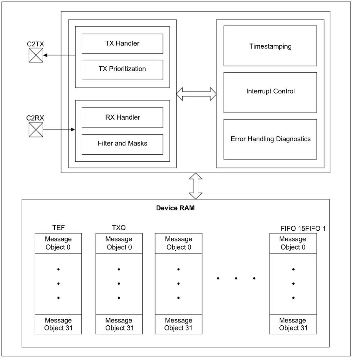
flowchart
System architecture flowchart showing data flow between Device RAM (TEF, TXQ) and C2TX/RX channels, with TX Handler, RX Handler, and Timestamping components.31.1 CAN-FD Control Registers
TABLE 31-1: CAN-FD REGISTER SUMMARY FOR PIC32MZ1025W104 DEVICES
| Virtual Address (BF82_#) | Register Name[1] | Bit Range | Bits | All Resets | |||||||||||||||||||||||||
| 31/15 | 30/14 | 29/13 | 28/12 | 27/11 | 26/10 | 25/9 | 24/8 | 23/7 | 22/6 | 21/5 | 20/4 | 19/3 | 18/2 | 17/1 | 16/0 | ||||||||||||||
| 3000 | CFD2CON | 31:16 | TXBWS[3:0] | ABAT | REQOP[2:0] | OPMOD[2:0] | TXQEN | STEF | SERR2-LOM | ESIGM | RTXAT | 0000 | |||||||||||||||||
| 15:0 ON | — | SIDL | BRSDIS | CAN-BUSY | WFT[1:0] | WAK-FIL | CLKSEL0 | PXEDIS | ISOCRCEN | DNCNT[4:0] | 0000 | ||||||||||||||||||
| 3004 | CFD2NBTCFG | 31:16 | BRP[7:0] | TSEG1[7:0] | 0000 | ||||||||||||||||||||||||
| 15:0 | — | TSEG2[6:0] | — | SJW[6:0] | 0000 | ||||||||||||||||||||||||
| 3008 | CFD2DBTCFG | 31:16 | BRP[7:0] | — | — | — | TSEG1[4:0] | 0000 | |||||||||||||||||||||
| 15:0 | — | — | — | — | TSEG2[3:0] | — | — | — | — | SJW[3:0] | 0000 | ||||||||||||||||||
| 300C | CFD2TDC | 31:16 | — | — | — | — | — | — | EDG-FLTEN | SID11 EN | — | — | — | — | — | — | TDCMOD[1:0] | 0000 | |||||||||||
| 15:0 | — | TDCO[6:0] | — | — | TDCV[5:0] | 0000 | |||||||||||||||||||||||
| 3010 | CFD2TBC | 31:16 | TBC[31:16] | 0000 | |||||||||||||||||||||||||
| 15:0 | TBC[15:0] | 0000 | |||||||||||||||||||||||||||
| 3014 | CFD2TSCON | 31:16 | — | — | — | — | — | — | — | — | — | — | — | — | — | TSRES | TSEOF | TBCEN | 0000 | ||||||||||
| 15:0 | — | — | — | — | — | — | TBCPRE[9:0] | 0000 | |||||||||||||||||||||
| 3018 | CFD2VEC | 31:16 | — | RXCODE[6:0] | — | TXCODE[6:0] | 0000 | ||||||||||||||||||||||
| 15:0 | — | — | — | FILHIT[4:0] | — | ICODE[6:0] | 0000 | ||||||||||||||||||||||
| 301C | CFD2INT | 31:16 | IVMIE | WAKIE | CERRIE | SERRIE | RXOVIE | TXATIE | SPI-CRCIE | ECCIE | — | — | — | TEFIE | MODIE | TBCIE | RXIE | TXIE | 0000 | ||||||||||
| 15:0 | IVMIF | WAKIF | CERRIF | SERRIF | RXOVIF | TXATIF | SPI-CRCIF | ECCIF | — | — | — | TEFIF | MODIF | TBCIF | RXIF | TXIF | 0000 | ||||||||||||
| 3020 | CFD2RXIF | 31:16 | RFIF[30:15] | 0000 | |||||||||||||||||||||||||
| 15:0 | RFIF[14:0] | — | 0000 | ||||||||||||||||||||||||||
| 3024 | CFD2TXIF | 31:16 | TFIF[31:16] | 0000 | |||||||||||||||||||||||||
| 15:0 | TFIF[15:0] | 0000 | |||||||||||||||||||||||||||
| 3028 | CFD2RXOVIF | 31:16 | RFOVIF[30:15] | 0000 | |||||||||||||||||||||||||
| 15:0 | RFOVIF[14:0] | — | 0000 | ||||||||||||||||||||||||||
Note 1: The lower order byte of the 32-bit register resides at the low-order address.
2: All registers in CAN-FD does not have corresponding CLR, SET and INV registers at their virtual addresses. SET, INV, CLR needs to be taken care by programming.
TABLE 31-1: CAN-FD REGISTER SUMMARY FOR PIC32MZ1025W104 DEVICES (CONTINUED)
| Virtual Address (BF82_#) | Register Name[1] | Bit Range | Bits | All Resets | |||||||||||||||
| 31/15 | 30/14 | 29/13 | 28/12 | 27/11 | 26/10 | 25/9 | 24/8 | 23/7 | 22/6 | 21/5 | 20/4 | 19/3 | 18/2 | 17/1 | 16/0 | ||||
| 302C | CFD2TXATIF | 31:16 | TFATIF[31:16] 0000 | ||||||||||||||||
| 15.0 | TFATIF[15:0] 0000 | ||||||||||||||||||
| 3030 | CFD2TXREQ | 31:16 | TXREQ[31:16] 0000 | ||||||||||||||||
| 15.0 | TXREQ[15:0] 0000 | ||||||||||||||||||
| 3034 | CFD2TREC | 31:16 | — | — | — | — | — | — | — | — | — | — | TXBO | TXBP | RXBP | TXWARN | RXWAR N | EWARN | 0000 |
| 15.0 | TERRCNT[7:0] | RERRCNT[7:0] | 0000 | ||||||||||||||||
| 3038 | CFD2BDIAG0 | 31:16 | DTERRCNT[7:0] | DRERRCNT[7:0] | 0000 | ||||||||||||||
| 15.0 | NTERRCNT[7:0] | NRERRCNT[7:0] | 0000 | ||||||||||||||||
| 303C | CFD2BDIAG1 | 31:16 | DLCMM | ESI | DCRCERR | DSTU-FERR | DFORMERR | — | DBITIERR | DBITOERR | — | — | NCRCERR | NSTU-FERR | NFORMERR | NACK-ERR | NBITIERR | NBITOERR | 0000 |
| 15.0 | EFMSGCNT[15:0] | 0000 | |||||||||||||||||
| 3040 | CFD2TEFCON | 31:16 | — | — | — | FSIZE[5:0] | — | — | — | — | — | — | — | — | 0000 | ||||
| 15.0 | — | — | — | — | — | FRESET | — | UINC | — | — | TEFTSEN | — | TEFOVIE | TEFFIE | TEFHIE | TEF-NEIE | 0000 | ||
| 3044 | CFD2TEFSTA | 31:16 | — | — | — | — | — | — | — | — | — | — | — | — | — | — | — | — | 0000 |
| 15.0 | — | — | — | — | — | — | — | — | — | — | — | — | TEFOVIF | TEFFIF | TEFHIF | TEF-NEIF | 0000 | ||
| 3048 | CFD2TEFUA | 31:16 | TEFUA[31:16] 0000 | ||||||||||||||||
| 15.0 | TEFUA[15:0] 0000 | ||||||||||||||||||
| 304C | CFD2FIFOBA | 31:16 | FIFOBA[31:16] | 0000 | |||||||||||||||
| 15.0 | FIFOBA[15:0] | 0000 | |||||||||||||||||
| 3050 | CFD2TXQCON | 31:16 | PLSIZE[2:0] | FSIZE[4:0] | — | TXAT[1:0] | TXPR[4:0] | 0000 | |||||||||||
| 15.0 | — | — | — | — | — | FRESET | TXREQ | UINC | TXEN | — | — | TXATIE | — | TXQEIE | — | TXQNIE | 0000 | ||
| 3054 | CFD2TXQSTA | 31:16 | — | — | — | — | — | — | — | — | — | — | — | — | — | — | — | — | 0000 |
| 15.0 | — | — | — | TXQC[4:0] | TXABT | TXLARB | TXERR | TXATIF | — | TXQEIF | — | TXQNIF | 0000 | ||||||
Note
1: The lower order byte of the 32-bit register resides at the low-order address.
2: All registers in CAN-FD does not have corresponding CLR, SET and INV registers at their virtual addresses. SET, INV, CLR needs to be taken care by programming.
TABLE 31-1: CAN-FD REGISTER SUMMARY FOR PIC32MZ1025W104 DEVICES (CONTINUED)
| Virtual Address(BF82,#) | Register Name[1] | Bit Range | Bits | All Resets | |||||||||||||||
| 31/15 | 30/14 | 29/13 | 28/12 | 27/11 | 26/10 | 25/9 | 24/8 | 23/7 | 22/6 | 21/5 | 20/4 | 19/3 | 18/2 | 17/1 | 16/0 | ||||
| 3058 | CFD2TXQUA | 31:16 | TXQUA[31:16] 0000 | ||||||||||||||||
| 15:0 | TXQUA[15:0] 0000 | ||||||||||||||||||
| 305C | CFD2FIFO-CON1 | 31:16 | PLSIZE[2:0] FSIZE[4:0] | — TXAT[1:0] TXPRI[4:0] 0000 | |||||||||||||||
| 15:0 | — | — | — | — | — | FRESET | TXREQ | UINC | TXEN | RTREN | RXTSEN | TXATIE | RXOVIE | TFERF-FIE | TFHRFHIE | TFNRF-NIE | 0000 | ||
| 3060 | CFD2FIFOS-TA1 | 31:16 | — | — | — | — | — | — | — | — | — | — | — | — | — | — | — | — | 0000 |
| 15:0 | — | — | — | FIFOCI[4:0] | TXABT | TXLARB | TXERR | TXATIF | RXOVIF | TFERFFI-F | TFHRF-HIF | TFN-RFNIF | 0000 | ||||||
| 3064 | CFD2FIFOUA1 | 31:16 | FIFOUA[31:16] | 0000 | |||||||||||||||
| 15:0 | FIFOUA[15:0] | 0000 | |||||||||||||||||
| 3068 | CFD2FIFO-CON2 | 31:16 | PLSIZE[2:0] | FSIZE[4:0] | — | TXAT[1:0] | TXPRI[4:0] | 0000 | |||||||||||
| 15:0 | — | — | — | — | — | FRESET | TXREQ | UINC | TXEN | RTREN | RXTSEN | TXATIE | RXOVIE | TFERF-FIE | TFHRFHIE | TFNRF-NIE | 0000 | ||
| 306C | CFD2FIFOS-TA2 | 31:16 | — | — | — | — | — | — | — | — | — | — | — | — | — | — | — | — | 0000 |
| 15:0 | — | — | — | FIFOCI[4:0] | TXABT | TXLARB | TXERR | TXATIF | RXOVIF | TFERFFI-F | TFHRH-HIF | TFN-RFNIF | 0000 | ||||||
| 3070 | CFD2FIFOUA2 | 31:16 | FIFOUA[31:16] | 0000 | |||||||||||||||
| 15:0 | FIFOUA[15:0] | 0000 | |||||||||||||||||
| 3074 | CFD2FIFO-CON3 | 31:16 | PLSIZE[2:0] | FSIZE[4:0] | — | TXAT[1:0] | TXPRI[4:0] | 0000 | |||||||||||
| 15:0 | — | — | — | — | — | FRESET | TXREQ | UINC | TXEN | RTREN | RXTSEN | TXATIE | RXOIVIE | TFERF-FIE | TFHRFHIE | TFNRF-NIE | 0000 | ||
| 3078 | CFD2FIFOS-TA3 | 31:16 | — | — | — | — | — | — | — | — | — | — | — | — | — | — | — | — | 0000 |
| 15:0 | — | — | — | FIFOCI[4:0] | TXABT | TXLARB | TXERR | TXATIF | RXOVIF | TFERFFI-F | TFHRHF-HIF | TFN-RFNIF | 0000 | ||||||
| 307C | CFD2FIFOUA3 | 31:16 | FIFOUA[31:16] | 0000 | |||||||||||||||
| 15:0 | FIFOUA[15:0] | 0000 | |||||||||||||||||
| 3080 | CFD2FIFO-CON4 | 31:16 | PLSIZE[2:0] FSIZE[4:0] | — TXAT[1:0] TXPRI[4:0] 0000 | |||||||||||||||
| 15:0 | — | — | — | — | — | FRESET | TXREQ | UINC | TXEN | RTREN | RXTSEN | TXATIE | RXOVIE | TFERF-FIE | TFHRFHIE | 0000 | |||
Note
1: The lower order byte of the 32-bit register resides at the low-order address.
2: All registers in CAN-FD does not have corresponding CLR, SET and INV registers at their virtual addresses. SET, INV, CLR needs to be taken care by programming.
TABLE 31-1: CAN-FD REGISTER SUMMARY FOR PIC32MZ1025W104 DEVICES (CONTINUED)
| Virtual Address (BF82_#) | Register Name[1] | Bit Range | Bits | All Resets | ||||||||||||||||
| 31/15 | 30/14 | 29/13 | 28/12 | 27/11 | 26/10 | 25/9 | 24/8 | 23/7 | 22/6 | 21/5 | 20/4 | 19/3 | 18/2 | 17/1 | 16/0 | |||||
| 3084 | CFD2FIFOS-TA4 | 31:16 | — — | — — | — — | — — | 0000 | |||||||||||||
| 15:0 | — | — | — | FIFOCI[4:0] | TXABT | TXLARB | TXERR | TXATIF | RXOVIF | TFERFFI F | TFHRF-HIF | TFN-RFNIF | 0000 | |||||||
| 3088 | CFD2FIFOUA4 | 31:16 | FIFOUA[31:16] | 0000 | ||||||||||||||||
| 15:0 | FIFOUA[15:0] | 0000 | ||||||||||||||||||
| 308C | CFD2FIFO-CONS | 31:16 | PLSIZE[2:0] | FSIZE[4:0] | — | TXAT[1:0] | TXPRI[4:0] | 0000 | ||||||||||||
| 15:0 | — | — | — | — | — | FRESET | TXREQ | UINC | TXEN | RTREN | RXTSEN | TXATIE | RXOVIE | TFERF-FIE | TFHRFHIE | TFNRF-NIE | 0000 | |||
| 3090 | CFD2FIFOS-TA5 | 31:16 | — — | — — | — — | 0000 | ||||||||||||||
| 15:0 | — | — | — | FIFOCI[4:0] | TXABT | TXLARB | TXERR | TXATIF | RXOVIF | TFERFFI F | TFHRF-HIF | TFN-RFNIF | 0000 | |||||||
| 3094 | CFD2FIFOUA5 | 31:16 | FIFOUA[31:16] | 0000 | ||||||||||||||||
| 15:0 | FIFOUA[15:0] | 0000 | ||||||||||||||||||
| 3098 | CFD2FIFO-CONS | 31:16 | PLSIZE[2:0] | FSIZE[4:0] | — | TXAT[1:0] | TXPRI[4:0] | 0000 | ||||||||||||
| 15:0 | — | — | — | — | — | FRESET | TXREQ | UINC | TXEN | RTREN | RXTSEN | TXATIE | RXOVIE | TFERF-FIE | TFHRFHIE | TFNRF-NIE | 0000 | |||
| 309C | CFD2FIFOS-TA6 | 31:16 | — — | — — | — — | 0000 | ||||||||||||||
| 15:0 | — | — | — | FIFOCI[4:0] | TXABT | TXLARB | TXERR | TXATIF | RXOVIF | TFERFFI F | TFHRF-HIF | TFN-RFNIF | ||||||||
| 30A0 | CFD2FIFOUA6 | 31:16 | FIFOUA[31:16] | 0000 | ||||||||||||||||
| 15:0 | FIFOUA[15:0] | 0000 | ||||||||||||||||||
| 30A4 | CFD2FIFO-CONS | 31:16 | PLSIZE[2:0] | FSIZE[4:0] | — | TXAT[1:0] | TXPRI[4:0] | 0000 | ||||||||||||
| 15:0 | — | — | — | — | — | FRESET | TXREQ | UINC | TXEN | RTREN | XRTSEN | TXATIE | RXOVIE | TFERF-FIE | TFHRFHIE | TFNRF-NIE | 0000 | |||
| 30A8 | CFD2FIFOS-TA7 | 31:16 | — — | — — | — — | 0000 | ||||||||||||||
| 15:0 | — | — | — | FIFOCI[4:0] | TXABT | TXLARB | TXERR | TXATIF | RXOVIF | TFERFFI F | TFHRF-HIF | TFN-RFNIF. | 0000 | |||||||
| 30AC | CFD2FIFOUA7 | 31:16 | FIFOUA[31:16] | 0000 | ||||||||||||||||
| 15:0 | FIFOUA[15:0] | 0000 | ||||||||||||||||||
Note
1: The lower order byte of the 32-bit register resides at the low-order address.
2: All registers in CAN-FD does not have corresponding CLR, SET and INV registers at their virtual addresses. SET, INV, CLR needs to be taken care by programming.
TABLE 31-1: CAN-FD REGISTER SUMMARY FOR PIC32MZ1025W104 DEVICES (CONTINUED)
| Virtual Address (BF82_#) | Register Name[1] | Bit Range | Bits | All Resets | ||||||||||||||||
| 31/15 | 30/14 | 29/13 | 28/12 | 27/11 | 26/10 | 25/9 | 24/8 | 23/7 | 22/6 | 21/5 | 20/4 | 19/3 | 18/2 | 17/1 | 16/0 | |||||
| 30B0 | CFD2FIFO-CON8 | 31:16 | PLSIZE[2:0] | FSIZE[4:0] | — TXAT[1:0] TXPRI[4:0] 0000 | |||||||||||||||
| 15:0 | — | — | — | — | — | FRESET | TXREQ | UINC | TXEN | RTREN | RXTSEN | TXATIE | RXOVIE | TFERF-FIE | TFHRFHIE | TFNRF-NIE | 0000 | |||
| 30B4 | CFD2FIFOS-TA8 | 31:16 | — | — | — | — | — | — | — | — | — | — | — | — | — | — | — | — | 0000 | |
| 15:0 | — | — | — | FIFOCI[4:0] | TXABT | TXLARB | TXERR | TXATIF | RXOVIF | TFERFFIF | TFHRF-HIF | TFN-RFNIF | 0000 | |||||||
| 30B8 | CFD2FIFOUA8 | 31:16 | FIFOUA[31:16] | 0000 | ||||||||||||||||
| 15:0 | FIFOUA[15:0] | 0000 | ||||||||||||||||||
| 30BC | CFD2FIFO-CON8 | 31:16 | PLSIZE[2:0] | FSIZE[4:0] | — | TXAT[1:0] | TXPRI[4:0] | 0000 | ||||||||||||
| 15:0 | — | — | — | — | — | FRESET | TXREQ | UINC | TXEN | RTREN | RXTSEN | TXATIE | RXOVIE | TFERF-FIE | TFHRFHIE | TFNRF-NIE | 0000 | |||
| 30C0 | CFD2FIFOS-TA9 | 31:16 | — | — | — | — | — | — | — | — | — | — | — | — | — | — | — | — | 0000 | |
| 15:0 | — | — | — | FIFOCI[4:0] | TXABT | TXLARB | TXERR | TXATIF | RXOVIF | TFERFFIF | TFHRH-HIF | TFN-RFNIF | 0000 | |||||||
| 30C4 | CFD2FIFOUA9 | 31:16 | FIFOUA[31:16] | 0000 | ||||||||||||||||
| 15:0 | FIFOUA[15:0] | 0000 | ||||||||||||||||||
| 30C8 | CFD2FIFO-CON10 | 31:16 | PLSIZE[2:0] | FSIZE[4:0] | — | TXAT[1:0] | TXPRI[4:0] | 0000 | ||||||||||||
| 15:0 | — | — | — | — | — | FRESET | TXREQ | UINC | TXEN | RTREN | RXTSEN | TXATIE | TXOVIE | TFERF-FIE | TFHRFHIE | TFNRF-NIE | 0000 | |||
| 30CC | CFD2FIFOS-TA10 | 31:16 | — | — | — | — | — | — | — | — | — | — | — | — | — | — | — | — | 0000 | |
| 15:0 | — | — | — | FIFOCI[4:0] | TXABT | TXLARB | TXERR | TXATIF | RXOVIF | TFERFFIF | TFHRHF-HIF | TFN-RFNIF | 0000 | |||||||
| 30D0 | CFD2FI-FOUA10 | 31:16 | FIFOUA[31:16] | 0000 | ||||||||||||||||
| 15:0 | FIFOUA[15:0] | 0000 | ||||||||||||||||||
| 30D4 | CFD2FIFO-CON11 | 31:16 | PLSIZE[2:0] FSIZE[4:0] | — TXAT[1:0] TXPRI[4:0] 0000 | ||||||||||||||||
| 15:0 | — | — | — | — | — | FRESET | TXREQ | UINC | TXEN | RTREN | RXTSEN | TXATIE | RXOVIE | TFERF-FIE | TFHRFHIE | TFNRF-NIE | ||||
| 30D8 | CFD2FIFOS-TA11 | 31:16 | — | — | — | — | — | — | — | — | — | — | — | — | — | — | — | — | 0000 | |
| 15:0 | — | — | — | FIFOCI[4:0] | TXABT | TXLARB | TXERR | TXATIF | RXOVIF | TFERFFIF | TFHRFHIF | TFN-RFNIF | 0000 | |||||||
Note
1: The lower order byte of the 32-bit register resides at the low-order address.
2: All registers in CAN-FD does not have corresponding CLR, SET and INV registers at their virtual addresses. SET, INV, CLR needs to be taken care by programming.
TABLE 31-1: CAN-FD REGISTER SUMMARY FOR PIC32MZ1025W104 DEVICES (CONTINUED)
| Virtual Address (BF82_#) | Register Name[1] | Bit Range | Bits | All Resets | |||||||||||||||
| 31/15 | 30/14 | 29/13 | 28/12 | 27/11 | 26/10 | 25/9 | 24/8 | 23/7 | 22/6 | 21/5 | 20/4 | 19/3 | 18/2 | 17/1 | 16/0 | ||||
| 30DC | CFD2FI-FOUA11 | 31:16 | FIFOUA[31:16] 0000 | ||||||||||||||||
| 15:0 | FIFOUA[15:0] 0000 | ||||||||||||||||||
| 30E0 | CFD2FIFO-CON12 | 31:16 | PLSIZE[2:0] FSIZE[4:0] | — TXAT[1:0] TXPRI[4:0] 0000 | |||||||||||||||
| 15:0 | — | — | — | — | — | FRESET | TXREQ | UINC | TXEN | RTREN | RXTSEN | TXATIE | RXOVIE | TFERF-FIE | TFHRFHIE | TFNRF-NIE | 0000 | ||
| 30E4 | CFD2FIFOS-TA12 | 31:16 | — | — | — | — | — | — | — | — | — | — | — | — | — | — | — | — | 0000 |
| 15:0 | — | — | — | FIFOCI[4:0] | TXABT | TXLARB | TXERR | TXATIF | RXOVIF | TFERFFIF | TFHRF-HIF | TFN-RFNIF | 0000 | ||||||
| 30EB | CFD2FI-FOUA12 | 31:16 | FIFOUA[31:16] 0000 | ||||||||||||||||
| 15:0 | FIFOUA[15:0] 0000 | ||||||||||||||||||
| 30EC | CFD2FIFO-CON13 | 31:16 | PLSIZE[2:0] | FSIZE[4:0] | — | TXAT[1:0] | TXPRI[4:0] | 0000 | |||||||||||
| 15:0 | — | — | — | — | — | FRESET | TXREQ | UINC | TXEN | RTREN | RXTSEN | TXATIE | RXOVIE | TFERF-FIE | TFHRFHIE | TFNRF-NIE | 0000 | ||
| 30F0 | CFD2FIFOS-TA13 | 31:16 | — | — | — | — | — | — | — | — | — | — | — | — | — | — | — | — | 0000 |
| 15:0 | — | — | — | FIFOCI[4:0] | TXABT | TXLARB | TXERR | TXATIF | RXOVIF | TFERFFIF | TFHRFHIF | TFN-RFNIF | 0000 | ||||||
| 30F4 | CFD2FI-FOUA13 | 31:16 | FIFOUA[31:16] 0000 | ||||||||||||||||
| 15:0 | FIFOUA[15:0] 0000 | ||||||||||||||||||
| 30F8 | CFD2FIFO-CON14 | 31:16 | PLSIZE[2:0] | FSIZE[4:0] | — | TXAT[1:0] | TXPRI[4:0] | 0000 | |||||||||||
| 15:0 | — | — | — | — | — | FRESET | TXREQ | UINC | TXEN | RTREN | RXTSEN | TXATIE | RXOIVIE | TFERF-FIE | TFHRFHIE | TFNRF-NIE | 0000 | ||
| 30FC | CFD2FIFOS-TA14 | 31:16 | — | — | — | — | — | — | — | — | — | — | — | — | — | — | — | — | 0000 |
| 15:0 | — | — | — | FIFOCI[4:0] | TXABT | TXLARB | TXERR | TXATIF | RXOVIF | TFERFFIF | TFHRF HIF | TFN-RFNIF | 0000 | ||||||
| 3100 | CFD2FI-FOUA14 | 31:16 | FIFOUA[31:16] 0000 | ||||||||||||||||
| 15:0 | FIFOUA[15:0] 0000 | ||||||||||||||||||
| 3104 | CFD2FIFO-CON15 | 31:16 | PLSIZE[2:0] FSIZE[4:0] | — TXAT[1:0] | TXPRI[4:0] 0000 | ||||||||||||||
| 15:0 | — | — | — | — | — | FRESET | TXREQ | UINC | TXEN | RTREN | RXTSEN | TXATIE | RXOVIE | TFERF-FIE | TFHRFHIE | TFNRF-NIE | 0000 | ||
Note 1: The lower order byte of the 32-bit register resides at the low-order address.
2: All registers in CAN-FD does not have corresponding CLR, SET and INV registers at their virtual addresses. SET, INV, CLR needs to be taken care by programming.
TABLE 31-1: CAN-FD REGISTER SUMMARY FOR PIC32MZ1025W104 DEVICES (CONTINUED)
| Virtual Address (BF82_#) | Register Name[1] | Bit Range | Bits | All Resets | |||||||||||||||
| 31/15 | 30/14 | 29/13 | 28/12 | 27/11 | 26/10 | 25/9 | 24/8 | 23/7 | 22/6 | 21/5 | 20/4 | 19/3 | 18/2 | 17/1 | 16/0 | ||||
| 3108 | CFD2FIFOS-TA15 | 31:16 | — — | — — | — — | — — | 0000 | ||||||||||||
| 15:0 | — | — | — | FIFOCI[4:0] | TXABT | TXLARB | TXERR | TXATIF | RXOVIF | TFERFFIF | TFHRF-HIF | TFN-RFNIF | 0000 | ||||||
| 310C | CFD2FI-FOUA15 | 31:16 | FIFOUA[31:16] | 0000 | |||||||||||||||
| 15:0 | FIFOUA[15:0] | 0000 | |||||||||||||||||
| 3110 | CFD2FLT-CON0 | 31:16 | FLTEN3 | — | — | F3BP[4:0] | FLTEN2 | — | — | F2BP[4:0] | 0000 | ||||||||
| 15:0 | FLTEN1 | — | — | F1BP[4:0] | FLTEN0 | — | — | F0BP[4:0] | 0000 | ||||||||||
| 3114 | CFD2FLT-CON1 | 31:16 | FLTEN7 | — | — | F7BP[4:0] | FLTEN6 | — | — | F6BP[4:0] | 0000 | ||||||||
| 15:0 | FLTEN5 | — | — | F5BP[4:0] | FLTEN4 | — | — | F4BP[4:0] | 0000 | ||||||||||
| 3118 | CFD2FLT-CON2 | 31:16 | FLTEN11 | — | — | F11BP | FLTEN10 | — | — | F10BP | 0000 | ||||||||
| 15:0 | — — | F9BP[4:0] | FLTEN8 | — | — | F8BP[4:0] | — | 0000 | |||||||||||
| 311C | CFD2FLT-CON3 | 31:16 | FLTEN15 | — | — | F15BP[4:0] | FLTEN14 | — | — | F14BP[4:0] | 0000 | ||||||||
| 15:0 | FLTEN13 | — | — | F13BP[4:0] | FLTEN12 | — | — | F12BP[4:0] | 0000 | ||||||||||
| 3120 | CFD2FLTOBJ0 | 31:16 | — | EXIDE | SID11 | EID[17:0] | 0000 | ||||||||||||
| 15:0 | EID[17:0] | SID[10:0] | 0000 | ||||||||||||||||
| 3124 | CFD2MASK0 | 31:16 | — | MIDE | MSID11 | MEID[17:0] | 0000 | ||||||||||||
| 15:0 | MEID[17:0] | MSID[10:0] | 0000 | ||||||||||||||||
| 3128 | CFD2FLTOBJ1 | 31:16 | — | EXIDE | SID11 | EID[17:0] | 0000 | ||||||||||||
| 15:0 | EID[17:0] | SID[10:0] | 0000 | ||||||||||||||||
| 312C | CFD2MASK1 | 31:16 | — | MIDE | MSID11 | MEID[17:0] | 0000 | ||||||||||||
| 15:0 | MEID[17:0] | MSID[10:0] | 0000 | ||||||||||||||||
| 3130 | CFD2FLTOBJ2 | 31:16 | — | EXIDE | SID11 | EID[17:0] | 0000 | ||||||||||||
| 15:0 | EID[17:0] | SID[10:0] | 0000 | ||||||||||||||||
| 3134 | CFD2MASK2 | 31:16 | — | MIDE | MSID11 | MEID[17:0] | 0000 | ||||||||||||
| 15:0 | MEID[17:0] | MSID[10:0] | 0000 | ||||||||||||||||
Note 1: The lower order byte of the 32-bit register resides at the low-order address.
2: All registers in CAN-FD does not have corresponding CLR, SET and INV registers at their virtual addresses. SET, INV, CLR needs to be taken care by programming.
TABLE 31-1: CAN-FD REGISTER SUMMARY FOR PIC32MZ1025W104 DEVICES (CONTINUED)
| Virtual Address (BF02_#) | Register Name[1] | Bit Range | Bits | All Resets | |||||||||||||||
| 31/15 | 30/14 | 29/13 | 28/12 | 27/11 | 26/10 | 25/9 | 24/8 | 23/7 | 22/6 | 21/5 | 20/4 | 19/3 | 18/2 | 17/1 | 16/0 | ||||
| 3138 | CFD2FLTOBJ3 | 31:16 | — EXIDE SID11 | EID[17:0] 0000 | |||||||||||||||
| 15:0 E | D[17:0] SID[10:0] 0000 | ||||||||||||||||||
| 313C | CFD2MASK3 | 31:16 | — | M | I D | E M S | I D 1 1 MEID[17:0] | 0000 | |||||||||||
| 15:0 | MEID[17:0] | MSID[10:0] | 0000 | ||||||||||||||||
| 3140 | CFD2FLTOBJ4 | 31:16 | — EXIDE SID11 | EID[17:0] 0000 | |||||||||||||||
| 15:0 E | D[17:0] SID[10:0] 0000 | ||||||||||||||||||
| 3144 | CFD2MASK4 | 31:16 | — | M | I D | E M S | I D 1 1 MEID[17:0] | 0000 | |||||||||||
| 15:0 | MEID[17:0] | MSID[10:0] | 0000 | ||||||||||||||||
| 3150 | CFD2FLTOBJ6 | 31:16 | — EXIDE SID11 | EID[17:0] 0000 | |||||||||||||||
| 15:0 E | D[17:0] SID[10:0] 0000 | ||||||||||||||||||
| 3154 | CFD2MASK6 | 31:16 | — | M | I D | E M S | I D 1 1 MEID[17:0] | 0000 | |||||||||||
| 15:0 | MEID[17:0] | MSID[10:0] | 0000 | ||||||||||||||||
| 3168 | CFD2FLTOBJ7 | 31:16 | — EXIDE SID11 | EID[17:0] 0000 | |||||||||||||||
| 15:0 E | D[17:0] SID[10:0] 0000 | ||||||||||||||||||
| 315C | CFD2MASK7 | 31:16 | — | M | I D | E M S | I D 1 1 MEID[17:0] | 0000 | |||||||||||
| 15:0 | MEID[17:0] | MSID[10:0] | 0000 | ||||||||||||||||
| 3180 | CFD2FLTOBJ8 | 31:16 | — EXIDE SID11 | EID[17:0] 0000 | |||||||||||||||
| 15:0 E | D[17:0] SID[10:0] 0000 | ||||||||||||||||||
| 3164 | CFD2MASK8 | 31:16 | — | M | I D | E M S | I D 1 1 MEID[17:0] | 0000 | |||||||||||
| 15:0 | MEID[17:0] | MSID[10:0] | 0000 | ||||||||||||||||
Note 1: The lower order byte of the 32-bit register resides at the low-order address.
2: All registers in CAN-FD does not have corresponding CLR, SET and INV registers at their virtual addresses. SET, INV, CLR needs to be taken care by programming.
TABLE 31-1: CAN-FD REGISTER SUMMARY FOR PIC32MZ1025W104 DEVICES (CONTINUED)
| Virtual Address(BF82,#) | Register Name[1] | Bit Range | Bits | All Resets | |||||||||||||||
| 31/15 | 30/14 | 29/13 | 28/12 | 27/11 | 26/10 | 25/9 | 24/8 | 23/7 | 22/6 | 21/5 | 20/4 | 19/3 | 18/2 | 17/1 | 16/0 | ||||
| 3168 | CFD2FLTOBJ9 | 31:16 | — EXIDE SID11 | EID[17:0] 0000 | |||||||||||||||
| 15:0 E | D[17:0] SID[10:0] 0000 | ||||||||||||||||||
| 316C | CFD2MASK9 | 31:16 | — | M | I D | E M S | I D 1 1 MEID[17:0] | 0000 | |||||||||||
| 15:0 | MEID[17:0] | MSID[10:0] | 0000 | ||||||||||||||||
| 3170 | CFD2FLTO-BJ10 | 31:16 | — EXIDE SID11 | EID[17:0] 0000 | |||||||||||||||
| 15:0 E | D[17:0] SID[10:0] 0000 | ||||||||||||||||||
| 3174 | CFD2MASK10 | 31:16 | — | M | I D | E M S | I D 1 1 MEID[17:0] | 0000 | |||||||||||
| 15:0 | MEID[17:0] | MSID[10:0] | 0000 | ||||||||||||||||
| 3180 | CFD2FLTO-BJ11 | 31:16 | — EXIDE SID11 | EID[17:0] 0000 | |||||||||||||||
| 15:0 E | D[17:0] SID[10:0] 0000 | ||||||||||||||||||
| 317C | CFD2MASK11 | 31:16 | — | M | I D | E M S | I D 1 1 MEID[17:0] | 0000 | |||||||||||
| 15:0 | MEID[17:0] | MSID[10:0] | 0000 | ||||||||||||||||
| 3190 | CFD2FLTO-BJ12 | 31:16 | — EXIDE SID11 | EID[17:0] 0000 | |||||||||||||||
| 15:0 E | D[17:0] SID[10:0] 0000 | ||||||||||||||||||
| 3184 | CFD2MASK12 | 31:16 | — | M | I D | E M S | I D 1 1 MEID[17:0] | 0000 | |||||||||||
| 15:0 | MEID[17:0] | MSID[10:0] | 0000 | ||||||||||||||||
| 3168 | CFD2FLTO-BJ13 | 31:16 | — EXIDE SID11 | EID[17:0] 0000 | |||||||||||||||
| 15:0 E | D[17:0] SID[10:0] 0000 | ||||||||||||||||||
| 318C | CFD2MASK13 | 31:16 | — | M | I D | E M S | I D 1 1 MEID[17:0] | 0000 | |||||||||||
| 15:0 | MEID[17:0] | MSID[10:0] | 0000 | ||||||||||||||||
| 3150 | CFD2FLTO-BJ14 | 31:16 | — EXIDE SID11 | EID[17:0] 0000 | |||||||||||||||
| 15:0 E | D[17:0] SID[10:0] 0000 | ||||||||||||||||||
| 3194 | CFD2MASK14 | 31:16 | — | M | I D | E M S | I D 1 1 MEID[17:0] | 0000 | |||||||||||
| 15:0 | MEID[17:0] | MSID[10:0] | 0000 | ||||||||||||||||
Note
1: The lower order byte of the 32-bit register resides at the low-order address.
2: All registers in CAN-FD does not have corresponding CLR, SET and INV registers at their virtual addresses. SET, INV, CLR needs to be taken care by programming.
TABLE 31-1: CAN-FD REGISTER SUMMARY FOR PIC32MZ1025W104 DEVICES (CONTINUED)
| Virtual Address (BF82_#) | Register Name | Bit Range | Bits | All Resets | |||||||||||||||
| 31/15 | 30/14 | 29/13 | 28/12 | 27/11 | 26/10 | 25/9 | 24/8 | 23/7 | 22/6 | 21/5 | 20/4 | 19/3 | 18/2 | 17/1 | 16/0 | ||||
| 3198 | CFD2FLTO-BJ15 | 31:16 | — EXIDE SID11 | EID[17:0] 0000 | |||||||||||||||
| 15:0 | EID[17:0] SID[10:0] 0000 | ||||||||||||||||||
| 319C | CFD2MASK15 | 31:16 | — | M | I D | E M S | I D 1 1 MEID[17:0] 0000 | ||||||||||||
| 15:0 | MEID[17:0] | MSID[10:0] | 0000 | ||||||||||||||||
Note 1: The lower order byte of the 32-bit register resides at the low-order address.
2: All registers in CAN-FD does not have corresponding CLR, SET and INV registers at their virtual addresses. SET, INV, CLR needs to be taken care by programming.
REGISTER 31-1: CFD2CON: CAN CONTROL REGISTER
| Bit Range | Bit 31/23/15/7 | Bit 30/22/14/6 | Bit 29/21/13/5 | Bit 28/20/12/4 | Bit 27/19/11/3 | Bit 26/18/10/2 | Bit 25/17/9/1 | Bit 24/16/8/0 |
| 31:24 | R/W-0 R/W-0 R/W-0 R/W-0 S/HC-0 R/W-1 R/W-0 R/W-0 | |||||||
| TXBWS[3:0] ABAT REQOP[2:0] | ||||||||
| 23:16 | R-1 R-0 R-0 R/W-1 R/W-1 R/W-0 R/W-0 R/W-0 | |||||||
| OPMOD[2:0] | TXQEN(1) | STEF(1) | SERR2LOM(1) | ESIGM(1) | RTXAT(1) | |||
| 15:8 | R/W-0 R/W-0 R/W-0 R/W-0 R/W-1 R/W-1 | |||||||
| ON | — | SIDL | BRSDIS | BUSY | WFT[1:0] | WAKFIL(1) | ||
| 7:0 | R/W-0 R/W-1 R/W-1 R/W-0 R/W-0 R/W-0 R/W-0 R/W-0 | |||||||
| CLKSEL0(1) | PXEDIS(1) | ISOCRCEN(1) | DNCNT[4:0] | |||||
Legend:
| R = Readable bit | W = Writable bit | U = Unimplemented bit, read as '0' |
| S = Settable bit | C = Clearable bit | x = Bit is unknown at Reset |
| ‘1’ = Bit is set at Reset | ‘0’ = Bit is cleared at Reset | HC = Hardware clear HS = Set by Hardware only |
bit 31-28 TXBWS[3:0]: Transmit Bandwidth Sharing bits
Delay between two consecutive transmissions (in arbitration bit times)
0000 = No delay
0001 = 2
0010 = 4
0011 = 8
0100 = 16
0101 = 32
0110 = 64
0111 = 128
1000 = 256
1001 = 512
1010 = 1024
1011 = 2048
1111-1100 = 4096
bit 27 ABAT: Abort All Pending Transmissions bit
1 = Signal all transmit buffers to abort transmission
0 = Module clears this bit when all transmissions are aborted
bit 26-24 REQOP[2:0]: Request Operation Mode bits
000 = Set Normal CAN-FD mode; supports mixing of full CAN-FD and classic CAN 2.0 frames
001 = Set Disable mode
010 = Set Internal Loopback mode
011 = Set Listen Only mode
100 = Set Configuration mode
101 = Set External Loopback mode
110 = Set Normal CAN 2.0 mode; error frames on CAN-FD frames
111 = Set Restricted Operation mode
Note 1: These bits can only be modified in Configuration mode (OPMOD = 100).
REGISTER 31-1: CFD2CON: CAN CONTROL REGISTER (CONTINUED)
bit 23-21 OPMOD[2:0]: Operation Mode Status bits
000 = Module is in Normal CAN-FD mode; supports mixing of full CAN-FD and classic CAN 2.0 frames
001 = Module is in Disable mode
010 = Module is in Internal Loopback mode
011 = Module is in Listen Only mode
100 = Module is in Configuration mode
101 = Module is in External Loopback mode
110 = Module is Normal CAN 2.0 mode; error frames on CAN-FD frames
111 = Module is Restricted Operation mode
bit 20 TXQEN: Enable Transmit Queue bit (1) 1 = Enables TXQ and reserves space in RAM 0 = Don't reserve space in RAM for TXQ
Note: Changes only in Configuration mode, since it changes the addresses in RAM.
bit 19 STEF: Store in Transmit Event FIFO bit (1) 1 = Save transmitted messages in TEF 0 = Don't save transmitted messages in TEF
Note: Changes only in Configuration mode, since it changes the addresses in RAM.
bit 18 SERR2LOM: Transition to Listen Only Mode on System Error bit(1) 1 = Transition to Listen Only Mode 0 = Transition to Restricted Operation Mode
bit 17 ESIGM: Transmit ESI in Gateway Mode bit (1) 1 = ESI is transmitted as recessive when ESI of message is high or CAN controller error passive 0 = ESI reflects error status of CAN controller
bit 16 RTXAT: Restrict Retransmission Attempts bit (1) 1 = Restricted retransmission attempts, use CiFIFOCONm.TXAT 0 = Unlimited number of retransmission attempts, CiFIFOCONm.TXAT is ignored
bit 15 ON: Enable bit 1 = CAN module is enabled 0 = CAN module is disabled
bit 14 Unimplemented: Read as '0'
bit 13 SIDL: Stop in Idle Control bit 1 = Stop module operation in Idle mode 0 = Don't stop module operation in Idle mode
bit 12 BRSDIS: Bit Rate Switching Disable bit 1 = Bit Rate Switching is Disabled, regardless of BRS in the Transmit Message Object 0 = Bit Rate Switching depends on BRS in the Transmit Message Object'
bit 11 BUSY: CAN Module is Busy bit 1 = The CAN module is active 0 = The CAN module is inactive
bit 10-9 WFT[1:0]: Selectable Wake-up Filter Time bits 00 = T00_FILTER 01 = T01_FILTER 10 = T10_FILTER 11 = T11_FILTER
bit 8 WAKFIL: Enable CAN Bus Line Wake-up Filter bit (1) 1 = Use CAN bus line filter for wake-up 0 = CAN bus line filter is not used for wake-up
Note 1: These bits can only be modified in Configuration mode (OPMOD = 100).
REGISTER 31-1: CFD2CON: CAN CONTROL REGISTER (CONTINUED)
bit 7 CLKSEL0: Module Clock Source Select bit (1)
1 = ETHPLL is selected
0 = PB2_CLK is selected
Note: The CAN source clock must be less than CAN UPB/peripheral clock (PB2_CLK). Select ETHPLL as the CAN source clock and configure CFGCON0.CANFDDIV, such that the CAN source clock (ETHPLL) is less than PB2_CLK (CAN UPB/peripheral clock).
bit 6 PXEDIS: Protocol Exception Event Detection Disabled bit ^(1)
A recessive "res bit" following a recessive FDF bit is called a Protocol Exception.
1 = Protocol Exception is treated as a Form Error.
0 = If a Protocol Exception is detected, the CAN enters Bus Integrating state.
bit 5 ISOCRCEN: Enable ISO CRC in CAN-FD Frames bit (1)
1 = Include Stuff Bit Count in CRC Field and use Non-Zero CRC Initialization Vector
0 = Do not include Stuff Bit Count in CRC Field and use CRC Initialization Vector with all zeros
bit 4-0 DNCNT[4:0]: Device Net Filter Bit Number bits
10011-11111 = Invalid Selection (compare up to 18-bits of data with EID)
10010 = Compare up to data byte 2 bit 6 with EID17
•
•
00001 = Compare up to data byte 0 bit 7 with EID0
00000 = Do not compare data bytes
Note 1: These bits can only be modified in Configuration mode (OPMOD = 100).
REGISTER 31-2: CFD2NBTCFG: NOMINAL BIT TIME CONFIGURATION REGISTER
| Bit Range | Bit 31/23/15/7 | Bit 30/22/14/6 | Bit 29/21/13/5 | Bit 28/20/12/4 | Bit 27/19/11/3 | Bit 26/18/10/2 | Bit 25/17/9/1 | Bit 24/16/8/0 |
| 31:24 | R/W-0 R/W-0 | R/W-0 R/W-0 | R/W-0 R/W-0 | R/W-0 R/W-0 | ||||
| BRP[7:0] | ||||||||
| 23:16 | R/W-0 R/W-0 | R/W-1 R/W-1 | R/W-1 R/W-1 | R/W-1 R/W-0 | ||||
| TSEG1[7:0] | ||||||||
| 15:8 | U-0 R/W-0 | R/W-0 R/W-0 | R/W-1 R/W-1 | R/W-1 R/W-1 | ||||
| — TSEG2[6:0] | ||||||||
| 7:0 | U-0 R/W-0 | R/W-0 R/W-0 | R/W-0 R/W-0 | R/W-0 R/W-0 | ||||
| — SJW[6:0] | ||||||||
Legend:
R = Readable bit W = Writable bit U = Unimplemented bit, read as '0'
| S = Settable bit | C = Clearable bit | x = Bit is unknown at Reset | |
| '1' = Bit is set at Reset | '0' = Bit is cleared at Reset | HC = Hardware clear | HS = Set by Hardware only |
bit 31-24 BRP[7:0]: Baud Rate Prescaler bits
$$ 1 1 1 1 \quad 1 1 1 1 = T _ {Q} = 2 5 6 / F _ {\text { SYS }} $$
...
$$ 0 0 0 0 \quad 0 0 0 0 = T _ {Q} = 1 / F _ {\text { SYS }} $$
bit 23-16 TSEG1[7:0]: Time Segment 1 bits (Propagation Segment + Phase Segment 1)
$$ 1 1 1 1 \quad 1 1 1 1 = \text { Length is } 2 5 6 \times T _ {\mathrm{Q}} $$
...
$$ 0 0 0 0 \quad 0 0 0 0 = \text { Length is } 1 \times T _ {Q} $$
bit 15 Unimplemented: Read as '0'
bit 14-8 TSEG2[6:0]: Time Segment 2 bits (Phase Segment 2)
$$ 1 1 1 \quad 1 1 1 1 = \text { Length is } 1 2 8 \times T _ {Q} $$
...
$$ 0 0 0 \quad 0 0 0 0 = \text { Length is } 1 \times T _ {Q} $$
bit 7 Unimplemented: Read as '0'
bit 6-0 SJW[6:0]: Synchronization Jump Width bits
$$ 1 1 1 \quad 1 1 1 1 = \text { Length is } 1 2 8 \times T _ {Q} $$
...
$$ 0 0 0 \quad 0 0 0 0 = \text { Length is } 1 \times T _ {Q} $$
Note: This register can only be modified in Configuration mode (OPMOD = 100).
REGISTER 31-3: CFD2DBTCFG: DATA BIT TIME CONFIGURATION REGISTER
| Bit Range | Bit 31/23/15/7 | Bit 30/22/14/6 | Bit 29/21/13/5 | Bit 28/20/12/4 | Bit 27/19/11/3 | Bit 26/18/10/2 | Bit 25/17/9/1 | Bit 24/16/8/0 |
| 31:24 | R/W-0 R/W | -0 R/W-0 R/W | -0 R/W-0 R/W-0 | R/W-0 R/W-0 | ||||
| BRP[7:0] | ||||||||
| 23:16 | U-0 U-0 U-0 R/W-0 R/W-1 R/W-1 R/W-1 R/W-0 | |||||||
| — — — | TSEG1[4:0] | |||||||
| 15:8 | U-0 U-0 U-0 U-0 R/W-0 R/W-0 R/W-1 R/W-1 | |||||||
| — — — | — TSEG2[6:0] | |||||||
| 7:0 | U-0 U-0 U-0 U-0 R/W-0 R/W-0 R/W-1 R/W-1 | |||||||
| — — — | — SJW[6:0] | |||||||
Legend:
R = Readable bit W = Writable bit U = Unimplemented bit, read as '0'
| S = Settable bit | C = Clearable bit | x = Bit is unknown at Reset | |
| ‘1’ = Bit is set at Reset | ‘0’ = Bit is cleared at Reset | HC = Hardware clear | HS = Set by Hardware only |
bit 31-24 BRP[7:0]: Baud Rate Prescaler bits
$$ 1 1 1 1 \quad 1 1 1 1 = T _ {Q} = 2 5 6 / F _ {\text { SYS }} $$
...
$$ 0 0 0 0 \quad 0 0 0 0 = T _ {Q} = 1 / F _ {\text {SYS}} $$
bit 23-21 Unimplemented: Read as '0'
bit 20-16 TSEG1[4:0]: Time Segment 1 bits (Propagation Segment + Phase Segment 1)
$$ 1 1 1 1 1 = \text { Length is } 3 2 \times T _ {Q} $$
...
$$ 0 0 0 0 0 = \text { Length is } 1 \times T _ {Q} $$
bit 15-12 Unimplemented: Read as '0'
bit 11-8 TSEG2[3:0]: Time Segment 2 bits (Phase Segment 2)
$$ 1 1 1 1 = \text { Length is } 1 6 \times T _ {Q} $$
...
$$ 0 0 0 0 = \text { Length is } 1 \times T _ {Q} $$
bit 7-4 Unimplemented: Read as '0'
bit 3-0 SJW[6:0]: Synchronization Jump Width bits
$$ 1 1 1 1 = \text { Length is } 1 6 \times T _ {Q} $$
...
$$ 0 0 0 0 = \text { Length is } 1 \times T _ {Q} $$
Note: This register can only be modified in Configuration mode (OPMOD = 100).
REGISTER 31-4: CFD2TDC: TRANSMITTER DELAY COMPENSATION REGISTER
| Bit Range | Bit 31/23/15/7 | Bit 30/22/14/6 | Bit 29/21/13/5 | Bit 28/20/12/4 | Bit 27/19/11/3 | Bit 26/18/10/2 | Bit 25/17/9/1 | Bit 24/16/8/0 |
| 31:24 | U-0 U-0 U-0 U-0 U-0 R/W-0 R/W-0 | |||||||
| — — — | — — — | E D | G | F L | T E | N | S I | |
| 23:16 | U-0 U-0 U-0 U-0 U-0 R/W-1 R/W-0 | |||||||
| — — — | — — — TDCM | OD[1:0] | ||||||
| 15:8 | U-0 R/W-0 R/W-0 R/W-1 | R/W-0 R/W-0 | R/W-0 R/W-0 | |||||
| — | T | D | ||||||
| 7:0 | U-0 U-0 | R/W-0 R/W-0 R/W-0 R/W-0 R/W-0 | ||||||
| — — TDCV[5:0] | ||||||||
Legend:
| R = Readable bit | W = Writable bit | U = Unimplemented bit, read as '0' |
| S = Settable bit | C = Clearable bit | x = Bit is unknown at Reset |
| '1' = Bit is set at Reset | '0' = Bit is cleared at Reset | HC = Hardware clear HS = Set by Hardware only |
bit 31-26 Unimplemented: Read as '0'
bit 25 EDGFLTEN: Enable Edge Filtering during Bus Integration state bit
1 = Edge Filtering enabled, according to ISO11898-1:2015
0 = Edge Filtering disabled
bit 24 SID11EN: Enable 12-Bit SID in CAN-FD Base Format Messages bit
1 = RRS is used as SID11 in CAN-FD base format messages: SID[11:0] = {SID[10:0], SID11}
0 = Don't use RRS; SID[10:0] according to ISO11898-1:2015
bit 23-18 Unimplemented: Read as '0'
bit 17-16 TDCMOD[1:0]: Transmitter Delay Compensation Mode bits; Secondary Sample Point (SSP)
10-11 Auto; measure delay and add CFD2DBTCFG.TSEG1; add TDCO.
01 = Manual; Don't measure, use TDCV + TDCO from register
00 = Disable
bit 15 Unimplemented: Read as '0'
bit 14-8 TDCO[6:0]: Transmitter Delay Compensation Offset bits; Secondary Sample Point (SSP)
Two's complement; offset can be positive, zero, or negative.
011 1111 = 63 x T _SYS_CLK
...
000 0000 = 0 x T _SYS_CLK
...
111 1111 = -64 x T _SYS_CLK
bit 7-6 Unimplemented: Read as '0'
bit 5-0 TDCV[5:0]: Transmitter Delay Compensation Value bits; Secondary Sample Point (SSP)
11 1111 = 63 × T _SYS_CLK
...
00 0000 = 0 x T _SYS_CLK
Note: This register can only be modified in Configuration mode (OPMOD = 100).
REGISTER 31-5: CFD2TBC: CAN TIME BASE COUNTER REGISTER
| Bit Range | Bit 31/23/15/7 | Bit 30/22/14/6 | Bit 29/21/13/5 | Bit 28/20/12/4 | Bit 27/19/11/3 | Bit 26/18/10/2 | Bit 25/17/9/1 | Bit 24/16/8/0 |
| 31:24 | R/W-0 R/W | -0 R/W-0 R/W | -0 R/W-0 R/W-0 | R/W-0 R/W-0 | ||||
| TBC[31:24] | ||||||||
| 23:16 | R/W-0 R/W | -0 R/W-0 R/W | -0 R/W-0 R/W-0 | R/W-0 R/W-0 | ||||
| TBC[23:16] | ||||||||
| 15:8 | R/W-0 R/W | -0 R/W-0 R/W | -0 R/W-0 R/W-0 | R/W-0 R/W-0 | ||||
| TBC[15:8] | ||||||||
| 7:0 | R/W-0 R/W | -0 R/W-0 R/W | -0 R/W-0 R/W-0 | R/W-0 R/W-0 | ||||
| TBC[7:0] | ||||||||
Legend:
R = Readable bit W = Writable bit    U = Unimplemented bit, read as '0'
S = Settable bit    C = Clearable bit    x = Bit is unknown at Reset
'1' = Bit is set at Reset    '0' = Bit is cleared at Reset    HC = Hardware clear    HS = Set by Hardware only
bit 31-0 TBC: CAN Base Counter bits
This is a free running timer that increments every TBCPRE clock when TBCEN is set.
Note 1: The TBC will be stopped and reset when TBCEN = 0 to save power.
2: The TBC prescaler count will be reset on any write to CFD2TBC (TBCPRE will be unaffected).
REGISTER 31-6: CFD2TSCON: CAN TIME STAMP CONTROL REGISTER
| R = Readable bit | W = Writable bit | U = Unimplemented bit, read as '0' |
| S = Settable bit | C = Clearable bit | x = Bit is unknown at Reset |
| '1' = Bit is set at Reset | '0' = Bit is cleared at Reset | HC = Hardware clear HS = Set by Hardware only |
bit 31-19 Unimplemented: Read as '0'
bit 18 TSRES: Time Stamp res bit (FD Frames only)
1 = at sample point of the bit following the FDF bit.
0 = at sample point of SOF
bit 17 TSEOF: Time Stamp EOF bit
1 = Time Stamp when frame is taken valid (11898-1 10.7):
- RX no error until last but one bit of EOF)
• TX no error until the end of EOF
0 = Time Stamp at "beginning" of Frame:
• Classical Frame: at sample point of SOF
• FD Frame: see TSRES bit.
bit 16 TBCEN: Time Base Counter Enable bit
1 = Enable TBC
0 = Stop and reset TBC
bit 15-10 Unimplemented: Read as '0'
bit 9-0 TBCPRE[9:0]: CAN Time Base Counter Prescaler bits
1023 = TBC increments every 1024 clocks
•
0 = TBC increments every 1 clock
R = Readable bit W = Writable bit U = Unimplemented bit, read as '0'
S = Settable bit C = Clearable bit x = Bit is unknown at Reset
'1' = Bit is set at Reset '0' = Bit is cleared at Reset HC = Hardware clear HS = Set by Hardware only
bit 31 Unimplemented: Read as '0'
bit 30-24 RXCODE[6:0]: Receive Interrupt Flag Code bits ^(1)
1000001-1111111 = Reserved
1000000 = No interrupt
0100000-0111111 = Reserved
0011111 = FIFO 31 interrupt (RFIF[31] set)
.
.
0000010 = FIFO 2 interrupt (RFIF[2] set)
0000001 = FIFO 1 interrupt (RFIF[1] set)
0000000 = Reserved. FIFO 0 cannot receive.
bit 23 Unimplemented: Read as '0'
bit 22-16 TXCODE[6:0]: Transmit Interrupt Flag Code bits ^(1)
1000001-1111111 = Reserved
1000000 = No interrupt
0100000-0111111 = Reserved
0011111 = FIFO 31 interrupt (TFIF[31] set)
.
.
0000001 = FIFO 1 interrupt (TFIF[1] set)
0000000 = FIFO 0 interrupt (TFIF[0] set)
bit 15-13 Unimplemented: Read as '0'
bit 12-8 FILHIT[4:0]: Filter Hit Number bits (1)
11111 = Filter 31
11110 = Filter 30
.
.
00001 = Filter 1
00000 = Filter 0
bit 7 Unimplemented: Read as '0'
Note 1: CFD2VEC: If multiple interrupts are pending, the interrupt with the highest number will be indicated.
REGISTER 31-7: CFD2VEC: INTERRUPT CODE REGISTER (CONTINUED)
bit 6-0 ICODE[6:0]: Interrupt Flag Code bits (1)
    1001011-1111111 = Reserved
    1001010 = Transmit attempt interrupt (any bit in CiTXATIF set)
    1001001 = Transmit event FIFO interrupt (any bit in CiTEFIF set)
    1001000 = Invalid message occurred (IVMIF/IE)
    1000111 = CAN Module Mode Change Occurred (MODIF/IE)
    1000110 = CAN Timer Overflow (CTMRIF/IE)
    1000101 = RX/TX MAB Overflow/Underflow (RX: message received before previous message is saved to memory; TX: cannot feed TX MAB fast enough to transmit consistent data.) (SERRIF/IE)
    1000100 = Address error interrupt (illegal FIFO address presented to system) (SERRIF/IE)
    1000011 = Receive FIFO overflow interrupt (any bit in CiRXOVIF set)
    1000010 = Wake-up interrupt (WAKIF/WAKIE)
    1000001 = Error interrupt (CERRIF/IE)
    1000000 = No interrupt
    0100000-0111111 = Reserved
    0011111 = FIFO 31 interrupt (TFIF[31] or RFIF[31] set)
    :
    0000001 = FIFO 1 interrupt (TFIF[1] or RFIF[1] set)
    0000000 = FIFO 0 interrupt (TFIF[0] set)
Note 1: CFD2VEC: If multiple interrupts are pending, the interrupt with the highest number will be indicated.
REGISTER 31-8: CFD2INT: INTERRUPT REGISTER
| Bit Range | Bit 31/23/15/7 | Bit 30/22/14/6 | Bit 29/21/13/5 | Bit 28/20/12/4 | Bit 27/19/11/3 | Bit 26/18/10/2 | Bit 25/17/9/1 | Bit 24/16/8/0 |
| 31:24 | R/W-0 R/W-0 R/W-0 R/W-0 R/W-0 R/W-0 R/W-0 | |||||||
| IVMIE WAKIE CERRIE SERRIE RXOVIE TXATIE SPICRCIE ECCIE | ||||||||
| 23:16 | U-0 | U-0 | U-0 | R/W-0 | R/W-0 | R/W-0 | R/W-0 | R/W-0 |
| — | — | — | TEFIE | MODIE | TBCIE | RXIE | TXIE | |
| 15:8 | HS/C-0 | HS/C-0 | HS/C-0 | HS/C-0 | R-0 | R-0 | R-0 | R-0 |
| IVMIF(1) | WAKIF(1) | CERRIF(1) | SERRIF(1) | RXOVIF TX | ATIF SPICRCIF | ECCIF | ||
| 7:0 | U-0 | U-0 | U-0 | R-0 | HS/C-0 | HS/C-0 | R-0 | R-0 |
| — | — | — | TEFIF | MODIF(1) | TBCIF(1) | RXIF | TXIF | |
Legend:
| R = Readable bit | W = Writable bit | U = Unimplemented bit, read as ‘0’ | |
| S = Settable bit | C = Clearable bit | x = Bit is unknown at Reset | |
| ‘1’ = Bit is set at Reset | ‘0’ = Bit is cleared at Reset | HC = Hardware clear | HS = Set by Hardware only |
bit 31 IVMIE: Invalid Message Interrupt Enable bit
bit 30 WAKIE: Bus Wake Up Activity Interrupt Enable bit
bit 29 CERRIE: CAN Bus Error Interrupt Enable bit
bit 28 SERRIE: System Error Interrupt Enable bit
bit 27 RXOVIE: Receive Buffer Overflow Interrupt Enable bit
bit 26 TXATIE: Transmit Attempt Interrupt Enable bit
bit 25 SPICRCIE: SPI CRC Error Interrupt Enable bit
bit 24 ECCIE: ECC Error Interrupt Enable bit
bit 23-21 Unimplemented: Read as '0'
bit 20 TEFIE: Transmit Event FIFO Interrupt Enable bit
bit 19 MODIE: Mode Change Interrupt Enable bit
bit 18 TBCIE: CAN Timer Interrupt Enable bit
bit 17 RXIE: Receive Object Interrupt Enable bit
bit 16 TXIE: Transmit Object Interrupt Enable bit
bit 15 IVMIF: Invalid Message Interrupt Flag bit ^(1)
bit 14 WAKIF: Bus Wake Up Activity Interrupt Flag bit(1)
bit 13 CERRIF: CAN Bus Error Interrupt Flag bit (1)
bit 12 SERRIF: System Error Interrupt Flag bit (1)
1 = A system error occurred (collision on dual-port RAM)
0 = No system error occurred
bit 11 RXOVIF: Receive Object Overflow Interrupt Flag bit
1 = Receive object overflow occurred
0 = No receive object overflow has occurred
bit 10 TXATIF: Transmit Attempt Interrupt Flag bit
bit 9 SPICRCIF: SPI CRC Error Interrupt Flag bit
bit 8 ECCIF: ECC Error Interrupt Flag bit
bit 7-5 Unimplemented: Read as '0'
Note 1: CFD2INT: Flags are set by hardware and cleared by application.
REGISTER 31-8: CFD2INT: INTERRUPT REGISTER (CONTINUED)
bit 4 TEFIF: Transmit Event FIFO Interrupt Flag bit
1 = Receive buffer overflow occurred
0 = No receive buffer overflow has occurred
bit 3 MODIF: CAN Mode Change Interrupt Flag bit (1)
1 = CAN Module mode change occurred (OPMOD has changed to reflect REQOP)
0 = No mode change occurred
bit 2 TBCIF: CAN Timer Overflow Interrupt Flag bit ^(1)
1 = TBC has overflowed
0 = TBC does not overflow
bit 1 RXIF: Receive Object Interrupt Flag bit
1 = Receive object interrupt is pending
0 = No receive object interrupt is pending
bit 0 TXIF: Transmit Object Interrupt Flag bit
1 = Transmit object interrupt is pending
0 = No transmit object interrupt is pending
Note 1: CFD2INT: Flags are set by hardware and cleared by application.
REGISTER 31-9: CFD2RXIF: RECEIVE INTERRUPT STATUS REGISTER
| Bit Range | Bit 31/23/15/7 | Bit 30/22/14/6 | Bit 29/21/13/5 | Bit 28/20/12/4 | Bit 27/19/11/3 | Bit 26/18/10/2 | Bit 25/17/9/1 | Bit 24/16/8/0 |
| 31:24 | R-0 R-0 | R-0 R-0 R-0 R-0 | R-0 R-0 | |||||
| RFIF^(1)[31:24] | ||||||||
| 23:16 | R-0 R-0 | R-0 R-0 R-0 R-0 | R-0 R-0 | |||||
| RFIF^(1)[23:16] | ||||||||
| 15:8 | R-0 R-0 | R-0 R-0 R-0 R-0 | R-0 R-0 | |||||
| RFIF^(1)[15:8] | ||||||||
| 7:0 | R-0 R-0 | R-0 R-0 R-0 R-0 | R-0 U-0 | |||||
| RFIF^(1)[7:1] — | ||||||||
Legend:
R = Readable bit W = Writable bit    U = Unimplemented bit, read as '0'
S = Settable bit    C = Clearable bit    x = Bit is unknown at Reset
'1' = Bit is set at Reset    '0' = Bit is cleared at Reset    HC = Hardware clear    HS = Set by Hardware only
bit 31-1 RFIF[31:1]: Receive FIFO Interrupt Pending bits ^(1)
1 = One or more enabled receive FIFO interrupts are pending
0 = No enabled receive FIFO interrupts are pending
bit 0 Unimplemented: Read as '0'
Note 1: CFD2RXIF: FIFO: RFIF = 'or' of enabled RXFIFO flags; (flags need to be cleared in FIFO register)
REGISTER 31-10: CFD2RXOVIF: RECEIVE OVERFLOW INTERRUPT STATUS REGISTER
| Bit Range | Bit 31/23/15/7 | Bit 30/22/14/6 | Bit 29/21/13/5 | Bit 28/20/12/4 | Bit 27/19/11/3 | Bit 26/18/10/2 | Bit 25/17/9/1 | Bit 24/16/8/0 |
| 31:24 | R-0 R-0 | R-0 R-0 R-0 | R-0 R-0 | |||||
| RFOVIF^(1) [31:24] | ||||||||
| 23:16 | R-0 R-0 | R-0 R-0 R-0 | R-0 R-0 | |||||
| RFOVIF^(1) [23:16] | ||||||||
| 15:8 | R-0 R-0 | R-0 R-0 R-0 | R-0 R-0 | |||||
| RFOVIF^(1) [15:8] | ||||||||
| 7:0 | R-0 R-0 | R-0 R-0 R-0 | R-0 U-0 | |||||
| RFOVIF^(1) [7:1] — | ||||||||
Legend:
R = Readable bit W = Writable bit U = Unimplemented bit, read as '0'
S = Settable bit C = Clearable bit x = Bit is unknown at Reset
'1' = Bit is set at Reset '0' = Bit is cleared at Reset HC = Hardware clear HS = Set by Hardware only
bit 31-1 RFOVIF[31:1]: Receive FIFO Overflow Interrupt Pending bits ^(1)
1 = Interrupt is pending
0 = Interrupt is not pending
bit 0 Unimplemented: Read as '0'
Note 1: CFD2RXOVIF: FIFO: RFOVIF (flag needs to be cleared in FIFO register)
REGISTER 31-11: CFD2TXIF: TRANSMIT INTERRUPT STATUS REGISTER
| Bit Range | Bit 31/23/15/7 | Bit 30/22/14/6 | Bit 29/21/13/5 | Bit 28/20/12/4 | Bit 27/19/11/3 | Bit 26/18/10/2 | Bit 25/17/9/1 | Bit 24/16/8/0 |
| 31:24 | R-0 R-0 R | -0 R-0 R-0 R-0 | R-0 R-0 | |||||
| TFIF^(1) [31:24] | ||||||||
| 23:16 | R-0 R-0 R | -0 R-0 R-0 R-0 | R-0 R-0 | |||||
| TFIF^(1) [23:16] | ||||||||
| 15:8 | R-0 R-0 R | -0 R-0 R-0 R-0 | R-0 R-0 | |||||
| TFIF^(1) [15:8] | ||||||||
| 7:0 | R-0 R-0 R | -0 R-0 R-0 R-0 | R-0 R-0 | |||||
| TFIF^(1) [7:0] | ||||||||
Legend:
R = Readable bit W = Writable bit U = Unimplemented bit, read as '0'
| S = Settable bit | C = Clearable bit | x = Bit is unknown at Reset | |
| ‘1’ = Bit is set at Reset | ‘0’ = Bit is cleared at Reset | HC = Hardware clear | HS = Set by Hardware only |
bit 31-0 TFIF[31:0]: Transmit FIFO/TXQ (2) Interrupt Pending bits(1)
1 = One or more enabled transmit FIFO/TXQ interrupts are pending
0 = No enabled transmit FIFO/TXQ interrupts are pending
Note 1: CFD2TXIF: FIFO: TFIF = 'or' of the enabled TXFIFO flags; (flags need to be cleared in FIFO register)
2: TFIF[0] is for the Transmit Queue.
REGISTER 31-12: CFD2TXATIF: TRANSMIT ATTEMPT INTERRUPT STATUS REGISTER
| Bit Range | Bit 31/23/15/7 | Bit 30/22/14/6 | Bit 29/21/13/5 | Bit 28/20/12/4 | Bit 27/19/11/3 | Bit 26/18/10/2 | Bit 25/17/9/1 | Bit 24/16/8/0 |
| 31:24 | R-0 R-0 R-0 R-0 R-0 R-0 | |||||||
| TFATIF^(1) [31:24] | ||||||||
| 23:16 | R-0 R-0 R-0 R-0 R-0 R-0 | |||||||
| TFATIF^(1) [23:16] | ||||||||
| 15:8 | R-0 R-0 R-0 R-0 R-0 R-0 | |||||||
| TFATIF^(1) [15:8] | ||||||||
| 7:0 | R-0 R-0 R-0 R-0 R-0 R-0 | |||||||
| TFATIF^(1) [7:0] | ||||||||
Legend:
R = Readable bit W = Writable bit U = Unimplemented bit, read as '0'
S = Settable bit C = Clearable bit x = Bit is unknown at Reset
'1' = Bit is set at Reset '0' = Bit is cleared at Reset HC = Hardware clear HS = Set by Hardware only
bit 31-0 TFATIF[31:0]: Transmit FIFO/TXQ ^(2) Attempt Interrupt Pending bits ^(1)
1 = Interrupt is pending
0 = Interrupt is not pending
Note 1: CFD2TXATIF: FIFO: TFATIF (flag needs to be cleared in FIFO register)
2: TFATIF[0] is for the Transmit Queue.
REGISTER 31-13: CFD2TXREQ: TRANSMIT REQUEST REGISTER
| Bit Range | Bit 31/23/15/7 | Bit 30/22/14/6 | Bit 29/21/13/5 | Bit 28/20/12/4 | Bit 27/19/11/3 | Bit 26/18/10/2 | Bit 25/17/9/1 | Bit 24/16/8/0 |
| 31:24 | S^(1)/HC-0 S | ^(1)/HC-0 S | ^(1)/HC-0 S | ^(1)/HC-0 S | ^(1)/HC-0 S | ^(1)/HC-0 S | ^(1)/HC-0 S | ^(1)/HC-0 |
| TXREQ[31:24] | ||||||||
| 23:16 | S^(1)/HC-0 S | ^(1)/HC-0 S | ^(1)/HC-0 S | ^(1)/HC-0 S | ^(1)/HC-0 S | ^(1)/HC-0 S | ^(1)/HC-0 S | ^(1)/MC-0 |
| TXREQ[23:16] | ||||||||
| 15:8 | S^(1)/HC-0 S | ^(1)/HC-0 S | ^(1)/HC-0 S | ^(1)/HC-0 S | ^(1)/HC-0 S | ^(1)/HC-0 S | ^(1)/HC-0 S | ^(1)/RC-0 |
| TXREQ[15:8] | ||||||||
| 7:0 | S^(1)/HC-0 S | ^(1)/HC-0 S | ^(1)/HC-0 S | ^(1)/HC-0 S | ^(1)/HC-0 S | ^(1)/HC-0 S | ^(1)/HC-0 S | ^(1)/LC-0 |
| TXREQ[7:0] | ||||||||
Legend:
R = Readable bit W = Writable bit U = Unimplemented bit, read as '0'
S = Settable bit
C = Clearable bit
x = Bit is unknown at Reset
'1' = Bit is set at Reset '0' = Bit is cleared at Reset HC = Hardware clear HS = Set by Hardware only
bit 31-1 TXREQ[31:1]: Message Send Request bits
TXEN = 1 (Object configured as a Transmit Object)
Setting this bit to '1' requests sending a message.
The bit is automatically cleared when the message(s) queued in the object is (are) successfully sent.
This bit can not be used for aborting a transmission.
TXEN = 0 (Object configured as a Receive Object)
This bit has no effect.
bit 0 TXREQ[0]: Transmit Queue Message Send Request bit
Setting this bit to '1' requests sending a message.
The bit is automatically cleared when the message(s) queued in the object is (are) successfully sent.
This bit can not be used for aborting a transmission.
Note 1: The TXREQ[x] bit represents the corresponding FIFO[x] message.
REGISTER 31-14: CFD2FIFOBA: MESSAGE MEMORY BASE ADDRESS REGISTER
| Bit Range | Bit31/23/15/7 | Bit30/22/14/6 | Bit29/21/13/5 | Bit28/20/12/4 | Bit27/19/11/3 | Bit26/18/10/2 | Bit25/17/9/1 | Bit24/16/8/0 |
| 31:24 | R/W-0 R/W | -0 R/W-0 R/W | -0 R/W-0 R/W-0 | R/W-0 R/W-0 | ||||
| FIFOBA[31:24] | ||||||||
| 23:16 | R/W-0 R/W | -0 R/W-0 R/W | -0 R/W-0 R/W-0 | R/W-0 R/W-0 | ||||
| FIFOBA[23:16] | ||||||||
| 15:8 | R/W-0 R/W | -0 R/W-0 R/W | -0 R/W-0 R/W-0 | R/W-0 R/W-0 | ||||
| FIFOBA[15:8] | ||||||||
| 7:0 | R/W-0 R/W | -0 R/W-0 R/W | -0 R/W-0 R/W-0 | U-0 | (1) | U-0^(1) | ||
| FIFOBA[7:0] | ||||||||
Legend:
R = Readable bit W = Writable bit U = Unimplemented bit, read as '0'
S = Settable bit C = Clearable bit x = Bit is unknown at Reset
'1' = Bit is set at Reset '0' = Bit is cleared at Reset HC = Hardware clear HS = Set by Hardware only
bit 31-0 FIFOBA[31:0]: Message Memory Base Address bits
Defines the base address for Transmit Event FIFO followed by the message objects.
Note 1: CFD2FIFOBA: Bits[1:0] are forced to '0' to be word aligned.
2: CFD2FIFOBA: This register can only be modified in Configuration mode (OPMOD = 100).
REGISTER 31-15: CFD2TXQCON: TRANSMIT QUEUE CONTROL REGISTER
| R = Readable bit | W = Writable bit | U = Unimplemented bit, read as '0' |
| S = Settable bit | C = Clearable bit | x = Bit is unknown at Reset |
| '1' = Bit is set at Reset | '0' = Bit is cleared at Reset | HC = Hardware clear HS = Set by Hardware only |
bit 31-29 PLSIZE[2:0]: Payload Size bits (1)
000 = 8 data bytes
001 = 12 data bytes
010 = 16 data bytes
011 = 20 data bytes
100 = 24 data bytes
101 = 32 data bytes
110 = 48 data bytes
111 = 64 data bytes
bit 28-14 FSIZE[4:0]: FIFO Size bits (1)
0 0000 = FIFO is 1 Message deep
0_0001 = FIFO is 2 Messages deep
0_0002 = FIFO is 3 Messages deep
.
.
1_1111 = FIFO is 32 Messages deep
bit 23 Unimplemented: Read as '0'
bit 22-21 TXAT[1:0]: Retransmission Attempts bits
This feature is enabled when CFD2CON.RTXAT is set.
00 = Disable retransmission attempts
01 = Three retransmission attempts
10 = Unlimited number of retransmission attempts
11 = Unlimited number of retransmission attempts
Note: Application must be able to change these bits in Normal mode. This can be used to go back on the bus after bus off to check if transmission works again.
bit 20-16 TXPRI[4:0]: Message Transmit Priority bits
00000 = Lowest Message Priority
.
•
11111 = Highest Message Priority
Note 1: These bits can only be modified in Configuration mode (OPMOD = 100).
2: This bit is updated when a message completes (or aborts) or when the FIFO is reset.
3: FRESET is set while in Configuration mode and is automatically cleared in Normal mode.
REGISTER 31-15: CFD2TXQCON: TRANSMIT QUEUE CONTROL REGISTER (CONTINUED)
bit 15-11 Unimplemented: Read as '0'
bit 10 FRESET: FIFO Reset bit (3)
1 = FIFO is reset when the bit is set and cleared by hardware when FIFO is reset. User must poll whether this bit is clear before taking any action.
0 = No effect
bit 9 TXREQ: Message Send Request bit (2)
1 = Requests sending a message; the bit is automatically cleared when all the messages queued in the TXQ are successfully sent
0 = Clearing the bit to '0' while set ('1') requests a message abort.
bit 8 UINC: Increment Head/Tail bit
When this bit is set, the FIFO head increments by a single message.
bit 7 TXEN: TX Enable
1 = Transmit Message Queue. This bit always reads 1.
bit 6-5 Unimplemented: Read as '0'
bit 4 TXATIE: Transmit Attempts Exhausted Interrupt Enable bit
1 = Enable interrupt
0 = Disable interrupt
bit 3 Unimplemented: Read as '0'
bit 2 TXQEIE: Transmit Queue Empty Interrupt Enable bit
1 = Interrupt enabled for TXQ empty
0 = Interrupt disabled for TXQ empty
bit 1 Unimplemented: Read as '0'
bit 0 TXQNIE: Transmit Queue Not Full Interrupt Enable bit
1 = Interrupt enabled for TXQ not full
0 = Interrupt disabled for TXQ not full
Note 1: These bits can only be modified in Configuration mode (OPMOD = 100).
2: This bit is updated when a message completes (or aborts) or when the FIFO is reset.
3: FRESET is set while in Configuration mode and is automatically cleared in Normal mode.
REGISTER 31-16: CFD2TXQSTA: TRANSMIT QUEUE STATUS REGISTER
| Bit Range | Bit 31/23/15/7 | Bit 30/22/14/6 | Bit 29/21/13/5 | Bit 28/20/12/4 | Bit 27/19/11/3 | Bit 26/18/10/2 | Bit 25/17/9/1 | Bit 24/16/8/0 |
| 31:24 | U-0 U-0 U-0 U-0 U-0 U-0 U-0 | |||||||
| — — — | — — — — | — | ||||||
| 23:16 | U-0 U-0 U-0 U-0 U-0 U-0 U-0 | |||||||
| — — — | — — — — | — | ||||||
| 15:8 | U-0 U-0 U-0 R-0 R-0 R-0 R-0 | |||||||
| — — — | TXQCI[4:0] (1) | |||||||
| 7:0 | R-0 R-0 R-0 HS/C-0 U-0 R-1 U-0 R-1 | |||||||
| TXABT(3,2) | TXLARB(3,2) | TXERR(3,2) | TXATIF | — | TXQEIF | — | TXQNIF | |
Legend:
| R = Readable bit | W = Writable bit | U = Unimplemented bit, read as '0' |
| S = Settable bit | C = Clearable bit | x = Bit is unknown at Reset |
| '1' = Bit is set at Reset | '0' = Bit is cleared at Reset | HC = Hardware clear HS = Set by Hardware only |
bit 31-13 Unimplemented: Read as '0'
bit 12-8 TXQCI[4:0]: Transmit Queue Message Index bits(1)
A read of this register returns an index to the message that the FIFO attempts to transmit next.
bit 7 TXABT: Message Aborted Status bit ^(3,2)
1 = Message is aborted
0 = Message completed successfully
bit 6 TXLARB: Message Lost Arbitration Status bit ^(3,2)
1 = Message lost arbitration while being sent
0 = Message does not loose arbitration while being sent
bit 5 TXERR: Error Detected During Transmission bit ^(3,2)
1 = A bus error occurs while the message is being sent
0 = A bus error does not occur while the message is being sent
bit 4 TXATIF: Transmit Attempts Exhausted Interrupt Pending bit
1 = Interrupt is pending
0 = Interrupt is not pending
bit 3 Unimplemented: Read as '0'
bit 2 TXQEIF: Transmit Queue Empty Interrupt Flag bit
1 = TXQ is empty
0 = TXQ is not empty, at least 1 message queued to be transmitted
bit 1 Unimplemented: Read as '0'
bit 0 TXQNIF: Transmit Queue Not Full Interrupt Flag bit
1 = TXQ is not full
0 = TXQ is full
Note 1: TXQCI[4:0] gives a zero-indexed value to the message in the TXQ. If the TXQ is 4 messages deep (FSIZE=5'h03) TXQCI will take on a value of 0 to 3 depending on the state of the TXQ.
2: This bit is reset on any read of this register or when the TXQ is reset.
3: This bit is updated when a message completes (or aborts) or when the TXQ is reset.
REGISTER 31-17: CFD2FIFOCONm: FIFO CONTROL REGISTER m, (m = 1 to 15)
R = Readable bit W = Writable bit U = Unimplemented bit, read as '0'
S = Settable bit C = Clearable bit x = Bit is unknown at Reset
'1' = Bit is set at Reset '0' = Bit is cleared at Reset HC = Hardware clear HS = Set by Hardware only
bit 31-29 PLSIZE[2:0]: Payload Size bits ^(1)
000 = 8 data bytes
001 = 12 data bytes
010 = 16 data bytes
011 = 20 data bytes
100 = 24 data bytes
101 = 32 data bytes
110 = 48 data bytes
111 = 64 data bytes
bit 28-24 FSIZE[4:0]: FIFO Size bits ^(1)
0 0000 = FIFO is 1 Message deep
0 0001 = FIFO is 2 Messages deep
0 0002 = FIFO is 3 Messages deep
. i_1111 = FIFO is 32 Messages deep
bit 23 Unimplemented: Read as '0'
bit 22-21 TXAT[1:0]: Retransmission Attempts bits
This feature is enabled when CFD2.RTXAT is set.
00 = Disable retransmission attempts
01 = Three retransmission attempts
10 = Unlimited number of retransmission attempts
11 = Unlimited number of retransmission attempts
Note: Application must be able to change these bits in Normal mode. This can be used to go back on the bus after bus off to check if transmission works again.
bit 20-16 TXPRI[4:0]: Message Transmit Priority bits
00000 = Lowest Message Priority
.
.
11111 = Highest Message Priority
bit 15-11 Unimplemented: Read as '0'
Note 1: These bits can only be modified in Configuration mode (OPMOD = 100).
2: This bit is updated when a message completes (or aborts) or when the FIFO is reset.
3: FRESET is set while in Configuration mode and is automatically cleared in Normal mode.
REGISTER 31-17: CFD2FIFOCONm: FIFO CONTROL REGISTER m, (m = 1 to 15) (CONTINUED)
bit 10 FRESET: FIFO Reset bit (3)
1 = FIFO is reset when the bit is set and cleared by hardware when FIFO is reset. User must poll whether this bit is clear before taking any action. 0 = No effect
bit 9 TXREQ: Message Send Request bit (2)
TXEN = 1 (FIFO configured as a Transmit FIFO)
1 = Requests sending a message; the bit is automatically cleared when all the messages queued in the FIFO are successfully sent
0 = Clearing the bit to '0' while set ('1') requests a message abort
TXEN = 0 (FIFO configured as a Receive FIFO)
This bit has no effect.
bit 8 UINC: Increment Head / Tail bit
TXEN = 1 (FIFO configured as a Transmit FIFO)
When this bit is set, the FIFO head increments by a single message
TXEN = 0 (FIFO configured as a Receive FIFO)
When this bit is set, the FIFO tail increments by a single message
bit 7 TXEN: TX/RX Buffer Selection bit (1)
1 = Transmit Message Object
0 = Receive Message Object
bit 6 RTREN: Auto RTR Enable bit
1 = When a remote transmit is received, TXREQ is set
0 = When a remote transmit is received, TXREQ is unaffected
bit 5 RXTSEN: Received Message Time Stamp Enable bit (1)
1 = Capture time stamp in received message object in RAM
0 = Capture time stamp is not captured
Note: Change only in Configuration mode, since it is used for address calculation.
bit 4 TXATIE: Transmit Attempts Exhausted Interrupt Enable bit
1 = Enable interrupt
0 = Disable interrupt
bit 3 RXOVIE: Overflow Interrupt Enable bit
1 = Interrupt enabled for overflow event
0 = Interrupt disabled for overflow event
bit 2 TFERFFIE: Transmit/Receive FIFO Empty/Full Interrupt Enable bit
TXEN = 1 (FIFO configured as a Transmit FIFO)
Transmit FIFO Empty Interrupt Enable
1 = Interrupt enabled for FIFO empty
0 = Interrupt disabled for FIFO empty
TXEN = 0 (FIFO configured as a Receive FIFO)
Receive FIFO Full Interrupt Enable
1 = Interrupt enabled for FIFO full
0 = Interrupt disabled for FIFO full
bit 1 TFHRFHIE: Transmit/Receive FIFO Half Empty/Half Full Interrupt Enable bit
TXEN = 1 (FIFO configured as a Transmit FIFO)
Transmit FIFO Half Empty Interrupt Enable
1 = Interrupt enabled for FIFO half empty
0 = Interrupt disabled for FIFO half empty
TXEN = 0 (FIFO configured as a Receive FIFO)
Receive FIFO Half Full Interrupt Enable
1 = Interrupt enabled for FIFO half full
0 = Interrupt disabled for FIFO half full
Note 1: These bits can only be modified in Configuration mode (OPMOD = 100).
2: This bit is updated when a message completes (or aborts) or when the FIFO is reset.
3: FRESET is set while in Configuration mode and is automatically cleared in Normal mode.
REGISTER 31-17: CFD2FIFOCONm: FIFO CONTROL REGISTER m, (m = 1 to 15) (CONTINUED)
bit 0 TFNRFNIE: Transmit/Receive FIFO Not Full/Not Empty Interrupt Enable bit
TXEN = 1 (FIFO configured as a Transmit FIFO)
Transmit FIFO Not Full Interrupt Enable
1 = Interrupt enabled for FIFO not full
0 = Interrupt disabled for FIFO not full
TXEN = 0 (FIFO configured as a Receive FIFO)
Receive FIFO Not Empty Interrupt Enable
1 = Interrupt enabled for FIFO not empty
0 = Interrupt disabled for FIFO not empty
Note 1: These bits can only be modified in Configuration mode (OPMOD = 100).
2: This bit is updated when a message completes (or aborts) or when the FIFO is reset.
3: FRESET is set while in Configuration mode and is automatically cleared in Normal mode.
REGISTER 31-18: CFD2FIFOSTAm: FIFO STATUS REGISTER m, (m = 1 to 15)
| Bit Range | Bit 31/23/15/7 | Bit 30/22/14/6 | Bit 29/21/13/5 | Bit 28/20/12/4 | Bit 27/19/11/3 | Bit 26/18/10/2 | Bit 25/17/9/1 | Bit 24/16/8/0 |
| 31:24 | U-0 U-0 U-0 U-0 U-0 U-0 U-0 | |||||||
| — — — | — — — — — | |||||||
| 23:16 | U-0 U-0 U-0 U-0 U-0 U-0 U-0 | |||||||
| — — — | — — — — — | |||||||
| 15:8 | U-0 U-0 U-0 R-0 R-0 R-0 R-0 | |||||||
| — — — | FIFOC[4:0] | (1) | ||||||
| 7:0 | R-0 R-0 R-0 HS/C-0 HS/C-0 R-0 R-0 R-0 | |||||||
| TXABT ^(3,2) | TXLARB ^(3,2) | TXERR ^(3,2) | TXATIF RX | OVIF TFERFF | TFHRFH | TFNRFNIF | ||
Legend:
| R = Readable bit | W = Writable bit | U = Unimplemented bit, read as ‘0’ |
| S = Settable bit | C = Clearable bit | x = Bit is unknown at Reset |
| ‘1’ = Bit is set at Reset | ‘0’ = Bit is cleared at Reset | HC = Hardware clear HS = Set by Hardware only |
bit 31-13 Unimplemented: Read as '0'
bit 4-0 FIFOCI[4:0]: FIFO Message Index bits
TXEN = 1 (FIFO configured as a Transmit Buffer)
A read of this register returns an index to the message that the FIFO attempts to transmit next.
TXEN = 0 (FIFO configured as a Receive Buffer)
A read of this register returns an index to the message that the FIFO uses to save the next message.
bit 7 TXABT: Message Aborted Status bit
1 = Message is aborted
0 = Message completed successfully
bit 6 TXLARB: Message Lost Arbitration Status bit
1 = Message lost arbitration while being sent
0 = Message does not loose arbitration while being sent
bit 5 TXERR: Error Detected During Transmission bit
1 = A bus error occurs while the message is being sent
0 = A bus error does not occur while the message is being sent
bit 4 TXATIF: Transmit Attempts Exhausted Interrupt Pending bit
TXEN = 1 (FIFO configured as a Transmit Buffer)
1 = Interrupt is pending
0 = Interrupt is not pending
TXEN = 0 (FIFO configured as a Receive Buffer)
Unused, reads '0'
bit 3 RXOVIF: Receive FIFO Overflow Interrupt Flag bit
TXEN = 1 (FIFO configured as a Transmit Buffer)
Unused, reads '0'
TXEN = 0 (FIFO configured as a Receive Buffer)
1 = Overflow event has occurred
0 = No overflow event occurred
Note 1: FIFOCI[4:0] gives a zero-indexed value to the message in the FIFO. If the FIFO is 4 messages deep (FSIZE=5'h03) FIFOCI will take on a value of 0 to 3 depending on the state of the FIFO.
2: This bit is reset on any read of this register or when the TXQ is reset.
3: This bit is updated when a message completes (or aborts) or when the FIFO is reset.
REGISTER 31-18: CFD2FIFOSTAm: FIFO STATUS REGISTER m, (m = 1 to 15) (CONTINUED)
bit 2 TFERFFIF: Transmit/Receive FIFO Empty/Full Interrupt Flag bit
TXEN = 1 (FIFO configured as a Transmit FIFO)
Transmit FIFO Empty Interrupt Flag
1 = FIFO is empty
0 = FIFO is not empty, at least 1 message queued to be transmitted
TXEN = 0 (FIFO configured as a Receive FIFO)
Receive FIFO Full Interrupt Flag
1 = FIFO is full
0 = FIFO is not full
bit 1 TFHRFHIF: Transmit/Receive FIFO Half Empty/Half Full Interrupt Flag bit
TXEN = 1 (FIFO configured as a Transmit FIFO)
Transmit FIFO Half Empty Interrupt Flag
1 = FIFO is <= half full
0 = FIFO is > half full
TXEN=0 (FIFO configured as a Receive FIFO)
Receive FIFO Half Full Interrupt Flag
1 = FIFO is >= half full
0 = FIFO is < half full
bit 0 TFNRFNIF: Transmit/Receive FIFO Not Full/Not Empty Interrupt Flag bit
TXEN = 1 (FIFO configured as a Transmit FIFO)
Transmit FIFO Not Full Interrupt Flag
1 = FIFO is not full
0 = FIFO is full
TXEN = 0 (FIFO configured as a Receive FIFO)
Receive FIFO Not Empty Interrupt Flag
1 = FIFO is not empty, has at least 1 message
0 = FIFO is empty
Note 1: FIFOCI[4:0] gives a zero-indexed value to the message in the FIFO. If the FIFO is 4 messages deep (FSIZE=5'h03) FIFOCI will take on a value of 0 to 3 depending on the state of the FIFO.
2: This bit is reset on any read of this register or when the TXQ is reset.
3: This bit is updated when a message completes (or aborts) or when the FIFO is reset.
REGISTER 31-19: CFD2TEFCON: TRANSMIT EVENT FIFO CONTROL REGISTER
| Bit Range | Bit 31/23/15/7 | Bit 30/22/14/6 | Bit 29/21/13/5 | Bit 28/20/12/4 | Bit 27/19/11/3 | Bit 26/18/10/2 | Bit 25/17/9/1 | Bit 24/16/8/0 |
| 31:24 | U-0 U-0 U-0 R/W-0 R/W-0 R/W-0 R/W-0 R/W-0 | |||||||
| — — — | FSIZE[4:0] | (1) | ||||||
| 23:16 | U-0 U-0 U-0 U-0 U-0 U-0 U-0 | |||||||
| — — — | — — — — | |||||||
| 15:8 | U-0 U-0 U-0 U-0 U-0 S/HC-1 U-0 S/HC-0 | |||||||
| — | — | — | — | — | FRESET | — | UINC | |
| 7:0 | U-0 U-0 R/W-0 U-0 R/W-0 R/W-0 R/W-0 | |||||||
| — — | TEFTSEN | (1) | — | TEFOVIE | TEFFIE | TEFHIE | TEFNEIE | |
Legend:
| R = Readable bit | W = Writable bit | U = Unimplemented bit, read as ‘0’ |
| S = Settable bit | C = Clearable bit | x = Bit is unknown at Reset |
| ‘1’ = Bit is set at Reset | ‘0’ = Bit is cleared at Reset | HC = Hardware clear HS = Set by Hardware only |
bit 31-29 Unimplemented: Read as '0'
bit 28-24 FSIZE[4:0]: FIFO Size bits ^(1)
0 0000 = FIFO is 1 message deep
0 0001 = FIFO is 2 messages deep
0_0002 = FIFO is 3 messages deep
.
•
1 1111 = FIFO is 32 messages deep
bit 23-11 Unimplemented: Read as '0'
bit 10 FRESET: FIFO Reset bit
1 = FIFO is reset when the bit is set and cleared by hardware. The user must poll this bit is clear before taking any action.
0 = No effect
bit 9 Unimplemented: Read as '0'
bit 8 UINC: Increment Tail bit
When this bit is set, the FIFO tail increments by a single message.
bit 7-6 Unimplemented: Read as '0
bit 5 TEFTSEN: Transmit Event FIFO Time Stamp Enable bit ^(1)
1 = Time stamp elements in TEF
0 = Don't time stamp elements in TEF
bit 4 Unimplemented: Read as '0'
bit 3 TEFOVIE: Transmit Event FIFO Overflow Interrupt Enable bit
1 = Interrupt enabled for overflow event
0 = Interrupt disabled for overflow event
bit 2 TEFFIE: Transmit Event FIFO Full Interrupt Enable bit
1 = Interrupt enabled for FIFO full
0 = Interrupt disabled for FIFO full
bit 1 TEFHIE: Transmit Event FIFO Half Full Interrupt Enable bit
1 = Interrupt enabled for FIFO half full
0 = Interrupt disabled for FIFO half full
bit 0 TEFNEIE: Transmit Event FIFO Not Empty Interrupt Enable bit
1 = Interrupt enabled for FIFO not empty
0 = Interrupt disabled for FIFO not empty
Note 1: CFD2TEFCON: These bits can only be modified in Configuration Mode (OPMOD = 100).
REGISTER 31-20: CFD2TEFSTA: TRANSMIT EVENT FIFO STATUS REGISTER
| Bit Range | Bit 31/23/15/7 | Bit 30/22/14/6 | Bit 29/21/13/5 | Bit 28/20/12/4 | Bit 27/19/11/3 | Bit 26/18/10/2 | Bit 25/17/9/1 | Bit 24/16/8/0 |
| 31:24 | U-0 U-0 U-0 U-0 U-0 U-0 U-0 | |||||||
| — — — | — — — — | — | ||||||
| 23:16 | U-0 U-0 U-0 U-0 U-0 U-0 U-0 | |||||||
| — — — | — — — — | — | ||||||
| 15:8 | U-0 U-0 U-0 U-0 U-0 U-0 U-0 | |||||||
| — — — | — — — — | — | ||||||
| 7:0 | U-0 U-0 U-0 U-0 HS/HC/C-0 | R-0 R-0 R-0 | ||||||
| — | — | — | — | TEFOVIF(2) | TEFFIF(1) | TEFHIF(1) | TEFNEIF(1) | |
Legend:
| R = Readable bit | W = Writable bit | U = Unimplemented bit, read as '0' |
| S = Settable bit | C = Clearable bit | x = Bit is unknown at Reset |
| '1' = Bit is set at Reset | '0' = Bit is cleared at Reset | HC = Hardware clear HS = Set by Hardware only |
bit 31-4 Unimplemented: Read as '0'
bit 3 TEFOVIF: Transmit Event FIFO Overflow Interrupt Flag bit ^(2)
1 = Overflow event has occurred
0 = No overflow event occurred
bit 2 TEFFIF: Transmit Event FIFO Full Interrupt Flag bit ^(1)
1 = FIFO is full
0 = FIFO is not full
bit 1 TEFHIF: Transmit Event FIFO Half Full Interrupt Flag bit ^(1)
1 = FIFO is >= half full
0 = FIFO is < half full
bit 0 TEFNEIF: Transmit Event FIFO Not Empty Interrupt Flag bit ^(1)
1 = FIFO is not empty, has at least 1 message
0 = FIFO is empty
Note 1: CFD2TEFSTA: This bit is read only and reflects the status of the FIFO.
2: TEFOVIF bit is cleared by FIFO Reset.
REGISTER 31-21: CFD2FIFOUAm: FIFO USER ADDRESS REGISTER m, (m = 1 to 15)
| Bit Range | Bit 31/23/15/7 | Bit 30/22/14/6 | Bit 29/21/13/5 | Bit 28/20/12/4 | Bit 27/19/11/3 | Bit 26/18/10/2 | Bit 25/17/9/1 | Bit 24/16/8/0 |
| 31:24 | R-x R-x R- | x R-x R-x R-x | R-x R-x | |||||
| FIFOUA^(1)[31:24] | ||||||||
| 23:16 | R-x R-x R- | x R-x R-x R-x | R-x R-x | |||||
| FIFOUA^(1)[23:16] | ||||||||
| 15:8 | R-x R-x R- | x R-x R-x R-x | R-x R-x | |||||
| FIFOUA^(1)[15:12] FIFOUA | (1)[11:8] | |||||||
| 7:0 | R-x R-x R- | x R-x R-x R-x | R-x R-x | |||||
| FIFOUA^(1)[7:0] | ||||||||
Legend:
R = Readable bit W = Writable bit U = Unimplemented bit, read as '0'
S = Settable bit
C = Clearable bit
x = Bit is unknown at Reset
'1' = Bit is set at Reset
'0' = Bit is cleared at Reset
HC = Hardware clear
HS = Set by Hardware only
bit 31-0 FIFOUA[31:0]: FIFO User Address bits ^(1)
TXEN= 1 (FIFO configured as a Transmit Buffer)
A read of this register returns the address where the next message is to be written (FIFO head).
TXEN= 0 (FIFO configured as a Receive Buffer)
A read of this register returns the address where the next message is to be read (FIFO tail).
Note 1: This register is not guaranteed to read correctly in Configuration mode and must only be accessed when the module is not in Configuration mode.
REGISTER 31-22: CFD2TEFUA: TRANSMIT EVENT FIFO USER ADDRESS REGISTER
| Bit Range | Bit 31/23/15/7 | Bit 30/22/14/6 | Bit 29/21/13/5 | Bit 28/20/12/4 | Bit 27/19/11/3 | Bit 26/18/10/2 | Bit 25/17/9/1 | Bit 24/16/8/0 |
| 31:24 | R-x R-x R | x R-x R-x R-x | R-x R-x | |||||
| TEFUA ^(1) [31:24] | ||||||||
| 23:16 | R-x R-x R | x R-x R-x R-x | R-x R-x | |||||
| TEFUA ^(1) [23:16] | ||||||||
| 15:8 | R-x R-x R | x R-x R-x R-x | R-x R-x | |||||
| TEFUA ^(1) [15:12] TEFUA | ^(1) [11:8] | |||||||
| 7:0 | R-x R-x R | x R-x R-x R-x | R-x R-x | |||||
| TEFUA ^(1) [7:0] | ||||||||
Legend:
R = Readable bit W = Writable bit U = Unimplemented bit, read as '0'
S = Settable bit
C = Clearable bit
x = Bit is unknown at Reset
'1' = Bit is set at Reset
'0' = Bit is cleared at Reset
HC = Hardware clear
HS = Set by Hardware only
bit 31-0 TEFUA[31:0]: Transmit Event FIFO User Address bits ^(1)
A read of this register returns the address where the next event is to be read (FIFO tail).
Note 1: This register is not guaranteed to read correctly in Configuration mode and must only be accessed when the module is not in Configuration mode.
REGISTER 31-23: CFD2TXQUA: TRANSMIT QUEUE USER ADDRESS REGISTER
| Bit Range | Bit 31/23/15/7 | Bit 30/22/14/6 | Bit 29/21/13/5 | Bit 28/20/12/4 | Bit 27/19/11/3 | Bit 26/18/10/2 | Bit 25/17/9/1 | Bit 24/16/8/0 |
| 31:24 | R-x R-x R- | x R-x R-x R-x | R-x R-x | |||||
| TXQUA^(1) [31:24] | ||||||||
| 23:16 | R-x R-x R- | x R-x R-x R-x | R-x R-x | |||||
| TXQUA^(1) [23:16] | ||||||||
| 15:8 | R-x R-x R- | x R-x R-x R-x | R-x R-x | |||||
| TXQUA^(1) [15:12] TXQUA | (1)[11:8] | |||||||
| 7:0 | R-x R-x R- | x R-x R-x R-x | R-x R-x | |||||
| TXQUA^(1) [7:0] | ||||||||
Legend:
R = Readable bit W = Writable bit U = Unimplemented bit, read as '0'
S = Settable bit
C = Clearable bit
x = Bit is unknown at Reset
'1' = Bit is set at Reset
'0' = Bit is cleared at Reset
HC = Hardware clear
HS = Set by Hardware only
bit 31-0 TXQUA[31:0]: TXQ User Address bits ^(1)
A read of this register returns the address where the next message is to be written (TXQ head).
Note 1: This register is not guaranteed to read correctly in Configuration mode and must only be accessed when the module is not in Configuration mode.
REGISTER 31-24: CFD2TREC: TRANSMIT/RECEIVE ERROR COUNT REGISTER
| R = Readable bit | W = Writable bit | U = Unimplemented bit, read as '0' | |
| S = Settable bit | C = Clearable bit | x = Bit is unknown at Reset | |
| '1' = Bit is set at Reset | '0' = Bit is cleared at Reset | HC = Hardware clear | HS = Set by Hardware only |
bit 31-22 Unimplemented: Read as '0'
bit 21 TXBO: Transmitter in Error State Bus Off bit (TERRCNT > 255) In Configuration mode, TXBO is set, since the module is not on the bus.
bit 20 TXBP: Transmitter in Error State Bus Passive bit (TERRCNT > 127)
bit 19 RXBP: Receiver in Error State Bus Passive bit (RERRCNT > 127)
bit 18 TXWARN: Transmitter in Error State Warning bit (128 > TERRCNT > 95)
bit 17 RXWARN: Receiver in Error State Warning bit (128 > RERRCNT > 95)
bit 16 EWARN: Transmitter or Receiver is in Error State Warning bit
bit 15-8 TERRCNT[7:0]: Transmit Error Counter bits
bit 7-0 RERRCNT[7:0]: Receive Error Counter bits
REGISTER 31-25: CFD2BDIAG0: BUS DIAGNOSTICS REGISTER 0
| Bit Range | Bit31/23/15/7 | Bit30/22/14/6 | Bit29/21/13/5 | Bit28/20/12/4 | Bit27/19/11/3 | Bit26/18/10/2 | Bit25/17/9/1 | Bit24/16/8/0 |
| 31:24 | R/W-0 R/W | -0 R/W-0 R/W | -0 R/W-0 R/W-0 | R/W-0 R/W-0 | ||||
| DTERRCNT[7:0] | ||||||||
| 23:16 | R/W-0 R/W | -0 R/W-0 R/W | -0 R/W-0 R/W-0 | R/W-0 R/W-0 | ||||
| DRERRCNT[7:0] | ||||||||
| 15:8 | R/W-0 R/W | -0 R/W-0 R/W | -0 R/W-0 R/W-0 | R/W-0 R/W-0 | ||||
| NTERRCNT[7:0] | ||||||||
| 7:0 | R/W-0 R/W | -0 R/W-0 R/W | -0 R/W-0 R/W-0 | R/W-0 R/W-0 | ||||
| NRERRCNT[7:0] | ||||||||
Legend:
R = Readable bit W = Writable bit U = Unimplemented bit, read as '0'
S = Settable bit
C = Clearable bit
x = Bit is unknown at Reset
'1' = Bit is set at Reset '0' = Bit is cleared at Reset HC = Hardware clear HS = Set by Hardware only
bit 31-24 DTERRCNT[7:0]: Data Bit Rate Transmit Error Counter bits
bit 23-16 DRERRCNT[7:0]: Data Bit Rate Receive Error Counter bits
bit 15-8 NTERRCNT[7:0]: Nominal Bit Rate Transmit Error Counter bits
bit 7-0 NRERRCNT[7:0]: Nominal Bit Rate Receive Error Counter bits
Note 1: Errors are captured in the nominal error bit register bits when the bits are transmitted with nominal bit rate (In a CAN 2.0 frame or a CAN-FD frame with BRS = 0).
2: Errors are captured in the data phase error bit register bits when the bits are transmitted with data bit rate (In a CAN 2.0 frame or a CAN-FD frame with BRS = 1).
REGISTER 31-26: CFD2BDIAG1: BUS DIAGNOSTICS REGISTER 1
| Bit Range | Bit 31/23/15/7 | Bit 30/22/14/6 | Bit 29/21/13/5 | Bit 28/20/12/4 | Bit 27/19/11/3 | Bit 26/18/10/2 | Bit 25/17/9/1 | Bit 24/16/8/0 |
| 31:24 | R/W-0 R/W | W-0 R/W-0 R/W | W-0 R/W-0 U-0 | R/W-0 R/W-0 | ||||
| DLCMM | ESI DCRCERR | ^(2) | DSTUFERR^(2) | DFORMERR^(2) | — DBIT1 | ERR^(2) | DBIT0ERR^(2) | |
| 23:16 | R/W-0 U-0 | R/W-0 R/W | 0 R/W-0 R/W-0 | R/W-0 R/W-0 | ||||
| TXBOERR | — | NCRCERR^(1) | NSTUFERR^(1) | NFORMERR^(1) | NACKERR^(1) | NBIT1ERR^(1) | NBIT0ERR^(1) | |
| 15:8 | R/W-0 R/W | W-0 R/W-0 R/W | W-0 R/W-0 R/W | 0 R/W-0 R/W-0 | ||||
| EFMSGCNT[15:8] | ||||||||
| 7:0 | R/W-0 R/W | W-0 R/W-0 R/W | W-0 R/W-0 R/W | 0 R/W-0 R/W-0 | ||||
| EFMSGCNT[7:0] | ||||||||
Legend:
R = Readable bit W = Writable bit
U = Unimplemented bit, read as '0'
S = Settable bit
C = Clearable bit
x = Bit is unknown at Reset
'1' = Bit is set at Reset
'0' = Bit is cleared at Reset
HC = Hardware clear
HS = Set by Hardware only
bit 31 DLCMM: DLC Mismatch bit
During a transmission or reception, the specified DLC is larger than the PLSIZE of the FIFO element.
bit 30 ESI: ESI flag of a received CAN-FD message is set.
bit 29 DCRCERR: The CRC check sum of a received message is incorrect in the data phase. The CRC of an incoming message does not match with the CRC calculated from the received data. ^(2)
bit 28 DSTUFERR: More than 5 equal bits in a sequence have occurred in a part of a received message where this is not allowed. ^(2)
bit 27 DFORMERR: A fixed format part of a received frame has the wrong format. ^(2)
bit 26 Unimplemented: Read as '0'
bit 25 DBIT1ERR: During the transmission of a message (with the exception of the arbitration field), the device wanted to send a recessive level (bit of logical value '1'), but the monitored bus value is dominant. ^(2)
bit 24 DBIT0ERR: During the transmission of a message (or acknowledge bit, or active error flag, or overload flag), the device wanted to send a dominant level (data or identifier bit logical value '0'), but the monitored bus value is recessive. During Bus_Off recovery this status is set each time a sequence of 11 recessive bits has been monitored. This enables the CPU to monitor the proceeding of the Bus_Off recovery sequence (indicating the bus is not stuck at dominant or continuously disturbed). ^(2)
bit 23 TXBOERR: Device went to bus-off (and auto-recovered)
bit 22 Unimplemented: Read as '0'
bit 21 NCRCERR: The CRC check sum of a received message is incorrect. The CRC of an incoming message does not match with the CRC calculated from the received data. ^(1)
bit 20 NSTUFERR: More than 5 equal bits in a sequence have occurred in a part of a received message where this is not allowed. ^(1)
bit 19 NFORMERR: A fixed format part of a received frame has the wrong format. ^(1)
bit 18 NACKERR: Transmitted message is not acknowledged. ^(1)
bit 17 NBIT1ERR: During the transmission of a message (with the exception of the arbitration field), the device wanted to send a recessive level (bit of logical value '1'), but the monitored bus value is dominant. ^(1)
Note 1: Errors are captured in the nominal error bit register bits when the bits are transmitted with Nominal bit rate (In a CAN 2.0 frame or a CAN-FD frame with BRS = 0).
2: Errors are captured in the data phase error bit register bits when the bits are transmitted with data bit rate (In a CAN 2.0 frame or a CAN-FD frame with BRS = 1).
bit 16 NBIT0ERR: During the transmission of a message (or acknowledge bit, or active error flag, or overload flag), the device wanted to send a dominant level (data or identifier bit logical value '0'), but the monitored bus value is recessive. During Bus_Off recovery this status is set each time a sequence of 11 recessive bits has been monitored. This enables the CPU to monitor the proceeding of the Bus_Off recovery sequence (indicating the bus is not stuck at dominant or continuously disturbed). ^(1)
bit 15-0 EFMSGCNT[15:0]: Error Free Message Counter bits
Note 1: Errors are captured in the nominal error bit register bits when the bits are transmitted with Nominal bit rate (In a CAN 2.0 frame or a CAN-FD frame with BRS = 0).
2: Errors are captured in the data phase error bit register bits when the bits are transmitted with data bit rate (In a CAN 2.0 frame or a CAN-FD frame with BRS = 1).
REGISTER 31-27: CFD2FLTCONm: FILTER CONTROL REGISTER m, (m = 0 to 3, n = 0 to 31)
| Bit Range | Bit31/23/15/7 | Bit30/22/14/6 | Bit29/21/13/5 | Bit28/20/12/4 | Bit27/19/11/3 | Bit26/18/10/2 | Bit25/17/9/1 | Bit24/16/8/0 |
| 31:24 | R/W-0 U-0 U-0 R/W-0 R/W-0 R/W-0 R/W-0 R/W-0 | |||||||
| FLTEN3 | — | — | F3BP[4:0] | |||||
| 23:16 | R/W-0 U-0 U-0 R/W-0 R/W-0 R/W-0 R/W-0 R/W-0 | |||||||
| FLTEN2 | — | — | F2BP[4:0] | |||||
| 15:8 | R/W-0 U-0 U-0 R/W-0 R/W-0 R/W-0 R/W-0 R/W-0 | |||||||
| FLTEN1 | — | — | F1BP[4:0] | |||||
| 7:0 | R/W-0 U-0 U-0 R/W-0 R/W-0 R/W-0 R/W-0 R/W-0 | |||||||
| FLTEN0 | — | — | F0BP[4:0] | |||||
Legend:
| R = Readable bit | W = Writable bit | U = Unimplemented bit, read as '0' |
| S = Settable bit | C = Clearable bit | x = Bit is unknown at Reset |
| '1' = Bit is set at Reset | '0' = Bit is cleared at Reset | HC = Hardware clear HS = Set by Hardware only |
bit 7, 15, 23, FLTENn: Enable Filter n to Accept Messages bits
31
1 = Filter is enabled
0 = Filter is disabled
bit 4-0, 12-8, FnBP[4:0]: Pointer to Object when Filter n hits bits
20-16, 28-24 1 1111 = Message matching filter is stored in Object 31
1 1110 = Message matching filter is stored in Object 30
.
•
0 0010 = Message matching filter is stored in Object 2
0 0001 = Message matching filter is stored in Object 1
0 0000 = Reserved. Object 0 is the TX Queue and can't receive messages.
Note 1: CFD2FLTCON: These bits can only be modified if the corresponding filter is disabled (FLTEN = 0).
2: CFD2FLTCON: Maximum value of m is configured using the number of filters module parameter (m = number of filters/4 - 1)
REGISTER 31-28: CFD2FLTOBJm: FILTER OBJECT REGISTER m, (m = 0 to 15)
| Bit Range | Bit31/23/15/7 | Bit30/22/14/6 | Bit29/21/13/5 | Bit28/20/12/4 | Bit27/19/11/3 | Bit26/18/10/2 | Bit25/17/9/1 | Bit24/16/8/0 |
| 31:24 | U-0 R/W-0 R/W-0 R/W-0 R/W-0 R/W-0 R/W-0 | |||||||
| — EXIDE SID11 | EID[17:13] | |||||||
| 23:16 | R/W-0 R/W-0 R/W-0 R/W-0 R/W-0 R/W-0 R/W-0 | |||||||
| EID[12:5] | ||||||||
| 15:8 | R/W-0 R/W-0 R/W-0 R/W-0 R/W-0 R/W-0 R/W-0 | |||||||
| EID[4:0] SID[10:8] | ||||||||
| 7:0 | R/W-0 R/W-0 R/W-0 R/W-0 R/W-0 R/W-0 R/W-0 | |||||||
| SID[7:0] | ||||||||
Legend:
| R = Readable bit W = Writable bit | U = Unimplemented bit, read as '0' | ||
| S = Settable bit | C = Clearable bit | x = Bit is unknown at Reset | |
| '1' = Bit is set at Reset | '0' = Bit is cleared at Reset | HC = Hardware clear | HS = Set by Hardware only |
bit 31 Unimplemented: Read as '0'
bit 30 EXIDE: Extended Identifier Enable bit
If MIDE = 1:
1 = Match only messages with extended identifier addresses
0 = Match only messages with standard identifier addresses
bit 29 SID11: Standard identifier filter bit
bit 28-11 EID[17:0]: Extended Identifier filter bits
In DeviceNet mode, these are the filter bits for the first 2 data bytes
bit 10-0 SID[10:0]: Standard Identifier filter bits
Note: These registers can only be changed when the filter is disabled (CFD2FLTCON.FLTENm = 0).
REGISTER 31-29: CFD2MASKm: MASK REGISTER m, (m = 0 to 15)
| Bit Range | Bit31/23/15/7 | Bit30/22/14/6 | Bit29/21/13/5 | Bit28/20/12/4 | Bit27/19/11/3 | Bit26/18/10/2 | Bit25/17/9/1 | Bit24/16/8/0 |
| 31:24 | U-0 R/W-0 R/W-0 R/W-0 R/W-0 R/W-0 R/W-0 | |||||||
| — MIDE MSID11 | MEID[17:13] | |||||||
| 23:16 | R/W-0 R/W-0 R/W-0 R/W-0 R/W-0 R/W-0 R/W-0 R/W-0 | |||||||
| MEID[12:5] | ||||||||
| 15:8 | R/W-0 R/W-0 R/W-0 R/W-0 R/W-0 R/W-0 R/W-0 R/W-0 | |||||||
| MEID[4:0] MSID[10:8] | ||||||||
| 7:0 | R/W-0 R/W-0 R/W-0 R/W-0 R/W-0 R/W-0 R/W-0 R/W-0 | |||||||
| MSID[7:0] | ||||||||
Legend:
| R = Readable bit W = Writable bit | U = Unimplemented bit, read as '0' | ||
| S = Settable bit | C = Clearable bit | x = Bit is unknown at Reset | |
| '1' = Bit is set at Reset | '0' = Bit is cleared at Reset | HC = Hardware clear | HS = Set by Hardware only |
bit 31 Unimplemented: Read as '0'
bit 30 MIDE: Identifier Receive Mode bit
1 = Match only message types (standard or extended address) that correspond to EXIDE bit in filter
0 = Match either standard or extended address message if filters match
(if (Filter SID) = (Message SID) or if (Filter SID/EID) = (Message SID/EID))
bit 29 MSID11: Standard Identifier Mask bit
bit 28-11 MEID[17:0]: Extended Identifier Mask bits
In DeviceNet mode, these are the mask bits for the first 2 data bytes
bit 10-0 MSID[10:0]: Standard Identifier Mask bits
Note: These registers can only be changed when the filter is disabled (CFD2FLTCON.FLTENm = 0).
32.0 WI-FI CONTROLLER
The PIC32MZ1025W104 supports on-chip IEEE 802.11b/g/n compliant Single Input Single Output (SISO) WLAN interface with integrated transceivers. Wireless Local Area Network (WLAN) block comprises of on-chip Base Band Processor (BBP)/MAC and RF transceiver.
Key features of the WLAN sub-system include:
- IEEE 802.11b/g/n 2.4 GHz, single stream (1x1) 20 MHz
- Capability to operate in one of the following modes: SoftAP or STA
• Supports IEEE 802.11 WEP, WPA, WPA2, WPA3 security - Transmit Power Control (TPC) and regulatory support
- High MAC throughput via hardware accelerated A-MSDU/A-MPDU
- Hardware support for immediate block acknowledgment and Reduced Interframe Spacing (RIFS)
• Wi-Fi timestamping support - Baseband implements hardware-based calibration mechanism intended to reduce test time and improve yield
Note: For detailed information on the list of features supported in the software, refer to the Software Release Notes.
32.1 Media Access Control (MAC)
The WLAN MAC subsystem along with a software stack executing in PIC32MZ1025W104 implements the MAC functions in compliance with IEEE 802.11n specifications.
802.11 WLAN MAC hardware is responsible for sharing access of the common wireless medium between different WLAN devices. The design is optimized for best performance by moving memory intensive and time critical functionality to the hardware. Some of the features which are part of the MAC hardware are:
- Access to the channel
- Ensuring data integrity (positive acknowledgment, FCS)
• Support for power management - Inter frame spacing required between transmission of wireless frames
• Network allocation vector to take care of virtual carrier-sensing mechanism - Implementation of the time critical back-off timers
- Encryption and decryption using the cipher engine (TKIP/CCMP)
• CCMP and TKIP replay detection - Fragmentation
-
Aggregation/De-aggregation
-
Checking for Sequence number and duplicate packet detection
- Control frame generation like Request to Send (RTS), Clear to Send (CTS), acknowledgment
32.2 Baseband Processor (BBP)/PHY
The PIC32MZ1025W104 WLAN PHY is designed to achieve reliable and power-efficient physical layer communication. The PIC32MZ1025W104 IEEE 802.11 PHY supports the following functions:
- Single antenna 1x1 stream in 20 MHz channels.
• Supports IEEE 802.11b DSSS-CCK and IEEE 802.11g OFDM
• 802.11n MCS0-7 in 20 MHz - Support for both short guard and long guard interval
- IEEE 802.11n mixed mode operation
• Per packet TX power control - Advanced channel estimation/equalization, automatic gain control, Clear Channel Assessment (CCA), carrier/symbol recovery and frame detection
32.3 RF Transceiver
The radio architecture in the PIC32MZ1025W104 is based on a direct conversion topology employing a fully integrated synthesizer. The receiver has an on-chip LNA, while the transmitter utilizes an on-chip pre-driver for the external PA.
The key RFIC features are:
- Ultra low-power direct conversion architecture
• Fractional-N synthesizer - Fast power up/down time
- On-chip Power Management Unit (PMU)
- Integrated LNA and diversity feature
- On-chip calibration (TX/RX I/Q phase/amplitude mismatch, LOFT, VCO, filter)
- Fast settling DC offset cancellation
- Receive RF RSSI for better interference handling
• Support for PA pre-distortion
32.4 Cycle Time Register (CTR)
The CTR module supports Wi-Fi timestamping feature. The Cycle Time Register (CTR) maintains the common network clock, which represents the de facto notion of time within the system.
The key CTR module features are:
- Directly applicable for 802.11v network time alignment
- Two independent counters, each of which counts in the Linear mode or in s mode
- Can validate a timestamp after it has been gener-
ated, used to validate reception timestamps on the Ethernet and Wi-Fi PHY/MAC
- Buffering of multiple stamps, relaxing service interval requirements
- Flexibility of using Ethernet PTP timestamp
The following events within the system can be timed versus this network clock. These events include network related events among other system events.
- First bit of the preamble of Rx 802.11v timing packet at the antenna
- First bit of the preamble of Tx of 802.11v timing packet at the antenna
- Ethernet start of frame
- USB Start of Frame (SoF)
- GPIO (x2) – Configurable
33.0 ETHERNET CONTROLLER
| Note: This data sheet summarizes the features of the PIC32MZ1025W104 family of devices. It is not intended to be a comprehensive reference source. To complement the information in this data sheet, refer to Section 35. “Ethernet Controller” (DS60001155) in the “PIC32 Family Reference Manual”, which is available from the Microchip website (www.microchip.com/PIC32). |
The Ethernet Controller is a bus manager module that interfaces with an off-chip Physical Layer (PHY) to implement a complete Ethernet node in a system.
Key features of the Ethernet Controller include:
• Supports 10/100 Mbps data transfer rates
• Supports full-duplex and half-duplex operation
• Supports RMII PHY interface
• Supports both manual and automatic flow control
- RAM descriptor-based DMA operation for both receive and transmit path
- Fully configurable interrupts
- Configurable receive packet filtering
- CRC check
- 64-byte pattern match
- Broadcast, multicast and unicast packets
- Magic Packet™
- 64-bit hash table
- Runt packet
• Supports packet payload checksum calculation
• Supports various hardware statistics counters
- PIC32MZ W1 can supply reference clock to save crystal cost in PHY
• IEEE 1588 Precision Time Protocol (PTP)
The figure below illustrates a block diagram of the Ethernet Controller.
FIGURE 33-1: ETHERNET CONTROLLER BLOCK DIAGRAM
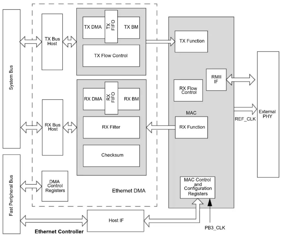
flowchart
graph TD
    A["System Bus"] <--> B["TX Bus Host"]
    B <--> C["TX DMA"]
    C --> D["TX FIFO"]
    D --> E["TX BM"]
    E --> F["TX Flow Control"]
    F --> G["TX Function"]
    H["Fast Peripheral Bus"] <--> I["DMA Control Registers"]
    I <--> J["Host IF"]
    J <--> K["Ethernet Controller"]
    K <--> L["External PHY"]
    M["Ethernet DMA"] --> N["RX DMA"]
    N --> O["RX FIFO"]
    O --> P["RX BM"]
    P --> Q["RX Filter"]
    Q --> R["Checksum"]
    S["External PHY"] <--> T["REF_CLK"]
    T --> U["MAC"]
    U --> V["RX Function"]
    V --> W["MAC Control and Configuration Registers"]
    W --> X["PB3_CLK"]
    X --> Y["Host IF"]
    Y --> K
The tables below show two interfaces and the associated pins that can be used with the Ethernet Controller.
Note: Ethernet Controller pins that are not used by selected interface can be used by other peripherals.
TABLE 33-1: RMII MODE DEFAULT INTERFACE SIGNALS (FMIIEN = 0, FETHIO = 1)
| Pin Name Description | |
| EMDC Management Clock | |
| EMDIO Management I/O | |
| ETXEN Transmit Enable | |
| ETXD0 Transmit Data | |
| ETXD1 Transmit Data | |
| EREFCLK Reference Clock | |
| ECRSDV Carrier Sense – Receive | Data Valid |
| ERXD0 Receive Data | |
| ERXD1 Receive Data | |
| ERXERR Receive Error |
TABLE 33-2: RMII MODE ALTERNATE INTERFACE SIGNALS (FMIIEN = 0, FETHIO = 0)
| Pin Name Description | |
| AEMDC Management Clock | |
| AEMDIO | Management I/O |
| AETXEN | Transmit Enable |
| AETXD0 | Transmit Data |
| AETXD1 | Transmit Data |
| AEREFCLK | Reference Clock |
| AECRSDV | Carrier Sense – Receive Data Valid |
| AERXD0 | Receive Data |
| AERXD1 | Receive Data |
| AERXERR | Receive Error |
33.1 Ethernet Controller Registers
TABLE 33-3: ETHERNET CONTROLLER REGISTER SUMMARY
Legend: x = unknown value on Reset; — = unimplemented, read as '0'. Reset values are shown in hexadecimal.
Note 1: All registers in this table (with the exception of ETHSTAT) have corresponding CLR, SET and INV registers at their virtual addresses, plus offsets of 0x4, 0x8 and 0xC, respectively. See Section 13.3 "CLR, SET and INV Registers" for more information.
2: Reset values default to the factory programmed value.
TABLE 33-3: ETHERNET CONTROLLER REGISTER SUMMARY (CONTINUED)
Legend: x = unknown value on Reset; — = unimplemented, read as '0'. Reset values are shown in hexadecimal.
Note 1: All registers in this table (with the exception of ETHSTAT) have corresponding CLR, SET and INV registers at their virtual addresses, plus offsets of 0x4, 0x8 and 0xC, respectively. See Section 13.3 "CLR, SET and INV Registers" for more information.
2: Reset values default to the factory programmed value.
REGISTER 33-1: ETHCON1: ETHERNET CONTROLLER CONTROL REGISTER 1
| Bit Range | Bit 31/23/15/7 | Bit 30/22/14/6 | Bit 29/21/13/5 | Bit 28/20/12/4 | Bit 27/19/11/3 | Bit 26/18/10/2 | Bit 25/17/9/1 | Bit 24/16/8/0 |
| 31:24 | R/W-0 R/W-0 R/W-0 R/W-0 R/W-0 | R/W-0 R/W-0 | ||||||
| PTV[15:8] | ||||||||
| 23:16 | R/W-0 R/W-0 R/W-0 R/W-0 R/W-0 R/W-0 | R/W-0 R/W-0 | ||||||
| PTV[7:0] | ||||||||
| 15:8 | R/W-0 U-0 | R/W-0 U-0 U-0 | U-0 R/W-0 R/W-0 | |||||
| ON | — | SIDL | — | — | — | TXRTS | RXEN(1) | |
| 7:0 | R/W-0 | U-0 | U-0 | R/W-0 | U-0 | U-0 | U-0 | R/W-0 |
| AUTOFC | — | — | MANFC | — | — | — | BUFCDEC | |
Legend:
| R = Readable bit | W = Writable bit | U = Unimplemented bit, read as '0' |
| -n = Value at POR | ‘1’ = Bit is set | ‘0’ = Bit is cleared x = Bit is unknown |
bit 31-16 PTV[15:0]: PAUSE Timer Value bits
PAUSE timer value used for flow control.
This register must only be written when RXEN (ETHCON1[8]) is not set.
These bits are only used for flow control operations.
bit 15 ON: Ethernet ON bit
1 = Ethernet module is enabled
0 = Ethernet module is disabled
bit 14 Unimplemented: Read as '0'
bit 13 SIDL: Ethernet Stop in Idle Mode bit
1 = Ethernet module transfers are paused during Idle mode
0 = Ethernet module transfers continue during Idle mode
bit 12-10 Unimplemented: Read as '0'
bit 9 TXRTS: Transmit Request to Send bit
1 = Activate the TX logic and send the packet(s) defined in the TX Ethernet Descriptor Table (EDT)
0 = Stop transmit (when cleared by software) or transmit done (when cleared by hardware)
After the bit is written with a '1', it clears to a '0' whenever the transmit logic has finished transmitting the requested packets in the EDT. If a '0' is written by the CPU, the transmit logic finishes the current packet's transmission and then stops any further.
This bit only affects TX operations.
bit 8 RXEN: Receive Enable bit ^(1)
1 = Enable RX logic, packets are received and stored in the RX buffer as controlled by the filter configuration
0 = Disable RX logic, no packets are received in the RX buffer
This bit only affects RX operations.
bit 7 AUTOFC: Automatic Flow Control bit
1 = Automatic flow control is enabled
0 = Automatic flow control is disabled
Setting this bit enables automatic flow control. If set, the full and empty watermarks are used to automatically enable and disable the flow control, respectively. When the number of received buffers BUFCNT (ETHSTAT[16:23]) rises to the full watermark, flow control is automatically enabled. When the BUFCNT falls to the empty watermark, flow control is automatically disabled. This bit is only used for flow control operations and affects both TX and RX operations.
bit 6-5 Unimplemented: Read as '0'
Note 1: It is not recommended to clear the RXEN bit and then make changes to any RX related field/register. The Ethernet Controller must be reinitialized (ON cleared to '0'), and then the RX changes applied.
REGISTER 33-1: ETHCON1: ETHERNET CONTROLLER CONTROL REGISTER 1 (CONTINUED)
bit 4 MANFC: Manual Flow Control bit
1 = Manual flow control is enabled
0 = Manual flow control is disabled
Setting this bit enables manual flow control. If set, the flow control logic sends a PAUSE frame using the PAUSE timer value in the PTV register. It then resends a PAUSE frame every 128 * PTV[15:0]/2 TX clock cycles until the bit is cleared.
Note: For 10 Mbps operation, TX clock runs at 2.5 MHz. For 100 Mbps operation, TX clock runs at 25 MHz.
When this bit is cleared, the flow control logic automatically sends a PAUSE frame with a 0x0000 PAUSE timer value to disable flow control. This bit is only used for flow control operations and affects both TX and RX operations.
bit 3-1 Unimplemented: Read as '0'
bit 0 BUFCDEC: Descriptor Buffer Count Decrement bit
The BUFCDEC bit is a write-1 bit that reads as '0'. When written with a '1', the BUFCNT decrements by one. If BUFCNT is incremented by the RX logic at the same time that this bit is written, the BUFCNT value remains unchanged. Writing a '0' does not have any effect. This bit is only used for RX operations.
Note 1: It is not recommended to clear the RXEN bit and then make changes to any RX related field/register. The Ethernet Controller must be reinitialized (ON cleared to '0'), and then the RX changes applied.
REGISTER 33-2: ETHCON2: ETHERNET CONTROLLER CONTROL REGISTER 2
| Bit Range | Bit31/23/15/7 | Bit30/22/14/6 | Bit29/21/13/5 | Bit28/20/12/4 | Bit27/19/11/3 | Bit26/18/10/2 | Bit25/17/9/1 | Bit24/16/8/0 |
| 31:24 | U-0 U-0 | U-0 U-0 U-0 U-0 | U-0 U-0 | |||||
| —— — | —— — — — | |||||||
| 23:16 | U-0 U-0 | U-0 U-0 U-0 U-0 | U-0 U-0 | |||||
| —— — | —— — — — | |||||||
| 15:8 | U-0 U-0 | U-0 U-0 U-0 R/W-0 | R/W-0 R/W-0 R/W-0 | |||||
| —— — | —— RXBUFSZ[6:4] | |||||||
| 7:0 | R/W-0 | R/W-0 R/W-0 R/W-0 | U-0 U-0 | U-0 U-0 | ||||
| RXBUFSZ[3:0] | —— — | — | ||||||
Legend:
| R = Readable bit | W = Writable bit | U = Unimplemented bit, read as '0' |
| -n = Value at POR | ‘1’ = Bit is set | ‘0’ = Bit is cleared x = Bit is unknown |
bit 31-11 Unimplemented: Read as '0'
bit 10-4 RXBUFSZ[6:0]: RX Data Buffer Size for All RX Descriptors (in 16-byte increments) bits
1111111 = RX data buffer size for descriptors is 2032 bytes
•
•
•
1100000 = RX data buffer size for descriptors is 1536 bytes
•
•
.
0000011 = RX data buffer size for descriptors is 48 bytes
0000010 = RX data buffer size for descriptors is 32 bytes
0000001 = RX data buffer size for descriptors is 16 bytes
0000000 = Reserved
bit 3-0 Unimplemented: Read as '0'
Note 1: This register is only used for RX operations.
2: The bits in this register may only be changed while the RXEN bit (ETHCON1[8]) = 0.
REGISTER 33-3: ETHTXST: ETHERNET CONTROLLER TX PACKET DESCRIPTOR START ADDRESS REGISTER
| Bit Range | Bit 31/23/15/7 | Bit 30/22/14/6 | Bit 29/21/13/5 | Bit 28/20/12/4 | Bit 27/19/11/3 | Bit 26/18/10/2 | Bit 25/17/9/1 | Bit 24/16/8/0 |
| 31:24 | R/W-0 R/W-0 R/W-0 R/W-0 R/W-0 R/W-0 | |||||||
| TXSTADDR[31:24] | ||||||||
| 23:16 | R/W-0 R/W-0 R/W-0 R/W-0 R/W-0 R/W-0 | |||||||
| TXSTADDR[23:16] | ||||||||
| 15:8 | R/W-0 R/W-0 R/W-0 R/W-0 R/W-0 R/W-0 | |||||||
| TXSTADDR[15:8] | ||||||||
| 7:0 | R/W-0 R/W-0 R/W-0 R/W-0 R/W-0 R/W-0 | |||||||
| TXSTADDR[7:2] | — | — | ||||||
Legend:
| R = Readable bit | W = Writable bit | U = Unimplemented bit, read as '0' |
| -n = Value at POR | '1' = Bit is set | '0' = Bit is cleared x = Bit is unknown |
bit 31-2 TXSTADDR[31:2]: Starting Address of First Transmit Descriptor bits
This register must not be written while any transmit, receive or DMA operations are in progress. This address must be 4-byte aligned (bits 1-0 must be '00').
bit 1-0 Unimplemented: Read as '0'
Note 1: This register is only used for TX operations.
2: This register will be updated by hardware with the last descriptor used by the last successfully transmitted packet.
REGISTER 33-4: ETHRXST: ETHERNET CONTROLLER RX PACKET DESCRIPTOR START ADDRESS REGISTER
| Bit Range | Bit 31/23/15/7 | Bit 30/22/14/6 | Bit 29/21/13/5 | Bit 28/20/12/4 | Bit 27/19/11/3 | Bit 26/18/10/2 | Bit 25/17/9/1 | Bit 24/16/8/0 |
| 31:24 | R/W-0 | R/W-0 | R/W-0 | R/W-0 | R/W-0 | R/W-0 | R/W-0 | R/W-0 |
| RXSTADDR[31:24] | ||||||||
| 23:16 | R/W-0 | R/W-0 | R/W-0 | R/W-0 | R/W-0 | R/W-0 | R/W-0 | R/W-0 |
| RXSTADDR[23:16] | ||||||||
| 15:8 | R/W-0 | R/W-0 | R/W-0 | R/W-0 | R/W-0 | R/W-0 | R/W-0 | R/W-0 |
| RXSTADDR[15:8] | ||||||||
| 7:0 | R/W-0 | R/W-0 | R/W-0 | R/W-0 | R/W-0 | R/W-0 | U-0 | U-0 |
| RXSTADDR[7:2] | — | — | ||||||
Legend:
| R = Readable bit | W = Writable bit | U = Unimplemented bit, read as '0' |
| -n = Value at POR | '1' = Bit is set | '0' = Bit is cleared x = Bit is unknown |
bit 31-2 RXSTADDR[31:2]: Starting Address of First Receive Descriptor bits
This register must not be written while any transmit, receive or DMA operations are in progress. This address must be 4-byte aligned (bits 1-0 must be '00').
bit 1-0 Unimplemented: Read as '0'
Note 1: This register is only used for RX operations.
2: This register will be updated by hardware with the last descriptor used by the last successfully transmitted packet.
REGISTER 33-5: ETHHT0: ETHERNET CONTROLLER HASH TABLE 0 REGISTER
| Bit Range | Bit 31/23/15/7 | Bit 30/22/14/6 | Bit 29/21/13/5 | Bit 28/20/12/4 | Bit 27/19/11/3 | Bit 26/18/10/2 | Bit 25/17/9/1 | Bit 24/16/8/0 |
| 31:24 | R/W-0 R/W-0 R/W-0 R/W-0 | R/W-0 R/W-0 | R/W-0 R/W-0 | |||||
| HT[31:24] | ||||||||
| 23:16 | R/W-0 R/W-0 R/W-0 | R/W-0 R/W-0 | R/W-0 R/W-0 | |||||
| HT[23:16] | ||||||||
| 15:8 | R/W-0 R/W-0 R/W-0 | R/W-0 R/W-0 | R/W-0 R/W-0 | |||||
| HT[15:8] | ||||||||
| 7:0 | R/W-0 R/W-0 R/W-0 | R/W-0 R/W-0 | R/W-0 R/W-0 | |||||
| HT[7:0] | ||||||||
Legend:
R = Readable bit W = Writable bit U = Unimplemented bit, read as '0'
-n = Value at POR '1' = Bit is set '0' = Bit is cleared x = Bit is unknown
bit 31-0 HT[31:0]: Hash Table Bytes 0-3 bits
Note 1: This register is only used for RX operations.
2: The bits in this register may only be changed while the RXEN bit (ETHCON1[8]) = 0 or the HTEN bit (ETHRXFC[15]) = 0.
REGISTER 33-6: ETHHT1: ETHERNET CONTROLLER HASH TABLE 1 REGISTER
| Bit Range | Bit31/23/15/7 | Bit30/22/14/6 | Bit29/21/13/5 | Bit28/20/12/4 | Bit27/19/11/3 | Bit26/18/10/2 | Bit25/17/9/1 | Bit24/16/8/0 |
| 31:24 | R/W-0 | R/W-0 | R/W-0 | R/W-0 | R/W-0 | R/W-0 | R/W-0 | R/W-0 |
| HT[63:56] | ||||||||
| 23:16 | R/W-0 | R/W-0 | R/W-0 | R/W-0 | R/W-0 | R/W-0 | R/W-0 | R/W-0 |
| HT[55:48] | ||||||||
| 15:8 | R/W-0 | R/W-0 | R/W-0 | R/W-0 | R/W-0 | R/W-0 | R/W-0 | R/W-0 |
| HT[47:40] | ||||||||
| 7:0 | R/W-0 | R/W-0 | R/W-0 | R/W-0 | R/W-0 | R/W-0 | R/W-0 | R/W-0 |
| HT[39:32] | ||||||||
Legend:
| R = Readable bit | W = Writable bit | U = Unimplemented bit, read as '0' |
| -n = Value at POR | '1' = Bit is set | '0' = Bit is cleared x = Bit is unknown |
bit 31-0 HT[63:32]: Hash Table Bytes 4-7 bits
Note 1: This register is only used for RX operations.
2: The bits in this register may only be changed while the RXEN bit (ETHCON1[8]) = 0 or the HTEN bit (ETHRXFC[15]) = 0.
REGISTER 33-7: ETHPMM0: ETHERNET CONTROLLER PATTERN MATCH MASK 0 REGISTER
| Bit Range | Bit31/23/15/7 | Bit30/22/14/6 | Bit29/21/13/5 | Bit28/20/12/4 | Bit27/19/11/3 | Bit26/18/10/2 | Bit25/17/9/1 | Bit24/16/8/0 |
| 31:24 | R/W-0 R/W-0 R/W-0 R/W-0 R/W-0 R/W-0 R/W-0 | |||||||
| PMM[31:24] | ||||||||
| 23:16 | R/W-0 R/W-0 R/W-0 R/W-0 R/W-0 R/W-0 R/W-0 | |||||||
| PMM[23:16] | ||||||||
| 15:8 | R/W-0 R/W-0 R/W-0 R/W-0 R/W-0 R/W-0 R/W-0 | |||||||
| PMM[15:8] | ||||||||
| 7:0 | R/W-0 R/W-0 R/W-0 R/W-0 R/W-0 R/W-0 R/W-0 | |||||||
| PMM[7:0] | ||||||||
Legend:
R = Readable bit W = Writable bit U = Unimplemented bit, read as '0' -n = Value at POR '1' = Bit is set '0' = Bit is cleared x = Bit is unknown
bit 31-24 PMM[31:24]: Pattern Match Mask 3 bits
bit 23-16 PMM[23:16]: Pattern Match Mask 2 bits
bit 15-8 PMM[15:8]: Pattern Match Mask 1 bits
bit 7-0 PMM[7:0]: Pattern Match Mask 0 bits
Note 1: This register is only used for RX operations.
2: The bits in this register may only be changed while the RXEN bit (ETHCON1[8]) = 0 or the PMMODE bit (ETHRXFC[11:8]) = 0.
REGISTER 33-8: ETHPMM1: ETHERNET CONTROLLER PATTERN MATCH MASK 1 REGISTER
| Bit Range | Bit31/23/15/7 | Bit30/22/14/6 | Bit29/21/13/5 | Bit28/20/12/4 | Bit27/19/11/3 | Bit26/18/10/2 | Bit25/17/9/1 | Bit24/16/8/0 |
| 31:24 | R/W-0 R/W | -0 R/W-0 R/W | -0 R/W-0 R/W | -0 R/W-0 R/W-0 | ||||
| PMM[63:56] | ||||||||
| 23:16 | R/W-0 R/W | -0 R/W-0 R/W | -0 R/W-0 R/W | -0 R/W-0 R/W-0 | ||||
| PMM[55:48] | ||||||||
| 15:8 | R/W-0 R/W | -0 R/W-0 R/W | -0 R/W-0 R/W | -0 R/W-0 R/W-0 | ||||
| PMM[47:40] | ||||||||
| 7:0 | R/W-0 R/W | -0 R/W-0 R/W | -0 R/W-0 R/W | -0 R/W-0 R/W-0 | ||||
| PMM[39:32] | ||||||||
Legend:
R = Readable bit W = Writable bit U = Unimplemented bit, read as '0' -n = Value at POR '1' = Bit is set '0' = Bit is cleared x = Bit is unknown
bit 31-24 PMM[63:56]: Pattern Match Mask 7 bits
bit 23-16 PMM[55:48]: Pattern Match Mask 6 bits
bit 15-8 PMM[47:40]: Pattern Match Mask 5 bits
bit 7-0 PMM[39:32]: Pattern Match Mask 4 bits
Note 1: This register is only used for RX operations.
2: The bits in this register may only be changed while the RXEN bit (ETHCON1[8]) = 0 or the PMMODE bit (ETHRXFC[11:8]) = 0.
REGISTER 33-9: ETHPMCS: ETHERNET CONTROLLER PATTERN MATCH CHECKSUM REGISTER
| Bit Range | Bit31/23/15/7 | Bit30/22/14/6 | Bit29/21/13/5 | Bit28/20/12/4 | Bit27/19/11/3 | Bit26/18/10/2 | Bit25/17/9/1 | Bit24/16/8/0 |
| 31:24 | U-0 U-0 | U-0 U-0 U-0 U-0 | U-0 U-0 | |||||
| —— — | —— — — — — | |||||||
| 23:16 | U-0 U-0 | U-0 U-0 U-0 U-0 | U-0 U-0 | |||||
| —— — | —— — — — — | |||||||
| 15:8 | R/W-0 R/W | R/W-0 R/W-0 R/W | R/W-0 R/W-0 R/W | R/W-0 R/W-0 R/W-0 | ||||
| PMCS[15:8] | ||||||||
| 7:0 | R/W-0 R/W | R/W-0 R/W-0 R/W | R/W-0 R/W-0 R/W | R/W-0 R/W-0 R/W-0 | ||||
| PMCS[7:0] | ||||||||
Legend:
R = Readable bit W = Writable bit U = Unimplemented bit, read as '0' -n = Value at POR '1' = Bit is set '0' = Bit is cleared x = Bit is unknown
bit 31-16 Unimplemented: Read as '0'
bit 15-8 PMCS[15:8]: Pattern Match Checksum 1 bits
bit 7-0 PMCS[7:0]: Pattern Match Checksum 0 bits
Note 1: This register is only used for RX operations.
2: The bits in this register may only be changed while the RXEN bit (ETHCON1[8]) = 0 or the PMMODE bit (ETHRXFC[11:8]) = 0.
REGISTER 33-10: ETHPMO: ETHERNET CONTROLLER PATTERN MATCH OFFSET REGISTER
| Bit Range | Bit 31/23/15/7 | Bit 30/22/14/6 | Bit 29/21/13/5 | Bit 28/20/12/4 | Bit 27/19/11/3 | Bit 26/18/10/2 | Bit 25/17/9/1 | Bit 24/16/8/0 |
| 31:24 | U-0 | U-0 | U-0 | U-0 | U-0 | U-0 | U-0 | U-0 |
| — | — | — | — | — | — | — | — | |
| 23:16 | U-0 | U-0 | U-0 | U-0 | U-0 | U-0 | U-0 | U-0 |
| — | — | — | — | — | — | — | — | |
| 15:8 | R/W-0 | R/W-0 | R/W-0 | R/W-0 | R/W-0 | R/W-0 | R/W-0 | R/W-0 |
| PMO[15:8] | ||||||||
| 7:0 | R/W-0 | R/W-0 | R/W-0 | R/W-0 | R/W-0 | R/W-0 | R/W-0 | R/W-0 |
| PMO[7:0] | ||||||||
Legend:
R = Readable bit W = Writable bit U = Unimplemented bit, read as '0' -n = Value at POR '1' = Bit is set '0' = Bit is cleared x = Bit is unknown
bit 31-16 Unimplemented: Read as '0'
bit 15-0 PMO[15:0]: Pattern Match Offset 1 bits
Note 1: This register is only used for RX operations.
2: The bits in this register may only be changed while the RXEN bit (ETHCON1[8]) = 0 or the PMMODE bit (ETHRXFC[11:8]) = 0.
REGISTER 33-11: ETHRXFC: ETHERNET CONTROLLER RECEIVE FILTER CONFIGURATION REGISTER
| Bit Range | Bit 31/23/15/7 | Bit 30/22/14/6 | Bit 29/21/13/5 | Bit 28/20/12/4 | Bit 27/19/11/3 | Bit 26/18/10/2 | Bit 25/17/9/1 | Bit 24/16/8/0 |
| 31:24 | U-0 U-0 | U-0 U-0 U-0 U-0 | U-0 U-0 | |||||
| — — — — — | — — — | — | ||||||
| 23:16 | U-0 U-0 | U-0 U-0 U-0 U-0 | U-0 U-0 | |||||
| — — — — — | — — — | — | ||||||
| 15:8 | R/W-0 | R/W-0 | U-0 | R/W-0 | R/W-0 | R/W-0 | R/W-0 | R/W-0 |
| HTEN | MPEN | — | NOTPM | PMMODE[3:0] | ||||
| 7:0 | R/W-0 | R/W-0 | R/W-0 | R/W-0 | R/W-0 | R/W-0 | R/W-0 | R/W-0 |
| CRCERREN | CRCOKEN | RUNTERREN | RUNTEN | UCEN | NOTMEEN | MCEN | BCEN | |
Legend:
| R = Readable bit | W = Writable bit | U = Unimplemented bit, read as '0' |
| -n = Value at POR | '1' = Bit is set | '0' = Bit is cleared x = Bit is unknown |
bit 31-16 Unimplemented: Read as '0'
bit 15 HTEN: Enable Hash Table Filtering bit
1 = Enable Hash Table Filtering
0 = Disable Hash Table Filtering
bit 14 MPEN: Magic Packet Enable bit
1 = Enable magic packet filtering
0 = Disable magic packet filtering
bit 13 Unimplemented: Read as '0'
bit 12 NOTPM: Pattern Match Inversion bit
1 = Pattern match checksum must not match for a successful pattern match to occur
0 = Pattern match checksum must match for a successful pattern match to occur
This bit determines whether pattern match checksum must match in order for a successful pattern match to occur.
Note 1: XOR = True when either one or the other conditions are true, but not both.
2: This hash table filter match is active regardless of the value of the HTEN bit.
3: This magic packet filter match is active regardless of the value of the MPEN bit.
4: This register is only used for RX operations.
5: The bits in this register may only be changed while the RXEN bit (ETHCON1[8]) = 0.
REGISTER 33-11: ETHRXFC: ETHERNET CONTROLLER RECEIVE FILTER CONFIGURATION REGISTER (CONTINUED)
bit 11-8 PMMODE[3:0]: Pattern Match Mode bits
1001 = Pattern match is successful if (NOTPM = 1 XOR Pattern Match Checksum matches) AND (Packet = Magic Packet) ^(1,3)
1000 = Pattern match is successful if (NO
TPM = 1 XOR Pattern Match Checksum matches) AND (Hash Table Filter match) ^(1,1)
0111 = Pattern match is successful if (NOTPM = 1 XOR Pattern Match Checksum matches) AND (Destination Address = Broadcast Address) ^(1)
0110 = Pattern match is successful if (NOTPM = 1 XOR Pattern Match Checksum matches) AND (Destination Address = Broadcast Address) ^(1)
0101 = Pattern match is successful if (NOTPM = 1 XOR Pattern Match Checksum matches) AND (Destination Address = Unicast Address) ^(1)
0100 = Pattern match is successful if (NOTPM = 1 XOR Pattern Match Checksum matches) AND (Destination Address = Unicast Address) ^(1)
0011 = Pattern match is successful if (NOTPM = 1 XOR Pattern Match Checksum matches) AND (Destination Address = Station Address) ^(1)
0010 = Pattern match is successful if (NOTPM = 1 XOR Pattern Match Checksum matches) AND (Destination Address = Station Address) ^(1)
0001 = Pattern match is successful if (NOTPM = 1 XOR Pattern Match Checksum matches) ^(1)
0000 = Pattern Match is disabled; pattern match is always unsuccessful
bit 7 CRCERREN: CRC Error Collection Enable bit
1 = The received packet CRC must be invalid for the packet to be accepted
0 = Disable CRC Error Collection filtering
This bit allows the user to collect all packets that have an invalid CRC.
bit 6 CRCOKEN: CRC OK Enable bit
1 = The received packet CRC must be valid for the packet to be accepted
0 = Disable CRC filtering
This bit allows the user to reject all packets that have an invalid CRC.
bit 5 RUNTERREN: Runt Error Collection Enable bit
1 = The received packet must be a runt packet for the packet to be accepted
0 = Disable Runt Error Collection filtering
This bit allows the user to collect all packets that are runt packets. For this filter, a runt packet is defined as any packet with a size of less than 64 bytes (when CRCOKEN = 0) or any packet with a size of less than 64 bytes that has a valid CRC (when CRCOKEN = 1).
bit 4 RUNTEN: Runt Enable bit
1 = The received packet must not be a runt packet for the packet to be accepted
0 = Disable Runt filtering
This bit allows the user to reject all runt packets. For this filter, a runt packet is defined as any packet with a size of less than 64 bytes.
bit 3 UCEN: Unicast Enable bit
1 = Enable unicast filtering
0 = Disable unicast filtering
This bit allows the user to accept all unicast packets whose Destination Address matches the Station Address.
Note 1: XOR = True when either one or the other conditions are true, but not both.
2: This hash table filter match is active regardless of the value of the HTEN bit.
3: This magic packet filter match is active regardless of the value of the MPEN bit.
4: This register is only used for RX operations.
5: The bits in this register may only be changed while the RXEN bit (ETHCON1[8]) = 0.
REGISTER 33-11: ETHRXFC: ETHERNET CONTROLLER RECEIVE FILTER CONFIGURATION REGISTER (CONTINUED)
bit 2 NOTMEEN: Not Me Unicast Enable bit
1 = Enable not me unicast filtering
0 = Disable not me unicast filtering
This bit allows the user to accept all unicast packets whose destination address does not match the station address.
bit 1 MCEN: Multicast Enable bit
1 = Enable multicast filtering
0 = Disable multicast filtering
This bit allows the user to accept all multicast address packets.
bit 0 BCEN: Broadcast Enable bit
1 = Enable broadcast filtering
0 = Disable broadcast filtering
This bit allows the user to accept all broadcast address packets.
Note 1: XOR = True when either one or the other conditions are true, but not both.
2: This hash table filter match is active regardless of the value of the HTEN bit.
3: This magic packet filter match is active regardless of the value of the MPEN bit.
4: This register is only used for RX operations.
5: The bits in this register may only be changed while the RXEN bit (ETHCON1[8]) = 0.
REGISTER 33-12: ETHRXWM: ETHERNET CONTROLLER RECEIVE WATERMARKS REGISTER
| Bit Range | Bit31/23/15/7 | Bit30/22/14/6 | Bit29/21/13/5 | Bit28/20/12/4 | Bit27/19/11/3 | Bit26/18/10/2 | Bit25/17/9/1 | Bit24/16/8/0 |
| 31:24 | U-0 U-0 | U-0 U-0 U-0 U-0 | U-0 U-0 | |||||
| —— — | —— — — — — | |||||||
| 23:16 | R/W-0 R/W | R/W-0 R/W-0 R/W | R/W-0 R/W-0 R/W | R/W-0 R/W-0 R/W-0 | ||||
| RXFWM[7:0] | ||||||||
| 15:8 | U-0 U-0 | U-0 U-0 U-0 U-0 | U-0 U-0 | |||||
| —— — | —— — — — — | |||||||
| 7:0 | R/W-0 R/W | R/W-0 R/W-0 R/W | R/W-0 R/W-0 R/W | R/W-0 R/W-0 | ||||
| RXEWM[7:0] | ||||||||
Legend:
R = Readable bit W = Writable bit U = Unimplemented bit, read as '0'
-n = Value at POR '1' = Bit is set '0' = Bit is cleared x = Bit is unknown
bit 31-24 Unimplemented: Read as '0'
bit 23-16 RXFWM[7:0]: Receive Full Watermark bits
The software controlled RX buffer full watermark pointer is compared against the RX BUFCNT to determine the Full Watermark condition for the FWMARK interrupt and for enabling flow control when automatic flow control is enabled. The full watermark pointer must always be greater than the empty watermark pointer.
bit 15-8 Unimplemented: Read as '0'
bit 7-0 RXEWM[7:0]: Receive Empty Watermark bits
The software controlled RX buffer empty watermark pointer is compared against the RX BUFCNT to determine the Empty Watermark condition for the EWMARK interrupt and for disabling flow control when automatic flow control is enabled. The empty watermark pointer must always be less than the full watermark pointer.
Note: This register is only used for RX operations.
REGISTER 33-13: ETHIEN: ETHERNET CONTROLLER INTERRUPT ENABLE REGISTER
| Bit Range | Bit 31/23/15/7 | Bit 30/22/14/6 | Bit 29/21/13/5 | Bit 28/20/12/4 | Bit 27/19/11/3 | Bit 26/18/10/2 | Bit 25/17/9/1 | Bit 24/16/8/0 |
| 31:24 | U-0 U-0 U-0 U-0 U-0 U-0 | |||||||
| — — — | — — — — | |||||||
| 23:16 | U-0 U-0 U-0 U-0 U-0 U-0 | |||||||
| — — — | — — — — | |||||||
| 15:8 | U-0 | R/W-0 | R/W-0 | U-0 | U-0 | U-0 | R/W-0 | R/W-0 |
| — | TXBUSEIE ^(1) | RXBUSEIE ^(2) | — | — | — | EWMARKIE ^(2) | FWMARKIE ^(2) | |
| 7:0 | R/W-0 | R/W-0 | R/W-0 | U-0 | R/W-0 | R/W-0 | R/W-0 | R/W-0 |
| RXDONEIE ^(2) | PKTPENDIE ^(2) | RXACTIE ^(2) | — | TXDONEIE ^(1) | TXABORTIE ^(1) | RXBUFNAIE ^(2) | RXOVFLWIE ^(2) | |
Legend:
| R = Readable bit | W = Writable bit | U = Unimplemented bit, read as '0' |
| -n = Value at POR | '1' = Bit is set | '0' = Bit is cleared x = Bit is unknown |
bit 31-15 Unimplemented: Read as '0'
bit 14 TXBUSEIE: Transmit BVCI Bus Error Interrupt Enable bit ^(1)
1 = Enable TXBUS error interrupt
0 = Disable TXBUS error interrupt
bit 13 RXBUSEIE: Receive BVCI Bus Error Interrupt Enable bit ^(2)
1 = Enable RXBUS error interrupt
0 = Disable RXBUS error interrupt
bit 12-10 Unimplemented: Read as '0'
bit 9 EWMARKIE: Empty Watermark Interrupt Enable bit ^(2)
1 = Enable EWMARK interrupt
0 = Disable EWMARK interrupt
bit 8 FWMARKIE: Full Watermark Interrupt Enable bit ^(2)
1 = Enable FWMARK interrupt
0 = Disable FWMARK interrupt
bit 7 RXDONEIE: Receiver Done Interrupt Enable bit ^(2)
1 = Enable RXDONE interrupt
0 = Disable RXDONE interrupt
bit 6 PKTPENDIE: Packet Pending Interrupt Enable bit ^(2)
1 = Enable PKTPEND interrupt
0 = Disable PKTPEND interrupt
bit 5 RXACTIE: RX Activity Interrupt Enable bit
1 = Enable RXACT interrupt
0 = Disable RXACT interrupt
bit 4 Unimplemented: Read as '0'
bit 3 TXDONEIE: Transmitter Done Interrupt Enable bit ^(1)
1 = Enable TXDONE interrupt
0 = Disable TXDONE interrupt
bit 2 TXABORTIE: Transmitter Abort Interrupt Enable bit ^(1)
1 = Enable TXABORT interrupt
0 = Disable TXABORT interrupt
bit 1 RXBUFNAIE: Receive Buffer Not Available Interrupt Enable bit ^(2)
1 = Enable RXBUFNA interrupt
0 = Disable RXBUFNA interrupt
bit 0 RXOVFLWIE: Receive FIFO Overflow Interrupt Enable bit ^(2)
1 = Enable RXOVFLW interrupt
0 = Disable RXOVFLW interrupt
Note 1: This bit is only used for TX operations.
2: This bit is only used for RX operations.
REGISTER 33-14: ETHIRQ: ETHERNET CONTROLLER INTERRUPT REQUEST REGISTER
| Bit Range | Bit31/23/15/7 | Bit30/22/14/6 | Bit29/21/13/5 | Bit28/20/12/4 | Bit27/19/11/3 | Bit26/18/10/2 | Bit25/17/9/1 | Bit24/16/8/0 |
| 31:24 | U-0 U-0 | U-0 U-0 U-0 U-0 | U-0 U-0 | |||||
| — — — | — — — — | |||||||
| 23:16 | U-0 U-0 | U-0 U-0 U-0 U-0 | U-0 U-0 | |||||
| — — — | — — — — | |||||||
| 15:8 | U-0 R/W | U-0 R/W-0 U-0 U | U-0 U-0 R/W-0 | R/W-0 | ||||
| — | TXBUSE(1) | RXBUSE(2) | — | — | — | EWMARK(2) | FWMARK(2) | |
| 7:0 | R/W-0 | R/W-0 | R/W-0 | U-0 | R/W-0 | R/W-0 | R/W-0 | R/W-0 |
| RXDONE(2) | PKTPEND(2) | RXACT(2) | — | TXDONE(1) | TXABORT(1) | RXBUFNA(2) | RXOVFLW(2) |
Legend:
| R = Readable bit | W = Writable bit | U = Unimplemented bit, read as '0' |
| -n = Value at POR | '1' = Bit is set | '0' = Bit is cleared x = Bit is unknown |
bit 31-15 Unimplemented: Read as '0'
bit 14 TXBUSE: Transmit BVCI Bus Error Interrupt bit ^(1)
1 = BVCI bus error has occurred
0 = BVCI bus error has not occurred
This bit is set when the TX DMA encounters a BVCI bus error during a memory access. It is cleared by either a Reset or CPU write of a '1' to the CLR register.
bit 13 RXBUSE: Receive BVCI Bus Error Interrupt bit ^(2)
1 = BVCI bus error has occurred
0 = BVCI bus error has not occurred
This bit is set when the RX DMA encounters a BVCI Bus error during a memory access. It is cleared by either a Reset or CPU write of a '1' to the CLR register.
bit 12-10 Unimplemented: Read as '0'
bit 9 EWMARK: Empty Watermark Interrupt bit ^(2)
1 = Empty watermark pointer reached
0 = No interrupt pending
This bit is set when the RX descriptor buffer count is less than or equal to the value in the RXEWM bit (ETHRXWM[0:7]) value. It is cleared by BUFCNT bit (ETHSTAT[16:23]) being incremented by hardware. Writing a '0' or a '1' has no effect.
bit 8 FWMARK: Full Watermark Interrupt bit ^(2)
1 = Full Watermark pointer reached
0 = No interrupt pending
This bit is set when the RX descriptor buffer count is greater than or equal to the value in the RXFWM bit (ETHRXWM[16:23]) field. It is cleared by writing the BUFCDEC (ETHCON1[0]) bit to decrement the BUFCNT counter. Writing a '0' or a '1' has no effect.
Note 1: This bit is only used for TX operations.
2: This bit is are only used for RX operations.
3: It is recommended to use the SET, CLR, or INV registers to set or clear any bit in this register. Setting or clearing any bits in this register must only be done for debug/test purposes.
REGISTER 33-14: ETHIRQ: ETHERNET CONTROLLER INTERRUPT REQUEST REGISTER (CONTINUED)
bit 7 RXDONE: Receive Done Interrupt bit (2)
1 = RX packet was successfully received
0 = No interrupt pending
This bit is set whenever an RX packet is successfully received. It is cleared by either a Reset or CPU write of a '1' to the CLR register.
bit 6 PKTPEND: Packet Pending Interrupt bit (2)
1 = RX packet pending in memory
0 = RX packet is not pending in memory
This bit is set when the BUFCNT counter has a value other than '0'. It is cleared by either a Reset or by writing the BUFCDEC bit to decrement the BUFCNT counter. Writing a '0' or a '1' has no effect.
bit 5 RXACT: Receive Activity Interrupt bit (2)
1 = RX packet data was successfully received
0 = No interrupt pending
This bit is set whenever RX packet data is stored in the RXBM FIFO. It is cleared by either a Reset or CPU write of a '1' to the CLR register.
bit 4 Unimplemented: Read as '0'
bit 3 TXDONE: Transmit Done Interrupt bit (1)
1 = TX packet was successfully sent
0 = No interrupt pending
This bit is set when the present TX packet completes transmission, and the transmit status vector is loaded into the first descriptor used for the packet. It is cleared by either a Reset or CPU write of a '1' to the CLR register.
bit 2 TXABORT: Transmit Abort Condition Interrupt bit ^(1)
1 = TX Abort condition occurred on the last TX packet
0 = No interrupt pending
This bit is set when the MAC aborts the transmission of a TX packet for one of the following reasons:
• Jumbo TX packet abort
- Underrun abort
• Excessive defer abort
- Late collision abort
• Excessive collisions abort
This bit is cleared by either a Reset or CPU write of a '1' to the CLR register.
bit 1 RXBUFNA: Receive Buffer Not Available Interrupt bit ^(2)
1 = RX BD Not Available condition has occurred
0 = No interrupt pending
This bit is set by a RX BD Overrun condition. It is cleared by either a Reset or a CPU write of a '1' to the CLR register.
bit 0 RXOVFLW: Receive FIFO Over Flow Error bit (2)
1 = RX FIFO Overflow Error condition has occurred
0 = No interrupt pending
RXOVFLW is set by the RXBM Logic for an RX FIFO Overflow condition. It is cleared by either a Reset or CPU write of a '1' to the CLR register.
Note 1: This bit is only used for TX operations.
2: This bit is are only used for RX operations.
3: It is recommended to use the SET, CLR, or INV registers to set or clear any bit in this register. Setting or clearing any bits in this register must only be done for debug/test purposes.
REGISTER 33-15: ETHSTAT: ETHERNET CONTROLLER STATUS REGISTER
| R = Readable bit | W = Writable bit U = Unimplemented bit, read as '0' |
| -n = Value at POR | '1' = Bit is set '0' = Bit is cleared x = Bit is unknown |
bit 31-24 Unimplemented: Read as '0'
bit 23-16 BUFCNT[7:0]: Packet Buffer Count bits ^(1)
Number of packet buffers received in memory. Once a packet has been successfully received, this register is incremented by hardware based on the number of descriptors used by the packet. Software decrements the counter (by writing to the BUFCDEC bit (ETHCON1[0]) for each descriptor used) after a packet has been read out of the buffer. The register does not roll over (0xFF to 0x00) when hardware tries to increment the register and the register is already at 0xFF. Conversely, the register does not roll under (0x00 to 0xFF) when software tries to decrement the register and the register is already at 0x0000. When software attempts to decrement the counter at the same time that the hardware attempts to increment the counter, the counter value remains unchanged.
When this register value reaches 0xFF, the RX logic halts (only if automatic flow control is enabled) awaiting software to write the BUFCDEC bit in order to decrement the register below 0xFF.
If automatic flow control is disabled, the RXDMA continues processing and the BUFCNT saturates at a value of 0xFF.
When this register is non-zero, the PKTPEND status bit is set and an interrupt may be generated, depending on the value of the ETHIEN bit [PKTPENDIE] register.
When the ETHRXST register is written, the BUFCNT counter is automatically cleared to 0x00.
Note: BUFCNT is not cleared when ON is set to '0'. This enables software to continue to utilize and decrement this count.
bit 15-8 Unimplemented: Read as '0'
bit 7 ETHBUSY: Ethernet Module Busy bit ^(5)
1 = Ethernet logic turns on (ON (ETHCON1[15]) = 1) or is completing a transaction 0 = Ethernet logic is idle
This bit indicates that the module has been turned on or is completing a transaction after being turned off.
Note 1: This bit is only used for RX operations.
2: This bit is only affected by TX operations.
3: This bit is only affected by RX operations.
4: This bit is affected by TX and RX operations.
5: This bit is set when the ON bit (ETHCON1[15]) = 1.
6: This bit is cleared when the ON bit (ETHCON1[15]) = 0.
REGISTER 33-15: ETHSTAT: ETHERNET CONTROLLER STATUS REGISTER (CONTINUED)
bit 6 TXBUSY: Transmit Busy bit (2,6)
1 = TX logic is receiving data
0 = TX logic is idle
This bit indicates that a packet is currently being transmitted. A change in this status bit is not necessarily reflected by the TXDONE interrupt, as TX packets may be aborted or rejected by the MAC.
bit 5 RXBUSY: Receive Busy bit (3,6)
1 = RX logic is receiving data
0 = RX logic is idle
This bit indicates that a packet is currently being received. A change in this status bit is not necessarily reflected by the RXDONE interrupt, as RX packets may be aborted or rejected by the RX filter.
bit 4-0 Unimplemented: Read as '0'
Note 1: This bit is only used for RX operations.
2: This bit is only affected by TX operations.
3: This bit is only affected by RX operations.
4: This bit is affected by TX and RX operations.
5: This bit is set when the ON bit (ETHCON1[15]) = 1.
6: This bit is cleared when the ON bit (ETHCON1[15]) = 0.
REGISTER 33-16: ETHRXOVFLOW: ETHERNET CONTROLLER RECEIVE OVERFLOW STATISTICS REGISTER
| Bit Range | Bit31/23/15/7 | Bit30/22/14/6 | Bit29/21/13/5 | Bit28/20/12/4 | Bit27/19/11/3 | Bit26/18/10/2 | Bit25/17/9/1 | Bit24/16/8/0 |
| 31:24 | U-0 U-0 | U-0 U-0 U-0 U-0 | U-0 U-0 | |||||
| ——— | ——— —— | |||||||
| 23:16 | U-0 U-0 | U-0 U-0 U-0 U-0 | U-0 U-0 | |||||
| ——— | ——— —— | |||||||
| 15:8 | R/W-0 R/W | R/W-0 R/W-0 R/W | R/W-0 R/W-0 R/W | R/W-0 R/W-0 R/W-0 | ||||
| RXOVFLWCNT[15:8] | ||||||||
| 7:0 | R/W-0 R/W | R/W-0 R/W-0 R/W | R/W-0 R/W-0 R/W | R/W-0 R/W-0 R/W-0 | ||||
| RXOVFLWCNT[7:0] | ||||||||
Legend:
R = Readable bit W = Writable bit U = Unimplemented bit, read as '0' -n = Value at POR '1' = Bit is set '0' = Bit is cleared x = Bit is unknown
bit 31-16 Unimplemented: Read as '0'
bit 15-0 RXOVFLWCNT[15:0]: Dropped Receive Frames Count bits
Increment counter for frames accepted by the RX filter and subsequently dropped due to internal receive error (RXFIFO overrun). This event also sets the RXOVFLW bit (ETHIRQ[0]) Interrupt flag.
Note 1: This register is only used for RX operations.
2: This register is automatically cleared by hardware after a read operation, unless the byte enables for bytes 0/1 are '0'.
3: It is recommended to use the SET, CLR, or INV registers to set or clear any bit in this register. Setting or clearing any bits in this register must only be done for debug/test purposes.
REGISTER 33-17: ETHFRMTXOK: ETHERNET CONTROLLER FRAMES TRANSMITTED OK STATISTICS REGISTER
| Bit Range | Bit 31/23/15/7 | Bit 30/22/14/6 | Bit 29/21/13/5 | Bit 28/20/12/4 | Bit 27/19/11/3 | Bit 26/18/10/2 | Bit 25/17/9/1 | Bit 24/16/8/0 |
| 31:24 | U-0 U-0 | U-0 U-0 U-0 U-0 | U-0 U-0 | |||||
| — — — | — — — — — | |||||||
| 23:16 | U-0 U-0 | U-0 U-0 U-0 U-0 | U-0 U-0 | |||||
| — — — | — — — — — | |||||||
| 15:8 | R/W-0 R/W | R/W-0 R/W-0 R/W | R/W-0 R/W-0 | R/W-0 R/W-0 | ||||
| FRMTXOKCNT[15:8] | ||||||||
| 7:0 | R/W-0 R/W | R/W-0 R/W-0 R/W | R/W-0 R/W-0 | R/W-0 R/W-0 | ||||
| FRMTXOKCNT[7:0] | ||||||||
Legend:
R = Readable bit W = Writable bit U = Unimplemented bit, read as '0' -n = Value at POR '1' = Bit is set '0' = Bit is cleared x = Bit is unknown
bit 31-16 Unimplemented: Read as '0'
bit 15-0 FRMTXOKCNT[15:0]: Frame Transmitted OK Count bits Increment counter for frames successfully transmitted.
Note 1: This register is only used for TX operations.
2: This register is automatically cleared by hardware after a read operation, unless the byte enables for bytes 0/1 are '0'.
3: It is recommended to use the SET, CLR, or INV registers to set or clear any bit in this register. Setting or clearing any bits in this register must only be done for debug/test purposes.
REGISTER 33-18: ETHSCOLFRM: ETHERNET CONTROLLER SINGLE COLLISION FRAMES STATISTICS REGISTER
| Bit Range | Bit31/23/15/7 | Bit30/22/14/6 | Bit29/21/13/5 | Bit28/20/12/4 | Bit27/19/11/3 | Bit26/18/10/2 | Bit25/17/9/1 | Bit24/16/8/0 |
| 31:24 | U-0 U-0 | U-0 U-0 U-0 U-0 | U-0 U-0 | |||||
| ——— | ——— —— | |||||||
| 23:16 | U-0 U-0 | U-0 U-0 U-0 U-0 | U-0 U-0 | |||||
| ——— | ——— —— | |||||||
| 15:8 | R/W-0 R/W | R/W-0 R/W-0 R/W | R/W-0 R/W-0 R/W | R/W-0 R/W-0 R/W-0 | ||||
| SCOLFRMCNT[15:8] | ||||||||
| 7:0 | R/W-0 R/W | R/W-0 R/W-0 R/W | R/W-0 R/W-0 R/W | R/W-0 R/W-0 | ||||
| SCOLFRMCNT[7:0] | ||||||||
Legend:
R = Readable bit W = Writable bit U = Unimplemented bit, read as '0' -n = Value at POR '1' = Bit is set '0' = Bit is cleared x = Bit is unknown
bit 31-16 Unimplemented: Read as '0'
bit 15-0 SCOLFRMCNT[15:0]: Single Collision Frame Count bits
Increment count for frames that were successfully transmitted on the second try.
Note 1: This register is only used for TX operations.
2: This register is automatically cleared by hardware after a read operation, unless the byte enables for bytes 0/1 are '0'.
3: It is recommended to use the SET, CLR, or INV registers to set or clear any bit in this register. Setting or clearing any bits in this register must only be done for debug/test purposes.
REGISTER 33-19: ETHMCOLFRM: ETHERNET CONTROLLER MULTIPLE COLLISION FRAMES STATISTICS REGISTER
R = Readable bit W = Writable bit U = Unimplemented bit, read as '0'
-n = Value at POR
'1' = Bit is set
'0' = Bit is cleared
x = Bit is unknown
bit 31-16 Unimplemented: Read as '0'
bit 15-0 MCOLFRMCNT[15:0]: Multiple Collision Frame Count bits
Increment count for frames that were successfully transmitted after there was more than one collision.
Note 1: This register is only used for TX operations.
2: This register is automatically cleared by hardware after a read operation, unless the byte enables for bytes 0/1 are '0'.
3: It is recommended to use the SET, CLR, or INV registers to set or clear any bit in this register. Setting or clearing any bits in this register must only be done for debug/test purposes.
REGISTER 33-20: ETHFRMRXOK: ETHERNET CONTROLLER FRAMES RECEIVED OK STATISTICS REGISTER
| Bit Range | Bit 31/23/15/7 | Bit 30/22/14/6 | Bit 29/21/13/5 | Bit 28/20/12/4 | Bit 27/19/11/3 | Bit 26/18/10/2 | Bit 25/17/9/1 | Bit 24/16/8/0 |
| 31:24 | U-0 U-0 | U-0 U-0 U-0 U-0 | U-0 U-0 | |||||
| — — — | — — — — | |||||||
| 23:16 | U-0 U-0 | U-0 U-0 U-0 U-0 | U-0 U-0 | |||||
| — — — | — — — — | |||||||
| 15:8 | R/W-0 R/W | R/W-0 R/W-0 R/W | R/W-0 R/W-0 | R/W-0 R/W-0 | ||||
| FRMRXOKCNT[15:8] | ||||||||
| 7:0 | R/W-0 R/W | R/W-0 R/W-0 R/W | R/W-0 R/W-0 | R/W-0 R/W-0 | ||||
| FRMRXOKCNT[7:0] | ||||||||
Legend:
R = Readable bit W = Writable bit U = Unimplemented bit, read as '0' -n = Value at POR '1' = Bit is set '0' = Bit is cleared x = Bit is unknown
bit 31-16 Unimplemented: Read as '0'
bit 15-0 FRMRXOKCNT[15:0]: Frames Received OK Count bits
Increment count for frames received successfully by the RX filter. This count is not incremented if there is a Frame Check Sequence (FCS) or alignment error.
Note 1: This register is only used for RX operations.
2: This register is automatically cleared by hardware after a read operation, unless the byte enables for bytes 0/1 are '0'.
3: It is recommended to use the SET, CLR, or INV registers to set or clear any bit in this register. Setting or clearing any bits in this register must only be done for debug/test purposes.
REGISTER 33-21: ETHFCSERR: ETHERNET CONTROLLER FRAME CHECK SEQUENCE ERROR STATISTICS REGISTER
| Bit Range | Bit 31/23/15/7 | Bit 30/22/14/6 | Bit 29/21/13/5 | Bit 28/20/12/4 | Bit 27/19/11/3 | Bit 26/18/10/2 | Bit 25/17/9/1 | Bit 24/16/8/0 |
| 31:24 | U-0 U-0 U | -U-0 U-0 U-0 U-0 | U-0 U-0 | |||||
| ——— | ——— —— | |||||||
| 23:16 | U-0 U-0 U | -U-0 U-0 U-0 U-0 | U-0 U-0 | |||||
| ——— | ——— —— | |||||||
| 15:8 | R/W-0 R/W | -R/W-0 R/W-0 | R/W-0 R/W-0 | R/W-0 R/W-0 | ||||
| FCSERRCNT[15:8] | ||||||||
| 7:0 | R/W-0 R/W | -R/W-0 R/W-0 | R/W-0 R/W-0 | R/W-0 R/W-0 | ||||
| FCSERRCNT[7:0] | ||||||||
Legend:
R = Readable bit W = Writable bit U = Unimplemented bit, read as '0'
-n = Value at POR
'1' = Bit is set
'0' = Bit is cleared
x = Bit is unknown
bit 31-16 Unimplemented: Read as '0'
bit 15-0 FCSERRCNT[15:0]: FCS Error Count bits
Increment count for frames received with FCS error and the frame length in bits is an integral multiple of 8 bits.
Note 1: This register is only used for RX operations.
2: This register is automatically cleared by hardware after a read operation, unless the byte enables for bytes 0/1 are '0'.
3: It is recommended to use the SET, CLR, or INV registers to set or clear any bit in this register. Setting or clearing any bits in this register must be only done for debug/test purposes.
REGISTER 33-22: ETHALGNERR: ETHERNET CONTROLLER ALIGNMENT ERRORS STATISTICS REGISTER
| Bit Range | Bit 31/23/15/7 | Bit 30/22/14/6 | Bit 29/21/13/5 | Bit 28/20/12/4 | Bit 27/19/11/3 | Bit 26/18/10/2 | Bit 25/17/9/1 | Bit 24/16/8/0 |
| 31:24 | U-0 U-0 U | -U-0 U-0 U-0 | U-0 U-0 | |||||
| ——— | ——— — | |||||||
| 23:16 | U-0 U-0 U | -U-0 U-0 U-0 | U-0 U-0 | |||||
| ——— | ——— — | |||||||
| 15:8 | R/W-0 R/W | -R/W-0 R/W-0 | R/W-0 R/W-0 | R/W-0 R/W-0 | ||||
| ALGNERRCNT[15:8] | ||||||||
| 7:0 | R/W-0 R/W | -R/W-0 R/W-0 | R/W-0 R/W-0 | R/W-0 R/W-0 | ||||
| ALGNERRCNT[7:0] | ||||||||
Legend:
| R = Readable bit | W = Writable bit | U = Unimplemented bit, read as '0' |
| -n = Value at POR | '1' = Bit is set | '0' = Bit is cleared x = Bit is unknown |
bit 31-16 Unimplemented: Read as '0'
bit 15-0 ALGNERRCNT[15:0]: Alignment Error Count bits
Increment count for frames with alignment errors. Note that an alignment error is a frame that has an FCS error and the frame length in bits is not an integral multiple of 8 bits (dribble nibble).
Note 1: This register is only used for RX operations.
2: This register is automatically cleared by hardware after a read operation, unless the byte enables for bytes 0/1 are '0'.
3: It is recommended to use the SET, CLR, or INV registers to set or clear any bit in this register. Setting or clearing any bits in this register must be only done for debug/test purposes.
REGISTER 33-23: EMAC1CFG1: ETHERNET CONTROLLER MAC CONFIGURATION 1 REGISTER
| Bit Range | Bit 31/23/15/7 | Bit 30/22/14/6 | Bit 29/21/13/5 | Bit 28/20/12/4 | Bit 27/19/11/3 | Bit 26/18/10/2 | Bit 25/17/9/1 | Bit 24/16/8/0 |
| 31:24 | U-0 U-0 | U-0 U-0 U-0 | U-0 U-0 | |||||
| — — — | — — — — | — | ||||||
| 23:16 | U-0 U-0 | U-0 U-0 U-0 | U-0 U-0 | |||||
| — — — | — — — — | — | ||||||
| 15:8 | R/W-1 | R/W-0 | U-0 | U-0 | R/W-0 | R/W-0 | R/W-0 | R/W-0 |
| SOFT RESET | SIM RESET | — | — | RESET RMCS | RESET RFUN | RESET TMCS | RESET TFUN | |
| 7:0 | U-0 | U-0 | U-0 | R/W-0 | R/W-1 | R/W-1 | R/W-0 | R/W-1 |
| — | — | — | LOOPBACK | TXPAUSE | RXPAUSE | PASSALL | RXENABLE |
Legend:
| R = Readable bit | W = Writable bit | U = Unimplemented bit, read as '0' |
| -n = Value at POR | '1' = Bit is set | '0' = Bit is cleared x = Bit is unknown |
bit 31-16 Unimplemented: Read as '0'
bit 15 SOFTRESET: Soft Reset bit
Setting this bit puts the MACMII in Reset. Its default value is '1'.
bit 14 SIMRESET: Simulation Reset bit
Setting this bit causes a Reset to the random number generator within the transmit function.
bit 13-12 Unimplemented: Read as '0'
bit 11 RESETRMCS: Reset MCS/RX bit
Setting this bit puts the MAC control sub-layer/receive domain logic in Reset.
bit 10 RESETRFUN: Reset RX Function bit
Setting this bit puts the MAC receive function logic in Reset.
bit 9 RESETTMCS: Reset MCS/TX bit
Setting this bit puts the MAC Control Sub-layer/TX domain logic in Reset.
bit 8 RESETTFUN: Reset TX Function bit
Setting this bit puts the MAC transmit function logic in Reset.
bit 7-5 Unimplemented: Read as '0'
bit 4 LOOPBACK: MAC Loopback mode bit
1 = MAC transmit interface is loop backed to the MAC Receive interface
0 = MAC normal operation
bit 3 TXPAUSE: MAC TX Flow Control bit
1 = PAUSE flow control frames are allowed to be transmitted
0 = PAUSE flow control frames are blocked
bit 2 RXPAUSE: MAC RX Flow Control bit
1 = The MAC acts upon received PAUSE flow control frames
0 = Received PAUSE flow control frames are ignored
bit 1 PASSALL: MAC Pass all Receive Frames bit
1 = The MAC accepts all frames regardless of type (normal vs. control)
0 = The received Control frames are ignored
bit 0 RXENABLE: MAC Receive Enable bit
1 = Enable the MAC receiving of frames
0 = Disable the MAC receiving of frames
Note: Both 16-bit and 32-bit accesses are allowed to these registers (including the SET, CLR and INV registers). 8-bit accesses are not allowed and are ignored by the hardware.
REGISTER 33-24: EMAC1CFG2: ETHERNET CONTROLLER MAC CONFIGURATION 2 REGISTER
| Bit Range | Bit 31/23/15/7 | Bit 30/22/14/6 | Bit 29/21/13/5 | Bit 28/20/12/4 | Bit 27/19/11/3 | Bit 26/18/10/2 | Bit 25/17/9/1 | Bit 25/16/8/0 |
| 31:24 | U-0 U-0 U-0 | U-0 U-0 U-0 | U-0 | |||||
| — — — | — — | — — | — | |||||
| 23:16 | U-0 U-0 U-0 | U-0 U-0 U-0 | U-0 | |||||
| — — — | — — | — — | — | |||||
| 15:8 | U-0 | R/W-1 | R/W-0 | R/W-0 | U-0 | U-0 | R/W-0 | R/W-0 |
| — | EXCESS DFR | BPNOBK OFF | NOBK OFF | — | — | LONGPRE | PUREPRE | |
| 7:0 | R/W-1 | R/W-0 | R/W-1 | R/W-1 | R/W-0 | R/W-0 | R/W-1 | R/W-0 |
| AUTOPAD^(1,2) | VLANPAD^(1,2) | PADENABLE^(1,3) | CRCENABLE | DELAYCRC | HUGEFRM | LENGTHCK | FULLDPLX |
Legend:
| R = Readable bit | W = Writable bit | U = Unimplemented bit, read as '0' |
| -n = Value at POR | '1' = Bit is set | '0' = Bit is cleared x = Bit is unknown |
bit 31-15 Unimplemented: Read as '0'
bit 14 EXCESSDER: Excess Defer bit
1 = MAC defers to carrier indefinitely as per the standard
0 = MAC aborts when the excessive deferral limit is reached
bit 13 BPNOBKOFF: Backpressure/No Backoff bit
1 = MAC after incidentally causing a collision during backpressure, immediately retransmits without backoff reducing the chance of further collisions and ensuring transmit packets get sent
0 = MAC does not remove the backoff
bit 12 NOBKOFF: No Backoff bit
1 = Following a collision, the MAC immediately retransmits rather than using the Binary Exponential Backoff algorithm as specified in the standard
0 = Following a collision, the MAC uses the Binary Exponential Backoff algorithm
bit 11-10 Unimplemented: Read as '0'
bit 9 LONGPRE: Long Preamble Enforcement bit
1 = MAC only allows receive packets which contain preamble fields less than 12 bytes in length
0 = MAC allows any length preamble as per the standard
bit 8 PUREPRE: Pure Preamble Enforcement bit
1 = MAC verifies the content of the preamble to ensure it contains 0x55 and is error-free. A packet with errors in its preamble is discarded
0 = MAC does not perform any preamble checking
bit 7 AUTOPAD: Automatic Detect Pad Enable bit ^(1,2)
1 = MAC automatically detects the type of frame, either tagged or untagged, by comparing the two octets following the source address with 0x8100 (VLAN Protocol ID) and pad accordingly
0 = MAC does not perform automatic detection
bit 6 VLANPAD: VLAN Pad Enable bit ^(1,2)
1 = MAC pads all short frames to 64 bytes and append a valid CRC
0 = MAC does not perform padding of short frames
Note 1: Table 33-4 provides a description of the pad function based on the configuration of this register.
2: This bit is ignored if the PADENABLE bit is cleared.
3: This bit is used in conjunction with the AUTOPAD and VLANPAD bits.
4: Both 16-bit and 32-bit accesses are allowed to these registers (including the SET, CLR and INV registers). 8-bit accesses are not allowed and are ignored by the hardware.
REGISTER 33-24: EMAC1CFG2: ETHERNET CONTROLLER MAC CONFIGURATION 2 REGISTER
bit 5 PADENABLE: Pad/CRC Enable bit (1,3)
1 = MAC pads all short frames
0 = Frames presented to the MAC have a valid length
bit 4 CRCENABLE: CRC Enable1 bit
1 = MAC appends a CRC to every frame whether padding was required or not. Must be set if the PADENABLE bit is set.
0 = Frames presented to the MAC have a valid CRC
bit 3 DELAYCRC: Delayed CRC bit
This bit determines the number of bytes, if any, of proprietary header information that exist on the front of the IEEE 802.3 frames.
1 = Four bytes of header (ignored by the CRC function)
0 = No proprietary header
bit 2 HUGEFRM: Huge Frame enable bit
1 = Frames of any length are transmitted and received
0 = Huge frames are not allowed for receive or transmit
bit 1 LENGTHCK: Frame Length checking bit
1 = Both transmit and receive frame lengths are compared to the length/type field. If the length/type field represents a length then the check is performed. Mismatches are reported on the transmit/receive statistics vector.
0 = Length/type field check is not performed
bit 0 FULLDPLX: Full-Duplex Operation bit
1 = MAC operates in Full-Duplex mode
0 = MAC operates in Half-Duplex mode
Note 1: Table 33-4 provides a description of the pad function based on the configuration of this register.
2: This bit is ignored if the PADENABLE bit is cleared.
3: This bit is used in conjunction with the AUTOPAD and VLANPAD bits.
4: Both 16-bit and 32-bit accesses are allowed to these registers (including the SET, CLR and INV registers). 8-bit accesses are not allowed and are ignored by the hardware.
| R = Readable bit | W = Writable bit | U = Unimplemented bit, read as '0' |
| -n = Value at POR | '1' = Bit is set | '0' = Bit is cleared x = Bit is unknown |
bit 31-7 Unimplemented: Read as '0'
bit 6-0 B2BIPKTGP[6:0]: Back-to-Back Interpacket Gap bits
This is a programmable field representing the nibble time offset of the minimum possible period between the end of any transmitted packet to the beginning of the next. In Full-Duplex mode, the register value must be the desired period in nibble times minus 3. In Half-Duplex mode, the register value must be the desired period in nibble times minus 6. In Full-Duplex mode, the recommended setting is 0x15 (21d), which represents the minimum IPG of 0.96 μs (in 100 Mbps) or 9.6 μs (in 10 Mbps). In Half-Duplex mode, the recommended setting is 0x12 (18d), which also represents the minimum IPG of 0.96 μs (in 100 Mbps) or 9.6 μs (in 10 Mbps).
Note: Both 16-bit and 32-bit accesses are allowed to these registers (including the SET, CLR and INV registers). 8-bit accesses are not allowed and are ignored by the hardware.
REGISTER 33-26: EMAC1IPGR: ETHERNET CONTROLLER MAC NON-BACK-TO-BACK INTERPACKET GAP REGISTER
| R = Readable bit | W = Writable bit | U = Unimplemented bit, read as '0' |
| -n = Value at POR | '1' = Bit is set | '0' = Bit is cleared x = Bit is unknown |
bit 31-15 Unimplemented: Read as '0'
bit 14-8 NB2BIPKTGP1[6:0]: Non-Back-to-Back Interpacket Gap Part 1 bits
This is a programmable field representing the optional carrierSense window referenced in Section 4.2.3.2.1 "Deference" of the IEEE 802.3 Specification. If carrier is detected during the timing of IPGR1, the MAC defers to carrier. If, however, carrier becomes after IPGR1, the MAC continues timing IPGR2 and transmits, knowingly causing a collision, thus ensuring fair access to medium. Its range of values is 0x0 to IPGR2. Its recommend value is 0xC (12d).
bit 7 Unimplemented: Read as '0'
bit 6-0 NB2BIPKTGP2[6:0]: Non-Back-to-Back Interpacket Gap Part 2 bits
This is a programmable field representing the non-back-to-back Inter-Packet-Gap. Its recommended value is 0x12 (18d), which represents the minimum IPG of 0.96 s (in 100 Mbps) or 9.6 s (in 10 Mbps).
Note: Both 16-bit and 32-bit accesses are allowed to these registers (including the SET, CLR and INV registers). 8-bit accesses are not allowed and are ignored by the hardware.
REGISTER 33-27: EMAC1CLRT: ETHERNET CONTROLLER MAC COLLISION WINDOW/RETRY LIMIT REGISTER
| R = Readable bit | W = Writable bit U = Unimplemented bit, read as '0' | ||
| -n = Value at POR | '1' = Bit is set | '0' = Bit is cleared | x = Bit is unknown |
bit 31-14 Unimplemented: Read as '0'
bit 13-8 CWINDOW[5:0]: Collision Window bits
This is a programmable field representing the slot time or collision window during which collisions occur in properly configured networks. Since the collision window starts at the beginning of transmission, the preamble and SFD is included. Its default of 0x37 (55d) corresponds to the count of frame bytes at the end of the window.
bit 7-4 Unimplemented: Read as '0'
bit 3-0 RETX[3:0]: Retransmission Maximum bits
This is a programmable field specifying the number of retransmission attempts following a collision before aborting the packet due to excessive collisions. The Standard specifies the maximum number of attempts (attemptLimit) to be 0xF (15d). Its default is '0xF'.
Note: Both 16-bit and 32-bit accesses are allowed to these registers (including the SET, CLR and INV registers). 8-bit accesses are not allowed and are ignored by the hardware.
REGISTER 33-28: EMAC1MAXF: ETHERNET CONTROLLER MAC MAXIMUM FRAME LENGTH REGISTER
| R = Readable bit | W = Writable bit | U = Unimplemented bit, read as '0' |
| -n = Value at POR | '1' = Bit is set | '0' = Bit is cleared x = Bit is unknown |
bit 31-16 Unimplemented: Read as '0'
bit 15-0 MACMAXF[15:0]: Maximum Frame Length bits ^(1)
These bits reset to 0x05EE, which represents a maximum receive frame of 1518 octets. An untagged maximum size Ethernet frame is 1518 octets. A tagged frame adds four octets for a total of 1522 octets. If a shorter/longer maximum length restriction is desired, program this 16-bit field.
Note 1: If a proprietary header is allowed, this bit must be adjusted accordingly. For example, if 4-byte headers are prepended to frames, MACMAXF could be set to 1527 octets. This would allow the maximum VLAN tagged frame plus the 4-byte header.
2: Both 16-bit and 32-bit accesses are allowed to these registers (including the SET, CLR and INV registers). 8-bit accesses are not allowed and are ignored by the hardware.
REGISTER 33-29: EMAC1SUPP: ETHERNET CONTROLLER MAC PHY SUPPORT REGISTER
| Bit Range | Bit 31/23/15/7 | Bit 30/22/14/6 | Bit 29/21/13/5 | Bit 28/20/12/4 | Bit 27/19/11/3 | Bit 26/18/10/2 | Bit 25/17/9/1 | Bit 24/16/8/0 |
| 31:24 | U-0 U-0 | U-0 U-0 U-0 U-0 | U-0 U-0 U-0 | |||||
| — — — | — — — — — | |||||||
| 23:16 | U-0 U-0 | U-0 U-0 U-0 U-0 | U-0 U-0 U-0 | |||||
| — — — | — — — — — | |||||||
| 15:8 | U-0 U-0 | U-0 U-0 R/W-0 | U-0 U-0 | R/W-0 | ||||
| — — — | — | RESETRMII | (1) | — — | SPEEDRMII | (1) | ||
| 7:0 | U-0 U-0 | U-0 U-0 U-0 U-0 | U-0 U-0 U-0 | |||||
| — — — | — — — — — |
Legend:
| R = Readable bit | W = Writable bit | U = Unimplemented bit, read as '0' |
| -n = Value at POR | '1' = Bit is set | '0' = Bit is cleared x = Bit is unknown |
bit 31-12 Unimplemented: Read as '0'
bit 11 RESETRMII: Reset RMII Logic bit ^(1)
1 = Reset the MAC RMII module
0 = Normal operation
bit 10-9 Unimplemented: Read as '0'
bit 8 SPEEDRMII: RMII Speed bit ^(1)
This bit configures the reduced MII logic for the current operating speed.
1 = RMII is running at 100 Mbps
0 = RMII is running at 10 Mbps
bit 7-0 Unimplemented: Read as '0'
Note 1: This bit is only used for the RMII module.
2: Both 16-bit and 32-bit accesses are allowed to these registers (including the SET, CLR and INV registers). 8-bit accesses are not allowed and are ignored by the hardware.
REGISTER 33-30: EMAC1TEST: ETHERNET CONTROLLER MAC TEST REGISTER
| R = Readable bit | W = Writable bit | U = Unimplemented bit, read as '0' |
| -n = Value at POR | '1' = Bit is set | '0' = Bit is cleared x = Bit is unknown |
bit 31-3 Unimplemented: Read as '0'
bit 2 TESTBP: Test Backpressure bit
1 = MAC asserts backpressure on the link. Backpressure causes preamble to be transmitted, raising carrier sense. A transmit packet from the system is sent during backpressure.
0 = Normal operation
bit 1 TESTPAUSE: Test PAUSE bit ^(1)
1 = MAC control sub-layer inhibits transmissions, just as if a PAUSE receive control frame with a non-zero pause time parameter was received 0 = Normal operation
bit 0 SHRTQNTA: Shortcut PAUSE Quanta bit ^(1)
1 = MAC reduces the effective PAUSE Quanta from 64 byte-times to 1 byte-time
0 = Normal operation
Note 1: This bit is only used for testing purposes.
2: Both 16-bit and 32-bit accesses are allowed to these registers (including the SET, CLR and INV registers). 8-bit accesses are not allowed and are ignored by the hardware
REGISTER 33-31: EMAC1SA0: ETHERNET CONTROLLER MAC STATION ADDRESS 0 REGISTER
| Bit Range | Bit 31/23/15/7 | Bit 30/22/14/6 | Bit 29/21/13/5 | Bit 28/20/12/4 | Bit 27/19/11/3 | Bit 26/18/10/2 | Bit 25/17/9/1 | Bit 24/16/8/0 |
| 31:24 | U-0 U-0 U | -U-0 U-0 U-0 | U-0 U-0 | |||||
| ——— | ——— — | |||||||
| 23:16 | U-0 U-0 U | -U-0 U-0 U-0 | U-0 U-0 | |||||
| ——— | ——— — | |||||||
| 15:8 | R/W-P | R/W-P | R/W-P | R/W-P | R/W-P | R/W-P | R/W-P | R/W-P |
| STNADDR6[7:0] | ||||||||
| 7:0 | R/W-P | R/W-P | R/W-P | R/W-P | R/W-P | R/W-P | R/W-P | R/W-P |
| STNADDR5[7:0] | ||||||||
| Legend: | P = Programmable bit | |
| R = Readable bit | W = Writable bit | U = Unimplemented bit, read as ‘0’ |
| -n = Value at POR | ‘1’ = Bit is set | ‘0’ = Bit is cleared x = Bit is unknown |
bit 31-16 Unimplemented: Read as '0'
bit 15-8 STNADDR6[7:0]: Station Address Octet 6 bits
These bits hold the sixth transmitted octet of the station address.
bit 7-0 STNADDR5[7:0]: Station Address Octet 5 bits
These bits hold the fifth transmitted octet of the station address.
Note 1: Both 16-bit and 32-bit accesses are allowed to these registers (including the SET, CLR and INV registers). 8-bit accesses are not allowed and are ignored by the hardware.
2: This register is loaded at Reset from the factory preprogrammed station address.
REGISTER 33-32: EMAC1SA1: ETHERNET CONTROLLER MAC STATION ADDRESS 1 REGISTER
| Bit Range | Bit 31/23/15/7 | Bit 30/22/14/6 | Bit 29/21/13/5 | Bit 28/20/12/4 | Bit 27/19/11/3 | Bit 26/18/10/2 | Bit 25/17/9/1 | Bit 24/16/8/0 |
| 31:24 | U-0 U-0 U | -U-0 U-0 U-0 U-0 | U-0 U-0 | |||||
| ——— | ——— —— | |||||||
| 23:16 | U-0 U-0 U | -U-0 U-0 U-0 U-0 | U-0 U-0 | |||||
| ——— | ——— —— | |||||||
| 15:8 | R/W-P R/W | -P R/W-P R/W | -P R/W-P R/W | -P R/W-P R/W-P | ||||
| STNADDR4[7:0] | ||||||||
| 7:0 | R/W-P R/W | -P R/W-P R/W | -P R/W-P R/W | -P R/W-P R/W-P | ||||
| STNADDR3[7:0] | ||||||||
Legend: P = Programmable bit
R = Readable bit W = Writable bit U = Unimplemented bit, read as '0'
-n = Value at POR '1' = Bit is set '0' = Bit is cleared x = Bit is unknown
bit 31-16 Unimplemented: Read as '0'
bit 15-8 STNADDR4[7:0]: Station Address Octet 4 bits
These bits hold the fourth transmitted octet of the station address.
bit 7-0 STNADDR3[7:0]: Station Address Octet 3 bits
These bits hold the third transmitted octet of the station address.
Note 1: Both 16-bit and 32-bit accesses are allowed to these registers (including the SET, CLR and INV registers). 8-bit accesses are not allowed and are ignored by the hardware.
2: This register is loaded at Reset from the factory preprogrammed station address.
REGISTER 33-33: EMAC1SA2: ETHERNET CONTROLLER MAC STATION ADDRESS 2 REGISTER
| Bit Range | Bit 31/23/15/7 | Bit 30/22/14/6 | Bit 29/21/13/5 | Bit 28/20/12/4 | Bit 27/19/11/3 | Bit 26/18/10/2 | Bit 25/17/9/1 | Bit 24/16/8/0 |
| 31:24 | U-0 U-0 U | -U-0 U-0 U-0 | U-0 U-0 | |||||
| —— — | —— — — | |||||||
| 23:16 | U-0 U-0 U | -U-0 U-0 U-0 | U-0 U-0 | |||||
| —— — | —— — — | |||||||
| 15:8 | R/W-P R/W | P R/W-P R/W-P | R/W-P R/W-P | R/W-P R/W-P | ||||
| STNADDR2[7:0] | ||||||||
| 7:0 | R/W-P R/W | P R/W-P R/W-P | R/W-P R/W-P | R/W-P R/W-P | ||||
| STNADDR1[7:0] | ||||||||
| Legend: P = Programmable bit | |||
| R = Readable bit | W = Writable bit | U = Unimplemented bit, read as ‘0’ | |
| -n = Value at POR | ‘1’ = Bit is set | ‘0’ = Bit is cleared | x = Bit is unknown |
bit 31-16 Reserved: Maintain as '0'; ignore read
bit 15-8 STNADDR2[7:0]: Station Address Octet 2 bits
These bits hold the second transmitted octet of the station address.
bit 7-0 STNADDR1[7:0]: Station Address Octet 1 bits
These bits hold the most significant (first transmitted) octet of the station address.
Note 1: Both 16-bit and 32-bit accesses are allowed to these registers (including the SET, CLR and INV registers). 8-bit accesses are not allowed and are ignored by the hardware.
2: This register is loaded at Reset from the factory preprogrammed station address.
The PIC32MZ W1 device contains a hardware CVD controller, which supports enhanced CVD Self and measurements. The enhanced CVD controller off-loads the CPU by performing CVD scans with programmable phase timing and oversampling. Also, the enhanced CVD controller calculates the measurement deltas and detects the touches based on thresholds.
Key features of the ENHANCED CVD controller include:
- Self measurement for basic touch detection.
- AddCap control to optimize sensitivity on systems with small sample capacitors.
- Support for busing of multiple RX inputs and/or TX outputs for detecting touch over larger areas and algorithmically searching for touch location.
- Four Scan Descriptors control the scan settings to enable SW controlled search algorithms by loading the next scan parameters while one is in progress.
- Oversampling of measurements to increase signal-to-noise ratio.
- Ability to control sequencing order of RX and TX scanning.
- Programmable thresholding to limit the data to the CPU to only those which exceed set threshold.
- Supports a maximum of 18 sense channels for touch interface.
The enhanced CVD controls the ADC core in a simplified mode that supports only the needs of CVD. The enhanced CVD controls the pin functions also. The RX and TX pins connect to a matrix of button electrodes or a touch screen/touch pad electrode grid. The capacitance of these electrodes will be measured to determine a touch or an approach.
Each RX/TX pin is assigned to an RX/TX index via SFRs. Each scan can span multiple RX/TX indexes enabling the user to scan multiple RX inputs in parallel, or drive multiple TX outputs in parallel. This is useful for doing full-panel touch detection (IE: for wakeup event).
34.1 SCAN DESCRIPTORS
The enhanced CVD supports four scan descriptors as part of the register set. Each descriptor indicates:
- RX indexes to be scanned,
• TX indexes to be driven,
• Number of RX indexes to scan at one time
• Number of TX indexes to scan at one time - Channel timing Control
- Oversampling/threshold support
- Provision to enable an interrupt when complete or
when threshold exceeded
The four descriptors enable the user software to identifying the exact touch location quickly, while avoiding the need to scan the entire RX/TX set. For example: Descriptor 1 could be configured to scan all RX inputs together while driving all TX outputs together. The software can pre-load the next descriptor to scan the screen in two halves, and the following descriptors to each scan either the left or right halves in two halves. While the hardware moves through the descriptors, the software can follow it and update used descriptors to continue the search based on the results of prior scans.
The figure below illustrates a block diagram of the enhanced CVD controller.
FIGURE 34-1: ENHANCED CVD CONTROLLER BLOCK DIAGRAM
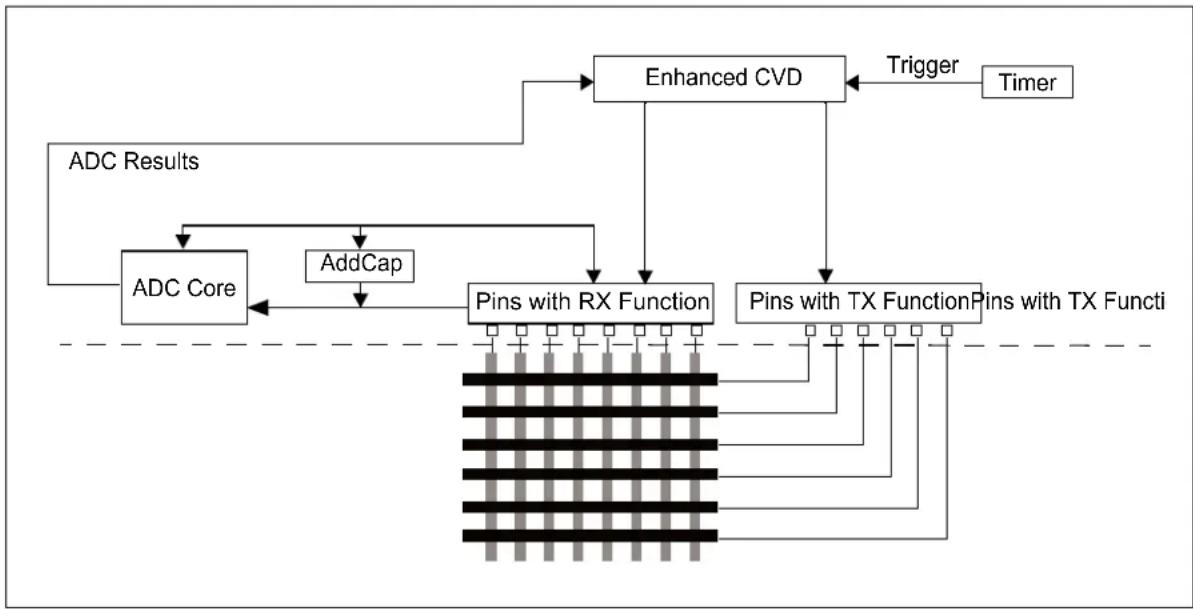
flowchart
graph TD
    A["ADC Core"] --> B["AddCap"]
    B --> C["Pins with RX Function"]
    D["Enhanced CVD"] --> E["Trigger"]
    E --> F["Timer"]
    G["ADC Results"] --> A
    H["Pins with TX Function"] --> I["Pins with TX Function"]
    I --> J["Pins with TX Function"]
    J --> K["Trigger"]
    K --> L["Timer"]
    M["Feedback to Pins with RX Function"] --> N["Feedback to AddCap"]
    N --> O["Feedback to ADC Core"]
    style A fill:#f9f,stroke:#333
    style D fill:#f9f,stroke:#333
    style G fill:#ccf,stroke:#333
    style H fill:#ccf,stroke:#333
    style I fill:#ccf,stroke:#333
    style J fill:#ccf,stroke:#333
    style K fill:#ccf,stroke:#333
    style L fill:#ccf,stroke:#333
34.2 CVD Control Registers
TABLE 34-1: ENHANCED CVD CONTROLLER REGISTER MAP SUMMARY
| Virtual Address(BF82_#) | Register Name ( 1 \ 1 ) | Bit Range | Bits | POR Values | |||||||||||||||
| 31/15 | 30/14 | 29/13 | 28/12 | 27/11 | 26/10 | 25/9 | 24/8 | 23/7 | 22/6 | 21/5 | 20/4 | 19/3 | 18/2 | 17/1 | 16/0 | ||||
| 4000 | CVDCON | 31:16 | ON | — | SIDL | ORDER | SDHOLD | — | ABORT | SWTRIG | THSTR | — | — | — | CVDIEN | FIFOIEN | FIFOTH[1:0] | 0000 | |
| 15:0 | FIFOTH[7:0] | — | — | CLKSEL[1:0] | TRIGSEL [3:0] | 0000 | |||||||||||||
| 4004 | CVDADC | 31:16 | — | — | — | — | — | — | — | — | — | — | — | — | — | — | — | — | 0000 |
| 15:0 | — | — | — | — | — | — | — | — | — | — | — | — | DIFF-PEN | DIGEN7 | SELRES[1:0] | 0000 | |||
| 4008 | CVDSTAT | 31:16 | FIFOFULL | FIFOWM | FIFOMT | — | — | — | — | FIFOCNT[9:0] | 0000 | ||||||||
| 15:0 | — | SD4INT | SD4DONE | SD4BUSY | — | SD3INT | SD3-DONE | SD3BUSY | — | SD2INT | SD2-DONE | SD2BUSY | — | SD1INT | SD1-DONE | SD1BUSY | 0000 | ||
| 400C | CVDRES0H | 31:16 | — | — | — | — | — | — | — | — | POS[7:0] | 0000 | |||||||
| 15:0 | POS[15:0] | 0000 | |||||||||||||||||
| 4010 | CVDRES0L | 31:16 | — | — | — | — | — | — | — | — | NEG[7:0] | 0000 | |||||||
| 15:0 | NEG[15:0] | 0000 | |||||||||||||||||
| 4014 | CVDRES0D | 31:16 | TXINDEX[4:0] | — | SDNUM[1:0] | RXINDEX[4:0] | — | DELTA[1:0] | 0000 | ||||||||||
| 15:0 | DELTA[15:0] | 0000 | |||||||||||||||||
| 4080 | CVDRX0 | 31:16 | — | — | RXAN3[5:0] | — | — | RXAN2[5:0] | 0000 | ||||||||||
| 15:0 | — | — | RXAN1[5:0] | — | — | RXAN0[5:0] | 0000 | ||||||||||||
| 4084 | CVDRX1 | 31:16 | — | — | RXAN7[5:0] | — | — | RXAN6[5:0] | 0000 | ||||||||||
| 15:0 | — | — | RXAN5[5:0] | — | — | RXAN4[5:0] | 0000 | ||||||||||||
| 4088 | CVDRX2 | 31:16 | — | — | RXAN11[5:0] | — | — | RXAN10[5:0] | 0000 | ||||||||||
| 15:0 | — | — | RXAN9[5:0] | — | — | RXAN8[5:0] | 0000 | ||||||||||||
| 408C | CVDRX3 | 31:16 | — | — | RXAN15[5:0] | — | — | RXAN14[5:0] | 0000 | ||||||||||
| 15:0 | — | — | RXAN13[5:0] | — | — | RXAN12[5:0] | 0000 | ||||||||||||
| 40C0 | CVDTX0 | 31:16 | — | — | TXAN3[5:0] | — | — | TXAN2[5:0] | 0000 | ||||||||||
| 15:0 | — | — | TXAN1[5:0] | — | — | TXAN0[5:0] | 0000 | ||||||||||||
| Virtual Address(BF82_#) | RegisterName | Bit Range | Bits | POR Values | |||||||||||||||
| 31/15 | 30/14 | 29/13 | 28/12 | 27/11 | 26/10 | 25/9 | 24/8 | 23/7 | 22/6 | 21/5 | 20/4 | 19/3 | 18/2 | 17/1 | 16/0 | ||||
| 40C4 | CVDTX1 | 31:16 | — | — | TXAN7[5:0] | — | — | TXAN6[5:0] | 0000 | ||||||||||
| 15:0 | — | — | TXAN5[5:0] | — | — | TXAN4[5:0] | 0000 | ||||||||||||
| 40C8 | CVDTX2 | 31:16 | — | — | TXAN11[5:0] | — | — | TXAN10[5:0] | 0000 | ||||||||||
| 15:0 | — | — | TXAN9[5:0] | — | — | TXAN8[5:0] | 0000 | ||||||||||||
| 40CC | CVDTX3 | 31:16 | — | — | TXAN15[5:0] | — | — | TXAN14[5:0] | 0000 | ||||||||||
| 15:0 | — | — | TXAN13[5:0] | — | — | TXAN12[5:0] | 0000 | ||||||||||||
| 4100 | CVDSD0C1 | 31:16 | SDOTHRESH[15:8] | 0000 | |||||||||||||||
| 15:0 | SDOTHRESH[7:0] SD0OVRSAMP[7:0] | 0000 | |||||||||||||||||
| 4104 | CVDSD0C2 | 31:16 | SDOTXSTRIDE2[1:0] SDOTXEND[5:0] SDOTXSTRIDE1[1:0] SDOTXBEG[5:0] | 0000 | |||||||||||||||
| 15:0 | SDORXSTRIDE2[1:0] SDORXEND[5:0] SDORXSTRIDE1[1:0] SDORXBEG[5:0] | 0000 | |||||||||||||||||
| 4108 | CVDSD0C3 | 31:16 | SD0EN[1:0] | — | — | SD0BUF | SD0IEN | SD0SELF | SD0MUT | — — | — | CVDEN | CVDCPL[2:0] | 0000 | |||||
| 15:0 | — | SD0ACQTIME[6:0] | — | SD0CHGTIME[6:0] | 0000 | ||||||||||||||
| 410C | CVDSD0T2 | 31:16 | — | SDOPOLTIME[6:0] | — | SD0OVRTIME[6:0] | 0000 | ||||||||||||
| 15:0 | — | SDOCHNTIME[6:0] | — | SD0CONTIME[6:0] | 0000 | ||||||||||||||
| 4110 | CVDSD1C1 | 31:16 | SD1THRESH[31:16] | 0000 | |||||||||||||||
| 15:0 | SD1THRESH[7:0] SD1OVRSAMP[7:0] | 0000 | |||||||||||||||||
| 4114 | CVDSD1C2 | 31:16 | SD1TXSTRIDE2[1:0] SD1TXEND[5:0] SD1TXSTRIDE1[1:0] SD1TXBEG[5:0] | 0000 | |||||||||||||||
| 15:0 | SD1RXSTRIDE2[1:0] SD1RXEND[5:0] SD1RXSTRIDE1[1:0] SD1RXBEG[5:0] | 0000 | |||||||||||||||||
| 411B | CVDSD1C3 | 31:16 | SD1EN[1:0] | — | — | SD1BUF | SD1IEN | SD1SELF | SD1MUT | — — | — | CVDEN | CVDCPL[2:0] | 0000 | |||||
| 15:0 | — | SD1ACQTIME[6:0] | — | SD1CHGTIME[6:0] | 0000 | ||||||||||||||
| 411C | CVDSD1T2 | 31:16 | — | SD1POLTIME[6:0] | — | SD1OVRTIME[6:0] | 0000 | ||||||||||||
| 15:0 | — | SD1CHNTIME[6:0] | — | SD1CONTIME[6:0] | 0000 | ||||||||||||||
| 4120 | CVDSD2C1 | 31:16 | SD2THRESH[31:16] | 0000 | |||||||||||||||
| 15:0 | SD2THRESH[7:0] SD2OVRSAMP[7:0] | 0000 | |||||||||||||||||
| 4124 | CVDSD2C2 | 31:16 | SD2TXSTRIDE2[1:0] SD2TXEND[5:0] SD2TXSTRIDE1[1:0] SD2TXBEG[5:0] | 0000 | |||||||||||||||
| 15:0 | SD2RXSTRIDE2[1:0] SD2RXEND[5:0] SD2RXSTRIDE1[1:0] SD2RXBEG[5:0] | 0000 | |||||||||||||||||
| 4128 | CVDSD2C3 | 31:16 | SD2EN[1:0] | — | — | SD2BUF | SD2IEN | SD2SELF | SD2MUT | — — — | CVDEN | CVDCPL[2:0 ] | 0000 | ||||||
| 15:0 | — | SD2ACQTIME[6:0] | — | SD2CHGTIME[6:0] | 0000 | ||||||||||||||
| 412C | CVDSD2T2 | 31:16 | — | SD2POLTIME[6:0] | — | SD2OVRTIME[6:0] | 0000 | ||||||||||||
| 15:0 | — | SD2CHNTIME[6:0] | — | SD2CONTIME[6:0] | 0000 | ||||||||||||||
| 4130 | CVDSD3C1 | 31:16 | SD3THRESH[31:16] | 0000 | |||||||||||||||
| 15:0 | SD3THRESH[7:0] | SD3OVRSAMP[7:0] | 0000 | ||||||||||||||||
| 4134 | CVDSD3C2 | 31:16 | SD3TXSTRIDE2[1:0] SD3TXEND[5:0] SD3TXSTRIDE1[1:0] SD3TXBEG[5:0] | 0000 | |||||||||||||||
| 15:0 | SD3RXSTRIDE2[1:0] SD3RXEND[5:0] SD3RXSTRIDE1[1:0] SD3RXBEG[5:0] | 0000 | |||||||||||||||||
| 4138 | CVDSD3C3 | 31:16 | SD3EN[1:0] | — | — | SD3BUF | SD3IEN | SD3SELF | SD3MUT | — — — | CVDEN | CVDCPL[2:0 ] | 0000 | ||||||
| 15:0 | — | SD3ACQTIME[6:0] | — | SD3CHGTIME[6:0] | 0000 | ||||||||||||||
| 413C | CVDSD3T2 | 31:16 | — | SD3POLTIME[6:0] | — | SD3OVRTIME[6:0] | 0000 | ||||||||||||
| 15:0 | — | SD3CHNTIME[6:0] | — | SD3CONTIME[6:0] | 0000 | ||||||||||||||
Legend: x = unknown value on Reset; — = unimplemented, read as '0'. Reset values are shown in hexadecimal.
REGISTER 34-1: CVDCON: CVD CONTROL REGISTER
| Bit Range | Bit31/23/15/7 | Bit30/22/14/6 | Bit29/21/13/5 | Bit28/20/12/4 | Bit27/19/11/3 | Bit26/18/10/2 | Bit25/17/9/1 | Bit24/16/8/0 |
| 31:24 | R/W-0 U-0 | R/W-0 R/W-0 | R/W-0 U-0 W/ | HC-0 W/HC-0 | ||||
| ON | — SIDL | ORDER SDW | REN — ABORT | SWTRIG | ||||
| 23:16 | R/W-0 U-0 | U-0 U-0 R/W-0 | R/W-0 R/W-1 | R/W-0 | ||||
| THSTR | — | — | — | CVDIEN | FIFOIEN | FIFOTH[9:8] | ||
| 15:8 | R/W-0 R/W-0 | R/W-0 R/W-0 | R/W-0 R/W-0 | R/W-0 | R/W-0 | |||
| FIFOTH[7:0] | ||||||||
| 7:0 | U-0 | U-0 R/W-0 | R/W-0 R/W-0 | R/W-0 R/W-0 | R/W-0 | |||
| — | — | CLKSEL[1:0] | TRIGSEL[3:0] | |||||
| Legend: HC = Hardware Cleared HS = Hardware SetR = Readable bit W = Writable bit U = Unimplemented bit, read as ‘0’-n = Value at POR ‘1’ = Bit is set ‘0’ = Bit is cleared x = Bit is unknown |
bit 31 ON: Enables the state machine to scan enabled scan descriptors upon next trigger. Before turning ON from 1'b1 to 1'b0, the Scan Enable bits of all descriptors must be cleared and the ENHANCED CVD controller must either be allowed to finish any scan in progress, or must be instructed to abort the scan with the ABORT bit.
bit 30 Unimplemented: Read as '0'
bit 29 SIDL: Stop in Idle Mode bit
1 = CVD controller halts when device enters Idle mode
0 = CVD controller continues running in Idle mode
bit 28 ORDER: RX/TX Loop Order
1 = Scan all requested TX indexes, then increment RX index and continue
0 = Scan all requested RX indexes, then increment TX index and continue
bit 27 SDWREN: Scan Descriptor Write Enable
1 = Enables writes to the scan descriptors
0 = Prevents writes to the scan descriptors
bit 26 Unimplemented: Read as '0'
bit 25 ABORT:
1 = Abort the current scan
0 = CVD controller continues with the current scan
Note: The controller will move on to the next enabled Scan Descriptor if there is one, else it will go idle. Cleared by hardware.
bit 24 SWTRIG: Software Trigger control
1 = Starts scan manually
0 = Continue without the scan
Note: Cleared by hardware.
bit 23 THSTR: Threshold Store Mode
1 = Store only results which exceed the programmed threshold for the Scan Descriptor
0 = Store all results in FIFO
bit 22-20 Unimplemented: Read as '0'
bit 19 CVDIEN: Global Interrupt Enable
1 = Enables the FIFO and scan descriptor interrupts
0 = Disables the FIFO and scan descriptor interrupts
bit 18 FIFOIEN: FIFO Threshold Interrupt Enable
1 = Controller will assert an interrupt when the FIFO threshold is met
0 = Controller will not assert an interrupt when the FIFO threshold is met
REGISTER 34-1: CVDCON: CVD CONTROL REGISTER (CONTINUED)
bit 17-8 FIFOTH[9:0]: Threshold for the results FIFO that will cause an interrupt and watermark FIFOWM status bit assertion.
bit 7-6 Unimplemented: Read as '0'
bit 5-4 CLKSEL[1:0]: Clock Select for CVD
00 = pB2_clk
01 = FRC
02 = LPRC
03 = REFO1
bit 3-0 TRIGSEL[3:0]: Selects one of 15 external trigger inputs to start scanning.
0000 = SFR controlled software trigger
0001 = TMR1 event
0010 = TMR2 event
0011 = TMR3 event
0100 = TMR4 event
0101 = TMR5 event
0110 = TMR6 event
0111 = TMR7 event
1000 = Reserved
1001 = Reserved
1010 = PTGO9
1011 =
.
.
.
.
1111 = Reserved
REGISTER 34-2: CVDADC: CVD ADC CONFIGURATION REGISTER
| Bit Range | Bit31/23/15/7 | Bit30/22/14/6 | Bit29/21/13/5 | Bit28/20/12/4 | Bit27/19/11/3 | Bit26/18/10/2 | Bit25/17/9/1 | Bit24/16/8/0 |
| 31:24 | U-0 U-0 | U-0 U-0 U-0 U-0 | U-0 U-0 | |||||
| — — — | — — — — | |||||||
| 23:16 | R/W-0 R/W-0 R/W-0 R/W-0 R/W-0 R/W-0 | R/W-0 | ||||||
| — — — | — — — — | |||||||
| 15:8 | R/W-0 R/W-0 R/W-0 R/W-0 R/W-0 R/W-0 | R/W-0 | ||||||
| — — — | — — — — | |||||||
| 7:0 | R/W-0 R/W-0 R/W-0 R/W-0 R/W-0 R/W-0 | R/W-0 | ||||||
| — | — | — | — | DIGEN7 | DIFFPEN | SELRES[1:0] | ||
Legend:
| R = Readable bit | W = Writable bit | U = Unimplemented bit, read as '0' |
| -n = Value at POR | '1' = Bit is set | '0' = Bit is cleared x = Bit is unknown |
bit 31-4 Unimplemented: Read as '0'
bit 3 DIGEN7: Shared ADC (ADC2) Digital Enable bit (Differential Mode Select from ADC controller)
1 = ADC2 is digital enabled
0 = ADC2 is digital disabled
bit 2 DIFFPEN: Control differential mode operation of ANN0
1= ANN0 (Differential) enabled
0= ANN0 (Differential) disabled
bit 1-0 SELRES[1:0]: Shared ADC (ADC2) Resolution bits
11 = 12 bits (default)
10 = 10 bits
01 = 8 bits
00 = 6 bits
Note: Changing the resolution of the ADC does not shift the result in the corresponding ADCDATAx register. The result will still occupy 12 bits, with the corresponding lower unused bits set to '0'. For example, a resolution of 6 bits will result in ADCDATAx[5:0] being set to '0', and ADCDATAx[11:6] holding the result.
REGISTER 34-3: CVDSTAT: CVD STATUS REGISTER
| Bit Range | Bit 31/23/15/7 | Bit 30/22/14/6 | Bit 29/21/13/5 | Bit 28/20/12/4 | Bit 27/19/11/3 | Bit 26/18/10/2 | Bit 25/17/9/1 | Bit 24/16/8/0 |
| 31:24 | R-0 R-0 R-0 U-0 U-0 U-0 | R-0 R-0 | ||||||
| FIFOFULL FIFOWM FIFOMT | — — — | FIFOCNT[9:8] | ||||||
| 23:16 | R-0 R-0 R-0 R-0 R-0 R-0 | R-0 R-1 | ||||||
| FIFOCNT[7:0] | ||||||||
| 15:8 | U-0 | R/W/HS-0 | R-0 | R-0 | U-0 | R/W/HS-0 | R-0 | R-0 |
| — | SD4INT | SD4DONE | SD4BUSY | — | SD3INT | SD3DONE | SD3BUSY | |
| 7:0 | U-0 | R/W/HS-0 | R/W-0 | R/W-0 | U-0 | R/W/HS-0 | R-0 | R-0 |
| — | SD2INT | SD2DONE | SD2BUSY | — | SD1INT | SD1DONE | SD1BUSY | |
| Legend: | HC = Hardware Cleared | HS = Hardware Set | |
| R = Readable bit | W = Writable bit | U = Unimplemented bit, read as ‘0’ | |
| -n = Value at POR | ‘1’ = Bit is set | ‘0’ = Bit is cleared | x = Bit is unknown |
bit 31 FIFOFULL: The Results FIFO is full.
1 = FIFO is full.
0 = Not full
bit 30 FIFOWM:
1 = FIFO has reached the programmed FIFOTHRESH threshold
0 = FIFO has not reached the programmed FIFOTHRESH threshold
bit 29 FIFOMT:
1 = FIFO is empty
0 = FIFO is not empty
bit 28-26 Unimplemented: Read as 0
bit 25-16 FIFOCNT: Results FIFO word count: Indicates the number of words in the Results FIFO.
bit 15 Unimplemented: Read as 0
bit 14 SD4INT:
1 = Scan Descriptor 4 has caused an interrupt
0 = Scan Descriptor 4 has not caused an interrupt
bit 13 SD4DONE:
1 = Scan Descriptor 4 has completed
0 = Scan Descriptor 4 has not completed
bit 12 SD4BUSY:
1 = Scan Descriptor 4 is in progress
0 = Scan Descriptor 4 is not in progress
bit 11 Unimplemented: Read as 0
bit 210 SD3NT:
1 = Scan Descriptor 3 has caused an interrupt
0 = Scan Descriptor 3 has not caused an interrupt
bit 9 SD3DONE: Core will set this bit if Scan Descriptor 3 has completed at least once. Core will clear this bit upon receiving next trigger for Scan Descriptor 3.
bit 8 SD3BUSY:
1 = Scan Descriptor 3 is in progress
0 = Scan Descriptor 3 is not in progress
bit 7 Unimplemented: Read as 0
bit 6 SD2NT:
1 = Scan Descriptor 2 has caused an interrupt
0 = Scan Descriptor 2 has not caused an interrupt
bit 5 SD2DONE: Core will set this bit if Scan Descriptor 2 has completed at least once. Core will clear this bit upon receiving next trigger for Scan Descriptor 2.
REGISTER 34-3: CVDSTAT: CVD STATUS REGISTER (CONTINUED)
bit 4 SD2BUSY:
1 = Scan Descriptor 2 is in progress
0 = Scan Descriptor 2 is not in progress
bit 3 Unimplemented: Read as 0
bit 2 SD1NT:
1 = Scan Descriptor 1 has caused an interrupt
0 = Scan Descriptor 1 has not caused an interrupt
bit 1 SD1DONE: Core will set this bit if Scan Descriptor 1 has completed at least once. Core will clear this bit upon receiving next trigger for Scan Descriptor 1.
bit 0 SD1BUSY:
1 = Scan Descriptor 1 is in progress
0 = Scan Descriptor 1 is not in progress
REGISTER 34-4: CVDRES0H: CVD RESULTS POS FIFO READ REGISTER
| Bit Range | Bit 31/23/15/7 | Bit 30/22/14/6 | Bit 29/21/13/5 | Bit 28/20/12/4 | Bit 27/19/11/3 | Bit 26/18/10/2 | Bit 25/17/9/1 | Bit 24/16/8/0 |
| 31:24 | U-0 U-0 | U-0 U-0 U-0 U-0 | U-0 U-0 | |||||
| — — — | — — — — | |||||||
| 23:16 | U-0 U-0 | U-0 U-0 U-0 U-0 | U-0 U-0 | |||||
| — — — | — — — — | |||||||
| 15:8 | U-0 U-0 | U-0 U-0 R-0 R-0 | R-0 R-0 | |||||
| — — — | — POS[11:8] | |||||||
| 7:0 | R-0 R-0 | R-0 R-0 R-0 R-0 | R-0 R-0 | |||||
| POS[7:0] | ||||||||
Legend:
R = Readable bit W = Writable bit U = Unimplemented bit, read as '0' -n = Value at POR '1' = Bit is set '0' = Bit is cleared x = Bit is unknown
bit 31-12 Unimplemented: Read as '0'
bit 11-0 POS[11:0]: The accumulated result of the positive-side measurements Since the controller supports up to 64x oversampling, each polarity can accumulate up to 12 bits.
REGISTER 34-5: CVDRES0L: CVD RESULTS NEG FIFO READ REGISTER
| Bit Range | Bit 31/23/15/7 | Bit 30/22/14/6 | Bit 29/21/13/5 | Bit 28/20/12/4 | Bit 27/19/11/3 | Bit 26/18/10/2 | Bit 25/17/9/1 | Bit 24/16/8/0 |
| 31:24 | U-0 U-0 | U-0 U-0 U-0 U-0 | U-0 U-0 | |||||
| — — — | — — — — — | |||||||
| 23:16 | U-0 U-0 | U-0 U-0 U-0 U-0 | U-0 U-0 | |||||
| — — — | — — — — — | |||||||
| 15:8 | U-0 U-0 | U-0 U-0 R-0 R-0 | R-0 R-0 | |||||
| — — — | — NEG[11:8] | |||||||
| 7:0 | R-0 R-0 | R-0 R-0 R-0 R-0 | R-0 R-0 | |||||
| NEG[7:0] | ||||||||
Legend:
| R = Readable bit W = Writable bit U = Unimplemented bit, read as '0' | ||
| -n = Value at POR | '1' = Bit is set | '0' = Bit is cleared x = Bit is unknown |
bit 31-12 Unimplemented: Read as '0'
bit 11-0 NEG[11:0]: The accumulated result of the negative-side measurements Since the controller supports up to 64x oversampling, each polarity can accumulate up to 12 bits.
REGISTER 34-6: CVDRES0D: CVD RESULTS DESCRIPTOR FIFO READ REGISTER
| Bit Range | Bit31/23/15/7 | Bit30/22/14/6 | Bit29/21/13/5 | Bit28/20/12/4 | Bit27/19/11/3 | Bit26/18/10/2 | Bit25/17/9/1 | Bit24/16/8/0 |
| 31:24 | R | - | 0 R | - | 0 | R | - | 0 R |
| TXINDEX[4:0] | — SDNUM[1:0] | |||||||
| 23:16 | R | - | 0 R | - | 0 | R | - | 0 R |
| RXINDEX[4:0] | — DELTA[17:16] | |||||||
| 15:8 | R | - | 0 R | - | 0 | R | - | 0 R |
| DELTA[15:8] | ||||||||
| 7:0 | R | - | 0 R | - | 0 | R | - | 0 R |
| DELTA[7:0] | ||||||||
Legend:
R = Readable bit W = Writable bit U = Unimplemented bit, read as '0' -n = Value at POR '1' = Bit is set '0' = Bit is cleared x = Bit is unknown
bit 31-27 TXINDEX[4:0]: Transmit Index for this result. If the Stride of the Scan Descriptor was more than one, the Transmit Index indicates the first one of the group.
bit 26 Unimplemented: Read as '0'
bit 25-24 SDNUM: Scan Descriptor Number that generated this result
bit 23-19 RXINDEX[4:0]: Receive Index for this result. If the Stride of the Scan Descriptor was more than one, the Receive Index indicates the first one of the group.
bit 18 Unimplemented: Read as '0'
bit 17-0 DELTA[17:0]: The delta of the accumulated results of the negative-side and positive-side measurements. Since the controller supports up to 64x oversampling, each polarity can accumulate up to 12 bits.
Note: Reading this register increments the FIFO read pointer, destroying the data in the previous two registers for NEG and POS absolute values. If the NEG and POS values are desired, those registers must be read BEFORE this one. If the absolute values are not required, bandwidth can be saved by reading only this descriptor register.
REGISTER 34-7: CVDRxN: CVD RECEIVE INDEX N CONFIGURATION n = 0-3
| Bit Range | Bit 31/23/15/7 | Bit 30/22/14/6 | Bit 29/21/13/5 | Bit 28/20/12/4 | Bit 27/19/11/3 | Bit 26/18/10/2 | Bit 25/17/9/1 | Bit 24/16/8/0 |
| 31:24 | U-0 U-0 | R/W-0 R/W-0 R | W-0 R/W-0 R | W-0 R/W-0 | ||||
| — — RXAN | (4n+3)[5:0] | |||||||
| 23:16 | U-0 U-0 | R/W-0 R/W-0 R | W-0 R/W-0 R | W-0 R/W-0 | ||||
| — — RXAN | (4n+2)[5:0] | |||||||
| 15:8 | U-0 U-0 | R/W-0 R/W-0 R | W-0 R/W-0 R | W-0 R/W-0 | ||||
| — — RXAN | (4n+1)[5:0] | |||||||
| 7:0 | U-0 U-0 | R/W-0 R/W-0 R | W-0 R/W-0 R | W-0 R/W-0 | ||||
| — — RXAN | (4n+0)[5:0] | |||||||
Legend:
| R = Readable bit W = Writable bit U = Unimplemented bit, read as '0' |
| -n = Value at POR '1' = Bit is set '0' = Bit is cleared x = Bit is unknown |
bit 31-30 Unimplemented: Read as '0'
bit 29-24 RXAN[4n+3][5:0]: ANx/CVDR channel to use for RX Index 4n+3
bit 23-22 Unimplemented: Read as '0'
bit 21-16 RXAN[4n+2][5:0]: ANx/CVDR channel to use for RX Index 4n+2
bit 15-14 Unimplemented: Read as '0'
bit 13-8 RXAN[4n+1][5:0]: ANx/CVDR channel to use for RX Index 4n+1
bit 7-6 Unimplemented: Read as '0'
bit 5-0 RXAN[4n+0][5:0]: ANx/CVDR channel to use for RX Index 4n+0
REGISTER 34-8: CVDTXn: CVD TRANSMIT INDEX n CONFIG n = 0-3
| Bit Range | Bit31/23/15/7 | Bit30/22/14/6 | Bit29/21/13/5 | Bit28/20/12/4 | Bit27/19/11/3 | Bit26/18/10/2 | Bit25/17/9/1 | Bit24/16/8/0 |
| 31:24 | U-0 U-0 | R/W-0 R/W-0 | R/W-0 R/W-0 | R/W-0 R/W-0 | ||||
| — — TXAN | (4n+3)[5:0] | |||||||
| 23:16 | U-0 U-0 | R/W-0 R/W-0 | R/W-0 R/W-0 | R/W-0 R/W-0 | ||||
| — — TXAN | (4n+2)[5:0] | |||||||
| 15:8 | U-0 U-0 | R/W-0 R/W-0 | R/W-0 R/W-0 | R/W-0 R/W-0 | ||||
| — — TXAN | (4n+1)[5:0] | |||||||
| 7:0 | U-0 U-0 | R/W-0 R/W-0 | R/W-0 R/W-0 | R/W-0 R/W-0 | ||||
| — — TXAN | (4n+0)[5:0] | |||||||
Legend:
R = Readable bit W = Writable bit U = Unimplemented bit, read as '0'
-n = Value at POR '1' = Bit is set '0' = Bit is cleared x = Bit is unknown
bit 31-30 Unimplemented: Read as '0'
bit 29-24 TXAN[4n+3][5:0]: ANx/CVDR channel to use for TX Index 4n+3
bit 23-22 Unimplemented: Read as '0'
bit 21-16 TXAN[4n+2][5:0]: ANx/CVDR channel to use for TX Index 4n+2
bit 15-14 Unimplemented: Read as '0'
bit 13-8 TXAN[4n+1][5:0]: ANx/CVDR channel to use for TX Index 4n+1
bit 7-6 Unimplemented: Read as '0'
bit 5-0 TXAN[4n+0][5:0]: ANx/CVDR channel to use for TX Index 4n+0
REGISTER 34-9: CVDSDnC1: CVD SCAN DESCRIPTOR n CONTROL 1, n = 0-3
| Bit Range | Bit31/23/15/7 | Bit30/22/14/6 | Bit29/21/13/5 | Bit28/20/12/4 | Bit27/19/11/3 | Bit26/18/10/2 | Bit25/17/9/1 | Bit24/16/8/0 |
| 31:24 | R/W-0 R/W | -0 R/W-0 R/W | -0 R/W-0 R/W | -0 R/W-0 R/W | 0 | |||
| SDnTH[23:16] | ||||||||
| 23:16 | R/W-0 R/W | -0 R/W-0 R/W | -0 R/W-0 R/W | -0 R/W-0 R/W | 0 | |||
| SDnTH[15:8] | ||||||||
| 15:8 | R/W-0 R/W | -0 R/W-0 R/W | -0 R/W-0 R/W | -0 R/W-0 R/W | 0 | |||
| SDnTH[7:0] | ||||||||
| 7:0 | R/W-0 R/W | -0 R/W-0 R/W | -0 R/W-0 R/W | -0 R/W-0 R/W | 0 | |||
| SDnOVRSAMP[7:0] | ||||||||
Legend:
R = Readable bit W = Writable bit U = Unimplemented bit, read as '0'
-n = Value at POR '1' = Bit is set '0' = Bit is cleared x = Bit is unknown
bit 31-8 SDnTH[23:0]: Scan Descriptor Threshold
The accumulators are subtracted after all oversampling is completed. The result of that subtraction is compared to this threshold to generate an interrupt and/or store data to the FIFO based on the configuration.
bit 7-0 SDnOVR SAMP[7:0]: Scan Descriptor Over Sampling
Determines the amount of oversampling done on each measurement.
0 = Only one measurement
1 = Two measurements accumulated
255 = 256 measurements accumulated
REGISTER 34-10: CVDSDnC2: CVD SCAN DESCRIPTOR n CONTROL 2, n = 0-3
| Bit Range | Bit 31/23/15/7 | Bit 30/22/14/6 | Bit 29/21/13/5 | Bit 28/20/12/4 | Bit 27/19/11/3 | Bit 26/18/10/2 | Bit 25/17/9/1 | Bit 24/16/8/0 |
| 31:24 | R/W-0 R/W | -0 R/W-0 R/W | -0 R/W-0 R/W | -0 R/W-0 R/W-0 | ||||
| SDnTXSTRIDE[3:2] SDn | TXEND[5:0] | |||||||
| 23:16 | R/W-0 R/W | -0 R/W-0 R/W | -0 R/W-0 R/W | -0 R/W-0 R/W-0 | ||||
| SDnTXSTRIDE[1:0] SDn | TXBEG[5:0] | |||||||
| 15:8 | R/W-0 R/W | -0 R/W-0 R/W | -0 R/W-0 R/W | -0 R/W-0 R/W-0 | ||||
| SDnTXSTRIDE[3:2] SDn | RXEND[5:0] | |||||||
| 7:0 | R/W-0 R/W | -0 R/W-0 R/W | -0 R/W-0 R/W | -0 R/W-0 R/W-0 | ||||
| SDnTXSTRIDE[1:0] SDn | RXBEG[5:0] | |||||||
Legend:
R = Readable bit W = Writable bit U = Unimplemented bit, read as '0'
-n = Value at POR '1' = Bit is set '0' = Bit is cleared x = Bit is unknown
bit 31-30 SDnTXSTRIDE[3:2]: Scan Descriptor TX Index Stride
Determines the number of TX Indexes included in a single measurement.
4'h0: One TX Index
4'bF: 16TX Indexes
bit 29-24 SDnTXEND[5:0]: Scan Descriptor TX Index End
Determines the last TX index to include in a scan. One the TX index pointer, which is incremented by the
SDnTXSTRIDE+1 value, meets or exceeds this value, the TX loop of the scan is complete.
bit 23-22 SDnRXSTRIDE[3:2]: Scan Descriptor TX Index Stride
Determines the number of TX Indexes included in a single measurement.
4'h0: One TX Index
4'bF: 16TX Indexes
bit 21-16 SDnTXBEG[5:0]: Scan Descriptor TX Index Start
Determines the first TX index to include in a scan.
bit 15-14 SDnRXSTRIDE[3:2]: Scan Descriptor RX Index Stride
Determines the number of TX Indexes included in a single measurement.
4'h0: One TX Index
4'bF: 16TX Indexes
bit 13-8 SDnRXEND[5:0]: Scan Descriptor RX Index End
Determines the last RX index to include in a scan. One the RX index pointer, which is incremented by the SDnRXSTRIDE+1 value, meets or exceeds this value, the RX loop of the scan is complete.
bit 7-6 SDnRXSTRIDE[1:0]: Scan Descriptor RX Index Stride
Determines the number of RX Indexes included in a single measurement.
4'h0: One RX Index
4'hF: 16 TX Indexes
bit 5-0 SDnRXBEG[5:0]: Scan Descriptor RX Index Start
Determines the first RX index to include in a scan.
REGISTER 34-11: CVDSDnC3: CVD SCAN DESCRIPTOR n CONTROL 3, n = 0-3
| Bit Range | Bit 31/23/15/7 | Bit 30/22/14/6 | Bit 29/21/13/5 | Bit 28/20/12/4 | Bit 27/19/11/3 | Bit 26/18/10/2 | Bit 25/17/9/1 | Bit 24/16/8/0 |
| 31:24 | R/W/HC-0 R/W/HC-0 U-0 U-0 | R/W-0 R/W-0 R/W-0 R/W-0 | ||||||
| SDnEN[1:0] | — — SDnBUF SDnINTEN SDnSELF SDnMUT | |||||||
| 23:16 | R/W-0 | R/W-0 | R/W-0 | R/W-0 | R/W-0 | R/W-0 | R/W-0 | R/W-0 |
| — | — | — — | CVDEN | CVDCPL[2:0] | ||||
| 15:8 | U-0 | R/W-0 | R/W-0 | R/W-0 | R/W-0 | R/W-0 | R/W-0 | R/W-0 |
| — | SDnACQTIME[6:0] | |||||||
| 7:0 | U-0 | R/W-0 | R/W-0 | R/W-0 | R/W-0 | R/W-0 | R/W-0 | R/W-0 |
| — | SDnCHGTIME[6:0] | |||||||
| Legend: | HC = Hardware Cleared | HS = Hardware Set |
| R = Readable bit | W = Writable bit | U = Unimplemented bit, read as ‘0’ |
| -n = Value at POR | ‘1’ = Bit is set | ‘0’ = Bit is cleared x = Bit is unknown |
bit 31-30 SDnEN[1:0]: Scan Descriptor Enable Mode
00 = Scan Descriptor Disabled
01 = Execute Scan Descriptor one time only, then clear the enable.
10 = Execute the Scan Descriptor, but keep enabled. Move on to next enabled descriptors.
11 = Execute the Scan Descriptor in a loop until a threshold match is detected, then clear the enable and move on to next enabled descriptors.
bit 29-28 Unimplemented: Read as '0'
bit 27 SDnBUF: Scan Descriptor CVD Buffer Enable
1 = CVD buffer output used as shared ADC (ADC2) input.
0 = CVD buffer output not used as shared ADC (ADC2) input
bit 26 SDnINTEN: Scan Descriptor Interrupt Enable
1 = Scan Descriptor creates an interrupt if the accumulator threshold is met
0 = Scan descriptor does not create an interrupt
bit 25 SDnSELF: Scan Descriptor Mutual Mode
1 = Self Measurement Mode; RX outputs are part of CVD measurement and are driven
0 = No Self Measurement; RX outputs are not part of CVD measurements
bit 24 SDnMUT: Scan Descriptor Mutual Mode
1 = Mutual Measurement Mode; TX outputs are part of CVD measurement and are driven
0 = No Mutual Measurement Mode; TX outputs are not part of CVD measurements
bit 23-20 Unimplemented: Read as '0'
bit 19 CVDEN: Capacitive Voltage Division Enable bit
1 = CVD operation is enabled
0 = CVD operation is disabled
bit 18-16 CVDCPL[2:0]: Capacitor Voltage Divider (CVD) Setting bits
111 = 7 * 2.5 pF = 17.5 pF
110 = 6 * 2.5 pF = 15 pF
101 = 5 * 2.5 pF = 12.5 pF
100 = 4 * 2.5 pF = 10 pF
011 = 3 * 2.5 pF = 7.5 pF
010 = 2 * 2.5 pF = 5 pF
001 = 1 * 2.5 pF = 2.5 pF
000 = 0 * 2.5 pF = 0 pF
bit 15 Unimplemented: Read as '0'
bit 14-8 SDnACQTIME[6:0]: Scan Descriptor Acquire Time
Time for which CVD waits for ADC voltage to settle.
bit 7 Unimplemented: Read as '0'
REGISTER 34-11: CVDSDnC3: CVD SCAN DESCRIPTOR n CONTROL 3, n = 0-3 (CONTINUED)
bit 6-0 SDnCHGTIME[6:0]: Scan Descriptor Charge Time
Time for which CVD remains in the charging state for internal/external capacitors and for TX outputs.
REGISTER 34-12: CVDSDnT2: CVD SCAN DESCRIPTOR n TIME 2, n = 1-4
| Bit Range | Bit 31/23/15/7 | Bit 30/22/14/6 | Bit 29/21/13/5 | Bit 28/20/12/4 | Bit 27/19/11/3 | Bit 26/18/10/2 | Bit 25/17/9/1 | Bit 24/16/8/0 |
| 31:24 | U-0 R/W-0 | R/W-0 R/W-0 | R/W-0 R/W-0 | R/W-0 R/W-0 | ||||
| — SDnP | OLTIME[6:0] | |||||||
| 23:16 | U-0 R/W-0 | R/W-0 R/W-0 | R/W-0 R/W-0 | R/W-0 R/W-0 | ||||
| — SDnQ | VRTIME[6:0] | |||||||
| 15:8 | U-0 U-0 | U-0 U-0 U-0 | U-0 U-0 | |||||
| — SDnCHNTIME[6:0] | ||||||||
| 7:0 | U-0 R/W-0 | R/W-0 R/W-0 | R/W-0 R/W-0 | R/W-0 R/W-0 | ||||
| — SDnC | ONTIME[6:0] | |||||||
Legend:
R = Readable bit W = Writable bit U = Unimplemented bit, read as '0'
-n = Value at POR '1' = Bit is set '0' = Bit is cleared x = Bit is unknown
bit 31 Unimplemented: Read as '0'
bit 30-24 SDnPOLTIME[6:0]: Scan Descriptor Polarity Time
Controls the number of cycles the state machine waits in the POLARITY state before taking the second polarity measurement of an RX/TX pair
bit 23 Unimplemented: Read as '0'
bit 22-16 SDnOVRTIME[6:0]: Scan Descriptor Oversample Time
Controls the number of cycles the state machine waits in the OVERSAMP state before taking the next oversampling measurement of an RX/TX pair.
bit 15 Unimplemented: Read as '0'
bit 14-8 SDnCHNTIME[6:0]: Scan Descriptor Channel Time
Controls the number of cycles the state machine waits in the RXCHAN or TXCHAN state before moving to the next RX/TX pair.
bit 7 Unimplemented: Read as '0'
bit 6-0 SDnCONTIME[6:0]: Scan Descriptor Charge Time
Controls the number of cycles the state machine waits in the CONVERT state waiting for the ADC sample data. It must be ensured that the ADC will assert End-Of-Convert (EOC) before the CONVERT state timer expires.
35.0 POWER MANAGEMENT UNIT (PMU)
This section describes PMU features of the PIC32MZ W1 devices. These devices offer various methods to monitor and program the BUCK/MLDO regulators.
Key features of the PMU include:
- Two-stage voltage regulation for optimal performance (stage1 – BUCK/MLDO, stage2 – LDOs)
- Seamless power-up in MLDO mode and Low Power mode exit without the need for PMU configurations and system clock dependency.
-
Auto-configuration of LDO and PMU modes for optimal power at various device operating modes.
-
Support override method for LDO and PMU mode configurations. Software can use the override feature if required.
- A memory mapped interface for programming BUCK/MLDO.
- Provides a register locking feature to avoid accidental writes to the critical PMU control registers.
- Provides a WOFF mode and WCM Retention mode in tandem with Wi-Fi low power modes.
- Provides a Wi-Fi Context Memory (WCM) retention feature to save necessary context while entering low power mode.
See Table 41-4 for more information.
FIGURE 35-1: TOPOLOGY ON CHIP DC-DC AND REGULATORS
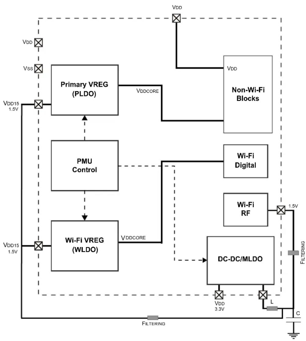
flowchart
graph TD
    A["Primary VREG (PLDO)"] -->|VDDCORE| B["Non-Wi-Fi Blocks"]
    C["PMU Control"] --> D["Wi-Fi Digital"]
    E["Wi-Fi VREG (WLDO)"] -->|VDDCORE| F["DC-DC/MLDO"]
    G["VDD15 1.5V"] --> A
    H["VDD 3.3V"] --> F
    I["VDD"] --> B
    J["Vss"] --> A
    K["VDD15 1.5V"] --> C
    L["C"] --> M["Filtering"]
    N["VDD"] --> B
    O["VDD"] --> B
    P["VDD"] --> B
    Q["VDD"] --> B
    R["VDD"] --> B
    S["VDD"] --> B
    T["VDD"] --> B
    U["VDD"] --> B
    V["L"] --> F
    W["FILTERING"] --> X["Ground"]
35.1 PMU Operations
The PMU controller can support 2 modes of controlling the system:
-
Hardware/Auto Switch mode – In this mode, the hardware automatically selects the power profile under system sleep entry/exit state based on the user configurations.
-
Software-based Override mode – In this mode, the user can change the current power profile on
the fly. The PMU also provides a software-based option to automatically turn OFF/ON the WLAN and WCM (Wi-Fi Context Memory) in system Low Power mode. For more details, refer to Section 36.6 "Wi-Fi Power Save Modes".
The following table provides more details on the configuration and usage of power modes.
TABLE 35-1: PMU OPERATIONS
| Condition Configuration/Usage | |
| Hardware/Auto Switch mode | PMUOVERCTRL.PHWC = 1, configure the PMUMODECTRL1 and PMUMODECTRL2 registers with appropriate Sleep and Run mode application profiles.Program PMUOVERCRL.PHWC = 0Mode based (Sleep/Run) power profile switching is enabled in hardware from here on.Power profile modes are switched in hardware on sleep entry/exit without software intervention.PMUSTATUS register provides current state of the PMU and LDOs for the users to monitor. |
| Software-based Override mode | PMUOVERCTRL.PHWC = 0Changes needed to the PMU power profiles are realized by simply writing into OVERCTRL register and PMUOVERCTRL.OVEREN = 1.Change in power profile via PMUOVERCTRL register write is still handled in HWPMUSTATUS register provides current state of the PMU. |
| WOFF mode • Configure the PMUCLKCTRL.WLDOFF = 1. | Subsequent entry into Sleep mode will turn OFF the WLDO.Subsequent Sleep mode exit will turn ON the WLDO. |
| WCM Retention mode • Configure PMUCLKCTRL.WCMRET = 1. | On subsequent entry into Sleep/Deep Sleep mode, the WCM will be put into retention/true-retention.On subsequent Sleep/Deep Sleep mode exit, the WCM will be out of retention. |
35.2 PMU Controller Registers
TABLE 35-2: PMU CONTROLLER REGISTER MAP
Legend: x = unknown value on Reset; — = unimplemented, read as '0'. Reset values are shown in hexadecimal.
Note 1: These register bits are only writable when PMULOCK Configuration (CFGCON0[10]) bit is '0'
2: The user must use the calibrated values from the NVRFLASH area for reliable operation.
REGISTER 35-1: PMUCLKCTRL: PMU CLOCK CONTROL REGISTER
| Bit Range | Bit 31/23/15/7 | Bit 30/22/14/6 | Bit 29/21/13/5 | Bit 28/20/12/4 | Bit 27/19/11/3 | Bit 26/18/10/2 | Bit 25/17/9/1 | Bit 24/16/8/0 |
| 31:24 | R/W/L-0 R/W/ | L-0 U-0 U-0 U-0 | U-0 U-0 U-0 | |||||
| WCMRET WLDOOFF | — — — | — — — | ||||||
| 23:16 | U-0 | U-0 | U-0 U-0 | U-0 U-0 U-0 U-0 | ||||
| — | — | — — — | — — — | |||||
| 15:8 | U-0 | U-0 | U-0 U-0 | U-0 U-0 U-0 U-0 | ||||
| — | — | — — — | — — — | |||||
| 7:0 | U-0 | U-0 | U-0 U-0 | U-0 U-0 U-0 U-0 | ||||
| — | — | — — — | — — — | |||||
Legend:
| R = Readable bit | W = Writable bit | U = Unimplemented bit, read as '0' |
| -n = Value at POR | '1' = Bit is set | '0' = Bit is cleared L = Lockable bit |
bit 31 WCMRET: Wi-Fi Context Memory Retention Mode bit
1 = WCM is kept in Retention mode in Sleep mode
0 = WCM in Normal mode
bit 30 WLDOOFF: Wi-Fi LDO Control bit
1 = WLDO is turned OFF in Sleep mode
0 = WLDO is kept ON in Sleep mode
bit 29-16 Unimplemented: Read as '0'
REGISTER 35-2: PMUMODECTRL(N): PMU MODE CONTROL REGISTER, WHERE N = 1 TO 4
| Bit Range | Bit 31/23/15/7 | Bit 30/22/14/6 | Bit 29/21/13/5 | Bit 28/20/12/4 | Bit 27/19/11/3 | Bit 26/18/10/2 | Bit 25/17/9/1 | Bit 24/16/8/0 |
| 31:24 | R/W/L-1 R/W/L-0 R/W/L-0 U-0 U-0 U-0 U-0 | U-0 | ||||||
| BUCKEN MLDOEN BUCKMODE | — — — | — — | ||||||
| 23:16 | U-0 U-0 | U-0 | U-0 U-0 | U-0 U-0 U-0 | ||||
| — | — | — | — — — | — — | ||||
| 15:8 | U-0 U-0 | U-0 | U-0 U-0 | U-0 U-0 U-0 | ||||
| — | — | — | — — — | — — | ||||
| 7:0 | U-0 U-0 | U-0 | U-0 U-0 | U-0 U-0 U-0 | ||||
| — | — | — | — — — | — — | ||||
Legend:
| R = Readable bit | W = Writable bit | U = Unimplemented bit, read as '0' |
| -n = Value at POR | '1' = Bit is set | '0' = Bit is cleared L = Lockable bit |
bit 31 BUCKEN: BUCK Enable Register bit
1 = DC-DC enabled and operational
0 = DC-DC is powered down
Note: This bit is only writable when CFGCON0.PMULOCK = 0.
bit 30 MLDOEN: MLDO Enable Register bit
1 = MLDO enabled
0 = MLDO disabled
Note: This bit is only writable when CFGCON0.PMULOCK = 0.
bit 29 BUCKMODE: BUCK Operational Mode bit
1 = PWM mode
0 = PSM mode
Note: This bit is only writable when CFGCON0.PMULOCK = 0.
bit 28-0 Unimplemented: Read as '0'
REGISTER 35-3: PMUOVERCTRL: PMU OVERRIDE CONTROL REGISTER
| Bit Range | Bit 31/23/15/7 | Bit 30/22/14/6 | Bit 29/21/13/5 | Bit 28/20/12/4 | Bit 27/19/11/3 | Bit 26/18/10/2 | Bit 25/17/9/1 | Bit 24/16/8/0 |
| 31:24 | R/W/L-1 R/W | L-0 R/W/L-0 U | -0 U-0 U-0 U-0 U | -0 | ||||
| OBUCKEN OMLDOEN OBUCKMODE | — — — | — | — | |||||
| 23:16 | R/W/L-0 R/W | L-1 | U-0 | U-0 U-0 U-0 U-0 | U-0 | |||
| OVEREN PHWC | — | — — — | — | — | ||||
| 15:8 | U-0 | U-0 U-0 | U-0 U-0 U-0 U-0 U-0 | |||||
| — | — | — | — | — | — | — | — | |
| 7:0 | U-0 | U-0 U-0 | U-0 U-0 U-0 U-0 U-0 | |||||
| — | — | — | — | — | — | — | — | |
Legend:
| R = Readable bit | W = Writable bit | U = Unimplemented bit, read as '0' |
| -n = Value at POR | '1' = Bit is set | '0' = Bit is cleared L = Lockable bit |
bit 31 OBUCKEN: BUCK Enable Register bit
1 = DC-DC enabled and operational
0 = DC-DC is powered down
Note: This bit is only writable when CFGCON0.PMULOCK = 0.
bit 30 OMLDOEN: MLDO Enable Register bit
1 = MLDO enabled
0 = MLDO disabled
Note: This bit is only writable when CFGCON0.PMULOCK = 0.
bit 29 BUCKMODE: BUCK Operational Mode bit
1 = PWM mode
0 = PSM mode
Note: This bit is only writable when CFGCON0.PMULOCK = 0.
bit 28-24 Unimplemented: Read as '0'
bit 23 OVEREN: BUCK Control Override
1 = Override enabled
0 = Override disabled
Note: This bit is only writable when CFGCON0.PMULOCK = 0.
bit 22 PHWC: Power-up Hardware Control Enable
1 = Enabled
0 = Disabled
bit 21-0 Unimplemented: Read as '0'
REGISTER 35-4: PMUCMODE: PMU CURRENT MODE REGISTER
| R = Readable bit W = Writable bit | U = Unimplemented bit, read as '0' | ||
| -n = Value at POR | '1' = Bit is set | '0' = Bit is cleared | x = Bit is unknown |
bit 31 CBUCKEN: BUCK Enable Register bit
1 = DC-DC enabled and operational
0 = DC-DC is powered down
bit 30 CMLDOEN: MLDO Enable Status Register bit
1 = MLDO enabled
0 = MLDO disabled
bit 29 CBUCKMODE: BUCK Operational Mode bit
1 = PWM mode
0 = PSM mode
bit 28-0 Unimplemented: Read as '0'
R = Readable bit W = Writable bit U = Unimplemented bit, read as '0'
-n = Value at POR '1' = Bit is set '0' = Bit is cleared x = Bit is unknown
bit 31-6 Unimplemented: Read as '0'
bit 5 WCMRM: WCM has entered or begin to enter the retention mode. Accesses are blocked.
1 = WCM in Retention mode or beginning to enter the retention mode. Accesses are blocked.
0 = WCM out of Retention mode and can be accessed.
bit 4-0 Unimplemented: Read as '0'
REGISTER 35-6: PMUSEQ(n): PMU SEQUENCE REGISTER
| Bit Range | Bit 31/23/15/7 | Bit 30/22/14/6 | Bit 29/21/13/5 | Bit 28/20/12/4 | Bit 27/19/11/3 | Bit 26/18/10/2 | Bit 25/17/9/1 | Bit 24/16/8/0 |
| 31:24 | R-cfg R-cfg R-cfg R-cfg R-cfg | |||||||
| SPIDATA[15:8] | ||||||||
| 23:16 | R-cfg R-cfg R-cfg R-cfg R-cfg | |||||||
| SPIDATA[7:0] | ||||||||
| 15:8 | R-cfg R-cfg R-cfg R-cfg R-cfg | |||||||
| SPIADDR[7:0] | ||||||||
| 7:0 | R-cfg R-cfg R-cfg R-cfg R-cfg R-cfg | |||||||
| CMD CMPBVAL DELAY[5:0] | ||||||||
Legend:
R = Readable bit W = Writable bit U = Unimplemented bit, read as '0' cfg = Configurable at Reset '1' = Bit is set '0' = Bit is cleared
bit 31-16 SPIDATA[15:0]: SPI Data
SPI read data compare if CMD = 1
SPI write data if CMD = 0
bit 15-8 SPIADDR[7:0]: SPI Address
SPI read address if CMD = 1
SPI write address if CMD = 0
bit 7 CMD: SPI Command bit
1 = SPI read command
0 = SPI write command
bit 6 CMPBVAL: Command to set the compare bit value in read sequence
1 = Compare for bit value 1. Bit value of '0' in SPIDATA is ignored for comparison.
0 = Compare for bit value 0. Bit value of '1' in SPIDATA is ignored for comparison
bit 5-0 DELAY[5:0]: Delay
REGISTER 35-7: PMUCFG: PMU CONFIGURATION REGISTER
| Bit Range | Bit 31/23/15/7 | Bit 30/22/14/6 | Bit 29/21/13/5 | Bit 28/20/12/4 | Bit 27/19/11/3 | Bit 26/18/10/2 | Bit 25/17/9/1 | Bit 24/16/8/0 |
| 31:24 | U-0 U-0 | U-0 U-0 U-0 U-0 | U-0 U-0 | |||||
| — — — | — — — — — | |||||||
| 23:16 | U-0 U-0 | U-0 U-0 U-0 U-0 | U-0 U-0 | |||||
| — — — — | — | — — — — | ||||||
| 15:8 | U-0 U-0 | U-0 U-0 U-0 U-0 | U-0 U-0 | |||||
| — — — — | — | — — — — | ||||||
| 7:0 | U-0 | U-0 | R-cfg | R-cfg | R-cfg | R-cfg | R-cfg | R-cfg |
| — — | DELAY[5:0] | |||||||
Legend:
| R = Readable bit | W = Writable bit | U = Unimplemented bit, read as '0' |
| cfg = Configurable at Reset | '1' = Bit is set | '0' = Bit is cleared |
bit 31-7 Unimplemented: Read as '0'
bit 5-0 DELAY[5:0]: Delay
REGISTER 35-8: PMUWCMCMD: PMU WI-FI CONTEXT MEMORY COMMAND REGISTER
| Bit Range | Bit 31/23/15/7 | Bit 30/22/14/6 | Bit 29/21/13/5 | Bit 28/20/12/4 | Bit 27/19/11/3 | Bit 26/18/10/2 | Bit 25/17/9/1 | Bit 24/16/8/0 |
| 31:24 | U-0 U-0 | U-0 R-1 U-0 | U-0 U-0 U-0 | |||||
| — — — | WCMRDY — | — | — | — | ||||
| 23:16 | U-0 U-0 | U-0 U-0 U-0 | U-0 U-0 U-0 | |||||
| — | — | — | — | — | — | — | — | |
| 15:8 | U-0 U-0 | U-0 U-0 U-0 | U-0 U-0 U-0 | |||||
| — | — | — | — | — | — | — | — | |
| 7:0 | U-0 U-0 | U-0 U-0 U-0 | U-0 U-0 U-0 | |||||
| — | — | — | — | — | — | — | — |
Legend:
| R = Readable bit | W = Writable bit | U = Unimplemented bit, read as '0' |
| -n = Value at POR | '1' = Bit is set | '0' = Bit is cleared x = Bit is unknown |
bit 31-29 Unimplemented: Read as '0'
bit 28 WCMRDY: PMU WCM Ready Flag
1 = PMU WCM transaction is complete or PMU WCM is ready for next WCM command.
0 = PMU WCM transaction in progress or WCM is busy
bit 27-0 Unimplemented: Read as '0'
36.0 POWER-SAVING FEATURES
This section describes power-saving features for the PIC32MZ1025W104 devices. These devices offer various methods and modes that allow the user to balance power consumption with device performance. In all of the methods and modes described in this section, power-saving is controlled by software.
36.1 Power-Saving with PMU Configuration
System efficiency can be further improved by effectively configuring the Buck/MLDO regulator operational mode while the system is in the Run, Idle or Sleep mode. Buck/MLDO can operate in 3 different modes, namely:
- MLDO mode: This mode is for soft start-up during power-up and after wake-up from Deep Sleep and Extreme Deep Sleep modes. This mode provides reliable soft start-up with factory calibrated values. It enables the system start-up with intermediate load and low efficiency.
- Buck-PWM (Pulse Width Modulation) mode or high power mode: In this mode, the PMU can deliver the highest output current with good efficiency. In PWM, it is expected to reach its highest efficiency under high load conditions, and efficiency decreases with load current.
- Buck-PSM (Pulse-Skipping Mode): In this mode, the PMU can deliver good efficiency for the lower load current.
PMU operational modes can switch automatically based on the system configuration. When the load current demand is high, it is advisable to configure the PMU in the Buck-PWM mode, and when the load current demand is low, it is advisable to enter the Buck-PSM mode. For more details on the system configuration for the PMU modes of operation, refer to Section 35.0 "Power Management Unit (PMU)".
36.2 Power-Saving with CPU Running
When the CPU is running, power consumption can be controlled by reducing the CPU clock frequency, lowering the speed of PBCLK6 or selecting a lower power clock source (LPRC or SOSC).
In addition, the Peripheral Bus Scaling mode is available for each peripheral bus where peripherals are clocked at reduced speed by selecting a higher divider for the associated PBCLKx, or by selectively disabling the clock completely. Power can be further reduced by disabling the peripheral using PMD. For more details, refer to Section 36.3 "Peripheral Module Disable".
36.2.1 Wi-Fi POWER-SAVE MODE WITH MCU IN RUN MODE
When the CPU is running, power can be reduced in WOFF mode, which turns off Wi-Fi. For more details on WOFF mode configuration, refer to Section 35.0 "Power Management Unit (PMU)".
TABLE 36-1: WI-FI POWER-SAVE MODE WITH MCU IN RUN MODE
| CPU State MCU Mode | Wi-Fi Power Save Mode |
| RUN RUN RUN | |
| WOFF |
36.3 Peripheral Module Disable
The Peripheral Module Disable (PMD) registers provide a method to disable a peripheral module by stopping all clock sources supplied to that module. When a peripheral is disabled using the appropriate PMD control bit, the peripheral is in a minimum power consumption state. The control and status registers associated with the peripheral are also disabled, so writes to those registers do not have an effect and the read values are invalid.
To disable a peripheral, the associated PMDx bit must be set to '1'. To enable a peripheral, the associated PMDx bit must be cleared (default). See Table 36-1 for more information.
Note: Disabling a peripheral module while its ON bit is set, may result in undefined behavior. The ON bit for the associated peripheral module must be cleared prior to disabling a module via the PMDx bits.
TABLE 36-2: PERIPHERAL MODULE DISABLE BITS AND LOCATIONS
| Peripheral PMDx Bit Name | Register Name and Bit Location | |
| ADC SAR0 | ADCSAR0MD | PMD1[0] |
| PLVD | PLVD1MD | PMD1[4] |
| Shared ADC SAR | ADCSARSHRMD | PMD1[7] |
| ADC | ADC1MD | PMD1[8] |
| PTG | PTGMD | PMD1[11] |
| CVD | CVD1MD | PMD1[15] |
| RTCC | RTCC1MD | PMD1[16] |
| Peripheral | PMDx Bit Name | Register Name and Bit Location |
| DMA DMA1MD PMD1[19] | ||
| Asymmetric crypto BA414MD PMD1[23] | ||
| Crypto CRYPT1MD PMD1[24] | ||
| Random Number Generator RNG1MD | PMD1[26] | |
| SQI SQI1MD PMD1[29] | ||
| Input Capture 1 IC1MD PMD2[0] | ||
| Input Capture 2 IC2MD PMD2[1] | ||
| Input Capture 3 IC3MD PMD2[2] | ||
| Input Capture 4 IC4MD PMD2[3] | ||
| Output Compare 1 OC1MD PMD2[8] | ||
| Output Compare 2 OC2MD PMD2[9] | ||
| Output Compare 3 OC3MD PMD2[10] | ||
| Output Compare 4 OC4MD PMD2[11] | ||
| Timer 1 | T1MD | PMD2[16] |
| Timer 2 | T2MD | PMD2[17] |
| Timer 3 | T3MD | PMD2[18] |
| Timer 4 | T4MD | PMD2[19] |
| Timer 5 | T5MD | PMD2[20] |
| Timer 6 | T6MD | PMD2[21] |
| Timer 7 | T7MD | PMD2[22] |
| Reference Clock Output 1 | REFO1MD | PMD2[28] |
| Reference Clock Output 2 | REFO2MD | PMD2[29] |
| Reference Clock Output 3 | REFO3MD | PMD2[30] |
| Reference Clock Output 4 | REFO4MD | PMD2[31] |
| UART1 | U1MD | PMD3[0] |
| UART2 | U2MD | PMD3[1] |
| UART3 | U3MD | PMD3[2] |
| Ethernet | ETH1MD | PMD3[4] |
| SPI1 | SPI1MD | PMD3[8] |
| SPI2 | SPI2MD | PMD3[9] |
| Wi-Fi | W24GMD | PMD3[12] |
| I2C1 | I2C1MD | PMD3[16] |
| I2C2 | I2C2MD | PMD3[17] |
| USB | USB1MD | PMD3[24] |
| CAN 1 CAN1MD | PMD3[27] | |
| CAN 2 CAN2MD | PMD3[28] | |
36.3.1 PERIPHERAL MODULE DISABLE REGISTERS
TABLE 36-3: PERIPHERAL MODULE DISABLE REGISTER SUMMARY
| Virtual Address (BF80_#) | Register Nano ^(12) | Bit Range | Bits | All Resets | |||||||||||||||
| 31/15 | 30/14 | 29/13 | 28/12 | 27/11 | 26/10 | 25/9 | 24/8 | 23/7 | 22/6 | 21/5 | 20/4 | 19/3 | 18/2 | 17/1 | 16/0 | ||||
| 0090 | PMD1 | 31:16 | — | — | SQ1MD | — | — | RNG1MD | — | CRYPT1MD | BA414MD | — | — | — | DMA1MD | — | — | RTCC1MD | 0000 |
| 15:0 | CVD1MD | — | — | — | PTGMD | — | — | ADC1MD | ADCSARSHRMD | — | — | PLVD1MD | — | — | — | ADCSAR0MD | 0000 | ||
| 00A0 | PMD2 | 31:16 | REFO4MD | REFO3MD | REFO2MD | REFO1MD | — | — | — | — | — | T7MD | T6MD | T5MD | T4MD | T3MD | T2MD | T1MD | 0000 |
| 15:0 | — | — | — | — | OC4MD | OC3MD | OC2MD | OC1MD | — | — | — | — | IC4MD | IC3MD | IC2MD | IC1MD | 0000 | ||
| 00B0 | PMD3 | 31:16 | — | — | — | CAN2MD | CAN1MD | — | — | USB1MD | — | — | — | — | — | — | I2C2MD | I2C1MD | 0000 |
| 15:0 | — | — | — | W24GMD | — | — | SPI2MD | SPI1MD | — | — | — | ETH1MD | — | U3MD | U2MD | U1MD | 0000 | ||
Legend: x = unknown value on Reset; — = unimplemented, read as '0'. Reset values are shown in hexadecimal.
1: All registers have corresponding CLR, SET and INV registers at their virtual addresses, plus offsets of 0x4, 0x8 and 0xC, respectively. See Section 13.3 "CLR, SET and INV Registers" for more information.
2: All register bits are only writable when PMDLOCK Configuration (CFGCON0[12]) bit is 0.
3: Disabling a peripheral module while its ON bit is set, may result in undefined behavior. The ON bit for the associated peripheral module must be cleared prior to disabling a module via the PMDx bits.
36.4 Power-Saving with CPU Halted
Peripherals and the CPU can be halted or disabled to further reduce power consumption.
36.4.1 IDLE MODE
In Idle mode, the CPU is halted; however, all clocks are still enabled. This allows the peripherals to continue to operate. Peripherals can be individually configured to halt when entering Idle by setting their respective SIDL bit. Latency, when exiting Idle mode, is very low due to the CPU oscillator source remaining active.
The device enters Idle mode when the SLPEN bit (OSCCON[4]) is clear and a WAIT instruction is executed.
The processor will wake or exit from Idle mode on the following events:
- On any interrupt event where the interrupt source is enabled. The priority of the interrupt event must be greater than the current priority of the CPU. If the priority of the interrupt event is lower than or equal to the current priority of the CPU, the CPU will remain halted and the device will remain in Idle mode.
- On any form of device Reset
- On a WDT time-out interrupt
- Wake on Wi-Fi data packet
36.4.1.1 Wi-Fi Power-Save Mode with MCU in IDLE Mode
When the CPU is in a halted state and the MCU is in the idle state, the device can be configured with the Wi-Fi power mode shown below to reduce the power consumption.
TABLE 36-4: WI-FI POWER SAVE MODE WITH MCU IN IDLE MODE ^(1)
| CPU State | MCU Mode | Wi-Fi Power Save Mode |
| HALTED IDLE WSM | ||
| WDS | ||
- For more details, refer to Section 36.6 "Wi-Fi Power Save Modes".
36.4.2 SLEEP MODE
Sleep mode has the lowest power consumption of the device power-saving operating modes while the CPU is halted. The CPU and most peripherals are halted and the associated clocks are disabled. Select peripherals can continue to operate in Sleep mode and can be used to wake the device from sleep. See the individual peripheral module sections for descriptions of the behavior in Sleep mode.
The device enters Sleep mode when the SLPEN bit (OSCCON[4]) is set and a WAIT instruction is executed.
Sleep mode includes the following characteristics:
- There can be a wake-up delay based on the oscillator selection
- The Fail-Safe Clock Monitor (FSCM) does not operate during Sleep mode
- The BOR circuit remains operative during Sleep mode
- WDT, if enabled, is not automatically cleared prior to entering Sleep mode
- Some peripherals can continue to operate at limited functionality in Sleep mode. These peripherals include I/O pins that detect a change in the input signal, WDT, ADC, UART and peripherals that use an external clock input or the internal LPRC oscillator (for example, RTCC, Timer1 and Input Capture).
- I/O pins continue to sink or source current in the same manner as they do when the device is not in Sleep mode
The processor will exit, or wake-up, from sleep on one of the following events:
- On any interrupt from an enabled source that is operating in Sleep mode. The interrupt priority must be greater than the current CPU priority.
- On any form of device Reset
- On a WDT time-out
If the interrupt priority is lower than or equal to the current priority, the CPU will remain halted, but the peripheral bus clocks will start running and the device will enter into the Idle mode.
36.4.2.1 Wi-Fi Power-Save Mode with MCU in Sleep/Dream Mode
When the CPU is in a halted state and the MCU is in the Sleep/Dream mode, the device can be configured with the Wi-Fi Power mode shown below to reduce the power consumption.
TABLE 36-5: WI-FI POWER-SAVE MODE WITH MCU IN SLEEP/DREAM MODE ^(1)
| CPU State | MCU Mode | Wi-Fi Power-Save Mode |
| Halted Sleep/Dream | WSM | |
| WDS | ||
| WOFF | ||
- For more details, refer to Section 36.2.1 "Wi-Fi Power-Save Mode With MCU in RUN Mode".
36.4.3 DREAM MODE
The device enters Dream mode when the DRMEN bit (OSCCON[23]) and SLPEN bit (OSCCON[4]) are set and a WAIT instruction is executed.
Dream mode includes the following characteristics:
- While entering Sleep mode, the CRU monitors the
DMA transfer status. If any DMA transaction is in progress, the CPU will enter idle mode until the DMA transfer is complete.
When the CPU is in Sleep mode and an interrupt triggers the DMA, the CPU enters idle mode again until the DMA transfer is complete. On completion, the CPU switches back to Sleep mode. (In this case, the interrupt priority is high enough to trigger a DMA but not to wake up the core).
36.4.4 DEEP SLEEP MODE
Perform the following steps to enter into the Deep Sleep mode:
- Disable all the interrupts, except INTO (as desired).
- Set the DSEN bit in the DSCON register.
- Check for any pending interrupts and if present, abort Deep Sleep and service the interrupt.
- If there are no pending interrupts, issue a WAIT command from the CPU.
To minimize the chance that Deep Sleep will be spuriously entered, it is recommended that the WAIT command be issued as the next instruction following the setting of the DSCON[DSEN] bit. This sequence can still be interrupted by interrupts and other system latencies, but will not prevent Deep Sleep being entered once the WAIT command is executed. The DSEN bit is, then, automatically cleared when exiting Deep Sleep mode.
Deep Sleep mode will be exited on any of the following events:
- POR event on the VDD supply
- DSWDT time-out
- RTCC alarm (if RTCEN = 1 and the RTCC is present)
- Assertion of the MCLR pin or INT0 pin.
Exiting Deep Sleep mode does not retain the state of the device, and is equivalent to a Power-on Reset of the device. Exceptions to this include the RTCC, which remains operational through the wake-up, the DSGPRn, DSCON and DSWAKE registers and may include other device specific features, such as I/O, timers, etc.
36.4.4.1 Zero-Power BOR (ZPBOR)
ZPBOR is a low power BOR used during the Deep Sleep operation. The ZPBOR is enabled only when the DSZPBOREN configuration bit is set as '1'. For more details on the device status under ZPBOR active during Deep Sleep Mode, refer to Table 36-7.
36.4.4.2 Enabling DSWDT in Deep Sleep Mode
To enable the Deep Sleep Mode Watchdog Timer (DSWDT) in Deep Sleep mode, the user must set the CFGCON3.DSWDTEN bit. The DSWDT is a separate timer from the device's WDT that is used in the Run mode. The device's WDT does not have to be enabled for the DSWDT to function. Entry into the Deep Sleep mode automatically resets the DSWDT.
36.4.4.3 Enabling Retention RAM in Deep Sleep Mode
To enable the Retention RAM (WCM) in Deep Sleep mode, the user must set the PMU controller CLKCTRL.WCMRET bit. If not enabled, WCM RAM is not retained during the Deep Sleep mode.
36.4.5 EXTREME DEEP SLEEP MODE
Perform the following steps to enter into the Extreme Deep Sleep mode:
- Disable all the interrupts, except INTO (as desired)
- Disable RTCC, DSWDT and WCM Retention.
- Set the DSEN bit in the DSCON register.
- Check for the pending interrupts, and, if present, abort the Extreme Deep Sleep mode and service the interrupt
- If there are no pending interrupts, issue a WAIT command from the CPU. To minimize the chance of entering the Extreme Deep Sleep mode spuriously, it is recommended the WAIT command be issued as the next instruction following the setting of the DSCON[DSEN] bit. This sequence can still be interrupted by interrupts and other system latencies, but it will not prevent the system entering the Extreme Deep Sleep mode once the WAIT command is executed. The DSEN bit is, then, automatically cleared when exiting the Extreme Deep Sleep mode. The Extreme Deep Sleep mode will be exited on any of the following events:
- POR event on the VDD supply
- Assertion of the MCLR pin or INT0 pin.
Exiting the Extreme Deep Sleep mode does not retain the state of the device, and is equivalent to a Power-on Reset of the device.
TABLE 36-6: SYSTEM LOW POWER STATUS DECODING
| VBAT DPSLP POR Description | |||
| 0 0 0 Non POR reset | |||
| 0 0 1 Normal POR reset, (no VBAT) | |||
| 0 | 1 | 0 | Reserved |
| 0 1 1 Normal Exit from Deep Sleep | |||
| 1 0 1 Exit from VBAT (no DEep Sleep mode or Extreme Deep Sleep mode) | |||
| 1 1 1 Exit from VBAT from Deep Sleep mode or Extreme Deep Sleep mode | |||
FIGURE 36-1: POWER SUBSYSTEM BLOCK DIAGRAM
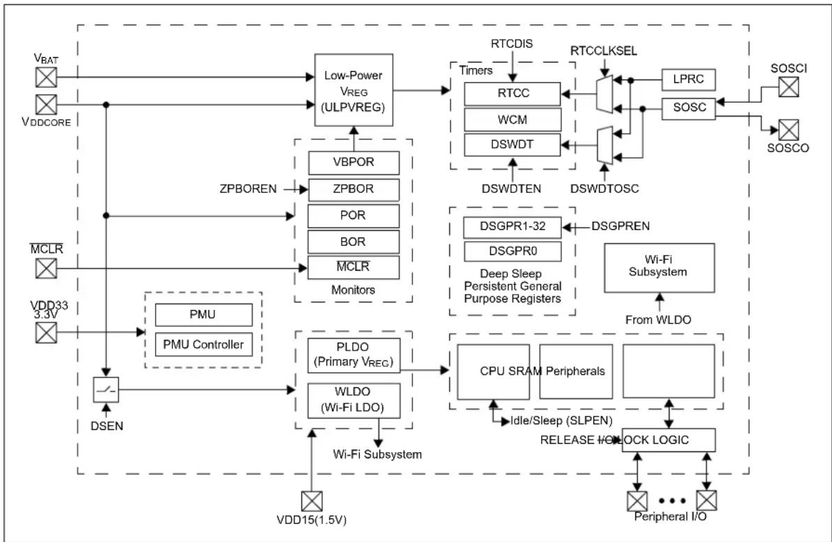
flowchart
graph TD
    A["VBAT"] --> B["Low-Power VREG (ULPVREG)"]
    C["VDDCORE"] --> B
    D["MCLR"] --> E["ZPBOREN"]
    E --> F["VBPOR"]
    F --> G["ZPBOR"]
    G --> H["POR"]
    H --> I["BOR"]
    I --> J["MCLR"]
    J --> K["MONitors"]
    K --> L["PLDO (Primary VREC)"]
    L --> M["WLDO (Wi-Fi LDO)"]
    M --> N["Wi-Fi Subsystem"]
    O["VDD33 3.3V"] --> P["PMU"]
    P --> Q["PMU Controller"]
    R["VDD15(1.5V)"] --> S["DSEN"]
    T["RTCDIS"] --> U["RTCC"]
    U --> V["DSWDT"]
    W["RTCCLKSEL"] --> X["DSWDTEN"]
    X --> Y["DSWDTOSC"]
    Z["DSGPR1-32"] --> AA["DSGPR0"]
    AB["Deep Sleep Persistent General Purpose Registers"] --> AC["Wi-Fi Subsystem"]
    AD["From WLDO"] --> AE["CPU SRAM Peripherals"]
    AF["Release WOC"] --> AG["OCK LOGIC"]
    AH["Peripheral I/O"] --> AI["..."]
    AJ["SOSCI"] --> AK["SOSCO"]
    AL["SOSC"] --> AM["LPRC"]
    AN["SOSC"] --> AO["SOSC"]
36.5 Deep Sleep Controller Registers
TABLE 36-7: DEEP SLEEP CONTROLLER REGISTER MAP
| Virtual Address (BF87_#) | Register Name | Bit Range | Bits | All Resets | |||||||||||||||
| 31/15 30 | 14 29/13 28/12 27/11 | 26/10 25/9 | 24/8 23/7 | 22/6 21/5 20/4 19/3 18 | 2 17/1 16/0 | ||||||||||||||
| 1000 | DSCON | 31:16 | — | — | — | — | — | — | — | — | — | — | — | — | — | — | — | — | 0000 |
| 15:0 | DSEN | — | DSGPREN | RTCDIS | — | — | — | RTCCWDIS | — | — | — | — | — | — | DSBOR | RELEASE | 0000 | ||
| 1004 | DSWAKE | 31:16 | — | — | — | — | — | — | — | — | — | — | — | — | — | — | — | — | 0000 |
| 15:0 | — | — | — | — | — | — | — | DSINTO | — | — | EXT | DSWDT | DSRTC | DSMCLR | — | — | 0000 | ||
| 1008 | DSGPR0 | 31:16 | DSGPR[31:0] | 0000 | |||||||||||||||
| 15:0 | 0000 | ||||||||||||||||||
| 1010 | DSGPR1 | 31:16 | DSGPR[31:0] | 0000 | |||||||||||||||
| 15:0 | 0000 | ||||||||||||||||||
| 1014 | DSGPR2 | 31:16 | DSGPR[31:0] | 0000 | |||||||||||||||
| 15:0 | 0000 | ||||||||||||||||||
| 1018 | DSGPR3 | 31:16 | DSGPR[31:0] | 0000 | |||||||||||||||
| 15:0 | 0000 | ||||||||||||||||||
| 101C | DSGPR4 | 31:16 | DSGPR[31:0] | 0000 | |||||||||||||||
| 15:0 | 0000 | ||||||||||||||||||
| 1020 | DSGPR5 | 31:16 | DSGPR[31:0] | 0000 | |||||||||||||||
| 15:0 | 0000 | ||||||||||||||||||
| 1024 | DSGPR6 | 31:16 | DSGPR[31:0] | 0000 | |||||||||||||||
| 15:0 | 0000 | ||||||||||||||||||
| 1028 | DSGPR7 | 31:16 | DSGPR[31:0] | 0000 | |||||||||||||||
| 15:0 | 0000 | ||||||||||||||||||
| 102C | DSGPR8 | 31:16 | DSGPR[31:0] | 0000 | |||||||||||||||
| 15:0 | 0000 | ||||||||||||||||||
| 1030 | DSGPR9 | 31:16 | DSGPR[31:0] | 0000 | |||||||||||||||
| 15:0 | 0000 | ||||||||||||||||||
| 1034 | DSGPR10 | 31:16 | DSGPR[31:0] | 0000 | |||||||||||||||
| 15:0 | 0000 | ||||||||||||||||||
| 1038 | DSGPR11 | 31:16 | DSGPR[31:0] | 0000 | |||||||||||||||
| 15:0 | 0000 | ||||||||||||||||||
| 103C | DSGPR12 | 31:16 | DSGPR[31:0] | 0000 | |||||||||||||||
| 15:0 | 0000 | ||||||||||||||||||
| 1040 | DSGPR13 | 31:16 | DSGPR[31:0] | 0000 | |||||||||||||||
| 15:0 | 0000 | ||||||||||||||||||
| 1044 | DSGPR14 | 31:16 | DSGPR[31:0] | 0000 | |||||||||||||||
| 15:0 | 0000 | ||||||||||||||||||
| 1048 | DSGPR15 | 31:16 | DSGPR[31:0] | 0000 | |||||||||||||||
| 15:0 | 0000 | ||||||||||||||||||
| Virtual Address (BF87.#) | Register Name | Bit Range | Bits | All Resets | |||||||||||||||
| 31/15 30 | 14 29/13 | 28/12 27/11 | 26/10 25/9 | 24/8 23/7 | 22/6 21/5 20 | 14 19/3 18 | 2 17/1 16/0 | ||||||||||||
| 104C | DSGPR16 | 31:16 | DSGPR[31:0] | 0000 | |||||||||||||||
| 15:0 | 0000 | ||||||||||||||||||
| 1050 | DSGPR17 | 31:16 | DSGPR[31:0] | 0000 | |||||||||||||||
| 15:0 | 0000 | ||||||||||||||||||
| 1054 | DSGPR18 | 31:16 | DSGPR[31:0] | 0000 | |||||||||||||||
| 15:0 | 0000 | ||||||||||||||||||
| 1058 | DSGPR19 | 31:16 | DSGPR[31:0] | 0000 | |||||||||||||||
| 15:0 | 0000 | ||||||||||||||||||
| 105C | DSGPR20 | 31:16 | DSGPR[31:0] | 0000 | |||||||||||||||
| 15:0 | 0000 | ||||||||||||||||||
| 1060 | DSGPR21 | 31:16 | DSGPR[31:0] | 0000 | |||||||||||||||
| 15:0 | 0000 | ||||||||||||||||||
| 1064 | DSGPR22 | 31:16 | DSGPR[31:0] | 0000 | |||||||||||||||
| 15:0 | 0000 | ||||||||||||||||||
| 1068 | DSGPR23 | 31:16 | DSGPR[31:0] | 0000 | |||||||||||||||
| 15:0 | 0000 | ||||||||||||||||||
| 106C | DSGPR24 | 31:16 | DSGPR[31:0] | 0000 | |||||||||||||||
| 15:0 | 0000 | ||||||||||||||||||
| 1070 | DSGPR25 | 31:16 | DSGPR[31:0] | 0000 | |||||||||||||||
| 15:0 | 0000 | ||||||||||||||||||
| 1074 | DSGPR26 | 31:16 | DSGPR[31:0] | 0000 | |||||||||||||||
| 15:0 | 0000 | ||||||||||||||||||
| 1078 | DSGPR27 | 31:16 | DSGPR[31:0] | 0000 | |||||||||||||||
| 15:0 | 0000 | ||||||||||||||||||
| 107C | DSGPR28 | 31:16 | DSGPR[31:0] | 0000 | |||||||||||||||
| 15:0 | 0000 | ||||||||||||||||||
| 1080 | DSGPR29 | 31:16 | DSGPR[31:0] | 0000 | |||||||||||||||
| 15:0 | 0000 | ||||||||||||||||||
| 1084 | DSGPR30 | 31:16 | DSGPR[31:0] | 0000 | |||||||||||||||
| 15:0 | 0000 | ||||||||||||||||||
| 1088 | DSGPR31 | 31:16 | DSGPR[31:0] | 0000 | |||||||||||||||
| 15:0 | 0000 | ||||||||||||||||||
| 108C | DSGPR32 | 31:16 | DSGPR[31:0] | 0000 | |||||||||||||||
| 15:0 | 0000 | ||||||||||||||||||
Legend: x = unknown value on Reset; — = unimplemented, read as '0'. Reset values are shown in hexadecimal.
Note: Supports Back-to-back write validation before updating the DSCON/DSWAKE/DSGPR0 registers.
REGISTER 36-1: DSCON – DEEP SLEEP CONTROL REGISTER
| Bit Range | Bit 31/23/15/7 | Bit 30/22/14/6 | Bit 29/21/13/5 | Bit 28/20/12/4 | Bit 27/19/11/3 | Bit 26/18/10/2 | Bit 25/17/9/1 | Bit 24/16/8/0 |
| 31:24 | R-0 R-0 R-0 | R-0 R-0 R-0 R-0 | R-0 R-0 | |||||
| — — — — | — — — — | |||||||
| 23:16 | R-0 R-0 R-0 | R-0 R-0 R-0 R-0 | R-0 R-0 | |||||
| — — — — | — — — — | |||||||
| 15:8 | R/W/HC-0 | U-0 | R/W-0 | R/W-0 | U-0 | U-0 | U-0 | R/W-0 |
| DSEN | — | DSGPREN | RTCDIS | — | — | — | RTCCWDIS | |
| 7:0 | U-0 | U-0 | U-0 | U-0 | U-0 | U-0 | R/W/C/HS-0 | R/C/HS/HC-0 |
| — — — — | — — | DSBOR | RELEASE |
Legend:
| HC = Cleared by hardware | HS = Set by hardware | R = Readable bit |
| U = Unimplemented bit | W = Writable bit | C = Clearable bit |
bit 31-16 Unimplemented: Read as '0'
bit 15 DSEN: Deep Sleep Enable bit ^(1)
0 = Sleep mode is entered on a WAIT command
1 = Deep Sleep mode is entered on a WAIT command
Note 1: To enter Deep Sleep mode, Sleep mode must be executed after setting the DSEN bit.
bit 14 Unimplemented: Read as '0'
bit 13 DSGPREN: General Purpose Registers Enable bit
0 = No general purpose register retention in Deep Sleep mode
1 = General purpose register retention is enabled in Deep Sleep mode
bit 12 RTCDIS: RTCC Module Disable bit
0 = RTCC is enabled
1 = RTCC is not enabled
bit 11-9 Unimplemented: Read as '0'
bit 8 RTCCWDIS: RTCC Wake-up Disable bit
0 = Wake-up from RTCC is enabled
1 = Wake-up from RTCC is disabled
bit 7-2 Unimplemented: Read as '0'
bit 1 DSBOR: Deep Sleep BOR Event Status bit
0 = DSZPBOREN was disabled, or VDD did not drop below the DSBOR threshold during Deep Sleep
1 = DSZPBOREN was enabled and VDD dropped below the DSBOR threshold during Deep Sleep
Note: Unlike all other events, a DSBOR event does not cause a wake-up from Deep Sleep. This bit is present only as a status bit.
bit 0 RELEASE: I/O Pin State Release bit
0 = Release I/O pins and allow their respective TRIS and LAT bits to control their states
1 = Upon waking from Deep Sleep, the I/O pins maintain their previous states (Not user settable).
Note: The RELEASE register bit is readable and clearable (but not settable) by the software. This bit is automatically set when entering the Deep Sleep mode. While exiting the Deep Sleep mode, due to any wake-up source other than MCLR, once all state related configuration is complete the software must clear the RELEASE bit. Once the RELEASE bit is cleared, the I/Os will go back to its last set state.
Note 1: All register bits are reset only in the case of a VDDBAT POR event.
REGISTER 36-2: DSWAKE – DEEP SLEEP WAKE-UP SOURCE REGISTER
| Bit Range | Bit31/23/15/7 | Bit30/22/14/6 | Bit29/21/13/5 | Bit28/20/12/4 | Bit27/19/11/3 | Bit26/18/10/2 | Bit25/17/9/1 | Bit24/16/8/0 |
| 31:24 | R-0 R-0 R-0 | R-0 R-0 R-0 | R-0 R-0 | |||||
| — — — — | — — — — | |||||||
| 23:16 | R-0 R-0 R-0 | R-0 R-0 R-0 | R-0 R-0 | |||||
| — — — — | — — — — | |||||||
| 15:8 | R-0 R-0 R-0 | R-0 R-0 R-0 | R-0 R/W/C/HS-0 | |||||
| — | — | — | — | — | — | — | DSINT0 | |
| 7:0 | R-0 | R-0 | R/W/C/HS-0 | R/W/C/HS-0 | R/W/C/HS-0 | R/W/C/HS-0 | R-0 | R-0 |
| — | — | EXT | DSWDT | DSRTC | DSMCLR | — | — |
Legend:
| HC = Cleared by hardware | HS = Set by hardware | R = Readable bit |
| U = Unimplemented bit | W = Writable bit | C = Clearable bit |
bit 31-9 Unimplemented: Read as '0'
bit 8 DSINT0: Deep Sleep Interrupt-on-change #0 bit (Only present if DS_NUM_INTS ≥ 1)
0 = Interrupt-on-change #0 was not asserted during Deep Sleep
1 = Interrupt-on-change #0 was asserted during Deep Sleep
bit 7-6 Unimplemented: Read as '0'
bit 5 EXT: External Wake-up Source bit
0 = No external wake-up event is detected during Deep Sleep
1 = An external wake-up event is detected during Deep Sleep
This bit is only present when DS_NUM_EXT_WAKE > 0.
bit 4 DSWDT: Deep Sleep Watchdog Timer Time-out bit
0 = DSWDT does not time out during Deep Sleep
1 = DSWDT timed out during Deep Sleep
bit 3 DSRTC: Deep Sleep Real Time Clock and Calendar Alarm bit
0 = Deep Sleep RTC and calendar does not trigger an alarm during Deep Sleep
1 = Deep Sleep RTC and calendar triggers an alarm during Deep Sleep
bit 2 DSMCLR: Deep Sleep MCLR Event bit
0 = DSMCLR pin is not active or is active, but not asserted during Deep Sleep
1 = DSMCLR pin is active and is asserted during Deep Sleep
bit 1-0 Unimplemented: Read as '0'
Note 1: All register bits are reset only in the case of a VDDBAT POR event or entry into VBAT Mode.
2: All register bits are cleared when the DSCON[DSEN] bit transitions from 1'b0 to 1'b1. They are updated while DSEN = 1.
3: The DSWAKE register is only writable by software when DSCON[RELEASE] = '0' (E.1).
REGISTER 36-3: DSGPRn – DEEP SLEEP PERSISTENT GENERAL PURPOSE REGISTER, WHERE n = 0 TO 32
| Bit Range | Bit31/23/15/7 | Bit30/22/14/6 | Bit29/21/13/5 | Bit28/20/12/4 | Bit27/19/11/3 | Bit26/18/10/2 | Bit25/17/9/1 | Bit24/16/8/0 |
| 31:24 | R/W-xxxx R/W- | xxxx R/W-xx | xx R/W-xxxx | R/W-xxxx R/W-xxx | R/W-xxxx R/W-xxxx | W-xxxx | ||
| DSGPR[31:24] | ||||||||
| 23:16 | R/W-xxxx R/W- | xxxx R/W-xx | xx R/W-xxxx | R/W-xxxx R/W-xxx | R/W-xxxx R/W-xxxx | W-xxxx | ||
| DSGPR[23:16] | ||||||||
| 15:8 | R/W-xxxx R/W- | xxxx R/W-xx | xx R/W-xxxx | R/W-xxxx R/W-xxx | R/W-xxxx R/W-xxxx | W-xxxx | ||
| DSGPR[15:8] | ||||||||
| 7:0 | R/W-xxxx R/W- | xxxx R/W-xx | xx R/W-xxxx | R/W-xxxx R/W-xxx | R/W-xxxx R/W-xxxx | W-xxxx | ||
| DSGPR[7:0] | ||||||||
Legend:
R = Readable bit
W = Writable bit
x = Bit is unknown at Reset
bit 31-0 DSGPRx: Deep Sleep Persistent General Purpose Register bits
The contents of the DSGPR0 register are retained, even in the Deep Sleep mode. The DSPGR0 through DSP-GR32 registers are disabled by default in the Deep Sleep mode but can be enabled with the DSGPREN bit (DSCON[13]). All register bits are reset only in the case of a VDD Power-on Reset (POR) event outside of the Deep Sleep mode.
Note 1: All register bits are reset only in the case of a VDDBAT POR event.
36.6 Wi-Fi Power Save Modes
The Wi-Fi Sleep Mode Controller (SMC) will take over the RF, MAC and BBP-PHY clock gating and power controls once the WDS/WSM mode is triggered. The SMC will automatically periodically switch between the Run and Sleep states in the Sleep modes. All the wait times related to the Sleep states are programmable.
In the PIC32MZ W1, the Wi-Fi subsystem shares the CPU with the MCU, therefore, the Wi-Fi Run mode cannot be complete until the MCU is in Run mode. The Wi-Fi Run mode will force the MCU to be in Run mode.
The MCU sleep entry forces the Wi-Fi (SMC) into Sleep mode and vice-versa. The MCU sleep exit forces the Wi-Fi (SMC) to exit and vice-versa.
The MCU sleep entry forces the Wi-Fi (SMC) into Sleep if it is not already in the Sleep mode but this is not true vice-versa. The Wi-Fi (SMC) sleep exit forces the MCU out of the Sleep mode if it is not in the Run mode but this is not true vice-versa.
The Wi-Fi (SMC) power save modes (WSM and WDS) have the following internal states:
- Run state:
- The Wi-Fi subsystem can transmit or receive any of the Wi-Fi packets. (Both TX and RX are active.)
- Sleep state:
- The Wi-Fi subsystem cannot transmit or receive any of the Wi-Fi packets. (Both TX and RX are inactive.)
36.6.1 WSM: Wi-Fi SLEEP MODE
- Faster recovery from the Sleep mode
- WSM can put the Wi-Fi (SMC) to sleep independently without putting the MCU into Sleep mode
- During the WSM-sleep state, the RF is in Sleep mode, POSC is ON, RF internal LDOs, PLL and TX/RX chains are clock-gated
• RAM and Wi-Fi register contents are retained - On wake-up, the CPU will continue execution from the next instruction from when it went to sleep
- Wake-up source from WSM:
- Wake on WSM sleep duration complete
- When Wi-Fi data is available from access point
- On the user's request, the MCU can trigger the exit of the Wi-Fi (SMC) Sleep mode
- The customer needs to use the Software User Guide API to enable the WSM mode
36.6.2 WDS: Wi-Fi DEEP SLEEP MODE
- Lowest power consuming Sleep state and favorable for longer sleep duration
- The RF is powered down completely including primary oscillator (POSC), RF internal LDOs, PLL and TX/RX chains
- If the primary oscillator has any system peripheral request apart from the Wi-Fi (SMC), the device will always enter into WSM even if the system requests WDS mode
• The SMC can exist in either the WDS Sleep state - The WDS can put the SMC to sleep independently without putting the system into Sleep mode
• The RAM and Wi-Fi register contents are retained - On wake-up, the CPU will continue execution from the next instruction from when it went to sleep
- Wake-up source from WDS:
- Wake on the WSM sleep duration complete
- When the Wi-Fi data is available from the access point
- On the user's request, the MCU can trigger the exit of the Wi-Fi (SMC) Sleep mode
- The customer needs to use Software User Guide API to enable WSM mode
36.6.3 WOFF: Wi-Fi POWER-OFF MODE
- The WOFF mode is where the complete Wi-Fi sub-system power is shut off and all the configuration registers and memory contents are lost
-
The WOFF can use WCM memory before triggering the WOFF mode to retain any content that needs to be retained.
-
Re-initialization of the Wi-Fi subsystem is required in case data are not retained in the WCM memory.
- On wake-up, the CPU will continue execution from the next instruction from when it went to sleep.
- Wake-up source from WOFF:
- There is no wake-up source for WOFF; the software has to reinitialize the Wi-Fi subsystem.
- The device enters WOFF mode when the WLDOOFF bit (PMUCLKCTRL[30]) is set.
REGISTER 36-4: PMD1: PERIPHERAL MODULE DISABLE 1 REGISTER
| Bit Range | Bit 31/23/15/7 | Bit 30/22/14/6 | Bit 29/21/13/5 | Bit 28/20/12/4 | Bit 27/19/11/3 | Bit 26/18/10/2 | Bit 25/17/9/1 | Bit 24/16/8/0 |
| 31:24 | U-0 U-0 R/W | W/L-0 U-0 U-0 | R/W/L-0 U-0 R/W/L-0 | |||||
| — | — | SQI1MD | — | — | RNG1MD | — | CRYPT1MD | |
| 23:16 | R/W/L-0 U-0 U-0 U-0 U-0 R/W/L-0 | U-0 | U-0 R/W/L-0 | |||||
| BA414MD | — | — | — | DMA1MD | — | — | RTCC1MD | |
| 15:8 | R/W/L-0 U-0 U-0 U-0 R/W/L-0 | U-0 | U-0 R/W/L-0 | |||||
| CVD1MD | — | — | — | PTGMD | — | — | ADC1MD | |
| 7:0 | R/W/L-0 U-0 U-0 R/W/L-0 U-0 | U-0 | U-0 R/W/L-0 | |||||
| ADCSARSHRMD | — | — | PLVD1MD | — | — | — | ADCSAR0MD |
Legend:
| R = Readable bit | W = Writable bit | U = Unimplemented bit, read as '0' |
| -n = Value at POR | '1' = Bit is set | '0' = Bit is cleared L = Lockable bit |
bit 31-30 Unimplemented: Read as '0'
bit 29 SQI1MD: SQI Module Disable bit
1 = Disabled
0 = Enabled
bit 28-27 Unimplemented: Read as '0'
bit 26 RNG1MD: RNG1 Module Disable bit
1 = Disabled
0 = Enabled
bit 25 Unimplemented: Read as '0'
bit 24 CRYPT1MD: CRYPTO1 Module Disable bit
1 = Disabled
0 = Enabled
bit 23 BA414MD: Asymmetric Crypto Module Disable bit
1 = Disabled
0 = Enabled
bit 22-20 Unimplemented: Read as '0'
bit 19 DMA1MD: DMA Controller Module Disable bit
1 = Disabled
0 = Enabled
bit 18-17 Unimplemented: Read as '0'
bit 16 RTCC1MD: RTCC Module Disable bit
1 = Disabled
0 = Enabled
bit 15 CVD1MD: CVD Module Disable bit
1 = Disabled
0 = Enabled
bit 14-12 Unimplemented: Read as '0'
bit 11 PTGMD: PTG Module Disable bit
1 = Disabled
0 = Enabled
bit 10-9 Unimplemented: Read as '0'
bit 8 ADC1MD: ADC Controller Module Disable bit
1 = Disabled
0 = Enabled
REGISTER 36-4: PMD1: PERIPHERAL MODULE DISABLE 1 REGISTER (CONTINUED)
bit 7 ADCSARSHRMD: Shared ADC SAR Core Module Disable bit
1 = When disabled, the corresponding ADC SAR SHARED will be disabled.
0 = Enabled
bit 6-5 Unimplemented: Read as '0'
bit 4 PLVD1MD: PLVD Module Disable bit
1 = When disabled, the corresponding PLVD will be disabled.
0 = Enabled
bit 3-1 Unimplemented: Read as '0'
bit 0 ADCSAR0MD: ADC SAR Core 0 Module Disable bit
1 = When disabled, the corresponding ADC SAR will be disabled.
0 = Enabled
REGISTER 36-5: PMD2: PERIPHERAL MODULE DISABLE 2 REGISTER
| Bit Range | Bit 31/23/15/7 | Bit 30/22/14/6 | Bit 29/21/13/5 | Bit 28/20/12/4 | Bit 27/19/11/3 | Bit 26/18/10/2 | Bit 25/17/9/1 | Bit 24/16/8/0 |
| 31:24 | R/W/L-0 R/W | W/L-0 R/W/L-0 R/W | W/L-0 U-0 U-0 | U-0 U-0 | ||||
| REFO4MD REFO3MD REFO2 | MD REFO1MD | — — — — | — | |||||
| 23:16 | U-0 | R/W/L-0 | R/W/L-0 | R/W/L-0 | R/W/L-0 | R/W/L-0 | R/W/L-0 | R/W/L-0 |
| — | T7MD | T6MD | T5MD | T4MD | T3MD | T2MD | T1MD | |
| 15:8 | U-0 | U-0 | U-0 | U-0 | R/W/L-0 | R/W/L-0 | R/W/L-0 | R/W/L-0 |
| — | — | — | — | OC4MD | OC3MD | OC2MD | OC1MD | |
| 7:0 | U-0 | U-0 | U-0 | U-0 | R/W/L-0 | R/W/L-0 | R/W/L-0 | R/W/L-0 |
| — | — | — | — | IC4MD | IC3MD | IC2MD | IC1MD |
Legend:
| R = Readable bit | W = Writable bit | U = Unimplemented bit, read as '0' |
| -n = Value at POR | '1' = Bit is set | '0' = Bit is cleared L = Lockable bit |
bit 31-28 REFOnMD: Reference (Clock) Out n Module Disable bit
1 = Disabled
0 = Enabled
bit 27-23 Unimplemented: Read as '0'
bit 22-16 TnMD: Timer n Module Disable bit
1 = Disabled
0 = Enabled
bit 15-12 Unimplemented: Read as '0'
bit 11-8 OCnMD: Output Compare n Module Disable bit
1 = Disabled
0 = Enabled
bit 7-4 Unimplemented: Read as '0'
bit 3-0 ICnMD: Input Capture n Module Disable bit
1 = Disabled
0 = Enabled
REGISTER 36-6: PMD3: PERIPHERAL MODULE DISABLE 3 REGISTER
| Bit Range | Bit 31/23/15/7 | Bit 30/22/14/6 | Bit 29/21/13/5 | Bit 28/20/12/4 | Bit 27/19/11/3 | Bit 26/18/10/2 | Bit 25/17/9/1 | Bit 24/16/8/0 |
| 31:24 | U-0 U-0 U-0 R/W/L-0 R/W/L-0 U-0 U-0 R/W/L-0 | |||||||
| — — — CAN2MD CAN1MD — — | U | S B | 1 | M | D | |||
| 23:16 | U-0 U-0 U-0 U-0 U-0 U-0 R/W/L-0 R/W/L-0 | |||||||
| — — — | — — — | I2C2MD I2C1MD | ||||||
| 15:8 | U-0 U-0 U-0 R/W/L-0 U-0 U-0 R/W/L-0 R/W/L-0 | |||||||
| — | — | — | W24GMD | — | — | SPI2MD | SPI1MD | |
| 7:0 | U-0 U-0 U-0 R/W/L-0 U-0 R/W/L-0 R/W/L-0 | |||||||
| — | — | — | ETH1MD | — | U3MD | U2MD | U1MD | |
Legend:
| R = Readable bit W = Writable bit | U = Unimplemented bit, read as '0' |
| -n = Value at POR '1' = Bit is set | '0' = Bit is cleared L = Lockable bit |
bit 31-29 Unimplemented: Read as '0'
bit 28-27 CANnMD: CAN Module Disable bit
1 = Disabled
0 = Enabled
bit 26-25 Unimplemented: Read as '0'
bit 24 USB1MD: USB Module Disable bit
1 = Disabled
0 = Enabled
bit 23-18 Unimplemented: Read as '0'
bit 17 I2C1MD: I2C 1 Module Disable bit
1 = Disabled
0 = Enabled
bit 16 I2C0MD: I2C 0 Module Disable bit
1 = Disabled
0 = Enabled
bit 15-13 Unimplemented: Read as '0'
bit 12 W24GMD: WiFi Module Disable bit
1 = Disabled
0 = Enabled
bit 11-10 Unimplemented: Read as '0'
bit 9 SPI2MD: SPI 2 Module Disable bit
1 = Disabled
0 = Enabled
bit 8 SPI1MD: SPI 1 Module Disable bit
1 = Disabled
0 = Enabled
bit 7-5 Unimplemented: Read as '0'
bit 4 ETH1MD: Ethernet Module Disable bit
1 = Disabled
0 = Enabled
bit 3 Unimplemented: Read as '0'
REGISTER 36-6: PMD3: PERIPHERAL MODULE DISABLE 3 REGISTER (CONTINUED)
bit 2-0 UnMD: UART Module Disable bit
1 = Disabled
0 = Enabled
36.6.4 CONTROLLING CONFIGURATION CHANGES
Peripherals can be disabled during run time, some restrictions on disabling peripherals are needed to prevent accidental configuration changes. PIC32MZ1025W104 devices include a Control Register Lock sequence to prevent alterations to enabled or disabled peripherals. For more details on configuration, refer to Section 38.0 "Special Features".
NOTES:
37.0 PROGRAMMABLE LOW VOLTAGE DETECT (PLVD)
The PIC32MZ W1 device supports a Programmable Low Voltage Detect (PLVD) module. The module is used to monitor the VDD supply voltage.
The LVD module is an interrupt-driven, supply-level detection. The voltage detection monitors the internal power supply by comparing the VDD to the band gap voltage. If the VDD is below the PLVD level, an NMI event will be triggered (RNMICON[18]). This module ensures that the supply voltage is sufficient for programming. A PLVD event will act to disable the flash controller from executing a programming sequence.
Key features:
• LVD trip point at a minimum of 3V
- Detect hysteresis
- Low going voltage detect only
- Generates an interrupt event
The LVD control module supports the following system modes:
- Sleep mode
- Idle mode
- Freeze mode
During the Sleep mode, all clocks to the module are disabled. However, interrupt generation will still occur if the module is enabled. In Idle mode, the CPU clocks are disabled, but the peripheral clocks (UPB clocks) are still active. The module continues to run normally in the Idle mode as long as LVDCON.SIDL = 0. If LVDCON.SIDL = 1, the module stops when the device is in the Idle mode. When the module stops, it behaves in the same way as in the Sleep mode. During the Freeze mode, all outputs of the module are frozen, and the register reads and writes are possible through the CPU interface. While in the Freeze mode, no events are generated.
37.1 PLVD Registers
TABLE 37-1: PLVD REGISTER MAP
| Virtual Address (BF80_#) | Register Name | Bit Range | Bits | All Resets | ||||||||||||||||
| 31/15 | 30/14 | 29/13 | 28/12 | 27/11 | 26/10 | 25/9 | 24/8 | 23/7 | 22/6 | 21/5 | 20/4 | 19/3 | 18/2 | 17/1 | 16/0 | |||||
| 1400h | LVDCON | 31:16 | — | — | — | — | — | — | — | — | — | — | — | — | — | — | — | — | — | 0000 |
| 15:00 | ON | — | SIDL | — | VDIR | BGVST | IRVST | EVENT | DISOUT | — | — | — | LVDL | 0000 | ||||||
Legend: x = unknown value on Reset; — = unimplemented, read as '0'. Reset values are shown in hexadecimal.
REGISTER 37-1: LVDCON: LOW-VOLTAGE DETECT CONTROL REGISTER
| Bit Range | Bit 31/23/15/7 | Bit 30/22/14/6 | Bit 29/21/13/5 | Bit 28/20/12/4 | Bit 27/19/11/3 | Bit 26/18/10/2 | Bit 25/17/9/1 | Bit 24/16/8/0 |
| 31:24 | U-0 | U-0 | U-0 | U-0 | U-0 | U-0 | U-0 | U-0 |
| — | — | — | — | — | — | — | — | |
| 23:16 | U-0 | U-0 | U-0 | U-0 | U-0 | U-0 | U-0 | U-0 |
| — | — | — | — | — | — | — | — | |
| 15:8 | R/W-0 | U-0 | R/W-0 | U-0 | R/W-0 | HS/HC/R-0 | HS/HC/R-0 | HS/HC/R-0 |
| ON | — | SIDL | — | VDIR | BGVST | IRVST | EVENT | |
| 7:0 | R/S-0 | U-0 | U-0 | U-0 | R/W-0 | R/W-0 | R/W-0 | R/W-0 |
| DISOUT | — | — | — | LVDL3 | LVDL2 | LVDL1 | LVDL0 |
Legend:
| HC = Cleared by hardware | HS = Set by hardware | |
| R = Readable bit | W = Writable bit | P = Programmable bit r = Reserved bit |
| U = Unimplemented bit | S = Settable bit | -n = Bit Value at POR: (0, 1, x = unknown) |
bit 31-16 Unimplemented: Read as '0'
| bit 15 | ON: Low-voltage Detect Power Enable bit1 = Enables LVD, powers up LVD circuit and supporting reference circuitry0 = Disables LVD, powers down LVD and supporting circuitry |
| bit 14 | Unimplemented: Read as ‘0’ |
| bit 13 | SIDL: Stop in Idle Mode bit1 = Discontinue operation of LVD when device enters Idle mode0 = Continue operation of LVD in Idle mode |
| bit 12 | Unimplemented: Read as ‘0’ |
| bit 11 | VDIR: Voltage Direction Magnitude Select bit1 = LVD Event occurs on voltage ≥ selected detection limit (LVDL[3:0])0 = LVD Event occurs on voltage ≤ selected detection limit (LVDL[3:0]) |
| bit 10 | BGVST: Band Gap Reference Voltages Stable Status bit1 = Indicates internal band gap voltage references is stable0 = Indicates internal band gap voltage reference is not stable |
| bit 9 | IRVST: Internal Reference Voltages Stable Status bit1 = Indicates all internal LVD voltage references are stable0 = Indicates all internal LVD voltage references are not stable |
| bit 8 | EVENT: Low Voltage Detection Event Status bit1 = Indicates LVD Event interrupt is active0 = Indicates LVD Event interrupt is not active |
| Note: Refer to Table 41-36 for the trip points. | |
REGISTER 37-1: LVDCON: LOW-VOLTAGE DETECT CONTROL REGISTER (CONTINUED)
bit 7 DISOUT: Disable Output bit
0 = Disable output of comparator
1 = Do not disable output of comparator
bit 6-4 Unimplemented: Read as '0' (Reserved for future expansion of LVDL[3:0] field)
bit 3-0 LVDL[3:0]: Low Voltage Detection Limit Select bits
0111 = Selects trip point 7
0110 = Selects trip point 6
0101 = Selects trip point 5
0100 = Selects trip point 4
Note: Refer to Table 41-36 for the trip points.
NOTES:
38.0 SPECIAL FEATURES
Note: This data sheet summarizes the features of the PIC32MZ1025W104 family of devices. However, it is not intended to be a comprehensive reference source. To complement the information in this data sheet, refer to Section 32 "Configuration" (DS60001124) and Section 33. "Programming and Diagnostics" (DS60001129) in the "PIC32 Family Reference Manual", which are available from the Microchip website (www.microchip.com/PIC32).
PIC32MZ1025W104 devices include several features intended to maximize application flexibility and reliability and minimize cost through elimination of external components. These are:
- Flexible device configuration
• Joint Test Action Group (JTAG) interface
• In-Circuit Serial Programming (ICSP) - Internal temperature sensor
38.1 Configuration Bits
This PIC32MZ W1 device provides several user writable configuration registers related to the configuration and operation of the system.
- Permission Group Configuration Register (CFGPG) defines the permission group.
- System Key Register (SYSKEY) defines the system key.
- Device and Revision ID Register (DEVID) defines the device and revision ID.
- Configuration Control Register 3 (CFGCON3) provides control, selection and locking for various features of the device.
- Configuration Control Register 0 (CFGCON0(L)) provides control, selection and locking for various features of the device. The registers those are marked with (L) are loadable from Flash.
- ICAP clock selection
- OCMP clock selection
- PPS register locking
- PMD register locking
- CFGPG register locking
- Config register locking
- USB diagnostics enable
- USB suspend sleep enable
- JTAG port enable and configuration
- iFlowtrace port enable
- Flash ECC control
-
DMA, CPU, FC
-
Configuration Control Register 1 (CFGCON1(L)) provides control, selection and locking for various features of the device.
- Debug port and feature configuration
- USB port control
- USB trim bits
- CFGCON0 locking control
- Class B functionality enable
- High-speed UART enable
-
Ethernet RMII enable
-
Configuration Control Register 2 (CFGCON2(L)) provides control, selection and locking for various features of the device.
- DMT enable and configuration
- WDT enable and configuration
- Clock monitoring and control
- Oscillator enable and configuration
- 2-Speed startup enabled in Sleep Mode bit
-
SYSPLL/EWPLL Postdiv2 programming
-
Configuration Control Register 4 (CFGCON4(L)) provides control, selection and locking for various features of the device.
- Deep sleep modules control
- SOSC configuration control
- User Unique ID Register (USERID(L)) provides the end user with a 16-bit ID field that maybe read out directly through the JTAG interface via the USERID JTAG instruction.
38.2 Special Features Registers
TABLE 38-1: DEVCFG: DEVICE CONFIGURATION WORD SUMMARY
| Virtual Address(BF60_#) | Register Name | Bit Range | Bits | All Resets | ||||||||||||||||
| 31/15 30 | 14 29/13 28 | 12 27/11 26 | 10 25/9 24/8 | 23/7 22/6 21/5 | 20/4 19/3 18 | 2 17/1 | 16/0 | |||||||||||||
| 0000 | CFGCON0(L)(1) | 31:16 | — | ETHTPSF | FECCCON[1:0] ETH | PLLHWMD | B TPLL-HWMD | SPLL-HWMD | UPLL-HWMD | PCM | — | CANFDDIV[1:0] | — | — | IC_ACLK | OC_ACLK | 3280 | |||
| 15:00 | CFGLOCK[1:0] | IOLOCK | PMDLOCK | PGLOCK | PMULOCK | — | USBSSEN | EXLPRI | DMAPRI | FCPRI | — | JTAGEN | TROEN | — | TDOEN | 00009 | ||||
| 0010 | CFGCON1(L)(1) | 31:16 | — | — | — | WDTPS[4:0] | USBDPTRIM[3:0] | USBDMTRIM[3:0] | 1F80 | |||||||||||
| 15:00 | HSUARTEN | SMCLR | HSSPIEN | VBUSIO | USBIDIO | CLASSBDIS | ETHEX-EREF | FMIEN | — | — | TRCEN IGESEL[1:0] | — | DEBUG[1:0] | BE39 | ||||||
| 0020 | CFGCON2(L)(1) | 31:16 | DMTEN | DMTCNT[4:0] | WDTWINSZ[1:0] | WDTEN | WINDIS | WDTSPGM | WDTPS[4:0] | 1F7E | ||||||||||
| 15:00 | FSCMEN | CKSWEN | WAKE2SPD | SOSCSEL | WDTRMCS[1:0] | POSCMOD[1:0] | — | — | DMTINTV[2:0] | — | — | — | FF39 | |||||||
| 0030 | CFGCON3(1) | 31:16 | — | — | — | — | — | — | — | — | — | — | — | — | — | — | BTPLLPOSTDIV2[5:4] | 0000 | ||
| 15:00 | BTPLLPOSTDIV2[3:0] | SPLLPOSTDIV2[5:0] | ETHPLLPOSTDIV2[5:0] | 0000 | ||||||||||||||||
| 0040 | CFGCON4(L)(1) | 31:16 | — | SOSCEN | — | DSEN DSWDTEN DSWD-TOSC | DSWDTPS [4:0] | DSZP-BOREN | — | — | — | 0418 | ||||||||
| 15:00 | — | — | — | — | — | — | — | — | — | — | SOSCCFG[7:0] | 0000 | ||||||||
| 0050 | CFGPG(2) | 31:16 | — | — | — | — | — | — | — | — | USBPG[1:0] | SQIPG[1:0] | ETHPG[1:0] | CRY1PG[1:0] | 0000 | |||||
| 15:00 | CAN2PG[1:0] | CAN1PG[1:0] | ADCPG[1:0] | WIFIPG[1:0] | ICDJPG[1:0] | DMAPG[1:0] | FCPG[1:0] | CPUPG[1:0] | 0000 | |||||||||||
| 0060 | DEVID | 31:16 | VER[3:0] | DEVID[27:16] | xxxxx | |||||||||||||||
| 15:00 | DEVID[15:0] | xxxxx | ||||||||||||||||||
| 0070 | USERID(L) | 31:16 | — | — | — | — | — | — | — | — | — | — | — | — | — | — | — | — | 0000 | |
| 15:00 | USERID[15:0] | 0000 | ||||||||||||||||||
| 0080 | SYSKEY | 31:16 | SYSKEY[31:16] | 0000 | ||||||||||||||||
| 15:00 | SYSKEY[15:0] | 0000 | ||||||||||||||||||
Legend: x = unknown value on Reset; — = unimplemented, read as '0'. Reset values are shown in hexadecimal.
Note 1: This register is only writable when CFGLOCK Configuration (CFGCON0[15:14]) bit is 00.
2: This register is only writable when PGLOCK Configuration (CFGCON0[11]) bit is 0.
REGISTER 38-1: CFGCON0(L): CONFIGURATION CONTROL REGISTER 0
| Bit Range | Bit 31/23/15/7 | Bit 30/22/14/6 | Bit 29/21/13/5 | Bit 28/20/12/4 | Bit 27/19/11/3 | Bit 26/18/10/2 | Bit 25/17/9/1 | Bit 24/16/8/0 |
| 31:24 | U-0 R/W | L-0 R/W/L-1 | R/W/L-1 R/W/L-0 | R/W/L-0 R/W/L-0 | W/L-0 R/W/L-0 | |||
| — ETHTPSF FECCC | ON[1:0] ETHPLLHWMD BTP | LLHWMD SPLH | WMD UPLLHWMD | |||||
| 23:16 | R/W/L-1 U-0 | R/W/L-0 R/W | W/L-0 U-0 | U-0 | R/W/L-0 R/W/L-0 | |||
| PCM | — | CANFDDIV | — | — | IC_ACLK | OC_ACLK | ||
| 15:8 | R/W/L-0 | R/W/L-0 | R/S/L-0 | R/S/L-0 | R/S/L-0 | R/S/L-0 | U-0 | R/W/L-0 |
| CFGLOCK[1:0] | IOLOCK | PMDLOCK | PGLOCK | PMULOCK | — USBSEN | |||
| 7:0 | R/W/L-0 | R/W/L-0 | R/W/L-0 | U-0 | R/W/L-1 | R/W/L-0 | U-0 | R/W/L-1 |
| EXLPRI | DMAPRI FCPRI | — | JTAGEN | TROEN | — | TDOEN | ||
Legend:
| R = Readable bit W = Writable bit | U = Unimplemented bit, read as '0' |
| -n = Value at POR '1' = Bit is set | '0' = Bit is cleared L = Lockable bit |
bit 31 Unimplemented: Read as '0'
bit 30 ETHTPSF: Ethernet TX SOF enabled for CTR measurements
1 = TPSF is enabled in CTR measurement 0 = RPSF is enabled in CTR measurement
bit 29-28 FECCCON: Flash ECC Controls
11 = ECC and Dynamically ECC Disabled 10 = ECC and Dynamically ECC Disabled 01 = Dynamically ECC Enabled 00 = ECC Enabled (NVMOP = Word Programming disabled)
bit 27 ETHPLLHWMD: EWPLL Hardware Control Mode for power down and Reset
1 = Power Down and Reset are generated by hardware 0 = Power Down and Reset are generated by software using corresponding PLLCON register bits
bit 26 BTPLLHWMD: BTPLL Hardware Control Mode for power down and Reset
1 = Power Down and Reset are generated by hardware 0 = Power Down and Reset are generated by software using corresponding PLLCON register bits
bit 25 SPLLHWMD: SPLL Hardware Control Mode for power down and Reset
1 = Power Down and Reset are generated by hardware 0 = Power Down and Reset are generated by software using corresponding PLLCON register bits
bit 24 UPLLHWMD: UPLL Hardware Control Mode for power down and Reset
1 = Power Down and Reset are generated by hardware 0 = Power Down and Reset are generated by software using corresponding PLLCON register bits
bit 23 PCM: Prefetch I/D Cacheable Mode
1 = Always enabled. Can be further enabled/disabled by Prefetch module SFR registers. 0 = The cache-ability is controlled by the MIPS CPU via HPROT[3]. This feature is not available on all the MIPS cores.
bit 22 Unimplemented: Read as '0'
bit 20-21 CANFDDIV: CAN-FD Back-up Clock Divider
0 = Divide-by 2 1 = Divide-by 2 2 = Divide-by 4 3 = Divide-by 8
bit 18-19 Unimplemented: Read as '0'
REGISTER 38-1: CFGCON0(L): CONFIGURATION CONTROL REGISTER 0 (CONTINUED)
bit 17 IC_ACLK: ICAP Alternate Clock Selection
1 = ICAP Modules use an alternative timer pair as their timebase clock
0 = All ICAP Modules use timer2/timer3 as their timebase clock
bit 16 OC_ACLK: OCMP Alternate Clock Selection
1 = OCMP Modules use an alternative timer pair as their timebase clock
0 = All OCMP Modules use timer2/timer3 as their timebase clock
bit 15-14 CFGLOCK[1:0]: Configuration Register Lock
11 = All NVR memory self-writes, Boot Configuration (BCFG0) and System Configuration registers
(CFG* and USERID) are locked and can not be written - CFGLOCK value can not be changed.
10 = All NVR memory self-writes, Boot Configuration (BCFG0) and System Configuration registers
(CFG* and USERID) are locked and can not be written - CFGLOCK value can be changed.
01 = Reserved for future use
00 = All NVR memory self-writes, Boot Configuration (BCFG0) and System Configuration registers
(CFG* and USERID) are not locked and can be written - CFGLOCK value can be changed.
bit 13 IOLOCK: IO Lock
1 = IO Remap SFR bits are locked and cannot be modified
0 = IO Remap SFR are not locked and can be modified
bit 12 PMDLOCK: Peripheral Module Disable (PMD) Lock
1 = PMDx SFR bits are locked and cannot be modified
0 = PMDx SFR bits are not locked and can be modified
Note: Once locked, only a Reset can unlock.
bit 11 PGLOCK: Permission Group Lock
1 = CFGPG SFR bits are locked and cannot be modified
0 = CFGPG SFR bits are not locked and can be modified
bit 10 PMULOCK: PMU Controller Register Lock
1 = PMU SFR bits are locked and cannot be modified
0 = PMU SFR bits are not locked and can be modified
bit 9 Unimplemented: Read as '0'
bit 8 USBSEN: USB Suspend Sleep Enable
Enables features for USB PHY FREF Clock shutdown in SUSPEND Mode.
1 = USB FREF clock is shut down when suspend mode is active.
0 = USB FREF clock continues to run when suspend mode is active.
bit 7 EXLPRI: CPU arbitration Priority to SRAM when servicing an Interrupt (i.e. EXL=1)
1 = CPU gets High Priority access to SRAM1, SRAM2
0 = CPU uses Least Recently Serviced Arbitration (same as other initiators)
bit 6 DMAPRI: DMAR and DMAW arbitration Priority to SRAM
1 = DMA gets High Priority access to SRAM1, SRAM2
0 = DMA uses Least Recently Serviced Arbitration (same as other initiators)
bit 5 FCPRI: FC arbitration Priority to SRAM
1 = FC gets High Priority access to SRAM1, SRAM2
0 = FC uses Least Recently Serviced Arbitration (same as other initiators)
bit 4 Unimplemented: Read as '0'
bit 3 JTAGEN: JTAG Enable
1 = JTAG Port Enabled
0 = JTAG Port Disabled
bit 2 TROEN: Trace Output Enable
1 = Start Trace Clock and enable Trace Outputs (Trace Probe must be present)
0 = Stop Trace Clock and disable Trace Outputs
bit 1 Unimplemented: Read as '0'
REGISTER 38-1: CFGCON0(L): CONFIGURATION CONTROL REGISTER 0 (CONTINUED)
bit 0 TDOEN: TDO enable for 2-wire JTAG
1 = 2-wire JTAG protocol uses TDO
0 = 2-wire JTAG protocol does not use TDO
Note: The TDOEN bit must not be modified by the user. The 2-wire JTAG (SWD) time-multiplexes TMS/TDI/TDO JTAG signals over the PGD line. TDO can be disabled to speed up the data transfer in some cases where no output is needed to be read off the device, for instance, when programming the Flash. This has to be done at controlled points either by using a Debug Executive or Programming Executive. Disabling the TDOEN bit makes it impossible to read any data from the device including device ID.
REGISTER 38-2: CFGCON1(L): CONFIGURATION CONTROL REGISTER 1
| Bit Range | Bit 31/23/15/7 | Bit 30/22/14/6 | Bit 29/21/13/5 | Bit 28/20/12/4 | Bit 27/19/11/3 | Bit 26/18/10/2 | Bit 25/17/9/1 | Bit 24/16/8/0 |
| 31:24 | U-0 U-0 U | -0 R/W/L-1 | R/W/L-1 R/W/L | -1 R/W/L-1 | R/W/L-1 | |||
| — — — WDTPS[4:0] | ||||||||
| 23:16 | R/W/L-0 R/W | W/L-0 R/W | L-0 R/W/L | -0 R/W/L-0 R/W | W/L-0 R/W | W/L-0 R/W/L-0 | ||
| USBDPTRIM[3:0] | USBDMTRIM[3:0] | |||||||
| 15:8 | R/W/L-0 R/W | W/L-1 R/W | L-0 R/W/L | -1 R/W/L-1 R/W | W/L-1 R/W | W/L-0 R/W/L-0 | ||
| HSUARTEN | SMCLR | HSSPIEN | VBUSIO | USBIDIO | CLASSBDIS | ETHEXEREF | USBSSEN | |
| 7:0 | U-0 | U-0 | R/W/L-1 | R/W/L-11 | R/W/L-11 | U-0 | R/W/L-11 | R/W/L-11 |
| — | — | TRCEN | ICESEL[1:0] | — | DEBUG[1:0] | |||
Legend:
| R = Readable bit | W = Writable bit | U = Unimplemented bit, read as '0' |
| -n = Value at POR | '1' = Bit is set | '0' = Bit is cleared L = Lockable bit |
bit 32-29 Unimplemented: Read as '0'
bit 28-24 WDTPS[4:0]: Watchdog Timer Post-scale Select Sleep bits
10100 = 1:1048576
10011 = 1:524288
10010 = 1:262144
10001 = 1:131072
10000 = 1:65536
01111 = 1:32768
01110 = 1:16384
01101 = 1:8192
01100 = 1:4096
01011 = 1:2048
01010 = 1:1024
01001 = 1:512
01000 = 1:256
00111 = 1:128
00110 = 1:64
00101 = 1:32
00100 = 1:16
00011 = 1:8
00010 = 1:4
00001 = 1:2
00000 = 1:1
bit 23-20 USBDPTRIM[3:0]: USB DP Rise/Fall Trim fuse bits
bit 19-16 USBDMTRIM[3:0]: USB DM Rise/Fall Trim fuse bits
bit 15 HSUARTEN: UART1 High Speed Mode Enable
1 = UART1 is driven from/to dedicated pins, resulting in the highest possible maximum baud rate
0 = UART1 is driven through PPS (I/O remap), resulting in a lower maximum baud rate
bit 14 SMCLR: Selects CRU handling of MCLR Control
1 = Legacy mode (system clear does not reset all state of device)
0 = MCLR causes a faux POR
REGISTER 38-2: CFGCON1(L): CONFIGURATION CONTROL REGISTER 1 (CONTINUED)
bit 13 HSSPIEN: High Speed Mode Enable (SPI-1)
1 = SPI1 is driven from/to dedicated pins, resulting in the highest interface speed
0 = SPI1 is driven through PPS (I/O remap), resulting in a lower interface speed
bit 12 VBUSIO: USB VBUS ON Selection bit
1 = VBUS_ON pin is controlled by the USB Module
0 = VBUS_ON pin is controlled by the Port Function
bit 11 USBIDIO: USB USBID Selection bit
1 = USBID pin is controlled by the USB Module
0 = USBID pin is controlled by the Port Function
bit 10 CLASSBDIS: Disable CLASSB Device Functionality
0 = CLASSB functions enabled
1 = CLASSB functions disabled
bit 9 ETHEXEREF: Exclusive Ethernet PHY Reference Clock Enable
0 = Ethernet clock out will be used as PHY reference clock
1 = PHY reference clock is made available on Ethernet Exclusive clock out
bit 8 FMIIEN: Ethernet1 MII Enable
1 = 18-pin 25MHz Media Independent Interface is enabled
0 = 10-pin 50MHz Reduced Media Independent Interface is enabled
bit 7-6 Unimplemented: Read as '0'
bit 5 TRCEN: Trace Enable
1 = Trace features in the CPU are enabled
0 = Trace features in the CPU are disabled
bit 4-3 ICESEL[1:0]: In-Circuit Emulator/Debugger Communication Channel Select bits
11 = PGC1/PGD1 pair is used
10 = PGC2/PGD2 pair is used
01 = Reserved
00 = PGC4/PGD4 pair is used
bit 2 Unimplemented: Read as '0'
bit 1-0 DEBUG[1:0]: Background Debugger Enable bits (forced to '11' if code-protect is enabled)
1x = Debugger is disabled
0x = Debugger is enabled
REGISTER 38-3: CFGCON2(L): CONFIGURATION CONTROL REGISTER 2
| Bit Range | Bit 31/23/15/7 | Bit 30/22/14/6 | Bit 29/21/13/5 | Bit 28/20/12/4 | Bit 27/19/11/3 | Bit 26/18/10/2 | Bit 25/17/9/1 | Bit 24/16/8/0 |
| 31:24 | R/W/L-0 R/W/L-1 R/W/L-1 | R/W/L-1 R/W/L-1 | R/W/L-1 R/W/L-1 | R/W/L-1 R/W/L-1 | ||||
| DMTEN DMTCNT[4:0] WDTWINSZ[1:0] | ||||||||
| 23:16 | R/W/L-0 R/W/L-1 R/W/L-1 | R/W/L-1 R/W/L-1 | R/W/L-1 R/W/L-1 | R/W/L-1 R/W/L-1 | ||||
| WDTEN WINDIS WDTSP | GM WDTPS[4:0] | |||||||
| 15:8 | R/W/L-1 R/W/L-1 R/W/L-1 | R/W/L-1 R/W/L-1 | R/W/L-1 R/W/L-1 | R/W/L-1 R/W/L-1 | ||||
| FSCMEN | CKSWEN | WAKE2SPD | SOSCSEL | WDTRMCS[1:0] | POSCMOD[1:0] | |||
| 7:0 | U-0 | U-0 | R/W/L-1 | R/W/L-1 | R/W/L-1 | U-0 | U-0 | U-0 |
| — | — | DMTINTV[2:0] | — | — | — | |||
Legend:
| R = Readable bit | W = Writable bit | U = Unimplemented bit, read as '0' |
| -n = Value at POR | '1' = Bit is set | '0' = Bit is cleared L = Lockable bit |
bit 31 DMTEN: Dead Man Timer Enable bit
1 = DMT enabled
0 = DMT disabled (control is placed on the DMTCON.ON bit)
bit 30-26 DMTCNT[4:0]: Dead Man Timer Count Select bits
00000 = Counter value is 2 ^8
00001 = Counter value is 2^9
.
•
10100 = Counter value is 2^28
10101 = Counter value is 2^29
10110 = Counter value is 2^30
10111 = Counter value is 2^31
11000 - 11111 = Reserved
bit 25-24 WDTWINSZ[1:0]: Watchdog Timer Window Size bits
00 = Window size is 75%
01 = Window size is 50%
10 = Window size is 37.5%
11 = Window size is 25%
bit 23 WDTEN: Watchdog Timer Enable bit
1 = WDT enabled
0 = WDT disabled (control is placed on the SWDTEN bit)
bit 22 WINDIS: Windowed Watchdog Timer Disable bit
1 = Standard WDT selected; windowed WDT disabled
0 = Windowed WDT enabled
bit 21 WDTSPGM: Watchdog Timer Stop during Flash Programming bit
1 = WDT stops during NVR programming (legacy)
0 = WDT runs during NVR programming (for read/execute while programming Flash systems)
REGISTER 38-3: CFGCON2(L): CONFIGURATION CONTROL REGISTER 2 (CONTINUED)
bit 20-16 WDTPS[4:0]: Watchdog Timer Post-scale Select Run bits
10100 = 1:1048576
10011 = 1:524288
10010 = 1:262144
10001 = 1:131072
10000 = 1:65536
01111 = 1:32768
01110 = 1:16384
01101 = 1:8192
01100 = 1:4096
01011 = 1:2048
01010 = 1:1024
01001 = 1:512
01000 = 1:256
00111 = 1:128
00110 = 1:64
00101 = 1:32
00100 = 1:16
00011 = 1:8
00010 = 1:4
00001 = 1:2
00000 = 1:1
bit 15 FSCMEN: Fail-Safe Clock Monitor Enable
1 = FSCM Enabled
0 = FSCM Disabled
bit 14 CKSWEN: Software Clock Switching Enable
1 = Software Clock Switching Enabled
0 = Software Clock Switching Disabled
Note: If there is a requirement to switch any PLL clock source to UPLL, switch to the FRC clock first, then to the UPLL. Switching from any PLL clock source to UPLL leads to a device Reset.
bit 13 WAKE2SPD: 2-Speed startup enabled in Sleep mode bit
1 = When the device EXITS Sleep Mode, the SYS_CLK will be from FRC until the selected clock is ready
0 = When the device EXITS Sleep Mode, the SYS_CLK will be from the selected clock.
bit 12 SOSCSEL: SOSC Selection Configuration bit
1 = Crystal (SOSCI/SOSCO) mode
0 = Digital (SCLKI) mode
bit 11-10 WDTRMCS[1:0]: WDT RUN Mode Clock Select
11 = LPRC
10 = Module PB clock
01 = Module PB clock
00 = Module PB clock
bit 9-8 POSCMOD[1:0]: Primary Oscillator Configuration bits
11 = Primary oscillator disabled
10 = HS oscillator mode selected
01 = HS oscillator mode selected
00 = HS oscillator mode selected
bit 7-6 Unimplemented: Read as '0'
bit 5-3 DMTINTV[2:0]: Dead Man Timer Count Window Interval bits
000 = Window/interval value is zero counter value
001 = Window/interval value is 1/2 counter value
010 = Window/interval value is 1/4 counter value
011 = Window/interval value is 1/8 counter value
100 = Window/interval value is 1/16 counter value
101 = Window/interval value is 1/32 counter value
110 = Window/interval value is 1/64 counter value
111 = Window/interval value is 1/128 counter value
REGISTER 38-3: CFGCON2(L): CONFIGURATION CONTROL REGISTER 2 (CONTINUED)
bit 2-0 Unimplemented: Read as '0'
REGISTER 38-4: CFGCONR3: CONFIGURATION CONTROL REGISTER 3
| Bit Range | Bit 31/23/15/7 | Bit 30/22/14/6 | Bit 29/21/13/5 | Bit 28/20/12/4 | Bit 27/19/11/3 | Bit 26/18/10/2 | Bit 25/17/9/1 | Bit 24/16/8/0 |
| 31:24 | U | - | 0 U | - | 0 | U | - | 0 U |
| ——— | ——— — | |||||||
| 23:16 | U | - | 0 U | - | 0 | U | - | 0 U |
| ——— | ——— BTPLLPOSTDIV2[5:4] | |||||||
| 15:8 | R/W-0 R/W | -0 R/W-0 R/W | -0 R/W-0 R/W-0 | R/W-0 R/W-0 | ||||
| BTPLLPOSTDIV2[3:0] SPLLPOSTDIV2[5:2] | ||||||||
| 7:0 | R/W-0 R/W | -0 R/W-0 R/W | -0 R/W-0 R/W-0 | R/W-0 R/W-0 | ||||
| SPLLPOSTDIV2[1:0] ETHPLLPOSTDIV2[5:0] | ||||||||
Legend:
| R = Readable bit W = Writable bit | U = Unimplemented bit, read as '0' | ||
| -n = Value at POR | '1' = Bit is set | '0' = Bit is cleared | x = Bit is unknown |
bit 31-18 Unimplemented: Read as '0'
bit 17-12 BTPLLPOSTDIV2[5:0]: BTPLL Post Divider bits for controlling auxiliary second PLL clock output. 1 ≤ xPLLPOSTDIV2 ≤ 63 , value of 0 is unused.
bit 11-6 SPLLPOSTDIV2[5:0]: SPLL Post Divider bits for controlling auxiliary second PLL clock output. 1 ≤ xPLLPOSTDIV2 ≤ 63 , value of 0 is unused.
bit 5-0 ETHPLLPOSTDIV2[5:0]: EWPLL Post Divider bits for controlling second PLL clock output for Wi-Fi block. 1 ≤ xPLLPOSTDIV2 ≤ 63 , value of 0 is unused.
REGISTER 38-5: CFGCON4(L): CONFIGURATION CONTROL REGISTER 4
| Bit Range | Bit 31/23/15/7 | Bit 30/22/14/6 | Bit 29/21/13/5 | Bit 28/20/12/4 | Bit 27/19/11/3 | Bit 26/18/10/2 | Bit 25/17/9/1 | Bit 24/16/8/0 |
| 31:24 | U-0 | R/W/L-0 | U-0 | R/W/L-0 | R/W/L-0 | R/W/L-0 | R/W/L-0 | R/W/L-0 |
| — | SOSCEN | — | DSEN | DSWDTEN | DSWDTOSC | DSWDTPS[4:3] | ||
| 23:16 | R/W/L-0 | R/W/L-0 | R/W/L-0 | R/W/L-0 | U-0 | U-0 | U-0 | U-0 |
| DSWDTPS[2:0] | DSZPBOREN | — | — | — | — | |||
| 15:8 | U-0 | U-0 | U-0 | U-0 | U-0 | U-0 | U-0 | U-0 |
| — | — | — | — | — | — | — | — | |
| 7:0 | R/W/L-0 | R/W/L-0 | R/W/L-0 | R/W/L-0 | R/W/L-0 | R/W/L-0 | R/W/L-0 | R/W/L-0 |
| SOSCCFG[7:0] | ||||||||
Legend:
| R = Readable bit | W = Writable bit | U = Unimplemented bit, read as '0' |
| -n = Value at POR | '1' = Bit is set | '0' = Bit is cleared L = Lockable bit |
bit 31 Unimplemented: Read as '0'
REGISTER 38-5: CFGCON4(L): CONFIGURATION CONTROL REGISTER 4 (CONTINUED)
bit 30 SOSCEN: Low-Power (Secondary) Oscillator Enable bit
1 = Enable low-power (secondary) oscillator, also at Reset
0 = Disable low-power (secondary) oscillator
bit 29 Unimplemented: Read as '0'
bit 28 DSEN: Deep Sleep Bit Enable bit
0 = Disable DS Bit in DSCON
1 = Enable DS Bit in DSCON
Note: This field is only writable when CFGLOCK[1:0] = 0.0
bit 27 DSWDTEN: Deep Sleep Watchdog Timer Enable bit
0 = Disable DSWDT during Deep Sleep
1 = Enable DSWDT during Deep Sleep
Note: This field is only writable when CFGLOCK[1:0] = 00
bit 26 DSWDTOSC: Deep Sleep Watchdog Timer Reference Clock Select bit
0 = Select SOSC as DSWDT reference clock
1 = Select LPRC as DSWDT reference clock
Note: This field is only writable when CFGLOCK[1:0] = 0.0
bit 25-21 DSWDTPS[4:0]: Deep Sleep Watchdog Timer Postscale Select bits
The DS WDT prescaler is 32; this creates an approximate base time unit of 1 ms.
11111 = 1:236 (25.7 days)
11110 = 1:235 (12.8 days)
11101 = 1:234 (6.4 days)
11100 = 1:233 (77.0 hours)
11011 = 1:232 (38.5 hours)
11010 = 1:231 (19.2 hours)
11001 = 1:230 (9.6 hours)
11000 = 1:229 (4.8 hours)
10111 = 1:228 (2.4 hours)
10110 = 1:227 (72.2 minutes)
10101 = 1:226 (36.1 minutes)
10100 = 1:225 (18.0 minutes)
10011 = 1:224 (9.0 minutes)
10010 = 1:223 (4.5 minutes)
10001 = 1:222 (135.3 s)
10000 = 1:221 (67.7 s)
01111 = 1:220 (33.825 s)
01110 = 1:219 (16.912 s)
01101 = 1:218 (8.456 s)
01100 = 1:217 (4.228 s)
01011 = 1:65536 (2.114 s)
01010 = 1:32768 (1.057 s)
01001 = 1:16384 (528.5 ms)
01000 = 1:8192 (264.3 ms)
00111 = 1:4096 (132.1 ms)
00110 = 1:2048 (66.1 ms)
00101 = 1:1024 (33 ms)
00100 = 1:512 (16.5 ms)
00011 = 1:256 (8.3 ms)
00010 = 1:128 (4.1 ms)
00001 = 1:64 (2.1 ms)
00000 = 1:32 (1 ms)
Note: This field is only writable when CFGLOCK[1:0] = 00
REGISTER 38-5: CFGCON4(L): CONFIGURATION CONTROL REGISTER 4 (CONTINUED)
bit 20 DSZPBOREN: Deep Sleep Zero-Power BOR Enable bit
0 = Disable ZPBOR during Deep Sleep
1 = Enable ZPBOR during Deep Sleep
Note: This field is only writable when CFGLOCK[1:0] = 0.0
bit 19-8 Unimplemented: Read as '0'
bit 7-0 SOSCCFG[7:0]: SOSC Configuration bits
Bit [0:1]: Gain programmability for oscillator
G3 > G2 > G1 > G0
00 = Gain is G0
01 = Gain is G1
10 = Gain is G2
11 = Gain is G3
Bit 2: Kick-starter programmability for oscillator
1 = Boost the kick Start
0 = Default kick Start
Bit [3:7]: Reserved
REGISTER 38-6: CFGPG: PERMISSION GROUP CONFIGURATION REGISTER
| Bit Range | Bit 31/23/15/7 | Bit 30/22/14/6 | Bit 29/21/13/5 | Bit 28/20/12/4 | Bit 27/19/11/3 | Bit 26/18/10/2 | Bit 25/17/9/1 | Bit 24/16/8/0 |
| 31:24 | U-0 U-0 | U-0 U-0 U-0 U-0 | U-0 U-0 | |||||
| — — — | — — — | — | — | |||||
| 23:16 | R/W/L-0 | R/W/L-0 | R/W/L-0 | R/W/L-0 | R/W/L-0 | R/W/L-0 | R/W/L-0 | R/W/L-0 |
| USBPG[1:0] | SQIPG[1:0] | ETHPG[1:0] | CRY1PG[1:0] | |||||
| 15:8 | R/W/L-0 | R/W/L-0 | R/W/L-0 | R/W/L-0 | R/W/L-0 | R/W/L-0 | R/W/L-0 | R/W/L-0 |
| CAN2PG[1:0] | CAN1PG[1:0] | ADCPG[1:0] | WIFIPG[1:0] | |||||
| 7:0 | R/W/L-0 | R/W/L-0 | R/W/L-0 | R/W/L-0 | R/W/L-0 | R/W/L-0 | R/W/L-0 | R/W/L-0 |
| ICDJPG[1:0] | DMAPG[1:0] | FCPG[1:0] | CPUPG[1:0] | |||||
Legend:
| R = Readable bit | W = Writable bit | U = Unimplemented bit, read as '0' |
| -n = Value at POR | '1' = Bit is set | '0' = Bit is cleared L = Lockable bit |
bit 31-24 Unimplemented: Read as '0'
bit 23-22 USBPG[1:0]: USB Permission Group bits
11 = Initiator is assigned to Permission Group 3
10 = Initiator is assigned to Permission Group 2
01 = Initiator is assigned to Permission Group 1
00 = Initiator is assigned to Permission Group 0
bit 21-20 SQIPG[1:0]: SQL Permission Group bits
11 = Initiator is assigned to Permission Group 3
10 = Initiator is assigned to Permission Group 2
01 = Initiator is assigned to Permission Group 1
00 = Initiator is assigned to Permission Group 0
bit 19-18 ETHPG[1:0]: ETH Permission Group bits
11 = Initiator is assigned to Permission Group 3
10 = Initiator is assigned to Permission Group 2
01 = Initiator is assigned to Permission Group 1
00 = Initiator is assigned to Permission Group 0
bit 17-16 CRY1PG[1:0]: CRY1 Permission Group bits
11 = Initiator is assigned to Permission Group 3
10 = Initiator is assigned to Permission Group 2
01 = Initiator is assigned to Permission Group 1
00 = Initiator is assigned to Permission Group 0
bit 15-14 CAN2PG[1:0]: CAN2 Permission Group bits
11 = Initiator is assigned to Permission Group 3
10 = Initiator is assigned to Permission Group 2
01 = Initiator is assigned to Permission Group 1
00 = Initiator is assigned to Permission Group 0
bit 13-12 CAN1PG[1:0]: CAN1 Permission Group bits
11 = Initiator is assigned to Permission Group 3
10 = Initiator is assigned to Permission Group 2
01 = Initiator is assigned to Permission Group 1
00 = Initiator is assigned to Permission Group 0
Note: The CPU as System Bus Initiator will use the permission group indicated in the GuestID bits of the CPU core. These bits change based on some CPU operations, such as interrupts. Refer to Series 5 Warrior M-class CPU core resources which is available at: www.imgtec.com.
REGISTER 38-6: CFGPG: PERMISSION GROUP CONFIGURATION REGISTER
bit 11-10 ADCPG[1:0]: ADC Permission Group bits
11 = Initiator is assigned to Permission Group 3
10 = Initiator is assigned to Permission Group 2
01 = Initiator is assigned to Permission Group 1
00 = Initiator is assigned to Permission Group 0
bit 9-8 WIFIPG[1:0]: Wi-Fi Permission Group bits
11 = Initiator is assigned to Permission Group 3
10 = Initiator is assigned to Permission Group 2
01 = Initiator is assigned to Permission Group 1
00 = Initiator is assigned to Permission Group 0
bit 7-6 ICDJPG[1:0]: ICD-JTAG Permission Group bits
11 = Initiator is assigned to Permission Group 3
10 = Initiator is assigned to Permission Group 2
01 = Initiator is assigned to Permission Group 1
00 = Initiator is assigned to Permission Group 0
bit 5-4 DMAPG[1:0]: DMA Permission Group bits
11 = Initiator is assigned to Permission Group 3
10 = Initiator is assigned to Permission Group 2
01 = Initiator is assigned to Permission Group 1
00 = Initiator is assigned to Permission Group 0
bit 3-2 FCPG[1:0]: FC Permission Group bits
11 = Initiator is assigned to Permission Group 3
10 = Initiator is assigned to Permission Group 2
01 = Initiator is assigned to Permission Group 1
00 = Initiator is assigned to Permission Group 0
bit 1-0 CPUPG[1:0]: CPU (Code) Permission Group bits
11 = Initiator is assigned to Permission Group 3
10 = Initiator is assigned to Permission Group 2
01 = Initiator is assigned to Permission Group 1
00 = Initiator is assigned to Permission Group 0
Note: The CPU as System Bus Initiator will use the permission group indicated in the GuestID bits of the CPU core. These bits change based on some CPU operations, such as interrupts. Refer to Series 5 Warrior M-class CPU core resources which is available at: www.imgtec.com.
REGISTER 38-7: DEVID: DEVICE AND REVISION ID REGISTER
| Bit Range | Bit 31/23/15/7 | Bit 30/22/14/6 | Bit 29/21/13/5 | Bit 28/20/12/4 | Bit 27/19/11/3 | Bit 26/18/10/2 | Bit 25/17/9/1 | Bit 24/16/8/0 |
| 31:24 | R | R | R | R | R | R | R | R |
| VER[3:0] DEVID[27:24] | ||||||||
| 23:16 | R | R | R | R | R | R | R | R |
| DEVID[23:16] | ||||||||
| 15:8 | R | R | R | R | R | R | R | R |
| DEVID[15:8] | ||||||||
| 7:0 | R | R | R | R | R | R | R | R |
| DEVID[7:0] | ||||||||
Legend:
R = Readable bit W = Writable bit U = Unimplemented bit, read as '0'
-n = Value at POR '1' = Bit is set '0' = Bit is cleared x = Bit is unknown
bit 31-28 VER[3:0]: Revision Identifier bits
bit 27-0 DEVID[27:0]: Device ID
REGISTER 38-8: USERID(L): USER UNIQUE ID REGISTER
| Bit Range | Bit 31/23/15/7 | Bit 30/22/14/6 | Bit 29/21/13/5 | Bit 28/20/12/4 | Bit 27/19/11/3 | Bit 26/18/10/2 | Bit 25/17/9/1 | Bit 24/16/8/0 |
| 31:24 | U-0 U-0 U | -U-0 U-0 U-0 | U-0 U-0 | |||||
| — — — | — — — | — | — | |||||
| 23-16 | U-0 U-0 U | -U-0 U-0 U-0 | U-0 U-0 | |||||
| — — — | — — — | — | — | |||||
| 15:8 | R/W/L-0 | R/W/L-0 | R/W/L-0 | R/W/L-0 | R/W/L-0 | R/W/L-0 | R/W/L-0 | R/W/L-0 |
| USERID[15:8] | ||||||||
| 7:0 | R/W/L-0 | R/W/L-0 | R/W/L-0 | R/W/L-0 | R/W/L-0 | R/W/L-0 | R/W/L-0 | R/W/L-0 |
| USERID[8:0] | ||||||||
Legend:
| R = Readable bit | W = Writable bit | U = Unimplemented bit, read as '0' |
| -n = Value at POR | '1' = Bit is set | '0' = Bit is cleared L = Lockable bit |
bit 31-16 Unimplemented: Read as '0'
bit 15-0 USERID: User unique ID, readable using the JTAG USERID instruction.
REGISTER 38-9: SYSKEY: SYSTEM KEY REGISTER
| Bit Range | Bit 31/23/15/7 | Bit 30/22/14/6 | Bit 29/21/13/5 | Bit 28/20/12/4 | Bit 27/19/11/3 | Bit 26/18/10/2 | Bit 25/17/9/1 | Bit 24/16/8/0 |
| 31:24 | R/W-0 | R/W-0 | R/W-0 | R/W-0 | R/W-0 | R/W-0 | R/W-0 | R/W-0 |
| SYSKEY[31:24] | ||||||||
| 23-16 | R/W-0 | R/W-0 | R/W-0 | R/W-0 | R/W-0 | R/W-0 | R/W-0 | R/W-0 |
| SYSKEY[23:16] | ||||||||
| 15:8 | R/W-0 | R/W-0 | R/W-0 | R/W-0 | R/W-0 | R/W-0 | R/W-0 | R/W-0 |
| SYSKEY[15:8] | ||||||||
| 7:0 | R/W-0 | R/W-0 | R/W-0 | R/W-0 | R/W-0 | R/W-0 | R/W-0 | R/W-0 |
| SYSKEY[8:0] | ||||||||
Legend:
| R = Readable bit | W = Writable bit | U = Unimplemented bit, read as '0' |
| -n = Value at POR | ‘1’ = Bit is set | ‘0’ = Bit is cleared x = Bit is unknown |
bit 31-0 SYSKEY: System Key
Keys are written to this register as part of a sequence to unlock system critical registers.
TABLE 38-2: BOOT CONFIGURATION SUMMARY
| Virtual Address (BF80_#) | Register Name | Bit Range | Bits | All Resets | |||||||||||||||||||
| 31/15 | 30 | /14 | 29/13 | 28/12 | 27 | /11 | 26/ | 10 | 25/9 | 24/8 | 23/7 | 22/6 | 21/5 | 20 | /4 | 19/3 | 18/2 | 17/1 | 16/0 | ||||
| 0100 | BCFG0 | 31:16 | BINFO-VALID0 | — | SIGN | CP | — | — | — | — | — | — | ×000 | ||||||||||
| 15:0 | — | — | — | — | — | — | — | — | — | — | C000 | ||||||||||||
Legend: x = unknown value on Reset; — = Reserved, read as '0'. Reset values are shown in hexadecimal.
REGISTER 38-10: BCFG0: BOOT CONFIGURATION 0 REGISTER
| Bit Range | Bit 31/23/15/7 | Bit 30/22/14/6 | Bit 29/21/13/5 | Bit 28/20/12/4 | Bit 27/19/11/3 | Bit 26/18/10/2 | Bit 25/17/9/1 | Bit 24/16/8/0 |
| 31:24 | R-cfg | R-0 | R-cfg | R-cfg | R-0 | R-0 | R-0 | R-0 |
| BINFOVALID0 | — | SIGN | CP | — | — | — | — | |
| 23:16 | R-0 | R-0 | R-0 | R-0 | R-0 | R-0 | R-0 | R-0 |
| — | — | — | — | — | — | — | — | |
| 15:8 | R-0 | R-0 | R-0 | R-0 | R-0 | R-0 | R-0 | R-0 |
| — | — | — | — | — | — | — | — | |
| 7:0 | R-0 | R-0 | R-0 | R-0 | R-cfg | R-0 | R-cfg | R-cfg |
| — | — | — | — | BOOTISA | — | PCSCMODE | — |
| Legend: | ||
| R = Readable bit | W = Writable bit | U = Unimplemented bit, read as ‘0’ |
| cfg = Configurable at Reset | ‘1’ = Bit is set | ‘0’ = Bit is cleared |
bit 31 BINFOVALID0: First 256-bit BCFG Information Valid
1 = Untrusted, Flash values ignored and safe values used
0 = Trusted, loaded from Flash
Note: This bit to be programmed to '0' for proper device operation
bit 30 Unimplemented: Read as '0'
bit 29 SIGN: Flash SIGN bit
1 = Unsigned
0 = Signed
bit 28 CP: Code Protect
0 = Protection Disabled
1 = Protection Enabled
bit 27-4 Unimplemented: Read as '0'
bit 3 BOOTISA: Boot ISA Selection
1 = Boot code and exception code is MIPS32
0 = Boot code and exception code is microMIPS
Note: The BOOTISA bit does not determine the initial ISA for boots using EJTAGBOOT, but only for normal (non-debug) CPU boots. The initial ISA for boots using EJTAGBOOT is determined by the ECR.ISAOnDebug EJTAG register bit.
bit 2 Unimplemented: Read as '0'
bit 1 PCSCMODE: PCHE Single Cache Mode
1 = PCHE ICache only. CPU instructions (code, data) go to PCHE ICache only.
0 = PCHE ICache and DCache. CPU opcodes go to PCEHE ICache port and data goes to PCHE DCache port.
Note: This bit to be programmed to '0' for proper device operation.
REGISTER 38-10: BCFG0: BOOT CONFIGURATION 0 REGISTER (CONTINUED)
bit 0 Unimplemented: Read as '0'
38.3 On-Chip Voltage Regulator
The core and digital logic for all PIC32MZ1025W104 devices is designed to operate at a nominal 1.2V. To simplify system designs, devices in the PIC32MZ1025W104 family incorporate an on-chip regulator providing the required core logic voltage from VDD.
38.3.1 ON-CHIP REGULATOR AND POR
It takes a fixed delay for the on-chip regulator to generate an output. During this time, designated as TPU, code execution is disabled. TPU is applied every time the device resumes operation after any power-down, including Sleep mode.
38.3.2 ON-CHIP REGULATOR AND BOR
PIC32MZ1025W104 devices also have a simple brown-out capability. If the voltage supplied to the regulator is inadequate to maintain a regulated level, the regulator Reset circuitry will generate a Brown-out Reset. This event is captured by the BOR flag bit (RCON[1]). The brown-out voltage levels are specific in Section 41.1.1 "DC Characteristics".
38.4 On-chip Temperature Sensor
PIC32MZ1025W104 devices include a temperature sensor that provides accurate measurement of a device's junction temperature (see Section 41.1.2 "AC Characteristics and Timing Parameters" for more information).
The temperature sensor is connected to the ADC module and can be measured using the shared S&H circuit (see Section 29.0 "12-bit High-Speed Successive Approximation Register (SAR) ADC" for more information).
38.5 Programming and Diagnostics
PIC32MZ1025W104 devices provide a complete range of programming and diagnostic features that can increase the flexibility of any application using them. These features allow system designers to include:
- Simplified field programmability using two-wire In-Circuit Serial Programming (ICSP) interfaces
- Debugging using ICSP
- Programming and debugging capabilities using the EJTAG extension of JTAG
- JTAG boundary scan testing for device and board diagnostics
- Programming and debugging capability using Trace controller
FIGURE 38-1: BLOCK DIAGRAM OF
PROGRAMMING,
DEBUGGING AND TRACE
PORTS
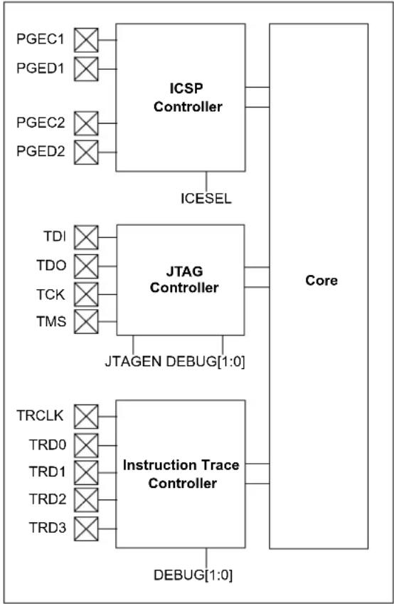
flowchart
graph TD
    A["PGEC1"] --> B["ICSP Controller"]
    C["PGED1"] --> B
    D["PGEC2"] --> B
    E["PGED2"] --> B
    B --> F["ICESEL"]
    G["TDI"] --> H["JTAG Controller"]
    I["TDO"] --> H
    J["TCK"] --> H
    K["TMS"] --> H
    H --> L["Core"]
    M["TRCLK"] --> N["Instruction Trace Controller"]
    O["TRD0"] --> N
    P["TRD1"] --> N
    Q["TRD2"] --> N
    R["TRD3"] --> N
    N --> S["DEBUG[1:0"]]
38.6 System Unlock Sequence
The following is the recommended system unlock sequence:
- Disable interrupts and DMA prior to the system unlock sequence.
- Execute the system unlock sequence by writing the Key values of 0xAA996655 and 0x556699AA to the SYSKEY register in two back-to-back Assembly or 'C' instructions.
- Perform the required configuration updates.
- Write a non-key value (such as 0x33333333) to the SYSKEY register to perform a lock.
- Re-enable interrupts and DMA.
Note: There are no timing requirements for the steps other than the initial back-to-back writing of the Key values to perform the unlock sequence. The unlock sequence unlocks all registers that are secured by the lock function. It is recommended that the system unlocked time be kept at a minimum.
Note: It is recommended that the reserved/undefined memory locations, such as read, write or read-modify-write, not be accessed. Accessing these memory locations could result in loss of functionality or unpredictable behavior of the device, and might adversely impact the device's health.
39.0 INSTRUCTION SET
The PIC32MZ W1 family supports both the microMIPS and MIPS32 instruction sets. Therefore all firmware must be written using microMIPS instructions, MIPS32 instructions, or a combination of both.
As dynamic switching between microMIPS and MIPS32 is possible (using the JALX and JALX32 instructions), the user need to only specify the ISA to be used for the first instruction after boot.
During a normal boot, the CPU fetches its first instruction from the reset vector at 0xBFC0_0000. The ISA for this instruction is specified using the BCFG0.BOOTISA bit. On a blank device, the reset value of the BCFG0.BOOTISA is '1', which places the device in MIPS32 instruction mode on exit from reset. However, it is assumed that on programming of the boot code, the BCFG0.BOOTISA bit is also programmed at the same time to match the instruction set of the boot code. The PIC32MZ1025W104 device family does not support the following features:
- Core extend instructions
• Coprocessor 2 instructions
Note: Refer to "MIPS32 ^® Architecture for Programmers Volume II: The MIPS32 ^® Instruction Set" for more information.
NOTES:
40.0 DEVELOPMENT SUPPORT
The PIC ^® MCUs and dsPIC ^® Digital Signal Controllers (DSC) are supported with a full range of software and hardware development tools:
• Integrated Development Environment
- MPLAB ^® X IDE Software
- Compilers/Assemblers/Linkers
- MPLAB XC Compiler
- MPASM ^TM Assembler
- M P L ^TM Object Linker/MPLIB ^TM Object Librarian
- MPLAB Assembler/Linker/Librarian for Various Device Families
- Simulators
- MPLAB X SIM Software Simulator
- Emulators
- MPLAB REAL ICE™ In-Circuit Emulator
• In-Circuit Debuggers (ICD)/Programmers
- MPLAB ICD 4/MPLAB ICD 5
- PICkit™ 3/PICkit™ 4/PICkit™ 5
- MPLAB Snap
- Device Programmers
- MPLAB PM3 Device Programmer
- Low-Cost Demonstration/Development Boards, Evaluation Kits and Starter Kits
• Third-party development tools
40.1 MPLAB X Integrated Development Environment Software
The MPLAB X IDE is a single, unified Graphical User Interface (GUI) for Microchip and third-party software, and hardware development tool that runs on Windows ^® , Linux and Mac OS ^® X. Based on the NetBeans IDE, MPLAB X IDE is an entirely new IDE with a host of free software components and plug-ins for high-performance application development and debugging. Moving between tools and upgrading from software simulators to hardware debugging and programming tools is simple with the seamless user interface.
With complete project management, visual call graphs, a configurable watch window and a feature-rich editor that includes code completion and context menus, MPLAB X IDE is flexible and friendly enough for new users. With the ability to support multiple tools on multiple projects with simultaneous debugging, MPLAB X IDE is also suitable for the needs of experienced users.
Feature-Rich Editor:
• Color syntax highlighting
- Smart code completion makes suggestions and provides hints as you type
• Automatic code formatting based on user-defined rules
- Live parsing
User-Friendly, Customizable Interface:
- Fully customizable interface: toolbars, toolbar buttons, windows, window placement, etc.
- Call graph window
Project-Based Workspaces:
- Multiple projects
- Multiple tools
- Multiple configurations
- Simultaneous debugging sessions
File History and Bug Tracking:
- Local file history feature
• Built-in support for Bugzilla issue tracker
40.2 MPLAB XC Compilers
The MPLAB XC Compilers are complete ANSI C compilers for all of Microchip's 8, 16, and 32-bit MCU and DSC devices. These compilers provide powerful integration capabilities, superior code optimization and ease of use. MPLAB XC Compilers run on Windows, Linux or MAC OS X.
For easy source level debugging, the compilers provide debug information that is optimized to the MPLAB X IDE.
The free MPLAB XC Compiler editions support all devices and commands, with no time or memory restrictions, and offer sufficient code optimization for most applications.
MPLAB XC Compilers include an assembler, linker and utilities. The assembler generates relocatable object files that can then be archived or linked with other relocatable object files and archives to create an executable file. MPLAB XC Compiler uses the assembler to produce its object file. Notable features of the assembler include:
- Support for the entire device instruction set
- Support for fixed-point and floating-point data
- Command-line interface
- Rich directive set
- Flexible macro language
- MPLAB X IDE compatibility
40.3 MPASM Assembler
The MPASM Assembler is a full-featured, universal macro assembler for PIC10/12/16/18 MCUs.
The MPASM Assembler generates relocatable object files for the MPLINK Object Linker, Intel® standard HEX files, MAP files to detail memory usage and symbol reference, absolute LST files that contain source lines and generated machine code, and COFF files for debugging.
The MPASM Assembler features include:
• Integration into MPLAB X IDE projects
- User-defined macros to streamline assembly code
- Conditional assembly for multipurpose source files
- Directives that allow complete control over the assembly process
40.4 MPLINK Object Linker/MPLIB Object Librarian
The MPLINK Object Linker combines relocatable objects created by the MPASM Assembler. It can link relocatable objects from precompiled libraries, using directives from a linker script.
The MPLIB Object Librarian manages the creation and modification of library files of precompiled code. When a routine from a library is called from a source file, only the modules that contain that routine will be linked in with the application. This allows large libraries to be used efficiently in many different applications.
The object linker/library features include:
- Efficient linking of single libraries instead of many smaller files
- Enhanced code maintainability by grouping related modules together
- Flexible creation of libraries with easy module listing, replacement, deletion and extraction
40.5 MPLAB Assembler, Linker and Librarian for Various Device Families
MPLAB Assembler produces relocatable machine code from symbolic assembly language for PIC24, PIC32 and dsPIC DSC devices. MPLAB XC Compiler uses the assembler to produce its object file. The assembler generates relocatable object files that can then be archived or linked with other relocatable object files and archives to create an executable file. Notable features of the assembler include:
- Support for the entire device instruction set
- Support for fixed-point and floating-point data
- Command-line interface
- Rich directive set
- Flexible macro language
- MPLAB X IDE compatibility
40.6 MPLAB X SIM Software Simulator
The MPLAB X SIM Software Simulator allows code development in a PC-hosted environment by simulating the PIC MCUs and dsPIC DSCs on an instruction level. On any given instruction, the data areas can be examined or modified and stimuli can be applied from a comprehensive stimulus controller. Registers can be logged to files for further run-time analysis. The trace buffer and logic analyzer display extend the power of the simulator to record and track program execution, actions on I/O, most peripherals and internal registers.
The MPLAB X SIM Software Simulator fully supports symbolic debugging using the MPLAB XC Compilers, and the MPASM and MPLAB Assemblers. The software simulator offers the flexibility to develop and debug code outside of the hardware laboratory environment, making it an excellent, economical software development tool.
40.7 MPLAB REAL ICE In-Circuit Emulator System
The MPLAB REAL ICE In-Circuit Emulator System is Microchip's next generation high-speed emulator for Microchip Flash DSC and MCU devices. It debugs and programs all 8, 16 and 32-bit MCU, and DSC devices with the easy-to-use, powerful GUI of the MPLAB X IDE.
The emulator is connected to the design engineer's PC using a high-speed USB 2.0 interface and is connected to the target with either a connector compatible with in-circuit debugger systems (RJ-11) or with the new high-speed, noise tolerant, Low-Voltage Differential Signal (LVDS) interconnection (CAT5).
The emulator is field upgradable through future firmware downloads in MPLAB X IDE. MPLAB REAL ICE offers significant advantages over competitive emulators including full-speed emulation, run-time variable watches, trace analysis, complex breakpoints, logic probes, a ruggedized probe interface and long (up to three meters) interconnection cables.
40.8 MPLAB ICD 4 and MPLAB ICD 5 In-Circuit Debugger System
The MPLAB ICD 4 and MPLAB ICD 5 In-Circuit Debugger are Microchip's most cost-effective, high-speed hardware debugger/programmer for Microchip Flash DSC and MCU devices. It debugs and programs PIC Flash MCUs and dsPIC DSCs with the powerful, yet easy-to-use GUI of the MPLAB IDE.
The MPLAB ICD 4 or MPLAB ICD 5 In-Circuit Debugger probe is connected to the PC using a high-speed USB 2.0 interface and can be connected to the target via a Microchip debug (RJ-11) connector (compatible with MPLAB ICD 2 and MPLAB REAL ICE systems). MPLAB ICD 4 and MPLAB ICD 5 supports all MPLAB ICD 2 headers.
40.9 PICkit 3, PICkit 4 and PICkit 5/ In-Circuit Debugger/Programmer
The MPLAB PICkit 3, PICkit 4 and PICkit 5 In-Circuit Debugger/Programmer are hardware debugger/programmer for PIC and dsPIC Flash MCUs at a most affordable price point using the powerful GUI of the MPLAB IDE.
The MPLAB PICkit 3 or PICkit 4 or PICkit 5 is connected to the PC using a full-speed USB interface and can be connected to the target via a Microchip debug (RJ-11) connector (compatible with MPLAB ICD 4, MPLAB ICD 5 and MPLAB REAL ICE). The connector uses two device I/O pins and the Reset line to implement In-Circuit Debugging and In-Circuit Serial Programming™ (ICSP).
40.10 MPLAB Snap In-Circuit Debugger/Programmer
The MPLAB Snap In-Circuit Debugger/Programmer is one of the most affordable hardware debugger/programmer for PIC and dsPIC Flash MCUs using the powerful GUI of the MPLAB IDE.
The user can connect the MPLAB Snap to the PC using a high-speed USB 2.0 interface, and it can also connect to the target via a Microchip debug (RJ-11 along with AC164110 and male to male header) connector (compatible with MPLAB ICD 4, MPLAB ICD 5 and MPLAB REAL ICE). The connector uses two device I/O pins and the Reset line to implement In-Circuit Debugging and In-Circuit Serial Programming (ICSP).
40.11 MPLAB PM3 Device Programmer
The MPLAB PM3 Device Programmer is a universal, CE compliant device programmer with programmable voltage verification at VDDMIN and VDDMAX for maximum reliability. It features a large LCD display (128 x 64) for menus and error messages, and a modular, detachable socket assembly to support various package types. The ICSP cable assembly is included as a standard item. In Stand-Alone mode, the MPLAB PM3 Device Programmer can read, verify and program PIC devices without a PC connection. It can also set code protection in this mode. The MPLAB PM3 connects to the host PC via an RS-232 or USB cable. The MPLAB PM3 has high-speed communications and optimized algorithms for quick programming of large memory devices, and incorporates an MMC card for file storage and data applications.
40.12 Demonstration/Development Boards, Evaluation Kits, and Starter Kits
A wide variety of demonstration, development and evaluation boards for various PIC MCUs and dsPIC DSCs allows quick application development on fully functional systems. Most boards include prototyping areas for adding custom circuitry and provide application firmware and source code for examination and modification.
The boards support a variety of features, including LEDs, temperature sensors, switches, speakers, RS-232 interfaces, LCD displays, potentiometers and additional EEPROM memory.
The demonstration and development boards can be used in teaching environments, for prototyping custom circuits and for learning about various MCU applications.
In addition to the PICDEM™ and dsPICDEM™ demonstration/development board series of circuits, Microchip has a line of evaluation kits and demonstration software for analog filter design, KEELOQ® security ICs, CAN, IrDA®, PowerSmart battery management, SEEVAL® evaluation system, Sigma-Delta ADC, flow rate sensing, plus many more.
Also available are starter kits that contain everything needed to experience the specified device. This usually includes a single application and debug capability, all on one board.
Check the Microchip website (www.microchip.com) for the complete list of demonstration, development and evaluation kits.
40.13 Third-Party Development Tools
Microchip also offers a great collection of tools from third-party vendors. These tools are carefully selected to offer good value and unique functionality.
• Device Programmers and Gang Programmers from companies, such as SoftLog and CCS
- Software Tools from companies, such as Gimpel and Trace Systems
- Protocol Analyzers from companies, such as Saleae and Total Phase
- Demonstration Boards from companies, such as MikroElektronika, Digilent® and Olimex
- Embedded Ethernet Solutions from companies, such as EZ Web Lynx, WIZnet and IPLogika®
41.0 ELECTRICAL SPECIFICATIONS
This chapter provides the electrical specifications and characteristics of the PIC32MZ1025W104 SoC and the WFI32 Module.
Note: All the information related to the WFI32E02 Module in this data sheet is Preliminary Information.
41.1 PIC32MZ1025W104 Electrical Specifications
The absolute maximum ratings for the PIC32MZ1025W104 devices are listed below. Exposure to these maximum rating conditions for extended periods may affect device reliability and performance. Functional operation of the device at these or any other conditions, above the parameters indicated in the operation listings of this specification, is not implied.
Absolute Maximum Ratings
Ambient temperature under bias....-40°C to +85°C
Storage temperature -65°C to +150°C
Voltage on VDD with respect to Vss -0.3V to +4.0V
Voltage on any pin with respect to Vss....-0.3V to (VDD + 0.3V)
Voltage on D+ or D- pin with respect to VUSB3V3 -0.3V to (VUSB3V3 + 0.3V)
Voltage on Vbus with respect to Vss -0.3V to (V_DD + 0.3V)
Maximum current out of Vss pin(s)....240 mA
Maximum current into VDD pin(s) ^(2) .....240 mA
Maximum current sunk/sourced by any 4x I/O pin ^(3) ....15 mA
Maximum current sunk/sourced by any 8x I/O pin ^(3) ....25 mA
Maximum current sunk by all ports 150 mA
Maximum current sourced by all ports ^(2) 150 mA
ESD Qualification:
Human Body Model (HBM) (JEDEC JS-001-2017) ±2000V
Changed Device Model (CDM) (JEDEC JS-002-2018) ±500V
Note 1: Stresses above those listed under “Absolute Maximum Ratings” may cause permanent damage to the device. This is a stress rating only and functional operation of the device at those or any other conditions, above those indicated in the operation listings of this specification, is not implied. Exposure to maximum rating conditions for extended periods may affect device reliability.
2: The maximum allowable current is a function of the device maximum power dissipation.
3: Characterized but not tested. Refer to parameters DO10 and DO20 for the 4x and 8x I/O pin lists.
TABLE 41-1: THERMAL OPERATING CONDITIONS
| Rating Symbol Min. Typ. Max. Unit | |||||
| Industrial Temperature Devices | |||||
| Operating junction temperature range T | J -40 — | +125 °C | |||
| Operating ambient temperature range T | A -40 — | +85 | °C | ||
| Power dissipation:Internal chip power dissipation: P_INT = V_DD × (I_DD - I_OH) I/O pin power dissipation: P_I/O = ((_DD - V_OH × I_OH) + (V_OL × I_OL)) | P_D | P_INT + P_I/O | W | ||
| Maximum allowed power dissipation | P_DMAX | (T_J - T_A)/ _JA | W | ||
TABLE 41-2: THERMAL PACKAGING CHARACTERISTICS
| Characteristics | Symbol | Typ. Max. | Unit | Notes | |
| Package thermal resistance, 132-pin DQFN (10x10x0.9 mm) | _JA | 24 | — | °C/W | 1 |
Note: Junction to ambient thermal resistance, Theta-JA (0JA) numbers are based on JEDEC 2S2P achieved by package simulations.
TABLE 41-3: RECOMMENDED OPERATING CONDITIONS
| DC CHARACTERISTICS | Standard Operating Conditions: 2.97V to 3.63V(unless otherwise stated)Operating temperature: -40°C ≤ TA ≤ +85°C | ||||||
| Param.No. | Symbol | Characteristics | Min. | Typical | Max. | Units | Conditions |
| DC10 | V_DD | Supply voltage(1) | 2.97 | 3.3 | 3.63 | V — | |
| V_BAT | Battery voltage range | V_DD | — | V_DD | V | — | |
| AV_DD | Analog supply voltage | V_DD | — | V_DD | V | — | |
| AVss | Analog ground voltage | V_SS | — | V_SS | V | — | |
| GNDDB | Common EDP ground reference | V_SS | V_SS | V_SS | V | — | |
| — | Wi-Fi Enable | On CPU frequency | 50 | — | 200 | MHz | — |
Note 1: Overall functional device operation at V BORMIN < VDD < VDDMIN is guaranteed, but not characterized. All device Analog modules, such as ADC, etc., will function, but with degraded performance below VDDMIN.
TABLE 41-4: PMU DC-DC MODE
| DC Characteristics | Standard Operating Conditions: 2.97V to 3.63V(unless otherwise stated)Operating temperature: -40°C ≤ TA ≤ +85°C | |||||
| Parameters | Characteristics | Min. | Typical | Max. | Units | Conditions |
| Output voltage range | — | 1.425 | 1.5 | 1.575 | V | — |
| Switching frequency | — | — | 1 | — | MHz | — |
| Operating Mode (PWM Mode) | ||||||
TABLE 41-4: PMU DC-DC MODE
| Load regulation(1) | Vout = 1.5V, IL = 0 mA to 450 mA | -1.5 0.5 | 1.5 % Depends on routing resis- | tance at the load applica-tion point | ||
| Line regulation | VIN = 2.97V to 3.63V, IL = 450 mA, Vout = 1.5 | -1.5 0.5 | 1.5 % — | |||
| Transient regulation | IL = 10 mA to 450 mA in 2 μs | -4 — 9 | % — | |||
| Efficiency(1) | VIN = 3.3V, Vout = 1.5V, 10 mA<IL<450 mA, DCR = 0.45 Ω | — | — | 85 | % | Depends on the inductor DCR and resistance of the load carrying paths |
| Quiescent current | Load Current = 0 | — | 350 | — | μA | — |
| Power Save Mode | ||||||
| Load current | — | 0.01 | — | 40 | mA | — |
| Load regulation | IL = 0.01 mA to 25 mA | -1.5 | 1 | 2 | % | — |
| Line regulation | VIN = 2.97V to 3.63V at IL = 25 mA | -1.5 1 | 2 % — | |||
| Transient regu-lation | IL = 0.01 mA to 25 mA | -1.5 1 | 2 — | |||
| Efficiency | VIN = 3.3V, Vout = 1.5V, 5 mA<IL<40 mA | — | — | 85 | % | — |
| Quiescent current | — | — | 150 | — | μA | — |
| External LC Filter Component(s) | ||||||
| Inductor (L) | — | — | 4.7 | — | μH | — |
| Inductor DCR (L_dcr)(1) | — | 0.05 | — | 0.29 | Ω | Lower is better for high load efficiency |
| Capacitor (C) | — | — | 10 | — | μF | — |
| Capacitor ESR(1) (Cesr) | — | — | 0.01 | — | Ω | Lower is better for low rip-ple |
| Capacitor ESL(1) (C_esl) | — | — | — | 5 | nH | Lower is better for high frequency ripple |
Note 1: Measurement depends on the quality of the evaluation board with respect to coupled noise, input bypass capacitor, output capacitor's ESR.
2: These parameters are characterized but not tested in manufacturing.
41.1.1 DC CHARACTERISTICS
TABLE 41-5: POR ELECTRICAL CHARACTERISTICS
| DC CHARACTERISTICS | Standard Operating Conditions: 2.97V to 3.63V(unless otherwise stated)Operating temperature: -40°C ≤ TA ≤ +85°C | ||||||
| Param.No. | Symbol | Characteristics | Min. | Typ. | Max. | Units | Conditions |
| DC16 | VPOR | VDD start voltageto ensure internalPOR signal(1) | 1.5 | — | — | V — | |
| DC17 | SVDD | VDD rise rateto ensure internalPOR signal | 0.03 | — | 0.115 V/ms | 110 | -28.7 ms at 3.3V |
TABLE 41-5: POR ELECTRICAL CHARACTERISTICS
Note 1: This is the limit to which VDD must be lowered to ensure POR.
TABLE 41-6: BOR ELECTRICAL CHARACTERISTICS
| DC CHARACTERISTICS | Standard Operating Conditions: 2.97V to 3.63V(unless otherwise stated)Operating temperature: -40°C ≤ TA ≤ +85°C | ||||||
| Param.No. | Symbol C | characteristics Min. | (1) | Typ. Max. Units | Conditions | ||
| BO10 | VBOR | BOR event on VDD transition high-to-low(2) | 2.6 — 2.8 | V | |||
Note 1: Parameters are for design guidance only and are not tested in manufacturing.
2: Overall functional device operation at VBORMIN < VDD < VDDMIN is tested, but not characterized. All device Analog modules, such as ADC, etc., will function, but with degraded performance below VDDMIN.
TABLE 41-7: OPERATING CURRENT (IDD, RF = OFF) (1)(2)
| DC CHARACTERISTICS | Standard Operating Conditions: 2.97V to 3.63V(unless otherwise stated)Operating temperature: -40°C ≤ TA ≤ +85°C | |||
| Param. No. | Typ.^(3) | Max. | Units | Conditions |
| I/O OPERATING CURRENT (IDD): PERIPHERAL ENABLED (PMDX = 0) | ||||
| DC20 | 3 | — | mA | 8 MHz ( FRC)^(4) |
| DC21 | 7.2 | — | mA | 40 MHz (POSC in HS mode) |
| DC22 | 10.7 | — | mA | 60 MHz (POSC in HS mode + SPLL)^(4) |
| DC23 | 12.5 | — | mA | 80 MHz (POSC in HS mode + SPLL)^(4) |
| DC24 | 14.2 | — | mA | 100 MHz (POSC in HS mode + SPLL)^(4) |
| DC25 | 16.2 | — | mA | 120 MHz (POSC in HS mode + SPLL)^(4) |
| DC26 | 23.6 | — | mA | 200 MHz (POSC in HS mode + SPLL)^(4) |
Note 1: A device's IDD supply current is mainly a function of the operating voltage and frequency. Other factors, such as PBCLK (Peripheral Bus Clock) frequency, number of peripheral modules enabled, internal code execution pattern, execution from Program Flash memory vs. SRAM, I/O pin loading and switching rate, oscillator type, as well as, temperature, can have an impact on the current consumption.
2: The test conditions for IDD measurements are as follows:
- CPU, Flash Panel and SRAM data memory are operational.
- All peripheral modules are disabled (ON bit = 0) but the associated PMD bit is cleared.
- Sysclk: PBCLK= 1:2.
• WDT and FSCM are disabled.
- All I/O pins are configured as inputs and pulled low.
- = V_DD
- VBUS3V3 connected to VDD.
• PMU in BUCK PWM mode.
3: Data in the "Typical" column is at 3.3V, 25°C unless otherwise stated.
4: This parameter is characterized but not tested in manufacturing.
TABLE 41-8: IDLE CURRENT (IDLE, RF = OFF)
| DC CHARACTERISTICS | Standard Operating Conditions: 2.97V to 3.63V(unless otherwise stated)Operating temperature: -40°C ≤ TA ≤ +85°C | |||
| Param. No. Typ. (1) | Max. Units Conditions | |||
| I/O Operating Current (IDLE): Core OFF (PMDx=0)(2) | ||||
| DC30a 2.6 — mA 8 MHz (FRC) | (3) | |||
| DC34a 16.2 — mA 200 MHz (POSC in HS mode + SP LL) | (3) | |||
Note 1: Data in the "Typical" column is at 3.3V, Ta = 25°C unless otherwise stated.
2: The test conditions for I IDLE current measurements are as follows:
- Sysclk: PBCLK = 1:2
• CPU in Idle mode (CPU core Halted)
- All peripheral modules are disabled (ON bit = 0), but the associated PMD bit is cleared
- WDT, FSCM and DMT Entry to Sleep state are disabled
- All I/O pins are configured as inputs and pulled high
- = V_DD
• PMU in BUCK PWM mode
3: This parameter is characterized but not tested in manufacturing.
TABLE 41-9: POWER-DOWN CURRENT (IPD)
| DC CHARACTERISTICS(6) | Standard Operating Conditions: 2.97V to 3.63V(unless otherwise stated)Operating temperature: -40°C ≤ TA ≤ +85°C | ||||
| Param. No. | Typ.(1) | Max. | Units | Conditions | |
| Power-Down Current (IPD)(2) | |||||
| DC40k | 1.75 | — | mA | -40°C | Sleep mode(2) |
| DC40l | 1.21 | — | mA | 25°C | |
| DC40m | 2.55 | — | mA | 85°C | |
| DC40o | 3.5 | — | μA | -40°C | Deep Sleep mode(4) |
| DC40p | 1.9 | — | μA | 25°C | |
| DC40q | 3.9 | — | μA | 85°C | |
| DC40s | 1.7 | — | μA | -40°C | Extreme Sleep mode(5) |
| DC40t | 0.71 | — | μA | 25°C | |
| DC40u | 2.12 | — | μA | 85°C | |
| Module Differential Current | |||||
| DC41e | 10 | — | μA | 3.3V | WDT current: ΔIwDT(3) |
| DC42e | 70 | — | μA | 3.3V | RTCC + Timer1 with 32 kHz Crystal: ΔIRTCC(3) |
| DC43d | 120 | — | μA | 3.3V | ADC: ΔIADC(3) |
| DC44 | 10 | — | μA | 3.3V | Deadman Timer Current: Dldmt(3) |
Note 1: Data in the "Typical" column is at 3.3V, Ta = 25°C unless otherwise stated.
2: The test conditions for IPD current measurements are as follows:
- All peripheral modules and clocks shut down (ON = 0, PMDx = 1)
• CPU clock is disabled
- All other system/PB clocks are disabled by hardware during sleep:
- Clock source oscillator except FRC is disabled, FRC is needed for PMU
- System clock-divider is optimally configured
- WLDO is turned OFF
- On-chip digital regulators are optimally configured to retain core
• PMU in BUCK PSM mode.
- All I/Os are configured as inputs and pulled high.
• WDT and FSCM are disabled.
- VUSB3V3 must be connected to VDD even when USB is not present
3: The current is the additional current consumed when the module is enabled. This current must be added to the base sleep mode (IPD) current.
4: Deep Sleep Test Condition:
• WCM Retention enabled
- RTC Enabled
- DSWDT enabled
- Extended semaphore set enabled
- PMU and Digital LDOs are turned off, System runs on 3.3V and ULPVREG
5: Extreme Deep Sleep Test Condition:
• WCM Retention disabled
- RTC disabled
- DSWDT disabled
- Extended semaphore set disabled
- PMU and Digital LDOs are turned off; System runs on 3.3V
6: These parameters are characterized but not tested in manufacturing.
TABLE 41-10: WI-FI POWER DOWN CURRENT
| DC CHARACTERISTICS ^(1, 2) | Standard Operating Conditions: 2.97V to 3.63V(unless otherwise stated)Operating temperature: -40°C ≤ TA ≤ +85°CMeasured at 25°C, 3.3V | |||
| Wi-Fi Power Mode | CPU State | Wi-Fi Functionality | Output Power (Typ.) (dBm) | Current (Typ.) (mA) ^(3) |
| WSM Sleep Wi-Fi | Sleep mode — 2.7 | |||
| WDS | Sleep Wi-Fi Deep Sleep mode | Sleep mode | — | 1.2 |
Note 1: Data in the "Typical" column is at 3.3V, Ta = 25°C unless otherwise stated.
2: CPU is in Wi-Fi RF Test mode.
3: The test conditions for current measurements are as follows:
- All peripheral modules and clocks shut down (ON = 0, PMDx = 1)
- CPU clock is disabled.
- All other system/PB clocks are disabled by hardware during sleep:
- Clock source oscillator except FRC are disabled, FRC is needed for PMU.
- System clock-divider are optimally configured.
- XTAL LDO is in Bypass mode.
- On-chip digital regulators are optimally configured to retain core.
- PMU in BUCK PSM mode.
- All I/Os are configured as inputs and pulled high.
- WDT and FSCM are disabled.
- Wake-up sources are disabled.
4: Wi-Fi Deep Sleep Test Condition:
- Clock source for WDS is LPRC.
5: The data is collected with RF Test software in lab condition without an active Wi-Fi connection to an Access Point (AP).
6: These parameters are characterized but not tested in manufacturing.
TABLE 41-11: WI-FI CURRENT
| DC CHARACTERISTICS(1, 2) | Standard Operating Conditions: 2.97V to 3.63V(unless otherwise stated)Operating temperature: -40°C ≤ TA ≤ +85°CMeasured at 25°C, 3.3V | ||
| Device States Code | Rate | Output Power (Typ.) (dBm) | Current (Typ.) (mA)(3) |
| On_Transmit(4) | 802.11b 1 Mbps 21.5 287 | ||
| 802.11b 1 Mbps 15.5 201 | |||
| 802.11b 11 Mbps 21.5 279 | |||
| 802.11g 6 Mbps 19.5 242 | |||
| 802.11g 54 Mbps 18.5 222 | |||
| 802.11n MCS0 19.5 251 | |||
| 802.11n MCS7 17.5 208 | |||
| 802.11n MCS7 11.5 169 | |||
| On_Receive | 802.11b 1 Mbps — 73 | ||
| 802.11n MCS7 — 88 | |||
Note 1: Measured along with RF matching network and FEM circuit (assume 50Ω impedance).
2: The test conditions for I IDD current measurements are as follows:
- CPU, Flash Panel and SRAM data memory are operational.
• CPU is operating at 50 MHz.
• CPU is in Wi-Fi RF Test mode.
- All peripheral modules are disabled (ON bit = 0) but the associated PMD bit is cleared.
• WDT and FSCM are disabled.
- All I/O pins are configured as inputs and pulled high.
• VBUS3V3 connected to VDD
- MCLR = VDD
3: Data in the "Typ." column is at 3.3V, 25°C unless otherwise stated.
4: Tested at channel 7 in Fixed Mode Gain.
5: These parameters are characterized but not tested in manufacturing.
TABLE 41-12: I/O PIN INPUT SPECIFICATIONS
| DC CHARACTERISTICS | Standard Operating Conditions: 2.97V to 3.63V (unless otherwise stated)Operating temperature: -40°C ≤ TA ≤ +85°C | ||||||
| Param.No. | Symbol | Characteristics | Min. | Typ.^(1) | Max. | Units | Conditions |
| DI10 | V_IL | Input low voltageI/O pinsSDAx, SCLxSDAx, SCLx | V_ss V_ss V_ss | — — — | 0.2 * V_DD 0.3 * V_DD 0.8 | VVV | — SMBus disabled^(4) SMBus enabled^(4) |
| DI18 | |||||||
| DI19 | |||||||
| DI20 | V_IH | Input high voltageI/O pins | 0.80 * V_DD | — | V_DD | V | (4) |
| DI30 | ICNPU | Change notification pull-up current | — | — | -40 | μA | V_DD = 3.3V, V_PIN = V_SS^(3) |
Note 1: Data in the "Typ." column is at 3.3V, +25°C unless otherwise stated.
2: The leakage current on the MCLR pin is strongly dependent on the applied voltage level. The specified levels represent normal operating conditions. Higher leakage current may be measured at different input voltages.
3: Negative current is defined as current sourced by the pin.
4: This parameter is characterized but not tested in manufacturing.
TABLE 41-12: I/O PIN INPUT SPECIFICATIONS (CONTINUED)
| DC CHARACTERISTICS | Standard Operating Conditions: 2.97V to 3.63V (unless otherwise stated)Operating temperature: -40°C ≤ TA ≤ +85°C | ||||||
| Param.No. | Symbol | Characteristics | Min. | Typ.^(1) | Max. | Units | Conditions |
| DI31 ICNPD | Change | notification pull-down current^(4) | 40 | — | — | μA | V_DD = 3.3V, V_PIN = V_DD |
| DI50 | I/L Input leakage current (3) | ||||||
| I/O ports | — | — | ±1 | μA | V_SS ≤ V_PIN ≤ V_DD, Pin at high-impedance | ||
| DI51 | Analog input pins | — | — | ±1 | μA | V_SS ≤ V_PIN ≤ V_DD, Pin at high-impedance | |
| DI55 MCLR | ——(2) | — | — | ±1 | μA | V_SS ≤ V_PIN ≤ V_DD | |
| DI56 | XTAL_IN | — | — | ±1 | μA | V_SS ≤ V_PIN ≤ V_DD, HS mode | |
Note 1: Data in the "Typ." column is at 3.3V, +25°C unless otherwise stated.
2: The leakage current on the MCLR pin is strongly dependent on the applied voltage level. The specified levels represent normal operating conditions. Higher leakage current may be measured at different input voltages.
3: Negative current is defined as current sourced by the pin.
4: This parameter is characterized but not tested in manufacturing.
TABLE 41-13: I/O PIN OUTPUT SPECIFICATIONS
| DC CHARACTERISTICS | Standard Operating Conditions: 2.97V to 3.63V(unless otherwise stated)Operating temperature: -40°C ≤ TA ≤ +85°C | ||||||
| Param.No. | Symbol C | Characteristic Min. Typ. Max. Units | Conditions | ||||
| DO10 | Vol | Output low voltageI/O pins:4x sink driver pins -RA2-RA10, RA12-RA15, RB0-RB13, RC9-RC12, RK0-RK12 | — | — | 0 | . 4 | IOL ¥ 10 mA, VDD = 3.3V |
| Output low voltageI/O pins:8x sink driver pins -RA0, RA1, RA11, RC0,RC1,RC8, RC9, RC13, RC14,RC15, RK13, RK14 | — | — | 0 | .V 4 | IOL ≤ 15 mA, VDD = 3.3V | ||
| DO20 V | OH | Output high voltageI/O pins:4x source driver pins -RA2-RA10, RA12-RA15, RB0-RB13, RC9-RC12, RK0-RK12 | 2.4 — | — | V | I | OH ≥ -10 mA, VDD = 3.3V |
| Output high voltageI/O pins:8x source driver pins -RA0, RA1, RA11, RC0,RC1,RC8, RC9, RC13, RC14,RC15, RK13, RK14 | 2.4 — | — | V | I | OH ≥ -15 mA, VDD = 3.3V | ||
| DO20a | VoH1 | Output high voltageI/O pins:4x source driver pins -RA2-RA10, RA12-RA15, RB0-RB13, RC9-RC12, RK0-RK12 | 1.5 — | — | V | I | OH ≥ -14 mA, VDD = 3.3V |
| 2.0 | — | — | V | IOH ≥ -12 mA, VDD = 3.3V | |||
| 3.0 | — | — | V | IOH ≥ -7 mA, VDD = 3.3V | |||
| Output high voltageI/O pins:8x source driver pins -RA0, RA1, RA11, RC0,RC1,RC8, RC9, RC13, RC14,RC15, RK13, RK14 | 1.5 — | — | V | I | OH ≥ -22 mA, VDD = 3.3V | ||
| 2.0 | — | — | V | IOH ≥ -18 mA, VDD = 3.3V | |||
| 3.0 — | — | V | I | OH ≥ -10 mA, VDD = 3.3V | |||
Note: These parameters are characterized but not tested in manufacturing.
41.1.2 AC CHARACTERISTICS AND
TIMING PARAMETERS
The information contained in this section defines the PIC32MZ1025W104 device AC characteristics and timing parameters.
FIGURE 41-1: LOAD CONDITIONS FOR DEVICE TIMING SPECIFICATIONS
Load Condition 1 – for all pins except XTAL_OUT
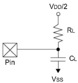
• R L = 464Ω
- C_L = 50 pF for all pins except XTAL_OUT
- C_L = 12 pF for XTAL_OUT output
TABLE 41-14: CAPACITIVE LOADING REQUIREMENTS ON OUTPUT PINS
| AC CHARACTERISTICS | Standard Operating Conditions: 2.97V to 3.63V(unless otherwise stated)Operating temperature: -40°C ≤ TA ≤ +85°C | ||||||
| Param.No. | Symbol | Characteristics Min. Typ. | (1) | Max. Units Conditions | |||
| DO56 | CL All I/O | pins (except pinsused as CxOUT) | — | — | 5 | 0 | pF — |
| DO58 | CB | SCLx, SDAx | — | — | 400 | pF | I2C mode |
| DO59 | CsQI | All SQI pins | — | — | 10 | pF | — |
Note 1: Data in the "Typ." column is at 3.3V, +25°C unless otherwise stated.
FIGURE 41-2: CRYSTAL OSCILLATOR TIMING CHARACTERISTICS

TABLE 41-15: CRYSTAL OSCILLATOR TIMING REQUIREMENTS
| AC CHARACTERISTICS | Standard Operating Conditions: 2.97V to 3.63V (unless otherwise stated)Operating temperature: -40°C ≤ TA ≤ +85°C | ||||||
| Param.No. | Symbol | Characteristics Min. Typ. | (3) | Max. Units Conditions | |||
| OS13 Fosc Primary oscillator crystal frequency (1,2) | — | 4 | 0 | — | M H | ||
| Frequency stability – temperature and aging(3) | -20 | — | 20 ppm | — | |||
| OS15 Fosc Secondary oscillator crystal frequency (2) | — | 32.768 | — | kHz | Sosc | ||
| Frequency stability – temperature and aging(3) | -100 — | 100 ppm | — | ||||
| OS20 | Tosc | Tosc | — | 1/Fosc | — | — | See parameter OS13 for Fosc value |
| OS40 | Tost | Oscillator start-up timer period(Only applies to HS, HSPLL and Sosc Clock Oscillator modes) | — | 1 (4) | 0— | 2Tosc | Crystal stabilization time only, not Oscillator Ready. |
| OS41 | TFSCM | Primary clock fail safe time-out period | — | 2 | — | ms | — |
| OS42 | Gm | External oscillator transconductance | — | 16 | — | μA/V | VDD = 3.3V,TA = +25°C |
| — | Cosco | XTAL_OUT pin capacitive load | — | — | 12 | pF | VDD = 3.3V,TA = +25°C |
Note 1: Crystal oscillator requirements:
• Crystal load capacitance = 12 pF
- ESR = 50Ω
• Maximum Drive level = 200 μW
2: Correct oscillator and associated components selection are critical to meet these specifications.
3: These parameters are characterized but not tested in manufacturing.
4: This value is for guidance only. A major component of crystal start-up time is based on the third-party crystal MFG parasitics that are outside the scope of this specification. If this is a major concern, the customer needs to characterize this based on their design choices.
TABLE 41-16: SYSTEM TIMING REQUIREMENTS
| AC CHARACTERISTICS | Standard Operating Conditions: 2.97V to 3.63V(unless otherwise stated)Operating temperature: -40°C ≤ TA ≤ +85°C | ||||||
| Param.No. | Symbol | Characteristics Min. Typ. Max. | Units Conditions | ||||
| OS51 Fsys System frequency DC — 200 MHz — | |||||||
| OS55a | FPB | Peripheral bus frequency | DC | — | 100 | MHz | — |
| OS56 F | REF | Reference clock frequency | — | — | 40 | MHz | — |
TABLE 41-17: PLL CLOCK TIMING SPECIFICATIONS
| AC CHARACTERISTICS | Standard Operating Conditions: 2.97V to 3.63V(unless otherwise stated)Operating temperature: -40°C ≤ TA ≤ +85°C | |||||||
| Param.No. | Symbol | Characteristics | Min. | Typ. | Max. | Units | Conditions | |
| OS50 | FIN | PLL input frequency range | 8 | — | 40 | MHz | BTPLL,SYS-PLL,EWPLL,UPLL modes | |
| OS52 | TLOCK | PLL start-up time (lock time) | — | — | 256 x R | μs | R = Divide reference period | |
| OS54 | FVco | PLL Vco frequency range | 880 | — | 1600 | MHz | — | |
| FPLL | PLL output frequency range | 16 | — | 200 | MHz | Non-bypass mode | ||
Note: These parameters are characterized but not tested in manufacturing.
TABLE 41-18: INTERNAL FRC ACCURACY
| AC CHARACTERISTICS | Standard Operating Conditions: 2.97V to 3.63V(unless otherwise stated)Operating temperature: -40°C ≤ TA ≤ +85°C | |||||
| Param.No. | Characteristics(1) | Min. | Typ. | Max. | Units | Conditions |
| Internal FRC Accuracy @ 8.00 MHz(2) | ||||||
| F20 | FRC | -0.9 | — | +0.9 | % | — |
Note 1: This parameter is characterized but not tested in manufacturing.
2: Frequency calibrated at +25^ and 3.3V. The TUN bits (OSCTUN[5:0]) can be used to compensate for temperature drift.
TABLE 41-19: INTERNAL LPRC ACCURACY
| AC CHARACTERISTICS | Standard Operating Conditions: 2.97V to 3.63V(unless otherwise stated)Operating temperature: -40°C ≤ TA ≤ +85°C | |||||
| Param.No. | Characteristics(1) | Min. | Typ. | Max. | Units | Conditions |
| Internal LPRC @ 32.768 kHz(2) | ||||||
| F21 | LPRC | -18 | — | +13 | % | — |
Note 1: This parameter is characterized but not tested in manufacturing.
2: Change of LPRC frequency as V_DD and temperature changes.
FIGURE 41-3: I/O TIMING CHARACTERISTICS
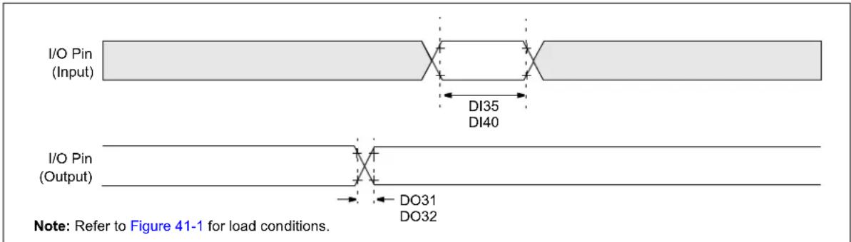
TABLE 41-20: I/O TIMING REQUIREMENTS
| AC CHARACTERISTICS | Standard Operating Conditions: 2.97V to 3.63V(unless otherwise stated)Operating temperature: -40°C ≤ TA ≤ +85°C | ||||||
| Param.No. | Symbol | Characteristics (2) | Min. Typ. (1) | Max. Units | Conditions | ||
| DO31 | TIOR Port | output rise timeI/O pins:4x source driver pins -RA2-RA10, RA12-RA15, RB0-RB13,RC9-RC12, RK0-RK12 | — | — | 9 | . | LOAD = 50 pF |
| — | — | 6 | n | s | |||
| Port output rise timeI/O pins:8x source driver pins -RA0, RA1, RA11, RC0, RC1,RC8,RC9, RC13, RC14, RC15, RK13,RK14 | — | — | 8 | n | s | ||
| — | — | 6 | n | LOAS = 20 pF | |||
| DO32 | TIOF | Port output fall timeI/O pins:4x source driver pins -RA2-RA10, RA12-RA15, RB0-RB13,RC9-RC12, RK0-RK12 | — | — | 9 | . | 5 n |
| — | — | 6 | n | LOAS = 20 pF | |||
| Port output fall timeI/O pins:8x source driver pins -RA0, RA1, RA11, RC0, RC1,RC8,RC9, RC13, RC14, RC15, RK13,RK14 | — | — | 8 | n | LOAS = 50 pF | ||
| — | — | 6 | n | LOAS = 20 pF | |||
| DI35 | TINP | INTx pin high or low time | 5 | — | — | ns | — |
| DI40 | TRBP | CNx high or low time (input) | 5 | — | — | ns | — |
Note 1: Data in the "Typ." column is at 3.3V, +25°C unless otherwise stated.
2: These parameters are characterized but not tested in manufacturing.
FIGURE 41-4: POWER-ON RESET TIMING CHARACTERISTICS
Clock Sources = (FRC, FRCDIV, FRCDIV16, FRCPLL and LPRC)
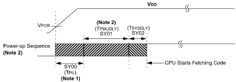
Clock Sources = (HS, HSPLL and Sosc)
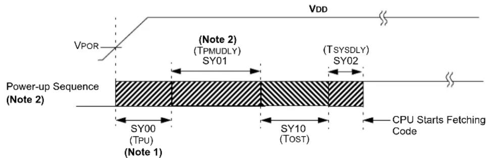
Note 1: The power-up period will be extended if the power-up sequence completes before the device exits from BOR (VDD < VBORmax).
2: SY01 is negligible when PMU is retained in MLDO mode.
FIGURE 41-5: EXTERNAL RESET TIMING CHARACTERISTICS
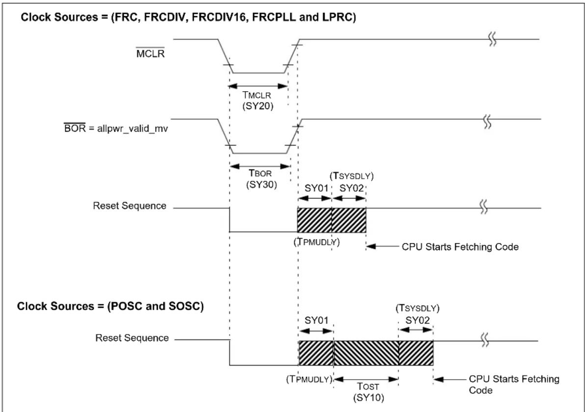
flowchart
graph TD
    A["Clock Sources = (FRC, FRCDIV, FRCDIV16, FRCPLL and LPRC)"] --> B["MCLR"]
    B --> C["TMCLR (SY20)"]
    C --> D["BOR = allpwr_valid_mv"]
    D --> E["TBOR (SY30)"]
    E --> F["Reset Sequence"]
    F --> G["(TPMUDLY)"]
    G --> H["CPU Starts Fetching Code"]
    I["Clock Sources = (POSC and SOSC)"] --> J["Reset Sequence"]
    J --> K["(TPMUDLY)"]
    K --> L["TOST (SY10)"]
    L --> M["(TPMUDLY)"]
    M --> N["CPU Starts Fetching Code"]
    O["Clock Sources = (POSC and SOSC)"] --> P["Reset Sequence"]
    P --> Q["(TPMUDLY)"]
    Q --> R["TOST (SY10)"]
    R --> S["(TPMUDLY)"]
    S --> T["CPU Starts Fetching Code"]
TABLE 41-21: RESETS TIMING
| AC CHARACTERISTICS | Standard Operating Conditions: 2.97V to 3.63V (unless otherwise stated)Operating temperature: -40°C ≤ TA ≤ +85°C | ||||||
| Param.No. | Symbol | Characteristics (1) | Min. Typ. (2) | Max. Units Conditions | |||
| SY00 T | PU Power-up periodinternal voltage regulator enabled | — 400 | 600 μs | — | |||
| SY02 T | SYSDLY | System delay period:time required to reload device con-figuration fuses plus SYSCLKdelay before first instruction isfetched. | — | 1 μs +8 SYSCLKcycles | — | — | — |
| SY20 T | MCLR | MCLR pulse width (low) | 2 | — | — | μs | — |
| SY30 T | BOR | BOR pulse width (low) | — | 1 | — | μs | — |
Note 1: These parameters are characterized but not tested in manufacturing.
2: Data in the "Typ" column is at 3.3V, +25°C unless otherwise stated.
FIGURE 41-6: TIMER1-TIMER7 TIMING CHARACTERISTICS
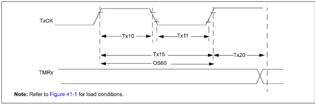
TABLE 41-22: TIMER1 TIMING REQUIREMENTS (1)
| AC CHARACTERISTICS | Standard Operating Conditions: 2.97V to 3.63V(unless otherwise stated)Operating temperature: -40°C ≤ TA ≤ +85°C | |||||||
| Param.No. | Symbol Characteristics (2) | Min. Typ. Max. Units Conditions | ||||||
| TA10 TTXH | T | x high time | Synchro-kous, with pres-caler | [(12.5 ns or 1 T_PB1\_CLK )/N] + 20 ns | — — | ns | Must also meet parameter TA15(3) | |
| Asynchro-nous, with pres-caler | 10 | — — | ns | — | ||||
| TA11 | TTXL | TxCK low time | Synchronous, with pres-caler | [(12.5 ns or 1 T_PB1\_CLK )/N] + 20 ns | — — | ns | Must also meet parameter TA15(3) | |
| Asynchro-nous, with pres-caler | 10 | — — | ns | — | ||||
| TA15 | TTXP | TxCK input period | Synchronous, with pres-caler | [(Greater of 20 ns or 2 T_PB1\_CLK )/N] + 30 ns | — | — | ns | V_DD > 2.97V (3) |
| Asynchro-nous, with pres-caler | 20 | — | — | ns | V_DD > 2.97V | |||
| OS60 | FT1 | SOSCI/T1CK oscillator input frequency range(osillator enabled by set-ting TCS bit (T1CON[1])) | 32.768 | — 50 | kHz | — | ||
| TA20 T | CKEXTMRL | Delay from external TxCK clock edge to timer increment | — | 1 | T_PB1\_CLK | — | ||
Note 1: Timer1 is a Type A timer.
2: These parameters are characterized but not tested in manufacturing.
3: N = Prescale Value (1, 8, 64, 256).
TABLE 41-23: TIMER2-TIMER7 TIMING REQUIREMENTS
| AC CHARACTERISTICS | Standard Operating Conditions: 2.97V to 3.63V(unless otherwise stated)Operating temperature: -40°C ≤ TA ≤ +85°C | |||||||
| Param.No. | Symbol | Characteristics Min. Max. Units Conditions | ||||||
| TB10 Ttx | H TxCK | high time | Synchro-nous, with prescaler | [(12.5 ns or 1 T_PB1\_CLK )/N] + 25 ns | — ns | Must also | meet parame-ter TB15 | N = pres-scale value(1, 2, 4, 8,16, 32, 64,256) |
| TB11 Ttx | L TxCK | low time | Synchro-nous, with prescaler | [(12.5 ns or 1 T_PB1\_CLK )/N] + 25 ns | — ns | Must also | meet parame-ter TB15 | |
| TB15 Ttx | P TxCK | input period | Synchro-nous, with prescaler | [(Greater of [(25 ns or 2 T_PB1\_CLK )/N] + 30 ns | — | ns | VDD >2.97V | |
| TB20 TCKEXT-MRL | Delay from external TXCK clock edge to timer increment | — | 1 | T_PB1\_CLK | — | |||
Note: These parameters are characterized but not tested in manufacturing.
FIGURE 41-7: INPUT CAPTURE (CAPx) TIMING CHARACTERISTICS
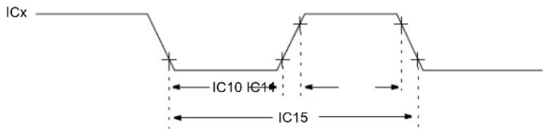
Note: Refer to Figure 41-1 for load conditions.
TABLE 41-24: INPUT CAPTURE MODULE TIMING REQUIREMENTS
| AC CHARACTERISTICS | Standard Operating Conditions: 2.97V to 3.63V(unless otherwise stated)Operating temperature: -40°C ≤ TA ≤ +85°C | ||||||
| Param.No. | Symbol | Characteristics Min. M | Max. Units Conditions | ||||
| IC10 TccL | ICx input | low time [(12.5 ns or 1 /N] + 25 ns | T_PB1\_CLK | — ns | Must alsomeetparameterIC15. | N = prescalevalue (1, 4, 16) | |
| IC11 | TccH | ICx input high time | [(12.5 ns or 1 T_PB1\_CLK /N] + 25 ns | — ns | Must alsomeetparameterIC15. | ||
| IC15 | TccP | ICx input period | [(25 ns or 2 T_PB1\_CLK /N] + 50 ns | — | ns | — | |
Note: These parameters are characterized but not tested in manufacturing.
FIGURE 41-8: OUTPUT COMPARE MODULE (OCx) TIMING CHARACTERISTICS
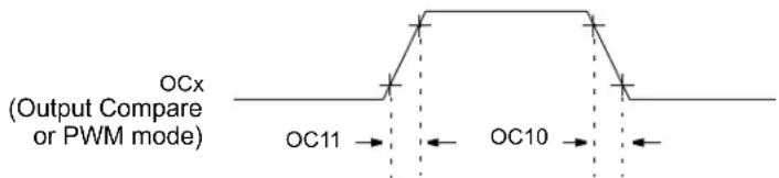
Note: Refer to Figure 41-1 for load conditions.
TABLE 41-25: OUTPUT COMPARE MODULE TIMING REQUIREMENTS
| AC CHARACTERISTICS | Standard Operating Conditions: 2.97V to 3.63V(unless otherwise stated)Operating temperature: -40°C ≤ TA ≤ +85°C | ||||||
| Param.No. | Symbol | Characteristics(1) | Min. Typ. | (2) | Max. | Units | Conditions |
| OC10 | TccF | OCx output fall time | — | — | — | ns | See parameter DO32 |
| OC11 | TccR | OCx output rise time | — | — | — | ns | See parameter DO31 |
Note 1: These parameters are characterized but not tested in manufacturing.
2: Data in the "Typ." column is at 3.3V, +25°C unless otherwise stated. Parameters are for design guidance only and are not tested.
FIGURE 41-9: SPIx MODULE HOST MODE (CKE = 0) TIMING CHARACTERISTICS
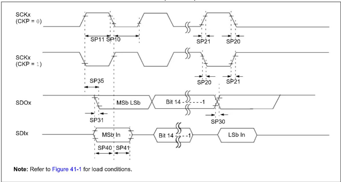
flowchart
graph TD
    A["SCKx (CKP = 0)"] --> B["SP11 SP10"]
    B --> C["SP21 SP20"]
    D["SCKx (CKP = 1)"] --> E["SP35"]
    E --> F["SP20 SP21"]
    G["SDOx"] --> H["MSb LSb"]
    H --> I["Bit 14 - - - 1"]
    I --> J["SP30"]
    K["SDIx"] --> L["MSb In"]
    L --> M["Bit 14 - - - 1"]
    M --> N["LSb In"]
    O["Note: Refer to Figure 41-1 for load conditions."]
TABLE 41-26: SPIx HOST MODE (CKE = 0) TIMING REQUIREMENTS
| AC CHARACTERISTICS | Standard Operating Conditions: 2.97V to 3.63V (unless otherwise stated)Operating temperature: -40°C ≤ TA ≤ +85°C | ||||||
| Param.No. | Symbol Characteristics (1) | Min. Typ. | (2) | Max. Units Conditions | |||
| SP10 TscL SCKx output low time (3) | Tsck/2 | — | — | ns — | |||
| SP11 | TscH | SCKx output high time(3) | Tsck/2 | — | — | ns — | |
| SP15 | Tsck | SPI clock speed | — | — | 40 | MHz | SPI1 on RPC6 |
| — | — | 20 | MHz | SPI1 on RPC6 and SPI2 on RPA11 on PPS configuration | |||
| SP20 TscF | SCKx output fall time (4) | — | — | — | ns | See parameter DO32 | |
| SP21 TscR | SCKx output rise time (4) | — | — | — | ns | See parameter DO31 | |
| SP30 TdoF | SDOx data output fall time (4) | — | — | — | ns | See parameter DO32 | |
| SP31 TdoR | SDOx data output rise time (4) | — | — | — | ns | See parameter DO31 | |
| SP35 TscH2doV, TscL2doV | SDOx data output valid after SCKx edge | — | — | 7 | ns | VDD > 2.97V | |
| SP40 TdiV2scH, TdiV2scL | Setup time of SDIx data input to SCKx edge | 5 | — | — | ns | — | |
| SP41 TscH2diL, TscL2diL | Hold time of SDIx data input to SCKx edge | 5 | — | — | ns | — | |
Note 1: These parameters are characterized but not tested in manufacturing.
2: Data in the "Typ." column is at 3.3V, +25°C unless otherwise stated.
3: The minimum clock period for SCKx is 25 ns. Therefore, the clock generated in Host mode must not violate this specification.
4: Assumes 10 pF load on all SPIx pins.
5: To achieve maximum data rate, V DD must be ≥ 3.3V , the SMP bit (SPIxCON[9]) must be equal to '1'.
FIGURE 41-10: SPIx MODULE HOST MODE (CKE = 1) TIMING CHARACTERISTICS
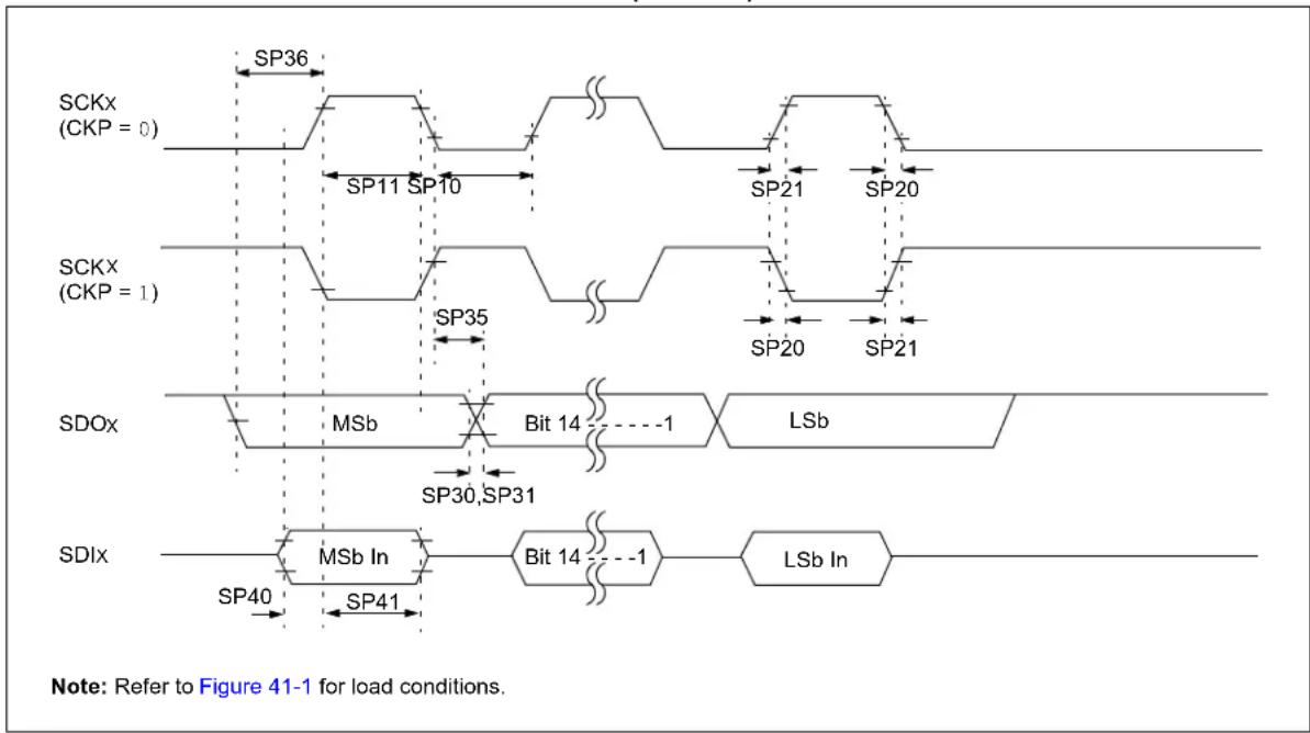
flowchart
graph TD
    A["SCKx (CKP = 0)"] --> B["SP36"]
    B --> C["SP11 SP10"]
    C --> D["SP21 SP20"]
    E["SCKx (CKP = 1)"] --> F["SP35"]
    F --> G["SP20 SP21"]
    H["SDOx"] --> I["MSb"]
    I --> J["Bit 14 -1"]
    J --> K["LSb"]
    L["SDIx"] --> M["MSb In"]
    M --> N["Bit 14 -1"]
    N --> O["LSb In"]
    P["Note: Refer to Figure 41-1 for load conditions."]
TABLE 41-27: SPIx MODULE HOST MODE (CKE = 1) TIMING REQUIREMENTS
| AC CHARACTERISTICS | Standard Operating Conditions: 2.97V to 3.63V(unless otherwise stated)Operating temperature: -40°C ≤ TA ≤ +85°C | ||||||
| Param.No. | Symbol Characteristics (1) | Min. Typ. (2) | Max. Units Conditions | ||||
| SP10 TscL SCKx output low time (3) | Tsck/2 — | — | ns — | ||||
| SP11 TscH SCKx output high time (3) | Tsck/2 — | — | ns — | ||||
| SP15 | Tsck | SPI clock speed | — | — | 40 | MHz | SPI1 on RPC6 |
| — | — | 20 | MHz | SPI1 and SPI2 on PPS configuration | |||
| SP20 TscF SCKx output fall time (4) | — | — | — | ns | See parameter DO32 | ||
| SP21 TscR SCKx output rise time (4) | — | — | — | ns | See parameter DO31 | ||
| SP30 TcOxF SDOx data output fall time (4) | — | — | — | ns | See parameter DO32 | ||
| SP31 TcORO SDOx data output rise time (4) | — | — | — | ns | See parameter DO31 | ||
| SP35 TscH2doV,TscL2doV | SDOx data output valid afterSCKx edge | — | — | 7 | ns | VDD > 2.97V | |
| SP36 TcOv2sc,TdoV2scL | SDOx data output setup tofirst SCKx edge | — | — | 7 | ns | — | |
| SP40 TcIv2scH,TdiV2scL | Setup time of SDIx data inputto SCKx edge | 7 | — | — | ns | VDD > 2.97V | |
| SP41 TscH2diL,TscL2diL | Hold time of SDIx data inputto SCKx edge | 7 | — | — | ns | VDD > 2.97V | |
Note 1: These parameters are characterized but not tested in manufacturing.
2: Data in the "Typ." column is at 3.3V, +25°C unless otherwise stated.
3: The minimum clock period for SCKx is 25 ns. Therefore, the clock generated in Host mode must not violate this specification.
4: Assumes 10 pF load on all SPIx pins.
5: To achieve the maximum data rate, V DD must be ≥ 3.3V and the SMP bit (SPIxCON[9]) must be equal to '1'.
FIGURE 41-11: SPIx MODULE CLIENT MODE (CKE = 0) TIMING CHARACTERISTICS
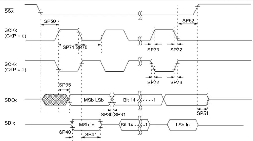
flowchart
graph TD
    subgraph SSx
        A["SP50"] --> B["SCKx (CKP = 0)"]
        B --> C["SP71 SP70"]
        C --> D["SCKx (CKP = 1)"]
        D --> E["SP35"]
        E --> F["SDOx"]
        F --> G["MSb LSb Bit 14 -1"]
        G --> H["SP30, SP31"]
        H --> I["SDIx"]
        I --> J["MSb In Bit 14 -1"]
        J --> K["LSb In"]
    end
    subgraph SCKx
        L["SP52"] --> M["SCKx (CKP = 0)"]
        M --> N["SP73 SP72"]
        N --> O["SCKx (CKP = 1)"]
        O --> P["SP72 SP73"]
        P --> Q["SP51"]
    end
    subgraph SDOx
        R["SP40"] --> S["SDIx"]
        S --> T["MSb In SP41"]
        T --> U["Bit 14 -1"]
        U --> V["LSb In"]
    end
Note: Refer to Figure 41-1 for load conditions.
TABLE 41-28: SPIx MODULE CLIENT MODE (CKE = 0) TIMING REQUIREMENTS
| AC CHARACTERISTICS | Standard Operating Conditions: 2.97V to 3.63V (unless otherwise stated)Operating temperature: -40°C ≤ TA ≤ +85°C | ||||||
| Param.No. | Symbol Characteristics (1) | Min. | Typ.^(2) | Max. | Units | Conditions | |
| SP15 | Tsck | SPI clock speed | — | — | 40 | MHz | SPI1 on RPC6 |
| — | — 20 MHz | SPI1 and SPI2 on PPS configuration | |||||
| SP70 TscL | SC | Kx input low time (3) | Tsck/2 | — | — | ns | — |
| SP71 TscH | SC | Kx input high time (3) | Tsck/2 | — | — | ns | — |
| SP72 | TscF | SCKx input fall time | — | — | — | ns | See parameter DO32 |
| SP73 | TscR | SCKx input rise time | — | — | — | ns | See parameter DO31 |
| SP30 TdoF | SD | Ox data output fall time (4) | — | — | — | ns | See parameter DO32 |
| Param.No. | Symbol Char | acteristics (1) | Min. Typ. (2) | Max. | Units | Conditions | |
| SP31 TdoR SDOx data | output rise time (4) | — — — | ns See parameter | DO31 | |||
| SP35 TscH2doV, TscL2doV | SDOx data output valid after SCKx edge | — | — | 7 | n | ISO > 2.97W | |
| SP40 TdiV2scH, TdiV2scL | Setup time of SDlx data input to SCKx edge | 5 | — | — | ns | — | |
| SP41 TscH2diL, TscL2diL | Hold time of SDlx data input to SCKx edge | 5 | — | — | ns | — | |
| SP50 TssL2scH, TssL2scL | SSx ↓ to SCKx ↑ or SCKx input | 55 | — | — | ns | — | |
| SP51 | TssH2doZ | SSx ↑ to SDOx output high-impedance(3) | 2.5 | — 12 ns | — | ||
| SP52 TscH2ssH TscL2ssH | SSx after SCKx edge | — 75 | — ns | — | |||
Note 1: These parameters are characterized but not tested in manufacturing.
2: Data in the "Typ." column is at 3.3V, +25°C unless otherwise stated.
3: The minimum clock period for SCKx is 25 ns.
4: Assumes 10 pF load on all SPIx pins.
FIGURE 41-12: SPIx MODULE CLIENT MODE (CKE = 1) TIMING CHARACTERISTICS
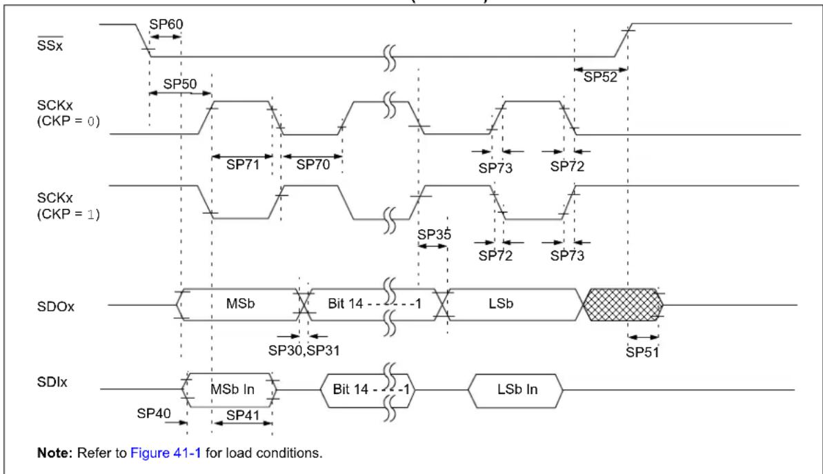
flowchart
graph TD
    subgraph SSx
        A["SP60"] --> B["SP50"]
        B --> C["SCKx (CKP = 0)"]
        C --> D["SP71"]
        D --> E["SP70"]
        E --> F["SCKx (CKP = 1)"]
        F --> G["SP35"]
        G --> H["SDOx"]
        H --> I["MSb"]
        I --> J["Bit 14"]
        J --> K["LSb"]
        K --> L["SP51"]
        M["SP40"] --> N["MSb In"]
        N --> O["Bit 14"]
        O --> P["LSb In"]
    end
    subgraph SCKx
        Q["SP52"] --> R["SP73"]
        R --> S["SCKx (CKP = 0)"]
        S --> T["SP72"]
        T --> U["SCKx (CKP = 1)"]
        U --> V["SP73"]
        V --> W["SCKx (CKP = 1)"]
        W --> X["SP72"]
        X --> Y["SCKx (CKP = 1)"]
    end
    subgraph SDOx
        Z["MSb"] --> AA["Bit 14"]
        AA --> AB["LSb"]
        AB --> AC["SP51"]
        AD["SP30,SP31"] --> AE["SP30,SP31"]
    end
    subgraph SDlx
        AF["MSb In"] --> AG["Bit 14"]
        AG --> AH["LSb In"]
        AH --> AI["SP51"]
    end
    note["Note: Refer to Figure 41-1 for load conditions."]
TABLE 41-29: SPIx MODULE CLIENT MODE (CKE = 1) TIMING REQUIREMENTS
| AC CHARACTERISTICS | Standard Operating Conditions: 2.97V to 3.63V(unless otherwise stated)Operating temperature: -40°C ≤ TA ≤ +85°C | ||||||
| Param.No. | Symbol Characteristics (1) | Min. Typ. | (2) | Max. Units | Conditions | ||
| SP15 Tscck SPI clock | speed — — 40 MHz SPI1 on RPC6 | ||||||
| — — 20 MHz SPI1 and SPI2 on | PPS configuration | ||||||
| SP70 TscL SCKx input low time (3) | Tsck/2 | — | — | ns | — | ||
| SP71 TscH SCKx input high time (3) | Tsck/2 | — | — | ns | — | ||
| SP72 | TscF | SCKx input fall time | — | — | 10 | ns | — |
| SP73 | TscR | SCKx input rise time | — | — | 10 | ns | — |
| SP30 TdoF SD | Ox data output fall time (4) | — — — | ns | See parameter DO32 | |||
| SP31 TdoR SD | Ox data output rise time (4) | — — — | ns | See parameter DO31 | |||
| SP35 TscH2doV, TscL2doV | SDOx data output valid after SCKx edge | — — 10 ns VDD > 2.97V | |||||
| SP40 TdiV2scH, TdiV2scL | Setup time of SDIx data input to SCKx edge | 0 | — | — | ns | — | |
| SP41 TscH2diL, TscL2diL | Hold time of SDIx data input to SCKx edge | 7 | — | — | ns | — | |
| SP50 TssL2scH, TssL2scL | SSx ↓ to SCKx ↓ or SCKx ↑ input | 55 | — | — | ns | — | |
| SP51 TssH2doZ SSx | — ↑ to SDOx output high-impedance(4) | 2.5 | — 12 ns | — | |||
| SP52 TscH2ssH TscL2ssH | SSx ↑ after SCKx Edge | 10 | — | — | ns | — | |
| SP60 TssL2doV SD | Ox Data Output Valid after SSx Edge | — — 12.5 ns | — | ||||
Note 1: These parameters are characterized but not tested in manufacturing.
2: Data in the "Typ." column is at 3.3V, +25°C unless otherwise stated.
3: The minimum clock period for SCKx is 25 ns.
4: Assumes 10 pF load on all SPIx pins.
FIGURE 41-13: SQI SERIAL INPUT TIMING CHARACTERISTICS
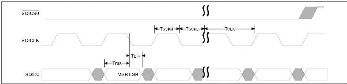
FIGURE 41-14: SQI SERIAL OUTPUT TIMING CHARACTERISTICS
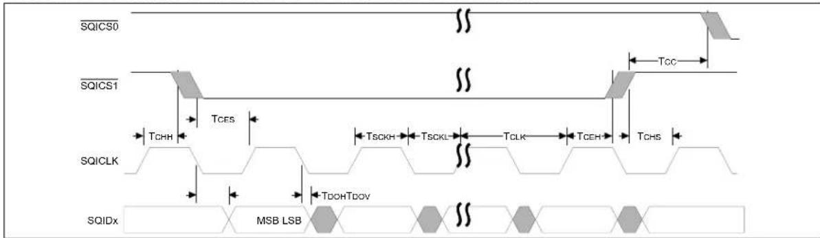
TABLE 41-30: SQI TIMING REQUIREMENTS
| AC CHARACTERISTICS | Standard Operating Conditions: 2.97V to 3.63V (unless otherwise stated)Operating temperature: -40°C ≤ TA ≤ +85°C | ||||||
| Param.No. | Symbol Characteristic (1,3) | Min. | Typ.^(2) | Max. | Units | Conditions | |
| SQ10 | FCLK | Serial clock frequency (1/TsqI) | — | — | 60 | MHz | Serial Flash mode |
| — | — | 25 | MHz | SPI mode 0 and 3 | |||
| SQ11 | TsCKH | Serial clock high time | 7.5 | — | — | ns | — |
| SQ12 | TsCKL | Serial clock low time | 7.5 | — | — | ns | — |
| SQ13 | TsCKR | Serial clock rise time | — | — | — | ns | See parameter DO31 |
| SQ14 | TsCKF | Serial clock fall time | — | — | — | ns | See parameter DO32 |
| SQ15 | Tcss (Tces) | active setup time | 5 | — | — | ns | — |
| SQ16 | Tcsh (TceH) | active hold time | 5 | — | — | ns | — |
| SQ17 | TCHS | not active setup time | 3 | — | — | ns | — |
| SQ18 | TCHH | not active hold time | 3 | — | — | ns | — |
| SQ19 | TCPH | high time | 16.67 | — | — | ns | — |
| SQ20 | TCHZ | high to high-Z data out | — | — | 16.67 | ns | — |
| SQ21 | TCLZ | SCK low to low-Z data out | 0 | — | — | ns | — |
| SQ22 | TDS | Data in setup time | 6 | — | — | ns | — |
| SQ23 | TDH | Data in hold time | 3 | — | — | ns | — |
| SQ24 | TOH | Data out hold | 0 | — | — | ns | — |
| SQ25 | Tov (TV) | Data out valid | — | — | 6 | ns | — |
Note 1: These parameters are characterized but not tested in manufacturing.
2: Data in the "Typ." column is at 3.3V, +25°C unless otherwise stated.
3: Assumes 10 pF load on all SQIx pins
FIGURE 41-15: I2Cx BUS START/STOP BITS TIMING CHARACTERISTICS (HOST MODE)
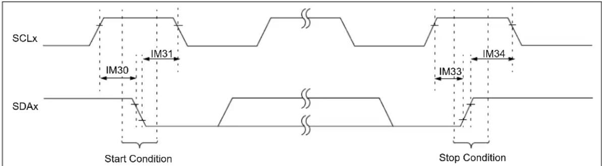
Note: Refer to Figure 41-1 for load conditions.
FIGURE 41-16: I2Cx BUS DATA TIMING CHARACTERISTICS (HOST MODE)
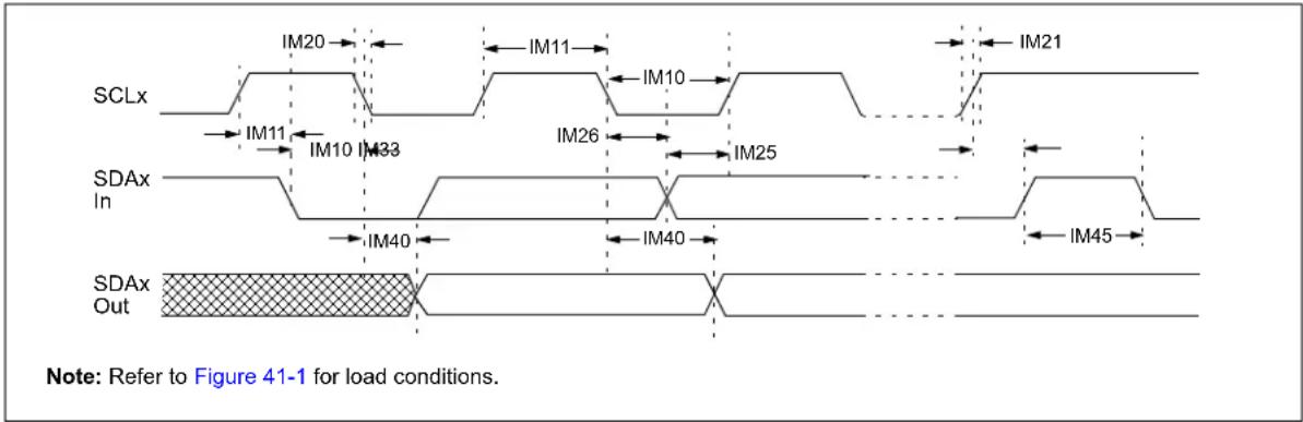
TABLE 41-31: I2Cx BUS DATA TIMING REQUIREMENTS (HOST MODE)
| AC CHARACTERISTICS | Standard Operating Conditions: 2.97V to 3.63V(unless otherwise stated)Operating temperature: -40°C ≤ TA ≤ +85°C | ||||||
| Param.No. | Symbol | Characteristics Min. | (1) | Max. Units | Conditions | ||
| IM10 | TLO:SCL | Clock low time | 100 kHz mode | 4.7 | — | μs | — |
| 400 kHz mode 1.3 — μs — | |||||||
| 1MHz mode^(2) | 0.5 — μs — | ||||||
| IM11 | THI:SCL | Clock high time | 100 kHz mode | 4 | — | μs | — |
| 400 kHz mode 1.3 — μs — | |||||||
| 1MHz mode^(2) | 0.5 — μs — | ||||||
| IM20 T | F:SCL | SDAx and SCLx fall time | 100 kHz mode | — | 300 | ns | CB is specified to be from 10 to 400 pF |
| 400 kHz mode | 20 + 0.1 CB | 300 | ns | ||||
| 1MHz mode^(2) | — | 170 | ns | ||||
| IM21 T | R:SCL | SDAx and SCLx rise time | 100 kHz mode | — | 1000 | ns | CB is specified to be from 10 to 400 pF |
| 400 kHz mode | 20 + 0.1 CB | 300 | ns | ||||
| 1MHz mode^(2) | — | 300 | ns | ||||
| IM25 T | SU:DAT | Data input setup time | 100 kHz mode 250 | — ns — | |||
| 400 kHz mode 100 | — ns | ||||||
| 1MHz mode^(2) | 100 | — ns | |||||
| Param.No. | Symbol | Characteristics | Min.(1) | Max. Units | Conditions | ||
| IM26 | THD:DAT | Data inputhold time | 100 kHz mode 0 | — μs — | μs | ||
| 400 kHz mode 0 | 0.9 μs | ||||||
| 1 MHz mode(2) | 0 | 0.4 | |||||
| IM30 T | SU:STA | start conditionsetup time | 100 kHz mode T | PBCLK * (BRG + 2) — | μs Only | relevant for | Repeated Startcondition |
| 400 kHz mode T | PBCLK * (BRG + 2) — | μs | |||||
| 1 MHz mode(2) | TPBCLK * (BRG + 2) — | μs | |||||
| IM31 T | HD:STA | start conditionhold time | 100 kHz mode | TPBCLK * (BRG + 2) | — | μs | After this period, thefirst clock pulse isgenerated |
| 400 kHz mode T | PBCLK * (BRG + 2) — | μs | |||||
| 1 MHz mode(2) | TPBCLK * (BRG + 2) — | μs | |||||
| IM33 T | SU:STO | $stop conditionsetup time | 100 kHz mode T | PBCLK * (BRG + 2) — | B | R | G + 2 |
| 400 kHz mode T | PBCLK * (BRG + 2) — | μs | |||||
| 1 MHz mode(2) | TPBCLK * (BRG + 2) — | μs | |||||
| IM34 T | HD:STO | Stop conditionhold time | 100 kHz mode | TPBCLK * (BRG + 2) | — | ns | — |
| 400 kHz mode | TPBCLK * (BRG + 2) | — | ns | ||||
| 1 MHz mode(2) | TPBCLK * (BRG + 2) — | ns | |||||
| IM40 T | AA:SCL | Output valid fromclock | 100 kHz mode — | 3500 ns — | |||
| 400 kHz mode — | 1000 ns — | ||||||
| 1 MHz mode(2) | — | 350 | ns | — | |||
| IM45 T | BF:SDA | Bus free time | 100 kHz mode | 4.7 | — | μs | The amount of timethe bus must be freebefore a newtransmission can start |
| 400 kHz mode 1.3 | — μs | ||||||
| 1 MHz mode(2) | 0.5 | — μs | |||||
| IM50 | Cb | Bus capacitive loading | — | 400 | pF | See parameter DO58 | |
Note 1: BRG is the value of the I²C Baud Rate Generator.
2: Maximum pin capacitance = 10 pF for all I2Cx pins (for 1 MHz mode only).
FIGURE 41-17: I2Cx BUS START/STOP BITS TIMING CHARACTERISTICS (CLIENT MODE)
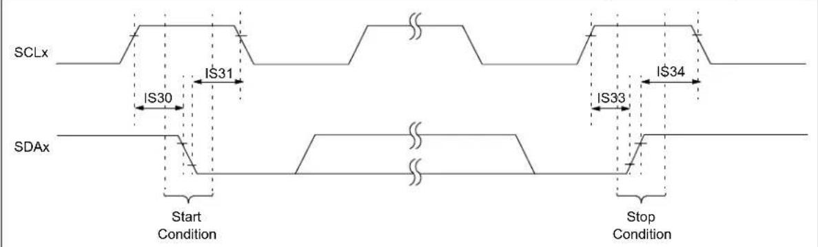
Note: Refer to Figure 41-1 for load conditions.
FIGURE 41-18: I2Cx BUS DATA TIMING CHARACTERISTICS (CLIENT MODE)
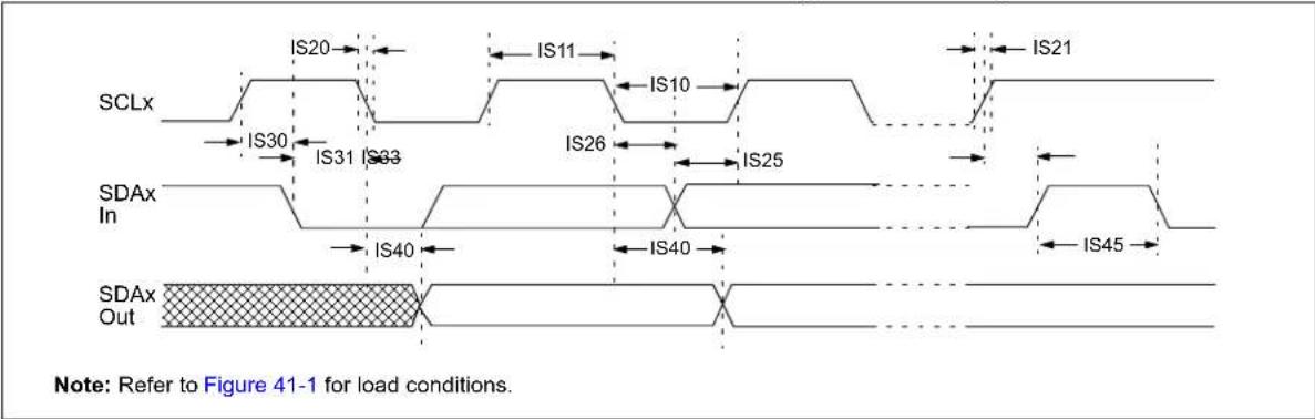
TABLE 41-32: I2Cx BUS DATA TIMING REQUIREMENTS (CLIENT MODE)
| AC CHARACTERISTICS | Standard Operating Conditions: 2.97V to 3.63V(unless otherwise stated)Operating temperature: -40°C ≤ TA ≤ +85°C | ||||||
| Param.No. | Symbol | Characteristics | Min. Max. Units Conditions | ||||
| IS10 T | LO:SCL C | lock low time | 100 kHz mode 4.7 — | μs | PBCLK must operate ata minimum of 800 kHz | ||
| 400 kHz mode 1.3 — | μs | PBCLK must operate ata minimum of 3.2 MHz | |||||
| 1 MHz mode(1) | 0.5 — μ— | ||||||
| IS11 | THI:SCL | Clock high time | 100 kHz mode 4.0 — | μs | PBCLK must operate ata minimum of 800 kHz | ||
| 400 kHz mode 0.6 — | μs | PBCLK must operate ata minimum of 3.2 MHz | |||||
| 1 MHz mode(1) | 0.5 — μ — | ||||||
| IS20 T | F:SCL | SDAx and SCLx fall time | 100 kHz mode | — | 300 | ns | CB is specified to be from 10 to 400 pF |
| 400 kHz mode | 20 + 0.1 CB | 300 | ns | ||||
| 1 MHz mode(1) | — | 100 | ns | ||||
| Param.No. | Symbol | Characteristics | Min. | Max. | Units | Conditions | |
| IS21 | TR:SCL | SDAx and SCLx rise time | 100 kHz mode — 100 ns CB is specified to be | from 10 to 400 pF | |||
| 400 kHz mode 20 + 0 | 1 C B 300 ns | ||||||
| 1MHzmode^( 1) | — 300 ns | ||||||
| IS25 T | SU:DAT Data input setup time | 100 kHz mode 250 — ns — | |||||
| 400 kHz mode 100 — ns | |||||||
| 1MHzmode^( 1) | 100 — ns | ||||||
| IS26 T | HD:DAT | Data input hold time | 100 kHz mode 0 | — ns — | |||
| 400 kHz mode 0 | 0.9 | μs | |||||
| 1MHzmode^( 1) | 0 | 0.3 | μs | ||||
| IS30 T | SU:STA | Start condition setup time | 100 kHz mode 4700 | — ns Only relevant for | Repeated Start condition | ||
| 400 kHz mode 600 — ns | |||||||
| 1MHzmode^( 1) | 250 — ns | ||||||
| IS31 T | HD:STA | Start condition hold time | 100 kHz mode 4000 | — ns After this period, the first | the first clock pulse is generated | ||
| 400 kHz mode 600 — ns | |||||||
| 1MHzmode^( 1) | 250 — ns | ||||||
| IS33 T | SU:STO | Stop condi- tion setup time | 100 kHz mode 4000 | — ns — | |||
| 400 kHz mode 600 — ns | |||||||
| 1MHzmode^( 1) | 600 — ns | ||||||
| IS34 T | HD:STO | Stop condition hold time | 100 kHz mode 4000 | — ns — | |||
| 400 kHz mode 600 — ns | |||||||
| 1MHzmode^( 1) | 250 | ns | |||||
| IS40 | TAA:SCL | Output valid from clock | 100 kHz mode 0 | 3500 ns — | |||
| 400 kHz mode 0 | 1000 ns | ||||||
| 1MHzmode^( 1) | 0 | 350 ns | |||||
| IS45 | TBF:SDA | Bus free time | 100 kHz mode | 4.7 | — | μs | The amount of time the bus must be free before a new transmission can start |
| 400 kHz mode 1.3 | — μs | ||||||
| 1MHzmode^( 1) | 0.5 | — μs | |||||
| IS50 C | B | Bus Capacitive Loading | — | 400 | pF | — | |
Note 1: Maximum pin capacitance = 10 pF for all I2Cx pins (for 1 MHz mode only).
FIGURE 41-19: CANx MODULE I/O TIMING CHARACTERISTICS
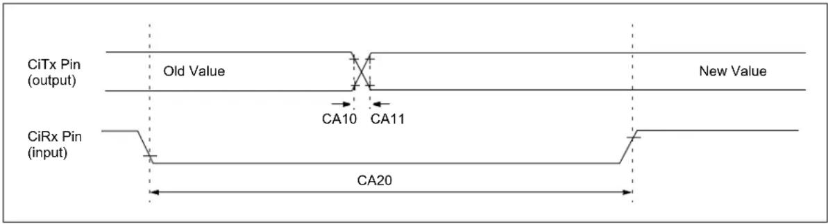
TABLE 41-33: CANx MODULE I/O TIMING REQUIREMENTS
| AC CHARACTERISTICS | Standard Operating Conditions: 2.97V to 3.63V(unless otherwise stated)Operating temperature: -40°C ≤ TA ≤ +85°C | ||||||
| Param No. | Symbol | Characteristic (1) | Min Typ | (2) | Max Units | Conditions | |
| CA10 TioF Port out | put fall time — — — ns See parameter DO32 | ||||||
| CA11 | TioR | Port output rise time | — | — | — | ns | See parameter DO31 |
| CA20 T | cWF Pu | se width to triggerCAN wake-up filter (CAN only) | 700 | — — ns | — | ||
| CA20 TcWF Pu | se width to triggerCAN wake-up filter(CAN-FD Only) | 700 | — — ns | — | |||
Note 1: These parameters are characterized but not tested in manufacturing.
2: Data in the "Typ" column is at 3.3V, +25°C unless otherwise stated.
TABLE 41-34: ADC MODULE SPECIFICATIONS (1, 2)
| AC CHARACTERISTICS | Standard Operating Conditions: 2.97V to 3.63V(unless otherwise stated)Operating temperature: -40°C ≤ TA ≤ +85°C | ||||||
| Param.No. | Symbol | Characteristics Min. | Typ. Max. Units | Conditions | |||
| Device Supply | |||||||
| AD01 AV | DD | Module VDD supply | VDD-0.3 | — | VDD+0.3 | V | — |
| AD02 | AVss | Module Vss supply | Vss | — | Vss+0.3 | V | — |
| Reference Inputs | |||||||
| AD05 V | REFH | Reference voltage high | — | — | AVDD | V | (1) |
| AD06 VREFL | Reference voltage low | AVss | — | — | V | (1) | |
| AD07 VREF | Absolute reference voltage (VREFH-VREFL) | AVDD-0.3 | — | AVDD+0.3 | V | (2) | |
| AD08 | IREF | Current drain | — | 102 | — | μA | Per ADCx ('x' = 0-4, 7) |
| Analog Input | |||||||
| AD12 V | INH-VINL | Full-Scale input span | VREFL | — | VREFH | V | — |
| AD13 | VINL | Absolute VINL input voltage | AVss | — | VREFL | V | — |
| AD14 | VINH | Absolute VINH input voltage | AVss | — | VREFH | V | — |
| ADC Accuracy | |||||||
| AD20c | NR | Resolution | 6 | — | 12 | bits | Selectable 6, 8, 10, 12 resolution ranges |
| AD21c | INL | Integral nonlinearity | — | ±3 | — | LSb | VINL = AVSS = VREFL = 0V, AVDD = VREFH = 3.3V |
| AD22c | DNL | Differential nonlinearity | — | ±1 | — | LSb | VINL = AVSS = VREFL = 0V, AVDD = VREFH = 3.3V |
| AD23c | GERR | Gain error | — | ±8 | — | LSb | VINL = AVSS = VREFL = 0V, AVDD = VREFH = 3.3V |
| AD24c | EOFF | Offset error | — | ±4 | — | LSb | VINL = AVSS = 0V, AVDD = 3.3V |
| Dynamic Performance | |||||||
| AD31b | SINAD | Signal to noise and distortion | — | 67 | — | dB | Single-ended(4)(5) |
| AD34b | NOB | Effective number of bits | — | 10.5 | — | bits | (4)(5) |
Note 1: The ADC module is functional at VBORMIN < VDD < VDDMIN, but with degraded performance. Unless otherwise stated, module functionality is guaranteed, but not characterized.
2: ADC performance is measured in the MCU mode only.
3: These parameters are not characterized or tested in manufacturing.
4: These parameters are characterized but not tested in manufacturing.
5: Characterized with a 1 kHz sine wave.
TABLE 41-35: ADC TIMING REQUIREMENTS (1)
| AC CHARACTERISTICS(3) | Standard Operating Conditions: 2.97V to 3.63V (unless otherwise stated)Operating temperature: -40°C ≤ TA ≤ +85°C | ||||||
| Symbol Char | acteristics Min. Typ. | (2) | Max. Units | Conditions | |||
| t_sys | ADC controller clock period 8 10 7142 ns — | ||||||
| t_ADC | SAR ADC core clock period 28.57 35.7 71 | 42 ns — | |||||
| DutyCyc | Duty cycle | 45 | 50 | 55 | % | — | |
| f_CNV | Sampling rate | selres = 11, rest = 12 | 0.01 | 2 | 2.5 | MSPS | — |
| selres = 10, rest = 10 | 0.01 | 2.33 | 3.5 | MSPS | — | ||
| selres = 01, rest = 8 | 0.01 | 2.8 | 4.375 | MSPS | — | ||
| selres = 00, rest = 6 | 0.01 | 3.5 | 5.833 | MSPS | — | ||
| N_CNV | Conversion cycle | selres = 11, rest = 12 | 14 | Cyc | — | ||
| selres = 10, rest = 10 | 12 | Cyc | — | ||||
| selres = 01, rest = 8 | 10 | Cyc | — | ||||
| selres = 00, rest = 6 | 8 | Cyc | — | ||||
| D_LATENCY | Data latency | selres = 11, rest = 12 | 14 | Cyc | — | ||
| selres = 10, rest = 10 | 12 | Cyc | — | ||||
| selres = 01, rest = 8 | 10 | Cyc | — | ||||
| selres = 00, rest = 6 | 8 | Cyc | |||||
| T_SEP | Separation time between command | 0 | ns — | ||||
| T_SAMP | Sample time | 2.5*t _ADC | — | infinite | — — | ||
| T_CSS | Conversion complete to sample start | — | 0 | — | ns | — | |
| T_WARMUP | Wake-up time for analog | — | — | 20 | ns | — | |
| T_SAMP\_DEL | Trigger Pos Edge to End-Of-Sample Delay | en_async_samp = 1 | 1 2 | 3 ns — | |||
| en_async_samp = 1 | — | (4+/-0.5)* t_sys | — | ns | — | ||
Note 1: ADC performance is measured in the MCU mode only.
2: These parameters are characterized but not tested in manufacturing.
3: The ADC module is functional at V_BORMIN < V_DD < V_DDMIN but with degraded performance. Unless otherwise stated, module functionality is guaranteed but not characterized.
FIGURE 41-1: PROGRAMMABLE LOW-VOLTAGE DETECT ELECTRICAL CHARACTERISTICS
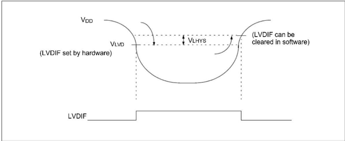
TABLE 41-36: PLVD ELECTRICAL CHARACTERISTICS
| DC Specifications | Standard Operating Conditions: 2.97V to 3.63V(unless otherwise stated)Operating temperature: -40°C ≤ TA ≤ +85°C | ||||||
| Symbol | Characteristic Min. Typ. Max. Units | Conditions | |||||
| Vlvd LVD voltage on VDD transition high to low | LVDL = 0100 3.4 3.526 3.62 V | ||||||
| LVDL = 0101 3.3 3.329 3.368 V | |||||||
| LVDL = 0110 | 3.216 | 3.278 | 3.322 V | ||||
| LVDL = 0111 | 2.932 2.991 3.034 | V | |||||
Note 1: Production tested at T_A=25^ . These parameters are characterized but not tested in manufacturing.
2: LVDL = 1000 to LVDL = 1011 are not supported.
TABLE 41-37: TEMPERATURE SENSOR SPECIFICATIONS
| AC CHARACTERISTICS | Standard Operating Conditions: 2.97V to 3.63V(unless otherwise stated)Operating temperature: -40°C ≤ TA ≤ +85°C | ||||||
| Param.No. | Symbol | Characteristics Min. Typ. | Max. Units | Conditions | |||
| TS10 | VTS | Rate of change | — | +5 | — | mV/°C | — |
| TS11 | TR | Resolution | -4 | — | +7 | °C | — |
| TS12 IV | TEMP | Voltage range | 0.5 | — | 1.5 | V | — |
| TS13 | TMIN | Minimum temperature | — | -40 | — | °C | IVTEMP = 0.5V |
| TS14 T | MAX | Maximum temperature | — | 125 | — | °C | IVTEMP = 1.3V |
Note: The temperature sensor is functional at V_BORMIN < V_DD < V_DDMIN , but with degraded performance. Unless otherwise stated, module functionality is tested, but not characterized.
TABLE 41-38: USB OTG ELECTRICAL SPECIFICATIONS
| AC CHARACTERISTICS | Standard Operating Conditions: 2.97V to 3.63V(unless otherwise stated)Operating temperature: -40°C ≤ TA ≤ +85°C | ||||||
| Param.No. | Symbol | Characteristics | Min. | Typ. | Max. | Units | Conditions |
| USB313 | VUSB3V3 | USB voltage | 3.0 | — | 3.6 | V | Voltage on VUSB3V3must be in this range for proper USB operation |
| Low-Speed and Full-Speed Modes | |||||||
| USB315 | VILUSB | Input low voltage for USB buffer | — | — | 0.8 | V | — |
| USB316 | VIHUSB | Input high voltage for USB buffer | 2.0 | — | — | V | — |
| USB318 | VDIFS | Differential input sensitivity | — | — | 0.2 | V | The difference between D+ and D- must exceed this value while VCM is met |
| USB319 | VCM | Differential common mode range | 0.8 | — | 2.5 | V | — |
| USB321 | VOL | Voltage output low | 0.0 | — | 0.3 | V | 1.425 kΩ load connected to VUSB3V3 |
| USB322 | VOH | Voltage output high | 2.8 | — | 3.6 | V | 14.25 kΩ load connected to ground |
Note: These parameters are characterized but not tested in manufacturing.
FIGURE 41-20: RMII ETHERNET AC TIMING DIAGRAM
![tREF_CLK tREF_CLKH tREF_CLKL EREFCK tRX[1:0]SU tRXERSU tRX[1:0]HOLD tRXERSHOLD ERX[1:0] ERXER tTX[1:0]VAL tTXENVAL ETX[1:0] ETXEN](/content/2026/05/935427/images/b92054b51bea7b06745af1635f0bb830c07f321fb77e360e120873b6a9d6a1dc.jpg)
TABLE 41-39: RMII ETHERNET MODULE SPECIFICATIONS
| AC CHARACTERISTICS | Standard Operating Conditions: 2.97V to 3.63V(unless otherwise stated)Operating temperature: -40°C ≤ TA ≤ +85°C | ||||||
| Param.No. | Symbol Characteristic Min. Typ. Max. Units Conditions | ||||||
| RMII Timing Requirements | |||||||
| ET_29 tREF CLK | Reference clock frequency — | 50 — | MHz | VDDIO = 3.3V | with C_LOAD =20 pF | ||
| ET_31 tREF CLKH | Reference clock high time — | tREF | CLK/2 | — | ns | ||
| ET_33 tREF CLKL | Reference clock low time | — tREF | CLK/2 | — | ns | ||
| ET_35 REF CLKDC | Reference clock duty cycle | — 50 — | % | ||||
| ET_41 tRX[1:0] SU tRXERSU | RXD[1:0], RXER set-up time | 5 | — | 12 | ns | ||
| ET_43 tRX[1:0] HOLD tRXERSHOLD | RXD[1:0], RXER hold time | 2 | — | 12 | ns | ||
| ET_45 tTX[1:0] VAL tTXENVAL | TXEN valid time | 5 | — | 12 | ns | ||
FIGURE 41-21: EJTAG/JTAG TIMING CHARACTERISTICS
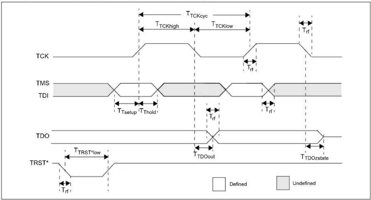
TABLE 41-40: EJTAG/JTAG TIMING REQUIREMENTS
| AC CHARACTERISTICS | Standard Operating Conditions: 2.97V to 3.63V(unless otherwise stated)Operating temperature: -40°C ≤ TA ≤ +85°C | ||||||
| Param.No. | Symbol Description Min. Typ. Max. Units Conditions | ||||||
| EJ1 T | TCKCYC | TCK cycle time | — | 100 | — | ns | — |
| EJ2 T | TCKHIGH | TCK high time | 10 | — | — | ns | — |
| EJ3 | TTCKLOW | TCK low time | 10 | — | — | ns | — |
| EJ4 T | TSETUP | TAP signals setup time before rising TCK | 5 | — | — | ns | — |
| EJ5 | TTHOLD | TAP signals hold time after rising TCK | 3 | — | — | ns | — |
| EJ6 T | TDOOUT | TDO output delay time from falling TCK | — | — | 5 | ns | — |
| EJ7 TTDOZSTATE TDO | 3-state delay time from falling TCK | — | — | 5 | ns | — | |
| EJ8 | TTRSTLOW | TRST low time | 25 | — | — | ns | — |
| EJ9 T | RF | TAP signals rise/fall time, all input and output | — | — | — | ns | — |
Note: These parameters are characterized but not tested in manufacturing.
41.1.3 RADIO PERFORMANCE OF
PIC32MZ1025W104 SoC AND FEM
This section describes the Wi-Fi radio specifications
and performance characteristics of the
PIC32MZ1025W104 SoC.
TABLE 41-41: RADIO SPECIFICATIONS
| Feature Description | |
| WLAN standards IEEE 802.1 | 1b, IEEE 802.11g, and IEEE 802.11n |
| Frequency range 2.412 GHz | ~ 2,472 GHz (2400 ~ 2483.5 MHz ISM band) |
| Number of channels 11 for North America and 13 for Europe and Japan | |
41.1.3.1 Receiver Performance
The following table provides the receiver performance
characteristics of the PIC32MZ1025W104 SoC.
TABLE 41-42: RECEIVER PERFORMANCE CHARACTERISTICS
| RF CHARACTERISTICS | Standard Operating Conditions: 2.97V to 3.63V(unless otherwise stated)Operating temperature: -40°C ≤ TA ≤ +85°C | ||||
| Parameter Description | Min. Typ. Max. Unit | ||||
| Frequency | — | 2412 | — | 2472 | MHz |
| Sensitivity 802.11b | 1 Mbps DSSS | — | -99 | — | dBm |
| 2 Mbps DSSS | — | -96 | — | ||
| 5.5 Mbps DSSS | — | -94 | — | ||
| 11 Mbps DSSS | — | -91 | — | ||
| Sensitivity 802.11g | 6 Mbps OFDM | — | -93 | — | dBm |
| 9 Mbps OFDM | — | -93 | — | ||
| 12 Mbps OFDM | — | -91 | — | ||
| 18 Mbps OFDM | — | -89 | — | ||
| 24 Mbps OFDM | — | -86 | — | ||
| 36 Mbps OFDM | — | -82 | — | ||
| 48 Mbps OFDM | — | -78 | — | ||
| 54 Mbps OFDM | — | -76 | — | ||
| Sensitivity 802.11n(Bandwidth at 20 MHz)(Both long GI andshort GI) | MCS 0 | — | -92 | — | dBm |
| MCS 1 | — | -89 | — | ||
| MCS 2 | — | -87 | — | ||
| MCS 3 | — | -84 | — | ||
| MCS 4 | — | -81 | — | ||
| MCS 5 | — | -76 | — | ||
| MCS 6 | — | -74 | — | ||
| MCS 7 | — | -72 | — | ||
| Maximum ReceiveSignal level | 1, 2 Mbps DSSS | -2 | — | — | dBm |
| 5.5, 11Mbps DSSS | -2 | — | — | ||
| 6 Mbps OFDM | -2 | — | — | ||
| 54 Mbps OFDM | -7.5 | — | — | ||
| MCS 0 | -2 | — | — | ||
| MCS 7 | -7.5 | — | — | ||
| Parameter | Description | Min. | Typ. | Max. | Unit |
| Adjacent Channel Rejection | 1 Mbps DSSS (30 MHz offset) 44.5 — | — | dB | ||
| 11 Mbps DSSS (25 MHz offset) 39.5 — | — | ||||
| 6 Mbps OFDM (25 MHz offset) 41.5 — | — | ||||
| 54 Mbps OFDM (25 MHz offset) 24.5 — | — | ||||
| MCS 0 – 20 MHz Bandwidth (25 MHz offset) | 39.5 — — | ||||
| MCS 7 – 20 MHz Bandwidth (25 MHz offset) | 21.5 — — | ||||
| RSSI Accuracy — -5 — +5 dB | |||||
Note 1: Measured after RF matching network and FEM output (assume 50Ω impedance).
2: RF performance is ensured at 3.3V, 25°C, with a 2-3 dB change at boundary conditions.
3: The availability of some specific channels and/or operational frequency bands are country-dependent and must be programmed in the host product at the factory to match the intended destination. Regulatory bodies prohibit exposing the settings to the end user. This requirement needs to be taken care of via host implementation.
4: The host product manufacturer must ensure that the RF behavior adheres to the certification (for example, FCC, ISED) requirements when the module is installed in the final host product.
5: These parameters are measured at 25^ C, 3.3V.
6: These parameters are characterized but not tested in manufacturing.
41.1.3.2 Transmitter Performance
The following table provides the transmitter performance characteristics of the PIC32MZ1025W104 SoC.
TABLE 41-43: TRANSMITTER PERFORMANCE CHARACTERISTICS
| RF CHARACTERISTICS | Standard Operating Conditions: 2.97V to 3.63V(unless otherwise stated)Operating temperature: -40°C ≤ TA ≤ +85°C | ||||
| Parameter Description Min. Typ. | (3) | Max. Unit | |||
| Frequency — 2412 — 2472 MHz | |||||
| Output power(1)(2) 802.11b 1 Mbps OFDM — 19.5 — | — | dBm | |||
| 2 Mbps DSSS — 21.5 | — | ||||
| 5.5 Mbps DSSS | — 21.5 | — | |||
| 11 Mbps DSSS | — 21.5 | — | |||
| Output power(1)(2) 802.11g 6 Mbps OFDM — 19.5 — | dBm | ||||
| 9 Mbps OFDM | — 19.5 | — | |||
| 12 Mbps OFDM | — 19.5 | — | |||
| 18 Mbps OFDM | — 19.5 | — | |||
| 24 Mbps OFDM | — 19.5 | — | |||
| 36 Mbps OFDM | — 19.5 | — | |||
| 48 Mbps OFDM | — 19.5 | — | |||
| 54 Mbps OFDM | — 18.5 | — | |||
| Output power(1)(2) 802.11n(Bandwidth at 20 MHz) | MCS 0 | — 19.5 | — | dBm | |
| MCS 1 | — 19.5 | — | |||
| MCS 2 | — 19.5 | — | |||
| MCS 3 | — 19.5 | — | |||
| MCS 4 | — 19.5 | — | |||
| MCS 5 | — 19 | — | |||
| MCS 6 | — 18 | — | |||
| MCS 7 | — 17.5 | — | |||
| Transmit Power Control (TPC) Accuracy | — | — | ±1.5(2) | — | dB |
| Harmonic Output Power(Radiated, Regulatory mode) | 2nd | — | 42 | 74(4) | dBuV/m |
| 3rd | — Below noise floor | 74(4) | |||
Note 1: Measured at IEEE 802.11 specification compliant EVM/Spectral mask.
2: Measured after RF matching network and FEM output (assume 50Ω impedance).
3: RF performance is ensured at 3.3V, 25°C, with a 2-3 dB change at boundary conditions.
4: FCC Radiated Emission limits (Restricted Band).
5: With respect to TX power, different (higher/lower) RF output power settings may be used for specific antennas and/or enclosures, in which case re-certification may be required. Program the custom gain table to control the transmit power using the MCHPRT3 tool (Testing PIC32MZ-W1 SoC with MCHPRT3 Tool (DS50003203)).
6: The availability of some specific channels and/or operational frequency bands are country-dependent and must be programmed in the host product at the factory to match the intended destination. Regulatory bodies prohibit exposing the settings to the end user. This requirement needs to be taken care of via host implementation.
7: The host product manufacturer must ensure that the RF behavior adheres to the certification (for example, FCC, ISED) requirements when the module is installed in the final host product.
8: These parameters are measured at 25°C, 3.3V.
9: These parameters are characterized but not tested in manufacturing.
41.1.4 PIC32MZ1025W104 SOC
CHARACTERISTICS GRAPHS
Note: The graphs provided are a statistical summary based on a limited number of samples and are provided for design guidance purposes only. The performance characteristics listed herein are not tested or guaranteed. In some graphs, the data presented may be outside the specified operating range (for example, outside specified power supply range) and, therefore, outside the warranted range.
41.1.4.1 AC and DC Characteristics Graphs
FIGURE 41-22: V OH - 4x DRIVER PINS
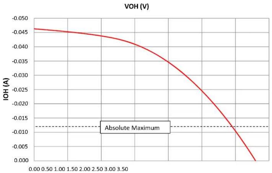
line
| x | y | | ---- | ------- | | 0.00 | -0.045 | | 0.50 | -0.046 | | 1.00 | -0.047 | | 1.50 | -0.048 | | 2.00 | -0.049 | | 2.50 | -0.050 | | 3.00 | -0.051 | | 3.50 | -0.052 | | 4.00 | -0.053 | | 4.50 | -0.054 | | 5.00 | -0.055 | | 5.50 | -0.056 | | 6.00 | -0.057 | | 6.50 | -0.058 | | 7.00 | -0.059 | | 7.50 | -0.060 | | 8.00 | -0.061 | | 8.50 | -0.062 | | 9.00 | -0.063 | | 9.50 | -0.064 | | 10.00| -0.065 | | 10.50| -0.066 | | 11.00| -0.067 | | 11.50| -0.068 | | 12.00| -0.069 | | 12.50| -0.070 | | 13.00| -0.071 | | 13.50| -0.072 | | 14.00| -0.073 | | 14.50| -0.074 | | 15.00| -0.075 | | 15.50| -0.076 | | 16.00| -0.077 | | 16.50| -0.078 | | 17.00| -0.079 | | 17.50| -0.080 | | 18.00| -0.081 | | 18.50| -0.082 | | 19.00| -0.083 | | 19.50| -0.084 | | 20.00| -0.085 | | 20.50| -0.086 | | 21.00| -0.087 | | 21.50| -0.088 | | 22.00| -0.089 | | 22.50| -0.090 | | 23.00| -0.091 | | 23.50| -0.092 | | 24.00| -0.093 | | 24.50| -0.094 | | 25.00| -0.095 | | 25.50| -0.096 | | 26.00| -0.097 | | 26.50| -0.098 | | 27.00| -0.099 | | 27.50| -0.100 | | 28.00| -0.101 | | 28.50| -0.102 | | 29.00| -0.103 | | 29.50| -0.104 | | 30.00| -0.105 | | 30.50| -0.106 | | 31.00| -0.107 | | 31.50| -0.108 | | 32.00| -0.109 | | 32.50| -0.110 | | 33.00| -0.111 | | 33.50| -0.112 | | 34.00| -0.113 | | 34.50| -0.114 | | 35.00| -0.115 |FIGURE 41-23: V OL - 4x DRIVER PINS
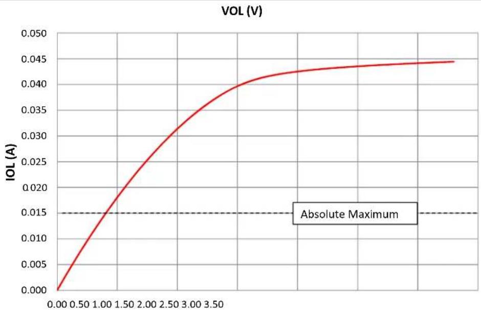
line
| x | IOL (A) | | ---- | ------- | | 0.00 | 0.000 | | 0.50 | 0.010 | | 1.00 | 0.020 | | 1.50 | 0.028 | | 2.00 | 0.035 | | 2.50 | 0.040 | | 3.00 | 0.043 | | 3.50 | 0.044 |FIGURE 41-24: Voh - 8x DRIVER PINS
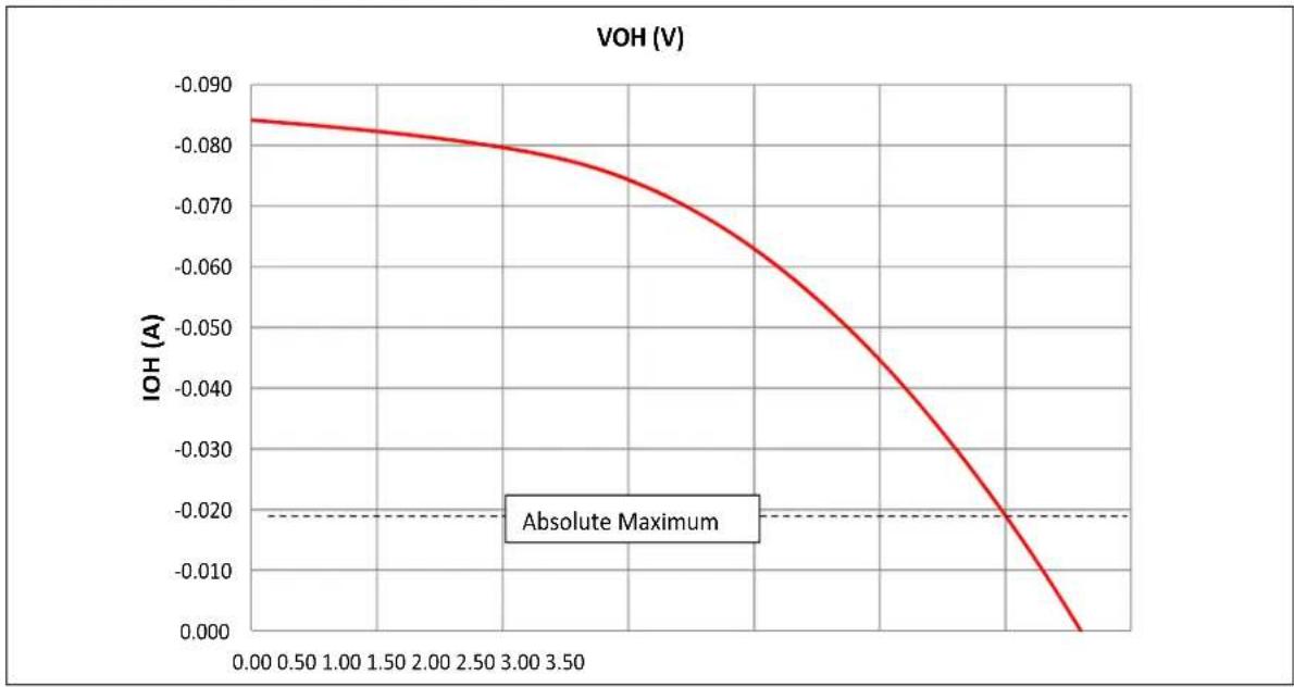
line
| x | y | |-------|---------| | 0.00 | -0.085 | | 0.50 | -0.086 | | 1.00 | -0.087 | | 1.50 | -0.088 | | 2.00 | -0.089 | | 2.50 | -0.090 | | 3.00 | -0.091 | | 3.50 | -0.092 | | 4.00 | -0.093 | | 4.50 | -0.094 | | 5.00 | -0.095 | | 5.50 | -0.096 | | 6.00 | -0.097 | | 6.50 | -0.098 | | 7.00 | -0.099 | | 7.50 | -0.100 | | 8.00 | -0.101 | | 8.50 | -0.102 | | 9.00 | -0.103 | | 9.50 | -0.104 | | 10.00 | -0.105 | | 10.50 | -0.106 | | 11.00 | -0.107 | | 11.50 | -0.108 | | 12.00 | -0.109 | | 12.50 | -0.110 | | 13.00 | -0.111 | | 13.50 | -0.112 | | 14.00 | -0.113 | | 14.50 | -0.114 | | 15.00 | -0.115 | | 15.50 | -0.116 | | 16.00 | -0.117 | | 16.50 | -0.118 | | 17.00 | -0.119 | | 17.50 | -0.120 | | 18.00 | -0.121 | | 18.50 | -0.122 | | 19.00 | -0.123 | | 19.50 | -0.124 | | 20.00 | -0.125 | | 20.50 | -0.126 | | 21.00 | -0.127 | | 21.50 | -0.128 | | 22.00 | -0.129 | | 22.50 | -0.130 | | 23.00 | -0.131 | | 23.50 | -0.132 | | 24.00 | -0.133 | | 24.50 | -0.134 | | 25.00 | -0.135 | | 25.50 | -0.136 | | 26.00 | -0.137 | | 26.50 | -0.138 | | 27.00 | -0.139 | | 27.50 | -0.140 | | 28.00 | -0.141 | | 28.50 | -0.142 | | 29.00 | -0.143 | | 29.50 | -0.144 | | 30.00 | -0.145 | | 30.50 | -0.146 | | 31.00 | -0.147 | | 31.50 | -0.148 | | 32.00 | -0.149 | | 32.50 | -0.150 | | 33.00 | -0.151 | | 33.50 | -0.152 | | 34.00 | -0.153 | | 34.50 | -0.154 | | 35.00 | -0.155 | | 35.50 | -0.156 | | 36.00 | -0.157 | | 36.50 | -0.158 | | 37.00 | -0.159 | | 37.50 | -0.160 | | 38.00 | -0.161 | | 38.50 | -0.162 | | 39.00 | -0.163 | | 39.50 | -0.164 | | 40.00 | -0.165 | | 40.50 | -0.166 | | 41.00 | -0.167 | | 41.50 | -0.168 | | 42.00 | -0.169 | | 42.50 | -0.170 | | 43.00 | -0.171 | | 43.50 | -0.172 | | 44.00 | -0.173 | | 44.50 | -0.174 | | 45.00 | -0.175 | | 45.50 | -0.176 | | 46.0FIGURE 41-25: V OL - 8x DRIVER PINS
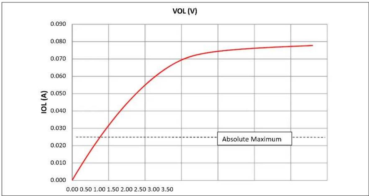
line
| x | y | | ---- | ----- | | 0.00 | 0.000 | | 0.50 | 0.010 | | 1.00 | 0.025 | | 1.50 | 0.040 | | 2.00 | 0.055 | | 2.50 | 0.065 | | 3.00 | 0.072 | | 3.50 | 0.076 | | 4.00 | 0.078 | | 4.50 | 0.079 | | 5.00 | 0.080 |FIGURE 41-26: TYPICAL TEMPERATURE SENSOR VOLTAGE
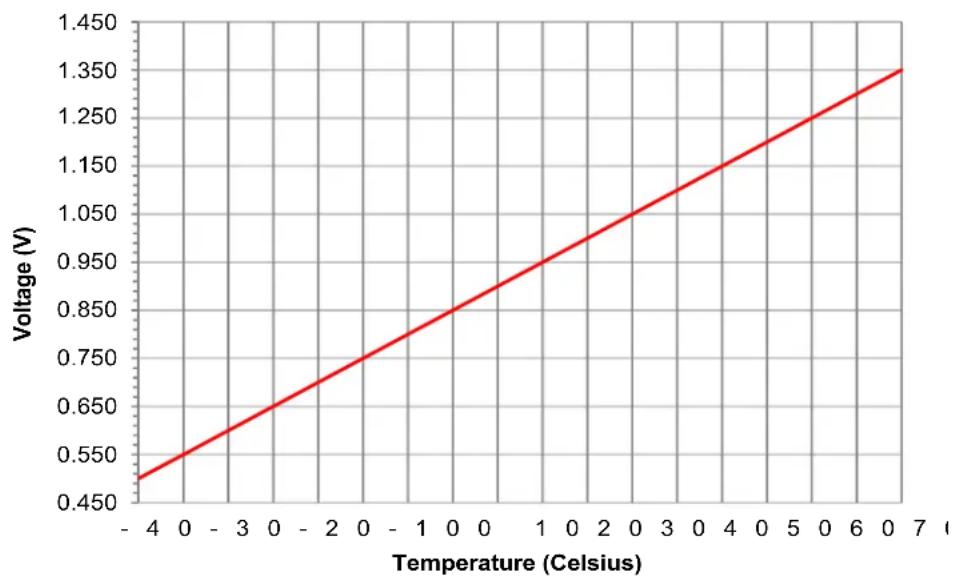
line
| Temperature (Celsius) | Voltage (V) | | --------------------- | ----------- | | -4 | 0.45 | | 0 | 0.55 | | 3 | 0.65 | | 6 | 0.75 | | 9 | 0.85 | | 12 | 0.95 | | 15 | 1.05 | | 18 | 1.15 | | 21 | 1.25 | | 24 | 1.35 | | 27 | 1.45 |41.1.4.2 Receiver and Transmitter Current Characteristics Graphs
FIGURE 41-27: RECEIVE CURRENT VS. TEMPERATURE
Receive Current vs. Temperature
MCS7, Channel 7, 3.3V
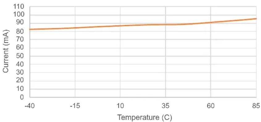
line
| Temperature (C) | Current (mA) | | --------------- | ------------ | | -40 | 82 | | -15 | 84 | | 10 | 86 | | 35 | 87 | | 60 | 89 | | 85 | 95 |Note 1: At all the data rates, the performance remains the same except the values. This graph is only for reference.
2: The current measurement includes the SoC and FEM current.
3: Measured at the FEM output.
4: This current includes processor current.
FIGURE 41-28: RECEIVE CURRENT VS. RECEIVE SIGNAL POWER
Receive Current vs. Receive Signal Power
MCS7, Channel 7, 3.3V, 25C
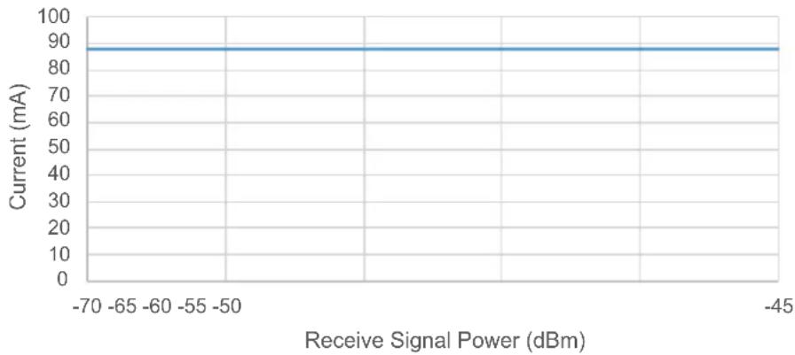
line
| Receive Signal Power (dBm) | Current (mA) | | -------------------------- | ------------ | | -70 | 88 | | -65 | 88 | | -60 | 88 | | -55 | 88 | | -50 | 88 | | -45 | 88 |Note 1: At all the data rates, the performance remains the same except the values. This graph is only for reference.
2: The current measurement includes the SoC and FEM current.
3: Measured at the FEM output.
4: This current includes processor current.
FIGURE 41-29: RECEIVE CURRENT VS. CPU FREQUENCY
Receive Current vs. CPU Frequency
MCS7, Channel 7, 3.3V, 25C
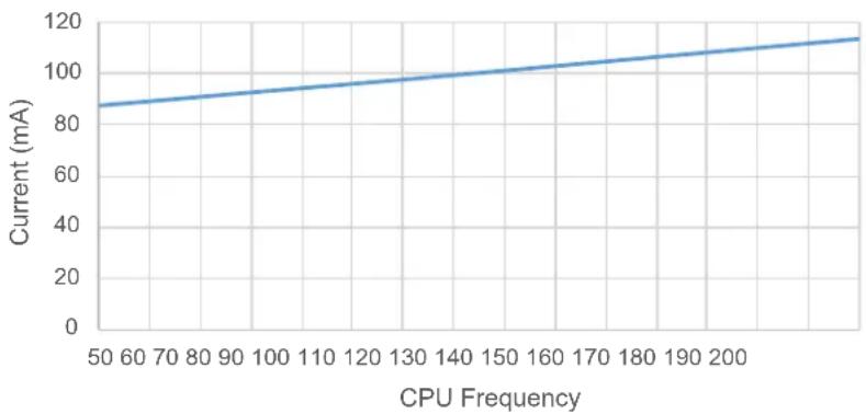
line
| CPU Frequency | Current (mA) | | ------------- | ------------ | | 50 | 85 | | 60 | 87 | | 70 | 89 | | 80 | 91 | | 90 | 93 | | 100 | 95 | | 110 | 97 | | 120 | 99 | | 130 | 101 | | 140 | 103 | | 150 | 105 | | 160 | 107 | | 170 | 109 | | 180 | 111 | | 190 | 113 | | 200 | 115 |Note 1: At all the data rates, the performance remains the same except the values. This graph is only for reference.
2: The current measurement includes the SoC and FEM current.
3: Measured at the FEM output.
4: This current includes processor current.
FIGURE 41-30: TRANSMIT CURRENT VS. TEMPERATURE
Transmit Current vs. Temperature
MCS7, Channel 7, 3.3V
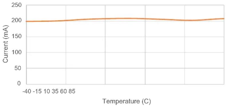
line
| Temperature (C) | Current (mA) | | --------------- | ------------ | | -40 | 195 | | -15 | 196 | | 10 | 197 | | 35 | 198 | | 60 | 199 | | 85 | 200 |Note 1: At all the data rates, the performance remains the same except the values. This graph is only for reference.
2: The current measurement includes the SoC and FEM current.
3: Measured at the FEM output.
4: This current includes processor current.
FIGURE 41-31: TRANSMIT CURRENT VS. OUTPUT POWER
Transmit Current vs. Output Power
MCS7, Channel 7, 3.3V, 25C
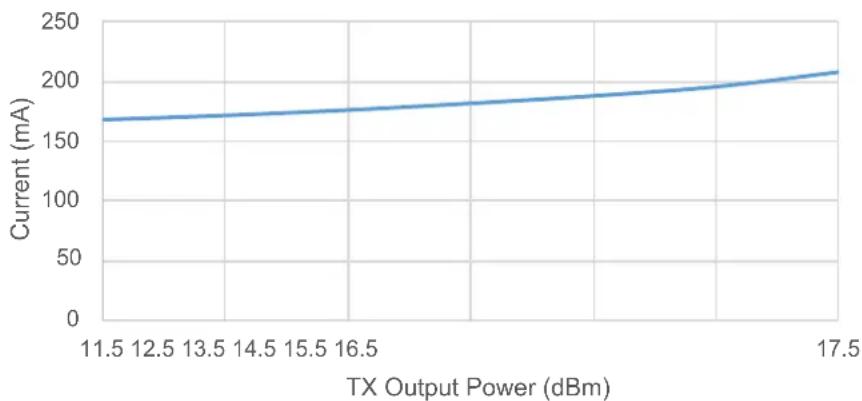
line
| TX Output Power (dBm) | Current (mA) | | --------------------- | ------------ | | 11.5 | 165 | | 12.5 | 168 | | 13.5 | 170 | | 14.5 | 173 | | 15.5 | 176 | | 16.5 | 179 | | 17.5 | 205 |Note 1: At all the data rates, the performance remains the same except the values. This graph is only for reference.
2: The current measurement includes the SoC and FEM current.
3: Measured at the FEM output.
4: This current includes processor current.
FIGURE 41-32: TRANSMIT CURRENT VS. CPU FREQUENCY
Transmit Current vs. CPU Frequency
MCS7, Channel 7, 3.3V, 25C
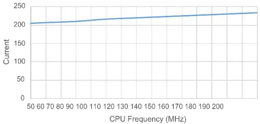
line
| CPU Frequency (MHz) | Current | | ------------------- | ------- | | 50 | 200 | | 60 | 202 | | 70 | 204 | | 80 | 206 | | 90 | 208 | | 100 | 210 | | 110 | 212 | | 120 | 214 | | 130 | 216 | | 140 | 218 | | 150 | 220 | | 160 | 222 | | 170 | 224 | | 180 | 226 | | 190 | 228 | | 200 | 230 |Note 1: At all the data rates, the performance remains the same except the values. This graph is only for reference.
2: The current measurement includes the SoC and FEM current.
3: Measured at the FEM output.
4: This current includes processor current.
41.1.4.3 Receiver and Transmitter Performance Characteristics Graphs
FIGURE 41-33: RECEIVE SENSITIVITY VS TEMPERATURE
RX Sensitivity vs Temperature
MCS7, Channel 7, 3.3V
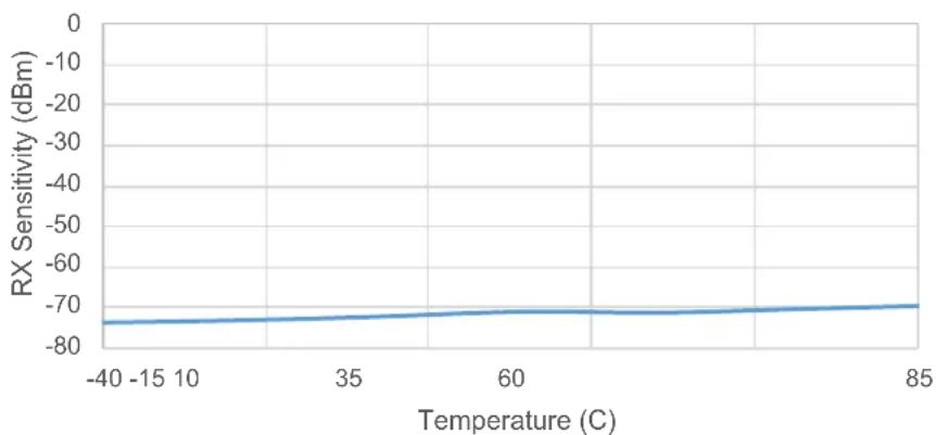
line
| Temperature (C) | RX Sensitivity (dBm) | | --------------- | -------------------- | | -40 | -75 | | -15 | -74 | | 10 | -73 | | 35 | -72 | | 60 | -71 | | 85 | -70 |Note 1: At all the data rates, the performance remains the same except the values. This graph is only for reference.
2: Measured at the FEM output.
FIGURE 41-34: RX SENSITIVITY VS CHANNELS
RX Sensitivity vs Channel
MCS7, 25C, 3.3V
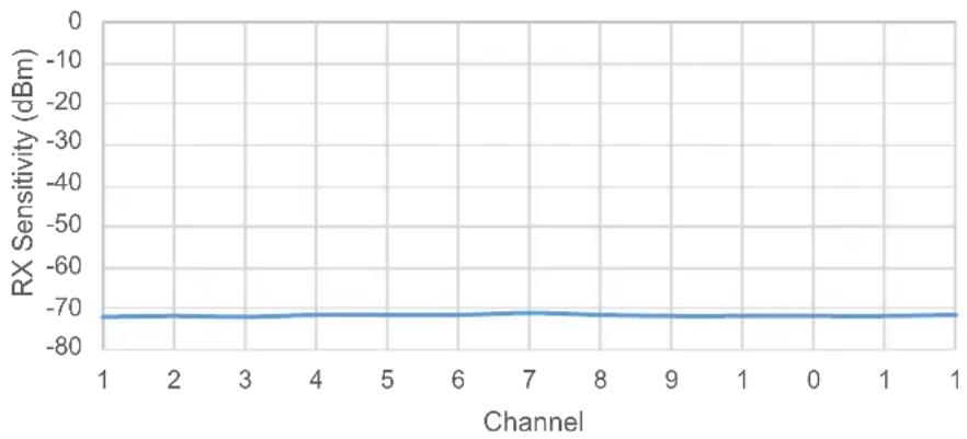
line
| Channel | RX Sensitivity (dBm) | | ------- | -------------------- | | 1 | -70 | | 2 | -70 | | 3 | -70 | | 4 | -70 | | 5 | -70 | | 6 | -70 | | 7 | -70 | | 8 | -70 | | 9 | -70 | | 0 | -70 | | 1 | -70 |Note 1: At all the data rates, the performance remains the same except the values. This graph is only for reference.
2: Measured at the FEM output.
FIGURE 41-35: RX SENSITIVITY VS VOLTAGE
RX Sensitivity vs Voltage
MCS7, Channel 7, 25C
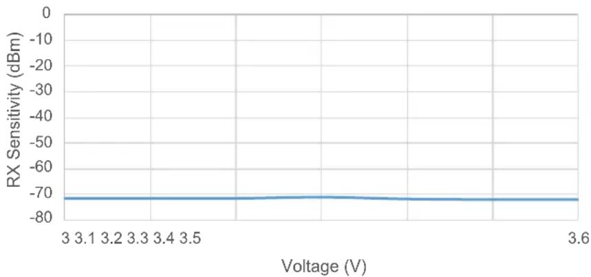
line
| Voltage (V) | RX Sensitivity (dBm) | | ----------- | -------------------- | | 3.0 | -70 | | 3.1 | -70 | | 3.2 | -70 | | 3.3 | -70 | | 3.4 | -70 | | 3.5 | -70 | | 3.6 | -70 |Note 1: At all the data rates, the performance remains the same except the values. This graph is only for reference.
2: Measured at the FEM output.
FIGURE 41-36: RSSI VS RECEIVE SIGNAL POWER
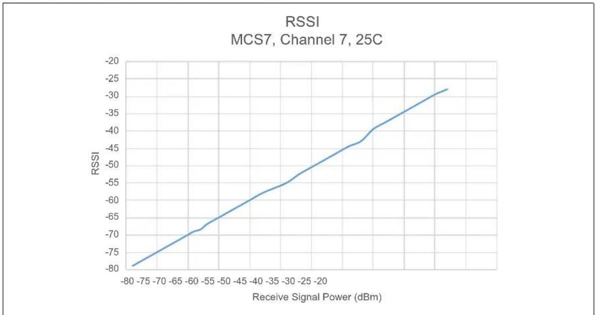
line
| Receive Signal Power (dBm) | RSSI | | -------------------------- | ---- | | -80 | -80 | | -75 | -75 | | -70 | -70 | | -65 | -65 | | -60 | -60 | | -55 | -55 | | -50 | -50 | | -45 | -45 | | -40 | -40 | | -35 | -35 | | -30 | -30 | | -25 | -25 | | -20 | -20 |Note 1: At all the data rates, the performance remains the same except the values. This graph is only for reference. 2: Measured at the FEM output.
FIGURE 41-37: TX POWER VS TEMPERATURE
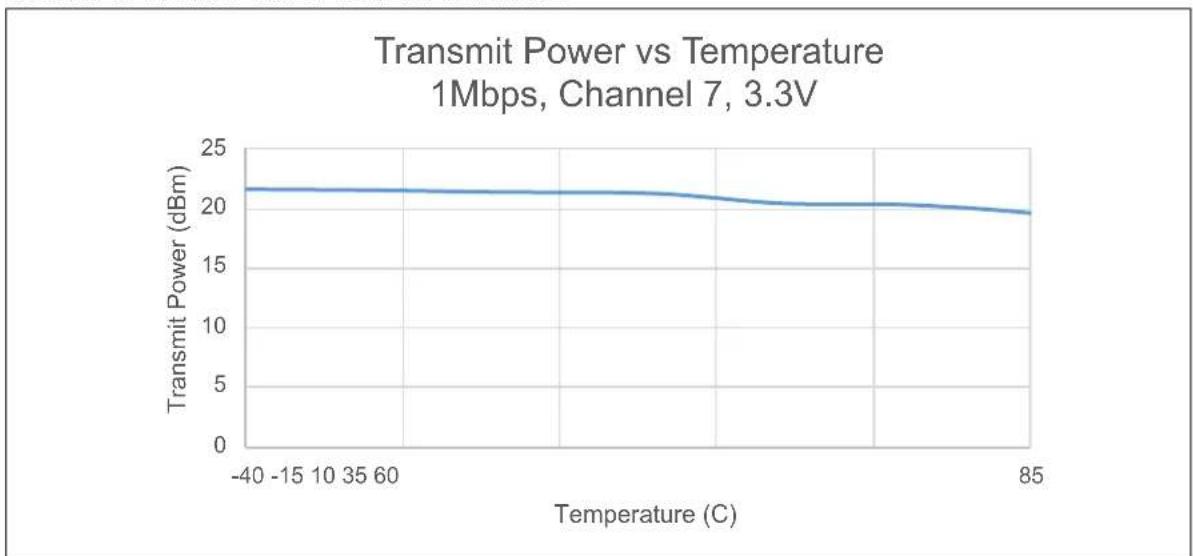
line
| Temperature (C) | Transmit Power (dBm) | | --------------- | -------------------- | | -40 | 21.5 | | -15 | 21.4 | | 10 | 21.3 | | 35 | 21.2 | | 60 | 21.1 | | 85 | 19.5 |Note 1: At all the data rates, the performance remains the same except the values. This graph is only for reference. 2: Measured at the FEM output.
FIGURE 41-38: TX POWER VS CHANNELS
Transmit Power vs Channel
1Mbps, 25C, 3.3V
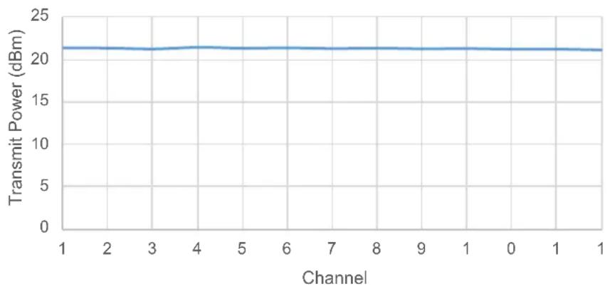
line
| Channel | Transmit Power (dBm) | | ------- | -------------------- | | 1 | 21.5 | | 2 | 21.4 | | 3 | 21.3 | | 4 | 21.4 | | 5 | 21.3 | | 6 | 21.3 | | 7 | 21.3 | | 8 | 21.3 | | 9 | 21.3 | | 10 | 21.3 | | 11 | 21.3 | | 12 | 21.3 | | 13 | 21.3 | | 14 | 21.3 | | 15 | 21.3 | | 16 | 21.3 | | 17 | 21.3 | | 18 | 21.3 | | 19 | 21.3 | | 20 | 21.3 | | 21 | 21.3 | | 22 | 21.3 | | 23 | 21.3 | | 24 | 21.3 | | 25 | 21.3 | | 26 | 21.3 | | 27 | 21.3 | | 28 | 21.3 | | 29 | 21.3 | | 30 | 21.3 | | 31 | 21.3 | | 32 | 21.3 | | 33 | 21.3 | | 34 | 21.3 | | 35 | 21.3 | | 36 | 21.3 | | 37 | 21.3 | | 38 | 21.3 | | 39 | 21.3 | | 40 | 21.3 | | 41 | 21.3 | | 42 | 21.3 | | 43 | 21.3 | | 44 | 21.3 | | 45 | 21.3 | | 46 | 21.3 | | 47 | 21.3 | | 48 | 21.3 | | 49 | 21.3 | | 50 | 21.3 | | 51 | 21.3 | | 52 | 21.3 | | 53 | 21.3 | | 54 | 21.3 | | 55 | 21.3 | | 56 | 21.3 | | 57 | 21.3 | | 58 | 21.3 | | 59 | 21.3 | | 60 | 21.3 | | 61 | 21.3 | | 62 | 21.3 | | 63 | 21.3 | | 64 | 21.3 | | 65 | 21.3 | | 66 | 21.3 | | 67 | 21.3 | | 68 | 21.3 | | 69 | 21.3 | | 70 | 21.3 | | 71 | 21.3 | | 72 | 21.3 | | 73 | 21.3 | | 74 | 21.3 | | 75 | 21.3 | | 76 | 21.3 | | 77 | 21.3 | | 78 | 21.3 | | 79 | 21.3 | | 80 | 21.3 | | 81 | 21.3 | | 82 | 21.3 | | 83 | 21.3 | | 84 | 21.3 | | 85 | 21.3 | | 86 | 21.3 | | 87 | 21.3 | | 88 | 21.3 | | 89 | 21.3 | | 90 | 21.3 | | 91 | 21.3 | | 92 | 21.3 | | 93 | 21.3 | | 94 | 21.3 | | 95 | 21.3 | | 96 | 21.3 | | 97 | 21.3 | | 98 | 21.3 | | 99 | 21.3 | | 100 | 21.3 |Note 1: At all the data rates, the performance remains the same except the values. This graph is only for reference.
2: Measured at the FEM output.
FIGURE 41-39: TX POWER VS VOLTAGES
Transmit Power vs Voltage
1Mbps, Channel 7, 25C
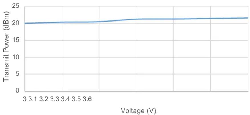
line
| Voltage (V) | Transmit Power (dBm) | | ----------- | -------------------- | | 3.1 | 20.0 | | 3.2 | 20.0 | | 3.3 | 20.0 | | 3.4 | 20.0 | | 3.5 | 20.0 | | 3.6 | 20.0 |Note 1: At all the data rates, the performance remains the same except the values. This graph is only for reference.
2: Measured at the FEM output.
41.2 WFI32 Module Electrical Specifications
The absolute maximum ratings for the WF132 Module are listed below. Exposure to these maximum rating conditions for extended periods may affect device reliability. Functional operation of the device at these or any other conditions, above the parameters indicated in the operation listings of this specification, is not implied.
Note: All the electrical specification of the PIC32MZ W1 applies to the WFI32 Module as well unless specified explicitly.
Absolute Maximum Ratings
Ambient temperature under bias....-40°C to +85°C
Storage temperature -40^ to +125^
Voltage on VDD with respect to GND -0.3V to (VDD + 0.3V)
Voltage on Vbus with respect to GND -0.3V to ( V_DD + 0.3V )
Maximum current out of GND pin(s) 500 mA
Maximum current into VDD pin(s) ^(2) .....500 mA
Note 1: Stresses above those listed under “Absolute Maximum Ratings” may cause permanent damage to the device. This is a stress rating only and functional operation of the device at those or any other conditions, above those indicated in the operation listings of this specification, is not implied. Exposure to maximum rating conditions for extended periods may affect device reliability.
2: The maximum allowable current is a function of the device's maximum power dissipation.
TABLE 41-44: RECOMMENDED OPERATING CONDITIONS
| Symbol | Parameter Min. Typ. Max. | Unit | |||
| V_DD | Power supply input voltage | 3.0 | 3.3 | 3.6 | V |
| V_BUS | USB bus voltage | 3.0 | 3.3 | 3.6 | V |
| AV_DD | Analog power supply input voltage | 3.0 | 3.3 | 3.6 | V |
41.2.1 DC CHARACTERISTICS
TABLE 41-45: WI-FI CURRENT
| DC CHARACTERISTICS | Standard Operating Conditions: 3.0V to 3.6V (unless otherwise stated)Operating temperature: -40°C ≤ TA ≤ +85°C | ||
| Device States Code | Rate | Output Power (Typ.) (dBm) | Current (Typ.) (mA)(3) |
| On_Transmit(4) | 802.11b 1 Mbps(5) | 20.5 293 | |
| 802.11b 1 Mbps(6) | 14.5 212 | ||
| 802.11b 11 Mbps(5) | 20.5 293 | ||
| 802.11g 6 Mbps(6) | 19.5 272 | ||
| 802.11g 54 Mbps(5) | 18.5 241 | ||
| 802.11n MCS0(6) | 18.5 258 | ||
| 802.11n MCS7(5) | 17.0 223 | ||
| 802.11n MCS7(6) | 11.0 179 | ||
| On_Receive | 802.11b 1 Mbps(6) | — | 75 |
| 802.11n MCS7(5) | — | 8 9 | |
Note 1: Measured along with RF matching network and FEM circuit (assume 50Ω impedance).
2: The test conditions for I DD measurements are as follows:
• CPU, Flash Panel and SRAM data memory are operational.
• CPU is operating at 50 MHz.
• CPU is in Wi-Fi RF Test mode.
- All peripheral modules are disabled (ON bit = 0) but the associated PMD bit is cleared.
• WDT and FSCM are disabled.
- All I/O pins are configured as inputs and pulled high.
• VBUS3V3 connected to V_DD
- = V_DD
3: Data in the "Typ." column is at 3.3V, 25°C unless otherwise stated.
4: Tested at channel 7 in Fixed Mode Gain.
5: This parameter is characterized and tested in manufacturing.
6: This parameter is characterized but not tested in manufacturing.
Note: For details on the DC characteristics, refer to Section 41.1.1 "DC Characteristics".
41.2.2 AC CHARACTERISTICS AND
TIMING PARAMETERS
Note: For details on the AC Characteristics and Timing Parameters, refer to Section 41.1.2 “AC Characteristics and Timing Parameters”.
41.2.3 RADIO PERFORMANCE OF WFI32
MODULE
This section describes the Wi-Fi radio specifications and performance characteristics of the WFI32 Module.
TABLE 41-46: RADIO SPECIFICATIONS
| Feature Description | |
| WLAN standards IEEE 802.1 | 1b, IEEE 802.11g, and IEEE 802.11n |
| Frequency range 2.412 GHz | ~ 2,472 GHz (2400 ~ 2483.5 MHz ISM band) |
| Number of channels 11 for North America and 13 for Europe and Japan | |
41.2.3.1 Receiver Performance
The following table provides the receiver performance characteristics of the WFI32 Module.
TABLE 41-47: WFI32 MODULE RECEIVER PERFORMANCE CHARACTERISTICS (1)
| RF CHARACTERISTICS | Standard Operating Conditions: 3.0V to 3.6V(unless otherwise stated)Operating temperature: -40°C ≤ TA ≤ +85°CMeasured at 25°C, 3.3V | ||||
| Parameter Description Min. Typ. Max. Unit | |||||
| Frequency — | 2412 — | 2472 MHz | |||
| Sensitivity 802.11b | 1 Mbps DSSS(5) | — | -99.5 | — | dBm |
| 2 Mbps DSSS(5) | — | -96.5 | — | ||
| 5.5 Mbps DSSS(5) | — | -94.5 | — | ||
| 11 Mbps DSSS(6) | — | -91.5 | — | ||
| Sensitivity 802.11g | 6 Mbps OFDM(5) | — | -93.5 | — | dBm |
| 9 Mbps OFDM(5) | — | -93 | — | ||
| 12 Mbps OFDM(5) | — | -91 | — | ||
| 18 Mbps OFDM(5) | — | -89 | — | ||
| 24 Mbps OFDM(5) | — | -86 | — | ||
| 36 Mbps OFDM(5) | — | -82.5 | — | ||
| 48 Mbps OFDM(5) | — | -78.5 | — | ||
| 54 Mbps OFDM(6) | — | -76.5 | — | ||
| Sensitivity 802.11n (Bandwidth at 20 MHz) (Both long GI and short GI) | MCS 0(5) | — | -92.5 | — | dBm |
| MCS 1(5) | — | -89.5 | — | ||
| MCS 2(5) | — | -87.5 | — | ||
| MCS 3(5) | — | -84.5 | — | ||
| MCS 4(5) | — | -80.5 | — | ||
| MCS 5(5) | — | -76.5 | — | ||
| MCS 6(5) | — | -74.5 | — | ||
| MCS 7(6) | — | -73 | — | ||
| Maximum Receive Signal level | 1, 2 Mbps DSSS(5) | -2 | — | — | dBm |
| 5.5, 11Mbps DSSS(5) | -2 | — | — | ||
| 6 Mbps OFDM(5) | -2 | — | — | ||
| 54 Mbps OFDM(5) | -7 | — | — | ||
| MCS 0(5) | -2 | — | — | ||
| MCS 7(5) | -8 | — | — | ||
| Parameter | Description | Min. | Typ. | Max. | Unit |
| Adjacent Channel Rejection | 1 Mbps DSSS(5)(30 MHz offset) | 44.5 — — | dB | ||
| 11 Mbps DSSS(5)(25 MHz offset) | 39.5 — — | ||||
| 6 Mbps OFDM(5)(25 MHz offset) | 41.5 — — | ||||
| 54 Mbps OFDM(5)(25 MHz offset) | 24.5 — — | ||||
| MCS 0 – 20 MHz Bandwidth (25 MHz offset)(5) | 40.5 — — | ||||
| MCS 7 – 20 MHz Bandwidth (25 MHz offset)(5) | 21.5 — — | ||||
| RSSI Accuracy — -5 — +5 dB | |||||
Note 1: Measured after RF matching network and FEM output (assume 50 impedance).
2: RF performance is ensured at 3.3V, 25°C, with a 2-3 dB change at boundary conditions.
3: The availability of some specific channels and/or operational frequency bands are country-dependent and must be programmed in the host product at the factory to match the intended destination. Regulatory bodies prohibit exposing the settings to the end user. This requirement needs to be taken care of via host implementation.
4: The host product manufacturer must ensure that the RF behavior adheres to the certification (for example, FCC, ISED) requirements when the module is installed in the final host product.
5: This parameter is characterized but not tested in manufacturing.
6: This parameter is characterized and tested in manufacturing.
41.2.3.2 Transmitter Performance
The following table provides the transmitter performance characteristics of the WFI32 Module.
TABLE 41-48: WFI32 MODULE TRANSMITTER PERFORMANCE CHARACTERISTICS
| RF CHARACTERISTICS | Standard Operating Conditions: 3.0V to 3.6V(unless otherwise stated)Operating temperature: -40°C ≤ TA ≤ +85°CMeasured at 25°C, 3.3V | ||||
| Parameter Description Min. Typ. | (3) | Max. Unit | |||
| Frequency — 2412 — 2472 MHz | |||||
| Output power(1)(2) 802.11b 1 Mbps DSSS (9) | — | 2 | 0 | . dBm 5 | |
| 2 Mbps DSSS(8) | — | 2 | 0 | ||
| 5.5 Mbps DSSS(8) | — | 2 | 0 | ||
| 11 Mbps DSSS(8) | — | 2 | 0 | ||
| Output power(1)(2) 802.11g 6 Mbps OFDM (8) | — | 1 | 9 | . dBm 5 | |
| 9 Mbps OFDM(8) | — | 1 | 9 | ||
| 12 Mbps OFDM(8) | — | 1 | 9 | ||
| 18 Mbps OFDM(8) | — | 1 | 9 | ||
| 24 Mbps OFDM(8) | — | 1 | 9 | ||
| 36 Mbps OFDM(8) | — | 1 | 9 | ||
| 48 Mbps OFDM(8) | — | 1 | 9 | ||
| 54 Mbps OFDM(9) | — | 1 | 8 | ||
| Output power(1)(2) 802.11n(Bandwidth at 20 MHz) | MCS 0(8) | — | 1 | 8 | . dBm 5 |
| MCS 1(8) | — | 1 | 8 | . | |
| MCS 2(8) | — | 1 | 8 | . | |
| MCS 3(8) | — | 1 | 8 | . | |
| MCS 4(8) | — | 1 | 8 | . | |
| MCS 5(8) | — | 1 | 8 | . | |
| MCS 6(8) | — | 18 | — | ||
| MCS 7(9) | — | 17 | — | ||
| Transmit Power Control (TPC) Accuracy | — | — | ±1.5(2) | — | dB |
| Harmonic Output Power(Radiated, Regulatory mode) | 2nd | — | 4 | 2(7) | 7 dBuV/m |
| 3rd | — Below noise floor | 74(7) | |||
Note 1: Measured at IEEE 802.11 specification compliant EVM/Spectral mask.
2: Measured after RF matching network and FEM output (assume 50Ω impedance).
3: RF performance is ensured at 3.3V, 25°C, with a 2-3 dB change at boundary conditions.
4: With respect to TX power, different (higher/lower) RF output power settings may be used for specific antennas and/or enclosures, in which case re-certification may be required. Program the custom gain table to control the transmit power using the MCHPRT3 tool (Testing PIC32MZ-W1 SoC with MCHPRT3 Tool (DS50003203)).
5: The availability of some specific channels and/or operational frequency bands are country-dependent and must be programmed in the host product at the factory to match the intended destination. Regulatory bodies prohibit exposing the settings to the end user. This requirement needs to be taken care of via host implementation.
6: The host product manufacturer must ensure that the RF behavior adheres to the certification (for example, FCC, ISED) requirements when the module is installed in the final host product.
7: FCC Radiated Emission limits (Restricted Band).
8: This parameter is characterized but not tested in manufacturing.
9: This parameter is characterized and tested in manufacturing.
41.2.4 WFI32 MODULE
CHARACTERISTICS GRAPH
41.2.4.1 Receiver and Transmitter Current
Characteristics Graphs
FIGURE 41-40: RECEIVE CURRENT VS. TEMPERATURE
Receive Current vs. Temperature
MCS7, Channel 7, 3.3V
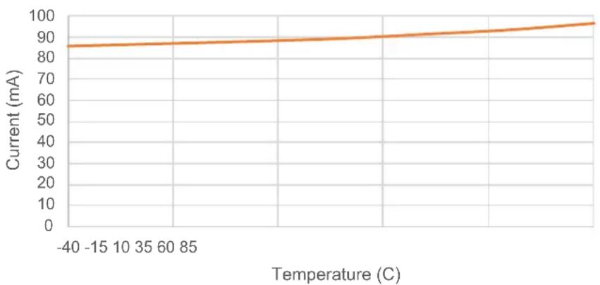
line
| Temperature (C) | Current (mA) | | --------------- | ------------ | | -40 | 85 | | -15 | 86 | | 10 | 87 | | 35 | 88 | | 60 | 89 | | 85 | 90 |Note 1: At all the data rates, the performance remains the same except the values. This graph is only for reference.
2: The current measurement includes the SoC and FEM current.
3: This current includes processor current.
FIGURE 41-41: RECEIVE CURRENT VS. RECEIVE SIGNAL POWER
Receive Current vs. Receive Signal Power
MCS7, Channel 7, 3.3V, 25C
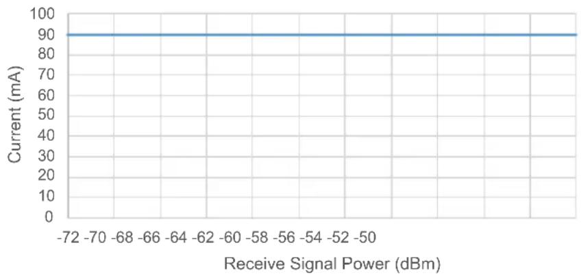
line
| Receive Signal Power (dBm) | Current (mA) | | -------------------------- | ------------ | | -72 | 90 | | -70 | 90 | | -68 | 90 | | -66 | 90 | | -64 | 90 | | -62 | 90 | | -60 | 90 | | -58 | 90 | | -56 | 90 | | -54 | 90 | | -52 | 90 | | -50 | 90 |Note 1: At all the data rates, the performance remains the same except the values. This graph is only for reference.
2: The current measurement includes the SoC and FEM current.
3: This current includes processor current.
FIGURE 41-42: RECEIVE CURRENT VS. CPU FREQUENCY
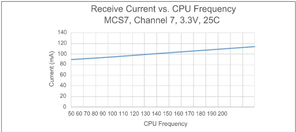
line
| CPU Frequency | Current (mA) | | ------------- | ------------ | | 50 | 90 | | 60 | 92 | | 70 | 94 | | 80 | 96 | | 90 | 98 | | 100 | 100 | | 110 | 102 | | 120 | 104 | | 130 | 106 | | 140 | 108 | | 150 | 110 | | 160 | 112 | | 170 | 114 | | 180 | 116 | | 190 | 118 | | 200 | 120 |Note 1: At all the data rates, the performance remains the same except the values. This graph is only for reference.
2: The current measurement includes the SoC and FEM current.
3: This current includes processor current.
FIGURE 41-43: TRANSMIT CURRENT VS. TEMPERATURE
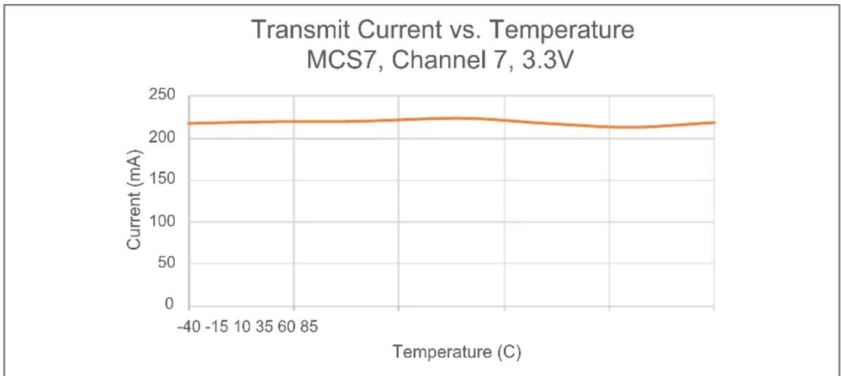
line
| Temperature (C) | Current (mA) | | --------------- | ------------ | | -40 | 215 | | -15 | 215 | | 10 | 215 | | 35 | 215 | | 60 | 215 | | 85 | 215 |Note 1: At all the data rates, the performance remains the same except the values. This graph is only for reference.
2: The current measurement includes the SoC and FEM current.
3: This current includes processor current.
FIGURE 41-44: TRANSMIT CURRENT VS. OUTPUT POWER
Transmit Current vs. Output Power
MCS7, Channel 7, 3.3V, 25C
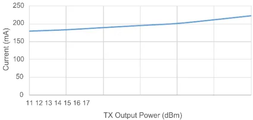
line
| TX Output Power (dBm) | Current (mA) | | --------------------- | ------------ | | 11 | 175 | | 12 | 178 | | 13 | 180 | | 14 | 182 | | 15 | 185 | | 16 | 188 | | 17 | 190 | | 18 | 195 | | 19 | 200 | | 20 | 205 | | 21 | 210 | | 22 | 215 | | 23 | 220 | | 24 | 225 | | 25 | 230 | | 26 | 235 | | 27 | 240 | | 28 | 245 | | 29 | 250 | | 30 | 255 |Note 1: At all the data rates, the performance remains the same except the values. This graph is only for reference.
2: The current measurement includes the SoC and FEM current.
3: This current includes processor current.
FIGURE 41-45: TRANSMIT CURRENT VS. CPU FREQUENCY
Transmit Current vs. CPU Frequency
MCS7, Channel 7, 3.3V, 25C
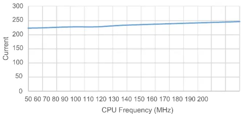
line
| CPU Frequency (MHz) | Current | | ------------------- | ------- | | 50 | 220 | | 60 | 222 | | 70 | 223 | | 80 | 224 | | 90 | 225 | | 100 | 226 | | 110 | 227 | | 120 | 228 | | 130 | 230 | | 140 | 232 | | 150 | 234 | | 160 | 236 | | 170 | 238 | | 180 | 240 | | 190 | 242 | | 200 | 244 |Note 1: At all the data rates, the performance remains the same except the values. This graph is only for reference.
2: The current measurement includes the SoC and FEM current.
3: This current includes processor current.
41.2.4.2 Receiver and Transmitter
Performance Characteristics Graphs
FIGURE 41-46: RX SENSITIVITY VS TEMPERATURE
RX Sensitivity vs Temperature
MCS7, Channel 7, 3.3V
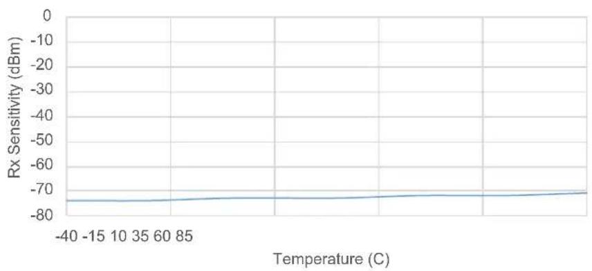
line
| Temperature (C) | Rx Sensitivity (dBm) | | --------------- | -------------------- | | -40 | -75 | | -15 | -75 | | 10 | -75 | | 35 | -75 | | 60 | -75 | | 85 | -75 |Note: At all the data rates, the performance remains the same except the values. This graph is only for reference.
FIGURE 41-47: RX SENSITIVITY VS CHANNELS
RX Sensitivity vs Channel
MCS7, 25C, 3.3V
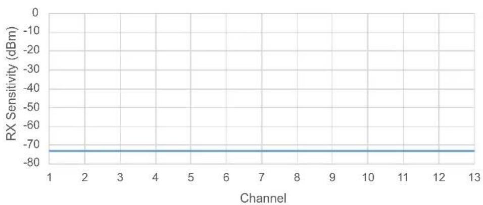
line
| Channel | RX Sensitivity (dBm) | | ------- | -------------------- | | 1 | -75 | | 2 | -75 | | 3 | -75 | | 4 | -75 | | 5 | -75 | | 6 | -75 | | 7 | -75 | | 8 | -75 | | 9 | -75 | | 10 | -75 | | 11 | -75 | | 12 | -75 | | 13 | -75 |Note: At all the data rates, the performance remains the same except the values. This graph is only for reference.
FIGURE 41-48: RX SENSITIVITY VS VOLTAGE
RX Sensitivity vs Voltage
MCS7, Channel 7, 25C
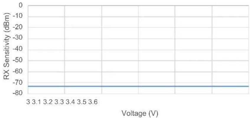
line
| Voltage (V) | RX Sensitivity (dBm) | | ----------- | -------------------- | | 3.1 | -75 | | 3.2 | -75 | | 3.3 | -75 | | 3.4 | -75 | | 3.5 | -75 | | 3.6 | -75 |Note: At all the data rates, the performance remains the same except the values. This graph is only for reference.
FIGURE 41-49: RSSI VS RECEIVE SIGNAL POWER
RSSI
MCS7, Channel 7, 25C
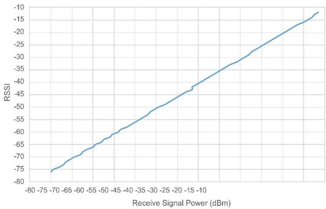
line
| Receive Signal Power (dBm) | RSSI | | -------------------------- | ---- | | -80 | -75 | | -75 | -72 | | -70 | -68 | | -65 | -65 | | -60 | -62 | | -55 | -58 | | -50 | -55 | | -45 | -52 | | -40 | -48 | | -35 | -45 | | -30 | -42 | | -25 | -38 | | -20 | -35 | | -15 | -32 | | -10 | -28 | | -5 | -25 | | 0 | -22 | | 5 | -18 | | 10 | -15 | | 15 | -12 | | 20 | -10 |Note: At all the data rates, the performance remains the same except the values. This graph is only for reference.
FIGURE 41-50: TX POWER VS TEMPERATURE
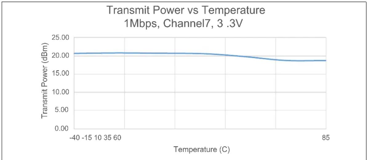
line
| Temperature (C) | Transmit Power (dBm) | | --------------- | -------------------- | | -40 | 20.0 | | -15 | 20.0 | | 10 | 20.0 | | 35 | 20.0 | | 60 | 20.0 | | 85 | 18.0 |Note: At all the data rates, the performance remains the same except the values. This graph is only for reference.
FIGURE 41-51: TX POWER VS CHANNELS
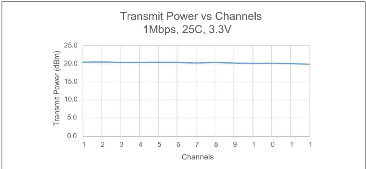
line
| Channels | Transmit Power (dBm) | | -------- | -------------------- | | 1 | 20.0 | | 2 | 20.0 | | 3 | 20.0 | | 4 | 20.0 | | 5 | 20.0 | | 6 | 20.0 | | 7 | 20.0 | | 8 | 20.0 | | 9 | 20.0 | | 10 | 20.0 | | 11 | 20.0 | | 12 | 20.0 | | 13 | 20.0 | | 14 | 20.0 | | 15 | 20.0 | | 16 | 20.0 | | 17 | 20.0 | | 18 | 20.0 | | 19 | 20.0 | | 20 | 20.0 | | 21 | 20.0 | | 22 | 20.0 | | 23 | 20.0 | | 24 | 20.0 | | 25 | 20.0 | | 26 | 20.0 | | 27 | 20.0 | | 28 | 20.0 | | 29 | 20.0 | | 30 | 20.0 | | 31 | 20.0 | | 32 | 20.0 | | 33 | 20.0 | | 34 | 20.0 | | 35 | 20.0 | | 36 | 20.0 | | 37 | 20.0 | | 38 | 20.0 | | 39 | 20.0 | | 40 | 20.0 | | 41 | 20.0 | | 42 | 20.0 | | 43 | 20.0 | | 44 | 20.0 | | 45 | 20.0 | | 46 | 20.0 | | 47 | 20.0 | | 48 | 20.0 | | 49 | 20.0 | | 50 | 20.0 | | 51 | 20.0 | | 52 | 20.0 | | 53 | 20.0 | | 54 | 20.0 | | 55 | 20.0 | | 56 | 20.0 | | 57 | 20.0 | | 58 | 20.0 | | 59 | 20.0 | | 60 | 20.0 | | 61 | 20.0 | | 62 | 20.0 | | 63 | 20.0 | | 64 | 20.0 | | 65 | 20.0 | | 66 | 20.0 | | 67 | 20.0 | | 68 | 20.0 | | 69 | 20.0 | | 70 | 20.0 | | 71 | 20.0 | | 72 | 20.0 | | 73 | 20.0 | | 74 | 20.0 | | 75 | 20.0 | | 76 | 20.0 | | 77 | 20.0 | | 78 | 20.0 | | 79 | 20.0 | | 80 | 20.0 | | 81 | 20.0 | | 82 | 20.0 | | 83 | 20.0 | | 84 | 20.0 | | 85 | 20.0 | | 86 | 20.0 | | 87 | 20.0 | | 88 | 20.0 | | 89 | 20.0 | | 90 | 20.0 | | 91 | 20.0 | | 92 | 20.0 | | 93 | 20.0 | | 94 | 20.0 | | 95 | 20.0 | | 96 | 20.0 | | 97 | 20.0 | | 98 | 20.0 | | 99 | 20.0 | |1 | ~19.5 |Note: At all the data rates, the performance remains the same except the values. This graph is only for reference.
FIGURE 41-52: TX POWER VS VOLTAGES
Transmit Power vs Voltages 1Mbps, Channel 7, 25C
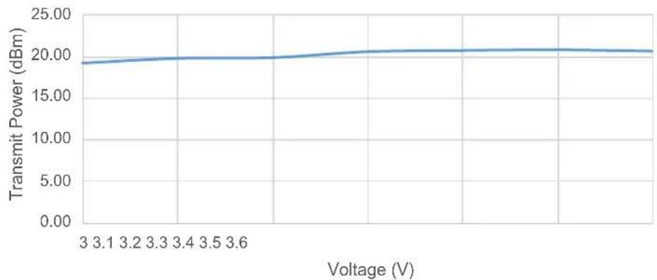
line
| Voltage (V) | Transmit Power (dBm) | | ----------- | -------------------- | | 3.1 | 19.0 | | 3.2 | 19.5 | | 3.3 | 19.8 | | 3.4 | 19.9 | | 3.5 | 20.0 | | 3.6 | 20.1 |Note: At all the data rates, the performance remains the same except the values. This graph is only for reference.
42.0 PACKAGING INFORMATION
This chapter provides the information on package markings, dimension and footprint of the PIC32MZ1025W104 SoC and the WFI32 Module.
42.1 PIC32MZ1025W104 SoC Packaging Information
42.1.1 PIC32MZ1025W104 SOC PACKAGE MARKING
FIGURE 42-1: PIC32MZ1025W104 SOC PACKAGE MARKINGS
Example
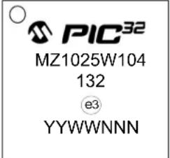
Legend: XX...X
| Y | Year code (last digit of calendar year) |
| YY | Year code (last 2 digits of calendar year) |
| WW | Week code (week of January 1 is week '01') |
| NNN | Alphanumeric traceability |
| Pb-free JEDEC designator for Matte Tin (Sn) | |
| * This package is Pb-free. The Pb-free JEDEC designator (3 can be found on the outer packaging for this package. | |
code
Note: In the event the full Microchip part number cannot be marked on one line, it will be carried over to the next line, thus limiting the number of available characters for customer-specific information.
42.1.2 PIC32MZ1025W104 SOC PACKAGING DIMENSION
This section provides the package dimension details of PIC32MZ1025W104.
FIGURE 42-2: PIC32MZ1025W104 SOC PACKAGE DRAWINGS
132-Lead Very Thin Plastic Quad Flat, No Lead Package (NVX) - 10x10x0.9 mm Body [VQFN]; With 5.5x5.5 mm Exposed Pad; Dual Row Terminals; Punch Singulated
Note: For the most current package drawings, please see the Microchip Packaging Specification located at http://www.microchip.com/packaging
![Microchip PIC32MZ1025W104132 - 132-Lead Very Thin Plastic Quad Flat, No Lead Package (NVX) - 10x10x0.9 mm Body [VQFN]; With 5.5x5.5 mm Exposed Pad; Dual Row Terminals; Punch Singulated - 1](/content/2026/05/935427/images/7cee764086e13a50cb729b3564f3e1c2938f9df8c08b9a08bb8e31a455692a7f.jpg)
Microchip Technology Drawing C04-472 Rev. A Sheet 1 of 2
FIGURE 42-3: PIC32MZ1025W104 SOC PACKAGE DRAWINGS - CONTD.,
132-Lead Very Thin Plastic Quad Flat, No Lead Package (NVX) - 10x10x0.9 mm Body [VQFN]; With 5.5x5.5 mm Exposed Pad; Dual Row Terminals; Punch Singulated
Note: For the most current package drawings, please see the Microchip Packaging Specification located at http://www.microchip.com/packaging
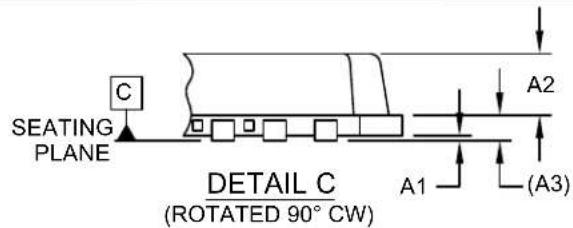
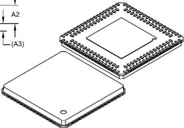
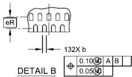
| Units | MILLIMETERS | |||
| Dimension Limits | MIN | NOM | MAX | |
| Number of Terminals | N | 132 | ||
| Terminals in Outer Row A | NA | 72 | ||
| Terminals in Inner Row B | NB | 60 | ||
| Pitch | e | 0.50 BSC | ||
| Pitch Between Rows | eR | 0.65 BSC | ||
| Overall Height | A | 0.80 | 0.85 | 0.90 |
| Standoff | A1 | 0.00 | 0.01 | 0.05 |
| Mold Cap Height A2 0.55 0.60 | 0.65 | |||
| Base Thickness | A3 | 0.25 REF | ||
| Overall Length | D | 10.00 BSC | ||
| Mold Cap Length | D1 9.73 BSC | |||
| Exposed Pad Length | D2 | 5.40 | 5.50 | 5.60 |
| Overall Width | E | 10.00 BSC | ||
| Mold Cap Width E1 9.73 BSC | ||||
| Exposed Pad Width | E2 | 5.40 | 5.50 | 5.60 |
| Terminal Length, Outer Row | La | 0.30 | 0.40 | 0.50 |
| Terminal Length, Inner Row | Lb | 0.30 | 0.40 | 0.50 |
| Terminal Width | b | 0.17 0.22 0.27 | ||
| K 0 | 20 MIN REFTerminal-to-Exposed-Pad | |||
| Corner Chamfer | P | 0.24 0.42 0.60 | ||
Notes:
- Pin 1 visual index feature may vary, but must be located within the hatched area.
- Package is punch singulated
- Dimensioning and tolerancing per ASME Y14.5M BSC: Basic Dimension. Theoretically exact value shown without tolerances. REF: Reference Dimension, usually without tolerance, for information purposes only.
Microchip Technology Drawing C04-472 Rev. A Sheet 2 of 2
42.1.3 PIC32MZ1025W104 SOC RECOMMENDED FOOTPRINT
The following figure illustrates the recommended footprint for the PIC32MZ1025W104.
FIGURE 42-4: RECOMMENDED FOOTPRINT FOR THE PIC32MZ1025W104
132-Lead Very Thin Plastic Quad Flat, No Lead Package (NVX) - 10x10x0.9 mm Body [VQFN]; With 5.5x5.5 mm Exposed Pad; Dual Row Terminals; Punch Singulated
Note: For the most current package drawings, please see the Microchip Packaging Specification located at http://www.microchip.com/packaging
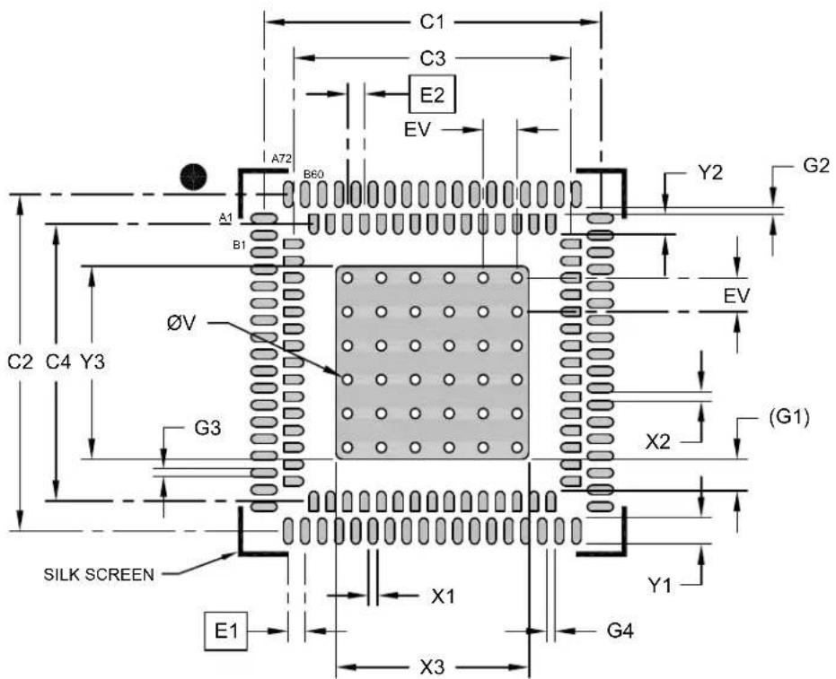
RECOMMENDED LAND PATTERN
| Units | MILLIMETERS | Units | MILLIMETERS | ||||||
| Dimension Limits | MIN | NOM | MAX | Dimension Limits | MIN | MAXOM | |||
| Outer Contact Pitch | E1 | 0.50 BSC | C4Inner Contact Pad Spacing | ||||||
| Inner Contact Pitch 0.50 BSCE2 | Outer Contact Pad Length (X72) Y1 | 0.78 | |||||||
| Outer Contact Pad Width (X72) | X1 0.30 | Inner Contact Pad Length (X60) | Y2 0.59 | ||||||
| Inner Contact Pad Width (X60) | X2 0.30 | Contact Pad to Center Pad (X60) G1 | 1.20 REF | ||||||
| Optional Center Pad Width | X3 | 5.60 | Inner Pad Row to Outer Pad Row | G2 | 0.20 | ||||
| Optional Center Pad Length | Y3 | 5.60 | Contact Pad to Contact Pad (X68) | G3 | 0.20 | ||||
| C1Outer Contact Pad Spacing | Contact Pad to Contact Pad (X56) | G4 | 0.20 | ||||||
| Outer Contact Pad Spacing | C2 | 9.93 | Thermal Via Diameter | V | 0.30 | ||||
| C3Inner Contact Pad Spacing | Thermal Via Pitch | EV | 1.00 | ||||||
Notes:
1. Dimensioning and tolerancing per ASME Y14.5M
BSC: Basic Dimension. Theoretically exact value shown without tolerances.
2. For best soldering results, thermal vias, if used, should be filled or tented to avoid solder loss during reflow process
Microchip Technology Drawing C04-2472 Rev. A
42.2 WFI32 Module Packaging Information
42.2.1 MODULE PACKAGE MARKING
42.2.1.1 WFI32E01 Module Package Marking
FIGURE 42-5: WFI32E01 MODULE PACKAGE MARKINGS
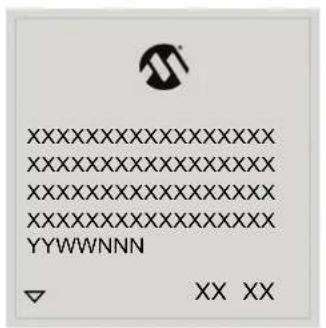
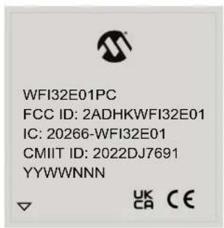
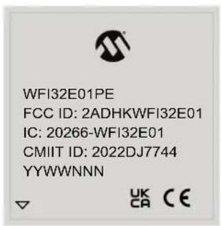
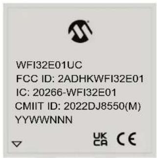
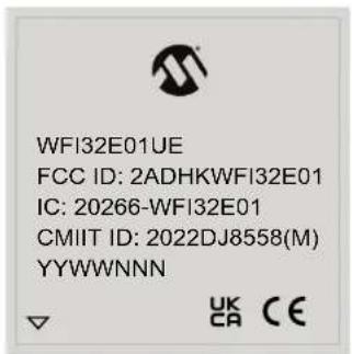
Legend:
XX....X Module part number and version and regulatory designator
YY: Year code (last 2 digits of calendar year)
WW Week code (week of January 1 is week "01")
NNN Alphanumeric traceability code
42.2.1.2 WFI32E02 Module Package Marking
FIGURE 42-6: WFI32E02 MODULE PACKAGE MARKINGS
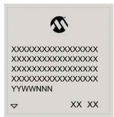
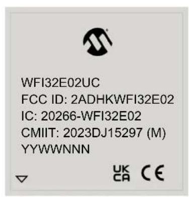
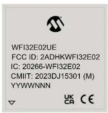
Legend:
XX....X Module part number and version and regulatory designator
YY: Year code (last 2 digits of calendar year)
WW Week code (week of January 1 is week "01")
NNN Alphanumeric traceability code
42.2.2 MODULE PACKAGING DIMENSION
Note: Module dimensions mentioned in the following figure are applicable to the PCB antenna and U.FL connector variants.
42.2.2.1 WFI32E01 Module Packaging Dimension
FIGURE 42-7: 54-PIN RF MODULE WITH SHIELD (6YX) - 20.5X24.5 MM [MODULE]
54-Lead RF Module With Shield (6YX) - 20.5x24.5 mm [MODULE]
Note: For the most current package drawings, please see the Microchip Packaging Specification located at http://www.microchip.com/packaging
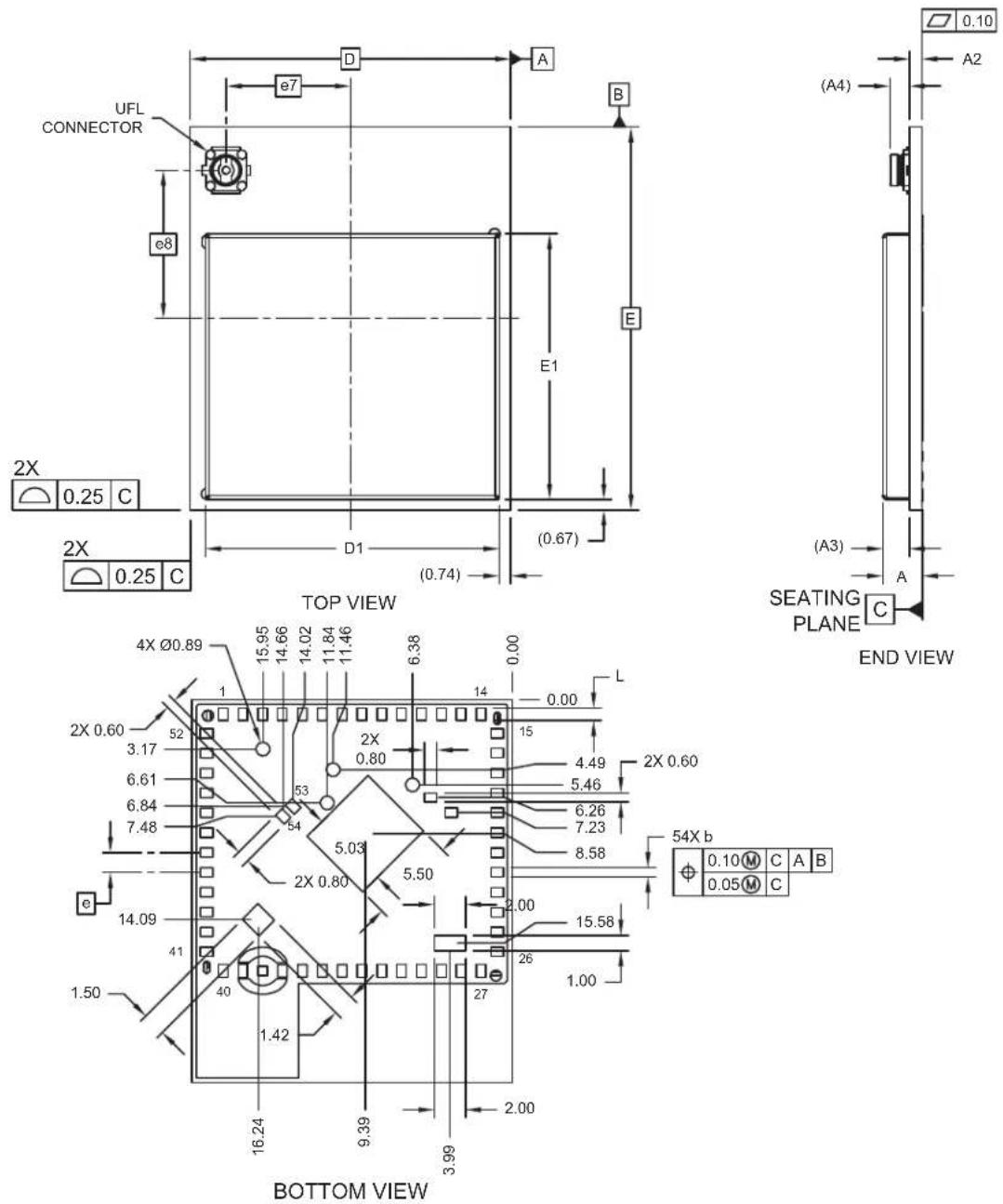
Microchip Technology Drawing C04-10050 Rev D Sheet 1 of 2
© 2023 Microchip Technology Inc.
FIGURE 42-8: 54-PIN RF MODULE WITH SHIELD (6YX) - 20.5X24.5 MM [MODULE]
54-Lead RF Module With Shield (6YX) - 20.5x24.5 mm [MODULE]
Note: For the most current package drawings, please see the Microchip Packaging Specification located at http://www.microchip.com/packaging
![Microchip PIC32MZ1025W104132 - 54-Lead RF Module With Shield (6YX) - 20.5x24.5 mm [MODULE] - 1](/content/2026/05/935427/images/feba72417e9e6dd614b6b5eb77a96334513022a683be594f94eda2e4b8afe6d7.jpg)
natural_image
Technical line drawing of two electronic components with visible internal structures and mounting points (no text or symbols)| Units | MILLIMETERS | |||
| Dimension Limits | MIN | NOM | MAX | |
| Number of Terminals | N | 54 | ||
| Overall Height | A | 2.40 | 2.50 | 2.60 |
| PCB Thickness | A2 | 0.70 | 0.80 | 0.90 |
| Shield Height | A3 | 1.70 REF | ||
| UFL Connector Height A4 1.25 REF | ||||
| Overall Length D 20.50 BSC | ||||
| Overall Width | E | 24.50 BSC | ||
| Shield Length D1 18.80 | 18.70 18 | 90 | ||
| Shield Width E1 17.00 | 16.90 17 | 10 | ||
| Terminal Width | b | 0.50 | 0.60 | 0.70 |
| Terminal Length | L | 0.70 | 0.80 | 0.90 |
Microchip Technology Drawing C04-10050 Rev D Sheet 2 of 2
© 2023 Microchip Technology Inc.
42.2.2.2 WFI32E02 Module Packaging Dimension
FIGURE 42-9: 87-PIN MODULE (TFC) WITH METAL SHIELD AND COAXIAL CONNECTOR - 22.5X24.50 MM [MODULE]
87L-PCB Module (TFC) - 22.50x24.50mm - [MODULE] With Metal Shield and Coaxial Connector
Note: For the most current package drawings, please see the Microchip Packaging Specification located at http://www.microchip.com/packaging
![Microchip PIC32MZ1025W104132 - 54-Lead RF Module With Shield (6YX) - 20.5x24.5 mm [MODULE] - 2](/content/2026/05/935427/images/704a4d4de2bf426591dafdda4561ae213e98ed16afcfd14eb82184210e10873a.jpg)
Microchip Technology Drawing C04-21568 Rev C Sheet 1 of 2
FIGURE 42-10: 87-PIN MODULE (TFC) WITH METAL SHIELD AND COAXIAL CONNECTOR - 22.5X24.5 MM [MODULE]
87L-PCB Module (TFC) - 22.50x24.50mm - [MODULE] With Metal Shield and Coaxial Connector
Note: For the most current package drawings, please see the Microchip Packaging Specification located at http://www.microchip.com/packaging
![Microchip PIC32MZ1025W104132 - 87L-PCB Module (TFC) - 22.50x24.50mm - [MODULE] With Metal Shield and Coaxial Connector - 1](/content/2026/05/935427/images/2b06ed8c537e496cd7f99b4a1d5fc5c4426055e110deaebfec52d4496f957243.jpg)
natural_image
Technical line drawing of a microchip or electronic component with two views: top shows top plate with grid pattern and central slot, bottom shows base with screw and mounting base (no text or symbols)| Units | MILLIMETERS | |||
| Dimension Limits | MIN | NOM | MAX | |
| Number of Terminals | N | 87 | ||
| Terminal Pitch | e | 1.27 BSC | ||
| Overall Height | A | 2.40 | 2.50 | 2.60 |
| PCB Thickness | A2 | 0.70 | 0.80 | 0.90 |
| Shield Height | A3 | 1.70 REF | ||
| UFL Connector Height A4 1.25 REF | ||||
| Overall Length D 22.50 BSC | ||||
| Overall Width | E | 24.50 BSC | ||
| Shield Length | D1 | 20.73 20.93 20.83 | ||
| Shield Width E1 18.03 | 17.93 18.13 | |||
| Terminal Width | b | 0.50 | 0.60 | 0.70 |
| Terminal Length | L | 0.70 | 0.80 | 0.90 |
Notes:
- All Dimensions are in Millimeters
BSC: Basic Dimension. Theoretically exact value shown without tolerances.
REF: Reference Dimension, usually without tolerance, for information purposes only.
Sheet 2 of 2Micro
42.2.3 MODULE RECOMMENDED FOOTPRINT
42.2.3.1 WFI32E01 Module Recommended Footprint
FIGURE 42-11: WFI32E01 RECOMMENDED MODULE FOOTPRINT ON THE HOST BOARD
54-Lead RF Module With Shield (6YX) - 20.5x24.5 mm [MODULE]
Note: For the most current package drawings, please see the Microchip Packaging Specification located at http://www.microchip.com/packaging
![Microchip PIC32MZ1025W104132 - 87L-PCB Module (TFC) - 22.50x24.50mm - [MODULE] With Metal Shield and Coaxial Connector - 2](/content/2026/05/935427/images/480f6fe826600b0c841d2cb505cf33a9e7f91d34ab274916f8dd64b5f33d67c7.jpg)
other
| Measurement | Value | |---|---| | 4.26 | 17.34 | | 4.54 | 17.34 | | 11.25 | 14.07 | | 16.51 | 14.07 | | 27 | 14.07 | | 62 | 14.07 | | 15.58 | 14.07 | | 1.27 | 14.07 | | 7.23 | 14.07 | | 6.26 | 14.07 | | 5.46 | 14.07 | | 2.17 | 14.07 | | 0.00 | 14.07 | | 1 | 14.07 | | 2 | 14.07 | | 4 | 14.07 | | 5 | 14.07 | | 6 | 14.07 | | 8 | 14.07 | | 9 | 14.07 | | 10 | 14.07 | | 11 | 14.07 | | 12 | 14.07 | | 13 | 14.07 | | 14 | 14.07 | | 15 | 14.07 | | 16 | 14.07 | | 17 | 14.07 | | 18 | 14.07 | | 19 | 14.07 | | 20 | 14.07 | | 21 | 14.07 | | 22 | 14.07 | | 23 | 14.07 | | 24 | 14.07 | | 25 | 14.07 | | 26 | 14.07 | | 27 | 14.07 | | 28 | 14.07 | | 29 | 14.07 | | 30 | 14.07 | | 31 | 14.07 | | 32 | 14.07 | | 33 | 14.07 | | 34 | 14.07 | | 35 | 14.07 | | 36 | 14.07 | | 37 | 14.07 | | 38 | 14.07 | | 39 | 14.07 | | 40 | 14.07 | | 41 | 14.07 | | 42 | 14.07 | | 43 | 14.07 | | 44 | 14.07 | | 45 | 14.07 | | 46 | 14.07 | | 47 | 14.07 | | 48 | 14.07 | | 49 | 14.07 | | 50 | 14.07 | | 51 | 14.07 | | 52 | 14.07 | | 53 | 14.07 | | 54 | 14.07 | | 55 | 14.07 | | 56 | 14.07 | | 57 | 14.07 | | 58 | 14.07 | | 59 | 14.07 | | 60 | 14.07 | | Note: The values in the table represent numerical data points, not percentages or units specified in the chart.RECOMMENDED LAND PATTERN
NOTE: Place pins 53, 54, 61, and 63 with 45^ angle
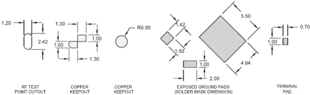
Notes:
All dimensions are in millimeters.1.
Microchip Technology Drawing C04-12050 Rev D
© 2023 Microchip Technology Inc.
Note: For routing guidelines, refer to Section 3.4 "WFI32 Module Routing Guidelines".
42.2.3.2 WFI32E02 Module Recommended Footprint
FIGURE 42-12: WFI32E02 RECOMMENDED MODULE FOOTPRINT ON THE HOST BOARD
87L-PCB Module (TFC) - 22.50x24.50mm - [MODULE] With Metal Shield and Coaxial Connector
Note: For the most current package drawings, please see the Microchip Packaging Specification located at http://www.microchip.com/packaging
![Microchip PIC32MZ1025W104132 - 87L-PCB Module (TFC) - 22.50x24.50mm - [MODULE] With Metal Shield and Coaxial Connector - 1](/content/2026/05/935427/images/beca8aea808d632b09c1e723000c34632ded679cef683c5f1e36a94a9d7406b0.jpg)
other
| Label | Value | |-------|-------| | A40 | 19.356 | | B25 | 15.098 | | B24 | 13.903 | | A41 | 9.586 | | B25 | 7.366 | | B24 | 6.299 | | B24 | 6.325 | | B35 | 4.435 | | B35 | 3.800 | | B35 | 3.296 | | B35 | 2.204 | | B35 | 0.823 | | A1 | 0.950 | | A1 | 2.204 | | A1 | 2.995 | | A1 | 3.630 | | A1 | 9.906 | | A1 | 11.278 | | A1 | 12.104 | | A1 | 14.655 | | A1 | 14.714 | | A1 | 16.123 | | A1 | 16.123 | | A1 | 88 | | A1 | 89 | | A1 | 90 | | A1 | 91 | | A1 | 96 | | A1 | 97 | | A1 | 98 | | A1 | 99 | | A1 | 100 | | A1 | 101 | | A1 | 92 | | A26 | 22.50 | | B24 | 4.00 | | B24 | 1.27 | | B24 | 1.27 | | B24 | 1.27 | | B24 | 1.27 | | B24 | 1.27 | | B24 | 1.27 | | B24 | 1.27 | | B24 | 1.27 | | B24 | - | | B24 | - | | B24 | - | | B24 | - | | B24 | - | | B24 | - | | B24 | - | | B24 | - | | B24 | - | | B24 | - | | B24 | - | | B24 | - |RECOMMENDED LAND PATTERN
![Microchip PIC32MZ1025W104132 - 87L-PCB Module (TFC) - 22.50x24.50mm - [MODULE] With Metal Shield and Coaxial Connector - 2](/content/2026/05/935427/images/34eba07ba18ea6a38427446339742cd35a0f2f3bd5844511a388c4b010ece920.jpg)
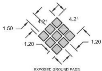
![Microchip PIC32MZ1025W104132 - 87L-PCB Module (TFC) - 22.50x24.50mm - [MODULE] With Metal Shield and Coaxial Connector - 4](/content/2026/05/935427/images/a173759f3aa8576abc3c9ca18afc01729b5f49bd7a173574375b64ab37164e27.jpg)
Notes:
All dimensions are in millimeters.1.
Microchip Technology Drawing C04-23568 Rev C
Note: For routing guidelines, refer to Section 3.4 "WFI32 Module Routing Guidelines".
APPENDIX A: REGULATORY APPROVALS
This chapter provides the information on the regulatory approval of the WFI32 Module.
The WFI32E01PC module has received regulatory approval from the following countries:
• United States/FCC ID: 2ADHKWFI32E01
- Canada/ISED
- IC: 20266-WFI32E01
- HVIN: WFI32E01PC
- PMN: WFI32E01 Module
- Europe/CE
• UKCA
- Japan
- Korea
• Taiwan
• China (SRRC)/CMIIT ID: 2022DJ7691
The WFI32E01PE module has received regulatory approval from the following countries:
• United States/FCC ID: 2ADHKWFI32E01
- Canada/ISED
- IC: 20266-WFI32E01
- HVIN: WFI32E01PE
- PMN: WFI32E01 Module
- Europe/CE
• UKCA
- Japan
- Korea
• Taiwan
• China (SRRC)/CMIIT ID: 2022DJ7744
The WFI32E01UC module has received regulatory approval from the following countries:
• United States/FCC ID: 2ADHKWFI32E01
- Canada/ISED
- IC: 20266-WFI32E01
- HVIN: WFI32E01UC
- PMN: WFI32E01 Module
- Europe/CE
• UKCA
- Japan
- Korea
• Taiwan
• China (SRRC)/CMIIT ID: 2022DJ8550(M)
The WFI32E01UE module has received regulatory approval from the following countries:
• United States/FCC ID: 2ADHKWFI32E01
- Canada/ISED
- IC: 20266-WFI32E01
- HVIN: WFI32E01UE
- PMN: WFI32E01 Module
- Europe/CE
• UKCA
- Japan
- Korea
• Taiwan
• China (SRRC)/CMIIT ID: 2022DJ8558(M)
The WFI32E02UC module has received regulatory approval from the following countries:
• United States/FCC ID: 2ADHKWFI32E02
- Canada/ISED
- IC: 20266-WFI32E02
- HVIN: WFI32E02UC
- PMN: WFI32E02 Module
- Europe/CE
• UKCA
- Japan
- Korea
• Taiwan
• China (SRRC)/CMIIT ID: 2023DJ15297 (M)
The WFI32E02UE module has received regulatory approval from the following countries:
• United States/FCC ID: 2ADHKWFI32E02
- Canada/ISED
- IC: 20266-WFI32E02
- HVIN: WFI32E02UE
- PMN: WFI32E02 Module
- Europe/CE
• UKCA
- Japan
- Korea
• Taiwan
• China (SRRC)/CMIIT ID: 2023DJ15301 (M)
A.1 United States
The WFI32E01PC/WFI32E01PE/WFI32E01UC/WFI32E01UE/WFI32E02UC/WFI32E02UE Modules have received Federal Communications Commission (FCC) CFR47 Telecommunications, Part 15 Subpart C "Intentional Radiators" single-modular approval in accordance with Part 15.212 Modular Transmitter approval. Single-modular transmitter approval is defined as a complete RF transmission sub-assembly, designed to be incorporated into another device, that must demonstrate compliance with FCC rules and policies independent of any host. A transmitter with a mod-
ular grant can be installed in different end-use products (referred to as a host, host product, or host device) by the grantee or other equipment manufacturer, then the host product may not require additional testing or equipment authorization for the transmitter function provided by that specific module or limited module device.
The user must comply with all of the instructions provided by the Grantee, which indicate installation and/or operating conditions necessary for compliance.
The host product itself is required to comply with all other applicable FCC equipment authorizations regulations, requirements and equipment functions that are not associated with the transmitter module portion. For example, compliance must be demonstrated: to regulations for other transmitter components within a host product; to requirements for unintentional radiators (Part 15 Subpart B), such as digital devices, computer peripherals, radio receivers, etc.; and to additional authorization requirements for the non-transmitter functions on the transmitter module (i.e., Suppliers Declaration of Conformity (SDoC) or certification) as appropriate (for example, Bluetooth and Wi-Fi transmitter modules may also contain digital logic functions).
A.1.1 LABELING AND USER INFORMATION REQUIREMENTS
The WFI32E01PC/WFI32E01PE/WFI32E01UC/WFI32E01UE/WFI32E02UC/WFI32E02UE modules have been labeled with its own FCC ID number, and if the FCC ID is not visible when the module is installed inside another device, then the outside of the finished product into which the module is installed must also display a label referring to the enclosed module. This exterior label can use wording as follows:
For the WFI32E01PC/WFI32E01PE/WFI32E01UC/WFI32E01UE:
Contains Transmitter FCC ID: 2ADHKWFI32E01
or
Contains FCC ID: 2ADHKWFI32E01
This device complies with Part 15 of the FCC Rules. Operation is subject to the following two conditions: (1) this device may not cause harmful interference, and (2) this device must accept any interference received, including interference that may cause undesired operation
For the WFI32E02UC/ WFI32E02UE:
Contains Transmitter FCC ID: 2ADHKWFI32E02
or
Contains FCC ID: 2ADHKWFI32E02
This device complies with Part 15 of the FCC Rules. Operation is subject to the following two conditions: (1) this device may not cause harmful interference, and (2) this device must accept any interference received, including interference that may cause undesired operation
A user's manual for the finished product must include the following statement:
This equipment has been tested and found to comply with the limits for a Class B digital device, pursuant to part 15 of the FCC Rules. These limits are designed to provide reasonable protection against harmful interference in a residential installation. This equipment generates, uses and can radiate radio frequency energy, and if not installed and used in accordance with the instructions, may cause harmful interference to radio communications. However, there is no guarantee that interference will not occur in a particular installation. If this equipment does cause harmful interference to radio or television reception, which can be determined by turning the equipment off and on, the user is encouraged to try to correct the interference by one or more of the following measures:
- Reorient or relocate the receiving antenna
- Increase the separation between the equipment and receiver
- Connect the equipment into an outlet on a circuit e different from that to which the receiver is connected
- Consult the dealer or an experienced radio/TV technician for help
Additional information on labeling and user information requirements for Part 15 devices can be found in KDB Publication 784748, which is available at the FCC Office of Engineering and Technology (OET) Laboratory Division Knowledge Database (KDB) https://apps.fcc.gov/oetcf/kdb/index.cfm
A.1.2 RF EXPOSURE
All transmitters regulated by FCC must comply with RF exposure requirements. KDB 447498 General RF Exposure Guidance provides guidance in determining whether proposed or existing transmitting facilities, operations or devices comply with limits for human exposure to Radio Frequency (RF) fields adopted by the Federal Communications Commission (FCC).
From the FCC Grant: Power output listed is conducted. Single Modular Approval. This module is granted for use in mobile only configuration as described in this filing.
Approval is limited to OEM installation only.
The antenna(s) used for this transmitter must be installed to provide a separation distance of at least 8 cm from all persons and must not be co-located or operating in conjunction with any other antenna or transmitter, except in accordance with FCC multi-transmitter product procedures. OEM integrators and end-users must be provided with specific operating instructions for satisfying RF exposure compliance requirements.
A.1.3 APPROVED ANTENNAS
To maintain modular approval in the United States, only the antenna types that have been tested shall be used. It is permissible to use different antenna, provided the same antenna type, antenna gain (equal to or less than), with similar in-band and out-of-band characteristics (refer to specification sheet for cutoff frequencies).
For WFI32E01PC/WFI32E01PE, the approval is received using the integral PCB antenna.
For
WFI32E01UC/WFI32E01UE/WFI32E02UC/WFI32E02UE, approved antennas are listed in the Table 3-4.
A.1.4 MODULE INTEGRATION IN THE HOST PRODUCT
Host products are to ensure continued compliance as per KDB 996369 Module Integration Guide.
A.1.5 HELPFUL WEBSITES
Federal Communications Commission (FCC): https://www.fcc.gov/
FCC Office of Engineering and Technology (OET) Laboratory Division Knowledge Database (KDB): https://apps.fcc.gov/oetcf/kdb/index.cfm
A.2 Canada
The WFI32E01PC/WFI32E01PE/WFI32E01UC/WFI32E01UE/WFI32E02UC/WFI32E02UE modules have been certified for use in Canada under Innovation, Science and Economic Development Canada (ISED, formerly Industry Canada) Radio Standards Procedure (RSP) RSP-100, Radio Standards Specification (RSS) RSS-Gen and RSS-247. Modular approval permits the installation of a module in a host device without the need to re-certify the device.
A.2.1 LABELING AND USER
INFORMATION REQUIREMENTS
Labeling Requirements (from RSP-100, Issue 12, Section 5): The host product shall be properly labeled to identify the module within the host device.
The Innovation, Science and Economic Development Canada certification label of a module shall be clearly visible at all times when installed in the host product, otherwise the host device must be labeled to display the Innovation, Science and Economic Development Canada certification number of the module, preceded by the word “Contains”, or similar word expressing the same meaning, as follows:
For the WFI32E01PC/WFI32E01PE/WFI32E01UC/WFI32E01UE:
Contains IC: 20266-WFI32E01
For the WFI32E02UC/ WFI32E02UE:
Contains IC: 20266-WFI32E02
User Manual Notice for License-Exempt Radio Apparatus (from Section 8.4 RSS-Gen, Issue 5, March 2019): User manuals for license-exempt radio apparatus shall contain the following or equivalent notice in a conspicuous location in the user manual or alternatively on the device or both:
This device contains license-exempt transmitter(s)/receiver(s) that comply with Innovation, Science and Economic Development Canada's license-exempt RSS(s). Operation is subject to the following two conditions:
Transmitter Antenna (From Section 6.8 RSS-GEN, Issue 5, March 2019): User manuals, for transmitters shall display the following notice in a conspicuous location:
This radio transmitter [IC: 20266-WFI32E01 and 20266-WFI32E02] has been approved by Innovation, Science and Economic Development Canada to operate with the antenna types listed below, with the maximum permissible gain indicated. Antenna types not included in this list that have a gain greater than the maximum gain indicated for any type listed are strictly prohibited for use with this device.
Immediately following the above notice, the manufacturer shall provide a list of all antenna types approved for use with the transmitter, indicating the maximum permissible antenna gain (in dBi) and required impedance for each.
A.2.2 RF EXPOSURE
All transmitters regulated by the Innovation, Science and Economic Development Canada (ISED) must comply with RF exposure requirements listed in RSS-102 - Radio Frequency (RF) Exposure Compliance of Radio communication Apparatus (All Frequency Bands).
This transmitter is restricted for use with a specific antenna tested in this application for certification, and must not be co-located or operating in conjunction with any other antenna or transmitters, except in accordance with Innovation, Science and Economic Development Canada multi-transmitter guidelines.
The module antenna must be installed to meet the RF exposure compliance separation distance of "20 cm" and any additional testing and authorization process as required. The host integrator installing this module into their product must ensure that the final composite product complies with the ISED requirements by a technical assessment.
A.2.3 APPROVED ANTENNAS
For WFI32E01PC/WFI32E01PE, the approval is received using the integral PCB antenna.
For
WFI32E01UC/WFI32E01UE/WFI32E02UC/WFI32E02UE, approved antennas are listed in the Table 3-4.
A.2.4 HELPFUL WEBSITES
Innovation, Science and Economic Development Canada (ISED): http://www.ic.gc.ca/
A.3 Europe
The WFI32E01PC/WFI32E01PE/WFI32E01UC/WFI32E01UE/WFI32E02UC/WFI32E02UE modules are Radio Equipment Directive (RED) assessed, CE marked, and have been manufactured and tested with the intention of being integrated into a final product.
The WFI32E01PC/WFI32E01PE/WFI32E01UC/WFI32E01UE/WFI32E02UC/WFI32E02UE modules have been tested to RED 2014/53/EU Essential Requirements mentioned in the following European Compliance table.
TABLE A-1: EUROPEAN COMPLIANCE
| Certification Standards Article | ||
| Safety | EN | 62368 |
| Health EN 62311 | ||
| Electro Magnetic Compatibility (EMC) | EN 301 489-1 3.1b | |
| EN 301 489-17 | ||
| Radio | EN 300 328 | 3.2 |
The ETSI provides guidance on modular devices in "Guide to the application of harmonised standards covering Article 3.1b and Article 3.2 of the Directive 2014/53/EU RED to multi-radio and combined radio and non-radio equipment" document available at http://www.etsi.org/deliver/etsi_eg/203300_203399/203367/01.01.01_60/eg_203367v010101p.pdf.
Note: To maintain conformance to the standards listed in the preceding European Compliance table, the module shall be installed in accordance with the installation instructions in this data sheet and shall not be modified. When integrating a radio module into a completed product, the integrator becomes the manufacturer of the final product and is therefore responsible for demonstrating compliance of the final product with the essential requirements against the RED.
A.3.1 LABELING AND USER INFORMATION REQUIREMENTS
The label on the final product, which contains the WFI32E01PC/WFI32E01PE/WFI32E01UC/WFI32E01UE/WFI32E02UC/WFI32E02UE modules must follow CE marking requirements.
A.3.2 CONFORMITY ASSESSMENT
From ETSI Guidance Note EG 203367, section 6.1 Non-radio products are combined with a radio product:
If the manufacturer of the combined equipment installs the radio product in a host non-radio product in equivalent assessment conditions (i.e., host equivalent to the one used for the assessment of the radio product) and according to the installation instructions for the radio product, then no additional assessment of the combined equipment against article 3.2 of the RED is required.
A.3.3 APPROVED ANTENNAS
For WFI32E01PC/WFI32E01PE, the approval is received using the integral PCB antenna.
For
WFI32E01UC/WFI32E01UE/WFI32E02UC/WFI32E02UE, the approval is received using the antennas listed in Table 3-4.
A.3.3.1 SIMPLIFIED EU DECLARATION OF CONFORMITY
Hereby, Microchip Technology Inc. declares that the radio equipment type WFI32E01PC/WFI32E01PE/WFI32E01UC/WFI32E01UE/WFI32E02UC/WFI32E02UE is in compliance with Directive 2014/53/EU.
The full text of the EU declaration of conformity for this product is available at http://www.micro-chip.com/PIC32MZW1 (available under Documents >Certifications).
A.3.4 HELPFUL WEBSITES
A document that can be used as a starting point in understanding the use of Short Range Devices (SRD) in Europe is the European Radio Communications Committee (ERC) Recommendation 70-03 E, which can be downloaded from the European Communications Committee (ECC) at: http://www.ecodocdb.dk/.
Additional helpful websites are:
• Radio Equipment Directive (2014/53/EU): https://ec.europa.eu/growth/single-market/european-standards/harmonised-standards/red_en
• European Conference of Postal and Telecommunications Administrations (CEPT):
http://www.cept.org
• European Telecommunications Standards Institute (ETSI): http://www.etsi.org
• The Radio Equipment Directive Compliance Association (REDCA): http://www.redca.eu/
A.4 UKCA
The WFI32E01PC/WFI32E01PE/WFI32E01UC/WFI32E01UE/WFI32E02UC/WFI32E02UE modules are UKCA assessed radio module that meets all the essential requirements according to CE RED requirements.
A.4.1 LABELING AND USER INFORMATION REQUIREMENTS
The label on the final product, which contains the WFI32E01PC/WFI32E01PE/WFI32E01UC/WFI32E01UE/WFI32E02UC/WFI32E02UE modules must follow UKCA marking requirements.

This UKCA mark is printed on the module or on the packaging label. For more details on the label requirements, refer to the https://www.gov.uk/guidance/using-the-ukca-marking#check-whether-you-need-to-use-the-new-ukca-marking.
A.4.2 UKCA DECLARATION OF CONFORMITY
Hereby, Microchip Technology Inc. declares that the radio equipment type WFI32E01PC/WFI32E01PE/WFI32E01UC/WFI32E01UE/WFI32E02UC/WFI32E02UE is in compliance with the Radio Equipment Regulations 2017.
The full text of the EU declaration of conformity for this product is available at http://www.micro-chip.com/PIC32MZW1 (available under Documents >Certifications).
A.4.3 APPROVED ANTENNAS
For WFI32E01PC/WFI32E01PE, the approval is received using the integral PCB antenna.
For
WFI32E01UC/WFI32E01UE/WFI32E02UC/WFI32E02UE, the approval is received using the antennas listed in Table34.
A.4.4 HELPFUL WEBSITES
For additional information, refer to the following website:
- https://www.gov.uk/guidance/placing-manufactured-goods-on-the-market-in-great-britain.
A.5 Japan
The WFI32E01PC/WFI32E01PE/WFI32E01UC/WFI32E01UE/WFI32E02UC/WFI32E02UE modules have received type certification and is required to be labeled with its own technical conformity mark and certification number as required to conform to the technical standards regulated by the Ministry of Internal Affairs and Communications (MIC) of Japan pursuant to the Radio Act of Japan.
Integration of this module into a final product does not require additional radio certification provided installation instructions are followed and no modifications of the module are allowed. Additional testing may be required:
- If the host product is subject to electrical appliance safety (for example, powered from an AC mains), the host product may require Product Safety Electrical Appliance and Material (PSE) testing. The integrator must contact their conformance laboratory to determine if this testing is required
- There is an voluntary Electromagnetic Compatibility (EMC) test for the host product administered by VCCI: http://www.vcci.jp/vcci_e/index.html.
A.5.1 LABELING AND USER
INFORMATION REQUIREMENTS
The label on the final product, which contains the WFI32E01PC/WFI32E01PE/WFI32E01UC/WFI32E01UE/WFI32E02UC/WFI32E02UE modules must follow Japan marking requirements. The integrator of the module must refer to the labeling requirements for Japan available at the Ministry of Internal Affairs and Communications (MIC) website.
For the WFI32E01PC/WFI32E01PE/WFI32E01UC/WFI32E01UE modules module/s, due to a limited module size, the technical conformity logo and ID is displayed in the data sheet and/or packaging and cannot be displayed on the module label. The final product in which this module is being used must have a label referring to the type certified module inside:

005-102870
For the WFI32E02UC/
WFI32E02UE modules module/s, due to a limited module size, the technical conformity logo and ID is displayed in the data sheet and/or packaging and cannot be displayed on the module label. The final product in which this module is being used must have a label referring to the type certified module inside:

020-230255
A.5.2 HELPFUL WEBSITES
- Ministry of Internal Affairs and Communications (MIC): http://www.tele.soumu.go.jp/e/index.htm.
- Association of Radio Industries and Businesses (ARIB): http://www.arib.or.jp/english/.
A.6 Korea
The WFI32E01PC/WFI32E01PE/WFI32E01UC/WFI32E01UE/WFI32E02UC/WFI32E02UE Modules have received certification of conformity in accordance with the Radio Waves Act. Integration of this module into a final product does not require additional radio certification provided installation instructions are followed and no modifications of the module are allowed.
A.6.1 LABELING AND USER
INFORMATION REQUIREMENTS
The label on the final product which contains the WFI32E01PC/WFI32E01PE/WFI32E01UC/WFI32E01UE/WFI32E02UC/WFI32E02UE Modules must follow KC marking requirements. The integrator of the module must refer to the labeling requirements for Korea available on the Korea Communications Commission (KCC) website.
On the WFI32E01PC/WFI32E01PE/WFI32E01UC/WFI32E01UE module, due to the limited module size, the KC mark and identifier is displayed in the data sheet only and cannot be displayed on the module label. The final product requires the KC mark and certificate number of the module:

R-R-mcp-WFI32E01
On the WFI32E02UC/
WFI32E02UE module, due to the limited module size, the KC mark and identifier is displayed in the data sheet
only and cannot be displayed on the module label. The final product requires the KC mark and certificate number of the module:

R-R-mcp-WFI32E02
A.6.2 HELPFUL WEBSITES
- Korea Communications Commission (KCC): http://www.kcc.go.kr.
• National Radio Research Agency (RRA): http://rra.go.kr.
A.7 Taiwan
The WFI32E01PC/WFI32E01PE/WFI32E01UC/WFI32E01UE/WFI32E02UC/WFI32E02UE Modules have received compliance approval in accordance with the Telecommunications Act. Customers seeking to use the compliance approval in their product must contact Microchip Technology sales or distribution partners to obtain a Letter of Authority.
Integration of this module into a final product does not require additional radio certification provided installation instructions are followed and no modifications of the module are allowed.
A.7.1 LABELING AND USER
INFORMATION REQUIREMENTS
For the WFI32E01UC/WFI32E01UE/WFI32E01PC/WFI32E01PE/WFI32E02UC/WFI32E02UE Modules, due to the limited module size, the NCC mark and ID are displayed in the data sheet and/or packaging and cannot be displayed on the module label.
WFI32E01UC Module:

CCAN21Y11030T2
WFI32E01UE Module:

CCAN21Y11031T1
WFI32E01PC Module:

CCAN21Y11032T3
WFI32E01PE Module:

CCAN21Y11033T5
WFI32E02UC Module:

CCAN23Y10660T4
WFI32E02UE Module:

CCAN23Y10661T6
The user's manual must contain following warning (for RF device) in traditional Chinese:
National Communications Commission (NCC): http://www.ncc.gov.tw
A.8 China
The WFI32E01PC/WFI32E01PE Modules have received certification of conformity in accordance with the China MIIT Notice 2014-01 of State Radio Regulation Committee (SRRC) certification scheme. Integration of this module into a final product does not require additional radio certification, provided installation instructions are followed and no modifications of the module are allowed. Refer to SRRC certificate available in WFI32E01PC/WFI32E01PE product page for expiry date.
The
WFI32E01UC/WFI32E01UE/WFI32E02UC/WFI32E02 UE Modules have received certification of conformity in accordance with the China MIIT Notice 2014-01 of State Radio Regulation Committee (SRRC) certification scheme under Limited Modular Approval (LMA). Integration of this module into a final product does require additional radio certification (radiated spurious emission test and EMC test), provided installation instructions are followed and no modifications of the module are allowed. Refer to SRRC certificate available in WFI32E01UC/WFI32E01UE product page for expiry date. Refer to the WFI32E01 Module with Wi-Fi® for China SRRC KBA (https://microchipsupport.force.com/s/article/WFI32E01-Module-with-Wi-Fi--for-China-SRRC) for more information regarding the use for LMA module.
A.8.1 LABELING AND USER
INFORMATION REQUIREMENTS
The WFI32E01PC Module is labeled with its own CMIIT ID as follows:
CMIIT ID: 2022DJ7691
The WFI32E01PE Module is labeled with its own CMIIT ID as follows:
CMIIT ID: 2022DJ7744
The WFI32E01UC Module is labeled with its own CMIIT ID as follows:
CMIIT ID: 2022DJ8550(M)
The WFI32E01UE Module is labeled with its own CMIIT ID as follows:
CMIIT ID: 2022DJ8558(M)
The WFI32E02UC Module is labeled with its own CMIIT ID as follows:
CMIIT ID: 2023DJ15297(M)
The WFI32E02UE Module is labeled with its own CMIIT ID as follows:
CMIIT ID: 2023DJ15301(M)
When Host system is using an approved Full Modular Approval (FMA) radio: The host must bear a label containing the statement "This device contains SRRC approved Radio module CMIIT ID: 2022DJ7691". (The CMIIT ID as per the Module selection).
A.8.2 HELPFUL WEBSITES
State Radio Regulation of China
A.9 Other Regulatory Information
- For information on the approvals received from the other countries' jurisdictions, which are not covered here, are available in the http://www.microchip.com/PIC32MZW1 (available under Documents > Certifications).
If the customer needs another regulatory jurisdiction certification or to re-certify the module for other reasons, contact Microchip for the required utilities and documentation.
NOTES:
APPENDIX B: ALTERNATE MODULE PLACEMENT GUIDELINES
- For any Wi-Fi product, the antenna placement affects the performance of the whole system. The antenna requires free space to radiate RF signals and it must not be surrounded by the ground plane. Thus, for best PCB antenna performance, the WFI32E01PC/WFI32E01PE module must be placed at the edge of the host board.
- The WFI32E01PC/WFI32E01PE module ground outline edge must be aligned with the edge of the host board ground plane (see the following figure).
• A low-impedance ground plane for the WFI32E01
module will ensure the best radio performance (best range and lowest noise). The ground plane can be extended beyond the minimum recommendation as required for the host board EMC and noise reduction.
- For best performance, keep metal structures and components (such as mechanical spacers, bump-on and so on) at least 31.75 mm away from the PCB trace antenna as illustrated in Figure 3-7.
- The antenna on the WFI32E01 module must not be placed in direct contact with or close proximity to plastic casing or objects. Keep a minimum clearance of 10 mm in all directions around the PCB antenna (see the following figure).
- Microchip uses the following module placement for EV12F11A.
FIGURE B-1: WFI32E01PC/WFI32E01PE MODULE PLACEMENT RECOMMENDATION (TOP VIEW)
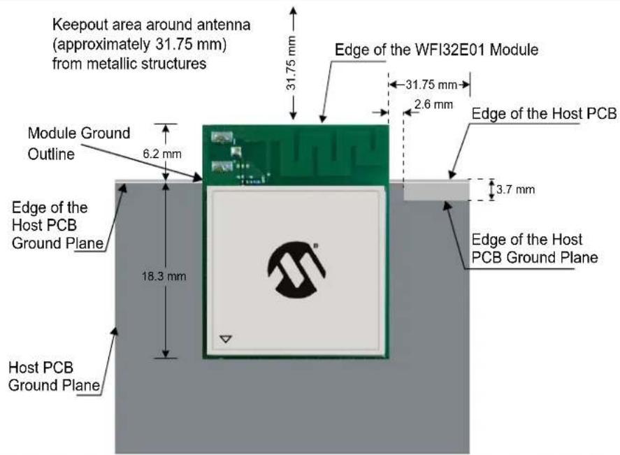
NOTES:
APPENDIX C: DOCUMENT REVISION HISTORY
Revision A (September 2020)
This is the initial version of this document.
Revision B (February 2021)
- Updated Figure 2-1.
- Updated Table 2-17.
- Updated Table 2-8.
- Updated Table 2-15.
- Updated note 4. in Table3.
- Updated Table 3-1.
- Updated 3.6.1 "WFI32E01 PCB Antenna".
- Updated Table 3-4.
- Updated Table 6-1.
- Updated Figure 14-1.
- Updated Table 26-1.
- Updated 26.0 "Asymmetric Crypto Engine".
- Added a note in 29.0 "12-bit High-Speed Successive Approximation Register (SAR) ADC".
- Updated 34.0 "Enhanced Capacitive Voltage Divider (CVD) touch Controller".
- Updated Table 34-1.
- Updated Register 34-1.
- Added 37.0 "Programmable Low Voltage Detect (PLVD)".
- Updated Register 38-1.
- Updated Register 38-5.
- Updated 41.1 "PIC32MZ1025W104 Electrical Specifications".
- Updated Table 41-37.
- Updated Table 41-12.
- Updated 41.2 "WFI32 Module Electrical Specifications".
- Updated Table 41-44.
- Updated note under Table 41-45.
- Updated Figure 42-11.
Revision C (November 2021)
- Updated the following in 1.0 "Ordering Information":
- Table 1-1 and Table 1-2
- Updated the following in 3.0 "WFI32 Module Description":
- 3.4 "WFI32 Module Routing Guidelines"
- Figure 3-19 in 3.6.1 "WFI32E01 PCB Antenna"
- Updated "Power Management and System Recovery".
- Updated the following in "Clock Management":
- Table 3, Figure 2-1 and Table 2-17
- Updated the following in 7.0 "Resets":
- Figure 11-1, Table 11-1, Register 11-7, Register 14-1.
- Updated Register 23-1 and Register 23-2
- Updated the following in 35.0 "Power Management Unit (PMU)":
- Added 35.1 "PMU Operations".
- Updated Table 35-1.
- Updated Register 35-1, Register 35-2, Register 35-3, Register 35-4, Register 35-5.
- Updated the contents and removed WCM related register information from 35.0 "Power Management Unit (PMU)".
- Updated the following in 36.0 "Power-Saving Features":
- Added 36.4.4 "Deep Sleep Mode".
- Added 36.5 "Deep Sleep Controller Registers".
- Updated low power mode information supported with the B0 silicon revision.
- Included design limitations/decisions from the errata sheet.
- Updated the following in 41.0 "Electrical Specifications":
- Ambient temperature value is updated from 105°C to 85°C.
- B0 characteristics information are updated in the relevant tables.
- Updated Table 41-6, Table 41-7, Table 41-8, Table 41-9, Table 41-10, Table 41-18, Table 41-19, Table 41-39, Table 41-42, Table 41-43, Table 41-45, Table 41-47 and Table 41-48.
- Added the following in 41.0 "Electrical Specifications"
- Table 41-4
- 41.1.4 "PIC32MZ1025W104 SOC Characteristics Graphs" and 41.2.4 "WFI32 Module Characteristics Graph"
- Updated with the new terminologies. For more details, see the following note.
Note: Microchip is aware that some terminologies used in the technical documents and existing software codes of this product are outdated and unsuitable. This document may use these new terminologies, which may or may not reflect on the source codes, software GUIs, and the documents referenced within this document. The following table shows the relevant terminology changes made in this document.
TABLE 42-1: TERMINOLOGY RELATED CHANGES
| Old Terminology | New Terminology Description | |
| Master Host | The following tables/sections/figures are updated with new terminologies: | |
| Slave Client | Table 2-10, Table 2-11, Table 3-121.0 “Serial Peripheral Interface (SPI) and Inter-IC Sound ( I^2S )”23.0 “Inter-Integrated Circuit ( I^2C )”41.0 “Electrical Specifications” | |
| Master | Manager | 6.0 “Memory Organization”10.0 “Direct Memory Access (DMA) Controller”30.0 “Controller Area Network (CAN)”33.0 “Ethernet Controller” |
| Master | Initiator | Figure 22-1 |
| Slave | Target | |
Revision D (January 2022)
- Updated Register 11-3 and Register 36-1
- Updated Figure 42-4
- Updated Register 35-1
- Updated 36.6 "Wi-Fi Power Save Modes"
Revision E (July 2022)
- Updated "Wireless Feature"
- Updated "Certifications"
- Updated Table 1-2
- Updated Register 11-3
- Updated 32.0 "Wi-Fi Controller"
- Added 32.4 "Cycle Time Register (CTR)"
- Updated Register 38-1
- Added Table 41-10
- Updated Table 41-15
- Updated 42.0 "Packaging Information"
- Added A.8 "China"
Revision F (April 2023)
- Updated "Communication Interfaces"
- Updated Table 2-13
- Updated Table 3-1
- Updated "Absolute Maximum Ratings"
- Updated Table 41-12
- Updated "Absolute Maximum Ratings"
- Updated Table 41-44
Revision G (February 2024)
TABLE 42-2: REVISION G CHANGE SUMMARY
| Section Description | |
| Document • Updated document title to PIC32MZ W1 MCU and WFI32 Module with Wi-Fi® and Hardware-Based Security Accelerator Data Sheet. All the information related to the WFI32E02 Module in this data sheet is Preliminary Information. | |
| “Introduction” • Added WFI32E02 Module variant. | |
| “WFI32 Module Features” • Added WFI32E02 Module variant. • Added features related to WFI32E02 Module variant. Table 1 and Table 2 updated with WFI32E02 Module variant. Table 3 updated with EPAD pin information for the PIC32MZ1025W104 SOC. | |
| 1.2 “WFI32 Module Ordering Information” | • Updated title to WFI32 Module Ordering Information. Table 1-2 updated with WFI32E02 Module variant ordering information. Updated Figure 1-2. |
| 2.2 “Function-wise Pinout Description” | • Added function-wise pinout details for the WFI32E02 Module variant. |
| 3.0 “WFI32 Module Descrip-tion” | • Updated title to WFI32 Module Description. • Added WFI32E02 Module variant. • Updated Figure 3-1 by adding I2C2 peripheral text information near the Trust & Go block. • Added Figure 3-2 for WFI32E02 Module variant. |
| 3.1.1 “WFI32E01 Pinout details” | • Updated Figure 3-3 with test points. |
| 3.1.2 “WFI32E02 Module Pinout Details” | • Added Figure 3-4 for WFI32E02 Module pinout. • Added Table 3-2 for WFI32E02 Module pin description. |
| 3.2 “Basic Connection Require-ment” | • Updated Figure 3-5. • Added Figure 3-6 for WFI32E02 Module basic connections. |
| 3.2.1 “Power Pins” | • Added Figure 3-8. |
| 3.2.5 “Unused I/O pins” | • Updated section to include the usage of unused pins in Low Power modes. |
| 3.3 “WFI32 Module Placement Guidelines” | • Updated title to WFI32 Module Placement Guidelines. • Added Figure 3-11 for Module placement recommendations. • Added Figure 3-15 |
| 3.4 “WFI32 Module Routing Guidelines” | • Added Figure 3-18. • Updated Figure 3-19 by removing module pad pin text. |
| 14.0 “Peripheral Trigger Generator (PTG)” | • Added Note 4 for bit “10” of “PTGSWT: Software Trigger bit”. • Updated Note 2 for bit “7” of “PTGSTRT: Start PTG Sequencer bit”. |
| 20.0 “Output Compare” | • Updated Table 20-1 by swapping X(MSB) Clock/Data and Y(MSB) Clock/Data columns. |
| 22.0 “Serial Quad Interface (SQI)” | • Updated Note 1 of FIGURE 22-1: “SQI Module Block Diagram” to include the information about configuration of CFGCON3.SPLLPOSTDIV2. |
TABLE 42-2: REVISION G CHANGE SUMMARY
| Section Description | |
| 24.0 “UART” | Updated Introduction with the information regarding the usage of CFG-CON1.HSUARTEN bit to enable the UART1 on PPS pins.Added Note for bit “3” of Register 24-1: “UxMODE: UARTx Mode Register”. |
| 31.0 “Controller Area Network-Flexible Data-Rate (CAN-FD) Module” | Updated bit “7” description of Register 31-1: “CFD2CON: CAN Control Register”Added Note for bit “7” of Register 31-1: “CFD2CON: CAN Control Register”. |
| 41.1.1 “DC Characteristics” | Updated Table 41-10, WSM current to 2.7 mA and WDS current to 1.2 mA. |
| 41.1.2 “AC Characteristics and Timing Parameters” | Updated Table 41-30 with latest supported clock frequency and related parameters. |
| 41.2 “WFI32 Module Electrical Specifications” | Updated Table 41-44 with AV_DD parameters. |
| 42.2 “WFI32 Module Packaging Information” | Added section 42.2.1.2 “WFI32E02 Module Package Marking” for module package marking information.Added section 42.2.2.2 “WFI32E02 Module Packaging Dimension” for module packing dimension.Added section 42.2.3.2 “WFI32E02 Module Recommended Footprint” for module recommended footprint. |
| 42.2.1 “Module Package Mark-ing” | Updated the section with latest package marking information. |
| Appendix A: “Regulatory Approvals” | Updated with WFI32E02 Module variant regulatory information. |
| Appendix B: “Alternate Module Placement Guidelines” | Added for alternate module placement recommendation. |
Note the following details of the code protection feature on Microchip products:
• Microchip products meet the specifications contained in their particular Microchip Data Sheet.
- Microchip believes that its family of products is secure when used in the intended manner, within operating specifications, and under normal conditions.
- Microchip values and aggressively protects its intellectual property rights. Attempts to breach the code protection features of Microchip product is strictly prohibited and may violate the Digital Millennium Copyright Act.
- Neither Microchip nor any other semiconductor manufacturer can guarantee the security of its code. Code protection does not mean that we are guaranteeing the product is "unbreakable" Code protection is constantly evolving. Microchip is committed to continuously improving the code protection features of our products.
This publication and the information herein may be used only with Microchip products, including to design, test, and integrate Microchip products with your application. Use of this information in any other manner violates these terms. Information regarding device applications is provided only for your convenience and may be superseded by updates. It is your responsibility to ensure that your application meets with your specifications. Contact your local Microchip sales office for additional support or, obtain additional support at https://www.microchip.com/en-us/support/design-help/client-support-services.
THIS INFORMATION IS PROVIDED BY MICROCHIP "AS IS". MICROCHIP MAKES NO REPRESENTATIONS OR WARRANTIES OF ANY KIND WHETHER EXPRESS OR IMPLIED, WRITTEN OR ORAL, STATUTORY OR OTHERWISE, RELATED TO THE INFORMATION INCLUDING BUT NOT LIMITED TO ANY IMPLIED WARRANTIES OF NON-INFRINGEMENT, MERCHANTABILITY, AND FITNESS FOR A PARTICULAR PURPOSE, OR WARRANTIES RELATED TO ITS CONDITION, QUALITY, OR PERFORMANCE.
IN NO EVENT WILL MICROCHIP BE LIABLE FOR ANY INDIRECT, SPECIAL, PUNITIVE, INCIDENTAL, OR CONSEQUENTIAL LOSS, DAMAGE, COST, OR EXPENSE OF ANY KIND WHATSOEVER RELATED TO THE INFORMATION OR ITS USE, HOWEVER CAUSED, EVEN IF MICROCHIP HAS BEEN ADVISED OF THE POSSIBILITY OR THE DAMAGES ARE FORESEEABLE. TO THE FULLEST EXTENT ALLOWED BY LAW, MICROCHIP'S TOTAL LIABILITY ON ALL CLAIMS IN ANY WAY RELATED TO THE INFORMATION OR ITS USE WILL NOT EXCEED THE AMOUNT OF FEES, IF ANY, THAT YOU HAVE PAID DIRECTLY TO MICROCHIP FOR THE INFORMATION.
Use of Microchip devices in life support and/or safety applications is entirely at the buyer's risk, and the buyer agrees to defend, indemnify and hold harmless Microchip from any and all damages, claims, suits, or expenses resulting from such use. No licenses are conveyed, implicitly or otherwise, under any Microchip intellectual property rights unless otherwise stated.
Trademarks
The Microchip name and logo, the Microchip logo, Adaptec, AVR, AVR logo, AVR Freaks, BesTime, BitCloud, CryptoMemory, CryptoRF, dsPIC, flexPWR, HELDO, IGLOO, JukeBlox, KeeLoq, Kleer, LANCheck, LinkMD, maXStylus, maXTouch, MediaLB, megaAVR, Microsemi, Microsemi logo, MOST, MOST logo, MPLAB, OptoLyzer, PIC, picoPower, PICSTART, PIC32 logo, PolarFire, Prochip Designer, QTouch, SAM-BA, SenGenuity, SpyNIC, SST, SST Logo, SuperFlash, Symmetricom, SyncServer, Tachyon, TimeSource, tinyAVR, UNI/O, Vectron, and XMEGA are registered trademarks of Microchip Technology Incorporated in the U.S.A. and other countries.
AgileSwitch, ClockWorks, The Embedded Control Solutions Company, EtherSynch, Flashtec, Hyper Speed Control, HyperLight Load, Libero, motorBench, mTouch, Powermite 3, Precision Edge, ProASIC, ProASIC Plus, ProASIC Plus logo, Quiet-Wire, SmartFusion, SyncWorld, TimeCesium, TimeHub, TimePictra, TimeProvider, and ZL are registered trademarks of Microchip Technology Incorporated in the U.S.A.
Adjacent Key Suppression, AKS, Analog-for-the-Digital Age, Any Capacitor, AnyIn, AnyOut, Augmented Switching, BlueSky, BodyCom, Clockstudio, CodeGuard, CryptoAuthentication, CryptoAutomotive, CryptoCompanion, CryptoController, dsPICDEM, dsPICDEM.net, Dynamic Average Matching, DAM, ECAN, Espresso T1S, EtherGREEN, EyeOpen, GridTime, IdealBridge, IGaT, In-Circuit Serial Programming, ICSP, INICnet, Intelligent Paralleling, IntelliMOS, InterChip Connectivity, JitterBlocker, Knob-on-Display, MarginLink, maxCrypto, maxView, memBrain, Mindi, MiWi, MPASM, MPF, MPLAB Certified logo, MPLIB, MPLINK, mSiC, MultiTRAK, NetDetach, Omniscient Code Generation, PICDEM, PICDEM.net, PICkit, PICtail, Power MOS IV, Power MOS 7, PowerSmart, PureSilicon, QMatrix, REAL ICE, Ripple Blocker, RTAX, RTG4, SAM-ICE, Serial Quad I/O, simpleMAP, SimpliPHY, SmartBuffer, SmartHLS, SMART-I.S., storClad, SQI, SuperSwitcher, SuperSwitcher II, Switchtec, SynchroPHY, Total Endurance, Trusted Time, TSHARC, Turing, USBCheck, VariSense, VectorBlox, VerIPHY, ViewSpan, WiperLock, XpressConnect, and ZENA are trademarks of Microchip Technology Incorporated in the U.S.A. and other countries.
SQTP is a service mark of Microchip Technology Incorporated in the U.S.A.
The Adaptec logo, Frequency on Demand, Silicon Storage Technology, and Symmcom are registered trademarks of Microchip Technology Inc. in other countries.
GestIC is a registered trademark of Microchip Technology Germany II GmbH & Co. KG, a subsidiary of Microchip Technology Inc., in other countries.
All other trademarks mentioned herein are property of their respective companies. © 2020-2024, Microchip Technology Incorporated and its subsidiaries.
All Rights Reserved.
ISBN: 978-1-6683-3781-3
For information regarding Microchip's Quality Management Systems, please visit www.microchip.com/quality.
Worldwide Sales and Service
AMERICAS
Corporate Office
2355 West Chandler Blvd.
Chandler, AZ 85224-6199
Tel: 480-792-7200
Fax: 480-792-7277
Technical Support:
http://www.microchip.com/
support
Web Address:
www.microchip.com
Atlanta
Duluth, GA
Tel: 678-957-9614
Fax: 678-957-1455
Austin, TX
Tel: 512-257-3370
Boston
Westborough, MA
Tel: 774-760-0087
Fax: 774-760-0088
Chicago
Itasca, IL
Tel: 630-285-0071
Fax: 630-285-0075
Dallas
Addison, TX
Tel: 972-818-7423
Fax: 972-818-2924
Detroit
Novi, MI
Tel: 248-848-4000
Houston, TX
Tel: 281-894-5983
Indianapolis
Noblesville, IN
Tel: 317-773-8323
Fax: 317-773-5453
Tel: 317-536-2380
Los Angeles
Mission Viejo, CA
Tel: 949-462-9523
Fax: 949-462-9608
Tel: 951-273-7800
Raleigh, NC
Tel: 919-844-7510
New York, NY
Tel: 631-435-6000
San Jose, CA
Tel: 408-735-9110
Tel: 408-436-4270
Canada - Toron
Tel: 905-695-1980
Fax: 905-695-2078
ASIA/PACIFIC
Australia - Sydney
Tel: 61-2-9868-6733
China - Beijing
Tel: 86-10-8569-7000
China - Chengdu
Tel: 86-28-8665-5511
China - Chongqing
Tel: 86-23-8980-9588
China - Dongguan
Tel: 86-769-8702-9880
China - Guangzhou
Tel: 86-20-8755-8029
China - Hangzhou
Tel: 86-571-8792-8115
China - Hong Kong SAR
Tel: 852-2943-5100
China - Nanjing
Tel: 86-25-8473-2460
China - Qingdao
Tel: 86-532-8502-7355
China - Shanghai
Tel: 86-21-3326-8000
China - Shenyang
Tel: 86-24-2334-2829
China - Shenzhen
Tel: 86-755-8864-2200
China - Suzhou
Tel: 86-186-6233-1526
China - Wuhan
Tel: 86-27-5980-5300
China - Xian
Tel: 86-29-8833-7252
China - Xiamen
Tel: 86-592-2388138
China - Zhuhai
Tel: 86-756-3210040
ASIA/PACIFIC
India - Bangalore
Tel: 91-80-3090-4444
India - New Delhi
Tel: 91-11-4160-8631
India - Pune
Tel: 91-20-4121-0141
Japan - Osaka
Tel: 81-6-6152-7160
Japan - Tokyo
Tel: 81-3-6880-3770
Korea - Daegu
Tel: 82-53-744-4301
Korea - Seoul
Tel: 82-2-554-7200
Malaysia - Kuala Lumpur
Tel: 60-3-7651-7906
Malaysia - Penang
Tel: 60-4-227-8870
Philippines - Manila
Tel: 63-2-634-9065
Singapore
Tel: 65-6334-8870
Taiwan - Hsin Chu
Tel: 886-3-577-8366
Taiwan - Kaohsiung
Tel: 886-7-213-7830
Taiwan - Taipei
Tel: 886-2-2508-8600
Thailand - Bangkok
Tel: 66-2-694-1351
Tel: 43-7242-2244-39
Fax: 43-7242-2244-393
Denmark - Copenhagen
Tel: 45-4485-5910
Fax: 45-4485-2829
Finland - Espoo
Tel: 358-9-4520-820
France - Paris
Tel: 33-1-69-53-63-20
Fax: 33-1-69-30-90-79
Germany - Garching
Tel: 49-8931-9700
Germany - Haan
Tel: 49-2129-3766400
Germany - Heilbronn
Tel: 49-7131-72400
Germany - Karlsruhe
Tel: 49-721-625370
Germany - Munich
Tel: 49-89-627-144-0
Fax: 49-89-627-144-44
Germany - Rosenheim
Tel: 49-8031-354-560
Israel - Ra'anana
Tel: 972-9-744-7705
Italy - Milan
Tel: 39-0331-742611
Fax: 39-0331-466781
Italy - Padova
Tel: 39-049-7625286
Netherlands - Drunen
Tel: 31-416-690399
Fax: 31-416-690340
Norway - Trondheim
Tel: 47-7288-4388
Poland - Warsaw
Tel: 48-22-3325737
Romania - Bucharest
Tel: 40-21-407-87-50
Spain - Madrid
Tel: 34-91-708-08-90
Fax: 34-91-708-08-91
Sweden - Gothenberg
Tel: 46-31-704-60-40
Sweden - Stockholm
Tel: 46-8-5090-4654
UK - Wokingham
Tel: 44-118-921-5800
Fax: 44-118-921-5820
- PIC32MZ W1 MCU and WFI32 Module with Wi-Fi® and Hardware-Based Security Accelerator Data Sheet
- INTRODUCTION
- PIC32MZ W1 FAMILY FEATURES
- Wireless Interfaces
- On-Chip Flash and SRAM
- Power Management and System Recovery
- Security
- Clock Management
- Direct Memory Access (DMA)
- Advanced Analog
- Communication Interfaces
- Timers/Output Compare/Input Capture
- Input/Output
- Peripheral Trigger Generator (PTG)
- Qualification and Class B Support
- Debugger Development Support
- Software and Tools Support
- Package and Operating Conditions
- WFI32 MODULE FEATURES
- Antenna Options
- Wireless Feature
- Certifications
- Table of Contents
- TO OUR VALUED CUSTOMERS
- Most Current Data Sheet
- Errata
- Customer Notification System
- Referenced Sources
- ORDERING INFORMATION
- PIC32MZ1025W104 SoC Ordering Information
- WFI32 Module Ordering Information
- PIC32MZ1025W104 SOC DESCRIPTION
- Block Diagram
- Function-wise Pinout Description
- WFI32 MODULE DESCRIPTION
- Pinout Details
- WFI32E01 PINOUT DETAILS
- WFI32E02 MODULE PINOUT DETAILS
- Basic Connection Requirement
- POWER PINS
- MASTER CLEAR (MCLR) PIN
- ICSP PINS
- JTAG
- UNUSED I/O PINS
- GPIO Pins/PPS Functions
- USB
- WFI32 Module Placement Guidelines
- WFI32 Module Routing Guidelines
- WFI32 Module RF Considerations
- WFI32 Module Antenna Considerations
- WFI32E01 PCB ANTENNA
- PCB Antenna Radiation Pattern
- EXTERNAL ANTENNA PLACEMENT RECOMMENDATIONS
- External Antennas
- WFI32 Module Reflow Profile Information
- CLEANING
- WFI32 Module Assembly Considerations
- CONFORMAL COATING
- CPU
- Architecture Overview
- EXECUTION UNIT
- MULTIPLY/DIVIDE UNIT
- SYSTEM CONTROL
- COPROCESSOR (CP0)
- Power Management
- INSTRUCTION-CONTROLLED POWER MANAGEMENT
- L1 Instruction and Data Caches
- INSTRUCTION CACHE (I-CACHE)
- DATA CACHE (D-CACHE)
- ATTRIBUTES
- EJTAG Debug Support
- MIPS DSP ASE Extension
- microMIPS ISA
- M-Class Core Configuration
- REGISTER 4-1: CONFIG: CONFIGURATION REGISTER; CP0 REGISTER 16, SELECT 0
- REGISTER 4-3: CONFIG3: CONFIGURATION REGISTER 3; CP0 REGISTER 16, SELECT 3 (CONTINUED)
- FLASH PROGRAM MEMORY
- Flash Control Registers
- REGISTER 5-1: NVMCON: PROGRAMMING CONTROL REGISTER (CONTINUED)
- REGISTER 5-2: NVMCON2: PROGRAMMING CONTROL2 REGISTER (CONTINUED)
- Legend:
- bit 31-0 NVMKEY[31:0]: Unlock Register bits
- MEMORY ORGANIZATION
- Memory Layout
- BOOT FLASH AND
- CONFIGURATION
- Boot Flash Configuration Registers
- System Bus Arbitration
- Permission Access and System Bus Registers
- RESETS
- Reset Control Registers
- REGISTER 7-1: RCON: RESET CONTROL REGISTER (CONTINUED)
- REGISTER 7-3: RNMICON: NON-MASKABLE INTERRUPT (NMI) CONTROL REGISTER (CONTINUED)
- CPU EXCEPTIONS AND INTERRUPT CONTROLLER
- CPU Exceptions
- Interrupts
- Interrupt Control Registers
- PREFETCH MODULE
- Prefetch Control Registers
- DIRECT MEMORY ACCESS (DMA) CONTROLLER
- DMA Control Registers
- REGISTER 10-4: DCRCCON: DMA CRC CONTROL REGISTER (CONTINUED)
- bit 31-0 DCRCDATA[31:0]: CRC Data Register bits
- REGISTER 10-7: DCHxCON: DMA CHANNEL x CONTROL REGISTER (CONTINUED)
- REGISTER 10-9: DCHxINT: DMA CHANNEL x INTERRUPT CONTROL REGISTER (CONTINUED)
- OSCILLATOR CONFIGURATION
- Oscillator Control Registers
- REGISTER 11-1: OSCCON: CRU OSCILLATOR CONTROL REGISTER (CONTINUED)
- REGISTER 11-7: REFOXCON: REFERENCE OSCILLATOR 1 CONTROL REGISTER (x = 1-4) (CONTINUED)
- REGISTER 11-10: SLEWCON: SLEW RATE CONTROL FOR CLOCK SWITCHING REGISTER (CONTINUED)
- REGISTER 11-11: CLKSTAT: CLOCK STATUS REGISTER (CONTINUED)
- FULL-SPEED USB ON-THE-GO (OTG)
- USB OTG Control Registers
- REGISTER 12-6: U1IR: USB INTERRUPT REGISTER (CONTINUED)
- REGISTER 12-8: U1EIR: USB ERROR INTERRUPT STATUS REGISTER (CONTINUED)
- REGISTER 12-9: U1EIE: USB ERROR INTERRUPT ENABLE REGISTER (1) (CONTINUED)
- REGISTER 12-11: U1CON: USB CONTROL REGISTER (CONTINUED)
- I/O PORTS
- Parallel I/O (PIO) Ports
- OPEN-DRAIN CONFIGURATION
- CONFIGURING ANALOG AND DIGITAL PORT PINS
- I/O PORT WRITE/READ TIMING
- INPUT CHANGE NOTIFICATION
- Registers for Slew Rate Control
- CLR, SET and INV Registers
- Peripheral Pin Select (PPS)
- AVAILABLE PINS
- AVAILABLE PERIPHERALS
- CONTROLLING PERIPHERAL PIN SELECT
- INPUT MAPPING
- VIRTUAL INPUT PINS
- OUTPUT MAPPING
- Control Register Lock
- CONTROLLING CONFIGURATION CHANGES
- Function Priority for Device Pins
- I/O Ports Control Registers
- PERIPHERAL TRIGGER GENERATOR (PTG)
- PTG Control Registers
- REGISTER 14-1: PTGCON: PTG CONTROL REGISTER (CONTINUED)
- TIMER1
- Timer1 Control Register
- REGISTER 15-1: T1CON: TYPE A TIMER CONTROL REGISTER (CONTINUED)
- TIMER2/3, TIMER4/5, AND TIMER6/7
- Timer2-Timer7 Control Registers
- REGISTER 16-1: TxCON: TYPE B TIMER CONTROL REGISTER (x = 2-7) (CONTINUED)
- DEADMAN TIMER (DMT)
- DMT Control Registers
- WATCHDOG TIMER (WDT)
- WDT Configuration
- WDT Control Registers
- INPUT CAPTURE
- Input Capture Control Registers
- OUTPUT COMPARE
- Output Compare Control Registers
- SERIAL PERIPHERAL INTERFACE (SPI) AND INTER-IC SOUND (I²S)
- SPI Control Registers
- REGISTER 21-1: SPIxCON: SPI CONTROL REGISTER (CONTINUED)
- REGISTER 21-3: SPIxSTAT: SPI STATUS REGISTER (CONTINUED)
- SERIAL QUAD INTERFACE (SQI)
- SQI Control Registers
- REGISTER 22-1: SQI1CFG: SQI CONFIGURATION REGISTER (1) (CONTINUED)
- REGISTER 22-7: SQI1INTSTAT: SQI INTERRUPT STATUS REGISTER (CONTINUED)
- bit 31-0 TXDATA[31:0]: Transmit Command Data bits
- bit 31-0 RXDATA[31:0]: Receive Data Buffer bits
- INTER-INTEGRATED CIRCUIT (I²C)
- I 2 C Control Registers
- REGISTER 23-2: I2CxSTAT: I 2 C STATUS REGISTER (CONTINUED)
- EQUATION 23-1: BRG RELOAD VALUE CALCULATION
- UART
- UART Control Registers
- REGISTER 24-1: UxMODE: UARTx MODE REGISTER (CONTINUED)
- REGISTER 24-2: UxSTA: UARTx STATUS AND CONTROL REGISTER (CONTINUED)
- Receive and Transmit Timing for UART Module
- REAL-TIME CLOCK AND CALENDAR (RTCC)
- RTCC Control Registers
- REGISTER 25-1: RTCCON: REAL-TIME CLOCK AND CALENDAR CONTROL REGISTER (CONTINUED)
- REGISTER 25-2: RTCALRM: REAL-TIME CLOCK ALARM CONTROL REGISTER (CONTINUED)
- ASYMMETRIC CRYPTO ENGINE
- SYMMETRIC CRYPTO ENGINE
- Symmetric Crypto Engine Control Registers
- REGISTER 27-5: CESTAT: CRYPTO ENGINE STATUS REGISTER (CONTINUED)
- Crypto Engine Buffer Descriptors
- Security Association Structure
- TRUE RANDOM NUMBER GENERATOR (TRNG)
- RNG Control Registers
- 12-BIT HIGH-SPEED SUCCESSIVE APPROXIMATION REGISTER (SAR) ADC
- Activation Sequence
- EQUATION 29-1: ADC THROUGHPUT RATE
- ADC Control Registers
- REGISTER 29-1: ADCCON1: ADC CONTROL REGISTER 1 (CONTINUED)
- REGISTER 29-2: ADCCON2: ADC CONTROL REGISTER 2 (CONTINUED)
- REGISTER 29-3: ADCCON3: ADC CONTROL REGISTER 3 (CONTINUED)
- REGISTER 29-5: ADCIMCON1: ADC INPUT MODE CONTROL REGISTER 1 (CONTINUED)
- REGISTER 29-15: ADCCMPCON1: ADC DIGITAL COMPARATOR 1 CONTROL REGISTER (CONTINUED)
- REGISTER 29-16: ADCCMPCON2: ADC DIGITAL COMPARATOR 2 CONTROL REGISTER (CONTINUED)
- REGISTER 29-25: ADCANCON: ADC ANALOG WARM-UP CONTROL REGISTER (CONTINUED)
- CONTROLLER AREA NETWORK (CAN)
- CAN Control Registers
- REGISTER 30-1: C1CON: CAN MODULE CONTROL REGISTER (CONTINUED)
- REGISTER 30-3: C1INT: CAN INTERRUPT REGISTER (CONTINUED)
- REGISTER 30-16: C1FIFOCONn: CAN FIFO CONTROL REGISTER 'n' ('n' = 0-15) (CONTINUED)
- CONTROLLER AREA NETWORK-FLEXIBLE DATA- RATE (CAN-FD) MODULE
- CAN-FD Control Registers
- REGISTER 31-1: CFD2CON: CAN CONTROL REGISTER (CONTINUED)
- REGISTER 31-8: CFD2INT: INTERRUPT REGISTER (CONTINUED)
- REGISTER 31-15: CFD2TXQCON: TRANSMIT QUEUE CONTROL REGISTER (CONTINUED)
- REGISTER 31-17: CFD2FIFOCONm: FIFO CONTROL REGISTER m, (m = 1 to 15) (CONTINUED)
- WI-FI CONTROLLER
- Media Access Control (MAC)
- Baseband Processor (BBP)/PHY
- RF Transceiver
- Cycle Time Register (CTR)
- ETHERNET CONTROLLER
- Ethernet Controller Registers
- REGISTER 33-1: ETHCON1: ETHERNET CONTROLLER CONTROL REGISTER 1 (CONTINUED)
- REGISTER 33-11: ETHRXFC: ETHERNET CONTROLLER RECEIVE FILTER CONFIGURATION REGISTER (CONTINUED)
- REGISTER 33-14: ETHIRQ: ETHERNET CONTROLLER INTERRUPT REQUEST REGISTER (CONTINUED)
- REGISTER 33-15: ETHSTAT: ETHERNET CONTROLLER STATUS REGISTER (CONTINUED)
- REGISTER 33-24: EMAC1CFG2: ETHERNET CONTROLLER MAC CONFIGURATION 2 REGISTER
- SCAN DESCRIPTORS
- CVD Control Registers
- REGISTER 34-1: CVDCON: CVD CONTROL REGISTER (CONTINUED)
- REGISTER 34-3: CVDSTAT: CVD STATUS REGISTER (CONTINUED)
- POWER MANAGEMENT UNIT (PMU)
- PMU Operations
- PMU Controller Registers
- POWER-SAVING FEATURES
- Power-Saving with PMU Configuration
- Power-Saving with CPU Running
- Wi-Fi POWER-SAVE MODE WITH MCU IN RUN MODE
- Peripheral Module Disable
- PERIPHERAL MODULE DISABLE REGISTERS
- Power-Saving with CPU Halted
- IDLE MODE
- Wi-Fi Power-Save Mode with MCU in IDLE Mode
- SLEEP MODE
- Wi-Fi Power-Save Mode with MCU in Sleep/Dream Mode
- DREAM MODE
- DEEP SLEEP MODE
- Zero-Power BOR (ZPBOR)
- Enabling DSWDT in Deep Sleep Mode
- Enabling Retention RAM in Deep Sleep Mode
- EXTREME DEEP SLEEP MODE
- Deep Sleep Controller Registers
- Wi-Fi Power Save Modes
- WSM: Wi-Fi SLEEP MODE
- WDS: Wi-Fi DEEP SLEEP MODE
- WOFF: Wi-Fi POWER-OFF MODE
- REGISTER 36-4: PMD1: PERIPHERAL MODULE DISABLE 1 REGISTER (CONTINUED)
- REGISTER 36-6: PMD3: PERIPHERAL MODULE DISABLE 3 REGISTER (CONTINUED)
- CONTROLLING CONFIGURATION CHANGES
- PROGRAMMABLE LOW VOLTAGE DETECT (PLVD)
- Key features:
- PLVD Registers
- bit 31-16 Unimplemented: Read as '0'
- REGISTER 37-1: LVDCON: LOW-VOLTAGE DETECT CONTROL REGISTER (CONTINUED)
- SPECIAL FEATURES
- Configuration Bits
- Special Features Registers
- REGISTER 38-1: CFGCON0(L): CONFIGURATION CONTROL REGISTER 0 (CONTINUED)
- REGISTER 38-2: CFGCON1(L): CONFIGURATION CONTROL REGISTER 1 (CONTINUED)
- REGISTER 38-5: CFGCON4(L): CONFIGURATION CONTROL REGISTER 4 (CONTINUED)
- REGISTER 38-6: CFGPG: PERMISSION GROUP CONFIGURATION REGISTER
- On-Chip Voltage Regulator
- ON-CHIP REGULATOR AND POR
- ON-CHIP REGULATOR AND BOR
- On-chip Temperature Sensor
- Programming and Diagnostics
- System Unlock Sequence
- INSTRUCTION SET
- DEVELOPMENT SUPPORT
- MPLAB X Integrated Development Environment Software
- MPLAB XC Compilers
- MPASM Assembler
- MPLINK Object Linker/MPLIB Object Librarian
- MPLAB Assembler, Linker and Librarian for Various Device Families
- MPLAB X SIM Software Simulator
- MPLAB REAL ICE In-Circuit Emulator System
- MPLAB ICD 4 and MPLAB ICD 5 In-Circuit Debugger System
- PICkit 3, PICkit 4 and PICkit 5/ In-Circuit Debugger/Programmer
- MPLAB Snap In-Circuit Debugger/Programmer
- MPLAB PM3 Device Programmer
- Demonstration/Development Boards, Evaluation Kits, and Starter Kits
- Third-Party Development Tools
- ELECTRICAL SPECIFICATIONS
- PIC32MZ1025W104 Electrical Specifications
- Absolute Maximum Ratings
- ESD Qualification:
- DC CHARACTERISTICS
- AC CHARACTERISTICS AND
- TIMING PARAMETERS
- RADIO PERFORMANCE OF
- Receiver Performance
- Transmitter Performance
- PIC32MZ1025W104 SOC
- CHARACTERISTICS GRAPHS
- AC and DC Characteristics Graphs
- WFI32 Module Electrical Specifications
- DC CHARACTERISTICS
- AC CHARACTERISTICS AND
- RADIO PERFORMANCE OF WFI32
- MODULE
- Receiver Performance
- Transmitter Performance
- WFI32 MODULE
- CHARACTERISTICS GRAPH
- Receiver and Transmitter Current
- Receiver and Transmitter
- PACKAGING INFORMATION
- PIC32MZ1025W104 SoC Packaging Information
- 132-Lead Very Thin Plastic Quad Flat, No Lead Package (NVX) - 10x10x0.9 mm Body [VQFN]; With 5.5x5.5 mm Exposed Pad; Dual Row Terminals; Punch Singulated
- Notes:
- PIC32MZ1025W104 SOC RECOMMENDED FOOTPRINT
- FIGURE 42-4: RECOMMENDED FOOTPRINT FOR THE PIC32MZ1025W104
- WFI32 Module Packaging Information
- MODULE PACKAGING DIMENSION
- FIGURE 42-8: 54-PIN RF MODULE WITH SHIELD (6YX) - 20.5X24.5 MM [MODULE]
- 54-Lead RF Module With Shield (6YX) - 20.5x24.5 mm [MODULE]
- FIGURE 42-10: 87-PIN MODULE (TFC) WITH METAL SHIELD AND COAXIAL CONNECTOR - 22.5X24.5 MM [MODULE]
- 87L-PCB Module (TFC) - 22.50x24.50mm - [MODULE] With Metal Shield and Coaxial Connector
- WFI32E02 Module Recommended Footprint
- FIGURE 42-12: WFI32E02 RECOMMENDED MODULE FOOTPRINT ON THE HOST BOARD
- APPENDIX A: REGULATORY APPROVALS
- A.1 United States
- A.1.1 LABELING AND USER INFORMATION REQUIREMENTS
- A.1.2 RF EXPOSURE
- A.1.3 APPROVED ANTENNAS
- A.1.4 MODULE INTEGRATION IN THE HOST PRODUCT
- A.1.5 HELPFUL WEBSITES
- A.2 Canada
- A.2.1 LABELING AND USER
- INFORMATION REQUIREMENTS
- A.2.2 RF EXPOSURE
- A.2.3 APPROVED ANTENNAS
- A.2.4 HELPFUL WEBSITES
- A.3 Europe
- A.3.1 LABELING AND USER INFORMATION REQUIREMENTS
- A.3.2 CONFORMITY ASSESSMENT
- A.3.3 APPROVED ANTENNAS
- A.3.3.1 SIMPLIFIED EU DECLARATION OF CONFORMITY
- A.3.4 HELPFUL WEBSITES
- A.4 UKCA
- A.4.1 LABELING AND USER INFORMATION REQUIREMENTS
- A.4.2 UKCA DECLARATION OF CONFORMITY
- A.4.3 APPROVED ANTENNAS
- A.4.4 HELPFUL WEBSITES
- A.5 Japan
- A.5.1 LABELING AND USER
- A.5.2 HELPFUL WEBSITES
- A.6 Korea
- A.6.1 LABELING AND USER
- R-R-mcp-WFI32E02
- A.6.2 HELPFUL WEBSITES
- A.7 Taiwan
- A.7.1 LABELING AND USER
- A.8 China
- The
- A.8.1 LABELING AND USER
- A.8.2 HELPFUL WEBSITES
- A.9 Other Regulatory Information
- APPENDIX B: ALTERNATE MODULE PLACEMENT GUIDELINES
- APPENDIX C: DOCUMENT REVISION HISTORY
- Revision A (September 2020)
- Revision B (February 2021)
- Revision C (November 2021)
- Revision D (January 2022)
- Revision E (July 2022)
- Revision F (April 2023)
- Revision G (February 2024)
- Note the following details of the code protection feature on Microchip products:
- Trademarks
- Worldwide Sales and Service
- AMERICAS
- ASIA/PACIFIC
Brand : Microchip
Model : PIC32MZ1025W104132
Category : Uncategorized