
DCP3700 - SSD Drive INTEL - Free user manual and instructions
Find the device manual for free DCP3700 INTEL in PDF.


| Product Type | Solid State Drive (SSD) |
| Model | Intel DCP3700 (DC P3700 Series) |
| Form Factor | 2.5-inch, 15mm thickness |
| Capacity | 800 GB (other variants available) |
| Interface | PCIe 3.0 x4, NVMe |
| Sequential Read Speed | Up to 2800 MB/s |
| Sequential Write Speed | Up to 1700 MB/s |
| Random Read IOPS (4K) | Up to 460,000 IOPS |
| Random Write IOPS (4K) | Up to 150,000 IOPS |
| Endurance | Up to 10 drive writes per day (DWPD) |
| Power Consumption (Active) | 25 W typical |
| Power Consumption (Idle) | 5 W typical |
| Weight | Approximately 150 g |
| Operating Temperature | 0°C to 55°C |
| Storage Temperature | -40°C to 85°C |
| Warranty | 5 years limited |
| Key Features | NVMe low latency, advanced power loss protection, high reliability for data centers |
| Maintenance & Cleaning | No moving parts; clean with dry cloth. Avoid liquids and static discharge. |
| Safety Precautions | Handle with ESD wrist strap; do not disassemble; avoid mechanical shock. |
| Spare Parts & Repairability | Not user-serviceable; contact Intel support for RMA. |
| General Information | Designed for enterprise and cloud storage workloads. |
Frequently Asked Questions - DCP3700 INTEL
User questions about DCP3700 INTEL
0 question about this device. Answer the ones you know or ask your own.
Ask a new question about this device
Download the instructions for your SSD Drive in PDF format for free! Find your manual DCP3700 - INTEL and take your electronic device back in hand. On this page are published all the documents necessary for the use of your device. DCP3700 by INTEL.
USER MANUAL DCP3700 INTEL
Intel® Solid-State Drive DC P3700 Series
■ Capacities: 400GB, 800GB, 1.6TB, 2TB
Components
- Intel ^® 20nm MLC NAND Flash Memory
Form Factors
- 2.5-inch Form Factor
- 15mm Z-height
• 8639-compatible connector
- AIC Form Factor
• Half-height, Half-length
- Single slot x4 connector
PCIe* Gen3 X4
Performance ^1,2
- Seq R/W: Up to 2800/2000MB/s ^3
- IOPS Rnd 4KB ^4 70/30 R/W: Up to 265K
- IOPS Rnd 4KB ^4 R/W: Up to 460/175K
- Seq Latency (typ) R/W: 20/20μs
■ Operating System Support:
- Windows* Server 2012 R2, 2012, 2008 R2 x64
- RHEL* 6.5, 7.0
- UEFI 2.3.1
Reliability
- Uncorrectable Bit Error Rate (UBER): 1 sector per 10^17 bits read
- Mean Time Before Failure (MTBF): 2 million hours
- T10 DIF protection
- Variable Sector Size: 512, 520, 528, 4096, 4104, 4160, 4224 Bytes
Compliance
- NVM Express* 1.0
- PCI Express Base Specification Rev 3.0
- Enterprise SSD Form Factor Version 1.0a
- PCI Express Card Electro-Mechanical (CEM) Specification Rev 2.0
■ Certifications and Declarations
- UL*, CE*, C-Tick*, BSMI*, KCC*, Microsoft* WHQL*, VCCI*
Product Specification
Power
- 2.5-inch: 3.3V and 12V Supply Rail
- AIC: 3.3V and 12V Supply Rail
- Enhanced power-loss data protection
- Active/Idle (TYP): Up to 25W/4W (TYP)
■ Endurance Rating
- Up to 36.5 PBW (Petabytes Written) ^5 10 Drive Writes/day (JESD219 workload)
■ Temperature Specification
- Operating:
- AIC: 0 to 55^ C ambient with specified airflow
• 2.5-inch: 0 to 35° C ambient, 0 to 70° C case with specified airflow
- Non-Operating ^6 : -55 to 95°C
- Temperature monitoring (In-band and by way of SMBUS)
- Thermal throttling
Airflow
- AIC (55° C airflow towards IO bracket 7)
• 400GB: 200 LFM
• 800GB, 1.6TB, 2.0TB: 300 LFM
- 2.5-inch (Airflow towards the connector)
• 400GB: 250/300 LFM (25/35°C)
• 800GB: 350/500 LFM (25/35°C)
• 1.6TB, 2TB:450/600 LFM (25/35°C)
Weight
- AIC: 400/800GB up to 185gm 1.6TB, 2TB up to 195gm
- 2.5-inch: 400/800GB up to 115gm 1.6TB, 2TB up to 125gm
Shock
- 2.5-inch: 1,000 G/0.5msec
- AIC: 50 G Trapezoidal, 170 in/s
Vibration
- Operating: 2.17 G RMS (5-700Hz)
- Non-Operating: 3.13 G RMS (5-800Hz)
Altitude (Simulated)
- Operating: -1,000 to 10,000 ft - Non-Operating: -1,000 to 40,000 ft
■ Product Ecological Compliance
- RoHS
Ordering Information
Contact your local Intel sales representative for ordering information.
INFORMATION IN THIS DOCUMENT IS PROVIDED IN CONNECTION WITH INTEL PRODUCTS. NO LICENSE, EXPRESS OR IMPLIED, BY ESTOPPEL OR OTHERWISE, TO ANY INTELLECTUAL PROPERTY RIGHTS IS GRANTED BY THIS DOCUMENT. EXCEPT AS PROVIDED IN INTEL'S TERMS AND CON-DITIONS OF SALE FOR SUCH PRODUCTS, INTEL ASSUMES NO LIABILITY WHATSOEVER AND INTEL DISCLAIMS ANY EXPRESS OR IMPLIED WARRANTY, RELATING TO SALE AND/OR USE OF INTEL PRODUCTS INCLUDING LIABILITY OR WARRANTIES RELATING TO FITNESS FOR A PARTICULAR PURPOSE, MERCHANTABILITY, OR INFRINGEMENT OF ANY PATENT, COPYRIGHT OR OTHER INTELLECTUAL PROPERTY RIGHT.
UNLESS OTHERWISE AGREED IN WRITING BY INTEL, THE INTEL PRODUCTS ARE NOT DESIGNED NOR INTENDED FOR ANY APPLICATION IN WHICH THE FAILURE OF THE INTEL PRODUCT COULD CREATE A SITUATION WHERE PERSONAL INJURY OR DEATH MAY OCCUR.
Intel may make changes to specifications and product descriptions at any time, without notice. Designers must not rely on the absence or characteristics of any features or instructions marked "reserved" or "undefined." Intel reserves these for future definition and shall have no responsibility whatsoever for conflicts or incompatibilities arising from future changes to them. The information here is subject to change without notice. Do not finalize a design with this information.
The products described in this document may contain design defects or errors known as errata which may cause the product to deviate from published specifications. Current characterized errata are available on request.
Contact your local Intel sales office or your distributor to obtain the latest specifications and before placing your product order. This document contains information on products in the design phase of development.
Copies of documents which have an order number and are referenced in this document, or other Intel literature, may be obtained by calling 1-800-548-4725, or go to: http://www.intel.com/design/literature.htmIntel and the Intel logo are trademarks of Intel Corporation in the U.S. and other countries.
*Other names and brands may be claimed as the property of others. Copyright © 2014 Intel Corporation. All rights reserved.
Contents
1 Overview 7
1.1 References....8
1.2 Terms and Acronyms....9
2 Product Specifications....10
2.1 Capacity 10
2.2 Performance....10
2.3 Electrical Characteristics....12
2.4 Environmental Conditions 13
2.5 Product Regulatory Compliance 15
2.6 Reliability Specifications....16
2.7 Temperature Sensor....16
2.8 Power Loss Capacitor Test....16
2.9 Hot Plug Support 16
2.10 Out of Band Management (SMBUS)....17
2.11 Variable Sector Size Support 17
3 Mechanical Information ....18
4 Pin and Signal Descriptions 20
4.1 2.5-inch Form Factor Pin Locations....20
4.2 Pin Signal Definitions....20
5 Supported Command Sets 23
5.1 NVMe* Admin Command Set....23
5.2 NVMe I/O Command Set....23
5.3 Log Page Support 24
5.4 SMART Attributes....24
5.5 Temperature Statistics 27
5.6 Drive Marketing Name Log 27
5.7 SET Feature Identifiers 27
6 NVMe Driver Support....29
7 Certifications and Declarations....30
Appendix A IDENTIFY Data Structure....31
Appendix B Vital Data Structure....38
Appendix C Out of Band Temperature Sensor Read Out 39
Appendix D PCIe* ID 40
Appendix E SCSI Command Translation 41
Appendix F Add-in Card LED Decoder 42
Figures
Figure 3-1 Intel ^ SSD DC P3700 Series SFF Dimensions....18
Figure 3-2 Intel ^ SSD DC P3700 Series PCIe* Dimensions ....19
Figure 4-1 2.5-inch Form Factor Pin Locations....20
Figure A-1 LED Location 42
Tables
Table 1: Standard Information referenced in this document....8
Table 2: Glossary of Terms and Acronyms....9
Table 3: User Addressable Sectors....10
Table 4: Random Read/Write Input/Output Operations Per Second (IOPS) ......10
Table 5: Random Read/Write IOPS Consistency....11
Table 6: Sequential Read and Write Bandwidth ....11
Table 7: Latency 11
Table 8: Quality of Service ......12
Table 9: Operating Voltage....12
Table 10: Power Consumption ....13
Table 11: Temperature, Shock, Vibration .....13
Table 12: Airflow Requirements for Intel® SSD DC P3700 Series (Add-In Card) .....14
Table 13: Airflow Requirements for Intel® SSD DC P3700 Series (2.5-inch Form Factor) .....14
Table 14: Product Regulatory Compliance Specifications ....15
Table 15: Reliability Specifications....16
Table 16: Pin Definition for 2.5-inch Form Factor (8639 connector specification)....20
Table 17: Pin Definition for Add-In Card (Half Height Half Length) Form Factor....22
Table 18: SMART Attributes (Log Identifier 02h)....24
Table 19: Additional SMART Attributes (Log Identifier CAh)....26
Table 20: Temperature Statistics (Log Identifier C5h)....27
Table 21: Drive Marketing Name Log (Log Identifier DDh)....27
Table 22: Set Max LBA Setting - Command Dword 11 and Command Dword 12....28
Table 23: Status Code - Set Max LBA Command Specific Status Values....28
Table 24: C6h - Set/Get Power Governor Setting - Command Dword 11....28
Table 25: Status Codes - Power Governor Setting Command Specific Status Values .....28
Table 26: D5h - Reset Timed Workload Counters - Command Dword 11....28
Table 27: NVMe* Driver Support....29
Table 28: Device Certifications and Declarations ....30
Table 29: Identify Controller....31
Table 30: Power State Descriptor....34
Table 31: Identify Namespace ....35
Table 32: LBA Format Data Structure ....37
Table 33: Vital Product Data Structure (VPD)....38
Table 34: Capability List Pointer (Out of Band Temperature Sensor)....38
Table 35: Register 0x05 read out format....39
Table 36: PCIe ID ....40
Table 37: LED Functionality....42
Revision History
| Document Number | Revision Number | Description | Revision Date |
| 330566 | 001 | Initial release | June 2014 |
| 330566 | 002 | Driver and temperature updatesUpdated performance information | July 2014 |
This page intentionally left blank.
1 Overview
This document describes the specifications and capabilities of the Intel® Solid-State Drive (SSD) DC P3700 Series.
P3700 Series is a PCIe* Gen3 SSD architected with the new high performance controller interface - NVMe* (Non-Volatile Memory express) delivering leading performance, low latency and Quality of Service. Matching the performance with world-class reliability and endurance, P3700 Series offers a range of capacity - 400GB, 800GB, 1.6TB and 2TB in both Add-In card and 2.5-inch form factor.
With PCIe Gen3 support and NVMe queuing interface, the P3700 Series delivers excellent sequential read performance of up to 2.8GB/s and sequential write speeds of up to 2.0GB/s. P3700 Series delivers very high random read IOPS of 460K and random write IOPS of 175K for 4KB operations. Taking advantage of the direct path from the storage to the CPU by means of NVMe, P3700 Series exhibits low latency of less than 20 s for sequential access to the SSD.
P3700 Series also includes High Endurance Technology (HET), which combines NAND silicon enhancements and SSD NAND management techniques to extend SSD write endurance up to 10 drive writes per day for 5 years.
The 2.5-inch P3700 Series takes advantage of the 8639 connector and provides hot-pluggable removal and insertion providing in-service replacement options.
P3700 Series includes these key features:
• Consistently High IOPS and throughput
• Sustained low latency
• High Endurance Technology (HET)
• Variable Sector Size and End-to-End data-path protection
• Enhanced power-loss data protection
• Power loss protection capacitor self-test
• Out of band management
• Thermal throttling and monitoring
1.1 References
Table 1: Standard Information referenced in this document
| Date | Title | Location |
| Jan 2013 | Enterprise SSD Form Factor Version 1.0a | http://www.ssdformfactor.org |
| Feb 2012 | NVMe* Revision 1.0c | http://www.nvmexpress.org |
| Nov 2010 | PCIe* Base Specification Revision 3.0 | http://pcisig.com |
| July 2012 | Solid-State Drive (SSD) Requirements and Endurance Test Method (JESD219) | http://www.jedec.org/standards-documents/results/jesd219 |
| Sept 2010 | Solid-State Drive (SSD) Requirements and Endurance Test Method (JESD218) | http://www.jedec.org/standards-documents/docs/jesd218/ |
| Dec 2008 | VCCI | http://www.vcci.jp/vcci_e/ |
| June 2009 | RoHS | http://qdms.intel.com/Click Search MDDS Database and search for material description datasheet |
| 1995 | International Electrotechnical Commission EN 610004-2 (Electrostatic discharge immunity test) | |
| 1996 | 4-3 (Radiated, radio-frequency, electromagnetic field immunity test) | |
| 1995 | 4-4 (Electrical fast transient/burst immunity test) | |
| 1995 | 4-5 (Surge immunity test) | |
| 1997 | 4-6 (Immunity to conducted disturbances, induced by radio- frequency fields) | |
| 1994 | 4-11 (Voltage Variations, voltage dips, short interruptions and voltage variations immunity tests) | |
| 1995 | ENV 50204(Radiated electromagnetic field from digital radio telephones) | http://www.dbicorporation.com/radimmun.htm/ |
1.2 Terms and Acronyms
Table 2: Glossary of Terms and Acronyms
| Term | Definition |
| ATA | Advanced Technology Attachment |
| CRC | Cyclic Redundancy Check |
| DAS | Device Activity Signal |
| DMA | Direct Memory Access |
| ECC | Error Correction Code |
| EEPROM | Electrically Erasable Programmable Read Only Memory |
| EXT | Extended |
| FPDMA | First Party Direct Memory Access |
| GB | GigabyteNote: The total usable capacity of the SSD may be less than the total physical capacity because a small portion of the capacity is used for NAND flash management and maintenance purposes. |
| Gb | Gigabit |
| HDD | Hard Disk Drive |
| HET | High Endurance Technology |
| KB | Kilobyte |
| I/O | Input/Output |
| IOPS | Input/Output Operations Per Second |
| ISO | International Standards Organization |
| LBA | Logical Block Address |
| MB | Megabyte (1,000,000 bytes) |
| MLC | Multi-level Cell |
| MTBF | Mean Time Between Failures |
| NOP | No Operation |
| NVMe* | Non-Volatile Memory Express |
| PB | Petabyte |
| PCB | Printed Circuit Board |
| RDT | Reliability Demonstration Test |
| RMS | Root Mean Square |
| SSD | Solid-State Drive |
| TB | Terabyte |
| TYP | Typical |
| UBER | Uncorrectable Bit Error Rate |
| VPD | Vital Product Data |
2 Product Specifications
2.1 Capacity
Table 3: User Addressable Sectors
| Intel® SSD DC P3700 Series | Unformatted Capacity(Total User Addressable Sectors in LBA Mode) |
| 400GB | 781,422,768 |
| 800GB | 1,562,824,368 |
| 1.6TB | 3,125,627,568 |
| 2TB | 3,907,029,168 |
NOTES:
1 GB = 1,000,000,000 bytes; 1 sector = 512 bytes or 520 bytes or 528 bytes.
LBA count shown represents total user storage capacity and will remain the same throughout the life of the drive.
The total usable capacity of the SSD may be less than the total physical capacity because a small portion of the capacity is used for NAND media management and maintenance. IDEMA or JEDEC standard is used.
2.2 Performance
Table 4: Random Read/Write Input/Output Operations Per Second (IOPS)
| Specification^1 | Unit | Intel® SSD DC P3700 Series | |||
| 400GB | 800GB | 1.6TB | 2TB | ||
| Random 4KB 70/30 Read/Write (up to) ^2 | IOPS | 150,000 | 200,000 | 240,000 | 265,000 |
| Random 8KB 70/30 Read/Write (up to) ^3 | IOPS | 75,000 | 100,000 | 140,000 | 150,000 |
| Random 4KB Read (up to) ^2 | IOPS | 450,000 | 460,000 | 450,000 | 450,000 |
| Random 4KB Write (up to) | IOPS | 75,000 | 90,000 | 150,000 | 175,000 |
| Random 8KB Read (up to) ^3 | IOPS | 275,000 | 285,000 | 290,000 | 295,000 |
| Random 8KB Write (up to) | IOPS | 32,000 | 45,000 | 75,000 | 90,000 |
NOTES:
- Performance measured using Iometer* on Windows* Server 2012 R2 driver with Queue Depth 32 and 4 workers. Measurements are performed on a full Logical Block Address (LBA) span of the drive. Power mode set at 25W.
- 4KB = 4,096 bytes
- 8KB = 8,192 bytes
Table 5: Random Read/Write IOPS Consistency
| Specification^1 | Unit | Intel® SSD DC P3700 Series | |||
| 400GB | 800GB | 1.6TB | 2TB | ||
| Random 4KB Read (up to) ^2 | % | 90 | 90 | 90 | 90 |
| Random 4KB Write (up to) | % | 90 | 90 | 90 | 90 |
| Random 8KB Read (up to) ^3 | % | 90 | 90 | 90 | 90 |
| Random 8KB Write(up to) | % | 90 | 90 | 90 | 90 |
NOTES:
-
Performance consistency measured using Iometer* based on Random 4KB with total queue depth of 128, measured as (IOPS in the 99.9th percentile slowest 1-second interval)/(average IOPS during the test). Measurements are performed on a full Logical Block Address (LBA) span of the drive once the workload has reached steady state but including all background activities required for normal operation and data reliability
-
4KB = 4,096 bytes
- 8KB = 8,192 bytes
Table 6: Sequential Read and Write Bandwidth
| Specification | Unit | Intel® SSD DC P3700 Series | |||
| 400GB | 800GB | 1.6TB | 2TB | ||
| Sequential Read (up to) ^1 | MB/s | 2,700 | 2,800 | 2,800 | 2,800 |
| Sequential Write (up to) ^1 | MB/s | 1,080 | 1,900 | 1,900 | 2,000 |
NOTES:
- Performance measured using Iometer* with 128 KB (131,072 bytes) of transfer size with Queue Depth 128. Power mode set at 25W.
Table 7: Latency
| Specification | Intel® SSD DC P3700 Series |
| 400GB, 800GB, 1.6TB and 2TB | |
| Latency ^1 (TYP)Read Sequential/RandomWrite Sequential/RandomPower On to Ready ^2 | 20/115 μs20/25 μs2.0 sec (TYP) |
NOTES:
- Device measured using Iometer. Latency measured using 4 KB (4,096 bytes) transfer size with Queue Depth equal to 1 on a sequential workload using Windows Server 2012 R2 driver. Power mode set at 25W.
- Power On To Ready time measured from de-assertion of PCIe* reset to first interface response. Exception handling like unsafe power shutdown will not be part of this specification. For unsafe shutdown, the time to ready can be up to 10 seconds (TYP).
Table 8: Quality of Service
| Specification | Unit | Intel® SSD DC P3700 Series | |
| QD=1 | QD=128 | ||
| Quality of Service ^1,2 (99%) | |||
| Reads | ms | 0.600 | 2 |
| Writes | ms | 0.090 | 11 |
| Quality of Service ^1,2 (99.99%) | |||
| Reads | ms | 4 | 5 |
| Writes | ms | 2 | 30 |
NOTES:
-
Device measured using Iometer. Quality of Service measured using 4KB (4,096 bytes) transfer size on a random workload on a full Logical Block Address (LBA) span of the drive once the workload has reached steady state but including all background activities required for normal operation and data reliability.
-
Based on Random 4KB QD=1,128 workloads, measured as the time taken for 99.0(or 99.99) percentile of commands to finish the round-trip from host to drive and back to host.
2.3 Electrical Characteristics
Table 9: Operating Voltage
| Electrical Characteristics | Intel® SSD DC P3700 Series |
| 3.3V Operating Characteristics: (Add-in Card only) | |
| Operating Voltage range | 3.3 V ( ± 10% ) |
| Rise time (Max/Min) | 50ms/1ms |
| Fall time (Max/Min) ^1 | 5s/1ms |
| Noise level | 300 mV pp 10Hz – 100 KHz |
| 50 mV pp 100KHz – 20 MHz | |
| Min Off time ^2 | 3 seconds |
| Inrush Current (Typical Peak) ^3 | 1.5 A |
| Max Average Current | 3.0 A |
| 12V Operating Characteristics: | |
| Operating Voltage range | 12 V (+10%/-20%) |
| Rise time (Max/Min) | 50ms/1ms |
| Fall time (Max/Min) ^1 | 5s/1ms |
| Noise level | 1000 mV pp 10Hz – 100 KHz |
| 100 mV pp 100KHz – 20 MHz | |
| Min Off time ^2 | 3 seconds |
| Inrush Current (Typical Peak) ^3 | 1.5 A |
| Max Average Current | 2.1 A/ 2.45 A (Add-in Card/ 2.5-inch FF) |
| 3.3Vaux Operating Characteristics: | |
| Operating Voltage range | 3.3 V (±9%) |
| Rise time (Max/Min) | 50ms/1ms |
| Fall time (Max/Min) ^1 | 5s/1ms |
| Noise level | 300 mV pp 10Hz - 100 KHz |
| 50 mV pp 100KHz - 20 MHz | |
| Max Current | 20mA/1mA (AIC/2.5-inch FF) |
Notes:
- Fall time needs to be equal or better than minimum in order to guarantee full functionality of enhanced power loss management.
- The drive must be powered off for at least 500msec before powering on.
- Measured during initial power supply application. Typically this will be seen within 2 seconds of initial power up. Inrush specified for 12V and 3.3V supply, not the 3.3Vaux.
Note: 3.3Vaux is optional, not needed for power up or functionality. 3.3Vaux is needed for accessing VPD page by means of SMBUS for both form factor.
Table 10: Power Consumption
| Specification | Unit | Intel® SSD DC P3700 Series | |||
| 400GB | 800GB | 1.6TB | 2TB | ||
| Active Write - Average ^1 | W | 18 | 18 | 22 | 25 |
| Active Read - Average ^2 | W | 9 | 9 | 10 | 11 |
| Idle | W | 4 | 4 | 4 | 4 |
Notes:
- The workload equates 128KB (131,072 bytes) Queue Depth equal to 128 sequential writes. Average power is measured using scope trigger over a 100 ms sample period.
- The workload equates 128KB (131,072 bytes) Queue Depth equal to 128 sequential reads.
2.4 Environmental Conditions
Table 11: Temperature, Shock, Vibration
| Temperature | Add-In card form factor | 2.5-inch form factor |
| TemperatureOperating1Non-operating3 | Ambient: 0 - 55°C / 0 -40 °C2-55-95°C | Ambient: 0-35°C, Case: 0-70°C |
| Temperature Gradient4OperatingNon-operating | 30°C/hr (Typical)30°C/hr (Typical) | 30°C/hr (Typical)30°C/hr (Typical) |
| HumidityOperatingNon-operating | 5-95%5-95% | 5-95%5-95% |
| Shock and Vibration | Range | |
| Shock^5 OperatingNon-operating | 50 G Trapezoidal, 170 in/s50 G Trapezoidal, 170 in/s | 1,000 G (Max) at 0.5 msec1,000 G (Max) at 0.5 msec |
| Vibration^6 OperatingNon-operating | 2.17 GRMS (5-700 Hz) Max3.13 G_RMS (5-800 Hz) Max | 2.17 GRMS (5-700 Hz) Max3.13 G_RMS (5-800 Hz) Max |
Notes:
-
Operating temperature implies ambient air temperature under defined airflow in Tables 12 and 13.
-
0-55 °C is for airflow from the server towards the card and 0-40°C is for airflow into the server.
-
Please contact your Intel representative for details on the non-operating temperature range.
-
Temperature gradient measured without condensation.
-
Shock specifications assume the SSD is mounted securely with the input vibration applied to the drive-mounting screws. Stimulus may be applied in the X, Y or Z axis. Shock specification is measured using Root Mean Squared (RMS) value.
-
Vibration specifications assume the SSD is mounted securely with the input vibration applied to the drive-mounting screws. Stimulus may be applied in the X, Y or Z axis. Vibration specification is measured using RMS value.
Table 12: Airflow Requirements for Intel® SSD DC P3700 Series (Add-In Card)
| Airflow Direction | Unit | Ambient Temperature | Intel® SSD DC P3700 Series | |||
| 400GB | 800GB | 1.6TB | 2TB | |||
| Towards the server | LFM | 40°C | 200 | 300 | 300 | 300 |
| Out of the server | LFM | 55°C | 200 | 300 | 300 | 300 |
NOTE: For Add-In cards airflow can be for both the directions. Airflow specified is based on approach velocity.
Table 13: Airflow Requirements for Intel® SSD DC P3700 Series (2.5-inch Form Factor)
| Airflow Definition | Unit | Ambient Temperature | Intel® SSD DC P3700 Series | |||
| 400GB | 800GB | 1.6TB | 2TB | |||
| Airflow Along Drive ^1 | LFM | 35°C | 300 | 500 | 650 | 650 |
| LFM | 25°C | 250 | 350 | 450 | 450 | |
| Approach Airflow ^2 | LFM | 35°C | 70 | 120 | 155 | 155 |
| LFM | 25°C | 60 | 85 | 110 | 110 | |
NOTE:
-
It is recommended that airflow for 2.5-inch form factor should be towards the server, from the non-connector side to the connector side. Airflow is specified across the surface of the drive. Spacing between two SSDs is assumed to be 3mm.
-
The approach velocity of the airflow will be less than the airflow along the surface. Approach area of 1.35 ft^2 is assumed.
2.5 Product Regulatory Compliance
Intel ^® SSD DC P3700 Series meets or exceeds the regulatory or certification requirements in Table 14.
Table 14: Product Regulatory Compliance Specifications
| Title | Description | Region For Which Conformity Declared |
| TITLE 47-Telecommunications CHAPTER 1 - FEDERAL COMMUNICATIONS COMMISSION PART 15 - RADIO FREQUENCY DEVICESICES*-003, Issue 4 Interference-Causing Equipment Standard Digital Apparatus | FCC Part 15B Class ACA/CSA-CEI/IEC CISPR 22:10. This is CISPR 22:2008 with Canadian Modifications | USACanada |
| IEC* 55024 Information Technology Equipment - Immunity characteristics - Limits and methods of measurement CISPR24:2010 | EN-55024: 2010 and its amendments | European Union |
| IEC 55022 Information Technology Equipment - Radio disturbance Characteristics - Limits and methods of measurement CISPR24:2008 (Modified) | EN-55022: 2010 and its amendments | European Union |
| EN-60950-1 2^nd Edition | Information Technology Equipment - Safety - Part 1: General Requirements | USA/Canada |
| UL/CSA EN-60950-1 2^nd Edition | Information Technology Equipment - Safety - Part 1: General Requirements | USA/Canada |
2.6 Reliability Specifications
Intel® SSD DC P3700 Series meets or exceeds SSD endurance and data retention requirements as specified in the JESD218 standard. Reliability specifications are listed in Table 15.
Table 15: Reliability Specifications
| Parameter | Value |
| Uncorrectable Bit Error Rate (UBER)Uncorrectable bit error rate will not exceed one sector in the specified number of bits read. In the unlikely event of a non-recoverable read error, the SSD will report it as a read failure to the host; the sector in error is considered corrupt and is not returned to the host. | < 1 sector per 10^17 bits read |
| Mean Time Between Failures (MTBF)Mean Time Between Failures is estimated based on Telcordia* methodology and demonstrated through Reliability Demonstration Test (RDT). | 2 million hours |
| Data RetentionThe time period for retaining data in the NAND at maximum rated endurance. | 3 months power-off retention once SSD reaches rated write endurance at 40^ |
| Endurance RatingThe number of drive writes such that the SSD meets the requirements according to the JESD218 standard. Endurance rating verification is defined to establish UBER <1E-16 at 60% upper confidence limit. | 400GB: 7.3 PBW800GB: 14.61.6TB: 29.2 PBW2.0TB: 36.5 PBW(10 drive writes/day*) |
Note: Petabytes Written (PBW). Refer to JESD218 standard table 1 for UBER, FFR and other Enterprise SSD requirements.
2.7 Temperature Sensor
P3700 Series has an internal temperature sensor with an accuracy of +/-2C over a range of -10C to +85C which can be monitored using NVMe* Health Log.
For more information on sensor reading see SMART attributes section. In addition, drive will provide out of band access to temperature by means of SMBUS. The sensor has an accuracy of +/- 3C over a range of -20C to 125C. SMBUS temperature sensor will not be reported in NVMe Health Log.
2.8 Power Loss Capacitor Test
P3700 Series supports testing of the power loss capacitor, which can be monitored using SMART attribute critical warning in log page identifier 02h, byte 0, bit 4.
2.9 Hot Plug Support
2.5-inch form factor will support surprise hot plug feature in capable platforms and OSs. P3700 Series supports hot insertion and removal and surprise hot insertion by means of presence detect and link-up detect. On surprise hot removal during IOs, P3700 Series will ensure the integrity of already committed data on the media and commit acknowledged writes to the media.
2.10 Out of Band Management (SMBUS)
Intel ^® SSD DC P3700 Series provides out of band management by means of SMBUS interface. This requires 3.3V Auxiliary voltage. SMBUS accesses a VPD page as listed in Appendix B through address 0X53.
Temperature sensor is accessed through address 0x1B. For temperature sensor access, temperature can be read by the BMC (base) using Read Temperature Data Register (0x05) by means of SMBUS 0x1B. Bits [11:0] return raw ambient temperature.
Host may also see 0x66 address in a bus scan. This is only used for write protecting the EEPROM during manufacturing.
Note: In certain tools the address for the VPD and temperature sensor will appear as 0xA6 and 0x36 respectively, due to bit shift.
2.11 Variable Sector Size Support
P3700 Series supports 512, 520, 528, 4096, 4104, 4160 and 4224 bytes of sector size. P3700 Series will also support DIF as specified in NVMe* 1.0 specification. Host sector sizes supporting DIF are 512 bytes and 4096 bytes with a PI (Protection Information) of 8 bytes.
In terms of protection information action (PRACT), bit 29 of DWORD12 in READ/WRITE command should not be equal to 1. Device only supports PRACT=0 implying protection information is passed to the SSD and checked by the SSD.
3 Mechanical Information
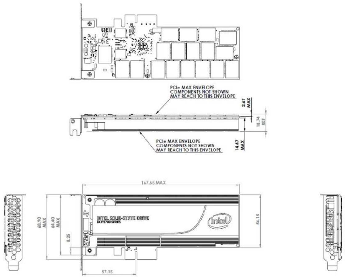
Figures 3-1 and 3-2 show the physical package information for the Intel® SSD DC P3700 Series in the 2.5-inch form factors. All dimensions are in millimeters.
Figure 3-1 Intel ^ SSD DC P3700 Series SFF Dimensions
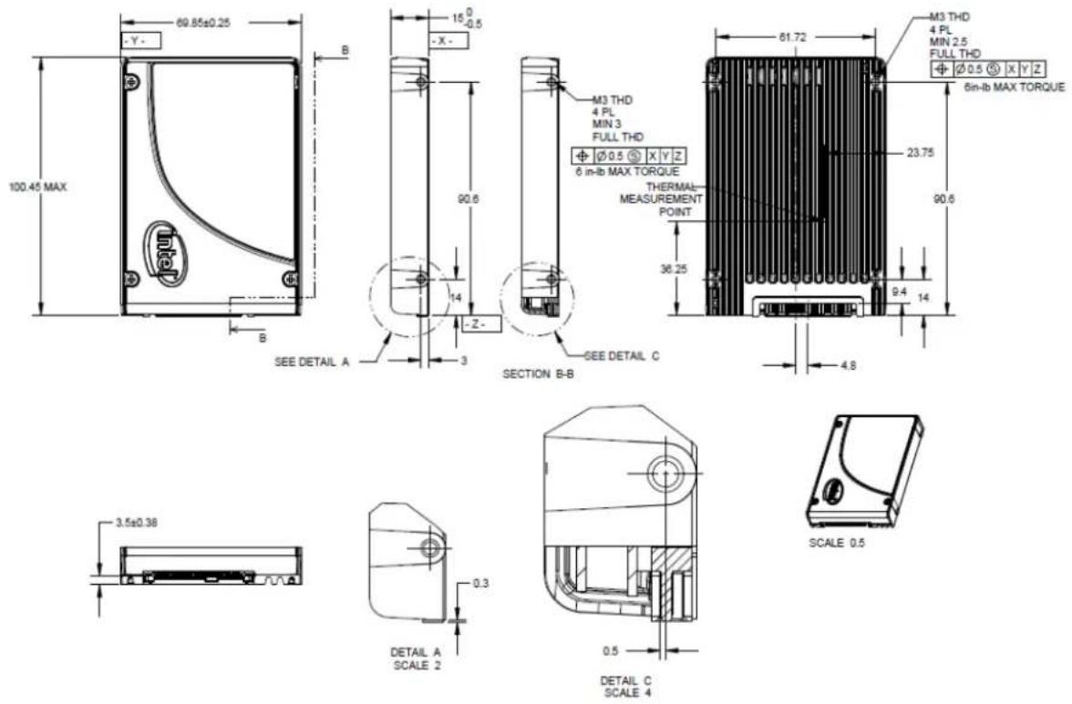
| X - Length | Y - Width | Z - Height |
| 100.45 Max | 69.85 +/- 0.25 | 15.0 +0/-0.5 |
Note: Length does not include 0.3 connector protrusion
Figure 3-2 Intel ^ SSD DC P3700 Series PCIe* Dimensions
4 Pin and Signal Descriptions
4.1 2.5-inch Form Factor Pin Locations
Figure 4-1 2.5-inch Form Factor Pin Locations
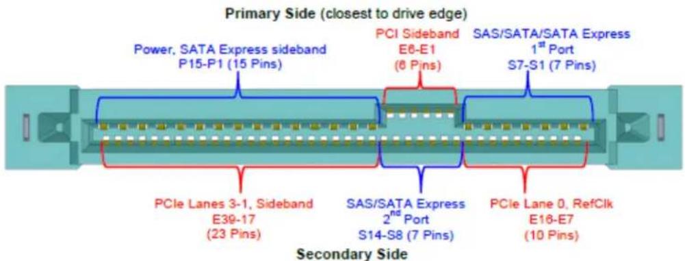
Note: 2.5-inch connector supports built in latching capability.
4.2 Pin Signal Definitions
Table 16: Pin Definition for 2.5-inch Form Factor (8639 connector specification)
| Pin | Name | Description | Pin | Name | Description |
| S1 | GND | Ground | E7 | REFCLK0+ | Reference clock port 0 |
| S2 | Not used (SATA/SAS) | E8 | REFCLK0- | Reference clock port 0 | |
| S3 | Not used (SATA/SAS) | E9 | GND | Ground | |
| S4 | GND | Ground | E10 | PETp0 | Transmitter differential pair, Lane 0 |
| S5 | Not used (SATA/SAS) | E11 | PETn0 | Transmitter differential pair, Lane 0 | |
| S6 | Not used (SATA/SAS) | E12 | GND | Ground | |
| S7 | GND | Ground | E13 | PERn0 | Receiver differential pair, Lane 0 |
| E1 | REFCLK1+ | Reference clock port 1 (not used) | E14 | PERp0 | Receiver differential pair, Lane 0 |
| E2 | REFCLK1- | Reference clock port 1 (not used) | E15 | GND | Ground |
| E3 | 3.3Vaux | 3.3V auxiliary power | E16 | RSVD | Reserved |
| E4 | PERST1# | Fundamental reset port 1 (not used) | S8 | GND | Ground |
| E5 | PERST0# | Fundamental reset port 0 | S9 | Not used (SATAe/SAS) | |
| E6 | RSVD | Reserved | S10 | Not used (SATAe/SAS) | |
| P1 | Not used (SATAe/SAS) | S11 | GND | Ground | |
| P2 | Not used (SATAe/SAS) | S12 | Not used (SATAe/SAS) | ||
| P3 | Not used (SATAe) | S13 | Not used (SATAe/SAS) | ||
| P4 | IfDet_N | Interface detect (drive type) | S14 | GND | Ground |
| P5 | GND | Ground | S15 | RSVD | Reserved |
| P6 | GND | Ground | S16 | GND | Ground |
| P7 | Not used (SATA/SAS) | S17 | PETp1 | Transmitter differential pair, Lane 1 | |
| P8 | Not used (SATA/SAS) | S18 | PETn1 | Transmitter differential pair, Lane 1 | |
| P9 | Not used (SATA/SAS) | S19 | GND | Ground | |
| P10 | PRSNT_N | Presence detect (also used for drive type) | S20 | PERn1 | Receiver differential pair, Lane 1 |
| P11 | Activity | Activity signal from the drive | S21 | PERp1 | Receiver differential pair, Lane 1 |
| P12 | Hot-Plug | Ground | S22 | GND | Ground |
| P13 | +12V_pre | 12V power | S23 | PETp2 | Transmitter differential pair, Lane 2 |
| P14 | +12V | 12V power | S24 | PETn2 | Transmitter differential pair, Lane 2 |
| P15 | +12V | 12V power | S25 | GND | Ground |
| S26 | PERn2 | Receiver differential pair, Lane 2 | |||
| S27 | PERp2 | Receiver differential pair, Lane 2 | |||
| S28 | GND | Ground | |||
| E17 | PETp3 | Transmitter differential pair, Lane 3 | |||
| E18 | PETn3 | Transmitter differential pair, Lane 3 | |||
| E19 | GND | Ground | |||
| E20 | PERn3 | Receiver differential pair, Lane 3 | |||
| E21 | PERp3 | Receiver differential pair, Lane 3 | |||
| E22 | GND | Ground | |||
| E23 | SMCLK | SMBus clock | |||
| E24 | SMDAT | SMBus data | |||
| E25 | DualPortEn_N | Dual port enable |
NOTES:
• SMCLK and SMDAT routes to an internal EEPROM which contains Vital Product Data (VPD).
- PRSNT_N is kept open by the P3700 Series.
- IfDet_N is grounded by P3700 Series.
- DualPortEn_N pin should be left un-connected or un-driven by the system to enable single port operation with all 4 lanes. If un-connected, P3700 Series will pull it high. However, if the pin is asserted by the system (driven low by storage backplane), then P3700 Series will be configured as x2 lanes.
- P11 is used for activity. When idle, logic level is low (LED Solid On). During IO activity and formatting, pin toggles 250msec high, 250msec low signal.
• P3700 Series only uses REFCLK0+ and REFCLK0- as reference clock pair.
• P3700 Series only uses PERST0# as a fundamental reset.
• 3.3Vaux is only needed during SMBUS access to the VPDROM.
Table 17: Pin Definition for Add-In Card (Half Height Half Length) Form Factor
| Side B | Side A | |||
| Pin | Name | Description | Name | Description |
| 1 | +12V | 12V power | PRSNT1# | Hot-Plug presence detect |
| 2 | +12V | 12V power | +12V | 12V power |
| 3 | +12V | 12V power | +12V | 12V power |
| 4 | GND | Ground | GND | Ground |
| 5 | SMCLK | SMBus(System Management Bus) clock | JTAG2 | TCK (Test Clock), clock input for JTAG Interface |
| 6 | SMDAT | SMBus (System Management Bus) data | JTAG3 | TDI (Test Data Input) |
| 7 | GND | Ground / UART_HOST | JTAG4 | TDO (Test Data Output) |
| 8 | +3.3V | 3.3V power | JTAG5 | TMS (Test Mode Select) |
| 9 | JTAG1 | TRST# (Test Reset) resets the JTAG interface | +3.3V | 3.3V power |
| 10 | 3.3Vaux | 3.3V auxiliary power | +3.3V | 3.3V power |
| 11 | WAKE# | Signal for Link reactivation | PERST# | Fundamental reset |
| Mechanical Key | ||||
| 12 | RSVD | Reserved | GND | Ground |
| 13 | GND | Ground | REFCLK+ | Reference clock (differential pair) |
| 14 | PETp0 | Transmitter differential pair, Lane 0 | REFCLK- | Reference clock (differential pair) |
| 15 | PETn0 | Transmitter differential pair, Lane 0 | GND | Ground |
| 16 | GND | Ground | PERp0 | Receiver differential pair, Lane 0 |
| 17 | PRSNT2# | Hot-Plug presence detect | PERn0 | Receiver differential pair, Lane 0 |
| 18 | GND | Ground | GND | Ground |
| End of the x1 Connector | ||||
| 19 | PETp1 | Transmitter differential pair, Lane 1 | RSVD | Reserved |
| 20 | PETn1 | Transmitter differential pair, Lane 1 | GND | Ground |
| 21 | GND | Ground | PERp1 | Receiver differential pair, Lane 1 |
| 22 | GND | Ground | PERn1 | Receiver differential pair, Lane 1 |
| 23 | PETp2 | Transmitter differential pair, Lane 2 | GND | Ground |
| 24 | PETn2 | Transmitter differential pair, Lane 2 | GND | Ground |
| 25 | GND | Ground | PERp2 | Receiver differential pair, Lane 2 |
| 26 | GND | Ground | PERn2 | Receiver differential pair, Lane 2 |
| 27 | PETp3 | Transmitter differential pair, Lane 3 | GND | Ground |
| 28 | PETn3 | Transmitter differential pair, Lane 3 | GND | Ground |
| 29 | GND | Ground | PERp3 | Receiver differential pair, Lane 3 |
| 30 | RSVD | Reserved | PERn3 | Receiver differential pair, Lane 3 |
| 31 | PRSNT2# | Hot-Plug presence detect | GND | Ground |
| 32 | GND | Ground | RSVD | Reserved |
| End of the x4 Connector | ||||
NOTES:
- All pins are numbered in ascending order from the left to the right, with side A on the top of the centerline and side B on the bottom of the centerline, use the reference drawing in Fig2, with the logo visible.
- The PCI Express interface pins PETpx, PETnx, PERpx, and PERnx are named with the following convention: "PE" stands for PCI Express high speed, "T" for Transmitter, "R" for Receiver, "p" for positive (+) and "n" for negative (-).
• The sequential mating for Hot-Plug is accomplished by staggering the edge fingers on the add-in card.
5 Supported Command Sets
Intel® SSD DC P3700 Series supports all mandatory Admin and I/O commands defined in NVMe* (Non-Volatile Memory Express) revision 1.0.
5.1 NVMe\* Admin Command Set
P3700 Series supports all mandatory NVMe commands, which consists of:
- Delete I/O Submission Queue
- Delete I/O Completion Queue
- Create I/O Submission Queue
- Create I/O Completion Queue
- Get Log Page
- Identify
- Abort
- SET Features
- GET Features
- Asynchronous Event Notification
P3700 Series also supports the following optional I/O commands defined in NVMe revision 1.0:
- Firmware Activate
- Firmware Image Download
- Format NVM
Note: See Appendix A, "Identify Controller Data Structure" for details on commands and capabilities.
5.2 NVMe\* I/O Command Set
P3700 Series supports all the mandatory NVMe I/O command set defined in NVMe 1.0 specification, which consists of:
- Flush
- Write
- Read
Additionally, the following optional commands are supported:
- Write Uncorrectable
– Dataset Management (De-allocate only)
Note: See Appendix E, "SCSI Command Translation Table" for details on SCSI supported commands and capabilities.
5.3 Log Page Support
Intel® SSD DC P3700 Series supports the following mandatory log pages defined in NVMe* 1.0 specification:
- Error Information (Log Identifier 01h)
- SMART/ Health Information (Log Identifier 02h)
- Firmware Slot Information (Log Identifier 03h)
Note: See NVMe 1.0 version of the specification for the log page content. Additionally, P3700 Series will support the following vendor unique log pages:
- Log Page Directory (Log Identifier C0h)
– Temperature Statistics (Log Identifier C5h)
– Vendor Unique SMART Log (Log Identifier CAh)
5.4 SMART Attributes
Table 18 lists the SMART attributes supported by the P3700 Series in accordance with NVMe 1.0 specification.
Table 18: SMART Attributes (Log Identifier 02h)
| Byte | # of Bytes | Attribute | Description |
| 0 | 1 | Critical Warning: These bits if set, flag various warning sources.Bit 0: Available Spare is below ThresholdBit 1: Temperature has exceeded ThresholdBit 2: Reliability is degraded due to excessive media or internal errorsBit 3: Media is placed in Read- Only ModeBit 4: Volatile Memory Backup System has failed (e.g., enhanced power loss capacitor test failure)Bits 5-7: Reserved | Any of the critical warning can be tied to asynchronous event notification. |
| 1 | 2 | Temperature: Overall Device current temperature in Kelvin. | For AIC, this reports the NAND temperature, for 2.5-inch FF, this reports the case temperature, |
| 3 | 1 | Available Spare: Contains a normalized percentage (0 to 100%) of the remaining spare capacity available | Starts from 100 and decrements. |
| 4 | 1 | Available Spare Threshold | Threshold is set to 10%. |
| 5 | 1 | Percentage Used Estimate (Value allowed to exceed 100%) | A value of 100 indicates that the estimated endurance of the device has been consumed, but may not indicate a device failure. The value is allowed to exceed 100. Percentages greater than 254 shall be represented as 255. This value shall be updated once per power-on hour (when the controller is not in a sleep state). |
| 32 | 16 | Data Units Read (in LBAs) | Contains the number of 512 byte data units the host has read from the controller; this value does not include metadata. This value is reported in thousands (i.e., a value of 1 corresponds to 1000 units of 512 bytes read) and is rounded up. When the LBA size is a value other than 512 bytes, the controller shall convert the amount of data read to 512 byte units. |
| 48 | 16 | Data Units Write (in LBAs) | Contains the number of 512 byte data units the host has written to the controller; this value does not include metadata. This value is reported in thousands (i.e., a value of 1 corresponds to 1000 units of 512 bytes written) and is rounded up. When the LBA size is a value other than 512 bytes, the controller shall convert the amount of data written to 512 byte units. For the NVM* command set, logical blocks written as part of Write operations shall be included in this value. Write Uncorrectable commands shall not impact this value. |
| 64 | 16 | Host Read Commands | Contains the number of read commands issued to the controller. |
| 80 | 16 | Host Write Commands | Contains the number of write commands issued to the controller. |
| 96 | 16 | Controller Busy Time (in minutes) | Contains the amount of time the controller is busy with I/O commands. The controller is busy when there is a command outstanding to an I/O Queue (specifically, a command was issued by way of an I/O Submission Queue Tail doorbell write and the corresponding completion queue entry has not been posted yet to the associated I/O Completion Queue). This value is reported in minutes. |
| 112 | 16 | Power Cycles | Contains the number of power cycles. |
| 128 | 16 | Power On Hours | Contains the number of power-on hours. This does not include time that the controller was powered and in a low power state condition. |
| 144 | 16 | Unsafe shutdowns | Contains the number of unsafe shutdowns. This count is incremented when a shutdown notification (CC.SHN) is not received prior to loss of power. |
| 160 | 16 | Media Errors | Contains the number of occurrences where the controller detected an unrecovered data integrity error. Errors such as uncorrectable ECC, CRC checksum failure, or LBA tag mismatch are included in this field. |
| 176 | 16 | Number of Error Information Log Entries | Contains the number of Error Information log entries over the life of the controller. |
Table 19: Additional SMART Attributes (Log Identifier CAh)
| Byte | # of Bytes | Attribute | Description |
| 0 | 1 | AB (Program Fail Count) | Raw value: shows total count of program fails. Normalized value: beginning at 100, shows the percent remaining of allowable program fails. |
| 3 | 1 | Normalized Value | |
| 5 | 6 | Current Raw Value | |
| 12 | 1 | AC (Erase Fail Count) | Raw value: shows total count of erase fails. Normalized value: beginning at 100, shows the percent remaining of allowable erase fails. |
| 15 | 1 | Normalized Value | |
| 17 | 6 | Current Raw Value | |
| 24 | 1 | AD (Wear Leveling Count) | Raw value: Bytes 1-0: Min. erase cycle Bytes 3-2: Max. erase cycle Bytes 5-4: Avg. erase cycles Normalized value: decrements from 100 to 0. |
| 27 | 1 | Normalized Value | |
| 29 | 6 | Current Raw Value | |
| 36 | 1 | B8 (End to End Error Detection Count) | Raw value: reports number of End-to-End detected and corrected errors by hardware. Normalized value: always 100. |
| 39 | 1 | Normalized Value | |
| 41 | 6 | Current Raw Value | |
| 48 | 1 | C7 (CRC Error Count) | Raw value: shows total number of encountered Interface cyclic redundancy check (CRC) errors. Normalized value: always 100. |
| 51 | 1 | Normalized Value | |
| 53 | 6 | Current Raw Value | |
| 60 | 1 | E2 (Timed Workload, Media Wear) | Raw value: measures the wear seen by the SSD (since reset of the workload timer, attribute E4h), as a percentage of the maximum rated cycles. Divide the raw value by 1024 to derive the percentage with 3 decimal points. Normalized value: always 100. |
| 63 | 1 | Normalized Value | |
| 65 | 6 | Current Raw Value | |
| 72 | 1 | E3 (Timed Workload, Host Reads %) | Raw value: shows the percentage of I/O operations that are read operations (since reset of the workload timer, attribute E4h). Reported as integer percentage from 0 to 100. Normalized value: always 100. |
| 75 | 1 | Normalized Value | |
| 77 | 6 | Current Raw Value | |
| 84 | 1 | E4 (Timed Workload, Timer) | Raw value: measures the elapsed time (number of minutes since starting this workload timer). Normalized value: always 100. |
| 87 | 1 | Normalized Value | |
| 89 | 6 | Current Raw Value | |
| 96 | 1 | EA (Thermal Throttle Status) | Raw value: reports Percent Throttle Status and Count of events Byte 0: Throttle status reported as integer percentage. Bytes 1-4: Throttling event count. Number of times thermal throttle has activated. Preserved over power cycles. Byte 5: Reserved. Normalized value: always 100. |
| 99 | 1 | Normalized Value | |
| 101 | 6 | Current Raw Value |
5.5 Temperature Statistics
Table 20: Temperature Statistics (Log Identifier C5h)
| Byte | # of Bytes | Description |
| 0 | 1 | Current Temperature |
| 24 | 8 | Highest temperature |
| 32 | 8 | Lowest temperature |
| 80 | 8 | Specified Maximum Operating Temperature |
| 96 | 8 | Specified Minimum Operating Temperature |
| 104 | 8 | Estimated offset |
Note: For 2.5-inch form factor, case temperature is reported. For Add-in Card, NAND temperature is reported.
5.6 Drive Marketing Name Log
Table 21: Drive Marketing Name Log (Log Identifier DDh)
| Byte | # of Bytes | Log Page Content |
| 0 | 8 | Intel® |
| 8 | 1 | Space |
| 9 | 3 | SSD |
| 12 | 1 | Space |
| 13 | 2 | DC |
| 15 | 1 | Space |
| 16 | 5 | P3700 |
| 21 | 1 | Space |
| 22 | 6 | Series |
| 28-511 | 484 | Reserved |
5.7 SET Feature Identifiers
In addition to the SMART attribute structure, features pertaining to the operation and health of the Intel ^® SSD DC P3700 Series can be reported to the host on request through the Get Features command. P3700 Series can change settings using SET Features on the following items as defined in NVMe* 1.0 specification.
- Arbitration (Feature Identifier 01h)
– Power Management (Feature Identifier 02h) - Temperature Threshold (Feature Identifier 04h)
- Error Recovery (Feature Identifier 05h)
- Volatile Write Cache (Feature Identifier 06h)
- Number of Queues (Feature Identifier 07h)
- Interrupt Coalescing (Feature Identifier 08h)
- Interrupt Vector Configuration (Feature Identifier 09h)
- Write Atomicity (Feature Identifier 0Ah)
- Asynchronous Event Configuration (Feature Identifier 0Bh)
Intel ^® SSD DC P3700 Series will also support the following vendor unique SET Features.
- Set/Get Max LBA (Feature Identifier C1h)
- Get Native Max LBA (Feature Identifier C2h)
– Power Governor Setting (Feature Identifier C6h) - Reset Timed Workload Counters (Feature Identifier D5h)
Table 22: Set Max LBA Setting - Command Dword 11 and Command Dword 12
| Bit | Description |
| 63:00 | Maximum User LBA: Write Usage: This field sets the 64-bit maximum LBA addressable by the Drive.Read Usage: This field contains the 64-bit maximum LBA addressable by the Drive.Command Dword 11 contains bits 31:00; Command Dword 12 contains bits 63:32. |
Table 23: Status Code - Set Max LBA Command Specific Status Values
| Value | Description |
| C0h | Requested MAX LBA exceeds Available capacity |
| C1h | Requested MAX LBA smaller than minimum allowable limit. |
| C2h | Requested MAX LBA is smaller than allocated Namespace requirements |
Table 24: C6h - Set/Get Power Governor Setting - Command Dword 11
| Bit | Description |
| 31:08 | Reserved (TBD) |
| 07:00 | Power Governor Setting: 00h = 25W, 01h = 20W, 02h =15W |
Table 25: Status Codes - Power Governor Setting Command Specific Status Values
| Value | Description |
| C0h | Invalid Setting |
Table 26: D5h - Reset Timed Workload Counters - Command Dword 11
| Bit | Description |
| 31:01 | Reserved |
| 00 | Timed Workload Reset Settings: Write Usage: 00 = NOP, 1 = Reset E2, E3,E4 counters; Read Usage: Not Supported |
Note: Get Features will not work for "Reset Timed Workload Counters" and status code is same as Table 25.
6 NVMe\* Driver Support
Table 27 describes the NVMe* Driver Support for Intel® SSD DC P3700 Series. The support includes releasing and validating NVMe drivers for certain operating systems and validating functionality for open source drive, inbox or native drivers for select operating systems.
Table 27: NVMe Driver Support
| Support Level | Operating System Description |
| Intel Provided1 | Windows* Server 2012 R2, 2012, 2008 R2 x64 |
| In-box Driver2 | RHEL 6.5, RHEL 7.0, Windows* Server 2012 R2 |
NOTES:
- With Intel provided driver, full product specification is guaranteed
- With open source non-Intel driver, compatibility and functionality is validated
7 Certifications and Declarations
Table 28: Device Certifications and Declarations
| Certification | Description |
| CE* Compliant | European Economic Area (EEA): Compliance with the essential requirements of EC Council Directives Low Voltage Directive (LVD) 2006/95/EC, EMC Directive 2004/108/EC and Directive 2011/65/EU. |
| UL* Recognized | Certified Underwriters Laboratories, Inc. Bi-National Component Recognition; UL 60950-1, 2nd Edition, 2007-03-27 (Information Technology Equipment - Safety - Part 1: General Requirements) CSA C22.2 No. 60950-1-07, 2nd Edition, 2007-03 (Information Technology Equipment - Safety - Part 1: General Requirements) |
| C-Tick* Compliant | Compliance with the Australia/New Zealand Standard AS/NZS3548 and Electromagnetic Compatibility (EMC) Framework requirements of the Australian Communication Authority (ACA). |
| BSMI* Compliant | Compliance to the Taiwan EMC standard CNS 13438: Information technology equipment - Radio disturbance Characteristics - limits and methods of measurement, as amended on June 1, 2006, is harmonized with CISPR 22: 2005.04. |
| KCC* | Compliance with paragraph 1 of Article 11 of the Electromagnetic Compatibility Control Regulation and meets the Electromagnetic Compatibility (EMC) Framework requirements of the Radio Research Laboratory (RRL) Ministry of Information and Communication Republic of Korea. |
| VCCI* | Voluntary Control Council for Interface to cope with disturbance problems caused by personal computers or facsimile. |
| Microsoft* WHCK | Microsoft Windows Hardware Certification KIt |
| RoHS* Compliant | Restriction of Hazardous Substance Directive |
| WEEE* | Directive on Waste Electrical and Electronic Equipment |
Appendix A IDENTIFY Data Structure
Table 29: Identify Controller
| Bytes | F = FixedV = VariableX = Both | Default Value | Interpretation | Description |
| 1-0 | F | 8086h | Contains the company vendor identifier that is assigned by the PCI SIG | PCI Vendor ID (VID) |
| 3-2 | F | 8086h | Contains the company vendor Identifier that is assigned by the PCI SIG for subsystem | PCI Subsystem Vendor ID (SSVID) |
| 23-4 | V | varies | Contains the serial number for the NVM subsystem | Serial Number (SN) |
| 63-24 | V | varies | Contains the serial number for the NVM subsystem that is assigned by the vendor as an ASCII string | Model Number (MN) |
| 71-64 | V | varies | Contains the currently active firmware revision for the NVM subsystem | Firmware Revision (FR) |
| 72 | F | 0h | Recommended Arbitration Burst size equals 1 | Recommended Arbitration Burst (RAB) |
| 75-73 | F | 5CD2E4h | Contains the Organization Unique Identifier (OUI) for the controller vendor | IEEE OUI Identifier (IEEE) |
| 76 | X | 0h | No of multiple PCI Express interfaces connected to the host, bit 0 determines multiple interface | Multi-Interface Capabilities (MIC) |
| 77 | F | 05h | Supports MDTS of 128K | Maximum Data Transfer Size (MDTS) |
| 255:78 | Reserved | |||
| 257-256 | F | 07h | Supports Security Send/Receive, Format NVM and Firmware Activate/Download | Optional Admin Command Support (OACS) |
| 258 | F | 03h | Supports up to 3 concurrently outstanding abort commands | Abort Command Limit (ACL) |
| 259 | F | 03h | Supports up to 3 concurrently outstanding asynchronous event requests | Asynchronous Event Request Limit (AERL) |
| 260 | X | 03h | Single slot Read/write capable | Firmware Updates (FRMW) |
| 261 | X | 0h | SMART/Health Log Support per drive not per namespace | Log Page Attributes (LPA) |
| 262 | F | 3Fh | Number of Error Information log entries equals 64 | Error Log Page Entries (ELPE) |
| 263 | F | 0h | Number of NVM Express* power states equal 1 | Number of Power States Support (NPSS) |
| 264 | F | 0h | Configuration settings for Admin Vendor Specific command handling | Admin Vendor Specific Command Configuration (AVSCC) |
| 511-265 | Reserved | |||
| 512 | F | 66h | Required and max submission queue entry size is 64 Byte | Submission Queue Entry Size (SQES) |
| 513 | F | 44h | Required and max submission queue entry size is 16 Byte | Completion Queue Entry Size (CQES) |
| 515-514 | Reserved | |||
| 519-516 | F | 01h | Supports single namespace | Number of Namespaces (NN) |
| 521-520 | F | 06h | Supports Dataset Management and Write Uncorrectable optional NVMe* commands. | Optional NVMe Command Support (ONCS) |
| 523-522 | F | 0h | Fused commands not supported | Fused Operation Support (FUSES) |
| 524 | F | 07h | Supports Crypto Erase and format of entire drive, not per namespace | Format NVM Attributes (FNA): |
| 525 | F | 0h | Volatile write cache is not present | Volatile Write Cache (VWC) |
| 527-526 | F | 0h | Atomic write size for controller during normal equals to 512B | Atomic Write Unit Normal (AWUN) |
| 529-528 | F | 0h | Indicates the atomic write size for the controller during a power fail condition equals 512B | Atomic Write Unit Power Fall (AWUPF) |
| 530 | X | 0h | Not Supported | NVM Vendor Specific Command Configuration (NVSCC) |
| 703-531 | Reserved | |||
| 2047-704 | Reserved | |||
| 2079-2048 | V | Indicates the characteristics of power state 0 | Power State 0 Descriptor (PSD0) | |
| 2111-2080 | V | Indicates the characteristics of power state 1 | Power State 1 Descriptor (PSD1) | |
| 2143-2112 | V | Indicates the characteristics of power state 2 | Power State 2 Descriptor (PSD2) | |
| 2175-2144 | V | Indicates the characteristics of power state 3 | Power State 3 Descriptor (PSD3) | |
| 2207-2176 | V | Indicates the characteristics of power state 4 | Power State 4 Descriptor (PSD4) | |
| 2239-2208 | V | Indicates the characteristics of power state 5 | Power State 5 Descriptor (PSD5) | |
| 2271-2240 | V | Indicates the characteristics of power state 6 | Power State 6 Descriptor (PSD6) | |
| 2303-2272 | V | Indicates the characteristics of power state 7 | Power State 7 Descriptor (PSD7) | |
| 2335-2304 | V | Indicates the characteristics of power state 8 | Power State 8 Descriptor (PSD8) | |
| 2367-2336 | V | Indicates the characteristics of power state 9 | Power State 9 Descriptor (PSD9) | |
| 2399-2368 | V | Indicates the characteristics of power state 10 | Power State 10 Descriptor (PSD10) | |
| 2431-2400 | V | Indicates the characteristics of power state 11 | Power State 11 Descriptor (PSD11) | |
| 2463-2432 | V | Indicates the characteristics of power state 12 | Power State 12 Descriptor (PSD12) | |
| 2495-2464 | V | Indicates the characteristics of power state 13 | Power State 13 Descriptor (PSD13) | |
| 2527-2496 | V | Indicates the characteristics of power state 14 | Power State 14 Descriptor (PSD14) | |
| 2559-2528 | V | Indicates the characteristics of power state 15 | Power State 15 Descriptor (PSD15) | |
| 2591-2560 | V | Indicates the characteristics of power state 16 | Power State 16 Descriptor (PSD16) | |
| 2623-2592 | V | Indicates the characteristics of power state 17 | Power State 17 Descriptor (PSD17) | |
| 2655-2624 | V | Indicates the characteristics of power state 18 | Power State 18 Descriptor (PSD18) | |
| 2687-2656 | V | Indicates the characteristics of power state 19 | Power State 19 Descriptor (PSD19) | |
| 2719-2688 | V | Indicates the characteristics of power state 20 | Power State 20 Descriptor (PSD20) | |
| 2751-2720 | V | Indicates the characteristics of power state 21 | Power State 21 Descriptor (PSD21) | |
| 2783-2752 | V | Indicates the characteristics of power state 22 | Power State 22 Descriptor (PSD22) | |
| 2815-2784 | V | Indicates the characteristics of power state 23 | Power State 23 Descriptor (PSD23) | |
| 2847-2816 | V | Indicates the characteristics of power state 24 | Power State 24 Descriptor (PSD24) | |
| 2879-2848 | V | Indicates the characteristics of power state 25 | Power State 25 Descriptor (PSD25) | |
| 2911-2880 | V | Indicates the characteristics of power state 26 | Power State 26 Descriptor (PSD26) | |
| 2943-2912 | V | Indicates the characteristics of power state 27 | Power State 27 Descriptor (PSD27) | |
| 2975-2944 | V | Indicates the characteristics of power state 28 | Power State 28 Descriptor (PSD28) | |
| 3007-2976 | V | Indicates the characteristics of power state 29 | Power State 29 Descriptor (PSD29) | |
| 3039-3008 | V | Indicates the characteristics of power state 30 | Power State 30 Descriptor (PSD30) | |
| 3071-3040 | V | Indicates the characteristics of power state 31 | Power State 31 Descriptor (PSD31) | |
| 3075 | F | 05h | Data striped at 128 KB, value shown is reported as 2^ (CAP.MPSMIN) | Internal stripe size |
| 3095-3076 | V | Varies | Shows healthy status or error code | Health indicator |
| 3096 | V | Varies | Reads current negotiated PCIe* link speed, as reported by PXLS register (PXCAP + 12h), bits[3:0] | Current PCIe Link Speed field (CLS) |
| 3097 | V | Varies | Reads current negotiated PCIe Link Width as reported by PXLS register (PXCAP + 12h), bits[9:4] | Negotiated Link Width (NLW) |
| 4095-3098 | V | NA | Range of bytes is allocated for vendor specific usage | Vendor Specific (VS) |
NOTES:
F = Fixed. The content of the word is fixed and does not change. For removable media devices, these values may change when media is removed or changed.
V = Variable. The state of at least one bit in a word is variable and may change depending on the state of the device or the commands executed by the device.
X = F or V. The content of the word may be fixed or variable.
Table 30: Power State Descriptor
| Bytes | F = FixedV = VariableX = Both | Default Value | Interpretation | Description |
| 255-125 | Reserved | |||
| 124-120 | F | 0h | Indicates the relative write latency associated with this power state | Relative Write Latency (RWL) |
| 119-117 | Reserved | |||
| 116-112 | F | 0h | Indicates the relative write throughput associated with this power state | Relative Write Throughput (RWT) |
| 111-109 | Reserved | |||
| 108-104 | F | 0h | Indicates the relative read latency associated with this power state | Relative Read Latency (RRL) |
| 103-101 | Reserved | |||
| 100-96 | F | 0h | Indicates the relative read throughput associated with this power state. | Relative Read Throughput (RRT) |
| 95-64 | F | 0h | Indicates the maximum exit latency in microseconds associated with exiting this power state. | Exit Latency (EXLAT) |
| 63-32 | F | 0h | Indicates the maximum entry latency in microseconds associated with entering this power state | Entry Latency (ENLAT) |
| 31-16 | Reserved | |||
| 15-00 | F | 09C4h | Indicates the maximum power consumed by the NVM subsystem in this power state. The power in Watts is equal to the value in this field multiplied by 0.01 | Maximum Power (MP) |
NOTES:
F = Fixed. The content of the word is fixed and does not change. For removable media devices, these values may change when media is removed or changed.
V = Variable. The state of at least one bit in a word is variable and may change depending on the state of the device or the commands executed by the device.
X = F or V. The content of the word may be fixed or variable.
Table 31: Identify Namespace
| Bytes | F = FixedV = VariableX = Both | Default Value | Interpretation | Description |
| 7-0 | V | varies | Indicates the total size of the namespace in logical blocks. | Namespace Size (NSZE) |
| 15-8 | V | varies | Indicates the maximum number of logical blocks that may be allocated in the namespace at any point in time | Namespace Capacity (NCAP) |
| 23-16 | V | varies | Indicates the current number of logical blocks allocated in the namespace | Namespace Utilization (NUSE) |
| 24 | F | 00h | Indicates thin provisioning is not supported | Namespace Features (NSFEAT) |
| 25 | F | 06h | Defines the number of supported LBA size and metadata size combinations supported by the namespace | Number of LBA Formats (NLBAF) |
| 26 | V | 00h | Indicates metadata transferred with the extended data LBA or in separate buffer | Formatted LBA Size (FLBAS) |
| 27 | F | 03h | Indicates support for metadata transferred with the extended data LBA and in separate buffer - both are supported | Metadata Capabilities (MC) |
| 28 | V | 11h | Indicates PI supports Type 1,2,3 with PI transferred as the first 8 bytes | End-to-end Data Protection Capabilities (DPC) |
| 29 | X | 00h | Indicates type settings for the namespace | End-to-end Data Protection Type Settings (DPS) |
| 127-30 | Reserved | |||
| 131-128 | V | MS:0, LBADS:9, RP:2 | Indicates the LBA format 0 that is supported by the controller | LBA Format 0 Support (LBAF0) |
| 135-132 | V | MS:8, LBADS:9, RP:2 | Indicates the LBA format 1 that is supported by the controller | LBA Format 1 Support (LBAF1) |
| 139-136 | V | MS:16, LBADS:9, RP:2 | Indicates the LBA format 2 that is supported by the controller | LBA Format 2 Support (LBAF2) |
| 143-140 | V | MS:0, LBADS:12, RP:0 | Indicates the LBA format 3 that is supported by the controller | LBA Format 3 Support (LBAF3) |
| 147-144 | V | MS:8, LBADS:12, RP:0 | Indicates the LBA format 4 that is supported by the controller | LBA Format 4 Support (LBAF4) |
| 151-148 | V | MS:64, LBADS:12, RP:0 | Indicates the LBA format 5 that is supported by the controller | LBA Format 5 Support (LBAF5) |
| 155-152 | V | MS:128, LBADS:12, RP:0 | Indicates the LBA format 6 that is supported by the controller | LBA Format 6 Support (LBAF6) |
| 159-156 | Not supported | Indicates the LBA format 7 that is supported by the controller | LBA Format 7 Support (LBAF7) | |
| 163-160 | Not supported | Indicates the LBA format 8 that is supported by the controller | LBA Format 8 Support (LBAF8) | |
| 167-164 | Not supported | Indicates the LBA format 9 that is supported by the controller | LBA Format 9 Support (LBAF9) | |
| 171-168 | Not supported | Indicates the LBA format 10 that is supported by the controller | LBA Format 10 Support (LBAF10) | |
| 175-172 | Not supported | Indicates the LBA format 11 that is supported by the controller | LBA Format 11 Support (LBAF11) | |
| 179-176 | Not supported | Indicates the LBA format 12 that is supported by the controller | LBA Format 12 Support (LBAF12) | |
| 183-180 | Not supported | Indicates the LBA format 13 that is supported by the controller | LBA Format 13 Support (LBAF13) | |
| 187-184 | Not supported | Indicates the LBA format 14 that is supported by the controller | LBA Format 14 Support (LBAF14) | |
| 191-188 | Not supported | Indicates the LBA format 15 that is supported by the controller | LBA Format 15 Support (LBAF15) | |
| 383-192 | Not supported | Reserved | ||
| 4095-384 | Not supported | Range of bytes is allocated for vendor specific usage | Vendor Specific (VS) |
NOTES:
F = Fixed. The content of the word is fixed and does not change. For removable media devices, these values may change when media is removed or changed.
V = Variable. The state of at least one bit in a word is variable and may change depending on the state of the device or the commands executed by the device.
X = F or V. The content of the word may be fixed or variable
Table 32: LBA Format Data Structure
| Bytes | F = FixedV = VariableX = Both | Default Value | Interpretation | Description |
| 31-26 | Reserved | |||
| 25-24 | V | Varies (2,0) | Relative Performance ranging from "best" to "degraded" | Relative Performance (RP) |
| 23-16 | V | Varies(9 and 12) | Indicates the LBA data size supported. The value is reported in terms of a power of two (2^n) | LBA Data Size (LBADS) |
| 15-00 | V | Varies(0, 8, 16,64, 128) | Indicates the number of metadata bytes provided per LBA based on the LBA Data Size indicated. | Metadata Size (MS) |
NOTES:
F = Fixed. The content of the word is fixed and does not change. For removable media devices, these values may change when media is removed or changed.
V = Variable. The state of at least one bit in a word is variable and may change depending on the state of the device or the commands executed by the device.
X = F or V. The content of the word may be fixed or variable.
Appendix B Vital Data Structure
Table 33: Vital Product Data Structure (VPD)
| Address | # Bytes | Function | Programming Value | Byte | Description |
| 0 | 3 | Class Code | 02h | 0 | Device type and Programming Interface |
| 08h | 1 | ||||
| 01h | 2 | ||||
| 3 | 2 | ID | 86h | 3 | PCI-SIG Vendor ID |
| 80h | 4 | ||||
| 5 | 20 | Varies | 5-24 | Serial Number | |
| 25 | 40 | Varies | 25-64 | Model Number | |
| 65 | 1 | PCIe* Port0 Capabilities | 03h | 65 | Maximum Link Speed |
| 66 | 1 | 04h | 66 | Maximum Link Width | |
| 67 | 1 | PCIe Port1 Capabilities | 03h | 67 | Maximum Link Speed |
| 68 | 1 | 04h | 68 | Maximum Link Width | |
| 69 | 1 | Initial Power Requirements | 0Ah | 69 | 12V Power rail initial power requirement (W) |
| 70 | 2 | Reserved | 00h | 70-71 | |
| 72 | 1 | Maximum Power Requirements | 19h | 72 | 12V Power rail maximum power requirement (W) |
| 73 | 2 | Reserved | 00h | 73-74 | |
| 75 | 2 | Capability List Pointer | 50h | 75 | 16b address pointer to start of capability list |
Table 34: Capability List Pointer (Out of Band Temperature Sensor)
| Addr (Hex) | 00 | 01 | 02 | 03 | 04 | 05 | 06 | 07 | 08 | 09 | A | B |
| 50 | A2 | 00 | 00 | 00 | 00 | 36 | 00 | 00 | varies | varies | varies | varies |
| Description | Capability ID (temp) | Next Capability (none) | Sensor Type | SMBUS address | Reserved | Warning Threshold | Over Temperature | |||||
Appendix C Out of Band Temperature Sensor Read Out
Register 0x05 on address 0x1B contains the temperature information for the latest readout. Measured temperature is captured by bit 12 to bit 0. Data format is two's complement. Bit12 represents sign value, bit11 presents 128 °C and bit0 represents 0.0625 °C. Following table gives an example of the read out.
Table 35: Register 0x05 read out format
| Binary | Hex | Temperature |
| 1 1100 1001 0000 | 1C90 | -55°C |
| 1 1100 1110 0000 | 1CE0 | -50°C |
| 1 1110 0111 0000 | 1E70 | -25°C |
| 1 1111 1111 1111 | 1FFFF | -0.0625°C |
| 0 0000 0000 0000 | 000 | 0°C |
| 0 0000 0000 0001 | 001 | 0.0625°C |
| 0 0001 1001 0000 | 190 | 25°C |
| 0 0011 0010 0000 | 320 | 50°C |
| 0 0111 1101 0000 | 7D0 | 55°C |
Appendix D PCIe\* ID
Table 36: PCIe* ID
| ID name | Description | Add-in Card | 2.5” FF | PCIe Register Location | Identify Controller Location | Vital Product Data Location |
| Vendor ID (VID) | Vendor ID assigned by PCI-SIG | 0x8086 | 0x8086 | PCI Header Offset 00h (bits 15:00) | Bytes 01:00h | Address 3, (size 2B) |
| Device ID (DID) | Device ID assigned by vendor | 0x0953 | 0x0953 | PCI Header Offset 00h (bits 31:16) | NA | NA |
| Subsystem Vendor ID | Indicates Sub-system vendor ID | 0x8086 | 0x8086 | PCI Header Offset 2Ch (bits 15:00) | Bytes 03:02h | NA |
| Subsystem ID | Sub-system identifier | 0x3702 | 0x3703 | PCI Header Offset 2Ch (bits 31:16) | NA | NA |
Appendix E SCSI Command Translation
Following SCSI commands are supported:
- Read 6,10,12,16
- Inquiry
- Mode Sense 6,10
- Mode Select 6.10
- Log Sense
- Read Capacity 10,16
- Report LUNs
- Request Sense
- Start Stop Unit
- Test Unit Ready
- Write Buffer
- Unmap
Note: Refer to NVM Express*: SCSI translation reference doc under nvmexpress.org
Appendix F Add-in Card LED Decoder
Table 37: LED Functionality
| LED | Description | Blink Behavior |
| LED 1( Amber) | Shows IO activity | Blinks at the rate of 250msec high, 250msec low with IO activity |
| LED 2 (Red) | Drive fail indicator | Solid red if drive is in disabled logical mode |
| LED 3 (Yellow) | Drive pre-fail indicator | Solid yellow if any of the critical warnings in log page 0x02 is triggered |
| LED 4 (Green) | Drive health indicator | Solid green when drive is healthy |
Figure A-1 LED Location
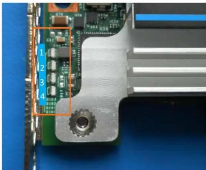
Note: 2.5-inch Form factor does not contain LEDs
- Intel® Solid-State Drive DC P3700 Series
- Product Specification
- Ordering Information
- Contents
- Figures
- Tables
- Revision History
- Overview
- References
- Terms and Acronyms
- Product Specifications
- Capacity
- NOTES:
- Performance
- Electrical Characteristics
- Environmental Conditions
- NOTE:
- Product Regulatory Compliance
- Reliability Specifications
- Temperature Sensor
- Power Loss Capacitor Test
- Hot Plug Support
- Out of Band Management (SMBUS)
- Variable Sector Size Support
- Mechanical Information
- Pin and Signal Descriptions
- 2.5-inch Form Factor Pin Locations
- Pin Signal Definitions
- Supported Command Sets
- NVMe\* Admin Command Set
- NVMe\* I/O Command Set
- Log Page Support
- SMART Attributes
- Temperature Statistics
- Drive Marketing Name Log
- SET Feature Identifiers
- NVMe\* Driver Support
- Certifications and Declarations
- Appendix A IDENTIFY Data Structure
- Appendix B Vital Data Structure
- Appendix C Out of Band Temperature Sensor Read Out
- Appendix D PCIe\* ID
- Appendix E SCSI Command Translation
- Appendix F Add-in Card LED Decoder
Brand : INTEL
Model : DCP3700
Category : SSD Drive