
AGM731F - Computer and Peripheral Cables NETGEAR - Free user manual and instructions
Find the device manual for free AGM731F NETGEAR in PDF.


User questions about AGM731F NETGEAR
0 question about this device. Answer the ones you know or ask your own.
Ask a new question about this device
Download the instructions for your Computer and Peripheral Cables in PDF format for free! Find your manual AGM731F - NETGEAR and take your electronic device back in hand. On this page are published all the documents necessary for the use of your device. AGM731F by NETGEAR.
USER MANUAL AGM731F NETGEAR
RoHS Compliant Small Form Factor Pluggable Transceiver for Gigabit Ethernet and Fiber Channel
AGM731F
RoHS Compliant Small Form Factor Pluggable Transceiver for Gigabit Ethernet and Fiber Channel
FEATURES
● Compliant with SFP Transceiver MSA specification
● Compliant with Specifications for IEEE 802.3z/Gigabit Ethernet
● Compliant with the 1.0625GBd Fiber Channel FC-PI 100-M5-SN-I Rev.13
● Compliant with Industry Standard RFT Electrical Connector and Cage
- Single + 3.3V Power Supply and TTL Logic Interface
- EEPROM with Serial ID Functionality
● Laser Class 1 Product which comply with the requirements of IEC 60825-1 and IEC 60825-2
- Duplex LC Connector interface
Description
This transceiver is hot pluggable 3.3V Small-Form-Factor transceiver module designed expressly for high-speed communication applications that require rates of up to 1.25Gbit/sec. It is compliant with the Gigabit Ethernet standards, as well as the SFP Multisource Agreement (MSA).
It provides with the LC receptacle that is compatible with the industry standard LC connector. The transceiver is also compatible with industry standard RFT connector and cage.
The post-amplifier of the transceiver also includes a LOS (Loss Of Signal) circuit that provides a TTL logic-high output when an unusable optical signal level is detected.
The transceiver is a Class 1 eye safety product. The optical power levels, under normal operation, are at eye safe level.
Applications
- Gigabit Ethernet
- Fibre channel
- Switch to Switch interface
● Switched backplane applications - File server interface
Performance
Data Link up to 550m in 50/125μm Multi Mode Fiber
Data Link up to 275m in 62.5/125μm Multi Mode Fiber
Absolute Maximum Ratings
| Parameter Symbol | Min. Typ. Max. | Unit Note | ||||
| Storage Temperature Ts -40 85 °C | ||||||
| Supply Voltage V | cc | 0 | 5 | V | ||
Recommended Operating Conditions
| Parameter Symbol | Min. Typ. Max. | Unit Note | ||||
| Case Operating Temperature | Tc -5 | 70 °C | ||||
| Supply Voltage V | cc 3.135 | 3.465 | V | |||
Electrical Characteristics
(V_cc = 3.135V to 3.465V)
| Parameter Symbol | Min. Typ. Max. | Unit Note | ||||
| Total Supply Current | ICCT | 180 | 300 | mA | ||
| Transmitter | ||||||
| Transmitter Differential Input Voltage | VDT | 0.5 | 2.4 | V | 1 | |
| Transmitter Disable Input-High | VDISH | 2 | V_CC+0.3 | V | ||
| Transmitter Disable Input-Low | VDISL | 0 | 0.8 | V | ||
| Transmitter Fault Output-High | VTXFH | 2 | V_CC+0.3 | V | 2 | |
| Transmitter Fault Output-Low | VTXFL | 0 | 0.8 | V | 2 | |
| Receiver | ||||||
| Receiver Differential Output Voltage V | DR | 0.35 | 0.7 | 2 | V | 3 |
| LOS Output Voltage-High | VLOSH | 2 | V_CC+0.3 | V | 2 | |
| LOS Output Voltage-Low | VLOSL | 0 | 0.8 | V | 2 | |
| Output Data Rise/Fall Time | tr / tf | 400 | psec | 4 | ||
| Total Jitter (pk-pk) | TJRX | 220 | psec | |||
Notes:
- Internally AC coupled and terminated to 100Ohm differential load.
- Pull up to V_cc with a 4.7K – 10K Ohm resistor on host Board
- Internally AC coupled, but requires a 100 Ohm differential termination at or internal to Serializer/ Deserializer.
- These are 20%\~80% values
Optical Characteristics
(V_cc = 3.135V to 3.465V , Data Rate = 1.25Gb/sec , PRBS = 2^7-1 NRZ, 50/125 m or 62.5/125 m MMF)
| Parameter Symbol Min. | Typ. Max. | Unit Note | ||||
| Transmitter | ||||||
| Output Optical Power (Avg.) P | o -9.5 | -3 dBm | ||||
| Optical Extinction Ratio | ER | 9 | dB | |||
| Center Wavelength | _c | 830 | 850 | 860 | nm | |
| Spectral Width (RMS) | σ | 0.85 | nm | |||
| Optical Rise/Fall Time | t_f/t_f | 260 | psec | 1 | ||
| Total Jitter (pk-pk) | TJ_TX | 220 | psec | |||
| Relative Intensity Noise | RIN | -117 | dB/Hz | |||
| Output Eye | Complies with the IEEE 802.3z/D2 specification, and is class 1 laser eye safety | |||||
| Receiver | ||||||
| Sensitivity (Avg.) | PIN | -17 | dBm | 2 | ||
| Input Optical Wavelength | λ | 850 | nm | |||
| LOS- De-Asserted (Avg.) | PD | -17 | dBm | |||
| LOS- asserted (Avg.) | PA | -30 | dBm | |||
| LOS-Hysteresis | PD-PA | 0.5 | dB | |||
| Overload | P_O -3 | dBm | ||||
Notes:
- These are 20%\~80% values
- The sensitivity is provided at a BER of 1 × 10^-10 or better with an input signal consisting of 1250Mb/s, 2^7-1 PRBS.
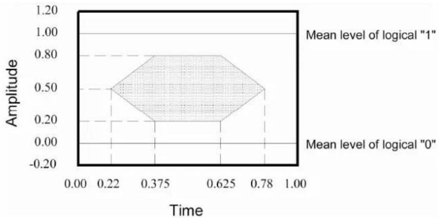
radar
| Time | Mean level of logical "0" | Mean level of logical "1" | |--------|---------------------------|---------------------------| | 0.22 | 0.00 | 0.50 | | 0.375 | 0.00 | 0.80 | | 0.625 | 0.00 | 0.80 | | 0.78 | 0.00 | 0.50 |Mask of the eye diagram for the optical transmit signal
SFP Transceiver Electrical Pad Layout
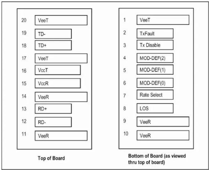
flowchart
graph TD
    subgraph_Top_of_Board["Top of Board"]
        A1["VeeT"] --> B1["TD-"]
        A2["TD+"] --> B2["TD-"]
        A3["VeeT"] --> B3["VccT"]
        A4["VccR"] --> B4["VccR"]
        A5["VeeR"] --> B5["RD+"]
        A6["RD-"] --> B6["RD-"]
        A7["VeeR"] --> B7["VeeR"]
    end
    subgraph_Bottom_of_Board["Bottom of Board (as viewed thru top of board)"]
        C1["VeeT"] --> D1["TxFault"]
        C2["Tx Disable"] --> D2["Tx Disable"]
        C3["MOD-DEF(2)"] --> D3["MOD-DEF(1)"]
        C4["MOD-DEF(0)"] --> D4["MOD-DEF(0)"]
        C5["Rate Select"] --> D5["Rate Select"]
        C6["LOS"] --> D6["LOS"]
        C7["VeeR"] --> D7["VeeR"]
        C8["VeeR"] --> D8["VeeR"]
Pin Function Definitions
| Pin Num. | Name Function Plug Seq. | Notes | ||
| 1 VeeT Transmitter Ground 1 | ||||
| 2 TX Fault Transmitter Fault Indication 3 Note 1 | ||||
| 3 TX Disable Transmitter Disable 3 | Note 2Module disables on high or open | |||
| 4 MOD-DEF2 Module Definition 2 3 Note 3, 2 wire serial ID interface | ||||
| 5 MOD-DEF1 Module Definition 1 3 Note 3, 2 wire serial ID interface | ||||
| 6 MOD-DEF0 Module Definition 0 3 Note 3, Grounded in Module | ||||
| 7 Rate Select Not Connect 3 Function not available | ||||
| 8 | LOS | Loss of Signal | 3 Note 4 | |
| 9 | VeeR Receiver Ground | 1 Note 5 | ||
| 10 | VeeR Receiver Ground | 1 Note 5 | ||
| 11 | VeeR Receiver Ground | 1 Note 5 | ||
| 12 | RD- | Inv. Received Data Out | 3 | Note 6 |
| 13 | RD+ | Received Data Out | 3 Note 7 | |
| 14 | VeeR Receiver Ground | 1 Note 5 | ||
| 15 | VccR Receiver Power | 2 3.3 ± 5% , Note 7 | ||
| 16 | VccT Transmitter Power | 2 3.3 ± 5% , Note 7 | ||
| 17 | VeeT Transmitter Ground 1 Note 5 | |||
| 18 | TD+ | Transmit Data In | 3 Note 8 | |
| 19 | TD- | Inv. Transmit Data In | 3 | Note 8 |
| 20 | VeeT Transmitter Ground 1 Note 5 | |||
Plug Seq.: Pin engagement sequence during hot plugging.
Notes:
1) TX Fault is an open collector/drain output, which should be pulled up with a 4.7K – 10KΩ resistor on the host board. Pull up voltage between 2.0V and VccT, R+0.3V. When high, output indicates a laser fault of some kind. Low indicates normal operation. In the low state, the output will be pulled to < 0.8V.
2) TX disable is an input that is used to shut down the transmitter optical output. It is pulled up within the module with a 4.7 - 10 K Ω resistor. Its states are:
Low (0 - 0.8V): Transmitter on
(>0.8, < 2.0V): Undefined
High (2.0 - 3.465V): Transmitter Disabled
Open: Transmitter Disabled
3) Mod-Def 0,1,2. These are the module definition pins. They should be pulled up with a 4.7K – 10KΩ resistor on the host board. The pull-up voltage shall be VccT or VccR (see Section IV for further details). Mod-Def 0 is grounded by the module to indicate that the module is present Mod-Def 1 is the clock line of two wire serial interface for serial ID Mod-Def 2 is the data line of two wire serial interface for serial ID
4) LOS (Loss of Signal) is an open collector/drain output, which should be pulled up with a 4.7K – 10KΩ resistor. Pull up voltage between 2.0V and VccT, R+0.3V. When high, this output indicates the received optical power is below the worst-case receiver sensitivity (as defined by the standard in use). Low indicates normal operation. In the low state, the output will be pulled to < 0.8V.
5) VeeR and VeeT may be internally connected within the SFP module.
6) RD-/+: These are the differential receiver outputs. They are AC coupled 100Ω differential lines which should be terminated with 100Ω (differential) at the user SERDES. The AC coupling is done inside the module and is thus not required on the host board. The voltage swing on these lines will be between 370 and 2000 mV differential (185 – 1000 mV single ended) when properly terminated.
7) VccR and VccT are the receiver and transmitter power supplies. They are defined as 3.3V ±5% at the SFP connector pin. Maximum supply current is 300mA. Recommended host board power supply filtering is shown below. Inductors with DC resistance of less than 1 ohm should be used in order to maintain the required voltage at the SFP input pin with 3.3V supply voltage. When the recommended supply-filtering network is used, hot plugging of the SFP transceiver module will result in an inrush current of no more than 30mA greater than the steady state value. VccR and VccT may be internally connected within the SFP transceiver module.
8) TD-/+: These are the differential transmitter inputs. They are AC-coupled, differential lines with 100Ω differential termination inside the module. The AC coupling is done inside the module and is thus not required on the host board. The inputs will accept differential swings of 500 – 2400 mV (250 – 1200 mV single-ended), though it is recommended that values between 500 and 1200 mV differential (250 – 600 mV single-ended) be used for best EMI performance.
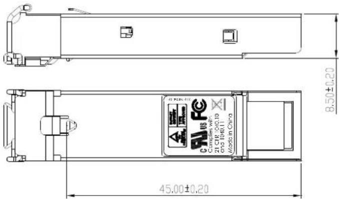
Package Outline Drawing for Metal Housing with Bail de-latch
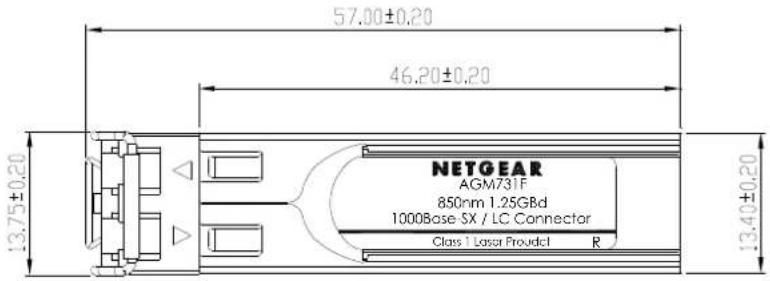
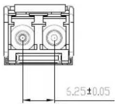
Unit:mm
SFP timing parameters for SFP management
| Parameter Symbol Min. | Max. | Unit | Unit Conditions | ||
| TX_DISABLE Assert time | t_off 10 | μsec | Time from rising edge of TX_DISABLE to when the optical output falls below 10% of nominal | ||
| TX_DISABLE Negate time | t_on 1 | msec | Time from falling edge of TX_DISABLE to when the modula ted optical output rises above 90% of nominal | ||
| Time to initialize, including reset of TX_FAULT | t_init | 300 | msec | From power on or negation of TX_Fault using TX Disable. | |
| TX Fault Assert Time | t_fault | 100 | μsec | Time from fault to TX fault on. | |
| TX_DISABLE to reset | t_rest | 10 | μsec | Time TX Disable must be held high to reset TX_Fault | |
| LOS Assert Time | t_loss_on | 100 | μsec | Time from LOS state to Rx LOS assert | |
| LOS Deassert Time | t_loss_off | 100 | μsec | Time from non-LOS state to Rx LOS deassert | |
| Serial ID Clock Rate | f_serial_clock | 100 | kHz | ||
SFP timing parameters
| Vcc > 3.15 V TX_FAULT TX_DISABLE Transmitted Signal t_init | Vcc > 3.15 V TX_FAULT TX_DISABLE Transmitted Signal t_init |
| Power on initialization of SFP transceiver, TX_DISABLE negated | Power on initialization of SFP, TX_DISABLE assert Initialization during hot plugging of SFP TRANSCEIVER |
| Vcc > 3.15 V TX_FAULT TX_DISABLE Transmitted Signal Insertion t_init | TX_FAULT TX_DISABLE Transmitted Signal t_off t_on |
| Example of initialization du ring hot plugging, TX_DISABLE negated. | SFP TX_DISABLE timing during normal operation. |
| Occurrence of Fault TX_FAULT TX_DISABLE Transmitted Signal t_fault | Occurrence of Fault TX_FAULT TX_DISABLE Transmitted Signal t_reset t_init* |
| Detection of transmitter safety fault condition Successful recovery from transient safety fault condition | |
| Occurrence of Fault TX_FAULT TX_DISABLE Transmitted Signal t_reset t_init* | Occurrence of loss LOS t_loss_on t_loss_off |
| Unsuccessful recovery from safety fault condition Timing of LOS detection | |
EEPROM Serial ID Memory Contents (2-Wire Address A0h)
| Address | Hex | ASCII | Address | Hex | ASCII | Address | Hex | ASCII | Address | Hex | ASCII | Address | Hex | ASCII | Address | Hex | ASCII |
| 00 03 | 25 | 41 | A 50 | 20 | 75 | SN | 100 | 00 | 125 | 00 | |||||||
| 01 04 | 26 | 52 | R 51 | 20 | 76 | SN | 101 | 00 | 126 | 00 | |||||||
| 02 07 | 27 | 20 | 52 | 20 | 77 | SN | 102 | 00 | 127 | 00 | |||||||
| 03 00 | 28 | 20 | 53 | 20 | 78 | SN | 103 | 00 | |||||||||
| 04 00 | 29 | 20 | 54 | 20 | 79 | SN | 104 | 00 | |||||||||
| 05 00 | 30 | 20 | 55 | 20 | 80 | SN | 105 | 00 | |||||||||
| 06 01 | 31 | 20 | 56 | 41 | 81 | SN | 106 | 00 | |||||||||
| 07 | 40 | 32 | 20 | 57 | 20 | 82 | SN | 107 | 00 | ||||||||
| 08 40 | 33 | 20 | 58 | 20 | 83 | SN | 108 | 00 | |||||||||
| 09 00 | 34 | 20 | 59 | 20 | 84 | DC | Note 3 | 109 | 00 | ||||||||
| 10 00 | 35 | 20 | 60 | 03 | 85 | DC | 110 | 00 | |||||||||
| 11 03 | 36 | 00 | 61 | 52 | 86 | DC | 111 | 00 | |||||||||
| 12 0D | 37 | 00 | 62 | 00 | 87 | DC | 112 | 00 | |||||||||
| 13 00 | 38 | 00 | 63 | CS1 | Note 1 | 88 | DC | 113 | 00 | ||||||||
| 14 00 | 39 | 00 | 64 | 00 | 89 | DC | 114 | 00 | |||||||||
| 15 00 | 40 | 41 | A 65 | 1A | 90 | DC | 115 | 00 | |||||||||
| 16 37 | 41 | 47 | G 66 | 00 | 91 | DC | 116 | 00 | |||||||||
| 17 1B | 42 | 4D | M | 67 00 | 92 | 00 | 117 | 00 | |||||||||
| 18 00 | 43 | 37 | 7 68 | SN | Note 2 | 93 00 | 118 | 00 | |||||||||
| 19 00 | 44 | 33 | 3 69 | SN | 94 | 00 | 119 | 00 | |||||||||
| 20 4E | N 45 | 31 | 1 70 | SN | 95 | CS2 | Note 4 | 120 | 00 | ||||||||
| 21 45 | E 46 | 46 | F 71 | SN | 96 | 00 | 121 | 00 | |||||||||
| 22 54 | T 47 | 20 | 72 | SN | 97 | 00 | 122 | 00 | |||||||||
| 23 47 | G | 48 20 | 73 | SN | 98 | 00 | 123 | 00 | |||||||||
| 24 45 | E 49 | 20 | 74 | SN | 99 | 00 | 124 | 00 |
Notes:
1) Byte 63: Check sum of bytes 0-62.
2) Byte 68-83 (SN): Serial number.
3) Byte 84-91 (DC): Date code.
4) Byte 95 (CS2): Check sum of bytes 64-94.
5) Byte 128-255 had been set hex. 00.
Regulatory Compliance
| Feature Reference | Performance | |
| Electromagnetic Interference (EMI) | FCC CRF 47, Part15 Class BEN 55022 Class B (CISPR 22A) | (1) Satisfied with electrical characteristics of product spec.(2) No physical damage |
| Radio Frequency Electromagnetic Field | EN 61000-4-3IEC 61000-4-3 | |
| Electrostatic Discharge to the Duplex LC Receptacle | EN 61000-4-2IEC 61000-4-2IEC 801.2 | |
| Electrostatic Discharge to the Electrical Pins | MIL-STD-883E Method 3015.7 | |
| Eye Safety US FDA CDRH AEL | Class 1EN 60950: 2000EN 60825-1: 1994+A11+A2EN 60825-2: 2000 | CDRH File # 0321539-00TUV Certificate No. R50032471 |
| Component Recognition Under | writers Laboratories and Canadian Standards Association Joint Component Recognition for Information Technology Equipment Including Electrical Business Equipment | UL File # E239394 |
NETGEAR®
© 2008 NETGEAR, Inc. NETGEAR, the NETGEAR Logo, NETGEAR Digital Entertainer Logo, Connect with Innovation, FrontView, IntelliFi, PowerShift, ProSafe, RAIDar, RAIDiator, X-RAID, RangeMax, ReadyNAS and Smart Wizard are trademarks of NETGEAR, Inc. in the United States and/or other countries. Other brand names mentioned herein are for identification purposes only and may be trademarks of their respective holder(s). Information is subject to change without notice. All rights reserved. DAGM731F0

Brand : NETGEAR
Model : AGM731F
Category : Computer and Peripheral Cables