NPPA-TT-S - Uncategorized Neutrik - Free user manual and instructions
Find the device manual for free NPPA-TT-S Neutrik in PDF.


| Product Type | TT (Tiny Telephone) Patchbay Connector |
| Color | Silver / Black |
| Material | Nickel-plated brass contacts, metal housing |
| Dimensions (approx.) | 0.5 x 0.5 x 1.5 inches (12.7 x 12.7 x 38.1 mm) |
| Weight (approx.) | 0.02 lbs (9 g) |
| Connection Type | TT (4.4 mm) male / female |
| Number of Contacts | 3 (Tip, Ring, Sleeve) / 2 (tip, sleeve) depending on variant |
| Compatibility | Standard TT patchbays and audio equipment |
| Application | Professional audio, broadcast, recording studios |
| Features | Secure locking mechanism (optional), high contact reliability |
| Maintenance | Clean contacts with a dry cloth; avoid moisture |
| Safety | Not for mains power use; low-voltage audio signal only |
| Spare Parts | Replacement connectors available from Neutrik |
| Reparability | Field-repairable with basic soldering skills |
| Warranty | Standard Neutrik warranty (usually 1 year) |
Frequently Asked Questions - NPPA-TT-S Neutrik
User questions about NPPA-TT-S Neutrik
0 question about this device. Answer the ones you know or ask your own.
Ask a new question about this device
Download the instructions for your Uncategorized in PDF format for free! Find your manual NPPA-TT-S - Neutrik and take your electronic device back in hand. On this page are published all the documents necessary for the use of your device. NPPA-TT-S by Neutrik.
USER MANUAL NPPA-TT-S Neutrik
text_image
NPPA-TT-3 Grounding Upper Base Channel Ground Common Signal Ground Induction to Ground Induction to Common Ground Common Signal Ground Bottom Base Module Attachment Top Use Key NPPA-TT-3| NEUTRIK AG Liechtenstein | NEUTRIK Zürich AG Switzerland | NEUTRIK (UK) Ltd. Great Britain | NEUTRIK USA INC. USA | NEUTRIK Tokyo Ltd. Japan | NEUTRIK France France | NEUTRIK Vertriebs GmbH Germany/Netherlands/Austria |
| Tel.: +423/237 24 24 | Tel.: +41 44/736 5010 | Tel.: +44 1983/811 441 | Tel.: +1 732/901 9488 | Tel.: +81 3/3663 4733 | Tel.: +33 1/4131 6750 | Tel.: +49 8131/28 08 90 |
| Fax: +423/232 53 93 | Fax: +41 44/736 5011 | Fax: +44 1983/811 439 | Fax: +1 732/901 9608 | Fax: +81 3/3663 4796 | Fax: +33 1/4131 0511 | Fax: +49 8131/28 08-30 |
| www.neutrik.com | ||||||
Index
- Electrical configuration....3
- Replacement of Jack Pairs....4
- Reconfiguration by hand....5
- Grounding variations .....7
- Wiring 8
- Cable retention to the unit....9
- Channel identification ....10
- Technical data .... 11
- Wiring Diagram....12
- Ordering Information....13
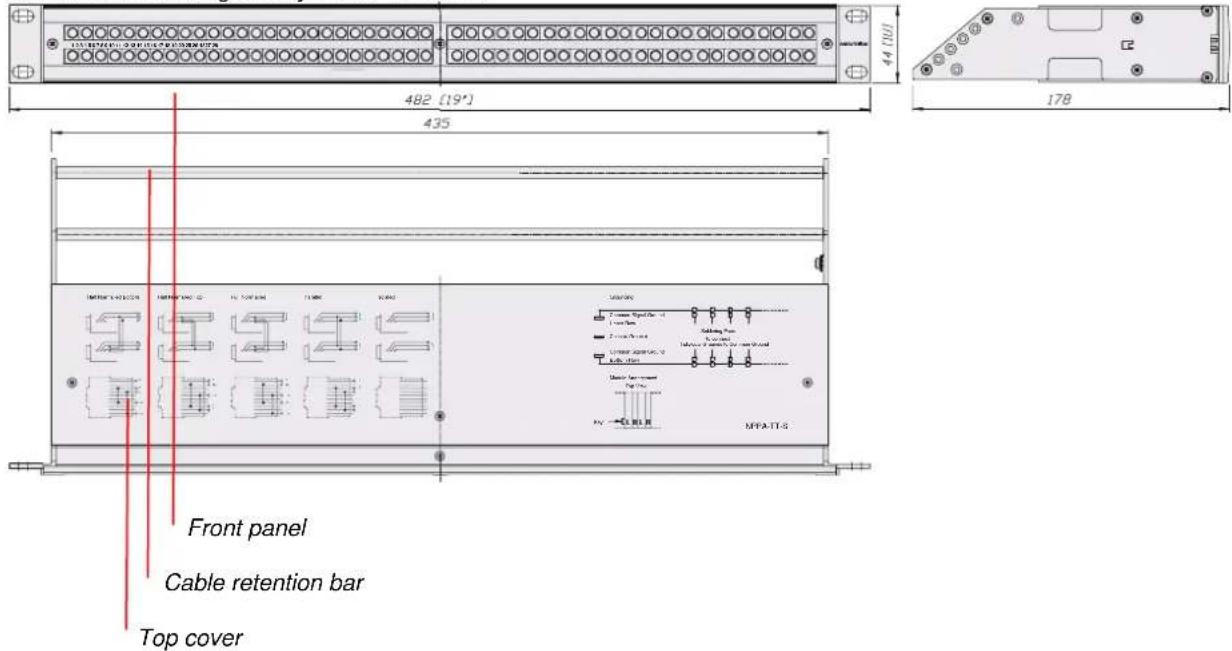
Dimensional Drawings "Easy Patch" NPPA-TT
text_image
Front panel Cable retention bar Top cover1. Electrical configuration
The Neutrik "Easy Patch" Patch Panel is fitted with high quality, long life NJ3TTA gold plated double contact jacks (2 x 48). This Patch Panel is an innovative and compact patching system (just 1 U high) for 19" rack mounting. Robustly housed in black coated steel shell and featuring precision aluminum fittings it is built to last. The Neutrik "Easy Patch" is suitable for analog and digital audio signals.
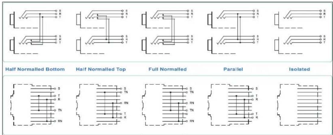
The "Easy Patch" is available in five normalling configurations (fully loaded).
• half normalled bottom row
• half normalled top row
- full normalled
- parallel
- isolated
text_image
Half Normalled Bottom Half Normalled Top Full Normalled Parallel IsolatedConfiguration Chart
Furthermore individual jack pairs can be changed to combine various normalings within one panel quickly and without fuss. This is even possible while the panel is "on air". For this we offer pre-configured jack pairs (NJ3TTA-4- ^* ).
In case of emergency the normalling for individual jack pairs can be changed by the use of normalling bars. Normalling bars to change the normalling of 4 channels are included.
2. Replacement of Jack Pairs
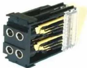
Each individual jack pair can be exchanged quickly and without fuss even while the panel is "on air". For replacement simply remove the easy accessible jack pairs.
natural_image
Stacked electronic components with gold contacts and black casing (no visible text or symbols)Module consisting of 2 Jack Pairs
natural_image
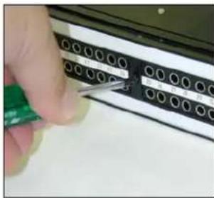
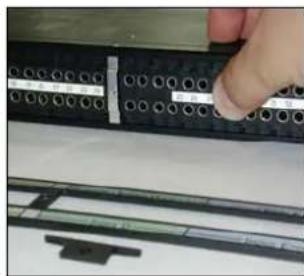
Close-up of a hand using a tool to adjust or install a device panel with circular ports (no visible text or symbols)Remove Front Panel by unscrewing the 3 black cross-recessed screws (M3x8 Taptite), remove the two side-stops.
natural_image
Close-up of a hand pressing down on a black plastic electronic component with circular holes (no visible text or symbols)Push out the channel identification strips.

natural_image
Close-up of a hand inserting a flexible plastic component into an electronic circuit board (no visible text or symbols)Pull one module out of the casing using the supplied disassembling pliers
text_image
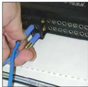
Input EAlternatively the jack pairs may be pulled out by the use of two Bantam plugs (diagonally plugged in).
natural_image
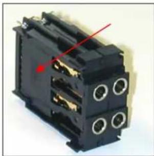
Close-up of a black electrical contactor component with four circular ports and a red arrow pointing to a section (no visible text or symbols)The two jack pairs have to be re-assembled in the right way so that the thicker body marked "left" is put on the left side with the mark outside and readable.
To complete, push the new jack pairs into the casing again with the mark on the left side (If more than one module are removed always assemble from the center to the right or left side and be careful that the keys on the left side of the jack pairs find their guiding slots. If all jack pairs are removed start at the casing support in the center and assemble to the right and left side). Slide in again the channel identification strips (best from the outside inwards) and fix the front panel with the black cross-recessed screws. Don't forget to insert the side-stops before fixing the screws (see page 10).
3. Reconfiguration by hand
Please note, in case of emergency the normalling can by changed by hand by the use of normalling bars. For easy and safe modification work we recommend our preconfigured jack pairs (NJ3TTA-4- ^* ).
natural_image
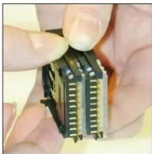
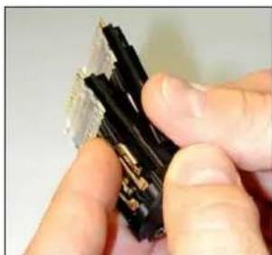
Close-up of hands holding a small electronic component with visible pins and traces (no text or symbols)The two jack pairs are separated by spreading apart the rear parts to unlock the fixing mechanism till it is possible...
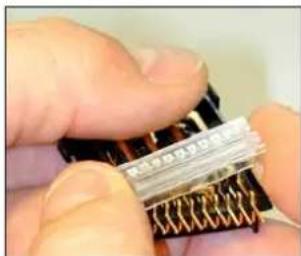
natural_image
Close-up of a hand holding a black plastic electronic component with wires (no visible text or symbols)...to slide the jack pairs against each other in axial direction.
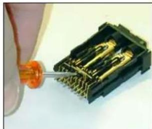
natural_image
Close-up of hands holding a small electronic component with metallic leads (no visible text or symbols)Then remove the cover with a tiny grip at the side and carefully
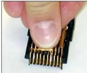
natural_image
Close-up of a hand using a screwdriver to disassemble a black plastic component with gold pins (no text or symbols visible)Pull out the configuration bars you need to exchange (preferably using a small screw-driver).
natural_image
Close-up of a finger pressing down on a black plastic component with gold pins (no text or symbols visible)Insert new bars carefully by pressing them in parallel at both ends.
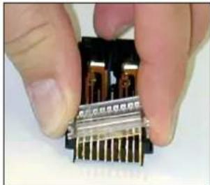
Attention: To ensure best contact conditions never reuse the configuration bars once being put in place! Always take new ones! Keep the contacts and switches in place with the thumb while manipulating the normalling contacts.
natural_image
Close-up of hands holding a black electronic component with gold pins (no visible text or symbols)Finally snap on the cover (Insert it first at one side and then snap slightly into the opposite groove with a light pressure on the nose).
4. Grounding variations
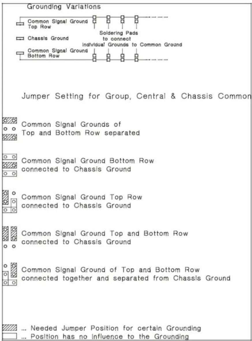
The flexible grounding system provides the following versions:
Individual: Each channel is individually grounded by its corresponding cable shield (default configuration).
Group: Selected channel grounds are connected via the ground bus on the PCB using solder bridges and track cuts to form a group that is connected to one common cable shield.
Central: All channel grounds (individual top and bottom row) are connected via the ground bus on the PCB using solder bridges and wired with only one cable shield.
Chassis-Common: The same as central grounding but with the addition of the common ground bus (top and / or bottom rows) connected to the patch panel chassis by means of jumpers.
text_image
Grounding Variations Common Signal Ground Top Row Soldering Pads to connect Chassis Ground individual Grounds to Common Ground Common Signal Ground Bottom Row Jumper Setting for Group, Central & Chassis Common Common Signal Grounds of Top and Bottom Row separated Common Signal Ground Bottom Row connected to Chassis Ground Common Signal Ground Top Row connected to Chassis Ground Common Signal Ground Top and Bottom Row connected to Chassis Ground Common Signal Ground of Top and Bottom Row connected together and separated from Chassis Ground ... Needed Jumper Position for certain Grounding ... Position has no Influence to the Grounding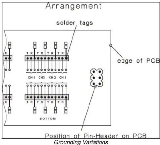
text_image
Arrangement solder tags edge of PCB Position of Pin-Header on PCB Grounding VariationsNOTE: In standard configuration there is no ground connection between top and bottom row unless it is provided by an inserted patch cable. If this is required, as in the case of phantom powered microphone lines, either make an internal connection by individually wiring the corresponding upper and lower 'S' terminals, or if the latter is critical with respect to possible ground loops make the connection via patch cable instead of using the normaling feature.
5. Wiring
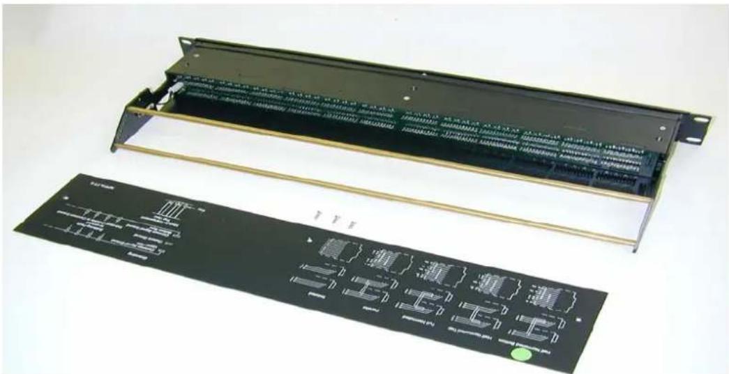
For access to the terminals remove the top- and bottom-cover with three cross-recessed screws (M2.5x8) each fixed in a triangle.
natural_image
Two electronic circuit boards with internal components, one showing a black panel and the other displaying traces (no visible text or symbols)Rear front for wiring
Standard solder lugs enable a reliable and long-lasting wiring.
Termination with solder lugs Solder bridges

text_image
33 32 31 30 29 28 27 26 25 Solder tags6. Cable retention to the unit
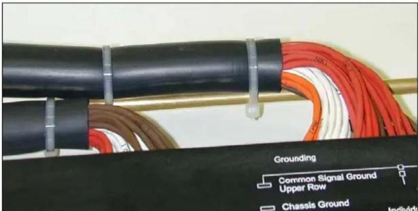
The built in cable retention bar is at the back of the casing. Simply attach the cables with cable ties to the bar as shown in the photo.
For large and heavy bundles there is an additional strain relief bar NPPA-S available. It is attached to the casing with four screws.
text_image
Grounding Common Signal Ground Upper Row Chassis Ground IndividualCable Retention Bar
7. Channel identification
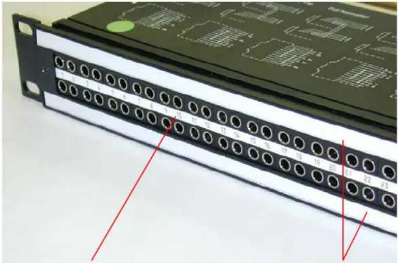
The front panel is equipped with channel identification strips located in the center of the channels and marked with the channel numbers 1-24 and 25-48 respectively.
natural_image
Close-up of a black network switch module with multiple circular connectors and labeled pins (no readable text or symbols beyond component labels)Channel identification strips Labeling strips
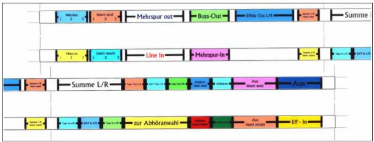
For the perfect management of the system and for individual identification according to customer's needs there are two large and separate labeling strips, one for the bottom and one for the top row.
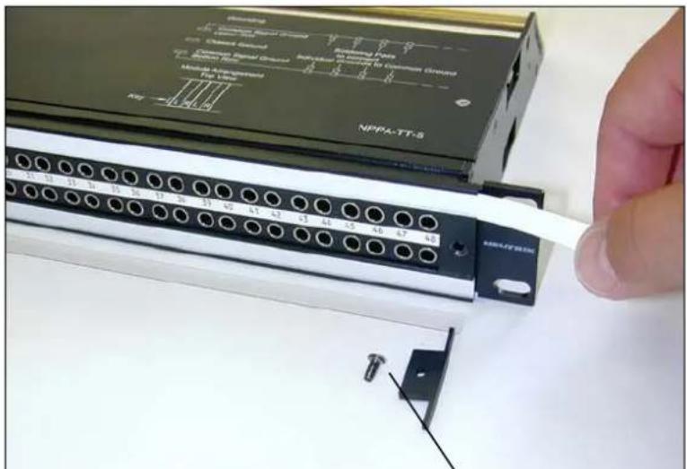
To write on the paper you have to unscrew one of the outer fixing screws of the front panel. Then pull out the side-stop, the transparent foil and the paper strip itself. After marking is done assemble the parts in reversed sequence.
text_image
Hounding Inverter Signal Ground NPPA-TT-5 Closed Ground Inverter Input to Common Ground Continuous Signal Ground Bottom Input Modular Configuration Pin Number NPPA-TT-5 MULIFLOWERRemove labeling strip Side Stop
NOTE: For easy and perfect marking you can use our designation software "PatchLabel" which is available on our web site www.neutrik.com free of charge.
Print-Out software "Patch Label"
flowchart
graph TD
    A["Millefion"] --> B["Insert send"]
    B --> C["Mehrspur out"]
    C --> D["Buss-Out"]
    D --> E["Effekt Out L/R"]
    E --> F["Summe L/R"]
    F --> G["Summe"]

    H["Millefion in"] --> I["Insert return"]
    I --> J["Line In"]
    J --> K["Mehrspur-In"]
    K --> L["Summe L/R"]
    L --> M["Tape In L/R"]
    M --> N["SAT In L/R"]

    O["Summe L/R"] --> P["Summe L/R"]
    P --> Q["Tape On L/R"]
    Q --> R["Start One: Case On In"]
    R --> S["Autohram"]
    S --> T["Autohram"]
    T --> U["Auto"]
    U --> V["Aux"]

    W["Summe L/R"] --> X["Tape In L/R"]
    X --> Y["SAT In L/R"]
    Y --> Z["Case In L/R"]
    Z --> AA["zur Abhöranwahl"]
    AA --> AB["Autohram"]
    AB --> AC["Auto"]
    AC --> AD["Eff - In"]
8. Technical data
8.1 Electrical
Frequency range DC to > 50 MHz
Digital suitability Digital audio acc. to AES/EBU
Channel separation > 100 dB @ 10 kHz, 600 Ω terminated
40 dB @ 6 MHz, 110 Ω terminated
Insulation resistance > 10 ^9 Ω @ 500 V dc
Connector contact resistance < 20 mΩ
Switch contact resistance < 25 mΩ
Dielectric strength 1000 V dc
8.2 Mechanical
Lifetime > 5.000 Insertion / withdrawal cycles
Insertion / Withdrawal force < 10 N / > 8 N
Cable retention force 70 N max per cable retention bar
Dimensions (rack mount) 482 mm (W) × 44 mm (H) (19" × 1 U)
Depth 178 mm (7")
Weight 2.9 kg
Temperature range -30°C to +80°C
8.3 Materials
Jack housing PA 66 blend
Jack contacts CuSn6 - TRIBOR
® plated
(0.2 μm AuCo over 2 μm NiP)
Housing Steel and aluminum, black coated
Front Panel AlMgSi 0.5 F22
9. Wiring Diagram
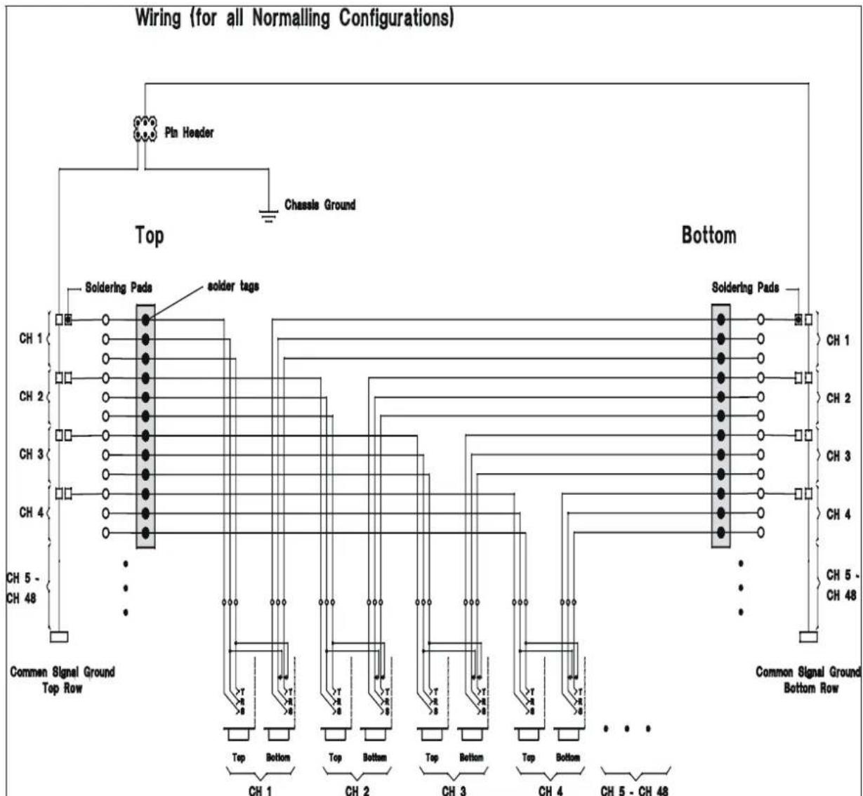
flowchart
graph TD
    A["Pin Header"] --> B["Top"]
    B --> C["Soldering Pads"]
    B --> D["solder tags"]
    C --> E["Common Signal Ground Top Row"]
    D --> F["Chassis Ground"]
    G["Common Signal Ground Bottom Row"] --> H["Top"]
    G --> I["Bottom"]
    H --> J["Ch 1"]
    H --> K["Ch 2"]
    H --> L["Ch 3"]
    H --> M["Ch 4"]
    H --> N["Ch 5 - CH 48"]
    I --> O["Ch 1"]
    I --> P["Ch 2"]
    I --> Q["Ch 3"]
    I --> R["Ch 4"]
    I --> S["Ch 5 - CH 48"]
    T["Chassis Ground"] --> U["Top"]
    T --> V["Bottom"]
    U --> W["Ch 1"]
    V --> X["Ch 2"]
    W --> Y["Ch 1"]
    X --> Z["Ch 2"]
    Y --> AA["Ch 3"]
    Z --> AB["Ch 4"]
    AA --> AC["Ch 5 - CH 48"]
Wiring diagram
10. Ordering Information
Patch Panels
Part Number Description Configuration\* Wiring Grounding
NPPA-TT-S 2 x 48 jacks half normalled bottom 288 solder terminals individual
NPPA-TT-S-FN 2 x 48 jacks full normalled 288 solder terminals individual
NPPA-TT-S-HNT 2 x 48 jacks half normalled top row 288 solder terminals individual
NPPA-TT-S-I 2 x 48 jacks isolated 288 solder terminals individual
NPPA-TT-S-P 2 x 48 jacks parallel 288 solder terminals individual
* fully loaded jack pairs only
Pre-configured Jack-Pairs
| Part Number | Description | Configuration* | |
| NJ3TTA-4-HNB | blocks of 2 channels | half normalled bottom row | cover ident color: clear |
| NJ3TTA-4-HNT | blocks of 2 channels | half normalled top row | cover ident color: yellow |
| NJ3TTA-4-FN | blocks of 2 channels | full normalled | cover ident color: green |
| NJ3TTA-4-P | blocks of 2 channels | parallel | cover ident color: red |
| NJ3TTA-4-I | blocks of 2 channels | isolated | cover ident color: orange |
Accessories
NPPA-S Strain Relief bar NKTT* Patch cords with NP3TT-1 plugs. Available in black, blue, green, red and yellow. Length: 30, 40, 60, 90, 120 cm
NPPA-NB Normalling bars for changing the normalling of all 48 channels
Standard supply
The compact Neutrik "Easy Patch" NPPA-TT-S consists of:
- Black coated steel casing with aluminium fittings
- 2 x 48 highly integrated Neutrik NJ3TTA jacks with gold plated double contacts and specially designed normalling mechanism (standard: half normalled bottom row)
- Integrated internal pre-wiring with selectable flexible grounding system
• Solder lugs termination
• 2 Built-in cable retention bars - Spare normalling configuration bars
4 Normal 1: "short", bridges 5 contacts
8 Normal 2: "medium", bridges 6 contacts
4 Normal 3: "long", bridges 7 contacts
• 1 Disassembling plier
• 1 Instruction Manual