
Vaio PCV-LX800 - Laptop SONY - Free user manual and instructions
Find the device manual for free Vaio PCV-LX800 SONY in PDF.


User questions about Vaio PCV-LX800 SONY
0 question about this device. Answer the ones you know or ask your own.
Ask a new question about this device
Download the instructions for your Laptop in PDF format for free! Find your manual Vaio PCV-LX800 - SONY and take your electronic device back in hand. On this page are published all the documents necessary for the use of your device. Vaio PCV-LX800 by SONY.
USER MANUAL Vaio PCV-LX800 SONY
© 2000 Sony Electronics Inc. Reproduction in whole or in part without written permission is prohibited. All rights reserved. This manual and the software described herein, in whole or in part, may not be reproduced, translated, or reduced to any machine-readable form without prior written approval.
SONY ELECTRONICS INC. PROVIDES NO WARRANTY WITH REGARD TO THIS MANUAL, THE SOFTWARE, OR OTHER INFORMATION CONTAINED HEREIN AND HEREBY EXPRESSLY DISCLAIMS ANY IMPLIED WARRANTIES OF MERCHANTABILITY OR FITNESS FOR ANY PARTICULAR PURPOSE WITH REGARD TO THIS MANUAL, THE SOFTWARE, OR SUCH OTHER INFORMATION. IN NO EVENT SHALL SONY ELECTRONICS INC. BE LIABLE FOR ANY INCIDENTAL, CONSEQUENTIAL, OR SPECIAL DAMAGES, WHETHER BASED ON TORT, CONTRACT, OR OTHERWISE, ARISING OUT OF OR IN CONNECTION WITH THIS MANUAL, THE SOFTWARE, OR OTHER INFORMATION CONTAINED HEREIN OR THE USE THEREOF.
Sony Electronics Inc. reserves the right to make any modification to this manual or the information contained herein at any time without notice. The software described herein is governed by the terms of a separate user license agreement.
This product contains software owned by Sony and licensed by third parties. Use of such software is subject to the terms and conditions of license agreements enclosed with this product. Some of the software may not be transported or used outside the United States. Software specifications are subject to change without notice and may not necessarily be identical to current retail versions.
Updates and additions to software may require an additional charge. Subscriptions to online service providers may require a fee and credit card information. Financial services may require prior arrangements with participating financial institutions.
Sony, VAIO, the VAIO logo, VAIO Smart, VAIO Digital Studio, VAIO Slimtop, Media Park, DVgate, Media Bar, Handycam, Mavica, PictureGear, i.LINK, and Memory Stick are trademarks of Sony. Intel, Pentium, and Celeron are trademarks of Intel Corporation. Microsoft, Windows, and the Windows Me logo are registered trademarks of Microsoft Corporation.
All other trademarks are trademarks or registered trademarks of their respective owners.
Owner's Record
The model number and serial number are located on the back of your VAIO® computer. Record the serial number in the space provided here. Refer to the model and serial number when you call your Sony Service Center.
Model Number: PCV-LX700/PCV-LX800
Serial Number: ____
Safety Information and Caution
CD-RW Laser Diode Properties
Max. Laser output (read) 1.0 mW
Max. Laser output (write) 35mW
Wavelength 777-787 nm
☐ To prevent fire or shock hazard, do not expose your desktop to rain or moisture. To avoid electrical shock, do not open the cabinet. Refer servicing to qualified personnel only.
☐ Never install modem or telephone wiring during a lightning storm.
☐ Never install telephone jacks in wet locations unless the jack is specifically designed for wet locations.
☐ Never touch uninsulated telephone wire or terminals unless the telephone line has been disconnected at the network interface.
☐ Use caution when installing or modifying telephone lines.
☐ Avoid using the modem during an electrical storm.
☐ Do not use the modem or a telephone to report a gas leak in the vicinity of the leak.
☐ The socket outlet shall be installed near the equipment and shall be easily accessible.
! To change the backup battery, contact your nearest Sony Service Center.
! Caution - The use of optical instruments with this product will increase eye hazard. As the laser beam used in this product is harmful to the eyes, do not attempt to disassemble the drive cabinet. Refer servicing to qualified personnel only.
! Danger - Visible and invisible laser radiation when open. Avoid direct exposure to beam.
! For CD-RW: Danger - Invisible laser radiation when open. Avoid direct exposure to beam.
! Caution: For ADSL modem models, to reduce the risk of fire, use only No. 26 AWG or larger telecommunication line cord.
For questions regarding your product or for the Sony Service Center nearest you, call 1-888-476-6972 in the United States or 1-800-961-7669 in Canada.
Sony Customer Support can be reached at www.sony.com/pcsupport.
Regulatory Information
Declaration of Conformity
Trade Name: SONY
Model No.: PCV-LX700/PCV-LX800
Responsible Party: Sony Electronics Inc.
Address: 1 Sony Drive
Park Ridge, NJ 07656
Telephone: 201-930-6972
This phone number is for FCC-related matters only.
This device complies with Part 15 of FCC Rules. Operation is subject to the two following conditions:
(1) This device may not cause harmful interference, and
(2) this device must accept any interference received, including interference that may cause undesired operation.
This equipment has been tested and found to comply with the limits for a Class B digital device, pursuant to Part 15 of the Rules. These limits are designed to provide reasonable protection against harmful interference in a residential installation. This equipment generates, uses, and can radiate radio frequency energy and, if not installed and used in accordance with the instructions, may cause harmful interference to radio communications. However, there is no guarantee that interference will not occur in a particular installation. If this equipment does cause harmful interference to radio or television reception, which can be determined by turning the equipment off and on, the user is encouraged to try to correct the interference by one or more of the following measures: :
☐ Reorient or relocate the receiving antenna.
☐ Increase the separation between the equipment and the receiver.
☐ Connect the equipment into an outlet on a circuit different from that to which the receiver is connected.
Consult the dealer or an experienced radio/TV technician for help.
You are cautioned that any changes or modifications not expressly approved in this manual could void your authority to operate this equipment.
Only peripherals (computer input/output devices, terminals, printers, etc.) that comply with FCC Class B limits may be attached to this computer product. Operation with noncompliant peripherals is likely to result in interference to radio and television reception.
All cables used to connect peripherals must be shielded and grounded. Operation with cables, connected to peripherals, that are not shielded and grounded, may result in interference to radio and television reception.
FCC Part 68
This equipment complies with Part 68 of the FCC rules. The FCC Ringer Equivalence Number (REN) for this equipment is 0.7. If requested, this information must be provided to the telephone company.
This modem uses the USOC RJ-11 telephone jack.
The REN is used to determine the quantity of devices which may be connected to the telephone line. Excessive RENs on the telephone line may result in the devices not ringing in response to an incoming call. In most, but not all areas, the sum of the RENs should not exceed five (5.0). To be certain of the number of devices that may be connected to the line, as determined by the total RENs, contact the telephone company to determine the maximum REN for the calling area.
If the terminal equipment causes harm to the telephone network, the telephone company will notify you in advance that temporary discontinuance of service may be required. But if advance notice is not practical, the telephone company will notify the customer as soon as possible. Also, you will be advised of your right to file a complaint with the FCC if you believe it is necessary.
The telephone company may make changes in its facilities, equipment, operations or procedures that could affect the operations of the equipment. If this happens, the telephone company will provide advance notice in order for you to make the necessary modifications in order to maintain uninterrupted service.
If trouble is experienced with this modem, for repair or warranty information, please contact 1-888-4SONY-PC, or write to the Sony Customer Information Center, 12451 Gateway Blvd., Fort Myers, FL 33913. If the trouble is causing harm to the telephone network, the telephone company may request that you remove the equipment from the network until the problem is resolved.
Repair of this equipment should be made only by a Sony Service Center or Sony authorized agent. For the Sony Service Center nearest you, call 1-888-4SONYPC (1-888-476-6972).
This equipment cannot be used on public coin service provided by the telephone company. Connection to Party Line Service is subject to state and possible provincial tariffs. (Contact the state or provincial utility service commission, public service commission, or corporation commission for information.)
Telephone Consumer Protection Act of 1991 (United States)
The Telephone Consumer Protection Act of 1991 makes it unlawful for any person to use a computer or other electronic device to send any message via a telephone facsimile machine unless such message clearly contains, in a margin at the top or bottom of each transmitted page or on the first page of the transmission, the date and time it is sent and an identification of the business, other entity, or individual sending the message, and the telephone number of the sending machine or such business, other entity, or individual.
In order to program this information into your facsimile, see your fax software documentation.
Telephone Consumer Guidelines (Canada)
Please refer to your telephone directory under 'Privacy Issues' and/or 'Terms of Service.' For more detailed information, please contact:
CRTC
This Class B digital apparatus complies with Canadian ICES-003.
You can return your unwanted lithium ion batteries to your nearest Sony Service Center or Factory Service Center.

In some areas the disposal of lithium ion batteries in household or business trash may be prohibited.
For the Sony Service Center nearest you, call 1-888-476-6972 in the United States or 1-800-961-7669 in Canada.
! Do not handle damaged or leaking lithium ion batteries.
! Danger of explosion if battery is incorrectly replaced. Replace only with the same or equivalent type recommended by the manufacturer. Discard used batteries according to the manufacturer's instructions.
! The battery pack used in this device may present a fire or chemical burn hazard if mistreated. Do not disassemble, heat above 212°F (100°C) or incinerate.
Dispose of used battery promptly.
Keep away from children.
NOTICE: The Industry Canada label identifies certified equipment. This certification means that the equipment meets certain telecommunications network protective, operational and safety requirements as prescribed in the appropriate Terminal Equipment Technical Requirements document(s). The Department does not guarantee the equipment will operate to the user's satisfaction.
Before installing this equipment, users should ensure that it is permissible to be connected to the facilities of the local telecommunications company. The equipment must also be installed using an acceptable method of connection.
The customer should be aware that compliance with the above conditions may not prevent degradation of service in some situations.
Repairs to certified equipment should be coordinated by a representative designated by the supplier. Equipment malfunctions or any repairs or alterations made by the user to this equipment may give the telecommunications company cause to request that the user disconnect the equipment.
Users should ensure for their own protection that the electrical ground connections of the power utility, telephone lines and internal metallic water pipe system, if present, are connected together. This precaution may be particularly important in rural areas.
CAUTION: Users should not attempt to make such connections themselves, but should contact the appropriate electrical inspection authority, or electrician, as appropriate.
NOTICE: The Ringer Equivalence Number (REN) assigned to each terminal device provides an indication of the maximum number of terminals allowed to be connected to a telephone interface. The termination on
an interface may consist of any combination of devices subject only to the requirement that the sum of the Ringer Equivalence Numbers of all the devices does not exceed 5. The Ringer Equivalence Number for this equipment is 0.7.
AVIS DE L'INDUSTRIE CANADA
Notice to Users ...... ii
Safety Information and Caution .... iii
Regulatory Information......v
FCC Part 68 ...... vi
Telephone Consumer Protection Act of 1991 (United States) ..... vi
Telephone Consumer Guidelines (Canada)...... vii
DISPOSAL OF LITHIUM ION BATTERY ...... vii
INDUSTRY CANADA NOTICE......viii
AVIS DE L'INDUSTRIE CANADA ...... viii
Chapter 1 — Identifying Components
Front View 2
Drives 3
Buttons and Switches ....4
Indicators 5
Connectors 6
Slots 7
Rear View 8
I/O Connectors ....10
Chapter 2 — Configuring Your System
Accessing the CMOS Setup Utility....14
Changing the Display's Power Management Settings .....15
Configuring the System Board 18
Configuration Switches....18
Chapter 3 — Removing, Installing, and Replacing Components
Removing the System Cover ....22
Replacing the System Cover 23
Installing an Add-In Card ....24
Removing an Add-in Card 25
Setting the Configuration Switches 27
Replacing the Lithium Battery 28
Removing the Power Supply....31
Replacing the Power Supply ....32
Installing System Memory ....33
Removing a Memory Module 35
Replacing the Hard Drive 37
Removing a Slot Cover....40
Covering an Open I/O Slot 41
Chapter 4 — System Board
Connectors ....44
Front Panel Header....44
IDE Connectors 45
PCI Slot Connectors....46
Memory Module (DIMM) Connectors 47
Power (ATX PWR) Connector 48
Fan (CPU FAN, CTRL PWR) Connectors ....49
USB Connectors ....50
VGA MONITOR Connector ....51
LCD Connector 52
Wake On LAN (WOL_CON) Connector....53
PHONES, LINE IN, and MIC Connectors ....54
Sony Memory Stick Slot Connector....55
i.LINK Interface Header Connectors ....55
i.LINK Connectors ....57
CD-In Connector....58
Configuration Switches ....59
Chapter 5 — Fax/Modem Card
Chapter 6 — CMOS Setup Options
Main Screen 65
Advanced Screen 68
Power Screen 73
Boot Screen ....75
Exit Screen....76
Chapter 7 — Miscellaneous Technical Information
About User and Supervisor Passwords ....78
Beep Code Error Messages ....79
PCI Configuration Status and Error Messages ....80
DMA Channel Assignments 81
IRQ Assignments 82
System I/O Address Map 83
Memory Map....85
Chapter 8 — Specifications
Processor 87
Chipset 87
PCI Bus 87
Memory Modules (DIMMs) 87
DIMM Configurations 88
L2 Cache 88
Graphics 88
Audio 89
Communications 89
I/O and Expansion Slots 89
i.LINK Interface 90
Ethernet Interface 90
Drives and Controllers 90
System CMOS 91
Chapter 1 Identifying Components
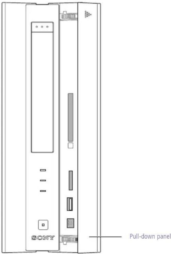
The following sections identify and describe each component that is visible from the exterior of the VAIO ^® Computer. Internal components are identified in Chapters 3, 4, and 5 of this manual.
Front View
text_image
SONY Pull-down panelSHA0001.VSD
Drives
text_image
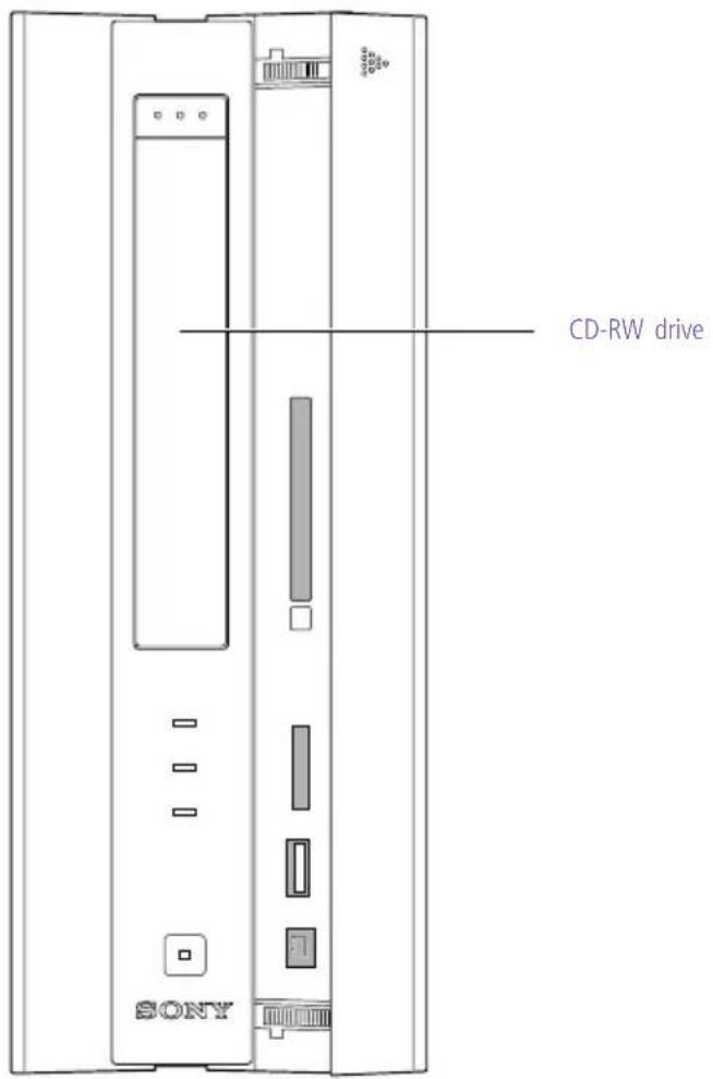
CD-RW drive SONYSHA0002.VSD
Drive Description
| CD-RW drive* | CD-ROM disc read: 32X (maximum performance).CD-R disc read: 32X (maximum performance).CD-R disc write: 8X (maximum performance).CD-RW disc read: 20X (maximum performance).CD-RW disc write: 4X (maximum performance). |
* The CD-RW/CD-R/CD-ROM data transfer standard 1X rate is 150 kbytes/s. Data on a CD-RW is read at a variable transfer rate, ranging from 8X at the innermost track to 20X at the outermost track. The average data transfer rate is 14X (2100 kbytes/s). Data on a CD-R/CD-ROM is read at a variable transfer rate, ranging from 13X at the innermost track to 32X at the outermost track. The average data transfer rate is 22.5X (3375 kbytes/s). Data on a CD-RW/CD-R is written at a constant transfer rate of 1X, 2X, 4X (max for CD-RW), or 8X, depending on the speed and media type you select.
Buttons and Switches
text_image
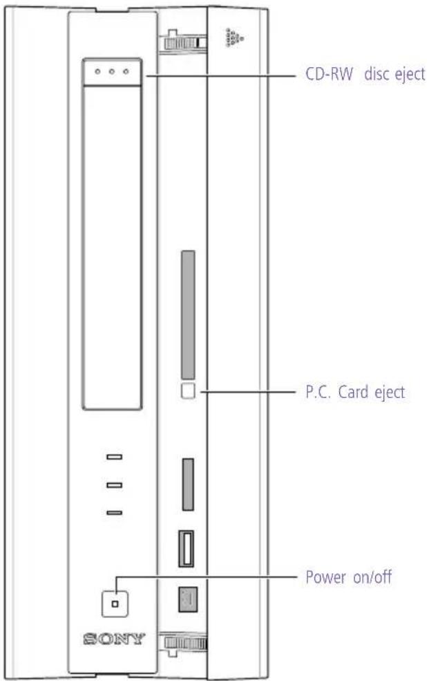
CD-RW disc eject P.C. Card eject Power on/off SONYSHA0003.VSD
Button or switch Description
Power/Standby switch Turns system power on and off.
CD-RW disc eject button Automatically opens the CD-RW tray.
P.C. Card eject button Ejects a PCMCIA card
Indicators
text_image
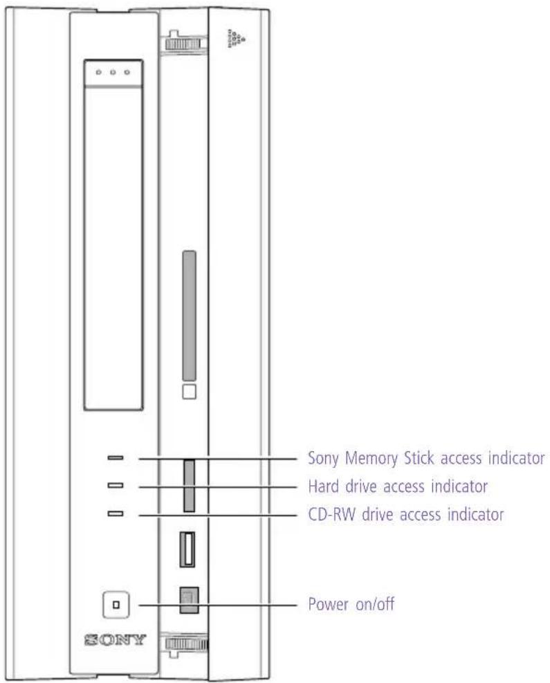
Sony Memory Stick access indicator Hard drive access indicator CD-RW drive access indicator Power on/off SONYSHA0004.VSD
Indicator Description
| Power/Standby indicator Standby (amber) indicates the computer is in standby mode. On (green) indicates the computer is out of standby mode, ready to use. Off (no color) indicates the computer is turned off. | |
| Sony Memory Stick access indicator | On (amber) indicates memory stick activity. |
| Hard disk drive access indicator | On (amber) indicates hard disk drive activity. |
| CD-RW drive access indicator | On (amber) indicates optical disc activity. |
Connectors
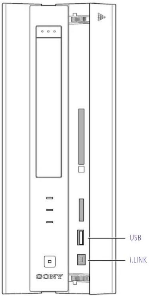
text_image
SONY USB i.LINKSHA0005.VSD
Connector Description
i.LINK ^® (IEEE1394) ^* Connects to digital devices that have a 4-pin i.LINK connector.
USB Connects to USB devices.
* To connect to a 6-pin i.LINK device, use the i.LINK connector on the back of the system. A 6-pin i.LINK connector can supply power from the computer to the device if the device also has a 6-pin i.LINK connector. A 4-pin i.LINK connector cannot supply power to the device.
Slots
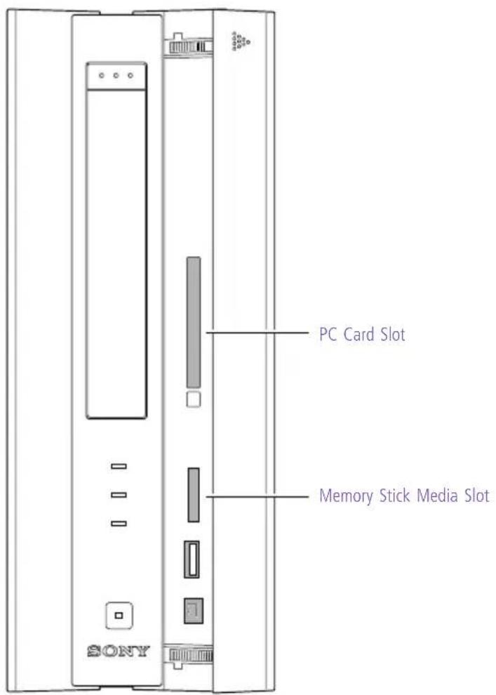
text_image
PC Card Slot Memory Stick Media Slot SONYSHA0006.VSD
Slot Description
PC Card Slot Accommodates one Type I or Type II PCMCIA card.
Memory Stick ^® Media Slot Accommodates Memory Stick media.
Rear View
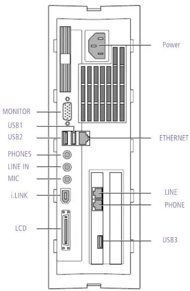
text_image
MONITOR USB1 USB2 PHONES LINE IN MIC i.LINK LCD Power ETHERNET LINE PHONE USB3SHA0007.VSD
Connector Description
Power AC input power.
ETHERNET Connects to RJ-45 Ethernet connector.
LINE Connects to phone cable from wall jack.
PHONE Connects to telephone.
USB3 Connects to USB devices.
MONITOR Connects to VGA monitor (optional).
USB1, USB2 Connects to USB devices.
PHONES Connects to headphones.
LINE IN Connects to output connector on audio device.
MIC Connects to microphone connector on audio device.
Connector Description
i.LINK (IEEE1394) ^*
Connects to digital device that has a 4-pin or 6-pin i.LINK connector.
LCD Connects to VAIO Slimtop
^TM LCD monitor.
* To connect to a 6-pin i.LINK device, use the i.LINK connector on the back of the system. A 6-pin i.LINK connector can supply power from the computer to the device if the device also has a 6-pin i.LINK connector. A 4-pin i.LINK connector cannot supply power to the device.
I/O Connectors
The following section identifies the various I/O connectors.
MONITOR
The MONITOR connector is a standard 15-pin female high-density VGA-type connector and is located on the rear panel.
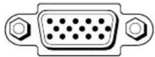
SHA0009.VSD
USB Connectors
A total of four USB connectors are available. Three USB connectors (USB1, USB2, and USB3) are accessible from the rear panel. USB1 and USB2 are located beneath the Ethernet connector, and USB3 is located on the Fax/Modem plug-in card.
The fourth USB connector (USB4) is located on the front panel between the i.LINK connector and the Sony Memory Stick slot.
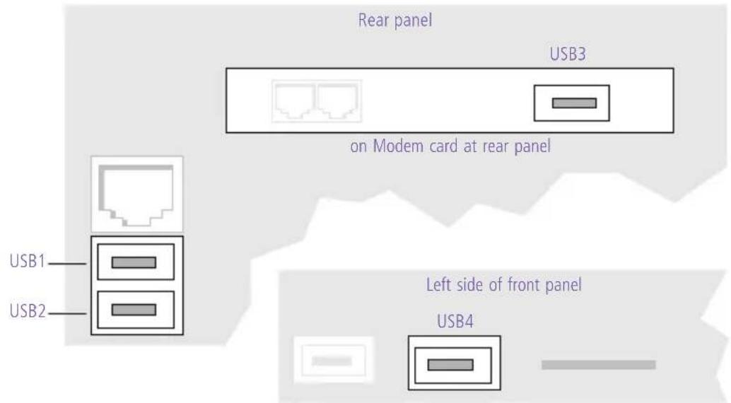
text_image
Rear panel USB3 on Modem card at rear panel USB1 USB2 Left side of front panel USB4KY0003.VSD
PHONE, LINE IN, and MIC
The PHONES, LINE IN, and MIC jacks are physically identical, but have different connections. They are standard 3.5 mm stereo mini-jacks and are located on the rear panel.
PHONES LINE IN MIC



KY0013.VSD
Connector Description
PHONES 1.0 Vrms output (typical) at 31 mW (32 ohm) output (max).
LINE IN 2.0 Vrms input (max), 50 Kohm impedance.
MIC Electret condenser microphone input.
i.LINK (IEEE1394)
The 6-pin i.LINK (IEEE1394) connector on the rear panel can supply power from the computer to a device if the device also has a 6-pin i.LINK connector. The connector supplies 10V to 12V. The total power supplied by the 6-pin i.LINK connector cannot exceed 6 watts.
6-pin i.LINK (IEEE1394)
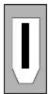
On rear panel
4-pin i.LINK (IEEE1394)

On front panel
KY0087.VSD
Ethernet
The Ethernet connector on the rear panel connects to a 10Base-T/100Base-TX Fast Ethernet network via an RJ-45 connector.
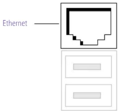
text_image
EthernetMAN009.VSD
LCD
The LCD connector is a 32-pin female MDR-type connector and is located on the rear panel.
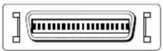
KY0004.VSD
Do not connect any LCD monitor other than the Sony VAIO Slimtop LCD monitor.
LINE and PHONE
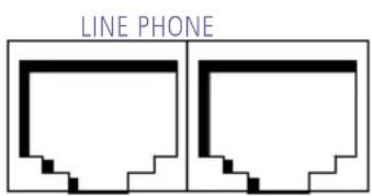
The LINE and PHONE jacks are physically identical and have identical connections. They are standard RJ-11 female phone jacks. However, the LINE jack is for connecting to a telephone line that comes from the wall jack, and the PHONE jack is for connecting the computer to a telephone. These jacks are located on the Modem plug-in card.
These connectors are located on the Modem plug-in card and are accessible from the rear panel.
text_image
LINE PHONEKY0014.VSD
Accidentally plugging a phone line from the wall into the modem's PHONE jack, and a telephone into the LINE jack, will not damage the modem card or telephone equipment. However, the modem will not work correctly.
Chapter 2 Configuring Your System
This chapter contains information on configuring your system. Configuring your system can consist of the following:
☐ Making changes to the CMOS settings
☐ Making changes to the display's power management settings
□ Changing the system board jumper position
Accessing the CMOS Setup Utility
You must access the CMOS Setup Utility to make changes to the CMOS settings (see "CMOS Setup Options" on page 63 for information on CMOS settings).
Before rebooting the system, save any open files and exit Windows®.
1 Reboot the system.
2 Press F2 when the Sony screen appears.
3 Use the left and right arrow keys to select an item from the main menu. Use the up and down arrow keys to select an item within the screen.
4 Press Enter to display a submenu of options for an item.
5 Use the up and down arrow keys to select an option within a submenu.
6 Press Enter to apply the new setting or Esc to cancel the submenu.
7 Press ESC to return to the main menu.
8 Select F10 when done, then follow the prompts, or choose an option from the Exit menu.
Changing the Display's Power Management Settings
A display that has power management capability is designed to operate on reduced power or shut itself off after the system has been idle for a specified period of time.
1 From the Start menu, point to Settings, then click Control Panel.
2 Click the Power Management icon.
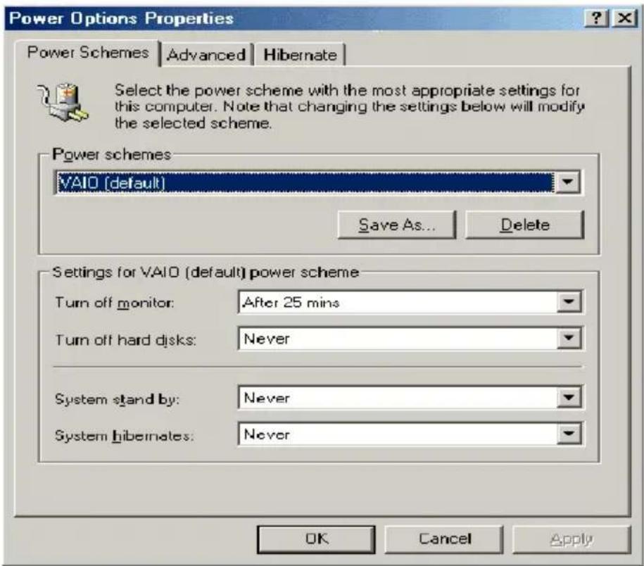
The Power Options Properties dialog box opens, with the Power Schemes tab displayed.
text_image
Power Options Properties Power Schemes | Advanced | Hibernate | Select the power scheme with the most appropriate settings for this computer. Note that changing the settings below will modify the selected scheme. Power schemes VAIO (default) Save As... Delete Settings for VAIO (default) power scheme Turn off monitor: After 25 mins Turn off hard disks: Never System stand by: Never System hibernates: Never OK Cancel Apply3 Select the power scheme that is most appropriate for the way you use your computer.
To change a power scheme, change the settings for Turn off monitor, and Turn off hard disks, System standby, and System Hibernate.
The Turn off monitor option allows you to specify the period of inactivity (in minutes) that you want to elapse before your monitor turns off when your computer is running on AC power. The display reactivates when you move the mouse or press a key.
The Turn off hard disks option allows you to specify the period of
inactivity (in minutes) that you want to elapse before your hard disks turn off when your computer is running on AC power.
The System standby option allows you to specify the period of inactivity (in minutes) that you want to elapse before your computer goes on standby when your computer is running on AC power. Power is reactivated when you click the left mouse button or press spacebar on the keyboard.
The System hibernate option allows you to specify the period of inactivity (in minutes) before your computer goes in the hibernate state. Power is reactivated when you push the power button.
4 To save a new power scheme, first modify the settings, click Save As, type a descriptive name, and then click OK.
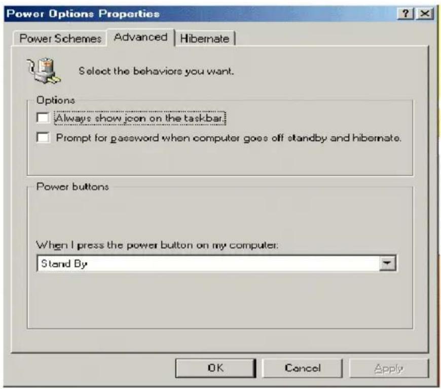
5 Click the Advanced tab.
text_image
Power Options Properties Power Schemes Advanced Hibernate Select the behaviors you want. Options □ Always show icon on the taskbar □ Prompt for password when computer goes off standby and hibernate. Power buttons When I press the power button on my computer: Stand By OK Cancel Apply6 Select the desired settings.
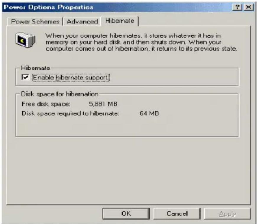
7 Click the Hibernate tab.
text_image
Power Options Properties Power Schemes | Advanced | Hibernate | When your computer hibernates, it stores whatever it has in memory on your hard disk and then shuts down. When your computer comes out of hibernation, it returns to its previous state. Hibernate ✓ Enable hibernate support: Disk space for hibernation Free disk space: 5,881 MB Disk space required to hibernate: 64 MB OK Cancel Apply8 Select the desired settings, and then click OK.
Configuring the System Board
The configuration should never need changing unless otherwise directed by a technical support or service technician.
Before opening the system, save any open files, exit Windows, turn off the power of the computer and all attached peripherals, and unplug the power cord.
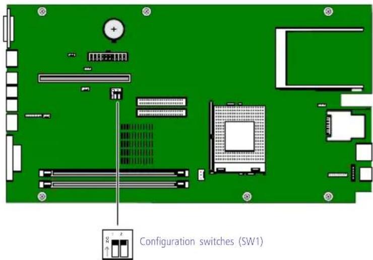
There are two configuration switches on the system board:
□ CMOS Clear switch
☐ Onboard VGA Interrupt (AGP_INT) switch
When the CMOS Clear switch is in the Normal position, it provides normal access to the BIOS Setup Utility.
The Central Processing Unit (CPU) input clock is forced to remain at 100 MHz (fast mode), and the Basic Input/Output System (BIOS) uses the User CMOS settings (as opposed to the System CMOS settings).
The CMOS and NVRAM settings are only cleared if the checksum test returns false. Access to specific setup fields is controlled by a supervisor password or user password.
When the CMOS Clear switch is in the Clear position, the password that is stored in CMOS is cleared. No other parameters are cleared.
If you install a VGA PCI add-in card, you can use the AGP_INT switch to enable or disable the onboard VGA controller.
To enable or disable the CMOS Clear or onboard VGA Interrupt, perform the following steps:
! Do not change any configuration switch unless directed by an authorized Sony technician.
1 Remove the system cover (see "Removing the System Cover" on page 22).
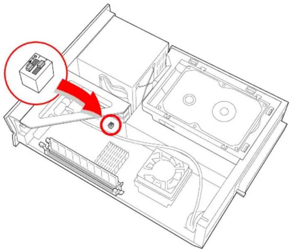
2 Set the switches according to the table show in the diagram (see also "Configuration Switches" on page 59).
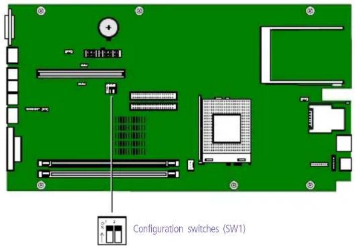
text_image
Configuration switches (SW1)| Switch # | Name | On | Off |
| 1 | CMOS | Clear password | Normal |
| 2 | AGP_INT | Enable | Disable |
KY0059.VSD
Chapter 3 Removing, Installing, and Replacing Components
This chapter describes removing, installing, and replacing major components for upgrading, reconfiguring, and troubleshooting the components.
Before opening the system unit, save any open files, exit Windows, turn off the power of the computer and all attached peripherals, and then unplug the power cord.
Removing the System Cover
You must remove the system cover to access the system board, add-in cards, power supply, battery, and internal drives.
From the rear of the unit, hold down the system cover while you pull out on the handle located at the rear panel.
2 Slide the system chassis out.
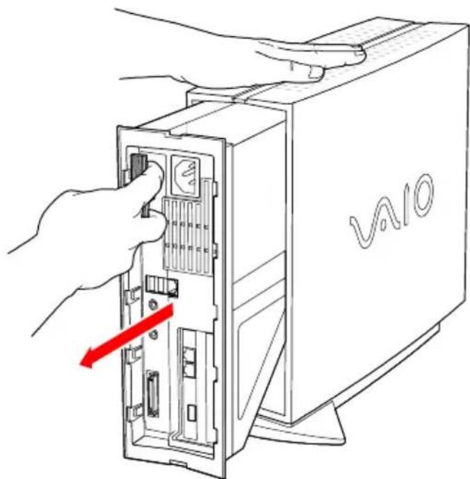
text_image
V40KY0064B.VSD
Replacing the System Cover
1 Insert the front of the chassis into the opening at the rear of the system cover, then slide the chassis in until it is flush with the front and rear.
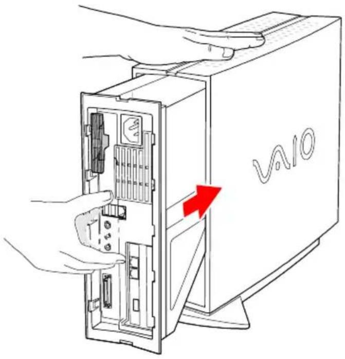
text_image
VASIOKY0077.VSD
Installing an Add-In Card
Before opening the system unit, save any open files, exit Windows, turn off the power of the computer and all attached peripherals, and then unplug the power cord.
1 Remove the system cover (see "Removing the System Cover" on page 22).
2 Remove the slot cover adjacent to the selected slot connector on the system board (see "Removing a Slot Cover" on page 40).
3 Insert the add-in card into the PCI slot connector. Use a gentle rocking motion, pressing down until the card is fully seated.
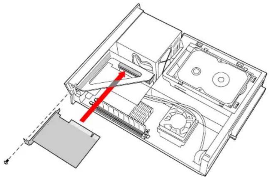
natural_image
Technical diagram of an open computer case with internal components and a red arrow indicating a specific component (no text or symbols present)KY0070.VSD
Align the card's bracket so that the bottom of the bracket fits into the slot at the bottom of the chassis. Assure that the top of the bracket fits snugly against the chassis lip after the card is fully inserted.
4 Attach any necessary cables to the card (see the instructions that came with the add-in card).
5 Replace the system cover (see "Replacing the System Cover" on page 23).
6 Turn on the computer and follow any instructions that came with the add-in card.
Removing an Add-in Card
Before opening the system unit, save any open files, exit Windows, turn off the power of the computer and all attached peripherals, and then unplug the power cord.
1 Remove the system cover (see "Removing the System Cover" on page 22).
2 Disconnect any cables attached to the add-in card.
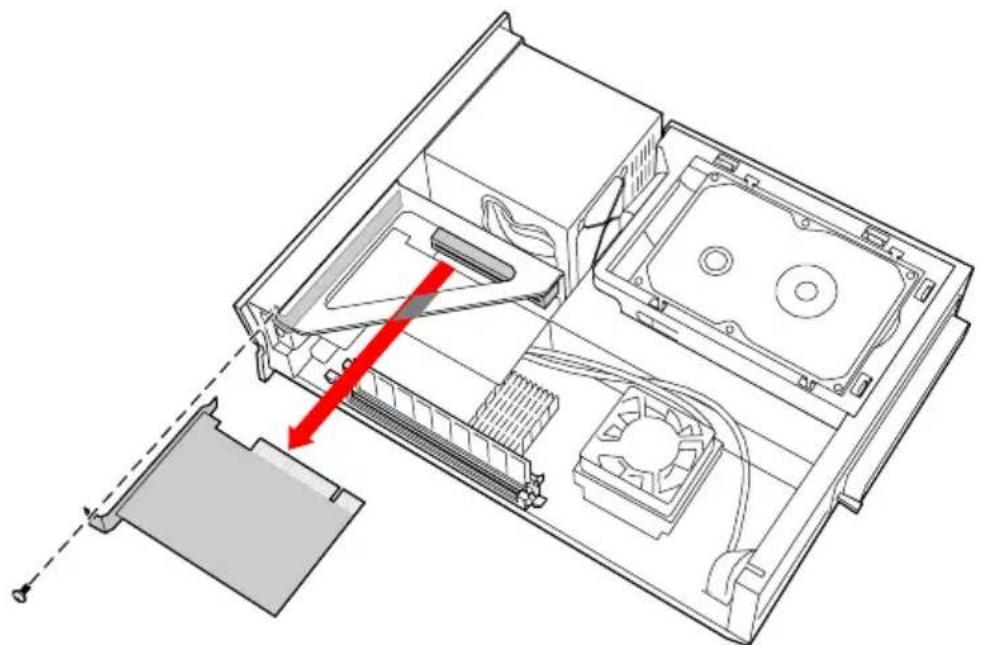
3 Remove the screw that secures the add-in card to the chassis.
4 Remove the add-in card from the PCI slot connector and store the card in an anti-static wrapper for future use.
natural_image
Technical diagram of an open computer case with internal components and a red arrow indicating a component (no text or symbols present)KY0071.VSD
Grasp the card with one hand on each end, and gently pull up as you rock the card from side to side.
Hold the add-in card by its edges and do not touch any components or connector contacts on the card. Static electricity in your body may damage sensitive components on the card. As a precaution, touch any exposed metal part on the metal chassis (preferably the metal part on the power supply) before handling an add-in card to discharge any static electricity in your body.
5 If you do not replace the card or install another add-in card, install a slot cover over the vacant slot at the rear of the chassis (see "Covering an Open I/O Slot" on page 41).
6 Replace the system cover (see "Replacing the System Cover" on page 23).
Setting the Configuration Switches
Before opening the system unit, save any open files, exit Windows, turn off the power of the computer and all attached peripherals, and then unplug the power cord.
1 Remove any add-in cards (see "Removing an Add-in Card" on page 25).
2 Set the switches as needed (see "Configuring the System Board" on page 18).
natural_image
Technical line drawing of an open computer case with internal components and a red arrow indicating a process (no text or symbols present)MAN008.VSD
3 Replace any add-in cards removed in step 1 (see "Installing an Add-In Card" on page 24).
Replacing the Lithium Battery
You may need to replace the lithium battery if your computer consistently loses the date or time settings after turning it off. The lithium battery has a typical life of three years, after which the battery may be too weak to power the CMOS memory.
! Sony recommends that you use an authorized service dealer to replace the lithium battery. However, if you wish to replace the battery yourself, read the following cautions, notes, and procedure.
When you remove the lithium battery, all values stored in the CMOS memory (BIOS setup values and Plug and Play values) may be lost. Although the computer can hold the charge for a short time while replacing the battery, it is safer to assume that the settings will be lost. When the values are lost, the BIOS values revert to their factory-default settings (see "Accessing the CMOS Setup Utility" on page 14).
Do not handle damaged or leaking batteries.
The lithium battery may explode if mistreated. Do not disassemble it or dispose of it in fire.
1 Reboot your computer by selecting Shut Down... from the Start menu, and then selecting Restart the computer.
2 If the error message "Error: Check date and time settings" appears during the reboot sequence, press F3, then press F2 during the reboot process to access the BIOS Setup Utility. Otherwise it is not necessary to replace the battery at this time, and you can skip all remaining steps.
3 Compare all the BIOS options to their default settings (see "CMOS Setup Options" on page 63). Make a list of all the BIOS options that are different from their default values. You will refer to this list when you restore the BIOS settings later.
4 Press ESC, then select Exit from the main menu using the right arrow key. The Exit Discarding Changes is automatically selected (it is the first item in the list).
5 Press Enter, type N when prompted to save, then press Enter to exit the BIOS Setup Utility.
6 Turn off the computer and unplug the power cord.
7 Remove the system cover (see "Removing the System Cover" on page 22).
8 Remove the power supply (see "Removing the Power Supply" on page 31).
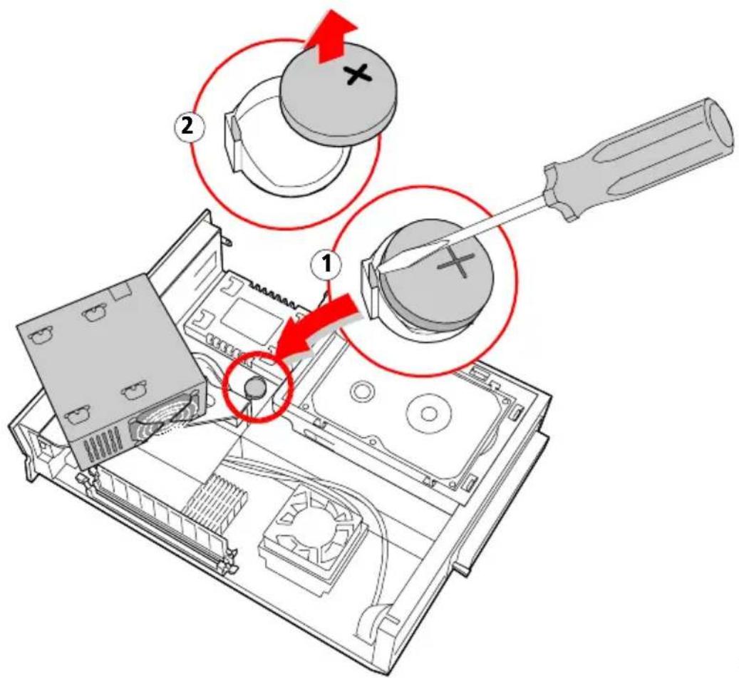
9 Use a screwdriver or similar tool to push the battery-eject lever against the battery holder (see 1 diagram). One side of the battery pops up.
text_image
Diagram showing a computer setup with labeled components and red arrows indicating action steps, including a screwdriver and a close-up of the main device.KY0072.VSD
10 Remove the battery (see 2 in diagram) and dispose according to the instructions that came with the new battery.
11 Insert the new battery into the battery holder, with the plus (+) side up, and press down until the battery snaps into position.
The Sony CR2032 battery is recommended. Using a type of battery other than a CR2032 may present a risk of fire or explosion.
12 Replace the power supply (see "Replacing the Power Supply" on page 32).
13 Replace the system cover (see "Replacing the System Cover" on page 23).
14 Reconnect the power cord and turn on the computer.
15 If the error message "Error: Check date and time settings." appears during the reboot sequence, press DEL to access the CMOS Setup Utility. If no error message displays, the computer's CMOS settings were retained during the battery replacement and you can skip the remaining steps.
16 Refer to the list you made in step 3 and restore any non-default CMOS settings (see "CMOS Setup Options" on page 63).
17 Press F10, then follow the onscreen prompt to save and exit. The computer's CMOS settings are now restored.
Removing the Power Supply
You must remove the power supply to replace the CMOS battery.
Before opening the system unit, save any open files, exit Windows, turn off the power of the computer and all attached peripherals, and then unplug the power cord.
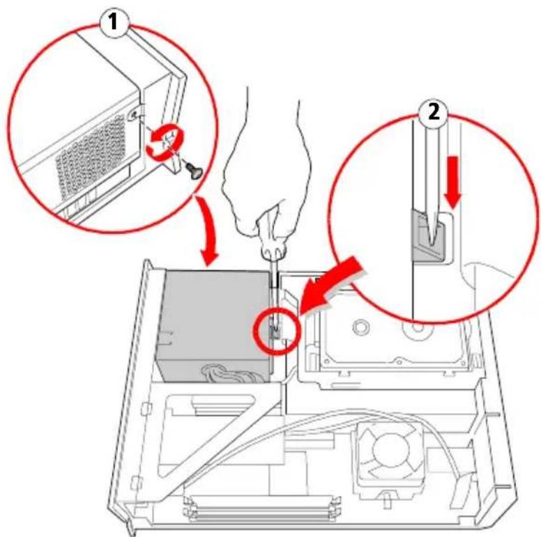
1 Remove the screw that secures the power supply to the chassis (see 1 in diagram).
text_image
Diagram showing two steps of installing a computer tower panel, with red arrows indicating the process and magnified views highlighting key components.MER001.VSD
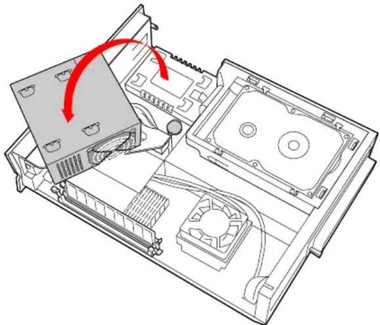
2 Press down on the plastic lever at the bottom of the power supply (see 2 in diagram) to release the power supply.
3 Lift the power supply up and out, and rest it upside down on top of the PCI card holder.
natural_image
Technical diagram of an open computer chassis showing CPU socket, heatsink, and fan assembly (no text or labels)MER002.VSD
Replacing the Power Supply
1 Lower the power supply down into position and press down until the power supply latches to the chassis.
2 Replace the screw that secures the power supply to the chassis.
Installing System Memory
Before opening the system unit, save any open files, exit Windows, turn off the power of the computer and all attached peripherals, and then unplug the power cord.
1 If necessary, remove the memory module you wish to replace (see "Removing a Memory Module" on page 35).
2 Remove the new memory module(s) from its anti-static package. Hold the memory module only by its edges to prevent static-electricity damage.
3 Choose the size of the memory module and configuration as shown in the following table. Memory modules can vary in size and speed between sockets. The minimum memory size is 8 MB. The maximum memory size is 512 MB. The BIOS automatically detects the type, size, and speed of the memory modules.
Memory module configurations (MB)
DIMM1 DIMM2
0, 8, 16, 32, 64, 128, 256 0, 8, 16, 32, 64, 128, 256
! Touch any exposed metal part of the chassis to discharge static electricity in your body before handling a memory module.
Use only 133 MHz memory. Supports SDRAM memory. Does not support EDO memory or buffered DIMM memory.
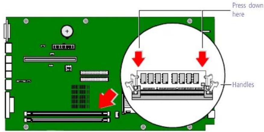
4 Align the module over the appropriate socket, noting the location of pin 1 on the module and pin 1 on the socket.
text_image
Press down here Handles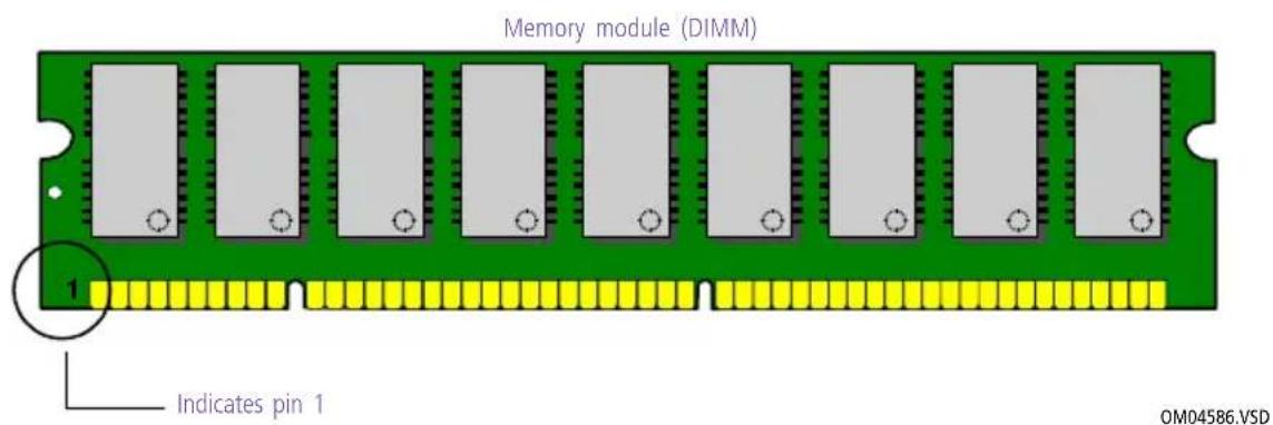
text_image
Memory module (DIMM) 1 Indicates pin 1 OM04586.VSD5 Carefully but firmly insert the edge of the module into the socket.
6 Press down firmly and evenly at both corners until the module is fully seated.
When the module is fully seated, the handles on each side are straight up and locked into the slot on each side of the module. If the handles are not totally straight upright, continue to press down on each side of the module until the handles lock into place.
7 Replace the system cover (see "Replacing the System Cover" on page 23).
Your computer automatically recognizes the extra memory and configures itself accordingly when you turn it on. No further action is required.
Removing a Memory Module
You may need to remove a memory module if you change the memory configuration or replace a bad module.
Before opening the system unit, save any open files, exit Windows, turn off the power of the computer and all attached peripherals, and then unplug the power cord.
1 Remove the system cover (see "Removing the System Cover" on page 22).
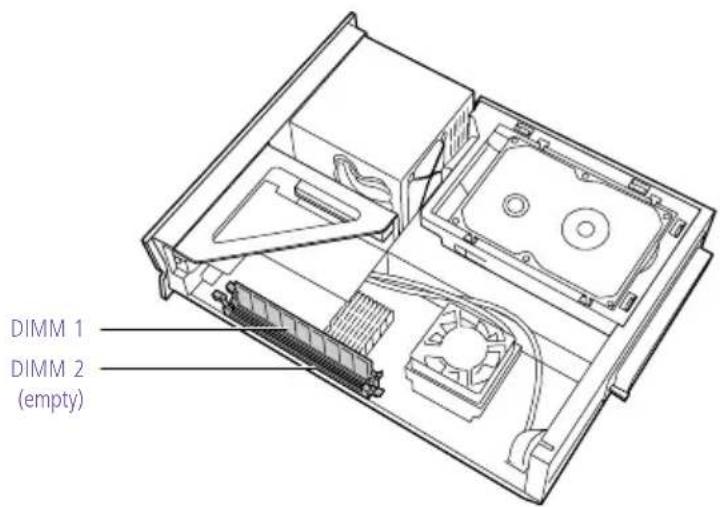
2 Locate the memory module you wish to remove.
text_image
DIMM 1 DIMM 2 (empty)KY0073.VSD
If the memory module you wish to remove is DIMM #2, skip steps 3 to 5. Otherwise, continue.
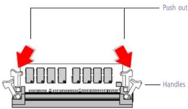
3 Push out the handle on each side of the memory module to eject the module from its socket.
text_image
Push out HandlesKY0042.VSD
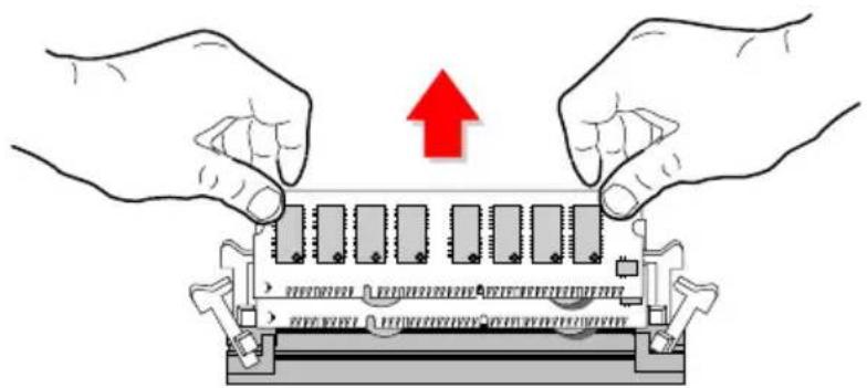
4 Lift the memory module out by grasping it by its edges. Store the module in a static-free bag.
natural_image
Illustration of hands assembling a memory module with a red upward arrow indicating process (no text or symbols)KY
! Touch any exposed metal part of the chassis to discharge static electricity in your body before handling the memory module.
If the memory module you removed is DIMM #2, stop. Otherwise, continue.
5 Replace the system cover (see "Replacing the System Cover" on page 23).
Replacing the Hard Drive
Before opening the system unit, save any open files, exit Windows, turn off the power of the computer and all attached peripherals, and then unplug the power cord.
Be sure to back up any files on your hard drive that you want to preserve before you replace the drive.
1 Remove the system cover (see "Removing the System Cover" on page 22).
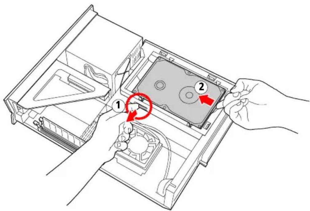
2 While pulling out on the tab (see 1 in diagram), push the hard drive towards the left inside the blue plastic drive carrier to release the drive.
text_image
Diagram showing a hand inserting a CD into an open case, with numbered annotations indicating component placement.MER003.VSD
3 Lift up on the left side of the drive and gently wiggle the drive up and out.
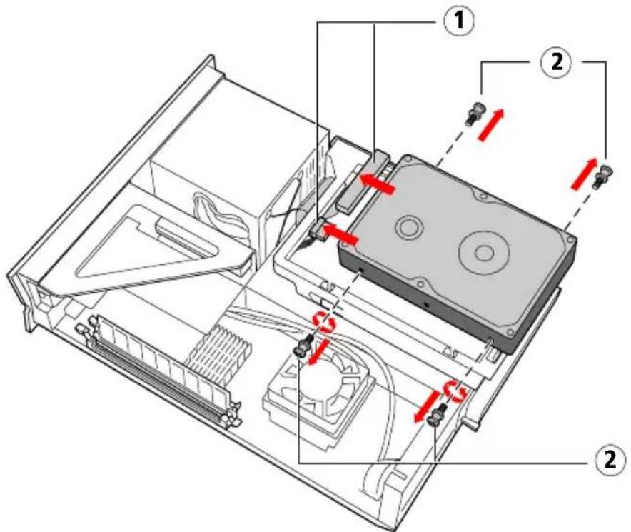
4 Unplug the ribbon cable and power supply cable (see 1 in diagram) from the hard drive.
text_image
Technical diagram of an internal hard disk drive with numbered components and red directional arrows indicating motion or movement.MER005.VSD
5 Remove the four pins (see 2 in diagram) from the hard drive.
6 Insert the four pins in the new hard drive in the same position as they were in the old hard drive.
7 Set the jumpers on the new hard drive to be the Primary Master IDE drive (refer to the instructions that came with your new hard drive).
8 Rest the hard drive upside down on a flat surface, with the connectors facing left.
9 Reconnect the ribbon cable and power supply cable to the new hard drive.
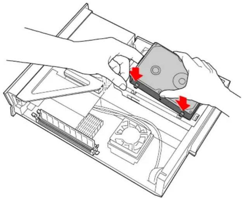
10 Align all four pins on the hard drive with the four slots in the drive carrier and gently press down until the drive is firmly into position.
natural_image
Technical line drawing of hands operating a computer drive with red arrows indicating ports (no text or symbols present)MER006.VSD
11 Replace the system cover (see "Replacing the System Cover" on page 23).
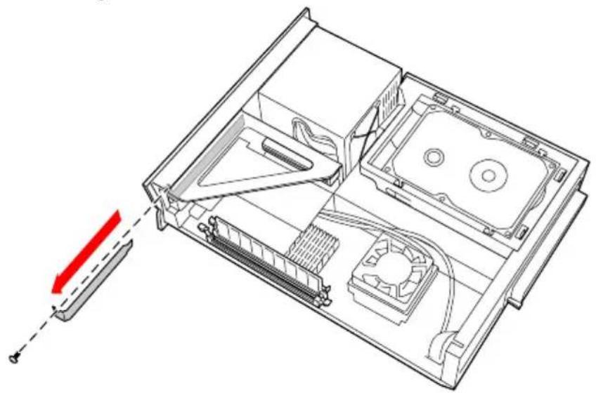
Removing a Slot Cover
You remove a slot cover when you install an add-in card that occupies a previously-empty slot.
1 Lay the system on its side with the open side facing up and the slot covers facing you.
2 Locate the slot of the cover you want to remove.
3 Remove the screw from the slot cover.
4 Carefully remove the loose slot cover and retain it for future use.
natural_image
Technical diagram of an open computer case with internal components and a red directional arrow indicating motion (no text or symbols)KY0069.VSD
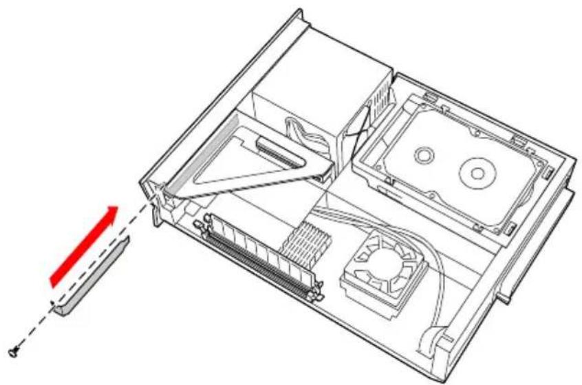
Covering an Open I/O Slot
Slot covers prevent air from escaping through the empty hole. If air escapes, the components inside the computer cannot be properly cooled. This may damage some components, especially the main processor (which generates the most heat).
1 Fit the bottom end of the slot cover (removed earlier) between the chassis and system board.
natural_image
Technical line drawing of an open hard disk drive with internal components and a red directional arrow indicating motion (no text or symbols)KY0076.VSD
2 Push the slot cover in until it rests firmly on the lip in the chassis. All add-in card brackets and slot covers rest on this lip.
3 Replace the screw (removed earlier) to secure the I/O slot cover.
Chapter 4 System Board
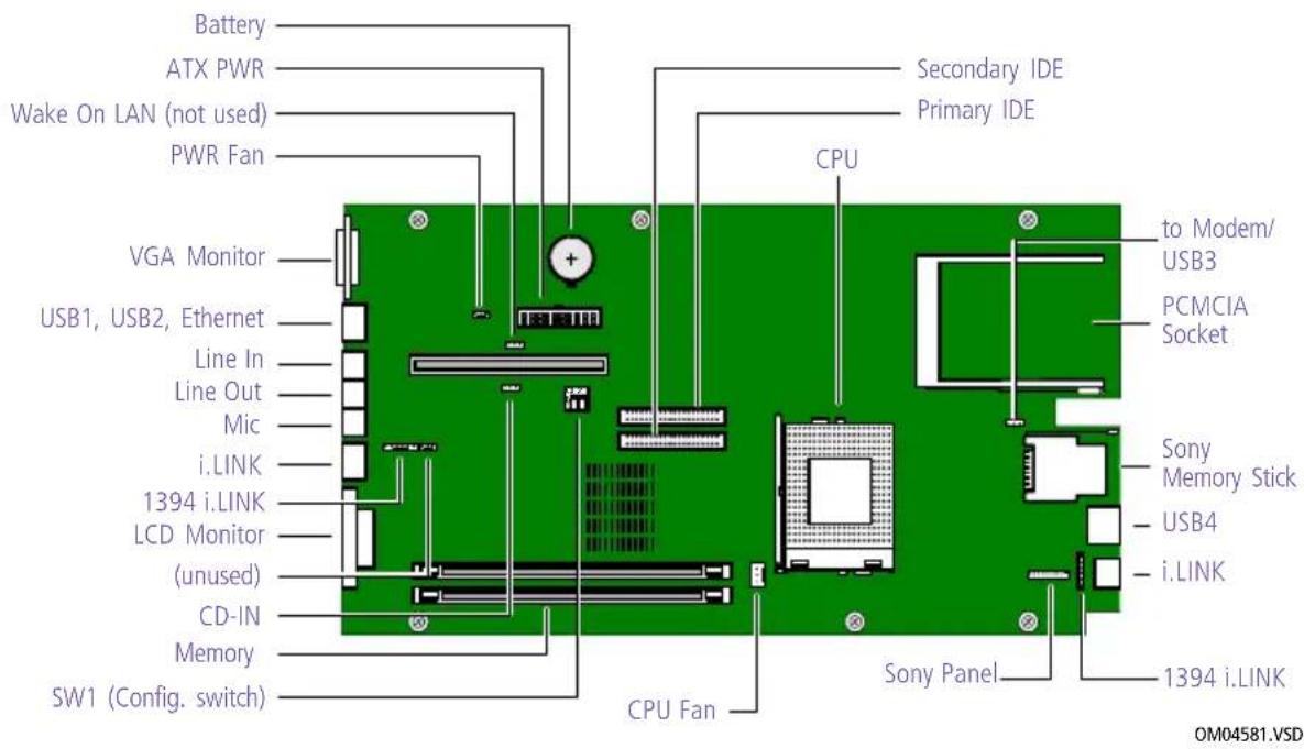
This chapter identifies each component on the system board and provides a detailed description of each connector and jumper on the system board.
text_image
Battery ATX PWR Wake On LAN (not used) PWR Fan VGA Monitor USB1, USB2, Ethernet Line In Line Out Mic i.LINK 1394 i.LINK LCD Monitor (unused) CD-IN Memory SW1 (Config. switch) CPU Fan Secondary IDE Primary IDE CPU to Modem/ USB3 PCMCIA Socket Sony Memory Stick USB4 i.LINK Sony Panel 1394 i.LINK OM04581.VSDConnectors
Front Panel Header
The front panel header is a 10-pin header that provides connections to various front panel functions.
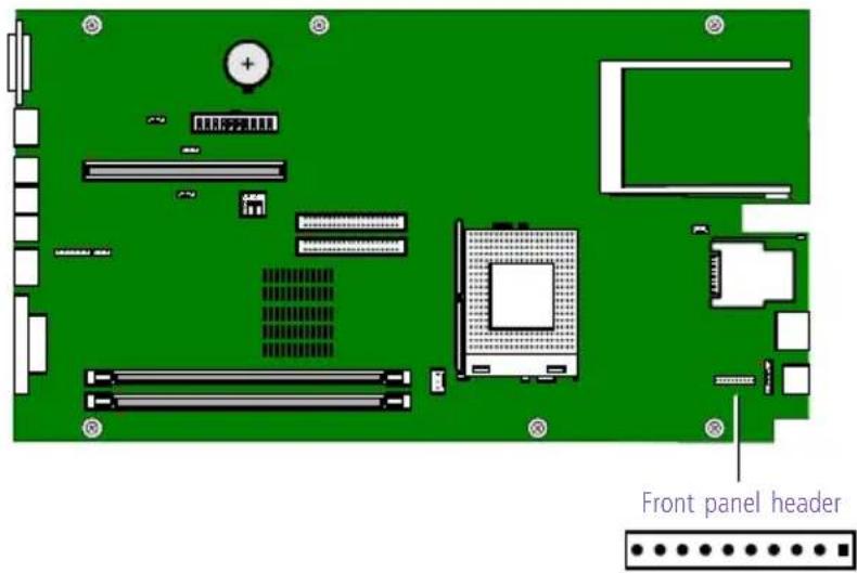
text_image
Front panel headerKY0031.VSD
Pin # Name Description
1 +5 +5V from power supply.
2 LED (CD-RW) Connects to LED on CD-RW.
3 LED (FDD) Connects to LED on floppy disk drive.
4 LED (HDD) Connects to LED on IDE hard disk drive.
5 LED (MODEM) Connects to LED on modem card.
6 Reserved Not used.
7 LED3 Connects to Standby/Sleep (red) signal from power supply.
8 LED4 Connects to Power (green) anode signal from power supply.
9 POWER SW Connects to power switch.
10 GND Connects to signal ground.
IDE Connectors
There are two IDE (Integrated Drive Electronics) connectors: a Primary IDE and a Secondary IDE connector.
The Primary IDE connector is a 40-pin 2.54 mm pitch header-type connector for the 3.5-inch hard disk drive.
The Secondary IDE connector is a 40-pin 2.54 mm pitch header-type connector for the 5.25-inch CD-RW drive.
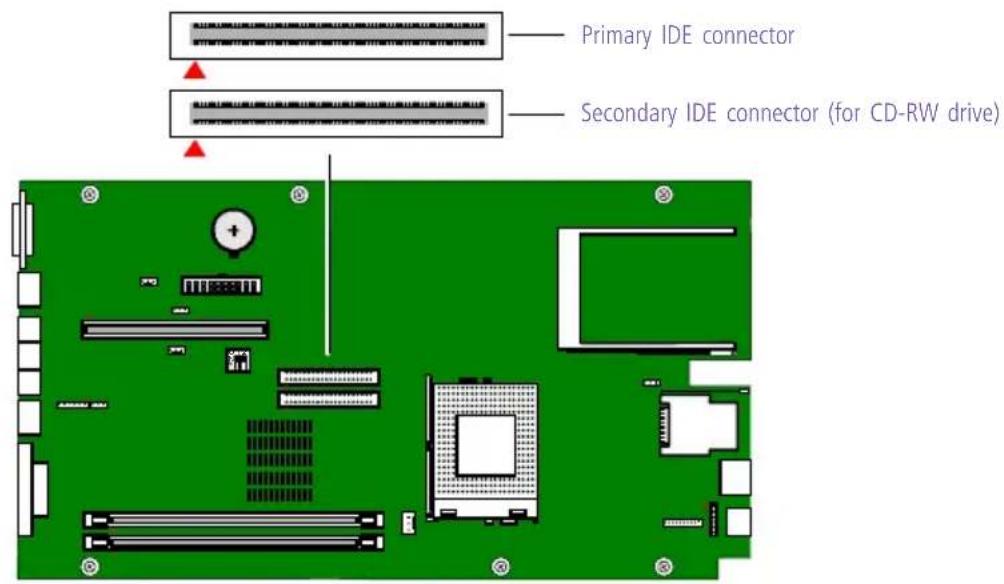
text_image
Primary IDE connector Secondary IDE connector (for CD-RW drive)OM04701G.VSD
PCI Slot Connectors
The system board contains one PCI Riser slot connector for a PCI riser card. The PCI riser card in turn provides two PCI slot connectors for PCI add-in cards. One PCI slot connector is occupied by the fax/modem card (slot #2), which also contains a USB connector.
The PCI slots in the riser card support 32-bit 5V and Universal (3.3/5V) PCI add-in cards.
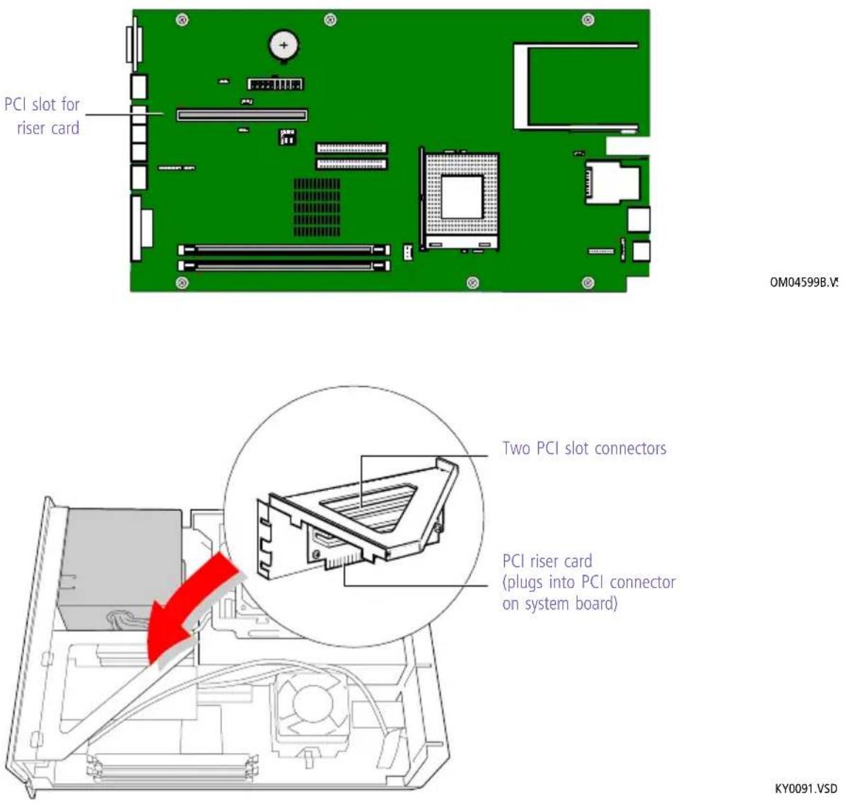
OM04599B.V.
Two PCI slot connectors
PCI riser card
(plugs into PCI connector on system board)
KY0091.VSD
Memory Module (DIMM) Connectors
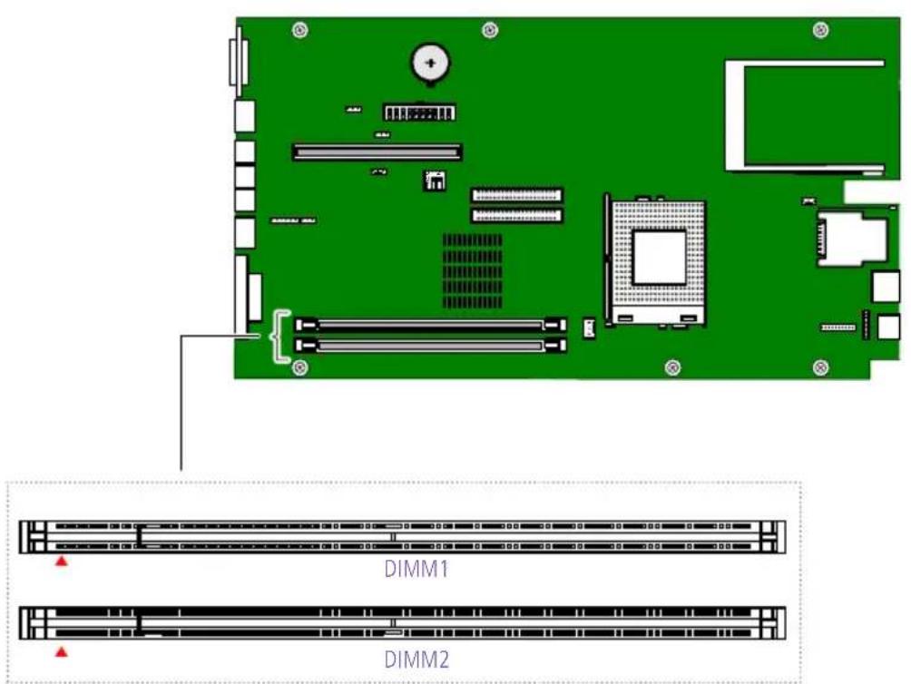
text_image
DIMM1 DIMM2OM04710A.VSD
Both sides of each Dual Inline Memory Module (DIMM) look very similar. The side with pin 1 has a small "1" to the left of pin 1. Be sure to orient a DIMM correctly in the DIMM connector (a small triangle on the connector indicates pin 1).
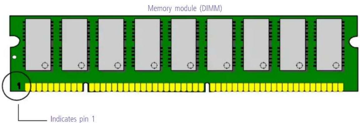
text_image
Memory module (DIMM) 1 Indicates pin 1OM04908B.VSD
Power (ATX PWR) Connector
The ATX PWR connector is a 20-pin Molex-type header connector that provides power to the system board.
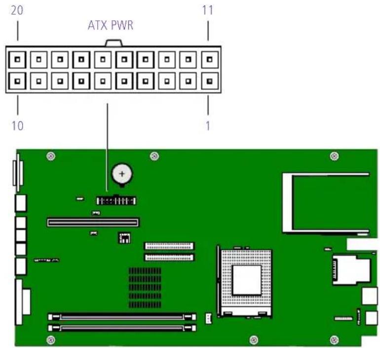
text_image
20 ATX PWR 11 10 1OM04701I.VSD
Power connector
| P | i | n | # | N | a | m | e | P | i | n | # | N | a | m | e |
| 1 +3.3V | 11 | +3.3V | |||||||||||||
| 2 +3.3V | 12 | -12V | |||||||||||||
| 3 | G | N | D | 1 | 3 | G | N | D | |||||||
| 4 +5V | 14 | PS-ON# (power supply | remote on/off control) | ||||||||||||
| 5 | G | N | D | 1 | 5 | G | N | D | |||||||
| 6 | + | 5 | V | 1 | 6 | G | N | D | |||||||
| 7 | G | N | D | 1 | 7 | G | N | D | |||||||
| 8 PWRGD (power good) | 18 NC | ||||||||||||||
| 9 | + | 5 | V | S | B | 1 | 9 | ||||||||
| 10 +12V | 20 +5V | ||||||||||||||
Fan (CPU FAN, PWR FAN) Connectors
The CPU Fan connector is a 1 x 3-pin straight header connector that controls the CPU cooling fan.
The PWR FAN connector is a 2 x 3-pin connector that controls the power supply cooling fan. It connects to P3 from the power supply.
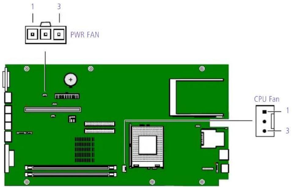
text_image
1 3 PWR FAN CPU Fan 1 3KY0034.VSD
CPU Fan connector
Pin Signal Name
1 GND
2 FAN_CTRL (+12V)
3 F A N _ S E N
PWR FAN connector
Pin Signal Name
1 G r o u n d
2 F *a n C
3 3 . 3 V s e n s e
USB Connectors
There are three USB ports (USB1 and USB2) on the system board that permit connection of USB peripheral devices directly to the system without having to use an external hub. If more USB devices are needed, connect an external hub to either USB port.
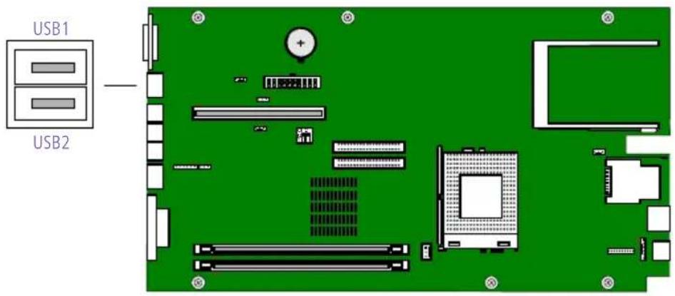
text_image
USB1 USB2KY0033.VSD
There is a USB port (USB3) on the Fax/Modem card (accessible from the rear panel), and a USB port (USB4) on the front panel. These connectors are identical to USB1 and USB2.
USB Connectors*
| Pin Signal Name | ||||||
| 1 | P | o | w | e | r | |
| 2 | U | S | B | P | n | # |
| 3 | U | S | B | P | n | |
| 4 | GND | |||||
* The n denotes the USB number (1, 2, 3, or 4).
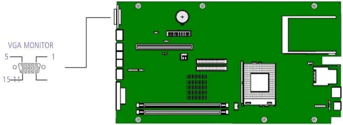
VGA MONITOR Connector
The VGA MONITOR connector is a 15-pin D-sub female connector.
text_image
VGA MONITOR 5 1 15-11OM04701D.VSI
VGA MONITOR connector
Pin Signal Name
| 1 | RED | |||||||
| 2 | G | R | E | E | N | |||
| 3 | BLUE | |||||||
| 4 | GND | |||||||
| 5 | DDC GND | |||||||
| 6 | R | E | D | G | N | D | ||
| 7 | G | R | E | E | N | G | N | D |
| 8 | BLUE GND | |||||||
| 9 | NC | |||||||
| 10 | GND | |||||||
| 11 | GND | |||||||
| 12 | SDA | |||||||
| 13 | HORIZONTAL SYNC | |||||||
| 14 | VERTICAL SYNC | |||||||
| 15 | SCL |
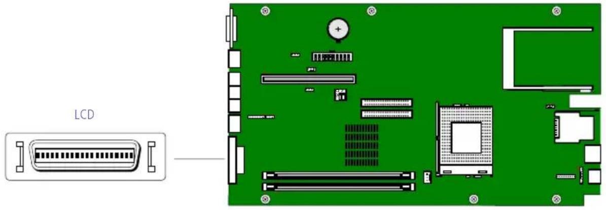
LCD Connector
The LCD connector is a 32-pin MDR-type connector for the Sony VAIO Slimtop LCD monitor.
text_image
LCDKY0094.VSD
Do not connect any LCD other than the Sony VAIO Slimtop LCD monitor that came with the PCV-LX700/PCV-LX800. The Sony VAIO Slimtop LCD monitor that came with earlier PCV-L models is not compatible with the PCV-LX700/PCV-LX800 system.
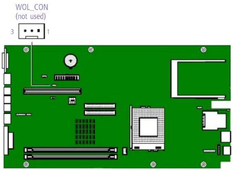
Wake On LAN (WOL\_CON) Connector
The WOL_CON connector is a 3-pin header connector that provides the Wake On LAN function (not used).
text_image
WOL_CON (not used) 3 1KY0096.VSD
Wake On LAN connector
| Pin Signal | |||||||||
| 1 | + | 5 | V | S | B | ||||
| 2 | GND | ||||||||
| 3 | W | O | L | s | i | g | n | a | l |
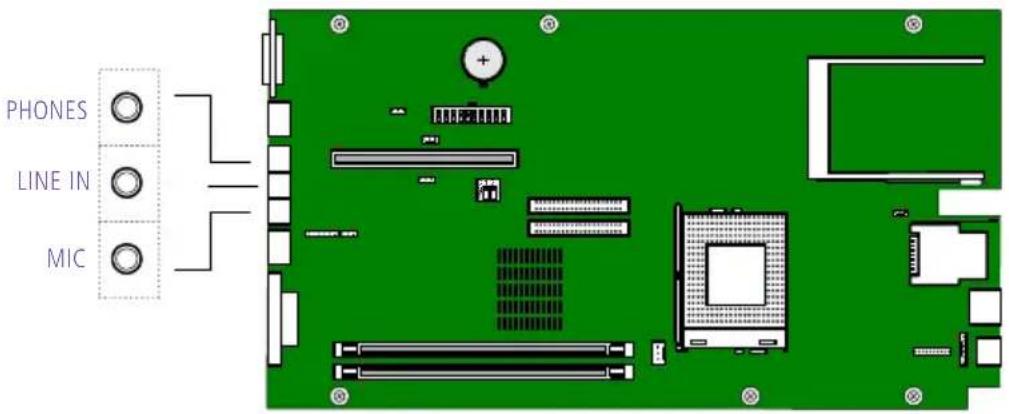
PHONES, LINE IN, and MIC Connectors
The PHONES jack is a stereo mini-jack (3.5 mm) that connects to headphones. The MIC jack is a stereo mini-jack (3.5 mm) that connects to a microphone. The LINE IN jack is a stereo mini-jack (3.5 mm) that connect to a stereo audio device (not an audio source from a video device). Connect a stereo audio output jack to the LINE IN jack.
text_image
PHONES LINE IN MICKY0058.VSD
LINE IN jack
Pin Signal
Sleeve GND
Tip Audio-Left In
Ring Audio-Right In
PHONES jack
Pin Signal
Sleeve GND
Tip Left out
Ring Right out
MIC jack
Pin Signal
Sleeve GND
Tip Microphone mono in
Ring Electret bias voltage
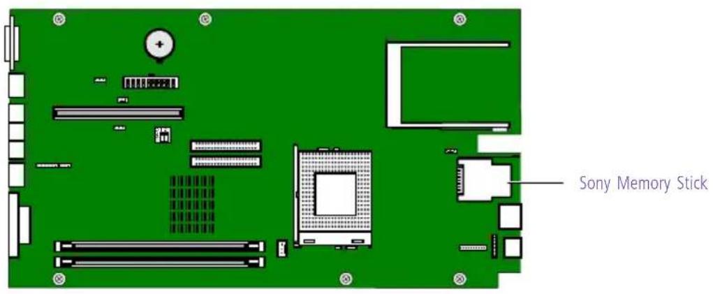
Sony Memory Stick Slot Connector
The Sony Memory Stick slot connector is a 10-pin MCR 103-10S connector.
text_image
Sony Memory StickKY0097.VSD
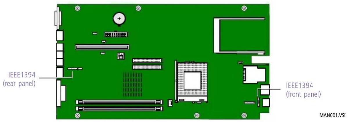
i.LINK Interface Header Connectors
The system board has two i.LINK (IEEE1394) interface header connectors. A cable connects each 6-pin header connector to the front panel.
text_image
IEEE1394 (rear panel) IEEE1394 (front panel) MAN001.VSIIEEE1394 interface header connector (rear panel)
Pin Signal Name
| 1 | G | r | o | u | n | d |
| 2 | T | A | 1 | + | ||
| 3 | T | A | 1 | - | ||
| 4 | T | B | 1 | + | ||
| 5 | T | B | 1 | - | ||
| 6 | G | r | o | u | n | d |
IEEE1394 interface header connector (front panel)
Pin Signal Name
| 1 | G | r | o | u | n | d |
| 2 | T | P | A | 2 | + | |
| 3 | T | P | A | 2 | - | |
| 4 | T | P | B | 2 | + | |
| 5 | T | P | B | 2 | - | |
| 6 | G | r | o | u | n | d |
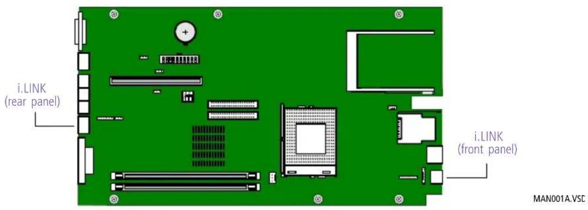
i.LINK Connectors
The system board has two i.LINK (IEEE1394) connectors: a 4-pin connector is accessible from the front panel, and a 6-pin connector is accessible from the rear panel.
Use the front-panel connector to connect to devices that use a 4-pin i.LINK (IEEE1394) connector. Use the rear-panel connector to connect to devices that use a 6-pin ^* i.LINK (IEEE1394) connector.
text_image
i.LINK (rear panel) i.LINK (front panel) MAN001A.VSDCD-In Connector
The system board has a CD-In connector that connects to the CD-RW drive.

text_image
CD-In 1 4MAN011.VSI
CD-In connector
| Pin Signal Name | ||||||||||
| 1 | L | e | f | t | C | D | - | I | n | |
| 2 | G | r | o | u | n | d | ||||
| 3 | G | r | o | u | n | d | ||||
| 4 | R | i | g | h | t | C | D | - | I | n |
Configuration Switches
A two-switch dual-inline package (DIP) provides configuration settings for clearing the CMOS password and enabling or disabling the onboard VGA interrupt (VGA_INT).
The computer ships with the CMOS switch (#1) set to OFF (Normal) and the VGA_INT switch (#2) set to OFF (Disable).
Do not change the position of any switch unless directed by a Sony-authorized technical support person.
text_image
Configuration switches (SW1)| Switch # | Name | On | Off |
| CMOS | Clear password1 | Normal | |
| 2 Enable | AGP_INT | Disable |
KY0059.VSD
Chapter 5 Fax/Modem Card
This card combines a Lucent 1648/V.90-compatible data fax/modem and a USB connector, and occupies PCI slot #2 in the Riser card.
The fax/modem uses two RJ-11 jacks: one to connect a telephone line, and one to connect a phone. A USB connector (USB3) is also located on this card.
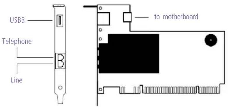
text_image
USB3 Telephone Line to motherboardKY0038.VSD
Name Connector Type Description
TELEPHONE RJ-11 Connects to phone.
LINE RJ-11 Connects to telephone line.
USB3 USB Connects to USB devices.
Chapter 6 CMOS Setup Options
This chapter describes each screen in the Award BIOS Setup Utility (see "Accessing the CMOS Setup Utility" on page 14).
The Award BIOS setup has five menu items on the menu bar. These are:
□ Main
□ Advanced
Power
□ Boot
□ Exit
Options that you can change are enclosed in brackets. Text that is not enclosed in brackets cannot be changed.
A small triangle ( ) indicates that there is a sub-menu with additional information and options. Press Enter to display the sub-menu. The information and options in a sub-menu are context-sensitive (they appear or disappear, depending on which options you select).
The item shown in [brackets] in this guide is the default option. The option shown in [brackets] on the screen is the option currently set for your system.
The other available options for each item are shown without brackets directly below the default option in this guide. The available options are listed in the order they occur when you press the + key.
Use the left and right arrow keys to choose a menu item. Use the up and down arrow keys to select an option. Press Enter to display a list of options, or press the + or - key to cycle through the other options.
If you display the list of options, use the up and down arrow keys to select an option in the list, then press Enter to apply the selection.
Press Esc to go back to the main menu.
Press F10 to save the changes and exit, or press Esc to discard the changes.
Follow the on-screen prompts for other choices. The bottom of the screen presents a summary of the keys to use for navigation and control.
Main Screen
System Time [00:00:00]
System Date [01/01/2000]
Legacy Diskette A [None]
360K, 5.25 in.
1.2M, 5.25 in.
720K, 3.5 in.
1.44M, 3.5 in.
2.88M, 3.5 in.
Primary Master (see "IDE Sub-Menus" on page 66)
Primary Slave (see "IDE Sub-Menus" on page 66)
Secondary Master (see "IDE Sub-Menus" on page 66)
Secondary Slave (see "IDE Sub-Menus" on page 66)
▶ Keyboard Features (see xref to keyboard features)
Language [English]
Supervisor Password [Disabled]
User Password [Disabled]
Halt On [All but Keyboard]
All but Disk
All but Disk/Keyboard
All Errors
No Error
Installed Memory 128 MB (depends on model)
▶IDE Sub-Menus
| Type [Auto] | |
| User Type HDD | |
| CD-ROM | |
| LS-120 | |
| ZIP-100 | |
| MO | |
| Other ATAPI Device | |
| None | |
| Cylinders* | [1024] |
| Heads† | [255] |
| Sectors† | [63] |
| CHS Capacity* | 8422MB |
| Maximum LBA Capacity* | 40020MB (actual size depends on model) |
| Multi-Sector Transfers* | [Maximum] |
| Disabled | |
| 2 Sectors | |
| 4 Sectors | |
| 8 Sectors | |
| 16 Sectors | |
| 32 Sectors | |
| SMART Monitoring* | [Disabled] |
| Enabled | |
| PIO Mode‡ | [4] |
| 0 | |
| 1 | |
| 2 | |
| 3 | |
| ULTRA DMA Mode† | [4] |
| Disabled | |
| 0 | |
| 1 | |
| 2 | |
| 3 | |
| Set Device As** | [Auto] |
| Floppy | |
| Hard Disk | |
▶ Keyboard Features Sub-Menu
Boot Up NumLock Status [On]
Off
Keyboard Auto-Repeat Rate [12/Sec]
15/Sec
20/Sec
24/Sec
30/Sec
6/Sec
8/Sec
10/Sec
Keyboard Auto-Repeat Delay [1/4 Sec]
1/2 Sec
3/4 Sec
1 Sec
Advanced Screen
Current CPU Internal Frequency 733 MHz (depends on model)
CPU Frequency Mutiple [5.5x]
FSB/SDRAM Freq. (MHz) [133/133]
CPU Level 1 Cache [Enabled]
Disabled
CPU Level 2 Cache [Enabled]
Disabled
CPU Level 2 Cache ECC Check [Disabled]
Enabled
Processor Serial Number [Disabled]
Enabled
BIOS Update [Enabled]
Disabled
PS/2 Mouse Function Control [Auto]
Enabled
USB Legacy Support [Auto]
Disabled
Enabled
OS/2 Onboard Memory > 64M [Disabled]
Enabled
▶ Chip Configuration (see "Chip Configuration Sub-Menu" on page 69)
▶ I/O Device Configuration (see "I/O Device Configuration Sub-Menu" on page 71)
▶ PCI Configuration (see “PCI Configuration Sub-Menu” on page 71)
Shadow Configuration (see "Shadow Configuration Sub-Menu" on page 72)
▶ Chip Configuration Sub-Menu
SDRAM Timing [By SPD]
User Define
SDRAM CAS Latency [3T]
SDRAM RAS to CAS Delay [4T]
SDRAM RAS Precharge Time [3T]
Refresh RAS Assertion [5T]
4T
6T
7T
Refresh Queue Depth [12]
0
4
8
SDRAM Refresh Mode [Simultaneous]
Staggered 1T
Memory Hole At Address [None]
15M-16M
14M-16M
12M-16M
Video Memory Cache Mode [USWC]
UC
Graphics Aperture Size [64MB]
128MB
256MB
4MB
8MB
16MB
32MB
VGA Shared Memory Size [ 8MB] (actual size depends on model)
16MB
32MB
64MB
2MB
4MB
| VGA LCD TV Display Type [Auto (BIOS Default)] |
| CRT1 Only |
| Composite NTSC |
| CRT1 + Composite NTSC |
| Composite PAL |
| CRT1 + Composite PAL |
| S-Video NTSC |
| CRT1 + S-Video NTSC |
| S-Video PAL |
| CRT1 + S-Video PAL |
| SCART |
| CRT1 + SCART |
| LCD with Scaling |
| CRT1 + LCD with Scaling |
| LCD without Scaling |
| CRT1 + LCD without Scaling |
| CRT2 |
| CRT1 + CRT2 |
| Hi-Vision TV |
| CRT1 + Hi-Vision TV |
| PCI 2.1 Support [Enabled] | Disabled |
| ISA Bus Clock [PCICLK/4] | 7.159MHz |
| Onboard PCI IDE Enable [Both] | PrimarySecondaryDisabled |
| USB Function [Enabled] | Disabled |
| Onboard LAN [Enabled] | Disabled |
| Onboard LAN Boot ROM [Disabled] | Enabled |
| Onboard 1394 Controller [Enabled] | Disabled |
| Onboard PCMCIA Controller [Enabled] | Disabled |
▶I/O Device Configuration Sub-Menu
Onboard AC97 Audio Controller [Enabled]
Disabled
Onboard Serial Port 1 [Disabled]
3F8H/IRQ4
2F8H/IRQ3
3E8H/IRQ4
2E8H/IRQ10
Onboard Serial Port 2 [2F8H/IRQ3]
3E8H/IRQ4
2E8H/IRQ10
Disabled
3F8H/IRQ4
Onboard Parallel Port [Disabled]
3BCH/IRQ7
378H/IRQ7
278H/IRQ5
▶ PCI Configuration Sub-Menu
Slot 1 IRQ [Auto]
NA
and 3
4
Slot 2 IRQ 5
7
9
10
11
12
14
15
PCI/VGA Palette Snoop [Disabled]
Enabled
PCI Latency Timer [32]
SYMBIOS SCSI BIOS [Auto]
Disabled
ONB VGA BIOS First [No]
Yes
▶ Shadow Configuration Sub-Menu
Video ROM BIOS Shadow [Enabled] Disabled
C8000-CBFFF Shadow [Disabled] Enabled
CC000-CFFFF Shadow [Disabled] Enabled
D0000-D3FFF Shadow [Disabled] Enabled
D4000-D7FFF Shadow [Disabled] Enabled
D8000-DBFFF Shadow [Disabled] Enabled
DC000-DFFFF Shadow [Disabled] Enabled
Power Screen
| Power Management [User Define] | DisabledMin SavingMax Saving |
| Video Off Option [Suspend -> Off] | Always On |
| Video Method [DPMS OFF] | DPMS Reduce ONBlank ScreenV/H SYNC+BlankDPMS StandbyDPMS Suspend |
| HDD Power Down [Disabled] | 1 Min2 Min3 Min4 Min5 Min6 Min7 Min8 Min9 Min10 Min11 Min12 Min13 Min14 Min15 Min |
| ACPI Mode [S3] | S1 |
| PS/2 Mouse Wake For S1 [Disabled] | Enabled |
| Suspend Mode [Disabled] | 1~2 Min2~3 Min4~5 Min8~9 Min20 Min30 Min40 Min1 Hour |
| PWR Button < 4 Secs [Soft Off] | Suspend |
Power Up Control
AC PWR Loss Restart [Disabled]
Enabled
Automatic PWR Up [Disabled]
Everyday
By Date
▶HardWare Monitor
MB Temperature [(displays actual temperature)]
Ignore
CPU Temperature [(displays actual temperature)]
Ignore
Power Fan Speed [(displays actual RPM)]
Ignore
CPU Fan Speed [(displays actual RPM)]
Ignore
VCORE Voltage [(displays actual voltage)]
Ignore
+3.3V Voltage [(displays actual voltage)]
Ignore
+5V Voltage [(displays actual voltage)]
Ignore
+12V Voltage [(displays actual voltage)]
Ignore
-12V Voltage [(displays actual voltage)]
Ignore
Boot Screen
- ATAPI CD-ROM [(displays installed drive)]
Disabled
- Removable Device [USB FDD]
USB ZIP
Disabled
Legacy Floppy
LS120
ZIP-100
ATAPI MO
- IDE Hard Drive [(displays installed drive)]
Disabled
- Other Boot Device [INT18 Device (Network)]
SCSI Boot Device
Disabled
Plug & Play O/S [No]
Yes
Boot Virus Detection [Enabled]
Disabled
Quick Power On Self Test [Enabled]
Disabled
Silent Boot [Enabled]
Disabled
Exit Screen
Exit Saving Changes
Exit Discarding Changes
Load Setup Defaults
Discard Changes
Save Changes
Chapter 7 Miscellaneous Technical Information
This chapter contains information on the following subjects:
□ User and Supervisor password
□ Beep code error messages
☐ PCI configuration status and error messages
☐ DMA channel assignments
☐ IRQ assignments
□ System I/O address map
□ Memory map
About User and Supervisor Passwords
The system allows you to specify up to two passwords (a User password and a Supervisor password) in the BIOS Setup Utility. The User password is required; the Supervisor password is optional.
Access to the BIOS Setup Utility depends on which passwords were previously set, as indicated next.
If you set these passwords... ...the following passwords are required:
User password only User password is required at bootup.
Supervisor password only No password is required at bootup.
Supervisor password is required by most setup options.
Both passwords User password is required at bootup.
Supervisor password is required by most setup options.
Beep Code Error Messages
During a normal bootup, a single short beep signifies that the system is OK. Other beep patterns signify errors. The number of beeps indicates the specific error that occurred.
The Sony Online Support technical representative will need to know how many beeps your system produces if there is an error, so be sure to count the number of beeps before calling for support.
PCI Configuration Status and Error Messages
The following is a list of status and error messages that may appear on your system from time to time.
| Message Meaning | |
| Floppy Disk Controller Resource Conflict | The diskette controller has requested a resource that is already in use. |
| CMOS Checksum Error, CMOS Cleared | The CMOS data was reinitialized due to a CMOS checksum error. |
| CMOS Data Invalid, CMOS Cleared | Invalid entry in the CMOS. |
| Parallel Port Resource Conflict The parallel port has requested a resource that is already in use. | |
| PCI Error Log is Full This message is displayed when more than 15 PCI conflict errors are detected. No additional PCI errors can be logged. | |
| PCI I/O Port Conflict Two devices requested the same resource, resulting in a conflict. | |
| PCI IRQ Conflict Two devices requested the same resource, resulting in a conflict. | |
| PCI Memory Conflict Two devices requested the same resource, resulting in a conflict. | |
| Primary Boot Device Not Found | The designated primary boot device (hard disk drive, diskette drive, DVD-ROM drive, or network drive) could not be found. |
| Primary IDE Controller Resource Conflict | The primary IDE controller has requested a resource that is already in use. |
| Primary Input Device Not Found | The designated primary input device (keyboard, mouse, or other, if input is redirected) could not be found. |
| Primary Output Device Not Found | The designated primary output device (display, serial port, or other, if input is redirected) could not be found. |
| Secondary IDE Controller Resource Conflict | The secondary IDE controller has requested a resource that is already in use. |
| Serial Port 1 Resource Conflict Serial port 1 has requested a resource that is already in use. | |
DMA Channel Assignments
This shows the factory default values. Windows Me reassigns resources to best meet the needs of a particular configuration.
DMA Default Channel Assignment
4 Direct memory access controller
IRQ Assignments
IRQ # Default Assignment
00 System timer
01 Standard 101/102-Key or Microsoft Natural Keyboard
02 Programmable interrupt controller
03 Communications port (COM2)
04 Sony OHCI i.LINK(IEEE 1394) PCI host controller
04 SiS 900 PCI fast ethernet adapter
04 ACPI IRQ holder for PCI IRQ steering
07 SiS 7001 PCI to USB open host controller
07 ACPI IRQ holder for PCI IRQ steering
07 SiS 7001 PCI to USB open host controller
08 System CMOS/real time clock
09 SCI IRQ used by ACPI bus
10 Sony PCI to Memory Stick I/F controller
10 SiS 7018 audio driver
10 ACPI IRQ holder for PCI IRQ steering
10 Ricoh RL5C475 CardBus controller
11 WDM communication device
11 ACPI IRQ holder for PCI IRQ steering
11 SiS 630
12 PS/2-compatible mouse port
13 Numeric data processor
14 SiS 5513 dual PCI IDE controller
14 Primary IDE controller (dual FIFO)
15 SiS 5513 dual PCI IDE controller
15 Secondary IDE controller (dual FIFO)
This shows the factory default values. Windows Me will reassign resources to best meet the needs of a particular configuration. PCI IRQs can be shared between several PCI devices.
System I/O Address Map
| Address | Description |
| Range (hex) | |
| 0000h - 000Fh Direct memory access controller | |
| 0010h - 001Fh Motherboard resources | |
| 0020h - 0021h Programmable interrupt controller | |
| 0022h - 002Dh Motherboard resources | |
| 0030h - 003Fh Motherboard resources | |
| 0040h - 0043h System timer | |
| 0044h - 005Fh Motherboard resources. | |
| 0060h - 0060h Standard 101/102-Key or Microsoft Natural Keyboard | |
| 0061h - 0061h System speaker | |
| 0062h - 0063h Motherboard resources | |
| 0064h - 0064h Standard 101/102-Key or Microsoft Natural Keyboard | |
| 0065h - 006Fh Motherboard resources | |
| 0070h - 0073h System CMOS/real time clock | |
| 0074h - 007Fh Motherboard resources | |
| 0080h - 0090h Direct memory access controller | |
| 0091h - 0093h Motherboard resources | |
| 0094h - 009Fh Direct memory access controller | |
| 00A0h - 00A1h Programmable interrupt controller | |
| 00A2h - 00BFh Motherboard resources | |
| 00C0h - 00DFh Direct memory access controller | |
| 00E0h - 00EFh Motherboard resources | |
| 00F0h - 00FFh Numeric data processor | |
| 0170h - 0177h Secondary IDE controller (dual FIFO) | |
| 0170h - 0177h SiS 5513 dual PCI IDE controller | |
| 01F0h - 01F7h Primary IDE controller (dual FIFO) | |
| 01F0h - 01F7h SiS 5513 dual PCI IDE controller | |
| 0290h - 0297h Motherboard resources | |
| 02F8h - 02FFh Communications port (COM2) | |
| 0376h - 0376h SiS 5513 dual PCI IDE controller | |
| 0376h - 0376h Secondary IDE controller (dual FIFO) | |
| 03B0h - 03BBh SiS 630 | |
| 03C0h - 03DFh SiS 630 | |
| 03F0h - 03F1h | Motherboard resources |
| 03F2h - 03F2h | In use by unknown device |
| 03F6h - 03F6h | SiS 5513 dual PCI IDE controller |
| 03F6h - 03F6h | Primary IDE controller (dual FIFO) |
| 0480h - 048Fh | Motherboard resources |
| 04D0h - 04D1h | Motherboard resources |
| 0CF8h - 0CFFh | PCI bus |
| 8400h - 84FFh | WDM communication device |
| 8800h - 8807h | WDM communication device |
| 9000h - 9FFFh | SiS accelerated graphics port |
| 9800h - 987Fh | SiS 630 |
| A800h - A8FFh | SiS 7018 audio driver |
| B000h - B0FFh | SiS 900 PCI fast ethernet adapter |
| B400h - B407h | Primary IDE controller (dual FIFO) |
| B400h - B40Fh | SiS 5513 dual PCI IDE controller |
| B408h - B40Fh | Secondary IDE controller (dual FIFO) |
| E400h - E4FEh | Motherboard resources |
Memory Map
Address Range Description
| 00000000h - 0009FFFFh System board extension for ACPI BIOS |
| 000A0000h - 000AFFFFh SiS 630 |
| 000B0000h - 000BFFFFh SiS 630 |
| 000C0000h - 000CBFFFh SiS 630 |
| 000CC000h - 000CFFFFh Unavailable for use by devices |
| 000F0000h - 000FFFFFFh System board extension for ACPI BIOS |
| 00100000h - 06FFFFFFh System board extension for ACPI BIOS |
| 07000000h - 07000FFFh* PCMCIA card services |
| 07800000h - 07800FFFh Ricoh RL5C475 CardBus controller |
| CB800000h - CB8000FFh WDM communication device |
| CC000000h - CC003FFFh Sony OHCI i.LINK(IEEE 1394) PCI host controller. |
| CC800000h - CC8007FFh Sony OHCI i.LINK(IEEE 1394) PCI host controller |
| CD000000h - CD0003FFh Sony PCI to Memory Stick I/F controller |
| CD800000h - CD81FFFFh SiS 630 |
| CD800000h - CDFFFFFFh SiS accelerated graphics port |
| CE000000h - CE000FFFh SiS 7018 audio driver |
| CE800000h - CE800FFFh SiS 7001 PCI to USB open host controller |
| CF000000h - CF000FFFh SiS 7001 PCI to USB open host controller |
| CF800000h - CF800FFFh SiS 900 PCI fast ethernet adapter |
| D0000000h - D7FFFFFFh PCI standard host CPU bridge |
| D8000000h - DFFFFFFh SiS 630 |
| D8000000h - E7EFFFFFFh SiS accelerated graphics port |
| FFEE0000h - FFEFFFFFFh System board extension for ACPI BIOS |
| FFFE0000h - FFFFFFFh System board extension for ACPI BIOS |
* Appears only when a PCI card is installed.
Chapter 8 Specifications
This chapter describes the technical specifications for the Sony PCV-LX700/PCV-LX800 computer.
Processor
PCV-LX700: 733 MHz ^ Intel ^® Pentium ^® III processor (with 133 MHz FSB) PCV-LX800: 800EB MHz ^ Intel ^® Pentium ^® III processor (with 133 MHz FSB)
* MHz denotes microprocessor internal clock speed. Other factors may affect application performance.
Chipset
SiS630 chipset
PCI Bus
PCI Level 2.1, 33 MHz zero wait state
2 PCI slots (one open)
Memory Modules (DIMMs)
Installed memory PCV-LX700: 64 Mbytes SDRAM PCV-LX800: 128 Mbytes SDRAM ^
Maximum memory 512 Mbytes (256 Mbytes in each socket)
Voltage 3.3 V memory only
Pins 168-pins with gold-plated contacts
SDRAM type PC133 (133 MHz), unrestricted CAS latency 2, unbuffered, 64 bits (non-ECC)
* 8 Mbytes allocated to video RAM.
† 16 Mbytes allocated to video RAM.
DIMM Configurations
DIMM1*
DIMM2*
0, 16, 32, 64, 128, 256 0, 16, 32, 64, 128, 256
* The PCV-LX700 is shipped with 64 MB. The PCV-LX800 is shipped with 128 MB. SDRAM is expandable to 512 MB. Computer SDRAM is unbuffered DIMM, specification Rev. 1.0 or later. Supports SDRAM memory. Does not support EDO memory or buffered DIMM memory. Memory can be installed in either socket. Memory size can vary between sockets. DIMMs can be single- or double-sided. DIMMs must be 3.3V unbuffered 4-clock, 64-bit or 72-bit, 133 MHz SDRAM module. Use only 133 MHz memory. Do not mix 100 MHz memory with 133 MHz memory.
L2 Cache
Installed 256 kbytes secondary write-back cache (in processor), direct-mapped organization, on-chip cache
Controller SiS630 host bridge controller
Graphics
Controller ^*
SiS630 graphics hardware acceleration
Video memory PCV-LX700: 8 Mbytes (uses system memory)
PCV-LX800: 16 Mbytes (uses system memory)
Resolution (displayed resolution depends on the graphics display you use)
True color (32 bits) Up to 1600 x 1280 at 85 Hz non-interlaced
High color (16 bits) Up to 2048 x 1536 at 70 Hz non-interlaced
256 colors (8 bits) Up to 2048 x 1536 at 70 Hz non-interlaced
* Supports DDC-1 and DDC-2b standards for Plug and Play displays.
Audio
Sound chip SiS7018 sound controller plus AC97
Wave synthesis SiS7018
Sound effects DirectSound-compatible
Audio sampling rate Up to 48 kHz at 16 bits
Front panel Mic (for microphone)
Phones (for stereo headphone)
Rear panel Line In (from audio output connector)
Communications
Modem Lucent 1648/V.90-compatible data/fax modem
Fax 14.4 kbps maximum
* Due to FCC limitations, the maximum permissible data speed is 53 kbps during download transmissions.
Actual data speeds may vary due to a variety of factors.
I/O and Expansion Slots
Modem ports Two RJ-11 connectors at rear panel for line and phone
USB ports USB1, USB2, and USB3 at rear panel, and USB4 at front panel
PCI slots One available slot. Maximum length for add-in cards is 6.6 inches
IDE connectors Primary and secondary
i.LINK Interface
Ports Two (one at front panel, one at rear panel)
Speed Up to 400 Mbps
Chipset TI TSB12LV22 and TSB41LV03 OHCI
Enable/disable function From BIOS
Ethernet Interface
Connector RJ-45 (on rear panel)
Type of LAN Ethernet
Speed 10Base-T/100Base-TX
Drives and Controllers
Diskette controller 82077-compatible (supports up to 2.88 MByte)
Diskette drive 1.44 MByte 3.5-inch MFDD
EIDE controller Supports PIO Mode 4 EIDE drives and Ultra DMA/66 Mode drives
IDE hard drive ^* PCV-LX700: 20.0 GByte ^ PCV-LX800: 40.0 GByte ^
CD-RW drive ^ CD-ROM disc read: 32X (maximum performance).
CD-R disc read: 32X (maximum performance).
CD-R disc write: 8X (maximum performance).
CD-RW disc read: 20X (maximum performance).
CD-RW disc write: 4X (maximum performance).
* Bus-mastering EIDE driver installed.
† GB means one billion bytes when referring to hard drive capacity. Accessible capacity may vary.
The CD-RW/CD-R/CD-ROM data transfer standard 1X rate is 150 kbytes/s. Data on a CD-RW is read at a variable transfer rate, ranging from 8X at the innermost track to 20X at the outermost track. The average data transfer rate is 14X (2100 kbytes/s). Data on a CD-R/CD-ROM is read at a variable transfer rate, ranging from 13X at the innermost track to 32X at the outermost track. The average data transfer rate is 22.5X (3375 kbytes/s). Data on a CD-RW/CD-R is written at a constant transfer rate of 1X, 2X, 4X (max for CD-RW), or 8X, depending on the speed and media type you select.
System CMOS
| Make and model Award |
| ROM 2Mbit flash-ROM |
| Passwords User and supervisor passwords supported |
| Recovery boot block Supported |
| Power management APM 1.2 |
| Advanced features ACPI-1.0 compliant hardware for use with APM and PNP BIOS APIs |
| Plug and Play devices Supported with steerable DMA channels and interrupts |
| Special features PC-99 compliant, multi-boot, PCI add-in card auto-configure |
Index
Symbols
{switch 2} switch 59
A
add-in card
installing 24
removing 25, 27
address map, system 83
audio specifications 89
B
battery - See lithium battery
beep codes 79
BIOS - See Also CMOS
BIOS setup utility
advanced screen 68
boot screen 75
exit screen 76
main screen 65
options 63
power screen 73
screens 63
C
card, fax/modem 61
CD-RW drive
access indicator 5
disc eject button 4
emergency-eject hole 4
location of 3
performance of discs 3, 90
specifications 90
chipset specifications 87
CMOS
configuring 14
See Also BIOS
setup utility 14
specifications 91
CMOS switch 59
codes, beeps 79
communications specifications 89
computer
lithium ion battery vii
computer safety information ii
configuration switch 59
configuring
CMOS setup utility 14
power management 15
system board 18
connectors
fan 49
i.LINK (IEEE-1394) 6, 57
i.LINK header 55
IDE 45
LCD 52
LINE 61
LINE IN 54
LINE OUT 54
MIC 54
modem card 61
PHONES 54
power 48
PRINTER 51
SERIAL 51
Sony Memory Stick slot 55
system board 44
TELEPHONE 61
USB 6, 50
VGA MONITOR 10, 51
Wake On LAN 53
cover
slot 40
system 22, 23
covering I/O slot 41
CPU
See processor
D
DIMM 47
configurations 88
See Also memory modules
display, power management 15
disposal of lithium ion battery vii
DMA channel assignments 81
drives
CD-RW specifications 90
controller specifications 90
IDE connectors 45
specifications 90
E
error messages
beep codes 79
PCI configuration 80
Ethernet connector 11
expansion slots
specifications for 89
F
fan connectors 49
CPU 49
PS-Fan 49
fax card - See fax/modem
fax/modem
add-in card 61
See Also communications
FCC Part 68 vi
front panel header 44
front view 2
buttons and switches 4
connectors 5, 6
drives 3
indicators 5
H
hard drive, replacing 37
header - See front panel header
/
i.LINK (IEEE-1394) connectors6, 57
i.LINK (IEEE1394) connectors11
i.LINK header connectors55
i.LINK interface, specifications 90
I/O address map 83
I/O connectors
Ethernet 11
i.LINK (IEEE1394) 11
LCD 12
LINE and PHONE 12
LINE IN 11
MIC 11
PHONE 11
USB 10, 50
VGA MONITOR 10
I/O slot covering 41
I/O slot specifications 89
IDE
connectors 45
specifications 90
IEEE-1394 - See i.LINK
installing
add-in card 24
system memory 33
interference v
IRQ assignments 82
L
L2 cache specifications 88
LCD - See Also monitor
LCD connector 12, 52
LINE and PHONE connectors 12
LINE IN connector 11, 54
LINE OUT connector 54
lithium battery, replacing 28
lithium ion battery
disposal vii
safety precautions vii
G
graphics controller, specifications88
M
memory
See Also system memory
Sony Memory Stick slot connector 55
memory map 85
memory modules
configurations 88
connectors 47
removing 35
specifications 87
messages
error 79
status and error 80
MIC connector 11, 54
microprocessor - See processor
model numbers ii
modem - See Also communications
modem card
connectors 61
view of 61
N
notice to users ii
P
passwords, user and supervisor 78
PCI
bus specifications 87
riser slot connector 46
PHONE connector 11
PHONES connector 54
power connector 48
power management, configuring 15
PRINTER connector 51
processor specifications 87
R
radio interference v
RAM - See Also system memory
rear view 8
I/O connectors 10
recording ii
regulatory information v
removing
add-in card 25, 27
memory module 35
slot cover 40
system cover 22
replacing
hard drive 37
lithium battery 28
system cover 23
resolution - See graphics controller
specifications
riser card, for PCI add-in cards 46
S
safety information ii
SERIAL connector 51
serial numbers ii
serial port - See serial port connector
slot - See Also I/O slot and expansion slot
slot connectors 46
slot cover, removing 40
Sony Memory Stick slot connector 55
specifications
audio 89
chipset 87
CMOS 91
communications 89
drives and controllers 90
graphics 88
i.LINK interface 90
I/O and expansion slots 89
L2 cache 88
memory module 87
PCI bus 87
processor 87
status and error messages 80
supervisor password 78
switches
{need info} 59
CMOS 59
system board
configuring 18
connectors 44
fan connectors 49
front panel header 44
IDE connectors 45
memory module connector 47
power connector 48
PRINTER connector 51
SERIAL connector 51
slot connectors 46
USB connectors 50
VGA MONITOR connector 51
system cover
removing 22
replacing 23
system I/O address map 83
system memory, installing ^33
T
Telephone Consumer Protection Act of 1991 vi
TV interference v
U
USB connectors 6, 10, 50
user password 78
V
VGA MONITOR
I/O connector 10
See Also LCD Monitor and display
VGA MONITOR connector 51
W
Wake On LAN connector 53