
X11SSW-4TF - Motherboard Supermicro - Free user manual and instructions
Find the device manual for free X11SSW-4TF Supermicro in PDF.


User questions about X11SSW-4TF Supermicro
0 question about this device. Answer the ones you know or ask your own.
Ask a new question about this device
Download the instructions for your Motherboard in PDF format for free! Find your manual X11SSW-4TF - Supermicro and take your electronic device back in hand. On this page are published all the documents necessary for the use of your device. X11SSW-4TF by Supermicro.
USER MANUAL X11SSW-4TF Supermicro
The information in this user's manual has been carefully reviewed and is believed to be accurate. The vendor assumes no responsibility for any inaccuracies that may be contained in this document, and makes no commitment to update or to keep current the information in this manual, or to notify any person or organization of the updates. Please Note: For the most up-to-date version of this manual, please see our website at www.supermicro.com.
Super Micro Computer, Inc. ("Supermicro") reserves the right to make changes to the product described in this manual at any time and without notice. This product, including software and documentation, is the property of Supermicro and/or its licensors, and is supplied only under a license. Any use or reproduction of this product is not allowed, except as expressly permitted by the terms of said license.
IN NO EVENT WILL Super Micro Computer, Inc. BE LIABLE FOR DIRECT, INDIRECT, SPECIAL, INCIDENTAL, SPECULATIVE OR CONSEQUENTIAL DAMAGES ARISING FROM THE USE OR INABILITY TO USE THIS PRODUCT OR DOCUMENTATION, EVEN IF ADVISED OF THE POSSIBILITY OF SUCH DAMAGES. IN PARTICULAR, SUPER MICRO COMPUTER, INC. SHALL NOT HAVE LIABILITY FOR ANY HARDWARE, SOFTWARE, OR DATA STORED OR USED WITH THE PRODUCT, INCLUDING THE COSTS OF REPAIRING, REPLACING, INTEGRATING, INSTALLING OR RECOVERING SUCH HARDWARE, SOFTWARE, OR DATA.
Any disputes arising between manufacturer and customer shall be governed by the laws of Santa Clara County in the State of California, USA. The State of California, County of Santa Clara shall be the exclusive venue for the resolution of any such disputes. Supermicro's total liability for all claims will not exceed the price paid for the hardware product.
FCC Statement: This equipment has been tested and found to comply with the limits for a Class A digital device pursuant to Part 15 of the FCC Rules. These limits are designed to provide reasonable protection against harmful interference when the equipment is operated in a commercial environment. This equipment generates, uses, and can radiate radio frequency energy and, if not installed and used in accordance with the manufacturer's instruction manual, may cause harmful interference with radio communications. Operation of this equipment in a residential area is likely to cause harmful interference, in which case you will be required to correct the interference at your own expense.
California Best Management Practices Regulations for Perchlorate Materials: This Perchlorate warning applies only to products containing CR (Manganese Dioxide) Lithium coin cells. "Perchlorate Material-special handling may apply. See www.dtsc.ca.gov/hazardouswaste/perchlorate".
WARNING: Handling of lead solder materials used in this product may expose you to lead, a chemical known to the State of California to cause birth defects and other reproductive harm.
The products sold by Supermicro are not intended for and will not be used in life support systems, medical equipment, nuclear facilities or systems, aircraft, aircraft devices, aircraft/emergency communication devices or other critical systems whose failure to perform be reasonably expected to result in significant injury or loss of life or catastrophic property damage. Accordingly, Supermicro disclaims any and all liability, and should buyer use or sell such products for use in such ultra-hazardous applications, it does so entirely at its own risk. Furthermore, buyer agrees to fully indemnify, defend and hold Supermicro harmless for and against any and all claims, demands, actions, litigation, and proceedings of any kind arising out of or related to such ultra-hazardous use or sale.
Manual Revision: 1.0a
Release Date: August 10, 2017
Unless you request and receive written permission from Super Micro Computer, Inc., you may not copy any part of this document. Information in this document is subject to change without notice. Other products and companies referred to herein are trademarks or registered trademarks of their respective companies or mark holders.
Copyright © 2017 by Super Micro Computer, Inc.
All rights reserved.
Printed in the United States of America
Preface
About This Manual
This manual is written for system integrators, IT technicians and knowledgeable end users. It provides information for the installation and use of the X11SSW-TF/-4TF motherboard.
About This Motherboard
The Super X11SSW-TF/-4TF motherboard supports Intel® Xeon® E3-1200 v6/v5 series, 7th/6th Gen Core™ i3, Pentium®, and Celeron® processors in an LGA 1151 (H4) socket. With support of the Intel C236 chipset, DDR4 2400MHz memory, SATA 3.0 connectors, PCIe 3.0 slot, M.2 slot, two (-TF) or four (-4TF) 10GbE Base-T and Trusted Platform Module (TPM), this motherboard offers a cost-effective WIO server solution, and is ideal for 1U/2 AOC applications. Please note that this motherboard is intended to be installed and serviced by professional technicians only. For processor/memory updates, please refer to our website at http://www.supermicro.com/products/.
Conventions Used in the Manual
Special attention should be given to the following symbols for proper installation and to prevent damage done to the components or injury to yourself:

Warning! Indicates important information given to prevent equipment/property damage or personal injury.

Warning! Indicates high voltage may be encountered when performing a procedure.

Important: Important information given to ensure proper system installation or to relay safety precautions.

Note: Additional Information given to differentiate various models or to provide information for correct system setup.
Contacting Supermicro
Headquarters
Address: Super Micro Computer, Inc.
980 Rock Ave.
San Jose, CA 95131 U.S.A.
Tel: +1 (408) 503-8000
Fax: +1 (408) 503-8008
Email: marketing@supermicro.com (General Information)
support@supermicro.com (Technical Support)
Website: www.supermicro.com
Europe
Address: Super Micro Computer B.V.
's-Hertogenbosch, The Netherlands
Tel: +31 (0) 73-6400390
Fax: +31 (0) 73-6416525
Email: sales@supermicro.nl (General Information)
support@supermicro.nl (Technical Support)
rma@supermicro.nl (Customer Support)
Website: www.supermicro.nl
Asia-Pacific
Address: Super Micro Computer, Inc.
3F, No. 150, Jian 1st Rd.
Zhonghe Dist., New Taipei City 235
Taiwan (R.O.C)
Tel: +886-(2) 8226-3990
Fax: +886-(2) 8226-3992
Email: support@supermicro.com.tw
Website: www.supermicro.com.tw
Table of Contents
Chapter 1 Introduction
1.1 Checklist....8
Quick Reference ....12
Quick Reference Table....13
Motherboard Features....15
1.2 Processor and Chipset Overview....19
1.3 Special Features ....19
Recovery from AC Power Loss....19
1.4 System Health Monitoring....20
Onboard Voltage Monitors 20
Fan Status Monitor with Firmware Control ....20
Environmental Temperature Control ....20
System Resource Alert....20
1.5 ACPI Features....20
1.6 Power Supply 21
1.7 Serial Port....21
Chapter 2 Installation
2.1 Static-Sensitive Devices....22
Precautions 22
Unpacking 22
2.2 Motherboard Installation....23
Tools Needed ....23
Location of Mounting Holes 23
Installing the Motherboard....24
2.3 Processor and Heatsink Installation....25
Installing the LGA1151 Processor....25
Installing an Active CPU Heatsink with Fan 28
Removing the Heatsink....30
2.4 Memory Support and Installation ....31
Memory Support....31
DIMM Module Population Configuration....31
DIMM Module Population Sequence 32
DIMM Installation 33
DIMM Removal 33
2.5 Rear I/O Ports ....34
2.6 Front Control Panel 39
2.7 Connectors 44
Power Connections 44
Headers....46
2.8 Jumper Settings ....57
How Jumpers Work....57
2.9 LED Indicators....63
Chapter 3 Troubleshooting
3.1 Troubleshooting Procedures ......66
Before Power On 66
No Power 66
No Video 66
System Boot Failure....67
Memory Errors 67
Losing the System's Setup Configuration....68
When the System Becomes Unstable....68
3.2 Technical Support Procedures 70
3.3 Frequently Asked Questions....71
3.4 Battery Removal and Installation 72
Battery Removal....72
Proper Battery Disposal....72
Battery Installation....72
3.5 Returning Merchandise for Service....73
Chapter 4 BIOS
4.1 Introduction....74
Starting the Setup Utility 74
4.2 Main Setup....75
4.3 Advanced Setup Configurations....77
4.4 Event Logs ....100
4.5 IPMI 102
4.6 Security....105
4.7 Boot....108
4.8 Save & Exit....110
Appendix A BIOS Codes
Appendix B Software Installation
B.1 Installing Software Programs 113
Appendix C Standardized Warning Statements
Battery Handling....115
Product Disposal 117
Appendix D UEFI BIOS Recovery
Appendix E Dual Boot Block
BIOS Boot Block 122
BIOS Boot Block Corruption Occurrence 122
Chapter 1
Introduction
Congratulations on purchasing your computer motherboard from an industry leader. Supermicro boards are designed to provide you with the highest standards in quality and performance.
Several important parts that are included with the motherboard are listed below. If anything listed is damaged or missing, please contact your retailer.
1.1 Checklist
| Main Parts List | ||
| Description Part Number Quantity | ||
| Supermicro Motherboard X11SSW-TF/-4TF 1 | ||
| SATA Cables CBL-0044L 6 | ||
| Quick Reference Guide MNL-1925-QRG 1 | ||
Important Links
For your system to work properly, please follow the links below to download all necessary drivers/utilities and the user's manual for your server.
- Supermicro product manuals: http://www.supermicro.com/support/manuals/
• Product drivers and utilities: ftp://ftp.supermicro.com - Product safety info: http://www.supermicro.com/about/policies/safety_information.cfm
- If you have any questions, please contact our support team at: support@supermicro.com
This manual may be periodically updated without notice. Please check the Supermicro website for possible updates to the manual revision level.
Figure 1-1. X11SSW-TF Motherboard Image
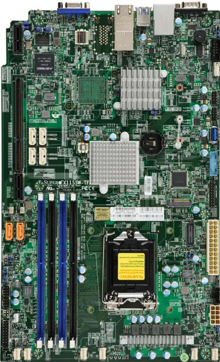
natural_image
Close-up of a green printed circuit board with various electronic components and connectors (no readable text or symbols)Figure 1-2. X11SSW-4TF Motherboard Image
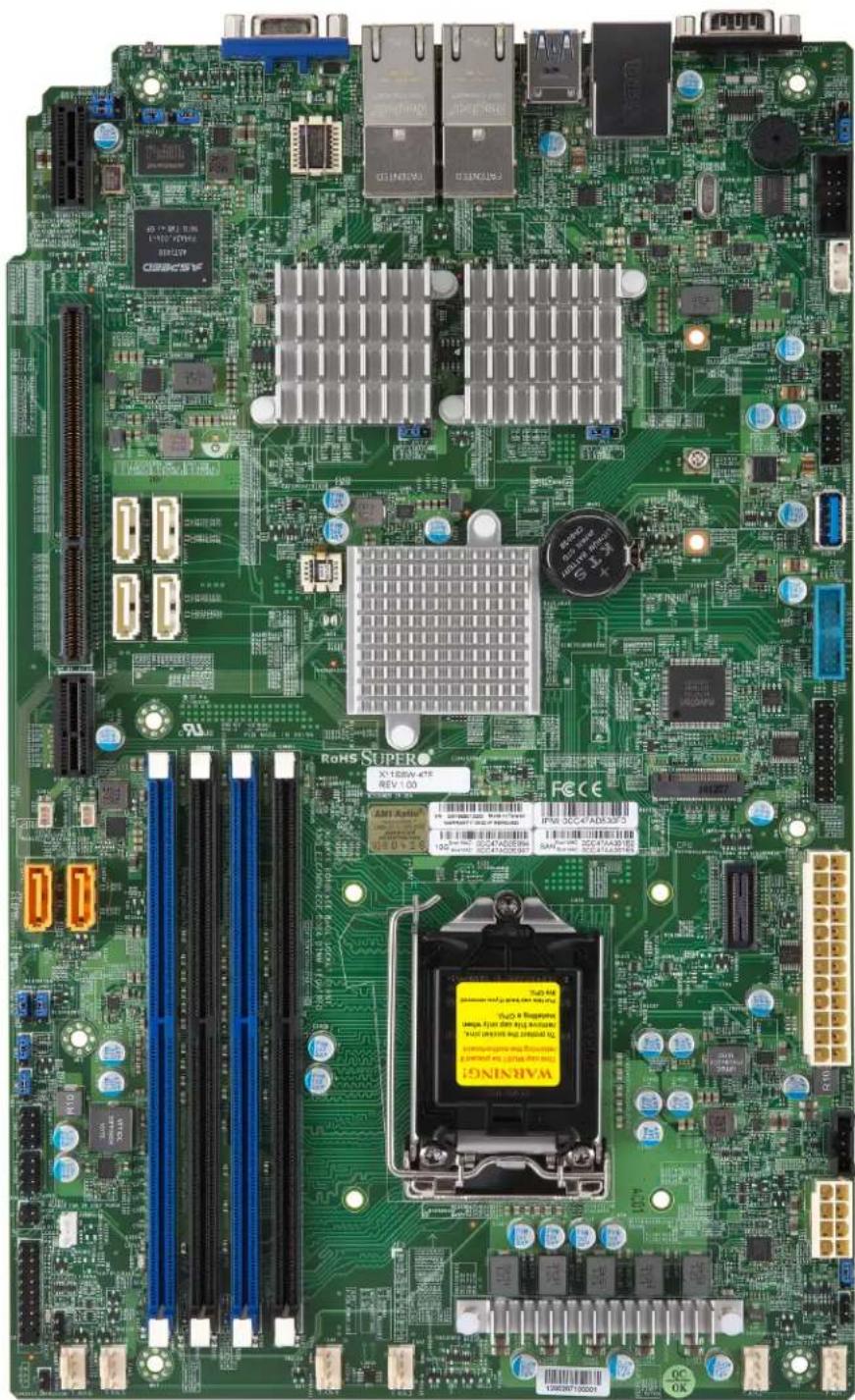
natural_image
Green printed circuit board with various electronic components and connectors (no readable text or symbols)
Note: All graphics shown in this manual were based upon the latest PCB revision available at the time of publication of the manual. The motherboard you received may or may not look exactly the same as the graphics shown in this manual.
Figure 1-3. X11SSW-TF/-4TF Motherboard Layout
(not drawn to scale)
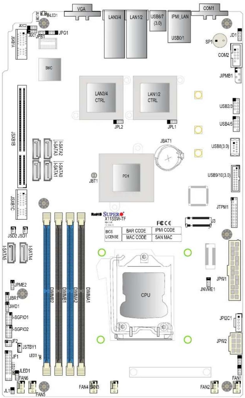
text_image
LED1 VGA LAN3/4 LAN1/2 USB6/7 (3.0) IPMI_LAN COM1 J2C2 J2C1 JPG1 JX8V4 BMC J5SATA2 I-SATA0 I-SATA3 I-SATA1 JSXB1B JSXB1C JSD2 JSD1 I-SATA4 JPME2 JBR1 JWD1 -SSGPIO1 -SSGPIO2 JF2 JSTBY1 LED3 JF1 FND2 JLED1 FAN6 JL1 FAN5 LAN3/4 CTRL LAN1/2 CTRL JPL2 JPL1 JBAT1 PCH JBT1 RoHS SUPER X11SSW-TF FCE CE BIOS LICENSE BAR CODE IPMI CODE MAC CODE SAN MAC CPU JNVMIE1 JFWI JPI2C1 JPW2 FAN2 COM2 JIPMB1 USB2/3 USB4/5 USB8(3.0) USB9/10(3.0) JTPM1Differences between X11SSW-TF and X11SSW-4TF
X11SSW-TF X11SSW-4TF
LAN3/LAN4 No Yes

Note: Components not documented are for internal testing only.
Quick Reference
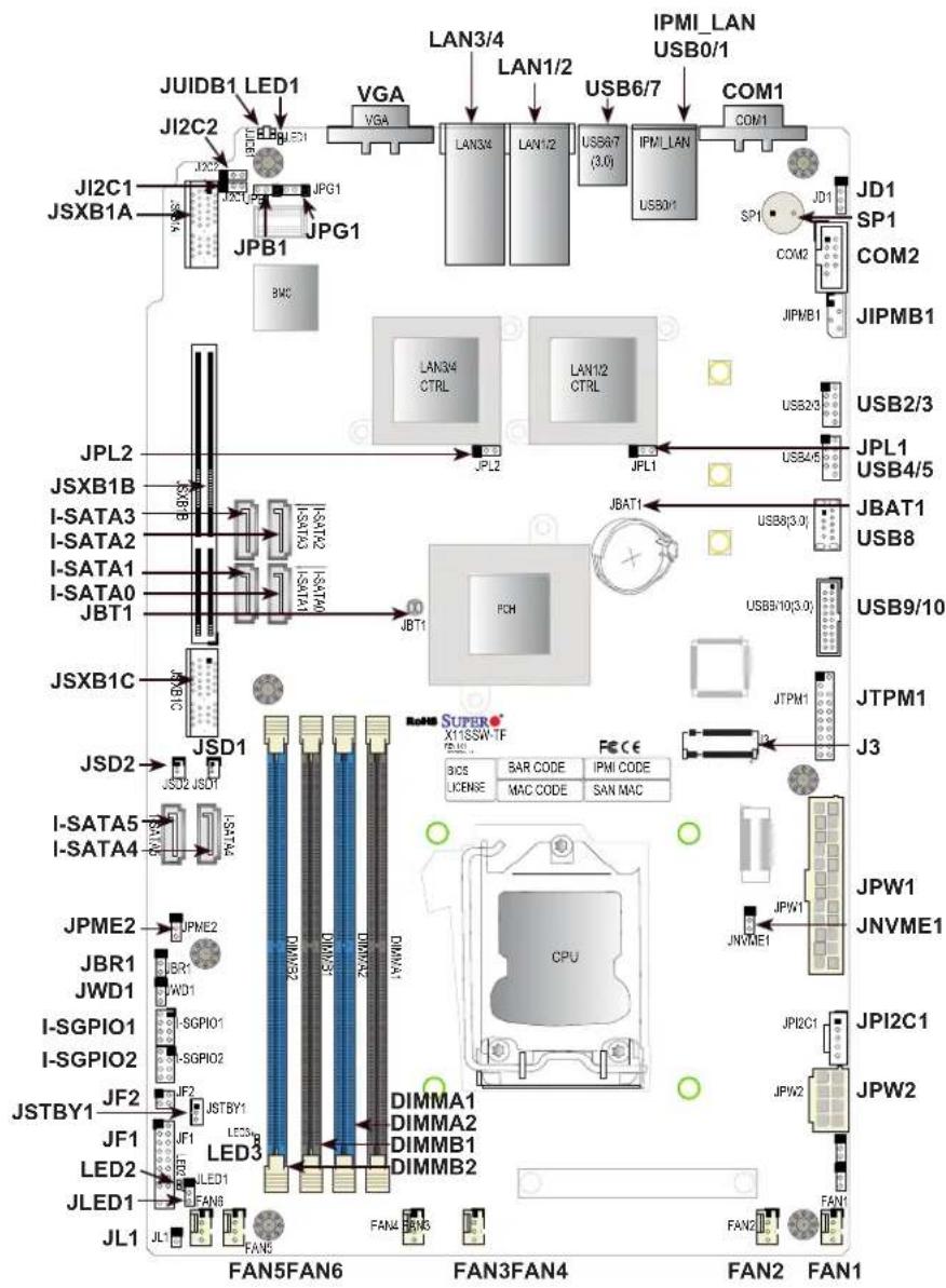
text_image
JUIDB1 LED1 J12C2 LED1 VGA VGA LAN3/4 LAN1/2 LAN1/2 USB6/7 IPMI_LAN USB0/1 J12C1 JSXB1A JPG1 JPB1 JPG1 BAC LAN3/4 LAN1/2 USB6/7 IPMI_LAN USB0/1 COM1 SP1 JD1 SP1 COM2 JIPMB1 JPL2 JSXB1B I-SATA3 I-SATA2 I-SATA1 I-SATA0 JBT1 JSXB1C JSD1 JSD2 JSU2 JSD1 I-SATA5 I-SATA4 JPM2 JBR1 JWD1 I-SGPIO1 I-SGPIO2 JF2 JSTBY1 JF1 LED2 JLED1 JL1 JL1 LED3 LED1 FAN5FAN6 FAN3FAN4 FAN2 FAN1 JCP SUPER X11SSWTF FECE BOS BAR CODE IPMI CODE LICENSE MAC CODE SAN MAC CPU DIMMA1 DIMMA2 DIMMB1 DIMMB2 FAN4 BNC3 FAN3 FAN4 FAN5 FAN6 FAN7 FAN8 FAN9 FAN10 FAN2 FAN3 FAN4 FAN5 FAN6 FAN7 FAN8 FAN9 FAN10 FAN2 FAN3 FAN4 FAN5 FAN6 FAN7 FAN8 FAN9 FAN10 FAN2 FAN3 FAN4 FAN5 FAN6 FAN7 FAN8 FAN9 FAN10 FAN2 FAN3 FAN4 FAN5 FAN6 FAN7 FON 3.0.0.0.0.0.0.0.0.0.0.0.0.0.0.0.0.0.0.0.0.0.0.0.0.0.0.0.0.0.0.0.0.0.0.0.0.0.0.0.0.0.0.0.0.0.0.0.0.0.0.3.0.0.0.0.0.0.0.0.0.0.0.0.0.0.0.0.0.0.0.0.0.0.0.0.0.0.0.0.0.0.3.3.3.3.3.3.3.3.3.3.3.3.3.3.3.3.3.3.3.3.3.3.3.3.3.3.3.3.3.3.3.3.3.3
Notes:
• See Chapter 2 for detailed information on jumpers, I/O ports, and JF1 front panel connections.
- "indicates the location of Pin 1.
- Jumpers/LED indicators not indicated are used for testing only.
- When JLED1 (Onboard Power LED indicator) is on, system power is on. Unplug the power cable before installing or removing any components.
Quick Reference Table
Jumper Description Default Setting
| JBR1 BIOS Recovery Pins 1-2 (Normal) | ||
| JBT1 Clear CMOS Short: Clear CMOS, Open: Normal | ||
| JI2C1/JI2C2 SMB to PCI Slots Pins 1-2 (Enabled) | ||
| JNVME1 NVMe Enable Pins 2-3 (Auto) | ||
| JPB1 BMC Enable/Disable Pins 1-2 (Enabled) | ||
| JPG1 VGA Enable Pins 1-2 (Enabled) | ||
| JPL1 | LAN1/LAN2 Enable | Pins 1-2 (Enabled) |
| JPL2 | LAN3/LAN4 Enable | Pins 1-2 (Enabled) |
| JPME2 | Manufacturing Mode Select | Pins 1-2 (Normal) |
| JWD1 | Watch Dog Enable | Pins 1-2 (Reset) |
LED Description Status
| LED1 | Rear UID LED | Blue On: Unit Identified |
| LED2 Power LED | Solid Green: Power On | |
| LED3 Standby Power LED | Solid Green: Standby Power On |
Connector Description
| COM1/COM2 | COM1: Port, COM2: Header |
| FAN1 ~ FAN6 | System/CPU Fan Headers |
| IPMI_LAN Dedicated IPMI Gigabit (RJ45) Port | |
| I-SATA0 ~ I-SATA5 | SATA 3.0 Connectors via Intel PCH (6Gb/s) |
| I-SGPIO 1/2 | Serial Link General Purpose I/O Connection Headers for I-SATA 3.0 connections(I-SGPIO1 for I-SATA0~3, I-SGPIO2 for I-SATA4~5) |
| J3 | M.2 Socket 3 (supports 2260, 2280, 22110 for NVMe) |
| JBAT1 | Onboard Battery |
| JD1 | Speaker/Buzzer Header (Pins 1-4: Speaker, Pins 3-4: Buzzer) |
| JF1 | Front Control Panel Header |
| JF2 | Activity LED Header for LAN3/LAN4 |
| JIPMB1 | 4-pin External BMC I2C Header (for an IPMI Card) |
| JL1 | Chassis Intrusion Header |
| JLED1 | 3-pin Power LED Indicator Header |
| JPI2C1 | Power I2C System Management Bus (Power SMB) Header |
| JPW1 | 24-pin ATX Main Power Connector (Required) |
| JPW2 | +12V 8-pin CPU Power Connector (Required) |
| JSD1/JSD2 | SATA Disk On Module (DOM) Power Connectors |
| JSTBY1 | Standby Power Header |
| JSXB1A/1B/1C | SMC Proprietary WIO_L (Left) Add-On Card Slot |

Note: Table is continued on the next page.
Connector Description
JTPM1 Trusted Platform Module (TPM)/Port 80 Connector
JUIDB1 UID (Unit Identification) Switch
LAN1/LAN2/LAN3/LAN4 10 Gigabit (RJ45) LAN Ports
SP1 Internal Speaker/Buzzer
USB 0/1 Back Panel USB 2.0 Ports
USB 2/3, USB 4/5 Front Accessible USB 2.0 Headers
USB 6/7 Back Panel USB 3.0 Ports
USB 8 Front Accessible USB 3.0 Type-A Header
USB 9/10 Front Accessible USB 3.0 Header
VGA Back Panel VGA Port
Motherboard Features
| Motherboard Features | |
| CPU | |
| Intel® Xeon® E3-1200 v6/v5 series, 7th/6th Gen CoreTM i3, Pentium®, and Celeron® processors in an LGA1151 (H4) socket. 80W max TDP. | |
| Memory | |
| Four (4) 288-pin DIMM slots support up to 64 GB of SDRAM 72-bit DDR4 unbuffered ECC 2400/2133/1866/1600MHz memory. | |
| DIMM Size | |
| 16GB, 8GB, and 4GB, up to 64GB at 1.2V | |
| Note 1: Memory speed support depends on the processors used in the system. | |
| Note 2: For the latest CPU/memory updates, please refer to our website at http://www.supermicro.com/products/motherboard. | |
| Chipset | |
| Intel PCH C236 | |
| Expansion Slots | |
| One (1) SMC-Proprietary WIO-L slots (JSXB1A/1B/1C)One (1) M.2 NGFF connector [supports PCIe 3.0 x4 (32 Gb/s)] | |
| Network | |
| Two Intel® 10G LAN chips (X540-AT2) for LAN1/LAN2/LAN3/LAN4 | |
| Baseboard Management Controller (BMC) | |
| ASpeed AST 2400 Baseboard Managemenr Controller (BMC) supports IPMI 2.0One (1) Dedicated IPMI LAN located on the rear I/O back panel | |
| Graphics | |
| Graphics controller via ASpeed 2400 BMC | |
| I/O Devices | |
| Serial (COM) Port | One (1) serial port on the rear I/O panel (COM1)One (1) front accessible serial header (COM2) |
| SATA 3.0 | Six (6) I-SATA 3.0 ports (I-SATA0 ~ 5)Two (2) SuperDOM connectors (I-SATA4 & I-SATA5) |
| RAID (PCH) • RAID 0, 1, 5, and 10 | |

Note: The table above is continued on the next page.
| Motherboard Features |
| Peripheral Devices |
| Two (2) USB 2.0 ports on the rear I/O panel (USB 0/1)Two (2) front accessible USB 2.0 headers (USB 2/3, 4/5)Two (2) USB 3.0 ports on the rear I/O panel (USB 6/7)One (1) USB 3.0 Type-A header (USB 8)One (1) front accessible USB 3.0 header (USB 9/10) |
| BIOS |
| 128Mb AMI BIOS® SPI Flash BIOSPlug and Play (PnP), Riser Card auto-detection, dual boot block, DMI 3.0, ACPI 3.0+, USB Keyboard, BIOS rescue hot-key, and SMBIOS 2.7+ |
| Power Management |
| ACPI power managementCPU fan auto-off in sleep modePower button override mechanismPower-on mode for AC power recovery |
| System Health Monitoring |
| Onboard voltage monitors for CPU cores, +3.3V, +5V, +12V, +5V AUX, +3.3V Stby, VBAT, VSA, Memory, PCH temperature, and system temperatureCPU 3+2-phase switching voltage regulatorCPU/System overheat controlCPU Thermal Trip support |
| Fan Control |
| Fan status monitoring with firmware 4-pin fan speed control via IPMI interfaceLow noise fan speed control |
| System Management |
| PECI (Platform Environment Configuration Interface) 3.1 supportIntel® Node ManagerIPMI 2.0 with KVM supportSuperDoctor® 5, Watch Dog, NMICHassis Intrusion header and detectionPower supply monitoring |
| LED Indicators |
| CPU/system overheat LEDPower / suspend-state indicator LEDFan failed LEDUID / Remote UIDHDD activity LEDLAN activity LED |

Note: The table above is continued on the next page.
| Motherboard Features |
| Other |
| • RoHS |
| Dimensions |
| • WIO form factor (13.0" x 8.0") (330.20 mm x 203.20 mm) |

Note 1: The CPU maximum thermal design power (TDP) is subject to chassis and heatsink cooling restrictions. For proper thermal management, please check the chassis and heatsink specifications for proper CPU TDP sizing.
Note 2: For IPMI configuration instructions, please refer to the Embedded IPMI Configuration User's Guide available at http://www.supermicro.com/support/manuals/.
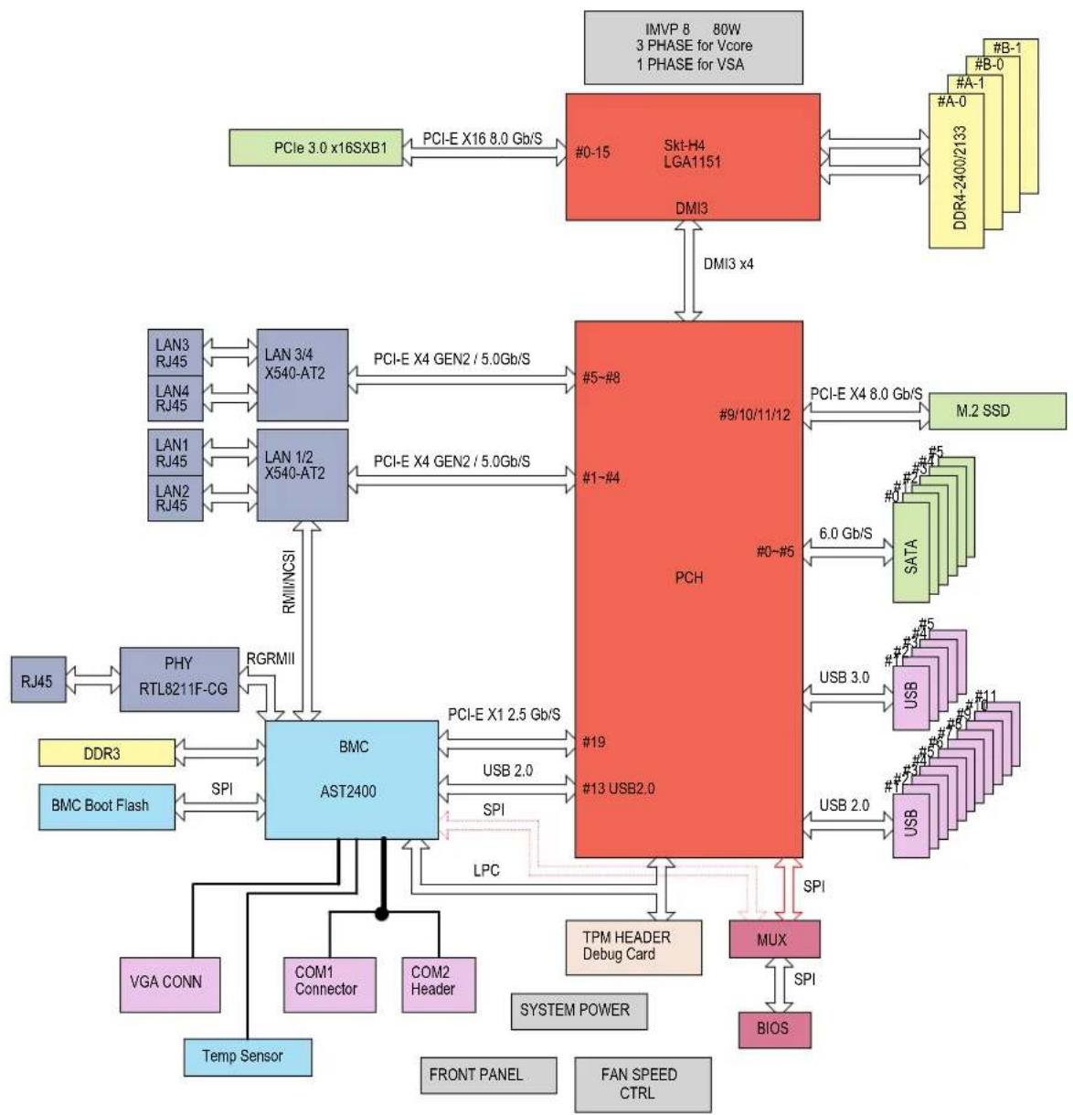
Figure 1-4. Chipset Block Diagram
flowchart
graph TD
    A["PCIe 3.0 x16SXB1"] -->|PCI-E X16 8.0 Gb/S| B["#0-15"]
    B --> C["Skt-H4 LGA1151"]
    C --> D["DMI3"]
    D --> E["DMI3 x4"]
    E --> F["#9/10/11/12"]
    F --> G["PCH"]
    G --> H["#0-#5"]
    H --> I["M.2 SSD"]
    I --> J["SATA"]
    J --> K["#1-#4"]
    K --> L["#13 USB2.0"]
    L --> M["LPC"]
    M --> N["TPM HEADER Debug Card"]
    M --> O["MUX"]
    O --> P["BIOS"]
    P --> Q["BIOS"]
    Q --> R["SYSTEM POWER"]
    R --> S["COM1 Connector"]
    R --> T["COM2 Header"]
    S --> U["Temp Sensor"]
    T --> V["FGM"]
    U --> W["VGA CONN"]
    V --> X["COM1 Connector"]
    V --> Y["COM2 Header"]
    W --> Z["Temp Sensor"]
    X --> AA["FGM"]
    Y --> AB["COM1 Connector"]
    Z --> AC["TPM HEADER Debug Card"]
    AA --> AD["COM2 Header"]
    AB --> AE["TPM HEADER Debug Card"]
    AC --> AF["COM1 Connector"]
    AD --> AG["COM2 Header"]
    AE --> AH["TPM HEADER Debug Card"]
    AF --> AI["COM1 Connector"]
    AG --> AJ["COM2 Header"]
    AH --> AK["TPM HEADER Debug Card"]
    AI --> AL["COM1 Connector"]
    AJ --> AM["COM2 Header"]
    AK --> AN["TPM HEADER Debug Card"]
    AL --> AO["COM1 Connector"]
    AM --> AP["COM2 Header"]
    AN --> AQ["TPM HEADER Debug Card"]
    AO --> AR["COM1 Connector"]
    AP --> AS["COM2 Header"]
    AQ --> AT["TPM HEADER Debug Card"]
    AR --> AU["COM1 Connector"]
    AS --> AV["COM2 Header"]
    AT --> AW["TPM HEADER Debug Card"]
    AU --> AX["COM1 Connector"]
    AV --> AY["COM2 Header"]
    AW --> AZ["TPM HEADER Debug Card"]
    AX --> BA["COM1 Connector"]
    AY --> BB["COM2 Header"]
    AZ --> BC["TPM HEADER Debug Card"]
    BA --> BD["COM1 Connector"]
    BB --> BE["COM2 Header"]
    BC --> BF["TPM HEADER Debug Card"]
    BD --> BG["MUX"]
    BE --> BH["MUX"]
    BF --> BI["MUX"]

Note: This is a general block diagram and may not exactly represent the features on your motherboard. See the previous pages for the actual specifications of your motherboard.
1.2 Processor and Chipset Overview
Built upon the functionality and capability of the Intel E3-1200 v6/v5 series processors (Socket LGA 1151) and the Intel C236 PCH, the X11SSW-TF/-4TF motherboard offers maximum I/O expandability, energy efficiency, and data reliability in a 14-nm process architecture, and is optimized for embedded storage solutions, networking applications, or cloud-computing platforms.
The Intel E3-1200 v6/v5 and PCH C236 platform supports the following features:
• ACPI Power Management Logic Support, Rev. 4.0a
- Intel Turbo Boost Technology 2.0 Power Monitoring/Power Control, Turbo Time Parameter (TAU), and Platform Power Control
- Configurable TDP (cTDP) and Lower-Power Mode
• Adaptive Thermal Management/Monitoring
- PCI-E 3.0, SATA 3.0 with transfer rates of up to 6 Gb/s, xHCI USB with SuperSpeed 3.0
• System Management Bus (SMBus) Specification, Version 2.0
• Integrated Sensor Hub (ISH)
• Intel Trusted Execution Technology (Intel TXT)
• Intel Rapid Storage Technology
• Intel Virtualization Technology for Directed I/O (Intel VT-d)
1.3 Special Features
This section describes the health monitoring features of the X11SSW-TF/-4TF motherboard. The motherboard has an onboard System Hardware Monitor chip that supports system health monitoring.
Recovery from AC Power Loss
The Basic I/O System (BIOS) provides a setting that determines how the system will respond when AC power is lost and then restored to the system. You can choose for the system to remain powered off (in which case you must press the power switch to turn it back on), or for it to automatically return to the power-on state. See the Advanced BIOS Setup section for this setting. The default setting is Last State.
1.4 System Health Monitoring
The motherboard has an onboard Baseboard Management Controller (BMC) chip that supports system health monitoring.
Onboard Voltage Monitors
The onboard voltage monitor will continuously scan crucial voltage levels. Once a voltage becomes unstable, it will give a warning or send an error message to the screen. Users can adjust the voltage thresholds to define the sensitivity of the voltage monitor. Real time readings of these voltage levels are all displayed in BIOS.
Fan Status Monitor with Firmware Control
The system health monitor chip can check the RPM status of a cooling fan. The CPU and chassis fans are controlled by BIOS Thermal Management through the back panel.
Environmental Temperature Control
System Health sensors monitor temperatures and voltage settings of onboard processors and the system in real time via the IPMI interface. Whenever the temperature of the CPU or the system exceeds a user-defined threshold, system/CPU cooling fans will be turned on to prevent the CPU or the system from overheating

Note: To avoid possible system overheating, please be sure to provide adequate airflow to your system.
System Resource Alert
This feature is available when used with SuperDoctor 5® in the Windows OS or in the Linux environment. SuperDoctor is used to notify the user of certain system events. For example, you can configure SuperDoctor to provide you with warnings when the system temperature, CPU temperatures, voltages and fan speeds go beyond a predefined range.
1.5 ACPI Features
ACPI stands for Advanced Configuration and Power Interface. The ACPI specification defines a flexible and abstract hardware interface that provides a standard way to integrate power management features throughout a computer system, including its hardware, operating system and application software. This enables the system to automatically turn on and off peripherals such as CD-ROMs, network cards, hard disk drives and printers.
In addition to enabling operating system-directed power management, ACPI also provides a generic system event mechanism for Plug and Play, and an operating system-independent interface for configuration control. ACPI leverages the Plug and Play BIOS data structures, while providing a processor architecture-independent implementation that is compatible with Windows 7, Windows 8, and Windows 2012 Operating Systems.
1.6 Power Supply
As with all computer products, a stable power source is necessary for proper and reliable operation. It is even more important for processors that have high CPU clock rates.
The X11SSW-TF/-4TF motherboard accommodates 24-pin ATX power supplies. Although most power supplies generally meet the specifications required by the CPU, some are inadequate. In addition, one 12V 8-pin power connection is also required to ensure adequate power supply to the system.
Warning: To avoid damaging the power supply or the motherboard, be sure to use a power supply that contains a 24-pin and 8-pin power connector. Be sure to connect the power supplies to the 24-pin power connector (JPW1), and the 8-pin power connector (JPW2) on the motherboard. Failure in doing so may void the manufacturer warranty on your power supply and motherboard.
It is strongly recommended that you use a high quality power supply that meets ATX power supply Specification 2.02 or above. It must also be SSI compliant. (For more information, please refer to the website at http://www.ssiforum.org/). Additionally, in areas where noisy power transmission is present, you may choose to install a line filter to shield the computer from noise. It is recommended that you also install a power surge protector to help avoid problems caused by power surges.
1.7 Serial Port
The X11SSW-TF/-4TF motherboard supports two serial communication connections. COM Ports 1 and 2 can be used for input/output. The UART provides legacy speeds with a baud rate of up to 115.2 Kbps as well as an advanced speed with baud rates of 250 K, 500 K, or 1 Mb/s, which support high-speed serial communication devices.
Chapter 2
Installation
2.1 Static-Sensitive Devices
Electrostatic Discharge (ESD) can damage electronic components. To prevent damage to your motherboard, it is important to handle it very carefully. The following measures are generally sufficient to protect your equipment from ESD.
Precautions
- Use a grounded wrist strap designed to prevent static discharge.
- Touch a grounded metal object before removing the board from the antistatic bag.
- Handle the board by its edges only; do not touch its components, peripheral chips, memory modules or gold contacts.
- When handling chips or modules, avoid touching their pins.
- Put the motherboard and peripherals back into their antistatic bags when not in use.
- For grounding purposes, make sure your computer chassis provides excellent conductivity between the power supply, the case, the mounting fasteners and the motherboard.
- Use only the correct type of onboard CMOS battery. Do not install the onboard battery upside down to avoid possible explosion.
Unpacking
The motherboard is shipped in antistatic packaging to avoid static damage. When unpacking the motherboard, make sure that the person handling it is static protected.
2.2 Motherboard Installation
All motherboards have standard mounting holes to fit different types of chassis. Make sure that the locations of all the mounting holes for both the motherboard and the chassis match. Although a chassis may have both plastic and metal mounting fasteners, metal ones are highly recommended because they ground the motherboard to the chassis. Make sure that the metal standoffs click in or are screwed in tightly.
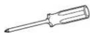
Phillips Screwdriver (1)

Phillips Screws (7)

Standoffs (7)
Only if Needed
Tools Needed
text_image
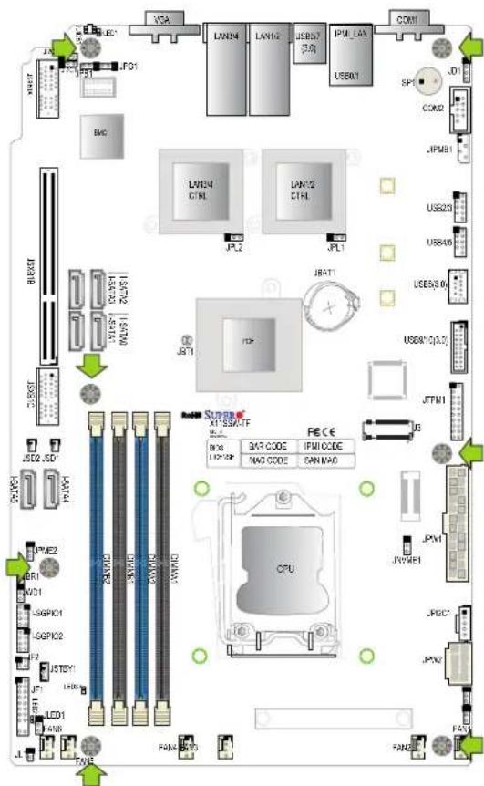
Circuit board layout diagram with labeled components including CPU, memory chips, and connectorsLocation of Mounting Holes

Note: 1) To avoid damaging the motherboard and its components, please do not use a force greater than 8 lb/inch on each mounting screw during motherboard installation. 2) Some components are very close to the mounting holes. Please take precautionary measures to avoid damaging these components when installing the motherboard to the chassis.
Installing the Motherboard
- Locate the mounting holes on the motherboard. See the previous page for the location.

text_image
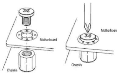
Chassis Chassis- Locate the matching mounting holes on the chassis. Align the mounting holes on the motherboard against the mounting holes on the chassis.
text_image
Motherboard Chassis Motherboard Chassis- Install standoffs in the chassis as needed.
- Install the motherboard into the chassis carefully to avoid damaging other motherboard components.
- Using the Phillips screwdriver, insert a Phillips head #6 screw into a mounting hole on the motherboard and its matching mounting hole on the chassis.
- Repeat Step 5 to insert #6 screws into all mounting holes.
- Make sure that the motherboard is securely placed in the chassis.

Note: Images displayed are for illustration only. Your chassis or components might look different from those shown in this manual.
2.3 Processor and Heatsink Installation
Warning: When handling the processor package, avoid placing direct pressure on the label area of the fan.

Important:
- Always connect the power cord last, and always remove it before adding, removing or changing any hardware components. Make sure that you install the processor into the CPU socket before you install the CPU heatsink.
- If you buy a CPU separately, make sure that you use an Intel-certified multi-directional heatsink only.
- Make sure to install the motherboard into the chassis before you install the CPU heatsink.
- When receiving a motherboard without a processor pre-installed, make sure that the plastic CPU socket cap is in place and none of the socket pins are bent; otherwise, contact your retailer immediately.
• Refer to the Supermicro website for updates on CPU support.
Installing the LGA1151 Processor
- Press the load lever to release the load plate, which covers the CPU socket, from its locking position.
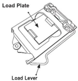
text_image
Load Plate Load Lever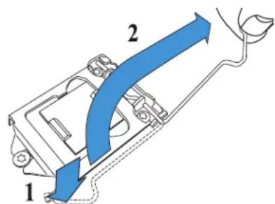
text_image
Diagram showing a mechanical or fluid system with labeled components and directional arrows, likely illustrating fluid flow or movement.- Gently lift the load lever to open the load plate. Remove the plastic cap.
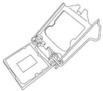
natural_image
Technical line drawing of a mechanical assembly with no visible text or symbols- Use your thumb and your index finger to hold the CPU at the North center edge and the South center edge of the CPU.
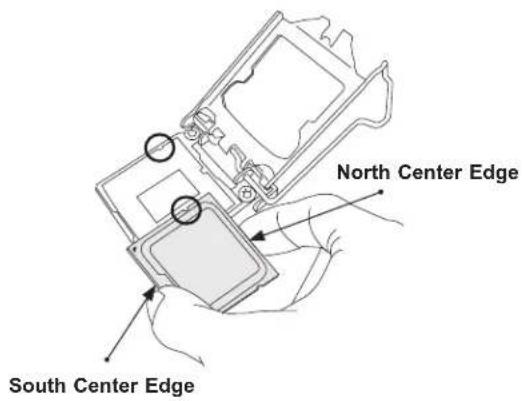
- Align the CPU key that is the semi-circle cutouts against the socket keys. Once it is aligned, carefully lower the CPU straight down into the socket. Do not drop the CPU on the socket. Do not move the CPU horizontally or vertically.

natural_image
Technical line drawing of a mechanical assembly with no visible text or symbols- Do not rub the CPU against the surface or against any pins of the socket to avoid damaging the CPU or the socket.
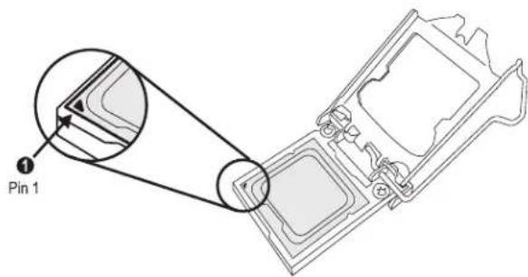
text_image
Pin 1-
With the CPU inside the socket, inspect the four corners of the CPU to make sure that the CPU is properly installed.
-
Use your thumb to gently push the load lever down to the lever lock.
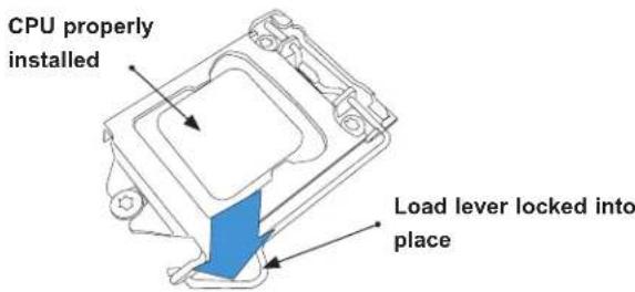
text_image
CPU properly installed Load lever locked into placeNote: You can only install the CPU inside the socket in one direction. Make sure that it is properly inserted into the CPU socket before closing the load plate. If it doesn't close properly, do not force it as it may damage your CPU. Instead, open the load plate again and double-check that the CPU is aligned properly.
Installing an Active CPU Heatsink with Fan
- Locate the CPU fan power connector on the motherboard. (Refer to the layout on the right for the CPU fan location.)
- Position the heatsink so that the heatsink fan wires are closest to the CPU fan power connector and are not interfering with other components.
- Inspect the CPU fan wires to make sure that the wires are routed through the bottom of the heatsink.
- Remove the thin layer of protective lm from the heatsink.

Important: CPU overheating may occur if the protective Im is not removed from the heatsink.
- Apply the proper amount of thermal grease on the CPU.

Note: If your heatsink came with a thermal pad, please ignore this step.
- If necessary, rearrange the wires to make sure that the wires are not pinched between the heatsink and the CPU. Also make sure to keep clearance between the fan wires and the ns of the heatsink.
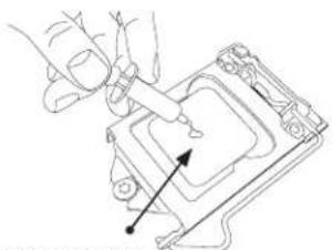
natural_image
Line drawing of a hand using a tool to adjust or install a component, with no visible text or symbols.Thermal Grease
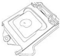
natural_image
Line drawing of a mechanical component with no visible text or symbolsHeatsink
text_image
FansRecommended Supermicro heatsink:
SNK-P0046A4 or SNK-P0051AP4 active heatsink (2U+ or 4U chassis)
-
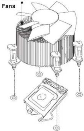
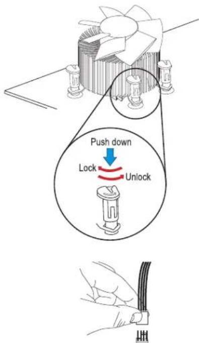
Align the four heatsink fasteners with the mounting holes on the motherboard. Gently push the pairs of diagonal fasteners (#1 & #2, and #3 & #4) into the mounting holes until you hear a click. Also, make sure to orient each fastener so that the narrow end of the groove is pointing outward.
-
Repeat step 7 to insert all four heatsink fasteners into the mounting holes.
-
Once all four fasteners are securely inserted into the mounting holes, and the heatsink is properly installed on the motherboard, connect the heatsink fan wires to the CPU fan connector.
text_image
Push down Lock UnlockRemoving the Heatsink

Note: We do not recommend that the CPU or the heatsink be removed. However, if you do need to remove the heatsink, please follow the instructions below to remove the heatsink and to prevent damage done to the CPU or other components.
Active Heatsink Removal
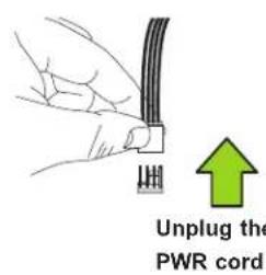
- Unplug the power cord from the power supply.
- Disconnect the heatsink fan wires from the CPU fan header.
- Use your finger tips to gently press on the fastener cap and turn it counterclockwise to make a 1/4 (90°) turn, and pull the fastener upward to loosen it.
- Repeat step 3 to loosen all fasteners from the mounting holes.
- With all fasteners loosened, remove the heatsink from the CPU.
text_image
Unplug the PWR cord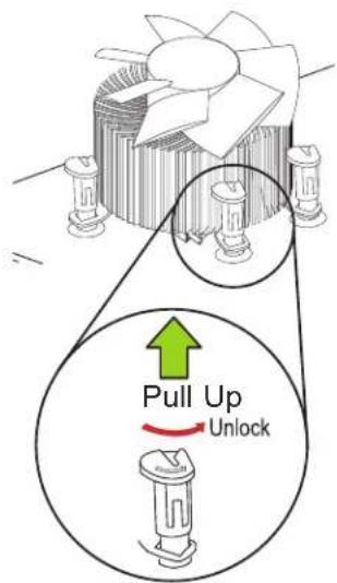
text_image
Pull Up Unlock2.4 Memory Support and Installation

Note: Check the Supermicro website for recommended memory modules.

Important: Exercise extreme care when installing or removing DIMM modules to prevent any possible damage.
Memory Support
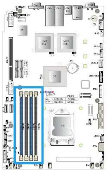
The X11SSW-TF/-4TF motherboard supports up to 64GB of unbuffered (UDIMM) DDR4 ECC 2400/2133/1866/1600MHz memory in four memory slots. Populating these DIMM slots with memory modules of the same type and size will result in interleaved memory, which will improve memory performance.
DIMM Module Population Configuration
For optimal memory performance, follow the table below when populating memory.
| Processors and their Corresponding Memory Modules | ||||
| CPU# Corresponding DIMM Modules | ||||
| CPU DIMM | MA1 DIMMA2 | DIMMB1 DIMMB2 | ||
| Memory Module Population for Optimal Performance | |
| Number of DIMMs | Memory Population Configuration Table(For memory to work properly, please follow the instructions below.) |
| 2 DIMMs DIMMB2/DIMMA2 | |
| 4 DIMMs DIMMB2/DIMMA2, DIMMB1/DIMMA1 | |
| Memory Module Population | ||||||
| DIMM Slots per Channel | DIMM Type | POR Speeds (MHz) | Ranks per DIMM | Layer Count | FW Base | Supported Voltage |
| 2 | Unbuffered DDR4 ECC | 2400, 2133 1866, 1600 | SR, DR 6 SPS | 1.2V | ||
| Memory Module Population | ||
| Max Memory Possible | 4GB DRAM Technology | 8GB DRAM Technology |
| Single Rank UDIMM | 16GB (4x 4GB DIMMs) | 32GB (4x 8GB DIMMs) |
| Dual Rank UDIMMs | 32GB (4x 8GB DIMMs) | 64GB (4x 16GB DIMMs) |
DIMM Module Population Sequence
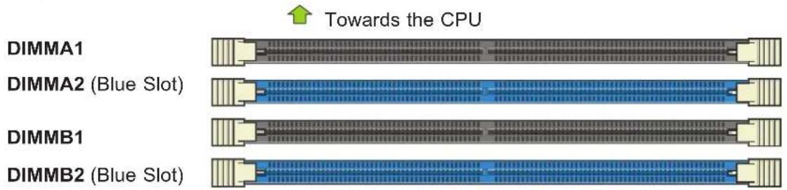
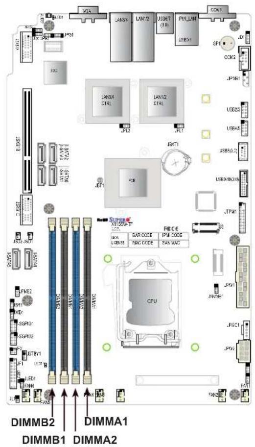
When installing memory modules, the DIMM slots should be populated in the following order: DIMMB2, DIMMA2, DIMMB1, DIMMA1.
• Always use DDR4 DIMM modules of the same type, size and speed.
- Mixed DIMM speeds can be installed. However, all DIMMs will run at the speed of the slowest DIMM.
- The motherboard will support odd-numbered modules (1 or 3 modules installed). However, for best memory performance, install DIMM modules in pairs to activate memory interleaving.
text_image
Towards the CPU DIMMA1 DIMMA2 (Blue Slot) DIMMB1 DIMMB2 (Blue Slot)Towards the edge of the motherboard
text_image
DIMMB2 DIMMA1 DIMMB1 DIMMA2 DIMMB2 DIMMA1 DIMMA2DIMM Installation
- Insert the desired number of DIMMs into the memory slots, starting with DIMMB2 (Channel B, Slot 2, blue slot). For best performance, please use the memory modules of the same type and speed in the same bank.
- Push the release tabs outwards on both ends of the DIMM slot to unlock it.
- Align the key of the DIMM module with the receptive point on the memory slot.
- Align the notches on both ends of the module against the receptive points on the ends of the slot.
- Use two thumbs together to press the notches on both ends of the module straight down into the slot until the module snaps into place.
- Press the release tabs to the lock positions to secure the DIMM module into the slot.
DIMM Removal
Press both release tabs on the ends of the DIMM module to unlock it. Once the DIMM module is loosened, remove it from the memory slot.
text_image
Circuit board layout diagram with labeled components and a highlighted component box for CPU control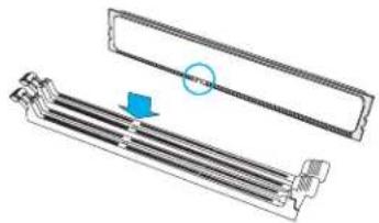
natural_image
Technical illustration of a mechanical component with a circular arrow indicating a specific feature (no text or symbols present)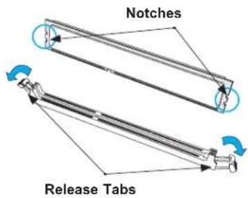
text_image
Notches Release Tabs
text_image
Press both notches straight down into the memory slot.2.5 Rear I/O Ports
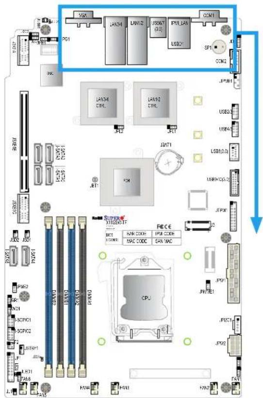
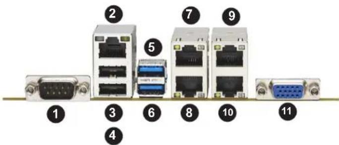
See Figure 2-1 below for the locations and descriptions of the various I/O ports on the rear of the motherboard.
text_image
Circuit board layout diagram with labeled components including CPU, memory chips, and connectorsFigure 2-1. I/O Port Locations and Definitions
text_image
Diagram showing 11 labeled network device ports and connectors, including VGA, Ethernet, and GND.| Rear I/O Ports | |||||
| # | Description | # | Description | # | Description |
| 1. | COM1 5. USB7 (3.0) 9. LAN4 (-4TF only) | ||||
| 2. | IPMI LAN | 6. | USB6 (3.0) | 10. | LAN3 (-4TF only) |
| 3. | USB1 (2.0) | 7. | LAN2 | 11. | VGA Port |
| 4. | USB0 (2.0) 8. LAN1 | ||||
VGA Port
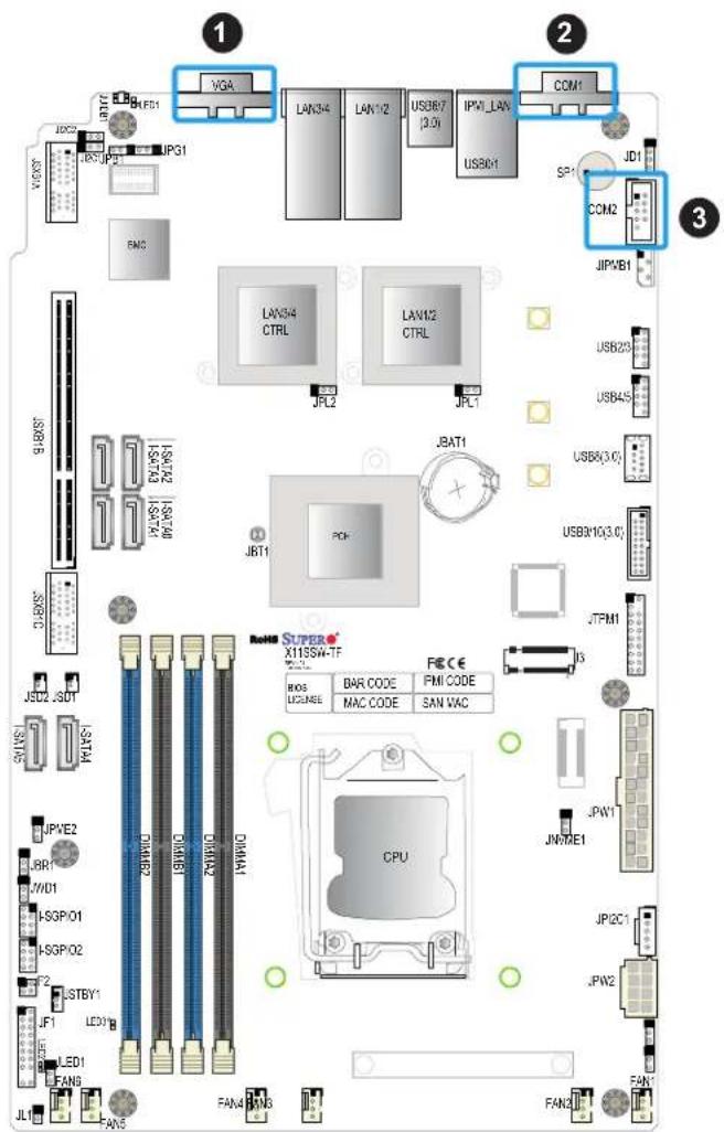
A video (VGA) port is located next to LAN3/4 on the I/O back panel. See the board layout below for the location.
Serial Ports
Two COM connections (COM1 and COM2) are located on the motherboard. COM1 is located on the I/O back panel. COM2 is located next to JD1. See the table below for pin definitions.
| COM PortPin Definitions | |||
| Pin# Definition Pin# Definition | |||
| 1 DCD | 6 DSR | ||
| 2 RXD | 7 RTS | ||
| 3 TXD | 8 CTS | ||
| 4 DTR | 9 RI | ||
| 5 Ground 10 N/A | |||
text_image
1 2 3 VGA LAN04 LAN12 USB67 (3.0) IPW1_LAW USB01 COM1 JDL JDP1 JPG1 JCP1 JDP2 JDP3 JDP4 JDP5 JDP6 JDP7 JDP8 JDP9 JDP10 JDP11 JDP12 JDP13 JDP14 JDP15 JDP16 JDP17 JDP18 JDP19 JDP20 JDP21 JDP22 JDP23 JDP24 JDP25 JDP26 JDP27 JDP28 JDP29 JDP30 JDP31 JDP32 JDP33 JDP34 JDP35 JDP36 JDP37 JDP38 JDP39 JDP40 JDP41 JDP42 JDP43 JDP44 JDP45 JDP46 JDP47 JDP48 JDP49 JDP50 JDP51 JDP52 JDP53 JDP54 JDP55 JDP56 JDP57 JDP58 JDP59 JDP60 JDP61 JDP62 JDP63 JDP64 JDP65 JDP66 JDP67 JDP68 JDP69 JDP70 JDP71 JDP72 JDP73 JDP74 JDP75 JDP76 JDP77 JDP78 JDP79 JDP80 JDP81 JDP82 JDP83 JDP84 JDP85 JDP86 JDP87 JDP88 JDP89 JDP90 JDP91 JDP92 JDP93 JDP94 JDP95 JDP96 JDP97 JDP98 JDP99 JDP100- VGA Port
- COM1
- COM2
Universal Serial Bus (USB) Ports
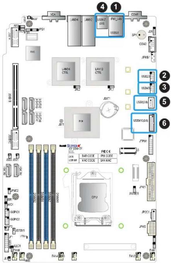
There are two USB 2.0 ports (USB0/1) and two USB 3.0 ports (USB6/7) located on the I/O back panel. The motherboard also has two front access USB 2.0 headers (USB2/3 and USB4/5) and one front access USB 3.0 header (USB9/10). The USB8 header is USB 3.0 Type-A. The onboard headers can be used to provide front side USB access with a cable (not included).
| Back Panel USB (2.0) 0/1 Pin Definitions | |||
| Pin# Definition Pin# Definition | |||
| 1 +5V | 5 +5V | ||
| 2 USB | N 6 USB_N | ||
| 3 USB | P 7 USB_P | ||
| 4 Ground | 8 Ground | ||
| Front Panel USB (2.0) 2/3, 4/5Pin Definitions | |||
| Pin# Definition Pin# Definition | |||
| 1 +5V | 2 +5V | ||
| 3 USB_N | 4 USB_N | ||
| 5 USB_P | 6 USB_P | ||
| 7 Ground | 8 Ground | ||
| 9 Key | 10 NC | ||
| Front Panel USB 9/10 (3.0) Pin Definitions | |||
| Pin# Definition Pin# Definition | |||
| 1 | VBUS 19 Power | ||
| 2 | Stda_SSRX- | 18 USB3_RN | |
| 3 | Stda_SSRX+ | 17 USB3_RP | |
| 4 | GND | 16 GND | |
| 5 | Stda_SSTX- | 15 USB3_TN | |
| 6 | Stda_SSTX+ | 14 USB3_TP | |
| 7 | GND | 13 GND | |
| 8 | D- | 12 USB_N | |
| 9 | D+ | 11 | USB_P |
| 10 | x | ||
| Type A USB 8 (3.0)Pin Definitions | |||
| Pin# Definition | Pin# Definition | ||
| 1 | VBUS | 5 | SSRX- |
| 2 | USB_N | 6 | SSRX+ |
| 3 | USB_P | 7 | GND |
| 4 | Ground | 8 | SSTX- |
| 9 | SSTX+ | ||
| Back Panel USB 6/7 (3.0)Pin Definitions | ||
| Pin# Definition Pin# Definition | ||
| A1 VBUS B1 Power | ||
| A2 D-B2 USB_N | ||
| A3 D+B3 USB_P | ||
| A4 GND B4 GND | ||
| A5 Stda_SSRX-B5 USB3_RN | ||
| A6 Stda_SSRX+B6 USB3_RP | ||
| A7 GND B7 GND | ||
| A8 Stda_SSTX-B8 USB3_TN | ||
| A9 Stda_SSTX+B9 USB3_TP | ||
text_image
VGA BLU1 JPG1 RUG LAN04 LAN12 USB07 I301 IFM1 LAN USB01 COM1 JU1 SP1 COM2 JFM5 LAN04 CTRL LAN12 CTRL JPL3 JPL1 JEA71 USB23 USB45 USB8(0.0) USBX(0.0) JPM1 JSD2 JSD1 JLSV2 JPM2 JMC1 SGPJC1 SGPJC2 JF2 JSTSY1 JF1 JSTC1 FAW6 JN5 FXA4 BNS FXA2 FXA1 FXA0 FXA1 FXA2 FXA3 FXA4 FXA5 FXA6 FXA7 FXA8 FXA9 FXA10 FXA11 FXA12 FXA13 FXA14 FXA15 FXA16 FXA17 FXA18 FXA19 FXA20 FXA21 FXA22 FXA23 FXA24 FXA25 FXA26 FXA27 FXA28 FXA29 FXA30 FXA31 FXA32 FXA33 FXA34 FXA35 FXA36 FXA37 FXA38 FXA39 FXA40 FXA41 FXA42 FXA43 FXA44 FXA45 FXA46 FXA47 FXA48 FXA49 FXA50 FXA51 FXA52 FXA53 FXA54 FXA55 FXA56 FXA57 FXA58 FXA59 FXA60 FXA61 FXA62 FXA63 FXA64 FXA65 FXA66 FXA67 FXA68 FXA69 FXA70 FXA71 FXA72 FXA73 FXA74 FXA75 FXA76 FXA77 FXA78 FXA79 FXA80 FXA81 FXA82 FXA83 FXA84 FXA85 FXA86 FXA87 FXA88 FXA89 FXA90 FXA91 FXA92 FXA93 FXA94 FXA95 FXA96 FXA97 FXA98 FXA99 FXB00- USB0/1
- USB2/3
- USB4/5
- USB6/7
- USB8
- USB9/10
LAN Ports
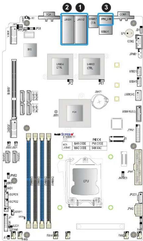
Two 10 Gigabit Ethernet ports (LAN1 and LAN2) are located on the I/O back panel of the motherboard. In addition, a dedicated IPMI LAN is located above USB 0/1 ports on the back panel. All of these ports accept RJ45 cables. Please refer to the LED Indicator section for LAN LED information.

Note: The -4TF board contains two additional 10 Gigabit Ethernet ports (LAN3 and LAN4), which are located next to LAN1 and LAN2.
| LAN PortPin Definitions | ||
| Pin# Definition Pin# Definition | ||
| 1 TX_D1+ 5 BI_D3- | ||
| 2 TX_D1- 6 RX_D2- | ||
| 3 RX_D2+ 7 BI_D4+ | ||
| 4 BI_D3+ 8 BI_D4- | ||
text_image
VGA LAN24 LAN12 USB67 (3.0) IPMLUAN USB01 CCM1 JD1 SP1 JCP1 JPG1 DCB LAN14 CTRL LAN12 CTRL JPL2 JPL1 JBA11 USB8(3.0) USB8(10.0) JPT1 PCH JDB3 JSD2 JSD1 JST1A JPS1 JPM2 JBR1 WD1 ISGP101 ISGP102 F2 USTBY1 LED1 FAM8 J41 FA5 FA4 FA6 FANG FANG1 CPU BAR CODE PWM CODE LCD/MS MAC CODE SAN MAC FCE CE BGS LIC/MS CPU JPM1 JIMVE1 JP2C1 JPM2 FA9- LAN1/2
- LAN3/4 (-4TF only)
- IPMI LAN
2.6 Front Control Panel
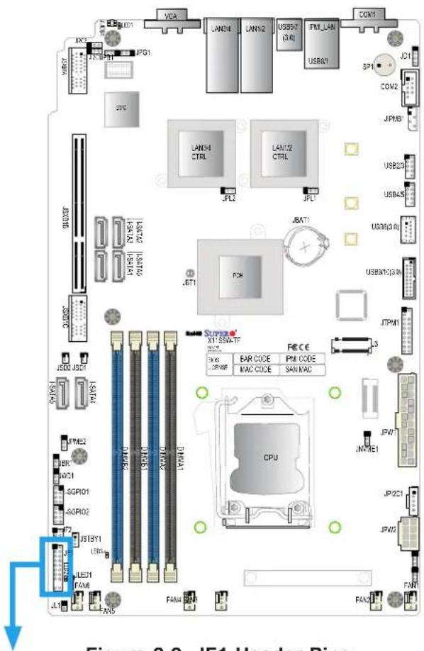
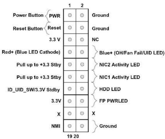
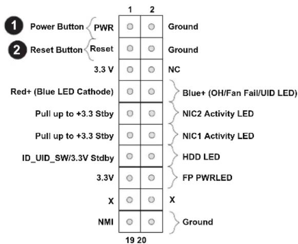
JF1 contains header pins for various buttons and indicators that are normally located on a control panel at the front of the chassis. These connectors are designed specifically for use with Supermicro chassis. See the figure below for the descriptions of the front control panel buttons and LED indicators.
text_image
VDA LAN04 LAN12 USB357 (3.0) PMI_LAN USB01 COM1 JCI CO42 JPN8 USB20 USB45 USB30(3.0) USB30(3.0) JPM1 JPTM1 JPTM2 JPL2 JPL1 LAN04 CTRL LAN12 CTRL JPL1 JBLT1 FCH SUPPLY® XISSNATF FECE € BAR CODE PMI CODE MAC CODE SAN MAC CPU JPM2 JNATE1 JP2C1 JPW2 FWR FAM8 FAM9 FAM10 FAM11 FAM12 FAM13 FAM14 FAM15 FAM16 FAM17 FAM18 FAM19 FAM20 FAM21 FAM22 FAM23 FAM24 FAM25 FAM26 FAM27 FAM28 FAM29 FAM30 FAM31 FAM32 FAM33 FAM34 FAM35 FAM36 FAM37 FAM38 FAM39 FAM40 FAM41 FAM42 FAM43 FAM44 FAM45 FAM46 FAM47 FAM48 FAM49 FAM50 FAM51 FAM52 FAM53 FAM54 FAM55 FAM56 FAM57 FAM58 FAM59 FAM60 FAM61 FAM62 FAM63 FAM64 FAM65 FAM66 FAM67 FAM68 FAM69 FAM70 FAM71 FAM72 FAM73 FAM74 FAM75 FAM76 FAM77 FAM78 FAM79 FAM80 FAM81 FAM82 FAM83 FAM84 FAM85 FAM86 FAM87 FAM88 FAM89 FAM90Figure 2-2. JF1 Header Pins
text_image
Power Button PWR Reset Button Reset 3.3 V Red+ (Blue LED Cathode) Pull up to +3.3 Stby Pull up to +3.3 Stby ID_UID_SW/3.3V Stdby 3.3V X NMI 19 20 Ground Ground NC Blue+ (OH/Fan Fail/UID LED) NIC2 Activity LED NIC1 Activity LED HDD LED FP PWRLED GroundPower Button
The Power Button connection is located on pins 1 and 2 of JF1. Momentarily contacting both pins will power on/off the system. This button can also be configured to function as a suspend button (with a setting in the BIOS - see Chapter 4). To turn off the power when the system is in suspend mode, press the button for 4 seconds or longer. See the table below for pin definitions.
| Power ButtonPin Definitions (JF1) | |
| Pin# | Definition |
| 1 | Signal |
| 2 | Ground |
Reset Button
The Reset Button connection is located on pins 3 and 4 of JF1. Attach it to a hardware reset switch on the computer case. See the table below for pin definitions.
| Reset ButtonPin Definitions (JF1) | |
| Pin# | Definition |
| 3 Reset | |
| 4 Ground | |
text_image
1 2 Power Button PWR Reset Button Reset 3.3 V NC Red+ (Blue LED Cathode) Pull up to +3.3 Stby Pull up to +3.3 Stby ID_UID_SW/3.3V Stdby 3.3V X NMI 19 20 Ground Ground Blue+ (OH/Fan Fail/UID LED) NIC2 Activity LED NIC1 Activity LED HDD LED FP PWRLED Ground-
PWR Button
-
Reset Button
Overheat (OH)/Fan Fail
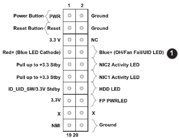
Connect an LED cable to pins 7 and 8 of the Front Control Panel to use the Overheat/Fan Fail LED connections. The LED on pin 8 provides warnings of overheat or fan failure. See the tables below for pin definitions.
| OH/Fan Fail Indicator Status | |
| State | Definition |
| Off Normal | |
| On Overheat | |
| Flashing Fan Fail | |
| OH/Fan Fail LEDPin Definitions (JF1) | |
| Pin# | Definition |
| 7 | Blue LED |
| 8 | OH/Fan Fail LED |
text_image
Power Button PWR Reset Button Reset 3.3 V Red+ (Blue LED Cathode) Pull up to +3.3 Stby Pull up to +3.3 Stby ID_UID_SW/3.3V Stdby 3.3V X NMI 19 20 Ground Ground NC Blue+ (OH/Fan Fail/UID LED) NIC2 Activity LED NIC1 Activity LED HDD LED FP PWRLED Ground- OH/Fan Fail
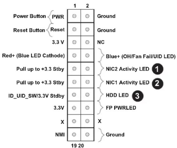
The NIC (Network Interface Controller) LED connection for LAN port 1 is located on pins 11 and 12 of JF1, and the LED connection for LAN port 2 is on pins 9 and 10. Attach the NIC LED cables here to display network activity. See the table below for pin definitions.
| LAN1/LAN2 LEDPin Definitions (JF1) | |
| Pin# | Definition |
| 9 Pull up to +3.3 Stby | |
| 10 NIC2 Activity LED | |
| 11 Pull up to +3.3 Stby | |
| 12 NIC1 Activity LED | |
HDD LED/UID Switch
The HDD LED/UID Switch connection is located on pins 13 and 14 of JF1. Attach a cable to pin 14 to show hard drive activity status. Attach a cable to pin 13 to use UID switch. See the table below for pin definitions.
| HDD LEDPin Definitions (JF1) | |
| Pin# | Definition |
| 13 | 3.3V Stdby/UID_SW |
| 14 | HDD Active |
text_image
Power Button PWR Reset Button Reset 3.3 V Red+ (Blue LED Cathode) Pull up to +3.3 Stby Pull up to +3.3 Stby ID_UID_SW/3.3V Stdby 3.3V X NMI 19 20 Ground Ground NC Blue+ (OH/Fan Fail/UID LED) NIC2 Activity LED ① NIC1 Activity LED ② HDD LED ③ FP PWRLED X Ground- NIC2 LED
- NIC1 LED
- HDD LED / UID Switch
Power LED
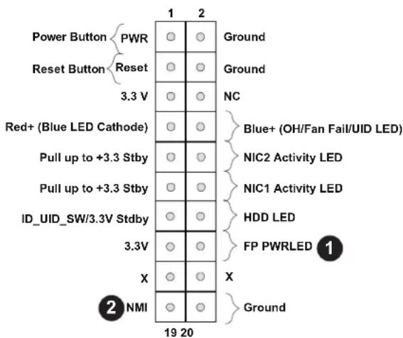
The Power LED connection is located on pins 15 and 16 of JF1. See the table below for pin definitions.
| Power LEDPin Definitions (JF1) | |
| Pin# | Definition |
| 15 | 3V |
| 16 | PWR LED |
NMI Button
The non-maskable interrupt button header is located on pins 19 and 20 of JF1. See the table below for pin definitions.
| NMI ButtonPin Definitions (JF1) | |
| Pin# | Definition |
| 19 | Control |
| 20 | Ground |
text_image
Power Button PWR Reset Button Reset 3.3 V Red+ (Blue LED Cathode) Pull up to +3.3 Stby Pull up to +3.3 Stby ID_UID_SW/3.3V Stdby 3.3V X NMI 19 20 Ground Ground NC Blue+ (OH/Fan Fail/UID LED) NIC2 Activity LED NIC1 Activity LED HDD LED FP PWRLED ① X Ground-
PWR LED
-
NMI
2.7 Connectors
Power Connections
Main ATX Power Supply Connector
The primary power supply connector (JPW1) meets the ATX SSI EPS 12V specification. You must also connect the 8-pin (JPW2) processor power connector to your power supply.
| ATX Power 24-pin Connector Pin Definitions | |
| Pin# Definition Pin# Definition | |
| 13 +3.3V 1 +3.3V | |
| 14 -12V 2 +3.3V | |
| 15 Ground 3 Ground | |
| 16 PS_ON 4 +5V | |
| 17 Ground 5 Ground | |
| 18 Ground 6 +5V | |
| 19 Ground 7 Ground | |
| 20 Res (NC) 8 PWR_OK | |
| 21 +5V 9 5VSB | |
| 22 +5V 10 +12V | |
| 23 +5V 11 +12V | |
| 24 Ground 12 +3.3V | |
Required Connection
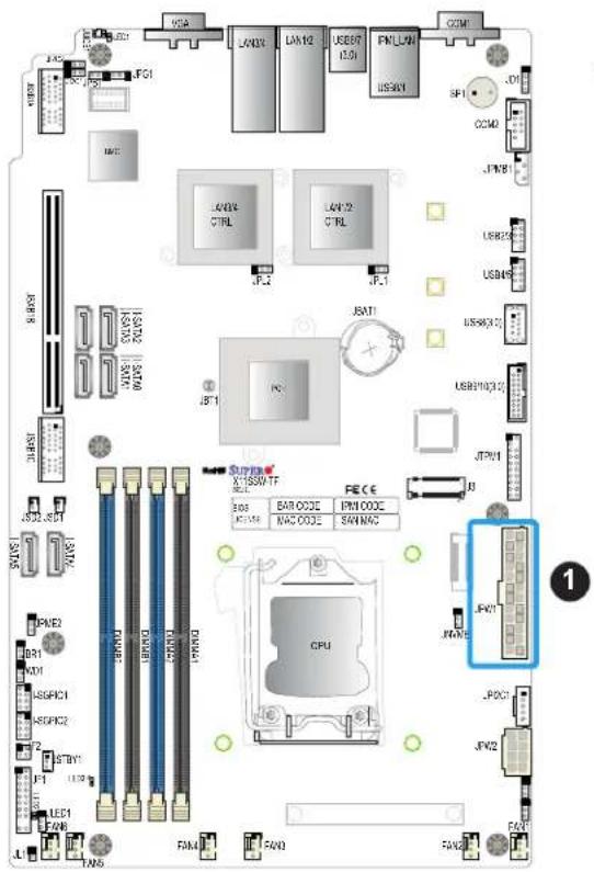
text_image
Labeled diagram of a computer motherboard showing CPU, memory chips, and hardware components with component numbers and labels.- 24-Pin ATX Main PWR (Required)
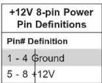
Secondary Power Connector
JPW2 must also be connected to the power supply. This connector is used to power the processor(s).
Required Connection

Important: To provide adequate power supply to the motherboard, be sure to connect the 24-pin ATX PWR and the 8-pin PWR connectors to the power supply. Failure to do so may void the manufacturer warranty on your power supply and motherboard.
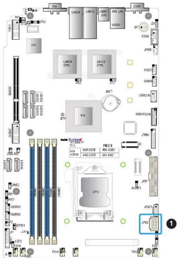
text_image
VGA LAN24 LAN12 USB7 (0.0) IFM1 LAN USBX1 COM1 JPNB LAN34 LAX12 CTRL JPLC JAT1 PCI8 JPM1 USB3X USB45 USB8(0.0) USB9(0.0) JPM1 JPM2 JSB JST21 JPM2 JPM2 JPM2 JPM2 JPM2 JPM2 JPM2 JPM2 JPM2 JPM2 JPM2 JPM2 JPM2 JPM2 JPM2 JPM2 JPM2 JPM2 JPM2 JPM2 JPM2 JPM2 JPM2 JPM2 JPM2 JPM1 JPM1 JPM1 JPM1 JPM1 JPM1 JPM1 JPM1 JPM1 JPM1 JPM1 JPM1 JPM1 JPM1 JPM1 JPM1 JPM1 JPM1 JPM1 JPM1 JPM1 JPM1 JPM1 JPM1 JPM1 JPM2 JPM2 JPM2 JPM2 JPM2 JPM2 JPM2 JPM2 JPM2 JPM2 JPM2 JPM2 JPM2 JPM2 JPM2 JPM2 JPM2 JPM2 JPM2 JPM2 JPM2 JPM2 JPM2 JPM2 Jpm21 Jpm21 Jpm21 Jpm21 Jpm21 Jpm21 Jpm21 Jpm21 Jpm21 Jpm21 Jpm21 Jpm21 Jpm21 Jpm21 Jpm21 Jpm21 Jpm21 Jpm21 Jpm21 Jpm21- 8-Pin PWR (Required)
Headers
Fan Headers
The X11SSW-TF/-4TF has six fan headers (Fan1 - Fan6). All of these 4-pin fan headers are backwards-compatible with the traditional 3-pin fans. However, fan speed control is available for 4-pin fans only by Thermal Management via the IPMI 2.0 interface. See the table below for pin definitions.
| Fan HeaderPin Definitions | |
| Pin# | Definition |
| 1 | Ground (Black) |
| 2 | 2.5A/+12V (Red) |
| 3 | Tachometer |
| 4 | PWM_Control |
Speaker/Buzzer Header
On the JD1 header, pins 1-4 are for the speaker and pins 3-4 are for the buzzer. If you wish to use an external speaker, connect its cable to pins 1-4.
| Speaker ConnectorPin Definitions | |
| Pin Setting | Definition |
| Pins 1-4 | Speaker |
| Pins 3-4 | Buzzer |
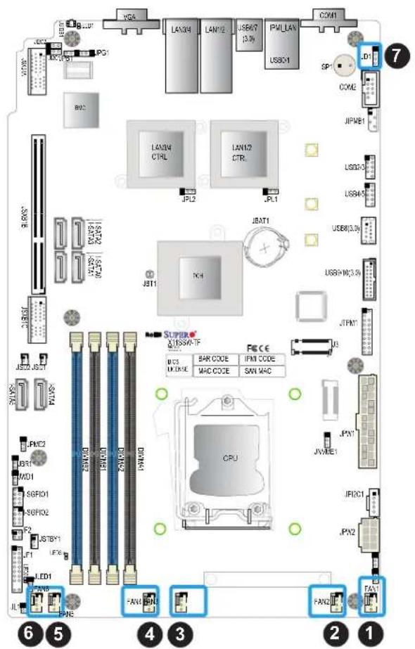
text_image
VGA LAN304 LAN12 USB67 PMLLAN USB01 COM1 SP1 JD1 CCME JIPMB1 LAN24 CTRL LAN12 CTR JPL2 JPL1 USB02 USB4 USB8/3.0V USB9/10/3.0V JBAT1 JBT1 TCH JTPMT JSTB1 JSTJ JSTX PULXS S15W5 JSTB JSTJ PUMC3 BR1 WD1 SGF01 SGP02 F2 USTBY1 LEX LED1 FAM8 JL PNE SUPPER &ISSW-TF FCE CE BAR CODE IPM CODE LMCKE MAC CODE SWN MAC CPU JVME1 JPY1 JRDC1 JPY2 FAI FAI 6 5 4 3 2 1 4 3 2 1- FAN1
- FAN2
- FAN3
- FAN4
- FAN5
- FAN6
- Speaker/Buzzer Header
Chassis Intrusion
A Chassis Intrusion header is located at JL1 on the motherboard. Attach the appropriate cable from the chassis to inform you of a chassis intrusion when the chassis is opened. See the table below for pin definitions.
| Chassis Intrusion Pin Definitions |
| Pin# Definition |
| 1 Intrusion Input |
| 2 Ground |
Internal Speaker/Buzzer
The Internal Speaker (SP1) can be used to provide audible notifications using various beep codes. Refer to the table below for pin definitions. See the layout below for the location of the internal buzzer.
| Internal BuzzerPin Definitions | ||
| Pin# Definition | ||
| 1 Pos | (+) DC 5V | |
| 2 Neg | (-) Signal In | |
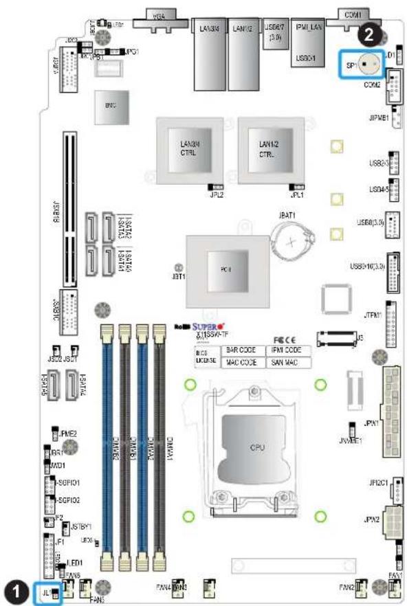
text_image
Labeled diagram of a computer motherboard showing CPU, memory chips, and hardware components with component names and labels.-
Chassis Intrusion
-
Internal Buzzer
SGPIO Headers
Two I-SGPIO (Serial Link General Purpose Input/Output) headers are located on the motherboard. They support the onboard I-SATA 3.0 ports. See the tables below for pin definitions.
| I-SGPIO 1/2 |
| I-SGPIO1 I-SATA 3.0 Ports 0-3 |
| I-SGPIO2 I-SATA 3.0 Ports 4-5 |
| SGPIO HeaderPin Definitions | |||
| Pin# Definition Pin# Definition | |||
| 1 NC | 2 NC | ||
| 3 GND | 4 Data | ||
| 5 Load | 6 GND | ||
| 7 Clock | 8 NC | ||
NC = No Connection
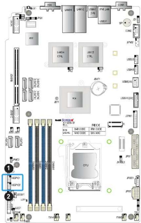
text_image
Labeled diagram of a computer motherboard showing CPU, memory chips, and hardware components with alphanumeric codes and labels.- I-SGPIO 1
- I-SGPIO 2
Standby Power
The +5V Standby Power header is located at JSTBY1 on the motherboard. You must have a card with a Standby Power connector and a cable to use this feature. See the table below for pin definitions.
| Standby Power Pin Definitions | |
| Pin# | Definition |
| 1 +5V | Standby |
| 2 Ground | |
| 3 NC | |
Disk On Module Power Connector
Two power connectors for SATA DOM (Disk On Module) devices are located at JSD1 and JSD2. Connect appropriate cables here to provide power support for your Serial Link DOM devices.
| DOM Power Pin Definitions | |
| Pin# Definition | |
| 1 5V | |
| 2 Ground | |
| 3 Ground | |
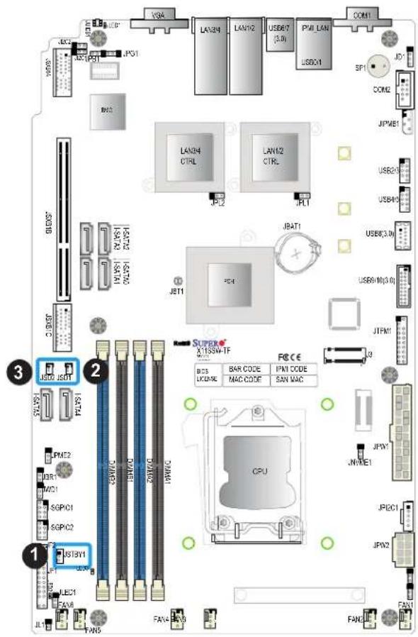
text_image
VISA LAN34 LAN12 USB67 JPN LAN USB01 COM1 JCP1 JPG1 JPG2 JPG3 JPG4 JPG5 JPG6 JPG7 JPG8 JPG9 JPG10 JPG11 JPG12 JPG13 JPG14 JPG15 JPG16 JPG17 JPG18 JPG19 JPG20 JPG21 JPG22 JPG23 JPG24 JPG25 JPG26 JPG27 JPG28 JPG29 JPG30 JPG31 JPG32 JPG33 JPG34 JPG35 JPG36 JPG37 JPG38 JPG39 JPG40 JPG41 JPG42 JPG43 JPG44 JPG45 JPG46 JPG47 JPG48 JPG49 JPG50 JPG51 JPG52 JPG53 JPG54 JPG55 JPG56 JPG57 JPG58 JPG59 JPG60 JPG61 JPG62 JPG63 JPG64 JPG65 JPG66 JPG67 JPG68 JPG69 JPG70 JPG71 JPG72 JPG73 JPG74 JPG75 JPG76 JPG77 JPG78 JPG79 JPG80 JPG81 JPG82 JPG83 JPG84 JPG85 JPG86 JPG87 JPG88 JPG89 JPG90 JPG91 JPG92 JPG93 JPG94 JPG95 JPG96 JPG97 JPG98 JPG99 JPG100 SIPR2 X:ISSN-1F FCE € BOS BAR CODE IPN1 CODE UXONAL MAC CODE SAN MACA Trusted Platform Module (TPM)/Port 80 header is located at JTPM1 to provide TPM support and a Port 80 connection. Use this header to enhance system performance and data security. See the table below for pin definitions.
| Trusted Platform Module HeaderPin Definitions | ||
| Pin# Definition Pin# Definition | ||
| 1 LCLK 2 GND | ||
| 3 LFRAME# 4 < (KEY)> | ||
| 5 LRESET# 6 +5V | ||
| 7 LAD3 8 LAD2 | ||
| 9 +3.3V 10 LAD1 | ||
| 11 LAD0 12 GND | ||
| 13 SMB_CLK 14 SMB_DAT | ||
| 15 +3V Stdby 16 SERIRQ | ||
| 17 GND 18 CLKRUN# | ||
| 19 LPCPD# 20 LDRQ# | ||
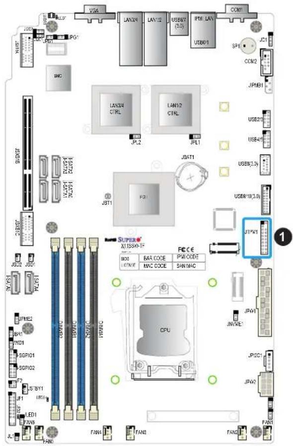
text_image
VGA LAN34 LAN12 USB7 (3.0) IPMI LAN USB01 COM1 JCI SP1 CCN2 JPMB1 LAN34 CTRL LAN12 CTRL JPL2 JFL1 JBAT1 JST1 F2 USB8(3.0) USB8(10/3.0) JTPN1 SUPER MISWIF FECE SOS BAR CODE PWM CODE LICNIE MMC CODE SAN MAC JPME2 JPMI2 JPMI1 JPMI01 JPMI02 JPSI JSTBY1 LED1 FAN6 JL1 FAN6 FNN4 FAN8 FAN2 JPMI1 JPMI2C1 JPMI2 JPMI2C2 JPMI2C3 JPMI2C4 JPMI2C5 JPMI2C6 JPMI2C7 JPMI2C8 JPMI2C9 JPMI2C10 JPMI2C11 JPMI2C12 JPMI2C13 JPMI2C14 JPMI2C15 JPMI2C16 JPMI2C17 JPMI2C18 JPMI2C19 JPMI2C20 JPMI2C21 JPMI2C22 JPMI2C23 JPMI2C24 JPMI2C25 JPMI2C26 JPMI2C27 JPMI2C28 JPMI2C29 JPMI2C30 JPMI2C31 JPMI2C32 JPMI2C33 JPMI2C34 JPMI2C35 JPMI2C36 JPMI2C37 JPMI2C38 JPMI2C39 JPMI2C40 JPMI2C41 JPMI2C42 JPMI2C43 JPMI2C44 JPMI2C45 JPMI2C46 JPMI2C47 JPMI2C48 JPMI2C49 JPMI2C50 JPMI2C51 JPMI2C52 JPMI2C53 JPMI2C54 JPMI2C55 JPMI2C56 JPMI2C57 JPMI2C58 JPMI2C59 JPMI2C60 JPMI2C61 JPMI2C62 JPMI2C63 JPMI2C64 JPMI2C65 JPMI2C66 JPMI2C67 JPMI2C68 JPMI2C69 JPMI2C70 JPMI2C71 JPMI2C72 JPMI2C73 JPMI2C74 JPMI2C75 JPMI2C76 JPMI2C77 JPMI2C78 JPMI2C79 JPMI2C80 JPMI2C81 JPMI2C82 JPMI2C83 JPMI2C84 JPMI2C85 JPMI2C86 JPMI2C87 JPMI2C88 JPMI2C89 JPMI2C90 JPMI2C91 JPMI2C92 JPMI2C93 JPMI2C94 JPMI2C95 JPMI2C96 JPMI2C97 JPMI2C98 JPMI2C99 JPMI2C100- TPM Header
Power SMB (I²C) Header
The Power System Management Bus (I²C) connector (JPI²C1) monitors the power supply, fan, and system temperatures. See the table below for pin definitions.
| Power SMB HeaderPin Definitions | |
| Pin# | Definition |
| 1 | Clock |
| 2 | Data |
| 3 | PMBUS_Alert |
| 4 | Ground |
| 5 | +3.3V |
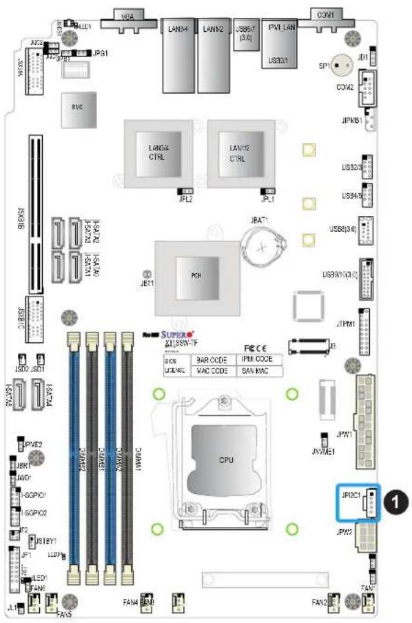
text_image
VGA LAN04 LAN12 USB9/7 JCI PWI LAN US3X1 COM1 JDI SP1 COM2 JPM61 LAN04 CTRL LAN12 CTRL JFL2 JPL1 USB8/3.0 USB9/3.0/2 JBT1 PCB JPM1 JPM1 JSD2 JGT1 JCP51 JCP52 JCP53 JCP54 JCP55 JCP56 JCP57 JCP58 JCP59 JCP60 JCP61 JCP62 JCP63 JCP64 JCP65 JCP66 JCP67 JCP68 JCP69 JCP70 JCP71 JCP72 JCP73 JCP74 JCP75 JCP76 JCP77 JCP78 JCP79 JCP80 JCP81 JCP82 JCP83 JCP84 JCP85 JCP86 JCP87 JCP88 JCP89 JCP90 JCP91 JCP92 JCP93 JCP94 JCP95 JCP96 JCP97 JCP98 JCP99 JCP100 SUPER* ALUSBN-FF FACE BIOS PAR CODE JPM CODE LICOME MAC CODE SAN MNC CPU JPM1 JPM2 JPM3 JPM4 JPM5 JPM6 JPM7 JPM8 JPM9 JPM10- PWR SMB
4-pin BMC External I²C Header
A System Management Bus header for IPMI 2.0 is located at JIPMB1. Connect the appropriate cable here to use the IPMB I²C connection on your system. See the table below for pin definitions.
| External I2C Header Pin Definitions | |
| Pin# | Definition |
| 1 Data | |
| 2 GND | |
| 3 Clock | |
| 4 NC | |
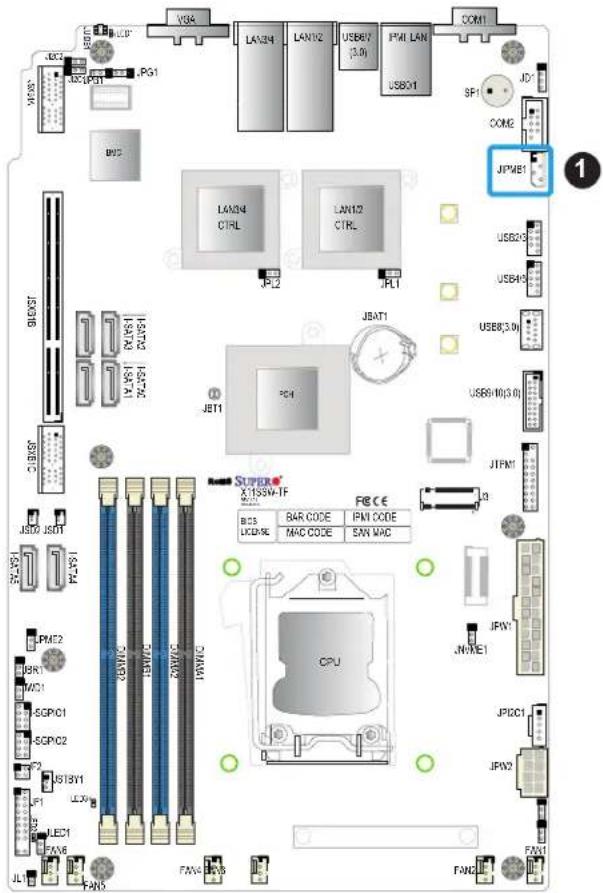
text_image
VBR LAN24 LAN12 USB1Y (3.0) FMI LAN USB01 COM1 JD1 COM2 JPME1 JCP1 JPG1 JPG2 LAN4 CTRL LAN12 CTRL JPL2 JPL1 JBAT1 USB05 USB49 USB3.00 USBH10(3.0) USBH10(3.0) JPT1 PC4 JBT1 JSPX1 JSPX2 JSPX3 JSPX4 JSPX5 JSPX6 JSPX7 JSPX8 JSPX9 JSPX10 JSPX11 JSPX12 JSPX13 JSPX14 JSPX15 JSPX16 JSPX17 JSPX18 JSPX19 JSPX20 JSPX21 JSPX22 JSPX23 JSPX24 JSPX25 JSPX26 JSPX27 JSPX28 JSPX29 JSPX30 JSPX31 JSPX32 JSPX33 JSPX34 JSPX35 JSPX36 JSPX37 JSPX38 JSPX39 JSPX40 JSPX41 JSPX42 JSPX43 JSPX44 JSPX45 JSPX46 JSPX47 JSPX48 JSPX49 JSPX50 JSPX51 JSPX52 JSPX53 JSPX54 JSPX55 JSPX56 JSPX57 JSPX58 JSPX59 JSPX60 JSPX61 JSPX62 JSPX63 JSPX64 JSPX65 JSPX66 JSPX67 JSPX68 JSPX69 JSPX70 JSPX71 JSPX72 JSPX73 JSPX74 JSPX75 JSPX76 JSPX77 JSPX78 JSPX79 JSPX80 JSPX81 JSPX82 JSPX83 JSPX84 JSPX85 JSPX86 JSPX87 JSPX88 JSPX89 JSPX90 JSPX91 JSPX92 JSPX93 JSPX94 JSPX95 JSPX96 JSPX97 JSPX98 JSPX99 JSPX100- BMC External Header
M.2 Connection
The X11SSW-TF/-4TF board contains one M.2 NGFF socket 3 connector at J3. M.2 was formerly Next Generation Form Factor (NGFF) and serves to replace mini PCI-E and mSATA. M.2 allows for a greater variety of card sizes, increased functionality, and spatial efficiency. The M.2 socket 3 supports 3.0 x4 (32 Gb/s) card in 2260, 2280, and 22110 form factors.
Onboard Power LED Header
An onboard Power LED header is located at JLED1. This Power LED header is connected to the Front Control Panel located at JF1 to indicate the status of system power. See the table below for pin definitions.
| Onboard Power LED Pin Definitions | |
| Pins Definition | |
| 1 VCC | |
| 2 | Connection to PWR LED on JF1 |
| 3 | Connection to PWR LED on JF1 |
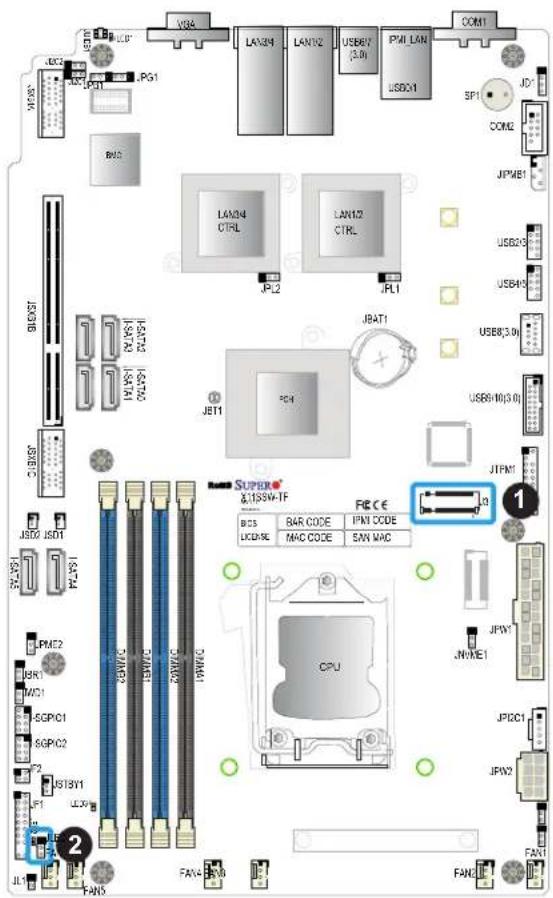
text_image
VGA LAN24 LAN12 USB6V (3.0) JPMI LAN USB01 COM1 SP1 JD1 COM2 JPMB1 LAN34 CTRL LAN12 CTRL JPL2 JPL1 JBAT1 JET1 PC4 JSPX JSD0 JSD1 PLS-1 PLS-2 PLS-3 PLS-4 JPM2 JRT1 JPGC1 SGPC2 JST3Y1 JF1 L30 JL1 FAN5 FAN5-RB FAN5-RB SUPEX GJSSW-TF RECE J3 BCS BAR CODE PMI CODE LCD/NC MAC CODE SAN MAC CPU JPMY JNWE1 JPDC1 JPN2 FAN1- M.2 Connector
- Onboard Power LED Header
LAN3/LAN4 Activity LED Header
The JF2 header provides LED activity for ports LAN3 and LAN4. See the table below for pin definitions.
| JF2 LAN3/LAN4 Activity LED Header Pin Definitions | ||
| Pin# Definition Pin# Definition | ||
| 1 +3.3 | Stby 2 NIC4 Activity LED | |
| 3 +3.3 | Stby 4 NIC3 Activity LED | |
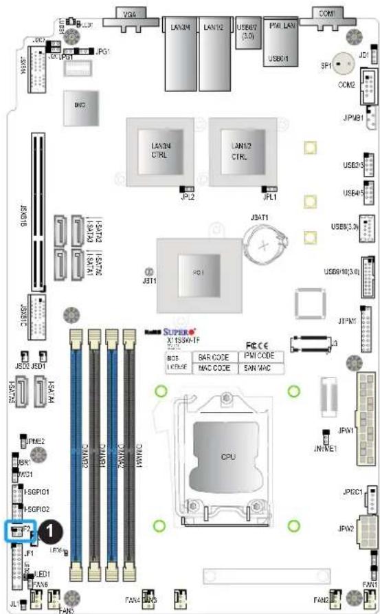
text_image
VGS LAN34 LAN12 USB67 (3.0) PML LAN USB01 COM1 JDI SP1 COM2 JPW81 LAN24 CTRL LAN12 CTRL JPL2 JFL1 JBAT1 USB(3.0) USB(10.3.0) JIPMT JSD2 JSD1 JWD1 JPM2 JPM2 JPM2 JPM2 JPM2 JPM2 JPM2 JPM2 JPM2 JPM2 JPM2 JPM2 JPM2 JPM2 JPM2 JPM2 JPM2 JPM2 JPM2 JPM2 JPM2 JPM2 JPM2 JPM2 JPM2 JPM1 JPM1 JPM1 JPM1 JPM1 JPM1 JPM1 JPM1 JPM1 JPM1 JPM1 JPM1 JPM1 JPM1 JPM1 JPM1 JPM1 JPM1 JPM1 JPM1 JPM1 JPM1 JPM1 JPM1 JPM1 JPM2 JPM2 JPM2 JPM2 JPM2 JPM2 JPM2 JPM2 JPM2 JPM2 JPM2 JPM2 JPM2 JPM2 JPM2 JPM2 JPM2 JPM2 JPM2 JPM2 JPM2 JPM2 JPM2 JPM2 JPF6C1 JPF6C1 FANX1 FANX1 FANX1 FANX1 FANX1 FANX1 FANX1 FANX1 FANX1 FANX1 FANX1 FANX1 FANX1 FANX1- LAN3/LAN4 Activity LED Header
SATA Ports
Six SATA 3.0 connectors, supported by the Intel C236 PCH chip, are located on the X11SSW-TF/-4TF motherboard. These SATA ports support RAID 0, 1, 5, and 10. SATA ports provide serial-link signal connections, which are faster than the connections of Parallel ATA. See the tables below for pin definitions.

Note 1: I-SATA4 and I-SATA5 are Supermicro SuperDOMs. These are yellow SATA-DOM connectors with power pins built in and do not require separate external power cables. These connectors are backwards-compatible with non-Supermicro SATADOMs that require an external power supply.
Note 2: For more information on the SATA HostRAID configuration, please refer to the Intel SATA HostRAID user's guide posted on our website at http://www.supermicro.com.
| X11SSW-TF/-4TF SATA 3.0 Connector Types | |
| Port # Connection Type | |
| I-SATA 0-3(Four) | SATA 3.0/6 Gb/sRAID 0, 1, 5, 10 |
| I-SATA 4-5(Two) | SATA 3.0/6 Gb/sRAID 0, 1, 5, 10SuperDOM connectors |
| Supported by Intel C236 PCH | |
| SATA 3.0 PortPin Definitions | |
| Pin# Signal | |
| 1 Ground | |
| 2 SATA_TXP | |
| 3 SATA_TXN | |
| 4 Ground | |
| 5 SATA_RXN | |
| 6 SATA_RXP | |
| 7 Ground |
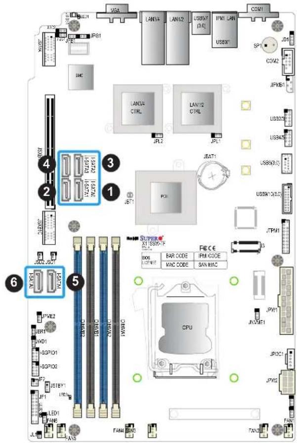
text_image
Labeled diagram of a computer motherboard showing CPU, memory chips, and hardware components with numbered annotations.- I-SATA0
- I-SATA1
- I-SATA2
- I-SATA3
- I-SATA4
- I-SATA5
Unit Identifier Switch/UID LED Indicator
A rear Unit Identifier (UID) switch and a rear UID LED (LED1) are located next to the VGA port on the motherboard. The front UID switch and UID LED are both located on the Front Control Panel (JF1) (with the front UID switch on pin 13, and the front LED on pin 7 of JF1). When you press the front or the rear UID switch, both front and rear UID LEDs will be turned on. Press the UID switch again to turn off the LED indicators. The UID Indicators provide easy identification of a system unit that may be in need of service.

Note: UID can also be triggered via IPMI on the motherboard. For more information on IPMI, please refer to the IPMI User's Guide posted on our website at http://www.supermicro.com.
| UID Switch Pin Definitions | |
| Pin# | Definition |
| 1 | Ground |
| 2 | Ground |
| 3 | Button In |
| 4 | Button In |
| UID LEDPin Definitions |
| Color Status |
| Blue: On Unit Identified |
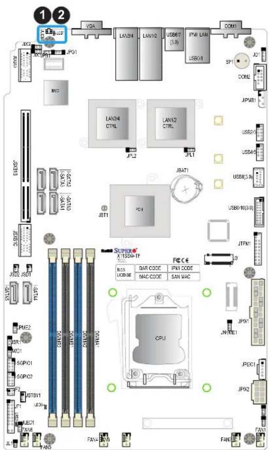
text_image
1 2 VGA LED LED PG1 VBR3 JCP1 BHD LED35* JSP4 JSP4 JSP4 JSP4 JSP4 JSP4 JSP4 JSP4 JSP4 JSP4 JSP4 JSP4 JSP4 JSP4 JSP4 JSP4 JSP4 JSP4 JSP4 JSP4 JSP4 JSP4 JSP4 JSP4 JSP4 JSP4- UID Switch
- UID LED
2.8 Jumper Settings
How Jumpers Work
To modify the operation of the motherboard, jumpers can be used to choose between optional settings. Jumpers create shorts between two pins to change the function of the connector. Pin 1 is identified with a square solder pad on the printed circuit board. See the diagram below for an example of jumping pins 1 and 2. Refer to the motherboard layout page for jumper locations.

Note: On two-pin jumpers, "Closed" means the jumper is on and "Open" means the jumper is off the pins.
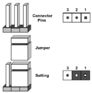
text_image
Connector Pins Jumper Setting 3 2 1 3 2 1CMOS Clear
JBT1 is used to clear the CMOS. Instead of pins, this jumper consists of contact pads to prevent accidental clearing of the CMOS. To clear the CMOS, use a metal object such as a small screwdriver to touch both pads at the same time to short the connection.

Note: Be sure to completely shut down the system, and then short JBT1 to clear the CMOS.
SMBus to PCI Slots
Use jumpers JI ^2 C1 and JI ^2 C2 to connect the System Management Bus (I ^2 C) to PCI-Express slots to improve PCI performance. These two jumpers should be set at the same time. See the table below for jumper settings. The default setting is Enabled.
| I2C for PCI-E SlotsJumper Settings | |
| Jumper Setting | Definition |
| Pins 1-2 Enabled | |
| Pins 2-3 Disabled | |
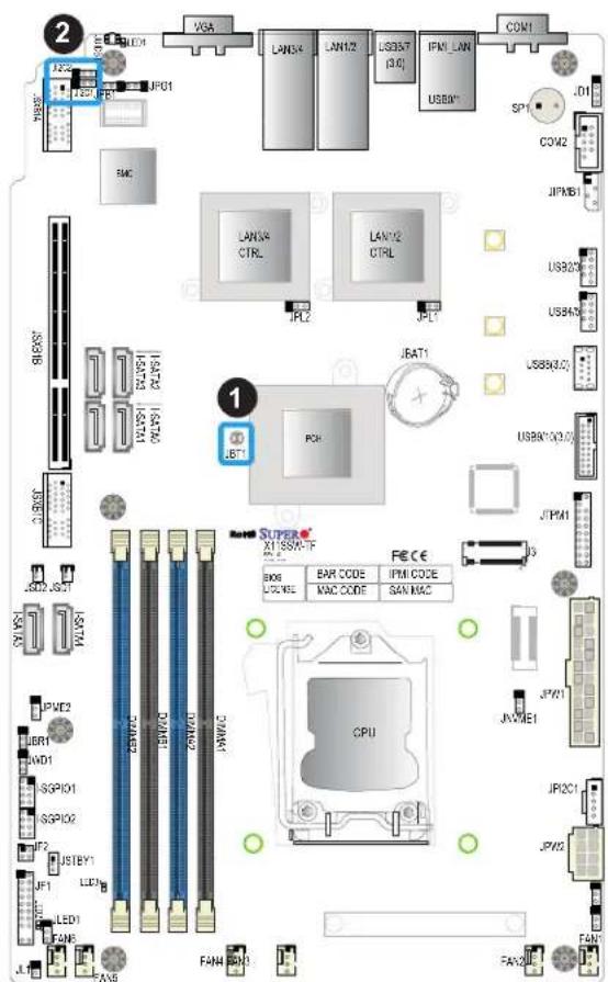
text_image
Labeled diagram of a computer motherboard showing CPU, memory chips, and hardware components with alphanumeric codes.- CMOS Clear
- SMBus to PCI Slots
Watch Dog
Watch Dog (JWD1) is a system monitor that can reboot the system when a software application hangs. Close pins 1-2 to reset the system if an application hangs. Close pins 2-3 to generate a non-maskable interrupt (NMI) signal for the application that hangs. Refer to the table below for jumper settings. The Watch Dog must also be enabled in the BIOS. The default setting is Reset.
| Watch DogJumper Settings | |
| Jumper Setting Definition | |
| Pins 1-2 Reset | |
| Pins 2-3 NMI | |
| Open Disabled | |
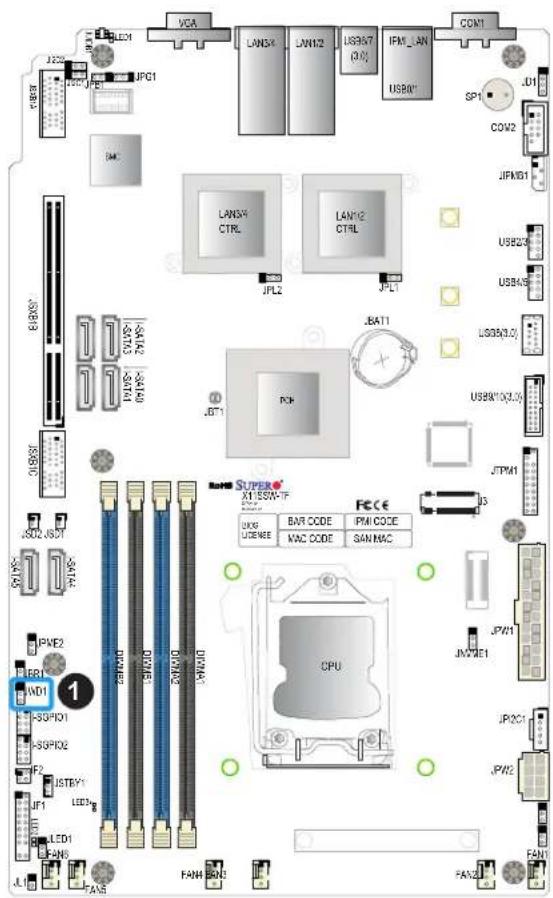
text_image
LED1 J229 JPG1 VGA LANX4 LNM12 USB57 (0.0) IFM_LAN USBN COM1 SP1 J01 COV2 JFM61 USB23 USB45 USB5(3.0) USBN(3.0) JPL2 JPL1 JBAT1 JST1 PCB JPM1 JPM2-JSD1 JPN5 JPG2-JSD1 JPG2-JSD1 JPG2-JSD1 JPG2-JSD1 JPG2-JSD1 JPG2-JSD1 JPG2-JSD1 JPG2-JSD1 JPG2-JSD1 JPG2-JSD1 JPG2-JSD1 JPG2-JSD1 JPG2-JSD1 JPG2-JSD1 JPG2-JSD1 SUSER AT SEW-TF FECE DWR CODE BAR CODE PWM CODE USSR LICENSE MAC CODE SAN MAC CPU JPM1GE1 JPW1 JP2C1 JPW2 FAN1 FAN2E FAN3E FAN4E FAN5E FAN6E FAN7E FAN8E FAN9E FAN10E- Watch Dog
LAN Port Enable/Disable
Jumpers JPL1 and JPL2 enable or disable LAN ports 1/2 and 3/4 respectively on the motherboard. Refer to the table below for jumper settings. The default setting is Enabled.
| LAN1-LAN4 Enable/Disable Jumper Settings |
| Jumper Setting Definition |
| Pins 1-2 Enabled |
| Pins 2-3 Disabled |
Manufacturing Mode Select
Close pins 2-3 of jumper JPME2 to bypass SPI flash security and force the system to operate in the manufacturing mode, which will allow the user to flash the system firmware from a host server for system setting modifications. See the table below for jumper settings. The default setting is Normal.
| Manufacturing ModeJumper Settings | |
| Jumper Setting Definition | |
| Pins 1-2 Normal | |
| Pins 2-3 Manufacturing Mode | |
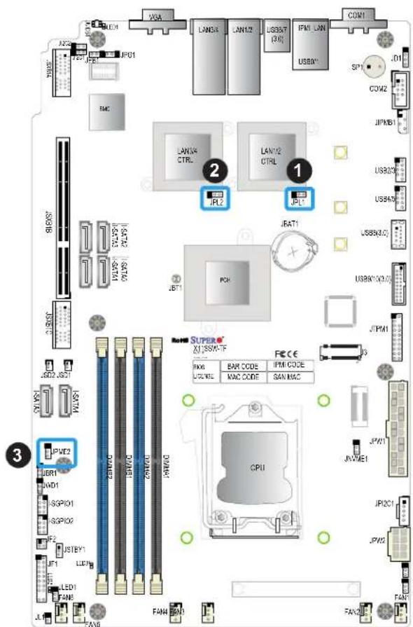
text_image
VGA LAN04 LAN12 USBAT (30) IPM1 LAN USBX® COM1 JDI COM2 JPNB1 USB20 USB40 USB80(30) USB80(30) JPTM1 JPM1 JPL2 JPL1 LAN04 CTRL LAN12 CTRL JPL2 JPL1 JBT1 POK JST26 JST25 JST24 JST23 JST22 JST21 JST20 JST19 JST18 JST17 JST16 JST15 JST14 JST13 JST12 JST11 JST10 JST9 JST8 JST7 JST6 JST5 JST4 JST3 JST2 JST1 JST0 JST9 JST8 JST7 JST6 JST5 JST4 JST3 JST2 JST1 JST0 JST9 JST8 JST7 JST6 JST5 JST4 JST3 JST2 JST1 JST0 JST9 JST8 JST7 JST6 JCTEY1 LED1 FAN8 FAN9 FAN8 FAN7 6000 6000 6000 6000 6000 6000 6000 6000 6000 6000 6000 6000 6000 6000 6000 6000 6000 6000 6000 6000 600-
LAN1/2 Ports Enable/Disable
-
LAN3/4 Ports Enable/Disable
-
Manufacturing Mode
VGA Enable/Disable
Jumper JPG1 allows the user to enable the onboard VGA connector. The default setting is pins 1-2 to enable the connection. See the table below for jumper settings. The default setting is Enabled.
| VGA Enable/Disable Jumper Settings | |
| Jumper Setting Definition | |
| Pins 1-2 Enabled | |
| Pins 2-3 Disabled |
BIOS Recovery
Use jumper JBR1 to recover the BIOS settings on the motherboard. See the table below for jumper settings. The default setting is Normal.
| BIOS RecoveryJumper Settings | |
| Jumper Setting Definition | |
| Pins 1-2 Normal | |
| Pins 2-3 BIOS Recovery | |
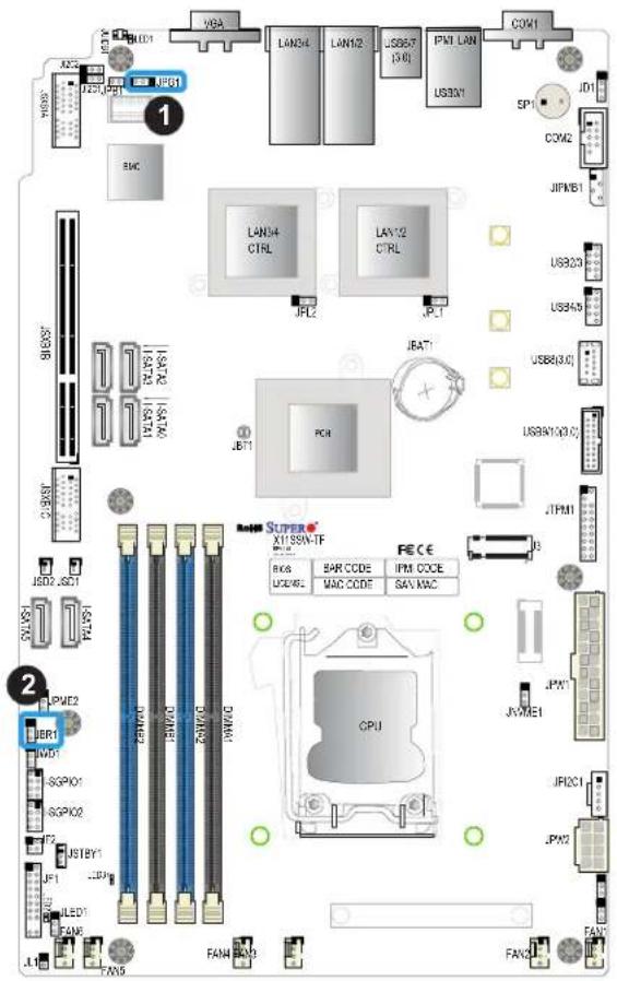
text_image
Labeled diagram of a computer motherboard showing CPU, memory chips, and hardware components with component names and labels.- VGA Enable
- BIOS Recovery
BMC Enabled
Jumper JPB1 allows the user to enable the embedded Baseboard Management Controller (BMC) to provide IPMI 2.0/KVM support on the motherboard. See the table below for jumper settings. The default setting is BMC Enable.
| BMC EnableJumper Settings |
| Jumper Setting Definition |
| Pins 1-2 BMC Enabled |
| Pins 2-3 Disabled |
NVMe Connection
Close pins 1 and 2 to manually enable the NVMe add-on card support on the motherboard, which will allow one of PCIe 3.0 x8 links to always run at dual PCIe 3.0 x4. See the table below for jumper settings. The default setting is Auto.

Note: Use only NVMe add-on cards that have been validated by Supermicro. For the latest updates, please refer to our website at http://www.supermicro.com/products/motherboard.
| NVMe ConnectionJumper Settings | |
| Jumper Setting Definition | |
| Pins 1-2 Manual | |
| Pins 2-3 Auto (Default) | |
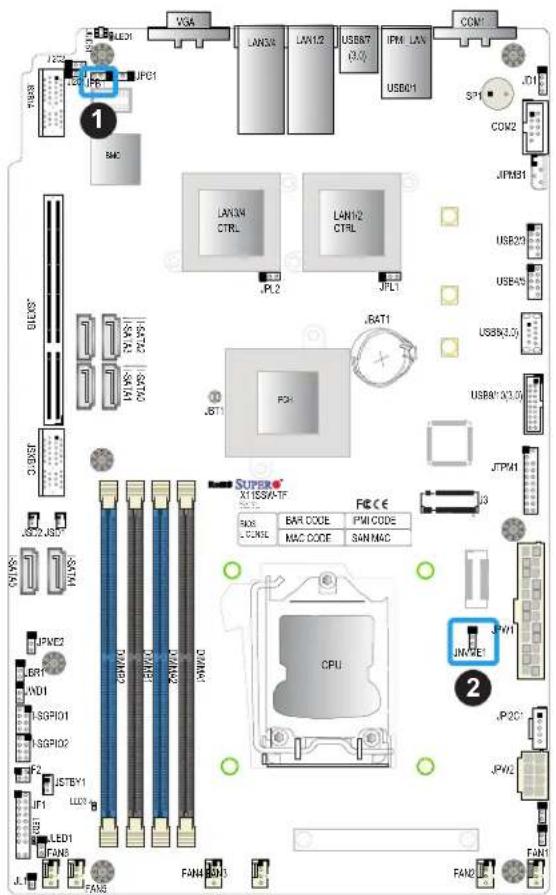
text_image
Circuit board layout diagram with labeled components and connectors-
BMC Enable
-
NVMe Connection
2.9 LED Indicators
LAN LEDs
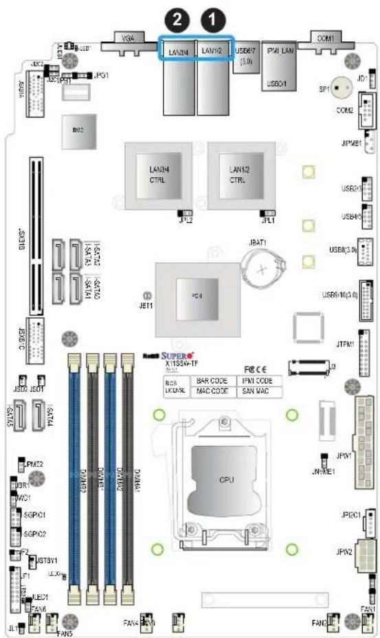
Four LAN ports (LAN 1/2 and LAN 3/4) are located on the I/O back panel of the motherboard. Each Ethernet LAN port has two LEDs. The green LED indicates activity, while the other Link LED may be green, amber, or off to indicate the speed of the connection. See the tables below for more information.
| LAN1/2/3/4 Activity LEDs (Right)LED State | ||
| Color | Status | Definition |
| Green Flashing | Active | |
| LAN1/2/3/4 Link LEDs (Left)LED State | |
| LED Color | Definition |
| Off No Connection | 10 Mbps/100 Mbps |
| Amber 1 Gbps | |
| Green 10 Gbps | |
text_image
2 1 VGA LAN24 LAN12 USB17 IPMI LAN COM1 LED LED USB1 PG1 BNC LAN34 CTRL LAN12 CTRL JPL2 JPL1 JBAT1 JET1 PC4 JSPX SULCK X1SSW-TF FECE RCS BAR CODE IPMI CODE LCD/NC MAC CODE SAN MAC JPMY JPMY1 JPMY2 JPMY3 JPMY4 JPMY5 JPMY6 JPMY7 JPMY8 JPMY9 JPMY10 JPMY11 JPMY12 JPMY13 JPMY14 JPMY15 JPMY16 JPMY17 JPMY18 JPMY19 JPMY20 JPMY21 JPMY22 JPMY23 JPMY24 JPMY25 JPMY26 JPMY27 JPMY28 JPMY29 JPMY30 JPMY31 JPMY32 JPMY33 JPMY34 JPMY35 JPMY36 JPMY37 JPMY38 JPMY39 JPMY40 JPMY41 JPMY42 JPMY43 JPMY44 JPMY45 JPMY46 JPMY47 JPMY48 JPMY49 JPMY50 JPMY51 JPMY52 JPMY53 JPMY54 JPMY55 JPMY56 JPMY57 JPMY58 JPMY59 JPMY60 JPMY61 JPMY62 JPMY63 JPMY64 JPMY65 JPMY66 JPMY67 JPMY68 JPMY69 JPMY70 JPMY71 JPMY72 JPMY73 JPMY74 JPMY75 JPMY76 JPMY77 JPMY78 JPMY79 JPMY80 JPMY81 JPMY82 JPMY83 JPMY84 JPMY85 JPMY86 JPMY87 JPMY88 JPMY89 JPMY90 JPMY91 JPMY92 JPMY93 JPMY94 JPMY95 JPMY96 JPMY97 JPMY98 JPMY99 JPMY100- LAN1/2 LEDs
- LAN3/4 LEDs
IPMI LAN LEDs
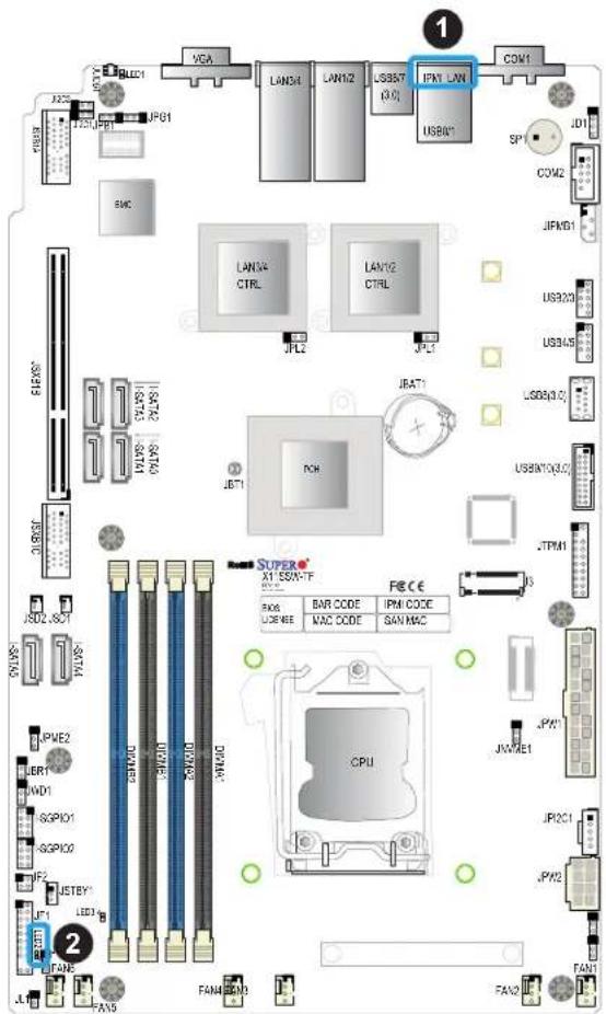
In addition to LAN1/2 and LAN3/4, a dedicated IPMI LAN is also located on the I/O back panel. The amber LED on the right indicates activity, while the green LED on the left indicates the speed of the connection. See the table below for more information.
IPMI LAN
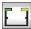
Activity LEDLink LED
| IPMI LAN LEDs | ||
| Color/State Definition | ||
| Link (left) | Green: SolidAmber: Solid | 100 Mbps1Gbps |
| Activity (Right) Amber: Blinking Active | ||
Onboard Power LED
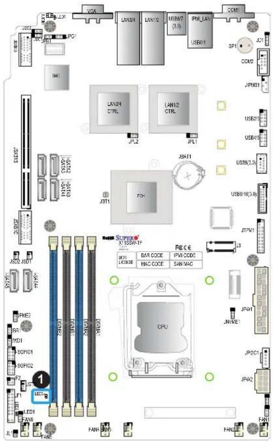
The Onboard Power LED is located at LED2 on the motherboard. When this LED is on, the system is on. Be sure to turn off the system and unplug the power cord before removing or installing components. See the table below for more information.
| Onboard Power LED Indicator |
| LED Color Definition |
| Off System Off |
| Green System On |
text_image
Labeled diagram of a computer motherboard showing CPU, memory chips, and hardware components with alphanumeric codes and labels.- IPMI LAN LED
- Onboard PWR LED
Standby Power LED
The 5V Standby Power LED is located at LED3 on the motherboard. When this LED is on, the standby power is connected. Be sure to unplug the power cable before removing or installing components. See the table below for more information.
| Standby Power LED Indicator | |
| LED Color Definition | |
| Off | Standby Power Off(power cable not connected) |
| Green Standby Power On | |
text_image
Labeled diagram of a computer motherboard floor with component labels and connectors- Standby Power LED
Chapter 3
Troubleshooting
3.1 Troubleshooting Procedures
Use the following procedures to troubleshoot your system. If you have followed all of the procedures below and still need assistance, refer to the 'Technical Support Procedures' and/or 'Returning Merchandise for Service' section(s) in this chapter. Always disconnect the AC power cord before adding, changing or installing any non hot-swap hardware components.
Before Power On
- Make sure that there are no short circuits between the motherboard and chassis.
- Disconnect all ribbon/wire cables from the motherboard, including those for the keyboard and mouse.
- Remove all add-on cards.
- Install the CPU (making sure it is fully seated) and connect the front panel connectors to the motherboard.
No Power
- Make sure that there are no short circuits between the motherboard and the chassis.
- Make sure that the ATX power connectors are properly connected.
- Check that the 115V/230V switch, if available, on the power supply is properly set.
- Turn the power switch on and off to test the system, if applicable.
- The battery on your motherboard may be old. Check to verify that it still supplies \~3VDC. If it does not, replace it with a new one.
No Video
- If the power is on but you have no video, remove all add-on cards and cables.
-
Use the speaker to determine if any beep codes are present. Refer to Appendix A for details on beep codes.
-
Remove all memory modules and turn on the system (if the alarm is on, check the specs of memory modules, reset the memory or try a different one).
System Boot Failure
If the system does not display POST or does not respond after the power is turned on, check the following:
- Check for any error beep from the motherboard speaker.
- If there is no error beep, try to turn on the system without DIMM modules installed. If there is still no error beep, replace the motherboard.
- If there are error beeps, clear the CMOS settings by unplugging the power cord and contacting both pads on the CMOS clear jumper (JBT1). (Refer to Section 2-8 in Chapter 2.)
-
Remove all components from the motherboard, especially the DIMM modules. Make sure that system power is on and that memory error beeps are activated.
-
Turn on the system with only one DIMM module installed. If the system boots, check for bad DIMM modules or slots by following the Memory Errors Troubleshooting procedure in this chapter.
Memory Errors
When a no-memory beep code is issued by the system, check the following:
-
Make sure that the memory modules are compatible with the system and that the DIMMs are properly and fully installed. (For memory compatibility, refer to the memory compatibility chart posted on our website at http://www.supermicro.com.)
-
Check if different speeds of DIMMs have been installed. It is strongly recommended that you use the same RAM type and speed for all DIMMs in the system.
-
Make sure that you are using the correct type of ECC DDR4 UDIMM modules recommended by the manufacturer.
-
Check for bad DIMM modules or slots by swapping a single module among all memory slots and check the results.
-
Make sure that all memory modules are fully seated in their slots. Follow the instructions given in Section 2-4 in Chapter 2.
-
Please follow the instructions given in the DIMM population tables listed in Section 2-4 to install your memory modules.
Losing the System's Setup Configuration
- Make sure that you are using a high-quality power supply. A poor-quality power supply may cause the system to lose the CMOS setup information. Refer to Section 2-7 for details on recommended power supplies.
- The battery on your motherboard may be old. Check to verify that it still supplies \~3VDC. If it does not, replace it with a new one. If the above steps do not fix the setup configuration problem, contact your vendor for repairs.
When the System Becomes Unstable
A. If the system becomes unstable during or after OS installation, check the following:
- CPU/BIOS support: Make sure that your CPU is supported and that you have the latest BIOS installed in your system.
- Memory support: Make sure that the memory modules are supported by testing the modules using memtest86 or a similar utility.

Note: Refer to the product page on our website at http://www.supermicro.com for memory and CPU support and updates.
- HDD support: Make sure that all hard disk drives (HDDs) work properly. Replace the bad HDDs with good ones.
- System cooling: Check the system cooling to make sure that all heatsink fans and CPU/system fans, etc., work properly. Check the hardware monitoring settings in the IPMI to make sure that the CPU and system temperatures are within the normal range. Also check the front panel Overheat LED and make sure that it is not on.
- Adequate power supply: Make sure that the power supply provides adequate power to the system. Make sure that all power connectors are connected. Please refer to our website for more information on the minimum power requirements.
- Proper software support: Make sure that the correct drivers are used.
B. If the system becomes unstable before or during OS installation, check the following:
-
Source of installation: Make sure that the devices used for installation are working properly, including boot devices such as CD/DVD.
-
Cable connection: Check to make sure that all cables are connected and working properly.
-
Using the minimum configuration for troubleshooting: Remove all unnecessary components (starting with add-on cards first), and use the minimum configuration (but with the CPU and a memory module installed) to identify the trouble areas. Refer to the steps listed in Section A above for proper troubleshooting procedures.
- Identifying bad components by isolating them: If necessary, remove a component in question from the chassis, and test it in isolation to make sure that it works properly. Replace a bad component with a good one.
- Check and change one component at a time instead of changing several items at the same time. This will help isolate and identify the problem.
- To find out if a component is good, swap this component with a new one to see if the system will work properly. If so, then the old component is bad. You can also install the component in question in another system. If the new system works, the component is good and the old system has problems.
3.2 Technical Support Procedures
Before contacting Technical Support, please take the following steps. Also, please note that as a motherboard manufacturer, Supermicro also sells motherboards through its channels, so it is best to first check with your distributor or reseller for troubleshooting services. They should know of any possible problems with the specific system configuration that was sold to you.
- Please go through the Troubleshooting Procedures and Frequently Asked Questions (FAQ) sections in this chapter or see the FAQs on our website (http://www.supermicro.com/) before contacting Technical Support.
- BIOS upgrades can be downloaded from our website (http://www.supermicro.com).
-
If you still cannot resolve the problem, include the following information when contacting Supermicro for technical support:
-
Motherboard model and PCB revision number
- BIOS release date/version (This can be seen on the initial display when your system first boots up.)
-
System configuration
-
An example of a Technical Support form is on our website at http://www.supermicro.com/RmaForm/.
- Distributors: For immediate assistance, please have your account number ready when placing a call to our Technical Support department. We can be reached by email at support@supermicro.com.
3.3 Frequently Asked Questions
Question: What type of memory does my motherboard support?
Answer: The motherboard supports ECC DDR4 UDIMM modules. To enhance memory performance, do not mix memory modules of different speeds and sizes. Please follow all memory installation instructions given on Section 2-4 in Chapter 2.
Question: How do I update my BIOS?
Answer: It is recommended that you do not upgrade your BIOS if you are not experiencing any problems with your system. Updated BIOS files are located on our website at http://www.supermicro.com. Please check our BIOS warning message and the information on how to update your BIOS on our website. Select your motherboard model and download the BIOS file to your computer. Also, check the current BIOS revision to make sure that it is newer than your BIOS before downloading. You can choose from the zip file and the .exe file. If you choose the zip BIOS file, please unzip the BIOS file onto a bootable USB device. Run the batch file using the format FLASH.BAT filename.rom from your bootable USB device to flash the BIOS. Then, your system will automatically reboot.
Warning: Do not shut down or reset the system while updating the BIOS to prevent possible system boot failure!)

Note: The SPI BIOS chip used on this motherboard cannot be removed. Send your motherboard back to our RMA Department at Supermicro for repair. For BIOS Recovery instructions, please refer to the AMI BIOS Recovery Instructions posted at http://www.supermicro.com.
3.4 Battery Removal and Installation
Battery Removal
To remove the onboard battery, follow the steps below:
- Power off your system and unplug your power cable.
- Locate the onboard battery as shown below.
- Using a tool such as a pen or a small screwdriver, push the battery lock outwards to unlock it. Once unlocked, the battery will pop out from the holder.
- Remove the battery.
Proper Battery Disposal
Please handle used batteries carefully. Do not damage the battery in any way; a damaged battery may release hazardous materials into the environment. Do not discard a used battery in the garbage or a public landfill. Please comply with the regulations set up by your local hazardous waste management agency to dispose of your used battery properly.
Battery Installation
- To install an onboard battery, follow the steps 1 and 2 above and continue below:
- Identify the battery's polarity. The positive (+) side should be facing up.
- Insert the battery into the battery holder and push it down until you hear a click to ensure that the battery is securely locked.

Important: When replacing a battery, be sure to only replace it with the same type.
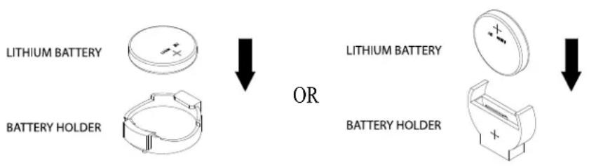
text_image
LITHIUM BATTERY BATTERY HOLDER OR LITHIUM BATTERY BATTERY HOLDER3.5 Returning Merchandise for Service
A receipt or copy of your invoice marked with the date of purchase is required before any warranty service will be rendered. You can obtain service by calling your vendor for a Returned Merchandise Authorization (RMA) number. When returning to the manufacturer, the RMA number should be prominently displayed on the outside of the shipping carton and mailed prepaid or hand-carried. Shipping and handling charges will be applied for all orders that must be mailed when service is complete.
For faster service, RMA authorizations may be requested online (http://www.supermicro.com/support/rma/).
This warranty only covers normal consumer use and does not cover damages incurred in shipping or from failure due to the alteration, misuse, abuse or improper maintenance of products.
During the warranty period, contact your distributor first for any product problems.
Chapter 4
BIOS
4.1 Introduction
This chapter describes the AMIBIOS™ Setup utility for the X11SSW-TF/-4TF motherboard. The BIOS is stored on a chip and can be easily upgraded using a flash program.
Note: Due to periodic changes to the BIOS, some settings may have been added or deleted and might not yet be recorded in this manual. Please refer to the Manual Download area of our website for any changes to the BIOS that may not be reflected in this manual.
Starting the Setup Utility
To enter the BIOS Setup Utility, hit the
The Main BIOS screen has two main frames. The left frame displays all the options that can be configured. "Grayed-out" options cannot be configured. The right frame displays the key legend. Above the key legend is an area reserved for a text message. When an option is selected in the left frame, it is highlighted in white. Often a text message will accompany it. (Note that BIOS has default text messages built in. We retain the option to include, omit, or change any of these text messages.) Settings printed in Bold are the default values.
A "▶" indicates a submenu. Highlighting such an item and pressing the
The BIOS setup utility uses a key-based navigation system called hot keys. Most of these hot keys (
4.2 Main Setup
When you first enter the AMI BIOS setup utility, you will enter the Main setup screen. You can always return to the Main setup screen by selecting the Main tab on the top of the screen. The Main BIOS setup screen is shown below. The following Main menu items will be displayed:
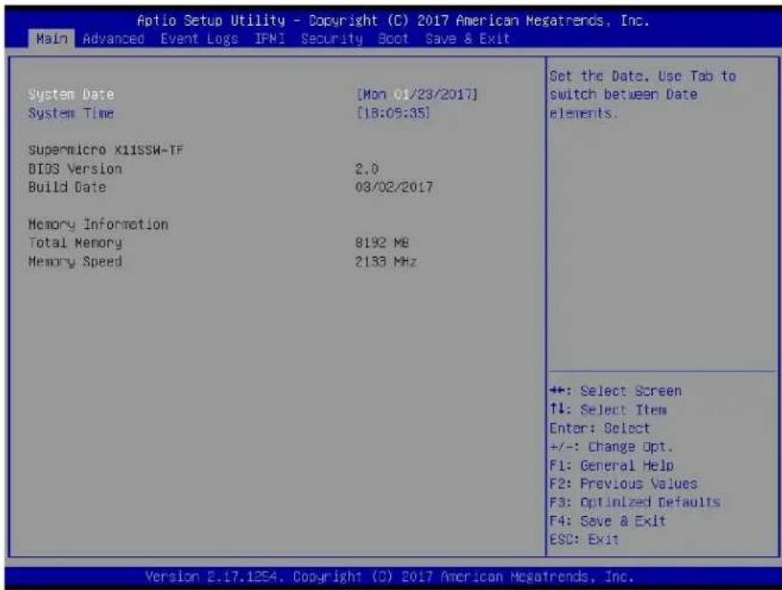
text_image
Antio Setup Utility - Copyright (C) 2017 American Megatrends, Inc. Main Advanced Event Logs IFNI Security Boot Save & Exit System Date [Mon 01/23/2017] System Time [18:05:35] Supermicro X11SSW-TF BIOS Version 2.0 Build Date 03/02/2017 Memory Information Total Memory 8192 MB Memory Speed 2133 MHz Set the Date. Use Tab to switch between Date elements. +: Select Screen ↑↓: Select Item Enter: Select +/-: Change Opt. F1: General Help F2: Previous Values F3: Optimized Defaults F4: Save & Exit ESC: Exit Version 2.17.1254. Copyright (C) 2017 American Megatrends, Inc.System Date/System Time
Use this option to change the system date and time. Highlight System Date or System Time using the arrow keys. Enter new values using the keyboard. Press the

Note: The time is in the 24-hour format. For example, 5:30 P.M. appears as 17:30:00. The date's default value is 03/02/2017 after RTC reset.
Supermicro X11SSW-TF
BIOS Version
This item displays the version of the BIOS ROM used in the system.
Build Date
This item displays the date when the version of the BIOS ROM used in the system was built.
Memory Information
Total Memory
This item displays the total size of memory available in the system.
Memory Speed
This item displays the memory speed.
4.3 Advanced Setup Configurations
Use the arrow keys to select Boot Setup and press
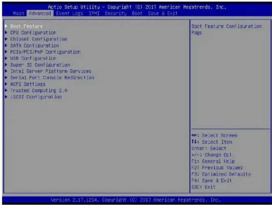
text_image
Actio Setup Utility - Copyright (C) 2017 American Megatrends, Inc. Main Advanced Event Logs IPMI Security Boot Save & Exit Boot Feature CPU Configuration Chipset Configuration SATA Configuration PCIe/PCI/PnP Configuration USB Configuration Super IO Configuration Intel Server Platform Services Serial Port Console Redirection ACPI Settings Trusted Computing 2.0 lSCSI Configuration Boot Feature Configuration Page +: Select Screen T↓: Select Item Enter: Select +/-: Change Opt. F1: General Help F2: Previous Values F3: Optimized Defaults F4: Save & Exit ESC: Exit Version 2.17.1254. Copyright (C) 2017 American Megatrends, Inc.Warning: Take caution when changing the Advanced settings. An incorrect value, a very high DRAM frequency, or an incorrect DRAM timing setting may make the system unstable. When this occurs, revert to the default to the manufacture default settings.
▶Boot Feature
Boot Feature
Quiet Boot
Use this feature to select the screen display between the POST messages and the OEM logo upon bootup. Select Disabled to display the POST messages. Select Enabled to display the OEM logo instead of the normal POST messages. The options are Disabled and Enabled.
AddOn ROM Display Mode
Use this feature to set the display mode for the Option ROM. Select Keep Current to display the current AddOn ROM setting. Select Force BIOS to use the Option ROM display set by the system BIOS. The options are Force BIOS and Keep Current.
Bootup NumLock State
Use this feature to set the Power-on state for the
Wait For "F1" If Error
Use this feature to force the system to wait until the "F1" key is pressed if an error occurs. The options are Disabled and Enabled.
INT19 (Interrupt 19) Trap Response
Interrupt 19 is the software interrupt that handles the boot disk function. When this item is set to Immediate, the ROM BIOS of the host adaptors will "capture" Interrupt 19 at bootup immediately and allow the drives that are attached to these host adaptors to function as bootable disks. If this item is set to Postponed, the ROM BIOS of the host adaptors will not capture Interrupt 19 immediately and allow the drives attached to these adaptors to function as bootable devices at bootup. The options are Immediate and Postponed.
Re-try Boot
If this item is enabled, the BIOS will automatically reboot the system from a specified boot device after its initial boot failure. The options are Disabled, Legacy Boot, and EFI Boot.
Install Windows 7 USB Support
Enable this feature to use the USB keyboard and mouse during the Windows 7 installation, since the native XHCI driver support is unavailable. Use a SATA optical drive as a USB drive, and USB CD/DVD drives are not supported. Disable this feature after the XHCI driver has been installed in Windows. The options are Disabled and Enabled.
Power Configuration
DeepSx Power Policies
Use this item to configure the Advanced Configuration and Power Interface (ACPI) settings for the system. Enable S3 to use Standby Mode (Suspend-to-RAM) and maintain power supply to the system RAM when the system is in the sleep mode. Enable S4 to use Hibernation mode (Suspend to Disk) so that all data stored in of the main memory can be saved in a non-volatile memory area such as in a hard drive and then power down the system. Enable S5 to power off the whole system except the power supply unit (PSU) and keep the power button "alive" so that the user can "wake-up" the system by using an USB keyboard or mouse. The options are Disabled and Enabled.
Watch Dog Function
If enabled, the Watch Dog Timer will allow the system to reset or generate NMI based on jumper settings when it is expired for more than 5 minutes. The options are Disabled and Enabled.
Power Button Function
This feature controls how the system shuts down when the power button is pressed. Select 4 Seconds Override for the user to power off the system after pressing and holding the power button for 4 seconds or longer. Select Instant Off to instantly power off the system as soon as the user presses the power button. The options are Instant Off and 4 Seconds Override.
Restore on AC Power Loss
Use this feature to set the power state after a power outage. Select Stay Off for the system power to remain off after a power loss. Select Power On for the system power to be turned on after a power loss. Select Last State to allow the system to resume its last power state before a power loss. The options are Stay Off, Power On, and Last State.
▶CPU Configuration
CPU Configuration
The following CPU information will be displayed:
- CPU Signature
- Microcode Patch
- Max CPU Speed
- Min CPU Speed
- CPU Speed
- Processor Cores
• Hyper Threading Technology
• Intel VT-x Technology
• Intel SMX Technology - 64-bit
- EIST Technology
- CPU C3 State
- CPU C6 State
- CPU C7 State
-
CPU C8 State
-
CPU C9 State
- CPU C10 State
- L1 Data Cache
- L1 Code Cache
- L2 Cache
- L3 Cache
- L4 Cache
Hyper-threading (Available when supported by the CPU)
Select Enabled to support Intel Hyper-threading Technology to enhance CPU performance. The options are Disabled and Enabled.
Active Processor Cores
This feature determines how many CPU cores will be activated for each CPU. When All is selected, all cores in the CPU will be activated. (Please refer to Intel's website for more information.) The options are All, 1, 2, and 3.
Execute Disable Bit (Available if supported by the OS & the CPU)
Set to Enabled for Execute Disable Bit support which will allow the processor to designate areas in the system memory where an application code can execute and where it cannot, thus preventing a worm or a virus from flooding illegal codes to overwhelm the processor or damaging the system during a virus attack. The options are Disabled and Enabled. (Refer to Intel and Microsoft websites for more information.)
Intel® Virtualization Technology
Select Enabled to use Intel Virtualization Technology so that I/O device assignments will be reported directly to the VMM (Virtual Memory Management) through the DMAR ACPI Tables. This feature offers fully-protected I/O resource-sharing across the Intel platforms, providing the user with greater reliability, security and availability in networking and data-sharing. The options are Disabled and Enabled.
Hardware Prefetcher (Available when supported by the CPU)
If set to Enabled, the hardware prefetcher will prefetch streams of data and instructions from the main memory to the L2 cache to improve CPU performance. The options are Disabled and Enabled.
Adjacent Cache Line Prefetch (Available when supported by the CPU)
The CPU prefetches the cache line for 64 bytes if this feature is set to Disabled. The CPU prefetches both cache lines for 128 bytes as comprised if this feature is set to Enabled.
CPU AES
Select Enabled to enable Intel CPU Advanced Encryption Standard (AES) Instructions for CPU to enhance data integrity. The options are Disabled and Enabled.
Boot Performance Mode
This feature allows the user to select the performance state that the BIOS will set before the operating system handoff. The options are Power Saving, Max Non-Turbo Performance, and Turbo Performance.
Hardware P-States (HWP)
Use this feature to enable or disable hardware P-States support. The options are Disabled and Enabled.
Intel® SpeedStep™
Intel SpeedStep Technology allows the system to automatically adjust processor voltage and core frequency to reduce power consumption and heat dissipation. The options are Disabled and Enabled.
Turbo Mode
Select Enabled for processor cores to run faster than the frequency specified by the manufacturer. The options are Disabled and Enabled.
Package Power Limit MSR Lock
Select Enabled to lock the package power limit for the model specific registers. The options are Disabled and Enabled.
Power Limit 1 Override
Select Enabled to support average power limit (PL1) override. The default setting is Disabled.
Power Limit 2 Override
Select Enabled to support rapid power limit (PL2) override. The default setting is Enabled.
Power Limit 2
Use this item to configure the value for Power Limit 2. The value is in milli watts and the step size is 125mW. Use the number keys on your keyboard to enter the value. Enter 0 to use the manufacture default setting. If the value is 0, the BIOS will set PL2 as 1.25* TDP.
1-Core Ratio Limit Override
This increases (multiplies) one clock speed in the CPU core in relation to the bus speed when one CPU core is active. Press "+" or "-" on your keyboard to change the value. Enter 0 to use the manufacture default setting.
2-Core Ratio Limit Override
This increases (multiplies) two clock speeds in the CPU core in relation to the bus speed when two CPU cores are active. Press "+" or "-" on your keyboard to change the value. Enter 0 to use the manufacture default setting.
3-Core Ratio Limit Override
This increases (multiplies) three clock speeds in the CPU core in relation to the bus speed when three CPU cores are active. Press "+" or "-" on your keyboard to change the value. Enter 0 to use the manufacture default setting.
4-Core Ratio Limit Override
This increases (multiplies) four clock speeds in the CPU core in relation to the bus speed when three CPU cores are active. Press "+" or "-" on your keyboard to change the value. Enter 0 to use the manufacture default setting.
CPU C-States
Use this feature to enable the C-State of the CPU. The options are Disabled and Enabled.
Enhanced C-States
Use this feature to enable or disable C1E, which is a power saving feature for the CPU. C1E drops the frequency and voltage of the CPU to reduce power usage when the system is idle. The options are Disabled and Enabled.
C-State Auto Demotion
Use this feature to prevent unnecessary excursions into the C-states to improve latency. The options are Disabled, C1, C3, and C1 and C3.
C-State Un-Demotion
This feature allows the user to enable or disable the un-demotion of C-State. The options are Disabled, C1, C3, and C1 and C3
Package C-State Demotion
Use this feature to enable or disable the Package C-State demotion. The options are Disabled and Enabled.
Package C-State Un-Demotion
Use this feature to enable or disable the Package C-State un-demotion. The options are Disabled and Enabled.
C-State Pre-Wake
This feature allows the user to enable or disable the C-State Pre-Wake. The options are Disabled and Enabled.
Package C-State Limit
Use this feature to set the Package C-State limit. The options are C0/C1, C2, C3, C6, C7, C7s, C8, and Auto.
▶CPU Thermal Configuration
CPU Thermal Configuration
CPU DTS
Select Enabled for the ACPI thermal management to use the DTS SMM mechanism to obtain CPU temperature values. Select Disabled for EC to report the CPU temperature values. The options are Disabled and Enabled.
ACPI 3.0 T-States
Select Enabled to support CPU throttling by the operating system to reduce power consumption. The options are Disabled and Enabled.
▶Chipset Configuration
Warning: Setting the wrong values in the following features may cause the system to malfunction.
▶System Agent (SA) Configuration
The following System Agent information will be displayed:
• System Agent Bridge Name
• SA PCIe Code Version
- VT-d
VT-d
Select Enabled to enable Intel Virtualization Technology support for Direct I/O VT-d by reporting the I/O device assignments to VMM through the DMAR ACPI Tables. This feature offers fully-protected I/O resource-sharing across the Intel platforms, providing the user with greater reliability, security and availability in networking and data-sharing. The options are Disabled and Enabled.
eDRAM Mode
Use this feature to select the eDRAM mode. The options are SW Mode eDRAM Off, SW Mode eDRAM On, and eDRAM HW Mode.
▶ Graphics Configuration
Graphics Configuration
Primary Display
Use this feature to select the graphics device to be used as the primary display. The options are Auto, PEG, and PCIE.
Primary PCIE
This feature allows the user to specify which graphics device to be used as the primary graphics card. The option is Onboard.
▶DMI/OPI Configuration
DMI/OPI Configuration
The following DMI information will be displayed:
• DMI
DMI VC1 Control
Use this feature to enable or disable DMI Virtual Channel 1. The options are Enabled and Disabled.
DMI VCm Control
Use this feature to enable or disable the DMI Virtual Channel map. The options are Enabled and Disabled.
CPU DMI Link ASPM Control
Use this feature to set the ASPM (Active State Power Management) state on the SA (System Agent) side of the DMI Link. The options are Disabled and L1.
DMI Extended Sync Control
Use this feature to enable or disable the DMI extended synchronization. The options are Enabled and Disabled.
DMI De-Emphasis Control
Use this feature to configure the De-emphasis control on DMI. The options are -6 dB and -3.5 dB.
▶Memory Configuration
Memory Configuration
The following memory information will be displayed:
• Memory RC Version
- Memory Frequency
- Total Memory
• VDD
- DIMMA1
- DIMMA2
- DIMMB1
- DIMMB2
• Memory Timings (tCL-tRCD-tRP-tRAS)
Maximum Memory Frequency
Use this feature to set the maximum memory frequency for onboard memory modules. The options are Auto, 1067, 1200, 1333, 1400, 1600, 1800, 1867, 2000, 2133, 2200, 2400, 2600, 2667, 2800, 2933, 3000, and 3200.
Max TOLUD
This feature sets the maximum TOLUD value, which specifies the "Top of Low Usable DRAM" memory space to be used by internal graphics devices, GTT Stolen Memory, and TSEG, respectively, if these devices are enabled. The options are Dynamic, 1 GB, 1.25 GB, 1.5 GB, 1.75 GB, 2 GB, 2.25 GB, 2.5 GB, 2.75 GB, 3 GB, 3.25 GB, and 3.5 GB.
Energy Performance Gain
Use this feature to enable or disable the energy performance gain. The options are Disabled and Enabled.
Memory Scrambler
Select Enabled to enable memory scrambler support. The options are Disabled and Enabled.
Fast Boot
Use this feature to enable or disable fast path through the memory reference code. The options are Enabled and Disabled.
REFRESH\_2X\_MODE
Use this feature to select the refresh mode. The options are Disabled, 1-Enabled for WARM or HOT, and 2-Enabled HOT only.
Closed Loop Thermal Management
Use this feature to monitor the power consumption and temperature of the system to predict a thermal trend. The options are Disabled and Enabled.
▶GT - Power Management Control
GT - Power Management Control
The following GT - Power Management Control information will be displayed:
- GT Info
RC6 (Render Standby)
Select Enabled to enable render standby support. RC6 is a power saving feature that allows the onboard graphics to enter standby mode to decrease power usage. The options are Disabled and Enabled.
▶PCH-IO Configuration
The following PCH-IO information will be displayed:
• Intel PCH RC Version
• Intel PCH SKU Name
- Intel PCH Rev ID
▶PCI Express Configuration
PCI Express Configuration
PCH DMI Link ASPM Control
Use this feature to set the ASPM (Active State Power Management) state on the SA (System Agent) side of the DMI Link. The options are Disabled and Enabled.
Peer Memory Write Enable
Use this feature to enable or disable peer memory write. The options are Disabled and Enabled.
▶PCH PCI-E 3.0 M.2
PCH PCI-E 3.0 M.2 ASPM Support
Use this item to set the Active State Power Management (ASPM) level for the PCI-E 3.0 M.2 device installed on the slot specified. Select Auto for the system BIOS to automatically set the ASPM level based on the system configuration. Select Disabled to disable ASPM support. The options are Disabled, L0s, L1, L0s & L1, and Auto.
PCH PCI-E 3.0 M.2 L1 Substates
Use this feature to configure the PCI Express L1 substates. The options are Disabled, L1.1, L1.2, and L1.1 & L1.2.
PCH PCI-E 3.0 M.2 PCIe Speed
Use this feature to select the PCI Express port speed. The options are Auto, Gen1, Gen2, and Gen3.
PCH PCI-E 3.0 M.2 Detect Non-Compliance
Select Enabled for the AMI BIOS to automatically detect a PCI-E device that is not compliant with the PCI-E standards. The options are Disabled and Enabled.
Port 61h bit-4 Emulation
Select Enabled to enable the emulation of Port 61h bit-4 toggling in SMM (System Management Mode). The options are Disabled and Enabled.
PCIe PLL SSC
Enable this feature to reduce EMI interference by down spreading clock 0.5%. Disable this feature to centralize the clock without spreading. The options are Disabled and Enabled.
▶SATA Configuration
When this submenu is selected, the AMI BIOS automatically detects the presence of the SATA devices that are supported by the Intel PCH chip and displays the following items:
SATA Controller(s)
This item enables or disables the onboard SATA controller supported by the Intel PCH chip. The options are Enabled and Disabled.
SATA Mode Selection
Use this item to select the mode for the installed SATA drives. The options are AHCI and RAID.
SATA Frozen
Use this item to enable the HDD Security Frozen Mode. The options are Disabled and Enabled.
*If the item "SATA Mode Selection" is set to AHCI, the following items will be displayed:
Serial ATA Port 0 \~ Port 5
This item displays the information detected on the installed SATA drive on the particular SATA port.
• Model number of drive and capacity
- Software Preserve Support
Port 0 \~ Port 5 Hot Plug
This feature designates the SATA port specified for hot plugging. Set this item to Enabled for hot-plugging support, which will allow the user to replace a SATA disk drive without shutting down the system. The options are Disabled and Enabled.
Port 0 \~ Port 5 Spin Up Device
On an edge detect from 0 to 1, set this item to allow the PCH to initialize the device. The options are Disabled and Enabled.
Port 0 \~ Port 5 SATA Device Type
Use this item to specify if the SATA port specified by the user should be connected to a Solid State drive or a Hard Disk Drive. The options are Hard Disk Drive and Solid State Drive.
*If the item "SATA Mode Selection" is set to RAID, the following items will be displayed:
SATA RAID Option ROM/UEFI Driver
Select UEFI to load the EFI driver for system boot. Select Legacy to load a legacy driver for system boot. The options are Legacy ROM and UEFI Driver.
Serial ATA Port 0 \~ Port 5
This item displays the information detected on the installed SATA drive on the particular SATA port.
• Model number of drive and capacity
- Software Preserve Support
Port 0 \~ Port 5 Hot Plug
This feature designates the SATA port specified for hot plugging. Set this item to Enabled for hot-plugging support, which will allow the user to replace a SATA disk drive without shutting down the system. The options are Disabled and Enabled.
Port 0 \~ Port 5 Spin Up Device
On an edge detect from 0 to 1, set this item to allow the PCH to initialize the device. The options are Disabled and Enabled.
Port 0 \~ Port 5 SATA Device Type
Use this item to specify if the SATA port specified by the user should be connected to a Solid State drive or a Hard Disk Drive. The options are Hard Disk Drive and Solid State Drive.
▶PCIe/PCI/PnP Configuration
The following information will be displayed:
• PCI Bus Driver Version
PCI Devices Common Settings:
PCI PERR/SERR Support
Select Enabled to allow a PCI device to generate a PERR/SERR number for a PCI Bus Signal Error Event. The options are Disabled and Enabled.
Above 4G Decoding (Available if the system supports 64-bit PCI decoding)
Select Enabled to decode a PCI device that supports 64-bit in the space above 4G Address. The options are Disabled and Enabled.
SR-IOV Support
Use this feature to enable or disable Single Root IO Virtualization Support. The options are Disabled and Enabled.
RSC-W-68 Riser:
Slot1: PCI-E 3.0 X16 OPROM
Use this feature to select which firmware type to be loaded for the add-on card in this slot. The options are Disabled, Legacy, and EFI.
Slot2: PCI-E 3.0 X8 OPROM
Use this feature to select which firmware type to be loaded for the add-on card in this slot. The options are Disabled, Legacy, and EFI.
Onboard LAN Option ROM Type
Select Enabled to enable Option ROM support to boot the computer using a network device specified by the user. The options are Legacy and EFI.
Onboard LAN1 Option ROM
Onboard LAN2 Option ROM
Onboard LAN3 Option ROM
Onboard LAN4 Option ROM
Use the above four items to select the type of device installed in a LAN port specified by the user for system boot. The default setting for Onboard LAN1 Option ROM is PXE, and the default setting for Onboard LAN2 Option ROM/Onboard LAN3 Option ROM/Onboard LAN4 Option ROM is Disabled.
Onboard Video Option ROM
Use this item to select the Onboard Video Option ROM type. The options are Disabled, Legacy, and EFI.
Network Stack
Select Enabled to enable PXE (Preboot Execution Environment) or UEFI (Unified Extensible Firmware Interface) for network stack support. The options are Disabled and Enabled.
*If the item "Network Stack" is set to Enabled, the four items below will be displayed:
IPv4 PXE Support
Select Enabled to enable IPv4 PXE boot support. The options are Disabled and Enabled.
IPv6 PXE Support
Select Enabled to enable IPv6 PXE boot support. The options are Disabled and Enabled.
PXE boot wait time
Use this option to specify the wait time to press the ESC key to abort the PXE boot. Press "+" or "-" on your keyboard to change the value. The default setting is 0.
Media detect count
Use this option to specify the number of times media will be checked. Press "+" or "-" on your keyboard to change the value. The default setting is 1.
▶USB Configuration
USB Configuration
The following USB items will be displayed:
- USB Module Version
- USB Controllers
- USB Devices
Legacy USB Support (Available when USB Functions is not Disabled)
Select Enabled to support legacy USB devices. Select Auto to disable legacy support if USB devices are not present. Select Disabled to have USB devices available for EFI (Extensive Firmware Interface) applications only. The settings are Enabled, Disabled, and Auto.
XHCI Hand-off
This item is for operating systems that do not support eXtensible Host Controller Interface (XHCI) hand-off. When this item is enabled, XHCI ownership change will be claimed by the XHCI driver. The settings are Enabled and Disabled.
Port 60/64 Emulation
Select Enabled for I/O port 60h/64h emulation support which will provide complete USB keyboard legacy support for the operating system that does not support Legacy USB devices. The options are Disabled and Enabled.
▶Super IO Configuration
Super IO Configuration
The following Super IO information will be displayed:
- Super IO Chip
▶Serial Port 1
Serial Port 1
This submenu allows the user the configure settings of Serial Port 1.
Serial Port 1
Select Enabled to enable the selected onboard serial port. The options are Disabled and Enabled.
Device Settings
This item displays the status of a serial part specified by the user.
Serial Port 1 Change Settings
This feature specifies the base I/O port address and the Interrupt Request address of a serial port specified by the user. Select Auto to allow the BIOS to automatically assign the base I/O and IRQ address. The options for Serial Port 1 are Auto, (IO=3F8h; IRQ=4), (IO=3F8h; IRQ=3, 4, 5, 6, 7, 9, 10, 11, 12), (IO=2F8h; IRQ=3, 4, 5, 6, 7, 9, 10, 11, 12), (IO=3E8h; IRQ=3, 4, 5, 6, 7, 9, 10, 11, 12), and (IO=2E8h; IRQ=3, 4, 5, 6, 7, 9, 10, 11, 12).
▶Serial Port 2
Serial Port 2
This submenu allows the user the configure settings of Serial Port 2.
Serial Port 2
Select Enabled to enable the selected onboard serial port. The options are Disabled and Enabled.
Device Settings
This item displays the status of a serial part specified by the user.
Serial Port 2 Change Settings
This feature specifies the base I/O port address and the Interrupt Request address of a serial port specified by the user. Select Auto to allow the BIOS to automatically assign the base I/O and IRQ address. The options for Serial Port 2 are Auto, (IO=2F8h; IRQ=3), (IO=3F8h; IRQ=3, 4, 5, 6, 7, 9, 10, 11, 12), (IO=2F8h; IRQ=3, 4, 5, 6, 7, 9, 10, 11, 12), (IO=3E8h; IRQ=3, 4, 5, 6, 7, 9, 10, 11, 12), and (IO=2E8h; IRQ=3, 4, 5, 6, 7, 9, 10, 11, 12).
Serial Port 2 Attribute (Available for Serial Port 2 only)
Select SOL to use COM Port 2 as a Serial Over LAN (SOL) port for console redirection. The options are SOL and COM.
▶Intel Server Platform Services
The following Intel Server Platform Services information will be displayed:
• ME BIOS Interface Version
- SPS Version
• ME FW Status Value
- ME FW State
• ME FW Operation State
• ME FW Error Code
• ME NM FW Status Value
• BIOS Booting Mode
- Cores Disabled
• ME FW SKU Information
• End-of-POST Status
▶Serial Port Console Redirection
COM1
COM1 Console Redirection
Select Enabled to enable console redirection support for a serial port specified by the user. The options are Disabled and Enabled.
*If the item "COM1 Console Redirection" is set to Enabled, the following items will become available for configuration:
▶COM1 Console Redirection Settings
This feature allows the user to specify how the host computer will exchange data with the client computer, which is the remote computer used by the user.
COM1 Terminal Type
This feature allows the user to select the target terminal emulation type for Console Redirection. Select VT100 to use the ASCII Character set. Select VT100+ to add color and function key support. Select ANSI to use the Extended ASCII Character Set. Select VT-UTF8 to use UTF8 encoding to map Unicode characters into one or more bytes. The options are VT100, VT100+, VT-UTF8, and ANSI.
COM1 Bits Per second
Use this feature to set the transmission speed for a serial port used in Console Redirection. Make sure that the same speed is used in the host computer and the client computer. A lower transmission speed may be required for long and busy lines. The options are 9600, 19200, 38400, 57600 and 115200 (bits per second).
COM1 Data Bits
Use this feature to set the data transmission size for Console Redirection. The options are 7 and 8.
COM1 Parity
A parity bit can be sent along with regular data bits to detect data transmission errors. Select Even if the parity bit is set to 0, and the number of 1's in data bits is even. Select Odd if the parity bit is set to 0, and the number of 1's in data bits is odd. Select None if you do not want to send a parity bit with your data bits in transmission. Select Mark to add a mark as a parity bit to be sent along with the data bits. Select Space to add a Space as a parity bit to be sent with your data bits. The options are None, Even, Odd, Mark, and Space.
COM1 Stop Bits
A stop bit indicates the end of a serial data packet. Select 1 Stop Bit for standard serial data communication. Select 2 Stop Bits if slower devices are used. The options are 1 and 2.
COM1 Flow Control
Use this feature to set the flow control for Console Redirection to prevent data loss caused by buffer overflow. Send a "Stop" signal to stop sending data when the receiving buffer is full. Send a "Start" signal to start sending data when the receiving buffer is empty. The options are None and Hardware RTS/CTS.
COM1 VT-UTF8 Combo Key Support
Select Enabled to enable VT-UTF8 Combination Key support for ANSI/VT100 terminals. The options are Disabled and Enabled.
COM1 Recorder Mode
Select Enabled to capture the data displayed on a terminal and send it as text messages to a remote server. The options are Disabled and Enabled.
COM1 Resolution 100x31
Select Enabled for extended-terminal resolution support. The options are Disabled and Enabled.
COM1 Legacy OS Redirection Resolution
Use this feature to select the number of rows and columns used in Console Redirection for legacy OS support. The options are 80x24 and 80x25.
COM1 Putty KeyPad
This feature selects the settings for Function Keys and KeyPad used for Putty, which is a terminal emulator designed for the Windows OS. The options are VT100, LINUX, XTERMR6, SC0, ESCN, and VT400.
COM1 Redirection After BIOS POST
Use this feature to enable or disable legacy console redirection after BIOS POST. When set to Bootloader, legacy console redirection is disabled before booting the OS. When set to Always Enable, legacy console redirection remains enabled when booting the OS. The options are Always Enable and BootLoader.
SOL/COM2
SOL/COM2 Console Redirection
Select Enabled to use the SOL port for Console Redirection. The options are Disabled and Enabled.
*If the item "SOL/COM2 Console Redirection" is set to Enabled, the following items will become available for configuration:
▶SOL/COM2 Console Redirection Settings
Use this feature to specify how the host computer will exchange data with the client computer, which is the remote computer used by the user.
COM2 Terminal Type
Use this feature to select the target terminal emulation type for Console Redirection. Select VT100 to use the ASCII Character set. Select VT100+ to add color and function key support. Select ANSI to use the Extended ASCII Character Set. Select VT-UTF8 to use UTF8 encoding to map Unicode characters into one or more bytes. The options are VT100, VT100+, VT-UTF8, and ANSI.
COM2 Bits Per second
Use this feature to set the transmission speed for a serial port used in Console Redirection. Make sure that the same speed is used in the host computer and the client computer. A lower transmission speed may be required for long and busy lines. The options are 9600, 19200, 38400, 57600 and 115200 (bits per second).
COM2 Data Bits
Use this feature to set the data transmission size for Console Redirection. The options are 7 and 8.
COM2 Parity
A parity bit can be sent along with regular data bits to detect data transmission errors. Select Even if the parity bit is set to 0, and the number of 1's in data bits is even. Select Odd if the parity bit is set to 0, and the number of 1's in data bits is odd. Select None if you do not want to send a parity bit with your data bits in transmission. Select Mark to add a mark as a parity bit to be sent along with the data bits. Select Space to add a Space as a parity bit to be sent with your data bits. The options are None, Even, Odd, Mark and Space.
COM2 Stop Bits
A stop bit indicates the end of a serial data packet. Select 1 Stop Bit for standard serial data communication. Select 2 Stop Bits if slower devices are used. The options are 1 and 2.
COM2 Flow Control
Use this feature to set the flow control for Console Redirection to prevent data loss caused by buffer overflow. Send a "Stop" signal to stop sending data when the receiving buffer is full. Send a "Start" signal to start sending data when the receiving buffer is empty. The options are None and Hardware RTS/CTS.
COM2 VT-UTF8 Combo Key Support
Select Enabled to enable VT-UTF8 Combination Key support for ANSI/VT100 terminals. The options are Disabled and Enabled.
COM2 Recorder Mode
Select Enabled to capture the data displayed on a terminal and send it as text messages to a remote server. The options are Disabled and Enabled.
COM2 Resolution 100x31
Select Enabled for extended-terminal resolution support. The options are Disabled and Enabled.
COM2 Legacy OS Redirection Resolution
Use this feature to select the number of rows and columns used in Console Redirection for legacy OS support. The options are 80x24 and 80x25.
COM2 Putty KeyPad
This feature selects Function Keys and KeyPad settings for Putty, which is a terminal emulator designed for the Windows OS. The options are VT100, LINUX, XTERMR6, SCO, ESCN, and VT400.
COM2 Redirection After BIOS POST
Use this feature to enable or disable legacy Console Redirection after BIOS POST. When set to Bootloader, legacy Console Redirection is disabled before booting the OS. When set to Always Enable, legacy Console Redirection remains enabled when booting the OS. The options are Always Enable and BootLoader.
Serial Port for Out-of-Band Management/Windows Emergency Management Services (EMS)
EMS Console Redirection
Select Enabled to use a COM port selected by the user for EMS Console Redirection. The options are Disabled and Enabled.
*If the item "EMS Console Redirection" is set to Enabled, the following items will become available for user's configuration:
▶EMS Console Redirection Settings
This feature allows the user to specify how the host computer will exchange data with the client computer, which is the remote computer used by the user.
Out-of-Band Mgmt Port
The feature selects a serial port in a client server to be used by the Microsoft Windows Emergency Management Services (EMS) to communicate with a remote host server. The options are COM1 and SOL/COM2.
Terminal Type
Use this feature to select the target terminal emulation type for Console Redirection. Select VT100 to use the ASCII character set. Select VT100+ to add color and function key support. Select ANSI to use the extended ASCII character set. Select VT-UTF8 to use UTF8 encoding to map Unicode characters into one or more bytes. The options are VT100, VT100+, VT-UTF8, and ANSI.
Bits Per Second
This item sets the transmission speed for a serial port used in Console Redirection. Make sure that the same speed is used in the host computer and the client computer. A lower transmission speed may be required for long and busy lines. The options are 9600, 19200, 57600, and 115200 (bits per second).
Flow Control
Use this item to set the flow control for Console Redirection to prevent data loss caused by buffer overflow. Send a "Stop" signal to stop sending data when the receiving buffer is full. Send a "Start" signal to start sending data when the receiving buffer is empty. The options are None, Hardware RTS/CTS, and Software Xon/Xoff.
The settings below are displayed:
Data Bits, Parity, Stop Bits
▶ACPI Settings
ACPI Settings
High Precision Event Timer
Select Enabled to activate the High Performance Event Timer (HPET) that produces periodic interrupts at a much higher frequency than a Real-time Clock (RTC) does in synchronizing multimedia streams, providing smooth playback and reducing the dependency on other timestamp calculation devices, such as an x86 RDTSC Instruction embedded in the CPU. The High Performance Event Timer is used to replace the 8254 Programmable Interval Timer. The options are Disabled and Enabled.
WHEA Support
Select Enabled to support the Windows Hardware Error Architecture (WHEA) platform and provide a common infrastructure for the system to handle hardware errors within the Windows OS environment to reduce system crashes and to enhance system recovery and health monitoring. The options are Disabled and Enabled.
▶Trusted Computing 2.0
TPM20 Device Found
Security Device Support
If this feature and the TPM jumper on the motherboard are both set to Enabled, onboard security devices will be enabled for TPM (Trusted Platform Module) support to enhance data integrity and network security. Please reboot the system for a change on this setting to take effect. The options are Disable and Enable.
The following Platform Configuration Register information will be displayed:
• Active PCR banks
• Available PCR banks
*If the item "Security Device Support" is set to Enable, the following items will become available for user's configuration:
SHA-1 PCR Bank
Use this item to disable or enable the SHA-1 Platform Configuration Register (PCR) bank for the installed TPM device. The options are Disabled and Enabled.
SHA256 PCR Bank
Use this item to disable or enable the SHA256 Platform Configuration Register (PCR) bank for the installed TPM device. The options are Disabled and Enabled.
Pending Operation
Use this item to schedule a TPM-related operation to be performed by a security device for system data integrity. Your system will reboot to carry out a pending TPM operation. The options are None and TPM Clear.
Platform Hierarchy
Use this item to disable or enable platform hierarchy for platform protection. The options are Disabled and Enabled.
Storage Hierarchy
Use this item to disable or enable storage hierarchy for cryptographic protection. The options are Disabled and Enabled.
Endorsement Hierarchy
Use this item to disable or enable endorsement hierarchy for privacy control. The options are Disabled and Enabled.
TPM2.0 UEFI Spec Version
Use this feature to specify the TPM UEFI spec version. TCG 1.2 has support for Windows® 2012, Windows 8, and Windows 10. TCG 2 has support for Windows 10 or later. The options are TCG_1_2 and TCG_2.
PH Randomization
Use this feature to disable or enable Platform Hierarchy Randomization. The options are Disabled and Enabled.
Device Select
Use this feature to select the TPM version. TPM 1.2 will restrict support to TPM 1.2 devices. TPM 2.0 will restrict support for TPM 2.0 devices. Select Auto to enable support for both versions. The default setting is Auto.
TXT Support
Intel TXT (Trusted Execution Technology) helps protect against software-based attacks and ensures protection, confidentiality and integrity of data stored or created on the system. Use this feature to enable or disable TXT Support. The options are Disabled and Enabled.
▶iSCSi Configuration
iSCSI Initiator Name
This feature allows the user to enter the unique name of the iSCSI Initiator in IQN format. Once the name of the iSCSI Initiator is entered into the system, configure the proper settings for the following items.
▶ Add an Attempt
▶ Delete Attempts
▶Change Attempt order
4.4 Event Logs
Use this feature to configure Event Log settings.
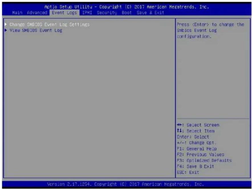
text_image
Action Setup Utility - Copyright (C) 2017 American Megatrends, Inc. Main Advanced Event Logs IPMI Security Boot Save & Exit Change SMBIOS Event Log Settings View SMBIOS Event Log Press▶Change SMBIOS Event Log Settings
Enabling/Disabling Options
SMBIOS Event Log
Change this item to enable or disable all features of the SMBIOS Event Logging during system boot. The options are Disabled and Enabled.
Erasing Settings
Erase Event Log
If No is selected, data stored in the event log will not be erased. Select Yes, Next Reset, data in the event log will be erased upon next system reboot. Select Yes, Every Reset, data in the event log will be erased upon every system reboot. The options are No, (Yes, Next reset), and (Yes, Every reset).
When Log is Full
Select Erase Immediately for all messages to be automatically erased from the event log when the event log memory is full. The options are Do Nothing and Erase Immediately.
SMBIOS Event Log Standard Settings
Log System Boot Event
This option toggles the System Boot Event logging to enabled or disabled. The options are Enabled and Disabled.
MECI
The Multiple Event Count Increment (MECI) counter counts the number of occurrences that a duplicate event must happen before the MECI counter is incremented. This is a numeric value. The default value is 1.
METW
The Multiple Event Time Window (METW) defines number of minutes must pass between duplicate log events before MECI is incremented. This is in minutes, from 0 to 99. The default value is 60.

Note: After making changes on a setting, be sure to reboot the system for the changes to take effect.
▶View SMBIOS Event Log
This item allows the user to view the event in the SMBIOS event log. The following categories are displayed:
DATE/TIME/ERROR CODE/SEVERITY
4.5 IPMI
Use this feature to configure Intelligent Platform Management Interface (IPMI) settings.
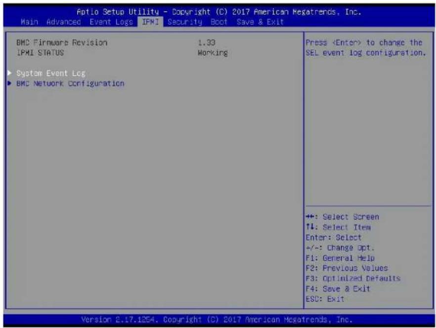
text_image
Aptio Setup Utility - Copyright (C) 2017 American Megatrends, Inc. Main Advanced Event Logs IPMI Security Boot Save & Exit BMC Firmware Revision 1.93 IPMI STATUS Working ► System Event Log ► BMC Network Configuration PressBMC Firmware Revision
This item indicates the IPMI firmware revision used in your system.
IPMI Status (Baseboard Management Controller)
This item indicates the status of the IPMI firmware installed in your system.
▶System Event Log
Enabling/Disabling Options
SEL Components
Select Enabled for all system event logging at bootup. The options are Disabled and Enabled.
Erasing Settings
Erase SEL
Select Yes, On next reset to erase all system event logs upon next system reboot. Select Yes, On every reset to erase all system event logs upon each system reboot. Select No to keep all system event logs after each system reboot. The options are No, (Yes, On next reset), and (Yes, On every reset).
When SEL is Full
This feature allows the user to decide what the BIOS should do when the system event log is full. Select Erase Immediately to erase all events in the log when the system event log is full. The options are Do Nothing and Erase Immediately.

Note: After making changes on a setting, be sure to reboot the system for the changes to take effect.
▶BMC Network Configuration
BMC Network Configuration
The following items will be displayed:
• IPMI LAN Selection
• IPMI Network Link Status
Update IPMI LAN Configuration
Select Yes for the BIOS to implement all IP/MAC address changes at the next system boot. The options are No and Yes.
*If the item "Update IPMI LAN Configuration" is set to Yes, the following item will become available for configuration:
Configuration Address Source
This feature allows the user to select the source of the IP address for this computer. If Static is selected, you will need to know the IP address of this computer and enter it to the system manually in the field. If DHCP is selected, the BIOS will search for a DHCP (Dynamic Host Configuration Protocol) server in the network that is attached to and request the next available IP address for this computer. The options are Static and DHCP.
Station MAC Address
This item displays the Station MAC address for this computer. MAC addresses are 6 two-digit hexadecimal numbers.
Station IP Address
This item displays the Station IP address for this computer. This should be in decimal and in dotted quad form (i.e., 192.168.10.253).
Subnet Mask
This item displays the sub-network that this computer belongs to. The value of each three-digit number separated by dots should not exceed 255.
Gateway IP Address
This item displays the Gateway IP address for this computer. This should be in decimal and in dotted quad form (i.e., 172.31.0.1).
VLAN
Use this item to enable or disable the IPMI VLAN function. The options are Disable and Enable.
*If the item "VLAN" is set to Enable, the following item will become available for configuration:
VLAN ID
Use this item to enter the VLAN ID. The default setting is 0.
4.6 Security
This menu allows the user to configure the following security settings for the system.
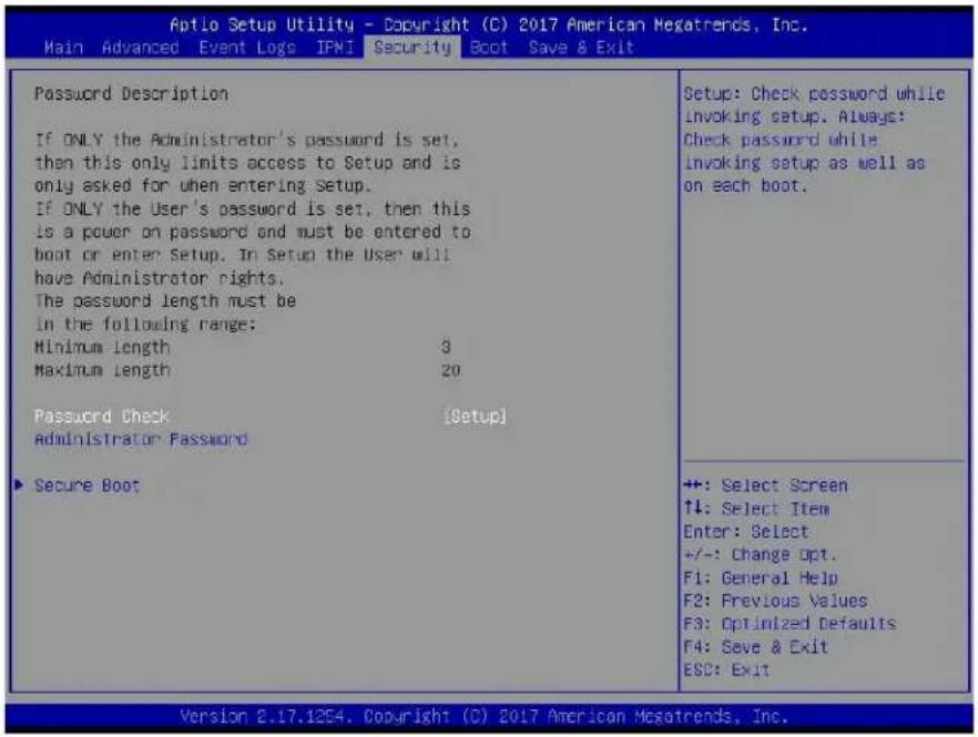
text_image
Antio Setup Utility - Copyright (C) 2017 American Megatrends, Inc. Main Advanced Event Logs IPNI Security Boot Save & Exit Password Description If ONLY the Administrator's password is set, then this only limits access to Setup and is only asked for when entering Setup. If ONLY the User's password is set, then this is a power on password and must be entered to boot or enter Setup. In Setup the User will have Administrator rights. The password length must be in the following range: Minimum length 3 Maximum length 20 Password Check [Setup] Administrator Password ▶ Secure Boot Setup: Check password while invoking setup. Always: Check password while invoking setup as well as on each boot. +: Select Screen ↑↓: Select Item Enter: Select +/-: Change Opt. F1: General Help F2: Previous Values F3: Optimized Defaults F4: Save & Exit ESC: Exit Version 8.17.1254. Copyright (C) 2017 American Megatrends, Inc.Password Check
Select Setup for the system to check for a password at Setup. Select Always for the system to check for a password at bootup or upon entering the BIOS Setup utility. The options are Setup and Always.
Administrator Password
Press Enter to create a new, or change an existing Administrator password.
▶Secure Boot
This section displays the contents of the following secure boot features:
- System Mode
- Secure Boot
- Vendor Keys
Secure Boot control
Use this item to enable secure boot. The options are Disabled and Enabled.
Secure Boot Mode
Use this item to select the secure boot mode. The options are Standard and Custom.
CSM Support
Select Enabled to support the EFI Compatibility Support Module (CSM), which provides compatibility support for traditional legacy BIOS for system boot. The options are Disabled and Enabled.
*If the item "Secure Boot Mode" is set to Custom, the following item will become available for configuration:
▶Key Management
This submenu allows the user to configure the following Key Management settings.
Provision Factory Default Keys
Select Enabled to install the default Secure Boot keys set by the manufacturer. The options are Disabled and Enabled.
▶ Delete all Secure Boot variables
Select Yes to delete all secure boot variables and reset the platform to setup mode. The options are Yes and No.
▶ Save all Secure Boot variables
This feature allows the user to decide if all secure boot variables should be saved.
Secure Boot variable: Size/Key#/Key Source
▶ Platform Key (PK)
This feature allows the user to configure the settings of the platform keys.
Set New Key
Select Yes to load the new platform keys (PK) from the manufacturer's defaults. Select No to load the platform keys from a file. The options are Yes and No.
▶Key Exchange Keys
Set New Key
Select Yes to load the KEK from the manufacturer's defaults. Select No to load the KEK from a file. The options are Yes and No.
Append Key
Select Yes to add the KEK from the manufacturer's defaults list to the existing KEK. Select No to load the KEK from a file. The options are Yes and No.
▶ Authorized Signatures
Set New Key
Select Yes to load the database from the manufacturer's defaults. Select No to load the DB from a file. The options are Yes and No.
Append Key
Select Yes to add the database from the manufacturer's defaults to the existing DB. Select No to load the DB from a file. The options are Yes and No.
▶Forbidden Signatures
Set New Key
Select Yes to load the DBX from the manufacturer's defaults. Select No to load the DBX from a file. The options are Yes and No.
Append Key
Select Yes to add the DBX from the manufacturer's defaults to the existing DBX. Select No to load the DBX from a file. The options are Yes and No.
▶ Authorized TimeStamps
Set New Key
Select Yes to load the DBT from the manufacturer's defaults. Select No to load the DBT from a file. The options are Yes and No.
Append Key
Select Yes to add the DBT from the manufacturer's defaults list to the existing DBT. Select No to load the DBT from a file. The options are Yes and No.
▶OsRecovery Signatures
Set New Key
Select Yes to load the DBR from the manufacturer's defaults. Select No to load the DBR from a file. The options are Yes and No.
Append Key
Select Yes to add the DBR from the manufacturer's defaults list to the existing DBR. Select No to load the DBR from a file. The options are Yes and No.
4.7 Boot
Use this feature to configure Boot Settings:
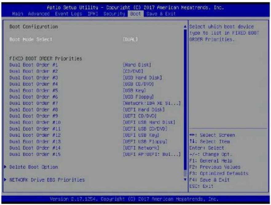
text_image
Aptio Setup Utility - Copyright (C) 2017 American Megatrends, Inc. Main Advanced Event Logs IPNI Security Boot Save & Exit Boot Configuration Boot Mode Select [DUAL] FIXED BOOT ORDER Priorities Dual Boot Order #1 [Hard Disk] Dual Boot Order #2 [CD/DVD] Dual Boot Order #3 [USB Hard Disk] Dual Boot Order #4 [USB CD/DVD] Dual Boot Order #5 [USB Key] Dual Boot Order #6 [USB Floppy] Dual Boot Order #7 [Network: IBA XE SL...] Dual Boot Order #8 [UEFI Hard Disk] Dual Boot Order #9 [UEFI CD/DVD] Dual Boot Order #10 [UEFI USB Hard Disk] Dual Boot Order #11 [UEFI USB CD/DVD] Dual Boot Order #12 [UEFI USB Key] Dual Boot Order #13 [UEFI USB Floppy] Dual Boot Order #14 [UEFI Network] Dual Boot Order #15 [UEFI AP:UEFI: Bul...] ► Delete Boot Option ► NETWORK Drive EDS Priorities Select which boot device type to list in FIXED BOOT ORDER Priorities. +: Select Screen ↑↓: Select Item Enter: Select +/-: Change Opt. F1: General Help F2: Previous Values F3: Optimized Defaults F4: Save & Exit ESC: Exit Version 8.17.1254. Copyright (C) 2017 American Megatrends, Inc.Boot Configuration
Boot Mode Select
Use this item to select the type of device that the system is going to boot from. The options are LEGACY, UEFI, and DUAL.
FIXED BOOT ORDER Priorities
This option prioritizes the order of bootable devices that the system to boot from. Press
*If the item "Boot Mode Select" is set to LEGACY/UEFI/DUAL the following items will be displayed:
- Dual Boot Order #1
- Dual Boot Order #2
• Dual Boot Order #3 - Dual Boot Order #4
-
Dual Boot Order #5
-
Dual Boot Order #6
- Dual Boot Order #7
• Dual Boot Order #8
• Dual Boot Order #9
• Dual Boot Order #10
• Dual Boot Order #11
• Dual Boot Order #12
• Dual Boot Order #13
• Dual Boot Order #14
• Dual Boot Order #15
▶ Delete Boot Option
Use this feature to remove a pre-defined boot device from which the system will boot during startup. The options are (Select one to Delete) and (UEFI: Built-in EFI Shell).
▶NETWORK Drive BBS Priorities
This feature allows the user to specify which UEFI network drive devices are boot devices.
• Legacy Boot Order #1
▶UEFI Application Boot Priorities
This feature allows the user to specify which UEFI devices are boot devices.
• UEFI Boot Order #1
4.8 Save & Exit
Select the Exit tab from the BIOS setup utility screen to enter the Exit BIOS Setup screen.
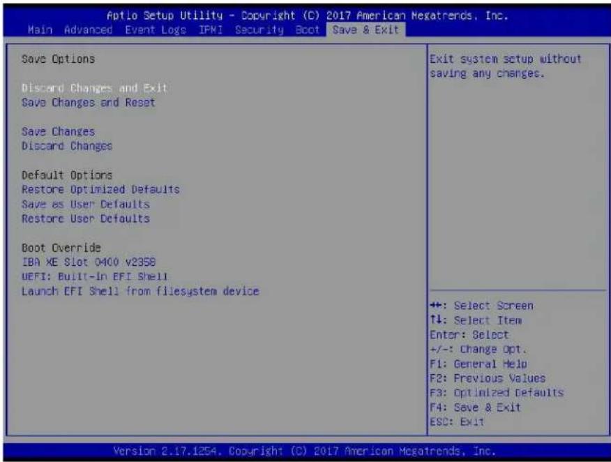
text_image
Aptio Setup Utility - Copyright (C) 2017 American Megatrends, Inc. Main Advanced Event Logs IPMI Security Boot Save & Exit Save Options Discard Changes and Exit Save Changes and Reset Save Changes Discard Changes Default Options Restore Optimized Defaults Save as User Defaults Restore User Defaults Boot Override IBA XE Slot 0400 v2358 UEFI: Built-In EFI Shell Launch EFI Shell from filesystem device Exit system setup without saving any changes. +: Select Screen ↑↓: Select Item Enter: Select +/-: Change Opt. F1: General Help F2: Previous Values F3: Optimized Defaults F4: Save & Exit ESC: Exit Version 2.17.1254. Copyright (C) 2017 American Megatrends, Inc.Discard Changes and Exit
Select this option to quit the BIOS Setup without making any permanent changes to the system configuration, and reboot the computer. Select Discard Changes and Exit from the Exit menu and press
Save Changes and Reset
When you have completed the system configuration changes, select this option to leave the BIOS setup utility and reboot the computer, which will allow the new system configuration parameters to take effect. Select Save Changes and Exit from the Exit menu and press
Save Changes
After completing the system configuration changes, select this option to save the changes you have made. This will not reset (reboot) the system.
Discard Changes
Select this option and press
Default Options
Restore Optimized Defaults
To set this feature, select Restore Optimized Defaults from the Save & Exit menu and press
Save as User Defaults
To set this feature, select Save as User Defaults from the Exit menu and press
To set this feature, select Restore User Defaults from the Exit menu and press
Boot Override
Listed on this section are other boot options for the system (i.e., Built-in EFI shell). Select an option and press
Appendix A
BIOS Codes
BIOS Error POST (Beep) Codes
During the POST (Power-On Self-Test) routines, which are performed upon each system boot, errors may occur.
Non-fatal errors are those which, in most cases, allow the system to continue to boot. These error messages normally appear on the screen.
Fatal errors will not allow the system to continue with bootup. If a fatal error occurs, you should consult with your system manufacturer for possible repairs.
These fatal errors are usually communicated through a series of audible beeps. The numbers on the fatal error list correspond to the number of beeps for the corresponding error.
| BIOS Beep (POST) Codes | ||
| Beep Code Error | Message Description | |
| 1 beep Refresh Ready to boot | ||
| 5 short, 1 long Memory error No memory detected in system | ||
| 5 beeps No con-in or con-out devices | Con-in includes USB or PS/2 keyboard, PCI or serial console redirection, and IPMI KVM or SOL.Con-out includes the video controller, PCI or serial console redirection, and IPMI SOL | |
| 1 beep per device R | Refresh 1 beep for each USB device detected | |
| IPMI Error Codes | ||
| Beep Code Error | Message Description | |
| 1 long continuous System OH System overheat condition | ||
Appendix B
Software Installation
B.1 Installing Software Programs
The Supermicro FTP site contains drivers and utilities for your system at ftp://ftp.supermicro.com. Some of these must be installed, such as the chipset driver.
After accessing the FTP site, go into the CDR_Images directory and locate the ISO file for your motherboard. Download this file to create a CD/DVD of the drivers and utilities it contains. (You may also use a utility to extract the ISO file if preferred.)
Another option is to go to the Supermicro website at http://www.supermicro.com/products/. Find the product page for your motherboard here, where you may download individual drivers and utilities.
After creating a CD/DVD with the ISO files, insert the disk into the CD/DVD drive on your system, and the following screen should appear.
Note 1: Click the icons showing a hand writing on paper to view the readme files for each item. Click the computer icons to the right of these items to install each item (from top to bottom) one at a time. After installing each item, you must reboot the system before moving on to the next item on the list. The bottom icon with a CD on it allows you to view the entire contents.

text_image
SUPERMICRO X11SSW-TF Motherboard Drivers & Tools (WIN7) SUPERMICRO Drivers & Tools Intel C236 Chipset X11SSW-TF/4TF SUPERMICRO Computer Inc. Intel Chipset INF files Microsoft .Net Framework 4.5.2 (Optional) ASPEED Graphos Driver Intel Rapid Storage Technology Enterprise Intel USB 3.0 Drivers Intel Management Engine Intel PRO Network Connections Drivers Intel Integrated Sensor Solution SUPERMICRO SuperDoctor 5 Build driver diskies and manuals Browse CD Auto Start Up Next Time For more information, please visit SUPERMICRO's web siteFigure B-1. Driver/Tool Installation Display Screen
Note 2: When making a storage driver diskette by booting into a driver CD, please set the SATA configuration to Compatible Mode, and configure the SATA as IDE in the BIOS setup. After making the driver diskette, be sure to change the SATA settings back to your original settings.B.2 SuperDoctor® 5
The Supermicro SuperDoctor 5 is a hardware monitoring program that functions in a command-line or web-based interface in Windows and Linux operating systems. The program monitors system health information, such as CPU temperature, system voltages, system power consumption, and fan speed, and provides alerts via email or the Simple Network Management Protocol (SNMP).
SuperDoctor 5 comes in local and remote management versions and can be used with Nagios to maximize your system monitoring needs. With the SuperDoctor 5 Management Server (SSM Server), you can remotely control the power status and reset chassis intrusion for multiple systems with SuperDoctor 5 or IPMI. SD5 Management Server monitors HTTP, FTP, and SMTP services to optimize the efficiency of your operation.

Note: The default username and password for SuperDoctor 5 is ADMIN/ADMIN.
Figure B-2. SuperDoctor 5 Interface Display Screen (Health Information)
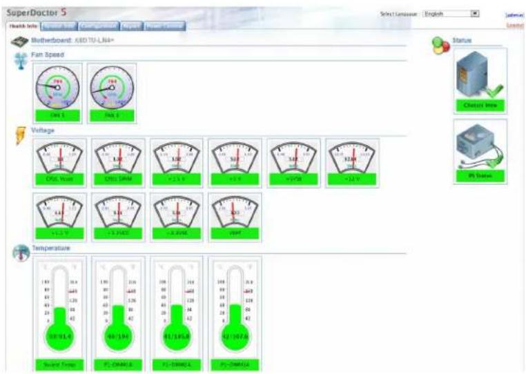
text_image
SuperDoctor S Health Info Mothedron: KED TUI-LN6+ Fan Speed 104 L 108 L 112 L 115 L 118 L 121 L 124 L 127 L 130 L 133 L 136 L 139 L 142 L 145 L 148 L 151 L 154 L 157 L 160 L 163 L 166 L 169 L 172 L 175 L 178 L 181 L 184 L 187 L 190 L 193 L 196 L 199 L 202 L 205 L 208 L 211 L 214 L 217 L 220 L 223 L 226 L 229 L 232 L 235 L 238 L 241 L 244 L 247 L 250 L 253 L 256 L 259 L 262 L 265 L 268 L 271 L 274 L 277 L 280 L 283 L 286 L 289 L 292 L 295 L 298 L 301 L 304 L 307 L 310 L 313 L 316 L 319 L 322 L 325 L 328 L 331 L 334 L 337 L 340 L 343 L 346 L 349 L 352 L 355 L 358 L 361 L 364 L 367 L 370 L 373 L 376 L 379 L 382 L 385 L 388 L 391 L 394 L 397 L 399 L 402 L 405 L 408 L 411 L 414 L 417 L 420 L 423 L 426 L 429 L 432 L 435 L 438 L 441 L 444 L 447 L 450 L 453 L 456 L 459 L 462 L 465 L 468 L 471 L 474 L 477 L 480 L 483L 10.0KΩ·V·A·W·A·G·A·A·A·A·A·A·A·A·A·A·A·A·A·A·A·A·A·A·A·A·A·A·A·A·A·A·A·A·A·A·A·A·A·A·A·A·A·A·A·A·A·A·A·A·A·A·A·A·A·A·C A C C C C C C C C C C C C C C C C C C C C C C C C C C C C C C C C C C C C C C C C C C C C C C C C C C C C C C C C C C C C C C C C A A A A A A A A A A A A A A A A A A A A A A A A A A A A A A A A A A A A A A A A A A A A A A A A A A A A A A A A A A A A A A A A A A A A A A A A A A A A A A A A A A A A A A A A A A A A A A A A A A A A B E M O R D O N T U T U T U T U T U T U T U T U T U T U T U T U T U T U T U T U T U T U T U T U T U T U T U T U T U T U T U T U T U T U T U T U T U T U T U T U T U T U T U T U T U T U T U T U T U T U T U T U T U T U TU T U T U T U T U T U T U T U T U T U T U T U T U T U T U T U T U T U T U T U T U T U T U T U T U T U T U T U T U T U T U T U T U T U T U T U T U T U T U T U T U T U T U T U T U T U T U T U T U T U T V E M O R D O N T I G H I N G H I N G H I N G H I N G H I N G H I N G H I N G H I N G H I N G H I N G H I N G H I N G H I N G H I N G H I N G H I N G H I N G H I N G H I N G H I N G H I N G H I N G H I N G H I N G H I N G H I I N G H I N G H I N G H I N G H I N G H I N G H I N G H I N G H I N G H I N G H I N G H I N G H I N G H I N G H I N G H I N G H I N G H I N G H I N G H I N G H I N G H I N G H I N G H I N G H I N GH I N G H I N G H I N G H I N G H I N G H I N G H I N G H I N G H I N G H I N G H I N G H I N G H I N G H I N G H I N G H I N G H I N G H I N G H I N G H I N G H I N G H I N G H I N G H I N G H I N G F O W D O W D O W D O W D O W D O W D O W D O W D O W D O W D O W D O W D O W D O W D O W D O W D O W D O W D O W D O W D O W D O W D O W D O W D O W D O W D O W D O W D O W D O W D O W D O W D O W D O W D D O W D D O W D D O W D D O W D D O W D D O W D D O W D D O W D D O W D D O W D D O W D D O W D D O W D D O W D D O W D D O W D D O W D D O W D D O W D D O W D D O W D D O W D D O W D D O W D D O WD E M O R D O N T I G H I N G H I N G H I N G H I N G H I N G H I N G H I N G H I N G H I N G H I N G H I N G H I N G H I N G H I N G H I N G H I N G H I N G H I N G H I N G H I N G H I N G H I N G HI N G H I N G H I N G H I N G H I N G H I N G H I N G H I N G H I N G H I N G H I N G H I N G H I N G H I N GH 10.0KΩ·V 10.0KΩ·V 10.0KΩ·V 10.0KΩ·V 10.0KΩ·V 10.0KΩ·V 10.0KΩ·V 10.0KΩ·V 10.0KΩ·V 10.0KΩ·V 10.0KΩ·V 10.0KΩ·V
Note: The SuperDoctor 5 program and user's manual can be downloaded from the Supermicro website at http://www.supermicro.com/products/nfo/sms_sd5.cfm.
Appendix C
Standardized Warning Statements
The following statements are industry standard warnings, provided to warn the user of situations that might potentially cause bodily injury. Should you have questions or experience difficulty, contact Supermicro's Technical Support department for assistance. Only certified technicians should attempt to install or configure components.
Read this section in its entirety before installing or configuring components.
These warnings may also be found on our website at http://www.supermicro.com/about/policies/safety_information.cfm.
Battery Handling

Warning! There is the danger of explosion if the battery is replaced incorrectly. Replace the battery only with the same or equivalent type recommended by the manufacturer. Dispose of used batteries according to the manufacturer's instructions
電池の取り扱い
Warning! Ultimate disposal of this product should be handled according to all national laws and regulations.
製品の廃棄
Warning: Do not upgrade the BIOS unless your system has a BIOS-related issue. Flashing the wrong BIOS can cause irreparable damage to the system. In no event shall Supermicro be liable for direct, indirect, special, incidental, or consequential damages arising from a BIOS update. If you need to update the BIOS, do not shut down or reset the system while the BIOS is updating to avoid possible boot failure.
D.1 Overview
The Unified Extensible Firmware Interface (UEFI) provides a software-based interface between the operating system and the platform firmware in the pre-boot environment. The UEFI specification supports an architecture-independent mechanism that will allow the UEFI OS loader stored in an add-on card to boot the system. The UEFI offers clean, hands-off management to a computer during system boot.
D.2 Recovering the UEFI BIOS Image
A UEFI BIOS flash chip consists of a recovery BIOS block and a main BIOS block (a main BIOS image). The recovery block contains critical BIOS codes, including memory detection and recovery codes for the user to flash a healthy BIOS image if the original main BIOS image is corrupted. When the system power is turned on, the recovery block codes execute first. Once this process is complete, the main BIOS code will continue with system initialization and the remaining POST (Power-On Self-Test) routines.

Note 1: Follow the BIOS recovery instructions below for BIOS recovery when the main BIOS block crashes.
Note 2: When the BIOS recovery block crashes, you will need to follow the procedures to make a Returned Merchandise Authorization (RMA) request. (For a RMA request, please see section 3.5 for more information). Also, you may use the Supermicro Update Manager (SUM) Out-of-Band (OOB) (https://www.supermicro.com.tw/products/nfo/SMS_SUM.cfm) to reflash the BIOS.
D.3 Recovering the Main BIOS Block with a USB Device
This feature allows the user to recover the main BIOS image using a USB-attached device without additional utilities used. A USB flash device such as a USB Flash Drive, or a USB CD/DVD ROM/RW device can be used for this purpose. However, a USB Hard Disk drive cannot be used for BIOS recovery at this time.
The file system supported by the recovery block is FAT (including FAT12, FAT16, and FAT32), which is installed on a bootable or non-bootable USB-attached device. However, the BIOS might need several minutes to locate the SUPER.ROM file if the media size becomes too large due to the huge volumes of folders and files stored in the device.
To perform UEFI BIOS recovery using a USB-attached device, follow the instructions below:
- Using a different machine, copy the "Super.ROM" binary image file into the Root "\" directory of a USB device or a writable CD/DVD.

Note 1: If you cannot locate the "Super.ROM" file in your drive disk, visit our website at www.supermicro.com to download the BIOS package. Extract the BIOS binary image into a USB flash device and rename it "Super.ROM" for BIOS recovery use.
Note 2: Before recovering the main BIOS image, confirm that the "Super.ROM" binary image file you download is the same version or a close version meant for your motherboard.
- Insert the USB device that contains the new BIOS image ("Super.ROM") into your USB drive and reset the system until the following screen appears:
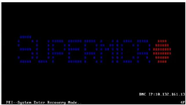
text_image
BMC IP:18.132.161.13 PEI--System Enter Recovery Mode... 4F
Note: On the other hand, if the following screen displays, please load the "Super. ROM" file to the root folder and connect this folder to the system. (You can do so by inserting a USB device that contains the new "Super.ROM" image to your machine for BIOS recovery.)
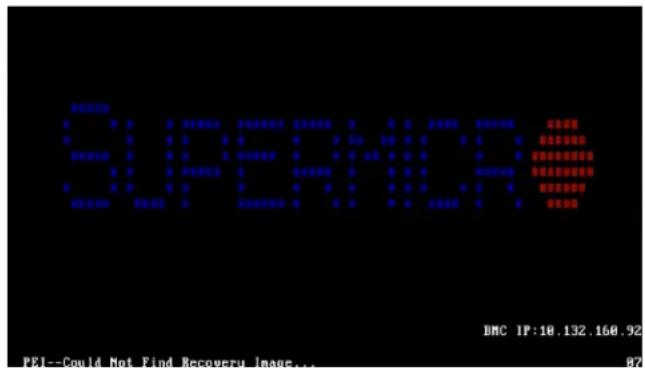
text_image
BMC IP:10.132.150.92 PRI--Could Not Find Recovery Image... 87- After locating the healthy BIOS binary image, the system will enter the BIOS Recovery menu as shown below:
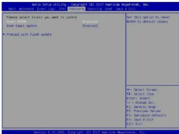
text_image
Optin Setup Utility - Copyright (C) 2017 American Megatrends, Inc. Main Advanced Event Log (DW) Recovery Security Boot Save & Exit Please select blocks you want to update Reset OK/OK [Enabled] Boot Block Update [Enabled] ► Proceed with flash update Set this option to reset NWSM to default values +: Select Screen T4: Select Item Enter: Select +/- Change Out. F1: General Help F2: Previous Values F3: Optimized Defaults F4: Save & Exit ESC: Exit Version 2.19.1766. Copyright (C) 2017 American Megatrends, Inc.
Note: At this point, you may decide if you want to start the BIOS recovery. If you decide to proceed with BIOS recovery, follow the procedures below.
- When the screen as shown above displays, use the arrow keys to select the item "Proceed with flash update" and press the
key. You will see the BIOS recovery progress as shown in the screen below:

Note: Do not interrupt the BIOS flashing process until it has completed.
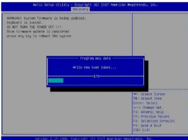
text_image
Aotio Setup Utility - Copyright (C) 2017 American Megatrends, Inc. Recovery WARNING System firmware is being updated. Keyboard is locked. DO NOT TURN THE POWER OFF III Once firmware update is completed press any key to reboot the system Program new data Write new boot block... 178 +: Select Screen T4: Select Item Enter: Select +/-: Change Opt. F1: General Help F2: Previous Values F3: Optimized Defaults F4: Save a Exit ESC: Exit Version 2.19.1266. Copyright (C) 2017 American Megatrends, Inc.- After the BIOS recovery process is complete, press any key to reboot the system.
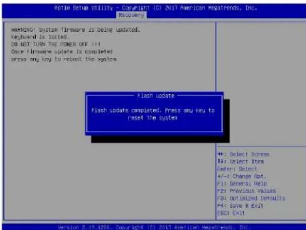
text_image
Action Setup Utility - Copyright (C) 2017 American Megatrends, Inc. Recovery WARNING System firmware is being updated. Keyboard is locked. DO NOT TURN THE POWER OFF !!! Once Firmware update is completed press any key to reboot the system Flash update Flash update completed. Press any key to reset the system +: Select Screen #: Select Item Enter: Select +/-: Change Opt. F1: General Help F2: Previous Values F3: Optimized Defaults F4: Save & Exit ESC: Exit Version 2.15.1266. Copyright (C) 2017 American Megatrends, Inc.-
Using a different system, extract the BIOS package into a bootable USB flash drive.
-
When a DOS prompt appears, enter FLASH.BAT BIOSname.### at the prompt.

Note: Do not interrupt this process until the BIOS flashing is complete.
-
After seeing the message indicating the BIOS update has completed, unplug the AC power cable from the power supply, clear CMOS, then plug the AC power cable in the power supply again to power on the system.
-
Press
continuously to enter the BIOS Setup utility. -
Press
to load the default settings. -
After loading the default settings, press
to save the settings and exit the BIOS Setup utility.
Appendix E
Dual Boot Block
E.1 Introduction
This motherboard supports the Dual Boot Block feature, which is the last-ditch mechanism to recover the BIOS boot block. This section provides an introduction to the feature.
BIOS Boot Block
A BIOS boot block is the minimum BIOS loader required to enable necessary hardware components for the BIOS crisis recovery flash that will update the main BIOS block. An on-call BIOS boot-block corruption may occur due to a software tool issue (see image below) or an unexpected power outage during BIOS updates.
| AMI Firmware Update Utility vX.XX.XX Copyright (C)XXXX American Megatrends Inc. All Rights Reserved. |
| Reading flash . . . . . . . . . . . . . . . . . . . done -- ME Data Size checking . ok -- FFS checksums . . . . . . . ok Erasing Boot Block . . . . . . . . . . . . . done __Updating Boot Block . . . . . . . . 0x00A91000 (13%) |
BIOS Boot Block Corruption Occurrence
When a BIOS boot block is corrupted due to an unexpected power outage or a software tool malfunctioning during BIOS updates, you can still reboot the system by closing pins 2 and 3 using a cap on jumper JBR1. When JBR1 is set to pins 2 and 3, the system will boot from a backup boot block pre-loaded in the BIOS by the manufacturer.
E.2 Steps to Reboot the System by Using Jumper JBR1
- Power down the system.
- Close pins 2-3 on jumper JBR1 and power on the system.
- Follow the BIOS recovery SOP listed in the previous chapter (Appendix D).
- After completing the steps above, power down the system.
- Close pins 1-2 on jumper JBR1 and power on the system.