QCM200 - Scale SRS - Free user manual and instructions
Find the device manual for free QCM200 SRS in PDF.


User questions about QCM200 SRS
0 question about this device. Answer the ones you know or ask your own.
Ask a new question about this device
Download the instructions for your Scale in PDF format for free! Find your manual QCM200 - SRS and take your electronic device back in hand. On this page are published all the documents necessary for the use of your device. QCM200 by SRS.
USER MANUAL QCM200 SRS
Stanford Research Systems certifies that this product met its published specifications at the time of shipment.
Warranty
This Stanford Research Systems product is warranted against defects in materials and workmanship for a period of one (1) year from the date of shipment.
Service
For warranty service or repair, this product must be returned to a Stanford Research Systems authorized service facility. Contact Stanford Research Systems or an authorized representative before returning this product for repair.
Information in this document is subject to change without notice.
Copyright © Stanford Research Systems, Inc., 2004, 2018. All rights reserved.
Stanford Research Systems, Inc.
1290-C Reamwood Avenue
Sunnyvale, California 94089
www.thinkSRS.com
Printed in U.S.A.
Safety and Preparation for Use
Line Voltage
The QCM200 Controller operates from a 90-132 or 175-264 VAC power source having a line frequency between 47 and 63 Hz. Power consumption is 20 VA total.
Power Entry Module
A power entry module, labeled A.C. POWER on the back panel of the QCM200 provides connection to the power source and to a protective ground.
Power Cord
The QCM200 package includes a detachable, three-wire power cord for connection to the power source and protective ground.
The exposed metal parts of the box are connected to the power ground to protect against electrical shock. Always use an outlet which has a properly connected protective ground. Consult with an electrician if necessary.
Keep all electrical wiring in your experimental setup neatly organized and in good working condition. Inspect all HV wires periodically for problems as part of your safety checkups.
Grounding
A chassis grounding lug is available on the back panel of the QCM200. Connect a heavy duty ground wire, #12AWG or larger, from the CHASSIS GROUND lug directly to a facility earth ground to provide additional protection against electrical shock.
BNC shields are connected to the chassis ground and the AC power source ground via the power cord. Do not apply any voltage to the shield.
GFCI (Ground Fault Circuit Interrupter)
GFCI protected outlets are often available in production and laboratory environments, particularly in proximity to water sources. GFCI's are generally regarded as an important defense against electrocution. However, the use of GFCI in conjunction with the QCM200 must not be regarded as a substitute for proper grounding and careful system design. GFCI's must also be tested regularly to verify their functionality. Always consult an electrician when in doubt.
Line Fuse
The LINE FUSE is internal to the instrument and may not be serviced by the user.
Operate Only With Covers In Place
To avoid personal injury, do not remove the product covers or panels. Do not operate the product without all covers and panels in place.
Liquid Contact
With the exception of the Crystal Holder, this product is intended for use only in a clean dry laboratory environment. Operation in other environments may cause damage to the product and reduce the effectiveness of the safety features. To reduce the risk of fire or electrocution do not expose this product to rain or excessive moisture. Be careful not to spill liquid of any kind onto or into the product.
Serviceable Parts
The QCM200 Controller does not include any user serviceable parts inside. Refer service to a qualified technician.
Contents
Safety and Preparation for Use i
Contents iii
Front Panel Overview v
Back Panel Overview vii
QCM25 Crystal Oscillator Overview ix
Specifications xi
Chapter 1 Getting Started 1
QCM200 System 1
Unpacking 2
Quick Start Instructions 3
QCM200 User Interface 4
Crystal Installation 6
Flow Cell 11
Chapter 2 Theory, Operation and Calibration 15
Background 15
The QCM Oscillator 16
Capacitance Cancellation 19
Frequency Measurement 20
Resistance Measurement 22
Gas-Phase Measurements 27
Liquid Contact Measurements 29
Immersion Test 32
Electrochemical Quartz Crystal Microbalance 32
Chemical and Biological Sensors 38
Self-Assembled Monolayers 41
Dissipation Technique 42
References 43
Chapter 3 Sensor Crystals and Holders 49
Introduction 49
Sensor Crystals 50
Principle of Operation 50
Crystal Handling 56
Surface Modifications 59
Crystal Holder 62
Crystal Cleaning Basket 63
Tips for Operation in Liquids 64
Tips for Operation in Gases 67
Bubbles and Liquid Flow Cells 68
References 70
Chapter 4 QCM Circuit Description 75
Introduction 75
QCM25 Crsytal Oscillator 75
QCM200 Analog Board 77
QCM200 Digital Boards 80
Parts Lists 83
Appendix A Frequency Counter Selection Criteria 99
Appendix B QCM200 Remote Programming 101
Introduction 101
Command Syntax 102
Command List 103
Front Panel Overview

text_image
SRS STANFORD RESEARCH SYSTEMS - MODEL QCM2056 - QUARTZ CRYSTAL MICROBALANCE ANALOG CONTROLLER PWR OSC Frequency Output Conductance Output C0 Compensation SET DIAL TO NULL C0 ADJUST HIGH HOLD LOW Measurement ZERO RS239 PARAMETER VALUE HOLD TO ZERO POWER PARS / Cat-5 / Straight 0.0V Rg=40 Ω 0-10V Rg=1 Hz F 5019260.00Figure 1. Front Panel of QCM200 Digital Controller
Power Switch (green PWR LED)
The QCM200 Controller is turned on by toggling the power switch. The green PWR LED lights up to indicate that the unit is powered on.
Crystal Probe Connector (green OSC LED)
The Crystal Probe connector is an RJ-45 receptacle used to connect the QCM200 Controller to the QCM25 Crystal Oscillator (QCM Controller connector). A 3 foot long Cat-5 (straight-thru) cable is used to connect the two boxes.
The green OSC LED lights up indicating the presence of an oscillating crystal in the circuit when the Conductance Output is >2V .
C. Compensation
A switch is available to set the controller into Adjust Mode for nulling C_0 .
A ten-turn dial controls the bias voltage (varactor bias) required by the QCM25 Crystal Oscillator to null C_0 . Four LEDs (HIGH/NULL/LOW) provide visual feedback while nulling C_0 .
Set the C_0 Compensation switch back to HOLD after nulling C_b .
Measurement Display (RS-232 and ZERO LEDs)
An alphanumeric LED display in the QCM200 Digital Controller displays frequency, mass and resistance measurements and also important instrument settings.
The RS-232 LED is an activity indicator that flashes whenever characters are received or transmitted over the RS-232 interface.
The ZERO LED flashes to indicate zeroing of the Relative Frequency and Relative Resistance readings after the VALUE key is held down for 2 seconds.
PARAMETER and VALUE keys
The PARAMETER and VALUE keys on the QCM200 are used to (1) select display modes, (2) program instrument settings and (3) zero the Relative Resistance (r) and Relative Frequency (f) readings.
Use these keys to navigate through the menu system. The PARAMETER key jumps to the next parameter and the VALUE key selects the next available value for the current parameter. The VALUE key walks through the circular list of possible values for the current parameter. The displayed value becomes active immediately. Pressing the PARAMETER key stores the new value and moves the menu display to the next parameter.
Relative Measurements
Hold down the VALUE key for 2 seconds while in the Absolute or Relative Resistance display modes to (1) set the Resistance Offset to the current Absolute Resistance value and (2) zero the Relative Resistance readings. Hold down the VALUE key for 2 seconds while in any other display mode to (1) set the Frequency Offset to the current Absolute Frequency value and (2) zero the Relative Frequency readings. The ZERO LED flashes to indicate zeroing of the Relative Frequency or Relative Resistance displays.
Frequency Output Connector
The Frequency Output connector outputs the crystal oscillator frequency. The signal has TTL (square wave) levels and a source resistance of 50 Ω. Use this output to connect to an external frequency counter (optional). The BNC shield is connected to chassis ground.
Conductance Output Connector
The Conductance Output connector outputs the conductance signal ( V_c ), related to the series resonance resistance of the QCM crystal by:
$$ = \quad , \quad \cdot \left(\frac {V _ {c}}{5}\right) - 7 5 0 0 0 0 1 0 R $$
Voltage levels span 0 to 10.625 VDC and the source impedance is 1 kΩ. Use this output to connect to an external high precision multimeter (optional). The BNC shield is connected to chassis ground.
Back Panel Overview
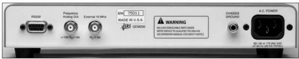
text_image
RS232 Frequency Analog Out +10V Rg-1 kΩ External 10 MHz Rg-1 kΩ SIN 75011 MADE IN U.S.A. JRS QCM200 WARNING NO USER/SERVICEABLE PARTS INDE REFER SERVICE TO QUALIFIED TECHNICAN SEE OPERATION MANUAL FOR SAFETY NOTICE CHASSIS GROUND A.C. POWER 90-132 or 175-264 VAC 47-68 Hz (90 VA TOTAL)Figure 2. Back Panel of QCM200 Digital Controller.
A.C. POWER
The Power Entry Module is used to connect the QCM200 Controller to a power source through the power cord provided with the instrument. The center pin is connected to the QCM200 chassis so that the entire box is grounded.
The source voltage requirements are: 90-132 or 175-264 VAC, 47-63 Hz (20 VA total).
Connect the QCM200 to a properly grounded outlet. Consult an electrician if necessary.
Chassis Ground
Use this grounding lug to connect the QCM200 chassis directly to facility ground.
RS-232
The QCM200 comes standard with an RS-232 communications port. The RS-232 interface connector is a standard 9 pin, type D, female connector configured as a DCE (transmit on pin 3, receive on pin 2). The communication parameters are fixed at: 9600 Baudrate, 8 Data bits, 1 Stop bit, No Parity, No Flow Control.
A host computer interfaced to the QCM200 can easily configure, diagnose and operate the quartz crystal microbalance using simple ASCII commands (see Appendix B).
Frequency Analog Output Connector
The Frequency Analog Out connector outputs a voltage linearly related to the Relative Frequency display of the QCM200 controller.
Voltage levels span 0 to ±10VDC (20 bit resolution) and the source impedance is 1 kΩ. Full scale ranges are user selectable: ±200 kHz, 100 kHz, 50 kHz, 20 kHz, 1 kHz, 5 kHz and 2 kHz. Use this output to connect to the external A/D Input connector of your potentiostat for EQCM applications.
The BNC shield is connected to chassis ground.
External 10 MHz Input Connector
The QCM200 features a built-in frequency counter to measure the resonant frequency and display it on the front panel. The stability and accuracy of the frequency counter is more than adequate for most QCM experiments. For extremely demanding applications, an external timebase, such as the SRS FS725 Rubidium Frequency Standard, can eliminate all frequency errors.
The external 10 MHz input allows the input of an ultra-high stability timebase signal. This input presents a 1 kΩ input impedance and takes a 1 volt peak-to-peak (nominal) input amplitude. The BNC shield is connected to chassis ground.
The QCM200 has an internal ±1.5 ppm TCXO oscillator. The internal oscillator will attempt to phase-lock with a user supplied external 10 MHz signal when “T External” is selected from the front panel or the “T1” command is sent via the remote RS-232 interface.
The internal oscillator frequency may be “pulled” up to ±10 ppm to achieve phase lock. The front panel display can indicate how far the internal oscillator is being pulled as a percentage of its full range ( ±100 ). This percentage provides a gross indication of the stability of the external 10 MHz input. After warmup of both the external oscillator and the QCM200, a pull percentage that fluctuates by more than a couple of counts indicates a problem with either the internal or the external oscillator. Contact SRS for assistance in this case.
QCM25 Crystal Oscillator Overview

text_image
QCM Controller Crystal Face Bias Power VSRS 1/4-20 MTG Hole QCM25 Crystal Oscillator 5 MHz CrystalFigure 3. QCM25 Crystal Controller (top view)
QCM Controller Connector
The QCM Controller connector is a RJ-45 connector. Use this connector to connect the QCM25 Crystal Oscillator to the QCM200 Controller (Crystal Probe connector).
A 3 foot long Cat-5 (Straight Through) cable is used to connect the two boxes. A cable up to 25 feet in length may be used.
A green Power LED lights up to indicate the presence of electrical power in the QCM25 box.
Crystal Face Bias
The Crystal Face Bias connector provides a direct electrical connection to the QCM crystal's liquid face electrode (i.e. outer electrode in contact with the solution).
Use this connector to electrically connect the crystal's liquid face to the Work Electrode lead of a potentiostat while using the QCM crystal in an electrochemical setup (EQCM).
Transformer isolation between the crystal electrodes and the oscillator circuit makes the QCM200 system ideal for electrochemical research and compatible with virtually all potentiostats.
5 MHz Crystal
Use this BNC connector to connect the QCM25 Crystal Oscillator to the Crystal Holder (or directly to your custom 5 MHz QCM crystal/holder)
1/4-20 MTG Hole
Use this threaded hole to mount the QCM25 Crystal Oscillator in your experimental setup, using a 1/4-20 threaded fastener.
Power LED
This LED lights up to that the QCM25 is powered on. This requires connection to a powered QCM200 Controller.
Specifications
QCM200
Frequency Measurement
Display
Gate times 0.1 s, 1 s, 10 s
Resolution 0.01 Hz (10 s gate)
0.1 Hz (1 s gate)
1.0 Hz (0.1 s gate)
Measurement (internal TCXO)
Stability <2×10^-9 typical 10 s Allan
variance
Accuracy ±1.5 ppm
Analog Frequency Output
Output ±10 V full scale (20-bit)
Ranges ±200 kHz, 100 kHz,
50 kHz, 20 kHz, 10 kHz,
5 kHz, 2 kHz
Frequency Output
Frequency 5 MHz (nominal)
Level TTL (square wave)
Source impedance 50 Ω
Connector BNC
Resistance Measurement
Display
Range 0 to 5000 Ω
Resolution 5 digits:
0.001 ,R < 100
0.01 Ω, 100 Ω ≤ R < 1000 Ω
0.1 Ω, 1000 Ω ≤ R < 5000 Ω
Conductance Output (Vc)
Resistance R=10,000 x (10 ^-Vc/5 ) -75 Ω
Resistance range 0 - 5000 Ω
Voltage level 0 - 10.625 VDC, log scale
Impedance 1 kΩ
Connector BNC
Capacitance Cancellation
Range 10 - 40 pF (20 pF nominal)
Limit 0.01 pF
Physical
Interface RS-232, 9600 baud, no parity,
no flow control
Dimensions 10.625" x 2" x 7" (WHD)
Weight 2 lbs.
Operating temperature 0^ C - 40^ C
Quartz Crystals (polished)
Frequency 5 MHz, AT-cut, plano-plano
Diameter 1 inch
Electrodes Chromium/gold, titanium/gold,
and titanium/platinum.
Crystal Holder
Material Kynar®
O-ring Viton®
Connector BNC
Chapter 1
Getting Started
This chapter provides instructions for (1) unpacking, (2) checking and (3) connecting the QCM200 Quartz Crystal Microbalance Controller to its accessories and to your experiment.
Quick Start instructions are also provided to perform QCM measurements.
QCM200 System
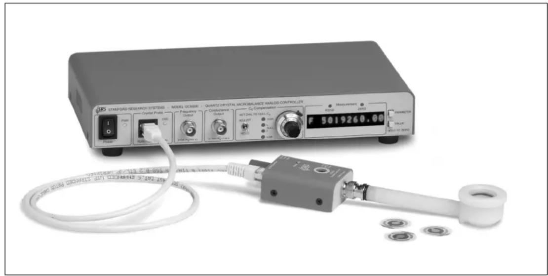
text_image
SRS STAMFORD RESEARCH SYSTEMS - MODEL GCMAX - QUARTZ ORIFETAL MICROBILANCE ANALOG CONTROLLER Cp Compensator Measurement RECOR ZERO PARAMETER SIRLATE GELD TO DENTU SRS 5019260.00 Pressure Crystal Pulse Frequency Output Conductor Output NET DIAL TO MAX C# IND/SY MAX HOLD GND F 5019260.00 SRS 5019260.00 SRS 5019260.00 SRS 5019260.00 SRS 5019260.00 SRS 5019260.00 SRS 5019260.00 SRS 5019260.00 SRS 378-384-388-394-401-408-414-418-424-428-434-436-438-440-442-444-446-448-450-452-454-456-458-460-462-464-466-468-470-472-474-476-478-480-482-483-484-486-488-490-492-493-494-495-496-497-498-499-500-501-502-503-504-505-506-507-508-509-510-511-512-513-514-515-516-517-518-519-520-521-522-523-524-525-526-527-528-529-530-531-532-533-534-535-536-537-538-539-540-541-542-543-544-545-546-547-548-549-550-551-552-553-554-555-556-557-558-559-560-561-562-563-564-565-566-567-568-569-570-571-572-573-574-575-576-577-578-579-580-581-582-583-584-585-586-587-588-589-590Figure 4. Complete QCM setup consisting of QCM200 Digital Controller, QCM25 Crystal Oscillator, Crystal Holder and three(3) quartz crystal sensors.
The QCM200 System is a stand-alone instrument with a built-in frequency counter and resistance meter. It includes controller, crystal oscillator electronics, crystal holder, and three (3) quartz crystals. Series resonance frequency and resistance are measured and displayed directly on the front panel, and there is an analog output proportional to the relative frequency to interface directly with potentiostats (EQCM applications). The QCM200 may be locked to a user supplied 10 MHz clock for ultra-stable frequency measurements. In addition, the QCM200 has an RS-232 interface and comes with both Windows and Mac software providing real-time display, analysis and storage of your QCM data.
Unpacking
Before You Open the Box
Read the entire Safety and Preparation for Use section of this manual before starting any setup procedure.
Read and follow all installation and operation instructions in this manual to ensure that the performance of this instrument is not compromised.
Checklist
- Open the box(es) and inspect all components of the QCM200 System.
• Report any damage to Stanford Research Systems immediately. - Compare the contents of the shipping boxes against your original order and the checklist below. Report any discrepancies to Stanford Research Systems immediately.
Standard Equipment Supplies
• QCM200 Quartz Crystal Microbalance Controller
• QCM25 Crystal Oscillator
• Operation and Service Manual
- Power cord
• 3 foot Cat-5 Cable
- Crystal Holder
• Three (3) chromium/gold QCM crystals, polished
Optional Equipment
- Replacement Crystals (SRS Part# O100RX1)
- Axial Flow Cell (SRS Part# O100FC.)
• Crystal Cleaning Basket (SRS Part# O100CCB) - Replacement Crystal Holder (O100RH)
• Ultra-stable Rubidium Frequency Standard (SRS model FS725)
Quick Start Instructions
- With the power switch in the Off position, connect the QCM200 Controller to a grounded outlet using the power cord provided.
- Connect the QCM200 Controller to the QCM25 Crystal Oscillator using the Cat-5 cable (3 feet long, straight-thru, RJ-45 end connectors).
- Mount a fresh quartz crystal in the Crystal Holder. See special instructions in the following Crystal Installation section.
- Connect the Crystal Holder to the 5 MHz Crystal BNC connector of the QCM25 Crystal Oscillator.
- If required, connect the Frequency Analog Output to (1) the Ext A/D Input of your potentiostat (EQCM), or (2) a precision voltmeter or (3) an analog-to-digital converter.
- If required, connect the RS-232 port to your Host PC and download and install the QCM software: www.thinksrs.com/downloads/soft.htm.
- Set the _0 Compensation switch to Hold and the ten-turn dial to 8.0 (Dry Operation Setting).
- Turn the Power switch on and check that the Power LEDs in the QCM200 and QCM25 boxes light up. The OSC LED of the QCM controller turns on as soon as proper quartz oscillation is established in the dry crystal.
After a short initialization period, an Absolute Frequency (F) very close to 5 MHz (nominal dry frequency) should be present on the front panel Measurement display. Press the PARAMETER key once to display Absolute Resistance (R) - a value < 75 Ohms should be present at this time. - The QCM200 System is now ready for mass and viscosity measurements.
- For operation under liquid immersion, record the “dry” frequency and conductance readings and immerse the entire crystal in the solution of interest. For accurate measurements (i.e. at “true” series resonance), perform a Capacitance Cancellation procedure as described in Chapter 2. Consult Chapter 3 for additional tips on QCM operation in liquids.
- For operation with a flow cell (see Figure 13), pay special attention when filling the flow chamber for the first time so that no air bubbles get trapped in the measurement volume. Consult Chapter 3 for useful tips on QCM operation in liquid flow cells, including bubble elimination techniques. Temperature stabilization to better than ±0.1 ^ is essential for high accuracy measurements in aqueous solutions due to the large temperature coefficient of viscosity.
- For operation in an electrochemistry setup consult the Electrochemical Quartz Crystal Microbalance (EQCM) section in Chapter 2.
QCM200 User Interface
The QCM200 user interface consists of:
• Measurement Display
- Menu System
• RS-232 interface with complete command set
Measurement Display (RS-232 and ZERO LEDS)
A 12-character, 5x7, alphanumeric LED display on the front panel of the QCM200 controller displays frequency, mass and resistance measurements, and also relevant instrument settings.
The RS-232 LED is an activity indicator that flashes whenever a character is received or transmitted over RS232.
The ZERO LED flashes to indicate zeroing of the Relative Frequency or Relative Resistance readings after the VALUE key is held down for 2 seconds.
Menu System (PARAMETER and VALUE buttons)
Two front panel keys, labeled PARAMETER and VALUE, navigate through the menus. Use the PARAMETER key to display the next parameter. The VALUE key walks through the circular list of possible values for the current parameter. The displayed value becomes active immediately. Pressing the PARAMETER key stores the new value into memory and displays the next parameter (also in a circular list).
| Parameter | Value | Symbol | Display |
| Frequency | Absolute Frequency | F | Absolute Frequency [Hz] = series resonance frequency of the quartz crystal |
| Relative Frequency | f | Relative Frequency [Hz] = Absolute Frequency – Frequency Offset | |
| Mass | m | Mass Displacement [ng] = Relative Frequency / 0.0566 | |
| Resistance | Absolute Resistance | R | Absolute Resistance [Ohm] = series resonance resistance of the quartz crystal |
| Relative Resistance | r | Relative Resistance [Ohm] = Absolute Resistance – Resistance Offset | |
| Gate | 10 seconds Gate 10 S | Gate time for the frequency counter | |
| 1 second Gate 1 S | |||
| 0.1 second Gate 100 mS | |||
| Scale | 200 Hz Scale 200 Hz | Voltage Scaling Factor for the Analog Frequency Output voltage [Hz/V] or [kHz/V]Analog Frequency Out [V] = Relative Frequency/Scale Factor | |
| 500 Hz Scale 500 Hz | |||
| 1 kHz Scale 1 kHz | |||
| 2 kHz Scale 2 kHz | |||
| 5 kHz Scale 5 kHz | |||
| 10 kHz Scale 10 kHz | |||
| 20 kHz Scale 20 kHz | |||
| T | Internal | T Internal TCXO as the timebase reference | Frequency counter is using the internal TCXO as the timebase reference |
| External | T Ext ±100 | Frequency counter is using the external timebase connected to the rear panel. Display shows how far the internal oscillator is being pulled to lock to the external timebase (percentage of full range). A stable number indicates a stable lock. | |
| T Ext N/A | External 10 MHz input not detected. Internal oscillator is being used instead. Check external source. | ||
Relative Frequency/Resistance Readings
Hold down the VALUE key for 2 seconds while in the Absolute or Relative Resistance display modes to (1) set the Resistance Offset to the current Absolute Resistance value and (2) zero the Relative Resistance readings. Hold down the VALUE key for 2 seconds while in any other display mode to (1) set the Frequency Offset to the current Absolute Frequency value, (2) zero the Relative Frequency readings, (3) zero the Mass Displacement display and (4) zero the Frequency Analog Out voltage output.
RS-232 Interface
The QCM200 comes standard with an RS-232 communications port and both Windows and Mac software. The standard software provided with the QCM200 system can be downloaded from the SRS Website: www.thinksrs.com. Use the on-line help provided with the software to learn about its powerful display and storage features.
For custom applications, requiring specialized software, any host computer interfaced to the QCM200 through its RS-232 port can easily configure, diagnose and operate the quartz crystal microbalance using simple ASCII commands. A complete listing of the RS-232 commands is in Appendix B of this manual.
The RS-232 interface connector is a standard 9 pin, type D, female connector configured as a DCE (transmit on pin 3, receive on pin 2). The communication parameters are fixed at: 9600 Baudrate, 8 Data bits, 1 Stop bit, No Parity, No Flow Control.
Crystal Installation
This section describes the procedure required to replace or install the QCM crystal in the Crystal Holder.
Figure 5 shows the basic components of the Crystal Holder, including a standard 1 inch sensor crystal.
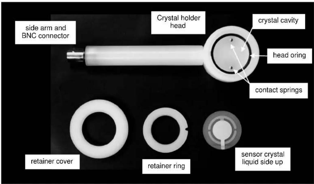
text_image
side arm and BNC connector Crystal holder head crystal cavity head oring contact springs retainer cover retainer ring sensor crystal liquid side upFigure 5. Crystal Holder components.
The standard 1 inch diameter sensor crystal has two sides that must be clearly identified before this procedure is started:
Contact Surface
The contact surface has two separate circuits and the smaller electrode pad.
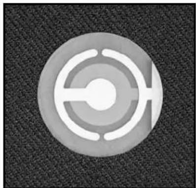
natural_image
Circular mechanical component with concentric rings and a central shaft, set against a textured dark background (no text or symbols)Figure 6. Contact Surface of QCM crystal
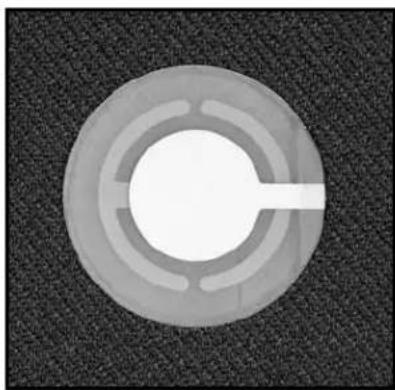
Liquid Surface
The liquid surface has the larger electrode pad, which connects through a wrap around pad to one of the circuits on the Contact Surface. This is the outside (i.e. modified) surface, in direct contact with the gas or liquid during QCM experiments.
natural_image
Circular mechanical component with concentric rings and a central shaft, set against a dark textured background (no text or symbols)Figure 7. Liquid surface of QCM crystal
In order to insert a new crystal into the holder, the following steps must be followed:
- Place the Crystal Holder's head on a flat surface, with its crystal cavity pointing up. The crystal cavity contains two spring-loaded contacts (POGO® pins), which connect the two Contact Surface circuits of the crystal to the BNC connector on the opposite end of the probe.
- Inspect the head o-ring to make sure it is free of defects, clean and properly seated in its dovetail groove. The o-ring should be free of low spots and show sufficient height above the center ring when viewed from the side with the naked eye.
- Make sure the crystal cavity is clean and dry. Dry if necessary.
- Test the travel of the POGO ^ contacts. Gently depress the POGO ^ pins (a thin wooden applicator does a good job). Make sure that they travel freely (i.e. their motion is not restricted.) They should drop to a level well below the surface of the probe o-ring (by an amount at least equal to the thickness of the crystal). When fully extended, they should protrude above the surface of the o-ring, by an amount equal or larger than the thickness of the sensor crystal.
-
Inspect the sensor crystal at this time and clean it if necessary.
-
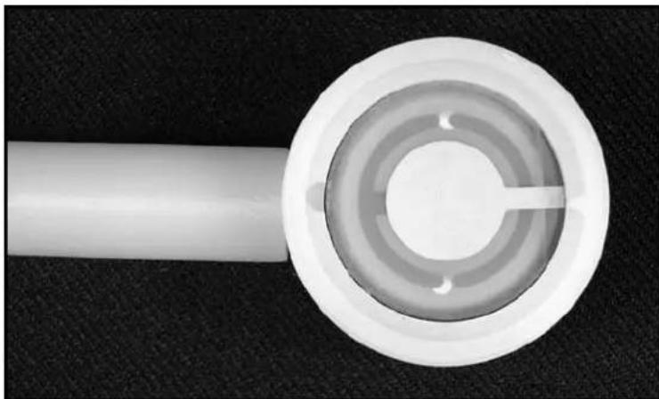
Hold the crystal, Contact Surface down, above the Crystal Holder's head and point the wrap-around electrode towards the reference pin (at end of probe). See Figure 8 below.
natural_image
Close-up of a white plastic bulb with concentric circular patterns and a central slot, against a dark textured background (no text or symbols)Figure 8. QCM Crystal in Crystal Holder cavity with wrap around electrode pointing towards reference pin.
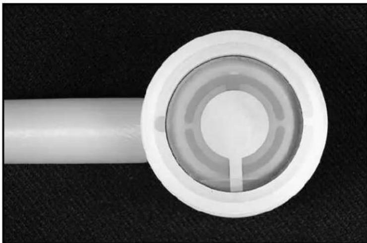
- Turn the crystal 90° clockwise before laying it centered onto the head o-ring. Turning the crystal as instructed assures a fresh contact surface develops between the crystal electrodes and the POGO® pins. The crystal should end up as shown in Figure 9 below.
natural_image
Close-up of a white plastic tube with concentric circular grooves, no text or symbols visibleFigure 9. Crystal in place with correct electrode orientation.
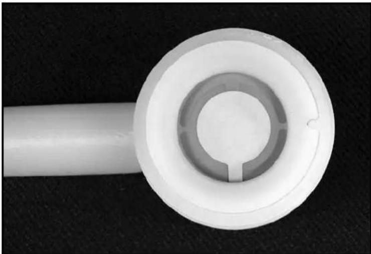
- Place the retainer ring (or Flow Cell) over the crystal, with its notch mating with the reference pin as shown in Figure 10 below.
natural_image
Close-up of a white plastic pipe fitting with a circular recessed hole, against a dark textured background (no text or symbols visible)Figure 10. Retainer ring in place.
- Attach the retainer cover and thread the first quarter turn. Inspect the retainer ring to make sure the alignment notch remained mated with the reference pin.
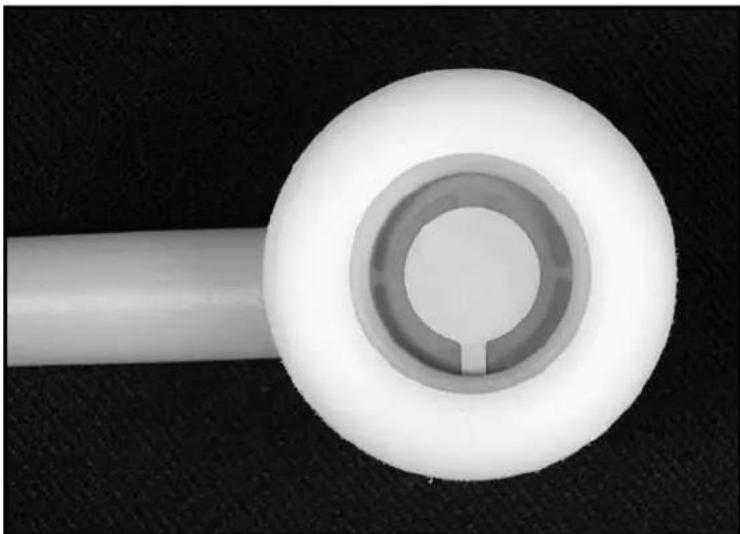
natural_image
Close-up of a white cylindrical object with a circular recess, against a dark textured background (no text or symbols visible)Figure 11. Retainer cover in place.
-
Tighten the retainer cover the rest of the way – finger tight is OK.
-
Connect the Crystal Holder to the QCM25 Crystal Oscillator as shown in Figure 12.
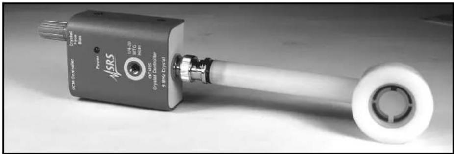
natural_image
Close-up of an ISRS Crystal Controller device with attached cylindrical ports (no visible text or symbols on body)Figure 12. The QCM Probe consisting of a Crystal Holder and QCM25 Crystal Oscillator.
Flow Cell
The Flow Cell Adapter (SRS Part# O100FC) attaches to the crystal holder to create a small volume Stagnation Point Flow Cell.
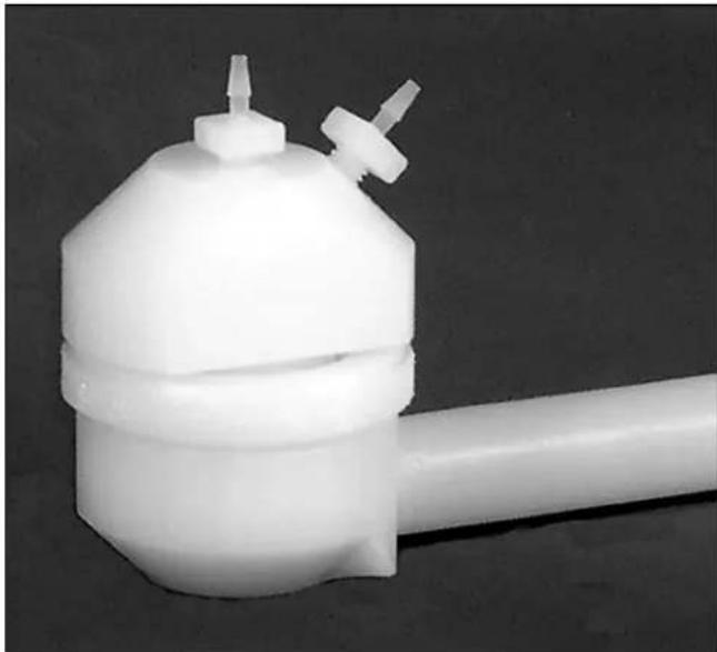
natural_image
White plastic mechanical component with a cylindrical body and a protruding handle (no text or symbols visible)Figure 13. The Axial Flow Cell Adapter mounted on a crystal holder.
Use the Axial Flow Cell Adapter for adsorption/desorption studies when: (1) well defined flow conditions are needed, (2) high sensitivity is required, (3) small rinse volume is desirable and (4) flow-induced surface shear forces need to be minimized.
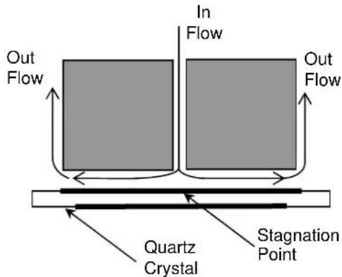
text_image
Out Flow In Flow Out Flow Quartz Crystal Stagnation PointFigure 14. Schematic representation of the liquid flow pattern in the Axial Flow Cell
A cross sectional view of the Axial Flow Cell, including a schematic representation of the stagnation point flow, is shown in Figure 14. In the axial flow cell the sample flows radially outward from the input port at the center of the cell to the exit channel at the edge of the cell, in a volume of about 150 l . The sample solution is perpendicularly injected
towards the flat surface of the QCM crystal. The stagnation point is located at the center of the crystal electrode, overlapping the area of highest sensitivity of the flat QCM oscillator.
The hydrodynamics associated with stagnation point flow are well understood. At the stagnation point there is zero hydrodynamic flow - i.e. without surface shear forces. While the injected solution flows about the stagnation point, any exchange with the surface of the crystal is diffusion limited. Thus the rate of adsorption of the sample molecules (or particles) to the crystal surface is diffusion limited as well. The hydrodynamics and deposition of molecules in stagnation point flow conditions have been investigated by Dabros and Van de Ven and the user is referred to their publications for details:
Dabros T., van de Ven T. G. M., “A direct method for studying particle deposition onto solid surfaces.” Colloid and Polymer Science 261 (1983) 694-707.
Dabros, T., and T. G. M. Van de Ven, “Deposition of latex particles on glass surfaces in an impinging jet”. Physicochem. Hydrodynamics 8 (1987)161-172.
The stagnation point flow cell was specifically designed for the study of adsorption kinetics of particles, micelles and chemical and biological molecules at solid-liquid interfaces, under well-controlled hydrodynamic conditions. Examples of surface-volume processes that have been studied with the aid of stagnation flow cells include: DNA-protein interactions, protein adsorption, cell adhesion, biofouling, biocompatibility, polymer degradation and hydration, biofilm formation, self-assembled monolayers, etc.
Installation
The flow cell is used in place of the Crystal Retainer Ring of the Crystal Holder. Once installed, the cell creates a flow chamber of small volume ( 0.15 mL). The flow cell is made of chemically resistant Kynar ^ and includes two inlet and outlet ports with 0.040” ID thru hole and fitted with barbed hose adapters for 0.062” ID tubing. Simply slide your tube over the barbed stems to create a reliable, low pressure connection to a syringe, siphon system or peristaltic pump. Consult Chapter 3 for additional tips on the operation of liquid flow cells.
Tip
For flowing QCM setups requiring connection to a flow injection or sequential injection analysis system it is common practice to interface the capillary tubing to the flow cell using a short section of 1/16" ID PHARMED® tubing (for example, part # 1557 from www.upchurch.com).
Eliminating gas bubbles trapped inside the crystal chamber is essential for accurate measurements. Please consult the “Bubbles and Liquid Flow Cells” section in Chapter 3 for some useful bubble elimination tricks.
Operation
Two modes of operation are common for QCM flow cells.
Batch Mode
The crystal is exposed to a sequence of sample/solvent batches through a series of load/rinse exchanges. Syringes and the siphon principle are commonly used to manually inject new solutions into the crystal chamber
Flow Mode
A constant flow of solution/solvent runs over the crystal in an open or closed-flow configuration.
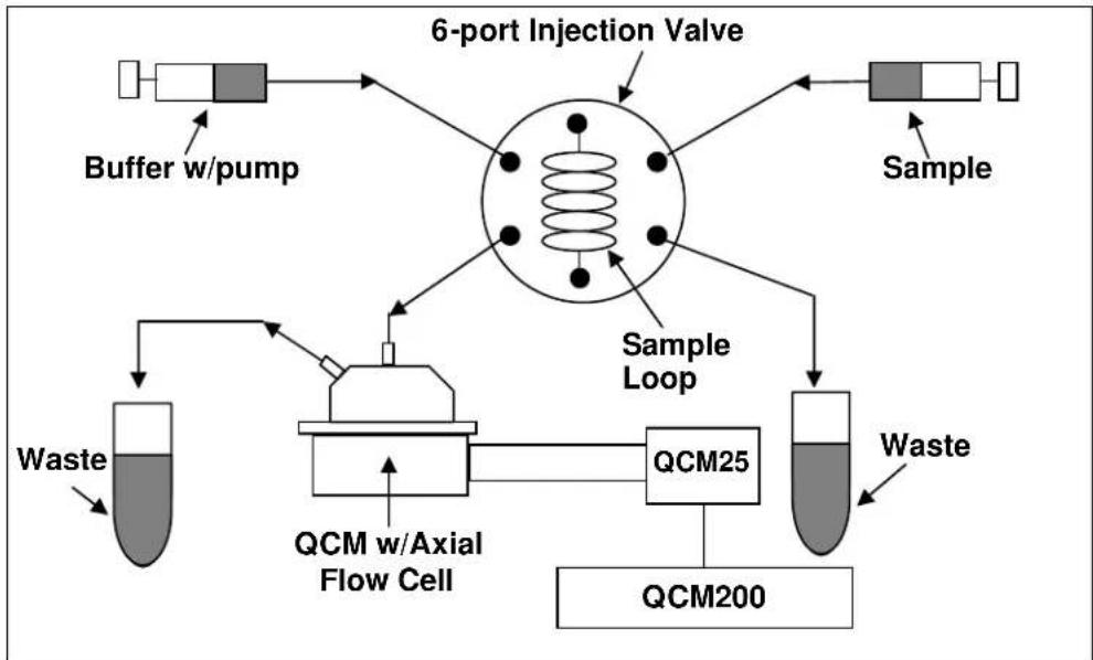
In open-flow systems the siphon principle is recommended to implement the lowest noise flow setup. Syringe pumps and 6 port injection valves are commonly used to expose the crystal to a sequence of analytes (see Figure 15). Most standard Flow Injection Analysis (FIA) and Sequential Injection Analysis (SIA) equipment is compatible with QCM flow cell operation.
Peristaltic pumps are often applied to closed-flow systems but they always add noise to the frequency signal due to pressure transients and coupled vibrations (pulse-dampening modules are always recommended).
In all cases, the flow rate must be kept under 5mL / min to avoid excessive stress on the sensor and to avoid leaks of liquid over the o-ring.
flowchart
graph TD
    A["Buffer w/pump"] --> B["6-port Injection Valve"]
    C["Sample"] --> B
    B --> D["Sample Loop"]
    D --> E["Waste"]
    D --> F["QCM25"]
    F --> G["QCM200"]
    E --> H["Waste w/ Axial Flow Cell"]
    F --> I["Waste"]
    style B fill:#f9f,stroke:#333
    style E fill:#ccf,stroke:#333
    style F fill:#cfc,stroke:#333
    style G fill:#fcc,stroke:#333
Figure 15. A Flow Injection Analysis QCM200 system consisting of syringe pump for buffer solution, 6-port injection valve for analyte injection and Axial Flow Cell for QCM Flow Chamber.
Specifications
Flow Volume (crystal chamber) \~ 0.15 mL
In/Out Ports Barbed hose adapters for 1/16" ID tubing, with 0.040" ID thru-hole.
(Model P-663 from www.upchurch.com)
Recommended flow rate <0.2 mL/min
Maximum flow rate 5 mL/min
Materials
Cell
Kynar®
Inlet-Outlet Tubes Tefzel
®
O-ring
Viton®
Chapter 2
Theory, Operation and Calibration
This chapter provides a brief introduction to the measurement techniques and calibration procedures available to QCM200 users and describes the most popular theoretical models used to interpret the results.
The procedure for capacitance compensation is also described in detail
Background
Sauerbrey ^1 was the first to recognize the potential usefulness of the Quartz Crystal Microbalance (QCM) technology and demonstrate the extremely sensitive nature of these piezoelectric devices towards mass changes at the surface of QCM electrodes. The results of his work are embodied in the Sauerbrey equation, which relates the mass change per unit area at the QCM electrode surface to the observed change in oscillation frequency of the crystal:
f m ACf
(eqn.
where
f = the observed frequency change in Hz,
m = the change in mass per unit area in g / cm^2
C_f = the sensitivity factor for the crystal (56.6 Hz g^1 cm ^2 for a 5 MHz AT-cut quartz crystal at room temperature).
The Sauerbrey equation relies on a linear sensitivity factor, C_f , which is a fundamental property of the QCM crystal. Thus, in theory, the QCM mass sensor does not require calibration. However, it must be kept in mind, that the Sauerbrey equation is only strictly applicable to uniform, rigid, thin-film deposits ^2 . Vacuum and gas phase thin-film depositions which fail to fulfill any of these conditions actually exhibit more complicated frequency-mass correlations and often require some calibration to yield accurate results.
For many years, QCMs were regarded as just gas-phase mass detectors, however, recently their application has been extended since scientists realized that they can be operated in contact with liquids and viscoelastic deposits. In this case, both resonance frequency and series resonance resistance of the quartz oscillator are important to completely characterize the material in contact with the crystal electrode. The development of QCM systems for use in fluids opened a new world of applications, including electrochemistry and microrheology. More recent developments have focused on tailoring electrode surface chemistry (i.e. specialized polymer coatings) so that these devices can be applied as discriminating mass detectors for (1) specific gas detection,
(2) environmental monitoring, (3) biosensing and (4) basic surface-molecule interaction studies.
The purpose of this chapter is to provide a brief introduction to the different measurement and calibration techniques available to QCM200 users, and to briefly describe the most popular theoretical models used to interpret QCM results. A complete coverage of these subjects is beyond the scope of this manual. However, many articles have been published on the operation and calibration of QCMs in applications ranging from vacuum thin-film deposition to electrochemical experiments, and QCM users are referred to the publications list at the end of this chapter for more detailed information.
The QCM Oscillator
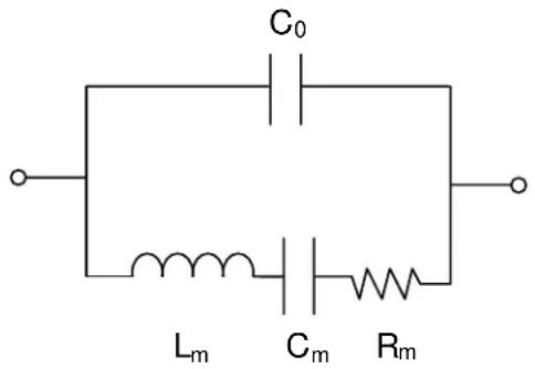
The Butterworth-van Dyke (BVD) electrical model ^3 for a quartz crystal resonator is shown in Figure 16. This model is often used to represent the electrical behavior of a crystal resonator near series resonance. The model has also been useful in predicting the frequency shifts and losses of an AT-cut quartz crystal in QCM applications.
chemical
Electrical circuit diagram with inductor, capacitor, and resistor components labeled Lm, Cm, Rm, and C0Figure 16. Butterworth-van Dyke model of Quartz Crystal Resonator.
The BVD electrical model consists of two arms. The motional arm has three series components modified by the mass and viscous loading of the crystal:
- R_m (resistor) corresponds to the dissipation of the oscillation energy from mounting structures and from the medium in contact with the crystal (i.e. losses induced by a viscous solution).
- C_m (capacitor) corresponds to the stored energy in the oscillation and is related to the elasticity of the quartz and the surrounding medium.
- L_m (inductor) corresponds to the inertial component of the oscillation, which is related to the mass displaced during the vibration.
Typical values for a 1" diameter, 5 MHz crystal used in the QCM200 System are C_m = 33 fF, L_m = 30 mH, and R_m = 10 Ω (for a dry crystal), R_m = 400 Ω (for a crystal with one face in water), or R_m = 3500 Ω (for a crystal with one face in 85% glycerol).
The motional arm is shunted by the parasitic capacitance, C_0 , which represents the sum of the static capacitances of the crystal's electrodes, holder, and connector capacitance. In the QCM200 System ^4 , C_0 is about 20 pF, a value which has been kept small by placing the electronics directly on the Crystal Holder, thereby eliminating any cable capacitance.
In a QCM application the motional inductance, L_m , is increased when mass is added to the crystal electrode - the frequency shift of the series resonance is a sensitive indicator of the added mass. Films of less than 1 ng/cm^2 can easily be resolved by the QCM. The motional resistance, R_m , can also provide important information about a process since soft films and viscous liquids will increase motional losses and increase the value of R_m .
text_image
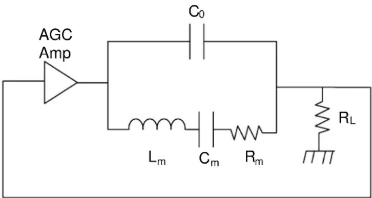
AGC Amp C₀ Lₘ Cₘ Rₘ RₗFigure 17. Oscillator Circuit consisting of AGC Amplifier, Quartz Resonator and Load Resistor.
Placing the crystal in an oscillator circuit provides a simple way to measure its motional parameters ^5 . Figure 17 shows the BVD crystal model, driven by an automatic gain control amplifier (AGC), and terminated into a load resistor, R_L . By returning the voltage on R_L to the input of the AGC amplifier, the circuit will oscillate at a frequency for which the phase shift around the loop is 0^ (or an integral multiple of 360^ ) provided there is sufficient gain (the Barkhausen condition). Absent C_o , it is easy to see that the phase condition is satisfied at the series resonance of C_m and L_m(f_SR = 1/[2(L_mC_m)^1/2] ). At series resonance, the reactance of C_m and L_m cancel, leaving only R_m . In this case, an amplifier gain of A_v = (R_m + R_L)/R_L will provide a loop gain of 1 to sustain oscillation.
Unfortunately, C_0 cannot be ignored in QCM applications. In the circuit shown in Figure 17, C_0 injects a leading current into R_L which must be canceled by a lagging current via the motional arm, in order to achieve the zero phase condition. This requires the circuit run above series resonance, where the net reactance of C_m and L_m is inductive. In fact, if R_m is large enough, it is possible that the motional arm will not be able to contribute enough lagging current to cancel the leading current via C_0 , and the circuit will not oscillate at all.
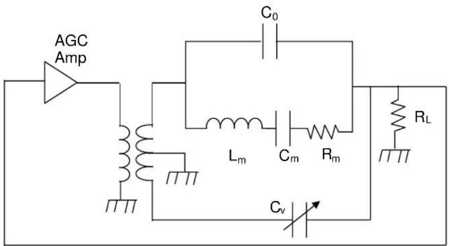
A method to cancel C_o is shown in Figure 18. In this circuit the AGC amplifier drives a transformer with two secondary windings. One secondary drives the crystal and load as before, while the other secondary inverts the voltage. The inverted voltage source injects a current via an adjustable capacitor, C_v , to cancel the current injected via C_o . Exact cancellation is achieved when the adjustable capacitor is made equal to C_o . In the SRS QCM25 Crystal Oscillator, C_v is a varactor, which is made equal to C_o by finding the bias setting which minimizes the gain required to sustain oscillation.
text_image
AGC Amp C₀ Lₘ Cₘ Rₘ Rₗ CᵥFigure 18. Oscillator Circuit with Varactor Nulling of C_0
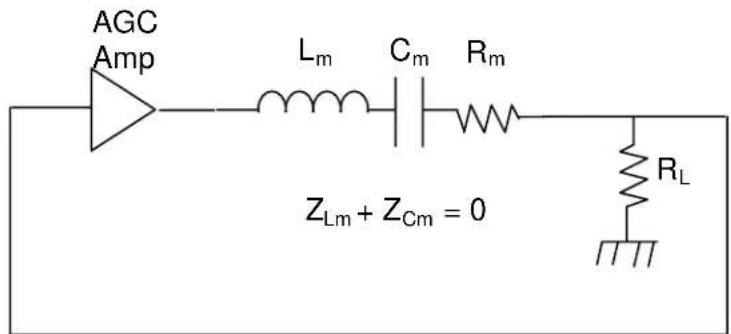
With C_0 canceled the circuit simplifies to that shown in Figure 19. For this circuit, the zero phase condition is achieved at series resonance where the reactance of C_m and L_m cancel. At series resonance R_m and R_L form a resistive attenuator requiring an AGC gain of A_v = (R_m + R_L) / R_L to sustain oscillation. By knowing the AGC gain ^6 , A_v , required to sustain oscillation, we can determine R_m = R_L · (A_v - 1) .
text_image
AGC Amp Lₘ Cₘ Rₘ Zₗₘ + Z꜀ₘ = 0 RₗFigure 19. Oscillator Circuit Model with C_0 cancelled by C_v .
Capacitance Cancellation
The QCM200 System incorporates a method of nulling C_0 capacitance insuring that the frequency and resistance values measured correspond to the true series resonant parameters of the quartz oscillator.
The front panel of the QCM200 Controller includes (1) a ten-turn dial to control the bias voltage required by the varactor C_v , and (2) a switch to set the controller into the Adjust Mode for nulling C_o .
There are two ways to operate the QCM200 Analog Controller to null C_0 .
- The unit-to-unit variations in C_o are small enough and the reproducibly of C_v is good enough ( ±2 pF) that most users can just set the varactor bias to a fixed value and forget about the whole issue. Set the ten-turn dial to 8.0, which will provide 9.0 volts of reverse bias to the varactor, making C_v about 18 pF. This method is recommended for “dry” applications where R_m is low. This is not recommended for “sticky” applications (such as solutions of glycerol) where R_m can be very high.
- Null C_0 with the conductance lock-in peak detection circuit. In the Adjust Mode, the unit will modulate the varactor bias with a 75 Hz sine wave and indicate if the C_0 compensation is High, Low or Nulled. Start with the ten-turn dial set to 8.0 (the LED should indicate that the crystal is oscillating) and switch to Adjust Mode. Reduce the setting on the dial if the High LED is on, increase the setting if the Low LED is on, and lock the dial at the middle of the range for which both Null LEDs glow with equal intensity. Return the switch to the HOLD Mode setting when done.
As A General Rule:
- Capacitance cancellation is essential for accurate measurements of liquids and lossy (i.e. soft) films.
- Capacitance cancellation should be checked and readjusted every time the environment around the crystal is changed. For example, when transitioning from air to a liquid phase.
- The cancellation adjustment must be performed with the Crystal Holder and crystal in the actual measurement environment.
- The switch must be in HOLD position during actual QCM measurements.
Frequency Measurement
QCM200 Frequency Outputs
The QCM200 system is a stand-alone instrument with a built-in frequency counter and resistance meter. Series resonance frequency and resistance are measured and displayed directly on the front panel without the need for an external frequency counter or precision voltmeter. There is also an analog output proportional to the Relative Frequency which can be used to interface with potentiostats (i.e. for EQCM applications). The Frequency Output port (BNC) on the front panel is for direct connection to an external frequency counter (if desired).
| Frequency Measurement (Internal Reference) | |
| Accuracy | ±1.5 ppm |
| Stability 0.01 Hz for 1 sec | 0.05 Hz for 10 sec or longer |
| Frequency Analog Out (back panel, DC) | |
| Range (full scale) ±10 V | |
| Resolution | 20-bit |
| Scales ( V_out = Relative Frequency/Scale) | 20 kHz/V, 10 kHz/V, 5 kHz/V, 2 kHz/V, 1kHz/V, 500 Hz/V, 200 Hz/V |
| Frequency Output* (front panel, AC) | |
| Frequency 5 MHz (nominal) | |
| Level TTL (square wave) | |
| Source impedance | 50 Ω |
| Connector BNC | |
*If desired (due to existing system integration or other issues), an external frequency counter may be used to measure the frequency of the square wave provided at the front panel Frequency Output. Consult Appendix A for recommendations on the selection of frequency counters for QCM measurements.
Error Analysis
The QCM25 Crystal Oscillator will oscillate at the frequency such that the phase shift around the entire loop is 360^ . Referring to Figure 20, important sources of phase shift within the network include:
- 180^ from the inverting amplifier A _1
- 180^ + [37 ^/Hz deviation from 5 MHz] from the low pass filter
- 0^ + [0.20^/pF (Rm = 40 ) or 0.81^/pF (Rm = 375 )] from uncompensated C_0
- 0^ + [0.20^/Hz (Rm = 40 ) or 0.04^/Hz (Rm = 375 ) deviation from series resonance] from the crystal in the R_s/R_m/R_L network.
If an extraneous phase shift (2) or (3) is present, the oscillator will operate away from series resonance allowing the crystal network (4) to cancel the extraneous phase shift.
The small value of the extraneous phase shifts, together with the large d/df of the crystal network, keeps these frequency errors small.
The QCM25 Crystal Oscillator is intended to operate only with 5 MHz crystals. Typical accuracy of the crystal frequency is 100 ppm, or 500 Hz. The low pass filter will add an additional phase shift of 37 ^/Hz deviation × 500 Hz = 0.0185^ when operated 500 Hz from 5 MHz. This will cause a dry crystal to run 0.0185^/(0.20^/Hz) = 0.092 Hz off series resonance, or a wet crystal to run 0.0185^/(0.04^/Hz) = 0.462 Hz off series resonance. Since the dφ/df of the low pass filter is 1000x smaller than the dφ/df of a wet crystal, the low pass filter does not contribute a significant error to the measurement of the series resonant frequency.
By modulating the varactor capacitance which nulls C_o , and using synchronous detection to locate the minimum gain operating point, the QCM200 allows the user to reproducibly null C_o to ±0.01 pF. The corresponding phase error for a wet crystal is ±0.01 pF x 0.81^/pF = ±0.0081^ , which gives rise to a frequency reproducibility of ±0.0081^/(0.04^/Hz) = ±0.20 Hz for a wet crystal. This error is virtually insignificant.
In water, the dominant source of frequency drift comes from the temperature dependence of the viscosity of the liquid. The series resonant frequency of a 5 MHz AT-cut crystal in water will increase by about 8 Hz/°C. The importance of temperature stabilization in liquid experiments is evident from the following table. With proper temperature stabilization (and/or compensation) it is possible to perform QCM measurements in water with detection limits well below 0.1 Hz rms.
Summary of sources of frequency error (in Water, f = 700 Hz)
| Source of Error Typical magnitude of Error for wet crystal | |
| Phase shift in low pass filter 0.65 Hz (<0.1%) | |
| Reproducibility of Co null <0.20 Hz | |
| Temperature dependence of viscosity (static) | ≈0.8 Hz / 0.1°C |
Resistance Measurement
QCM200 Resistance Outputs
The QCM200 system is a stand-alone instrument with a built-in frequency counter and resistance meter. Series resonance frequency and resistance are measured and displayed directly on the front panel without a need for an external frequency counter or precision voltmeter.
| Resistance Display (Absolute and Relative Resistance) | |
| Range | 0 to 5000 Ω |
| Resolution | 5 digits: 0.001 Ω for R < 100 Ω0.01 Ω for 100 Ω ≤ R < 1000 Ω0.1 Ω for 1000 Ω ≤ R < 5000 Ω |
| Conductance Output V_c^* (front panel) | |
| Resistance Calculation | R = 10,000 x ( 10^-Vc/5 ) - 75 Ω |
| Resistance range | 0 to 5000 Ω |
| Impedance | 1 kΩ |
| Voltage level 0 to 10.625 VDC, log | scale |
| Connector BNC | |
*If desired (due to existing system integration or other issues), the Conductance Voltage output (V_c) may be read with a high-precision digital voltmeter with at least 6 digits of resolution and a computer interface. The calculation of R_m is then performed by the computer.
Resistance Calculation
flowchart
graph TD
    A["ATTN"] --> B["LPF"]
    B --> C["AGC"]
    C --> D["X5"]
    D --> E["X2.5"]
    E --> F["Vc"]
    G["Aa x A1"] --> H["Rs"]
    H --> I["Rm"]
    I --> J["Rt"]
    J --> K["A2"]
    K --> L["Af = 1"]
    M["-50dB/V"] --> N["Ground"]
    style A fill:#f9f,stroke:#333
    style B fill:#ccf,stroke:#333
    style C fill:#cfc,stroke:#333
    style D fill:#fcc,stroke:#333
    style E fill:#cff,stroke:#333
    style F fill:#ffc,stroke:#333
    style G fill:#fff,stroke:#333
    style H fill:#fff,stroke:#333
    style I fill:#fff,stroke:#333
    style J fill:#fff,stroke:#333
    style K fill:#fff,stroke:#333
    style L fill:#fff,stroke:#333
Figure 20. QCM Gain Model
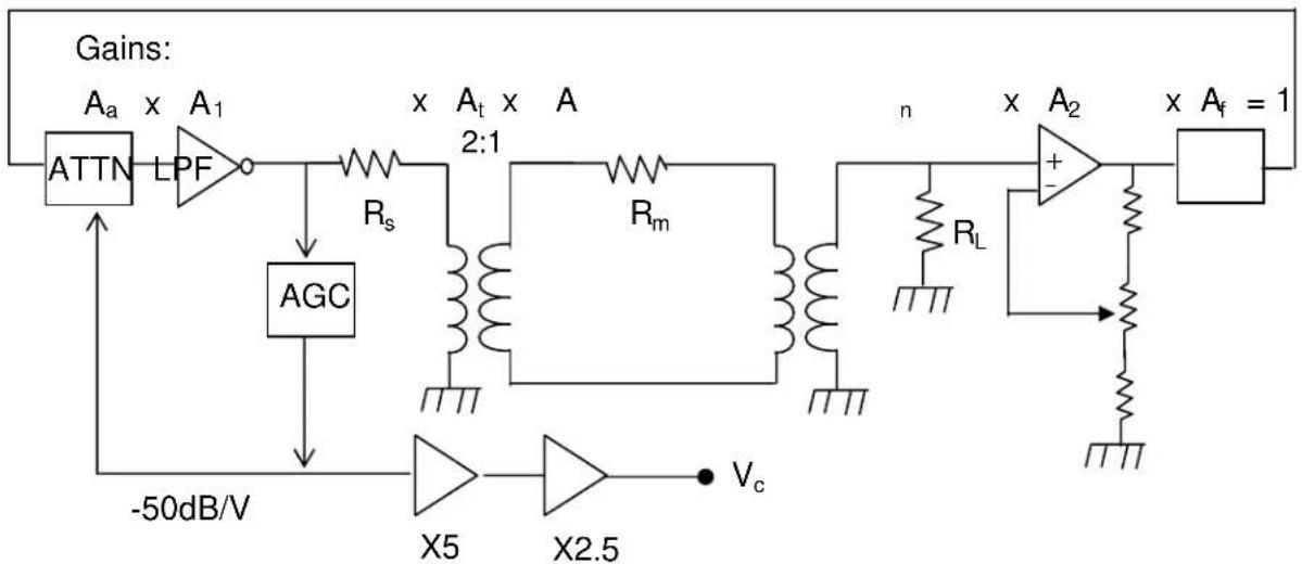
A gain model of the QCM25 Crystal Oscillator is shown in Figure 20. At series resonance the reactance of the crystal's motional inductance and motional capacitance cancel and so the crystal may be represented by just R_m , the motional resistance of the crystal. (It is also assumed that the static capacitance, C_0 , has been nulled as previously described.) The circuit will oscillate at the frequency for which the net phase shift around the loop is 360^ , provided there is sufficient gain to overcome the circuit losses.
Two network elements in the model provide a phase shift. The inverting amplifier provides 180^ of phase shift. The low pass filter is adjusted to provide 180^ of phase shift at 5 MHz. Hence the circuit will oscillate at the frequency for which the crystal is resistive, i.e. at series resonance.
The loop gain is the product of the gain (or attenuation) of each of the network elements. If the loop gain is exactly one, then the oscillation amplitude will be maintained at a fixed level. An AGC circuit controls the loop gain via a voltage controlled variable attenuator.
From left to right, the circuit consists of the following:
-
A voltage controlled variable attenuator with attenuation of A_a . An automatic gain control circuit generates a voltage to maintain the oscillation amplitude at a fixed level of 1 V_pp . The attenuator is controlled by this voltage, between 0 and 1 Vdc, providing an attenuation of 50 dB/volt so that A_a=10^V_age·50/20 . The AGC voltage is amplified by 5x in the QCM25 Crystal Oscillator, and by 2.5 x in the QCM200 Controller, before being output via the Conductance BNC on the front panel of the QCM200. Hence, referenced to the voltage V_c at the QCM200 Conductance output BNC, A_a=10^-V_c/5 .
-
A fixed gain amplifier with gain A_1=45 dB+20 (250/200)=46.94 dB (or 222 x.) This inverting amplifier has a bandwidth of 500 MHz, and so introduces very little extraneous phase shift.
-
A source resistance, R_s , of 100 Ω. This source resistance consists of two series 50 Ω resistors, one of which is inside the amplifier A_1 . This source impedance is reduced by a factor of 4 x, to 25 Ω, by the 2:1 transformer which follows.
-
An isolation transformer with a 2:1 turns ratio, hence an attenuation of A_t=0.5 . This transformer allows galvanic isolation of the crystal from the oscillator circuit which is important in electrochemistry applications. In addition to reducing the source impedance by 4 x, the transformer also increases the load impedance seen at the input of the transformer by 4 x, so that when R_m=0 , the load will be 200 .
-
R_m , the motional resistance of the crystal at series resonance. R_m can vary from about 10-40 Ω for a dry crystal, to about 375 Ω for a crystal in water, to about 5 kΩ for a crystal in 90% (w/w) glycerol/water solution.
-
A second isolation transformer with a turns ratio of 1:1. This transformer allows galvanic isolation of the crystal from the oscillator circuit.
-
A load resistance b , of R50 . The network of Rs , R_m , and R_L provide a network attenuation, A_n , which depends on the crystal's motional resistance.
$$ A _ {n} = \frac {R _ {L}}{R _ {s} / 4 + R _ {m} + R _ {L}} \tag {eqn.} $$
-
An RF amplifier with an adjustable gain, A_2 , of about 4.43 x. The gain of this amplifier, A_2 , is set during calibration to compensate for gain variations of all the other circuit elements.
-
A low pass filter. This filter is a 5^th order Bessel low pass filter with f_c=3.7MHz , adjusted so as to provide 180^ of phase shift at 5 MHz. The phase shift of this filter, together with the 180^ phase shift of the inverting amplifier A_f , provides the 360^ of phase shift necessary for oscillation. The low pass filter is required to suppress spurious oscillations which would occur due to the high bandwidth of the loop amplifiers. The low pass filter attenuates a signal at 5 MHz by about A_f=-7.8dB (or 0.407x).
The motional resistance of the crystal at series resonance can now be computed. The product of the gain (or attenuation) of all of the elements around the loop is exactly one when the circuit is oscillating at constant amplitude. Hence,
$$ \mathrm{a} \cdot 1 \cdot \mathrm{t} \cdot \mathrm{n} \cdot 2 \cdot \mathrm{f} = 1 \mathrm{A} \text {AAA} \tag {eqn.3} $$
Rearranging and substituting the equation for A_n and solving for R_m ,
$$ \frac {1}{A _ {n}} = \frac {\mathrm{s} / 4 R _ {\mathrm{r}} R _ {\mathrm{m}} + R _ {\mathrm{L}}}{R _ {\mathrm{L}}} \quad \left(\text { } _ {1 a} \dots \text { } _ {T} A A A A A _ {f}\right) \tag {eqn.4} $$
$$ R _ {m} = R _ {L} \cdot A _ {a} \cdot \left(A _ {1} \cdot A _ {t} \cdot A _ {2} \cdot A _ {f}\right) - R _ {L} - \frac {R _ {s}}{4} \tag {eqn.5} $$
From the characteristics of the voltage variable attenuator described above, A_a=10^-V_c/5 , where V_c is the voltage at the Conductance output BNC on the QCM200. A_2 is adjusted
during factory calibration so that the product of the gains (A_1 A_1 A_2 A_1) = 200 . So we have,
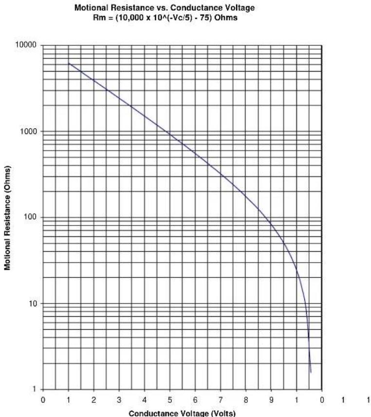
$$ m ^ {c / 5 - V}. 7 5, 1 0 0 0 0 1 0 R \quad (e q n. $$
Where R_m is the motional series resonance resistance in and V_c is the conductance voltage output in V.
The motional resistance of the crystal at series resonance, R_m can be computed from the above equation. Figure 21 below graphs R_m vs V_c .
line
| Conductance Voltage (Volts) | Motional Resistance (Ohms) | | --------------------------- | -------------------------- | | 1 | 10000 | | 2 | 3162 | | 3 | 1000 | | 4 | 316 | | 5 | 100 | | 6 | 31 | | 7 | 10 | | 8 | 3 | | 9 | 1 | | 10 | 0.316 | | 11 | 0.1 | | 12 | 0.0316 | | 13 | 0.01 | | 14 | 0.00316 | | 15 | 0.001 | | 16 | 0.000316 | | 17 | 0.0001 | | 18 | 0.0000316 | | 19 | 0.00001 | | 20 | 0.00000316 |Figure 21. Motional series resonance resistance vs. conductance voltage
Error Analysis
Errors in the measurement of R_m will be less than 3 + 3% of R_m (for R_m < 2 k ), and are dominated by the departure of the voltage controlled attenuator from its nominal (voltage-gain) characteristic.
Keep in mind that the resistance measurement in liquids and soft films is also affected by temperature, mostly through the temperature coefficient of the viscosity. For example, a 4 /^ change in resistance is to be expected in water around room temperature.
Noise Analysis
V_c varies logarithmically with R_m over most of the range of interest. There is an important advantage in this: the fractional resolution of the resistance is nearly independent of the resistance and so allows detailed and low-noise measurement of the viscous losses. To estimate the noise in resistance measurements, we can take the derivative of the equation for the motional resistance (units are Ohms and Ohms/Volt):
$$ m = \quad \cdot \quad^ {c / 5 - V} 7 5 - 1 0 1 0 0 0 0 R _ {(e q n. 7)} $$
$$ \frac {\mathrm{d} R _ {\mathrm{m}}}{\mathrm{d} V _ {\mathrm{c}}} = 1 0 0 0 0 \cdot 1 0 ^ {- V _ {\mathrm{c}} / 5} \cdot \ln (1 0) \cdot \left(- \frac {1}{5} (\right) =) \quad \cdot 2, 0 0 0 \cdot \ln 1 0 ^ {1 0 / 5} \tag {eqn.8} $$
$$ \frac {\mathrm{d} R _ {\mathrm{m}}}{\mathrm{d} V _ {\mathrm{c}}} \approx - 4 6 0 5 \cdot 1 0 ^ {- V _ {\mathrm{c}} / 5} = - 0. 4 6 0 5 \cdot (R _ {\mathrm{m}} + 7 5) \tag {eqn.9} $$
Noise on the V_c signal, V_c , is typically ±50 V (with one second averaging). R_m for a 5 MHz crystal in water is about 375 . The fractional noise in the resistance measurement is then:
$$ \frac {\Delta \mathrm{R} _ {\mathrm{m}}}{\mathrm{R} _ {\mathrm{m}}} = \frac {\Delta \mathrm{V} _ {\mathrm{c}}}{\mathrm{R} _ {\mathrm{m}}} \cdot \frac {\mathrm{dR} _ {\mathrm{m}}}{\mathrm{dV} _ {\mathrm{c}}} = \frac {\Delta \mathrm{V} _ {\mathrm{c}}}{\mathrm{R} _ {\mathrm{m}}} \cdot [ - 0. 4 6 0 5 \cdot (\mathrm{R} _ {\mathrm{m}} + 7 5) ] = \pm 2 8 \mathrm{ppm} \tag {eqn.10} $$
This low noise floor for fractional resistance measurements allows very small changes in dissipation losses to be measured. This is why a high precision voltmeter (i.e. with at least six digits of resolution) is recommended for measuring the analog conductance output and why a very high resolution (24 bit) A/D converter is used by the QCM200 to calculate resistance readings.
Calibration of R_m
Resistance measurements for the QCM25 Crystal Oscillator/QCM200 are calibrated by replacing the crystal with a precision resistor in parallel with a 18 pF capacitor. Two resistor values are used: 25 Ω and 925 Ω. The equation for R_m may be inverted to determine the calibration value for V_c . (Motional resistance, R_m , in Ω and conductance voltage output, V_c , in volts.)
$$ m \quad \cdot = ^ {c / 5 - V} 7 5 - 1 0 1 0, 0 0 0 R \quad V _ {\text { and }} 5 \log \left[ \frac {1 0 , 0 0 0}{R _ {m} + 7 5} \right] \tag {eqn.11} $$
The low pass filter is adjusted so that the QCM25 Crystal Oscillator oscillates at 5 MHz with the 25 Ω resistor in place of the crystal. The varactor dial is adjusted so that the Crystal Controller oscillates at 5 MHz with the 925 Ω resistor in place of the crystal. Calibration potentiometers in the QCM25 Crystal Oscillator are adjusted so that (P1 pot) V_c = 10.000 ± 0.005 Vdc with a calibration resistor of 25 Ω, and (P2 pot) V_c = 5.000 ± 0.005 Vdc with a calibration resistor of 925 Ω. Iterate P1 and P2 adjustments as necessary.
Gas-Phase Measurements
The first use of QCMs was as mass sensors and thickness monitors in gas phase, thin-film depositions. To this date, this continues to be an important area of application for this technology.
Sauerbrey Equation
Sauerbrey's equation (eqn. 12) is often used to calculate mass loadings and thin-film thicknesses in vacuum depositions. The basic assumption is that the incremental change in mass from the foreign film is treated as though it were really an extension of the thickness of the underlying quartz. The foreign film is considered rigid and so thin that it does not experience any shear forces during vibration. As a result, the sensitivity factor, C_f , is a fundamental property of the quartz crystal and does not consider any of the properties of the foreign film (i.e. it is only dependent on the acousto-elastic properties of quartz).
$$ C _ {t} = \frac {2 n f _ {0} ^ {2}}{\left(p _ {q ^ {\infty} q}\right) ^ {1 / 2}} \tag {eqn.12} $$
where
n = number of the harmonic at which the crystal is driven,
f_0= the resonant frequency of the fundamental mode of the crystal in Hz,
_q= density of quartz = 2.648 g cm ^-3 ,
_q = shear modulus of quartz = 2.947× 10^11gcm^-1· s^-2
The dependence of the frequency change on the mass coverage per unit area, emphasizes the fact that, within certain limits, the sensitivity factor is independent of the electrode geometry. Thus, in theory, the QCM mass sensor does not require calibration for this application. This ability to calculate mass loading from first principles is obviously a very attractive feature of these devices.
Film thickness is often the parameter of interest in gas-phase thin-film depositions. If the mass coverage is believed to be uniform, the thickness of the film is easily calculated by dividing the mass per unit area provided by Sauerbrey's equation by the material's density.
$$ T _ {f} = \frac {\Delta m}{\rho_ {f}} \tag {eqn.} $$
where
_f= density of film material in g/cm ^3 ,
m = change in mass per unit area in g / cm^2 (calculated from Sauerbrey's equation),
T_f= thickness of the film in cm.
Z-match Method
It is generally accepted that when the mass loading from the deposit causes a change in frequency of less than 2% of the frequency of the unloaded crystal, Sauerbrey's equation can be used to obtain accurate results in thin-film thickness calculations ^9 . As the thickness of the film increases, the Sauerbrey equation must be extended to incorporate the elasticity of the deposit. Lu and Lewis ^10 gave a simple equation (eqn. 14) for the calculation of the dependence of f on m , which is currently applied by most QCM users to calculate rigid thin-film thicknesses in gas phase depositions.
$$ \left(\frac {N _ {q} \rho_ {q}}{\pi Z f _ {L}}\right). \quad - 1 \left[ \cdot \left[ \begin{array}{c} \pi (f _ {t} - f _ {u}) \ \tan z \tan r \ f _ {U} \end{array} \right] \right] \tag {eqn.} $$
where,
$$ \Delta \mathsf {m} = \text { change in mass per unit area in } \mathrm{g/cm} ^ {2}, $$
$$ \mathrm{N} _ {\mathrm{q}} = \text { Frequency Constant for AT - cut quartz crystal } = 1. 6 6 8 \times 1 0 ^ {1 3} \mathrm{Hz} \mathrm {\AA}, $$
$$ \rho_ {\mathrm{q}} = \text { density of quartz } = 2. 6 4 8 \mathrm{g} \mathrm{cm} ^ {- 3}, $$
$$ \mathrm{f} _ {\mathrm{U}} = \text { frequency of unloaded crystal (prior to deposition) in Hz }, $$
$$ f _ {L} = \text { frequency of loaded crystal in Hz }, $$
$$ Z = Z \text {-Factor of film material} = [ (\rho_ {q} \alpha_ {q}) / (\rho_ {f} \alpha_ {f}) ] ^ {1 / 2}, $$
$$ \rho_ {\mathrm{f}} = \text { density of film material in g cm } ^ {- 3}, $$
$$ \propto_ {\mathrm{q}} = \text { shear modulus of quartz } = 2. 9 4 7 \times 1 0 ^ {1 1} \mathrm{gcm} ^ {- 1} \mathrm{s} ^ {- 2}, $$
$$ \propto_ {\mathrm{f}} = \text { shear modulus of film material. } $$
This analysis of frequency changes, including the acoustic impedances of the quartz and film, is often called the “Z-match” method. The accuracy of the mass load and film-thickness calculation is often limited by how well the Z-Factor and density of the material are known. Density and Z-Factor values are typically very close to bulk values. The bulk density and shear modulus values for common film materials can be found in many material reference handbooks.
The Lu and Lewis equation is generally considered to be a good match to the experimental results ^17 for frequency changes up to 40% (relative to the unloaded crystal). Keep also in mind that the Z-match equation strictly applies to “rigid” deposits. Films which behave viscoelastically, such as some organic polymer films with large thickness or viscosity, will exhibit significant deviations from both equations 1 and 5.
Crystal failures are also often seen before a 40% shift in frequency is reached. Common problems are (1) shorts in the crystal electrodes due to excessive buildup, (2) mode hopping to other (anharmonic) resonant frequencies due to the buildup of composite resonant modes, (3) deviations from theory due to fringing electrode fields developed between the electrodes and the film, (4) unexpected shifts in fundamental frequency due to stress build up on the crystal surface, (5) splitting of source material resulting in non-uniform films, etc.
Liquid Contact Measurements
Until fairly recently, it was believed that excessive viscous loading would prohibit use of the QCM in liquids. In fact, operation in liquids is indeed possible ^12 , and the response of the QCM is still extremely sensitive to mass changes at the crystal-solution interface. For many years, QCMs have been used in direct contact with liquids and/or viscoelastic films to assess changes in mass and viscoelastic properties during chemical and electrochemical surface processes.
When the QCM comes in contact with a solution, there is a decrease in frequency that is dependent upon the viscosity and the density of the solution. A quantitative understanding of the resonator behavior is a prerequisite for proper interpretation of experimental results under total liquid immersion. This problem was first treated by Glassford ^13 , and later by Kanazawa and Gordon ^14 .
Kanazawa's treatment of the influence of the solution properties on the crystal (eqn. 15) permits the prediction of the change in resonance frequency which accompanies immersion of the crystal into a viscous medium:
$$ \Delta = \mathrm { {U} ^ {3 / 2}} \left(\frac {\rho {\mathrm{L}} \eta_ {\mathrm{L}}}{q ^ {\infty} \bar {q} \rho}\right) ^ {1 / 2} \tag {eqn.} $$
where
f_U = frequency of oscillation of unloaded crystal,
_q = density of quartz = 2.648~gcm^-3
_q = shear modulus of quartz = 2.947× 10^11gcm^-1s^-2
_L= density of the liquid in contact with the electrode,
_L= viscosity of the liquid in contact with the electrode.
Viscous coupling of the liquid medium to the oscillating crystal surface results not only in a decrease in the series resonant frequency but also in damping of the resonant oscillation - the viscous loss is manifested as an increase in series resonance resistance, R, of the QCM resonator. Thus, R serves as an excellent independent measure of viscous loading by the medium (liquid or soft-film) at the crystal's surface.
f and R measurements are both routinely used as independent indicators of mass loading and viscosity at the crystal-liquid interface of the QCM resonator during chemical and electrochemical depositions in solution ^15 .
In a separate study ^16 , a Butterworth-Van Dyke equivalent circuit model (Figure 16) was applied to derive a linear relationship between the change in series resonance resistance, R , of the quartz oscillator and (_L_L)^1/2 under liquid loading:
$$ \Delta R = \left(\frac {n \omega L}{\pi}\right) \cdot \left(\frac {2 \omega \rho \eta_ {L L} s _ {u s}}{\rho_ {q} \propto_ {q}}\right) ^ {1 / 2} \tag {eqn.16} $$
Where
R = change in series resonance resistance in
n = number of sides in contact with liquid,
_s = angular frequency at series resonance (2 f_s)
L_u = inductance for the unperturbed (dry) resonator, usually in mH .
The QCM200 System was specifically designed for operation under heavy viscous loading. The standard Crystal Holder supports operation in gas and liquid environments, and provides single-electrode exposure to liquids ^17 (i.e. n = 1 in eqn. 16) as required for compatibility with electrochemical QCM measurements. The Crystal Oscillator provides both frequency and resistance change signals and will maintain oscillation up to a series resonance resistance of about 5 kΩ (it will support crystal operation in highly viscous solutions up to 88% (w/w) glycerol in water). Transformer isolation of the oscillator circuit provides compatibility with virtually any potentiostat.
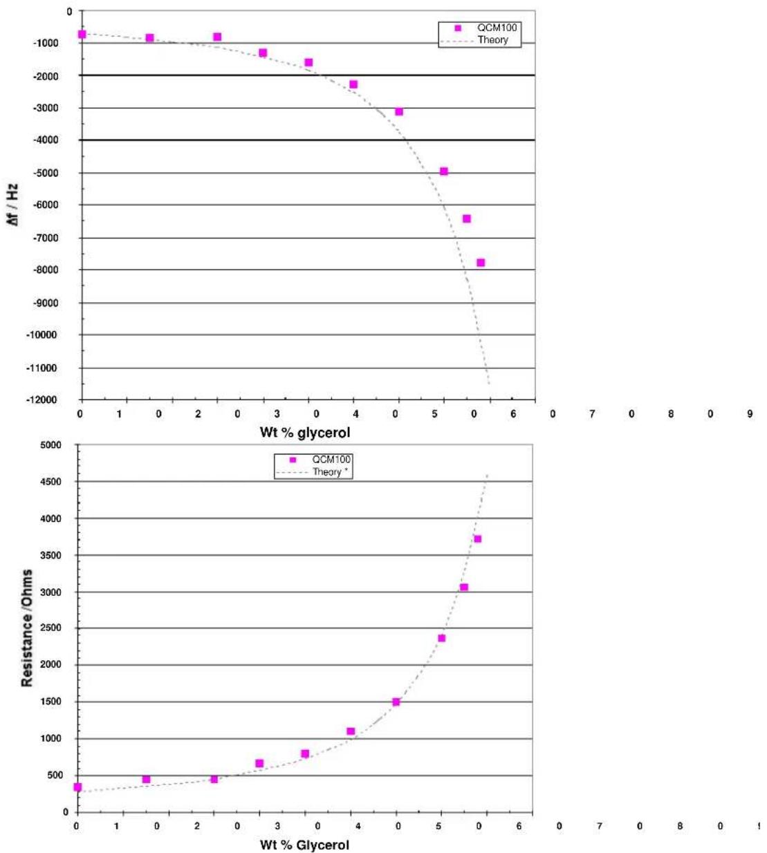
As an example, eqn. 15 predicts a decrease in t_0 of 715 Hz on transfer from vacuum to pure water ^18 at 20°C, in agreement with the results observed with a QCM200 using 1 inch diameter, polished, gold coated, 5 MHz crystals, mounted on a standard Crystal Holder. Excellent agreement between the frequency and resistance equations and the experimental results has been proved ^19 , making the QCM an excellent tool for the evaluation of fluid properties. Application examples include in situ monitoring of lubricant and petroleum properties ^20 . The tight correspondence between theory (eqns. 15 & 16) and experiment is clearly illustrated by Figure 22.
line
| Wt % glycerol | QCM100 Δf / Hz | Theory Δf / Hz | QCM100 Resistance / Ohms | Theory Resistance / Ohms | | ------------- | -------------- | -------------- | ------------------------ | ------------------------ | | 0 | -800 | -800 | 300 | 300 | | 1 | -900 | -900 | 400 | 400 | | 2 | -1000 | -1000 | 450 | 450 | | 3 | -1200 | -1200 | 650 | 650 | | 4 | -2200 | -2200 | 800 | 800 | | 5 | -3200 | -3200 | 1500 | 1500 | | 6 | -800 | -800 | 3700 | 3700 |Figure 22. Frequency Shift (Hz) and Resistance Shift(Ohms) versus glycerol weight percentage (in water) as predicted by theory and as measured with QCM200 and a 5 MHz polished crystal.
Immersion Test
A comparison against the theoretical predictions of equations 6 and 7 is usually a good starting point when testing a new experimental liquid QCM200 setup. Two common “checkup” procedures are described.
Water Immersion
For a gold coated, 5 MHz, polished crystal, and assuming that the electrode capacitance has been properly cancelled, a decrease in frequency of ≈715 Hz, and an increase in series resonance resistance of ≈380 , is expected when switching from air to complete immersion in water at 20^ .
Glycerol/H₂O Immersion
Figure 22 shows resistance and frequency change values expected for a polished 5 MHz crystal immersed in a series of viscous glycerol/water solutions at 20°C. Operation at increasing glycerol concentrations is an excellent test of a QCM experimental setup, and should provide predictable results up to more than 88% glycerol.
In both procedures, an agreement between measured and expected values within ±25% is generally considered acceptable for glycerol concentrations up to 70%.
Frequency shifts are much larger (at least a factor of two) and unpredictable for unpolished crystals so they are not recommended for system checkup.
Electrochemical Quartz Crystal Microbalance
In most electrochemical experiments, mass changes occur as material is deposited or lost from the “working” electrode. It is of interest to monitor those changes simultaneously with the electrochemical response, and the QCM is the standard means of doing so. As a gravimetric probe, the QCM has been used in many types of electrochemical studies, including: underpotential deposition of metals ^21 , corrosion, oxide formation, dissolution studies ^22 , adsorption/desorption of surfactants ^23 and changes in conductive polymer films during redox processes ^24 .
The basic principles and applications of the QCM to electrochemical processes have been extensively reviewed in the electrochemical literature ^25 and will only be discussed briefly in this manual. Please refer to the publications list at the end of this chapter for more detailed information.
Electrochemical Apparatus
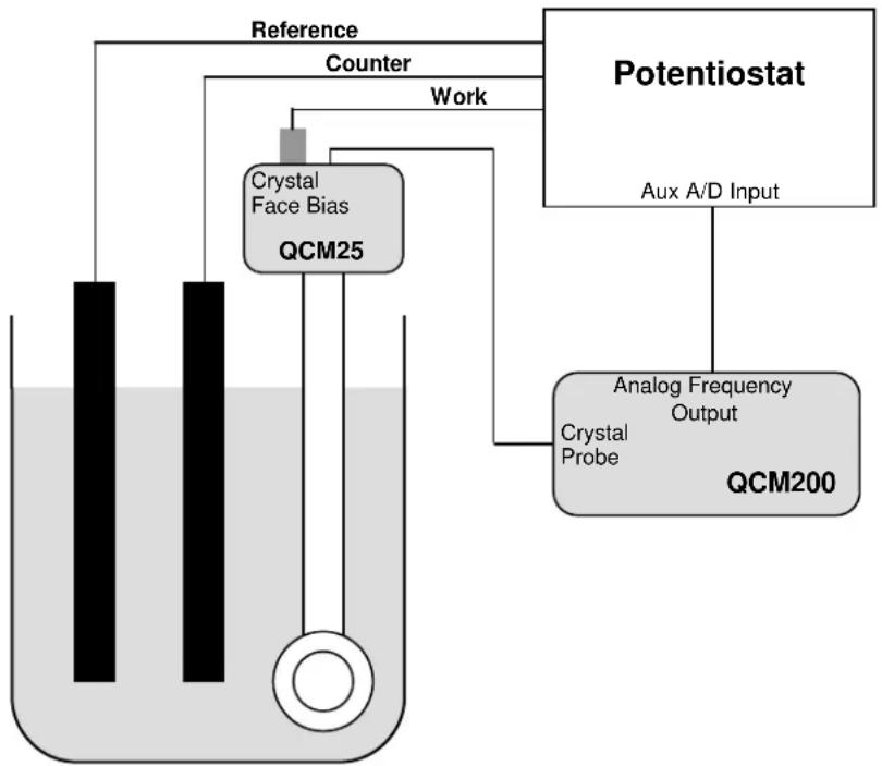
A schematic diagram of the apparatus for electrochemical quartz crystal microbalance (EQCM) experiments is given in Figure 23. In this example, a 1 inch diameter, polished QCM crystal is mounted on a Crystal Holder with only one electrode exposed to the conductive solution. The Crystal Holder is connected to a QCM25 Crystal Oscillator, and
the liquid-contact electrode is connected to the “working electrode” lead of the potentiostat (through the Crystal Face Bias connector of the QCM25 Crystal Oscillator).
Notes
- The QCM25 Crystal Oscillator provides transformer isolation of the crystal's front face (i.e. liquid surface) electrode. This allows direct electrical connection of the quartz crystal face to the “working electrode” pin of any standard potentiostat/galvanostat.
- The Frequency Analog Out voltage signal is proportional to the Relative Frequency readings and can be used to interface the QCM frequency signal to the data acquisition infrastructure of most commercially available potentiostats.
- Temperature stabilization is essential in EQCM experiments for high accuracy measurements.
flowchart
graph TD
    A["Reference"] --> B["Counter"]
    B --> C["Work"]
    C --> D["Potentiostat"]
    D --> E["Aux A/D Input"]
    F["Crystal Face Bias QCM25"] --> D
    G["Analog Frequency Output"] --> H["QCM200"]
    I["Crystal Probe"] --> H
Figure 23. Basic EQCM setups with a QCM200).
For the QCM200 setup, the Frequency Analog Out signal of the QCM controller is connected to the Ext A/D Input of the potentiostat. The Scale value is adjusted to best match the Relative Frequency changes expected during the electrochemical processes. The potentiostat digitizes the voltage signal, and its PC software displays the Relative Frequency changes in synchronicity with the electrochemical data.
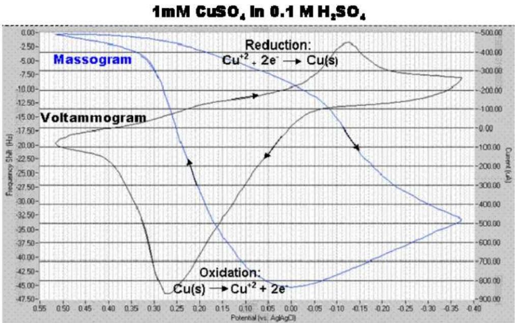
With the setup of Figure 23, a typical cyclic voltammetric EQCM experiment would involve the application of the electrochemical waveform to the working electrode and the simultaneous measurement of the current flowing through the electrochemical cell and the oscillation frequency and series resonance resistance of the crystal.
Figure 24 is an example of a typical voltammogram-massogram plot obtained from a 10mM solution of CuSO_4 in 0.1M H_2SO_4 using a 1 inch diameter, Au coated, quartz crystal mounted in a standard Crystal Holder as the working electrode. (Note: cathodic current is treated as positive)
line
| Potential (vs. Ag/AgCl) | Frequency Shift (Hz) | Current (A) | | ---------------------- | -------------------- | ----------- | | 0.55 | 0.00 | 500.00 | | 0.50 | -2.50 | 400.00 | | 0.45 | -5.00 | 300.00 | | 0.40 | -7.50 | 200.00 | | 0.35 | -10.00 | 100.00 | | 0.30 | -12.50 | 0.00 | | 0.25 | -15.00 | -100.00 | | 0.20 | -17.50 | -200.00 | | 0.15 | -20.00 | -300.00 | | 0.10 | -22.50 | -400.00 | | 0.05 | -25.00 | -500.00 | | 0.00 | -27.50 | -600.00 | | -0.05 | -30.00 | -700.00 | | -0.10 | -32.50 | -800.00 | | -0.15 | -35.00 | -900.00 | | -0.20 | -37.50 | -850.00 | | -0.25 | -40.00 | -750.00 | | -0.30 | -42.50 | -650.00 | | -0.35 | -45.00 | -550.00 | | -0.40 | -47.50 | -450.00 |Figure 24. Cyclic voltammogram and massogram data for Cu deposition on a Au electrode. The frequency–potential diagram shows a frequency decrease in perfect sync with the deposition of Cu metal (reduction) on the crystal's surface.
The mass sensing capabilities of the QCM200 are complemented by its ability to simultaneously detect subtle changes in the viscous loading of the QCM crystal during redox processes. Figure 25 is a graphical representation of the changes in series resonance resistance that take place at the QCM sensor (i.e. working electrode) during a cyclic voltammetric scan of a 50 mM solution of K3Fe(CN)6 in 1M Na_2SO_4 (50 mV/sec scan rate). As the potential of the electrode becomes less positive, Fe(CN)6^3- is depleted and replaced by a layer of Fe(CN)6^4- adjacent to the sensor crystal. Since solutions of Fe(CN)6^4- are more viscous than Fe(CN)6^3- the resistance readings increase at more negative voltages as the more viscous reduced product exerts additional loading on the crystal. The resistance change corresponding to the conversion of Fe(CN)6^3- to Fe(CN)6^4- is 4 Ohms, in complete agreement with a 0.9% estimated relative change in ()^1/2 calculated from previously reported calibration curves ^26 .
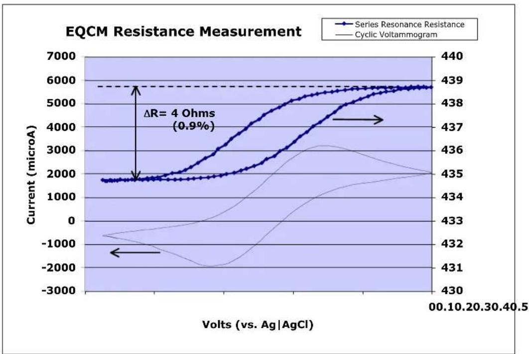
Figure 25. Changes in series resonance resistance at the QCM sensor during the electrochemical oxidation/reduction of Fe(CN)_6^3- / Fe(CN)_6^4- . The resistance–potential diagram shows a resistance increase in perfect sync with the generation of a viscous layer of Fe(CN)_6^4- (reduction) adjacent to the QCM electrode.
Calibration
It has been amply demonstrated in the literature that when experiments involve only relative frequency shifts which are measured in a fixed solution, the offset caused by the viscous loading of the liquid, has negligible effect on the accuracy of the Sauerbrey equation for the determination of small mass changes in rigid deposits ^27 . Quantitative interpretation of the EQCM data in those cases is based on the combination of the Sauerbrey equation (eqn. 1) and Faraday's law. The former relates change in frequency to change in mass for thin, rigid deposits, whereas the latter relates charge passed in an electrochemical experiment to the number of moles of material electrolyzed. Therefore, frequency changes can be related to the total charge passed.
An example would be the electrodeposition of Ag on a Pt electrode QCM crystal. The charge, Q , is an integral measure of the total number of electrons delivered at the interface during the reduction process. To the extent, that each electron supplied results in the deposition of one atom of Ag, there should be a linear relationship between Q and f as is given by equation 8:
$$ \Delta f = \frac {{} ^ {6} {} _ {\mathrm{w}} \cdot {} _ {\mathrm{f}} \cdot \mathrm{QCM10}}{\mathrm{n} \cdot \mathrm{F} \cdot \mathrm{A}} \tag {eqn.17} $$
where
f = frequency change in Hz,
M_w = apparent molar mass of the depositing species in grams/mole,
C_f = Sauerbrey's sensitivity factor for the crystal used (see eqn. 1),
Q = integrated charge during the reduction in Coulombs,
A = active deposition area of the working (liquid contact) electrode in cm²,
F = Faraday's constant = 9.648 × 10^4 Coulomb/mole,
n = number of electrons transferred to induce deposition (i.e. n = 1 for Ag deposition).
(The factor of 10^6 provides for the unit conversion from g in C_f to g in M_w .)
A plot of f vs Q will deliver the apparent mass per electron of the deposited species, when n is taken into account. This is often used to elucidate the mass changes that accompany redox processes, and hence is very useful for characterizing the mechanisms of electron-transfer reactions.
However, before any calculations can be performed based on eqn. 17, the EQCM must be calibrated in order to properly derive (1) the proportionality constant, Q , of the Sauerbrey equation in solution and (2) to account for the effective area of the working electrode. This is generally done using a well behaved electrochemical reaction - typically electrodeposition of silver, copper or lead on a Au or Pt electrode.
The EQCM calibration method favored by Stanford Research Systems for its QCM200 System is based on the galvanostatic deposition of Ag. A 50 mM solution of AgNO_3 in 0.5 M HNO_3 is subjected to a reducing potential and Ag is deposited with a fixed cathodic current density of 50-500 A/cm^2 . The cathodic current is integrated to obtain the charge as a function of time. Excellent linearity is generally observed in f vs Q plots for depositions within 1 g/cm^2 , providing a very reliable way to calibrate the proportionality constant of eqn. 17.
Several calibration procedures are also described in the electrochemistry literature ^28 , and users are referred to the publications list at the end of this chapter for details.
Polymer Modified Electrodes
The EQCM has been extensively used to study polymer modified electrodes, particularly as a gravimetric tool to follow redox processes ^29 . However, for the linear frequency-to-mass relationship (described by eqn. 17) to hold true, the polymer overlayer must exhibit no changes in rigidity during the electrochemical process. Otherwise, the viscoelastic changes will also contribute to the frequency change, leading to an erroneous interpretation of the mass changes ^30 . As a consequence, it is essential to determine whether or not viscoelastic properties of the polymer film influence the frequency measurement during polymer film experiments!
0.1M Pyrrole in 0.1M HClO4
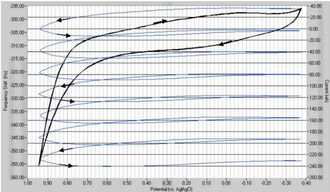
Figure 26. Voltammogram and massogram data for the oxidation of pyrrole to form a polypyrrole film on a gold coated QCM Sensor Crystal. Seven cycles of voltammetry, between -0.4 and 0.95 V were conducted in this experiment. Pyrrole monomer can be oxidized to its radical at 0.65 V. As this happens, a thin polypyrrole film is formed on the crystal surface, resulting in a decrease in the fundamental frequency of oscillation of the crystal. The continuous growth of the film is evidenced by the irreversible decrease in frequency during the scans.
A straightforward way to detect changes in film viscoelastic properties of redox films is to simultaneously monitor the series resonance resistance, R, of the quartz oscillator during the electrochemical experiment ^31 . Some theoretical models ^32 , based on the simultaneous measurement of f and R , have been discussed in the literature for the extension of EQCM gravimetric measurements to non-rigid films. The viscoelastic analysis of polymeric thin films in EQCM systems, is complex because the shear wave exists simultaneously in the quartz crystal, the viscoelastic film and the adjacent solution, so reflection of the shear wave must be taken into account. However, solution of this problem would be worthwhile, specially if the material properties of the film could be derived. This would allow correlation of the electrochemical behavior of the film with its material properties ^33 .
The unique property of the QCM technique is its ability to determine the mass of very thin layers while simultaneously giving information about their viscoelastic properties. The ability to measure both mass and structural changes means it is possible to detect phase-transitions, cross-linking and swelling in polymeric thin films ^34 .
Chemical and Biological Sensors
Anything that has mass can generate a response from a QCM sensor. The universal response of the device is the reason for the wide range of application of the technology. However, the downside of such universal sensitivity is that you always have a great danger of interference. For analytical purposes, it is imperative to find ways of getting the QCM sensor to respond only to what you are interested in, i.e. build specificity into the device. This usually involves the addition of a sensitive layer on the surface of the crystal ^35 .
Organic polymers comprise the most common type of coating used with QCM chemical sensors due to their capability to reversibly sorb vapors and liquids ^36 . In much of the work published on the use of polymer coatings for vapor sensing, the acoustic properties of the polymer material have been neglected. The relative importance of the mass-loading and viscoelastic contributions of the film to the observed QCM response is a subject that has yet to be resolved.
In no area have the QCM applications seen such dramatic increase in recent years as in the field of biochemical analysis. QCM devices are routinely used as biochemical and immunological probes ^37 , as well as for the investigation and/or monitoring of biochemically significant processes.
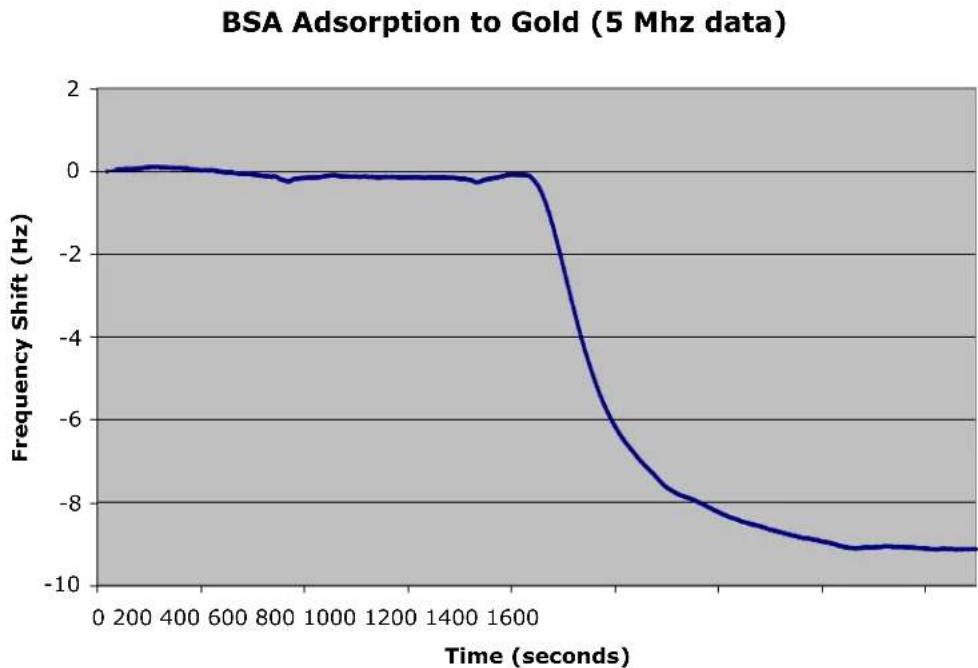
line
| Time (seconds) | Frequency Shift (Hz) | | -------------- | -------------------- | | 0 | 0.0 | | 200 | 0.0 | | 400 | 0.0 | | 600 | 0.0 | | 800 | -0.1 | | 1000 | -0.1 | | 1200 | -0.1 | | 1400 | -0.1 | | 1600 | -0.1 | | 1800 | -7.5 | | 2000 | -8.5 | | 2200 | -9.0 | | 2400 | -9.2 | | 2600 | -9.3 | | 2800 | -9.4 | | 3000 | -9.5 |Figure 27. A 10×g/ml solution of BSA in 2mM NaCl is flowed over a polished Au/Cr QCM crystal in an axial flow cell at a rate of 50×L/min. Due to the non-specific adsorption of the protein, the frequency of oscillation decreases by 9Hz over a period of 5 minutes. The sensitivity of the QCM200 for the detection of microgram quantities of proteins is clearly demonstrated by this very straightforward experiment.
An example of a complex and dynamic biochemical process which has been successfully studied with quartz crystal microbalances is the adsorption of proteins to solid surfaces ^38 . Figure 27 is the result of a QCM experiment following the adsorption kinetics of bovine serum albumin (BSA) from an aqueous saline solution on to a polished unmodified gold surface (i.e. physical adsorption). The adsorbed mass is small compared to the mass of the quartz crystal, evenly distributed and rigidly attached to the gold surface resulting in a frequency decrease of 9 Hz, proportional to the mass of protein adsorbed on the polished gold electrode. The sensitivity of the QCM200 for the detection of microgram quantities of proteins is clearly demonstrated by this very simple experiment.
Sensitive, selective detection of biochemically active compounds can be achieved by employing antigen-antibody ^39 , enzyme substrates and other receptor–protein pairs. The potential analytical uses of these materials has been reviewed, particularly with respect to the development of biochemical sensors ^40 . QCM studies have provided detailed information about the functionalized surfaces developed for a range of biochip and biosensor applications.
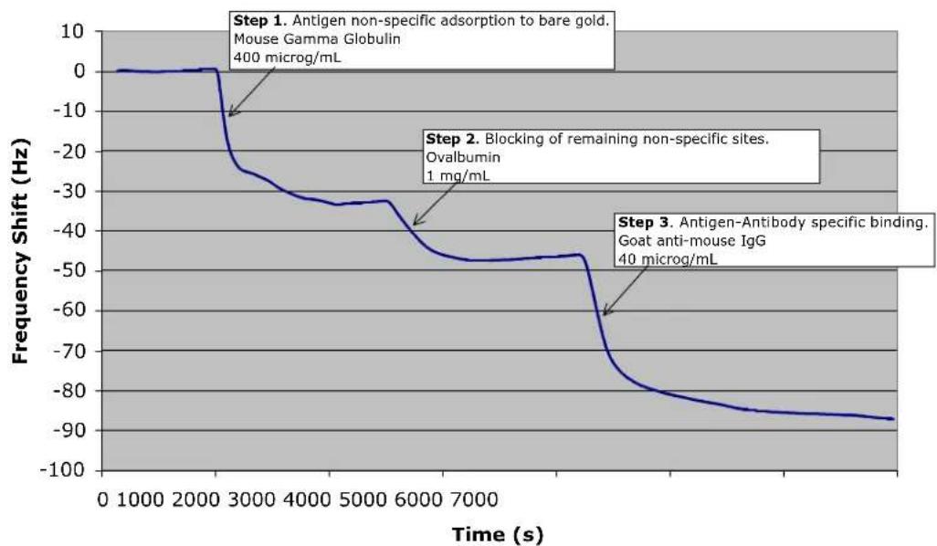
line
| Step | Description | Frequency Shift (Hz) | |------|--------------------------------------------------|----------------------| | Step 1 | Antigen non-specific adsorption to bare gold. Mouse Gamma Globulin | 400 | | Step 2 | Blocking of remaining non-specific sites. Ovalbumin | 1 | | Step 3 | Antigen-Antibody specific binding. Goat anti-mouse IgG | 40 |QCM Immunosensor - Antigen-Antibody Interaction
Figure 28. Antigen-antibody reaction monitored with a QCM200 system. This example shows the immobilization of mouse gamma globulin antigen on a bare gold surface (Step 1) and the subsequent binding of an antibody directed against the gamma globulin (Step 3). Since the gold surface is not completely covered by antigen in Step 1, a blocking solution of concentrated ovalbumin is used in Step 2 to block all uncovered sites.
Figure 28 is an example of an application of the QCM200 system as a protein biosensor and a demonstration of the sensitivity of the technology towards protein-protein interactions. The entire experiment took place on a polished Au/Cr QCM crystal housed within an axial flow cell connected to a standard flow injection analysis system consisting of a single syringe pump and a 6-port injection valve. Typical flow rates were 50 L / min , temperature stability was ± 0.1^ at 27^ and the buffer solution was PBS pH7.5. Antigen (mouse gamma globulin) was first introduced into the cell (Step 1)
resulting in a -35Hz frequency step caused by the non-specific metal-protein binding interactions between the protein and the bare gold surface (i.e. physical adsorption). The remaining non-specific binding sites were then blocked with excess ovalbumin (Step 2) resulting in the second (and smaller) frequency step. Finally (Step 3), antibody (goat anti-mouse IgG) was flowed over the immobilized protein layer and the specific interaction between antigen and antibody proteins resulted in the final -40Hz frequency step. The real advantage of the QCM technology in this application is that it is label free - the sample flowed over the immobilized surface layer does not need to be modified or labeled in any way. Thus it is much more physiologically relevant because labeling something with a fluorescent probe (i.e. ELISA) often changes its properties. The ability to see changes in the QCM signal after every individual step provides an additional advantage over standard immunoassays such as ELISA, where no user feedback is available until the entire process is completed.
TIP
Using a QCM biosensor you cannot only tell whether something binds to a given protein immobilized on the crystal, but you can also tell how tightly it binds ^4 - this is very useful additional information.
QCM Systems are applied routinely by biologists, immunologists and biochemists to obtain information about processes such as: (1) protein adsorption/desorption ^42 , (2) cell adhesion ^43 , (3) Protein-protein interaction, (4) Degradation of polymers, (5) biofouling and biofilm formation, (6) drug analysis ^44 , (7) self-assembled monolayers ^45 and (8) DNA biosensors ^46 . For more detailed information please consult the references listed at the end of this chapter.
Self-Assembled Monolayers
A self-assembled monolayer (SAM) is defined as a two-dimensional film, one molecule thick, covalently assembled at an interface. The classical example of a SAM is the reaction of alkanethiols with a gold surface.
Since sulfur donor atoms strongly coordinate on metal substrates (Au, Ag, Pt, etc), sulfur-containing molecules such as disulfides (R-SS-R), sulfides (R-S-R) and thiols ^47 (RSH) can form various functionalized SAMs with highly organized and compact construction. For example, when a clean gold surface is immersed in an alkanethiol solution, the following self-assembly chemisorption reaction takes place:
$$ \mathrm{Au} + \mathrm{RSH} \leftrightarrow \mathrm{Au} - \mathrm{SR} + 1 / 2 \mathrm{H} _ {2} \uparrow $$
This reaction self terminates at one monolayer, when all accessible gold sites are consumed. The Langmuir adsorption model has been applied successfully to model the adsorption /desorption kinetics of these processes.
The self-assembly of alkanethiol monolayers onto gold has been studied extensively due to the potential application of these interfaces to (1) chemical and biological sensing, (2) nano- and micro-device manufacturing and (3) surface modification.
A significant amount of work has been dedicated to understanding the steady-state properties of SAMs once they have formed. However, more recently it has become clear that alkanethiol SAMs are highly dynamic structures, and a lot of renewed effort has been dedicated to the understanding of the mechanism of monolayer formation ^48 .
The QCM200 system provides a unique opportunity to monitor, in-situ and in real-time, the rate of adsorption of alkanethiols onto gold - the change (i.e. decrease) in frequency resulting from the adsorption of alkanethiol molecules onto the gold electrode of a QCM crystal allows direct measurement of the rate of formation of SAMs.
Tip
Silanes are another common material used in SAMs ^49 . Silanization has also been studied with QCMs using crystals with electrodes custom coated with thin layers of Si(111).
Several examples of direct measurement of adsorption kinetics of alkanethiolate SAMs on QCM crystals, from both gas and liquid phase, are included in the references list at the end of this chapter.
Figure 29 is a graphical representation of the chemical adsorption kinetics of 16-mercaptohexadecanoic acid on to bare gold measured, in real time, with a QCM200 quartz crystal microbalance. In this simple experiment, a polished Au/Cr crystal (mounted on a standard holder) was immersed in 200~mL of ethanol housed inside a temperature stabilized 500~mL beaker. The reaction was triggered by rapidly injecting 1mL of 10^-2M solution of 16-mercaptohexadecanoic acid, providing a diluted 5× 10^5M solution of alkanethiol to react with the bare gold. A short transient in the frequency and resistance indicates the point of insertion of the thiol and is due to a slight temperature difference between the solvent and the sample solution. The fast drop in frequency following the injection is due to the fast formation of thiol-gold bonds, followed by a
slower annealing process. The absence of a sharp positive step in the resistance verifies that the fast frequency drop is not due to a change in the viscosity of the solution. The results are in excellent agreement with the observations of Blanchard's group ^50 corresponding to the adsorption/desorption kinetics of thiols from hexane and under very similar experimental conditions.
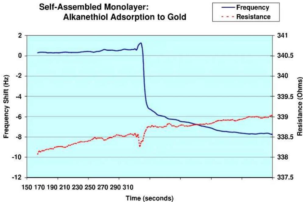
line
| Time (seconds) | Frequency Shift (Hz) | Resistance (Ohms) | | -------------- | -------------------- | ----------------- | | 150 | 0.0 | 338.0 | | 170 | 0.0 | 338.2 | | 190 | 0.0 | 338.4 | | 210 | 0.0 | 338.6 | | 230 | 0.0 | 338.8 | | 250 | 0.0 | 339.0 | | 270 | 0.0 | 339.2 | | 290 | 0.0 | 339.4 | | 310 | 1.0 | 339.6 | | 330 | -5.0 | 339.8 | | 350 | -6.0 | 340.0 | | 370 | -7.0 | 340.2 | | 390 | -7.5 | 340.4 | | 410 | -8.0 | 340.6 | | 430 | -8.5 | 340.8 | | 450 | -9.0 | 341.0 | | 470 | -9.5 | 341.2 | | 490 | -10.0 | 341.4 | | 510 | -10.5 | 341.6 | | 530 | -11.0 | 341.8 | | 550 | -11.5 | 342.0 | | 570 | -12.0 | 342.2 | | 590 | -12.5 | 342.4 | | 610 | -13.0 | 342.6 | | 630 | -13.5 | 342.8 | | 650 | -14.0 | 343.0 | | 670 | -14.5 | 343.2 | | 690 | -15.0 | 343.4 | | 710 | -15.5 | 343.6 | | 730 | -16.0 | 343.8 | | 750 | -16.5 | 344.0 | | 770 | -17.0 | 344.2 | | 790 | -17.5 | 344.4 | | 810 | -18.0 | 344.6 | | 830 | -18.5 | 344.8 | | 850 | -19.0 | 345.0 | | 870 | -19.5 | 345.2 | | 890 | -20.0 | 345.4 | | 910 | -20.5 | 345.6 | | 930 | -21.0 | 345.8 | | 950 | -21.5 | 346.0 | | 970 | -22.0 | 346.2 | | 990 | -22.5 | 346.4 | | 1010 | -23.0 | 346.6 | | 1030 | -23.5 | 346.8 | | 1050 | -24.0 | 347.0 | | 1070 | -24.5 | 347.2 | | 1090 | -25.0 | 347.4 | | 1110 | -25.5 | 347.6 | | 1130 | -26.0 | 347.8 | | 1150 | -26.5 | 348.0 | | 1170 | -27.0 | 348.2 | | 1190 | -27.5 | 348.4 | | 1210 | -28.0 | 348.6 | | 1230 | -28.5 | 348.8 | | 1250 | -29.0 | 349.0 | | 1270 | -29.5 | 349.2 | | 1290 | -30.0 | 349.4 | | 1310 | -30.5 | 349.6 | | 1330 | -31.0 | 349.8 | | 1350 | -31.5 | 350.0 | | 1370 | -32.0 | 350.2 | | 1390 | -32.5 | 350.4 | | 1410 | -33.0 | 350.6 | | 1430 | -33.5 | 350.8 | | 1450 | -34.0 | 351.0 | | 1470 | -34.5 | 351.2 | | 1490 | -35.0 | 351.4 | | 1510 | -35.5 | 351.6 | | 1530 | -36.0 | 351.8 | | 1550 | -36.5 | 352.0 | | 1570 | -37.0 | 352.2 | | 1590 | -37.5 | 352.4 | | 1610 | -38.0 | 352.6 | | 1630 | -38.5 | 352.8 | | 1650 | -39.0 | 353.0 | | 1670 | -39.5 | 353.2 | | 1690 | -40.0 | 353.4 | | 1710 | -40.5 | 353.6 | | 1730 | -41.0 | 353.8 | | 1750 | -41.5 | 354.0 | | 1770 | -42.0 | 354.2 | | 1790 | -42.5 | 354.4 | | 1810 | -43.0 | 354.6 | | 1830 | -43.5 | 354.8 | | 1850 | -44.0 | 355.0 | | 1870 | -44.5 | 355.2 | | 1890 | -45.0 | 355.4 | | 1910 | -45.5 | 355.6 | | 1930 | -46.0 | 355.8 | | 1950 | -46.5 | 356.0 | | 1970 | -47.0 | 356.2 | | 1990 | -47.5 | 356.4 | | 2010 | -48.0 | 356.6 | | 2030 | -48.5 | 356.8 | | 2050 | -49.0 | 357.0 | | 2070 | -49.5 | 357.2 | | 2090 | -50.0 | 357.4 | | 2110 | -50.5 | 357.6 | | 2130 | -51.0 | 357.8 | | 2150 | -51.5 | 358.0 | | 2170 | -52.0 | 358.2 | | 2190 | -52.5 | 358.4 | | 2210 | -53.0 | 358.6 | | 2230 | -53.5 | 358.8 | | 2250 | -54.0 | 359.0 | | 2270 | -54.5 | 359.2 | | 2290 | -55.0 | 359.4 | | 2310 | -55.5 | 359.6 | | 2330 | -56.0 | 359.8 | | 2350 | -56.5 | 360.0 | | 2370 | -57.0 | 360.2 | | 2390 | -57.5 | 360.4 | | 2410 | -58.0 | nan | The Frequency Shift (Hz) and Resistance (Ohms) are calculated based on the sum of frequencies and resistances for each component of the self-assembled monolayer (Monolayer). The values for Frequency Shift are calculated as follows: Frequency Shift = Frequency Shift (Hz), Resistance = Resistance (Ohms). The values for Resistance are calculated as follows: Frequency Shift = Resistance (Ohms). The values for Resistance are calculated as follows: Frequency Shift = Resistance (Ohms). The values for Resistance are calculated as follows: Frequency Shift = Resistance (Ohms). The values for Resistance are calculated as follows: Frequency Shift = Resistance (Ohms). The values for Resistance are calculated as follows: Frequency Shift = Resistance (Ohms). The values for Resistance are calculated as follows: Frequency Shift = Resistance (Ohms). The values for Resistance are calculated as follows : Frequency Shift = Frequency Shift (Hz) / Frequency Shift = Resistance (Ohms). The values for Resistance are calculated as follows : Frequency Shift = Resistance (Ohms). The values for Resistance are calculated as follows : Frequency Shift = Resistance (Ohms). The values for Resistance are calculated as follows : Frequency Shift = Resistance (Ohms). The values for Resistance are calculated as follows : Frequency Shift = Resistance (Ohms). The values for Resistance are calculated as follows : Frequency Shift = Resistance (Ohms). The values for Resistance are calculated as follows : Frequency Shift = Resistance (Ohms). The values for Resistance are calculated by the formula 'Frequency Shift' and 'Resistance'.Figure 29. Raw QCM “Δf vs time” and “Resistance vs time” data for adsorption of 510 ^-5 M 16-mercaptohexadecanoic acid from ethanol to bare gold.
Besides good mechanical and chemical properties, an additional advantage of SAMs is that they make it possible to tailor probe surfaces at the molecular level for the immobilization of specific biomolecules such as proteins ^51 or DNA ^52 . Several studies have reported significant improvement in detection limits when SAM immobilization is used to design immunosensor QCM probes ^53 .
Dissipation Technique
An alternative method ^54 for studying the properties of the loaded QCM Sensor, called the “Dissipation Technique” has been used in gaseous as well as in liquid environments. In this case, the crystal is driven at its resonant frequency by an oscillator that can be intermittently disconnected causing the crystal oscillation amplitude to decay exponentially. From the recorded decay curve the absolute Q-factor (inversely proportional to R) and the frequency of the oscillator are simultaneously obtained. Independent studies ^55 have shown that as long as the effect of the parasitic capacitance ( C_0 ) is properly cancelled (i.e. as easily accomplished with the QCM200), the results provided by the Dissipation Technique should be in good agreement with the measurements provided by the QCM200 System.
References
^1 G. Sauerbrey, Z. Phys. 155 (1959) 206.
^2 Daniel Buttry, “Applications of the QCM to Electrochemistry”, in A Series of Advances in Electroanalytical Chemistry, edited by Allen Bard, Marcel Dekker, 1991, p. 23-33.
^3 John Henderson, Electronic Devices. Concepts and Applications, Prentice Hall, NJ, (1991) p. 357.
^4 For example, standard Crystal Holder with a 1 inch, 5 MHz crystal, connected directly to an SRS QCM25 Crystal Oscillator.
^5 C. Chagnard, P. Gilbert, N. Watkins, T. Beeler and David W. Paul, “An electronic oscillator with automatic gain control: EQCM Applications”, Sensors and Actuators B 32(1996) 129-136.
A. Arnau, T. Sogorb and Y. Jimenez, “Circuit for continuous motional series resonant frequency and motional resistance monitoring of quartz crystal resonators by parallel capacitance cancellation”, Rev. Sci. Instrum. 73(7)(2002) 2724.
^6 For example, from the Conductance Output of the QCM200.
^7 Conductance is the inverse of resistance: Conductance = 1/Resistance or Resistance = 1/Conductance. The units of resistance are Ohms [Ω = V/A] and the units of conductance are Siemens [S = A/V].
^8 For example, Agilent 34401A, with 6 digit resolution or 3458, with eight digits resolution.
^9 D.R. Denison, “Linearity of a Heavily Loaded Quartz Crystal Microbalance”, J. Vac. Sci. Technol. 10(1) (1973) 126.
Klaus H. Behrndt, “Long Term Operation of Crystal Oscillators in Thin-Film Deposition”, J. Vac. Sci. technol. 8(5)(1971) 622.
^10 C. Lu and O. Lewis, “Investigation of film-thickness determination by oscillating quartz resonators with large mass load”, J. Appl. Phys. 43 (1972) 4385.
Chih-shun Lu, “Mass determination with piezoelectric quartz crystal resonators”, J. Vac. Sci Technol., 12(1) (1975) 578.
^11 D. R. Denison, “Linearity of Heavily Loaded Quartz Crystal Microbalance”, J. Vac. Sci. Technol. 10(1973) 126. K. H. Behrndt, “Long Term Operation of Crystal Oscillators in Thin-Film Deposition”, J. Vac. Sci. Technol. 8(5) (1971) 622.
^12 T. Nomura and M. Okuhara, Anal. Chim. Acta 142(1982) 281.
^13 A. P. M. Glassford, “Response of a Quartz Crystal Microbalance to a liquid Deposit”, J. Vac. Sci. Technol., 15(6)(1978) 1836.
^14 K. Keiji Kanazawa and Joseph Gordon II, “Frequency of a Quartz Microbalance in Contact with Liquid”, Anal Chem. 57(1985) 1770.
K. Keiji Kanazawa and Joseph G. Gordon II, Analytica Chimica Acta, 175(1985) 99-105.
^15 Stephen J. Martin, James J. Spates, Kurt O. Wesendorf, Thomas Schneider and Robert J. Huber, “Resonator / Oscillator Response to Liquid Loading”, Anal Chem 69(1997) 2050.
^16 Stephen Martin, Victoria Edwards Granstaff and Gregory C. Frye, “Characterization of a Quartz Crystal Microbalance with Simultaneous Mass and Liquid Loading”, Anal. Chem. 63 (1991) 2272.
^17 Operation in liquids requires that the crystal be mounted in a holder such that only the front surface of the crystal is in contact with the fluid, while at the same time providing an electrical connection to both electrodes.
^18 For pure water, at 20 ^ , _L=0.9982 g cm^-3 , and _L=1.002·10^-2 g cm^-1 s^-1 .
^19 H. Muramatsu, Eiichi Tamiya and Isao Karube, “Computation of Equivalent Circuit Parameters of Quartz Crystals in Contact with Liquids and Study of Liquid Properties”, Anal. Chem. 60(1988) 2142.
S.J. Geelhood, C. W. Frank and K. Kanazawa, “Transient Quartz Crystal Microbalance Behaviors Compared”, Journal of the Electrochemical Society, 149(2002) H33-H38.
Mengsu Yang and Michael Thompson, “Multiple Chemical Information from the Thickness Shear Mode Acoustic Wave Sensor in the liquid Phase”, Anal. Chem. 65(1993) 1158.
^20 S. J. Martin, R. W. Cernosek and J.J. Spates, “Sensing Liquid Properties with Shear-mode Resonator Sensors”, in Proceeds from Transducers/Eurosensors IX, Stockholm, Sweden (1995).
^21 Mark R. Deakin and Owen Melroy, “Underpotential Metal Deposition on Au, monitored in situ with a Quartz Microbalance”, J. Electroanal. Chem. 239(1988) 321.
O. Melroy, K. Kanazawa, J.G. Gordon II and D. Buttry, “Direct Determination of the Mass of an Underpotentially Deposited Monolayer of Lead on Gold”, Langmuir 2(1986) 697.
Masahiro Seo, Masaki Aomi and Kengo Yoshida, “A combined Piezoelectric and EQCM study of Underpotential Deposition of Silver on Gold Electrodes”, Electrochimica Acta, 39(8/9) (1994) 1039.
Youngran Lim and Euijin Hwang, “An Electrochemical QCM study of Oxygen reduction during the Underpotential Deposition of Lead on a Gold Electrode”, Bull. Korean Chem Soc. 17(12)(1996) 1091.
^22 EQCM/Wall Jet Split-Ring Disk Electrode study on Copper dissolution in Chloride Aqueous solution”, Anal. Sciences,16(2000) 1049.
Michael Benje, Matthias Eiermann, Udo Pittermann and Konrad G. Weil, “An improved Quartz microbalance. Applications to ElectrocrySTALLization and dissolution of Niquel”, Ber. Bunsenges, Phys. Chem. 90(1986) 435.
^23 Jorg Auge, Peter Hauptmann, Frank Eichelbaum and Stephen Rosler, “QCM sensor in liquids”, Sensors and Actuators B, 18-19 (1994) 518.
^24 Adrian W. Bott, “Characterization of Films Immobilized on an Electrode Surface Using the EQCM”, Current Separations 18:3(1999) 79.
^25 Mark Deakin and Daniel Buttry, “Electrochemical Applications of the Quartz Crystal Microbalance”, Anal Chem, 61(20)(1989) 183.
Daniel Buttry and Michael Ward, “Measurement of Interfacial Processes at electrode surfaces with the EQCM”, Chem. Rev. 92(6) (1992) 1355.
^26 Cheryl Chagnard, Patty Gilbert, A. Neal Watkins, Theodore Beeler and David Paul, “An electronic Oscillator with automatic gain control: EQCM Applications”, Sensors and actuators, B 32(1996) 129-136. Note: the same experiment as described in Figure 10 is described in page 134 of this publication. The numbers required to calculate the change in viscosity in the Nernst layer were obtained from: M. D. Ward et. al. Anal Chem 65 (1993) 3232.
^27 Wolfgang Stockel and Rolf Schumacher, “In situ Microweighing at the Junction Metal/Electrolyte”, Ber. Bunsenges. Phys. Chem. 91(1987) 345.
^28 C. Gabrielli, M. Keddam and R. Torrei., “Calibration of the Electrochemical Quartz Crystal Microbalance”, J. Electrochem. Soc. 139(9) (1991) 2657. Note: A calibration procedure based on the deposition of Ag on Au electrodes is described.
Graeme Andrew Snook, "Investigation of Solid-State Reactions by Electrochemical and Quartz Crystal Microbalance Measurements" Ph.D. Thesis, 2000, Department of Chemistry, Monash University, Clayton 3168, Melbourne, Australia and Division of Minerals, CSIRO, Clayton South 3169 Melbourne, Australia, under the supervision of Professor Alan Maxwell Bond (Monash) and Professor Stephen Fletcher (CSIRO). Available for download from: http://www.bond.chem.monash.edu.au/theses/.
Note: the use of Lead acetate is proposed as a better alternative to Cu and Ag deposition.
Bruckenstein S. and Shay M., “Experimental aspects of use of the quartz crystal microbalance in solution”, Electrochim. Acta 30(1985) 1295.
^29 Duke Orata and Daniel A. Buttry, “Determination of Ion Populations and Solvent Content as functions of Redox State and pH in Polyaniline”, J. Am. Chem. Soc. 109(1987) 3574.
^30 Michael Ward, “Investigation of Open Circuit Reactions of Polymer Films Using the QCM. Reactions of Polyvinylferrocene Films”, J. Phys. Chem. 92(1988) 2049.
Charles K. Baker and John R. Reynolds, “A quartz microbalance study of the electrosynthesis of polypyrrole”, J. Electroanal Chem, 251(1988) 307.
^31 Stephen Martin, Victoria Edwards Granstaff and Gregory C. Frye, “Characterization of a Quartz Crystal Microbalance with Simultaneous Mass and Liquid Loading”, Anal. Chem. 63 (1991) 2272.
Ralf Lucklum and Peter Hauptmann, “The Df-DR QCM technique: an approach to an advanced sensor signal interpretation”, Electrochimica Acta, 45(2000) 3907.
^32 R.A. Etchenique and E. L. Calvo, “Gravimetric measurement in redox polymer electrodes with the EQCM beyond the Sauerbrey limit”, Electrochemistry Communications, 1(5)(1999) 167.
R.A. Etchenique and E. J. Calvo, “Electrochemical Quartz Crystal Impedance Study of Redox Hydrogen Mediators for Amperometric Enzyme Electrodes”, Anal. Chem. 69(1997) 4833.
^33 E. J. Calvo, R. Etchenique, P. N. Bartlett, K. Singhal and Santamaria, “Quartz Crystal Impedance studies at 10 MHz of viscoelastic liquids and films”, Faraday Discuss., 107(1997) 141.
Diethelm Johannsmann, “Viscoelastic Analysis of Organic Thin Films” on quartz resonators”, Macromol. Chem. Phys. 200(1999) 501.
^34 C. E. Reed, K. Keiji Kanazawa and J. Kaufman, “Physical description of a viscoelastically loaded AT-cut quartz resonator”, J. Appl. Phys. 68(5) (1990) 1993.
^35 D. S. Ballantine, R. M. White, S. J. Martin, A. J. Rico, E. T. Zellers, G. C. Frye and H. Woltjen, Acoustic Wave Sensors: Theory, Design and Physico-Chemical Applications, Acad. Press, London, UK, 1997. Chapter 5 (Chemical and Biological Sensors), p. 222.
^36 G.G. Guilbault and J. Jordan, “Analytical uses of piezoelectric crystals”, CRC Reviews 19, p. 1-28.
W. H. King, “Piezoelectric Sorption Detector”, Anal. Chem. 36 (1964) 1735.
^37 Iddo Ben-Dov and Itamar Willmer, “Piezoelectric Immunosensors for Urine Specimens of Chlamidia trachomatis Employing QCM Microgravimetric Analysis”, Anal. Chem. 69(1997) 3506.
Storri, et. al., “Surface modifications for the development of piezoimmunosensors”, Biosensors and Bioelectronics 13 (1998) 347.
Tajima, I., et. al., “Monitor of antibodies in human saliva using a piezoelectric QC biosensor”, Anal. Chim. Acta 365 (1998) 147-149.
^38 Makoto Muratsugu et. al., “QCM for the detection of microgram quantities of human serum albumin: Relationship between the frequency change and the mass of protein adsorbed”, Anal. Chem. 65 (1993) 2933-2937.
M. Malmsteen, J. Coll. Interf. Sci. 172 (1995) 106.
Note: the data in these papers is in very good agreement with what was observed at SRS with the QCM200 system and BSA as the test protein.
^39 A. Hengerer, C. Kösslinger1, J. Decker, S. Hauck1, I. Queitsch2, H. Wolf and S. Dübel2, “Determination of Phage Antibody Affinities to Antigen by a Microbalance Sensor System”, BioTechniques 26:956-964 (May 1999).
^40 G. G. Guibault, Analytical uses of immobilized Enzymes: Modern Monographs in Analytical Chemistry, Vol. 2, Marcel Dekker, New York (1984).
G. M. Minunni, M. Mascini, G.G. Guilbault, B. Hock, “The Quartz Crystal Microbalance as Biosensor. A Status Report on its Future”, Anal. Lett. 28, 5(1995) 749.
S. Tombelli, M. Mascini, “Piezoelectric Quartz Crystal Biosensor: Recent Immobilisation Schemes”, Anal. Lett. 33(11), 2000, pp. 2129-2151.
Kim R. Rogers, “Principles of Affinity Based Biosensors”, Molecular Biotechnology 14(2000) 109.
^41 A. Hengerer, et. al., “Determination of Phage Antibody Affinities to Antigen by a Microbalance Sensor System”, BioTechniques, 26 (1999) 956. Note: the affinity results are compared against ELISA and SPR numbers showing excellent agreement.
^42 Fredrik Hook, et. al., “Structural changes in hemoglobin during adsorption to solid surfaces: effects of pH, ionic strength and ligand binding”, Proc. Natl. Acad. Sci. USA 95(1998) 12271.
^43 C. Fredriksson, S. Kihlman, M. Rodahl and B. Kasemo, “The Piezoelectric Quartz crystal Mass and Dissipation Sensor: A means of studying Cell adhesion”, Langmuir, 19(1998) 248.
Ann-Sofie Cans, et. al., “Measurement of the Dynamics of Exocytosis and Vesicle Retrieval at Cell Populations Using a QCM”, Anal. Chem. 73(2001) 5805.
C. A. Keller and B. Kasemo, "Surface Specific Kinetics of Lipid Vesicle Adsorption Measured with a QCM", Biophysical Journal, 75(1998) 1397.
^44 Wei, W. Z. et. al., “Selective pharmaceutical analysis technique with sensitive piezoelectric quartz sensors”, Anal. Lett. 26(11)(1993) 2371.
^45 Brenda D. Spangler and Bonnie J. Tyler, “Capture agents for a QCM-continuous flow biosensor: functionalized self assembled monolayers on gold”, Analytica Chimica Acta, 399 (1999) 51-62. See also www.sensopath.com.
Y. C. Liu et. al., “Comparison of Different protein immobilization methods on QCM surface in flow injection immunoassay”, Anal. Biochem. 299 (2001) 130-135.
^46 Storri, S., Santoni, T., Mascini, M., “A piezoelectric biosensor for DNA hybridization detection”, Anal. Lett. 31(11)(1998) 1795.
^47 K. L. Prime, G. M. Whitesides, Science, 252 (1991) 1164. K. Prime, G. Whitesides, J. Am. Chem. Soc., 1993, v.115, 10714-10721. “A Model System Using Self-Assembled Monolayers”.
Ramon Colorado, Jr., Ramon J. Villazana, and T. Randall Lee, "Self-Assembled Monolayers on Gold Generated from Aliphatic Dithiocarboxylic Acids", Langmuir 14 (1998) 6337-6340.
Spangler, B.D. and Tyler, B., "Capture Agents for a Quartz Crystal Microbalance - Continuous Flow Biosensor: Functionalized Self-assembled Monolayers on Gold", Anal. Chim. Acta., 399 (1999) 51-62.
Note: Professor Spangler is also CEO of SensoPath Technologies, a company specialized in the development of materials for the design and fabrication of SAMs on gold surfaces (www.sensoPath.com).
^48 D. S. Karpovich and G. J. Blanchard, “Direct Measurement of the Adsorption Kinetics of Alkanethiolate Self-Assembled Monolayers on a Microcrystalline Gold Surface”, Langmuir 10 (1994) 3315.
^49 C. R. Suri, et. al., “Biosensors and Bioelectronics, 9 (1994) 325, S. Yamaguchi et. al., “Adsorption, Immobilization and Hybridization of DNA Studies by the use of QC Oscillators”, Anal Chem 65 (1993) 1925.
P. E. Hockberger et. al., "Cellular engineering: control of cell-substrate interactions" in Nanofabrication and Biosystems, H. C. Hoch, L. W. Jelinski and H. G. Craighead Eds., Cambridge University Press, 1996, 276-299.
^50 D. S. Karpovich and G. J. Blanchard, “Direct Measurement of the Adsorption Kinetics of Alkanethiolate Self-Assembled Monolayers on a Microcrystalline Gold Surface”, Langmuir 10 (1994) 3315.
H. M. Schessler et. al., “Quantitating the Balance between Enthalpic and Entropic Forces in Alkanethiol/Gold Monolayer Self Assembly”, J. Am. Chem. Soc. 118 (1996) 9645.
D. S. Karpovich and G. J. Blanchard, “Vapor adsorption onto metal and modified interfaces: Evidence for adsorbate penetration of an alkanethiol Monolayer on Gold”, Langmuir 13 (1997) 4031.
D. S. Karpovich and G. J. Blanchard, "An Undergraduate Laboratory Experiment for the Direct Measurement of Monolayer Formation Kinetics", J. Chem. Education, 72 (1995) 466.
^51 J. Justin Gooding and D. Brynn Hibbert, “The application of alkanethiol self-assembled monolayers to enzyme electrodes”, TrAC Trends in Analytical Chemistry 18(8) (1999) 525.
Zhao-Yang Wu et. al., “QCM Immunosensor for Schistsoma-Japonicum-Infected Rabbit Serum”, Analytical Sciences, 19 (2003) 437.
Yung-Chuan Liu, Chih-Ming Wang and Kuang-Pin Hsiung, “Comparison of Different Protein Immobilization Methods on Quartz Crystal Microbalance Surface in Flow Injection Immunoassay”, Analytical Biochemistry 299 (2001) 130–135.
^52 S. Yamaguchi, et. al. “Adsorption, Immobilization and Hybridization of DNA Studies by the use of QC Oscillators”, Anal Chem 65 (1993) 1925.
F. Caruso et. al., “QCM Study of DNA Immobilization and Hybridization for Nucleic Acid Sensor Development”, Anal Chem 69 (1997) 2043.
Ito K., et. al., "Quantitative analysis for solid phase hybridization reaction and binding reaction of DNA binder to hybrids using a QCM", Anal. Chim. Acta 32 (1996) 29-35.
Caruso F., et. al., "In-situ measurement of DNA immobilization and hybridization using a 27MHz QCM", Colloids Surf. B Biointerfaces 10 (1998) 199-204.
^53 Yung-Chuan Liu, Chih-Ming Wang and Kuang-Pin Hsiung, “Comparison of Different Protein Immobilization Methods on Quartz Crystal Microbalance Surface in Flow Injection Immunoassay”, Analytical Biochemistry 299 (2001) 130–135.
^54 Michael Rodahl, Fredrik Hook, Anatol Krozer, Peter Brzezinski and Bengt Kasemo, “QCM setup for frequency and Q-factor measurements in gaseous and liquid environments”, Rev. Sci. Instrum. 66(7)(1995) 3924.
^55 S. J. Geelhood, C.W. Frank and K. Kanazawa, “Transient QCM Behaviors Compared”, J. of the Electrochemical Society”, 149(1) (2002) H33.
Chapter 3
Sensor Crystals and Holders
This chapter describes the basic features and functionality of the QCM Sensor Crystals and Holder, including recommended practices for (1) cleaning, (2) handling, (3) surface modification, (4) probe mounting, (5) electrical connection and (6) general maintenance.
Introduction
The standard sensor crystal used by the QCM200 System consists of a thin disk of 5MHz , AT-cut, -quartz with circular electrodes patterned on both sides.
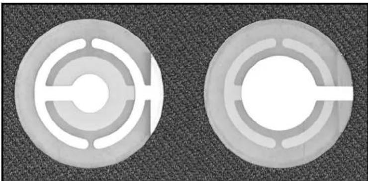
natural_image
Two circular mechanical components with concentric rings and internal slots, shown against a dark textured background (no text or symbols)Figure 30. Standard 1 inch QCM sensor crystal. The crystal on the left shows the contact surface, while the one on the right shows the liquid surface.
Standard sensor crystals are 1 inch in diameter and are available with a variety of electrode materials.
Stanford Research Systems also provides a rugged and easy to operate Crystal Holder compatible with both gas and liquid QCM experiments. Crystal Holders must be electrically connected to the QCM25 Crystal Oscillator for operation with a QCM200 Controller.
Sensor Crystals
QCM Sensor Crystals are available directly from Stanford Research Systems in a variety of electrode materials and surface finishes.
| Standard 1 inch, 5MHz, QCM Sensor Crystals - Qty. 10 per pack | ||||
| SRS Part# | SRS Order# | Material | Finish | Maxtek Part# |
| 6-00613 | O100RX1 | Chrome/Gold | Polished | 149211-1 |
| 6-00615 | O100RX3 | Titanium/Gold | Polished | 149238-1 |
| 6-00617 | O100RX4 | Titanium/Platinum | Polished | 149240-1 |
Principle of Operation
AT-cut quartz crystals are most commonly used as QCM sensors because of their superior mechanical and piezoelectric properties ^1 , and because they can be cut to give nearly zero temperature coefficients at room temperature.
Due to the piezoelectric properties and crystalline orientation of AT-cut quartz, the application of a voltage between the sensor crystal electrodes results in the production of internal mechanical stress. An oscillating electric field of the proper frequency applied across the disk induces a pure shear mode oscillation that propagates through the crystal. The designation of the oscillation as a pure shear mode indicates that the motion of the disk surface is perfectly parallel to the disk's face.
For shear mode oscillation there are several frequencies that correspond to resonant conditions. For all resonant modes, displacement maxima occur at the crystal faces, making the device sensitive to surface perturbations. The perturbations to be considered include surface loading by
• a thin-film mass layer ^2 ,
- a contacting Newtonian fluid ^3 ,
- a viscoelastic layer of finite thickness ^4 .
Frequency
The nominal frequency of oscillation of all standard QCM Sensor Crystals is 5 MHz (fundamental mode). The unperturbed crystals will normally be within ±1,000 ppm of their nominal frequency.
Operation at 5 MHz is regarded as optimal for laboratory use since it provides (1) acceptable (submonolayer) sensitivity, (2) robustness (331 ∝m crystal thickness), and (3) stable oscillation in most viscous media.
Geometry
Figure 30 shows a top and bottom view of a standard 1 inch diameter QCM Sensor Crystal, with what is called a “wrap-around” electrode configuration. A conductive metallic pad is used to allow connection to the front electrode (liquid surface) from the back of the crystal (electrical contact surface). This is required for mounting of the crystal into its Crystal Holder and for proper operation in conductive liquids.
The exposed area of the front electrode in contact with the liquid is 1.37cm^-2 , however, the active electrode oscillation (i.e. displacement area) is mostly restricted to the area of overlap between the two circular pad electrodes or 0.40cm^2 .
All standard 1 inch QCM sensor crystals are planar, with both faces parallel to within 1 m. Crystal thickness is 331 m as required for fundamental oscillation at 5 MHz.
The large diameter of the crystal (1 inch), and the relatively much smaller oscillation area, assures good separation between the active electrode pads and the mounting structure of the holder and minimizes the coupling of other resonant modes to the thickness shear oscillation ^6 .
Surface Finish
Electrode surface roughness can cause large apparent mass loadings due to the liquid that is trapped within pores at the crystal surface ^7 . As a general rule, optically polished crystals (50 Å average surface roughness) are required to obtain good agreement between theory and experiment during liquid immersion experiments.
Rough surfaces are popular because they are less expensive and provide enhanced surface area. However, they suffer from a quantitatively unpredictable dependence of the oscillation frequency in a liquid due to trapping of fluid in the pores and pits on the surface ^8 .
Tip
For liquid-phase applications, optically polished crystals are required ^9 if crystal-to-crystal reproducibility is to be expected. A water Immersion Test (refer to Chapter 2) usually provides a quick-and-easy way to test the quality of a crystal finish for liquid-QCM applications.
Electrode Materials
Gold electrodes (100-1000 nm thick) are the most commonly used in QCM applications because of the ease with which gold is evaporated. However, other metals such as Pt, Cu, Al and Ni have also been used.
A thin (2-20 nm) adhesion layer of either Cr, Ti or Si is often deposited directly on the quartz to aid in the adhesion of the metal electrode. Chromium is recommended for
polished blank surfaces and also for crystals operated in a harsh environment. However, Cr can be a problem in some electrochemical applications - spurious electrochemical responses can sometimes result if diffusion of the adhesion material to the electrode surface occurs. In that case Titanium is recommended as a substitute adhesive layer. If Ti is still a problem, Palladium can be utilized as a barrier metal between the Cr or Ti and the primary metallization (consult Stanford Research Systems for availability of alternative electrode materials).
A zinc layer, sandwiched between the adhesion layer and the electrode pad on the front or deposition side of the crystal has a relatively low bulk modulus, and has been shown to absorb stress imposed by the deposited materials. The buffer layer prolongs useful crystal life, particularly when depositing dielectric materials. The crystal should have a modest surface roughness as keying-in structure. The buffer layer can be a zinc layer of 600 nm sandwiched between a titanium or chromium adhesion layer of 10 to 16 nm and a gold, silver, or aluminum outer electrode layer of about 200 nm ^10 .
In principle, any type of material that can be deposited onto the surface of the underlying metal electrode can be used on the sensor crystals ^11 . The only limitation on the use of such materials is that their deposition must be carried out in such a way that the temperature of the quartz crystal does not exceed 573°C, above which α-quartz loses its piezoelectric activity. Strict attention to cleanliness is required while performing a custom electrode deposition.
It is important to keep in mind that mass changes at the QCM active electrode surface influence the frequency because these electrodes are part of the composite resonator composed of (1) the quartz crystal, (2) its metal electrodes, (3) any film deposited on the electrodes and (4) any liquid adjacent to the electrode surface which experiences shear forces. For this reason, when electrodes become delaminated (due to poor adhesion of the underlayer or stress caused by the deposit), discontinuous changes in frequency occur which render the crystal useless.
Mass Sensitivity
The quartz crystal microbalance is an extremely sensitive sensor capable of measuring mass changes in the nanogram/cm ^2 range with a wide dynamic range extending into the 100 g/cm ^2 range.
Sauerbrey ^12 was the first to recognize the potential usefulness of the technology and demonstrate the extremely sensitive nature of these piezoelectric devices towards mass changes at the surface of the QCM electrodes. The results of his work are embodied in the Sauerbrey equation, which relates the mass change per unit area at the QCM electrode surface to the observed change in oscillation frequency of the crystal:
f ΔmΔCf
where
f = the observed frequency change in Hz,
m = the change in mass per unit area, in g / cm^2
C_f= the sensitivity factor for the crystal (56.6 Hz g^1cm^2 for a 5 MHz crystal at room temperature).
The minimum detectable mass change is typically a few ng/cm^2 and limited by the noise specifications of the crystal oscillator and the resolution of the frequency counter used to measure frequency shifts. For example, based on Sauerbrey's equation, a minimum detectable mass specification of 0.18ng/cm^2 should be expected from a QCM system with a 0.01Hz frequency measurement resolution. As a comparison, consider that a monolayer of a 20kDa protein (100% coverage) adsorbed on a QCM crystal amounts to roughly 10Hz frequency shift, or 180ng/cm^2 .
The Sauerbrey equation relies on a sensitivity factor, C_i , which is a fundamental property of the QCM crystal. Thus, in theory, the QCM mass sensor does not require calibration. This ability to calculate the mass sensitivity from first principles is obviously a very attractive feature of these devices. However, it is very important to notice that the Sauerbrey equation is only strictly applicable to uniform, rigid, thin-film deposits originating from a low pressure (i.e. vacuum) gas environment ^13 . Thick deposits and operation in liquid environments or in contact with viscoelastic films, relies on the use of more complex equations relating the frequency shifts to mass loading, and often requires calibration of the setup for accurate results. Several articles have presented simple ways to calibrate the mass sensitivity of QCMs for electrochemical applications ^4 and for vacuum thin-film deposition processes ^15 and some useful calibration guidelines were also included in Chapter 2 of this manual.
There is ample evidence supporting a Gaussian mass sensitivity distribution for AT-cut crystals ^16 , with the maximum sensitivity at the center of the electrode and zero sensitivity at the edges for harmonically driven plane crystals. The mass sensitivity distribution has also been shown to become slightly more confined to the electrode region as the mass loading is increased. In order to assure reproducibility of results, it is very important to assure uniform coverage of the electrodes during measurements.
There are also situations in which the QCM does not act as a microbalance at all, but responds instead to properties such as viscosity ^17 and/or elasticity ^18 of the liquid or film in contact with its surface.
Maximum Loads
QCM sensor crystals can be coated with virtually any material as long as it can be deposited in a sufficiently thin, uniform and well-attached layer. Layer thicknesses typically vary from a few Angstrom to a few micrometers. The maximum layer thickness depends on the viscoelastic properties of the coating material. As a general rule, thicker layers are possible for more rigid coating materials.
The maximum load on a crystal is limited by two factors: (1) total damping or (2) lost sensitivity. For highly viscous or solid materials, the damping of the crystal increases with increasing layer thickness. At a certain thickness (usually a couple of micrometers) the damping becomes so high that the crystal can no longer be driven, i.e. the measurement fails due to lack of oscillation. More elastic materials do not couple completely to the crystal's oscillation. With increasing layer thickness the outermost parts of the attached layer will couple weakly and at a certain thickness (usually a few micrometers) it is lost completely. Oscillation is still detected, and a frequency is still measured, but the equipment can only sense the part of the layer in the vicinity of the crystal ^19 .
Useful Life
Sensor crystals are often reusable several times. However, reusing a crystal requires careful handling and cleaning procedures that do not harm the quartz material, its electrode pads and its coatings. Many practitioners consider their QCM crystals expendable and always discard them at the end of their measurements ^20 .
Traces of consumption and wear can often be detected visually:
- Edges of the sensor crystal might become cracked and the coating start to show scratches and holes.
- In electrochemistry experiments it is not unusual to observe changes in the adhesion layer of the liquid surface electrode which ultimately result in peeling of the metal pad). A common problem is loss of the Cr adhesion layer in Au/Cr electrodes. These changes are visible from the contact side of the crystal.
- The liquid surface electrode might become irreversibly discolored or stained from chemical reaction with the analytes, buffers or solvent.
When a crystal is close to being consumed, the measurement signal will become noisy, possibly even shaky. It might even be difficult to obtain a stable baseline. Spurious signals might become evident in electrochemical QCM experiments.
As the sensor crystal is coated, the series resonance resistance increases, indicating a loss of crystal Q^21 . When this occurs, the circuit may occasionally resonate at one of the anharmonic frequencies. The oscillation may switch to an anharmonic mode, or it may alternate between the fundamental and anharmonic frequencies, a condition known as mode hopping. This is a potentially dangerous scenario, since it might lead to early termination of a deposition or film-growth process. Notice that there is no outward evidence of mode hopping except for a discontinuity in the film thickness. Also, even though the film thickness changes dramatically, the mass sensitivity and rate of growth change by only a few percent.
Some experiments can cause irreversible changes on the crystal surface. For example, the use of silver depositions on gold electrodes for calibration of electrochemical QCMs is not always recommended because silver is hard to remove reversibly from gold electrodes. Copper or lead ^22 are often recommended instead. Crystals exposed to etching solutions (i.e. Piranha solution) usually need to be replaced after two to three experiments.
Film stress can be particularly damaging. Stress can bend the crystal and induce a frequency change not related to mass. It can cause the electrode to tear from the quartz and, in the worst case, it can even cause the quartz itself to fracture ^23 .
Temperature effects
The intrinsic dependence of the resonant frequency of a quartz crystal on temperature is well known and generally quite small ^24 . In fact, the AT-cut quartz crystals commonly used in QCM experiments owe their popularity to their near zero temperature coefficient at room temperature. As a result, the intrinsic temperature dependence of the QCM
sensor crystals is negligible at or around room temperature ( 1-3 Hz/ ^ C) and is generally ignored for monolayer adsorption/desorption processes in the gas phase.
A thermal effect less often discussed in connection with quartz crystal oscillators is based on the fact that dynamic changes in temperature around a crystal unit can produce thermal gradients which induce frequency transients dependent on the rate of temperature change ^25 around the sensor. The static frequency vs temperature characteristic is modified by this thermal-transient effect resulting from the thermal-gradient-induced stresses ^26 . Proper thermal compensation requires consideration of both static and dynamic (i.e. rate-of-change) frequency-temperature behavior of the QCM crystals.
Larger changes in frequency with temperature should be expected when QCM crystals are immersed in liquids. This is due to the coupling of the shear mode oscillation with the temperature dependent viscosity and density of the fluid. The temperature coefficient due to this effect is 8~Hz/^ (and 4~/^ ) for water. As a result, for experiments in liquid phase in which the frequency is to be monitored at length, the temperature must be controlled to at least 0.1^ , and preferably better. If temperature control is not possible or practical, it is always good practice to wait at least 30 minutes before performing any accurate measurements after the crystal comes in contact with a new liquid medium and measure the temperature of the solution around the crystal during the experiments to perform temperature compensation.
Careful control of the temperature is required in high accuracy measurements to avoid frequency hysteresis effects ^27 - the dependence of resonator frequency at a specific temperature on its prior temperature history. For example, it is often observed that the frequency-vs-temperature curve obtained going from T_1 to T_2 will not coincide with the one obtained immediately after going from T_2 to T_1 . The causes of hysteresis and retrace are not well understood - the experimental evidence to date is inconclusive. The mechanisms that can cause these effects include strain changes, changes in the quartz, contamination redistribution in the crystal enclosure, and apparent hysteresis or retrace due to thermal gradients.
In electrochemical experiments temperature control is often required to control reaction rates and is typically achieved with temperature controlled baths and jacketed cells.
Tight temperature control is necessary for QCM measurements involving protein adsorption, protein-protein interaction, immunosensor development, self-assembled monolayers, Langmuir films and DNA hybridization studies. Temperature stabilization better than ±0.05 ^ is generally required to eliminate temperature related transients and drifts in lengthy measurements. This level of temperature control is particularly important if small series resonance resistance changes need to be detected and measured.
Each individual QCM user must determine the effect of temperature on the experiments being performed and either control the temperature accordingly, or measure the temperature and compensate for it. The table below summarizes some of the most relevant static temperature coefficients for 5 MHz QCM crystals around room temperature.
Some very important temperature coefficients are listed below:
Temperature coefficient in air 1-3 Hz/°C
Temperature coefficient in water 8 Hz/°C, -4Ω/°C
Tip
Whenever practical, the use of flow cells is recommend for both gas and liquid studies to minimize temperature transient effects. Temperature stabilization better than ±0.05 ^ is generally required to eliminate temperature related transients and drifts in lengthy measurements.
Crystal Handling
Please follow these instructions about general handling of sensor crystals.
- Keep the crystals in a clean and dry place. When not in use store them in their original box and wrapper.
- Avoid touching the metal electrodes of the crystal.
- Rinse only with deionized water, or another appropriate residue-free solvent, before drying the crystal.
• Always use a flow of dry, oil-free, inert gas (e.g. nitrogen) to blow-dry the crystal. It is better to blow the liquid off the crystal than to let it evaporate on the electrodes. - Do not handle the sensor crystal using bare fingers. Hold the sensor crystal with tweezers and only from its outer edge (outside the electrode area) to prevent scratches. The tweezers should have smooth gripping surfaces and preferably be made out of soft plastic material.
- Before starting a surface cleaning confirm that the crystal material will not be damaged by the cleaning solutions. Perform a test run on a discarded or practice crystal whenever possible.
Cleaning
The surface properties of the sensor crystal determine the interaction of sample material with the surface. Therefore, the development of proper protocols for surface preparation and cleaning are required to obtain reproducible measurements. This section provides the basic information you need to develop a cleaning protocol suitable for your sample/surface system.
Figure 30 shows a standard 1 inch diameter, gold-coated, sensor crystal. When mounted on a Crystal Holder, it is the Liquid Surface that will be in contact with the sample (gas or liquid) during the measurements. The counter electrode and electrical contacts for the electrodes are on the Contact Surface of the crystal in the leak-proof crystal chamber.
The most appropriate cleaning method depends on the sample system, the interaction of the sample with the crystal surface, and the properties of the sensor crystal itself.
Note
Before starting a surface cleaning, ensure that the crystal material will not be damaged by the chemicals. Perform a practice test on a discarded crystal whenever possible. Avoid basic (high pH) cleaners since they will etch all exposed quartz surfaces.
Tip
A Crystal Cleaning Basket (SRS Part# O100CCB described later in this chapter) is available directly from Stanford Research Systems. This accessory makes cleaning and surface modification treatment of the standard 1" QCM crystals very safe and easy. The cleaning basket holds four crystals, is made entirely of Teflon® and it is specifically designed for immersion into a 100 mL beaker.
Several cleaning procedures are described below which can be used as guidelines to develop your own. Proper crystal handling practices must be used throughout any cleaning process.
General Purpose
For general purpose applications such as electrochemistry, liquid and viscoelastic film studies, it is usually sufficient to sonicate the crystals in a solution of non-basic detergent in deionized water. Immediately rinse liberally with deionized water and dry in a gentle flow of nitrogen gas.
Hydrocarbon contaminants
UV/ozone treatment ^28 , CO_2 snow cleaning ^29 and plasma cleaning ^30 are some low cost and very efficient methods used for cleaning hydrocarbon impurities adsorbed from the ambient air. Neither method affects the quartz/gold surfaces. They are both often applied to components used in high vacuum environments.
Biomaterials (lipids, proteins and similar biomolecules)
- Treat the crystal in a UV/ozone or plasma cleaning chamber for 10 minutes.
- Immerse the crystal into a 1:1:5 solution of hydrogen peroxide (30%), ammonia (25%) and deionized water heated to a temperature of about 75^ C for 5 minutes ^31 .
- Immediately rinse with deionized water and dry with nitrogen gas.
- Treat the crystal again with UV/ozone for 10 minutes immediately before measurement (this removes any remaining surface contaminants).
Lipid vesicles
- Treat the crystal in a UV/ozone or plasma cleaning chamber for 10 minutes.
- Immerse the crystal into water with 2% of sodium dodecyl sulfate (SDS) at room temperature for 30 minutes ^32 .
- Immediately rinse with deionized water and blow dry with nitrogen gas.
- Treat the crystal again with UV/ozone for 10 minutes immediately before measurement (this removes any remaining surface contaminants).
Self-assembled Monolayers
It is common practice to wash crystals with piranha solution (see next section) at the end of a QCM immunoassay. Piranha solution is also often used to precondition the crystals for a SAM deposition.
- Treat the crystal(s) with piranha solution for three minutes.
- Repeat treatment step 1 two more times with fresh piranha solution.
- Rinse liberally with deionized water and dry in a gentle flow of nitrogen gas.
Piranha Solution
Piranha solutions are used to remove organic residues from substrates, particularly in microfabrication labs. The traditional piranha solution is a 3:1 mixture of sulfuric acid and 30% hydrogen peroxide. The solution may be mixed before application or prepared on the sample, applying the sulfuric acid first, followed by the peroxide.
Warnings
Piranha solutions are extremely reactive and may result in explosion or skin burns if not handled with extreme caution.
- Prepare the smallest possible volume. Some QCM users mix the cleaning solution on the crystal surface, pipetting the proper ratio of sulfuric acid and hydrogen peroxide directly on the liquid surface electrode of the quartz resonator.
- Do not expose the crystal holder to Piranha solution. Wash separately.
- Wear gloves, goggles and a lab coat.
• Work in a fume hood.
• The mixture of hydrogen peroxide and sulfuric acid is very exothermic. - Do not touch the glassware after mixing - HOT! (up to 120^ ).
- Use heat resistant glassware. This mixture can get really hot and shutter non-thermal graded glass!
- Rinse thoroughly.
- Keep the etching solution away from organic solvents.
- Treat with very healthy respect.
• Properly clean and dispose of all chemicals. - Consider safer alternatives compatible with your application.
• If not sure how to proceed, STOP and seek help from an experienced chemist! - Prolonged exposure to Piranha solution damages QCM crystals. The failure mechanism is believed to involve chemical degradation of the Cr bonding layer located between the quartz and the gold electrode. Typically, a QCM crystal can be exposed to Piranha solution a maximum of three times before noticeable degradation of performance occurs. The first signs of crystal degradation are reduced stability in the frequency baseline ^33 .
Polystyrene removal
- Immerse the crystal into a 1:1 solution of hexane and deionized water and treat it in an ultrasonic bath for 1 minute.
- Rinse thoroughly with deionized water and blow dry with nitrogen gas.
Crystal rinsing
Rinse sensor crystals with deionized or distilled water or another appropriate pure liquid.
In order to prevent recontamination follow these steps:
- Hold the crystal with a pair of tweezers from underneath to prevent transferring contaminants from the tweezers onto the crystal. This is generally most critical in biological applications.
- Blow the remaining liquid off the crystal with a gentle flow of nitrogen gas.
- Use a clean, lint-free cloth to wick off any liquid remaining on the edge of the crystal.
Surface Modifications
The biggest drawback of the QCM sensor is that it is inherently non-specific - anything that has mass can generate a response from the device. The danger of this universal response is that you have a greater chance of experiencing interferences. This issue has been addressed in various ways so that the device will only respond to the analyte of interest. Those “ways” usually involve a chemically or biologically sensitive layer (i.e. a coating) applied to the surface of the crystal ^34 .
Often, the hardest part of the problem is deciding what kind of chemically sensitive material you are going to put on top of the crystal so that it responds specifically to what you are trying to measure.
In biosensor research, the chemical stability of the sensor substrate often limits the quality of the data generated. The continuous oxidation of metal electrodes can make it very difficult to reach a drift-free signal baseline in aqueous media. Polyimide, polystyrene and PVC are amongst the polymeric materials recommended to protect QCM devices.
Tip
A Crystal Cleaning Basket (SRS Part# O100CCB described at the end of this chapter) is available directly from Stanford Research Systems. This accessory makes cleaning and surface modification treatment of the standard 1" QCM crystals very safe and easy. The cleaning basket holds four crystals, is made entirely of Teflon® and it is specifically designed for immersion into a 100 mL beaker.
Several examples of surface modification techniques are described below. While not exhaustive, they may serve as useful guidelines while developing your own protocols.
Sputtering or evaporation
Thin films (i.e. nm thickness) of metals or metal oxides are commonly deposited by sputtering or evaporation. To obtain reproducible results, careful attention must be paid to cleanliness, both in the vacuum chamber and in the preparation of the crystals prior to coating. It is generally realized by individual researchers that, unless highly specialized coatings are required, it is a lot more convenient and cost effective to have a specialized commercial source deposit the electrodes on crystal blanks.
Spin-coating
Spin-coating ^35 is a technique by which very thin polymeric films (nm to m thickness) are deposited onto a solid substrate ^36 .
To fabricate thin polymer films, the polymer material is first dissolved in a volatile solvent. If a drop of solution is placed on a substrate, it can flow to form a metastable, continuous film or form a droplet on the surface, depending on the "wettability" of the substrate. By spinning the substrate, the droplet is forced to spread out while the solvent evaporates. If deposition conditions such as choice of solvent, solution concentration and spin-speed are chosen carefully, a thin film of uniform thickness is deposited on the substrate.
Polystyrene is a common material spin-coated onto QCM sensor crystals. Toluene is the solvent of choice. UV/Ozone treatment can be used to tailor the hydrophobicity of organic polymeric coatings ^37 .
Compact and easy-to-use laboratory spin-coaters, compatible with QCM crystals, are commercially available. Consult the factory for recommendations.
Langmuir-Blodgett films
Langmuir-Blodgett films (LBFs) are artificial structures prepared by sequential transfer of monomolecular layers (one molecule thick), performed on a liquid surface (usually H_2O ), onto a solid substrate (such as a glass slide or a silicon wafer). LBFs are very thin and very well ordered. This technology is attractive to researchers because of its ability to produce thin films (1) whose thicknesses can be precisely varied and (2) which can be modified to produce smart sensing devices. ^38
Self-Assembled Monolayers (SAM)
Self-assembled monolayer (SAM) techniques offer a new strategy for the immobilization of antibodies, antigens and DNA on the surface of quartz crystal electrodes ^39 .
SAMs can be deposited on gold or silver electrodes by thiolization. Since sulfur donor atoms strongly coordinate on metal substrates (Au, Ag, Pt, etc), sulfur containing molecules such as disulfides (R-SS-R), sulfides (R-S-R) and thiols ^40 can form various functionalized SAMs with highly organized and compact construction. Besides good mechanical and chemical properties, an additional advantage of SAMs is that they make it possible to tailor electrode surfaces at the molecular level for the immobilization of specific biomolecules such as proteins or DNA ^41 .
Tip
Thiolization agents specifically designed for SAM immobilization of proteins and DNA on metallic surfaces have recently become commercially available. Consult the factory for up-to-date recommendations.
A silane layer (silanization) is another common material used for SAMs ^42 . However, since the coating can react irreversibly with the quartz material, the QCM crystal cannot be used repeatedly in this application.
SAMs vs. Polymer films
Most conventional methods used for the development of QCM immunosensors have relied heavily on polymeric coatings deposited on the electrodes and capable of forming hydrophobic or covalent bonds with antibodies. Polymeric films suffer of several disadvantages: (1) polymer films attach to the electrode surface through weak hydrophobic bonds which can be easily broken by mechanical interaction, washing, and even changes in pH and (2) swelling of the polymer films in aqueous solution can lead to reduced sensitivity and reproducibility of the immunosensor.
Electroless Deposition Pre-treatment
QCMs are used to measure (1) plating rates and thicknesses in both electrolytic and electroless baths, (2) plating efficiencies in electrolytic baths and (3) etching rates in chemical etching processes. It is important to assure that the sensor crystal is properly preconditioned during the electroless ^43 deposition of metals. Plating initiation must be complete, and the crystal must be in close proximity to the action taking place in the rest of the tank. Preplating is recommended if adhesion problems are observed with untreated crystals. Pre-treatment with catalyst may be prescribed in some cases. It is recommended not to expose the entire Crystal Holder to catalysis during pre-treatment, to avoid excessive metallization of the holder during deposition.
Crystal Holder
Description
The standard Crystal Holder, bundled with the QCM200 system, is specifically designed to provide users with a rugged, compact and easy-to-use sensor crystal housing for QCM experiments in air or liquids.
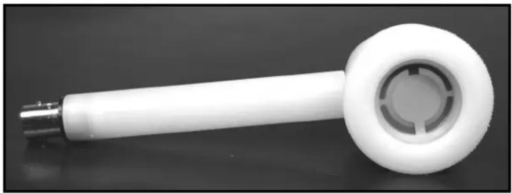
natural_image
White plastic showerhead with circular opening and metallic handle (no text or symbols visible)Figure 31. The Crystal Holder with a 1 inch sensor crystal mounted.
Its main features include:
- rugged design ^44
- compatibility with all standard, 1 inch diameter, QCM sensor crystals
- compatible with Crystal Oscillator, SRS Model QCM25
- liquid and gas compatibility (leak-proof design)
- single-electrode exposure to liquids ^45 (for compatibility with electrochemical QCM measurements)
- chemical resistance: Kynar ^46 material with Viton O-rings
• broad temperature range: -25^ to 110^ - easy crystal replacement (a simple, hand-removable retainer cover permits easy crystal replacement without tools)
• standard female BNC connector for easy electrical connection - flow cell adapters available (SRS Part# O100FC)
Several methods for mounting sensor crystals have been described in the scientific QCM literature. The mounting fixture requires serious consideration because of the influence of stress on the absolute frequency of oscillation and because simple and rapid exchange of crystals is required when the thin-film electrodes become damaged or used up.
For electrochemical applications in solution, it must be feasible to expose only one side of the QCM disk to the liquid bath (This is necessary to prevent the two QCM electrodes from being capacitively shunted by the solution, which can cause cessation of the oscillation) The Crystal Holder was specifically designed to address all the above issues while at the same time providing optimal crystal performance when connected to a QCM25 Crystal Oscillator and a QCM200 Controller.
Head Cleaning
It is not uncommon for crystals to break or for o-ring seals to leak during normal operation. If chemical leakage into the crystal cavity is suspected, it is very important to act fast and rinse the cavity, the POGO ^® contacts and the POGO ^® contact sockets to remove any traces of solution that might lead to damage of the holder.
Start by removing the crystal from the Crystal Holder and exposing the POGO ^® pins. Putting your thumbnail (or the flat head of a jeweler screwdriver) under the POGO ^® head pull firmly up to remove each contact pin from its socket. Rinse the pins and the sockets with deionized water to remove all traces of chemicals. Replace the POGO ^® pins with new ones if necessary.
Keep in mind that even though the POGO ^® contacts and sockets are gold coated, unrinsed chemicals can still lead to corrosion and permanent damage to the holder. This is specially true in electrochemical applications where oxidizing acids are often components of the liquid solution in contact with the crystal.
Crystal Cleaning Basket
A Crystal Cleaning Basket (SRS Part# O100CCB) is available directly from Stanford Research Systems. This accessory makes cleaning and surface modification treatment of the standard 1" QCM crystals very safe and easy. The cleaning basket is shown in Figure 32, it holds four crystals, is made entirely of Teflon® and it is specifically designed for immersion into a 100 mL beaker.
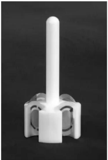
natural_image
White plastic cylindrical object with a pointed tip, mounted on a multi-plate base against a dark background (no text or symbols visible)Figure 32. Crystal Cleaning Basket - SRS Part# O100CCB. The entire basket is made out of Teflon and is shown here holding its maximum load of 4 crystals (not included).
Tips for Operation in Liquids
To minimize measurement errors in liquid phase QCM experiments, the sample fluids should be prepared carefully. Changes in temperature, flow-rates, properties of the solvent as well as air bubbles will affect the sensor signal. For reproducible measurements, keep the following tips in mind.
Check for Chemical Compatibility
Before starting an experiment, check for chemical compatibility between sample solutions, solvents, holder, flow cell, o-rings and crystals. For example, avoid contact between Viton ^® o-rings and DMSO solvent. If necessary consider replacing incompatible components with alternative materials.
Check the POGO contacts regularly
It is good practice to check the POGO ^® contacts regularly for signs of corrosion and wear. Replace the pins with new ones if necessary (see “Head Cleaning” above).
Degas the sample liquid
Whenever possible, sample liquids should be degassed to avoid the growth of air bubbles on the surface of immersed crystals.
Presoak the crystal in the sample liquid
To minimize long-term (i.e. hours long) signal drift it is best to immerse the quartz crystal, premounted on its holder, in the sample solution several hours before measurements are started.
Temperature-independent frequency drifts as large as 10 Hz, and resistance drifts as large 2 Ohms, are to be expected over a 24 hr period even in the purest deionized water bath. Long-term drifts have many different origins including chemical interaction between the liquid and the electrodes, swelling of the o-rings, diffusion of liquid into the quartz, changes in coatings, etc.
In flowing systems, expose the crystal to the carrier solution for as long as practically possible prior to sample injection.
Wait for the temperature to stabilize
To avoid the generation of air bubbles and reduce temperature related signal changes, the sample liquid should be at approximately the same temperature as the sensor/holder and the entire experimental setup should be temperature stabilized.
The generation of air bubbles is facilitated when the temperature of the liquid is lower than that of the holder/flow cell. Avoid temperature differences greater than 2 ^ between the sample liquid and the crystal holder.
Keep in mind that frequency readings are not just affected by the static temperature, but also by the rate of change of temperature around the sensor. This is very important during the implementation of temperature compensation or stabilization schemes. For example, PI, PID and Fuzzy Logic stabilized temperature controllers are recommended instead of On-Off controllers for temperature stabilization.
To ensure signal stability for flowrates greater than 0.2 mL/min use external temperature stabilization (as necessary) to make sure that the sample liquid is temperature equilibrated prior to flowing into the flow chamber. Immersing the flow cell/crystal holder in a water bath and running the sample fluid through the same bath (i.e. heating loop) prior to entering the QCM chamber is a simple way to assure temperature equalization between the holder and its liquid sample solutions.
Prepare your solutions carefully
To avoid unwanted effects due to changes in the properties of the carrier/buffer liquid (or solvent), solutions should be prepared carefully. Whenever possible, use purified samples at high concentration and dilute them in the appropriate buffer (or solvent) just before measurement. Use solvents or buffers from the same stock during each measurement series.
Avoid mechanical vibrations
Keep the sensor away from mechanical equipment containing motors or similar vibrating parts. Fasten all dangling cables that might transfer vibrations to the crystal holder/flow cell.
Avoid transients
Avoid sudden mechanical stresses such as knocking on the crystal holder, pulling on cables, sudden shifts in the experimental setup, etc.
Avoid sudden temperature changes. In AT-cut quartz crystals, frequency fluctuations depend not only on the T but also on the rate of change of T.
Avoid sudden pressure changes such as pressure transients in gas flow systems or flowrate changes in liquid flow injection systems. Whenever possible replace peristaltic pumps with siphon setups or syringe pumps.
Relax mechanical stress
It is often a good practice to tap on the holder/flow cell before starting a new set of measurements. Gentle tapping helps to dislodge trapped bubbles and relaxes mechanical stresses at the o-ring seats resulting in reduced drift problems.
Wait for the signal to stabilize after liquid exchange
In flowing setups it is important to keep in mind that detectable signal transients are to be expected after sudden changes in flow rates and after liquid exchanges (i.e. new sample injections). Flow transients can last less several seconds and can seriously compromise your long-term measurements if bubbles are introduced into the flow stream, or large temperature differences between the liquid and the holder are established.
Use small and constant flow rates
During liquid flow experiments, flowrates should be kept small and constant to eliminate signal transients due to pressure and temperature fluctuations. Recommended flow rates should be below 0.2 mL/min to assure minimal transients and flow-induced noise in the frequency measurements.
Rely on gravity, the siphon principle or syringe pumps to flow liquids through a cell in Open-Flow Systems whenever possible. If necessary, use Flow Injection Analysis (FIA) compatible pumps and high-quality injection ports to flow sample and carriers over the
crystal. Syringe based injection analysis systems often produce cleaner baselines because of the absence of noise transients induced by peristaltic pumps.
Peristaltic pumps are suitable for flow measurements in closed systems but they always add noise to the signal. A capillary tube located between the chamber outlet and the pump is often recommended to reduce noise caused by pressure fluctuations induced by the pump. Pulse-dampening modules, located between the pump and the crystal, are often used in Flow Injection Analysis setups ^47 although noise reduction is not always as good as expected.
In order to avoid excessive stress to the crystal and leaks over the o-ring seals, flowrates should not exceed 5 mL/min under any circumstances. External temperature (i.e. heating loop) stabilization of the liquid samples is recommended for flow rates above 0.2 mL/min.
Do not tighten the crystal retainer during experiments
Tightening of the crystal retainer will exert additional stress on the crystal and change its frequency of oscillation. Tighten the retainer at the beginning of an experiment and do not touch it again until all measurements are finished. O-rings often swell when coming in contact with liquids and that can contribute additional drift in the frequency when immersing a crystal holder in a new liquid.
Dry QCM crystals carefully
A common trick used to eliminate residual water from QCM crystals that need to be immersed in dry organic solvents is to rinse the cleaned/dried QCM crystals with tetrahydrofuran (THF) before immersion followed by drying in a flow of dry nitrogen.
Tips for Operation in Gases
To minimize errors in QCM measurements, all gas-phase experiments (i.e. gas sensor development) should be designed carefully. Changes in temperature, flow-rates and gas pressure will adversely affect QCM measurements. For reproducible measurements, keep the following tips in mind.
Check for Chemical Compatibility
Before starting an experiment check for chemical compatibility between the sample gases, holder, flow cell, o-rings and crystals. If necessary consider replacing components with alternative materials..
Operate in a flowing gas configuration
In order to avoid frequency transients due to sudden air movements around the crystal, operate the QCM sensor in a flowing gas configuration. Frequency transients as large as 10 Hz can be registered by simply walking past a QCM crystal fully exposed to air.
Operation within a flow cell also facilitates achieving proper temperature equalization between the crystal and the gas sample.
Wait for the temperature to stabilize
In order to avoid frequency transients due to temperature changes it is best to temperature stabilize the flow cell/crystal holder and eliminate temperature differences between the gas samples and the holder. Immersion in a temperature-stabilized water bath often does the job, and allows the preheating loop to equalize the gas temperature with the sensor. Keep in mind that changes in frequency are not only related to static changes in temperature around the crystal, but also to the rate of change of temperature with time.
Use small and constant flow rates
During flow experiments, flowrates should be kept small and constant to eliminate signal transients due to pressure and temperature fluctuations.
Control humidity if necessary
Adjustment of the humidity is often a requirement for accurate gas phase measurements. It is generally recommended to adjust/control the humidity of the gas before flowing into the measurement chamber. A common procedure consists of exposing the gas to saturated salt solutions with well known humidity values ^48 .
Bubbles and Liquid Flow Cells
Eliminating gas bubbles trapped inside flow cell chambers is essential for accurate long-term QCM measurements. The highest risk of bubble formation is when liquid enters an empty chamber. Bubbles can also form spontaneously if liquids are not previously degassed and the chamber temperature is greater ( T > 2 ^ ) than the liquid temperature.
This section describes some simple tricks known to effectively prevent and remove bubble trapping in flowing QCM systems and also presents some of the common indicators used to detect the presence of bubbles in liquid flow chambers.
Eliminating dissolved gases from all sample solutions is the most basic precaution recommended for the minimization of bubble trapping. Commercially available online degassing stages and bubble traps are recommended for flow injection analysis setups.
When filling an empty chamber with a syringe pump for the first time the following procedure generally works very well to displace all trapped bubbles: Connect a > 3 mL syringe, loaded with the solution you wish to inject into the QCM chamber, to the inlet port of the flow cell. Connect the outlet port to the body of a 3 mL syringe with its plunger removed and mounted vertically to act as a waste collector. Push about 1-2 mL of solution through the chamber into the waste container. Press the syringe back and forth a few times until no more bubbles are seen to evolve into the waste container. The number of bubbles will decrease after each back and forth action until no more bubbles are visible. Flow reversals are very efficient at displacing bubbles out of the chamber.
For siphon systems (see Figure 33) a similar method can be employed to remove bubbles from a freshly filled chamber: in this case the sample reservoir, with the sample solution, is connected to the inlet port and a 3-5 mL syringe, loaded with >2 mL of the same sample, is connected to the output port. Pull the syringe plunger up to (1) force liquid into the chamber and (2) eliminate the bubbles formed from the fresh syringe connection. Press the syringe back and forth a few times until no more bubbles evolve into the sample reservoir. Stop the flow at the inlet and disconnect the syringe when no more bubbles are seen.
It is generally preferable to position the output port above the inlet port in flowing systems. Fewer bubbles are generally trapped if the chamber is filled slowly from the bottom up, with the output port being the last section of the internal chamber to come in contact with liquid.
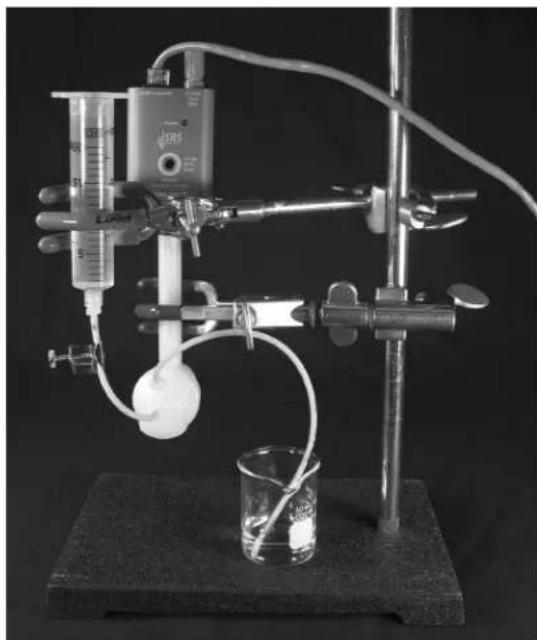
natural_image
Laboratory distillation setup with syringe, condenser, and beaker (no visible text or labels)Figure 33. Simple siphon setup with axial flow cell, syringe-body sample reservoir and flow clamp.
The presence or relocation of bubbles on the surface of a crystal is generally detected by paying careful attention to the frequency and resistance readings from the sensor. Bubbles displace liquid from the surface of the QCM crystal resulting in increased frequency and reduced resistance readings. Tapping gently on a flow cell with a hard object can change the number or location of bubbles - if a sharp and opposite sudden shift in frequency and resistance readings is observed, the presence of trapped bubbles must be suspected.
It is sometimes possible to infer the presence of bubbles if the frequency and resistance of the crystal are premeasured by direct immersion of the holder/crystal into the same sample solution used in the flow setup. Resistance values significantly smaller than the immersion results should prompt the presence of trapped bubbles within the flow chamber.
Temperature stabilization usually requires immersion of the flow cell into a constant temperature liquid bath. In many cases the liquid bath is operated above room temperature. If the flowrates are high (i.e. greater than 0.2 mL/min) or the temperature of the bath is far away from the temperature of the sample liquid (i.e. T > +2^ ), external thermal equilibration of the sample fluid is recommended. A common trick is to add a temperature equalization loop, immersed in the liquid bath, between the sample container and the flow cell to provide complete equalization.
References
^1 D.S. Ballantine et. al., Acoustic Wave Sensors-Theory, Design, and Physico-Chemical Applications, Academic Press, 1996.
^2 C. Lu and O. Lewis, “Investigation of film-thickness determination by oscillating quartz resonators with large mass load”, J. Appl. Phys. 43 (1972) 4385.
^3 S. J. Martin, R. J. Huber et al., “Resonator/Oscillator Response to Liquid Loading”, Anal. Chem. 69 (1997) 2050.
^4 D. Johannsmann, “Viscoelastic Analysis of Organic Thin Films on Quartz Resonators”, Macromol. Chem. Phys. 200 (1999) 501. E. J. Calvo, et. al., “Quartz Crystal impedance studies at 10 MHz of viscoelastic liquids and films”, Faraday Discuss. 107 (1997) 141.
^5 R.W. Cernosek et. al. “Analysis of the radial dependence of mass sensitivity for modified electrode quartz crystal resonators”, Anal. Chem. 50 (1998) 237.
H. K. Pulker and W. Schadler, Nuovo Cimento 57B(1968) 19.
^6 T. W. Schneider and S. J. Martin, “Influence of compressional wave generation on a thickness shear mode resonator response in a fluid”, Anal. Chem. 67 (1995) 3324.
H. Bahadurand R. Parshad, Physical Acoustics, Vol. 16, W.P. Mason and R. N. Thurston Eds., Academic Press, NY, 1982, p. 37-171.
^7 Stephen Martin, et. al., “Effect of Surface Roughness on the Response of Thickness-Shear Mode Resonators in Liquids”, Anal. Chem., 65(1993) 2910.
Michael Ward and Edward J. Delawski, "Radial Mass Sensitivity of the Quartz Crystal Microbalance in Liquid Media", Anal. Chem. 63(1991) 886.
^8 S. J. Martin et. al., “Effect of Surface Roughness on the Response of Thickness-Shear Mode Resonators in Liquids”, Anal. Chem. 65(1993) 2910.
^9 C. K. Sullivan and G.G. Guilbault, “Commercial Quartz Crystal Microbalances - theory and applications”, Biosensors and Bioelectronics 14(1999) 663-670.
^10 US Patent number 5,233,261.
^11 See, for example: Rupa Patel, R. Zhou, K. Zinszer, F. Josse, and R. Cernozek, “Real-time Detection of Organic Compounds in Liquid Environments Using Polymer-coated Thickness Shear Mode Quartz Resonators”, Anal. Chem. 72(2000) 4888.
^12 G. Sauerbrey, Z. Phys. 155 (1959) 206
^13 Daniel Buttry, “Applications of the QCM to Electrochemistry”, in A Series of Advances in Electroanalytical Chemistry, edited by Allen Bard, Marcel Dekker, 1991, p. 23-33.
^14 C. Gabrielli et. al., “Calibration of the Electrochemical Quartz Crystal Microbalance”, J. Electrochem. Soc. 139(9) (1991) 2657.
^15 D. R. Denison, “Linearity of Heavily Loaded Quartz Crystal Microbalance”, J. Vac. Sci. Technol. 10(1973) 126.
K. H. Behrndt, “Long Term Operation of Crystal Oscillators in Thin-Film Deposition”, J. Vac. Sci. Technol. 8(5) (1971) 622.
Chih-shun Lu, “Mass determination with piezoelectric quartz crystal resonators”, J. Vac. Sci Technol., 12(1) (1975) 578.
^16 Ward M. D. and Delawski E. J., “Radial Mass Sensitivity of the Quartz Crystal Microbalance in Liquid Media”, Anal. Chem. 63(1991) 886. R.W. Cernosek et. al. “Analysis of the radial dependence of mass sensitivity for Modified electrode quartz crystal resonators”, Anal. Chem. 50(1998) 237.
^17 S. J. Martin, R. J. Huber et. al., “Resonator/Oscillator Response to Liquid Loading”, Anal. Chem. 69 (1997) 2050.
^18 S. Martin, H. Bandey, R. Cernozek, A. R. Hillman and M.J. Brown, “Equivalent-circuit model for the thickness-shear mode resonator with a viscoelastic film near film resonance”, Anal Chem. 72(2000) 141.
^19 Consult ref. 17.
^20 Celia Henry, “Measuring the masses: Quartz Crystal Microbalances”, Anal. Chem. News and Features, October 1, 1996, p. 626A.
^21 Daniel A. Buttry and Michael Ward, “Measurement of Interfacial Processes at Electrode Surfaces with the Electrochemical Quartz Crystal Microbalance”, Chem. Rev. 92(6) (1992) 1355.
^22 Graeme Andrew Snook, "Investigation of Solid-State Reactions by Electrochemical and Quartz Crystal Microbalance Measurements" Ph.D. Thesis, 2000, Department of Chemistry, Monash University, Clayton 3168, Melbourne, Australia and Division of Minerals, CSIRO, Clayton South 3169 Melbourne, Australia, under the supervision of Professor Alan Maxwell Bond (Monash) and Professor Stephen Fletcher (CSIRO). Available for download from: http://www-bond.chem.monash.edu.au/theses/ Note: the use of Lead acetate is proposed as a better alternative to Cu and Ag deposition.
^23 Scott Grimshaw, “Quartz Crystal Thin-Film Monitoring Forges Ahead”, Photonics Spectra, April 2003, p. 82.
^24 John R. Vig and Arthur Ballato, Ultrasonic Instruments and Devices, Academic Press, 1999. Chapter 7, “Frequency Control Devices”. Note: this is probably the most thorough paper on the properties of QCM quartz crystal resonators.
^25 Ballato, A., and Vig, J. R., “Static and dynamic frequency-temperature behavior of singly and doubly rotated, oven-controlled quartz resonators.”, Pmt. 32nd Ann. Symp. Freq. Conk, NTIS Accession No. AD-A955718, pp. 180-188, 1978
^26 M. N. Rocklein and S. M. George, “Temperature-Induced Apparent Mass Changes Observed during QCM Measurements of Atomic Layer Deposition”, Anal. Chem. 75 (2003) 4975. Note: This is a dramatic demonstration of thermally induced frequency transients caused by temperature transients in the gas phase.
^27 Kusters, J. A., and Vig, J. R., “Thermal hysteresis in quartz resonators-a review”, Proc. 44th Ann. Symp. Freq. Contr, IEEE Catalog No. 9OCH2818-03, pp. 165-175, 1990
^28 J. R. Vig, "UV/Ozone Cleaning of Surfaces," in Treatise on Clean Surface Technology, Vol. 1, ed. by K. L. Mittal, Plenum Press, pp. 1-26, 1987.
J. R. Vig and J. W. LeBus, "UV/Ozone Cleaning of Surfaces," IEEE Trans. on Parts, Hybrids and Packaging, Vol. PHP-12, pp. 365-370, 1976.
J. R. Vig, "UV/Ozone cleaning of surfaces", J. Vac. Sci. Technol. A3 (1985) 1027
^29 L. Layden and D. Wadlow, “High Velocity carbon dioxide snow for cleaning vacuum system surfaces”, J. Vac. Sci. Technol. A 8(5) (1990) 3881.
Dave Laube, “Limitations of CO_2 Cleaning for Semiconductor Process Tools”, Advancing Applications in Contamination Control, Feb. 2001, p. 9.
^30 There are many different Plasma Cleaner manufacturers. Look for a small system which supports cleaning of wafers for semiconductor industry or optics for IR internal reflectance applications.
^31 W. Kern and D.A. Puotinen, “Cleaning solutions based on hydrogen peroxide for use in silicon semiconductor technology”, RCA Review 31(2)(1970) 187.
^32 K. Harewood and J. S. Wolf, Anal Biochem 55(1973) 573.
^33 H. M. Schessler et. al., “Quantitating the Balance between Enthalpic and Entropic Forces in Alkanethiol/Gold Monolayer Self Assembly”, J. Am. Chem. Soc. 118 (1996) 9645.
^34 Y. Cohen, S. Levi, S. Rubin and I. Willner, “Modified Monolayer electrodes for electrochemical and PZ analysis. Novel immunosensor electrodes”, J. ElectroAnal Chem. 417(1996) 65.
Minunni, M., Guilbault, G.G. and Hock, B., “Quartz Crystal microbalance as a biosensor”, Anal. Lett. 28(1995) 749.
Rupa Patel, R. Zhou, K. Zinszer, F. Josse, and R. Cernozek, “Real-time Detection of Organic Compounds in Liquid Environments Using Polymer-coated Thickness Shear Mode Quartz Resonators”, Anal. Chem. 72(2000) 4888.
^35 R. Rella, et. al., "Optochemical vapor detection using spin coated thin films of metal substituted phthalocyanine", Sensors and Actuators B: Chemical 89 (2003) 86.
^36 T. G. Stange et. al., "STM and AFM Characterization of Polystyrene Spin-coated onto Silicon Surfaces", Langmuir 8 (1992) 920.
^37 J. R. Vig, “UV/Ozone cleaning of surfaces: A review”, in Surface contamination: Genesis, Detection and Control, K.L. Mittal Ed., Plenum Press, NY, 1979, Pages 235-253.
A. Krozer and Michael Rodahl, "X-ray Photoemission spectroscopy study of UV/ozone oxidation of Au under ultrahigh vacuum conditions", J. Vac. Sci. Technol. A 15(3) (1997) 1704.
^38 Advincula, R.; Park, M. Yang, J.; Mays, J. “Subphase Adsorption of Polyelectrolyte Block Copolymer Amphiphiles at the Air-Water Interface: In-situ Investigations using the Quartz Crystal Microbalance Technique and the Langmuir-Blodgett Trough”, Polymer Preprints 1999, 40, 1084.
S.-Ryeol Kim, JD Kim, MS Park, YK Chang and SM Chang, "The Characteristics of Quartz Crystal Microbalance Coated with Lipid Langmuir -Blodgett Films as an olfactory sensing system", Sensors and Materials 8(8) (1996) 513-521.
^39 K. L. Prime, G. M. Whitesides, Science, 252 (1991) 1164.
K. Prime, G. Whitesides, “A Model System Using Self-Assembled Monolayers”, J. Am. Chem. Soc., 1993, v.115, 10714-10721.
Ramon Colorado, Jr., Ramon J. Villazana, and T. Randall Lee, “Self-Assembled Monolayers on Gold Generated from Aliphatic Dithiocarboxylic Acids”, Langmuir 14 (1998) 6337-6340.
Zhao-Yang Wu et. al., “QCM Immunosensor for Schistsoma-Japonicum-Infected Rabbit Serum”, Analytical Sciences, 19 (2003) 437.
^40 Spangler, B.D. and Tyler, B., "Capture Agents for a Quartz Crystal Microbalance - Continuous Flow Biosensor: Functionalized Self-assembled Monolayers on Gold", Anal. Chim. Acta., 399, 51-62 (1999). Note: Professor Spangler is also CEO of SensoPath Technologies, a company specialized in the development of materials for the design and fabrication of SAMs on gold surfaces (www.sensoPath.com).
D. S. Karpovich and G. J. Blanchard, "Direct measurement of the adsorption kinetics of alkanethiolate SAMs on a microcrystalline gold surface", Langmuir 10 (1994) 3315.
H. M. Schessler et. al., "Quantitating the Balance between Enthalpic and Entropic Forces in Alkanethiol/Gold Monolayer Self Assembly", J. Am. Chem. Soc. 118 (1996) 9645.
D. S. Karpovich and G. J. Blanchard, "Vapor adsorption onto metal and modified interfaces: Evidence for adsorbate penetration of an alkanethiol Monolayer on Gold", Langmuir 13 (1997) 4031
^41 S. Yamaguchi, et. al. “Adsorption, Immobilization and Hybridization of DNA Studies by the use of QC Oscillators”, Anal Chem. 65 (1993) 1925.
F. Caruso et. al., “QCM Study of DNA Immobilization and Hybridization for Nucleic Acid Sensor Development”, Anal. Chem. 69 (1997) 2043.
^42 C. R. Suri, et. al., “Biosensors and Bioelectronics, 9 (1994) 325.
S. Yamaguchi et. al., “Adsorption, Immobilization and Hybridization of DNA Studies by the use of QC Oscillators”, Anal Chem 65 (1993) 1925.
P. E. Hockberger et. al., “Cellular engineering: control of cell-substrate interactions” in Nanofabrication and Biosystems, H. C. Hoch, L.W. Jelinski and H.G. Craighead Eds., Cambridge University press, 1996, 276-299.
^43 Dirk Jope, Joachim Sell, Howard W. Pickering, Konrad G. Weil "Application of a Quartz Crystal Microbalance to the Study of Copper Corrosion in Acid Solution Inhibited by Triazole-Iodide Protective Films." J. Electrochem. Soc. 142 (1995) 2170 – 2173.
^44 The CH100 Crystal Holder is also compatible with Maxtek's 1 inch diameter crystals and is also a replacement for its crystal holders model CHC-100, CHT-100 and CHK-100.
^45 Operation in liquids requires that the crystal be mounted in a holder such that only the front surface of the crystal is in contact with the fluid, while at the same time providing an electrical connection to both electrodes.
^46 Kynar ^ polyvinilidene fluoride, a homopolymer of 1,1-di-fluoro-ethene, is a tough thermoplastic that offers unique properties including: high chemical inertness, low permeability to gases and liquids, resistance to radiation and excellent mechanical strength and toughness. For detailed material information consult: www.atofinachemicals.com.
^47 Erich Uttenhaler, et. al., “Ultrasensitive QCM Sensors for detection of M13-Phages in liquids”, Biosensors and Bioelectronics, 16 (2001) 735-743.
^48 Greenspan L., “Humidity fixed points of binary saturated aqueous solutions”, Journal of Research (NIST) 81A (1977) 89-96.
Chapter 4
QCM Circuit Description
The Quartz Crystal Microbalance system consists of two circuits
- QCM25 Crystal Oscillator, located in a small enclosure that attaches directly to the crystal holder
- QCM200 Controller
The QCM25 attaches to the QCM200 via a Cat-5 cable wired straight-through to RJ-45 connectors.
This section describes the circuitry of the QCM25 and the QCM200.
Introduction
The Quartz Crystal Microbalance consists of two circuits - the QCM25 Crystal Oscillator located in a small enclosure that attaches directly to the crystal holder, and the QCM200 Controller. The QCM25 attaches to the QCM200 via a Cat-5 cable wired straight-through to RJ-45 connectors. This cable can be up to 25 feet in length.
The QCM25 consists of transformer isolated and gain controlled RF amplifiers which maintain the 5 MHz oscillation of the crystal in the holder. The QCM25 is powered from the QCM200, which also provides the varactor bias to the QCM25 to null the effect of the crystal's static and holder capacitance, allowing the crystal to run at the series resonance frequency. The 5 MHz signal from the QCM25 is sent differentially to the QCM200 via one twisted pair in the Cat-5 cable, allowing measurement of the crystal's series resonant frequency. An analog voltage, which is proportional to the RF gain in dB required to sustain the crystal's oscillation, is also passed to the QCM200, allowing measurement of the crystal's motional resistance.
QCM25 Crsytal Oscillator
The heart of the QCM25 is U1, an AD8367 RF amplifier with 500 MHz bandwidth and up to 45 dB of voltage-controlled gain. The integrated circuit also has a square-law detector (SLD) and automatic gain control (AGC) amplifier which measures and controls the amplitude of its output. The oscillation of the 5 MHz crystal is sustained by the gain provided by this integrated circuit. The gain required to sustain the oscillation is a measure of the losses in the crystal.
The RF output of U1 is applied via the transformer T1 to the resistor network formed from the series combination of the 50 Ω output resistance of U1 plus R12 (49.9 Ω) plus the crystal's resistance (0-4 kΩ) and terminated into R17 (49.9 Ω). The attenuation of this network is the smallest at the series resonant frequency of the crystal. The AGC amplifier
has sufficient gain to maintain the amplitude of the output of U1 at 1 Vpp provided that the crystal's series resistance is less than 4k . Dry crystals have about 10 of resistance at series resonance while crystals with one face in water have about 400 of resistance at series resonance.
At series resonance, the crystal impedance is resistive. In addition there is about 15 pF of capacitance in parallel with this resistance due to the crystal's electrodes and holder. The current which passes through this capacitance is canceled by an equal and opposite current which passes through the varactor diode, D2. The QCM200 provides a bias to the varactor diode so that the varactor capacitance is equal to the electrode plus holder capacitance. The varactor is driven by the inverted version of the 5 MHz signal from the center-tapped secondary of transformer T1.
The output from the crystal network is amplified by U4, an AD8009 RF operational amplifier. The gain of U4 can be adjusted between 3.5x-5.2x with the potentiometer P2. The pot is adjusted during factory calibration to calibrate the offset on the AGC voltage. . The slope and offset of the AGC voltage is adjusted to assure compliance to the V_cond vs. R_crystal characteristic.
The output of U4 drives a 5^th order Bessel low-pass filter. The filter serves two purposes. The first is to attenuate very high frequency signals so that the loop will only oscillate at the crystal's fundamental mode. The second is to provide 180^ of phase shift at 5 MHz. The filter's phase shift, together with the 180^ of phase shift from the inverting amplifier U1, gives the 360^ of phase shift required to sustain oscillation. The filter is adjusted during factory calibration so that the loop oscillates at 5 MHz when the crystal is replaced by a 50 resistor.
The gain of U1 is controlled by the voltage, Vc, at pin 5. The gain is equal to (45-50xVc) (dB), where Vc is between 0 and 1 Vdc. Increasing Vc decreases the amplifier gain. The SLD output current on pin 6 will ramp Vc up (to decrease the gain) if the detected signal at the amplifier output, pin 10, is greater than 1 Vpp. The SDL output sinks a current to increase the amplifier gain if the detected amplifier output is less than 1 Vpp. In this way, U1 adjusts the loop gain to maintain the oscillation at constant amplitude. R11 and C4 determine the AGC loop characteristics and have been selected to provide a critically damped response.
The AGC voltage is buffered and amplified by U3, an OPA337 operational amplifier. The gain, which is about 5x, is adjusted during factory calibration to calibrate the slope of the AGC curve. The slope and offset of the AGC voltage is adjusted to assure compliance to the V_cond vs. R_crystal characteristic. The amplified AGC voltage and ground reference are sent to the QCM200 via two 1.000 kΩ resistors over a twisted pair. The signal is received in the QCM200 by a differential amplifier to remove common mode signals. The AGC signal is filtered and amplified by 2.5x before being output on the front panel V_cond BNC.
The 5 MHz signal on the primary of T1 is converted to a TTL signal by U2, a DS8921A RS-485 transceiver. The 5 MHz TTL signal is converted by U2 into a differential RS-485 signal which drives one pair of the Cat-5 cable connected to the QCM200. This pair is terminated into 100 and converted to TTL in the QCM200.
The front face of the crystal is connected to the shield of the BNC connector which is connected to the binding post connector on the QCM25. The back face of the crystal is connected to the front face via the RF transformers, and so both faces of the crystal are at the same dc potential. Both faces are electrically isolated at dc from all circuits in the QCM25 and the QCM200 allowing the user to make unburdened measurements of dc currents on and off the front face of the crystal as might occur in electrochemistry measurements.
The QCM25 chassis ground is ac coupled to the circuit ground via the series combination of C9 (0.1 F) and R5 (47 ). The front face of the crystal (and so the bias point binding post) are ac coupled to the circuit ground via the series combination of C10 (1000 pF) and R6 (47 ).
QCM200 Analog Board
The analog board contains all of the analog circuitry of the QCM200 - power, AGC amplifier, filter, etc. The digital board and display board contain the microprocessor controlled frequency counter, A/D and D/A converter, RS-232 interface and display. This section only describes the analog circuitry.
The analog board is used with the QCM25 Oscillator to provide power, varactor bias, and conversion of the differential 5 MHz and AGC signals from the QCM25 into single-ended signals available to the user on the front panel BNCs.
The QCM200 is powered by a universal input +15VDC/1A power supply. The line input should be between 90 and 264 VAC, 47 to 63 Hz, allowing worldwide operation from line power. The +15 VDC from the switching power supply is re-regulated to +12 VDC and +5 VDC by linear regulators. The +12 VDC power supply is used for analog circuits and the +5 VDC supply is used to power the 5 MHz TTL output buffer and to power the QCM25 oscillator via the Cat-5 cable.
The differential RS-485 5 MHz signal from the QCM25 is terminated into R12 (100 Ω) and converted to a single-ended TTL signal by U5, a DS8921A RS-485 transceiver. The 5 MHz TTL signal drives all eight inputs of U6, a 74HC541 octal buffer. The outputs of the octal buffer are combined via R15 & R16 (each 100 Ω) which drive the output BNC via the balun, T1. The output has a 50 Ω output impedance and the balun ensures that the shield current returns to the source, which reduces the opportunity for the 5 MHz spreading everywhere.
The differential AGC signal is ac terminated by R29/R30 and C16/17 and is applied to the differential amplifier U9A, creating a single-ended voltage with a gain of 1x. (The gain of 1x is with respect to the AGC voltage in the QCM25. One needs to be aware that the QCM25 has a source resistance of 2x1 kΩ for the differential AGC signal to compute the gain correctly.) U9B functions as a comparator which turns the OSC LED “on” when the AGC voltage exceeds about 0.8 VDC, or V_cond > 2.0 , which corresponds to crystal with a resistance of less than 4 kΩ.
The single-ended AGC voltage is further amplified and filtered by two low-pass Butterworth filters. Both filters have two poles. The first, U10B, is set to 80 Hz and the second, U10A, is set to 8 Hz. The V_cond BNC output is driven by the second filter via a
1 kΩ resistor. Together, these filters provide a gain of 2.5x for the AGC signal from the QCM25. The gain is adjusted at the factory by setting P1.
Capacitive Nulling
The rest of the circuits on the analog board schematic are used to determine and set the correct bias for the varactor in the QCM25. As previously discussed, a varactor is used in the QCM25 circuit which cancels the current that flows though the crystal's electrode and holder capacitance. By canceling this current, the capacitances are effectively eliminated from the oscillator circuit, allowing the crystal to oscillate at its series resonance frequency. The varactor capacitance is controlled by the ten-turn potentiometer on the front panel. Cancellation is achieved when the varactor capacitance is equal to the crystal's electrode and holder capacitance. Increasing the dial setting increases the reverse bias on the varactor which decreases the varactor capacitance. The dial should be set to the position which minimizes the gain required to sustain oscillation; it is at this point where the capacitive currents cancel.
The gain required to sustain oscillation can be inferred from the AGC voltage - the higher the AGC voltage, the lower the gain required to sustain oscillation. This can be done manually (by finding the dial setting for which the AGC voltage is at a maximum) or by modulating the varactor voltage and detecting the minimum gain setting using synchronous detection. The second method is much faster and more accurate and is used by the QCM200.
When the ADJUST/HOLD switch on the front panel is placed in the ADJUST position, the varactor voltage will be modulated by ±5% around the dial set point. The modulation frequency is 75 Hz and the waveform is sinusoidal. If the dial is set below the optimum set point then increasing the varactor bias will increase the AGC voltage. If the dial is set above the optimum set point then increasing the varactor bias will decrease the AGC voltage. If the varactor voltage is modulated, then the AGC will also be modulated. The AGC modulation will be in-phase with the varactor modulation if the dial is below the optimum set point and the AGC modulation will be out of phase with the varactor modulation if the dial is above the optimum set point. The AGC modulation will go to zero when the dial is set to the optimum set point.
The QCM200 uses a synchronous detector (i.e. lock-in amplifier) to measure the AGC modulation. The user need only adjust the dial to null the detected AGC voltage as indicated by four front panel LEDs. If the HIGH LED is “on” the dial should be moved to a lower setting. . If the LOW LED is “on” the dial should be moved to a higher setting. Both NULL LEDs will be “on” when the dial is in the optimum position. The reproducibility of this procedure is typically ±0.01 pF.
Nulling the crystal capacitance is only important if the motional loss (i.e. crystal resistance) is high. The variation of AGC voltage will be very small when the crystal losses are low, and so it may not be possible to use this method in low loss situations.
Dry crystals will oscillate very near their series resonance frequency even when the capacitance has not been nulled. Wet crystals, or any situation for which the crystal's motional losses are high, will require capacitive cancellation in order to oscillate at series resonance, or in some cases, to oscillate at all.
The 75 Hz modulation frequency is provided by U4, a CD4060 oscillator with a 14-stage binary divider. A 76.8 kHz crystal is used in the oscillator circuit. The oscillator frequency is divided by 2^10 , providing a 75 Hz square wave. The 75 Hz square wave is level shifted by R9/R10 to produce a square wave between +6 and +12 VDC. That square wave is used to switch a dual 1:4 analog multiplexer, U14. The analog multiplexer is used to generate the ±5% modulated varactor voltage and to synchronously detect a 75 Hz signal on the amplified AGC voltage.
U7, a MAX6250, provides +5.00 VDC used as the varactor reference voltage. The front panel 10-turn potentiometer, P2, divides the reference voltage, which is amplified and buffered by U8A. The output of U8A is 1.05x the varactor hold voltage. The resistive divider, R20-R23, provides 1.00x and 0.95x the varactor hold voltage. When in the HOLD mode, the multiplexer sends the 1.00x tap to the varactor via the output filter/buffer, U8B. When in the ADJUST mode, the multiplexer switches between the 1.05x and 0.95x taps at 75 Hz. This 75 Hz offset square wave is filtered by the output filter/buffer to produce an offset and 90° phase-shifted sine wave to modulate the varactor voltage.
The AGC voltage from the differential amplifier U9A, is filtered and 90^ phase-shifted by the two-pole Butterworth filter U10B. The AC component of this signal is amplified by 100x by U11, an OPA277 low-offset voltage operational amplifier. The output of U11 is further amplified by a voltage controlled gain amplifier consisting of U12, an LM13700 dual operational transconductance amplifier, and U13B.
The gain of the voltage controlled amplifier, U12, is controlled by the AGC voltage. The gain increases exponentially with the AGC voltage, varying between 1x and 100x as the AGC voltage goes from 0 VDC to 10 VDC. As mentioned previously, there is little modulation of the AGC voltage when the crystal losses are low (i.e. when the AGC voltage is high.) The purpose of this gain control is to increase the gain for the AGC modulation when the crystal losses are low, so that the apparent sensitivity of the front panel dial is more nearly constant over a wide variety of crystal resistances.
The gain of U12 is proportional to its bias current. In this circuit, the lower half of U12 is used as the amplifier channel. The top half of U12, together with the Darlington pairs (that are normally used as output buffers), are used to generate an amplifier bias current which varies exponentially with the AGC voltage.
The output of the transconductance amplifier, pin 12 on U12, is a current. This current is converted to a voltage by U13B, which is arranged as a transimpedance amplifier. U13A inverts the output of U13B, and the multiplexer switches between the signal and its inverse at 75 Hz to synchronously detect the modulation on the AGC signal. The detected signal is filtered by U3A, a two-pole Butterworth filter with a low-pass set to 0.8 Hz.
The detected signal will be a positive if the dial setting is too high, and will be negative if the dial setting is too low. The quad comparators, U15 and U16, activate front panel LEDs to indicate to the user how to adjust the dial: If the HIGH LED is “on” the dial should be set lower and if the LOW LED is “on” the dial should be set higher. The NULL LEDs indicate that the dial is set correctly. A sawtooth waveform at 16x the modulation frequency is added to the detected signal via R68 in order to “blur” the comparator response. Even with this blurring, the sensitivity and reproducibility is
remarkable: the crystal's electrode and holder capacitance can be nulled with a resolution of about 0.01 pF.
The 75 Hz modulation on the varactor voltage will also modulate the frequency of the 5 MHz signal which is used to detect mass accumulation on the crystal face. Most users will want to turn this modulation off while making mass measurements. However, the effect of this modulation, and frequency modulations caused by the line frequency, will be virtually eliminated if gate times for the frequency measurement are an integral multiple of 0.2 S so that there are an integral number of modulation cycles during each measurement.
QCM200 Digital Boards
The QCM200 digital boards contain all of the digital circuitry for the microprocessor controlled frequency counter, A/D and D/A converter, RS-232 interface and display. See the previous section for a description of the analog circuitry inside the QCM200.
The digital section consists of two boards: Main Board and Display Board. The Main board measures the QCM crystal frequency and conductance voltage, supplies an output voltage proportional to the relative frequency, accepts a 10 MHz timebase, and provides an RS-232 computer interface. The display board holds a 12 character alphanumeric LED display and 2 momentary contact pushbuttons.
The +15V output of the universal switcher supplies the Main board. The +15V is regulated down to +12V (U26), +5V Analog (U24), VCC (U26) and VCCINT (U23). A switching inverter (U27) generates -12V, which is regulated down to -5V (U28). The 12VDC and 5VDC supplies are used in analog circuits. VCC (5V digital) powers the PIC processor and the 12-character LED display. The VCCINT (3.3V digital) powers the CPLD (U14), the TCXO (Y1), the external reference detector (Q12), and the TCXO control voltage MUX (U32).
The CPLD divides the 40 MHz from the TCXO (Y1) down to 10 MHz to clock the MCU, 5 MHz for a test signal and to 2 MHz to clock the DAC. If an external timebase is detected then the 10 MHz MCU clock and the external timebase 10 MHz are applied to an XOR phase comparator inside the CPLD. If the user selects the external timebase then the output of the phase comparator (PLL_PHASE_DET) is filtered and sent to the TCXO frequency adjust pin via the MUX (U32). This “locks” the QCM200 TXCO frequency reference to the external timebase. The TCXO frequency is accurate to 1.5ppm, but can be “pulled” up to 10ppm to accommodate an external reference.
The QCM200 uses a PIC16F873A MCU (U21) to communicate with a remote computer (via its built-in UART), monitor the front panel buttons, collect data from the CPLD and ADC, calculate the frequency and resistance, and update the DAC value and LED display. The MCU communicates with the XC95288 CPLD (U14), LT2410 ADC (U17), DAC1220 DAC (U16), and the HCMS-2975 and 2965 LED displays serially using a common clock (SCLK). Each of these peripherals has a dedicated chip select from the MCU. The CPLD, DAC, and LED display receive data from the MCU on a single data line (SDATA). The ADC transmits data to the MCU on ADCDO and the CPLD transmits to the MCU using two data lines (SIG_COUNT_Q and SIG_COUNT_QB). R211 charges C213 to provide a delayed reset (active low) directly to the MCU and to the
display (-DISP_RESET) via R215. Connector J212 is for factory use only – the QCM200 can be damaged or destroyed by external voltages on J212.
The unknown frequency signal from the analog board appears on connector CN12 goes to the CPLD through a protection resistor (R142). After the MCU writes the current gate interval to the CPLD, it initiates a new count cycle by asserting CNTR_EN (high). At the end of the gate interval, the CPLD notifies the MCU that a new count value is ready by asserting CNT_DONE (high). When the MCU detects the count done condition, it asserts -CNTR_WR (low). Then the MCU clocks (toggling SCLK) the count and interpolation data (SIG_COUNT_Q and SIG_COUNT_QB) from the CPLD and de-asserts -CNTR_WR (high). The MCU calculates the frequency by dividing the total count by the actual gate interval to interpolate the unknown frequency to the nearest sixteenth of a cycle (12.5ns out of 200ns).
The MCU subtracts the frequency from the offset to arrive at the delta frequency and scales the result with a constant to calculate the delta mass. The DAC value is calculated by multiplying the delta frequency by a constant determined by the Scale setting and adding an offset calibration constant. The exact values of the DAC scaling factors and offset calibrations are determined at the factory and permanently written into the MCU program of each QCM200. The MCU asserts -DAC1_CS (low) and clocks (toggles SCLK) 32 bits of configuration and data on SDATA to the DAC. The 0V to 5V output of the 20-bit Delta-Sigma DAC (U16) is buffered, offset by 2.5V, inverted, and amplified by U12. R124 protects U12 from damage in the event of a short circuit at the output BNC. T11 accurately couples the output signal to the BNC while rejecting ground noise from the circuit board. U18 supplies an extremely stable 2.5V reference for the DAC.
A voltage signal representing the log of the crystal conductance is connected from the analog board to J171 on the QCM200 main board. The conductance signal is attenuated by R172 and R173 to accommodate the 0V to 2.5V input range of the 24-bit Delta-Sigma ADC (U17). The ADC completes a conversion in about 135 ms. The MCU samples the conversion complete signal (ADCD0) by asserting -ADC_CS (low). When the ADC has completed the conversion, it responds by pulling ADCD0 low and the MCU clocks out the conversion result by toggling SCLK and sampling ADCD0. The MCU scales the sample by a calibration constant determined by the factory, calculates the antilog, and subtracts 75 ohms. The final Resistance is displayed and subtracted from the R offset to yield the delta Resistance. U13 supplies a stable 5V reference for the ADC.
The Phase Lock Loop (PLL) circuitry enables QCM200 to synchronize with an external 10 MHz signal. The External Reference signal is fed into the main board via J31 and is converted to a digital signal (EXT_REF) using a high-speed differential comparator (U31). C31, and R326 remove any DC bias from the external reference signal. R32 protects the comparator from damage. R33 and R34 provide hysteresis to prevent oscillations near the zero crossings. The CPLD buffers EXT_REF to produce EXT_REF_CPLD. R35, C32, R37, D13, Q12, R36, and C33 form an AC coupled rectifier. -EXT_REF_DET (active low) indicates that an external timebase signal is present. When the user selects Timebase : External the MCU de-asserts (pulls low) PLL_DISABLE_PIC to the CPLD. If both PLL_DISABLE_PIC and EXT_REF_DET are low then the CPLD pulls TCXO_ALONE low which allows the PLL_PHASE_DET signal to control the TCXO frequency. The loop is considered “locked” when PLL_PHASE_DET is stable and within the TCXO control range (1.65V\~V). The MCU displays the voltage at PLL_PHASE_DET scaled to 100% of the available 3V
TCXO control range. If either -EXT_REF_DET or PLL_DISABLE_PIC is high, then the voltage at trimmer R327 is selected and the MUX (U32) passes this DC voltage to the TCXO control pin (Y1 pin1). R323, C34, R324, R325, and C36 filter the TCXO control voltage to maintain a stable system clock under all operating conditions.
RS-232 communication to a remote user or program are provided by the Universal Asynchronous Receiver / Transmitter (UART) within the MCU. TX and RX signals are buffered and translated to RS-232 levels (6V) by the transceiver (U22). The charge pump inverter inside U22 uses C222 through C225 to generate the required RS-232 voltages. The CPLD asserts LED_TRAFFIC (high) for 16mS when it detects RS-232 activity on RX_TFC or TX_TFC. D11 on the Display board is a bi-color (green/red) LED that lights green when LED_TRAFFIC is asserted (high). The MCU pulses COM_ERR high whenever it detects an illegal or malformed command from the RS232. The CPLD asserts LED_ERR (high) for 132ms when COM_ERR is active. D11 on the Display board lights red when LED_ERR is active.
Display board
The 12-character LED display consists of a 4-character display (U11) and an 8-character display (U12). The MCU controls the on/off state of the 420 individual LED by asserting -DISP_CE (low) and clocking (toggling SCLK) while setting or clearing SDATA. The LED state is clocked with DISP_RS held low. An 8 bit control header is clocked in first with DISP_RS held high.
The momentary push button signals (BUTTON0 and BUTTON1) assert low when the button is pressed. If the user holds the SELECT button pressed for 2 seconds (BUTTON1) the MCU asserts REL_LED (high) and saves the current value of F or R as the Offset value to use in the Relative F or R calculation.
The resistors supplying the bi-color RS-232 LED are always passing current. Normally, the CPLD signals LED_ERR and LED_TFC are low which shunts the current away from D11 on the Display board. The CPLD drives the cathode of D12 or D13 high steer the current though D11 and light the LED.
Parts Lists
Analog Board and Display Board
| REF. | SRS | PART | VALUE | DESCRIPTION | |
| C 1 | 5-0 | 0318-569 | 2.2U/T35 | Cap, Tantalum, SMT (all case sizes) | |
| C 2 | 5-0 | 0318-569 | 2.2U/T35 | Cap, Tantalum, SMT (all case sizes) | |
| C 3 | 5-0 | 0318-569 | 2.2U/T35 | Cap, Tantalum, SMT (all case sizes) | |
| C 4 | 5-0 | 0299-568 | .1U | Cap, Ceramic 50V SMT (1206) +/-10% X7R | |
| C 5 | 5-0 | 0372-552 | 56P | Capacitor, Chip (SMT 1206), 50V, 5%, NPO | |
| C 6 | 5-0 | 0363-552 | 10P | Capacitor, Chip (SMT 1206), 50V, 5%, NPO | |
| C 7 | 5-0 | 0299-568 | .1U | Cap, Ceramic 50V SMT (1206) +/-10% X7R | |
| C 8 | 5-0 | 0299-568 | .1U | Cap, Ceramic 50V SMT (1206) +/-10% X7R | |
| C 9 | 5-0 | 0299-568 | .1U | Cap, Ceramic 50V SMT (1206) +/-10% X7R | |
| C 10 | 5-0 | 0299-568 | .1U | Cap, Ceramic 50V SMT (1206) +/-10% X7R | |
| C 11 | 5-0 | 0299-568 | .1U | Cap, Ceramic 50V SMT (1206) +/-10% X7R | |
| C 12 | 5-0 | 00052-512 | .01U | Cap, Stacked Metal Film 50V 5% -40/+85c | |
| C 13 | 5-0 | 00052-512 | .01U | Cap, Stacked Metal Film 50V 5% -40/+85c | |
| C 14 | 5-0 | 00056-512 | .1U | Cap, Stacked Metal Film 50V 5% -40/+85c | |
| C 15 | 5-0 | 00056-512 | .1U | Cap, Stacked Metal Film 50V 5% -40/+85c | |
| C 16 | 5-0 | 00299-568 | .1U | Cap, Ceramic 50V SMT (1206) +/-10% X7R | |
| C 17 | 5-0 | 00299-568 | .1U | Cap, Ceramic 50V SMT (1206) +/-10% X7R | |
| C 18 | 5-0 | 00299-568 | .1U | Cap, Ceramic 50V SMT (1206) +/-10% X7R | |
| C 19 | 5-0 | 00299-568 | .1U | Cap, Ceramic 50V SMT (1206) +/-10% X7R | |
| C 20 | 5-0 | 00052-512 | .01U | Cap, Stacked Metal Film 50V 5% -40/+85c | |
| C 21 | 5-0 | 00052-512 | .01U | Cap, Stacked Metal Film 50V 5% -40/+85c | |
| C 22 | 5-0 | 00052-512 | .01U | Cap, Stacked Metal Film 50V 5% -40/+85c | |
| C 23 | 5-0 | 00052-512 | .01U | Cap, Stacked Metal Film 50V 5% -40/+85c | |
| C 24 | 5-0 | 00060-512 | 1.0U | Cap, Stacked Metal Film 50V 5% -40/+85c | |
| C 25 | 5-0 | 00299-568 | .1U | Cap, Ceramic 50V SMT (1206) +/-10% X7R | |
| C 26 | 5-0 | 00375-552 | 100P | Capacitor, Chip (SMT1206), 50V, 5%, NPO | |
| C 27 | 5-0 | 00299-568 | .1U | Cap, Ceramic 50V SMT (1206) +/-10% X7R | |
| C 28 | 5-0 | 00299-568 | .1U | Cap, Ceramic 50V SMT (1206) +/-10% X7R | |
| C 1110 | 5-00299-568 | .1U | Cap, Ceramic 50V SMT (1206) +/-10% X7R | ||
| C 1120 | 5-00299-568 | .1U | Cap, Ceramic 50V SMT (1206) +/-10% X7R | ||
| C 1210 | 5-00299-568 | .1U | Cap, Ceramic 50V SMT (1206) +/-10% X7R | ||
| C 1220 | 5-00299-568 | .1U | Cap, Ceramic 50V SMT (1206) +/-10% X7R | ||
| C 1230 | 5-00299-568 | .1U | Cap, Ceramic 50V SMT (1206) +/-10% X7R | ||
| D 1 | 3-0 | 0010-303 | GREEN | LED, T1 Package | |
| D 2 | 3-0 | 0010-303 | GREEN | LED, T1 Package | |
| D 3 | 3-0 | 0011-303 | RED | LED, T1 Package | |
| D 4 | 3-0 | 0011-303 | RED | LED, T1 Package | |
| D 5 | 3-0 | 0011-303 | RED | LED, T1 Package | |
| D 6 | 3-0 | 0011-303 | RED | LED, T1 Package | |
| D 11 | 3-0 | 01163-303 | XLUGR29M | LED, T1 Package | |
| D 12 | 3-0 | 00544-360 | BAV70LT1 | Integrated Circuit (Surface Mount Pkg) | |
| D 13 | 3-0 | 00544-360 | BAV70LT1 | Integrated Circuit (Surface Mount Pkg) | |
| D 121 | 3-00010-303 | GREEN | LED, T1 Package | ||
| J 1 | 1-00031-133 | 16 PIN SRA | Connector, Male, Right Angle | ||
| J 1 | 1-00505-100 | RJ45, MODULAR | Connector, Misc. | ||
| REF. | SRS | PART VALUE | DESCRIPTION | |
| P 1 | 4-00370-441 | 500 | Pot, Multi-Turn Trim, 3/8" Square Top Ad | |
| P 2 | 4-00019-443 | 20K | Pot, 10-Turn Panel | |
| PC1 | 7-01422-701 | QCM | 100 Printed Circuit Board | |
| PC1 | 7-01512-701 | QCM | 200, DISPLAY Printed Circuit Board | |
| Q 1 | 3-00580-360 | MMBT3906LT1 | Integrated Circuit (Surface Mount Pkg) | |
| Q 12 | 3-00601-360 | MMBT3904LT1 | Integrated Circuit (Surface Mount Pkg) | |
| R 1 | 4-01213-462 | 10.0K | Thin Film, 1%, 50 ppm, MELF Resistor | |
| R 2 | 4-01280-462 | 49.9K | Thin Film, 1%, 50 ppm, MELF Resistor | |
| R 3 | 4-01471-461 | 470 Thick Film, 5%, 200 ppm, Chip Resistor | ||
| R 4 | 4-01503-461 | 10K Thick Film, 5%, 200 ppm, Chip Resistor | ||
| R 5 | 4-01503-461 | 10K Thick Film, 5%, 200 ppm, Chip Resistor | ||
| R 6 | 4-01503-461 | 10K Thick Film, 5%, 200 ppm, Chip Resistor | ||
| R 7 | 4-01503-461 | 10K Thick Film, 5%, 200 ppm, Chip Resistor | ||
| R 8 | 4-01503-461 | 10K Thick Film, 5%, 200 ppm, Chip Resistor | ||
| R 9 | 4-01503-461 | 10K Thick Film, 5%, 200 ppm, Chip Resistor | ||
| R 10 | 4-01575-461 | 10M | Thick Film, 5%, 200 ppm, Chip Resistor | |
| R 11 | 4-01338-462 | 200K | Thin Film, 1%, 50 ppm, MELF Resistor | |
| R 11 | 4-01466-461 | 300 Thick Film, 5%, 200 ppm, Chip Resistor | ||
| R 12 | 4-01455-461 | 100 Thick Film, 5%, 200 ppm, Chip Resistor | ||
| R 12 | 4-01466-461 | 300 Thick Film, 5%, 200 ppm, Chip Resistor | ||
| R 13 | 4-01447-461 | 47 | Thick Film, 5%, 200 ppm, Chip Resistor | |
| R 14 | 4-01447-461 | 47 | Thick Film, 5%, 200 ppm, Chip Resistor | |
| R 15 | 4-01455-461 | 100 Thick Film, 5%, 200 ppm, Chip Resistor | ||
| R 15 | 4-01479-461 | 1.0K Thick Film, 5%, 200 ppm, Chip Resistor | ||
| R 16 | 4-01455-461 | 100 Thick Film, 5%, 200 ppm, Chip Resistor | ||
| R 16 | 4-01479-461 | 1.0K Thick Film, 5%, 200 ppm, Chip Resistor | ||
| R 17 | 4-01146-462 | 2.00K | Thin Film, 1%, 50 ppm, MELF Resistor | |
| R 18 | 4-01209-462 | 9.09K | Thin Film, 1%, 50 ppm, MELF Resistor | |
| R 19 | 4-01242-462 | 20.0K | Thin Film, 1%, 50 ppm, MELF Resistor | |
| R 20 | 4-01088-462 | 499 Thin Film, 1%, 50 ppm, MELF Resistor | ||
| R 21 | 4-01088-462 | 499 Thin Film, 1%, 50 ppm, MELF Resistor | ||
| R 22 | 4-01227-462 | 14.0K | Thin Film, 1%, 50 ppm, MELF Resistor | |
| R 23 | 4-01213-462 | 10.0K | Thin Film, 1%, 50 ppm, MELF Resistor | |
| R 24 | 4-01338-462 | 200K | Thin Film, 1%, 50 ppm, MELF Resistor | |
| R 25 | 4-01338-462 | 200K | Thin Film, 1%, 50 ppm, MELF Resistor | |
| R 26 | 4-01213-462 | 10.0K | Thin Film, 1%, 50 ppm, MELF Resistor | |
| R 27 | 4-01191-462 | 5.90K | Thin Film, 1%, 50 ppm, MELF Resistor | |
| R 28 | 4-01455-461 | 100 Thick Film, 5%, 200 ppm, Chip Resistor | ||
| R 29 | 4-01447-461 | 47 | Thick Film, 5%, 200 ppm, Chip Resistor | |
| R 30 | 4-01447-461 | 47 | Thick Film, 5%, 200 ppm, Chip Resistor | |
| R 31 | 4-01117-462 | 1.00K | Thin Film, 1%, 50 ppm, MELF Resistor | |
| R 32 | 4-01117-462 | 1.00K | Thin Film, 1%, 50 ppm, MELF Resistor | |
| R 33 | 4-01146-462 | 2.00K | Thin Film, 1%, 50 ppm, MELF Resistor | |
| R 34 | 4-01146-462 | 2.00K | Thin Film, 1%, 50 ppm, MELF Resistor | |
| R 35 | 4-01527-461 | 100K | Thick Film, 5%, 200 ppm, Chip Resistor | |
| R 36 | 4-01199-462 | 7.15K | Thin Film, 1%, 50 ppm, MELF Resistor | |
| R 37 | 4-01479-461 | 1.0K Thick Film, 5%, 200 ppm, Chip Resistor | ||
| R 38 | 4-01338-462 | 200K | Thin Film, 1%, 50 ppm, MELF Resistor | |
| R 39 | 4-01338-462 | 200K | Thin Film, 1%, 50 ppm, MELF Resistor | |
| R 40 | 4-01213-462 | 10.0K | Thin Film, 1%, 50 ppm, MELF Resistor | |
| R 41 | 4-01191-462 | 5.90K | Thin Film, 1%, 50 ppm, MELF Resistor | |
| REF. | SRS PART | VALUE | DESCRIPTION | |
| R 42 | 4-01660-462 | 2.00M | Thin Film, 1%, 50 ppm, MELF Resistor | |
| R 43 | 4-01660-462 | 2.00M | Thin Film, 1%, 50 ppm, MELF Resistor | |
| R 44 | 4-01215-462 | 10.5K | Thin Film, 1%, 50 ppm, MELF Resistor | |
| R 50 | 4-01191-462 | 5.90K | Thin Film, 1%, 50 ppm, MELF Resistor | |
| R 51 | 4-01479-461 | 1.0K | Thick Film, 5%, 200 ppm, Chip Resistor | |
| R 52 | 4-01242-462 | 20.0K | Thin Film, 1%, 50 ppm, MELF Resistor | |
| R 53 | 4-01242-462 | 20.0K | Thin Film, 1%, 50 ppm, MELF Resistor | |
| R 54 | 4-01660-462 | 2.00M | Thin Film, 1%, 50 ppm, MELF Resistor | |
| R 55 | 4-01338-462 | 200K | Thin Film, 1%, 50 ppm, MELF Resistor | |
| R 56 | 4-01527-461 | 100K | Thick Film, 5%, 200 ppm, Chip Resistor | |
| R 57 | 4-01213-462 | 10.0K | Thin Film, 1%, 50 ppm, MELF Resistor | |
| R 58 | 4-01213-462 | 10.0K | Thin Film, 1%, 50 ppm, MELF Resistor | |
| R 59 | 4-01471-461 | 470 | Thick Film, 5%, 200 ppm, Chip Resistor | |
| R 60 | 4-01338-462 | 200K | Thin Film, 1%, 50 ppm, MELF Resistor | |
| R 61 | 4-01184-462 | 4.99K | Thin Film, 1%, 50 ppm, MELF Resistor | |
| R 62 | 4-01213-462 | 10.0K | Thin Film, 1%, 50 ppm, MELF Resistor | |
| R 63 | 4-01213-462 | 10.0K | Thin Film, 1%, 50 ppm, MELF Resistor | |
| R 64 | 4-01660-462 | 2.00M | Thin Film, 1%, 50 ppm, MELF Resistor | |
| R 65 | 4-01660-462 | 2.00M | Thin Film, 1%, 50 ppm, MELF Resistor | |
| R 66 | 4-01213-462 | 10.0K | Thin Film, 1%, 50 ppm, MELF Resistor | |
| R 67 | 4-01191-462 | 5.90K | Thin Film, 1%, 50 ppm, MELF Resistor | |
| R 68 | 4-01519-461 | 47K | Thick Film, 5%, 200 ppm, Chip Resistor | |
| R 69 | 4-01479-461 | 1.0K | Thick Film, 5%, 200 ppm, Chip Resistor | |
| R 70 | 4-01527-461 | 100K | Thick Film, 5%, 200 ppm, Chip Resistor | |
| R 71 | 4-01479-461 | 1.0K | Thick Film, 5%, 200 ppm, Chip Resistor | |
| R 72 | 4-01431-461 | 10 | Thick Film, 5%, 200 ppm, Chip Resistor | |
| R 73 | 4-01431-461 | 10 | Thick Film, 5%, 200 ppm, Chip Resistor | |
| R 74 | 4-01479-461 | 1.0K | Thick Film, 5%, 200 ppm, Chip Resistor | |
| R 75 | 4-01527-461 | 100K | Thick Film, 5%, 200 ppm, Chip Resistor | |
| R 76 | 4-01479-461 | 1.0K | Thick Film, 5%, 200 ppm, Chip Resistor | |
| R 77 | 4-01479-461 | 1.0K | Thick Film, 5%, 200 ppm, Chip Resistor | |
| R 78 | 4-01479-461 | 1.0K | Thick Film, 5%, 200 ppm, Chip Resistor | |
| R 121 | 4-01479-461 | 1.0K | Thick Film, 5%, 200 ppm, Chip Resistor | |
| R 122 | 4-01479-461 | 1.0K | Thick Film, 5%, 200 ppm, Chip Resistor | |
| S 11 | 2-00053-208 | B3F-1052 | Switch, Momentary Push Button, NO | |
| S 12 | 2-00053-208 | B3F-1052 | Switch, Momentary Push Button, NO | |
| SW1 | 2-00025-217 | SPDT | ||
| T 1 | 6-00622-610 | ADT1-6T | ||
| U 1 | 3-00346-329 | 7812 | ||
| U 2 | 3-00112-329 | 7805 | ||
| U 3 | 3-00581-360 | AD822 | ||
| U 4 | 3-00684-360 | CD4060BCM | ||
| U 5 | 3-00375-360 | DS8921AM | ||
| U 6 | 3-00749-360 | 74HC541 | ||
| U 7 | 3-01469-360 | MAX6250BCSA | ||
| U 8 | 3-00581-360 | AD822 | ||
| U 9 | 3-01445-360 | LMC6082IM | ||
| U 10 | 3-01445-360 | LMC6082IM | Integrated Circuit (Surface Mount Pkg) | |
| U 11 | 3-01143-306 | HCM S-2965 | LED Rectangular | |
| U 11 | 3-01370-360 | OPA277UA | Integrated Circuit (Surface Mount Pkg) | |
| U 12 | 3-00372-360 | LM13700M | Integrated Circuit (Surface Mount Pkg) | |
| REF. | SRS | PART | VALUE | DESCRIPTION | |
| U 12 | 3-01144-306 | HCM | S-2975 | LED, Rectangular | |
| U 13 | 3-01445-360 | LMC | 6082IM | Integrated Circuit (Surface Mount Pkg) | |
| U 14 | 3-00752-360 | 4052 | Integrated Circuit (Surface Mount Pkg) | ||
| U 15 | 3-00728-360 | LM393 | Integrated Circuit (Surface Mount Pkg) | ||
| U 16 | 3-00728-360 | LM393 | Integrated Circuit (Surface Mount Pkg) | ||
| U 26 | 3-00112-329 | 7805 | Voltage Reg., TO-220 (TAB) Package | ||
| Y 1 | 6-00958-620 | 76.8KHZ | Crystal | ||
| Z 0 | 0-00002-008 | 2607 | Dial | ||
| Z 0 | 0-00009-000 | FOOT | Hardware, Misc. | ||
| Z 0 | 0-00011-057 | GROMMET | Grommet | ||
| Z 0 | 0-00025-005 | 3/8" | Lugs | ||
| Z 0 | 0-00043-011 | 4-40 KEP | Nut, Kep | ||
| Z 0 | 0-00079-031 | 4-40X3/16 M/F | Standoff | ||
| Z 0 | 0-00098-042 | #6 LOCK | Washer, lock | ||
| Z 0 | 0-00141-032 | 2-520 | 94-2 | Termination | |
| Z 0 | 0-00185-021 | 6-32X3/8PP | Screw, Panhead Phillips | ||
| Z 0 | 0-00187-021 | 4-40X1/4PP | Screw, Panhead Phillips | ||
| Z 0 | 0-00197-002 | 3ED8 | Power Entry Hardware | ||
| Z 0 | 0-00210-020 | 4-40X5/16PF | Screw, Flathead Phillips | ||
| Z 0 | 0-00222-021 | 6-32X1/4PP | Screw, Panhead Phillips | ||
| Z 0 | 0-00240-026 | 4-40X3/8PF | Screw, Black, All Types | ||
| Z 0 | 0-00297-026 | 6-32 X | 3/16" | Screw, Black, All Types | |
| Z 0 | 0-00434-054 | 2" #26 WHITE | Wire #26 UL1061 | ||
| Z 0 | 0-00517-000 | BINDING POST | Hardware, Misc. | ||
| Z 0 | 0-00536-032 | 31894 | Termination | ||
| Z 0 | 0-00907-020 | 6-32X1/4 PF UC | Screw, Flathead Phillips | ||
| Z 0 | 0-00996-016 | BUTTON CAP | Power Button | ||
| Z 0 | 1-00003-120 | BNC | Connector, BNC | ||
| Z 0 | 1-00273-171 | 10 COND DIL | Cable Assembly, Ribbon | ||
| Z 0 | 1-00472-112 | 2 PIN, 24AWG/WH | Connector, Amp, MTA-100 | ||
| Z 0 | 2-00049-211 | SPST ON-NONE-OF | Switch, Rocker | ||
| Z 0 | 6-00965-615 | 15V-15W-1A | Power Supply | ||
| Z 0 | 7-01421-720 | QCM100, P/S CVR | Fabricated Part | ||
| Z 0 | 7-01502-720 | QCM200-CHASSIS | Fabricated Part | ||
| Z 0 | 7-01503-720 | QCM200-COVER | Fabricated Part | ||
| Z 0 | 7-01504-709 | QCM200-LEXAN | Lexan Overlay | ||
| Z 0 | 9-00267-917 | GENERIC | Product Labels |
QCM200 Main Board
| REF. | SRS PART | VALUE | DESCRIPTION | |
| C 11 | 5-00531-504 | .022 | UF X7R Capacitor, Chip (SMT0805), 50V, 10%, NPO | |
| C 12 | 5-00531-504 | .022 | UF X7R Capacitor, Chip (SMT0805), 50V, 10%, NPO | |
| C 13 | 5-00531-504 | .022 | UF X7R Capacitor, Chip (SMT0805), 50V, 10%, NPO | |
| C 14 | 5-00531-504 | .022 | UF X7R Capacitor, Chip (SMT0805), 50V, 10%, NPO | |
| C 15 | 5-00531-504 | .022 | UF X7R Capacitor, Chip (SMT0805), 50V, 10%, NPO | |
| C 16 | 5-00531-504 | .022 | UF X7R Capacitor, Chip (SMT0805), 50V, 10%, NPO | |
| C 17 | 5-00531-504 | .022 | UF X7R Capacitor, Chip (SMT0805), 50V, 10%, NPO | |
| C 18 | 5-00531-504 | .022 | UF X7R Capacitor, Chip (SMT0805), 50V, 10%, NPO | |
| C 19 | 5-00531-504 | .022 | UF X7R Capacitor, Chip (SMT0805), 50V, 10%, NPO | |
| C 31 | 5-00376-552 | 120P | Capacitor, Chip (SMT1206), 50V, 5%, NPO | |
| C 32 | 5-00299-568 | .1U | Cap, Ceramic 50V SMT (1206) +/-10% X7R | |
| C 33 | 5-00299-568 | .1U | Cap, Ceramic 50V SMT (1206) +/-10% X7R | |
| C 34 | 5-00299-568 | .1U | Cap, Ceramic 50V SMT (1206) +/-10% X7R | |
| C 36 | 5-00399-552 | .01U | Capacitor, Chip (SMT1206), 50V, 5%, NPO | |
| C 110 | 5-00470-569 | 2.2U/T16 | Cap, Tantalum, SMT (all case sizes) | |
| C 120 | 5-00470-569 | 2.2U/T16 | Cap, Tantalum, SMT (all case sizes) | |
| C 121 | 5-00387-552 | 1000P | Capacitor, Chip (SMT1206), 50V, 5%, NPO | |
| C 161 | 5-00393-552 | 3300P | Capacitor, Chip (SMT1206), 50V, 5%, NPO | |
| C 162 | 5-00399-552 | .01U | Capacitor, Chip (SMT1206), 50V, 5%, NPO | |
| C 191 | 5-00531-504 | .022UF X7R | Capacitor, Chip (SMT0805), 50V, 10%, NPO | |
| C 212 | 5-00299-568 | .1U | Cap, Ceramic 50V SMT (1206) +/-10% X7R | |
| C 213 | 5-00299-568 | .1U | Cap, Ceramic 50V SMT (1206) +/-10% X7R | |
| C 221 | 5-00299-568 | .1U | Cap, Ceramic 50V SMT (1206) +/-10% X7R | |
| C 222 | 5-00299-568 | .1U | Cap, Ceramic 50V SMT (1206) +/-10% X7R | |
| C 223 | 5-00299-568 | .1U | Cap, Ceramic 50V SMT (1206) +/-10% X7R | |
| C 224 | 5-00299-568 | .1U | Cap, Ceramic 50V SMT (1206) +/-10% X7R | |
| C 225 | 5-00299-568 | .1U | Cap, Ceramic 50V SMT (1206) +/-10% X7R | |
| C 271 | 5-00399-552 | .01U | Capacitor, Chip (SMT1206), 50V, 5%, NPO | |
| C 310 | 5-00299-568 | .1U | Cap, Ceramic 50V SMT (1206) +/-10% X7R | |
| C 320 | 5-00299-568 | .1U | Cap, Ceramic 50V SMT (1206) +/-10% X7R | |
| C 1110 | 5-00299-568 | .1U | Cap, Ceramic 50V SMT (1206) +/-10% X7R | |
| C 1111 | 5-00299-568 | .1U | Cap, Ceramic 50V SMT (1206) +/-10% X7R | |
| C 1120 | 5-00299-568 | .1U | Cap, Ceramic 50V SMT (1206) +/-10% X7R | |
| C 1130 | 5-00299-568 | .1U | Cap, Ceramic 50V SMT (1206) +/-10% X7R | |
| C 1140 | 5-00299-568 | .1U | Cap, Ceramic 50V SMT (1206) +/-10% X7R | |
| C 1150 | 5-00299-568 | .1U | Cap, Ceramic 50V SMT (1206) +/-10% X7R | |
| C 1160 | 5-00299-568 | .1U | Cap, Ceramic 50V SMT (1206) +/-10% X7R | |
| C 1170 | 5-00299-568 | .1U | Cap, Ceramic 50V SMT (1206) +/-10% X7R | |
| C 1180 | 5-00299-568 | .1U | Cap, Ceramic 50V SMT (1206) +/-10% X7R | |
| C 1190 | 5-00299-568 | .1U | Cap, Ceramic 50V SMT (1206) +/-10% X7R | |
| C 1210 | 5-00299-568 | .1U | Cap, Ceramic 50V SMT (1206) +/-10% X7R | |
| C 1220 | 5-00299-568 | .1U | Cap, Ceramic 50V SMT (1206) +/-10% X7R | |
| C 1310 | 5-00299-568 | .1U | Cap, Ceramic 50V SMT (1206) +/-10% X7R | |
| C 1320 | 5-00299-568 | .1U | Cap, Ceramic 50V SMT (1206) +/-10% X7R | |
| C 1610 | 5-00299-568 | .1U | Cap, Ceramic 50V SMT (1206) +/-10% X7R | |
| C 1620 | 5-00470-569 | 2.2U/T16 | Cap, Tantalum, SMT (all case sizes) | |
| C 1630 | 5-00299-568 | .1U | Cap, Ceramic 50V SMT (1206) +/-10% X7R | |
| C 1640 | 5-00470-569 | 2.2U/T16 | Cap, Tantalum, SMT (all case sizes) | |
| REF. SRS PART VALUE DESCRIPTION | ||||
| C 1710 | 5-00471-569 | 10U/T16 | Cap, Tantalum, | SMT (all case sizes) |
| C 1720 | 5-00299-568 | .1U | Cap, Ceramic 50V | SMT (1206) +/-10% X7R |
| C 2310 | 5-00299-568 | .1U | Cap, Ceramic 50V | SMT (1206) +/-10% X7R |
| C 2320 | 5-00528-568 | 2.2U | Cap, Ceramic 50V | SMT (1206) +/-10% X7R |
| C 2410 | 5-00519-569 | .33U/T35 | Cap, Tantalum, | SMT (all case sizes) |
| C 2420 | 5-00299-568 | .1U | Cap, Ceramic 50V | SMT (1206) +/-10% X7R |
| C 2510 | 5-00519-569 | .33U/T35 | Cap, Tantalum, | SMT (all case sizes) |
| C 2520 | 5-00299-568 | .1U | Cap, Ceramic 50V | SMT (1206) +/-10% X7R |
| C 2610 | 5-00519-569 | .33U/T35 | Cap, Tantalum, | SMT (all case sizes) |
| C 2620 | 5-00299-568 | .1U | Cap, Ceramic 50V | SMT (1206) +/-10% X7R |
| C 2710 | 5-00472-569 | 4.7U/T35 | Cap, Tantalum, | SMT (all case sizes) |
| C 2720 | 5-00593-569 | 33U-25V | Cap, Tantalum, | SMT (all case sizes) |
| C 2730 | 5-00593-569 | 33U-25V | Cap, Tantalum, | SMT (all case sizes) |
| C 2740 | 5-00593-569 | 33U-25V | Cap, Tantalum, | SMT (all case sizes) |
| C 2750 | 5-00299-568 | .1U | Cap, Ceramic 50V | SMT (1206) +/-10% X7R |
| C 2810 | 5-00519-569 | .33U/T35 | Cap, Tantalum, | SMT (all case sizes) |
| C 2820 | 5-00299-568 | .1U | Cap, Ceramic 50V | SMT (1206) +/-10% X7R |
| CN12 | 1-00473-114 | 2 PIN, WHITE | Header, Amp, | MTA-100 |
| CN21 | 1-00251-130 | 10 PIN DIL | Connector, Male | |
| D 13 | 3-00544-360 | BAV70LT1 | Integrated Circuit (Surface Mount Pkg) | |
| D 2710 | 3-00926-360 | MBR0540T1 | Integrated Circuit (Surface Mount Pkg) | |
| J 11 | 1-00289-130 | 6 PIN DI TSW 07 | Connector, Male | |
| J 21 | 1-00473-114 | 2 PIN, WHITE | Header, Amp, | MTA-100 |
| J 23 | 1-00473-114 | 2 PIN, WHITE | Header, Amp, | MTA-100 |
| J 31 | 1-00473-114 | 2 PIN, WHITE | Header, Amp, | MTA-100 |
| J 171 | 1-00473-114 | 2 PIN, WHITE | Header, Amp, | MTA-100 |
| L 271 | 6-00273-600 | 33UH-SMT | Misc. Components | |
| PC1 | 7-01511-701 | QCM200, MAIN BD | Printed Circuit Board | |
| Q 12 | 3-00601-360 | MMBT3904LT1 | Integrated Circuit (Surface Mount Pkg) | |
| R 11 | 4-01455-461 | 100 | Thick Film, 5%, 200 ppm, Chip Resistor | |
| R 12 | 4-01455-461 | 100 | Thick Film, 5%, 200 ppm, Chip Resistor | |
| R 13 | 4-01455-461 | 100 | Thick Film, 5%, 200 ppm, Chip Resistor | |
| R 14 | 4-01455-461 | 100 | Thick Film, 5%, 200 ppm, Chip Resistor | |
| R 15 | 4-01455-461 | 100 | Thick Film, 5%, 200 ppm, Chip Resistor | |
| R 16 | 4-01455-461 | 100 | Thick Film, 5%, 200 ppm, Chip Resistor | |
| R 17 | 4-01455-461 | 100 | Thick Film, 5%, 200 ppm, Chip Resistor | |
| R 18 | 4-01455-461 | 100 | Thick Film, 5%, 200 ppm, Chip Resistor | |
| R 19 | 4-01455-461 | 100 | Thick Film, 5%, 200 ppm, Chip Resistor | |
| R 21 | 4-01511-461 | 22K | Thick Film, 5%, 200 ppm, Chip Resistor | |
| R 22 | 4-01519-461 | 47K | Thick Film, 5%, 200 ppm, Chip Resistor | |
| R 23 | 4-01467-461 | 330 | Thick Film, 5%, 200 ppm, Chip Resistor | |
| R 31 | 4-01431-461 | 10 | Thick Film, 5%, 200 ppm, Chip Resistor | |
| R 32 | 4-01455-461 | 100 | Thick Film, 5%, 200 ppm, Chip Resistor | |
| R 33 | 4-01167-462 | 3.32K | Thin Film, 1%, 50 ppm, MELF Resistor | |
| R 34 | 4-01455-461 | 100 | Thick Film, 5%, 200 ppm, Chip Resistor | |
| R 35 | 4-01455-461 | 100 | Thick Film, 5%, 200 ppm, Chip Resistor | |
| R 36 | 4-01117-462 | 1.00K | Thin Film, 1%, 50 ppm, MELF Resistor | |
| R 37 | 4-01117-462 | 1.00K | Thin Film, 1%, 50 ppm, MELF Resistor | |
| R 120 | 4-01471-461 | 470 | Thick Film, 5%, 200 ppm, Chip Resistor | |
| R 121 | 4-01213-462 | 10.0K | Thin Film, 1%, 50 ppm, MELF Resistor | |
| R 122 | 4-01213-462 | 10.0K | Thin Film, 1%, 50 ppm, MELF Resistor | |
| REF. | SRS PART VALUE | DESCRIPTION | ||
| R 123 | 4-01280-462 49.9K | Thin Film, 1%, 50 ppm, MELF Resistor | ||
| R 124 | 4-01021-462 100 | Thin Film, 1%, 50 ppm, MELF Resistor | ||
| R 125 | 4-01280-462 49.9K | Thin Film, 1%, 50 ppm, MELF Resistor | ||
| R 126 | 4-01455-461 100 | Thick Film, 5%, 200 ppm, Chip Resistor | ||
| R 127 | 4-01471-461 470 | Thick Film, 5%, 200 ppm, Chip Resistor | ||
| R 131 | 4-01213-462 10.0K | Thin Film, 1%, 50 ppm, MELF Resistor | ||
| R 132 | 4-01213-462 10.0K | Thin Film, 1%, 50 ppm, MELF Resistor | ||
| R 141 | 4-01455-461 100 | Thick Film, 5%, 200 ppm, Chip Resistor | ||
| R 142 | 4-01461-461 180 | Thick Film, 5%, 200 ppm, Chip Resistor | ||
| R 171 | 4-01455-461 100 | Thick Film, 5%, 200 ppm, Chip Resistor | ||
| R 172 | 4-01213-462 10.0K | Thin Film, 1%, 50 ppm, MELF Resistor | ||
| R 173 | 4-01146-462 2.00K | Thin Film, 1%, 50 ppm, MELF Resistor | ||
| R 211 | 4-01519-461 47K | Thick Film, 5%, 200 ppm, Chip Resistor | ||
| R 213 | 4-01467-461 330 | Thick Film, 5%, 200 ppm, Chip Resistor | ||
| R 214 | 4-01467-461 330 | Thick Film, 5%, 200 ppm, Chip Resistor | ||
| R 215 | 4-01496-461 5.1K | Thick Film, 5%, 200 ppm, Chip Resistor | ||
| R 271 | 4-01155-462 2.49K | Thin Film, 1%, 50 ppm, MELF Resistor | ||
| R 272 | 4-01246-462 22.1K | Thin Film, 1%, 50 ppm, MELF Resistor | ||
| R 310 | 4-01431-461 10 | Thick Film, 5%, 200 ppm, Chip Resistor | ||
| R 320 | 4-01431-461 10 | Thick Film, 5%, 200 ppm, Chip Resistor | ||
| R 321 | 4-01129-462 1.33K | Thin Film, 1%, 50 ppm, MELF Resistor | ||
| R 322 | 4-01129-462 1.33K | Thin Film, 1%, 50 ppm, MELF Resistor | ||
| R 323 | 4-01471-461 470 | Thick Film, 5%, 200 ppm, Chip Resistor | ||
| R 324 | 4-01455-461 100 | Thick Film, 5%, 200 ppm, Chip Resistor | ||
| R 325 | 4-01455-461 100 | Thick Film, 5%, 200 ppm, Chip Resistor | ||
| R 326 | 4-01479-461 1.0K | Thick Film, 5%, 200 ppm, Chip Resistor | ||
| R 327 | 4-00485-441 1K | Pot, Multi-Turn Trim, 3/8" Square Top Ad | ||
| R 1210 | 4-01431-461 10 | Thick Film, 5%, 200 ppm, Chip Resistor | ||
| R 1220 | 4-01431-461 10 | Thick Film, 5%, 200 ppm, Chip Resistor | ||
| R 1310 | 4-01431-461 10 | Thick Film, 5%, 200 ppm, Chip Resistor | ||
| R 1320 | 4-01431-461 10 | Thick Film, 5%, 200 ppm, Chip Resistor | ||
| R 1610 | 4-01455-461 100 | Thick Film, 5%, 200 ppm, Chip Resistor | ||
| R 1620 | 4-01431-461 10 | Thick Film, 5%, 200 ppm, Chip Resistor | ||
| R 1710 | 4-01431-461 10 | Thick Film, 5%, 200 ppm, Chip Resistor | ||
| T 11 | 6-00622-610 ADT-1-6T | Transformer | ||
| U 12 | 3-00952-360 | OPA2277UA | Integrated Circuit (Surface Mount Pkg) | |
| U 13 | 3-00967-360 | OPA177GS | Integrated Circuit (Surface Mount Pkg) | |
| U 14 | 3-01145-360 | XC95288XL | Integrated Circuit (Surface Mount Pkg) | |
| U 16 | 3-00969-360 | DAC1220E | Integrated Circuit (Surface Mount Pkg) | |
| U 17 | 3-01397-360 | LTC2410CGN | Integrated Circuit (Surface Mount Pkg) | |
| U 18 | 3-00970-360 | MAX6225BCSA | Integrated Circuit (Surface Mount Pkg) | |
| U 21 | 3-01146-360 | PIC16F873A-I/SO | Integrated Circuit (Surface Mount Pkg) | |
| U 22 | 3-00936-360 | MAX3232CSE | Integrated Circuit (Surface Mount Pkg) | |
| U 23 | 3-01008-360 | LT1521CST-3.3V | Integrated Circuit (Surface Mount Pkg) | |
| U 24 | 3-00709-360 | 78L05 | Integrated Circuit (Surface Mount Pkg) | |
| U 25 | 3-00602-360 | 78L12 | Integrated Circuit (Surface Mount Pkg) | |
| U 27 | 3-01147-360 | LM2674M | Integrated Circuit (Surface Mount Pkg) | |
| U 28 | 3-00712-360 | 79L05 | Integrated Circuit (Surface Mount Pkg) | |
| U 31 | 3-00781-360 | NJM360 | Integrated Circuit (Surface Mount Pkg) | |
| U 32 | 3-00753-360 | 4053 | Integrated Circuit (Surface Mount Pkg) | |
| Y 1 | 6-00639-623 | 40.00MHZ/3.3V | Temp. Controlled Crystal Osc. | |
QCM25 Crystal Oscillator
| REF. | SRS PART | VALUE | DESCRIPTION | |
| C 1 | 5-00318-569 | 2.2U/T35 | Cap, Tantalum, SMT (all case sizes) | |
| C 2 | 5-00299-568 | .1U | Cap, Ceramic 50V SMT (1206) +/-10% X7R | |
| C 3 | 5-00299-568 | .1U | Cap, Ceramic 50V SMT (1206) +/-10% X7R | |
| C 4 | 5-00299-568 | .1U | Cap, Ceramic 50V SMT (1206) +/-10% X7R | |
| C 5 | 5-00299-568 | .1U | Cap, Ceramic 50V SMT (1206) +/-10% X7R | |
| C 6 | 5-00298-568 | .01U | Cap, Ceramic 50V SMT (1206) +/-10% X7R | |
| C 7 | 5-00299-568 | .1U | Cap, Ceramic 50V SMT (1206) +/-10% X7R | |
| C 8 | 5-00299-568 | .1U | Cap, Ceramic 50V SMT (1206) +/-10% X7R | |
| C 9 | 5-00299-568 | .1U | Cap, Ceramic 50V SMT (1206) +/-10% X7R | |
| C 10 | 5-00387-552 | 1000P | Capacitor, Chip (SMT1206), 50V, 5%, NPO | |
| C 11 | 5-00299-568 | .1U | Cap, Ceramic 50V SMT (1206) +/-10% X7R | |
| C 12 | 5-00387-552 | 1000P | Capacitor, Chip (SMT1206), 50V, 5%, NPO | |
| C 13 | 5-00387-552 | 1000P | Capacitor, Chip (SMT1206), 50V, 5%, NPO | |
| C 14 | 5-00299-568 | .1U | Cap, Ceramic 50V SMT (1206) +/-10% X7R | |
| C 15 | 5-00299-568 | .1U | Cap, Ceramic 50V SMT (1206) +/-10% X7R | |
| C 16 | 5-00299-568 | .1U | Cap, Ceramic 50V SMT (1206) +/-10% X7R | |
| C 17 | 5-00299-568 | .1U | Cap, Ceramic 50V SMT (1206) +/-10% X7R | |
| C 18 | 5-00299-568 | .1U | Cap, Ceramic 50V SMT (1206) +/-10% X7R | |
| C 19 | 5-00364-552 | 12P | Capacitor, Chip (SMT1206), 50V, 5%, NPO | |
| C 20 | 5-00372-552 | 56P | Capacitor, Chip (SMT1206), 50V, 5%, NPO | |
| C 21 | 5-00372-552 | 56P | Capacitor, Chip (SMT1206), 50V, 5%, NPO | |
| C 22 | 5-00380-552 | 270P | Capacitor, Chip (SMT1206), 50V, 5%, NPO | |
| C 23 | 5-00376-552 | 120P | Capacitor, Chip (SMT1206), 50V, 5%, NPO | |
| C 24 | 5-00384-552 | 560P | Capacitor, Chip (SMT1206), 50V, 5%, NPO | |
| D 1 | 3-00010-303 | GREEN | LED, T1 Package | |
| D 2 | 3-00803-360 | MMBV609 | Integrated Circuit (Surface Mount Pkg) | |
| J 1 | 1-00505-100 | RJ45, MODULAR | Connector, Misc. | |
| L 1 | 6-00236-631 | FR47 | Ferrite bead, SMT | |
| L 2 | 6-00013-606 | 2.2UH - 5PH | Inductor, Variable | |
| L 3 | 6-00171-606 | 4.7UH-5PH | Inductor, Variable | |
| P 1 | 4-00486-441 | 50 | Pot, Multi-Turn Trim, 3/8" Square Top Ad | |
| P 2 | 4-00486-441 | 50 | Pot, Multi-Turn Trim, 3/8" Square Top Ad | |
| PC1 | 7-01426-701 | QCM25 | Printed Circuit Board | |
| R 1 | 4-01471-461 | 470 | Thick Film, 5%, 200 ppm, Chip Resistor | |
| R 2 | 4-01431-461 | 10 | Thick Film, 5%, 200 ppm, Chip Resistor | |
| R 3 | 4-01431-461 | 10 | Thick Film, 5%, 200 ppm, Chip Resistor | |
| R 5 | 4-01447-461 | 47 | Thick Film, 5%, 200 ppm, Chip Resistor | |
| R 6 | 4-01447-461 | 47 | Thick Film, 5%, 200 ppm, Chip Resistor | |
| R 7 | 4-01175-462 | 4.02K | Thin Film, 1%, 50 ppm, MELF Resistor | |
| R 8 | 4-01117-462 | 1.00K | Thin Film, 1%, 50 ppm, MELF Resistor | |
| R 9 | 4-00217-408 | 1.000K | Resistor, Metal Film, 1/8W, 0.1%, 25ppm | |
| R 10 | 4-00217-408 | 1.000K | Resistor, Metal Film, 1/8W, 0.1%, 25ppm | |
| R 11 | 4-01463-461 | 220 | Thick Film, 5%, 200 ppm, Chip Resistor | |
| R 12 | 4-00992-462 | 49.9 | Thin Film, 1%, 50 ppm, MELF Resistor | |
| R 13 | 4-01447-461 | 47 | Thick Film, 5%, 200 ppm, Chip Resistor | |
| R 14 | 4-01527-461 | 100K | Thick Film, 5%, 200 ppm, Chip Resistor | |
| R 15 | 4-01527-461 | 100K | Thick Film, 5%, 200 ppm, Chip Resistor | |
| R 16 | 4-01447-461 | 47 | Thick Film, 5%, 200 ppm, Chip Resistor | |
| REF. | SRS | PART | VALUE | DESCRIPTION | |
| R 17 | 4-00992-462 | 49.9 | Thin Film, 1%, 50 ppm, MELF Resistor | ||
| R 18 | 4-01184-462 | 4.99K | Thin Film, 1%, 50 ppm, MELF Resistor | ||
| R 19 | 4-01184-462 | 4.99K | Thin Film, 1%, 50 ppm, MELF Resistor | ||
| R 20 | 4-01431-461 | 10 | Thick Film, 5%, 200 ppm, Chip Resistor | ||
| R 21 | 4-01076-462 | 374 | Thin Film, 1%, 50 ppm, MELF Resistor | ||
| R 22 | 4-01021-462 | 100 | Thin Film, 1%, 50 ppm, MELF Resistor | ||
| R 23 | 4-01021-462 | 100 | Thin Film, 1%, 50 ppm, MELF Resistor | ||
| T 1 | 6-00622-610 | ADT1-6T | Transformer | ||
| T 2 | 6-00622-610 | ADT1-6T | Transformer | ||
| U 1 | 3-00369-340 | AD8367ARU | Integrated Circuit (Thru-hole Pkg) | ||
| U 2 | 3-00375-360 | DS8921AM | Integrated Circuit (Surface Mount Pkg) | ||
| U 3 | 3-00686-360 | OPA337UA | Integrated Circuit (Surface Mount Pkg) | ||
| U 4 | 3-00898-360 | AD8009 | Integrated Circuit (Surface Mount Pkg) | ||
| Z 0 | 0-00025-005 | 3/8" | Lugs | ||
| Z 0 | 0-00150-026 | 4-40X1/4PF | Screw, Black, All Types | ||
| Z 0 | 0-00241-021 | 4-40X3/16PP | Screw, Panhead Phillips | ||
| Z 0 | 0-00276-102 | PCB POST, RED | Binding Post | ||
| Z 0 | 0-00277-053 | 4" #24 BLK | Wire #24 UL1007 Strip 1/4x1/4 Tin | ||
| Z 0 | 0-00386-003 | BNC BUSHING | Insulators | ||
| Z 0 | 0-00696-043 | 3/8X5/8 .032THK | Washer, nylon | ||
| Z 0 | 1-00388-120 | MALE BNC 4979 | Connector, BNC | ||
| Z 0 | 7-01412-720 | EQCM | Fabricated Part | ||
| Z 0 | 7-01413-720 | EQCM | Fabricated Part | ||
| Z 0 | 9-00267-917 | GENERIC | Product Labels | ||
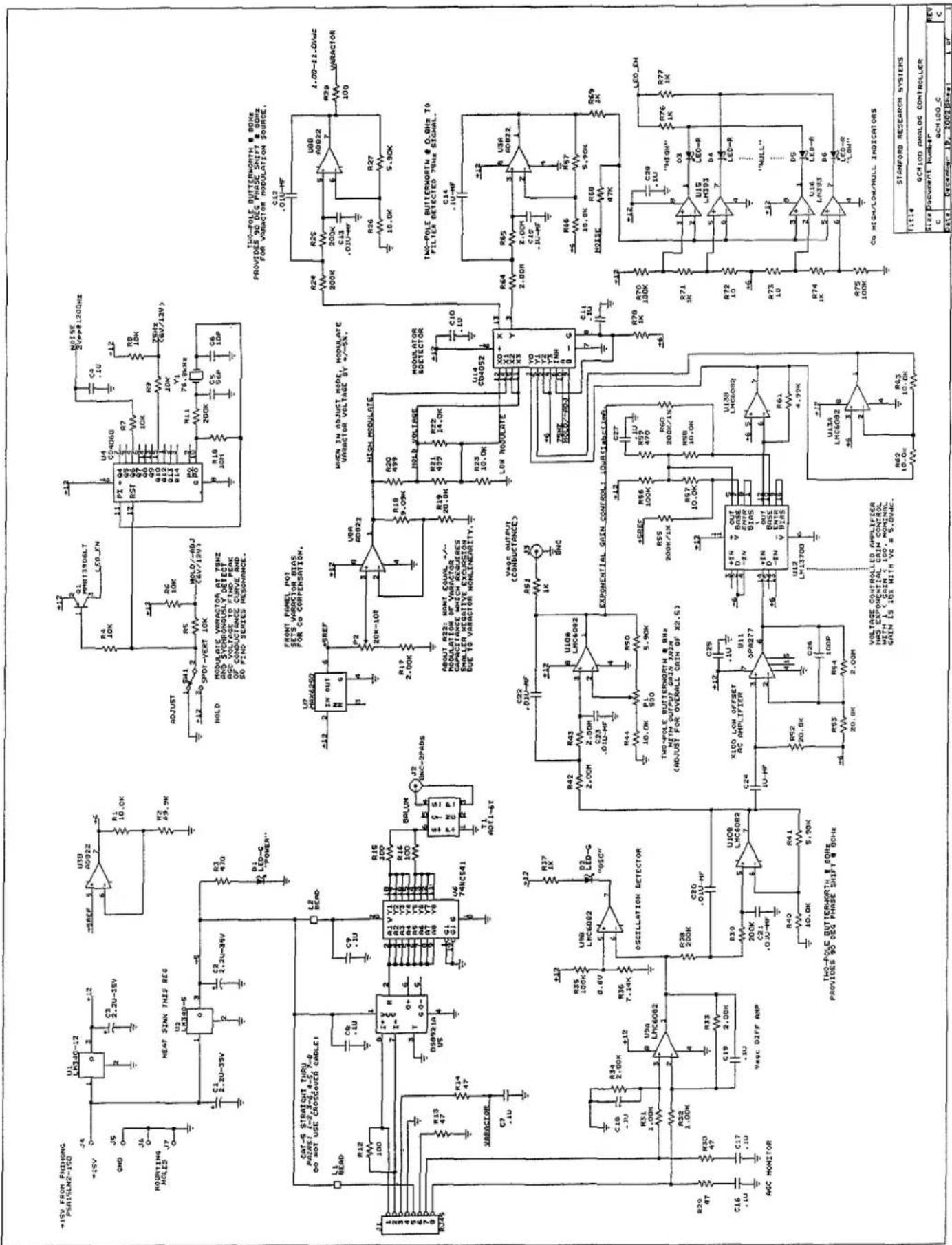
text_image
+15V FROM FUKINGHONG PSAISLN2-150 J4 +15V J6 J8 J8 MOUNTING HOLES J7 +15V HEAT SINK THIS REG U3 L3350-5 C1 2.2U-35V C2 2.2U-35V R3 470 D1 LED-G "POWER" CAT-S STRATGHT THU PAISET I=2.9-8.4-2.9-8. DO NOT USE COROCOVER CABLE! L2 BAND L1 READ R12 100 R13 47 R14 47 R15 47 R16 100 R17 2.00K R18 100 R19 20.0k R20 499 R21 479 R22 14.0k R23 10.0k R24 100 R25 200K R26 10.0k R27 9.0k R28 VARACTOR C7 .1U VARACTOR C7 .1U R24S 1.00-11.0MHz TWO-POLE BUTTERWORTH & BONF PROVIDES NO DIS PHASE SHIFT & BONE FOR VARIATOR MODULATION SOURCE. FRONT PANEL PO1 SETS VARIATOR BIAS, FOR CO COMPENSATION. WHEN IN ADJUST MODE, MODULATE VARIATOR VOLTAGE BY +/-SN. L77 MFBX250 IN OUT 6 SREF P2 20K-10T R UBA 60B22 R17 2.00K R18 9.0kN R20 499 HOLD VOLTAGE R21 479 R22 14.0kN R23 10.0kN MODULATOR DETECTOR LOW NOVULATE VASE OUTPUT (CONDUCTANCE) C32 0.0U-NF C33 0.0U-NF C34 0.0U-NF C35 0.0U-NF C36 7.14kN C37 1K C38 100K- C39 2.00K- C40 2.00K- C41 2.00K- C42 2.0U-HF C43 2.00K- C44 2.0U-HF C45 2.0U-HF C46 2.0U-HF C47 2.0U-HF C48 2.0U-HF C49 2.0U-HF C50 2.0U-HF C51 2.0U-HF C52 2.0U-HF C53 2.0U-HF C54 2.0U-HF C55 2.0U-HF C56 2.0U-HF C57 2.0U-HF C58 2.0U-HF C59 2.0U-HF C60 2.0U-HF C61 2.0U-HF C62 2.0U-HF C63 2.0U-HF C64 2.0U-HF C65 2.0U-HF C66 2.0U-HF C67 2.0U-HF C68 2.0U-HF C69 2.0U-HF C70 2.0U-HF C71 2.0U-HF C72 2.0U-HF C73 2.0U-HF C74 2.0U-HF C75 2.0U-HF C76 2.0U-HF C77 2.0U-HF C78 2.0U-HF C79 2.0U-HF C80 2.0U-HF C81 2.0U-HF C82 2.0U-HF C83 2.0U-HF C84 2.0U-HF C85 2.0U-HF C86 2.0U-HF C87 2.0U-HF C88 2.0U-HF C89 2.0U-HF C90 2.0U-HF C91 2.0U-HF C92 2.0U-HF C93 2.0U-HF C94 2.0U-HF C95 2.0U-HF C96 2.0U-HF C97 2.0U-HF C98 2.0U-HF C99 2.0U-HF TWO-POLE BUTTERWORTH & BONE, PROVIDES NO DIS PHASE SHIFT & BONE. STANFORD RESEARCH SYSTEMS. TST1# GCHLDG ANALOG CONTROLLER. Size Document Number:REF. GCHLDG_C GCHLDG_C C RATE Reference ID: 2,9,9,9,9,9,9,9,9,9,9,9,9,9,9,9,9,9,9,9,9,9,9,9,9,9,9,9,9,9,9,9,9,9,9,9,9,9,9,9,9,9,9,9,9,9,9,9,9,9,9,5 LCF.| DATE: DECEMBER 19, 200256847. 1 OF 1 | ||
| CIA: DOCUMENT NUMBER CCM.C | KEY | |
| SIZE: DOCUMENT NUMBER | ||
| MATERIALS: EQUIVALE NAME (GCH25) | ||
| UNITS: CAPITAL MICROLOGICALS (CH25) | ||
| 1131- | ||
| STANDARD RESEARCH SYSTEMS | ||
| 1290 REMOOOO | ||
(Holet) There is a gain of 2.5x for the acc signals in the core controller.)
A548.4 = PUCN, 7990 K00.T=1828 H11M A964.6 = PUCN, 7990 OS=1828 H11M
adjust PA 1 PA 50 THAT AT THE OUTPUT OF THE SCHOOL:
RESISTANCE CALIFORNION: Rm = (10,000X105(-veoned/8) - 75) otherwise
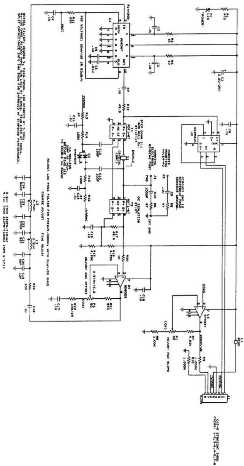
text_image
Circuit schematic diagram of a standard RC-ADC system with component labels, ICs, and connections for signal processing and control logic.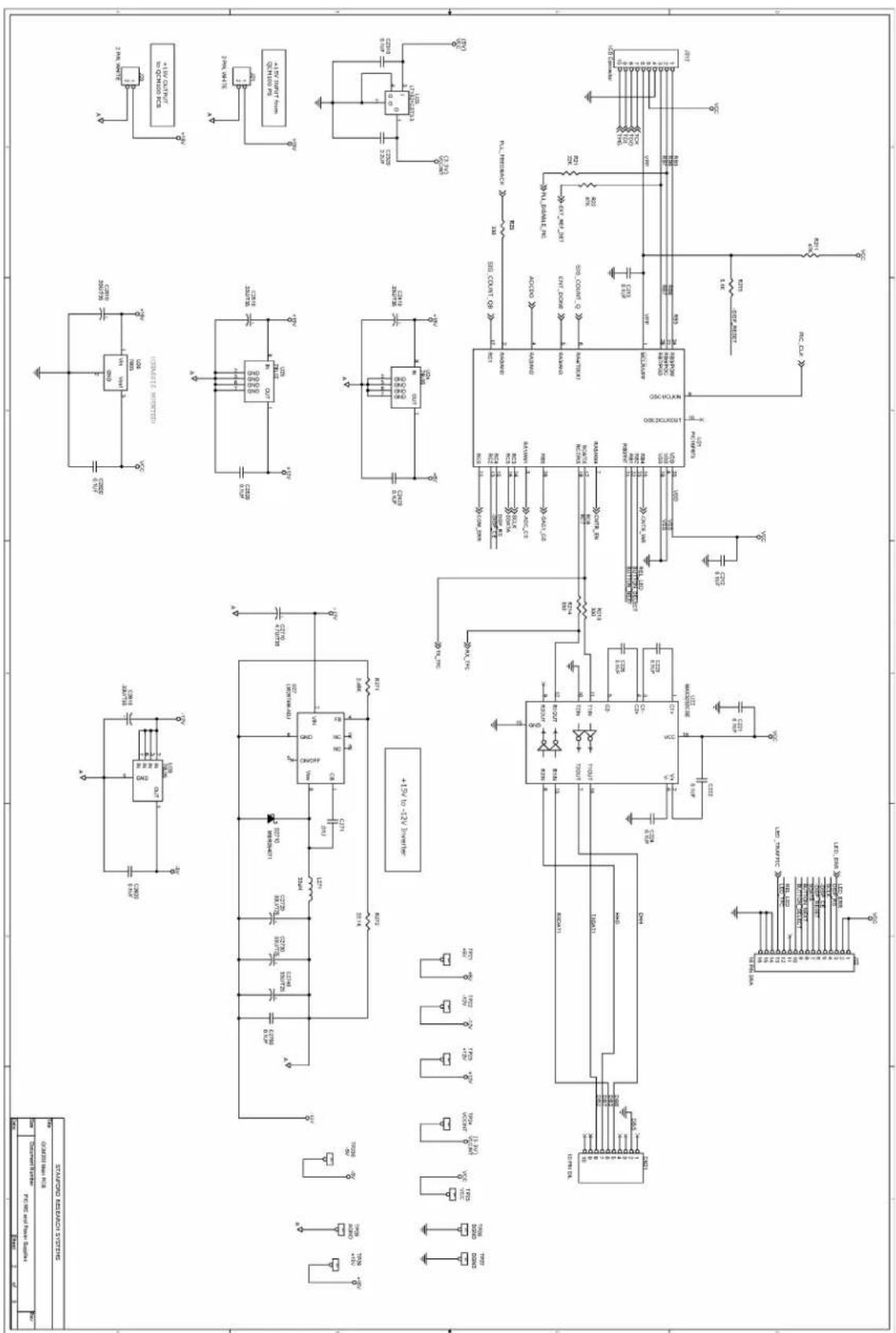
text_image
Holding Wiring (200kΩ) Power Supply ECM Power Diode SHULGAS HOWRGEN ONGARVIS UHALAWAY 150V/150V 3.1MHz Vdc 2 ECM Optimized on JN4500 A1+ 3.1MHz Vdc 2 50V 150V/150V 50V 150V/150V 50V 150V/150V 50V 150V/150V 50V 150V/150V 50V 150V/150V 50V 150V/150V 50V 150V/150V LONERAM ACB LONERAM ACB LONERAM ACB LONERAM ACB LONERAM ACB LONERAM ACB LONERAM ACB LONERAM ACB LONERAM ACB LONERAM ACB LONERAM ACB LONERAM ACB LONERAM ACB LONERA ACB LONERA ACB LONERA ACB LONERA ACB LONERA ACB LONERA ACB LONERA ACB LONERA ACB LONERA ACB LONERA ACB LONERA ACB LONERA ACB LONERA ACB LONERA ACB LONERA AcB-6A LONERA-6A LONERA-6A LONERA-6A LONERA-6A LONERA-6A LONERA-6A LONERA-6A LONERA-6A LONERA-6A LONERA-6A LONERA-6A LONERA-6A LONERA-6A LONERA-6A LONERA-7A LONERA-7A LONERA-7A LONERA-7A LONERA-7A LONERA-7A LONERA-7A LONERA-7A LONERA-7A LONERA-7A LONERA-7A LONERA-7A LONERA-7A LONERA-8A LONERA-8A LONERA-8A LONERA-8A LONERA-8A LONERA-8A LONERA-8A LONERA-8A LONERA-8A LONERA-8A LONERA-8A LONERA-8A LONERA-8A LONERA-9A LONERA-9A LONERA-9A LONERA-9A LONERA-9A LONERA-9A LONERA-9A LONERA-9A LONERA-9A LONERA-9A LONERA-9A LONERA-9A LONERA-9A LONERA-9A LONERA-9A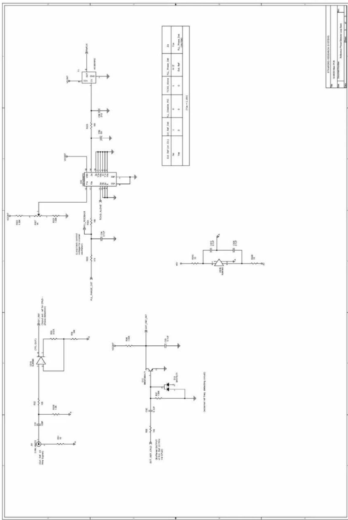
text_image
(Ext. Ref. 10 Heter Signal) R21 100 R22 1.2K R23 1.5K R24 1.5K R25 1.5K R26 1.5K R27 1.5K R28 1.5K R29 1.5K R30 1.5K R31 1.5K R32 1.5K R33 1.5K R34 1.5K R35 1.5K R36 1.5K R37 1.5K R38 1.5K R39 1.5K R40 1.5K R41 1.5K R42 1.5K R43 1.5K R44 1.5K R45 1.5K R46 1.5K R47 1.5K R48 1.5K R49 1.5K R50 1.5K R51 1.5K R52 1.5K R53 1.5K R54 1.5K R55 1.5K R56 1.5K R57 1.5K R58 1.5K R59 1.5K R60 1.5K R61 1.5K R62 1.5K R63 1.5K R64 1.5K R65 1.5K R66 1.5K R67 1.5K R68 1.5K R69 1.5K R70 1.5K R71 1.5K R72 1.5K R73 1.5K R74 1.5K R75 1.5K R76 1.5K R77 1.5K R78 1.5K R79 1.5K R80 1.5K R81 1.5K R82 1.5K R83 1.5K R84 1.5K R85 1.5K R86 1.5K R87 1.5K R88 1.5K R89 1.5K R90 1.5K R91 1.5K R92 1.5K R93 1.5K R94 1.5K R95 1.5K R96 1.5K R97 1.5K R98 1.5K R99 1.5K R100= 1.2V (External inf freq, detecting circuit) (Center) R20 (MΩ/Hz) C20 (MΩ/Hz) C30 (MΩ/Hz) C40 (MΩ/Hz) C50 (MΩ/Hz) C60 (MΩ/Hz) C70 (MΩ/Hz) C80 (MΩ/Hz) C90 (MΩ/Hz) C100 (MΩ/Hz) C100 (MΩ/Hz) C100 (MΩ/Hz) C100 (MΩ/Hz) C100 (MΩ/Hz) C100 (MΩ/Hz) C100 (MΩ/Hz) C100 (MΩ/Hz) C100 (MΩ/Hz) C100 (MΩ/Hz) C1Eo (MΩ/Hz) C2Eo (MΩ/Hz) C3Eo (MΩ/Hz) C4Eo (MΩ/Hz) C5Eo (MΩ/Hz) C6Eo (MΩ/Hz) C7Eo (MΩ/Hz) C8Eo (MΩ/Hz) C9Eo (MΩ/Hz) C10Eo (MΩ/Hz) C20Eo (MΩ/Hz) C30Eo (MΩ/Hz) C40Eo (MΩ/Hz) C50Eo (MΩ/Hz) C60Eo (MΩ/Hz) C70Eo (MΩ/Hz) C80Eo (MΩ/Hz) C90Eo (MΩ/Hz) C100Eo (MΩ/Hz) C200Eo (MΩ/Hz) C300Eo (MΩ/Hz) C400Eo (MΩ/Hz) C500Eo (MΩ/Hz) C600Eo (MΩ/Hz) C700Eo (MΩ/Hz) C800Eo (MΩ/Hz) C900Eo (MΩ/Hz) C100Eo (MΩ/Hz) C200Eo (MΩ/Hz) C300Eo (MΩ/Hz) C400Eo (MΩ/Hz) C500Eo (MΩ/Hz) C600Eo (MΩ/Hz) C700Eo (MΩ/Hz) C800Eo( MΩ/Hz ) C900Eo( MΩ/Hz ) C100Eo( MΩ/Hz ) C200Eo( MΩ/Hz ) C300Eo( MΩ/Hz ) C400Eo( MΩ/Hz ) C500Eo( MΩ/Hz ) C600Eo( MΩ/Hz ) C700Eo( MΩ/Hz ) C800Eo( MΩ/Hz ) C900Eo( MΩ/Hz ) C100Eo( MΩ/Hz ) C200Eo( MΩ/Hz ) C300Eo( MΩ/Hz ) C400Eo( MΩ/Hz ) C500Eo( MΩ/Hz ) C600Eo( MΩ/Hz ) C70O EOT( VccuOET ) VccuOET( VccuOET ) VccuOET( VccuOET ) VccuOET( VccuOET ) VccuOET( VccuOET ) VccuOET( VccuOET ) VccuOET( VccuOET ) VccuOET( VccuOET ) VccuOET( VccuOET ) VccuOET( VcculOET ) VccuOET( VcculOET ) VccuOET( VcculOET ) VccuOET( VcculOET ) VccuOET( VcculOET ) VccuOET( VcculOET ) VccuOET( VcculOET ) VccuOET( VcculOET ) VccuOET( VcculOET ) Yin = 1.2V STANDARD RESEARCH SYSTEMS. No. Q-CCSS Main PCS. Document Reader: Reference Phase Detector Loop Back. Data: 7, 8, 9, 10, 1, 2, 3, 4, 5, 6, 7, 8, 9, 10, 1, 2, 3, 4, 5, 6, 7, 8, 9, 10, 1, 2, 3, 4, 5, 6, 7, 8, 9, 10, 1, 2, 3, 4, 5, 6, 7, 8,9, 10, 1, 2, 3, 4, 5, 6, 7, 8,9, 10, 1, 2, 3, 4, 5, 6, 7, 8,9, 10, 1, 2, 3, 4, 5, 6, 7, 8,9, 10, 1,2V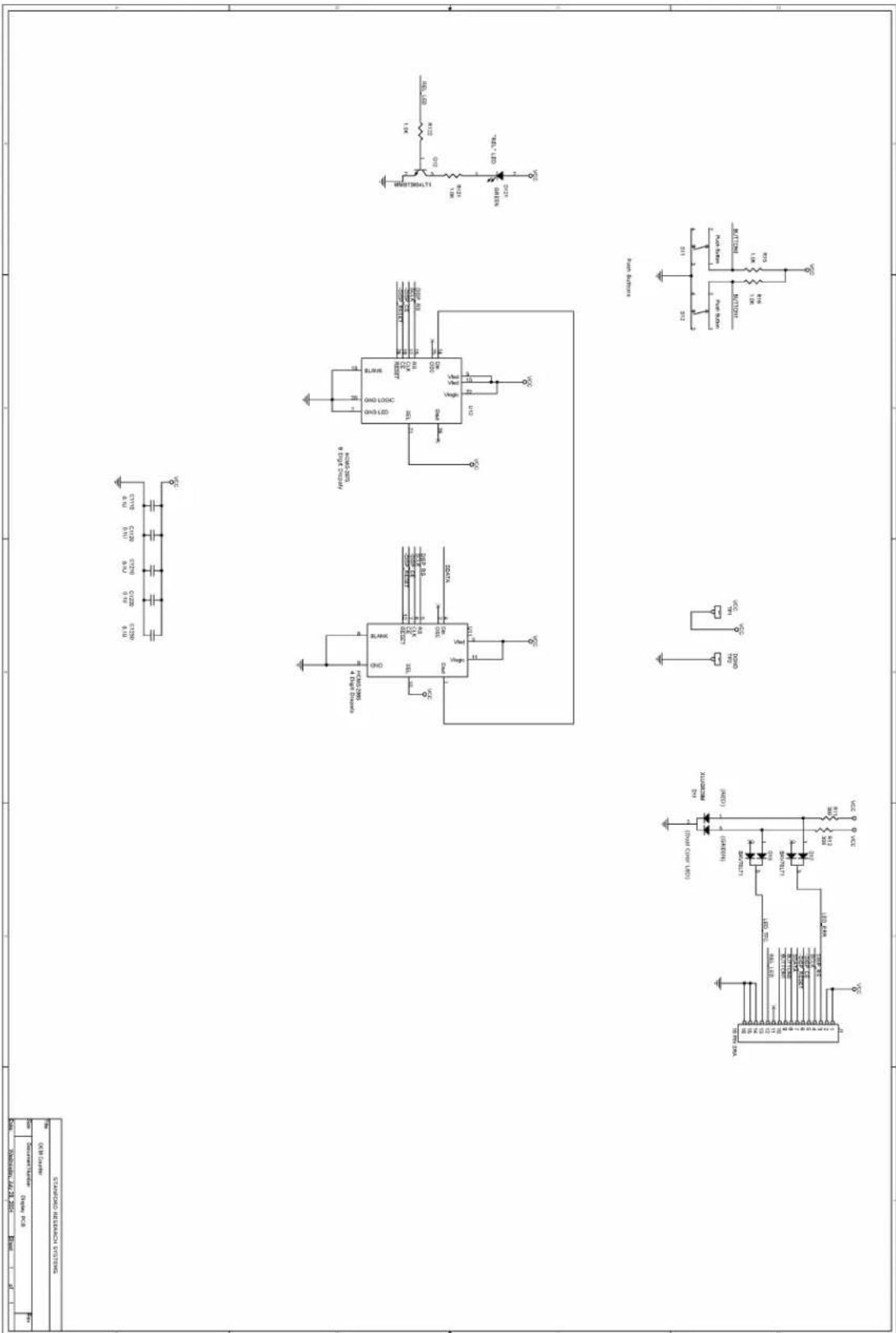
text_image
SHIELDS SHEDDER COLDERS 120 V 97.100V DC DC (WD) DC (WD) DC (WD) DC (WD) DC (WD) DC (WD) DC (WD) DC (WD) DC (WD) DC (WD) DC (WD) DC (WD) DC (WD) DC (WD) DC (WD) DC (WD) DC (WD) DC (WD) DC (WD) DC (WD) DC (WD) DC (WD) DC (WD) DC (WD) DC (WD) DC (WD) 100V DC (WD) 100V DC (WD) 100V DC (WD) 100V DC (WD) 100V DC (WD) 100V DC (WD) 100V DC (WD) 100V DC (WD) 100V DC (WD) 100V DC (WD) 100VAppendix A
Frequency Counter Selection Criteria
The QCM200 includes a Frequency Output port (BNC) on the front panel for connection to an external frequency counter.
| Frequency Output (front panel, AC signal) | |
| Frequency 5 MHz (nominal) | |
| Level TTL (square wave) | |
| Source Impedance | 50 Ω |
| Connector BNC | |
The QCM200 Digital Controller features a built-in frequency counter to measure the resonant frequency and display it on the front panel. The stability and accuracy of the frequency counter is more than adequate for most QCM experiments. For extremely demanding applications, an external timebase, such as the SRS FS725 Rubidium Frequency Standard, can eliminate all frequency errors.
However, the option to connect an external frequency counter is also available to (1) compare frequency measurements against an external counter and (2) provide connectivity to a pre-existing experimental setup including an integrated frequency counter.
The selection criteria for a frequency counter for QCM applications include resolution, speed, time-base stability, computer interfaces and software drivers. Careful selection is required, otherwise the frequency counter may degrade the quality of mass measurements.
The table below lists the typical characteristics of the frequency signal from the QCM200 Frequency Output port for a crystal in water.
| Description | Typical | Value |
| Frequency 5±0.01 MHz | ||
| Waveform (into 50 Ω) | 2.4 V square wave | |
| Stability (second to second) 0.002 Hz | ||
| Stability (minute to minute) 0.10 Hz | ||
| Temperature Coefficient (static) 8 Hz/°C | ||
| Frequency/Mass coefficient 0.057 Hz/(ng/cm ^2 ) |
Many of a frequency counter's characteristics are determined by its time-base. If the time-base changes frequency by 10 ppm the reported values will also change by 10 ppm. While the accuracy of the counter's time-base is not particularly important, the stability of the time-base is critically important as variations in the time-base will be indistinguishable from changes in accumulated mass on the surface of the crystal. Often manufacturers will specify accuracy and aging but do not specify short-term stability. In virtually all counters, the short-term stability will improve if they are allowed to warm-up for an extended period of time. To avoid degrading frequency measurements, the time-base should have a 1 second stability of better than .002 Hz/5 MHz or 4 × 10^-10 .
The speed/resolution of a counter is also important. The accumulated mass can change rapidly in a typical QCM measurement and it is desirable to make frequency measurements with a resolution of 1:10^8 in a one second interval to not significantly degrade the mass resolution of, or add noise to, the measurement. Simply counting cycles of the frequency output over a one second interval can not provide resolution better than 1 in 5×10^6 , and so a more elaborate counter architecture is required. A “reciprocal-interpolating” counter can provide a much better frequency resolution than ±1 cycle per gate interval.
Virtually all frequency counters can measure the frequency of the 2.4V_pp square wave into 50 provided by the QCM200 Frequency Output.
Counters are available with RS-232 and/or IEEE-488 interfaces to facilitate computer data acquisition. The speed of the interface is not very critical, as typically only one reading is taken each second. Counters are relatively simple to set-up and read via their computer interfaces. Software drivers for National Instruments LabView products, or other data acquisition programs, are often available.
Frequency counters used at SRS for QCM measurements are listed below:
| Manufacturer | Model | Digits/Second |
| Stanford Research Systems SR620 10 | ||
| Agilent 53131 10 | ||
| Agilent | 53132 | 12 |
Appendix B
QCM200 Remote Programming
Introduction
The QCM200 Quartz Crystal Microbalance Controller may be remotely programmed via the standard RS-232 serial interface. Any host computer interfaced to the QCM200 can easily configure, diagnose and operate the quartz crystal microbalance using simple ASCII commands.
RS-232 Port
The QCM200 comes standard with an RS-232 communications port.
The RS-232 interface connector is a standard 9 pin, type D, female connector configured as a DCE (transmit on pin3, receive on pin2). The communication parameters are fixed at: 9600 Baud rate, 8 Data bits, 1 Stop bit, No Parity, No Flow Control.
Front Panel Indicator
To assist in programming, the QCM200 has a front panel RS-232 LED located above the Measurement display. The RS-232 LED is an activity indicator that flashes every time a character is received or transmitted over the RS-232 lines.
Command Format
Communications with the QCM200 uses ASCII characters. A command to the QCM200 consists of a one letter mnemonic with optional “?”, an argument if necessary, and a command terminator. Commands may be either UPPER or lower case. Carriage return,
The QCM200 has a small (eight character) input buffer and processes commands in the order received. If the input buffer overflows, it is cleared and a communication error is flagged. Since no handshaking is supported, it is recommended (1) to send commands one at a time, (2) to confirm all settings with query commands and (3) waiting for query responses to be fully transmitted before sending a new command to the QCM200.
A query is constructed by appending a question mark “?” to the command. Values returned by the QCM200 are transmitted as a string of ASCII characters terminated by a
Examples of commands:
F
G
G?
D0
D?
|
Command Syntax
The one letter mnemonic (shown in CAPS) in each command sequence specifies the command. The rest of the sequence consists of parameters. Parameters shown in {} are not always required. Generally, parameters in {} are required to set a value in the QCM200.
The present value of a parameter may be determined by sending a query command. Commands that MAY be queried show a question mark in parenthesis (?) after the mnemonic.
A query is formed by including the question mark ? after the command mnemonic and omitting the queried parameter from the command. The query parameters shown in {} are NOT sent with a query. The query returns the values of these parameters. Values are returned as a string of ASCII characters.
Do NOT send () or {} or spaces as part of the command.
Command List
| D(?){i} | Display | Mode | ||||
| Set (query) the Display Mode. The parameter i selects a Display Mode below. | ||||||
| i | Display Mode | |||||
| 0 | F: Absolute Frequency | |||||
| 1 | f: Relative Frequency | |||||
| 2 | m: Mass Displacement | |||||
| 3 | R: Absolute Resistance | |||||
| 4 | r: Relative Resistance | |||||
| 5 | Gate: Gate time | |||||
| 6 | Scale: Analog Frequency Scale Factor | |||||
| Example | ||||||
| D0 | Set the Measurement display to Absolute Frequency. | |||||
| D? | Returns the Display Mode i. | |||||
| V(?){i} Analog Frequency Scale | ||||||
| i | Scale Factor | |||||
| 0 | 200 | Hz/V | ||||
| 1 | 500 | Hz/V | ||||
| 2 | 1 | kHz/V | ||||
| 3 | 2 | kHz/V | ||||
| 4 | 5 | kHz/V | ||||
| 5 | 10 | kHz/V | ||||
| 6 | 20 | kHz/V | ||||
| Example | ||||||
| D3 | Set the Scale factor to 2 kHz/V. | |||||
| D? | Returns the Scale Factor i. | |||||
| P(?){i} | Gate | Time | ||||
| Set (query) the Gate time. | ||||||
| The Gate Time is the time interval spent by the frequency counter to determine the resonance frequency of the crystal. It determines the data acquisition rate and the frequency resolution of the QCM200. | ||||||
| i | Gate time | |||||
| 0 | 100 | msec | ||||
| 1 | 1 | sec | ||||
| 2 | 10 | sec | ||||
| Example | ||||||
| P1 | Set the gate time to 1 second. | |||||
| P? | Returns the Gate Time i. | |||||
| F | Query | Absolute | Frequency | |||
| Query the Absolute Frequency. | ||||||
| Example | ||||||
| FReturns the Absolute Frequency in Hz. | ||||||
| G(?) | Frequency | Offset | ||||
| Set the Frequency Offset value or query the Relative Frequency. | ||||||
| Relative Frequency = Absolute Frequency - Frequency Offset | ||||||
| Example | ||||||
| GSet the Frequency Offset to the current Absolute Frequency. | ||||||
| G?Returns the Relative Frequency in Hz. | ||||||
| R | Query | Absolute | Resistance | |||
| Query the Absolute Resistance. | ||||||
| Example | ||||||
| RThe Absolute Resistance is returned in Ohms. | ||||||
| S(?) | Resistance | Offset | ||||
| Set the Resistance Offset or query the Relative Resistance. | ||||||
| Relative Resistance= Absolute Resistance - Resistance Offset | ||||||
| Example | ||||||
| SSet the Resistance Offset to the current Absolute Resistance. | ||||||
| S?Returns the Resistance Offset in Ohms. | ||||||
| I | Identification | String | ||||
| Query the Identification String. | ||||||
| Example | ||||||
| IReturns a string similar to “QCM200 rev 1.04 s/n69001”. | ||||||
| B | Query | Status | ||||
| Query the Status Byte. The value is returned as a decimal number from 0 to 255. The conditions for each bit are listed below. | ||||||
| Bit Set by | ||||||
| 0 New R value | ||||||
| 1 New F value | ||||||
| 2 Frequency Over Range | ||||||
| 3 Frequency Under Range | ||||||
| 4 Communication Error | ||||||
| 5 unused | ||||||
| 6 unused | ||||||
| 7 unused | ||||||
| Example | ||||||
| BReturns the Status Byte in decimal format. Executing this query clears the Status bits. | ||||||
T(?){i}
Timebase
Set (query) the timebase.
An ultra-stable external timebase (if available) can improve the stability of the frequency measurements.
| i | Timebase | |
| 0 | internal | TCXO |
| 1 | lock the TCXO to the exter | |
Example
T1
T?
If no signal is present at the rear panel 10 MHz BNC then the QCM200 will revert to using the internal TCXO. A timebase query will return 0 in this case.