
CPM1 - Industrial Automation OMRON - Free user manual and instructions
Find the device manual for free CPM1 OMRON in PDF.


| Product Type | Programmable Logic Controller (PLC) |
| Brand | OMRON |
| Model | CPM1 |
| Supply Voltage | 24 VDC (typical model) or 100-240 VAC depending on version |
| Power Consumption | Approx. 30 VA |
| Dimensions (L x D x H) | 90 x 65 x 90 mm |
| Weight | Approx. 200 g |
| Number of digital inputs | 6 (depending on model) |
| Number of digital outputs | 4 (depending on model) |
| Input type | 24 VDC |
| Output type | Relay or transistor |
| Program memory | 2K words |
| Programming language | Ladder Diagram (LD) |
| Main functions | Boolean logic, timers, counters, shift registers |
| Display | None (without screen) |
| Protection | IP20 |
| Operating conditions | 0-55°C, humidity 10-90% |
| Maintenance and cleaning | Clean with a dry cloth, avoid solvents |
| Safety | Grounding, cut off power before intervention |
| Spare parts and repairability | Contact OMRON customer service, no spare parts available for the user |
| General information | Detailed manual available in PDF format |
| Warranty | 2 years (standard) |
| Certification | CE, UL |
Frequently Asked Questions - CPM1 OMRON
User questions about CPM1 OMRON
0 question about this device. Answer the ones you know or ask your own.
Ask a new question about this device
Download the instructions for your Industrial Automation in PDF format for free! Find your manual CPM1 - OMRON and take your electronic device back in hand. On this page are published all the documents necessary for the use of your device. CPM1 by OMRON.
USER MANUAL CPM1 OMRON
CPM1/CPM1A/CPM2A/CPM2C/SRM1(-V2)
Programmable Controllers
PROGRAMMING MANUAL
CPM1/CPM1A/CPM2A/CPM2C/SRM1(-V2)
Programmable Controllers
Programming Manual
Revised February 2008
Notice:
OMRON products are manufactured for use according to proper procedures by a qualified operator and only for the purposes described in this manual.
The following conventions are used to indicate and classify precautions in this manual. Always heed the information provided with them. Failure to heed precautions can result in injury to people or damage to property.

DANGER
Indicates an imminently hazardous situation which, if not avoided, will result in death or serious injury.

WARNING
Indicates a potentially hazardous situation which, if not avoided, could result in death or serious injury.

Caution
Indicates a potentially hazardous situation which, if not avoided, may result in minor or moderate injury, or property damage.
OMRON Product References
All OMRON products are capitalized in this manual. The word "Unit" is also capitalized when it refers to an OMRON product, regardless of whether or not it appears in the proper name of the product.
The abbreviation "Ch," which appears in some displays and on some OMRON products, often means "word" and is abbreviated "Wd" in documentation in this sense.
The abbreviation "PC" means Programmable Controller and is not used as an abbreviation for anything else.
Visual Aids
The following headings appear in the left column of the manual to help you locate different types of information.
Note Indicates information of particular interest for efficient and convenient operation of the product.
1, 2, 3... 1. Indicates lists of one sort or another, such as procedures, checklists, etc.
OMRON, 1999
All rights reserved. No part of this publication may be reproduced, stored in a retrieval system, or transmitted, in any form, or by any means, mechanical, electronic, photocopying, recording, or otherwise, without the prior written permission of OMRON.
No patent liability is assumed with respect to the use of the information contained herein. Moreover, because OMRON is constantly striving to improve its high-quality products, the information contained in this manual is subject to change without notice. Every precaution has been taken in the preparation of this manual. Nevertheless, OMRON assumes no responsibility for errors or omissions. Neither is any liability assumed for damages resulting from the use of the information contained in this publication.
TABLE OF CONTENTS
PRECAUTIONS . xvii
1 Intended Audience xviii
2 General Precautions xviii
3 Safety Precautions xviii
4 Operating Environment Precautions xx
5 Application Precautions xxi
SECTION 1
PC Setup 1
1-1 PC Setup 2
1-2 Basic PC Operation and I/O Processes 16
1-3 CPM2C Changes in SW2 21
SECTION 2
Special Features 25
2-1 CPM2A/CPM2C Interrupt Functions 26
2-2 CPM2A/CPM2C High-speed Counters 45
2-3 CPM1/CPM1A Interrupt Functions 77
2-4 SRM1(-V2) Interrupt Functions 94
2-5 CPM2A/CPM2C Pulse Output Functions 97
2-6 CPM1A Pulse Output Functions 131
2-7 Synchronized Pulse Control (CPM2A/CPM2C Only) 134
2-8 Data Computation Standards 146
2-9 Analog I/O Functions (CPM1/CPM1A/CPM2A/CPM2C Only) 147
2-10 Temperature Sensor Input Functions (CPM1A/CPM2A/CPM2C Only) 147
2-11 CompoBus/S I/O Slave Functions (CPM1A/CPM2A/CPM2C Only) 147
2-12 CompoBus/S I/O Master Functions (SRM1(-V2) and CPM2C-S Only) 148
2-13 Analog Controls (CPM1/CPM1A/CPM2A Only) 150
2-14 Quick-response Inputs 153
2-15 Macro Function 157
2-16 Calculating with Signed Binary Data 158
2-17 Differential Monitor 159
2-18 Expansion Instructions (CPM2A/CPM2C/SRM1(-V2) Only) 160
2-19 Using the CPM2A/CPM2C Clock Function 163
SECTION 3
Using Expansion Units 165
3-1 Analog I/O Units 166
3-2 Temperature Sensor Units 193
3-3 CompoBus/S I/O Link Units 214
3-4 DeviceNet I/O Link Unit 219
SECTION 4
Communications Functions 225
4-1 Introduction 226
4-2 CPM1/CPM1A Communications Functions 227
4-3 CPM2A/CPM2C Communications Functions 231
4-4 SRM1(-V2) Communications Functions 268
4-5 Host Link Commands 281
SECTION 5
Memory Areas 307
5-1 Memory Area Functions 308
5-2 I/O Allocation for CPM1/CPM1A/CPM2A PCs 313
5-3 I/O Allocation for CPM2C PCs 323
SECTION 6
Ladder-diagram Programming 333
6-1 Basic Procedure 334
6-2 Instruction Terminology 334
6-3 Basic Ladder Diagrams 335
6-4 Controlling Bit Status 354
6-5 Work Bits (Internal Relays) 356
6-6 Programming Precautions 358
6-7 Program Execution 360
SECTION 7
Instruction Set 361
7-1 Notation 364
7-2 Instruction Format 364
7-3 Data Areas, Definer Values, and Flags 364
7-4 Differentiated Instructions 366
7-5 Coding Right-hand Instructions 367
7-6 Instruction Tables 370
7-7 Ladder Diagram Instructions 376
7-8 Bit Control Instructions 377
7-9 NO OPERATION - NOP(00) 381
7-10 END-END(01) 381
7-11 INTERLOCK and INTERLOCK CLEAR - IL(02) and ILC(03) 381
7-12 JUMP and JUMP END-JMP(04) and JME(05) 383
7-13 User Error Instructions:
FAILURE ALARM AND RESET - FAL(06) and
SEVERE FAILURE ALARM - FALS(07) 385
7-14 Step Instructions: STEP DEFINE and STEP START-STEP(08)/SNXT(09) 385
7-15 Timer and Counter Instructions 388
7-16 Shift Instructions 404
7-17 Data Movement Instructions 411
7-18 Data Control Instructions 421
7-19 Comparison Instructions 432
7-20 Conversion Instructions 439
7-21 BCD Calculation Instructions 457
7-22 Binary Calculation Instructions 467
7-23 Special Math Instructions 471
7-24 Logic Instructions 479
7-25 Increment/Decrement Instructions 483
7-26 Subroutine Instructions 484
7-27 Pulse Output Instructions 487
7-28 Special Instructions 497
7-29 Interrupt Control Instructions 501
7-30 Communications Instructions 505
SECTION 8
PC Operations and Processing Time 511
8-1 CPM1/CPM1A Cycle Time and I/O Response Time 512
8-2 CPM2A/CPM2C Cycle Time and I/O Response Time 523
8-3 SRM1(-V2) Cycle Time and I/O Response Time 537
TABLE OF CONTENTS
SECTION 9
Troubleshooting 549
9-1 Introduction 550
9-2 Programming Console Operation Errors 550
9-3 Programming Errors 551
9-4User-defined Errors 552
9-5 Operating Errors 553
9-6 Error Log 555
9-7 Host Link Errors 557
9-8 Troubleshooting Flowcharts 557
Appendices
A Programming Instructions 559
B Error and Arithmetic Flag Operation 565
C Memory Areas 569
D I/O Assignment Sheet 587
E Program Coding Sheet 589
F List of FAL Numbers 593
G Extended ASCII 595
Index 597
Revision History 603
About this Manual:
This manual provides information on programming the CPM1, CPM1A, CPM2A, CPM2C (including the CPM2C-S), and SRM1(-V2) PCs. The following manuals describe the system configurations and installation of the PCs and provide a basic explanation of operating procedures for the Programming Consoles. Read the relevant manual first to acquaint yourself with the PC.
| Manual | Catalog No. |
| CPM1 Operation Manual | W262 |
| CPM1A Operation Manual | W317 |
| CPM2A Operation Manual | W352 |
| CPM2C Operation Manual | W356 |
| CPM2C-S Operation Manual | W377 |
| SRM1(-V2) Operation Manual | W318 |
Note 1. Version 2 (-V2) of the SRM1 is included beginning with following revision of the manual: W318-E1-3.
- Refer to sections on the CPM2C for information on CPM2C instructions and Expansion Units.
For programming the CPM1, CPM1A, CPM2A, CPM2C (including the CPM2C-S), and SRM1(-V2) PCs, use the CX-Programmer, special Support Software that runs in a Windows environment. The SYSMAC Support Software and SYSMAC-CPT Support Software can also be used. Please refer to the relevant manuals listed in the following table when using any one of Support Software.
| Name | Model No. | Manual | Catalog No. |
| CX-Programmer version 3.1 | WS02-CXPC1-EV3 | CX-Programmer Operation Manual | W414 |
| CX-Programmer version 4.0 | WS02-CXPC1-EV4 | W425 | |
| SYSMAC Support Software | C500-ZL3AT1-E | SYSMAC Support Software Operation Manual: Basic | W247 |
| SYSMAC Support Software Operation Manual: C-series PCs | W248 | ||
| SYSMAC-CPT Support Software | WS02-CPTB1-E | SYSMAC-CPT Support Software Quick Start Guide | W332 |
| SYSMAC-CPT Support Software User Manual | W333 |
Please read this manual carefully and be sure you understand the information provided before attempting to program or operate the PC.
Section 1 explains the PC Setup. The PC Setup can be used to control the operating parameters.
Section 2 explains special features of the PC.
Section 3 describes how to use the CPM1A-MAD01 and CPM2C-MAD11 Analog I/O Units, the CPM1A-TS□□□ and CPM2C-TS□□□ Temperature Sensor Units, and the CPM1A-SRT21 and CPM2C-SRT21 CompoBus/S I/O Link Units.
WARNING
Failure to read and understand the information provided in this manual may result in personal injury or death, damage to the product, or product failure. Please read each section in its entirety and be sure you understand the information provided in the section and related sections before attempting any of the procedures or operations given.
About this Manual, Continued
Section 4 describes how to use the communications functions provided in the PCs.
Section 5 describes the structure of the PC memory areas and explains how to use them. Details of some areas are provided in Appendix C.
Section 6 explains the basic steps and concepts involved in writing a basic ladder diagram program. It introduces the instructions that are used to build the basic structure of the ladder diagram and control its execution.
Section 7 explains instructions individually and provides the ladder diagram symbol, data areas, and flags used with each.
Section 8 explains the internal PC processing, as well as the time required for processing and execution.
Section 9 describes how to diagnose and correct hardware and software errors that can occur during operation.
Various Appendices are also provided for easy reference. Refer to the table of contents for a list of appendices.
Read and Understand this Manual
Please read and understand this manual before using the product. Please consult your OMRON representative if you have any questions or comments.
Warranty and Limitations of Liability
WARRANTY
OMRON's exclusive warranty is that the products are free from defects in materials and workmanship for a period of one year (or other period if specified) from date of sale by OMRON.
OMRON MAKES NO WARRANTY OR REPRESENTATION, EXPRESS OR IMPLIED, REGARDING NON-INFRINGEMENT, MERCHANTABILITY, OR FITNESS FOR PARTICULAR PURPOSE OF THE PRODUCTS. ANY BUYER OR USER ACKNOWLEDGES THAT THE BUYER OR USER ALONE HAS DETERMINED THAT THE PRODUCTS WILL SUITABLY MEET THE REQUIREMENTS OF THEIR INTENDED USE. OMRON DISCLAIMS ALL OTHER WARRANTYES, EXPRESS OR IMPLIED.
LIMITATIONS OF LIABILITY
OMRON SHALL NOT BE RESPONSIBLE FOR SPECIAL, INDIRECT, OR CONSEQUENTIAL DAMAGES, LOSS OF PROFITS OR COMMERCIAL LOSS IN ANY WAY CONNECTED WITH THE PRODUCTS, WHETHER SUCH CLAIM IS BASED ON CONTRACT, WARRANTY, NEGLIGENCE, OR STRICT LIABILITY.
In no event shall the responsibility of OMRON for any act exceed the individual price of the product on which liability is asserted.
IN NO EVENT SHALL OMRON BE RESPONSIBLE FOR WARRANTY, REPAIR, OR OTHER CLAIMS REGARDING THE PRODUCTS UNLESS OMRON'S ANALYSIS CONFIRMS THAT THE PRODUCTS WERE PROPERLY HANDLED, STORED, INSTALLED, AND MAINTAINED AND NOT SUBJECT TO CONTAMINATION, ABUSE, MISUSE, OR INAPPROPRIATE MODIFICATION OR REPAIR.
Application Considerations
| SUITABILITY FOR USE |
| OMRON shall not be responsible for conformity with any standards, codes, or regulations that apply to the combination of products in the customer's application or use of the products. |
| At the customer's request, OMRON will provide applicable third party certification documents identifying ratings and limitations of use that apply to the products. This information by itself is not sufficient for a complete determination of the suitability of the products in combination with the end product, machine, system, or other application or use. |
| The following are some examples of applications for which particular attention must be given. This is not intended to be an exhaustive list of all possible uses of the products, nor is it intended to imply that the uses listed may be suitable for the products: • Outdoor use, uses involving potential chemical contamination or electrical interference, or conditions or uses not described in this manual. • Nuclear energy control systems, combustion systems, railroad systems, aviation systems, medical equipment, amusement machines, vehicles, safety equipment, and installations subject to separate industry or government regulations. • Systems, machines, and equipment that could present a risk to life or property. |
| Please know and observe all prohibitions of use applicable to the products. |
| NEVER USE THE PRODUCTS FOR AN APPLICATION INVOLVING SERIOUS RISK TO LIFE OR PROPERTY WITHOUT ENSURING THAT THE SYSTEM AS A WHOLE HAS BEEN DESIGNED TO ADDRESS THE RISKS, AND THAT THE OMRON PRODUCTS ARE PROPERLY RATED AND INSTALLED FOR THE INTENDED USE WITHIN THE OVERALL EQUIPMENT OR SYSTEM. |
| PROGRAMMABLE PRODUCTS |
| OMRON shall not be responsible for the user's programming of a programmable product, or any consequence thereof. |
Disclaimers
| CHANGE IN SPECIFICATIONS |
| Product specifications and accessories may be changed at any time based on improvements and other reasons.It is our practice to change model numbers when published ratings or features are changed, or when significant construction changes are made. However, some specifications of the products may be changed without any notice. When in doubt, special model numbers may be assigned to fix or establish key specifications for your application on your request. Please consult with your OMRON representative at any time to confirm actual specifications of purchased products. |
| DIMENSIONS AND WEIGHTS |
| Dimensions and weights are nominal and are not to be used for manufacturing purposes, even when tolerances are shown. |
| PERFORMANCE DATA |
| Performance data given in this manual is provided as a guide for the user in determining suitability and does not constitute a warranty. It may represent the result of OMRON's test conditions, and the users must correlate it to actual application requirements. Actual performance is subject to the OMRON Warranty and Limitations of Liability. |
| ERRORS AND OMISSIONS |
| The information in this manual has been carefully checked and is believed to be accurate; however, no responsibility is assumed for clerical, typographical, or proofreading errors, or omissions. |
This section provides general precautions for using the Programmable Controller (PC) and related devices.
The information contained in this section is important for the safe and reliable application of the Programmable Controller. You must read this section and understand the information contained before attempting to set up or operate a PC system.
1 Intended Audience xviii
2 General Precautions xviii
3 Safety Precautions xviii
4 Operating Environment Precautions xx
5 Application Precautions xxi
1 Intended Audience
This manual is intended for the following personnel, who must also have knowledge of electrical systems (an electrical engineer or the equivalent).
- Personnel in charge of installing FA systems.
- Personnel in charge of designing FA systems.
- Personnel in charge of managing FA systems and facilities.
2 General Precautions
The user must operate the product according to the performance specifications described in the operation manuals.
Before using the product under conditions which are not described in the manual or applying the product to nuclear control systems, railroad systems, aviation systems, vehicles, combustion systems, medical equipment, amusement machines, safety equipment, and other systems, machines, and equipment that may have a serious influence on lives and property if used improperly, consult your OMRON representative.
Make sure that the ratings and performance characteristics of the product are sufficient for the systems, machines, and equipment, and be sure to provide the systems, machines, and equipment with double safety mechanisms.
This manual provides information for programming and operating the Unit. Be sure to read this manual before attempting to use the Unit and keep this manual close at hand for reference during operation.
WARNING
It is extremely important that a PC and all PC Units be used for the specified purpose and under the specified conditions, especially in applications that can directly or indirectly affect human life. You must consult with your OMRON representative before applying a PC System to the above-mentioned applications.
3 Safety Precautions
WARNING
Do not attempt to take any Unit apart while the power is being supplied. Doing so may result in electric shock.
WARNING
Do not attempt to disassemble, repair, or modify any Units. Any attempt to do so may result in malfunction, fire, or electric shock.
WARNING
Always turn OFF the power supply to the PC before attempting any of the following. Not turning OFF the power supply may result in malfunction or electric shock.
- Assembling the Units.
- Mounting or dismounting I/O Units, CPU Units, or any other Units.
- Connecting or wiring the cables.
- Connecting or disconnecting the connectors.
- Setting DIP switches.
- Replacing the battery
WARNING
Do not touch any of the terminals or terminal blocks while the power is being supplied. Doing so may result in electric shock.
WARNING
Always ground the system to 100 or less when installing the Units. Not connecting to a ground of 100 or less may result in electric shock.
WARNING
Provide safety measures in external circuits (i.e., not in the Programmable Controller), including the following items, to ensure safety in the system if an abnormality occurs due to malfunction of the PC or another external factor affecting the PC operation. Not doing so may result in serious accidents.
- Emergency stop circuits, interlock circuits, limit circuits, and similar safety measures must be provided in external control circuits.
- The PC will turn OFF all outputs when its self-diagnosis function detects any error or when a severe failure alarm (FALS) instruction is executed. As a countermeasure for such errors, external safety measures must be provided to ensure safety in the system.
- The PC outputs may remain ON or OFF due to deposition or burning of the output relays or destruction of the output transistors. As a countermeasure for such problems, external safety measures must be provided to ensure safety in the system.
- When the 24-VDC output (service power supply to the PC) is overloaded or short-circuited, the voltage may drop and result in the outputs being turned OFF. As a countermeasure for such problems, external safety measures must be provided to ensure safety in the system.
WARNING
When handling the Memory Backup Battery, never drop, disassemble, distort, short-circuit, recharge, heat to a temperature exceeding 100^ , or throw into fire. The Battery may explode, catch fire, or leak fluid if mishandled in any of these ways.
Caution
Execute online edit only after confirming that no adverse effects will be caused by extending the cycle time. Otherwise, input signals may not be readable.
Caution
When transferring programs to other nodes, or when making changes to I/O memory, confirm the safety of the destination node before transfer. Not doing so may result in injury.
Caution
Tighten the screws on the terminal block of the AC Power Supply Unit to the torque specified in the operation manual. The loose screws may result in fire or malfunction.
Caution
When connecting the PC to a personal computer or other peripheral device, either ground the 0-V side of the PC or do not ground the PC at all. Although some grounding methods short the 24-V side, as shown in the following diagram, never do so with the PC.
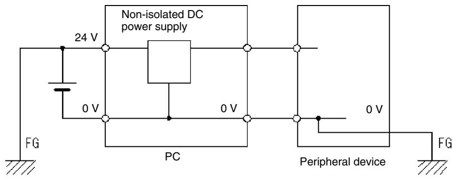
INCORRECT Grounding: Shorting the 24-V side of the Power Supply
4 Operating Environment Precautions
Caution Do not operate the control system in the following places:
- Locations subject to direct sunlight.
- Locations subject to temperatures or humidity outside the range specified in the specifications.
- Locations subject to condensation as the result of severe changes in temperature.
- Locations subject to corrosive or flammable gases.
- Locations subject to dust (especially iron dust) or salts.
- Locations subject to exposure to water, oil, or chemicals.
- Locations subject to shock or vibration.
!Caution Take appropriate and sufficient countermeasures when installing systems in the following situations:
- Locations subject to static electricity or other forms of noise.
- Locations subject to strong electromagnetic fields.
- Locations subject to possible exposure to radioactivity.
- Locations close to power supplies.
Caution The operating environment of the PC System can have a large effect on the longevity and reliability of the system. Improper operating environments can lead to malfunction, failure, and other unforeseeable problems with the PC System. Be
sure that the operating environment is within the specified conditions at installation and remains within the specified conditions during the life of the system.
5 Application Precautions
Observe the following precautions when using the PC System.
Caution
Failure to abide by the following precautions could lead to faulty operation of the PC or the system, or could damage the PC or PC Units. Always heed these precautions.
Designing Circuits or Creating Ladder Programs
- Fail-safe measures must be taken by the customer to ensure safety in the event of incorrect, missing, or abnormal signals caused by broken signal lines, momentary power interruptions, or other causes.
- Construct a control circuit so that power supply for the I/O circuits does not come ON before power supply for the Unit. If power supply for the I/O circuits comes ON before power supply for the Unit, normal operation may be temporarily interrupted.
- If the operating mode is changed from RUN or MONITOR mode to PROGRAM mode, with the IOM Hold Bit ON, the output will hold the most recent status. In such a case, ensure that the external load does not exceed specifications. (If operation is stopped because of an operating error, including errors generated by FALS instructions, the values in the internal memory of the CPU Unit will be saved, but the outputs will all turn OFF.)
- For models with only the super-capacitor installed, the contents of the READ/WRITE enable area of the DM area, HR area, AR area, and CNT data area may be damaged if the power is turned OFF for a long time. To prevent such damage, provide ladder program that will check AR 1314 to ensure proper operation of the system.
- The life of relays largely varies depending on switching conditions. Be sure to test operating conditions using actual Units and use the product within the specified number of switchings so as not to cause any performance problems. Using the product with performance problems may result in defective insulation between circuits or burning of the relays.
Installation
- Install the Units properly as specified in the relevant operation manual(s). Improper installation of the Units may result in malfunction.
- Do not install the PC or PC Units in places where the Units may be affected by excessive noise. Doing so may result in malfunction.
- Install the Units properly so that they will not fall off.
- Be sure that all the mounting screws, terminal screws, and cable connector screws are tightened to the torque specified in the relevant manuals. Incorrect tightening torque may result in malfunction.
- Install the Expansion I/O Unit connector cover to the last Expansion I/O Unit to prevent dust or foreign matter from entering inside the Unit. Not doing so may result in malfunction.
- Be sure that the terminal blocks, expansion cables, and other items with locking devices are properly locked into place. Improper locking may result in malfunction.
Wiring and Connection
- Be sure to use cables as specified in the relevant manual(s).
- Install external breakers and take other safety measures against short-circuiting in external wiring. Insufficient safety measures against short-circuiting may result in burning.
-
When wiring signal lines, do not place them in the same duct as high-voltage lines or power lines. Doing so may result in malfunction.
-
Be sure that terminal blocks and connectors are connected in the specified direction with the correct polarity. Not doing so may result in malfunction.
- Leave the labels attached CPM1 or CPM2A Units when wiring to prevent wiring cuttings from entering the Units.
- Attach the labels supplied with CPM1A or CPM2C Units or provide other protective covers when wiring to prevent dust or wiring cuttings from entering the Units.
- Remove the labels after the completion of wiring to ensure proper heat dissipation. Leaving the labels attached may result in malfunction.
- Use the connectors and wiring materials specified in the relevant manual(s).
- Be sure to wire according to the relevant manual(s). Incorrect wiring may result in burning.
I/O Connection and System Startup
- Disconnect the functional ground terminal when performing withstand voltage tests.
- Always use the power supply voltages specified in the operation manual(s). An incorrect voltage may result in malfunction or burning.
- Take appropriate measures to ensure that the specified power with the rated voltage and frequency is supplied. Be particularly careful in places where the power supply is unstable.
- Do not apply voltages to the input terminals in excess of the rated input voltage. Excess voltages may result in burning.
- Do not apply voltages or connect loads to the output terminals in excess of the maximum switching capacity. Excess voltage or loads may result in burning.
- Double-check all wiring and switch settings before turning ON the power supply. Incorrect wiring may result in burning.
- Check the user program for proper execution before actually running it on the Unit. Not checking the program may result in an unexpected operation.
Handling Precautions
- When using, storing, or transporting the product, keep within the specifications listed in the relevant manual(s).
-
Confirm that no adverse effect will occur in the system before attempting any of the following. Not doing so may result in an unexpected operation.
-
Changing the operating mode of the PC.
- Force-setting/force-resetting any bit in memory.
-
Changing the present value of any word or any set value in memory.
-
Before touching a Unit, be sure to first touch a grounded metallic object to discharge any static built-up. Not doing so may result in malfunction or damage.
- Do not touch the Expansion I/O Unit Connecting Cable while the power is being supplied to prevent any malfunction due to static electricity.
- Do not pull on the cables or bend the cables beyond their natural limit. Doing either of these may break the cables.
- Do not place objects on top of the cables. Doing so may break the cables.
- When disposing of Units or other products, be sure to do so according to local laws and regulations.
-
When using a Temperature Sensor Unit with a thermocouple input (CPM1A-TS001/002, CPM2C-TS001), observe the following precautions:
-
With the CPM1A-TS001/002, do not remove the cold junction compensator attached at the time of delivery. If the cold junction compensator is removed the Unit will not be able to measure temperatures correctly.
-
With the CPM1A-TS001/002, each of the input circuits is calibrated with the cold junction compensator attached to the Unit. If the Unit is used with the cold junction compensator from other Units, the Unit will not be able to measure temperatures correctly.
- With the CPM1A-TS001/002 or the CPM2C-TS001, do not touch the cold junction compensator. Doing so may result in incorrect temperature measurement.
Maintenance
- When replacing a part, be sure to confirm that the rating of a new part is correct. Not doing so may result in malfunction or burning.
- When the CPU Unit is replaced, resume operation only after transferring to the new CPU Unit the contents of the DM and HR Areas required for operation. Not doing so may result in an unexpected operation.
Transportation and Storage
- When transporting the Units, use special packing boxes. Do not subject the Units or other products to excessive vibration or shock during transportation and do not to drop them.
- Store the Units within the following temperature and humidity ranges:
Storage temperature: -25 to 65^
Storage humidity: 25% to 85% (with no icing or condensation)
SECTION 1
PC Setup
This section explains the PC Setup in the CPM1, CPM1A, CPM2A, CPM2C (including the CPM2C-S), and SRM1(-V2) PCs. The PC Setup can be used to control the operating parameters. To change the PC Setup, refer to the Operation Manual of the PC for Programming Console procedures.
Refer to the SSS Operation Manual: C-series PCs for SSS procedures. Refer to the SYSMAC-CPT Support Software Quick Start Guide (W332) and User Manual (W333) for SYSMAC-CPT Support Software procedures.
If you are not familiar with OMRON PCs or ladder diagram program, you can read 1-1 PC Setup as an overview of the operating parameters available for the CPM1/CPM1A, CPM2A/CPM2C, and SRM1(-V2). You may then want to read Section 5 Memory Areas, Section 6 Ladder-diagram Programming, and related instructions in Section 7 Instruction Set before completing this section.
1-1 PC Setup 2
1-1-1 Changing the PC Setup 2
1-1-2 CPM1/CPM1A PC Setup Settings 3
1-1-3 CPM2A/CPM2C PC Setup Settings 7
1-1-4 SRM1(-V2) PC Setup Settings 13
1-2 Basic PC Operation and I/O Processes 16
1-2-1 Startup Mode 16
1-2-2 Hold Bit Status 17
1-2-3 Program Memory Write-protection 17
1-2-4 RS-232C Port Servicing Time (CPM2A/CPM2C/SRM1(-V2) Only) 18
1-2-5 Peripheral Port Servicing Time 18
1-2-6 Cycle Monitor Time 18
1-2-7 Minimum Cycle Time 19
1-2-8 Input Time Constants 19
1-2-9 Error Log Settings 21
1-3 CPM2C Changes in SW2 21
1-1 PC Setup
The PC Setup comprises various operating parameters that control PC operation. In order to make the maximum use of PC functionality when using interrupt processing and communications functions, the PC Setup may be customized according to operating conditions.
At the time of shipping, the defaults are set for general operating conditions, so that the PC can be used without having to change the settings. You are, however, advised to check the default values before operation.
Default Values
The default values for the PC Setup are 0000 for all words (except for the low battery error enable in DM 6655 bits 12 to 15 for CPM2A CPU Units). The default values can be reset at any time by turning ON SR 25210 in PROGRAM mode.
Caution
When data memory (DM) is cleared from a Programming Device, the PC Setup settings will also be cleared to all zeros.
1-1-1 Changing the PC Setup
PC Setup settings are accessed at various times depending on the setting, as described below.
- DM 6600 to DM 6614: Accessed only when PC's power supply is turned ON.
- DM 6615 to DM 6644: Accessed only when program execution begins.
- DM 6645 to DM 6655: Accessed regularly when the power is ON.
Since changes in the PC Setup become effective only at the times given above, the PC will have to be restarted to make changes in DM 6600 to DM 6614 effective, and program execution will have to be restarted to make changes in DM 6615 to DM 6644 effective.
When DM 6602 bits 00 to 03 are set to protect the program memory, DM 6602 cannot be changed using the PC Setup operation of the Support Software. To change DM 6602, use the I/O Monitor or DM Edit operation.
Making Changes from a Programming Device
The PC Setup can be read, but not overwritten, from the user program. Writing can be done only by using a Programming Device.
Although the PC Setup is stored in DM 6600 to DM 6655, settings can be made and changed only from a Programming Device (e.g., SSS, or Programming Console). DM 6600 to DM 6644 can be set or changed only while in PROGRAM mode. DM 6645 to DM 6655 can be set or changed while in either PROGRAM mode or MONITOR mode. The cycle time will be rather long when the PC Setup is changed in MONITOR mode.
The following settings can be made in PROGRAM mode from the SSS using menu operations. All other settings must be made using the hexadecimal setting operation.
- Startup Mode (DM 6600)
- I/O Hold Bit Status and Forced Status Hold Bit Status (DM 6601)
- Cycle Monitor Time (DM 6618)
- Cycle Time (DM 6619)
- RS-232C Port Settings (DM 6645 to DM 6649)
Note The RS-232C Port Settings (DM 6645 to DM 6649) are not used in CPM1/CPM1A PCs because these PCs aren't equipped with an RS-232C port.
Errors in the PC Setup
If an incorrect PC Setup setting is accessed, a non-fatal error (error code 9B) will be generated, the corresponding error flag (AR 1300 to AR 1302) will be turned ON, and the default setting will be used instead of the incorrect setting.
1-1-2 CPM1/CPM1A PC Setup Settings
The PC Setup is broadly divided into four categories: 1) Settings related to basic PC operation and I/O processes, 2) Settings related to the cycle time, 3) Settings related to interrupts, and 4) Settings related to communications. This section will explain the settings according to these classifications.
The following table shows the settings for CPM1/CPM1A PCs in order. Refer to the page number in the last column for more details on that setting.
| Word(s) | Bit(s) | Function | Page |
| Startup Processing (DM 6600 to DM 6614)The following settings are effective after transfer to the PC only after the PC is restarted. | |||
| DM 6600 | 00 to 07 | Startup mode (effective when bits 08 to 15 are set to 02).00: PROGRAM; 01: MONITOR 02: RUN | 16 |
| 08 to 15 | Startup mode designation00: According to communications port setting switch and peripheral port connection(See table at the bottom of this page.)01: Continue operating mode last used before power was turned OFF.02: Setting in 00 to 07 | ||
| DM 6601 | 00 to 07 | Not used. | 17 |
| 08 to 11 | IOM Hold Bit (SR 25212) Status at Startup0: Reset; 1: Maintain (See note 3.) | ||
| 12 to 15 | Forced Status Hold Bit (SR 25211) Status at Startup0: Reset; 1: Maintain (See note 3.) | ||
| DM 6602 | 00 to 03 | Program memory write-protection0: Program memory unprotected1: Program memory write-protected (except DM 6602 itself) | 17 |
| 04 to 07 | Programming Console display language0: English; 1: Japanese | ||
| 08 to 15 | Not used. | ||
| DM 6603 | 00 to 15 | Not used. | |
| DM 6604 | 00 to 07 | 00: If data could not be saved with the built-in capacitor (AR 1314 ON), a memory error will not be generated.01: If data could not be saved with the built-in capacitor (AR 1314 ON), a memory error will be generated. | |
| 08 to 15 | Not used. | ||
| DM 6605 toDM 6614 | 00 to 15 | Not used. | |
| Cycle Time Settings (DM 6615 to DM 6619)The following settings are effective after transfer to the PC the next time operation is started. | |||
| DM 6615,DM 6616 | 00 to 15 | Not used. | |
| DM 6617 | 00 to 07 | Servicing time for peripheral port (effective when bits 08 to 15 are set to 01)00 to 99 (BCD): Percentage of cycle time used to service peripheral. | 18 |
| 08 to 15 | Peripheral port servicing setting enable00: 5% of the cycle time01: Use time in 00 to 07. | ||
| DM 6618 | 00 to 07 | Cycle monitor time (effective when bits 08 to 15 are set to 01, 02, or 03)00 to 99 (BCD): Setting (see 08 to 15) | 18 |
| 08 to 15 | Cycle monitor enable (Setting in 00 to 07 x unit; 99 s max.)00: 120 ms (setting in bits 00 to 07 disabled)01: Setting unit: 10 ms02: Setting unit: 100 ms03: Setting unit: 1 s | ||
| DM 6619 | 00 to 15 | Cycle time0000: Variable (no minimum)0001 to 9999 (BCD): Minimum time in ms | 19 |
| Interrupt Processing (DM 6620 to DM 6639)The following settings are effective after transfer to the PC the next time operation is started. | |||
| DM 6620 | 00 to 03 | Input constant for IR 00000 to IR 000020: 8 ms; 1: 1 ms; 2: 2 ms; 3: 4 ms; 4: 8 ms; 5: 16 ms; 6: 32 ms; 7: 64 ms; 8: 128 ms | 19 |
| 04 to 07 | Input constant for IR 00003 and IR 00004 (Setting same as bits 00 to 03) | ||
| 08 to 11 | Input constant for IR 00005 and IR 00006 (Setting same as bits 00 to 03) | ||
| 12 to 15 | Input constant for IR 00007 to IR 00011 (Setting same as bits 00 to 03) | ||
| DM 6621 | 00 to 07 | Input constant for IR 00100: 8 ms; 01: 1 ms; 02: 2 ms; 03: 4 ms; 04: 8 ms; 05: 16 ms; 06: 32 ms; 07: 64 ms; 08:128 ms | |
| 08 to 15 | Input constant for IR 002 (Setting same as for IR 001.) | ||
| DM 6622 | 00 to 07 | Input constant for IR 003 (Setting same as for IR 001.) | |
| 08 to 15 | Input constant for IR 004 (Setting same as for IR 001.) | ||
| DM 6623 | 00 to 07 | Input constant for IR 005 (Setting same as for IR 001.) | |
| 08 to 15 | Input constant for IR 006 (Setting same as for IR 001.) | ||
| DM 6624 | 00 to 07 | Input constant for IR 007 (Setting same as for IR 001.) | |
| 08 to 15 | Input constant for IR 008 (Setting same as for IR 001.) | ||
| DM 6625 | 00 to 07 | Input constant for IR 009 (Setting same as for IR 001.) | |
| 08 to 15 | Not used. | ||
| DM 6626 toDM 6627 | 00 to 15 | Not used. | |
| DM 6628 | 00 to 03 | Interrupt enable for IR 00003 (0: Normal input; 1: Interrupt input; 2: Quick-response) | 79 |
| 04 to 07 | Interrupt enable for IR 00004 (0: Normal input; 1: Interrupt input; 2: Quick-response) | ||
| 08 to 11 | Interrupt enable for IR 00005 (0: Normal input; 1: Interrupt input; 2: Quick-response) | ||
| 12 to 15 | Interrupt enable for IR 00006 (0: Normal input; 1: Interrupt input; 2: Quick-response) | ||
| DM 6629 toDM 6641 | 00 to 15 | Not used. | |
| High-speed Counter Settings (DM 6640 to DM 6644)The following settings are effective after transfer to the PC the next time operation is started. | |||
| DM 6640 toDM 6641 | 00 to 15 | Not used. | |
| DM 6642 | 00 to 03 | High-speed counter mode0: Up/down counter mode; 4: Incrementing counter mode | 86 |
| 04 to 07 | High-speed counter reset mode0: Z phase and software reset; 1: Software reset only | ||
| 08 to 15 | High-speed counter enable00: Don't use high-speed counter; 01: Use high-speed counter with settings in 00 to 07 | ||
| DM 6643,DM 6644 | 00 to 15 | Not used. | |
| Word(s) | Bit(s) | Function | Page | ||||
| Peripheral Port SettingsThe following settings are effective after transfer to the PC. | |||||||
| DM 6645 to DM 6649 | 00 to 15 | Not used. | 226 | ||||
| DM 6650 | 00 to 07 | Port settings00: Standard (1 start bit, 7-bit data, even parity, 2 stop bits, 9,600 bps)01: Settings in DM 6651(Other settings will cause a non-fatal error and AR 1302 will turn ON.) | |||||
| 08 to 11 | Link area for 1:1 PC Link via peripheral port:0: LR 00 to LR 15 | ||||||
| 12 to 15 | Communications mode0: Host Link; 2: 1:1 PC Link Slave; 3: 1:1 PC Link Master; 4: 1:1 NT Link(Other settings will cause a non-fatal error and AR 1302 will turn ON.) | ||||||
| DM 6651 | 00 to 07 | Baud rate00: 1.2K, 01: 2.4K, 02: 4.8K, 03: 9.6K, 04: 19.2K, 05 to 07: Cannot be used (see note 2)(Other settings will cause a non-fatal error and AR 1302 will turn ON.) | |||||
| 08 to 15 | Frame formatStart Length Stop Parity00: 1 bit 7 bits 1 bit Even01: 1 bit 7 bits 1 bit Odd02: 1 bit 7 bits 1 bit None03: 1 bit 7 bits 2 bits Even04: 1 bit 7 bits 2 bits Odd05: 1 bit 7 bits 2 bits None06: 1 bit 8 bits 1 bit Even07: 1 bit 8 bits 1 bit Odd08: 1 bit 8 bits 1 bit None09: 1 bit 8 bits 2 bits Even10: 1 bit 8 bits 2 bits Odd11: 1 bit 8 bits 2 bits None(Other settings will cause a non-fatal error and AR 1302 will turn ON.) | ||||||
| DM 6652 | 00 to 15 | Transmission delay (Host Link) (See note 4.)0000 to 9999: In ms.(Other settings will cause a non-fatal error and AR 1302 will turn ON.) | |||||
| DM 6653 | 00 to 07 | Node number (Host Link)00 to 31 (BCD)(Other settings will cause a non-fatal error and AR 1302 will turn ON.) | |||||
| 08 to 15 | Not used. | ||||||
| DM 6654 | 00 to 15 | Not used. | |||||
| Error Log Settings (DM 6655)The following settings are effective after transfer to the PC. | |||||||
| DM 6655 | 00 to 03 | Style0: Shift after 7 records have been stored1: Store only first 7 records (no shifting)2 to F: Do not store records | 21 | ||||
| 04 to 07 | Not used. | ||||||
| 08 to 11 | Cycle time monitor enable0: Detect long cycles as non-fatal errors1: Do not detect long cycles | ||||||
| 12 to 15 | Not used. | ||||||
Note 1. When the startup mode is set to continue the operating mode last used before the power was turned off, that operating mode will be retained by the built-in capacitor. If the power remains off for longer than the backup time of the capacitor, the data may be lost. (For details on the holding time, refer to the CPM1A or CPM1 Operation Manual.)
3. Retention of IOM Hold Bit (SR 25212) Status
- Do not set to "05" to "07." If set to this value, the CPM1/CPM1A will not operate properly and the RUN PC Setup Error Flag (AR 1302 ON) will not turn ON.
If the "IOM Hold Bit Status at Startup" (DM 6601, bits 08 to 11) is set to "Maintain" with the IOM Hold Bit (SR 25212) turned ON, operation can be started with the I/O memory (I/O, IR, LR) status just as it was before the power was turned OFF. (The input area is refreshed at startup, however, so it is overwritten by the most recently updated input status.)
Retention of Forced Status Hold Bit (SR 25211) Status
If the "Forced Status Hold Bit Status at Startup" (DM 6601, bits 12 to 15) is set to "Maintain" with the Forced Status Hold Bit (SR 25211) turned ON, operation can be started with the forced set/reset status just as it was before the power was turned OFF. (When starting up in RUN Mode, however, the forced set/reset status is cleared.)
Even if the "IOM Hold Bit Status at Startup" or "Forced Status Hold Bit Status at Startup" is set to "Maintain," the IOM Hold Bit (SR 25212) or Forced Status Hold Bit (SR 25211) status may be cleared if the power remains OFF for longer than the backup time of the built-in capacitor. (For details on the holding time, refer to the CPM1A or CPM1 Operation Manual.) At this time the I/O memory will also be cleared, so set up the system so that clearing the I/O memory will not cause problems.
- The transmission delay is the delay between the previous transmission and the next transmission.
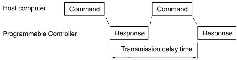
- If an out-of-range value is set, the following communications conditions will result. In that case, reset the value so that it is within the permissible range.
Communications mode: Host Link
Communications format: Standard settings (1 start bit, 7-bit data; even parity, 2 stop bits, 9,600 bps)
Transmission delay: No
Node number: 00
1-1-3 CPM2A/CPM2C PC Setup Settings
The PC Setup is broadly divided into four categories: 1) Settings related to basic PC operation and I/O processes, 2) Settings related to pulse output functions, 3) Settings related to interrupts, and 4) Settings related to communications. This section will explain the settings according to these classifications.
The following table shows the setting in order in the DM area. For details, refer to the page numbers shown.
| Word(s) | Bit(s) | Function | Page |
| Startup Processing (DM 6600 to DM 6614) The following settings are effective after transfer to the PC only after the PC is restarted. | |||
| DM 6600 | 00 to 07 | Startup mode (effective when bits 08 to 15 are set to 02). 00: PROGRAM; 01: MONITOR; 02: RUN | 16 |
| 08 to 15 | Startup mode designation 00: Mode set on Programming Console switch if Programming Console is connected. No Programming Device connected: RUN Mode Programming Console connected: Mode set on mode switch on Programming Console Other Programming Device connected: PROGRAM Mode 01: Continue operating mode last used before power was turned OFF. 02: Setting in 00 to 07 The setting of the switch SW2 will affect the operating mode for all CPM2C CPU Units produced before 1 September 2000. Refer to 1-3 Changes in SW2 for details. | ||
| DM 6601 | 00 to 07 | Not used. | 17 |
| 08 to 11 | IOM Hold Bit (SR 25212) Status at Startup 0: Reset to 0; 1: Maintain previous status | ||
| 12 to 15 | Forced Status Hold Bit (SR 25211) Status at Startup 0: Reset to 0; 1: Maintain previous status | ||
| DM 6602 | 00 to 03 | Program memory write-protection 0: Program memory unprotected 1: Program memory write-protected (except DM 6602 itself) | 17 |
| 04 to 07 | Programming Console display language 0: English; 1: Japanese | ||
| 08 to 11 | Expansion instruction function code assignments 0: Default settings 1: User assignments | 161 | |
| 12 to 15 | Not used. | ||
| DM 6603 | 00 to 15 | Not used. | |
| DM 6604 | 00 to 07 | 00: A memory error will not be generated if data could not be retained by the battery. 01: A memory error will be generated if data could not be retained by the battery. | |
| 08 to 15 | Not used. | ||
| DM 6605 to DM 6614 | 00 to 15 | Not used. | |
Note For CPM2C PCs with lot number of 31800 or earlier, the startup operating mode will be as shown in the following table if bits 08 to 15 of DM 6600 are set to 00.
| Peripheral port connected to | Communications port setting switch | |
| SW2 OFF | SW2 ON | |
| Nothing | PROGRAM | RUN |
| Programming Console | Mode set on Programming Console mode switch | PROGRAM (The CPM2C will not be able to communicate with Programming Console.) |
| Other Programming Device | PROGRAM (The CPM2C will not be able to communicate with Programming Device.) | PROGRAM |
| Word(s) | Bit(s) | Function | Page |
| Cycle Time Settings (DM 6615 to DM 6619)The following settings are effective after transfer to the PC the next time operation is started. | |||
| DM 6615 | 00 to 15 | Not used. | |
| DM 6616 | 00 to 07 | Servicing time for RS-232C port (Effective when bits 08 to 15 are set to 01.)00 to 99 (BCD): Percentage of cycle time used to service RS-232C port. | 18 |
| 08 to 15 | RS-232C port servicing setting enable00: 5% of the cycle time01: Use time in bits 00 to 07. | ||
| DM 6617 | 00 to 07 | Servicing time for peripheral port (Effective when bits 08 to 15 are set to 01.)00 to 99 (BCD): Percentage of cycle time used to service peripheral. | 18 |
| 08 to 15 | Peripheral port servicing setting enable00: 5% of the cycle time01: Use time in bits 00 to 07. | ||
| DM 6618 | 00 to 07 | Cycle monitor time (Effective when bits 08 to 15 are set to 01, 02, or 03.)00 to 99 (BCD): Setting (See bits 08 to 15, below.)A fatal error will be generated and PC operation will stop if the cycle time exceeds thecycle monitor time set here. | 18 |
| 08 to 15 | Cycle monitor enable (Setting in 00 to 07 × units; 99 s max.)00: 120 ms (setting in bits 00 to 07 disabled)01: Setting units: 10 ms02: Setting units: 100 ms03: Setting units: 1 s | ||
| DM 6619 | 00 to 15 | Minimum cycle time0000: Variable (no minimum)0001 to 9999 (BCD): Minimum time in ms | 19 |
| Interrupt Processing (DM 6620 to DM 6639)The following settings are effective after transfer to the PC the next time operation is started. | |||
| DM 6620 | 00 to 03 | Input time constant for IR 00000 to IR 000020: 10 ms; 1: 1 ms; 2: 2 ms; 3: 3 ms; 4: 5 ms; 5: 10 ms; 6: 20 ms; 7: 40 ms; 8: 80 ms | 19 |
| 04 to 07 | Input time constant for IR 00003 and IR 00004 (Setting same as bits 00 to 03) | ||
| 08 to 11 | Input time constant for IR 00005 and IR 00006 (Setting same as bits 00 to 03) | ||
| 12 to 15 | Input time constant for IR 00007 to IR 00011 (Setting same as bits 00 to 03) | ||
| DM 6621 | 00 to 07 | Input time constant for IR 00100: 10 ms01: 1 ms02: 2 ms03: 3 ms04: 5 ms05: 10 ms06: 20 ms07: 40 ms08: 80 ms | |
| 08 to 15 | Input constant for IR 002 (Setting same as for IR 001.) | ||
| DM 6622 | 00 to 07 | Input constant for IR 003 (Setting same as for IR 001.) | |
| 08 to 15 | Input constant for IR 004 (Setting same as for IR 001.) | ||
| DM 6623 | 00 to 07 | Input constant for IR 005 (Setting same as for IR 001.) | |
| 08 to 15 | Input constant for IR 006 (Setting same as for IR 001.) | ||
| DM 6624 | 00 to 07 | Input constant for IR 007 (Setting same as for IR 001.) | |
| 08 to 15 | Input constant for IR 008 (Setting same as for IR 001.) | ||
| DM 6625 | 00 to 07 | Input constant for IR 009 (Setting same as for IR 001.) | |
| 08 to 15 | Not used. | ||
| DM 6626 toDM 6627 | 00 to 15 | Not used. | |
| DM6628 | 00 to 03 | Interrupt enable for IR 00003 (0: Normal input; 1: Interrupt input; 2: Quick-response) | 30 |
| 04 to 07 | Interrupt enable for IR 00004 (0: Normal input; 1: Interrupt input; 2: Quick-response) | ||
| 08 to 11 | Interrupt enable for IR 00005 (0: Normal input; 1: Interrupt input; 2: Quick-response)(Set to 0 in CPM2C CPU Units with 10 I/O points.) | ||
| 12 to 15 | Interrupt enable for IR 00006 (0: Normal input; 1: Interrupt input; 2: Quick-response)(This input does not exist in CPM2C CPU Units with 10 I/O points.) | ||
| DM 6629 | 00 to 03 | PV coordinate system for pulse output 0 0: Relative coordinates; 1: Absolute coordinates | 101 |
| 04 to 07 | PV coordinate system for pulse output 1 0: Relative coordinates; 1: Absolute coordinates | ||
| 08 to 15 | Not used. | ||
| DM 6630 to DM 6641 | 00 to 15 | Not used. | |
| High-speed Counter Settings (DM 6640 to DM 6644) The following settings are effective after transfer to the PC the next time operation is started. | |||
| DM 6640 to DM 6641 | 00 to 15 | Not used. | |
| DM 6642 | 00 to 03 | High-speed counter mode 0: Differential phase mode (5 kHz) 1: Pulse + direction input mode (20 kHz) 2: Up/down input mode (20 kHz) 4: Increment mode (20 kHz) | 47, 56 |
| 04 to 07 | High-speed counter reset mode 0: Z phase and software reset; 1: Software reset only | ||
| 08 to 15 | High-speed counter/Synchronized pulse control for IR 00000 to IR 00002 00: Don't use either function. 01: Use as high-speed counters. 02: Use for synchronized pulse control (10 to 500 Hz). 03: Use for synchronized pulse control (20 Hz to 1 kHz). 04: Use for synchronized pulse control (300 Hz to 20 kHz). | ||
| DM 6643, DM 6644 | 00 to 15 | Not used. | |
| RS-232C Port Communications Settings The following settings are effective after transfer to the PC. If the CPM2A CPU Unit's Communications Switch is ON, communications through the CPM2A's RS-232C port are gov- erned by the default settings (all 0) regardless of the settings in DM 6645 through DM 6649. If pin 2 of the CPM2C CPU Unit's DIP switch is ON, communications through the CPM2C's RS-232C port are governed by the default settings (all 0) regardless of the settings in DM 6645 through DM 6649. | |||
| DM 6645 | 00 to 03 | Port settings 0: Standard (1 start bit, 7 data bits, even parity, 2 stop bits, 9,600 bps), Host Link unit number: 0 1: Settings in DM 6646 (Any other setting will cause a non-fatal error and AR 1302 will turn ON.) | 226 |
| 04 to 07 | CTS control setting 0: Disable CTS control; 1: Enable CTS control (Any other setting will cause a non-fatal error and AR 1302 will turn ON.) | ||
| 08 to 11 | Link words for 1:1 data link 0: LR 00 to LR 15 (Any other settings are ineffective.) | ||
| 12 to 15 | Communications mode 0: Host Link; 1: No-protocol; 2: 1:1 PC Link Slave; 3: 1:1 PC Link Master; 4: NT Link (Any other setting causes a non-fatal error and turns ON AR 1302.) | ||
| Word(s) | Bit(s) | Function | Page | |||
| DM 6646 | 00 to 07 | Baud rate00: 1,200 bps; 01: 2,400 bps; 02: 4,800 bps; 03: 9,600 bps; 04: 19,200 bps | 226 | |||
| 08 to 15 | Frame formatStart bits Data bits Stop bits Parity00: 1 bit 7 bits 1 bit Even01: 1 bit 7 bits 1 bit Odd02: 1 bit 7 bits 1 bit None03: 1 bit 7 bits 2 bits Even04: 1 bit 7 bits 2 bits Odd05: 1 bit 7 bits 2 bits None06: 1 bit 8 bits 1 bit Even07: 1 bit 8 bits 1 bit Odd08: 1 bit 8 bits 1 bit None09: 1 bit 8 bits 2 bits Even10: 1 bit 8 bits 2 bits Odd11: 1 bit 8 bits 2 bits None(Any other setting specifies standard settings (1 start bit, 7 data bits; even parity, 2 stop bits, 9,600 bps), causes a non-fatal error, and turns ON AR 1302.) | |||||
| DM 6647 | 00 to 15 | Transmission delay (0000 to 9999 BCD sets a delay of 0 to 99,990 ms.)(Any other setting specifies a delay of 0 ms, causes a non-fatal error, and turns ON AR 1302.) | 226 | |||
| DM 6648 | 00 to 07 | Node number (Host Link)00 to 31 (BCD)(Any other setting specifies a node number of 00, causes a non-fatal error, and turns ON AR 1302.) | 226 | |||
| 08 to 11 | Start code selection for no-protocol communications0: Enables start code; 1: Enables start code in DM 6649(Any other setting disables the start code, causes a non-fatal error, and turns ON AR 1302.) | |||||
| 12 to 15 | End code selection for no-protocol communications0: Enables end code; 1: Enables end code in DM 6649; 2: Sets end code of CR, LF.(Any other setting disables the end code, causes a non-fatal error, and turns ON AR 1302.) | |||||
| DM 6649 | 00 to 07 | Start code (00 to FF)(This setting is valid only when bits 8 to 11 of DM 6648 are set to 1.) | 226 | |||
| 08 to 15 | When bits 12 to 15 of DM 6648 set to 0:Sets the number of bytes to receive. (00: 256 bytes; 01 to FF: 1 to 255 bytes)When bits 12 to 15 of DM 6648 set to 1:Sets the end code. (00 to FF) | |||||
| Peripheral Port Communications SettingsThe following settings are effective after transfer to the PC.If the CPM2A CPU Unit's Communications Switch is ON, communications through the peripheral port are governed by the default settings (all 0) regardless of the settings in DM 6650 through DM 6654.The CPM2A's Communications Switch setting has no effect on communications with a Programming Console connected to the peripheral port or Support Software set for peripheral bus communications. The CPM2A CPU Unit will auto-detect either Programming Device and automatically establish communications.SW2 on the CPM2C CPU Unit must be OFF in order for communications through the CPM2C's peripheral port to be gov- erned by the settings in DM 6650 through DM 6654. | ||||||
| DM 6650 | 00 to 03 | Port settings00: Standard (1 start bit, 7 data bits, even parity, 2 stop bits, 9,600 bps), Host Link unit number: 001: Settings in DM 6651(Any other setting specifies standard settings, causes a non-fatal error, and turns ON AR 1302.) | 226 | |||
| 04 to 11 | Not used. | |||||
| 12 to 15 | Communications mode0: Host Link or peripheral bus; 1: No-protocol(Any other setting specifies Host Link, causes a non-fatal error, and turns ON AR 1302.) | |||||
| DM 6651 | 00 to 07 | Baud rate00: 1,200 bps; 01: 2,400 bps; 02: 4,800 bps; 03: 9,600 bps; 04: 19,200 bps | ||||
| 08 to 15 | Frame formatStart bitsData bitsStop bitsParity00: 1 bit7 bits1 bitEven01: 1 bit7 bits1 bitOdd02: 1 bit7 bits1 bitNone03: 1 bit7 bits2 bitsEven04: 1 bit7 bits2 bitsOdd05: 1 bit7 bits2 bitsNone06: 1 bit8 bits1 bitEven07: 1 bit8 bits1 bitOdd08: 1 bit8 bits1 bitNone09: 1 bit8 bits2 bitsEven10: 1 bit8 bits2 bitsOdd11: 1 bit8 bits2 bitsNone(Any other setting specifies standard settings (1 start bit, 7 data bits; even parity, 2 stop bits, 9,600 bps), causes a non-fatal error, and turns ON AR 1302.) | |||||
| DM 6652 | 00 to 15 | Transmission delay (0000 to 9999 BCD sets a delay of 0 to 99,990 ms.)(Any other setting specifies a delay of 0 ms, causes a non-fatal error, and turns ON AR 1302.) | 226 | |||
| DM 6653 | 00 to 07 | Node number (Host Link)00 to 31 (BCD)(Any other setting specifies a node number of 00, causes a non-fatal error, and turns ON AR 1302.) | ||||
| 08 to 11 | Start code selection for no-protocol communications0: Disables start code; 1: Enables start code in DM 6649(Any other setting disables the start code, causes a non-fatal error, and turns ON AR 1302.) | |||||
| 12 to 15 | End code selection for no-protocol communications0: Disables end code; 1: Enables end code in DM 6649; 2: Sets end code of CR, LF.(Any other setting disables the end code, causes a non-fatal error, and turns ON AR 1302.) | |||||
| Word(s) | Bit(s) | Function | Page |
| DM 6654 | 00 to 07 | Start code (00 to FF)(This setting is valid only when bits 8 to 11 of DM 6648 are set to 1.) | 226 |
| 08 to 15 | When bits 12 to 15 of DM 6648 set to 0:Sets the number of bytes to receive. (00: 256 bytes; 01 to FF: 1 to 255 bytes)When bits 12 to 15 of DM 6648 set to 1:Set the end code. (00 to FF) | ||
| Error Log Settings (DM 6655)The following settings are effective after transfer to the PC. | |||
| DM 6655 | 00 to 03 | Style0: Shift after 7 records have been stored1: Store only first 7 records (no shifting)2 to F: Do not store records | 21 |
| 04 to 07 | Not used. | ||
| 08 to 11 | Cycle time monitor enable0: Generate a non-fatal error for a cycle time that is too long.1: Do not generate a non-fatal error. | ||
| 12 to 15 | Low battery error enable0: Generate a non-fatal error for low battery voltage.1: Do not generate a non-fatal error.Low battery error detection is disabled (i.e., set to 1) by default in CPU Units that do not have a clock. If the PC Setup is cleared, the setting will changed to 0 and a low battery error will occur.Bits 12 to 15 should always be set to 0 when the optional CPM2C-BAT01 is mounted. | ||
1-1-4 SRM1(-V2) PC Setup Settings
The PC Setup is broadly divided into three categories: 1) Settings related to basic PC operation and I/O processes, 2) Settings related to the cycle time, and 3) Settings related to communications. This section will explain the settings according to these classifications.
The following table shows the settings for SRM1(-V2) PCs in order. Refer to the page number in the last column for more details on that setting.
| Word(s) | Bit(s) | Function | Page |
| Startup Processing (DM 6600 to DM 6614)The following settings are effective after transfer to the PC only after the PC is restarted. | |||
| DM 6600 | 00 to 07 | Startup mode (effective when bits 08 to 15 are set to 02).00: PROGRAM; 01: MONITOR 02: RUN | 16 |
| 08 to 15 | Startup mode designation00: Programming Console switch01: Continue operating mode last used before power was turned off02: Setting in 00 to 07 | ||
| DM 6601 | 00 to 07 | Not used. | 17 |
| 08 to 11 | IOM Hold Bit (SR 25212) Status0: Reset; 1: Maintain (See caution on page 17.) | ||
| 12 to 15 | Forced Status Hold Bit (SR 25211) Status0: Reset; 1: Maintain | ||
| DM 6602 | 00 to 03 | Program memory write-protection0: Program memory unprotected1: Program memory write-protected (except DM 6602 itself) | 17 |
| 04 to 07 | Programming Console display language0: English; 1: Japanese | ||
| 08 to 11 | Expansion Instructions0: Default settings; 1: User settings | ||
| 12 to 15 | Not used. | ||
| DM 6603 | 00 to 03 | Maximum number of CompoBus/S devices0: Max. no. 321: Max. no. 16 | |
| 04 to 07 | CompoBus/S communications mode setting (V2 only)0: High-speed communications1: Long-distance communications | ||
| 08 to 15 | Not used. | ||
| DM 6604 | 00 to 07 | 00: If data could not be saved for a power interruption (AR 1314 ON), a memory error will not be generated.01: If data could not be saved for a power interruption (AR 1314 ON), a memory error will be generated. | |
| 08 to 15 | Not used. | ||
| DM 6605 toDM 6614 | 00 to 15 | Not used. | |
| Cycle Time Settings (DM 6615 to DM 6619)The following settings are effective after transfer to the PC the next time operation is started. | |||
| DM 6615 | 00 to 15 | Not used. | |
| DM 6616 | 00 to 07 | Servicing time for RS-232C port (effective when bits 08 to 15 are set)00 to 99 (BCD): Percentage for cycle time used to service peripheral. | 18 |
| 08 to 15 | RS-232C port servicing enable00: 5% of the cycle time01: Use time in 00 to 07. | ||
| DM 6617 | 00 to 07 | Servicing time for peripheral port (effective when bits 08 to 15 are set to 01)00 to 99 (BCD): Percentage of cycle time used to service peripheral. | 18 |
| 08 to 15 | Peripheral port servicing setting enable00: 5% of the cycle time01: Use time in 00 to 07. | ||
| DM 6618 | 00 to 07 | Cycle monitor time (effective when bits 08 to 15 are set to 01, 02, or 03)00 to 99 (BCD): Setting (see 08 to 15) | 18 |
| 08 to 15 | Cycle monitor enable (Setting in 00 to 07 x unit; 99 s max.)00: 120 ms (setting in bits 00 to 07 disabled)01: Setting unit: 10 ms02: Setting unit: 100 ms03: Setting unit: 1 s | ||
| DM 6619 | 00 to 15 | Cycle time0000: Variable (no minimum)0001 to 9999 (BCD): Minimum time in ms | 19 |
| DM 6620 toDM 6644 | 00 to 15 | Not used. | |
| RS-232C Port SettingsThe following settings are effective after transfer to the PC. | |||
| DM 6645 | 00 to 03 | Port settings0: Standard (1 start bit, 7-bit data, even parity, 2 stop bits, 9,600 bps)1: Settings in DM 6646 | 268 |
| 04 to 07 | CTS control settings0: Disable; 1: Set | ||
| 08 to 11 | When using a 1:1 data link: Sets the link area for 1:1 PC Link.0: LR 00 to LR 15Not 0: DisableWhen using a 1:N NT Link: Sets the maximum PT node number.1 to 7 | ||
| 12 to 15 | Communications mode0: Host Link; 1: No-protocol; 2: 1:1 PC Link Slave; 3: 1:1 PC Link Master; 4: 1:1 NTLink; 5: 1:N NT Link(Any other setting specifies Host Link mode, causes a non-fatal error, and turns ONAR 1302.)The 1:N NT Link is supported by SRM1-C02-V2 only. | ||
| DM 6646 | 00 to 07 | Baud rate00: 1.2K, 01: 2.4K, 02: 4.8K, 03: 9.6K, 04: 19.2K | |
| 08 to 15 | Frame formatStart Length Stop Parity00: 1 bit7 bits1 bitEven01: 1 bit7 bits1 bitOdd02: 1 bit7 bits1 bitNone03: 1 bit7 bits2 bitsEven04: 1 bit7 bits2 bitsOdd05: 1 bit7 bits2 bitsNone06: 1 bit8 bits1 bitEven07: 1 bit8 bits1 bitOdd08: 1 bit8 bits1 bitNone09: 1 bit8 bits2 bitsEven10: 1 bit8 bits2 bitsOdd11: 1 bit8 bits2 bitsNoneOther: 1 bit7 bits2 bitsEvenAR 1302 will turn ON to indicate a non-fatal system setting error if any value not be-tween 00 and 11 is set. | ||
| DM 6647 | 00 to 15 | Transmission delay (Host Link)0000 to 9999 (BCD): Set in units of 10 ms, e.g., setting of 0001 equals 10 ms | |
| DM 6648 | 00 to 07 | Node number (Host Link, effective when bits 12 to 15 of DM 6645 are set to 0.)00 to 31 (BCD) | |
| 08 to 11 | Start code enable (RS-232C, effective when bits 12 to 15 of DM 6645 are set to 1.)0: Disable; 1: Set | ||
| 12 to 15 | End code enable (RS-232C, effective when bits 12 to 15 of DM 6645 are set to 1.)0: Disable (number of bytes received)1: Set (specified end code)2: CR, LF | ||
| Word(s) | Bit(s) | Function | Page | ||||
| DM 6649 | 00 to 07 | Start code (RS-232C)00 to FF (binary) | 268 | ||||
| 08 to 15 | When bits 12 to 15 of DM 6648 are set to 0:Number of bytes received00: Default setting (256 bytes)01 to FF: 1 to 255 bytesWhen bits 12 to 15 of DM 6648 are set to 1:End code (RS-232C)00 to FF (binary) | ||||||
| Peripheral Port SettingsThe following settings are effective after transfer to the PC. | |||||||
| DM 6650 | 00 to 03 | Port settings00: Standard (1 start bit, 7-bit data, even parity, 2 stop bits, 9,600 bps)01: Settings in DM 6651(Other settings will cause a non-fatal error and AR 1302 will turn ON.) | 268 | ||||
| 04 to 07 | Not used. | ||||||
| 08 to 11 | Not used. | ||||||
| 12 to 15 | Communications mode0: Host Link; 1: No-protocol(Other settings will cause a non-fatal error and AR 1302 will turn ON.) | ||||||
| DM 6651 | 00 to 07 | Baud rate00: 1.2K, 01: 2.4K, 02: 4.8K, 03: 9.6K, 04: 19.2K | |||||
| 08 to 15 | Frame formatStartLengthStopParity00: 1 bit7 bits1 bitEven01: 1 bit7 bits1 bitOdd02: 1 bit7 bits1 bitNone03: 1 bit7 bits2 bitsEven04: 1 bit7 bits2 bitsOdd05: 1 bit7 bits2 bitsNone06: 1 bit8 bits1 bitEven07: 1 bit8 bits1 bitOdd08: 1 bit8 bits1 bitNone09: 1 bit8 bits2 bitsEven10: 1 bit8 bits2 bitsOdd11: 1 bit8 bits2 bitsNoneOther: 1 bit7 bits2 bitsEvenAR 1302 will turn ON to indicate a non-fatal system setting error if any value not be-tween 00 and 11 is set. | ||||||
| DM 6652 | 00 to 15 | Transmission delay (Host Link)0000 to 9999 (BCD): Set in units of 10 ms.(Other settings will cause a non-fatal error and AR 1302 will turn ON.) | 268 | ||||
| DM 6653 | 00 to 07 | Node number (Host Link)00 to 31 (BCD)(Other settings will cause a non-fatal error and AR 1302 will turn ON.) | |||||
| 08 to 11 | Start code enable (RS-232C, effective when bits 12 to 15 of DM6650 are set to 1.)0: Disable (number of bytes received)1: Set (specified end code)2: CR, LF | ||||||
| 12 to 15 | End code enable (RS-232C, effective when bits 12 to 15 of DM6650 are set to 1.)0: Disable (number of bytes received)1: Set (specified end code)2: CR, LF | ||||||
| Word(s) | Bit(s) | Function | Page |
| DM 6654 | 00 to 07 | Start code (effective when bits 08 to 11 of DM6650 are set to 1.)00: 256 bytes01 to FF: 1 to 255 bytes | 268 |
| 08 to 15 | End codeWhen bits 12 to 15 of DM6653 are set to 0:00: 256 bytes01 to FF: 1 to 255 bytesWhen bits 12 to 15 of DM6653 are set to 1:Setting: 00 to FF (binary) | ||
| Error Log Settings (DM 6655)The following settings are effective after transfer to the PC. | |||
| DM 6655 | 00 to 03 | Style0: Shift after 7 records have been stored1: Store only first 7 recordsErrors will not be stored if other values are set. | 21 |
| 04 to 07 | Not used. | ||
| 08 to 11 | Cycle time monitor enable0: Detect long cycles as non-fatal errors1: Do not detect long cycles | ||
| 12 to 15 | Low battery error enable0: Generate a non-fatal error for low battery voltage.1: Do not generate a non-fatal error. | ||
Note If an out-of-range value is set, the following communications conditions will result. In that case, reset the value so that it is within the permissible range.
Communications mode: Host Link
Communications format: Standard settings
(1 start bit, 7-bit data; even parity, 2 stop bits, 9,600 bps)
Transmission delay: No
Node number: 00
1-2 Basic PC Operation and I/O Processes
This section explains the PC Setup settings related to basic operation and I/O processes.
1-2-1 Startup Mode
The operation mode the PC will start in when power is turned on can be set as shown below.
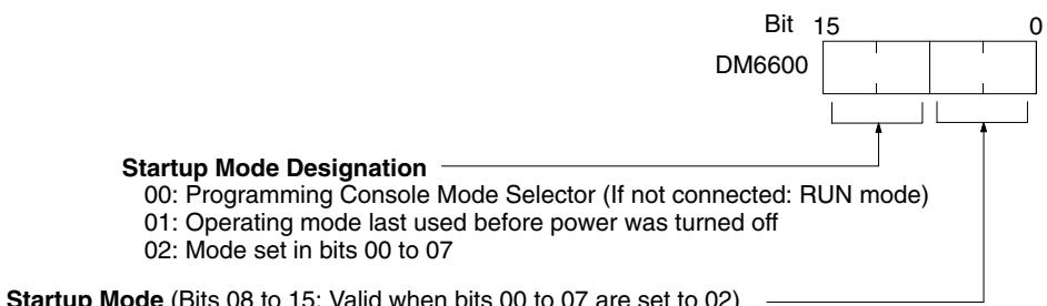
Startup Mode (Bits 08 to 15: Valid when bits 00 to 07 are set to 02)
00: PROGRAM mode
01: MONITOR mode
02:RUNmode
Default: Programming Console Mode Selector or RUN mode when Programming Console is not connected.
Note When the "startup mode designation" is set to 00 and pin 2 of the CPM2C CPU Unit's DIP switch is ON, the CPM2C will enter RUN mode automatically, regardless of the Programming Console's mode switch setting.
1-2-2 Hold Bit Status
Make the settings shown below to determine whether, when the power supply is turned on, the Forced Status Hold Bit (SR 25211) and/or IOM Hold Bit (SR 25212) will retain the status that was in effect when the power was last turned off, or whether the previous status will be cleared.
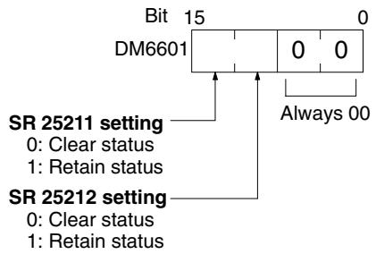
Default: Clear both.
The Forced Status Hold Bit (SR 25211) determines whether or not the forced set/reset status is retained when changing from PROGRAM mode to MONITOR mode.
The IOM Hold Bit (SR 25212) determines whether or not the status of IR bits and LR bits is retained when PC operation is started and stopped.
Caution
In PCs with capacitor backup, do not use the I/O Hold Bit Status and Forced Status Hold Bit Status Bits (DM 6601) when the power to the PC is going to be turned off longer than the memory backup time of the internal capacitor. If the memory backup time is exceeded, memory status will be unstable even if the I/O Hold Bit Status and Forced Status Hold Bit Status Bits are used. Unpredictable results may occur if operation is attempted with unstable memory status.
Note 1. The memory backup time of the internal capacitor varies with the ambient temperature, but is 20 days at 25^ . Refer to hardware specifications for more details.
- The memory backup time assumes that the internal capacitor is fully charged before power is turned off. Fulling charging the capacitor requires that power is supplied to the CPU Unit for at least 15 minutes.
1-2-3 Program Memory Write-protection
In CPM1, CPM1A, CPM2A, and CPM2C PCs, the program memory can be protected by setting bits 00 to 03 of DM 6602 to 1. Bits 04 to 07 determine whether Programming Console messages are displayed in English or Japanese.
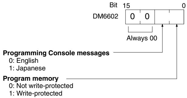
Default: English displays, not write-protected
Note DM 6602 itself can still be changed after the program memory has been write-protected by setting bits 04 to 07 of DM 6602 to 1.
1-2-4 RS-232C Port Servicing Time (CPM2A/CPM2C/SRM1(-V2) Only)
The following settings are used to determine the percentage of the cycle time devoted to servicing the RS-232C port.
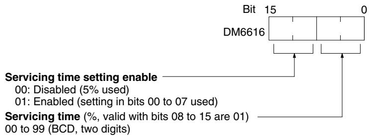
Default: 5% of cycle time
Example: If DM 6616 is set to 0110, the RS-232C port will be serviced for 10% of the cycle time.
The servicing time will be 0.34 ms minimum.
The entire servicing time will not be used unless processing requests exist.
1-2-5 Peripheral Port Servicing Time
The following settings are used to determine the percentage of the cycle time devoted to servicing the peripheral port.
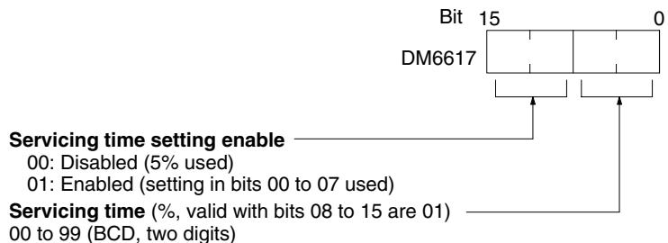
Default: 5% of cycle time
Example: If DM 6617 is set to 0115, the peripheral port will be serviced for 15% of the cycle time.
The servicing time will be 0.34 ms minimum.
The entire servicing time will not be used unless processing requests exist.
1-2-6 Cycle Monitor Time
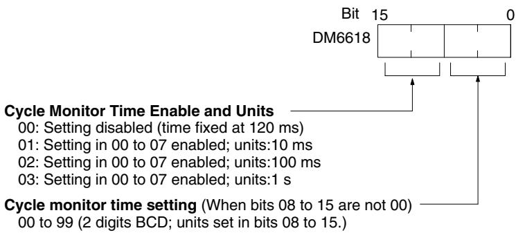
Default: 120 ms.
The cycle monitor time is used for checking for extremely long cycle times, as can happen when the program goes into an infinite loop. If the cycle time exceeds the cycle monitor setting, a fatal error (FALS 9F) will be generated.
Note
- The units used for the maximum and current cycle times recorded in the AR area (AR 14 and AR 15) are determined by the setting for the cycle monitor time in DM 6618, as shown below.
Bits 08 to 15 set to 01: 0.1 ms
Bits 08 to 15 set to 02: 1 ms
Bits 08 to 15 set to 03: 10 ms
- If the cycle time is 1 s or longer, the cycle time read from Programming Devices will be 999.9 ms. The correct maximum and current cycle times will be recorded in the AR area.
Example
If 0230 is set in DM 6618, an FALS 9F error will not occur until the cycle time exceeds 3 s. If the actual cycle time is 2.59 s, the current cycle time stored in the AR area will be 2590 (ms), but the cycle time read from a Programming Device will be 999.9 ms.
A "cycle time over" error (non-fatal) will be generated when the cycle time exceeds 100 ms unless detection of long cycle times is disable using the setting in DM 6655.
1-2-7 Minimum Cycle Time
Make the settings shown below to standardize the cycle time and to eliminate variations in I/O response time by setting a minimum cycle time.
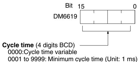
Default: Cycle time variable
If the actual cycle time is shorter than the minimum cycle time, execution will wait until the minimum time has expired. If the actual cycle time is longer than the minimum cycle time, then operation will proceed according to the actual cycle time. AR 2405 will turn ON if the minimum cycle time is exceeded.
1-2-8 Input Time Constants
Make the settings shown below to set the time from when the actual inputs from the DC Input Unit are turned ON or OFF until the corresponding input bits are updated (i.e., until their ON/OFF status is changed). Make these settings when you want to adjust the time until inputs stabilize.
Increasing the input time constant can reduce the effects from chattering and external noise.
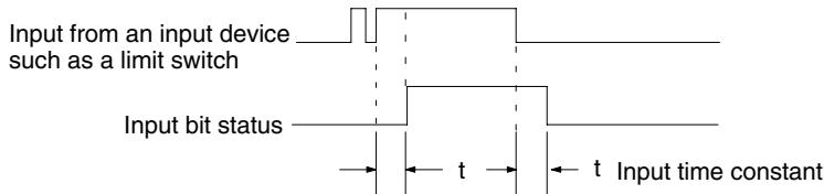
The SRM1(-V2) does not have this setting.
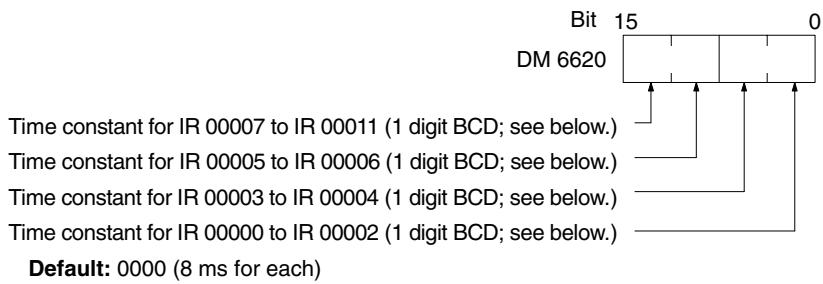
CPM1/CPM1A PCs
Set the input time constants for CPM1/CPM1A inputs from a Programming Device.
Input Time Constants for IR 000
Input Time Constants for IR 001 to IR 009
DM 6621: IR 001 and IR 002
DM 6622: IR 003 and IR 004
DM 6623: IR 005 and IR 006
DM 6624: IR 007 and IR 008
DM 6625:IR009
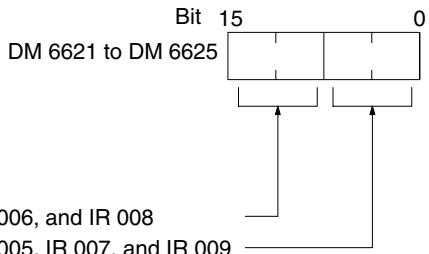
Time constant for IR 002, IR 004, IR 006, and IR 008
Time constant for IR 001, IR 003, IR 005, IR 007, and IR 009
Default: 0000 (8 ms for each)
The nine possible settings for the input time constant are shown below. (Set only the rightmost digit for each setting for IR 000.)
00: 8 ms 01: 1 ms 02: 2 ms 03: 4 ms 04: 8 ms
05:16 ms 06:32 ms 07:64 ms 08:128 ms
The CPM1/CPM1A's I/O response time is the input time constant (1 ms to 128 ms; default is 8 ms) + the cycle time.
Refer to 8-1 CPM1/CPM1A Cycle Time and I/O Response Time for more details.
CPM2A/CPM2C PCs
Set the input time constants for CPM2A/CPM2C inputs from a Programming Device.
Input Time Constants for IR 000
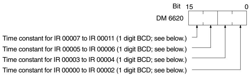
Default: 0000 (10 ms for each)
Input Time Constants for IR 001 to IR 009
DM 6621: IR 001 and IR 002
DM 6622: IR 003 and IR 004
DM 6623: IR 005 and IR 006
DM 6624: IR 007 and IR 008
DM 6625:IR 009
DM 6621 to DM 6625

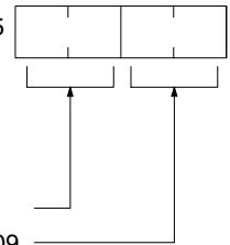
15 0
Time constant for IR 002, IR 004, IR 006, and IR 008
Time constant for IR 001, IR 003, IR 005, IR 007, and IR 009
Default: 0000 (10 ms for each)
The nine possible settings for the input time constant are shown below. (Set only the rightmost digit for IR 000.)
00:10ms
01:1ms
02: 2 ms
03:3ms
04:5ms
05:10ms
06:20ms
07:40 ms
08:80ms
1-2-9 Error Log Settings
Error Detection and Error Log Operation (DM 6655)
Make the settings shown below to determine whether or not a non-fatal error is to be generated when the cycle time exceeds 100 ms or when the voltage of the built-in battery drops (CPM2A/CPM2C only), and to set the method for storing records in the error log when errors occur.
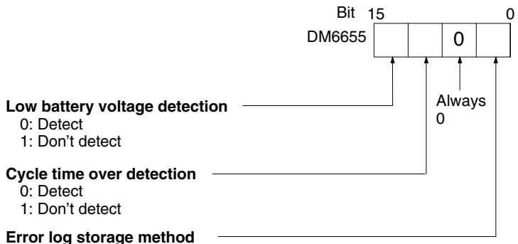
0: Error records for the 7 most recent errors always stored (older errors deleted).
1: Only the first 7 error records stored (no errors stored beyond that point).
2 to F: Error records not stored.
Default: Low battery voltage and cycle time over errors detected, and error records stored for the 7 most recent errors.
Battery errors and cycle time overrun errors are non-fatal errors.
For details on the error log, refer to Section 9 Troubleshooting.
Note The low battery error is applicable to CPM2A/CPM2C only. This digit isn't used in CPM1/CPM1A/SRM1(-V2) PCs and CPM2C PCs that aren't equipped with a battery.
1-3 CPM2C Changes in SW2
The connection of a Programming Console to the peripheral connector is automatically detected for CPM2C CPU Units with lot numbers of 01900 (1 September 2000) or later. This has resulted in a change to the operation of SW2 on the front of the CPU Unit. Check the lot number to confirm the operation of SW2 for any of the following model numbers before attempting operations.
CPU Units with Changed Specifications for SW2
| I/O | Units with Relay Outputs and a Terminal Block | Units with Transistor Outputs and a Connector | |
| Sinking outputs | Sourcing outputs | ||
| 10 I/O points | CPM2C-10CDR-D | CPM2C-10CDTC-D | CPM2C-10CDT1C-D |
| CPM2C-10C1DR-D | CPM2C-10C1DTC-D | CPM2C-10C1DT1C-D | |
| 20 I/O points | --- | CPM2C-20CDTC-D | CPM2C-20CDT1C-D |
| CPM2C-20C1DTC-D | CPM2C-20C1DT1C-D | ||
Interpreting Lot Numbers
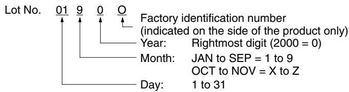
Operation Previous CPU Units
The following instructions apply to CPU Units with lot numbers of 31800 (August 2000) or earlier.
The previous CPU Units do not detect a Programming Console connected to the peripheral port, and SW2 of the DIP switch was used to set either "Programming Console" or "Other device."
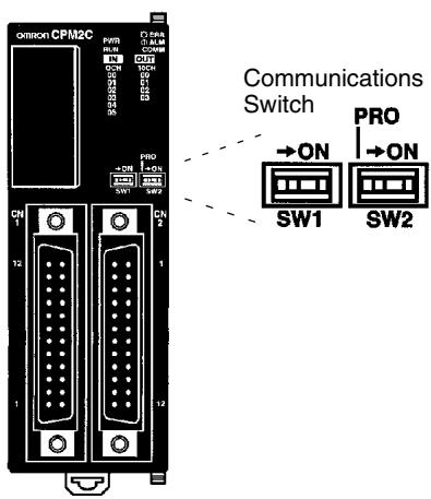
SW2 Setting
| Setting | Meaning |
| OFF | Programming Console connected to peripheral port. |
| ON | Device other than Programming Console connected to peripheral port. |
SW1 Setting
| Setting | Meaning |
| OFF | Use PC Setup settings for RS-232C port (DM 6645 to DM 6649). |
| ON | Use default settings for RS-232C port. |
The relationship between the PC Setup settings, the setting of SW2, and the startup operating mode for previous CPU Units is shown in the following table.
| PC Setup | CPM2C Operating Mode | ||||
| Address | Bits | Setting | |||
| DM6600 | 08 to 15 | 00 Hex | According to communications switch SW2 and peripheral port device. | ||
| Peripheral device | SW2 setting | ||||
| OFF | ON | ||||
| Nothing connected | PROGRAM mode | RUN mode | |||
| Programming Console | According to Programming Console key switch. | PROGRAM mode (See note.) | |||
| Other | PROGRAM mode (See note.) | PROGRAM mode | |||
| Note: Communications will not be possible between the CPM2C and the peripheral device for these combinations. | |||||
| 01 Hex | Mode used immediately before power interruption | ||||
| 02 Hex | Mode specified in bits 00 to 07. | ||||
| 00 to 07 | 00 Hex | PROGRAM mode | |||
| 01 Hex | MONITOR mode | ||||
| 02 Hex | RUN mode | ||||
Note
- The default setting for DM 6600, bits 06 to 15 is 00 Hex, i.e., according to the communications switch on the front panel. If SW2 is set for connecting a device other than a Programming Console to the peripheral connector, the CPU Unit will start in RUN mode as soon as power is turned ON. Be sure that adequate precautions are taken to ensure safety.
- If SW2 is for connecting a device other than a Programming Console to the peripheral connector, the CPU Unit will start in RUN mode as soon as power is turned ON even if a device is connected to the RS-232C port. Be sure that adequate precautions are taken to ensure safety.
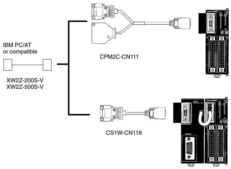
Connections
SECTION 2
Special Features
This section explains special features of the CPM1, CPM1A, CPM2A, CPM2C (including the CPM2C-S), and SRM1(-V2).
2-1 CPM2A/CPM2C Interrupt Functions 26
2-1-1 Processing the Same Memory Locations with the Main Program and Interrupt Subroutines 27
2-1-2 Interrupt Inputs 30
2-1-3 Interval Timer Interrupts 37
2-1-4 Precautions on Programming Interrupts 42
2-2 CPM2A/CPM2C High-speed Counters 45
2-2-1 Using High-speed Counters 47
2-2-2 Input Interrupts In Counter Mode 68
2-3 CPM1/CPM1A Interrupt Functions 77
2-3-1 Types of Interrupts 77
2-3-2 Input Interrupts 79
2-3-3 Masking All Interrupts 83
2-3-4 Interval Timer Interrupts 84
2-3-5 High-speed Counter Interrupts 86
2-3-6 Precautions on Programming Interrupts 94
2-4 SRM1(-V2) Interrupt Functions 94
2-4-1 Types of Interrupts 94
2-4-2 Interval Timer Interrupts 94
2-5 CPM2A/CPM2C Pulse Output Functions 97
2-5-1 Using Single-phase Pulse Outputs Without Acceleration and Deceleration (Fixed Duty Ratio) 101
2-5-2 Using Pulse Outputs With Variable Duty Ratio 111
2-5-3 Using Pulse Outputs With Trapezoidal Acceleration and Deceleration 117
2-6 CPM1A Pulse Output Functions 131
2-6-1 Programming Example in Continuous Mode 132
2-6-2 Programming Example in Independent Mode 132
2-6-3 Using Pulse Output Instructions 132
2-6-4 Changing the Frequency 133
2-6-5 Stopping Pulse Output 133
2-7 Synchronized Pulse Control (CPM2A/CPM2C Only) 134
2-8 Data Computation Standards 146
2-8-1 Pulse Outputs 146
2-8-2 Synchronized Pulse Control 146
2-9 Analog I/O Functions (CPM1/CPM1A/CPM2A/CPM2C Only) 147
2-10 Temperature Sensor Input Functions (CPM1A/CPM2A/CPM2C Only) 147
2-11 CompoBus/S I/O Slave Functions (CPM1A/CPM2A/CPM2C Only) 147
2-12 CompoBus/S I/O Master Functions (SRM1(-V2) and CPM2C-S Only) 148
2-13 Analog Controls (CPM1/CPM1A/CPM2A Only) 150
2-14 Quick-response Inputs 153
2-14-1 CPM1/CPM1A Quick-response Inputs 153
2-14-2 CPM2A/CPM2C Quick-response Inputs 154
2-15 Macro Function 157
2-16 Calculating with Signed Binary Data 158
2-16-1 Definition of Signed Binary Data 159
2-16-2 Arithmetic Flags 159
2-16-3 Inputting Signed Binary Data Using Decimal Values 159
2-17 Differential Monitor 159
2-18 Expansion Instructions (CPM2A/CPM2C/SRM1(-V2) Only) 160
2-18-1 CPM2A/CPM2C/CPM2C-S Expansion Instructions 161
2-18-2 SRM1(-V2) Expansion Instructions 162
2-19 Using the CPM2A/CPM2C Clock Function 163
2-19-1 Data Area Words 163
2-19-2 Setting the Time 163
2-1 CPM2A/CPM2C Interrupt Functions
Types of Interrupts
The CPM2A and CPM2C (including the CPM2C-S) provide the following kinds of interrupt processing. Interrupts may be disabled temporarily when online editing is performed during operation or STUP(—) is executed to change settings.
Note *Input points 00005 and 00006 do not exist in CPM2C CPU Units with only 10 I/O points or in CPM2C-S CPU Units. In these CPU Units, interrupt subroutine numbers 000 and 001 are allocated to input points 00003 and 00004.
Interrupt Inputs
Interrupt programs are executed when inputs to the CPU Unit's built-in input points (00003 to 00006) are turned from OFF to ON. Interrupt subroutine numbers 000 to 003^ are allocated to input points 00003 to 00006*.
Interval Timer Interrupts
Interval timer interrupt programs are executed with a precision of 0.1 ms. Interrupt subroutine numbers 000 to 049 are allocated by instructions.
Count-up Interrupts Using Interrupt Inputs (Counter Mode)
Input signals to the CPU Unit's built-in input points (00003 to 00006) are counted at high speed (2 kHz), and the normal program is stopped and an interrupt program is executed. Interrupt subroutine numbers 000 to 003^ are allocated to input points 00003 to 00006^* .
Count-check Interrupts Using the High-speed Counter
Pulse inputs to the CPU Unit's input points (00000 to 00002) are counted at high speed (20 kHz/5 kHz), and an interrupt program is executed when the present value matches the target value or falls within a given range. Interrupt subroutine numbers 000 to 049 are allocated by instructions.
Note Interrupts will be temporarily disabled if online editing is performed during operation or if the PC Setup is changed during operation (including changes made with STUP(-)).
Writing Interrupt Programs
Interrupt programs are defined as interrupt subroutines within the user program. Just like ordinary subroutines, an interrupt subroutine is defined by SBN(92) and RET(93). It is written at the end of the normal program.
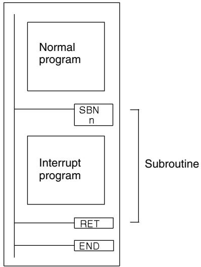
1, 2, 3... 1. A new interrupt can be defined in an interrupt subroutine, and an existing one can be cleared.
-
Within any given interrupt subroutine, it is not possible to write another subroutine for processing another interrupt. Do not nest another interrupt subroutine between the SBN(92) and RET(93) instructions.
-
It is not possible to write a subroutine program within an interrupt subroutine. Do not nest an ordinary subroutine program between the SBN(92) and RET(93) instructions.
- It is not possible to write an interrupt subroutine within an ordinary subroutine program. Do not nest an interrupt subroutine between the SBN(92) and RET(93) instructions.
When an interrupt subroutine is defined, an SBS UNDEFD error will be generated during the program check but execution will be normal.
Caution
Although IORF(97) can be used in interrupt subroutines, you must be careful of the interval between IORF(97) executions. If IORF(97) is executed too frequently, a fatal system error may occur (FALS 9F), stopping operation. The interval between executions of IORF(97) should be at least 1.3ms + total execution time of the interrupt subroutine.
Order of Priority for Interrupts
The order of priority for interrupts is as follows:

If an interrupt with a higher priority is generated, during interrupt program execution, the interrupt that is currently being processed will be stopped and the new interrupt will be processed first. Then the original interrupt will be resumed after the higher-priority interrupt processing has been completed.
If interrupts of the same priority are generated simultaneously, they will be processed in the following order:
Interrupt input 0 Interrupt input 1 Interrupt input 2 Interrupt input 3 (including count-up mode)
Interval timer interrupt High-speed counter interrupt
2-1-1 Processing the Same Memory Locations with the Main Program and Interrupt Subroutines
If a memory location is manipulated both by the main program and an interrupt subroutine, an interrupt mask must be set to disable interrupts.
When an interrupt occurs, execution of the main program will be interrupted immediately, even during execution of an instruction. The intermediate processing results is saved for use after completing the interrupt subroutine, i.e., when the interrupt subroutine has been executed, execution of the main program is started from the same position with data restored to the previous condition. If any of the memory locations being used by the main program are changed in the interrupt subroutine, the changes will be lost when data is restored to the previous state when restarting execution of the main program. It is thus necessary to disable interrupts before and enable interrupts after any instructions that should be executed to completion even if an interrupt occurs.
Processing Interrupted between 1st and 3rd Operands
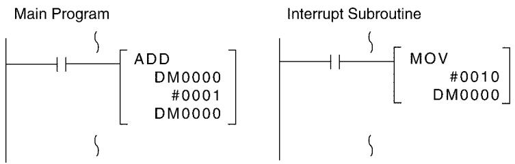
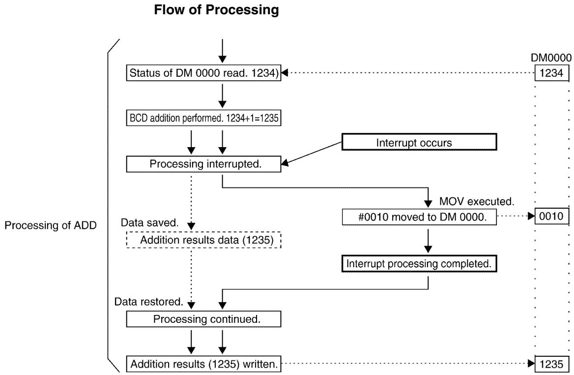
When the interrupt occurs while processing ADD, the addition result, 1235, is saved temporarily in memory and not stored in DM 0000. Although #0010 is moved to DM 0000 in the interrupt program, the addition result that was saved is written to DM 0000 as soon as processing returns to the main program, effectively undoing the results of the interrupt program.
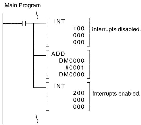
Countermeasure for Above Problem
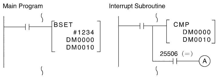
Interrupting Writing Multiple Words of Data
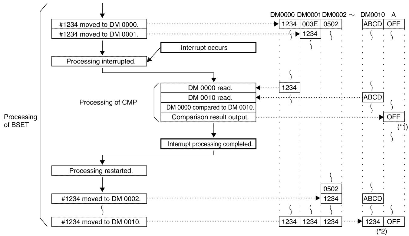
Flow of Processing
Processing was interrupted for BSET when #1234 was not yet written to DM 0010. Therefore, in the comparison at point *1, the contents of DM 0000 and DM 0001 are not equal and processing stops with A in the OFF state. As a result, although the contents of DM 0000 and DM 0010 agree at the value 1234, an incorrect comparison result is reflected in comparison result output A.
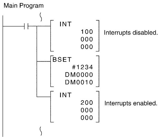
Countermeasure for Above Problem
2-1-2 Interrupt Inputs
By turning the CPU Unit's built-in input points from OFF to ON, the normal program can be stopped and the interrupt program executed. The interrupt inputs are allocated to four points (00003 to 00006, see note).
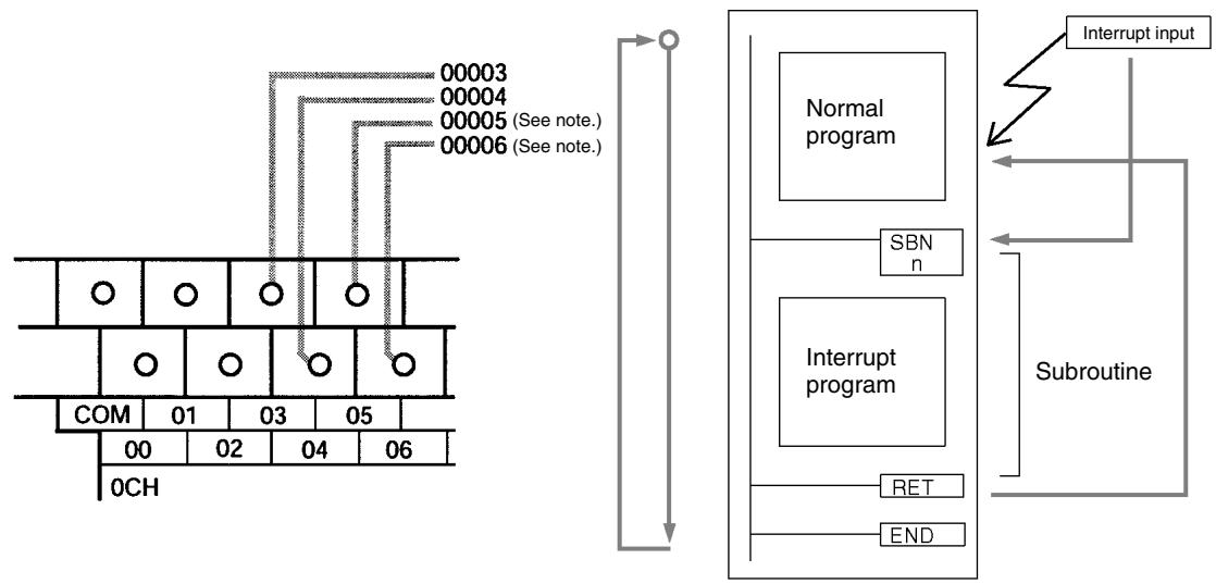
Note Input points 00005 and 00006 do not exist in CPM2C CPU Units with only 10 I/O points or in CPM2C-S CPU Units.
| Input number (Note 1) | Interrupt number | Subroutine number (Note 2) | Minimum input signal width | Interrupt response time |
| 00003 | 0 | 000 | 50 μs | 0.3 ms (from when input turns ON until program execution) |
| 00004 | 1 | 001 | ||
| 00005 (See note 3.) | 2 | 002 | ||
| 00006 (See note 3.) | 3 | 003 |
Note
- Input numbers 00003 to 00006 can be used for any of the following functions: interrupt inputs, interrupt inputs (counter mode), or quick-response inputs. When not being used for any of these, they can be used as ordinary inputs.
- Subroutine numbers 000 to 003 are the subroutine numbers for interrupt programs started up when interrupt inputs or count-up interrupts for interrupt inputs (counter mode) are generated. When not being used for this purpose, they can be used as ordinary inputs.
- Input points 00005 and 00006 do not exist in CPM2C CPU Units with only 10 I/O points or in CPM2C-S CPU Units.
The following table shows the relationships between interrupt inputs and the CPM2A/CPM2C PC's other functions.
| Function | Interrupt inputs (counter mode) |
| Synchronized pulse control | Can be used simultaneously. |
| Interrupt inputs | See note 1. |
| Interval timer interrupts | Can be used simultaneously. |
| High-speed counters | Can be used simultaneously. |
| Interrupt inputs (counter mode) | See note 1. |
| Pulse outputs | Can be used simultaneously. |
| Quick-response inputs | See note 1. |
| Input time constant | See note 2. |
| Clock | Can be used simultaneously. |
Note
- The same input number (from 00003 to 00006) cannot be used for more than one of the following functions: interrupt inputs, interrupt inputs (counter mode), or quick-response inputs.
- When inputs 00003 to 00006 are set for use as interrupt inputs (counter mode), the input time constants for the relevant inputs are disabled. The input time constants remain in effect, however, for the values for refreshing the relevant input relay area.
Procedure for Using Interrupt Inputs
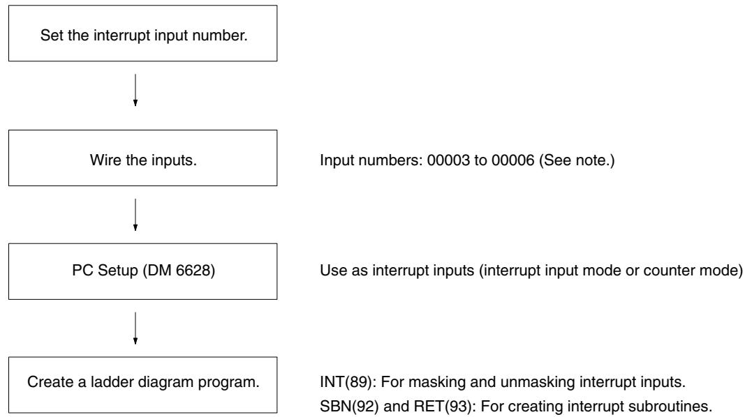
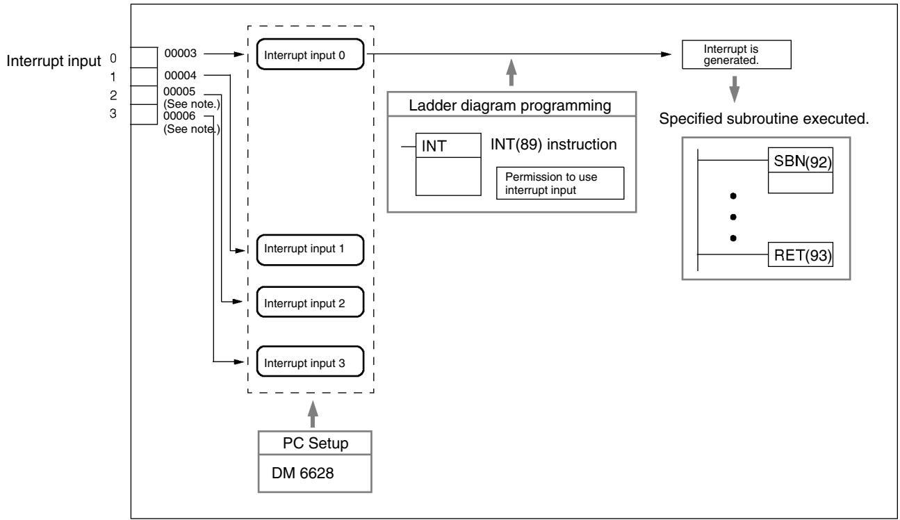
Note Input points 00005 and 00006 do not exist in CPM2C CPU Units with only 10 I/O points or in CPM2C-S CPU Units.
Setting the Interrupt Input Number
With interrupt inputs (interrupt input mode), the subroutine numbers executed for the input numbers are fixed.
| Input number | Interrupt number | Subroutine number |
| 00003 | 0 | 000 |
| 00004 | 1 | 001 |
| 00005 (See note.) | 2 | 002 |
| 00006 (See note.) | 3 | 003 |
The same input number (from 00003 to 00006) cannot be used for more than one of the following functions: interrupt inputs, interrupt inputs (counter mode), or quick-response inputs.
Wiring the Inputs
With a CPM2A, wire to the input terminals as shown in the following illustration.
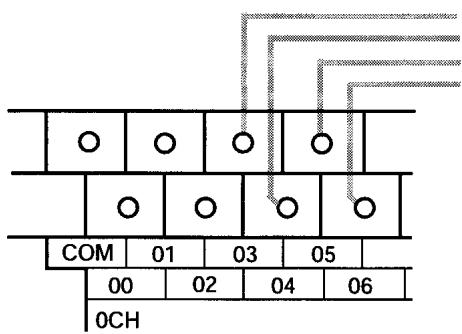
Input number 00003: Interrupt input 0
Input number 00004: Interrupt input 1
Input number 00005: Interrupt input 2
Input number 00006: Interrupt input 3
With a CPM2C, wire to the input terminals as shown in the following illustration.
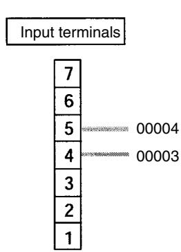
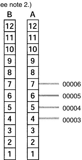
Note 1. Refer to the operation manual for your CPU Unit for information on wiring.
2. Input terminal and pin numbers depend on the model. Refer to the CPM2C Operation Manual (W356) for details.
PC Setup
The following table shows the settings in the PC Setup area related to interrupt input usage.
| Word | Bits | Function | Setting | |
| DM 6628 | 00 to 03 | Interrupt setting for input 00003 | 0: Normal input1: Interrupt input (interrupt input mode or counter mode)2: Quick-response input | 1 |
| 04 to 07 | Interrupt setting for input 00004 | |||
| 08 to 11 | Interrupt setting for input 00005* | |||
| 12 to 15 | Interrupt setting for input 00006* | |||
Note *Input points 00005 and 00006 do not exist in CPM2C CPU Units with only 10 I/O points and in CPM2C-S CPU Units.
The settings will go into effect when the mode is changed (from PROGRAM to MONITOR/RUN) or when the power supply is turned ON to the CPM2A/ CPM2C.
Ladder Diagram Programming
The following table shows the instruction operations related to interrupt input control.
| Instruction | Control | Operation |
| (@)INT(89) | Mask/unmask interrupt inputs | Prohibits or permits specified interrupts. |
| Clear interrupt inputs | Clears the cause of a prohibited interrupt input. | |
| Read current mask status | Reads the permitted/prohibited status of an interrupt input. | |
| Mask all interrupts | Prohibits all interrupts, including interrupt inputs, interval timer interrupts, high-speed counters, etc. | |
| Unmask all interrupts | Permits all interrupts, including interrupt inputs, interval timer interrupts, high-speed counters, etc. |
Masking or Unmasking Interrupt Inputs
This function is used to mask or unmask input numbers 00003 to 00006 (interrupt inputs 0 to 3).
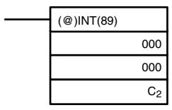
Interrupt control designation (000: Mask/unmask interrupt inputs)
Fixed at 000.
Control data word
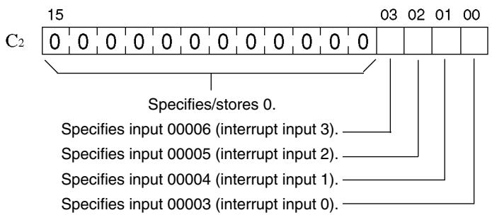
0: Clear mask (interrupt input permitted).
1: Set mask (interrupt input prohibited).
All interrupt inputs are prohibited at the beginning of operation (in either PROGRAM mode or in RUN/MONITOR mode). To use interrupt inputs, use INT(89) to permit them.
Clearing Interrupt Inputs
This function is used to clear input numbers 00003 to 00006 (interrupt inputs 0 to 3). Since interrupt inputs are recorded, masked interrupts will be serviced after the mask is removed unless they are cleared first. Use INT(89) to clear the cause of the interrupt inputs so that they will not be executed when interrupt inputs are permitted (i.e., when the mask is removed).
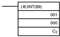
Interrupt control designation (001: Clear interrupt inputs)
Fixed at 000.
Control data word
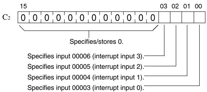
0: Retain cause of interrupt input.
1: Clear cause of interrupt input.
While interrupt inputs are masked, one cause is recorded for each interrupt input.
Reading Current Mask Status
This function is used to read the current mask status for input numbers 00003 to 00006 (interrupt inputs 0 to 3).

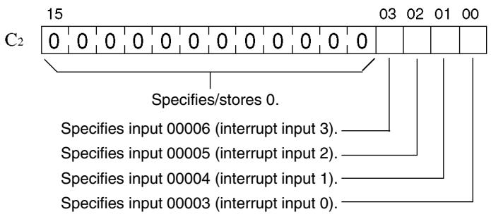
0: Mask is cleared (interrupt inputs permitted).
1: Mask is set (interrupt inputs prohibited).
Masking or Unmasking All Interrupts
This function is used to mask or unmask all interrupt processing, including interrupt inputs (interrupt input mode and counter mode), interval timer interrupts, and high-speed counters. Masked inputs are recorded, but ignored.
Masking All Interruptions

Unmasking All Interrupts

The masking or unmasking all interrupts cannot be executed within an interrupt subroutine.
If causes for interrupts occur while all interrupts are masked, the causes will be recorded for each interrupt but the interrupt processing will not be executed. When "unmask all interrupts" is executed, the processing will then be carried out according to the interrupt mask status at that point in time.
Interrupt masks cannot be cleared simply by executing "unmask all interrupts." Executing "unmask all interrupts" merely restores the status that was in effect prior to the execution of "mask all interrupts."
Note INT(89) must be executed in order, with "mask all interrupts" followed by "unmask all interrupts."
Operation Example
Explanation
In this example, an interrupt subroutine is executed by turning input 00003 from OFF to ON. The interrupt subroutine adds 1 to DM 0000.
Wiring
The following diagram shows input wiring in the CPM2A.
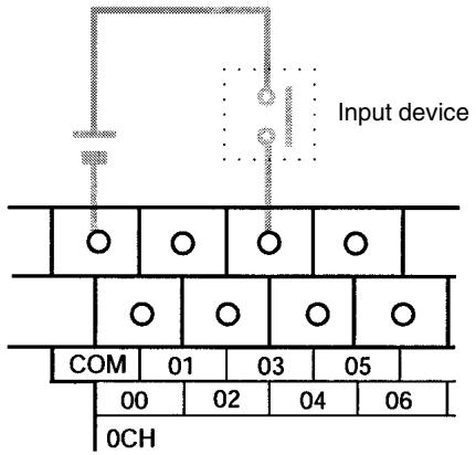
The following diagram shows input wiring in the CPM2C.
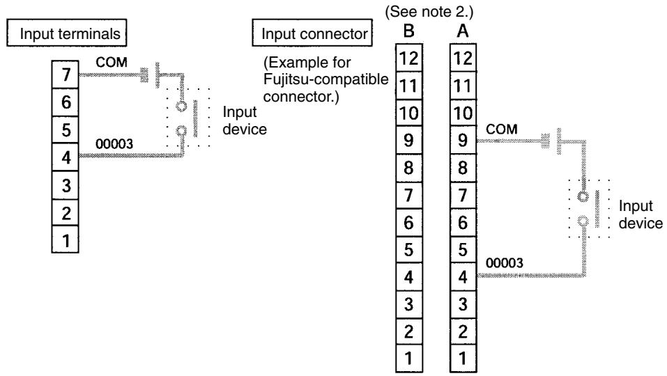
PC Setup
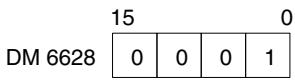
Input 00003 is used as an interrupt input.
(Inputs 00004 to 00006 are used as ordinary inputs.)
Programming
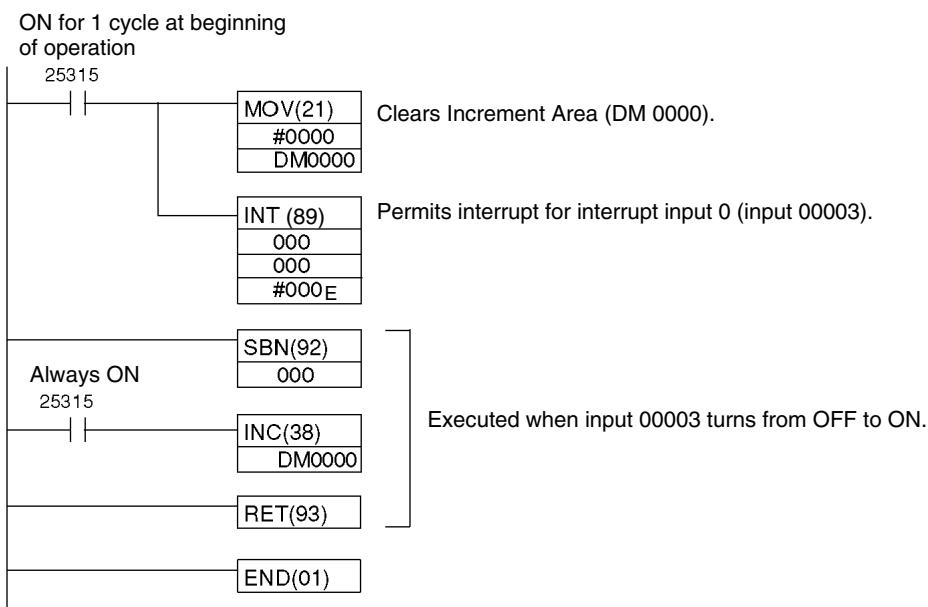
2-1-3 Interval Timer Interrupts
One interval timer (precision: 0.1 ms) is supported and it can be set from 0.5 ms to 319,968 ms. There are two interrupt modes: the one-shot mode, in which a single interrupt is executed when the time is up, and the scheduled-interrupt mode, in which interrupts are executed at regular intervals.
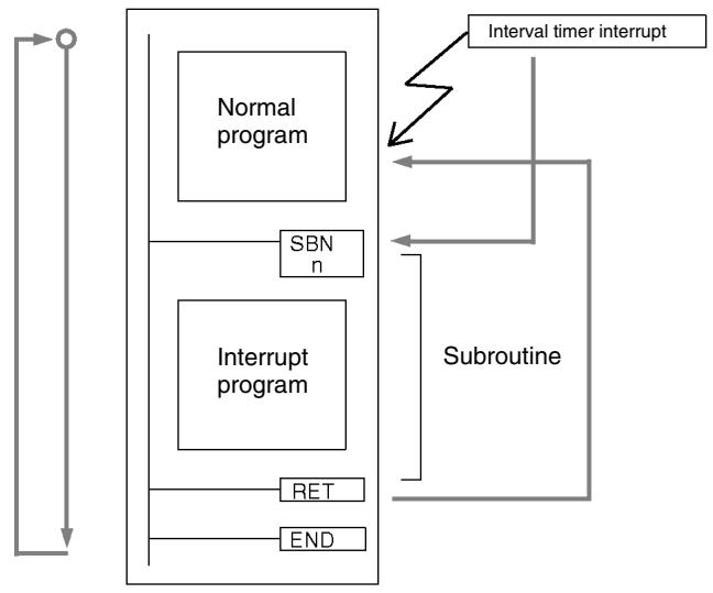
| One-shot mode | Scheduled-interrupt mode | |
| Operation | Interrupt is executed once when time has elapsed. | Interrupts are executed at regular intervals. |
| Set time | 0.5 to 316,968 ms (Unit: 0.1 ms) | |
| Interrupt response time | 0.3 ms (from when time has elapsed until execution of interrupt program) | |
The following table shows the relationships between interval timer interrupts and the CPM2A/CPM2C's other functions.
| Interval timer interrupts | |
| Synchronized pulse control | Can be used simultaneously. |
| Interrupt inputs | Can be used simultaneously. |
| Interval timer interrupts | --- |
| High-speed counters | Can be used simultaneously. |
| Interrupt inputs (counter mode) | Can be used simultaneously. |
| Pulse outputs | Can be used simultaneously. |
| Quick-response inputs | Can be used simultaneously. |
| Input time constant | Can be used simultaneously. |
| Clock | Can be used simultaneously. |
Procedure for Using Interval Timer Interrupts
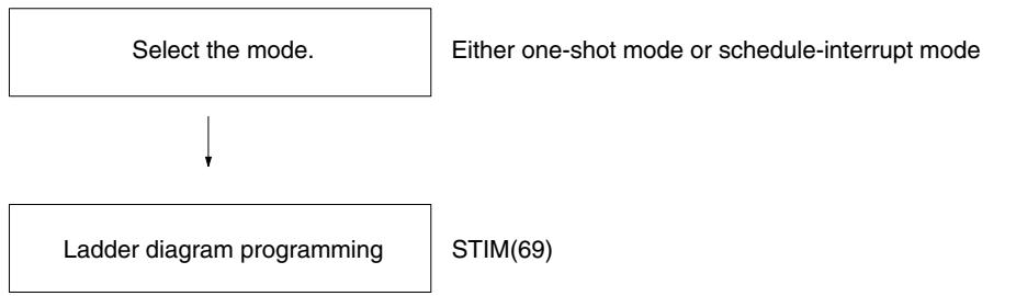
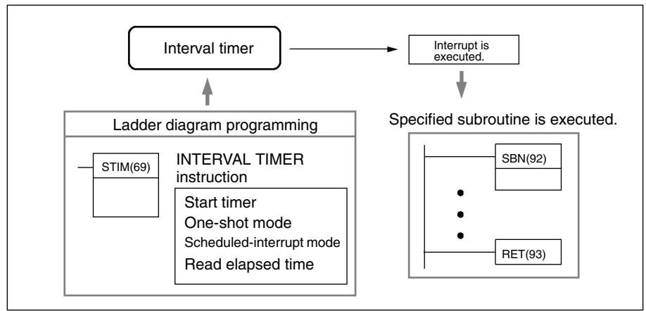
Selecting the Mode
Select either the one-shot mode or the scheduled-interrupt mode. One-shot Mode
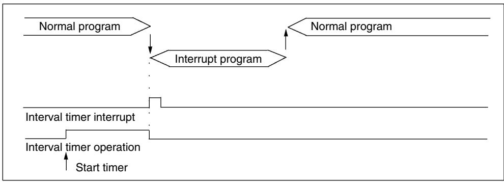
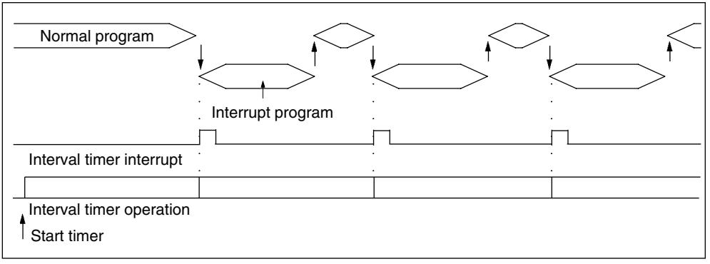
Scheduled-interrupt Mode
Ladder Diagram Programming
In the scheduled-interrupt mode, the timer is reset each time the interrupt program is called when the set time elapses, and then the interval timer operates again.
Be careful with regard to the interrupt program's execution time and the interval timer's set time. If the interrupt program's execution time exceeds the interval timer's set time, scheduled interrupts cannot be executed properly.
The following table shows the instruction operations related to interrupt input control.
| Instruction | Control | Operation |
| (@)STIM(69) | Start one-shot timer | Starts interval timer in one-shot mode. |
| Start scheduled-interrupt timer | Starts interval timer in scheduled-interrupt mode. | |
| Read timer PV | Reads the timer PV. | |
| Stop timer | Stops timer operations. | |
| (@)INT(89) | Mask all interrupts | Prohibits all interrupts, including interrupt inputs, interval timer interrupts, high-speed counters, etc. |
| Unmask all interrupts | Permits all interrupts, including interrupt inputs, interval timer interrupts, high-speed counters, etc. |
Starting Timers
This function sets the mode (one-shot or scheduled-interrupt) and the timer's SV, and starts the interval timer.
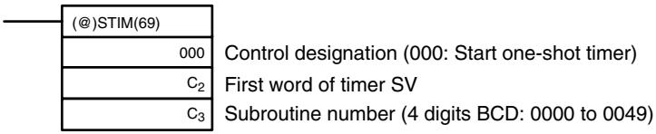
One-shot Mode
Scheduled-interrupt Mode


The interval from when STIM(69) is executed until the set time elapses is calculated as follows:
$$ \begin{array}{l} \left(\text {C o n t e n t} \mathrm {w o r d} \mathrm {C} _ {2}\right) \times \left(\text {C o n t e n t} \mathrm {w o r d} \mathrm {C} _ {2} + 1\right) \times 0. 1 \mathrm {m s} \ (0. 5 \text {t o} 3 1 9, 9 6 8 \mathrm {m s}) \ \end{array} $$
When a constant is set for C2, that value will be taken as the decrementing counter initial value, and the decrementing time interval will become 10 (1 ms).
(The SV is specified just as it is, in units of ms.)
Reading Timer PVs
This function reads interval timer PVs.
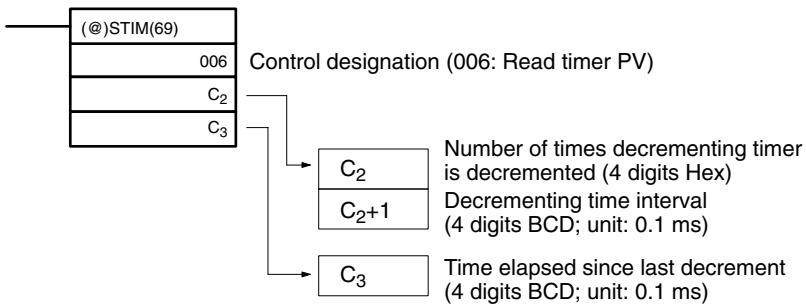
Stopping Timers
This function stops the interval timer.
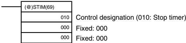
Masking or Unmasking All Interrupts
For details on masking/unmasking all interrupts, refer to 2-1-2 Interrupt Inputs and 7-29 Interrupt Control Instructions.
Operation Example
One-shot Mode
Explanation
In this example, the timer is started when the execution condition (00005) turns from OFF to ON. When the time (approx. 1 s) has elapsed, the interrupt subroutine is executed one time. When the interrupt subroutine is executed, 1 is added to DM 0000.
Elapsed time: 100 × 100 × 0.1 = 1,000 ms
Programming
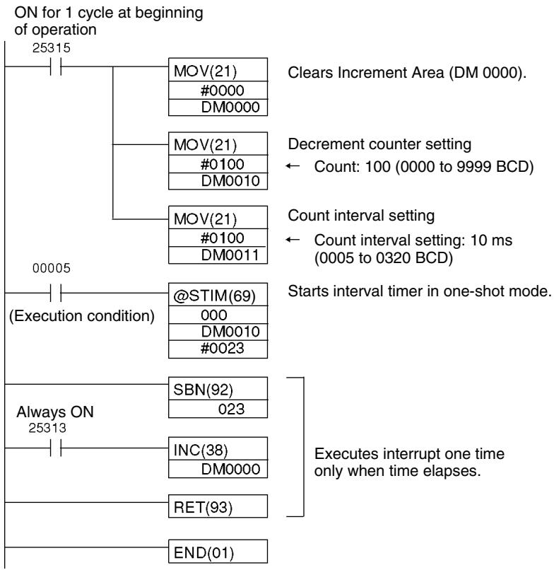
Scheduled-interrupt Mode
Explanation
In this example, the timer is started when the execution condition (00005) turns from OFF to ON. Then the interrupt subroutine is executed each time that the set time (approx. 1 s) elapses. Each time the interrupt subroutine is executed, 1 is added to DM 0000.
Elapsed time: 100 × 100 × 0.1 = 1,000 ms
Programming
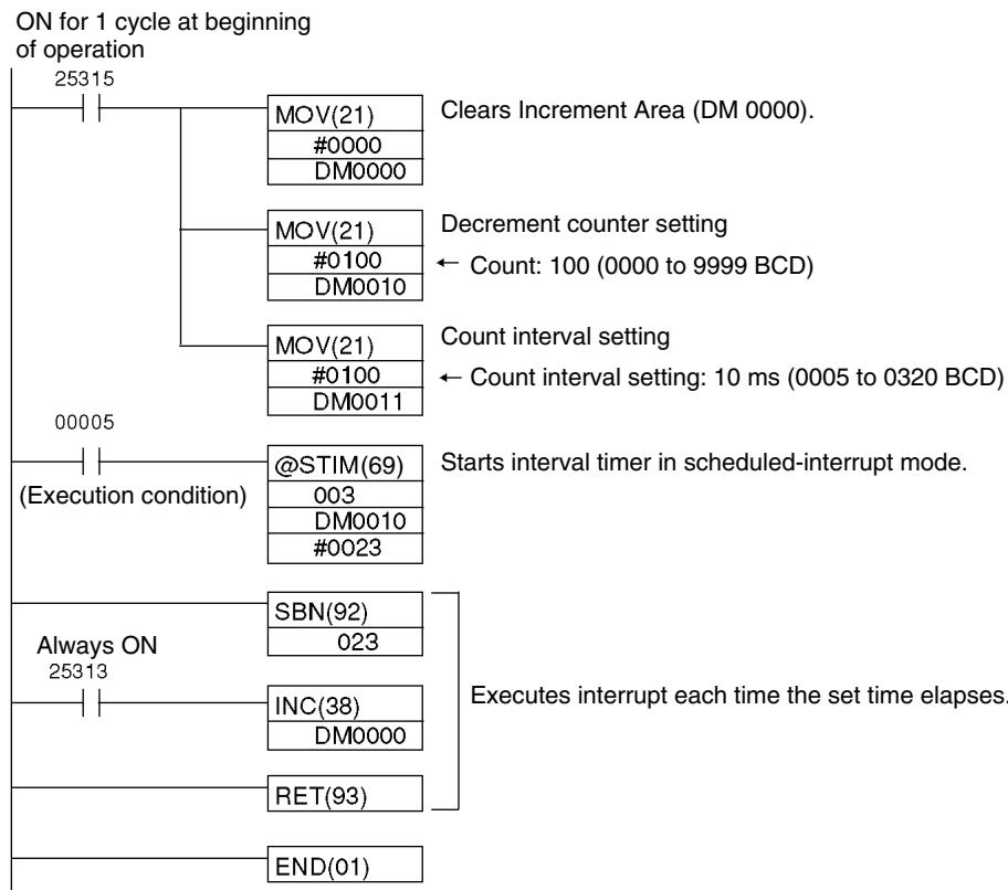
2-1-4 Precautions on Programming Interrupts
If words in memory are being manipulated both in the main program and in an interrupt program, the interrupts must be masked when the words are being manipulated in the main program.
When an interrupt occurs, any instruction being executed in the main program will be interrupted and processing data will be temporarily stored while the interrupt program is being executed. When execution of the interrupt program has been completed, the original execution status of the main program will be restored and execution will be continued. Thus, if the manipulation of words in the main program is interrupted and the same words are altered in the interrupt program, the words altered in the interrupt program will simply be restored to the status that was in the process of being written in the main program, effectively canceling the result of the interrupt program. If there are instructions that should not be interrupted during processing in the main program, disable interrupts before and after executing them.
The are two cases in which the above problem can occur: When manipulating the contents of one word and when manipulating the contents of multiple words.
Manipulating One Word
A problem can occur in the situation shown below because processing of the ADD instruction could be interrupted between the 1st and 3rd operands and the MOV instruction then executed in the interrupt program.
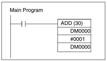
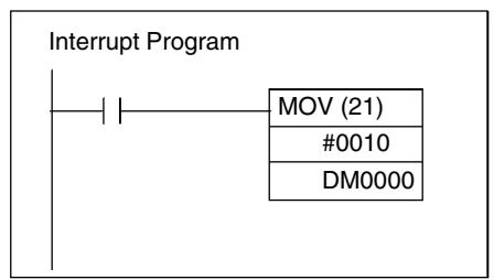
Flow of Processing
The processing that would occur when the ADD instruction above is interrupted is illustrated below.
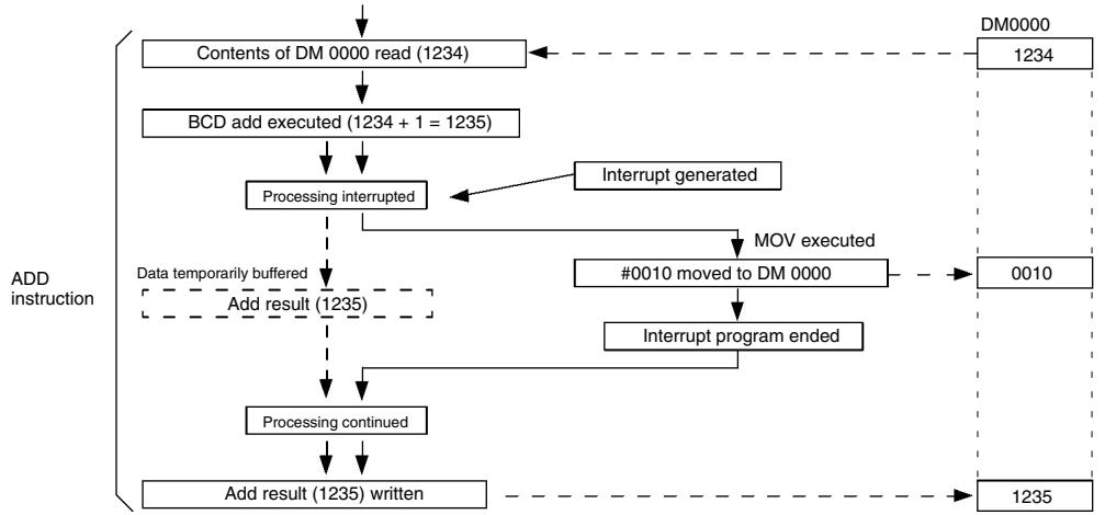
Processing is interrupted before the result of the add operation can be written to DM 0000 and the result is buffered. The interrupt program writes #0010 to DM 0000, but this is immediately overwritten by the result of the add (1235) as soon as execution of the interrupt program has been completed. In other words, the result of the interrupt program have been consequently nullified.
Solution
The INT instruction can be used to enable and disable interrupts before and after the add operation as shown below.
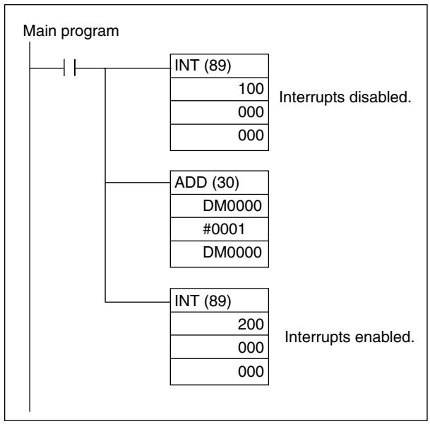
Manipulating Multiple Words
A problem can occur in the situation shown below because processing of the BSET instruction could be interrupted before all of the data for BSET has been written and the CMP instruction then executed in the interrupt program.
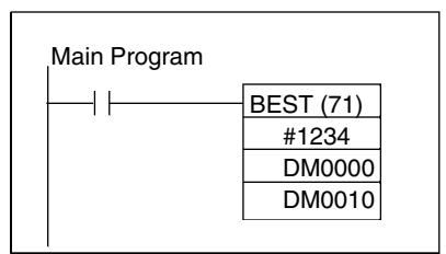
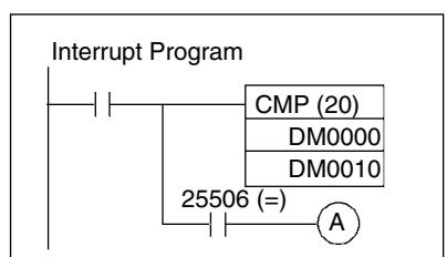
Flow of Processing
The processing that would occur when the BSET instruction above is interrupted is illustrated below.
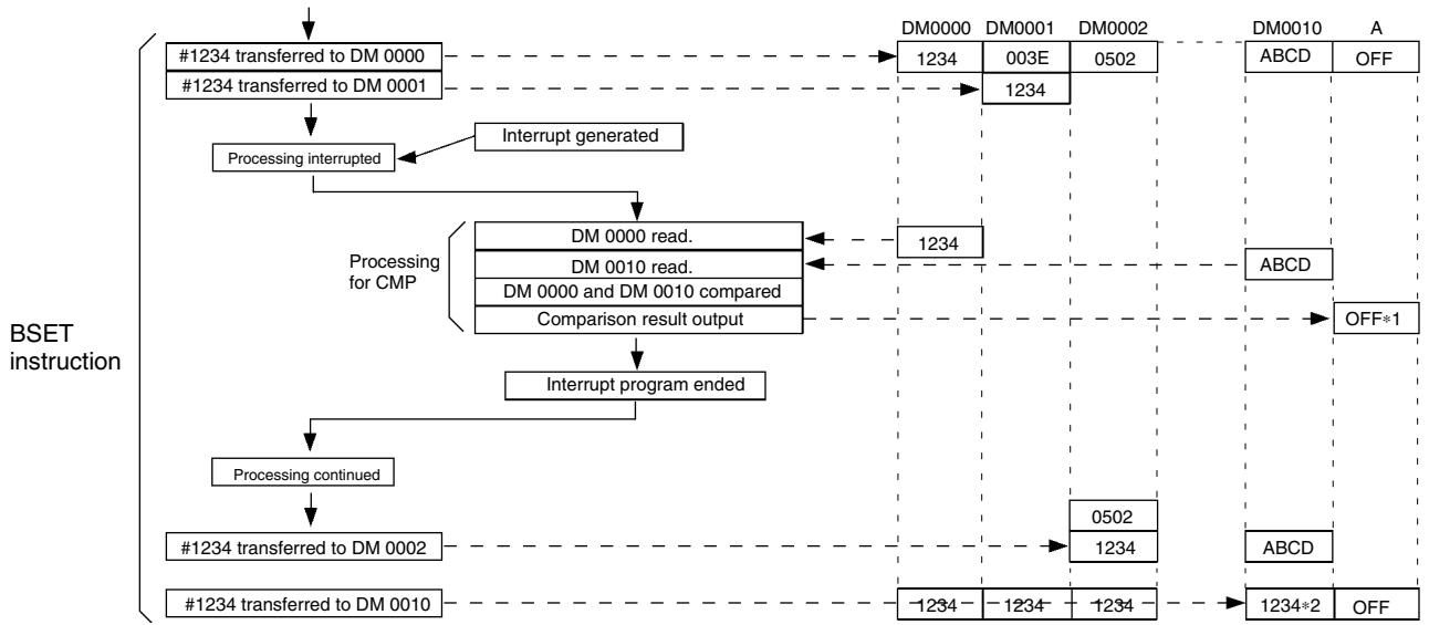
Processing is interrupted before #1234 can be written to DM 0010. Bit A in the interrupt program is thus turned OFF and will remain OFF when execution of the main program is resumed even though the contents of DM 0000 and DM 0010 will be the same as soon as the main program is resumed, i.e., the result of the comparison is not correct
Solution
The INT instruction can be used to enable and disable interrupts before and after the BSET instruction as shown below.
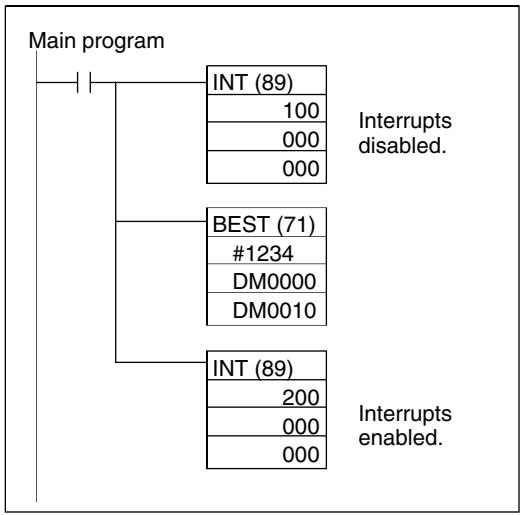
2-2 CPM2A/CPM2C High-speed Counters
CPM2A CPU Units and most CPM2C CPU Units have five points for high-speed counters: One point for a high-speed counter with a maximum response frequency of 20kHz , and four points for interrupt inputs (counter mode).
CPM2C CPU Units with 10 I/O points have four points for high-speed counters: One point for a high-speed counter with a maximum response frequency of 20kHz , and three points for interrupt inputs (counter mode).
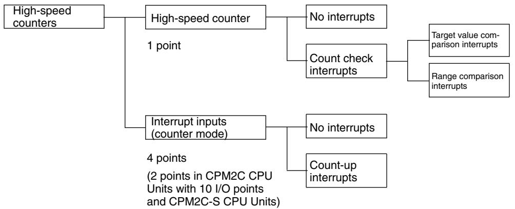
Types of High-speed Counters
The CPM2A/CPM2C provides both a built-in high-speed counter and built-in interrupt inputs.
High-speed Counter
The built-in high-speed counter is a counter based on inputs to the CPU Unit's built-in points 00000 to 00002. The high-speed counter itself has one point, and it can provide either an incrementing/decrementing or just an incrementing count depending on the mode setting.
| Input No. (See note.) | Response frequency | Input mode (count value) | Control method |
| 00000 | 5 kHz | Differential phase input mode (-8388608 to 8388607) | Target value comparison interrupts |
| 00001 | |||
| 00002 | 20 kHz | Pulse + direction input mode(-8388608 to 8388607) Up/down pulse input mode (-8388608 to 8388607) Increment mode (0 to 16777215) | Range comparison interrupts |
Note Input points not used for counter inputs can be used as ordinary inputs.
Interrupt Inputs (Counter Mode)
Interrupt inputs (counter mode) are counters based on inputs to the CPU Unit's built-in points 00003 to 00006 (00003 to 00004 in CPM2C CPU Units with 10 I/O points and in CPM2C-S CPU Units). These counters have four points, and they can provide either an incrementing or decrementing count depending on the mode setting. Since this function utilizes interrupt inputs for counting, it is not possible to use the same inputs for other interrupt inputs.
| Input No. (See note.) | Response frequency | Input mode (count value) | Control method |
| 00003 | 2 kHz | Incrementing counter (0000 to FFFF) | Count-up interrupts |
| 00004 | Decrementing counter (0000 to FFFF) | ||
| 00005 | |||
| 00006 |
Note 1. Input points not used for counter inputs can be used as ordinary inputs.
- Input points 00005 and 00006 do not exist in CPM2C CPU Units with 10 I/O points and CPM2C-S CPU Units.
High-speed Counter Interrupts
Interrupts by High-speed Counter (Count-check Interrupts)
Target Value Comparison Interrupts
The current count is compared to each target value in the order that they are registered in the table. When the count is the same as the current target value, an interrupt subroutine is executed. Up to 16 target values and interrupt subroutines can be registered in the table in either the incrementing or decrementing direction.
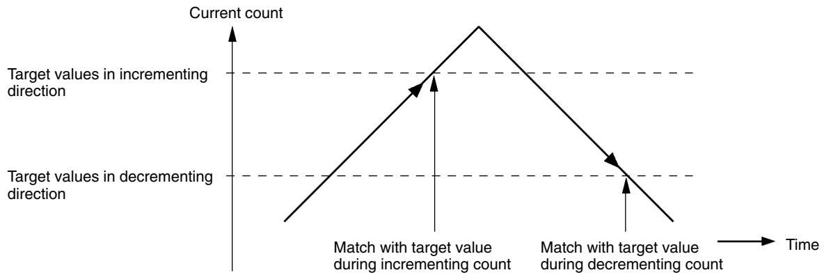
Interrupt processing can be executed when the current count matches a target value in either the incrementing or decrementing direction.
Range Comparison Interrupts
A range comparison table contains up to eight ranges which are each defined by a lower limit and an upper limit, as well as their corresponding subroutine numbers. The corresponding subroutine is called and executed when the current count (the counter PV) falls within a given range.
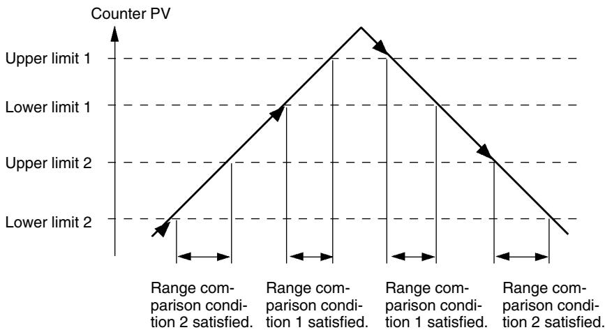
Interrupt processing can be executed when a range comparison condition is satisfied.
Furthermore, when the counter PV is within a range between an upper limit and a lower
limit, the corresponding bits (from 0 to 7) in AR 11 will turn ON.
Count-up Interrupts by Interrupt Inputs (Counter Mode)
An interrupt subroutine is executed each time the condition is satisfied that the counter PV equals the counter SV (in incrementing mode) or 0 (in decrementing mode).
2-2-1 Using High-speed Counters
The CPM2A/CPM2C's CPU Unit has one built-in channel for a high-speed counter that can count inputs at a maximum of 20kHz . Using this in conjunction with the interrupt function enables target value comparison control or range comparison control to be executed without deviating from the cycle time.

| Item | Input mode | ||||
| Differential phase | Pulse + direction | Up/down input | Increment | ||
| Input number | 00000 | Phase-A inputs | Pulse inputs | CW inputs | Pulse inputs |
| 00001 | Phase-B inputs | Direction inputs | CCW inputs | See note 1. | |
| 00002 | Phase-Z inputs (Reset inputs) (See note 1.) | ||||
| Input method | Differential phase inputs (4X) | Phase inputs | Phase inputs | Phase inputs | |
| Response frequency | 5 kHz | 20 kHz | 20 kHz | 20 kHz | |
| Count value | -8388608 to 8388607 | 0 to 16777215 | |||
| Counter PV storage destination (See note 2.) | Words SR 248 (rightmost digit) and SR 249 (leftmost digit) | ||||
| Interrupts | Target value comparison | Up to 16 target values and interrupt subroutine numbers can be registered in either the incrementing or decrementing direction. | |||
| Range comparison | Up to eight ranges (with upper and lower limits) and subroutine numbers can be registered. | ||||
| Counter reset method | Phase-Z signal + software reset: Counter is reset when IR 00002 turns ON while SR 25200 is ON. Software reset: Counter is reset when SR 25200 turns ON. | ||||
Note 1. Input points not used for counter inputs can be used as ordinary inputs.
- When not used for the counter PV storage destination, these words can be used as ordinary IR words.
- SR 25200 is read once each cycle. Up to one cycle may be required for a reset to occur on the leading edge of phase Z.
The following table shows the relationships between the high-speed counter and the CPM2A/CPM2C's other functions.
| Function | Interval timer interrupts |
| Synchronized pulse control | Cannot be used simultaneously. |
| Interrupt inputs | Can be used simultaneously. |
| Interval timer interrupts | Can be used simultaneously. |
| High-speed counters | --- |
| Interrupt inputs (counter mode) | Can be used simultaneously. |
| Pulse outputs | Can be used simultaneously. |
| Quick-response inputs | Can be used simultaneously. |
| Input time constant | See note. |
| Clock | Can be used simultaneously. |
Note When inputs 00000 to 00002 are set for use as a high-speed counter, the input time constants for the relevant inputs are disabled. The input time constants remain in effect, however, for the values for refreshing the relevant input relay area.
Operation Example
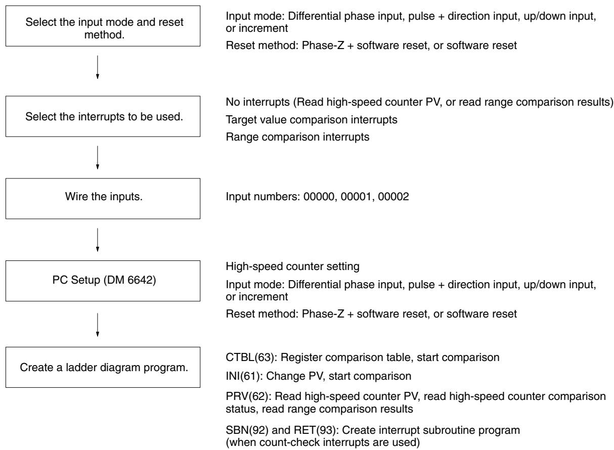
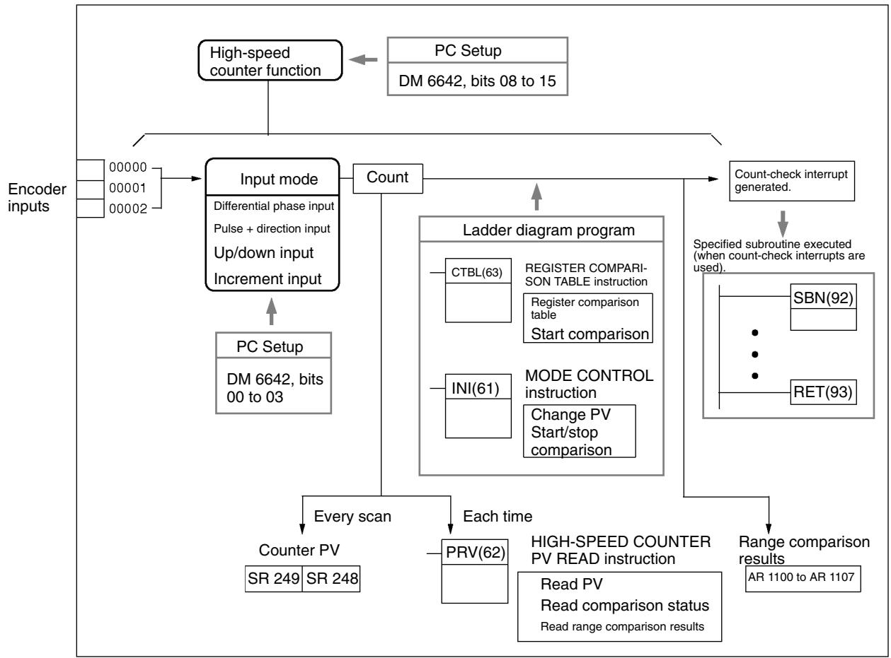
Selecting the Input Mode and Reset Method
Input Mode
Select the input mode for the high-speed counter according to the signal type.
Differential Phase Input Mode
In the differential phase input mode, the count is incremented or decremented according to two differential phase signals with a multiplication of 4 (phase A and phase B).
Maximum frequency: 5 kHz
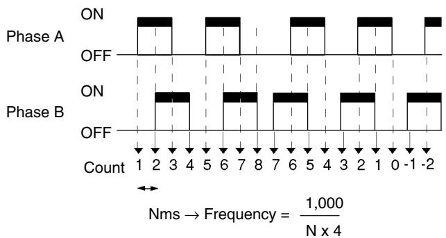
Pulse + Direction Input Mode
In the pulse + direction input mode, pulse signals and direction signals are input, and the count is incremented or decremented according to the direction signal status.
Maximum frequency: 20kHz
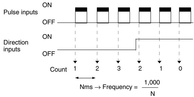
Up/Down Pulse Input Mode
In the up/down pulse input mode, CW signals (up pulses) and CCW signals (down pulses) are input, and the count is incremented or decremented accordingly.
Maximum frequency: 20kHz
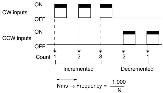
Increment Mode
In the increment mode, pulse signals are input and the count is incremented with each pulse. IR 00001 can be used as an ordinary input.
Maximum frequency: 20kHz
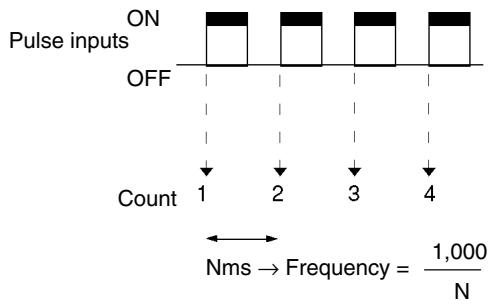
When the differential phase input mode is used, the inputs must be 4X differential phase inputs. When an encoder is connected in this mode, the number of counts per revolution will be four times the encoder resolution. When selecting an encoder take into account the relationship with the number of counts that are possible.
Count Values
The range of numbers counted by the high-speed counter are in linear mode only. If the count is outside of the permissible range, an overflow or underflow will result. The PV will become 0FFFFFF if an overflow occurs, or FFFFFFF if an underflow occurs, and the comparison will be stopped.
| Differential phase input mode | -8388608 | 0 | 8388607 |
| Pulse + direction input mode | ← Underflow (FFFFFF) | → Overflow (0FFFFFF) | |
| Up/down pulse input mode | |||
| Increment mode | 0 | 16777215 | |
| → Overflow (0FFFFFF) | |||
To restart the count following an overflow or underflow, reset the PV. (The PV is automatically reset whenever operation is started or stopped.)
Reset Method
Either of the following two methods can be selected for resetting the counter PV to 0.
Phase-Z Signal (Reset Input) + Software Reset
The PV is reset when a phase-Z signal (i.e., a reset input) turns ON while the High-speed Counter Reset Flag (25200) is ON.

Software Reset
The PV is reset when the High-speed Counter Reset Flag (25200) turns ON.
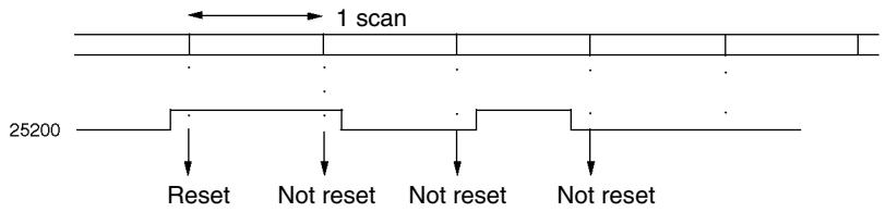
The High-speed Counter Reset Flag (25200) is refreshed with every scan, so it must remain ON for at least one cycle time to be certain it is read.
Even when the PV is reset, the comparison table registration status, the comparison execution status, and the range comparison results are all retained just as they were before the PV reset. (If a comparison was underway prior to the PV reset, that comparison will be continued with no change following the reset.)
Following the reset, the High-speed Counter Reset Flag (25200) must be turned OFF in order to be able to execute the next reset. To be certain that it is turned OFF, it must be remain OFF for at least one cycle time.
Selecting the Interrupts to be Used
High-speed Counter Interrupts
High-speed counter interrupts use a comparison table and perform a count check by either of the methods described below (i.e., target value comparison or range comparison). If the conditions are satisfied, then an interrupt is generated.
For details regarding interrupt priorities, refer to Order of Priority for Interrupts under 2-1 Interrupts.
If an interrupt is generated during execution of one of the high-speed counter control instructions, i.e., CTBL(63), INI(61), or PRV(62), these instructions will not be executed within the interrupt program.
Target Value Comparison Interrupts
Up to 16 combinations of comparison conditions (target value and count direction) and interrupt subroutine numbers can be registered in the comparison table. The specified subroutine is executed when the counter PV matches a target value in the comparison table.
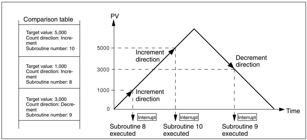
The relationship between the target value comparison count check and the comparison table is different for the CPM1/CPM1A. Refer to the individual manuals for details.
It is not possible to specify more than one comparison direction condition for the same target value in the comparison table.
Either target value comparison or range comparison can be used for high-speed counter interrupts.
Range Comparison Interrupts
Up to eight combinations of comparison conditions (upper limit and lower limit) and interrupt subroutine numbers can be registered in the comparison table. The specified subroutine is executed once when the counter PV is greater than or equal to the lower limit and less than or equal to the upper limit in the comparison table.
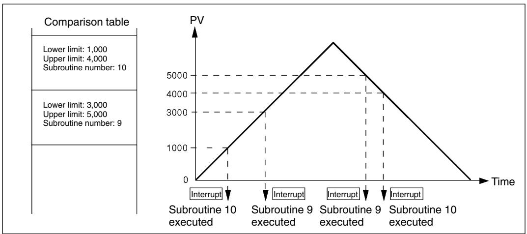
If two or more comparison conditions are satisfied simultaneously (in the same cycle), the interrupt for the condition closest to the beginning of the comparison table will be executed.
Either target value comparison or range comparison can be used for high-speed counter interrupts.
If an interrupt is generated during execution of one of the high-speed counter control instructions, i.e., CTBL(63), INI(61), or PRV(62), these instructions will not be executed within the interrupt program.
If an interrupt is generated while an instruction controlling the high-speed counter is being executed in the normal program area, the CTBL(63), INI(61), and PRV(62), instructions will not be executed within the interrupt program. This situation can be avoided by means of the following programming.
Method 1
Prohibit interrupts in the normal program area while executing the instruction.
Method 2
In the normal program area, re-execute the instruction that could not be executed.
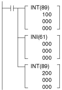
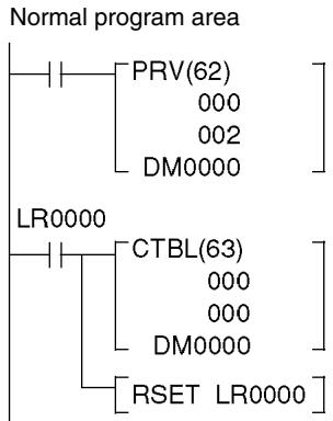
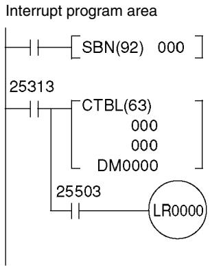
Interrupt processing subroutines are defined by SBN(92) and RET(93), just like ordinary subroutines.
An SBS UNDEFD error will be generated during the program check while an interrupt processing subroutine is being defined, but execution will be normal.
Wiring Inputs
Wire the inputs as shown in the following illustrations, according to the input mode and the reset method.
CPM2A Inputs
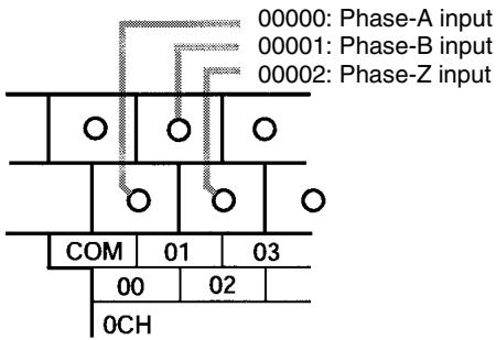
Differential Phase Input Mode
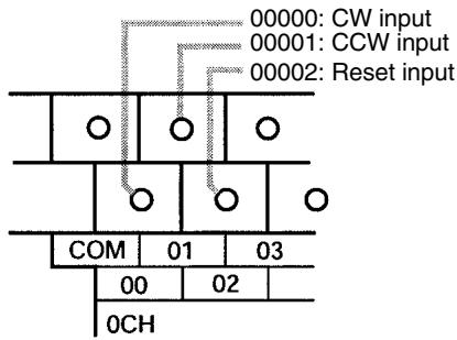
Up/Down Pulse Input Mode
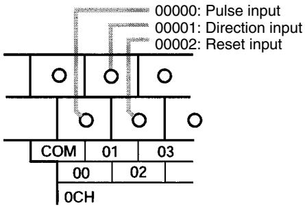
Pulse + Direction Input Mode
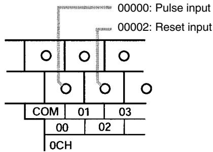
Increment Mode
CPM2C Inputs
Note The following examples are for Fujitsu-compatible connectors. Input bit addresses and connector pin numbers depend on the models. Refer to the CPM2C Operation Manual (W356) or the CPM2C-S Operation Manual (W377) for details.
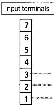
Differential Phase Input Mode
Input connector
(See above note.)

B

A
When phase-Z and reset inputs are not used, 00002 can be used as an ordinary input.
PC Setup
Set the PC Setup areas related to the high-speed counter as follows:
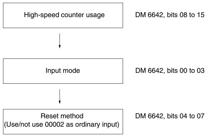
| Word | Bits | Function | Setting |
| DM 6642 | 00 to 03 | High-speed counter input mode setting | 0, 1, 2, or 4 |
| 0: Differential phase input 5 kHz | |||
| 1: Pulse + direction input 20 kHz | |||
| 2: Up/down input 20 kHz | |||
| 4: Increment 20 kHz | |||
| 04 to 07 | High-speed counter reset method setting | 0 or 1 | |
| 0: Phase-Z signal + software reset | |||
| 1: Software reset | |||
| 08 to 15 | High-speed counter usage setting | 01 | |
| 00: Do not use. | |||
| 01: Use as high-speed counter | |||
| 02: Use as pulse synchronization control (10 Hz to 500 Hz) | |||
| 03: Use as pulse synchronization control (20 Hz to 1 kHz) | |||
| 04: Use as pulse synchronization control (300 Hz to 20 kHz) |
The new settings for the System Setup go into effect when operation begins (when PROGRAM mode is changed to MONITOR or RUN mode), or when the CPM2A/CPM2C's power is turned ON.
Ladder Diagram Programming
The following table shows the instructions related to high-speed counter control.
| Instruction | Control | Operation |
| (@)CTBL(63) | Register target value comparison table | Registers target value comparison table. |
| Register range comparison table | Registers range comparison table. | |
| Register target value comparison table and start comparison | Registers target value comparison table and starts comparison. | |
| Register range comparison table and start comparison | Registers range comparison table and starts comparison. | |
| (@)INI(61) | Start comparison | Starts comparison with registered comparison table. |
| Stop comparison | Stops comparison. | |
| Change PV | Changes the high-speed counter PV. | |
| (@)PRV(62) | Read PV | Reads the high-speed counter PV. |
| Read status | Reads the high-speed counter status. | |
| Read range comparison result | Reads range comparison result. | |
| (@)INT(89) | Mask all interrupts | Prohibits all interrupts, including interrupt inputs, interval timer interrupts, high-speed counters, etc. |
| Unmask all interrupts | Permits all interrupts, including interrupt inputs, interval timer interrupts, high-speed counters, etc. |
The following table shows the data areas related to high-speed counter control.
| Word | Bits | Name | Contents |
| 248 | 00 to 15 | High-speed counter PV | Reads high-speed counter PV. |
| 249 | 00 to 15 | ||
| 252 | 00 | High-speed counter reset | When this bit turns ON, a software reset is triggered for the high-speed counter. |
| AR11 | 00 to 07 | High-speed counter range comparison results | ON: Condition satisfiedOFF: Condition not satisfied |
| 08 | High-speed counter comparison | ON: Comparison in progressOFF: Comparison stopped | |
| 09 | High-speed counter PV overflow/underflow | ON: Overflow/overflowOFF: Normal |
Register Target Value Comparison Table
Register Target Value Comparison Table and Start Comparison
These functions register a comparison table to the CPM2A/CPM2C for the purpose of count checking in target value comparison. It is also possible to start the comparison along with the registration.
Register Target Value Comparison Table
| (@)CTBL(63) |
| 000 |
| 002 |
| S |
Port specifier (000: High-speed counter)
Mode designation (002: Register target value comparison table only)
Beginning word of comparison table
Register Target Value Comparison Table and Start Comparison
| (@)CTBL(63) |
| 000 |
| 000 |
| S |
Port specifier (000: High-speed counter)
Mode designation (000: Register target value comparison table and start comparison)
Beginning word of comparison table
Target Value Comparison Table
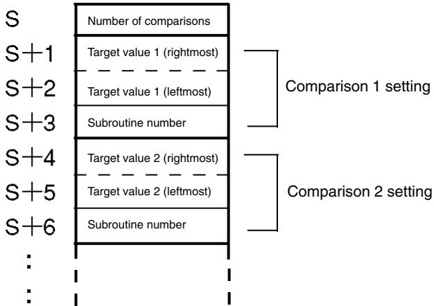
Number of comparisons
0001 to 0016 BCD
Target value (rightmost, leftmost)
Register the counter value to be compared.
The leftmost digit shows the sign (+ / - )
Differential phase input mode
Pulse + direction input mode
Up/down pulse input mode
When incrementing: F8388607 to 08388607
When decrementing: F8388608 to 08388606
Increment mode
00000001 to 16777215
The range that can be specified depends on the mode
when target comparison interrupts are specified.
Subroutine number
Register the direction of comparison and the subroutine
number to be executed when there is a match.
The leftmost digit shows the direction (increment/decrement).
Increment direction: 0000 to 0049
Decrement direction: F000 to F049
It is not possible to specify more than one comparison direction condition for the same target value in the comparison table.
Once a comparison table has been registered, it will be saved in the CPM2A/ CPM2C as long as no other comparison table is registered and the mode is not changed to PROGRAM mode (and as long as the power is not turned OFF).
Register Range Comparison Table
Register Range Comparison Table and Start Comparison
These functions register a comparison table to the CPM2A/CPM2C for the purpose of count checking in range comparison. It is also possible to start the comparison along with the registration.
Register Range Comparison Table
| (@)CTBL(63) | |
| 000 | |
| 003 | |
| S | |
Port specifier (000: High-speed counter)
Mode designation (003: Register range comparison table only)
Beginning word of comparison table
Register Range Comparison Table and Start Comparison
| (@)CTBL(63) |
Port specifier (000: High-speed counter)
Mode designation (001: Register range comparison table and start comparison)
Beginning word of comparison table
Range Comparison Table
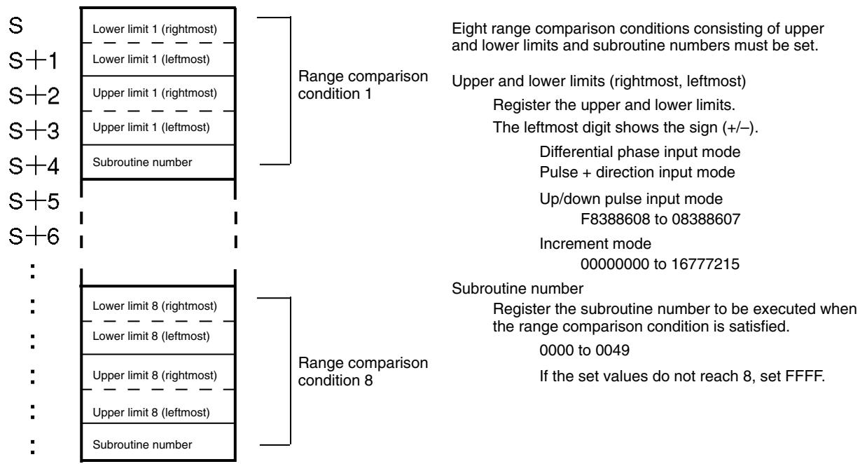
If two or more comparison conditions are satisfied simultaneously (in the same cycle), the interrupt for the condition closest to the beginning of the comparison table will be executed.
Once a comparison table has been registered, it will be saved in the CPM2A/ CPM2C as long as no other comparison table is registered and the mode is not changed to PROGRAM mode (and as long as the power is not turned OFF).
Start/Stop Comparison
The comparison can be started or stopped according to the table that has already been registered to the CPM2A/CPM2C by CTBL(63).
Start Comparison
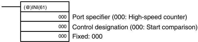
Stop Comparison
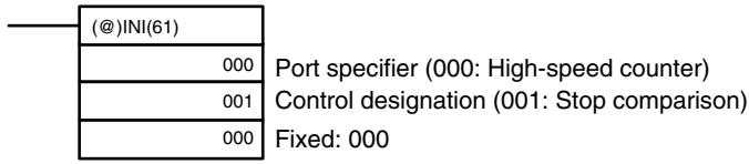
Change PV
This function changes the high-speed counter PV.
(@)INl(61)
000
Port specifier (000: High-speed counter)
002
Control designation (002: Change PV)
Beginning word of PV data to change
C2
C2+1
Rightmost 4 digits
Leftmost 4 digits
PV data to change (Rightmost and leftmost)
Register the PV data to be changed.
The leftmost digit shows the sign (+ / - )
Differential phase input mode
Pulse + direction input mode
Up/down pulse input mode
F8388608 to 08388607
Increment mode
00000000 to 16777215
No interrupt will occur during a target value comparison even if the target value registered in the comparison table is changed by INI(61).
Read PV
This function reads the high-speed counter PV.
Using an Instruction
| (@)PRV(62) |
| 000 |
| 002 |
| C2 |
Port specifier (000: High-speed counter)
Control designation (000: Read PV)
Beginning word for storing PV
Rightmost 4 digits
Leftmost 4 digits
PV (Rightmost and leftmost)
The read PV will be stored here.
The leftmost digit shows the sign (+ / - )
Differential phase input mode
Pulse + direction input mode
Up/down pulse input mode
F8388608 to 08388607
Increment mode
00000000 to 16777215
Using Data Areas
The high-speed counter PV is stored in words 248 and 249 as shown below.
SR 248
PV (Rightmost word)
SR 249
PV (Leftmost word)
Words 248 and 249 are refreshed with every scan, so there may be a discrepancy from the exact PV at any given time.
When the high-speed counter is not used, words 248 and 249 can be used as work words.
When the PV is read by executing PRV(62), words 248 and 249 are refreshed with the same timing.
Read Status
This function reads the high-speed counter status, such as whether a comparison operation is in progress or whether an overflow or underflow has occurred.
Using an Instruction
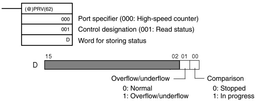
Using Data Areas
The status is stored in AR 1108 and AR 1109 as shown below.
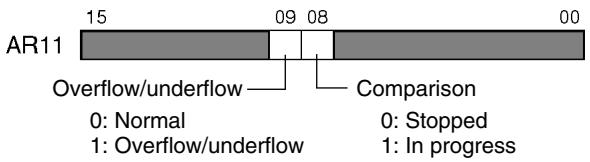
AR 1108 and AR 1109 are refreshed with every scan, so there may be a discrepancy from the exact status at any given time.
When the status is read by executing PRV(62), AR 1108 and AR 1109 are refreshed with the same timing.
Read Range Comparison Result
This function reads the result of a range comparison showing whether or not the PV is within a range.
Using an Instruction

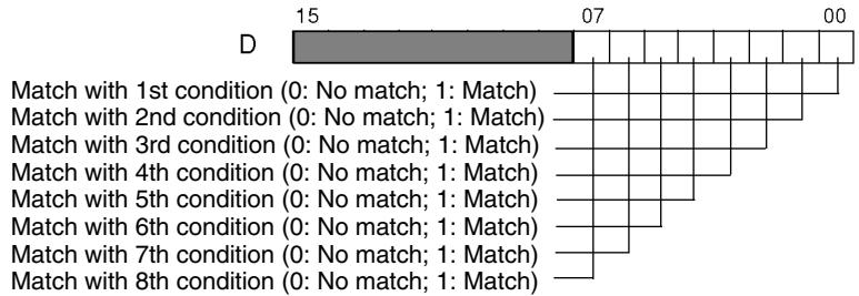
Using Data Areas
The range comparison result is stored in AR 1100 through AR 1107, as shown below.
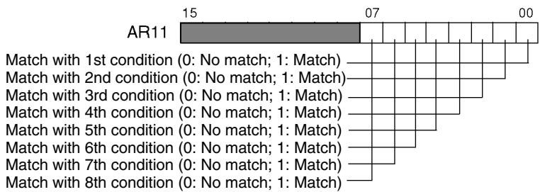
AR 1100 through AR 1107 are refreshed with every scan, so there may be a discrepancy from the exact PV range comparison result at any given time.
When the range comparison result is read by executing PRV(62), AR 1100 through AR 1107 are refreshed with the same timing.
Mask/Unmask All Interrupts
For details regarding masking and unmasking all interrupts, refer to 2-1-2 Interrupt Inputs.
Application Examples
Target Value Comparison
Explanation
In this example, specified interrupt subroutines are executed by matching the high-speed counter's PV with five values set as a target value comparison table. With each interrupt, the data in DM 0000 to DM 0004 is incremented by one.
Wiring (CPM2A)
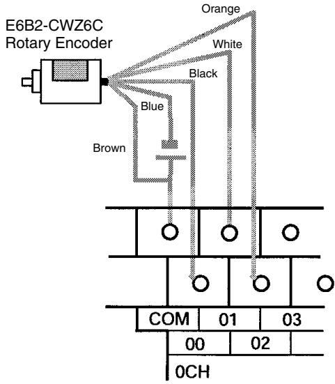
Wiring (CPM2C)
Note The following examples are for Fujitsu-compatible connectors. Input bit addresses and connector pin numbers depend on the models. Refer to the CPM2C Operation Manual (W356) or the CPM2C-S Operation Manual (W377) for details.
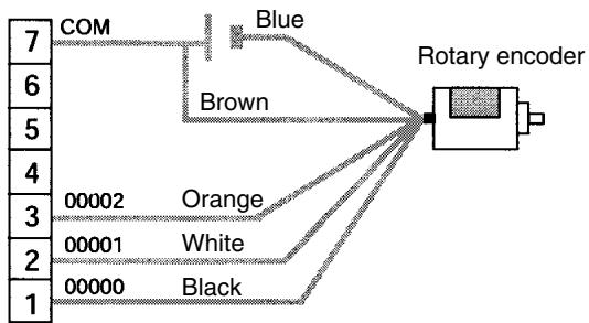
Input terminals
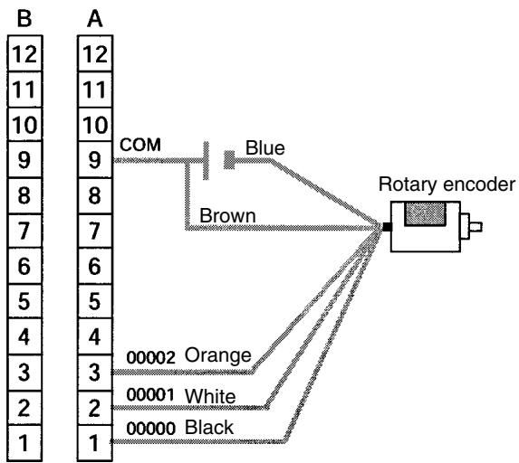
Input connector (See above note.)
PC Setup
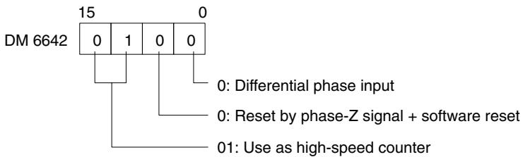
Programming
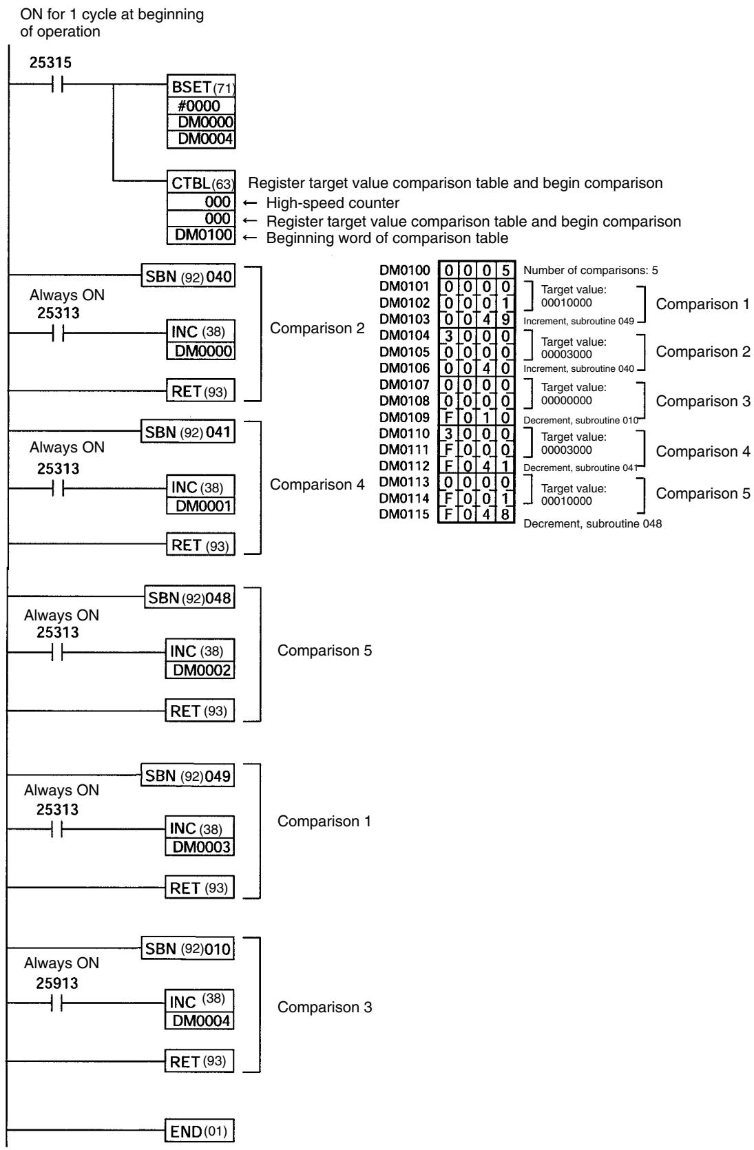
Range Comparison
Explanation
In this example, specified interrupt subroutines are executed by matching the high-speed counter's PV with five range set as a range comparison table. With each interrupt, the data in DM 0000 to DM 0004 is incremented by one.
Wiring (CPM2A)

Wiring (CPM2C)
Note The following examples are for Fujitsu-compatible connectors. Input bit addresses and connector pin numbers depend on the models. Refer to the CPM2C Operation Manual (W356) or the CPM2C-S Operation Manual (W377) for details.
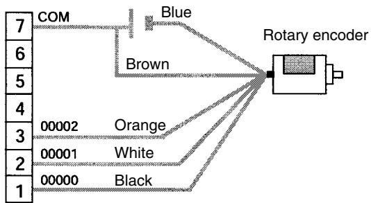
Input terminals
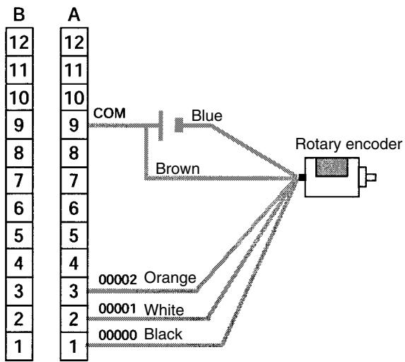
Input connector (See above note.)
PC Setup
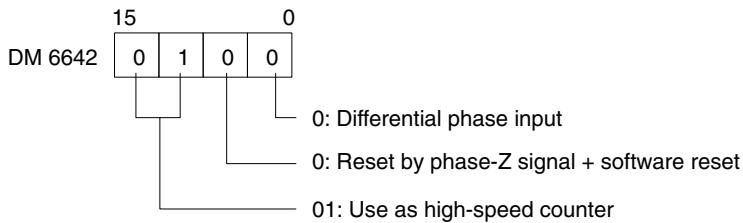
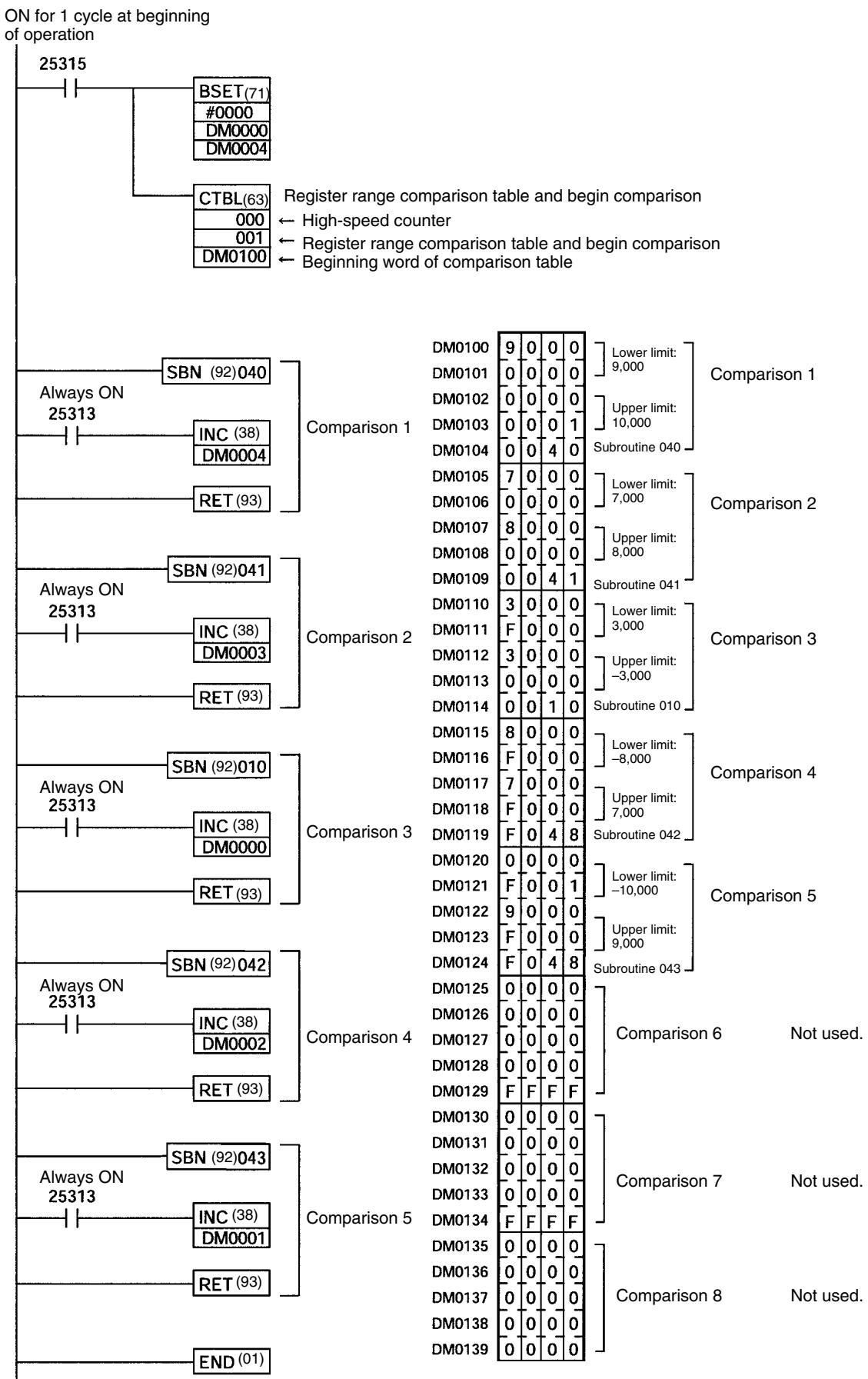
Programming
2-2-2 Input Interrupts In Counter Mode
The four built-in interrupt inputs in the CPM2A/CPM2C's CPU Unit can be used in counter mode as inputs of up to 2kHz . These inputs can be used as either incrementing counters or decrementing counters, triggering an interrupt (i.e., executing an interrupt subroutine) when the count matches the set value.
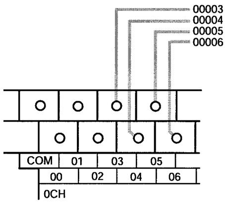

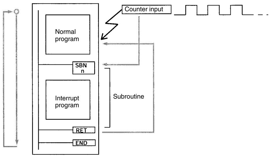
| Input number (Note 2) | Count | Interrupt number | Subroutine number (Note 3) | Response frequency |
| 00003 | 0 to 65535 (0000 to FFFF) | 0 | 000 | 2 kHz |
| 00004 | 1 | 001 | ||
| 00005 | 2 | 002 | ||
| 00006 | 3 | 003 |
Note
- Input number 00005 and 00006 cannot be used in CPM2C CPU Units with 10 I/O points and CPM2C-S CPU Units.
- Input numbers 00003 to 00006 can be used for any of the following functions: interrupt inputs, interrupt inputs (counter mode), or quick-response inputs. When not being used for any of these, they can be used as ordinary inputs.
- Subroutine numbers 000 to 003 are the subroutine numbers for interrupt programs started up when interrupt inputs or count-up interrupts for interrupt inputs (counter mode) are generated. When not being used for this purpose, they can be used as ordinary inputs.
Although IORF(97) can be used in interrupt subroutines, you must be careful of the interval between IORF(97) executions. If IORF(97) is executed too frequently, a fatal system error may occur (FALS 9F), stopping operation. The interval between executions of IORF(97) should be at least 1.3ms+ total execution time of the interrupt subroutine.
The following table shows the relationships between interrupt inputs (counter mode) and the CPM2A/CPM2C's other functions.
| Function | Interrupt inputs (counter mode) |
| Synchronized pulse control | Can be used simultaneously. |
| Interrupt inputs | See note 1. |
| Interval timer interrupts | Can be used simultaneously. |
| High-speed counters | Can be used simultaneously. |
| Interrupt inputs (counter mode) | See note 1. |
| Pulse outputs | Can be used simultaneously. |
| Quick-response inputs | See note 1. |
| Input time constant | See note 2. |
| Clock | Can be used simultaneously. |
Note
- The same input number (from 00003 to 00006) cannot be used for more than one of the following functions: interrupt inputs, interrupt inputs (counter mode), or quick-response inputs.
- When inputs 00003 to 00006 are set for use as interrupt inputs (counter mode), the input time constants for the relevant inputs are disabled. The input time constants remain in effect, however, for the values for refreshing the relevant input relay area.
Procedure for Using Interrupt Inputs in Counter Mode
Caution
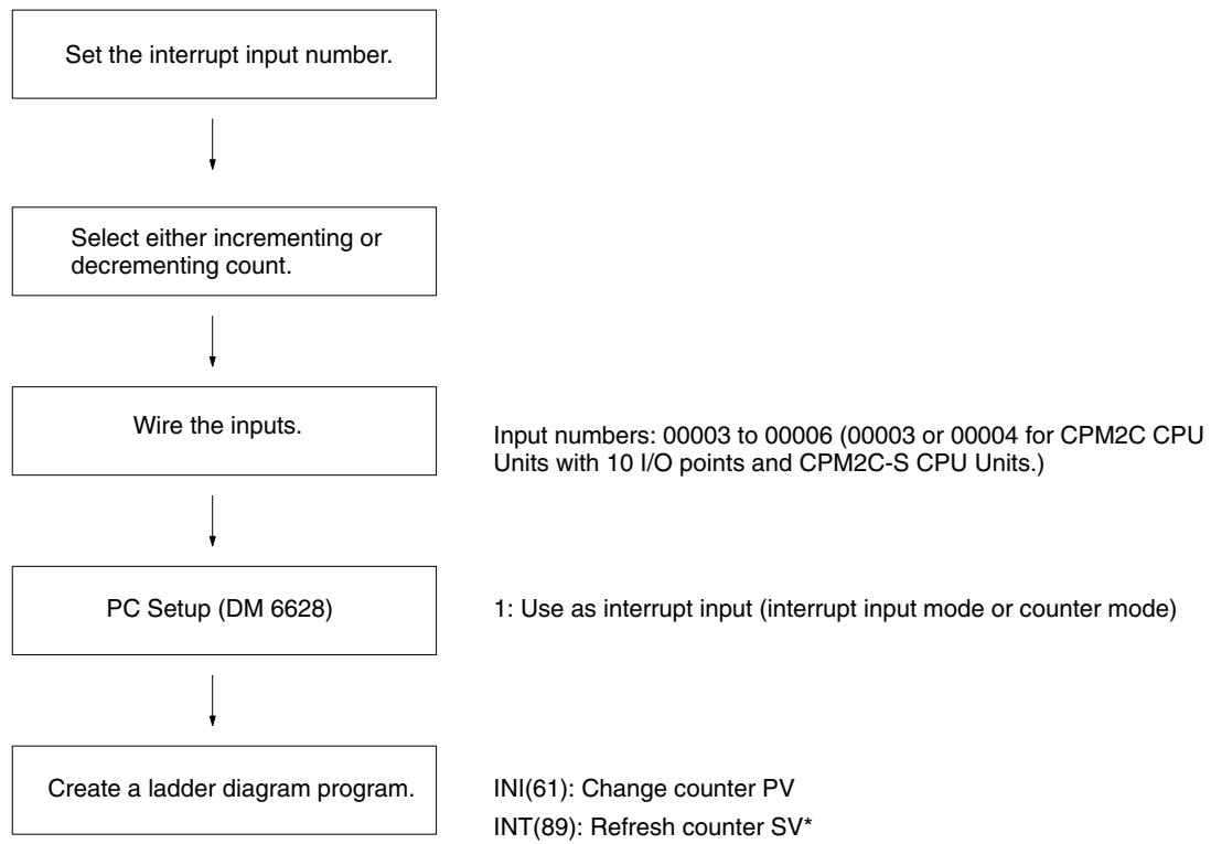
*Used only for count-up interrupts.
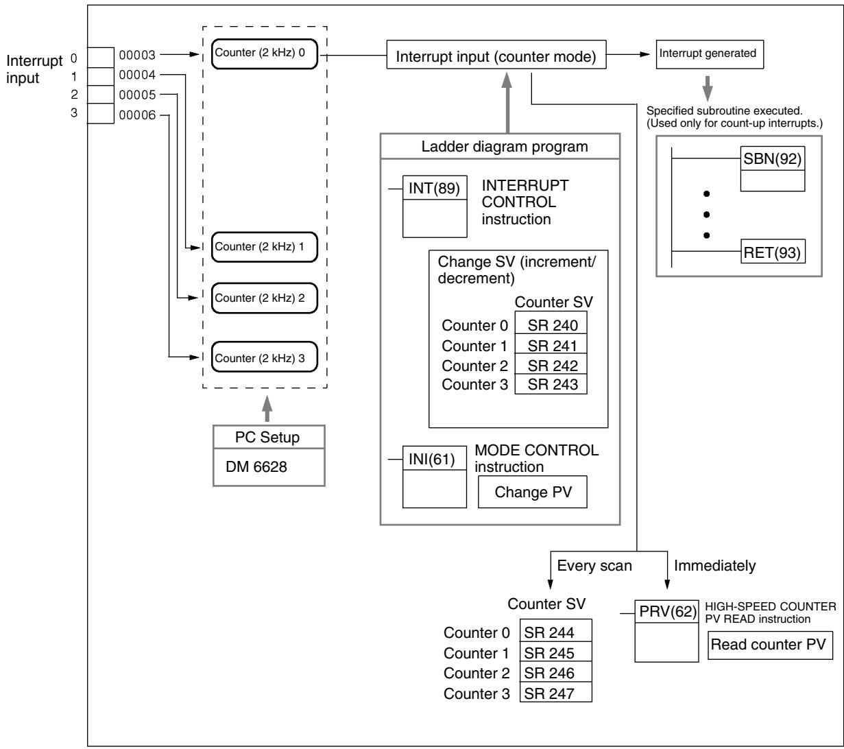
Setting the Interrupt Input Number
With interrupt inputs in counter mode, the subroutine to be executed is determined by the interrupt corresponding to the input number.
| Input number | Interrupt number | Subroutine number |
| 00003 | 0 | 000 |
| 00004 | 1 | 001 |
| 00005* | 2 | 002 |
| 00006* | 3 | 003 |
Note *Input numbers 00005 and 00006 cannot be used for CPM2C CPU Units with 10 I/O points and for CPM2C-S CPU Units.
The same input number (from 00003 to 00006) cannot be used for more than one of the following functions: interrupt inputs, interrupt inputs (counter mode), or quick-response inputs.
Selecting Incrementing or Decrementing Count
Either an incrementing or decrementing count can be used with interrupt inputs in counter mode.
Incrementing Counter Mode
As the set value (SV) is refreshed, the count is incremented from 0, and the interrupt subroutine is executed when the present value (PV) matches the SV.
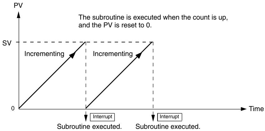
Decrementing Counter Mode
As the set value (SV) is refreshed, the count is decremented toward 0, and the interrupt subroutine is executed when the present value (PV) reaches 0.
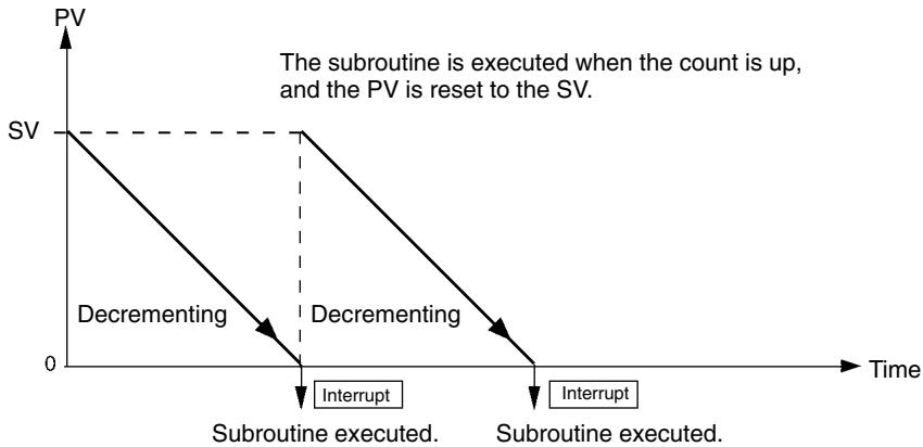
Wiring the Inputs
With the CPM2A, wire the input terminals as shown in the following illustration.
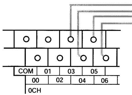
Input 00003: Input interrupt (counter mode) 0
Input 00004: Input interrupt (counter mode) 1
Input 00005: Input interrupt (counter mode) 2
Input 00006: Input interrupt (counter mode) 3
With the CPM2C, wire the input terminals as shown in the following illustration.
Note The following examples are for Fujitsu-compatible connectors. Input bit addresses and connector pin numbers depend on the models. Refer to the CPM2C Operation Manual (W356) or the CPM2C-S Operation Manual (W377) for details.

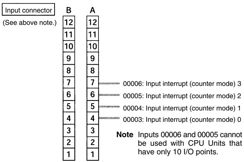
PC Setup
The following table shows the settings in the PC Setup area related to interrupt input usage.
| Word | Bits | Function | Setting | |
| DM 6628 | 00 to 03 | Interrupt setting for input 00003 | 0: Normal input1: Interrupt input (interrupt input mode or counter mode)2: Quick-response input | 1 |
| 04 to 07 | Interrupt setting for input 00004 | |||
| 08 to 11 | Interrupt setting for input 00005* | |||
| 12 to 15 | Interrupt setting for input 00006* | |||
Note *Input number 00005 and 00006 cannot be used in CPM2C CPU Units with 10 I/O points and in CPM2C-S CPU Units.
The setting will go into effect when the mode is changed (from PROGRAM to MONITOR/RUN) or when the power supply is turned ON to the CPM2A/ CPM2C.
Ladder Diagram Programming
The following table shows the instruction operations related to interrupt input (counter mode) control.
| Instruction | Control | Operation |
| (@)INT(89) | Refresh incrementing counter SV | Refreshes the counter's SV and starts the incrementing count. |
| Refresh decrementing counter SV | Refreshes the counter's SV and starts the decrementing count. | |
| Mask all interrupts | Prohibits all interrupts, including interrupt inputs, interval timer interrupts, high-speed counters, etc. | |
| Unmask all interrupts | Permits all interrupts, including interrupt inputs, interval timer interrupts, high-speed counters, etc. | |
| (@)INI(61) | Change PV | Changes the counter's PV. |
| (@)PRV(62) | Read PV | Reads the counter's PV. |
The functions related to input interrupts (counter mode) are executed according to the data areas shown in the following table.
| Word | Bits | Name | Contents |
| 240 | 00 to 15 | SV area for input interrupt (counter mode) 0 | Stores the counter's set value (SV). |
| 241 | 00 to 15 | SV area for input interrupt (counter mode) 1 | |
| 242 | 00 to 15 | SV area for input interrupt (counter mode) 2 | |
| 243 | 00 to 15 | SV area for input interrupt (counter mode) 3 | |
| 244 | 00 to 15 | PV area for input interrupt (counter mode) 0 | Stores the counter's present value (PV). |
| 245 | 00 to 15 | PV area for input interrupt (counter mode) 1 | |
| 246 | 00 to 15 | PV area for input interrupt (counter mode) 2 | |
| 247 | 00 to 15 | PV area for input interrupt (counter mode) 3 |
Refresh Incrementing Counter SV / Refresh Decrementing Counter SV
These functions store the counter's set values in data areas and refresh them by means of INT(89). In this way, they start the count operation for interrupt inputs (counter mode) and they permit interrupts.
Storing Set Values in Data Areas
The counter's set values are stored in words 240, 241, 242, and 243.
| SR 240 |
| SR 241 |
| SR 242 |
| SR 243 |
SV for interrupt input (count mode) 0: 0000 to FFFF
SV for interrupt input (count mode) 1: 0000 to FFFF
SV for interrupt input (count mode) 2: 0000 to FFFF
SV for interrupt input (count mode) 3: 0000 to FFFF
Starting the Count Operation and Permitting Interrupts
Incrementing Counter
| (@)INT(89) |
| 004 |
| 000 |
| C2 |
Interrupt control designation (004: Refresh incrementing counter SV)
Fixed: 000
Control data word
Decrementing Counter
| (@)INT(89) |
| 003 |
| 000 |
| C2 |
Interrupt control designation (003: Refresh decrementing counter SV)
Fixed: 000
Control data word

0:Refresh SV
1: Do not refresh SV
Note When INT(89) is executed to mask interrupts during counter operation (interrupt control designation 000), counter operation will be stopped and the counter PV will be reset. To use the counter again, start the counter operation again as described above.
Change PV
This function refreshes the counter's present value (PV).
| (@)INT(89) |
| P |
| 002 |
| C2 |
Port specifier (100. 102, 102, 103: Interrupt inputs (counter mode) 0 to 3)
Control designation (002: Change PV)
Change PV data word
Change PV data
Registers the PV data to be changed.
0000 to FFFF
Read PV
This function reads the counter's present value (PV).
Using an Instruction
| (@)PRV(62) |
| P |
| 000 |
| D |
Port specifier (100, 102, 102, 103: Interrupt inputs (counter mode) 0 to 3)
Control designation (000: Read PV)
Word for storing PV
Read PV data
The PV that is read is stored here.
0000 to FFFF
Using Data Areas
The high-speed counter's present value (PV) is stored in words SR 244 to SR 247 as shown below.
| SR 244 |
| SR 245 |
| SR 246 |
| SR 247 |
PV Interrupt input (counter mode) 0
PV Interrupt input (counter mode) 1
PV Interrupt input (counter mode) 2
PV Interrupt input (counter mode) 3
Words SR 244 to SR 247 are refreshed with every scan, so there may be a discrepancy from the exact PV at any given time.
Words SR 244 to SR 247 cannot be used as work word even when the interrupt inputs (counter mode) are not used.
When the PV is read by executing PRV(62), words 244 to 247 are refreshed with the same timing.
Mask/Unmask All Interrupts
For details regarding masking and unmasking all interrupts, refer to 2-1-2 Interrupt Inputs.
Application Example
Explanation
In this example, the PV is decremented every time input 00003 is turned ON, and DM 0000 is incremented by 1 by an interrupt subroutine every 100 times (64 Hex) that input 00003 is turned ON.
Wiring
The following diagram shows input wiring in the CPM2A.
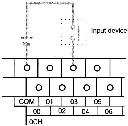
The following diagram shows input wiring in the CPM2C.
Note The following examples are for Fujitsu-compatible connectors. Input bit addresses and connector pin numbers depend on the models. Refer to the CPM2C Operation Manual (W356) or the CPM2C-S Operation Manual (W377) for details.
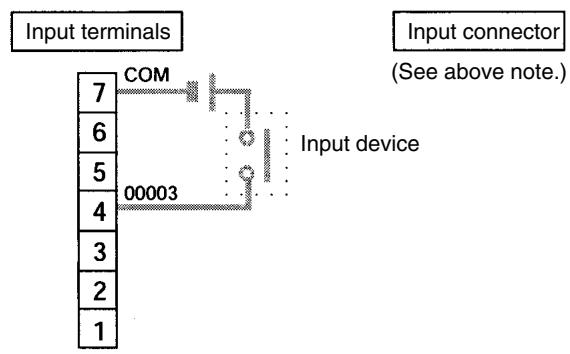
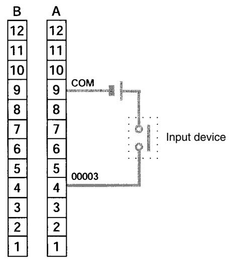
PC Setup
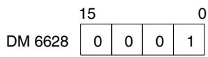
Specifies bit 00003 as an interrupt input (counter mode). Inputs 00004 to 00006 are used as ordinary inputs.
Programming
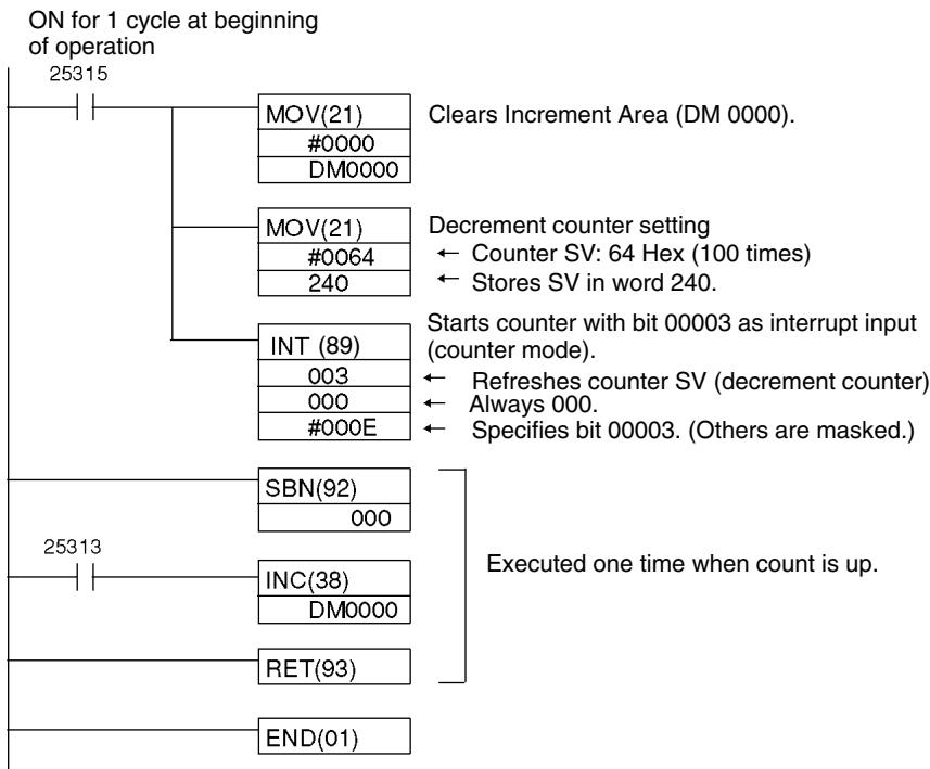
2-3 CPM1/CPM1A Interrupt Functions
This section explains the settings and methods for using the CPM1/CPM1A interrupt functions.
2-3-1 Types of Interrupts
| The CPM1/CPM1A has three types of interrupt processing, as outlined below. Input Interrupts CPM1/CPM1A PCs have two or four interrupt inputs. Interrupt processing is executed when one of these inputs is turned ON from an external source. Interval Timer Interrupts Interrupt processing is executed by an interval timer with a precision of 0.1 ms. High-speed Counter Interrupts The high-speed counter counts pulse inputs to one of CPU bits 00000 to 00002. Interrupt processing is executed when the count reaches the set value of a built-in high-speed counter. | |
| Interrupt Priority | When an interrupt is generated, the specified interrupt processing routine is executed. Interrupts have the following priority ranking. Input interrupts > Interval interrupts = High-speed counter interrupts When an interrupt with a higher priority is received during interrupt processing, the current processes will be stopped and the newly received interrupt will be processed instead. After that routine has been completely executed, then processing of the previous interrupt will be resumed. When an interrupt with a lower or equal priority is received during interrupt processing, then the newly received interrupt will be processed as soon as the routine currently being processed has been completely executed. When two interrupts with equal priority are received at the same time, they are executed in the following order: Input interrupt 0 > Input interrupt 1 > Input interrupt 2 > Input interrupt 3 Interval interrupts > High-speed counter interrupts |
| Interrupt Program Precautions | Observe the following precautions when using interrupt programs: 1, 2, 3... 1. A new interrupt can be defined within an interrupt program. Furthermore, an interrupt can be cleared from within an interrupt program. 2. Another interrupt program cannot be written within an interrupt program. 3. A subroutine program cannot be written within an interrupt program. Do not write a SUBROUTINE DEFINE instruction, SBN(92), within an interrupt program. 4. An interrupt program cannot be written within a subroutine program. Do not write an interrupt program between a SUBROUTINE DEFINE instruction (SBN(92)) and a RETURN instruction (RET(93)). Inputs used as interrupts cannot be used as regular inputs. |
| High-speed Counter Instructions and Interrupts | The following instructions cannot be executed in an interrupt subroutine when an instruction that controls high-speed counters is being executed in the main program: INI(61), PRV(62), or CTBL(63) |
The following methods can be used to circumvent this limitation:
Method 1
All interrupt processing can be masked while the instruction is being executed.
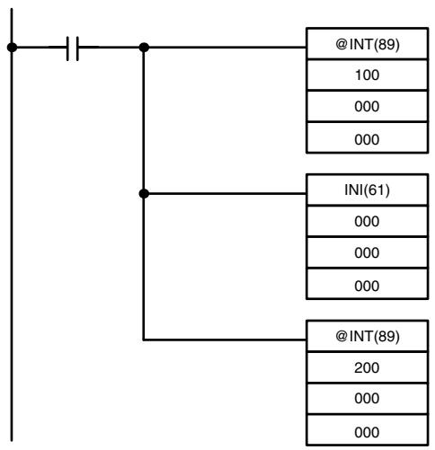
Method 2
Execute the instruction again in the main program.
1, 2, 3... 1. This is the program section from the main program:
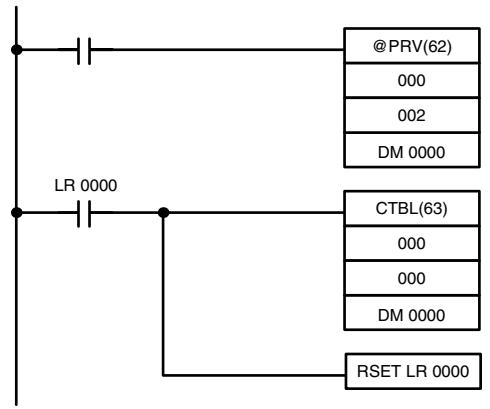
- This is the program section from the interrupt subroutine:

Note 1. Define interrupt routines at the end of the main program with SBN(92) and RET(93) instructions, just like regular subroutines.
- When defining an interrupt routine, a "SBS UNDEFD" error will occur during the program check operation, but the program will be executed normally.
2-3-2 Input Interrupts
The 10-pt CPU Units (CPM1-10CDR-□ and CPM1A-10CDR-□) have two interrupt inputs (00003 and 00004).
The 20-, 30-, and 40-pt CPU Units (CPM1-20CDR- , CPM1A-20CDR- , CPM1-30CDR- (-V1), CPM1A-30CDR- and CPM1A-40CDR- ) have four interrupt inputs (00003 to 00006).
There are two modes for input interrupts: input interrupt mode and counter mode.
CPM1 PCs
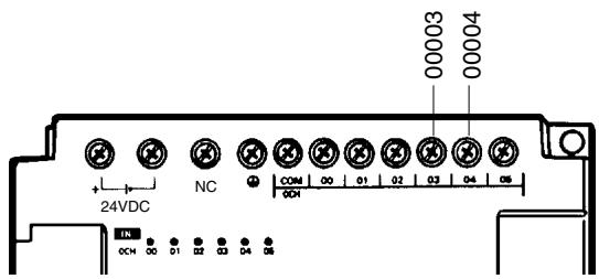
10-pt CPU Units (CPM1-10CDR-□)
20- and 30-pt CPU Units (CPM1-20CDR-□ and CPM1-30CDR-(-V1))
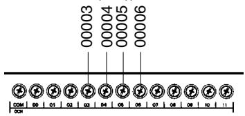
CPM1A PCs
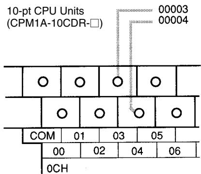
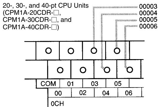
| CPU Unit | Input | Interrupt number | Response time | |
| Interrupt mode | Counter mode | |||
| CPM1-10CDR-□ | 00003 | 00 | 0.3 ms max. (Time until the interrupt program is executed.) | 1 kHz |
| CPM1A-10CD□-□ | 00004 | 01 | ||
| CPM1-20CDR-□ | 00003 | 00 | ||
| CPM1A-20CD□-□ | 00004 | 01 | ||
| CPM1-30CDR-□(-V1) | 00003 | 02 | ||
| CPM1A-30CD□-□ | 00004 | 03 | ||
| CPM1A-40CD□-□ | ||||
Note If input interrupts are not used, use inputs 00003 to 00006 as regular inputs.
Input Interrupt Settings
Inputs 00003 to 00006 must be set as interrupt inputs in DM 6628 if they are to be used for input interrupts in the CPM1/CPM1A. Set the corresponding digit to 1 if the input is to be used as an interrupt input (input interrupt or counter mode); set it to 0 if it is to be used as a regular input.
| Word | Setting |
| DM 6628 | 0: Regular input (default setting) 1: Interrupt input 2: Quick-response input |
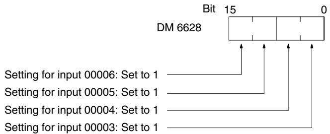
Interrupt Subroutines
Interrupts from inputs 00003 to 00006 are allocated interrupt numbers 00 to 03 and call subroutines 000 to 003. If the input interrupts aren't being used, subroutines 000 to 003 can be used in regular subroutines.
| Input number | Interrupt number | Subroutine number |
| 00003 | 0 | 000 |
| 00004 | 1 | 001 |
| 00005 | 2 | 002 |
| 00006 | 3 | 003 |
Input Refreshing
If input refreshing is not used, input signal status within the interrupt routine will not be reliable. Depending on the input time constant, the input signals might not go ON even if input refreshing is used. This includes the status of the interrupt input bit that activated the interrupt.
For example, IR 00000 would not be ON in interrupt routine for input interrupt 0 unless it was refreshed. In this case, use the Always ON Flag, SR 25313 in the interrupt routine instead of IR 00000.
Input Interrupt Mode
When an input interrupt signal is received, the main program is interrupted and the interrupt program is executed immediately, regardless of the point in the cycle in which the interrupt is received. The signal must be ON for 200 s or more to be detected.
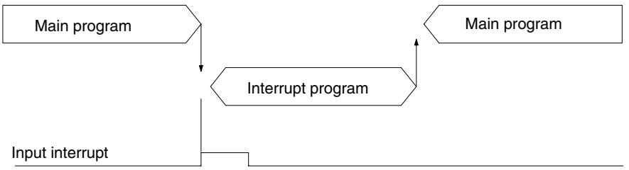
Use the following instructions to program input interrupts using the Input Interrupt Mode.
Masking/Unmasking of Interrupts
With the INT(89) instruction, set or clear input interrupt masks as required.
| (@)INT(89) |
| 000 |
| 000 |
| D |
Make the settings with word D bits 0 to 3, which correspond to input interrupts 0 to 3.
0: Mask cleared. (Input interrupt enabled.)
1: Mask set. (Input interrupt disabled.)
All of the input interrupts are masked when PC operation is started. If input interrupt mode is being used, be sure to enable the inputs by executing INT(89) as shown above.
Clearing Masked Interrupts
If the bit corresponding to an input interrupt turns ON while masked, that input interrupt will be saved in memory and will be executed as soon as the mask is cleared. In order for that input interrupt not to be executed when the mask is cleared, the interrupt must be cleared from memory.
Only one interrupt signal will be saved in memory for each interrupt number. With the INT(89) instruction, clear the input interrupt from memory.
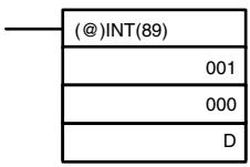
If D bits 0 to 3, which correspond to input interrupts 0 to 3, are set to "1," then the input interrupts will be cleared from memory.
0: Input interrupt retained.
1: Input interrupt cleared.
Reading Mask Status
With the INT(89) instruction, read the input interrupt mask status.
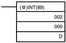
The status of the rightmost digit of the data stored in word D (bits 0 to 3) show the mask status.
0: Mask cleared. (Input interrupt enabled.)
1: Mask set. (Input interrupt disabled.)
Program Example
When input 00003 (interrupt no. 0) goes ON, operation moves immediately to the interrupt program with subroutine number 000. Inputs for DM 6628 have been set to 0001.
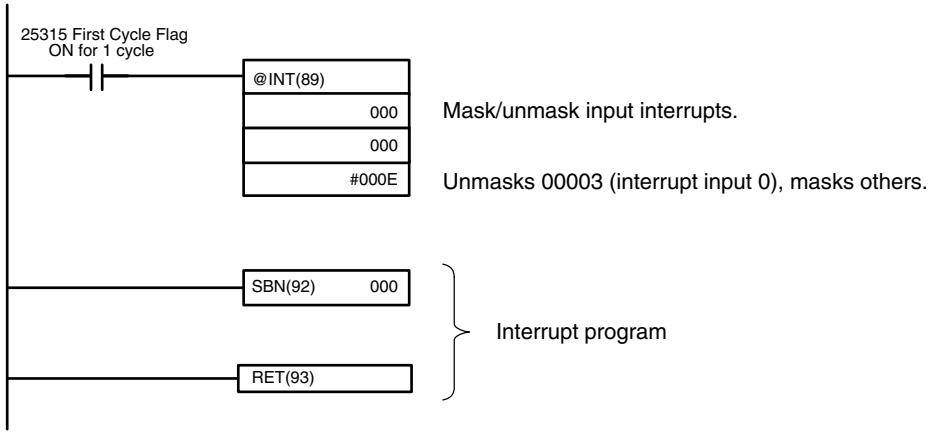
Counter Mode
External signal inputs are counted at high speed and an interrupt is generated when the count reaches the set value. When an interrupt is generated, the main program is interrupted and the interrupt program is executed. Signals up to 1 kHz can be counted.
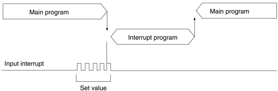
Use the following steps to program input interrupts using the Counter Mode.
1,2,3...
- Write the set values for counter operation to the SR words shown in the following table. The set values are written between 0000 and FFFF (0 to 65,535). A value of 0000 will disable the count operation until a new value is set and step 2, below, is repeated.
| Interrupt | Word |
| Input interrupt 0 | SR 240 |
| Input interrupt 1 | SR 241 |
| Input interrupt 2 | SR 242 |
| Input interrupt 3 | SR 243 |
The SR words used in the Counter Mode (SR 240 to SR 243) contain hexadecimal data, not BCD. If the Counter Mode is not used, these words can be used as work bits.
Note These SR words are cleared at the beginning of operation, and must be written from the program.
- With the INT(89) instruction, refresh the Counter Mode set value and enable interrupts.
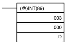
If D bits 0 to 3, which correspond to input interrupts 0 to 3, are set to "0," then the set value will be refreshed and interrupts will be permitted.
0: Counter mode set value refreshed and mask cleared.
1: Not refreshed.
Be sure to set the corresponding bit to 1 if an input interrupt isn't being controlled.
The input interrupt for which the set value is refreshed will be enabled in Counter Mode. When the counter reaches the set value, an interrupt will occur, the counter will be reset, and counting/interrupts will continue until the counter is stopped.
Note
-
If the INT(89) instruction is used during counting, the present value (PV) will return to the set value (SV). You must, therefore, use the differentiated form of the instruction or an interrupt may never occur.
-
The set value will be set when the INT(89) instruction is executed. If interrupts are already in operation, then the set value will not be changed just by changing the content of SR 240 to SR 243, i.e., if the contents are changed, the set value must be refreshed by executing the INT(89) instruction again.
Interrupts can be masked using the same process used with the Input Interrupt Mode, but if the masked interrupts are cleared using the same process, the interrupts will operate in Input Interrupt Mode, not Counter Mode.
Interrupt signals received for masked interrupts can also be cleared using the same process as for the Input Interrupt Mode.
Counter PV in Counter Mode
When input interrupts are used in Counter Mode, the counter PV will be stored in the SR word corresponding to input interrupts 0 to 3. Values are 0000 to FFFE (0 to 65,534) and will equal the counter PV minus one.
| Interrupt | Word |
| Input interrupt 0 | SR 244 |
| Input interrupt 1 | SR 245 |
| Input interrupt 2 | SR 246 |
| Input interrupt 3 | SR 247 |
Example: The present value for an interrupt whose set value is 000A will be recorded as 0009 immediately after INT(89) is executed.
Note Even if input interrupts are not used in Counter Mode, these SR bits cannot be used as work bits.
Program Example
When input 00003 (interrupt no. 0) goes ON 10 times, operation moves immediately to the interrupt program with subroutine number 000. The following table shows where the counters' set values and present values -1 are stored. Inputs for DM 6628 have been set to 0001.
| Interrupt | Word containing SV | Word containing PV-1 |
| Input 00003 (input interrupt 0) | SR 240 | SR 244 |
| Input 00004 (input interrupt 1) | SR 241 | SR 245 |
| Input 00005 (input interrupt 2) | SR 242 | SR 246 |
| Input 00006 (input interrupt 3) | SR 243 | SR 247 |
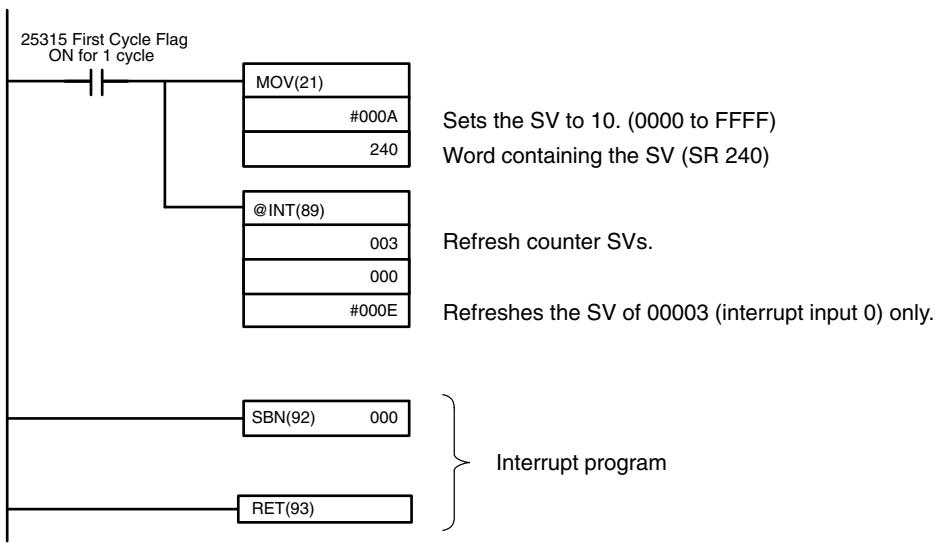
2-3-3 Masking All Interrupts
All interrupts, including input interrupts, interval timer interrupts, and high-speed counter interrupts, can be masked and unmasked as a group by means of the INT(89) instruction. The mask is in addition to any masks on the individual types of interrupts. Furthermore, clearing the masks for all interrupts does not clear the masks on the individual types of interrupts, but restores them to the masked conditions that existed before INT(89) was executed to mask them as a group.
Do not use INT(89) to mask interrupts unless it is necessary to temporarily mask all interrupts and always use INT(89) instructions in pairs to do so, using the first INT(89) instruction to mask and the second one to unmask interrupts.
INT(89) cannot be used to mask and unmask all interrupts from within interrupt routines.
Masking Interrupts
Use the INT(89) instruction to disable all interrupts.
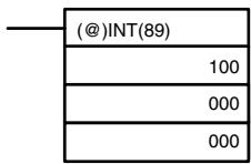
If an interrupt is generated while interrupts are masked, interrupt processing will not be executed but the interrupt will be recorded for the input, interval timer, and high-speed counter interrupts. The interrupts will then be serviced as soon as interrupts are unmasked.
Unmasking Interrupts
Use the INT(89) instruction to unmask interrupts as follows:
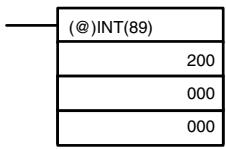
2-3-4 Interval Timer Interrupts
The CPM1/CPM1A is equipped with one interval timer. When the interval timer times out, the main program is interrupted and the interrupt program is executed immediately, regardless of the point in the cycle.
There are two modes for interval timer operation, the One-shot Mode, in which only one interrupt will be executed when time expires, and the Scheduled Interrupt Mode in which the interrupt is repeated at a fixed interval.
The interval timer's set value can be set anywhere from 0.5 to 319968 ms, in units of 0.1 ms.
Operation
Use the following instruction to activate and control the interval timer.
Starting Up in One-Shot Mode
Use the STIM(69) instruction to start the interval timer in the one-shot mode.
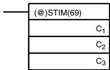
C_1 : Interval timer, one-shot mode (000)
C_2 : Timer set value (first word address)
C_3 : Subroutine no. (4 digits BCD): 0000 to 0049
1, 2, 3... 1. When C_2 is entered as a word address:
C_2 : Decrementing counter set value (4 digits BCD): 0000 to 9999
C_2 + 1 : Decrementing time interval (4 digits BCD; unit: 0.1 ms): 0005 to 0320 (0.5 ms to 32 ms)
Each time that the interval specified in word C_2 + 1 elapses, the decrementing counter will decrement the present value by one. When the PV reaches 0, the designated subroutine will be called just once and the timer will stop.
The time from when the STIM(69) instruction is executed until time elapses is calculated as follows:
(Content of C_2 ) × (Content of C_2 + 1 ) × 0.1 ms = (0.5 to 319,968 ms)
- When C_2 is entered as a constant:
The set value of the decrementing counter will equal the specified constant (in ms) and the decrementing time interval will be 10 (1 ms).
Starting Up in Scheduled Interrupt Mode
Use the STIM(69) instruction to start the interval timer in the scheduled interrupt mode.
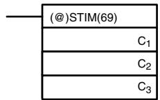
C_1 : Interval timer, scheduled interrupt mode (003)
C_2 : Timer set value (leading word no.)
C_3 : Subroutine no. (4 digits BCD): 0000 to 0049
- When C_2 is entered as a word address:
C_2 : Decrementing counter set value (4 digits BCD): 0000 to 9999
C_2 + 1 : Decrementing time interval (4 digits BCD; unit: 0.1 ms): 0005 to 0320 (0.5 ms to 32 ms)
The meanings of the settings are the same as for the one-shot mode, but in the scheduled interrupt mode the timer PV will be reset to the set value and decrementing will begin again after the subroutine has been called. In the scheduled interrupt mode, interrupts will continue to be repeated at fixed intervals until the operation is stopped.
2. When C_2 is entered as a constant:
The settings are the same as for the one-shot mode, but interrupts will continue to be repeated at fixed intervals until the operation is stopped.
Reading the Timer's Elapsed Time
Use the STIM(69) instruction to read the timer's elapsed time.
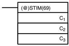
C_1 : Read elapsed time (006)
C_2 : Leading word of parameter 1
C_3 : Parameter 2
C2: Number of times the decrementing counter has ben decremented (4 digits BCD)
C_2 + 1 : Decrementing counter time interval (4 digits BCD; unit: 0.1ms
C_3 : Elapsed time from previous decrement (4 digits BCD; unit: 0.1 ms)
The time from when the interval timer is started until the execution of this instruction is calculated as follows:
(Content of C2) × (Content of C2 + 1) + (Content of C3) × 0.1 ms
If the specified interval timer is stopped, then "0000" will be stored.
Stopping the Timer
Use the STIM(69) instruction to stop the interval timer. The interval timer will be stopped.
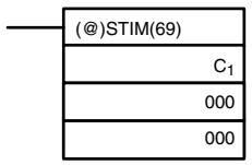
C_1 : Stop interval timer (010)
Application Example (One-shot Mode)
In this example, an interrupt is generated 2.4ms (0.6ms × 4) after input 00005 goes ON; the interrupt executes interrupt subroutine number 23.
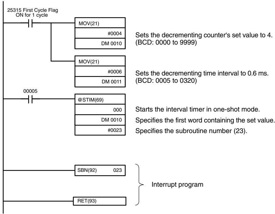
Application Example (Scheduled Interrupt Mode)
In this example, an interrupt is generated every 4.0 ms (1.0 ms × 4) after input 00005 goes ON; the interrupts execute interrupt subroutine number 23.
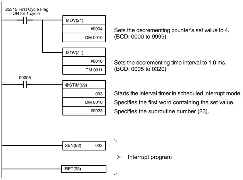
2-3-5 High-speed Counter Interrupts
CPM1/CPM1A PCs have a high-speed counter function that can be used in incrementing mode or up/down mode. The high-speed counter can be combined with input interrupts to perform target value control or zone comparison control that isn't affected by the PC's cycle time.
High-speed counter signals can be input to CPU bits 00000 through 00002.
CPM1 PCs
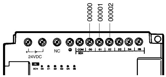
CPM1A PCs
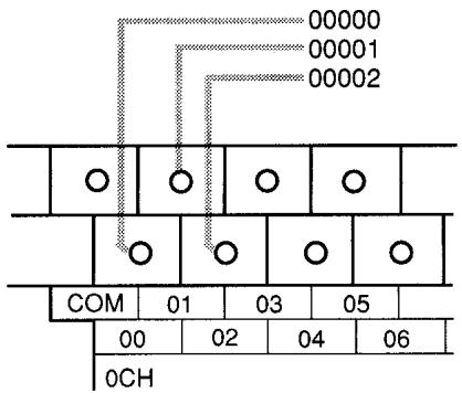
| Mode | Input functions | Input method | Count frequency | Count range | Control methods |
| Up/Down | 00000: Phase-A input 00001: Phase-B input 00002: Phase-Z input | Phase-difference, 4× inputs | 2.5 kHz max. | -32767 to 32767 | Target value control: Up to 16 target values and interrupt subroutine numbers can be registered. Zone comparison control: Up to 8 sets of upper limit values, lower limit values, and interrupt subroutine numbers can be registered. |
| Incrementing | 00000: Count input 00001: See note. 00002: Reset input | Individual inputs | 5.0 kHz max. | 0 to 65535 |
Note In incrementing mode, input 00001 can be used as a regular input. When the reset method is used for the software reset, input 00002 can be used as a regular input. Also, even when used for the phase-Z signal and software reset, the input status is reflected inn 00002 of the I/O memory.
High-speed Counter Settings
The following settings must be made in DM 6642 when using the CPM1/CPM1A's high-speed counter function.
| DM 6642Bits | Function | Settings | ||
| Incrementing | Up/Down | Not used | ||
| 00 to 03 | Sets the counter mode:0: Up/down4: Incrementing | 4 | 0 | 0 or 4 |
| 04 to 07 | Sets the reset method:0: Phase-Z + software reset1: Software reset | 0 or 1 | 0 or 1 | 0 or 1 |
| 08 to 15 | Sets the counter:00: Counter not being used.01: Counter being used. | 01 | 01 | 00 |
Count Range
The CPM1/CPM1A's high-speed counter uses linear operation and the count (present value) is stored in SR 248 and SR 249. (The upper four digits are stored in SR 249 and the lower four digits are stored in SR 248.)
| Mode | Count range |
| Up/Down | F003 2767 to 0003 2767 (−32,767 to 32,767) The leftmost digit in SR 248 indicates the sign. F is negative, 0 is positive. |
| Incrementing | 0000 0000 to 0006 5535 (0 to 65,535) |
An overflow will occur if the count exceeds the upper limit in the count range and an underflow will occur if the count goes below the lower limit in the count range.
| Error | Incrementing | Up/Down | Present value |
| Overflow | Occurs when the count is incremented from 65,535. | Occurs when the count is incremented from 32,767. | 0FFF FFFF |
| Underflow | --- | Occurs when the count is decremented from -32,767. | FFFF FFFF |
Processing
Two types of signals can be input from a pulse encoder. The count mode used for the high-speed counter will depend on the signal type. The count mode and reset mode are set in DM 6642; these settings become effective when the power is turned on or PC operation is started.
Up/Down Mode:
Phase-A difference 4 × two-phase signal (phase-A and phase-B) and a phase-Z signal are used for inputs. The count is incremented or decremented according to differences in the 2-phase signals.
Incrementing Mode:
One single-phase pulse signal and a count reset signal are used for inputs. The count is incremented according to the single-phase signal.
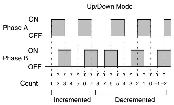
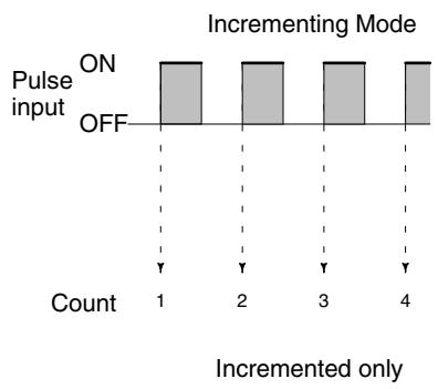
Note One of the reset methods described below should always be used to reset the counter when restarting it. The counter will be automatically reset when program execution is started or stopped.
The following signal transitions are handled as forward (incrementing) pulses: Phase-A leading edge to phase-B leading edge to phase-A trailing edge to phase-B trailing edge. The following signal transitions are handled as reverse (decrementing) pulses: Phase-B leading edge to phase-A leading edge to phase-B trailing edge to phase-A trailing edge.
The Up/Down Mode always uses a 4 × phase-difference input. The number of counts for each encoder revolution would be 4 times the resolution of the counter. Select the encoder based on the countable ranges.
Reset Methods
Either of the two methods described below may be selected for resetting the PV of the count (i.e., setting it to 0).
Phase-Z signal + software reset:
The PV is reset when the phase-Z signal (reset input) is turned ON while the High-speed Counter Reset Bit (SR 25200) is ON.
Software reset:
The PV is reset when the High-speed Counter Reset Bit (SR 25200) is turned ON.

Phase-Z Signal + Software Reset
| No. | Operation timing | Reset |
| (1) | Phase-Z signal turns ON when SR 25200 turns OFF. | Not reset. |
| (2) | Phase-Z signal turns ON within one cycle after SR 25200 turns ON. | Not reset. |
| (3) | Phase-Z signal turns ON after at least one cycle elapses after SR 25200 turns ON. | Reset with phase-Z leading edge. |
| (4) | Phase-Z signal turns ON within one cycle after SR 25200 turns OFF. | Reset with phase-Z leading edge. |
| (5) | SR 25200 turns ON when phase-Z signal is ON. | Not reset. |
Note The High-speed Counter Reset Bit (SR 25200) is refreshed once every cycle, so in order for it to be read reliably it must be ON for at least one cycle.
The "Z" in "phase-Z" is an abbreviation for "Zero." It is a signal that shows that the encoder has completed one cycle.
High-speed Counter Interrupt Count
For high-speed counter 0 interrupts, a comparison table is used instead of a "count up." The count check can be carried out by either of the two methods described below. In the comparison table, comparison conditions (for comparing to the PV) and interrupt routine combinations are saved.
Target value:
A maximum of 16 comparison conditions (target values and count directions) and interrupt routine combinations are saved in the comparison table. When the counter PV and the count direction match the comparison conditions, then the specified interrupt routine is executed.
Range (zone) comparison:
Eight comparison conditions (upper and lower limits) and interrupt routine combinations are saved in the comparison table. When the PV is greater than or equal to the lower limit and less than or equal to the upper limit, then the specified interrupt routine is executed.
Target Value Comparisons
The current count is compared to the target values in the order that target values are set in the comparison table and interrupts are generated as the count equals each target value. Once the count has equaled all of the target values in the table, the target value is set to the first target value in the table, which is again compared to the current counted until the two values are equal.
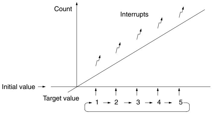
Comparison Table
| Target value 1 |
| Target value 2 |
| Target value 3 |
| Target value 4 |
| Target value 5 |
Range Comparisons
The current count is compared in cyclic fashion to all of the ranges at the same time and interrupts are generated based on the results of the comparisons.
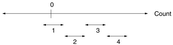
Comparison Table
| Rage setting 1 |
| Rage setting 2 |
| Rage setting 3 |
| Rage setting 4 |
Note When performing target value comparisons, do not repeatedly use the INI instruction to change the current value of the count and start the comparison operation. The interrupt operation may not work correctly if the comparison operation is started immediately after changing the current value from the program. (The comparison operation will automatically return to the first target value once an interrupt has been generated for the last target value. Repetitive operation is thus possible merely by changing the current value.)
Programming
Use the following steps to program the high-speed counter.
The high-speed counter begins the counting operation when the proper PC Setup settings are made, but comparisons will not be made with the comparison table and interrupts will not be generated unless the CTBL(63) instruction is executed.
The high-speed counter is reset to "0" when power is turned ON and when operation begins.
The present value of high-speed counter is maintained in SR 248 and SR 249.
Controlling High-speed Counter Interrupts
1, 2, 3... 1. Use the CTBL(63) instruction to save the comparison table in the CPM1/CPM1A and begin comparisons.
| (@)CTBL(63) |
| P |
| C |
| TB |
C: (3 digits BCD)
000: Target table set and comparison begun
001: Range table set and comparison begun
002: Target table set only
003: Range table set only
TB: Beginning word of comparison table
If C is set to 000, then comparisons will be made by the target matching method; if 001, then they will be made by the range comparison method. The comparison table will be saved, and, when the save operation is complete, then comparisons will begin. While comparisons are being executed, high-speed interrupts will be executed according to the comparison table. For details on the contents of the comparison tables that are saved, refer to the explanation of the CTBL(63) instruction in Section 7 Instruction Set.
Note The comparison results are normally stored in AR 1100 through AR 1107 while the range comparison is being executed.
If C is set to 002, then comparisons will be made by the target matching method; if 003, then they will be made by the range comparison method. For either of these settings, the comparison table will be saved, but comparisons will not begin, and the INI(61) instruction must be used to begin comparisons.
- To stop comparisons, execute the INI(61) instruction as shown below.
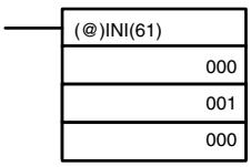
To start comparisons again, set the second operand to "000" (execute comparison), and execute the INI(61) instruction.
Once a table has been saved, it will be retained in the CPM1/CPM1A during operation (i.e., during program execution) as long as no other table is saved.
Reading the PV
There are two ways to read the PV. The first is to read it from SR 248 and SR 249, and the second to use the PRV(62) instruction.
Reading SR 248 and SR 249
The PV of high-speed counter is stored in SR 248 and SR 249 as shown below. The leftmost bit will be F for negative values.
Leftmost 4 digits
Rightmost 4 digits
Up/Down Mode
Incrementing Mode
SR 249
SR248
F0032767 to 00032767
0000000 to 00065535
(-32767)
Note 1. These words are refreshed only once every cycle, so there may be a difference from the actual PV.
2. When high-speed counter is not being used, the bits in these words can be used as work bits.
Using the PRV(62) Instruction
Read the PV of the high-speed counter by using the PRV(62) instruction.
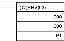
P1: Leading word of PV
The PV of the high-speed counter is stored as shown below. The leftmost bit will be F for negative values.
Leftmost 4 digits
Rightmost 4 digits
Up/Down Mode
Incrementing Mode
P1+1
P1
F0032767 to 00032767 (-32767)
0000000 to 00065535
Changing the PV
The PV is read when the PRV(62) instruction is actually executed.
There are two ways to change the PV of high-speed counter. The first way is to reset it by using the reset methods. (In this case the PV is reset to 0.) The second way is to use the INI(61) instruction.
The method using the INI(61) instruction is explained here. For an explanation of the reset method, refer to the beginning of this description of high-speed counter.
Change the timer PV by using the INI(61) instruction as shown below.
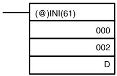
D: Leading word for storing PV change data
Leftmost 4 digits
Rightmost 4 digits
Up/Down Mode
Incrementing Mode


F0032767 to 00032767
00000000 to 00065535
Application Example (Incrementing Mode)
To specify a negative number in up/down mode, set F in the leftmost digit.
This example shows a program that uses the high-speed counter with single-phase inputs in the incrementing Mode, making comparisons by means of the target matching method.
The comparison conditions (target values and count directions) are stored in the comparison table with the subroutine numbers. Up to 16 target values can be stored. The corresponding subroutine is executed when the counter's PV matches the target value.
The following data is stored for the comparison table:
DM 0000 0002 Number of comparison conditions: 2
DM 0001 1000 Target value 1: 1000
DM 0002 0000
DM 0003 0030 Comparison 1 interrupt subroutine no.: 30
DM 0004 2000 Target value 2: 2000
DM 0005 0000
DM 0006 0031 Comparison 2 interrupt subroutine no.: 31
The following diagram shows the example ladder program. DM 6642 must be set to 01 4 , where is the reset method which can be set to 0 or 1.
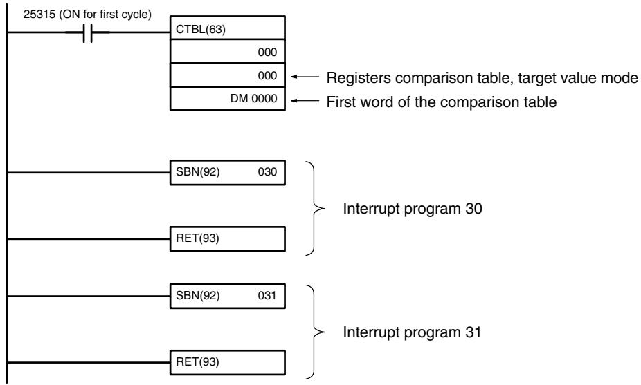
Application Example (Up/Down Mode)
This example shows a program that uses the high-speed counter with phase-difference inputs in the Up/Down Mode, making comparisons by means of the range comparison method.
The comparison conditions (upper/ lower limits of the ranges) are stored in the comparison table with the subroutine numbers. Up to 8 separate ranges can be defined. The corresponding subroutine is executed when the counter's PV is within the range.
Note Always set 8 ranges. If fewer than 8 ranges are needed, set the remaining subroutine numbers to FFFF. A value of FFFF indicates that no subroutine is to be executed.
The following data is stored for the comparison table:
DM0000 1500
DM0001 0000
DM 0002 3000
DM 0003 0000
DM 0004 0040
DM0005 7500
DM 0006 0000
DM 0007 0000
DM 0008 0001
DM 0009 0041
DM0010 0000
DM 0011 0000
DM 0012 0000
DM0013 0000
DM 0014 FFFF Range 3 interrupt subroutine not executed
.
.
.
.
DM 0035 0000
DM 0036 0000
DM 0037 0000
DM 0038 0000
DM 0039 FFFF Range 8 interrupt subroutine not executed
The following diagram shows the example ladder program. DM 6642 must be set to 01 0 , where is the reset method which can be set to 0 or 1.
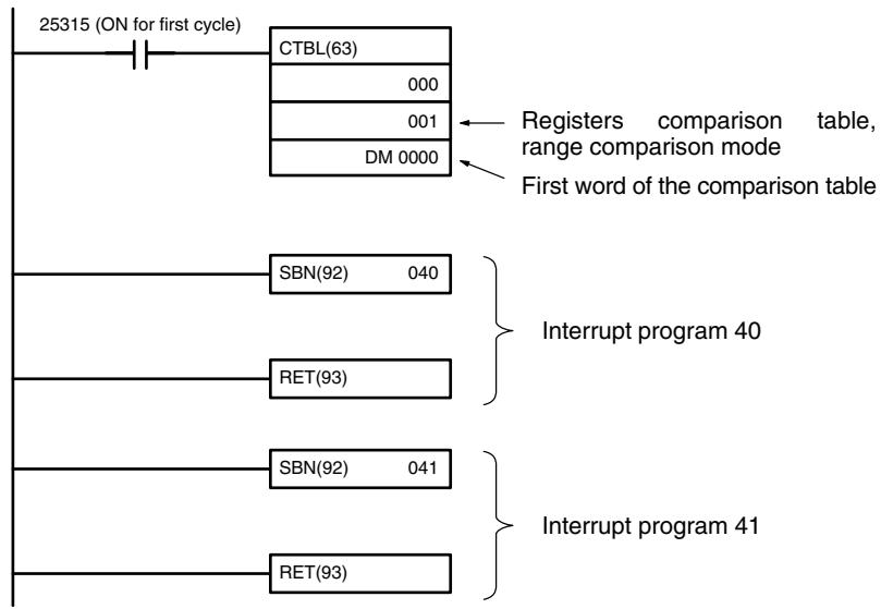
2-3-6 Precautions on Programming Interrupts
If words in memory are being manipulated both in the main program and in an interrupt program, the interrupts must be masked when the words are being manipulated in the main program. Refer to 2-1-4 Precautions on Programming Interrupts for details.
2-4 SRM1(-V2) Interrupt Functions
This section explains the settings and methods for using the SRM1(-V2) interrupt functions.
2-4-1 Types of Interrupts
The SRM1(-V2) has only one type of interrupt processing, as outlined below.
Interval Timer Interrupts
Interrupt processing is executed by an interval timer with a precision of 0.1 ms.
2-4-2 Interval Timer Interrupts
The SRM1(-V2) is equipped with one interval timer. When the interval timer times out, the main program is interrupted and the interrupt program is executed immediately, regardless of the point in the cycle.
There are two modes for interval timer operation, the One-shot Mode, in which only one interrupt will be executed when time expires, and the Scheduled Interrupt Mode in which the interrupt is repeated at a fixed interval.
The interval timer's set value can be set anywhere from 0.5 to 319,968 ms, in units of 0.1 ms.
Operation
Use the following instruction to activate and control the interval timer.
Starting Up in One-Shot Mode
Use the STIM(69) instruction to start the interval timer in the one-shot mode.
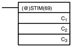
C_1 : Interval timer, one-shot mode (000)
C_2 : Timer set value (first word address)
C_3 : Subroutine no. (4 digits BCD): 0000 to 0049
- When C_2 is entered as a word address:
C_2 : Decrementing counter set value (4 digits BCD): 0000 to 9999
C_2 + 1 : Decrementing time interval (4 digits BCD; unit: 0.1 ms): 0005 to 0320
(0.5 ms to 32 ms)
Each time that the interval specified in word C_2 + 1 elapses, the decrementing counter will decrement the present value by one. When the PV reaches 0, the designated subroutine will be called just once and the timer will stop.
The time from when the STIM(69) instruction is executed until time elapses is calculated as follows:
(Content of C_2 ) × (Content of C_2 + 1 ) × 0.1 ms = (0.5 to 319,968 ms)
- When C_2 is entered as a constant:
The set value of the decrementing counter will equal the specified constant (in ms) and the decrementing time interval will be 10 (1 ms).
Starting Up in Scheduled Interrupt Mode
Use the STIM(69) instruction to start the interval timer in the scheduled interrupt mode.
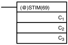
C_1 : Interval timer, scheduled interrupt mode (003)
C_2 : Timer set value (leading word no.)
C_3 : Subroutine no. (4 digits BCD): 0000 to 0049
- When C_2 is entered as a word address:
C2: Decrementing counter set value (4 digits BCD): 0000 to 9999
C_2 + 1 : Decrementing time interval (4 digits BCD; unit: 0.1 ms): 0005 to 0320 (0.5 ms to 32 ms)
The meanings of the settings are the same as for the one-shot mode, but in the scheduled interrupt mode the timer PV will be reset to the set value and decrementing will begin again after the subroutine has been called. In the scheduled interrupt mode, interrupts will continue to be repeated at fixed intervals until the operation is stopped.
- When C_2 is entered as a constant:
The settings are the same as for the one-shot mode, but interrupts will continue to be repeated at fixed intervals until the operation is stopped.
Reading the Timer's Elapsed Time
Use the STIM(69) instruction to read the timer's elapsed time.
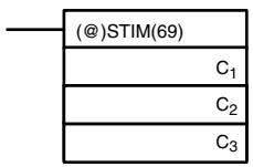
C_1 : Read elapsed time (006)
C_2 : Leading word of parameter 1
C3: Parameter 2
C2: Number of times the decrementing counter has been decremented (4 digits BCD)
C_2 + 1 : Decrementing counter time interval (4 digits BCD; unit: 0.1ms
C3: Elapsed time from previous decrement (4 digits BCD; unit: 0.1 ms)
The time from when the interval timer is started until the execution of this instruction is calculated as follows:
(Content of C2) × (Content of C2 + 1) + (Content of C3) × 0.1 ms
If the specified interval timer is stopped, then "0000" will be stored.
Stopping the Timer
Use the STIM(69) instruction to stop the interval timer. The interval timer will be stopped.
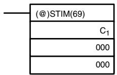
C_1 : Stop interval timer (010)
Application Example (One-shot Mode)
In this example, an interrupt is generated 2.4 ms (0.6 ms × 4) after input 00005 goes ON; the interrupt executes interrupt subroutine number 23.
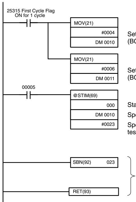
Sets the decrementing counter's set value to 4. (BCD: 0000 to 9999)
Sets the decrementing time interval to 0.6 ms. (BCD: 0005 to 0320)
Starts the interval timer in one-shot mode.
Specifies the first word containing the set value.
Specifies the subroutine number (only lower bytes are effective).
Interrupt program
Application Example (Scheduled Interrupt Mode)
In this example, an interrupt is generated every 4.0 ms (1.0 ms × 4) after input 00005 goes ON; the interrupts execute interrupt subroutine number 23.
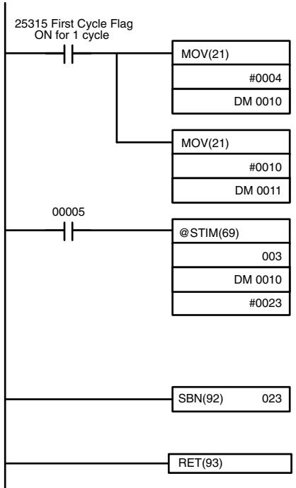
Sets the decrementing counter's set value to 4. (BCD: 0000 to 9999)
Sets the decrementing time interval to 1.0 ms. (BCD: 0005 to 0320)
Starts the interval timer in scheduled interrupt mode.
Specifies the first word containing the set value.
Specifies the subroutine number (only the lower bytes are effective).
Interrupt program
2-5 CPM2A/CPM2C Pulse Output Functions
The CPM2A/CPM2C has two pulse outputs. By means of a selection in the PC Setup, these outputs can be used as two single-phase outputs without acceleration and deceleration, two variable duty ratio pulse outputs, or pulse outputs with trapezoidal acceleration/deceleration (one pulse + direction output and one up/down pulse output). The pulse output PV coordinate system can also be specified in the PC Setup as either relative or absolute.
There are two pulse output modes: Independent mode, in which outputs are stopped at a preset amount of pulses, and continuous mode, in which outputs are stopped by an instruction.
Note To use pulse outputs, it is necessary to use a CPU Unit with transistor outputs, i.e., either a CPM2A-□□CDT-D or CPM2A-□□CDT1-D.
The following diagram shows the configuration for a CPM2A, but the configuration for a CPM2C is identical.
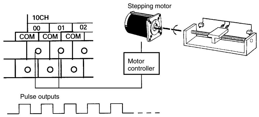
| Item | Single-phase pulse outputs without accel/decel | Variable duty ratio pulse outputs | Single-phase pulse outputs with trapezoidal acceleration/deceleration | ||||
| Pulse + direction outputs | Up/down pulse outputs | ||||||
| Execution instructions | PULS(65) and SPED(64) | PWM(—) | PULS(65) and ACC(—) | ||||
| Output number | 01000 | Pulse output 0 (See note 1.) | Pulse output 0 (See note 1.) | Pulse output 0 | Pulse output | Pulse output 0 | CW pulse output |
| 01001 | Pulse output 1 (See note 1.) | Pulse output 1 (See note 1.) | Direction output | CCW pulse output | |||
| Output frequency range | 10 Hz to 10 kHz | 0.1 to 999.9 Hz | 10 Hz to 10 kHz | 10 Hz to 10 kHz | |||
| Pitch | 10 Hz | 0.1 Hz | 10 Hz | 10 Hz | |||
| Up/down frequency pitch | --- | --- | 10 Hz (See note 2.) | 10 Hz (See note 2.) | |||
| Start speed pitch | --- | --- | 10 Hz | 10 Hz | |||
| Output mode | Continuous, Independent | Continuous | Continuous, Independent | Continuous, Independent | |||
| Number of pulses | 1 to 16777215 | --- | ±1 to 16777215 | ±1 to 16777215 | |||
| Duty ratio (See note 3.) | 50% | 0 to 100% | 50% | 50% | |||
| Control method | Movement specification | Yes | No | Yes | Yes | ||
| Accel/decel specification | No | No | Yes | Yes | |||
| Start speed specification | No | No | Yes | Yes | |||
| Duty specification | No | Yes | No | No | |||
Note 1. With single-phase pulse outputs, pulse outputs 0 and 1 can each be output independently.
2. Pulse outputs can be accelerated or decelerated in units of 10Hz every 10 ms.
3. Actual pulses are affected by the transistor output's ON response time (20 μs max.) and OFF response time (40 μs max.).
The following table shows the relationships between the high-speed counter and the CPM2A/CPM2C's other functions.
| Interval timer interrupts | |
| Synchronized pulse control | Cannot be used simultaneously. |
| Interrupt inputs | Can be used simultaneously. |
| Interval timer interrupts | Can be used simultaneously. |
| High-speed counters | Can be used simultaneously. |
| Interrupt inputs (counter mode) | Can be used simultaneously. |
| Pulse outputs | See note. |
| Quick-response inputs | Can be used simultaneously. |
| Input time constant | Can be used simultaneously. |
| Clock | Can be used simultaneously. |
Note The number of simultaneous outputs varies according to the type of pulse output, as shown in the following table.
| Combination | Single-phase pulse output | Pulse + direction output | Up/down pulse output | ||
| Fixed duty ratio | Variable duty ratio | ||||
| Single-phase pulse output | Fixed duty ratio | Can use two points simultaneously (independently). | Can use one point at a time (independently). | Cannot be used. | Cannot be used. |
| Variable duty ratio | Can use one point at a time (independently). | Can use two points simultaneously (independently). | Cannot be used. | Cannot be used. | |
| Pulse + direction output | Cannot be used. | Cannot be used. | Cannot be used. | Cannot be used. | |
| Up/down pulse output | Cannot be used. | Cannot be used. | Cannot be used. | Cannot be used. | |
Up to two points can be output simultaneously with only single-phase pulse outputs, so two-point output is possible when fixed duty ratio and variable duty ratio are used in combination.
Outputs are possible for only one point at a time with pulse + direction outputs and up/down pulse outputs, so no other pulses can be output.
Types of Pulse Outputs
There are three types of pulse outputs: Single-phase pulse outputs without acceleration and deceleration, variable duty ratio pulse outputs, and single-phase pulse outputs with trapezoidal acceleration and deceleration.
Single-phase Pulse Outputs Without Acceleration and Deceleration
- Frequency: 10 Hz to 10 kHz (Set in units of 10 Hz.)
Output destination: Output number 01000 (Word 010, bit 00)
Output number 01001 (Word 010, bit 01)
(Pulses can be output simultaneously and independently from two points.
-
Output mode: Continuous or Independent
Number of pulses: 1 to 16,777,215 -
Instructions: PULS(65) and SPED(64)
-
With PULS(65), the number of pulses is set for each point (in independent mode only).
- With SPED(64), the output mode and target frequency are set for each point, and pulses are output.

The output is stopped automatically when the set number of pulses has been output.
Continuous mode
Instruction execution: SPED(64) (Continuous mode)
Pulses continue to be output at the set frequency until stopped by the instruction.
Variable Duty Ratio Pulse Outputs
- Duty ratio: 0% to 100% (Set in units of 1% .)
- Frequency: 0.1 to 999.9 Hz (Set in units of 0.1 Hz.)
Output destination: Output number 01000 (Word 010, bit 00)
Output number 01001 (Word 010, bit 01)
(Pulses can be output simultaneously and independently from two points.)
- Output mode: Continuous
- Instruction: PWM(—)
With PWM(-) , pulses are output with a variable duty ratio.
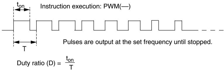
Single-phase Pulse Outputs With Trapezoidal Acceleration/Deceleration
- Frequency: 10 Hz to 10 kHz (Set in units of 10 Hz.)
- Acceleration/deceleration rate: 10 ~Hz / 10 ~ms to 10 kHz / 10 ~ms (Set in units of 10 ~Hz .)
Pulse + Direction Outputs
- For CW Output: Output number 01001 (Word 010, bit 01) turned OFF. Pulses output from output number 01000 (Word 010, bit 00).
- For CCW Output: Output number 01001 (Word 010, bit 01) turned ON. Pulses output from output number 01000 (Word 010, bit 00).
01000
Pulse outputs
01001
Direction outputs (OFF: CW operation; ON: CCW operation)

Up/Down Pulse Outputs
- For CW output: Pulses output from output number 01000 (Word 010, bit 00).
- For CCW output: Pulses output from output number 01001 (Word 010, bit 01).

Output mode: Continuous and Independent
Number of pulses: 1 to 16,777,215
- Instructions: PULS(65) and ACC(—)
- With PULS(65), the number of pulses is set (in independent mode only).
- With ACC(—), the output mode, starting frequency, target frequency, and acceleration/deceleration rate are set, and the pulse outputs are started. From when the pulse outputs are started until they are stopped, they are controlled at a constant-ratio frequency change.
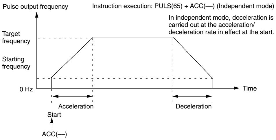
Independent Mode
Continuous Mode
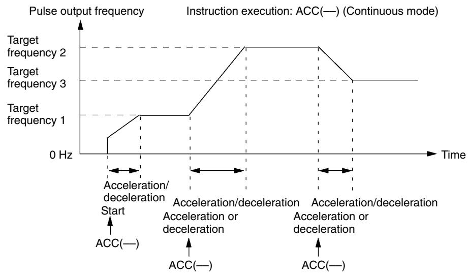
2-5-1 Using Single-phase Pulse Outputs Without Acceleration and Deceleration (Fixed Duty Ratio)
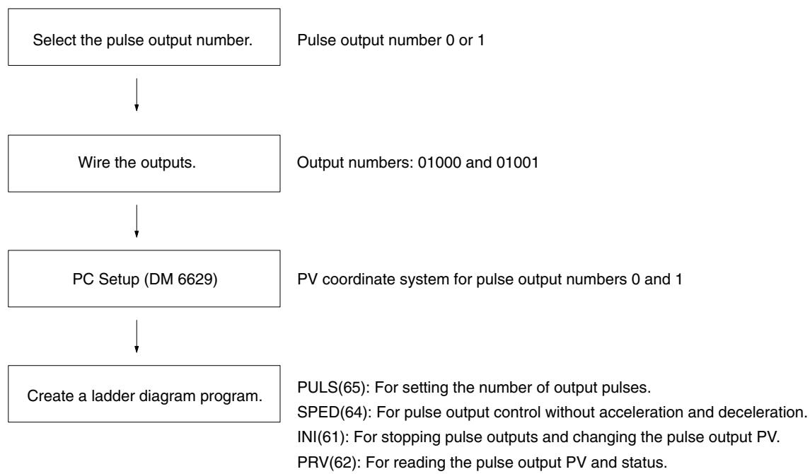
Single-phase Pulse Outputs
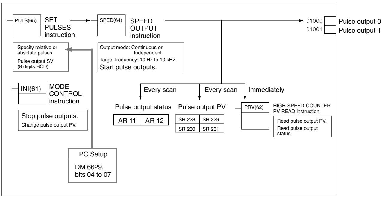
Selecting the Pulse Output Number
Select either pulse number 0 or 1.
| Output number | Pulse output number |
| 01000 | 0 |
| 01001 | 1 |
Wiring the Outputs
Wire the CPM2A outputs as shown in the following illustration. (Pulses can be output independently from pulse outputs 0 and 1.)
Output 01000: Pulse output 0 (single-phase output)
Output 01001: Pulse output 1 (single-phase output)
Wire the CPM2C outputs as shown in the following illustration. (Pulses can be output independently from pulse outputs 0 and 1.)
Note The following examples are for Fujitsu-compatible connectors. Output bit addresses and connector pin numbers depend on the models. Refer to the CPM2C Operation Manual (W356) or the CPM2C-S Operation Manual (W377) for details.
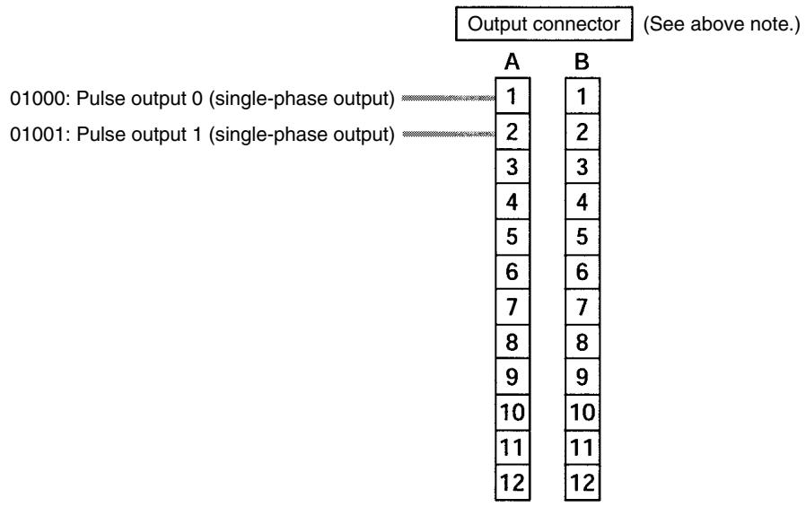
PC Setup
Make the following settings in the PC Setup.
| Word | Bits | Function | Setting | |
| DM 6629 | 00 to 03 | Pulse 0 PV coordinate system | 0: Relative coordinate system | Either 0 or 1 |
| 04 to 07 | Pulse 1 PV coordinate system | 1: Absolute coordinate system | ||
| DM 6642 | 08 to 15 | High-speed counter setting | 00: Do not use.01: Use as high-speed counter02: Use as synchronized pulse control (10 to 500 Hz).03: Use as synchronized pulse control (20 Hz to 1 kHz).04: Use as synchronized pulse control (300 Hz to 20 kHz). | Either 00 or 01 |
If absolute pulses are specified with PULS(65), be sure to set the absolute coordinate system (1).
Synchronized pulse control cannot be used simultaneously.
The settings will go into effect when the mode is changed (from PROGRAM to MONITOR/RUN) or when the power supply is turned ON to the PC.
The following table shows the instruction operations related to pulse outputs without acceleration and deceleration (fixed duty ratio).
Ladder Diagram Programming
| Instruction | Control | Operation |
| (@)PULS(65) | Set number of pulses | Sets the number of pulses to be output in independent mode. |
| (@)SPED(64) | Set frequency and start pulse outputs | Sets the frequency for outputs in the independent mode or continuous mode, and starts the pulse outputs. |
| Change frequency | Changes the frequency for outputs in the independent mode or continuous mode. | |
| Stop pulse outputs | Stops the pulse outputs (by changing the speed to a frequency of 0 Hz). | |
| (@)INI(61) | Stop pulse outputs | Stops the pulse outputs. |
| Change pulse output PV | Changes the pulse output PV. | |
| (@)PRV(62) | Read pulse output PV | Reads the pulse output PV. |
| Read pulse output status | Reads the pulse output status. |
The following table shows which instructions can be executed during pulse outputs without acceleration and deceleration.
| PULS(65) | SPED(64) | INI(61) | PRV(62) | ACC(—) | PWM(—) | |
| Continuous mode | No | Yes (See note 2.) | Yes (See note 1.) | Yes | No | No |
| Independent mode | No | Yes (See note 2.) | Yes (See note 1.) | Yes | No | No |
Note
- This instruction can be executed only while pulse outputs are stopped. The PV cannot be changed while pulses are being output. If the PV needs to be changed, be sure to stop the pulse output first.
- This instruction can be used only for changing the frequency and stopping the pulse output. It cannot be used for switching between independent mode and continuous mode.
The following table shows the words and bits related to pulse outputs without acceleration and deceleration (fixed duty ratio).
| Word | Bits | Name | Contents |
| 228 | 00 to 15 | Pulse output PV 0, rightmost 4 digits | Cannot be used as work bits even when not used as pulse outputs. |
| 229 | 00 to 15 | Pulse output PV 0, leftmost 4 digits | |
| 230 | 00 to 15 | Pulse output PV 1, rightmost 4 digits | |
| 231 | 00 to 15 | Pulse output PV 1, leftmost 4 digits | |
| 252 | 04 | Pulse output 0 PV reset | Clears PV 0 when ON. |
| 05 | Pulse output 1 PV reset | Clears PV 1 when ON. | |
| AR 11 | 12 | Pulse output 0 PV overflow/underflow | ON: Occurred OFF: Normal |
| 13 | Number of pulses set for pulse output 0 | ON: Set (by PULS(65)) OFF: Not set | |
| 14 | Pulse output completed for pulse output 0 | ON: Completed (by SPED(64)) OFF: Not completed | |
| 15 | Pulse output in progress for pulse output 0 | ON: In progress (by SPED(64)) OFF: Stopped | |
| AR 12 | 12 | Pulse output 1 PV overflow/underflow | ON: Occurred OFF: Normal |
| 13 | Number of pulses set for pulse output 1 | ON: Set (by PULS(65)) OFF: Not set | |
| 14 | Pulse output completed for pulse output 1 | ON: Completed (by SPED(64)) OFF: Not completed | |
| 15 | Pulse output in progress for pulse output 0 | ON: In progress (by SPED(64)) OFF: Stopped |
Set Number of Pulses
Specify the number of pulses to be output in independent mode.
| (@)PULS(65) |
| P |
| D |
| N |
| N |
| N+1 |
Rightmost 4 digits
Leftmost 4 digits
Number of pulses (Rightmost, leftmost digits)
Register the number of pulses to be set.
96,777,215 to 16,777,215
Negative numbers are expressed by turning ON the leftmost bit.
Type of Pulse Output
000: Relative pulses (SV for number of pulses = Number of pulses moved)
001: Absolute pulses (SV for number of pulses = The next PV on the absolute coordinate system, i.e., the pulse output PV + number of pulses moved)*
*Absolute pulses can only be specified by PULS(65) when the PV coordinate system in the PC Setup is set for an absolute coordinate system.
Set Frequency and Start Pulse Outputs
Change Frequency
These functions set the pulse output number, the output mode, and the frequen-
cy, and begin pulse outputs. They can also be used to change the frequency if pulse outputs are already in progress.
| (@)SPED(64) |
| P |
| M |
| F |
Port specifier (000: Pulse output 0; 010: Pulse output 1)
Mode designation (000: Independent; 001: Continuous)
Target frequency data word
F
Target frequency
Register the target frequency data to be set.
0001 to #1000 (4 digits BCD): 10 Hz to 10 kHz
0000: Pulse output stopped
Change Pulse Output PV
Resetting Pulse Output PV
This function changes the pulse output present value (PV). The PV can also be cleared by using SR 25204 and SR 25205.
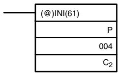
Port specifier (000: Pulse output 0; 010: Pulse output 1)
Control designation (004: Change pulse output PV)
Beginning word for PV change data
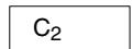
Rightmost 4 digits
Change PV data (Rightmost, leftmost digits)
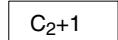
Leftmost 4 digits
Register the PV data to be changed.
96,777,215 to 16,777,215
Negative numbers are expressed by turning
ON the leftmost bit.
The pulse output PV can only be changed or reset while pulse outputs are stopped. Check to be sure that the Pulse Output In Progress Flags (AR 1115 and AR 1215) have been turned OFF.
Stop Pulse Outputs
This function stops the pulse outputs.
Using SPED(64)
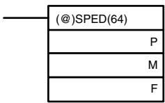
Port specifier (000: Pulse output 0; 010: Pulse output 1)
Mode designation (000: Independent; 001: Continuous)
Target frequency data word
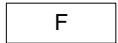
0000
Specifies a frequency of 0Hz
Using INI(61)
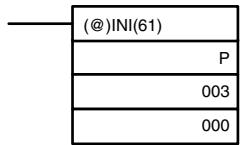
Port specifier (000: Pulse output 0; 010: Pulse output 1)
Control designation (003: Stop pulse outputs)
Fixed: 000
Besides executing the instructions shown above, it is also possible to stop pulse outputs by stopping operation (PROGRAM mode).
Read Pulse Output PV
This function reads the pulse output PV.
Using an Instruction
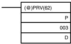
Port specifier (000: Pulse output 0; 010: Pulse output 1)
Control designation (003: Read pulse output PV)
Beginning word for storing pulse output PV
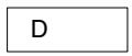
Rightmost 4 digits
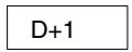
Leftmost 4 digits
Pulse output PV (rightmost, leftmost digits)
The PV data that is read is stored here.
96,777,215 to 16,777,215
Negative numbers are expressed by turning
ON the leftmost bit.
Using Data Areas
As shown in the following illustration, the pulse output PV for pulse output 0 is stored in words 228 and 229, and the pulse output PV for pulse output 1 is stored in words 230 and 231.
Pulse Output 0

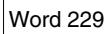
PV (Rightmost)
PV (Leftmost)
Pulse Output 1
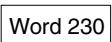
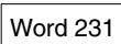
PV (Rightmost)
PV (Leftmost)
Words 228 to 231 are refreshed with every scan, so there may be a discrepancy from the exact PV at any given time.
Words 228 to 231 cannot be used as work words even when pulse outputs are not being used.
When the PV is read by executing PRV(62), words 228 to 231 are refreshed with the same timing.
Read Pulse Output Status
This function reads the pulse output status.
Using an Instruction
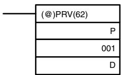
Port specifier (000: Pulse output 0; 010: Pulse output 1)
Control designation (001: Read pulse output status)
Word for storing pulse output status
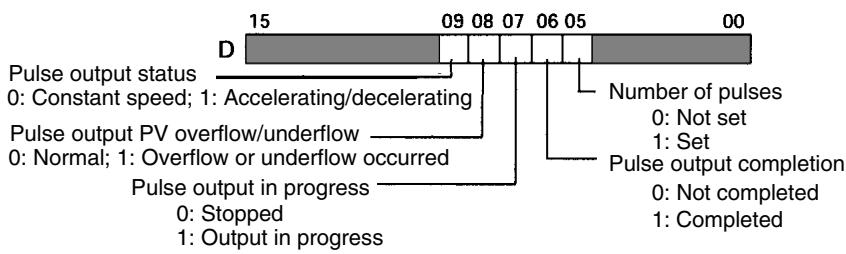
Using Data Areas
As shown in the following illustration, the pulse output status for pulse output 0 is stored in AR 11, and the pulse output status for pulse output 1 is stored in AR 12.
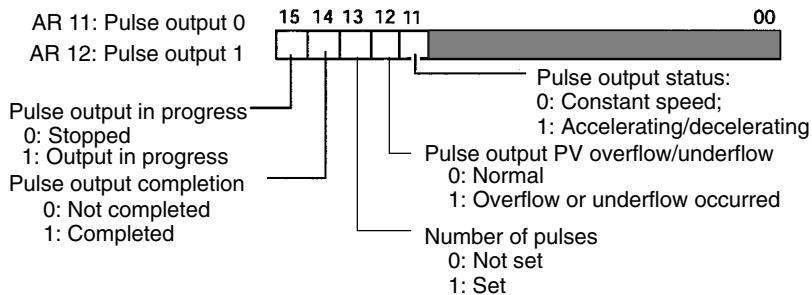
Note The flags in AR 11 and AR 12 are refreshed once each cycle, so the values in these words may not reflect the actual status during each cycle, but the flags in AR 11 and AR 12 are refreshed when the status is read with PRV(62).
Relationship Between Status and Operation
Independent Mode (Without Acceleration and Deceleration)

Continuous Mode
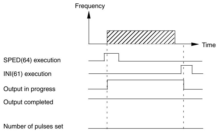
Stopping Output in Independent Mode (Without Acceleration and Deceleration)
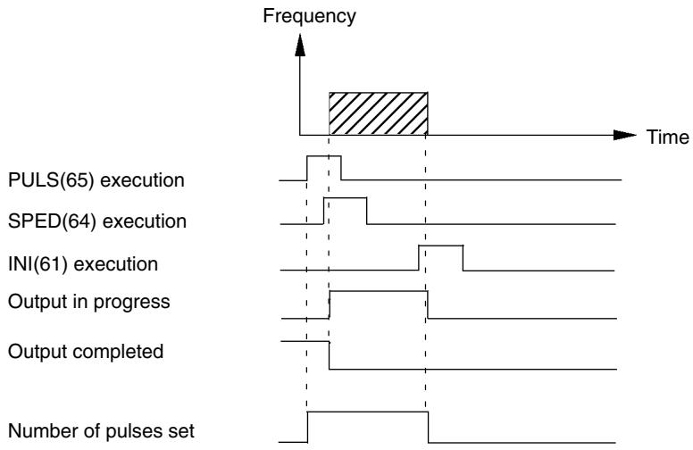
Application Examples
Positioning
Explanation
In this example, when the execution condition (00005) turns ON, 100 pulses are output from output 01000 (pulse output 0) at a frequency of 60Hz .
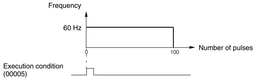
Wiring
Wire the CPM2A to the motor driver as shown in the following illustration.
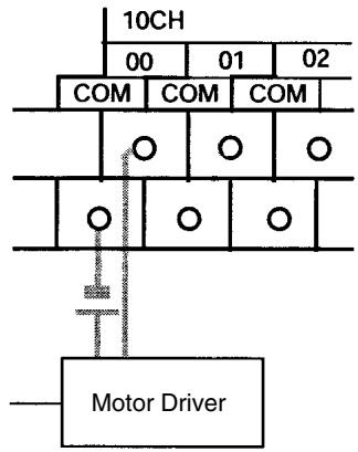
Wire the CPM2C to the motor driver as shown in the following illustration. In this case, a CPU Unit with sinking transistor outputs is used.
Note The following examples are for Fujitsu-compatible connectors. Output bit addresses and connector pin numbers depend on the models. Refer to the CPM2C Operation Manual (W356) or the CPM2C-S Operation Manual (W377) for details.
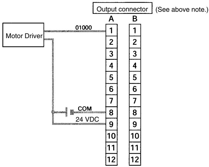
PC Setup

Programming
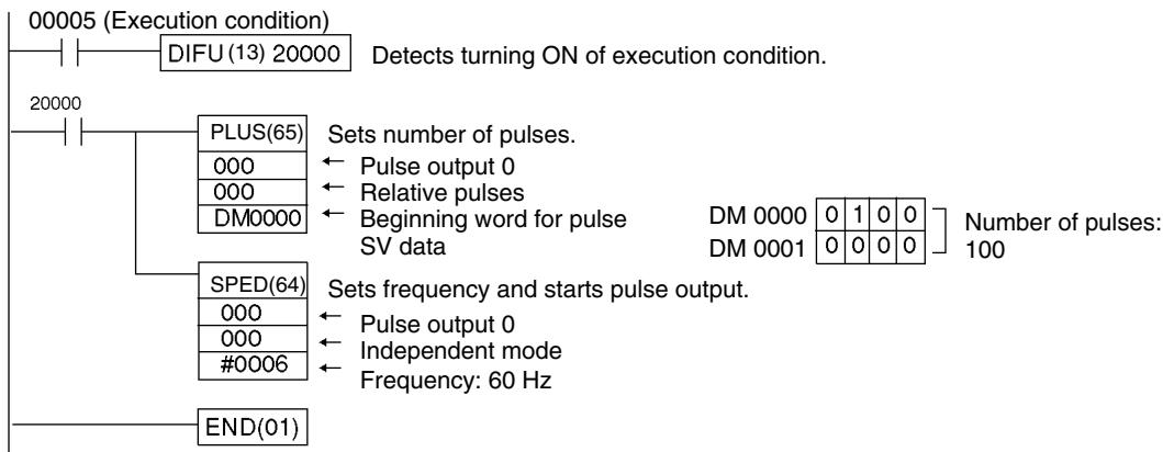
JOG Operation
Explanation
In this example, when the execution condition (00005) turns ON, JOG pulses are output at a frequency of 100Hz from either output 01000 (pulse output 0) or output 01001 (pulse output 1). When the execution condition (00005) turns OFF, the output is stopped. Switching between output 01000 (pulse output 0) and output 01001 (pulse output 1) is performed by means of the direction designator (00006).
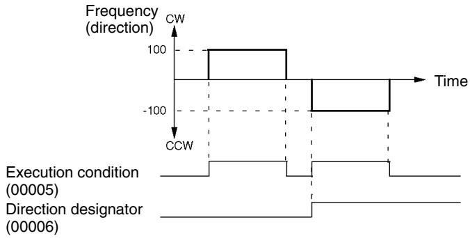
Wiring
Wire the CPM2A to the motor driver as shown in the following illustration.
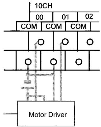
Wire the CPM2C to the motor driver as shown in the following illustration. In this case, a CPU Unit with sinking transistor outputs is used.
Note The following examples are for Fujitsu-compatible connectors. Output bit addresses and connector pin numbers depend on the models. Refer to the CPM2C Operation Manual (W356) or the CPM2C-S Operation Manual (W377) for details.
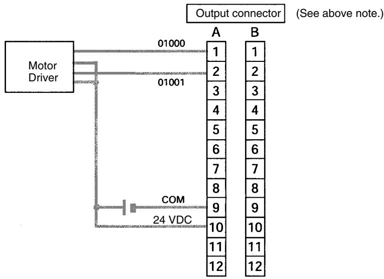
Note Refer to page operation manual for details on wiring outputs.
PC Setup

Programming
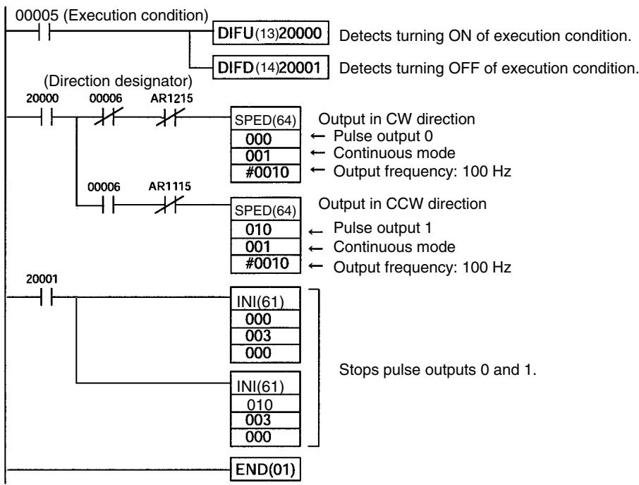
2-5-2 Using Pulse Outputs With Variable Duty Ratio
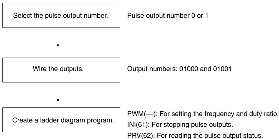
Pulse Outputs With Variable Duty Ratio
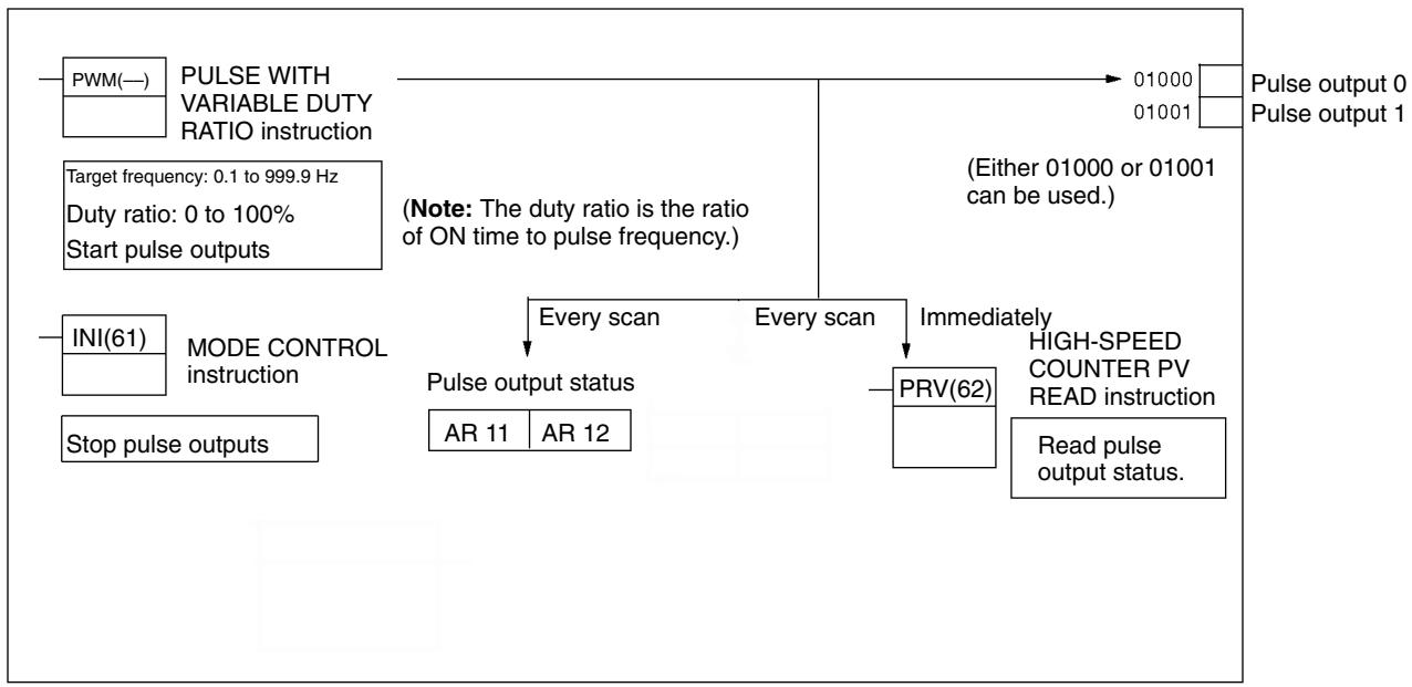
Selecting the Pulse Output Number
Select either pulse output 0 or 1.
| Output number | Pulse output number |
| 01000 | 0 |
| 01001 | 1 |
Wiring the Outputs
Wire the CPM2A outputs as shown in the following illustration. (Pulses can be output independently from pulse outputs 0 and 1.)
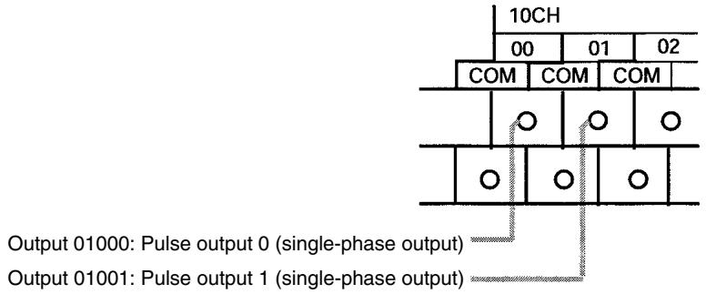
Wire the CPM2C outputs as shown in the following illustration. (Pulses can be output independently from pulse outputs 0 and 1.)
Note The following examples are for Fujitsu-compatible connectors. Output bit addresses and connector pin numbers depend on the models. Refer to the CPM2C Operation Manual (W356) or the CPM2C-S Operation Manual (W377) for details.
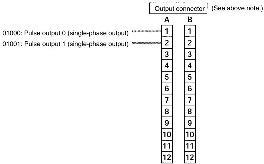
PC Setup
Make the following settings in the PC Setup.
| Word | Bits | Function | Setting | |
| DM 6642 | 08 to 15 | High-speed counter setting | 00: Do not use.01: Use as high-speed counter02: Use as synchronized pulse control (10 to 500 Hz).03: Use as synchronized pulse control (20 Hz to 1 kHz).04: Use as synchronized pulse control (300 Hz to 20 kHz). | Either 00 or 01 |
Ladder Diagram Programming
Synchronized pulse control cannot be used simultaneously.
The settings will go into effect when the mode is changed (from PROGRAM to MONITOR/RUN) or when the power supply is turned ON to the PC.
The following table shows the instruction operations related to pulse outputs with variable duty ratio.
| Instruction | Control | Operation |
| (@)PWM(—) | Pulse output with variable duty ratio | Sets the frequency and duty ratio and starts the pulse outputs. |
| Change duty ratio | Changes the duty ratio during pulse while pulse outputs with variable duty ratio are already in progress. | |
| (@)INI(61) | Stop pulse outputs | Stops the pulse outputs. |
| (@)PRV(62) | Read pulse output status | Reads the pulse output status (during pulse outputs). |
The following table shows which instructions can be executed during pulse outputs without acceleration and deceleration.
| PULS(65) | SPED(64) | INI(61) | PRV(62) | ACC(—) | PWM(—) |
| No | No | Yes (See note 1.) | Yes | No | Yes (See note 2.) |
Note 1. This instruction can be used only for stopping pulse outputs.
- This instruction can be used only for changing the duty ratio. The frequency cannot be changed while pulses are being output. If the frequency needs to be changed, be sure to stop the pulse output first.
The following table shows the words and bits related to pulse outputs with variable duty ratio.
| Word | Bit | Name | Contents |
| AR 11 | 15 | Pulse output in progress for pulse output 0 | ON: In progress (by SPED(64), ACC(—), or PWM(—)) OFF: Stopped |
| AR 12 | 15 | Pulse output in progress for pulse output 1 | ON: In progress (by SPED(64), ACC(—), or PWM(—)) OFF: Stopped |
Pulse Output With Variable Duty Ratio
Change Duty Ratio
These functions set the position for outputting pulses (01000, 01001), the frequency, and the duty ratio, and start the pulse outputs. By changing the duty ratio setting and executing PWM(—) again, it is also possible to change the duty ratio while pulse outputs with variable duty ratio are already in progress.
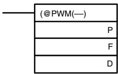
Port specifier (000: Pulse output 0; 010: Pulse output 1)
Target frequency data word
Duty ratio data word

Target frequency
Register the target frequency to be set.
0001 to #9999 (4 digits BCD): 0.1 Hz to 999.9 Hz
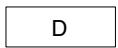
Duty ratio
Register the duty ratio to be set.
0000 to #0100 (4 digits BCD): 0% to 100%
The pulse frequency cannot be changed while pulses are being output.
Stop Pulse Outputs
This function stops pulse outputs.
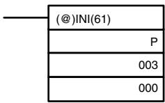
Port specifier (000: Pulse output 0; 010: Pulse output 1)
Control designation (003: Stop pulse outputs)
Fixed: 000
Note The pulse outputs can also be stopped by switching the PC to PROGRAM mode.
Read Pulse Output Status
This function reads the pulse output status.
Using an Instruction
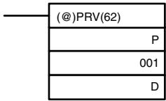
Port specifier (000: Pulse output 0; 010: Pulse output 1)
Control designation (001: Read pulse output status)
Beginning word for storing pulse output status

0: Stopped
1: Output in progress
Using Data Areas
As shown in the following illustration, the pulse output status for pulse output 0 is stored in AR 1115, and the pulse output status for pulse output 1 is stored in AR 1215.
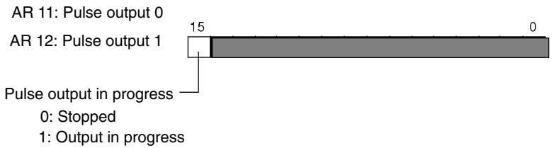
Note AR 1115 and AR 1215 are refreshed once each cycle, so the values in these words may not reflect the actual status during each cycle, but AR 1115 and AR 1215 are refreshed when the status is read with PRV(62).
Relationship Between Status and Operation
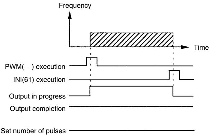
Continuous Mode (Pulse Output With Variable Duty Ratio)
Application Example
Explanation
In this example, when the execution condition (00005) turns ON, variable duty pulses are output from output 01000 (pulse output 0) at a frequency of 100Hz . The duty ratio at this time can be changed with the thumbwheel switch 0.
Wiring
Wire the CPM2A to the motor driver and thumbwheel switch as shown in the following illustration.
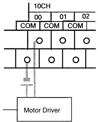
Wire the CPM2C to the motor driver and thumbwheel switch as shown in the following illustration. In this case, a CPU Unit with sinking transistor outputs is used.
Note The following examples are for Fujitsu-compatible connectors. I/O bit addresses and connector pin numbers depend on the models. Refer to the CPM2C Operation Manual (W356) or the CPM2C-S Operation Manual (W377) for details.
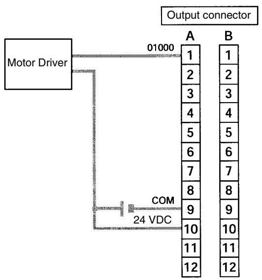
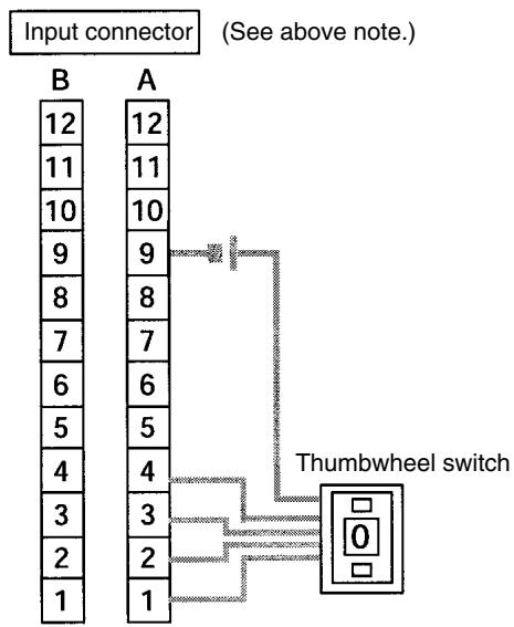
Note Refer to the operation manual for details on wiring.
PC Setup

Programming (CPM2A Example)
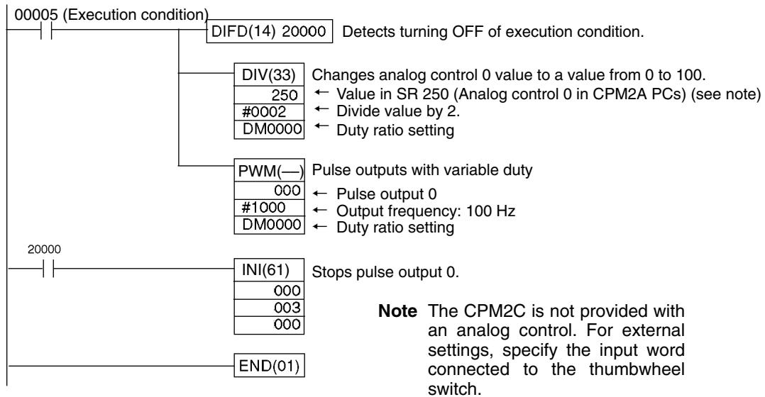
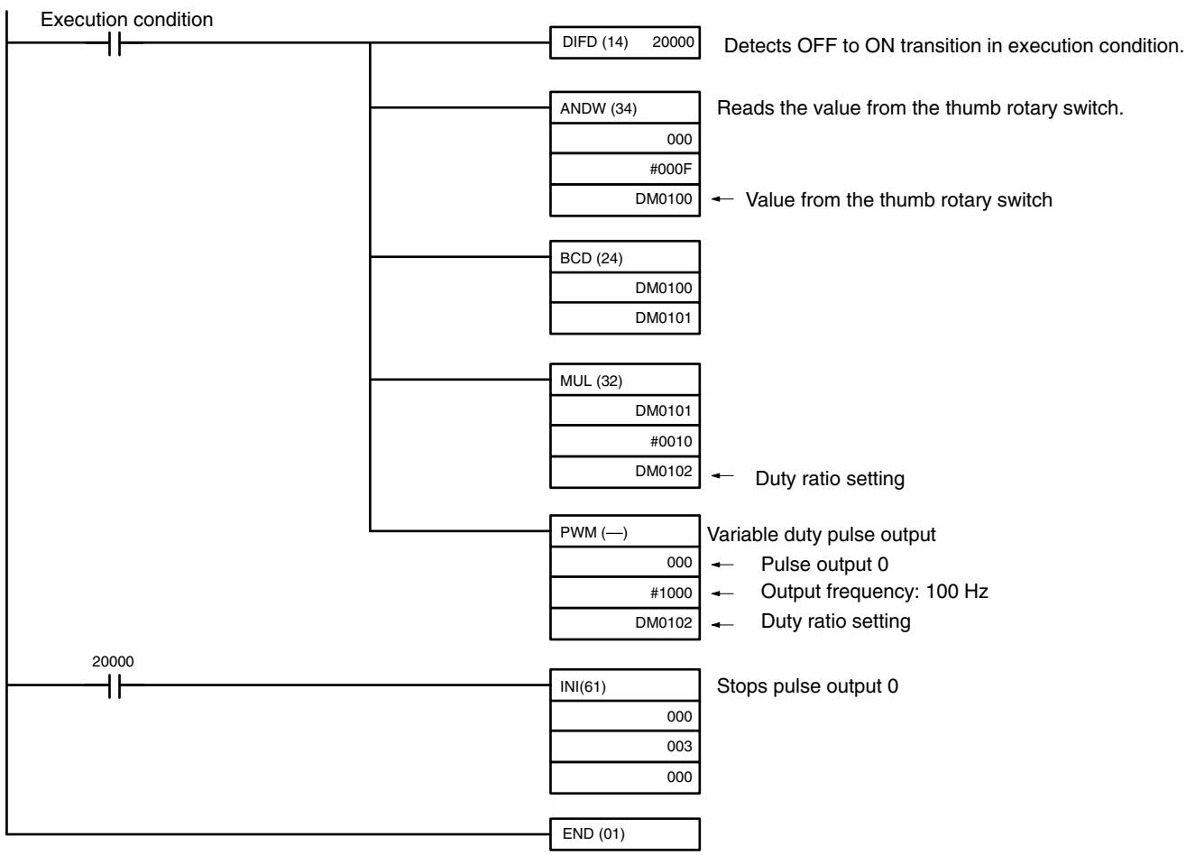
Programming (CPM2C Example)
2-5-3 Using Pulse Outputs With Trapezoidal Acceleration and Deceleration
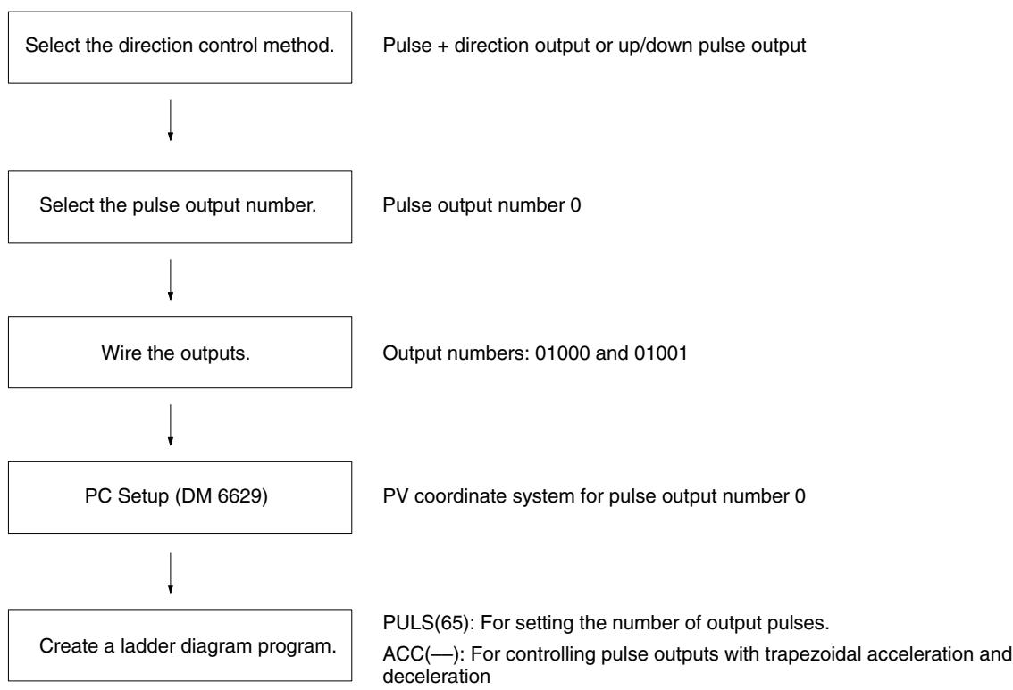
INI(61): For stopping pulse outputs and changing the pulse output PV.
PRV(62): For reading the pulse output PV and status.
Pulse Outputs With Trapezoidal Acceleration and Deceleration
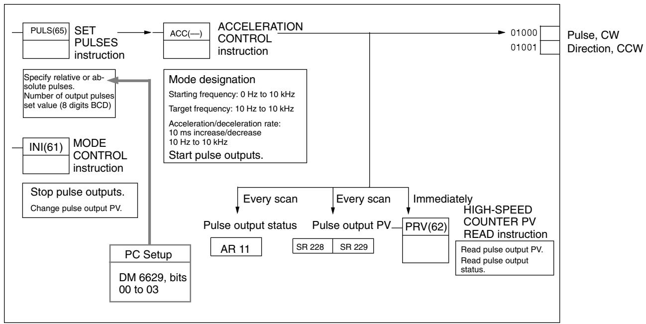
Selecting the Direction Control Method
Select the pulse output direction control method according to the type of signal used.

Pulse + Direction Outputs
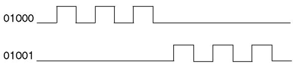
Up/down Pulse Outputs
Selecting the Pulse Output Number
Select pulse output 0.
| Output number | Pulse output number |
| 01000 | 0 |
| 01001 |
Wiring the Outputs
Wire the CPM2A outputs as shown in the following illustration.
Pulse + Direction Outputs
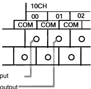
Up/down Pulse Outputs
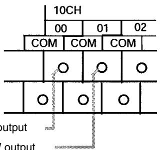
Output 01000: Pulse output
Output 01001: Direction output
Output 01000: CW output
Output 01001: CCW output
Wire the CPM2C outputs as shown in the following illustration.
Note The following examples are for Fujitsu-compatible connectors. Output bit addresses and connector pin numbers depend on the models. Refer to the CPM2C Operation Manual (W356) or the CPM2C-S Operation Manual (W377) for details.
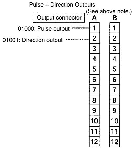
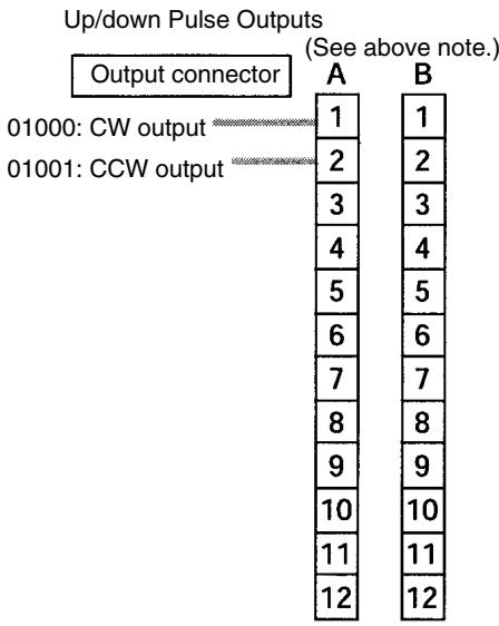
PC Setup
Make the following settings in the PC Setup.
| Word | Bits | Function | Setting | |
| DM 6629 | 00 to 03 | Pulse 0 PV coordinate system | 0: Relative coordinate system1: Absolute coordinate system | Either 0 or 1 |
| DM 6642 | 08 to 15 | High-speed counter setting | 00: Do not use.01: Use as high-speed counter02: Use as synchronized pulse control (10 to 500 Hz).03: Use as synchronized pulse control (20 Hz to 1 kHz).04: Use as synchronized pulse control (300 Hz to 20 kHz). | Either 00 or 01 |
If absolute pulses are specified with PULS(65), be sure to set the absolute coordinate system (1).
Synchronized pulse control cannot be used simultaneously.
The settings will go into effect when the mode is changed (from PROGRAM to MONITOR/RUN) or when the power supply is turned ON to the PC.
Ladder Diagram Programming
The following table shows the instruction operations related to pulse outputs with trapezoidal acceleration and deceleration (fixed duty ratio).
| Instruction | Control | Operation |
| (@)PULS(65) | Set number of pulses | Sets the number of pulses to be output in independent mode. |
| (@)ACC(—) | Set frequency and start pulse outputs | Sets the target frequency, starting frequency, and acceleration/deceleration rate for outputs in independent mode or continuous mode, and starts the pulse outputs. |
| Change frequency | Changes the frequency during pulse output in continuous mode by accelerating or decelerating according to the specified acceleration/deceleration rate. | |
| Stop pulse outputs | Decelerates pulse outputs to a stop according to the specified acceleration/deceleration rate. | |
| (@)INI(61) | Stop (decelerate stop) pulse outputs | Stops the pulse outputs. |
| Change pulse output PV | Changes the pulse output PV. | |
| (@)PRV(62) | Read pulse output PV | Reads the pulse output PV. |
| Read pulse output status | Reads the pulse output status. |
The following table shows which instructions can be executed during pulse outputs with trapezoidal acceleration and deceleration.
| PULS(65) | SPED(64) | INI(61) | PRV(62) | ACC(—) | PWM(—) | |
| Continuous mode | No | No | Yes (See note 1.) | Yes | No | No |
| Independent mode | No | No | Yes (See note 1.) | Yes | Yes (See note 2.) | No |
Note
- This instruction can be executed only while pulse outputs are stopped. The PV cannot be changed while pulses are being output. If the PV needs to be changed, be sure to stop the pulse output first.
- This instruction can be used only for changing the frequency and stopping the pulse output. It cannot be used for switching between independent mode and continuous mode. Moreover, ACC(—) cannot be received during acceleration or deceleration.
The following table shows the words and bits related to pulse outputs with trapezoidal acceleration and deceleration (fixed duty ratio).
| Word | Bits | Name | Contents |
| 228 | 00 to 15 | Pulse output PV 0, rightmost 4 digits | Cannot be used as work bits even when not used as pulse outputs. |
| 229 | 00 to 15 | Pulse output PV 0, leftmost 4 digits | |
| 252 | 04 | Pulse output 0 PV reset | Clears PV 0 when ON. |
| AR 11 | 11 | Pulse output status for pulse output 0 | ON: Accelerating or decelerating OFF: Constant speed |
| 12 | Pulse output 0 PV overflow/underflow | ON: Occurred OFF: Normal | |
| 13 | Number of pulses set for pulse output 0 | ON: Set OFF: Not set | |
| 14 | Pulse output completed for pulse output 0 | ON: Completed OFF: Not completed | |
| 15 | Pulse output in progress for pulse output 0 | ON: In progress (by SPED(64), ACC(—), or PWM(—)) OFF: Stopped |
Set Number of Pulses
Specify the number of pulses to be output in independent mode.
@PULS(65)
000 Fixed at 000: Pulse output 0
D Type of Pulse Output (000: Relative pulses; 001: Absolute pulses) (See note.)
N | Beginning word of setting for number of pulses
N
Rightmost 4 digits
Number of pulses (Rightmost, leftmost digits)
N+1
Leftmost 4 digits
Register the number of pulses to be set.
96,777,215 to 16,777,215
Negative numbers are expressed by turning
ON the leftmost bit.
Type of Pulse Output
000: Relative pulses (SV for number of pulses = Number of pulses moved)
001: Absolute pulses (SV for number of pulses = The next PV on the absolute coordinate system, i.e., the pulse output PV + number of pulses moved)*
*Absolute pulses can only be specified by PULS(65) when the PV coordinate system in the PC Setup is set for an absolute coordinate system.
Set Frequency and Start Pulse Outputs Change Frequency
These functions set the output mode, the target frequency, the starting frequency, and the acceleration/deceleration rate, and they begin pulse outputs. They can also be used to change the frequency, by accelerating or decelerating at the specified acceleration/deceleration rate, if pulse outputs are already in progress in continuous mode.
Setting the Frequencies, Acceleration/Deceleration, and Starting Pulse Outputs in Independent Mode
| (@)ACC(—) |
| 000 |
| M |
| T |
| Fixed at 000: Pulse output 0 |
| Output mode designation |
| Beginning word of settings table |
M
Output mode
Specify the output mode.
000: Up/down pulse outputs, independent mode
002: Pulse + direction outputs, independent mode
T
Acceleration/deceleration rate (#0001 to #1000 BCD: 10 Hz to 10 kHz)
T+1
Target frequency (#0001 to #1000 BCD: 10 Hz to 10 kHz)
T+2
Starting frequency (#0000 to #1000 BCD: 0 to 10 kHz)
Register the data for each frequency.
The acceleration/deceleration rate is the increase or decrease in the frequency every 10 ms.
Pulse output frequency
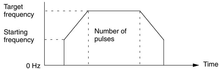
In independent mode, the acceleration and deceleration points are determined from the number of pulses, the acceleration/deceleration rate, the target frequency, and the starting frequency.
Setting the Frequency and Acceleration/Deceleration, Starting Pulse Outputs, and Changing the Frequency in Continuous Mode
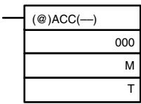
Fixed at 000: Pulse output 0
Output mode designation
Beginning word of settings table
Output mode
Specify the output mode.
010: Up/down pulse output, CW, continuous mode
011: Up/down pulse output, CCW, continuous mode
012: Pulse + direction output, CW, continuous mode
013: Pulse + direction output, CCW, continuous mode
Acceleration/deceleration rate (#0001 to #1000 BCD: 10 Hz to 10 kHz)
Target frequency (#0001 to #1000 BCD: 10 Hz to 10 kHz)
Starting frequency (#0000 to #1000 BCD: 0 to 10 kHz)
Register the data for each frequency.
The acceleration/deceleration rate is the increase or decrease in the frequency every 10 ms.
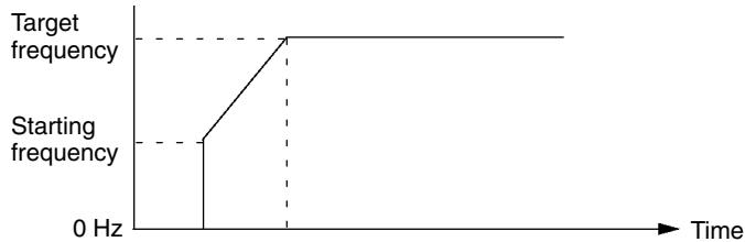
Pulse output frequency
In continuous mode, pulses are output at the target frequency until stopped. The next ACC(—) instruction cannot be received except during acceleration or deceleration.
Change Pulse Output PV
This function changes the pulse output PV.
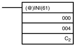
Fixed at 000: Pulse output 0
Control designation (004: Change pulse output PV)
Beginning word for PV change data
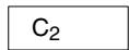
Rightmost 4 digits
Change PV data (Rightmost, leftmost digits)
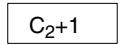
Leftmost 4 digits
Register the PV data to be changed.
96,777,215 to 16,777,215
Negative numbers are expressed by turning ON the leftmost bit.
Stop Pulse Outputs,
Decelerate and Stop Pulse Outputs
These functions stop the pulse outputs.
Stop Pulse Outputs

Fixed at 000: Pulse output 0
Control designation (003: Stop pulse outputs)
Fixed at 000
Decelerate Stop Pulse Outputs
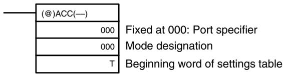
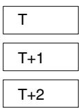
Acceleration/deceleration rate (#0001 to #1000 BCD: 10 Hz to 10 kHz)
Target frequency (#0000 to #1000 BCD: 0 Hz to 10 kHz)
Starting frequency (#0000 to #1000 BCD: 0 to 10 kHz)
Register the data for each frequency.
The acceleration/deceleration rate is the increase or decrease in the frequency every 10 ms.
Note The pulse outputs can also be stopped by switching the PC to PROGRAM mode.
Read Pulse Output PV
This function reads the pulse output PV.
Using an Instruction
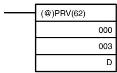
Fixed at 000: Pulse output 0
Control designation (003: Read pulse output PV)
Beginning word for storing pulse output PV
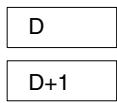
Rightmost 4 digits
Leftmost 4 digits
Pulse output PV (rightmost, leftmost digits)
The PV data that is read is stored here.
96,777,215 to 16,777,215
Negative numbers are expressed by turning
ON the leftmost bit.
Using Data Areas
As shown in the following illustration, the pulse output PV for pulse output 0 is stored in words 228 and 229.
Pulse Output 0
PV (Rightmost)
PV (Leftmost)
SR 228 and SR 229 are refreshed once each cycle, so the values in these words may not reflect the actual status during each cycle. SR 228 and SR 229 are refreshed immediately when their status is read with PRV(62).
SR 228 to SR 231 are refreshed with every scan, so there may be a discrepancy from the exact PV at any given time.
SR 228 to SR 231 cannot be used as work words even when pulse outputs are not being used.
When the PV is read by executing PRV(62), SR 228 to SR 231 are refreshed with the same timing.
Read Pulse Output Status
This function reads the pulse output status.
Using an Instruction
| (@)PRV(62) |
| 000 |
| 001 |
| D |
Fixed at 000: Pulse output 0
Control designation (001: Read pulse output status)
Word for storing pulse output status
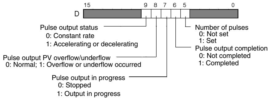
Using Data Areas
As shown in the following illustration, the pulse output status for pulse output 0 is stored in AR 1111 to AR 1115.
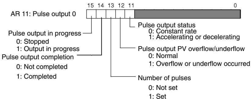
Note AR 1111 through AR 1115 are refreshed once each cycle, so the values of these flags may not reflect the actual status, but these flags are refreshed immediately when their status is read with PRV(62).
Relationship Between Status and Operation
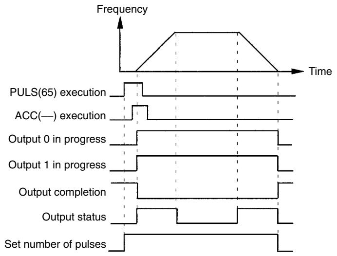
Independent Mode with Acceleration and Deceleration
Continuous Mode with Acceleration and Deceleration 1
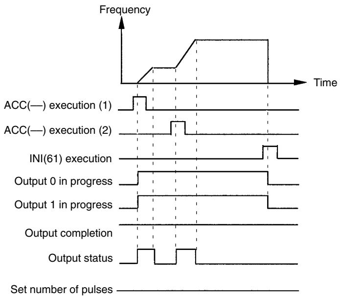
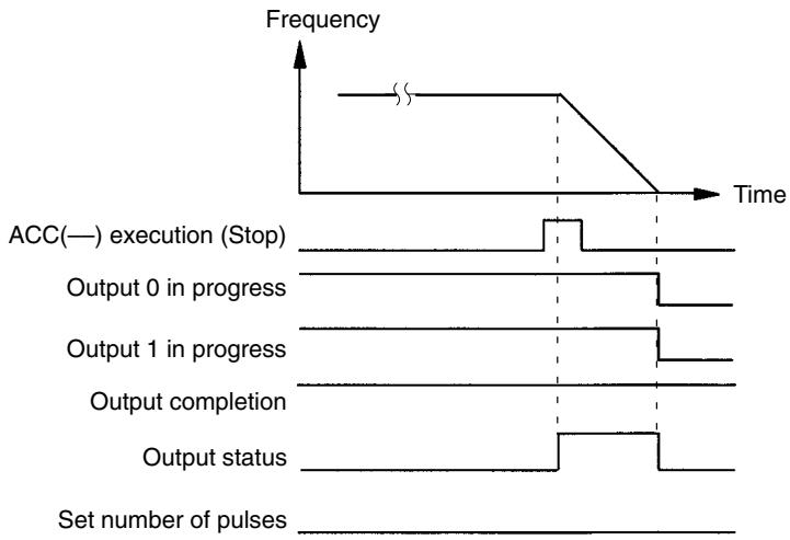
Continuous Mode with Acceleration and Deceleration 2
Stopping Outputs in Continuous Mode with Acceleration and Deceleration 1
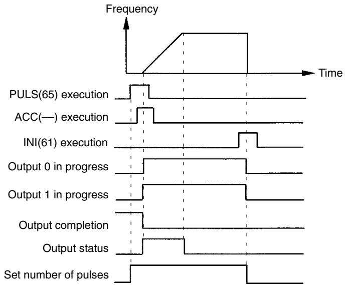
Stopping Outputs in Continuous Mode with Acceleration and Deceleration 2
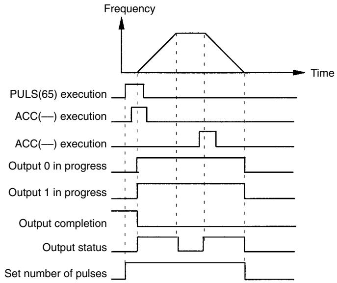
Application Example Positioning
Explanation
In this example, when the execution condition (00005) turns ON, 1000 pulses are output from output 01000 (pulse output 0) in a trapezoidal acceleration/deceleration pattern as shown in the following diagram.
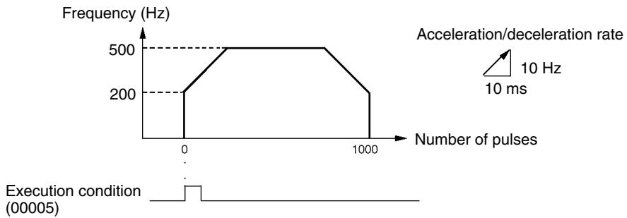
Wiring
Wire the CPM2A to the motor driver as shown in the following illustration.
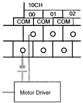
Wire the CPM2C to the motor driver as shown in the following illustration. In this case, a CPU Unit with sinking transistor outputs is used.
Note The following examples are for Fujitsu-compatible connectors. Output bit addresses and connector pin numbers depend on the models. Refer to the CPM2C Operation Manual (W356) or the CPM2C-S Operation Manual (W377) for details.
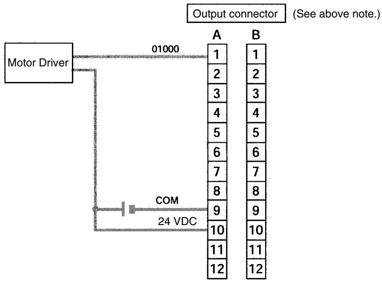
Note Refer to the operation manual for details on wiring.
PC Setup

Programming
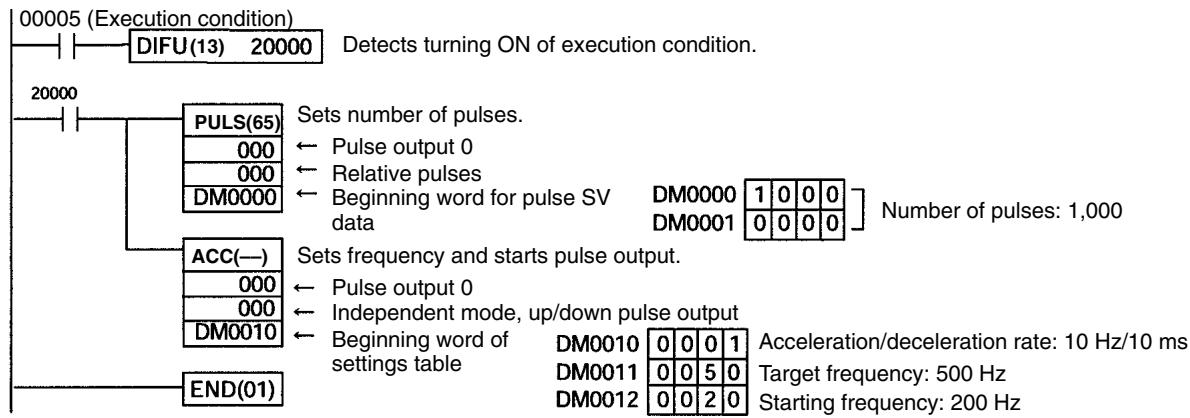
Jogging
Explanation
In this example, when the execution condition (00005) turns ON, JOG pulses are output at a frequency of 100Hz from either output 01000 (CW direction) or output 01001 (CCW direction). When the execution condition (00005) turns OFF, the output is stopped. As shown in the following diagram, the JOG pulses are accelerated and decelerated at the start and stop of the operation. Switching between output 01000 (CW direction) and output 01001 (CCW direction) is performed by means of the direction designator (00006).
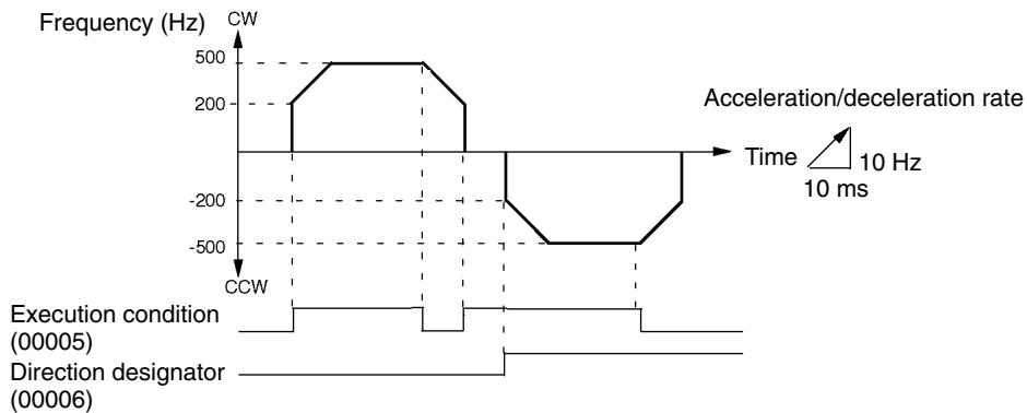
Wiring
Wire the CPM2A to the motor driver as shown in the following illustration.
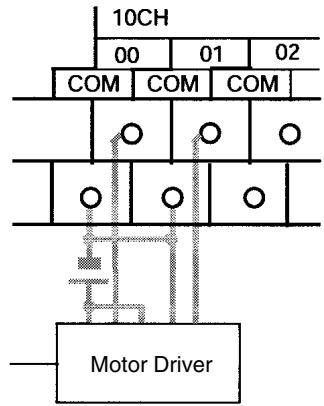
Wire the CPM2C to the motor driver as shown in the following illustration. In this case, a CPU Unit with sinking transistor outputs is used.
Note The following examples are for Fujitsu-compatible connectors. Output bit addresses and connector pin numbers depend on the models. Refer to the CPM2C Operation Manual (W356) or the CPM2C-S Operation Manual (W377) for details.
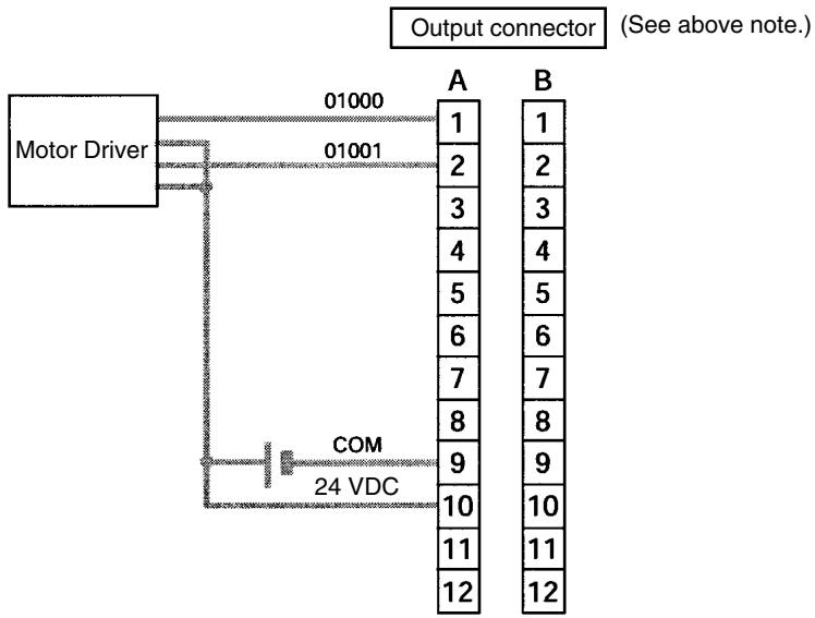
Note Refer to the operation manual for details on wiring.
PC Setup

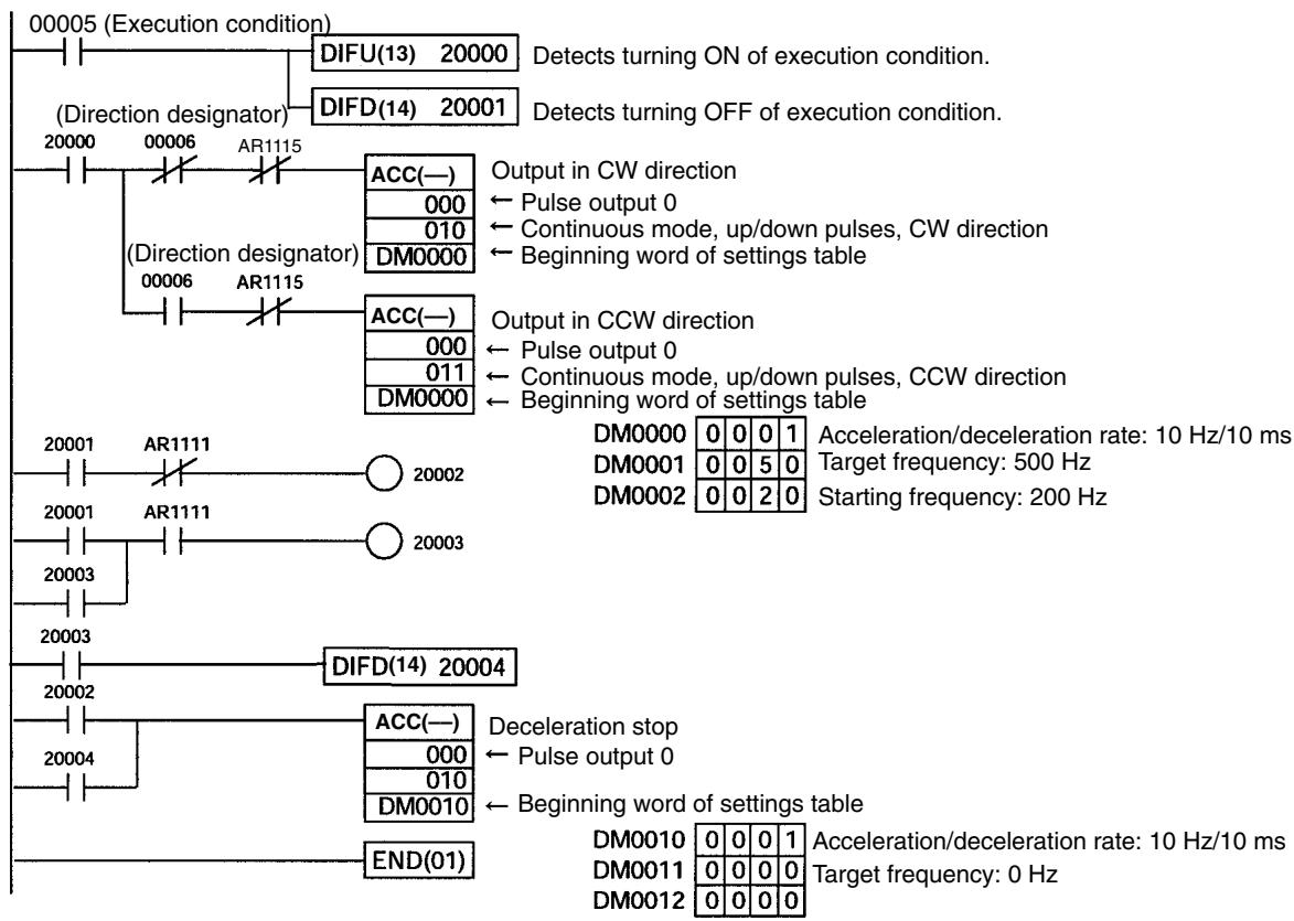
Programming
2-6 CPM1A Pulse Output Functions
The CPM1A PCs with transistor outputs have a pulse output function capable of outputting a pulse of 20Hz to 2kHz (single-phase). Either IR 01000 or IR 01001 can be selected for pulse output, and the pulse output can be set to either the continuous mode, under which the output can be stopped by an instruction, or the independent mode, under which the output is stopped after a preset number of pulses (1 to 16,777,215).
Refer to the CPM1A Operation Manual (W317) for details on hardware connections to output points and ports.
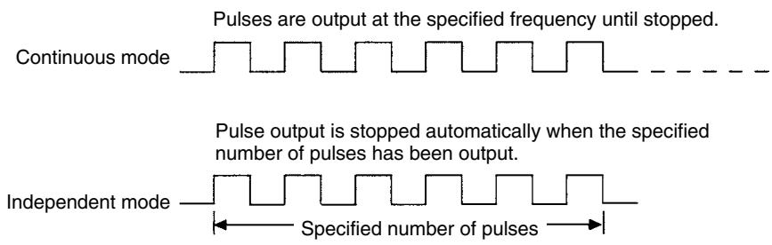
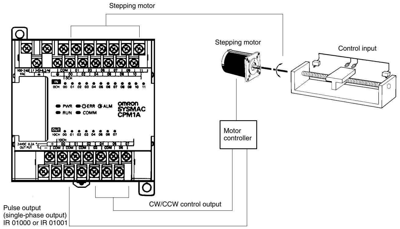
Note 1. The CPM1A uses a single-phase pulse output. The control signal for the direction of rotation (CW/CCW) for the motor driver must be written in the program.
2. Be sure to use a CPU Unit with transistor outputs.
2-6-1 Programming Example in Continuous Mode
In this example program, pulse output begins from IR 01000 when input IR 00004 turns ON, and is stopped when input IR 00005 turns ON.
SPED(64) can be used to stop pulse output. When using SPED(64) for that purpose, specify #0000 (constant or word contents) as the pulse frequency.
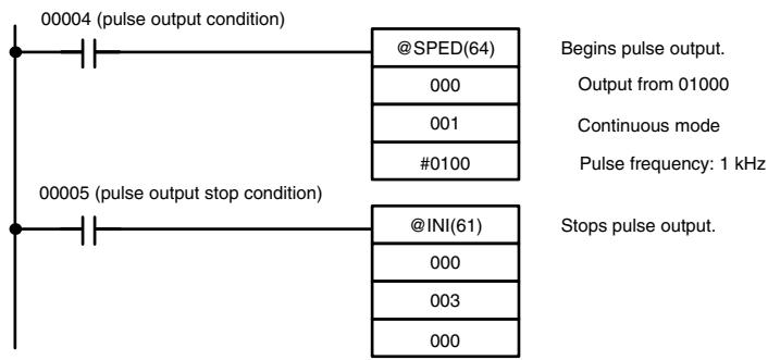
2-6-2 Programming Example in Independent Mode
In this example program, pulse output begins from IR 01000 when input IR 00004 turns ON, and is stopped after the specified number of pulses have been output. The pulse amount is set in DM 0100 and DM 0101.
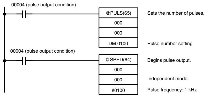
2-6-3 Using Pulse Output Instructions
Setting the Number of Pulses
Before beginning pulse output using the independent mode use PULS(65) as shown below to set the number of pulses to be output. This setting is not required for the continuous mode.
| @PULS(65) |
| 000 |
| 000 |
| N |
In N, set the beginning word address of the words where the number of pulses is set. Store the number of pulses in words N and N+1, in eight digits BCD, with the leftmost four digits in N+1 and the rightmost four digits in N.
Make the setting within a range of 00000001 to 16777215 (BCD).
Beginning Pulse Output
With SPED(64), set the bit location for pulse outputs (IR 01000 or IR 01001), the output mode (independent, continuous), and the pulse frequency to begin the pulse output.
| @SPED(64) |
| P |
| M |
| F |
P (3 digits BCD)
000: Outputs to IR 01000
010: Outputs to IR 01001
M (3 digits BCD)
000: Independent mode
001 Continuous mode
F (4 digits BCD)
For the beginning pulse output frequency, specify a constant or word contents. The specified value and set frequency are as follows:
Specified value: 0002 to 0200
Set frequency: 20 to 2,000 Hz
Note 1. Pulses can be output from only one bit at a time.
- When pulse output is begun in independent mode, the number of pulses is read when SPED(64) is executed. PULS(65) cannot be used to change the number of pulses while pulses are being output.
2-6-4 Changing the Frequency
To change the frequency during pulse output, change the frequency setting with SPED(64). At that time, set the operands other than the frequency to the same settings as at the beginning of pulse output.
| @SPED(64) |
| P |
| M |
| F |
P (3 digits BCD)
Same as at beginning of pulse output.
M (3 digits BCD)
Same as at beginning of pulse output.
F (4 digits BCD)
For the changed pulse output frequency, specify a constant or word contents. The specified value and set frequency are as follows:
Specified value: 0002 to 0200
Set frequency: 20 to 2,000 Hz
2-6-5 Stopping Pulse Output
When pulses are output in the independent mode, the pulse output will automatically stop after the number of pulses specified with PULS(65) has been output. When pulses are output in the continuous mode, either of the following two methods can be used to stop the pulse output.
- Use SPED(64) to set the frequency to 0.
- Use INI(61) to stop the pulse output.
Using SPED(64)
The first method is to use SPED(64) to stop the pulse output by setting the frequency to 0. For details, refer to 2-6-4 Changing the Frequency.
Using INI(61)
The second method is to use INI(61) to stop the pulse output, as follows:
| @INI(61) |
| 000 |
| 003 |
| 000 |
2-7 Synchronized Pulse Control (CPM2A/CPM2C Only)
By combining the CPM2A/CPM2C's high-speed counter function with the pulse output function, the output pulse frequency can be controlled as a specified multiple of the input pulse frequency.
Note A CPU Unit with transistor outputs is required in order to use synchronized pulse control, i.e., either a CPM2A-□□CDT-D or CPM2A-□□CDT1-D.
The following diagram shows the configuration for a CPM2A, but the configuration for a CPM2C is identical.
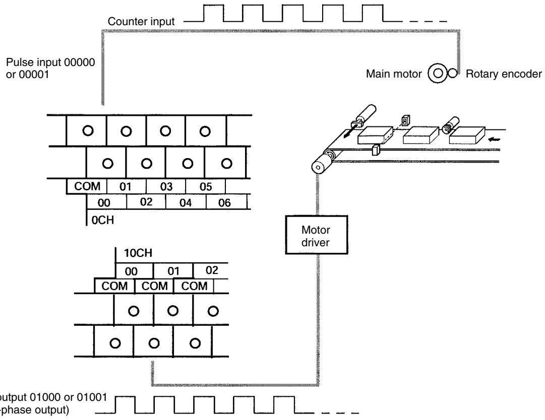
| Item | Input mode | ||||
| Differential phase input mode | Pulse + direction input mode | Up/down pulse input mode | Increment mode | ||
| Input number | 00000 | Phase-A input | Count input | CW input | Count input |
| 00001 | Phase-B input | Direction input | CCW input | (See note 1.) | |
| Input method | Differential phase input (4X) | Single-phase input | Single-phase input | Single-phase input | |
| Input frequency range | 10 to 500 Hz (accuracy ±1 Hz) 20 Hz to 1 kHz (accuracy ±1 Hz) 300 Hz to 20 kHz (accuracy ±25 Hz) (See note 2.) | ||||
| Output number (See note 3.) | 01000 | Pulse output 0 | |||
| 01001 | Pulse output 1 | ||||
| Output method | Single-phase output | ||||
| Output frequency range | 10 Hz to 10 kHz (accuracy 10 Hz) | ||||
| Frequency ratio | 1% to 1,000% (Can be specified in units of 1%). | ||||
| Synchronized control cycle | 10 ms | ||||
Note 1. Can be used as an ordinary input.
2. When 10kHz or less, then the accuracy is ± 10Hz .
3. Either can be selected as the output number, using SYNC(—).
The directions of pulse inputs are all ignored. The frequency of a pulse that has been input is read, without regard to the direction.
The following table shows the relationships between synchronized pulse control and the CPM2A's other functions.
| Function | Synchronized pulse control |
| Synchronized pulse control | --- |
| Interrupt inputs | Can be used simultaneously. |
| Interval timer interrupts | Can be used simultaneously. |
| High-speed counters | Cannot be used simultaneously. |
| Interrupt inputs (counter mode) | Can be used simultaneously. |
| Pulse outputs | Cannot be used simultaneously. |
| Quick-response inputs | Can be used simultaneously. |
| Input time constant | See note. |
| Clock | Can be used simultaneously. |
Note When inputs 00000 and 00001 are set for use as synchronized pulse control inputs, the input time constant settings for the affected inputs are disabled. The input time constants remain in effect, however, for the values for refreshing the relevant input data area.
The relationship between the pulse input frequency and the pulse output frequency is shown below.
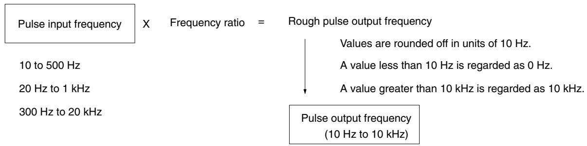
The scaling factor control cycle is 10 ms, and the pulse output frequency is changed at intervals of 10 ms with respect to the pulse input frequency.
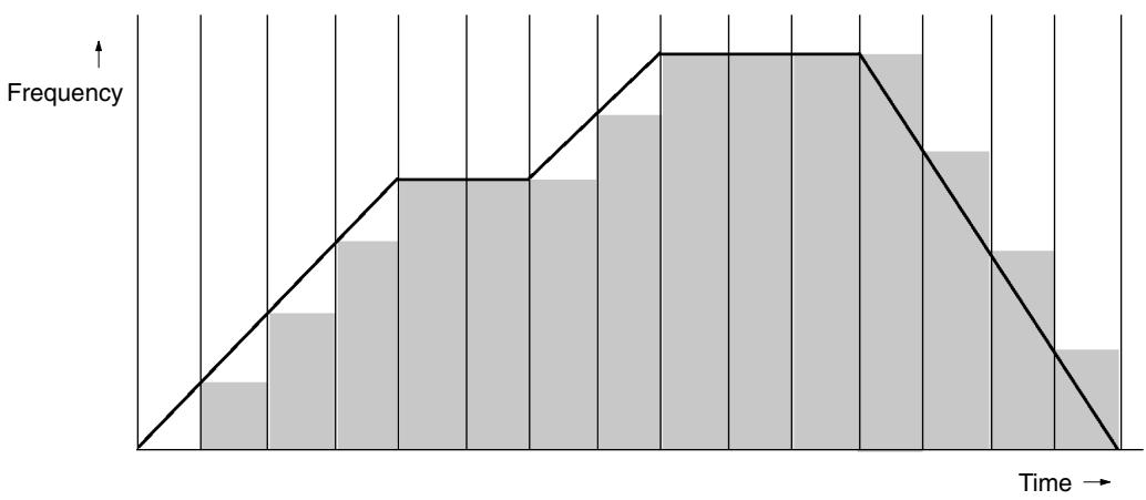
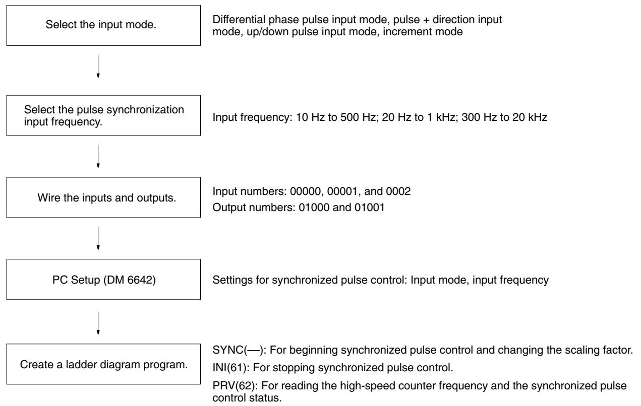
Using Synchronized Pulse Control
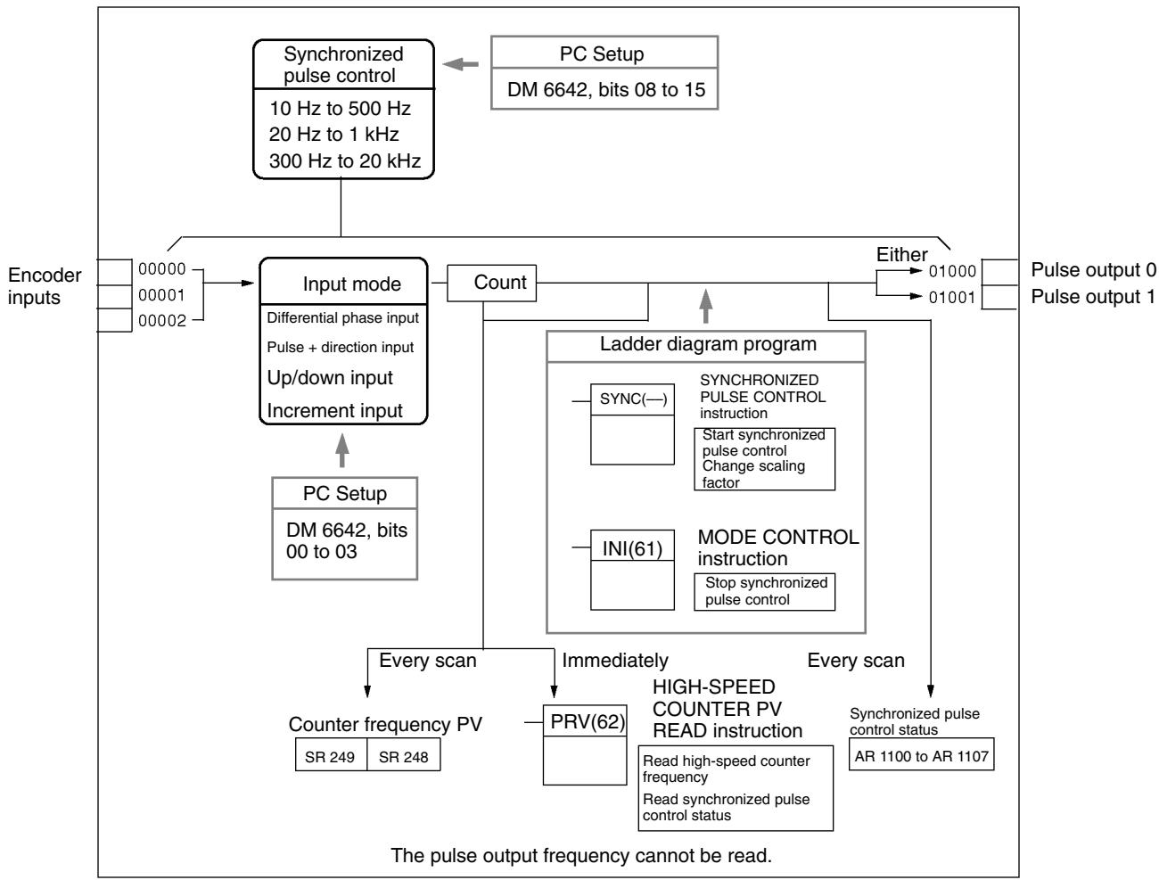
Selecting the Input Mode
Select the differential phase input mode, the pulse + direction input mode, the up/down pulse input mode, or the increment mode. These modes are explained below.
Selecting the Pulse Synchronization Input Frequency
Select one of the following as the input frequency range: 10Hz to 500Hz , 20Hz to 1kHz , or 300Hz to 20kHz . For more information on input frequencies, refer to the following diagrams.
Differential Phase Input Mode
In the differential phase input mode, the count is incremented or decremented according to two differential phase signals (phase A and phase B) with a multiplication factor of 4.
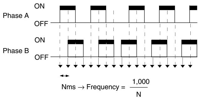
Pulse + Direction Input Mode
In the pulse + direction input mode, pulse signals and direction signals are input, and the count is incremented or decremented according to the direction signal status.
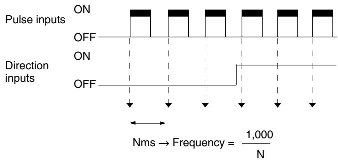
Up/Down Pulse Input Mode
In the up/down pulse input mode, CW signals (up pulses) and CCW signals (down pulses) are input, and the count is incremented or decremented accordingly.
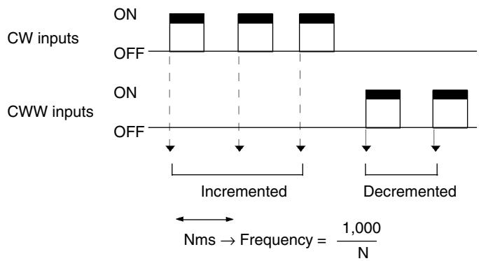
Increment Mode
In the increment mode, pulse signals are input and the count is incremented with each pulse. Phase-B inputs can be used as ordinary inputs.
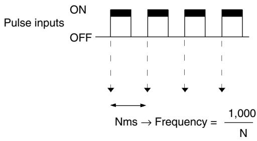
Wiring the Inputs
Input Wiring
Wire the CPM2A inputs as shown in the following diagram.
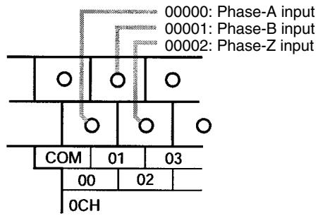
Differential Phase Input Mode
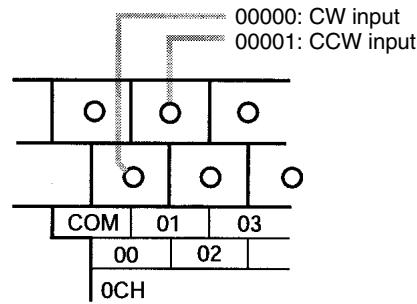
Up/Down Pulse Input Mode
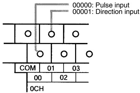
Pulse + Direction Input Mode
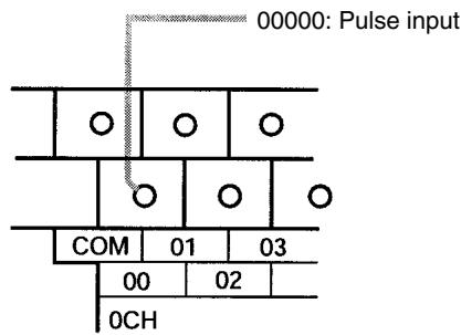
Increment Mode
Wire the CPM2C inputs as shown in the following diagram.
Note The following examples are for Fujitsu-compatible connectors. Input bit addresses and connector pin numbers depend on the models. Refer to the CPM2C Operation Manual (W356) or the CPM2C-S Operation Manual (W377) for details.
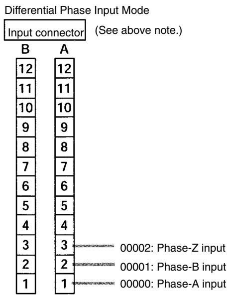
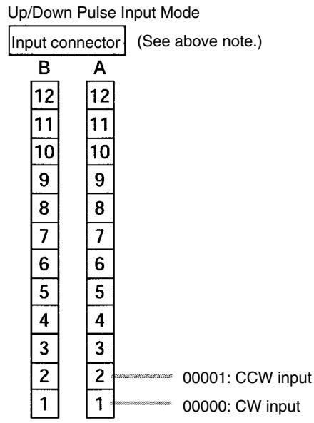
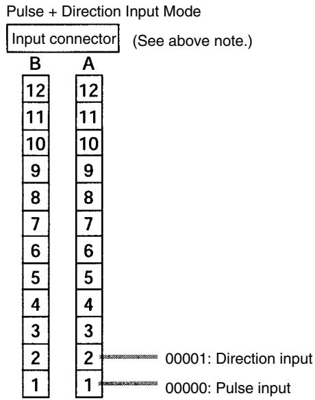
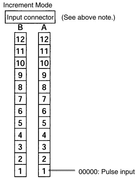
Output Wiring
Wire the CPM2A outputs as shown in the following diagram.
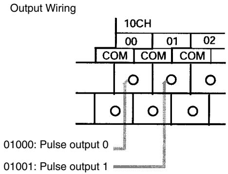
Wire the CPM2C outputs as shown in the following diagram.
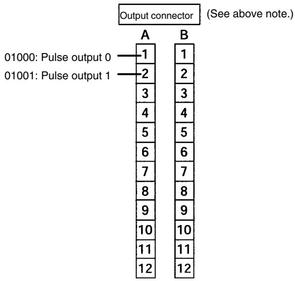
PC Setup
The settings in the PC Setup related to synchronized pulse control are listed in the following table.
| Word | Bits | Function | Setting |
| DM 6642 | 00 to 03 | High-speed counter input mode setting0: Differential phase input 5 kHz1: Pulse + direction input 20 kHz2: Up/down input 20 kHz4: Increment 20 kHz | 0, 1, 2, or 4 |
| 04 to 07 | High-speed counter reset method setting0: Phase-Z signal + software reset1: Software reset | 0 or 1 | |
| 08 to 15 | High-speed counter setting00: Do not use.01: Use as high-speed counter02: Use as synchronized pulse control(10 Hz to 500 Hz)03: Use as synchronized pulse control(20 Hz to 1 kHz)04: Use as synchronized pulse control(300 Hz to 20 kHz) | 02, 03, 04 |
Ladder Diagram Programming
The settings will go into effect when the mode is changed (from PROGRAM to MONITOR/RUN) or when the power supply is turned ON to the PC.
The following table shows the instruction operations related to synchronized pulse control.
| Instruction | Control | Operation |
| (@)SYNC(—) | Start synchronized control | Specifies the frequency scaling factor and the output port, and outputs pulses. |
| Change frequency scaling factor | Changes the frequency scaling factor during pulse output. | |
| (@)INI(61) | Stop synchronized control | Stops the pulse outputs. |
| (@)PRV(62) | Read input frequency | Reads the input frequency. |
| Read synchronized control status | Reads the synchronized control status. |
The following table shows the words and bits related to synchronized pulse control.
| Word | Bits | Name | Contents |
| 248 | 00 to 15 | Input frequency PV, rightmost digits | Reads the input frequency PV. |
| 249 | 00 to 15 | Input frequency PV, leftmost digits | |
| AR 11 | 15 | Pulse output in progress for pulse output 0 | ON: Output in progress OFF: Stopped |
| AR 12 | 15 | Pulse output in progress for pulse output 1 |
Start Frequency Control
This function specifies the bits for pulse outputs (01000, 01001) and the frequency scaling factor (1% to 1,000%), and starts the pulse output.
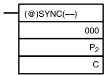
Pulse input port designation (000: High-speed counter)
Pulse output port designation (000: Pulse output 0; 010: Pulse output 1)
Frequency scaling factor setting
Frequency scaling factor
Register the frequency scaling factor to be set.
0001 to #1000 (4 digits BCD): 1 to 1,000%
Note When using SYNC(—) to specify a frequency scaling factor, be careful to keep the pulse output frequency below 10kHz .
Change Frequency Scaling Factor
This function changes the frequency scaling factor during synchronized control (during pulse output) by specifying the bits for pulse outputs (01000, 01001) and the frequency scaling factor (1% to 1,000%) and executing SYNC(—).
Stop Synchronized Control
This function stops the pulse outputs.
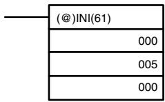
Port specifier (000: High-speed counter)
Control designation (005: Stop synchronized control)
Fixed: 000
Note The pulse output can also be stopped by switching the PC to PROGRAM mode.
Read Input Frequency
This function reads the input frequency PV.
Using an Instruction
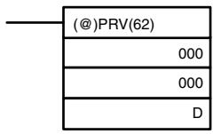
Fixed: 000
Control designation (000: Read high-speed counter input frequency)
Beginning word for storing input frequency PV

Using Data Areas
As shown in the following illustration, the input frequency is stored in words 248 and 249.
Word 248 Input frequency PV (Rightmost)
Word 249 Input frequency PV (Leftmost)
Words 248 and 249 are refreshed with every scan, so there may be a discrepancy from the exact PV at any given time.
When the PV is read by executing PRV(62), words 248 and 249 are refreshed with the same timing.
Read Synchronized Control Status
This function reads the synchronized control status.
Using an Instruction
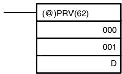
Port specifier (000: Pulse output 0; 010: Pulse output 1)
Control designation (001: Read synchronized control status)
Beginning word for storing synchronized control status
- Port specifier: 000
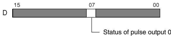
0: Stopped
1: Pulse output in progress
- Port specifier: 010
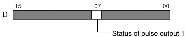
0: Stopped
1: Pulse output in progress
Using Data Areas
As shown in the following illustration, the status of pulse output 0 is stored in AR 1115, and the status of pulse output 1 is stored in AR 1215.

0: Stopped
1: Output in progress

0: Stopped
1: Output in progress
AR 1115 and AR 1215 are refreshed once each cycle, so there may be a discrepancy from the exact PV at any given time.
When the PV is read by executing PRV(62), AR 1112 and AR 1212 are refreshed immediately.
Relationship Between Status and Operation
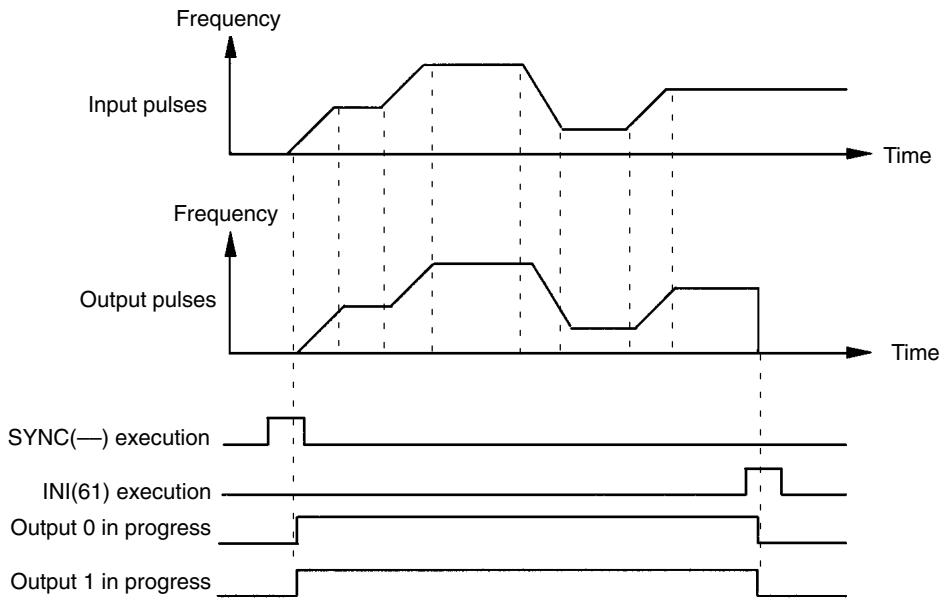
Application Example
Explanation
In this example, when the execution condition (00005) turns ON, synchronized pulse control is started and pulses are output from output 01000 (pulse output 0) according to the pulses input by the high-speed counter. At this time, the frequency scaling factor can be changed by means of analog control 0. When the execution condition (00005) turns OFF, synchronized pulse control is stopped.
Wiring
Wire the CPM2A as shown in the following illustration.
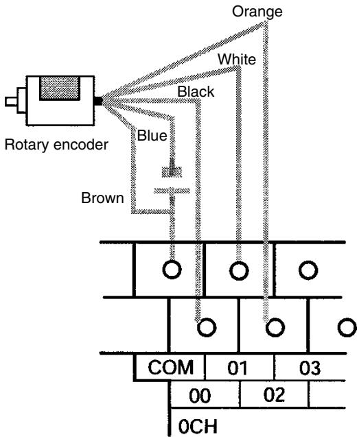
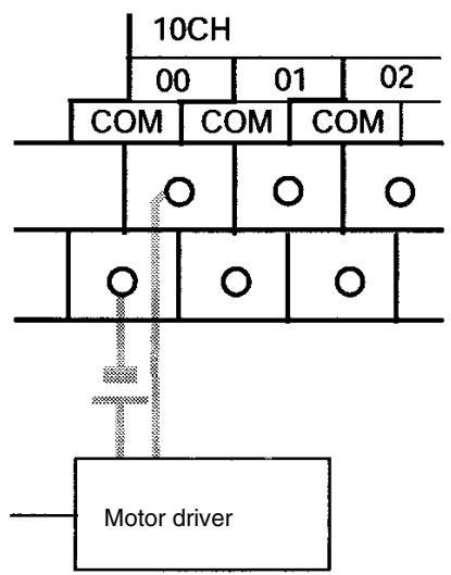
Wire the CPM2C as shown in the following illustration. In this case, a CPU Unit with sinking transistor outputs is used.
Note The following examples are for Fujitsu-compatible connectors. I/O bit addresses and connector pin numbers depend on the models. Refer to the CPM2C Operation Manual (W356) or the CPM2C-S Operation Manual (W377) for details.
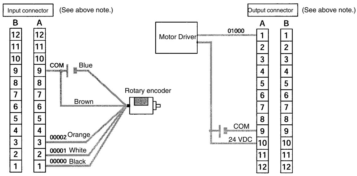
Note For details regarding motor driver wiring to outputs and rotary encoder wiring to inputs, refer to the CPM2A Operation Manual (W352)/CPM2C (W356) Operation Manual CPM2C-S Operation Manual (W377).

PC Setup
Programming (Example for CPM2A)
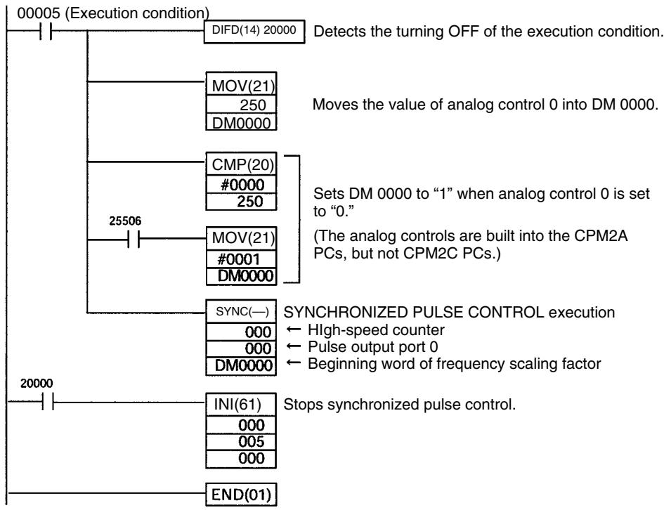
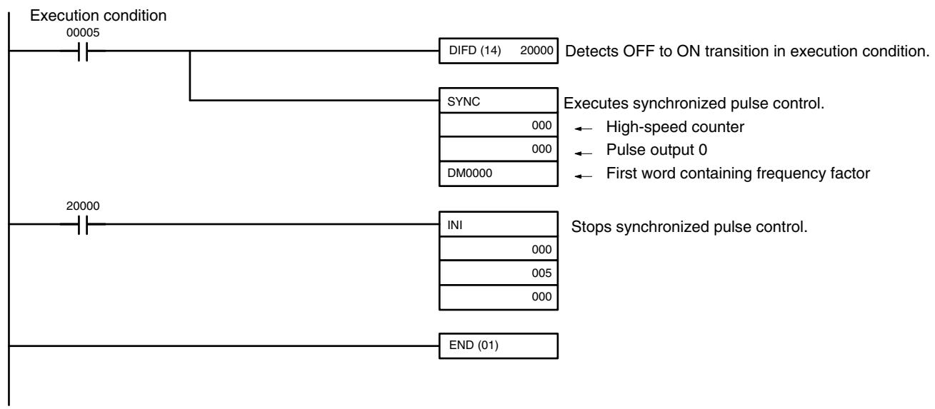
Programming (Example for CPM2C)
2-8 Data Computation Standards
The degree of error and performance in pulse outputs and synchronized pulse control are described in this section.
2-8-1 Pulse Outputs
Delays in Frequency Changes
There will be a delay before a change in the frequency during pulse output is actually applied to the output, as shown below.
Frequency Error

Maximum delay (ms) = One period of the current pulse output ÷ 2 + 10 + instruction execution time
There will be an error between the frequency of the output pulse and the set frequency of less than ± 1% due to internal processing error.
2-8-2 Synchronized Pulse Control
The following diagram shows the delay that will occur between starting synchronized pulse control and the start of actual pulse output.
Delay in Start of Pulse Output

Maximum delay (ms) = One period of the pulse input x2 + 16.25
There will be a delay before a change in the frequency during pulse output is actually applied to the output when performing synchronized pulse control, as shown below.
Delays in Frequency Changes

Maximum delay (ms) = One period of the current pulse output ÷ 2 + 10
The following diagram shows the delay that will occur between stopping synchronized pulse control (0 Hz) and the end of actual pulse output during synchronized pulse control.
Delay in Stop of Pulse Output

Maximum delay (ms) = Setting in DM 6642 (see below) + One period of the current pulse output ÷ 2 + 10
| Setting of DM 6642 bits 08 to 15 | Frequency range | Delay |
| 02 | 10 to 500 Hz | 262 ms |
| 03 | 20 Hz to 1 kHz | 66 ms |
| 04 | 300 Hz to 20 kHz | 4 ms |
Frequency Error
There will be an error between the frequencies of the input pulse and output pulse, as described below. The error consists of error in the input pulse frequency measurement and error in the output pulse frequency.
Input Pulse Frequency Measurement Error
The error in measuring the frequency of the input pulse depends on the setting in DM 6642, as shown below. If a multiplication factor is specified for synchronized pulse control, the error given in the table must also be multiplied by the same factor.
| Setting of DM 6642 bits 08 to 15 | Frequency range | Error |
| 02 | 10 to 500 Hz | ±1 Hz |
| 03 | 20 Hz to 1 kHz | ±1 Hz |
| 04 | 300 Hz to 20 kHz | ±10 Hz |
Output Pulse Frequency Error
There will be an error between the frequency of the output pulse and the set frequency of less than ± 1% due to internal processing error.
Example
DM 6642 bits 08 to 15: 4 (frequency range: 300Hz to 20kHz )
Multiplication factor: 300%
Input frequency: 1 kHz (error: 0%)
If synchronized pulse control is performed under the above conditions, there will be an error of ± 10Hz in measuring the frequency range of the input pulse. The input frequency will thus be 990 to 1010Hz . The multiplication factor of 300% , however, would make this 2970 to 3030Hz . There would also be an error of ± 1% in the frequency of the output pulse, so the output would be in the range 2940 to 3060Hz .
2-9 Analog I/O Functions (CPM1/CPM1A/CPM2A/CPM2C Only)
One or more Analog I/O Units can be connected to the PC to provide analog I/O. One Analog I/O Unit allows 2 analog inputs and 1 analog output. Refer to 3-1 Analog I/O Units for details.
2-10 Temperature Sensor Input Functions (CPM1A/CPM2A/CPM2C Only)
Temperature Sensor Units can be added to directly input temperature sensor inputs into the PC. Temperature Sensor Units are available for either thermocouple or platinum resistance thermometer inputs.
For the CPM1A or CPM2A, up to three CPM1A-TS001/101 Temperature Sensor Units or one CPM1A-TS002/102 Temperature Sensor Unit can be connected. Up to 6 temperature inputs are possible for one PC.
For the CPM2C, up to four CPM2C-TS001/101 Temperature Sensor Units can be connected, enabling up to 8 temperature inputs for one PC.
Up to three Units can be connected for the CPM2C-S.
2-11 CompoBus/S I/O Slave Functions (CPM1A/CPM2A/CPM2C Only)
The PC can function as a Slave to a CompoBus/S Master Unit (or SRM1 CompoBus/S Master Control Unit) when a CompoBus/S I/O Link Unit is connected. Refer to 3-3 CompoBus/S I/O Link Unit for details.
2-12 CompoBus/S I/O Master Functions (SRM1(-V2) and CPM2C-S Only)
Maximum Number of Nodes A maximum of either 16 or 32 CompoBus/S nodes may be connected.
| Communications mode | No. of nodes set | Communications response time |
| High-speed mode | 16 | 0.5 ms |
| 32 | 0.8 ms | |
| Long-distance mode | 16 | 4.0 ms |
| 32 | 6.0 ms |
The communications mode and maximum number of nodes are set in the PC Setup, as shown in the following table.
| Word | Bit(s) | Function | Setting |
| DM 6603 | 00 to 03 | Maximum number of CompoBus/S nodes | 0 or 1 |
| 0: 32 nodes | |||
| 1: 16 nodes | |||
| 04 to 07 | CompoBus/S communications mode | 0 or 1 | |
| 0: High-speed communications | |||
| 1: Long-distance communications | |||
| 08 to 15 | Not used. | 00 |
Note When changes are made to these settings, always turn the power off and on again to make the new setting effective.
Slave Interrupts
Input bits in IR 000 to IR 007 and output bits in IR 010 to IR 017 are used as interrupts for CompoBus/S I/O Terminals. The CompoBus/S I/O Terminal interrupts (IN 0 to 15 and OUT 0 to 15) are allocated as indicated in the following table. IN0 to IN15 are the node addresses for the Input Terminals and OUT0 to OUT15 are the node addresses for the Output Terminals.
| Word | Bit | ||||||||||||||||
| 15 | 14 | 13 | 12 | 11 | 10 | 9 | 8 | 7 | 6 | 5 | 4 | 3 | 2 | 1 | 0 | ||
| Input | IR 000 | IN1 | IN0 | ||||||||||||||
| IR 001 | IN3 | IN2 | |||||||||||||||
| IR 002 | IN5 | IN4 | |||||||||||||||
| IR 003 | IN7 | IN6 | |||||||||||||||
| IR 004 | IN9 | IN8 | |||||||||||||||
| IR 005 | IN11 | IN10 | |||||||||||||||
| IR 006 | IN13 | IN12 | |||||||||||||||
| IR 007 | IN15 | IN14 | |||||||||||||||
| Output | IR 010 | OUT1 | OUT0 | ||||||||||||||
| IR 011 | OUT3 | OUT2 | |||||||||||||||
| IR 012 | OUT5 | OUT4 | |||||||||||||||
| IR 013 | OUT7 | OUT6 | |||||||||||||||
| IR 014 | OUT9 | OUT8 | |||||||||||||||
| IR 015 | OUT11 | OUT10 | |||||||||||||||
| IR 016 | OUT13 | OUT12 | |||||||||||||||
| IR 017 | OUT15 | OUT14 | |||||||||||||||
Note 1. When the maximum number of CompoBus/S nodes is set to 16, IN8 to IN15 can be used as work bits.
2. CompoBus/S Terminals with less than 8 points are allocated bit addresses from either 0 or 8.
- CompoBus/S Terminals with 16 points can be set for only even number addresses.
- Analog Terminals can be set for only even number addresses.
Status Flags
The communications status between CompoBus/S terminals is output through AR04 to AR07 Slave Add Flags and Slave Communications Error Flags.
| Word | Uppermost bits: Slave Communications Error Flags | Lower Bits: Slave Add Flags | ||||||||||||||
| 15 | 14 | 13 | 12 | 11 | 10 | 9 | 8 | 7 | 6 | 5 | 4 | 3 | 2 | 1 | 0 | |
| AR04 | OUT7 | OUT6 | OUT5 | OUT4 | OUT3 | OUT2 | OUT1 | OUT0 | OUT7 | OUT6 | OUT5 | OUT4 | OUT3 | OUT2 | OUT1 | OUT0 |
| AR05 | IN7 | IN6 | IN5 | IN4 | IN3 | IN2 | IN1 | IN0 | IN7 | IN6 | IN5 | IN4 | IN3 | IN2 | IN1 | IN0 |
| AR06 | OUT15 | OUT14 | OUT13 | OUT12 | OUT11 | OUT10 | OUT9 | OUT8 | OUT15 | OUT14 | OUT13 | OUT12 | OUT11 | OUT10 | OUT9 | OUT8 |
| AR07 | IN15 | IN14 | IN13 | IN12 | IN11 | IN10 | IN9 | IN8 | IN15 | IN14 | IN13 | IN12 | IN11 | IN10 | IN9 | IN8 |
Note 1. IN0 to IN15 are the input terminals and OUT0 to OUT15 are the output terminals.
2. When the maximum number of CompoBus/S units is set to 16, IN8 to IN15 and OUT8 to OUT15 cannot be used.
3. The Slave Add Flag turns ON when a slave joins the communications. When the power to the CPU Unit is turned OFF and ON again all bits will turn OFF.
4. The Slave Communications Error Flag turns ON when a slave participating in the network is separated from the network. The bit will turn OFF when the slave re-enters the network.
5. For the SRM1, an error will not occur even if the same node address is allocated to more than one slave. Errors will also not occur when communications go down or communications errors, such as broken lines, occur. Set all node addresses very carefully and confirm slave operation by including a section of ladder program using the Status Flags. An example is shown below.
Example

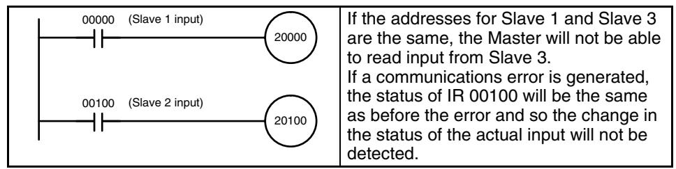

- Example of Countermeasure in Ladder Program
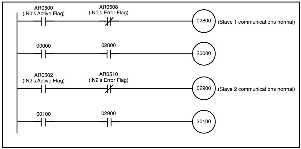
2-13 Analog Controls (CPM1/CPM1A/CPM2A Only)
The PCs are equipped with analog controls that automatically transfer the settings on the CPU Unit's adjustment switches to words in the CPU Unit's I/O memory. This function is very useful when there are set values that need to be precisely adjusted during operation. These set values can be changed just by turning the adjustment switches on the CPU Unit.
Settings
The PCs have two analog adjustment controls that can be used for a wide range of timer and counter analog settings. The following diagrams show the adjustment controls. As these controls are turned, values from 0000 to 0200 (BCD) are stored in the SR Area. Use a Phillips screwdriver to adjust the settings.
The storage words are refreshed once with every CPU Unit cycle.
CPM1
The analog setting for control 0 is in SR 250.
The analog setting for control 1 is in SR 251.
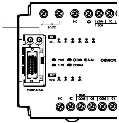
CPM1A/CPM2A
The analog setting for control 0 is in SR 250.
The analog setting for control 1 is in SR 251.
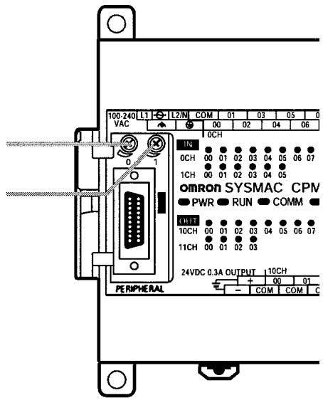
Note The above diagram shows the CPM2A, but the settings are the same for the CPM1A.

The analog setting may change with changing temperatures. Do not use the analog adjustment controls for applications that require a precise, fixed setting.
Using Analog Controls
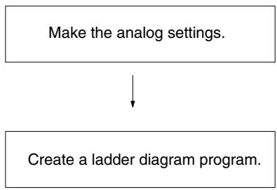
Use a Phillips screwdriver to adjust the controls.
Connect a Programming Device such as a Programming Console, and check the values stored in SR 250 and SR 251.
Read the values in SR 250 and SR 251 with the ladder diagram program.
Analog control 0
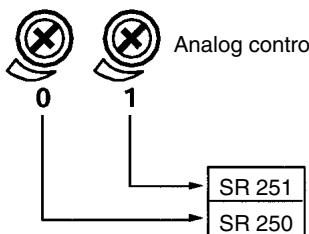
Analog control 1
Analog control 1 set value (SV)
Analog control 0 set value (SV)
Making the Analog Settings
Use a Phillips screwdriver to adjust the analog controls. The set values can be checked by connecting a Programming Device such as a Programming Console and reading the values stored in SR 250 and SR 251.
Analog control 0


Analog control 1
Ladder Diagram Programming
The following table shows the words and bits where the analog settings are stored.
| Word | Bit | Name | Value |
| SR 250 | 00 to 15 | Analog control 0 SV storage area | 0000 to 0200 (BCD) |
| SR 251 | 00 to 15 | Analog control 1 SV storage area |
In the following example program, the analog control SV (0000 to 0200 BCD) stored in SR 250 is set as a timer SV. The timer's set range is 0.0s to 20.0s .
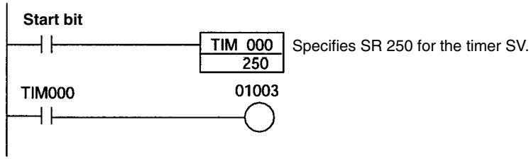
2-14 Quick-response Inputs
2-14-1 CPM1/CPM1A Quick-response Inputs
The CPM1/CPM1A have quick response inputs that can be used to enable inputting shorter signals.
All 10-point CPU Units have 2 quick-response input terminals and the 20-, 30-, and 40-point CPU Units have 4 quick-response input terminals. The same terminals are used for quick-response inputs and interrupt inputs.
Quick-response Operation
Quick-response inputs have an internal buffer, so input signals shorter than one cycle can be detected. Signals with a pulse width as short as 0.2ms can be detected, regardless of their timing during the PC cycle.
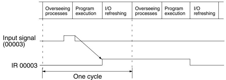
| CPU Unit | Input bits | Min. input pulse width |
| 10-point CPU Units | IR 00003 to IR 00004 | 0.2 ms |
| 20-, 30-, 40-point CPU Units | IR 00003 to IR 00006 |
Setting Quick-response Inputs
The input bits in the above table can be set as quick-response inputs in DM 6628, as shown in the following table.
| Word | Settings |
| DM 6628 | 0: Normal input 1: Interrupt input 2: Quick-response input (Default setting: 0) |
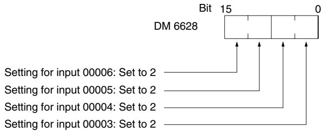
Program Example
In this example, DM 6628 has been set to 0002.
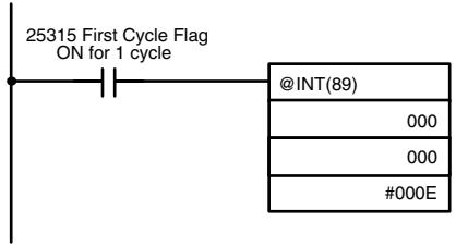
Mask/unmask input interrupts.
Unmasks 00003 (interrupt input 0), masks others.
2-14-2 CPM2A/CPM2C Quick-response Inputs
The CPM2A and CPM2C have four inputs used for quick-response inputs (shared with interrupt inputs and 2-kHz high-speed counter inputs). With quick-response inputs, signals that are changed within a cycle can be received by maintaining an internal buffer.
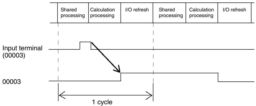
| Input number (See note.) | Minimum input signal width |
| 00003 | 50 μs |
| 00004 | |
| 00005 | |
| 00006 (See note 2.) |
Note
- Input numbers 00003 to 00006 can be used as interrupt inputs, 2-kHz high-speed counter inputs, or quick-response inputs. If they are not used for any of these purposes, then they can be used as ordinary inputs.
- Input number 00006 does not exist in CPM2C CPU Units with 10 I/O points.
The following table shows the relationships between quick-response inputs and the CPM2A/CPM2C's other functions.
| Function | Interval timer interrupts |
| Synchronized pulse control | Can be used simultaneously. |
| Interrupt inputs | See note 1. |
| Interval timer interrupts | Can be used simultaneously. |
| High-speed counters | Can be used simultaneously. |
| Interrupt inputs (counter mode) | See note 2. |
| Pulse outputs | Can be used simultaneously. |
| Quick-response inputs | See note 3. |
| Input time constant | See note 4. |
| Clock | Can be used simultaneously. |
Note
- Quick-response inputs utilize the interrupt input function, so the same input number from 00003 to 00006 cannot be assigned for both a quick-response input and an interrupt input in the PC Setup.
- A quick-response input and an interrupt in counter mode cannot be assigned the same input number in the PC Setup.
- The input numbers allocated for quick-response inputs are 00003 to 00006. These inputs can be set and operated as quick-response inputs.
- Input time constants are disabled for all inputs that are set as quick-response inputs.
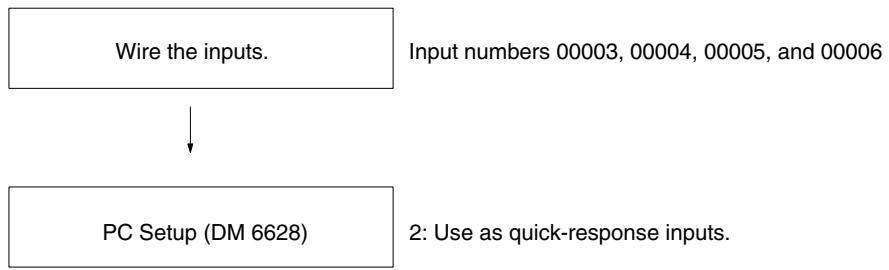
Using Quick-response Inputs
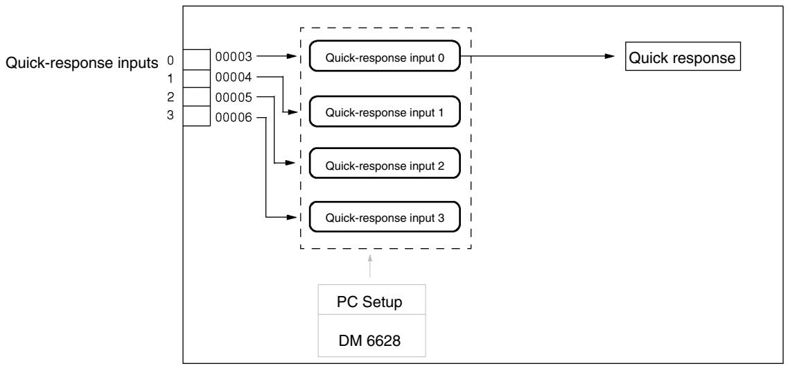
Wiring the Inputs
Wire the CPM2A's inputs as shown in the following diagram.
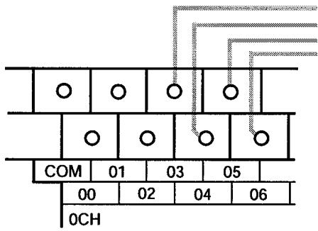
Input 00003: Quick-response input 0
Input 00004: Quick-response input 1
Input 00005: Quick-response input 2
Input 00006: Quick-response input 3
Wire the CPM2C's inputs as shown in the following diagram.
Note The following examples are for Fujitsu-compatible connectors. Input bit addresses and connector pin numbers depend on the models. Refer to the CPM2C Operation Manual (W356) or the CPM2C-S Operation Manual (W377) for details.
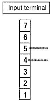
CPU Units with 10 I/O Points
Input 00004: Quick-response input 1
Input 00003: Quick-response input 0
Input connector
(See above note.)
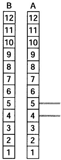
CPU Units with 20/32 I/O Points
00004: Quick-response input 1
00003: Quick-response input 0
Input connector
(See above note.)


00006: Quick-response input 3^*
00005: Quick-response input 2^*
00004: Quick-response input 1
00003: Quick-response input 0
PC Setup
To use quick-response inputs with the CPM2A or CPM2C, make the following settings in the System Setup Area (DM 6628) from a Programming Device.
| Word | Bits | Function | Setting | |
| DM 6628 | 00 to 03 | Interrupt setting for input number 3 | 0: Ordinary input1: Interrupt input (interrupt input mode or counter mode)2: Quick-response input | 2 |
| 04 to 07 | Interrupt setting for input number 4 | |||
| 08 to 11 | Interrupt setting for input number 5* | |||
| 12 to 15 | Interrupt setting for input number 6* | |||
Note *Input numbers 00005 and 00006 does not exist in CPM2C CPU Units with 10 I/O points.
The settings will go into effect when the mode is changed (from PROGRAM to MONITOR/RUN) or when the power supply is turned ON to the PC.
2-15 Macro Function
Using Macros
The macro function allows a single subroutine (programming pattern) to be used by simply changing the I/O word. A number of similar program sections can be managed with just one subroutine, thereby greatly reducing the number of steps in the program and making the program easier to understand.
To use a macro, call a subroutine by means of the MACRO instruction, MCRO(99), as shown below, in stead of SBS(91) (SUBROUTINE ENTRY).
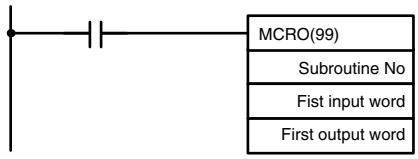
When MCRO(99) is executed, operation will proceed as follows:
1, 2, 3... 1. The contents of the four consecutive words beginning with the first input word will be transferred to SR 232 through SR 235.
- The specified subroutine will be executed until RET(93) (Subroutine Return) is executed.
- The contents of SR 236 through SR 239 (results of the subroutine execution) will be transferred to the four consecutive words beginning with the first output word.
- MCRO(99) will then be finished.
When MCRO(99) is executed, the same instruction pattern can be used as needed simply by changing the first input word or the first output word.
The following restrictions apply when the macro function is used.
- The only words that can be used for each execution of the macro are the four consecutive words beginning with the first input word number (for input) and the four consecutive words beginning with the first output word (for output).
- The specified inputs and outputs must correctly correspond to the words used in the subroutine.
- Even when the direct output method is used for outputs, subroutine results will be actually reflected in the specified output words only when the subroutine has been completed (step 3 above).
Note SR 232 through SR 239 can be used as work bits when MCRO(99) is not used.
The first input word and the first output word can be specified not with I/O bits, but also with other bits (such as HR bits, work bits, etc.) or with DM words.
Subroutines called by MCRO(99) are defined by SBN(92) and RET(93), just as are ordinary subroutines.
Application Example
When a macro is used, the program can be simplified as shown below.

2-16 Calculating with Signed Binary Data
The CPM1/CPM1A/CPM2A/SRM1(-V2) allow calculations on signed binary data. The following instructions manipulate signed binary data. Signed data is handled using 2's complements.
CPM2A/CPM2C and SRM1(-V2) Instructions
The following signed-binary instructions are available in CPM2A, CPM2C, and SRM1(-V2) PCs:
- BINARY ADD - ADB(50)
- BINARY SUBTRACT - SBB(51)
- 2'S COMPLEMENT - NEG(—)
CPM1/CPM1A Instructions
The following signed-binary instructions are available in CPM1/CPM1A PCs:
- BINARY ADD - ADB(50)
- BINARY SUBTRACT - SBB(51)
Signed Data Calculations
Addition
7 + 3 = 10
(-7) + 3 = -4
7 + (-3) = 4
(-7) + (-3) = -10
Subtraction
7 - 3 = 4
(-7) - 3 = -10
7 - (-3) = 10
(-7) - (-3) = -4
2-16-1 Definition of Signed Binary Data
Signed binary data is manipulated using 2's complements and bit 15 is used as the sign bit. The range of data that can be expressed using one word is as follows: -32,768 to 32,767 (8000 to 7FFF hexadecimal).
The following table shows equivalents between decimal and hexadecimal data.
| Decimal | 4-digit Hexadecimal |
| 32,767 | 7FFF |
| 32,766 | 7FFE |
| . | . |
| . | . |
| . | . |
| 2 | 0002 |
| 1 | 0001 |
| 0 | 0000 |
| -1 | FFFF |
| -2 | FFFE |
| . | . |
| . | . |
| . | . |
| -32,767 | 8001 |
| -32,768 | 8000 |
2-16-2 Arithmetic Flags
The results of executing signed binary instructions is reflected in the arithmetic flags. The flags and the conditions under which it will turn ON are given in the following table. The flags will be OFF when these conditions are not met.
| Flag | ON conditions |
| Carry Flag (SR 25504) | Carry in an addition. Negative results for subtraction. |
| Equals Flag (SR 25506) | The results of addition, subtraction, multiplication, or division is 0. Results of converting 2’s complement is 0. |
2-16-3 Inputting Signed Binary Data Using Decimal Values
Although calculations for signed binary data use hexadecimal expressions, inputs from the Programming Console or SSS can be done using decimal inputs and mnemonics for the instructions. The procedure to using the Programming Console to input using decimal values is shown in the CPM1 Operation Manual, CPM1A Operation Manual, CPM2A Operation Manual, CPM2C Operation Manual, and SRM1 Master Control Unit Operation Manual. Refer to the SSS Operation Manual: C-series PCs for details on using the SSS.
Inputting Instructions
Refer to the CPM1 Operation Manual, CPM1A Operation Manual, CPM2C Operation Manual, CPM2A Operation Manual, and SRM1 Master Control Unit Operation Manual details on inputting instructions from the Programming Console.
2-17 Differential Monitor
The CPM1/CPM1A, CPM2A//CPM2C, and SRM1(-V2) support differential monitoring from either the Programming Console or the SSS. The operator can detect on OFF-to-ON or ON-to-OFF transition in a specified bit. When the specified transition takes place, the transition is indicated on the display and a buzzer sounds to enable easy recognition of the transition.
Refer to the CPM1 Operation Manual, CPM1A Operation Manual, CPM2A Operation Manual, CPM2C Operation Manual, or SRM1 Master Control Units Operation Manual for details on the Programming Console Differential Monitor procedure and to the SSS Operation Manual: C-series PCs for the SYSMAC Support Software procedure.
2-18 Expansion Instructions (CPM2A/CPM2C/SRM1(-V2) Only)
A set of expansion instructions is available for the CPM2A, CPM2C (including the CPM2C-S), and SRM1(-V2) to aid in special programming needs. Function codes can be assigned to up to 18 of the expansion instructions to enable using them in programs. This allows the user to pick the instructions needed by each CPM2A, CPM2C, or SRM1(-V2) program to more effectively use the function codes required to input instructions.
The mnemonics of expansion instructions are followed by “(—)” as the function code to indicate that they must be assigned function codes by the user in the instructions table before they can be used in programming (unless they are used under their default settings).
Any of the instructions not assigned function codes will need to be assigned function codes in the instructions table used by the Programming Device and the CPM2A/CPM2C or SRM1(-V2) before they can be used in programming. The assignments of expansion instructions in the instructions table will change the meaning of instructions and operands, so be sure to set the instructions table before programming and transfer the proper instructions table to the CPM2A/ CPM2C or SRM1(-V2) before program execution.
Example: CPM2A/CPM2C PCs
The specific instructions used in the following example are for the CPM2A/ CPM2C. The concepts are the same for the SRM1(-V2).

At the time of shipping, the function codes are assigned as shown above. (In this example, the instructions all relate to pulse outputs.)
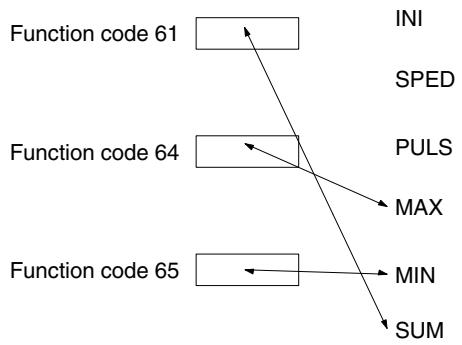
If pulse outputs are not being used, and if maximum values, minimum values, and sums are required, then the Set Instructions operation can be used as shown above to reassign instructions in the instruction table.
Note 1. Set the PC model to "CQM1" when setting the expansion instructions for the SRM1(-V2) or CPM2A/CPM2C from the SSS.
2. The PC Setup must be set for user-defined expansion instruction function codes in order for function codes to be assigned. Set bits 08 to 11 of DM 6602 to 1.
2-18-1 CPM2A/CPM2C/CPM2C-S Expansion Instructions
The following 18 function codes can be used for expansion instructions: 17, 18, 19, 47, 48, 60, 61, 62, 63, 64, 65, 66, 67, 68, 69, 87, 88, and 89. The function code assignments can be changed with a Programming Console or the Support Software.
Refer to 4-4-5 Assigning Expansion Instruction Function Codes in the CPM2A or CPM2C Operation Manual for the Programming Console procedure.
Refer to the SSS Operation Manual: -series PCs for the SSS procedure.
Refer to the SYSMAC-CPT Support Software Quick Start Guide (W332) and User Manual (W333) for the SYSMAC-CPT Support Software procedure.
The expansion instructions that can be used are listed below, along with the default function codes that are assigned when the PC is shipped.
| Mnemonic | Function code |
| ASFT | 17 |
| --- | 18 |
| --- | 19 |
| RXD | 47 |
| TXD | 48 |
| CMPL | 60 |
| INI | 61 |
| PRV | 62 |
| CTBL | 63 |
| SPED | 64 |
| PULS | 65 |
| SCL | 66 |
| BCNT | 67 |
| BCMP | 68 |
| STIM | 69 |
| --- | 87 |
| --- | 88 |
| INT | 89 |
| ACC | --- |
| AVG | --- |
| FCS | --- |
| HEX | --- |
| HMS | --- |
| MAX | --- |
| MIN | --- |
| NEG | --- |
| PID | --- |
| PWM | --- |
| SCL2 | --- |
| SCL3 | --- |
| SEC | --- |
| SRCH | --- |
| STUP | --- |
| SUM | --- |
| SYNC | --- |
| TIML | --- |
| TMHH | --- |
| ZCP | --- |
| ZCPL | --- |
2-18-2 SRM1(-V2) Expansion Instructions
The following 18 function codes can be used for expansion instructions: 17, 18, 19, 47, 48, 60, 61, 62, 63, 64, 65, 66, 67, 68, 69, 87, 88, and 89. The function code assignments can be changed with a Programming Console or the Support Software.
Refer to 4-2-6 Setting Expansion Instructions in the SRM1 Master Control Unit Operation Manual for the Programming Console procedure. Refer to the SSS Operation Manual: C-series PCs for the SSS procedure. Refer to the SYSMAC-CPT Support Software Quick Start Guide (W332) and User Manual (W333) for the SYSMAC-CPT Support Software procedure.
The expansion instructions that can be used are listed below, along with the default function codes that are assigned when the SRM1(-V2) is shipped.
| Mnemonic | Function code |
| ASFT | 17 |
| --- | 18 |
| --- | 19 |
| RXD | 47 |
| TXD | 48 |
| CMPL | 60 |
| --- | 61 |
| --- | 62 |
| --- | 63 |
| --- | 64 |
| --- | 65 |
| SCL* | 66 |
| BCNT | 67 |
| BCMP | 68 |
| STIM | 69 |
| --- | 87 |
| --- | 88 |
| --- | 89 |
| FCS | --- |
| HEX | --- |
| NEG* | --- |
| PID* | --- |
| STUP | --- |
| ZCP* | --- |
Note *SCL(66), NEG(—), PID(—), and ZCP (—) are supported by the SRM1-C0□-V2 CPUs only.
2-19 Using the CPM2A/CPM2C Clock Function
The CPM2A PCs and some CPM2C (including the CPM2C-S) PCs have a built-in clock function. This section explains how to use the clock.
2-19-1 Data Area Words
This following illustration shows the configuration of the words (AR 17 through AR 21) that are used with the clock. These words can be read and used as required. (AR 17 is provided so that the hour and minute can be accessed quickly.)
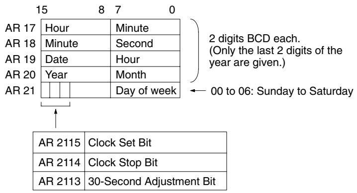
2-19-2 Setting the Time
To set the time, use a programming device as follows:
Setting Everything
1, 2, 3... 1. Turn ON AR 2114 (Clock Stop Bit) to stop the clock and allow AR 18 through AR 21 to be overwritten.
- Using a Programming Device, set AR 18 through AR 20 (minute/second, date/hour, and year/month) and AR 2100 through AR 2107 (day of week).
- Turn ON AR 2115 (Clock Set Bit) when the time set in step 2 is reached. The clock will start operating from the time that is set, and the Clock Stop Bit and Clock Set Bit will be turned OFF automatically.
Setting Only the Seconds
It is also possible, by using AR 2113, to simply set the seconds to "00" without going through a complicated procedure. When AR 2113 is turned ON, the clock time will change as follows:
If the seconds setting is from 00 to 29, the seconds will be reset to "00" and the minute setting will remain the same.
If the seconds setting is from 30 to 59, the seconds will be reset to "00" and the minute setting will advance by one.
When the time setting is complete, AR 2113 will turn OFF automatically.
Note The time can be set easily using menu operations from a Programming Console or SSS. Refer to the CPM2A Operation Manual or the CPM2C Operation Manual for the Programming Console procedure or to the SSS Operation Manual: C-series PCs for the SSS procedure.
SECTION 3
Using Expansion Units
This section describes how to use the CPM1A-MAD01, CPM1A-MAD11, and CPM2C-MAD11 Analog I/O Units; the CPM1A-TS001/002/101/102 and CPM2C-TS001/101 Temperature Sensor Units; the CPM1A-SRT21 and CPM2C-SRT21 CompoBus/S I/O Link Units; and the CPM1A-DRT21 DeviceNet I/O Link Unit. The CPM1A-MAD11 and CPM2C-MAD11 Analog I/O Units provide the same functions, and are thus described in the same section even though they are supported by different PCs.
3-1 Analog I/O Units 166
3-1-1 CPM1A-MAD01 Analog I/O Unit 166
3-1-2 CPM1A-MAD11 and CPM2C-MAD11 Analog I/O Units 177
3-2 Temperature Sensor Units 193
3-2-1 CPM1A/CPM2A Temperature Sensor Units 193
3-2-2 CPM2C Temperature Sensor Units 194
3-2-3 Using Temperature Sensor Units 195
3-2-4 Connecting Temperature Sensor Units 195
3-2-5 Setting Temperature Ranges 197
3-2-6 Connecting Temperature Sensors 200
3-2-7 Ladder Programming 202
3-2-8 Two-decimal-place Mode 208
3-3 CompoBus/S I/O Link Units 214
3-4 DeviceNet I/O Link Unit 219
3-1 Analog I/O Units
3-1-1 CPM1A-MAD01 Analog I/O Unit
A maximum of 3 Expansion Units or Expansion I/O Units, including CPM1AMAD01 Analog I/O Units, can be connected to a CPM1, CPM1A (see note) or CPM2A PC. One Analog I/O Unit allows 2 analog inputs and 1 analog output. With the maximum of 3 Analog I/O Units connected, 6 analog inputs and 3 analog outputs are possible.
- The analog input range can be set to 0 to 10 VDC, 1 to 5 VDC, or 4 to 20mA with a resolution of 1/256.
- An open-circuit detection function can be used with the 1 to 5 VDC and 4 to 20 mA settings.
- The analog output range can be set to 0 to 10 VDC, 4 to 20mA , or -10 to 10 VDC. The output has a resolution of 1/256 when the range is set to 0 to 10 VDC or 4 to 20mA , or a resolution of 1/512 when set to -10 to 10 VDC.
A maximum of 3 Expansion Units or Expansion I/O Units can be connected.
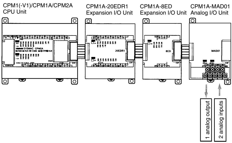
Note The CPM1-30CDR-□-V1 is the only CPM1 CPU Unit to which 3 Expansion Units or Expansion I/O Units can be connected. Only one Expansion Unit or Expansion I/O Unit can be connected to models without the "V1" suffix. Analog Units cannot be connected to 10-point or 20-point CPM1A CPU Units. You must use a 30-point or 40-point CPU Unit to connect to the CPM1A.
| Item | Voltage I/O | Current I/O | |
| Analog Input Section | Number of inputs | 2 | |
| Input signal range | 0 to 10 V/1 to 5 V | 4 to 20 mA | |
| Max. rated input | ±15 V | ±30 mA | |
| External input impedance | 1 MΩ min. | 250 Ω rated current | |
| Resolution | 1/256 | ||
| Accuracy | 1.0% full scale | ||
| A/D conversion data | 8-bit binary | ||
| Analog Output Section (See note 1.) | Number of outputs | 1 | |
| Output signal range | 0 to 10 V or -10 to 10 V | 4 to 20 mA | |
| Max. external output current | 5 mA | --- | |
| Allowable external output load resistance | --- | 350 Ω | |
| Resolution | 1/256 (1/512 when the output signal range is -10 to 10 V) | ||
| Accuracy | 1.0% of full scale | ||
| Set data | 8-bit signed binary | ||
| Conversion time | 10 ms max. per Unit (See note 2.) | ||
| Isolation method | Photocoupler isolation between I/O terminals and PC signals. No isolation between analog I/O signals. | ||
Note 1. With analog outputs it is possible to use both voltage outputs and current outputs at the same time. In this case however, the total output current must not exceed 21mA .
2. The conversion time is the total time for 2 analog inputs and 1 analog output.
Part Names
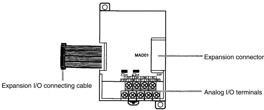
Analog I/O Terminals
Connected to analog I/O devices.
Expansion I/O
Connecting Cable
Connected to the CPU Unit or previous Expansion Unit. The cable is provided with the Unit and cannot be removed.

Do not touch the cables during operation. Static electricity may cause operating errors.
Expansion Connector
Connected to the next Expansion Unit or Expansion I/O Unit.
Analog I/O Signal Ranges
Analog Input Signal Ranges
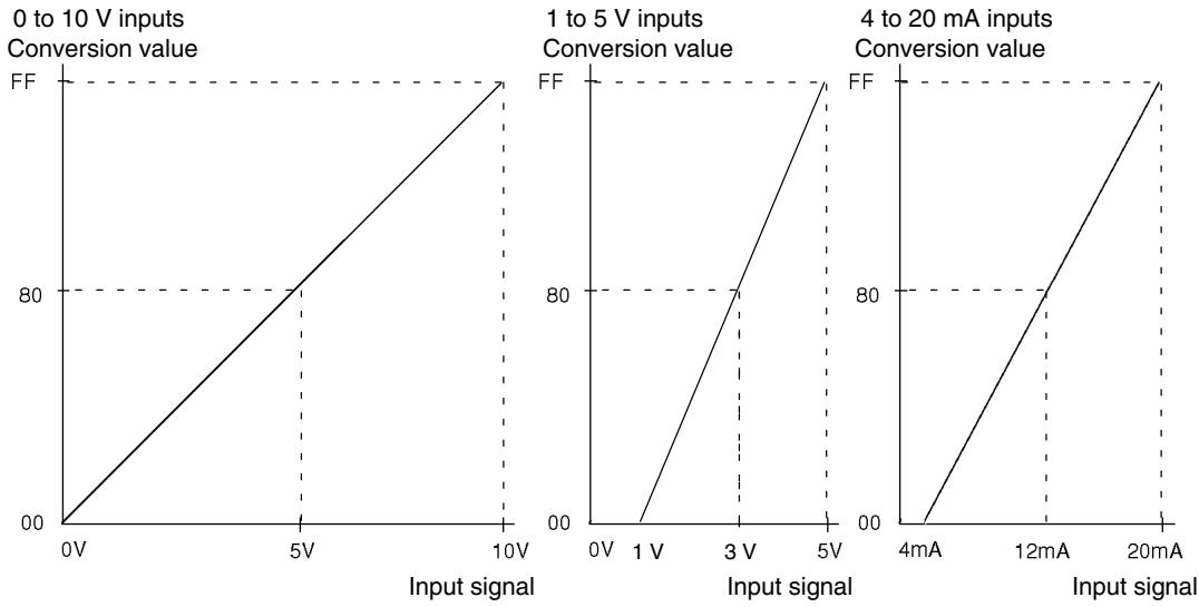
Analog Output Signal Ranges
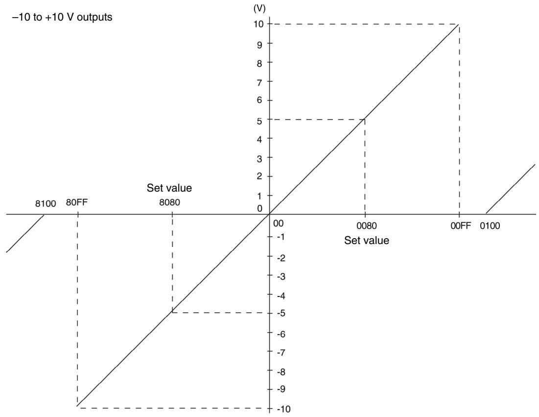
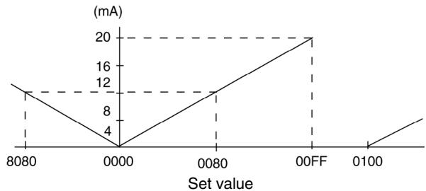
4 to 20 mA outputs
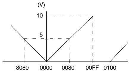
0 to 10 V output
Using Analog I/O
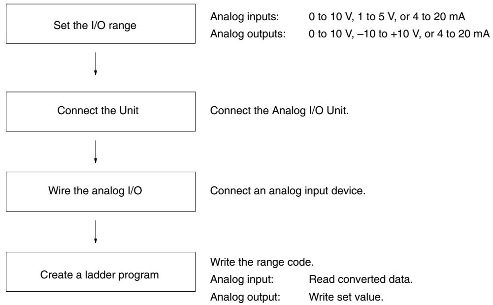
Analog Inputs
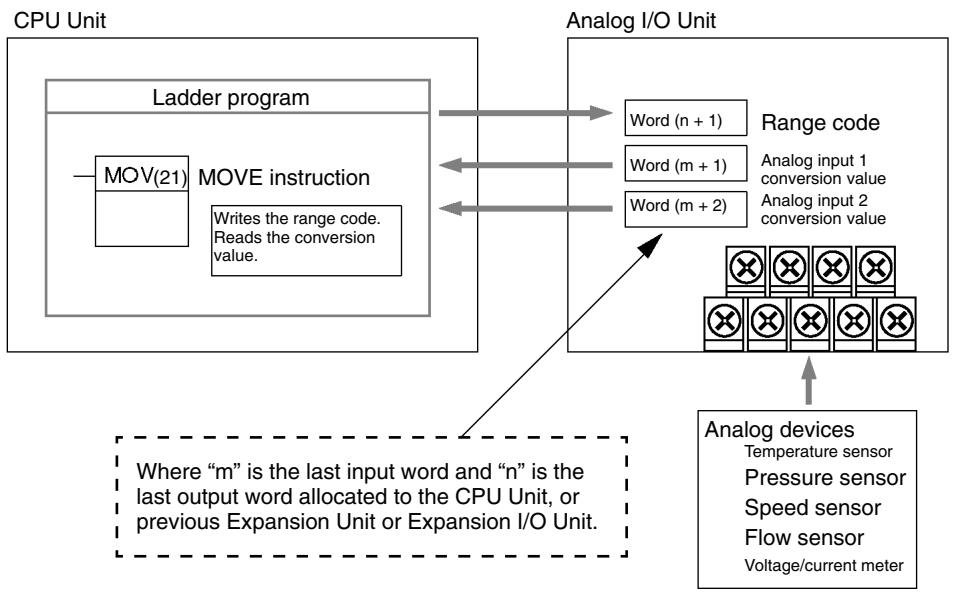
Analog Outputs
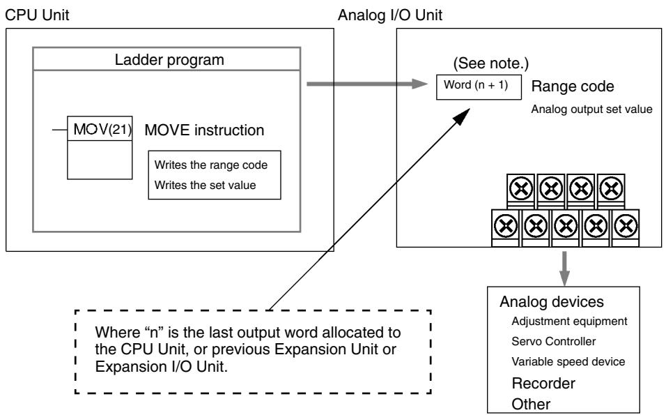
Note Word (n + 1) can be used for either the range code or the analog output set value.
Setting I/O Signal Range
The I/O signal range is set by wiring the I/O terminal and by writing the range code to the Analog I/O Unit's output word.
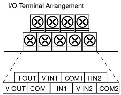
Note When using current inputs, short terminal V IN1 with I IN1 and terminal V IN2 with I IN2.
| V OUT | Voltage output |
| I OUT | Current output |
| COM | Output common |
| V IN1 | Voltage input 1 |
| I IN1 | Current input 1 |
| COM1 | Input common 1 |
| V IN2 | Voltage input 2 |
| I IN2 | Current input 2 |
| COM2 | Input common 2 |
Range Code
The range code must be set for the Analog I/O Unit to convert data.
The 8 range code settings provide 8 combinations of signal ranges for the analog inputs and analog output, as shown in the following table.
| Range code | Analog input 1 signal range | Analog input 2 signal range | Analog output signal range |
| FF00 | 0 to 10 V | 0 to 10 V | 0 to 10 V or 4 to 20 mA |
| FF01 | 0 to 10 V | 0 to 10 V | -10 to 10 V or 4 to 20 mA |
| FF02 | 1 to 5 V or 4 to 20 mA | 0 to 10 V | 0 to 10 V or 4 to 20 mA |
| FF03 | 1 to 5 V or 4 to 20 mA | 0 to 10 V | -10 to 10 V or 4 to 20 mA |
| FF04 | 0 to 10 V | 1 to 5 V or 4 to 20 mA | 0 to 10 V or 4 to 20 mA |
| FF05 | 0 to 10 V | 1 to 5 V or 4 to 20 mA | -10 to 10 V or 4 to 20 mA |
| FF06 | 1 to 5 V or 4 to 20 mA | 1 to 5 V or 4 to 20 mA | 0 to 10 V or 4 to 20 mA |
| FF07 | 1 to 5 V or 4 to 20 mA | 1 to 5 V or 4 to 20 mA | -10 to 10 V or 4 to 20 mA |
Write the range code to the Analog I/O Unit's output word (n + 1) in the first cycle of program execution.
SR 25315 First Cycle Flag
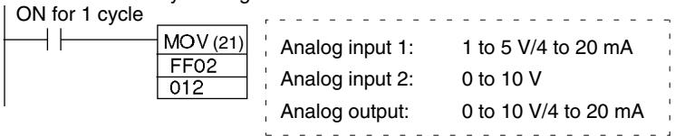

The Analog I/O Unit will not start converting analog I/O values until the range code has been written.
Once the range code has been set, it is not possible to change the setting while power is being supplied to the CPU Unit. To change the I/O range, turn the CPU Unit OFF then ON again.
Note If a range code other than those specified in the above table is written to n + 1 , the range code will not be received by the Analog I/O Unit and analog I/O conversion will not start.
Analog I/O Unit Connection
This section describes how to connect an Analog I/O Unit to the CPU Unit.
A maximum of 3 Expansion Units or Expansion I/O Units, including Analog I/O Units, can be connected to one PC. When the Analog I/O Unit is used in combination with other Expansion Units or Expansion I/O Units, there are no restrictions on the connection order.
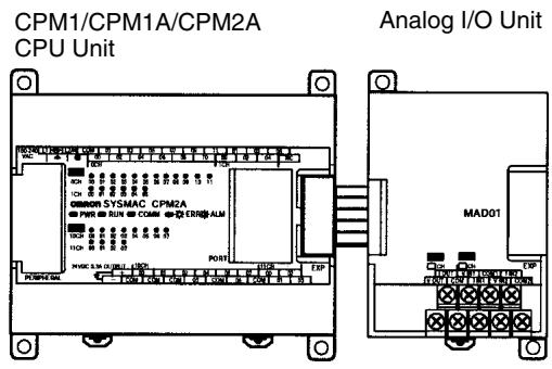
I/O Allocation
I/O is allocated for the Analog I/O Unit in the same way as other Expansion Units or Expansion I/O Units starting from the next word following the last allocated word on the CPU Unit, or previous Expansion Unit or Expansion I/O Unit. When “m” is the last allocated input word and “n” the last allocated output word on the
CPU Unit, or previous Expansion Unit or Expansion I/O Unit, the allocation will be as follows:
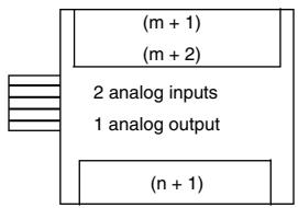
Analog I/O Unit
For example, in the following diagram an Analog I/O Unit is connected to a CPU Unit with 30 I/O points.
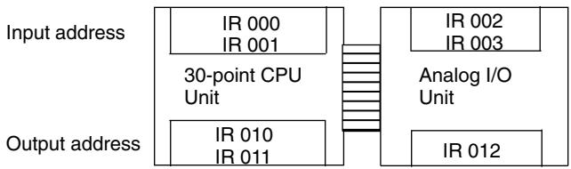
Wiring Analog I/O Devices
Analog Input Wiring
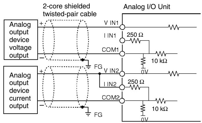
Analog Output Wiring
Voltage Outputs
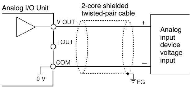
Current Outputs
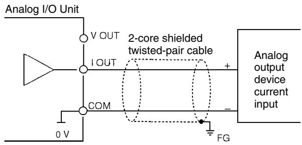
For analog outputs it is possible to use both voltage outputs and current outputs at the same time, but the total current output must not exceed 21 mA.
Note 1. Use 2-core shielded twisted-pair cables.
- Wire away from power lines (AC power supply wires, power lines, etc.)
- When an input is not being used, short V IN and I IN to the COM terminal.
- Use crimp terminals. (Tighten terminals to a torque of 0.5 N·m.)
- When using current inputs, short V IN to I IN.
- When there is noise in the power supply line, install a noise filter on the input section and the Power Supply Unit.
Ladder Program
Specifying the Range Code
Specify the I/O signal range by writing the range code to the Analog I/O Unit's output word from the ladder program in the first cycle of program execution. The Analog I/O Unit will start to convert analog I/O values once the range code has been specified. (Refer to page 170.)
Write the range code to the Analog I/O Unit's output word in the first cycle of operation; the Analog I/O Unit's output word is "n+1" when "n" is the last word allocated to the CPU Unit, or previous Expansion Unit or Expansion I/O Unit in the configuration.
Reading Converted Analog Input Values
A ladder program can be used to read the memory area where the converted values are stored. Values are output to the next two words ( + 1, + 2) following the last input word (m) allocated to the CPU Unit, or previous Expansion Unit or Expansion I/O Unit.
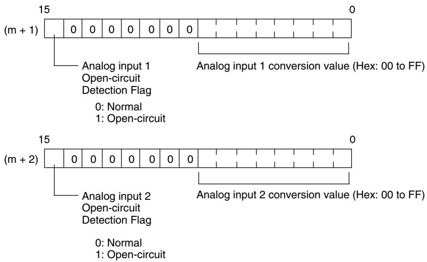
Note The Open-circuit Detection Flag is turned ON when the input signal range is set to 1 to 5V or 4 to 20mA and the input signal falls below 1V or 4mA . (Open circuits are not detected when the input signal range is set to 0 to 10V .)
Writing Analog Output Set Values
A ladder program can be used to write data to the output word where the set value is stored. The output word will be “n+1” when “n” is the last output word allocated to the CPU Unit, or previous Expansion Unit or Expansion I/O Unit.
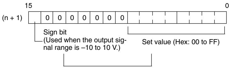
1, 2, 3... 1. The set value range is 0000 to 00FF when the output signal range is 0 to 10 V/4 to 20 mA.
- The set value range is divided into two parts: 8000 to 80FF (-10 to 0V) and 0000 to 00FF (0 to 10V ) when the output signal range is -10 to 10V .
- If FF is input, 0 ~V / 4 ~mA will be output.
- If an output value is specified, the following bits will be ignored.
Output range of -10 to 10 V: Bits 08 to 14
Output range of 0 to 10V / 4 to 20mA :Bits 08 to 15
Startup Operation
After power is turned ON, it will require two cycle times plus approx. 100 ms before the first data is converted. The following instructions can be placed at the beginning of the program to delay reading converted data from analog inputs until conversion is actually possible.
Note Analog input data will be 0000 until initial processing has been completed. Analog output data will be 0V or 0mA until the range code has been written. After the range code has been written, the analog output data will be 0V or 4mA if the range is 0 to 10V, -10 to 10V, or 4 to 20mA .
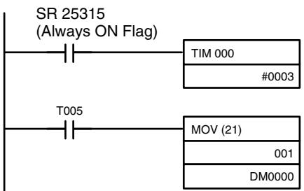
TIM 000 will start as soon as power turns ON. After 0.2 to 0.3 s (200 to 300 ms), the Completion Flag for TIM 000 will turn ON, and the converted data from analog input will be read from IR 001 and stored in DM 0000.
Handling Unit Errors
If an error occurs in an Analog I/O Unit, the Error Flags in AR 0200 to AR 0204 will be turned ON. The addresses of the Error Flags are in the order that the Expansion Units and Expansion I/O Units are connected in the PC, with AR 0200 used for the Expansion Unit or Expansion I/O Unit closest to the CPU Unit. Use these flags in the program when it is necessary to detect errors.
When an error occurs in the Analog I/O Unit, analog input data will be 0000 and 0V or 4mA will be output as the analog output.
Programming Example
This programming example uses these ranges:
Analog input 0: 0 to 10V
Analog input 1: 1 to 5V or 4 to 20mA
Analog output: 0 to 10V or 4 to 20mA
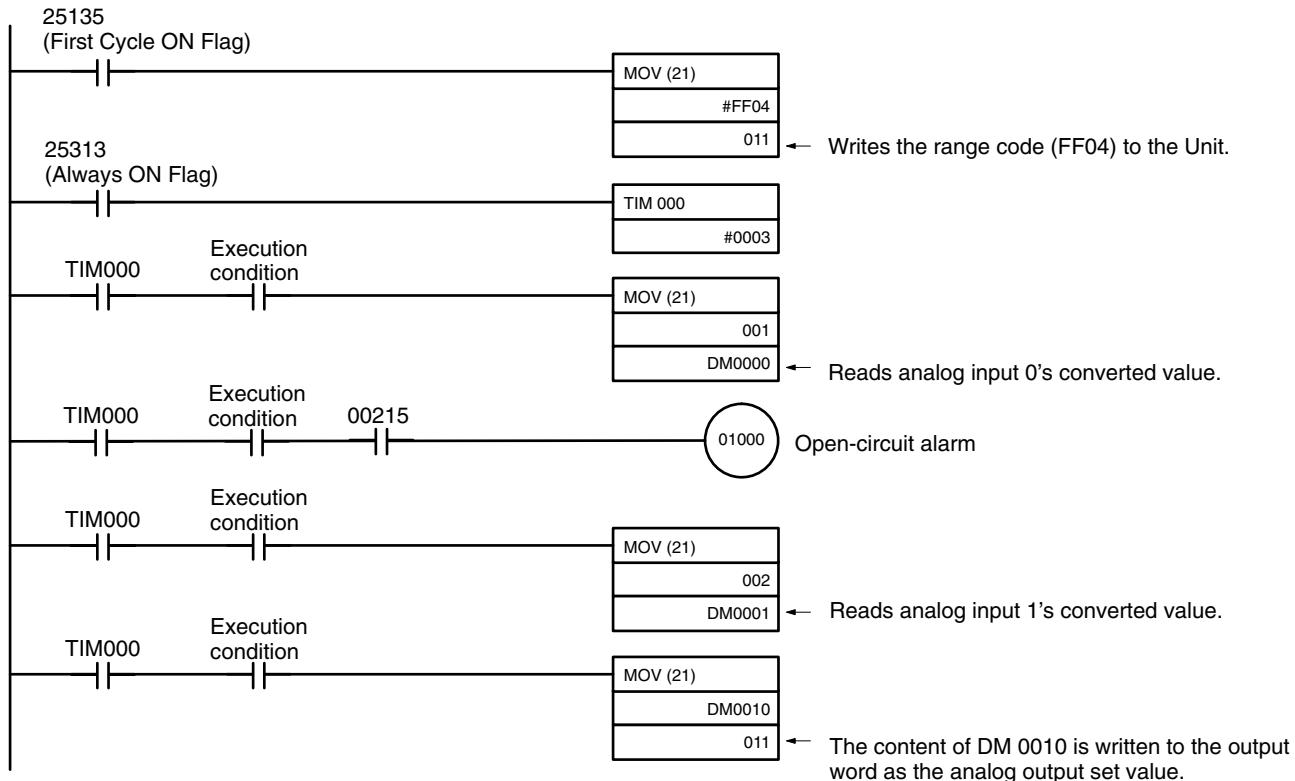
Example
Analog Input Program Example
Analog I/O Unit Connection
In this example, an Analog I/O Unit is connected to a CPU Unit with 30 I/O points. I/O words are allocated to the Analog I/O Unit beginning with the next word address following the last words allocated to the CPU Unit.
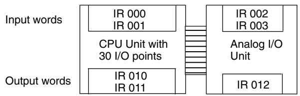
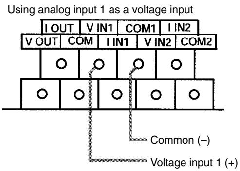
Analog I/O Wiring
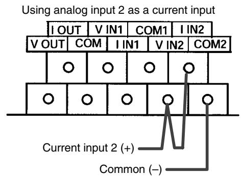
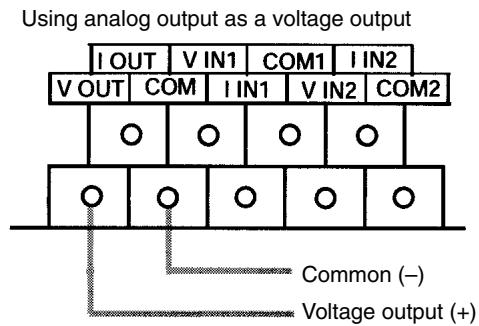
Analog I/O Settings
Input 1 signal range: 0 to 10V
Input 2 signal range: 4 to 20mA
Output signal range: 0 to 10V
Range Code Setting: FF04

Program
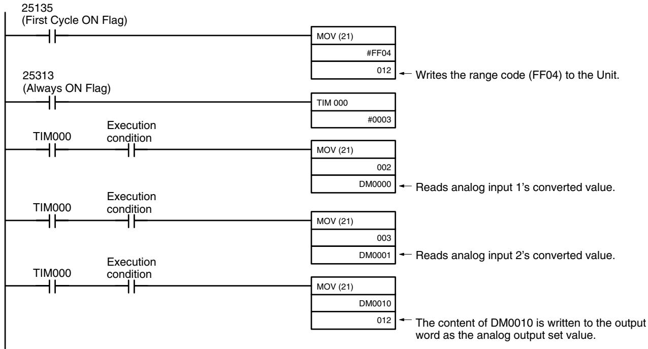
3-1-2 CPM1A-MAD11 and CPM2C-MAD11 Analog I/O Units
The following information applies to both the CPM1A-MAD11 and CPM2C-MAD11 Analog I/O Units unless otherwise specified.
A maximum of 3 Expansion Units or Expansion I/O Units, including up to 3 CPM1A-MAD11 Analog I/O Units, can be connected to a CPM2A or CPM1A. One Analog I/O Unit allows 2 analog inputs and 1 analog output. With the maximum of 3 Analog I/O Units connected, 6 analog inputs and 3 analog outputs are possible.
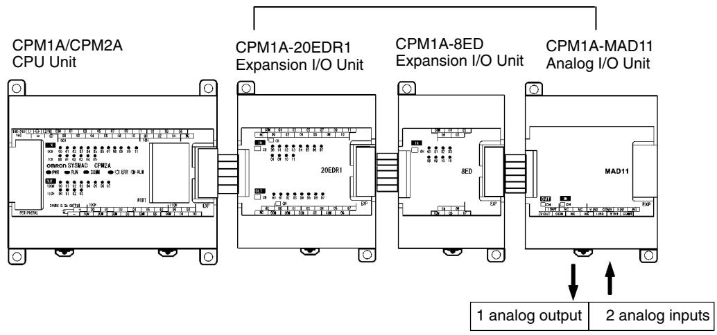
Possible to connect to a maximum of 3 Units including Expansion I/O Units
A maximum of 5 Expansion Units or Expansion I/O Units, including up to 4 CPM2C-MAD11 Analog I/O Units, can be connected to a CPM2C (A maximum of 3 Units can be connected to the CPM2C-S). One Analog I/O Unit allows 2 analog inputs and 1 analog output. With the maximum of 4 Analog I/O Units connected, 8 analog inputs and 4 analog outputs are possible.
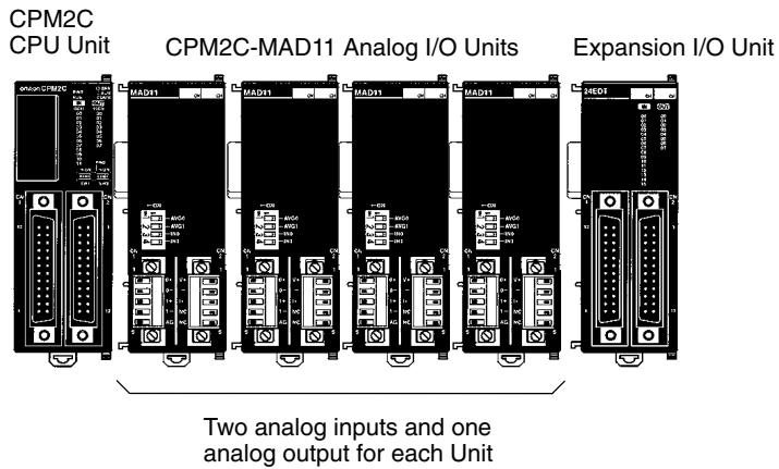
- The analog input range can be set to 0 to 5 VDC, 1 to 5 VDC, 0 to 10 VDC, -10 to 10 VDC, 0 to 20 mA, or 4 to 20 mA. The inputs have a resolution of 1/6000.
- An open-circuit detection function can be used with the 1 to 5 VDC and 4 to 20 mA settings.
- The analog output range can be set to 1 to 5 VDC, 0 to 10 VDC, -10 to 10 VDC, 0 to 20mA , or 4 to 20mA . The outputs have a resolution of 1/6000.
| Item | Voltage I/O | Current I/O | ||
| Analog Input Section | Number of inputs | 2 inputs (2 words allocated) | ||
| Input signal range | 0 to 5 VDC, 1 to 5 VDC, 0 to 10 VDC, or -10 to 10 VDC | 0 to 20 mA or 4 to 20 mA | ||
| Max. rated input | ±15 V | ±30 mA | ||
| External input impedance | 1 MΩ min. | 250 Ω | ||
| Resolution | 1/6000 (full scale) | |||
| Overall accuracy | 25°C | 0.3% full scale | 0.4% full scale | |
| 0 to 55°C | 0.6% full scale | 0.8% full scale | ||
| A/D conversion data | 16-bit binary (4-digit hexadecimal)Full scale for -10 to 10 V: F448 to 0BB8 HexFull scale for other ranges: 0000 to 1770 Hex | |||
| Averaging function | Supported (Settable for individual inputs via DIP switch) | |||
| Open-circuit detection function | Supported | |||
| Analog Output Section | Number of outputs | 1 output (1 word allocated) | ||
| Output signal range | 1 to 5 VDC, 0 to 10 VDC, or-10 to 10 VDC, | 0 to 20 mA or 4 to 20 mA | ||
| Allowable external output load resistance | 1 kΩ min. | 600 Ω max. | ||
| External output impedance | 0.5 Ω max. | --- | ||
| Resolution | 1/6000 (full scale) | |||
| Overall accuracy | 25°C | 0.4% full scale | ||
| 0 to 55°C | 0.8% full scale | |||
| Set data (D/A conversion) | 16-bit binary (4-digit hexadecimal)Full scale for -10 to 10 V: F448 to 0BB8 HexFull scale for other ranges: 0000 to 1770 Hex | |||
| Conversion time | 2 ms/point (6 ms/all points) | |||
| Isolation method | Photocoupler isolation between analog I/O terminals and internal circuits.No isolation between analog I/O signals. | |||
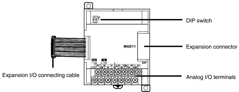
CPM1A-MAD11 Part Names
Analog I/O Terminals
Connected to analog I/O devices.
Expansion I/O
Connecting Cable
Connected to the CPU Unit or previous Expansion Unit. The cable is provided with the Unit and cannot be removed.

Do not touch the cables during operation. Static electricity may cause operating errors.
Expansion Connector
Connected to the next Expansion Unit or Expansion I/O Unit.
DIP Switch
Used to enable or disable averaging.
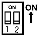
Pin1: Average processing for analog input 0
(OFF: Average processing not performed; ON: Average processing performed)
Pin2: Average processing for analog input 1
(OFF: Average processing not performed; ON: Average processing performed)
CPM2C-MAD11 Part Names
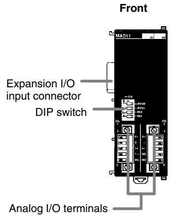
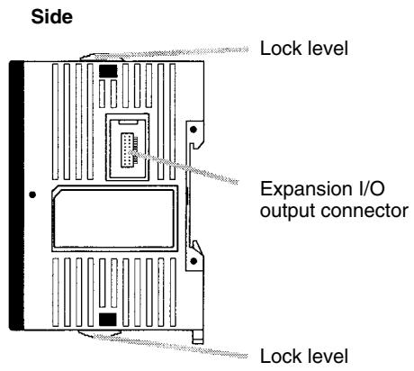
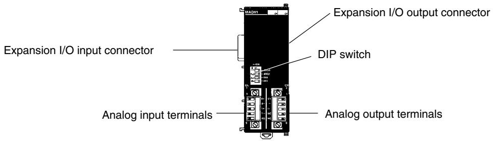
Analog I/O Terminals
Connected to analog I/O devices.
DIP Switch
Used to specify current or voltage inputs and to enable or disable averaging.
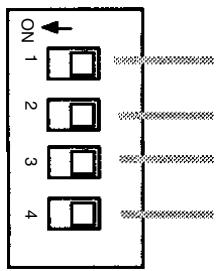
Average processing for analog input 0
(OFF: Average processing not performed; ON: Average processing performed)
Average processing for analog input 1
(OFF: Average processing not performed; ON: Average processing performed)
Input type for analog input 0
(OFF: Voltage input; ON: Current input)
Input type for analog input 1
(OFF: Voltage input; ON: Current input)

Caution
Do not touch the DIP switch during operation. Static electricity may cause operating errors.
Expansion I/O Input Connector
Connected to the expansion I/O output connector on the CPU Unit or previous Expansion (I/O) Unit.
Expansion I/O Output Connector
Connected to the expansion I/O input connector on the next Expansion (I/O) Unit.
Note
-
A maximum of 5 Expansion (I/O) Units can be connected to the CPU Unit and the total number of allocated words must be 10 maximum for inputs and 10 maximum for outputs.
-
Use the connector cover provided with the CPU Unit to protect the output connector when it is not used.

Do not touch the cables during operation. Static electricity may cause operating errors.
Lock Levers
Used to secure the Expansion Unit.
Analog I/O Signal Ranges
Analog Input Signal Ranges
Analog I/O signal ranges are digitally converted as described in this section.
The Analog I/O Unit converts analog input data to digital values. The digital values depend on the input signal ranges, as shown in the following diagrams. When the input exceeds the specified range, the AD converted data will be fixed at either the lower limit or upper limit.
-10 to 10 V
The -10- to 10-V range corresponds to the hexadecimal values F448 to 0BB8 (-3000 to 3000). The entire data range is F31C to OCE4 (-3300 to 3300). A negative voltage is expressed as a two's complement.
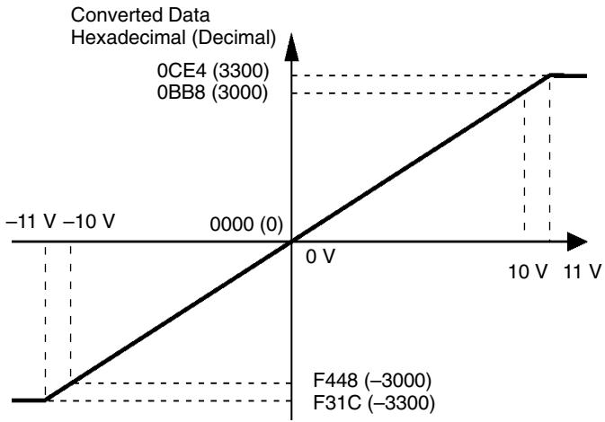
0 to 10 V
The 0- to 10-V range corresponds to the hexadecimal values 0000 to 1770 (0 to 6000). The entire data range is FED4 to 189C (-300 to 6300). A negative voltage is expressed as a two's complement.
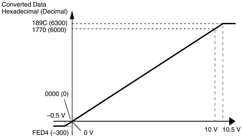
0 to 5 V
The 0- to 5-V range corresponds to the hexadecimal values 0000 to 1770 (0 to 6000). The entire data range is FED4 to 189C (-300 to 6300). A negative voltage is expressed as a two's complement.
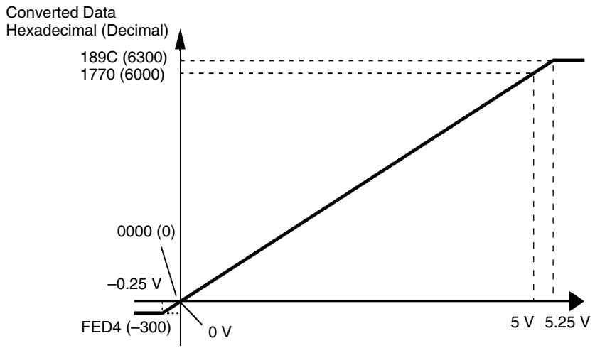
1 to 5 V
The 1- to 5-V range corresponds to the hexadecimal values 0000 to 1770 (0 to 6000). The entire data range is FED4 to 189C (-300 to 6300). Inputs between 0.8 and 1 V are expressed as two's complements. If the input falls below 0.8 V, open-circuit detection will activate and converted data will be 8000.
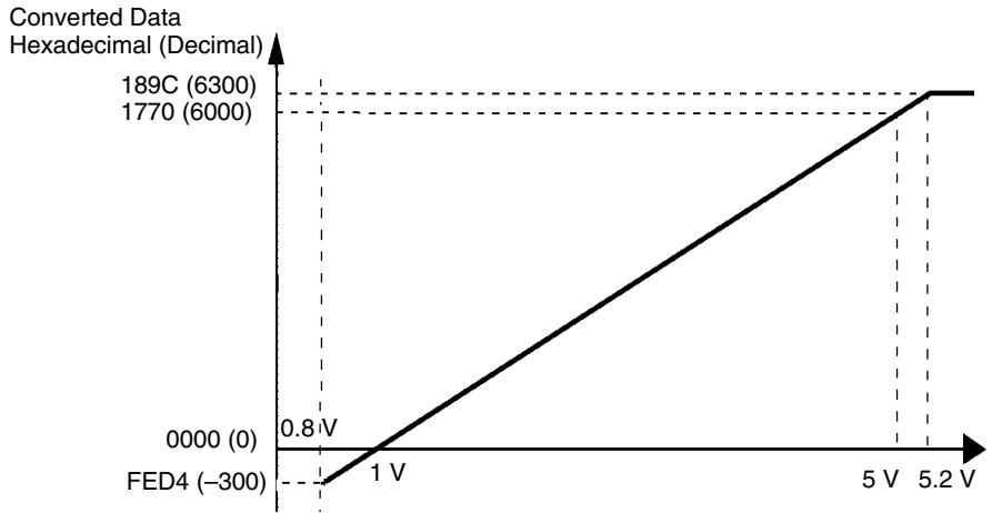
0 to 20 mA
The 0- to 20-mA range corresponds to the hexadecimal values 0000 to 1770 (0 to 6000). The entire data range is FED4 to 189C (-300 to 6300). A negative voltage is expressed as a two's complement.
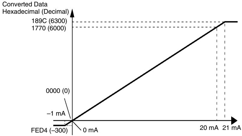
4 to 20 mA
The 4- to 20-mA range corresponds to the hexadecimal values 0000 to 1770 (0 to 6000). The entire data range is FED4 to 189C (-300 to 6300). Inputs between 3.2 and 4 mA are expressed as two's complements. If the input falls below 3.2 mA, open-circuit detection will activate and converted data will be 8000.
Converted Data
Hexadecimal (Decimal)
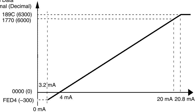
Analog Output Signal Ranges
The Analog I/O Unit converts the digital output data to analog values. The analog values depend on the output signal ranges, as shown in the following diagrams.
-10 to 10 V
The hexadecimal values F448 to 0BB8 (-3000 to 3000) correspond to an analog voltage range of -10 to 10V . The entire output range is -11 to 11V . Specify a negative voltage as a two's complement.
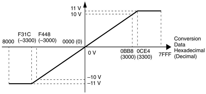
0 to 10 V
The hexadecimal values 0000 to 1770 (0 to 6000) correspond to an analog voltage range of 0 to 10V . The entire output range is -0.5 to 10.5V . Specify a negative voltage as a two's complement.
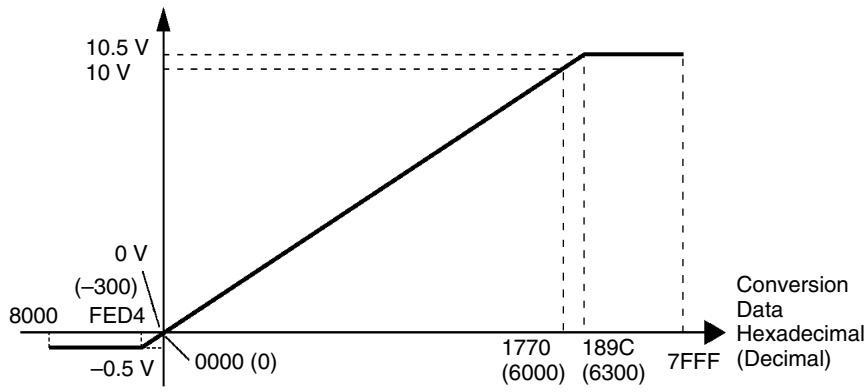
1 to 5 V
The hexadecimal values 0000 to 1770 (0 to 6000) correspond to an analog voltage range of 1 to 5V . The entire output range is 0.8 to 5.2V .
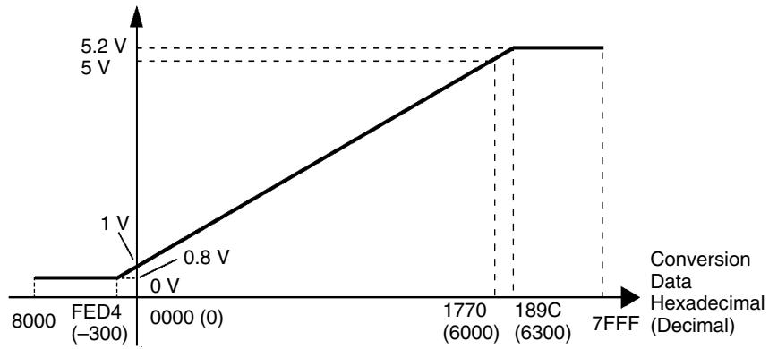
0 to 20mA
The hexadecimal values 0000 to 1770 (0 to 6000) correspond to an analog current range of 0 to 20mA . The entire output range is 0 to 21mA .
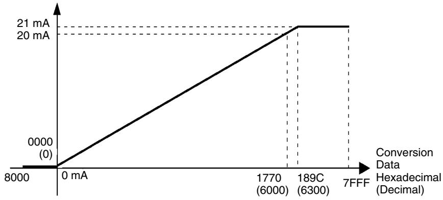
4 to 20 mA
The hexadecimal values 0000 to 1770 (0 to 6000) correspond to an analog current range of 4 to 20mA . The entire output range is 3.2 to 20.8mA .
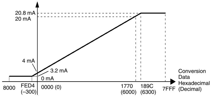
Averaging Function for Analog Inputs
Open-circuit Detection Function for Analog Inputs
The averaging function can be enabled for inputs using the DIP switch. The averaging function stores the average (a moving average) of the last eight input values as the converted value. Use this function to smooth inputs that vary at a short interval.
The open-circuit detection function is activated when the input range is set to 1 to 5V and the voltage drops below 0.8V , or when the input range is set to 4 to 20mA and the current drops below 3.2mA . When the open-circuit detection function is activated, the converted data will be set to 8000.
The open-circuit detection function is enabled or cleared when data is converted. If the input returns to the convertible range, the open-circuit detection is cleared automatically and the output returns to the normal range.
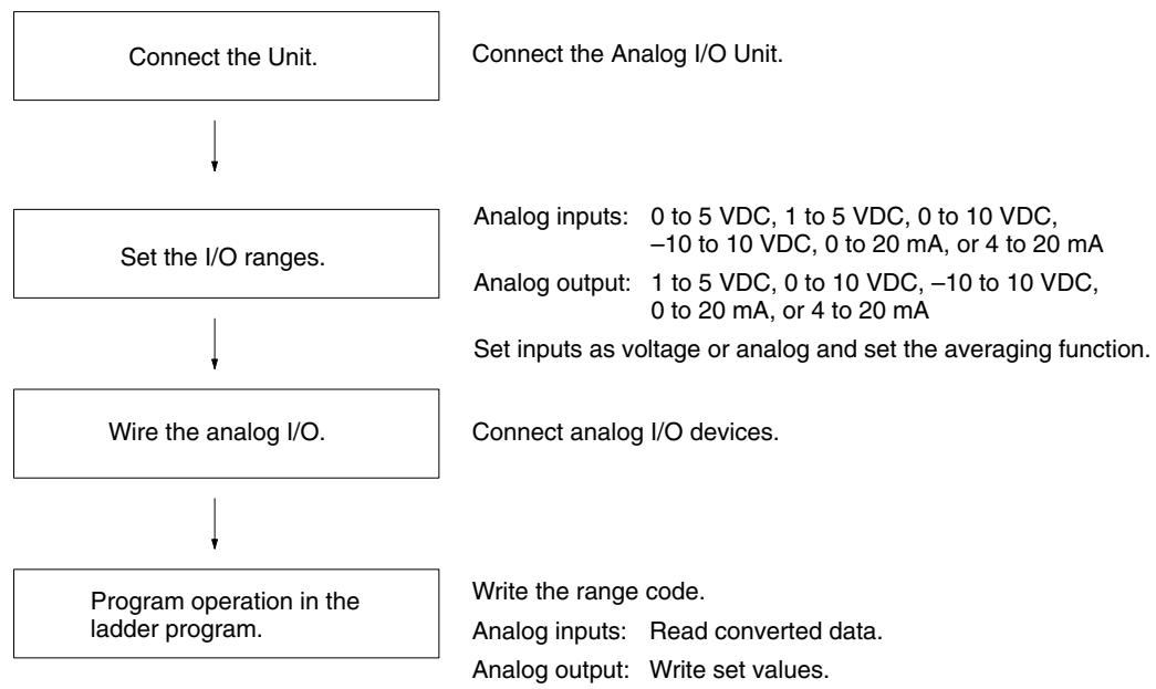
Using Analog I/O
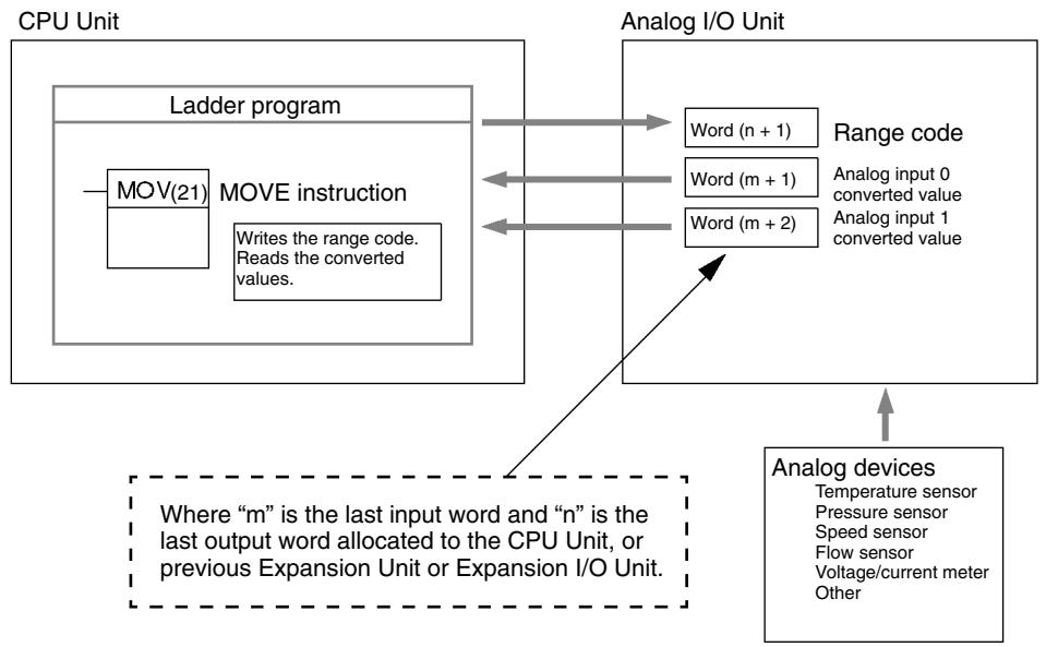
Analog Inputs
Analog Outputs
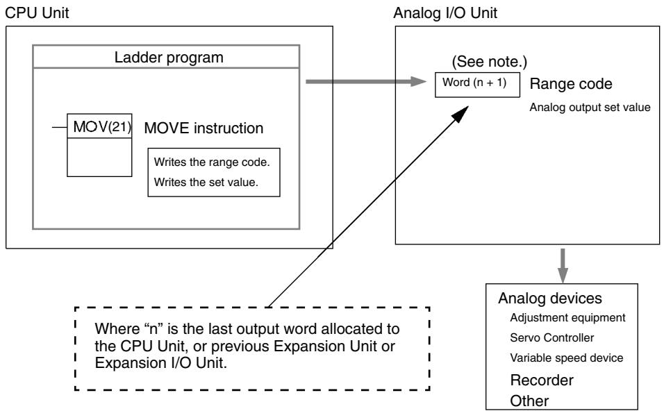
Note Word (n + 1) can be used for either the range code or the analog output set value.
Connecting the CPM1A-MAD11 Analog I/O Unit
This section describes how to connect an Analog I/O Unit to the CPU Unit.
A maximum of 3 Expansion Units or Expansion I/O Units, including up to 3 Analog I/O Units, can be connected to one CPM2A or CPM1A PC. When the Analog I/O Unit is used in combination with other Expansion Units or Expansion I/O Units, there are no restrictions on the connection order.
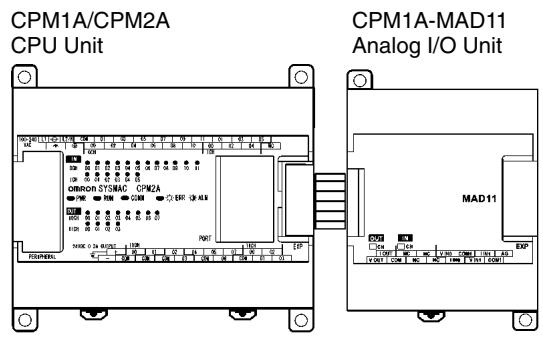
I/O Allocation
I/O is allocated for the Analog I/O Unit in the same way as other Expansion Units or Expansion I/O Units starting from the next word following the last allocated word on the CPU Unit or previous Expansion Unit or Expansion I/O Unit. When "m" is the last allocated input word and "n" the last allocated output word on the CPU Unit, or previous Expansion Unit or Expansion I/O Unit, the allocation will be as follows:
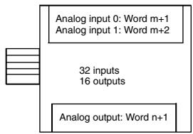
CPM1A-MAD11 Analog I/O Unit
For example, in the following diagram an Analog I/O Unit is connected to a CPU Unit with 30 I/O points.

Connecting the CPM2C-MAD11 Analog I/O Unit
This section describes how to connect an Analog I/O Unit to the CPU Unit.
A maximum of 5 Expansion Units or Expansion I/O Units (a maximum of 3 Units for the CPM2C-S), including up to 3 (see note.) Analog I/O Units, can be connected to one CPM2C PC. When the Analog I/O Unit is used in combination with other Expansion Units or Expansion I/O Units, there are no restrictions on the connection order.
Note When using the CPM2C-PA201, there is a limit to the number of CPM2C-MAD11 Units that can be connected. This limit ensures that the power consumption of the CPU Unit, Expansion Units, and Expansion I/O Units does not exceed the total power capacity of the service power supply from the Power Supply Unit (24V× 600mA = 14.4W)
- CPU Unit with 4-W power consumption: Connect no more than two CPM2CMAD11 Units
- CPU Unit with 3-W power consumption: Connect no more than three CPM2C-MAD11 Units
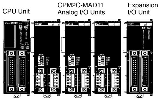
I/O Allocation
I/O is allocated for the Analog I/O Unit in the same way as other Expansion Units or Expansion I/O Units starting from the next word following the last allocated word on the CPU Unit or previous Expansion Unit or Expansion I/O Unit. When "m" is the last allocated input word and "n" the last allocated output word on the CPU Unit, or previous Expansion Unit or Expansion I/O Unit, the allocation will be as follows:
CPM2C-MAD11 Analog I/O Unit
Analog input 0: Word m+1
Analog input 1: Word m+2
Analog output: Word n + 1
For example, in the following diagram an Analog I/O Unit is connected to a CPU Unit with 20 I/O points.
CPU Unit CPM2C-MAD11 Analog I/O Unit
| CPU Unit inputs: | IR 000 |
| Analog input 0: | IR 001 |
| Analog input 1: | IR 002 |
CPU Unit outputs: IR 010
Analog output: IR 011
Setting I/O Signal Range
I/O signal ranges are set by writing a range code to the output word of the Analog I/O Unit. The range code must be set for the Analog I/O Unit to convert data.
The range code settings provide the combinations of signal ranges for the analog inputs and analog output, as shown in the following table.
Voltage/current selections for the CPM1A-MAD11 are made by connecting the appropriate terminals. Refer to page 188 for details.
Voltage/current selections for the CPM2C-MAD11 are made using pins 3 and 4 on the DIP switch. refer to page 179 for details.
| Range code | Analog input 0 signal range | Analog input 1 signal range | Analog output signal range |
| 000 | -10 to 10 V | -10 to 10 V | |
| 001 | 0 to 10 V | 0 to 10 V | |
| 010 | 1 to 5 V or 4 to 20 mA | 1 to 5 V | |
| 011 | 0 to 5 V or 0 to 20 mA | 0 to 20 mA | |
| 100 | --- | 4 to 20 mA | |
Note Be sure to write the correct terminals.
Write the range codes to the Analog I/O Unit's output word (n + 1) in the first cycle of program execution.
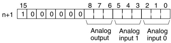
Example
The following instructions set analog input 0 to 4 to 20mA , analog input 1 to 0 to 10V , and the analog output to -10 to 10V .
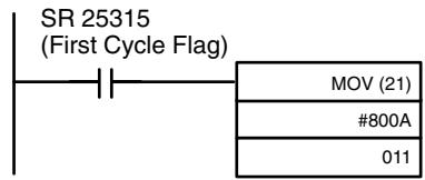
| Analog input 0: | 4 to 20 mA |
| Analog input 1: | 0 to 10 V |
| Analog output: | -10 to 10 V |
The Analog I/O Unit will not start converting analog I/O values until the range code has been written. Until conversion starts, inputs will be 0000, and 0V or 0mA will be output.
After the range code has been set, 0V or 0mA will be output for the 0 to 10-V, -10 to 10-V, or 0 to 20-mA ranges, and 1V or 4mA will be output for the 1 to 5-V and 4 to 20-mA ranges until a convertible value has been written to the output word.
Once the range code has been set, it is not possible to change the setting while power is being supplied to the CPU Unit. To change the I/O range, turn the CPU Unit OFF then ON again.
Wiring Analog I/O Devices
CPM1A-MAD11 Internal Circuits
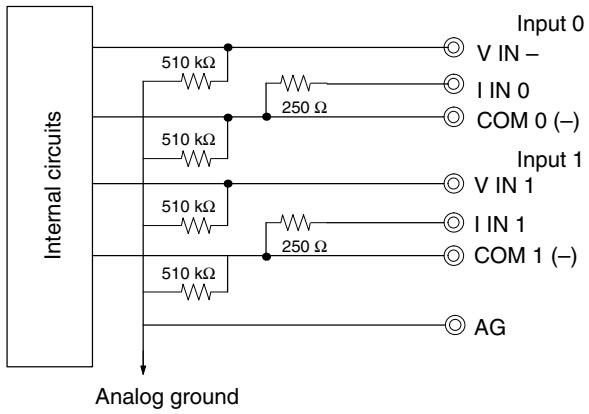
Analog Inputs
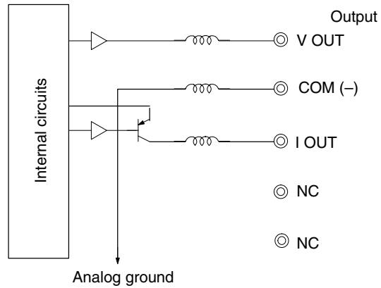
Analog Outputs
CPM1A-MAD11 Terminal Arrangements
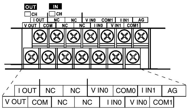
| Label | Signal |
| V OUT | Voltage output |
| I OUT | Current output |
| COM | Output common |
| V IN0 | Voltage input 0 |
| I IN0 | Current input 0 |
| COM0 | Input common 0 |
| V IN1 | Voltage input 1 |
| I IN1 | Current input 1 |
| COM1 | Input common 1 |
Note For current inputs, short V IN0 to I IN0 and V IN1 to I IN1
Wiring for Analog Inputs
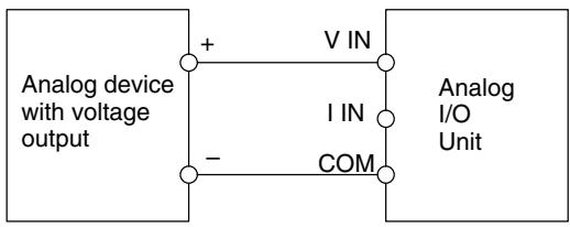
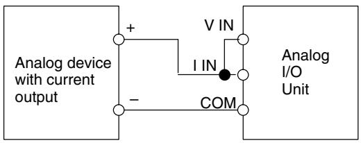
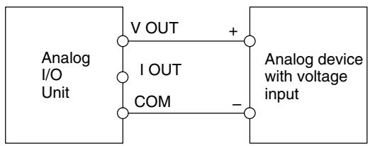
Wiring for Analog Outputs
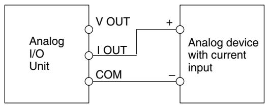
Note 1. Use shielded twisted-pair cables, but do not connect the shield.
2. When an input is not being used, short the + and - terminals.
3. Separate wiring from power lines (AC power supply lines, high-voltage lines, etc.)
4. When there is noise in the power supply line, install a noise filter on the input section and the Power Supply Unit.
CPM2C-MAD11 Internal Circuits
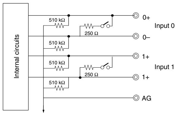
Analog Inputs
Analog ground
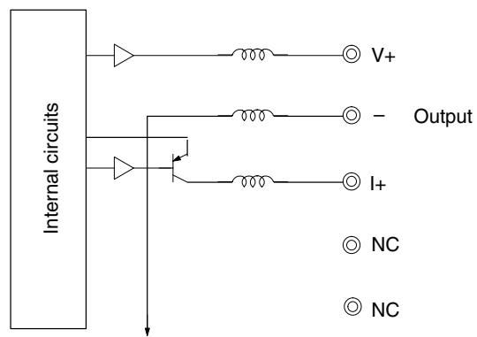
Analog Outputs
Analog ground
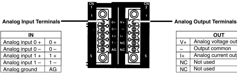
CPM2C-MAD11 Terminal Arrangements
Analog Input Wiring
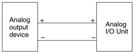
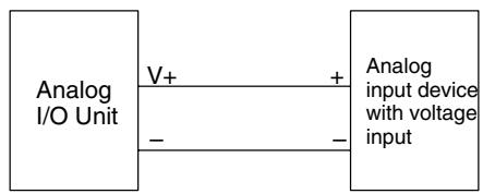
Analog Output Wiring

Note 1. Use shielded twisted-pair cables, but do not connect the shield.
- When an input is not being used, short the + and - terminals.
- Separate wiring from power lines (AC power supply lines, high-voltage lines, etc.)
- When there is noise in the power supply line, install a noise filter on the input section and the Power Supply Unit.
Reference Information
Consider the following information on open input circuits when using voltage inputs.
If the same power supply is used as shown in the following diagram and an open circuit occurs at point A or B, an unwanted current flow will occur as shown by the dotted lines in the diagram, creating a voltage at the other input of about 1/3 to 1/2. If the 1 to 5-V range is being used, the open-circuit detection function will not operate. Also, if there is an open circuit at C, the open-circuit detection function will not operate because the negative sides are the same.
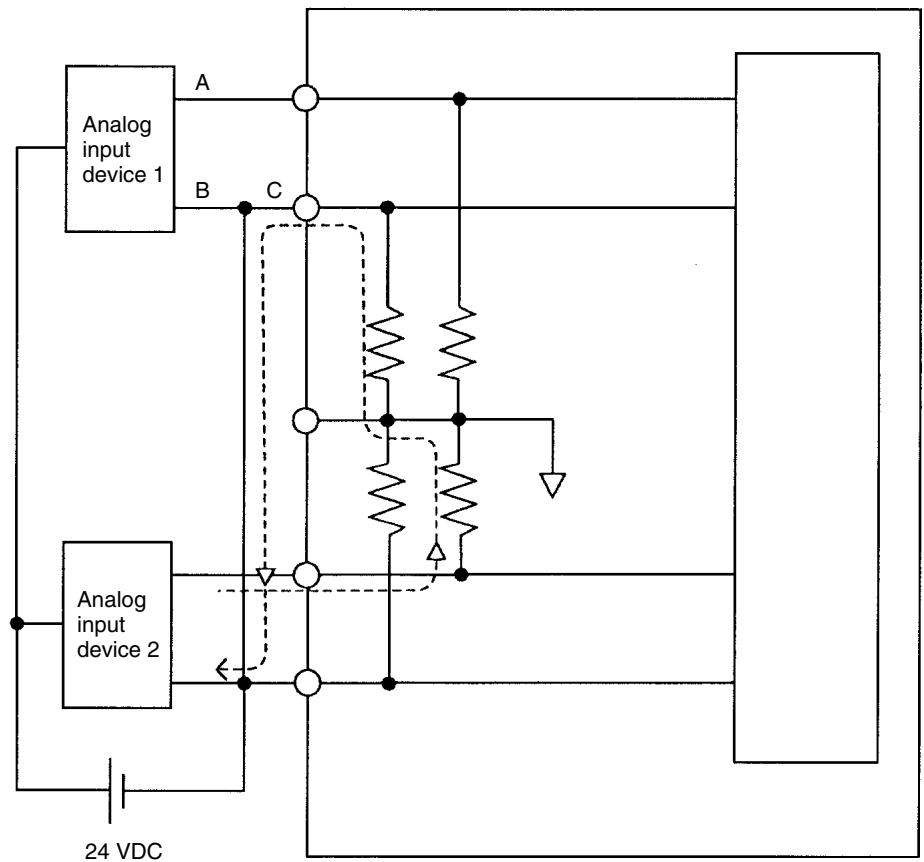
For example, if analog input device 2 is outputting 5V and the same power supply is being used as shown above, about 1/3 , or 1.6V , will be applied at the input for input device 1.
To eliminate the above problem, either use separate power supplies, or install an isolator at each input. This problem will not occur for current inputs even if the same power supply is used.
Note When power is supplied (when setting the range code), or when there is a power interruption, pulse-form analog output of up to 1 ms may be generated. If this causes problems with operation, take countermeasure such as those suggested below.
-
Turn ON the power supply for the CPU Unit first, and then turn ON the power supply for the load after confirming correct operation.
-
Turn OFF the power supply for the load before turning OFF the power supply for the CPU Unit.
Ladder Program
Specifying the Range Code
Specify the I/O signal range by writing the range code to the Analog I/O Unit's output word from the ladder program in the first cycle of program execution. The Analog I/O Unit will start to convert analog I/O values once the range code has been specified and convertible values are provided. (Refer to page 170.)
Write the range code to the Analog I/O Unit's output word in the first cycle of operation; the Analog I/O Unit's output word is "n+1" when "n" is the last word allocated to the CPU Unit, or previous Expansion Unit or Expansion I/O Unit in the configuration.
Reading Converted Analog Input Values
The ladder program can be used to read the memory area where the converted values are stored. Values are output to the next two words ( + 1, + 2) following the last input word (m) allocated to the CPU Unit or previous Expansion Unit or Expansion I/O Unit.
Writing Analog Output Set Values
The ladder program can be used to write data to the output word where the set value is stored. The output word will be “n+1” when “n” is the last output word allocated to the CPU Unit, or previous Expansion Unit or Expansion I/O Unit.
Startup Operation
After power is turned ON, it will require two cycle times plus approx. 50 ms before the first data is converted. The following instructions can be placed at the beginning of the program to delay reading converted data from analog inputs until conversion is actually possible.
Note Analog input data will be 0000 until initial processing has been completed. Analog output data will be 0V or 0mA until the range code has been written. After the range code has been written, the analog output data will be 0V or 0mA if the range is 0 to 10V, -10 to 10V, or 0 to 20mA, or it will be 1V or 4mA if the range is 1 to 5V or 4 to 20mA .
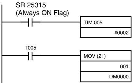
TIM 005 will start as soon as power turns ON. After 0.1 to 0.2 s (100 to 200 ms), the Completion Flag for TIM 005 will turn ON, and the converted data from analog input will be read from IR 001 and stored in DM 0000.
Handling Unit Errors
If an error occurs in an Analog I/O Unit, the Error Flags in AR 0200 to AR 0204 for the CPM2C and AR 0200 to AR 0202 for the CPM1A/CPM2A will be turned ON. The addresses of the Error Flags are in the order that the Expansion Units and Expansion I/O Units are connected in the PC, with AR 0200 used for the Expansion Unit or Expansion I/O Unit closest to the CPU Unit. Use these flags in the program when it is necessary to detect errors.
When an error occurs in the Analog I/O Unit, analog input data will be 0000 and 0V or 0mA will be output as the analog output.
If a CPU error or an I/O bus error (fatal errors) occurs at the CPU Unit and the analog output is set to 1 to 5V or 4 to 20mA , 0V or 0mA will be output. For any other fatal errors at the CPU Unit, 1V or 4mA will be output.
Programming Example
This programming example uses these ranges:
Analog input 0: 0 to 10V
Analog input 1: 4 to 20mA
Analog output: 0 to 10V
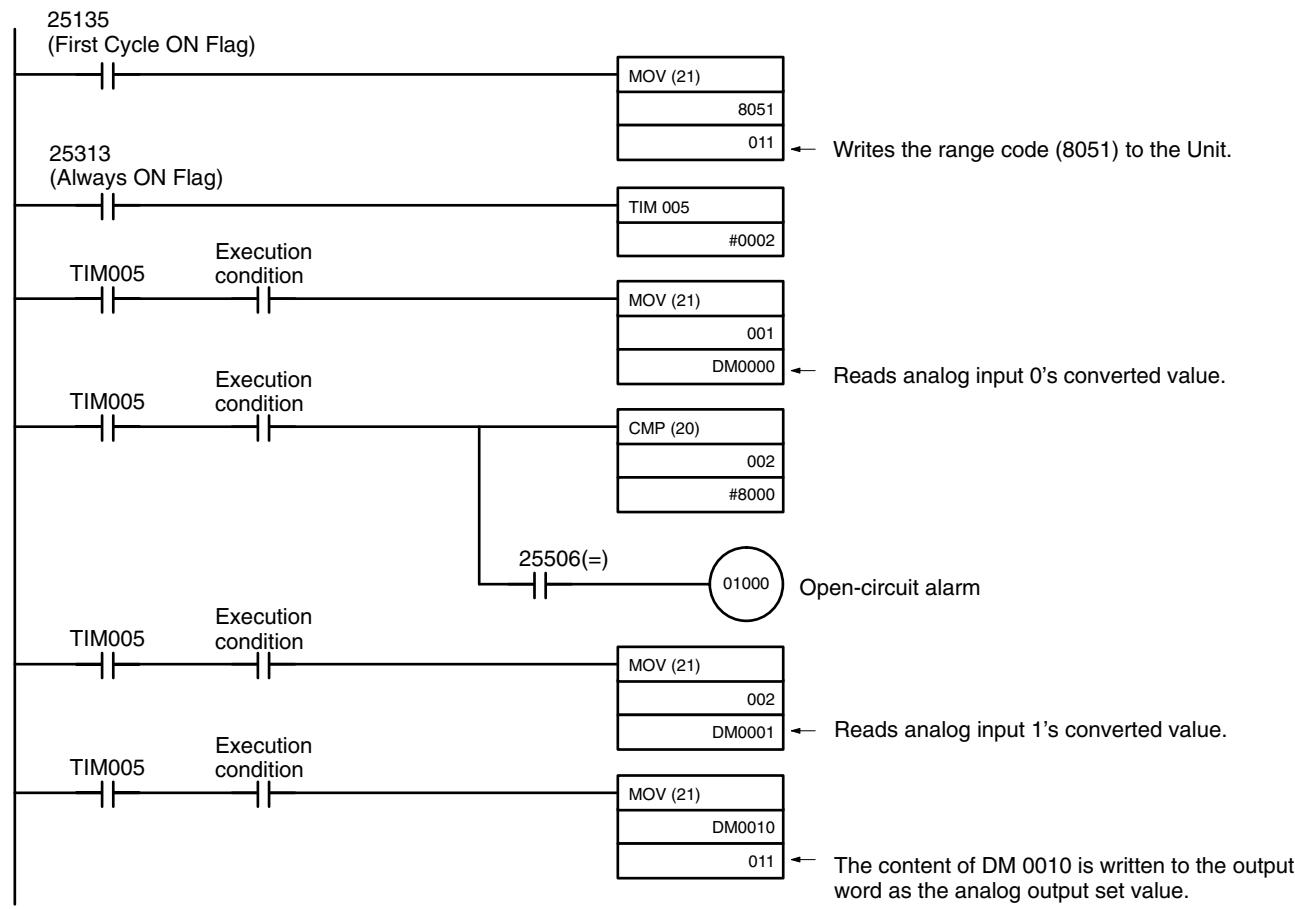
3-2 Temperature Sensor Units
3-2-1 CPM1A/CPM2A Temperature Sensor Units
With the CPM1A or CPM2A, up to three Expansion Units or Expansion I/O Units can be connected to the CPU Unit. One, two, or three of these Units can be CPM1A-TS001 or CPM1A-TS101 Temperature Sensor Units. If a CPM1A-TS002 or CPM1A-TS102 Temperature Sensor Unit is connected to the CPU Unit, then only one other Expansion Unit or Expansion I/O Unit can be connected. The other Unit can be a CPM1A-TS001/TS101 Temperature Sensor Unit.
The CPM1A-TS001/TS101 Temperature Sensor Units each provide 2 input points and the CPM1A-TS002/TS102 Temperature Sensor Units each provide 4 input points, meaning up to 6 temperature input points can be used on one CPM1A or CPM2A PC. The inputs can be from thermocouples or platinum resistance thermometers.

Specifications
| Item | CPM1A-TS001 | CPM1A-TS002 | CPM1A-TS101 | CPM1A-TS102 |
| Temperature sensors | Thermocouples Switchable between K and J, but same type must be used for all inputs. | Platinum resistance thermometer Switchable between Pt100 and JPt100, but same type must be used for all inputs. | ||
| Number of inputs | 2 | 4 | 2 | 4 |
| Allocated input words | 2 | 4 | 2 | 4 |
| Max. number of Units (See note 1.) | 3 | 1 | 3 | 1 |
| Accuracy | (The larger of ±0.5% of converted value or ±2°C) ±1 digit max. (See note 2.) | (The larger of ±0.5% of converted value or ±1°C) ±1 digit max. | ||
| Conversion time | 250 ms for 2 or 4 input points | |||
| Converted temperature data | 16-bit binary data (4-digit hexadecimal) | |||
| Isolation | Photocouplers between all temperature input signals | |||
Note 1. If only the CPM1A-TS001 and CPM1A-TS101 are connected, then up to 3 Units including Expansion I/O Units and other Expansion Units can be connected. If the CPM1A-TS002 or CPM1A-TS102 is connected, then only one other Expansion I/O Unit or Expansion Unit can be connected. The CPM1A-TS001 or CPM1A-TS101 may be the other Unit, but another CPM1A-TS002 or CPM1A-TS102 cannot be connected.
- Accuracy for a K-type sensor at -100^ or less is ± 4^ ± 1 digit max.
3-2-2 CPM2C Temperature Sensor Units
With the CPM2C (including the CPM2C-S), up to four CPM2C-TS001/TS101 Temperature Sensor Units can be connected (up to three Units for the CPM2C-S). Each Temperature Sensor Unit provides 2 input points meaning that a total of 8 input points can be used. The inputs can be from thermocouples or platinum resistance thermometers.
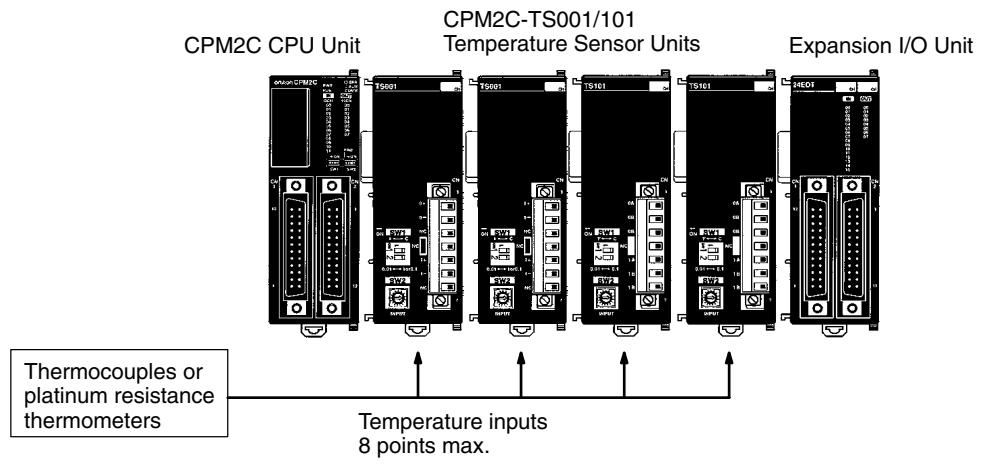
Specifications
| Item | CPM2C-TS001 | CPM2C-TS101 |
| Temperature sensors | Thermocouples Switchable between K and J, but same type must be used for all inputs. | Platinum resistance thermometer Switchable between Pt100 and JPt100, but same type must be used for all inputs. |
| Number of inputs | 2 | |
| Allocated input words | 2 | |
| Max. number of Units (See note 1.) | 4 | 4 |
| Accuracy | (The larger of ±0.5% of converted value or ±2°C) ±1 digit max. (See note.) | (The larger of ±0.5% of converted value or ±1°C) ±1 digit max. |
| Conversion time | 250 ms for 2 input points | |
| Converted temperature data | 16-bit binary data (4-digit hexadecimal) | |
| Isolation | Photocouplers between all temperature input signals | |
Note 1. Accuracy for a K-type sensor at -100^ or less is ± 4^ ± 1 digit max.
2. The error deviation for temperatures in ^ F is double that for ^ C .
3-2-3 Using Temperature Sensor Units
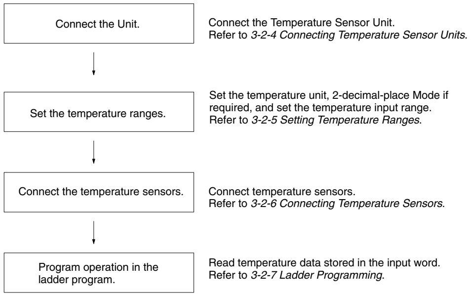
3-2-4 Connecting Temperature Sensor Units
This section shows example configurations containing Temperature Sensor Units.
CPM1A/CPM2A Temperature Sensor Unit Allocations
Words are allocated to Temperature Sensor Units just like other Expansion I/O Units and Expansion Units: In the order in which the Units are connected. A Temperature Sensor Unit will thus be allocated the next input words after the Unit to which it is connected (CPU Unit or other Unit).
Note Only one 4-input Temperature Sensor Unit (CPM1A-TS002 or CPM1A-TS102, 4 words allocated) can be mounted to the CPU Unit. There are, however, no restrictions on the mounting order.
Temperature Sensor Units with 2 Inputs: CPM1A-TS001 and CPM1A-TS101 (2 Words Allocated)
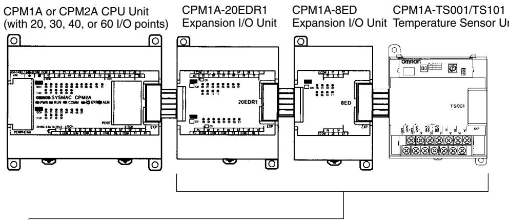
| Temperature Sensor Units | 2 inputs | CPM1A-TS001 CPM1A-TS101 | Up to 3 Units can be connected. There are no restrictions on the order in which Units are connected. |
| Expansion I/O Units | With 8 or 20 I/O points | ||
| Analog I/O Units | CPM1A-MAD01 | ||
| CompoBus/S I/O Link Unit | CPM1A-SRT21 | ||
Word Allocations
The CPM1A-TS001 and CPM1A-TS101 are allocated two words each (one for each input point). No output words are allocated.
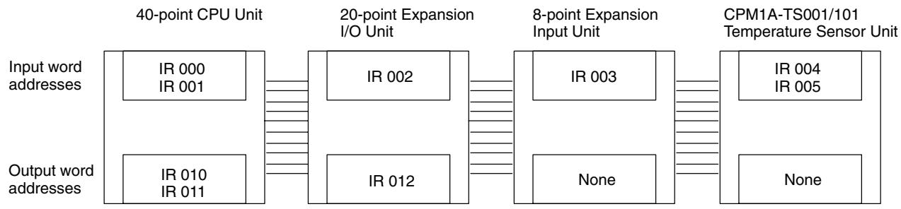
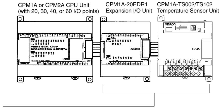
Temperature Sensor Units with 4 Inputs (4 Words Allocated): CPM1A-TS002 and CPM1A-TS102
| Temperature Sensor Units | 4 inputs | CPM1A-TS002 or CPM1A-TS102 | 1 Unit only | Up to 2 Units can be connected. There are no restrictions on the order in which Units are connected. |
| 2 inputs | CPM1A-TS001 or CPM1A-TS101 | 1 Unit only | ||
| Expansion I/O Units | With 8 or 20 I/O points | |||
| Analog I/O Units | CPM1A-MAD01 | |||
| CompoBus/S I/O Link Unit | CPM1A-SRT21 | |||
Word Allocations
The CPM1A-TS002 and CPM1A-TS102 are allocated four words each (one for each input point). No output words are allocated.
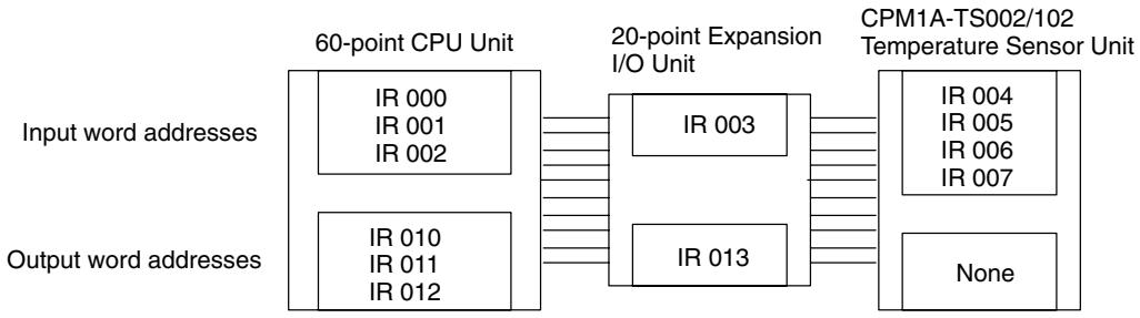
CPM2C Temperature Sensor Unit Allocations
Up to four CPM2C-TS001/101 Temperature Sensor Units can be connected. Up to a total of five Expansion I/O Units and Expansion Units can be connected (in-
cluding the Temperature Sensor Units.) Up to three Units can be connected to the CPM2C-S. No matter how many Units are connected, however, no more than 0 input words and 10 output words can be allocated in one PC. There are no restrictions on the order in which Units can be connected.
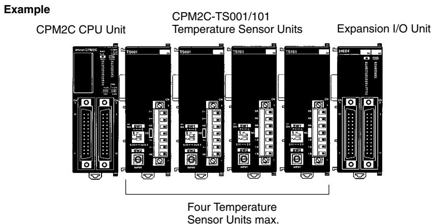
Word Allocation
Words are allocated to Temperature Sensor Units just like other Expansion I/O Units and Expansion Units: In the order in which the Units are connected. A CPM2C-TS001 or CPM2C-TS101 Temperature Sensor Unit will thus be allocated the next two input words after the Unit to which it is connected (CPU Unit or other Unit). No output words are allocated.
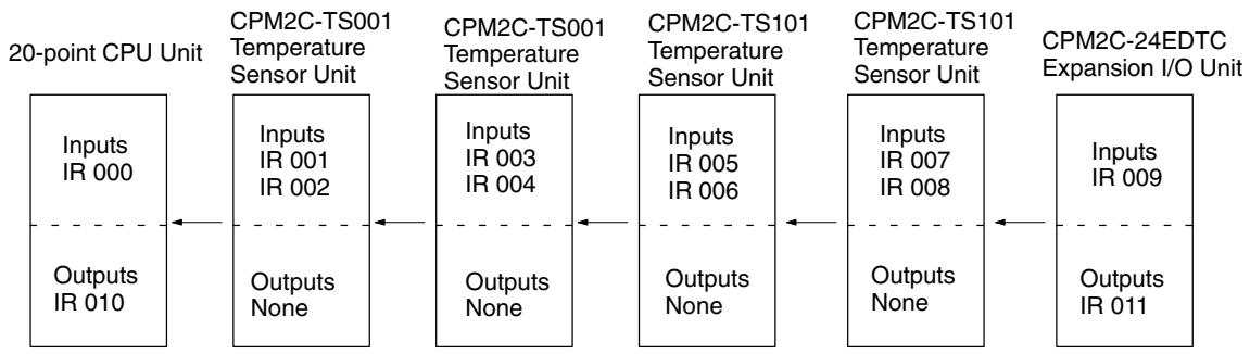
3-2-5 Setting Temperature Ranges
The temperature unit, the number of decimal places used, and the temperature input range are set on the DIP switch and rotary switch on the Temperature Sensor Unit.
Note 1. Always turn OFF the power supply before setting the temperature range.
2. Never touch the DIP switch or rotary switch during Temperature Sensor Unit operation. Static electricity may cause operating errors.
CPM1A/CPM2A Temperature Sensor Units CPM1A-TS001/002/101/102
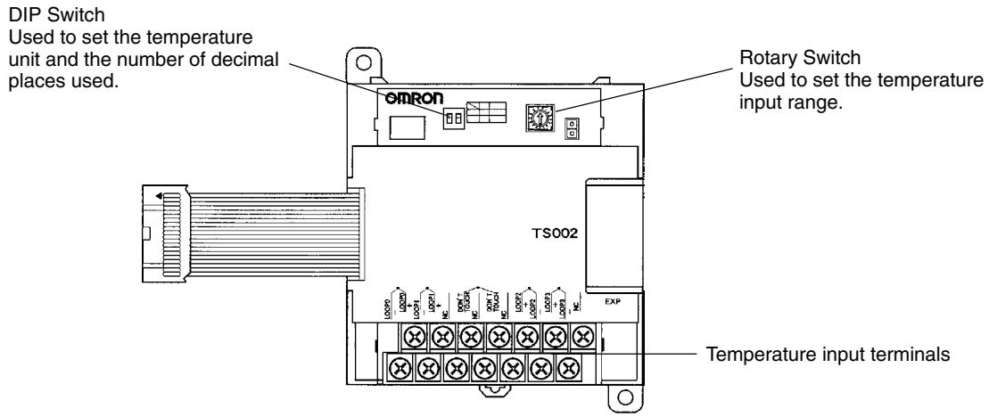
CPM2C Temperature Sensor Units CPM2C-TS001/101
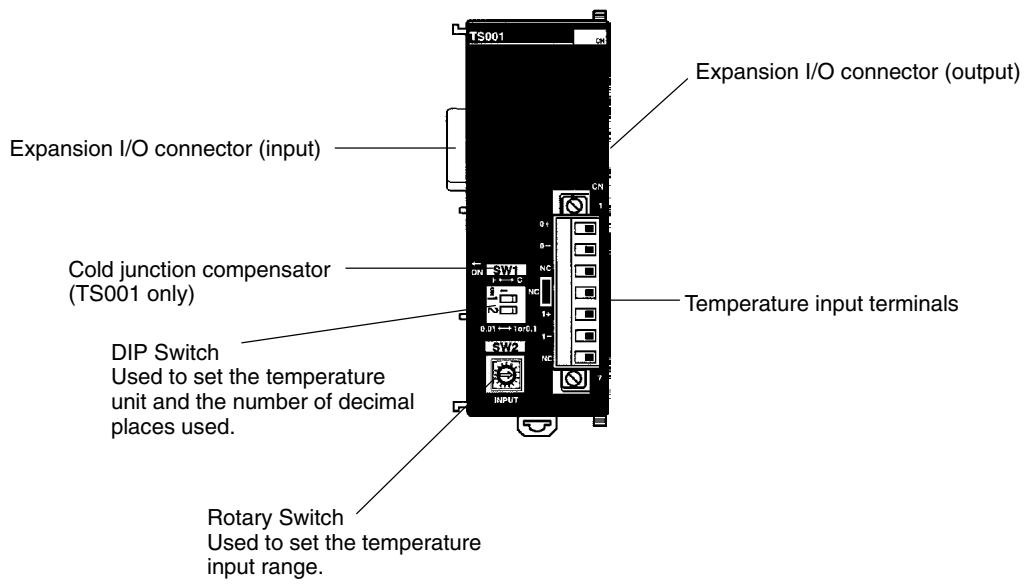
DIP Switch Settings
The DIP switch is used to set the temperature unit (°C or °F) and the number of decimal places used.
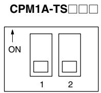
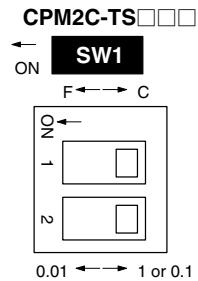
| SW1 | Setting | ||
| 1 | Temperature unit | OFF | °C |
| ON | °F | ||
| 2 | Number of decimal places used | OFF | Normal (0 or 1 digit after the decimal point, depending on the input range) |
| ON | 2-decimal-place Mode (e.g., 0.01) | ||
Note For details on 2-decimal-place Mode, refer to 3-2-8 Two-decimal-place Mode.
Note 1. Turn OFF the power supply before changing the temperature range setting.
2. Do not touch the DIP switch or rotary switches while power is turned ON. Static electricity may cause malfunctions.
Rotary Switch Setting
The rotary switch is used to set the temperature range.

Caution
Set the temperature range according to the type of temperature sensor connected to the Unit. Temperature data will not be converted correctly if the temperature range does not match the sensor.

Caution
Do not set the temperature range to any values other than those for which temperature ranges are given in the following table. An incorrect setting may cause operating errors.
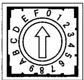
| Setting | CPM1A-TS001/002 CPM2C-TS001 | CPM1A-TS101/102 CPM2C-TS101 | ||||
| Input type | Range (°C) | Range (°F) | Input type | Range (°C) | Range (°F) | |
| 0 | K | -200 to 1,300 | -300 to 2,300 | Pt100 | -200.0 to 650.0 | -300.0 to 1,200.0 |
| 1 | 0.0 to 500.0 | 0.0 to 900.0 | JPt100 | -200.0 to 650.0 | -300.0 to 1,200.0 | |
| 2 | J | -100 to 850 | -100 to 1,500 | --- | Setting not possible | |
| 3 | 0.0 to 400.0 | 0.0 to 750.0 | --- | |||
| 4 to F | --- | Setting not possible | --- | |||
3-2-6 Connecting Temperature Sensors
CPM1A/CPM2A Temperature Sensor Units
Thermocouples
CPM1A-TS001
Either K or J thermocouples can be connected, but both of the thermocouples must be of the same type and the same input range must be used for each.
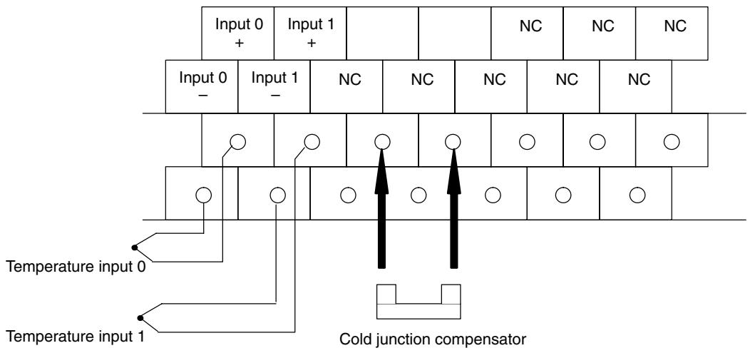
CPM1A-TS002
Either K or J thermocouples can be connected, but all four of the thermocouples must be of the same type and the same input range must be used for each.
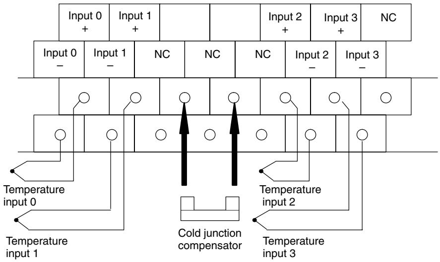
Note When using a Temperature Sensor Unit with a thermocouple input, observe the following precautions:
- Do not remove the cold junction compensator attached at the time of delivery. If the cold junction compensator is removed, the Unit will not be able to measure temperatures correctly.
- Each of the input circuits is calibrated with the cold junction compensator attached to the Unit. If the Unit is used with the cold junction compensator from other Units, the Unit will not be able to measure temperatures correctly.
- Do not touch the cold junction compensator. Doing so may result in incorrect temperature measurement.
Platinum Resistance Thermometers
CPM1A-TS101
Either Pt100 or JPt100 platinum resistance thermometers can be connected, but both of the thermometers must be of the same type and the same input range must be used for each.
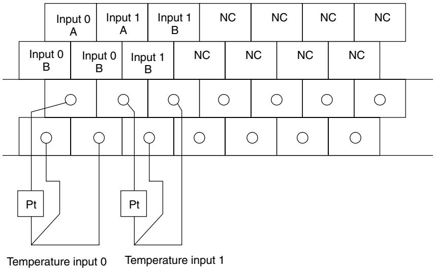
CPM1A-TS102
Either Pt100 or JPt100 platinum resistance thermometers can be connected, but all four of the thermometers must be of the same type and the same input range must be used for each.
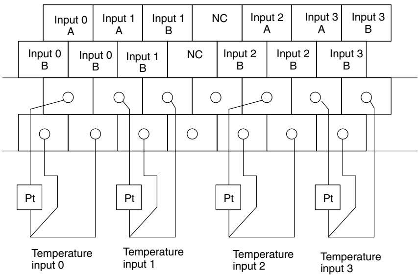
CPM2C Temperature Sensor Units
CPM2C-TS001 (Thermocouples)
Either K or J thermocouples can be connected, but both of the thermocouples must be of the same type and the same input range must be used for each.
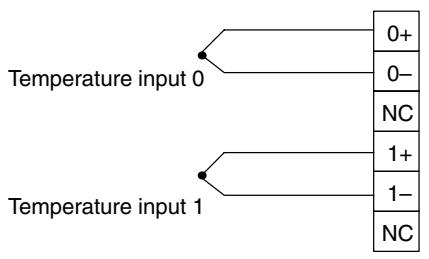
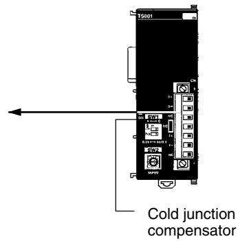
Note When using a Temperature Sensor Unit with a thermocouple input, observe the following precautions:
- Do not touch the cold junction compensator. Doing so may result in incorrect temperature measurement.
CPM2C-TS101 (Platinum Resistance Thermometers)
Either Pt100 or JPt100 platinum resistance thermometers can be connected, but both of the thermometers must be of the same type and the same input range must be used for each.
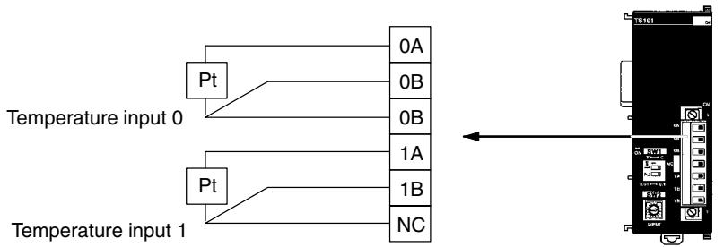
3-2-7 Ladder Programming
Converted Temperature Data
The temperature data will be stored in the input words allocated to the Temperature Sensor Unit in 4-digit hexadecimal.
CPM1A-TS001/TS101 and CPM2C-TS001/TS101
"m" is the last word allocated to the CPU Unit, Expansion I/O Unit, or Expansion Unit connected immediately before the Temperature Sensor Unit.
| Word | Contents |
| m + 1 | Converted temperature data from input 0 |
| m + 2 | Converted temperature data from input 1 |
CPM1A-TS002/TS102
“m” is the last word allocated to the CPU Unit, Expansion I/O Unit, or Expansion Unit connected immediately before the Temperature Sensor Unit.
| Word | Contents |
| m + 1 | Converted temperature data from input 0 |
| m + 2 | Converted temperature data from input 1 |
| m + 3 | Converted temperature data from input 2 |
| m + 4 | Converted temperature data from input 3 |
All Temperature Sensor Units
Negative values are stored as 2's complements. Data for range codes that in-
clude one digit after the decimal point are stored without the decimal point, i.e., 10 times the actual value is stored. Some examples are provided in the following table.
| Input | Data conversion examples | |
| Unit: 1° | K or J | 850° → 0352 Hex -200° → FF38 Hex |
| Unit: 0.1° | K, J, Pt100 or JPt100 | ×10 500.0° → 5000 → 1388 Hex -20.0° → -200 → FF38 Hex -200.0° → -2000 → F830 Hex |
If the input temperature exceeds the range that can be converted, the converted temperature data will be held at the maximum or minimum value in the range. If the input temperature exceeds the range by more than a specified amount, the open-circuit detection function will detect an open-circuit and the converted temperature data will be set to 7FFF. The open-circuit detection function will also operate if the cold junction compensator is faulty. The open-circuit detection function will be automatically cleared and normal input temperature conversion will begin automatically when the input temperature returns to the convertible range.
Startup Operation
After power is turned ON, it will require approximately 1 s before the first data is converted. The following instructions can be placed at the beginning of the program and then IR 02000 can be used to delay reading converted data until conversion is actually begun.

Note Input data will be 7FFE until actual conversion starts.
Handling Unit Errors
If an error occurs in an Expansion Unit, the Error Flags in AR 0200 to AR 0204 will be turned ON (AR 0200 to AR 0202 for the CPM1A/CPM2A). Refer to page 572 for details. The addresses of the Error Flags are in order that the Expansion Units are connected in the PC, with AR 0200 used for the Expansion Unit closest to the CPU Unit. Use these flags in the program when it is necessary to detect errors.
When an error occurs in a Temperature Sensor Unit, converted temperature data will be 7FFF.
Note The status of AR 0200 to AR 0204 will not change for the open-circuit detection function.
Programming Example 1
The following programming example shows how to convert the input data from 2 temperature sensor inputs to BCD and store the result in DM 0000 and DM 0001. The following system configuration is used.
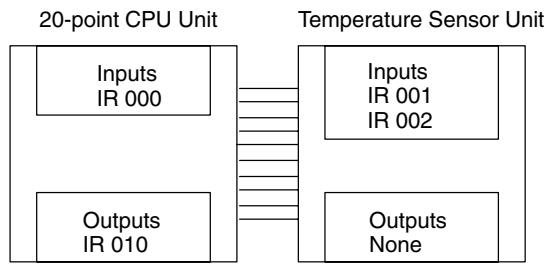
Temperature unit setting:
Two-decimal-place Mode:
Input range setting:
Temperature input 0 storage word:
Temperature input 1 storage word:
OFF (^) OFF (normal)
1 (K2, 0.0 to 500.0^) IR 001
IR 002
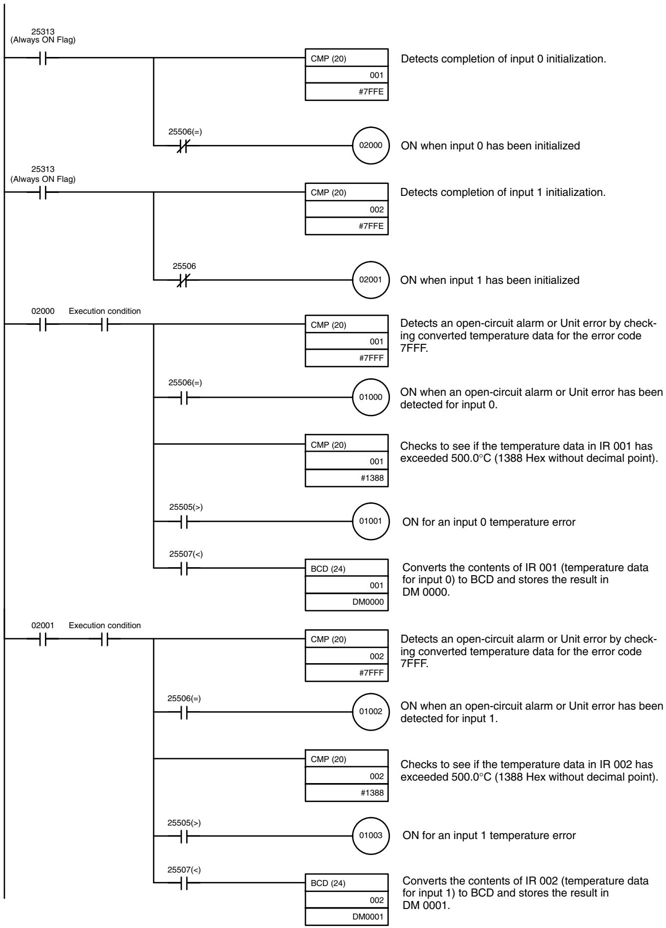
Programming Example 2
The following programming example shows how to convert the data for temperature input 0 to BCD and store the result in DM 0000 and DM 0001. "0001" is stored in DM 0001 when the input data is a negative value. The following system configuration is used.
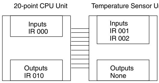
Temperature unit setting: OFF (^) Two-decimal-place Mode: OFF (normal)
Input range setting: 1 (Pt100, -200.0 to 650.0^) Temperature input O storage word: IR 001
Programming with BCD(24) Instruction
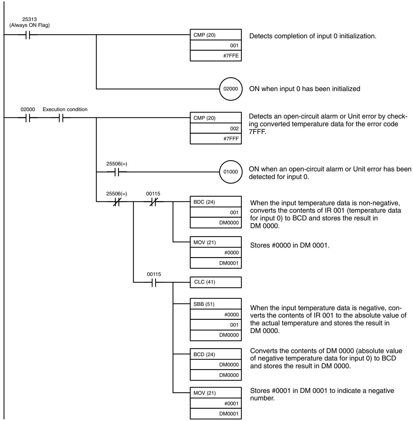
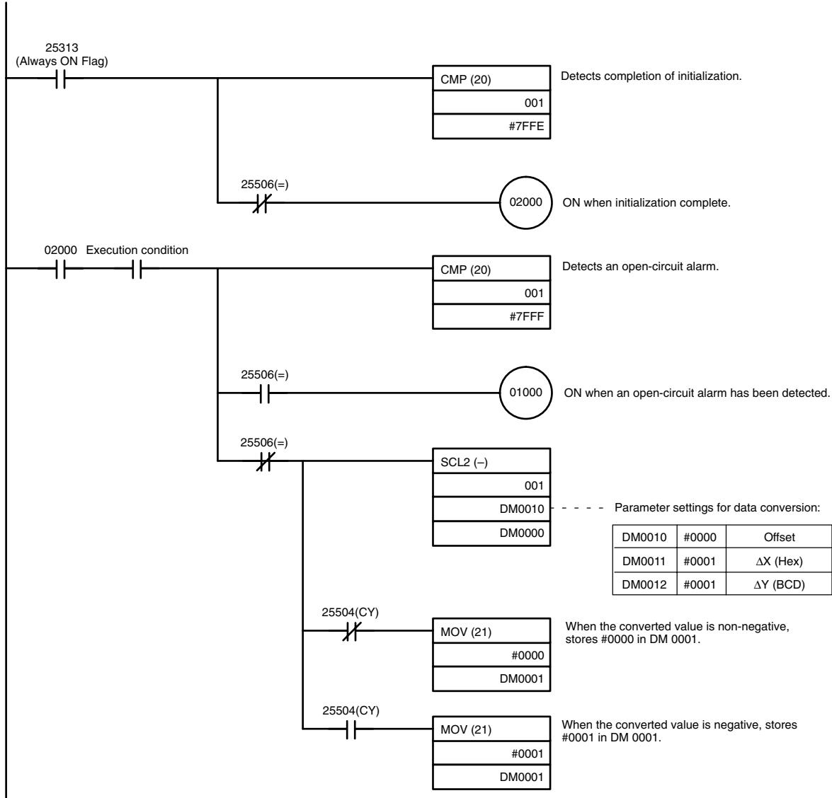
Programming with SCL2(—) Instruction (CPM2A/CPM2C Only)
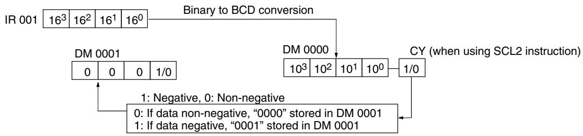
Operation
3-2-8 Two-decimal-place Mode
If pin 2 on the DIP switch is turned ON, values are stored to two decimal places. In this case, temperature data is stored as 6-digit signed hexadecimal (binary) data with 4 digits in the integer portion and 2 digits after the decimal point. The actual data stored in memory is 100 times the actual value, i.e., the decimal point is not indicated. Methods for handling this data are described in this section.
Note When set to store values to two decimal places, temperature data as far as two digits after the decimal point is converted to 6-digit binary data, but the actual resolution is not 0.01^ ( ^ ). For this reason, there may be skipping and inaccuracies in the first digit after the decimal point (0.1). Treat any resolution above that specified for the normal data format as reference data.
Data Structure
The structure of the data stored in memory is shown below. The value will be 100 times the actual temperature.
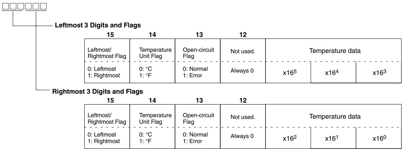
Leftmost/Rightmost Flag: Indicates whether the leftmost or rightmost 3 digits are provided.
Temperature Unit Flag: Indicates whether the temperature is in ^ C or ^ .
Open-circuit Flag: Turns ON (1) when an open-circuit is detected. The temperature data will be 7FF FFF if this flag is ON.
Data Conversion Examples
Some examples of the data stored for various temperature inputs are provided below.
Example 1
Temperature: 1,130.25°C
×100: 113025
Temperature Data: 01B981 (hexadecimal for 113025)
Leftmost 3 Digits and Flags
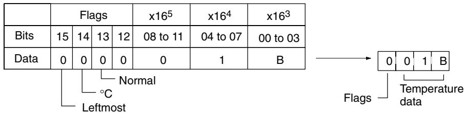
Rightmost 3 Digits and Flags

Example 2
Temperature: -100.12°C
×100: -10012
Temperature Data: FFD8E4 (hexadecimal for -10012)
Leftmost 3 Digits and Flags
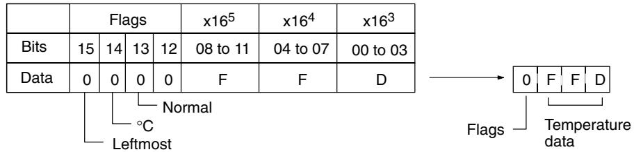
Rightmost 3 Digits and Flags
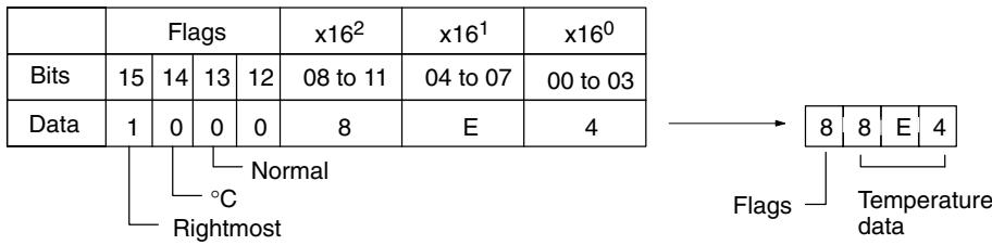
Example 3
Temperature: -200.12°F
×100: -20012
Temperature Data: FFB1D4 (hexadecimal for -20012)
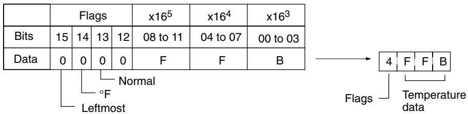
Leftmost 3 Digits and Flags
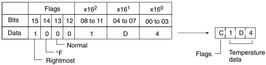
Rightmost 3 Digits and Flags
Example 4
Temperature: Open circuit (^)
Temperature Data: 7FFFFFFF

Leftmost 3 Digits and Flags
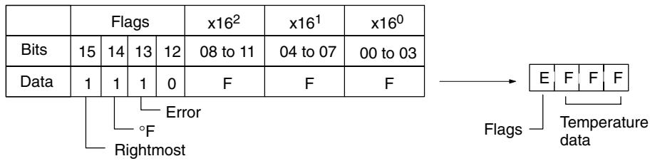
Rightmost 3 Digits and Flags
Note 1. Leftmost digits are stored in the lower memory addresses. Treat the data in the lower memory address as the leftmost digits when programming.
- Be sure that the data is read at least once every 125 ms to allow for the CPU Unit's cycle time and communications time. Correct data may not be obtained if the read cycle is greater than 125 ms.
Programming Example
The following programming example shows how to use 2-decimal-place Mode for the following PC configuration.
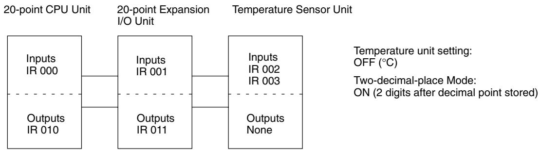
In this example, 100 times the temperature data for temperature input 0 is stored in binary form in DM 0100 to DM 0102.
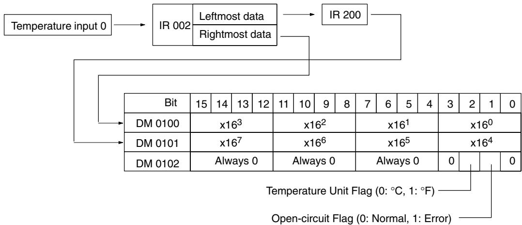
The following program would be used.
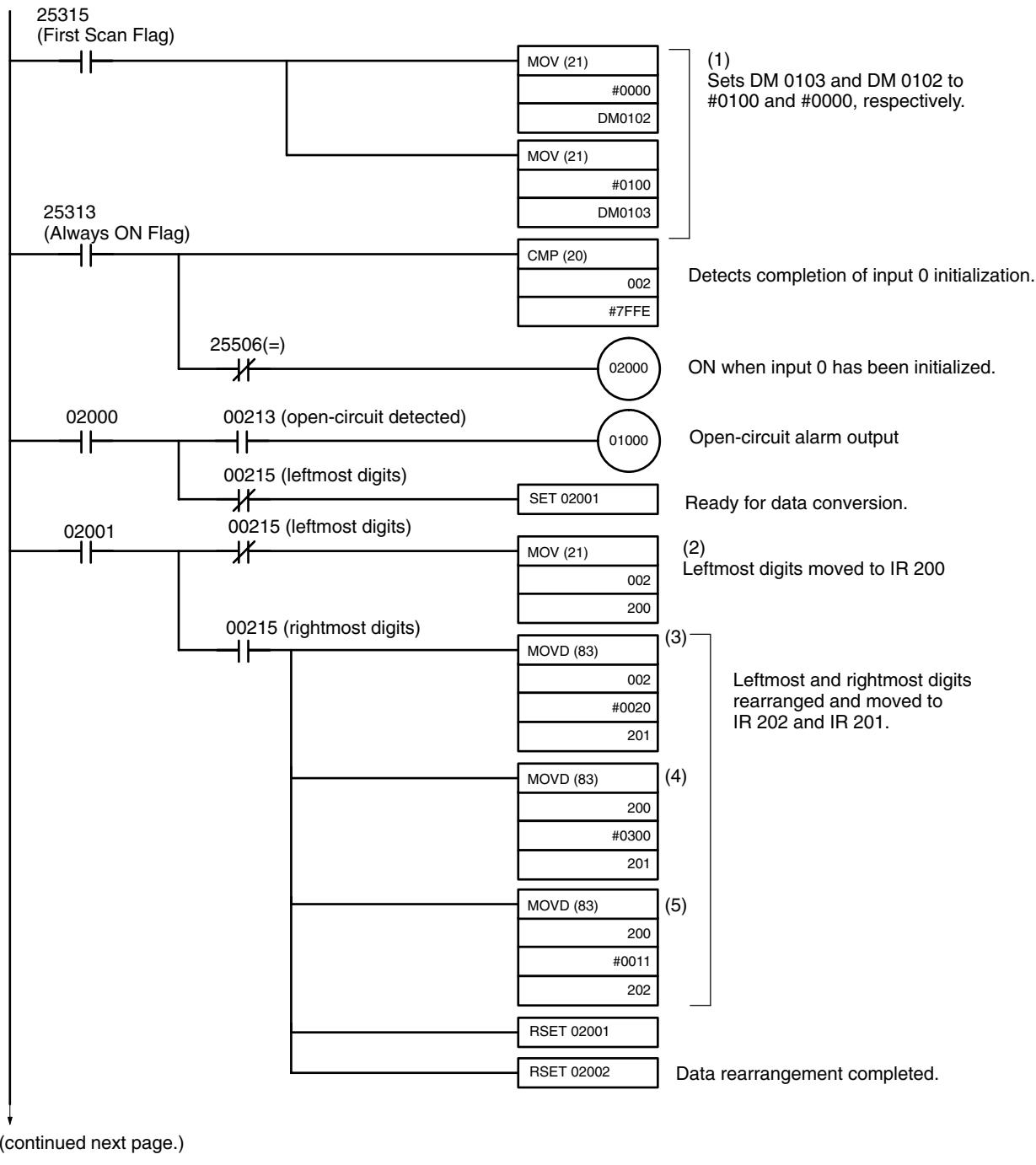
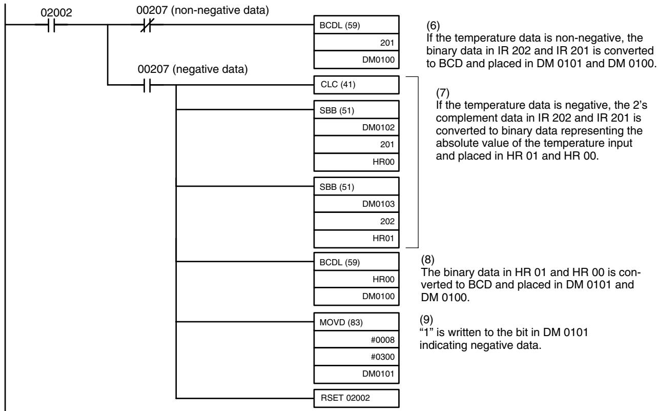
Note The BCDL(59) instruction is only available with the CPM2A and CPM2C.
The data movements corresponding to the numbers in the above ladder programming example are illustrated in the following diagram.
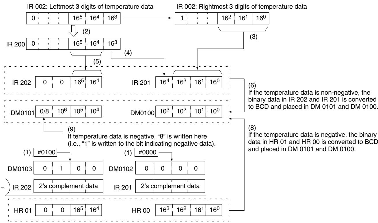
(7)
The 2's complement data in IR 202 and IR 201 is subtracted, as binary data, from the data in DM 0103 and DM 0102 and placed in HR 01 and HR 00.
3-3 CompoBus/S I/O Link Units
The CPM1A, CPM2A, or CPM2C (including the CPM2C-S) PCs can function as Slaves to a CompoBus/S Master Unit (or SRM1 CompoBus/S Master Control Unit) when a CompoBus/S I/O Link Unit is connected. The CompoBus/S I/O Link Unit establishes an I/O link of 8 inputs and 8 outputs between the Master Unit and the PC.
Note For the CPM1A, a CPM1A CPU Unit with 30 or 40 I/O points must be used to connected the CompoBus/S I/O Link Unit. It cannot be connected to a CPM1A CPU Unit with 10 or 20 I/O points.
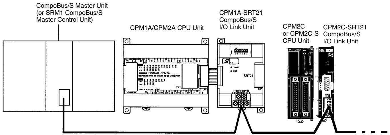
Special Flat Cable, 2-core VCTF cable, or 4-core VCTF cable (You cannot mix Special Flat Cable, 2-core VCTF cable, and 4-core VCTF cable. Use only one type of cable.)
| Cable | Model | Specifications |
| Special Flat Cable | SCA1-4F10 | 4-core flat cable, 0.75 mm² |
| VCTF cable | --- | 0.75 mm² × 2 cores or 0.75 mm² × 4 cores (JIS C 3306) |
From the standpoint of the CPU Unit, the 8 input bits and 8 output bits allocated to the CompoBus/S I/O Link Unit are identical to input and output bits allocated to Expansion I/O Units even though the CompoBus/S I/O Link Unit does not control actual inputs and outputs. The input and output bits allocated to the CompoBus/S I/O Link Unit are one side of an I/O link between the slave CPU Unit and the CPU Unit to which the Master Unit is connected.
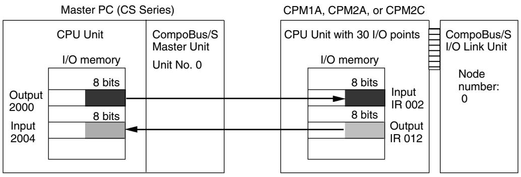
Specifications
| Item | Specification |
| Model number | CPM1A or CPM2A: CPM1A-SRT21 CPM2C or CPM2C-S : CPM2C-SRT21 |
| Master/slave | CompoBus/S Slave |
| Number of I/O points | 8 input points, 8 output points |
| Number of words allocated in CPU Unit I/O memory | 1 input word, 1 output word (Allocated in the same way as Expansion I/O Units and other Expansion Units) |
| Node number setting | Set using the DIP switch (Set before turning on the CPU Unit's power supply.) |
| Current consumption | 50 mA |
LED Indicators
| Indicator | Status | Meaning |
| COMM (yellow) | ON | Communications in progress. |
| OFF | Communications stopped or error has occurred. | |
| ERR (red) | ON | A communications error has occurred. |
| OFF | Indicates normal communications or stand-by. |
Usage Procedure
Connect the Unit.
Connect the CompoBus/S I/O Link Unit.
Determine the node address of the CompoBus/S I/O Link Unit and set the DIP switch.
The node number should be a unique number between 0 and 15. Use the DIP switch to set the CompoBus/S I/O Link Unit's node number, communications mode, and the status of output data when a communications error occurs.
Wire the CompoBus/S transmission path.
Connect the CompoBus/S I/O Link Unit to a CompoBus/S transmission path.
Connecting the CompoBus/S I/O Link Unit
Connect the CompoBus/S I/O Link Unit to the CPU Unit. The number of CompoBus/S I/O Link Units that can be connected depends on the PC. Three Units can be connected to the CPM1A/CPM2A, five Units can be connected to the CPM2C, and three Units can be connected to the CPM2C-S. When Expansion I/O Units or other Expansion Units are also connected, they can be connected in any order from the CPU Unit.
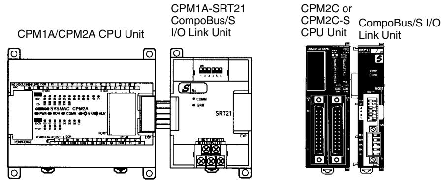
I/O Allocation
I/O words are allocated to the CompoBus/S I/O Link Unit in the same way as Expansion I/O Units or other Expansion Units, the next available input and output words are allocated. When “m” is the last allocated input word and “n” is the
last allocated output word, the CompoBus/S I/O Link Unit is allocated "m+1" as its input word and "n+1" as its output word.
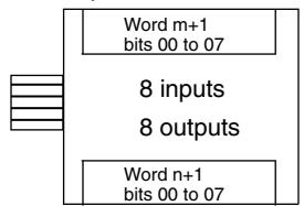
CompoBus/S I/O Link Unit
In the following example, a CompoBus/S I/O Link Unit is connected to a CPU Unit with 30 I/O points.
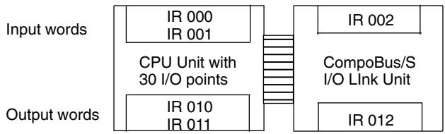
The input word (m + 1) contains the 8 bits of data from the Master Unit and two CompoBus/S communications flags.
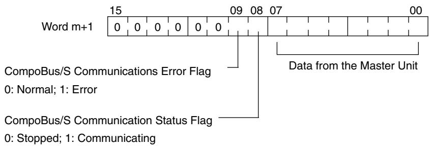
Write the data to be transmitted to the Master Unit in the output word (n + 1) .

The 8 bits of I/O data are not always transmitted simultaneously. In other words, 8 bits of data transmitted from the Master CPU Unit at the same time will not always reach the Slave CPU Unit simultaneously, and 8 bits of data transmitted from the Slave CPU Unit at the same time will not always reach the Master CPU Unit simultaneously.
When the 8 bits of input data must be read together, modify the ladder program in the CPU Unit receiving the data. For example, read the input data twice in succession and accept the data only when the two values match.
Unused bits in the CompoBus/S I/O Link Unit's output word can be used as work bits, but unused bits in the output slaves cannot be used as work bits.
Unused bits in input word cannot be used as work bits.
Determining the Node Number and Making DIP Switch Settings
Node Number
The CompoBus/S I/O Link Unit is a Slave Unit with 8 input bits and 8 output bits. The node number setting is made using the DIP switch; the inputs and outputs share the same node number.
The range of possible node number settings is determined by the type of PC the Master Unit is mounted to and the settings on the Master Unit. For details refer to the CompoBus/S Operation Manual.
DIP Switch Settings
Use the DIP switch to set the CompoBus/S I/O Link Unit's node number, communications mode, and the status of output data when a communications error occurs.
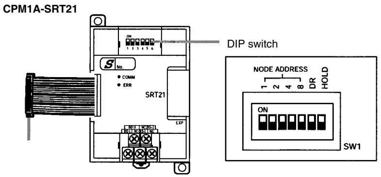
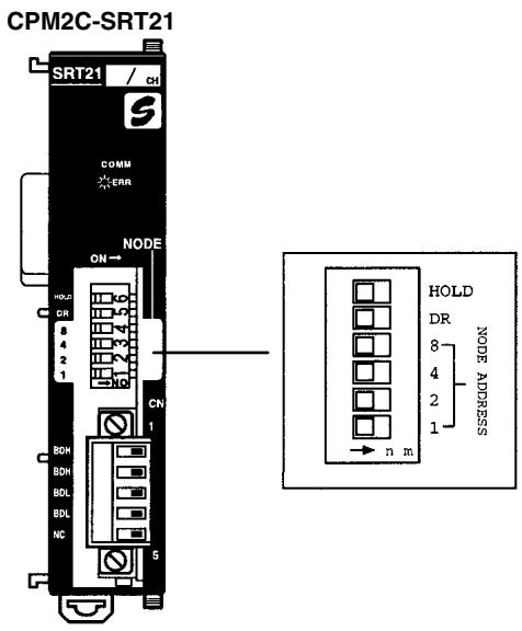
| Pin labels | Contents | |||
| 1, 2, 4, and 8 | Node Address Setting | |||
| Address | Pins 8421 | Address | Pins 8421 | |
| 0 | 0000 | 8 | 1000 | |
| 1 | 0001 | 9 | 1001 | |
| 2 | 0010 | 10 | 1010 | |
| 3 | 0011 | 11 | 1011 | |
| 4 | 0100 | 12 | 1100 | |
| 5 | 0101 | 13 | 1101 | |
| 6 | 0110 | 14 | 1110 | |
| 7 | 0111 | 15 | 1111 | |
| 1 = ON, 0 = OFF | ||||
| DR | ON | Long-distance communications mode (See note 2.) | ||
| OFF | High-speed communications mode | |||
| HOLD | ON | Retain inputs after a communications error. | ||
| OFF | Clear inputs after a communications error. | |||
Note 1. Always turn OFF the power supply before changing the DIP switch settings.
2. Never touch the DIP switch when the Unit is operating. Static electricity may cause operating errors.
Wiring the CompoBus/S Communications Path
- The long-distance communications mode can be used only when one of the following Master Units is connected: C200HW-SRM21-V1, CQM1-SRM21-V1, or SRM1-C0□-V2.
Wire the CompoBus/S communications path as shown in the following diagrams.
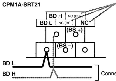
These terminals are not used. They can however be used as communications power supply relay terminals.
Connect the CompoBus/S Communications Cable.
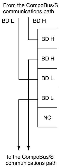
CPM2C-SRT21
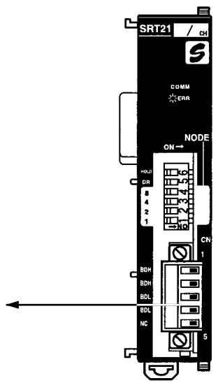
3-4 DeviceNet I/O Link Unit
The CPM1A or CPM2A PCs can function as slaves to a DeviceNet master when a DeviceNet I/O Link Unit is connected. The DeviceNet I/O Link Unit establishes an I/O link of 32 inputs and 32 outputs between the master and the PC.
A maximum of 3 DeviceNet I/O Link Units, can be connected to a CPM2A or CPM1A to create I/O Links for up to 192 points (96 inputs and 96 outputs).
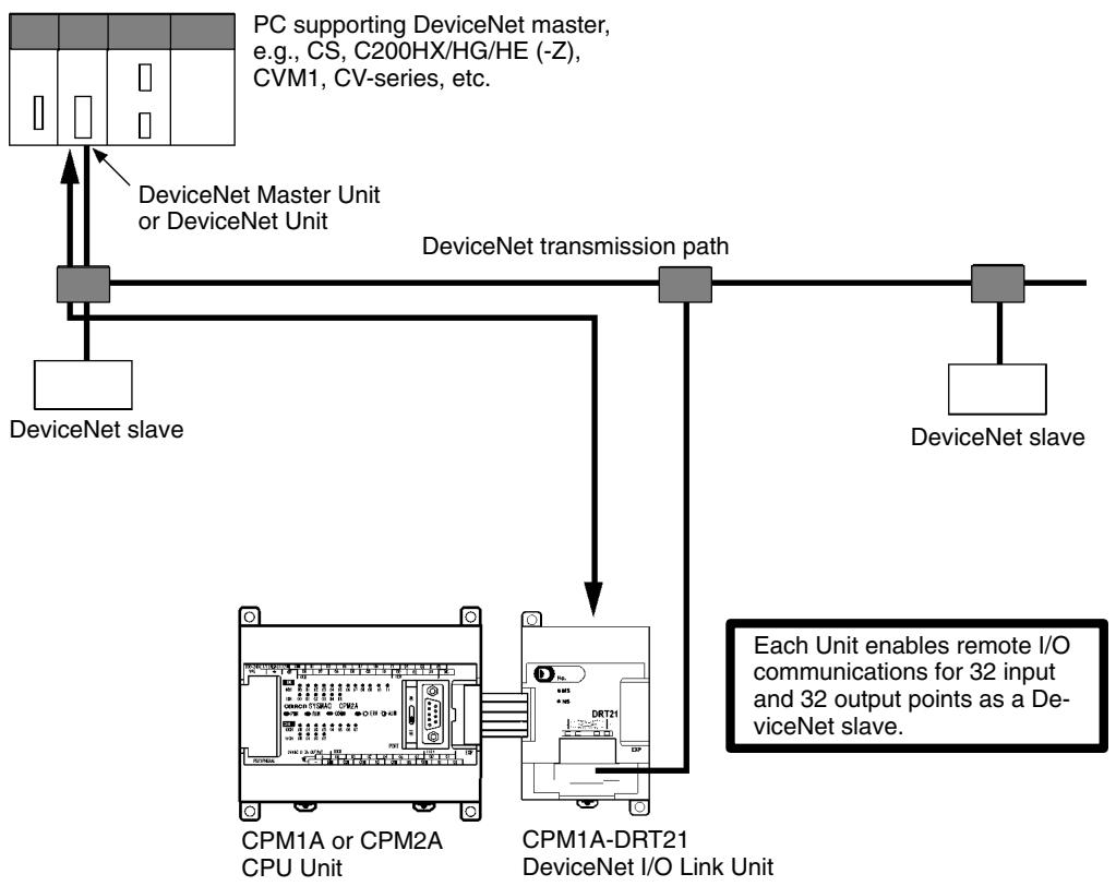
From the standpoint of the CPU Unit, the 32 input bits and 32 output bits allocated to the DeviceNet I/O Link Unit are identical to input and output bits allocated to Expansion I/O Units even though the DeviceNet I/O Link Unit does not control external inputs and outputs. The input and output bits allocated to the DeviceNet I/O Link Unit are one side of an I/O link between the slave CPU Unit and the CPU Unit to which the Master Unit is connected.

Note Refer to the DeviceNet Slaves Operation Manual (W347) for details on DeviceNet networks.
Specifications
| Item | Specification |
| Model number | CPM1A-DRT21 |
| Master/slave | DeviceNet Slave |
| Number of I/O points | 32 input points, 32 output points |
| Number of words allocated in CPU Unit I/O memory | 2 input words, 2 output words (Allocated in the same way as Expansion I/O Units and other Expansion Units) |
| Node number setting | Set using the rotary switches (Set before turning ON the CPU Unit's power supply.) |
| Communications current consumption | 30 mA |
LED Indicators
| Indicator | Color | Status | Meaning |
| MS | Green | Lit | Normal status |
| Flashing | Switch settings being read | ||
| Red | Lit | Fatal hardware error (watchdog timer) | |
| Flashing | Nonfatal error: Incorrect switch settings. | ||
| --- | OFF | Power not supplied. Waiting for initialization to start. Reset in progress. | |
| NS | Green | Lit | Network normal and communications established. |
| Flashing | Network normal and communications not established. | ||
| Red | Lit | Fatal communications error: Unit has detected network status preventing normal communications. Node number duplications Bus OFF detected. | |
| Flashing | Nonfatal communications error: Communications timeout or communications error for one or more slaves. | ||
| --- | OFF | Waiting for node number check by master. Switch setting error. Power not supplied. |
Handling Unit Errors
If an error occurs in the DeviceNet I/O Link Unit, the Error Flags in AR 0200 to AR 0202 will be turned ON. The addresses of the Error Flags are in the order that the Expansion Units are connected in the PC, with AR 0200 used for the Expansion Unit closest to the CPU Unit. Use these flags in the program when it is necessary to detect errors.
Usage Procedure
Connect the Unit.
Determine the node number of the DeviceNet I/O Link Unit and set the rotary switches.
Wire the DeviceNet transmission path.
Connect the DeviceNet I/O Link Unit.
The node number should be a unique number between 0 and 63.
Use the DIP switch to set the DeviceNet I/O Link Unit's baud rate and the status of output data when a communications error occurs.
Connect the DeviceNet I/O Link Unit to a DeviceNet transmission path.
Connecting the DeviceNet I/O Link Unit
Connect the DeviceNet I/O Link Unit to the CPU Unit. Up to three Units can be connected to the CPM1A/CPM2A. When Expansion I/O Units or other Expansion Units are also connected, they can be connected in any order from the CPU Unit.
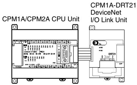
I/O Allocation
I/O words are allocated to the DeviceNet I/O Link Unit in the same way as Expansion I/O Units or other Expansion Units, the next available input and output words are allocated. When "m" is the last allocated input word and "n" is the last allocated output word, the DeviceNet I/O Link Unit is allocated "m+1" as its input word and "n+1" as its output word.
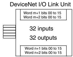
In the following example, a DeviceNet I/O Link Unit is connected to a CPU Unit with 30 I/O points.
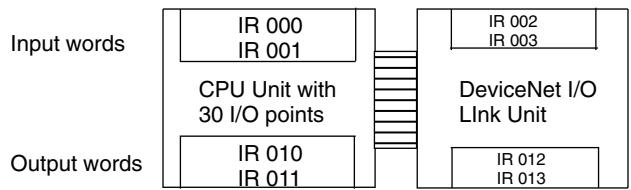
All of the words allocated to the DeviceNet I/O Link Unit are used to read and write data between the CPU Unit of the DeviceNet I/O Link Unit and the CPU Unit of the DeviceNet master, as shown in the following illustration.
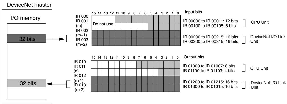
The 32 bits each of I/O data are not always transmitted simultaneously. In other words, 32 bits of data transmitted from the Master CPU Unit at the same time will not always reach the Slave CPU Unit simultaneously, and 32 bits of data transmitted from the Slave CPU Unit at the same time will not always reach the Master CPU Unit simultaneously.
When the 32 bits of input data must be read together, modify the ladder program in the CPU Unit receiving the data. For example, read the input data twice in succession and accept the data only when the two values match.
Unused bits in the DeviceNet I/O Link Unit's output words can be used as work bits if they are not used for output from the slave.
Unused bits in input word cannot be used as work bits.
Determining the Node Number and Making DIP Switch Settings
Node Address Switches
Use these switches to set the node address of the Unit.
SW3

X10
SW2

X1
Note
Setting method: Two-digit decimal
Setting range: 0 to 63 (Do not set 64 to 99.)
- Set the rotary switches before turning ON the power supply. The switch settings are read only at startup.
- Any node address from 0 through 63 can be set as long as it hasn't been set on another slave node.
- If the node address is the same as one set on another node, a node address duplication error will occur and it won't be possible to start up network communications. Refer to the DeviceNet Slaves Operation Manual (W347) for details.
DIP Switch
The DIP switch on the front of the DeviceNet I/O Link Unit is used to set the baud rate and whether to hold or clear the remote outputs when a communications error occurs in the slave.
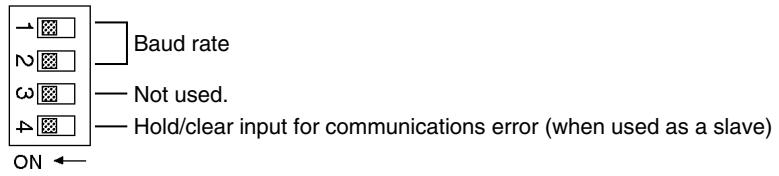
The settings of the DIP switch pins are shown in the following table. All pins are set to OFF at the factory.
| Pin | Function | Setting |
| 1 | Baud rate | See the next table. |
| 2 | ||
| 3 | Not used | OFF |
| 4 | Hold/clear remote outputs for communications error | OFF: Clear remote outputs ON: Hold remote outputs |
Baud Rate
Pins 1 and 2 are used to set the baud rate as shown in the following table.
| Pin 1 | Pin 2 | Baud rate | Max. transmission path length (reference) |
| OFF | OFF | 125 kbps | 500 m |
| ON | OFF | 250 kbps | 250 m |
| OFF | ON | 500 kbps | 100 m |
| ON | ON | Not allowed. | --- |
Note 1. Always turn OFF the PC before changing the DIP switch settings.
- Set the same baud rate on all of the nodes (Master and Slaves) in the Network. Any slaves with baud rates different from the master's rate won't be able to participate in communications and may cause a communications error between nodes that have been set properly.
Hold/Clear Remote Outputs
When the DeviceNet Unit is used as a slave, pin 4 is used to set whether to hold or clear remote outputs when a communications error occurs.
Note When using AR 02 (Expansion Unit Error Flags) in the program, turn ON pin 4 on the DIP switch. If communications are set to be cleared, the timing for clearing outputs and setting the Error Flags may not agree.
Wire the DeviceNet communications path as shown in the following diagram.
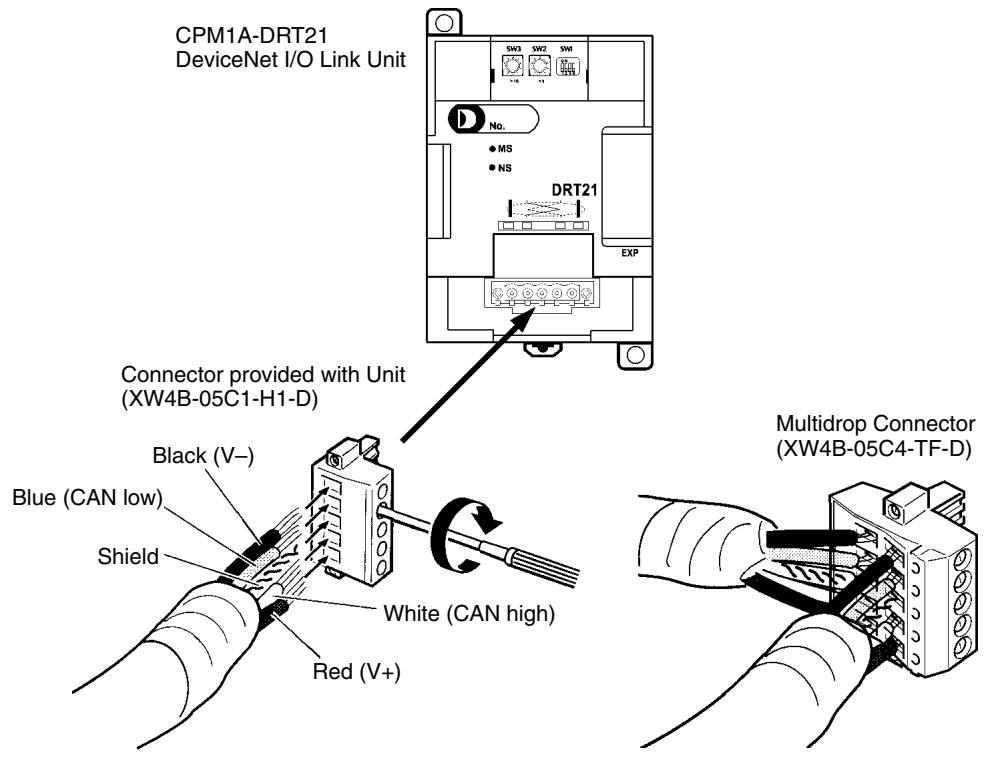
Wiring the DeviceNet Communications Path
DeviceNet Connectors
Use the following connectors.
| Model | Form and specifications |
| XW4B-05C1-H1-D | OMRON connector with screws (included with DeviceNet I/O Link Unit). |
| XW4B-05C4-TF-D | OMRON connector for multidrop connections (See note.) |
Note Use the XW4B-05C4-TF-D when wiring multidrop connections using Thick Cables.
Use the following screwdriver for the above connector.

I/O Response Time
Refer to the DeviceNet Slaves Operation Manual (W347) for details on the response time. The data read/write time for one cycle for the CPM1A-DRT21 is approximately 0.5 ms. Add a maximum of 1 ms to the I/O response time.
This section describes how to use the communications functions provided in the CPM1, CPM1A, CPM2A, CPM2C (including the CPM2C-S), and SRM1(-V2) PCs.
4-1 Introduction 226
4-1-1 Overview 226
4-1-2 Wiring Ports 226
4-2 CPM1/CPM1A Communications Functions 227
4-2-1 Host Link Communications 227
4-2-2 One-to-one NT Link Communications 228
4-2-3 One-to-one PC Link Communications 229
4-3 CPM2A/CPM2C Communications Functions 231
4-3-1 Host Link Communications 231
4-3-2 No-protocol Communications 251
4-3-3 One-to-one NT Link Communications 260
4-3-4 One-to-one PC Link Communications 263
4-4 SRM1(-V2) Communications Functions 268
4-4-1 Host Link Communications 268
4-4-2 No-protocol Communications 272
4-4-3 One-to-one NT Link Communications 277
4-4-4 One-to-N NT Link Communications 278
4-4-5 One-to-one PC Link Communications 279
4-5 Host Link Commands 281
4-5-1 IR/SR AREA READ - RR 281
4-5-2 LR AREA READ - RL 282
4-5-3 HR AREA READ - RH 282
4-5-4 PV READ - RC 282
4-5-5 TC STATUS READ - RG 283
4-5-6 DM AREA READ-RD 283
4-5-7 AR AREA READ - RJ 284
4-5-8 IR/SR AREA WRITE - WR 285
4-5-9 LR AREA WRITE - WL 285
4-5-10 HR AREA WRITE-WH 286
4-5-11 PVWRITE-WC 286
4-5-12 TC STATUS WRITE-WG 287
4-5-13 DM AREA WRITE-WD 288
4-5-14 AR AREA WRITE-WJ 288
4-5-15 SVREAD1-R# 289
4-5-16 SV READ 2 - R$ 290
4-5-17 SV CHANGE 1-W# 291
4-5-18 SV CHANGE 2-W$ 292
4-5-19 STATUS READ - MS 293
4-5-20 STATUSWRITE-SC 294
4-5-21 ERROR READ-MF 295
4-5-22 FORCED SET-KS 296
4-5-23 FORCED RESET - KR 297
4-5-24 MULTIPLE FORCED SET/RESET-FK 298
4-5-25 FORCED SET/RESET CANCEL - KC 299
4-5-26 PC MODEL READ-MM 300
4-5-27 TEST-TS 300
4-5-28 PROGRAM READ - RP 301
4-5-29 PROGRAMWRITE-WP 301
4-5-30 COMPOUND COMMAND - QQ 302
4-5-31 ABORT-XZ 304
4-5-32 INITIALIZE -** 304
4-5-33 TXD RESPONSE - EX 304
4-5-34 Undefined Command - IC 305
4-1 Introduction
4-1-1 Overview
CPM1/CPM1A Communications
The CPM1/CPM1A can execute a variety of communications through its peripheral port via an RS-232C Adapter or an RS-422 Adapter.
Host Link Communications
The CPM1/CPM1A PCs are compatible with the Host Link System, which allows up to 32 PCs to be controlled from a host computer. An RS-232C Adapter is used for 1:1 communications and an RS-422 Adapter and B500-AL004 Link Adapter are used for 1:N communications.
A CPM1/CPM1A equipped with an RS-232C Adapter can also communicate with a OMRON Programmable Terminal using host link commands.
Refer to 4-2-1 CPM1/CPM1A Host Link Communications in this manual and 1-2-2 Host Link Communications in the CPM1 Operation Manual or 1-2-2 Host Link Communications in the CPM1A Operation Manual for more details.
One-to-one PC Link
A data link can be created with a data area in another CPM1, CPM1A, CPM2A, CPM2C, CQM1, C200HX/HG/HE, or C200HS PC. An RS-232C Adapter is used to make the 1:1 connection.
Refer to 4-2-3 CPM1/CPM1A 1:1 PC Link Communications in this manual and 1-2-3 One-to-one PC Communications Links in the CPM1 Operation Manual or 1-2-3 One-to-one PC Communications Links in the CPM1A Operation Manual for more details.
One-to-one NT Link
Using the 1:1 NT Link, the CPM1/CPM1A PC can be connected to the OMRON Programmable Terminal (NT Link Interface) through an RS-232C Adapter.
Refer to 4-2-2 CPM1/CPM1A 1:1 NT Link Communications in this manual and 1-2-4 One-to-one NT Link Communications in the CPM1 Operation Manual or NT Link Communications in the CPM1A Operation Manual for more details.
CPM2A/CPM2C Communications
The following types of communications can be executed through the ports of the CPM2A/CPM2C.
- Host Link communications with a host computer
- RS-232C communications with a computer or other device
One-to-one PC Link communications with another PC - One-to-one NT Link communications with OMRON Programmable Terminals
This section explains the required PC Setup and methods for using these types of communications.
SRM1(-V2) Communications
The following types of communications can be executed through the ports of the SRM1(-V2).
- Host Link communications with a host computer
- RS-232C communications with a computer or other device
One-to-one PC Link communications with another PC - One-to-one NT Link communications with OMRON Programmable Terminals
Note
One-to-one NT Link communications are not possible with the SRM1-C01, which is equipped with only a peripheral port. The SRM1-C01 may be connected to a PT through an RS-232C Adapter in Host Link mode.
4-1-2 Wiring Ports
Refer to the CPM1 Operation Manual, CPM1A Operation Manual, CPM2A Operation Manual, CPM2C Operation Manual, or SRM1 Master Control Units Operation Manual for information on wiring the communications ports.
4-2 CPM1/CPM1A Communications Functions
4-2-1 Host Link Communications
Host Link communications were developed by OMRON for the purpose of connecting PCs and one or more host computers by RS-232C cable, and controlling PC communications from the host computer. Normally the host computer issues a command to a PC, and the PC automatically sends back a response. Thus the communications are carried out without the PCs being actively involved. The PCs also have the ability to initiate data transmissions when direct involvement is necessary.
In general, there are two means for implementing Host Link communications. One is based on C-mode commands, and the other on FINS (CV-mode) commands. The CPM1/CPM1A supports C-mode commands only. For details on Host Link communications, refer to 4-5 Host Link Commands.
The CPM1/CPM1A's peripheral port settings must be set properly in order to use the Host Link communications, as shown in the following table.
PC Setup Settings
| Word | Bit | Function | Setting | |||
| DM 6650 | 00 to 07 | Port settings100: Standard (1 start bit, 7-bit data, 2 stop bits, even parity, 9,600 bps)01: Settings in DM 6651 | 00 | |||
| 08 to 11 | Link area for 1:1 PC Link via peripheral port0: LR 00 to LR 15 | 0(Any value is OK) | ||||
| 12 to 15 | Communications mode10: Host Link; 2: 1:1 PC Link Slave; 3: 1:1 PC Link Master; 4: 1:1 NT Link | 0 | ||||
| DM 6651 | 00 to 07 | Baud rate100: 1.2K, 01: 2.4K, 02: 4.8K, 03: 9.6K, 04: 19.2K | 00(Any value is OK) | |||
| 08 to 15 | Frame format1Start Length Stop Parity00: 1 bit 7 bits 1 bit Even01: 1 bit 7 bits 1 bit Odd02: 1 bit 7 bits 1 bit None03: 1 bit 7 bits 2 bit Even04: 1 bit 7 bits 2 bit Odd05: 1 bit 7 bits 2 bit None06: 1 bit 8 bits 1 bit Even07: 1 bit 8 bits 1 bit Odd08: 1 bit 8 bits 1 bit None09: 1 bit 8 bits 2 bit Even10: 1 bit 8 bits 2 bit Odd11: 1 bit 8 bits 2 bit None | 00(Any value is OK) | ||||
| DM 6652 | 00 to 15 | Transmission delay (Host Link)10000 to 9999: In ms. | 0000 | |||
| DM 6653 | 00 to 07 | Node number (Host Link)100 to 31 (BCD) | 00 to 31 | |||
| 08 to 15 | Not used. | 00(Any value is OK) | ||||
Note 1. If an improper setting is used, a non-fatal error will occur, AR 1302 will be turned ON, and the default setting (0, 00, or 0000) will be used.
-
For information on the Host Link settings for another OMRON PC, refer to that PC's Operation Manual.
-
If an out-of-range value is set, the following communications conditions will result. In that case, reset the value so that it is within the permissible range.
Communications mode: Host Link
Communications format: Standard settings
(1 start bit, 7-bit data; 2 stop bits, even parity, 9,600 bps)
Transmission delay: No
Node number: 00
Example Program
This example shows a BASIC program that reads the status of the CPM1's inputs in IR 000. For more details, refer to 4-5 Host Link Commands.
An FCS (frame check sequence) check isn't performed on the received response data in this program. Be sure that the host computer's RS-232C port is configured correctly before executing the program.
1010 'CPM1 SAMPLE PROGRAM
1020 'SET THE COMMAND DATA
1030 S$="@00RR00000001"
1040 FCS=0
1050 FOR I=1 TO LEN(S$)
1060 FCS=FCS XOR ASC(MID(S,I,1))
1070 NEXT I
1080 FCS=(FCS):IF LEN(FCS)=1 THEN FCS="0"+FCS
1090 CLOSE 1
1100 CLS
1110 PRINT "SENDING COMMAND"
1120 OPEN "COM:E73" AS #1
1130 PRINT #1,S+ FCS + CHR(13);
1140 CLS
1150 PRINT "RECEIVING RESPONSE DATA"
1160 LINE INPUT #1,A$
1170 PRINT A$
1180 END
4-2-2 One-to-one NT Link Communications
Using the 1:1 NT Link, the CPM1/CPM1A PC can be connected to the Programmable Terminal (NT Link Interface) through an RS-232C Adapter.
CPM1 PCs
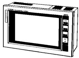
OMRON Programmable Terminal

RS-232C Cable
RS-232C Adapter
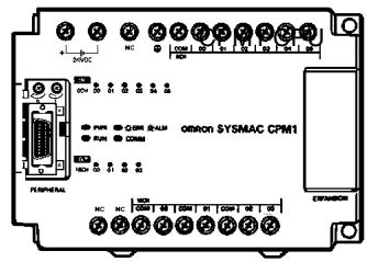
CPM1 CPU Unit
CPM1A PCs
OMRON Programmable Terminal

RS-232C Cable
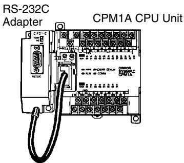
PC Setup Settings
The settings relating to 1:1 NT Link PC communications must be set as shown in the following table.
| Word | Bit | Function | Setting |
| DM 6650 | 00 to 07 | Port settings1 00: Standard (1 start bit, 7-bit data, 2 stop bits, even parity, 9,600 bps) 01: Settings in DM 6651 | 00 (Any value is OK) |
| 08 to 11 | Link area for 1:1 PC Link via peripheral port 0: LR 00 to LR 15 | 0 (Any value is OK) | |
| 12 to 15 | Communications mode1 0: Host Link; 2: 1:1 PC Link Slave; 3: 1:1 PC Link Master; 4: 1:1 NT Link | 4 |
Note 1. If an improper setting is used, a non-fatal error will occur, AR 1302 will be turned ON, and the default setting (0 or 00) will be used.
2. For information on the NT Link settings for another OMRON PC, refer to that PC's Operation Manual.
3. If an out-of-range value is set, the following communications conditions will result. In that case, reset the value so that it is within the permissible range.
Communications mode: Host Link
Communications format: Standard settings
(1 start bit, 7-bit data; 2 stop bits, even parity, 9,600 bps)
Transmission delay: No
Node number: 00
4-2-3 One-to-one PC Link Communications
In a 1:1 PC Link, a CPM1/CPM1A is linked to another CPM1/CPM1A, CPM2A/ CPM2C, CQM1, C200HX/HG/HE, or C200HS PC through an RS-232C Adapter and standard RS-232C cable. One of the PCs will serve as the Master and the other as the Slave. The 1:1 PC Link can connect up to 256 bits (LR 0000 to LR 1515) in the two PCs.
CPM1/CPM1A One-to-one PC Links
The following diagram shows a 1:1 PC Link between two CPM1s PCs. Refer to the CPM1A Operation Manual for the corresponding information on the CPM1A.
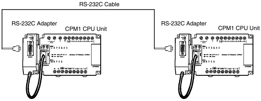
The words used for the 1:1 PC Link are as shown below.

Limitations of 1:1 PC Links with a CPM1/CPM1A
Only the 16 LR words from LR 00 to LR 15 can be linked in the CPM1/CPM1A, so use only those 16 words in the CQM1 or C200HS when making a 1:1 PC Link with one of those PCs. A 1:1 PC Link cannot be made to a CPM1/CPM1A PC using LR 16 through LR 63 in the CQM1, C200HX/HG/HE, or C200HS.
PC Setup Settings
The settings relating to 1:1 PC Link communications must be set as shown in the following table.
| Word | Bit | Function | Setting (Master) | Setting (Slave) |
| DM 6650 | 00 to 07 | Port settings100: Standard (1 start bit, 7-bit data, 2 stop bits, even parity, 9,600 bps)01: Settings in DM 6651 | 00(Any value is OK) | 00(Any value is OK) |
| 08 to 11 | Link area for 1:1 PC Link via peripheral port0: LR 00 to LR 15 | 0 | 0(Any value is OK) | |
| 12 to 15 | Communications mode10: Host Link; 2: 1:1 PC Link Slave; 3: 1:1 PC Link Master; 4: 1:1 NT Link | 3 | 2 |
Note 1. If an improper setting is used, a non-fatal error will occur, AR 1302 will be turned ON, and the default setting (0 or 00) will be used.
- For information on the 1:1 PC Link settings for another OMRON PC, refer to that PC's Operation Manual.
- For information on CPM1/CPM1A 1:1 PC Link connections and wiring diagrams refer to 3-4-7 Host Link Connections in the CPM1 Operation Manual or CPM1A Operation Manual. For the SRM1(-V2) refer to 3-4-4 RS-232C Port Wiring in the SRM1 Master Control Unit Operation Manual.
- If an out-of-range value is set, the following communications conditions will result. In that case, reset the value so that it is within the permissible range.
Communications mode: Host Link
Communications format: Standard settings
(1 start bit, 7-bit data; 2 stop bits, even parity, 9,600 bps)
Transmission delay: No
Node number: 00
Example Program
This example shows ladder programs that copy the status of IR 000 in each CPM1/CPM1A to SR 200 in the other CPM1/CPM1A.
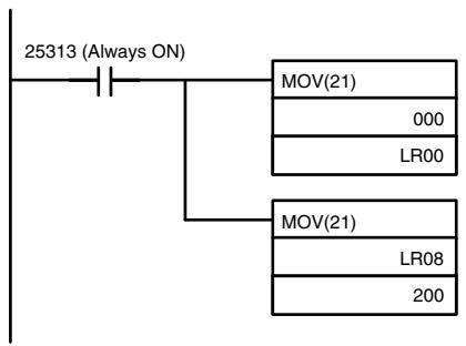
Program in the Master
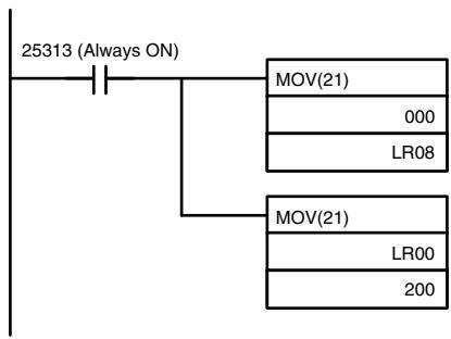
Program in the Slave

4-3 CPM2A/CPM2C Communications Functions
This section describes how to use CPM2A/CPM2C (including the CPM2C-S) communications functions. Read this section if you are using Host Link, no-protocol, 1:1 NT Link, or 1:1 PC Link communications.
4-3-1 Host Link Communications
Host Link communications are a conversational-type communications protocol, in which the PC sends responses to commands issued from a host computer and can be used to read or write data in the PC's data areas and control some PC operations. There is no need for a communications program in the PC. Host Link communications can be used through the peripheral port or the CPM2A/ CPM2C's RS-232C port.
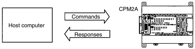
CPM2A One-to-one Communications
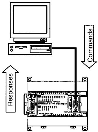
CPM2A RS-232C port connection (See note.)
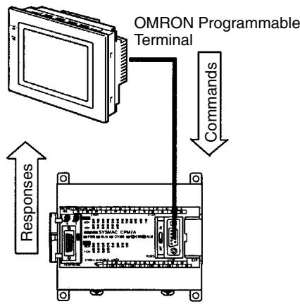
CPM2A RS-232C port connection (See note.)
Note When connecting to the peripheral port, an RS-232C Adapter or computer connection cable (CQM1-CIF01 or CQM1-CIF02) is necessary.
CPM2C One-to-one Communications
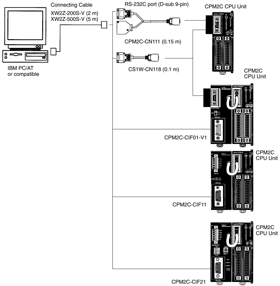
Note The CSW1-CN226/626 can be connected directly to the CPU Unit. With the CPM2C-CIF01-V1, the cable switch (SW1) can be turned ON to enable connecting to a personal computer with a CS1W-CN226/CN626 Connecting Cable.
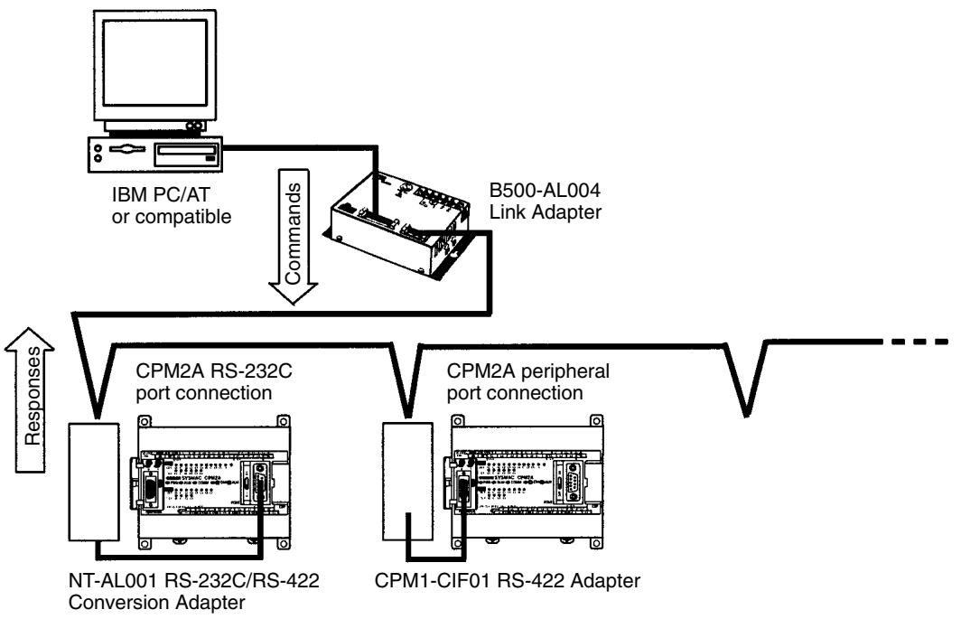
CPM2A 1:N Communications
CPM2C 1:N Communications
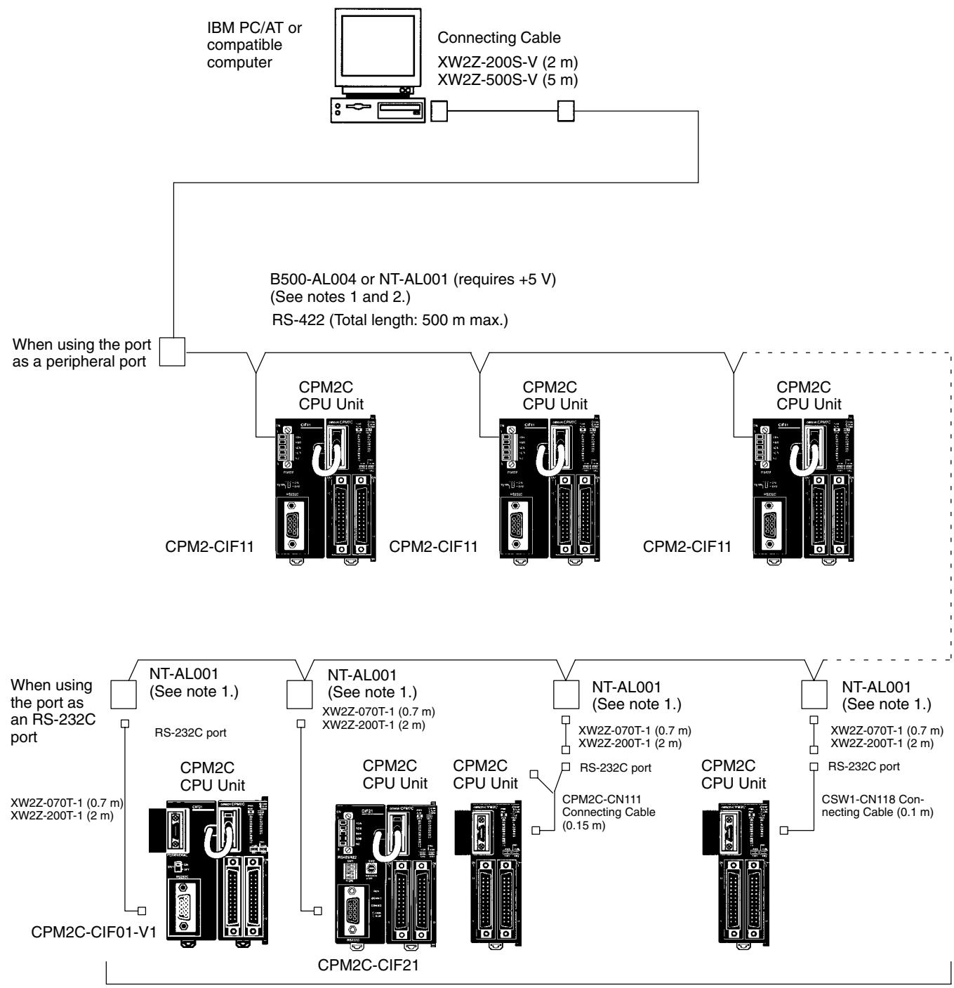
Up to 32 PCs
Frame Transmission and Reception
In Host Link communications, the host computer ordinarily has the transmission right first and initiates the communications. The CPM2A/CPM2C then automatically sends a response.
Commands and responses are exchanged in the order shown in the illustration below. The block of data transferred in a single transmission is called a "frame." A single frame is configured of a maximum of 131 characters of data. The right to send a frame is called the "transmission right." The Unit that has the transmission right is the one that can send a frame at any given time. The transmission right is traded back and forth between the host computer and the CPM2A/ CPM2C each time a frame is transmitted. The transmission right is passed from the transmitting Unit to the receiving Unit when either a terminator (the code that marks the end of a command or response) or a delimiter (the code that sets frames apart) is received.
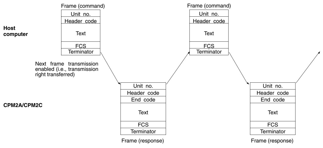
Slave-initiated Communications
Data transmissions from the PC to the host computer can be initiated by the CPU Unit using TXD(48).
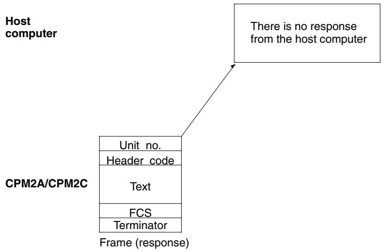
Command and Response Formats
This section explains the formats for the commands and responses that are exchanged in Host Link communications. Command Format When transmitting a command from the host computer, prepare the command data in the format shown below.

@
An "@" symbol must be placed at the beginning.
Node No.
Identifies the CPM2A/CPM2C PC communicating with the host computer. Specify the CPM2A/CPM2C's node number in the PC Setup (DM 6648, DM 6653).
Header Code
Set the 2-character command code.
Text
Set the command parameters.
FCS
Set a 2-character Frame Check Sequence code. See page 239.
Terminator
Set two characters, “*” and the carriage return (CHR$(13)) to indicate the end of the command.
Response Format
The response from the CPM2A/CPM2C is returned in the format shown below. Prepare a program so that the response data can be interpreted and processed.

@, Node No., Header Code
Contents identical to those of the command are returned.
End Code
The completion status of the command (e.g., whether or not an error has occurred) is returned.
Text
Text is returned only when there is data such as read data.
FCS
The set 2-character Frame Check Sequence is returned.
Terminator
Set two characters, “*” and the carriage return (CHR$(13)) to indicate the end of the response.
Long Transmissions
The largest block of data that can be transmitted as a single frame is 131 characters. A command or response of 132 characters or more must therefore be divided into more than one frame before transmission. When a transmission is split, the ends of the first and intermediate frames are marked by a delimiter instead of a terminator.
Dividing Commands
As each frame is transmitted by the host computer, the computer waits for the delimiter to be transmitted from the CPM2A/CPM2C. After the delimiter has been transmitted, the next frame will then be sent. This procedure is repeated until the entire command has been transmitted.
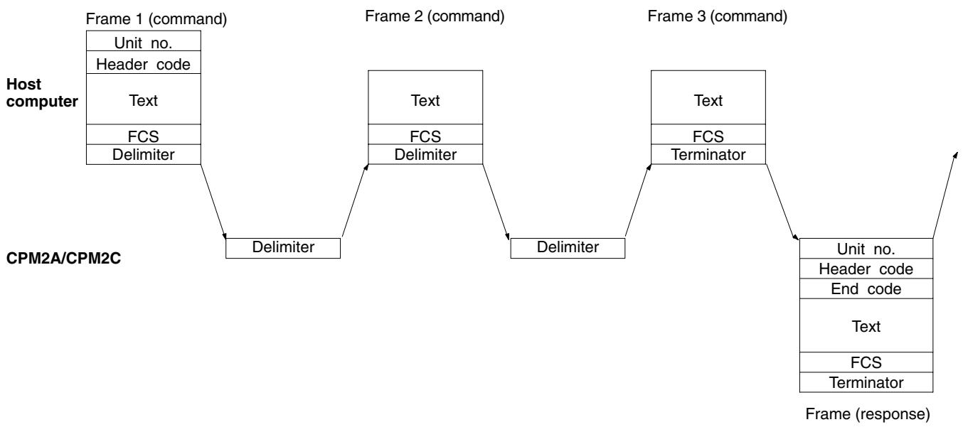
Dividing Responses
As each frame is received by the host computer, a delimiter is transmitted to the CPM2A/CPM2C. After the delimiter has been transmitted, the CPM2A/CPM2C will transmit the next frame. This procedure is repeated until the entire response has been transmitted.
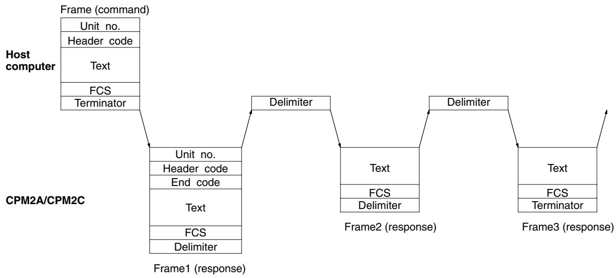
Precautions for Long Transmissions
When dividing commands such as WR, WL, WC, or WD that execute write operations, be careful not to divide into separate frames data that is to be written into a single word. As shown in the illustration below, be sure to divide frames so that they coincide with the divisions between words.

Frame 1 (131 characters maximum)
Frame 2 (128 characters maximum)
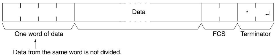
FCS (Frame Check Sequence)
When a frame is transmitted, an FCS is placed just before the delimiter or terminator in order to check whether any data error has been generated. The FCS is 8-bit data converted into two ASCII characters. The 8-bit data is the result of an EXCLUSIVE OR performed on the data from the beginning of the frame until the end of the text in that frame (i.e., just before the FCS). Calculating the FCS each time a frame is received and checking the result against the FCS that is included in the frame makes it possible to check for data errors in the frame.

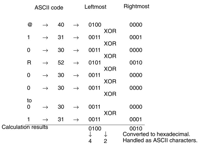
Example Program for FCS
This example shows a BASIC subroutine program for executing an FCS check on a frame received by the host computer.
Normal reception data includes the FCS, delimiter or terminator, and so on. When an error occurs in transmission, however the FCS or some other data may not be included. Be sure to program the system to cover this possibility.
400 *FCSCHECK
410 L = LEN (RESPONSE$) ' Data transmitted and received
420 Q = 0 : FCSCCK$ = ""
430 A= RIGHT(RESPONSE$, 1)
440 PRINT RESPONSE, A, L
450 IF A= "* THEN LENG = LEN (RESPONSE$) - 3
    ELSE LENG= LEN (RESPONSE) - 2
460 FCSP= MID(RESPONSE, LENG + 1, 2) ' FCS data received
470 FOR I = 1 TO LENG$ Number of characters in FCS
480 Q = ASC (MID(RESPONSE, I, 1)) XOR Q
490 NEXT I
500 FCSD= HEX(Q)
510 IF LEN (FCSO) = 1 THEN FCSD = " 0 " + FCSD$' FCS result
520 IF FCSD< FCSP THEN FCSCK$ = " ERR "
530 PRINT " FCSD= "; FCSD, " FCSP= "; FCSP, " FCSCK= "; FCSCK
540 RETURN
Commands
| Header code | CPM2A/CPM2C Operating Mode | Name | Page | ||
| RUN | MONITOR | PROGRAM | |||
| RR | Valid | Valid | Valid | IR/WR/SR AREA READ | 281 |
| RL | Valid | Valid | Valid | LR AREA READ | 282 |
| RH | Valid | Valid | Valid | HR AREA READ | 282 |
| RC | Valid | Valid | Valid | TC PV READ | 282 |
| RG | Valid | Valid | Valid | TC STATUS READ | 283 |
| RD | Valid | Valid | Valid | DM AREA READ | 283 |
| RJ | Valid | Valid | Valid | AR AREA READ | 284 |
| WR | Not Valid | Valid | Valid | IR/WR/SR AREA WRITE | 285 |
| WL | Not Valid | Valid | Valid | LR AREA WRITE | 285 |
| WH | Not Valid | Valid | Valid | HR AREA WRITE | 286 |
| WC | Not Valid | Valid | Valid | TC PV WRITE | 286 |
| WG | Not Valid | Valid | Valid | TC STATUS WRITE | 287 |
| WD | Not Valid | Valid | Valid | DM AREA WRITE | 288 |
| WJ | Not Valid | Valid | Valid | AR AREA WRITE | 288 |
| R# | Valid | Valid | Valid | SV READ 1 | 289 |
| R | Valid | Valid | Valid | SV READ 2 | 290 |
| W# | Not Valid | Valid | Valid | SV CHANGE 1 | 291 |
| W | Not Valid | Valid | Valid | SV CHANGE 2 | 292 |
| MS | Valid | Valid | Valid | STATUS READ | 293 |
| SC | Valid | Valid | Valid | STATUS WRITE | 294 |
| MF | Valid | Valid | Valid | ERROR READ | 295 |
| KS | Not Valid | Valid | Valid | FORCED SET | 296 |
| KR | Not Valid | Valid | Valid | FORCED RESET | 297 |
| FK | Not Valid | Valid | Valid | MULTIPLE FORCED SET/RESET | 298 |
| KC | Valid | Valid | Valid | FORCED SET/RESET CANCEL | 299 |
| MM | Valid | Valid | Valid | PC MODEL READ | 300 |
| TS | Valid | Valid | Valid | TEST | 300 |
| RP | Valid | Valid | Valid | PROGRAM READ | 301 |
| WP | Not Valid | Not Valid | Valid | PROGRAM WRITE | 301 |
| Valid | Valid | Valid | COMPOUND COMMAND | 302 | |
| XZ | Valid | Valid | Valid | ABORT (command only) | 304 |
| ** | Valid | Valid | Valid | INITIALIZE (command only) | 304 |
| EX | Valid | Valid | Not Valid | TXD RESPONSE (response only) | 304 |
| IC | --- | --- | --- | Undefined command (response only) | 305 |
Note ---: Not affected by the mode.
Response Codes
| End code | Contents | Probable cause | Corrective measures |
| 00 | Normal completion | --- | --- |
| 01 | Not executable in RUN mode | The command that was sent cannot be executed when the PC is in RUN mode. | Check the relation between the command and the PC mode. |
| 02 | Not executable in MONITOR mode | The command that was sent cannot be executed when the PC is in MONITOR mode. | |
| 04 | Address over | The user program area's highest address was exceeded. | Check the program. |
| 0B | Not executable in PROGRAM mode | The command that was sent cannot be executed when the PC is in PROGRAM mode. | This code is not presently being used. |
| 13 | FCS error | The FCS is wrong. Either the FCS calculation is mistaken or there is adverse influence from noise. | Check the FCS calculation method. If there was influence from noise, transfer the command again. |
| 14 | Format error | The command format is wrong. | Check the format and transfer the command again. |
| 15 | Entry number data error | The read/write area specification is wrong. | Correct the areas and transfer the command again. |
| 16 | Command not supported | The specified command does not exist in the specified address. (Reading the SV, etc.) | Check the address and instruction. |
| 18 | Frame length error | The maximum frame length was exceeded. | Divide the command into multiple frames. |
| 19 | Not executable | Items to read not registered for composite command (QQ). | Execute QQ to register items to read before attempting batch read. |
| 23 | User memory write-protected | The memory is write-protected in the PC Setup. | Change the setting in the PC Setup (DM 6602). |
| A3 | Aborted due to FCS error in transmit data | The error was generated while a command extending over more than one frame was being executed. | Check for corrupted frames, correct if necessary, and try the transfer again. |
| A4 | Aborted due to format error in transmit data | ||
| A5 | Aborted due to entry number data error in transmit data | Note: The data up to that point has already been written to the appropriate area of the CPU Unit. | |
| A8 | Aborted due to frame length error in transmit data | ||
| Other | --- | Influence from noise was received. | Transfer the command again. |
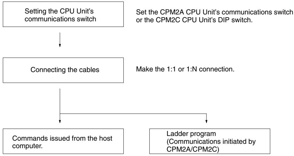
Application Procedure
Communications Switch Setting
The CPM2A's communications are controlled by the communications switch on the front of the CPU Unit and the CPM2C's communications are controlled by the DIP switch on the front of the CPU Unit.
CPM2A Communications Switch Setting
When the communications switch is set to OFF, communications through the peripheral port and RS-232C port are governed by the settings in the PC Setup. When the communications switch is set to ON, communications through the peripheral port and RS-232C port are governed by the standard Host Link settings (1 start bit, 7 data bits, 2 stop bits, even parity, and 9,600 bps baud rate).
Note When a Programming Console is connected to the peripheral port, communications with the Programming Console are unaffected by either the communications switch or PC Setup.
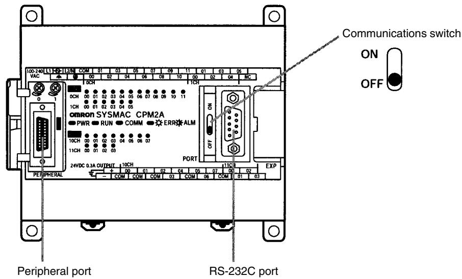
An RS-232C Adapter is needed to perform Host Link communications from a peripheral port.
CPM2C DIP Switch Settings
When SW2 is set to OFF, communications through the peripheral port are set to Programming Console protocol, regardless of the setting of pin 1 or the settings in the PC Setup.
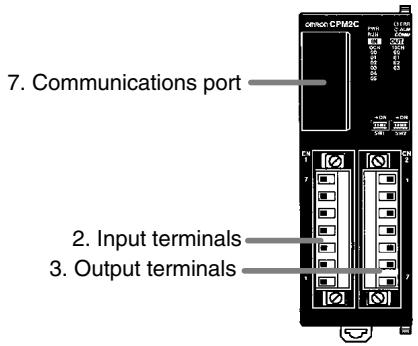
Front View
CPU Unit with Relay Outputs via Terminal Block
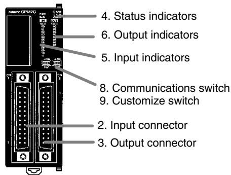
CPU Unit with Transistor Outputs via Fujitsu-compatible Connector
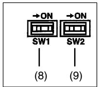
DIP switch for Units with 10/20 I/O points
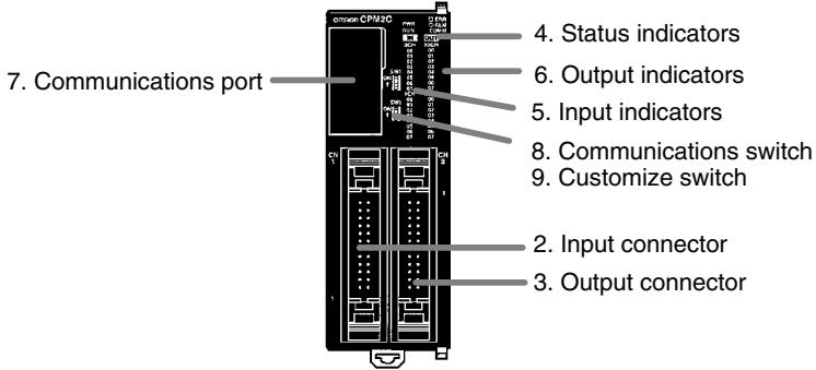
CPU Unit with Transistor Outputs via MIL Connector
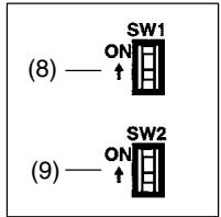
DIP switch for Units with 32 I/O points
When SW 2 is set to ON, the status of SW 1 determines whether communications through the peripheral port and RS-232C port are governed by the settings in the PC Setup or the standard settings (1 start bit, 7 data bits, 2 stop bits, even parity, and 9,600 bps baud rate).
| SW1 | Communications settings |
| OFF | The communications settings for the peripheral port and RS-232C port will be determined by the settings in the PC Setup (DM 6645 to DM 6649, DM 6650 to DM 6654). If a Programming Console is connected to the peripheral port, however, operation for that port will be in the Programming Console mode. |
| ON | The communications settings for the peripheral port and RS-232C port will be the standard settings. If a Programming Console is connected to the peripheral port, however, operation for that port will be in the Programming Console mode. |
An RS-232C Adapter is needed to perform Host Link communications from a peripheral port.
Note When performing host link communications via the peripheral port of a CPU Unit with a manufacturing number of 3180O or earlier (i.e., manufactured on or before April 31, 2000), set SW2 to ON. See above for details of the settings of SW2. When using a CPU Unit with a manufacturing number of 3180O or earlier (i.e., manufactured on or before April 31, 2000), do not change the setting of SW2 with a Programming Console, the CPM2C-CIF01-V1/11, or the CQM1-CIF01/02 connected. If the setting of SW2 is changed in this state, communications will be interrupted, and a communications error will be generated or the Programming Console will enter a "no-response" state (i.e., pressing the keys of the Programming Console will have no effect and the display will stay the same).
Connecting the Cables
This section describes RS-232C connections.
One-to-one Connections
The RS-232C port on the Host Link computer and the RS-232C port on the CPM2A/CPM2C or CPM1-CIF01 RS-232C Adapter are connected as shown in the following diagram when there is no CTS control on the RS-232C port. With the CPM2C, the CPM2C-CN111 and CS1W-CN118 connecting cables can be used in place of the RS-232C Adapter.
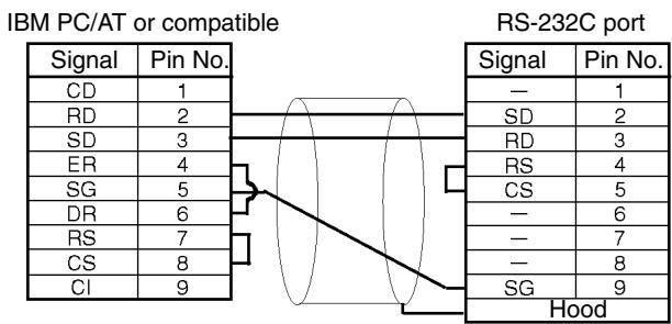
One-to-N Connections
Set the DIP switch on the NT-AL001 RS-232C/RS-422 Conversion Adapter.
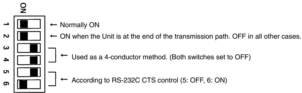
The RS-232C port with the NT-AL001 RS-232C/RS-422 Conversion Adapter and the RS-232C port of the CPM2A/CPM2C or CPM1-CIF01 RS-232C Adapter are connected as shown in the following diagram when there is no CTS control on the RS-232C port. A power supply of 5 VDC is supplied to the RS-232C/RS-422 Conversion Adapter. With the CPM2C, the CPM2C-CN111 and CS1W-CN118 connecting cables can be used in place of the RS-232C Adapter.
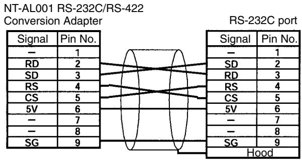
Note Do not connect external devices other than the NT-AL001 Conversion Adapter to the 5 VDC power supply of pin number 6 on the CPM2A/CPM2C's RS-232C port. Doing so may result in damage to the CPM2A/CPM2C or to the external device.
PC Setup
The PC Setup settings that are required depend on whether a peripheral port or an RS-232C port is used.
Settings for RS-232C Port
Note If SW1 on the front panel of the CPU Unit is ON, the RS-232C port will operate with the default settings regardless of the settings in DM 6645 to DM 6649.
| Word | Bit | Function | Setting | |||||
| DM 6645 | 00 to 03 | Port settings0: Standard (1 start bit, 7-bit data, 2 stop bits, even parity, 9,600 bps; Host Link unit number: 0)1: Settings in DM 6646(Other settings will cause a non-fatal error, the default setting will be used, and AR 1302 will turn ON.) | Match host parameters | |||||
| 04 to 07 | CTS control settings0: Disable; 1: Set | 0 or 1 | ||||||
| 08 to 11 | Link words for 1:1 PC Link0: LR 00 to LR 15; Other: Not effective | Any | ||||||
| 12 to 15 | Communications mode0: Host Link (default setting); 1: RS-232C (no-protocol); 2: 1:1 PC Link Slave; 3: 1:1 PC Link Master; 4: 1:1 NT Link(Other settings will cause a non-fatal error, the Host Link setting will be used, and AR 1302 will turn ON.) | 0 | ||||||
| DM 6646 | 00 to 07 | Baud rate:00: 1,200 bps 01: 2,400 bps 02: 4,800 bps 03: 9,600 bps 04: 19,200 bps | Match host parameters | |||||
| 08 to 15 | Frame formatStart Length Stop Parity00: 1 7 1 Even01: 1 7 1 Odd02: 1 7 1 None03: 1 7 2 Even04: 1 7 2 Odd05: 1 7 2 None06: 1 8 1 Even07: 1 8 1 Odd08: 1 8 1 None09: 1 8 2 Even10: 1 8 2 Odd11: 1 8 2 None(Other settings will cause a non-fatal error, the default settings (03) will be used, and AR 1302 will turn ON.) | |||||||
| DM 6647 | 00 to 15 | Transmission delay (Host Link)0000 to 9999 (BCD): Set in units of 10 ms, e.g., setting of 0001 equals 10 ms(Other settings will cause a non-fatal error, the default setting (0000) will be used, and AR 1302 will turn ON.) | 0000 to 9999 | |||||
| DM 6648 | 00 to 07 | 00 to 31 (BCD): Node number (Host Link)(Other settings will cause a non-fatal error, the default setting (00) will be used, and AR 1302 will turn ON.) | 00 to 31 | |||||
| 08 to 11 | Start code enable (RS-232C)0: Disable; 1: Use start code in DM 6649. | Any | ||||||
| 12 to 15 | End code enable (RS-232C)0: Disable (number of bytes received)1: Use end code in DM 6649.2: CR, LF(Other settings will cause a non-fatal error, the disable setting will be used, and AR 1302 will turn ON.) | Any | ||||||
| Word | Bit | Function | Setting |
| DM 6649 | 00 to 07 | Start code (01 to FF) (No-protocol, effective when bits 8 to 11 of DM 6648 are set to 1.) | Any |
| 00 to 15 | No. of bytes of data received (No-protocol, effective when bits 12 to 15 of DM 6648 are set to 0.) 00: 256 bytes 01 to FF: 1 to 255 bytes | Any | |
| End code (00 to FF) (No-protocol, effective when bits 12 to 15 of DM 6648 are set to 1.) |
Settings for Peripheral Port
| Word | Bit | Function | Setting | |||||
| DM 6650 | 00 to 03 | Port settings0: Standard (1 start bit, 7-bit data, 2 stop bits, even parity, 9,600 bps; Host Link unit number: 0)1: Settings in DM 6651(Other settings will cause a non-fatal error, the default setting (0) will be used, and AR 1302 will turn ON.) | Match host parameters | |||||
| 04 to 11 | Not used | 0 | ||||||
| 12 to 15 | Communications mode0: Host Link or peripheral bus; 1: No-protocol(Other settings will cause a non-fatal error, the Host Link setting (0) will be used, and AR 1302 will turn ON.) | 0 | ||||||
| DM 6651 | 00 to 07 | Baud rate00: 1,200 bps, 01: 2,400 bps, 02: 4,800 bps, 03: 9,600 bps, 04: 19,200 bps | Match host parameters | |||||
| 08 to 15 | Frame formatStart Length Stop Parity00: 1 7 1 Even01: 1 7 1 Odd02: 1 7 1 None03: 1 7 2 Even04: 1 7 2 Odd05: 1 7 2 None06: 1 8 1 Even07: 1 8 1 Odd08: 1 8 1 None09: 1 8 2 Even10: 1 8 2 Odd11: 1 8 2 None(Other settings will cause a non-fatal error, the default settings (03) will be used, and AR 1302 will turn ON.) | |||||||
| DM 6652 | 00 to 15 | Transmission delay (Host Link)0000 to 9999 (BCD): Set in units of 10 ms.(Other settings will cause a non-fatal error, the default setting (0000) will be used, and AR 1302 will turn ON.) | 0000 to 9999 | |||||
Note 1. If SW1 on the front panel of the CPU Unit is ON, the peripheral port will operate with the default settings regardless of the settings in DM 6645 to DM 6649.
- When connecting a computer running Support Software via the peripheral bus, turn OFF SW1 on the front panel of the CPU Unit and set DM 6650 to 0001 (Host Link). The CPU Unit will automatically switch to peripheral bus communications for the serial communications port.
| Word | Bit | Function | Setting |
| DM 6653 | 00 to 07 | Node number (Host Link)00 to 31 (BCD)(Other settings will cause a non-fatal error, the default setting (03) will be used, and AR 1302 will turn ON.) | 00 to 31 |
| 08 to 11 | Start code enable (Peripheral port)0: Disable1: Use start code in DM 6654. | Any | |
| 12 to 15 | End code enable (Peripheral port)0: Disable (number of bytes received)1: Use end code in DM 6654.2: CR, LF(Other settings will cause a non-fatal error, the disable setting (0) will be used, and AR 1302 will turn ON.) | Any | |
| DM 6654 | 00 to 07 | Start code(Peripheral port, effective when bits 08 to 11 of DM 6653 are set to 1.)01 to FF (Hex) | Any |
| 08 to 15 | No. of bytes of data received(Peripheral port, effective when bits 12 to 15 of DM 6653 are set to 0.)00: 256 bytes01 to FF: 1 to 255 bytes | Any | |
| End code (00 to FF)(Peripheral port, effective when bits 12 to 15 of DM 6653 are set to 1.) |
Issuing Commands from a Host Computer
This example shows a BASIC program that reads the status of the CPM2A/ CPM2C's inputs in IR 000. For more details see 4-5 Host Link Commands.
An FCS (frame check sequence) check isn't performed on the received response data in this program.
Be sure that the host computer's RS-232C port is configured correctly before executing the program.
1000 '
1010 ' CPM2A/CPM2C Sample Program for BASIC
1020 '
1050 '
1060 ' --Set value RS-232C SPEED:9600BPS,PARITY:EVEN,DATA:7,STOP:2---
1070 OPEN "COM:E73" AS #1
1080 *REPEAT
1090 --Transmission data input--
1100 INPUT " send data : ",send$
1110 ' --FCS Calculation--
1120 FCS=0
1130 FOR IFCS = 1 TO LEN ( send$ )
1140 FCS = FCS XOR ASC(MID(SEND,IFCS,1))
1150 NEXT
1160 FCS= RIGHT( "0" + HEX$( FCS),2)
1170 ' --Communications execute--
1180 ZZ= SEND + SCS+ "* " + CHR(13)
1190 PRINT #1 , ZZZ$ ;
1200 ' --Response check--
1210 RECCNT = 0 : TMP$ - ""
1220 *DRECLOOP
1230 IF LOC(1) < > 0 THEN *DREC1
1240 RECCNT = RECCNT + 1
1250 IF RECCNT = 5000 THEN *DRECERR ELSE *DRECLOOP
1260 *DREC1
1270 TMP= TMP + INPUT$(LOC(1),#1)
1280 IF RIGHT(TMP,1) = CHR$(13) THEN *DRECEND ELSE RECCNT = 0 : GOTO *DRECLOOP
1290 *DRECERR
1300 TMP= " No response ! " + CHR(13)
1310 *DRECEND
1320 PRINT "receive data : "; RECV$
1340 ' --Go to transmission data input--
1350 GOTO *REPEAT
1360 ' --Processing complete--
1370 CLOSE #1
1380 END
Ladder Program (Mnemonics)
The unsolicited Host Link communications are executed using TXD(48).
| Mnemonic | Control | Contents |
| (@)TXD(48) | Communications port output | Reads data from I/O memory and transmits it in the specified frame format. |
Host Link communications are controlled with the following AR area flags.
| Word | Bit(s) | Contents |
| AR 08 | 00 to 03 | RS-232C Port Error Code 0: Normal completion 1: Parity error 2: Frame error 3: Overrun error |
| 04 | RS-232C Communications Error Flag ON: RS-232C port communications error occurred OFF: Normal | |
| 05 | RS-232C Transmit Ready Flag ON: The PC is ready to transmit data. | |
| 08 to 11 | Peripheral Port Error Code 0: Normal completion 1: Parity error 2: Frame error 3: Overrun error | |
| 12 | Peripheral Port Communications Error Flag ON: Peripheral port communications error occurred. | |
| 13 | Peripheral Port Transmit Ready Flag ON: The PC is ready to transmit data. |
Unsolicited Communications
A data transmission to the host computer is initiated by the PC.
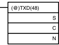
S: Leading address of data to be transmitted
C: Control data
N: Number of bytes to be transmitted (BCD: 0001 to 0061)
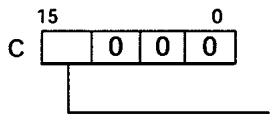
Communications port
0: RS-232 port; 1: Peripheral port
When Host Link communications are being used, TXD(48) converts the N-bytes of data starting at S to ASCII, adds the Host Link header, FCS, and terminator, and transmits this data as a Host Link frame.
The transmitted Host Link frame will be as shown in the following diagram.
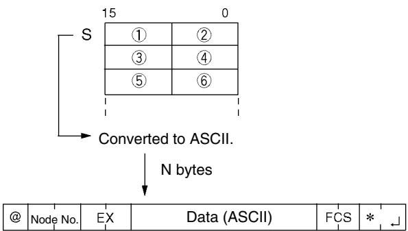
In the following program example TXD(48) is used to transmit data from an RS-232C port to a host computer. If AR 0805 (the RS-232C Transmit Ready Flag) is ON when IR 00100 turns ON, the ten bytes of data (DM 0100 to DM 0104) will be transmitted to the host computer, leftmost bytes first.
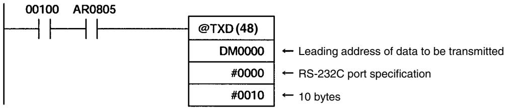
4-3-2 No-protocol Communications
Overview
When no-protocol communications are used, data can be exchanged with serial devices such as bar code readers and serial printers using TXD(48) and RXD(47). No-protocol communications can be used with either an RS-232C port or peripheral port.
CPM2A Connections
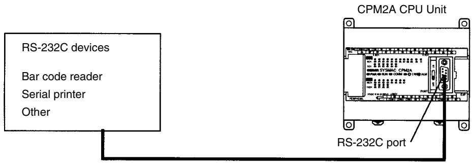
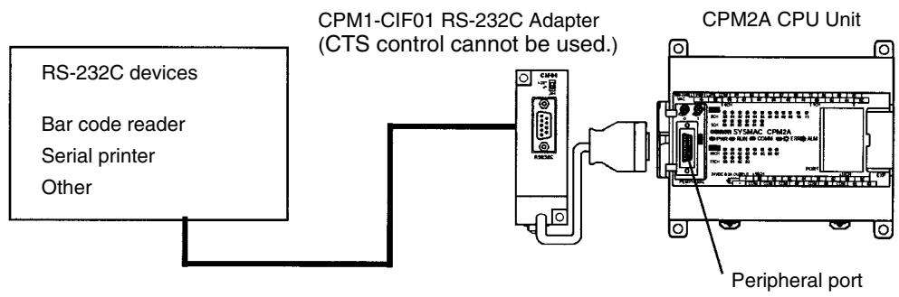
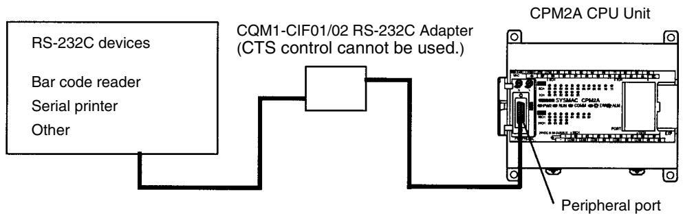
CPM2C Connections
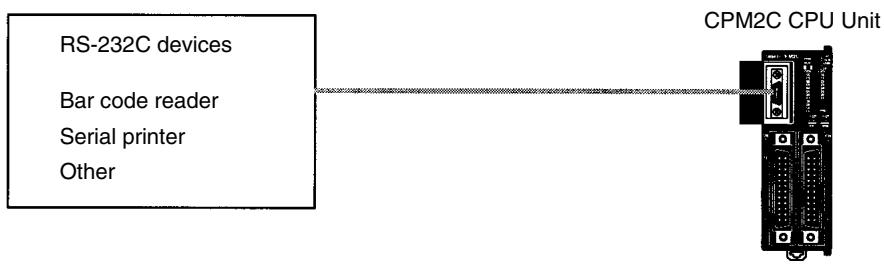
Note A CPM1-CIF01 RS-232C Adapter can also be used for no-protocol communications through the peripheral port, or for a CPM2C, a CPM2C-CIF01-V1 Peripheral/RS-232C Adapter Unit can be used to connect to external devices. Refer to the CPM2C Operation Manual for details.
Transmission Data Configuration
When no-protocol communications are used, TXD(48) is used to send data and RXD(47) to receive data. The maximum amount of data that can be either sent or received is 259 bytes, including the start and end codes.
No Start or End Code:
Data (Specified No. of bytes)
Only a Start Code:
ST
Data (Specified No. of bytes)
Only an End Code:
Data (256 bytes max.)
ED
Both a Start and End Code:
ST
Data (256 bytes max.)
ED
End Code of CR, LF:
Data (256 bytes max.)
CR
LF
Start Code 00-FF/End Code CR,LF:
| ST | Data (256 bytes max.) | CR | LF |
Note 1. The start and end codes are set in DM 6648 to DM 6649 (RS-232C) or DM 6653 to DM 6654 (peripheral port) in the PC Setup.
- When there are several start or end codes in the transmission, the first of each will be effective.
- When the end code is accidentally duplicated in the transmission data and the transmission is stopped part way through, use CR and LF as the end code.
- The start and end codes themselves are not transmitted and received.
Transmission Flags
When sending data from the CPM2A/CPM2C, check that the Transmission Enable Flag is ON for executing TXD(48). The Transmission Enable Flag will turn
OFF while the data is being transmitted and will turn ON again when transmission is complete.
After the CPM2A/CPM2C has received data, the Receive Enable Flag turns ON. When RXD(47) is executed, the data received will be written to the specified words and the Reception Complete Flag will turn OFF.
| Flag | Peripheral port | RS-232C port |
| Transmit Ready Flag | AR 0813 | AR 0805 |
| Reception Completed Flag | AR 0814 | AR 0806 |
Note The CPM2A/CPM2C starts and completes data reception at the following points:
Reception Start:
Start code disabled: Continually available for reception
Start code enabled: After start code is received
Reception Complete:
When either the end code, the specified no. of bytes, or 256 bytes are received.
Application Procedure
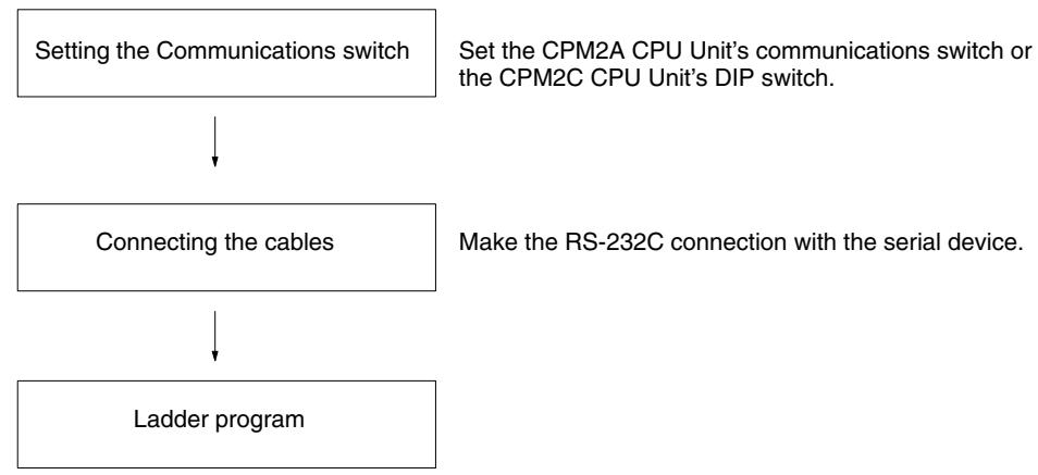
Communications Switch Setting
The CPM2A's communications are controlled by the communications switch on the front of the CPU Unit and the CPM2C's communications are controlled by the DIP switch on the front of the CPU Unit.
CPM2A Communications Switch Setting
Turn OFF the Communications switch when using no-protocol communications. No-protocol communications will not be possible if the communications switch is ON.
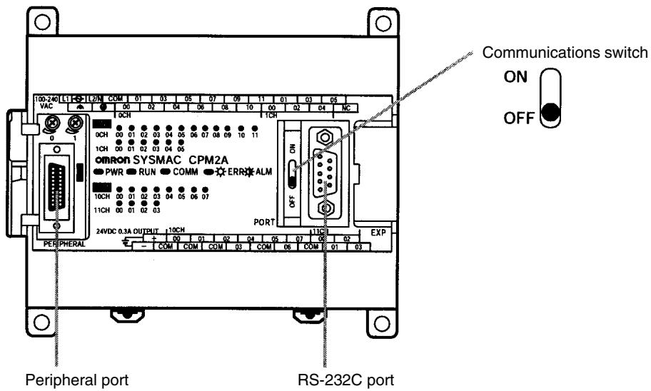
Note An RS-232C adapter is required for no-protocol communications on the peripheral port.
CPM2C DIP Switch Settings
Turn OFF pin 1 of the DIP switch when using no-protocol communications so that communications through the RS-232C port are governed by the settings in the PC Setup (DM 6645 to DM 6649).
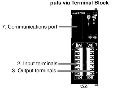
Front View
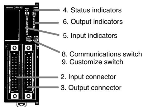
CPU Unit with Transistor Outputs via Fujitsu-compatible Connector
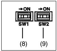
DIP switch for Units with 10/20 I/O points
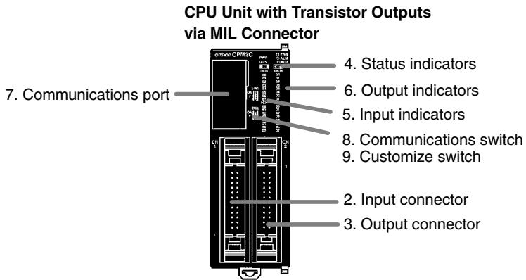
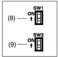
DIP switch for Units with 32 I/O points
| Pin settings | RS-232C port communications |
| Pin 1 | |
| OFF | Governed by the PC Setup (DM 6645 to DM 6649) |
| ON | Governed by standard settings |
Note An RS-232C Adapter is needed to perform no-protocol communications through the peripheral port.
Connecting the Cables
This section describes RS-232C connections.
The RS-232C port on the serial device and the RS-232C port of the CPM2A/ CPM2C or CPM1-CIF01 RS-232C Adapter are connected as shown in the fol
lowing diagram. With the CPM2C, the CPM2C-CN111 and CS1W-CN118 connecting cables can be used in place of the RS-232C Adapter.
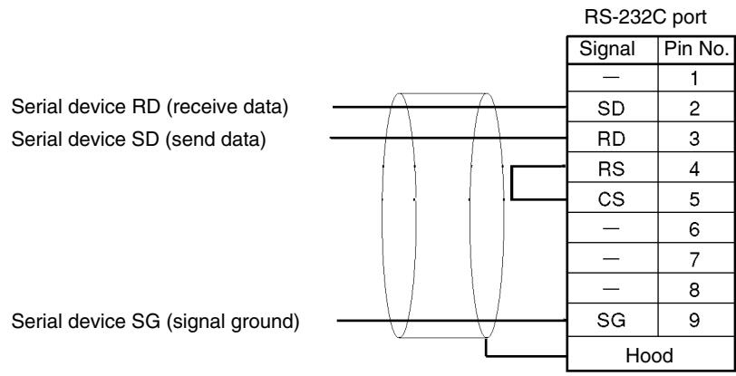
Recommended Cables
From Fujikura Densen
UL2464 AWG25X5P IFS-RVV-SB (UL-compliant)
AWG28X5P IFVV-SB (not UL-compliant)
From Hitachi
UL2464-SB (MA) 5PX28AWG (7/0.127) (UL-compliant)
CO-MA-VV-SB 5PX28AWG (7/0.127) (not UL-compliant)
PC Setup
The PC Setup settings that are required depend on whether a peripheral port or an RS-232C port is used.
Settings for RS-232C Port
| Word | Bit | Function | Setting |
| DM 6645 | 00 to 03 | Port settings 0: Standard (1 start bit, 7-bit data, 2 stop bits, even parity, 9,600 bps; Host Link unit number: 0) 1: Settings in DM 6646 (Other settings will cause a non-fatal error, the default setting will be used, and AR 1302 will turn ON.) | As required |
| 04 to07 | CTS control settings 0: Disable; 1: Set | ||
| 08 to 11 | Link words for 1:1 PC Link 0: LR 00 to LR 15; Other: Not effective | Any | |
| 12 to 15 | Communications mode 0: Host Link; 1: No-protocol; 2: 1:1 PC Link Slave; 3: 1:1 PC Link Master; 4: 1:1 NT Link (Other settings will cause a non-fatal error, the Host Link setting will be used, and AR 1302 will turn ON.) | 1 |
| Word | Bit | Function | Setting | ||||
| DM 6646 | 00 to 07 | Baud rate00: 1,200 bps; 01: 2,400 bps; 02: 4,800 bps; 3: 9,600 bps; 04: 19,200 bps | As required | ||||
| 08 to 15 | Frame formatStart Length Stop Parity00: 1 7 1 Even01: 1 7 1 Odd02: 1 7 1 None03: 1 7 2 Even04: 1 7 2 Odd05: 1 7 2 None06: 1 8 1 Even07: 1 8 1 Odd08: 1 8 1 None09: 1 8 2 Even10: 1 8 2 Odd11: 1 8 2 None(Other settings will cause a non-fatal error, the default settings (03) will be used, and AR 1302 will turn ON.) | ||||||
| DM 6647 | 00 to 15 | Transmission delay (Host Link)0000 to 9999 (BCD): Set in units of 10 ms, e.g., setting of 0001 equals 10 ms(Other settings will cause a non-fatal error, the default setting (0000) will be used, and AR 1302 will turn ON.) | 0000 to 9999 | ||||
| DM 6648 | 00 to 07 | 00 to 31 (BCD): Node number (Host Link)(Other settings will cause a non-fatal error, the default setting (00) will be used, and AR 1302 will turn ON.) | As required | ||||
| 08 to 11 | Start code enable (RS-232C)0: Disable; 1: Use start code in DM 6649. | 0 or 1 | |||||
| 12 to 15 | End code enable (RS-232C)0: Disable (number of bytes received)1: Use end code in DM 6649.2: CR, LF(Other settings will cause a non-fatal error, the default setting (0) will be used, and AR 1302 will turn ON.) | 0 to 2 | |||||
| DM 6649 | 00 to 07 | Start code (00 to FF)(No-protocol, effective when bits 8 to 11 of DM 6648 are set to 1.) | 00 to FF | ||||
| 08 to 15 | No. of bytes of data received(No-protocol, effective when bits 12 to 15 of DM 6648 are set to 0.)00: 256 bytes01 to FF: 1 to 255 bytes | 00 to FF | |||||
| End code (00 to FF)(No-protocol, effective when bits 12 to 15 of DM 6648 are set to 1.) | 00 to FF | ||||||
Note If SW1 on the front panel of the CPU Unit is ON, the RS-232C port will operate with the default settings regardless of the settings in DM 6645 to DM 6649.
Settings for Peripheral Port
| Word | Bit | Function | Setting |
| DM 6650 | 00 to 03 | Port settings 0: Standard (1 start bit, 7-bit data, 2 stop bits, even parity, 9,600 bps; Host Link unit number: 0) 1: Settings in DM 6651 (Other settings will cause a non-fatal error, the default setting (0) will be used, and AR 1302 will turn ON.) | As required |
| 04 to 11 | Not used | 0 | |
| 12 to 15 | Communications mode 0: Host Link or peripheral bus; 1: No-protocol (Other settings will cause a non-fatal error, the Host Link setting will be used, and AR 1302 will turn ON.) | 1 |
| Word | Bit | Function | Setting | ||||
| DM 6651 | 00 to 07 | Baud rate00: 1,200 bps; 01: 2,400 bps; 02: 4,800 bps; 03: 9,600 bps; 04: 19,200 bps | As required | ||||
| 08 to 15 | Frame formatStart Length Stop Parity00: 1 7 1 Even01: 1 7 1 Odd02: 1 7 1 None03: 1 7 2 Even04: 1 7 2 Odd05: 1 7 2 None06: 1 8 1 Even07: 1 8 1 Odd08: 1 8 1 None09: 1 8 2 Even10: 1 8 2 Odd11: 1 8 2 None(Other settings will cause a non-fatal error, the default settings (03) will be used, and AR 1302 will turn ON.) | ||||||
| DM 6652 | 00 to 15 | Transmission delay (Host Link)0000 to 9999 (BCD): Set in units of 10 ms.(Other settings will cause a non-fatal error, the default setting (0000) will be used, and AR 1302 will turn ON.) | 0000 to9999 | ||||
| DM 6653 | 00 to 07 | 00 to 31 (BCD): Node number (Host Link)(Other settings will cause a non-fatal error, the default setting (00) will be used, and AR 1302 will turn ON.) | As required | ||||
| 08 to 11 | Start code enable (Peripheral port)0: Disable1: Use start code in DM 6654. | 0 or 1 | |||||
| 12 to 15 | End code enable (Peripheral port)0: Disable (number of bytes received)1: Use end code in DM 6654.2: CR. LF(Other settings will cause a non-fatal error, the default setting (0) will be used, and AR 1302 will turn ON.) | 0 to 2 | |||||
| DM 6654 | 00 to 07 | Start code (00 to FF)(Peripheral port, effective when bits 8 to 11 of DM 6653 are set to 1.) | 00 to FF | ||||
| 08 to 15 | No. of bytes of data received(Peripheral port, effective when bits 12 to 15 of DM 6653 are set to 0.)00: 256 bytes01 to FF: 1 to 255 bytes | 00 to FF | |||||
| End code (00 to FF)(Peripheral port, effective when bits 12 to 15 of DM 6653 are set to 1) | 00 to FF | ||||||
Note
- If SW1 on the front panel of the CPU Unit is ON, the peripheral port will operate with the default settings regardless of the settings in DM 6645 to DM 6649.
- When connecting a computer running Support Software via the peripheral bus, turn OFF SW1 on the front panel of the CPU Unit and set DM 6650 to 0001 (Host Link). The CPU Unit will automatically switch to peripheral bus communications for the serial communications port.
Program
The following instructions are used in no-protocol communications.
| Mnemonic | Control | Contents |
| (@)TXD(48) | Communications port output | Reads data from I/O memory and transmits it in the specified frame format (the start and end codes can be enabled/disabled). |
| (@)RXD(47) | Communications port input | Receives data in the specified frame format (the start and end codes can be enabled/disabled) and stores only the data in I/O memory. |
No-protocol communications are controlled with the following AR area flags.
| Word | Bit(s) | Contents |
| AR 08 | 00 to 03 | RS-232C Port Error Code 0: Normal completion; 1: Parity error; 2: Frame error; 3: Overrun error |
| 04 | RS-232C Communications Error Flag ON: RS-232C port communications error occurred. OFF: Normal | |
| 05 | RS-232C Transmit Ready Flag ON: The PC is ready to transmit data. | |
| 06 | RS-232C Reception Completed Flag ON: The PC has completed reading data. | |
| 07 | RS-232C Reception Overflow Flag ON: A reception overflow has occurred. | |
| 08 to 11 | Peripheral Port Error Code 0: Normal completion; 1: Parity error; 2: Frame error; 3: Overrun error | |
| 12 | Peripheral Port Communications Error Flag ON: A peripheral port communications error occurred. OFF: Normal | |
| 13 | Peripheral Port Transmit Ready Flag ON: The PC is ready to transmit data. | |
| 14 | Peripheral Port Reception Completed Flag ON: The PC has completed reading data. | |
| 15 | Peripheral Port Reception Overflow Flag ON: A reception overflow has occurred. | |
| AR 09 | 00 to 15 | RS-232C Port Reception Counter (4 digits BCD) |
| AR 10 | 00 to 15 | Peripheral Port Reception Counter (4 digits BCD) |
No-protocol Data Transmission
TXD(48) is used to transmit data to RS-232C devices.
| (@)TXD(48) |
| S |
| C |
| N |
S: Leading address of data to be transmitted
C: Control data
N: Number of bytes to be transmitted (BCD: 0001 to 0256)

When no-protocol communications are being used, TXD(48) transmits N bytes of data beginning at S.
No-protocol Data Reception
RXD(47) is used to receive data from RS-232C devices.
| (@)RXD(47) |
| S |
| C |
| N |
D: Leading address for storing reception data
C: Control data
N: Number of bytes to receive (BCD: 0001 to 0256)
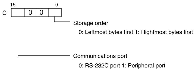
The following program example is for no-protocol communications conducted through a RS-232C port using TXD(48) and RXD(47) instructions.
If AR 0805 (the RS-232C Transmit Ready Flag) is ON when 00100 turns ON, then data from DM 0100 to DM 0104 is transmitted from leftmost bytes to rightmost bytes. When AR 0806 (the Reception Completed Flag) turns ON, 256 bytes of received data are read and written to DM 0200 from leftmost bytes to rightmost bytes.
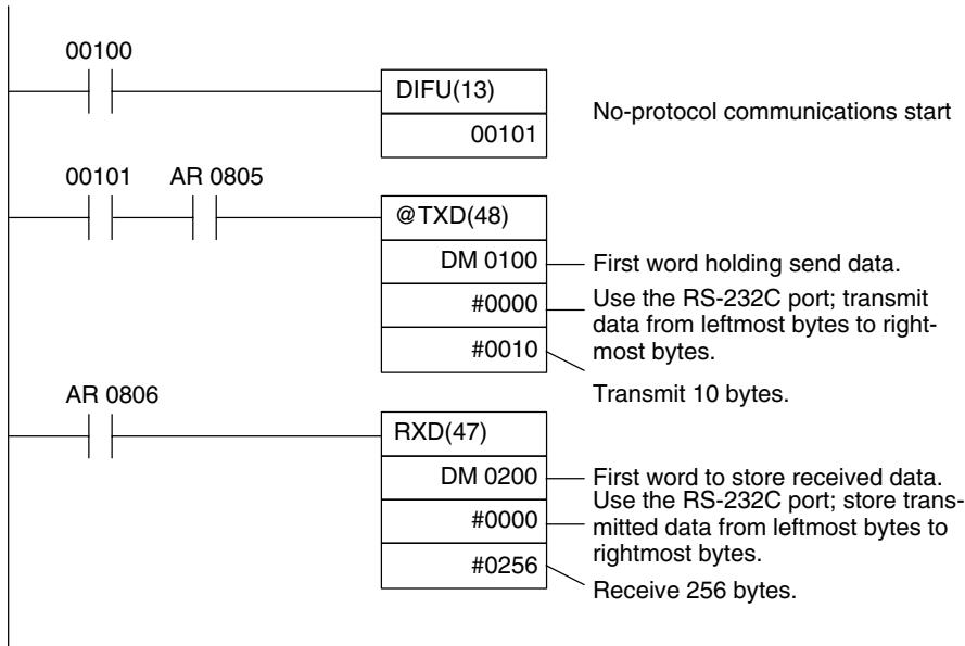
4-3-3 One-to-one NT Link Communications
The NT Link allows a CPM2A/CPM2C PC to be connected directly to an OMRON Programmable Terminal. There is no need for a communications program on the PC. The NT Link can be used with an RS-232C port.
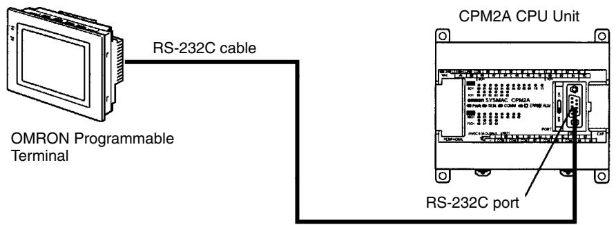
CPM2A Connection
CPM2C/CPM2C-S 1:1 NT Link Connection
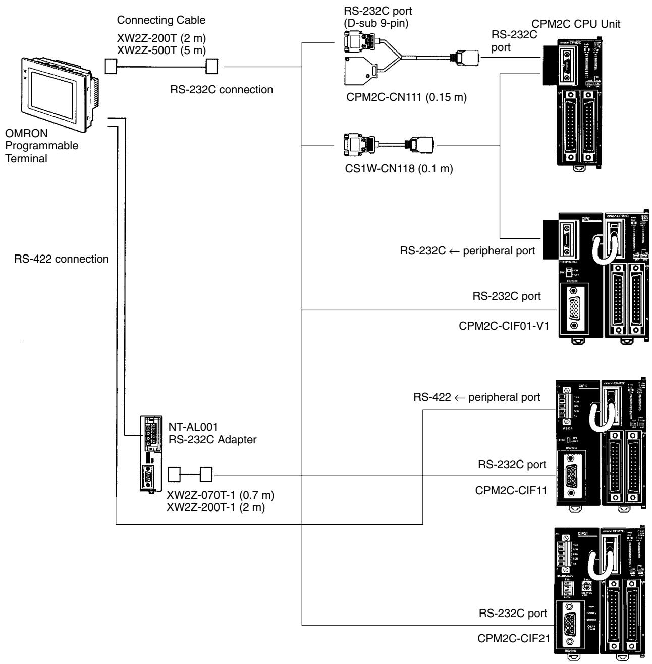
Note The Programmable Terminal cannot be connected using a peripheral port connection when communicating via a 1:1 NT Link.
Application Procedure
Communications Switch Setting
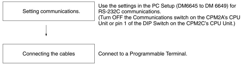
The CPM2A's communications are controlled by the communications switch on the front of the CPU Unit and the CPM2C's communications are controlled by the DIP switch on the front of the CPU Unit.
CPM2A Communications Switch Setting
Turn OFF the communications switch when using 1:1 NT Link communications. One-to-one NT Link communications will not be possible if the communications switch is ON.
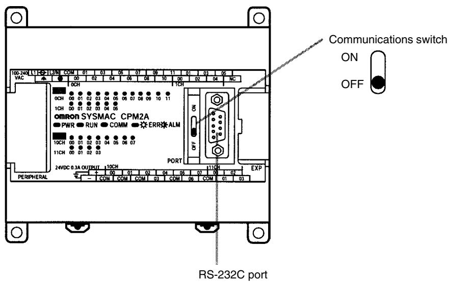
CPM2C DIP Switch Settings
Turn OFF pin 1 of the DIP switch when using 1:1 NT Link communications so that communications through the RS-232C port are governed by the settings in the PC Setup (DM 6645 to DM 6649).
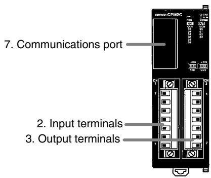
Front View
CPU Unit with Relay Outputs via Terminal Block
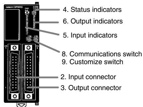
CPU Unit with Transistor Outputs via Fujitsu-compatible Connector
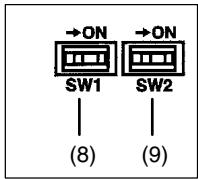
DIP switch for Units with 10/20 I/O points
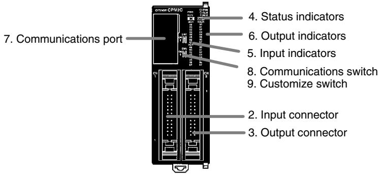
CPU Unit with Transistor Outputs via MIL Connector
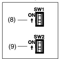
DIP switch for Units with 32 I/O points
| Pin settings | RS-232C port communications |
| Pin 1 | |
| OFF | Governed by the PC Setup (DM 6645 to DM 6649) |
| ON | Governed by standard settings |
When using an NT Link with a CPM2A/CPM2C PC, the following settings must be made to the PC Setup (DM 6645) using a Programming Device.
PC Setup
| Word | Bit | Function | Setting |
| DM 6645 | 00 to 03 | Port settings0: Standard (1 start bit, 7-bit data, 2 stop bits, even parity, 9,600 bps; Host Link unit number: 0)1: Settings in DM 6646(Other settings will cause a non-fatal error, the default setting (00) will be used, and AR 1302 will turn ON.) | Any |
| 04 to 07 | CTS control settings0: Disable1: Set | Any | |
| 08 to 11 | Link area for 1:1 PC Link0: LR 00 to LR 15(Other settings: Disabled) | Any | |
| 12 to 15 | Communications mode0: Host Link; 1: No-protocol; 2: 1:1 PC Link Slave; 3: 1:1 PC Link Master;4: 1:1 NT Link(Other settings will cause a non-fatal error, the Host Link setting will be used, and AR 1302 will turn ON.) | 4 |
For information on the 1:1 NT Link settings of an OMRON Programmable Terminal, refer to that PT's Operation Manual.
Connecting the Cables
This section describes RS-232C connections.
The RS-232C port on the Programmable Terminal and the RS-232C port on the CPM2A/CPM2C or CPM1-CIF01 RS-232C Adapter are connected as shown in the following diagram when there is no CTS control on the RS-232C port. With the CPM2C, the CPM2C-CN111 and CS1W-CN118 connecting cables are used.
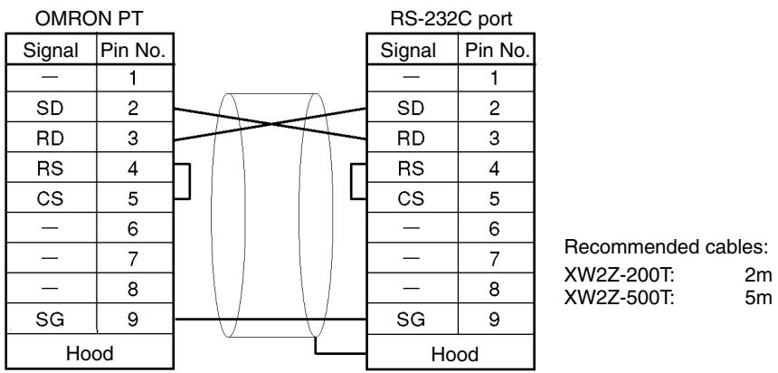
4-3-4 One-to-one PC Link Communications
A 1:1 PC Link of up to 256 bits (LR0000 to LR1515) can be created with the data area of another CPM2A/CPM2C, CQM1, CPM1, CPM1A, SRM1(-V2), or a C200HX/HG/HE PC, where one serves as the Master, the other as a Slave. There is no need for a communications program on the PC.
The 1:1 PC Link can be used with an RS-232C port.
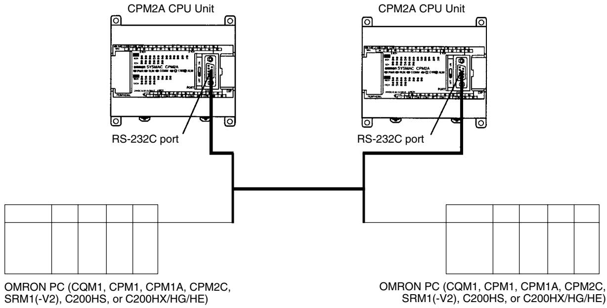
One-to-one PC Link
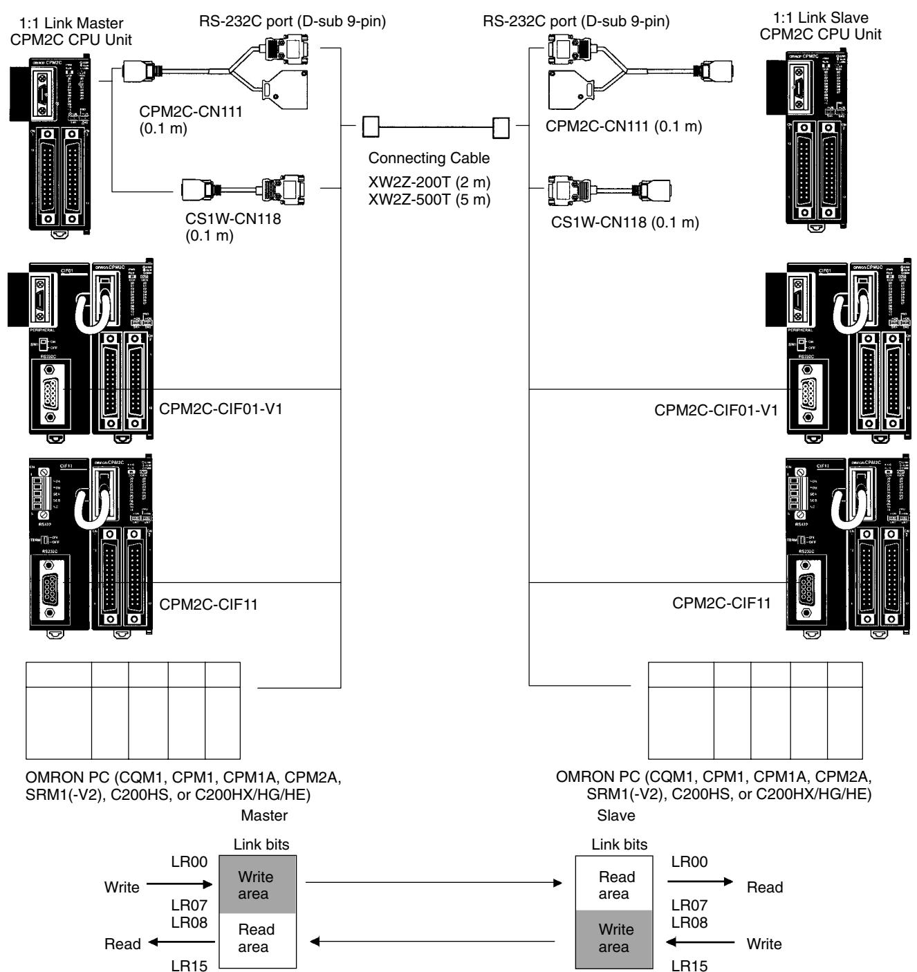
Note Even though the peripheral port on the CPM2C-CIF01-V1 can output RS-232C, this port cannot be used for one-to-one link communications.
PC Links with Other PCs
The link relay area on CPM2A/CPM2C PCs is only 16 words, LR00 to LR15. When performing a 1:1 PC Link with a CPM2A/CPM2C PC and a CQM1, C200HS, or C200HX/HE/HG use the corresponding 16 words, LR00 to LR15 on the CQM1, C200HS, or C200HX/HE/HG PC. A 1:1 PC Link with a CPM2A/ CPM2C PC cannot be formed using LR16 to LR 63.
Application Procedure
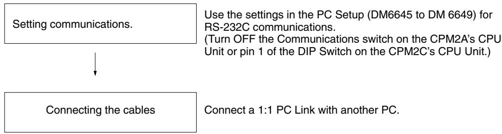
Communications Switch Setting
The CPM2A's communications are controlled by the communications switch on the front of the CPU Unit and the CPM2C's communications are controlled by the DIP switch on the front of the CPU Unit.
CPM2A Communications Switch Setting
Turn OFF the Communications switch when using 1:1 PC Link communications. One-to-one PC Link communications will not be possible if the communications switch is ON.
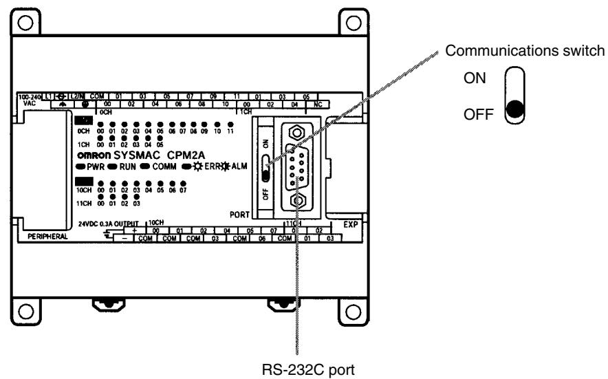
CPM2C DIP Switch Settings
Turn OFF pin 1 of the DIP switch when using 1:1 PC Link communications so that communications through the RS-232C port are governed by the settings in the PC Setup (DM 6645 to DM 6649).
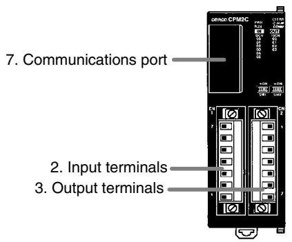
Front View
CPU Unit with Relay Outputs via Terminal Block
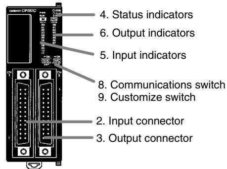
CPU Unit with Transistor Outputs via Fujitsu-compatible Connector
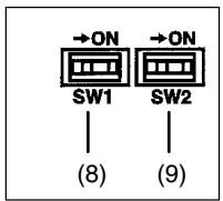
DIP switch for Units with 10/20 I/O points
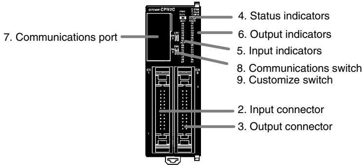
CPU Unit with Transistor Outputs via MIL Connector
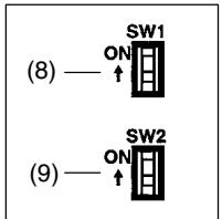
DIP switch for Units with 32 I/O points
| Pin settings | RS-232C port communications |
| Pin 1 | |
| OFF | Governed by the PC Setup (DM 6645 to DM 6649) |
| OFF | |
| ON | Governed by standard settings |
| ON |
PC Setup
When creating a 1:1 PC Link with a CPM2A/CPM2C PC, use a Programming Device to make the following settings to the PC Setup (DM 6645) in the Master and Slave.
| Word | Bit | Function | Master Setting | Slave Setting |
| DM 6645 | 00 to 03 | Port settings00: Standard (1 start bit, 7-bit data, 2 stop bits, even parity, 9,600 bps)01: Settings in DM 6646(Other settings will cause a non-fatal error, the default setting (00) will be used, and AR 1302 will turn ON.) | Any | Any |
| 04 to07 | CTS control settings0: Disable1: Set | 0 | 0 | |
| 08 to 11 | Link area for 1:1 PC Link0: LR 00 to LR 15(Other settings: Disabled) | 0 | 0 | |
| 12 to 15 | Communications mode0: Host Link; 1: No-protocol; 2: 1:1 PC Link Slave;3: 1:1 PC Link Master; 4: 1:1 NT Link(Other settings will cause a non-fatal error, the Host Link setting will be used, and AR 1302 will turn ON.) | 3 | 2 |
For information on the 1:1 PC Link settings of another OMRON PC, refer to that PC's Operation Manual.
Connecting the Cables
This section describes the RS-232C connection.
The RS-232C cable used for 1:1 PC Links is a cross connection cable. When there is no CTS control on the RS-232C port, the connection is made as shown in the following diagram. With the CPM2C, the CPM2C-CN111 and CS1W-CN118 connecting cables are used.
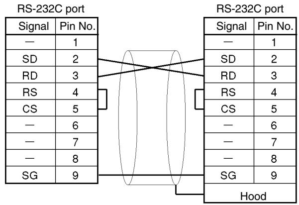
Recommended cables
XW2Z-200T: 2m
XW2Z-500T: 5m
4-4 SRM1(-V2) Communications Functions
4-4-1 Host Link Communications
Host Link communications were developed by OMRON for the purpose of connecting PCs and one or more host computers by RS-232C cable, and controlling PC communications from a host computer. Normally the host computer issues a command to a PC, and the PC automatically sends back a response. Thus the communications are carried out without the PCs being actively involved. The PCs also have the ability to initiate data transmissions when direct involvement is necessary.
In general, there are two means for implementing Host Link communications. One is based on C-mode commands, and the other on FINS (CV-mode) com
mands. The SRM1(-V2) supports C-mode commands only. For details on Host Link communications, refer to 4-5 Host Link Commands.
The SRM1(-V2)'s peripheral port and RS-232C port settings must be set properly in order to use the Host Link communications, as shown in the following table.
PC Setup Settings
| Word | Bit | Function | Setting | |||
| Peripheral Port SettingsThe following settings are effective after transfer to the PC. | ||||||
| DM 6650 | 00 to 03 | Port settings0: Standard (1 start bit, 7-bit data, 2 stop bits, even parity, 9,600 bps)1: Settings in DM 6651(Other settings will cause a non-fatal error, the default setting (0) will be used, and AR 1302 will turn ON.) | To match host pa-rameters | |||
| 04 to 07 | Not used. | 0 | ||||
| 08 to 11 | Not used. | 0 | ||||
| 12 to 15 | Communications mode0: Host Link; 1: No-protocol(Other settings will cause a non-fatal error, the default setting (0) will be used, and AR 1302 will turn ON.) | 0: Host Link | ||||
| DM 6651 | 00 to 07 | Baud rate00: 1.2K, 01: 2.4K, 02: 4.8K, 03: 9.6K, 04: 19.2K | To match host pa-rameters | |||
| 08 to 15 | Frame formatStartLengthStopParity00: 1 bit7 bits1 bitEven01: 1 bit7 bits1 bitOdd02: 1 bit7 bits1 bitNone03: 1 bit7 bits2 bitEven04: 1 bit7 bits2 bitOdd05: 1 bit7 bits2 bitNone06: 1 bit8 bits1 bitEven07: 1 bit8 bits1 bitOdd08: 1 bit8 bits1 bitNone09: 1 bit8 bits2 bitEven10: 1 bit8 bits2 bitOdd11: 1 bit8 bits2 bitNone(Other settings will cause a non-fatal error, the default setting (00) will be used, and AR 1302 will turn ON.) | To match host pa-rameters | ||||
| DM 6652 | 00 to 15 | Transmission delay (Host Link)0000 to 9999 (BCD): Set in units of 10 ms.(Other settings will cause a non-fatal error, the default setting (0000) will be used, and AR 1302 will turn ON.) | To match host pa-rameters | |||
| DM 6653 | 00 to 07 | Node number (Host Link)00 to 31 (BCD)(Other settings will cause a non-fatal error, the default setting (0000) will be used, and AR 1302 will turn ON.) | 00 to 31 | |||
| 08 to 11 | Start code enable (RS-232C, effective when bits 12 to 15 of DM 6650 are set to 1.)0: Disable1: Set | Any | ||||
| 12 to 15 | End code enable (RS-232C, effective when bits 12 to 15 of DM 6650 are set to 1.)0: Disable (number of bytes received)1: Set (specified end code)2: CR, LF | Any | ||||
| Word | Bit | Function | Setting |
| DM 6654 | 00 to 07 | Start code (effective when bits 08 to 11 of DM6650 are set to 1.)00: 256 bytes01 to FF: 1 to 255 bytes | Any |
| 08 to 15 | End code (no-protocol)When bits 12 to 15 of DM6653 are set to 0:00: 256 bytes01 to FF: 1 to 255 bytesWhen bits 12 to 15 of DM6653 are set to 1:Setting: 00 to FF (Hex) | Any |
Note If an out-of-range value is set, the following communications conditions will result. In that case, reset the value so that it is within the permissible range.
Communications mode: Host Link
Communications format: Standard settings
(1 start bit, 7-bit data; 2 stop bits, even parity, 9,600 bps)
Transmission delay: No
Node number: 00
| Word | Bit | Function | Setting | |||
| RS-232C Port SettingsThe following settings are effective after transfer to the PC. | ||||||
| DM 6645 | 00 to 03 | Port settings0: Standard (1 start bit, 7-bit data, 2 stop bits, even parity, 9,600 bps)1: Settings in DM 6646 | To match host pa-rameters | |||
| 04 to 07 | CTS control settings0: Disable; 1: Set | 0 | ||||
| 08 to 11 | When using a 1:1 PC Link: Sets the link words for 1:1 PC Link.0: LR 00 to LR 15Not 0: DisableWhen using a 1:N NT Link: Sets the maximum PT node number.1 to 7 | |||||
| 12 to 15 | Communications mode0: Host Link; 1: No-protocol; 2: 1:1 PC Link Slave; 3: 1:1 PC Link Master; 4: 1:1 NTLink; 5: 1:N NT Link(Any other setting specifies Host Link mode, causes a non-fatal error, and turns ONAR 1302.)The 1:N NT Link is supported by SRM1-C02-V2 only. | 0 | ||||
| DM 6646 | 00 to 07 | Baud rate00: 1.2K, 01: 2.4K, 02: 4.8K, 03: 9.6K, 04: 19.2K | To match host pa-rameters | |||
| 08 to 15 | Frame formatStartLengthStopParity00: 1 bit7 bits1 bitEven01: 1 bit7 bits1 bitOdd02: 1 bit7 bits1 bitNone03: 1 bit7 bits2 bitEven04: 1 bit7 bits2 bitOdd05: 1 bit7 bits2 bitNone06: 1 bit8 bits1 bitEven07: 1 bit8 bits1 bitOdd08: 1 bit8 bits1 bitNone09: 1 bit8 bits2 bitEven10: 1 bit8 bits2 bitOdd11: 1 bit8 bits2 bitNone | To match host pa-rameters | ||||
| DM 6647 | 00 to 15 | Transmission delay (Host Link)0000 to 9999 (BCD): Set in units of 10 ms, e.g., setting of 0001 equals 10 ms | To match host pa-rameters | |||
| Word | Bit | Function | Setting | |||
| DM 6648 | 00 to 07 | Node number (Host Link, effective when bits 12 to 15 of DM 6645 are set to 0.)00 to 31 (BCD) | 00 to 31 | |||
| 08 to 11 | Start code enable (RS-232C, effective when bits 12 to 15 of DM 6645 are set to 1.)0: Disable; 1: Set | Any | ||||
| 12 to 15 | End code enable (RS-232C, effective when bits 12 to 15 of DM 6645 are set to 1.)0: Disable (number of bytes received)1: Set (specified end code)2: CR, LF | Any | ||||
| DM 6649 | 00 to 07 | Start code (RS-232C)00: 256 bytes01 to FF: 1 to 255 bytes | Any | |||
| 08 to 15 | End code enable (RS-232C)00 to FF (BIN) | Any | ||||
| Note If an out-of-range value is set, the following communications conditions will result. In that case, reset the value so that it is within the permissible range.Communications mode: Host LinkCommunications format: Standard settings(1 start bit, 7-bit data; 2 stop bits, even parity,9,600 bps)Transmission delay: NoNode number: 00Example Program This example shows a BASIC program that reads the status of the SRM1(-V2)'s inputs in IR 000. For more details, refer to 4-5 Host Link Commands.An FCS (frame check sequence) check isn't performed on the received response data in this program. Be sure that the host computer's RS-232C port is configured correctly before executing the program. | ||||||
| 1000 '-------- | ||||||
| 1010 'SRM1 Sample Program for BASIC | ||||||
| 1020 '-------- | ||||||
| 1050 '-------- | ||||||
| 1060 '-------- Set value RS-232C SPEED:9600BPS, PARITY:EVENT, DATA:7, STOP:2 -- | ||||||
| 1070 OPEN "COM:E73" AS #1 | ||||||
| 1080 *REPEAT | ||||||
| 1090 'Transmission data input | ||||||
| 1100 INPUT "send data:",SEND | ||||||
| 1110 'FCS Calculation | ||||||
| 1120 FCS=0 | ||||||
| 1130 FOR IFCS=1 TO LEN(SEND) | ||||||
| 1140 FCS=FCS XOR ASC(MID(SEND;IFCS,1) | ||||||
| 1150 NEXT | ||||||
| 1160 FCS=RIGHT( "0" + HEX(FCS),2) | ||||||
| 1170 'Communications execute | ||||||
| 1180 ZZZ=SEND+FCS"*" + CHR(13) | ||||||
| 1190 PRINT #1,ZZZ; | ||||||
| 1200 '----- Response check | ||||||
| 1210 RECCNT=0:TMP="" | ||||||
| 1220 *DRECLoop | ||||||
| 1230 IF LOC(1) <> 0 THEN *DREC1 | ||||||
| 1240 RECCNT=RECCNT+1 | ||||||
| 1250 IF RECCNT=5000 THEN *DRECERR ELSE *DRECLOOP | ||||||
| 1260 *DREC1 | ||||||
| 1270 TMP=TMP+INPUT(LOC(1),#1) | ||||||
| 1280 IF RIGHT(TMP,1)=CHR$(13) THEN *DRECEND ELSE RECCNT=0:GOTO *DRECLOOP | ||||||
| 1290 *DRECERR | ||||||
1300 TMP ="No response!!"+CHR (13)
1310 DRECEND
1320 RECV=TMP
1330 PRINT "receive data:";RECV$
1340 '----- Go to transmission data input------
1350 GOTO REPEAT
1360 '----- Processing complete------
1370 CLOSE #1
1380 END
4-4-2 No-protocol Communications
This section explains no-protocol (RS-232C) communications. No-protocol communications allow data to be exchanged with standard RS-232C devices such as printers and bar code readers. Data can be printed out by a printer or read by a bar code reader. Handshaking is not supported for no-protocol communications.
Communications Procedure
Transmissions
1, 2, 3... 1. Check to see that AR 0805 (the RS-232C Port Transmit Ready Flag) has turned ON.
- Use the TXD(48) instruction to transmit the data.
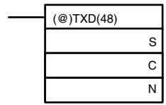
S: Leading word no. of data to be transmitted
C: Control data
N: Number of bytes to be transmitted (4 digits BCD), 0000 to 0256
From the time this instruction is executed until the data transmission is complete, AR 0805 ( or AR0813 for the peripheral port) will remain OFF. (It will turn ON again upon completion of the data transmission.)
Start and end codes are not included when the number of bytes to be transmitted is specified. The largest transmission that can be sent with or without start and end codes in 256 bytes, N will be between 254 and 256 depending on the designations for start and end codes. If the number of bytes to be sent is set to 0000, only the start and end codes will be sent.
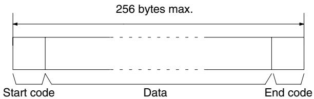
To reset the RS-232C port (i.e., to restore the initial status), turn on SR 25209. To reset the peripheral port, turn on SR 25208. These bits will turn OFF automatically after the reset.
Receptions
1, 2, 3... 1. Confirm that AR 0806 (RS-232C Reception Complete Flag) or AR 0814 (Peripheral Reception Complete Flag) is ON.
- Use the RXD(47) instruction to receive the data.
| (@)RXD(47) |
| D |
| C |
| N |
D: Leading word no. for storing reception data
C: Control data
Bits 00 to 03
0: Leftmost bytes first
1: Rightmost bytes first
Bits 12 to 15
0: RS-232C port
1: Peripheral port
N: Number of bytes stored (4 digits BCD), 0000 to 0256
- The results of reading the data received will be stored in the AR area. Check to see that the operation was successfully completed. The contents of these bits will be reset each time RXD(47) is executed.
| RS-232C port | Peripheral port | Error |
| AR 0800 to AR 0803 | AR 0808 to AR 0811 | RS-232C port error code (1 digit BCD) 0: Normal completion 1: Parity error 2: Framing error 3: Over-run error |
| AR 0804 | AR0812 | Communications error |
| AR 0807 | AR0815 | Reception Overrun Flag (After reception was completed, the subsequent data was received before the data was read by means of the RXD(47) instruction.) |
| AR 09 | AR10 | Number of bytes received |
To reset the RS-232C port (i.e., to restore the initial status), turn ON SR 25209. To reset the peripheral port, turn ON SR 25208. These bits will turn OFF automatically after the reset.
The start code and end code are not included in AR 09 or AR 10 (number of bytes received).
The data will be as follows: "31323132313231323132CR LF"
Peripheral Port Settings
When the peripheral port is used to conduct no-protocol communications, the following settings must be made from the Programming Device to DM 6650 to DM 6653 in the SRM1(-V2).
| Word | Bit | Function | Setting |
| Peripheral Port SettingsThe following settings are effective after transfer to the PC. | |||
| DM 6650 | 00 to 03 | Port settings0: Standard (1 start bit, 7-bit data, 2 stop bits, even parity, 9,600 bps)1: Settings in DM 6651(Other settings will cause a non-fatal error, the default setting (0) will be used, and AR 1302 will turn ON.) | As required |
| 04 to 07 | Not used. | 0 | |
| 08 to 11 | Not used. | 0 | |
| 12 to 15 | Communications mode0: Host Link; 1: No-protocol(Other settings will cause a non-fatal error, the default setting (0) will be used, and AR 1302 will turn ON.) | 1: No-pro-tocol | |
| Word | Bit | Function | Setting | ||||
| DM 6651 | 00 to 07 | Baud rate00: 1.2K, 01: 2.4K, 02: 4.8K, 03: 9.6K, 04: 19.2K | As required | ||||
| 08 to 15 | Frame formatStart Length Stop Parity00: 1 bit 7 bits 1 bit Even01: 1 bit 7 bits 1 bit Odd02: 1 bit 7 bits 1 bit None03: 1 bit 7 bits 2 bit Even04: 1 bit 7 bits 2 bit Odd05: 1 bit 7 bits 2 bit None06: 1 bit 8 bits 1 bit Even07: 1 bit 8 bits 1 bit Odd08: 1 bit 8 bits 1 bit None09: 1 bit 8 bits 2 bit Even10: 1 bit 8 bits 2 bit Odd11: 1 bit 8 bits 2 bit None(Other settings will cause a non-fatal error, the default setting (00) will be used, and AR 1302 will turn ON.) | As required | |||||
| DM 6652 | 00 to 15 | Transmission delay (Host Link)0000 to 9999 (BCD): Set in units of 10 ms.(Other settings will cause a non-fatal error, the default setting (0000) will be used, and AR 1302 will turn ON.) | To match host parameters | ||||
| DM 6653 | 00 to 07 | Node number (Host Link)00 to 31 (BCD)(Other settings will cause a non-fatal error, the default setting (0000) will be used, and AR 1302 will turn ON.) | 00 to 31 | ||||
| 08 to 11 | Start code enable (RS-232C, effective when bits 12 to 15 of DM 6650 are set to 1.)0: Disable1: Set | As required | |||||
| 12 to 15 | End code enable (RS-232C, effective when bits 12 to 15 of DM 6650 are set to 1.)0: Disable (number of bytes received)1: Set (specified end code)2: CR, LF | As required | |||||
| DM 6654 | 00 to 07 | Start code (effective when bits 08 to 11 of DM6650 are set to 1.)00: 256 bytes01 to FF: 1 to 255 bytes | As required | ||||
| 08 to 15 | End code (no-protocol)When bits 12 to 15 of DM6653 are set to 0:00: 256 bytes01 to FF: 1 to 255 bytesWhen bits 12 to 15 of DM6653 are set to 1:Setting: 00 to FF (Hex) | As required | |||||
Note If an out-of-range value is set, the following communications conditions will result. In that case, reset the value so that it is within the permissible range.
Communications mode: Host Link
Communications format: Standard settings
(1 start bit, 7-bit data; 2 stop bits, even parity, 9,600 bps)
Transmission delay: No
Node number: 00
RS-232C Port Settings
When the RS-232C port is used to conduct no-protocol communications, the following settings must be made from the Programming Device to DM 6645 to DM 6649 in the SRM1(-V2).
| Word | Bit | Function | Setting | |||
| RS-232C Port SettingsThe following settings are effective after transfer to the PC. | ||||||
| DM 6645 | 00 to 03 | Port settings0: Standard (1 start bit, 7-bit data, 2 stop bits, even parity, 9,600 bps)1: Settings in DM 6646 | As required | |||
| 04 to 07 | CTS control settings0: Disable; 1: Set | |||||
| 08 to 11 | When using a 1:1 PC link: Sets the link words for 1:1 PC Link.0: LR 00 to LR 15Not 0: DisableWhen using a 1:N NT Link: Sets the maximum PT node number.1 to 7The 1:N NT Link is supported by SRM1-C02-V2 only. | 0 | ||||
| 12 to 15 | Communications mode0: Host Link; 1: No-protocol; 2: 1:1 PC Link Slave; 3: 1:1 PC Link Master; 4: 1:1 NTLink; 5: 1:N NT Link(Any other setting specifies Host Link mode, causes a non-fatal error, and turns ONAR 1302.)The 1:N NT Link is supported by SRM1-C02-V2 only. | 1 | ||||
| DM 6646 | 00 to 07 | Baud rate00: 1.2K, 01: 2.4K, 02: 4.8K, 03: 9.6K, 04: 19.2K | As required | |||
| 08 to 15 | Frame formatStartLengthStopParity00: 1 bit7 bits1 bitEven01: 1 bit7 bits1 bitOdd02: 1 bit7 bits1 bitNone03: 1 bit7 bits2 bitEven04: 1 bit7 bits2 bitOdd05: 1 bit7 bits2 bitNone06: 1 bit8 bits1 bitEven07: 1 bit8 bits1 bitOdd08: 1 bit8 bits1 bitNone09: 1 bit8 bits2 bitEven10: 1 bit8 bits2 bitOdd11: 1 bit8 bits2 bitNone | As required | ||||
| DM 6647 | 00 to 15 | Transmission delay (Host Link)0000 to 9999 (BCD): Set in units of 10 ms, e.g., setting of 0001 equals 10 ms | As required | |||
| DM 6648 | 00 to 07 | Node number (Host Link, effective when bits 12 to 15 of DM 6645 are set to 0.)00 to 31 (BCD) | As required | |||
| 08 to 11 | Start code enable (RS-232C, effective when bits 12 to 15 of DM 6645 are set to 1.)0: Disable; 1: Set | As required | ||||
| 12 to 15 | End code enable (RS-232C, effective when when bits 12 to 15 of DM 6645 are set to 1.)0: Disable (number of bytes received)1: Set (specified end code)2: CR, LF | |||||
| DM 6649 | 00 to 07 | Start code (RS-232C)00: 256 bytes01 to FF: 1 to 255 bytes | ||||
| 08 to 15 | End code enable (RS-232C)00 to FF (BIN) | |||||
Note If an out-of-range value is set, the following communications conditions will result. In that case, reset the value so that it is within the permissible range.
Communications mode: Host Link
Communications format: Standard settings
(1 start bit, 7-bit data; 2 stop bits, even parity, 9,600 bps)
Transmission delay: No
Transmission Data Configuration
Node number: 00
When no-protocol communications are used, TXD(48) is used to send data and RXD(47) to receive data. The maximum amount of data that can be either sent or received is 259 bytes, including the start/end code.
- No Start or End Code:
Data (256 bytes max.)
- Only a Start Code:
| ST | Data (256 bytes max.) |
- Only an End Code:
| Data (256 bytes max.) | ED |
- Both an Start and End Code:
| ST | Data (256 bytes max.) | ED |
End Code of CR, LF:
| Data (256 bytes max.) | CR | LF |
- Start Code 00-FF/End Code CR,LF:
| ST | Data (256 bytes max.) | CR | LF |
Note 1. The start and end codes are set in DM 6648 to DM 6649 and DM 6653 to DM 6654 of the PC Setup.
- When there are several start and end codes, the first part of each will be effective.
- When the end code duplicates the transmission data and the transmission is stopped part way through, use CR or LF as the end code.
- The start and end codes are not stored.
When sending data from the SRM1(-V2), check that the Transmission Enable Flag is ON for executing the TXD(48) instruction. The Transmission Enable Flag will turn OFF while the data is being transmitted and will turn ON again when transmission is complete.
Transmission Flags
After the SRM1(-V2) has received data, the Receive Enable Flag turns ON. When the RXD instruction is executed, the data received will be written to the specified words and the Reception Complete Flag will turn OFF.
| Flag | Peripheral port | RS-232C port |
| Transmission Enable Flag | AR 0813 | AR 0805 |
| Reception Complete Flag | AR 0814 | AR 0806 |
Note The timing from data reception starting to completion for the SRM1(-V2) is as indicated below.
Reception Start:
Without start code: Normal reception status
With start code: After start code is received.
Program Example
Reception Complete:
When either the end code, the specified no. of bytes, or 256 bytes are received.
The following program example is for no-protocol communication conducted through a RS-232C port using TXD(48) and RXD(47) instructions.
If AR 0805 (Transmission Enable Flag) is ON when 00100 is ON, then data from DM0100 to DM0104 is transmitted from higher to lower values. When AR 0806 (Reception Enable Flag) turns ON, 256 bytes of received data are read and written to DM 0200 from higher to lower values.
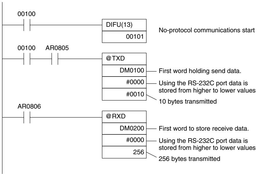
4-4-3 One-to-one NT Link Communications
Using the 1:1 NT Link, the SRM1(-V2) PC can be connected to the Programmable Terminal (NT Link Interface.) The RS-232C port can be used for the 1:1 NT Link.
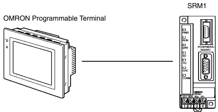
The 1:1 NT Link is possible only with the SRM1-C02-V1/-V2 PCs, which have an RS-232C port.
PC Setup Settings
The settings relating to 1:1 NT Link PC communications must be set as shown in the following table.
| Word | Bit | Function | Setting |
| DM 6645 | 00 to 03 | Port settings1 00: Standard (1 start bit, 7-bit data, 2 stop bits, even parity, 9,600 bps) 01: Settings in DM 6646 | 00 or 01 |
| 04 to 07 | CTS control settings 0: Disable 1: Set | 0 or 1 | |
| 08 to 11 | When using a 1:1 PC Link: Sets the link words for 1:1 PC Link. 0: LR 00 to LR 15 Not 0: Disable When using a 1:N NT Link: Sets the maximum PT node number. 1 to 7 The 1:N NT Link is supported by SRM1-C02-V2 only. | Any | |
| 12 to 15 | Communications mode¹ 0: Host Link; 1: No-protocol; 2: 1:1 PC Link Slave; 3: 1:1 PC Link Master; 4: 1:1 NT Link; 5: 1:N NT Link The 1:N NT Link is supported by SRM1-C02-V2 only. | 4 |
Note 1. If an improper setting is used, a non-fatal error will occur, AR 1302 will be turned ON, and the default setting (0 or 00) will be used.
2. For information on the NT Link settings for another OMRON PC, refer to that PC's Operation Manual.
3. If an out-of-range value is set, the following communications conditions will result. In that case, reset the value so that it is within the permissible range.
Communications mode: Host Link
Communications format: Standard settings
(1 start bit, 7-bit data; 2 stop bits, even parity, 9,600 bps)
Transmission delay: No
Node number: 00
4-4-4 One-to-N NT Link Communications
The 1:N NT Link allows an SRM1(-V2) PC to be connected to as many as 8 OMRON Programmable Terminals (PTs) and direct access provides high-speed communications. The 1:N NT Link can be used with the RS-232C port.
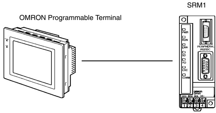
The 1:N NT Link is possible only with the SRM1-C02-V2 PCs, which have an RS-232C port.
Cable Connections
Refer to the SRM1 Master Control Units Operation Manual for information on cable connections in a 1:N NT Link.
PC Setup Settings
When the RS-232C port is used for a 1:N NT Link, make the following PC Setup settings from a Programming Device.
| Word | Bit | Function | Setting |
| DM 6645 | 00 to 03 | Port settings1 00: Standard (1 start bit, 7-bit data, 2 stop bits, even parity, 9,600 bps) 01: Settings in DM 6646 | 00 or 01 |
| 04 to 07 | CTS control settings 0: Disable 1: Set | 0 or 1 | |
| 08 to 11 | When using a 1:1 PC link: Sets the link words for 1:1 PC Link. 0: LR 00 to LR 15 Not 0: Disable When using a 1:N NT Link: Sets the maximum PT node number. 1 to 7 The 1:N NT Link is supported by SRM1-C02-V2 only. | 1 to 7 | |
| 12 to 15 | Communications mode1 0: Host Link; 1: No-protocol; 2: 1:1 PC Link Slave; 3: 1:1 PC Link Master; 4: 1:1 NT Link; 5: 1:N NT Link The 1:N NT Link is supported by SRM1-C02-V2 only. | 5 |
Note 1. If an improper setting is used, a non-fatal error will occur, AR 1302 will be turned ON, and the default setting (0 or 00) will be used.
2. For information on 1:N NT Link settings for OMRON PTs, refer to the PT's Operation Manual.
3. If an out-of-range value is set, the following communications conditions will result. In that case, reset the value so that it is within the permissible range.
Communications mode: Host Link
Communications format: Standard settings
(1 start bit, 7-bit data; 2 stop bits, even parity, 9,600 bps)
Transmission delay: No
Node number: 00
4-4-5 One-to-one PC Link Communications
In a 1:1 PC Link, an SRM1 is linked to another SRM1, CPM1, CPM1A, CPM2A, CPM2C, CQM1, C200HS, or C200HX/HG/HE PC through a standard RS-232C cable. One of the PCs will serve as the master and the other as the slave. The 1:1 PC Link can connect up to 256 bits (LR 0000 to LR 1515) in the two PCs.
One-to-one SRM1(-V2) PC Links
The following diagram shows a 1:1 PC Link between two SRM1(-V2)s.
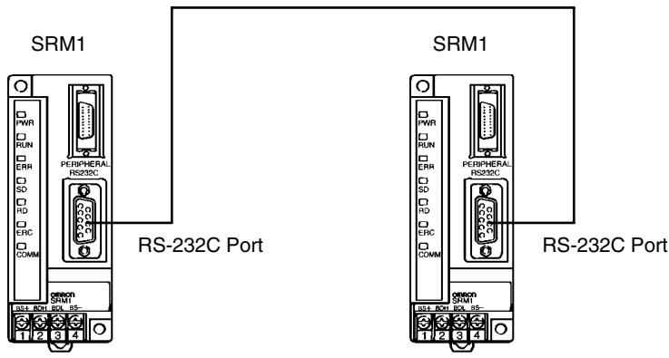
The words used for the 1:1 PC Link are as shown below.

Limitations of 1:1 PC Links with a SRM1(-V2)
A 1:1 PC Link is possible only with the SRM1-C02-V1/V2 PCs, which are equipped with an RS-232C port.
Only the 16 LR words from LR 00 to LR 15 can be linked in the SRM1, so use only those 16 words in the CQM1 or C200HS when making a 1:1 PC Link with one of those PCs. A 1:1 PC Link cannot be made to an SRM1 PC using LR 16 through LR 63 in the CQM1 or C200HS.
Cable Connections
Refer to the SRM1 Master Control Units Operation Manual for information on cable connections in a 1:1 PC Link.
PC Setup Settings
When an SRM1(-V2) is used in a 1:1 PC Link, make the following PC Setup settings from a Programming Device.
| Word | Bit | Function | Setting (Master) | Setting (Slave) |
| DM 6645 | 00 to 03 | Port settings100: Standard (1 start bit, 7-bit data, 2 stop bits, even parity, 9,600 bps)01: Settings in DM 6651 | 00 or 01 | 00 or 01 |
| 04 to 07 | CTS Control settings0: Disable1: Set | 0 | 0 | |
| 08 to 11 | When using a 1:1 PC Link: Sets the link words for 1:1 PC Link.0: LR 00 to LR 15Not 0: DisableWhen using a 1:N NT Link: Sets the maximum PT node number.1 to 7 | 0 | 0 | |
| 12 to 15 | Communications mode10: Host Link; 1: No-protocol; 2: 1:1 PC Link Slave; 3: 1:1 PC Link Master; 4:1:1 NT Link; 5: 1:N NT Link | 3 | 2 |
Note 1. If an improper setting is used, a non-fatal error will occur, AR 1302 will be turned ON, and the default setting (0 or 00) will be used.
- For information on the 1:1 PC Link settings for another OMRON PC, refer to that PC's Operation Manual.
- If an out-of-range value is set, the following communications conditions will result. In that case, reset the value so that it is within the permissible range.
Communications mode: Host Link
Communications format: Standard settings (1 start bit, 7-bit data; 2 stop bits, even parity, 9,600 bps)
Transmission delay: No
Node number: 00
Example Program
This example shows ladder programs that copy the status of IR 000 in each SRM1 to IR 200 in the other SRM1.
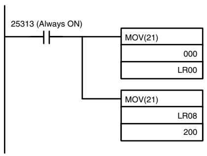
Program in the Master
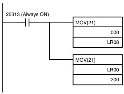
Program in the Slave

4-5 Host Link Commands
This section explains the commands that can be issued from the host computer to the PC.
4-5-1 IR/SR AREA READ - RR
Reads the contents of the specified number of IR and SR words, starting from the specified word.
Command Format

Note *Beginning word: 0000 to 0049 and 0200 to 0255 in CPM2A/CPM2C PCs, 0000 to 0019 and 0200 to 0255 in CPM1/CPM1A/SRM1(-V2) PCs. (A response of “0000” will be returned for non-existent IR and SR words.)
Response Format
An end code of 00 indicates normal completion.

Note 1. Words 0050 to 0199 cannot be specified in CPM2A/CPM2C PCs and words 0020 to 0199 cannot be specified in CPM1/CPM1A/SRM1(-V2) PCs. If an attempt to read any of these words is made, a response of 0000 will be returned.
2. The response will be divided when reading more than 30 words of data.
Parameters
Read Data (Response)
The contents of the number of words specified by the command are returned in hexadecimal as a response. The words are returned in order, starting with the specified beginning word.
4-5-2 LR AREA READ - RL
Reads the contents of the specified number of LR words, starting from the specified word.
Command Format

Note 1. Beginning word: 0000 to 0015
2. No. of words: 0001 to 0016
Response Format
An end code of 00 indicates normal completion.

Parameters
Read Data (Response)
The contents of the number of words specified by the command are returned in hexadecimal as a response. The words are returned in order, starting with the specified beginning word.
4-5-3 HR AREA READ - RH
Reads the contents of the specified number of HR words, starting from the specified word.
Command Format

Note 1. Beginning word: 0000 to 0019
2. No. of words: 0001 to 0020
Response Format
An end code of 00 indicates normal completion.

Parameters
Read Data (Response)
The contents of the number of words specified by the command are returned in hexadecimal as a response. The words are returned in order, starting with the specified beginning word.
4-5-4 PV READ - RC
Reads the contents of the specified number of timer/counter PVs (present values), starting from the specified timer/counter.
Command Format
| @ | x 10^1 | x 10^0 | R | C | x 10^3 | x 10^2 | x 10^1 | x 10^0 | x 10^3 | x 10^2 | x 10^1 | x 10^0 | * | \ | ||
| Node no. | Header code | Beginning timer/counter^1 | No. of timers/counter^2 | FCS | Terminator | |||||||||||
Note 1. Beginning T/C: 0000 to 0255 in CPM2A/CPM2C PCs, 0000 to 0127 in CPM1/CPM1A/SRM1(-V2) PCs
2. No. of T/Cs: 0001 to 0256 in CPM2A/CPM2C PCs, 0001 to 0128 in CPM1/CPM1A/SRM1(-V2) PCs
Response Format
An end code of 00 indicates normal completion.
| @ | x 10^1 | x 10^0 | R | C | x 16^1 | x 16^0 | x 10^3 | x 10^2 | x 10^1 | x 10^0 | * | \ | |||
| Node no. | Header code | End code | Read data (1 word) | FCS | Terminator | ||||||||||
| Read data (for number of words read) | |||||||||||||||
The response will be divided when reading more than 30 words of data.
Parameters
Read Data (Response)
The number of present values specified by the command is returned in hexadecimal as a response. The PVs are returned in order, starting with the specified beginning timer/counter.
4-5-5 TC STATUS READ - RG
Reads the status of the Completion Flags of the specified number of timers/ counters, starting from the specified timer/counter.
Command Format
| @ | x 10^1 | x 10^0 | R | G | x 10^3 | x 10^2 | x 10^1 | x 10^0 | x 10^3 | x 10^2 | x 10^1 | x 10^0 | * | \ | ||
| Node no. | Header code | Beginning timer/counter^1 | No. of timers/counter^2 | FCS | Terminator | |||||||||||
Note 1. Beginning T/C: 0000 to 0255 in CPM2A/CPM2C PCs, 0000 to 0127 in CPM1/CPM1A/SRM1(-V2) PCs
2. No. of T/Cs: 0001 to 0256 in CPM2A/CPM2C PCs, 0001 to 0128 in CPM1/CPM1A/SRM1(-V2) PCs
Response Format
An end code of 00 indicates normal completion.
| @ | x 10^1 | x 10^0 | R | G | x 16^1 | x 16^0 | ON/OFF | * | ↓ | |||
| Node no. | Header code | End code | Read data(1 timer/counter) | FCS | Terminator | |||||||
| Read data(for number of TC read) | ||||||||||||
The response will be divided when reading the status of more than 123 timer/ counters.
Parameters
Read Data (Response)
The status of the number of Completion Flags specified by the command is returned as a response. "1" indicates that the Completion Flag is ON.
4-5-6 DM AREA READ - RD
Reads the contents of the specified number of DM words, starting from the specified word.
Command Format
| @ | x 10^1 | x 10^0 | R | D | x 10^3 | x 10^2 | x 10^1 | x 10^0 | x 10^3 | x 10^2 | x 10^1 | x 10^0 | * | \(\longleftarrow\) | ||
| Node no. | Header code | Beginning word* | No. of words (0001 to 6656) | FCS | Terminator | |||||||||||
Note Beginning word:
DM 0000 to DM 1023 and DM 6144 to DM 6655 in CPM1/CPM1A PCs
DM 0000 to DM 2047 and DM 6144 to DM 6655 in CPM2A/CPM2C/SRM1(-V2) PCs. (A response of “0000” will be returned for non-existent DM words.)
Response Format
An end code of 00 indicates normal completion.
| @ | x 10^1 | x 10^0 | R | D | x 16^1 | x 16^0 | x 16^3 | x 16^2 | x 16^1 | x 16^0 | * | \(\longleftarrow\) | |||
| Node no. | Header code | End code | Read data (1 word) | FCS | Terminator | ||||||||||
| Read data (for number of words read) | |||||||||||||||
Note 1. Words DM 1024 to DM 6143 in CPM1/CPM1A PCs and words DM 2048 to DM 6143 in CPM2A/CPM2C/SRM1(-V2) PCs cannot be specified. If an attempt to read any of these words is made, a response of 0000 will be returned.
2. The response will be divided when reading more than 30 words of data.
Parameters
Read Data (Response)
The contents of the number of words specified by the command are returned in hexadecimal as a response. The words are returned in order, starting with the specified beginning word.
Note Be careful about the configuration of the DM area, as it varies depending on the CPU Unit model.
4-5-7 AR AREA READ - RJ
Reads the contents of the specified number of AR words, starting from the specified word.
Command Format
| @ | x 10^1 | x 10^0 | R | J | x 10^3 | x 10^2 | x 10^1 | x 10^0 | x 10^3 | x 10^2 | x 10^1 | x 10^0 | * | \(\urcorner\) | ||
| Node no. | Header code | Beginning word^1 | No. of words^2 | FCS | Terminator | |||||||||||
Note 1. Beginning word: 0000 to 0023 in CPM2A/CPM2C PCs, 0000 to 0015 in CPM1/CPM1A/SRM1(-V2) PCs
2. No. of words: 0001 to 0024 in CPM2A/CPM2C PCs, 0001 to 0016 in CPM1/CPM1A/SRM1(-V2) PCs
Response Format
An end code of 00 indicates normal completion.
| @ | x 10^1 | x 10^0 | R | J | x 16^1 | x 16^0 | x 16^3 | x 16^2 | x 16^1 | x 16^0 | * | \ | |||
| Node no. | Header code | End code | Read data (1 word) | FCS | Terminator | ||||||||||
| Read data (for number of words read) | |||||||||||||||
Parameters
Read Data (Response)
The contents of the number of words specified by the command are returned in hexadecimal as a response. The words are returned in order, starting with the specified beginning word.
4-5-8 IR/SR AREA WRITE - WR
Writes data to the IR and SR areas, starting from the specified word. Writing is done word by word.
Command Format

Note 1. Beginning word: 0000 to 0049 and 0200 to 0252 in CPM2A/CPM2C PCs, 0000 to 0019 and 0200 to 0252 in CPM1/CPM1A/SRM1(-V2) PCs. 2. Divide the command when writing more than 30 words of data.
Response Format
An end code of 00 indicates normal completion.
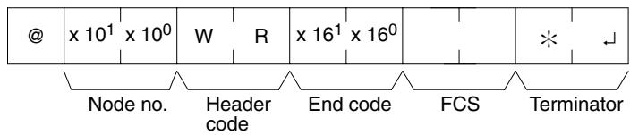
Note Words 0050 to 0199 cannot be specified in CPM2A/CPM2C PCs and words 0020 to 0199 cannot be specified in CPM1/CPM1A/SRM1(-V2) PCs. If an attempt is made to write to any of these words, the writing operation will not be executed and normal completion occurs.
Parameters
Write Data (Command)
Specify in order the contents of the number of words to be written to the IR or SR area in hexadecimal, starting with the specified beginning word.
Note If data is specified for writing which exceeds the allowable range, an error will be generated and the writing operation will not be executed. If, for example, 252 is specified as the beginning word for writing, and two words of data are specified, then 253 will become the last word for writing data, and the command will not be executed because SR 253 is beyond the writable range.
4-5-9 LR AREA WRITE - WL
Writes data to the LR area, starting from the specified word. Writing is done word by word.
Command Format

Note Beginning word: 0000 to 0015
Response Format
An end code of 00 indicates normal completion.
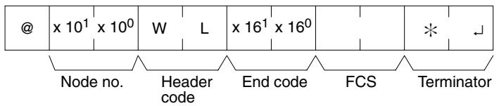
Parameters
Write Data (Command)
Specify in order the contents of the number of words to be written to the LR area in hexadecimal, starting with the specified beginning word.
Note If data is specified for writing which exceeds the allowable range, an error will be generated and the writing operation will not be executed. If, for example, 12 is specified as the beginning word for writing and five words of data are specified, then 16 will become the last word for writing data, and the command will not be executed because LR 16 is beyond area boundary.
4-5-10 HR AREA WRITE - WH
Writes data to the HR area, starting from the specified word. Writing is done word by word.
Command Format

Note Beginning word:0000 to 0019
Response Format
An end code of 00 indicates normal completion.
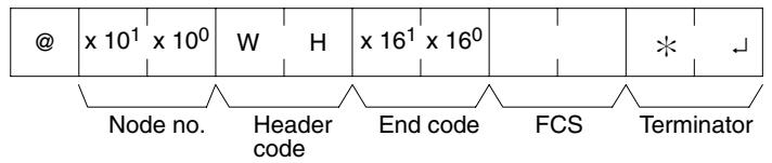
Parameters
Write Data (Command)
Specify in order the contents of the number of words to be written to the HR area in hexadecimal, starting with the specified beginning word.
Note If data is specified for writing which exceeds the allowable range, an error will be generated and the writing operation will not be executed. If, for example, 18 is specified as the beginning word for writing, and three words of data are specified, then 20 will become the last word for writing data, and the command will not be executed because HR 20 is beyond area boundary.
4-5-11 PV WRITE - WC
Writes the PVs (present values) of timers/counters starting from the specified timer/counter.
Command Format

Note 1. Beginning T/C: 0000 to 0255 in CPM2A/CPM2C PCs, 0000 to 0127 in CPM1/ CPM1A/SRM1(-V2) PCs
2. Divide the command when writing more than 29 words of data.
Response Format
An end code of 00 indicates normal completion.
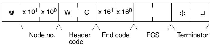
Parameters
Write Data (Command)
Specify in decimal numbers (BCD) the present values for the number of timers/ counters that are to be written, starting from the beginning timer/counter.
Note 1. When this command is used to write data to the PV area, the Completion Flags for the timers/counters that are written will be turned OFF.
2. If data is specified for writing which exceeds the allowable range, an error will be generated and the writing operation will not be executed. If, for example, 126 is specified as the beginning word for writing in a CPM1 PC, and three words of data are specified, then 128 will become the last word for writing data, and the command will not be executed because TC 128 is beyond area boundary.
4-5-12 TC STATUS WRITE - WG
Writes the status of the Completion Flags for timers and counters in the TC area, starting from the specified timer/counter (number). Writing is done number by number.
Command Format
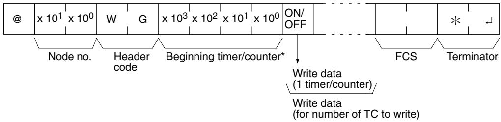
Note 1. Beginning T/C: 0000 to 0255 in CPM2A/CPM2C PCs, 0000 to 0127 in CPM1/ CPM1A/SRM1(-V2) PCs
2. Divide the command when writing the status of more than 118 timer/counters.
Response Format
An end code of 00 indicates normal completion.
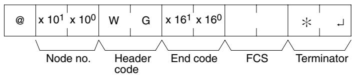
Parameters
Write Data (Command)
Specify the status of the Completion Flags, for the number of timers/counters to be written, in order (from the beginning word) as ON (i.e., "1") or OFF (i.e., "0"). When a Completion Flag is ON, it indicates that the time or count is up.
Note If data is specified for writing which exceeds the allowable range, an error will be generated and the writing operation will not be executed. If, for example, 126 is specified as the beginning word for writing in a CPM1 PC, and three words of data are specified, then 128 will become the last word for writing data, and the command will not be executed because TC 128 is beyond area boundary.
4-5-13 DM AREA WRITE - WD
Writes data to the DM area, starting from the specified word. Writing is done word by word.
Command Format

Note 1. Beginning word:
DM 0000 to DM 1023 and DM 6144 to DM 6655 in CPM1/CPM1A PCs
DM 0000 to DM 2047 and DM 6144 to DM 6655 in CPM2A/CPM2C/SRM1(-V2) PCs
- Divide the command when writing more than 29 words of data.
Response Format
An end code of 00 indicates normal completion.
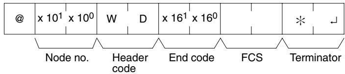
Note Words DM 1024 to DM 6143 in CPM1/CPM1A PCs and words DM 2048 to DM 6143 in CPM2A/CPM2C/SRM1(-V2) PCs cannot be specified. If an attempt is made to write to any of these words, the writing operation will not be executed for these words and the command will end normally.
Parameters
Write Data (Command)
Specify in order the contents of the number of words to be written to the DM area in hexadecimal, starting with the specified beginning word.
Note 1. If data is specified for writing which exceeds the allowable range, an error will be generated and the writing operation will not be executed. If, for example, 1022 is specified as the beginning word for writing in a CPM1 PC, and three words of data are specified, then 1024 will become the last word for writing data, and the command will not be executed because DM 1024 is beyond the writable range.
- Be careful about the configuration of the DM area, as it varies depending on the CPU Unit model.
4-5-14 AR AREA WRITE - WJ
Writes data to the AR area, starting from the specified word. Writing is done word by word.
Command Format

Note Beginning word: 0000 to 0023 in CPM2A/CPM2C PCs, 0000 to 0015 in CPM1/CPM1A and SRM1(-V2) PCs
Response Format
An end code of 00 indicates normal completion.
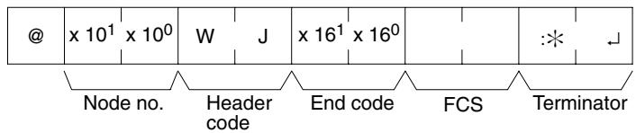
Parameters
Write Data (Command)
Specify in order the contents of the number of words to be written to the AR area in hexadecimal, starting with the specified beginning word.
Note If data is specified for writing which exceeds the allowable range, an error will be generated and the writing operation will not be executed. If, for example, 12 is specified as the beginning word for writing in a CPM1 PC, and five words of data are specified, then 16 will become the last word for writing data, and the command will not be executed because AR 16 is beyond the writable range.
4-5-15 SV READ 1 - R#
Searches for the first instance of a timer or counter instruction (TIM, TIMH(15), TIML(—), TMHH(—), CNT, or CNTR(12)) with the specified TC number in the user's program and reads the PV, which is assumed to be set as a constant. The SV that is read is a 4-digit decimal number (BCD). The program is searched from the beginning, which may take as much as 10 seconds to produce a response.
Command Format

Note TC number: 0000 to 0255 in CPM2A/CPM2C PCs and 0000 to 0127 in CPM1/CPM1A/SRM1(-V2) PCs
Response Format

Parameters
Name, TC Number (Command)
Specify the instruction for reading the SV in "Name." Make this setting in 4 characters. In "TC number," specify the timer/counter number used for the instruction.
| Name | Instruction name | |||
| OP1 | OP2 | OP3 | OP4 | |
| T | I | M | (Space) | TIMER |
| T | I | M | H | HIGH-SPEED TIMER |
| T | I | M | L | LONG TIMER |
| T | M | H | H | VERY HIGH-SPEED TIMER |
| C | N | T | (Space) | COUNTER |
| C | N | T | R | REVERSIBLE COUNTER |
SV (Response)
The constant SV is returned.
Note 1. The instruction specified under "Name" must be in four characters.
- If the same instruction is used more than once in a program, only the first one will be read.
- Use this command only when it is definite that a constant SV has been set.
- The response end code will indicate an error (16) if the SV wasn't entered as a constant.
Reads the constant SV or the word address where the SV is stored. The SV that is read is a 4-digit decimal number (BCD) written as the second operand for the TIM, TIMH(15), TIML(—), TMHH(—), CNT, or CNTR(12) instruction at the specified program address in the user's program. This can only be done with a program of less than 10K.
Command Format

Note TC number: 0000 to 0255 in CPM2A/CPM2C PCs and 0000 to 0127 in CPM1/CPM1A/SRM1(-V2) PCs
Response Format
An end code of 00 indicates normal completion.

Parameters
Name, TC Number (Command)
Specify the name of the instruction for reading the SV in "Name." Make this setting in 4 characters. In "TC number," specify the timer/counter number used by the instruction.
| Name | Instruction name | |||
| OP1 | OP2 | OP3 | OP4 | |
| T | I | M | (Space) | TIMER |
| T | I | M | H | HIGH-SPEED TIMER |
| T | I | M | L | LONG TIMER |
| T | M | H | H | VERY HIGH-SPEED TIMER |
| C | N | T | (Space) | COUNTER |
| C | N | T | R | REVERSIBLE COUNTER |
Operand, SV (Response)
The name that indicates the SV classification is returned to "Operand," and either the word address where the SV is stored or the constant SV is returned to "SV."
| Operand | Classification | Constant or word address | ||||
| OP1 | OP2 | OP3 | OP4 | CPM2A/ CPM2C PCs | CPM1 PCs | |
| C | I | O | (Space) | IR or SR | 0000 to 0049 | 0000 to 0019 |
| 0200 to 0255 | 0200 to 0255 | |||||
| L | R | (Space) | (Space) | LR | 0000 to 0015 | 0000 to 0015 |
| H | R | (Space) | (Space) | HR | 0000 to 0019 | 0000 to 0019 |
| A | R | (Space) | (Space) | AR | 0000 to 0023 | 0000 to 0015 |
| D | M | (Space) | (Space) | DM | 0000 to 6655 | 0000 to 6655 |
| D | M | * | (Space) | DM (indirect) | 0000 to 6655 | 0000 to 6655 |
| C | O | N | (Space) | Constant | 0000 to 9999 | 0000 to 9999 |
Note The instruction name specified under "Name" must be in four characters. Fill any gaps with spaces to make a total of four characters.
4-5-17 SV CHANGE 1 - W#
Searches for the first instance of the specified TIM, TIMH(15), TIML(—), TMHH(—), CNT, or CNTR(12) instruction in the user's program and changes the SV to new constant SV specified in the second word of the instruction. The program is searched from the beginning, and it may therefore take approximately 10 seconds to produce a response.
Command Format
| @ | x 10^1 | x 10^0 | W | # | OP1 | OP2 | OP3 | OP4 | x 10^3 | x 10^2 | x 10^1 | x 10^0 | x 10^3 | x 10^2 | x 10^1 | x 10^0 | * | - | ||
| Node no. | Header code | Name | TC number* | SV (0000 to 9999) | FCS | Terminator | ||||||||||||||
Note TC number: 0000 to 0255 in CPM2A/CPM2C PCs and 0000 to 0127 in CPM1/CPM1A/SRM1(-V2) PCs
Response Format
An end code of 00 indicates normal completion.
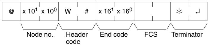
Parameters
Name, TC Number (Command)
In "Name," specify the name of the instruction, in four characters, for changing the SV. In "TC number," specify the timer/counter number used for the instruction.
| Instruction name | Classification | |||
| OP1 | OP2 | OP3 | OP4 | |
| T | I | M | (Space) | TIMER |
| T | I | M | H | HIGH-SPEED TIMER |
| T | I | M | L | LONG TIMER |
| T | M | H | H | VERY HIGH-SPEED TIMER |
| C | N | T | (Space) | COUNTER |
| C | N | T | R | REVERSIBLE COUNTER |
4-5-18 SV CHANGE 2 - W$
Changes the contents of the second word of the TIM, TIMH(15), TIML(—), TMHH(—), CNT, or CNTR(12) at the specified program address in the user's program. This can only be done with a program of less than 10K.
Command Format


Note TC number: 0000 to 0255 in CPM2A/CPM2C PCs and 0000 to 0127 in CPM1/CPM1A/SRM1(-V2) PCs
Response Format
An end code of 00 indicates normal completion.
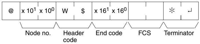
Parameters
Name, TC Number (Command)
In "Name," specify the name of the instruction, in four characters, for changing the SV. In "TC number," specify the timer/counter number used for the instruction.
| Instruction name | Classification | |||
| OP1 | OP2 | OP3 | OP4 | |
| T | I | M | (Space) | TIMER |
| T | I | M | H | HIGH-SPEED TIMER |
| T | I | M | L | LONG TIMER |
| T | M | H | H | VERY HIGH-SPEED TIMER |
| C | N | T | (Space) | COUNTER |
| C | N | T | R | REVERSIBLE COUNTER |
Operand, SV (Response)
In "Operand," specify the name that indicates the SV classification. Specify the name in four characters. In "SV," specify either the word address where the SV is stored or the constant SV.
| Operand | Classification | Constant or word address | ||||
| OP1 | OP2 | OP3 | OP4 | CPM2A/ CPM2C PCs | CPM1/CPM1A/ SRM1(-V2) PCs | |
| C | I | O | (Space) | IR or SR | 0000 to 0049 | 0000 to 0019 |
| 0200 to 0252 | 0200 to 0252 | |||||
| L | R | (Space) | (Space) | LR | 0000 to 0015 | 0000 to 0015 |
| H | R | (Space) | (Space) | HR | 0000 to 0019 | 0000 to 0019 |
| A | R | (Space) | (Space) | AR | 0000 to 0023 | 0000 to 0015 |
| D | M | (Space) | (Space) | DM | 0000 to 2047 | 0000 to 1023* |
| 6144 to 6655 | 6144 to 6655 | |||||
| D | M | * | (Space) | DM (indirect) | 0000 to 2047 | 0000 to 1023* |
| 6144 to 6655 | 6144 to 6655 | |||||
| C | O | N | (Space) | Constant | 0000 to 9999 | 0000 to 9999 |
Note *For SRM1(-V2) PCs, the DM range is from 0000 to 2047.
4-5-19 STATUS READ - MS
Reads the PC operating conditions.
Command Format
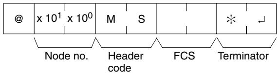
Response Format
An end code of 00 indicates normal completion.

Parameters
Status Data, Message (Response)
"Status data" consists of four digits (two bytes) hexadecimal. The leftmost byte indicates CPU Unit operation mode, and the rightmost byte indicates the size of the program area.
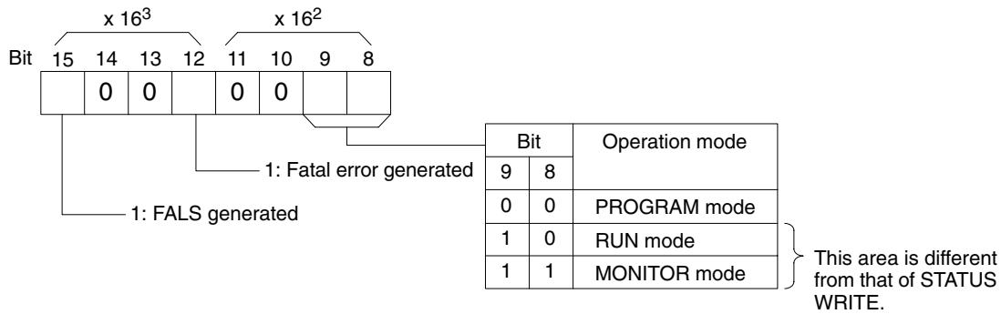
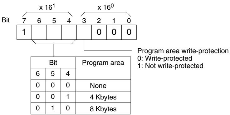
The "Message" parameter is a 16-character message that exists when MSG(47) has been executed. When there is no message, this parameter is omitted.
4-5-20 STATUS WRITE - SC
Changes the PC operating mode.
Command Format
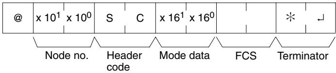
Response Format
An end code of 00 indicates normal completion.
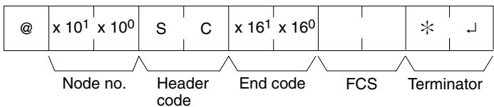
Parameters
Mode Data (Command)
"Mode data" consists of two digits (one byte) hexadecimal. With the leftmost two bits, specify the PC operating mode. Set all of the remaining bits to "0."
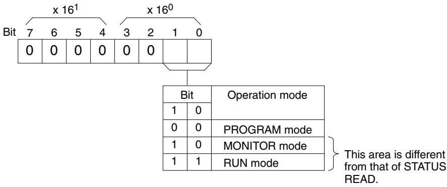
4-5-21 ERROR READ - MF
Reads and clears errors in the PC. Also checks whether previous errors have been cleared.
Command Format
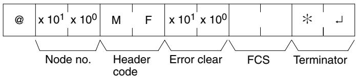
Response Format
An end code of 00 indicates normal completion.

Parameters
Error Clear (Command)
Specify 01 to clear errors and 00 to not clear errors (BCD). Fatal errors can be cleared only when the PC is in PROGRAM mode.
Error Information (Response)
The error information comes in two words.
CPM1/CPM1A/CPM2A/CPM2C PCs
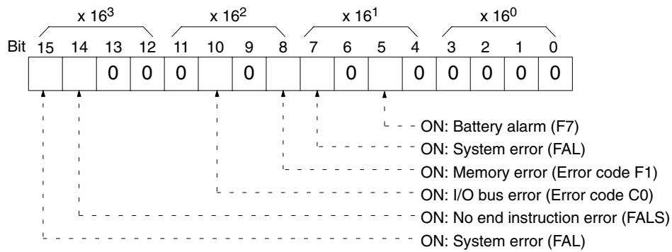
1st word
2nd word
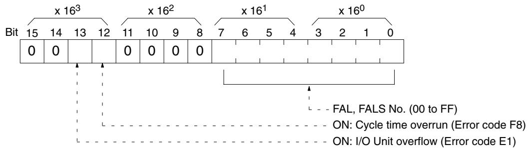
SRM1(-V2)PCs
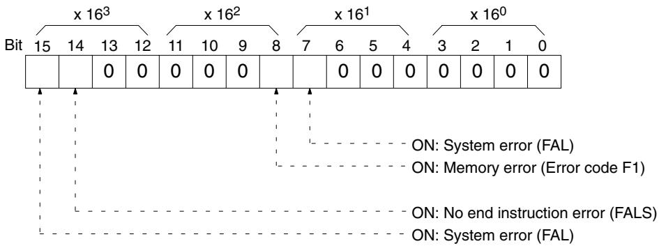
1st word
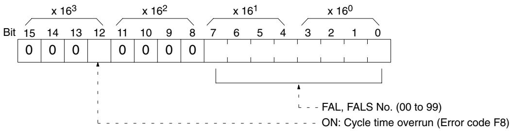
2nd word
4-5-22 FORCED SET - KS
Force sets a bit in the IR, SR, LR, HR, AR, or TC area. Just one bit can be force set at a time.
Once a bit has been forced set or reset, that status will be retained until a FORCED SET/RESET CANCEL (KC) command or the next FORCED SET/RESET command is transmitted.
Command Format

Response Format
An end code of 00 indicates normal completion.
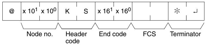
Parameters
Name, Word address, Bit (Command)
In “Name,” specify the area (i.e., IR, SR, LR, HR, AR, or TC) that is to be forced set. Specify the name in four characters. In “Word address,” specify the address of the word, and in “Bit” the number of the bit that is to be forced set.
| Name | Classification | Word address setting range | Bit | ||||
| OP1 | OP2 | OP3 | OP4 | CPM2A/ CPM2C PCs | CPM1/ CPM1A/ SRM1(-V2) PCs | ||
| C | I | O | (Space) | IR or SR | 0000 to 0049 | 0000 to 0019 | 00 to 15 (decimal) |
| 0200 to 0252 | 0200 to 0252 | ||||||
| L | R | (Space) | (Space) | LR | 0000 to 0015 | 0000 to 0015 | |
| H | R | (Space) | (Space) | HR | 0000 to 0019 | 0000 to 0019 | |
| A | R | (Space) | (Space) | AR | 0000 to 0023 | 0000 to 0015 | |
| T | I | M | (Space) | Completion Flag (timer) | 0000 to 0255 | 0000 to 0127 | Always 00 |
| T | I | M | H | Completion Flag (high-speed timer) | |||
| T | I | M | L | Completion Flag (long timer) | |||
| T | M | H | H | Completion Flag (very high-speed timer) | |||
| C | N | T | (Space) | Completion Flag (counter) | |||
| C | N | T | R | Completion Flag (reversible counter) | |||
Note The area specified under "Name" must be in four characters. Add spaces after the data area name if it is shorter than four characters.
4-5-23 FORCED RESET - KR
Force resets a bit in the IR, SR, LR, HR, AR, or TC area. Just one bit can be force reset at a time.
Once a bit has been forced set or reset, that status will be retained until a FORCED SET/RESET CANCEL (KC) command or the next FORCED SET/RESET command is transmitted.
Command Format

Response Format
An end code of 00 indicates normal completion.
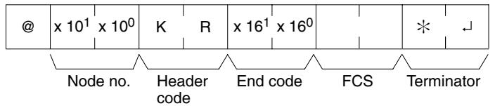
Parameters
Name, Word address, Bit (Command)
In "Name," specify the area (i.e., IR, SR, LR, HR, AR, or TC) that is to be forced reset. Specify the name in four characters. In "Word address," specify the address of the word, and in "Bit" the number of the bit that is to be forced reset.
| Name | Classification | Word address setting range | Bit | ||||
| OP1 | OP2 | OP3 | OP4 | CPM2A/CPM2C PCs | CPM1/CPM1A/SRM1(-V2)PCs | ||
| C | I | O | (Space) | IR or SR | 0000 to 00490200 to 0252 | 0000 to 00190200 to 0252 | 00 to 15 (decimal) |
| L | R | (Space) | (Space) | LR | 0000 to 0015 | 0000 to 0015 | |
| H | R | (Space) | (Space) | HR | 0000 to 0019 | 0000 to 0019 | |
| A | R | (Space) | (Space) | AR | 0000 to 0023 | 0000 to 0015 | |
| T | I | M | (Space) | Completion Flag (timer) | 0000 to 0255 | 0000 to 0127 | Always 00 |
| T | I | M | H | Completion Flag (high-speed timer) | |||
| T | I | M | L | Completion Flag (long timer) | |||
| T | M | H | H | Completion Flag (very high-speed timer) | |||
| C | N | T | (Space) | Completion Flag (counter) | |||
| C | N | T | R | Completion Flag (reversible counter) | |||
Note The area specified under "Name" must be in four characters. Add spaces after the data area name if it is shorter than four characters.
4-5-24 MULTIPLE FORCED SET/RESET - FK
Force sets, force resets, or cancels the status of the bits in one word in the IR, SR, LR, HR, AR, or TC area.
Command Format
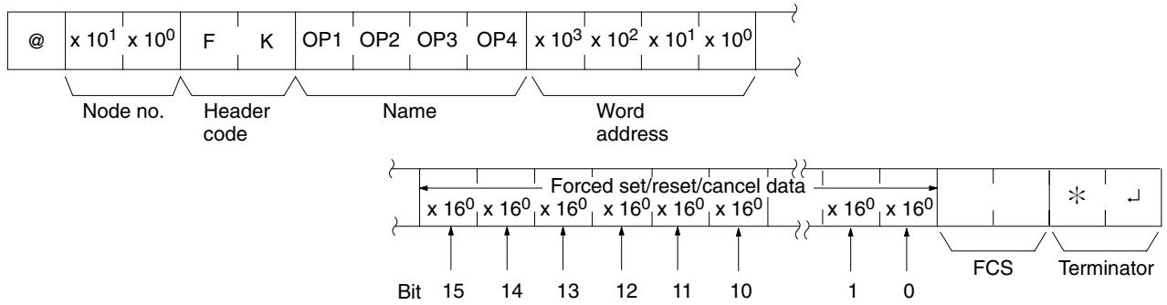
Response Format
An end code of 00 indicates normal completion.
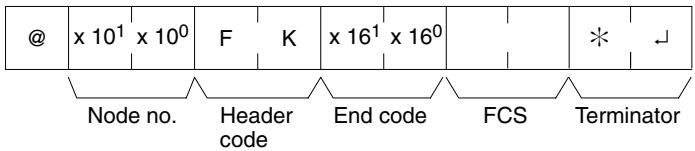
Parameters
Name, Word address (Command)
In "Name," specify the area (i.e., IR, SR, LR, HR, AR, or TC) that is to be forced set or reset. Specify the name in four characters. In "Word address," specify the address of the word that is to be forced set or reset.
| Name | Classification | Word address setting range | ||||
| OP1 | OP2 | OP3 | OP4 | CPM2A/CPM2C PCs | CPM1/CPM1A/ SRM1(-V2) PCs | |
| C | I | O | (Space) | IR or SR | 0000 to 0049 0200 to 0252 | 0000 to 0019 0200 to 0252 |
| L | R | (Space) | (Space) | LR | 0000 to 0015 | 0000 to 0015 |
| H | R | (Space) | (Space) | HR | 0000 to 0019 | 0000 to 0019 |
| A | R | (Space) | (Space) | AR | 0000 to 0023 | 0000 to 0015 |
| T | I | M | (Space) | Completion Flag (timer) | 0000 to 0255 | 0000 to 0127 |
| T | I | M | H | Completion Flag (high-speed timer) | 0000 to 0255 | 0000 to 0127 |
| T | I | M | L | Completion Flag (long timer) | 0000 to 0255 | 0000 to 0127 |
| T | M | H | H | Completion Flag (very high-speed timer) | 0000 to 0255 | 0000 to 0127 |
| C | N | T | (Space) | Completion Flag (counter) | ||
| C | N | T | R | Completion Flag (reversible counter) | ||
Forced set/Reset/Cancel data (Command)
If a timer or counter completion flag is specified, only bit 15 is effective and all other bits will be ignored. Only force-setting and force-resetting are possible for timers/counters.
If a word address is specified, the content of the word specifies the desired process for each bit in the specified word, as shown in the following table.
| Hexadecimal setting | Process |
| 0000 | No action (bit status not changed) |
| 0002 | Reset |
| 0003 | Set |
| 0004 | Forced-reset |
| 0005 | Forced-set |
| 0008 | Forced set/reset status cancel |
The bits that are merely set or reset may change status the next time the program is executed, but bits that are force-set or force-reset will maintain the forced status until it is cleared.
Response Format
An end code of 00 indicates normal completion.
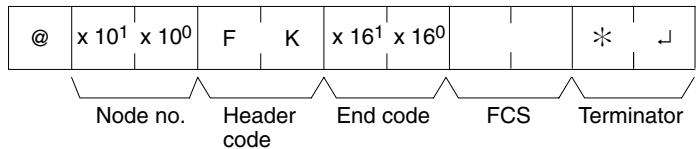
4-5-25 FORCED SET/RESET CANCEL - KC
Cancel all forced set and forced reset bits (including those set by FORCED SET, FORCED RESET, and MULTIPLE FORCED SET/RESET). If multiple bits are set, the forced status will be cancelled for all of them. It is not possible to cancel bits one by one using KC.
Command Format
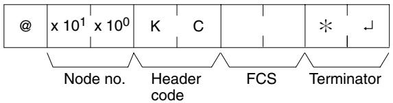
Response Format
An end code of 00 indicates normal completion.
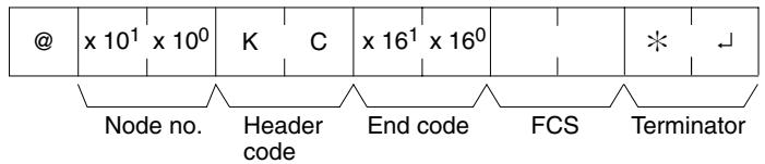
4-5-26 PC MODEL READ - MM
Reads the model type of the PC.
Command Format
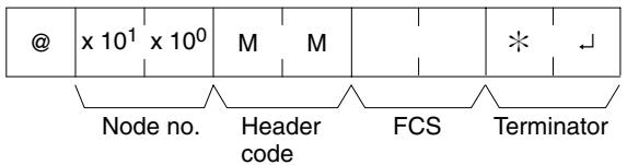
Response Format
An end code of 00 indicates normal completion.

Parameters
Model Code
"Model code" indicates the PC model in two digits hexadecimal.
| Model code | Model |
| 01 | C250 |
| 02 | C500 |
| 03 | C120 |
| 0E | C2000 |
| 10 | C1000H |
| 11 | C2000H/CQM1/CPM2A/CPM2C/CPM1/CPM1A/SRM1(-V2) |
| 12 | C20H/C28H/C40H/C200H/C200HS |
| 20 | CV500 |
| 21 | CV1000 |
| 22 | CV2000 |
| 40 | CVM1-CPU01-E |
| 41 | CVM1-CPU11-E |
| 42 | CVM1-CPU21-E |
4-5-27 TEST - TS
Returns, unaltered, one block of data transmitted from the host computer.
Command Format

Response Format
An end code of 00 indicates normal completion.

Parameters
Characters (Command, Response)
For the command, this setting specifies any characters other than the carriage return (CHR$(13)). For the response, the same characters as specified by the command will be returned unaltered if the test is successful.
4-5-28 PROGRAM READ - RP
Reads the contents of the PC user's program area in machine language (object code). The contents are read as a block, from the beginning to the end.
Command Format
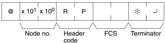
Response Format
An end code of 00 indicates normal completion.

Parameters
Program (Response)
The program is read from the entire program area.
Note To stop this operation in progress, execute the ABORT (XZ) command.
4-5-29 PROGRAM WRITE - WP
Writes to the PC user's program area the machine language (object code) program transmitted from the host computer. The contents are written as a block, from the beginning.
Command Format
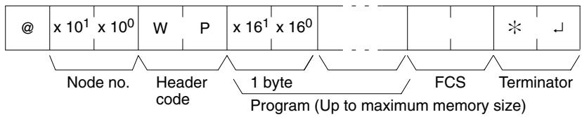
Response Format
An end code of 00 indicates normal completion.
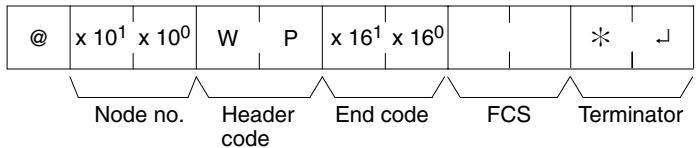
Parameters
Program (Command)
Program data up to the maximum memory size.
4-5-30 COMPOUND COMMAND - QQ
Registers at the PC all of the bits, words, and timers/counters that are to be read, and reads the status of all of them as a batch.
Registering Read Information
Register the information on all of the bits, words, and timers/counters that are to be read.
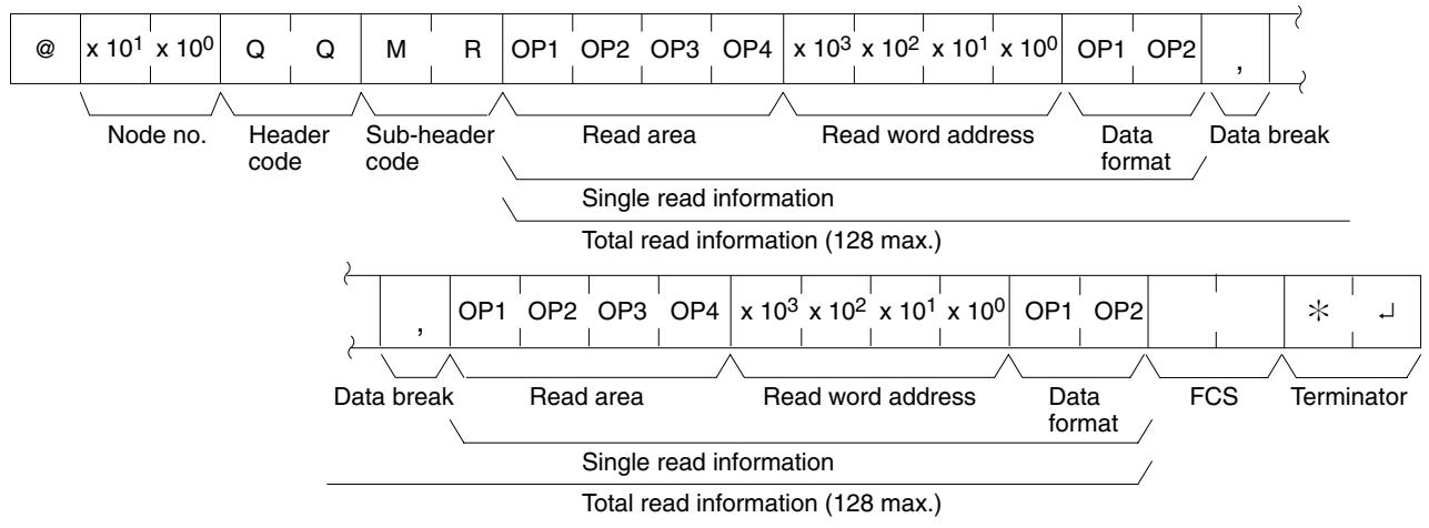
Command Format
Response Format
An end code of 00 indicates normal completion.

Parameters
Read Area (Command)
Specify in four-character code the area that is to be read. The codes that can be specified are listed in the following table.
Read Word address, Data Format (Command)
Depending on the area and type of data that are to be read, the information to be read is as shown in the following table. The "read data" is specified in four digits BCD, and the data format is specified in two digits BCD.
| Area classification | Read data | Read area | Read word | Data format | |
| CPM2A/ CPM2C PCs | CPM1/ CPM1A/ SRM1(-V2) PCs | ||||
| IR or SR | Bit | C I O (S) | 0000 to 0049 | 0000 to 0019 | 00 to 15 (decimal) |
| Word | 0200 to 0255 | 0200 to 0255 | “CH” | ||
| LR | Bit | L R (S) (S) | 0000 to 0015 | 0000 to 0015 | 00 to 15 (decimal) |
| Word | “CH” | ||||
| HR | Bit | H R (S) (S) | 0000 to 0019 | 0000 to 0019 | 00 to 15 (decimal) |
| Word | “CH” | ||||
| AR | Bit | A R (S) (S) | 0000 to 0023 | 0000 to 0015 | 00 to 15 (decimal) |
| Bit | “CH” | ||||
| Timer | Completion Flag | T I M (S) | 0000 to 0255 | 0000 to 0127 | 2 characters other than “CH” |
| PV | “CH” | ||||
| High-speed timer | Completion Flag | T I M H | 0000 to 0255 | 0000 to 0127 | 2 characters other than “CH” |
| PV | “CH” | ||||
| Long timer | Completion Flag | T I M L | 0000 to 0255 | Not used. | 2 characters other than “CH” |
| PV | “CH” | ||||
| Very high-speed timer | Completion Flag | T M H H | 0000 to 0255 | Not used. | 2 characters other than “CH” |
| PV | “CH” | ||||
| Counter | Completion Flag | C N T (S) | 0000 to 0255 | 0000 to 0127 | 2 characters other than “CH” |
| PV | “CH” | ||||
| Reversible counter | Completion Flag | C N T R | 0000 to 0255 | 0000 to 0127 | 2 characters other than “CH” |
| PV | “CH” | ||||
| DM | Word | D M (S) (S) | 0000 to 2047 | 0000 to 1023* | Any 2 characters |
| 6144 to 6655 | 6144 to 6655 | ||||
Note *For SRM1(-V2) PCs, the DM range is from 0000 to 2047.
(S): Space
Data Break (Command)
The read information is specified one item at a time separated by a break code (,). The maximum number of items that can be specified is 128. (When the PV of a timer/counter is specified, however, the status of the Completion Flag is also returned, and must therefore be counted as two items.)
Batch Reading
The bit, word, and timer/counter status is read as a batch according to the read information that was registered with QQ.
Command Format
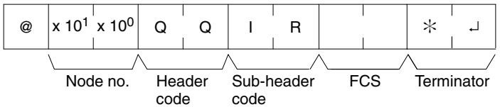
Response Format
An end code of 00 indicates normal completion.
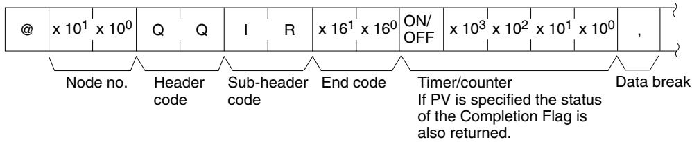
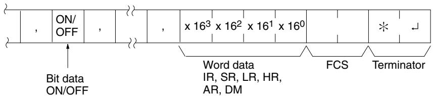
Parameters
Read Data (Response)
Read data is returned according to the data format and the order in which read information was registered using QQ. If "Completion Flag" has been specified, then bit data (ON or OFF) is returned. If "Word" has been specified, then word data is returned. If "PV" has been specified for timers/counters, however, then the PV is returned following the Completion Flag.
Data Break (Response)
The break code (,) is returned between sections that are read.
4-5-31 ABORT - XZ
Aborts the Host Link operation that is currently being processed, and then enables reception of the next command. The ABORT command does not receive a response.
Command Format
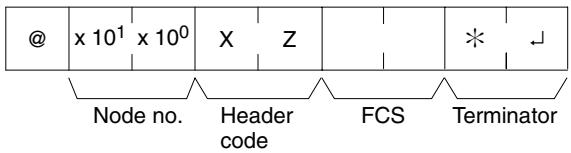
4-5-32 INITIALIZIZE -**
Initializes the transmission control procedure of all the PCs connected to the host computer. The INITIALIZE command does not use node numbers or FCS, and does not receive a response.
Command Format
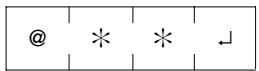
4-5-33 TXD RESPONSE - EX
This command is supported by CPM2A/CPM2C PCs only.
This is the response format used when the PC's TXD(48) instruction is executed in Host Link communications mode. There is no command associated with EX. TXD(48) converts the specified data into ASCII and transmits it to the host computer with this format. The response can contain up to 122 characters of ASCII data. (TXD(48) does not support multiple frames.)
Response Format
An end code of 00 indicates normal completion.

Parameters
Characters (Response)
This is the data specified in TXD(48) that has been converted to ASCII.
4-5-34 Undefined Command - IC
This response is returned if the header code of a command cannot be decoded. Check the header code.
Response Format
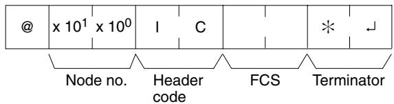
SECTION 5
Memory Areas
This section describes the structure of the PC memory areas and explains how to use them.
5-1 Memory Area Functions 308
5-1-1 Memory Area Structure 308
5-1-2 Functions 311
5-1-3 CPM1/CPM1A/SRM1(-V2) Flash Memory 313
5-2 I/O Allocation for CPM1/CPM1A/CPM2A PCs 313
5-2-1 CPU Units 313
5-2-2 Expansion I/O Units 317
5-2-3 Expansion Units 318
5-2-4 Examples of Expansion Unit and Expansion I/O Unit Allocation 319
5-3 I/O Allocation for CPM2C PCs 323
5-3-1 CPU Units 323
5-3-2 Expansion I/O Units 325
5-3-3 Expansion Units 328
5-3-4 Examples of Expansion Unit and Expansion I/O Unit Allocation 329
5-1 Memory Area Functions
5-1-1 Memory Area Structure
CPM1/CPM1A
The following memory areas can be used with the CPM1/CPM1A.
| Data area | Words | Bits | Function | |
| IR \(area^1\) | Input area | IR 000 to IR 009(10 words) | IR 00000 to IR 00915(160 bits) | These bits are allocated to the external I/O terminals. |
| Output area | IR 010 to IR 019(10 words) | IR 01000 to IR 01915(160 bits) | ||
| Work area | IR 200 to IR 231(32 words) | IR 20000 to IR 23115(512 bits) | Work bits can be freely used within the pro-gram. | |
| SR area | SR 232 to SR 255(24 words) | SR 23200 to SR 25515(384 bits) | These bits serve specific functions such asflags and control bits. | |
| TR area | --- | TR 0 to TR 7(8 bits) | These bits are used to temporarily storeON/OFF status at program branches. | |
| HR \(area^2\) | HR 00 to HR 19(20 words) | HR 0000 to HR 1915(320 bits) | These bits store data and retain their ON/OFF status when power is turned off, or operation starts or stops. They are used in the same way as work bits. | |
| AR \(area^2\) | AR 00 to AR 15(16 words) | AR 0000 to AR 1515(256 bits) | These bits serve specific functions such asflags and control bits. | |
| LR \(area^1\) | LR 00 to LR 15(16 words) | LR 0000 to LR 1515(256 bits) | Used for a 1:1 PC Link with another PC. | |
| Timer/Counter \(area^2\) | TC 000 to TC 127 (timer/counter numbers)\(^3\) | Timers and counters use the TIM,TIMH(15), CNT and CNTR(12) instructions.The same numbers are used for both timers and counters. | ||
| DM area | Read/write\(^2\) | DM 0000 to DM 0999DM 1022 to DM 1023(1,002 words) | --- | DM area data can be accessed in wordunits only. Word values are retained whenthe power is turned off, or operation startedor stopped.Read/write areas can be read and writtenfreely within the program. |
| Error log | DM 1000 to DM 1021(22 words) | --- | Used to store the time of occurrence anderror code of errors that occur. These wordscan be used as ordinary read/write DMwhen the error log function is not beingused. | |
| Read-only\(^4\) | DM 6144 to DM 6599(456 words) | --- | Cannot be overwritten from program. | |
| PC Setup\(^4\) | DM 6600 to DM 6655(56 words) | --- | Used to store various parameters that con-trol PC operation. | |
Note 1. IR and LR bits that are not used for their allocated functions can be used as work bits.
2. The contents of the HR area, AR area, Counter area, and read/write DM area are backed up by a capacitor. The backup time varies with the ambient temperature, but at 25^ , the capacitor will back up memory for 20 days. If the power supply is off longer than the backup time, memory contents will be cleared and AR1314 will turn ON. (This flag turns ON when data can no longer be retained by the built-in capacitor.) Refer to 2-1-2 Characteristics in the CPM1 and CPM1A Operation Manual for a graph showing the backup time vs. temperature.
3. When accessing a PV, TC numbers are used as word data; when accessing Completion Flags, they are used as bit data.
4. Data in DM 6144 to DM 6655 cannot be overwritten from the program, but they can be changed from a Programming Device.
The following memory areas can be used with the CPM2A/CPM2C.
CPM2A/CPM2C
| Data area | Words | Bits | Function | |
| IR area1 | Input area | IR 000 to IR 009(10 words) | IR 00000 to IR 00915(160 bits) | These bits are allocated to the external I/O terminals. |
| Output area | IR 010 to IR 019(10 words) | IR 01000 to IR 01915(160 bits) | ||
| Work area | IR 020 to IR 049,IR 200 to IR 227(58 words) | IR 02000 to IR 04915,IR 20000 to IR 22715(928 bits) | Work bits can be freely used within the pro-gram. | |
| SR area | SR 228 to SR 255(28 words) | SR 22800 to SR 25515(448 bits) | These bits serve specific functions such asflags and control bits. | |
| TR area | --- | TR 0 to TR 7(8 bits) | These bits are used to temporarily storeON/OFF status at program branches. | |
| HR area2 | HR 00 to HR 19(20 words) | HR 0000 to HR 1915(320 bits) | These bits store data and retain their ON/OFF status when power is turned OFF, or operation starts or stops. They are used inthe same way as work bits. | |
| AR area2 | AR 00 to AR 23(24 words) | AR 0000 to AR 2315(384 bits) | These bits serve specific functions such asflags and control bits. | |
| LR area1 | LR 00 to LR 15(16 words) | LR 0000 to LR 1515(256 bits) | Used for a 1:1 PC Link with another PC. | |
| Timer/Counter area2 | TC 000 to TC 255 (timer/counter numbers)3 | Timers and counters use the TIM,TIMH(15), CNT, CNTR(12), TMHH(—), andTIML(—) instructions. The same numbersare used for both timers and counters. | ||
| DM area | Read/write2 | DM 0000 to DM 1999DM 2022 to DM 2047(2,026 words) | --- | DM area data can be accessed in wordunits only. Word values are retained whenthe power is turned off, or operation startedor stopped.Read/write areas can be read and writtenfreely within the program. |
| Error log | DM 2000 to DM 2021(22 words) | --- | Used to store the time of occurrence anderror code of errors that occur. These wordscan be used as ordinary read/write DMwhen the error log function isn't being used. | |
| Read-only4,5 | DM 6144 to DM 6599(456 words) | --- | Cannot be overwritten from program. | |
| PC Setup4,5 | DM 6600 to DM 6655(56 words) | --- | Used to store various parameters that con-trol PC operation. | |
Note 1. IR and LR bits that are not used for their allocated functions can be used as work bits.
- The contents of the HR area, AR area, Counter area, and read/write DM area are backed up by the CPU Unit's battery. If the battery is removed or fails, the contents of these areas will be lost and returned to default values. (In CPM2C CPU Units without a battery, these areas are backed up by a capacitor.)
- When a TC numbers is used as a word operand, the timer or counter PV is accessed; when used as a bit operand, its Completion Flag is accessed.
- Data in DM 6144 to DM 6655 cannot be overwritten from the program, but they can be changed from a Programming Device.
- The program and data in DM 6144 to DM 6655 are stored in flash memory.
SRM1(-V2)
The following memory areas can be used with the SRM1(-V2).
| Data area | Words | Bits | Function | |
| IR area1 | Input area | IR 000 to IR 007(8 words) | IR 00000 to IR 00715(128 bits) | These bits are allocated to the external I/O terminals. The ON/OFF status of the I/O bits will be the same as the ON/OFF status of the I/O terminals(When the CompoBus/S is used in 128-bit mode, IR 004 to IR 007 and IR 014 to IR 017 can also be used as work bits.) |
| Output area | IR 010 to IR 017(8 words) | IR 01000 to IR 01715(128 bits) | ||
| Work area | IR 008 to IR 009IR 018 to IR 019IR 200 to IR 239(44 words) | IR 00800 to IR 00915IR 01800 to IR 01915IR 20000 to IR 23915(704 bits) | Work bits can be freely used within the program. IR 232 to IR 239 however, are used as the MACRO input area when MCRO(99) is being used. | |
| SR area | SR 240 to SR 255(16 words) | SR 24000 to SR 25507(248 bits) | These bits serve specific functions such as flags and control bits. | |
| TR area | --- | TR 0 to TR 7(8 bits) | These bits are used to temporarily store ON/OFF status at program branches. | |
| HR area2 | HR 00 to HR 19(20 words) | HR 0000 to HR 1915(320 bits) | These bits store data and retain their ON/OFF status when power is turned off, or operation starts or stops. They are used in the same way as work bits. | |
| AR area2 | AR 00 to AR 15(16 words) | AR 0000 to AR 1515(256 bits) | These bits serve specific functions such as flags and control bits. AR 04 to 07 are used as slaves. Refer to AR Area. | |
| LR area1 | LR 00 to LR 15(16 words) | LR 0000 to LR 1515(256 bits) | Used for a 1:1 PC Link with another PC. | |
| Timer/Counter area2 | TC 000 to TC 127 (timer/counter numbers)3 | Timers and counters use the TIM,TIMH(15), CNT and CNTR(12) instructions.The same numbers are used for both timers and counters. | ||
| DM area | Read/write2 | DM 0000 to DM 1999(2,000 words) | --- | DM area data can be accessed in word units only. Word values are retained when the power is turned off, or operation started or stopped.Read/write areas can be read and written freely within the program. |
| Error log | DM 2000 to DM 2021(22 words) | --- | Used to store the time of occurrence and error code of errors that occur. These words can be used as ordinary read/write DM when the error log function is not being used. | |
| Read-only4 | DM 6144 to DM 6599(456 words) | --- | Cannot be overwritten from program. | |
| PC Setup4 | DM 6600 to DM 6655(56 words) | --- | Used to store various parameters that control PC operation. | |
Note 1. IR and LR bits that are not used for their allocated functions can be used as work bits.
- The contents of the HR area, AR area, Counter area, and read/write DM area are backed up by a capacitor or a battery. Refer to 2-1-2 Characteristics in the SRM1 Master Control Unit Operation Manual for a graph showing the backup time vs. temperature.
- When accessing a PV, TC numbers are used as word data; when accessing Completion Flags, they are used as bit data.
- Data in DM 6144 to DM 6655 cannot be overwritten from the program, but they can be changed from a Programming Device.
5-1-2 Functions
IR Area
The functions of the IR area are explained below.
With CPM1, CPM1A, CPM2A, and CPM2C PCs, IR area bits from IR 00000 to IR 01915 are allocated to terminals on the CPU Unit and Expansion I/O Units. With the SRM1(-V2), IR area bits from IR 00000 to IR 00715 and IR 01000 to IR 01715 are allocated to CompoBus/S Slaves. They reflect the ON/OFF status of input and output signals. Input bits begin at IR 00000, and output bits begin at IR 01000.
IR words that are not allocated to inputs or outputs can be used as work words. In addition, unused bits in IR words allocated to outputs can be used as work bits.
Work Bits
The work bits can be used freely within the program. They can only be used within the program, however, and not for direct external I/O.
Note 1. The input bits shown in the following tables can operate as normal inputs or they can be assigned special functions in the PC Setup.
Special functions for input bits IR 00000 through IR 00002 are set in DM 6642:
| Bit address | PC Setup setting (DM 6642 bits 08 to15) | ||
| 00 | 01 | 02, 03, or 04 | |
| IR 00000 | Used as normal inputs. | Used as high-speed counter inputs. | Used as inputs for synchronized pulse control. |
| IR 00001 | |||
| IR 00002 | Used as a normal input. | ||
Special functions for input bits IR 00003 through IR 00006 are set in DM 6628:
| Bit address | Bits in DM 6628 | PC Setup setting (in DM 6628) | ||
| 0 | 1 | 2 | ||
| IR 00003 | 00 to 03 | Used as normal inputs. | Used as interrupt inputs (including counter mode). | Used as quick-response inputs. |
| IR 00004 | 04 to 07 | |||
| IR 00005* | 08 to 11 | |||
| IR 00006* | 12 to 15 | |||
Note *Input 00006 does not exist and input 00005 must be used as a normal input in CPM2C CPU Units with 10 I/O points.
- Output bits IR 01000 and IR 01001 can operate as normal inputs or they can be used for pulse outputs with PULS(65), SYNC(), or PWM(). (Use a CPU Unit with transistor outputs for the pulse output functions.)
| Instruction | Function |
| PULS(65) | With SPED(64): Single-phase pulse output without acceleration or deceleration |
| With ACC(—): Single-phase pulse output with trapezoidal acceleration and deceleration | |
| SYNC(—) | Synchronized pulse control output |
| PWM(—) | Variable duty-ratio pulse output |
SR Area
These bits mainly serve as flags to PC operation or contain present and set values for various functions. For details on the various bit functions, refer to relevant sections in this manual or to Appendix C Memory Areas.
Some SR area words can be used as work words when they are not used for their assigned purpose.
TR Area
When a complex ladder diagram cannot be programmed in mnemonic code just as it is, these bits are used to temporarily store ON/OFF execution conditions at
| program branches. They are used only for mnemonic code. When programming directly with ladder diagrams using the SYSMAC Support Software (SSS) or the SYSMAC-CPT Support Software, TR bits are automatically processed for you. The same TR bits cannot be used more than once within the same instruction block, but can be used again in different instruction blocks. The ON/OFF status of TR bits cannot be monitored from a Programming Device. Examples showing the use of TR bits in programming are provided on page 350. | |
| HR Area | These bits retain their ON/OFF status even after the PC power supply has been turned off or when operation begins or stops. They are used in the same way as work bits. |
| AR Area | These bits mainly serve as flags related to PC operation. These bits retain their status even after the PC power supply has been turned off or when operation begins or stops. For details on the various bit functions, refer to relevant sections in this manual or to Appendix C Memory Areas. |
| LR Area | When the CPM1/CPM1A/CPM2A/CPM2C/SRM1(-V2) is linked 1:1 with another CPM1/CPM1A/CPM2A/CPM2C/SRM1(-V2), a CQM1, an C200HS or C200HX/HG/HE PC, these bits are used to share data. For details, refer to page 229. LR bits can be used as work bits when not used for 1:1 PC Links. |
| Timer/Counter Area | This area is used to manage timers and counters created with TIM, TIMH(15), TMHH(-)*, TIML(-)*, CNT, and CNTR(12). The same numbers are used for both timers and counters and each number can be used only once in the user program. Do not use the same TC number twice even for different instructions. Use TC numbers 000 through 003 for TIMH(15) and TC numbers 004 to 007 for TMHH(-)*. When these timer numbers are used, timing is performed as an interrupt process and the cycle timer does not affect timer operation. TC numbers are used to create timers and counters, as well as to access Completion Flags and present values (PVs). If a TC number is designated for word data, it will access the present value (PV); if it is used for bit data, it will access the Completion Flag for the timer/counter. Refer to instructions beginning on page 388 for details on timers and counters. |
| DM Area | DM area data is accessed in word units only. The contents of the DM area are retained even after the PC power supply has been turned off or when operation begins or stops. CPM1/CPM1A DM words DM 0000 through DM 0999, DM 1022, and DM 1023 can be used freely in the program; other DM words are allocated specific functions, described below. DM 1000 through DM 1021 contain the error log information. Refer to Section 9 Troubleshooting for details on the error log. CPM2A/CPM2C DM words DM 0000 through DM 1999 and DM 2022 through DM 2047 can be used freely in the program; other DM words are allocated specific functions, described below. DM 2000 through DM 2021 contain the error log information. Refer to Section 9 Troubleshooting for details on the error log. SRM1(-V2) DM words DM 0000 through DM 1999 can be used freely in the program; other DM words are allocated specific functions, described below. DM 2000 through DM 2021 contain the error log information. Refer to Section 9 Troubleshooting for details on the error log. Note DM 6600 through DM 6655 contain the PC Setup. Refer to 1-1 PC Setup for details. |
5-1-3 CPM1/CPM1A/SRM1(-V2) Flash Memory
The following settings must be made to use the flash memory area for CPM1/CPM1A/SRM1(-V2) PCs.
Writing Data
In order to write the contents of the UM area, the DM read-only area (DM 6144 to DM 6599, and the PC Setup area (DM 6600 to DM 6655) to the flash memory, either one of the following operations must be performed.
- Switch the PC to either the MONITOR or PROGRAM mode.
- Turn the power to the PC OFF and ON again.
Note SRM1-CO01/02 Capacitor Backup
If changes are made to the above memory areas, they are not written to the flash memory, and the power is switched off for 20 days or more (at 25^ ), the changes (in RAM) will be lost. If this occurs, the unchanged contents will be read from the flash memory when the PC is started again.
Changing Memory Areas
When operating the SRM1 for the first time after changes have been made to the UM area, the DM read only area (DM 6144 to DM 6599, and the PC Setup area (DM 6600 to DM 6655), beware of the effect resulting from the SRM1's delay in the operation on other devices.
The first operation for the SRM1 after the above memory areas have been changed will be a maximum of 850 ms later than the normal first operation without changes.
SRM1 Cycle Times
A cycle time overflow warning will not be issued when any of the following operations are performed in either MONITOR or OPERATION modes. Be careful of the effect of using online editing on SRM1 I/O response time.
Changes to the program using online editing.
Changes to the read-only DM area (DM 6144 to DM 6599.)
Changes to the PC Setup area (DM 6600 to DM 6655.)
When any of the above operations are performed, the SRM1 cycle time will be increased by a maximum of 850 ms. During this tiny interrupts will be disabled while the program or memory contents is written.
5-2 I/O Allocation for CPM1/CPM1A/CPM2A PCs
5-2-1 CPU Units
CPM1
| No. of I/O (on CPU Unit) | Model number | I/O | Allocated bits | Max. No. of Expansion I/O Units | Max. No. of I/O (see note 1) |
| 10 | CPM1-10CDR-□ | Input | 6 inputs: 00000 to 00005 | 1 (see note 1) | 30 |
| Output | 4 outputs: 01000 to 01003 | ||||
| 20 | CPM1-20CDR-□ | Input | 12 inputs: 00000 to 00011 | 1 (see note 1) | 40 |
| Output | 8 outputs: 01000 to 01007 | ||||
| 30 | CPM1-30CDR-□ | Input | 18 inputs: 00000 to 00011 00100 to 00105 | 1 (see note 1) | 50 |
| Output | 12 outputs: 01000 to 01007 01100 to 01103 | ||||
| 30 | CPM1-30CDR-□-V1 | Input | 18 inputs: 00000 to 00011 00100 to 00105 | 3 (see note 2) | 90 |
| Output | 12 outputs: 01000 to 01007 01100 to 01103 |
Note 1. The values for the maximum number of I/O in the above table include I/O on Expansion I/O Units.
-
When using a CPM1 CPU Unit other than the CPM1-30CDR- -V1, one of the following 20-point Expansion I/O Units can be connected to the PC:
-
CPM1-20EDR (relay outputs)
- CPM1A-20EDRT (sinking transistor outputs)
- CPM1A-20EDT1 (sourcing transistor outputs)
- When using the CPM1-30CDR-□-V1, up to 3 CPM1/CPM1A Expansion I/O Units or CPM1A-MAD01 Analog I/O Units can be connected to the PC.
CPM1A
| No. of I/O (on CPU Unit) | Model number | I/O | Allocated bits | Max. No. of Expansion I/O Units | Max. No. of I/O (see note 1) |
| 10 | CPM1A-10CDR-□ CPM1A-10CDT-D CPM1A-10CDT1-D | Input | 6 inputs: 00000 to 00005 | None | 10 |
| Output | 4 outputs: 01000 to 01003 | ||||
| 20 | CPM1A-20CDR-□ CPM1A-20CDT-D CPM1A-20CDT1-D | Input | 12 inputs: 0000 to 00011 | None | 20 |
| Output | 8 outputs: 01000 to 01007 | ||||
| 30 | CPM1A-30CDR-□ CPM1A-30CDT-D CPM1A-30CDT1-D | Inputs | 18 inputs: 00000 to 00011 00100 to 00105 | 3 (see note) | 90 |
| Output | 12 outputs: 01000 to 01007 01100 to 01103 | ||||
| 40 | CPM1A-40CDR-□ CPM1A-40CDT-D CPM1A-40CDT1-D | Inputs | 24 inputs: 00000 to 00011 00100 to 00111 | 3 (see note) | 100 |
| Output | 16 outputs: 01000 to 01007 01100 to 01107 |
Note 1. The values for the maximum number of I/O in the above table include I/O on Expansion I/O Units.
- When using a CPM1A CPU Unit with 30 or 40 I/O points, up to 3 Expansion Units or Expansion I/O Units can be connected to the PC.
CPM2A
| No. of I/O (on CPU Unit) | Model number | I/O | Allocated bits | Max. No. of Expansion I/O Units | Max. No. of I/O (see note 1) |
| 20 | CPM2A-20CDR-□ CPM2A-20CDT-D CPM2A-20CDT1-D | Input | 12 inputs: 0000 to 00011 | 3 | 80 |
| Output | 8 outputs: 01000 to 01007 | ||||
| 30 | CPM2A-30CDR-□ CPM2A-30CDT-D CPM2A-30CDT1-D | Input | 18 inputs: 00000 to 00011 00100 to 00105 | 3 | 90 |
| Output | 12 outputs: 01000 to 01007 01100 to 01103 | ||||
| 40 | CPM2A-40CDR-□ CPM2A-40CDT-D CPM2A-40CDT1-D | Input | 24 inputs: 00000 to 00011 00100 to 00111 | 3 | 100 |
| Output | 16 outputs: 01000 to 01007 01100 to 01107 | ||||
| 60 | CPM2A-60CDR-□ CPM2A-60CDT-D CPM2A-60CDT1-D | Input | 36 inputs: 00000 to 00011 00100 to 00111 00200 to 00211 | 3 | 120 |
| Output | 24 outputs: 01000 to 01007 01100 to 01107 01200 to 01207 |
Note 1. The values for the maximum number of I/O in the above table include the I/O on Expansion I/O Units.
2. When using a CPM2A CPU Unit, up to 3 Expansion Units or Expansion I/O Units can be connected to the PC.
CPU Unit Allocation
- In the following diagrams, shaded areas indicate bits actually used for inputs or outputs.
- Input bits are allocated starting from IR 00000.
- Output bits are allocated starting from IR 01000.
- Bits in the output words that are not used as output bits can be used as work bits.
- Bits in the input words that are not used as input bits cannot be used as work bits.
CPU Units with 10 I/O Points
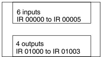
CPM1-10CDR-□ CPM1A-10CD□-□
| Bits | 15 | 14 | 13 | 12 | 11 | 10 | 09 | 08 | 07 | 06 | 05 | 04 | 03 | 02 | 01 | 00 | |
| Inputs | IR 000 | Do not use | |||||||||||||||
| Outputs | IR 010 | ||||||||||||||||
CPU Units with 20 I/O Points
| 12 inputs IR 00000 to IR 00011 | |
| 8 outputs IR 01000 to IR 01007 |
CPM1-20CDR-□
CPM1A-20CD□-□
CPM2A-20CD□-□
| Bits | 15 | 14 | 13 | 12 | 11 | 10 | 09 | 08 | 07 | 06 | 05 | 04 | 03 | 02 | 01 | 00 | |
| Inputs | IR 000 | Do not use | |||||||||||||||
| Outputs | IR 010 | ||||||||||||||||
CPU Units with 30 I/O Points
| 18 inputs IR 00000 to IR 00011 IR 00100 to IR 00105 |
| 12 outputs IR 01000 to IR 01007 IR 01100 to IR 01103 |
CPU Units with 40 I/O Points
| 24 inputs IR 00000 to IR 00011 IR 00100 to IR 00111 |
| 16 outputs IR 01000 to IR 01007 IR 01100 to IR 01107 |
CPM1A-40CD□-□
CPM2A-40CD□-□
| Bits | 15 | 14 | 13 | 12 | 11 | 10 | 09 | 08 | 07 | 06 | 05 | 04 | 03 | 02 | 01 | 00 | |
| Inputs | IR 000 | Do not use | |||||||||||||||
| IR 001 | |||||||||||||||||
| Outputs | IR 010 | ||||||||||||||||
| IR 011 | |||||||||||||||||
CPU Units with 60 I/O Points
| 36 inputs IR 00000 to IR 00011 IR 00100 to IR 00111 IR 00200 to IR 00211 |
| 24 outputs IR 01000 to IR 01007 IR 01100 to IR 01107 IR 01200 to IR 01207 |
CPM1A-60CD□-□
CPM2A-60CD□-□
| Bits | 15 | 14 | 13 | 12 | 11 | 10 | 09 | 08 | 07 | 06 | 05 | 04 | 03 | 02 | 01 | 00 | |
| Inputs | IR 000 | Do not use | |||||||||||||||
| IR 001 | |||||||||||||||||
| IR 002 | |||||||||||||||||
| Outputs | IR 010 | ||||||||||||||||
| IR 011 | |||||||||||||||||
| IR 012 | |||||||||||||||||
5-2-2 Expansion I/O Units
| No. of I/O | Model number | I/O | Allocated bits | Compatible CPU Units |
| 8 | CPM1A-8ED | Input | 8 inputs: Word (m+1), bits 00 to 07 | CPM1-30CDR-☐-V1 CPM1A CPM2A |
| Output | --- | |||
| 8 | CPM1A-8ER | Input | --- | CPM1-30CDR-☐-V1 CPM1A |
| CPM1A-8ET | Output | 8 outputs: Word (n+1), bits 00 to 07 | CPM2A | |
| CPM1A-8ET1 | ||||
| 20 | CPM1A-20EDR | Input | 12 inputs: Word (m+1), bits 00 to 11 | CPM1-30CDR-☐-V1 CPM1A |
| CPM1A-20EDR1 | Output | 8 outputs: Word (n+1), bits 00 to 07 | CPM2A | |
| CPM1A-20EDT | ||||
| 20 | CPM1A-20EDR | Input | 12 inputs: Word (m+1), bits 00 to 11 | CPM1-10CDR-☐ CPM1-20CDR-☐ CPM1-30CDR-☐(-V1) |
| Output | 8 outputs: Word (n+1), bits 00 to 07 |
Note m: “m” denotes the last input word allocated to the CPU Unit, or to the previous Expansion Unit or Expansion I/O Unit if one is already connected.
n: “n” denotes the last output word allocated to the CPU Unit, or to the previous Expansion Unit or Expansion I/O Unit if one is already connected.
Expansion I/O Unit Allocation
- In the following diagrams, shaded areas indicate bits actually used for inputs or outputs.
- Input bits are allocated to Expansion I/O Units from word ( + 1) , where "m" is the last input word allocated to the CPU Unit, or to the previous Expansion Unit or Expansion I/O Unit if one is already connected.
- Output bits are allocated to Expansion I/O Units from word (n + 1) , where "n" is the last output word allocated to the CPU Unit, or to the previous Expansion Unit or Expansion I/O Unit if one is already connected.
- Bits in the output words that are not used as output bits can be used as work bits.
- Bits in the input words that are not used as input bits cannot be used as work bits.
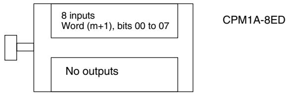
Expansion I/O Units with 8 Inputs
| Bits | 15 | 14 | 13 | 12 | 11 | 10 | 09 | 08 | 07 | 06 | 05 | 04 | 03 | 02 | 01 | 00 | |
| Inputs | m+1 | Do not use | |||||||||||||||
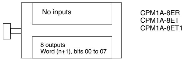
Expansion I/O Units with 8 Outputs
| Bits | 15 | 14 | 13 | 12 | 11 | 10 | 09 | 08 | 07 | 06 | 05 | 04 | 03 | 02 | 01 | 00 | |
| Outputs | n+1 | ||||||||||||||||
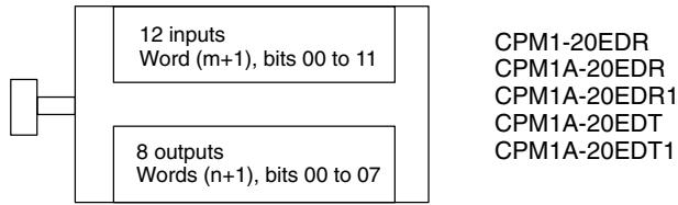
Expansion I/O Units with 20 I/O Points
| Bits | 15 | 14 | 13 | 12 | 11 | 10 | 09 | 08 | 07 | 06 | 05 | 04 | 03 | 02 | 01 | 00 | |
| Inputs | m+1 | Do not use | |||||||||||||||
| Outputs | n+1 | ||||||||||||||||
5-2-3 Expansion Units
| Unit | Model number | I/O | Allocated words/bits | Max. No. of Units | Compatible CPU Units |
| Analog I/O Unit | CPM1A-MAD01 | Input | 2 words: m+1, m+2 | 3 (see note 2) | CPM1 |
| CPM1A-MAD11 | CPM1A | ||||
| Output | 1 word: n+1 | CPM2A | |||
| Temperature Sensor Units | CPM1A-TS001 | Input | 2 words: m+1, m+2 | 3 | CPM1A |
| CPM1A-TS101 | CPM2A | ||||
| Output | --- | ||||
| CPM1A-TS002 | Input | 4 words: m+1 to m+4 | 1 | CPM1A | |
| CPM1A-TS102 | CPM2A | ||||
| Output | --- | ||||
| CompoBus/S I/O Link Unit | CPM1A-SRT21 | Input | 8 bits: m+1 | 3 | CPM1A |
| Output | 8 bits: n+1 | CPM2A | |||
| DeviceNet I/O Link Unit | CPM1A-DRT21 | Input | 32 bits: m+1, m+2 | 3 | CPM1A |
| Output | 32 bits: n+1, n+2 | CPM2A |
Note 1. m: "m" denotes the last input word allocated to the CPU Unit, or to the previous Expansion Unit or Expansion I/O Unit if one is already connected.
n: "n" denotes the last output word allocated to the CPU Unit, or to the previous Expansion Unit or Expansion I/O Unit if one is already connected.
- Only CPM1 CPU Units with the "-V1" suffix can have 3 Analog I/O Units connected. CPU Units without the "-V1" suffix can only have one Analog I/O Unit connected.
- Only one CPM1A-TS002/102 Temperature Sensor Unit can be connected to the PC. If a CPM1A-TS002/102 Temperature Sensor Unit is connected to the PC, one more Expansion Unit (other than another CPM1A-TS002/102 Temperature Sensor Unit) or Expansion I/O Unit can be connected.
Analog I/O Unit
CPM1A-MAD01/MAD11
2 analog inputs
Input 0: word ( + 1)
Input 1: word (m + 2)
1 analog output
Output 0: word (n + 1)
Temperature Sensor Units
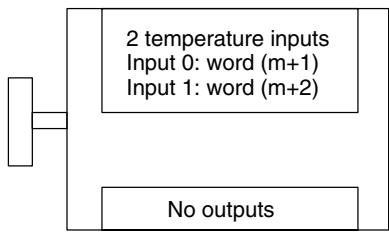
CPM1A-TS001/TS101
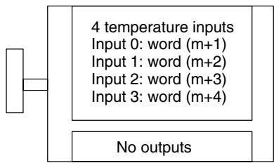
CPM1A-TS002/TS102
CompoBus/S I/O Link Unit and DeviceNet I/O Link Unit
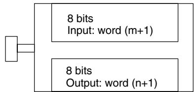
CPM1A-SRT21
CPM1A-DRT21

Note Input bits 00 to 07 in word ( + 1) are for outputs from the Master. Output bits 00 to 07 in word (n + 1) , are for inputs to the Master.
5-2-4 Examples of Expansion Unit and Expansion I/O Unit Allocation
- When using a CPM1 CPU Unit without "-V1" at the end of the model number, only one Expansion I/O Unit can be connected.
- When using a CPM1 CPU Unit with "-V1" at the end of the model number, up to 3 CPM1A-series Expansion I/O Units can be connected.
- When using a CPM1A CPU Unit with 30 or 40 I/O points, or when using a CPM2A CPU Unit, up to 3 Expansion Units or Expansion I/O Units, excluding 4-input Temperature Sensor Units, can be connected. Only one 4-input Temperature Sensor Unit can be connected. If a 4-input Temperature Sensor Unit is connected to the PC, only one more Expansion Unit (except for another 4-input Temperature Sensor Unit) or Expansion I/O Unit can be connected.
Example: CPU Unit with 20 I/O Points + Expansion I/O Unit with 20 I/O Points
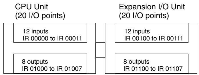
| Bits | 15 | 14 | 13 | 12 | 11 | 10 | 09 | 08 | 07 | 06 | 05 | 04 | 03 | 02 | 01 | 00 | |
| Inputs | IR 000 | Do not use | |||||||||||||||
| IR 001 | Do not use | ||||||||||||||||
| Outputs | IR 010 | ||||||||||||||||
| IR 011 | |||||||||||||||||
- IR 00000 to IR 00011 and IR 00100 to IR 00111 are allocated as input bits. IR 00012 to 00015 cannot be used.
- IR 01000 to IR 01007 and IR 01100 to IR 01107 are allocated as output bits. IR 01108 to IR 01115 can be used as work bits.
- IR 002 to IR 009 of the input words and IR 012 to IR 019 of the output words can all be used as work words.
Example: CPU Unit with 30 I/O Points + 3 Expansion I/O Units with 20 I/O Points
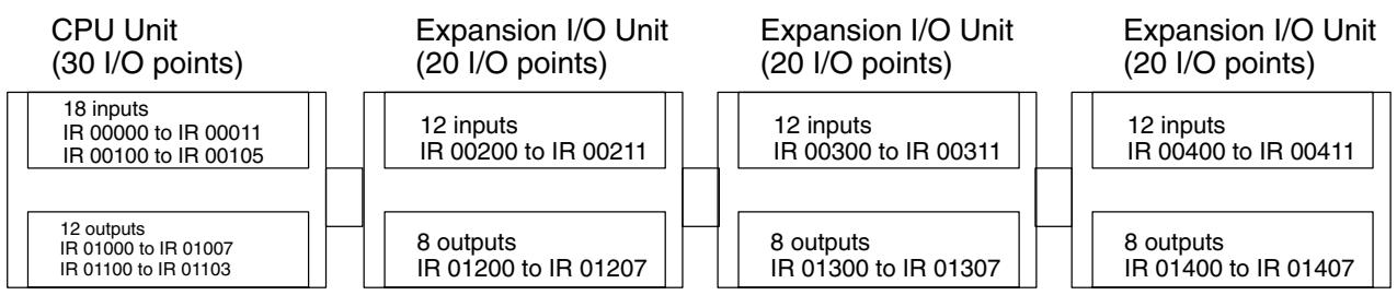
| Bits | 15 | 14 | 13 | 12 | 11 | 10 | 09 | 08 | 07 | 06 | 05 | 04 | 03 | 02 | 01 | 00 | |
| Inputs | IR 000 | Do not use | |||||||||||||||
| IR 001 | Do not use | ||||||||||||||||
| IR 002 | Do not use | ||||||||||||||||
| IR 003 | Do not use | ||||||||||||||||
| IR 004 | Do not use | ||||||||||||||||
| Outputs | IR 010 | ||||||||||||||||
| IR 011 | |||||||||||||||||
| IR 012 | |||||||||||||||||
| IR 013 | |||||||||||||||||
| IR 014 | |||||||||||||||||

Example: CPU Unit with 60 I/O Points + 3 Expansion I/O Units
| Bits | 15 | 14 | 13 | 12 | 11 | 10 | 09 | 08 | 07 | 06 | 05 | 04 | 03 | 02 | 01 | 00 | |
| Inputs | IR 000 | Do not use | |||||||||||||||
| IR 001 | Do not use | ||||||||||||||||
| IR 002 | Do not use | ||||||||||||||||
| IR 003 | Do not use | ||||||||||||||||
| IR 004 | Do not use | ||||||||||||||||
| Outputs | IR 010 | ||||||||||||||||
| IR 011 | |||||||||||||||||
| IR 012 | |||||||||||||||||
| IR 013 | |||||||||||||||||
| IR 014 | |||||||||||||||||
| IR 015 | |||||||||||||||||
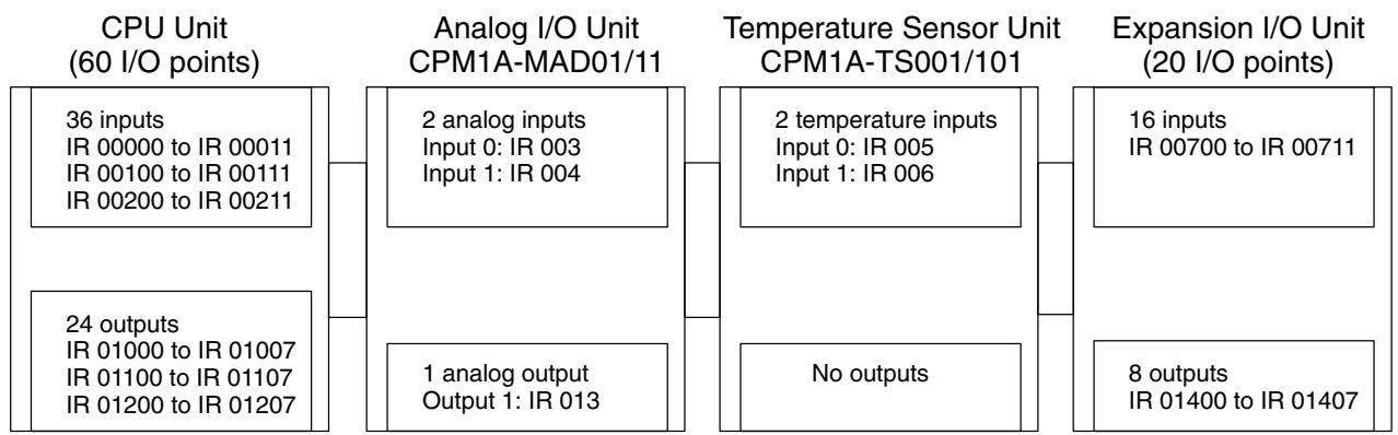
Example: Configuration Including Analog I/O Unit, Temperature Sensor Unit, and Expansion I/O Unit
| Bits | 15 | 14 | 13 | 12 | 11 | 10 | 09 | 08 | 07 | 06 | 05 | 04 | 03 | 02 | 01 | 00 | |
| Inputs | IR 000 | Do not use | |||||||||||||||
| IR 001 | Do not use | ||||||||||||||||
| IR 002 | Do not use | ||||||||||||||||
| IR 003 | Used for input 0 of the Analog I/O Unit | ||||||||||||||||
| IR 004 | Used for input 1 of the Analog I/O Unit | ||||||||||||||||
| IR 005 | Used for input 0 of the Temperature Sensor Unit | ||||||||||||||||
| IR 006 | Used for input 1 of the Temperature Sensor Unit | ||||||||||||||||
| IR 007 | Do not use | ||||||||||||||||
| Outputs | IR 010 | ||||||||||||||||
| IR 011 | |||||||||||||||||
| IR 012 | |||||||||||||||||
| IR 013 | Used for the output of the Analog I/O Unit | ||||||||||||||||
| IR 014 | |||||||||||||||||
With the exception of CPM1A-TS002/102 Temperature Sensor Units, up to 3 Expansion Units (Analog I/O Units, Temperature Sensor Units, or CompoBus/S Units) can be connected to a CPM1A or CPM2A PC. Only one CPM1A-TS002/102 Temperature Sensor Unit can be connected. (See page 323 for an example of CPM1A-TS002/102 allocations.)
Example: Configuration Including Temperature Sensor Unit with 4 Inputs and CompoBus/S Link Unit
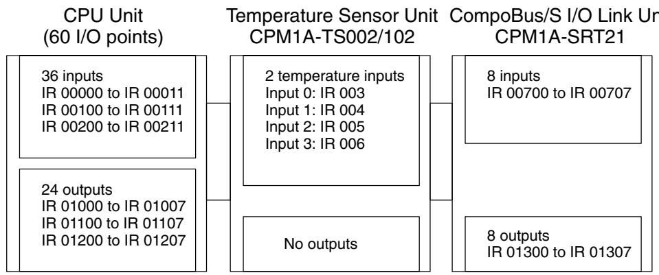
| Bits | 15 | 14 | 13 | 12 | 11 | 10 | 09 | 08 | 07 | 06 | 05 | 04 | 03 | 02 | 01 | 00 | |
| Inputs | IR 000 | Do not use | |||||||||||||||
| IR 001 | Do not use | ||||||||||||||||
| IR 002 | Do not use | ||||||||||||||||
| IR 003 | Used for input 0 of the Temperature Sensor Unit | ||||||||||||||||
| IR 004 | Used for input 1 of the Temperature Sensor Unit | ||||||||||||||||
| IR 005 | Used for input 1 of the Temperature Sensor Unit | ||||||||||||||||
| IR 006 | Used for input 1 of the Temperature Sensor Unit | ||||||||||||||||
| IR 007 | Do not use | ||||||||||||||||
| Outputs | IR 010 | ||||||||||||||||
| IR 011 | |||||||||||||||||
| IR 012 | |||||||||||||||||
| IR 013 | |||||||||||||||||
Only one 4-input Temperature Sensor Unit (CPM1A-TS002/102) can be connected to the PC. The CPM1A-TS002/102 can, however, be connected together with an Expansion I/O Unit or a different Expansion Unit.
5-3 I/O Allocation for CPM2C PCs
5-3-1 CPU Units
| No. of I/O (on CPU Unit) | Model number | I/O | Allocated bits | Max. No. of Expansion I/O Units | Max. No. of I/O (see note 1) |
| 10 | CPM2C-10C□D□□□-D | Inputs | 6 inputs: 00000 to 00005 | 5 | 170 |
| Outputs | 4 outputs: 01000 to 01003 | ||||
| 20 | CPM2C-20C□D□□□-D | Inputs | 12 inputs: 00000 to 00011 | 5 | 180 |
| Outputs | 8 outputs: 01000 to 01007 | ||||
| 32 | CPM2C-32CDT□□-D | Inputs | 16 inputs: 00000 to 00007 and 00100 to 00107 | 5 | 192 |
| Outputs | 16 outputs: 01000 to 01007 and 01100 to 01107 |
Note 1. The values for the maximum number of I/O in the above table include the I/O on Expansion I/O Units.
2. Although only up to 5 Expansion Units or Expansion I/O Units can be connected to a CPM2C PC, no more than 10 input words and 10 output words can be allocated.
CPU Unit Allocation
- In the following diagrams, shaded areas indicate bits actually used for inputs or outputs.
- Input bits are allocated starting from IR 00000.
Output bits are allocated starting from IR 01000. - Bits in the output words that are not used as output bits can be used as work bits.
- Bits in the input words that are not used as input bits cannot be used as work bits.
CPU Units with 10 I/O Points
| 6 inputs IR 00000 to IR 00005 |
| 4 outputs IR 01000 to IR 01003 |
CPM2C-10C□D□□-□
| Bits | 15 | 14 | 13 | 12 | 11 | 10 | 09 | 08 | 07 | 06 | 05 | 04 | 03 | 02 | 01 | 00 | |
| Inputs | IR 000 | Do not use | |||||||||||||||
| Outputs | IR 010 | ||||||||||||||||
CPU Units with 20 I/O Points
| 12 inputs |
| IR 00000 |
| to |
| IR 00011 |
| 8 outputs |
| IR 01000 |
| to |
| IR 01007 |
CPM2C-20C□D□□-□
| Bits | 15 | 14 | 13 | 12 | 11 | 10 | 09 | 08 | 07 | 06 | 05 | 04 | 03 | 02 | 01 | 00 | |
| Inputs | IR 000 | Do not use | |||||||||||||||
| Outputs | IR 010 | ||||||||||||||||
CPU Units with 32 I/O Points
16 inputs
IR 00000 to IR 00007
and
IR 00100 to IR 00107
16 outputs
IR 01000 to IR 01007
and
IR 01100 to IR 01107
CPM2C-32CDT□□-D
| Bits | 15 | 14 | 13 | 12 | 11 | 10 | 09 | 08 | 07 | 06 | 05 | 04 | 03 | 02 | 01 | 00 | |
| Inputs | IR 000 | Do not use | |||||||||||||||
| IR 001 | |||||||||||||||||
| Bits | 15 | 14 | 13 | 12 | 11 | 10 | 09 | 08 | 07 | 06 | 05 | 04 | 03 | 02 | 01 | 00 | |
| Outputs | IR 010 | ||||||||||||||||
| IR 011 | |||||||||||||||||
5-3-2 Expansion I/O Units
| No. of I/O | Model number | I/O | Allocated bits | Max. No. of Units | |
| CPM2C | CPM2C-S | ||||
| 8 | CPM2C-8ED□ | Input | 8 inputs: Word (m+1), bits 00 to 07 | 5 | 3 |
| Output | --- | ||||
| 16 | CPM2C-16ED□ | Input | 16 inputs: Word (m+1), bits 00 to 15 | 5 | 3 |
| Output | --- | ||||
| 8 | CPM2C-8ER | Input | --- | 5 | 3 |
| CPM2C-8ET□ | |||||
| CPM2C-8ET1□ | Output | 8 outputs: Word (n+1), bits 00 to 07 | |||
| 16 | CPM2C-16ET□ | Input | --- | 5 | 3 |
| CPM2C-16ET1□ | Output | 16 outputs: Word (n+1), bits 00 to 15 | |||
| 10 | CPM2C-10EDR | Input | 6 inputs: Word (m+1), bits 00 to 05 | 5 | 3 |
| Output | 4 outputs: Word (n+1), bits 00 to 03 | ||||
| 20 | CPM2C-20EDR | Input | 12 inputs: Word (m+1), bits 00 to 11 | 5 | 3 |
| Output | 8 outputs: Word (n+1), bits 00 to 07 | ||||
| 24 | CPM2C-24EDT□ | Input | 16 inputs: Word (m+1), bits 00 to 15 | 5 | 3 |
| CPM2C-24EDT1□ | Output | 8 outputs: Word (n+1), bits 00 to 07 | |||
| 32 | CPM2C-32EDT□ | Input | 16 inputs: Word (m+1), bits 00 to 15 | 5 | 3 |
| CPM2C-32EDT1□ | Output | 16 outputs: Word (n+1), bits 00 to 15 | |||
Note m: "m" denotes the last input word allocated to the CPU Unit, or to the previous Expansion Unit or Expansion I/O Unit if one is already connected.
n: “n” denotes the last output word allocated to the CPU Unit, or to the previous Expansion Unit or Expansion I/O Unit if one is already connected.
Expansion I/O Unit Allocation
- In the following diagrams, shaded areas indicate bits actually used for inputs or outputs.
- Input bits are allocated to Expansion I/O Units starting from word (m + 1) , where "m" is the last input word allocated to the CPU Unit, or to the previous Expansion Unit or Expansion I/O Unit if one is already connected.
-
Output bits are allocated to Expansion I/O Units starting from word (n + 1) , where "n" is the last output word allocated to the CPU Unit, or to the previous Expansion Unit or Expansion I/O Unit if one is already connected.
-
Bits in the output words that are not used as output bits can be used as work bits.
- Bits in the input words that are not used as input bits can be used as work bits.
Expansion I/O Unit with 8 Inputs
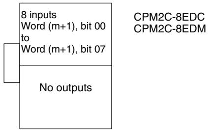
| Bits | 15 | 14 | 13 | 12 | 11 | 10 | 09 | 08 | 07 | 06 | 05 | 04 | 03 | 02 | 01 | 00 | |
| Inputs | m+1 | Do not use | |||||||||||||||
Expansion I/O Unit with 16 Inputs
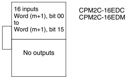
| Bits | 15 | 14 | 13 | 12 | 11 | 10 | 09 | 08 | 07 | 06 | 05 | 04 | 03 | 02 | 01 | 00 | |
| Inputs | m+1 | ||||||||||||||||
Expansion I/O Units with 8 Outputs
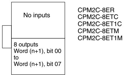
| Bits | 15 | 14 | 13 | 12 | 11 | 10 | 09 | 08 | 07 | 06 | 05 | 04 | 03 | 02 | 01 | 00 | |
| Outputs | n+1 | ||||||||||||||||
Expansion I/O Units with 16 Outputs
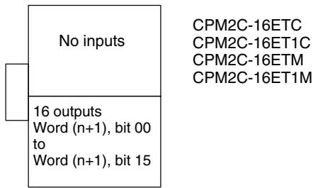
| Bits | 15 | 14 | 13 | 12 | 11 | 10 | 09 | 08 | 07 | 06 | 05 | 04 | 03 | 02 | 01 | 00 | |
| Outputs | n+1 | ||||||||||||||||
Expansion I/O Unit with 10 I/O Points
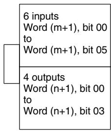
CPM2C-10EDR
| Bits | 15 | 14 | 13 | 12 | 11 | 10 | 09 | 08 | 07 | 06 | 05 | 04 | 03 | 02 | 01 | 00 | |
| Inputs | m+1 | Do not use | |||||||||||||||
| Outputs | n+1 | ||||||||||||||||
Expansion I/O Unit with 20 I/O Points
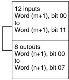
CPM2C-20EDR
| Bits | 15 | 14 | 13 | 12 | 11 | 10 | 09 | 08 | 07 | 06 | 05 | 04 | 03 | 02 | 01 | 00 | |
| Inputs | m+1 | Do not use | |||||||||||||||
| Outputs | n+1 | ||||||||||||||||
Expansion I/O Units with 24 I/O Points
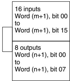
CPM2C-24EDTC
CPM2C-24EDT1C
CPM2C-24EDTM
CPM2C-24EDT1M
| Bits | 15 | 14 | 13 | 12 | 11 | 10 | 09 | 08 | 07 | 06 | 05 | 04 | 03 | 02 | 01 | 00 | |
| Inputs | m+1 | ||||||||||||||||
| Outputs | n+1 | ||||||||||||||||
Expansion I/O Units with 32 I/O Points
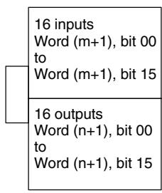
CPM2C-32EDTC
CPM2C-32EDT1C
CPM2C-32EDTM
CPM2C-32EDT1M
| Bits | 15 | 14 | 13 | 12 | 11 | 10 | 09 | 08 | 07 | 06 | 05 | 04 | 03 | 02 | 01 | 00 | |
| Inputs | m+1 | ||||||||||||||||
| Outputs | n+1 | ||||||||||||||||
5-3-3 Expansion Units
| Unit | Model number | I/O | Allocated words | Max. No. of Units | |
| CPM2C | CPM2C-S | ||||
| Analog I/O Unit | CPM2C-MAD11 | Input | 2 inputs: m+1, m+2 | 4 | 3 |
| Output | 1 output: n+1 | ||||
| Temperature Sensor Unit | CPM2C-TS001 | Input | 2 inputs: m+1, m+2 | 4 | 3 |
| CPM2C-TS101 | Output | --- | |||
| CompoBus/S I/O Link Unit | CPM2C-SRT21 | Input | 1 input: m+1 | 5 | 3 |
| Output | 1 output: n+1 | ||||
Note 1. m: "m" denotes the last input word allocated to the CPU Unit, or to the previous Expansion Unit or Expansion I/O Unit if one is already connected.
n: “n” denotes the last output word allocated to the CPU Unit, or to the previous Expansion Unit or Expansion I/O Unit if one is already connected.
- Because the CPM2C-MAD11 Analog I/O Unit and the CPM2C-TS001/101 Temperature Sensor Units require 2 I/O words each, only 4 of these Units can be connected to the PC. (The CPU Unit itself requires one input word and one output word.) A different Unit, such as an Expansion I/O Unit or the CPM2C-SRT21 CompoBus/S I/O Link Unit, can, however, be connected in addition to 4 Analog I/O Units or Temperature Sensor Units.
Analog I/O Unit
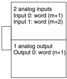
CPM2C-MAD11
Temperature Sensor Units
CPM2C-TS001/TS101
2 temperature inputs
Input 0: word (m + 1) Input 1: word (m + 2)
No outputs
CompoBus/S I/O Link Unit
CPM2C-SRT21
8 inputs Input: word ( + 1)
8 outputs Output: word (n + 1)
Note Input bits 00 to 07 in word ( + 1) are for outputs from the Master. Output bits 00 to 07 in word (n + 1) , are for inputs to the Master.
5-3-4 Examples of Expansion Unit and Expansion I/O Unit Allocation
Up to 5 Expansion Units or Expansion I/O Units can be connected to a CPM2C PC. Input bits and output bits are automatically allocated starting from the CPU Unit and continuing through Expansion Units and Expansion I/O Units in the order in which they are connected. The input area consists of the 10 words from IR 000 to 009, and the output area consists of the 10 words from IR 010 to 019. Although I/O bits are allocated automatically, it is necessary to ensure that both the number of input words and the number of output words do not exceed 10. For example, the Analog I/O Unit and Temperature Sensor Unit require 2 input words and so it is not possible to connect 5 of these Units.
Example: CPU Unit with 20 I/O Points + Expansion I/O Unit with 24 I/O Points
| CPU Unit (20 I/O points) | Expansion I/O Unit (24 I/O points) |
| 12 inputs | 16 inputs |
| IR 00000 | IR 00100 |
| to | to |
| IR 00011 | IR 00115 |
| 8 outputs | 8 outputs |
| IR 01000 | IR 01100 |
| to | to |
| IR 01007 | IR 01107 |
| Bits | 15 | 14 | 13 | 12 | 11 | 10 | 09 | 08 | 07 | 06 | 05 | 04 | 03 | 02 | 01 | 00 | |
| Inputs | IR 000 | Do not use | |||||||||||||||
| IR 001 | |||||||||||||||||
| Outputs | IR 010 | ||||||||||||||||
| IR 011 | |||||||||||||||||
Example: CPU Unit with 32 I/O Points + 5 Expansion I/O Units with 32 I/O Points
| CPU Unit (32 I/O points) | Expansion I/O Unit (32 I/O points) | Expansion I/O Unit (32 I/O points) | Expansion I/O Unit (32 I/O points) | Expansion I/O Unit (32 I/O points) | Expansion I/O Unit (32 I/O points) |
| 16 inputs | 16 inputs | 16 inputs | 16 inputs | 16 inputs | 16 inputs |
| IR 00000 to IR 00007 and IR 00100 to IR 00107 | IR 00200 to IR 00215 | IR 00300 to IR 00315 | IR 00400 to IR 00415 | IR 00500 to IR 00515 | IR 00600 to IR 00615 |
| 16 outputs | 16 outputs | 16 outputs | 16 outputs | 16 outputs | 16 outputs |
| IR 01000 to IR 01007 and IR 01100 to IR 01107 | IR 01200 to IR 01215 | IR 01300 to IR 012315 | IR 01400 to IR 01415 | IR 01500 to IR 01515 | IR 01600 to IR 01615 |
| Bits | 15 | 14 | 13 | 12 | 11 | 10 | 09 | 08 | 07 | 06 | 05 | 04 | 03 | 02 | 01 | 00 | |
| Inputs | IR 000 | Do not use | |||||||||||||||
| IR 001 | |||||||||||||||||
| IR 002 | |||||||||||||||||
| IR 003 | |||||||||||||||||
| IR 004 | |||||||||||||||||
| IR 005 | |||||||||||||||||
| IR 006 | |||||||||||||||||
| Outputs | IR 010 | ||||||||||||||||
| IR 011 | |||||||||||||||||
| IR 012 | |||||||||||||||||
| IR 013 | |||||||||||||||||
| IR 014 | |||||||||||||||||
| IR 015 | |||||||||||||||||
| IR 016 | |||||||||||||||||
Example: Configuration Including Expansion I/O Units and a CompoBus/S I/O Link Unit
| CPU Unit (20 I/O points) | Expansion I/O Unit (16 input points) | Expansion I/O Unit (16 input points) | Expansion I/O Unit (16 output points) | Expansion I/O Unit (16 output points) | CompoBus/S I/O Link Unit |
| 12 inputs | 16 inputs | 16 inputs | No inputs | No inputs | 8 inputs |
| IR 00000 to | IR 00100 to | IR 00200 to | IR 00300 to | ||
| IR 00011 | IR 00115 | IR 00215 | IR 00307 | ||
| 8 outputs | No outputs | No outputs | 16 outputs | 16 outputs | 8 outputs |
| IR 01000 to | IR 01100 to | IR 01200 to | IR 01300 to | ||
| IR 01007 | to | IR 01215 | IR 01307 |
| Bits | 15 | 14 | 13 | 12 | 11 | 10 | 09 | 08 | 07 | 06 | 05 | 04 | 03 | 02 | 01 | 00 | |
| Inputs | IR 000 | Do not use | |||||||||||||||
| IR 001 | |||||||||||||||||
| IR 002 | |||||||||||||||||
| IR 003 | Do not use | ||||||||||||||||
| Outputs | IR 010 | ||||||||||||||||
| IR 011 | |||||||||||||||||
| IR 012 | |||||||||||||||||
| IR 013 | |||||||||||||||||
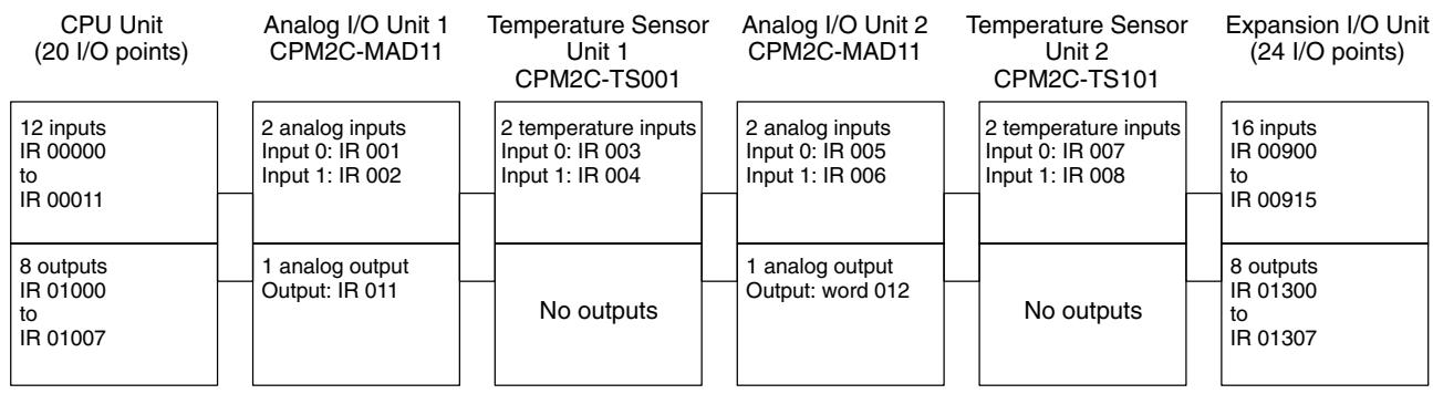
Example: Configuration Including Analog I/O Units, Temperature Sensor Units, and Expansion I/O Unit
| Bits | 15 | 14 | 13 | 12 | 11 | 10 | 09 | 08 | 07 | 06 | 05 | 04 | 03 | 02 | 01 | 00 | |
| Inputs | IR 000 | Do not use | |||||||||||||||
| IR 001 | Used for input 0 of Analog I/O Unit 1 | ||||||||||||||||
| IR 002 | Used for input 1 of Analog I/O Unit 1 | ||||||||||||||||
| IR 003 | Used for input 0 of Temperature Sensor Unit 1 | ||||||||||||||||
| IR 004 | Used for input 1 of Temperature Sensor Unit 1 | ||||||||||||||||
| IR 005 | Used for input 0 of Analog I/O Unit 2 | ||||||||||||||||
| IR 006 | Used for input 1 of Analog I/O Unit 2 | ||||||||||||||||
| IR 007 | Used for input 0 of Temperature Sensor Unit 2 | ||||||||||||||||
| IR 008 | Used for input 1 of Temperature Sensor Unit 2 | ||||||||||||||||
| IR 009 | |||||||||||||||||
| Outputs | IR 010 | ||||||||||||||||
| IR 011 | Used for the output of Analog I/O Unit 1 | ||||||||||||||||
| IR 012 | Used for the output of Analog I/O Unit 2 | ||||||||||||||||
| IR 013 | |||||||||||||||||
This section explains the basic steps and concepts involved in writing a basic ladder diagram program. It introduces the instructions that are used to build the basic structure of the ladder diagram and control its execution. The entire set of instructions used in programming is described in Section 7 Instruction Set.
6-1 Basic Procedure 334
6-2 Instruction Terminology 334
6-3 Basic Ladder Diagrams 335
6-3-1 Basic Terms 335
6-3-2 Mnemonic Code 336
6-3-3 Ladder Instructions 337
6-3-4 OUTPUT and OUTPUT NOT 340
6-3-5 The END Instruction 341
6-3-6 Logic Block Instructions 341
6-3-7 Coding Multiple Right-hand Instructions 349
6-3-8 Branching Instruction Lines 349
6-3-9 Jumps 353
6-4 Controlling Bit Status 354
6-4-1 SET and RESET 354
6-4-2 DIFFERENTIATE UP and DIFFERENTIATE DOWN 355
6-4-3 KEEP 355
6-4-4 Self-maintainingBits (Seal) 356
6-5 Work Bits (Internal Relays) 356
6-6 Programming Precautions 358
6-7 Program Execution 360
6-1 Basic Procedure
There are several basic steps involved in writing a program. Sheets that can be copied to aid in programming are provided in Appendix D I/O Assignment Sheet and Appendix E Program Coding Sheet.
1, 2, 3... 1. Obtain a list of all I/O devices and the I/O points that have been assigned to them and prepare a table that shows the I/O bit allocated to each I/O device.
2. If you are using LR bits to link two PCs, prepare sheet showing the used of these bits.
3. Determine what words are available for work bits and prepare a table in which you can allocate these as you use them.
4. Also prepare tables of TC numbers and jump numbers so that you can allocate these as you use them. Remember, the function of a TC number can be defined only once within the program; jump numbers 01 through 99 can be used only once each. (TC number are described in 7-15 Timer and Counter Instructions; jump numbers are described later in this section.)
5. Draw the ladder diagram.
6. Input the program into the CPU Unit. When using the Programming Console, this will involve converting the program to mnemonic form.
7. Check the program for syntax errors and correct these.
8. Execute the program to check for execution errors and correct these.
9. After the entire Control System has been installed and is ready for use, execute the program and fine tune it if required.
The basics of ladder-diagram programming and conversion to mnemonic code are described in 6-3 Basic Ladder Diagrams. Preparing for and inputting the program via the Programming Console are described in the CPM1 Operation Manual, the CPM1A Operation Manual, the CPM2A Operation Manual, the CPM2C Operation Manual, and the SRM1 Master Control Units Manual and via the SSS in the SSS Operation Manual: C-series PCs.
The rest of Section 6 covers more advanced programming, programming precautions, and program execution. All special application instructions are covered in Section 7 Instruction Set. Debugging is described in the CPM1 Operation Manual, the CPM1A Operation Manual, the CPM2A Operation Manual, the CPM2C Operation Manual, the SRM1 Master Control Units Manual, and SSS Operation Manual: C-series PCs. Section 9 Troubleshooting also provides information required for debugging.
6-2 Instruction Terminology
There are basically two types of instructions used in ladder-diagram programming: instructions that correspond to the conditions on the ladder diagram and are used in instruction form only when converting a program to mnemonic code and instructions that are used on the right side of the ladder diagram and are executed according to the conditions on the instruction lines leading to them.
Most instructions have at least one or more operands associated with them. Operands indicate or provide the data on which an instruction is to be performed. These are sometimes input as the actual numeric values, but are usually the addresses of data area words or bits that contain the data to be used. For instance, a MOVE instruction that has IR 000 designated as the source operand will move the contents of IR 000 to some other location. The other location is also designated as an operand. A bit whose address is designated as an operand is called an operand bit; a word whose address is designated as an operand is called an operand word. If the actual value is entered as a constant, it is preceded by # to indicate that it is not an address.
Other terms used in describing instructions are introduced in Section 7 Instruction Set.
6-3 Basic Ladder Diagrams
A ladder diagram consists of one line running down the left side with lines branching off to the right. The line on the left is called the bus bar; the branching lines, instruction lines or rungs. Along the instruction lines are placed conditions that lead to other instructions on the right side. The logical combinations of these conditions determine when and how the instructions at the right are executed. A ladder diagram is shown below.

As shown in the diagram above, instruction lines can branch apart and they can join back together. The vertical pairs of lines are called conditions. Conditions without diagonal lines through them are called normally open conditions and correspond to a LOAD, AND, or OR instruction. The conditions with diagonal lines through them are called normally closed conditions and correspond to a LOAD NOT, AND NOT, or OR NOT instruction. The number above each condition indicates the operand bit for the instruction. It is the status of the bit associated with each condition that determines the execution condition for following instructions. The way the operation of each of the instructions corresponds to a condition is described below. Before we consider these, however, there are some basic terms that must be explained.
Note When displaying ladder diagrams with the SSS, a second bus bar will be shown on the right side of the ladder diagram and will be connected to all instructions on the right side. This does not change the ladder-diagram program in any functional sense. No conditions can be placed between the instructions on the right side and the right bus bar, i.e., all instructions on the right must be connected directly to the right bus bar. Refer to the SSS Operation Manual: C-series PCs for details.
6-3-1 Basic Terms
Normally Open and Normally Closed Conditions
Each condition in a ladder diagram is either ON or OFF depending on the status of the operand bit that has been assigned to it. A normally open condition is ON if the operand bit is ON; OFF if the operand bit is OFF. A normally closed condition is ON if the operand bit is OFF; OFF if the operand bit is ON. Generally speaking, you use a normally open condition when you want something to happen when a
bit is ON, and a normally closed condition when you want something to happen when a bit is OFF.
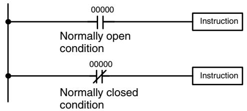
Instruction is executed when IR bit 00000 is ON.
Instruction is executed when IR bit 00000 is OFF.
Execution Conditions
In ladder diagram programming, the logical combination of ON and OFF conditions before an instruction determines the compound condition under which the instruction is executed. This condition, which is either ON or OFF, is called the execution condition for the instruction. All instructions other than LOAD instructions have execution conditions.
Operand Bits
The operands designated for any of the ladder instructions can be any bit in the IR, SR, HR, AR, LR, or TC areas. This means that the conditions in a ladder diagram can be determined by I/O bits, flags, work bits, timers/counters, etc. LOAD and OUTPUT instructions can also use TR area bits, but they do so only in special applications. Refer to 6-3-8 Branching Instruction Lines for details.
Logic Blocks
The way that conditions correspond to what instructions is determined by the relationship between the conditions within the instruction lines that connect them. Any group of conditions that go together to create a logic result is called a logic block. Although ladder diagrams can be written without actually analyzing individual logic blocks, understanding logic blocks is necessary for efficient programming and is essential when programs are to be input in mnemonic code.
Instruction Block
An instruction block consists of all the instructions that are interconnected across the ladder diagram. One instruction block thus consists of all the instructions between where you can draw a horizontal line across the ladder diagram without intersecting any vertical lines and the next place where you can draw the same type of horizontal line.
6-3-2 Mnemonic Code
The ladder diagram cannot be directly input into the PC via a Programming Console; the SSS is required. To input from a Programming Console, it is necessary to convert the ladder diagram to mnemonic code. The mnemonic code provides exactly the same information as the ladder diagram, but in a form that can be typed directly into the PC. Actually you can program directly in mnemonic code, although it in not recommended for beginners or for complex programs. Also, regardless of the Programming Device used, the program is stored in memory in mnemonic form, making it important to understand mnemonic code.
Because of the importance of the Programming Console as a Programming Device and because of the importance of mnemonic code in complete understanding of a program, we will introduce and describe the mnemonic code along with the ladder diagram. Remember, you will not need to use the mnemonic code if you are inputting via the SSS (although you can use it with the SSS if you prefer).
Program Memory Structure
The program is input into addresses in Program Memory. Addresses in Program Memory are slightly different to those in other memory areas because each address does not necessarily hold the same amount of data. Rather, each address holds one instruction and all of the definers and operands (described in more
detail later) required for that instruction. Because some instructions require no operands, while others require up to three operands, Program Memory addresses can be from one to four words long.
Program Memory addresses start at 00000 and run until the capacity of Program Memory has been exhausted. The first word at each address defines the instruction. Any definers used by the instruction are also contained in the first word. Also, if an instruction requires only a single bit operand (with no definer), the bit operand is also programmed on the same line as the instruction. The rest of the words required by an instruction contain the operands that specify what data is to be used. When converting to mnemonic code, all but ladder diagram instructions are written in the same form, one word to a line, just as they appear in the ladder diagram symbols. An example of mnemonic code is shown below. The instructions used in it are described later in the manual.
| Address | Instruction | Operands | |
| 00000 | LD | HR | 0001 |
| 00001 | AND | 00001 | |
| 00002 | OR | 00002 | |
| 00003 | LD NOT | 00100 | |
| 00004 | OR | 00101 | |
| 00005 | AND LD | ||
| 00006 | MOV(21) | ||
| 000 | |||
| DM | 0000 | ||
| 00007 | CMP(20) | ||
| DM | 0000 | ||
| HR | 00 | ||
| 00008 | AND | 25505 | |
| 00009 | OUT | 20000 | |
| 00010 | MOV(21) | ||
| DM | 0000 | ||
| DM | 0500 | ||
| 00011 | LD | 00502 | |
| 00012 | AND | 00005 | |
| 00013 | OUT | 20001 | |
The address and instruction columns of the mnemonic code table are filled in for the instruction word only. For all other lines, the left two columns are left blank. If the instruction requires no definer or bit operand, the operand column is left blank for first line. It is a good idea to cross through any blank data column spaces (for all instruction words that do not require data) so that the data column can be quickly scanned to see if any addresses have been left out.
When programming, addresses are automatically displayed and do not have to be input unless for some reason a different location is desired for the instruction. When converting to mnemonic code, it is best to start at Program Memory address 00000 unless there is a specific reason for starting elsewhere.
6-3-3 Ladder Instructions
The ladder instructions are those instructions that correspond to the conditions on the ladder diagram. Ladder instructions, either independently or in combination with the logic block instructions described next, form the execution conditions upon which the execution of all other instructions are based.
LOAD and LOAD NOT
The first condition that starts any logic block within a ladder diagram corresponds to a LOAD or LOAD NOT instruction. Each of these instruction requires one line of mnemonic code. "Instruction" is used as a dummy instruction in the following examples and could be any of the right-hand instructions described later in this manual.

| Address | Instruction | Operands |
| 00000 | LD | 00000 |
| 00001 | Instruction | |
| 00002 | LD NOT | 00000 |
| 00003 | Instruction |
When this is the only condition on the instruction line, the execution condition for the instruction at the right is ON when the condition is ON. For the LOAD instruction (i.e., a normally open condition), the execution condition would be ON when IR 00000 was ON; for the LOAD NOT instruction (i.e., a normally closed condition), it would be ON when 00000 was OFF.
AND and AND NOT
When two or more conditions lie in series on the same instruction line, the first one corresponds to a LOAD or LOAD NOT instruction; and the rest of the conditions, to AND or AND NOT instructions. The following example shows three conditions which correspond in order from the left to a LOAD, an AND NOT, and an AND instruction. Again, each of these instructions requires one line of mnemonic code.

| Address | Instruction | Operands |
| 00000 | LD | 00000 |
| 00001 | AND NOT | 00100 |
| 00002 | AND | LR 0000 |
| 00003 | Instruction |
The instruction would have an ON execution condition only when all three conditions are ON, i.e., when IR 00000 was ON, IR 00100 was OFF, and LR 0000 was ON.
AND instructions in series can be considered individually, with each taking the logical AND of the execution condition (i.e., the total of all conditions up to that point) and the status of the AND instruction's operand bit. If both of these are ON, an ON execution condition will be produced for the next instruction. If either is OFF, the result will also be OFF. The execution condition for the first AND instruction in a series is the first condition on the instruction line.
Each AND NOT instruction in a series would take the logical AND between its execution condition and the inverse of its operand bit.
OR and OR NOT
When two or more conditions lie on separate instruction lines running in parallel and then joining together, the first condition corresponds to a LOAD or LOAD NOT instruction; the rest of the conditions correspond to OR or OR NOT instructions. The following example shows three conditions which correspond in order from the top to a LOAD NOT, an OR NOT, and an OR instruction. Again, each of these instructions requires one line of mnemonic code.
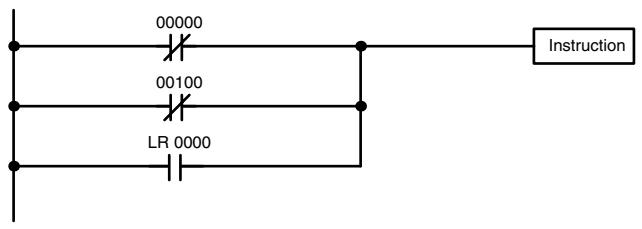
| Address | Instruction | Operands |
| 00000 | LD NOT | 00000 |
| 00001 | OR NOT | 00100 |
| 00002 | OR | LR 0000 |
| 00003 | Instruction |
The instruction would have an ON execution condition when any one of the three conditions was ON, i.e., when IR 00000 was OFF, when IR 00100 was OFF, or when LR 0000 was ON.
OR and OR NOT instructions can be considered individually, each taking the logical OR between its execution condition and the status of the OR instruction's operand bit. If either one of these were ON, an ON execution condition would be produced for the next instruction.
Combining AND and OR Instructions
When AND and OR instructions are combined in more complicated diagrams, they can sometimes be considered individually, with each instruction performing a logic operation on the execution condition and the status of the operand bit. The following is one example. Study this example until you are convinced that the mnemonic code follows the same logic flow as the ladder diagram.
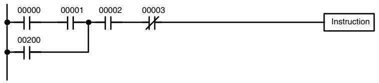
| Address | Instruction | Operands |
| 00000 | LD | 00000 |
| 00001 | AND | 00001 |
| 00002 | OR | 00200 |
| 00003 | AND | 00002 |
| 00004 | AND NOT | 00003 |
| 00005 | Instruction |
Here, an AND is taken between the status of IR 00000 and that of IR 00001 to determine the execution condition for an OR with the status of IR 00200. The result of this operation determines the execution condition for an AND with the status of IR 00002, which in turn determines the execution condition for an AND with the inverse (i.e., and AND NOT) of the status of IR 00003.
In more complicated diagrams, however, it is necessary to consider logic blocks before an execution condition can be determined for the final instruction, and that's where AND LOAD and OR LOAD instructions are used. Before we consider more complicated diagrams, however, we'll look at the instructions required to complete a simple "input-output" program.
6-3-4 OUTPUT and OUTPUT NOT
The simplest way to output the results of combining execution conditions is to output it directly with the OUTPUT and OUTPUT NOT. These instructions are used to control the status of the designated operand bit according to the execution condition. With the OUTPUT instruction, the operand bit will be turned ON as long as the execution condition is ON and will be turned OFF as long as the execution condition is OFF. With the OUTPUT NOT instruction, the operand bit will be turned ON as long as the execution condition is OFF and turned OFF as long as the execution condition is ON. These appear as shown below. In mnemonic code, each of these instructions requires one line.
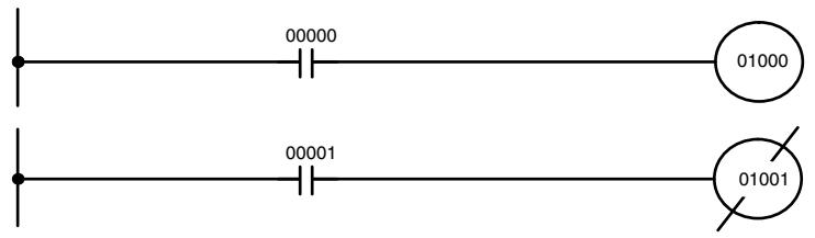
| Address | Instruction | Operands |
| 00000 | LD | 00000 |
| 00001 | OUT | 01000 |
| Address | Instruction | Operands |
| 00000 | LD | 00001 |
| 00001 | OUT NOT | 01001 |
In the above examples, IR 01000 will be ON as long as IR 00000 is ON and IR 01001 will be OFF as long as IR 00001 is ON. Here, IR 00000 and IR 00001 would be input bits and IR 01000 and IR 01001 output bits assigned to the Units controlled by the PC, i.e., the signals coming in through the input points assigned IR 00000 and IR 00001 are controlling the output points assigned IR 01000 and IR 01001, respectively.
The length of time that a bit is ON or OFF can be controlled by combining the OUTPUT or OUTPUT NOT instruction with Timer instructions. Refer to Examples under 7-15-1 Timer - TIM for details.
6-3-5 The END Instruction
The last instruction required to complete a simple program is the END instruction. When the CPU Unit scans the program, it executes all instructions up to the first END instruction before returning to the beginning of the program and beginning execution again. Although an END instruction can be placed at any point in a program, which is sometimes done when debugging, no instructions past the first END instruction will be executed until it is removed. The number following the END instruction in the mnemonic code is its function code, which is used when inputted most instruction into the PC. These are described later. The END instruction requires no operands and no conditions can be placed on the same instruction line with it.

If there is no END instruction anywhere in the program, the program will not be executed at all.
Now you have all of the instructions required to write simple input-output programs. Before we finish with ladder diagram basic and go onto inputting the program into the PC, let's look at logic block instruction (AND LOAD and ORLOAD), which are sometimes necessary even with simple diagrams.
6-3-6 Logic Block Instructions
Logic block instructions do not correspond to specific conditions on the ladder diagram; rather, they describe relationships between logic blocks. The AND LOAD instruction logically ANDs the execution conditions produced by two logic blocks. The OR LOAD instruction logically ORs the execution conditions produced by two logic blocks.
AND LOAD
Although simple in appearance, the diagram below requires an AND LOAD instruction.
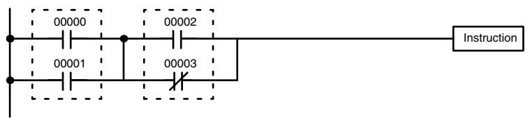
| Address | Instruction | Operands |
| 00000 | LD | 00000 |
| 00001 | OR | 00001 |
| 00002 | LD | 00002 |
| 00003 | OR NOT | 00003 |
| 00004 | AND LD | --- |
The two logic blocks are indicated by dotted lines. Studying this example shows that an ON execution condition will be produced when: either of the conditions in the left logic block is ON (i.e., when either IR 00000 or IR 00001 is ON), and when either of the conditions in the right logic block is ON (i.e., when either IR 00002 is ON or IR 00003 is OFF).
The above ladder diagram cannot, however, be converted to mnemonic code using AND and OR instructions alone. If an AND between IR 00002 and the results of an OR between IR 00000 and IR 00001 is attempted, the OR NOT between IR 00002 and IR 00003 is lost and the OR NOT ends up being an OR NOT between just IR 00003 and the result of an AND between IR 00002 and the first OR. What we need is a way to do the OR (NOT)'s independently and then combine the results.
To do this, we can use the LOAD or LOAD NOT instruction in the middle of an instruction line. When LOAD or LOAD NOT is executed in this way, the current execution condition is saved in special buffers and the logic process is begun over. To combine the results of the current execution condition with that of a previous "unused" execution condition, an AND LOAD or an OR LOAD instruction is used. Here "LOAD" refers to loading the last unused execution condition. An unused execution condition is produced by using the LOAD or LOAD NOT instruction for any but the first condition on an instruction line.
Analyzing the above ladder diagram in terms of mnemonic instructions, the condition for IR 00000 is a LOAD instruction and the condition below it is an OR instruction between the status of IR 00000 and that of IR 00001. The condition at IR 00002 is another LOAD instruction and the condition below is an OR NOT instruction, i.e., an OR between the status of IR 00002 and the inverse of the status of IR 00003. To arrive at the execution condition for the instruction at the right, the logical AND of the execution conditions resulting from these two blocks would have to be taken. AND LOAD does this. The mnemonic code for the ladder diagram is shown below. The AND LOAD instruction requires no operands of its own, because it operates on previously determined execution conditions. Here too, dashes are used to indicate that no operands need designated or input.
OR LOAD
The following diagram requires an OR LOAD instruction between the top logic block and the bottom logic block. An ON execution condition would be produced for the instruction at the right either when IR 00000 is ON and IR 00001 is OFF or when IR 00002 and IR 00003 are both ON. The operation of and mnemonic code for the OR LOAD instruction is exactly the same as those for a AND LOAD instruction except that the current execution condition is ORed with the last unused execution condition.
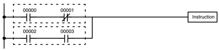
| Address | Instruction | Operands |
| 00000 | LD | 00000 |
| 00001 | AND NOT | 00001 |
| 00002 | LD | 00002 |
| 00003 | AND | 00003 |
| 00004 | OR LD | --- |
Naturally, some diagrams will require both AND LOAD and OR LOAD instructions.
Logic Block Instructions in Series
To code diagrams with logic block instructions in series, the diagram must be divided into logic blocks. Each block is coded using a LOAD instruction to code the first condition, and then AND LOAD or OR LOAD is used to logically combine the blocks. With both AND LOAD and OR LOAD there are two ways to achieve this. One is to code the logic block instruction after the first two blocks and then after each additional block. The other is to code all of the blocks to be combined, starting each block with LOAD or LOAD NOT, and then to code the logic block instructions which combine them. In this case, the instructions for the last pair of blocks should be combined first, and then each preceding block should be combined, working progressively back to the first block. Although either of these methods will produce exactly the same result, the second method, that of coding all logic block instructions together, can be used only if eight or fewer blocks are being combined, i.e., if seven or fewer logic block instructions are required.
The following diagram requires AND LOAD to be converted to mnemonic code because three pairs of parallel conditions lie in series. The two means of coding the programs are also shown.
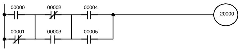
| Address | Instruction | Operands |
| 00000 | LD | 00000 |
| 00001 | OR NOT | 00001 |
| 00002 | LD NOT | 00002 |
| 00003 | OR | 00003 |
| 00004 | AND LD | — |
| 00005 | LD | 00004 |
| 00006 | OR | 00005 |
| 00007 | AND LD | — |
| 00008 | OUT | 20000 |
| Address | Instruction | Operands |
| 00000 | LD | 00000 |
| 00001 | OR NOT | 00001 |
| 00002 | LD NOT | 00002 |
| 00003 | OR | 00003 |
| 00004 | LD | 00004 |
| 00005 | OR | 00005 |
| 00006 | AND LD | — |
| 00007 | AND LD | — |
| 00008 | OUT | 20000 |
Again, with the method on the right, a maximum of eight blocks can be combined. There is no limit to the number of blocks that can be combined with the first method.
The following diagram requires OR LOAD instructions to be converted to mnemonic code because three pairs of conditions in series lie in parallel to each other.
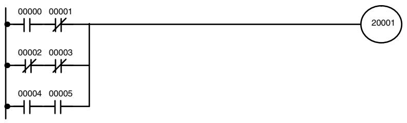
The first of each pair of conditions is converted to LOAD with the assigned bit operand and then ANDed with the other condition. The first two blocks can be coded first, followed by OR LOAD, the last block, and another OR LOAD, or the three blocks can be coded first followed by two OR LOADs. The mnemonic code for both methods is shown below.
| Address | Instruction | Operands |
| 00000 | LD | 00000 |
| 00001 | AND NOT | 00001 |
| 00002 | LD NOT | 00002 |
| 00003 | AND NOT | 00003 |
| 00004 | OR LD | — |
| 00005 | LD | 00004 |
| 00006 | AND | 00005 |
| 00007 | OR LD | — |
| 00008 | OUT | 20001 |
| Address | Instruction | Operands |
| 00000 | LD | 00000 |
| 00001 | AND NOT | 00001 |
| 00002 | LD NOT | 00002 |
| 00003 | AND NOT | 00003 |
| 00004 | LD | 00004 |
| 00005 | AND | 00005 |
| 00006 | OR LD | — |
| 00007 | OR LD | — |
| 00008 | OUT | 20001 |
Again, with the method on the right, a maximum of eight blocks can be combined. There is no limit to the number of blocks that can be combined with the first method.
Combining AND LOAD and OR LOAD
Both of the coding methods described above can also be used when using AND LOAD and OR LOAD, as long as the number of blocks being combined does not exceed eight.
The following diagram contains only two logic blocks as shown. It is not necessary to further separate block b components, because it can coded directly using only AND and OR.
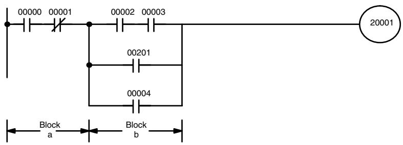
| Address | Instruction | Operands |
| 00000 | LD | 00000 |
| 00001 | AND NOT | 00001 |
| 00002 | LD | 00002 |
| 00003 | AND | 00003 |
| 00004 | OR | 00201 |
| 00005 | OR | 00004 |
| 00006 | AND LD | — |
| 00007 | OUT | 20001 |
Although the following diagram is similar to the one above, block b in the diagram below cannot be coded without separating it into two blocks combined with OR LOAD. In this example, the three blocks have been coded first and then OR LOAD has been used to combine the last two blocks followed by AND LOAD to combine the execution condition produced by the OR LOAD with the execution condition of block a.
When coding the logic block instructions together at the end of the logic blocks they are combining, they must, as shown below, be coded in reverse order, i.e., the logic block instruction for the last two blocks is coded first, followed by the one to combine the execution condition resulting from the first logic block instruction and the execution condition of the logic block third from the end, and on back to the first logic block that is being combined.
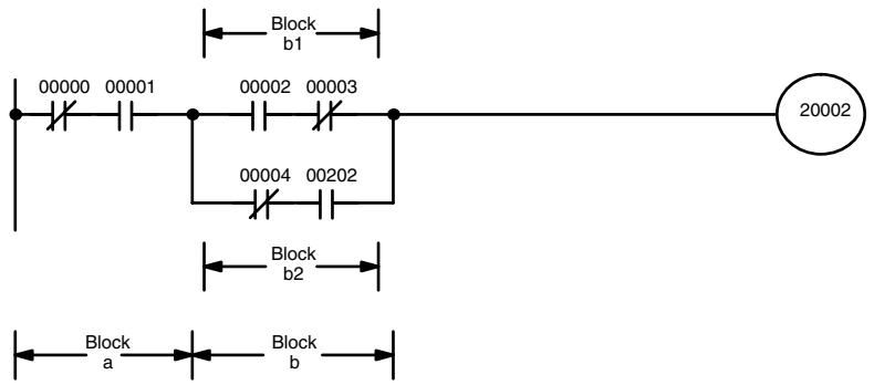
| Address | Instruction | Operands |
| 00000 | LD NOT | 00000 |
| 00001 | AND | 00001 |
| 00002 | LD | 00002 |
| 00003 | AND NOT | 00003 |
| 00004 | LD NOT | 00004 |
| 00005 | AND | 00202 |
| 00006 | OR LD | — |
| 00007 | AND LD | — |
| 00008 | OUT | 20002 |
Complicated Diagrams
When determining what logic block instructions will be required to code a diagram, it is sometimes necessary to break the diagram into large blocks and then continue breaking the large blocks down until logic blocks that can be coded without logic block instructions have been formed. These blocks are then coded, combining the small blocks first, and then combining the larger blocks. Either AND LOAD or OR LOAD is used to combine the blocks, i.e., AND LOAD or OR LOAD always combines the last two execution conditions that existed, regardless of whether the execution conditions resulted from a single condition, from logic blocks, or from previous logic block instructions.
When working with complicated diagrams, blocks will ultimately be coded starting at the top left and moving down before moving across. This will generally mean that, when there might be a choice, OR LOAD will be coded before AND LOAD.
The following diagram must be broken down into two blocks and each of these then broken into two blocks before it can be coded. As shown below, blocks a and b require an AND LOAD. Before AND LOAD can be used, however, OR LOAD must be used to combine the top and bottom blocks on both sides, i.e., to combine a1 and a2; b1 and b2.
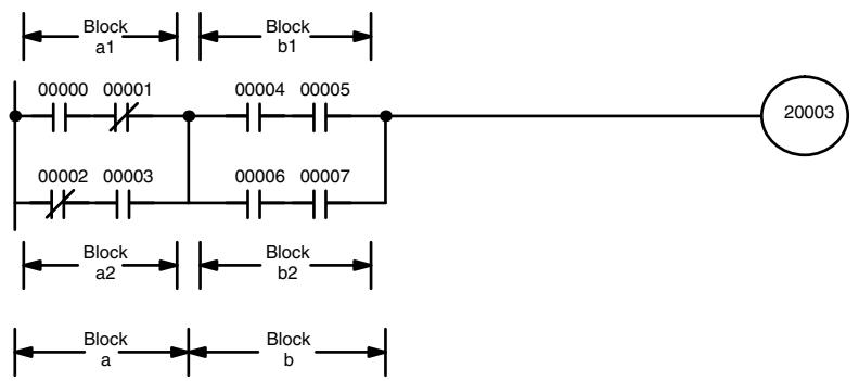
| Address | Instruction | Operands |
| 00000 | LD | 00000 |
| 00001 | AND NOT | 00001 |
| 00002 | LD NOT | 00002 |
| 00003 | AND | 00003 |
| 00004 | OR LD | — |
| 00005 | LD | 00004 |
| 00006 | AND | 00005 |
| 00007 | LD | 00006 |
| 00008 | AND | 00007 |
| 00009 | OR LD | — |
| 00010 | AND LD | — |
| 00011 | OUT | 20003 |
Blocks a1 and a2
Blocks b1 and b2
Blocks a and b
The following type of diagram can be coded easily if each block is coded in order: first top to bottom and then left to right. In the following diagram, blocks a and b would be combined using AND LOAD as shown above, and then block c would be coded and a second AND LOAD would be used to combine it with the execution condition from the first AND LOAD. Then block d would be coded, a third AND LOAD would be used to combine the execution condition from block d with the execution condition from the second AND LOAD, and so on through to block n.
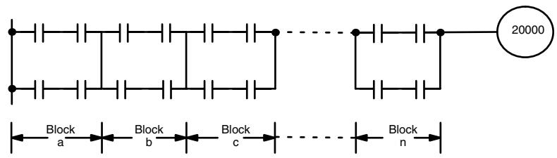
The following diagram requires an OR LOAD followed by an AND LOAD to code the top of the three blocks, and then two more OR LOADs to complete the mnemonic code.
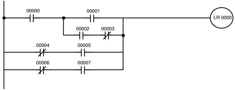
| Address | Instruction | Operands |
| 00000 | LD | 00000 |
| 00001 | LD | 00001 |
| 00002 | LD | 00002 |
| 00003 | AND NOT | 00003 |
| 00004 | OR LD | -- |
| 00005 | AND LD | -- |
| 00006 | LD NOT | 00004 |
| 00007 | AND | 00005 |
| 00008 | OR LD | -- |
| 00009 | LD NOT | 00006 |
| 00010 | AND | 00007 |
| 00011 | OR LD | -- |
| 00012 | OUT | LR 0000 |
Although the program will execute as written, this diagram could be drawn as shown below to eliminate the need for the first OR LOAD and the AND LOAD, simplifying the program and saving memory space.
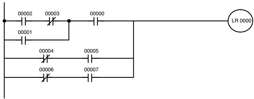
| Address | Instruction | Operands |
| 00000 | LD | 00002 |
| 00001 | AND NOT | 00003 |
| 00002 | OR | 00001 |
| 00003 | AND | 00000 |
| 00004 | LD NOT | 00004 |
| 00005 | AND | 00005 |
| 00006 | OR LD | -- |
| 00007 | LD NOT | 00006 |
| 00008 | AND | 00007 |
| 00009 | OR LD | -- |
| 00010 | OUT | LR 0000 |
The following diagram requires five blocks, which here are coded in order before using OR LOAD and AND LOAD to combine them starting from the last two blocks and working backward. The OR LOAD at program address 00008 combines blocks d and e, the following AND LOAD combines the resulting execution condition with that of block c, etc.
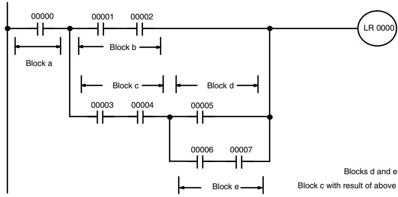
| Address | Instruction | Operands |
| 00000 | LD | 00000 |
| 00001 | LD | 00001 |
| 00002 | AND | 00002 |
| 00003 | LD | 00003 |
| 00004 | AND | 00004 |
| 00005 | LD | 00005 |
| 00006 | LD | 00006 |
| 00007 | AND | 00007 |
| 00008 | OR LD | -- |
| 00009 | AND LD | -- |
| 00010 | OR LD | -- |
| 00011 | AND LD | -- |
| 00012 | OUT | LR 0000 |
Blocks d and e
Block c with result of above
Block b with result of above
Block a with result of above
Again, this diagram can be redrawn as follows to simplify program structure and coding and to save memory space.
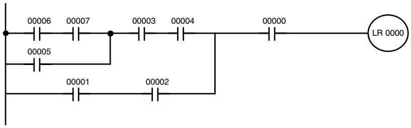
| Address | Instruction | Operands |
| 00000 | LD | 00006 |
| 00001 | AND | 00007 |
| 00002 | OR | 00005 |
| 00003 | AND | 00003 |
| 00004 | AND | 00004 |
| 00005 | LD | 00001 |
| 00006 | AND | 00002 |
| 00007 | OR LD | -- |
| 00008 | AND | 00000 |
| 00009 | OUT | LR 0000 |
The next and final example may at first appear very complicated but can be coded using only two logic block instructions. The diagram appears as follows:
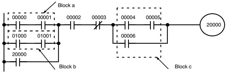
The first logic block instruction is used to combine the execution conditions resulting from blocks a and b, and the second one is to combine the execution condition of block c with the execution condition resulting from the normally closed condition assigned IR 00003. The rest of the diagram can be coded with OR, AND, and AND NOT instructions. The logical flow for this and the resulting code are shown below.
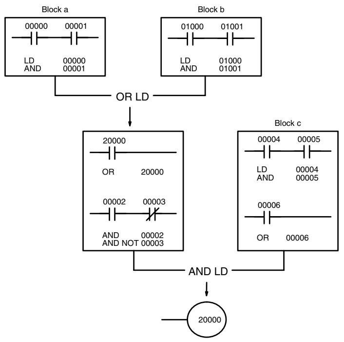
| Address | Instruction | Operands |
| 00000 | LD | 00000 |
| 00001 | AND | 00001 |
| 00002 | LD | 01000 |
| 00003 | AND | 01001 |
| 00004 | OR LD | -- |
| 00005 | OR | 20000 |
| 00006 | AND | 00002 |
| 00007 | AND NOT | 00003 |
| 00008 | LD | 00004 |
| 00009 | AND | 00005 |
| 00010 | OR | 00006 |
| 00011 | AND LD | -- |
| 00012 | OUT | 20000 |
6-3-7 Coding Multiple Right-hand Instructions
If there is more than one right-hand instruction executed with the same execution condition, they are coded consecutively following the last condition on the instruction line. In the following example, the last instruction line contains one more condition that corresponds to an AND with IR 00004.
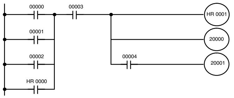
| Address | Instruction | Operands |
| 00000 | LD | 00000 |
| 00001 | OR | 00001 |
| 00002 | OR | 00002 |
| 00003 | OR | HR 0000 |
| 00004 | AND | 00003 |
| 00005 | OUT | HR 0001 |
| 00006 | OUT | 20000 |
| 00007 | AND | 00004 |
| 00008 | OUT | 20001 |
6-3-8 Branching Instruction Lines
When an instruction line branches into two or more lines, it is sometimes necessary to use either interlocks or TR bits to maintain the execution condition that existed at a branching point. This is because instruction lines are executed across to a right-hand instruction before returning to the branching point to execute instructions one a branch line. If a condition exists on any of the instruction lines after the branching point, the execution condition could change during this time making proper execution impossible. The following diagrams illustrate this. In both diagrams, instruction 1 is executed before returning to the branching point and moving on to the branch line leading to instruction 2.
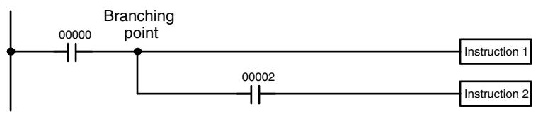
Diagram A: Correct Operation
| Address | Instruction | Operands |
| 00000 | LD | 00000 |
| 00001 | Instruction 1 | |
| 00002 | AND | 00002 |
| 00003 | Instruction 2 |
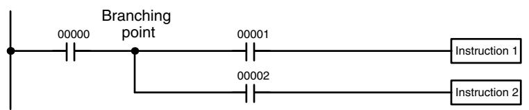
Diagram B: Incorrect Operation
| Address | Instruction | Operands |
| 00000 | LD | 00000 |
| 00001 | AND | 00001 |
| 00002 | Instruction 1 | |
| 00003 | AND | 00002 |
| 00004 | Instruction 2 |
If, as shown in diagram A, the execution condition that existed at the branching point cannot be changed before returning to the branch line (instructions at the far right do not change the execution condition), then the branch line will be executed correctly and no special programming measure is required.
If, as shown in diagram B, a condition exists between the branching point and the last instruction on the top instruction line, the execution condition at the branching point and the execution condition after completing the top instruction line will sometimes be different, making it impossible to ensure correct execution of the branch line.
There are two means of programming branching programs to preserve the execution condition. One is to use TR bits; the other, to use interlocks (IL(02)/IL(03)).
TR Bits
The TR area provides eight bits, TR 0 through TR 7, that can be used to temporarily preserve execution conditions. If a TR bit is placed at a branching point, the current execution condition will be stored at the designated TR bit. When returning to the branching point, the TR bit restores the execution status that was saved when the branching point was first reached in program execution.
The previous diagram B can be written as shown below to ensure correct execution. In mnemonic code, the execution condition is stored at the branching point using the TR bit as the operand of the OUTPUT instruction. This execution condition is then restored after executing the right-hand instruction by using the same TR bit as the operand of a LOAD instruction
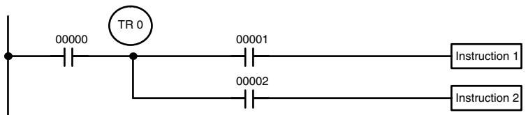
Diagram B: Corrected Using a TR bit
| Address | Instruction | Operands |
| 00000 | LD | 00000 |
| 00001 | OUT | TR 0 |
| 00002 | AND | 00001 |
| 00003 | Instruction 1 | |
| 00004 | LD | TR 0 |
| 00005 | AND | 00002 |
| 00006 | Instruction 2 |
In terms of actual instructions the above diagram would be as follows: The status of IR 00000 is loaded (a LOAD instruction) to establish the initial execution condition. This execution condition is then output using an OUTPUT instruction to TR 0 to store the execution condition at the branching point. The execution condition is then ANDed with the status of IR 00001 and instruction 1 is executed accordingly. The execution condition that was stored at the branching point is then re-loaded (aLOAD instruction with TR 0 as the operand), this is ANDed with the status of IR 00002, and instruction 2 is executed accordingly.
The following example shows an application using two TR bits.
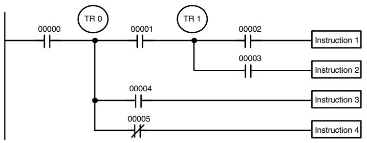
| Address | Instruction | Operands |
| 00000 | LD | 00000 |
| 00001 | OUT | TR 0 |
| 00002 | AND | 00001 |
| 00003 | OUT | TR 1 |
| 00004 | AND | 00002 |
| 00005 | Instruction 1 | |
| 00006 | LD | TR 1 |
| 00007 | AND | 00003 |
| 00008 | Instruction 2 | |
| 00009 | LD | TR 0 |
| 00010 | AND | 00004 |
| 00011 | Instruction 3 | |
| 00012 | LD | TR 0 |
| 00013 | AND NOT | 00005 |
| 00014 | Instruction 4 |
In this example, TR 0 and TR 1 are used to store the execution conditions at the branching points. After executing instruction 1, the execution condition stored in TR 1 is loaded for an AND with the status IR 00003. The execution condition stored in TR 0 is loaded twice, the first time for an AND with the status of IR 00004 and the second time for an AND with the inverse of the status of IR 00005.
TR bits can be used as many times as required as long as the same TR bit is not used more than once in the same instruction block. Here, a new instruction block is begun each time execution returns to the bus bar. If, in a single instruction block, it is necessary to have more than eight branching points that require the execution condition be saved, interlocks (which are described next) must be used.
When drawing a ladder diagram, be careful not to use TR bits unless necessary. Often the number of instructions required for a program can be reduced and ease of understanding a program increased by redrawing a diagram that would otherwise require TR bits. In both of the following pairs of diagrams, the bottom versions require fewer instructions and do not require TR bits. In the first example, this is achieved by reorganizing the parts of the instruction block: the bottom one, by separating the second OUTPUT instruction and using another LOAD instruction to create the proper execution condition for it.
Note Although simplifying programs is always a concern, the order of execution of instructions is sometimes important. For example, a MOVE instruction may be required before the execution of a BINARY ADD instruction to place the proper data in the required operand word. Be sure that you have considered execution order before reorganizing a program to simplify it.
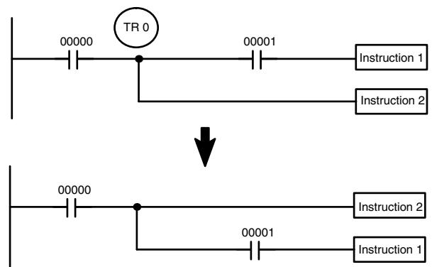
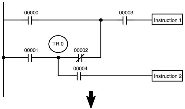
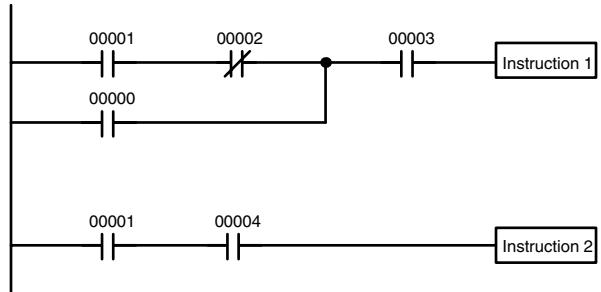
Note TR bits are must be input by the user only when programming using mnemonic code. They are not necessary when inputting ladder diagrams directly because they are processed for you automatically. The above limitations on the number of branching points requiring TR bits, and considerations on methods to reduce the number of programming instructions, still hold.
Interlocks
The problem of storing execution conditions at branching points can also be handled by using the INTERLOCK (IL(02)) and INTERLOCK CLEAR (ILC(03)) instructions to eliminate the branching point completely while allowing a specific execution condition to control a group of instructions. The INTERLOCK and INTERLOCK CLEAR instructions are always used together.
When an INTERLOCK instruction is placed before a section of a ladder program, the execution condition for the INTERLOCK instruction will control the execution of all instruction up to the next INTERLOCK CLEAR instruction. If the execution condition for the INTERLOCK instruction is OFF, all right-hand instructions through the next INTERLOCK CLEAR instruction will be executed with OFF execution conditions to reset the entire section of the ladder diagram. The effect that this has on particular instructions is described in 7-11 INTERLOCK and INTERLOCK CLEAR - IL(02) and ILC(03).
Diagram B can also be corrected with an interlock. Here, the conditions leading up to the branching point are placed on an instruction line for the INTERLOCK instruction, all of lines leading from the branching point are written as separate instruction lines, and another instruction line is added for the INTERLOCK CLEAR instruction. No conditions are allowed on the instruction line for INTERLOCK CLEAR. Note that neither INTERLOCK nor INTERLOCK CLEAR requires an operand.
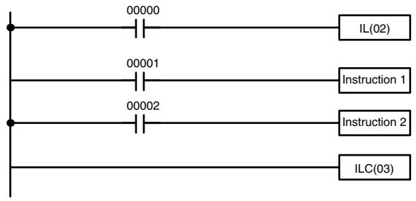
| Address | Instruction | Operands |
| 00000 | LD | 00000 |
| 00001 | IL(02) | --- |
| 00002 | LD | 00001 |
| 00003 | Instruction 1 | |
| 00004 | LD | 00002 |
| 00005 | Instruction 2 | |
| 00006 | ILC(03) | --- |
If IR 00000 is ON in the revised version of diagram B, above, the status of IR 00001 and that of IR 00002 would determine the execution conditions for instructions 1 and 2, respectively. Because IR 00000 is ON, this would produce the same results as ANDing the status of each of these bits. If IR 00000 is OFF, the INTERLOCK instruction would produce an OFF execution condition for instructions 1 and 2 and then execution would continue with the instruction line following the INTERLOCK CLEAR instruction.
As shown in the following diagram, more than one INTERLOCK instruction can be used within one instruction block; each is effective through the next INTERLOCK CLEAR instruction.
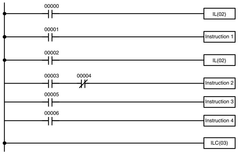
| Address | Instruction | Operands |
| 00000 | LD | 00000 |
| 00001 | IL(02) | --- |
| 00002 | LD | 00001 |
| 00003 | Instruction 1 | |
| 00004 | LD | 00002 |
| 00005 | IL(02) | --- |
| 00006 | LD | 00003 |
| 00007 | AND NOT | 00004 |
| 00008 | Instruction 2 | |
| 00009 | LD | 00005 |
| 00010 | Instruction 3 | |
| 00011 | LD | 00006 |
| 00012 | Instruction 4 | |
| 00013 | ILC(03) | --- |
If IR 00000 in the above diagram is OFF (i.e., if the execution condition for the first INTERLOCK instruction is OFF), instructions 1 through 4 would be executed with OFF execution conditions and execution would move to the instruction following the INTERLOCK CLEAR instruction. If IR 00000 is ON, the status of IR 00001 would be loaded as the execution condition for instruction 1 and then the status of IR 00002 would be loaded to form the execution condition for the second INTERLOCK instruction. If IR 00002 is OFF, instructions 2 through 4 will be executed with OFF execution conditions. If IR 00002 is ON, IR 00003, IR 00005, and IR 00006 will determine the first execution condition in new instruction lines.
6-3-9 Jumps
A specific section of a program can be skipped according to a designated execution condition. Although this is similar to what happens when the execution condition for an INTERLOCK instruction is OFF, with jumps, the operands for all instructions maintain status. Jumps can therefore be used to control devices that require a sustained output, e.g., pneumatics and hydraulics, whereas interlocks can be used to control devices that do not require a sustained output, e.g., electronic instruments.
Jumps are created using the JUMP (JMP(04)) and JUMP END (JME(05)) instructions. If the execution condition for a JUMP instruction is ON, the program is executed normally as if the jump did not exist. If the execution condition for the JUMP instruction is OFF, program execution moves immediately to a JUMP END instruction without changing the status of anything between the JUMP and JUMP END instruction.
All JUMP and JUMP END instructions are assigned jump numbers ranging between 00 and 99. There are two types of jumps. The jump number used determines the type of jump.
A jump can be defined using jump numbers 01 through 99 only once, i.e., each of these numbers can be used once in a JUMP instruction and once in a JUMP END instruction. When a JUMP instruction assigned one of these numbers is executed, execution moves immediately to the JUMP END instruction that has the same number as if all of the instruction between them did not exist. Diagram B from the TR bit and interlock example could be redrawn as shown below using a jump. Although 01 has been used as the jump number, any number between 01 and 99 could be used as long as it has not already been used in a different part of the program. JUMP and JUMP END require no other operand and JUMP END never has conditions on the instruction line leading to it.
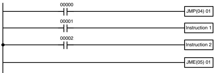
Diagram B: Corrected with a Jump
| Address | Instruction | Operands |
| 00000 | LD | 00000 |
| 00001 | JMP(04) | 01 |
| 00002 | LD | 00001 |
| 00003 | Instruction 1 | |
| 00004 | LD | 00002 |
| 00005 | Instruction 2 | |
| 00006 | JME(05) | 01 |
This version of diagram B would have a shorter execution time when IR 00000 was OFF than any of the other versions.
The other type of jump is created with a jump number of 00. As many jumps as desired can be created using jump number 00 and JUMP instructions using 00 can be used consecutively without a JUMP END using 00 between them. It is even possible for all JUMP 00 instructions to move program execution to the same JUMP END 00, i.e., only one JUMP END 00 instruction is required for all JUMP 00 instruction in the program. When 00 is used as the jump number for a JUMP instruction, program execution moves to the instruction following the next JUMP END instruction with a jump number of 00. Although, as in all jumps, no status is changed and no instructions are executed between the JUMP 00 and JUMP END 00 instructions, the program must search for the next JUMP END 00 instruction, producing a slightly longer execution time.
Execution of programs containing multiple JUMP 00 instructions for one JUMP END 00 instruction is similar to that of interlocked sections. The following diagram is the same as that used for the interlock example above, except redrawn with jumps. The execution of this diagram would differ from that of the diagram described above (e.g., in the previous diagram interlocks would reset certain parts of the interlocked section, however, jumps do not affect the status of any bit between the JUMP and JUMP END instructions).
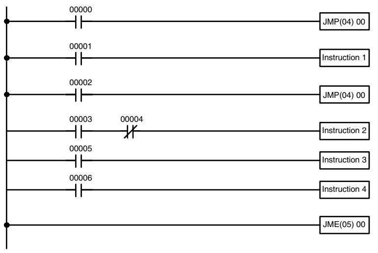
| Address | Instruction | Operands |
| 00000 | LD | 00000 |
| 00001 | JMP(04) | 00 |
| 00002 | LD | 00001 |
| 00003 | Instruction 1 | |
| 00004 | LD | 00002 |
| 00005 | JMP(04) | 00 |
| 00006 | LD | 00003 |
| 00007 | AND NOT | 00004 |
| 00008 | Instruction 2 | |
| 00009 | LD | 00005 |
| 00010 | Instruction 3 | |
| 00011 | LD | 00006 |
| 00012 | Instruction 4 | |
| 00013 | JME(05) | 00 |
6-4 Controlling Bit Status
There are seven basic instructions that can be used generally to control individual bit status. These are the OUTPUT, OUTPUT NOT, SET, RESET, DIFFERENTIATE UP, DIFFERENTIATE DOWN, and KEEP instructions. All of these instructions appear as the last instruction in an instruction line and take a bit address for an operand. Although details are provided in 7-8 Bit Control Instructions, these instructions (except for OUTPUT and OUTPUT NOT, which have already been introduced) are described here because of their importance in most programs. Although these instructions are used to turn ON and OFF output bits in the IR area (i.e., to send or stop output signals to external devices), they are also used to control the status of other bits in the IR area or in other data areas.
6-4-1 SET and RESET
The SET and RESET instructions are very similar to the OUTPUT and OUTPUT NOT instructions except that they only change the status of their operand bits for ON execution conditions. Neither instructions will affect the status of its operand bit when the execution condition is OFF.
SET will turn ON the operand bit when the execution condition goes ON, but unlike the OUTPUT instruction, SET will not turn OFF the operand bit when the execution condition goes OFF. RESET will turn OFF the operand bit when the execution condition goes OFF, but unlike OUTPUT NOT, RESET will not turn ON the operand bit when the execution condition goes OFF.
In the following example, IR 20000 will be turned ON when IR 00100 goes ON and will remain ON until IR 00101 goes ON, regardless of the status of IR 00100. When IR 00101 goes ON, RESET will turn IR 20000 OFF.
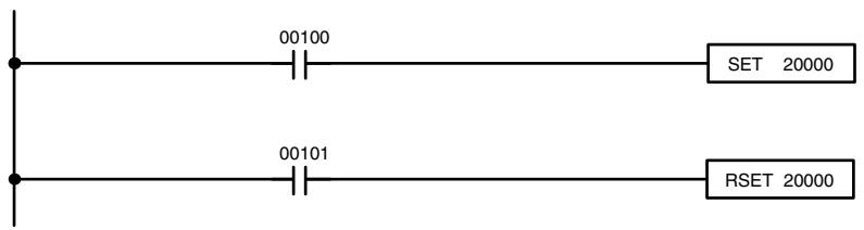
| Address | Instruction | Operands |
| 00000 | LD | 00100 |
| 00001 | SET | 20000 |
| 00002 | LD | 00101 |
| 00003 | RSET | 20000 |
Note SET and RSET do not have function codes. To input them from the Programming Console, press the FUN and SET Keys or FUN and RSET Keys followed by the bit address.
6-4-2 DIFFERENTIATE UP and DIFFERENTIATE DOWN
DIFFERENTIATE UP and DIFFERENTIATE DOWN instructions are used to turn the operand bit ON for one cycle at a time. The DIFFERENTIATE UP instruction turns ON the operand bit for one cycle after the execution condition for it goes from OFF to ON; the DIFFERENTIATE DOWN instruction turns ON the operand bit for one cycle after the execution condition for it goes from ON to OFF. Both of these instructions require only one line of mnemonic code.
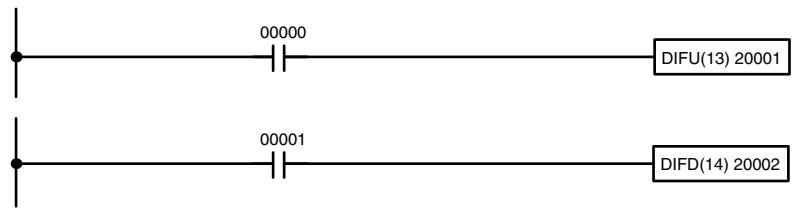
| Address | Instruction | Operands |
| 00000 | LD | 00000 |
| 00001 | DIFU(13) | 20001 |
| Address | Instruction | Operands |
| 00000 | LD | 00001 |
| 00001 | DIFD(14) | 20002 |
Here, IR 20001 will be turned ON for one cycle after IR 00000 goes ON. The next time DIFU(13) 20001 is executed, IR 20001 will be turned OFF, regardless of the status of IR 00000. With the DIFFERENTIATE DOWN instruction, IR 20002 will be turned ON for one cycle after IR 00001 goes OFF (IR 20002 will be kept OFF until then), and will be turned OFF the next time DIFD(14) 20002 is executed.
6-4-3 KEEP
The KEEP instruction is used to maintain the status of the operand bit based on two execution conditions. To do this, the KEEP instruction is connected to two instruction lines. When the execution condition at the end of the first instruction line is ON, the operand bit of the KEEP instruction is turned ON. When the execution condition at the end of the second instruction line is ON, the operand bit of the KEEP instruction is turned OFF. The operand bit for the KEEP instruction will maintain its ON or OFF status even if it is located in an interlocked section of the diagram.
In the following example, HR 0000 will be turned ON when IR 00002 is ON and IR 00003 is OFF. HR 0000 will then remain ON until either IR 00004 or IR 00005 turns ON. With KEEP, as with all instructions requiring more than one instruction line, the instruction lines are coded first before the instruction that they control.
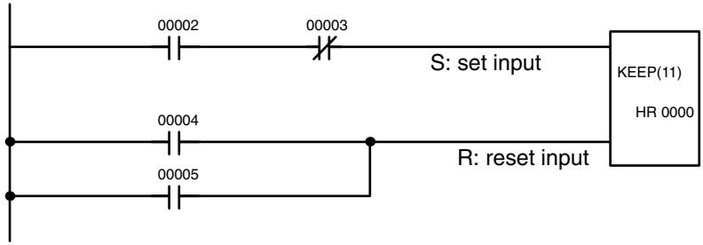
| Address | Instruction | Operands |
| 00000 | LD | 00002 |
| 00001 | AND NOT | 00003 |
| 00002 | LD | 00004 |
| 00003 | OR | 00005 |
| 00004 | KEEP(11) | HR 0000 |
6-4-4 Self-maintaining Bits (Seal)
Although the KEEP instruction can be used to create self-maintaining bits, it is sometimes necessary to create self-maintaining bits in another way so that they can be turned OFF when in an interlocked section of a program.
To create a self-maintaining bit, the operand bit of an OUTPUT instruction is used as a condition for the same OUTPUT instruction in an OR setup so that the operand bit of the OUTPUT instruction will remain ON or OFF until changes occur in other bits. At least one other condition is used just before the OUTPUT instruction to function as a reset. Without this reset, there would be no way to control the operand bit of the OUTPUT instruction.
The above diagram for the KEEP instruction can be rewritten as shown below. The only difference in these diagrams would be their operation in an interlocked program section when the execution condition for the INTERLOCK instruction was ON. Here, just as in the same diagram using the KEEP instruction, two reset bits are used, i.e., HR 0000 can be turned OFF by turning ON either IR 00004 or IR 00005.
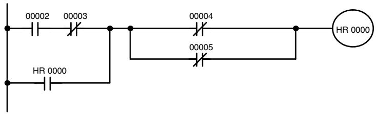
| Address | Instruction | Operands |
| 00000 | LD | 00002 |
| 00001 | AND NOT | 00003 |
| 00002 | OR | HR 0000 |
| 00003 | AND NOT | 00004 |
| 00004 | OR NOT | 00005 |
| 00005 | AND LD | --- |
| 00006 | OUT | HR 0000 |
6-5 Work Bits (Internal Relays)
In programming, combining conditions to directly produce execution conditions is often extremely difficult. These difficulties are easily overcome, however, by using certain bits to trigger other instructions indirectly. Such programming is achieved by using work bits. Sometimes entire words are required for these purposes. These words are referred to as work words.
Work bits are not transferred to or from the PC. They are bits selected by the programmer to facilitate programming as described above. I/O bits and other dedicated bits cannot be used as works bits. All bits in the IR area that are not allocated as I/O bits, and certain unused bits in the AR area, are available for use as work bits. Be careful to keep an accurate record of how and where you use work bits. This helps in program planning and writing, and also aids in debugging operations.
Work Bit Applications
Examples given later in this subsection show two of the most common ways to employ work bits. These should act as a guide to the almost limitless number of ways in which the work bits can be used. Whenever difficulties arise in programming a control action, consideration should be given to work bits and how they might be used to simplify programming.
Work bits are often used with the OUTPUT, OUTPUT NOT, DIFFERENTIATE UP, DIFFERENTIATE DOWN, and KEEP instructions. The work bit is used first as the operand for one of these instructions so that later it can be used as a condition that will determine how other instructions will be executed. Work bits can also be used with other instructions, e.g., with the SHIFT REGISTER instruction (SFT(10)). An example of the use of work words and bits with the SHIFT REGISTER instruction is provided in 7-16-1 SHIFT REGISTER - SFT(10).
Although they are not always specifically referred to as work bits, many of the bits used in the examples in Section 7 Instruction Set use work bits. Understanding the use of these bits is essential to effective programming.
Reducing Complex Conditions
Work bits can be used to simplify programming when a certain combination of conditions is repeatedly used in combination with other conditions. In the following example, IR 00000, IR 00001, IR 00002, and IR 00003 are combined in a logic block that stores the resulting execution condition as the status of IR 21600. IR 21600 is then combined with various other conditions to determine output conditions for IR 20000, IR 20001, and IR 20002, i.e., to turn the outputs allocated to these bits ON or OFF.
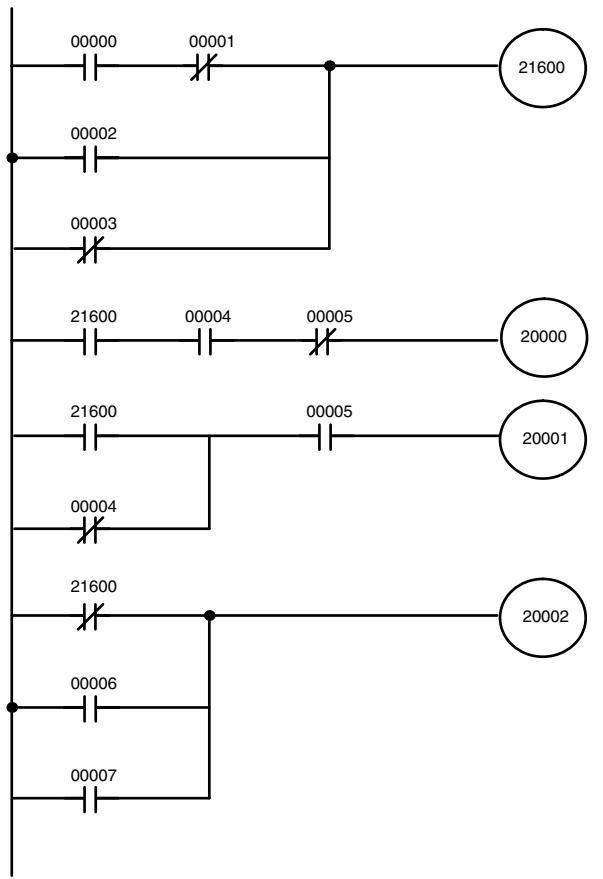
| Address | Instruction | Operands |
| 00000 | LD | 00000 |
| 00001 | AND NOT | 00001 |
| 00002 | OR | 00002 |
| 00003 | OR NOT | 00003 |
| 00004 | OUT | 21600 |
| 00005 | LD | 21600 |
| 00006 | AND | 00004 |
| 00007 | AND NOT | 00005 |
| 00008 | OUT | 20000 |
| 00009 | LD | 21600 |
| 00010 | OR NOT | 00004 |
| 00011 | AND | 00005 |
| 00012 | OUT | 20001 |
| 00013 | LD NOT | 21600 |
| 00014 | OR | 00006 |
| 00015 | OR | 00007 |
| 00016 | OUT | 20002 |
Differentiated Conditions
Work bits can also be used if differential treatment is necessary for some, but not all, of the conditions required for execution of an instruction. In this example, IR 20000 must be left ON continuously as long as IR 001001 is ON and both IR 00002 and IR 00003 are OFF, or as long as IR 00004 is ON and IR 00005 is OFF. It must be turned ON for only one cycle each time IR 00000 turns ON (unless one of the preceding conditions is keeping it ON continuously).
This action is easily programmed by using IR 22500 as a work bit as the operand of the DIFFERENTIATE UP instruction (DIFU(13)). When IR 00000 turns ON, IR 22500 will be turned ON for one cycle and then be turned OFF the next cycle by DIFU(13). Assuming the other conditions controlling IR 20000 are not keeping it ON, the work bit IR 22500 will turn IR 20000 ON for one cycle only.
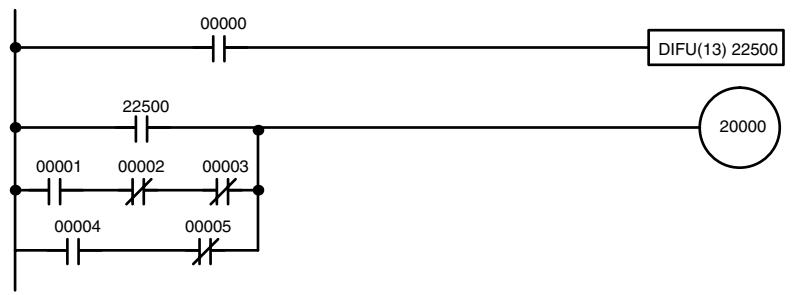
| Address | Instruction | Operands |
| 00000 | LD | 00000 |
| 00001 | DIFU(13) | 22500 |
| 00002 | LD | 22500 |
| 00003 | LD | 00001 |
| 00004 | AND NOT | 00002 |
| 00005 | AND NOT | 00003 |
| 00006 | OR LD | --- |
| 00007 | LD | 00004 |
| 00008 | AND NOT | 00005 |
| 00009 | OR LD | --- |
| 00010 | OUT | 20000 |
6-6 Programming Precautions
The number of conditions that can be used in series or parallel is unlimited as long as the memory capacity of the PC is not exceeded. Therefore, use as many conditions as required to draw a clear diagram. Although very complicated diagrams can be drawn with instruction lines, there must not be any conditions on lines running vertically between two other instruction lines. Diagram A shown below, for example, is not possible, and should be drawn as diagram B. Mnemonic code is provided for diagram B only; coding diagram A would be impossible.
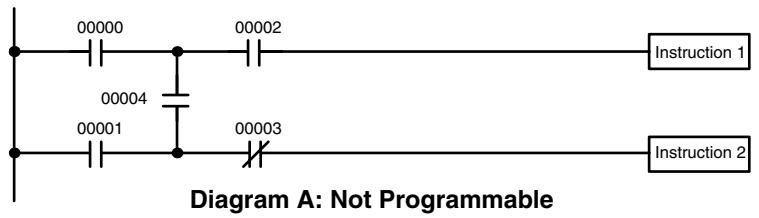
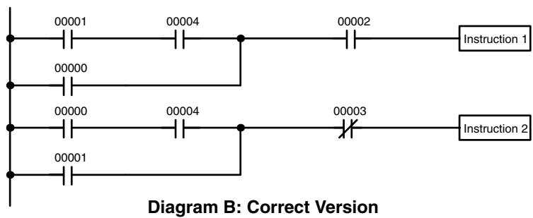
| Address | Instruction | Operands |
| 00000 | LD | 00001 |
| 00001 | AND | 00004 |
| 00002 | OR | 00000 |
| 00003 | AND | 00002 |
| 00004 | Instruction 1 | |
| 00005 | LD | 00000 |
| 00006 | AND | 00004 |
| 00007 | OR | 00001 |
| 00008 | AND NOT | 00003 |
| 00009 | Instruction 2 |
The number of times any particular bit can be assigned to conditions is not limited, so use them as many times as required to simplify your program. Often, complicated programs are the result of attempts to reduce the number of times a bit is used.
Except for instructions for which conditions are not allowed (e.g., INTERLOCK CLEAR and JUMP END, see below), every instruction line must also have at least one condition on it to determine the execution condition for the instruction at the right. Again, diagram A, below, must be drawn as diagram B. If an instruction must be continuously executed (e.g., if an output must always be kept ON while the program is being executed), the Always ON Flag (SR 25313) in the SR area can be used.


| Address | Instruction | Operands |
| 00000 | LD | 25313 |
| 00001 | Instruction |
There are a few exceptions to this rule, including the INTERLOCK CLEAR, JUMP END, and step instructions. Each of these instructions is used as the second of a pair of instructions and is controlled by the execution condition of the first of the pair. Conditions should not be placed on the instruction lines leading to these instructions. Refer to Section 7 Instruction Set for details.
When drawing ladder diagrams, it is important to keep in mind the number of instructions that will be required to input it. In diagram A, below, an OR LOAD instruction will be required to combine the top and bottom instruction lines. This can be avoided by redrawing as shown in diagram B so that no AND LOAD or OR LOAD instructions are required. Refer to 7-7-2 AND LOAD and OR LOAD for more details.
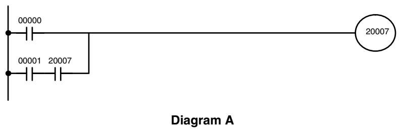
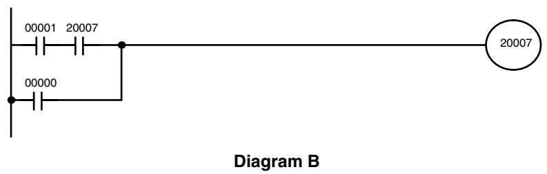
| Address | Instruction | Operands |
| 00000 | LD | 00000 |
| 00001 | LD | 00001 |
| 00002 | AND | 20007 |
| 00003 | OR LD | --- |
| 00004 | OUT | 20007 |
| Address | Instruction | Operands |
| 00000 | LD | 00001 |
| 00001 | AND | 20007 |
| 00002 | OR | 00000 |
| 00003 | OUT | 20007 |
6-7 Program Execution
When program execution is started, the CPU Unit scans the program from top to bottom, checking all conditions and executing all instructions accordingly as it moves down the bus bar. It is important that instructions be placed in the proper order so that, for example, the desired data is moved to a word before that word is used as the operand for an instruction. Remember that an instruction line is completed to the terminal instruction at the right before executing an instruction lines branching from the first instruction line to other terminal instructions at the right.
Program execution is only one of the tasks carried out by the CPU Unit as part of the cycle time. Refer to Section 8 PC Operations and Processing Time for details.
SECTION 7
Instruction Set
The CPM1, CPM1A, CPM2A, CPM2C (including the CPM2C-S), and SRM1(-V2) PCs have large programming instruction sets that allow for easy programming of complicated control processes. This section explains instructions individually and provides the ladder diagram symbol, data areas, and flags used with each.
The many instructions provided by these PCs are organized in the following subsections by instruction group. These groups include Ladder Diagram Instructions, instructions with fixed function codes, and set instructions.
Some instructions, such as Timer and Counter instructions, are used to control execution of other instructions, e.g., a TIM Completion Flag might be used to turn ON a bit when the time period set for the timer has expired. Although these other instructions are often used to control output bits through the Output instruction, they can be used to control execution of other instructions as well. The Output instructions used in examples in this manual can therefore generally be replaced by other instructions to modify the program for specific applications other than controlling output bits directly.
7-1 Notation 364
7-2 Instruction Format 364
7-3 Data Areas, Definer Values, and Flags 364
7-4 Differentiated Instructions 366
7-5 Coding Right-hand Instructions 367
7-6 Instruction Tables 370
7-6-1 CPM1/CPM1A Function Codes 370
7-6-2 CPM2A/CPM2C Function Codes 371
7-6-3 SRM1(-V2) Function Codes 372
7-6-4 Alphabetic List by Mnemonic 373
7-7 Ladder Diagram Instructions 376
7-7-1 LOAD,LOAD NOT,AND,AND NOT,OR,and OR NOT 376
7-7-2 AND LOAD and OR LOAD 377
7-8 Bit Control Instructions 377
7-8-1 OUTPUT and OUTPUT NOT - OUT and OUT NOT 377
7-8-2 SET and RESET - SET and RSET 378
7-8-3 KEEP-KEEP(11) 379
7-8-4 DIFFERENTIATE UP and DOWN - DIFU(13) and DIFD(14) 380
7-9 NO OPERATION - NOP(00) 381
7-10 END-END(01) 381
7-11 INTERLOCK and INTERLOCK CLEAR - IL(02) and ILC(03) 381
7-12 JUMP and JUMP END-JMP(04) and JME(05) 383
7-13 User Error Instructions:
FAILURE ALARM AND RESET - FAL(06) and
SEVERE FAILURE ALARM - FALS(07) 385
7-14 Step Instructions: STEP DEFINE and STEP START-STEP(08)/SNXT(09) 385
7-15 Timer and Counter Instructions 388
7-15-1 TIMER-TIM 389
7-15-2 HIGH-SPEED TIMER -TIMH(15) 390
7-15-3VERY HIGH-SPEED TIMER:TMHH(—) 391
7-15-4 LONG TIMER: TIML(—) 392
7-15-5 COUNTER-CNT 394
7-15-6 REVERSIBLE COUNTER-CNTR(12) 395
7-15-7 REGISTER COMPARISON TABLE - CTBL(63) 396
7-15-8 MODE CONTROL - INI(61) 399
7-15-9 HIGH-SPEED COUNTER PV READ - PRV(62) 401
7-16 Shift Instructions 404
7-16-1 SHIFT REGISTER - SFT(10) 404
7-16-2 WORD SHIFT - WSFT(16) 405
7-16-3 ARITHMETIC SHIFT LEFT - ASL(25) 405
7-16-4 ARITHMETIC SHIFT RIGHT - ASR(26) 406
7-16-5 ROTATE LEFT - ROL(27) 406
7-16-6 ROTATE RIGHT - ROR(28) 407
7-16-7 ONE DIGIT SHIFT LEFT - SLD(74) 408
7-16-8 ONE DIGIT SHIFT RIGHT - SRD(75) 408
7-16-9 REVERSIBLE SHIFT REGISTER - SFTR(84) 409
7-16-10 ASYNCHRONOUS SHIFT REGISTER - ASFT(17) 410
7-17 Data Movement Instructions 411
7-17-1 MOVE-MOV(21) 411
7-17-2 MOVE NOT-MVN(22) 412
7-17-3 BLOCK TRANSFER-XFER(70) 413
7-17-4 BLOCK SET-BSET(71) 414
7-17-5 DATA EXCHANGE-XCHG(73) 415
7-17-6 SINGLE WORD DISTRIBUTE - DIST(80) 415
7-17-7 DATA COLLECT-COLL(81) 417
7-17-8 MOVE BIT-MOBB(82) 419
7-17-9 MOVE DIGIT-MOVD(83) 420
7-18 Data Control Instructions 421
7-18-1 SCALING-SCL(66) 421
7-18-2 SIGNED BINARY TO BCD SCALING -SCL2(-) 423
7-18-3 BCD TO SIGNED BINARY SCALING -SCL3(-) 424
7-18-4 PID CONTROL-PID(-) 426
7-19 Comparison Instructions 432
7-19-1 COMPARE-CMP(20) 432
7-19-2 TABLE COMPARE -TCMP(85) 433
7-19-3 BLOCK COMPARE - BCMP(68) 434
7-19-4 DOUBLE COMPRE - CMPL(60) 436
7-19-5 AREA RANGE COMPARE-ZCP(—) 437
7-19-6 DOUBLE AREA RANGE COMPRE -ZCPL(-) 438
7-20 Conversion Instructions 439
7-20-1 BCD-TO-BINARY-BIN(23) 439
7-20-2 BINARY-TO-BCD - BCD(24) 440
7-20-3 DOUBLE BCD-TO-DOUBLE BINARY-BINL(58) 440
7-20-4 DOUBLE BINARY-TO-DOUBLE BCD - BCDL(59) 441
7-20-5 4-TO-16 DECODER - MLPX(76) 442
7-20-6 16-TO-4 ENCODER - DMPX(77) 444
7-20-7 7-SEGMENTDECODER-SDEC(78) 446
7-20-8 ASCIICONVERT-ASC(86) 449
7-20-9 ASCII-TO-HEXADECIMAL - HEX(-) 451
7-20-10 HOURS-TO-SECONDS - SEC(—) 453
7-20-11 SECONDS-TO-HOURS-HMS(—) 454
7-20-12 2'S COMPLEMENT - NEG(—) 455
7-21 BCD Calculation Instructions 457
7-21-1 SET CARRY -STC(40) 457
7-21-2 CLEAR CARRY - CLC(41) 457
7-21-3 BCD ADD - ADD(30) 457
7-21-4 BCD SUBTRACT - SUB(31) 458
7-21-5 BCD MULTIPLY - MUL(32) 460
7-21-6 BCD DIVIDE - DIV(33) 461
7-21-7 DOUBLE BCD ADD - ADDL(54) 462
7-21-8 DOUBLE BCD SUBTRACT - SUBL(55) 464
7-21-9 DOUBLE BCD MULTIPLY - MULL(56) 466
7-21-10 DOUBLE BCD DIVIDE - DIVL(57) 466
7-22 Binary Calculation Instructions 467
7-22-1 BINARY ADD - ADB(50) 467
7-22-2 BINARY SUBTRACT-SBB(51) 468
7-22-3 BINARY MULTIPLY - MLB(52) 470
7-22-4 BINARY DIVIDE - DVB(53) 470
7-23 Special Math Instructions 471
7-23-1 DATA SEARCH - SRCH(—) 471
7-23-2 FIND MAXIMUM-MAX(-) 472
7-23-3 FIND MINIMUM - MIN(—) 474
7-23-4 AVERAGE VALUE - AVG(-) 476
7-23-5 SUM-SUM(—) 478
7-24 Logic Instructions 479
7-24-1 COMPLEMENT-COM(29) 479
7-24-2 LOGICAL AND - ANDW(34) 480
7-24-3 LOGICAL OR - ORW(35) 481
7-24-4 EXCLUSIVE OR-XORW(36) 481
7-24-5 EXCLUSIVE NOR - XNRW(37) 482
7-25 Increment/Decrement Instructions 483
7-25-1 BCD INIncrement - INC(38) 483
7-25-2 BCD DECREMENT - DEC(39) 483
7-26 Subroutine Instructions 484
7-26-1 SUBROUTINE ENTER - SBS(91) 484
7-26-2 SUBROUTINE DEFINE and RETURN - SBN(92)/RET(93) 486
7-26-3 MACRO-MCRO(99) 486
7-27 Pulse Output Instructions 487
7-27-1 SETPULSES-PULS(65) 487
7-27-2 SPEED OUTPUT-SPED(64) 489
7-27-3 ACCELERATION CONTROL - ACC(—) 491
7-27-4PULSE WITH VARIABLE DUTY RATIO-PWM(—) 494
7-27-5 SYNCHRONIZED PULSE CONTROL-SYNC(—) 496
7-28 Special Instructions 497
7-28-1MESSAGE DISPLAY-MSG(46) 497
7-28-2 I/O REFRESH -IORF(97) 498
7-28-3 BIT COUNTER - BCNT(67) 499
7-28-4 FRAME CHECKSUM-FCS(—) 500
7-29 Interrupt Control Instructions 501
7-29-1 INTERRUPT CONTROL - INT(89) 501
7-29-2 INTERVAL TIMER-STIM(69) 504
7-30 Communications Instructions 505
7-30-1 RECEIVE - RXD(47) 505
7-30-2 TRANSMIT-TXD(48) 507
7-30-3 CHANGE RS-232C SETUP-STUP(-) 509
7-1 Notation
In the remainder of this manual, all instructions will be referred to by their mnemonics. For example, the OUTPUT instruction will be called OUT; the AND LOAD instruction, AND LD. If you're not sure of the instruction a mnemonic is used for, refer to Appendix A Programming Instructions.
If an instruction is assigned a function code, it will be given in parentheses after the mnemonic. These function codes, which are 2-digit decimal numbers, are used to input most instructions into the CPU Unit. A table of instructions listed in order of function codes is also provided in Appendix A Programming Instructions. Lists of instructions are also provided in 7-6 Instruction Tables.
An @ before a mnemonic indicates the differentiated version of that instruction. Differentiated instructions are explained in 7-4 Differentiated Instructions.
7-2 Instruction Format
Most instructions have at least one or more operands associated with them. Operands indicate or provide the data on which an instruction is to be performed. These are sometimes input as the actual numeric values (i.e., as constants), but are usually the addresses of data area words or bits that contain the data to be used. A bit whose address is designated as an operand is called an operand bit; a word whose address is designated as an operand is called an operand word. In some instructions, the word address designated in an instruction indicates the first of multiple words containing the desired data.
Each instruction requires one or more words in Program Memory. The first word is the instruction word, which specifies the instruction and contains any definers (described below) or operand bits required by the instruction. Other operands required by the instruction are contained in following words, one operand per word. Some instructions require up to four words.
A definer is an operand associated with an instruction and contained in the same word as the instruction itself. These operands define the instruction rather than telling what data it is to use. Examples of definers are TC numbers, which are used in timer and counter instructions to create timers and counters, as well as jump numbers (which define which Jump instruction is paired with which Jump End instruction). Bit operands are also contained in the same word as the instruction itself, although these are not considered definers.
7-3 Data Areas, Definer Values, and Flags
In this section, each instruction description includes its ladder diagram symbol, the data areas that can be used by its operands, and the values that can be used as definers. Details for the data areas are also specified by the operand names and the type of data required for each operand (i.e., word or bit and, for words, hexadecimal or BCD).
Not all addresses in the specified data areas are necessarily allowed for an operand, e.g., if an operand requires two words, the last word in a data area cannot be designated as the first word of the operand because all words for a single operand must be within the same data area. Other specific limitations are given in a Limitations subsection. Refer to Section 5 Memory Areas for addressing conventions and the addresses of flags and control bits.

The IR and SR areas are considered as separate data areas. If an operand has access to one area, it doesn't necessarily mean that the same operand will have access to the other area. The border between the IR and SR areas can, however, be crossed for a single operand, i.e., the last bit in the IR area may be specified for an operand that requires more than one word as long as the SR area is also allowed for that operand.
The Flags subsection lists flags that are affected by execution of an instruction. These flags include the following SR area flags.
| Abbreviation | Name | Bit |
| ER | Instruction Execution Error Flag | 25503 |
| CY | Carry Flag | 25504 |
| GR | Greater Than Flag | 25505 |
| EQ | Equals Flag | 25506 |
| LE | Less Than Flag | 25507 |
ER is the flag most commonly used for monitoring an instruction's execution. When ER goes ON, it indicates that an error has occurred in attempting to execute the current instruction. The Flags subsection of each instruction lists possible reasons for ER being ON. ER will turn ON if operands are not entered correctly. Instructions are not executed when ER is ON. A table of instructions and the flags they affect is provided in Appendix B Error and Arithmetic Flag Operation.
Indirect Addressing
When the DM area is specified for an operand, an indirect address can be used. Indirect DM addressing is specified by placing an asterisk before the DM: *DM.
When an indirect DM address is specified, the designated DM word will contain the address of the DM word that contains the data that will be used as the operand and of the instruction. If, for example, *DM 0001 was designated as the first operand and LR 00 as the second operand of MOV(21), the contents of DM 0001 was 1111, and DM 1111 contained 5555, the value 5555 would be moved to LR 00.
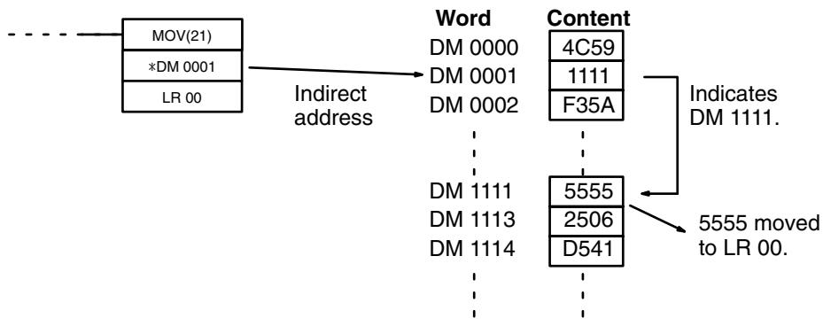
When using indirect addressing, the address of the desired word must be in BCD and it must specify a word within the DM area. In the above example, the content of DM 0001 has to be in BCD and has to specify an address in the DM area of the PC being used. (Refer to Section 5 Memory Areas for DM area details.)
Designating Constants
Although data area addresses are most often given as operands, many operands and all definers are input as constants. The available value range for a given definer or operand depends on the particular instruction that uses it. Constants must also be entered in the form required by the instruction, i.e., in BCD or in hexadecimal.
7-4 Differentiated Instructions
Most instructions are provided in both differentiated and non-differentiated forms. Differentiated instructions are distinguished by an @ in front of the instruction mnemonic.
A non-differentiated instruction is executed each time it is scanned as long as its execution condition is ON. A differentiated instruction is executed only once after its execution condition goes from OFF to ON. If the execution condition has not changed or has changed from ON to OFF since the last time the instruction was scanned, the instruction will not be executed. The following two examples show how this works with MOV(21) and @MOV(21), which are used to move the data in the address designated by the first operand to the address designated by the second operand.
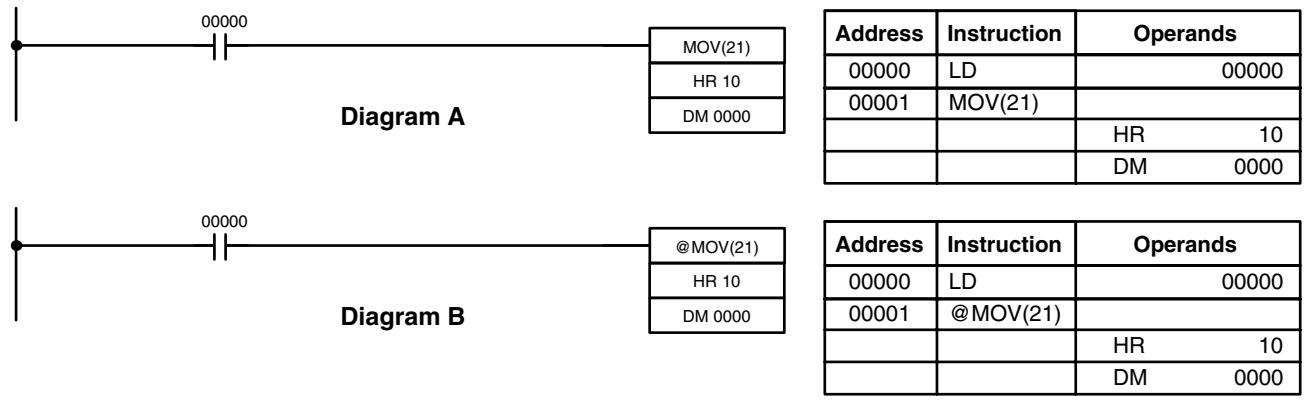
In diagram A, the non-differentiated MOV(21) will move the content of HR 10 to DM 0000 whenever it is scanned with 00000. If the cycle time is 80ms and 00000 remains ON for 2.0 seconds, this move operation will be performed 25 times and only the last value moved to DM 0000 will be preserved there.
In diagram B, the differentiated @MOV(21) will move the content of HR 10 to DM 0000 only once after 00000 goes ON. Even if 00000 remains ON for 2.0 seconds with the same 80 ms cycle time, the move operation will be executed only once during the first cycle in which 00000 has changed from OFF to ON. Because the content of HR 10 could very well change during the 2 seconds while 00000 is ON, the final content of DM 0000 after the 2 seconds could be different depending on whether MOV(21) or @MOV(21) was used.
All operands, ladder diagram symbols, and other specifications for instructions are the same regardless of whether the differentiated or non-differentiated form of an instruction is used. When inputting, the same function codes are also used, but NOT is input after the function code to designate the differentiated form of an instruction. Most, but not all, instructions have differentiated forms.
Refer to 7-11 INTERLOCK and INTERLOCK CLEAR - IL(02) and IL(03) for the effects of interlocks on differentiated instructions.
The CPM2A/CPM2C also provides differentiation instructions: DIFU(13) and DIFD(14). DIFU(13) operates the same as a differentiated instruction, but is used to turn ON a bit for one cycle. DIFD(14) also turns ON a bit for one cycle, but does it when the execution condition has changed from ON to OFF. Refer to 7-8-4 DIFFERENTIATE UP and DOWN - DIFU(13) and DIFD(14) for details.
7-5 Coding Right-hand Instructions
Writing mnemonic code for ladder instructions is described in Section 6 Ladder-diagram Programming. Converting the information in the ladder diagram symbol for all other instructions follows the same pattern, as described below, and is not specified for each instruction individually.
The first word of any instruction defines the instruction and provides any definers. If the instruction requires only a signal bit operand with no definer, the bit operand is also placed on the same line as the mnemonic. All other operands are placed on lines after the instruction line, one operand per line and in the same order as they appear in the ladder symbol for the instruction.
The address and instruction columns of the mnemonic code table are filled in for the instruction word only. For all other lines, the left two columns are left blank. If the instruction requires no definer or bit operand, the data column is left blank for first line. It is a good idea to cross through any blank data column spaces (for all instruction words that do not require data) so that the data column can be quickly scanned to see if any addresses have been left out.
If an IR or SR address is used in the data column, the left side of the column is left blank. If any other data area is used, the data area abbreviation is placed on the left side and the address is placed on the right side. If a constant to be input, the number symbol (#) is placed on the left side of the data column and the number to be input is placed on the right side. Any numbers input as definers in the instruction word do not require the number symbol on the right side. TC bits, once defined as a timer or counter, take a TIM (timer) or CNT (counter) prefix.
When coding an instruction that has a function code, be sure to write in the function code, which will be necessary when inputting the instruction via the Programming Console. Also be sure to designate the differentiated instruction with the @ symbol.
Note The mnemonics of expansion instructions are followed by “(—)” as the function code to indicate that they must be assigned function codes by the user in the instructions table before they can be used in programming. Refer to page 160 for details.
The following diagram and corresponding mnemonic code illustrates the points described previously.
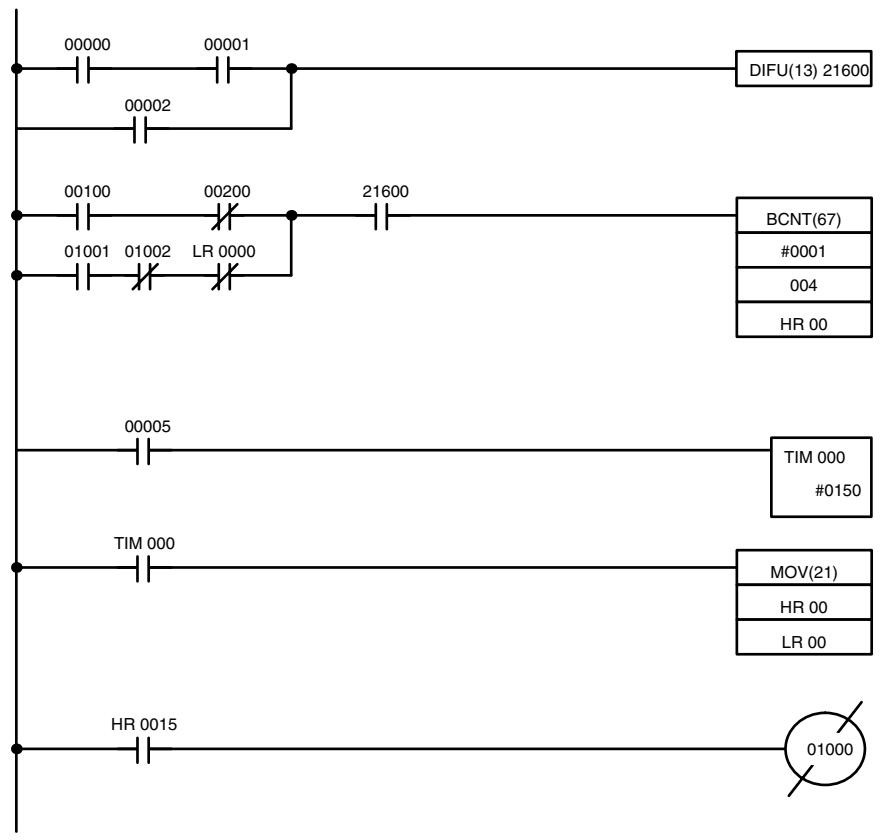
| Address | Instruction | Data |
| 00000 | LD | 00000 |
| 00001 | AND | 00001 |
| 00002 | OR | 00002 |
| 00003 | DIFU(13) | 21600 |
| 00004 | LD | 00100 |
| 00005 | AND NOT | 00200 |
| 00006 | LD | 01001 |
| 00007 | AND NOT | 01002 |
| 00008 | AND NOT | LR 0000 |
| 00009 | OR LD | — |
| 00010 | AND | 21600 |
| 00011 | BCNT(67) | — |
| # 0001 | ||
| 004 | ||
| HR 00 | ||
| 00012 | LD | 00005 |
| 00013 | TIM | 000 |
| # 0150 | ||
| 00014 | LD | TIM 000 |
| 00015 | MOV(21) | — |
| HR 00 | ||
| LR 00 | ||
| 00016 | LD | HR 0015 |
| 00017 | OUT NOT | 01000 |
Multiple Instruction Lines
If a right-hand instruction requires multiple instruction lines (such as KEEP(11)), all of the lines for the instruction are entered before the right-hand instruction. Each of the lines for the instruction is coded, starting with LD or LD NOT, to form 'logic blocks' that are combined by the right-hand instruction. An example of this for SFT(10) is shown below.
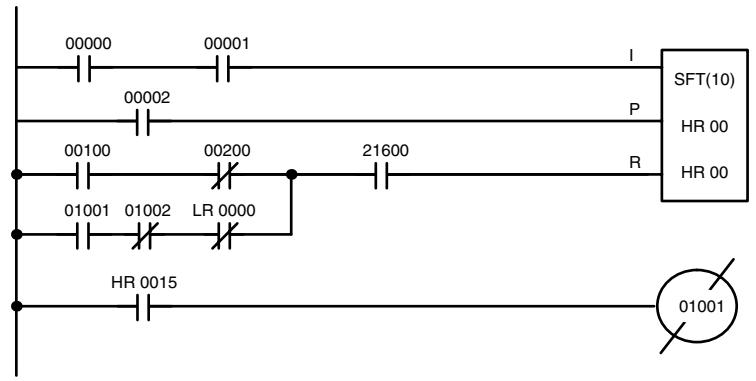
| Address | Instruction | Data | |
| 00000 | LD | 00000 | |
| 00001 | AND | 00001 | |
| 00002 | LD | 00002 | |
| 00003 | LD | 00100 | |
| 00004 | AND NOT | 00200 | |
| 00005 | LD | 01001 | |
| 00006 | AND NOT | 01002 | |
| 00007 | AND NOT | LR | 0000 |
| 00008 | OR LD | — | |
| 00009 | AND | 21600 | |
| 00010 | SFT(10) | HR | 00 |
| HR | 00 | ||
| 00011 | LD | HR | 0015 |
| 00012 | OUT NOT | 01001 | |
7-6 Instruction Tables
This section provides tables of the instructions supported by the CPM1/CPM1A, CPM2A/CPM2C, and SRM1(-V2) PCs. The first few tables can be used to find instructions by function code. The last table can be used to find instructions by mnemonic. In both tables, the @ symbol indicates instructions with differentiated forms.
7-6-1 CPM1/CPM1A Function Codes
The following table lists the CPM1/CPM1A instructions that have fixed function codes. Each instruction is listed by mnemonic and by instruction name. Use the numbers in the leftmost column as the left digit and the number in the column heading as the right digit of the function code.
| Left digit | Right digit | |||||||||
| 0 | 1 | 2 | 3 | 4 | 5 | 6 | 7 | 8 | 9 | |
| 0 | NOP NO OPERATION | END END | IL INTERLOCK | ILC INTERLOCK CLEAR | JMP JUMP | JME JUMP END | (@) FAL FAILURE ALARM AND RESET | FALS SEVERE FAILURE ALARM | STEP STEP DEFINE | SNXT STEP START |
| 1 | SFT SHIFT REGISTER | KEEP KEEP | CNTR REVERS- IBLE COUNTER | DIFU DIFFER- ENTIATE UP | DIFD DIFFER- ENTIATE DOWN | TIMH HIGH- SPEED TIMER | (@) WSFT WORD SHIFT | (@) ASFT ASYNCHRO- NOUS SHIFT REGISTER | --- | --- |
| 2 | CMP COMPARE | (@) MOV MOVE | (@) MVN MOVE NOT | (@) BIN BCD TO BINARY | (@) BCD BINARY TO BCD | (@) ASL SHIFT LEFT | (@) ASR SHIFT RIGHT | (@) ROL ROTATE LEFT | (@) ROR ROTATE RIGHT | (@) COM COMPLE- MENT |
| 3 | (@) ADD BCD ADD | (@) SUB BCD SUBTRACT | (@) MUL BCD MULTIPLY | (@) DIV BCD DIVIDE | (@) ANDW LOGICAL AND | (@) ORW LOGICAL OR | (@) XORW EXCLUSIVE OR | (@) XNRW EXCLUSIVE NOR | (@) INC INIncrement | (@) DEC DECRE- MENT |
| 4 | (@) STC SET CARRY | (@) CLC CLEAR CARRY | --- | --- | --- | --- | (@) MSG MESSAGE DISPLAY | --- | --- | --- |
| 5 | (@) ADB BINARY ADD | (@) SBB BINARY SUBTRACT | (@) MLB BINARY MULTIPLY | (@) DVB BINARY DIVIDE | (@) ADDL DOUBLE BCD ADD | (@) SUBL DOUBLE BCD SUBTRACT | (@) MULL DOUBLE BCD MULTIPLY | (@) DIVL DOUBLE BCD DIVIDE | --- | --- |
| 6 | CMPL DOUBLE COMPARE | (@) INI MODE CON- TROL | (@) PRV HIGH- SPEED COUNTER PV READ | (@) CTBL COMPARI- SON TABLE LOAD | (@) SPD SPEED OUT- PUT (see note) | (@) PULS SET PULSES (see note) | --- | (@) BCNT BIT COUNT- ER | (@) BCMP BLOCK COMPARE | (@) STIM INTERVAL TIMER |
| 7 | (@) XFER BLOCK TRANSFER | (@) BSET BLOCK SET | --- | (@) XCHG DATA EXCHANGE | (@) SLD ONE DIGIT SHIFT LEFT | (@) SRD ONE DIGIT SHIFT RIGHT | (@) MLPX 4-TO-16 DECODER | (@) DMPX 16-TO-4 ENCODER | (@) SDEC 7-SEGMENT DECODER | --- |
| 8 | (@) DIST SINGLE WORD DISTRIBUTE | (@) COLL DATA COLLECT | (@) MOVB MOVE BIT | (@) MOVD MOVE DIGIT | (@) SFTR REVERS- IBLE SHIFT REGISTER | (@) TCMP TABLE COMPARE | (@) ASC ASCII CONVERT | --- | --- | (@) INT INTERRUPT CONTROL |
| 9 | --- | (@) SBS SUBROU- TINE ENTRY | SBN SUBROU- TINE DEFINE | RET SUBROU- TINE RETURN | --- | --- | --- | (@) IORF I/O REFRESH | --- | (@) MCRO MACRO |
Note Only for the CPM1A transistor output models.
7-6-2 CPM2A/CPM2C Function Codes
The following table lists the CPM2A/CPM2C (including the CPM2C-S) instructions that have fixed function codes. Each instruction is listed by mnemonic and by instruction name. Use the numbers in the leftmost column as the left digit and the number in the column heading as the right digit of the function code.
| Left digit | Right digit | |||||||||
| 0 | 1 | 2 | 3 | 4 | 5 | 6 | 7 | 8 | 9 | |
| 0 | NOP NO OPERATION | END END | IL INTERLOCK | ILC INTERLOCK CLEAR | JMP JUMP | JME JUMP END | (@) FAL FAILURE ALARM AND RESET | FALS SEVERE FAILURE ALARM | STEP STEP DEFINE | SNXT STEP START |
| 1 | SFT SHIFT REGISTER | KEEP KEEP | CNTR REVERS- IBLE COUNTER | DIFU DIFFER- ENTIATE UP | DIFD DIFFER- ENTIATE DOWN | TIMH HIGH- SPEED TIMER | (@) WSFT WORD SHIFT | (@) ASFT ASYNCHRO- NOUS SHIFT REGISTER | --- | --- |
| 2 | CMP COMPARE | (@) MOV MOVE | (@) MVN MOVE NOT | (@) BIN BCD TO BINARY | (@) BCD BINARY TO BCD | (@) ASL SHIFT LEFT | (@) ASR SHIFT RIGHT | (@) ROL ROTATE LEFT | (@) ROR ROTATE RIGHT | (@) COM COMPLE- MENT |
| 3 | (@) ADD BCD ADD | (@) SUB BCD SUBTRACT | (@) MUL BCD MULTIPLY | (@) DIV BCD DIVIDE | (@) ANDW LOGICAL AND | (@) ORW LOGICAL OR | (@) XORW EXCLUSIVE OR | (@) XNRW EXCLUSIVE NOR | (@) INC INIncrement | (@) DEC DECRE- MENT |
| 4 | (@) STC SET CARRY | (@) CLC CLEAR CARRY | --- | --- | --- | --- | (@) MSG MESSAGE DISPLAY | (@) RXD RECEIVE | (@) TXD TRANSMIT | --- |
| 5 | (@) ADB BINARY ADD | (@) SBB BINARY SUBTRACT | (@) MLB BINARY MULTIPLY | (@) DVB BINARY DIVIDE | (@) ADDL DOUBLE BCD ADD | (@) SUBL DOUBLE BCD SUBTRACT | (@) MULL DOUBLE BCD MULTIPLY | (@) DIVL DOUBLE BCD DIVIDE | (@) BINL DOUBLE BCD-TO- DOUBLE BINARY | (@) BCDL DOUBLE BINARY-TO- DOUBLE BCD |
| 6 | CMPL DOUBLE COMPARE | (@) INI MODE CON- TROL | (@) PRV HIGH- SPEED COUNTER PV READ | (@) CTBL COMPARI- SON TABLE LOAD | (@) SPD SPEED OUT- PUT | (@) PULS SET PULSES | (@) SCL SCALING | (@) BCNT BIT COUNT- ER | (@) BCMP BLOCK COMPARE | (@) STIM INTERVAL TIMER |
| 7 | (@) XFER BLOCK TRANSFER | (@) BSET BLOCK SET | --- | (@) XCHG DATA EXCHANGE | (@) SLD ONE DIGIT SHIFT LEFT | (@) SRD ONE DIGIT SHIFT RIGHT | (@) MLPX 4-TO-16 DECODER | (@) DMPX 16-TO-4 ENCODER | (@) SDEC 7-SEGMENT DECODER | --- |
| 8 | (@) DIST SINGLE WORD DISTRIBUTE | (@) COLL DATA COLLECT | (@) MOVB MOVE BIT | (@) MOVD MOVE DIGIT | (@) SFTR REVERS- IBLE SHIFT REGISTER | (@) TCMP TABLE COMPARE | (@) ASC ASCII CONVERT | --- | --- | (@) INT INTERRUPT CONTROL |
| 9 | --- | (@) SBS SUBROU- TINE ENTRY | SBN SUBROU- TINE DEFINE | RET SUBROU- TINE RETURN | --- | --- | --- | (@) IORF I/O REFRESH | --- | (@) MCRO MACRO |
Note The shaded areas are function codes to which expansion instructions are allocated by default or to which the user can allocate expansion instructions. The following expansion instructions are available in addition to the ones listed above with default function codes.
| Mnemonic | Name | Mnemonic | Name |
| (@)ACC | ACCELERATION CONTROL | (@)SCL3 | BCD TO SIGNED BINARY SCALING |
| AVG | AVERAGE VALUE | (@)SEC | HOURS TO SECONDS |
| (@)FCS | FCS CALCULATE | (@)SRCH | DATA SEARCH |
| (@)HEX | ASCII-TO-HEXADECIMAL | (@)STUP | CHANGE RS-232C SETUP |
| (@)HMS | SECONDS TO HOURS | (@)SUM | SUM CALCULATE |
| (@)MAX | FIND MAXIMUM | SYNC | SYNCHRONIZED PULSE CONTROL |
| (@)MIN | FIND MINIMUM | TIML | LONG TIMER |
| (@)NEG | 2'S COMPLEMENT | TMHH | VERY HIGH-SPEED TIMER |
| PID | PID CONTROL | ZCP | AREA RANGE COMPRE |
| (@)PWM | PULSE WITH VARIABLE DUTY RATIO | ZCPL | DOUBLE AREA RANGE COMPRE |
| (@)SCL2 | SIGNED BINARY TO BCD SCALING |
7-6-3 SRM1(-V2) Function Codes
The following table lists the SRM1(-V2) instructions that have fixed function codes. Each instruction is listed by mnemonic and by instruction name. Use the numbers in the leftmost column as the left digit and the number in the column heading as the right digit of the function code.
| Left digit | Right digit | |||||||||
| 0 | 1 | 2 | 3 | 4 | 5 | 6 | 7 | 8 | 9 | |
| 0 | NOP NO OPERATION | END END | IL INTERLOCK | ILC INTERLOCK CLEAR | JMP JUMP | JME JUMP END | (@) FAL FAIL ALARM AND RESET | FALS SEVERE FAIL ALARM | STEP STEP DEFINE | SNXT STEP START |
| 1 | SFT SHIFT REGISTER | KEEP KEEP | CNTR REVERS- IBLE COUNTER | DIFU DIFFER- ENTIATE UP | DIFD DIFFER- ENTIATE DOWN | TIMH HIGH- SPEED TIMER | (@) WSFT WORD SHIFT | (@) ASFT ASYNCHRO- NOUS SHIFT REGISTER | --- | --- |
| 2 | CMP COMPARE | (@) MOV MOVE | (@) MVN MOVE NOT | (@) BIN BCD TO BINARY | (@) BCD BINARY TO BCD | (@) ASL SHIFT LEFT | (@) ASR SHIFT RIGHT | (@) ROL ROTATE LEFT | (@) ROR ROTATE RIGHT | (@) COM COMPLE- MENT |
| 3 | (@) ADD BCD ADD | (@) SUB BCD SUBTRACT | (@) MUL BCD MULTIPLY | (@) DIV BCD DIVIDE | (@) ANDW LOGICAL AND | (@) ORW LOGICAL OR | (@) XORW EXCLUSIVE OR | (@) XNRW EXCLUSIVE NOR | (@) INC INIncrement | (@) DEC DECRE- MENT |
| 4 | (@) STC SET CARRY | (@) CLC CLEAR CARRY | --- | --- | --- | --- | (@) MSG MESSAGE DISPLAY | (@) RXD RECEIVE | (@) TXD TRANSMIT | --- |
| 5 | (@) ADB BINARY ADD | (@) SBB BINARY SUBTRACT | (@) MLB BINARY MULTIPLY | (@) DVB BINARY DIVIDE | (@) ADDL DOUBLE BCD ADD | (@) SUBL DOUBLE BCD SUBTRACT | (@) MULL DOUBLE BCD MULTIPLY | (@) DIVL DOUBLE BCD DIVIDE | --- | --- |
| 6 | CMPL DOUBLE COMPARE | --- | --- | --- | --- | --- | (@) SCL SCALING | (@) BCNT BIT COUNT- ER | (@) BCMP BLOCK COMPARE | (@) STIM INTERVAL TIMER |
| 7 | (@) XFER BLOCK TRANSFER | (@) BSET BLOCK SET | --- | (@) XCHG DATA EXCHANGE | (@) SLD ONE DIGIT SHIFT LEFT | (@) SRD ONE DIGIT SHIFT RIGHT | (@) MLPX 4-TO-16 DECODER | (@) DMPX 16-TO-4 ENCODER | (@) SDEC 7-SEGMENT DECODER | --- |
| 8 | (@) DIST SINGLE WORD DISTRIBUTE | (@) COLL DATA COLLECT | (@) MOVB MOVE BIT | (@) MOVD MOVE DIGIT | (@) SFTR REVERS- IBLE SHIFT REGISTER | (@) TCMP TABLE COMPARE | (@) ASC ASCII CONVERT | --- | --- | --- |
| 9 | --- | (@) SBS SUBROU- TINE ENTRY | SBN SUBROU- TINE DEFINE | RET SUBROU- TINE RETURN | --- | --- | --- | --- | --- | (@) MCRO MACRO |
Note The shaded areas are function codes to which expansion instructions are allocated by default or to which the user can allocate expansion instructions. The following expansion instructions are available in addition to the ones listed above with default function codes.
| Mnemonic | Name |
| (@)FCS | FCS CALCULATE |
| (@)HEX | ASCII-TO-HEXADECIMAL |
| (@)NEG* | 2'S COMPLEMENT |
| PID* | PID CONTROL |
| (@)STUP | CHANGE RS-232C SETUP |
| ZCP* | AREA RANGE COMPARE |
Note *SCL(66), NEG(-), PID(-), and ZCP (-) are supported by the SRM1-C0□-V2 CPUs only.
7-6-4 Alphabetic List by Mnemonic
Dashes ("—") in the Code column indicate expansion instructions, which do not have fixed function codes. "None" indicates instructions for which function codes are not used.
In the CPU Units column, "SRM1" indicates all versions of the SRM1 CPU Units and "SRM1(-V2)" indicates only version 2 of the SRM1 CPU Units.
| Mnemonic | Code | Words | Name | CPU Units | Page |
| ACC (@) | — | 4 | ACCELERATION CONTROL | CPM2A/CPM2C | 491 |
| ADB (@) | 50 | 4 | BINARY ADD | All | 467 |
| ADD (@) | 30 | 4 | BCD ADD | All | 457 |
| ADDL (@) | 54 | 4 | DOUBLE BCD ADD | All | 463 |
| AND | None | 1 | AND | All | 376 |
| AND LD | None | 1 | AND LOAD | All | 377 |
| AND NOT | None | 1 | AND NOT | All | 376 |
| ANDW (@) | 34 | 4 | LOGICAL AND | All | 480 |
| ASC (@) | 86 | 4 | ASCII CONVERT | All | 449 |
| ASFT (@) | 17 | 4 | ASYNCHRONOUS SHIFT REGISTER | All | 410 |
| ASL (@) | 25 | 2 | ARITHMETIC SHIFT LEFT | All | 405 |
| ASR (@) | 26 | 2 | ARITHMETIC SHIFT RIGHT | All | 406 |
| AVG | — | 4 | AVERAGE VALUE | CPM2A/CPM2C | 476 |
| BCD (@) | 24 | 3 | BINARY TO BCD | All | 440 |
| BCDL (@) | 59 | 3 | DOUBLE BINARY-TO-DUUBLE BCD | CPM2A/CPM2C | 441 |
| BCMP (@) | 68 | 4 | BLOCK COMPARE | All | 434 |
| BCNT (@) | 67 | 4 | BIT COUNTER | All | 499 |
| BIN (@) | 23 | 3 | BCD-TO-BINARY | All | 439 |
| BINL (@) | 58 | 3 | DOUBLE BCD-TO-DUUBLE BINARY | CPM2A/CPM2C | 440 |
| BSET (@) | 71 | 4 | BLOCK SET | All | 414 |
| CLC (@) | 41 | 1 | CLEAR CARRY | All | 457 |
| CMP | 20 | 3 | COMPARE | All | 432 |
| CMPL | 60 | 4 | DOUBLE COMPARE | All | 436 |
| CNT | None | 2 | COUNTER | All | 394 |
| CNTR | 12 | 3 | REVERSIBLE COUNTER | All | 395 |
| COLL (@) | 81 | 4 | DATA COLLECT | All | 417 |
| COM (@) | 29 | 2 | COMPLEMENT | All | 479 |
| CTBL (@) | 63 | 4 | COMPARISON TABLE LOAD | All | 396 |
| DEC (@) | 39 | 2 | BCD DECREMENT | All | 483 |
| DIFD | 14 | 2 | DIFFERENTIATE DOWN | All | 380 |
| DIFU | 13 | 2 | DIFFERENTIATE UP | All | 380 |
| DIST (@) | 80 | 4 | SINGLE WORD DISTRIBUTE | All | 415 |
| DIV (@) | 33 | 4 | BCD DIVIDE | All | 461 |
| DIVL (@) | 57 | 4 | DOUBLE BCD DIVIDE | All | 466 |
| DMPX (@) | 77 | 4 | 16-TO-4 ENCODER | All | 444 |
| DVB (@) | 53 | 4 | BINARY DIVIDE | All | 470 |
| END | 01 | 1 | END | All | 381 |
| FAL (@) | 06 | 2 | FAILURE ALARM AND RESET | All | 385 |
| FALS | 07 | 2 | SEVERE FAILURE ALARM | All | 385 |
| FCS (@) | — | 4 | FCS CALCULATE | CPM2A/CPM2C/SRM1(-V2) | 500 |
| HEX (@) | — | 4 | ASCII-TO-HEXADECIMAL | CPM2A/CPM2C/SRM1(-V2) | 451 |
| HMS | — | 4 | SECONDS TO HOURS | CPM2A/CPM2C | 454 |
| IL | 02 | 1 | INTERLOCK | All | 381 |
| ILC | 03 | 1 | INTERLOCK CLEAR | All | 381 |
| INC (@) | 38 | 2 | INIncrement | All | 483 |
| INI (@) | 61 | 4 | MODE CONTROL | All | 399 |
| INT (@) | 89 | 4 | INTERRUPT CONTROL | All | 501 |
| IORF (@) | 97 | 3 | I/O REFRESH | All except SRM1 | 498 |
| JME | 05 | 2 | JUMP END | All | 383 |
| JMP | 04 | 2 | JUMP | All | 383 |
| KEEP | 11 | 2 | KEEP | All | 379 |
| LD | None | 1 | LOAD | All | 376 |
| LD NOT | None | 1 | LOAD NOT | All | 376 |
| MAX (@) | — | 4 | FIND MAXIMUM | CPM2A/CPM2C | 472 |
| MCRO (@) | 99 | 4 | MACRO | All | 486 |
| MIN (@) | — | 4 | FIND MINIMUM | CPM2A/CPM2C | 474 |
| MLB (@) | 52 | 4 | BINARY MULTIPLY | All | 470 |
| MLPX (@) | 76 | 4 | 4-TO-16 DECODER | All | 442 |
| MOV (@) | 21 | 3 | MOVE | All | 411 |
| MOVB (@) | 82 | 4 | MOVE BIT | All | 419 |
| MOVD (@) | 83 | 4 | MOVE DIGIT | All | 420 |
| MSG (@) | 46 | 2 | MESSAGE | All | 497 |
| MUL (@) | 32 | 4 | BCD MULTIPLY | All | 460 |
| MULL (@) | 56 | 4 | DOUBLE BCD MULTIPLY | All | 466 |
| MVN (@) | 22 | 3 | MOVE NOT | All | 412 |
| NEG (@) | — | 4 | 2'S COMPLEMENT | CPM2A/CPM2C/SRM1(-V2) | 455 |
| NOP | 00 | 1 | NO OPERATION | All | 381 |
| OR | None | 1 | OR | All | 376 |
| OR LD | None | 1 | OR LOAD | All | 377 |
| OR NOT | None | 1 | OR NOT | All | 376 |
| ORW (@) | 35 | 4 | LOGICAL OR | All | 481 |
| OUT | None | 2 | OUTPUT | All | 377 |
| OUT NOT | None | 2 | OUTPUT NOT | All | 377 |
| PID | — | 4 | PID CONTROL | CPM2A/CPM2C/SRM1(-V2) | 426 |
| PRV (@) | 62 | 4 | HIGH-SPEED COUNTER PV READ | All except SRM1 | 401 |
| PULS (@) | 65 | 4 | SET PULSES | CPM1A/CPM2A/CPM2C(Transistor outputs only) | 487 |
| PWM (@) | — | 4 | PULSE WITH VARIABLE DUTY RATIO | CPM2A/CPM2C | 494 |
| RET | 93 | 1 | SUBROUTINE RETURN | All | 486 |
| ROL (@) | 27 | 2 | ROTATE LEFT | All | 406 |
| ROR (@) | 28 | 2 | ROTATE RIGHT | All | 407 |
| RSET | None | 2 | RESET | All | 378 |
| RXD (@) | 47 | 4 | RECEIVE | CPM2A/CPM2C/SRM1 | 505 |
| SBB (@) | 51 | 4 | BINARY SUBTRACT | All | 468 |
| SBN | 92 | 2 | SUBROUTINE DEFINE | All | 486 |
| SBS (@) | 91 | 2 | SUBROUTINE ENTRY | All | 484 |
| SCL (@) | 66 | 4 | SCALING | CPM2A/CPM2C/SRM1(-V2) | 421 |
| SCL2 (@) | — | 4 | SIGNED BINARY TO BCD SCALING | CPM2A/CPM2C | 423 |
| SCL3 (@) | — | 4 | BCD TO SIGNED BINARY SCALING | CPM2A/CPM2C | 424 |
| SDEC (@) | 78 | 4 | 7-SEGMENT DECODER | CPM2A/CPM2C | 446 |
| SEC | — | 4 | HOURS TO SECONDS | CPM2A/CPM2C | 453 |
| SET | None | 2 | SET | All | 378 |
| SFT | 10 | 3 | SHIFT REGISTER | All | 404 |
| SFTR (@) | 84 | 4 | REVERSIBLE SHIFT REGISTER | All | 409 |
| SLD (@) | 74 | 3 | ONE DIGIT SHIFT LEFT | All | 408 |
| SNXT | 09 | 2 | STEP START | All | 385 |
| SPED (@) | 64 | 4 | SPEED OUTPUT | CPM1A/CPM2A/CPM2C(Transistor outputs only) | 489 |
| SRCH (@) | — | 4 | DATA SEARCH | CPM2A/CPM2C | 471 |
| SRD (@) | 75 | 3 | ONE DIGIT SHIFT RIGHT | All | 408 |
| STC (@) | 40 | 1 | SET CARRY | All | 457 |
| STEP | 08 | 2 | STEP DEFINE | All | 385 |
| STIM (@) | 69 | 4 | INTERVAL TIMER | All | 504 |
| STUP | — | 3 | CHANGE RS-232C SETUP | CPM2A/CPM2C/SRM1 | 509 |
| SUB (@) | 31 | 4 | BCD SUBTRACT | All | 458 |
| SUBL (@) | 55 | 4 | DOUBLE BCD SUBTRACT | All | 464 |
| SUM (@) | — | 4 | SUM | CPM2A/CPM2C | 478 |
| SYNC (@) | — | 4 | SYNCHRONIZED PULSE CONTROL | CPM2A/CPM2C | 496 |
| TCMP (@) | 85 | 4 | TABLE COMPARE | All | 433 |
| TIM | None | 2 | TIMER | All | 389 |
| TIMH | 15 | 3 | HIGH-SPEED TIMER | All | 390 |
| TIML | — | 4 | LONG TIMER | CPM2A/CPM2C | 392 |
| TMHH | — | 4 | VERY HIGH-SPEED TIMER | CPM2A/CPM2C | 391 |
| TXD (@) | 48 | 4 | TRANSMIT | CPM2A/CPM2C/SRM1 | 507 |
| WSFT (@) | 16 | 3 | WORD SHIFT | All | 405 |
| XCHG (@) | 73 | 3 | DATA EXCHANGE | All | 415 |
| XFER (@) | 70 | 4 | BLOCK TRANSFER | All | 413 |
| XNRW (@) | 37 | 4 | EXCLUSIVE NOR | All | 482 |
| XORW (@) | 36 | 4 | EXCLUSIVE OR | All | 481 |
| ZCP | — | 4 | AREA RANGE COMPARE | CPM2A/CPM2C/SRM1(-V2) | 437 |
| ZCPL | — | 4 | DOUBLE AREA RANGE COMPARE | CPM2A/CPM2C | 438 |
7-7 Ladder Diagram Instructions
Ladder diagram instructions include ladder instructions and logic block instructions and correspond to the conditions on the ladder diagram. Logic block instructions are used to relate more complex parts.
7-7-1 LOAD,LOAD NOT,AND,AND NOT,OR,and OR NOT
| Ladder Symbols | Operand Data Areas | |
| LOAD - LD | B | B: Bit |
| IR, SR, AR, HR, TC, LR, TR | ||
| LOAD NOT - LD NOT | B | B: Bit |
| IR, SR, AR, HR, TC, LR | ||
| AND - AND | B | B: Bit |
| IR, SR, AR, HR, TC, LR | ||
| AND NOT - AND NOT | B | B: Bit |
| IR, SR, AR, HR, TC, LR | ||
| OR - OR | B | B: Bit |
| IR, SR, AR, HR, TC, LR | ||
| OR NOT - OR NOT | B | B: Bit |
| IR, SR, AR, HR, TC, LR | ||
Limitations
There is no limit to the number of any of these instructions, or restrictions in the order in which they must be used, as long as the memory capacity of the PC is not exceeded.
Description
These six basic instructions correspond to the conditions on a ladder diagram. As described in Section 6 Ladder-diagram Programming, the status of the bits assigned to each instruction determines the execution conditions for all other instructions. Each of these instructions and each bit address can be used as many times as required. Each can be used in as many of these instructions as required.
The status of the bit operand (B) assigned to LD or LD NOT determines the first execution condition. AND takes the logical AND between the execution condition and the status of its bit operand; AND NOT, the logical AND between the execution condition and the inverse of the status of its bit operand. OR takes the logical OR between the execution condition and the status of its bit operand; OR NOT, the logical OR between the execution condition and the inverse of the status of its bit operand.
Flags
There are no flags affected by these instructions.
7-7-2 AND LOAD and OR LOAD
AND LOAD-ANDLD
Ladder Symbol
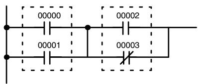
OR LOAD-ORLD
Ladder Symbol
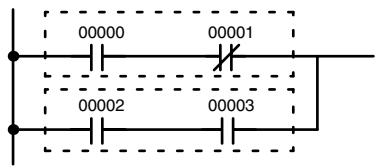
Description
When instructions are combined into blocks that cannot be logically combined using only OR and AND operations, AND LD and OR LD are used. Whereas AND and OR operations logically combine a bit status and an execution condition, AND LD and OR LD logically combine two execution conditions, the current one and the last unused one.
In order to draw ladder diagrams, it is not necessary to use AND LD and OR LD instructions, nor are they necessary when inputting ladder diagrams directly, as is possible from the SSS. They are required, however, to convert the program to and input it in mnemonic form.
In order to reduce the number of programming instructions required, a basic understanding of logic block instructions is required. For an introduction to logic blocks, refer to 6-3-6 Logic Block Instructions.
Flags
There are no flags affected by these instructions.
7-8 Bit Control Instructions
There are seven instructions that can be used generally to control individual bit status. These are OUT, OUT NOT, DIFU(13), DIFD(14), SET, RSET, and KEEP(11). These instructions are used to turn bits ON and OFF in different ways.
7-8-1 OUTPUT and OUTPUT NOT - OUT and OUT NOT
OUTPUT - OUT
Ladder Symbol
Operand Data Areas
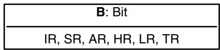
OUTPUT NOT - OUT NOT
Ladder Symbol
Operand Data Areas
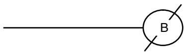
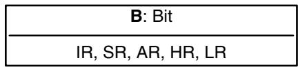
Limitations
Any output bit can generally be used in only one instruction that controls its status.
Description
OUT and OUT NOT are used to control the status of the designated bit according to the execution condition.
OUT turns ON the designated bit for an ON execution condition, and turns OFF the designated bit for an OFF execution condition. With a TR bit, OUT appears at a branching point rather than at the end of an instruction line. Refer to 6-3-8 Branching Instruction Lines for details.
OUT NOT turns ON the designated bit for a OFF execution condition, and turns OFF the designated bit for an ON execution condition.
OUT and OUT NOT can be used to control execution by turning ON and OFF bits that are assigned to conditions on the ladder diagram, thus determining execution conditions for other instructions. This is particularly helpful and allows a complex set of conditions to be used to control the status of a single work bit, and then that work bit can be used to control other instructions.
The length of time that a bit is ON or OFF can be controlled by combining the OUT or OUT NOT with TIM. Refer to Examples under 7-15-1 TIMER - TIM for details.
Flags
There are no flags affected by these instructions.
7-8-2 SET and RESET - SET and RSET
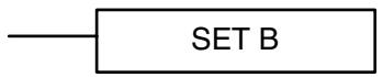
Ladder Symbols
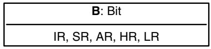
Operand Data Areas
RSET B
B:Bit
IR, SR, AR, HR, LR
Description
SET turns the operand bit ON when the execution condition is ON, and does not affect the status of the operand bit when the execution condition is OFF. RSET turns the operand bit OFF when the execution condition is ON, and does not affect the status of the operand bit when the execution condition is OFF.
The operation of SET differs from that of OUT because the OUT instruction turns the operand bit OFF when its execution condition is OFF. Likewise, RSET differs from OUT NOT because OUT NOT turns the operand bit ON when its execution condition is OFF.
Note On the Programming Console, input SET by pressing the FUN and SET Keys and input RSET by pressing the FUN and RESET Keys.
Precautions
The status of operand bits for SET and RSET programmed between IL(02) and ILC(03) or JMP(04) and JME(05) will not change when the interlock or jump condition is met (i.e., when IL(02) or JMP(04) is executed with an OFF execution condition).
Flags
There are no flags affected by these instructions.
Examples
The following examples demonstrate the difference between OUT and SET/ RSET. In the first example (Diagram A), IR 20000 will be turned ON or OFF whenever IR 00000 goes ON or OFF.
In the second example (Diagram B), IR 10000 will be turned ON when IR 00001 goes ON and will remain ON (even if IR 00001 goes OFF) until IR 00002 goes ON.

| Address | Instruction | Operands |
| 00000 | LD | 00000 |
| 00001 | OUT | 20000 |
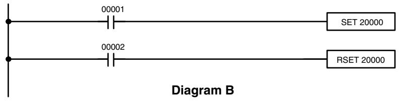
| Address | Instruction | Operands |
| 00000 | LD | 00001 |
| 00001 | SET | 20000 |
| 00002 | LD | 00002 |
| 00003 | RSET | 20000 |
7-8-3 KEEP - KEEP(11)
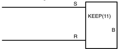
Ladder Symbol
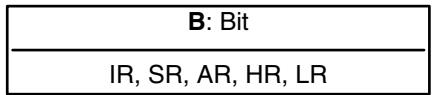
Operand Data Areas
Limitations
Any output bit can generally be used in only one instruction that controls its status.
Description
KEEP(11) is used to maintain the status of the designated bit based on two execution conditions. These execution conditions are labeled S and R. S is the set input; R, the reset input. KEEP(11) operates like a latching relay that is set by S and reset by R.
When S turns ON, the designated bit will go ON and stay ON until reset, regardless of whether S stays ON or goes OFF. When R turns ON, the designated bit will go OFF and stay OFF until reset, regardless of whether R stays ON or goes OFF. The relationship between execution conditions and KEEP(11) bit status is shown below.
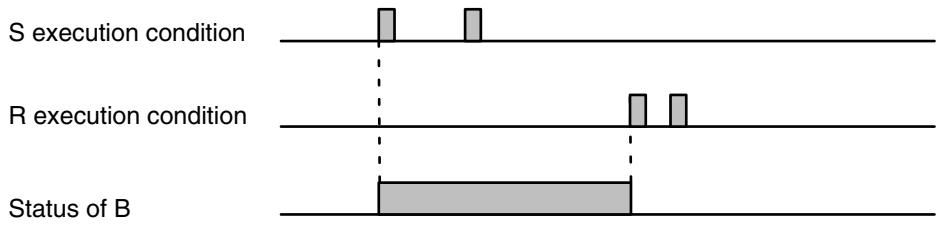
Flags
There are no flags affected by this instruction.
Precautions
Exercise caution when using a KEEP reset line that is controlled by an external normally closed device. Never use an input bit in an inverse condition on the reset (R) for KEEP(11) when the input device uses an AC power supply. The delay in shutting down the PC's DC power supply (relative to the AC power supply to the input device) can cause the designated bit of KEEP(11) to be reset. This situation is shown below.
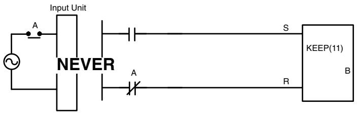
Bits used in KEEP are not reset in interlocks. Refer to the 7-11 INTERLOCK – and INTERLOCK CLEAR IL(02) and ILC(03) for details.
7-8-4 DIFFERENTIATE UP and DOWN - DIFU(13) and DIFD(14)
Ladder Symbols
DIFU(13) B
Operand Data Areas
B:Bit
IR, SR, AR, HR, LR
DIFD(14) B
B:Bit
IR, SR, AR, HR, LR
Limitations
Any output bit can generally be used in only one instruction that controls its status.
Description
DIFU(13) and DIFD(14) are used to turn the designated bit ON for one cycle only.
Whenever executed, DIFU(13) compares its current execution with the previous execution condition. If the previous execution condition was OFF and the current one is ON, DIFU(13) will turn ON the designated bit. If the previous execution condition was ON and the current execution condition is either ON or OFF, DIFU(13) will either turn the designated bit OFF or leave it OFF (i.e., if the designated bit is already OFF). The designated bit will thus never be ON for longer than one cycle, assuming it is executed each cycle (see Precautions, below).
Whenever executed, DIFD(14) compares its current execution with the previous execution condition. If the previous execution condition was ON and the current one is OFF, DIFD(14) will turn ON the designated bit. If the previous execution condition was OFF and the current execution condition is either ON or OFF, DIFD(14) will either turn the designated bit OFF or leave it OFF. The designated bit will thus never be ON for longer than one cycle, assuming it is executed each cycle (see Precautions, below).
These instructions are used when differentiated instructions (i.e., those prefixed with an @) are not available and single-cycle execution of a particular instruction is desired. They can also be used with non-differentiated forms of instructions that have differentiated forms when their use will simplify programming. Examples of these are shown below.
Flags
There are no flags affected by these instructions.
Precautions
DIFU(13) and DIFD(14) operation can be uncertain when the instructions are programmed between IL and ILC, between JMP and JME, or in subroutines. Refer to 7-11 INTERLOCK and INTERLOCK CLEAR - IL(02) and ILC(03), 7-12 JUMP and JUMP END - JMP(04) and JME(05), 7-26 Subroutine Instructions, and 7-29-1 INTERRUPT CONTROL - INT(89).
Example
In this example, IR 20014 will be turned ON for one cycle when IR 00000 goes from OFF to ON. IR 20015 will be turned ON for one cycle when IR 00000 goes from ON to OFF.

| Address | Instruction | Operands |
| 00000 | LD | 00000 |
| 00001 | DIFU(13) | 20014 |
| 00002 | DIFD(14) | 20015 |
NOP(00) is not generally required in programming and there is no ladder symbol for it. When NOP(00) is found in a program, nothing is executed and the program execution moves to the next instruction. When memory is cleared prior to programming, NOP(00) is written at all addresses. NOP(00) can be input through the 00 function code.
Flags There are no flags affected by NOP(00).
7-10 END - END(01)
Ladder Symbol
END(01)
Description
END(01) is required as the last instruction in any program. If there are subroutines, END(01) is placed after the last subroutine. No instruction written after END(01) will be executed. END(01) can be placed anywhere in the program to execute all instructions up to that point, as is sometimes done to debug a program, but it must be removed to execute the remainder of the program.
If there is no END(01) in the program, no instructions will be executed and the error message "NO END INST" will appear.
Flags END(01) turns OFF the ER, CY, GR, EQ, and LE flags.
7-11 INTERLOCK and INTERLOCK CLEAR - IL(02) and ILC(03)
Ladder Symbol
IL(02)
Ladder Symbol
ILC(03)
Description
IL(02) is always used in conjunction with ILC(03) to create interlocks. Interlocks are used to enable branching in the same way as can be achieved with TR bits, but treatment of instructions between IL(02) and ILC(03) differs from that with TR bits when the execution condition for IL(02) is OFF. If the execution condition of IL(02) is ON, the program will be executed as written, with an ON execution condition used to start each instruction line from the point where IL(02) is located through the next ILC(03). Refer to 6-3-8 Branching Instruction Lines for basic descriptions of both methods.
If the execution condition for IL(02) is OFF, the interlocked section between IL(02) and ILC(03) will be treated as shown in the following table:
| Instruction | Treatment |
| OUT and OUT NOT | Designated bit turned OFF. |
| TIM and TIMH(15) | Reset. |
| CNT, CNTR(12) | PV maintained. |
| KEEP(11) | Bit status maintained. |
| DIFU(13) and DIFD(14) | Not executed (see below). |
| All other instructions | The instructions are not executed, and all IR, AR, LR, HR, and SR bits and words written to as operands in the instructions are turned OFF. |
IL(02) and ILC(03) do not necessarily have to be used in pairs. IL(02) can be used several times in a row, with each IL(02) creating an interlocked section through the next ILC(03). ILC(03) cannot be used unless there is at least one IL(02) between it and any previous ILC(03).
DIFU(13) and DIFD(14) in Interlocks
Changes in the execution condition for a DIFU(13) or DIFD(14) are not recorded if the DIFU(13) or DIFD(14) is in an interlocked section and the execution condition for the IL(02) is OFF. When DIFU(13) or DIFD(14) is execution in an interlocked section immediately after the execution condition for the IL(02) has gone ON, the execution condition for the DIFU(13) or DIFD(14) will be compared to the execution condition that existed before the interlock became effective (i.e., before the interlock condition for IL(02) went OFF). The ladder diagram and bit status changes for this are shown below. The interlock is in effect while 00000 is OFF. Notice that 20000 is not turned ON at the point labeled A even though 00001 has turned OFF and then back ON.
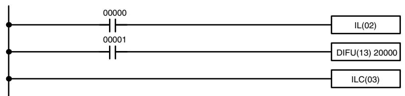
| Address | Instruction | Operands |
| 00000 | LD | 00000 |
| 00001 | IL(02) | |
| 00002 | LD | 00001 |
| 00003 | DIFU(13) | 20000 |
| 00004 | ILC(03) |
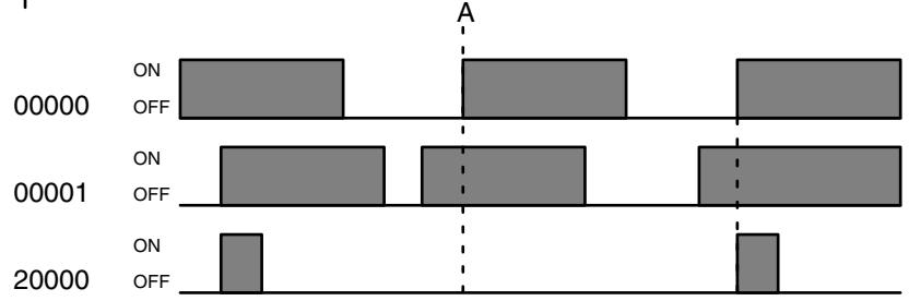
Precautions
There must be an ILC(03) following any one or more IL(02).
Although as many IL(02) instructions as are necessary can be used with one ILC(03), ILC(03) instructions cannot be used consecutively without at least one IL(02) in between, i.e., nesting is not possible. Whenever a ILC(03) is executed, all interlocks between the active ILC(03) and the preceding ILC(03) are cleared.
When more than one IL(02) is used with a single ILC(03), an error message will appear when the program check is performed, but execution will proceed normally.
Flags
There are no flags affected by these instructions.
The following diagram shows IL(02) being used twice with one ILC(03).
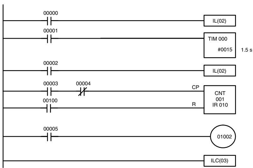
Example
| Address | Instruction | Operands |
| 00000 | LD | 00000 |
| 00001 | IL(02) | |
| 00002 | LD | 00001 |
| 00003 | TIM | 000 |
| # 0015 | ||
| 00004 | LD | 00002 |
| 00005 | IL(02) | |
| 00006 | LD | 00003 |
| 00007 | AND NOT | 00004 |
| 00008 | LD | 00100 |
| 00009 | LD | 00100 |
| 00010 | CNT | 001 |
| 010 | ||
| 00011 | LD | 00005 |
| 00012 | OUT | 01002 |
| 00013 | ILC(03) |
When the execution condition for the first IL(02) is OFF, TIM 000 will be reset to 1.5 s, CNT 001 will not be changed, and 01002 will be turned OFF. When the execution condition for the first IL(02) is ON and the execution condition for the second IL(02) is OFF, TIM 000 will be executed according to the status of 00001, CNT 001 will not be changed, and 01002 will be turned OFF. When the execution conditions for both the IL(02) are ON, the program will execute as written.
Jump numbers 01 through 49 may be used only once in JMP(04) and once in JME(05), i.e., each can be used to define one jump only. Jump number 00 can be used as many times as desired.
Description
JMP(04) is always used in conjunction with JME(05) to create jumps, i.e., to skip from one point in a ladder diagram to another point. JMP(04) defines the point from which the jump will be made; JME(05) defines the destination of the jump. When the execution condition for JMP(04) in ON, no jump is made and the program is executed consecutively as written. When the execution condition for JMP(04) is OFF, a jump is made to the JME(05) with the same jump number and the instruction following JME(05) is executed next.
If the jump number for JMP(04) is between 01 and 49, jumps, when made, will go immediately to JME(05) with the same jump number without executing any instructions in between. The status of timers, counters, bits used in OUT, bits used in OUT NOT, and all other status bits controlled by the instructions between JMP(04) and JMP(05) will not be changed. Each of these jump numbers can be used to define only one jump. Because all of instructions between JMP(04) and JME(05) are skipped, jump numbers 01 through 49 can be used to reduce cycle time.
| Jump Number 00 If the jump number for JMP(04) is 00, the CPU Unit will look for the next JME(05) with a jump number of 00. To do so, it must search through the program, causing a longer cycle time (when the execution condition is OFF) than for other jumps. The status of timers, counters, bits used in OUT, bits used in OUT NOT, and all other status controlled by the instructions between JMP(04) 00 and JME(05) 00 will not be changed. jump number 00 can be used as many times as desired. A jump from JMP(04) 00 will always go to the next JME(05) 00 in the program. It is thus possible to use JMP(04) 00 consecutively and match them all with the same JME(05) 00. It makes no sense, however, to use JME(05) 00 consecutively, because all jumps made to them will end at the first JME(05) 00. | |
| DIFU(13) and DIFD(14) in Jumps | Although DIFU(13) and DIFD(14) are designed to turn ON the designated bit for one cycle, they will not necessarily do so when written between JMP(04) and JME(05). Once either DIFU(13) or DIFD(14) has turned ON a bit, it will remain ON until the next time DIFU(13) or DIFD(14) is executed again. In normal programming, this means the next cycle. In a jump, this means the next time the jump from JMP(04) to JME(05) is not made, i.e., if a bit is turned ON by DIFU(13) or DIFD(14) and then a jump is made in the next cycle so that DIFU(13) or DIFD(14) are skipped, the designated bit will remain ON until the next time the execution condition for the JMP(04) controlling the jump is ON. |
| TIMH(15) and TMHH(—) in Jumps | When TIMH(15) or TMHH(—) is programmed between JMP(04) and JME(05), timing will be performed by interrupt if jump numbers 01 through 49 are used but timing won't be performed if jump number 00 is used. |
| Precautions | When JMP(04) and JME(05) are not used in pairs, an error message will appear when the program check is performed. This message also appears if JMP(04) 00 and JME(05) 00 are not used in pairs, but the program will execute properly as written. |
| Flags | There are no flags affected by these instructions. |
| Examples | Examples of jump programs are provided in 6-3-9 Jumps. |
7-13 User Error Instructions: FAILURE ALARM AND RESET - FAL(06) and SEVERE FAILURE ALARM - FALS(07)

Ladder Symbols
Definer Data Areas
| N: FAL number |
| # (00 to 99) |
FALS(07) N
| N: FAL number |
| # (01 to 99) |
Description
FAL(06) and FALS(07) are provided so that the programmer can output error numbers for use in operation, maintenance, and debugging. When executed with an ON execution condition, either of these instructions will output a FAL number to bits 00 to 07 of SR 253. The FAL number that is output can be between 01 and 99 and is input as the definer for FAL(06) or FALS(07). FAL(06) with a definer of 00 is used to reset this area (see below).

FAL Area
FAL(06) produces a non-fatal error and FALS(07) produces a fatal error. When FAL(06) is executed with an ON execution condition, the ALARM/ERROR indicator on the front of the CPU Unit will flash, but PC operation will continue. When FALS(07) is executed with an ON execution condition, the ALARM/ERROR indicator will light and PC operation will stop.
The system also generates error codes to the FAL area.
Resetting Errors
FAL error codes will be retained in memory, although only one of these is available in the FAL area. To access the other FAL codes, reset the FAL area by executing FAL(06) 00. Each time FAL(06) 00 is executed, another FAL error will be moved to the FAL area, clearing the one that is already there.
FAL(06) 00 is also used to clear message programmed with the instruction, MSG(46).
If the FAL area cannot be cleared, as is generally the case when FALS(07) is executed, first remove the cause of the error and then clear the FAL area through the Programming Console or SSS.
7-14 Step Instructions: STEP DEFINE and STEP START-STEP(08)/SNXT(09)
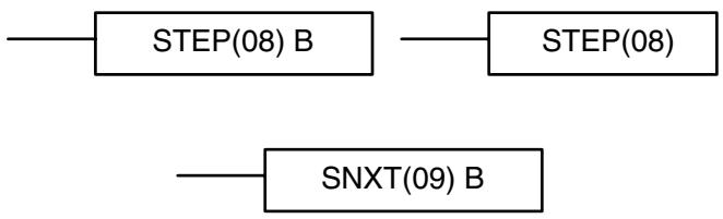
Ladder Symbols
Definer Data Areas
| B: Control bit |
| IR, AR, HR, LR |
B: Control bit
IR, AR, HR, LR
Limitations
Description
All control bits must be in the same word and must be consecutive.
The step instructions STEP(08) and SNXT(09) are used together to set up breakpoints between sections in a large program so that the sections can be executed as units and reset upon completion. A section of program will usually be defined to correspond to an actual process in the application. (Refer to the application examples later in this section.) A step is like a normal programming code, except that certain instructions (i.e., END(01), IL(02)/ILC(03), JMP(04)/JME(05), and SBN(92)) may not be included.
STEP(08) uses a control bit in the IR or HR areas to define the beginning of a section of the program called a step. STEP(08) does not require an execution condition, i.e., its execution is controlled through the control bit. To start execution of the step, SNXT(09) is used with the same control bit as used for STEP(08). If SNXT(09) is executed with an ON execution condition, the step with the same control bit is executed. If the execution condition is OFF, the step is not executed. The SNXT(09) instruction must be written into the program so that it is executed before the program reaches the step it starts. It can be used at different locations before the step to control the step according to two different execution conditions (see example 2, below). Any step in the program that has not been started with SNXT(09) will not be executed.
Once SNXT(09) is used in the program, step execution will continue until STEP(08) is executed without a control bit. STEP(08) without a control bit must be preceded by SNXT(09) with a dummy control bit. The dummy control bit may be any unused IR or HR bit. It cannot be a control bit used in a STEP(08).
Execution of a step is completed either by execution of the next SNXT(09) or by turning OFF the control bit for the step (see example 3 below). When the step is completed, all of the IR and HR bits in the step are turned OFF and all timers in the step are reset to their SVs. Counters, shift registers, and bits used in KEEP(11) maintain status. Two simple steps are shown below.
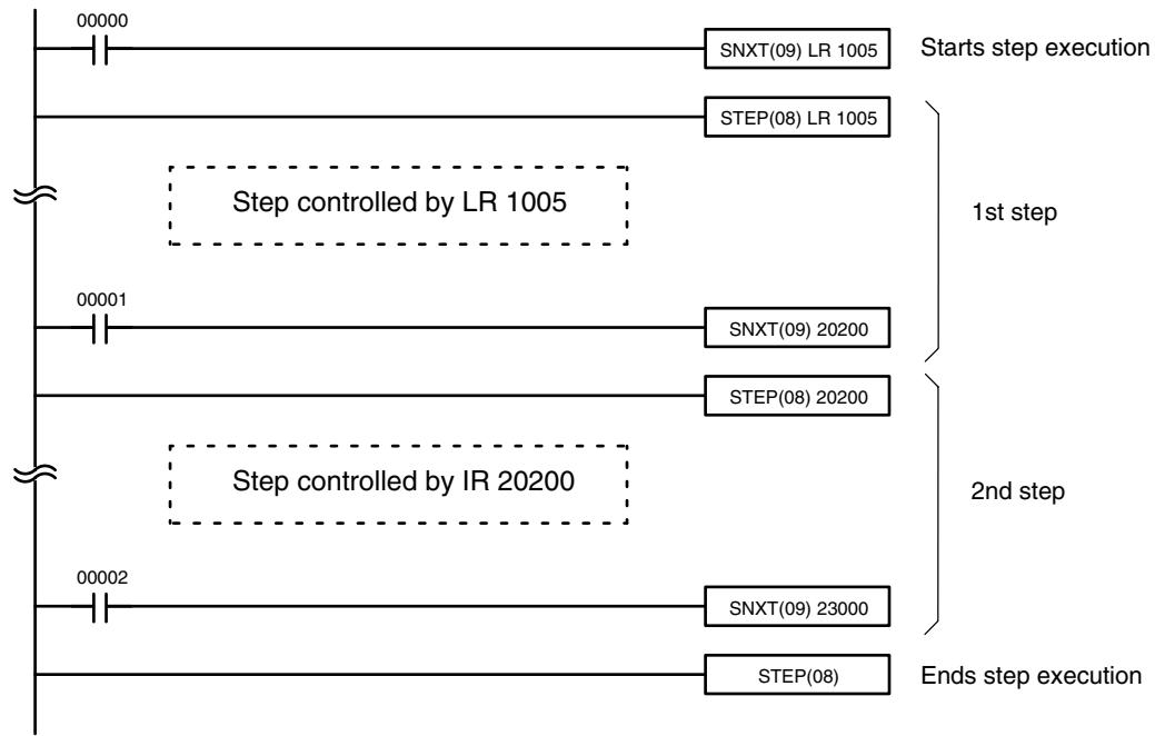
| Address | Instruction | Operands |
| 00000 | LD | 00000 |
| 00001 | SNXT(09) | LR 1005 |
| 00002 | STEP(08) | LR 1005 |
| Step controlled by LR 1005. | ||
| 00100 | LD | 00001 |
| 00101 | SNXT(09) | 20200 |
| Address | Instruction | Operands |
| 00102 | STEP(08) | 20200 |
| Step controlled by IR 20200. | ||
| 00200 | LD | 00002 |
| 00201 | SNXT(09) | 23000 |
| 00202 | STEP(08) | --- |
Precautions
Steps can be programmed in consecutively. Each step must start with STEP(08) and generally ends with SNXT(09) (see example 3, below, for an exception). When steps are programmed in series, three types of execution are possible: sequential, branching, or parallel. The execution conditions for, and the positioning of, SNXT(09) determine how the steps are executed. The three examples given below demonstrate these three types of step execution.
Interlocks, jumps, SBN(92), and END(01) cannot be used within step programs.
Bits used as control bits must not be used anywhere else in the program unless they are being used to control the operation of the step (see example 3, below). All control bits must be in the same word and must be consecutive.
If IR or LR bits are used for control bits, their status will be lost during any power interruption. If it is necessary to maintain status to resume execution at the same step, HR bits must be used.
Flags
25407: Step Start Flag; turns ON for one cycle when STEP(08) is executed and can be used to reset counters in steps as shown below if necessary.
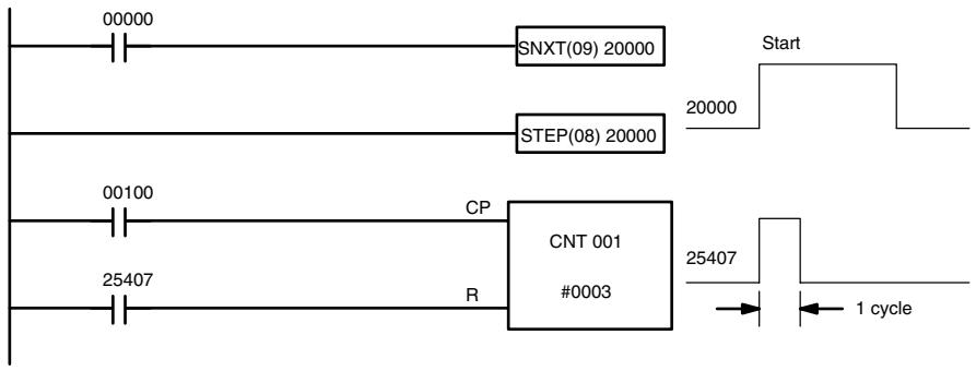
| Address | Instruction | Operands |
| 00000 | LD | 00000 |
| 00001 | SNXT(09) | 20000 |
| 00002 | STEP(08) | 20000 |
| 00003 | LD | 00100 |
| Address | Instruction | Operands |
| 00004 | LD | 25407 |
| 00005 | CNT | 01 |
| # 0003 |
7-15 Timer and Counter Instructions
TIM and TIMH(15) are decrementing ON-delay timer instructions which require a TC number and a set value (SV). STIM(69) is used to control the interval timers, which are used to activate interrupt routines.
CNT is a decrementing counter instruction and CNTR(12) is a reversible counter instruction. Both require a TC number and a SV. Both are also connected to multiple instruction lines which serve as an input signal(s) and a reset. CTBL(63), INT(89), and PRV(62) are used to manage the high-speed counter. INT(89) is also used to stop pulse output.
Any one TC number cannot be defined twice, i.e., once it has been used as the definer in any of the timer or counter instructions, it cannot be used again. Once defined, TC numbers can be used as many times as required as operands in instructions other than timer and counter instructions.
TC numbers run from 000 through 255 in the CPM2A/CPM2C PCs and from 000 through 127 in the CPM1/CPM1A/SRM1(-V2) PCs. No prefix is required when using a TC number as a definer in a timer or counter instruction. Once defined as a timer, a TC number can be prefixed with TIM for use as an operand in certain instructions. The TIM prefix is used regardless of the timer instruction that was used to define the timer. Once defined as a counter, a TC number can be prefixed with CNT for use as an operand in certain instructions. The CNT is also used regardless of the counter instruction that was used to define the counter.
TC numbers can be designated as operands that require either bit or word data. When designated as an operand that requires bit data, the TC number accesses a bit that functions as a 'Completion Flag' that indicates when the time/count has expired, i.e., the bit, which is normally OFF, will turn ON when the designated SV has expired. When designated as an operand that requires word data, the TC number accesses a memory location that holds the present value (PV) of the timer or counter. The PV of a timer or counter can thus be used as an operand in CMP(20), or any other instruction for which the TC area is allowed. This is done by designating the TC number used to define that timer or counter to access the memory location that holds the PV.
Note that "TIM 000" is used to designate the TIMER instruction defined with TC number 000, to designate the Completion Flag for this timer, and to designate the PV of this timer. The meaning of the term in context should be clear, i.e., the first is always an instruction, the second is always a bit operand, and the third is always a word operand. The same is true of all other TC numbers prefixed with TIM or CNT.
An SV can be input as a constant or as a word address in a data area. If an IR area word assigned to an Input Unit is designated as the word address, the Input Unit can be wired so that the SV can be set externally through thumbwheel switches or similar devices. Timers and counters wired in this way can only be set externally during RUN or MONITOR mode. All SVs, including those set externally, must be in BCD.
7-15-1 TIMER - TIM
Definer Values
Ladder Symbol
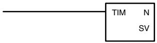
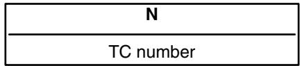
Operand Data Areas
SV: Set value (word, BCD)
IR, SR, AR, DM, HR, LR, #
Limitations
SV is between 000.0 and 999.9. The decimal point is not entered.
Each TC number can be used as the definer in only one TIMER or COUNTER instruction. TC numbers run from 000 through 255 in the CPM2A/CPM2C PCs and from 000 through 127 in the CPM1/CPM1A/SRM1(-V2) PCs.
TC 000 through TC 003 (TC 000 through TC 015 in the CPM2A/CPM2C) should not be used in TIM if they are required for TIMH(15). Refer to 7-15-2 HIGH-SPEED TIMER - TIMH(15) for details.
In the CPM2A/CPM2C PCs, TC 004 through TC 007 should not be used in TIM if they are required for TMHH(—). Refer to 7-15-3 VERY HIGH-SPEED TIMER – TMHH(—) for details.
Description
A timer is activated when its execution condition goes ON and is reset (to SV) when the execution condition goes OFF. Once activated, TIM measures in units of 0.1 second from the SV.
If the execution condition remains ON long enough for TIM to time down to zero, the Completion Flag for the TC number used will turn ON and will remain ON until TIM is reset (i.e., until its execution condition is goes OFF).
The following figure illustrates the relationship between the execution condition for TIM and the Completion Flag assigned to it.
Execution condition
Completion Flag
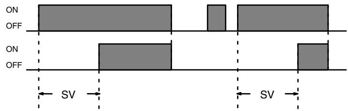
Precautions
Timers in interlocked program sections are reset when the execution condition for IL(02) is OFF. Power interruptions also reset timers. If a timer that is not reset under these conditions is desired, SR area clock pulse bits can be counted to produce timers using CNT. Refer to 7-15-5 COUNTER - CNT for details.
The Completion Flag may be turned ON one cycle late when reading its status from the user program.
Always reset the timer after changing between TIM and TIMH(015) in online editing. The timer will not work properly if it is not reset.
If the timer's set value is set to 0000, the Completion Flag will turn ON as soon as the timer's execution condition turns ON. If the timer's set value is set to 0001, the Completion Flag will turn ON somewhere between 0 and 0.1 s after the timer's execution condition turns ON (i.e., the timer accuracy will actually determine the time), and may turn ON as soon as the timer's execution condition turns ON.
Always consider the accuracy of the timer (0 to -0.1 s) in application programs.
Flags
ER: Indirectly addressed DM word is non-existent. (Content of *DM word is not BCD, or the DM area boundary has been exceeded.)
| Ladder Symbol | N |
| TC number | |
| TIMH(15) N SV | Operand Data Areas |
| SV: Set value (word, BCD) | |
| IR, SR, AR, DM, HR, LR, # |
Limitations
SV is between 00.00 and 99.99. (Although 00.00 and 00.01 may be set, 00.00 will disable the timer, i.e., turn ON the Completion Flag immediately, and 00.01 is not reliably scanned.) The decimal point is not entered.
Each TC number can be used as the definer in only one TIMER or COUNTER instruction. TC numbers run from 000 through 255 in the CPM2A/CPM2C PCs and from 000 through 127 in the CPM1/CPM1A/SRM1(-V2) PCs.
Description
TIMH(15) operates in the same way as TIM except that TIMH measures in units of 0.01 second. Refer to 7-15-1 TIMER - TIM for operational details.
Precautions
Timers in interlocked program sections are reset when the execution condition for IL(02) is OFF. Power interruptions also reset timers. If a timer that is not reset under these conditions is desired, SR area clock pulse bits can be counted to produce timers using CNT. Refer to 7-15-5 COUNTER - CNT for details.
Timers in jumped program sections will not be reset when the execution condition for JMP(04) is OFF. The timer will stop timing if jump number 00 is used, but will continue timing if other jump numbers are used.
Always reset the timer when changing between TIM and TIMH(15) in online editing. Also, when changing a TIMH(15) instruction with interrupt refreshing, do so only in PROGRAM mode.
Use timer numbers 000 to 003 for TIMH(15). High-speed timers with timer numbers TC 004 through TC 127 (TC 016 through TC 255 in the CPM2A/CPM2C) may not be accurate when the cycle time exceeds 10 ms.
| PC | Interrupt refreshing every 10 ms | Refreshed when TIMH(015) is executed |
| CPM2A/CPM2C | TC 000 through TC 003 | TC 004 through TC 255 |
| CPM1, CPM1A, and SRM1(-V2) | TC 000 through TC 003 | TC 004 through TC 127 |
In the CPM2A/CPM2C PCs, TC 004 through TC 007 should not be used in TIMH(15) if they are required for TMHH(-). Refer to 7-15-3 VERY HIGH-SPEED TIMER - TMHH(-) for details.
If the timer's set value is set to 0000, the Completion Flag will turn ON as soon as the timer's execution condition turns ON. If TIM000 to TIM003 are used, however, there may be a delay before the flag turns ON.
If the timer's set value is set to 0001, the Completion Flag will turn ON somewhere between 0 and 0.01 s after the timer's execution condition turns ON (i.e., the timer accuracy will actually determine the time), and may turn ON as soon as the timer's execution condition turns ON.
Always consider the accuracy of the timer (0 to -0.01 s) in application programs.
Flags
ER: Indirectly addressed DM word is non-existent. (Content of *DM word is not BCD, or the DM area boundary has been exceeded.)
Example
The following example shows a timer set with a constant. CIO 01600 will be turned ON after CIO 00000 goes ON and stays ON for at least 1.5 seconds. When 00000 goes OFF, the timer will be reset and CIO 01600 will be turned OFF.
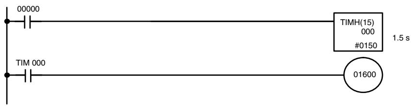
| Address | Instruction | Operands |
| 00000 | LD | 00000 |
| 00001 | TIMH(15) | 000 |
| # 0150 | ||
| 00002 | LD | TIM 000 |
| 00003 | OUT | 01600 |
7-15-3 VERY HIGH-SPEED TIMER: TMHH(—)
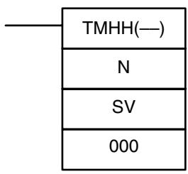
Ladder Symbol
Operand Data Areas
| N |
| TC number (see Limitations) |
| SV: Set value |
| IR, SR, AR, DM, HR, LR, # |
| 000 |
| Set to 000. |
This instruction is supported by the CPM2A/CPM2C only.
Limitations
Each TC number can be used as the definer in only one TIMER or COUNTER instruction. TC numbers run from TIM000 through TIM255. (You must enter "TIM" along with the actual timer number when using the Programming Console. The instruction will not work if only the number is entered.)
SV is BCD between 0000 and 9999 (0 to 9.999 s).
Set the third operand to 000. (This operand is ignored.)
Description
TMHH(—) is a decrementing ON-delay timer that times in 1-ms units. The timer set value can be 0 to 9.999 s and the timer has a accuracy of 1 ms.
A very high-speed timer is activated when its execution condition goes ON and is reset (to the SV) when the execution condition goes OFF. Once activated, TMHH(—) times down from the SV in units of 1 ms.
The timer will time out when the PV reaches #0000 (0 ms). Once the timer has timed out, the PV and Completion Flag status will be maintained. The timer can be restarted by temporarily turning its execution condition from ON to OFF or
changing its PV to a value other than #0000 with an instruction such as MOV(21).
The operation of very high-speed timers in jumped program sections depends upon the TC number used to define the timer, as shown in the following table.
| TC number | Operation |
| 000 to 003, 008 to 255 | The timer will stop when the execution condition for JMP(04) is OFF. This can greatly reduce the accuracy of timers in jumped program sections. |
| 004 to 007 | If jump number 00 is used, the timer will stop timing when the execution condition for JMP(04) is OFF. This can greatly reduce the accuracy of timers in jumped program sections. If any other jump number is used, the timer will continue timing normally when the execution condition for JMP(04) is OFF. |
Precautions
Very high-speed timers with timer numbers other than TC 004 through TC 007 may not be accurate when the cycle time exceeds 1 ms. (The cycle time will not affect very high-speed timers defined with TC 004 through TC 007.)
Very high-speed timers in interlocked program sections are reset (to the SV) when the execution condition for IL(02) is OFF.
If the timer's set value is set to 0000, the Completion Flag will turn ON as soon as the timer's execution condition turns ON. If TIM004 to TIM007 are used, however, there may be a delay before the flag turns ON.
If the timer's set value is set to 0001, the Completion Flag will turn ON somewhere between 0 and 1 ms after the timer's execution condition turns ON (i.e., the timer accuracy will actually determine the time), and may turn ON as soon as the timer's execution condition turns ON.
Always consider the accuracy of the timer (0 to -1 ms) in application programs.
Flags
ER: N is not a valid TC number.
Example
In the following example, CIO 20000 will be turned ON after CIO 00000 goes ON and stays ON for at least 1.5 seconds. When 00000 goes OFF, the timer will be reset and CIO 20000 will be turned OFF.
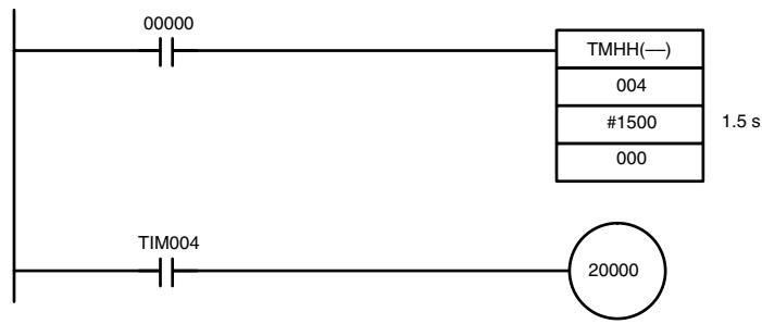
| Address | Instruction | Operands |
| 00000 | LD | 00000 |
| 00001 | TMHH(—) | --- |
| 004 | ||
| # 1500 | ||
| 000 | ||
| 00002 | LD | TIM 004 |
| 00003 | OUT | 20000 |
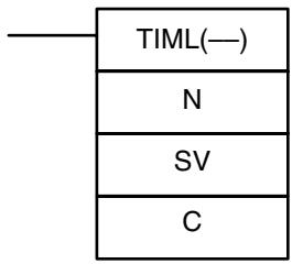
Ladder Symbol
Operand Data Areas
| N |
| TC number (see Limitations) |
| SV: Set value |
| IR, SR, AR, DM, HR, LR, # |
| C: Control data |
| 000 or 001 |
This instruction is supported by the CPM2A/CPM2C only.
| Limitations | Each timer number can be used as the definer in only one TIMER or COUNTER instruction. Timer numbers run from TIM000 through TIM255. (You must enter “TIM” along with the actual timer number when using the Programming Console. The instruction will not work if only the number is entered.) |
| SV is BCD between 0000 and 9999 (0 to 9,999 s when C=000 and 0 to 99,990 s when C=001). | |
| C must be 000 (1-s timing units) or 001 (10-s timing units). | |
| Description | TIML(—) is a decrementing ON-delay timer that can time in 1-s units or 10-s units. The timer set value can be 0 to 9,999 s (accuracy 0 to 1 s) when 1-s units are used (C=000) or 0.10 to 99,990 s (accuracy 0 to 10 s) when 10-s units are used (C=001). |
| A long timer is activated when its execution condition goes ON and is reset (to the SV) when the execution condition goes OFF. Once activated, TIML(—) times down from the SV in units of 1 s or 10 s (depending upon the value of C). | |
| TIML(—) accuracy is 0 to 1 s with 1-s units or 0 to 10 s with 10-s units. | |
| The timer will time out when the PV reaches #0000 (0 s). Once the timer has timed out, the PV and Completion Flag status will be maintained. The timer can be restarted by temporarily turning its execution condition from ON to OFF or changing its PV to a value other than #0000 with an instruction such as MOV(21). | |
| Long timers in jumped program sections will not be reset when the execution condition for JMP(04) is OFF, but the timer will stop timing and the PV will be maintained. Timing will resume when the execution condition for JMP(04) goes ON again. This can greatly reduce the accuracy of long timers in jumped program sections. | |
| Precautions | TIML(—) may not be accurate when the cycle time exceeds 1 s (C=000) or 10 s (C=001). |
| Long timers in interlocked program sections are reset (to the SV) when the execution condition for IL(02) is OFF. | |
| The timing units in C can be changed while the long timer is timing. Changing the timing units during operation reduces the timer's accuracy by up to 10 s. | |
| You must enter “TIM” along with the actual timer number when using TIML(—). The instruction will not work if only the number is entered. | |
| If the timer’s set value is set to 0000, the Completion Flag will turn ON as soon as the timer’s execution condition turns ON. If the timer’s set value is set to 0001, the Completion Flag will turn ON somewhere between 0 and 1 s or between 0 and 10 s after the timer’s execution condition turns ON (i.e., the timer accuracy will actually determine the time), and may turn ON as soon as the timer’s execution condition turns ON. | |
| Always consider the accuracy of the timer (0 to -1 s or 0 to -10 s) in application programs. | |
| Flags | ER: N is not a valid timer number. |
| C is not 000 or 001. |
Example
In the following example, CIO 20000 will be turned ON after CIO 00000 goes ON and stays ON for at least 1,500 seconds. When 00000 goes OFF, the timer will be reset and CIO 20000 will be turned OFF.
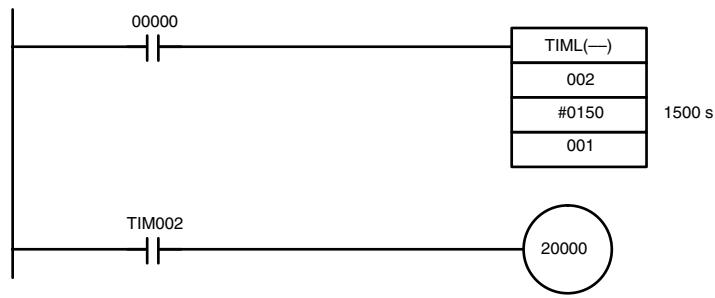
| Address | Instruction | Operands |
| 00000 | LD | 00000 |
| 00001 | TIML(—) | --- |
| 002 | ||
| # 0150 | ||
| 001 | ||
| 00002 | LD | TIM 002 |
| 00003 | OUT | 20000 |
7-15-5 COUNTER-CNT
Definer Values
Ladder Symbol
| CP | CNT N |
| R | SV |
| N |
| TC number |
Operand Data Areas
| SV: Set value (word, BCD) |
| IR, SR, AR, DM, HR, LR, # |
Limitations
Each TC number can be used as the definer in only one TIMER or COUNTER instruction. TC numbers run from 000 through 255 in the CPM2A/CPM2C PCs and from 000 through 127 in the CPM1/CPM1A/SRM1(-V2) PCs.
Description
CNT is used to count down from SV when the execution condition on the count pulse, CP, goes from OFF to ON, i.e., the present value (PV) will be decremented by one whenever CNT is executed with an ON execution condition for CP and the execution condition was OFF for the last execution. If the execution condition has not changed or has changed from ON to OFF, the PV of CNT will not be changed. The Completion Flag for a counter is turned ON when the PV reaches zero and will remain ON until the counter is reset.
CNT is reset with a reset input, R. When R goes from OFF to ON, the PV is reset to SV. The PV will not be decremented while R is ON. Counting down from SV will begin again when R goes OFF. The PV for CNT will not be reset in interlocked program sections or by power interruptions.
Changes in execution conditions, the Completion Flag, and the PV are illustrated below. PV line height is meant only to indicate changes in the PV.
Execution condition on count pulse (CP)
Execution condition on reset (R)
Completion Flag
PV
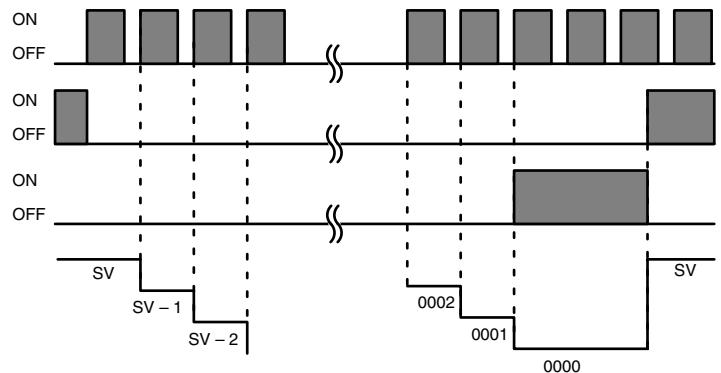
| Precautions | Program execution will continue even if a non-BCD SV is used, but the SV will not be correct. |
| Flags | ER: Indirectly addressed DM word is non-existent. (Content of *DM word is not BCD, or the DM area boundary has been exceeded.) |
| Example | In the following example, CNT is used to create extended timers by counting SR area clock pulse bits. CNT 001 counts the number of times the 1-second clock pulse bit (SR 25502) goes from OFF to ON. Here again, IR 00000 is used to control the times when CNT is operating. Because in this example the SV for CNT 001 is 700, the Completion Flag for CNT 002 turns ON when 1 second x 700 times, or 11 minutes and 40 seconds have expired. This would result in IR 20002 being turned ON. |
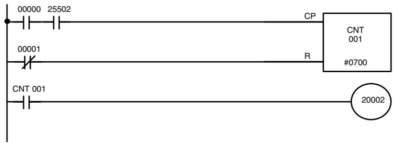
| Address | Instruction | Operands |
| 00000 | LD | 00000 |
| 00001 | AND | 25502 |
| 00002 | LD NOT | 00001 |
| 00003 | CNT | 001 |
| # 0700 | ||
| 00004 | LD | CNT 001 |
| 00005 | OUT | 20002 |

The shorter clock pulses will not necessarily produce accurate timers because their short ON times might not be read accurately during longer cycles. In particular, the 0.02-second and 0.1-second clock pulses should not be used to create timers with CNT instructions.
7-15-6 REVERSIBLE COUNTER - CNTR(12)
Ladder Symbol
| II | |
| DI | CNTR(12)N |
| R | SV |
Definer Values
| N |
| TC number |
Operand Data Areas
| SV: Set value (word, BCD) |
| IR, SR, AR, DM, HR, LR, # |
Limitations
Each TC number can be used as the definer in only one TIMER or COUNTER instruction. TC numbers run from 000 through 255 in the CPM2A/CPM2C PCs and from 000 through 127 in the CPM1/CPM1A/SRM1(-V2) PCs.
Description
The CNTR(12) is a reversible, up/down circular counter, i.e., it is used to count between zero and SV according to changes in two execution conditions, those in the increment input (II) and those in the decrement input (DI).
The present value (PV) will be incremented by one whenever CNTR(12) is executed with an ON execution condition for II and the last execution condition for II was OFF. The present value (PV) will be decremented by one whenever CNTR(12) is executed with an ON execution condition for DI and the last execution condition for DI was OFF. If OFF to ON changes have occurred in both II and DI since the last execution, the PV will not be changed.
If the execution conditions have not changed or have changed from ON to OFF for both II and DI, the PV of CNT will not be changed.
When decremented from 0000, the present value is set to SV and the Completion Flag is turned ON until the PV is decremented again. When incremented past the SV, the PV is set to 0000 and the Completion Flag is turned ON until the PV is incremented again.
CNTR(12) is reset with a reset input, R. When R goes from OFF to ON, the PV is reset to zero. The PV will not be incremented or decremented while R is ON. Counting will begin again when R goes OFF. The PV for CNTR(12) will not be reset in interlocked program sections or by the effects of power interruptions.
Changes in II and DI execution conditions, the Completion Flag, and the PV are illustrated below starting from part way through CNTR(12) operation (i.e., when reset, counting begins from zero). PV line height is meant to indicate changes in the PV only.
Execution condition on increment (II)
Execution condition on decrement (DI)
Completion Flag
PV
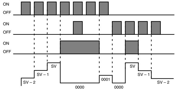
Precautions
Program execution will continue even if a non-BCD SV is used, but the SV will not be correct.
Flags
ER: Indirectly addressed DM word is non-existent. (Content of *DM word is not BCD, or the DM area boundary has been exceeded.)
7-15-7 REGISTER COMPARISON TABLE - CTBL(63)
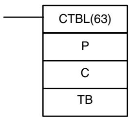
Ladder Symbols
@CTBL(63)
P
C
TB
Operand Data Areas
| P: Port specifier |
| 000 |
| C: Control data |
| 000 to 003 |
| TB: First comparison table word |
| IR, SR, AR, DM, HR, LR |
This instruction is not supported by SRM1(-V2) PCs.
Limitations
The first and last comparison table words must be in the same data area. (The length of the comparison table varies according to the settings.)
P must be 000 and C must be between 000 and 003.
Description
When the execution condition is OFF, CTBL(63) is not executed. When the execution condition is ON, CTBL(63) registers a comparison table for use with the high-speed counter PV. Depending on the value of C, comparison with the high-speed counter PV can begin immediately or it can be started separately with INI(61).
The port specifier (P) specifies the high-speed counter that will be used in the comparison. Always set P to 000.
The function of CTBL(63) is determined by the control data, C, as shown in the following table. These functions are described after the table.
| C | CTBL(63) function |
| 000 | Registers a target value comparison table and starts comparison. (See note.) |
| 001 | Registers a range comparison table and starts comparison. (See note.) |
| 002 | Registers a target value comparison table. Start comparison with INI(61). |
| 003 | Registers a range comparison table. Start comparison with INI(61). |
Note If C is set to 000 or 001, CTBL(63) will continue the comparison operation even when executed only once. As a rule, use the differentiated form (@) of the instruction or an input condition that turns ON for only one cycle.
When the PV agrees with a target value or falls within a specified range, the specified subroutine is called and executed. Refer to 2-3-5 High-speed Counter Interruptions for more details on table comparison.
If the high-speed counter is enabled in the PC Setup (DM 6642), it will begin counting from zero when the CPM2A/CPM2C begins operation. The PV will not be compared to the comparison table until the table is registered and comparison is initiated with INI(61) or CTBL(63). Comparison can be stopped and started, or the PV can be reset with INI(61).
Common Characteristics of Target Value and Range Comparisons
The operation of a target value comparison is different from a range comparison, but the two functions share some common characteristics.
1, 2, 3...
- Subroutine numbers 000 to 049 can be used and the same subroutine number can be used more than once in the table.
- An undefined subroutine number or FFFF can be set for the subroutine number if interrupt processing is not required.
- Comparison can be stopped with INI(61). A registered table is valid until PC operation stops or a new comparison table is registered.
- CTBL(62) cannot be executed if the high-speed counter is disabled in the PC Setup (DM 6642). (An error will occur if CTBL(63) is executed when the high-speed counter is disabled.)
Target Value Comparison
A target value comparison table contains up to sixteen target values. A subroutine number is also registered for each target value. The corresponding subroutine is called and executed when the PV matches a target value. (When interrupt processing is not required, an undefined subroutine number may be entered.)
- In the CPM1/CPM1A, target value comparisons are performed one item at a time in order of the comparison table. When the PV reaches the first target value in the table, the interrupt subroutine is executed and comparison continues to the next value in the table. When processing has been completed for the last target value in the table, comparison returns to the first value in the table and the process is repeated.
- In the CPM2A/CPM2C, the PV is compared to all of the target values in the table each time CTBL(63) is executed. When the PV matches a target value the corresponding subroutine is called and executed.
The following diagram shows the structure of a target value comparison table. Target values must be unique; an error will occur if a target value appears in the table more than once.
| TB | Number of target values (0001 to 0016, BCD) |
| TB+1 | Target value #1, lower 4 digits (BCD) |
| TB+2 | Target value #1, upper 4 digits (BCD) |
| TB+3 | Subroutine number for #1 (See note.) |
| : | : : : : : |
| : | : : : : : |
Note The subroutine number can be F000 to F049 to activate the subroutine when decrementing and can be 0000 to 0049 to activate the subroutine when incrementing. An error will occur if the high-speed counter is set to increment mode but a decrementing subroutine number (F000 to F049) is specified.
Range Comparison
A range comparison table contains 8 ranges which are defined by an 8-digit lower limit and an 8-digit upper limit, as well as their corresponding subroutine numbers. The comparison is performed once each cycle at the end of program execution and can be performed during program execution with INI(61).
When the PV falls within a given range the corresponding subroutine is called and executed. (When interrupt processing is not required, an undefined subroutine number may be entered.) Ranges can overlap, so the PV can fall within more than one range; in the PV is within two or more ranges, the subroutine for the first of the ranges will be executed.
The following diagram shows the structure of a range comparison table. Always set 8 ranges. If fewer than 8 ranges are needed, set the remaining subroutine numbers to FFFF.
| TB | Lower limit #1, lower 4 digits (BCD) |
| TB+1 | Lower limit #1, upper 4 digits (BCD) |
| TB+2 | Upper limit #1, lower 4 digits (BCD) |
| TB+3 | Upper limit #1, upper 4 digits (BCD) |
| TB+4 | Subroutine number (See note 2.) |
| : | : |
| : | : |
| TB+35 | Lower limit #8, lower 4 digits (BCD) |
| TB+36 | Lower limit #8, upper 4 digits (BCD) |
| TB+37 | Upper limit #8, lower 4 digits (BCD) |
| TB+38 | Upper limit #8, upper 4 digits (BCD) |
| TB+39 | Subroutine number (See note 2.) |
Note 1. Each range's lower limit must be less than its upper limit. An error will occur if the lower limit is greater than the upper limit.
- The subroutine number can be 0000 to 0049 and the subroutine will be executed as long as the counter's PV is within the specified range. A value of FFFF indicates that no subroutine is to be executed.
- Since the comparison is usually performed just once each cycle, be sure to take the cycle time into account when the upper and lower limits represent time values.
- A subroutine number can be used more than once in the table.
Flags
ER: The comparison table exceeds the data area boundary, or there is an error in the comparison table settings.
Indirectly addressed DM word is non-existent. (Content of *DM word is not BCD, or the DM area boundary has been exceeded.)
P is not 000 or C is not between 000 and 003.
There is a CTBL(63) instruction using a different comparison format in the subroutine called by another CTBL(63) instruction.
A CTBL(63) instruction using a different comparison format is executed during comparison.
CTBL(63) is executed in an interrupt subroutine while a pulse I/O or high-speed counter instruction (INI(61), PRV(62), CTBL(63), SPED(64), PULS(65), ACC(), PWM(), or SYNC()) is being executed in the main program.
Target Value Comparison Errors:
The number of target values (in TB) is not between 0001 and 0016.
A target value is not between F838 8608 and 0838 8607 (differential phase mode, pulse + direction input mode, and up/down input mode).
A target value is not between 0000 0001 and 1677 7215 or a subroutine number is not between 0000 and 0049 (increment mode).
If 0000 0000 is set in increment mode, 25503 (ER) will turn ON and the instruction will not be executed.
Range Comparison Errors:
A range's upper limit value is less than its lower limit value.
A target value is not between F838 8608 and 0838 8607 (differential phase mode, pulse + direction input mode, and up/down input mode).
A target value is not between 0000 0000 and 1677 7215 or a subroutine number is not between 0000 and 0049 (increment mode).
7-15-8 MODE CONTROL - INI(61)
Ladder Symbols
| @INI(61) | |
| P | P |
| C | C |
| P1 | P1 |
Operand Data Areas
| P: Port specifier |
| 000, 010, 100, 101, 102, 103 |
| C: Control data |
| 000 to 005 |
| P1: First PV word |
| IR, SR, AR, DM, HR, LR (or 000) |
This instruction is not supported by SRM1(-V2) PCs.
Limitations
In the CPM1/CPM1A PCs, P must be 000 and C must be 000 to 003.
In CPM2A/CPM2C PCs, P must be 000, 010, 100, 101, 102, or 103 and C must be 000 to 005.
P1 must be 000 unless C is 002 or 004.
P1 and P1 + 1 must be in the same data area.
If a DM address is used for P1, it must be read/write DM.
Description
When the execution condition is OFF, INI(61) is not executed. When the execution condition is ON, INI(61) is used to control high-speed counter operation and stop pulse output.
The port specifier (P) specifies the high-speed counter or pulse output that will be controlled.
| P | Function |
| 000 | Specifies high-speed counter input (inputs 00000, 00001, and 00002), single-phase pulse output 0 with no acceleration/deceleration (output 01000 or 01001), single-phase pulse output 0 with trapezoidal acceleration/deceleration (output 01000). |
| 010* | Specifies single-phase pulse output 1 with no acceleration/deceleration (output 01001). |
| 100* | Specifies interrupt input 0 in counter mode (input 00003). |
| 101* | Specifies interrupt input 1 in counter mode (input 00004). |
| 102* | Specifies interrupt input 2 in counter mode (input 00005). |
| 103* | Specifies interrupt input 3 in counter mode (input 00006). |
Note *These settings can be used in CPM2A/CPM2C PCs only.
The function of INI(61) is determined by the control data, C.
| C | P1 | INI(61) function |
| 000 | 000 | Starts CTBL(63) table comparison. |
| 001 | 000 | Stops CTBL(63) table comparison. |
| 002 | New PV | Changes PV of the high-speed counter or an interrupt input in counter mode. |
| 003 | 000 | Stops pulse output. |
| 004* | New PV | Changes PV of the pulse output. |
| 005* | 000 | Stops synchronized pulse control output. |
Note *These settings can be used in CPM2A/CPM2C PCs only.
Start or Stop Comparison (C=000 or C=001)
If C is 000 or 001, INI(61) starts or stops comparison of the high-speed counter's PV to the comparison table registered with CTBL(63). An error will occur if this function is executed without first registering a comparison table with CTBL(63). In general, @INI(61) should be used when C=000 because the instruction needs to be executed only one time to start table comparison.
Change PV (C=002)
If C is 002, INI(61) changes the PV of the specified high-speed counter or interrupt input (counter mode).
High-speed Counter PV (P=000)
INI(61) changes the PV of the specified high-speed counter to the 8-digit BCD value in P1 and P1 + 1 .
The new PV can be F838 8608 to 0838 8607 in differential phase mode, pulse + direction input mode, or up/down input mode. (The hexadecimal “F” in the first digit acts as a minus sign.)
The new PV can be 0000 0000 to 1677 7215 in increment mode.
Interrupt Input PV (P=100 to 103)
INI(61) changes the PV of the specified interrupt input (counter mode) to the 4-digit hexadecimal value (0000 to FFFF) in P1.
Stop Pulse Output (C=003)
If C is 003, INI(61) stops the pulse output.
Change PV (C=004)
INI(61) changes the PV of the pulse output to the 8-digit BCD value in P1 and P1+1. The PV cannot be changed while the pulse output is in progress.
The new PV can be -16,777,215 to 16,777,215 . Bit 15 of P1 + 1 acts as a sign bit; the number is negative if bit 15 is ON, positive if it is OFF.
Stop Synchronized Pulse Control Output (C=003)
If C is 003, INI(61) stops the synchronized pulse control output.
Flags
ER: The port specifier and control data are incompatible. (For example: P=010 and C=000)
There is an error in the operand settings or the specified PV is not within the acceptable range.
The address specified for P1 or P1 + 1 exceeds the data area boundary.
Indirectly addressed DM word is non-existent. (Content of *DM word is not BCD, or the DM area boundary has been exceeded.)
The specified function is incompatible with actual PC operation. For example, do not set C = 005 if synchronized pulse control is not being used.
INI(61) is executed to change the PV of a pulse output (C=004) while the pulse output is operating.
INI(61) is executed in an interrupt subroutine while a pulse I/O or high-speed counter instruction (INI(61), PRV(62), CTBL(63), SPED(64), PULS(65), ACC(), PWM(), or SYNC()) is being executed in the main program.
INI(61) is executed in an interrupt subroutine while a pulse I/O or high-speed counter instruction is being executed in the main program.
7-15-9 HIGH-SPEED COUNTER PV READ - PRV(62)
Ladder Symbols
| PRV(62) | @PRV(62) |
| P | P |
| C | C |
| D | D |
Operand Data Areas
| P: Port specifier |
| 000, 010, 100, 101, 102, 103 |
| C: Control data |
| 000, 001, 002, or 003 |
| D: First destination word |
| IR, SR, AR, DM, HR, LR |
This instruction is not supported by SRM1(-V2) PCs.
Limitations
In the CPM1/CPM1A PCs, P must be 000 and C must be 000 to 002.
In CPM2A/CPM2C PCs, P must be 000, 010, 100, 101, 102, or 103 and C must be 000 to 003.
D and D + 1 must be in the same data area.
If a DM address is used for D, it must be read/write DM.
Description
When the execution condition is OFF, PRV(62) is not executed. When the execution condition is ON, PRV(62) controls the high-speed counter PV, pulse output PV, interrupt input (counter mode) PV, or input frequency for synchronized control as specified by P and C.
The port specifier (P) specifies the high-speed counter or pulse output that will be controlled.
| P | Function |
| 000 | Specifies high-speed counter input (inputs 00000, 00001, and 00002), in-put frequency for synchronized pulse control (inputs 00000, 00001, and 00002), single-phase pulse output 0 with no acceleration/deceleration (outputs 01000 and 01001), single-phase pulse output 0 with trapezoidal acceleration/deceleration (output 01000), or synchronized pulse control output 0 (output 01000/01001). |
| 010* | Specifies single-phase pulse output 1 with no acceleration/deceleration (output 01001) or synchronized pulse control output 1 (output 01001). |
| 100* | Specifies interrupt input 0 in counter mode (input 00003). |
| 101* | Specifies interrupt input 1 in counter mode (input 00004). |
| 102* | Specifies interrupt input 2 in counter mode (input 00005). |
| 103* | Specifies interrupt input 3 in counter mode (input 00006). |
Note *These settings can be used in CPM2A/CPM2C PCs only.
The control data, C, determines which type of data will be accessed.
| C | Function | Destination word(s) |
| 000 | Reads the PV of the high-speed counter or interrupt input (counter mode) or the input frequency of the synchronized pulse control. | D and D+1 |
| 001 | Reads the status of the high-speed counter or pulse output. | D |
| 002 | Reads the results of range comparison. | D |
| 003* | Reads the PV of the pulse output. | D and D+1 |
Note *This setting can be used in CPM2A/CPM2C PCs only.
Read PV (C=000)
If C is 000, PRV(62) reads the PV of the specified high-speed counter or interrupt input (counter mode).
High-speed Counter PV or Input Frequency (P = 000)
When the output is used for a high-speed counter, PRV(62) reads the PV of the specified high-speed counter and writes the 8-digit BCD value in D and D + 1 . (The leftmost 4 digits are written to D + 1 .)
The PV can be F838 8608 to 0838 8607 in differential phase mode, pulse + direction input mode, or up/down input mode. (The hexadecimal “F” in the first digit acts as a minus sign.)
The PV can be 0000 0000 to 1677 7215 in increment mode.
When the output is used for synchronized pulse control, PRV(62) reads the input frequency and writes the 8-digit BCD value in D and D + 1 . The input frequency can be 0000 0000 to 0002 0000.
Interrupt Input PV (P=100 to 103)
PRV(62) reads the PV of the specified interrupt input (counter mode) and writes the 4-digit hexadecimal value (0000 to FFFF) in D.
Read Status (C=001)
If C is 001, PRV(62) reads the operating status of the specified high-speed counter or pulse output and writes the data to D.
High-speed Counter or Pulse Output 0 Status (P=000)
The following table shows the function of the bits in D when P = 000 . Bits not listed in the table are not used and will always be 0.
| Usage | Bit | Function |
| High-speed counter | 00 | High-speed counter comparison status. (0: Stopped; 1: Comparing) |
| 01 | High-speed counter underflow/overflow. (0: Normal; 1: Underflow/Overflow occurred.) | |
| Pulse output | 05 | Total number of pulses specified for pulse output 0. (0: Not specified; 1: Specified.) |
| 06 | Pulse output 0 completed. (0: Not completed; 1: Completed) | |
| 07 | Pulse output 0 status (0: Stopped; 1: Outputting) | |
| 08 | Pulse output 0 PV underflow/overflow. (0: Normal; 1: Underflow/Overflow occurred.) | |
| 09 | Pulse output 0 acceleration 0: Constant; 1: Accelerating or decelerating |
Pulse Output 1 Status (P=010)
The following table shows the function of the bits in D when P = 010 . Bits not listed in the table are not used and will always be 0.
| Bit | Function |
| 05 | Total number of pulses specified for pulse output 1. (0: Not specified; 1: Specified.) |
| 06 | Pulse output 1 completed. (0: Not completed; 1: Completed) |
| 07 | Pulse output 1 status (0: Stopped; 1: Outputting) |
| 08 | Pulse output 1 PV underflow/overflow. (0: Normal; 1: Underflow/Overflow occurred.) |
| 09 | Pulse output 1 acceleration (0: Constant; 1: Accelerating or decelerating) |
Read Range Comparison Results (C=002)
If C is 002, PRV(62) reads the results of the comparison of the PV to the 8 ranges defined by CTBL(63) and writes this data to D. Bits 00 through 07 of D contain the Comparison Result Flags for ranges 1 to 8. (0: Not in range; 1: In range)
Read Pulse Output PV (C=003)
If C is 003, PRV(62) reads the pulse output PV and writes the 8-digit BCD value in D and D + 1 . (The leftmost 4 digits are written to D + 1 .)
The PV can be -16,777,215 to 16,777,215. Bit 15 of D+1 acts as a sign bit; the number is negative if bit 15 is ON, positive if it is OFF.
Flags
ER: The port specifier and control data are incompatible.
(For example: P = 010 and C = 000 )
The address specified for D or D + 1 exceeds the data area boundary.
There is an error in the operand settings.
Indirectly addressed DM word is non-existent. (Content of *DM word is not BCD, or the DM area boundary has been exceeded.)
PRV(62) is executed in an interrupt subroutine while a pulse I/O or high-speed counter instruction (INI(61), PRV(62), CTBL(63), SPED(64), PULS(65), ACC(), PWM(), or SYNC()) is being executed in the main program.
7-16 Shift Instructions
7-16-1 SHIFT REGISTER - SFT(10)
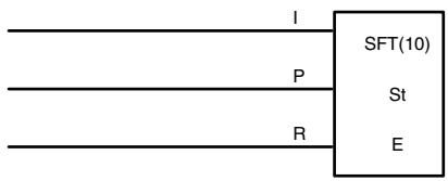
Ladder Symbol
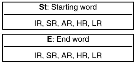
Operand Data Areas
Limitations
E must be greater than or equal to St, and St and E must be in the same data area.
If a bit address in one of the words used in a shift register is also used in an instruction that controls individual bit status (e.g., OUT, KEEP(11)), an error ("COIL/OUT DUPL") will be generated when program syntax is checked on the Programming Console or another Programming Device. The program, however, will be executed as written. See Example 2: Controlling Bits in Shift Registers for a programming example that does this.
Description
SFT(10) is controlled by three execution conditions, I, P, and R. If SFT(10) is executed and 1) execution condition P is ON and was OFF the last execution, and 2) R is OFF, then execution condition I is shifted into the rightmost bit of a shift register defined between St and E, i.e., if I is ON, a 1 is shifted into the register; if I is OFF, a 0 is shifted in. When I is shifted into the register, all bits previously in the register are shifted to the left and the leftmost bit of the register is lost.

The execution condition on P functions like a differentiated instruction, i.e., I will be shifted into the register only when P is ON and was OFF the last time SFT(10) was executed. If execution condition P has not changed or has gone from ON to OFF, the shift register will remain unaffected.
St designates the rightmost word of the shift register; E designates the leftmost. The shift register includes both of these words and all words between them. The same word may be designated for St and E to create a 16-bit (i.e., 1-word) shift register.
When execution condition R goes ON, all bits in the shift register will be turned OFF (i.e., set to 0) and the shift register will not operate until R goes OFF again.
Flags
ER: St and E are not in the same area or St is greater than E.
Example
The following example uses the 1-second clock pulse bit (25502) so that the execution condition produced by 00000 is shifted into HR 00 every second. Output 20000 is turned ON whenever a "1" is shifted into HR 0007.
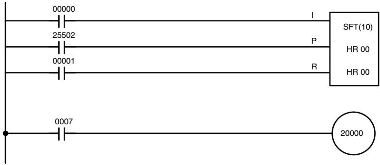
| Address | Instruction | Operands |
| 00000 | LD | 00000 |
| 00001 | LD | 25502 |
| 00002 | LD | 00001 |
| 00003 | SFT(10) | HR 00 |
| HR 00 | ||
| 00004 | LD | HR 0007 |
| 00005 | OUT | 20000 |
7-16-2 WORD SHIFT - WSFT(16)
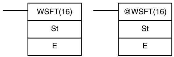
Ladder Symbols
Operand Data Areas
| St: Starting word |
| IR, SR, AR, DM, HR, LR |
| E: End word |
| IR, SR, AR, DM, HR, LR |
Limitations
St and E must be in the same data area, and E must be greater than or equal to St.
DM 6144 to DM 6655 cannot be used for St or E.
Description
When the execution condition is OFF, WSFT(16) is not executed. When the execution condition is ON, WSFT(16) shifts data between St and E in word units. Zeros are written into St and the content of E is lost.
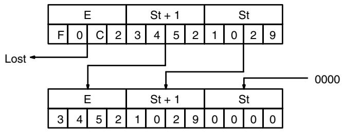
Flags
ER: The St and E words are in different areas, or St is greater than E. Indirectly addressed DM word is non-existent. (Content of *DM word is not BCD, or the DM area boundary has been exceeded.)
7-16-3 ARITHMETIC SHIFT LEFT - ASL(25)
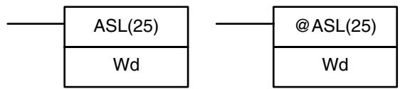
Ladder Symbols
Operand Data Areas
| Wd: Shift word |
| IR, SR, AR, DM, HR, LR |
Limitations
DM 6144 to DM 6655 cannot be used for Wd.
Description
When the execution condition is OFF, ASL(25) is not executed. When the execution condition is ON, ASL(25) shifts a 0 into bit 00 of Wd, shifts the bits of Wd one bit to the left, and shifts the status of bit 15 into CY.
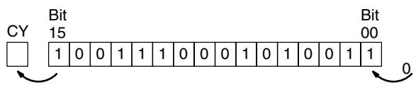
Precautions
A 0 will be shifted into bit 00 every cycle if the undifferentiated form of ASL(25) is used. Use the differentiated form (@ASL(25)) or combine ASL(25) with DIFU(13) or DIFD(14) to shift just one time.
Flags
ER: Indirectly addressed DM word is non-existent. (Content of *DM word is not BCD, or the DM area boundary has been exceeded.)
CY: Receives the status of bit 15.
EQ: ON when the content of Wd is zero; otherwise OFF.
7-16-4 ARITHMETIC SHIFT RIGHT - ASR(26)
Ladder Symbols
Operand Data Areas

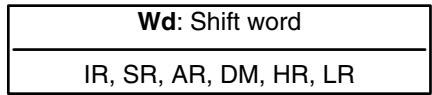
Limitations
DM 6144 to DM 6655 cannot be used for Wd.
Description
When the execution condition is OFF, ASR(25) is not executed. When the execution condition is ON, ASR(25) shifts a 0 into bit 15 of Wd, shifts the bits of Wd one bit to the right, and shifts the status of bit 00 into CY.
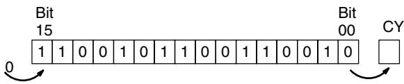
Precautions
A 0 will be shifted into bit 15 every cycle if the undifferentiated form of ASR(26) is used. Use the differentiated form (@ASR(26)) or combine ASR(26) with DIFU(13) or DIFD(14) to shift just one time.
Flags
ER: Indirectly addressed DM word is non-existent. (Content of *DM word is not BCD, or the DM area boundary has been exceeded.)
CY: Receives the data of bit 00.
EQ: ON when the content of Wd is zero; otherwise OFF.
7-16-5 ROTATE LEFT - ROL(27)
Ladder Symbols
Operand Data Areas
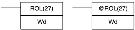
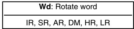
Limitations
DM 6144 to DM 6655 cannot be used for Wd.
Description
When the execution condition is OFF, ROL(27) is not executed. When the execution condition is ON, ROL(27) shifts all Wd bits one bit to the left, shifting CY into bit 00 of Wd and shifting bit 15 of Wd into CY.
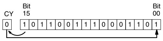
Precautions
Use STC(41) to set the status of CY or CLC(41) to clear the status of CY before doing a rotate operation to ensure that CY contains the proper status before executing ROL(27).
CY will be shifted into bit 00 every cycle if the undifferentiated form of ROL(27) is used. Use the differentiated form (@ROL(27)) or combine ROL(27) with DIFU(13) or DIFD(14) to shift just one time.
Flags
ER: Indirectly addressed DM word is non-existent. (Content of *DM word is not BCD, or the DM area boundary has been exceeded.)
CY: Receives the data of bit 15.
EQ: ON when the content of Wd is zero; otherwise OFF.
7-16-6 ROTATE RIGHT - ROR(28)
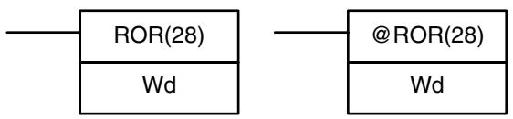
Ladder Symbols
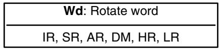
Operand Data Areas
Limitations
DM 6144 to DM 6655 cannot be used for Wd.
Description
When the execution condition is OFF, ROR(28) is not executed. When the execution condition is ON, ROR(28) shifts all Wd bits one bit to the right, shifting CY into bit 15 of Wd and shifting bit 00 of Wd into CY.
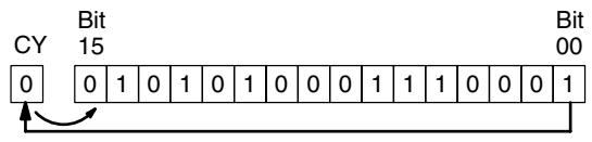
Precautions
Use STC(41) to set the status of CY or CLC(41) to clear the status of CY before doing a rotate operation to ensure that CY contains the proper status before execution ROR(28).
CY will be shifted into bit 15 every cycle if the undifferentiated form of ROR(28) is used. Use the differentiated form (@ROR(28)) or combine ROR(28) with DIFU(13) or DIFD(14) to shift just one time.
Flags
ER: Indirectly addressed DM word is non-existent. (Content of *DM word is not BCD, or the DM area boundary has been exceeded.)
CY: Receives the data of bit 00.
EQ: ON when the content of Wd is zero; otherwise OFF.
7-16-7 ONE DIGIT SHIFT LEFT - SLD(74)
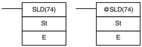
Ladder Symbols
Operand Data Areas
| St: Starting word |
| IR, SR, AR, DM, HR, LR |
| E: End word |
| IR, SR, AR, DM, HR, LR |
Limitations
St and E must be in the same data area, and E must be greater than or equal to St.
DM 6144 to DM 6655 cannot be used for St or E.
Description
When the execution condition is OFF, SLD(74) is not executed. When the execution condition is ON, SLD(74) shifts data between St and E (inclusive) by one digit (four bits) to the left. 0 is written into the rightmost digit of the St, and the content of the leftmost digit of E is lost.
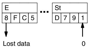
Precautions
If a power failure occurs during a shift operation across more than 50 words, the shift operation might not be completed.
A 0 will be shifted into the least significant digit of St every cycle if the undifferentiated form of SLD(74) is used. Use the differentiated form (@SLD(74)) or combine SLD(74) with DIFU(13) or DIFD(14) to shift just one time.
Flags
ER: The St and E words are in different areas, or St is greater than E. Indirectly addressed DM word is non-existent. (Content of *DM word is not BCD, or the DM area boundary has been exceeded.)
7-16-8 ONE DIGIT SHIFT RIGHT - SRD(75)
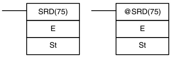
Ladder Symbols
Operand Data Areas
| E: End word |
| IR, SR, AR, DM, HR, LR |
Limitations
St and E must be in the same data area, and E must be less than or equal to St. DM 6144 to DM 6655 cannot be used for St or E.
Description
When the execution condition is OFF, SRD(75) is not executed. When the execution condition is ON, SRD(75) shifts data between St and E (inclusive) by one digit (four bits) to the right. 0 is written into the leftmost digit of St and the rightmost digit of E is lost.
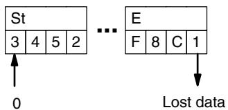
Precautions
If a power failure occurs during a shift operation across more than 50 words, the shift operation might not be completed.
A 0 will be shifted into the most significant digit of St every cycle if the undifferentiated form of SRD(75) is used. Use the differentiated form (@SRD(75)) or combine SRD(75) with DIFU(13) or DIFD(14) to shift just one time.
Flags
ER: The St and E words are in different areas, or St is less than E.
Indirectly addressed DM word is non-existent. (Content of *DM word is not BCD, or the DM area boundary has been exceeded.)
7-16-9 REVERSIBLE SHIFT REGISTER - SFTR(84)
Ladder Symbols
Operand Data Areas
C: Control word
IR, SR, AR, DM, HR, LR
St: Starting word
IR, SR, AR, DM, HR, LR
E: End word
IR, SR, AR, DM, HR, LR
Limitations
St and E must be in the same data area and St must be less than or equal to E.
DM 6144 to DM 6655 cannot be used for C, St, or E.
Description
SFTR(84) is used to create a single- or multiple-word shift register that can shift data to either the right or the left. To create a single-word register, designate the same word for St and E. The control word provides the shift direction, the status to be put into the register, the shift pulse, and the reset input. The control word is allocated as follows:
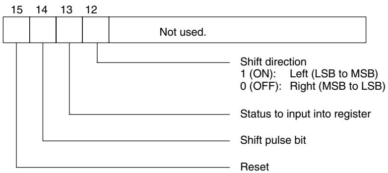
The data in the shift register will be shifted one bit in the direction indicated by bit 12, shifting one bit out to CY and the status of bit 13 into the other end whenever SFTR(84) is executed with an ON execution condition as long as the reset bit is OFF and as long as bit 14 is ON. If SFTR(84) is executed with an OFF execution condition or if SFTR(84) is executed with bit 14 OFF, the shift register will remain unchanged. If SFTR(84) is executed with an ON execution condition and the reset bit (bit 15) is OFF, the entire shift register and CY will be set to zero.
Flags
ER: St and E are not in the same data area or ST is greater than E.
Indirectly addressed DM word is non-existent. (Content of *DM word is not BCD, or the DM area boundary has been exceeded.)
CY: Receives the status of bit 00 of St or bit 15 of E, depending on the shift direction.
Example
In the following example, IR 00000, IR 00001, IR 00002, and IR 00003 are used to control the bits of C used in @SFTR(84). The shift register is in DM 0010, and it is controlled through IR 00004.
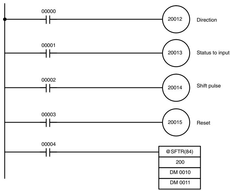
| Address | Instruction | Operands |
| 00000 | LD | 00000 |
| 00001 | OUT | 20012 |
| 00002 | LD | 00001 |
| 00003 | OUT | 20013 |
| 00004 | LD | 00002 |
| 00005 | OUT | 20014 |
| 00006 | LD | 00003 |
| 00007 | OUT | 20015 |
| 00008 | LD | 00004 |
| 00009 | @SFTR(84) | |
| 200 | ||
| DM 0010 | ||
| DM 0011 |
7-16-10 ASYNCHRONOUS SHIFT REGISTER - ASFT(17)
Operand Data Areas
Ladder Symbols
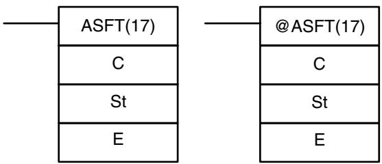
| C: Control word |
| IR, SR, AR, DM, HR, LR, # |
| St: Starting word |
| IR, SR, AR, DM, HR, LR |
| E: End word |
| IR, SR, AR, DM, HR, LR |
Note ASFT(17) is an expansion instruction for the SRM1(-V2). The function code 17 is the factory setting and can be changed for the SRM1(-V2) if desired.
Limitations
St and E must be in the same data area, and E must be greater than or equal to St.
DM 6144 to DM 6655 cannot be used for St or E.
Description
When the execution condition is OFF, ASFT(17) does nothing and the program moves to the next instruction. When the execution condition is ON, ASFT(17) is used to create and control a reversible asynchronous word shift register between St and E. This register only shifts words when the next word in the register is zero, e.g., if no words in the register contain zero, nothing is shifted. Also, only one word is shifted for each word in the register that contains zero. When the contents of a word are shifted to the next word, the original word's contents are set to zero. In essence, when the register is shifted, each zero word in the register trades places with the next word. (See Example below.)
The shift direction (i.e. whether the "next word" is the next higher or the next lower word) is designated in C. C is also used to reset the register. All of any portion of the register can be reset by designating the desired portion with St and E.
Control Word
Bits 00 through 12 of C are not used. Bit 13 is the shift direction: turn bit 13 ON to shift down (toward lower addressed words) and OFF to shift up (toward higher addressed words). Bit 14 is the Shift Enable Bit: turn bit 14 ON to enable shift register operation according to bit 13 and OFF to disable the register. Bit 15 is the Reset bit: the register will be reset (set to zero) between St and E when ASFT(17) is executed with bit 15 ON. Turn bit 15 OFF for normal operation.
Note If the non-differentiated form of ASFT(17) is used, data will be shifted every cycle while the execution condition is ON. Use the differentiated form to prevent this.
Flags
ER: The St and E words are in different areas, or St is greater than E. Indirectly addressed DM word is non-existent. (Content of *DM word is not BCD, or the DM area boundary has been exceeded.)
Example
The following example shows instruction ASFT(17) used to shift words in an 11-word shift register created between DM 0100 and DM 0110 with C=#6000. Non-zero data is shifted towards St (DM 0110).

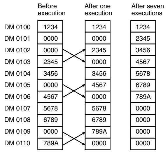
Note The zeroes are shifted "upward" if C = 4000 , and the entire shift register is set to zero if C = 8000 .
7-17 Data Movement Instructions
7-17-1 MOVE-MOV(21)
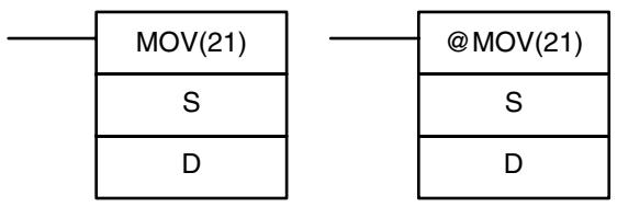
Ladder Symbols
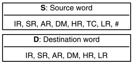
Operand Data Areas
| Limitations | DM 6144 to DM 6655 cannot be used for D. | ||||||||||||||||||
| Description | When the execution condition is OFF, MOV(21) is not executed. When the execution condition is ON, MOV(21) copies the content of S to D. | ||||||||||||||||||
| Precautions | TC numbers cannot be designated as D to change the PV of the timer or counter. You can, however, easily change the PV of a timer or a counter by using BSET(71). | ||||||||||||||||||
| Flags | ER: Indirectly addressed DM word is non-existent. (Content of *DM word is not BCD, or the DM area boundary has been exceeded.) EQ: ON when all zeros are transferred to D. | ||||||||||||||||||
| Example | The following example shows @MOV(21) being used to copy the content of IR 001 to HR 05 when IR 00000 goes from OFF to ON. | ||||||||||||||||||
| 00000 | @MOV(21) | ||||||||||||||||||
| 001 | |||||||||||||||||||
| HR 05 | |||||||||||||||||||
| Address | Instruction | Operands | |||||||||||||||||
| 00000 | LD | 00000 | |||||||||||||||||
| 00001 | @MOV(21) | 001 | |||||||||||||||||
| 001 | HR | 05 | |||||||||||||||||
| IR 000 | 0 | 1 | 1 | 1 | 0 | 0 | 1 | 1 | 1 | 0 | 0 | 0 | 1 | 0 | 1 | ||||
| HR 05 | 0 | 1 | 1 | 1 | 0 | 0 | 1 | 1 | 1 | 0 | 0 | 0 | 1 | 0 | 1 | ||||
7-17-2 MOVE NOT - MVN(22)
| Ladder Symbols | Operand Data Areas | |
| MVN(22) | @MVN(22) | S: Source word |
| S | S | IR, SR, AR, DM, HR, TC, LR, # |
| D | D | D: Destination word |
| IR, SR, AR, DM, HR, LR | ||
| Limitations | DM 6144 to DM 6655 cannot be used for D. | |
| Description | When the execution condition is OFF, MVN(22) is not executed. When the execution condition is ON, MVN(22) transfers the inverted content of S (specified word or four-digit hexadecimal constant) to D, i.e., for each ON bit in S, the corresponding bit in D is turned OFF, and for each OFF bit in S, the corresponding bit in D is turned ON. | |
| Precautions | TC numbers cannot be designated as D to change the PV of the timer or counter. However, these can be easily changed using BSET(71). | |
Flags
ER: Indirectly addressed DM word is non-existent. (Content of *DM word is not BCD, or the DM area boundary has been exceeded.)
EQ: ON when all zeros are transferred to D.
Example
The following example shows @MVN(22) being used to copy the complement of #F8C5 to DM 0010 when IR 00001 goes from OFF to ON.

| Address | Instruction | Operands |
| 00000 | LD | 00001 |
| 00001 | @MOV(21) | |
| # F8C5 | ||
| DM 0010 |
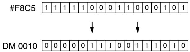
7-17-3 BLOCK TRANSFER - XFER(70)
Ladder Symbols
| — | XFER(70) | — | @ XFER(70) |
| N | N | ||
| S | S | ||
| D | D |
Operand Data Areas
| N: Number of words (BCD) |
| IR, SR, AR, DM, HR, TC, LR, # |
| S: Starting source word |
| IR, SR, AR, DM, HR, TC, LR |
| D: Starting destination word |
| IR, SR, AR, DM, HR, TC, LR |
Limitations
S and S + N must be in the same data area, as must D and D + N .
DM 6144 to DM 6655 cannot be used for D.
Description
When the execution condition is OFF, XFER(70) is not executed. When the execution condition is ON, XFER(70) copies the contents of S, S+1, ..., S+N to D, D+1, ..., D+N.
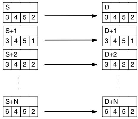
Flags
ER: N is not BCD
S and S + N or D and D + N are not in the same data area.
Indirectly addressed DM word is non-existent. (Content of *DM word is not BCD, or the DM area boundary has been exceeded.)
7-17-4 BLOCK SET - BSET(71)
Ladder Symbols
| — | BSET(71) | — | @BSET(71) |
| S | S | ||
| St | St | ||
| E | E |
Operand Data Areas
| S: Source data |
| IR, SR, AR, DM, HR, TC, LR, # |
| St: Starting word |
| IR, SR AR, DM, HR, TC, LR |
| E: End Word |
| IR, SR, AR, DM, HR, TC, LR |
Limitations
St must be less than or equal to E, and St and E must be in the same data area. DM 6144 to DM 6655 cannot be used for St or E.
Description
When the execution condition is OFF, BSET(71) is not executed. When the execution condition is ON, BSET(71) copies the content of S to all words from St through E.
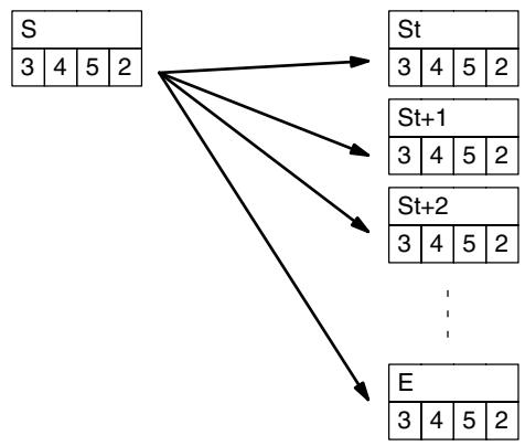
BSET(71) can be used to change timer/counter PV. (This cannot be done with MOV(21) or MVN(22).) BSET(71) can also be used to clear sections of a data area, i.e., the DM area, to prepare for executing other instructions. It can also be used to clear words by transferring all zeros.
Flags
ER: St and E are not in the same data area or St is greater than E.
Indirectly addressed DM word is non-existent. (Content of *DM word is not BCD, or the DM area boundary has been exceeded.)
Example
The following example shows how to use BSET(71) to copy a constant (#0000) to a block of the DM area (DM 0000 to DM 0500) when IR 00000 is ON.
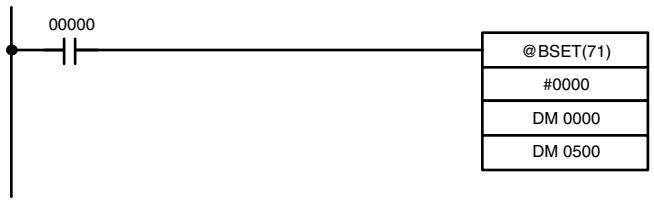
| Address | Instruction | Operands |
| 00000 | LD | 00000 |
| 00001 | @BSET(71) | |
| # 0000 | ||
| DM 0000 | ||
| DM 0500 |
7-17-5 DATA EXCHANGE - XCHG(73)
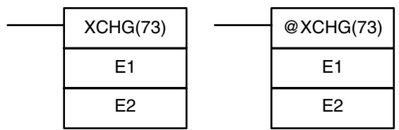
Ladder Symbols
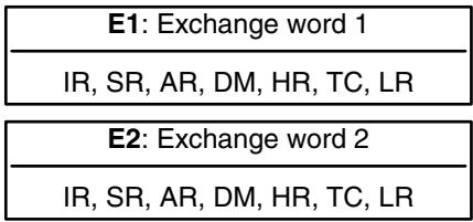
Operand Data Areas
Limitations
Description
DM 6144 to DM 6655 cannot be used for E1 or E2.
When the execution condition is OFF, XCHG(73) is not executed. When the execution condition is ON, XCHG(73) exchanges the content of E1 and E2.

If you want to exchange content of blocks whose size is greater than 1 word, use work words as an intermediate buffer to hold one of the blocks using XFER(70) three times.
Flags
ER: Indirectly addressed DM word is non-existent. (Content of *DM word is not BCD, or the DM area boundary has been exceeded.)
7-17-6 SINGLE WORD DISTRIBUTE - DIST(80)
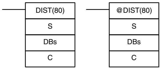
Ladder Symbols
Operand Data Areas
| S: Source data |
| IR, SR, AR, DM, HR, TC, LR, # |
| DBs: Destination base word |
| IR, SR, AR, DM, HR, TC, LR |
| C: Control word (BCD) |
| IR, SR, AR, DM, HR, TC, LR, # |
Limitations
C must be BCD.
DM 6144 to DM 6655 cannot be used for DBs or C.
Description
DIST(80) can be used for single-word distribution or for a stack operation depending on the content of the control word, C.
Single-word Distribution
When bits 12 to 15 of C = 0 to 8, DIST(80) can be used for a single word distribute operation. The entire contents of C specifies an offset, Of (0000 to 2047 in BCD). When the execution condition is OFF, DIST(80) is not executed. When the execution condition is ON, DIST(80) copies the content of S to DBs+Of, i.e., Of is added to DBs to determine the destination word.
Note 1. DBs and DBs+Of must be in the same data area and cannot be between DM 6144 and DM 6655.
- IR 000 to IR 019 or IR 000 to IR 049 is treated as a different memory area from IR 200 to IR 255 for the source data area. The entire source data area must be within one or the other of these areas. An error will occur if words from both areas are included.
Example
The following example shows how to use DIST(80) to copy #00FF to HR 10 + Of. The content of LR 10 is #3005, so #00FF is copied to HR 15 (HR 10 + 5) when IR 00000 is ON.
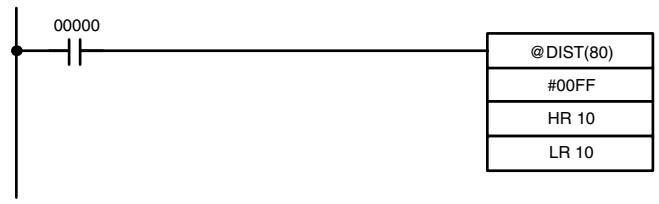
| Address | Instruction | Operands |
| 00000 | LD | 00000 |
| 00001 | @DIST(80) | |
| # 00FF | ||
| HR 10 | ||
| LR 10 |
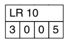
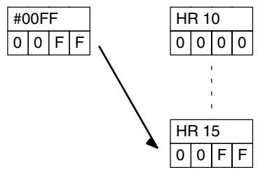
Stack Operation
When bits 12 to 15 of C = 9 , DIST(80) can be used for a stack operation. The other 3 digits of C specify the number of words in the stack (000 to 999 in BCD). The content of DBs is the stack pointer.
When the execution condition is OFF, DIST(80) is not executed. When the execution condition is ON, DIST(80) copies the content of S to DBs+1+the content of DBs. In other words, 1 and the content of DBs are added to DBs to determine the destination word. The content of DBs is then incremented by 1.
Note 1. DIST(80) will be executed every cycle unless the differentiated form (@DIST(80)) is used or DIST(80) is used with DIFU(13) or DIFD(14).
- Be sure to initialize the stack pointer before using DIST(80) as a stack operation.
Example
The following example shows how to use DIST(80) to create a stack between DM 0001 and DM 0005. DM 0000 acts as the stack pointer.
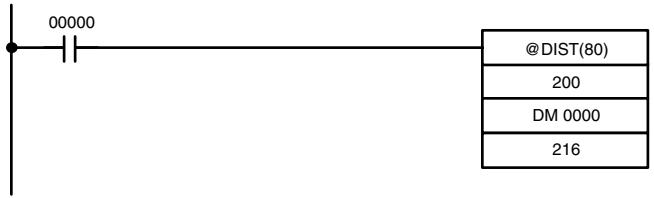
| Address | Instruction | Operands |
| 00000 | LD | 00000 |
| 00001 | @DIST(80) | |
| 200 | ||
| DM 0000 | ||
| 216 |
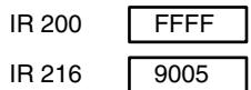
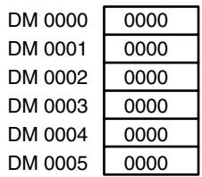
Stack pointer incremented
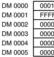
DM 0000 C
DM 0001 F
DM 0002 C
DM 0003 C
DM 0004 C
DM 0005 C

Stack pointer incremented
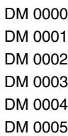
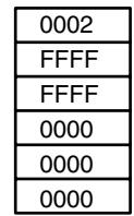
Flags
ER: The offset or stack length in the control word is not BCD.
Indirectly addressed DM word is non-existent. (Content of *DM word is not BCD, or the DM area boundary has been exceeded.)
During stack operation, the value of the stack pointer+1 exceeds the length of the stack.
EQ: ON when the content of S is zero; otherwise OFF.
7-17-7 DATA COLLECT-COLL(81)
Ladder Symbols
| COLL(81) | @COLL(81) |
| SBs | SBs |
| C | C |
| D | D |
Operand Data Areas
| SBs: Source base word |
| IR, SR, AR, DM, HR, TC, LR |
| C: Control word (BCD) |
| IR, SR, AR, DM, HR, TC, LR, # |
| D: Destination word |
| IR, SR, AR, DM, HR, TC, LR |
Limitations
C must be BCD.
DM 6144 to DM 6655 cannot be used for D.
Description
COLL(81) can be used for data collection, an FIFO stack operation, or an LIFO stack operation depending on the content of the control word, C.
Data Collection
When bits 12 to 15 of C = 0 to 7, COLL(81) is used for data collection. The entire contents of C specifies an offset, Of (0000 to 2047 in BCD).
When the execution condition is OFF, COLL(81) is not executed. When the execution condition is ON, COLL(81) copies the content of SBs + Of to D, i.e., Of is added to SBs to determine the source word.
Note 1. SBs and SBs+Of must be in the same data area.
- IR 000 to IR 019 or IR 000 to IR 049 is treated as a different memory area from IR 200 to IR 255 for the source data area. The entire source data area must be within one or the other of these areas. An error will occur if words from both areas are included.
Example
The following example shows how to use COLL(81) to copy the content of DM 0000+Of to LR 00. The content of 200 is #0005, so the content of DM 0005 (DM 0000 + 5) is copied to LR 00 when IR 00001 is ON.
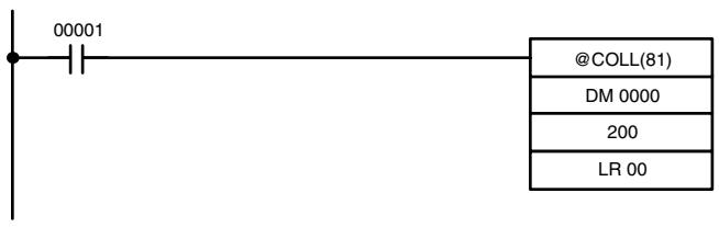
| Address | Instruction | Operands |
| 00000 | LD | 00001 |
| 00001 | @DIST(80) | |
| DM 0000 | ||
| 200 | ||
| LR 00 |
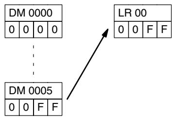
FIFO Stack Operation
When bits 12 to 15 of C = 9 , COLL(81) can be used for an FIFO stack operation. The other 3 digits of C specify the number of words in the stack (000 to 999, in BCD). The content of SBs is the stack pointer.
When the execution condition is ON, COLL(81) shifts the contents of each word within the stack down by one address, finally shifting the data from SBs+1 (the first value written to the stack) to the destination word (D). The content of the stack pointer (SBs) is then decremented by one.
Note COLL(81) will be executed every cycle unless the differentiated form (@COLL(81)) is used or COLL(81) is used with DIFU(13) or DIFD(14).
Example
The following example shows how to use COLL(81) to create a stack between DM 0001 and DM 0005. DM 0000 acts as the stack pointer.
When IR 00000 goes from OFF to ON, COLL(81) shifts the contents of DM 0002 to DM 0005 down by one address, and shifts the data from DM 0001 to IR 001. The content of the stack pointer (DM 0000) is then decremented by one.
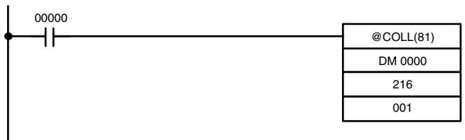
| Address | Instruction | Operands |
| 00000 | LD | 00000 |
| 00001 | @COLL(81) | |
| DM 0000 | ||
| 216 | ||
| 001 |
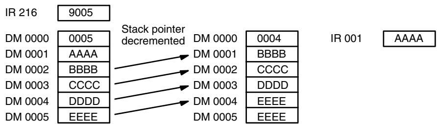
LIFO Stack Operation
When bits 12 to 15 of C = 8 , COLL(81) can be used for an LIFO stack operation. The other 3 digits of C specify the number of words in the stack (000 to 999). The content of SBs is the stack pointer.
When the execution condition is ON, COLL(81) copies the data from the word indicated by the stack pointer (SBs+the content of SBs) to the destination word (D). The content of the stack pointer (SBs) is then decremented by one.
The stack pointer is the only word changed in the stack.
Note COLL(81) will be executed every cycle unless the differentiated form (@DIST(80)) is used or DIST(80) is used with DIFU(13) or DIFD(14).
Example
The following example shows how to use COLL(81) to create a stack between DM 0001 and DM 0005. DM 0000 acts as the stack pointer.
When IR 00000 goes from OFF to ON, COLL(81) copies the content of DM 0005 (DM 0000 + 5 ) to IR 001. The content of the stack pointer (DM 0000) is then decremented by one.
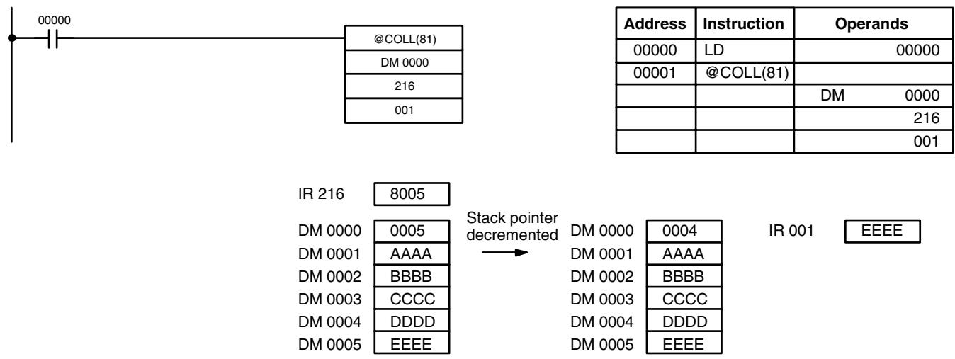
Flags
ER: The offset or stack length in the control word is not BCD.
Indirectly addressed DM word is non-existent. (Content of *DM word is not BCD, or the DM area boundary has been exceeded.)
During stack operation, the value of the stack pointer exceeds the length of the stack; an attempt was made to write to a word beyond the end of the stack.
EQ: ON when the content of S is zero; otherwise OFF.
7-17-8 MOVE BIT - MOVB(82)
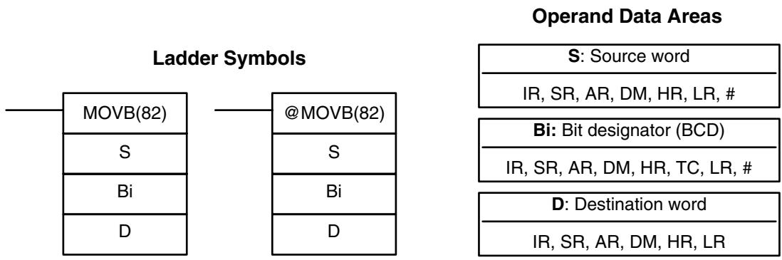
Limitations
The rightmost two digits and the leftmost two digits of Bi must each be between 00 and 15.
DM 6144 to DM 6655 cannot be used for Bi or D.
Description
When the execution condition is OFF, MOVB(82) is not executed. When the execution condition is ON, MOVB(82) copies the specified bit of S to the specified bit in D. The bits in S and D are specified by Bi. The rightmost two digits of Bi designate the source bit; the leftmost two bits designate the destination bit.
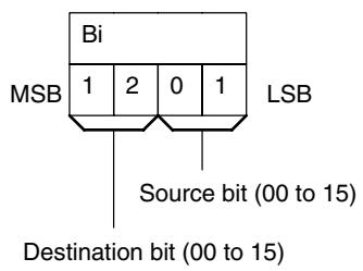
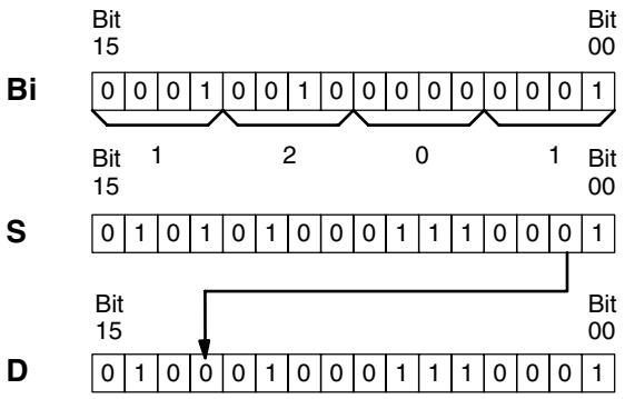
Flags
ER: Bi is not BCD, or it is specifying a non-existent bit (i.e., bit specification must be between 00 and 15).
Indirectly addressed DM word is non-existent. (Content of *DM word is not BCD, or the DM area boundary has been exceeded.)
7-17-9 MOVE DIGIT - MOVD(83)
Ladder Symbols
| MOVD(83) | @MOVD(83) |
| S | S |
| Di | Di |
| D | D |
Operand Data Areas
| S: Source word |
| IR, SR, AR, DM, HR, TC, LR, # |
| Di: Digit designator (BCD) |
| IR, SR, AR, DM, HR, TC, LR, # |
| D: Destination word |
| IR, SR, AR, DM, HR, TC, LR |
Limitations
The rightmost three digits of Di must each be between 0 and 3. DM 6144 to DM 6655 cannot be used for Di or D.
Description
When the execution condition is OFF, MOVD(83) is not executed. When the execution condition is ON, MOVD(83) copies the content of the specified digit(s) in S to the specified digit(s) in D. Up to four digits can be transferred at one time. The first digit to be copied, the number of digits to be copied, and the first digit to receive the copy are designated in Di as shown below. Digits from S will be copied to consecutive digits in D starting from the designated first digit and continued for the designated number of digits. If the last digit is reached in either S or D, further digits are used starting back at digit 0.
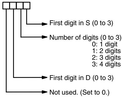
Digit number:
Digit Designator
The following show examples of the data movements for various values of Di.
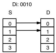
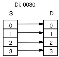
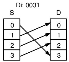
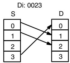
Flags
ER: At least one of the rightmost three digits of Di is not between 0 and 3. Indirectly addressed DM word is non-existent. (Content of *DM word is not BCD, or the DM area boundary has been exceeded.)
7-18 Data Control Instructions
7-18-1 SCALING - SCL(66)
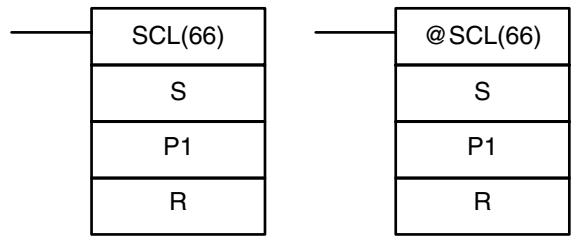
Ladder Symbols
Operand Data Areas
| S: Source word |
| IR, SR, AR, DM, HR, TC, LR, # |
| P1: First parameter word |
| IR, SR, AR, DM, HR, TC, LR |
| R: Result word |
| IR, SR, AR, DM, HR, LR |
Limitations
This instruction is available in the CPM2A/CPM2C/SRM1(-V2) only.
S must be BCD.
P1 through P1+3 must be in the same data area.
DM 6144 to DM 6655 cannot be used for P1 through P1+3 or R.
Description
SCL(66) is used to linearly convert a 4-digit hexadecimal value to a 4-digit BCD value. Unlike BCD(24), which converts a 4-digit hexadecimal value to its 4-digit BCD equivalent ( S_hex S_BCD ), SCL(66) can convert the hexadecimal value according to a specified linear relationship. The conversion line is defined by two points specified in the parameter words P1 to P1+3.
When the execution condition is OFF, SCL(66) is not executed. When the execution condition is ON, SCL(66) converts the 4-digit hexadecimal value in S to the 4-digit BCD value on the line defined by points (P1, P1+1) and (P1+2, P1+3) and places the results in R. The results is rounded off to the nearest integer. If the results is less than 0000, then 0000 is written to R, and if the result is greater than 9999, then 9999 is written to R.
The following table shows the functions and ranges of the parameter words:
| Parameter | Function | Range | Comments |
| P1 | BCD point #1 (AY) | 0000 to 9999 | --- |
| P1+1 | Hex. point #1 (AX) | 0000 to FFFF | Do not set P1+1=P1+3. |
| P1+2 | BCD point #2 (BY) | 0000 to 9999 | --- |
| P1+3 | Hex. point #2 (BX) | 0000 to FFFF | Do not set P1+3=P1+1. |
The following diagram shows the source word, S, converted to D according to the line defined by points (A_Y, A_X) and (B_Y, B_X) .
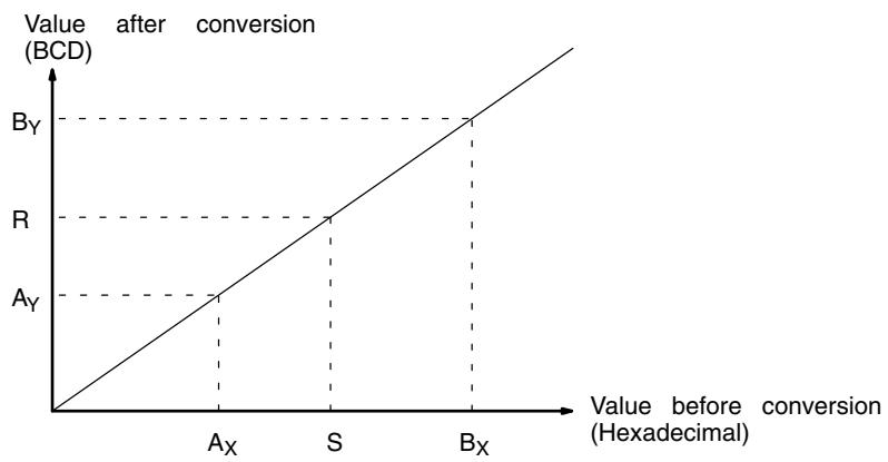
The results can be calculated by first converting all values to BCD and then using the following formula.
$$ \text {R e s u l t s} = \mathrm {B} _ {\mathrm {Y}} - \left[ \left(\mathrm {B} _ {\mathrm {Y}} - \mathrm {A} _ {\mathrm {Y}}\right) / \left(\mathrm {B} _ {\mathrm {X}} - \mathrm {A} _ {\mathrm {X}}\right) \times \left(\mathrm {B} _ {\mathrm {X}} - \mathrm {S}\right) \right] $$
Flags
ER: The value in P1 + 1 equals that in P1 + 3 .
Indirectly addressed DM word is non-existent. (Content of *DM word is not BCD, or the DM area boundary has been exceeded.)
P1 and P1 + 3 are not in the same data area, or other setting error.
EQ: ON when the result, R, is 0000.
Example
When 00000 is turned ON in the following example, the BCD source data in DM 0100 (#0100) is converted to hexadecimal according to the parameters in DM 0150 to DM 0153. The result (#0512) is then written to DM 0200.
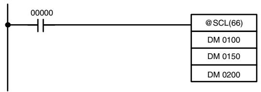
| Address | Instruction | Operands |
| 00000 | LD | 00000 |
| 00001 | @SCL(66) | |
| DM 0100 | ||
| DM 0150 | ||
| DM 0200 |
| DM 0150 | 0010 |
| DM 0151 | 0005 |
| DM 0152 | 0050 |
| DM 0153 | 0019 |
| DM 0100 | 0100 |
| DM 0200 | 0512 |
7-18-2 SIGNED BINARY TO BCD SCALING - SCL2(—)
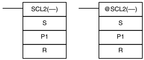
Ladder Symbols
Operand Data Areas
| S: Source word |
| IR, SR, AR, DM, HR, LR |
| P1: First parameter word |
| IR, SR, AR, DM, HR, LR |
| R: Result word |
| IR, SR, AR, DM, HR, LR |
Limitations
This instruction is available in the CPM2A/CPM2C only.
S must be BCD.
P1 through P1+2 must be in the same data area.
DM 6144 to DM 6655 cannot be used for R.
Description
SCL2(—) is used to linearly convert a 4-digit signed hexadecimal value to a 4-digit BCD value. Unlike BCD(24), which converts a 4-digit hexadecimal value to its 4-digit BCD equivalent ( S_hex S_BCD ), SCL2(—) can convert the signed hexadecimal value according to a specified linear relationship. The conversion line is defined by the x-intercept and the slope of the line specified in the parameter words P1 to P1+2.
When the execution condition is OFF, SCL2(—) is not executed. When the execution condition is ON, SCL2(—) converts the 4-digit signed hexadecimal value in S to the 4-digit BCD value on the line defined by the x-intercept (P1, 0) and the slope (P1 + 2 ÷ P1 + 1) and places the results in R. The result is rounded off to the nearest integer.
If the result is negative, then CY is set to 1. If the result is less than -9999, then -9999 is written to R. If the result is greater than 9999, then 9999 is written to R.
The following table shows the functions and ranges of the parameter words:
| Parameter | Function | Range |
| P1 | x-intercept (signed hex.) | 8000 to 7FFF (-32,768 to 32,767) |
| P1+1 | ΔX (signed hex.) | 8000 to 7FFF (-32,768 to 32,767) |
| P1+2 | ΔY (BCD) | 0000 to 9999 |
The following diagram shows the source word, S, converted to R according to the line defined by the point (P1, 0) and slope Y / X .
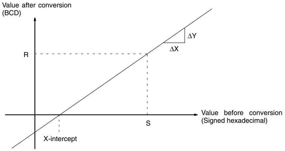
The result can be calculated by first converting all signed hexadecimal values to BCD and then using the following formula.
$$ R = \frac {\Delta Y}{\Delta X} \times (S - P 1) $$
Flags
ER: Indirectly addressed DM word is non-existent. (Content of *DM word is not BCD, or the DM area boundary has been exceeded.)
P1 and P1 + 2 are not in the same data area, or other setting error.
CY: ON when the result, R, is negative.
EQ: ON when the result, R, is 0000.
Example
When 05000 is turned ON in the following example, the signed binary source data in 200 (#FFE2) is converted to BCD according to the parameters in DM 0000 to DM 0002. The result (#0018) is then written to LR 00 and CY is turned ON because the result is negative.
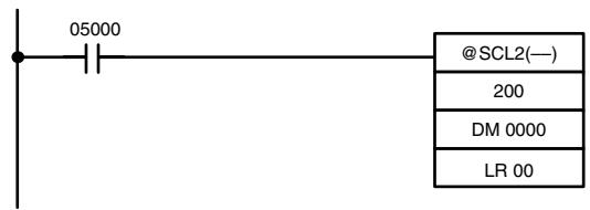
| Address | Instruction | Operands |
| 00000 | LD | 05000 |
| 00001 | @SCL2(—) | |
| 200 | ||
| DM 0000 | ||
| LR 00 |
| DM 0000 | FFFD |
| DM 0001 | 0003 |
| DM 0002 | 0002 |
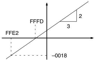
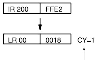
$$ \begin{array}{l} R = \frac {0 0 0 2}{0 0 0 3} \times (F F E 2 - F F F D) \ = \frac {2}{3} \times (- 1 B) = - 1 8 \ \end{array} $$
CY flag is turned ON because the conversion result is negative.
7-18-3 BCD TO SIGNED BINARY SCALING - SCL3(—)
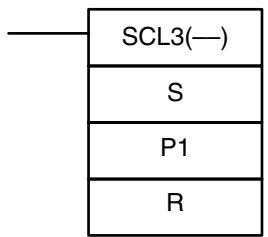
Ladder Symbols
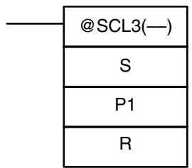
Operand Data Areas
| S: Source word |
| IR, SR, AR, DM, HR, LR |
| P1: First parameter word |
| IR, SR, AR, DM, HR, LR |
| R: Result word |
| IR, SR, AR, DM, HR, LR |
Limitations
This instruction is available in the CPM2A/CPM2C only.
P1+1 must be BCD.
P1 through P1+4 must be in the same data area.
DM 6144 to DM 6655 cannot be used for R.
Description
SCL3(—) is used to linearly convert a 4-digit 4-digit BCD value to 4-digit signed hexadecimal. SCL3(—) converts the BCD value according to a specified linear relationship. The conversion line is defined by the y-intercept and the slope of the line specified in the parameter words P1 to P1+2.
When the execution condition is OFF, SCL3(—) is not executed. When the execution condition is ON, SCL3(—) converts the 4-digit BCD value in S to the 4-digit signed hexadecimal value on the line defined by the y-intercept (0, P1) and the slope (P1 + 2 ÷ P1 + 1) and places the result in R. The result is rounded off to the nearest integer.
The content of S can be 0000 to 9999, but S will be treated as a negative value if CY = 1 , so the effective range of S is actually -9999 to 9999 . Be sure to set the desired sign in CY using STC(40) or CLC(41).
Parameter words P1 + 3 and P1 + 4 define upper and lower limits for the result. If the result is greater than the upper limit in P1 + 3 , then the upper limit is written to R. If the result is less than the lower limit in P1 + 4 , then the lower limit is written to R.
Note The upper and lower limits for a 12-bit Analog Input Unit would be 07FF and F800.
The following table shows the functions and ranges of the parameter words:
| Parameter | Function | Range |
| P1 | x-intercept (signed hex.) | 8000 to 7FFF (-32,768 to 32,767) |
| P1+1 | ΔX (BCD) | 0001 to 9999 |
| P1+2 | ΔY (signed hex.) | 8000 to 7FFF (-32,768 to 32,767) |
| P1+3 | Upper limit (signed hex.) | 8000 to 7FFF (-32,768 to 32,767) |
| P1+4 | Lower limit (signed hex.) | 8000 to 7FFF (-32,768 to 32,767) |
The following diagram shows the source word, S, converted to R according to the line defined by the point (0, P1) and slope Y / X .
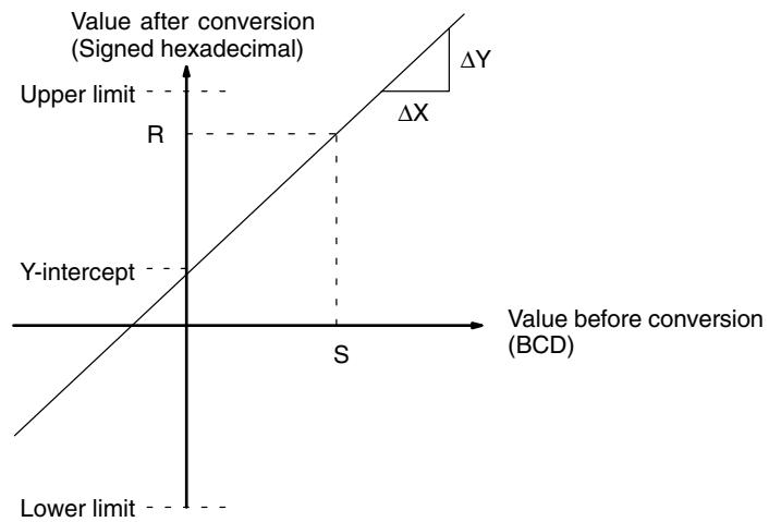
The result can be calculated by first converting all BCD values to signed binary and then using the following formula.
ER: Indirectly addressed DM word is non-existent. (Content of *DM word is not BCD, or the DM area boundary has been exceeded.)
The content of S is not BCD.
CY: CY is not changed by SCL3(—). (CY shows the sign of S before execution.)
EQ: ON when the result, R, is 0000.
Example
The status of 00101 determines the sign of the BCD source word in the following example. If 00101 is ON, then the source word is negative. When 00100 is turned ON, the BCD source data in LR 02 is converted to signed binary according to the parameters in DM 0000 to DM 0004. The result is then written to DM 0100. (In the second conversion, the signed binary equivalent of -1035 is less than the lower limit specified in DM 0004, so the lower limit is written to DM 0100.)
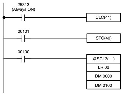
| Address | Instruction | Operands |
| 00000 | LD | 25313 |
| 00001 | CLC(41) | |
| 00002 | LD | 00101 |
| 00101 | STC(40) | |
| 00004 | LD | 00100 |
| 00005 | SCL3(—) | |
| LR 02 | ||
| DM 0000 | ||
| DM 0100 |
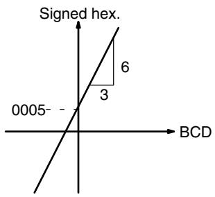
This instruction is available in the CPM2A/CPM2C and SRM1(-V2) only.
DM 6144 to DM 6655 cannot be used for P1 or OW.
P1 to P1+32 must be in the same data area.

A total of 33 continuous words starting with P1 must be provided for PID(—) to operate correctly. Also, PID(—) may not operate dependably in any of the following situations: In interrupt programs, in subroutines, between IL(02) and ILC(03), between JMP(04) and JME(05), and in step programming (STEP(08)/SNXT(09)). Do not program PID(—) in these situations.
Description
PID(—) performs PID control based on the parameters specified in P1 through P1+6.
When the execution condition OFF, PID() is not executed. When the execution condition is ON, PID() carries out PID control according to the designated parameters. It takes the specified input range of binary data from the contents of IW and carries out the PID action according to the parameters that are set. The result is then stored as the manipulated variable in OW.
The following table shows the function of the parameter words.
| Word | Bits | Parameter name | Function/Setting range |
| P1 | 00 to 15 | Set value (SV). | This is the target value for PID control. It can be set to any binary number with the number of bits set by the input range parameter. |
| P1+1 | 00 to 15 | Proportional band width. | This parameter specifies the proportional band width输入/Output range ratio from 0.1% to 999.9%. It must be BCD from 0001 to 9999. |
| P1+2 | 00 to 15 | Integral time (Tik)/ sampling period (τ) | Sets the strength of integral action. Increasing this value strengthens the integral action. It must be BCD from 0001 to 8191, or 9999. A setting of 9999 disables integral control. |
| Set the integral time divided by the sampling time. | |||
| P1+3 | 00 to 15 | Derivative time (Tdk)/sampling period (τ) | Sets the strength of derivative action. Increasing this value strengthens the derivative action. It must be BCD from 0001 to 8191, or 0000. (A setting of 0000 disables derivative control.) |
| Set the derivative time divided by the sampling time. | |||
| P1+4 | 00 to 15 | Sampling period (τ) | Sets the interval between samplings of the input data. It must be BCD from 0001 to 1023. The period will be from 0.1 to 102.3 s |
| P1+5 | 00 to 03 | Operation specifier | Sets reverse or normal operation. Set to 0 to specify reverse operation or 1 to specify normal operation. |
| 04 to 15 | Input filter coefficient (α) | Determines the strength of the input filter. The lower the coefficient, the weaker the filter. This setting must be BCD from 100 to 199, or 000. A setting of 000 sets the default value (0.65) and a setting of 100 to 199 sets the coefficient from 0.00 to 0.99. | |
| P1+6 | 00 to 03 | Output range | Determines the number of bits of output data. This setting must be between 0 and 8, which sets the output range between 8 and 16 bits. |
| 08 to 15 | Input range | Determines the number of bits of input data. This setting must be between 00 and 08, which sets the input range between 8 and 16 bits. | |
| P1+7 to P1+32 | 00 to 15 | Work area | Do not use. (Used by the system.) |

Caution
Changes made to the parameters will not be effective until the execution condition for PID(—) goes from OFF to ON.
Note Do not use PID(—) in the following situations; it may not be executed properly.
In interrupt programs
In subroutine programs
In interlocked program sections (between IL and ILC)
In jump program sections (between JMP and JME)
In step ladder program section (created with STEP)
When the execution condition is ON, PID() performs the PID calculation on the input data when the sampling period has elapsed. The sampling period is the time that must pass before input data is read for processing.
The following diagram shows the relationship between the sampling period and PID processing. PID processing is performed only when the sampling period (100 ms in this case) has elapsed.
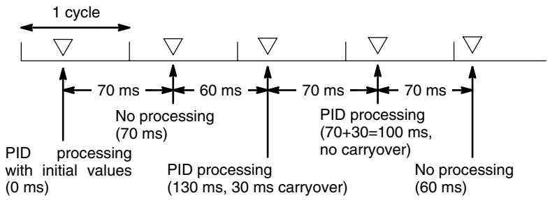
PID CONTROL Action
Execution Condition OFF
All data that has been set is retained. When the execution condition is OFF, the manipulated variable can be written to the output word (OW) to achieve manual control.
Rising Edge of the Execution Condition
The work area is initialized based on the PID parameters that have been set and the PID control action is begin. Sudden and radical changes in the manipulated variable output are not made when starting action to avoid adverse affect on the controlled system (bumpless operation).
When PID parameters are changed, they first become valid when the execution condition changes from OFF to ON.
Execution Condition ON
The PID action is executed at the intervals based on the sampling period, according to the PID parameters that have been set.
Sampling Period and PID Execution Timing
The sampling period is the time interval to retrieve the measurement data for carrying out a PID action. PID(—), however, is executed according to CPU cycle, so there may be cases where the sampling period is exceeded. In such cases, the time interval until the next sampling is reduced.
PID Control Method
PID control actions are executed by means of PID control with feed-forward control (two degrees of freedom).
When overshooting is prevented with simple PID control, stabilization of disturbances is slowed (1). If stabilization of disturbances is speeded up, on the other hand, overshooting occurs and response toward the target value is slowed (2). With feed-forward PID control, there is no overshooting, and response toward the target value and stabilization of disturbances can both be speeded up (3).
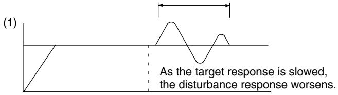
Simple PID Control
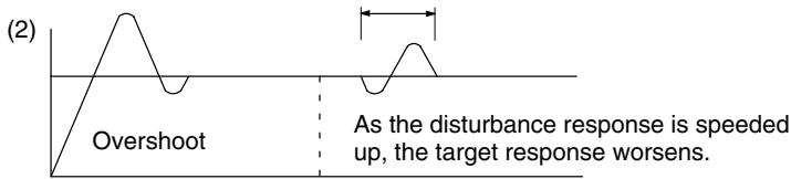
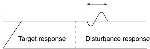
Feed-forward PID control
Control Actions
Proportional Action (P)
Proportional action is an operation in which a proportional band is established with respect to the set value (SV), and within that band the manipulated variable (MV) is made proportional to the deviation. An example for reverse operation is shown in the following illustration
If the proportional action is used and the present value (PV) becomes smaller than the proportional band, the manipulated variable (MV) is 100% (i.e., the maximum value). Within the proportional band, the MV is made proportional to the deviation (the difference between from SV and PV) and gradually decreased until the SV and PV match (i.e., until the deviation is 0), at which time the MV will be 0% (i.e., the minimum value). The MV will also be 0% when the PV is larger than the SV.
The proportional band is expressed as a percentage of the total input range. The smaller the proportional band, the larger the proportional constant and the stronger the corrective action will be. With proportional action an offset (residual deviation) generally occurs, but the offset can be reduced by making the proportional band smaller. If it is made too small, however, hunting will occur.
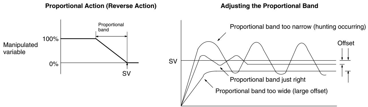
Integral Action (I)
Combining integral action with proportional action reduces the offset according to the time that has passed. The strength of the integral action is indicated by the integral time, which is the time required for the manipulated variable of the integral action to reach the same level as the manipulated variable of the proportional action with respect to the step deviation, as shown in the following illustration. The shorter the integral time, the stronger the correction by the integral action will be. If the integral time is too short, the correction will be too strong and will cause hunting to occur.
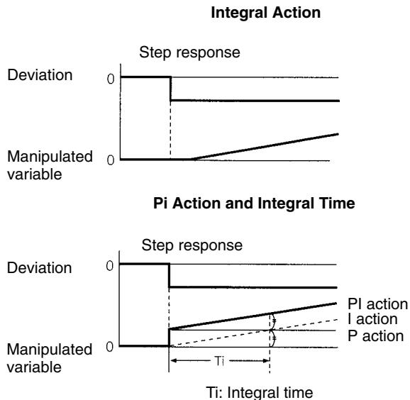
Derivative Action (D)
Proportional action and integral action both make corrections with respect to the control results, so there is inevitably a response delay. Derivative action compensates for that drawback. In response to a sudden disturbance it delivers a large manipulated variable and rapidly restores the original status. A correction is executed with the manipulated variable made proportional to the incline (derivative coefficient) caused by the deviation.
The strength of the derivative action is indicated by the derivative time, which is the time required for the manipulated variable of the derivative action to reach the same level as the manipulated variable of the proportional action with respect to the step deviation, as shown in the following illustration. The longer the derivative time, the stronger the correction by the derivative action will be.
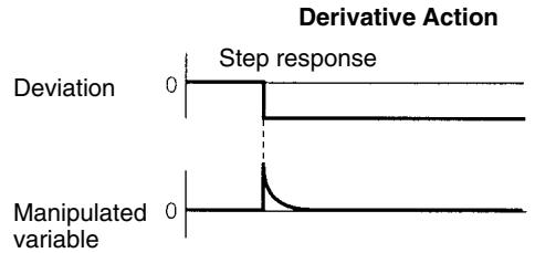
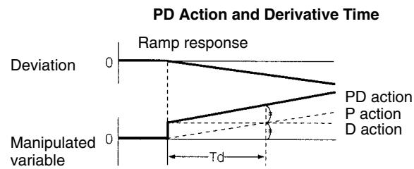
Td: Derivative time
PID Action
PID action combines proportional action (P), integral action (I), and derivative action (D). It produces superior control results even for control objects with dead time. It employs proportional action to provide smooth control without hunting, integral action to automatically correct any offset, and derivative action to speed up the response to disturbances.
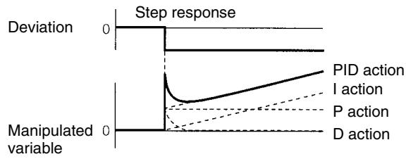
Step Response of PID Control Action Output
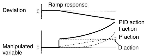
Ramp Response of PID Control Action Output
Direction of Action
When using PID action, select either of the following two control directions. In either direction, the MV increases as the difference between the SV and the PV increases.
- Forward action: MV is increased when the PV is larger than the SV.
- Reverse action: MV is increased when the PV is smaller than the SV.
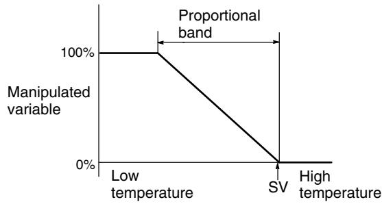
Reverse Action
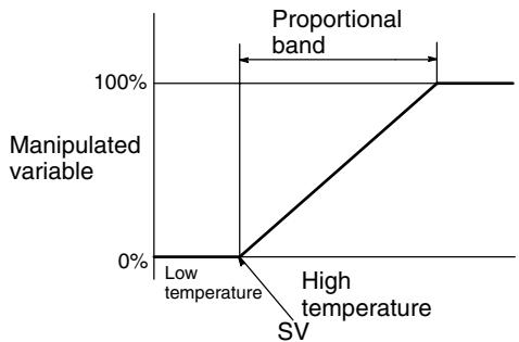
Forward Action
Adjusting PID Parameters
The general relationship between PID parameters and control status is shown below.
- When it is not a problem if a certain amount of time is required for stabilization (settlement time), but it is important not to cause overshooting, then enlarge the proportional band.
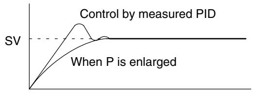
- When overshooting is not a problem but it is desirable to quickly stabilize control, then narrow the proportional band. If the proportional band is narrowed too much, however, then hunting may occur.
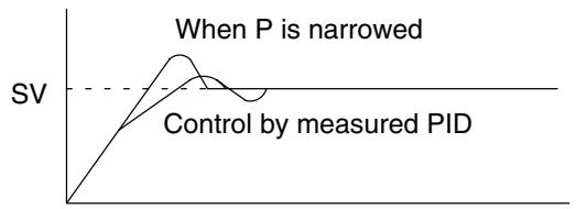
- When there is broad hunting, or when operation is tied up by overshooting and undershooting, it is probably because integral action is too strong. The hunting will be reduced if the integral time is increased or the proportional band is enlarged.
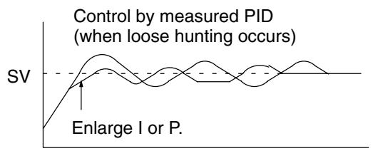
- If the period is short and hunting occurs, it may be that the control system response is quick and the derivative action is too strong. In that case, set the derivative action lower.
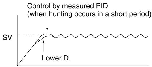
Flags
ER: There is an error in the parameter settings.
The cycle time is more than twice as long as the sampling period, so PID() cannot be executed accurately. PID() will be executed in this case.
P1 and P1 + 32 are not in the same area or a parameter setting is not within the specified range.
Indirectly addressed DM word is non-existent. (Content of *DM word is not BCD, or the DM area boundary has been exceeded.)
CY: ON when PID processing is being performed. (OFF when the sampling period has not elapsed.)
7-19 Comparison Instructions
7-19-1 COMPARE - CMP(20)
Ladder Symbols
| CMP(20) |
| Cp1 |
| Cp2 |
Operand Data Areas
| Cp1: First compare word |
| IR, SR, AR, DM, HR, TC, LR, # |
| Cp2: Second compare word |
| IR, SR, AR, DM, HR, TC, LR, # |
Limitations
When comparing a value to the PV of a timer or counter, the value must be in BCD.
Description
When the execution condition is OFF, CMP(20) is not executed. When the execution condition is ON, CMP(20) compares Cp1 and Cp2 and outputs the result to the GR, EQ, and LE flags in the SR area.
Precautions
Placing other instructions between CMP(20) and the operation which accesses the EQ, LE, and GR flags may change the status of these flags. Be sure to access them before the desired status is changed.
Flags
ER: Indirectly addressed DM word is non-existent. (Content of *DM word is not BCD, or the DM area boundary has been exceeded.)
EQ: ON if Cp1 equals Cp2.
LE: ON if Cp1 is less than Cp2.
GR: ON if Cp1 is greater than Cp2.
| Flag | Address | C1 < C2 | C1 = C2 | C1 > C2 |
| GR | 25505 | OFF | OFF | ON |
| EQ | 25506 | OFF | ON | OFF |
| LE | 25507 | ON | OFF | OFF |
Example: Saving CMP(20) Results
The following example shows how to save the comparison result immediately. If the content of HR 09 is greater than that of DM 0000, 20000 is turned ON; if the two contents are equal, 20001 is turned ON; if content of HR 09 is less than that of DM 0000, 20002 is turned ON. In some applications, only one of the three OUTs would be necessary, making the use of TR 0 unnecessary. With this type of programming, 20000, 20001, and 20002 are changed only when CMP(20) is executed.
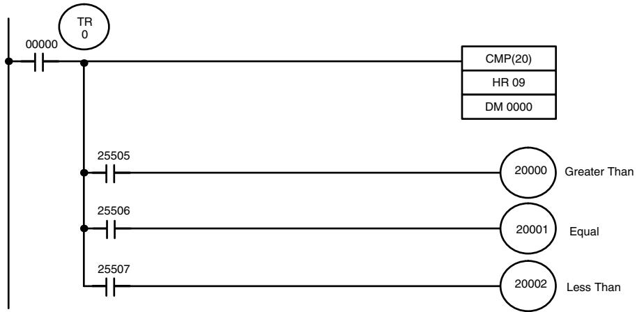
| Address | Instruction | Operands |
| 00000 | LD | 00000 |
| 00001 | OUT | TR 0 |
| 00002 | CMP(20) | |
| HR 09 | ||
| DM 0000 | ||
| 00003 | AND | 25505 |
| 00004 | OUT | 20000 |
| Address | Instruction | Operands |
| 00005 | LD | TR 0 |
| 00006 | AND | 25506 |
| 00007 | OUT | 20001 |
| 00008 | LD | TR 0 |
| 00009 | AND | 25507 |
| 00010 | OUT | 20002 |
7-19-2 TABLE COMPRE - TCMP(85)
Ladder Symbols
| TCMP(85) | @TCMP(85) |
| CD | CD |
| TB | TB |
| R | R |
Operand Data Areas
| CD: Compare data |
| IR, SR, DM, HR, TC, LR, # |
| TB: First comparison table word |
| IR, SR, DM, HR, TC, LR |
| R: Result word |
| IR, SR, DM, HR, TC, LR |
Limitations
DM 6144 to DM 6655 cannot be used for R.
Description
When the execution condition is OFF, TCMP(85) is not executed. When the execution condition is ON, TCMP(85) compares CD to the content of TB, TB+1, TB+2, ..., and TB+15. If CD is equal to the content of any of these words, the corresponding bit in R is set, e.g., if the CD equals the content of TB, bit 00 is turned ON, if it equals that of TB+1, bit 01 is turned ON, etc. The rest of the bits in R will be turned OFF.
Flags
ER: The comparison table (i.e., TB through TB+15) exceeds the data area. Indirectly addressed DM word is non-existent. (Content of *DM word is not BCD, or the DM area boundary has been exceeded.)
Example
The following example shows the comparisons made and the results provided for TCMP(85). Here, the comparison is made during each cycle when IR 00000 is ON.


7-19-3 BLOCK COMPARE - BCMP(68)
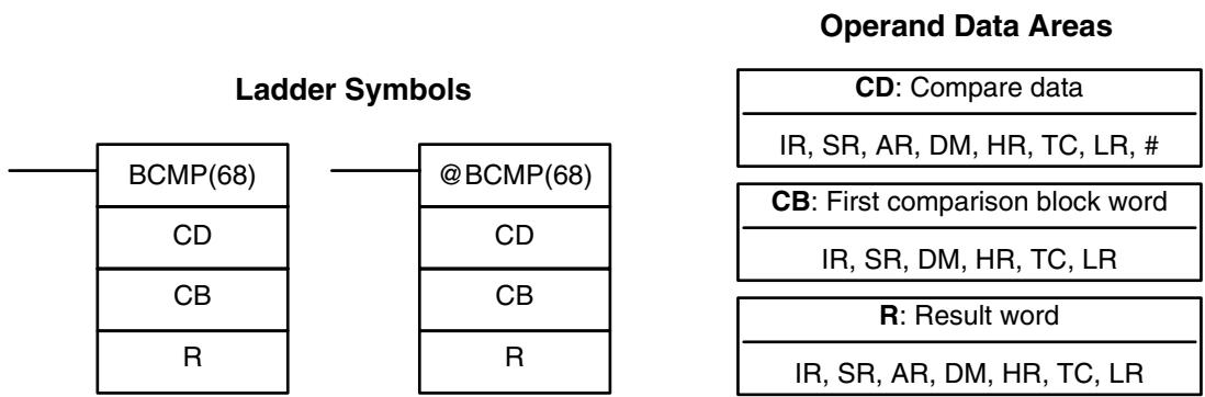
Note BCMP(68) is an expansion instruction for the SRM1(-V2). The function code 68 is the factory setting and can be changed for the SRM1(-V2) if desired.
Limitations
Each lower limit word in the comparison block must be less than or equal to the upper limit.
DM 6144 to DM 6655 cannot be used for R.
Description
When the execution condition is OFF, BCMP(68) is not executed. When the execution condition is ON, BCMP(68) compares CD to the ranges defined by a block consisting of CB, CB+1, CB+2, ..., CB+31. Each range is defined by two words, the first one providing the lower limit and the second word providing the upper limit. If CD is found to be within any of these ranges (inclusive of the upper and lower limits), the corresponding bit in R is set. The comparisons that are made and the corresponding bit in R that is set for each true comparison are shown below. The rest of the bits in R will be turned OFF.
| CB ≤ CD ≤ CB+1 | Bit 00 |
| CB+2 ≤ CD ≤ CB+3 | Bit 01 |
| CB+4 ≤ CD ≤ CB+5 | Bit 02 |
| CB+6 ≤ CD ≤ CB+7 | Bit 03 |
| CB+8 ≤ CD ≤ CB+9 | Bit 04 |
| CB+10 ≤ CD ≤ CB+11 | Bit 05 |
| CB+12 ≤ CD ≤ CB+13 | Bit 06 |
| CB+14 ≤ CD ≤ CB+15 | Bit 07 |
| CB+16 ≤ CD ≤ CB+17 | Bit 08 |
| CB+18 ≤ CD ≤ CB+19 | Bit 09 |
| CB+20 ≤ CD ≤ CB+21 | Bit 10 |
| CB+22 ≤ CD ≤ CB+23 | Bit 11 |
| CB+24 ≤ CD ≤ CB+25 | Bit 12 |
| CB+26 ≤ CD ≤ CB+27 | Bit 13 |
| CB+28 ≤ CD ≤ CB+29 | Bit 14 |
| CB+30 ≤ CD ≤ CB+31 | Bit 15 |
Flags
ER: The comparison block (i.e., CB through CB+31) exceeds the data area. Indirectly addressed DM word is non-existent. (Content of *DM word is not BCD, or the DM area boundary has been exceeded.)
Example
The following example shows the comparisons made and the results provided for BCMP(68). Here, the comparison is made during each cycle when IR 00000 is ON.

HR 00
HR 00
0210
Compare data in IR 001 (which contains 0210) with the given ranges.
Lower limits
| DM 0010 | 0000 |
| DM 0012 | 0101 |
| DM 0014 | 0201 |
| DM 0016 | 0301 |
| DM 0018 | 0401 |
| DM 0020 | 0501 |
| DM 0022 | 0601 |
| DM 0024 | 0701 |
| DM 0026 | 0801 |
| DM 0028 | 0901 |
| DM 0030 | 1001 |
| DM 0032 | 1101 |
| DM 0034 | 1201 |
| DM 0036 | 1301 |
| DM 0038 | 1401 |
| DM 0040 | 1501 |
Upper limits
| DM 0011 | 0100 |
| DM 0013 | 0200 |
| DM 0015 | 0300 |
| DM 0017 | 0400 |
| DM 0019 | 0500 |
| DM 0021 | 0600 |
| DM 0023 | 0700 |
| DM 0025 | 0800 |
| DM 0027 | 0900 |
| DM 0029 | 1000 |
| DM 0031 | 1100 |
| DM 0033 | 1200 |
| DM 0035 | 1300 |
| DM 0037 | 1400 |
| DM 0039 | 1500 |
| DM 0041 | 1600 |
R:LR 05
| LR 0500 | 0 |
| LR 0501 | 0 |
| LR 0502 | 1 |
| LR 0503 | 0 |
| LR 0504 | 0 |
| LR 0505 | 0 |
| LR 0506 | 0 |
| LR 0507 | 0 |
| LR 0508 | 0 |
| LR 0509 | 0 |
| LR 0510 | 0 |
| LR 0511 | 0 |
| LR 0512 | 0 |
| LR 0513 | 0 |
| LR 0514 | 0 |
| LR 0515 | 0 |
7-19-4 DOUBLE COMPRE - CMPL(60)
Ladder Symbols
| CMPL(60) |
| Cp1 |
| Cp2 |
| — |
Operand Data Areas
| Cp1: First word of first compare word pair |
| IR, SR, AR, DM, HR, TC, LR |
| Cp2: First word of second compare word pair |
| IR, SR, AR, DM, HR, TC, LR |
Note CMPL(60) is an expansion instruction for the SRM1(-V2). The function code 60 is the factory setting and can be changed for the SRM1(-V2) if desired.
Limitations
Cp1 and Cp1 + 1 must be in the same data area.
Cp2 and Cp2 + 1 must be in the same data area.
Set the third operand to 000.
Description
When the execution condition is OFF, CMPL(60) is not executed. When the execution condition is ON, CMPL(60) joins the 4-digit hexadecimal content of Cp1 + 1 with that of Cp1 , and that of Cp2 + 1 with that of Cp2 to create two 8-digit hexadecimal numbers, Cp + 1,Cp1 and Cp2 + 1,Cp2 . The two 8-digit numbers are then compared and the result is output to the GR, EQ, and LE flags in the SR area.
Precautions
Placing other instructions between CMPL(60) and the operation which accesses the EQ, LE, and GR flags may change the status of these flags. Be sure to access them before the desired status is changed.
Flags
ER: Indirectly addressed DM word is non-existent. (Content of *DM word is not BCD, or the DM area boundary has been exceeded.)
GR: ON if Cp1 + 1,Cp1 is greater than Cp2 + 1,Cp2 .
EQ: ON if Cp1+1,Cp1 equals Cp2+1,Cp2.
LE: ON if Cp1 + 1,Cp1 is less than Cp2 + 1,Cp2
Example:
Saving CMPL(60) Results
The following example shows how to save the comparison result immediately. If the content of HR 10, HR 09 is greater than that of DM 0001, DM 0000, then 20000 is turned ON; if the two contents are equal, 20001 is turned ON; if content of HR 10, HR 09 is less than that of DM 0001, DM 0000, then 20002 is turned ON. In some applications, only one of the three OUTs would be necessary, making the use of TR 0 unnecessary. With this type of programming, 20000, 20001, and 20002 are changed only when CMPL(60) is executed.
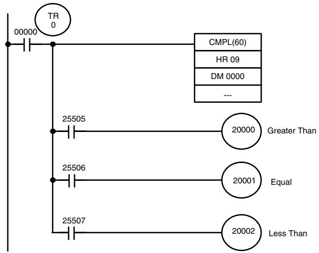
| Address | Instruction | Operands |
| 00000 | LD | 00000 |
| 00001 | OUT | TR 0 |
| 00002 | CMPL(60) | |
| HR 09 | ||
| DM 0000 | ||
| 00003 | AND | 25505 |
| 00004 | OUT | 20000 |
| 00005 | LD | TR 0 |
| 00006 | AND | 25506 |
| 00007 | OUT | 20001 |
| 00008 | LD | TR 0 |
| 00009 | AND | 25507 |
| 00010 | OUT | 20002 |
7-19-5 AREA RANGE COMPARE - ZCP(—)
Ladder Symbol
| ZCP(—) |
| CD |
| LL |
| UL |
Operand Data Areas
| CD: Compare data |
| IR, SR, AR, DM, HR, TC, LR, # |
| LL: Lower limit of range |
| IR, SR, AR, DM, HR, TC, LR, # |
| UL: Upper limit of range |
| IR, SR, AR, DM, HR, TC, LR, # |
Limitations
This instruction is available in the CPM2A/CPM2C/SRM1(-V2) only.
LL must be less than or equal to UL.
Description
When the execution condition is OFF, ZCP() is not executed. When the execution condition is ON, ZCP() compares CD to the range defined by lower limit LL and upper limit UL and outputs the result to the GR, EQ, and LE flags in the SR area. The resulting flag status is shown in the following table.
| Comparison result | Flag status | ||
| GR (SR 25505) | EQ (SR 25506) | LE (SR 25507) | |
| CD < LL | 0 | 0 | 1 |
| LL ≤ CD ≤ UL | 0 | 1 | 0 |
| UL < CD | 1 | 0 | 0 |
Precautions
Placing other instructions between ZCP(—) and the operation which accesses the EQ, LE, and GR flags may change the status of these flags. Be sure to access them before the desired status is changed.
Flags
ER: Indirectly addressed DM word is non-existent. (Content of *DM word is not BCD, or the DM area boundary has been exceeded.)
LL is greater than UL.
In the following example, the content of IR 200 (#6FA4) is compared to the range #0010 to #AB1F. Since #0010 ≤ #6FA4 ≤ #AB1F, the EQ flag and IR 10101 are turned ON.
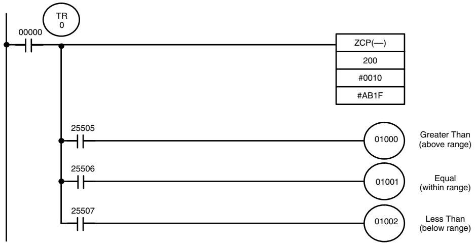
| Address | Instruction | Operands |
| 00000 | LD | 00000 |
| 00001 | OUT | TR 0 |
| 00002 | ZCP(—) | |
| 200 | ||
| # 0010 | ||
| # AB1F | ||
| 00003 | AND | 25505 |
| Address | Instruction | Operands |
| 00004 | OUT | 01000 |
| 00005 | LD | TR 0 |
| 00006 | AND | 25506 |
| 00007 | OUT | 01001 |
| 00008 | LD | TR 0 |
| 00009 | AND | 25507 |
| 00010 | OUT | 01002 |
| LL: #0010 | < | CD: 200 | < | UL: #AB1F | → | 20000: OFF | |||||||||
| 0 | 0 | 1 | 0 | 6 | F | A | 4 | A | B | 1 | F | 20001: ON | |||
| 20002: OFF | |||||||||||||||
7-19-6 DOUBLE AREA RANGE COMPARE - ZCPL(—)
Ladder Symbol
| ZCPL(—) |
| CD |
| LL |
| UL |
Operand Data Areas
| CD: Compare data |
| IR, SR, AR, DM, HR, LR |
| LL: Lower limit of range |
| IR, SR, AR, DM, HR, LR |
| UL: Upper limit of range |
| IR, SR, AR, DM, HR, LR |
Limitations
This instruction is available in the CPM2A/CPM2C only.
The 8-digit value in LL + 1, LL must be less than or equal to UL + 1, UL .
Description
When the execution condition is OFF, ZCPL() is not executed. When the execution condition is ON, ZCPL() compares the 8-digit value in CD, CD+1 to the range defined by lower limit LL+1,LL and upper limit UL+1,UL and outputs the result to the GR, EQ, and LE flags in the SR area. The resulting flag status is shown in the following table.
| Comparison result | Flag status | ||
| GR(SR 25505) | EQ(SR 25506) | LE(SR 25507) | |
| CD, CD+1< LL+1,LL | 0 | 0 | 1 |
| LL+1,LL≤ CD, CD+1≤ UL+1,UL | 0 | 1 | 0 |
| UL+1,UL< CD, CD+1 | 1 | 0 | 0 |
Precautions
Placing other instructions between ZCPL(—) and the operation which accesses the EQ, LE, and GR flags may change the status of these flags. Be sure to access them before the desired status is changed.
Flags
ER: Indirectly addressed DM word is non-existent. (Content of *DM word is not BCD, or the DM area boundary has been exceeded.) LL+1,LL is greater than UL+1,UL.
EQ: ON if LL + 1, LL ≤ CD , CD + 1 ≤ UL + 1, UL
LE: ON if CD, CD + 1 < LL + 1,LL
GR: ON if CD, CD + 1 > UL + 1,UL
7-20 Conversion Instructions
7-20-1 BCD-TO-BINARY - BIN(23)
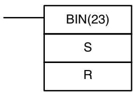
Ladder Symbols
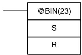
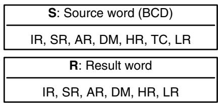
Operand Data Areas
Limitations
DM 6144 to DM 6655 cannot be used for R.
Description
When the execution condition is OFF, BIN(23) is not executed. When the execution condition is ON, BIN(23) converts the BCD content of S into the numerically equivalent binary bits, and outputs the binary value to R. Only the content of R is changed; the content of S is left unchanged.
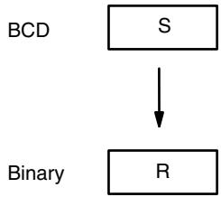
BIN(23) can be used to convert BCD to binary so that displays on the Programming Console or any other programming device will appear in hexadecimal rather than decimal. It can also be used to convert to binary to perform binary arithmetic operations rather than BCD arithmetic operations, e.g., when BCD and binary values must be added.
Flags
ER: The content of S is not BCD.
Indirectly addressed DM word is non-existent. (Content of *DM word is not BCD, or the DM area boundary has been exceeded.)
EQ: ON when the result is zero.
7-20-2 BINARY-TO-BCD - BCD(24)
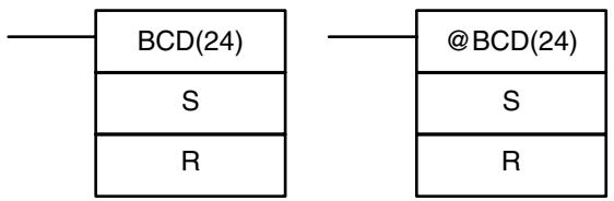
Ladder Symbols

Operand Data Areas
Limitations
If the content of S exceeds 270F, the converted result would exceed 9999 and BCD(24) will not be executed. When the instruction is not executed, the content of R remains unchanged.
DM 6144 to DM 6655 cannot be used for R.
Description
BCD(24) converts the binary (hexadecimal) content of S into the numerically equivalent BCD bits, and outputs the BCD bits to R. Only the content of R is changed; the content of S is left unchanged.
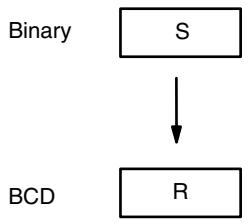
BCD(24) can be used to convert binary to BCD so that displays on the Programming Console or any other programming device will appear in decimal rather than hexadecimal. It can also be used to convert to BCD to perform BCD arithmetic operations rather than binary arithmetic operations, e.g., when BCD and binary values must be added.
Flags
ER: Indirectly addressed DM word is non-existent. (Content of *DM word is not BCD, or the DM area boundary has been exceeded.)
EQ: ON when the result is zero.
7-20-3 DOUBLE BCD-TO-DOUBLE BINARY-BINL(58)
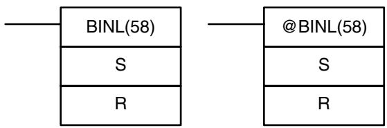
Ladder Symbols
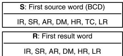
Operand Data Areas
Limitations
This instruction is available in the CPM2A/CPM2C only.
DM 6144 to DM 6655 cannot be used for R.
Description
When the execution condition is OFF, BINL(58) is not executed. When the execution condition is ON, BINL(58) converts an eight-digit number in S and S+1 into 32-bit binary data, and outputs the converted data to R and R+1.
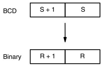
Flags
ER: The contents of S and/or S+1 words are not BCD.
Indirectly addressed DM word is non-existent. (Content of *DM word is not BCD, or the DM area boundary has been exceeded.)
EQ: ON when the result is zero.
7-20-4 DOUBLE BINARY-TO-DOUBLE BCD - BCDL(59)
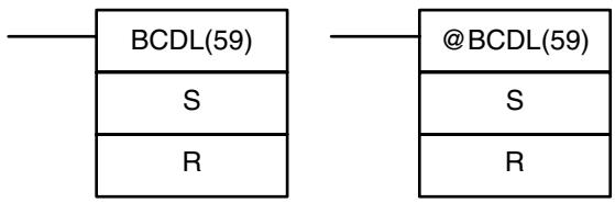
Ladder Symbols
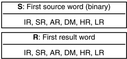
Operand Data Areas
Limitations
This instruction is available in the CPM2A/CPM2C only.
If the content of S exceeds 05F5E0FF, the converted result would exceed 99999999 and BCDL(59) will not be executed. When the instruction is not executed, the content of R and R + 1 remain unchanged.
DM 6144 to DM 6655 cannot be used for R.
Description
BCDL(59) converts the 32-bit binary content of S and S + 1 into eight digits of BCD data, and outputs the converted data to R and R + 1 .
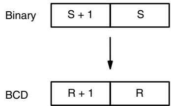
Flags
ER: Content of R and R + 1 exceeds 99999999.
Indirectly addressed DM word is non-existent. (Content of *DM word is not BCD, or the DM area boundary has been exceeded.)
EQ: ON when the result is zero.
7-20-5 4-TO-16 DECODER - MLPX(76)
Ladder Symbols
| MLPX(76) | @MLPX(76) |
| S | S |
| Di | Di |
| R | R |
Operand Data Areas
| S: Source word |
| IR, SR, AR, DM, HR, TC, LR |
| Di: Digit designator |
| IR, SR, AR, DM, HR, TC, LR, # |
| R: First result word |
| IR, SR, AR, DM, HR, LR |
Limitations
The rightmost two digits of Di must each be between 0 and 3.
All result words must be in the same data area.
DM 6144 to DM 6655 cannot be used for R.
Description
When the execution condition is OFF, MLPX(76) is not executed. When the execution condition is ON, MLPX(76) converts up to four, four-bit hexadecimal digits from S into decimal values from 0 to 15, each of which is used to indicate a bit position. The bit whose number corresponds to each converted value is then turned ON in a result word. If more than one digit is specified, then one bit will be turned ON in each of consecutive words beginning with R. (See examples, below.)
The following is an example of a one-digit decode operation from digit number 1 of S, i.e., here Di would be 0001.
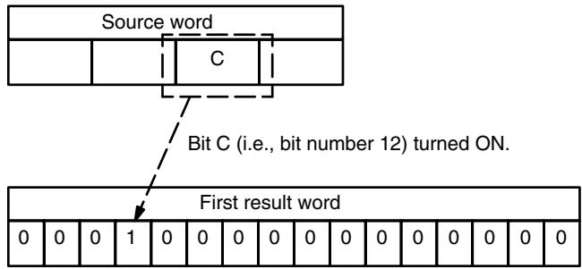
The first digit and the number of digits to be converted are designated in Di. If more digits are designated than remain in S (counting from the designated first digit), the remaining digits will be taken starting back at the beginning of S. The final word required to store the converted result (R plus the number of digits to be converted) must be in the same data area as R, e.g., if two digits are converted, the last word address in a data area cannot be designated; if three digits are converted, the last two words in a data area cannot be designated.
Digit Designator
The digits of Di are set as shown below.
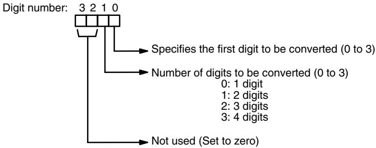
Some example Di values and the digit-to-word conversions that they produce are shown below.
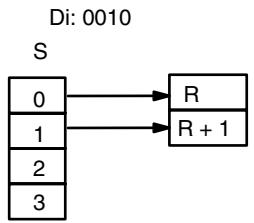
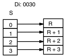
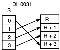
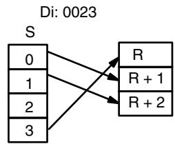
Flags
ER: Undefined digit designator, or R plus number of digits exceeds a data area.
Indirectly addressed DM word is non-existent. (Content of *DM word is not BCD or the DM area boundary has been exceeded.)
Example
The following program converts digits 1 to 3 of data from DM 0020 to bit positions and turns ON the corresponding bits in three consecutive words starting with HR 10. Digit 0 is not converted.

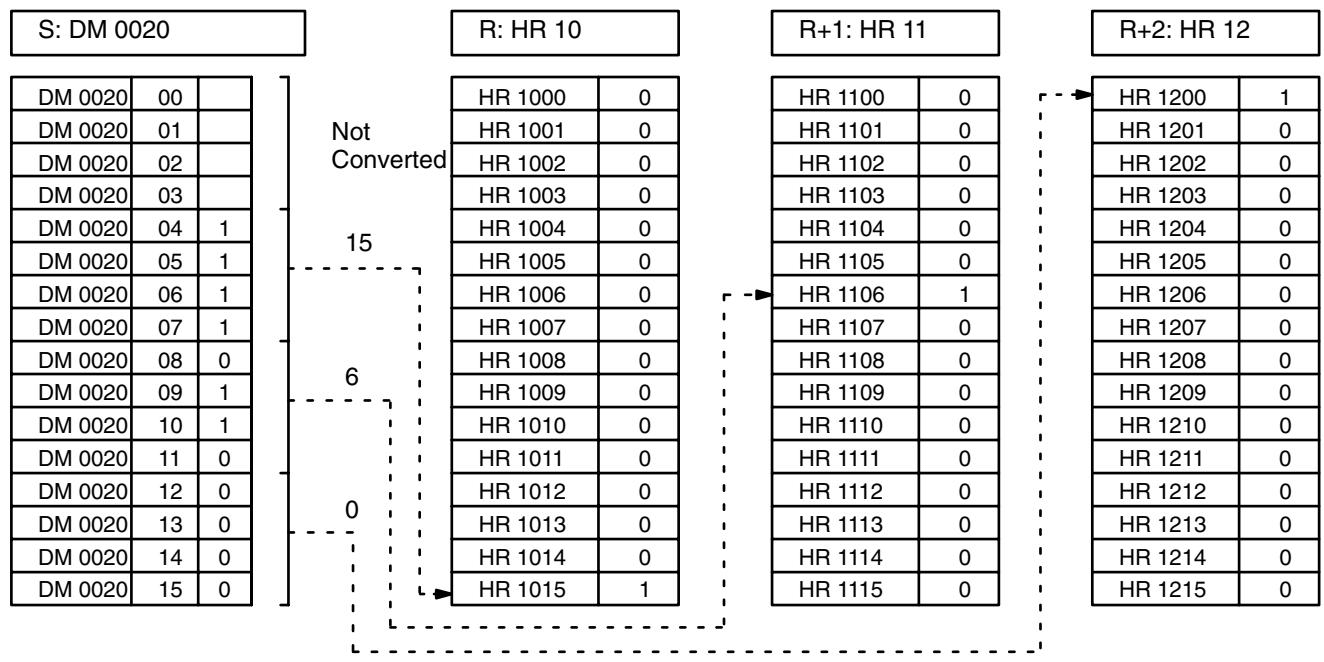
7-20-6 16-TO-4 ENCODER - DMPX(77)
Ladder Symbols
| DMPX(77) | @DMPX(77) |
| SB | SB |
| R | R |
| Di | Di |
Operand Data Areas
| SB: First source word |
| IR, SR, AR, DM, HR, TC, LR |
| R: Result word |
| IR, SR, AR, DM, HR, LR |
| Di: Digit designator |
| IR, SR, AR, DM, HR, TC, LR, # |
Limitations
The rightmost two digits of Di must each be between 0 and 3.
All source words must be in the same data area.
DM 6144 to DM 6655 cannot be used for SB, R, or Di.
Description
When the execution condition is OFF, DMPX(77) is not executed. When the execution condition is ON, DMPX(77) determines the position of the highest ON bit in S, encodes it into single-digit hexadecimal value corresponding to the bit number of the highest ON bit number, then transfers the hexadecimal value to the specified digit in R. The digits to receive the results are specified in Di, which also specifies the number of digits to be encoded.
The following is an example of a one-digit encode operation to digit number 1 of R, i.e., here Di would be 0001.
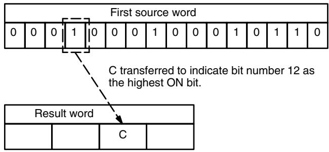
Up to four digits from four consecutive source words starting with S may be encoded and the digits written to R in order from the designated first digit. If more digits are designated than remain in R (counting from the designated first digit), the remaining digits will be placed at digits starting back at the beginning of R.
The final word to be converted (S plus the number of digits to be converted) must be in the same data area as SB.
Digit Designator
The digits of Di are set as shown below.
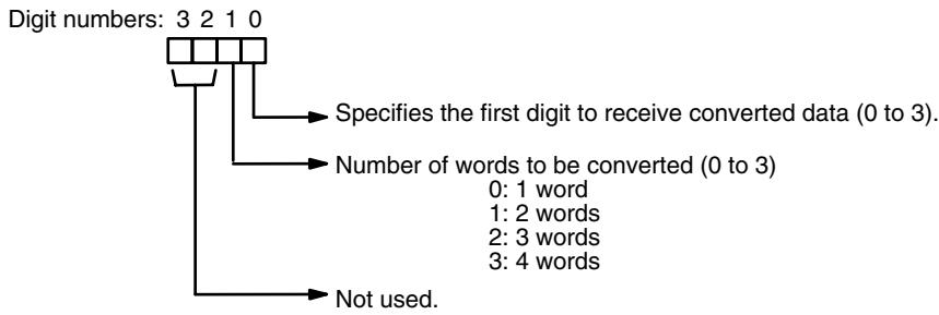
Some example Di values and the word-to-digit conversions that they produce are shown below.
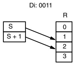
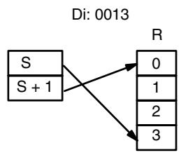
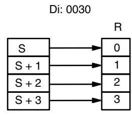
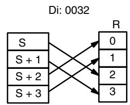
Flags
ER: Undefined digit designator, or S plus number of digits exceeds a data area.
Content of a source word is zero.
Indirectly addressed DM word is non-existent. (Content of *DM word is not BCD, or the DM area boundary has been exceeded.)
Example
When 00000 is ON, the following diagram encodes IR words 200 and 201 to the first two digits of HR 10 and then encodes LR 10 and 11 to the last two digits of HR 10. Although the status of each source word bit is not shown, it is assumed that the bit with status 1 (ON) shown is the highest bit that is ON in the word.
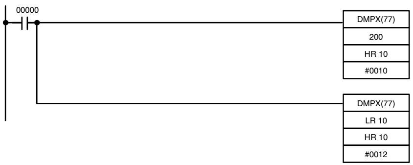
| Address | Instruction | Operands |
| 00000 | LD | 00000 |
| 00001 | DMPX(77) | |
| 200 | ||
| HR 10 | ||
| # 0010 | ||
| 00002 | DMPX(77) | |
| LR 10 | ||
| HR 10 | ||
| # 0012 |
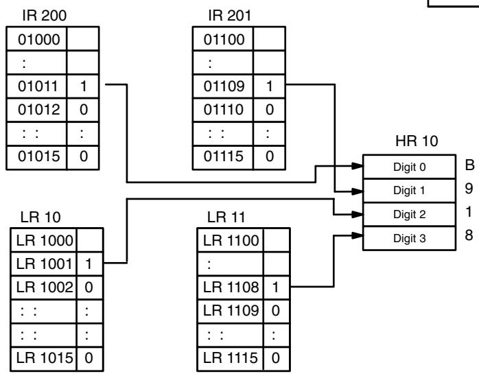
7-20-7 7-SEGMENT DECODER - SDEC(78)
Ladder Symbols
| SDEC(78) | @SDEC(78) |
| S | S |
| Di | Di |
| D | D |
Operand Data Areas
| S: Source word (binary) |
| IR, SR, AR, DM, HR, TC, LR |
| Di: Digit designator |
| IR, SR, AR, DM, HR, TC, LR, # |
| D: First destination word |
| IR, SR, AR, DM, HR, LR |
Limitations
Di must be within the values given below.
All destination words must be in the same data area.
DM 6144 to DM 6655 cannot be used for D.
Description
When the execution condition is OFF, SDEC(78) is not executed. When the execution condition is ON, SDEC(78) converts the designated digit(s) of S into the equivalent 8-bit, 7-segment display code and places it into the destination word(s) beginning with D.
Any or all of the digits in S may be converted in sequence from the designated first digit. The first digit, the number of digits to be converted, and the half of D to receive the first 7-segment display code (rightmost or leftmost 8 bits) are designated in Di. If multiple digits are designated, they will be placed in order starting from the designated half of D, each requiring two digits. If more digits are designated than remain in S (counting from the designated first digit), further digits will be used starting back at the beginning of S.
Digit Designator
The digits of Di are set as shown below.
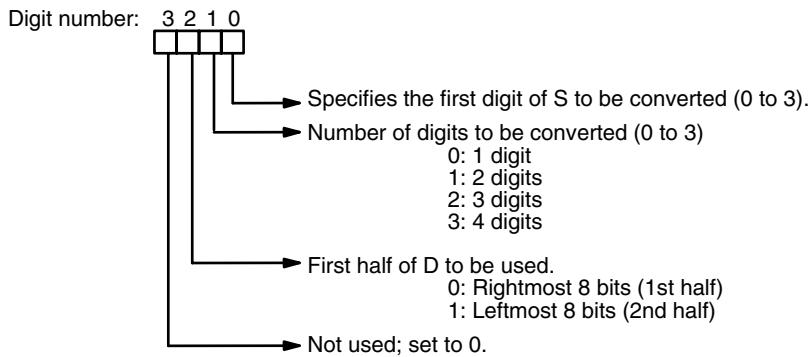
Some example Di values and the 4-bit binary to 7-segment display conversions that they produce are shown below.
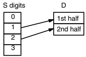
Di: 0011
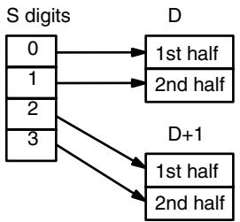
Di: 0030
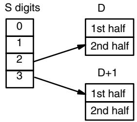
Di: 0112
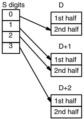
Di: 0130
Example
The following example shows the data to produce an 8. The lower case letters show which bits correspond to which segments of the 7-segment display. The table underneath shows the original data and converted code for all hexadecimal digits.
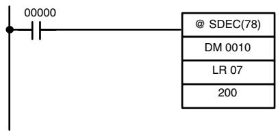
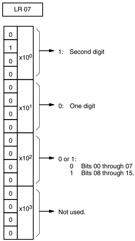
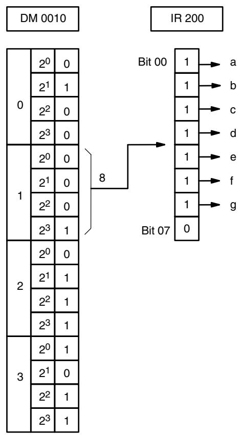
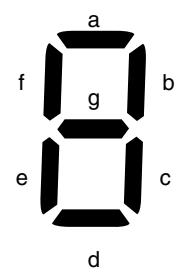
| Original data | Converted code (segments) | Display | |||||||||||
| Digit | Bits | - | g | f | e | d | c | b | a | ||||
| 0 | 0 | 0 | 0 | 0 | 0 | 0 | 1 | 1 | 0 | 0 | 0 | 0 | 0 |
| 1 | 0 | 0 | 0 | 1 | 0 | 0 | 1 | 1 | 0 | 0 | 0 | 0 | 1 |
| 2 | 0 | 0 | 1 | 0 | 0 | 0 | 1 | 1 | 0 | 0 | 1 | 1 | 2 |
| 3 | 0 | 0 | 1 | 1 | 0 | 0 | 1 | 1 | 0 | 0 | 1 | 1 | 3 |
| 4 | 0 | 1 | 0 | 0 | 0 | 0 | 1 | 1 | 0 | 1 | 0 | 0 | 4 |
| 5 | 0 | 1 | 0 | 1 | 0 | 0 | 1 | 1 | 0 | 1 | 0 | 1 | 5 |
| 6 | 0 | 1 | 1 | 0 | 0 | 0 | 1 | 1 | 0 | 1 | 0 | 1 | 6 |
| 7 | 0 | 1 | 1 | 1 | 0 | 0 | 1 | 1 | 0 | 1 | 1 | 1 | 7 |
| 8 | 1 | 0 | 0 | 0 | 0 | 0 | 1 | 1 | 1 | 0 | 0 | 0 | 8 |
| 9 | 1 | 0 | 0 | 1 | 0 | 0 | 1 | 1 | 1 | 0 | 0 | 1 | 9 |
| A | 1 | 0 | 1 | 0 | 0 | 1 | 0 | 0 | 0 | 0 | 0 | 1 | B |
| B | 1 | 0 | 1 | 1 | 0 | 1 | 0 | 0 | 0 | 0 | 1 | 0 | b |
| C | 1 | 1 | 0 | 0 | 0 | 1 | 0 | 0 | 0 | 0 | 1 | 1 | C |
| D | 1 | 1 | 0 | 1 | 0 | 1 | 0 | 0 | 0 | 1 | 0 | 0 | d |
| E | 1 | 1 | 1 | 0 | 0 | 1 | 0 | 0 | 0 | 1 | 0 | 1 | E |
| F | 1 | 1 | 1 | 1 | 0 | 1 | 0 | 0 | 0 | 1 | 1 | 0 | f |
Flags
ER: Incorrect digit designator, or data area for destination exceeded.
Indirectly addressed DM word is non-existent. (Content of *DM word is not BCD, or the DM area boundary has been exceeded.)
7-20-8 ASCII CONVERT - ASC(86)
Ladder Symbols
| — | ASC(86) | — | @ASC(86) |
| S | — | S | |
| Di | — | Di | |
| D | — | D |
Operand Data Areas
| S: Source word |
| IR, SR, AR, DM, HR, TC, LR |
| Di: Digit designator |
| IR, SR, AR, DM, HR, TC, LR, # |
| D: First destination word |
| IR, SR, AR, DM, HR, LR |
Limitations
Di must be within the values given below.
All destination words must be in the same data area.
DM 6144 to DM 6655 cannot be used for D.
Description
When the execution condition is OFF, ASC(86) is not executed. When the execution condition is ON, ASC(86) converts the designated digit(s) of S into the equivalent 8-bit ASCII code and places it into the destination word(s) beginning with D.
Any or all of the digits in S may be converted in order from the designated first digit. The first digit, the number of digits to be converted, and the half of D to receive the first ASCII code (rightmost or leftmost 8 bits) are designated in Di. If multiple digits are designated, they will be placed in order starting from the designated half of D, each requiring two digits. If more digits are designated than remain in S (counting from the designated first digit), further digits will be used starting back at the beginning of S.
Note Refer to Appendix G for a table of ASCII characters.
Digit Designator
The digits of Di are set as shown below.
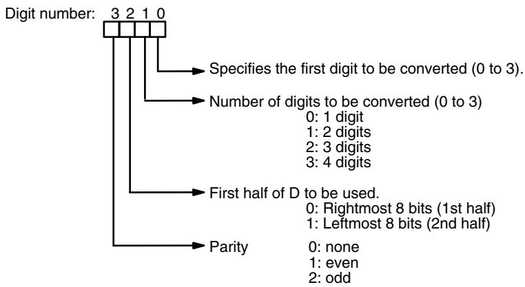
Some examples of Di values and the 4-bit binary to 8-bit ASCII conversions that they produce are shown below.
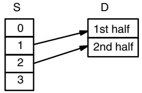
Di: 0011
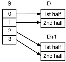
Di: 0030
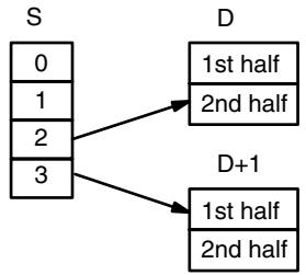
Di: 0112
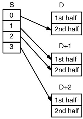
Di: 0130
Parity
The leftmost bit of each ASCII character (2 digits) can be automatically adjusted for either even or odd parity. If no parity is designated, the leftmost bit will always be zero.
When even parity is designated, the leftmost bit will be adjusted so that the total number of ON bits is even, e.g., when adjusted for even parity, ASCII "31" (00110001) will be "B1" (10110001: parity bit turned ON to create an even number of ON bits); ASCII "36" (00110110) will be "36" (00110110: parity bit turned OFF because the number of ON bits is already even). The status of the parity bit does not affect the meaning of the ASCII code.
When odd parity is designated, the leftmost bit of each ASCII character will be adjusted so that there is an odd number of ON bits.
Flags
ER: Incorrect digit designator, or data area for destination exceeded.
Indirectly addressed DM word is non-existent. (Content of *DM word is not BCD, or the DM area boundary has been exceeded.)
7-20-9 ASCII-TO-HEXADECIMAL - HEX(—)
Ladder Symbols
| HEX(—) | @HEX(—) |
| S | S |
| Di | Di |
| D | D |
Operand Data Areas
| S: First source word |
| IR, SR, AR, DM, HR, TC, LR, # |
| Di: Digit designator |
| IR, SR, AR, DM, HR, TC, LR, # |
| D: Destination word |
| IR, SR, AR, DM, HR, LR |
Limitations
This instruction is available in the CPM2A/CPM2C/SRM1(-V2) only.
Di must be within the values given below.
All source words must be in the same data area.
Bytes in the source words must contain the ASCII code equivalent of hexadecimal values, i.e., 30 to 39 (0 to 9) or 41 to 46 (A to F).
DM 6144 to DM 6655 cannot be used for D.
Description
When the execution condition is OFF, HEX(—) is not executed. When the execution condition is ON, HEX(—) converts the designated byte(s) of ASCII code from the source word(s) into the hexadecimal equivalent and places it into D.
Up to 4 ASCII codes may be converted beginning with the designated first byte of S. The converted hexadecimal values are then placed in D in order from the designated digit. The first byte (rightmost or leftmost 8 bits), the number of bytes to be converted, and the digit of D to receive the first hexadecimal value are designated in Di. If multiple bytes are designated, they will be converted in order starting from the designated half of S and continuing to S+1 and S+2, if necessary.
If more digits are designated than remain in D (counting from the designated first digit), further digits will be used starting back at the beginning of D. Digits in D that do not receive converted data will not be changed.
Digit Designator
The digits of Di are set as shown below.
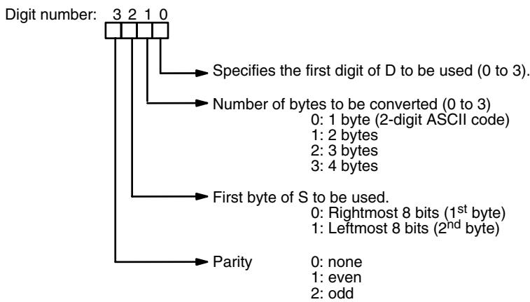
Some examples of Di values and the 8-bit ASCII to 4-bit hexadecimal conversions that they produce are shown below.
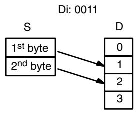
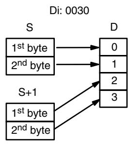
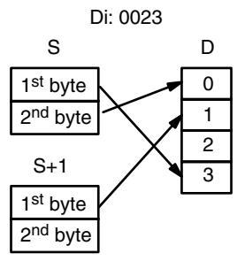
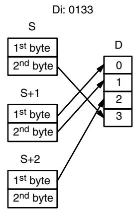
ASCII Code Table
The following table shows the ASCII codes before conversion and the hexadecimal values after conversion. Refer to Appendix G for a table of ASCII characters.
| Original data | Converted data | ||||||||||||
| ASCII Code | Bit status (See note.) | Digit | Bits | ||||||||||
| 30 | * | 0 | 1 | 1 | 0 | 0 | 0 | 0 | 0 | 0 | 0 | 0 | 0 |
| 31 | * | 0 | 1 | 1 | 0 | 0 | 0 | 1 | 1 | 0 | 0 | 0 | 1 |
| 32 | * | 0 | 1 | 1 | 0 | 0 | 1 | 0 | 2 | 0 | 0 | 1 | 0 |
| 33 | * | 0 | 1 | 1 | 0 | 0 | 1 | 1 | 3 | 0 | 0 | 1 | 1 |
| 34 | * | 0 | 1 | 1 | 0 | 1 | 0 | 0 | 4 | 0 | 1 | 0 | 0 |
| 35 | * | 0 | 1 | 1 | 0 | 1 | 0 | 1 | 5 | 0 | 1 | 0 | 1 |
| 36 | * | 0 | 1 | 1 | 0 | 1 | 1 | 0 | 6 | 0 | 1 | 1 | 0 |
| 37 | * | 0 | 1 | 1 | 0 | 1 | 1 | 1 | 7 | 0 | 1 | 1 | 1 |
| 38 | * | 0 | 1 | 1 | 1 | 0 | 0 | 0 | 8 | 1 | 0 | 0 | 0 |
| 39 | * | 0 | 1 | 1 | 1 | 0 | 0 | 1 | 9 | 1 | 0 | 0 | 1 |
| 41 | * | 1 | 0 | 1 | 0 | 0 | 0 | 1 | A | 1 | 0 | 1 | 0 |
| 42 | * | 1 | 0 | 1 | 0 | 0 | 1 | 0 | B | 1 | 0 | 1 | 1 |
| 43 | * | 1 | 0 | 1 | 0 | 0 | 1 | 1 | C | 1 | 1 | 0 | 0 |
| 44 | * | 1 | 0 | 1 | 0 | 1 | 0 | 0 | D | 1 | 1 | 0 | 1 |
| 45 | * | 1 | 0 | 1 | 0 | 1 | 0 | 1 | E | 1 | 1 | 1 | 0 |
| 46 | * | 1 | 0 | 1 | 0 | 1 | 1 | 0 | F | 1 | 1 | 1 | 1 |
Note The leftmost bit of each ASCII code is adjusted for parity.
Parity
The leftmost bit of each ASCII character (2 digits) is automatically adjusted for either even or odd parity.
With no parity, the leftmost bit should always be zero. With odd or even parity, the leftmost bit of each ASCII character should be adjusted so that there is an odd or even number of ON bits.
If the parity of the ASCII code in S does not agree with the parity specified in Di, the ER Flag (SR 25503) will be turned ON and the instruction will not be executed.
Flags
ER: Incorrect digit designator, or data area for destination exceeded.
The source words do not contain ASCII data that can be converted to hexadecimal, i.e., values ranging from 0 to 9 or A to F.
Indirectly addressed DM word is non-existent. (Content of *DM word is not BCD, or the DM area boundary has been exceeded.)
Example
In the following example, the 2^nd byte of LR 10 and the 1^st byte of LR 11 are converted to hexadecimal values and those values are written to the first and second bytes of IR 200.
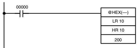
| Address | Instruction | Operands |
| 00000 | LD | 00000 |
| 00001 | @HEX(—) | |
| LR 10 | ||
| HR 10 | ||
| 200 |
HR 10 0 1 1 0
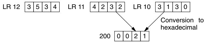
7-20-10 HOURS-TO-SECONDS - SEC(—)
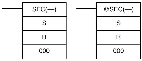
Ladder Symbols
Operand Data Areas
| S: Beginning source word (BCD) |
| IR, SR, AR, DM, HR, TC, LR |
| R: Beginning result word (BCD) |
| IR, SR, AR, DM, HR, TC, LR |
| 000: No function |
| 000 |
Limitations
This instruction is available in the CPM2A/CPM2C only.
S and S+1 must be within the same data area. R and R+1 must be within the same data area. S and S+1 must be BCD and must be in the proper hours/minutes/seconds format.
DM 6144 to DM 6655 cannot be used for R.
Description
SEC() is used to convert time notation in hours/minutes/seconds to an equivalent in just seconds.
For the source data, the seconds are designated in bits 00 through 07 and the minutes are designated in bits 08 through 15 of S. The hours are designated in S+1. The maximum is thus 9,999 hours, 59 minutes, and 59 seconds.
The result is output to R and R + 1 . The maximum obtainable value is 35,999,999 seconds.
Flags
ER: S and S + 1 or R and R + 1 are not in the same data area.
S and/or S+1 do not contain BCD.
Number of seconds and/or minutes exceeds 59.
Indirectly addressed DM word is non-existent. (Content of *DM word is not BCD, or the DM area boundary has been exceeded.)
EQ: ON when the result is zero.
Example
When 00000 is OFF (i.e., when the execution condition is ON), the following instruction would convert the hours, minutes, and seconds given in HR 12 and HR 13 to seconds and store the results in DM 0100 and DM 0101 as shown.
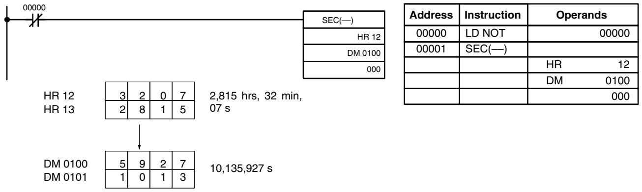
7-20-11 SECONDS-TO-HOURS - HMS(—)
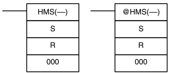
Ladder Symbols
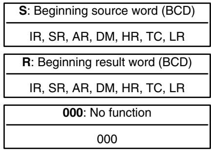
Operand Data Areas
Limitations
This instruction is available in the CPM2A/CPM2C only.
S and S+1 must be within the same data area. R and R+1 must be within the same data area. S and S+1 must be BCD and must be between 0 and 35,999,999 seconds.
DM 6144 to DM 6655 cannot be used for R.
Description
HMS(—) is used to convert time notation in seconds to an equivalent in hours/ minutes/seconds.
The number of seconds designated in S and S+1 is converted to hours/minutes/seconds and placed in R and R+1.
For the results, the seconds are placed in bits 00 through 07 and the minutes are placed in bits 08 through 15 of R. The hours are placed in R+1. The maximum is 9,999 hours, 59 minutes, and 59 seconds.
Flags
ER: S and S + 1 or R and R + 1 are not in the same data area.
S and/or S+1 do not contain BCD or exceed 36,000,000 seconds.
Indirectly addressed DM word is non-existent. (Content of *DM word is not BCD, or the DM area boundary has been exceeded.)
EQ: ON when the result is zero.
Example
When 00000 is OFF (i.e., when the execution condition is ON), the following instruction would convert the seconds given in HR 12 and HR 13 to hours, minutes, and seconds and store the results in DM 0100 and DM 0101 as shown.
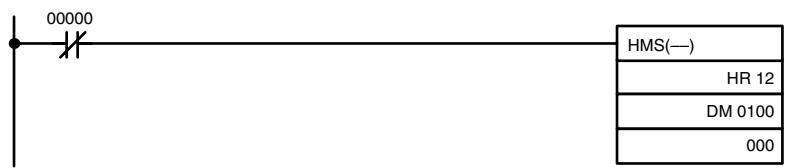
| HR 12 | 5 | 9 | 2 | 7 | 10,135,927 s |
| HR 13 | 1 | 0 | 1 | 3 | |
| DM 0100 | 3 | 2 | 0 | 7 | 2,815 hrs, 32 min, 07 s |
| DM 0101 | 2 | 8 | 1 | 5 |
| Address | Instruction | Operands |
| 00000 | LD NOT | 00000 |
| 00001 | HMS(—) | |
| HR 12 | ||
| DM 0100 | ||
| 000 |
7-20-12 2'S COMPLEMENT - NEG(—)
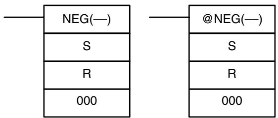
Ladder Symbols
Operand Data Areas
| S: Source word |
| IR, SR, AR, DM, HR, TC, LR, # |
| R: Result word |
| IR, SR, AR, DM, HR, LR |
| 000 |
| Not used. Set to 000. |
Limitations
This instruction is available in the CPM2A/CPM2C/SRM1(-V2) only.
DM 6144 to DM 6655 cannot be used for R.
Description
Converts the four-digit hexadecimal content of the source word (S) to its 2's complement and outputs the result to the result word (R). This operation is effectively the same as subtracting S from 0000 and outputting the result to R; it will calculate the absolute value of negative signed binary data.
If the content of S is 0000, the content of R will also be 0000 after execution and EQ (SR 25506) will be turned on.
If the content of S is 8000, the content of R will also be 8000 after execution and UF (SR 25405) will be turned on.
Note Refer to 2-16 Calculating with Signed Binary Data for more details.
Flags
ER: Indirectly addressed DM word is non-existent. (Content of *DM word is not BCD, or the DM area boundary has been exceeded.)
EQ: ON when the content of R is zero after execution; otherwise OFF.
UF: ON when the content of S is 8000; otherwise OFF.
N: ON when bit 15 of R is ON; otherwise OFF.
Example
The following example shows how to use NEG(—) to find the 2's complement of the content of DM 0005 and output the result to IR 105.
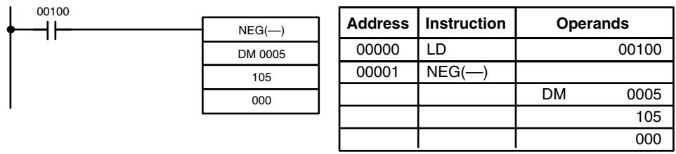
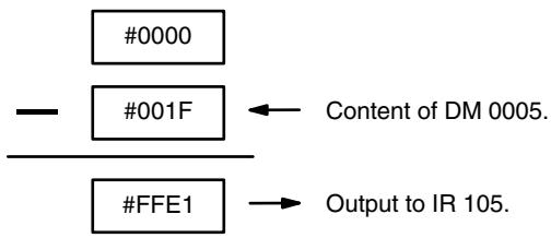
7-21 BCD Calculation Instructions
7-21-1 SET CARRY - STC(40)

Ladder Symbols
When the execution condition is OFF, STC(40) is not executed. When the execution condition is ON, STC(40) turns ON CY (SR 25504).
Note Refer to Appendix B Error and Arithmetic Flag Operation for a table listing the instructions that affect CY.
7-21-2 CLEAR CARRY - CLC(41)

Ladder Symbols
When the execution condition is OFF, CLC(41) is not executed. When the execution condition is ON, CLC(41) turns OFF CY (SR 25504).
CLEAR CARRY is used to reset (turn OFF) CY (SR 25504) to "0."
Note Refer to Appendix B Error and Arithmetic Flag Operation for a table listing the instructions that affect CY.
7-21-3 BCD ADD - ADD(30)
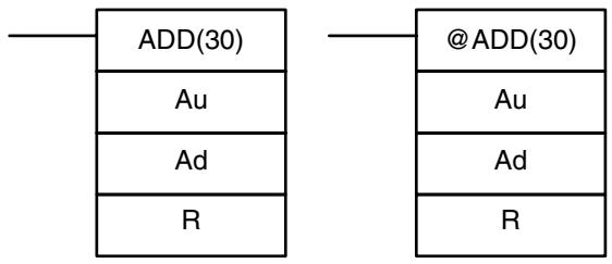
Ladder Symbols
Operand Data Areas
| Au: Augend word (BCD) |
| IR, SR, AR, DM, HR, TC, LR, # |
| Ad: Addend word (BCD) |
| IR, SR, AR, DM, HR, TC, LR, # |
| R: Result word |
| IR, SR, AR, DM, HR, LR |
Limitations
DM 6144 to DM 6655 cannot be used for R.
Description
When the execution condition is OFF, ADD(30) is not executed. When the execution condition is ON, ADD(30) adds the contents of Au, Ad, and CY, and places the result in R. CY will be set if the result is greater than 9999.

Flags
ER: Au and/or Ad is not BCD.
Indirectly addressed DM word is non-existent. (Content of *DM word is not BCD, or the DM area boundary has been exceeded.)
CY: ON when there is a carry in the result.
EQ: ON when the result is 0.
Example
If 00002 is ON, the program represented by the following diagram clears CY with CLC(41), adds the content of IR 200 to a constant (6103), places the result in DM 0100, and then moves either all zeros or 0001 into DM 0101 depending on the status of CY (25504). This ensures that any carry from the last digit is preserved in R + 1 so that the entire result can be later handled as eight-digit data.
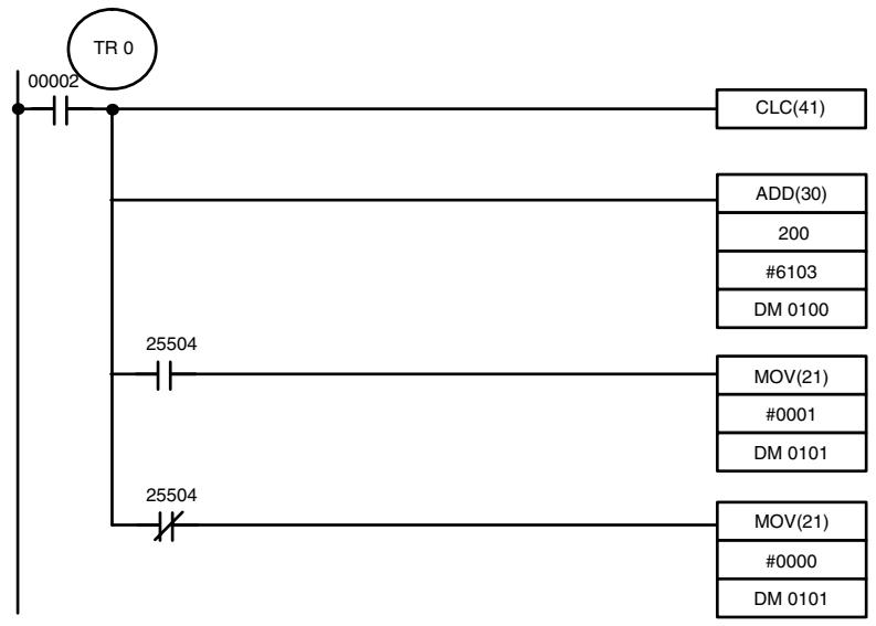
| Address | Instruction | Operands |
| 00000 | LD | 00002 |
| 00001 | OUT | TR 0 |
| 00002 | CLC(41) | |
| 00003 | ADD(30) | |
| 200 | ||
| # 6103 | ||
| DM 0100 | ||
| 00004 | AND | 25504 |
| 00005 | MOV(21) | |
| # 0001 | ||
| DM 0101 | ||
| 00006 | LD | TR 0 |
| 00007 | AND NOT | 25504 |
| 00008 | MOV(21) | |
| # 0000 | ||
| DM 0101 |
Although two ADD(30) can be used together to perform eight-digit BCD addition, ADDL(54) is designed specifically for this purpose.
7-21-4 BCD SUBTRACT - SUB(31)
Ladder Symbols
| Mi: Minuend word (BCD) |
| IR, SR, AR, DM, HR, TC, LR, # |
| Su: Subtrahend word (BCD) |
| IR, SR, AR, DM, HR, TC, LR, # |
| R: Result word |
| IR, SR, AR, DM, HR, LR |
Limitations
DM 6144 to DM 6655 cannot be used for R.
Description
When the execution condition is OFF, SUB(31) is not executed. When the execution condition is ON, SUB(31) subtracts the contents of Su and CY from Mi, and places the result in R. If the result is negative, CY is set and the 10's complement of the actual result is placed in R. To convert the 10's complement to the true result, subtract the content of R from zero (see example below).

Flags
ER: Mi and/or Su is not BCD.
Indirectly addressed DM word is non-existent. (Content of *DM word is not BCD, or the DM area boundary has been exceeded.)
CY: ON when the result is negative, i.e., when Mi is less than Su plus CY.
EQ: ON when the result is 0.

Be sure to clear the carry flag with CLC(41) before executing SUB(31) if its previous status is not required, and check the status of CY after doing a subtraction with SUB(31). If CY is ON as a result of executing SUB(31) (i.e., if the result is negative), the result is output as the 10's complement of the true answer. To convert the output result to the true value, subtract the value in R from 0.
Example
When 00002 is ON, the following ladder program clears CY, subtracts the contents of DM 0100 and CY from the content of 201 and places the result in HR 10. If CY is set by executing SUB(31), the result in HR 10 is subtracted from zero (note that CLC(41) is again required to obtain an accurate result), the result is placed back in HR 10, and HR 1100 is turned ON to indicate a negative result. If CY is not set by executing SUB(31), the result is positive, the second subtraction is not performed, and HR 1100 is not turned ON. HR 1100 is programmed as a self-maintaining bit so that a change in the status of CY will not turn it OFF when the program is rescanned.
In this example, differentiated forms of SUB(31) are used so that the subtraction operation is performed only once each time 00002 is turned ON. When another subtraction operation is to be performed, 00002 will need to be turned OFF for at least one cycle (resetting HR 1100) and then turned back ON.
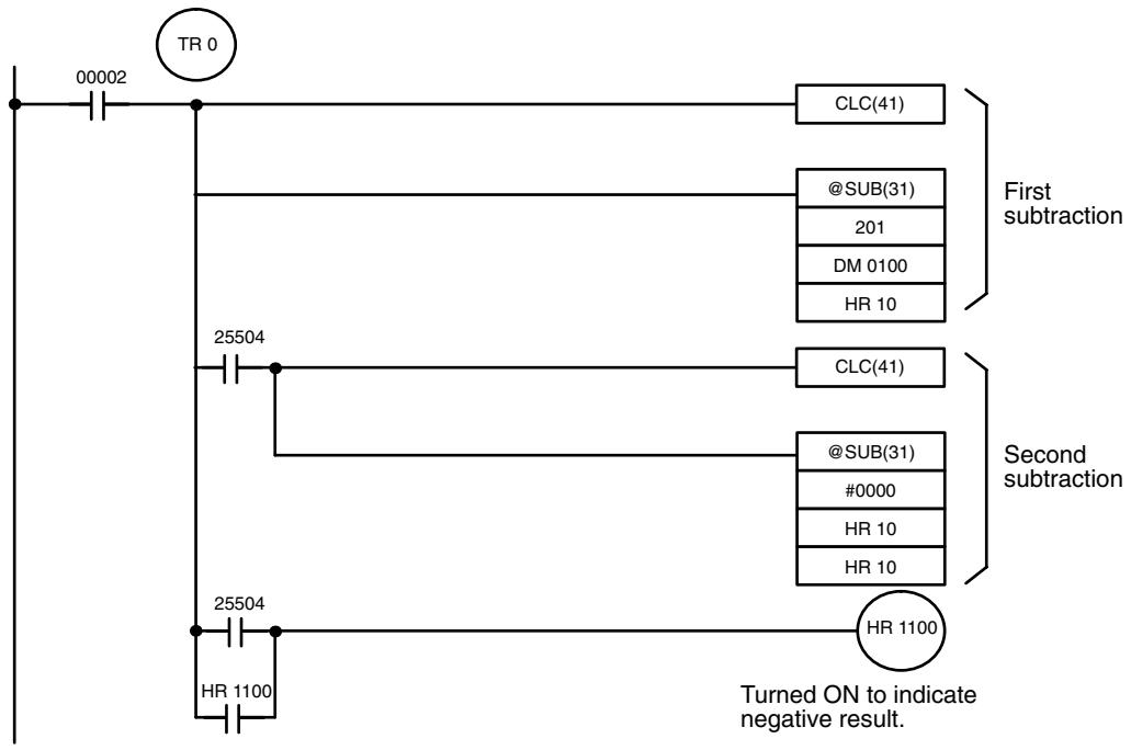
| Address | Instruction | Operands |
| 00000 | LD | 00002 |
| 00001 | OUT | TR 0 |
| 00002 | CLC(41) | |
| 00003 | @SUB(31) | |
| 201 | ||
| DM 0100 | ||
| HR 10 | ||
| 00004 | AND | 25504 |
| 00005 | CLC(41) | |
| 00006 | @SUB(31) | |
| # 0000 | ||
| HR 10 | ||
| HR 10 | ||
| 00007 | LD | TR 0 |
| 00008 | LD | 25504 |
| 00009 | OR | HR 1100 |
| 00010 | AND LD | --- |
| 00011 | OUT | HR 1100 |
The first and second subtractions for this diagram are shown below using example data for 201 and DM 0100.
Note The actual SUB(31) operation involves subtracting Su and CY from 10,000 plus Mi. For positive results the leftmost digit is truncated. For negative results the 10s complement is obtained. The procedure for establishing the correct answer is given below.
First Subtraction
IR 201 1029
DM 0100 -3452
CY -0
HR 10 7577 (1029 + (10000 - 3452))
CY 1 (negative result)
Second Subtraction
0000
HR 10 -7577
CY -0
HR 10 2423 (0000 + (10000 - 7577))
CY 1 (negative result)
In the above case, the program would turn ON HR 1100 to indicate that the value held in HR 10 is negative.
7-21-5 BCD MULTIPLY - MUL(32)
Ladder Symbols
| MUL(32) | @MUL(32) |
| Md | Md |
| Mr | Mr |
| R | R |
Operand Data Areas
| Md: Multiplicand (BCD) |
| IR, SR, AR, DM, HR, TC, LR, # |
| Mr: Multiplier (BCD) |
| IR, SR, AR, DM, HR, TC, LR, # |
| R: First result word |
| IR, SR, AR, DM, HR LR |
Limitations
DM 6144 to DM 6655 cannot be used for R.
Description
When the execution condition is OFF, MUL(32) is not executed. When the execution condition is ON, MUL(32) multiplies Md by the content of Mr, and places the result In R and R+1.
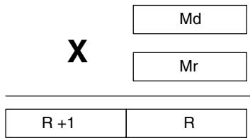
Example
When IR 00000 is ON with the following program, the contents of IR 013 and DM 0005 are multiplied and the result is placed in HR 07 and HR 08. Example data and calculations are shown below the program.
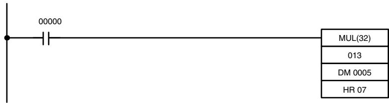
| Address | Instruction | Operands |
| 00000 | LD | 00000 |
| 00001 | MUL(32) | |
| 013 | ||
| DM 0005 | ||
| HR 07 |
| Md: IR 013 | |||
| 3 | 3 | 5 | 6 |
X
| Mr: DM 0005 | |||
| 0 | 0 | 2 | 5 |
| R+1: HR 08 | R: HR 07 | ||||||
| 0 | 0 | 0 | 8 | 3 | 9 | 0 | 0 |
Flags
ER: Md and/or Mr is not BCD.
Indirectly addressed DM word is non-existent. (Content of *DM word is not BCD, or the DM area boundary has been exceeded.)
CY: ON when there is a carry in the result.
EQ: ON when the result is 0.
7-21-6 BCD DIVIDE - DIV(33)
Ladder Symbol
| DIV(33) |
| Dd |
| Dr |
| R |
Operand Data Areas
| Dd: Dividend word (BCD) |
| IR, SR, AR, DM, HR, TC, LR, # |
| Dr: Divisor word (BCD) |
| IR, SR, AR, DM, HR, TC, LR, # |
| R: First result word (BCD) |
| IR, SR, AR, DM, HR, LR |
Limitations
R and R+1 must be in the same data area. DM 6144 to DM 6655 cannot be used for R.
Description
When the execution condition is OFF, DIV(33) is not executed and the program moves to the next instruction. When the execution condition is ON, Dd is divided by Dr and the result is placed in R and R + 1 : the quotient in R and the remainder in R + 1 .

Flags
ER: Dd or Dr is not in BCD.
Indirectly addressed DM word is non-existent. (Content of *DM word is not BCD, or the DM area boundary has been exceeded.)
EQ: ON when the result is 0.
Example
When IR 00000 is ON with the following program, the content of IR 216 is divided by the content of HR 09 and the result is placed in DM 0017 and DM 0018. Example data and calculations are shown below the program.
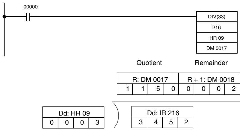
| Address | Instruction | Operands |
| 00000 | LD | 00000 |
| 00001 | DIV(33) | |
| 216 | ||
| HR 09 | ||
| DM 0017 |
7-21-7 DOUBLE BCD ADD - ADDL(54)
Ladder Symbols
| ADDL(54) | @ADDL(54) |
| Au | Au |
| Ad | Ad |
| R | R |
Operand Data Areas
| Au: First augend word (BCD) |
| IR, SR, AR, DM, HR, TC, LR |
| Ad: First addend word (BCD) |
| IR, SR, AR, DM, HR, TC, LR |
| R: First result word |
| IR, SR, AR, DM, HR, LR |
Limitations
DM 6144 to DM 6655 cannot be used for R.
Description
When the execution condition is OFF, ADDL(54) is not executed. When the execution condition is ON, ADDL(54) adds the contents of CY to the 8-digit value in Au and Au + 1 to the 8-digit value in Ad and Ad + 1 , and places the result in R and R + 1 . CY will be set if the result is greater than 99999999.
| Au + 1 | Au |
| Ad + 1 | Ad |

CY
CY
R+1
8
Flags
ER: Au and/or Ad is not BCD.
Indirectly addressed DM word is non-existent. (Content of *DM word is not BCD, or the DM area boundary has been exceeded.)
CY: ON when there is a carry in the result.
EQ: ON when the result is 0.
Example
When 00000 is ON, the following program section adds two 12-digit numbers, the first contained in LR 00 through LR 02 and the second in DM 0010 through DM 0012. The result is placed in HR 10 through HR 13.
The rightmost 8 digits of the two numbers are added using ADDL(54), i.e., the contents of LR 00 and LR 01 are added to DM 0010 and DM 0011 and the results is placed in HR 10 and HR 11. The second addition adds the leftmost 4 digits of each number using ADD(30), and includes any carry from the first addition. The last instruction, ADB(50) (see 7-22-1 BINARY ADD - ADB(50)) adds two all-zero constants to place any carry from the second addition into HR 13.
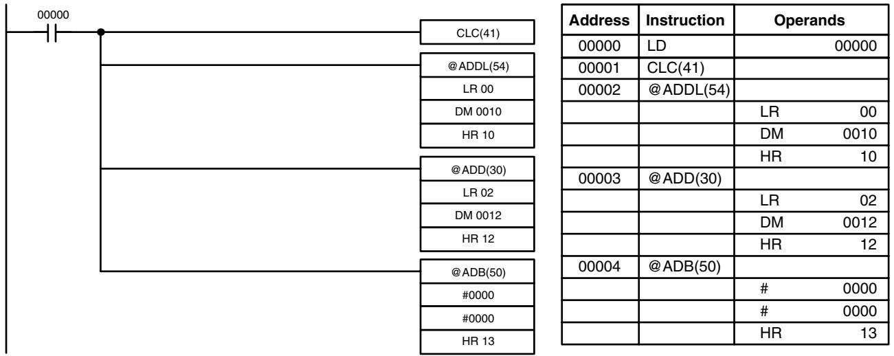
7-21-8 DOUBLE BCD SUBTRACT - SUBL(55)
Ladder Symbols
| SUBL(55) | @SUBL(55) |
| Mi | Mi |
| Su | Su |
| R | R |
Operand Data Areas
| Mi: First minuend word (BCD) |
| IR, SR, AR, DM, HR, TC, LR, # |
| Su: First subtrahend word (BCD) |
| IR, SR, AR, DM, HR, TC, LR, # |
| R: First result word |
| IR, SR, AR, DM, HR, LR |
Limitations
DM 6144 to DM 6655 cannot be used for R.
Description
When the execution condition is OFF, SUBL(55) is not executed. When the execution condition is ON, SUBL(55) subtracts CY and the 8-digit contents of Su and Su+1 from the 8-digit value in Mi and Mi+1, and places the result in R and R+1. If the result is negative, CY is set and the 10's complement of the actual result is placed in R. To convert the 10's complement to the true result, subtract the content of R from zero. Since an 8-digit constant cannot be directly entered, use the BSET(71) instruction (see 7-17-4 BLOCK SET-BSET(71)) to create an 8-digit constant.
| Mi + 1 | Mi |
| Su + 1 | Su |
| CY |

CY
R+1
B
Flags
ER: Mi, M+1,Su, or Su+1 are not BCD.
Indirectly addressed DM word is non-existent. (Content of *DM word is not BCD, or the DM area boundary has been exceeded.)
CY: ON when the result is negative, i.e., when Mi is less than Su.
EQ: ON when the result is 0.
Example
The following example works much like that for single-word subtraction. In this example, however, BSET(71) is required to clear the content of DM 0000 and DM 0001 so that a negative result can be subtracted from 0 (inputting an 8-digit constant is not possible).
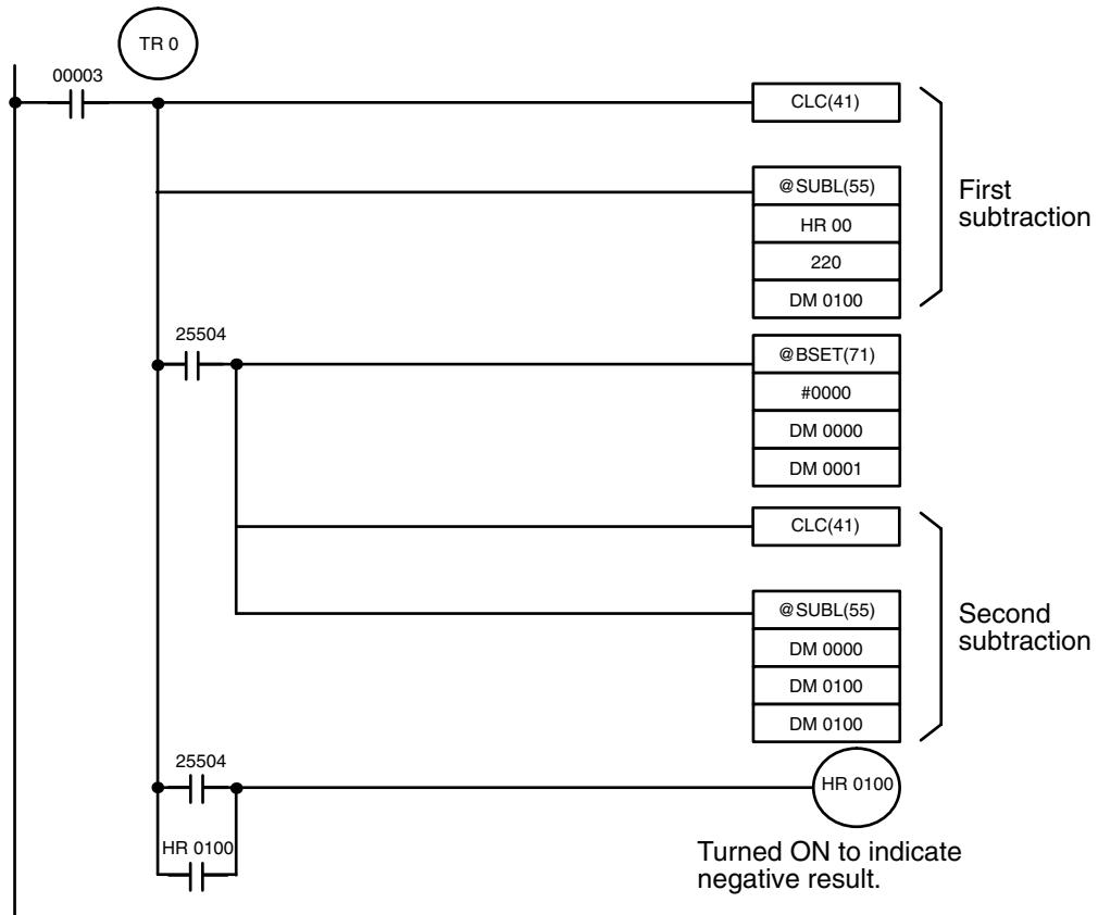
| Address | Instruction | Operands |
| 00000 | LD | 00003 |
| 00001 | OUT | TR 0 |
| 00002 | CLC(41) | |
| 00003 | @SUBL(55) | |
| HR 00 | ||
| 220 | ||
| DM 0100 | ||
| 00004 | AND | 25504 |
| 00005 | @BSET(71) | |
| # 0000 | ||
| DM 0000 | ||
| DM 0001 |
| Address | Instruction | Operands |
| 00006 | CLC(41) | |
| 00007 | @SUBL(55) | |
| DM 0000 | ||
| DM 0100 | ||
| DM 0100 | ||
| 00008 | LD | TR 0 |
| 00009 | LD | 25504 |
| 00010 | OR | HR 0100 |
| 00011 | AND LD | |
| 00012 | OUT | HR 0100 |
7-21-9 DOUBLE BCD MULTIPLY - MULL(56)
Operand Data Areas
Ladder Symbols
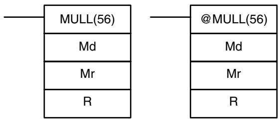
Md: First multiplicand word (BCD)
IR, SR, AR, DM, HR, TC, LR
Mr: First multiplier word (BCD)
IR, SR, AR, DM, HR, TC, LR
R: First result word
IR, SR, AR, DM, HR LR
Limitations
DM 6144 to DM 6655 cannot be used for R.
Description
When the execution condition is OFF, MULL(56) is not executed. When the execution condition is ON, MULL(56) multiplies the eight-digit content of Md and Md+1 by the content of Mr and Mr+1, and places the result in R to R+3.

Flags
ER: Md, Md+1,Mr, or Mr+1 is not BCD.
Indirectly addressed DM word is non-existent. (Content of *DM word is not BCD, or the DM area boundary has been exceeded.)
CY: ON when there is a carry in the result.
EQ: ON when the result is 0.
7-21-10 DOUBLE BCD DIVIDE - DIVL(57)
Operand Data Areas
Ladder Symbols
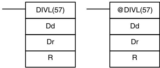
Dd: First dividend word (BCD)
IR, SR, AR, DM, HR, TC, LR
Dr: First divisor word (BCD)
IR, SR, AR, DM, HR, TC, LR
R: First result word
IR, SR, AR, DM, HR LR
Limitations
DM 6144 to DM 6655 cannot be used for R.
Description
When the execution condition is OFF, DIVL(57) is not executed. When the execution condition is ON, DIVL(57) the eight-digit content of Dd and D + 1 is divided by the content of Dr and Dr + 1 and the result is placed in R to R + 3 : the quotient in R and R + 1 , the remainder in R + 2 and R + 3 .
Remainder
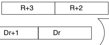
Quotient
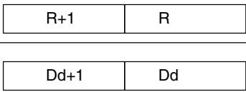
Flags
ER: Dr and Dr + 1 contain O.
Dd, Dd + 1 ,Dr, or Dr + 1 is not BCD.
Indirectly addressed DM word is non-existent. (Content of *DM word is not BCD, or the DM area boundary has been exceeded.)
EQ: ON when the result is 0.
7-22 Binary Calculation Instructions
7-22-1 BINARY ADD - ADB(50)
Ladder Symbols
| ADB(50) | @ADB(50) |
| Au | Au |
| Ad | Ad |
| R | R |
Operand Data Areas
| Au: Augend word (binary) |
| IR, SR, AR, DM, HR, TC, LR, # |
| Ad: Addend word (binary) |
| IR, SR, AR, DM, HR, TC, LR, # |
| R: Result word |
| IR, SR, AR, DM, HR, LR |
Limitations
DM 6144 to DM 6655 cannot be used for R.
Description
When the execution condition is OFF, ADB(50) is not executed. When the execution condition is ON, ADB(50) adds the contents of Au, Ad, and CY, and places the result in R. CY will be set if the result is greater than FFFF.

ADB(50) can also be used to add signed binary data. With the CPM1A, CPM2A, CPM2C, and SRM1(-V2), the underflow and overflow flags (SR 25404 and SR 25405) indicate whether the result has exceeded the lower or upper limits of the 16-bit signed binary data range.
Flags
ER: Indirectly addressed DM word is non-existent. (Content of *DM word is not BCD, or the DM area boundary has been exceeded.)
CY: ON when the result is greater than FFFF.
EQ: ON when the result is 0.
OF: ON when the result exceeds +32,767 (7FFF).
UF: ON when the result is below -32,768 (8000).
Example
The following example shows a four-digit addition with CY used to place either #0000 or #0001 into R+1 to ensure that any carry is preserved.
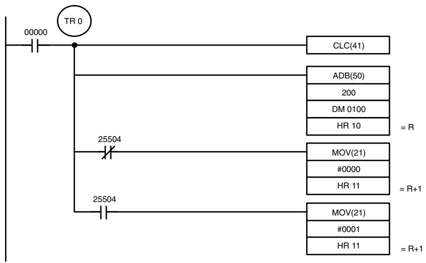
| Address | Instruction | Operands |
| 00000 | LD | 00000 |
| 00001 | OUT | TR 0 |
| 00002 | CLC(41) | |
| 00003 | ADB(50) | |
| 200 | ||
| DM 0100 | ||
| HR 10 | ||
| 00004 | AND NOT | 25504 |
| 00005 | MOV(21) | |
| # 0000 | ||
| HR 11 | ||
| 00006 | LD | TR 0 |
| 00007 | AND | 25504 |
| 00008 | MOV(21) | |
| # 00001 | ||
| HR 11 |
In the case below, A6E2 + 80C5 = 127A7 . The result is a 5-digit number, so CY (SR 25504) = 1, and the content of R + 1 becomes #0001.
| Au: IR 200 | |||
| A | 6 | E | 2 |

| Ad: DM 0100 | |||
| 8 | 0 | C | 5 |
| R+1: HR 11 | R: HR 10 | ||||||
| 0 | 0 | 0 | 1 | 2 | 7 | A | 7 |
Note For signed binary calculations, the status of the UF and OF flags indicate whether the result has exceeded the signed binary data range (-32,768 (8000) to +32,767 (7FFF)).
7-22-2 BINARY SUBTRACT - SBB(51)
Ladder Symbols
| SBB(51) | @ SBB(51) |
| Mi | Mi |
| Su | Su |
| R | R |
Operand Data Areas
| Mi: Minuend word (binary) |
| IR, SR, AR, DM, HR, TC, LR, # |
| Su: Subtrahend word (binary) |
| IR, SR, AR, DM, HR, TC, LR, # |
| R: Result word |
| IR, SR, AR, DM, HR, LR |
Limitations
DM 6144 to DM 6655 cannot be used for R.
Description
When the execution condition is OFF, SBB(51) is not executed. When the execution condition is ON, SBB(51) subtracts the contents of Su and CY from Mi and places the result in R. If the result is negative, CY is set and the 2's complement of the actual result is placed in R.

SBB(51) can also be used to subtract signed binary data. With the CPM1A, CPM2A, CPM2C, and SRM1(-V2), the underflow and overflow flags (SR 25404 and SR 25405) indicate whether the result has exceeded the lower or upper limits of the 16-bit signed binary data range.
Flags
ER: Indirectly addressed DM word is non-existent. (Content of *DM word is not BCD, or the DM area boundary has been exceeded.)
CY: ON when the result is negative, i.e., when Mi is less than Su plus CY.
EQ: ON when the result is 0.
OF: ON when the result exceeds +32,767 (7FFF).
UF: ON when the result is below -32,768 (8000).
Example
The following example shows a four-digit subtraction. When IR 00001 is ON, the content of LR 00 and CY are subtracted from the content of IR 002 and the result is written to HR 01.
CY is turned ON if the result is negative. If normal data is being used, a negative result (signed binary) must be converted to normal data using NEG(—). Refer to 7-20-12 2's COMPLEMENT - NEG(—) for details.
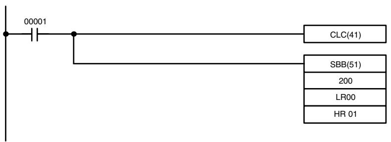
| Address | Instruction | Operands |
| 00000 | LD | 00001 |
| 00001 | OUT | TR 1 |
| 00002 | CLC(41) | |
| 00003 | SBB(51) | |
| 200 | ||
| LR 00 | ||
| HR 01 |
In the case below, the content of LR 00 (#7A03) and CY are subtracted from IR 002 (#F8C5). Since the result is positive, CY is 0.
If the result had been negative, CY would have been set to 1. For normal (unsigned) data, the result would have to be converted to its 2's complement.
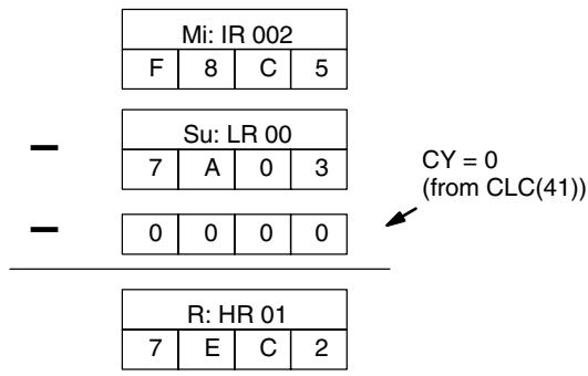
Note For signed binary calculations, the status of the UF and OF flags indicate whether the result has exceeded the signed binary data range (-32,768 (8000) to +32,767 (7FFF)).
7-22-3 BINARY MULTIPLY - MLB(52)
Operand Data Areas
| Ladder Symbols | |
| MLB(52) | @MLB(52) |
| Md | Md |
| Mr | Mr |
| R | R |
| Md: Multiplicand word (binary) |
| IR, SR, AR, DM, HR, TC, LR, # |
| Mr: Multiplier word (binary) |
| IR, SR, AR, DM, HR, TC, LR, # |
| R: First result word |
| IR, SR, AR, DM, HR LR |
Limitations
DM 6144 to DM 6655 cannot be used for R.
MLB(52) cannot be used to multiply signed binary data.
Description
When the execution condition is OFF, MLB(52) is not executed. When the execution condition is ON, MLB(52) multiplies the content of Md by the contents of Mr, places the rightmost four digits of the result in R, and places the leftmost four digits in R+1.
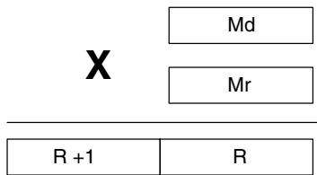
Flags
ER: Indirectly addressed DM word is non-existent. (Content of *DM word is not BCD, or the DM area boundary has been exceeded.)
EQ: ON when the result is 0.
7-22-4 BINARY DIVIDE - DVB(53)
Operand Data Areas
| Ladder Symbols | |
| DVB(53) | @DVB(53) |
| Dd | Dd |
| Dr | Dr |
| R | R |
| Dd: Dividend word (binary) |
| IR, SR, AR, DM, HR, TC, LR, # |
| Dr: Divisor word (binary) |
| IR, SR, AR, DM, HR, TC, LR, # |
| R: First result word |
| IR, SR, AR, DM, HR LR |
Limitations
DM 6144 to DM 6655 cannot be used for R.
DVB(53) cannot be used to divide signed binary data.
Description
When the execution condition is OFF, DVB(53) is not executed. When the execution condition is ON, DVB(53) divides the content of Dd by the content of Dr and the result is placed in R and R + 1 : the quotient in R , the remainder in R + 1 .
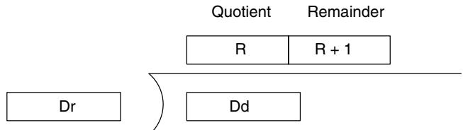
Flags
ER: Dr contains 0.
Indirectly addressed DM word is non-existent. (Content of *DM word is not BCD, or the DM area boundary has been exceeded.)
EQ: ON when the result is 0.
7-23 Special Math Instructions
7-23-1 DATA SEARCH - SRCH(—)
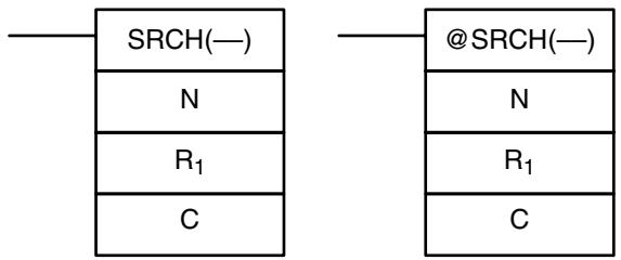
Ladder Symbols
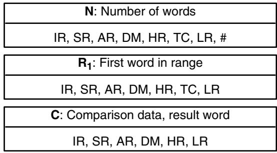
Operand Data Areas
Limitations
This instruction is available in the CPM2A/CPM2C only.
N must be BCD between 0001 to 9999.
R_1 and R_1 + N - 1 must be in the same data area.
DM 6144 to DM 6655 cannot be used for C.
Description
When the execution condition is OFF, SRCH(—) is not executed. When the execution condition is ON, SRCH(—) searches the range of memory from R_1 to R_1 + N - 1 for addresses that contain the comparison data in C. If one or more addresses contain the comparison data, the EQ Flag (SR 25506) is turned ON and the lowest address containing the comparison data is identified in C + 1 . The address is identified differently for the DM area:
1, 2, 3...
- For an address in the DM area, the word address is written to C+1. For example, if the lowest address containing the comparison data is DM 0114, then #0114 is written in C+1.
- For an address in another data area, the number of addresses from the beginning of the search is written to C + 1 . For example, if the lowest address containing the comparison data is IR 114 and the first word in the search range is IR 014, then #0100 is written in C + 1 .
If none of addresses in the range contain the comparison data, the EQ Flag (SR 25506) is turned OFF and C + 1 is left unchanged.
Flags
ER: Indirectly addressed DM word is non-existent. (Content of *DM word is not BCD, or the DM area boundary has been exceeded.)
N is not BCD between 0001 and 9999.
R_1 and R_1 + N - 1 are not in the same data area.
EQ: ON when the comparison data has been matched in the search range.
Example
In the following example, the 10 word range from IR 200 to IR 209 is searched for addresses that contain the same data as DM 0100 (89AB). Since IR 204 con
tains the same data, the EQ Flag (SR 25506) is turned ON and #0004 is written to DM 0101.

| Address | Instruction | Operands |
| 00000 | LD | 00000 |
| 00001 | @SRCH(—) | |
| # 0010 | ||
| 0200 | ||
| DM 0100 |
DM 0100 89AB
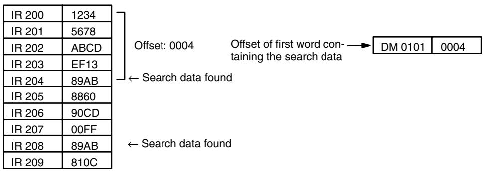
Note The matching search data in IR 208 is ignored because the search data was found in an earlier word in the range.
This instruction is available in the CPM2A/CPM2C only.
N must be BCD between 0001 to 9999.
R_1 and R_1 + N - 1 must be in the same data area.
DM 6144 to DM 6655 cannot be used for D.
Description
When the execution condition is OFF, MAX() is not executed. When the execution condition is ON, MAX() searches the range of memory from R_1 to R_1 + N - 1 for the address that contains the maximum value and outputs the maximum value to the destination word (D).
The address is identified differently for the DM area:
1,2,3...
- For an address in the DM area, the word address is written to C+1. For example, if the address containing the maximum value is DM 0114, then #0114 is written in D+1.
- For an address in another data area, the number of addresses from the beginning of the search is written to D + 1 . For example, if the address containing the maximum value is IR 114 and the first word in the search range is IR 014, then #0100 is written in D + 1 .
If bit 14 of C is ON and more than one address contains the same maximum value, the position of the lowest of the addresses will be output to D+1. The position will be output as the DM address for the DM area, but as an absolute position relative to the first word in the range for all other areas.
The number of words within the range (N) is contained in the 3 rightmost digits of C, which must be BCD between 001 and 999.
When bit 15 of C is OFF, data within the range is treated as unsigned binary and when it is ON the data is treated as signed binary.
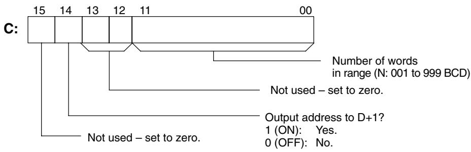
Caution
If bit 14 of C is ON, values above #8000 are treated as negative numbers, so the results will differ depending on the specified data type. Be sure that the correct data type is specified.
Flags
ER: Indirectly addressed DM word is non-existent. (Content of *DM word is not BCD, or the DM area boundary has been exceeded.) R_1 and R_1 + N - 1 are not in the same data area.
EQ: ON when the maximum value is #0000.
Example
When IR 00000 is ON, the control data in DM 0000 (4010) will cause a search for the maximum value in the 10 words starting at IR 200. The largest unsigned val-
ue will be stored in DM 0500. The offset from the beginning of the search of the word containing the maximum value will be stored in DM 0501.

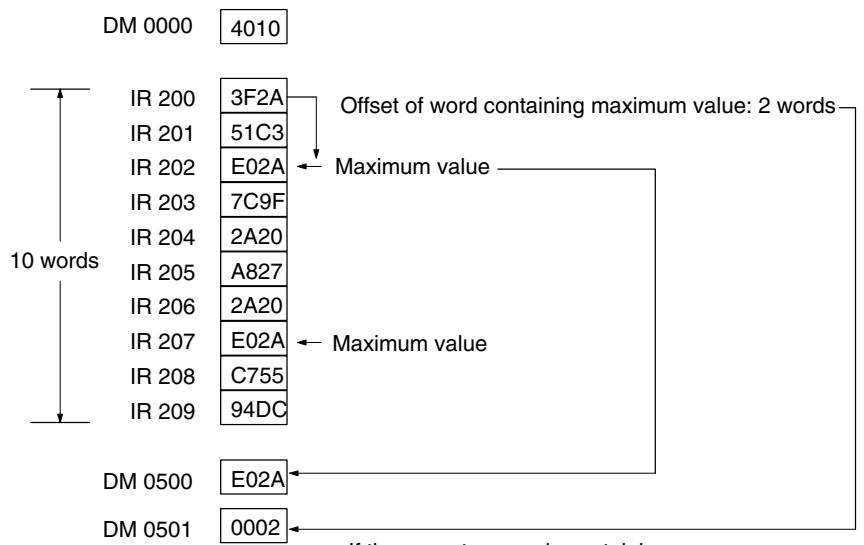
If there are two words containing the maximum value, the one found first will be stored in DM 0501.
7-23-3 FIND MINIMUM - MIN(—)
Ladder Symbols
| MIN(—) | @MIN(—) |
| C | C |
| R1 | R1 |
| D | D |
Operand Data Areas
| C: Control data |
| IR, SR, AR, DM, HR, TC, LR, # |
| R1: First word in range |
| IR, SR, AR, DM, HR, TC, LR |
| D: Destination word |
| IR, SR, AR, DM, HR, LR |
Limitations
This instruction is available in the CPM2A/CPM2C only.
N must be BCD between 0001 to 9999.
R_1 and R_1 + N - 1 must be in the same data area.
DM 6144 to DM 6655 cannot be used for D.
Description
When the execution condition is OFF, MIN() is not executed. When the execution condition is ON, MIN() searches the range of memory from R_1 to R_1 + N - 1 for the address that contains the minimum value and outputs the minimum value to the destination word (D).
The address is identified differently for the DM area:
1, 2, 3... 1. For an address in the DM area, the word address is written to C + 1 . For example, if the address containing the minimum value is DM 0114, then #0114 is written in D + 1 .
- For an address in another data area, the number of addresses from the beginning of the search is written to D + 1 . For example, if the address containing the minimum value is IR 114 and the first word in the search range is IR 014, then #0100 is written in D + 1 .
If bit 14 of C is ON and more than one address contains the same minimum value, the position of the lowest of the addresses will be output to D+1. The position will be output as the DM address for the DM area, but as an absolute position relative to the first word in the range for all other areas.
The number of words within the range (N) is contained in the 3 rightmost digits of C, which must be BCD between 001 and 999.
When bit 15 of C is OFF, data within the range is treated as unsigned binary and when it is ON the data is treated as signed binary.
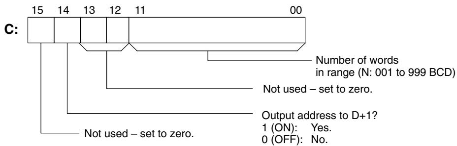
!Caution
If bit 14 of C is ON, values above #8000 are treated as negative numbers, so the results will differ depending on the specified data type. Be sure that the correct data type is specified.
Flags
ER: Indirectly addressed DM word is non-existent. (Content of *DM word is not BCD, or the DM area boundary has been exceeded.) R_1 and R_1 + N - 1 are not in the same data area.
EQ: ON when the minimum value is #0000.
Example
When IR 00000 is ON, the control data in DM 0300 (4010) will cause a search for the maximum value in the 10 words starting at DM 0000. The smallest unsigned
value will be stored in DM 0500. The address of the word containing the minimum value (0014) will be stored in DM 0501.

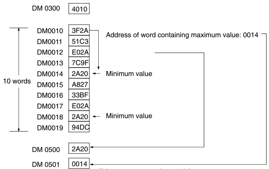
If there are two words containing the minimum value, the one found first will be stored in DM 0501.
7-23-4 AVERAGE VALUE - AVG(—)
Ladder Symbols
| AVG(—) |
| S |
| N |
| D |
Operand Data Areas
| S: Source word |
| IR, SR, AR, DM, HR, TC, LR |
| N: Number of cycles |
| IR, SR, AR, DM, HR, TC, LR, # |
| D: First destination word |
| IR, SR, AR, DM, HR, LR |
Limitations
This instruction is available in the CPM2A/CPM2C only.
S must be hexadecimal.
N must be BCD from #0001 to #0064.
D and D + N + 1 must be in the same data area.
DM 6144 to DM 6655 cannot be used for S, N, or D to D + N + 1
Description
AVG(-) is used to calculate the average value of S over N cycles.
When the execution condition is OFF, AVG(—) is not executed.
Each time that AVG() is executed, the content of S is stored in words D+2 to D+N+1. On the first execution, AVG() writes the content of S to D+2; on the second execution it writes the content of S to D+3, etc. On the Nth execution, AVG() writes the content of S is stored in D+N+1, AVG() calculates the average value of the values stored in D+2 to D+N+1, and writes the average to D.
The following diagram shows the function of words D to D + N + 1
| D | Average value (after N or more executions) |
| D+1 | Used by the system. |
| D+2 | Content of S from the 1stexecution of AVG(—) |
| D+3 | Content of S from the 2ndexecution of AVG(—) |
| : | : : : : |
| : | : : : : |
| : | : : : : |
| D+N+1 | Content of S from the Nthexecution of AVG(—) |
Precautions
The average value is calculated in binary. Be sure that the content of S is in binary.
N must be BCD from #0001 to #0064. If the content of N ≥ #0065, AVG() will operate with N=64.
The average value will be rounded off to the nearest integer value. (0.5 is rounded up to 1.)
Set the contents of D + 1 to #0000 to execute AVG(—) from the first scan.
Flags
ER: Indirectly addressed DM word is non-existent. (Content of *DM word is not BCD, or the DM area boundary has been exceeded.)
One or more operands have been set incorrectly.
D and D + N + 1 are not in the same data area.
Example
In the following example, the content of IR 200 is set to #0000 and then incremented by 1 each cycle. For the first two cycles, AVG() moves the content of IR 200 to DM 1002 and DM 1003. On the third and later cycles AVG() calculates the average value of the contents of DM 1002 to DM 1004 and writes that average value to DM 1000.
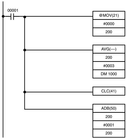
| Address | Instruction | Operands |
| 00000 | LD | 00001 |
| 00001 | @MOV(21) | |
| # 0000 | ||
| 200 | ||
| 00002 | AVG(—) | |
| 200 | ||
| # 0003 | ||
| DM 1000 | ||
| 00003 | CLC(41) | |
| 00004 | ADB(50) | |
| 200 | ||
| # 0001 | ||
| 200 |
| IR 200 | 1stcycle | 2ndcycle | 3rdcycle | 4thcycle |
| 0000 | 0001 | 0002 | 0003 |
| 1stcycle | 2ndcycle | 3rdcycle | 4thcycle | |
| DM 1000 | 0000 | 0001 | 0001 | 0002 |
| DM 1001 | ||||
| DM 1002 | 0000 | 0000 | 0000 | 0003 |
| DM 1003 | --- | 0001 | 0001 | 0001 |
| DM 1004 | --- | --- | 0002 | 0002 |
7-23-5 SUM-SUM(—)

Ladder Symbols
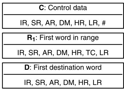
Operand Data Areas
Limitations
This instruction is available in the CPM2A/CPM2C only.
The 3 rightmost digits of C must be BCD between 001 and 999.
DM 6144 to DM 6655 cannot be used for D.
If bit 14 of C is OFF (setting for BCD data), all data within the range R_1 to R_1 + N - 1 must be BCD.
Description
When the execution condition is OFF, SUM() is not executed. When the execution condition is ON, SUM() adds either the contents of words R_1 to R_1 + N - 1 or the bytes in words R_1 to R_1 + N / 2 - 1 and outputs that value to the destination words (D and D+1). The data can be summed as binary or BCD and will be output in the same form. Binary data can be either signed or unsigned.
The function of bits in C are shown in the following diagram and explained in more detail below.
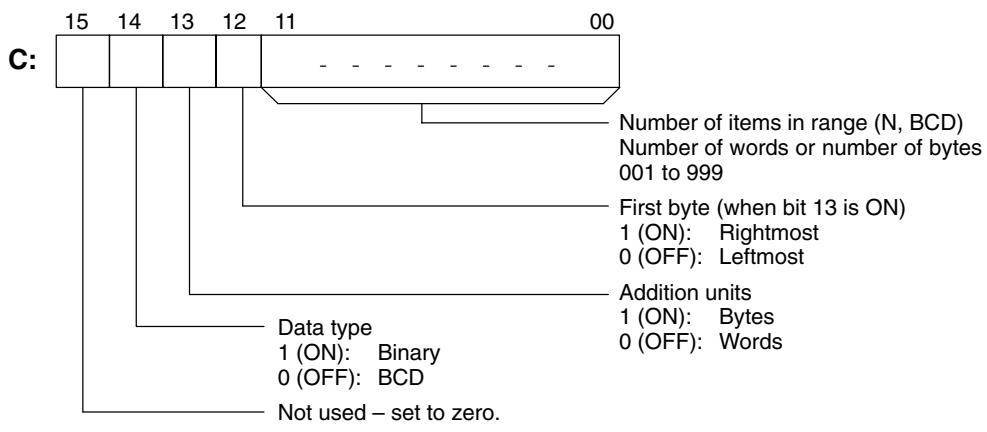
Number of Items in Range
The number of items within the range (N) is contained in the 3 rightmost digits of C, which must be BCD between 001 and 999. This number will indicate the number of words or the number of bytes depending the items being summed.
Addition Units
Words will be added if bit 13 is OFF and bytes will be added if bit 13 is ON. If bytes are specified, the range can begin with the leftmost or rightmost byte of R_1 . The leftmost byte of R_1 will not be added if bit 12 is ON.
The bytes will be added in this order when bit 12 is OFF: 1 + 2 + 3 + 4
The bytes will be added in this order when bit 12 is ON: 2 + 3 + 4
Data within the range is treated as unsigned binary when bit 14 of C is ON and bit 15 is OFF, and it is treated as signed binary when both bits 14 and 15 are ON.
Data within the range is treated as BCD when bit 14 of C is OFF, regardless of the status of bit 15.
Flags
ER: Indirectly addressed DM word is non-existent. (Content of *DM word is not BCD, or the DM area boundary has been exceeded.)
R_1 and R_1 + N - 1 are not in the same data area.
The number of items in C is not BCD between 001 and 999.
The data being summed in not BCD when BCD was designated.
EQ: ON when the result is zero.
Example
In the following example, the BCD contents of the 8 words from DM 0000 to DM 0007 are added when IR 00001 is ON and the result is written to DM 0010 and DM 0011.
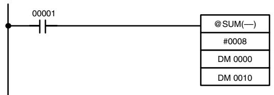
| Address | Instruction | Operands |
| 00000 | LD | 00001 |
| 00001 | @SUM(—) | |
| # 0008 | ||
| DM 0000 | ||
| DM 0010 |
7-24 Logic Instructions
7-24-1 COMPLEMENT - COM(29)
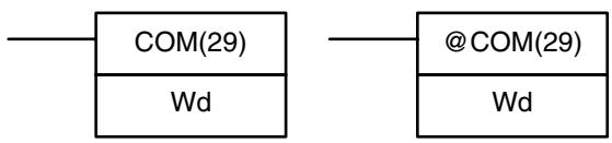
Ladder Symbols
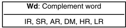
Operand Data Areas
Limitations
DM 6144 to DM 6655 cannot be used for Wd.
Description
When the execution condition is OFF, COM(29) is not executed. When the execution condition is ON, COM(29) clears all ON bits and sets all OFF bits in Wd.
Precautions
The complement of Wd will be calculated every cycle if the undifferentiated form of COM(29) is used. Use the differentiated form (@COM(29)) or combine COM(29) with DIFU(13) or DIFD(14) to calculate the complement just once.
Example
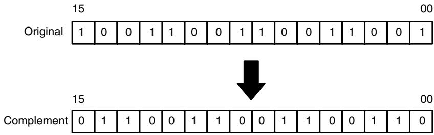
Flags
ER: Indirectly addressed DM word is non-existent. (Content of *DM word is not BCD, or the DM area boundary has been exceeded.)
EQ: ON when the result is 0.
7-24-2 LOGICAL AND - ANDW(34)
Ladder Symbols
| ANDW(34) | @ANDW(34) |
| I1 | I1 |
| I2 | I2 |
| R | R |
Operand Data Areas
| I1: Input 1 |
| IR, SR, AR, DM, HR, TC, LR, # |
| I2: Input 2 |
| IR, SR, AR, DM, HR, TC, LR, # |
| R: Result word |
| IR, SR, AR, DM, HR, LR |
Limitations
DM 6144 to DM 6655 cannot be used for R.
Description
When the execution condition is OFF, ANDW(34) is not executed. When the execution condition is ON, ANDW(34) logically AND's the contents of I1 and I2 bit-by-bit and places the result in R.
Example
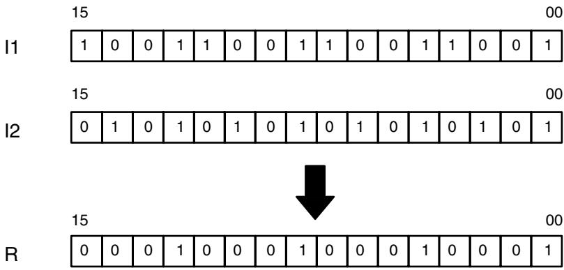
Flags
ER: Indirectly addressed DM word is non-existent. (Content of *DM word is not BCD, or the DM area boundary has been exceeded.)
EQ: ON when the result is 0.
7-24-3 LOGICAL OR - ORW(35)
Ladder Symbols
| ORW(35) | @ORW(35) |
| I1 | I1 |
| I2 | I2 |
| R | R |
Operand Data Areas
| I1: Input 1 |
| IR, SR, AR, DM, HR, TC, LR, # |
| I2: Input 2 |
| IR, SR, AR, DM, HR, TC, LR, # |
| R: Result word |
| IR, SR, AR, DM, HR, LR |
Limitations
DM 6144 to DM 6655 cannot be used for R.
Description
When the execution condition is OFF, ORW(35) is not executed. When the execution condition is ON, ORW(35) logically OR's the contents of I1 and I2 bit-by-bit and places the result in R.
Example
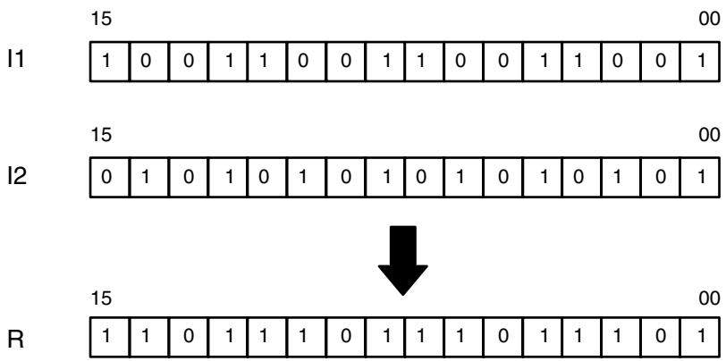
Flags
ER: Indirectly addressed DM word is non-existent. (Content of *DM word is not BCD, or the DM area boundary has been exceeded.)
EQ: ON when the result is 0.
7-24-4 EXCLUSIVE OR - XORW(36)
Ladder Symbols
| XORW(36) | @XORW(36) |
| I1 | I1 |
| I2 | I2 |
| R | R |
Operand Data Areas
| I1: Input 1 |
| IR, SR, AR, DM, HR, TC, LR, # |
| I2: Input 2 |
| IR, SR, AR, DM, HR, TC, LR, # |
| R: Result word |
| IR, SR, AR, DM, HR, LR |
Limitations
DM 6144 to DM 6655 cannot be used for R.
Description
When the execution condition is OFF, XORW(36) is not executed. When the execution condition is ON, XORW(36) exclusively OR's the contents of I1 and I2 bit-by-bit and places the result in R.
Example
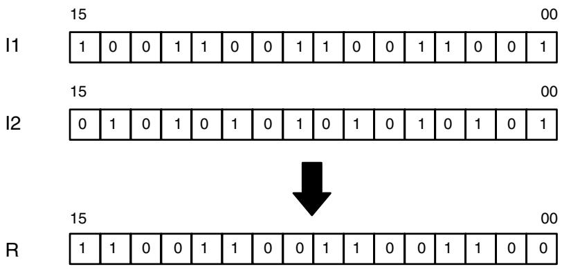
Flags
ER: Indirectly addressed DM word is non-existent. (Content of *DM word is not BCD, or the DM area boundary has been exceeded.)
EQ: ON when the result is 0.
7-24-5 EXCLUSIVE NOR - XNRW(37)
Ladder Symbols
| XNRW(37) | @XNRW(37) |
| I1 | I1 |
| I2 | I2 |
| R | R |
Operand Data Areas
| I1: Input 1 |
| IR, SR, AR, DM, HR, TC, LR, # |
| I2: Input 2 |
| IR, SR, AR, DM, HR, TC, LR, # |
| R: Result word |
| IR, SR, AR, DM, HR, LR |
Limitations
DM 6144 to DM 6655 cannot be used for R.
Description
When the execution condition is OFF, XNRW(37) is not executed. When the execution condition is ON, XNRW(37) exclusively NOR's the contents of I1 and I2 bit-by-bit and places the result in R.
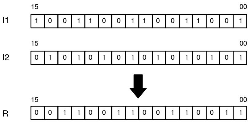
Flags
ER: Indirectly addressed DM word is non-existent. (Content of *DM word is not BCD, or the DM area boundary has been exceeded.)
EQ: ON when the result is 0.
7-25 Increment/Decrement Instructions
7-25-1 BCD INIncrement - INC(38)
Ladder Symbols
| INC(38) | @INC(38) |
| Wd | Wd |
Operand Data Areas
| Wd: Increment word (BCD) |
| IR, SR, AR, DM, HR, LR |
Limitations
DM 6144 to DM 6655 cannot be used for Wd.
Description
When the execution condition is OFF, INC(38) is not executed. When the execution condition is ON, INC(38) increments Wd, without affecting Carry (CY).
Precautions
The content of Wd will be incremented every cycle if the undifferentiated form of INC(38) is used. Use the differentiated form (@INC(38)) or combine INC(38) with DIFU(13) or DIFD(14) to increment Wd just once.
Flags
ER: Wd is not BCD
Indirectly addressed DM word is non-existent. (Content of *DM word is not BCD, or the DM area boundary has been exceeded.)
EQ: ON when the incremented result is 0.
7-25-2 BCD DECREMENT - DEC(39)
Ladder Symbols
| — | DEC(39) | — | @DEC(39) |
| Wd | Wd |
Operand Data Areas
| Wd: Decrement word (BCD) |
| IR, SR, AR, DM, HR, LR |
Limitations
DM 6144 to DM 6655 cannot be used for Wd.
Description
When the execution condition is OFF, DEC(39) is not executed. When the execution condition is ON, DEC(39) decrements Wd, without affecting CY. DEC(39) works the same way as INC(38) except that it decrements the value instead of incrementing it.
Precautions
The content of Wd will be decremented every cycle if the undifferentiated form of DEC(39) is used. Use the differentiated form (@DEC(39)) or combine DEC(39) with DIFU(13) or DIFD(14) to decrement Wd just once.
Flags
ER: Wd is not BCD.
Indirectly addressed DM word is non-existent. (Content of *DM word is not BCD, or the DM area boundary has been exceeded.)
EQ: ON when the decremented result is 0.
7-26 Subroutine Instructions
Subroutines break large control tasks into smaller ones and enable you to reuse a given set of instructions. When the main program calls a subroutine, control is transferred to the subroutine and the subroutine instructions are executed. The instructions within a subroutine are written in the same way as main program code. When all the subroutine instructions have been executed, control returns to the main program to the point just after the point from which the subroutine was entered (unless otherwise specified in the subroutine).
7-26-1 SUBROUTINE ENTER - SBS(91)
Ladder Symbol
SBS(91) N
Definer Data Areas
N: Subroutine number
000 to 049
Limitations
The subroutine number must be between 000 and 049.
Description
A subroutine can be executed by placing SBS(91) in the main program at the point where the subroutine is desired. The subroutine number used in SBS(91) indicates the desired subroutine. When SBS(91) is executed (i.e., when the execution condition for it is ON), the instructions between the SBN(92) with the same subroutine number and the first RET(93) after it are executed before execution returns to the instruction following the SBS(91) that made the call.
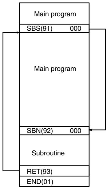
SBS(91) may be used as many times as desired in the program, i.e., the same subroutine may be called from different places in the program).
SBS(91) may also be placed into a subroutine to shift program execution from one subroutine to another, i.e., subroutines may be nested. When the second subroutine has been completed (i.e., RET(93) has been reached), program execution returns to the original subroutine which is then completed before returning to the main program. Nesting is possible to up to sixteen levels. A subroutine cannot call itself (e.g., SBS(91) 000 cannot be programmed within the subroutine defined with SBN(92) 000). The following diagram illustrates two levels of nesting.
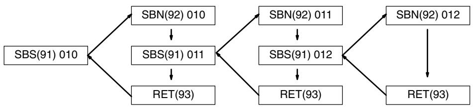
The following diagram illustrates program execution flow for various execution conditions for two SBS(91).
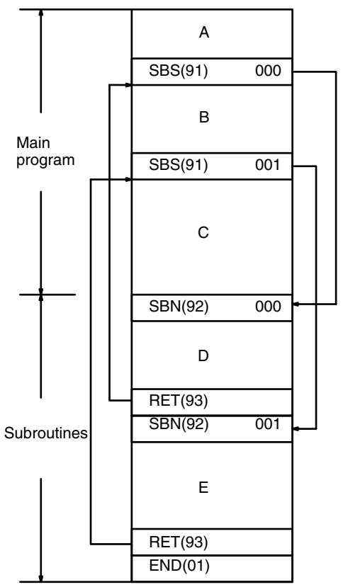
OFF execution conditions for subroutines 000 and 001
ON execution condition for subroutine 000 only
ON execution condition for subroutine 001 only
ON execution conditions for subroutines 000 and 001
Flags
ER: A subroutine does not exist for the specified subroutine number.
A subroutine has called itself.
An active subroutine has been called.
7-26-2 SUBROUTINE DEFINE and RETURN - SBN(92)/RET(93)
Ladder Symbols
Definer Data Areas
SBN(92) N
N: Subroutine number
000 to 049
RET(93)
Limitations
The subroutine number must be between 000 and 049.
Each subroutine number can be used in SBN(92) once only.
Description
SBN(92) is used to mark the beginning of a subroutine program; RET(93) is used to mark the end. Each subroutine is identified with a subroutine number, N, that is programmed as a definer for SBN(92). This same subroutine number is used in any SBS(91) that calls the subroutine (refer to 7-26-1 SUBROUTINE ENTER - SBS(91)). No subroutine number is required with RET(93).
All subroutines must be programmed at the end of the main program. When one or more subroutines have been programmed, the main program will be executed up to the first SBN(92) before returning to address 00000 for the next cycle. Subroutines will not be executed unless called by SBS(91).
END(01) must be placed at the end of the last subroutine program, i.e., after the last RET(93). It is not required at any other point in the program.
Precautions
If SBN(92) is mistakenly placed in the main program, it will inhibit program execution past that point, i.e., program execution will return to the beginning when SBN(92) is encountered.
If either DIFU(13) or DIFU(14) is placed within a subroutine, the operand bit will not be turned OFF until the next time the subroutine is executed, i.e., the operand and bit may stay ON longer than one cycle.
Flags
There are no flags directly affected by these instructions.
7-26-3 MACRO - MCRO(99)
Ladder Symbols
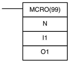
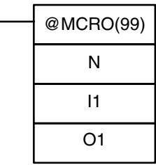
Operand Data Areas
| N: Subroutine number |
| 000 to 127 |
| I1: First input word |
| IR, SR, AR, DM, HR, TC, LR |
| 01: First output word |
| IR, SR, AR, DM, HR, LR |
Limitations
The subroutine number must be between 000 and 049.
If a DM address is used for O1, O1 through O1+3 must be read/write DM.
Description
The MACRO instruction allows a single subroutine to replace several subroutines that have identical structure but different operands. There are 4 input words (SR 232 to SR 235) and 4 output words (SR 236 to SR 239), allocated to MCRO(99). These 8 words are used in the subroutine and take their contents from I1 to I1+3 and O1 to O1+3 when the subroutine is executed.
When the execution condition is OFF, MCRO(99) is not executed. When the execution condition is ON, MCRO(99) copies the contents of I1 to I1+3 to SR 232 to SR 235, and then calls and executes the subroutine specified in N. When the subroutine is completed, the contents of SR 236 through SR 239 are then transferred back to O1 to O1+3 before MCRO(99) is completed.
Note Refer to page 157 for more details on MCRO(99).
Example
In this example, the contents of DM 0010 through DM 0013 are copied to SR 232 through SR 235, and then subroutine 10 is called and executed. When the subroutine is completed, the contents of SR 236 through SR 239 are copied to output words DM 0020 to DM 0023.
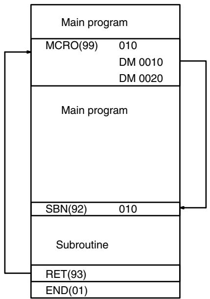
Flags
ER: A subroutine does not exist for the specified subroutine number.
An operand has exceeded a data area boundary.
Indirectly addressed DM word is non-existent. (Content of *DM word is not BCD, or the DM area boundary has been exceeded.)
A subroutine has called itself.
An active subroutine has been called.
7-27 Pulse Output Instructions
7-27-1 SET PULSES - PULS(65)
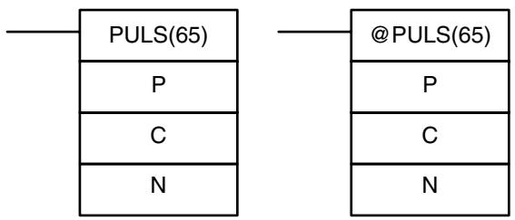
Ladder Symbols
Operand Data Areas
| P: Port specifier |
| 000 or 010 |
| C: Control data |
| 000 or 001 |
| N: Number of pulses |
| IR, SR, AR, DM, HR, LR |
Limitations
This instruction is supported by the CPM1A and CPM2A/CPM2C PCs with transistor outputs only.
N and N + 1 must be in the same data area.
DM 6144 to DM 6655 cannot be used for N.
Description
PULS(65) is used to set the number of pulses for pulse outputs that are started later in the program using SPED(64) or ACC(-). The number of pulses set with PULS(65) are output in independent mode.
The number of pulses cannot be changed while pulses are being output. In general, PULS(65) should be executed just once each time that the number of pulses needs to be set; use the differentiated variation (@PULS(65)) or an input condition that is ON for just one cycle.
Note Refer to 2-5 Pulse Output Functions for more details.
Port Specifier (P)
The port specifier indicates the pulse output location. The parameters set by the in C and N will apply to the next SPED(64) or ACC(-) instruction in which the same port output location is specified.
| P | Pulse output location(s) |
| 000 | Single-phase pulse output 0 without acceleration or deceleration (output 01000) or single-phase pulse output 0 with trapezoidal acceleration and deceleration (outputs 01000 and 01001) |
| 010 | Single-phase pulse output 1 without acceleration or deceleration (output 01001)This setting is supported by CPM2A/CPM2C PCs only. |
Control Data (C)
The control data determines the type of pulses (relative or absolute).
| C | Pulse type |
| 000 | Relative pulse specification |
| 001 | Absolute pulse specification (Valid only when the absolute coordinate system is being used.) |
| This setting is supported by CPM2A/CPM2C PCs only. |
Number of Output Pulses (N+1 and N)
N+1 and N contain the 8-digit BCD number of output pulses setting for independent mode pulse outputs. The number of output pulses can be -16,777,215 to 16,777,215. Bit 15 of N+1 acts as a sign bit; the number is negative if bit 15 is ON, positive if it is OFF.
Positive: 0 to +16,777,215 (0000 0000 to 1677 7215)
Negative: -16,777,215 to 0 (9677 7215 to 8000 0000)
N+1 contains the leftmost 4 digits and N contains the rightmost 4 digits.
Number of Movement Pulses
The number of movement pulses depends upon the number of output pulses (N + 1 and N) and the pulse type (C).
| Coordinate system | Movement pulses |
| Relative | Number of movement pulses = Number of output pulses |
| Absolute | Pulse type: Relative (C=000) Number of movement pulses = Number of output pulses Pulse type: Absolute (C=001, CPM2A/CPM2C only) Number of movement pulses = Number of output pulses - PV |
After PULS(65) has been executed, the calculated number of movement pulses will not be changed even if INI(61) is executed to change the pulse output PV. A specification that causes movement outside of the allowed PV range (-16,777,215 to 16,777,215) can be specified without problems.
PULS(65) will not be executed and an error will occur (SR 25503 ON) if the calculated number of movement pulses is 0.
When the pulse output is operating in independent mode without acceleration or deceleration and the number of movement pulses is negative, the absolute val-
ue of the number of movement pulses will be used. (For example, if the number of movement pulses is -500 , a value of 500 will be used.)
Flags
ER: A data area boundary is exceeded.
Indirectly addressed DM word is non-existent. (Content of *DM word is not BCD, or the DM area boundary has been exceeded.)
P is not 000 or 010.
C is not 000 or 001. (C cannot be set to 001 when relative coordinates are being used.)
The number of output pulses is not between -16,777,215 and 16,777,215.
PULS(65) is executed in an interrupt subroutine while a pulse I/O or high-speed counter instruction (INI(61), PRV(62), CTBL(63), SPED(64), PULS(65), ACC(), PWM(), or SYNC()) is being executed in the main program.
After PULS(65) is executed, the absolute value of the number of movement pulses is not between 1 and 16,777,215.
7-27-2 SPEED OUTPUT-SPED(64)
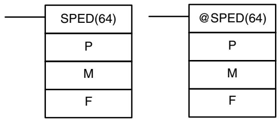
Ladder Symbols
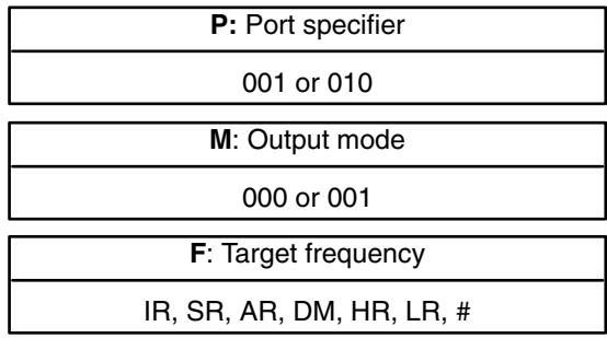
Operand Data Areas
Limitations
This instruction is supported by the CPM1A and CPM2A/CPM2C PCs with transistor outputs only.
In the CPM1A: F must be BCD, #0000 or #0002 to #0200.
In the CPM2A/CPM2C: F must be BCD, #0000 or #0001 to #1000.
DM 6144 to DM 6655 cannot be used for F.
Description
SPED(64) is used to set the output pulse frequency and start the pulse output from the specified output bit. When the execution condition is OFF, SPED(64) is not executed. When the execution condition is ON, SPED(64) sets the pulse frequency F for the output bit specified by P . M determines the output mode.
In general, SPED(64) should be executed just once each time that the frequency needs to be set; use the differentiated variation (@SPED(64)) or an input condition that is ON for just one cycle.
Note Refer to 2-5 Pulse Output Functions for more details.
Port Specifier (P)
The port specifier indicates the output bit where the pulses will be output.
| P | Pulse output location(s) |
| 000 | Single-phase pulse output 0 without acceleration or deceleration (output 01000) |
| 010 | Single-phase pulse output 1 without acceleration or deceleration (output 01001) This setting is supported by CPM2A/CPM2C PCs only. |
Output Mode (M)
The value of M determines the output mode.
| M | Pulse type |
| 000 | Independent mode |
| 001 | Continuous mode |
Operation in independent mode and continuous mode is described below.
Target Frequency (F)
The 4-digit BCD value of F sets the pulse frequency in units of 10Hz , as shown below. Setting F to 0000 will stop the pulse output from the specified output bit.
| PC | Possible values of F |
| CPM1A | 0000 (stops pulse output) or 0002 to 0200 (20 Hz to 2 kHz) |
| CPM2A/CPM2C | 0000 (stops pulse output) or 0001 to 1000 (10 Hz to 10 kHz) |
General Operation
The pulse output started by SPED(64) will continue until one of the following occurs:
1,2,3...
- The INI(61) instruction is executed with C = 003 .
- In independent mode, the number of output pulses specified by PULS(65) is reached. (Execute PULS(65) before SPED(64).)
- SPED(64) is executed again with the target frequency, F, set to #0000.
- The PC is switched to PROGRAM mode.
Pulses can be output simultaneously and independently from two output bits.
When outputting pulses in independent mode, specify the number of pulses beforehand by executing PULS(65). The number of output pulses must be specified again with PULS(65) each time that the pulse output has been stopped.
The frequency cannot be changed with SPED(64) when pulses are already being output from the specified output bit by ACC(—) or PWM(—). An error will occur and SR 25503 will be turned ON if SPED(64) is executed under these circumstances.
Operation in Independent Mode
In independent mode, just the number of output pulses set by PULS(65) will be output. The number of output pulses must be specified by executing PULS(65) before executing SPED(64). (Pulses won't be output if the number of output pulses has not been specified in advance.)
When the calculated number of movement pulses is negative, the absolute value of the number of movement pulses will be used. (For example, if the number of movement pulses is -500 , a value of 500 will be used.)
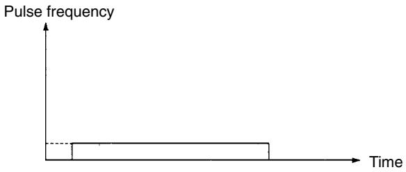
Operation in Continuous Mode
In continuous mode, pulses will be output indefinitely until stopped by executing INI(61) with C=003, executing SPED(64) again with F=0000, or switching the PC to PROGRAM mode.
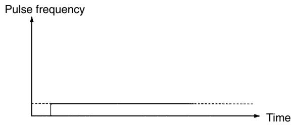
Flags
ER: A data area boundary is exceeded.
Indirectly addressed DM word is non-existent. (Content of *DM word is not BCD, or the DM area boundary has been exceeded.)
P is not 000 or 010, M is not 000 or 001, or F is not 0000 to 1000.
SPED(64) is executed in an interrupt subroutine while a pulse I/O or high-speed counter instruction (INI(61), PRV(62), CTBL(63), SPED(64), PULS(65), ACC(), PWM(), or SYNC()) is being executed in the main program.
7-27-3 ACCELERATION CONTROL - ACC(—)
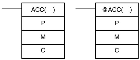
Ladder Symbols
Operand Data Areas
| P: Port specifier |
| 000 |
| M: Mode specifier |
| 000, 002, or 010 to 013 |
| C: First control word |
| IR, SR, AR, DM, HR, LR |
Limitations
This instruction is available in the CPM2A/CPM2C only.
P must be 001 or 002 and M must be 000 to 003.
C to C + 3 must be in the same data area.
Description
ACC(—) is used to specify the acceleration/deceleration rate and start the pulse output for a pulse output with trapezoidal acceleration and deceleration.
In general, ACC() should be executed just once each time that the acceleration/deceleration rate needs to be set; use the differentiated variation (@ACC()) or an input condition that is ON for just one cycle.
Note Refer to 2-5 Pulse Output Functions for more details.
Port Specifier (P)
Always set the port specifier to 000. The 000 setting specifies single-phase pulse output 0 with trapezoidal acceleration and deceleration.
Mode Specifier (M)
The value of M determines the output mode.
| M | Mode | Note |
| 000 | Independent mode and up/down pulse output mode | --- |
| 002 | Independent mode and pulse + direction output mode | --- |
| 010 | CW (continuous mode and up/down pulse output mode) | CW: Clockwise CCW: Counter-clockwise |
| 011 | CCW (continuous mode and up/down pulse output mode) | |
| 012 | CW (continuous mode and pulse + direction output mode) | |
| 013 | CCW (continuous mode and pulse + direction output mode) |
In independent mode, the output direction is set when PULS(65) is executed.
Control Words (C, C+1, and C+2)
The 3 control words indicate the acceleration rate, target frequency, and deceleration rate. (Each frequency is set in multiples of 10Hz .)
| Word | Function |
| C | The content of C determines the acceleration rate. During acceleration, the output frequency is increased by the amount set in C every 10 ms. C must be BCD from 0001 to 1000 (10 Hz to 10 kHz). |
| C+1 | The content of C+1 specifies the target frequency. C+1 must be BCD from 0001 to 1000 (10 Hz to 10 kHz). |
| C+2 | The content of C+2 determines the deceleration rate. During deceleration, the output frequency is decreased by the amount set in C+2 every 10 ms. C must be BCD from 0001 to 1000 (10 Hz to 10 kHz). |
General Operation
Two output bits are required for pulse outputs controlled by ACC(—).
Up/down pulse output mode
IR 01000 (CW operation)
IR 01001 (CCW operation)
Pulse + direction output mode
IR 01000 (Pulse output)
IR 01001 (Direction specifier)
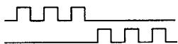
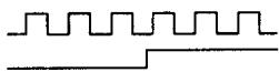
The pulse output will start when ACC(—) is executed and the output frequency will be increased every 10 ms by amount specified in control word C. When the target frequency (specified in C+1) is reached, acceleration is stopped and the pulse output continues at a constant frequency.
When the pulse output is operating with trapezoidal acceleration and deceleration, the pulse output can be stopped by one of the following methods.
1,2,3...
- Execute the INI(61) instruction with C=003. (Immediate stop)
- In independent mode, the number of output pulses specified by PULS(65) is reached. (Decelerates to a stop.)
- ACC(—) is executed with the target frequency (in + 1 ) set to 0000.
a) When pulses are being output in independent mode, the output will decelerate to a stop at the deceleration rate set when the pulse output was started.
b) When pulses are being output in continuous mode, the output will decelerate to a stop at the specified deceleration rate.
- Switch the PC to PROGRAM mode. (Immediate stop)
Operation in Independent Mode
In independent mode, just the number of output pulses set by PULS(65) will be output. The number of output pulses must be specified by executing PULS(65) before executing ACC(-). (Pulses won't be output if the number of output pulses has not been specified in advance.)
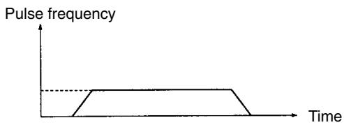
The number of output pulses must be specified again with PULS(65) each time that the pulse output has been stopped.
In independent mode, the pulse output will begin decelerating at the point determined by the preset number of output pulses and the acceleration/deceleration rates. The pulse output will stop when the preset number of output pulses has been output.
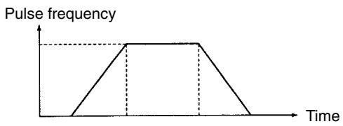
(The number of output pulses is always accurately output.)
If the number of output pulses required for acceleration and deceleration (the time to reach the target frequency × the target frequency) exceeds the preset number of pulses, the acceleration and deceleration will be cut short and the pulse output will be triangular rather than trapezoidal.
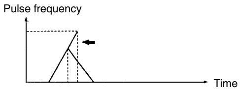
(The number of output pulses is always accurately output.)
If a high acceleration/deceleration rate and a low number of output pulses are set, there will be effectively no acceleration and deceleration. (The pulse output will operate at a constant speed.)
If the (target frequency ÷ acceleration/deceleration rate) is not an integer value, the specified acceleration/deceleration rates will be increased or decreased. In the following example, the acceleration and deceleration are 10-ms long, (1) is the acceleration/deceleration rate, and (2) is the target frequency.
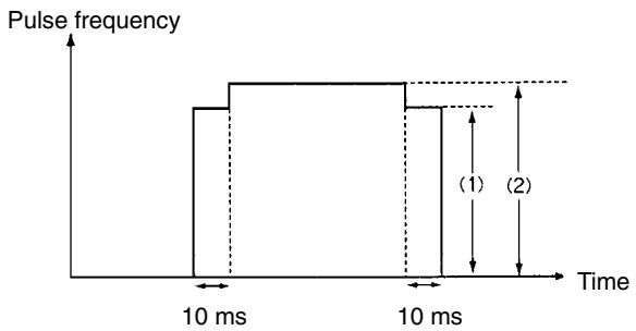
Operation in Continuous Mode
In continuous mode, pulses will be output indefinitely until stopped by executing INI(61) with C = 003 , executing ACC(-) again with the target frequency (in C + 1 ) set to 0000, or switching the PC to PROGRAM mode.
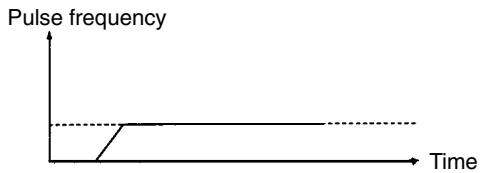
The following conditions apply when ACC(—) is executed while pulses are already being output with trapezoidal acceleration/deceleration.
- ACC(—) will have no effect if it is executed when the pulse output is accelerating or decelerating.
- When ACC(—) is executed while pulses are being output in continuous mode, the frequency can be changed to a new target frequency (0001 to 1000: 10Hz to 10kHz ) with the set acceleration/deceleration rates.
- If pulses are being output in independent mode, the pulse output can be decelerated to a stop while by executing ACC(—) with the target frequency (in C+1) set to 0000. The acceleration/deceleration rates and number of output pulses won't be checked or changed.
- ACC(—) will have no effect if it is executed when pulses are being output by one of the following instructions. (The pulse output will continue unchanged.)
- Pulses being output from output 01000 by SPED(64).
- Pulses being output from output 01001 by SPED(64).
- Pulses being output from output 01000 by PWM(—).
- Pulses being output from output 01001 by PWM(—).
Note Be sure to check the status of the pulse output before executing ACC(—).
Flags
ER: A data area boundary is exceeded.
Indirectly addressed DM word is non-existent. (Content of *DM word is not BCD, or the DM area boundary has been exceeded.)
P is not 000.
M is not 000, 002, or 010 to 013. (The mode specifier is read only when starting the pulse output.)
ACC(—) is executed for a bit from which pulses are already being output by PWM(—) or SPED(64).
ACC(—) is executed in an interrupt subroutine while a pulse I/O or high-speed counter instruction (INI(61), PRV(62), CTBL(63), SPED(64), PULS(65), ACC(—), PWM(—), or SYNC(—)) is being executed in the main program.
7-27-4 PULSE WITH VARIABLE DUTY RATIO - PWM(—)
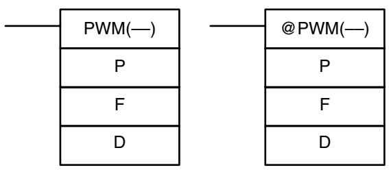
Ladder Symbols
Operand Data Areas
| P: Port specifier |
| 000 or 010 |
| F: Frequency |
| IR, SR, AR, DM, HR, LR, # |
| D: Duty ratio |
| IR, SR, AR, DM, HR, LR, # |
Limitations
This instruction is available in the CPM2A/CPM2C only.
P must be 000 or 010, F must be BCD between 0001 and 9999, and D must be BCD between 0001 and 0100.
Description
PWM(—) is used to output pulses with the specified duty ratio from the specified output bit. The pulse output continues until PWM(-) is executed again with a different duty ratio, INI(61) is executed with C = 003 , or the PC is switched to PROGRAM mode.
In general, PWM(—) should be executed just once to start the pulse output; use the differentiated variation (@PWM(—)) or an input condition that is ON for just one cycle.
Variable duty-ratio pulses can be output simultaneously and independently from two output bits.
When variable duty-ratio pulses are being output from an output bit and PWM(—) is executed for that bit again with a different duty ratio, pulses will continue being output with the new duty ratio. The frequency cannot be changed.
PWM(—) cannot be executed for an output bit if pulses are already being output from that bit by SPED(64) or ACC(—). An error will occur and SR 25503 will be turned ON if PWM(—) is executed under these circumstances.
Note Refer to 2-5 Pulse Output Functions for more details.
Port Specifier (P)
The port specifier indicates the output bit where the pulses will be output.
| P | Pulse output location(s) |
| 000 | Variable duty-ratio pulse output 0 (output 01000) |
| 010 | Variable duty-ratio pulse output 1 (output 01001) |
Frequency (F)
The 4-digit BCD value of F sets the pulse frequency in units of 0.1Hz . The frequency can be set between 0001 and 9999 (0.1 to 999.9 Hz).
Duty Ratio (D)
The 4-digit BCD value of D specifies the duty ratio of the pulse output, i.e., the percentage of time that the output is ON. The duty ratio can be set between 0001 and 0100 (1% to 100%). The duty ratio is 75% in the following diagram.
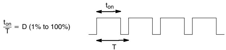
Flags
ER: A data area boundary is exceeded.
Indirectly addressed DM word is non-existent. (Content of *DM word is not BCD, or the DM area boundary has been exceeded.)
P is not 000 or 010, F is not BCD between 0001 and 9999, or D is not BCD between 0001 and 0100. (The frequency setting in F is read only when starting the pulse output.)
ACC(—) is executed for a bit from which pulses are already being output by ACC(—) or SPED(64).
PWM(—) is executed in an interrupt subroutine while a pulse I/O or high-speed counter instruction (INI(61), PRV(62), CTBL(63), SPED(64), PULS(65), ACC(—), PWM(—), or SYNC(—)) is being executed in the main program.
7-27-5 SYNCHRONIZED PULSE CONTROL - SYNC(—)
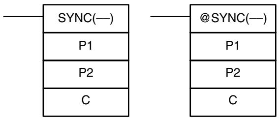
Ladder Symbols
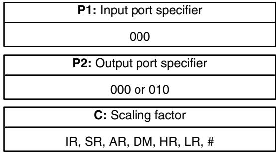
Operand Data Areas
Limitations
This instruction is available in the CPM2A/CPM2C only.
P1 must be 000 and P2 must be 000 or 010.
Description
SYNC(—) takes the frequency of the input pulse received through the high-speed counter inputs, multiplies it by a fixed scaling factor, and outputs pulses from the specified output bit at the resulting frequency.
Output frequency = Input frequency × Scaling factor/100
In general, SYNC() should be executed just once each time that synchronized pulse output control needs to be set; use the differentiated variation (@SYNC()) or an input condition that is ON for just one cycle.
Note Refer to 2-5 Pulse Output Functions for more details.
Input Port Specifier (P1)
Always set P1 to 000.
Output Port Specifier (P2)
The value of P2 determines where the scaled pulse frequency is output.
| P2 | Pulse output location(s) |
| 000 | Synchronized pulse output 0 (output 01000) |
| 010 | Synchronized pulse output 1 (output 01001) |
PC Setup Settings and General Operation
Scaling Factor (C)
The 4-digit BCD value of C sets the scaling factor by which the input frequency is multiplied. The scaling factor can be set between 0001 and 1000 (1 to 1,000% ).
The counter input mode for inputs 00000 and 00001 is set in bits 00 to 03 of DM 6642.
| DM 6642 bits 00 to 03 | High-speed counter setting |
| 0 | Differential phase mode (5 kHz) |
| 1 | Pulse + direction input mode (20 kHz) |
| 2 | Up/down input mode (20 kHz) |
| 4 | Increment mode (20 kHz) |
Input Frequency Range
The input frequency range for the synchronized pulse control is set in bits 08 to 15 of DM 6642, as shown in the following table.
| DM 6642 bits 08 to 15 | Function of inputs 00000 and 00001 |
| 02 | Use for synchronized pulse control (10 to 500 Hz) |
| 03 | Use for synchronized pulse control (20 Hz to 1 kHz). |
| 04 | Use for synchronized pulse control (300 Hz to 20 kHz). |
Synchronized pulse control cannot be executed unless inputs 00000 to 00003 are set for synchronized pulse control in bits 08 to 15 (settings 02, 03, and 04). An error will occur and SR 25503 will be turned ON if SYNC(—) is executed but DM 6642 is not set for synchronized pulse control.
The high-speed counter function and pulse output functions cannot be used while synchronized pulse control is in operation. An error will occur and SR 25503 will be turned ON if a related pulse output instruction is executed to use one of these functions while synchronized pulse control is being performed.
If the input frequency exceeds the maximum in the table above, the maximum input frequency for that range will be used. If the input frequency falls below the minimum, an input frequency of 0Hz will be used.
Output Frequency Range
The output frequency range is 10Hz to 10kHz . If the calculated output frequency (input frequency × scaling factor/100) exceeds 10kHz , pulses will be output at 10kHz . If the calculated output frequency falls below 10Hz , pulses will not be output (0Hz) .
Changing the Scaling Factor or Output Port
The scaling factor can be changed while synchronized pulse control is in operation by executing SYNC(—) again with a different scaling factor, but the output port specifier cannot be changed during operation.
Stopping the Synchronized Pulse Control Output
The synchronized pulse output can be stopped by executing INI(61) with C=005 or switching the PC to PROGRAM mode.
Flags
ER: A data area boundary is exceeded.
Indirectly addressed DM word is non-existent. (Content of *DM word is not BCD, or the DM area boundary has been exceeded.)
P1 is not 000, P2 is not 000 or 010, or C is not BCD between 0001 and 1000.
SYNC(—) is executed when bits 08 to 15 of DM 6642 are not set for synchronized pulse control.
SYNC(—) is executed in an interrupt subroutine while a pulse I/O or high-speed counter instruction (INI(61), PRV(62), CTBL(63), SPED(64), PULS(65), ACC(—), PWM(—), or SYNC(—)) is being executed in the main program.
7-28 Special Instructions
7-28-1MESSAGE DISPLAY-MSG(46)
Ladder Symbols
DM 6649 to DM 6655 cannot be used for FM.
When executed with an ON execution condition, MSG(46) reads eight words of extended ASCII code from FM to FM+7 and displays the message on the Programming Console. The displayed message can be up to 16 characters long, i.e., each ASCII character code requires eight bits (two digits). Refer to Appendix G for the ASCII codes. Japanese katakana characters are included in this code.
If not all eight words are required for the message, it can be stopped at any point by inputting "OD." When OD is encountered in a message, no more words will be read and the words that normally would be used for the message can be used for other purposes.
Message Buffering and Priority
Up to three messages can be buffered in memory. Once stored in the buffer, they are displayed on a first in, first out basis. Since it is possible that more than three MSG(46)s may be executed within a single cycle, there is a priority scheme, based on the area where the messages are stored, for the selection of those messages to be buffered.
The priority of the data areas is as follows for message display:
$$ \mathrm {L R} > \mathrm {I R} > \mathrm {H R} > \mathrm {A R} > \mathrm {T C} > \mathrm {D M} $$
In handling messages from the same area, those with the lowest address values have higher priority.
In handling indirectly addressed messages (i.e. *DM), those with the lowest final DM addresses have higher priority.
Clearing Messages
To clear a message, execute FAL(06) 00 or clear it via a Programming Console or the Support Software.
If the message data changes while the message is being displayed, the display will also change.
Flags
ER: Indirectly addressed DM word is non-existent. (Content of *DM word is not BCD, or the DM area boundary has been exceeded.)
Example
The following example shows the display that would be produced for the instruction and data given when 00000 was ON. If 00001 goes ON, a message will be cleared.
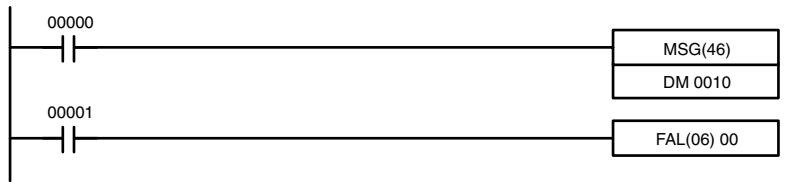
| Address | Instruction | Operands |
| 00000 | LD | 00000 |
| 00001 | MSG(46) | |
| DM 0010 | ||
| 00002 | LD | 00001 |
| 00003 | FAL(06) | 00 |
| DM contents | ASCII equivalent | |||||
| DM 0010 | 4 | 1 | 4 | 2 | A | B |
| DM 0011 | 4 | 3 | 4 | 4 | C | D |
| DM 0012 | 4 | 5 | 4 | 6 | E | F |
| DM 0013 | 4 | 7 | 4 | 8 | G | H |
| DM 0014 | 4 | 9 | 4 | A | I | J |
| DM 0015 | 4 | B | 4 | C | K | L |
| DM 0016 | 4 | D | 4 | E | M | N |
| DM 0017 | 4 | F | 5 | 0 | O | P |
MSG ABCDEFGHIJKLMNOP
7-28-2 I/O REFRESH -IORF(97)
Ladder Symbol
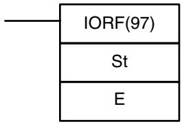
Operand Data Areas
| St: Starting word |
| IR 000 to IR 019 |
| E: End word |
| IR 000 to IR 019 |
Note This instruction is not supported by SRM1(-V2) PCs.
Limitations
St must be less than or equal to E.
Description
To refresh I/O words, specify the first (St) and last (E) I/O words to be refreshed. When the execution condition for IORF(97) is ON, all words between St and E will be refreshed. This will be in addition to the normal I/O refresh performed during the CPU Unit's cycle.
(If St>E, IORF(97) will be treated as NOP(00).)
Normally, I/O refreshing is performed just once each cycle at the end of program execution, but IORF(97) can be used to refresh I/O words immediately during program execution.
Caution
Although IORF(97) can be used in interrupt subroutines, you must be careful of the interval between IORF(97) executions. If IORF(97) is executed to frequently, a fatal system error may occur (FALS 9F), stopping operation. The interval between executions of IORF(97) should be at least 1.3ms+ total execution time of the interrupt subroutine.
Flags
ER: St or E is not within the allowed range (IR 000 to IR 019).
St is greater than E. (If St>E, IORF(97) will be treated as NOP(00).)
Flags
There are no flags affected by this instruction.
7-28-3 BIT COUNTER - BCNT(67)
Ladder Symbols
| BCNT(67) | @BCNT(67) |
| N | N |
| SB | SB |
| R | R |
Operand Data Areas
| N: Number of words (BCD) |
| IR, SR, AR, DM, HR, TC, LR, # |
| SB: Source beginning word |
| IR, SR, AR, DM, HR, TC, LR |
| R: Destination word |
| IR, SR, AR, DM, HR, TC, LR |
Note BCNT(67) is an expansion instruction in the CPM2A/CPM2C and SRM1(-V2). The function code 67 is the factory setting and can be changed for if desired.
Limitations
N cannot be 0.
DM 6144 to DM 6655 cannot be used for R.
Description
When the execution condition is OFF, BCNT(67) is not executed. When the execution condition is ON, BCNT(67) counts the total number of bits that are ON in all words between SB and SB + (N - 1) and places the result in R.
Flags
ER: N is not BCD, or N is 0; SB and SB + (N - 1) are not in the same area.
A DM address is used for SB, but SB through SB + (N - 1) are not all in read/write DM.
Indirectly addressed DM word is non-existent. (Content of *DM word is not BCD, or the DM area boundary has been exceeded.)
EQ: ON when the result is 0.
7-28-4 FRAME CHECKSUM - FCS(—)
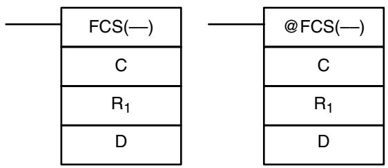
Ladder Symbols
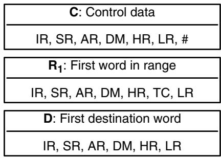
Operand Data Areas
Limitations
This instruction is available in the CPM2A/CPM2C/SRM1(-V2) only.
The 3 rightmost digits of C must be BCD between 001 and 999.
DM 6144 to DM 6655 cannot be used for D.
Description
FCS(—) can be used to check for errors when transferring data through communications ports.
When the execution condition is OFF, FCS(—) is not executed. When the execution condition is ON, FCS(—) calculates the frame checksum of the specified range by exclusively ORing either the contents of words R_1 to R_1 + N - 1 or the bytes in words R_1 to R_1 + N - 1 . The frame checksum value (hexadecimal) is then converted to ASCII and output to the destination words (D and D+1).
The function of bits in C are shown in the following diagram and explained in more detail below.
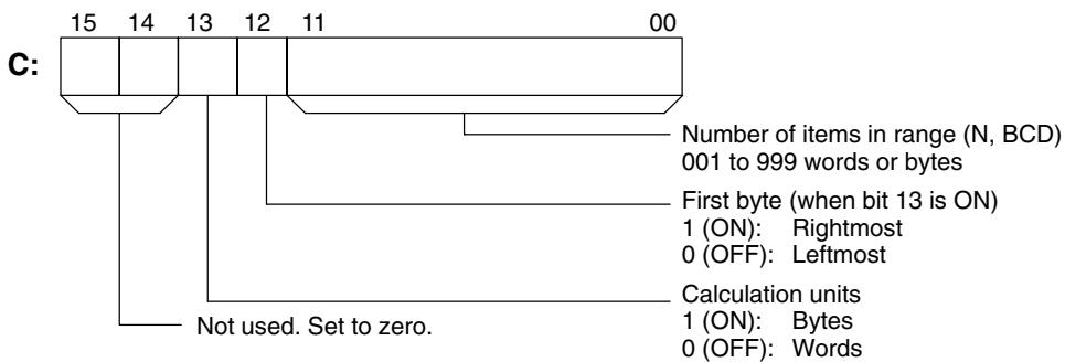
Number of Items in Range
The number of items within the range (N) is contained in the 3 rightmost digits of C, which must be BCD between 001 and 999.
Calculation Units
The frame checksum of words will be calculated if bit 13 is OFF and the frame checksum of bytes will be calculated if bit 13 is ON.
If bytes are specified, the range can begin with the leftmost or rightmost byte of R_1 . The leftmost byte of R_1 will not be included if bit 12 is ON.
When bit 12 is OFF the bytes will be ORed in this order: 1, 2, 3, 4, ....
When bit 12 is ON the bytes will be ORed in this order: 2, 3, 4, 5, ....
The byte frame checksum calculation yields a 2-digit hexadecimal value which is converted to its 4-digit ASCII equivalent. The word frame checksum calculation
yields a 4-digit hexadecimal value which is converted to its 8-digit ASCII equivalent, as shown below.
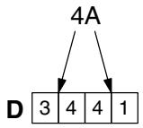
Byte frame checksum value
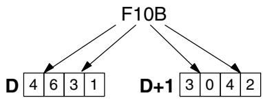
Word frame checksum value
Flags
ER: Indirectly addressed DM word is non-existent. (Content of *DM word is not BCD, or the DM area boundary has been exceeded.)
The number of items is not 001 to 999 BCD.
Example
When IR 00000 is ON in the following example, the frame checksum (0008) is calculated for the 8 words from DM 0000 to DM 0007 and the ASCII equivalent (30 30 30 38) is written to DM 0010 and DM 0011.
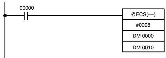
| Address | Instruction | Operands |
| 00000 | LD | 00000 |
| 00001 | @FCS(—) | |
| # 0008 | ||
| DM 0000 | ||
| DM 0010 |
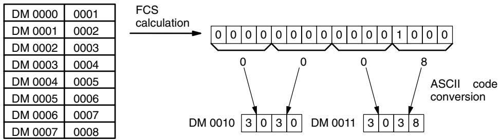
7-29 Interrupt Control Instructions
This section describes the operation of INT(89) and STIM(69). For general information on interrupt processing in CPM1/CPM1A, CPM2A/CPM2C, or SRM1(-V2) PCs refer to the section shown in the following table.
| PC | Reference |
| CPM1/CPM1A | See 2-3 CPM1/CPM1A Interrupt Functions. |
| CPM2A/CPM2C | See 2-1 CPM2A/CPM2C Interrupt Functions. |
| SRM1(-V2) | See 2-4 SRM1 Interrupt Functions. |
7-29-1 INTERRUPT CONTROL - INT(89)
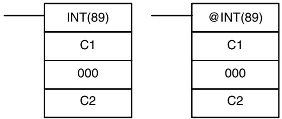
Ladder Symbols
Operand Data Areas
| C1: Control code |
| # (000 to 004, 100, or 200) |
| 000: No function |
| 000 |
| C2: Control data |
| IR, SR, AR, DM, HR, TC, LR, # |
Note This instruction is not supported by SRM1(-V2) PCs.
Limitations
DM 6144 to DM 6655 cannot be used for C2 when C1 = 002
Description
When the execution condition is OFF, INT(89) is not executed. When the execution condition is ON, INT(89) is used to control interrupts and performs one of the seven functions shown in the following table depending on the value of C1.
| C1 | INT(89) function |
| 000 | Mask/unmask interrupt inputs |
| 001 | Clear interrupt inputs |
| 002 | Read current mask status of interrupt inputs |
| 003 | Restart decrementing counter and unmask interrupt |
| 004* | Restart incrementing counter and unmask interrupt |
| 100 | Mask all interrupts |
| 200 | Unmask all interrupts |
Note *This setting can be used in CPM2A/CPM2C PCs only.
Mask/Unmask Interrupt Inputs (C1=000)
This function is used to mask and unmask interrupt inputs 00003 to 00006. Masked inputs are recorded, but ignored. When an input is masked, the interrupt program for it will be run as soon as the bit is unmasked (unless it is cleared beforehand by executing INT(89) with C1=001).
Set the corresponding bit in C2 to 0 or 1 to unmask or mask an interrupt input.
Bits 00 to 03 correspond to 00003 to 00006. Bits 04 to 15 should be set to 0.
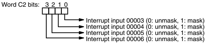
Clear Interrupt Inputs (C1=001)
All of the interrupt inputs are masked at the start of PC operation, so the inputs must be unmasked in order to be used.
This function is used to clear interrupt inputs 00003 to 00006. Since interrupt inputs are recorded, masked interrupts will be serviced as soon as the mask is removed unless they are cleared first.
Set the corresponding bit in C2 to 1 to clear an I/O interrupt input. Bits 00 to 03 correspond to 00003 to 00006. Bits 04 to 15 should be set to 0.
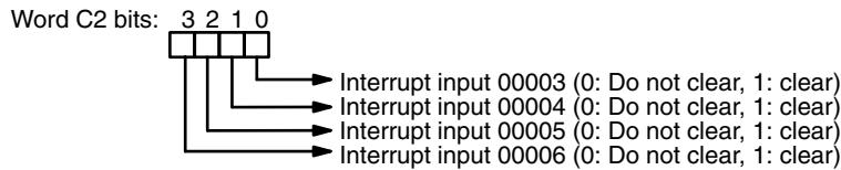
Read Current Mask Status (C1=002)
This function reads the current mask status for interrupt inputs 00003 to 00006 and writes that information to word C2. The corresponding bit will be ON if the input is masked. (Bits 00 to 03 correspond to 00003 to 00006.)
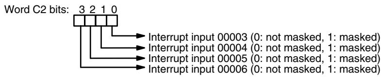
Restart Counter and Unmask Interrupt (C1=003 or C1=004)
These functions are used to restart interrupt inputs (counter mode) by refreshing the counter SV (in SR 240 to SR 243) and unmasking the interrupt input (00003 to 00006).
Set C1=3 to restart decrementing counters or C1=4 (CPM2A/CPM2C PCs only) to restart incrementing counters.
Set the corresponding bit in C2 to 0 to refresh the input's counter SV and unmask the interrupt. (Bits 00 to 03 correspond to 00003 to 00006.)
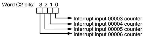
Use the differentiated variation (@INT(89)) or an input condition that is ON for just one cycle when executing INT(89) with C1=003 or C1=004. The counter PV will be reset to the SV if INT(89) is executed while the counter is operating, so the interrupt will never be generated if INT(89) is executed every cycle.
When INT(89) is executed with C1=003 or C1=004 and the SV word contains a non-zero SV (0001 to FFFF), the corresponding counter will begin operating (decrementing or incrementing) and the corresponding interrupt will be enabled in counter mode. When the count reaches the SV, an interrupt will be generated and the PV will be returned to the SV, so interrupts will be generated repeatedly until the counter is stopped.
Writing 0000 to a counter's SV word (SR 240 to SR 243) and executing INT(89) to refresh the SV will stop the counter and disable the corresponding interrupt. To restart the counter, write the non-zero SV to its SV word and execute INT(89). (The SV words are reset to 0000 at the start of operation, so the counter's SV must be written to its SV word from the ladder program.)
When an interrupt has already been enabled (unmasked), the SV cannot be refreshed just by writing a new value to the SV word. Refresh the SV by executing INT(89) with C1=003 (C1=004 for an incrementing counter).
A counter mode interrupt can be masked by executing INT(89) with C1=000 and the corresponding bit in C2 set to 1, but an input will operate in interrupt input mode, not counter mode, when its corresponding bit in C2 is set to 0.
Masking or Unmasking All Interrupts (C1=100 or C1=200)
All interrupts, including input interrupts, interval timer interrupts, and high-speed counter interrupts, can be masked or unmasked as a group by executing INT(89) with C1=100 or C1=200. The masked inputs are recorded, but ignored. The global mask is in addition to any masks on the individual types of interrupts. Furthermore, clearing the masks for all interrupts does not clear the masks on the individual types of interrupts, but restores them to the masked conditions that existed before INT(89) was executed to mask them as a group.
Do not use INT(89) to mask interrupts unless it is necessary to temporarily mask all interrupts. Always use INT(89) instructions in pairs to do so, using the first INT(89) instruction to mask all interrupts and the second one to unmask all interrupts.
INT(89) cannot be used to mask and unmask all interrupts from within interrupt routines.
Masking Interruptions (C1=100)
Use the INT(89) instruction with C1 = 100 to mask all interrupts.
| (@)INT(89) |
| 100 |
| 000 |
| 000 |
If an interrupt is generated while interrupts are masked, interrupt processing will not be executed but the interrupt will be recorded for the input, interval timer, and high-speed counter interrupts. The interrupts will then be serviced as soon as interrupts are unmasked.
Unmasking Interruptions (C1=200)
Use the INT(89) instruction with C1=200 to unmask interrupts as follows:
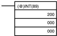
Flags
ER: A data area boundary is exceeded.
Indirectly addressed DM word is non-existent. (Content of *DM word is not BCD, or the DM area boundary has been exceeded.)
C1 is not 000 to 004,100, or 200.
C2 is not 0000 to 000F.
INT(89) is executed with C1=100 or C1=200 while an interrupt program was being executed.
INT(89) is executed with C1=100 when all inputs were already masked.
C1=200 when inputs were not all unmasked.
7-29-2 INTERVAL TIMER - STIM(69)
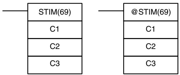
Ladder Symbols
Operand Data Areas
| C1: Control data #1 |
| 000 to 008, 010 to 012 |
| C2: Control data #2 |
| IR, SR, AR, DM, HR, TC, LR, # |
| C3: Control data #3 |
| IR, SR, AR, DM, HR, TC, LR, # |
Note STIM(69) is an expansion instruction in the CPM2A/CPM2C and SRM1(-V2). The function code 69 is the default setting and can be changed if desired.
Limitations
C1 must be 000, 003, 006. or 010.
If C1 is 000 or 003, C3 represents a BCD subroutine number up to 0049.
If C1 is 006, constants cannot be used for C2 or C3.
If C1 is 010, both C2 and C3 must be set to 000.
Description
STIM(69) is used to control the interval timers by performing four basic functions: starting the timer for a one-shot interrupt, starting the timer for scheduled interrupts, reading the timer's PV, and stopping the timer. Set the value of C1 to specify which of these functions will be performed, as shown in the following table. Refer to Section 2 Special Features for more detailed descriptions of using interval timer interrupts. STIM(69) is also described in more detail after the table.
| C1 value | Function |
| 000 | Starts the one-shot interrupt timer. |
| 003 | Starts the scheduled interrupt timer. |
| 006 | Reads the timer PV. |
| 010 | Stops the timer. |
Starting Interrupt Timers (C1= 000 or 003)
Set C1=000 to activate the one-shot interrupt timer. Set C1=003 to start the scheduled interrupt timer.
| C2, which specifies the timer's SV, can be a constant or the first of two words containing the SV. The settings are slightly different depending on the method used. C2 = Constant If C2 is a constant, it specifies the SV of the decrementing counter in BCD. The setting range is 0000 to 9999 (0 to 9.999 ms). (The timing units are fixed at 1 ms.) C3 specifies subroutine number: 0000 to 0049. C2 = Word Address If C2 is a word address, the content of C2 contains the SV of the decrementing counter (BCD, 0000 to 9999). The content of C2+1 specifies the timing units (BCD, 0005 to 0320) in units of 0.1 ms. The decrementing time interval can thus be 0.5 to 32 ms. The timer SV is: (the content of C2) × (the content of C2+1) × 0.1 ms. C3 specifies subroutine number: 0000 to 0049. | |
| Reading the Timer PV (C1=006) | Set C1=006 to read the timer PV. C2 specifies the first of two destination words that will receive the timer's PV. C2 receives the number of times the decrementing counter has been decremented (hexadecimal, 0000 to 9999) and C2+1 receives the timing units (BCD in 0.1 ms units). C3 specifies the destination word that receives the time which has elapsed since the last time the timer was decremented (BCD in 0.1 ms units). Note The time that has elapsed since the timer was started is computed as follows: ((Content of C2) × (Content of C2+1)) + ((Content of C3)) × 0.1 ms |
| Stopping the Timer (C=010) | Set C1=010 to stop the timer. C2 and C3 have no function and should both be set to 000. |
| Flags | ER: C1 is not 000, 003, 006, or 010. A specified subroutine number is not between 0000 and 0049. Indirectly addressed DM word is non-existent. (Content of *DM word is not BCD, or the DM area boundary has been exceeded.) A data area boundary has been exceeded. |
7-30 Communications Instructions
7-30-1 RECEIVE - RXD(47)
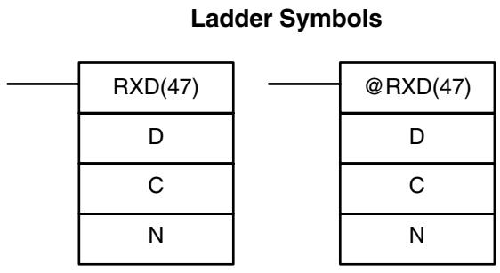
| D: First destination word |
| IR, SR, AR, DM, HR, TC, LR |
| C: Control word |
| # |
| N: Number of bytes |
| IR, SR, AR, DM, HR, TC, LR, # |
Limitations
This instruction is available in the CPM2A/CPM2C and SRM1(-V2) only.
D and D + (N ÷ 2) - 1 must be in the same data area.
DM 6144 to DM 6655 cannot be used for D or N.
| Description | N must be BCD from #0000 to #0256. (#0000 to #0061 in Host Link mode) |
| When the execution condition is OFF, RXD(47) is not executed. When the execution condition is ON, RXD(47) reads N bytes of data received at the port specified in the control word, and then writes that data in words D to D+(N÷2)-1. Up to 256 bytes of data can be read at one time. If fewer than N bytes are received, the amount received will be read. | |
| Note Refer to 4-1Communications Functions for details on using the RXD(47) instruction, setting communications protocol in the PC Setup, etc. | |
| Caution The PC will be incapable of receiving more data once 256 bytes have been received if received data is not read using RXD(47). Read data as soon as possible after the Reception Completed Flag is turned ON (AR 0806 for the RS-232C port, AR 0814 for the peripheral port.) | |
| Control Word | The value of the control word determines the port from which data will be read and the order in which data will be written to memory. Digit number: 3 2 1 0 Byte order 0: Most significant bytes first, same word 1: Least significant bytes first, same word Not used. (Set to 00.) Port 0: RS-232C port. 1: Peripheral port. |
| The order in which data is written to memory depends on the value of digit 0 of C. Eight bytes of data 12345678... will be written in the following manner: | |
| Digit 0 = 0 MSB LSB Digit 0 = 1 MSB LSB | |
| D 1 2 | |
| D+1 3 4 | |
| D+2 5 6 | |
| D+3 7 8 | |
| Digit 0 = 2 MSB LSB Digit 0 = 3 MSB LSB | |
| D 1 1 | |
| D+1 2 3 | |
| D+2 4 5 | |
| D+3 6 7 | |
| Digit 0 = 3 MSB LSB Digit 0 = 4 MSB LSB | |
| Flags | ER: The settings in C are not correct. N is greater than 256. The PC Setup is not set for no-protocol mode. RXD(47) is already being executed. AR 08: AR 0806 will be turned ON when data has been received normally at the RS-232C port. Reset when RXD(47) is executed. |
AR 0814 will be turned ON when data has been received normally at the peripheral port. Reset when RXD(47) is executed.
AR 09: Contains the number of bytes received at the RS-232C port. Reset to 0000 when RXD(47) is executed.
AR 10: Contains the number of bytes received at the peripheral port. Reset to 0000 when RXD(47) is executed.
Note Communications flags and counters can be cleared either by specifying 0000 for N or using the Port Reset Bits (SR 25208 for peripheral port and SR 25209 for RS-232C port.)
7-30-2 TRANSMIT - TXD(48)
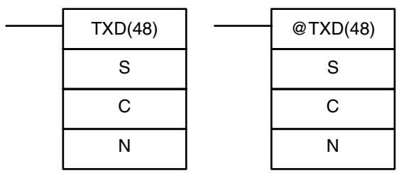
Ladder Symbols
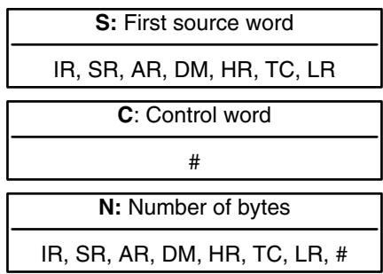
Operand Data Areas
Limitations
This instruction is available in the CPM2A/CPM2C and SRM1(-V2) only.
S and S_+(N ÷ 2) - 1 must be in the same data area.
DM 6144 to DM 6655 cannot be used for S or N.
N must be BCD from #0000 to #0256. (#0000 to #0061 in Host Link mode)
Description
When the execution condition is OFF, TXD(48) is not executed. When the execution condition is ON, TXD(48) reads N bytes of data from words S to S + (N ÷ 2) - 1 , converts it to ASCII, and outputs the data from the specified port. TXD(48) operates differently in Host Link mode and RS-232C mode, so these modes are described separately.
Note
- Flag AR 0805 will be ON when the PC is capable of transmitting data through the RS-232C port and AR 0813 will be ON when the PC is capable of transmitting data through the peripheral port.
- Refer to 4-1 Communications Functions for details on using the TXD(48) instruction, setting communications protocol in the PC Setup, etc.
Host Link Mode
N must be BCD from #0000 to #0061 (i.e., up to 122 bytes of ASCII). The value of the control word determines the port from which data will be output, as shown below.
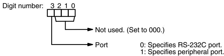
The specified number of bytes will be read from S through S + (N/2) - 1 , converted to ASCII, and transmitted through the specified port. The bytes of source data shown below will be transmitted in this order: 12345678...
The following diagram shows the format for Host Link command (TXD) sent from the CPM2A/CPM2C. The CPM2A/CPM2C automatically attaches the prefixes and suffixes, such as the node number, header, and FCS.
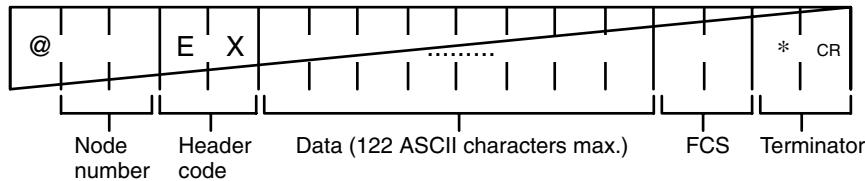
RS-232C Mode
N must be BCD from #0000 to #00256. The value of the control word determines the port from which data will be output and the order in which data will be written to memory.
Control Word
The value of the control word determines the port from which data will be read and the order in which data will be written to memory.
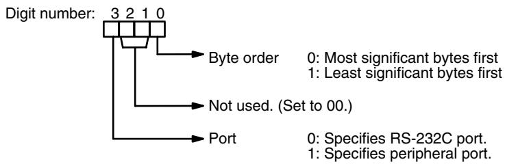
The specified number of bytes will be read from S through S + (N ÷ 2) - 1 and transmitted through the specified port.
When digit 0 of C is 0, the bytes of source data shown above will be transmitted in this order: 12345678...
When digit 0 of C is 1, the bytes of source data shown above will be transmitted in this order: 21436587...
Note When start and end codes are specified the total data length should be 256 bytes max., including the start and end codes.
Flags
ER: The settings in C are not correct.
N is greater than 256 for no-protocol mode or greater than 61 for Host Link mode.
The PC Setup is not set for the correct communications mode.
Indirectly addressed DM word is non-existent. (Content of *DM word is not BCD, or the DM area boundary has been exceeded.)
TXD(48) is already being executed.
AR 08: AR 0805 will be turned ON when it is possible to transmit through the RS-232C port. AR 0813 will be turned ON when it is possible to transmit through the peripheral port.
7-30-3 CHANGE RS-232C SETUP - STUP(—)
Ladder Symbols
| N: RS-232C port specifier |
| 000 |
| S: First source word |
| IR, SR, AR, DM, HR, LR, # |
The third operand is ignored.
Limitations
This instruction is available in the CPM2A/CPM2C and SRM1(-V2) only.
N must be 000.
S and S + 4 must be in the same data area.
(S can be set to #0000 to change the RS-232C settings to their defaults.)
STUP(-) can't be executed within an interrupt subroutine.
Description
When the execution condition is OFF, STUP() is not executed. When the execution condition is ON, STUP() changes the PC Setup settings for the built-in RS-232C port. The settings are changed in the PC Setup, but they are not written to flash memory until the PC is switched to PROGRAM mode (from RUN or MONITOR mode) or the PC is turned OFF and then ON again.
In CPM2A/CPM2C and SRM1(-V2) PCs, N must be 000 because STUP(—) can change the RS-232C Setup for the built-in RS-232C port (DM 6645 to DM 6649) only.
If S is a word address, the contents of S through S+4 are copied to DM 6645 to DM 6649.
If S is input as the constant #0000, the settings for the built-in RS-232C port are returned to their default values.
| S | Function |
| Word address | The contents of S through S+4 are copied to DM 6645 through DM 6649. |
| Constant (#0000) | The settings in DM 6645 through DM 6649 are returned to their default values. |
Note
- The Changing RS-232C Setup Flag (SR 25312) will be ON while STUP(—) is being executed; it is turned OFF when STUP(—) is completed.
- In the CPM2A/CPM2C, an error will occur and STUP(—) will not be executed if the Communications Switch on the front of the CPU Unit is ON. When this switch is ON, RS-232C communications are governed by the default settings.
Application Example
This example shows a program that transfers the contents of DM 0100 through DM 0104 to the PC Setup area for the built-in RS-232C port (DM 6645 through DM 6649).
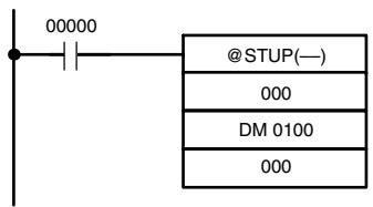
| Address | Instruction | Operands |
| 00000 | LD | 00000 |
| 00001 | @STUP(—) | |
| 000 | ||
| DM 0100 | ||
| --- |
The settings are transferred as shown below. The Changing RS-232C Setup Flag (SR 25312) will be turned OFF when the transfer has been completed.
The following table shows the function of the transferred setup data.
| Source word | Destination word | Content | Function |
| DM 0100 | DM 6645 | 1001 | Enables the communications settings in DM 0101 and sets the communications mode to no-protocol. |
| DM 0101 | DM 6646 | 0803 | Sets the following communications settings: 9,600 bps, 1 start bit, 8-bit data, 1 stop bit, no parity |
| DM 0102 | DM 6647 | 0000 | No transmission delay (0 ms) |
| DM 0103 | DM 6648 | 2000 | Enables the end code CR, LF. |
| DM 0104 | DM 6649 | 0000 | (No function when DM 6648 is set to 2000.) |
Flags
ER: Indirectly addressed DM word is non-existent. (Content of *DM word is not BCD, or the DM area boundary has been exceeded.)
The port specifier (N) isn't 000.
In the CPM2A/CPM2C, the Communications Switch on the front of the CPU Unit is ON.
Another STUP(—) instruction is already being executed or event processing is being performed.
The specified source words exceed the data area.
The instruction was executed from an interrupt program.
The PC Setup is write-protected.
SECTION 8
PC Operations and Processing Time
This section explains the internal processing of the CPM1, CPM1A, CPM2A, CPM2C, and SRM1(-V2), as well as the time required for processing and execution. Refer to this section to gain an understanding of the precise timing of PC operation.
8-1 CPM1/CPM1A Cycle Time and I/O Response Time 512
8-1-1 The CPM1/CPM1A Cycle 512
8-1-2 CPM1/CPM1A Cycle Time 513
8-1-3 I/O Response Time 514
8-1-4 One-to-one PC Link I/O Response Time 515
8-1-5 Interrupt Processing Time 517
8-1-6 CPM1/CPM1A Instruction Execution Times 518
8-2 CPM2A/CPM2C Cycle Time and I/O Response Time 523
8-2-1 CPM2A/CPM2C Cycle Time 523
8-2-2 I/O Response Time 524
8-2-3 One-to-one PC Link I/O Response Time 525
8-2-4 Interrupt Processing Time 527
8-2-5 CPM2A/CPM2C Instruction Execution Times 528
8-3 SRM1(-V2) Cycle Time and I/O Response Time 537
8-3-1 The SRM1(-V2) Cycle 537
8-3-2 SRM1(-V2) Cycle Time 538
8-3-3 I/O Response Time 540
8-3-4 One-to-one PC Link I/O Response Time 541
8-3-5 Interrupt Processing Time 542
8-3-6 SRM1(-V2) Instruction Execution Times 543
8-1 CPM1/CPM1A Cycle Time and I/O Response Time
8-1-1 The CPM1/CPM1A Cycle
The overall flow of CPM1/CPM1A operation is as shown in the following flowchart.
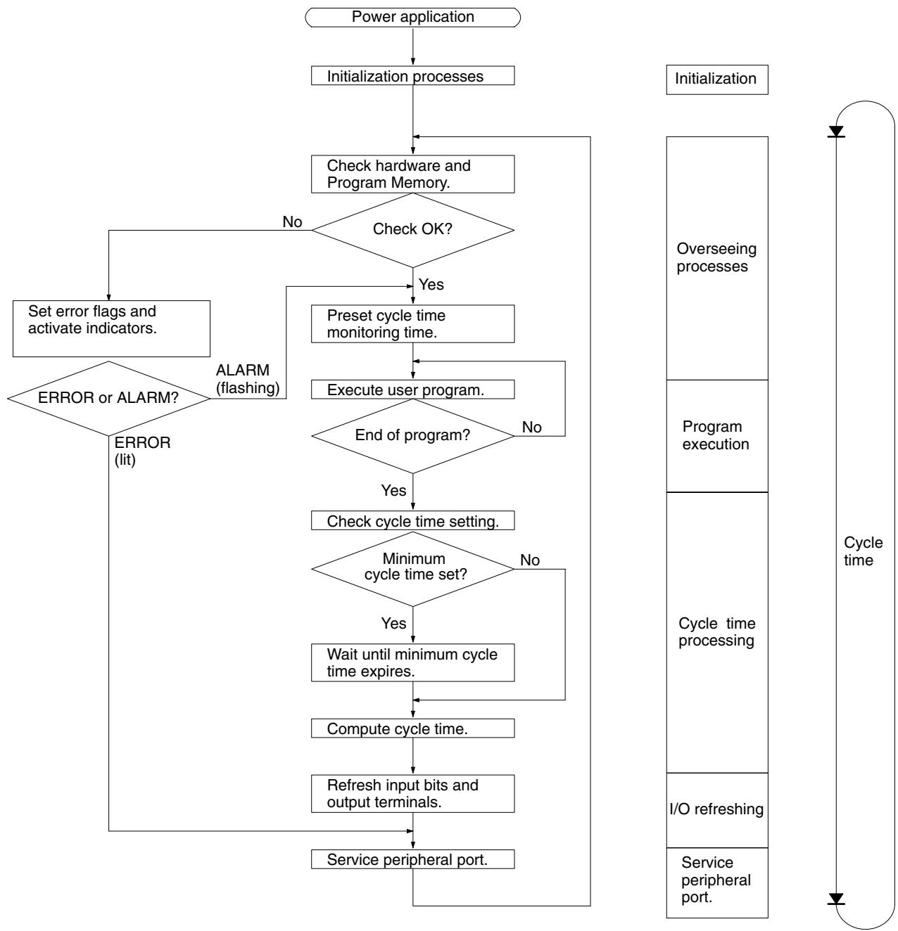
Note Initialization processes include clearing the IR, SR, and AR areas, presetting system timers, and checking I/O Units.
8-1-2 CPM1/CPM1A Cycle Time
The processes involved in a single CPM1/CPM1A cycle are shown in the following table, and their respective processing times are explained.
| Process | Content | Time requirements |
| Overseeing | Setting cycle watchdog timer, I/O bus check, UM check, clock refreshing, refreshing bits allocated to new functions, etc. | 0.6 ms |
| Program execution | User program is executed. | Total time for executing instructions. (Varies according to content of user's program.) |
| Cycle time calculation | Standby until set time, when minimum cycle time is set in DM 6619 of PC Setup. Calculation of cycle time. | Almost instantaneous, except for standby processing. |
| I/O refresh | Input information is read to input bits. Output information (results of executing program) is written to output bits. | 10-point CPU: 0.06 ms20-point CPU: 0.06 ms30-point CPU: 0.3 msExpansion I/O Unit: 0.3 ms |
| Peripheral port servicing | Devices connected to peripheral port serviced. | 0.26 ms min., 5% or less of cycle time up to 66 ms (see note) |
Note The percentage of the cycle allocated to peripheral port servicing can be changed in the PC Setup (DM 6617).
Cycle Time and Operations
The effects of the cycle time on CPM1/CPM1A operations are as shown below. When a long cycle time is affecting operation, either reduce the cycle time or improve responsiveness with interrupt programs.
| Cycle time | Operation conditions |
| 10 ms or longer | TIMH(15) may be inaccurate when TC 004 through TC 127 are used (operation will be normal for TC 000 through TC 003). |
| 20 ms or longer | Programming using the 0.02-second Clock Bit (SR 25401) may be inaccurate. |
| 100 ms or longer | TIM may be inaccurate. Programming using the 0.1-second Clock Bit (SR 25500) may be inaccurate. A CYCLE TIME OVER error is generated (SR 25309 will turn ON). See note 1. |
| 120 ms or longer | The FALS 9F monitoring time SV is exceeded. A system error (FALS 9F) is generated, and operation stops. See note 2. |
| 200 ms or longer | Programming using the 0.2-second Clock Bit (SR 25501) may be inaccurate. |
Note 1. The PC Setup (DM 6655) can be used to disable detection of CYCLE TIME OVER error.
- The cycle monitoring time can be changed in the PC Setup (DM 6618).
Cycle Time Example
In this example, the cycle time is calculated for a CPM1/CPM1A CPU Unit with 20 I/O points (12 input points and 8 output points). The I/O is configured as follows:
Inputs: 1 word (00000 to 00011)
Outputs: 1 word (01000 to 01007)
The rest of the operating conditions are assumed to be as follows:
User's program:500 instructions (consists of only LD and OUT)
Cycle time: Variable (no minimum set)
The average processing time for a single instruction in the user's program is assumed to be 2.86~ s . The cycle times are as shown in the following table.
| Process | Calculation method | Time with Programming Device | Time without Programming Device |
| 1. Overseeing | Fixed | 0.6 ms | 0.6 ms |
| 2. Program execution | 2.86 × 500 (μs) | 1.43 ms | 1.43 ms |
| 3. Cycle time calculation | Negligible | 0 ms | 0 ms |
| 4. I/O refresh | 0.01 × 1 + 0.005 × 1 (μs) | 0.06 ms | 0.06 ms |
| 5. Peripheral port servicing | Minimum time | 0.26 ms | 0 ms |
| Cycle time | (1) + (2) + (3) + (4) + (5) | 2.35 ms | 2.09 ms |
Note 1. The cycle time can be read from the PC via a Programming Device.
- The maximum and current cycle time are stored in AR 14 and AR 15.
- The cycle time can vary with actual operating conditions and will not necessarily agree precisely with the calculated value.
8-1-3 I/O Response Time
The I/O response time is the time it takes after an input signal has been received (i.e., after an input bit has turned ON) for the PC to check and process the information and to output a control signal (i.e., to output the result of the processing to an output bit). The I/O response time varies according to the timing and processing conditions.
The minimum and maximum I/O response times are shown here, using the following program as an example.
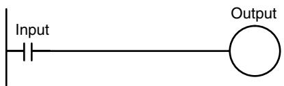
The following conditions are taken as examples for calculating the I/O response times.
Input ON delay: 8 ms (input time constant: default setting)
Overseeing time: 1 ms (includes I/O refresh for CPM1A)
Instruction execution time: 14 ms
Output ON delay: 10 ms
Peripheral port: Not used.
Minimum I/O Response Time
The CPM1/CPM1A responds most quickly when it receives an input signal just prior to I/O refreshing, as shown in the illustration below.
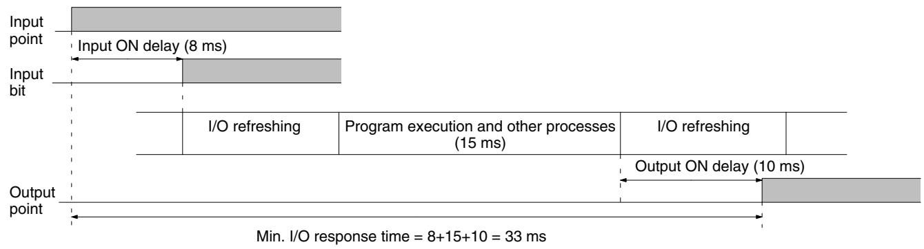
Maximum I/O Response Time
The CPM1/CPM1A takes longest to respond when it receives the input signal just after the input refresh phase of the cycle, as shown in the illustration below. In that case, a delay of approximately one cycle will occur.
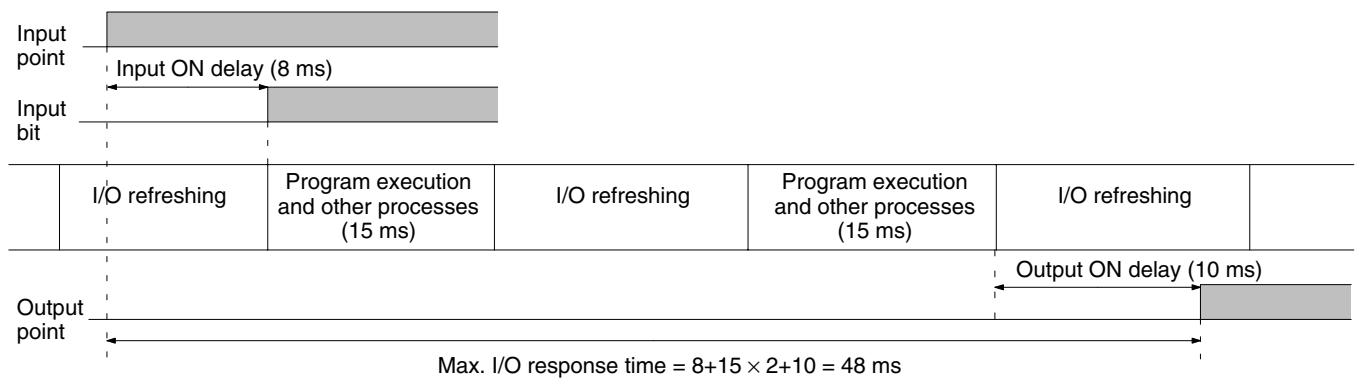
8-1-4 One-to-one PC Link I/O Response Time
When two CPM1/CPM1As are linked 1:1, the I/O response time is the time required for an input executed at one of the CPM1/CPM1As to be output to the other CPM1/CPM1A by means of 1:1 PC Link communications.
The minimum and maximum I/O response times are shown here, using as an example the following instructions executed at the master and the slave. In this example, communications proceed from the master to the slave.
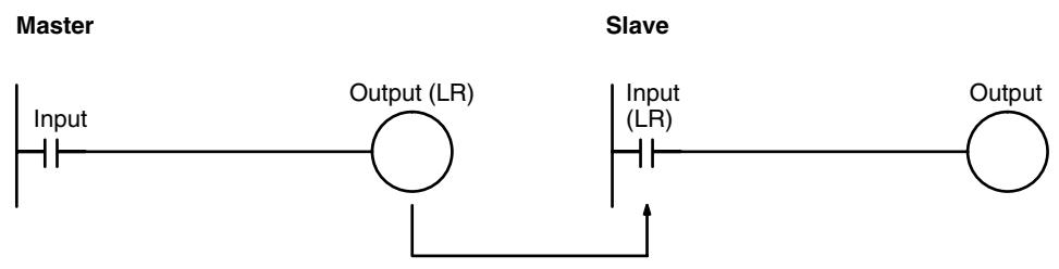
The following conditions are taken as examples for calculating the I/O response times. In CPM1/CPM1A PCs, LR area words LR 00 to LR 15 are used in 1:1 data links and the transmission time is fixed at 12 ms.
Input ON delay: 8 ms (input time constant: default setting)
Master cycle time: 10 ms
Slave cycle time: 15 ms
Output ON delay: 10 ms
Peripheral port: Not used.
Minimum I/O Response Time The CPM1/CPM1A responds most quickly under the following circumstances:
1, 2, 3... 1. The CPM1/CPM1A receives an input signal just prior to the input refresh phase of the cycle.
-
The Master's communications servicing occurs just as the Master-to-Slave transmission begins.
-
The Slave's communications servicing occurs just after the transmission is completed.
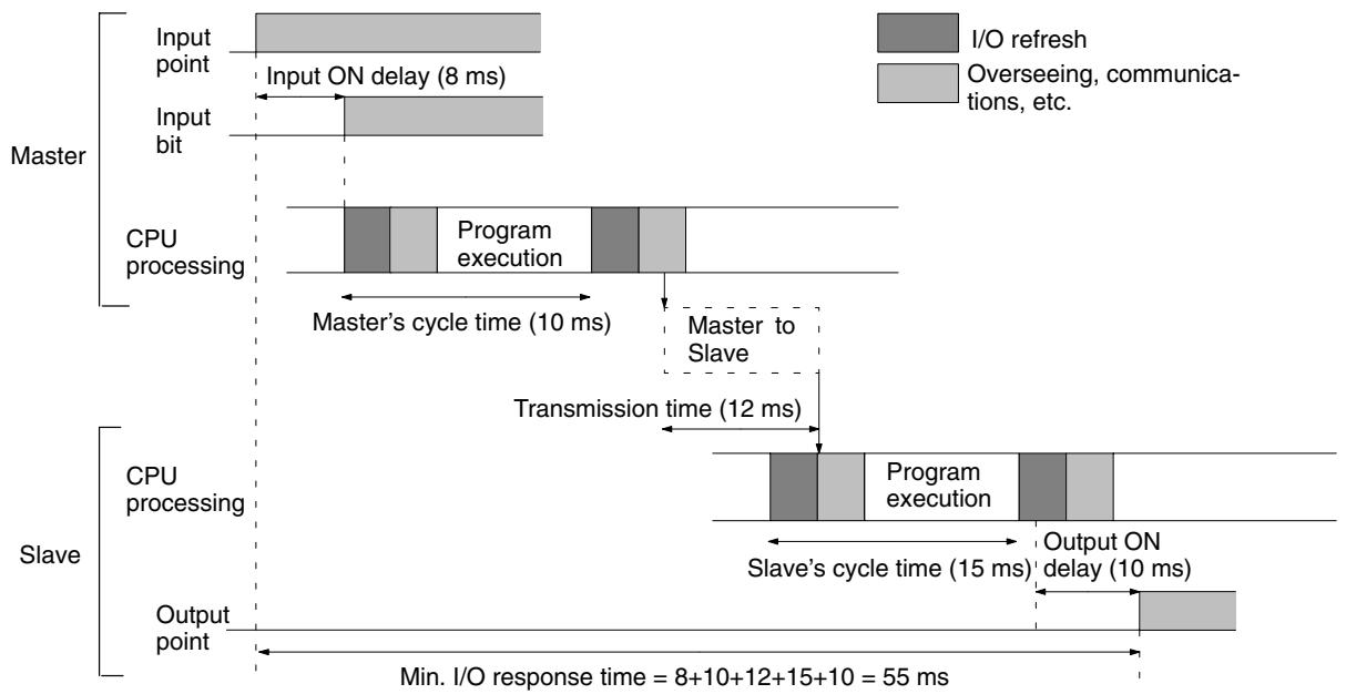
Calculation formula = Input ON response time + Master's cycle time + Slave's cycle time + Output ON response time
Maximum I/O Response Time
The CPM1/CPM1A takes the longest to respond under the following circumstances:
1, 2, 3... 1. The CPM1/CPM1A receives an input signal just after the input refresh phase of the cycle.
- The Master's communications servicing just misses the Master-to-Slave transmission.
- The transmission is completed just after the Slave's communications servicing ends.
I/O Maximum Response Time
Input ON response time + Master's cycle time x 2 + Transmission time x 3 + Output ON response time
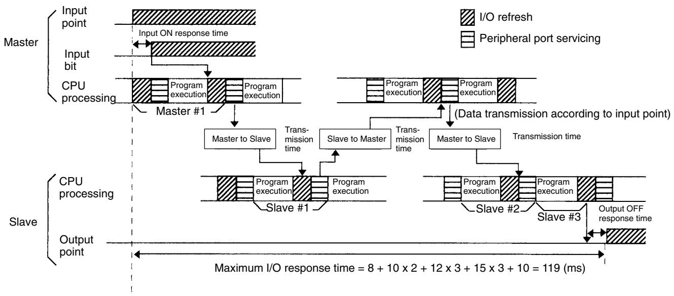
8-1-5 Interrupt Processing Time
This section explains the processing times involved from the time an interrupt is executed until the interrupt processing routine is called, and from the time an interrupt processing routine is completed until returning to the initial location. This explanation applies to input interrupts, interval timer interrupts, and high-speed counter interrupts.
1, 2, 3... 1. Source of interrupt
- Interrupt ON delay
- Wait for completion of interrupt-mask processing
- Change to interrupt processing
- Interrupt routing (CPM1A only)
- Return to initial location
The table below shows the times involved from the generation of an interrupt signal until the interrupt processing routine is called, and from when the interrupt processing routine is completed until returning to the original position.
| Item | Contents | Time |
| Interrupt ON delay | This is the delay time from the time the interrupt input bit turns ON until the time that the interrupt is executed. This is unrelated to other interrupts. | 100 μs |
| Wait for completion of interrupt-mask processing | This is the time during which interrupts are waiting until processing has been completed. This situation occurs when a mask processes is executed. It is explained below in more detail. | See below. |
| Change to interrupt processing | This is the time it takes to change processing to an interrupt. | 30 μs |
| Return | This is the time it takes, from execution of RET(93), to return to the processing that was interrupted. | 30 μs |
Mask Processing
Interrupts are masked during processing of the operations described below. Until the processing is completed, any interrupts will remain masked for the indicated times.
Generation and clearing of non-fatal errors:
When a non-fatal error is generated and the error contents are registered at the CPM1, or when an error is being cleared, interrupts will be masked for a maximum of 100 s until the processing has been completed.
Online editing:
Interrupts will be masked for a maximum of 600 ms (i.e.: editing DM 6144 to DM 6655) when online editing is executed during operation. In addition, the system processing may have to wait for a maximum of 170~ s during this processing.
Example Calculation
This example shows the interrupt response time (i.e., the time from when the interrupt input turns ON until the start of the interrupt processing routine) when input interrupts are used under the conditions shown below.
Minimum Response Time
| Interrupt ON delay: | 100 μs | |
| Interrupt mask standby time: | 0 μs | |
| + | Change-to-interrupt processing: | 30 μs |
| Minimum response time: | 130 μs |
Maximum Response Time
(Except for the Online Editing of DM 6144 to DM6655)
| Interrupt ON delay: | 100 μs | |
| Interrupt mask standby time: | 170 μs | |
| + | Change-to-interrupt processing: | 30 μs |
| Maximum response time: | 300 μs |
In addition to the response time shown above, the time required for executing the interrupt processing routine itself and a return time of 30~ s must also be accounted for when returning to the process that was interrupted.
8-1-6 CPM1/CPM1A Instruction Execution Times
The following table lists the execution times for CPM1/CPM1A instructions.
Basic Instructions
| Code | Mnemonic | ON execution time (μs) | Conditions (Top: min.; bottom: max.) | OFF execution time (μs) | ||
| RSET | IL | JMP | ||||
| --- | LD | 1.72 | Any | --- | ||
| --- | LD NOT | |||||
| --- | AND | 1.32 | ||||
| --- | AND NOT OR | |||||
| --- | OR NOT | |||||
| --- | AND LD | 0.72 | ||||
| --- | OR LD OR LD | |||||
| --- | OUT | 4.0 | ||||
| --- | OUT NOT | |||||
| --- | SET | 5.8 | ||||
| --- | RSET | 5.9 | ||||
| --- | TIM | 10.0 | Constant for SV | 16.2 | 16.0 | 6.4 |
| *DM for SV | 31.4 | 31 | 6.4 | |||
| --- | CNT | 12.5 | Constant for SV | 14.1 | 6.2 | 6.6 |
| *DM for SV | 29.1 | 6.2 | 6.6 | |||
Special Instructions
| Code | Mnemonic | ON execution time (μs) | Conditions (Top: min.; bottom: max.) | OFF execution time (μs) | ||
| 00 | NOP | 0.36 | Any | |||
| 01 | END | 10.8 | ||||
| 02 | IL | 4.6 | 2.6 | |||
| 03 | ILC | 3.6 | 3.6 | |||
| 04 | JMP | 4.3 | 2.4 | |||
| 05 | JME | 4.7 | 4.7 | |||
| 06 | FAL | 38.5 | 5.5 | |||
| 07 | FALS | 5.0 | 5.4 | |||
| 08 | STEP | 14.9 | 11.1 | |||
| 09 | SNXT | 14.2 | 7.6 | |||
| 10 | SFT | 21.9 | With 1-word shift register | Reset | IL | JMP |
| 19.7 | 2.6 | 2.6 | ||||
| 34.1 | With 10-word shift register | 26.5 | 2.6 | 2.6 | ||
| 93.6 | With 100-word shift register | 60.1 | 2.6 | 2.6 | ||
| 11 | KEEP | 6.2 | Any | Reset | IL | JMP |
| 6.1 | 3.1 | 3.1 | ||||
| 12 | CNTR | 25.8 | Constant for SV | Reset | IL | JMP |
| 16.8 | 12.2 | 12.2 | ||||
| 41.2 | *DM for SV | |||||
| 13 | DIFU | 11.8 | Any | Shift | IL | JMP |
| 10.1 | 12.2 | 12.2 | ||||
| 14 | DIFD | 11.0 | Any | Shift | IL | JMP |
| 10.0 | 9.9 | 2.3 | ||||
| 15 | TIMH | 19.0 | Regular execution, constant for SV | Reset | IL | JMP |
| 25.7 | 28.4 | 15.8 | ||||
| 20.2 | Interrupt execution, constant for SV | |||||
| 19.0 | Regular execution, *DM for SV | 41.2 | 43.6 | 15.8 | ||
| 20.2 | Interrupt execution, *DM for SV | |||||
| 16 | WSFT | 29.2 | With 1-word shift register | 5.6 | ||
| 40.7 | With 10-word shift register | |||||
| 1.42 ms | With 1,024-word shift register using *DM | |||||
| 17 | ASFT | 29.6 | Shifting a word | 5.6 | ||
| 50.2 | Shifting 10 words | |||||
| 1.76 ms | Shifting 1,023 words via *DM | |||||
| 20 | CMP | 15.8 | When comparing a constant to a word | 5.6 | ||
| 17.2 | When comparing two words | |||||
| 46.3 | When comparing two *DM | |||||
| 21 | MOV | 16.3 | When transferring a constant to a word | 5.6 | ||
| 17.7 | When transferring from one word to another | |||||
| 45.5 | When transferring *DM to *DM | |||||
| 22 | MVN | 16.4 | When transferring a constant to a word | 5.6 | ||
| 17.5 | When transferring from one word to another | |||||
| 45.7 | When transferring *DM to *DM | |||||
| 23 | BIN | 31.6 | When converting a word to a word | 5.6 | ||
| 45.7 | When converting *DM to *DM | |||||
| 24 | BCD | 29.5 | When converting a word to a word | 5.6 | ||
| 57.3 | When converting *DM to *DM | |||||
| 25 | ASL | 17.3 | When shifting a word | 5.5 | ||
| 31.3 | When shifting *DM | |||||
| 26 | ASR | 16.9 | When shifting a word | 5.5 | ||
| 31.1 | When shifting *DM | |||||
| 27 | ROL | 14.5 | When rotating a word | 5.5 | ||
| 28.5 | When rotating *DM | |||||
| 28 | ROR | 14.5 | When rotating a word | 5.5 | ||
| 28.5 | When rotating *DM | |||||
| 29 | COM | 18.1 | When inverting a word | 5.5 | ||
| 32.1 | When inverting *DM | |||||
| 30 | ADD | 29.5 | Constant + word → word | 5.6 | ||
| 30.9 | Word + word → word | |||||
| 72.7 | *DM + *DM → *DM | |||||
| 31 | SUB | 29.3 | Constant - word → word | 5.6 | ||
| 30.5 | Word - word → word | |||||
| 72.5 | *DM - *DM → *DM | |||||
| 32 | MUL | 49.1 | Constant × word → word | 5.6 | ||
| 50.5 | Word × word → word | |||||
| 95.1 | *DM × *DM → *DM | |||||
| 33 | DIV | 47.7 | Word + constant → word | 5.6 | ||
| 50.9 | word + word → word | |||||
| 94.3 | *DM + *DM → *DM | |||||
| 34 | ANDW | 27.1 | Constant n word → word | 5.6 | ||
| 28.7 | Word n word → word | |||||
| 70.7 | *DM n *DM → *DM | |||||
| Code | Mnemonic | ON execution time (μs) | Conditions (Top: min.; bottom: max.) | OFF execution time (μs) |
| 35 | ORW | 27.1 | Constant V word → word | 5.6 |
| 28.7 | Word V word → word | |||
| 70.7 | *DM V *DM → *DM | |||
| 36 | XORW | 27.1 | Constant V word → word | 5.6 |
| 28.7 | Word V word → word | |||
| 70.5 | *DM V *DM → *DM | |||
| 37 | XNRW | 27.0 | Constant V word → word | 5.6 |
| 28.6 | Word V word → word | |||
| 70.5 | *DM V *DM → *DM | |||
| 38 | INC | 17.9 | When incrementing a word | 5.5 |
| 31.9 | When incrementing *DM | |||
| 39 | DEC | 18.3 | When decrementing a word | 5.5 |
| 32.3 | When decrementing *DM | |||
| 40 | STC | 6.3 | Any | 5.5 |
| 41 | CLC | 6.3 | 5.5 | |
| 46 | MSG | 21.5 | With message in words | 5.5 |
| 35.7 | With message in *DM | |||
| 50 | ADB | 30.5 | Constant + word → word | 5.6 |
| 32.1 | Word + word → word | |||
| 73.9 | *DM + *DM → *DM | |||
| 51 | SBB | 30.9 | Constant - word → word | 5.6 |
| 32.7 | Word - word → word | |||
| 74.5 | *DM - *DM → *DM | |||
| 52 | MLB | 34.7 | Constant × word → word | 5.6 |
| 36.3 | Word × word → word | |||
| 80.7 | *DM × *DM → *DM | |||
| 53 | DVB | 35.1 | Word + constant → word | 5.6 |
| 36.7 | Word + word → word | |||
| 81.1 | *DM + *DM → *DM | |||
| 54 | ADDL | 48.9 | Word + word → word | 5.6 |
| 94.7 | *DM + *DM → *DM | |||
| 55 | SUBL | 48.9 | Word - word → word | 5.6 |
| 94.7 | *DM - *DM → *DM | |||
| 56 | MULL | 138.7 | Word × word → word | 5.6 |
| 184.3 | *DM × *DM → *DM | |||
| 57 | DIVL | 136.7 | Word + word → word | 5.6 |
| 181.3 | *DM + *DM → *DM | |||
| 60 | CMPL | 30.4 | Comparing words | 5.6 |
| 60.8 | Comparing *DM | |||
| 61 | INI | 112.0 | Starting comparison via word | 5.6 |
| 126.0 | Starting comparison via *DM | |||
| 48.0 | Stopping comparison via word | |||
| 48.0 | Stopping comparison via *DM | |||
| 120.0 | Changing PV via word | |||
| 128.0 | Changing PV via *DM | |||
| 46.0 | Stopping pulse output via word | |||
| 60.0 | Stopping pulse output via *DM | |||
| 62 | PRV | 62.2 | Designating output via word | 5.6 |
| 78.0 | Designating output via *DM | |||
| 63 | CTBL | 106.3 | Target table with 1 target in words and start | 5.6 |
| 120.3 | Target table with 1 target in *DM and start | |||
| 775.5 | Target table with 16 targets in words and start | |||
| 799.5 | Target table with 16 targets in *DM and start | |||
| 711.5 | Range table in words and start | |||
| 722.5 | Range table in *DM and start | |||
| 91.9 | Target table with 1 target in words | |||
| 106.3 | Target table with 1 target in *DM | |||
| 693.5 | Target table with 16 targets in words | |||
| 709.5 | Target table with 16 targets in *DM | |||
| 607.5 | Range table in words | |||
| 621.5 | Range table in *DM | |||
| 64 | SPED | 73.6 | Specifying a constant | 5.6 |
| 75.0 | Specifying a word | |||
| 88.8 | Specifying *DM | 5.6 | ||
| 65 | PULS | 62.0 | Specifying a word | 5.6 |
| 78.0 | Specifying *DM | |||
| 67 | BCNT | 52.6 | Counting a word | 5.6 |
| 4.08 ms | Counting 6,656 words via *DM | |||
| 68 | BCMP | 79.6 | Comparing constant, results to word | 5.6 |
| 80.8 | Comparing word, results to word | |||
| 123.2 | Comparing *DM, results to *DM | |||
| 69 | STIM | 47.5 | Word-set one-shot interrupt start | 5.6 |
| 58.7 | *DM-set one-shot interrupt start | |||
| 47.9 | Word-set scheduled interrupt start | |||
| 59.1 | *DM-set scheduled interrupt start | |||
| 33.5 | Word-set timer read | |||
| 63.5 | *DM-set timer read | |||
| 25.7 | Word-set timer stop | |||
| 54.1 | *DM-set timer stop | |||
| 70 | XFER | 45.5 | When transferring a constant to a word | 5.6 |
| 47.1 | When transferring a word to a word | |||
| 1.78 ms | When transferring 1,024 words using *DM | |||
| 71 | BSET | 28.1 | When setting a constant to 1 word | 5.6 |
| 38.3 | When setting word constant to 10 words | |||
| 1.12 ms | When setting *DM to 1,024 words | |||
| 73 | XCHG | 30.5 | Word → word | 5.6 |
| 59.1 | *DM → *DM | |||
| 74 | SLD | 25.9 | Shifting 1 word | 5.6 |
| 51.7 | Shifting 10 word | |||
| 3.02 ms | Shifting 1024 words using *DM | |||
| 75 | SRD | 25.9 | Shifting 1 word | 5.6 |
| 51.7 | Shifting 10 word | |||
| 3.02 ms | Shifting 1,024 words using *DM | |||
| 76 | MLPX | 47.7 | When decoding word to word | 5.6 |
| 92.7 | When decoding *DM to *DM | |||
| 77 | DMPX | 59.5 | When encoding word to word | 5.6 |
| 95.5 | When encoding *DM to *DM | |||
| 78 | SDEC | 51.1 | When decoding word to word | 5.6 |
| 96.3 | When decoding *DM to *DM | |||
| 80 | DIST | 39.1 | When setting a constant to a word + a word | 5.6 |
| 40.9 | When setting a word to a word + a word | |||
| 84.7 | When setting *DM to *DM +*DM | |||
| 63.4 | When setting a constant to a stack | |||
| 65.0 | When setting a word to a stack | |||
| 109.6 | When setting *DM to a stack via *DM | |||
| 81 | COLL | 42.6 | When setting a constant + a word to a word | 5.6 |
| 43.6 | When setting a word + a word to a word | |||
| 83.4 | When setting *DM + *DM to *DM | |||
| 78.0 | When setting a word + constant to FIFO stack | |||
| 79.2 | When setting a word + word to FIFO stack | |||
| 1.76 ms | When setting a *DM + *DM to FIFO stack via *DM | |||
| 66.8 | When setting a word + constant to LIFO stack | |||
| 68.0 | When setting a word + word to LIFO stack | |||
| 112.0 | When setting a *DM + *DM to LIFO stack via *DM | |||
| 82 | MOVB | 32.5 | When transferring a constant to a word | 5.6 |
| 37.5 | When transferring from one word to another | |||
| 79.1 | When transferring *DM to *DM | |||
| 83 | MOVD | 28.3 | When transferring a constant to a word | 5.6 |
| 33.3 | When transferring from one word to another | |||
| 75.5 | When transferring *DM to *DM | |||
| 84 | SFTR | 39.3 | Shifting 1 word | 5.6 |
| 52.9 | Shifting 10 word | |||
| 1.42 ms | Shifting 1,024 words using *DM | |||
| 85 | TCMP | 57.7 | Comparing constant to word-set table | 5.6 |
| 58.9 | Comparing word to word-set table | |||
| 101.9 | Comparing *DM to *DM-set table | |||
| 86 | ASC | 56.7 | Word → word | 5.6 |
| 103.9 | *DM → *DM | |||
| 89 | INT | 32.3 | Set masks via word | 5.6 |
| 46.3 | Set masks via *DM | |||
| 29.1 | Clear interrupts via word | |||
| 43.1 | Clear interrupts via *DM | |||
| 27.3 | Read mask status via word | |||
| 41.5 | Read mask status via *DM | |||
| 29.7 | Change counter SV via word | |||
| 43.7 | Change counter SV via *DM | |||
| 15.3 | Mask all interrupts via word | |||
| 15.3 | Mask all interrupts via *DM | |||
| 15.9 | Clear all interrupts via word | |||
| 15.9 | Clear all interrupts via *DM | |||
| 91 | SBS | 36.6 | Any | 5.5 |
| 92 | SBN | 1.7 | 1.7 | |
| 93 | RET | 15.0 | 2.5 | |
| 97 | IORF | 40.0 | Refreshing IR 000 | 6.0 |
| 142.6 | Refreshing one input word | |||
| 135.4 | Refreshing one output word | |||
| 99 | MCRO | 74.0 | With word-set I/O operands | 5.6 |
| 116.4 | With *DM-set I/O operands |
8-2 CPM2A/CPM2C Cycle Time and I/O Response Time
8-2-1 CPM2A/CPM2C Cycle Time
The processes involved in a single CPM2A/CPM2C cycle are shown in the following table, and their respective processing times are explained. Refer to the CPM2C-S Operation Manual (W377) for information on the cyclic operation of the CPM2C-S.
| Process | Content | Time requirements |
| Overseeing | Setting cycle watchdog timer, I/O bus check, UM check, clock refreshing, refreshing bits allocated to new functions. | 0.3 ms |
| Program execution | User program is executed. | Total time for executing instructions. (Varies according to content of user's program.) |
| Cycle time calculation | Automatic delay until minimum cycle time when a minimum cycle time is set in DM 6619 of PC Setup. Calculation of cycle time. | Negligible except for the delay itself when required. |
| I/O refreshing | Output information (results of executing program) is written to output bits.Input information is read to input bits. | CPM2C CPU Unit: 0.06 ms20-point CPM2A CPU Unit: 0.06 ms30-point CPM2A CPU Unit: 0.3 ms40-point CPM2A CPU Unit: 0.3 ms60-point CPM2A CPU Unit: 0.54 msExpansion I/O Unit: 0.3 ms |
| RS-232C port servicing | Communications processing when a Programming Device or Communications Adapter is connected to the RS-232C port. | 0.55 ms min., 5% or less of cycle time up to 131 ms(The percentage of cycle time allocated to RS-232C servicing can be set in DM 6616.) |
| Peripheral port servicing | Devices connected to peripheral port serviced. | 0.55 ms min., 5% or less of cycle time up to 131 ms(The percentage of cycle time allocated to peripheral port servicing can be set in DM 6617.) |
Cycle Time and Operations
The effects of the cycle time on CPM2A/CPM2C operations are as shown below. When a long cycle time is affecting operation, either reduce the cycle time or improve responsiveness with interrupt programs.
| Cycle time | Operation conditions |
| 1 ms or longer | TMHH(—) may be inaccurate when TC 000 through TC 003 or TC 008 through TC 255 are used (operation will be normal for TC 004 through TC 007). |
| 10 ms or longer | TIMH(15) may be inaccurate when TC 004 through TC 255 are used (operation will be normal for TC 000 through TC 003). |
| 20 ms or longer | Programming using the 0.02-second Clock Bit (SR 25401) may be inaccurate. |
| 100 ms or longer | TIM may be inaccurate. Programming using the 0.1-second Clock Bit (SR 25500) may be inaccurate. A CYCLE TIME OVER error is generated (SR 25309 will turn ON). |
| 120 ms or longer | The FALS 9F monitoring time SV is exceeded. A system error (FALS 9F) is generated, and operation stops. |
| 200 ms or longer | Programming using the 0.2-second Clock Bit (SR 25501) may be inaccurate. |
Cycle Time Example
In this example, the cycle time is calculated for a CPM2A/CPM2C CPU Unit with 30 I/O points (18 input points and 12 output points). The I/O is configured as follows:
18 inputs: 2 words (00000 to 00011, 00100 to 00105)
12 outputs: 2 words (01000 to 01007, 01100 to 01103)
The rest of the operating conditions are assumed to be as follows:
User's program:500 instructions (consists of only LD and OUT)
Cycle time: Variable (no minimum set)
The average processing time for a single instruction in the user's program is assumed to be 1.26 s . The cycle times are as shown in the following table.
| Process | Calculation method | Time with Programming Device | Time without Programming Device |
| 1. Overseeing | Fixed | 0.3 ms | 0.3 ms |
| 2. Program execution | 1.26 × 500 (μs) | 0.6 ms | 0.6 ms |
| 3. Cycle time calculation | Negligible | 0 ms | 0 ms |
| 4. I/O refreshing | Fixed | 0.3 ms (CPM2C: 0.06 ms) | 0.3 ms (CPM2C: 0.06 ms) |
| 5. Peripheral port servicing | Minimum time | 0.55 ms | 0 ms |
| Cycle time | (1) + (2) + (3) + (4) + (5) | 1.75 ms (CPM2C: 1.51 ms) | 1.2 ms (CPM2C: 0.96 ms) |
Note 1. The cycle time can be read from the PC via a Programming Device.
2. The maximum and current cycle time are stored in AR 14 and AR 15.
3. The cycle time can vary with actual operating conditions and will not necessarily agree precisely with the calculated value.
8-2-2 I/O Response Time
The I/O response time is the time it takes after an input signal has been received (i.e., after an input bit has turned ON) for the PC to check and process the information and to output a control signal (i.e., to output the result of the processing to an output bit). The I/O response time varies according to the timing and processing conditions.
The minimum and maximum I/O response times are shown here, using the following program as an example.
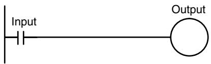
The following conditions are taken as examples for calculating the I/O response times.
Input ON delay: 10 ms (input time constant: default setting)
Overseeing time: 1 ms (includes I/O refreshing)
Instruction execution time: 14 ms
Output ON delay: 15 ms
Communications ports: Not used.
Minimum I/O Response Time
The CPM2A/CPM2C responds most quickly when it receives an input signal just prior to I/O refreshing, as shown in the illustration below.
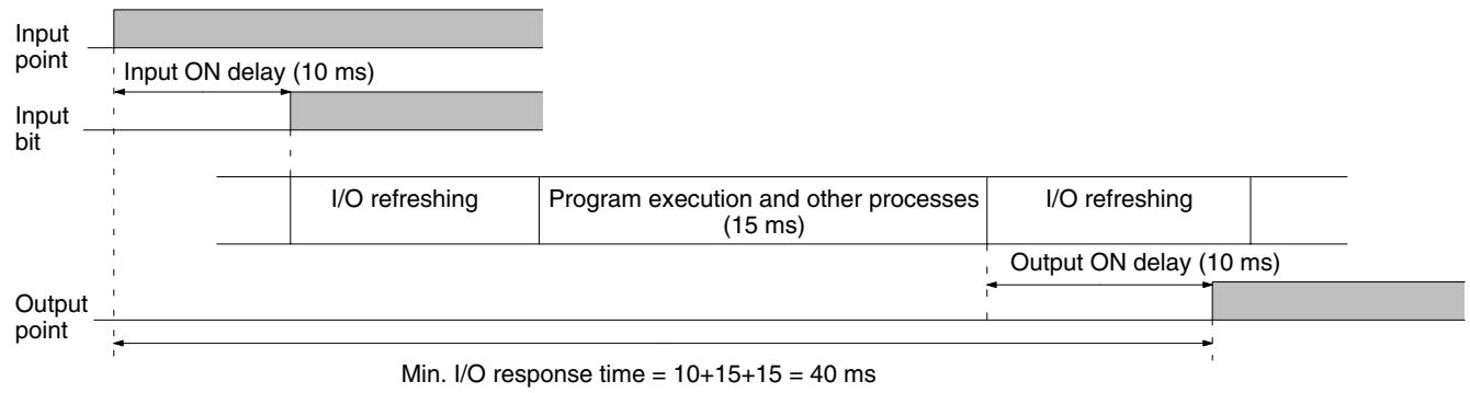
Maximum I/O Response Time
The CPM2A/CPM2C takes longest to respond when it receives the input signal just after the input refresh phase of the cycle, as shown in the illustration below. In that case, a delay of approximately one cycle will occur.
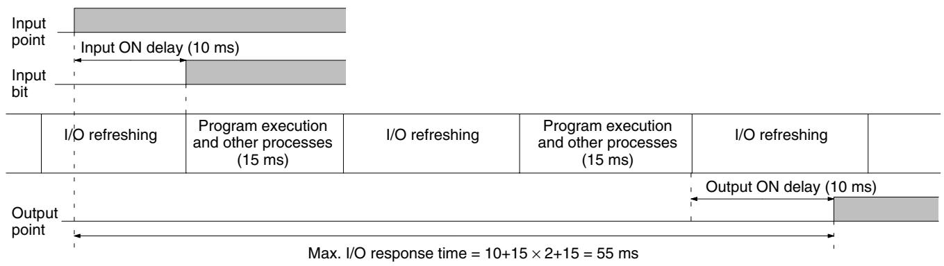
8-2-3 One-to-one PC Link I/O Response Time
When two CPM2A/CPM2Cs are linked 1:1, the I/O response time is the time required for an input executed at one of the CPM2A/CPM2Cs to be output to the other CPM2A/CPM2C by means of 1:1 PC Link communications.
The minimum and maximum I/O response times are shown here, using as an example the following instructions executed at the master and the slave. In this example, communications proceed from the master to the slave.
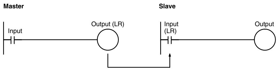
The following conditions are taken as examples for calculating the I/O response times. In CPM2A/CPM2C PCs, LR area words LR 00 to LR 15 are used in 1:1 data links and the transmission time is fixed at 21 ms.
Input ON delay: 10 ms (input time constant: default setting)
Master cycle time: 10 ms
Slave cycle time: 15 ms
Output ON delay: 15 ms
Minimum I/O Response Time The CPM2A/CPM2C responds most quickly under the following circumstances:
1, 2, 3... 1. The CPM2A/CPM2C receives an input signal just prior to the input refresh phase of the cycle.
2. The Master's communications servicing occurs just as the Master-to-Slave transmission begins.
3. The Slave's communications servicing occurs just after the transmission is completed.
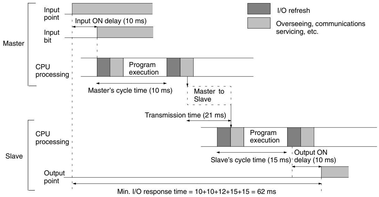
Maximum I/O Response Time The CPM2A/CPM2C takes the longest to respond under the following circumstances:
1, 2, 3... 1. The CPM2A/CPM2C receives an input signal just after the input refresh phase of the cycle.
- The Master's communications servicing just misses the Master-to-Slave transmission.
- The transmission is completed just after the Slave's communications servicing ends.
I/O Maximum Response Time Input ON response time + Master's cycle time × 2 + Transmission time × 3 + Slave's cycle time × 2 + Output ON response time
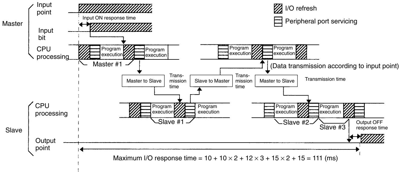
8-2-4 Interrupt Processing Time
This section explains the processing times involved from the time an interrupt is executed until the interrupt processing routine is called, and from the time an interrupt processing routine is completed until returning to the initial location. This explanation applies to input interrupts, interval timer interrupts, and high-speed counter interrupts.
1, 2, 3... 1. Source of interrupt
- Interrupt ON delay
- Wait for completion of interrupt-mask processing
- Change to interrupt processing
- Interrupt routing (CPM1A/CPM2A/CPM2C only)
- Return to initial location
The table below shows the times involved from the generation of an interrupt signal until the interrupt processing routine is called, and from when the interrupt processing routine is completed until returning to the original position.
| Item | Contents | Time |
| Interrupt ON delay | This is the delay time from the time the interrupt input bit turns ON until the time that the interrupt is executed. This delay does not affect other interrupts. | 100 μs |
| Wait for completion of interrupt-mask processing | When a process that disables (masks) the interrupt is being executed, this is the time required for that process to be completed. | See below. |
| Change to interrupt processing | This is the time it takes to change processing to the interrupt process. | 30 μs |
| Return | This is the time it takes, from execution of RET(93), to return to the processing that was interrupted. | 30 μs |
Mask Processing
Interrupts are masked during processing of the operations described below. Until the processing is completed, any interrupts will remain masked for the indicated times.
Generation and clearing of non-fatal errors:
Interrupts will be masked for up to 100~ s when a non-fatal error has been generated and the error contents are being registered in the PC, or when an error is being cleared.
Online editing:
Operation will stop and interrupts will be masked for up to 600 ms (for DM 6144 to DM 6655) when online editing is executed or the settings are changed with STUP(—) during operation. The program or PC Setup can be overwritten during that delay.
In addition to the online editing delay, interrupts may be masked for up to 170~ s for system processing.
Example Calculation
This example shows the interrupt response time (i.e., the time from when the interrupt input turns ON until the start of the interrupt processing routine) when input interrupts are used under the conditions shown below.
Minimum Response Time
Interrupt ON delay: 100 μs
Interrupt mask standby time: 0 μs
- Change-to-interrupt processing: 30 μs
Minimum response time: 130 μs
Maximum Response Time
(Except for the Online Editing of DM 6144 to DM 6655)
Interrupt ON delay: 100 μs
Interrupt mask standby time: 170 μs
- Change-to-interrupt processing: 30 μs
Maximum response time: 300 μs
In addition to the response time shown above, the time required for executing the interrupt processing routine itself and a return time of 30~ s must also be accounted for when returning to the process that was interrupted.
8-2-5 CPM2A/CPM2C Instruction Execution Times
The following table lists the execution times for CPM2A/CPM2C (including the CPM2C-S) instructions.
Basic Instructions
| Code | Mnemonic | ON execution time (μs) | Conditions (Top: min.; bottom: max.) | OFF execution time (μs) | ||
| RSET | IL | JMP | ||||
| --- | LD | 0.64 | Any | --- | ||
| --- | LD NOT | |||||
| --- | AND | 0.52 | ||||
| --- | AND NOT OR | |||||
| --- | OR NOT | |||||
| --- | AND LD | 0.26 | ||||
| --- | OR LD | |||||
| --- | OUT | 1.88 | ||||
| --- | OUT NOT | |||||
| --- | SET | 2.58 | ||||
| --- | RSET | |||||
| --- | TIM | 4.76 | Constant for SV | 7.8 | 7.6 | 2.9 |
| *DM for SV | 15.6 | 15.4 | 2.9 | |||
| --- | CNT | 4.50 | Constant for SV | 6.8 | 2.9 | 3.1 |
| *DM for SV | 14.5 | 2.9 | 3.1 | |||
Special Instructions
| Code | Mnemonic | ON execution time (μs) | Conditions (Top: min.; bottom: max.) | OFF execution time (μs) | ||
| 00 | NOP | 0.15 | Any | |||
| 01 | END | 6.2 | ||||
| 02 | IL | 1.1 | 2.1 | |||
| 03 | ILC | 1.6 | 1.6 | |||
| 04 | JMP | 0.95 | 1.8 | |||
| 05 | JME | 2.1 | 2.1 | |||
| 06 | FAL | 20.5 | 2.5 | |||
| 07 | FALS | 2.9 | 2.5 | |||
| 08 | STEP | 7.3 | 6.0 | |||
| 09 | SNXT | 5.1 | 3.6 | |||
| 10 | SFT | 10.4 | With 1-word shift register | Reset | IL | JMP |
| 9.2 | 0.98 | 0.98 | ||||
| 15.3 | With 10-word shift register | 11.9 | 1.0 | 1.0 | ||
| 39.6 | With 53-word shift register | 26.2 | 1.0 | 1.0 | ||
| 11 | KEEP | 3.2 | Any | Reset | IL | JMP |
| 3.1 | 1.2 | 1.3 | ||||
| 12 | CNTR | 10.9 | Constant for SV | Reset | IL | JMP |
| 7.9 | 5.5 | 5.6 | ||||
| 18.8 | *DM for SV | |||||
| 13 | DIFU | 5.5 | Any | Shift | IL | JMP |
| 5.1 | 4.8 | 0.96 | ||||
| 14 | DIFD | 5.3 | Any | Shift | IL | JMP |
| 5.4 | 4.7 | 0.97 | ||||
| 15 | TIMH | 9.0 | Regular execution, constant for SV | Reset | IL | JMP |
| 13.0 | 12.6 | 6.1 | ||||
| 9.6 | Interrupt execution, constant for SV | 14.4 | 14.0 | 7.5 | ||
| 9.8 | Regular execution, *DM for SV | 20.8 | 20.5 | 6.1 | ||
| 10.7 | Interrupt execution, *DM for SV | 22.2 | 22.0 | 7.5 | ||
| 16 | WSFT | 14.0 | With 1-word shift register | 2.6 | ||
| 18.6 | With 10-word shift register | |||||
| 1.15 ms | With 2,048-word shift register using *DM | |||||
| 17 | ASFT | 13.0 | Shifting 1 word | 2.6 | ||
| 22.9 | Shifting 10 words | |||||
| 1.51 ms | Shifting 2,048 words via *DM | |||||
| 20 | CMP | 7.0 | When comparing a constant to a constant | 2.6 | ||
| 8.3 | When comparing two words | |||||
| 12.1 | When comparing two *DM | |||||
| 21 | MOV | 7.8 | When transferring a constant to a word | 2.6 | ||
| 8.4 | When transferring from one word to another | |||||
| 22.8 | When transferring *DM to *DM | |||||
| 22 | MVN | 7.9 | When transferring a constant to a word | 2.6 | ||
| 8.4 | When transferring from one word to another | |||||
| 22.8 | When transferring *DM to *DM | |||||
| 23 | BIN | 15.8 | When converting a word to a word | 2.6 | ||
| 30.3 | When converting *DM to *DM | |||||
| 24 | BCD | 14.6 | When converting a word to a word | 2.6 | ||
| 29.0 | When converting *DM to *DM | |||||
| 25 | ASL | 8.6 | When shifting a word | 2.5 | ||
| 15.8 | When shifting *DM | |||||
| 26 | ASR | 8.4 | When shifting a word | 2.5 | ||
| 15.6 | When shifting *DM | |||||
| 27 | ROL | 7.3 | When rotating a word | 2.5 | ||
| 14.5 | When rotating *DM | |||||
| 28 | ROR | 7.3 | When rotating a word | 2.5 | ||
| 14.5 | When rotating *DM | |||||
| 29 | COM | 8.9 | When inverting a word | 2.5 | ||
| 16.1 | When inverting *DM | |||||
| 30 | ADD | 14.7 | Constant + constant → word | 2.6 | ||
| 16.0 | Word + word → word | |||||
| 37.6 | *DM + *DM → *DM | |||||
| 31 | SUB | 14.6 | Constant - constant → word | 2.6 | ||
| 15.8 | Word - word → word | |||||
| 37.5 | *DM - *DM → *DM | |||||
| 32 | MUL | 26.8 | Constant × constant → word | 2.6 | ||
| 28.3 | Word × word → word | |||||
| 51.0 | *DM × *DM → *DM | |||||
| 33 | DIV | 25.9 | Constant + constant → word | 2.6 | ||
| 27.5 | word + word → word | |||||
| 50.1 | *DM + *DM → *DM | |||||
| 34 | ANDW | 12.3 | Constant n constant → word | 2.6 | ||
| 13.8 | Word n word → word | |||||
| 35.4 | *DM n *DM → *DM | |||||
| Code | Mnemonic | ON execution time (μs) | Conditions (Top: min.; bottom: max.) | OFF execution time (μs) |
| 35 | ORW | 12.3 | Constant V constant → word | 2.6 |
| 13.8 | Word V word → word | |||
| 35.4 | *DM V *DM → *DM | |||
| 36 | XORW | 12.3 | Constant V constant → word | 2.6 |
| 13.8 | Word V word → word | |||
| 35.4 | *DM V *DM → *DM | |||
| 37 | XNRW | 12.3 | Constant V constant → word | 2.6 |
| 13.8 | Word V word → word | |||
| 35.5 | *DM V *DM → *DM | |||
| 38 | INC | 8.8 | When incrementing a word | 2.5 |
| 15.9 | When incrementing *DM | |||
| 39 | DEC | 8.9 | When decrementing a word | 2.5 |
| 16.1 | When decrementing *DM | |||
| 40 | STC | 3.0 | Any | 2.5 |
| 41 | CLC | 3.0 | 2.5 | |
| 46 | MSG | 9.9 | With message in words | 2.5 |
| 17.8 | With message in *DM | |||
| 47 | RXD | 71.9 | Word specification, 1 byte input | 2.6 |
| 314.5 | *DM specification, 256 bytes input | |||
| 48 | TXD | 32.4 | Word specification, 1 byte input, RS-232C | 2.6 |
| 264.5 | *DM specification, 256 bytes input, RS-232C | |||
| 27.7 | Word specification, 1 byte input, Host Link | |||
| 42.2 | *DM specification, 256 bytes input, Host Link | |||
| 50 | ADB | 14.1 | Constant + constant → word | 2.6 |
| 15.6 | Word + word → word | |||
| 37.4 | *DM + *DM → *DM | |||
| 51 | SBB | 14.4 | Constant - constant → word | 2.6 |
| 15.9 | Word - word → word | |||
| 37.7 | *DM - *DM → *DM | |||
| 52 | MLB | 16.8 | Constant × constant → word | 2.6 |
| 18.5 | Word × word → word | |||
| 41.2 | *DM × *DM → *DM | |||
| 53 | DVB | 16.9 | Constant ÷ constant → word | 2.6 |
| 18.6 | Word ÷ word → word | |||
| 41.3 | *DM ÷ *DM → *DM | |||
| 54 | ADDL | 25.3 | Word + word → word | 2.6 |
| 48.6 | *DM + *DM → *DM | |||
| 55 | SUBL | 25.3 | Word - word → word | 2.6 |
| 48.6 | *DM - *DM → *DM | |||
| 56 | MULL | 79.1 | Word × word → word | 2.6 |
| 102.1 | *DM × *DM → *DM | |||
| 57 | DIVL | 73.9 | Word ÷ word → word | 2.6 |
| 98.6 | *DM ÷ *DM → *DM | |||
| 58 | BINL | 23.9 | When converting word data to a word | 2.6 |
| 38.5 | When converting *DM to *DM | |||
| 59 | BCDL | 19.1 | When converting word data to a word | 2.6 |
| 33.7 | When converting *DM to *DM | |||
| 60 | CMPL | 14.8 | Comparing words | 2.6 |
| 30.6 | Comparing *DM | |||
| 61 | INI | 68.8 | Starting high-speed counter comparison | 2.6 |
| 12.0 | Stopping high-speed counter comparison | |||
| 43.3 | Specifying a constant when changing high-speed counter PV | |||
| 51.8 | Specifying *DM when changing high-speed counter PV | |||
| 42.8 | Specifying increment mode via constant | |||
| 50.8 | Specifying increment mode via *DM | |||
| 60.1 | Stopping pulse output | |||
| 42.7 | Specifying a constant when changing pulse output PV | |||
| 50.7 | Specifying *DM when changing pulse output PV | |||
| 17.8 | Stopping synchronized control of high-speed counter | |||
| 20.0 | Specifying a constant when changing interrupt counter PV | |||
| 27.6 | Specifying *DM when changing interrupt counter PV | |||
| 62 | PRV | 36.9 | Reading high-speed counter PV via word | 2.6 |
| 44.7 | Reading high-speed counter PV *DM | |||
| 36.6 | Specifying increment mode via word | |||
| 44.3 | Specifying increment mode via *D | |||
| 38.5 | Specifying a word when using synchronized control | |||
| 46.2 | Specifying *DM when using synchronized control | |||
| 20.2 | Reading high-speed counter pulse output status via word | |||
| 27.4 | Reading high-speed counter pulse output status via *DM | |||
| 24.4 | Reading high-speed counter read range comparison results via word | |||
| 32.4 | Reading high-speed counter read range comparison results via *DM | |||
| 39.9 | Reading pulse output PV via word | |||
| 47.8 | Reading pulse output PV via *DM | |||
| 20.1 | Reading interrupt counter PV via word | |||
| 27.1 | Reading interrupt counter PV via *DM | |||
| 63 | CTBL | 186.0 | Registering a target value comparison table and starting comparison in incrementing/decrementing pulse input mode via word | 2.6 |
| 807.5 | Registering a target value comparison table and starting comparison in incrementing/decrementing pulse input mode via *DM | |||
| 185.8 | Registering a target value comparison table and starting comparison in incrementing mode via word | |||
| 781.9 | Registering a target value comparison table and starting comparison in incrementing mode via *DM | |||
| 410.0 | Registering a range comparison table and starting comparison in incrementing/decrementing pule input mode via word | |||
| 418.9 | Registering a range comparison table and starting comparison in incrementing/decrementing pule input mode via *DM | |||
| 380.6 | Registering a range comparison table and starting comparison in incrementing mode via word | |||
| 399.7 | Registering a range comparison table and starting comparison in incrementing mode via *DM | |||
| 183.4 | Only registering a target value comparison table in incrementing/decrementing pulse input mode via word | |||
| 810.3 | Only registering a target value comparison table in incrementing/decrementing pulse input mode via *DM | |||
| 182.4 | Only registering a target value comparison table in incrementing mode via word | |||
| 776.3 | Only registering a target value comparison table in incrementing mode via *DM | |||
| 351.0 | Only registering a range comparison table in incrementing/decrementing pule input mode via word | |||
| 359.1 | Only registering a range comparison table in incrementing/decrementing pule input mode via *DM | |||
| 331.2 | Only registering a range comparison table in incrementing mode via word | |||
| 335.9 | Only registering a range comparison table in incrementing mode via *DM | |||
| 64 | SPED | 44.6 | Specifying a constant in independent mode | 2.6 |
| 53.8 | Specifying *DM in independent mode | |||
| 42.9 | Specifying a constant in continuous pulse out-put mode | |||
| 52.0 | Specifying *DM in continuous pulse output mode | |||
| 34.1 | Specifying a word when changing output fre-quency | |||
| 39.8 | Specifying *DM when changing output fre-quency | |||
| 65 | PULS | 38.4 | Specifying a relative pulse for the set pulse output via a word | 2.6 |
| 46.6 | Specifying a relative pulse for the set pulse output via *DM | |||
| 40.0 | Specifying an absolute pulse for the set pulse output via a word | |||
| 48.1 | Specifying an absolute pulse for the set pulse output via *DM | |||
| 66 | SCL | 37.9 | Specifying a parameter word; constant to word | 2.6 |
| 39.2 | Specifying a parameter word; word to word | |||
| 59.9 | Specifying a parameter *DM; *DM to *DM | |||
| 67 | BCNT | 24.9 | When counting 1 word | 2.6 |
| 4.32 ms | When counting 2,048 words via *DM | |||
| 68 | BCMP | 35.3 | Comparing constant, results to word | 2.6 |
| 38.3 | Comparing word, results to word | |||
| 58.1 | Comparing *DM, results to *DM | |||
| 69 | STIM | 25.7 | Constant-set one-shot interrupt start | 2.6 |
| 47.8 | *DM-set one-shot interrupt start | |||
| 25.9 | Constant-set scheduled interrupt start | |||
| 47.8 | *DM-set scheduled interrupt start | |||
| 34.0 | Constant-set timer read | |||
| 46.4 | *DM-set timer read | |||
| 10.6 | Stopping timer | |||
| 70 | XFER | 21.3 | When transferring a constant to a word | 2.6 |
| 23.8 | When transferring a word to a word | |||
| 1.52 ms | When transferring 2,048 words using *DM | |||
| 71 | BSET | 13.8 | When setting a constant to a word | 2.6 |
| 14.3 | When setting a word to a word | |||
| 971.1 | When setting *DM to 2,048 words | |||
| 73 | XCHG | 14.5 | Word → word | 2.6 |
| 29.3 | *DM → *DM | |||
| 74 | SLD | 12.3 | Shifting 1 word | 2.6 |
| 23.9 | Shifting 10 words | |||
| 2.83 ms | Shifting 2,048 words using *DM | |||
| 75 | SRD | 12.3 | Shifting 1 word | 2.6 |
| 23.9 | Shifting 10 words | |||
| 2.83 ms | Shifting 2,048 words using *DM | |||
| 76 | MLPX | 16.8 | When decoding word to word | 2.6 |
| 46.1 | When decoding *DM to *DM | |||
| 77 | DMPX | 19.7 | When encoding word to word | 2.6 |
| 52.1 | When encoding *DM to *DM | |||
| 78 | SDEC | 19.8 | When decoding word to word | 2.6 |
| 48.3 | When decoding *DM to *DM | |||
| 80 | DIST | 18.7 | When setting a constant to a word + a word | 2.6 |
| 20.2 | When setting a word to a word + a word | |||
| 43.1 | When setting *DM to *DM + *DM | |||
| 31.0 | When setting a constant to a stack | |||
| 32.7 | When setting a word to a stack | |||
| 55.9 | When setting *DM to a stack via *DM | |||
| 81 | COLL | 21.5 | When setting a constant + a word to a word | 2.6 |
| 21.9 | When setting a word + a word to a word | |||
| 42.5 | When setting *DM + *DM to *DM | |||
| 31.5 | When setting a word + constant to FIFO stack | |||
| 32.0 | When setting a word + word to FIFO stack | |||
| 784.7 | When setting a *DM + *DM to FIFO stack via *DM | |||
| 33.6 | When setting a word + constant to LIFO stack | |||
| 34.0 | When setting a word + word to LIFO stack | |||
| 57.1 | When setting a *DM + *DM to LIFO stack via *DM | |||
| 82 | MOVB | 17.3 | When transferring a constant to a word | 2.6 |
| 18.0 | When transferring from one word to another | |||
| 41.7 | When transferring *DM to *DM | |||
| 83 | MOVD | 13.8 | When transferring a constant to a word | 2.6 |
| 16.2 | When transferring from one word to another | |||
| 38.1 | When transferring *DM to *DM | |||
| 84 | SFTR | 22.8 | Shifting 1 word | 2.6 |
| 24.3 | Shifting 10 words | |||
| 1.15 ms | Shifting 2,048 words using *DM | |||
| 85 | TCMP | 27.5 | Comparing constant to word-set table | 2.6 |
| 28.0 | Comparing word to word-set table | |||
| 48.3 | Comparing *DM to *DM-set table | |||
| 86 | ASC | 19.1 | Word → word | 2.6 |
| 52.2 | *DM → *DM | |||
| 89 | INT | 22.1 | Set masks via word | 2.6 |
| 30.1 | Set masks via *DM | |||
| 18.4 | Clear interrupts via word | |||
| 26.4 | Clear interrupts via *DM | |||
| 17.2 | Read mask status via word | |||
| 24.1 | Read mask status via *DM | |||
| 23.1 | Change counter SV via word | |||
| 31.1 | Change counter SV via *DM | |||
| 10.7 | Mask all interrupts via word | |||
| 10.7 | Mask all interrupts via *DM | |||
| 11.0 | Clear all interrupts via word | |||
| 11.0 | Clear all interrupts via *DM | |||
| 91 | SBS | 10.8 | Any | 2.6 |
| 92 | SBN | --- | 0.76 | |
| 93 | RET | 6.2 | 1.0 | |
| 97 | IORF | 16.8 | Refreshing IR 000 | 2.8 |
| 130.7 | Refreshing one input word | |||
| 110.7 | Refreshing one output word | |||
| 99 | MCRO | 26.1 | With word-set I/O operands | 2.6 |
| 42.3 | With *DM-set I/O operands |
Expansion Instructions without Default Function Codes
| Code | Mnemonic | ON execution time (μs) | Conditions (Top: min.; bottom: max.) | OFF execution time (μs) |
| --- | ACC | 66.5 | When specifying a word in independent mode and CW/CCW mode | 2.6 |
| 92.1 | When specifying *DM in independent mode and CW/CCW mode | |||
| 66.2 | When specifying a word in independent mode and Feed/Dir mode | |||
| 92.2 | When specifying *DM in independent mode and Feed/Dir mode | |||
| 65.5 | When executing the word designation in CW continuous mode and CW/CCW mode | |||
| 75.0 | When executing the *DM designation in CW continuous mode and CW/CCW mode | |||
| 45.4 | When changing the word designation in CW continuous mode and CW/CCW mode | |||
| 53.8 | When changing the *DM designation in CW continuous mode and CW/CCW mode | |||
| 65.5 | When executing the word designation in CCW continuous mode and CW/CCW mode | |||
| 75.0 | When executing the *DM designation in CCW continuous mode and CW/CCW mode | |||
| 45.5 | When changing the word designation in CCW continuous mode and CW/CCW mode | |||
| 53.6 | When changing the *DM designation in CCW continuous mode and CW/CCW mode | |||
| 65.0 | When executing the word designation in CW continuous mode and Feed/Dir mode | |||
| 74.5 | When executing the *DM designation in CW continuous mode and Feed/Dir mode | |||
| 45.4 | When changing the word designation in CW continuous mode and Feed/Dir mode | |||
| 53.5 | When changing the *DM designation in CW continuous mode and Feed/Dir mode | |||
| 65.4 | When executing the word designation in CCW continuous mode and Feed/Dir mode | |||
| 74.8 | When executing the *DM designation in CCW continuous mode and Feed/Dir mode | |||
| 45.5 | When changing the word designation in CCW continuous mode and Feed/Dir mode | |||
| 53.6 | When changing the *DM designation in CCW continuous mode and Feed/Dir mode | |||
| --- | AVG | 23.2 | Average for 1 cycle (constant designation) | 3.2 |
| 23.9 | Average for 1 cycle (word designation) | |||
| 84.2 | Average for 64 cycles (*DM designation) | |||
| --- | FCS | 27.6 | Adding one word and outputting to word | 2.6 |
| 592.3 | Adding 999 words and outputting to *DM | |||
| --- | HEX | 25.8 | Word → Word | 2.6 |
| 72.2 | *DM → *DM | |||
| --- | HMS | 30.7 | When converting word to word | 2.6 |
| 45.0 | When converting *DM to *DM | |||
| --- | MAX | 21.9 | Searching one word and outputting to word | 2.6 |
| 713.9 | Searching 999 words and outputting to *DM | |||
| --- | MIN | 21.9 | Searching one word and outputting to word | 2.6 |
| 713.9 | Searching 999 words and outputting to *DM |
| Code | Mnemonic | ON execution time (μs) | Conditions (Top: min.; bottom: max.) | OFF execution time (μs) | ||
| --- | NEG | 12.0 | Converting constant to word | 3.0 | ||
| 12.8 | Converting word to word | |||||
| 28.3 | Converting *DM to *DM | |||||
| --- | PID | 392.5 | Initializing word to word | 3.3 | ||
| 418.8 | Initializing *DM to *DM | |||||
| 29.3 | Sampling word to word | |||||
| 58.7 | Sampling *DM to *DM | |||||
| --- | PWM | 30.3 | Constant for pulse width ratio | 2.6 | ||
| 43.4 | Word for pulse width ratio | |||||
| 46.0 | *DM for pulse width ratio | |||||
| --- | SCL2 | 35.1 | Parameter word designation, word to word | 2.6 | ||
| 59.3 | Parameter *DM designation, *DM to *DM | |||||
| --- | SCL3 | 37.1 | Parameter word designation, word to word | 2.6 | ||
| 62.3 | Parameter *DM designation, *DM to *DM | |||||
| --- | SEC | 29.8 | Converting from word to word | 2.6 | ||
| 44.0 | Converting from *DM to *DM | |||||
| --- | SRCH | 28.9 | Searching one word and outputting to a word | 2.6 | ||
| 1.40 ms | *DM specification, searching 2,048 words and outputting to *DM | |||||
| --- | STUP | 3.42 ms | Constant specification, executed first scan | 2.6 | ||
| 34.1 | Constant specification, executed second scan or later | |||||
| 3.44 ms | *DM specification, executed first scan | |||||
| 39.8 | *DM specification, executed second scan or later | |||||
| --- | SUM | 22.8 | Word added and output to word | 2.6 | ||
| 1.44 ms | *DM specification, 999 bytes added and output to *DM | |||||
| --- | SYNC | 34.6 | Constant ratio specification, when executed | 2.6 | ||
| 35.3 | Word ratio specification, when executed | |||||
| 42.5 | *DM ratio specification, when executed | |||||
| 25.3 | Word ratio specification, when changed | |||||
| 32.6 | *DM ratio specification, when changed | |||||
| --- | TIML | 12.8 | Normal execution, constant specification | Reset | IL | JMP |
| 17.9 | 17.5 | 8.1 | ||||
| 13.5 | Interrupt execution, constant specification | 25.7 | 25.5 | 8.1 | ||
| --- | TMHH | 12.3 | Normal execution, constant specification | Reset | IL | JMP |
| 15.6 | 15.1 | 7.4 | ||||
| 12.7 | Interrupt execution, constant specification | 17.2 | 16.9 | 9.1 | ||
| 12.7 | Normal execution, *DM specification | 23.6 | 23.3 | 7.7 | ||
| 13.6 | Interrupt execution, *DM specification | 25.1 | 24.7 | 9.1 | ||
| --- | ZCP | 9.4 | Comparing a constant to a constant range and output to word | 2.6 | ||
| 11.8 | Comparing a word to a word range and output to word | |||||
| 33.4 | Comparing *DM to *DM and output to *DM | |||||
| --- | ZCPL | 19.5 | Comparing a word to a word range | 2.6 | ||
| 45.2 | Comparing *DM to *DM | |||||
8-3 SRM1(-V2) Cycle Time and I/O Response Time
8-3-1 The SRM1(-V2) Cycle
The overall flow of SRM1(-V2) operation is as shown in the following flowchart.
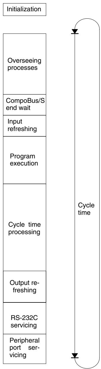
Note 1. The cycle time can be read using Programming Devices.
- Cycle time maximum and current cycle time are stored in AR 14 and AR 15.
- Change to processing will cause cycle times to change therefore the calculated values and actual values (for cycle time) will no always match.
8-3-2 SRM1(-V2) Cycle Time
The processes involved in a single SRM1(-V2) cycle are shown in the following table, and their respective processing times are explained.
| Process | Content | Time requirements |
| Overseeing | Setting cycle watchdog timer, UM check, etc. | 0.18 ms |
| CompoBus/S end wait | Waiting for CompoBus/S processing to finish | CompoBus/S communications re-sponse time – Overseeing time – RS-232C port servicing time – periph-eral port servicing time |
| Input refreshing | Input information is read to input bits. | 0.02 ms |
| Program execution | User program is executed.Refer to 8-3-6 SRM1(-V2) Instruction Execution Times. | Total time for executing instructions.(Varies according to content of user's program.) |
| Cycle time calculation | Standby until set time, when minimum cycle time is set in DM 6619 of PC Setup.Calculation of cycle time. | Almost instantaneous, except for standby processing. |
| Output refreshing | Output information (results of executing program) is written to output bits.CompoBus/S communications are started. | 0.05 ms |
| RS-232C port servicing | Devices connected to RS-232C port serviced. | 5% or less of cycle time, but always between 0.55 and 131 ms(Set in DM 6616.) |
| Peripheral port servicing | Devices connected to peripheral port serviced. | 5% or less of cycle time, but always between 0.55 and 131 ms(Set in DM 6617.) |
Minimum Cycle Time
In SRM1(-V2) PCs, CompoBus/S communications are started after the output refresh is completed. As a result, when the overseeing time plus the RS-232C port servicing time plus the peripheral port servicing time is shorter than the CompoBus/S communications response time, processing is placed on stand-by until CompoBus/S communications are completed.
The minimum cycle time therefore is the the CompoBus/S communications response time plus the program execution time plus the input refresh time plus the output refresh time. The CompoBus/S communications response time depends on the "maximum number of nodes" and "communications mode" settings, as follows:
| Max. number of nodes | Communications mode | CompoBus/S response time |
| 32 | High-speed mode | 0.8 ms |
| Long-distance mode | 6.0 ms | |
| 16 | High-speed mode | 0.5 ms |
| Long-distance mode | 4.0 ms |
Note The maximum number of nodes and communications mode are set in the PC Setup (DM 6603).
Cycle Time and Operations
The effects of the cycle time on SRM1(-V2) operations are as shown below. When a long cycle time is affecting operation, either reduce the cycle time or improve responsiveness with interrupt programs.
| Cycle time | Operation conditions |
| 10 ms or longer | TIMH(15) may be inaccurate when TC 004 through TC 127 are used (operation will be normal for TC 000 through TC 003). |
| 20 ms or longer | Programming using the 0.02-second Clock Bit (SR 25401) may be inaccurate. |
| 100 ms or longer | TIM may be inaccurate. Programming using the 0.1-second Clock Bit (SR 25500) may be inaccurate. A CYCLE TIME OVER error is generated (SR 25309 will turn ON). See note 1. |
| 120 ms or longer | The FALS 9F monitoring time SV is exceeded. A system error (FALS 9F) is generated, and operation stops. See note 2. |
| 200 ms or longer | Programming using the 0.2-second Clock Bit (SR 25501) may be inaccurate. |
Note 1. The PC Setup (DM 6655) can be used to disable detection of CYCLE TIME OVER error.
2. The cycle monitoring time can be changed in the PC Setup (DM 6618).
Cycle Time Example
The following is an example of a cycle time calculation.
The operating conditions are assumed to be as follows:
User's program:500 instructions (consists of only LD and OUT)
Cycle time: Variable (no minimum set)
RS-232C port: Not used.
Max. nodes: 32 nodes and high-speed communications mode (CompoBus/S communication response time = 0.8 ms)
Peripheral: 0.7 ms
The average processing time for a single instruction in the user's program is assumed to be 1.16 s . The cycle times are as shown in the following table.
| Process | Calculation method | Peripheral port used | Peripheral port not used |
| 1. Overseeing | Fixed | 0.18 ms | 0.18 ms |
| 2. CompoBus/S end wait | See previous page. | 0.00 ms | 0.62 ms |
| 3. Input refresh | Fixed | 0.02 ms | 0.02 ms |
| 4. Program execution | 1.16 × 500 (μs) | 0.8 ms | 0.8 ms |
| 5. Cycle time calculation | Negligible | 0.00 ms | 0.00 ms |
| 6. Output refresh | 0.01 × 1 + 0.005 × 1 (μs) | 0.05 ms | 0.05 ms |
| 7. RS-232C port servicing | Not required | 0.00 ms | 0.00 ms |
| 8. Peripheral port servicing | 5% of cycle time | 0.7 ms | 0.00 ms |
| Cycle time | (1) + (2) + (3) + ...+ (8) | 1.75 ms | 1.67 ms |
Note 1. The cycle time can be read from the PC via a Programming Device.
- The maximum and current cycle time are stored in AR 14 and AR 15.
- The cycle time can vary with actual operating conditions and will not necessarily agree precisely with the calculated value.
- When the peripheral port is used, there is no CompoBus/S end wait time as it is always 0 or less.
- CompoBus/S end wait time = 0.8 - 0.18 - 0 - 0 = 0.62 (CompoBus/S communication response time - Overseeing - RS-232C port servicing time - peripheral port servicing time.
8-3-3 I/O Response Time
The I/O response time is the time it takes after an input signal has been received (i.e., after an input bit has turned ON) for the PC to check and process the information and to output a control signal (i.e., to output the result of the processing to an output bit).
CompoBus/S communications are started when the SRM1(-V2) input refresh finishes. The ON/OFF status is read from the Input Terminals during the input refresh and the ON/OFF status is output to the Output Terminal during the output refresh. Accordingly, the SRM1(-V2) I/O response time varies according to the cycle time and CompoBus/S communications cycle status or I/O timing.
Example calculations of the I/O response time are provided next.
Minimum I/O Response Time
Minimum I/O response time =
Input ON delay + Output ON delay + CompoBus/S communications cycle time + SRM1(-V2) cycle time
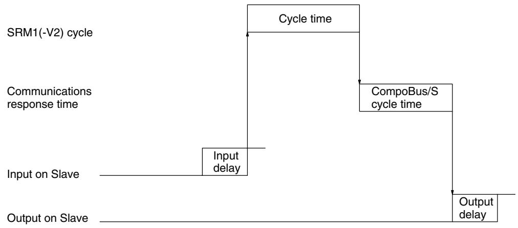
Maximum I/O Response Time
Maximum I/O response time =
Input ON delay + Output ON delay + CompoBus/S communications cycle time + SRM1(-V2) cycle time x 2

8-3-4 One-to-one PC Link I/O Response Time
When two SRM1s are linked in a 1:1 PC Link, the I/O response time is the time required for an input executed at one of the SRM1s to be output to the other SRM1 by means of 1:1 PC Link communications.
Minimum I/O Response Time
The SRM1(-V2) responds most quickly under the following circumstances:
1, 2, 3...
- The SRM1(-V2) receives an input signal just prior to the I/O refresh phase of the cycle.
- The Master's communications servicing occurs just as the Master-to-Slave transmission begins.
- The Slave's communications servicing occurs just after the transmission is completed.
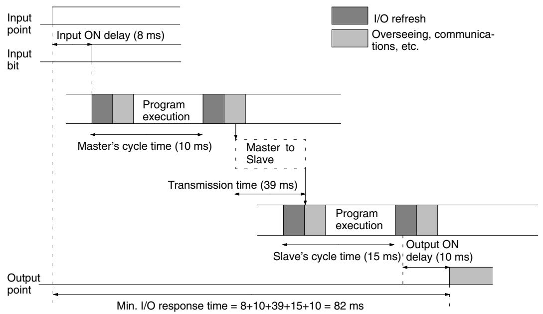
Maximum I/O Response Time
The SRM1(-V2) takes the longest to respond under the following circumstances:
1,2,3...
- The SRM1(-V2) receives an input signal just after the I/O refresh phase of the cycle.
-
The Master's communications servicing just misses the Master-to-Slave transmission.
-
The transmission is completed just after the Slave's communications servicing ends.
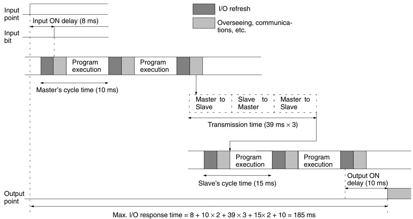
8-3-5 Interrupt Processing Time
This section explains the processing times involved from the time an interrupt is executed until the interrupt processing routine is called, and from the time an interrupt processing routine is completed until returning to the initial location. This explanation applies to input, interval timer interrupts.
1, 2, 3... 1. Source of interrupt
2. Wait for completion of interrupt-mask processing
3. Change to interrupt processing
4. Interrupt routing (CPM1A only)
5. Return to initial location
The table below shows the times involved from the generation of an interrupt signal until the interrupt processing routine is called, and from when the interrupt processing routine is completed until returning to the original position.
| Item | Contents | Time |
| Wait for completion of interrupt-mask processing | This is the time during which interrupts are waiting until processing has been completed. This situation occurs when a mask processes is executed. It is explained below in more detail. | See below. |
| Change to interrupt processing | This is the time it takes to change processing to an interrupt. | 15 μs |
| Return | This is the time it takes, from execution of RET(93), to return to the processing that was interrupted. | 15 μs |
Mask Processing
Interrupts are masked during processing of the operations described below. Until the processing is completed, any interrupts will remain masked for the indicated times.
Generation and clearing of non-fatal errors:
When a non-fatal error is generated and the error contents are registered at the SRM1(-V2), or when an error is being cleared, interrupts will be masked for a maximum of 100 s until the processing has been completed.
Online editing:
Interrupts will be masked for a maximum of 600 ms (i.e.: editing DM 6144 to DM 6655) when online editing is executed during operation. In addition, the system processing may have to wait for a maximum of 170~ s during this processing.
8-3-6 SRM1(-V2) Instruction Execution Times
The following table lists the execution times for SRM1(-V2) instructions.
Basic Instructions
| Code | Mnemonic | ON execution time (μs) | Conditions (Top: min.; bottom: max.) | OFF execution time (μs) | ||
| RSET | IL | JMP | ||||
| --- | LD | 0.97 | Any | --- | ||
| --- | LD NOT | 0.97 | ||||
| --- | AND | 0.77 | ||||
| --- | OR | 0.78 | Any | --- | ||
| --- | OR NOT | 0.39 | Any | --- | ||
| --- | AND LD | 2.2 | ||||
| --- | OUT | 2.2 | ||||
| --- | OUT NOT | |||||
| --- | SET | 2.7 | ||||
| --- | RSET | 2.8 | ||||
| --- | TIM | 5.7 | Constant for SV | 9.3 | 9.1 | 3.5 |
| *DM for SV | 17.4 | 17.2 | 3.5 | |||
| --- | CNT | 6.6 | Constant for SV | 8.0 | 3.6 | 3.8 |
| *DM for SV | 16.3 | 3.6 | 3.8 | |||
Special Instructions and Expansion Instructions
| Code | Mnemonic | ON execution time (μs) | Conditions (Top: min.; bottom: max.) | OFF execution time (μs) | ||
| 00 | NOP | 0.20 | Any | |||
| 01 | END | 4.8 | ||||
| 02 | IL | 2.5 | 1.4 | |||
| 03 | ILC | 1.9 | 1.9 | |||
| 04 | JMP | 2.2 | 1.3 | |||
| 05 | JME | 2.5 | 2.5 | |||
| 06 | FAL | 18.4 | 2.9 | |||
| 07 | FALS | 3.6 | 2.9 | |||
| 08 | STEP | 10.7 | 9.0 | |||
| 09 | SNXT | 5.9 | 4.1 | |||
| 10 | SFT | 14.5 | With 1-word shift register | Reset | IL | JMP |
| 11.0 | 1.4 | 1.4 | ||||
| 21.0 | With 10-word shift register | 14.9 | 1.4 | 1.4 | ||
| 49.1 | With 100-word shift register | 30.8 | 1.4 | 1.4 | ||
| 11 | KEEP | 3.0 | Any | Reset | IL | JMP |
| 3.4 | 1.6 | 1.7 | ||||
| 12 | CNTR | 14.8 | Constant for SV | Reset | IL | JMP |
| 9.1 | 6.6 | 6.5 | ||||
| 23.2 | *DM for SV | |||||
| 13 | DIFU | 6.7 | Any | Shift | IL | JMP |
| 5.8 | 5.2 | 1.3 | ||||
| 14 | DIFD | 6.4 | Any | Shift | IL | JMP |
| 5.8 | 5.7 | 1.3 | ||||
| 15 | TIMH | 10.3 | Regular execution, constant for SV | Reset | IL | JMP |
| 14.1 | 13.9 | 7.0 | ||||
| 10.9 | Interrupt execution, constant for SV | 15.6 | 15.4 | 8.5 | ||
| 10.3 | Regular execution, *DM for SV | 22.8 | 22.1 | 7.0 | ||
| 10.9 | Interrupt execution, *DM for SV | 23.9 | 23.6 | 8.5 | ||
| 16 | WSFT | 16.2 | With 1-word shift register | 2.9 | ||
| 23.0 | With 10-word shift register | |||||
| 712.3 | With 1,024-word shift register using *DM | |||||
| 17 | ASFT* | 18.6 | Shifting a word | 3.0 | ||
| 25.9 | Shifting 10 words | |||||
| 865.7 | Shifting 1,023 words via *DM | |||||
| 20 | CMP | 9.1 | When comparing a constant to a word | 3.0 | ||
| 9.9 | When comparing two words | |||||
| 25.6 | When comparing two *DM | |||||
| 21 | MOV | 9.1 | When transferring a constant to a word | 3.0 | ||
| 9.5 | When transferring from one word to another | |||||
| 24.9 | When transferring *DM to *DM | |||||
| 22 | MVN | 9.3 | When transferring a constant to a word | 3.0 | ||
| 9.8 | When transferring from one word to another | |||||
| 25.1 | When transferring *DM to *DM | |||||
| 23 | BIN | 17.2 | When converting a word to a word | 3.0 | ||
| 32.0 | When converting *DM to *DM | |||||
| 24 | BCD | 15.8 | When converting a word to a word | 3.0 | ||
| 30.6 | When converting *DM to *DM | |||||
| 25 | ASL | 9.9 | When shifting a word | 2.9 | ||
| 17.3 | When shifting *DM | |||||
| 26 | ASR | 9.7 | When shifting a word | 3.0 | ||
| 17.2 | When shifting *DM | |||||
| 27 | ROL | 8.5 | When rotating a word | 2.9 | ||
| 16.1 | When rotating *DM | |||||
| 28 | ROR | 8.5 | When rotating a word | 2.9 | ||
| 16.1 | When rotating *DM | |||||
| 29 | COM | 10.5 | When inverting a word | 3.0 | ||
| 17.7 | When inverting *DM | |||||
| 30 | ADD | 15.9 | Constant + word → word | 3.1 | ||
| 16.4 | Word + word → word | |||||
| 39.5 | *DM + *DM → *DM | |||||
| 31 | SUB | 15.6 | Constant - word → word | 3.0 | ||
| 16.3 | Word - word → word | |||||
| 38.6 | *DM - *DM → *DM | |||||
| 32 | MUL | 29.7 | Constant × word → word | 3.0 | ||
| 28.5 | Word × word → word | |||||
| 51.6 | *DM × *DM → *DM | |||||
| 33 | DIV | 27.2 | Word ÷ constant → word | 2.9 | ||
| 28.5 | word ÷ word → word | |||||
| 53.1 | *DM ÷ *DM → *DM | |||||
| Code | Mnemonic | ON execution time (μs) | Conditions (Top: min.; bottom: max.) | OFF execution time (μs) |
| 34 | ANDW | 14.3 | Constant n word → word | 2.9 |
| 15.2 | Word n word → word | |||
| 37.3 | *DM n *DM → *DM | |||
| 35 | ORW | 14.3 | Constant V word → word | 2.9 |
| 15.2 | Word V word → word | |||
| 37.3 | *DM V *DM → *DM | |||
| 36 | XORW | 14.3 | Constant V word → word | 2.9 |
| 15.2 | Word V word → word | |||
| 37.3 | *DM V *DM → *DM | |||
| 37 | XNRW | 14.3 | Constant V word → word | 2.9 |
| 15.2 | Word V word → word | |||
| 37.3 | *DM V *DM → *DM | |||
| 38 | INC | 9.9 | When incrementing a word | 2.9 |
| 17.3 | When incrementing *DM | |||
| 39 | DEC | 10.2 | When decrementing a word | 2.9 |
| 17.4 | When decrementing *DM | |||
| 40 | STC | 3.5 | Any | 2.9 |
| 41 | CLC | 3.0 | 2.9 | |
| 46 | MSG | 11.3 | With message in words | 2.9 |
| 19.4 | With message in *DM | |||
| 47 | RXD* | 39.1 | Word specification, 1 byte input | 2.9 |
| 116.8 | *DM specification, 256 bytes input | |||
| 48 | TXD* | 31.3 | Word specification, 1 byte input (RS-232C) | 2.9 |
| 266.5 | *DM specification, 256 bytes input (RS-232C) | |||
| 26.7 | Word specification, 1 byte input (Host Link) | |||
| 34.0 | *DM specification, 256 bytes input (Host Link) | |||
| 50 | ADB | 16.8 | Constant + word → word | 3.0 |
| 17.6 | Word + word → word | |||
| 39.9 | *DM + *DM → *DM | |||
| 51 | SBB | 17.0 | Constant - word → word | 3.0 |
| 17.8 | Word - word → word | |||
| 40.2 | *DM - *DM → *DM | |||
| 52 | MLB | 19.1 | Constant × word → word | 3.0 |
| 20.1 | Word × word → word | |||
| 43.5 | *DM × *DM → *DM | |||
| 53 | DVB | 19.5 | Word + constant → word | 3.0 |
| 20.4 | Word + word → word | |||
| 43.7 | *DM + *DM → *DM | |||
| 54 | ADDL | 26.7 | Word + word → word | 3.0 |
| 49.9 | *DM + *DM → *DM | |||
| 55 | SUBL | 26.8 | Word - word → word | 3.0 |
| 49.9 | *DM - *DM → *DM | |||
| 56 | MULL | 81.4 | Word × word → word | 3.0 |
| 106.2 | *DM × *DM → *DM | |||
| 57 | DIVL | 76.9 | Word + word → word | 3.0 |
| 101.8 | *DM + *DM → *DM | |||
| 60 | CMPL | 16.9 | Comparing words | 2.9 |
| 32.9 | Comparing *DM | |||
| 66 | SCL* | 69.5 | Word specification | 3.0 |
| 91.5 | *DM specification | |||
| 67 | BCNT* | 26.9 | Counting a word | 3.0 |
| 2.29 ms | Counting 6,656 words via *DM | |||
| 68 | BCMP* | 41.4 | Comparing constant, results to word | 3.0 |
| 41.9 | Comparing word, results to word | |||
| 64.5 | Comparing *DM, results to *DM | |||
| 69 | STIM* | 34.7 | Word specification, one-shot timer start | 3.0 |
| 49.5 | *DM specification, one-shot timer start | |||
| 35.3 | Word specification, scheduled interrupt start | |||
| 50.0 | *DM specification, scheduled interrupt start | |||
| 33.9 | Words specification, timer read | |||
| 49.5 | *DM specification timer read | |||
| 11.4 | Word specification, timer stop | |||
| 70 | XFER | 22.9 | When transferring a constant to a word | 3.0 |
| 24.0 | When transferring a word to a word | |||
| 902.0 | When transferring 1,024 words using *DM | |||
| 71 | BSET | 15.2 | When setting a constant to 1 word | 3.0 |
| 15.7 | When setting word constant to 10 words | |||
| 565.2 | When setting *DM to 1,024 words | |||
| 73 | XCHG | 16.2 | Word → word | 3.1 |
| 31.5 | *DM → *DM | |||
| 74 | SLD | 13.6 | Shifting 1 word | 3.0 |
| 26.7 | Shifting 10 word | |||
| 1.54 ms | Shifting 1024 words using *DM | |||
| 75 | SRD | 13.6 | Shifting 1 word | 3.0 |
| 26.6 | Shifting 10 word | |||
| 1.54 ms | Shifting 1,024 words using *DM | |||
| 76 | MLPX | 25.5 | When decoding word to word | 3.0 |
| 48.9 | When decoding *DM to *DM | |||
| 77 | DMPX | 35.1 | When encoding word to word | 3.0 |
| 58.1 | When encoding *DM to *DM | |||
| 78 | SDEC | 26.8 | When decoding word to word | 2.9 |
| 49.9 | When decoding *DM to *DM | |||
| 80 | DIST | 21.3 | When setting a constant to a word + a word | 3.0 |
| 21.9 | When setting a word to a word + a word | |||
| 45.7 | When setting *DM to *DM + *DM | |||
| 34.3 | When setting a constant to a stack | |||
| 35.3 | When setting a word to a stack | |||
| 59.3 | When setting *DM to a stack via *DM | |||
| 81 | COLL | 21.4 | When setting a constant + a word to a word | 3.0 |
| 21.8 | When setting a word + a word to a word | |||
| 44.9 | When setting *DM + *DM to *DM | |||
| 34.0 | When setting a word + constant to FIFO stack | |||
| 33.9 | When setting a word + word to FIFO stack | |||
| 892.0 | When setting a *DM + *DM to FIFO stack via *DM | |||
| 35.4 | When setting a word + constant to LIFO stack | |||
| 36.1 | When setting a word + word to LIFO stack | |||
| 60.5 | When setting a *DM + *DM to LIFO stack via *DM | |||
| 82 | MOVB | 18.2 | When transferring a constant to a word | 3.0 |
| 19.0 | When transferring one word to another | |||
| 42.1 | When transferring *DM to *DM | |||
| 83 | MOVD | 16.3 | When transferring a constant to a word | 2.9 |
| 17.6 | When transferring one word to another | |||
| 39.9 | When transferring *DM to *DM | |||
| 84 | SFTR | 21.0 | Shifting 1 word | 3.0 |
| 26.9 | Shifting 10 word | |||
| 718.5 | Shifting 1,024 words using *DM | |||
| 85 | TCMP | 30.0 | Comparing constant to word-set table | 3.0 |
| 30.7 | Comparing word to word-set table | |||
| 53.1 | Comparing *DM to *DM-set table | |||
| 86 | ASC | 30.0 | Word → word | 3.0 |
| 53.7 | *DM → *DM | |||
| 91 | SBS | 13.2 | Any | 3.0 |
| 92 | SBN | --- | 1.3 | |
| 93 | RET | 7.8 | 1.3 | |
| 99 | MCRO | 26.8 | With word-set I/O operands | 3.0 |
| 43.5 | With *DM-set I/O operands |
Note Those instructions marked with an asterisk are expansion instructions.
Expansion Instructions without Default Function Codes
| Code | Mnemonic | ON execution time (μs) | Conditions (Top: min.; bottom: max.) | OFF execution time (μs) |
| --- | FCS | 23.4 | Adding one word and outputting to word | 3.0 |
| 643.7 | Adding 999 words and outputting to *DM | |||
| --- | HEX | 43.6 | DM → DM | 3.0 |
| 73.5 | *DM → *DM | |||
| --- | NEG | 46.0 | Converting constant to word | 3.0 |
| 48.0 | Converting word to word | |||
| 65.5 | Converting *DM to *DM | |||
| --- | PID | 420.0 | Initializing word to word | 3.0 |
| 452.0 | Initializing *DM to *DM | |||
| 63.0 | Sampling word to word | |||
| 84.5 | Sampling *DM to *DM | |||
| --- | STUP | 51.2 | Transferring constant to word | 3.0 |
| 58.2 | Transferring word to word | |||
| --- | ZCP | 45.0 | Comparing a word to a constant range | 3.0 |
| 46.5 | Comparing a word to a word range | |||
| 69.0 | Comparing *DM to *DM |
SECTION 9
Troubleshooting
This section describes how to diagnose and correct the hardware and software errors that can occur during PC operation.
9-1 Introduction 550
9-2 Programming Console Operation Errors 550
9-3 Programming Errors 551
9-4User-defined Errors 552
9-5 Operating Errors 553
9-5-1 Non-fatal Errors 553
9-5-2 Fatal Errors 554
9-5-3 Other Errors 554
9-6 Error Log 555
9-7 Host Link Errors 557
9-8 Troubleshooting Flowcharts 557
9-1 Introduction
PC errors can be divided broadly into the following four categories:
1, 2, 3... 1. Program Input Errors
These errors occur when inputting a program or attempting an operation used to prepare the PC for operation.
2. Programming Errors
These errors will occur when the program is checked using the Program Check operation.
3. User-defined Errors
There are three instructions that the user can use to define his own errors or messages. The instructions will be executed when a particular condition (defined by the user) has occurred during operation.
4. Operating Errors
These errors occur after program execution has been started.
a) Non-fatal Operating Errors
PC operation and program execution will continue after one or more of these errors have occurred.
b) Fatal Operating Errors
PC operation and program execution will stop and all outputs from the
PC will be turned OFF when any of these errors have occurred.
The PC's indicators will indicate when a PC error has occurred and an error message or code will be displayed on the Programming Console or host computer if one is connected. The error code is also contained in SR 25300 to SR 25307.
For the most recent errors, both the type of error and time of occurrence will be recorded in the PC's error log area. Details are provided starting on page 555.
There are flags and other information provided in the SR and AR areas that can be used in troubleshooting. Refer to Section 3 Memory Areas for lists of these.
Note In addition to the errors described above, communications errors can occur when the PC is part of a Host Link System. Refer to page 557 for details.
9-2 Programming Console Operation Errors
The following error messages may appear when performing operations on the Programming Console. Correct the error as indicated and continue with the operation. The asterisks in the displays shown below will be replaced with numeric data, normally an address, in the actual display. Refer to the Ladder Support Software Operation Manual, SYSMAC Support Software Operation Manual: C-series PCs, or Data Access Console Operation Manual for errors that may appear when operating the SSS or a Data Access Console.
| Message | Meaning and appropriate response |
| REPL ROM | An attempt was made to write to write-protected memory. Set bits 00 to 03 of DM 6602 to “0.” |
| PROG OVER | The instruction at the last address in memory is not NOP(00). Erase all unnecessary instructions at the end of the program. |
| ADDR OVER | An address was set that is larger than the highest memory address in Program Memory. Input a smaller address. |
| SET DATA ERR | FALS 00 has been input, and “00” cannot be input. Re-input the data. |
| I/O NO. ERR | A data area address has been designated that exceeds the limit of the data area, e.g., an address is too large. Confirm the requirements for the instruction and re-enter the address. |
9-3 Programming Errors
These errors in program syntax will be detected when the program is checked using the Program Check operation.
Three levels of program checking are available. The desired level must be designated to indicate the type of errors that are to be detected. The following table provides the error types, displays, and explanations of all syntax errors. Check level 0 checks for type A, B, and C errors; check level 1, for type A and B errors; and check level 2, for type A errors only.
Level A Errors
| Message | Meaning and appropriate response |
| ????? | The program has been damaged, creating a non-existent function code. Re-enter the program. |
| CIRCUIT ERR | The number of logic blocks and logic block instructions does not agree, i.e., either LD or LD NOT has been used to start a logic block whose execution condition has not been used by another instruction, or a logic block instruction has been used that does not have the required number of logic blocks. Check your program. |
| OPERAND ERR | A constant entered for the instruction is not within defined values. Change the constant so that it lies within the proper range. |
| NO END INSTR | There is no END(01) in the program. Write END(01) at the final address in the program. |
| LOCN ERR | An instruction is in the wrong place in the program. Check instruction requirements and correct the program. |
| JME UNDEFD | A JME(05) instruction is missing for a JMP(04) instruction. Correct the jump number or insert the proper JME(05) instruction. |
| DUPL | The same jump number or subroutine number has been used twice. Correct the program so that the same number is only used once for each. |
| SBN UNDEFD | The SBS(91) instruction has been programmed for a subroutine number that does not exist. Correct the subroutine number or program the required subroutine. |
| STEP ERR | STEP(08) with a section number and STEP(08) without a section number have been used incorrectly. Check STEP(08) programming requirements and correct the program. |
Level B Errors
| Message | Meaning and appropriate response |
| IL-ILC ERR | IL(02) and ILC(03) are not used in pairs. Correct the program so that each IL(02) has a unique ILC(03). Although this error message will appear if more than one IL(02) is used with the same ILC(03), the program will be executed as written. Make sure your program is written as desired before proceeding. |
| JMP-JME ERR | JMP(04) and JME(05) are not used in pairs. Make sure your program is written as desired before proceeding. |
| SBN-RET ERR | If the displayed address is that of SBN(92), two different subroutines have been defined with the same subroutine number. Change one of the subroutine numbers or delete one of the subroutines. If the displayed address is that of RET(93), RET(93) has not been used properly. Check requirements for RET(93) and correct the program. |
Level C Errors
| Message | Meaning and appropriate response |
| COIL DUPL | The same bit is being controlled (i.e., turned ON and/or OFF) by more than one instruction (e.g., OUT, OUT NOT, DIFU(13), DIFD(14), KEEP(11), SFT(10)). Although this is allowed for certain instructions, check instruction requirements to confirm that the program is correct or rewrite the program so that each bit is controlled by only one instruction. |
| JMP UNDEFD | JME(05) has been used with no JMP(04) with the same jump number. Add a JMP(04) with the same number or delete the JME(05) that is not being used. |
| SBS UNDEFD | A subroutine exists that is not called by SBS(91). Program a subroutine call in the proper place, or delete the subroutine if it is not required. |
Caution
Expansion instructions (those assigned to function codes 17, 18, 19, 47, 48, 60 to 69, 87, 88, and 89) are not subject to program checks. Program checks also do not cover DM 1024 to DM 6143 for PCs that do not support this part of the DM area. Data will not be written even if these areas are specified and data read from these areas will always be "0000."
9-4 User-defined Errors
MESSAGE - MSG(46)
There are four instructions that the user can use to define his own errors or messages. These instructions are used to send messages to the Programming Console connected to the PC, cause a non-fatal or a fatal error.
MSG(46) is used to display a message on the Programming Console. The message, which can be up to 16 characters long, is displayed when the instruction's execution condition is ON. Refer to page 497 for details.
FAILURE ALARM - FAL(06)
FAL(06) is an instruction that causes a non-fatal error. Refer to page 385 for details. The following will occur when an FAL(06) instruction is executed:
1,2,3...
- The ERR/ALM indicator on the CPU Unit will flash. PC operation will continue.
- The instruction's 2-digit BCD FAL number (01 to 99) will be written to SR 25300 to SR 25307.
- The FAL number will be recorded in the PC's error log area. The time of occurrence will also be recorded in CPM2A PCs and CPM2C PCs that are equipped with an internal clock.
The FAL numbers can be set arbitrarily to indicate particular conditions. The same number cannot be used as both an FAL number and an FALS number. To clear an FAL error, correct the cause of the error, execute FAL 00, and then clear the error using the Programming Console.
SEVERE FAILURE ALARM - FALS(07)
FALS(07) is an instruction that causes a fatal error. Refer to page 385 for details. The following will occur when an FALS(07) instruction is executed:
1,2,3...
- Program execution will be stopped and outputs will be turned OFF.
- The ERR/ALM indicator on the CPU Unit will be lit.
- The instruction's 2-digit BCD FALS number (01 to 99) will be written to SR 25300 to SR 25307.
- The FALS number will be recorded in the PC's error log area. The time of occurrence will also be recorded in CPM2A PCs and CPM2C PCs that are equipped with an internal clock.
The FALS numbers can be set arbitrarily to indicate particular conditions. The same number cannot be used as both an FAL number and an FALS number. To clear an FALS error, switch the PC to PROGRAM Mode, correct the cause of the error, and then clear the error using the Programming Console.
9-5 Operating Errors
There are two kinds of operating errors, non-fatal and fatal. PC operation will continue after a non-fatal error occurs, but operation will be stopped if a fatal error occurs.

Investigate all errors, whether fatal or not. Remove the cause of the error as soon as possible and restart the PC. Refer to the CPM1 Operation Manual, CPM2A Operation Manual, or CPM2C Operation Manual for hardware information and Programming Console operations related to errors. Refer to the SSS Operation Manual for SSS operations related to errors.
9-5-1 Non-fatal Errors
PC operation and program execution will continue after one or more of these errors have occurred. Although PC operation will continue, the cause of the error should be corrected and the error cleared as soon as possible.
When one of these errors occurs, the POWER and RUN indicators will remain lit and the ERR/ALM indicator will flash.
| Message | FAL No. | Meaning and appropriate response |
| SYS FAIL FAL** (See note.) | 01 to 99 | An FAL(06) instruction has been executed in the program. Check the FAL number to determine conditions that would cause execution, correct the cause, and clear the error. |
| 9B | An error has been detected in the PC Setup. Check flags AR 1300 to AR 1302, and correct as directed.AR 1300 ON: An incorrect setting was detected in the PC Setup (DM 6600 to DM 6614) when power was turned on. Correct the settings in PROGRAM Mode and turn on the power again.AR 1301 ON: An incorrect setting was detected in the PC Setup (DM 6615 to DM 6644) when switching to RUN Mode. Correct the settings in PROGRAM Mode and switch to RUN Mode again.AR 1302 ON: An incorrect setting was detected in the PC Setup (DM 6645 to DM 6655) during operation. Correct the settings and clear the error. | |
| BATT LOW (CPM2A/CPM2C PCs only) | F7 | If the voltage of the CPM2A-BAT01 or CPM2C-BAT01 backup battery is below the minimum level, the ERR/ALM indicator will flash and SR 25308 will be turned ON.Replace the battery. (Data will be backed up for one week after this error occurs.) |
| SCAN TIME OVER | F8 | Watchdog timer has exceeded 100 ms. (SR 25309 will be ON.)This indicates that the program cycle time is longer than recommended. Reduce cycle time if possible. (The PC Setup can be set so that this error won't be detected.) |
Note ** is 01 to 99 or 9B.
9-5-2 Fatal Errors
PC operation and program execution will stop and all outputs from the PC will be turned OFF when any of these errors have occurred.
All CPU Unit indicators will be OFF for the power interruption error. For all other fatal operating errors, the POWER and ERR/ALM indicators will be lit. The RUN indicator will be OFF.
| Message | FALS No. | Meaning and appropriate response |
| Power interruption (no message) | 00 | Power has been interrupted for at least 10 ms. Check power supply voltage and power lines. Try to power-up again. |
| MEMORY ERR | F1 | AR 1308 ON: An unspecified bit area exists in the user program. Check the program and correct errors. |
| AR 1309 ON: An error has occurred in the flash memory. Since the number of writings to the flash memory has exceeded the specified level, replace the CPU Unit. | ||
| AR 1310 ON: A checksum error has occurred in read-only DM (DM 6144 to DM 6599). Check and correct the settings in the read-only DM area. | ||
| AR 1311 ON: A checksum error has occurred in the PC Setup. Initialize all of the PC Setup and re-input. | ||
| AR 1312 ON: A checksum error has occurred in the program. Check the program and correct any errors detected. | ||
| AR 1313 ON: A checksum error has occurred in the expansion instruction's function code assignment area. Expansion instruction function codes will be returned to default settings. Assign function codes again. | ||
| AR 1314 ON: Power interruption hold area was not held. Clear the error and reset the settings of the power interruption hold area. | ||
| AR 1315 ON: An error has occurred in CompoBus/S communications. If the error cannot be corrected, replace the CPU Unit (SRM1(-V2) only). | ||
| NO END INST | F0 | END(01) is not written in the program. Write END(01) at the end of the program. |
| I/O BUS ERR (See note 1.) | C0 | An error has occurred during data transfer between the CPU Unit and an Expansion Unit or Expansion I/O Unit. Check the Unit's connecting cable. |
| I/O UNIT OVER (See note 1.) | E1 | Too many Expansion Units or Expansion I/O Units have been connected. Check the PC configuration. |
| SYS FAIL FALS**(See note 2.) | 01 to 99 | A FALS(07) instruction has been executed in the program. Check the FALS number to determine the conditions that caused execution, correct the cause, and clear the error. |
| 9F | The cycle time has exceeded the FALS 9F Cycle Time Monitoring Time (DM 6618). Check the cycle time and adjust the Cycle Time Monitoring Time if necessary. |
Note 1. CPM1/CPM1A/CPM2A/CPM2C only.
2. ** is 01 to 99 or 9F.
9-5-3 Other Errors
The PWR indicator will be ON for the following fatal errors. Ignore the status of other indicators unless a specific status is given in the following table.
| Error status | FALS No. | Meaning and appropriate response |
| CompoBus/S communications error | None | The ERC indicator will light to indicate an error in CompoBus/S communications. Check the slaves and the transmission path and restart the system. |
| RS-232C port communications error | None | If an error occurs in communications through the RS-232C port, the COMM indicator will be OFF and the error flag (AR 0804) will be ON. Check the connecting cables and restart. |
| Peripheral port communications error | None | If an error occurs in communications through the peripheral port, the COMM indicator will be OFF and the error flag (AR 0812) will be ON. Check the connecting cables and restart. |
9-6 Error Log
The error log function registers the error code of any fatal or non-fatal error that occurs in the PC. The date and time at which the error occurred are registered along with the error code. Refer to page 553 for error codes.
CPM1/CPM1A Error Log Area
In CPM1/CPM1A PCs, the error log is stored in DM 1000 through DM 1021.
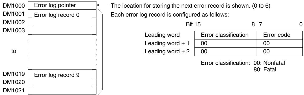
Error Log Storage Methods
The error log storage method is set in the PC Setup (DM 6655). Set any of the following methods.
1,2,3...
- You can store the most recent 10 error log records and discard older records. This is achieved by shifting the records as shown below so that the oldest record (record 0) is lost whenever a new record is generated.
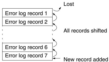
- You can store only the first 10 error log records, and ignore any subsequent errors beyond those 10.
- You can disable the log so that no records are stored.
The default setting is the first method. Refer to Error Log Settings on page 21 for details on the PC Setup for the error log.
Clearing the Error Log
To clear the entire error log, turn ON SR 25214 from a Programming Device. (After the error log has been cleared, SR 25214 will turn OFF again automatically.)
In CPM2A/CPM2C PCs, the error log is stored in DM 2000 through DM 2021. Up to 7 error records can be stored.
CPM2A/CPM2C Error Log Area
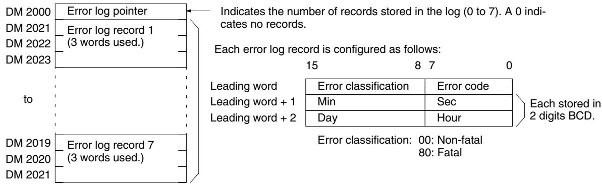
Note An error record with an error code of 00 will be stored in the error log for power interruptions.
Error Log Storage Methods
The error log storage method is set in the PC Setup (DM 6655). Set any of the following methods.
1,2,3...
- You can store the most recent 7 error log records and discard older records. This is achieved by shifting the records as shown below so that the oldest record (record 0) is lost whenever a new record is generated.
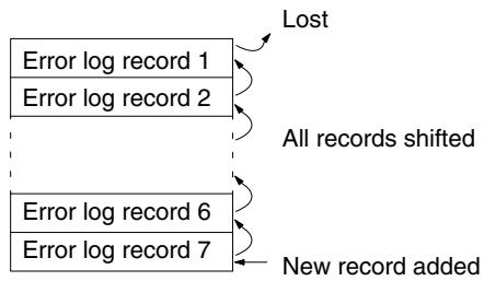
- You can store only the first 7 error log records, and ignore any subsequent errors beyond those 7.
- You can disable the log so that no records are stored.
The default setting is the first method. Refer to Error Log Settings on page 21 for details on the PC Setup for the error log.
Clearing the Error Log
To clear the entire error log, turn ON SR 25214 from a Programming Device. (After the error log has been cleared, SR 25214 will turn OFF again automatically.)
SRM1 Error Log Area
In SRM1(-V2) PCs, the error log is stored in DM 2000 through DM 2021.
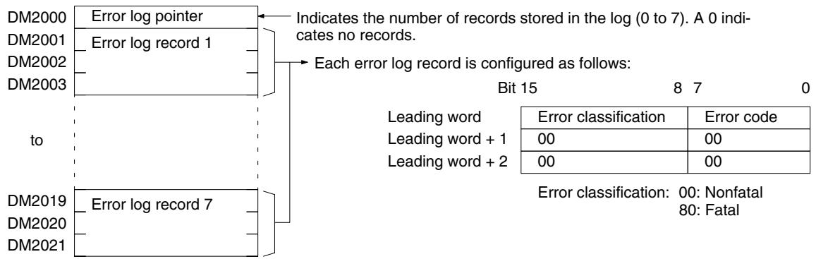
Error Log Storage Methods
The error log storage method is set in the PC Setup (DM 6655). Set any of the following methods.
1,2,3...
- You can store the most recent 7 error log records and discard older records. This is achieved by shifting the records as shown below so that the oldest record (record 0) is lost whenever a new record is generated.
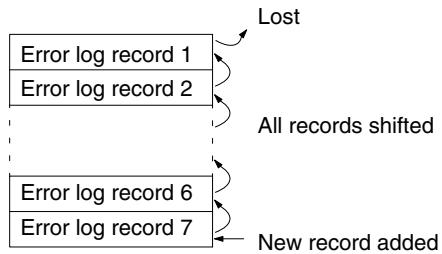
-
You can store only the first 7 error log records, and ignore any subsequent errors beyond those 7.
-
You can disable the log so that no records are stored.
The default setting is the first method. Refer to Error Log Settings on page 21 for details on the PC Setup for the error log.
Clearing the Error Log
To clear the entire error log, turn ON SR 25214 from a Programming Device. (After the error log has been cleared, SR 25214 will turn OFF again automatically.)
9-7 Host Link Errors
See 4-3 Host Link Communications for a description of the response format and the response codes that are returned when a command from a host computer cannot be processed.
9-8 Troubleshooting Flowcharts
The troubleshooting flowcharts are available in the Operation Manuals.
CPM1 Flowcharts
Refer to 5-6 Troubleshooting Flowcharts in the CPM1 Operation Manual.
CPM1A Flowcharts
Refer to 5-6 Troubleshooting Flowcharts in the CPM1A Operation Manual.
CPM2A Flowcharts
Refer to 5-5 Troubleshooting Flowcharts in the CPM2A Operation Manual.
CPM2C Flowcharts
Refer to 5-5 Troubleshooting Flowcharts in the CPM2C Operation Manual.
SRM1 Flowcharts
Refer to 5-6 Troubleshooting Flowcharts in the SRM1 Operation Manual.
Appendix A
Programming Instructions
A PC instruction is input either by pressing the corresponding Programming Console key(s) (e.g., LD, AND, OR, NOT) or by using function codes. To input an instruction with its function code, press FUN, the function code, and then WRITE. Refer to the pages listed programming and instruction details.
| Code | Mnemonic | Name | Function | Page |
| — | AND | AND | Logically ANDs status of designated bit with execution condi-tion. | 376 |
| — | AND LD | AND LOAD | Logically ANDs results of preceding blocks. | 377 |
| — | AND NOT | AND NOT | Logically ANDs inverse of designated bit with execution condition. | 376 |
| — | CNT | COUNTER | A decrementing counter. | 394 |
| — | LD | LOAD | Used to start instruction line with the status of the designated bit or to define a logic block for use with AND LD and OR LD. | 376 |
| — | LD NOT | LOAD NOT | Used to start instruction line with inverse of designated bit. | 376 |
| — | OR | OR | Logically ORs status of designated bit with execution condi-tion. | 376 |
| — | OR LD | OR LOAD | Logically ORs results of preceding blocks. | 377 |
| — | OR NOT | OR NOT | Logically ORs inverse of designated bit with execution condi-tion. | 376 |
| — | OUT | OUTPUT | Turns ON operand bit for ON execution condition; turns OFF operand bit for OFF execution condition. | 377 |
| — | OUT NOT | OUTPUT NOT | Turns operand bit OFF for ON execution condition; turns op- erand bit ON for OFF execution condition (i.e., inverts oper-a-tion). | 377 |
| — | RSET | RESET | Turns the operand bit OFF when the execution condition is ON, and does not affect the status of the operand bit when the execution condition is OFF. | 378 |
| — | SET | SET | Turns the operand bit ON when the execution condition is ON, and does not affect the status of the operand bit when the execution condition is OFF. | 378 |
| — | TIM | TIMER | ON-delay (decrementing) timer operation. | 389 |
| 00 | NOP | NO OPERATION | Nothing is executed and program moves to next instruction. | 381 |
| 01 | END | END | Required at the end of the program. | 381 |
| 02 | IL | INTERLOCK | If interlock condition is OFF, all outputs are turned OFF and all timer PVs reset between this IL(02) and the next ILC(03).Other instructions are treated as NOP; counter PVs are maintained. | 381 |
| 03 | ILC | INTERLOCK CLEAR | 381 | |
| 04 | JMP | JUMP | If jump condition is OFF, all instructions between JMP(04) and the corresponding JME(05) are ignored. | 383 |
| 05 | JME | JUMP END | 383 | |
| 06 | (@)FAL | FAILURE ALARM AND RESET | Generates a non-fatal error and outputs the designated FAL number to the Programming Console. | 385 |
| 07 | FALS | SEVERE FAILURE ALARM | Generates a fatal error and outputs the designated FALS number to the Programming Console. | 385 |
| 08 | STEP | STEP DEFINE | When used with a control bit, defines the start of a new step and resets the previous step. When used without N, defines the end of step execution. | 385 |
| 09 | SNXT | STEP START | Used with a control bit to indicate the end of the step, reset the step, and start the next step. | 385 |
| 10 | SFT | SHIFT REGISTER | Creates a bit shift register. | 404 |
| 11 | KEEP | KEEP | Defines a bit as a latch controlled by set and reset inputs. | 379 |
| 12 | CNTR | REVERSIBLE COUNTER | Increases or decreases PV by one whenever the increment input or decrement input signals, respectively, go from OFF to ON. | 395 |
| 13 | DIFU | DIFFERENTIATE UP | Turns ON the designated bit for one cycle on the rising edge of the input signal. | 380 |
| 14 | DIFD | DIFFERENTIATE DOWN | Turns ON the bit for one cycle on the trailing edge. | 380 |
| 15 | TIMH | HIGH-SPEED TIMER | A high-speed, ON-delay (decrementing) timer. | 390 |
| 16 | (@)WSFT | WORD SHIFT | Shifts data between starting and ending words in word units, writing zeros into starting word. | 405 |
| 17 to 19 | For expansion instructions. | 160 | ||
| 20 | CMP | COMPARE | Compares the contents of two words and outputs result to GR, EQ, and LE Flags. | 432 |
| 21 | (@)MOV | MOVE | Copies source data (word or constant) to destination word. | 411 |
| 22 | (@)MVN | MOVE NOT | Inverts source data (word or constant) and then copies it to destination word. | 412 |
| 23 | (@)BIN | BCD TO BINARY | Converts four-digit, BCD data in source word into 16-bit binary data, and outputs converted data to result word. | 439 |
| 24 | (@)BCD | BINARY TO BCD | Converts binary data in source word into BCD, and outputs converted data to result word. | 440 |
| 25 | (@)ASL | ARITHMETIC SHIFT LEFT | Shifts each bit in single word of data one bit to left, with CY. | 405 |
| 26 | (@)ASR | ARITHMETIC SHIFT RIGHT | Shifts each bit in single word of data one bit to right, with CY. | 406 |
| 27 | (@)ROL | ROTATE LEFT | Rotates bits in single word of data one bit to left, with CY. | 406 |
| 28 | (@)ROR | ROTATE RIGHT | Rotates bits in single word of data one bit to right, with CY. | 407 |
| 29 | (@)COM | COMPLEMENT | Inverts bit status of one word of data. | 479 |
| 30 | (@)ADD | BCD ADD | Adds two four-digit BCD values and content of CY, and outputs result to specified result word. | 457 |
| 31 | (@)SUB | BCD SUBTRACT | Subtracts a four-digit BCD value and CY from another four-digit BCD value and outputs result to the result word. | 458 |
| 32 | (@)MUL | BCD MULTIPLY | Multiplies two four-digit BCD values and outputs result to specified result words. | 460 |
| 33 | (@)DIV | BCD DIVIDE | Divides four-digit BCD dividend by four-digit BCD divisor and outputs result to specified result words. | 461 |
| 34 | (@)ANDW | LOGICAL AND | Logically ANDs two 16-bit input words and sets corresponding bit in result word if corresponding bits in input words are both ON. | 480 |
| 35 | (@)ORW | LOGICAL OR | Logically ORs two 16-bit input words and sets corresponding bit in result word if one or both of corresponding bits in input data are ON. | 481 |
| 36 | (@)XORW | EXCLUSIVE OR | Exclusively ORs two 16-bit input words and sets bit in result word when corresponding bits in input words differ in status. | 481 |
| 37 | (@)XNRW | EXCLUSIVE NOR | Exclusively NORs two 16-bit input words and sets bit in result word when corresponding bits in input words are same in status. | 482 |
| 38 | (@)INC | BCD INIncrement | Increments four-digit BCD word by one. | 483 |
| 39 | (@)DEC | BCD DECREMENT | Decrements four-digit BCD word by one. | 483 |
| 40 | (@)STC | SET CARRY | Sets carry flag (i.e., turns CY ON). | 457 |
| 41 | (@)CLC | CLEAR CARRY | Clears carry flag (i.e., turns CY OFF). | 457 |
| 46 | (@)MSG | MESSAGE | Displays a 16-character message on the Programming Con-sole display. | 497 |
| 47 & 48 | For expansion instructions. | 160 | ||
| 50 | (@)ADB | BINARY ADD | Adds two four-digit hexadecimal values and content of CY, and outputs result to specified result word. | 467 |
| 51 | (@)SBB | BINARY SUBTRACT | Subtracts a four-digit hexadecimal value and CY from anoth-er four-digit hexadecimal value and outputs result to the re-sult word. | 468 |
| 52 | (@)MLB | BINARY MULTIPLY | Multiplies two four-digit hexadecimal values and outputs re-sult to specified result words. | 470 |
| 53 | (@)DVB | BINARY DIVIDE | Divides four-digit hexadecimal dividend by four-digit hexa-cimal divisor and outputs result to specified result words. | 470 |
| 54 | (@)ADDL | DOUBLE BCD ADD | Adds two eight-digit values (2 words each) and content of CY, and outputs result to specified result words. | 463 |
| 55 | (@)SUBL | DOUBLE BCD SUBTRACT | Subtracts an eight-digit BCD value and CY from another eight-digit BCD value and outputs result to the result words. | 464 |
| 56 | (@)MULL | DOUBLE BCD MULTIPLY | Multiplies two eight-digit BCD values and outputs result to specified result words. | 466 |
| 57 | (@)DIVL | DOUBLE BCD DIVIDE | Divides eight-digit BCD dividend by eight-digit BCD divisor and outputs result to specified result words. | 466 |
| 58 | (@)BINL | DOUBLE BCD TO DOUBLE BINARY | Converts BCD value in two consecutive source words into binary and outputs converted data to two consecutive result words. (CPM2A only) | 440 |
| 59 | (@)BCDL | DOUBLE BINARY TO DOUBLE BCD | Converts binary value in two consecutive source words into BCD and outputs converted data to two consecutive result words. (CPM2A only) | 441 |
| 60 to 69 | For expansion instructions. | 160 | ||
| 70 | (@)XFER | BLOCK TRANSFER | Moves content of several consecutive source words to consecutive destination words. | 413 |
| 71 | (@)BSET | BLOCK SET | Copies content of one word or constant to several consecutive words. | 414 |
| 73 | (@)XCHG | DATA EXCHANGE | Exchanges contents of two different words. | 415 |
| 74 | (@)SLD | ONE DIGIT SHIFT LEFT | Left shifts data between starting and ending words by one digit (four bits). | 408 |
| 75 | (@)SRD | ONE DIGIT SHIFT RIGHT | Right shifts data between starting and ending words by one digit (four bits). | 408 |
| 76 | (@)MLPX | 4-TO-16 DECODER | Converts up to four hexadecimal digits in source word into decimal values from 0 to 15 and turns ON, in result word(s), bit(s) whose position corresponds to converted value. | 442 |
| 77 | (@)DMPX | 16-TO-4 ENCODER | Determines position of highest ON bit in source word(s) and turns ON corresponding bit(s) in result word. | 444 |
| 78 | (@)SDEC | 7-SEGMENT DECODER | Converts hexadecimal values from source word to data for seven-segment display. | 446 |
| 80 | (@)DIST | SINGLE WORD DISTRIBUTE | Moves one word of source data to destination word whose address is given by destination base word plus offset. | 415 |
| 81 | (@)COLL | DATA COLLECT | Extracts data from source word and writes it to destination word. | 417 |
| 82 | (@)MOVB | MOVE BIT | Transfers designated bit of source word or constant to designated bit of destination word. | 419 |
| 83 | (@)MOVD | MOVE DIGIT | Moves hexadecimal content of specified four-bit source digit(s) to specified destination digit(s) for up to four digits. | 420 |
| 84 | (@)SFTR | REVERSIBLE SHIFT REGISTER | Shifts data in specified word or series of words to either left or right. | 409 |
| 85 | (@)TCMP | TABLE COMPARE | Compares four-digit hexadecimal value with values in table consisting of 16 words. | 433 |
| 86 | (@)ASC | ASCII CONVERT | Converts hexadecimal values from the source word to eight-bit ASCII code starting at leftmost or rightmost half of starting destination word. | 449 |
| 87 to 89 | For expansion instructions. | 160 | ||
| 91 | (@)SBS | SUBROUTINE ENTRY | Calls and executes subroutine N. | 484 |
| 92 | SBN | SUBROUTINE DEFINE | Marks start of subroutine N. | 486 |
| 93 | RET | RETURN | Marks the end of a subroutine and returns control to main program. | 486 |
| 97 | (@)IORF | I/O REFRESH | Refreshes all I/O words between the start and end words. Cannot be used with the SRM1(-V2). | 498 |
| 99 | (@)MCRO | MACRO | Calls and executes a subroutine replacing I/O words. | 486 |
Expansion Instructions
The following table shows the instructions that can be treated as expansion instructions in the CPM2A, CPM2C, and SRM1(-V2) PCs. The default function codes are given for instructions that have codes assigned by default.
| Code | Mnemonic | Name | Function | CPU Units | Page |
| 17 | (@)ASFT | ASYNCHRONOUS SHIFT REGITER | Creates a shift register that exchanges the contents of adjacent words when one of the words is zero and the other is not. | All | 410 |
| 47 | (@)RXD | RECEIVE | Receives data via a communications port. | All | 505 |
| 48 | (@)TXD | TRANSMIT | Sends data via a communications port. | All | 507 |
| 60 | CMPL | DOUBLE COMPARE | Compares two eight-digit hexadecimal values. | All | 436 |
| 61 | (@)INI | MODE CONTROL | Starts and stops counter operation, compares and changes counter PVs, and stops pulse output. | All | 399 |
| 62 | (@)PRV | HIGH-SPEED COUNTER PV READ | Reads counter PVs and status data for the high-speed counter. | CPM2A/ CPM2C | 401 |
| 63 | (@)CTBL | COMPARISON TABLE LOAD | Compares counter PVs and generates a direct table or starts operation. | CPM2A/ CPM2C | 396 |
| 64 | (@)SPED | SPEED OUTPUT | Outputs pulses at the specified frequency (10 Hz to 50 KHz in 10 Hz units). The output fre quency can be changed while pulses are being output. | CPM2A/ CPM2C | 489 |
| 65 | (@)PULS | SET PULSES | Outputs the specified number of pulses at the specified frequency. The pulse output cannot be stopped until the specified number of pulses have been output. | CPM2A/ CPM2C | 487 |
| 66 | (@)SCL | SCALING | Performs a scaling conversion on the calculated value.Use the Programming Console or SSS to access this instruction for the SRM1(-V2). | All (But, Ver- sion 2 only for SRM1) | 421 |
| 67 | (@)BCNT | BIT COUNTER | Counts the total number of bits that are ON in the specified block of words. | All | 499 |
| 68 | (@)BCMP | BLOCK COMPARE | Judges whether the value of a word is within 16 ranges (defined by lower and upper limits). | All | 434 |
| 69 | (@)STIM | INTERVAL TIMER | Controls interval timers used to perform sched- uled interrupts. | All | 504 |
| 89 | (@)INT | INTERRUPT CONTROL | Performs interrupt control, such as masking and unmasking the interrupt bits for I/O interrupts. | CPM2A/ CPM2C | 501 |
| --- | (@)ACC | ACCELERATION CONTROL | Together with PULS(—), ACC(—) controls the acceleration and/or deceleration of pulses output from port 1 or 2. | CPM2A/ CPM2C | 491 |
| --- | AVG | AVERAGE VALUE | Adds the specified number of hexadecimal words and computes the mean value. Rounds off to 4 digits past the decimal point. | CPM2A/ CPM2C | 476 |
| --- | (@)FCS | FCS CALCULATE | Checks for errors in data transmitted by a Host Link command. | All | 500 |
| --- | (@)HEX | ASCII-TO-HEXADECIMAL | Converts ASCII data to hexadecimal data. | All | 451 |
| --- | (@)HMS | SECONDS TO HOURS | Converts second data to hour and minute data. | CPM2A/ CPM2C | 454 |
| --- | (@)MAX | FIND MAXIMUM | Finds the maximum value in specified data area and outputs that value to another word. | CPM2A/ CPM2C | 472 |
| --- | (@)MIN | FIND MINIMUM | Finds the minimum value in specified data area and outputs that value to another word. | CPM2A/ CPM2C | 474 |
| --- | (@)NEG | 2'S COMPLEMENT | Converts the four-digit hexadecimal content of the source word to its 2's complement and outputs the result to R.Use the Programming Console or SSS to ac- cess this instruction for the SRM1(-V2). | All (But, Ver- sion 2 only for SRM1) | 455 |
| --- | PID | PID CONTROL | Performs PID control based on the specified parameters.Use the Programming Console or SSS to access this instruction for the SRM1(-V2). | All(But, Version 2 only for SRM1) | 426 |
| --- | (@)PWM | PULSE WITH VARIABLE DUTY RATIO | Outputs pulses with the specified duty ratio (0% to 99%) from port 1 or 2. | CPM2A/ CPM2C | 494 |
| --- | (@)SCL2 | SIGNED BINARY TO BCD SCALING | Linearly converts a 4-digit signed hexadecimal value to a 4-digit BCD value. | CPM2A/ CPM2C | 423 |
| --- | (@)SCL3 | BCD TO SIGNED BINARY SCALING | Linearly converts a 4-digit BCD value to a 4-digit signed hexadecimal value. | CPM2A/ CPM2C | 424 |
| --- | (@)SEC | HOURS TO SECONDS | Converts hour and minute data to second data. | CPM2A/ CPM2C | 453 |
| --- | (@)SRCH | DATA SEARCH | Searches the specified range of memory for the specified data. Outputs the word address(es) of words in the range that contain the data. | CPM2A/ CPM2C | 471 |
| --- | (@)STUP | CHANGE RS-232C SETUP | Changes the communications parameters in the PC Setup for a specified port. | All | 509 |
| --- | (@)SUM | SUM CALCULATE | Computes the sum of the contents of the words in the specified range of memory. | CPM2A/ CPM2C | 478 |
| --- | SYNC | SYNCHRONIZED PULSE CONTROL | Multiplies an input pulse frequency by a fixed scaling factor and outputs pulses from the speci-fied output bit at the resulting frequency. | CPM2A/ CPM2C | 496 |
| --- | TIML | LONG TIMER | A decrementing ON-delay timer with SV of up to 99,990 s | CPM2A/ CPM2C | 392 |
| --- | TMHH | VERY HIGH-SPEED TIMER | A high-speed, decrementing ON-delay timer that times in 1-ms units | CPM2A/ CPM2C | 391 |
| --- | ZCP | AREA RANGE COMPARE | Compares a word to a range defined by lower and upper limits and outputs the result to the GR, EQ, and LE flags.Use the Programming Console or SSS to ac-cess this instruction for the SRM1(-V2). | All(But, Version 2 only for SRM1) | 437 |
| --- | ZCPL | DOUBLE AREA RANGE COMPARE | Compares an 8-digit value to a range defined by lower and upper limits and outputs the result to the GR, EQ, and LE flags. | CPM2A/ CPM2C | 438 |
Appendix B Error and Arithmetic Flag Operation
The following table shows the instructions that affect the ER, CY, GT, LT and EQ flags. In general, ER indicates that operand data is not within requirements. CY indicates arithmetic or data shift results. GT indicates that a compared value is larger than some standard, LT that it is smaller, and EQ, that it is the same. EQ also indicates a result of zero for arithmetic operations. Refer to Section 7 Instruction Set for details.
Vertical arrows in the table indicate the flags that are turned ON and OFF according to the result of the instruction. Although ladder diagram instructions, TIM, and CNT are executed when ER is ON, other instructions with a vertical arrow under the ER column are not executed if ER is ON. All of the other flags in the following table will also not operate when ER is ON.
Instructions not shown do not affect any of the flags in the table. Although only the non-differentiated form of each instruction is shown, differentiated instructions affect flags in exactly the same way.
The ER, CY, GT, LT and EQ Flags are turned OFF when END(01) is executed, so their status cannot be monitored with a Programming Device.
The status of the ER, CY, GT, LT and EQ Flags is affected by instruction execution and will change each time an instruction that affects them is executed. Differentiated instructions are executed only once when their execution condition changes (ON to OFF or OFF to ON) and are not executed again until the next specified change in their execution condition. The status of the ER, CY, GT, LT and EQ Flags is thus affected by a differentiated instruction only when the execution condition changes and is not affected during scans when the instruction is not executed, i.e., when the specified change does not occur in the execution condition. When a differentiated instruction is not executed, the status of the ER, CY, GT, LT and EQ Flags will not change and will maintain the status produced by the last instruction that was executed.
| Instructions | 25503 (ER) | 25504 (CY) | 25505 (GR) | 25506 (EQ) | 25507 (LE) | 25402 (N) | Page |
| TIM | ↓ | Unaffected | Unaffected | Unaffected | Unaffected | Unaffected | 389 |
| CNT | 394 | ||||||
| END(01) | OFF | OFF | OFF | OFF | OFF | OFF | 381 |
| STEP(08) | Unaffected | Unaffected | Unaffected | Unaffected | Unaffected | Unaffected | 385 |
| SNXT(09) | 385 | ||||||
| CNTR(12) | ↓ | 395 | |||||
| TIMH(15) | 390 | ||||||
| WSFT(16) | 405 | ||||||
| CMP(20) | ↓ | Unaffected | ↓ | ↓ | ↓ | Unaffected | 432 |
| MOV(21) | ↓ | Unaffected | Unaffected | ↓ | Unaffected | ↓ | 411 |
| MVN(22) | 412 | ||||||
| BIN(23) | OFF | 439 | |||||
| BCD(24) | Unaffected | 440 | |||||
| ASL(25) | ↓ | ↓ | Unaffected | ↓ | Unaffected | ↓ | 405 |
| ASR(26) | OFF | 406 | |||||
| ROL(27) | ↓ | 406 | |||||
| ROR(28) | 407 | ||||||
| COM(29) | ↓ | Unaffected | Unaffected | ↓ | Unaffected | ↓ | 479 |
| ADD(30) | ↓ | ↓ | ↓ | Unaffected | 457 | ||
| SUB(31) | 458 | ||||||
| MUL(32) | ↓ | Unaffected | Unaffected | ↓ | Unaffected | Unaffected | 460 |
| DIV(33) | 461 | ||||||
| ANDW(34) | ↓ | 480 | |||||
| ORW(35) | 481 | ||||||
| XORW(36) | 481 | ||||||
| XNRW(37) | 482 | ||||||
| INC(38) | Unaffected | 483 | |||||
| DEC(39) | 483 | ||||||
| STC(40) | Unaffected | ON | Unaffected | Unaffected | Unaffected | Unaffected | 457 |
| CLC(41) | OFF | 457 | |||||
| MSG(46) | ↓ | Unaffected | 497 | ||||
| ADB(50) | ↓ | ↓ | Unaffected | ↓ | Unaffected | ↓ | 467 |
| SBB(51) | 468 | ||||||
| MLB(52) | Unaffected | ↓ | Unaffected | Unaffected | ↓ | 470 | |
| DVB(53) | ↓ | Unaffected | Unaffected | ↓ | Unaffected | 470 | |
| ADDL(54) | ↓ | ↓ | ↓ | Unaffected | 463 | ||
| SUBL(55) | 464 | ||||||
| MULL(56) | ↓ | Unaffected | Unaffected | ↓ | Unaffected | Unaffected | 466 |
| DIVL(57) | 466 | ||||||
| BINL(58) | OFF | 440 | |||||
| BCDL(59) | Unaffected | 441 | |||||
| XFER(70) | ↓ | Unaffected | Unaffected | Unaffected | Unaffected | Unaffected | 413 |
| BSET(71) | 414 | ||||||
| XCHG(73) | ↓ | Unaffected | Unaffected | Unaffected | Unaffected | Unaffected | 415 |
| SLD(74) | 408 | ||||||
| SRD(75) | 408 | ||||||
| MLPX(76) | 442 | ||||||
| DMPX(77) | 444 | ||||||
| SDEC(78) | 446 | ||||||
| DIST(80) | ↓ | Unaffected | Unaffected | ↓ | Unaffected | ↓ | 415 |
| COLL(81) | 417 | ||||||
| MOVB(82) | Unaffected | Unaffected | 419 | ||||
| MOVD(83) | 420 | ||||||
| SFTR(84) | ↓ | ↓ | Unaffected | Unaffected | Unaffected | Unaffected | 409 |
| TCMP(85) | ↓ | Unaffected | ↓ | 433 | |||
| ASC(86) | ↓ | Unaffected | 449 | ||||
| SBS(91) | 484 | ||||||
| MCRO(99) | ↓ | 486 |
Expansion Instructions (CPM2A/CPM2C and SRM1(-V2))
| Instructions | 25503 (ER) | 25504 (CY) | 25505 (GR) | 25506 (EQ) | 25507 (LE) | 25402 (N) | Page |
| ASFT(17) | ↑ | Unaffected | Unaffected | Tnafted | Unaffected | Unaffected | 410 |
| RXD(47) | 505 | ||||||
| TXD(48) | 507 | ||||||
| CMPL(60) | ↑ | ↑ | ↑ | ↑ | 436 | ||
| INI(61) | ↑ | Unaffected | Unaffected | Unaffected | Unaffected | 399 | |
| PRV(62) | 401 | ||||||
| CTBL(63) | 396 | ||||||
| SPED(64) | 489 | ||||||
| PULS(65) | 487 | ||||||
| SCL(66) | Unaffected | ↑ | 421 | ||||
| BCNT(67) | 499 | ||||||
| BCMP(68) | Unaffected | 434 | |||||
| STIM(69) | 504 | ||||||
| INT(89) | ↑ | 501 | |||||
| SRCH(—) | 471 | ||||||
| MAX(—) | ↑ | 472 | |||||
| MIN(—) | 474 | ||||||
| HMS(—) | Unaffected | 454 | |||||
| NEG(—)* | 455 | ||||||
| SEC(—) | 453 | ||||||
| SUM(—) | ↑ | 478 | |||||
| FCS(—) | Unaffected | Unaffected | 500 | ||||
| HEX(—) | 451 | ||||||
| AVG(—) | 476 | ||||||
| PID(—) | 426 | ||||||
| ZCP(—) | Unaffected | ↑ | ↑ | ↑ | 437 |
Note *Depending on the results, NEG(—) may also affect the status of the underflow flag (SR 25405).
Expansion Instructions (CPM2A/CPM2C Only)
| Instructions | 25503 (ER) | 25504 (CY) | 25505 (GR) | 25506 (EQ) | 25507 (LE) | Page |
| PWM(—) | ↓ | Unaffected | Unaffected | Unaffected | Unaffected | 494 |
| ZCPL(—) | ↓ | ↓ | ↓ | 438 | ||
| ACC(—) | 491 | |||||
| SCL2(—) | ↓ | Unaffected | Unaffected | 423 | ||
| SCL3(—) | Unaffected | 424 | ||||
| SYNC(—) | 424 |
Appendix C Memory Areas
CPM1/CPM1A Memory Areas
Memory Area Structure
The following memory areas can be used with the CPM1/CPM1A.
| Data area | Words | Bits | Function | |
| IR area1 | Input area | IR 000 to IR 009(10 words) | IR 00000 to IR 00915(160 bits) | These bits can be allocated to the external I/O terminals. |
| Output area | IR 010 to IR 019(10 words) | IR 01000 to IR 01915(160 bits) | ||
| Work area | IR 200 to IR 231(32 words) | IR 20000 to IR 23115(512 bits) | Work bits can be freely used within the pro-gram. | |
| SR area | SR 232 to SR 255(24 words) | SR 23200 to SR 25515(384 bits) | These bits serve specific functions such as flags and control bits. | |
| TR area | --- | TR 0 to TR 7(8 bits) | These bits are used to temporarily store ON/OFF status at program branches. | |
| HR area2 | HR 00 to HR 19(20 words) | HR 0000 to HR 1915(320 bits) | These bits store data and retain their ON/OFF status when power is turned off. | |
| AR area2 | AR 00 to AR 15(16 words) | AR 0000 to AR 1515(256 bits) | These bits serve specific functions such as flags and control bits. | |
| LR area1 | LR 00 to LR 15(16 words) | LR 0000 to LR 1515(256 bits) | Used for a 1:1 data link with another PC. | |
| Timer/Counter area2 | TC 000 to TC 127 (timer/counter numbers)3 | The same numbers are used for both timers and counters. | ||
| DM area | Read/write2 | DM 0000 to DM 0999DM 1022 to DM 1023(1,002 words) | --- | DM area data can be accessed in word units only. Word values are retained when the power is turned off. |
| Error log2 | DM 1000 to DM 1021(22 words) | --- | Used to store the error code of errors that occur. These words can be used as ordinary read/write DM when the error log func-tion isn't being used. | |
| Read-only4 | DM 6144 to DM 6599(456 words) | --- | Cannot be overwritten from program. | |
| PC Setup4 | DM 6600 to DM 6655(56 words) | --- | Used to store various parameters that con-rol PC operation. | |
Note 1. IR and LR bits that are not used for their allocated functions can be used as work bits.
2. The contents of the HR area, AR area, Counter area, and read/write DM area are backed up by a capacitor. The backup time varies with the ambient temperature, but at 25^ , the capacitor will back up memory for 20 days. If the power supply is off longer than the backup time, memory contents will be cleared and AR1314 will turn ON. (This flag turns ON when data can no longer be retained by the built-in capacitor.) Refer to 2-1-2 Characteristics in the CPM1 Operation Manual for a graph showing the backup time vs. temperature.
3. When accessing a PV, TC numbers are used as word data; when accessing Completion Flags, they are used as bit data.
4. Data in DM 6144 to DM 6655 cannot be overwritten from the program, but they can be changed from a Programming Device.
SR Area
These bits mainly serve as flags related to CPM1/CPM1A operation or contain present and set values for various functions. The functions of the SR area are explained in the following table.
Note "Read-only" words and bits can be read as status in controller PC operation, but they cannot be written from the ladder program. Bits and words that are "Not used" are also read-only.
| Word(s) | Bit(s) | Function | Read/write | Page |
| SR 232 to SR 235 | 00 to 15 | Macro Function Input AreaContains the input operands for MCRO(99).(Can be used as work bits when MCRO(99) is not used.) | Read/write | 157 |
| SR 236 to SR 239 | 00 to 15 | Macro Function Output AreaContains the output operands for MCRO(99).(Can be used as work bits when MCRO(99) is not used.) | ||
| SR 240 | 00 to 15 | Input Interrupt 0 Counter Mode SVSV when input interrupt 0 is used in counter mode (4 digits hexadecimal).(Can be used as work bits when input interrupt 0 is not used in counter mode.) | 81 | |
| SR 241 | 00 to 15 | Input Interrupt 1 Counter Mode SVSV when input interrupt 1 is used in counter mode (4 digits hexadecimal).(Can be used as work bits when input interrupt 1 is not used in counter mode.) | ||
| SR 242 | 00 to 15 | Input Interrupt 2 Counter Mode SVSV when input interrupt 2 is used in counter mode (4 digits hexadecimal).(Can be used as work bits when input interrupt 2 is not used in counter mode.) | ||
| SR 243 | 00 to 15 | Input Interrupt 3 Counter Mode SVSV when input interrupt 3 is used in counter mode (4 digits hexadecimal).(Can be used as work bits when input interrupt 3 is not used in counter mode.) | ||
| SR 244 | 00 to 15 | Input Interrupt 0 Counter Mode PV Minus OneCounter PV-1 when input interrupt 0 is used in counter mode (4 digits hexadecimal). | Read-only | 82 |
| SR 245 | 00 to 15 | Input Interrupt 1 Counter Mode PV Minus OneCounter PV-1 when input interrupt 1 is used in counter mode (4 digits hexadecimal). | ||
| SR 246 | 00 to 15 | Input Interrupt 2 Counter Mode PV Minus OneCounter PV-1 when input interrupt 2 is used in counter mode (4 digits hexadecimal). | ||
| SR 247 | 00 to 15 | Input Interrupt 3 Counter Mode PV Minus OneCounter PV-1 when input interrupt 3 is used in counter mode (4 digits hexadecimal). | ||
| SR 248,SR 249 | 00 to 15 | High-speed Counter PV Area Can be used as work bits when the high-speed counter is not used. | 87 | |
| SR 250 | 00 to 15 | Analog Setting 0Used to store the 4-digit BCD set value (0000 to 0200) from analog control 0. | 150 | |
| SR 251 | 00 to 15 | Analog Setting 1Used to store the 4-digit BCD set value (0000 to 0200) from analog control 1. | ||
| SR 252 | 00 | High-speed Counter Reset Bit | Read/write | 88 |
| 01 to 07 | Not used. | |||
| 08 | Peripheral Port Reset BitTurn ON to reset peripheral port. (Not valid when Programming Device is connected.) Automatically turns OFF when reset is complete. | Read/write | 272 | |
| 09 | Not used. | |||
| 10 | PC Setup Reset BitTurn ON to initialize PC Setup (DM 6600 through DM 6655). Automatically turns OFF again when reset is complete. Only effective if the PC is in PRO-GRAM mode. | Read/write | 2 | |
| 11 | Forced Status Hold Bit (See note.)OFF: The forced status of bits that are forced set/reset is cleared when switching between PROGRAM mode and MONITOR mode.ON: The status of bits that are forced set/reset are maintained when switch-ing between PROGRAM mode and MONITOR mode.The status of this bit can be maintained when PC power turns off by using the PC Setup. | 17 | ||
| 12 | I/O Hold Bit (See note.)OFF: IR and LR bits are reset when starting or stopping operation.ON: IR and LR bit status is maintained when starting or stopping operation.The status of this bit can be maintained when PC power turns off by using the PC Setup. | 17 | ||
| 13 | Not used. | |||
| 14 | Error Log Reset BitTurn ON to clear error log. Automatically turns OFF again when operation is complete. | Read/write | 555 | |
| 15 | Not used. | |||
| SR 253 | 00 to 07 | FAL Error CodeThe error code (a 2-digit number) is stored here when an error occurs. The FAL number is stored here when FAL(06) or FALS(07) is executed. This word is reset (to 00) by executing a FAL 00 instruction or by clearing the error from a Programming Device. | Read-only | 385 |
| 08 | Not used. | |||
| 09 | Cycle Time Overrun FlagTurns ON when a cycle time overrun occurs (i.e., when the cycle time exceeds 100 ms). | Read-only | --- | |
| 10 to 12 | Not used. | |||
| 13 | Always ON Flag | Read-only | --- | |
| 14 | Always OFF Flag | --- | ||
| 15 | First Cycle FlagTurns ON for 1 cycle at the start of operation. | --- | ||
| SR 254 | 00 | 1-minute clock pulse (30 seconds ON; 30 seconds OFF) | --- | |
| 01 | 0.02-second clock pulse (0.01 second ON; 0.01 second OFF) | --- | ||
| 02 | Negative (N) Flag | --- | ||
| 03 to 05 | Not used. | |||
| 06 | Differential Monitor Complete FlagTurns ON when differential monitoring is complete. | Read-only | 159 | |
| 07 | STEP(08) Execution FlagTurns ON for 1 cycle only at the start of process based on STEP(08). | 385 | ||
| 08 to 15 | Not used. | |||
| SR 255 | 00 | 0.1-second clock pulse (0.05 second ON; 0.05 second OFF) | Read-only | --- |
| 01 | 0.2-second clock pulse (0.1 second ON; 0.1 second OFF) | --- | ||
| 02 | 1.0-second clock pulse (0.5 second ON; 0.5 second OFF) | --- | ||
| 03 | Instruction Execution Error (ER) FlagTurns ON when an error occurs during execution of an instruction. | --- | ||
| 04 | Carry (CY) FlagTurns ON when there is a carry in the results of an instruction execution. | --- | ||
| 05 | Greater Than (GR) FlagTurns ON when the result of a comparison operation is “greater.” | --- | ||
| 06 | Equals (EQ) FlagTurns ON when the result of a comparison operation is “equal,” or when the result of an instruction execution is 0. | --- | ||
| 07 | Less Than (LE) FlagTurns ON when the result of a comparison operation is “less.” | --- | ||
| 08 to 15 | Not used. | |||
Note DM 6601 in the PC Setup can be set to maintain the previous status of the I/O Hold Bit (SR 25212) and the I/O Hold Bit (SR 25212) when power is turned OFF. If power is left OFF for longer than the backup time, however, status may be cleared. For details regarding the backup time, refer to the CPM1A or CPM1 Operation Manual. Refer to 1-1-2 CPM1/CPM1A PC Setup Settings for details on the PC Setup.
AR Area
These bits mainly serve as flags related to CPM1/CPM1A operation. These bits retain their status even after the CPM1/CPM1A power supply has been turned off or when operation begins or stops.
| Word(s) | Bit(s) | Function | Page | |
| AR 00, AR 01 | 00 to 15 | Not used. | ||
| AR 02 | 00 | Expansion Unit Error Flag for 1st Unit | These flags turn ON when there is an error in the corresponding Unit. | --- |
| 01 | Expansion Unit Error Flag for 2nd Unit (Not used by CPM1 CPU Units without “-V1” suffix.) | |||
| 02 | Expansion Unit Error Flag for 3rd Unit (Not used by CPM1 CPU Units without “-V1” suffix.) | |||
| 03 to 07 | Not used. | |||
| 08 to 11 | Number of I/O Units Connected | --- | ||
| 12 to 15 | Not used. | |||
| AR 03 to AR 07 | 00 to 15 | Not used. | ||
| AR 08 | 00 to 07 | Not used. | ||
| 08 to 11 | Programming Device Error Code 0: Normal completion 1: Parity error 2: Frame error 3: Overrun error | 273 | ||
| 12 | Programming Device Error Flag | |||
| 13 to 15 | Not used. | |||
| AR 09 | 00 to 15 | Not used. | ||
| AR 10 | 00 to 15 | Power-off Counter (4 digits BCD) This is the count of the number of times that the power has been turned off. To clear the count, write “0000” from a Programming Device. | --- | |
| Word(s) | Bit(s) | Function | Page | |
| AR 11 | 00 to 07 | High-speed Counter Range Comparison Flags00 ON: Counter PV is within comparison range 101 ON: Counter PV is within comparison range 202 ON: Counter PV is within comparison range 303 ON: Counter PV is within comparison range 404 ON: Counter PV is within comparison range 505 ON: Counter PV is within comparison range 606 ON: Counter PV is within comparison range 707 ON: Counter PV is within comparison range 8 | 90 | |
| 08 to 14 | Not used. | |||
| 15 | Pulse Output StatusON: Stopped.OFF: Pulses being output. | --- | ||
| AR 12 | 00 to 15 | Not used. | ||
| AR 13 | 00 | Power-up PC Setup Error FlagTurns ON when there is an error in DM 6600 to DM 6614 (the part of the PC Setup area that is read at power-up). | 553 | |
| 01 | Start-up PC Setup Error FlagTurns ON when there is an error in DM 6615 to DM 6644 (the part of the PC Setup area that is read at the beginning of operation). | |||
| 02 | RUN PC Setup Error FlagTurns ON when there is an error in DM 6645 to DM 6655 (the part of the PC Setup area that is always read). | |||
| 03, 04 | Not used. | |||
| 05 | Long Cycle Time FlagTurns ON if the actual cycle time is longer than the cycle time set in DM 6619. | --- | ||
| 06, 07 | Not used. | |||
| 08 | Memory Area Specification Error FlagTurns ON when a non-existent data area address is specified in the program. | --- | ||
| 09 | Flash Memory Error FlagTurns ON when there is an error in flash memory. | --- | ||
| 10 | Read-only DM Error Flag (See note 3.)Turns ON when a checksum error occurs in the read-only DM (DM 6144 to DM 6599) and that area is initialized. | 554 | ||
| 11 | PC Setup Error FlagTurns ON when a checksum error occurs in the PC Setup area. | |||
| 12 | Program Error FlagTurns ON when a checksum error occurs in the program memory (UM) area, or when an improper instruction is executed. | --- | ||
| 13 | Not used. | |||
| 14 | Data Save Error FlagTurns ON when power is turned on if data could not be saved with the built-in capacitor.Data is saved in the following areas with the built-in capacitor:DM area (Read/write-capable: DM 0000 to 0999 and DM 1022 to 1023)HR area (HR 00 to 19)Counter area (CNT 000 to 127)SR area, word 252, bits 11, 12 (when PC Setup in DM 6601 is set to maintain status)AR area, word 10 (power-off counter)Operation mode (when PC Setup in DM 6600 is set to continue mode last used before power failure)If data could not be saved in the above areas:The DM, error log, HR, counter, SR (word 252, bits 11 and 12), and AR (word 10) areas will be cleared and the operating mode will go into PROGRAM mode if DM 0000 is set to continue mode last used before power failure or if DM6604 is set to generate an error.(For details regarding the holding time, refer to the CPM1A Operation Manual.) | --- | ||
| 15 | Not used. | |||
| AR 14 | 00 to 15 | Maximum Cycle Time (4 digits BCD) (See note 1.)The longest cycle time since the beginning of operation is stored. It is cleared at the beginning, and not at the end, of operation.The units can be any of the following, depending on the setting of in DM 6618.Default: 0.1 ms; “10 ms” setting: 0.1 ms; “100 ms” setting: 1 ms; “1 s” setting: 10 ms | 537 | |
| AR 15 | 00 to 15 | Current Cycle Time (4 digits BCD) (See note 1.)The most recent cycle time during operation is stored. The Current Cycle Time is not cleared when operation stops.The units can be any of the following, depending on the setting of in DM 6618.Default: 0.1 ms; “10 ms” setting: 0.1 ms; “100 ms” setting: 1 ms; “1 s” setting: 10 ms | ||
Note 1. The units will be as follows, depending on the unit setting for the cycle monitor time (DM 6618):
Initial status: 0.1-ms unit
When 10-ms unit is set: 0.1-ms unit
When 100-ms unit is set: 1-ms unit
When 1-s unit is set: 10-ms unit
- Areas that cannot be used are cleared when the power is turned on.
- The contents of AR 10 is backed up by the built-in capacitor. If power is left OFF for longer than the backup time, however, the contents may be cleared. For details regarding the backup time, refer to the CPM1A or CPM1 Operation Manual.
CPM2A/CPM2C Memory Areas
Memory Area Structure
The following memory areas can be used with the CPM2A/CPM2C. Refer to the CPM2C-S Operation Manual (W377) for information on CPM2C-S memory areas.
| Data area | Words | Bits | Function | |
| IR area1 | Input area | IR 000 to IR 009 (10 words) | IR 00000 to IR 00915 (160 bits) | These bits can be allocated to the external I/O terminals. |
| Output area | IR 010 to IR 019 (10 words) | IR 01000 to IR 01915 (160 bits) | ||
| Work area | IR 020 to IR 049 IR 200 to IR 227 (58 words) | IR 02000 to IR 04915 IR 20000 to IR 22715 (928 bits) | Work bits can be freely used within the pro-gram. | |
| SR area | SR 228 to SR 255 (28 words) | SR 22800 to SR 25515 (448 bits) | These bits serve specific functions such as flags and control bits. | |
| TR area | --- | TR 0 to TR 7 (8 bits) | These bits are used to temporarily store ON/OFF status at program branches. | |
| HR area2 | HR 00 to HR 19 (20 words) | HR 0000 to HR 1915 (320 bits) | These bits store data and retain their ON/OFF status when power is turned off. | |
| AR area2 | AR 00 to AR 23 (24 words) | AR 0000 to AR 2315 (384 bits) | These bits serve specific functions such as flags and control bits. | |
| LR area1 | LR 00 to LR 15 (16 words) | LR 0000 to LR 1515 (256 bits) | Used for a 1:1 data link with another PC. | |
| Timer/Counter area2 | TC 000 to TC 255 (timer/counter numbers)3 | The same numbers are used for both timers and counters. | ||
| DM area | Read/write2 | DM 0000 to DM 1999 DM 2022 to DM 2047 (2,026 words) | --- | DM area data can be accessed in word units only. Word values are retained when the power is turned off. |
| Error log2 | DM 2000 to DM 2021 (22 words) | --- | Used to store the error code of errors that occur. These words can be used as ordinary read/write DM when the error log func-tion isn't being used. | |
| Read-only4 | DM 6144 to DM 6599 (456 words) | --- | Cannot be overwritten from program. | |
| PC Setup4 | DM 6600 to DM 6655 (56 words) | --- | Used to store various parameters that con-rol PC operation. | |
Note 1. IR and LR words that are not used for their allocated functions can be used as work words.
-
The contents of the HR area, AR area, Counter area, and read/write DM area are backed up by the CPU Unit's battery. If the battery is removed or fails, the data in these areas will be lost and reset to default values. (In CPM2C CPU Units without a battery, these areas are backed up by a capacitor. At 25^ , the capacitor will back up memory for 10 days.)
-
When a TC number is used as a word operand, it accesses the timer or counter's PV; when used as a bit operand, it accesses the Completion Flag.
-
Data in DM 6144 to DM 6655 cannot be overwritten from the program, but they can be changed from a Programming Device. The program and data in DM 6144 to DM 6655 are backed up in flash memory.
SR Area
These bits mainly serve as flags related to CPM2A/CPM2C operation or contain present and set values for various functions. The functions of the SR area are explained in the following table.
Note "Read-only" words and bits can be read as status in controller PC operation, but they cannot be written from the ladder program. Bits and words that are "Not used" are also read-only.
| Word(s) | Bit(s) | Function | Read/write | Page |
| SR 228,SR 229 | 00 to 15 | Pulse Output PV 0Contains the pulse output PV (-16,777,215 to 16,777,215). SR 22915 acts as the sign bit; a negative number is indicated when SR 22915 is ON.(The same PV data can be read immediately with PRV(62).)Only Pulse Output PV 0 is used for ACC(-). | Read-only | 106 |
| SR 230,SR 231 | 00 to 15 | Pulse Output PV 1Contains the pulse output PV (-16,777,215 to 16,777,215). SR 23115 acts as the sign bit; a negative number is indicated when SR 23115 is ON.(The same PV data can be read immediately with PRV(62).) | ||
| SR 232toSR 235 | 00 to 15 | Macro Function Input AreaContains the input operands for MCRO(99).(Can be used as work bits when MCRO(99) is not used.) | Read/write | 157 |
| SR 236toSR 239 | 00 to 15 | Macro Function Output AreaContains the output operands for MCRO(99).(Can be used as work bits when MCRO(99) is not used.) | ||
| SR 240 | 00 to 15 | Interrupt Input 00003 Counter Mode SVSV when interrupt input 00003 is used in counter mode (4 digits hexadecimal).(Can be used as work bits when interrupt input 00003 is not used in counter mode.) | 73 | |
| SR 241 | 00 to 15 | Interrupt Input 00004 Counter Mode SVSV when interrupt input 00004 is used in counter mode (4 digits hexadecimal).(Can be used as work bits when interrupt input 00004 is not used in counter mode.) | ||
| SR 242 | 00 to 15 | Interrupt Input 00005 Counter Mode SVSV when interrupt input 00005 is used in counter mode (4 digits hexadecimal).(Can be used as work bits when interrupt input 00005 is not used in counter mode.) | ||
| SR 243 | 00 to 15 | Interrupt Input 00006 Counter Mode SVSV when interrupt input 00006 is used in counter mode (4 digits hexadecimal).(Can be used as work bits when interrupt input 00006 is not used in counter mode.)(Input 00006 does not exist in CPM2C CPU Units with 10 I/O points.) | ||
| SR 244 | 00 to 15 | Interrupt Input 00003 Counter Mode PV Counter PV when interrupt input 00003 is used in counter mode (4 digits hex- decimal). | Read-only | 75 |
| SR 245 | 00 to 15 | Interrupt Input 00004 Counter Mode PV Counter PV when interrupt input 00004 is used in counter mode (4 digits hex- decimal). | ||
| SR 246 | 00 to 15 | Interrupt Input 00005 Counter Mode PV Counter PV when interrupt input 00005 is used in counter mode (4 digits hex- decimal). | ||
| SR 247 | 00 to 15 | Interrupt Input 00006 Counter Mode PV Counter PV when interrupt input 00006 is used in counter mode (4 digits hex- decimal). (Input 00006 does not exist in CPM2C CPU Units with 10 I/O points.) | ||
| SR 248, SR 249 | 00 to 15 | High-speed Counter PV Area (Can be used as work bits when the high-speed counter is not used.) | 60 | |
| SR 250 | 00 to 15 | Analog Setting 0 (CPM2A PCs only) Used to store the 4-digit BCD set value (0000 to 0200) from analog control 0. | 150 | |
| SR 251 | 00 to 15 | Analog Setting 1 (CPM2A PCs only) Used to store the 4-digit BCD set value (0000 to 0200) from analog control 1. | ||
| SR 252 | 00 | High-speed Counter Reset Bit | Read/write | 51 |
| 01 to 03 | Not used. | |||
| 04 | Pulse Output 0 PV Reset Bit Turn ON to clear the PV of pulse output 0. | Read/write | 97 | |
| 05 | Pulse Output 1 PV Reset Bit Turn ON to clear the PV of pulse output 1. | |||
| 06, 07 | Not used. | |||
| 08 | Peripheral Port Reset Bit Turn ON to reset the peripheral port. Automatically turns OFF when reset is complete. | Read/write | --- | |
| 09 | RS-232C Port Reset Bit Turn ON to reset the RS-232C port. Automatically turns OFF when reset is complete. | --- | ||
| 10 | PC Setup Reset Bit Turn ON to initialize PC Setup (DM 6600 through DM 6655). Automatically turns OFF again when reset is complete. Only effective if the PC is in PRO-GRAM mode. | 2 | ||
| 11 | Forced Status Hold Bit (See note.) OFF: The forced status of bits that are forced set/reset is cleared when switching between PROGRAM mode and MONITOR mode. ON: The status of bits that are forced set/reset are maintained when switching between PROGRAM mode and MONITOR mode. The PC Setup can be set to maintain the status of this bit when the PC is turned off. | 17 | ||
| 12 | I/O Hold Bit (See note.) OFF: IR and LR bits are reset when starting or stopping operation. ON: IR and LR bit status is maintained when starting or stopping operation. The PC Setup can be set to maintain the status of this bit when the PC is turned off. | 17 | ||
| 13 | Not used. | |||
| 14 | Error Log Reset Bit Turn ON to clear error log. Automatically turns OFF again when operation is complete. | Read/write | 555 | |
| 15 | Not used. | |||
| SR 253 | 00 to 07 | FAL Error CodeThe error code (a 2-digit number) is stored here when an error occurs. The FAL number is stored here when FAL(06) or FALS(07) is executed. This word is reset (to 00) by executing a FAL 00 instruction or by clearing the error from a Programming Device. | Read-only | 385 |
| 08 | Battery Error FlagTurns ON when the CPU Unit backup battery's voltage is too low. | --- | ||
| 09 | Cycle Time Overrun FlagTurns ON when a cycle time overrun occurs (i.e., when the cycle time exceeds 100 ms). | --- | ||
| 10,11 | Not used. | |||
| 12 | Changing RS-232C Setup FlagTurns ON when the RS-232C port's settings are being changed. | Read/write | --- | |
| 13 | Always ON Flag | Read-only | --- | |
| 14 | Always OFF Flag | --- | ||
| 15 | First Cycle FlagTurns ON for 1 cycle at the start of operation. | --- | ||
| SR 254 | 00 | 1-minute clock pulse (30 seconds ON; 30 seconds OFF) | --- | |
| 01 | 0.02-second clock pulse (0.01 second ON; 0.01 second OFF) | --- | ||
| 02 | Negative (N) Flag | --- | ||
| 03 | Not used. | |||
| 04 | Overflow (OF) FlagTurns ON when an overflow occurs in a signed binary calculation. | Read-only | --- | |
| 05 | Underflow (UF) FlagTurns ON when an underflow occurs in a signed binary calculation. | --- | ||
| 06 | Differential Monitor Complete FlagTurns ON when differential monitoring is completed. | 159 | ||
| 07 | STEP(08) Execution FlagTurns ON for 1 cycle only at the start of process based on STEP(08). | 385 | ||
| 08 to 15 | Not used. | |||
| SR 255 | 00 | 0.1-second clock pulse (0.05 second ON; 0.05 second OFF) | Read-only | --- |
| 01 | 0.2-second clock pulse (0.1 second ON; 0.1 second OFF) | --- | ||
| 02 | 1.0-second clock pulse (0.5 second ON; 0.5 second OFF) | --- | ||
| 03 | Instruction Execution Error (ER) FlagTurns ON when an error occurs during execution of an instruction. | --- | ||
| 04 | Carry (CY) FlagTurns ON when there is a carry in the results of an instruction execution. | --- | ||
| 05 | Greater Than (GR) FlagTurns ON when the result of a comparison operation is "greater." | --- | ||
| 06 | Equals (EQ) FlagTurns ON when the result of a comparison operation is "equal," or when the result of an instruction execution is 0. | --- | ||
| 07 | Less Than (LE) FlagTurns ON when the result of a comparison operation is "less." | --- | ||
| 08 to 15 | Not used. | |||
Note DM 6601 in the PC Setup can be set to maintain the previous status of the Forced Status Hold Bit (SR 25211) and the I/O Hold Bit (SR 25212) when power is turned OFF. Refer to 1-1-3 CPM2A/CPM2C PC Setup Settings for details on the PC Setup.
AR Area
These bits mainly serve as flags related to CPM2A/CPM2C operation. These bits retain their status even after the CPM2A/CPM2C power supply has been turned off or when operation begins or stops.
| Word(s) | Bit(s) | Function | Page | |
| AR 00, AR 01 | 00 to 15 | Not used. | ||
| AR 02 | 00 | Expansion Unit Error Flag for 1st Unit | These flags turn ON when there is an error in the corresponding Unit. | --- |
| 01 | Expansion Unit Error Flag for 2nd Unit | |||
| 02 | Expansion Unit Error Flag for 3rd Unit | |||
| 03 | Expansion Unit Error Flag for 4th Unit (Not used by CPM2A.) | |||
| 04 | Expansion Unit Error Flag for 5th Unit (Not used by CPM2A.) | |||
| 05 to 07 | Not used. | |||
| 08 to 11 | Number of Expansion Units and Expansion I/O Units Connected | --- | ||
| 12 to 15 | Not used. | |||
| AR 03 to AR 06 | 00 to 15 | Not used. | ||
| AR 07 | 00 to 11 | Not used. | --- | |
| 12 | Valid only for CPM2C CPU Units with lot numbers of 0190 or later. (Cannot be used for CPM2C CPU Units with lot numbers of 3180 or earlier and cannot be used with CPM2A CPU Units.) Refer to 1-3 Changes in SW2 for information on lot numbers. ON: SW2 on the front of the CPU Unit is ON. OFF: SW2 on the front of the CPU Unit is OFF. | |||
| 13 to 15 | Not used. | |||
| AR 08 | 00 to 03 | RS-232C Port Error Code | 250, 258 | |
| 0: Normal completion | ||||
| 1: Parity error | ||||
| 2: Frame error | ||||
| 3: Overrun error | ||||
| 04 | RS-232C Communications Error Flag Turns ON when an RS-232C port communications error occurs. | |||
| 05 | RS-232C Transmit Ready Flag Turns ON when the PC is ready to transmit data. (No-protocol and Host Link only) | |||
| 06 | RS-232C Reception Completed Flag Turns ON when the PC has completed reading data. (No-protocol only) | |||
| 07 | RS-232C Reception Overflow Flag Turns ON when an overflow has occurred. (No-protocol only) | |||
| 08 to 11 | Peripheral Port Error Code | |||
| 0: Normal completion | ||||
| 1: Parity error | ||||
| 2: Frame error | ||||
| 3: Overrun error | ||||
| 12 | Peripheral Port Communications Error Flag Turns ON when a peripheral port communications error occurs. | |||
| 13 | Peripheral Port Transmit Ready Flag Turns ON when the PC is ready to transmit data. (No-protocol and Host Link only) | |||
| 14 | Peripheral Port Reception Completed Flag Turns ON when the PC has completed reading data. (No-protocol only) | |||
| 15 | Peripheral Port Reception Overflow Flag Turns ON when an overflow has occurred. (No-protocol only) | |||
| AR 09 | 00 to 15 | RS-232C Port Reception Counter (4 digits BCD) Valid only when no-protocol communications are used. | 258 | |
| AR 10 | 00 to 15 | Peripheral Port Reception Counter (4 digits BCD) Valid only when no-protocol communications are used. | 258 | |
| Word(s) | Bit(s) | Function | Page | |
| AR 11(Note 1) | 00 to 07 | High-speed Counter Range Comparison Flags00 ON: Counter PV is within comparison range 101 ON: Counter PV is within comparison range 202 ON: Counter PV is within comparison range 303 ON: Counter PV is within comparison range 404 ON: Counter PV is within comparison range 505 ON: Counter PV is within comparison range 606 ON: Counter PV is within comparison range 707 ON: Counter PV is within comparison range 8 | 61 | |
| 08 | High-speed Counter Comparison OperationON: OperatingOFF: Stopped | |||
| 09 | High-speed Counter PV Overflow/Underflow FlagON: An overflow or underflow occurred.OFF: Normal operation | |||
| 10 | Not used. | |||
| 11 | Pulse Output 0 Output StatusON: Pulse output 0 is accelerating or decelerating.OFF: Pulse output 0 is operating at a constant rate. | 104 | ||
| 12 | Pulse Output 0 Overflow/Underflow FlagON: An overflow or underflow occurred.OFF: Normal operation | |||
| 13 | Pulse Output 0 Pulse Quantity Set FlagON: Pulse quantity has been set.OFF: Pulse quantity has not been set. | |||
| 14 | Pulse Output 0 Pulse Output Completed FlagON: CompletedOFF: Not completed | |||
| 15 | Pulse Output 0 Output StatusON: Pulses being output.OFF: Stopped. | |||
| AR 12(Note 1) | 00 to 11 | Not used. | ||
| 12 | Pulse Output 1 Overflow/Underflow FlagON: An overflow or underflow occurred.OFF: Normal operation | 104 | ||
| 13 | Pulse Output 1 Pulse Quantity Set FlagON: Pulse quantity has been set.OFF: Pulse quantity has not been set. | |||
| 14 | Pulse Output 1 Pulse Output Completed FlagON: CompletedOFF: Not completed | |||
| 15 | Pulse Output 1 Output StatusON: Pulses being output.OFF: Stopped. | |||
| AR 13 | 00 | Power-up PC Setup Error FlagTurns ON when there is an error in DM 6600 to DM 6614 (the part of the PC Setup area that is read at power-up). | 553 | |
| 01 | Start-up PC Setup Error FlagTurns ON when there is an error in DM 6615 to DM 6644 (the part of the PC Setup area that is read at the beginning of operation). | |||
| 02 | RUN PC Setup Error FlagTurns ON when there is an error in DM 6645 to DM 6655 (the part of the PC Setup area that is always read). | |||
| 03, 04 | Not used. | |||
| 05 | Cycle Time Too Long FlagTurns ON if the actual cycle time is longer than the cycle time set in DM 6619. | --- | ||
| 06, 07 | Not used. | |||
| 08 | Memory Area Specification Error FlagTurns ON when a non-existent data area address is specified in the program. | --- | ||
| 09 | Flash Memory Error FlagTurns ON when there is an error in flash memory. | --- | ||
| 10 | Read-only DM Error FlagTurns ON when a checksum error occurs in the read-only DM (DM 6144 to DM 6599) and that area is initialized. | 554 | ||
| 11 | PC Setup Error FlagTurns ON when a checksum error occurs in the PC Setup area. | |||
| 12 | Program Error FlagTurns ON when a checksum error occurs in the program memory (UM) area, or when an improper instruction is executed. | --- | ||
| 13 | Expansion Instruction Area Error FlagTurns ON when a checksum error occurs in the expansion instruction assignments area. The expansion instruction assignments will be cleared to their default settings. | |||
| 14 | Data Save Error FlagTurns ON if data could not be retained with the backup battery.The following words are normally backed up by the battery:DM read/write words (DM 0000 to DM 1999 and DM 2022 to DM 2047), Error Log(DM 2000 to DM 2021), HR area, counter area, SR 25511, SR 25512 (if DM 6601 is set to hold I/O memory at startup), AR 23, operating mode (if DM 6600 is set to use the previous operating mode), and clock words (AR 17 to AR 21, for CPU Units with clocks).If the above words cannot be retained, all data will be cleared except that AR 2114 will be turned ON. The CPU Unit will start in PROGRAM mode if DM 6600 is set to use the previous operating mode. (If DM 6604 is set to generate an error, the PC will start in PROGRAM mode regardless.) | --- | ||
| 15 | Not used. | |||
| AR 14 | 00 to 15 | Maximum Cycle Time (4 digits BCD, see note 3)The longest cycle time since the beginning of operation is stored. It is not cleared when operation stops, but it is cleared when operation starts again. | 523 | |
| AR 15 | 00 to 15 | Current Cycle Time (4 digits BCD, see note 3)The most recent cycle time during operation is stored. The Current Cycle Time is not cleared when operation stops. | ||
| AR 16 | 00 to 15 | Not used. | ||
| AR 17(Note 2) | 00 to 07 | Minute (00 to 59, BCD) | 163 | |
| 08 to 15 | Hour (00 to 59, BCD) | |||
| AR 18(Note 2) | 00 to 07 | Second (00 to 59, BCD) | ||
| 08 to 15 | Minute (00 to 59, BCD) | |||
| AR 19(Note 2) | 00 to 07 | Hour (00 to 23, BCD) | ||
| 08 to 15 | Day of the Month (01 to 31, BCD) | |||
| AR 20(Note 2) | 00 to 07 | Month (01 to 12, BCD) | ||
| 08 to 15 | Year (00 to 99, BCD) | |||
| AR 21 (Note 2) | 00 to 07 | Day of the Week3 (00 to 06, BCD) 00: Sunday 01: Monday 02: Tuesday 03: Wednesday | 163 | |
| 04: Thursday 05: Friday 06: Saturday | ||||
| 08 to 12 | Not used. | |||
| 13 | 30-second Compensation Bit Turn this bit ON to round off to the nearest minute. When the seconds are 00 to 29, the seconds are cleared to 00 and the rest of the time setting is left unchanged. When the seconds are 30 to 59, the seconds are cleared to 00 and the time is incremented by one minute. | 163 | ||
| 14 | Clock Stop Bit Turn this bit ON to stop the clock. The time/date can be overwritten while this bit is ON. | |||
| 15 | Clock Set Bit To change the time/date, turn ON AR 2114, write the new time/date (being sure to leave AR 2114 ON), and then turn this bit ON to enable a new time/date setting. The clock will restart and both AR 2114 and AR 2115 will be turned OFF automatically. | |||
| AR 22 | 00 to 15 | Not used. | ||
| AR 23 | 00 to 15 | Power-off Counter (4 digits BCD) This is the count of the number of times that the power has been turned off. To clear the count, write “0000” from a Programming Device. | --- | |
Note 1. The same data can be read immediately with PRV(62).
2. The time and date can be set while AR 2114 is ON. The new setting becomes effective when AR 2115 is turned ON. (AR 2114 and AR 2115 are turned OFF automatically when the new setting goes into effect.) These words will contain 0000 in CPM2C CPU Units that are not equipped with the clock function.
3. The units for the maximum and current cycle times are determined by the setting in bits 08 to 15 of DM 6618. A setting of 00 specifies 0.1-ms units, 01 specifies 0.1-ms units, 02 specifies 1-ms units, and 03 specifies 10-ms units.
SRM1 Memory Areas
Memory Area Structure
The following memory areas can be used with the SRM1.
| Data area | Words | Bits | Function | |
| IR area1 | Input area | IR 000 to IR 007 (8 words) | IR 00000 to IR 00715 (128 bits) | These bits can be allocated to the external I/O terminals. The ON/OFF status of the I/O bits will be the same as the ON/OFF status of the I/O terminals (When the CompoBus/S is used in 128-bit mode, IR 004 to IR 007 and IR 014 to IR 017 can also be used as work bits.) |
| Output area | IR 010 to IR 017 (8 words) | IR 01000 to IR 01715 (128 bits) | ||
| Work area | IR 008 to IR 009 IR 018 to IR 019 IR 200 to IR 239 (44 words) | IR 00800 to IR 00915 IR 01800 to IR 01915 IR 20000 to IR 23915 (704 bits) | Work bits can be freely used within the pro-gram. IR 232 to IR 239 however, are used as the MACRO input area when MCRO(99) is being used. | |
| SR area | SR 240 to SR 255 (16 words) | SR 24000 to SR 25507 (248 bits) | These bits serve as storage space for flags and function set values/present values for SRM1 operation. Refer to SR Area. | |
| TR area | --- | TR 0 to TR 7 (8 bits) | When a complicated ladder diagram cannot be recorded as a mnemonic these bits are used to temporarily store ON/OFF status at program branches. These temporary bits cannot be used within the same block but if the blocks are different several may be used. The ON/OFF status of these bits cannot be monitored using the monitoring func- tion of a Programming Device. | |
| HR area2 | HR 00 to HR 19 (20 words) | HR 0000 to HR 1915 (320 bits) | These bits store data and retain their ON/ OFF status when power is turned off, or op- eration starts or stops. They are used in the same way as work bits. | |
| AR \(area^2\) | AR 00 to AR 15(16 words) | AR 0000 to AR 1515(256 bits) | These bits serve specific functions such as flags and control bits. AR 04 to 07 are used as slaves. Refer to AR Area. | |
| LR \(area^1\) | LR 00 to LR 15(16 words) | LR 0000 to LR 1515(256 bits) | Used for a 1:1 data link with another SRM1,CQM1 or C200HS PC. | |
| Timer/Counter \(area^2\) | TC 000 to TC 127 (timer/counter numbers)\(^\text{3}\) | Timers and counter use the TIM, TIMH(15),CNT and CNTR(12) instructions. The same numbers are used for both timers and counters.Timer/counter numbers should be specified as bits when dealing with timer/counter present values. The counter data will be stored even when the SRM1 power is turned off or operation is stopped or started.When timer/counter are treated as up-flags the number should be specified as relay data. | ||
| DM area | Read/write2 | DM 0000 to DM 1999(2,000 words) | --- | DM area data can be accessed in word units only. Word values are retained when the power is turned off, or operation started or stopped.Read/write areas can be read and written freely within the program. |
| Error \(\log^{4}\) | DM 2000 to DM 2021(22 words) | --- | Used to store the time of occurrence and error code of errors that occur. Refer to 7-5 Coding Right-hand Instructions. | |
| Read-only4 | DM 6144 to DM 6599(456 words) | --- | Cannot be overwritten from program. | |
| PC \(Setup^4\) | DM 6600 to DM 6655(56 words) | --- | Used to store various parameters that con-trol PC operation. | |
Note 1. IR and LR bits that are not used for their allocated functions can be used as work bits.
2. The contents of the HR area, LR area, Counter area, and read/write DM area are backed up by a capacitor. At 25^ , the capacitor will back up memory for 20 days. Refer to 2-1-2 Characteristics in the SRM1 Master Control Unit Operation Manual for a graph showing the backup time vs. temperature.
3. When accessing a PV, TC numbers are used as word data; when accessing Completion Flags, they are used as bit data.
4. Data in DM 6144 to DM 6655 cannot be overwritten from the program, but they can be changed from a Programming Device.
SR Area
These bits mainly serve as flags related to SRM1 operation or contain present and set values for various functions. The functions of the SR area are explained in the following table.
Note "Read-only" words and bits can be read as status in controller PC operation, but they cannot be written from the ladder program. Bits and words that are "Not used" are also read-only.
| Word(s) | Bit(s) | Function | Read/write | Page |
| SR 240 to SR 247 | 00 to 15 | Not used. | ||
| SR 248, SR 249 | 00 to 15 | Reserved. | ||
| SR 250, SR 251 | 00 to 15 | Not used. | ||
| SR 252 | 00 | Not used.(system use) | ||
| 01 to 07 | Not used. | |||
| 08 | Peripheral Port Reset BitTurn ON to reset peripheral port.(Not valid when Programming Device is connected.) Automatically turns OFF when reset is complete. | Read/write | 272 | |
| 09 | RS-232C Port Reset BitAutomatically turns OFF when reset is complete. | |||
| 10 | PC Setup Reset BitTurn ON to initialize PC Setup (DM 6600 through DM 6655). Automatically turns OFF again when reset is complete. Only effective if the PC is in PRO-GRAM mode. | 2 | ||
| 11 | Forced Status Hold BitOFF: The forced status of bits that are forced set/reset is cleared when switching between PROGRAM mode and MONITOR mode.ON: The status of bits that are forced set/reset are maintained when switch-ing between PROGRAM mode and MONITOR mode. | 17 | ||
| 12 | I/O Hold BitOFF: IR and LR bits are reset when starting or stopping operation.ON: IR and LR bit status is maintained when starting or stopping operation. | 17 | ||
| 13 | Not used. | |||
| 14 | Error Log Reset BitTurn ON to clear error log. Automatically turns OFF again when operation is complete. | Read/write | 555 | |
| 15 | Not used. | |||
| SR 253 | 00 to 07 | FAL Error CodeThe error code (a 2-digit number) is stored here when an error occurs. The FAL number is stored here when FAL(06) or FALS(07) is executed. This word is reset (to 00) by executing a FAL 00 instruction or by clearing the error from a Programming Device. | Read-only | 385 |
| 08 | Not used. | |||
| 09 | Cycle Time Overrun FlagTurns ON when a cycle time overrun occurs. | Read-only | --- | |
| 10 to 11 | Not used. | |||
| 12 | RS-232C Port Set BitTurn ON to set RS-232C port.Turn OFF when reset is complete. | Read/write | ||
| 13 | Always ON Flag | Read-only | --- | |
| 14 | Always OFF Flag | --- | ||
| 15 | First Cycle FlagTurns ON for 1 cycle at the start of operation. | --- | ||
| SR 254 | 00 | 1-minute clock pulse (30 seconds ON; 30 seconds OFF) | --- | |
| 01 | 0.02-second clock pulse (0.01 second ON; 0.01 second OFF) | --- | ||
| 02 | Negative (N) Flag | --- | ||
| 03 | Not used. | |||
| 04 | Overflow Flag | Read-only | --- | |
| 05 | Underflow Flag | --- | ||
| 06 | Differential Monitor Complete FlagTurns ON when differential monitoring is complete. | 159 | ||
| 07 | STEP(08) Execution FlagTurns ON for 1 cycle only at the start of process based on STEP(08). | 385 | ||
| 08 to 15 | Not used. | |||
| SR 255 | 00 | 0.1-second clock pulse (0.05 second ON; 0.05 second OFF) | Read-only | --- |
| 01 | 0.2-second clock pulse (0.1 second ON; 0.1 second OFF) | --- | ||
| 02 | 1.0-second clock pulse (0.5 second ON; 0.5 second OFF) | --- | ||
| 03 | Instruction Execution Error (ER) FlagTurns ON when an error occurs during execution of an instruction. | --- | ||
| 04 | Carry (CY) FlagTurns ON when there is a carry in the results of an instruction execution. | --- | ||
| 05 | Greater Than (GR) FlagTurns ON when the result of a comparison operation is “greater.” | --- | ||
| 06 | Equals (EQ) FlagTurns ON when the result of a comparison operation is “equal,” or when the result of an instruction execution is 0. | --- | ||
| 07 | Less Than (LE) FlagTurns ON when the result of a comparison operation is “less.” | --- | ||
| 08 to 15 | Not used. | |||
AR Area
These bits mainly serve as flags related to SRM1 operation. These bits retain their status even after the SRM1 power supply has been turned off or when operation begins or stops.
| Word(s) | Bit(s) | Function | Page |
| AR 00, AR 01 | 00 to 15 | Not used. | |
| AR 02 | 00 to 07 | Not used. | |
| 08 to 11 | Not used. (system use) | ||
| 12 to 15 | Not used. | ||
| AR 03 | 00 to 15 | Not used. | |
| AR 04 to AR 07 | 00 to 15 | Slave Status Flag | --- |
| AR 08 | 00 to 03 | RS-232C Error Code (1-digit number) 0: Normal completion 1: Parity error 2: Framing error 3: Overrun error | --- |
| 04 | RS-232C Communications Error | --- | |
| 05 | RS-232C Transmission Enabled Flag Valid only when Host Link, no-protocol communications are used. | --- | |
| 06 | RS-232C Reception Completed Flag Valid only when no-protocol communications are used. | --- | |
| 07 | RS-232C Reception Overflow Flag Valid only when no-protocol communications are used. | --- | |
| 08 to 11 | Programming Device Error Code 0: Normal completion 1: Parity error 2: Frame error 3: Overrun error | 273 | |
| 12 | Programming Device Error Flag | ||
| 13 | Programming Device Transmission Enabled Flag Valid only when Host Link, no-protocol communications are used. | --- | |
| 14 | Programming Device Reception Completed Flag Valid only when no-protocol communications are used. | --- | |
| 15 | Programming Device Reception Overflow Flag Valid only when no-protocol communications are used. | --- | |
| AR 09 | 00 to 15 | When the no-protocol communications mode is being used:RS-232C Reception Counter (4 digits BCD) | --- |
| When the 1:N NT Link communications mode is being used (V2 only):Communicating with PT Flags (Bits 00 to 07 are flags for PTs 0 to 7.)Registering Priority with PT Flags (Bits 08 to 15 are flags for PTs 0 to 7.) | --- | ||
| AR 10 | 00 to 15 | Programming Device Reception Counter (4 digits BCD)Valid only when no-protocol communications are used. | --- |
| AR 11 | 00 to 15 | 4 digits BCDPower supply cut frequency. | --- |
| AR 12 | 00 to 15 | Not used. | |
| AR 13 | 00 | Power-up PC Setup Error FlagTurns ON when there is an error in DM 6600 to DM 6614 (the part of the PC Setup area that is read at power-up). | 553 |
| 01 | Start-up PC Setup Error FlagTurns ON when there is an error in DM 6615 to DM 6644 (the part of the PC Setup area that is read at the beginning of operation). | ||
| 02 | RUN PC Setup Error FlagTurns ON when there is an error in DM 6645 to DM 6655 (the part of the PC Setup area that is always read). | ||
| 03, 04 | Not used. | ||
| 05 | Long Cycle Time FlagTurns ON if the actual cycle time is longer than the cycle time set in DM 6619. | --- | |
| 06 | Turns ON when the program memory (UM) area is full. | --- | |
| 07 | Turns ON when instructions other than those in the support software area used. | --- | |
| 08 | Memory Area Specification Error FlagTurns ON when a non-existent data area address is specified in the program. | --- | |
| 09 | Flash Memory Error FlagTurns ON when there is an error in flash memory. | --- | |
| 10 | Read-only DM Error FlagTurns ON when a checksum error occurs in the read-only DM (DM 6144 to DM 6599) and that area is initialized. | 554 | |
| 11 | PC Setup Error FlagTurns ON when a checksum error occurs in the PC Setup area. | ||
| 12 | Program Error FlagTurns ON when a checksum error occurs in the program memory (UM) area, or when an improper instruction is executed. | --- | |
| 13 | Not used. (Cleared when power is turned on.) | ||
| AR 13 | 14 | Data Save Error FlagTurns ON when power is turned on if data could not be saved in the following areas:DM area (read/write-capable), HR area, CNT area, SR 252, bits 11, 12 (when PC Setup in DM 6601 is set to maintain status), error log, operation mode (when PC Setup in DM 6600 is set to continue mode last used before power failure).(For details regarding the holding time, refer to the SRM1 Operation Manual.)If data could not be saved in the above areas:The DM (read/write-capable), error log, HR, and CNT areas, and SR 252, bits 11 and 12 will be cleared. The operation mode will go into PROGRAM mode. | |
| 15 | SRM1 CompoBus/S Communications Error Flag | --- | |
| AR 14 | 00 to 15 | Maximum Cycle Time (4 digits BCD)The longest cycle time since the beginning of operation is stored. It is cleared at the beginning, and not at the end, of operation.The units can be any of the following, depending on the setting of in DM 6618.Default: 0.1 ms; "10 ms" setting: 0.1 ms; "100 ms" setting: 1 ms; "1 s" setting: 10 ms | 523 |
| AR 15 | 00 to 15 | Current Cycle Time (4 digits BCD)The most recent cycle time during operation is stored. The Current Cycle Time is not cleared when operation stops.The units can be any of the following, depending on the setting of in DM 6618.Default: 0.1 ms; "10 ms" setting: 0.1 ms; "100 ms" setting: 1 ms; "1 s" setting: 10 ms | |
Appendix D
I/O Assignment Sheet
| Name of system | Produced by | Verified by | Authorized by | ||||
| PC model | Sheet No. | ||||||
| IR__ | Unit No.: | Model: | IR__ | Unit No.: | Model: | ||
| 00 | 00 | ||||||
| 01 | 01 | ||||||
| 02 | 02 | ||||||
| 03 | 03 | ||||||
| 04 | 04 | ||||||
| 05 | 05 | ||||||
| 06 | 06 | ||||||
| 07 | 07 | ||||||
| 08 | 08 | ||||||
| 09 | 09 | ||||||
| 10 | 10 | ||||||
| 11 | 11 | ||||||
| 12 | 12 | ||||||
| 13 | 13 | ||||||
| 14 | 14 | ||||||
| 15 | 15 | ||||||
| IR__ | Unit No.: | Model: | IR__ | Unit No.: | Model: | ||
| 00 | 00 | ||||||
| 01 | 01 | ||||||
| 02 | 02 | ||||||
| 03 | 03 | ||||||
| 04 | 04 | ||||||
| 05 | 04 | ||||||
| 06 | 05 | ||||||
| 07 | 06 | ||||||
| 08 | 07 | ||||||
| 09 | 08 | ||||||
| 09 | 09 | ||||||
| 10 | 10 | ||||||
| 11 | 11 | ||||||
| 12 | 12 | ||||||
| 13 | 13 | ||||||
| 14 | 14 | ||||||
| 15 | 15 | ||||||
Appendix E
Program Coding Sheet
| Name of system | Produced by | Verified by | Authorized by | |
| PC | Chart No. | |||
| Address | Instruction | Function code | Operands | ||||||
| 0 | 0 | ||||||||
| 0 | 1 | ||||||||
| 0 | 2 | ||||||||
| 0 | 3 | ||||||||
| 0 | 4 | ||||||||
| 0 | 5 | ||||||||
| 0 | 6 | ||||||||
| 0 | 7 | ||||||||
| 0 | 8 | ||||||||
| 0 | 9 | ||||||||
| 1 | 0 | ||||||||
| 1 | 1 | ||||||||
| 1 | 2 | ||||||||
| 1 | 3 | ||||||||
| 1 | 4 | ||||||||
| 1 | 5 | ||||||||
| 1 | 6 | ||||||||
| 1 | 7 | ||||||||
| 1 | 8 | ||||||||
| 1 | 9 | ||||||||
| 2 | 0 | ||||||||
| 2 | 1 | ||||||||
| 2 | 2 | ||||||||
| 2 | 3 | ||||||||
| 2 | 4 | ||||||||
| 2 | 5 | ||||||||
| 2 | 6 | ||||||||
| 2 | 7 | ||||||||
| 2 | 8 | ||||||||
| 2 | 9 | ||||||||
| 3 | 0 | ||||||||
| 3 | 1 | ||||||||
| 3 | 2 | ||||||||
| 3 | 3 | ||||||||
| Address | Instruction | Function code | Operands | |||||
| 3 | 4 | |||||||
| 3 | 5 | |||||||
| 3 | 6 | |||||||
| 3 | 7 | |||||||
| 3 | 8 | |||||||
| 3 | 9 | |||||||
| 4 | 0 | |||||||
| 4 | 1 | |||||||
| 4 | 2 | |||||||
| 4 | 3 | |||||||
| 4 | 4 | |||||||
| 4 | 5 | |||||||
| 4 | 6 | |||||||
| 4 | 7 | |||||||
| 4 | 8 | |||||||
| 4 | 9 | |||||||
| 5 | 0 | |||||||
| 5 | 1 | |||||||
| 5 | 2 | |||||||
| 5 | 3 | |||||||
| 5 | 4 | |||||||
| 5 | 5 | |||||||
| 5 | 6 | |||||||
| 5 | 7 | |||||||
| 5 | 8 | |||||||
| 5 | 9 | |||||||
| 6 | 0 | |||||||
| 6 | 1 | |||||||
| 6 | 2 | |||||||
| 6 | 3 | |||||||
| 6 | 4 | |||||||
| 6 | 5 | |||||||
| 6 | 6 | |||||||
| 6 | 7 | |||||||
| 6 | 8 | |||||||
| 6 | 9 | |||||||
| 7 | 0 | |||||||
| 7 | 1 | |||||||
| 7 | 2 | |||||||
| Address | Instruction | Function code | Operands | ||||||
| 7 | 3 | ||||||||
| 7 | 4 | ||||||||
| 7 | 5 | ||||||||
| 7 | 6 | ||||||||
| 7 | 7 | ||||||||
| 7 | 8 | ||||||||
| 7 | 9 | ||||||||
| 8 | 0 | ||||||||
| 8 | 1 | ||||||||
| 8 | 2 | ||||||||
| 8 | 3 | ||||||||
| 8 | 4 | ||||||||
| 8 | 5 | ||||||||
| 8 | 6 | ||||||||
| 8 | 7 | ||||||||
| 8 | 8 | ||||||||
| 8 | 9 | ||||||||
| 9 | 0 | ||||||||
| 9 | 1 | ||||||||
| 9 | 2 | ||||||||
| 9 | 3 | ||||||||
| 9 | 4 | ||||||||
| 9 | 5 | ||||||||
| 9 | 6 | ||||||||
| 9 | 7 | ||||||||
| 9 | 8 | ||||||||
| 9 | 9 | ||||||||
Appendix F
List of FAL Numbers
| Name of system | Produced by | Verified by | Authorized by | |
| PC model | Chart No. | |||
| FAL No. | FAL contents | Corrective measure | FAL No. | FAL contents | Corrective measure |
| 00 | 35 | ||||
| 01 | 36 | ||||
| 02 | 37 | ||||
| 03 | 38 | ||||
| 04 | 39 | ||||
| 05 | 40 | ||||
| 06 | 41 | ||||
| 07 | 42 | ||||
| 08 | 43 | ||||
| 09 | 44 | ||||
| 10 | 45 | ||||
| 11 | 46 | ||||
| 12 | 47 | ||||
| 13 | 48 | ||||
| 14 | 49 | ||||
| 15 | 50 | ||||
| 16 | 51 | ||||
| 17 | 52 | ||||
| 18 | 53 | ||||
| 19 | 54 | ||||
| 20 | 55 | ||||
| 21 | 56 | ||||
| 22 | 57 | ||||
| 23 | 58 | ||||
| 24 | 59 | ||||
| 25 | 60 | ||||
| 26 | 61 | ||||
| 27 | 62 | ||||
| 28 | 63 | ||||
| 29 | 64 | ||||
| 30 | 65 | ||||
| 31 | 66 | ||||
| 32 | 67 | ||||
| 33 | 68 | ||||
| 34 | 69 | ||||
| 70 | 85 | ||||
| 71 | 86 | ||||
| 72 | 87 | ||||
| 73 | 88 | ||||
| 74 | 89 | ||||
| 75 | 90 | ||||
| 76 | 91 | ||||
| 77 | 92 | ||||
| 78 | 93 | ||||
| 79 | 94 | ||||
| 80 | 95 | ||||
| 81 | 96 | ||||
| 82 | 96 | ||||
| 83 | 97 | ||||
| 84 | 99 |
Appendix G
Extended ASCII
The following codes are used to output characters to the Programming Console or Data Access Console using MSG(46). Refer to pages 497 for details.
| Right digit | Left digit | ||||||||||||
| 0, 1,8,9 | 2 | 3 | 4 | 5 | 6 | 7 | A | B | C | D | E | F | |
| 0 | 0 | 0 | P | ` | P | - | a | P | ` | P | |||
| 1 | ! | 1 | A | Q | a | a | ! | 1 | A | Q | a | a | |
| 2 | " | 2 | B | R | b | r | " | 2 | B | R | b | r | |
| 3 | # | 3 | C | S | c | s | # | 3 | C | S | c | s | |
| 4 | 4 | D | T | d | t | 4 | D | T | d | t | |||
| 5 | x | 5 | E | U | e | u | x | 5 | E | U | e | u | |
| 6 | & | 6 | F | U | f | v | & | 6 | F | U | f | v | |
| 7 | ? | ? | G | W | g | w | ? | ? | G | W | g | w | |
| 8 | ( | 8 | H | X | h | x | ( | 8 | H | X | h | x | |
| 9 | ) | 9 | I | Y | i | y | ) | 9 | I | Y | i | y | |
| A | * | " | J | Z | j | z | * | " | J | Z | j | z | |
| B | + | ? | K | L | k | k | + | ? | K | L | k | k | |
| C | , | < | L | ¥ | I | I | , | < | L | ¥ | I | I | |
| D | - | = | M | J | m | y | - | = | M | J | m | ? | |
| E | . | > | N | ^ | n | + | . | > | N | ^ | n | ||
| F | ✓ | ? | O | - | o | + | ✓ | ? | O | - | o | + | |
Index
Numbers
1:1 PC Link
CPM1/CPM1A, 229
CPM2A/CPM2C, 263
SRM1, 279
1:1 PC Link communications, I/O response timing
CPM1/CPM1A, 515
CPM2A/CPM2C, 525
SRM1, 541
A-B
analog controls, 150
analog I/O functions, 147, 166, 177
Analog I/O Units, 147
for CPM1A/CPM2A, 166
for CPM2C, 177
Analog Input Units
averaging function, 183
input range, 180
open-circuit detection function, 183
analog inputs, 169, 184
Analog Output Units, output range, 182
analog outputs, 170, 185
analog settings, 150
arithmetic flags, 159, 365
ASCII
converting data, 449, 451
table of codes, 595
averaging function, 183
binary data, signed binary, 159
bits,controlling,377
C
check levels, program checks, 551
checksum, calculating frame checksum, 500
clock, 163
communications
1:1 NT Link
CPM2A/CPM2C, 260
SRM1, 277
1:1 PC Link
CPM1/CPM1A, 229
CPM2A/CPM2C, 263
SRM1, 279
1:N NT Link, SRM1, 278
errors, 554
host link
CPM1/CPM1A, 227
CPM2A/CPM2C, 231
SRM1, 268
NT Link, CPM1/CPM1A, 228
types, 226
wiring, 226
communications functions, 225
Communications Switch, setting
CPM2A, 253, 262, 266
CPM2C, 254, 262, 267
CompoBus/S I/O Link Unit, 147, 214
using, 214
CompoBus/S I/O Master functions, 148
CompoBus/S I/O Slave functions, 147, 214
constants, operands, 365
counter mode interrupts, CPM2A/CPM2C, 68
counters
conditions when reset, 394, 396
creatingextendedtimers,395
reversible counters, 395
cycle monitor time, PC Setup settings, 18
cycle time
CPM1/CPM1A
calculating, 513
effects on operations, 513
processes, 513
CPM2A/CPM2C
calculating, 523
effects on operations, 523
processes, 523
SRM1
calculating, 538
effects on operations, 539
processes, 538
cycle time (minimum), PC Setup settings, 19
D
data
computation standards, 146
decrementing, 483
incrementing, 483
decrementing. See data
definers, definition, 364
Differential Monitor, function, 159
differential monitoring, 159
differentiated instructions, 366
function codes, 364
display, for Temperature Sensor Units, 208
duty ratio
fixed duty ratio pulse outputs, 101
variable duty ratio pulse outputs, 111
E
error codes, programming, 385
error log, PC Setup settings, 21
error log area, 552
error messages, programming, 497
errors
communications, 554
degree of error in pulse outputs, 146
fatal, 554
general, 550
non-fatal, 553
other, 554
PC Setup, 2
programming, 551
Programming Console operations, 550
programming messages, 497
resetting, 385
types, 550
user-defined errors, 552
execution condition, definition, 336
expansion instructions, 371, 372, 562
function codes, 160
Expansion Units, using, 165
F
FAL area, 385
FAL numbers, table, 593
FAL(06), 552
FALS(07), 552
flag
arithmetic, programming example, 433, 437
CY
clearing, 457
setting, 457
flags, error and arithmetic, 565
Frame Check Sequence. See frames, FCS
frame checksum, calculating with FCS(—), 500
frames,FCS,239
function codes, 364
expansion instructions, 160, 161, 162, 371, 372
H
high-speed counter interrupts
CPM1/CPM1A, 86
CPM2A/CPM2C, 46
high-speed counters, CPM2A/CPM2C, 45
hold bit status, PC Setup settings, 17
host link
CPM1/CPM1A,227
CPM2A/CPM2C, 231
SRM1,268
host link commands
**,304
EX, 304
FK, 298
IC, 305
KC, 299
KR, 297
KS, 296
MF, 295
MM, 300
MS, 293
QQ, 302
R#, 289
R\$, 290
RC, 282
RD, 283
RG, 283
RH, 282
RJ, 284
RL, 282
RP, 301
RR, 281
SC, 294
TS, 300
W#, 291
W\$, 292
WC, 286
WD, 288
WG, 287
WH,286
WJ, 288
WL, 285
WP, 301
WR, 285
XZ, 304
I-J
I/O points, refreshing, 498
I/O response time
1:1 PC Link communications
CPM1/CPM1A, 515
CPM2A/CPM2C, 525
SRM1, 541
CPM1/CPM1A. See timing
CPM2A/CPM2C. See timing
SRM1. See timing
incrementing, 483
indicators, CompoBus/S LED indicators, 215, 220
indirect addressing, 365
INI(61), 133
initialization processes, CPM1/CPM1A, 512
input interrupts
CPM1/CPM1A, 79
CPM2A/CPM2C, 30
input interrupts (counter mode), CPM2A/CPM2C, 68
input mode
CPM2A/CPM2C, 49
selecting, 137
input time constants, PC Setup settings, 19
inputs, quick-response inputs, 153
instruction set, 559
ACC(—), 491
ADB(50), 467
ADD(30), 457
ADDL(54), 462
AND, 338, 376
combining with OR, 339
ANDLD,341,377
combining with OR LD, 344
use in logic blocks, 343
AND NOT, 338, 376
ANDW(34), 480
ASC(86) ,449
ASFT(17), 410
ASL(25), 405
ASR(26), 406
AVG(-) , 476
BCD(24), 440
BCDL(59), 441
BCMP(68), 434
BCNT(67), 499
BIN(23), 439
BINL(58), 440
BSET(71), 414
CLC(41), 457
CMP(20), 432
CMPL(60), 436
CNT, 394
CNTR(12), 395
COLL(81), 417
COM(29), 479
CTBL(63), 396
DEC(39), 483
DIFD(14), 355, 380-389
using in interlocks, 382
using in jumps, 384
DIFU(13), 355, 380-389
using in interlocks, 382
using in jumps, 384
DIST(80), 415
DIV(33), 461
DIVL(57), 466
DMPX(77), 444
DVB(53), 470
END(01),341,381
FAL(06), 385
FALS(07), 385
FCS(—), 500
HEX(—), 451
HTS(65), 453
IL(02), 351, 381-383
ILC(03), 351, 381-383
INC(38), 483
INI(61) , 133, 399
INT(89), 83, 501
IORF(97), 498
JME(05),383
JMP(04), 383
JMP(04) and JME(05), 353
KEEP(11), 379
in controlling bit status, 355
ladder instructions, 337
LD, 338, 376
LD NOT, 338, 376
MAX(-), 472
MCRO(99), 157, 486
MIN(—), 474
MLB(52), 470
MLPX(76), 442
MOV(21), 411
MOVB(82), 419
MOVD(83), 420
MSG(46), 497
MUL(32), 460
MULL(56), 466
MVN(22), 412
NEG(—), 455
NOP(00), 381
NOT, 335
operands, 334
OR, 339, 376
combining with AND, 339
OR LD, 342, 377
combining with AND LD, 344
use in logic blocks, 343
OR NOT, 339, 376
ORW(35), 481
OUT, 340, 377
OUT NOT, 340, 377
PID(—), 426
PRV(62), 401
PULS(65), 132, 487
PWM(—), 494
RESET, 354
RET(93), 486
ROL(27), 406
ROR(28), 407
RSET,378-379
RXD(47), 252, 276, 505
SBB(51), 468
SBN(92), 26, 77, 486
SBS(91), 484
SCL(66), 421
SCL2(—), 423
SCL3(—), 424
SDEC(78), 446
SET, 354, 378-379
SFT(10), 404
SFTR(84), 409
SLD(74), 408
SNXT(09), 385
SPED(64), 132, 489
SRCH(—), 471
SRD(75), 408
STC(40), 457
STEP(08), 385
STH(-) ,454
STIM(69), 504
STUP(-) , 509
SUB(31), 458
SUBL(55), 464
SUM(—), 478
SYNC(—), 496
TCMP(85), 433
terminology, 334
TIM,389
TIMH(15), 390
using in jumps, 384
TIML(—), 392
TMHH(—), 391
using in jumps, 384
TXD(48), 252, 276, 507
WSFT(16), 405
XCHG(73), 415
XFER(70), 413
XNRW(37), 482
XORW(36), 481
ZCP(—), 437
ZCPL(—), 438
instructions
execution times
CPM1/CPM1A, 518
CPM2A/CPM2C, 528
SRM1, 543
expansion, 160
instruction set lists, 370
mnemonics list, ladder, 373
right-hand instructions, coding multiple, 349
subroutines, 484
INT(89), 83
interlocks, 381-383
using self-maintaining bits, 356
interrupt functions
CPM1/CPM1A, 77
CPM2A/CPM2C, 26
SRM1(V2), 94
interrupt processing
calculating response time
CPM1/CPM1A, 517
CPM2A/CPM2C, 527
masking
CPM1/CPM1A, 517
CPM2A/CPM2C, 527
SRM1, 542
timing
CPM1/CPM1A, 517
CPM2A/CPM2C, 527
SRM1, 542
interrupts
control, 501
CPM1/CPM1A
counter mode, 82
high-speed counter, 86
overflows and underflows, 88
input interrupt mode, 80
input interrupts, 79
interval timers, 84
scheduled interrupt mode, 84
masking, 83
setting modes, 80
types, 77
unmasking, 84
CPM2A/CPM2C
high-speed counter, 46
input interrupts, 30
interval timers, 37
scheduled interrupt mode, 39
masking, 34
order of priority, 27
selecting interrupts to be used, 51
setting modes, 33
types, 26
unmasking, 34, 35
high-speed counter, programming, 57, 90
masking,masking,35
SRM1
interval timers, 94
scheduled interrupt mode, 95
types, 94
unmasking, 504
interval timer interrupts
CPM1/CPM1A,84
CPM2A/CPM2C, 37
SRM1, 94
JOG operation, CPM2A/CPM2C, 109
jogging, 128
jump numbers, 383
jumps, 383-384

ladder diagram
branching, 349
IL(02) and ILC(03), 351
using TR bits, 350
combining logic blocks, 345
controlling bit status
using DIFU(13) and DIFD(14), 355, 380-389
using KEEP(11), 379-380
using OUT and OUT NOT, 340
using SET and RESET, 354
using SET and RSET, 378-379
converting to mnemonic code, 336-354
display via GPC, FIT, LSS, or SSS, 335
instructions
combining, AND LD and OR LD, 344
controlling bit status
using KEEP(11), 355
using OUT and OUT NOT, 377
format, 364
notation, 364
structure, 335
using logic blocks, 341
ladder diagram instructions, 376-377
logic block instructions, converting to mnemonic code, 341-348
logic blocks. See ladder diagram
M
macro function, subroutines. See programming
masking
CPM1/CPM1A interrupt processes, 517
CPM2A/CPM2C interrupt processes, 527
SRM1 interrupt processes, 542
MCRO(99), 157
memory areas
AR area bits
CPM2A/CPM2C, 578
SRM1, 584
flags and control bits
CPM1/CPM1A,569
CPM2A/CPM2C, 575
SRM1, 582
structure
CPM1/CPM1A,308,569
CPM2A/CPM2C,309,574
SRM1, 310, 581
messages, programming, 497
mnemonic code, converting, 336-354
MSG(46), 552
N
nesting,subroutines,485
no-protocol communications
CPM2A/CPM2C, 251
program example, 257, 277
SRM1, 272
transmission data configuration, 252, 276
transmission flags, 252, 276
normally open/closed condition, definition, 335
NOT, definition, 335
NT Link
CPM1/CPM1A, 228
CPM2A/CPM2C, 260
SRM1, 277, 278
0
open-circuit detection function, 183
operandbit,336
operands, 364
allowable designations, 364
requirements, 364
operations
CPM1/CPM1A internal processing, flowchart, 512
effects on CPM1/CPM1A cycle time, 513
effects on CPM2A/CPM2C cycle time, 523
effects on SRM1 cycle time, 539
SRM1 internal processing, flowchart, 537
output bit
controlling ON/OFF time, 378
controllingstatus,354,356
P
PC Link, CPM2A/CPM2C, 263
PC Setup. See settings
PC Setup settings
CPM1/CPM1A, 3
CPM2A/CPM2C, 7
SRM1(V2), 13
peripheral port, servicing time, 18
peripheral port servicing time, PC Setup settings, 18
positioning, 126
precautions, general, xvii
program coding sheet, 589
ProgramMemory,structure,336
program write protection, PC Setup settings, 17
programming
errors, 551
for temperature monitoring, 202
high-speed counter
CPM1/CPM1A, 90
CPM2A/CPM2C, 57
instructions, 559
interrupts, 57, 90
jumps, 353
macro function, subroutines, 157
precautions, 358
preparing data in data areas, 414
program coding sheet, 589
special features, 160
writing, 334
programs
checking, check levels, 551
executing, 360
PULS(65), 132
pulse output
errors/delays, 146
fixed duty ratio, 101
synchronized to input frequency, 134, 496
variable duty ratio, 111
pulse output functions
CPM1A, 131
CPM2A/CPM2C, 97
PV
CNTR(12), 395
timers and counters, 389
R
range code, 173, 191
range comparison interrupts, CPM2A/CPM2C, 52
right-hand instructions, coding. See instructions
RS-232C
communications
receiving
CPM2A/CPM2C, 259
SRM1, 272
transmitting
CPM2A/CPM2C, 258
SRM1, 272
control bits, SRM1, 273
RS-232C port, servicing time (CPM2A/CPM2C/SRM1), 18
RS-232C port servicing time, PC Setup settings, 18
RXD(47), 252, 276
s
SBN(92), 26, 77
serial communications, CPM2A/CPM2C, 251
settings
basic operations
hold bit status, 17
startup mode, 16
changing, 2
communications, 226
host link
CPM1/CPM1A, 227
CPM2A/CPM2C, 231
SRM1, 268
defaults, 2
I/O operations, 16
port servicing scan time, 18, 19
seven-segment displays, converting data, 446
signed binary data, 158, 159
SPED(64), 132
startup mode, PC Setup settings, 16
subroutine number, 486
subroutines,interruptsubroutines,26
SV
CNTR(12), 395
timers and counters, 389
synchronized pulse control, 134
errors/delays, 146
synchronized pulse output, 496
T-W
target value comparison table, CPM2A/CPM2C, 57
TC numbers, 388
temperature sensor input functions, 147
Temperature Sensor Units, 147, 193
time
reading the time, 163
setting the time, 163
timers, conditions when reset, 389, 390
TIML(—), 393
TMHH(—), 392
timing
basic instructions
CPM1/CPM1A, 518
CPM2A/CPM2C, 528
SRM1, 543
CPM1/CPM1A cycle time, 513
CPM2A/CPM2C cycle time, 523
I/O response time
CPM1/CPM1A, 514
CPM2A/CPM2C, 524
SRM1, 540
instruction execution
CPM1/CPM1A. See instruction
CPM2A/CPM2C. See instruction
SRM1. See instruction
interrupt processing
CPM1/CPM1A, 517
CPM2A/CPM2C, 527
SRM1, 542
special instructions
CPM1/CPM1A, 518
CPM2A/CPM2C,528,535
SRM1, 543, 547
SRM1 cycle time, 538
TR bits, use in branching, 350
two-decimal place display, 208
TXD(48), 252, 276
write protecting the program, PC Setup settings, 17
Revision History
A manual revision code appears as a suffix to the catalog number on the front cover of the manual.
Cat. No. W353-E1-06
Revision code
The following table outlines the changes made to the manual during each revision. Page numbers refer to the previous version.
| Revision code | Date | Revised content |
| 1 | May 1999 | Original production |
| 2 | January 2000 | Information on new Expansion Units and the relevant PCs was added throughout the manual. Additional changes were made on the following pages:Page xi: Updated to new contents of manual.Page xv: Change made to first caution.Page xvi: Change made to first installation precaution.Page xvii: Ground precaution changed to warning and moved to safety precaution section. Other precautions expanded or reworded.Page xv: Caution on online editing reworded.Page xvi: First installation precaution expanded.Pages 9, 11, 185, 186, 194, 195, 200: Host Link unit number added to port settings.Page 11, 186, 195: Communications mode description changed.Page 17: Setting to protect memory changed.Page 24: Position of notes changed.Page 54, 55, 56, 57, 58, 71, 79, 92, 99, 106, 107, 112, 113, 115, 116, 117, 119, 133, 153, 154, 160, 174, 175, 198, 201, 213, 348, 414, 425, 428, 429: Changes to graphicsPages 96, 111: Change to “Pulse Output Flag” description.Page 120: Pulse output number changed in program.Page 134: Section added on data calculations.Pages 137 to 139: Analog control sections combined.Pages 148, 149: Corrections made for function codes.Page 159: Table removed.Pages 187, 207: Change to first line of program.Pages 190, 300, 475: Note added.Pages 238, 367, 444: Changes made to tables.Pages 283-285: Updated to new contents and order of section.Pages 293, 294: Changes made to existing table. Table added.Pages 311-314: Information added to “Precautions.”Page 313: Changes made to graphics and “Limitations.” Section moved to the end of section on “TMHH.”Page 314: Changes made to graphics and “Limitations.”Pages 387, 388: Example added.Page 413: Section on“SRCH” moved before section on “MAX.”Page 443: Information on “I/O refreshing” added.Page 490: “Volume” removed from information on SR 250 and SR 251.Pages 490, 491, 495-497, 501-503: “Read/write” column added to table.Page 497: Changes made to information on AR 02.Page 498: Changes made to information on AR 1111.Page 499: Changes made to information on AR 1314. |
| 03 | February 2001 | Revisions and additions were made accompanying specifications changes and new products.The CPM1A-MAD11 Analog I/O Unit was added as section 3-1-2 and the CPM1A-DRT21 DeviceNet I/O Link Unit was added as section 3-4.Interrupt programming precautions were added to sections 2-1 and 2-3.Specific changes are as follows:Pages xi, 1, 23, 148, 163, 177, 197, 203, 331, 341, 383, 495, 500, and 546: CPM2C-S added.Pages 7 and 21: Information added on DIP switch changes.Page 138: Note added.Page 161: Information added on startup operation.Page 162: Programming example modified.Page 295 to 298 and 300: Models added.Page 545: Description of AR 1314 altered.Page 550: Description of AR 0712 added. |
| 04 | July 2003 | The following revisions and changes were made.Page xi: Support Software information updated.Page xv: Caution added.Page 27: Section added.Page 164: Bottom illustration changed.Page 170, 411, and 413: Notes added.Page 183: Range for range code 011 corrected, note following table changed, and top illustration corrected.Page 202: DM area address corrected for SBB and BCD instructions at bottom of ladder program code.Page 216: Communications current consumption added to top table.Page 219: Callouts in top illustration corrected.Page 229, 231, 257, and 261: “-V1” version added to illustration.Page 240 and 248: “-V1” added to version in note.Page 251: Recommended cables added.Page 313: Model number added at top of page Pages 385 to 388, 390, and 391: Timer/counter notation changed in introductions.Page 387 and 389: “TML(—)” corrected to “the Programming Console.”Page 388: Programming example corrected.Page 549: Information added to description of F7 in table. |
| 05 | February 2004 | The following revisions and changes were made.Page xi: CX-Programmer information updated in table.Page 131: Catalog number of manual added.Page 214 and 219: “CS1” changed to “CS.”Page 233: Note changed.Page 397: Note added. |
| 06 | February 2008 | Page xii: Added information on warranty and liability.Page 7: Changed description of a setting of 00 for bits 08 to 15 of CM 6600.Page 71: Replaced top two graphics.Page 186: Changed number of Analog I/O Units to 3 and added note.Page 187: Changed analog input numbers in table column headings.Page 214: Changed bottom callout in top diagram and added table. |
- Programmable Controllers
- PROGRAMMING MANUAL
- Notice:
- DANGER
- WARNING
- Caution
- OMRON Product References
- Visual Aids
- OMRON, 1999
- TABLE OF CONTENTS
- PRECAUTIONS . xvii
- SECTION 1
- PC Setup 1
- SECTION 2
- Special Features 25
- SECTION 3
- Using Expansion Units 165
- SECTION 4
- Communications Functions 225
- SECTION 5
- Memory Areas 307
- SECTION 6
- Ladder-diagram Programming 333
- SECTION 7
- Instruction Set 361
- SECTION 8
- PC Operations and Processing Time 511
- SECTION 9
- Troubleshooting 549
- Appendices
- Index 597
- Revision History 603
- About this Manual:
- About this Manual, Continued
- Read and Understand this Manual
- Warranty and Limitations of Liability
- WARRANTY
- LIMITATIONS OF LIABILITY
- Application Considerations
- Disclaimers
- Intended Audience
- General Precautions
- Safety Precautions
- Operating Environment Precautions
- Application Precautions
- Designing Circuits or Creating Ladder Programs
- Installation
- Wiring and Connection
- I/O Connection and System Startup
- Handling Precautions
- Maintenance
- Transportation and Storage
- PC Setup
- 1-1 PC Setup
- Default Values
- 1-1-1 Changing the PC Setup
- Making Changes from a Programming Device
- Errors in the PC Setup
- 1-1-2 CPM1/CPM1A PC Setup Settings
- Retention of IOM Hold Bit (SR 25212) Status
- Retention of Forced Status Hold Bit (SR 25211) Status
- 1-1-3 CPM2A/CPM2C PC Setup Settings
- 1-1-4 SRM1(-V2) PC Setup Settings
- 1-2 Basic PC Operation and I/O Processes
- 1-2-1 Startup Mode
- 1-2-2 Hold Bit Status
- 1-2-3 Program Memory Write-protection
- 1-2-4 RS-232C Port Servicing Time (CPM2A/CPM2C/SRM1(-V2) Only)
- 1-2-5 Peripheral Port Servicing Time
- 1-2-6 Cycle Monitor Time
- Note
- Example
- 1-2-7 Minimum Cycle Time
- 1-2-8 Input Time Constants
- CPM1/CPM1A PCs
- Input Time Constants for IR 000
- Input Time Constants for IR 001 to IR 009
- CPM2A/CPM2C PCs
- 1-2-9 Error Log Settings
- Error Detection and Error Log Operation (DM 6655)
- 1-3 CPM2C Changes in SW2
- CPU Units with Changed Specifications for SW2
- Interpreting Lot Numbers
- Operation Previous CPU Units
- Special Features
- 2-1 CPM2A/CPM2C Interrupt Functions
- Types of Interrupts
- Interrupt Inputs
- Interval Timer Interrupts
- Count-up Interrupts Using Interrupt Inputs (Counter Mode)
- Count-check Interrupts Using the High-speed Counter
- Writing Interrupt Programs
- Order of Priority for Interrupts
- 2-1-1 Processing the Same Memory Locations with the Main Program and Interrupt Subroutines
- Processing Interrupted between 1st and 3rd Operands
- 2-1-2 Interrupt Inputs
- Procedure for Using Interrupt Inputs
- Setting the Interrupt Input Number
- Wiring the Inputs
- Masking or Unmasking Interrupt Inputs
- Clearing Interrupt Inputs
- Reading Current Mask Status
- Masking or Unmasking All Interrupts
- Masking All Interruptions
- Unmasking All Interrupts
- Operation Example
- Explanation
- Wiring
- Programming
- 2-1-3 Interval Timer Interrupts
- Procedure for Using Interval Timer Interrupts
- Selecting the Mode
- Ladder Diagram Programming
- Starting Timers
- Reading Timer PVs
- Stopping Timers
- One-shot Mode
- Scheduled-interrupt Mode
- 2-1-4 Precautions on Programming Interrupts
- Manipulating One Word
- Flow of Processing
- Solution
- Manipulating Multiple Words
- 2-2 CPM2A/CPM2C High-speed Counters
- Types of High-speed Counters
- High-speed Counter
- Interrupt Inputs (Counter Mode)
- High-speed Counter Interrupts
- Interrupts by High-speed Counter (Count-check Interrupts)
- Target Value Comparison Interrupts
- Range Comparison Interrupts
- Count-up Interrupts by Interrupt Inputs (Counter Mode)
- 2-2-1 Using High-speed Counters
- Selecting the Input Mode and Reset Method
- Input Mode
- Differential Phase Input Mode
- Pulse + Direction Input Mode
- Up/Down Pulse Input Mode
- Increment Mode
- Count Values
- Reset Method
- Phase-Z Signal (Reset Input) + Software Reset
- Software Reset
- Selecting the Interrupts to be Used
- Method 1
- Method 2
- Wiring Inputs
- CPM2A Inputs
- CPM2C Inputs
- Register Target Value Comparison Table
- Register Target Value Comparison Table and Start Comparison
- Target Value Comparison Table
- Register Range Comparison Table
- Register Range Comparison Table and Start Comparison
- Range Comparison Table
- Start/Stop Comparison
- Start Comparison
- Stop Comparison
- Change PV
- Read PV
- Using an Instruction
- Using Data Areas
- Read Status
- Read Range Comparison Result
- Mask/Unmask All Interrupts
- Application Examples
- Target Value Comparison
- Wiring (CPM2A)
- Wiring (CPM2C)
- Range Comparison
- 2-2-2 Input Interrupts In Counter Mode
- Procedure for Using Interrupt Inputs in Counter Mode
- Selecting Incrementing or Decrementing Count
- Incrementing Counter Mode
- Decrementing Counter Mode
- Refresh Incrementing Counter SV / Refresh Decrementing Counter SV
- Storing Set Values in Data Areas
- Starting the Count Operation and Permitting Interrupts
- Incrementing Counter
- Decrementing Counter
- Application Example
- 2-3 CPM1/CPM1A Interrupt Functions
- 2-3-1 Types of Interrupts
- 2-3-2 Input Interrupts
- CPM1 PCs
- CPM1A PCs
- Input Interrupt Settings
- Interrupt Subroutines
- Input Refreshing
- Input Interrupt Mode
- Masking/Unmasking of Interrupts
- Clearing Masked Interrupts
- Reading Mask Status
- Program Example
- Counter Mode
- Counter PV in Counter Mode
- 2-3-3 Masking All Interrupts
- Masking Interrupts
- Unmasking Interrupts
- 2-3-4 Interval Timer Interrupts
- Operation
- Starting Up in One-Shot Mode
- Starting Up in Scheduled Interrupt Mode
- When C_2 is entered as a constant:
- Reading the Timer's Elapsed Time
- Stopping the Timer
- Application Example (One-shot Mode)
- Application Example (Scheduled Interrupt Mode)
- 2-3-5 High-speed Counter Interrupts
- High-speed Counter Settings
- Count Range
- Processing
- Up/Down Mode:
- Incrementing Mode:
- Reset Methods
- High-speed Counter Interrupt Count
- Target Value Comparisons
- Range Comparisons
- Controlling High-speed Counter Interrupts
- Reading the PV
- Reading SR 248 and SR 249
- Using the PRV(62) Instruction
- Changing the PV
- Application Example (Incrementing Mode)
- Application Example (Up/Down Mode)
- 2-3-6 Precautions on Programming Interrupts
- 2-4 SRM1(-V2) Interrupt Functions
- 2-4-1 Types of Interrupts
- 2-4-2 Interval Timer Interrupts
- 2-5 CPM2A/CPM2C Pulse Output Functions
- Types of Pulse Outputs
- Single-phase Pulse Outputs Without Acceleration and Deceleration
- Continuous mode
- Variable Duty Ratio Pulse Outputs
- Single-phase Pulse Outputs With Trapezoidal Acceleration/Deceleration
- Pulse + Direction Outputs
- Up/Down Pulse Outputs
- 2-5-1 Using Single-phase Pulse Outputs Without Acceleration and Deceleration (Fixed Duty Ratio)
- Single-phase Pulse Outputs
- Selecting the Pulse Output Number
- Wiring the Outputs
- Set Number of Pulses
- Rightmost 4 digits
- Number of pulses (Rightmost, leftmost digits)
- Type of Pulse Output
- Set Frequency and Start Pulse Outputs
- Change Frequency
- Change Pulse Output PV
- Resetting Pulse Output PV
- Stop Pulse Outputs
- Using SPED(64)
- Using INI(61)
- Read Pulse Output PV
- Read Pulse Output Status
- Relationship Between Status and Operation
- Independent Mode (Without Acceleration and Deceleration)
- Stopping Output in Independent Mode (Without Acceleration and Deceleration)
- Positioning
- JOG Operation
- 2-5-2 Using Pulse Outputs With Variable Duty Ratio
- Pulse Outputs With Variable Duty Ratio
- Pulse Output With Variable Duty Ratio
- Change Duty Ratio
- Programming (CPM2A Example)
- 2-5-3 Using Pulse Outputs With Trapezoidal Acceleration and Deceleration
- Pulse Outputs With Trapezoidal Acceleration and Deceleration
- Selecting the Direction Control Method
- Set Frequency and Start Pulse Outputs Change Frequency
- Setting the Frequencies, Acceleration/Deceleration, and Starting Pulse Outputs in Independent Mode
- Setting the Frequency and Acceleration/Deceleration, Starting Pulse Outputs, and Changing the Frequency in Continuous Mode
- Stop Pulse Outputs,
- Decelerate and Stop Pulse Outputs
- Decelerate Stop Pulse Outputs
- Stopping Outputs in Continuous Mode with Acceleration and Deceleration 1
- Stopping Outputs in Continuous Mode with Acceleration and Deceleration 2
- Application Example Positioning
- Jogging
- 2-6 CPM1A Pulse Output Functions
- 2-6-1 Programming Example in Continuous Mode
- 2-6-2 Programming Example in Independent Mode
- 2-6-3 Using Pulse Output Instructions
- Beginning Pulse Output
- 2-6-4 Changing the Frequency
- 2-6-5 Stopping Pulse Output
- 2-7 Synchronized Pulse Control (CPM2A/CPM2C Only)
- Selecting the Input Mode
- Selecting the Pulse Synchronization Input Frequency
- Input Wiring
- Output Wiring
- Start Frequency Control
- Change Frequency Scaling Factor
- Stop Synchronized Control
- Read Input Frequency
- Read Synchronized Control Status
- 2-8 Data Computation Standards
- 2-8-1 Pulse Outputs
- 2-8-2 Synchronized Pulse Control
- Frequency Error
- Input Pulse Frequency Measurement Error
- Output Pulse Frequency Error
- 2-9 Analog I/O Functions (CPM1/CPM1A/CPM2A/CPM2C Only)
- 2-10 Temperature Sensor Input Functions (CPM1A/CPM2A/CPM2C Only)
- 2-11 CompoBus/S I/O Slave Functions (CPM1A/CPM2A/CPM2C Only)
- 2-12 CompoBus/S I/O Master Functions (SRM1(-V2) and CPM2C-S Only)
- Slave Interrupts
- Status Flags
- 2-13 Analog Controls (CPM1/CPM1A/CPM2A Only)
- Settings
- CPM1
- CPM1A/CPM2A
- Using Analog Controls
- Making the Analog Settings
- 2-14 Quick-response Inputs
- 2-14-1 CPM1/CPM1A Quick-response Inputs
- Quick-response Operation
- Setting Quick-response Inputs
- 2-14-2 CPM2A/CPM2C Quick-response Inputs
- 2-15 Macro Function
- Using Macros
- 2-16 Calculating with Signed Binary Data
- CPM2A/CPM2C and SRM1(-V2) Instructions
- CPM1/CPM1A Instructions
- Signed Data Calculations
- Addition
- Subtraction
- 2-16-1 Definition of Signed Binary Data
- 2-16-2 Arithmetic Flags
- 2-16-3 Inputting Signed Binary Data Using Decimal Values
- 2-17 Differential Monitor
- 2-18 Expansion Instructions (CPM2A/CPM2C/SRM1(-V2) Only)
- Example: CPM2A/CPM2C PCs
- 2-18-1 CPM2A/CPM2C/CPM2C-S Expansion Instructions
- 2-18-2 SRM1(-V2) Expansion Instructions
- 2-19 Using the CPM2A/CPM2C Clock Function
- 2-19-1 Data Area Words
- 2-19-2 Setting the Time
- Setting Everything
- Setting Only the Seconds
- Using Expansion Units
- 3-1 Analog I/O Units
- 3-1-1 CPM1A-MAD01 Analog I/O Unit
- Part Names
- Analog I/O Signal Ranges
- Analog Input Signal Ranges
- Analog Output Signal Ranges
- Using Analog I/O
- Analog Inputs
- Analog Outputs
- Setting I/O Signal Range
- Range Code
- Analog I/O Unit Connection
- I/O Allocation
- Wiring Analog I/O Devices
- Analog Input Wiring
- Analog Output Wiring
- Voltage Outputs
- Current Outputs
- Ladder Program
- Specifying the Range Code
- Reading Converted Analog Input Values
- Writing Analog Output Set Values
- Startup Operation
- Handling Unit Errors
- Programming Example
- Analog Input Program Example
- 3-1-2 CPM1A-MAD11 and CPM2C-MAD11 Analog I/O Units
- DIP Switch
- CPM2C-MAD11 Part Names
- Analog I/O Terminals
- Expansion I/O Input Connector
- Expansion I/O Output Connector
- Lock Levers
- -10 to 10 V
- to 10 V
- to 5 V
- to 5 V
- to 20 mA
- to 20 mA
- to 20mA
- Averaging Function for Analog Inputs
- Open-circuit Detection Function for Analog Inputs
- Connecting the CPM2C-MAD11 Analog I/O Unit
- CPM1A-MAD11 Internal Circuits
- CPM1A-MAD11 Terminal Arrangements
- Wiring for Analog Inputs
- CPM2C-MAD11 Internal Circuits
- Reference Information
- 3-2 Temperature Sensor Units
- 3-2-1 CPM1A/CPM2A Temperature Sensor Units
- 3-2-2 CPM2C Temperature Sensor Units
- Specifications
- 3-2-3 Using Temperature Sensor Units
- 3-2-4 Connecting Temperature Sensor Units
- CPM1A/CPM2A Temperature Sensor Unit Allocations
- Temperature Sensor Units with 2 Inputs: CPM1A-TS001 and CPM1A-TS101 (2 Words Allocated)
- Word Allocations
- CPM2C Temperature Sensor Unit Allocations
- Word Allocation
- 3-2-5 Setting Temperature Ranges
- CPM1A/CPM2A Temperature Sensor Units CPM1A-TS001/002/101/102
- CPM2C Temperature Sensor Units CPM2C-TS001/101
- DIP Switch Settings
- Rotary Switch Setting
- 3-2-6 Connecting Temperature Sensors
- CPM1A/CPM2A Temperature Sensor Units
- Thermocouples
- CPM1A-TS001
- CPM1A-TS002
- Platinum Resistance Thermometers
- CPM1A-TS101
- CPM1A-TS102
- CPM2C Temperature Sensor Units
- CPM2C-TS001 (Thermocouples)
- CPM2C-TS101 (Platinum Resistance Thermometers)
- 3-2-7 Ladder Programming
- Converted Temperature Data
- CPM1A-TS001/TS101 and CPM2C-TS001/TS101
- CPM1A-TS002/TS102
- All Temperature Sensor Units
- Programming Example 1
- Programming Example 2
- Programming with BCD(24) Instruction
- 3-2-8 Two-decimal-place Mode
- Data Structure
- Data Conversion Examples
- Example 1
- Leftmost 3 Digits and Flags
- Rightmost 3 Digits and Flags
- Example 2
- Example 3
- Example 4
- 3-3 CompoBus/S I/O Link Units
- LED Indicators
- Usage Procedure
- Connecting the CompoBus/S I/O Link Unit
- Determining the Node Number and Making DIP Switch Settings
- Node Number
- Wiring the CompoBus/S Communications Path
- 3-4 DeviceNet I/O Link Unit
- Connecting the DeviceNet I/O Link Unit
- Node Address Switches
- Baud Rate
- Hold/Clear Remote Outputs
- DeviceNet Connectors
- I/O Response Time
- 4-1 Introduction
- 4-1-1 Overview
- Host Link Communications
- One-to-one PC Link
- One-to-one NT Link
- 4-1-2 Wiring Ports
- 4-2 CPM1/CPM1A Communications Functions
- 4-2-1 Host Link Communications
- Example Program
- 4-2-2 One-to-one NT Link Communications
- PC Setup Settings
- 4-2-3 One-to-one PC Link Communications
- CPM1/CPM1A One-to-one PC Links
- Limitations of 1:1 PC Links with a CPM1/CPM1A
- 4-3 CPM2A/CPM2C Communications Functions
- 4-3-1 Host Link Communications
- CPM2A One-to-one Communications
- Frame Transmission and Reception
- Command and Response Formats
- Node No.
- Header Code
- Text
- FCS
- Terminator
- Response Format
- @, Node No., Header Code
- End Code
- Long Transmissions
- Dividing Commands
- Dividing Responses
- Precautions for Long Transmissions
- FCS (Frame Check Sequence)
- Example Program for FCS
- Communications Switch Setting
- CPM2A Communications Switch Setting
- CPM2C DIP Switch Settings
- Connecting the Cables
- One-to-one Connections
- One-to-N Connections
- Settings for RS-232C Port
- Issuing Commands from a Host Computer
- Ladder Program (Mnemonics)
- Unsolicited Communications
- 4-3-2 No-protocol Communications
- Overview
- CPM2A Connections
- Transmission Data Configuration
- No Start or End Code:
- Only a Start Code:
- Only an End Code:
- Both a Start and End Code:
- End Code of CR, LF:
- Start Code 00-FF/End Code CR,LF:
- Transmission Flags
- Reception Start:
- Reception Complete:
- Application Procedure
- Recommended Cables
- Program
- No-protocol Data Transmission
- No-protocol Data Reception
- 4-3-3 One-to-one NT Link Communications
- 4-3-4 One-to-one PC Link Communications
- PC Links with Other PCs
- 4-4 SRM1(-V2) Communications Functions
- 4-4-1 Host Link Communications
- 4-4-2 No-protocol Communications
- Communications Procedure
- Transmissions
- Receptions
- Peripheral Port Settings
- 4-4-3 One-to-one NT Link Communications
- 4-4-4 One-to-N NT Link Communications
- Cable Connections
- 4-4-5 One-to-one PC Link Communications
- One-to-one SRM1(-V2) PC Links
- Limitations of 1:1 PC Links with a SRM1(-V2)
- 4-5 Host Link Commands
- 4-5-1 IR/SR AREA READ - RR
- Command Format
- Parameters
- Read Data (Response)
- 4-5-2 LR AREA READ - RL
- 4-5-3 HR AREA READ - RH
- 4-5-4 PV READ - RC
- 4-5-5 TC STATUS READ - RG
- 4-5-6 DM AREA READ - RD
- 4-5-7 AR AREA READ - RJ
- 4-5-8 IR/SR AREA WRITE - WR
- Write Data (Command)
- 4-5-9 LR AREA WRITE - WL
- 4-5-10 HR AREA WRITE - WH
- 4-5-11 PV WRITE - WC
- 4-5-12 TC STATUS WRITE - WG
- 4-5-13 DM AREA WRITE - WD
- 4-5-14 AR AREA WRITE - WJ
- 4-5-15 SV READ 1 - R#
- Name, TC Number (Command)
- SV (Response)
- Operand, SV (Response)
- 4-5-17 SV CHANGE 1 - W#
- 4-5-18 SV CHANGE 2 - W$
- 4-5-19 STATUS READ - MS
- Status Data, Message (Response)
- 4-5-20 STATUS WRITE - SC
- Mode Data (Command)
- 4-5-21 ERROR READ - MF
- Error Clear (Command)
- Error Information (Response)
- CPM1/CPM1A/CPM2A/CPM2C PCs
- SRM1(-V2)PCs
- 4-5-22 FORCED SET - KS
- Name, Word address, Bit (Command)
- 4-5-23 FORCED RESET - KR
- 4-5-24 MULTIPLE FORCED SET/RESET - FK
- Name, Word address (Command)
- Forced set/Reset/Cancel data (Command)
- 4-5-25 FORCED SET/RESET CANCEL - KC
- 4-5-26 PC MODEL READ - MM
- Model Code
- 4-5-27 TEST - TS
- Characters (Command, Response)
- 4-5-28 PROGRAM READ - RP
- Program (Response)
- 4-5-29 PROGRAM WRITE - WP
- Program (Command)
- 4-5-30 COMPOUND COMMAND - QQ
- Registering Read Information
- Read Area (Command)
- Read Word address, Data Format (Command)
- (S): Space
- Data Break (Command)
- Batch Reading
- Data Break (Response)
- 4-5-31 ABORT - XZ
- 4-5-32 INITIALIZIZE -**
- 4-5-33 TXD RESPONSE - EX
- Characters (Response)
- 4-5-34 Undefined Command - IC
- Memory Areas
- 5-1 Memory Area Functions
- 5-1-1 Memory Area Structure
- 5-1-2 Functions
- IR Area
- Work Bits
- SR Area
- TR Area
- 5-1-3 CPM1/CPM1A/SRM1(-V2) Flash Memory
- Writing Data
- Note SRM1-CO01/02 Capacitor Backup
- Changing Memory Areas
- SRM1 Cycle Times
- 5-2 I/O Allocation for CPM1/CPM1A/CPM2A PCs
- 5-2-1 CPU Units
- CPU Unit Allocation
- CPU Units with 10 I/O Points
- CPU Units with 20 I/O Points
- CPU Units with 30 I/O Points
- CPU Units with 40 I/O Points
- CPU Units with 60 I/O Points
- 5-2-2 Expansion I/O Units
- Expansion I/O Unit Allocation
- Analog I/O Unit
- Temperature Sensor Units
- CompoBus/S I/O Link Unit and DeviceNet I/O Link Unit
- 5-2-4 Examples of Expansion Unit and Expansion I/O Unit Allocation
- Example: CPU Unit with 20 I/O Points + Expansion I/O Unit with 20 I/O Points
- Example: CPU Unit with 30 I/O Points + 3 Expansion I/O Units with 20 I/O Points
- Example: Configuration Including Temperature Sensor Unit with 4 Inputs and CompoBus/S Link Unit
- 5-3 I/O Allocation for CPM2C PCs
- 5-3-1 CPU Units
- CPU Units with 32 I/O Points
- 5-3-2 Expansion I/O Units
- Expansion I/O Unit with 8 Inputs
- Expansion I/O Unit with 16 Inputs
- Expansion I/O Units with 8 Outputs
- Expansion I/O Units with 16 Outputs
- Expansion I/O Unit with 10 I/O Points
- Expansion I/O Unit with 20 I/O Points
- Expansion I/O Units with 24 I/O Points
- Expansion I/O Units with 32 I/O Points
- 5-3-3 Expansion Units
- CompoBus/S I/O Link Unit
- 5-3-4 Examples of Expansion Unit and Expansion I/O Unit Allocation
- Example: CPU Unit with 20 I/O Points + Expansion I/O Unit with 24 I/O Points
- Example: CPU Unit with 32 I/O Points + 5 Expansion I/O Units with 32 I/O Points
- Example: Configuration Including Expansion I/O Units and a CompoBus/S I/O Link Unit
- 6-1 Basic Procedure
- 6-2 Instruction Terminology
- 6-3 Basic Ladder Diagrams
- 6-3-1 Basic Terms
- Execution Conditions
- Operand Bits
- Logic Blocks
- Instruction Block
- 6-3-2 Mnemonic Code
- Program Memory Structure
- 6-3-3 Ladder Instructions
- LOAD and LOAD NOT
- AND and AND NOT
- OR and OR NOT
- Combining AND and OR Instructions
- 6-3-4 OUTPUT and OUTPUT NOT
- 6-3-5 The END Instruction
- 6-3-6 Logic Block Instructions
- OR LOAD
- Logic Block Instructions in Series
- Combining AND LOAD and OR LOAD
- Complicated Diagrams
- 6-3-7 Coding Multiple Right-hand Instructions
- 6-3-8 Branching Instruction Lines
- TR Bits
- Interlocks
- 6-3-9 Jumps
- 6-4 Controlling Bit Status
- 6-4-1 SET and RESET
- 6-4-2 DIFFERENTIATE UP and DIFFERENTIATE DOWN
- 6-4-3 KEEP
- 6-4-4 Self-maintaining Bits (Seal)
- 6-5 Work Bits (Internal Relays)
- Work Bit Applications
- Reducing Complex Conditions
- Differentiated Conditions
- 6-6 Programming Precautions
- 6-7 Program Execution
- Instruction Set
- 7-1 Notation
- 7-2 Instruction Format
- 7-3 Data Areas, Definer Values, and Flags
- Indirect Addressing
- Designating Constants
- 7-4 Differentiated Instructions
- 7-5 Coding Right-hand Instructions
- Multiple Instruction Lines
- 7-6 Instruction Tables
- 7-6-1 CPM1/CPM1A Function Codes
- 7-6-2 CPM2A/CPM2C Function Codes
- 7-6-3 SRM1(-V2) Function Codes
- 7-6-4 Alphabetic List by Mnemonic
- 7-7 Ladder Diagram Instructions
- 7-7-1 LOAD,LOAD NOT,AND,AND NOT,OR,and OR NOT
- Limitations
- Description
- Flags
- 7-7-2 AND LOAD and OR LOAD
- 7-8 Bit Control Instructions
- 7-8-1 OUTPUT and OUTPUT NOT - OUT and OUT NOT
- 7-8-2 SET and RESET - SET and RSET
- Precautions
- Examples
- 7-8-3 KEEP - KEEP(11)
- 7-8-4 DIFFERENTIATE UP and DOWN - DIFU(13) and DIFD(14)
- Ladder Symbols
- Operand Data Areas
- 7-10 END - END(01)
- Ladder Symbol
- 7-11 INTERLOCK and INTERLOCK CLEAR - IL(02) and ILC(03)
- DIFU(13) and DIFD(14) in Interlocks
- 7-13 User Error Instructions: FAILURE ALARM AND RESET - FAL(06) and SEVERE FAILURE ALARM - FALS(07)
- Resetting Errors
- 7-14 Step Instructions: STEP DEFINE and STEP START-STEP(08)/SNXT(09)
- 7-15 Timer and Counter Instructions
- 7-15-1 TIMER - TIM
- Definer Values
- 7-15-3 VERY HIGH-SPEED TIMER: TMHH(—)
- 7-15-5 COUNTER-CNT
- 7-15-6 REVERSIBLE COUNTER - CNTR(12)
- 7-15-7 REGISTER COMPARISON TABLE - CTBL(63)
- Common Characteristics of Target Value and Range Comparisons
- 1, 2, 3...
- Target Value Comparison Errors:
- Range Comparison Errors:
- 7-15-8 MODE CONTROL - INI(61)
- High-speed Counter PV (P=000)
- Interrupt Input PV (P=100 to 103)
- 7-15-9 HIGH-SPEED COUNTER PV READ - PRV(62)
- High-speed Counter PV or Input Frequency (P = 000)
- High-speed Counter or Pulse Output 0 Status (P=000)
- Pulse Output 1 Status (P=010)
- Read Range Comparison Results (C=002)
- Read Pulse Output PV (C=003)
- 7-16 Shift Instructions
- 7-16-1 SHIFT REGISTER - SFT(10)
- 7-16-2 WORD SHIFT - WSFT(16)
- 7-16-3 ARITHMETIC SHIFT LEFT - ASL(25)
- 7-16-4 ARITHMETIC SHIFT RIGHT - ASR(26)
- 7-16-5 ROTATE LEFT - ROL(27)
- 7-16-6 ROTATE RIGHT - ROR(28)
- 7-16-7 ONE DIGIT SHIFT LEFT - SLD(74)
- 7-16-8 ONE DIGIT SHIFT RIGHT - SRD(75)
- 7-16-9 REVERSIBLE SHIFT REGISTER - SFTR(84)
- 7-16-10 ASYNCHRONOUS SHIFT REGISTER - ASFT(17)
- Control Word
- 7-17 Data Movement Instructions
- 7-17-1 MOVE-MOV(21)
- 7-17-2 MOVE NOT - MVN(22)
- 7-17-3 BLOCK TRANSFER - XFER(70)
- 7-17-4 BLOCK SET - BSET(71)
- 7-17-5 DATA EXCHANGE - XCHG(73)
- 7-17-6 SINGLE WORD DISTRIBUTE - DIST(80)
- Stack Operation
- 7-17-7 DATA COLLECT-COLL(81)
- Data Collection
- FIFO Stack Operation
- LIFO Stack Operation
- 7-17-8 MOVE BIT - MOVB(82)
- 7-17-9 MOVE DIGIT - MOVD(83)
- Digit Designator
- 7-18 Data Control Instructions
- 7-18-1 SCALING - SCL(66)
- 7-18-2 SIGNED BINARY TO BCD SCALING - SCL2(—)
- 7-18-3 BCD TO SIGNED BINARY SCALING - SCL3(—)
- PID CONTROL Action
- Execution Condition OFF
- Rising Edge of the Execution Condition
- Execution Condition ON
- Sampling Period and PID Execution Timing
- PID Control Method
- Control Actions
- Proportional Action (P)
- Integral Action (I)
- Derivative Action (D)
- PID Action
- Direction of Action
- Adjusting PID Parameters
- 7-19 Comparison Instructions
- 7-19-1 COMPARE - CMP(20)
- Example: Saving CMP(20) Results
- 7-19-2 TABLE COMPRE - TCMP(85)
- 7-19-3 BLOCK COMPARE - BCMP(68)
- HR 00
- 0210
- Lower limits
- Upper limits
- R:LR 05
- 7-19-4 DOUBLE COMPRE - CMPL(60)
- Example:
- Saving CMPL(60) Results
- 7-19-5 AREA RANGE COMPARE - ZCP(—)
- 7-19-6 DOUBLE AREA RANGE COMPARE - ZCPL(—)
- 7-20 Conversion Instructions
- 7-20-1 BCD-TO-BINARY - BIN(23)
- 7-20-2 BINARY-TO-BCD - BCD(24)
- 7-20-3 DOUBLE BCD-TO-DOUBLE BINARY-BINL(58)
- 7-20-4 DOUBLE BINARY-TO-DOUBLE BCD - BCDL(59)
- 7-20-5 4-TO-16 DECODER - MLPX(76)
- 7-20-6 16-TO-4 ENCODER - DMPX(77)
- 7-20-7 7-SEGMENT DECODER - SDEC(78)
- 7-20-8 ASCII CONVERT - ASC(86)
- Parity
- 7-20-9 ASCII-TO-HEXADECIMAL - HEX(—)
- ASCII Code Table
- 7-20-10 HOURS-TO-SECONDS - SEC(—)
- 7-20-11 SECONDS-TO-HOURS - HMS(—)
- 7-20-12 2'S COMPLEMENT - NEG(—)
- 7-21 BCD Calculation Instructions
- 7-21-1 SET CARRY - STC(40)
- 7-21-2 CLEAR CARRY - CLC(41)
- 7-21-3 BCD ADD - ADD(30)
- 7-21-4 BCD SUBTRACT - SUB(31)
- First Subtraction
- Second Subtraction
- 7-21-5 BCD MULTIPLY - MUL(32)
- 7-21-6 BCD DIVIDE - DIV(33)
- 7-21-7 DOUBLE BCD ADD - ADDL(54)
- 7-21-8 DOUBLE BCD SUBTRACT - SUBL(55)
- 7-21-9 DOUBLE BCD MULTIPLY - MULL(56)
- 7-21-10 DOUBLE BCD DIVIDE - DIVL(57)
- 7-22 Binary Calculation Instructions
- 7-22-1 BINARY ADD - ADB(50)
- 7-22-2 BINARY SUBTRACT - SBB(51)
- 7-22-3 BINARY MULTIPLY - MLB(52)
- 7-22-4 BINARY DIVIDE - DVB(53)
- 7-23 Special Math Instructions
- 7-23-1 DATA SEARCH - SRCH(—)
- 1,2,3...
- 7-23-3 FIND MINIMUM - MIN(—)
- !Caution
- 7-23-4 AVERAGE VALUE - AVG(—)
- 7-23-5 SUM-SUM(—)
- Number of Items in Range
- Addition Units
- 7-24 Logic Instructions
- 7-24-1 COMPLEMENT - COM(29)
- 7-24-2 LOGICAL AND - ANDW(34)
- 7-24-3 LOGICAL OR - ORW(35)
- 7-24-4 EXCLUSIVE OR - XORW(36)
- 7-24-5 EXCLUSIVE NOR - XNRW(37)
- 7-25 Increment/Decrement Instructions
- 7-25-1 BCD INIncrement - INC(38)
- 7-25-2 BCD DECREMENT - DEC(39)
- 7-26 Subroutine Instructions
- 7-26-1 SUBROUTINE ENTER - SBS(91)
- Definer Data Areas
- 7-26-2 SUBROUTINE DEFINE and RETURN - SBN(92)/RET(93)
- 7-26-3 MACRO - MCRO(99)
- 7-27 Pulse Output Instructions
- 7-27-1 SET PULSES - PULS(65)
- Port Specifier (P)
- Control Data (C)
- Number of Output Pulses (N+1 and N)
- Number of Movement Pulses
- 7-27-2 SPEED OUTPUT-SPED(64)
- Output Mode (M)
- Target Frequency (F)
- General Operation
- Operation in Independent Mode
- Operation in Continuous Mode
- 7-27-3 ACCELERATION CONTROL - ACC(—)
- Mode Specifier (M)
- Control Words (C, C+1, and C+2)
- 7-27-4 PULSE WITH VARIABLE DUTY RATIO - PWM(—)
- Frequency (F)
- Duty Ratio (D)
- 7-27-5 SYNCHRONIZED PULSE CONTROL - SYNC(—)
- Input Port Specifier (P1)
- Output Port Specifier (P2)
- PC Setup Settings and General Operation
- Scaling Factor (C)
- Input Frequency Range
- Output Frequency Range
- Changing the Scaling Factor or Output Port
- Stopping the Synchronized Pulse Control Output
- 7-28 Special Instructions
- 7-28-1MESSAGE DISPLAY-MSG(46)
- Message Buffering and Priority
- Clearing Messages
- 7-28-2 I/O REFRESH -IORF(97)
- 7-28-3 BIT COUNTER - BCNT(67)
- 7-28-4 FRAME CHECKSUM - FCS(—)
- Calculation Units
- 7-29 Interrupt Control Instructions
- 7-29-1 INTERRUPT CONTROL - INT(89)
- Mask/Unmask Interrupt Inputs (C1=000)
- Clear Interrupt Inputs (C1=001)
- Read Current Mask Status (C1=002)
- Restart Counter and Unmask Interrupt (C1=003 or C1=004)
- Masking Interruptions (C1=100)
- Unmasking Interruptions (C1=200)
- 7-29-2 INTERVAL TIMER - STIM(69)
- Starting Interrupt Timers (C1= 000 or 003)
- 7-30 Communications Instructions
- 7-30-1 RECEIVE - RXD(47)
- 7-30-2 TRANSMIT - TXD(48)
- Host Link Mode
- RS-232C Mode
- 7-30-3 CHANGE RS-232C SETUP - STUP(—)
- PC Operations and Processing Time
- 8-1 CPM1/CPM1A Cycle Time and I/O Response Time
- 8-1-1 The CPM1/CPM1A Cycle
- 8-1-2 CPM1/CPM1A Cycle Time
- Cycle Time and Operations
- Cycle Time Example
- 8-1-3 I/O Response Time
- Minimum I/O Response Time
- Maximum I/O Response Time
- 8-1-4 One-to-one PC Link I/O Response Time
- I/O Maximum Response Time
- 8-1-5 Interrupt Processing Time
- Mask Processing
- Example Calculation
- Minimum Response Time
- Maximum Response Time
- (Except for the Online Editing of DM 6144 to DM6655)
- 8-1-6 CPM1/CPM1A Instruction Execution Times
- 8-2 CPM2A/CPM2C Cycle Time and I/O Response Time
- 8-2-1 CPM2A/CPM2C Cycle Time
- 8-2-2 I/O Response Time
- 8-2-3 One-to-one PC Link I/O Response Time
- 8-2-4 Interrupt Processing Time
- (Except for the Online Editing of DM 6144 to DM 6655)
- 8-2-5 CPM2A/CPM2C Instruction Execution Times
- 8-3 SRM1(-V2) Cycle Time and I/O Response Time
- 8-3-1 The SRM1(-V2) Cycle
- 8-3-2 SRM1(-V2) Cycle Time
- Minimum Cycle Time
- 8-3-3 I/O Response Time
- 8-3-4 One-to-one PC Link I/O Response Time
- 8-3-5 Interrupt Processing Time
- 8-3-6 SRM1(-V2) Instruction Execution Times
- Troubleshooting
- 9-1 Introduction
- 1, 2, 3... 1. Program Input Errors
- Programming Errors
- User-defined Errors
- Operating Errors
- 9-2 Programming Console Operation Errors
- 9-3 Programming Errors
- Level C Errors
- 9-4 User-defined Errors
- MESSAGE - MSG(46)
- FAILURE ALARM - FAL(06)
- SEVERE FAILURE ALARM - FALS(07)
- 9-5 Operating Errors
- 9-5-1 Non-fatal Errors
- 9-5-2 Fatal Errors
- 9-5-3 Other Errors
- 9-6 Error Log
- CPM1/CPM1A Error Log Area
- Error Log Storage Methods
- Clearing the Error Log
- CPM2A/CPM2C Error Log Area
- SRM1 Error Log Area
- 9-7 Host Link Errors
- 9-8 Troubleshooting Flowcharts
- Appendix A
- Programming Instructions
- Expansion Instructions
- Appendix B Error and Arithmetic Flag Operation
- Appendix C Memory Areas
- CPM1/CPM1A Memory Areas
- Memory Area Structure
- AR Area
- CPM2A/CPM2C Memory Areas
- SRM1 Memory Areas
- Appendix D
- I/O Assignment Sheet
- Appendix E
- Program Coding Sheet
- Appendix F
- List of FAL Numbers
- Appendix G
- Extended ASCII
- Index
- Numbers
- A-B
- C
- D
- E
- F
- H
- I-J
- M
- N
- 0
- P
- R
- s
- T-W
- Revision History
Brand : OMRON
Model : CPM1
Category : Industrial Automation