
Atom Z3460 - Processor INTEL - Free user manual and instructions
Find the device manual for free Atom Z3460 INTEL in PDF.


| Product Type | Processor |
| Brand | Intel |
| Model | Atom Z3460 |
| Socket Type | BGA (soldered to motherboard) |
| Core Architecture | Silvermont |
| Number of Cores | 2 |
| Number of Threads | 2 |
| Base Clock Speed | 1.6 GHz |
| Burst Frequency | 2.0 GHz |
| Cache | 1 MB L2 |
| Lithography | 22 nm |
| Memory Support | LPDDR3-1066, LPDDR2-800 |
| Memory Channels | 1 |
| Integrated Graphics | Intel HD Graphics |
| TDP | 2.5 W |
| Operating Temperature | 0°C to 90°C (junction) |
| Package Dimensions | Approximately 22 mm x 22 mm |
| Weight | Approximately 3 g |
| Power Supply | 3.3V / 1.8V, regulated by motherboard |
| Maintenance | No regular maintenance required; clean cooling system periodically |
| Safety | Use ESD precautions; do not touch gold contacts |
| Repairability | Not user-serviceable; replacement via motherboard swap |
Frequently Asked Questions - Atom Z3460 INTEL
User questions about Atom Z3460 INTEL
0 question about this device. Answer the ones you know or ask your own.
Ask a new question about this device
Download the instructions for your Processor in PDF format for free! Find your manual Atom Z3460 - INTEL and take your electronic device back in hand. On this page are published all the documents necessary for the use of your device. Atom Z3460 by INTEL.
USER MANUAL Atom Z3460 INTEL
Intel® Atom™ Processor Z3600 and Z3700 Series
Datasheet
December 2014
Revision 003
You may not use or facilitate the use of this document in connection with any infringement or other legal analysis concerning Intel products described herein. You agree to grant Intel a non-exclusive, royalty-free license to any patent claim thereafter drafted which includes subject matter disclosed herein.
No license (express or implied, by estoppel or otherwise) to any intellectual property rights is granted by this document.
The products described may contain design defects or errors known as errata which may cause the product to deviate from published specifications. Current characterized errata are available on request.
All information provided here is subject to change without notice. Contact your Intel representative to obtain the latest Intel product specifications and roadmaps.
Copies of documents which have an order number and are referenced in this document may be obtained by calling 1-800-548-4725 or visitwww.intel.com/design/literature.htm.
Intel, Intel Atom and the Intel logo, are trademarks of Intel Corporation in the U.S. and/or other countries.
*Other names and brands may be claimed as the property of others. See Trademarks on intel.com for full list of Intel trademarks. © 2014 Intel Corporation.
Contents
1 Introduction....16
1.1 Terminology 19
1.2 Feature Overview 20
1.2.1 Type 4 SoC.... 20
1.2.2 Type 3 SoC.... 24
1.3 SKU Information 29
1.4 Difference between SoC SKUs 30
1.5 References 30
2 Physical Interfaces 32
2.1 Pin States Through Reset 34
2.2 System Memory Controller Interface Signals 35
2.3 USB 2.0 Host (EHCI/xHCI) Interface Signals 37
2.4 USB 2.0 HSIC Interface Signals 37
2.5 USB 3.0 (xHCI) Host Interface Signals 37
2.6 USB 2.0 Device (ULPI) Interface Signals 38
2.7 USB 3.0 Device Interface Signals.... 38
2.8 Integrated Clock Interface Signals 39
2.9 Display - Digital Display Interface (DDI) Signals 39
2.10 MIPI DSI Interface Signals....41
2.11 MIPI Camera Serial Interface (CSI) & ISP Interface Signals....41
2.12 Low Power Engine (LPE) for Audio (I 2S) Interface Signals 42
2.13 Storage Control Cluster (eMMC, SDIO, SD) Interface Signals.... 42
2.14 SIO - High Speed UART Interface Signals 43
2.15 SIO - I 2 Interface Signals 44
2.16 SIO - Serial Peripheral Interface (SPI) Signals 44
2.17 PCU - iLB - Real Time Clock (RTC) Interface Signals 45
2.18 PCU - iLB - Low Pin Count (LPC) Bridge Interface Signals 45
2.19 PCU - Serial Peripheral Interface (SPI) Signals.... 45
2.20 PCU - Power Management Controller (PMC) Interface Signals 46
2.21 JTAG and Debug Interface Signals 47
2.22 Miscellaneous Signals.... 47
2.23 GPIO Signals 47
2.24 Power And Ground Pins 52
2.25 Hardware Straps 54
2.26 Configurable IO: GPIO Muxing.... 54
3 Processor Core 78
3.1 Features 78
3.1.1 Intel Virtualization Technology (Intel VT).... 79
3.1.2 Security and Cryptography Technologies 80
3.1.3 Power Aware Interrupt Routing 81
3.1.4 Intel Burst Technology 81
3.2 Platform Identification and CPUID 82
3.3 References 83
4 System Memory Controller....84
4.1 Signal Descriptions 84
4.2 Features 88
4.2.1 System Memory Technology Supported 88
5 Graphics, Video and Display....90
5.1 Features....90
5.2 SoC Graphics Display 91
5.2.1 Primary Planes A and B 91
5.2.2 Video Sprite Planes A, B, C and D 91
5.2.3 Cursors A and B 91
5.3 Display Pipes....91
5.4 Display Physical Interfaces....92
5.4.1 Digital Display Interfaces 92
5.5 References....99
5.6 3D Graphics and Video 99
5.7 Features....100
5.7.1 3D Engine Execution Units ....101
5.7.2 3D Pipeline ....101
5.7.3 Video Engine....102
5.8 VED (Video Encode/Decode).... 102
5.8.1 Features.... 103
6 MIPI-Camera Serial Interface (CSI) and ISP....104
6.1 Signal Descriptions 104
6.2 Features....106
6.2.1 Imaging Capabilities....106
6.2.2 Simultaneous Acquisition 107
6.2.3 Primary Camera Still Image Resolution 107
6.2.4 Burst Mode Support 108
6.2.5 Continuous Mode Capture 108
6.2.6 Secondary Camera Still Image Resolution 108
6.2.7 Primary Camera Video Resolution 108
6.2.8 Secondary Camera Video Resolution.... 108
6.2.9 Bit Depth....108
6.3 Imaging Subsystem Integration....109
6.3.1 CPU Core....109
6.3.2 Imaging Signal Processor (ISP)....109
6.4 Functional Description ....111
6.4.1 Preview Mode....111
6.4.2 Image Capture 111
6.4.3 Video Capture 111
6.4.4 ISP Overview 111
6.4.5 Memory Management Unit (MMU) 112
6.5 MIPI-CSI-2 Receiver.... 112
6.5.1 MIPI-CSI-2 Receiver Features....114
7 Low Power Engine (LPE) for Audio (I 2 S)....116
7.1 Signal Descriptions 116
7.2 Features....117
7.2.1 Audio Capabilities 118
7.3 Detailed Block Level Description.... 119
7.3.1 LPE Core 119
7.3.2 Memory Architecture 120
7.3.3 Instruction Closely Coupled Memory (CCM) 121
7.3.4 Data Closely Coupled Memory (CCM)....121
7.3.5 Mailbox Memory and Data Exchange 121
7.4 Software Implementation Considerations 121
7.4.1 SoC Processor Core Cache Coherence....121
7.4.2 Interrupts.... 122
7.4.3 Power Management Options for the LPE Core 122
7.4.4 External Timer 123
7.5 Clocks....123
7.5.1 Clock Frequencies.... 123
7.5.2 50 MHz Clock for LPE 124
7.5.3 Cache and CCM Clocking 124
7.5.4 SSP Clocking 124
7.5.5 M/N Divider 124
7.6 SSP (I 2 S) 126
7.6.1 SSP Features 127
7.6.2 Operation.... 127
7.6.3 LPE and DMA FIFO Access 128
7.6.4 Supported Formats 128
7.7 Programming Model.... 132
7.7.1 PIO and DMA Programming Considerations 132
7.7.2 Trailing Bytes in the Receive FIFO.... 134
8 Storage Control Cluster (eMMC, SDIO, SD Card) 136
8.1 Signal Descriptions 136
8.2 Features 138
8.2.1 eMMC Interface Features 138
8.2.2 SDIO/SD Card Interface Features 139
8.2.3 Storage Interfaces.... 139
8.3 References 140
9 USB Device Controller Interfaces (3.0, ULPI)....142
9.0.1 Signal Descriptions 142
9.1 USB Device Controller 144
9.1.1 Features 144
9.1.2 Power Management Features 144
9.1.3 Interrupts 145
9.2 References 145
10 USB Host Controller Interfaces (xHCI, EHCI) 146
10.1 Signal Descriptions 146
10.2 USB 3.0 xHCI (Extensible Host Controller Interface).... 148
10.2.1 Features of USB 3.0 Host 148
10.2.2 USB HSIC Features.... 149
10.3 USB 2.0 Enhanced Host Controller Interface (EHCI) 149
10.3.1 EHCI USB 2.0 Controller Features 149
10.4 References 150
10.4.1 Host Controller Specifications.... 150
11 Integrated Clock.... 152
11.1 Features 153
12 Serial IO (SIO) Overview....156
12.1 SIO - I 2 C Interface 156
12.1.1 Signal Descriptions 157
12.1.2 Features 157
12.1.3 Use 163
12.1.4 References 165
12.2 SIO - Pulse Width Modulation (PWM).... 165
12.2.1 Signal Descriptions 165
12.2.2 Features 166
intel®
12.2.3 Use....167
12.3 SIO - Serial Peripheral Interface (SPI) 167
12.3.1 Signal Descriptions 168
12.3.2 Features....168
12.4 SIO - High Speed UART 171
12.4.1 Signal Descriptions 171
12.4.2 Features....172
12.4.3 Use....174
13 Intel ® Trusted Execution Engine (Intel ® TXE)....176
13.1 Features....176
13.1.1 Security Feature ....176
14 Platform Controller Unit (PCU) Overview 178
14.1 Features....178
15 PCU - Power Management Controller (PMC) 180
15.1 Signal Descriptions .... 180
15.2 Features....182
15.2.1 Sx-G3-Sx, Handling Power Failures 182
15.2.2 Event Input Signals and Their Usage 183
15.2.3 System Power Planes 185
15.2.4 SMI#/SCI Generation.... 186
15.2.5 Platform Clock Support....189
15.2.6 INIT# (Initialization) Generation 189
15.3 References....190
PCU - Serial Peripheral Interface (SPI) 192
16.1 Signal Descriptions .... 192
16.2 Features....193
16.2.1 Operation Mode Features ....193
16.2.2 Descriptor Mode 194
16.2.3 Flash Descriptor 195
16.2.4 Flash Access 198
16.2.5 Serial Flash Device Compatibility Requirements 199
16.2.6 Multiple Page Write Usage Model....203
16.2.7 Soft Flash Protection 20
16.2.8 SPI Flash Device Recommended Pinout.... 204
16.2.9 Serial Flash Device Package 204
16.3 Use....205
16.3.1 Hardware vs. Software Sequencing 205
PCU - Universal Asynchronous Receiver/Transmitter (UART)....208
17.1 Signal Descriptions 208
17.2 Features....209
17.2.1 FIFO Operations 210
17.3 Use....211
17.3.1 Base I/O Address.... 211
17.3.2 Legacy Interrupt....211
17.4 UART Enable/Disable....211
PCU - Intel Legacy Block (iLB) Overview 212
18.1 Signal Descriptions 212
18.2 Features....213
18.2.1 Key Features....213
18.2.2 Non-Maskable Interrupt....214
18.2.3 S0ix Support 214
18.3 Use 214
18.3.1 S0ix Support 214
19 PCU - iLB - Low Pin Count (LPC) Bridge 216
19.1 Signal Descriptions 216
19.2 Features 217
19.2.1 Memory Cycle Notes 218
19.2.2 Trusted Platform Module (TPM) 1.2 Support 218
19.2.3 FWH Cycle Notes 218
19.2.4 Other Notes.... 219
19.2.5 POST Code Redirection.... 219
19.2.6 Power Management 219
19.2.7 Serialized IRQ (SERIRQ)...... 219
19.3 Use 222
19.3.1 LPC Clock Delay Compensation.... 222
19.3.2 LPC Power Management 223
19.3.3 SERIRQ Disable.... 223
19.4 References 223
20 PCU - iLB - Real Time Clock (RTC) 224
20.1 Signal Descriptions 224
20.2 Features 225
20.2.1 Update Cycles 226
20.3 Interrupts.... 226
20.3.1 Lockable RAM Ranges 226
20.3.2 Clearing Battery-Backed RTC CMOS RAM 226
20.3.3 Using GPI to Clear CMOS.... 227
20.3.4 Clearing Battery Backed RTC Registers.... 227
20.3.5 S0ix Support 227
20.4 References 228
21 PCU - iLB - 8254 Timers.... 230
21.1 Signal Descriptions 230
21.2 Features 230
21.2.1 Counter 0, System Timer.... 230
21.2.2 Counter 1, Refresh Request Signal.... 231
21.2.3 Counter 2, Speaker Tone.... 231
21.2.4 S0ix Support 231
21.3 Use 231
21.3.1 Timer Programming 231
21.3.2 Reading from Interval Timer 232
22 PCU - iLB - High Precision Event Timer (HPET) 236
22.1 Features 236
22.1.1 Non-Periodic Mode - All Timers 236
22.1.2 Periodic Mode - Timer 0 only.... 237
22.1.3 S0ix Support 238
22.2 References 238
23 PCU - iLB - GPIO 240
23.1 Signal Descriptions 240
23.2 Features 240
23.3 Use 241
23.4 GPIO Registers.... 242
24 PCU - iLB - IO APIC 244
24.1 Features 244
24.2 Use....246
24.3 Indirect I/O APIC Registers 247
25 PCU - iLB - 8259 Programmable Interrupt Controllers (PIC) 248
25.1 Features....248
25.1.1 Interrupt Handling 249
25.1.2 Initialization Command Words (ICWx) 251
25.1.3 Operation Command Words (OCW) 252
25.1.4 Modes of Operation 252
25.1.5 End of Interrupt (EOI) Operations 254
25.1.6 Masking Interrupts.... 255
25.1.7 S0ix Support....255
26 PCU - iLB - Interrupt Decoding and Routing 256
26.1 Features....256
26.1.1 Interrupt Decoder 256
26.1.2 Interrupt Router 256
27 Power Management 258
27.1 Power Management Features....258
27.2 Power Management States Supported.... 258
27.2.1 S-State Definition 258
27.2.2 System States....260
27.2.3 Processor States....261
27.2.4 Integrated Graphics Display States 261
27.2.5 Integrated Memory Controller States 262
27.2.6 Interface State Combinations ......262
27.3 Processor Core Power Management 263
27.3.1 Enhanced Intel SpeedStep ® Technology .....263
27.3.2 Dynamic Cache Sizing 263
27.3.3 Low-Power Idle States.... 264
27.3.4 Processor Core C-States Description....265
27.3.5 Package C-States 266
27.3.6 Graphics Power Management.... 268
27.4 Memory Controller Power Management 269
27.4.1 Disabling Unused System Memory Outputs.... 269
27.4.2 DRAM Power Management and Initialization 270
28 Thermal Management 272
28.1 Thermal Design Power (TDP)....272
28.2 Scenario Design Power (SDP) 273
28.3 Thermal Sensors....273
28.4 Hardware Trips....274
28.4.1 Catastrophic Trip (THERMTRIP) 274
28.5 SoC Programmable Trips 274
28.5.1 Aux3 Trip 274
28.5.2 Aux2, Aux1, Aux0 Trip.... 274
28.6 Platform Trips 275
28.6.1 PROCHOT# 275
28.7 Thermal Throttling Mechanisms ......275
28.8 Thermal Status.... 275
29 Electrical Specifications 276
29.1 Absolute Maximum and Minimum Specifications.... 276
29.2 Thermal Specifications 276
29.3 Storage Conditions 277
29.3.1 Post Board-Attach 278
29.4 Voltage and Current Specifications.... 278
29.4.1 VCC and VNN Voltage Specifications.... 282
29.4.2 Voltage Identification (VID) 282
29.5 Crystal Specifications 290
29.6 DC Specifications.... 291
29.6.1 Display DC Specification 292
29.6.2 MIPI-Camera Serial Interface (CSI) DC Specification 296
29.6.3 SCC - SDIO DC Specification.... 296
29.6.4 SCC - SD Card DC Specification.... 296
29.6.5 SCC - eMMC 4.41 DC Specification.... 297
29.6.6 SCC - eMMC 4.51 DC Specification.... 298
29.6.7 JTAG (TAP) DC Specification 298
29.6.8 DDR3L-RS Memory Controller DC Specification 300
29.6.9 LPDDR3 Memory Controller DC Specification 300
29.6.10USB 2.0 Host DC Specification.... 301
29.6.11USB 3.0 DC Specification.... 303
29.6.12PCU - iLB - LPC DC Specification.... 304
29.6.13PCU - SPI (Platform Control Unit) DC Specification 305
29.6.14PCU - Power Management/Thermal (PMC) and iLB RTC DC Specification ..... 305
29.6.15SVID DC Specification 307
29.6.16GPIO DC Specification 308
29.6.17SIO - I 2 C DC Specification 309
29.6.18SIO - UART DC Specification 309
29.6.19I 2 S (Audio) DC Specification 309
30 Ballout and Package Information.... 310
30.1 Type 4 SoC.... 310
30.1.1 SoC Attributes 310
30.1.2 Ballout 311
30.1.3 Package Diagrams 313
30.2 Type 3 SoC.... 314
30.2.1 SoC Attributes 314
30.2.2 Ballout 315
30.2.3 Package Diagrams 317
31 SoC Pin Location 318
31.1 Type 4 SoC - Pin List Location 318
31.2 Type 3 SoC - Pin List Location 337
Figures
Figure 1 Type 4 SoC Block Diagram ...... 17
Figure 2Type 3 SoC Block Diagram 18
Figure 3Signals Pin List (1 of 2)....32
Figure 4Signals Pin List (2 of 2)....33
Figure 5Sub-Display Connection 95
Figure 6Block Diagram of Bridge Device to Drive LVDS Panels 96
Figure 7HDMI Overview....97
Figure 8DisplayPort* Overview 98
Figure 93D Graphics Block Diagram 100
Figure 10Camera Connectivity ....106
Figure 11Image Processing Components ....109
Figure 12MIPI-CSI Bus Block Diagram 113
Figure 13Audio Cluster Block Diagram 119
Figure 14 Memory Connections for LPE ....120
Figure 15SSP CCLK Structure 125
Figure 16Programmable Serial Protocol Format....130
Figure 17Programmable Serial Protocol Format (Consecutive Transfers)....131
Figure 18SD Memory Card Bus Topology.... 139
Figure 19SDIO Device Bus Topology ....140
Figure 20eMMC Interface 140
Figure 21xHCI and EHCI Port Mapping ....148
Figure 22Clocking Example....153
Figure 23Data Transfer on the I²C Bus....159
Figure 24START and STOP Conditions 159
Figure 25Seven-Bit Address Format....160
Figure 26Ten-Bit Address Format 161
Figure 27Master Transmitter Protocol ....162
Figure 28Master Receiver Protocol.... 162
Figure 29START Byte Transfer 163
Figure 30PWM Block Diagram 166
Figure 31SPI Interface Signals....168
Figure 32Clock Phase and Polarity ....169
Figure 33UART Data Transfer Flow 172
Figure 34Flash Descriptor Sections ....196
Figure 35Dual Output Fast Read Timing 202
Figure 36LPC Interface Diagram....218
Figure 37Detailed Block Diagram....245
Figure 38MSI Address and Data 246
Figure 39Idle Power Management Breakdown of the Processor Cores 265
Figure 40Definition of Differential Voltage and Differential Voltage Peak-to-Peak....294
Figure 41Definition of Pre-emphasis ....294
Figure 42eMMC DC Bus signal level ....298
Figure 43VHYS 308
Figure 44 Type 4 Pin Location (Top View, Center) - Part A ....311
Figure 45 Type 4 Pin Location (Top View, Center) - Part B 312
Figure 46Type 4 Package Mechanical Drawing.... 313
Figure 47 Type 3 Pin Location (Top View, Center) - Part A ....315
Figure 48 Type 3 Pin Location (Top View, Center) - Part B 316
Figure 49Type 3 Package Mechanical Drawing.... 317
Tables
Table 1SoC SKU List....29
Table 2Difference between SoC SKUs 30
Table 3Platform Power Well Definitions ....34
Table 4Default Buffer State Definitions....34
Table 5LPDDR3 System Memory Signals ....35
Table 6DDR3L-RS System Memory Signals ....36
Table 7USB 2.0 Interface Signals ....37
Table 8USB 2.0 Interface Signals ....37
Table 9USB 2.0 HSIC Interface Signals ....37
Table 10USB 2.0 HSIC Interface Signals ....37
Table 11USB 3.0 Interface Signals .... 38
Table 12USB 2.0 Device (ULPI) Interface Signals 38
Table 13USB 3.0 Device Interface Signals 38
Table 14 Integrated Clock Interface Signals 39
Table 15 Integrated Clock Interface Signals 39
Table 16Digital Display Interface Signals.... 39
Table 17Digital Display Interface Signals.... 41
Table 18MIPI DSI Interface Signals....41
Table 19MIPI DSI Interface Signals....41
Table 20MIPI CSI Interface Signals....41
Table 21LPE Interface Signals 42
Table 22LPE Interface Signals 42
Table 23Storage Control Cluster (eMMC, SDIO, SD) Interface Signals 42
Table 24Storage Control Cluster (eMMC, SDIO, SD) Interface Signals 43
Table 25High Speed UART Interface Signals 43
Table 26High Speed UART Interface Signals 43
Table 27SIO - I²C Interface Signals.... 44
Table 28SIO - I²C Interface Signals.... 44
Table 29SIO - Serial Peripheral Interface (SPI) Signals 44
Table 30SIO - Serial Peripheral Interface (SPI) Signals 44
Table 31PCU - iLB - Real Time Clock (RTC) Interface Signals 45
Table 32PCU - iLB - Real Time Clock (RTC) Interface Signals 45
Table 33PCU - iLB - LPC Bridge Interface Signals 45
Table 34PCU - iLB - LPC Bridge Interface Signals 45
Table 35PCU - Serial Peripheral Interface (SPI) Signals....46
Table 36PCU - Serial Peripheral Interface (SPI) Signals....46
Table 37PCU - Power Management Controller (PMC) Interface Signals.... 46
Table 38PCU - Power Management Controller (PMC) Interface Signals.... 46
Table 39JTAG and Debug Interface Signals 47
Table 40JTAG and Debug Interface Signals 47
Table 41 Miscellaneous Signals and Clocks 47
Table 42GPIO Signals....48
Table 43Power and Ground Pins....52
Table 44Straps....54
Table 45Type 4 SoC - Multiplexed GPIO Functions.... 55
Table 46Type 3 SoC - Multiplexed GPIO Functions.... 67
Table 47Memory Channel 0 LPDDR3 Signals....85
Table 48Memory Channel 1 LPDDR3 Signals.... 86
Table 49Memory Channel 0 DDR3L Signals 87
Table 50 Supported LPDDR3 Configurations 89
Table 51 Supported DDR3L DRAM Devices 89
Table 52Supported DDR3L-RS Memory Size Per Rank 89
Table 53Display Physical Interfaces Signal Names 92
Table 54Display Physical Interfaces Signal Names (2 of 2) 93
Table 55Graphics clock frequency by SKUs.... 100
Table 56Hardware Accelerated Video Decode Codec Support 103
Table 57CSI Signals....104
Table 58GPIO Signals....105
Table 59Imaging Capabilities....107
Table 60LPE Signals....117
Table 61Clock Frequencies.... 123
Table 62M/N Values, Examples.... 126
Table 63M/N Configurable Fields....126
Table 64 Programmable Protocol Parameters....131
Table 65eMMC Signals....137
Table 66SDIO Signals....137
Table 67SD Card Signals....138
Table 68USB 3.0 Device Signals....143
Table 69USB ULPI Device Signals....143
Table 70USB 3 SS Signals....147
Table 71USB 2 FS/HS Signals ....147
Table 72USB 2 HSIC Signals....147
Table 73SoC Clock Inputs ....154
Table 74SoC Clock Outputs ....154
Table 75I2C[6:0] Signals 157
Table 76I 2 C Definition of Bits in First Byte 161
Table 77PWM Signals 166
Table 78Example PWM Output Frequency and Resolution .....167
Table 79SPI Modes....170
Table 80UART 1 Interface Signals .... 171
Table 81UART 2 Interface Signals ....172
Table 82Baud Rates Achievable with Different DLAB Settings 173
Table 83PMC Signals 180
Table 84Transitions Due to Power Failure ....183
Table 85Transitions Due to Power Button 183
Table 86System Power Planes ......185
Table 87Causes of SMI and SCI 187
Table 88INIT# Assertion Causes ....190
Table 89SPI Signals ......193
Table 90SPI Flash Regions ....194
Table 91Region Size Versus Erase Granularity of Flash Components....195
Table 92Region Access Control ....197
Table 93Hardware Sequencing Commands and Opcode Requirements.... 201
Table 94Recommended Pinout for 8-Pin Serial Flash Device ....204
Table 95Recommended Pinout for 16-Pin Serial Flash Device 204
Table 96UART Signals....208
Table 97Baud Rate Examples....209
Table 98iLB Signals....213
Table 99NMI Sources....214
Table 100LPC Signals 217
Table 101SERIRQ, Stop Frame Width to Operation Mode Mapping ....221
Table 102SERIRQ Interrupt Mapping ....221
Table 103RTC Signals....225
Table 104Register Bits Reset by ILB_RTC_RST# Assertion....227
Table 1058254 Signals 230
Table 106Counter Operating Modes ......232
Table 1078254 Interrupt Mapping ....238
Table 108GPIO Signals 240
Table 109Interrupt Controller Connections ......248
Table 110Interrupt Status Registers 249
Table 111Content of Interrupt Vector Byte ....250
Table 112SoC Sx-States to SLP_S*#....259
Table 113SoC Sx-States to SLP_S*# 259
Table 114General Power States for System 260
Table 115ACPI PM State Transition Rules 260
Table 116Processor Core/ States Support.... 261
Table 117SoC Graphics Adapter State Control 261
Table 118Main Memory States....262
Table 119G, S and C State Combinations 262
Table 120D, S and C State Combinations 262
Table 121Coordination of Core/Module Power States at the Package Level.... 267
Table 122Temperature Reading Based on DTS (If TJ-MAX =90oC).... 273
Table 123SoC Thermal Specifications 277
Table 124Storage Conditions Prior to Board Attach....277
Table 125Intel® Atom™ Processor Z3600/Z3700 Series Type 4 SoC Power Rail DC Specs and Max Current....279
Table 126Intel® Atom™ Processor Z3700 Series Type 3 SoC Power Rail DC Specs and Max Current....280
Table 127VCC and VNN DC Voltage Specifications 282
Table 128IMVP7.0 Voltage Identification Reference 283
Table 129ILB RTC Crystal Specification.... 290
Table 130 Integrated Clock Crystal Specification 291
Table 131DDI Main Transmitter DC specification 292
Table 132DDI AUX Channel DC Specification 293
Table 133MIPI DSI DC Specification 295
Table 134MIPI HS-RX/MIPI LP-RX Minimum, Nominal, and Maximum Voltage Parameters..... 296
Table 135SDIO DC Specification 296
Table 136SD Card DC Specification 297
Table 137eMMC 4.41 Signal DC Electrical Specifications....297
Table 138eMMC 4.51 Signal DC Electrical Specifications....298
Table 139TAP Signal Group DC Specification (TAP_TCK, TAP_TRSRT#, TAP_TMS, TAP_TDI) ... 298
Table 140TAP Signal Group DC Specification (TAP_TDO) 299
Table 141TAP Signal Group DC Specification (TAP_PRDY#, TAP_PREQ#)....299
Table 142DDR3L-RS Signal Group DC Specifications.... 300
Table 143LPDDR3 Signal Group DC Specifications 300
Table 144LPC Signal Group DC Specification (LPC_V1P8V3P3_S4 = 1.8V (ILB_LPC_AD)[3:0], ILB_LPC_FRAME#, ILB_LPC_SERIRQ, ILB_LPC_CLKRUN#)) .... 304
Table 145LPC Signal Group DC Specification LPC_V1P8V3P3_S4 = 3.3V (ILB_LPC_AD[3:0], ILB_LPC_FRAME#, ILB_LPC_CLKRUN#) 304
Table 146SPI Signal Group DC Specification (PCU_SPI_MISO, PCU_SPI_CS[1:0]#, PCU_SPI_MOSI, PCU_SPI_CLK).... 305
Table 147Power Management 1.8V Suspend Well Signal Group DC Specification.... 305
Table 148PMC_RSTBTN# 1.8V Core Well Signal Group DC Specification 306
Table 149Power Management & RTC Well Signal Group DC Specification (PMC_RSMRST#, PMC_CORE_PWROK, ILB_RTC_RST#) 306
Table 150iLB RTC Well DC Specification (ILB_RTC_TEST#)....306
Table 151ILB RTC Oscillator Optional DC Specification (ILB_RTC_X1)....307
Table 152PROCHOT# Signal Group DC Specification 307
Table 153SVID Signal Group DC Specification (SVID_DATA, SVID_CLK, SVID_ALERT#) ...... 307
Table 154GPIO 1.8V Core Well Signal Group DC Specification (GPIO_S0_SC[101:0])...... 308
Table 155GPIO 1.8V Suspend Well Signal Group DC Specification (GPIO_S5[43:0])...... 309
Table 156I²C Signal Electrical Specifications....309
Revision History
| Document Number | Revision Number | Description Revision Date | |
| 329474 001 | Initial release | September 2013 | |
| 329474 002 | Changed title to Intel® AtomTM Processor Z3600 and Z3700 SeriesAdded Intel® AtomTM Processor Z3700 Series Type 3 SoC related information in the following:- Chapter 1, "Introduction"- Chapter 2, "Physical Interfaces"- Chapter 29, "Electrical Specifications"- Chapter 30, "Ballout and Package Information"- Chapter 31, "SoC Pin Location" | April 2014 | |
| 329474 003 | Chapter 1, "Introduction"- Updated SKU List and notes for SKU information in Table 1.- Updated Media encode and decode details in Table 2.Chapter 2, "Physical Interfaces"- Removed PMC_PWRBTN# from the GPIO table, as it is used as dedicated Pin for Reset conditions.Removed Details of BIOS/EFI Top swap from EDS, as it is Non POR.Chapter 5, "Graphics, Video and Display"- Updated Video Decode and Encode Format in Table 56Chapter 29, "Electrical Specifications"- Updated DC tolerance of V1P24Sx (VSFR) rail to ± 2.5% and Voltage level of V1P05S rail to 1.0V In Table 126. | December 2014 |
1 Introduction
The Intel® Atom™ Processor Z3600 and Z3700 Series Datasheet is the Intel Architecture (IA) SoC that integrates the next generation Intel® processor core, Graphics, Memory Controller, and I/O interfaces into a single system-on-chip solution.
The figures below show the system level block diagram of the SoC. Refer to the subsequent chapters for detailed information on the functionality of the different interface blocks.
Note: Throughout this document Intel® Atom™ Processor Z3600 And Z3700 Series is referred as SoC.
Figure 1. Type 4 SoC Block Diagram
![graph TD A["JTAG"] --> B["1MiB L2"] B --> C["SoC Transaction Router"] C --> D["P-Unit"] C --> E["SVID"] C --> F["Memory Controller"] C --> G["Integrated Clock"] H["Video"] --> C I["3D Graphics"] --> C J["DDI"] --> C K["MIPI-DSI"] --> C L["MIPI-CSI"] --> C M["GPIO"] --> C N["I²S/PCM"] --> O["I/O Fabr…](/content/2026/08/1584379/images/79733499f7a94c1939ac3566f8323329767530849b834d35caed59beea0b381d.jpg)
Figure 2. Type 3 SoC Block Diagram
![graph TD A["IO"] --> B["JTAG"] B --> C["1MiB L2"] C --> D["SoC Transaction Router"] D --> E["Video"] D --> F["3D Graphics"] D --> G["Camera ISP"] D --> H["P-Unit"] D --> I["SVID"] D --> J["Memory Controller"] J --> K["Channel 0"] J --> L["Integrated Clock"] M["IO 2"] --> N["DDI"] M --> O["MIPI-DSI"]…](/content/2026/08/1584379/images/24eeb21d146670534584f893026c61a4c56a86e8881bdc3c2e3357576721276f.jpg)
1.1 Terminology
| Term Description | |
| ACPI Advanced Configuration and Power Interface | |
| Cold Reset | Full reset is when PWROK is de-asserted and all system rails except VCCRTC are powered down |
| CRT Cathode | Ray Tube |
| CRU Clock Reset Unit | |
| DP Display Port | |
| DTS Digital Thermal Sensor | |
| EIOB Electronic In/Out Board | |
| EMI Electro Magnetic Interference | |
| eDP embedded Display Port | |
| HDMI High Definition Multimedia Interface. HDMI supports standard, enhanced, or high-definition video, plus multi-channel digital audio on a single cable. HDMI transmits all Advanced Television Systems Committee (ATSC) HDTV standards and supports 8-channel digital audio, with bandwidth to spare for future requirements and enhancements (additional details available at http://www.hdmi.org/). | |
| IGD Internal Graphics Unit | |
| Intel® TXE Intel ® Trusted Execution Engine | |
| LCD Liquid Crystal Display | |
| LPDDR | Low Power Dual Data Rate memory technology. |
| LPE | Low Power Engine |
| MIPI CSI | MIPI Camera Interface Specification |
| MIPI DSI | MIPI Display Interface Specification |
| MPEG | Moving Picture Experts Group |
| MSI Message | Signaled Interrupt. MSI is a transaction initiated outside the host,conveying interrupt information to the receiving agent through the same path that normally carries read and write commands. |
| MSR | Model Specific Register, as the name implies, is model-specific and may change from processor model number (n) to processor model number (n+1). An MSR is accessed by setting ECX to the register number and executing either the RDMSR or WRMSR instruction. The RDMSR instruction will place the 64 bits of the MSR in the EDX: EAX register pair. The WRMSR writes the contents of the EDX: EAX register pair into the MSR. |
| PWM | Pulse Width Modulation |
| Rank A unit | of DRAM corresponding to the set of SDRAM devices that are accessed in parallel for a given transaction. For a 64-bit wide data bus using 8-bit (x8) wide SDRAM devices, a rank would be eight devices. Multiple ranks can be added to increase capacity without widening the data bus, at the cost of additional electrical loading. |
| SCI | System Control Interrupt. SCI is used in the ACPI protocol. |
| SDRAM | Synchronous Dynamic Random Access Memory |
| SERR | System Error. SERR is an indication that an unrecoverable error has occurred on an I/O bus. |
| SKU Stock Keeping Units | |
| SMC System | Management Controller or External Controller refers to a separate system management controller that handles reset sequences, sleep state transitions, and other system management tasks. |
| SMI System | Management Interrupt is used to indicate any of several system conditions (such as thermal sensor events, throttling activated, access to System Management RAM, chassis open, or other system state related activity). |
| SIO Serial I/O | |
| TMDS Transition-Minimized Differential Signaling. TMDS is a serial signaling interface used in DVI and HDMI to send visual data to a display. TMDS is based on low-voltage differential signaling with 8/10b encoding for DC balancing. | |
| VCO Voltage | Controlled Oscillator |
| Warm Reset | Warm reset is when both PMC_PLTRST# and PMC_CORE_PWROK are asserted. |
1.2 Feature Overview
All features subject to software availability.
1.2.1 Type 4 SoC
Processor Core
Refer Chapter 3, "Processor Core" for more details.
- Dual or Quad-core CPU
- Up to four IA-compatible low power Intel processor cores
— One thread per core
- Two-wide instruction decode, out of order execution
- On-die, 32 KB 8-way L1 instruction cache and 24 KB 6-way L1 data cache per core
- On-die, 1 MB, 16-way L2 cache, shared per two cores
• 36-bit physical address, 48-bit linear address size support
• Supported C-states: C0, C1, C1E, C6C, C6, C7
• Supports Intel ® Burst Technology
System Memory Controller
Refer Chapter 4, "System Memory Controller" for more details.
• Supports up to two channels of LPDDR3
• Supports one Channel of DDR3L
- 64 bit data bus for each channel
- ECC supported in single channel mode only Supports LPDDR3 with 1066 MT/s data rate
• Supports x64 LPDDR3 SDRAM package data widths
• Supports x16 DDR3L-RS SDRAM device data widths - Total memory bandwidth supported is 8.5GB/s (for 1066 MT/s single-channel) to 17.1GB/s (for 1066 MT/s dual-channel)
- Supports DDR3L-RS with 1333 MT/s data rate
— Total memory bandwidth supported is 10.6 GB/s (for 1333 MT/s single channel)
• Supports different physical mappings of bank addresses to optimize performance - Out-of-order request processing to increase performance
- Aggressive power management to reduce power consumption
• Proactive page closing policies to close unused pages
• Supports soldered down DRAM devices
Display Controller
Refer Chapter 5, "Graphics, Video and Display" for more details.
• Support 2 MIPI DSI ports with Stereoscopic 3D formats
• Support 2 DDI ports to enable eDP 1.3, DP 1.1a, DVI, or HDMI 1.4a
• Support 2 panel power sequence for 2 eDP ports
• Support Audio on DP and HDMI
- Supports Intel ® Display Power Saving Technology (DPST) 6.0, Panel Self Refresh (PSR) and Display Refresh Rate Switching Technology (DRRS)
Graphics and Media Engine
Refer Chapter 5, "Graphics, Video and Display" for more details.
- Intel's 7th generation (Gen 7) graphics and media encode/decode engine
• VED video decoder in addition to Gen 7 Media decoder
• Graphics Burst enabled through energy counters - Supports DX*11, OpenGL 3.0 (OGL 3.0), OpenCL 1.2 (OCL 1.2), OpenGLES 2.0 (OGLES 2.0)
• GPU shader is capable of up to 8 gigaflops - 4x anti-aliasing
• Full HW acceleration for decode of H.264, MPEG2, MVC, VC-1, VP8, MJPEG
• Full HW acceleration for encode of H.264, MPEG2, MVC
• Supports 2.0 Stereoscopic 3D Stretch
• Polyphase 8 tap scaling
- HD HQV
Image Signal Processor
Refer Chapter 6, "MIPI-Camera Serial Interface (CSI) and ISP" for more details.
• Support up to three MIPI CSI ports
• Support for up to 24MP sensors
• Supports Stereoscopic Video
Power Management
Refer Chapter 27, "Power Management" for more details.
- ACPI 5.0 support
- Processor states: C0-C7
- Display device states: D0, D0ix - D3
• Graphics device states: D0, D0i3, D3
• System sleep states: S0, S0i1, S0i2, S0i3, S4, S5
• Support CPU and GFX Burst for selected SKUs - Dynamic I/O power reductions (disabling sense amps on input buffers, tristating output buffers)
• Conditional memory self-refresh during C2-C6
• Active power-down of display links - Downloadable power management firmware
USB xHCI Controller
Refer Chapter 10, "USB Host Controller Interfaces (xHCI, EHCI)" for more details.
• Supports USB 3.0/2.0/1.1
- Implements xHCI software host controller interface
• One USB 3.0 Super Speed (SS) port
- Four ports multiplexed with EHCI controller that are High Speed/Full Speed (HS/FS)
USB 2.0 EHCI Controller
Refer Chapter 10, "USB Host Controller Interfaces (xHCI, EHCI)" for more details.
- Internal Rate Matching Hub to support USB 1.1 to 2.0 devices
- Four Ports multiplexed with xHCI controller
• Enhanced EHCI descriptor caching
USB 2.0 (ULPI) and 3.0 Device
Refer Chapter 9, "USB Device Controller Interfaces (3.0, ULPI)" for more details.
• Supports one USB 3.0 SS port with USB device compatibility
• Supports one ULPI port with HS/LS support
Audio Controllers
Low Power Engine (LPE) Audio
LPE is a complete audio solution based on an internal audio processing engine, which includes three I 2 S output ports. Refer Chapter 7, "Low Power Engine (LPE) for Audio (I 2 S)" for more details.
LPE supports:
- I 2 S and DDI with dedicated DMA
• MP3, AAC, AC3/DD+, WMA9, PCM (WAV)
Note: Codecs supported depend on software and may be different.
Storage Control Cluster (eMMC, SDIO, SD)
Refer Chapter 8, "Storage Control Cluster (eMMC, SDIO, SD Card)" for more details.
• Supports one SDIO 3.0 controller
• Supports one eMMC 4.51 controller
• Supports one SDXC controller
Intel ® Trusted Execution Engine (Intel ® TXE)
Intel TXE system contains a security engine and additional hardware security features that enable a secure and robust platform.
Refer Chapter 13, "Intel ® Trusted Execution Engine (Intel ® TXE)" for more details.
Security features include:
- Isolated execution environment for crypto operations (SKU-enabled)
- Theft deterrence
• Supports secure boot - with customer programmable keys to secure code
Note: The SoC requires TXE firmware in the PCU SPI flash image to function.
Serial I/O (SIO)
Refer Chapter 12, "Serial IO (SIO) Overview" for links to more information about each interface.
- Controller for external devices via SPI, UART, I 2 C or PWM
• Each port is multiplexed with general purpose I/O for configurations flexibility
• Supports up to 7 I 2 C, 2 HSUART, 2 PWM, 1 SPI interface
Platform Control Unit (PCU)
The platform controller unit is a collection of HW blocks, including UART, debug/boot SPI and Intel legacy block (iLB), that are critical to implement a Windows* compatible platform. Refer Chapter 14, "Platform Controller Unit (PCU) Overview" for links to more information about each interface.
Key PCU features include:
• Universal Asynchronous Receiver/Transmitter (UART) with COM1 interface
- A Serial Peripheral Interface (SPI) for Flash only - stores boot FW and system configuration data
- Intel Legacy Block (iLB) supports legacy PC platform features
— RTC, Interrupts, Timers, General Purpose I/Os (GPIO) and Peripheral interface (LPC for TPM) blocks.
Package
This SoC is packaged in a Flip-Chip Ball Grid Array (FCBGA) package with 1380 solder balls with 0.40 mm (minimum) ball pitch. The package dimensions are 17mm x 17mm. Refer Chapter 30, "Ballout and Package Information" for more details.
1.2.2 Type 3 SoC
Processor Core
Refer Chapter 3, "Processor Core" for more details.
- Quad-core SoC
- Up to four IA-compatible low power Intel processor cores
— One thread per core
- Two-wide instruction decode, out of order execution
- On-die, 32 KB 8-way L1 instruction cache and 24 KB 6-way L1 data cache per core
- On-die, 1 MB, 16-way L2 cache, shared per two cores
• 36-bit physical address, 48-bit linear address size support
• Supported C-states: C0, C1, C1E, C4, C6CNS, C6, C7
- Supports Intel Virtualization Technology (Intel VT-x)
• Supports Intel ® Burst Technology
System Memory Controller
Refer Chapter 4, "System Memory Controller" for more details.
• Supports one Channel of DDR3L/L-RS
• 16 bit data bus for each channel
• Supports x32 and x64 DDR3L/L-RS SDRAM device data widths
• Supports DDR3L/L-RS with 1333 MT/s data rates
— Memory bandwidth supported is 10.6 GB/s (for x64 data width 1333 MT/s single channel)
— Memory bandwidth supported is 5.3 GB/s (for x32 data width 1333 MT/s single channel)
• Supports different physical mappings of bank addresses to optimize performance
- Out-of-order request processing to increase performance
- Aggressive power management to reduce power consumption
- Proactive page closing policies to close unused pages
• Supports soldered down DRAM devices
Display Controller
Refer Chapter 5, "Graphics, Video and Display" for more details.
• Support 1 MIPI DSI port
— MIPI DSI resolution supported: 19x12
• Support 2 DDI port to enable HDMI 1.4
— HDMI resolution supported: 1080p
• Support Audio on HDMI
- Supports Intel Display Power Saving Technology (DPST) 6.0, Panel Self Refresh (PSR) and Display Refresh Rate Switching Technology (DRRS)
- Supports 1080p30fps video playback for both 1x32 and 1x64 memory configuration.
Graphics and Media Engine
Refer Chapter 5, "Graphics, Video and Display" for more details.
- Intel's 7th generation (Gen 7) graphics and media encode/decode engine
• VED video decoder in addition to Gen 7 Media decoder
• Graphics Burst enabled through energy counters -
Supports DX*11, OpenGL 3.0 (OGL 3.0), OpenCL 1.1 (OCL 1.1), OpenGLES 2.0 (OGLES 2.0)
• GPU shader is capable of up to 8 gigaflops -
4x anti-aliasing
• Full HW acceleration for decode of 1080p60 (H.264, VP8, WMV9, VC1)
• Full HW acceleration for encode of 1080p30 (H.264, VP8, WMV9, VC1) - Intel ® Wireless Display (WiDi) support
Image Signal Processor
Refer Chapter 6, "MIPI-Camera Serial Interface (CSI) and ISP" for more details.
• Support up to two MIPI CSI ports
• Support for up to 8MP sensors.
— Max Rear Camera MP: 2M-8MPixel
— Max Front Camera MP: 0.3M-2MPixel
• Supports 1080p30fps/720p30fps Video recording.
Power Management
Refer Chapter 27, "Power Management" for more details.
- ACPI 5.0 support
- Processor states: C0-C7
- Display device states: D0, D0ix - D3
• Graphics device states: D0, D0i3, D3
• System sleep states: S0, S0i1, S0i2, S0i3, S4, S5
• Support SoC and GFX Burst for selected SKUs - Dynamic I/O power reductions (disabling sense amps on input buffers, tristating output buffers)
• Active power-down of display links - Downloadable power management firmware
USB xHCI Controller
Refer Chapter 10, "USB Host Controller Interfaces (xHCI, EHCI)" for more details.
• Supports 2 USB 2.0/1.1 Host port.
Note: Only one host controller (xHCI or ECHI) can be used.
USB EHCI Controller
Refer Chapter 10, "USB Host Controller Interfaces (xHCI, EHCI)" for more details.
• Supports 2 USB 2.0/1.1 Host port.
NOTES:
- The EHCI is not used when the xHCI is used. The EHCI is primarily present for legacy usage, in cases when xHCI support is not available.
- Intel recommends using the xHCI controller for the USB2.0 ports. The EHCI controller is provided for legacy OS/driver compatibility which is generally not required for tablet platforms. Using the xHCI controller will deliver significant power and performance benefits.
- When using only EHCI on a platform, the Windows logo requirement of USB debug port may not be met. Consult with Intel regarding the impact of this.
USB 2.0 (ULPI) Device Mode
Refer Chapter 9, "USB Device Controller Interfaces (3.0, ULPI)" for more details.
• Supports one USB 2.0 port with USB device compatibility.
Audio Controllers
Low Power Engine (LPE) Audio
LPE is a complete audio solution based on an internal audio processing engine, which includes 2 I 2 S output ports. Refer Chapter 7, "Low Power Engine (LPE) for Audio (I 2 S)"for more details.
LPE supports:
- I 2 S and DDI with dedicated DMA
• MP3, AAC, AC3/DD+, WMA9, PCM (WAV)
Note: Codecs supported depend on software and may be different.
Storage Control Cluster (eMMC, SDIO, SD)
Refer Chapter 8, "Storage Control Cluster (eMMC, SDIO, SD Card)" for more details.
• Supports one SDIO 3.0 controller
• Supports one eMMC 4.5 controller
• Supports one SDXC controller
Intel ® Trusted Execution Engine (Intel ® TXE)
Intel TXE system contains a security engine and additional hardware security features that enable a secure and robust platform.
Refer Chapter 13, "Intel ® Trusted Execution Engine (Intel ® TXE)" for more details.
Security features include:
- Isolated execution environment for crypto operations
- Theft deterrence
• Supports secure boot - with customer programmable keys to secure code
Note: The SoC requires TXE firmware in the PCU SPI flash image to function.
Serial I/O (SIO)
Refer Chapter 12, "Serial IO (SIO) Overview" for more details.
- Controller for external devices via SPI, UART, I 2 C or PWM
• Each port is multiplexed with general purpose I/O for configurations flexibility
• Supports up to 5 general purpose I 2 C, 2 HSUART, 2 PWM, 1 SPI interface
Platform Control Unit (PCU)
The platform controller unit is a collection of HW blocks, including UART, debug/boot SPI and Intel legacy block (iLB), that are critical to implement a Windows* compatible platform. Refer Chapter 14, "Platform Controller Unit (PCU) Overview" for more details.
Key PCU features include:
• Universal Asynchronous Receiver/Transmitter (UART) with COM1 interface
- A Serial Peripheral Interface (SPI) for Flash only - stores boot FW and system configuration data
- Intel Legacy Block (iLB) supports legacy PC platform features
— RTC, Interrupts, Timers, General Purpose I/Os (GPIO).
Package
This SoC is packaged in a Flip-Chip Ball Grid Array (FCBGA) package with 592 solder balls with 0.65mm (minimum) ball pitch. The package dimensions are 17mm x 17mm. See Chapter 30, "Ballout and Package Information" for more details.
1.3 SKU Information
Table 1. SoC SKU List
| Processor Number | Stepping | SDP(W) | Core LFM (MHz)/ HFM (GHz) | Core max Burst (GHz) | Tjmax(°C) | GFx Normal/ Burst (MHz) | Memory Channel | Memory Speed (MT/s) |
| Z3770 | B-2 | 2.0 | 532/1.46 | 2.4 | 90 31 | 1/667 | 1x64 LPD | DR3-1067 |
| Z3740 B-2 | 2.0 532/1 | 33 1 | 8 90 311/677 | 1x64 LPDDR3-1067 | ||||
| Z3770D | B-2 | 2.2 | 500/1.5 | 2.4 | 90 | 313/688 | 1x64 | DDR3L-RS- 1333 |
| Z3740D | B-2 | 2.2 | 500/1.33 | 1.83 | 90 | 313/688 | 1x64 | DDR3L-RS- 1333 |
| Z3770 | B-3 | 2.0 | 532/1.46 | 2.39 | 90 31 | 1/667 | 1x64 LPD | DR3-1067 |
| Z3740 B-3 | 2.0 532/1 | 33 1.36 | 90 311/677 1x64 LPDDR3-1067 | |||||
| Z3770D | B-3 | 2.2 | 500/1.5 | 2.4 | 90 | 313/688 | 1x64 | DDR3L-RS- 1333 |
| Z3740D | B-3 | 2.2 | 500/1.33 | 1.83 | 90 | 313/688 | 1x64 | DDR3L-RS- 1333 |
| Z3680 B-3 | 2.0 532/1 | 33 2 | 0 90 311/667 | 1x64 LPDDR3-1067 | ||||
| Z3680D | B-3 | 2.2 | 500/1.33 | 2.0 | 90 | 313/688 | 1x64 | DDR3L-RS- 1333 |
| Z3745 | C-0 | 2.0 | 532/1.33 | 1.86 | 105 | 311/778 | 1x64 | LPDDR3-1067 |
| Z3745D | C-0 | 2.2 | 500/1.33 | 1.83 | 105 | 313/792 | 1x64 | DDR3L-RS- 1333 |
| Z3795 | C-0 | 2.0 | 532/1.66 | 2.39 | 105 | 311/778 | 1x64 | LPDDR3-1067 |
| Z3775 | C-0 | 2.0 | 532/1.46 | 2.39 | 105 | 311/778 | 1x64 | LPDDR3-1067 |
| Z3785 | C-0 | 2.2 | 500/1.5 | 2.416 | 105 | 313/833 | 2x64 | LPDDR3 - 1067 |
| Z3775D | C-0 | 2.2 | 500/1.5 | 2.416 | 105 | 313/792 | 1x64 | DDR3L-RS- 1333 |
| Z3735D | C-0 | 2.2 | 500/1.33 | 1.83 | 105 | 313/646 | 1x64 | DDR3L-RS- 1333 |
| Z3735E | C-0 | 2.2 | 500/1.33 | 1.83 | 105 | 313/646 | 1x32 | DDR3L-RS- 1333 |
| Z3735F | C-0 | 2.2 | 500/1.33 | 1.83 | 90 | 313/646 | 1x64 | DDR3L-RS- 1333 |
| Z3735G | C-0 | 2.2 | 500/1.33 | 1.83 | 90 | 313/646 | 1x32 | DDR3L-RS- 1333 |
| Z3736F | C-0 | 2.2 | 500/1.33 | 2.16 | 90 | 313/646 | 1x64 | DDR3L-RS- 1333 |
| Z3736G | C-0 | 2.2 | 500/1.33 | 2.16 | 90 | 313/646 | 1x32 | DDR3L-RS- 1333 |
NOTES:
- Z3735D, Z3735E, Z3735F, Z3735G Entry SKUs support 1C/2C burst up to 1.83 GHz, 3C/4C burst up to 1.58GHz. The POR feature set of these SKUs is mentioned in Section 1.2.2 above.
- Z3735D, Z3735E are in Type 4 Package. For the ballout and package mechanical information pertaining to these SKUs, refer Section 30.1 in Chapter 30, "Ballout and Package Information".
- Z3735F, Z3735G, Z3736F, Z3736G are in Type 3 Package or for the ballout and package mechanical information pertaining to these SKUs, refer Section 30.2 in Chapter 30, "Ballout and Package Information".
1.4 Difference between SoC SKUs
Table 2. Difference between SoC SKUs
| Interface | Category | Intel® AtomTM Processor Z3600/Z3700 Series Type 4 SoC | Intel® AtomTM Processor Z3700 Series Type 3 SoC |
| Package | IO count 620+ 367 | ||
| Ball count 1380 592 | |||
| Min Ball pitch 0.4mm 0.65mm | |||
| Memory | Interface, Max transfer data rate | Dual Channel 2x64 bit, LPDDR3 -1066MT/S, 1x64 DDR3L-RS -1333MT/S | Single Channel 1x64, 1x32 DDR3L/L-RS - 1333MT/S |
| Min, Max Capacity | Min: 1GB LPDDR3 or 2GB for DDR3L-RS Max: 4GB LPDDR3 or 2GB DDR3L-RS | Min: 1GB, DDR3L/L-RS Max: 2GB, DDR3L/L-RS | |
| Imaging Number of ports 3 CSI ports | 2 CSI ports | ||
| Media | Media decode rate | Upto 1080p@60fps and 3x 4k×2k @30fps (H.264/JPEG/ MJPEG/MVC/MPEG-2 /WMV9/ VC1) | Upto 1080p@60fps (H.264/JPEG/MJPEG/MVC/ MPEG-2/WMV9/VC1) |
| Media encode rate | Upto 1080p@60fps and 1x 4k×2k @30fps (H.264) | Upto 1080p@60fps (H.264) | |
| Audio | LPE (Low Power Engine) | 3 I2S ports 2 I2S ports | |
| Connectivity and Storage | USB3 | 1x USB3 xHCI (includes 1 host + device) | Not Supported |
| USB2 4xUSB2 xHCI 2x USB 2.0 Host + 1x Device | |||
| USB HSIC | 2x USB HSIC Not Supported | ||
| LPC | YES | Not Supported | |
| LP I/O's | 7 I2C, 2 SPI | 5 I2C, 1 SPI | |
| Video/Display | Max MIPI DSI Resolution Recommended | 25x16 | 19x12 - 1x64 DDR3L/L-RS, 12x8 -1x32 DDR3L/L-RS[1] |
| MIPI-DSI | 2x 4 Lanes 1Ghz | 1x 4 Lanes 1Ghz | |
NOTE:
- Higher resolutions MIPI DSI may be supported, but may lead to performance loss.
1.5 References
Refer to the following documents, which may be beneficial when reading this document or for additional information:
| Document Document Number | |
| Intel® 64 and IA-32 Architectures Software Developer's ManualsVolume 1: Basic ArchitectureVolume 2A: Instruction Set Reference, A-MVolume 2B: Instruction Set Reference, N-ZVolume 3A: System Programming GuideVolume 3B: System Programming Guide | http://www.intel.com/products/processor/manuals/index.htm |
| Intel® AtomTM Processor Z3000 Series Specification Update 329475 | |
2 Physical Interfaces
Many interfaces contain physical pins. These groups of pins make up the physical interfaces. Because of the large number of interfaces and the small size of the package, Some interfaces share their pins with GPIOs, while others use dedicated physical pins. This section summarizes the physical interfaces, including the diversity in GPIO multiplexing options.
Figure 3. Signals Pin List (1 of 2)
![graph TD A["Dual Channel LPDDR3 Memory Interface"] --> B["Atom™ Cores"] A --> C["MIPI CSI (CSS)"] A --> D["Processor Power/Thermal"] A --> E["Integrated Clock"] B --> F["Display"] C --> F D --> G["JTAG/Debug Port"] F --> H["Direct Display Interface 0"] F --> I["MIPI DSI"] G --> J["DDI[1:0"]_BKLTCTL]…](/content/2026/08/1584379/images/1ecce21d104b38cd88029c894e8a6dbf55a1ffec7b047b4a5622b51c4a367ade.jpg)
Figure 4. Signals Pin List (2 of 2)
![graph TD A["Continued In Figure Above"] --> B["eMMC"] A --> C["SD"] A --> D["SDIO"] B --> E["SD/eMMC"] C --> F["SD/eMMC"] D --> G["SD/eMMC"] H["Listener (IIB)"] --> I["USER"] J["Speaker"] --> K["LPC"] L["RTC"] --> M["LPC"] N["NFC_I2C_DATA"] --> O["NFC_I2C"] P["NFC_I2C_CLK"] --> Q["NFC_I2C"] R["I2S (…](/content/2026/08/1584379/images/d635e77283d8feb93a31593badb5a9bb59cb4563513cc6c4697d90445a9d0f25.jpg)
2.1 Pin States Through Reset
This section describes the states of each signal before, during and directly after reset. Additionally, Some signals have internal pull-up/pull-down termination resistors, and their values are also provided. All signals with the “+” symbol are muxed and may not be available without configuration. Refer Section 2.26, "Configurable IO: GPIO Muxing" on page 54.
Table 3. Platform Power Well Definitions
| Power Type | Power Well Description |
| V1P05S 1.05 V | rail. On in S0 and S0ix only. |
| V1P0A 1.0 V rail. | On in S0 through S4/5. |
| V1P0S 1.0 V rail. | On in S0 and S0ix only. |
| V1P0Sx 1.0 V rail. | On in S0 only. |
| V1P24A 1.24 V | rail. On in S0 through S4/5. |
| V1P24S 1.24 V | rail. On in S0 and S0ix only. |
| V1P24Sx 1.24 V | rail. On in S0 only. |
| V1P35U 1.35 V | rail. On in S0 through S0iX. |
| V1P8A 1.8 V rail. | On in S0 through S4/5. |
| V1P35S 1.35 V | rail. On in S0 and S0ix only. |
| V1P8S 1.8 V rail. | On in S0 and S0ix only. |
| V3P3A 3.3 V rail. | On in S0 through S4/5. |
| VAUD 1.5 V rail for HD Audio. 1.8 V rail for I 2 S. On in S0 and S0ix only. | |
| VCC Variable core rail. On in S0 and S0ix only. | |
| VLPC 1.8 or 3.3 V rail for LPC. On in S0 and S0ix only. | |
| VNN Variable rail. On in S0 and S0ix only. | |
| VRTC RTC voltage rail. On in S0 through G3. | |
| VSDIO 1.8 or 3.3 V rail for SD3. On in S0 and S0ix only. | |
| VSFR 1.24 V rail for internal PLLs. On in S0 and S0ix only. | |
| VUSB2 | 3.3 V rail. On in S0 through S4/5. |
| VVGA_GPIO | 3.3 V rail for VGA sideband. On in S0 and S0ix only. |
Table 4. Default Buffer State Definitions (Sheet 1 of 2)
| Buffer State | Description |
| High-Z | The SoC places this output in a high-impedance state. For inputs, external drivers are not expected. |
| Do Not Care | The state of the input (driven or tristated) does not affect the SoC. For outputs, it is assumed that the output buffer is in a high-impedance state. |
| VOH | The SoC drives this signal high with a termination of 50 Ω . |
| VOL | The SoC drives this signal low with a termination of 50 Ω . |
Table 4. Default Buffer State Definitions (Sheet 2 of 2)
| Buffer State Description | |
| Unknown The SoC drives or expects an indeterminate value. | |
| VIH | The SoC expects/requires the signal to be driven high. |
| VIL | The SoC expects/requires the signal to be driven low. |
| Pull-up | This signal is pulled high by a pull-up resistor (internal value specified in "Term" column). |
| Pull-down This signal is pulled low by a pull-down resistor (internal value specified in "Term" column). | |
| Running/T The clock is toggling, or the signal is transitioning. | |
| Off The power plane for this signal is powered down. The SoC does not drive outputs, and inputs should not be driven to the SoC. (VSS on output) | |
2.2 System Memory Controller Interface Signals
Refer Chapter 4, "System Memory Controller" for more details.
Table 5. LPDDR3 System Memory Signals (Sheet 1 of 2)
| Default Buffer State | |||||||
| Signal Name Dir | Term | Plat. Power | S4/S5 | Reset | Enter S0 | S0ix | |
| DRAM0_CA[9:0] | O | - | V1P24S | Off | High-Z | High-Z | |
| DRAM0_CKP[2,0] | O | - | V1P24S | Off | High-Z | High-Z | |
| DRAM0_CKN[2,0] | O | - | V1P24S | Off | High-Z | High-Z | |
| DRAM0_CKE[3:0] | O | - | V1P24S | Off | VOL | VOL | |
| DRAM0_CS#[2,0] | O | - | V1P24S | Off | VOH | VOH | |
| DRAM0_ODT[2,0] | O | - | V1P24S | Off | VOL | VOL | |
| DRAM0_DQ[63:0] | I/O | - | V1P24S | Off | High-Z | High-Z | |
| DRAM0_DM[7:0] | O | - | V1P24S | Off | High-Z | High-Z | |
| DRAM0_DQSP[7:0] | I/O | - | V1P24S | Off | High-Z | High-Z | |
| DRAM0_DQSN[7:0] | I/O | - | V1P24S | Off | High-Z | High-Z | |
| DRAM1_CA[9:0] | O | - | V1P24S | Off | High-Z | High-Z | |
| DRAM1_CKP[2,0] | O | - | V1P24S | Off | High-Z | High-Z | |
| DRAM1_CKN[2,0] | O | - | V1P24S | Off | High-Z | High-Z | |
| DRAM1_CKE[3:0] | O | - | V1P24S | Off | VOL | VOL | |
| DRAM1_CS#[2,0] | O | - | V1P24S | Off | VOH | VOH | |
| DRAM1_ODT[2,0] | O | - | V1P24S | Off | VOL | VOL | |
| DRAM1_DQ[63:0] | I/O | - | V1P24S | Off | High-Z | High-Z | |
| DRAM1_DM[7:0] | O | - | V1P24S | Off | High-Z | High-Z | |
| DRAM1_DQSP[7:0] | I/O | - | V1P24S | Off | High-Z | High-Z | |
Table 5. LPDDR3 System Memory Signals (Sheet 2 of 2)
| Default Buffer State | |||||||
| Signal Name Dir Term | Plat. Power | S4/S5 | Reset Enter S0 | S0ix | |||
| DRAM1_DQSN[7:0] I/O - V1P24S | Off High-Z High-Z | ||||||
| DRAM_VDD_S4_PWROK I - V1P24S V | IL | Unknown V | IH | ||||
| DRAM_CORE_PWROK I - V1P24S V | IL | Unknown V | IH | ||||
| DRAM_VREF I - V1P24S | |||||||
| DRAM_RCOMP[2:0] I/O - V1P24S | |||||||
Table 6. DDR3L-RS System Memory Signals
| Default Buffer State | |||||||
| Signal Name Dir Term | Plat. Power | S4/S5 Reset Enter S0 | S0ixNotes | ||||
| DRAM0_CKP[0] | O | - | V1P35U | Off | High-Z | High-Z | |
| DRAM0_CKN[0] | O | - | V1P35U | Off | High-Z | High-Z | |
| DRAM0_CS#[0] | O | - | V1P35U | Off | VOH | VOH | |
| DRAM0_CKE[1,0] | O | - | V1P35U | Off | VOL | VOL | |
| DRAM0_CAS# | O | - | V1P35U | Off | High-Z | High-Z | |
| DRAM0_RAS# | O | - | V1P35U | Off | High-Z | High-Z | |
| DRAM0_WE# | O | - | V1P35U | Off | High-Z | High-Z | |
| DRAM0_BS[2:0] | O | - | V1P35U | Off | High-Z | High-Z | |
| DRAM0_DRAMRST# | O | - | V1P35U | Off | - | - | |
| DRAM0_ODT[0] | O | - | V1P35U | Off | VOL | VOL | |
| DRAM0_DQ[63:0] | I/O | - | V1P35U | Off | High-Z | High-Z | |
| DRAM0_DM[7:0] | O | - | V1P35U | Off | High-Z | High-Z | |
| DRAM0_DQSP[7:0] | I/O | - | V1P35U | Off | High-Z | High-Z | |
| DRAM0_DQSN[7:0] | I/O | - | V1P35U | Off | High-Z | High-Z | |
| DRAM_VDD_S4_PWROKI - | V1P35U | V | IL | Unknown | VIH | ||
| DRAM_CORE_PWROKI - | V1P35U | V | IL | Unknown | VIH | ||
| DRAM_VREF | I - | V1P35U | |||||
| DRAM_RCOMP[2:0] | - | - | V1P35U | ||||
2.3 USB 2.0 Host (EHCI/xHCI) Interface Signals
Refer Chapter 10, "USB Host Controller Interfaces (xHCI, EHCI)" for more details.
Table 7. USB 2.0 Interface Signals
| Default Buffer State | |||||||
| Signal Name Dir Term | Plat. Power | S4/S5 Reset Enter S0 S0ix | |||||
| USB_DN[3:0] I/O - VUSB2 | |||||||
| USB_DP[3:0] I/O - VUSB2 | |||||||
| USB_OC[1:0]#† | I | 20k(H) | V1P8A | Pull-up | Pull-up | Pull-up | Pull-up |
| USB_RCOMPI | I | - | - | ||||
| USB_RCOMPO | O | - | - | ||||
NOTE: All signals with the “+” symbol are muxed and may not be available without configuration.
2.4 USB 2.0 HSIC Interface Signals
Refer Chapter 10, "USB Host Controller Interfaces (xHCI, EHCI)" for more details.
Table 9. USB 2.0 HSIC Interface Signals
| Default Buffer State | |||||||
| Signal Name | Dir | Term | Plat. Power | S4/S5 | Reset | Enter S0 | S0ix |
| USB_HSIC0_DATA | I/O | V1P24A | |||||
| USB_HSIC0_STROBE I/O | - | V1P24A | |||||
| USB_HSIC1_DATA | I/O | V1P24A | |||||
| USB_HSIC1_STROBE I/O | - | V1P24A | |||||
| USB_HSIC_RCOMP I - | V1P24A | ||||||
2.5 USB 3.0 (xHCI) Host Interface Signals
Refer Chapter 10, "USB Host Controller Interfaces (xHCI, EHCI)" for more details.
Table 11. USB 3.0 Interface Signals
| Default Buffer State | |||||||
| Signal Name Dir Term | Plat. Power | S4/S5 Reset Enter S0 S0ix | |||||
| USB3_TXN[0] O - V1P0A | |||||||
| USB3_TXP[0] O - V1P0A | |||||||
| USB3_RXN[0] I - V1P0A | |||||||
| USB3_RXP[0] I - V1P0A | |||||||
| USB3_REXT[0] I - V1P0A | V | OL | VOH | VOH | |||
2.6 USB 2.0 Device (ULPI) Interface Signals
Refer Chapter 9, "USB Device Controller Interfaces (3.0, ULPI)" for more details.
Table 12. USB 2.0 Device (ULPI) Interface Signals
| Default Buffer State | |||||||
| Signal Name | Dir | Term | Plat. Power | S4/S5 | Reset | Enter S0 | S0ix |
| USB_ULPI_CLK | I | 20k(L) | V1P8A | Pull-down | Pull-down | Pull-down | Pull-down |
| USB_ULPI_DATA[0:7] | I/O | 20k(L) | V1P8A | Pull-down | Pull-down | Pull-down | Pull-down |
| USB_ULPI_DIR | I | 20k(H) | V1P8A | Pull-up | Pull-up | Pull-up | Pull-up |
| USB_ULPI_NXT | I | 20k(L) | V1P8A | Pull-down | Pull-down | Pull-down | Pull-down |
| USB_ULPI_STP | O | 20k(H) | V1P8A | Pull-up | Pull-up | Pull-up | Pull-up |
| USB_ULPI_REFCLK | O | 20k(L) | V1P8A | Pull-down | Pull-down | Pull-down | Pull-down |
| USB_ULPI_RST# | O - | V1P8A | |||||
NOTE: All signals with the "†" symbol are muxed and may not be available without configuration.
2.7 USB 3.0 Device Interface Signals
Refer Chapter 9, "USB Device Controller Interfaces (3.0, ULPI)" for more details.
Table 13. USB 3.0 Device Interface Signals (Sheet 1 of 2)
| Default Buffer State | |||||||
| Signal Name | Dir | Term | Plat. Power | S4/S5 Reset | Enter S0 | S0ix | |
| USB3DEV_TXN[0] | O | - V1 | P0S | ||||
| USB3DEV_TXP[0] | O | - V1 | P0S | ||||
Table 13. USB 3.0 Device Interface Signals (Sheet 2 of 2)
| Default Buffer State | |||||||
| Signal Name Dir Term | Plat. Power | S4/S5 Reset Enter S0 S0ix | |||||
| USB3DEV_RXN[0] I - V1POS | |||||||
| USB3DEV_RXP[0] I - V1POS | |||||||
| USB3DEV_REXT[0] I - V1POS | |||||||
2.8 Integrated Clock Interface Signals
Refer Chapter 11, "Integrated Clock" for more details.
Table 14. Integrated Clock Interface Signals
| Default Buffer State | |||||||
| Signal Name | Dir Term | Plat. Power | S4/S5 | Reset | Enter S0 | S0ix | |
| ICLK_OSCIN | I | - | Off | Running | Running | ||
| ICLK_OSCOUT | O | - | Off | Running | Running | ||
| ICLK_ICOMP | -- | Off | |||||
| ICLK_RCOMP | -- | Off | |||||
| ICLK_DRAM_TERM[1:0] | - | - | - | Pull-down | Pull-down | Pull-down | |
| ICLK_USB_TERM[1:0] | - | - | - | Pull-down | Pull-down | Pull-down | |
2.9 Display - Digital Display Interface (DDI) Signals
Refer Chapter 5, "Graphics, Video and Display" for more details.
Table 16. Digital Display Interface Signals (Sheet 1 of 2)
| Default Buffer State | |||||||
| Signal Name | Dir | Term | Plat. Power | S4/S5 | Reset | Enter S0 | S0ix |
| DDIO_TXP[3:0] | O | V1P0Sx | Off | ||||
| DDIO_TXN[3:0] O | V1P0Sx | Off | |||||
| DDIO_AUXP | I/O | V1P0Sx | Off | ||||
| DDIO_AUXN | I/O | V1P0Sx | Off | ||||
| DDIO_BKLTCTL | I/O | 20k(L) | V1P8S | Off | Pull-down | Pull-down | |
| DDIO_BKLTEN | I/O | 20k(L) | V1P8S | Off | Pull-down | Pull-down | |
| DDIO_DDCCLK | I/O | 20k(H) | V1P8S | Off | Pull-up | Pull-up | |
Table 16. Digital Display Interface Signals (Sheet 2 of 2)
| Default Buffer State | |||||||
| Signal Name | Dir | Term | Plat. Power | S4/S5 | Reset | Enter S0 | S0ix |
| DDI0_DDCDATA + I/O 20k(L) | V1P8S Off Pull-down Pull-down | ||||||
| DDI0_HPD + I/O 20k(L) | V1P8S Off Pull-down Pull-down | ||||||
| DDI0_VDDEN + I/O 20k(L) | V1P8S Off Pull-down Pull-down | ||||||
| DDI_RCOMP_P/N - - V1P0Sx | |||||||
| DDI1_TXP[3:0] O | V1P0Sx | Off | |||||
| DDI1_TXN[3:0] O | V1P0Sx | Off | |||||
| DDI1_AUXP | I/O | V1P0Sx | Off | ||||
| DDI1_AUXN | I/O | V1P0Sx | Off | ||||
| DDI1_BKLTCTL + | I/O 20k(L) V1P8S Off Pull-down Pull-down | ||||||
| DDI1_BKLTEN + | I/O 20k(L) V1P8S Off Pull-down Pull-down | ||||||
| DDI1_DDCCLK + | I/O | 20k(H) | V1P8S | Off | Pull-up | Pull-up | |
| DDI1_DDCDATA + I/O 20k(L) | V1P8S Off Pull-down Pull-down | ||||||
| DDI1_HPD + I/O 20k(L) | V1P8S Off Pull-down Pull-down | ||||||
| DDI1_VDDEN + I/O 20k(L) | V1P8S Off Pull-down Pull-down | ||||||
NOTE: All signals with the "+" symbol are muxed and may not be available without configuration.
2.10 MIPI DSI Interface Signals
Refer Chapter 5, "Graphics, Video and Display" for more details.
Table 18. MIPI DSI Interface Signals
| Default Buffer State | ||||||||
| Signal Name Dir | Term | Plat. Power | Type S4/S5 Reset | Enter S0 | S0ix | |||
| MDSI_A_TE I/O 20k(L) | V1P8S | CMOS | Off Pull-down | Pull- | down | Pull-down | ||
| MDSI_C_TE I 20k(L) | V1P8S | CMOS | Off Pull-down | Pull- | down | Pull-down | ||
| MDSI_A_CLKN | O | V1P24S | ||||||
| MDSI_A_CLKP | O | V1P24S | ||||||
| MDSI_A_DN[0:3] | I/O V | 1P24S | ||||||
| MDSI_A_DP[0:3] | I/O V | 1P24S | ||||||
| MDSI_C_CLKN | O | V1P24S | ||||||
| MDSI_C_CLKP | O | V1P24S | ||||||
| MDSI_C_DN[0:3] | I/O V | 1P24S | ||||||
| MDSI_C_DP[0:3] | I/O V | 1P24S | ||||||
| MDSI_RCOMP | - V1 | P24S | ||||||
| MDSI_DDCDATA | I/O | 20k(H) | V1P8S | CMOS_OD | ||||
| MDSI_DDC_CLK | I/O | 20k(H) | V1P8S | CMOS_OD | ||||
2.11 MIPI Camera Serial Interface (CSI) & ISP Interface Signals
Refer Chapter 6, "MIPI-Camera Serial Interface (CSI) and ISP" for more details.
Table 20. MIPI CSI Interface Signals (Sheet 1 of 2)
| Default Buffer State | |||||||
| Signal Name | Dir | Term | Plat. Power | S4/S5 Reset | Enter S0 | S0ix | |
| MCSI1_CLKN | I | V1P24S | Off | ||||
| MCSI1_CLKP | I | V1P24S | Off | ||||
| MCSI1_DN[0:3] | I | V1P24S | Off | ||||
| MCSI1_DP[0:3] | I | V1P24S | Off | ||||
| MCSI2_CLKN | I | V1P24S | Off | ||||
| MCSI2_CLKP | I | V1P24S | Off | ||||
| MCSI2_DN[0] | I | V1P24S | Off | ||||
| MCSI2_DP[0] | I | V1P24S | Off | ||||
Table 20. MIPI CSI Interface Signals (Sheet 2 of 2)
| Default Buffer State | |||||||
| Signal Name Dir Term | Plat. Power | S4/S5 Reset Enter S0 S0ix | |||||
| MCSI3_CLKN I V1P24S | Off | ||||||
| MCSI3_CLKP I V1P24S | Off | ||||||
| MCSI_RCOMP - V1P24S | Off High-Z High-Z | ||||||
2.12 Low Power Engine (LPE) for Audio (I 2 S) Interface Signals
Refer Chapter 7, "Low Power Engine (LPE) for Audio (I2S) " for more details.
Table 21. LPE Interface Signals
| Default Buffer State | |||||||
| Signal Name | Dir | Term | Plat. Power | S4/S5 | Reset | Enter S0 | S0ix |
| LPE_I2S[2:0]_CLK | I/O | 20k(L) | V1P8S | Off | Pull-down | Pull-down | |
| LPE_I2S[2:0]_FRM | I/O | 20k(H) | V1P8S | Off | Pull-up | Pull-up | |
| LPE_I2S[2:0]_DATAOUT | O | 20k(H) | V1P8S | Off | Pull-up | Pull-up | |
| LPE_I2S[2:0]_DATAIN | I | 20k(L) | V1P8S | Off | Pull-down | Pull-down | |
2.13 Storage Control Cluster (eMMC, SDIO, SD) Interface Signals
Refer Chapter 8, "Storage Control Cluster (eMMC, SDIO, SD Card)" for more details.
Table 23. Storage Control Cluster (eMMC, SDIO, SD) Interface Signals (Sheet 1 of 2)
| Default Buffer State | |||||||
| Signal Name Dir | Term | Plat. Power | S4/S5 | Reset | Enter S0 | S0ix | |
| MMC1_D[7:0]† | I/O | 20k(H) | V1P8S | Off | Pull-up | Pull-up | |
| MMC1_CMD† | I/O | 20k(H) | V1P8S | Off | Pull-up | Pull-up | |
| MMC1_CLK† | I/O | 20k(L) | V1P8S | Off | Pull-down | Pull-down | |
| MMC1_RST#† | I/O | 20k(L) | V1P8S | Off | Pull-down | Pull-down | |
| MMC1_RCOMP | - | - V1P8S | |||||
| SD2_D[3:0]† | I/O | 20k(H) | V1P8S | Off | Pull-up | Pull-up | |
| SD2_CMD† | I/O | 20k(H) | V1P8S | Off | Pull-up | Pull-up | |
Table 23. Storage Control Cluster (eMMC, SDIO, SD) Interface Signals (Sheet 2 of 2)
| Default Buffer State | |||||||
| Signal Name | Dir | Term | Plat. Power | S4/S5 | Reset | Enter S0 S0ix | |
| SD2_CLK I/O 20k(L) | V1P8 | S Off Pull-down Pull-down | |||||
| SD3_D[3:0] I/O 20k(H) | VSDIO Off Pull-up Pull-up | ||||||
| SD3_CMD I/O 20k(H) | VSDIO Off Pull-up Pull-up | ||||||
| SD3_CLK I/O 20k(L) | VSDIO Off Pull-down Pull-down | ||||||
| SD3_PWREN # | O | 20k(H) | V1P8S Off Pull-up Pull-up | ||||
| SD3_CD # | I | 20k(H) | V1P8S Off Pull-up Pull-up | ||||
| SD3_1P8EN | O | 20k(L) | V1P8S Off Pull-down Pull-down | ||||
| SD3_RCOMP | - | - | VSDIO | ||||
NOTES:
- All signals with the “+” symbol are muxed and may not be available without configuration.
- VSDIO voltage selection is controlled by SD3_1P8EN. 3.3V is default due to pull-down. VSDIO can be either 1.8 or 3.3 V when these VSDIO referenced signals are configured to be GPIO's to meet different platform requirements.
2.14 SIO - High Speed UART Interface Signals
Refer Chapter 12, "Serial IO (SIO) Overview" for more details.
Table 25. High Speed UART Interface Signals
| Default Buffer State | |||||||
| Signal Name Dir | Term | Plat. Power | S4/S5 | Reset Enter S0 | S0ix | ||
| SIOUART1RXD^† | I/O | 20k(H) | V1P8S | Off | Pull-up | Pull-up | |
| SIOUART1TXD^† | I/O | 20k(H) | V1P8S | Off | Pull-up | Pull-up | |
| SIOUART1RTS#^† | I/O | 20k(H) | V1P8S | Off | Pull-up | Pull-up | |
| SIOUART1CTS#^† | I/O | 20k(H) | V1P8S | Off | Pull-up | Pull-up | |
| SIOUART2RXD^† | I/O | 20k(H) | V1P8S | Off | Pull-up | Pull-up | |
| SIOUART2TXD^† | I/O | 20k(H) | V1P8S | Off | Pull-up | Pull-up | |
| SIOUART2RTS#^† | I/O | 20k(H) | V1P8S | Off | Pull-up | Pull-up | |
| SIOUART2CTS#^† | I/O | 20k(H) | V1P8S | Off | Pull-up | Pull-up | |
NOTE: All signals with the “+” symbol are muxed and may not be available without configuration.
2.15 SIO - I 2 C Interface Signals
Refer Chapter 12, "Serial IO (SIO) Overview" for more details.
Table 27. SIO - I 2 C Interface Signals
| Default Buffer State | |||||||
| Signal Name Dir Term | Plat. Power | S4/S5 Reset Enter S0 | S0ix | ||||
| SIO_I2C0_DATA+ I/O 20k(H) | V1P8S Off Pull-up | Pull-up | |||||
| SIO_I2C0_CLK+ | I/O 20k(H) V1P8S Off Pull-up | Pull-up | |||||
| SIO_I2C1_DATA+ I/O 20k(H) | V1P8S Off Pull-up | Pull-up | |||||
| SIO_I2C1_CLK+ | I/O 20k(H) V1P8S Off Pull-up | Pull-up | |||||
| SIO_I2C2_DATA+ I/O 20k(H) | V1P8S Off Pull-up | Pull-up | |||||
| SIO_I2C2_CLK+ | I/O 20k(H) V1P8S Off Pull-up | Pull-up | |||||
| SIO_I2C3_DATA+ I/O 20k(H) | V1P8S Off Pull-up | Pull-up | |||||
| SIO_I2C3_CLK+ | I/O 20k(H) V1P8S Off Pull-up | Pull-up | |||||
| SIO_I2C4_DATA+ I/O 20k(H) | V1P8S Off Pull-up | Pull-up | |||||
| SIO_I2C4_CLK+ | I/O 20k(H) V1P8S Off Pull-up | Pull-up | |||||
| SIO_I2C5_DATA+ I/O 20k(H) | V1P8S Off Pull-up | Pull-up | |||||
| SIO_I2C5_CLK+ | I/O 20k(H) V1P8S Off Pull-up | Pull-up | |||||
| SIO_I2C6_DATA+ I/O 20k(H) | V1P8S Off Pull-up | Pull-up | |||||
| SIO_I2C6_CLK+ | I/O 20k(H) V1P8S Off Pull-up | Pull-up | |||||
| NFC_I2C_DATA+ | I/O 20k(H) V1P8S Off Pull-up | Pull-up | |||||
| NFC_I2C_CLK+ | I/O 20k(H) V1P8S Off Pull-up | Pull-up | |||||
NOTE: All signals with the “+” symbol are muxed and may not be available without configuration.
2.16 SIO - Serial Peripheral Interface (SPI) Signals
Refer Chapter 12, "Serial IO (SIO) Overview" for more details.
Table 29. SIO - Serial Peripheral Interface (SPI) Signals
| Default Buffer State | |||||||
| Signal Name | Dir Term | Plat. Power | S4/S5 | Reset | Enter S0 | S0ix | |
| SIO_SPI_CLK† | I/O | 20k(L) | V1P8S | Off | Pull-down | Pull-down | |
| SIO_SPI_CS#† | I/O | 20k(H) | V1P8S | Off | Pull-up | Pull-up | |
| SIO_SPI_MOSI† | I/O | 20k(H) | V1P8S | Off | Pull-up | Pull-up | |
| SIO_SPI_MISO† | I/O | 20k(H) | V1P8S | Off | Pull-up | Pull-up | |
NOTE: All signals with the “+” symbol are muxed and may not be available without configuration.
2.17 PCU - iLB - Real Time Clock (RTC) Interface Signals
Refer Chapter 20, "PCU - iLB - Real Time Clock (RTC)" for more details.
Table 31. PCU - iLB - Real Time Clock (RTC) Interface Signals
| Default Buffer State | ||||||
| Signal Name Dir Term | Plat. Power | S4/S5 Reset Enter S0 | ||||
| ILB_RTC_X1 I - VRTC Running Running Running | ||||||
| ILB_RTC_X2 O - VRTC Running Running Running | ||||||
| ILB_RTC_RST# I - VRTC V | IH | VIH | VIH | |||
| ILB_RTC_TEST# | I - VRTC V | IH | VIH | VIH | ||
| ILB_RTC_EXTPAD | O - VRTC V | |||||
2.18 PCU - iLB - Low Pin Count (LPC) Bridge Interface Signals
Refer Chapter 19, "PCU - iLB - Low Pin Count (LPC) Bridge" for more details.
Table 33. PCU - iLB - LPC Bridge Interface Signals
| Default Buffer State | |||||||
| Signal Name Dir | Term | Plat. Power | S4/S5 | Reset | Enter S0 | S0ix | |
| ILBLPCAD[3:0] | I/O | 20k(H) | VLPC | Off | Pull-up | Running | |
| ILBLPCFRAME# | I/O | 20k(H) | VLPC | Off | VOH | Running | |
| ILBLPCSERIRQ | I/O | 20k(H) | V1P8S | Off | Pull-up | Running | |
| ILBLPCCLKRUN# | I/O | 20k(H) | VLPC | Off | Pull-up | Running | |
| ILBLPCCLK[1:0] | I/O | 20k(L) | VLPC | Off | VOL | Running | |
| LPC_RCOMP | - | VLPC | |||||
NOTE: All signals with the “+” symbol are muxed and may not be available without configuration.
2.19 PCU - Serial Peripheral Interface (SPI) Signals
Refer Chapter 16, "PCU - Serial Peripheral Interface (SPI)" for more details.
Table 35. PCU - Serial Peripheral Interface (SPI) Signals
| Default Buffer State | |||||||
| Signal Name Dir Term | Plat. Power | S4/S5 Reset Enter S0 S0ix | |||||
| PCU_SPI_CLK O - V1P8A | Pull-up Pull-up | Running | V | IL/VOL | |||
| PCU_SPI_CS[0]# | O - V1P8A Pull-up Pull-up Running | V | IH/VOH | ||||
| PCU_SPI_CS[1]#† | O 20k(H) | V1P8A | Pull-up | Pull-up | Running | ||
| PCU_SPI_MOSI | I/O 20k(H) | V1P8A | Pull-up | Pull-up | Running | VIL/VOL | |
| PCU_SPI_MISO | I 20k(H) | V1P8A | Pull-up | Pull-up | Pull-up | Pull-up | |
NOTE: All signals with the “+” symbol are muxed and may not be available without configuration.
2.20 PCU - Power Management Controller (PMC) Interface Signals
Refer Chapter 15, "PCU - Power Management Controller (PMC)" for more details.
Table 37. PCU - Power Management Controller (PMC) Interface Signals
| Default Buffer State | |||||||
| Signal Name | Dir | Term | Plat. Power | S4/S5 Reset | Enter | S0 | S0ix |
| PMC_PLTRST# | O | - | V1P8A | Off/VOL | VOL ->VOH | VOH | VOH |
| PMC_PWRBTN#† | I | 20k(H) | V1P8A | ||||
| PMC_RSTBTN# | I | 20k(H) | V1P8S | Off | Pull-up | Pull-up | Pull-up |
| PMC_SUSPWRDNACK† O | - | V1P8A | |||||
| PMC_SUS_STAT#† | O | - V1P8A | |||||
| PMC_SUSCLK[0] | O | - | V1P8A | Off/Running | Running | Running | Running |
| PMC_SUSCLK[3:1]† | O | - | |||||
| PMC_SLP_S4# | O | - V1P8A | Off/VOL | VOH | VOH | VOH | VOH |
| PMC_SLP_S0ix# | I/O | V1P8A | Off/VOL | VOH | VOH | VOH | |
| PMC_ACPRESENT | I | 20k(L) | V1P8A | Off/High-Z | Pull-down | Pull-down | Pull-down |
| PMC_BATLOW# | I | 20k(H) | V1P8A | Off/Pull-up | Pull-up | Pull-up | Pull-up |
| PMC_CORE_PWROK | I | VRTC | VIL | VIL | VIH | ||
| PMC_RSMRST# | I | VRTC | VIH | VIH | VIH | ||
NOTE: All signals with the “+” symbol are muxed and may not be available without configuration.
2.21 JTAG and Debug Interface Signals
Table 39. JTAG and Debug Interface Signals
| Default Buffer State | |||||||
| Signal Name Dir Term | Plat. Power | S4/S5 Reset Enter S0 | S0ix | ||||
| TAP_TCK I 2k(L) V1 | P8A | Pull-down | Pull-down | Pull-down | Pull-down | ||
| TAP_TDI | I | 2k(H) | V1P8A | Pull-up | Pull-up | Pull-up | Pull-up |
| TAP_TDO | O | - | V1P8A | Pull-up | Pull-up | Pull-up | Pull-down |
| TAP_TMS | I | 2k(H) | V1P8A | Pull-up | Pull-up | Pull-up | Pull-up |
| TAP_TRST# | I | 2k(H) | V1P8A | Pull-up | Pull-up | Pull-up | Pull-up |
| TAP_PRDY# | O | 2k(H) | V1P8A | Pull-up | Pull-up | Pull-up | Pull-up |
| TAP_PREQ# | I | 2k(H) | V1P8A | Pull-up | Pull-up | Pull-up | Pull-up |
2.22 Miscellaneous Signals
Table 41. Miscellaneous Signals and Clocks
| Default Buffer State | ||||||
| Signal Name Dir Term | Plat. Power | S4/S5 | Reset | Enter S0 | ||
| SVID_DATA | I/O | 2k(H) | V1P0S | Off | Pull-up | Pull-up |
| SVID_CLK | O | 2k(H) | V1P0S | Off | Pull-up | Pull-up |
| SVID_ALERT# | I | 2k(H) | V1P0S | Off | Pull-up | Pull-up |
| PROCHOT# | I/O | 2k(H) | V1P0S | Off | Pull-up | Pull-up |
| ILB_8254_SPKR | O | 20k(H) | V1P8S | Off | Pull-up | Pull-up |
| ILB_NMI | I | 20k(H) | V1P8S | Off | Pull-up | Pull-up |
| PMC_PLT_CLK[5:0]† | O | 20k(L) | V1P8S | Off | Pull-down | Pull-down |
| P_RCOMP_P/N | I/O | - | Pull-up/down | Pull-up/down | ||
| S_RCOMP_P/N | I/O | - | Pull-up/down | Pull-up/down | ||
| GPIO_RCOMP | - | - | V1P8S | Off | Active | Active |
2.23 GPIO Signals
Most GPIO's are configurable via multiplexors. Refer Chapter 30, "Ballout and Package Information" for configuration options with the interfaces presented in this section.
Table 42. GPIO Signals (Sheet 1 of 5)
| Default Buffer State | ||||||
| Signal Name Dir Term | Plat. Power | S4/S5 Reset Enter S0 | ||||
| GPIO_S0_SC[000]+ I/O | 20k, | V1P8S Off Pull-down | Pull-down | |||
| GPIO_S0_SC[001]+ I/O | 20k, | V1P8S Off Pull-down | Pull-down | |||
| GPIO_S0_SC[002]+ I/O | 20k, | H V1P8S Off Pull-up | Pull-up | |||
| GPIO_S0_SC[003]+ I/O | 20k, | H V1P8S Off Pull-up | Pull-up | |||
| GPIO_S0_SC[004]+ I/O | 20k, | H V1P8S Off Pull-up | Pull-up | |||
| GPIO_S0_SC[005]+ I/O | 20k, | H V1P8S Off Pull-up | Pull-up | |||
| GPIO_S0_SC[006]+ I/O | 20k, | H V1P8S Off Pull-up | Pull-up | |||
| GPIO_S0_SC[007]+ I/O | 20k, | H V1P8S Off Pull-up | Pull-up | |||
| GPIO_S0_SC[008]+ I/O | 20k, | VAUD Off Pull-down | Down Pull-down | |||
| GPIO_S0_SC[009]+ I/O | 20k, | VAUD Off Pull-down | Down Pull-down | |||
| GPIO_S0_SC[010]+ I/O | 20k, | VAUD Off Pull-down | Down Pull-down | |||
| GPIO_S0_SC[011]+ I/O | 20k, | VAUD Off Pull-down | Down Pull-down | |||
| GPIO_S0_SC[012]+ I/O | 20k, | VAUD Off Pull-down | Down Pull-down | |||
| GPIO_S0_SC[013]+ I/O | 20k, | VAUD Off Pull-down | Down Pull-down | |||
| GPIO_S0_SC[014]+ I/O | 20k, | VAUD Off Pull-down | Down Pull-down | |||
| GPIO_S0_SC[015]+ I/O | 20k, | V1P8S Off Pull-down | Pull-down | |||
| GPIO_S0_SC[016]+ I/O | 20k, | V1P8S Off Pull-down | Pull-down | |||
| GPIO_S0_SC[017]+ I/O | 20k, | H V1P8S Off Pull-up | Pull-up | |||
| GPIO_S0_SC[018]+ I/O | 20k, | H V1P8S Off Pull-up | Pull-up | |||
| GPIO_S0_SC[019]+ I/O | 20k, | H V1P8S Off Pull-up | Pull-up | |||
| GPIO_S0_SC[020]+ I/O | 20k, | H V1P8S Off Pull-up | Pull-up | |||
| GPIO_S0_SC[021]+ I/O | 20k, | H V1P8S Off Pull-up | Pull-up | |||
| GPIO_S0_SC[022]+ I/O | 20k, | H V1P8S Off Pull-up | Pull-up | |||
| GPIO_S0_SC[023]+ I/O | 20k, | H V1P8S Off Pull-up | Pull-up | |||
| GPIO_S0_SC[024]+ I/O | 20k, | H V1P8S Off Pull-up | Pull-up | |||
| GPIO_S0_SC[025]+ I/O | 20k, | H V1P8S Off Pull-up | Pull-up | |||
| GPIO_S0_SC[026]+ I/O | 20k, | V1P8S Off Pull-down | Pull-down | |||
| GPIO_S0_SC[027]+ I/O | 20k, | V1P8S Off Pull-down | Pull-down | |||
| GPIO_S0_SC[028]+ I/O | 20k, | H V1P8S Off Pull-up | Pull-up | |||
| GPIO_S0_SC[029]+ I/O | 20k, | H V1P8S Off Pull-up | Pull-up | |||
| GPIO_S0_SC[030]+ I/O | 20k, | H V1P8S Off Pull-up | Pull-up | |||
| GPIO_S0_SC[031]+ I/O | 20k, | H V1P8S Off Pull-up | Pull-up | |||
| GPIO_S0_SC[032]+ I/O | 20k, | H V1P8S Off Pull-up | Pull-up | |||
| GPIO_S0_SC[033]+ I/O | 20k, | VSDIO | Off Pull-down Pull-down | |||
Table 42. GPIO Signals (Sheet 2 of 5)
| Default Buffer State | ||||||
| Signal Name | Dir | Term | Plat. Power | S4/S5 | Reset | Enter S0 |
| GPIO_S0_SC[034]+ I/O | 20k,H | VSDIO Off Pull-up | Pull-up | |||
| GPIO_S0_SC[035]+ I/O | 20k,H | VSDIO Off Pull-up | Pull-up | |||
| GPIO_S0_SC[036]+ I/O | 20k,H | VSDIO Off Pull-up | Pull-up | |||
| GPIO_S0_SC[037]+ I/O | 20k,H | VSDIO Off Pull-up | Pull-up | |||
| GPIO_S0_SC[038]+ I/O | 20k,H | V1P8S Off Pull-up | Pull-up | |||
| GPIO_S0_SC[039]+ I/O | 20k,H | VSDIO Off Pull-up | Pull-up | |||
| GPIO_S0_SC[040]+ I/O | 20k,L | V1P8S Off Pull-down | Pull-down | |||
| GPIO_S0_SC[041]+ I/O | 20k,H | V1P8S Off Pull-up | Pull-up | |||
| GPIO_S0_SC[042]+ I/O | 20k,H | VLPC Off Pull-up | Pull-up | |||
| GPIO_S0_SC[043]+ I/O | 20k,H | VLPC Off Pull-up | Pull-up | |||
| GPIO_S0_SC[044]+ I/O | 20k,H | VLPC Off Pull-up | Pull-up | |||
| GPIO_S0_SC[045]+ I/O | 20k,H | VLPC Off Pull-up | Pull-up | |||
| GPIO_S0_SC[046]+ I/O | 20k,H | VLPC Off | ||||
| GPIO_S0_SC[047]+ I/O | 20k,L | VLPC Off | ||||
| GPIO_S0_SC[048]+ I/O | 20k,L | VLPC Off | ||||
| GPIO_S0_SC[049]+ I/O | 20k,H | VLPC Off Pull-up | Pull-up | |||
| GPIO_S0_SC[050]+ I/O | 20k,H | V1P8S Off Pull-up | Pull-up | |||
| GPIO_S0_SC[051]+ I/O | 20k,H | V1P8S Off Pull-up | Pull-up | |||
| GPIO_S0_SC[052]+ I/O | 20k,H | V1P8S Off Pull-up | Pull-up | |||
| GPIO_S0_SC[053]+ I/O | 20k,H | V1P8S Off Pull-up | Pull-up | |||
| GPIO_S0_SC[054]+ I/O | 20k,H | V1P8S Off Pull-up | Pull-up | |||
| GPIO_S0_SC[055]+ I/O | 20k,L | V1P8S Off Pull-down | Pull-down | |||
| GPIO_S0_SC[056]+ I/O | 20k,H | V1P8S Off Pull-up | Pull-up | |||
| GPIO_S0_SC[057]+ I/O | 20k,H | V1P8S Off Pull-up | Pull-up | |||
| GPIO_S0_SC[058]+ I/O | 20k,L | V1P8S Off Pull-down | Pull-down | |||
| GPIO_S0_SC[059]+ I/O | 20k,L | V1P8S Off Pull-down | Pull-down | |||
| GPIO_S0_SC[060]+ I/O | 20k,L | V1P8S Off Pull-down | Pull-down | |||
| GPIO_S0_SC[061]+ I/O | 20k,H | V1P8S Off Pull-up | Pull-up | |||
| GPIO_S0_SC[062]+ I/O | 20k,L | V1P8S Off Pull-down | Pull-down | |||
| GPIO_S0_SC[063]+ I/O | 20k,H | V1P8S Off Pull-up | Pull-up | |||
| GPIO_S0_SC[064]+ I/O | 20k,L | V1P8S Off Pull-down | Pull-down | |||
| GPIO_S0_SC[065]+ I/O | 20k,H | V1P8S Off Pull-up | Pull-up | |||
| GPIO_S0_SC[066]+ I/O | 20k,H | V1P8S Off Pull-up | Pull-up | |||
| GPIO_S0_SC[067]+ I/O | 20k,H | V1P8S Off Pull-up | Pull-up | |||
| GPIO_S0_SC[068]+ I/O | 20k,H | V1P8S Off Pull-up | Pull-up | |||
Table 42. GPIO Signals (Sheet 3 of 5)
| Default Buffer State | ||||||
| Signal Name | Dir | Term | Plat. Power | S4/S5 | Reset | Enter S0 |
| GPIO_S0_SC[069]† I/O | 20k, | V1P8S Off Pull-down | Pull-down | |||
| GPIO_S0_SC[070]† I/O | 20k, | H V1P8S Off Pull-up | Pull-down | |||
| GPIO_S0_SC[071]† I/O | 20k, | H V1P8S Off Pull-up | Pull-up | |||
| GPIO_S0_SC[072]† I/O | 20k, | H V1P8S Off Pull-up | Pull-up | |||
| GPIO_S0_SC[073]† I/O | 20k, | H V1P8S Off Pull-up | Pull-up | |||
| GPIO_S0_SC[074]† I/O | 20k, | H V1P8S Off Pull-up | Pull-up | |||
| GPIO_S0_SC[075]† I/O | 20k, | H V1P8S Off Pull-up | Pull-up | |||
| GPIO_S0_SC[076]† I/O | 20k, | H V1P8S Off Pull-up | Pull-up | |||
| GPIO_S0_SC[077]† I/O | 20k, | H V1P8S Off Pull-up | Pull-up | |||
| GPIO_S0_SC[078]† I/O | 20k, | H V1P8S Off Pull-up | Pull-up | |||
| GPIO_S0_SC[079]† I/O | 20k, | H V1P8S Off Pull-up | Pull-up | |||
| GPIO_S0_SC[080]† I/O | 20k, | H V1P8S Off Pull-up | Pull-up | |||
| GPIO_S0_SC[081]† I/O | 20k, | H V1P8S Off Pull-up | Pull-up | |||
| GPIO_S0_SC[082]† I/O | 20k, | H V1P8S Off Pull-up | Pull-up | |||
| GPIO_S0_SC[083]† I/O | 20k, | H V1P8S Off Pull-up | Pull-up | |||
| GPIO_S0_SC[084]† I/O | 20k, | H V1P8S Off Pull-up | Pull-up | |||
| GPIO_S0_SC[085]† I/O | 20k, | H V1P8S Off Pull-up | Pull-up | |||
| GPIO_S0_SC[086]† I/O | 20k, | H V1P8S Off Pull-up | Pull-up | |||
| GPIO_S0_SC[087]† I/O | 20k, | H V1P8S Off Pull-up | Pull-up | |||
| GPIO_S0_SC[088]† I/O | 20k, | H V1P8S Off Pull-up | Pull-up | |||
| GPIO_S0_SC[089]† I/O | 20k, | H V1P8S Off Pull-up | Pull-up | |||
| GPIO_S0_SC[090]† I/O | 20k, | H V1P8S Off Pull-up | Pull-up | |||
| GPIO_S0_SC[091]† I/O | 20k, | H V1P8S Off Pull-up | Pull-up | |||
| GPIO_S0_SC[092]† I/O | 20k, | H V1P8S Off Pull-up | Pull-up | |||
| GPIO_S0_SC[093]† I/O | 20k, | H V1P8S Off Pull-up | Pull-up | |||
| GPIO_S0_SC[094]† I/O | 20k, | L V1P8S Off Pull-down | Pull-down | |||
| GPIO_S0_SC[095]† I/O | 20k, | L V1P8S Off Pull-down | Pull-down | |||
| GPIO_S0_SC[096]† I/O | 20k, | L V1P8S Off Pull-down | Pull-down | |||
| GPIO_S0_SC[097]† I/O | 20k, | L V1P8S Off Pull-down | Pull-down | |||
| GPIO_S0_SC[098]† I/O | 20k, | L V1P8S Off Pull-down | Pull-down | |||
| GPIO_S0_SC[099]† I/O | 20k, | L V1P8S Off Pull-down | Pull-down | |||
| GPIO_S0_SC[100]† I/O | 20k, | L V1P8S Off Pull-down | Pull-down | |||
| GPIO_S0_SC[101]† I/O | 20k, | L V1P8S Off Pull-down | Pull-down | |||
| GPIO_S5[00]† I/O 20k, | H V1P8A Pull-up | Pull-up | Pull-up | |||
| GPIO_S5[01]† I/O 20k, | H V1P8A Pull-up | Pull-up | Pull-up | |||
Table 42. GPIO Signals (Sheet 4 of 5)
| Default Buffer State | ||||||
| Signal Name | Dir | Term | Plat. Power | S4/S5 | Reset | Enter S0 |
| GPIO_S5[02]+ I/O 20k | H V1P | 8A Pull-up | Pull-up Pull-up | |||
| GPIO_S5[03]+ I/O 20k | H V1P | 8A Pull-up | Pull-up Pull-up | |||
| GPIO_S5[04]+ I/O 20k | L V1P | 8A Pull-down | Pull-down Pull-down | |||
| GPIO_S5[05]+ I/O 20k | L V1P | 8A Pull-down | Pull-down Pull-down | |||
| GPIO_S5[06]+ I/O 20k | L V1P | 8A Pull-down | Pull-down Pull-down | |||
| GPIO_S5[07]+ I/O 20k | L V1P | 8A Pull-down | Pull-down Pull-down | |||
| GPIO_S5[08]+ I/O 20k | L V1P | 8A Pull-down | Pull-down Pull-down | |||
| GPIO_S5[09]+ I/O 20k | L V1P | 8A Pull-down | Pull-down Pull-down | |||
| GPIO_S5[10]+ I/O 20k | H V1P | 8A Pull-up | Pull-up Pull-up | |||
| GPIO_S5[11]+ I/O - V1 | P8A 0/1 | 0/1 | ||||
| GPIO_S5[12]+ I/O - V1 | P8A T | T | T | |||
| GPIO_S5[13]+ I/O - V1 | P8A 0 | 0 0/1 | ||||
| GPIO_S5[14]+ I/O - V1 | P8A 0 | 0 0/1 | ||||
| GPIO_S5[15]+ I/O 20k | H V1P | 8A | Pull-up Pull-up | |||
| GPIO_S5[16]+ I/O 20k | H V1P | 8A | Pull-up Pull-up | |||
| GPIO_S5[17]+ I/O 20k | H V1P | 8A Pull-up | Pull-up Pull-up | |||
| GPIO_S5[18]+ I/O - V1 | P8A 0 | 0 | 1 | |||
| GPIO_S5[19]+ I/O 20k | H V1P | 8A Pull-up | Pull-up Pull-up | |||
| GPIO_S5[20]+ I/O 20k | H V1P | 8A Pull-up | Pull-up Pull-up | |||
| GPIO_S5[21]+ I/O 20k | H V1P | 8A Pull-up | Pull-up Pull-up | |||
| GPIO_S5[22]+ I/O 20k | L V1P | 8A Pull-down | Pull-down Pull-down | |||
| GPIO_S5[23]+ I/O 20k | L V1P | 8A Pull-down | Pull-down Pull-down | |||
| GPIO_S5[24]+ I/O 20k | L V1P | 8A Pull-down | Pull-down Pull-down | |||
| GPIO_S5[25]+ I/O 20k | L V1P | 8A Pull-down | Pull-down Pull-down | |||
| GPIO_S5[26]+ I/O 20k | L V1P | 8A Pull-down | Pull-down Pull-down | |||
| GPIO_S5[27]+ I/O 20k | H V1P | 8A Pull-up | Pull-up Pull-up | |||
| GPIO_S5[28]+ I/O 20k | H V1P | 8A Pull-up | Pull-up Pull-up | |||
| GPIO_S5[29]+ I/O 20k | H V1P | 8A Pull-up | Pull-up Pull-up | |||
| GPIO_S5[30]+ I/O 20k | H V1P | 8A Pull-up | Pull-up Pull-up | |||
| GPIO_S5[31]+ I/O 20k | L V1P | 8A Pull-down | Pull-down Pull-down | |||
| GPIO_S5[32]+ I/O 20k | L V1P | 8A Pull-down | Pull-down Pull-down | |||
| GPIO_S5[33]+ I/O 20k | L V1P | 8A Pull-down | Pull-down Pull-down | |||
| GPIO_S5[34]+ I/O 20k | L V1P | 8A Pull-down | Pull-down Pull-down | |||
| GPIO_S5[35]+ I/O 20k | L V1P | 8A Pull-down | Pull-down Pull-down | |||
| GPIO_S5[36]+ I/O 20k | L V1P | 8A Pull-down | Pull-down Pull-down | |||
Table 42. GPIO Signals (Sheet 5 of 5)
| Default Buffer State | ||||||
| Signal Name | Dir | Term | Plat. Power | S4/S5 | Reset | Enter S0 |
| GPIO_S5[37]+ I/O 20k | L V1P | 8A Pull-down | Pull-down | Pull-down | ||
| GPIO_S5[38]+ I/O 20k | L V1P | 8A Pull-down | Pull-down | Pull-down | ||
| GPIO_S5[39]+ I/O 20k | L V1P | 8A Pull-down | Pull-down | Pull-down | ||
| GPIO_S5[40]+ I/O 20k | H V1P | 8A Pull-up | Pull-up Pull-up | |||
| GPIO_S5[41]+ I/O 20k | L V1P | 8A Pull-down | Pull-down | Pull-down | ||
| GPIO_S5[42]+ I/O 20k | H V1P | 8A Pull-up | Pull-up Pull-up | |||
| GPIO_S5[43]+ I/O 20k | L V1P | 8A Pull-up | Pull-down | Pull-down | ||
2.24 Power And Ground Pins
Power Rail Ball Name Format: [Function]_[Voltage]_[S-State]{_[Filter]}:
• [Function]: The SoC function associated with the power rail.
— E.g CORE, USB, ...
• [Voltage]: The nominal voltage associated with the power rail.
— E.g. 1P05, 3P3, VCC, ...
• [S-State]: The ACPI system state, from S0 to G3, when the this rail is turned off.
- [Filter]: An optional indicator that one or more power rail balls have unique filtering requirements or requirement to be uniquely identified.
Table 43. Power and Ground Pins (Sheet 1 of 2)
| Power Rails | Platform Power | Nominal Voltages | First Off State |
| CORE_V1P05_S4 | 1.05 V | S4 | |
| CORE_VCC_S0iX | Variable | S0iX | |
| CORE_VCC_SENSE | Refer CORE_VCC_S0iX | ||
| CORE_VSS_SENSE | - | ||
| DDI_V1P0_S0iX | 1.0 V | S0iX | |
| DRAM_V1P0_S0iX | 1.0 V | S0iX | |
| DRAM_V1P24_S0iX_F1 | 1.24 V | S0iX | |
| DRAM_VDD_S4 | 1.24 V | S4 | |
| GPIO_V1P0_S4 | 1.0 V | S4 | |
| ICLK_V1P24_S4_F1 | 1.24 V | S4 | |
| ICLK_V1P24_S4_F2 | 1.24 V | S4 | |
Table 43. Power and Ground Pins (Sheet 2 of 2)
| Power Rails | Platform Power | Nominal Voltages | First Off State |
| LPC_V1P8V3P3_S4 | 1.8/3.3 V | S4 | |
| LPE_V1P8_S4 | 1.8 V | S4 | |
| MIPI_V1P24_S4 | 1.24 V | S4 | |
| MIPI_V1P8_S4 | 1.8 V | S4 | |
| PCU_V1P8_G3 | 1.8 V | G3 | |
| PCU_V3P3_G3 | 3.3 V | G3 | |
| PMC_V1P8_G3 | 1.8 V | G3 | |
| PWR_RVD_V1P0 | 1.0 V | ||
| RTC_VCC | 2.0-3.3 V (normally battery backed) | ||
| SD3_V1P8V3P3_S4 | 1.8/3.3 V | S4 | |
| SIO_V1P8_S4 | 1.8 V | S4 | |
| SVID_V1P0_S4 | 1.0 V | S4 | |
| UNCORE_V1P0_G3 | 1.0 V | G3 | |
| UNCORE_V1P0_S0iX | 1.0 V | S0iX | |
| UNCORE_V1P0_S4 | 1.0 V | S4 | |
| UNCORE_V1P24_S0iX_F1 | 1.24 V | S0iX | |
| UNCORE_V1P24_S0iX_F2 | 1.24 V | S0iX | |
| UNCORE_V1P24_S0iX_F3 | 1.24 V | S0iX | |
| UNCORE_V1P24_S0iX_F4 | 1.24 V | S0iX | |
| UNCORE_V1P24_S0iX_F5 | 1.24 V | S0iX | |
| UNCORE_V1P24_S0iX_F6 | 1.24 V | S0iX | |
| UNCORE_V1P8_G3 | 1.8 V | G3 | |
| UNCORE_V1P8_S4 | 1.8 V | S4 | |
| UNCORE_VNN_S4 | Variable | S4 | |
| UNCORE_VNN_SENSE | Refer UNCORE_VNN_S4 | ||
| USB_HSIC_V1P24_G3 | V1P2A 1.20 V | G3 | |
| USB_ULPI_V1P8_G3 | 1.8 V | G3 | |
| USB_V1P0_S4 | 1.0 V | S4 | |
| USB_V1P8_G3 | 1.8 V | G3 | |
| USB_V3P3_S0iX | 3.3 V | G3 | |
| USB_VSSA - | |||
| USB3_V1P0_G3 | 1.0 V | G3 | |
| USB3DEV_V1P0_S4 | 1.0 V | S4 | |
| VSS | - | - | |
| VSSA | - | - | |
Note: USB_HSIC_V1P24_G3 pin(s) can be connected to V1P0A platform rail if USB HSIC is not used. MIPI_V1P24_S4 can be grounded if MIPI interfaces (CSI & DSI) aren't used.
2.25 Hardware Straps
All straps are sampled on the rising edge of PMC_CORE_PWROK. Defaults are based on internal termination.
Table 44. Straps
| Signal Name Function Default Strap Exit Strap Description | ||||
| GPIO_S0_SC[056] | Legacy | 1b | PMC_CORE_PWROK de-asserted | Top Swap (A16 Override)0 = Top address bit is unchanged1 = Top address bit is inverted |
| GPIO_S0_SC[063] | Legacy | 1b | PMC_CORE_PWROK de-asserted | BIOS Boot Selection0 = LPC1 = SPI |
| GPIO_S0_SC[065] | Legacy | 1b | PMC_CORE_PWROK de-asserted | Security Flash Descriptors0 = Override1 = Normal Operation |
| DDI0_DDCDATA | Display | 0b | PMC_CORE_PWROK de-asserted | DDI0 Detect0 = DDI0 not detected1 = DDI0 detected |
| DDI1_DDCDATA | Display | 0b | PMC_CORE_PWROK de-asserted | DDI1 Detect0 = DDI1 not detected1 = DDI1 detected |
| MDSI_DDCDATA | Display | 0b | PMC_CORE_PWROK de-asserted | MIPI DSI Detect0 = DSI not detected1 = DSI detected |
2.26 Configurable IO: GPIO Muxing
Not all interfaces may be active at the same time. To provide flexibility, some interfaces are muxed with configurable IO balls. An interface's signal is selected by a function number.
Note: Configurable IO defaults to function 0 at boot. All configurable IO with GPIO's for function 0 default to input at boot.
For Type 4 SoC multiplexed GPIO functions refer Table 45.
For Type 3 SoC multiplexed GPIO functions refer Table 46
Table 45. Type 4 SoC - Multiplexed GPIO Functions (Sheet 1 of 13)
| GPIO Name F Function Signal | Name Dir | |
| GPIO_S0_SC[00] | 0 | G P |
| 1 | ||
| 2 | R E | |
| 3 | ||
| GPIO_S0_SC[01] | 0 | G P |
| 1 | ||
| 2 | ||
| 3 | ||
| GPIO_S0_SC[02] | 0 | G P |
| 1 | ||
| 2 | ||
| 3 | ||
| GPIO_S0_SC[03] | 0 | G P |
| 1 | ||
| 2 | ||
| 3 | ||
| GPIO_S0_SC[04] | 0 | G P |
| 1 | ||
| 2 | ||
| 3 | ||
| GPIO_S0_SC[05] | 0 | G P |
| 1 | ||
| 2 | ||
| 3 | ||
| GPIO_S0_SC[06] | 0 | G P |
| 1 | ||
| 2 | ||
| 3 | ||
| GPIO_S0_SC[07] | 0 | G P |
| 1 | R E | |
| 2 | ||
| 3 |
Table 45. Type 4 SoC - Multiplexed GPIO Functions (Sheet 2 of 13)
| GPIO Name F | Function Signal Name | Dir | ||
| GPIO_S0_SC[08] | 0 GPIO_S0_SC[08] I/O | |||
| 1 I2S0_CLK | ||||
| 2 | ||||
| 3 | ||||
| GPIO_S0_SC[09] | 0 GPIO_S0_SC[09] I/O | |||
| 1 I2S0_FRM | ||||
| 2 | ||||
| 3 | - | |||
| GPIO_S0_SC[10] | 0 GPIO_S0_SC[10] I/O | |||
| 1 I2S0_DATAOUT | ||||
| 2 | - | |||
| 3 | - | - | ||
| GPIO_S0_SC[11] | 0 GPIO_S0_SC[11] I/O | |||
| 1 I2S0_DATAIN | ||||
| 2 | - | |||
| 3 | - | - | ||
| GPIO_S0_SC[12:13] | 0 GPIO_S0_SC[12:13] I/O | |||
| 1 I2S1_CLK, I2S1_FRM | ||||
| 2 | ||||
| 3 | - | - | ||
| GPIO_S0_SC[14] | 0 GPIO_S0_SC[14] I/O | |||
| 1 I2S1_DATAOUT | ||||
| 2 | - | |||
| 3 | - | - | ||
| GPIO_S0_SC[15] | 0 GPIO_S0_SC[15] I/O | |||
| 1 I2S1_DATAIN | ||||
| 2 | ||||
| 3 | - | - | ||
| GPIO_S0_SC[16] | 0 GPIO_S0_SC[16] I/O | |||
| 1 MMC1_CLK | ||||
| 2 | - | - | ||
| 3 | - | - | ||
| GPIO_S0_SC[17] | 0 GPIO_S0_SC[17] I/O | |||
| 1 | M | M | ||
| 2 | ||||
| 3 | ||||
Table 45. Type 4 SoC - Multiplexed GPIO Functions (Sheet 3 of 13)
| GPIO Name F Function Signal | Name Dir | |
| GPIO_S0_SC[18] | 0 | G P |
| 1 | M M | |
| 2 | ||
| 3 | ||
| GPIO_S0_SC[19] | 0 | G P |
| 1 | M M | |
| 2 | ||
| 3 | - | |
| GPIO_S0_SC[20] | 0 | G P |
| 1 | M M | |
| 2 | ||
| 3 | ||
| GPIO_S0_SC[21] | 0 | G P |
| 1 | M M | |
| 2 | ||
| 3 | ||
| GPIO_S0_SC[22] | 0 | G P |
| 1 | M M | |
| 2 | ||
| 3 | ||
| GPIO_S0_SC[23] | 0 | G P |
| 1 | M M | |
| 2 | ||
| 3 | ||
| GPIO_S0_SC[24] | 0 | G P |
| 1 | M M | |
| 2 | ||
| 3 | ||
| GPIO_S0_SC[25] | 0 | G P |
| 1 MMC1_CMD | ||
| 2 | ||
| 3 | ||
| GPIO_S0_SC[26] | 0 | G P |
| 1 MMC1_RST# | ||
| 2 | ||
| 3 | ||
Table 45. Type 4 SoC - Multiplexed GPIO Functions (Sheet 4 of 13)
| GPIO Name F Function Signal Name Dir | |||
| GPIO_S0_SC[27] | 0 GPIO_S0_SC[27] I/O | ||
| 1 SD2_CLK | |||
| 2 | |||
| 3 | |||
| GPIO_S0_SC[28] | 0 GPIO_S0_SC[28] I/O | ||
| 1 | S D | ||
| 2 | |||
| 3 | |||
| GPIO_S0_SC[29] | 0 GPIO_S0_SC[29] I/O | ||
| 1 | S D | ||
| 2 | |||
| 3 | |||
| GPIO_S0_SC[30] | 0 GPIO_S0_SC[30] I/O | ||
| 1 | S D | ||
| 2 | |||
| 3 | |||
| GPIO_S0_SC[31] | 0 GPIO_S0_SC[31] I/O | ||
| 1 SD2_D[3]_CD# | |||
| 2 | |||
| 3 | |||
| GPIO_S0_SC[32] | 0 GPIO_S0_SC[32] I/O | ||
| 1 SD2_CMD | |||
| 2 | |||
| 3 | |||
| GPIO_S0_SC[33] | 0 GPIO_S0_SC[33] I/O | ||
| 1 SD3_CLK | |||
| 2 | |||
| 3 | |||
| GPIO_S0_SC[34] | 0 GPIO_S0_SC[34] I/O | ||
| 1 | S D | ||
| 2 | |||
| 3 | |||
| GPIO_S0_SC[35] | 0 GPIO_S0_SC[35] I/O | ||
| 1 | S D | ||
| 2 | |||
| 3 | |||
Table 45. Type 4 SoC - Multiplexed GPIO Functions (Sheet 5 of 13)
| GPIO Name F Function Signal | Name | Dir | |
| GPIO_S0_SC[36] | 0 | G P | |
| 1 SD3_D[2] | |||
| 2 | |||
| 3 | |||
| GPIO_S0_SC[37] | 0 | G P | |
| 1 SD3_D[3] | |||
| 2 | |||
| 3 | |||
| GPIO_S0_SC[38] | 0 | G P | |
| 1 SD3_CD# | |||
| 2 | |||
| 3 | |||
| GPIO_S0_SC[39] | 0 | G P | |
| 1 SD3_CMD | |||
| 2 | |||
| 3 | |||
| GPIO_S0_SC[40] | 0 | G P | |
| 1 SD3_1P8EN | |||
| 2 | |||
| 3 | |||
| GPIO_S0_SC[41] | 0 | G P | |
| 1 | S D | ||
| 2 | |||
| 3 | |||
| GPIO_S0_SC[42:45] | 0 GPIO_S0_SC[42:45] I/O | ||
| 1 ILB_LPC_AD[0:3] | |||
| 2 | |||
| 3 | |||
| GPIO_S0_SC[46] | 0 | G P | |
| 1 | I L | ||
| 2 | |||
| 3 | |||
| GPIO_S0_SC[47:48] | 0 GPIO_S0_SC[47:48] I/O | ||
| 1 ILB_LPC_CLK[0:1] | |||
| 2 | |||
| 3 | |||
Table 45. Type 4 SoC - Multiplexed GPIO Functions (Sheet 6 of 13)
| GPIO Name F Function Signal Name Dir | |||
| GPIO_S0_SC[49] | 0 GPIO_S0_SC[49] I/O | ||
| 1 ILB_LPC_CLKRUN# | |||
| 2 | |||
| 3 | |||
| GPIO_S0_SC[50] | 0 GPIO_S0_SC[50] I/O | ||
| 1 | I L | ||
| 2 | |||
| 3 | |||
| GPIO_S0_SC[51] | 0 GPIO_S0_SC[51] I/O | ||
| 1 | |||
| 2 | |||
| 3 | |||
| GPIO_S0_SC[52] | 0 GPIO_S0_SC[52] I/O | ||
| 1 | |||
| 2 | |||
| 3 | |||
| GPIO_S0_SC[53] | 0 GPIO_S0_SC[53] I/O | ||
| 1 | |||
| 2 | |||
| 3 | |||
| GPIO_S0_SC[54] | 0 GPIO_S0_SC[54] I/O | ||
| 1 ILB_8254_SPKR | |||
| 2 RESERVED | |||
| 3 | |||
| GPIO_S0_SC[55] | 0 GPIO_S0_SC[55] I/O | ||
| 1 RESERVED | |||
| 2 | |||
| 3 | |||
| GPIO_S0_SC[56] | 0 GPIO_S0_SC[56] I/O | ||
| 1 RESERVED | |||
| 2 | |||
| 3 | |||
| GPIO_S0_SC[57] | 0 GPIO_S0_SC[57] I/O | ||
| 1 PCU_UART_TXD | |||
| 2 | |||
| 3 | |||
B
Table 45. Type 4 SoC - Multiplexed GPIO Functions (Sheet 7 of 13)
| GPIO Name | F | Function Signal Name | Dir |
| GPIO_S0_SC[58] | 0 | G P | |
| 1 | R E | ||
| 2 | |||
| 3 | |||
| GPIO_S0_SC[59] | 0 | G P | |
| 1 | R E | ||
| 2 | |||
| 3 | |||
| GPIO_S0_SC[60] | 0 | G P | |
| 1 | R E | ||
| 2 | |||
| 3 | |||
| GPIO_S0_SC[61] | 0 | G P | |
| 1 | P C | ||
| 2 | - | - | |
| 3 | - | - | |
| GPIO_S0_SC[62] | 0 | G P | |
| 1 LPE_I2S2_CLK I/O | |||
| 2 | - | ||
| 3 | - | - | |
| GPIO_S0_SC[63] | 0 | G P | |
| 1 LPE_I2S2_FRM I/O | |||
| 2 | R E | ||
| 3 | - | - | |
| GPIO_S0_SC[64] | 0 | G P | |
| 1 LPE_I2S2_DATAIN I/O | |||
| 2 | - | - | |
| 3 | - | - | |
| GPIO_S0_SC[65] | 0 | G P | |
| 1 LPE_I2S2_DATAOUT I/O | |||
| 2 | - | - | |
| 3 | - | - | |
| GPIO_S0_SC[66] | 0 | G P | |
| 1 | SIO_SPI_CS# | I/O | |
| 2 | - | - | |
| 3 | - | - | |
Table 45. Type 4 SoC - Multiplexed GPIO Functions (Sheet 8 of 13)
| GPIO Name | F | Function Signal Name | Dir |
| GPIO_S0_SC[67] | 0 GPIO_S0_SC[67] I | ||
| 1 | S I | ||
| 2 | - | - | |
| 3 | - | - | |
| GPIO_S0_SC[68] | 0 GPIO_S0_SC[68] I/O | ||
| 1 | S I | ||
| 2 | - | - | |
| 3 | - | - | |
| GPIO_S0_SC[69] | 0 GPIO_S0_SC[69] I/O | ||
| 1 | S I | ||
| 2 | - | - | |
| 3 | - | - | |
| GPIO_S0_SC[70] | 0 GPIO_S0_SC[70] I/O | ||
| 1 | S I | ||
| 2 RESERVED - | |||
| 3 | - | - | |
| GPIO_S0_SC[71] | 0 GPIO_S0_SC[71] I/O | ||
| 1 SIO_UART1_TXD | |||
| 2 RESERVED - | |||
| 3 | - | - | |
| GPIO_S0_SC[72] | 0 GPIO_S0_SC[72] I/O | ||
| 1 SIO_UART1_RTS# | |||
| 2 | |||
| 3 | |||
| GPIO_S0_SC[73] | 0 GPIO_S0_SC[73] I/O | ||
| 1 SIO_UART1_CTS# | |||
| 2 | |||
| 3 | |||
| GPIO_S0_SC[74] | 0 GPIO_S0_SC[74] I/O | ||
| 1 | S I | ||
| 2 | |||
| 3 | |||
| GPIO_S0_SC[75] | 0 GPIO_S0_SC[75] I/O | ||
| 1 SIO_UART2_TXD | |||
| 2 | |||
| 3 | |||
Table 45. Type 4 SoC - Multiplexed GPIO Functions (Sheet 9 of 13)
| GPIO Name F Function Signal | Name Dir | |
| GPIO_S0_SC[76] | 0 | G P |
| 1 SIO_UART2_RTS# | ||
| 2 | ||
| 3 | ||
| GPIO_S0_SC[77] | 0 | G P |
| 1 SIO_UART2_CTS# | ||
| 2 | ||
| 3 | ||
| GPIO_S0_SC[78] | 0 | G P |
| 1 SIO_I2C0_DATA | ||
| 2 | ||
| 3 | ||
| GPIO_S0_SC[79] | 0 | G P |
| 1 SIO_I2C0_CLK | ||
| 2 | ||
| 3 | ||
| GPIO_S0_SC[80] | 0 | G P |
| 1 SIO_I2C1_DATA | ||
| 2 | ||
| 3 | ||
| GPIO_S0_SC[81] | 0 | G P |
| 1 SIO_I2C1_CLK | ||
| 2 | ||
| 3 | ||
| GPIO_S0_SC[82] | 0 | G P |
| 1 SIO_I2C2_DATA | ||
| 2 | ||
| 3 | ||
| GPIO_S0_SC[83] | 0 | G P |
| 1 SIO_I2C2_CLK | ||
| 2 | ||
| 3 | ||
| GPIO_S0_SC[84] | 0 | G P |
| 1 SIO_I2C3_DATA | ||
| 2 | ||
| 3 |
Table 45. Type 4 SoC - Multiplexed GPIO Functions (Sheet 10 of 13)
| GPIO Name F Function Signal Name Dir | |||
| GPIO_S0_SC[85] | 0 GPIO_S0_SC[85] I/O | ||
| 1 SIO_I2C3_CLK | |||
| 2 | |||
| 3 | |||
| GPIO_S0_SC[86] | 0 GPIO_S0_SC[86] I/O | ||
| 1 SIO_I2C4_DATA | |||
| 2 | |||
| 3 | |||
| GPIO_S0_SC[87] | 0 GPIO_S0_SC[87] I/O | ||
| 1 SIO_I2C4_CLK | |||
| 2 | |||
| 3 | |||
| GPIO_S0_SC[88] | 0 GPIO_S0_SC[88] I/O | ||
| 1 SIO_I2C5_DATA | |||
| 2 | |||
| 3 | |||
| GPIO_S0_SC[89] | 0 GPIO_S0_SC[89] I/O | ||
| 1 SIO_I2C5_CLK | |||
| 2 | |||
| 3 | |||
| GPIO_S0_SC[90] | 0 GPIO_S0_SC[90] I/O | ||
| 1 SIO_I2C6_DATA | |||
| 2 | N | M | |
| 3 | |||
| GPIO_S0_SC[91] | 0 GPIO_S0_SC[91] I/O | ||
| 1 SIO_I2C6_CLK | |||
| 2 | |||
| 3 | |||
| GPIO_S0_SC[92] | 0 NFC_I2C_DATA I/O | ||
| 1 GPIO_S0_SC[92] | |||
| 2 | |||
| 3 | |||
| GPIO_S0_SC[93] | 0 NFC_I2C_CLK I/O | ||
| 1 GPIO_S0_SC[93] | |||
| 2 | |||
| 3 | |||
Table 45. Type 4 SoC - Multiplexed GPIO Functions (Sheet 11 of 13)
| GPIO Name | F | Function Signal Name | Dir |
| GPIO_S0_SC[94] | 0 | G P | |
| 1 | S I | ||
| 2 | |||
| 3 | |||
| GPIO_S0_SC[95] | 0 | G P | |
| 1 | S I | ||
| 2 | |||
| 3 | |||
| GPIO_S0_SC[96:101] | 0 GPIO_S0_SC[96:101] I/O | ||
| 1 PMC_PLT_CLK[0:5] | |||
| 2 | |||
| 3 | |||
| GPIO_S5[0] | 0 GPIO_S5[0] I/O | ||
| 1 | - | - | |
| 2 | - | - | |
| 3 | - | - | |
| GPIO_S5[1:3] | 0 GPIO_S5[0:3] I/O | ||
| 1 | - | - | |
| 2 | - | - | |
| 6 | - | ||
| GPIO_S5[4] | 0 GPIO_S5[4] I/O | ||
| 1 | - | - | |
| 2 | - | - | |
| 3 | - | - | |
| GPIO_S5[5:7] | 0 GPIO_S5[5:7] I/O | ||
| 1 PMU_SUSCLK[1:3] O | |||
| 2 | - | - | |
| 3 | - | - | |
| GPIO_S5[8:10] | 0 GPIO_S5[8:10] I/O | ||
| 1 | - | - | |
| 2 | - | - | |
| 3 | - | - | |
| GPIO_S5[11] | 0 | PMC_SUSPWRDNACK | O |
| 1 | GPIO_S5[11] I/O | ||
| 2 | - | - | |
| 3 | - | - | |
Table 45. Type 4 SoC - Multiplexed GPIO Functions (Sheet 12 of 13)
| GPIO Name | F | Function Signal Name | Dir |
| GPIO_S5[12] | 0 | P M | |
| 1 | G P | ||
| 2 | - | - | |
| 3 | - | - | |
| GPIO_S5[13] | 0 PMC_SLP_SOIX# | ||
| 1 | G P | ||
| 2 | - | - | |
| 3 | - | - | |
| GPIO_S5[14] | 0 | ||
| 1 | G P | ||
| 2 | U S | ||
| 3 | - | - | |
| GPIO_S5[15] | 0 | ||
| 1 | G P | ||
| 2 | - | - | |
| 3 | - | - | |
| GPIO_S5[17] | 0 | ||
| 1 | G P | ||
| 2 | - | - | |
| 3 | - | - | |
| GPIO_S5[18] | 0 PMC_SUS_STAT# | ||
| 1 | G P | ||
| 2 | - | - | |
| 3 | - | - | |
| GPIO_S5[19:20] | 0 USB_OC[0:1]# - | ||
| 1 | G P | ||
| 2 | - | - | |
| 3 | - | - | |
| GPIO_S5[21] | 0 PCU_SPI_CS[1]# O | ||
| 1 | G P | ||
| 2 | - | - | |
| 3 | - | - | |
| GPIO_S5[22:30] | 0 | G P | |
| 1 | - | - | |
| 2 | - | - | |
| 3 | - | - | |
Table 45. Type 4 SoC - Multiplexed GPIO Functions (Sheet 13 of 13)
| GPIO Name | F | Function Signal Name | Dir |
| GPIO_S5[31] | 0 GPIO_S5[31] I/O | ||
| 1 | U S | ||
| 2 | - | - | |
| 3 | - | - | |
| GPIO_S5[32:39] | 0 GPIO_S5[32:39] I/O | ||
| 1 | USB_ULPI_DATA[0:7] | - | |
| 2 | - | - | |
| 3 | - | - | |
| GPIO_S5[40] | 0 GPIO_S5[40] I/O | ||
| 1 | U S | ||
| 2 | - | - | |
| 3 | - | - | |
| GPIO_S5[41] | 0 GPIO_S5[41] I/O | ||
| 1 | U S | ||
| 2 | - | - | |
| 3 | - | - | |
| GPIO_S5[42] | 0 GPIO_S5[42] I/O | ||
| 1 | U S | ||
| 2 | - | - | |
| 3 | - | - | |
| GPIO_S5[43] | 0 GPIO_S5[43] I/O | ||
| 1 | U S | ||
| 2 | - | - | |
| 3 | - | - | |
B
Table 46. Type 3 SoC - Multiplexed GPIO Functions (Sheet 1 of 10)
| GPIO Name | F | Function Signal Name | Dir |
| GPIO_S0_SC[00] | 0 | GPIO_S0_SC[00] | I/O |
| 1 | |||
| 2 | |||
| 3 | |||
| GPIO_S0_SC[01] | 0 | GPIO_S0_SC[01] | I/O |
| 1 | |||
| 2 | |||
| 3 |
Table 46. Type 3 SoC - Multiplexed GPIO Functions (Sheet 2 of 10)
| GPIO Name F Function Signal Name Dir | |||
| GPIO_S0_SC[02] | 0 GPIO_S0_SC[02] I/O | ||
| 1 | |||
| 2 | |||
| 3 | |||
| GPIO_S0_SC[03] | 0 GPIO_S0_SC[03] I/O | ||
| 1 | |||
| 2 | |||
| 3 | |||
| GPIO_S0_SC[07] | 0 GPIO_S0_SC[07] I/O | ||
| 1 | |||
| 2 | |||
| 3 | |||
| GPIO_S0_SC[08] | 0 GPIO_S0_SC[08] I/O | ||
| 1 I2S0_CLK | |||
| 2 | |||
| 3 | |||
| GPIO_S0_SC[09] | 0 GPIO_S0_SC[09] I/O | ||
| 1 I2S0_FRM | |||
| 2 | |||
| 3 | - | ||
| GPIO_S0_SC[10] | 0 GPIO_S0_SC[10] I/O | ||
| 1 I2S0_DATAOUT | |||
| 2 | - | ||
| 3 | - | - | |
| GPIO_S0_SC[11] | 0 GPIO_S0_SC[11] I/O | ||
| 1 I2S0_DATAIN | |||
| 2 | - | ||
| 3 | - | - | |
| GPIO_S0_SC[12:13] | 0 GPIO_S0_SC[12:13] I/O | ||
| 1 I2S1_CLK, I2S1_FRM | |||
| 2 | |||
| 3 | - | - | |
| GPIO_S0_SC[14] | 0 GPIO_S0_SC[14] I/O | ||
| 1 I2S1_DATAOUT | |||
| 2 | - | ||
| 3 | - | - | |
Table 46. Type 3 SoC - Multiplexed GPIO Functions (Sheet 3 of 10)
| GPIO Name F Function Signal | Name Dir | ||
| GPIO_S0_SC[15] | 0 | G P | |
| 1 I2S1_DATAIN | |||
| 2 | |||
| 3 | - | - | |
| GPIO_S0_SC[16] | 0 | G P | |
| 1 | M M | ||
| 2 | - | - | |
| 3 MMC_45_CLK - | |||
| GPIO_S0_SC[17] | 0 | G P | |
| 1 | M M | ||
| 2 | |||
| 3 MMC_45_D0 | |||
| GPIO_S0_SC[18] | 0 | G P | |
| 1 | M M | ||
| 2 | |||
| 3 MMC_45_D1 | |||
| GPIO_S0_SC[19] | 0 | G P | |
| 1 | M M | ||
| 2 | |||
| 3 MMC_45_D2 - | |||
| GPIO_S0_SC[20] | 0 | G P | |
| 1 | M M | ||
| 2 | |||
| 3 MMC_45_D3 | |||
| GPIO_S0_SC[21] | 0 | G P | |
| 1 | M M | ||
| 2 | |||
| 3 MMC_45_D4 | |||
| GPIO_S0_SC[22] | 0 | G P | |
| 1 | M M | ||
| 2 | |||
| 3 MMC_45_D5 | |||
| GPIO_S0_SC[23] | 0 | G P | |
| 1 | M M | ||
| 2 | |||
| 3 MMC_45_D6 | |||
Table 46. Type 3 SoC - Multiplexed GPIO Functions (Sheet 4 of 10)
| GPIO Name F | Function Signal Name | Dir | ||
| GPIO_S0_SC[24] | 0 GPIO_S0_SC[24] I/O | |||
| 1 | M | M | ||
| 2 | ||||
| 3 MMC_45_D7 | ||||
| GPIO_S0_SC[25] | 0 GPIO_S0_SC[25] I/O | |||
| 1 MMC1_CMD | ||||
| 2 | ||||
| 3 MMC_45_CMD | ||||
| GPIO_S0_SC[26] | 0 GPIO_S0_SC[26] I/O | |||
| 1 | M | M | ||
| 2 | ||||
| 3 MMC_45_RST# | ||||
| GPIO_S0_SC[27] | 0 GPIO_S0_SC[27] I/O | |||
| 1 SD2_CLK | ||||
| 2 | ||||
| 3 | ||||
| GPIO_S0_SC[28] | 0 GPIO_S0_SC[28] I/O | |||
| 1 | S | D | ||
| 2 | ||||
| 3 | ||||
| GPIO_S0_SC[29] | 0 GPIO_S0_SC[29] I/O | |||
| 1 | S | D | ||
| 2 | ||||
| 3 | ||||
| GPIO_S0_SC[30] | 0 GPIO_S0_SC[30] I/O | |||
| 1 | S | D | ||
| 2 | ||||
| 3 | ||||
| GPIO_S0_SC[31] | 0 GPIO_S0_SC[31] I/O | |||
| 1 SD2_D[3]_CD# | ||||
| 2 | ||||
| 3 | ||||
| GPIO_S0_SC[32] | 0 GPIO_S0_SC[32] I/O | |||
| 1 SD2_CMD | ||||
| 2 | ||||
| 3 | ||||
Table 46. Type 3 SoC - Multiplexed GPIO Functions (Sheet 5 of 10)
| GPIO Name F Function Signal | Name Dir | ||
| GPIO_S0_SC[33] | 0 | G P | |
| 1 | S D | ||
| 2 | |||
| 3 | |||
| GPIO_S0_SC[34] | 0 | G P | |
| 1 SD3_D[0] | |||
| 2 | |||
| 3 | |||
| GPIO_S0_SC[35] | 0 | G P | |
| 1 SD3_D[1] | |||
| 2 | |||
| 3 | |||
| GPIO_S0_SC[36] | 0 | G P | |
| 1 SD3_D[2] | |||
| 2 | |||
| 3 | |||
| GPIO_S0_SC[37] | 0 | G P | |
| 1 SD3_D[3] | |||
| 2 | |||
| 3 | |||
| GPIO_S0_SC[38] | 0 | G P | |
| 1 SD3_CD# | |||
| 2 | |||
| 3 | |||
| GPIO_S0_SC[39] | 0 | G P | |
| 1 SD3_CMD | |||
| 2 | |||
| 3 | |||
| GPIO_S0_SC[40] | 0 | G P | |
| 1 SD3_1P8EN | |||
| 2 | |||
| 3 | |||
| GPIO_S0_SC[41] | 0 | G P | |
| 1 | S D | ||
| 2 | |||
| 3 | |||
Table 46. Type 3 SoC - Multiplexed GPIO Functions (Sheet 6 of 10)
| GPIO Name F Function Signal | Name | Dir | |
| GPIO_S0_SC[54] | 0 GPIO_S0_SC[54] I/O | ||
| 1 ILB_8254_SPKR | |||
| 2 | |||
| 3 | |||
| GPIO_S0_SC[57] | 0 GPIO_S0_SC[57] I/O | ||
| 1 PCU_UART_TXD | |||
| 2 | |||
| 3 | |||
| GPIO_S0_SC[61] | 0 GPIO_S0_SC[61] I/O | ||
| 1 | P C | ||
| 2 | - | - | |
| 3 | - | - | |
| GPIO_S0_SC[70] | 0 GPIO_S0_SC[70] I/O | ||
| 1 | S I | ||
| 2 | |||
| 3 | - | - | |
| GPIO_S0_SC[71] | 0 GPIO_S0_SC[71] I/O | ||
| 1 SIO_UART1_TXD | |||
| 2 | |||
| 3 | - | - | |
| GPIO_S0_SC[72] | 0 GPIO_S0_SC[72] I/O | ||
| 1 SIO_UART1_RTS# | |||
| 2 | |||
| 3 | |||
| GPIO_S0_SC[73] | 0 GPIO_S0_SC[73] I/O | ||
| 1 SIO_UART1_CTS# | |||
| 2 | |||
| 3 | |||
| GPIO_S0_SC[74] | 0 GPIO_S0_SC[74] I/O | ||
| 1 | S I | ||
| 2 | |||
| 3 | |||
| GPIO_S0_SC[75] | 0 GPIO_S0_SC[75] I/O | ||
| 1 SIO_UART2_TXD | |||
| 2 | |||
| 3 | |||
Table 46. Type 3 SoC - Multiplexed GPIO Functions (Sheet 7 of 10)
| GPIO Name F Function Signal | Name Dir | |
| GPIO_S0_SC[76] | 0 | G P |
| 1 SIO_UART2_RTS# | ||
| 2 | ||
| 3 | ||
| GPIO_S0_SC[77] | 0 | G P |
| 1 SIO_UART2_CTS# | ||
| 2 | ||
| 3 | ||
| GPIO_S0_SC[78] | 0 | G P |
| 1 SIO_I2C0_DATA | ||
| 2 | ||
| 3 | ||
| GPIO_S0_SC[79] | 0 | G P |
| 1 SIO_I2C0_CLK | ||
| 2 | ||
| 3 | ||
| GPIO_S0_SC[80] | 0 | G P |
| 1 SIO_I2C1_DATA | ||
| 2 | ||
| 3 | ||
| GPIO_S0_SC[81] | 0 | G P |
| 1 SIO_I2C1_CLK | ||
| 2 | ||
| 3 | ||
| GPIO_S0_SC[82] | 0 | G P |
| 1 SIO_I2C2_DATA | ||
| 2 | ||
| 3 | ||
| GPIO_S0_SC[83] | 0 | G P |
| 1 SIO_I2C2_CLK | ||
| 2 | ||
| 3 | ||
| GPIO_S0_SC[84] | 0 | G P |
| 1 SIO_I2C3_DATA | ||
| 2 | ||
| 3 |
Table 46. Type 3 SoC - Multiplexed GPIO Functions (Sheet 8 of 10)
| GPIO Name | F | Function Signal Name | Dir |
| GPIO_S0_SC[85] | 0 GPIO_S0_SC[85] I/O | ||
| 1 SIO_I2C3_CLK | |||
| 2 | |||
| 3 | |||
| GPIO_S0_SC[86] | 0 GPIO_S0_SC[86] I/O | ||
| 1 SIO_I2C4_DATA | |||
| 2 | |||
| 3 | |||
| GPIO_S0_SC[87] | 0 GPIO_S0_SC[87] I/O | ||
| 1 SIO_I2C4_CLK | |||
| 2 | |||
| 3 | |||
| GPIO_S0_SC[94] | 0 GPIO_S0_SC[94] I/O | ||
| 1 | S I | ||
| 2 | |||
| 3 | |||
| GPIO_S0_SC[95] | 0 GPIO_S0_SC[95] I/O | ||
| 1 | S I | ||
| 2 | |||
| 3 | |||
| GPIO_S0_SC[96:100] | 0 GPIO_S0_SC[96:100] I/O | ||
| 1 PMC_PLT_CLK[0,1,3,4] | |||
| 2 | |||
| 3 | |||
| GPIO_S5[0] | 0 | G P | |
| 1 | - | - | |
| 2 | - | - | |
| 3 | - | - | |
| GPIO_S5[1:3] | 0 GPIO_S5[1:3] | I/O | |
| 1 | - | - | |
| 2 | - | - | |
| 6 | - | ||
| GPIO_S5[4] | 0 | G P | |
| 1 | - | - | |
| 2 | - | - | |
| 3 | - | - | |
Table 46. Type 3 SoC - Multiplexed GPIO Functions (Sheet 9 of 10)
| GPIO Name | F | Function Signal Name | Dir |
| GPIO_S5[5:7] | 0 GPIO_S5[5:7] I/O | ||
| 1 PMU_SUSCLK[1:3] O | |||
| 2 | - | - | |
| 3 | - | - | |
| GPIO_S5[8] | 0 GPIO_S5[8] I/O | ||
| 1 | - | - | |
| 2 | - | - | |
| 3 | - | - | |
| GPIO_S5[11] | 0 | P M | C |
| 1 GPIO_S5[11] I/O | |||
| 2 | - | - | |
| 3 | - | - | |
| GPIO_S5[12] | 0 PMC_SUSCLK[0] | ||
| 1 GPIO_S5[12] I/O | |||
| 2 | - | - | |
| 3 | - | - | |
| GPIO_S5[13] | 0 PMC_SLP_S0IX# | ||
| 1 GPIO_S5[13] I/O | |||
| 2 | - | - | |
| 3 | - | - | |
| GPIO_S5[14] | 0 | ||
| 1 GPIO_S5[14] I/O | |||
| 2 | U S | ||
| 3 | - | - | |
| GPIO_S5[18] | 0 PMC_SUS_STAT# | ||
| 1 GPIO_S5[18] I/O | |||
| 2 | - | - | |
| 3 | - | - | |
| GPIO_S5[19:20] | 0 | USB_OC[0:1]# | - |
| 1 GPIO_S5[19:20] I/O | |||
| 2 | - | - | |
| 3 | - | - | |
| GPIO_S5[21] | 0 | PCU_SPI_CS[1]# | O |
| 1 GPIO_S5[21] I/O | |||
| 2 | - | - | |
| 3 | - | - | |
Table 46. Type 3 SoC - Multiplexed GPIO Functions (Sheet 10 of 10)
| GPIO Name | F | Function Signal Name | Dir |
| GPIO_S5[22:30] | 0 | G P | |
| 1 | - | - | |
| 2 | - | - | |
| 3 | - | - | |
| GPIO_S5[31] | 0 | G P | |
| 1 | U S | ||
| 2 | - | - | |
| 3 | - | - | |
| GPIO_S5[32:39] | 0 | G P | |
| 1 | USB_ULPI_DATA[0:7] | - | |
| 2 | - | - | |
| 3 | - | - | |
| GPIO_S5[40] | 0 | G P | |
| 1 | USB_ULPI_DIR | - | |
| 2 | - | - | |
| 3 | - | - | |
| GPIO_S5[41] | 0 | G P | |
| 1 | U S | ||
| 2 | - | - | |
| 3 | - | - | |
| GPIO_S5[42] | 0 | G P | |
| 1 | USB_ULPI_STP | - | |
| 2 | - | - | |
| 3 | - | - | |
| GPIO_S5[43] | 0 | G P | |
| 1 | U S | ||
| 2 | - | - | |
| 3 | - | - |
I
I
B
I
I
I
B
I
I
3 Processor Core
Up to four out-of-order execution processor cores are supported, each dual core module supports up to 1 MiB of L2 cache.
![graph TD A["Processor Core 1MiB L2"] --> B["OOE Intel® Atom™ Processor Core"] A --> C["OOE Intel® Atom™ Processor Core"] A --> D["OOE Intel® Atom™ Processor Core"] A --> E["OOE Intel® Atom™ Processor Core"] A --> F["OOE Intel® Atom™ Processor Core"] style A fill:#f9f,stroke:#333 style B fill:#ccf,st…](/content/2026/08/1584379/images/9f2c8c7170dcba83945bf1596ebbc3bca1f8f0243ad6ecf9971dd2451f0e3908.jpg)
3.1 Features
- Dual or Quad Out-of-Order Execution (OOE) processor cores
- Primary 32 KiB, 8-way L1 instruction cache and 24 KiB, 6-way L1 write-back data cache
- Cores are grouped into dual-core modules: modules share a 1 MiB, 16-way L2 cache (2 MiB total for Quad Core)
- Intel ® Streaming SIMD Extensions 4.1 and 4.2 (SSE4.1 and SSE4.2), which include new instructions for media and for fast XML parsing
- Intel ® 64 architecture
• Support for IA 32-bit
• Support for Intel® VT-x - Supports Intel ® Advanced Encryption Standard (AES) New instructions (AES-NI)
- Support for Intel® Carry-Less Multiplication Instruction (PCLMULQDQ)
• Support for a Digital Random Number Generator (DRNG)
• Supports C0, C1, C1E, C6C, C6 and C7 states - Thermal management support via Intel® Thermal Monitor (TM1 & TM2)
• Uses Power Aware Interrupt Routing (PAIR) - Intel® Burst Technology
- Uses 22 nm process technology
Note: Intel
® Hyper-Threading Technology is not supported.
3.1.1 Intel ® Virtualization Technology (Intel® VT)
Intel® Virtualization Technology (Intel® VT) makes a single system appear as multiple independent systems to software. This allows multiple, independent operating systems to run simultaneously on a single system. Intel® VT comprises technology components to support virtualization of platforms based on Intel architecture microprocessors and chipsets. Intel® Virtualization Technology for IA-32, Intel® 64 and Intel® Architecture (Intel® VT-x) added hardware support in the processor to improve the virtualization performance and robustness.
Intel® VT-x specifications and functional descriptions are included in the Intel® 64 and IA-32 Architectures Software Developer's Manual, Volume 3B and is available at: http://www.intel.com/products/processor/manuals/index.htm
Other Intel® VT documents can be referenced at: http://www.intel.com/technology/virtualization/index.htm
3.1.1.1 Intel ® VT-x Objectives
- Robust: VMMs no longer need to use paravirtualization or binary translation. This means that they will be able to run off-the-shelf OSs and applications without any special steps.
- Enhanced: Intel VT enables VMMs to run 64-bit guest operating systems on IA x86 processors.
- More reliable: Due to the hardware support, VMMs can now be smaller, less complex, and more efficient. This improves reliability and availability and reduces the potential for software conflicts.
- More secure: The use of hardware transitions in the VMM strengthens the isolation of VMs and further prevents corruption of one VM from affecting others on the same system. Intel® VT-x provides hardware acceleration for virtualization of IA platforms. Virtual Machine Monitor (VMM) can use Intel® VT-x features to provide improved reliable virtualized platform.
3.1.1.1.1 Intel ® VT-x Features
• Extended Page Tables (EPT)
— EPT is hardware assisted page table physical memory virtualization
— Support guest VM execution in unpaged protected mode or in real-address mode
— It eliminates VM exits from guest OS to the VMM for shadow page-table maintenance
• Virtual Processor IDs (VPID)
— A VM Virtual Processor ID is used to tag processor core hardware structures (such as TLBs) to allow a logic processor to cache information (such as TLBs) for multiple linear address spaces
— This avoids flushes on VM transitions to give a lower-cost VM transition time and an overall reduction in virtualization overhead
- Guest Preemption Timer
— Mechanism for a VMM to preempt the execution of a guest OS VM after an amount of time specified by the VMM. The VMM sets a timer value before entering a guest.
— The feature aids VMM developers in flexibility and Quality of Service (QoS) guarantees flexibility in guest VM scheduling and building Quality of Service (QoS) schemes
- Descriptor-Table Exiting
— Descriptor-table exiting allows a VMM to protect a guest OS from internal (malicious software based) attack by preventing relocation of key system data structures like IDT (interrupt descriptor table), GDT (global descriptor table), LDT (local descriptor table), and TSS (task segment selector)
— A VMM using this feature can intercept (by a VM exit) attempts to relocate these data structures and prevent them from being tampered by malicious software
- VM Functions
— A VM function is an operation provided by the processor that can be invoked using the VMFUNC instruction from guest VM without a VM exit
— A VM function to perform EPTP switching is supported and allows guest VM to load a new value for the EPT pointer, thereby establishing a different EPT paging structure hierarchy
3.1.2 Security and Cryptography Technologies
3.1.2.1 Advanced Encryption Standard New Instructions (AES-NI)
The processor supports Advanced Encryption Standard New Instructions (AES-NI) that are a set of Single Instruction Multiple Data (SIMD) instructions that enable fast and secure data encryption and decryption based on the Advanced Encryption Standard (AES). AES-NI are valuable for a wide range of cryptographic applications, for example: applications that perform bulk encryption/decryption, authentication, random number generation, and authenticated encryption. AES is broadly accepted as the standard for both government and industry applications, and is widely deployed in various protocols.
AES-NI consists of six Intel® SSE instructions. Four instructions, namely AESENC, AESENCLAST, AESDEC, and AESDELAST facilitate high performance AES encryption and decryption. The other two, AESIMC and AESKEYGENASSIST, support the AES key expansion procedure. Together, these instructions provide a full hardware for support AES, offering security, high performance, and a great deal of flexibility.
3.1.2.2 PCLMULQDQ Instruction
The processor supports the carry-less multiplication instruction, PCLMULQDQ. PCLMULQDQ is a Single Instruction Multiple Data (SIMD) instruction that computes the 128-bit carry-less multiplication of two, 64-bit operands without generating and propagating carries. Carry-less multiplication is an essential processing component of several cryptographic systems and standards. Hence, accelerating carry-less multiplication can significantly contribute to achieving high speed secure computing and communication.
3.1.2.3 Digital Random Number Generator
The processor introduces a software visible digital random number generation mechanism supported by a high quality entropy source. This capability is available to programmers through the new RDRAND instruction. The resultant random number generation capability is designed to comply with existing industry standards (ANSI X9.82 and NIST SP 800-90).
Some possible uses of the new RDRAND instruction include cryptographic key generation as used in a variety of applications including communication, digital signatures, secure storage, etc.
3.1.3 Power Aware Interrupt Routing
PAIR is an improvement in H/W routing of "redirectable" interrupts. Each core power-state is considered in the routing selection to reduce the power or performance impact of interrupts. System BIOS configures the routing algorithm, e.g. fixed-priority, rotating, hash, or PAIR, during setup via non-architectural register. The PAIR algorithm can be biased to optimize for power or performance and the largest gains will be seen in systems with high interrupt rates.
3.1.4 Intel ® Burst Technology
Note: Intel Burst Technology may not be available on all SKUs.
Intel Burst Technology will increase the ratio of application power to TDP. Thus, thermal solutions and platform cooling that are designed to less than thermal design guidance might experience thermal and performance issues since more applications will tend to run at the maximum power limit for significant periods of time.
Intel Burst Technology is a feature that allows the processor to opportunistically and automatically run faster than its rated operating core and/or render clock frequency when there is sufficient power headroom, and the product is within specified temperature and current limits. The Intel Burst Technology feature is designed to increase performance of both multi-threaded and single-threaded workloads. The processor supports a Burst mode where the processor can use the thermal capacity associated with the package and run at power levels higher than TDP power for short durations. This improves the system responsiveness for short, bursty usage conditions. The burst feature needs to be properly enabled by BIOS for the processor to operate
with maximum performance. Since the burst feature is configurable and dependent on many platform design limits outside of the processor control, the maximum performance cannot be ensured. Burst Mode availability is independent of the number of active cores; however, the Burst Mode frequency is dynamic and dependent on the instantaneous application power load, the number of active cores, user configurable settings, operating environment, and system design.
3.1.4.1 Intel ® Burst Technology Frequency
The processor's rated frequency assumes that all execution cores are active and are at the sustained thermal design power (TDP). However, under typical operation not all cores are active or at executing a high power workload. Therefore, most applications are consuming less than the TDP at the rated frequency. Intel Burst Technology takes advantage of the available TDP headroom and active cores are able to increase their operating frequency. To determine the highest performance frequency amongst active cores, the processor takes the following into consideration to recalculate burst frequency during runtime:
- The number of cores operating in the C0 state.
• The estimated core current consumption. - The estimated package prior and present power consumption.
• The package temperature.
Any of these factors can affect the maximum frequency for a given workload. If the power, current, or thermal limit is reached, the processor will automatically reduce the frequency to stay with its TDP limit. Burst processor frequencies are only active if the operating system is requesting the P0 state. For more information on P-states and C-states refer to Chapter 27, "Power Management"
3.2 Platform Identification and CPUID
In addition to verifying the processor signature, the intended processor platform type must be determined to properly target the microcode update. The intended processor platform type is determined by reading bits [52:50] of the IA32_PLATFORM_ID register, (MSR 17h) within the processor. This is a 64-bit register that must be read using the RDMSR instruction. The 3 Platform Id bits, when read as a binary coded decimal (BCD) number, indicate the bit position in the microcode update header's Processor Flags field that is asSoCiated with the installed processor.
Executing the CPUID instruction with EAX=1 will provide the following information.
| EAX Field description | |
| [31:28] | Reserved |
| [27:20] | Extended Family value |
| [19:16] | Extended Model value |
| [15:13] | Reserved |
| [12] | Processor Type Bit |
| [11:8] | Family value |
| [7:4] | Model value |
| [3:0] | Stepping ID Value |
3.3 References
For further details of Intel® 64 and IA-32 architectures refer to Intel® 64 and IA-32 Architectures Software Developer's Manual Combined Volumes:1, 2A, 2B, 2C, 3A, 3B, and 3C:
- http://www.intel.com/content/www/μs/en/processors/architectures-software-developer-manuals.html
For more details on AES-NI refer to:
- Intel ® Performance Primitives (IPP) web page - http://software.intel.com/en-us/intel-ipp/
- White Paper on AES-NI - http://software.intel.com/en-us/articles/intel-advanced-encryption-standard-aes-instructions-set/
For more details on using the RDRAND instruction refer to Intel ® Advanced Vector Extensions Programming Reference.
4 System Memory Controller
The system memory controller supports DDR3L and LPDDR3 protocol with up to two 64-bit wide dual rank channels at data rates up to 1333 MT/s.
Note:
The memory data rate is fixed for each SoC. Example, for SoC supporting 1333 MT/s, only memory devices with 1333 MT/s is supported. For single channel use cases, Channel 0 must be used.
![graph TD A["Input Module"] --> B["Memory Controller"] B --> C["IO"] B --> D["Channel 0"] B --> E["Channel 1"]](/content/2026/08/1584379/images/c543fd8402380750355a2abaffef611a128654c7f65d664b2d8ff4a1ffa813de.jpg)
4.1 Signal Descriptions
Refer Chapter 2, "Physical Interfaces" for additional details.
The signal description table has the following headings:
• Signal Name: The name of the signal/pin
- Direction: The buffer direction can be either input, output, or I/O (bidirectional)
- Type: The buffer type found in Chapter 29, "Electrical Specifications"
- Description: A brief explanation of the signal's function
Table 47. Memory Channel 0 LPDDR3 Signals (Sheet 1 of 2)
| Signal Name | Direction Type | Description |
| DRAM0_CKP[2,0]DRAM0_CKN[2,0] | OLPDDR3 | SDRAM Differential Clock:The differential clock pair is used to latch the command into DRAM. Pair [0] corresponds to lower 32 bits on DRAM side, and Pair [2] corresponds to upper 32 bits on DRAM side. |
| DRAM0_CS[2,0] O | LPDDR3 | Chip Select: (1 per Rank). Used to qualify the command on the command bus for a particular rank. |
| DRAM0_ODT[2,0] O | LPDDR3 | On Die Termination:ODT signals going to DRAM. |
| DRAM0_CKE[3:0] O | LPDDR3 | Clock Enable: (power management)It is used during DRAM power up/power down and Self refresh.Note: LPDDR3 uses DRAM0_CKE[0,1] for one rank, and DRAM0_CKE[2,3] for the other rank. |
| DRAM0_CA[9:0] O | LPDDR3 | Command Address Bus: These signals are used to define the command and address being accessed for the memory. |
| DRAM0_DQ[63:0] I/O | LPDDR3 | Data Lines. Data signal interface to the DRAM data bus |
| DRAM0_DM[7:0] O | LPDDR3 | Data Mask. DM is an output mask signal for write data. Output data is masked when DM is sampled HIGH coincident with that output data during a Write access. DM is sampled on both edges of DQS. |
| DRAM0_DQSP[7:0]DRAM0_DQSN[7:0] | I/OLPDDR3 | Data Strobes: DRAM0_DQSP[7:0] and its complement signal group make up a differential strobe pair. The data is captured at the crossing point of DRAM0_DQSP[7:0] and its DRAM0_DQSN[7:0] during read and write transactions. For Read, the Strobe crossover and data are edge aligned, whereas in the Write command, the strobe crossing is in the centre of the data window. |
| DRAM_RCOMP[2] O | Analog | System Memory Impedance Compensation: This signal needs to be terminated to VSS on board. |
| DRAM_RCOMP[1] O | Analog | System Memory Impedance Compensation: This signal needs to be terminated to VSS on board. |
| DRAM_RCOMP[0] O | Analog | System Memory Impedance Compensation: This signal needs to be terminated to VSS on board. |
Table 47. Memory Channel 0 LPDDR3 Signals (Sheet 2 of 2)
| Signal Name | Direction Type | Description |
| DRAM_VREF I | Analog | DRAM interface Reference Voltage |
| DRAM_CORE_PWROK I | Asynchronous CMOS | This signal indicates the status of the DRAM Core power supply. |
| DRAM_VDD_S4_PWROK I | Asynchronous CMOS | Power OK: Asserted once the VRM is settled. Used primarily in the DRAM PHY to determine S4 |
Table 48. Memory Channel 1 LPDDR3 Signals
| Signal Name | Direction Type | Description |
| DRAM1_CKP[2,0] DRAM1_CKN[2,0] | O LPDDR3 | SDRAM and inverted Differential Clock:The differential clock pair is used to latch the command into DRAM. Pair [0] corresponds to lower 32 bits on DRAM side, and Pair [2] corresponds to upper 32 bits on DRAM side. |
| DRAM1_CS[2,0]# O | LPDDR3 | Chip Select: (1 per Rank). Used to qualify the command on the command bus for a particular rank. |
| DRAM0_ODT[2,0] O | LPDDR3 | On Die Termination:ODT signals going to DRAM. |
| DRAM1_CKE[3:0] O | LPDDR3 | Clock Enable: (power management)It is used during DRAM power up/power down and Self refresh.Note: LPDDR3 uses DRAM1_CKE[0,1] for one rank, and DRAM1_CKE[2,3] for the other rank. |
| DRAM1_CA[9:0] O | LPDDR3 | Command Address Bus: These signals are used to define the command and address being accessed for the memory. |
| DRAM1_DQ[63:0] I/O | LPDDR3 | Data Lines. Data signal interface to the DRAM data bus. |
| DRAM1_DM[7:0] O | LPDDR3 | Data Mask. DM is an output mask signal for write data.Output data is masked when DM is sampled HIGH coincident with that output data during a Write access. DM is sampled on both edges of DQS. |
| DRAM1_DQSP[7:0] DRAM1_DQSN[7:0] | I/O LPDDR3 | Data Strobes: DRAM1_DQSP[7:0] and its complement signal group make up a differential strobe pair. The data is captured at the crossing point of DRAM1_DQSP[7:0] and its DRAM1_DQSN[7:0] during read and write transactions. For Read, the Strobe crossover and data are edge aligned, whereas in the Write command, the strobe crossing is in the centre of the data window. |
Table 49. Memory Channel 0 DDR3L Signals (Sheet 1 of 2)
| Signal Name | Direction Type | Description |
| DRAM0_CKP[0]DRAM0_CKN[0] | ODDR3 | SDRAM and inverted Differential Clock: (1 pair per Rank)The differential clock pair is used to latch the command into DRAM. Each pair corresponds to one rank on DRAM side. |
| DRAM0_CS[0]# O | DDR3 | Chip Select: (1 per Rank). Used to qualify the command on the command bus for a particular rank. |
| DRAM0_CKE[1,0] O | DDR3 | Clock Enable: (power management)It is used during DRAM power up/power down and Self refresh.Note: DDR3L-RS uses only DRAM0_CKE[2,0].DRAM0_CKE[1,3] are not being used for DDR3L-RS. |
| DRAM0_MA[14:0] O | DDR3 | Memory Address: Memory address bus for writing data to memory and reading data from memory. These signals follow common clock protocol w.r.t.DRAM0_CKN, DRAM0_CKP pairs |
| DRAM0_BS[2:0] O | DDR3 | Bank Select: These signals define which banks are selected within each DRAM rank |
| DRAM0_RAS# O | DDR3 | Row Address Select: Used with DRAM0_CAS# and DRAM0_WE# (along with DRAM0_CS#) to define the DRAM Commands |
| DRAM0_CAS# O | DDR3 | Column Address Select: Used with DRAM0_RAS# and DRAM0_WE# (along with DRAM0_CS#) to define the SRAM Commands |
| DRAM0_WE# O | DDR3 | Write Enable Control Signal: Used with DRAM0_WE# and DRAM0_CAS# (along with control signal, DRAM0_CS#) to define the DRAM Commands. |
| DRAM0_DQ[63:0] I/O | DDR3 | Data Lines: Data signal interface to the DRAM data bus |
| DRAM0_DM[7:0] O | DDR3 | Data Mask: DM is an output mask signal for write data. Output data is masked when DM is sampled HIGH coincident with that output data during a Write access. DM is sampled on both edges of DQS. |
| DRAM0_DQSP[7:0]DRAM0_DQSN[7:0] | I/ODDR3 | Data Strobes: The data is captured at the crossing point of each 'P' and its compliment 'N' during read and write transactions.For reads, the strobe crossover and data are edge aligned, whereas in the Write command, the strobe crossing is in the centre of the data window. |
| DRAM0_ODT[0] O | DDR3 | On Die Termination: ODT signal going to DRAM in order to turn ON the DRAM ODT during Write. |
| DRAM_RCOMP[2] O | Analog | Resistor Compensation: This signal needs to be terminated to VSS on board. This external resistor termination scheme is used for Resistor compensation of DRAM ODT strength. |
Table 49. Memory Channel 0 DDR3L Signals (Sheet 2 of 2)
| Signal Name | Direction Type | Description |
| DRAM_RCOMP[1] O | Analog | Resistor Compensation: This signal needs to be terminated to VSS on board. This external resistor termination scheme is used for Resistor compensation of DQ buffers |
| DRAM_RCOMP[0] O | Analog | Resistor Compensation: This signal needs to be terminated to VSS on board. This external resistor termination scheme is used for Resistor compensation of CMD buffers. |
| DRAM_VREF I | Analog | Reference Voltage: DRAM interface Reference Voltage |
| DRAM_CORE_PWROK I | Asynchronous CMOS | Core Power OK: This signal indicates the status of the DRAM Core power supply (power on in S0). |
| DRAM_VDD_S4_PWR OK | I Asynchronous CMOS | VDD Power OK: Asserted once the VRM is settled. Used primarily in the DRAM PHY to determine S3 state. |
| DRAM0_DRAMRST# | O | DRAM Reset: This signal is used to reset DRAM devices. |
| ICLK_DRAM_TERM [1:0] | I/O Pull-down to VSS through an 100kOhm 1% resistor. | |
4.2 Features
4.2.1 System Memory Technology Supported
The system memory controller supports the following DDR3L and LPDDR3 DRAM technologies, Data Transfer Rates and other features:
• DDR3L Data Transfer Rates (Fixed per SKU): 1333MT/s (10.6 GB/s per channel)
- DDR3L SDRAM's (1.35 V DRAM interface I/Os, including DDR3L-RS)
• LPDDR3 Data Transfer Rates: 1066MT/s (8.5 GB/s per channel)
• LPDDR3 SDRAM's (1.24 V DRAM VDDQ)
• LPDDR3 DRAM Device Technology
- x64, 253 ball LPDDR3 DRAM package.
- 8 GB (1 rank per channel), 16 GB (2 rank per channel) package density.
— Standard 4 GB and 8 GB, x32b DRAM technologies and addressing.
• DDR3L-RS DRAM Device Technology
— Standard 4 GB technologies and addressing.
— Read latency 5, 6, 7, 8, 9, 10, 11
— Write latency 5, 6, 7, 8
• Supports Trunk Clock Gating
• Supports channel 0 only for single channel configuration
• Supports early SR exit
• Supports slow power down
• Supports CA tri-state when not driving a valid command.
• Supports LPDDR3 configurations
Table 50. Supported LPDDR3 Configurations
| Channels Technology Technology Details | Max System Capacity | Bandwidth (GB/s) | ||
| 2 x 64 LPDDR3-1066 Max 2 packages, x64 package width, 8 GB each package, 1 Rank/Channel | 2GB 17.1 | |||
| 2 x 64 LPDDR3-1066 Max 2 packages, x64 package width, 16 GB each package, 2 Ranks/Channel | 4GB 17.1 | |||
Table 51. Supported DDR3L DRAM Devices
| DRAM Density | Data Width | Banks | Bank Address | Row Address | Column Address | Page Size |
| 4 GB x16 | 8 BA[2:0] | A[14:0] | A[9:0] | 2 KB |
Table 52. Supported DDR3L-RS Memory Size Per Rank
| Memory Size/ Rank | DRAM Chips/ Rank | DRAM Chip Density | DRAM Chip Data Width | Page Size @ 64-bit Data Bus |
| 2 GB | 4 | 4 GB | x16 | 8KB = 2KB * 4 chips |
5 Graphics, Video and Display
This section provides an overview of Graphics, Video and Display features of the SoC.
![graph TD A["Component 1"] --> B["Component 2"] B --> C["Component 3"] C --> D["Component 4"] D --> E["Component 5"] E --> F["Component 6"] F --> G["Component 7"] G --> H["Component 8"] H --> I["Component 9"] I --> J["Component 10"] J --> K["Sub- Mongolia Unit"] style A fill:#f9f,stroke:#333 style K…](/content/2026/08/1584379/images/2c41405317cf9ba4b5d863b2591aa5a7b8918c7dd871f09d0aeb3dbda99a3fad.jpg)
5.1 Features
The key features of the individual blocks are as follows:
- Refreshed seventh generation Intel graphics core with four Execution Units (EUs)
— 3D graphics hardware acceleration including support for DirectX*11, OCL 1.2, OGL ES Halti/2.0/1.1, OGL 3.2
— Video decode hardware acceleration including support for H.264, MPEG2, MVC, VC-1, WMV9 and VP8 formats
— Video encode hardware acceleration including support for H.264, MPEG2 and MVC formats
— Display controller, incorporating the display planes, pipes and physical interfaces
— Four planes available per pipe - 1x Primary, 2x Video Sprite & 1x Cursor
— Two multi-purpose Digital Display Interface (DDI) PHYs implementing HDMI, DVI, DisplayPort (DP) or Embedded DisplayPort (eDP) support
— Two dedicated digital Display Serial Interface PHYs implementing MIPI-DSI support
5.2 SoC Graphics Display
![graph TD A["To SoC Transaction Router"] --> B["3D Graphics"] A --> C["Video"] A --> D["Display Controller"] D --> E["DDIO"] D --> F["DDI1"] D --> G["MIPI-DSI"] E --> H["o"] F --> I["i0"] G --> J["i0"] H --> K["SoC Transaction Router"] I --> K J --> K K --> L["Display Arbiter"] L --> M["Display Plane…](/content/2026/08/1584379/images/c52ade6a0737c801c3c81d484a6ac44fbf6cdd314af57b193e42b579076b5b50.jpg)
The Processor Graphics controller display pipe can be broken down into three components:
- Display Planes
- Display Pipes
• Display Physical Interfaces
A display plane is a single displayed surface in memory and contains one image (desktop, cursor, overlay). It is the portion of the display hardware logic that defines the format and location of a rectangular region of memory that can be displayed on a display output device and delivers that data to a display pipe. This is clocked by the Core Display Clock.
5.2.1 Primary Planes A and B
Planes A and B are the main display planes and are associated with Pipes A and B respectively. Each plane supports per-pixel alpha blending.
5.2.2 Video Sprite Planes A, B, C and D
Video Sprite Planes A, B, C & D are planes optimized for video decode. Planes A and B are associated with Pipe A and Planes C and D are associated with Pipe B.
5.2.3 Cursors A and B
Cursors A and B are small, fixed-sized planes dedicated for mouse cursor acceleration, and are associated with Planes A and B respectively.
5.3 Display Pipes
The display pipe blends and synchronizes pixel data received from one or more display planes and adds the timing of the display output device upon which the image is displayed.
The display pipes A and B operate independently of each other at the rate of one pixel per clock. They can attach to any of the display interfaces.
5.4 Display Physical Interfaces
The display physical interfaces consist of output logic and pins that transmit the display data to the associated encoding logic and send the data to the display device. These interfaces are digital (MIPI-DSI, DisplayPort*, Embedded DisplayPort*, DVI and HDMI*) interfaces.
5.4.1 Digital Display Interfaces
5.4.1.1 Signal Descriptions
Refer Chapter 2, "Physical Interfaces" for additional details.
The signal description table has the following headings:
• Signal Name: The name of the signal/pin
- Direction: The buffer direction can be either input, output, or I/O (bidirectional)
- Type: The buffer type found in Chapter 29, "Electrical Specifications"
- Description: A brief explanation of the signal's function
Table 53. Display Physical Interfaces Signal Names (Sheet 1 of 2)
| Signal Name Direction Description | |||
| HDMI / DVI DP / eDP | |||
| DDI[1,0]_TXP[0]DDI[1,0]_TXP[1]DDI[1,0]_TXP[2]DDI[1,0]_TXP[3] | O Ports 1,0: Transmit Signals | ||
| DDI[1,0]_TXN[0]DDI[1,0]_TXN[1]DDI[1,0]_TXN[2]DDI[1,0]_TXN[3] | O Ports 1,0: Transmit Complement Signals | ||
| DDI[1,0]_AUXP I/O Ports 1,0: Display Port Auxiliary Channel | |||
| DDI[1,0]_AUXN I/O Ports 1,0: Display Port Auxiliary Channel Complement | |||
| DDI[1,0]_HPD | I | Ports 1,0: Hot Plug Detect | |
| TMDS[1,0]_HPD | DP[1,0]_HPD | ||
Table 53. Display Physical Interfaces Signal Names (Sheet 2 of 2)
| Signal Name | Direction | Description | |
| HDMI / DVI | DP / eDP | ||
| DDI[1,0]_DDCCLK I/O | Ports 1,0: | DDC Clock | |
| TMDS[1,0]_DDCCLK Unused | |||
| DDI[1,0]_DDCDATA I/O | Ports 1,0: | DDC Data | |
| TMDS[1,0]_DDCDATA DP[1,0]_EN - Port O Enable Strap | |||
| DDI[1,0]_BKLTCTL O | Ports 1,0: | Panel Backlight Brightness Control | |
| HDMI / DVI / DP eDP Only | |||
| Unused EDP[1,0]_BKLTCTL | |||
| DDI[1,0]_BKLTEN O | Ports 1,0: | Panel Backlight Enable | |
| HDMI / DVI / DP eDP Only | |||
| Unused EDP[1,0]_BKLTEN | |||
| DDI[1,0]_VDDEN O | Ports 1,0: | Panel Power Enable | |
| HDMI / DVI / DP eDP Only | |||
| Unused EDP[1,0]_VDDEN | |||
| DDI_RCOMP_P/N I/O | DDI RCOMPThis signal is used for pre-driver slew rate compensation.An external precision resistor of 402 Ω ± 1% should be connected between DDI_RCOMP_P and DDI_RCOMP_N. | ||
Table 54. Display Physical Interfaces Signal Names (2 of 2)
| Signal names | Direction Type | Description |
| MDSI_A_CLKP | O | MIPI Clock output for pipe A |
| MDSI_A_CLKN | O | MIPI Clock complement output for pipe A |
| MDSI_A_DP[3:0] | I/O | MIPI Data Lane 3:0 for Pipe A |
| MDSI_A_DN[3:0] | I/O | MIPI Data Lane 3:0 complement for Pipe A |
| MDSI_C_CLKP | O | MIPI Clock output for pipe C |
| MDSI_C_CLKN | O | MIPI Clock complement output for pipe C |
| MDSI_C_DP[3:0] | I/O | MIPI Data Lane 3:0 for Pipe C |
| MDSI_C_DN[3:0] | I/O | MIPI Data Lane 3:0 complement for Pipe C |
| MDSI_A_TE | I/O | Tearing Effect Signal from x4 Pipe A display |
| MDSI_C_TE | I | Tearing Effect Signal from x4 Pipe C display |
Table 54. Display Physical Interfaces Signal Names (2 of 2)
| Signal names | Direction Type | Description |
| MDSI_DDCDATA | I/O | DDC Data |
| MDSI_DDCCLK | I/O | DDC Clock |
| MDSI_RCOMP | I/O | MDSI_RCOMP: This is for pre-driver slew rate compensation for the MIPI DSI Interface.An external precision resistor of 150 Ω ±1% should be connected from this pin to ground. |
5.4.1.2 Features
5.4.1.2.1 MIPI-DSI
Each interface supports display resolution up to 1920 x 1080p @ 60 Hz with 24b per pixel.
Interface supports maximum of 1 GBps per lane.
Full Frame Buffer Panel
The display controller supports full frame buffer display (also called command-mode display) with optimizations for both SoC power consumption and system power consumption. Full frame buffer panel does not need to be refreshed regularly by a frame buffer in system memory so the path between panel and system memory can be power-managed as much as possible until a new request occurs to update one or more planes that are active in the display pipe.
Sub-Display Support
The display controller supports a sub-display panel that uses a different virtual channel and shares the same interface with the main panel. The pixel data for this sub-display can come from a direct system memory read or it can come from the output at the pipe as described. Sub-display allows, for example, the pixel stream to be updated more frequently or presented in a format and/or resolution that would require software to convert or scale the panel resolution.
One example usage of sub-display is as a view finder for camera. The camera interface unit may output images in a format and resolution that are not read by the sub-display itself or must be blended with camera application graphics.
Figure 5. Sub-Display Connection
![graph TD A["DSI Serial Data"] --> B["Channel Select"] B --> C["0"] C --> D["Video Drivers"] D --> E["Main Display Video Mode"] B --> F["1"] F --> G["Command Formatter"] G --> H["Sub-Display (Command Mode)"] H --> E E --> I["Display Panel"]](/content/2026/08/1584379/images/0c6434c29832d73cde47c17ee1cb2168ef73e7f5c5823aa34edc76d411195c56.jpg)
Partial Display Mode Support
The display controller supports a partial display mode that utilizes the MIPI command set to transition the panel from normal mode to partial display mode, so a small part of the display panel can be kept active for pixel data. The same panel can switch from full screen mode to a sub-display mode with a handful of scan lines to show time, date, signal strength indicator, etc., to save power for the host processor and display panel.
There are two scenarios:
- Type 1 display panel—both full display and partial display operates in command mode.
- Type 2 display panel—full display (normal mode) operate in video mode; partial display operates in command mode. This requires the host processor and display panel to be in sync in transition from normal mode to partial mode after 2 frames from the enter_partial_mode command.
The software driver must implement most of the protocols of transition and send the correct commands to the display panel to start the transition. The software driver must program the display controller to select the buffer for partial display (display pipe output or system memory) and follow the protocol to be in sync with the display panel.
When the display transitions from partial mode to normal mode, it is recommended to turn the display off to avoid tearing effect as in a flow chart in DCS specification.
MIPI DSI Dual-link Mode
The SoC supports MIPI DSI dual-link mode, so that a single display can transmit a single stream of video data across two independent MIPI DSI interfaces. The packetization and timing of each link follows MIPI DSI 1.00 and DPHY 1.00 precisely, but the receiving device, which is a panel or a bridge, can combine the streaming data from two interfaces and display it in a single panel.
There are two types of dual-link panels that the SoC can support: front-back type and pixel alternative type. In the front-back type of panel, the first half of columns of pixels is always transmitted by port A and the TXEond half of columns of pixels is always transmitted by port B.
In the pixel alternative type of panel, odd columns of pixels are always transmitted by port A and even columns of pixels are always transmitted by port B. So the 1st , 3rd , 5th , 7th , etc., pixels are separated at the source and sent in the first interface; the 2nd , 4th , 6th , 8th , etc., pixels are sent in the TXEond interface. When the platform requires a dual-link interface for a large MIPI DSI panel or bridge (usually with resolution larger than 1920x1080 in which a 4-lane interface does not have enough bandwidth), the driver treats dual-link a special port configuration, with special handling of DSI controller but the operation of dual-link mode is consistent with single-link mode for planes and pipe operations. The system interface with upper level of SW doesn't need to change, like flip mechanism, interrupt, and so on.
Stereoscopic Support on MIPI
MIPI supports S3D content depending on the panel. If the MIPI panel is detected to support 3D video format then the SW driver will program them for the correct pipe timing parameters.
The left and right frames can be loaded from independent frame buffers in the main memory. Depending on the input S3D format, the display controller can be enabled do perform frame repositioning, image scaling, and line interleaving.
LVDS Panel Support
An external MIPI DSI-to-LVDS bridge device is required to connect the display controller to a LVDS panel. A bridge device is used for larger panels. Figure 6 shows the block diagram.
Figure 6. Block Diagram of Bridge Device to Drive LVDS Panels
![graph LR A["Display planes"] --> B["MEMS"] B --> C["GPU"] C --> D["IATL-Per"] D --> E["MIP1 --> LVDS Bridge chip"] E --> F["LVDS Panel"]](/content/2026/08/1584379/images/2c782adcdab400d0b1450b3df246f3d90d0e1ea7bd437abb10361546b7114965.jpg)
5.4.1.3 High Definition Multimedia Interface
The High-Definition Multimedia Interface (HDMI) is provided for transmitting digital audio and video signals from DVD players, set-top boxes and other audiovisual sources to television sets, projectors and other video displays. It can carry high quality multi-
channel audio data and all standard and high-definition consumer electronics video formats. HDMI display interface connecting the SoC and display devices utilizes transition minimized differential signaling (TMDS) to carry audiovisual information through the same HDMI cable.
HDMI includes three separate communications channels: TMDS, DDC, and the optional CEC (consumer electronics control) (not supported by the SoC). As shown in Figure 7 the HDMI cable carries four differential pairs that make up the TMDS data and clock channels. These channels are used to carry video, audio, and auxiliary data. In addition, HDMI carries a VESA DDC. The DDC is used by an HDMI Source to determine the capabilities and characteristics of the sink.
Audio, video and auxiliary (control/status) data is transmitted across the three TMDS data channels. The video pixel clock is transmitted on the TMDS clock channel and is used by the receiver for data recovery on the three data channels. The digital display data signals driven natively through the SoC are AC coupled and needs level shifting to convert the AC coupled signals to the HDMI compliant digital signals.
The SoC HDMI interface is designed as per the High-Definition Multimedia Interface Specification 1.4. The SoC supports High-Definition Multimedia Interface Compliance Test Specification 1.4.
5.4.1.3.1 Stereoscopic Support on HDMI
SoC display supports HDMI 1.4 3D video formats. If the HDMI panel is detected to support 3D video format then the SW driver will program Pipe2dB for the correct pipe timing parameters.
The left and right frames can be loaded from independent frame buffers in the main memory. Depending on the input S3D format, the display controller can be enabled to perform frame repositioning, image scaling, line interleaving.
Figure 7. HDMI Overview
![graph LR A["HDMI TX"] -->|TMDS Data Channel 0| B["HDMI RX"] A -->|TMDS Data Channel 1| B A -->|TMDS Data Channel 2| B A -->|TMDS Clock Channel| B A -->|Hot Plug Detect| B B -->|Display Data Channel (DDC)| A A -->|HDMI SOURCE| A B -->|HDMI SINK| B](/content/2026/08/1584379/images/eb76674f290f9d45aec34c54a0d0ae435b441004fef0d00fa82edd2fa00a0a5c.jpg)
5.4.1.4 Display Port
Display Port is a digital communication interface that utilizes differential signalling to achieve a high bandwidth bus interface designed to support connections between PCs and monitors, projectors, and TV displays. Display Port is also suitable for display connections between consumer electronics devices such as high definition optical disc players, set top boxes, and TV displays.
A Display Port consists of a Main Link, Auxiliary channel, and a Hot Plug Detect signal. The Main Link is a uni-directional, high-bandwidth, and low latency channel used for transport of isochronous data streams such as uncompressed video and audio. The Auxiliary Channel (AUX CH) is a half-duplex bidirectional channel used for link management and device control. The Hot Plug Detect (HPD) signal serves as an interrupt request for the sink device.
The SoC supports DisplayPort Standard Version 1.1.
Figure 8. DisplayPort* Overview
![graph LR A["DisplayPort SOURCE"] --> B["DP TX"] B --> C["Main Link (Isochronous Streams)"] B --> D["Auxiliary Channel (Link/Device Management)"] B --> E["Hot Plug Detect (Interrupt Request)"] F["DisplayPort SINK"] --> G["DP RX"] G --> C](/content/2026/08/1584379/images/32d332dde9c62377df5baf4350adf5e4531b44aa3f7d2d310d8d64ce7a8f0a1c.jpg)
5.4.1.5 Embedded DisplayPort (eDP)
Embedded DisplayPort (eDP) is a embedded version of the DisplayPort standard oriented towards applications such as notebook and All-In-One PCs. eDP is supported only on Digital Display Interfaces 0 and/or 1. Like DisplayPort, Embedded DisplayPort also consists of a Main Link, Auxiliary channel, and a optional Hot Plug Detect signal.
Each eDP port can be configured for up-to 4 lanes.
The SoC supports Embedded DisplayPort Standard Version 1.3.
5.4.1.5.1 DisplayPort Auxiliary Channel
A bidirectional AC coupled AUX channel interface replaces the I 2 C for EDID read, link management and device control. I 2 C-to-Aux bridges are required to connect legacy display devices.
5.4.1.5.2 Hot-Plug Detect (HPD)
The SoC supports HPD for Hot-Plug sink events on the HDMI and DisplayPort interfaces.
5.4.1.5.3 Integrated Audio over HDMI and DisplayPort
SoC can support two audio streams on DP/HDMI ports. Each stream can be programmable to either DDI port. HDMI/DP audio streams can be sent with video streams as follows.
LPE mode: In this mode the uncompressed or compressed audio sample buffers are generated either by OS the audio stack or by audio Lower Power Engine (LPE) and stored in system memory. The display controller fetches audio samples from these buffers, forms an SPDIF frame with VUCP and preamble (if needed), then sends out with video packets.
5.4.1.5.4 High-Bandwidth Digital Content Protection (HDCP)
HDCP is the technology for protecting high definition content against unauthorized copy or unreceptive between a source (computer, digital set top boxes, etc.) and the sink (panels, monitor, and TV). The SoC supports HDCP 1.4/2.1 for content protection over wired displays (HDMI, DisplayPort and Embedded DisplayPort).
5.5 References
• High-Definition Multimedia Interface Specification, Version 1.4
• High-bandwidth Digital Content Protection System, Revision 1.4
• VESA DisplayPort Standard, Version 1.1
• VESA Embedded DisplayPort Standard, Version 1.1
5.6 3D Graphics and Video
The SoC implements a derivative of the Generation 7 graphics engine which consists of rendering engine and bit stream encoder/decoder engine. The rendering engine is used for 3D rendering, media compositing and video encoding. The Graphics engine is built around four execution units (EUs).
![graph TD A["3D Graphics"] --> B["Video"] B --> C["Display Controller"] C --> D["DDI0"] C --> E["DDI1"] C --> F["MIPI-DSI"] D --> G["I0"] E --> H["I0"] F --> I["2 I0"]](/content/2026/08/1584379/images/45a9eb23ab9a70763e9059bdf7aa399c5507dc17138c98bd98a427e0eedf22eb.jpg)
Figure 9. 3D Graphics Block Diagram
![graph TD A["Command Streamers"] --> B["Media Processing"] B --> C["Multi-Format Codec"] C --> D["Display"] E["Vertex Processing"] --> F["Instruction Cache"] F --> G["4 Execution Units"] G --> H["Eu"] G --> I["EU"] G --> J["EU"] H & I & J --> K["Media Sampler"] H & I & J --> L["Texture Sampler"] H &…](/content/2026/08/1584379/images/48b8ae6be509dc00114e388ce2de6acdecf9916b2cbcf56f689cba14a933fbf2.jpg)
5.7 Features
The 3D graphics pipeline architecture simultaneously operates on different primitives or on different portions of the same primitive. All the cores are fully programmable, increasing the versatility of the 3D Engine. The Gen 7.0 3D engine provides the following performance and power-management enhancements:
- Hierarchal-Z
• Video quality enhancements
5.7.1 3D Engine Execution Units
• The EUs perform 128-bit wide execution per clock.
- Support SIMD8 instructions for vertex processing and SIMD16 instructions for pixel processing.
5.7.2 3D Pipeline
The VF stage executes 3DPRIMITIVE commands. Some enhancements have been included to better support legacy D3D APIs as well as SGI OpenGL*.
5.7.2.2 Vertex Shader (VS) Stage
The VS stage performs shading of vertices output by the VF function. The VS unit produces an output vertex reference for every input vertex reference received from the VF unit, in the order received.
5.7.2.3 Geometry Shader (GS) Stage
The GS stage receives inputs from the VS stage. Compiled application-provided GS programs, specifying an algorithm to convert the vertices of an input object into some output primitives. For example, a GS shader may convert lines of a line strip into polygons representing a corresponding segment of a blade of grass centered on the line. Or it could use adjacency information to detect silhouette edges of triangles and output polygons extruding out from the edges.
5.7.2.4 Clip Stage
The Clip stage performs general processing on incoming 3D objects. However, it also includes specialized logic to perform a Clip Test function on incoming objects. The Clip Test optimizes generalized 3D Clipping. The Clip unit examines the position of incoming vertices, and accepts/rejects 3D objects based on its Clip algorithm.
5.7.2.5 Strips and Fans (SF) Stage
The SF stage performs setup operations required to rasterize 3D objects. The outputs from the SF stage to the Windower stage contain implementation-specific information required for the rasterization of objects and also supports clipping of primitives to some extent.
5.7.2.6 Windower/IZ (WIZ) Stage
The WIZ unit performs an early depth test, which removes failing pixels and eliminates unnecessary processing overhead.
The Windower uses the parameters provided by the SF unit in the object-specific rasterization algorithms. The WIZ unit rasterizes objects into the corresponding set of pixels. The Windower is also capable of performing dithering, whereby the illusion of a higher resolution when using low-bpp channels in color buffers is possible. Color dithering diffuses the sharp color bands seen on smooth-shaded objects.
5.7.3 Video Engine
The video engine is part of the Intel Processor Graphics for image processing, play-back and transcode of Video applications. Processor Graphics video engine has a dedicated fixed hardware pipe-line for high quality decode and encode of media content. This engine supports Full HW acceleration for decode of AVC/H.264, VC-1 and MPEG -2 contents along with encode of MPEG-2 and AVC/H.264 apart from various video processing features. The new Processor Graphics Video engine adds support for processing features such as frame rate conversion, image stabilization and gamut conversion.
5.8 VED (Video Encode/Decode)
The video engine is part of the Intel Processor Graphics for image processing, play-back and transcode of Video applications. Processor Graphics video engine has a dedicated fixed hardware pipe-line for high quality decode and encode of media content. SoC Video Encode Decode block incorporates VXD 392 video decode core and supports the following codec: VP8.
![graph TD A["3D Graphics"] --> B["Video"] C["Display Controller"] --> D["DDI0"] --> E["O"] C --> F["DDI1"] --> G["IO"] C --> H["MIPI-DSI"] --> I["IO"] J["To SoC Transaction Router"] --> C](/content/2026/08/1584379/images/f8a4390d19a099b4dae63780b5246adec33c837910348f2626ff50f3306af992.jpg)
5.8.1 Features
The features for the Video decode hardware accelerator in SoC are:
- VED core can be configured on a time division multiplex basis to handle single, dual and multi-stream HD decoding.
- VED provides full hardware acceleration support for VP8.
Table 56. Hardware Accelerated Video Decode Codec Support
| Category Codec Format | |
| Media decode rate Upto 1080p@60fps and3x 4k×2k @30fps (H.264/JPEG/MJPEG/MVC/MPEG-2 /WMV9/VC1) | |
| Media encode rate Upto 1080p@60fps and1x 4k×2k @30fps (H.264) |
Note: We use IMG VP8 video decode engine on SoC. There are 21 functional units in this decoder. The spec shows that you can dynamically clock gate some of these units.
6 MIPI-Camera Serial Interface (CSI) and ISP
The MIPI CSI and controller front end interfaces with three sensors and is capable of simultaneously acquiring three streams, one from each sensor. These three streams are presented to the ISP.
Note: If a 1-lane sensor needs to be connected to a MIPI-CSI port, that port must use a 1-lane port configuration.
![graph TD subgraph I/O Interactions A["Input"] --> B["MIPI-CSI"] C["Input"] --> D["GPIO"] end subgraph Camera ISP E["MIPI-CSI"] --> F["Output"] G["GPIO"] --> H["Output"] end style I/O Interactions fill:#f9f,stroke:#333 style Camera ISP fill:#bbf,stroke:#333](/content/2026/08/1584379/images/548d63c7672f5f141655418532b1c487dfce4cca4735f64e58ea6afcb8e5b8fb.jpg)
6.1 Signal Descriptions
Refer Chapter 2, "Physical Interfaces" for additional details.
The signal description table has the following headings:
• Signal Name: The name of the signal/pin
- Direction: The buffer direction can be either input, output, or I/O (bidirectional)
- Type: The buffer type found in Chapter 29, "Electrical Specifications"
- Description: A brief explanation of the signal's function
Table 57. CSI Signals (Sheet 1 of 2)
| Signal Name Direction Description | ||
| MCSI1_CLKP/N | I | Clock Lane: MIPI CSI input clock lane 0 for port 1. |
| MCSI1_DP/N[3:0] | I | Data Lanes: Four MIPI CSI Data Lanes (0-3) for port 1.Lanes 2 and 3 can optionally used as data lanes for port 3. |
| MCSI2_CLKP/N | I | Clock Lane: MIPI CSI input clock lane 0 for port 2. |
Table 57. CSI Signals (Sheet 2 of 2)
| Signal Name Direction Description | ||
| MCSI2_DP/N[0] | I Data | Lane: Single MIPI CSI Data Lanes for port 2. |
| MCSI3_CLKP/N I | Clock Lane: MIPI CSI input clock lane 0 for port 3. | |
| MCSI_RCOMP I/O | Resistor Compensation: This is for pre-driver slew rate compensation for the MIPI CSI Interface. | |
Table 58. GPIO Signals
| Signal Name | Direction /Type | Description |
| MCSI_GPIO[00] | I/O Output from shutter switch when its pressed halfway. This switch state is used to trigger the Auto focus LED for Xenon Flash or Torch mode for LED Flash | |
| MCSI_GPIO[01] I/O | Output from shutter switch when its pressed full way. This switch state is used to trigger Xenon flash or LED Flash | |
| MCSI_GPIO[02] I/O | Active high control signal to Xenon Flash to start charging the Capacitor | |
| MCSI_GPIO[03] I/O | Active low output from Xenon Flash to indicate that the capacitor is fully charged and is ready to be triggered | |
| MCSI_GPIO[04] I/O | Active high Xenon Flash trigger / Enables Torch Mode on LED Flash IC | |
| MCSI_GPIO[05] I/O | Enables Red Eye Reduction LED for Xenon / Triggers STROBE on LED Flash IC / | |
| MCSI_GPIO[06] I/O | Camera Sensor 0 Strobe Output to SoC to indicate beginning of capture / Active high signal to still camera to power down the device. | |
| MCSI_GPIO[07] I/O | Camera Sensor 1 Strobe Output to SoC to indicate beginning of capture / Active high signal to still camera to power down the device. | |
| MCSI_GPIO[08] | I/O | Active high signal to video camera to power down the device. |
| MCSI_GPIO[09] I/O | Active low output signal to reset digital still camera #0. | |
| MCSI_GPIO[10] I/O | Active low output signal to reset digital still camera #1 | |
| MCSI_GPIO[11] | I/O | Active low output signal to reset digital video camera |
Figure 10. Camera Connectivity
![graph LR A["Image Signal Processor"] --> B["MIPI-CSI Controller"] B --> C["Camera GPIO"] C --> D["Port 1 PHY"] C --> E["Port 2 PHY"] C --> F["Port 3 PHY"] B --> G["Data 0 Data 1 Data 2 Data 3 Clock"] B --> H["Data 0 Data 0 Clock"] B --> I["Data 1 Data 1 Clock"] B --> J["Data 0 Data 2 Data 3 Clock"]…](/content/2026/08/1584379/images/95862a879c21028d58a0fdf152ee0082404f09af4ad3d461582c252c5306d4a3.jpg)
6.2 Features
- Integrated MIPI-CSI 2.0 interface
• Image Signal Processor (ISP) with DMA and local SRAM - Imaging data is received by the MIPI-CSI interface and is relayed to the ISP for processing
- Up to five MIPI-CSI 2.0 data lanes
— Each lane can operate at up to 1GT/s. resulting in roughly 800 Mbit/s of actual pixels - The MIPI-CSI interface supports lossless compressed image streams to increase the effective bandwidth without losing data
- Up to 24MP sensors supported, and full HD 1080p60
— Can also support Stereo HD 1080p30 - Up to two cameras can be operated simultaneously
— Stereoscopic Captures
— Front + Back Camera Usage
6.2.1 Imaging Capabilities
The following table summarizes imaging capabilities.
Table 59. Imaging Capabilities
| Feature Capabilities | |
| Sensor interface Configurable MIPI-CSI2 interfaces.3 sensors: x2, x2, x1 or x3, x1, x12 sensors: x4, x1 | |
| Simultaneous sensors | Up to 2 simultaneous sensors |
| 2D Image capture 24MP @ 15fps | |
| 2D video capture Up to 1080p60 | |
| Input formats (Sensor -> SoC) | RAW 8, 10, 12, 14, RGB444, 565, 888, YUV420, 422, JPEG. |
| Output formats (SoC -> Sensor) | YUV422, YUV420, RAW |
| Special Features Image and video stabilizationLow light noise reductionBurst mode captureMemory to memory processing3A (Auto Exposure (AE), Auto White Balance (AWB) and Auto Focus (AF))High Dynamic Range (HDR)Multi-focusZero shutter lag | |
6.2.2 Simultaneous Acquisition
All three cameras can be active at the same time.
SoC will support on-the-fly processing for only one image at a time. While this image is being processed on-the-fly, images from the other two cameras are saved to DRAM for later processing.
6.2.3 Primary Camera Still Image Resolution
Maximum still image resolution for the primary camera in post-processing mode is limited by the resolution of the sensors. Currently 24 Mpixel sensors are supported.
Maximum primary camera on-the-fly still image resolution for primary camera is 16 Mpixel at 18 fps.
Higher resolution, or higher frame rates are supported as long as the product of resolution and frame rate does not exceed 288 Mpixels/s (= 16 Mpixels * 18 fps).
Maximum primary camera on-the-fly stereoscopic still image resolution for primary camera is 8 Mpixel for each of the left and right images at 18 fps. The number of Mpixels can be increased by decreasing the frame rate.
6.2.4 Burst Mode Support
The SoC supports capturing multiple images back to back at maximum sensor resolution. At least 5 images must be captured in burst mode. The maximum number of images that can be so captured is limited only by available system memory. These images need not be processed on-the-fly.
6.2.5 Continuous Mode Capture
SoC supports capturing images and saving them to DRAM in a ring of frame buffers continuously at maximum sensor resolution. These images must then be fetched and processed on-the-fly by the ISP. This adds a round trip to memory for every frame and increases the bandwidth requirements.
6.2.6 Secondary Camera Still Image Resolution
Maximum secondary camera still image resolution is 4 Mpixel at 15 fps.
6.2.7 Primary Camera Video Resolution
Maximum primary camera video resolution is 1080p60.
Maximum primary camera dual video resolution is 1080p30.
Maximum stereo resolution is 1080p30.
6.2.8 Secondary Camera Video Resolution
Maximum secondary camera video resolution is 1080p30.
6.2.9 Bit Depth
Capable of processing 14-bit images at the stated performance levels.
Capable of processing 18-bit images at half the performance levels, i.e. process on-the-fly 16 Mpixel 18-bit images at 7 fps instead of 15 fps.
Capable of processing up to 18-bit precision.
The higher precision processing will be employed mainly for high dynamic range imaging (HDR).
6.3 Imaging Subsystem Integration
Figure 11. Image Processing Components
![graph TD Lens --> Sensor1["Sensor 1"] Sensor1 -->|x1 data (x3 data)| CameraI2C1["Camera I2C 1"] CameraI2C1 -->|x2 Data (x1 data)| Sensor2["Sensor 2"] Sensor2 -->|x2 data (x1 data)| CameraI2C2["Camera I2C 2"] CameraI2C2 -->|x2 data (x1 data)| Sensor3["Sensor 3"] Sensor3 -->|x2 data (x1 data)| CameraP…](/content/2026/08/1584379/images/d37cf4fd982039b215e9761f7197f3032621540594ead218be25381779a9fe75.jpg)
6.3.1 CPU Core
The CPU core augments the signal processing capabilities of the hardware to perform post-processing on images such as auto focus, auto white balance, and auto exposure. The CPU also runs the drivers that control the GPIOs and I 2 C for sensor control.
6.3.2 Imaging Signal Processor (ISP)
The ISP (Imaging Signal Processor) includes a 64-way vector processor enabling high quality camera functionality. Key features include support of three camera sensors.
6.3.2.1 MIPI-CSI-2 Ports
The SoC has three MIPI clock lanes and five MIPI data lanes. The Analog Front End (AFE) and Digital Physical Layer (DPHY) take these lanes and connects them to three virtual ports. Two data lanes are dedicated to each of the rear facing cameras and the remaining one data lane is connected to the front facing camera. The MIPI interfaces follow the MIPI-CSI-2 specifications as defined by the MIPI Alliance. They support YUV420, YUV422, RGB444, RGB555, RGB565, and RAW 8b/10b/12b. Both MIPI ports
support compression settings specified in MIPI-CSI-2 draft specification 1.01.00 Annex E. The compression is implemented in Hardware with support for Predictor 1 and Predictor 2. Supported compression schemes:
• 12-8-12
• 12-7-12
• 12-6-12
• 10-8-10
• 10-7-10
• 10-6-10
The data compression schemes above use an X-Y-Z naming convention where X is the number of Bits per pixel in the original image, Y is the encoded (compressed) Bits per pixel and Z is the decoded (uncompressed) Bits per pixel.
6.3.2.2 I 2 C for Camera Interface
The platform supports three (3) I 2 C ports for the camera interface. These ports are used to control the camera sensors and the camera peripherals such as flash LED and lens motor.
6.3.2.3 Camera Sideband for Camera Interface
Twelve (12) GPIO signals are allocated for camera functions, refer to Table 58 for signal names. These GPIOs are multiplexed and are available for other usages without powering on the ISP. The ISP provides a timing control block through which the GPIOs can be controlled to support assertion, de-assertion, pulse widths and delay. The configuration below of camera GPIOs is just an example of how the GPIOs can be used. Several of these functions could be implemented using I 2 C, depending on the sensor implementation for the platform.
- Sensor Reset signals
—Force hardware reset on one or more of the sensors. - Sensor Single Shot Trigger signal
—Indicate that the target sensor needs to send a full frame in a single shot mode, or to capture the full frame for flash synchronization.
- PreLight Trigger signal
—Light up a pilot lamp prior to firing the flash for preventing red-eye.
- Flash Trigger signal
—Indicate that a full frame is about to be captured. The Flash fires when it detects an assertion of the signal.
- Sensor Strobe Trigger signal
—Asserted by the target sensor to indicate the start of a full frame, when it is configured in the single shot mode, or to indicate a flash exposed frame for flash synchronization.
6.4 Functional Description
At a high level, the Camera Subsystem supports the following modes:
- Preview
• Image capture
• Video capture
6.4.1 Preview Mode
Once the ISP and the camera subsystem is enabled, the ISP goes into the preview mode where very low resolution frames, such as VGA/480p (programmable), are being processed.
6.4.2 Image Capture
During the image capture mode, the camera subsystem can acquire at a peak throughput of 24 Mpixels @ 15fps. While doing this, it continues to output preview frames simultaneously.
- The ISP can output RAW, RGB or YUV formats. The ISP can capture one full frame at a time or perform burst mode capture, where up to five full back-to-back frames are recorded.
- The ISP will not limit the number of back-to-back full frames captured, but the number is programmable and determined on how much memory can be allocated dynamically.
- The ISP can process all the frames on the fly and writes to memory only after fully processing the frames, without requiring download of any part of the frame for further processing.
—The exceptions to this approach are image stabilization and some other advanced functions requiring temporal information over multiple frames.
The ISP can support image stabilization in image capture model.
• The ISP initially outputs preview frames.
- When the user decides to capture the picture, image stabilization is enabled. The ISP checks the previous frame for motion and compensates for it appropriately.
Auto Exposure (AE), Auto Focus (AF), and Auto White Balance (AWB), together known as 3A, are implemented in the CPU to provide flexibility.
6.4.3 Video Capture
During video recording, the ISP can capture video up to 1080p @ 60 fps and output preview frames concurrently. The ISP output video frames to memory in YUV420 or YUV422 format.
6.4.4 ISP Overview
The Camera Subsystem consists of 2 parts, the hardware subsystem and a software stack that implements the ISP functionality on top of this hardware.
The core of the ISP is a vector processor. The vector processor is supported by the following components:
• Interfaces for data and control
- A small input formatter that parallelizes the data
- A scalar (RISC) processor, for system control and low-rate processing
- An accelerator for scaling, digital zoom, and lens distortion correction
- A DMA engine transfers large amounts of data such as input and output image data or large parameter sets between LPDDR2 and the ISP block.
6.4.5 Memory Management Unit (MMU)
The camera subsystem has capabilities to deal with a virtual address space, since a contiguous memory range in the order 16-32MB cannot be guaranteed by the OS.
6.4.5.1 Interface
The MMU performs the lookup required for address translation from a virtual to physical 32-bit address. The lookup tables are stored external to the system. The MMU performs the lookup through a master interface without burst support that is connected to the Open Core Protocol (OCP) master of the subsystem. The MMU configuration registers can be accessed through a 32-bit Core I/O (CIO) slave interface. Additionally there is a 32-bit CIO slave interface connected to the address translator.
6.5 MIPI-CSI-2 Receiver
MIPI-CSI-2 devices are camera serial interface devices. They are categorized into two types, a CSI transmitter device with Camera Control Interface (CCI) slave and CSI receiver device with CCI master.
Data transfer by means of MIPI-CSI is unidirectional that is, from transmitter to receiver. CCI data transfer is bidirectional between the CCI slave and master.
Camera Serial Interface Bus (CSI) is a type of serial bus that enables transfer of data between a Transmitter device and a receiver device. The CSI device has a point-to-point connections with another CSI device by means of D-PHYs and as shown in Figure 12.
Similarly, CCI (Camera Control Interface bus) is a type of serial bus that enables transfer back and forth between the master CCI and a Slave CCI Unit.
Figure 12. MIPI-CSI Bus Block Diagram
![graph LR A["Device e.g. a Camera containing the CSI transmitter and CCI slave"] --> B["CSI Transmitter"] B --> C["DataN+"] B --> D["DataN-"] B --> E["..."] B --> F["Data1+"] B --> G["Data1-"] B --> H["Clock+"] B --> I["Clock-"] J["Device e.g. an application engine or base band containing the CSI rec…](/content/2026/08/1584379/images/46101d0520d4b0104e6c03eca3309dd8bf432f56eaf62a402e5ada90e84b0f48.jpg)
D-PHY data lane signals are transferred point-to-point differentially using two signal lines and a clock lane. There are two signaling modes, a high speed mode that operates at 1000Mbs and a low power mode that works at 10Mbs. The mode is set to low power mode and a stop state at start up/power up. Depending on the desired data transfer type, the lanes switch between high and low power modes.
The CCI interface consists of an I 2 C bus which has a clock line and a bidirectional data line.
The MIPI-CSI-2 devices operate in a layered fashion. There are 5 layers identified at the receiver and transmitter ends.
MIPI-CSI-2 Functional Layers:
- PHY Layer:
— An embedded electrical layer sends and detects start of packet signalling and end of packet signalling on the data lanes. It contains a serializer and deserializer unit to interface with the PPI / lane management unit. There is also a clock divider unit to source and receive the clock during different modes of operation.
• PPI/Lane Management Unit:
— This layer does the lane buffering and distributes the data in the lanes as programmed in a round robin manner and also merges them for the PLI/Low Level Protocol unit.
• PLI/Low Level Protocol Unit:
— This layer packetizes as well as de-packetizes the data with respect to channels, frames, colors and line formats. There are ECC generator and corrector units to recover the data free from errors in the packet headers. There is also a CRC checker or CRC generator unit to pack the payload data with CRC checksum Bits for payload data protection.
- Pixel/Byte to Byte/Pixel Packing Formats:
— Conversion of pixel formats to data bytes in the payload data is done depending on the type of image data supported by the application. It also re-converts the raw data bytes to pixel format understandable to the application layer.
- Application:
— Depending on the type of formats, camera types, capability of the camera used by the transmitter, the application layer recovers the image formats and reproduces the image in the display unit. It also works on de-framing the data into pixel-to-packing formats. High level encoding and decoding of image data is handled in the application unit.
6.5.1 MIPI-CSI-2 Receiver Features
CSI Features:
- Compliant to CSI-2 MIPI specification for Camera Serial Interface (Version 1.00)
• Supports standard D-PHY transceiver compliant to the MIPI Specification
• Supports PHY data programmability up to four lanes.
• Supports PHY data time-out programming. - Has controls to start and re-start the CSI-2 data transmission for synchronization failures and to support recovery.
- The ISP may not support all the data formats that the CSI-2 receiver can handle.
—Refer to Table 59 for formats supported by the ISP
• Supports all generic short packet data types. - Single Image Signal Processor interface for pixel transfers to support multiple image streams for all virtual channel numbers.
D-PHY Features:
• Supports synchronous transfer in high speed mode with a bit rate of 80-1000Mb/s
• Supports asynchronous transfer in low power mode with a bit rate of 10Mb/s.
• Differential signalling for HS data
- Spaced one-hot encoding for Low Power [LP] data
• Data lanes support transfer of data in high speed as well as low power modes.
• Supports ultra low power mode, escape mode, and high speed mode
- Has a clock divider unit to generate clock for parallel data reception and transmission from and to the PPI unit.
- Activates and disconnects high speed terminators for reception and control mode.
- Activates and disconnects low power terminators for reception and transmission.
7 Low Power Engine (LPE) for Audio (I²S)
The Low Power Engine for Audio provides acceleration for common audio and voice functions. The voice and audio engine provides a mechanism for rendering audio and voice streams and tones from the operating system, applications to an audio or voice codec, and ultimately to the speaker, headphones, or Bluetooth headsets.
Audio streams in the SoC can be encoded and decoded by the Low Power Engine (LPE) in the Audio subsystem.
LPE Audio provides three external I 2 S audio interfaces.
Note: LPE_I2S[1:0] are multiplexed on the same balls as High Definition Audio.
Note: When LPE is active, the High Definition Audio functionality is disabled.
![graph TD A["Component Block"] --> B["IO 3"] B --> C["I²S/PCM"] C --> D["LPE"]](/content/2026/08/1584379/images/8a3ebefd4d0e5499f2a8d8e0c547b3f079108350e220fca8d7642c6781a12362.jpg)
7.1 Signal Descriptions
Refer Chapter 2, "Physical Interfaces" for additional details.
The signal description table has the following headings:
• Signal Name: The name of the signal/pin
- Direction: The buffer direction can be either input, output, or I/O (bidirectional)
- Type: The buffer type found in Chapter 29, "Electrical Specifications"
- Description: A brief explanation of the signal's function
Table 60. LPE Signals
| Signal Name | Direction /Type | Description |
| LPE_I2S2_CLK | I/O Clock signal for I 2S | |
| LPE_I2S2_FRM I/O Frame select signal for I 2S | ||
| LPE_I2S2_DATAIN I/O RX data for I 2S | ||
| LPE_I2S2_DATAOUT I/O TX data for I 2S | ||
NOTE: All LPE signals are muxed and may be used by other functions.
7.2 Features
The LPE Audio Subsystem consists of the following:
- Integrated, power-efficient 32-bit architecture core with 24-bit audio processing instructions
• Core processing speeds up to 343 MHz
• Closely Coupled Memories (CCMs)
— 80KB Instruction RAM
— 160KB Data RAM
— 48KB Instruction Cache
— 96KB Data Cache
- Very low-power consumption coupled with high-fidelity 24-bit audio
- Dual-issue, static, super-scalar VLIW processing engine
- Mode-less switching between 16-, 24-, and 64-bit dual-issue instructions
- Dual MACs which can operate with 32 x 16-bit and/or 24 x 24-bit operands
- Inter-Process Communication (IPC) mechanism to communicate with the SoC Processor Core including 4KB mailbox memory
-
Flexible audio interfaces include three SSPs with I 2 S port functionality for I-directional audio transfers
-
I²S mode supports PCM payloads
— Frame counters for all I 2 S ports
- PWM (Pulse Width Modulation) function
• High Performance DMA
— DMA IP to support multiple outstanding transactions
— Interleaved scatter-gather support for Audio DMA transfers
- Clock switching logic including new frequency increments
- External timer function with an always running clock.
The LPE core runs at a peak clock frequency of 343 MHz and has dedicated on-chip program and data memories and caches. The LPE core can access shared SRAM blocks, and external DRAM through OCP fabric. It communicates with audio peripherals using the audio sub-fabric, and employs Inter-Processor Communication (IPC) mechanism to communicate with the SoC Processor Core.
The Audio subsystem includes two OCP-based DMA engines. These DMA engines support single and multi-block transfers. They can be configured to transfer data between DRAM and audio CCMs or transfer data between CCMs and the audio peripheral interfaces
All these interfaces are peripherals in the Audio subsystem. LPE, LPE DMA, or the SoC processor core may access the peripherals during normal operation. The PMC may access all peripherals during specific tasks such as at boot time or during power state changes. A complete audio solution based on an internal audio processing engine which includes several I²S-based output ports.
The audio core used is a dedicated audio DSP core designed specifically for audio processing (decoding, post-processing, mixing, etc.)
Note: LPE requires systems with more than 512MB memory. This is required since the LPE firmware must reside at a stolen memory location on 512MB boundaries below 3 GiB. The LPE firmware itself is \~1MB, and is reserved by BIOS for LPE use.
7.2.1 Audio Capabilities
7.2.1.1 Audio Decode
The Audio core supports decoding of the following formats:
• MP3
- AAC-LC
- HE-AAC v1/2
• WMA9,10, PRO, Lossless, Voice
- MPEG layer 2
• RealAudio
- OggVorbis
- FLAC
- DD/DD+
7.2.1.2 Audio Encode
The Audio core supports encoding of the following formats:
• MP3
- AAC-LC
• WMA
- DD-2channel
7.3 Detailed Block Level Description
7.3.1 LPE Core
The LPE core in the SoC runs at maximum frequency of 343 MHz and interfaces with the rest of the SoC system through the OCP bus. It is one of the masters on the Audio Sub-Fabric The IA-32 CPU and LPE DMA engines are the other masters on the fabric. The following figure shows the LPE core and its interfaces.
Figure 13. Audio Cluster Block Diagram
![graph TD A["Instruction Cache"] --> B["JTAG Trace Logic Interrupt"] C["Instruction RAM"] --> D["LPE Core"] D --> E["EXT I/F"] E --> F["Bridge"] F --> G["64-bit"] G --> H["Audio Sub Fabric"] H --> I["To/From IOSF2OCP bridge OCP"] H --> J["SSP0"] J --> K["M/N CLK"] J --> L["SSP1"] L --> M["M/N CLK"] L…](/content/2026/08/1584379/images/f372b0848a0f9f840d687cb30d13f5c45be51035ab425981c5bb390bc65d413b.jpg)
The main DSP hardware is a two-multiplier, multiply/accumulate unit, a register file LPE_PR to hold pairs of 24-bit data items, a register file LPE-OR to hold 56-bit accumulator values, an arithmetic/logic unit to operate on the LPE_PR and LPE_OR values, and a shift unit to operate on the LPE_PR and LPE_OR values. The multiply/
accumulate unit also supports multiplication of 32-bit values from LPE_OR registers by 16-bit values from LPE_PR registers, with the 48-bit result written or accumulated in the LPE_OR register. The instructions for the DSP subsystems are built from operations that are divided into two sets: the slot 0 set and the slot 1 set. In each execution cycle, zero or one operations from each set can be executed independently according to the static bundling expressed in the machine code.
7.3.2 Memory Architecture
The LPE core is configured to use local memory and local caches. It has 80KB of Instruction Closely Coupled Memory (CCM), 160KB of Data CCM, 48KB of Instruction Cache and 96KB of Data Cache. The LPE core also has access to 4KB of mailbox memory and external DRAM.
Figure 14. Memory Connections for LPE
![graph TD A["Instruction CCM (80KB)"] --> B["LPE Core"] C["I-Cache Data Array (48KB)"] --> B B --> D["Prefetch buffer (8x128B)"] B --> E["Bridge"] B --> F["LPE shim registers"] B --> G["Mailbox memory (4KB)"] B --> H["Data CCM (160KB)"] B --> I["D-Cache Data array (96KB)"] J["Audio Fabric"] --> B](/content/2026/08/1584379/images/8d0c337753bbf85672b6608b82b6ff99cbb0f9067dd8b87cfe9bad8c7606165a.jpg)
7.3.3 Instruction Closely Coupled Memory (CCM)
Instruction CCM for the core is used for loading commonly used routines as well as time-critical processing. Examples of time critical processing are acoustic echo cancellation and noise cancellation during voice calls.
Instruction CCM is initialized after reset by an external DMA controller. Runtime update of instruction CCM can be done either using explicit instructions or using an external DMA controller with inbound access.
7.3.4 Data Closely Coupled Memory (CCM)
Data CCM can be initialized after reset by an external DMA controller using inbound access. Runtime update of data CCM can be done either using stores to Data CCM or using an external DMA controller with inbound access.
7.3.5 Mailbox Memory and Data Exchange
The mailbox memory is a shared memory region in LPE address space that is accessible by the SOC Processor Core, PMC, and LPE. It is used when Doorbell registers cannot hold all the information that one processor wishes to communicate to the other. A typical example of such data blocks are audio stream related parameters when starting a new stream. The structures of data communicated through the mailbox are not defined in hardware so that software may partition the mailbox memory in any desired way and create any meaningful structures required.
7.4 Software Implementation Considerations
7.4.1 SoC Processor Core Cache Coherence
Traffic generated by the LPE core is considered non-cacheable and non-coherent with respect to the SoC Processor Core cache. DMA traffic is considered cacheable and checked for coherency with the SoC Processor Core cache.
Implications of this implementation are as follows:
- All code and tables for the LPE core need to be explicitly flushed from the SoC Processor Core cache if they are ever accessed.
- If the LPE core directly accesses data buffers in system DDR, the driver must explicitly flush the buffer from the SoC Processor Core cache
- If DMA accesses data buffers from system DRAM, the driver need not flush the data buffer from the SoC Processor Core cache.
7.4.2 Interrupts
7.4.2.1 LPE Peripheral Interrupts
Each of the LPE peripherals generates its own interrupts. SSP0, SSP1, and SSP2 have one interrupt each. Each of the DMA channels have individual interrupt lines. These interrupts are connected to the LPE core through the PISR register. The same interrupts are routed to IOAPIC through the ISRX register. The LPE core and SoC Processor Core have individual masks to enable these interrupts.
7.4.2.2 Interrupts Between SoC Processor Core and the LPE
The interrupts between the SoC Processor Core and the LPE are handled through the inter-processor communication registers. Whenever the SoC Processor Core writes to the IPCX communication register an interrupt is generated to the LPE. The LPE firmware sees there is a message waiting from the SoC Processor Core, and reads the IPCX register for the data. This data is a pre-configured message, where the message structure has been decided beforehand between the SoC Processor Core and the LPE. Similarly we have the IPCD register for the communication between the LPE and SoC Processor Core. Once the LPE writes to the IPCD register, an interrupt should be generated for the SoC Processor Core and the SoC Processor Core should read the message from the IPCD register and act accordingly. From a software viewpoint, the mechanism remains the same as before. From a hardware view point, the interrupt to IA-32 gets routed by means of the IOAPIC block. The IPC from Audio to IA-32 gets a dedicated interrupt line to the IOAPIC.
7.4.2.3 Interrupts between PMC and LPE
The interrupts between PMC and LPE are also handled using Inter Process Communication registers.
7.4.3 Power Management Options for the LPE Core
- WAITI
— Allows the LPE core to suspend operation until an interrupt occurs by executing the optional WAITI instruction.
• External Run/Stall Control Signal
— This processor input allows external logic to stall large portions of the LPE pipeline by shutting off the clock to much of the processor's logic to reduce operating power when the LPE computational capabilities are not immediately needed by the system.
Note: Using the WAITI instruction to power down the processor will save more power than use of the external run/stall signal because the WAITI instruction disables more of the LPE's internal clocks.
7.4.3.1 Audio S0ix Low Power Mode Entry
- S0i1 and S0i2 entry are identical from the audio subsystem perspective. The choice between S0i1 and S0i2 is decided by the latency that can be tolerated. For MP3 codec playback the system uses S0i2.
- As part of S0ix entry decision making, SCU firmware needs to comprehend the frequency requirements of the audio core and the latency tolerance (LTR) as reported by audio firmware to SCU firmware (by means of the IPC). The audio core frequency requirement has to be either 19.2 or 38.4 MHz for the system to enter into S0ix with audio ON. Similarly the LTR reported earlier by audio firmware has to allow S0ix entry.
7.4.4 External Timer
This timer always runs from SSP clock (before M/N divider) at 19.2/25MHz. The timer starts running once the run bit is set and the clear bit is cleared.
The timer generates an Interrupt pulse when the counter value matches the "match" value. The interrupt does not get generated if the match value is set to "0". The timer runs in free running mode and rolls over after all 32 Bits have become all 1's.
The timer continues to run as long as the run bit is set. Once the run bit is cleared the timer holds the current value. The clear bit needs to be set to restart the timer from "0".
7.5 Clocks
7.5.1 Clock Frequencies
Table61 shows the clock frequency options for the Audio functional blocks.
Table 61. Clock Frequencies
| Clock Frequency Notes | ||
| Audio core 343/250/200 MHz/100/50 MHz/2x Osc/Osc | Audio input clock trunk. CCU drives one of several frequencies as noted. | |
| DMA 0 50/OSC DMA clock | ||
| DMA1 50/OSC DMA clock | ||
| Audio fabric clock | 50/OSC | Fabric clock derived from audio core clock |
| SSP0 Clock | Fabric side: 50/OSCLink side: Up to 19.2 MHz | SSP0 clock domains |
| SSP1 Clock | Fabric side: 50/OSCLink side: Up to 19.2 MHz | SSP1 clock domains |
| SSP2 Clock | Fabric side: 50/OSCLink side: Up to 19.2 MHz | SSP2 clock domains |
7.5.2 50 MHz Clock for LPE
50 MHz, the 2X OSC clock, is added to increase MIPS for low power MP3 mode. This frequency will be supplied by the clock doubler internal to the SoC's Clock Control Unit.
7.5.3 Cache and CCM Clocking
Data CCM, Data cache, Instruction CCM, and Instruction Cache run off of the LPE clock. These memories are in a single clock domain.
Note: All Data CCM and Instruction CCM run in the same clock domain.
7.5.4 SSP Clocking
SSP could be used as either clock masters or clock slaves. Consequently, theses IP have dual clock domains.
The first clock domain is clocked from an internal clock (e.g., fabric clock) and is used for generic logic like interrupt generation and register access.
The second clock domain drives the serial shift register (either driven internally or externally). When driven internally, this clock can be sourced from XTAL clock 25 MHz or PLL 19.2 MHz. These clocks are then divided down within the serial interface IP to generate the final bit clock for the interface.
After power on, if the SSP input IO clock is in high state, first transition of the clock from high to low may be missing due to the Soc clock gating logic.
Note: "Frame Master" mode cannot be used when operating as clock slave and "Frame Slave" mode cannot be used when operating as clock master.
7.5.5 M/N Divider
LPE SSP in master mode uses the SSP CCLK to drive the serial clock. It has very limited option to divide CCLK. An M/N divider is added between the 25 MHz clock (XOSC) from CCU to each SSP CCLK input as shown in following diagram:
Figure 15. SSP CCLK Structure
![graph TD A["XOSC = 25MHz / PLL = 19.2MHz"] --> B["CFG REG"] B --> C["M/N"] C --> D["SSPO CCLK"] D --> E["SSPO"] F["CFG REG"] --> G["M/N"] G --> H["SSP1 CCLK"] H --> I["SSP1"] J["CFG REG"] --> K["M/N"] K --> L["SSP2 CCLK"] L --> M["SSP2"]](/content/2026/08/1584379/images/87ce110832ee970d8837d7700686abf87fd34e700c4866a75f474e2013dbd1d6.jpg)
Note: The M/N divider has bypass option so VLV could be configured to act same as TNG.
The LPE M/N divider is designed to produce a clock signal for the SSP block used in master mode. The divider is based on a generic NOM/DENOM divider. The supplied Master clock is 25 MHz (XTAL) or 19.2 MHz (LPPLL), but usually be used by the 25 MHz clock.
This mechanism is good for a wide spectrum of generated clocks. Two registers must be configured to get the target SSP clock. The values for the Nominator and Denominator registers are the smallest divider of:
Nominator / Denominator = Sourceclock / Targetclock
7.5.5.1 Example
If we want to generate 17.64 MHz (=400x44.1 KHz) output clock out of 25 MHz clock, we need to program "NOM = 441" and "DENOM = 625";
1 7. 6 4 MHz = (4 4 1 / 6 2 5) × 2 5 MHz
In general the M over N can generate fractional devisor that could be used for generating the required clocks for Audio codec. Table 62 describes some configuration options of this generic divider:
Table 62. M/N Values, Examples
| Source Clock Frequency | Requested Clock M/N | Value |
| 25 MHz | 48 KHz 6/3125 | |
| 48K x 24 = 1.152 MHz 1152/ | 25000 | |
| 48K x32 = 1.536 MHz 1536/ | 25000 | |
| 48K x 64 = 3.072 MHz 3072/ | 25000 | |
| 44.1 KHz 441/250000 | ||
| 48K x 400 = 19.2 MHz 96/125 | ||
| 44.1K x 400 = 17.64 MHz 441/625 |
7.5.5.2 Accuracy and Jitter
The output of the M/N is equal to the desired clock in average with Jitter of 20nTXE for 25 MHz input clock.
7.5.5.3 Configuration
Following configurable fields per M/N divider/SSP are in LPE shim registers:
Table 63. M/N Configurable Fields
| Field Width Description | ||
| Bypass | 1 bit | When set M/N divider is bypass. Clock from CCU is connected directly to SSP CCLK |
| EN | 1 bit | Enable the divider |
| Update 1 bit Update divider parameters | ||
| M Value | 20 Bits | Nominator value |
| N Value | 20 Bits | Denominator value |
7.6 SSP (I 2 S)
The SoC audio subsystem consists of the LPE Audio Engine and three Synchronous Serial Protocol (SSP) ports. These ports are used in PCM mode and enable simultaneous support of voice and audio streams over I²S. The SoC audio subsystem also includes two DMA controllers dedicated to the LPE. The LPE DMA controllers are used for transferring data between external memory and CCMs, between CCMs and the SSP ports, and between CCMs. All peripheral ports can operate simultaneously.
The Enhanced SSP Serial Ports are full-duplex synchronous serial interfaces. They can connect to a variety of external analog-to-digital (A/D) converters, audio, and telecommunication codecs, and many other devices which use serial protocols for transferring data. Formats supported include National* Microwire, Texas Instruments* Synchronous Serial Protocol (SSP), Motorola* Serial Peripheral Interface (SPI) protocol and a flexible Programmable Serial Port protocol (PSP).
The Enhanced SSPs operate in master mode (the attached peripheral functions as a slave) or slave mode (the attached peripheral functions as a master), and support serial bit rates from 0 to 25 Mbps, dependent on the input clock. Serial data formats range from 4 to 32-Bits in length. Two on-chip register blocks function as independent FIFOs for transmit and receive data.
FIFOs may be loaded or emptied by the system processor using single transfers or DMA burst transfers of up to the FIFO depth. Each 32-bit word from the bus fills one entry in a FIFO using the lower significant Bits of a 32-bit word.
7.6.1 SSP Features
The SSP port features are:
- Inter-IC Sound (I 2 S) protocols, are supported by programming the Programmable Serial Protocol (PSP).
- One FIFO for transmit data (TXFIFO) and a second, independent, FIFO for receive data (RXFIFO), where each FIFO is 16 samples deep x 32 Bits wide
• Data sample sizes from 8, 16, 18, or 32 Bits
• 12.5 Mbps maximum serial bit-rate in both modes: master and slave.
- Clock master or slave mode operations
- Receive-without-transmit operation
- Network mode with up to eight time slots for PSP formats, and independent transmit/receive in any/all/none of the time slots.
- After updating SSP configuration, for example active slot count, the SSP will need to be disabled and enabled again. In other words, a SSP will not function correctly if a user changes the configuration setting on the fly.
7.6.2 Operation
Serial data is transferred between the LPE core or the SoC Processor Core and an external peripheral through FIFOs in one of the SSP ports. Data transfers between an SSP port and memory are initiated by either the LPE core or the SoC Processor Core using programmed I/O, or by DMA bursts. Although it is possible to initiate transfers directly from the SoC Processor Core, current driver design uses LPE for all PCM operations. Separate transmit and receive FIFOs and serial data paths permit simultaneous transfers in both directions to and from the external peripheral, depending on the protocols chosen.
Programmed I/O can transfer data between:
• The LPE core and the FIFO Data register for the TXFIFO
• The SoC Processor Core and the FIFO Data register for the TXFIFO
• The LPE core and the FIFO Data register for the RXFIFO
• The SoC Processor Core and the FIFO Data register for the RXFIFO
• The SoC Processor Core and the control or status registers
• The LPE core and the control or status registers
DMA bursts can transfer data between:
• Universal memory and the FIFO Data register for the TXFIFO
• Universal memory and the FIFO Data register for the RXFIFO
• Universal memory and the sequentially addressed control or status registers
7.6.3 LPE and DMA FIFO Access
The LPE or DMA access data through the Enhanced SSP Port's Transmit and Receive FIFOs. An LPE access takes the form of programmed I/O, transferring one FIFO entry per access. LPE accesses would normally be triggered off of an SSSR Interrupt and must always be 32 Bits wide. LPE Writes to the FIFOs are 32 Bits wide, but the serializing logic will ignore all Bits beyond the programmed FIFO data size (EDSS/DSS value). LPE Reads to the FIFOs are also 32 Bits wide, but the Receive data written into the RX FIFO (from the RXD line) is stored with zeroes in the MSBs down to the programmed data size. The FIFOs can also be accessed by DMA bursts, which must be in multiples of 1, 2 or 4 bytes, depending upon the EDSS value, and must also transfer one FIFO entry per access. When the SSCR0.EDSS bit is set, DMA bursts must be in multiples of 4 bytes (the DMA must have the Enhanced SSP configured as a 32-bit peripheral). The DMA's width register must be at least the SSP data size programmed into the SSP control registers EDSS and DSS. The FIFO is seen as one 32-bit location by the processor. For Writes, the Enhanced SSP port takes the data from the Transmit FIFO, serializes it, and sends it over the serial wire (I2S[2:0]_DATAOUT) to the external peripheral. Receive data from the external peripheral (on I2S[2:0]_DATAIN) is converted to parallel words and stored in the Receive FIFO.
A programmable FIFO trigger threshold, when exceeded, generates an Interrupt or DMA service request that, if enabled, signals the CPU or DMA respectively to empty the Receive FIFO or to refill the Transmit FIFO.
The Transmit and Receive FIFOs are differentiated by whether the access is a Read or a Write transfer. Reads automatically target the Receive FIFO, while Writes will write data to the Transmit FIFO. From a memory-map perspective, they are at the same address. FIFOs are 16 samples deep by 32 Bits wide. Each read or write is to 1 SSP sample.
7.6.4 Supported Formats
The SSP consists of four pins that are used to transfer data between the SoC and external Audio codecs, modems, or other peripherals. Although four serial-data formats exist, each has the same basic structure, and in all cases the following pins are used in the following manner:
- I2Sx_CLK—Defines the bit rate at which serial data is driven onto and sampled from the port
- I2Sx_FRM—Defines the boundaries of a basic data "unit," comprised of multiple serial Bits
- I2Sx_DATAIN—The serial data path for transmitted data, from system to peripheral
- I2Sx_DATAOUT—The serial data path for received data, from peripheral to system
A data frame can contain from 4 to 32 Bits, depending on the selected format. Serial data is transmitted most significant bit first. The Programmable Serial Protocol (PSP) format is used to implement I 2 S.
Master and Slave modes are supported. When driven by the Enhanced SSP, the I2Sx_CLK only toggles during active transfers (not continuously) unless ECRA/ECRB functions are used. When the I2Sx_CLK is driven by another device, it is allowed to be either continuous or only driven during transfers, but certain restrictions on PSP parameters apply.
Normally, the serial clock (I2Sx_CLK), if driven by the Enhanced SSP Port, only toggles while an active data transfer is underway. There are several conditions, however, that may cause the clock to run continuously. If the Receive With Out Transmit mode is enabled by setting the SSCR1.RWOT bit to 1, the I2Sx_CLK will toggle regardless of whether Transmit data exists within the Transmit FIFO. The I2Sx_CLK will also toggle continuously if the Enhanced SSP is in Network mode, or if ECRA, or ECRB is enabled. At other times, I2Sx_CLK will be held in an inactiveI2Sx_FRM or idle state, as defined by the specified protocol under which it operates.
7.6.4.1 Programmable Serial Protocol (PSP)
There are many variations of the frame behavior for different codecs and protocol formats. To allow flexibility the PSP format allows I2Sx_FRM to be programmable in direction, delay, polarity, and width. Master and Slave modes are supported. PSP can be programmed to be either full or half duplex.
The I2Sx_CLK function behavior varies between each format. PSP lets programmers choose which edge of I2Sx_CLK to use for switching Transmit data, and for sampling Receive data. In addition, programmers can control the idle state for I2Sx_CLK and the number of active clocks that precede and follow the data transmission.
The PSP format provides programmability for several parameters that determine the transfer timings between data samples. There are four possible serial clock sub-modes, depending on the I2Sx_CLK edges selected for driving data and sampling received data, and the selection of idle state of the clock.
For the PSP format, the Idle and Disable modes of the I2Sx_DATAOUT, I2Sx_CLK, and I2Sx_FRM are programmable by means of the SSPSP.ETDS, SSPSP.SCMODE and SSPSP.SFRMP Bits. When Transmit data is ready, the I2Sx_CLK will remain in its Idle state for the number of serial clock (I2Sx_CLK) clock periods programmed within the Start Delay (SSPSP.STRTDLY) field. I2Sx_CLK will then start toggling, I2Sx_DATAOUT will remain in the idle state for the number of cycles programmed within the Dummy Start (SSPSP.DMYSTRT) field. The I2Sx_FRM signal will be asserted after the number of half-clocks programmed in the SSPSP.SFRDLY field. The I2Sx_FRM signal will remain asserted for the number of clocks programmed within the SSPSP.SFRMWDTH then de-assert. Four to 32 Bits can be transferred per frame. Once the last bit (LSB) is transferred, the I2Sx_CLK will continue toggling based off the Dummy Stop (SSPSP.DMYSTOP) field. I2Sx_DATAOUT either retains the last value transmitted or is
forced to zero, depending on the value programmed within the End of Transfer Data State (SSPSP.ETDS) field, when the controller goes into Idle mode, unless the Enhanced SSP port is disabled or reset (which forces I2Sx_DATAOUT to zero).
With the assertion of I2Sx_FRM, Receive data is simultaneously driven from the peripheral on I2Sx_DATAIN, most significant bit first. Data transitions on I2Sx_CLK based on the Serial Clock Mode selected and is sampled by the controller on the opposite edge. When the Enhanced SSP is a master to the frame synch (I2Sx_FRM) and a slave to the clock (I2Sx_CLK), then at least three extra clocks (I2Sx_CLKs) will be needed at the beginning and end of each block of transfers to synchronize control signals from the APB clock domain into the SSP clock domain (a block of transfers is a group of back-to-back continuous transfers).
Figure 16. Programmable Serial Protocol Format

NOTE: When in PSP format, if the SSP is the master of the clock (I2Sx_CLK is an output) and the SSPSP.ETDS bit is cleared, the End of Transfer Data State for the I2Sx_DATAOUT line is 0. If the SSP is the master of the clock, and the SSPSP.ETDS bit is set, the I2Sx_DATAOUT line remains at the last bit transmitted (LSB). If the SSP is a slave to the clock (I2Sx_CLK is an input), and modes 1 or 3 are used, the ETDS can only change from the LSB if more clocks (I2Sx_CLK) are sent to the SSP (i.e., dummy stop clocks or slave clock is free running.
Figure 17. Programmable Serial Protocol Format (Consecutive Transfers)

Table 64. Programmable Protocol Parameters
| Symbol | Definition(Register.Bit Field) | Range Units | |
| Serial Clock Mode(SSPSP.SCMODE) | (Drive, Sample, I2Sx_CLKIdle)0 = Fall, Rise, Low1 = Rise, Fall, Low2 = Rise, Fall, High3 = Fall, Rise, High | ||
| Serial Frame Polarity(SSPSP.SFRMP) | High or Low | ||
| T1 Start Delay(SSPSP.STRTDLY) | 0-7 Clock Period | ||
| T2 Dummy Start(SSPSP.DMYSTRT) | 0-3 Clock Period | ||
| T3 Data Size(SSCRO.EDSS AND SSCRO.DSS) | 4-32 Clock Period | ||
| T4 Dummy Stop(SSPSP.DMYSTOP) | 0-3 Clock Period | ||
| T5 I2Sx_FRM Delay(SPSP.SFRMDLY) | 0-88 Half Clock | Period | |
| T6 | I2Sx_FRM Width(SSPSP.SFRMWDTH) | 1-44 Clock Period | |
| End of Transfer Data State(SSPSP.ETDS) | Low or [bit 0] | ||
Note:
The I2Sx_FRM Delay must not extend beyond the end of T4. I2Sx_FRM Width must be asserted for at least 1 I2Sx_CLK, and should be de-asserted before the end of the T4 cycle (for example, in terms of time, not bit values, (T5 + T6) <= (T1 + T2 + T3 + T4) ,
1<= T6 < (T2 + T3 + T4), and (T5 + T6) >= (T1 + 1) to ensure that I2Sx_FRM is asserted for at least 2 edges of the I2Sx_CLK). The T1 Start Delay value should be programmed to 0 when the I2Sx_CLK is enabled by either of the SSCR1.ECRA or SSCR1.ECRB Bits. While the PSP can be programmed to generate the assertion of I2Sx_FRM during the middle of the data transfer (after the MSB was sent), the Enhanced SSP will not be able to receive data in Frame slave mode (SSCR1SFRMDIR = 1) if the assertion of Frame is not before the MSB is sent (i.e. T5 <= T2 if SSCR1.SFRMDIR = 1). Transmit Data will transition from the "End of Transfer Data State" to the next MSB value upon the assertion of Frame. The Start Delay field should be programmed to 0 whenever I2Sx_CLK or I2Sx_FRM is configured as an input. Clock state is not defined between two active frame periods. Clock can be active or inactive between two active frame periods.
7.7 Programming Model
The CPU or DMA access data through the Enhanced SSP Port's Transmit and Receive FIFOs. A CPU access takes the form of programmed I/O, transferring one FIFO entry per access. CPU accesses would normally be triggered off of an SSSR Interrupt and must always be 32 Bits wide. The CPU Writes to the FIFOs are 32 Bits wide, but the serializing logic will ignore all Bits beyond the programmed FIFO data size (EDSS/DSS value). CPU Reads to the FIFOs are also 32 Bits wide, but the Receive data written into the RX FIFO (from the RXD line) is stored with zeroes in the MSBs down to the programmed data size. The FIFOs can also be accessed by DMA bursts, which must be in multiples of 1, 2, or 4 bytes, depending upon the EDSS value, and must also transfer one FIFO entry per access. When the SSCR0.EDSS bit is set, DMA bursts must be in multiples of 4 bytes (the DMA must have the Enhanced SSP configured as a 32-bit peripheral). The DMA DCMD.width register must be at least the SSP data size programmed into the SSP control registers EDSS and DSS. The FIFO is seen as one 32-bit location by the processor. For Writes, the Enhanced SSP port takes the data from the Transmit FIFO, serializes it, and sends it over the serial wire (I2Sx_DATAOUT) to the external peripheral. Receive data from the external peripheral (on I2Sx_DATAIN) is converted to parallel words and stored in the Receive FIFO.
A programmable FIFO trigger threshold, when exceeded, generates an Interrupt or DMA service request that, if enabled, signals the IA-32 CPU or DMA respectively to empty the Receive FIFO or to refill the Transmit FIFO. The Transmit and Receive FIFOs are differentiated by whether the access is a Read or a Write transfer. Reads automatically target the Receive FIFO, while Writes will write data to the Transmit FIFO. From a memory-map perspective, they are at the same address. Each read or write is 1 SSP sample.
7.7.1 PIO and DMA Programming Considerations
All CPU and DMA accesses transfer one FIFO entry per access. Data in the FIFOs is always stored with one 32-bit value per data sample, regardless of the format data word length. Within each 32-bit field, the stored data sample is right-justified, with the least significant bit of the word in bit 0. In the Receive FIFO, unused Bits are packed as zeroes above the most significant bit. In the Transmit FIFO, unused don't-care Bits are
above the most significant bit (i.e., DMA and CPU access do not have to write to the unused bit locations). Logic in the Enhanced SSP automatically formats data in the Transmit FIFO so that the sample is properly transmitted on I2Sx_DATAOUT in the selected frame format.
Two separate and independent FIFOs are present for Transmit (to peripheral) and Receive (from peripheral) serial data. FIFOs are filled or emptied by programmed I/O or DMA bursts.
7.7.1.1 Programmed IO Considerations
FIFO filling and emptying can be performed by the processor in response to an Interrupt from the FIFO logic. Each FIFO has a programmable FIFO trigger threshold at which an Interrupt is triggered. When the number of entries in the Receive FIFO exceeds the SSCR1.RFT value, an interrupt is generated (if enabled), which signals the CPU to empty the Receive FIFO. When the number of entries in the Transmit FIFO is less than or equal to the SSCR1.TFT value plus 1, an Interrupt is generated (if enabled), which signals the CPU to refill the Transmit FIFO.
Users can also poll the Enhanced SSP Status register to determine how many samples are in a FIFO, and whether the FIFO is full or empty. Software is responsible for ensuring that the proper RFT and TFT values are chosen to prevent ROR and TUR error conditions.
Note: If the software attempts to read from an empty Receive FIFO, it will receive a duplicate of the previously read value.
7.7.1.2 DMA Considerations
The DMA controller can also be programmed to transfer data to and from the Enhanced SSP FIFOs. To prevent over-runs of the Transmit FIFO or under-runs of the Receive FIFO when using the DMA, be careful when setting the Transmit and Receive FIFO trigger threshold levels.
There are restrictions on how the DMA can be programmed when used with the SSP Controller.
- The DMA Transfer Width must be greater than or equal to the SSP data size. For example if the SSP Data Size is 16b then the DMA Transfer Width should be 16b.
- The DMA may not support the DMA Transfer Width of the SSP Data Size and therefore the DMA Transfer Width must be larger than the SSP Data Size. If this is the case then software must manage any extra data Bits.
- The DMA Burst Transaction Length for RX must be less than or equal to the RX Threshold.
- The DMA Burst Transaction Length for TX must be less than or equal to the number of empty locations in the TX FIFO. A safe value is the Total TX FIFO Size - TX Threshold.
- DMA must be in Fixed Address mode to read or write the SSP Data Register.
In full-duplex formats where the Enhanced SSP always receives the same number of data samples as it transmits, the DMA should be set up to transmit and receive the same number of bytes.
Note: A TFT value of 0 means that there is one sample left in the TX FIFO.
Because the Enhanced SSP is not flow controlled, software must program the TX FIFO Threshold (TFT), RX FIFO Threshold (RFT), and the DMA burst size to ensure that a TX FIFO overflow or RX FIFO underflow does not occur. Software must also ensure that the Enhanced SSP DMA requests are properly prioritized in the system to prevent fatal overruns and under-runs.
The programming model for using the DMA is as follows:
- Program the total number of Transmit/Receive byte lengths, DMA burst, and DMA Width in the DMA.
- Set the preferred values in the Enhanced SSP Control registers.
- Enable the Enhanced SSP by setting SSCRO.SSE.
- Set the run bit in DMA Command Register.
- The DMA will wait for either the Transmit or Receive Service requests.
- If the Transmit/Receive byte length is not an even multiple of the transfer burst size, a trailing byte condition may occur.
7.7.2 Trailing Bytes in the Receive FIFO
When the number of samples in the Receive FIFO is less than its FIFO trigger threshold level, and no additional data is received, the remaining bytes are called trailing bytes. Trailing bytes can be handled by either the DMA or the processor, as indicated by the SSCR1.TRAIL bit. Trailing bytes are identified by means of a timeout mechanism and the existence of data within the Receive FIFO.
7.7.2.1 Timeout
A timeout condition exists when the Receive FIFO has been idle for a period of time (in APB clocks) defined by the value programmed within the Timeout register (SSTO). When a timeout occurs, the receiver timeout interrupt SSSR.TINT bit will be set to a 1, and if the Timeout Interrupt is enabled SSCR1.TINTE=1, a Timeout Interrupt will occur to signal the processor that a timeout condition has occurred. The timeout timer is reset after a new sample is received. Once the SSSR.TINT bit is set it must be cleared by software by writing a 1 to it. Clearing this bit also causes the Timeout Interrupt, if enabled, to be de-asserted.
7.7.2.2 Peripheral Trailing Byte Interrupt
It is possible for the DMA to reach the end of its Descriptor chain while removing Receive FIFO data. When this happens, the processor is forced to take over because the DMA can no longer service the Enhanced SSP request until a new chain is linked. When the DMA has reached the end of its Descriptor chain, and there is data in the receive FIFO, the Enhanced SSP will do the following:
- Sets the peripheral trailing byte interrupt SSSR.PINT bit to 1
- Asserts the Enhanced SSP Interrupt to signal to the processor that a Peripheral Trailing Byte Interrupt condition has occurred (if SSCR1.PINTE=1 to enable the interrupt).
- Sets the SSSR.EOC status bit which must be cleared by software. If more data is received after the EOC bit was set (and EOC bit is still set), then the SSSR.PINT bit will be set to a 1.
Once the SSSR.PINT bit is set, it must be cleared by software by writing a 1 to it. Clearing the SSSR.PINT bit also de-asserts the Peripheral Interrupt if it has been enabled (SSCR1.PINTE=1).
The remaining bytes must then be removed by means of a processor I/O as described in the processor-based method below, or by reprogramming a new Descriptor chain and restarting the DMA. Programmers need to be aware of this possibility.
7.7.2.3 Removing Trailing Bytes (Processor Based SSCR1.TRAIL=0)
This is the default method indicated by a zero in the SSCR1.TRAIL bit. In this case, no Receive DMA service request is generated. To read out the trailing bytes, software should wait for the timeout Interrupt and then read all remaining entries as indicated by the SSSR.RFL and SSSR.RNE Bits within the Enhanced SSP Status register (SSSR).
Note: To use the Trailing bytes feature through the CPU, the Timeout Interrupt must be enabled by setting SSCR1.TINTE=1 (to enable the interrupt).
7.7.2.4 Removing Trailing Bytes (DMA Based SSCR1.TRAIL=1)
When the DMA is to handle trailing bytes (SSCR1.TRAIL = 1) a DMA service request is automatically issued for the remaining number of samples left in the Receive buffer. The DMA will then empty the contents of the Receive buffer unless the DMA reaches the end of its Descriptor chain. If a timeout occurs, the processor is only interrupted by means of a Timeout Interrupt if it has been enabled by setting SSCR1.TINTE=1. When handling trailing bytes by means of the DMA, if a timeout occurs and the receive FIFO is empty, an End-of-Receive (EOR) will be sent to the DMA Controller. If an EOC occurs at the time that the last sample is read out of the FIFO (the DMA descriptor chain was just exactly long enough), and the timeout counter is still running (that is, a time out has not occurred and the SSTO register is non-zero), then, when the time out does occur, the Enhanced SSP will generate a DMA request which will create an RAS interrupt from the DMA. When this occurs, software must re-program the DMA registers and re-enable the channel for the Enhanced SSP to send its EOR to the DMA controller.
8 Storage Control Cluster (eMMC, SDIO, SD Card)
The Storage Control Cluster (SCC) consists of SDIO, SD Card and eMMC controllers to support mass storage and IO devices.
• One eMMC 4.5 interface
• One SD Card 3.0 interface
• One SDIO 3.0 interface for SDIO-based Wi-Fi
Note: All units in the SCC support both PCI mode and ACPI mode of operation. A level shifter may be needed on the platform for SDIO 3.0 compliance.
![graph TD A["Input Module 1"] --> B["Processing Unit"] C["Input Module 2"] --> B D["Input Module 3"] --> B E["Input Module 4"] --> B F["Input Module 5"] --> B G["Input Module 6"] --> B H["Input Module 7"] --> B I["Input Module 8"] --> B J["Input Module 9"] --> B K["Input Module 10"] --> B L["IO 3"] -…](/content/2026/08/1584379/images/d0e8c34d0a303d96e35d86b5ead225b4c310fa989c3fa828e455ae47280f40f0.jpg)
8.1 Signal Descriptions
Refer Chapter 2, "Physical Interfaces" for additional details.
The signal description table has the following headings:
• Signal Name: The name of the signal/pin
- Direction: The buffer direction can be either input, output, or I/O (bidirectional)
- Type: The buffer type found in Chapter 29, "Electrical Specifications"
- Description: A brief explanation of the signal's function
Table 65. eMMC Signals
| Signal Name | Direction Power | Description |
| MMC1_CLK | O V1P8S | eMMC ClockThe frequency may vary between 26 and 52 MHz. |
| MMC1_D[7:0] I/O | V1P8S | eMMC Port Data Bits 0 to 7Bidirectional port used to transfer data to and from eMMC device.By default, after power up or reset, only D[0] is used for data transfer. A wider data bus can be configured for data transfer, using either D[0]-D[3] or D[0]-D[7], by the MultiMedia Card controller.The MultiMedia Card includes internal pull-ups for data lines D[1]-D[7].Immediately after entering the 4-bit mode, the card disconnects the internal pull ups of lines D[1], D[2], and D[3]. Correspondingly, immediately after entering to the 8-bit mode the card disconnects the internal pull-ups of lines D[1]-D[7]. |
| MMC1_CMD I/O | V1P8S | eMMC Port CommandThis signal is used for card initialization and transfer of commands. It has two modes—open-drain for initialization, and push-pull for fast command transfer. |
| MMC1_RCOMP - eMMC RCOMP | This signal is used for pre-driver slew rate compensation. | |
| MMC1_RST# O | V1P8S | eMMC Reset SignalsActive low to reset. |
Table 66. SDIO Signals
| Signal Name | Direction Power | Description |
| SD2_CLK | O V1P8S | SDIO ClockThe frequency may vary between 24 and 50MHz. |
| SD2_D[2:0] I/O | V1P8S | SDIO Port Data Bits 0 to 2Bidirectional port used to transfer data to and from SDIO device.By default, after power up or reset, only D[0] is used for data transfer. A wider data bus can be configured for data transfer, using D[0]-D[3]. |
| SD2_D[3]_CD# I/O | V1P8S | SDIO Port Data bit 3Bidirectional port used to transfer data to and from the SDIO device.Also, Card Detect.Active low when device is present. |
| SD2_CMD I/O | V1P8S | SDIO Port CommandThis signal is used for card initialization and transfer of commands. It has two modes—open-drain for initialization, and push-pull for fast command transfer. |
Table 67. SD Card Signals
| Signal Name | Direction Power | Description |
| SD3_CLK | O VSDIO | SD Card ClockThe frequency may vary between 24 and 50 MHz. |
| SD3_D[3:0] I/O | VSDIO | SD Card Data Bits 0 to 3Bidirectional port used to transfer data to and from SD card.By default, after power up or reset, only D[0] is used for data transfer. A wider data bus can be configured for data transfer, using D[0]-D[3]. |
| SD3_CD# I/O | V1P8S | SD Card DetectActive low when a card is present. Floating (pulled high with internal PU) when a card is not present. |
| SD3_CMD I/O | VSDIO | SD Card CommandThis signal is used for card initialization and transfer of commands. It has two modes—open-drain for initialization, and push-pull for fast command transfer. |
| SD3_1P8EN O | V1P8S | SD Card 1.8V EnableIndicates the voltage of the SD Card to the power delivery subsystem. The default voltage (3.3 V) is requested when this signal is driven low. 1.8 V is requested when this signal is high. This voltage change applies to the SD3_V1P8V3P3_S4 (VSDIO) rail on the SoC. |
| SD3_RCOMP - SD Card RCOMP | This signal is used for pre-driver slew rate compensation. | |
| SD3_PWREN# O | V1P8S | SD Card Power EnableThis signal is used to enable power on a SD device. |
8.2 Features
8.2.1 eMMC Interface Features
• eMMC 4.5 controller supported
- Transfers the data in 1 bit, 4 bit and 8 bit modes.
- Transfers data in the following speed classes: Baseline (1, 4, 8 bit up to 25Mhz), HS SDR/DDR (4, 8 bit up to 50Mhz) and HS200 (4, 8 bit up to 200MHz - 4.5 controller only)
• Cyclic Redundancy Check CRC7 for command and CRC16 for data integrity.
• Supports MMC Plus and MMC mobile.
• Supports both round-robin and priority-based arbitration for transmit operation.
- Run-time configurability of channel ID Bits.
8.2.2 SDIO/SD Card Interface Features
- Up to 832Mbits per second data rate using 4 parallel data lines.
• Transfers the data in 1 bit and 4 bit SD modes.
• Transfers the data in following UHS-I modes: HS and DDR50.
• Cyclic Redundancy Check CRC7 for command and CRC16 for data integrity. - Designed to work with I/O cards, Read-only cards and Read/Write cards.
• Supports Read wait Control.
8.2.3 Storage Interfaces
This section provides a very high level overview of the SD, SDIO, eMMC 4.5 specification.
8.2.3.1 SD Card 3.0 Bus Interface
The SD Card bus has a single master, single slaves (card), synchronous topology (refer to Figure 18). During initialization process commands are sent to the card, allowing the application to detect the card and assign logical addresses to the physical slot. All data communication in the Card Identification Mode uses the command line (CMD) only.
SD bus allows dynamic configuration of the number of data lines. After power up, by default, the SD Card will use only SD3_D[0] for data transfer. After initialization the host can change the bus width (number of active data lines). This feature allows easy trade off between hardware cost and system performance. Note that while DAT1-SD3_D[3:1] are not in use, the SoC will tri-state those signals.
Figure 18. SD Memory Card Bus Topology
![graph LR A["SD Host"] --> B["CLK"] A --> C["VDD"] A --> D["Vss"] A --> E["D[3:0"]] A --> F["CMD"] G["SD Memory Card"] --> B G --> C G --> D G --> E G --> F](/content/2026/08/1584379/images/76ca2d598214036005c3b4f928e0a217c42587bec4bc2024c791ba6930fa047d.jpg)
8.2.3.2 SDIO 3.0 Interface
The SDIO interface is the very much like the SD card interface. The SoC supports one SDIO device.
Note: SDIO interface does not support WAKE function.
Figure 19. SDIO Device Bus Topology
![graph LR A["SD Host"] --> B["CLK"] A --> C["CMD"] A --> D["D[0"]] A --> E["D[1"]] A --> F["D[2"]] A --> G["D[3"]] B --> H["CLK"] C --> I["CMD"] D --> J["D[0"]] E --> K["D[1"]/Interrupt] F --> L["D[2"]/Wait for Read] G --> M["CD/D[3"]] H --> N["SD I/O Device"] I --> N J --> N K --> N L --> N M --> N](/content/2026/08/1584379/images/769337aa410d2bf1b22e9476c61ffb2910866c235d2532cdd7798c6dbeef4c42.jpg)
8.2.3.3 eMMC4.5 Interface
Figure 20. eMMC Interface
![graph LR A["eMMC Host"] -->|CLK| B["eMMC Device"] A -->|CMD| B A -->|D["0:7"]| B A -->|RST#| B](/content/2026/08/1584379/images/ae27b370d03c4dc533a149b003527ec8824f6569468b7aeb4e3929096e544627.jpg)
8.3 References
The controller is configured to comply with:
• SD Specification Part 01 Physical Layer Specification version 3.00, April 16, 2009
• SD Specification Part E1 SDIO Specification version 3.00, December 16, 2010
- SD Specification Part A2 SD Host Controller Standard Specification version 3.00, February 18, 2010
• SD Specification Part 03 security Specification version 1.01, April 15, 2001
- Embedded MultiMedia Card (eMMC) Product Standard v4.51, JESD84-A451
9 USB Device Controller Interfaces (3.0, ULPI)
The SoC implements a single USB 3.0 device controller, where the platform acts as a peripheral to another device or another PC.
The USB Device controller supports connections at Super Speed (3.0) on the USB3DEV interface, and High and Full speeds (2.0/1.x) on the ULPI interface. To support High and Full Speed devices on ULPI, an external PHY is required.

9.0.1 Signal Descriptions
Refer Chapter 2, "Physical Interfaces" for additional details.
The signal description table has the following headings:
• Signal Name: The name of the signal/pin
- Direction: The buffer direction can be either input, output, or I/O (bidirectional)
- Type: The buffer type found in Chapter 29, "Electrical Specifications"
- Description: A brief explanation of the signal's function
Table 68. USB 3.0 Device Signals
| Signal Name | Direction /Type | Description |
| USB3DEV_RXP/N[0] | IUSB 3.0 | Data In:High speed serialized data inputs |
| USB3DEV_TXP/N[0] O | USB 3.0 | Data Out:High speed serialized data outputs. |
| USB3DEV_REXT[0] Resistor Compensation: | ||
Table 69. USB ULPI Device Signals
| Signal Name | Direction /Type | Description |
| USB_ULPI_CLK | I Interface ClockBy default, control and data signals are synchronous to clock. | |
| USB_ULPI_DATA[7:0] I/O Bi-directional data busDriven low by the Link during idle. The Link starts a transfer by sending a non-zero pattern. The PHY must assert USB_ULPI_DIR before using the data bus. A turnaround cycle is required every time that USB_ULPI_DIR toggles. | ||
| USB_ULPI_DIR I Direction of the data busBy default, USB_ULPI_DIR is low and the PHY listens for non-zero data from the Link. The PHY asserts USB_ULPI_DIR to get control of the data bus. | ||
| USB_ULPI_NXT I Next Data | The PHY drives USB_ULPI_NXT high to throttle the data bus | |
| USB_ULPI_STP O Stop data | The Link drives USB_ULPI_STP high to signal the end of its data stream. The Link can also drive USB_ULPI_STP high to request data bus access from the PHY | |
| USB_ULPI_REFCLK O Reference clock | ULPI reference clock for external PHY | |
| USB_ULPI_RST# O Reset | Used to reset the external PHY. Not part of ULPI specification. Optionally used by driver. | |
9.1 USB Device Controller
The USB device controller can control one USB 3.0 Device port. Either a combo SS + ULPI Device port, or UPLI only port. It supports hosts conforming to USB 3.0 at bit rates up to 5 Gbps on USB3DEV interface as well as USB 2.0 hosts at up to 480 Mbps via a PHY on ULPI.
9.1.1 Features
Features supported by the Device Controller include:
- Enumerable by both ACPI and PCI. The USB3 device subsystem is designed to appear to the OS as a true PCI device. It will also support ACPI-enumerated methods.
- Device controller registers and data structures are implemented as extensions to the EHCI programmers interface.
• Support for LPM (Link Power Management)
Some of the key features of the ULPI device controller are:
• Supports up to 8 endpoints when acting as device
- 8-bit data interface transmitted at 60 MHz ULPI clock
Note: Recommended not to disconnect the connection when a debug session is in progress.
9.1.2 Power Management Features
The USB 3.0 device subsystem supports the following device power states:
• D0: Functional and highest power state.
- D0i1: Hardware managed low power state in which clock gating is enabled
- RTD3 (D3): Software managed deepest low power state in which state is saved/restored if needed prior to entry/exit
- D0i3: Power gated state—used when no host/device is attached or the link is in L2. This state is entered when the link is suspended by software.
—The external USB 2.0 PHY reference clock is gated.
9.1.2.1 D0
This is the Functional and highest power state. The USB 3.0 device subsystem is in this state when the USB link is in U0 (U0 is the normal operational state where packets can be transmitted and received).
9.1.2.2 D0i1
The D0i1 state is entered autonomously without intervention from software when the link is in the U1/U2 states (U1 is a low power state where no packets are to be transmitted and both ports agree to enter into a low power state. U2 is a link state where more power saving opportunities than U1, but with an increased exit latency).
Power consumption of the USB controller is lowered during entry into D0i1 by unit-level clock gating within the controller.
The controller automatically handles U1/U2 exits.
9.1.2.3 D3
D3 is a low power state that is used when the link is suspended; for example, U3 (U3 is a link state where a device is put into a suspend state. Significant link and device powers are saved).
This is a software directed state in which the controller is either power gated or the power is disabled.
9.1.3 Interrupts
A Functional Interrupt is generated by the logic in the USB device controller core to indicate the occurrence of an event needing application intervention. The design of the USB device core is such that events such as "link change" that would traditionally trigger an interrupt through an interrupt status register, are instead delivered to an 'Event buffer' in host memory, together with an interrupt indicating this.
9.2 References
Universal Serial Bus (USB) 3.0 Revision Specification
Universal Serial Bus (USB) 2.0 Revision Specification
ULPI Working Group: http://www.ulpi.org/
10 USB Host Controller Interfaces (xHCI, EHCI)
The USB Host Controllers (xHCI, EHCI) supports:
• One (1) Super Speed (SS) port on xHCI
• Four (4) Full Speed (FS)/High Speed (HS) ports on xHCI or EHCI
- Two (2) High Speed (HS) High Speed Inter-Chip (HSIC) ports on xHCI
Note: The SS port must share a FS/HS port to have a full SS connector leaving three FS/HS ports available.
Note: Only one host controller (xHCI or ECHI) can be used. To enable HSIC and SS ports, xHCI must be used.

10.1 Signal Descriptions
Refer Chapter 2, "Physical Interfaces" for additional details.
The signal description table has the following headings:
• Signal Name: The name of the signal/pin
- Direction: The buffer direction can be either input, output, or I/O (bidirectional)
- Type: The buffer type found in Chapter 29, "Electrical Specifications"
- Description: A brief explanation of the signal's function
Table 70. USB 3 SS Signals
| Signal Name | Direction /Type | Description |
| USB3_TXP/N[0] | OUSB3 | Data Out: High speed serialized data outputs. Used for debug mode in xHCI operation. |
| USB3_RXP/N[0] I | USB3 | Data In: High speed serialized data inputs. Used for debug mode in xHCI operation. |
| USB3_REXT[0] I | Analog | Resistor Compensation: An external 1.24Kohm +/-1% calibration resistor must be connected between this pin and package ground. |
Table 71. USB 2 FS/HS Signals
| Signal Name | Direction /Type | Description |
| USB_DP/N[0:3] | I/OUSB2 | USB Data: High speed serialized data I/O.Note: USB_DP/N[1] used for debug mode in EHCI operation only. SS port must be implemented to have debug mode during xHCI operation. |
| USB_OC[0:1]# I | USB2 | Over-Current Protection: Over-current notification for all USB ports (SS/FS/HS). |
| USB_RCOMPI I | Analog | Resistor Compensation: An external resistor must be connected. |
| USB_RCOMPO O | Analog | Resistor Compensation: An external resistor must be connected. |
Table 72. USB 2 HSIC Signals
| Signal Name | Direction /Type | Description |
| USB_HSIC[0:1]_DATA | I/OUSB3 | HSIC Data: High speed serialized data. |
| USB_HSIC[0:1]_STROBE | I/OUSB3 | HSIC Strobe: Strobe reference for data. |
| USB_HSIC_RCOMP I | Analog | Resistor Compensation: An external 50ohm resistor must be connected. |
Figure 21. xHCI and EHCI Port Mapping
![graph TD A["EHCI xHCI"] -->|P4| B["Port 3 (1/2.0)"] A -->|P3| C["Port 2 (1/2.0)"] A -->|P2| D["Port 1 (1/2.0)"] A -->|P1| E["Port 0 (1/2.0)"] A -->|P1-4| F["SSP1 (3.0)"] A -->|P5| G["HSIC 0 (2.0)"] A -->|P6| H["HSIC 1 (2.0)"] B --> I["USB 1/2/3 Connector"] C --> I D --> I E --> I F --> I G --> I H -…](/content/2026/08/1584379/images/b5da1b584abd9cdb6e24c6288f58f68c091a50e94dabdf0e248329d1eecd2e3f.jpg)
10.2 USB 3.0 xHCI (Extensible Host Controller Interface)
The xHCI compliant host controller can control up to 7 USB host ports. It supports devices conforming to USB 1.x to 3.0 at bit rates up to 5 Gbps.
10.2.1 Features of USB 3.0 Host
The USB 3.0 Super Speed data interface is a four wire differential (TX and RX pairs) interface that supports simultaneous bi-directional data transmission. The interface supports a bit rate of 5 Gbps with a maximum theoretical data throughput over 3.2 Gbps due to 8b/10b symbol encoding scheme and protocol overhead (link flow control, packet framing and protocol overhead).
Low Frequency Periodic signaling (LFPS) is used to communicate initialization, training and power management information across a link that is in low power link state without using Super Speed signaling. This reduces power consumption.
The USB3.0 port may be paired with any USB2 port at the connector – selection of any USB2 port other than port 0 will require the appropriate mapping. Figure 21 shows the USB3 port paired with USB2 port.
USB3.0 Controller Features
• Supported by xHCI software host controller interface
- USB3 port disable
• Supports local dynamic clock gating and trunk clock gating
- Supports USB 3.0 LPM (U0, U1, U2, and U3) and also a SS Disabled low power state
• Support for USB3 Debug Device
Note: Recommended not to disconnect the connection when a debug session is in progress.
10.2.2 USB HSIC Features
HSIC is a 2-signal (strobe and data) source synchronous serial interface for on board inter-chip USB communication. The interface uses 240 MHz DDR signaling to provide High-Speed 480 Mb/s USB transfers which are 100% host driver compatible with traditional USB cable connected topologies. Full Speed (FS) and Low Speed (LS) USB transfers are not directly supported by the HSIC interface.
For details of HSIC applications supported, contact local Intel Sales office.
Major feature and performance highlights are as follows:
• Supported by xHCI software host controller interface
• High-Speed 480 Mb/s data rate only
- Source-synchronous serial interface
- Interface Power is only consumed when a transfer is in progress
- No hot plug removal/attach at HSIC pins
• Signals driven at 1.2V standard LVCMOS levels
- Designed for low power applications
- Support for two host ports compliant to High Speed Inter-Chip Supplement (HSIC) to the USB 2.0 Specification. (USB 2.0)
10.3 USB 2.0 Enhanced Host Controller Interface (EHCI)
The EHCI compliant host controller supports up to 4 USB 2.0 ports in legacy mode. USB 2.0 allows data transfers up to 480 Mbps. The controller integrates a Root Matching Hub (RMH) to support USB 1.1 devices.
Note: The EHCI is not used when the xHCI is used. The EHCI is primarily present for legacy usage, in cases when xHCI support is not available.
Note: Unlike the xHCI, bandwidth of all four ports on the EHCI is shared across a single HS (480 Mbps) internal link.
10.3.1 EHCI USB 2.0 Controller Features
The EHCI USB2.0 Controller supports the following features:
-
Compliant with the specification for: USB 1.x, 2.0 (1.5 Mbps, 12 Mbps, 480 Mbps).
• 4 Ports shared with xHCI controller
• Enhanced EHCI descriptor caching -
All ports provided through USB Rate Matching Hubs (RMH) to support FS/LS devices
• Supports one Debug port at USB2 transfer rates
• Supports of USB suspend mode including PLL turn off in S0/S0ix.
• Supports wakeup from suspend states S4/S5 and remote-suspend wakeup - All USB2 ports provide support for HS/FS/LS devices
• Per port USB disable
• Supports local dynamic clock gating and trunk clock gating
• Supports USB 2.0 LPM (L0, L1 and L2 low power states)
10.4 References
USB 3.0 Specification
USB 2.0 Specification (Includes High-Speed Inter-Chip USB Electrical Specification)
10.4.1 Host Controller Specifications
Extensible Host Controller Interface (xHCI) Specification for USB 3.0 version 1.0
Enhanced Host Controller Interface (EHCI) Specification for USB 2.0
11 Integrated Clock
Clocks are integrated, consisting of multiple variable frequency clock domains, across different voltage domains. This architecture achieves a low power clocking solution that supports the various clocking requirements of the SoC's many interfaces.
![graph TD A["Module 1"] --> B["Central Block"] C["Module 2"] --> B D["Module 3"] --> B E["Module 4"] --> B F["Module 5"] --> B G["Module 6"] --> B H["Module 7"] --> B I["Module 8"] --> B J["Module 9"] --> B K["Module 10"] --> B L["Output Node"] --> M["Integrated Clock"] style M fill:#000,stroke:#000,…](/content/2026/08/1584379/images/f76e725fd387354374626e3651406186f7305d492233835b9caf234c648c2c68.jpg)
Figure 22. Clocking Example
![graph TD A["HDMI"] --> B["DDI1_TXPN[3"] DDI1_DDCCLK] C["DP / eDP"] --> D["DDI0_DDCCLK"] E["MIPI"] --> F["MDSI_A_CLKP/N<br>MDSI_C_CLKP/N"] G["HSIC PORT"] --> H["PMC_PLT_CLK4"] I["NFC"] --> J["PMC_PLT_CLK5"] K["USB PHY"] --> L["USB_ULPI_REFCLK<br>USB_ULPI_CLK"] M["OTG"] --> N["25MHz Primary Reference"…](/content/2026/08/1584379/images/929d60cd671d7e3f92f899a923a55a332c12061905d4881dbac088724ab976ec.jpg)
11.1 Features
Platform clocking is provided internally by the Integrated Clock logic. No external clock chips are required for the SoC to function. All the required platform clocks are provided by two crystal inputs: a 25 MHz primary reference for the integrated clock block and a 32.768 kHz reference for the Real Time Clock (RTC) block.
The different inputs and outputs are listed below.
Table 73. SoC Clock Inputs
| Clock Domain | Signal Name Frequency | Usage/Description |
| Main | ICLK_OSCINICLK_OSCOUT | 25 MHz Reference crystal for the iCLK PLL |
| RTC ILB_RTC_X1 | ILB_RTC_X2 | 32.768 kHz RTC crystal I/O for RTC block |
| MIPI CSI MCSI1_CLKP/NMCSI2_CLKP/NMCSI3_CLKP/N | 40-533 MHz Clocks for cameras | |
| LPC ILB_LPC_CLK[1] 25 MHz Can be configured as an input tocompensate for board routing delays through Soft Strap. | ||
| USB PHY USB_ULPI_CLK 60 MHz Interface clock from ULPI PHY. | ||
Table 74. SoC Clock Outputs (Sheet 1 of 2)
| Clock Domain | Signal Name | Frequency | Usage/Description |
| Memory | DRAM0_CKP/N[2,0]DRAM1_CKP/N[2,0] | 533 MHz Drives | the Memory ranks 0-1. Data rate (MT/s) is 2x the clock rate.Note: The frequency is fused in each SOC. It is not possible to support both frequencies on one SOC. |
| eMMC | MMC1_CLKMMC1_45_CLK | 25-50 MHz25-200 MHz | Clock for eMMC 4.41 devicesClock for eMMC 4.51 devices |
| SDIO | SD2_CLK | 25-50 MHz Clock | for SDIO devices |
| SD Card | SD3_CLK | 25-50 MHz Clock | for SD card devices |
| SPI | PCU_SPI_CLK | 20 MHz,33 MHz,50 MHz | Clock for SPI flash |
| PMIC/COMMS | PMC_SUSCLK[3:0] | 32.768 kHz | Pass through clock from RTC oscillator |
| LPC ILB_LPC_CLK | [0:1] 25 MHz | Provided to devices requiring LPC clock | |
| USB PHY USB_ULPI_REFCLK 19.2 MHz | Clock for USB devices | ||
| HDMI | DDI[1:0]_TXP/N[3] | 25-148.5 MHz | Differential clock for HDMI devices |
| HDMI DDC | DDI[1:0]_DDCCLK | 100 kHz | Clock for HDMI DDC devices |
| MIPI DSI | MDSI_A_CLKP/NMDSI_C_CLKP/N | 1067/800 MHz | Differential clock for MIPI DSI Devices |
| SVID | SVID_CLK | 25 MHz | Clock used by voltage regulator |
| I2S | LPE_I2S[2:0]_CLK | 12.5 MHz | Continuous serial clock for I2S interfaces |
Table 74. SoC Clock Outputs (Sheet 2 of 2)
| Clock Domain | Signal Name | Frequency | Usage/Description |
| Platform Clocks P | MC_PLT_CLK [5:0] 19 | 2/25 MHz Platform | m clocks. For example:PLT_CLK [2:0] - CameraPLT_CLK [3] - Audio CodecPLT_CLK [4] -PLT_CLK [5] - COMMs |
| SIO SPI SIO_SPI | CLK 15 MHz SPI clock | output | |
| I2C SIO_I2C[6:0] | CLK 100 kHz, | 400 kHz,1 MHz,3.4 MHz | I2C clocks |
| NFC NFC_I2C_CLK | 100 kHz, | 400 kHz | Clock for NFC device |
12 Serial IO (SIO) Overview
The Serial I/O (SIO) is a collection of hardware blocks that implement simple but key serial I/O interfaces for platform usage. These hardware blocks include:
- SIO - I 2 C Interface
• SIO - Pulse Width Modulation (PWM)
• SIO - Serial Peripheral Interface (SPI)
• SIO - High Speed UART
![graph TD A["Module 1"] --> B["Block 1"] C["Module 2"] --> B D["Module 3"] --> B E["Module 4"] --> B F["Module 5"] --> B G["Module 6"] --> B H["Module 7"] --> B I["PWM"] --> J["OS"] K["HSUART"] --> J L["SPI"] --> J M["I²C"] --> J](/content/2026/08/1584379/images/b7dd85995b01120e6fa8fe650fead84250318caf1b85d439136e9989dd6f3d29.jpg)
12.1 SIO - I 2 C Interface
The SoC supports 7 instances of I²C controller. Both 7-bit and 10-bit addressing modes are supported. These controllers operate in master mode only.
![graph TD A["Module 1"] --> B["Component Block"] C["Module 2"] --> B D["Module 3"] --> B E["Module 4"] --> B F["Module 5"] --> B G["Module 6"] --> B H["Module 7"] --> B I["IO 2"] --> J["PWM"] K["IO 2"] --> L["HSUART"] M["IO"] --> N["SPI"] O["IO 7"] --> P["I²C"] Q["IO"] --> R["SI"] S["IO"] --> T["SI"]…](/content/2026/08/1584379/images/f39394f5c038209789808b7223b252cfb46368ef04b5a4c1cb082eaa226d0aa1.jpg)
12.1.1 Signal Descriptions
I2C is a two-wire bus for inter-IC communication. Data and clock signals carry information between the connected devices. The following is the I2C Interface. The SoC supports 7 I2C interfaces for general purpose to control external devices. The I2C signals are muxed over GPIOs.
Refer Chapter 2, "Physical Interfaces" for additional details.
The signal description table has the following headings:
• Signal Name: The name of the signal/pin
- Direction: The buffer direction can be either input, output, or I/O (bidirectional)
- Type: The buffer type found in Chapter 29, "Electrical Specifications"
- Description: A brief explanation of the signal's function
Table 75. I 2C 6 : 0 Signals
| Signal Name | Direction /Type | Description |
| SIO_I2C[6:0]_DATA | I/O CMOS1.8 | I2C Serial DataThese signals are muxed and may be used by other functions. |
| SIO_I2C[6:0]_CLK I/O CMOS1.8 | I/O CMOS1.8 | I2C Serial ClockThese signals are muxed and may be used by other functions. |
12.1.2 Features
12.1.2.1 I 2 C Protocol
The I 2 C bus is a two-wire serial interface, consisting of a serial data line and a serial clock. These wires carry information between the devices connected to the bus. Each device is recognized by a unique address and can operate as either a "transmitter" or "receiver," depending on the function of the device. Devices are considered slaves when performing data transfers, as the SoC will always be a Master. A master is a device which initiates a data transfer on the bus and generates the clock signals to permit that transfer. At that time, any device addressed is considered a slave.
- The SoC is always the I 2 C master; and it supports multi-master mode.
- The SoC can support clock stretching by slave devices.
- The SIO_I2Cx_DATA line is a bidirectional signal and changes only while the SIO_I2Cx_CLK line is low, except for STOP, START, and RESTART conditions.
- The output drivers are open-drain or open-collector to perform wire-AND functions on the bus.
- The maximum number of devices on the bus is limited by the maximum capacitance specification of 400 pF
• Refer to Chapter 29, "Electrical Specifications" for details.
• Data is transmitted in byte packages.
12.1.2.2 I 2 C Modes of Operation
The I 2 C module can operate in the following modes:
- Standard mode (with a bit rate up to 100 Kb/s)
- Fast mode (with a bit rate up to 400 Kb/s)
- Fast-mode Plus (Fm+, with a bit rate up to 1 Mb/s)
• High-speed mode (Hs-mode, with a bit rate up to 3.4 Mb/s)
The I 2 C can communicate with devices only using these modes as long as they are attached to the bus. Additionally, high speed mode, fast mode plus and fast mode devices are downward compatible.
- High-speed mode devices can communicate with fast mode and standard mode devices in a mixed speed bus system.
- Fast mode devices can communicate with standard mode devices in a 0–100 Kb/s I²C bus system.
However, according to the I 2 C specification, standard mode devices are not upward compatible and should not be incorporated in a fast-mode I 2 C bus system since they cannot follow the higher transfer rate and unpredictable states would occur.
12.1.2.3 Functional Description
- The I 2 C master is responsible for generating the clock and controlling the transfer of data.
- The slave is responsible for either transmitting or receiving data to/from the master.
- The acknowledgement of data is sent by the device that is receiving data, which can be either a master or a slave.
• Each slave has a unique address that is determined by the system designer:
— When a master wants to communicate with a slave, the master transmits a START/RESTART condition that is then followed by the slave's address and a control bit (R/W), to determine if the master wants to transmit data or receive data from the slave.
— The slave then sends an acknowledge (ACK) pulse after the address.
- If the master (master-transmitter) is writing to the slave (slave-receiver)
— The receiver gets one byte of data.
— This transaction continues until the master terminates the transmission with a STOP condition.
- If the master is reading from a slave (master-receiver)
— The slave transmits (slave-transmitter) a byte of data to the master, and the master then acknowledges the transaction with the ACK pulse.
— This transaction continues until the master terminates the transmission by not acknowledging (NACK) the transaction after the last byte is received, and then the master issues a STOP condition or addresses another slave after issuing a RESTART condition. This behavior is illustrated in below figure.
Figure 23. Data Transfer on the I 2 C Bus

START and STOP Conditions
When the bus is idle, both the clock and data signals are pulled high through external pull-up resistors on the bus.
When the master wants to start a transmission on the bus, the master issues a START condition.
- This is defined to be a high-to-low transition of the data signal while the clock is high.
- When the master wants to terminate the transmission, the master issues a STOP condition. This is defined to be a low-to-high transition of the data line while the clock is high. Figure 24 shows the timing of the START and STOP conditions.
- When data is being transmitted on the bus, the data line must be stable when the clock is high.
Figure 24. START and STOP Conditions
![graph LR A["Start Conditions"] --> B["Change of Data Allowed"] B --> C["Data Line Stable"] C --> D["Data Line Valid"] D --> E["Change of Data Allowed"] E --> F["Stop Condition"] G["Clock"] --> H["S"] H --> I["Change of Data Allowed"] I --> J["Data Line Stable"] J --> K["Data Line Valid"] K --> L["Ch…](/content/2026/08/1584379/images/be0cb7af942a86a863d5e51824ce1a30f4cf989184b1531032ef5f926eb212a0.jpg)
The signal transitions for the START/STOP conditions, as depicted above, reflect those observed at the output of the master driving the I²C bus. Care should be taken when observing the data/clock signals at the input of the slave(s), because unequal line delays may result in an incorrect data/clock timing relationship.
Addressing Slave Protocol
There are two address formats—seven-bit address format and 10-bit address format.
- Seven-bit Address Format
— During the seven-bit address format, the first seven bits (bits 7:1) of the first byte set the slave address and the LSB bit (bit 0) is the R/W bit as shown in Figure 25.
— When bit 0 (R/W) is set to 0, the master writes to the slave. When bit 0 (R/W) is set to 1, the master reads from the slave.
Figure 25. Seven-Bit Address Format

- Ten-bit Address Format
— During 10-bit addressing, 2 bytes are transferred to set the 10-bit address. The transfer of the first byte contains the following bit definition.
■ The first five bits (bits 7:3) notify the slaves that this is a 10-bit transfer. The next two bits (bits 2:1) set the slaves address bits 9:8, and the LSB bit (bit 0) is the RW bit.
■ The second byte transferred sets bits 7:0 of the slave address.
■ Figure 26 shows the 10-bit address format, and Table 76 defines the special purpose and reserved first byte addresses.
Figure 26. Ten-Bit Address Format

Table 76. I 2C Definition of Bits in First Byte
| Slave Address | RW Bit Description |
| 0000 000 0 General Call Address—The I 2C controller places the data in the receive buffer and issues a General Call interrupt. | |
| 0000 000 1 | |
| 0000 001 X | |
| 0000 010 X | |
| 0000 011 X | Reserved |
| 0000 1XX X | |
| 1111 1XX X | Reserved |
| 1111 0XX X | Ten (10)-bit slave addressing |
Transmit and Receive Protocol
The master can initiate data transmission and reception to/from the bus, acting as either a master-transmitter or master-receiver. A slave responds to requests from the master by either transmitting data or receiving data to/from the bus, acting as either a slave-transmitter or slave-receiver, respectively.
• Master-Transmitter and Slave-Receiver
All data is transmitted in byte format, with no limit on the number of bytes transferred per data transfer. After the master sends the address and RW bit or the master transmits a byte of data to the slave, the slave-receiver must respond with the acknowledge signal (ACK). When a slave-receiver does not respond with an ACK pulse, the master aborts the transfer by issuing a STOP condition. The slave must leave the data line high so that the master can abort the transfer.
If the master-transmitter is transmitting data as shown in Figure 27, then the slave-receiver responds to the master-transmitter with an acknowledge pulse after every byte of data is received.
Figure 27. Master Transmitter Protocol

• Master-Receiver and Slave-Transmitter
If the master is receiving data as shown in Figure 28, the master responds to the Slave-Transmitter with an acknowledge pulse after a byte of data has been received, except for the last byte. This is the way the Master-Receiver notifies the Slave-Transmitter that this is the last byte. The Slave-Transmitter relinquishes the data line after detecting the No Acknowledge (NACK) so that the master can issue a STOP condition.
When a master does not want to relinquish the bus with a STOP condition, the master can issue a RESTART condition. This is identical to a START condition except it occurs after the ACK pulse. The master can then communicate with the same slave or a different slave.
Figure 28. Master Receiver Protocol

START BYTE Transfer Protocol
The START BYTE Transfer protocol is set up for systems that do not have an on-board dedicated I 2 C hardware module. When the I 2 C controller is a master, it supports the generation of START BYTE transfers at the beginning of every transfer in case a slave device requires it. This protocol consists of 7 '0's being transmitted followed by a 1, as illustrated in Figure 29. This allows the processor that is polling the bus to under-sample the address phase until 0s are detected. Once the microcontroller detects a 0, it switches from the under sampling rate to the correct rate of the master.
The START BYTE procedure is as follows:
- Master generates a START condition.
- Master transmits the START byte (0000 0001).
- Master transmits the ACK clock pulse. (Present only to conform with the byte handling format used on the bus.)
- No slave sets the ACK signal to 0.
- Master generates a RESTART (R) condition.
A hardware receiver does not respond to the START BYTE because it is a reserved address and resets after the RESTART condition is generated.
12.1.3 Use
12.1.3.1 Master Mode Operation
To use the I 2 C controller as a master, perform the following steps:
- Disable the I 2 C controller by writing 0 (zero) to IC_ENABLE. ENABLE.
- Write to the IC_CON register to set the maximum speed mode supported for slave operation IC_CON.SPEED and to specify whether the I²C controller starts its transfers in 7/10 bit addressing mode when the device is a slave (IC_CON.IC_10BITADDR_SLAVE).
- Write to the IC_TAR register the address of the I 2 C device to be addressed. It also indicates whether a General Call or a START BYTE command is going to be performed by I 2 C. The desired speed of the I 2 C controller master-initiated
transfers, either 7-bit or 10-bit addressing, is controlled by the IC_TAR.IC_10BITADDR_MASTER bit field.
-
Write to the IC_HS_MADDR register the desired master code for the I 2 C controller. The master code is programmer-defined.
-
Enable the I 2 C controller by writing a 1 in IC_ENABLE.
-
Now write the transfer direction and data to be sent to the IC_DATA_CMD register. If the IC_DATA_CMD register is written before the I²C controller is enabled, the data and commands are lost as the buffers are kept cleared when the I²C controller is not enabled.
The I 2 C controller supports dynamic updating of the IC_TAR.IC_TAR and IC_TAR.IC_10BITADDR_MASTER. The IC_TAR register can be dynamically written to provided the following conditions are met:
- The I 2 C controller is not enabled (IC_ENABLE.ENABLE=0)
OR
- The I 2 C controller is enabled (IC_ENABLE.ENABLE=1); AND the I 2 C controller is NOT engaged in any Master (tx, rx) operation (IC_STATUS.MST_ACTIVITY=0); AND the I 2 C controller is enabled to operate in Master mode (IC_CON.MASTER_MODE=1); AND there are NO entries in the TX FIFO (IC_STATUS.TFE=1)
The I 2 C controller supports switching back and forth between reading and writing dynamically. To transmit data, write the data to be written to the lower byte of the I 2 C Rx/Tx Data Buffer and Command Register (IC_DATA_CMD). The IC_DATA_CMD.CMD should be written to 0 for I 2 C write operations. Subsequently, a read command may be issued by writing "don't cares" to IC_DATA_CMD.DAT register bits, and a 1 should be written to the IC_DATA_CMD.CMD bit.
12.1.3.2 Disabling the I 2 C Controller
The register IC_ENABLE allows software to unambiguously determine when the hardware has completely shutdown in response to the IC_ENABLE. ENABLE register being cleared from 1 to 0.
Procedure
-
Define a timer interval ( ti2cpoll ) equal to 10 times the signaling period for the highest I2C transfer speed used in the system and supported by the I2C controller. For example, if the highest I2C transfer mode is 400Kb/s, then this ti2cpoll is 25 µ s.
-
Define a maximum time-out parameter, MAX_T_POLL_COUNT, such that if any repeated polling operation exceeds this maximum value, an error is reported.
-
Execute a blocking thread/process/function that prevents any further I 2 C master transactions to be started by software, but allows any pending transfers to be completed.
-
The variable POLL_COUNT is initialized to zero (0).
-
Clear IC_ENABLE. ENABLE to zero (0).
- Read the IC_ENABLE_STATUS.IC_EN bit. Increment POLL_COUNT by one. If POLL_COUNT >= MAX_T_POLL_COUNT, exit with the relevant error code.
- If IC_ENABLE_STATUS.IC_EN is 1, then sleep for ti2cpoll and proceed to the previous step. Otherwise, exit with a relevant success code.
12.1.3.3 Clock Stretching
The I 2 C controllers do not support clock stretching.
12.1.4 References
I²C-Bus Specification and User Manual, Revision 03: http://ics.nxp.com/support/documents/interface/pdf/i2c.bus.specification.pdf.
12.2 SIO - Pulse Width Modulation (PWM)
The Pulse Width Modulation block allows control the frequency and duty cycle of an output signal. The SoC has 2 instances of the PWM interface.
![graph TD A["Module 1"] --> B["Block 1"] C["Module 2"] --> B D["Module 3"] --> B E["Module 4"] --> B F["Module 5"] --> B G["Module 6"] --> B H["Module 7"] --> B B --> I["PWM"] B --> J["HSUART"] B --> K["SPI"] B --> L["I²C"] I --> M["SIO"]](/content/2026/08/1584379/images/e3d3f4e168059aa6266b093f0fa885b73164d3629bc502cb53f59224cce73d38.jpg)
12.2.1 Signal Descriptions
Refer Chapter 2, "Physical Interfaces" for additional details.
The signal description table has the following headings:
• Signal Name: The name of the signal/pin
- Direction: The buffer direction can be either input, output, or I/O (bidirectional)
- Type: The buffer type found in Chapter 29, "Electrical Specifications"
- Description: A brief explanation of the signal's function
Table 77. PWM Signals
| Signal Name | Direction /Type | Description |
| SIO_PWM[0] | O Pulse | Width Modulation output 0. |
| SIO_PWM[1] O | Pulse Width | Modulation output 1. |
12.2.2 Features
The software controls the PWM block by updating the PWMCTRL register and setting the PWMCTRL.PWM_SW_UPDATE bit whenever a change in frequency or duty cycle of the PWM output signal is required. The PWM block applies the new settings at the start of the next output cycle and resets the PWMCTRL.PWM_SW_UPDATE bit. The SoC uses 25 MHz for the counter. Refer Figure 30 for PWM block diagram:
Figure 30. PWM Block Diagram
![graph TD A["Base unit register-- unsigned(8,8)"] --> B["+"] C["25Mhz"] --> D["Duty cycle control counter - unsigned(8,8)"] D --> E["duty_cyc_cnt(15:8)"] E --> F["A < B"] G["pwm_on_time_divisor"] --> H["B"] H --> F F --> I["Output"]](/content/2026/08/1584379/images/4a7d92664d3126b1816a62dde59337795bc48b44df8514d9adbd1114c27dc401.jpg)
There are two controls of the PWM output:
- Frequency is controlled by the PWMCTRL.PWM_BASE_UNIT bits. The PWMCTRL.PWM_BASE_UNIT value is added to a 16 bit counter every clock cycle and the counter roll-over marks the start of a new cycle.
- Duty cycle is controlled by the PWMCTRL.PWM_ON_TIME_DIVISOR setting (0 to 255). When the counter rolls-over it is reset and a new cycle starts with the output signal being 0, once the counter reaches the PWMCTRL.PWM_ON_TIME_DIVISOR value the output toggles to 1 and stays high until the counter rolls over.
The PWM block is clocked by the 25 MHz oscillator clock. The output frequency can be estimated with the equation:
- Target frequency = 25MHz * base_unit value/256
Note that the larger the value of base_unit, the larger the error that the PWM output frequency will have with respect to the equation above. For example any
Base_unit_value > 128 will result in 12.5 MHz max frequency. Any value between 86 and 128 will result in 8.33 MHz output frequency. And accordingly the larger the base_unit value the smaller duty cycle resolution. Maximum duty cycle resolution is 8 bits.
Table 78 illustrates the output frequency and duty-cycle resolution for different settings of the base_unit_value (when using 25 MHz oscillator clock).
Table 78. Example PWM Output Frequency and Resolution
| Target Frequency | Base Unit Value | CLK Cycle Count | Duty Cycle Resolution |
| 12.5 MHz >=1 | 28 1 no resolution | ||
| 1.07 MHz 11 | 23 <8 bit resolution | ||
| 488 kHz | 5 | 51 | <8 bit resolution |
| 97.6 kHz | 1 | 256 | 8 resolution |
| 48.8 kHz | 0.5 | Theoretically 512 but only 255 available since On Time Divisor is only 8b | >8bit |
| 0 | 0 | 0 | Flat 0 output |
12.2.3 Use
12.2.3.1 PWM Programming Sequence
For first time activation, follow sequence:
- Program the counter value PWMCTRL.PWM_BASE_UNIT and PWMCTRL.PWM_ON_TIME_DIVISOR
- Set the PWMCTRL.PWM_SW_UPDATE bit
- Enable PWM output by setting the PWMCTRL.PWM_ENABLE bit
For update on the fly, follow sequence:
- Program the counter value PWMCTRL.PWM_BASE_UNIT and PWMCTRL.PWM_ON_TIME_DIVISOR
- Set the update bit PWMCTRL.PWM_SW_UPDATE
12.3 SIO - Serial Peripheral Interface (SPI)
The Serial I/O implements one SPI controller that supports master mode.
Note: This SPI controller does not support platform firmware (BIOS). See the SPI controller in the PCU instead.
![graph TD A["Component Layer"] --> B["Subcomponent Block"] B --> C["Component Layer"] C --> D["Output Layer"] style A fill:#f9f,stroke:#333 style B fill:#ccf,stroke:#333 style C fill:#cfc,stroke:#333 style D fill:#fcc,stroke:#333 subgraph System E["PWM"] --> F["HSUART"] G["IO"] --> H["SPI"] I["I²C"]…](/content/2026/08/1584379/images/806a86e31bce958e05958a016c8a631cbb74f393a3baace3ba8ba4771d67a595.jpg)
12.3.1 Signal Descriptions
See Chapter 2, "Physical Interfaces" for additional details.
The signal description table has the following headings:
• Signal Name: The name of the signal/pin
- Direction: The buffer direction can be either input, output, or I/O (bidirectional)
- Platform Power: The reference power plane.
- Description: A brief explanation of the signal's function
Figure 31. SPI Interface Signals
| Signal Name | Direction Plat. Power | Description |
| SIO_SPI_CLK | I/O V1P8S | SPI Serial Clock |
| SIO_SPI_CS# | I/O V1P8S | SPI Chip Select SPI Chip Select is active low. |
| SIO_SPI_MOSI O | V1P8S | SPI Master Output Slave Input |
| SIO_SPI_MISO | I V1P8S | SPI Slave Output Master Input |
12.3.2 Features
The following is a list of SPI features:
- Single interrupt line
— Could be assigned to interrupt PCI INT [A] or ACPISIO INT[1] - Configurable frame format, clock polarity and clock phase
• supporting one SPI peripheral only
• Supports master mode only
- Receive and transit buffers are both 256x32bits
— The receive buffer has only 1 water mark
— The transmit buffer has 2 water marks
• Supports up to 15 Mbps
12.3.2.1 Clock Phase and Polarity
SPI clock phase and clock polarity overview.
- The SSCR1.SPO polarity setting bit determines whether the serial transfer occurs on the rising edge of the clock or the falling edge of the clock.
— When SSCR1.SPO = 0, the inactive or idle state of SIO_SPI_CLK is low.
- When SSCR1.SPO = 1, the inactive or idle state of SIO_SPI_CLK is high.
- The SSCR1.SPH phase setting bit selects the relationship of the serial clock with the slave select signal.
- When SSCR1.SPH = 0, SIO_SPI_CLK is inactive until one cycle after the start of a frame and active until 1/2 cycle after the end of a frame.
— When SSCR1.SPH = 1, SIO_SPI_CLK is inactive until 1/2 cycle after the start of a frame and active until one cycle after the end of a frame.
Below figure shows an 8-bit data transfer with different phase and polarity settings.
Figure 32. Clock Phase and Polarity

- In a single frame transfer, the SPI controller supports all four possible combinations for the serial clock phase and polarity.
12.3.2.2 Mode Numbers
The combinations of polarity and phases are referred to as modes which are commonly numbered according to the following convention, with SSCR1.SPO as the high order bit and SSCR1.SPH as the low order bit.
Table 79. SPI Modes
| Mode SSCR1.SPO SSCR1.SPH | ||
| 0 | 0 | 0 |
| 1 | 0 | 1 |
| 2 | 1 | 0 |
| 3 | 1 | 1 |
12.3.2.3 Frame Direction
The SSCR1.SFRMDIR bit is a read-write bit that determines whether the SSP is the master or slave with respect to driving the SSPSFRM. When SSCR1.SFRMDIR=0, the SSP generates the SSPSFRM internally, acts as the master and drives it. When SSCR1.SFRMDIR=1, the SSP acts as the slave and receives the SSPSFRM signal from an external device. When the SSP is to be configured as a slave to the frame, the external device driving frame must wait until the SSSR.CSS bit is cleared after enabling the SSP before asserting frame (i.e. not external clock cycles are needed, the external device just needs to wait a certain amount of time before asserting frame). When the GPIO alternate function is selected for the SSP, this bit has precedence over the GPIO direction bit (i.e. if SFRMDIR=1, the GPIO is an input, and if SFRMDIR=0, then the pin is an output). Therefore, the SCLKDIR and SFRMDIR bits should be written to before the GPIO direction bits (to prevent any possible contention of the SSPSCLK or SSPSFRM pins). Also, when the SCLKDIR bit is set, the SSCR0.NCS and SSCR0.ECS bits must be cleared.
12.4 SIO - High Speed UART
The SoC implements two instances of high speed UART controller that support baud rates between 300 and 3686400. Hardware flow control is also supported.
![graph TD A["Component Layer"] --> B["Subcomponent Block"] B --> C["Component Layer"] C --> D["Output Layer"] E["Input Layer"] --> F["Output Layer"] G["OS"] --> H["PWM"] G --> I["HSUART"] G --> J["SPI"] G --> K["I²C"]](/content/2026/08/1584379/images/364652ed987a26a4e1537241c1aacf34bf60289260f73fd18ffb98e459c04682.jpg)
12.4.1 Signal Descriptions
Refer Chapter 2, "Physical Interfaces" for additional details.
The signal description table has the following headings:
• Signal Name: The name of the signal/pin
- Direction: The buffer direction can be either input, output, or I/O (bidirectional)
- Type: The buffer type found in Chapter 29, "Electrical Specifications"
- Description: A brief explanation of the signal's function
Table 80. UART 1 Interface Signals
| Signal Name | Direction /Type | Description |
| SIO_UART1_RXD | I | High-speed UART receive data input:This signal is muxed and may be used by other functions. |
| SIO_UART1_TXD O | High-speed | UART transmit data:This signal is muxed and may be used by other functions. |
| SIO_UART1_RTS# | O | High-speed UART request to send:This signal is muxed and may be used by other functions. |
| SIO_UART1_CTS# I | High-speed | UART clear to send:This signal is muxed and may be used by other functions. |
Table 81. UART 2 Interface Signals
| Signal Name | Direction /Type | Description |
| SIO_UART2_RXD | I | High-speed UART receive data input:This signal is muxed and may be used by other functions. |
| SIO_UART2_TXD O | High-speed | UART transmit data:This signal is muxed and may be used by other functions. |
| SIO_UART2_RTS# | O | High-speed UART request to send:This signal is muxed and may be used by other functions. |
| SIO_UART2_CTS# | I | High-speed UART clear to send:This signal is muxed and may be used by other functions. |
12.4.2 Features
12.4.2.1 UART Function
The UART transmits and receives data in bit frames as shown in Figure 33.
- Each data frame is between 7 and 12 bits long, depending on the size of data programmed and if parity and stop bits are enabled.
- The frame begins with a start bit that is represented by a high-to-low transition.
- Next, 5 to 8 bits of data are transmitted, beginning with the least significant bit. An optional parity bit follows, which is set if even parity is enabled and an odd number of ones exist within the data byte; or, if odd parity is enabled and the data byte contains an even number of ones.
- The data frame ends with one, one-and-one-half, or two stop bits (as programmed by users), which is represented by one or two successive bit periods of a logic one.
Figure 33. UART Data Transfer Flow
![Start Bit Data [0] Data [1] Data [2] Data [3] Data [4] Data [5] Data [6] Data [7] Parity Bit Stop Bit 1 Stop Bit 2 TXD or RXD pin LSB MSB Shaded bits are optional that users can program.](/content/2026/08/1584379/images/fe6259518e3368d3c0c4b4e27862f34c7087589a94245b00dd34409c453cd049.jpg)
Each UART has a Transmit FIFO and a Receive FIFO and each holds 64 characters of data. There are two separate methods for moving data into/out of the FIFOs—Interrupts and Polling.
12.4.2.2 Clock and Reset
The BAUD rate generates from base frequency of 50 MHz.
12.4.2.3 Baud Rate Generator
The baud rates for the UARTs are generated with from the base frequency (Fbase) indicated in Table 82 by programming the DLH and DLL registers as divisor. The hexadecimal value of the divisor is (IER_DLH[7:0]<<8) | RBR_THR_DLL[7:0].
Fbase 44236800 Hz can be achieved by programming the DDS Multiplier as 44,236,800 (in decimal), and DDS Divisor as the system clock frequency in Hz. (50,000,000 in decimal when the system clock frequency is 50 MHz.)
The output baud rate 3686400 is equal to the base frequency divided by thirteen times the value of the divisor, as follows: baud rate = (Fbase) / (13 * divisor). The output baud rate for all other baud rates is equal to the base frequency divided by sixteen times the value of the divisor, as follows: baud rate = (Fbase) / (16 * divisor).
Table 82. Baud Rates Achievable with Different DLAB Settings
| DLH,DLL Divisor | DLH,DLL Divisor Hexadecimal | Baud Rate |
| Fbase 1: 47923200 Hz | ||
| 1 0001 3686400 | ||
| Fbase 2: 44236800 Hz | ||
| 1 0001 2764800 | ||
| 3 0003 921600 | ||
| 6 0006 460800 | ||
| 9 0009 307200 | ||
| 12 000C 230400 | ||
| 15 000F 184320 | ||
| 18 0012 153600 | ||
| 24 0018 115200 | ||
| 48 0030 57600 | ||
| 72 0048 38400 | ||
| 144 0090 19200 | ||
| 288 0120 | 9600 | |
| 384 | 0180 | 7200 |
| 576 | 0240 | 4800 |
| 768 0300 | 3600 | |
| 1152 | 0480 | 2400 |
| 1536 | 0600 | 1800 |
| 2304 | 0900 | 1200 |
| 4608 | 1200 | 600 |
| 9216 | 2400 | 300 |
12.4.3 Use
Each UART has a transmit FIFO and a receive FIFO, each FIFO holding 64 characters of data. Three separate methods move data into and out of the FIFOs: interrupts, DMA, and polled.
12.4.3.1 DMA Mode Operation
Receiver DMA
The data transfer from the HSUART to host memory is controlled by the DMA write channel. To configure the channel in write mode, channel direction in the channel control register needs to be programmed to "1". The software need to program the descriptor start address register, descriptor transfer size register, and descriptor control register before starting the channel using the channel active bit in the channel control register.
Transmit DMA
The data transfer from host memory to HSUART is controlled by DMA read channel. To configure the channel in read mode, channel direction in the channel control register needs to be programmed to "0". The software need to program the descriptor start address register, descriptor transfer size register, and descriptor control register before starting the channel using the channel active bit in the channel control register.
Removing Trailing Bytes in DMA Mode
When the number of entries in the Receive FIFO is less than its trigger level, and no additional data is received, the remaining bytes are called Trailing bytes. These are DMAed out by the DMA as it has visibility into the FIFO Occupancy register.
12.4.3.2 FIFO Polled-Mode Operation
With the FIFOs enabled (IIR_FCR.IID0_FIFOE bit set to 1), clearing IER_DLH[7] and IER_DLH[4:0] puts the serial port in the FIFO Polled Operation mode. Because the receiver and the transmitter are controlled separately, either one or both can be in Polled Operation mode. In this mode, software checks Receiver and Transmitter status using the Line Status Register (LSR). The processor polls the following bits for Receive and Transmit Data Service.
Receive Data Service
The processor checks data ready (LSR.DR) bit which is set when 1 or more bytes remains in the Receive FIFO or Receive Buffer Register (RBR_THR_DLL).
Transmit Data Service
The processor checks transmit data request LSR.THRE bit, which is set when the transmitter needs data.
The processor can also check transmitter empty LSR.TEMT, which is set when the Transmit FIFO or Holding register is empty.
Autoflow Control
Autoflow Control uses Clear-to-Send (nCTS) and Request-to-Send (nRTS) signals to automatically control the flow of data between the UART and external modem. When autoflow is enabled, the remote device is not allowed to send data unless the UART asserts nRTS low. If the UART de-asserts nRTS while the remote device is sending data, the remote device is allowed to send one additional byte after nRTS is deasserted. An overflow could occur if the remote device violates this rule. Likewise, the UART is not allowed to transmit data unless the remote device asserts nCTS low. This feature increases system efficiency and eliminates the possibility of a Receive FIFO Overflow error due to long interrupt latency.
Autoflow mode can be used in two ways: Full autoflow, automating both nCTS and nRTS, and half autoflow, automating only nCTS. Full Autoflow is enabled by writing a 1 to bits 1 and 5 of the Modem Control Register (MCR). Auto-nCTS-Only mode is enabled by writing a 1 to bit 5 and a 0 to bit 1 of the MCR register.
RTS (UART Output)
When in full autoflow mode, nRTS is asserted when the UART FIFO is ready to receive data from the remote transmitter. This occurs when the amount of data in the Receive FIFO is below the programmable threshold value. When the amount of data in the Receive FIFO reaches the programmable threshold, nRTS is de-asserted. It will be asserted once again when enough bytes are removed from the FIFO to lower the data level below the threshold.
CTS (UART Input)
When in Full or Half-Autoflow mode, nCTS is asserted by the remote receiver when the receiver is ready to receive data from the UART. The UART checks nCTS before sending the next byte of data and will not transmit the byte until nCTS is low. If nCTS goes high while the transfer of a byte is in progress, the transmitter will complete this byte.
13 Intel ® Trusted Execution Engine (Intel ® TXE)
This section describes the security components and capabilities. The security system contains an Intel ® TXE and additional hardware security feature that enable a secure and robust platform.
13.1 Features
13.1.1 Security Feature
The Intel ® TXE in the SoC is responsible for supporting and handling security related features.
Intel ® TXE features:
• 32-bit RISC processor
- 256KB Data/Code RAM accessible only to the Intel® TXE
- 128KB On Chip Mask ROM for storage of Intel® TXE code
- Inter-Processor Communication for message passing between the Host CPU and Intel® TXE
- 64 byte input and output command buffers
- 256 byte shared payload (enables 2048-bit keys to be exchanged as part of the command)
- Multiple context DMA engine to transfer data between Host CPU address domain (System memory) and the Intel® TXE; programmable by the Intel® TXE CPU only.
- Secure I 2 C interface to NFC using master I 2 C block integrated into the Intel TXE - IP. Auxiliary GPIOs to support input alert and two GP Outputs.
13.1.1.1 HW Accelerators
- DES/3DES (ECB, CBC) - 128b ABA key for 3DES Key Ladder Operations
- Three AES engines - Two fast -128 and one slow- 128/256
- Exponentiation Acceleration Unit (EAU) for modular exponentiation, modular reduction, large number addition, subtraction, and multiplication
• SHA1, SHA256/384/512, MD5
13.1.1.2 FW Utilities and Ciphers
• RSA (with EAU acceleration)
- Flash Write Enable/Disable
• Comprehensive IPC Command Set
- Chip Unique Key encryption key wrapping of other platform keys (Flash)
13.1.1.3 Downloadable FW Utilities and Ciphers
- Integrated Theft Deterrence Technology - Intel® Anti-Theft Technology (Intel® AT)
• One Time Programmable (OTP) - Firmware TPM (fTPM) measured boot
§
14 Platform Controller Unit (PCU) Overview
The Platform Controller Unit (PCU) is a collection of HW blocks that are critical for implementing a Windows* compatible platform. These HW blocks include:
• PCU - Power Management Controller (PMC)
• PCU - Serial Peripheral Interface (SPI)
— For boot FW and system configuration data Flash storage
• PCU - Universal Asynchronous Receiver/Transmitter (UART)
• PCU - Intel Legacy Block (iLB) Overview
The PCU also implements some high level configuration features for BIOS/EFI boot.
![graph TD A["UART"] --> B["SPI"] B --> C["PMC"] C --> D["LPC"] D --> E["GPIO"] E --> F["RTC"] F --> G["8254"] G --> H["HPET"] H --> I["8259"] I --> J["APIC"] K["iLB"] --> L["10"] K --> M["10"] K --> N["10"] K --> O["10"] K --> P["10"] K --> Q["10"]](/content/2026/08/1584379/images/5f209aaabe89cc1454f85b0d8c9e0e4fc7f35ff7e2166a689e510899f22fe3a3.jpg)
14.1 Features
The key features of the individual blocks are as follows:
• Universal Asynchronous Receiver/Transmitter (UART)
— 16550 controller compliant
— Reduced Signal Count: TX and RX only
- COM1 interface
- Serial Peripheral Interface (SPI)
— For one or two SPI Flash, of up to 16MB size each, only. No other SPI peripherals are supported.
— Stores boot FW and system configuration data
— Supports frequencies of 20 MHz, 33MHz and 50MHz.
• Power Management Controller (PMC)
— Controls many of the power management features present in the SoC.
- Intel Legacy Block (iLB)
— Supports legacy PC platform features
— Sub-blocks include LPC, GPIO, 8259 PIC, IO-APIC, 8254 timers, HPET timers and the RTC.
§
15 PCU - Power Management Controller (PMC)
The Power Management Controller (PMC) controls many of the power management features present in the SoC.
![graph TD A["UART"] --> B["SPI"] B --> C["PMC"] C --> D["iLB"] style A fill:#f9f,stroke:#333 style B fill:#ccf,stroke:#333 style C fill:#cfc,stroke:#333 style D fill:#fcc,stroke:#333](/content/2026/08/1584379/images/b7731c3d91ce4a148730173266b43b2ef74b4c573d93e221c5a1a1dd19807e49.jpg)
15.1 Signal Descriptions
Refer Chapter 2, "Physical Interfaces" for additional details.
The signal description table has the following headings:
• Signal Name: The name of the signal/pin
- Direction: The buffer direction can be either input, output, or I/O (bidirectional)
- Type: The buffer type found in Chapter 29, "Electrical Specifications"
- Description: A brief explanation of the signal's function
Table 83. PMC Signals (Sheet 1 of 3)
| Signal Name | Direction /Type | Description |
| PMC_ACPRESENT | I CMOS | AC Present: This input pin indicates when the platform is plugged into AC power. |
| PMC_BATLOW# I | CMOS | Battery Low: An input from the battery to indicate that there is insufficient power to boot the system. Assertion will prevent wake from the S4/S5 state. This signal can also be enabled to cause an SMI# when asserted.In desktop configurations without a battery, this signal should be tied high to V1P8_S5. |
Table 83. PMC Signals (Sheet 2 of 3)
| Signal Name | Direction /Type | Description |
| PMC_CORE_PWROK | ICMOS | Core Power OK: When asserted, this signal is an indication to the SoC that all of its core power rails have been stable for 10 ms. It can be driven asynchronously. When it is negated, the SoC asserts PMC_PLTRST#.NOTE: PMC_CORE_PWROK must not glitch, even if PMC_RSMRST# is low. |
| PMC_PLTRST# O | CMOS | Platform Reset: The SoC asserts this signal to reset devices on the platform. The SoC asserts the signal during power-up and when software initiates a hard reset sequence through the Reset Control (RST_CNT) register. |
| PMC_PWRBTN# I | CMOS | Power Button: The signal will cause SMI# or SCI to indicate a system request to go to a sleep state. If the system is already in a sleep state, this signal will cause a wake event. If the signal is pressed for more than 4 seconds, this will cause an unconditional transition (power button override) to the S5 state. Override will occur even if the system is in the S4 states. This signal has an internal pull-up resistor and has an internal 16 ms de-bounce on the input. |
| PMC_RSMRST# I | CMOS | Resume Well Reset: Used for resetting the resume well. An external RC circuit is required to guarantee that the resume well power is valid prior to this signal going high. |
| PMC_RSTBTN# I | CMOS | System Reset: This signal forces an internal reset after being debounced (~16ms).This signal is muxed and may be used by other functions. |
| PMC_SLP_S0IX# | OCMOS | S0ix Sleep Control: This signal is for power plane control. It can be used to control system power when it is in a S0ix state. |
| PMC_SLP_S4# O | CMOS | S4 Sleep Control: This signal is for power plane control. It can be used to control system power when it is in a S4 (Suspend to Disk) or S5 (Soft Off) state. |
| PMC_SUS_STAT# O | CMOS | Suspend Status: This signal is asserted by the SoC to indicate that the system will be entering a low power state soon. This can be monitored by devices with memory that need to switch from normal refresh to suspend refresh mode. It can also be used by other peripherals as an indication that they should isolate their outputs that may be going to powered-off planes.This signal is muxed and may be used by other functions. |
Table 83. PMC Signals (Sheet 3 of 3)
| Signal Name | Direction /Type | Description |
| PMC_SUSCLK O | CMOS | Suspend Clock: This 32 kHz clock is an output of the RTC generator circuit for use by other chips for refresh clock.This signal is muxed and may be used by other functions. |
| PMC_SUSPWRDNACK | O CMOS | Suspend Power Down Acknowledge: Asserted by the SoC when it does not require its Suspend well to be powered. This pin requires a pull-up to UNCORE_V1P8_G3.This signal is muxed and may be used by other functions. |
| PMC_PLT_CLK[5:0] | O CMOS | Platform Clocks: Configurable single ended clocks, configurable to 19.2 MHz or 25 MHz.This signal is muxed and may be used by other functions. |
15.2 Features
15.2.1 Sx-G3-Sx, Handling Power Failures
Depending on when the power failure occurs and how the system is designed, different transitions could occur due to a power failure.
The GEN_PMCON1.AG3E bit provides the ability to program whether or not the system should boot once power returns after a power loss event. If the policy is to not boot, the system remains in an S5 state (unless previously in S4). There are only two possible events that will wake the system after a power failure.
- PMC_PWRBTN#: PMC_PWRBTN# is always enabled as a wake event. When RSMRST# is low (G3 state), the PM1_STS_EN.PWRBTN_STS bit is reset. When the SoC exits G3 after power returns (PMC_RSMRST# goes high), the PMC_PWRBTN# signal is already high (because the suspend plane goes high before PMC_RSMRST# goes high) and the PM1_STS_EN.PWRBTN_STS bit is 0b.
- RTC Alarm: The PM1_STS_EN.RTC_EN bit is in the RTC well and is preserved after a power loss. Like PM1_STS_EN.PWRBTN_STS the PM1_STS_EN.RTC_STS bit is cleared when PMC_RSMRST# goes low.
The SoC monitors both PMC_CORE_PWROK and PMC_RSMRST# to detect for power failures. If PMC_CORE_PWROK goes low, the GEN_PMCON1.PWR_FLR bit is set. If PMC_RSMRST# goes low, GEN_PMCON1.SUS_PWR_FLR is set.
Table 84. Transitions Due to Power Failure
| State at Power Failure | GEN_PMCON1.AG3E bit | Transition When Power Returns |
| S0 | 1 | S5 |
| 0 | S0 | |
| S4 | 1 | S4 |
| 0 | S0 | |
| S5 | 1 | S5 |
| 0 | S0 |
15.2.2 Event Input Signals and Their Usage
The SoC has various input signals that trigger specific events. This section describes those signals and how they should be used.
15.2.2.1 PMC_PWRBTN# (Power Button)
The PMC_PWRBTN# signal operates as a "Fixed Power Button" as described in the Advanced Configuration and Power Interface specification. The signal has a 16 ms debounce on the input. The state transition descriptions are included in Table 85. Note that the transitions start as soon as the PMC_PWRBTN# is pressed (but after the debounce logic), and does not depend on when the power button is released.
Note: During the time that the PMC_SLP_S4# signal is stretched for the minimum assertion width (if enabled), the power button is not a wake event. Refer to note below for more details.
Table 85. Transitions Due to Power Button
| Present State | Event Transition/Action Comment | ||
| S0/Cx PM | MC_PWRBTN# goes low | SMI# or SCI generated (depending on PM1_CNT.SCI_EN, PM1_STS_EN.PWRBTN_EN and SMI_EN.GBL_SMI_EN) | Software typically initiates a Sleep state |
| S4/S5 PM | MC_PWRBTN# goes low | Wake Event. Transitions to S0 state | Standard wakeup |
| G3 | PMC_PWRBTN# pressed | None | No effect since no power Not latched nor detected |
| S0, S4 | PMC_PWRBTN# held low for at least 4 consecutive seconds | Unconditional transition to S5 state | No dependence on processor or any other subsystem |
| S0ix | PMC_PWRBTN# goes low | Wake Event. Transitions to S0 state | PM1_STS_EN.PWRBTN_EN should be set since a SMI/SCI event is required. |
Power Button Override Function
If PMC_PWRBTN# is observed active for at least four consecutive seconds, the state machine should unconditionally transition to the S5 state, regardless of present state (S0-S4), even if the PMC_CORE_PWROK is not active. In this case, the transition to the G2/S5 state should not depend on any particular response from the processor nor any similar dependency from any other subsystem.
The PMC_PWRBTN# status is readable to check if the button is currently being pressed or has been released. The status is taken after the de-bounce, and is readable using the GEN_PMCON2.PWRBTN_LVL bit.
Note: The 4-second PMC_PWRBTN# assertion should only be used if a system lock-up has occurred. The 4-second timer starts counting when the SoC is in a S0 state. If the PMC_PWRBTN# signal is asserted and held active when the system is in a suspend state (S4), the assertion causes a wake event. Once the system has resumed to the S0 state, the 4-second timer starts.
Note: During the time that the SLP_S4# signal is stretched for the minimum assertion width (if enabled by GEN_PMCON1.S4ASE), the power button is not a wake event. As a result, it is conceivable that the user will press and continue to hold the power button waiting for the system to awake. Since a 4-second press of the power button is already defined as an unconditional power down, the power button timer will be forced to inactive while the power-cycle timer is in progress. Once the power-cycle timer has expired, the power button awakes the system. Once the minimum PMC_SLP_S4# power cycle expires, the power button must be pressed for another 4 to 5 seconds to create the override condition to S5.
15.2.2.2 Sleep Button
The Advanced Configuration and Power Interface specification defines an optional sleep button. It differs from the power button in that it only is a request to go from S0 to S4 (not S5). Also, in an S5 state, the power button can wake the system, but the sleep button cannot.
Although the SoC does not include a specific signal designated as a sleep button, one of the GPIO signals can be used to create a "Control Method" sleep button.
15.2.2.3 PME_B0 (PCI Power Management Event Bus 0)
The GPE0a_STS.PME_B0_STS bit exists to implement PME#-like functionality for any internal device on Bus 0 with PCI power management capabilities.
15.2.2.4 PMC_RSTBTN# Signal
When the PMC_RSTBTN# pin is detected as active after the 16 ms debounce logic, the SoC attempts to perform a "graceful" reset, by waiting for the relevant internal devices to signal their idleness. If all devices are idle when the pin is detected active, the reset
occurs immediately; otherwise, a counter starts. If at any point during the count all devices go idle the reset occurs. If the counter expires and any device is still active, a reset is forced upon the system even though activity is still occurring.
Once the reset is asserted, it remains asserted for 5 to 6 ms regardless of whether the PMC_RSTBTN# input remains asserted or not. It cannot occur again until PMC_RSTBTN# has been detected inactive after the debounce logic, and the system is back to a full S0 state with PMC_PLTRST# inactive. Note that if RST_CNT.FULL_RST is set then PMC_RSTBTN# will result in a full power cycle reset.
15.2.3 System Power Planes
The system has several independent power planes, as described in Table 86. Note that when a particular power plane is shut off, it should go to a 0 V level.
Table 86. System Power Planes
| Plane Controlled By Description | ||
| Devices and Memory | PMC_SLP_S4# When PM | MC_SLP_S4# goes active, power can be shut off to any circuit not required to wake the system from the S4/S5. Since the memory context does not need to be preserved in the S4/S5 state, the power to the memory can also be shut down.S4 and S5 requests are treated the same so no PMC_SLP_S5# signal is implemented. |
| Devices Implementation Specific | Individual subsystems may have their own power plane. For example, GPIO signals may be used to control the power to disk drives, audio amplifiers, or the display screen. | |
| Suspend PMC_SUSPWRDNACK The | suspend power planes are generally left on whenever the system has a charged main battery or is plugged in to AC power.In some cases, it may be preferable to disable the suspend power planes in S4/S5 states to save additional power. This requires some external logic (such as an embedded controller) to ensure that a wake event is still possible (such as the power button).When the SeC is enabled it is advised that the suspend power planes not be removed. Doing so may result in extremely long Sx exit times since the SeC if forced to consider it a cold boot which may, in turn, cause exit latency violations for software using the TXE. | |
15.2.3.1 Power Plane Control with PMC_SLP_S0IX# and PMC_SLP_S4#
The PMC_SLP_S0IX# output signal can be used to cut power to any systems supplies that are not required during a S0ix system state.
Cutting power to the core may be done using the power supply, or by external FETs on the motherboard.
The PMC_SLP_S4# output signal can be used to cut power to the system core supply, as well as power to the system memory, since the context of the system is saved on the disk. Cutting power to the memory may be done using the power supply, or by external FETs on the motherboard.
15.2.3.2 PMC_SLP_S4# and Suspend-To-RAM Sequencing
The system memory suspend voltage regulator is controlled by the Glue logic. The PMC_SLP_S4# signal should be used to remove power to system memory. The PMC_SLP_S4# logic in the SoC provides a mechanism to fully cycle the power to the DRAM and/or detect if the power is not cycled for a minimum time.
Note: To use the minimum DRAM power-down feature that is enabled by the GEN_PMCON1.S4ASE bit, the DRAM power must be controlled by the PMC_SLP_S4# signal.
15.2.3.3 PMC_CORE_PWROK Signal
When asserted, PMC_CORE_PWROK is an indication to the SoC that its core well power rails are powered and stable. PMC_CORE_PWROK can be driven asynchronously. When PMC_CORE_PWROK is low, the SoC asynchronously asserts PMC_PLTRST#. PMC_CORE_PWROK must not glitch, even if PMC_RSMRST# is low.
Note: PMC_RSTBTN# is recommended for implementing the system reset button. This saves external logic that is needed if the PMC_CORE_PWROK input is used. Additionally, it allows for better handling of the processor resets and avoids improperly reporting power failures.
15.2.3.4 PMC_BATLOW# (Battery Low)
The PMC_BATLOW# input can inhibit waking from S4, and S5 states if there is not sufficient power. It also causes an SMI if the system is already in an S0 state.
15.2.4 SMI#/SCI Generation
Upon any enabled SMI event taking place while the SMI_EN.EOS bit is set, the SoC will clear the EOS bit and assert SMI to the CPU core, which will cause it to enter SMM space. SMI assertion is performed using a Virtual Legacy Wire (VLW) message. Prior system generations (those based upon legacy processors) used an actual SMI# pin.
Once the SMI message has been delivered, the SoC takes no action on behalf of active SMI events until Host software sets the End of SMI (EOS) bit. At that point, if any SMI events are still active, the SoC will send another SMI message.
The SCI is a level-mode interrupt that is typically handled by an ACPI-aware operating system. In non-APIC systems (which is the default), the SCI IRQ is routed to one of the 8259 interrupts (IRQ 9, 10, or 11). The 8259 interrupt controller must be programmed to level mode for that interrupt.
In systems using the APIC, the SCI can be routed to interrupts IRQs[11:9] or IRQs[23:20]. The interrupt polarity changes depending on whether it is on an interrupt shareable with a PIRQ or not. The interrupt remains asserted until all SCI sources are removed.
Table 87 shows which events can cause an SMI and SCI. Note that some events can be programmed to cause either an SMI or SCI. The usage of the event for SCI (instead of SMI) is typically associated with an ACPI-based system. Each SMI or SCI source has a corresponding enable and status bit.
Table 87. Causes of SMI and SCI (Sheet 1 of 3)
| Event | Status Indication1 | Enable Condition | Interrupt Result | |||
| SMI_EN.GBL_SMI_EN=1b | SMI_EN.GBL_SMI_EN=0b | |||||
| PM1_CNT.SCI_EN=1b | PM1_CNT.SCI_EN=0b | PM1_CNT.SCI_EN=1b | PM1_CNT.SCI_EN=0b | |||
| Power Button Override3 | PM1_STS_EN.PWRBTNOR_STS | None SCI None SCI | None | |||
| RTC Alarm PM1_ST | S_EN.RTC_STS | PM1_STS_EN_EN.RTC_EN=1b | SCI SMI | SCI None | ||
| Power Button Press | PM1_STS_EN.PWRBTN_STS | PM1_STS_EN_EN.PWRBTN_EN=1b | SCI SMI | SCI None | ||
| SMI_EN.BIOS_RLS bit written to 1b4 | PM1_STS_EN.GBL_STS | PM1_STS_EN_EN.GBL_EN=1b | SCI | |||
| ACPI Timer overflow (2.34 seconds) | PM1_STS_EN.TMROF_STS | PM1_STS_EN_EN.TMROF_EN =1b | SCI SMI | SCI None | ||
| GPI[n]9 | GPE0a_STS.CORE_GPIO_STS[n]2orGPE0a_STS.SUS_GPIO_STS[n]2 | GPIO_ROUT[n] = 10b&GPE0a_EN.CORE_GPIO_EN[n]2=1borGPE0a_EN.SUS_GPIO_EN[n]2=1b | SCI None | SCI None | ||
| Internal, Bus 0,PME-Capable Agents (PME_B0) | GPE0a_STS.PME_B0_STS | GPE0_EN.PME_B0_EN=1b | SCI SMI | SCI None | ||
| BATLOW# pin goes low | GPE0a_STS.BATLOW_STS# | GPE0_EN.BATLOW_EN=1b | SCI SMI | SCI None | ||
| Software Generated GPE | GPE0a_STS.SWGPE_STS | GPE0_EN.SWGPE_EN=1b | SCI SMI | SCI None | ||
Table 87. Causes of SMI and SCI (Sheet 2 of 3)
| Event | Status Indication1 | Enable Condition | Interrupt Result | |||
| SMI_EN.GBL_SMI_EN=1b | SMI_EN.GBL_SMI_EN=0b | |||||
| PM1_CNT.SCI_EN=1b | PM1_CNT.SCI_EN=0b | PM1_CNT.SCI_EN=1b | PM1_CNT.SCI_EN=0b | |||
| DOSCI message from GUNIT5 | GPE0a_STS.GUNIT_STS | None (enabled by G-Unit8) | SCI None | SCI None | ||
| ASSERT_SMI message from SPI5 | SMI_STS.SPI_SMI_STS | None (enabled by SPI controller) | SMI None | |||
| ASSERT_IS_SMI message from USB | SMI_STS.USB_IS_STS | SMI_EN.USB_IS_SMI_EN=1b | SMI None | |||
| ASSERT_SMI message from USB | SMI_STS.USB_STS | SMI_EN.USB_SMI_EN=1b | SMI None | |||
| ASSERT_SMI message from iLB5 | SMI_STS.ILB_SMI_STS | None (enabled by iLB) | SMI None | |||
| Periodic timer expires | SMI_STS. PERIODIC_STS | SMI_EN. PERIODIC_EN=1b | SMI None | |||
| WDT first expiration | SMI_STS.TCO_STS | SMI_EN.TCO_EN=1b | SMI None | |||
| 64 ms timer expires | SMI_STS.SWSMI_TMR_STS | SMI_EN.SWSMI_TMR_EN=1b | SMI None | |||
| PM1_CNT.SLP_EN bit written to 1b | SMI_STS.SMI_ON_SLP_EN_STS | SMI_EN.SMI_ON_SLP_EN=1b | Sync SMI6 | None | ||
| PM1_CNT.GBL_RLS written to 1b | SMI_STS.BIOS_STS | SMI_EN.BIOS_EN=1b | Sync SMI6 | None | ||
| DOSMI message from GUNIT5 | SMI_STS.GUNIT_SMI_STS | None (enabled by G-Unit8) | SMI None | |||
| ASSERT_IS_SMI message from iLB5 | SMI_STS.ILB_SMI_STS | None (enabled by iLB) | Sync SMI7 | None | ||
| GPI[n]10 | ALT_GPIO_SMI.CORE_GPIO_SMI_STS[n]2orALT_GPIO_SMI.SUS_GPIO_SMI_STS[n]2 | GPIO_ROUT[n]=01b&ALT_GPIO_SMI.CORE_GPIO_SMI_EN[n]2=1borALT_GPIO_SMI.SUS_GPIO_SMI_EN[n]2=1b | SMI None | |||
Table 87. Causes of SMI and SCI (Sheet 3 of 3)
| Event | Status Indication1 | Enable Condition | Interrupt Result | |||
| SMI_EN.GBL_SMI_EN=1b | SMI_EN.GBL_SMI_EN=0b | |||||
| PM1_CNT.SCI_EN=1b | PM1_CNT.SCI_EN=0b | PM1_CNT.SCI_EN=1b | PM1_CNT.SCI_EN=0b | |||
| USB Per-Port Registers Write Enable bit is changed from 0b to 1b | UPRWC.WE_STS & SMI_STS. USB_IS_STS | UPRWC. WE_SMI_E=1b & SMI_EN. USB_IS_SMI_EN =1b | Sync SMI6 | None | ||
NOTES:
-
Most of the status bits (except otherwise is noted) are set according to event occurrence regardless to the enable bit.
-
GPIO status bits are set only if enable criteria is true. GPIO_ROUT[n]=10b & GPE0a_EN.x_GPIO_EN[n] for GPE0a_STS.x_GPIO_STS[n] (SCI). GPIO_ROUT[n]=01b & ALT_GPIO_SMI. x_GPIO_SMI_EN[n]=1b for ALT_GPIO_SMI.x_GPIO_SMI_STS[n] (SMI).
-
When power button override occurs, the system will transition immediately to S5. The SCI will only occur after the next wake to S0 if the residual status bit (PM1_STS_EN.PWRBTNOR_STS) is not cleared prior to setting PM1_CNT.SCI_EN.
-
PM1_STS_EN.GBL_STS being set will cause an SCI, even if the PM1_CNT.SCI_EN bit is not set. Software must take great care not to set the SMI_ENBIOS_RLS bit (which causes PM1_STS_EN.GBL_STS to be set) if the SCI handler is not in place.
-
No enable bits for these SCI/SMI messages in the PMC. Enable capability should be implemented in the source unit.
-
Sync SMI has the same message opcode toward T-Unit. Special treatment regarding this Sync SMI is holding completion to host till SYNC_SMI_ACK message is received from T-Unit.
-
Sync SMI has the same message opcode toward T-Unit. Special treatment regarding this Sync SMI is holding the SSMI_ACK message to ILB till SYNC_SMI_ACK message is received from T-Unit.
-
The G-Unit is an internal functional sub-block which forms part of the graphics functional block.
-
The GPE0a_STS.CORE_GPIO_STS[31:24] & GPE0a_EN.CORE_GPIO_EN[31:24] register bits correspond to GPIO_S0_SC[7:0]. GPE0a_STS.SUS_GPIO_STS[23:16] & GPE0a_EN.SUS_GPIO_EN[23:16] correspond to GPIO_S5[7:0].
- The ALT_GPIO_SMI.CORE_GPIO_SMI_STS[31:24] & ALT_GPIO_SMI.CORE_GPIO_SMI_EN[15:8] register bits correspond to GPIO_S0_SC[7:0]. ALT_GPIO_SMI.SUS_GPIO_SMI_STS[23:16] & ALT_GPIO_SMI.SUS_GPIO_SMI_EN[7:0] correspond to GPIO_S5[7:0].
15.2.5 Platform Clock Support
The SoC supports up to 6 clocks (PMC_PLT_CLK[5:0]) with a frequency of either 19.2 MHz or 25 MHz. These clocks are available for general system use, where appropriate and each have Control & Frequency register fields associated with them.
15.2.6 INIT# (Initialization) Generation
The INIT# functionality is implemented as a 'virtual wire' internal to the SoC rather than a discrete signal. This virtual wire is asserted based on any one of the events described in below table. When any of these events occur, INIT# is asserted for 16 PCI clocks and then driven high.
INIT#, when asserted, resets integer registers inside the CPU cores without affecting its internal caches or floating-point registers. The cores then begin execution at the power on Reset vector configured during power on configuration.
Table 88. INIT# Assertion Causes
| Cause |
| PORT92.INIT_NOW transitions from 0b to1b. |
| RST_CNT.SYS_RST = 0b and RST_CNT.RST_CPU transitions from 0b to 1b |
15.3 References
Advanced Configuration and Power Interface Specification, Revision 3.0: http://www.acpi.info/
16 PCU - Serial Peripheral Interface (SPI)
The SoC implements a SPI controller as the interface for BIOS Flash storage. This SPI Flash device is also required to support firmware for the Trusted Execution Engine (required). The controller supports a maximum of two SPI Flash devices, using two chip select signals, with speeds of 20 MHz, 33 MHz or 50 MHz.
Note: The default interface speed is 20 MHz.
![graph TD A["Component 1"] --> B["Component 2"] C["Component 3"] --> D["Component 4"] E["Component 5"] --> F["Component 6"] G["Component 7"] --> H["Component 8"] I["Component 9"] --> J["Component 10"] K["Component 11"] --> L["Component 12"] M["Component 13"] --> N["Component 14"] O["Component 15"] --…](/content/2026/08/1584379/images/8976f12a89e6bdd288323d904e96bf716fbdf4a62a369041f6e2c4a109d35d43.jpg)
16.1 Signal Descriptions
Refer Chapter 2, "Physical Interfaces" for additional details.
The signal description table has the following headings:
• Signal Name: The name of the signal/pin
- Direction: The buffer direction can be either input, output, or I/O (bidirectional)
- Type: The buffer type found in Chapter 29, "Electrical Specifications"
- Description: A brief explanation of the signal's function
Table 89. SPI Signals
| Signal Name | Direction /Type | Description |
| PCU_SPI_CLK O | CMOS1.8 | SPI Clock: When the bus is idle, the owner will drive the clock signal low. |
| PCU_SPI_CS[0]# O | CMOS1.8 | SPI Chip Select 0: Used as the SPI bus request signal for the first SPI Flash device. |
| PCU_SPI_CS[1]# O | CMOS1.8 | SPI Chip Select 1: Used as the SPI bus request signal for the second SPI Flash devices.This signal is muxed and may be used by other functions. |
| PCU_SPI_MISO I | CMOS1.8 | SPI Master IN Slave OUT: Data input pin for the SoC. |
| PCU_SPI_MOSI I/O | CMOS1.8 | SPI Master OUT Slave IN: Data output pin for the SoC. Operates as a second data input pin for the SoC when in Single Input, Dual Output Fast Read mode. |
Note: All SPI signals are tri-stated with 20k ohm internal weak pull-up until PMC_CORE_PWROK is asserted.
16.2 Features
The SPI controller supports up to two SPI Flash devices using two separate chip select pins. Each SPI Flash device can be up to 16 MB. The SoC SPI interface supports 20 MHz, 33 MHz and 50 MHz SPI Flash devices. No other types of SPI devices are supported.
Communication on the SPI bus is done with a Master – Slave protocol. The Slave is connected to the SoC and is implemented as a tri-state bus.
Note: When GCS.BBS = 00b, LPC is selected as the location for BIOS. The SPI Flash may still contain data and firmware for other SoC functionality.
Note: When GCS.BBS =11b and a SPI device is detected by the SoC, LPC based BIOS Flash is disabled.
16.2.1 Operation Mode Features
The SPI controller has two operational modes, Non-Descriptor and Descriptor.
16.2.1.1 Non-Descriptor Mode
If no valid signature is read (either because there is no SPI Flash, or there is an SPI Flash with no valid descriptor), the Flash Controller will operate in a Non-Descriptor mode.
The following features are not supported in Non-Descriptor mode:
- Trusted Execution Engine
- Secure Boot
- Soft Straps
- Two SPI Flash device support
• Hardware sequencing access - Descriptor-based security access restrictions
Note: When operating in Non-Descriptor mode, software sequencing must be used to access the Flash.
Note: When operating in Non-Descriptor Mode, and a SPI Flash is attached to the SoC, it is required that the Flash Valid Signature, at offset 10h of the Flash Descriptor, does not equal the expected valid value (0FF0A55Ah) or the SPI Controller will wrongly interpret that it has a valid signature and that a Flash Descriptor has been implemented.
16.2.2 Descriptor Mode
Descriptor Mode is required to enable many features of the SoC:
• Trusted Execution Engine
- Secure Boot
• Supports for two SPI components using two separate chip select pins
- Hardware enforced security restricting master accesses to different regions
- Soft Strap region providing the ability to use Flash NVM to remove the need for pull-up/pull-down resistors for strapping SoC features
- Support for the SPI Fast Read instruction and frequencies greater than 20 MHz
• Support for Single Input, Dual Output Fast reads
- Use of standardized Flash instruction set
SPI Flash Regions
In Descriptor Mode the Flash is divided into five separate regions:
Table 90. SPI Flash Regions
| Region Content | |
| 0 Flash Descriptor | |
| 1 | B I |
| 2 Trusted Execution Engine | |
| 3 | |
| 4 | P I |
0
S
a
t
f
Only masters can access the four regions: The SoC CPU core running BIOS code and the Trusted Execution Engine. The only required region is Region 0, the Flash Descriptor. Region 0 must be located in the first sector of Device 0.
Flash Regions Sizes
SPI Flash space requirements differ by platform and configuration. Table 91 indicates the space needed in the Flash for each region.
Table 91. Region Size Versus Erase Granularity of Flash Components
| Region | Size with 4 KB Blocks | Size with 8 KB Blocks | Size with 64 KB Blocks |
| Descriptor 4 KB 8 | KB 64 KB | ||
| BIOS Varies by Platform Varies by Platform | |||
16.2.3 Flash Descriptor
The maximum size of the Flash Descriptor is 4 KB. If the block/sector size of the SPI Flash device is greater than 4 KB, the Flash descriptor will only use the first 4 KB of the first block. The Flash descriptor requires its own block at the bottom of memory (00h). The information stored in the Flash Descriptor can only be written during the manufacturing process as its read/write permissions must be set to Read only when the system containing the SoC leaves the manufacturing floor.
The Flash Descriptor is made up of eleven sections as indicated in below figure.
Figure 34. Flash Descriptor Sections
![graph TD A["4 KB"] --> B["256B OEM Section"] B --> C["Descriptor Upper Map"] B --> D["VSCC Table"] B --> E["Reserved"] E --> F["Soft Straps"] E --> G["Master"] E --> H["Region"] E --> I["Component"] E --> J["Descriptor Map"] E --> K["Signature"] E --> L["Reserved"] M["10 h"] --> N["0 h"]](/content/2026/08/1584379/images/52fd96c6797d575d704b8a0a898d23b4ba7bd133278073a821ff72ba18b774e4.jpg)
- The Reserved section at offset 0h is related to functionality not supported by the SoC.
- The Signature section selects Descriptor Mode as well as verifies if the Flash is programmed and functioning. The data at the bottom of the Flash (offset 10h) must be 0FF0A55Ah in order to be in Descriptor mode.
- The Descriptor Map section defines the logical structure of the Flash in addition to the number of components used.
- The Component section has information about the SPI Flash in the system including:
— Density of each component
— Illegal instructions (such as chip erase)
— Frequencies for read, fast read and write/erase instructions.
- The Region section points to the four other regions as well as the size of each region.
- The Master region contains the security settings for the Flash, granting read/write permissions for each region and identifying each master by a requestor ID.
- The Soft Straps section contains parameter bits that can be used to configure SoC features and/or behaviors.
- The Reserved section between the top of the Soft Straps section and the bottom of the VSCC Table is reserved for future SoC usages.
- The VSCC Table section holds the JEDEC ID and the VSCC (Vendor Specific Component Capabilities) information of the entire SPI Flash supported by the NVM image.
- The Descriptor Upper Map section determines the length and base address of the VSCC Table section.
- The OEM Section is 256 Bytes reserved at the top of the Flash Descriptor for use by an OEM.
16.2.3.1 Master Section
The Master section defines read and write access setting for each region of the SPI device, when the SPI controller is running in Descriptor mode. The master region recognizes masters: SoC CPU core running BIOS code and the Trusted Execution Engine.
Note:
Each master is only allowed to do direct reads of its primary regions. The Trusted Execution Engine is may also do a direct read of the BIOS region if it has been given read access to that region. Refer Section 16.2.4.1, "Direct Access" on page 198 for further details on direct reads.
Table 92. Region Access Control
| Master Read/Write Access | ||
| Region BIOS Trusted Execution Engine | ||
| Descriptor N/A N/A | ||
| BIOS CPU core and BIOS can | always read from and write to BIOS Region | Read / Write |
| Trusted Execution Engine Read | / Write Trusted Execution can always read from and write to Trusted Execution Engine Region | |
| Platform Data | N/A N/A | |
16.2.3.2 Invalid Flash Descriptor Handling
The SoC will respond to an invalid Flash Descriptor with the following:
- The SPI controller will operate in Non-Descriptor mode.
-
If the BBS strap (refer Chapter 14, "Platform Controller Unit (PCU) Overview" for details) is set to 1, BIOS direct read access will be forwarded to the SPI Controller without any address translation.
-
The HSFSTS.FDV register bits remains at 0b.
- All security checks are disabled and the entire Flash is open for reading and writing. No restriction on the 4k crossing.
- Trusted Execution Engine direct read accesses will not be handled, and the SPI controller will return all 1's.
Note:
To ensure BIOS boot access even when the Flash Descriptor is invalid the BIOS region can be placed at the top of Flash Component 0. Placing the BIOS region in any other location will necessitate a full reprogramming of the Flash before boot is possible from that Flash.
16.2.3.3 Descriptor Security Override Strap
A strap is implemented on GPIO_S0_SC[065] to allow descriptor security to be overridden when the strap is sampled low.
If the strap is set (0b), it will have the following effect:
- The Master Region Read Access and Master Region Write Access permissions that were loaded from the Flash Descriptor Master Section will be overridden giving every master read and write permissions to the entire Flash component including areas outside the defined regions.
- BIOS Protected Range 4 (PR4), if enabled by soft strap, will be overridden so that all masters are able to write to the PR4. The PR4 base and limit addresses are fetched and received from soft strap.
16.2.4 Flash Access
There are two types of Flash accesses: Direct Access and Program Register Access.
16.2.4.1 Direct Access
- Direct writes are not allowed for any master.
- The SoC CPU core is only allowed to do a direct read of the BIOS region
- The Trusted Execution Engine is only allowed to do a direct read of the Trusted Execution Engine region. It may also do a direct read of the BIOS region if it has been given read access to that region.
Note:
Trusted Execution Engine region direct reads are not supported when the SPI controller is operating in Non-Descriptor mode. The SPI controller returns all 1s if a direct read is attempted.
16.2.4.2 Security
- Calculated Flash Linear Address (FLA) must fall between primary region base/limit
Note:
During non descriptor mode, the Flash Physical Address is used instead. Only the two BIOS ranges at the E0000h and F0000h segments just below 1MB are supported.
- Direct Read Cache contents are reset to 0's on a read from a different master
16.2.4.3 Program Register Access
- Reads, Writes and Erases are all supported.
- Program Register Access may use Hardware or Software Sequencing. Refer Section 16.3.1, "Hardware vs. Software Sequencing" on page 205 for further information.
- Program Register Accesses are not allowed to cross a 4 KB boundary and can not issue a command that might extend across two components
- Software programs the FLA corresponding to the region desired
— Software must read the devices Primary Region Base/Limit address to create a FLA.
Each master accesses the Flash through a set of memory mapped registers that are dedicated to each device.
There are two separate control and status registers that software can use when using register access to the Flash. The Hardware Sequencing control/status registers rely on hardware to issue appropriate Flash instructions and atomic sequences. The Software Sequencer puts control into the hands of the software for what instructions to issue and when.
The goal is to support all Flash components through hardware sequencing. Software sequencing is intended only for a back-up strategy.
Note: Software sequencing is required when operating in a non-descriptor mode.
16.2.4.4 Security
- Only primary region masters can access the registers
- Masters are only allowed to read or write those regions they have read/write permission
- Using the Flash region access permissions, one master can give another master read/write permissions to their area
- Using the five Protected Range registers, each master can add separate read/write protection above that granted in the Flash Descriptor for their own accesses
— Example: BIOS may want to protect different regions of BIOS from being erased
— Ranges can extend across region boundaries
16.2.5 Serial Flash Device Compatibility Requirements
A variety of serial Flash devices exist in the market. For a serial Flash device to be compatible with the SoC SPI bus, it must meet the minimum requirements detailed in the following sections.
Note: To support a SPI controller clock frequency of 50 MHz, the attached SPI flash device must meet 66 MHz timing requirements.
16.2.5.1 BIOS SPI Flash Requirements
The SPI Flash device must meet the following minimum requirements when used explicitly for system BIOS storage.
- Erase size capability of at least one of the following: 64 Kbytes, 8 Kbytes, 4 Kbytes, or 256 bytes.
- Device must support multiple writes to a page without requiring a preceding erase cycle (Refer to Section 16.2.6.)
- Serial Flash device must ignore the upper address bits such that an address of FFFFFFFh aliases to the top of the Flash memory.
- SPI Compatible Mode 0 support (clock phase is 0 and data is latched on the rising edge of the clock).
- If the device receives a command that is not supported or incomplete (less than 8 bits), the device must complete the cycle gracefully without any impact on the Flash content.
- An erase command (page, sector, block, chip, etc.) must set all bits inside the designated area (page, sector, block, chip, etc.) to 1 (Fh).
- Status Register bit 0 must be set to 1 when a write, erase or write to status register is in progress and cleared to 0 when a write or erase is NOT in progress.
• Devices requiring the Write Enable command must automatically clear the Write Enable Latch at the end of Data Program instructions.
- Byte write must be supported. The flexibility to perform a write between 1 byte to 64 bytes is recommended.
- Hardware Sequencing requirements are optional in BIOS only platforms.
- SPI Flash devices that do not meet hardware sequencing command set requirements may work in BIOS only platforms using software sequencing.
- If implementing two SPI flash devices, both devices must have the same erasable block/sector size. Additionally, the first device must be of a binary size.
16.2.5.2 Intel® Trusted Execution Engine Firmware SPI Flash Requirements
Intel® Trusted Execution Engine Firmware must meet all the requirements in Section 16.2.5.1 plus:
- Hardware sequencing
- The Flash device must have a uniform 4-KB erasable block throughout the entire device or have 64 KB blocks with the first block (lowest address) divided into 4-KB or 8-KB blocks.
- The write protection scheme must meet SPI Flash unlocking requirements for the Trusted Execution Engine
SPI Flash Unlocking Requirements for Intel® Trusted Execution Engine
Flash devices must be globally unlocked (read, write and erase access on the Trusted Execution Engine region) from power on by writing 00h to the Flash's status register to disable write protection.
If the status register must be unprotected, it must use the enable write status register command 50h or write enable 06h.
Opcode 01h (write to status register) must then be used to write a single byte of 00h into the status register. This must unlock the entire device. If the SPI Flash's status register has non-volatile bits that must be written to, bits [5:2] of the Flash's status register must be all 0h to indicate that the Flash is unlocked.
If bits [5:2] return a non zero values, the Trusted Execution Engine firmware will send a write of 00h to the status register. This must keep the Flash part unlocked.
If there is no need to execute a write enable on the status register, then opcodes 06h and 50h must be ignored.
After global unlock, the BIOS has the ability to lock down small sections of the Flash as long as they do not involve the Trusted Execution Engine.
16.2.5.3 Hardware Sequencing Requirements
Below table contains a list of commands and the associated opcodes that a SPI-based serial Flash device must support in order to be compatible with hardware sequencing.
Table 93. Hardware Sequencing Commands and Opcode Requirements
| Commands Opcode Notes | ||
| Write to Status Register 01h Writes a byte | to SPI Flash's status register. EnableWrite to Status Register command must be run prior to this command. | |
| Program Data 02h Single byte or 64 byte | write as determined by Flash part capabilities and software. | |
| Read Data 03h | ||
| Write Disable 04h | ||
| Read Status 05h Outputs contents of SPI | Flash's status register | |
| Write Enable 06h | ||
| Fast Read | 0Bh | |
| Enable Write to Status Register | 50h Enables a bit in the status register to allow an update to the status register | |
| Erase | Programmable | Uses the value from LVSSC.LEO register or UVSSC.UEO register depending on the FLA and whether it is below or above the FPBA respectively |
Single Input, Dual Output Fast Read
The SPI controller supports the functionality of a single input, dual output fast read: Opcode 3Bh. This instruction has the same timing (including a dummy byte) and the same frequencies as the Fast Read instruction, with the difference that the read data from the Flash is presented on both the MISO and MOSI pins. During a Dual Read instruction, the odd data bits are on the MISO pin and the even data bits are on the MOSI pin.
Note: When Dual Output Fast Read Support is enabled the Fast Read Support must be enabled as well.
Note: Micronix* SPI Flash uses a different opcode for dual fast read, and requires that during the address phase that the address bits are sent on both MOSI and MISO. The SoC does not support this implementation of the protocol.
Figure 35. Dual Output Fast Read Timing
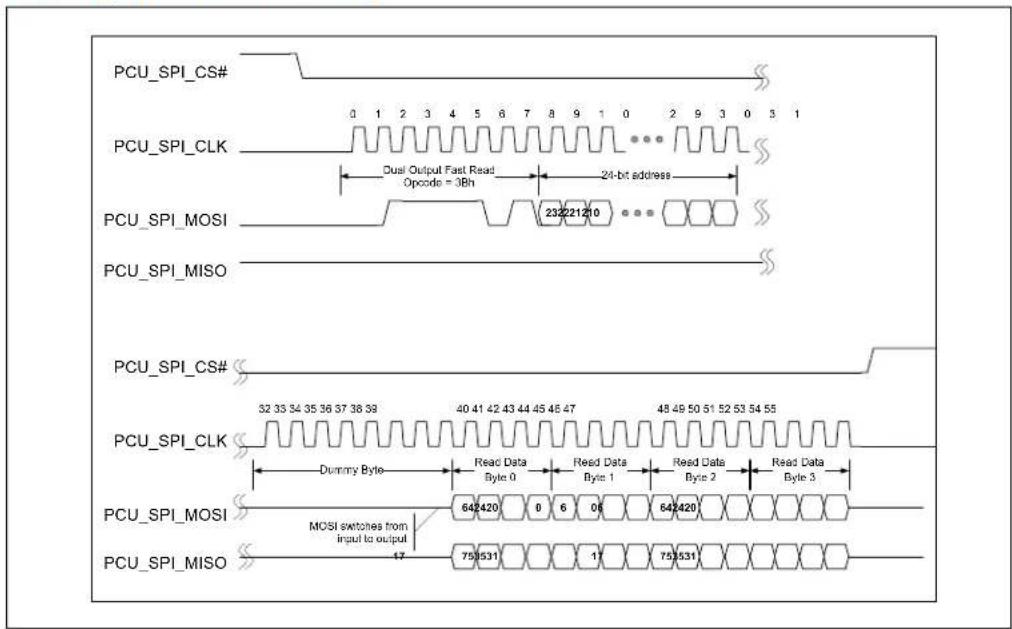
JEDEC ID
Since each serial Flash device may have unique capabilities and commands, the JEDEC ID is the necessary mechanism for identifying the device so the uniqueness of the device can be comprehended by the controller (master). The JEDEC ID uses the opcode 9Fh and a specified implementation and usage model. This JEDEC Standard Manufacturer and Device ID read method is defined in Standard JESD21-C, PRN03-NV.
Error Correction and Detection
If the first 8 bits specify an opcode which is not supported the slave will not respond and wait for the next high to low transition on PCU_SPI_CS[1:0]#. The SPI controller should automatically discard 8 bit words that were not completely received upon de-assertion of the signal.
Any other error correction or detection mechanisms must be implemented in firmware and/or software.
16.2.6 Multiple Page Write Usage Model
The BIOS and Trusted Execution Engine firmware usage models require that the serial Flash device support multiple writes to a page (minimum of 512 writes) without requiring a preceding erase command. The BIOS commonly uses capabilities such as counters that are used for error logging and system boot progress logging. These counters are typically implemented by using byte-writes to 'increment' the bits within a page that have been designated as the counter. The Trusted Execution Engine firmware usage model requires the capability for multiple data updates within any given page. These data updates occur using byte-writes without executing a preceding erase to the given page. Both the BIOS and Trusted Execution Engine firmware multiple page write usage models apply to sequential and non-sequential data writes.
This usage model requirement is based on any given bit only being written once from a '1' to a '0' without requiring the preceding erase. An erase would be required to change bits back to the 1 state.
16.2.7 Soft Flash Protection
There are two types of Flash protection that are not defined in the Flash descriptor supported by the SPI controller:
- Flash Range Read and Write Protection
- Global Write Protection
16.2.7.1 Flash Range Read and Write Protection
The SPI controller provides a method for blocking reads and writes to specific ranges in the Flash when the Protected Ranges are enabled. This is achieved by checking the read or write cycle type and the address of the requested command against the base and limit fields of a Read or Write Protected range. Protected range registers are only applied to Programmed Register accesses and have no effect on Direct Reads.
Note: Once BIOS has locked down the Protected BIOS Range registers, this mechanism remains in place until the next system reset.
16.2.7.2 Global Write Protection
The SPI controller has a Write Protection Disable (BCR.WPD) configuration bit. When BCR.WPD=0b, BIOS is not able to perform any write or erase commands to the Flash. When BCR.WPD=1b, protection against BIOS erase and rewrite is disabled. When the lock enable (BCR.LE) bit is set, the BIOS can disable this protection only during System Management Mode (SMM) execution.
If BCR.LE=1b, the SPI controller confirms that only SMM code succeeds to set BCR.WPD=1b. In addition, if BCS.SMIWPEN=1b, the SPI controller should initiate an SMI when non SMM code tries to set BCR.WPD=1b.
16.2.8 SPI Flash Device Recommended Pinout
This table contains the recommended serial Flash device pin-out for an 8-pin device. Use of the recommended pin-out on an 8-pin device reduces complexities involved with designing the serial Flash device onto a motherboard and allows for support of a common footprint usage model (refer to Section 16.2.9.1).
Table 94. Recommended Pinout for 8-Pin Serial Flash Device
| Pin # Signal | |
| 1 | C |
| 2 | D |
| 3 Write Protect | |
| 4 Ground | |
| 5 Data Input | |
| 6 Serial Clock | |
| 7 | H |
| 8 Supply Voltage |
Although an 8-pin device is preferred over a 16-pin device due to footprint compatibility, Table 95 contains the recommended serial Flash device pin-out for a 16-pin SOIC.
16.2.9 Serial Flash Device Package
Table 95. Recommended Pinout for 16-Pin Serial Flash Device
| Pin # | Signal | Pin # | Signal |
| 1 | Hold / Reset | 9 | Write Protect |
| 2 | Supply Voltage | 10 | Ground |
| 3 | No Connect | 11 | No Connect |
| 4 | No Connect | 12 | No Connect |
| 5 | No Connect | 13 | No Connect |
Table 95. Recommended Pinout for 16-Pin Serial Flash Device
| Pin # | Signal | Pin # | Signal |
| 6 No Connect | 14 No Connect | ||
| 7 Chip Select | 15 Serial Data In | ||
| 8 | Serial Data Out | 16 | Serial Clock |
16.2.9.1 Common Footprint Usage Model
To minimize platform motherboard redesign and to enable platform Bill of Material (BOM) selectability, many OEMs design their motherboard with a single common footprint. This common footprint allows the population of a soldered down device or a socket that accepts a leadless device. This enables the board manufacturer to support, using selection of the appropriate BOM, either of these solutions on the same system without requiring any board redesign.
The common footprint usage model is desirable during system debug and by Flash content developers since the leadless device can be easily removed and reprogrammed without damage to device leads. When the board and Flash content is mature for high-volume production, both the socketed leadless solution and the soldered down leaded solution are available through BOM selection.
16.2.9.2 Serial Flash Device Package Recommendations
It is highly recommended that the common footprint usage model be supported. An example of how this can be accomplished is as follows:
- The recommended pinout for 8-pin serial Flash devices is used (refer to Table 94).
- The 8-pin device is supported in either an 8-contact VDFPN (6x5 mm MLP) package or an 8-contact WSON (5x6 mm) package. These packages can fit into a socket that is land pattern compatible with the wide body SO8 package.
- The 8-pin device is supported in the SO8 (150 mil) and in the wide-body SO8 (200 mil) packages.
- The 16-pin device is supported in the SO16 (300 mil) package.
16.3 Use
16.3.1 Hardware vs. Software Sequencing
Hardware and Software sequencing are the two methods the SoC uses to communicate with the Flash via programming registers for each of the three masters.
16.3.1.1 Hardware Sequencing
Hardware sequencing has a predefined list of opcodes, refer Table 93 for more details, with only the erase opcode being programmable. This mode is only available if the descriptor is present and valid. Security Engine firmware must use HW sequencing, so
BIOS must properly set up the SoC to account for this. The Host VSCC registers and VSCC Table have to be correctly configured for BIOS and Security Engine have read/write access to SPI.
16.3.1.2 Software Sequencing
All commands other than the standard (memory) reads must be programmed by the software in the Software Sequencing Control, Flash Address, Flash Data, and Opcode configuration registers. Software must issue either Read ID or Read JEDEC ID, or a combination of the two to determine what Flash component is attached. Based on the Read ID, software can determine the appropriate Opcode instructions sets to set in the program registers and at what SPI frequency to run the command.
Software must program the Flash Linear Address for all commands, even for those commands that don't require address such as the Read ID or Read Status. This is because the SPI controller uses the address to determine which chip select to use.
The opcode type and data byte count fields determine how many clocks to run before deasserting the chip enable. The Flash data is always shifted in for the number of bytes specified and the Flash Data out is always shifted out for the number of data bytes specified. Note that the hardware restricts the burst lengths that are allowed.
A status bit indicates when the cycle has completed on the SPI port allowing the host to know when read results can be checked and/or when to initiate a new command.
The controller also provides the "Atomic Cycle Sequence" for performing erases and writes to the SPI Flash. When this bit is 1 (and the Go bit is written to 1), a sequence of cycles is performed on the SPI interface without allowing other SPI device to arbitrate and interleave cycles to the Flash device. In this case, the specified cycle is preceded by the Prefix Command (8-bit programmable Opcode) and followed by repeated reads to the Status Register (Opcode 05h) until bit 0 indicates the cycle has completed. The hardware does not attempt to check that the programmed cycle is a write or erase.
If a Programmed Access is initiated (Cycle Go written to 1) while the SPI controller is already busy with a Direct Memory Read, then the SPI Host hardware will hold the new Programmed Access pending until the preceding SPI access completes.
Once the SPI controller has committed to running a programmed access, subsequent writes to the programmed cycle registers that occur before it has completed will not modify the original transaction and will result in the assertion of the FCERR bit. Software should never purposely behave in this way and rely on this behavior. However, the FCERR bit provides basic error-reporting in this situation. Writes to the following registers cause the FCERR bit assertion in this situation:
- Software Sequencing Control
- Software Sequencing Address
- SPI Data
With the exception of Illegal Opcodes, the SPI controller does not police which opcodes are valid to be used in SW Sequencing. For example, if SW programs a Dual Output Fast Read opcode, then the Dual Output Fast Read cycle will be issued, independent of whether the Dual Output Fast Read enable bit was set in the component descriptor section.
17 PCU - Universal Asynchronous Receiver/Transmitter (UART)
This section describes the Universal Asynchronous Receiver/Transmitter (UART) serial port integrated into the PCU. The UART may be controlled through programmed IO.
Note:
Only a minimal ball-count, comprising receive & transmit signals, UART port is implemented. Further, a maximum baud rate of only 115,200 bps is supported. For this reason, it is recommended that the UART port be used for debug purposes only.
![graph TD A["UART"] --> B["SPI"] A --> C["PMC"] B --> D["iLB"] C --> D D --> E["10"] D --> F["10"] D --> G["10"] D --> H["10"] D --> I["10"] D --> J["10"]](/content/2026/08/1584379/images/c68ec7bed98586123f6797cb3a0d6d604cbd0a08c367908fc194945400a7731d.jpg)
17.1 Signal Descriptions
Refer Chapter 2, "Physical Interfaces" for additional details.
The signal description table has the following headings:
• Signal Name: The name of the signal/pin
- Direction: The buffer direction can be either input, output, or I/O (bidirectional)
- Type: The buffer type found in Chapter 29, "Electrical Specifications"
- Description: A brief explanation of the signal's function
Table 96. UART Signals
| Signal Name | Direction /Type | Description |
| PCU_UART_RXD | I | COM1 Receive: Serial data input from device pin to the receive port.This signal is muxed and may be used by other functions. |
| PCU_UART_TXD | O | COM1 Transmit: Serial data output from transmit port to the device pin.This signal is muxed and may be used by other functions. |
17.2 Features
The serial port consists of a UART which supports a subset of the functions of the 16550 industry standard.
The UART performs serial-to-parallel conversion on data characters received from a peripheral device and parallel-to-serial conversion on data characters received from the processor. The processor may read the complete status of the UART at any time during the functional operation. Available status information includes the type and condition of the transfer operations being performed by the UART and any error conditions.
The serial port may operate in either FIFO or non-FIFO mode. In FIFO mode, a 16-byte transmit FIFO holds data from the processor to be transmitted on the serial link and a 16-byte Receive FIFO buffers data from the serial link until read by the processor.
The UART includes a programmable baud rate generator which is capable of generating a baud rate of between 50 bps and 115,200 bps from a fixed baud clock input of 1.8432 MHz. The baud rate is calculated as follows:
Baud Rate Calculation:
BaudRate = 1 . 8 4 3 2 × 1 0 ^ 61 6 Divisor ×
The divisor is defined by the Divisor Latch LSB and Divisor Latch MSB registers. Some common values are shown in Table 97.
Table 97. Baud Rate Examples
| Desired Baud Rate Divisor | Divisor Latch LSB Register | Divisor Latch MSB Register | |
| 115,200 1 1h 0h | |||
| 57,600 2 2h 0h | |||
| 38,400 3 3h 0h | |||
| 19,200 6 6h 0h | |||
| 9,600 12 | Ch | 0h | |
| 4,800 24 | 18h | 0h | |
| 2,400 48 | 30h | 0h | |
| 1,200 96 | 60h | 0h | |
| 300 | 384 | 80h | 1h |
| 50 2,304 0h 9h | |||
The UART has interrupt support and those interrupts may be programmed to the user's requirements, minimizing the computing required to handle the communications link. Each UART may operate in a polled or an interrupt driven environment as configured by software.
17.2.1 FIFO Operations
17.2.1.1 FIFO Interrupt Mode Operation
Receiver Interrupt
When the Receive FIFO and receiver interrupts are enabled (FIFO Control Register, bit 0 = 1b and Interrupt Enable Register (IIR), bit 0 = 1b), receiver interrupts occur as follows:
- The receive data available interrupt is invoked when the FIFO has reached its programmed trigger level. The interrupt is cleared when the FIFO drops below the programmed trigger level.
- The IIR receive data available indication also occurs when the FIFO trigger level is reached, and like the interrupt, the bits are cleared when the FIFO drops below the trigger level.
- The receiver line status interrupt (IIR = C6h), as before, has the highest priority. The receiver data available interrupt (IIR = C4h) is lower. The line status interrupt occurs only when the character at the top of the FIFO has errors.
- The COM1_LSR.DR bit is set to 1b as soon as a character is transferred from the shift register to the Receive FIFO. This bit is reset to 0b when the FIFO is empty.
Character Time Out Interrupt
When the receiver FIFO and receiver time out interrupt are enabled, a character time out interrupt occurs when all of the following conditions exist:
- At least one character is in the FIFO.
- The last received character was longer than four continuous character times ago (if 2 stop bits are programmed the second one is included in this time delay).
- The most recent processor read of the FIFO was longer than four continuous character times ago.
- The receiver FIFO trigger level is greater than one.
The maximum time between a received character and a timeout interrupt is 160 ms at 300 baud with a 12-bit receive character (i.e., 1 start, 8 data, 1 parity, and 2 stop bits).
When a time out interrupt occurs, it is cleared and the timer is reset when the processor reads one character from the receiver FIFO. If a time out interrupt has not occurred, the time out timer is reset after a new character is received or after the processor reads the receiver FIFO.
Transmit Interrupt
When the transmitter FIFO and transmitter interrupt are enabled (FIFO Control Register, bit 0 = 1b and Interrupt Enable Register, bit 0 = 1b), transmit interrupts occur as follows:
The Transmit Data Request interrupt occurs when the transmit FIFO is half empty or more than half empty. The interrupt is cleared as soon as the Transmit Holding Register is written (1 to 16 characters may be written to the transmit FIFO while servicing the interrupt) or the Interrupt Identification Register is read.
17.2.1.2 FIFO Polled Mode Operation
With the FIFOs enabled (FIFO Control register, bit 0 = 1b), setting Interrupt Enable register (IER), bits 3:0 = 000b puts the serial port in the FIFO polled mode of operation. Since the receiver and the transmitter are controlled separately, either one or both may be in the polled mode of operation. In this mode, software checks receiver and transmitter status through the Line Status Register (LSR). As stated in the register description:
- LSR[0] is set as long as there is one byte in the receiver FIFO.
- LSR[1] through LSR[4] specify which error(s) has occurred for the character at the top of the FIFO. Character error status is handled the same way as interrupt mode. The Interrupt Identification Register is not affected since IER[2] = 0b.
- LSR[5] indicates when the transmitter FIFO needs data.
- LSR[6] indicates that both the transmitter FIFO and shift register are empty.
- LSR[7] indicates whether there are any errors in the receiver FIFO.
17.3 Use
17.3.1 Base I/O Address
The base I/O address for the COM1 UART is fixed to 3F8h.
17.3.2 Legacy Interrupt
The legacy interrupt assigned to the COM1 UART is fixed to IRQ3.
17.4 UART Enable/Disable
The COM1 UART may be enabled or disabled using the UART_CONT.COM1EN register bit. By default, the UART is disabled.
Note: It is recommended that the UART be disabled during normal platform operation. An enabled UART can interfere with platform power management.
18 PCU - Intel Legacy Block (iLB) Overview
The Intel Legacy Block (iLB) is a collection of disparate functional blocks that are critical for implementing the legacy PC platform features. These blocks include:
• PCU - iLB - Low Pin Count (LPC) Bridge
• PCU - iLB - Real Time Clock (RTC)
• PCU - iLB - 8254 Timers
• PCU - iLB - High Precision Event Timer (HPET)
- PCU - iLB - GPIO
- PCU - iLB - IO APIC
• PCU - iLB - 8259 Programmable Interrupt Controllers (PIC)
The iLB also implements a register range for configuration of some of those blocks along with support for Non-Maskable Interrupts (NMI).
![graph TD subgraph Platform Control Unit A["UART"] --> B["SPI"] B --> C["PMC"] C --> D["LPC"] D --> E["GPIO"] E --> F["RTC"] F --> G["8254"] G --> H["HPET"] H --> I["8259"] I --> J["APIC"] end style Platform Control Unit fill:#f9f,stroke:#333 style iLB fill:#ccf,stroke:#333](/content/2026/08/1584379/images/6548ed3edd20be4b61665b7dd4993036d4688f359d09df7d26f070d0f51a2dc2.jpg)
18.1 Signal Descriptions
Refer Chapter 2, "Physical Interfaces" for additional details as well as the subsequent sections.
The signal description table has the following headings:
• Signal Name: The name of the signal/pin
- Direction: The buffer direction can be either input, output, or I/O (bidirectional)
- Type: The buffer type found in Chapter 29, "Electrical Specifications"
- Description: A brief explanation of the signal's function
Table 98. iLB Signals
| Signal Name | Direction /Type | Description |
| ILB_NMI | I Non-Maskable Interrupt: This is an NMI event indication into the SoC.This signal is muxed and may be used by other functions. | |
18.2 Features
18.2.1 Key Features
The key features of various blocks are as follows:
- LPC Interface
— Supports Low Pin Count (LPC) 1.1 Specification
— No support for DMA or bus mastering
— Supports Trusted Platform Module (TPM) 1.2
- General Purpose Input Output
— Legacy control interface for SoC GPIOs
• 8259 Programmable Interrupt Controller
— Legacy interrupt support
— 15 total interrupts through two cascaded controllers
• I/O Advanced Programmable Interrupt Controller
— Legacy-free interrupt support
— 87 total interrupts
• 8254
— Legacy timer support
— Three timers with fixed uses: System Timer, Refresh Request Signal and Speaker Tone
• HPET - High Performance Event Timers
— Legacy-free timer support
— Three timers and one counter
• Real-Time Clock (RTC)
— 242 byte RAM backed by battery (aka CMOS RAM)
— Can generate wake/interrupt when time matches programmed value
— I/O and indexed registers
18.2.2 Non-Maskable Interrupt
NMI support is enabled by setting the NMI Enable (NMI_EN) bit, at IO Port 70h, Bit 7, to 1b.
Non-Maskable Interrupts (NMIs) can be generated by several sources, as described in Table 99.
Table 99. NMI Sources
| NMI Source | NMI Source Enabler/Disabler | NMI Source Status | Alternate Configuration |
| SERR# goes activeNOTE:A SERR# is only generated internally in the SoC) | NSC.SNE NSC.SNS All NMI sources may, alternatively, generate a SMI by settingGNMI.NMI2SMIEN=1b | ||
| IOCHK# goes activeNOTE:A IOCHK# is only generated as a SERIRQ# frame | NSC.INE NSC.INS | The SoC usesGNMI.NMI2SMIST for observing SMI status | |
| ILB_NMI goes activeNOTE:Active can be defined as being on the positive or negative edge of the signal using the GNMI.GNMIED register bit. | GNMI.GNMIED | GNMI.GNMIS | |
| Software sets the GNMI.NMIN register bit | GNMI.NMIN | GNMI.NMINS | |
18.2.3 S0ix Support
During S0i1, the iLB is kept running. During S0i2 & S0i3, the iLB is halted.
18.3 Use
18.3.1 S0ix Support
Prior to entry into S0i2 or S0i3 state, the driver/OS must set HPET_GCFG.EN to 0b to indicate RTD3hot status.
19 PCU - iLB - Low Pin Count (LPC) Bridge
The SoC implements an LPC Interface as described in the LPC 1.1 Specification. The Low Pin Count (LPC) bridge function of the SoC resides in PCI Device 31, Function 0.
Note:
In addition to the LPC bridge interface function, D31:F0 contains other functional units including interrupt controllers, timers, power management, system management, GPIO, and RTC.
![graph TD A["UART"] --> B["SPI"] B --> C["PMC"] C --> D["LPC"] D --> E["GPIO"] D --> F["RTC"] D --> G["8254"] D --> H["HPET"] D --> I["8259"] D --> J["APIC"] K["iLB"] --> L["Platform Control Unit"] style K fill:#f9f,stroke:#333,stroke-width:2px](/content/2026/08/1584379/images/33c9d1f52f9647c23f67be27e85d09a8fbfbf9382794bb8613a616a17c2eed33.jpg)
19.1 Signal Descriptions
Refer Chapter 2, "Physical Interfaces" for additional details.
The signal description table has the following headings:
• Signal Name: The name of the signal/pin
• Direction: The buffer direction can be either input, output, or I/O (bidirectional)
- Type: The buffer type found in Chapter 29, "Electrical Specifications"
- Description: A brief explanation of the signal's function
Table 100. LPC Signals
| Signal Name | Direction/ Type | Description |
| ILB_LPC_AD[3:0] | I/O CMOS3.3/ 1.8 | LPC Multiplexed Command, Address, Data: Internal pull-ups are provided for these signals. These signals are muxed and may be used by other functions. |
| ILB_LPC_CLK[0] O | CMOS3.3/ 1.8 | LPC Clock [0] Out: 25 MHz PCI-like clock driven to LPC peripherals. These signals are muxed and may be used by other functions. |
| ILB_LPC_CLK[1] | O or I CMOS3.3/ 1.8 | LPC Clock [1] Out: 25 MHz PCI-like clock driven to LPC peripherals. Can be configured as an input to compensate for board routing delays through Soft Strap. These signals are muxed and may be used by other functions. |
| ILB_LPC_CLKRUN# | I/OD CMOS3.3/ 1.8 | LPC Clock Run: Input to determine the status of ILB_LPC_CLK and an open drain output used to request starting or speeding up ILB_LPC_CLK. This is a sustained tri-state signal used by the central resource to request permission to stop or slow ILB_LPC_CLK. The central resource is responsible for maintaining the signal in the asserted state when ILB_LPC_CLK is running and deasserts the signal to request permission to stop or slow ILB_LPC_CLK. An internal pull-up is provided for this signal. This signal is muxed and may be used by other functions. |
| ILB_LPC_FRAME# O | CMOS3.3/ 1.8 | LPC Frame: This signal indicates the start of an LPC cycle, or an abort. This signal is muxed and may be used by other functions. |
| ILB_LPC_SERIRQ | I/O CMOS1.8 | Serial Interrupt Request: This signal implements the serial interrupt protocol. This signal is muxed and may be used by other functions. |
19.2 Features
The LPC interface to the SoC is shown in Figure 36. Note that the SoC implements all of the signals that are shown as optional, but peripherals are not required to do so.
Note: The LPC controller does not implement bus mastering cycles or DMA.
Figure 36. LPC Interface Diagram
![graph LR A["SOC LPC Device"] -->|ILB_LPC_A_D["3:0"]| B["LAD [3:0"]] A -->|ILB_LPC_FRAME#| C["LFRAME#"] A -->|PMC_PLTRST#| D["LRESET#"] A -->|ILB_LPC_CLK| E["LCLK"] A -->|ILB_LPC_SERIRQ| F["SERIRQ (Optional)"] A -->|ILB_LPC_CLKRUN#| G["CLKRUN# (Optional)"] A -->|PMC_SUS_STAT#| H["LPCPD# (Optional)"]…](/content/2026/08/1584379/images/af27590e23c435483fcdfb1ea4c66a5eddc4bf6a7c55da85bdb84e3f72965beb.jpg)
NOTE: The General Purpose Input (GPI) must use a SMI capable GPIO: GPIO_S0_SC[7:0].
19.2.1 Memory Cycle Notes
For cycles below 16M, the LPC Controller will perform standard LPC memory cycles. For cycles targeting firmware (BIOS/EFI code only), firmware memory cycles are used. Only 8-bit transfers are performed. If a larger transfer appears, the LPC controller will break it into multiple 8-bit transfers until the request is satisfied.
If the cycle is not claimed by any peripheral (and subsequently aborted), the LPC Controller will return a value of all 1's to the CPU.
19.2.2 Trusted Platform Module (TPM) 1.2 Support
The LPC interface supports accessing Trusted Platform Module (TPM) 1.2 devices via the LPC TPM START encoding. Memory addresses within the range FED00000h to FED40FFFh will be accepted by the LPC Bridge and sent on LPC as TPM special cycles. No additional checking of the memory cycle is performed.
Note: This is different to the FED00000h to FED4BFFFh range implemented on some other Intel components since no Intel® Trusted Execution Technology (Intel® TXT) transactions are supported.
19.2.3 FWH Cycle Notes
If the LPC controller receives any SYNC returned from the device other than short (0101), long wait (0110), or ready (0000) when running a FWH cycle, indeterminate results may occur. A FWH device is not allowed to assert an Error SYNC.
BIOS/EFI boot from LPC is not supported when Secure Boot is enabled.
19.2.4 Other Notes
All cycles that are not decoded internally, and are not targeted for LPC (i.e., configuration cycles, IO cycles above 64KB and memory cycles above 16MB), will be sent to LPC with ILB_LPC_FRAME# not asserted.
19.2.5 POST Code Redirection
Writes to addresses 80h - 8Fh in IO register space will also be passed to the LPC bus.
Note: Reads of these addresses do not result in any LPC transactions.
19.2.6 Power Management
19.2.6.1 LPCPD# Protocol
Same timings as for PMC_SUS_STAT#. After driving PMC_SUS_STAT# active, the SoC drives ILB_LPC_FRAME# low, and tri-states (or drives low) ILB_LPC_AD[3:0].
Note: The Low Pin Count Interface Specification, Revision 1.1 defines the LPCPD# protocol where there is at least 30 μs from LPCPD# assertion to LRST# assertion. This specification explicitly states that this protocol only applies to entry/exit of low power states which does not include asynchronous reset events. The SoC asserts both PMC_SUS_STAT# (connects to LPCPD#) and ILB_PLTRST# (connects to LRST#) at the same time during a global reset. This is not inconsistent with the LPC LPCPD# protocol.
19.2.6.2 Clock Run (CLKRUN)
When there are no pending LPC cycles, and SERIRQ is in quiet mode, the SoC can shut down the LPC clock. The SoC indicates that the LPC clock is going to shut down by de-asserting the ILB_LPC_CLKRUN# signal. LPC devices that require the clock to stay running should drive ILB_LPC_CLKRUN# low within 4 clocks of its de-assertion. If no device drives the signal low within 4 clocks, the LPC clock will stop. If a device asserts ILB_LPC_CLKRUN#, the SoC will start the LPC clock and assert ILB_LPC_CLKRUN#.
Note: The CLKRUN protocol is disabled by default. Refer Section 19.3.2.2, "Clock Run Enable" on page 223 for further details.
19.2.7 Serialized IRQ (SERIRQ)
The interrupt controller supports a serial IRQ scheme. The signal used to transmit this information is shared between the interrupt controller and all peripherals that support serial interrupts. The signal line, ILB_LPC_SERIRQ, is synchronous to LPC clock, and follows the sustained tri-state protocol that is used by LPC signals. The serial IRQ protocol defines this sustained tri-state signaling in the following fashion:
• S - Sample Phase: Signal driven low
• R - Recovery Phase: Signal driven high
• T - Turn-around Phase: Signal released
The interrupt controller supports 21 serial interrupts. These represent the 15 ISA interrupts (IRQ0- 1, 3-15), the four PCI interrupts, and the control signals SMI# and IOCHK#. Serial interrupt information is transferred using three types of frames:
- Start Frame: ILB_LPC_SERIRQ line driven low by the interrupt controller to indicate the start of IRQ transmission
- Data Frames: IRQ information transmitted by peripherals. The interrupt controller supports 21 data frames.
- Stop Frame: ILB_LPC_SERIRQ line driven low by the interrupt controller to indicate end of transmission and next mode of operation.
19.2.7.1 Start Frame
The serial IRQ protocol has two modes of operation which affect the start frame:
- Continuous Mode: The interrupt controller is solely responsible for generating the start frame
- Quiet Mode: Peripheral initiates the start frame, and the interrupt controller completes it.
These modes are entered via the length of the stop frame.
Continuous mode must be entered first, to start the first frame. This start frame width is 8 LPC clocks. This is a polling mode.
In Quiet mode, the ILB_LPC_SERIRQ line remains inactive and pulled up between the Stop and Start Frame until a peripheral drives ILB_LPC_SERIRQ low. The interrupt controller senses the line low and drives it low for the remainder of the Start Frame. Since the first LPC clock of the start frame was driven by the peripheral, the interrupt controller drives ILB_LPC_SERIRQ low for 1 LPC clock less than in continuous mode. This mode of operation allows for lower power operation.
19.2.7.2 Data Frames
Once the Start frame has been initiated, the ILB_LPC_SERIRQ peripherals start counting frames based on the rising edge of ILB_LPC_SERIRQ. Each of the IRQ/DATA frames has exactly 3 phases of 1 clock each:
- Sample Phase: During this phase, a device drives ILB_LPC_SERIRQ low if its corresponding interrupt signal is low. If its corresponding interrupt is high, then the ILB_LPC_SERIRQ devices tri-state ILB_LPC_SERIRQ. ILB_LPC_SERIRQ remains high due to pull-up resistors.
- Recovery Phase: During this phase, a device drives ILB_LPC_SERIRQ high if it was driven low during the Sample Phase. If it was not driven during the sample phase, it remains tri-stated in this phase.
- Turn-around Phase: The device tri-states ILB_LPC_SERIRQ.
19.2.7.3 Stop Frame
After the data frames, a Stop Frame will be driven by the interrupt controller. ILB_LPC_SERIRQ will be driven low for two or three LPC clocks. The number of clocks is determined by the SCNT.MD register bit. The number of clocks determines the next mode, as indicated in Table 10 1.
Table 101. SERIRQ, Stop Frame Width to Operation Mode Mapping
| Stop Frame Width | Next Mode |
| Two LPC clocks | Quiet Mode: Any SERIRQ device initiates a Start Frame |
| Three LPC clocks | Continuous Mode: Only the interrupt controller initiates a Start Frame |
19.2.7.4 Serial Interrupts Not Supported
There are four interrupts on the serial stream which are not supported by the interrupt controller. These interrupts are:
- IRQ0: Heartbeat interrupt generated off of the internal 8254 counter 0.
- IRQ8: RTC interrupt can only be generated internally.
- IRQ13: This interrupt (floating point error) is not supported.
The interrupt controller will ignore the state of these interrupts in the stream.
19.2.7.5 Data Frame Format and Issues
Table below shows the format of the data frames.
The other interrupts decoded via SERIRQ are also ANDed with the corresponding internal interrupts. For example, if IRQ10 is set to be used as the SCI, then it is ANDed with the decoded value for IRQ10 from the SERIRQ stream.
Table 102. SERIRQ Interrupt Mapping
| Data Frame # | Interrupt | Clocks Past Start Frame | Comment |
| 1 IRQ0 | 2 Ignored. | Can only be generated via the internal 8524 | |
| 2 IRQ1 | 5 Before port 60h latch | ||
| 3 | SMI# | 8 Causes SMI# if low. Sets SMI_STS.ILB_SMI_STS register bit. | |
| 4 | IRQ3 | 11 | |
| 5 | IRQ4 | 14 | |
| 6 | IRQ5 | 17 | |
| 7 | IRQ6 | 20 | |
| 8 | IRQ7 | 23 |
Table 102. SERIRQ Interrupt Mapping
| Data Frame # | Interrupt | Clocks Past Start Frame | Comment |
| 9 IRQ8 26 Ignored. | IRQ8# can only be generated internally | ||
| 10 IRQ9 29 | |||
| 11 IRQ10 32 | |||
| 12 IRQ11 35 | |||
| 13 IRQ12 38 Before port 60h latch | |||
| 14 IRQ13 41 Ignored. | |||
| 15 IRQ14 44 Ignored | |||
| 16 IRQ15 47 | |||
| 17 IOCHCK# 50 Same as ISA IOCHCK# going active. | |||
19.2.7.6 S0ix Support
During S0i2 and S0i3, the LPC and SERIRQ interfaces are disabled.
19.3 Use
19.3.1 LPC Clock Delay Compensation
In order to meet LPC interface AC timing requirements, a LPC clock loop back is required. The operation of this loop back can be configured in two ways:
- On the SOC: In this configuration, ILB_LPC_CLK[0] is looped back on itself on the SOC pad.
a. Benefit:
ILB_LPC_CLK[0] and ILB_LPC_CLK[1] are both available for system clocking
b. Drawback:
Clock delay compensation is less effective at compensating for mainboard delay c. Soft Strap & Register Requirements:
Soft Strap LPCCLK_SLC = 0b Configuration is reflected by register bit LPCC.LPCCLK_SLC=0b Soft Strap LPCCLK1_ENB = 0b (ILB_LPC_CLK[1] disabled) or 1b (ILB_LPC_CLK[1] enabled)
-
Configuration is reflected by register bit LPCC.LPCCLK1EN=0b (ILB_LPC_CLK[1] disabled) or 1b (ILB_LPC_CLK[1] enabled)
-
On the main board: In this configuration, ILB_LPC_CLK[0] is looped back to ILB_LPC_CLK[1] on the main board.
a. Benefit:
Clock delay compensating in more effective at compensating for main board delay b. Drawback:
Only ILB_LPC_CLK[0] is available for system clocking. ILB_LPC_CLK[1] must be disabled.
c. Soft Strap & Register Requirements:
Soft Strap LPCCLK_SLC = 1b
Configuration is reflected by register bit LPCC.LPCCLK_SLC=1b
Soft Strap LPCCLK1_ENB = 0b (ILB_LPC_CLK[1] disabled)
Configuration is reflected by register bit LPCC.LPCCLK1EN=0b
19.3.2 LPC Power Management
19.3.2.1 Clock Enabling
The LPC clocks can be enabled or disabled by setting or clearing, respectively, the LPCC.LPCCLK[1:0]EN bits.
19.3.2.2 Clock Run Enable
The Clock Run protocol is disabled by default and should only be enabled during operating system run-time, once all LPC devices have been initialized. The Clock Run protocol is enabled by setting the LPCC.CLKRUN_EN register bit.
19.3.3 SERIRQ Disable
Serialized IRQ support may be disabled by setting the OIC.SIRQEN bit to 0b.
19.4 References
- Low Pin Count Interface Specification, Revision 1.1 (LPC): http://www.intel.com/design/chipsets/industry/lpc.htm
- Serialized IRQ Support for PCI Systems, Revision 6.0: http://www.smsc.com/media/Downloads_Public/papers/serirq60.doc
- Implementing Industry Standard Architecture (ISA) with Intel® Express Chipsets (318244): http://www.intel.com/assets/pdf/whitepaper/318244.pdf
20 PCU - iLB - Real Time Clock (RTC)
The SoC contains a Motorola MC146818B-compatible real-time clock with 242 bytes of battery-backed RAM. The real-time clock performs twos key functions—keeping track of the time of day and storing system data, even when the system is powered down. The RTC operates on a 32.768 kHz crystal and a 3.3 V battery.
The RTC supports two lockable memory ranges. By setting bits in the configuration space, two 8-byte ranges can be locked to read and write accesses. This prevents unauthorized reading of passwords or other system security information.
The RTC supports a date alarm that allows for scheduling a wake up event up to 30 days in advance.
![graph TD A["UART"] --> B["SPI"] A --> C["PMC"] B --> D["LPC"] C --> E["GPIO"] D --> F["RTC"] E --> F F --> G["8254"] F --> H["HPET"] F --> I["8259"] F --> J["APIC"] K["Platform Control Unit"] --> L["iLB"] L --> M["10"] L --> N["10"] L --> O["10"] L --> P["10"] L --> Q["10"] L --> R["10"]](/content/2026/08/1584379/images/e1ea3ff3492a5a9eb8b18d39627cff3b96a4e71bb629c31f2bbcd485daa0f951.jpg)
20.1 Signal Descriptions
Refer Chapter 2, "Physical Interfaces" for additional details.
The signal description table has the following headings:
• Signal Name: The name of the signal/pin
- Direction: The buffer direction can be either input, output, or I/O (bidirectional)
- Type: The buffer type found in Chapter 29, "Electrical Specifications"
- Description: A brief explanation of the signal's function
Table 103. RTC Signals
| Signal Name | Direction /Type | Description |
| ILB_RTC_X1 | IAnalog | Crystal Input 1: This signal is connected to the 32.768 kHz crystal. If no external crystal is used, the signal can be driven with the desired clock rate. |
| ILB_RTC_X2 I | Analog | Crystal Input 2: This signal is connected to the 32.768 kHz crystal. If no external crystal is used, the signal should be left floating. |
| ILB_RTC_RST# | I | RTC Reset: An external RC circuit creates a time delay for the signal such that it will go high (de-assert) sometime after the battery voltage is valid. The RC time delay should be in the 10-20 ms range.When asserted, this signal resets all register bits in the RTC well except for GEN_PMCON1.RPS.NOTE: Unless registers are being cleared (only to be done in the G3 power state), the signal input must always be high when all other RTC power planes are on.NOTE: In the case where the RTC battery is dead or missing on the platform, the signal should be deasserted before the PMC_RSMRST# signal is deasserted. |
| ILB_RTC_TEST# | I | RTC Battery Test: An external RC circuit creates a time delay for the signal such that it will go high (de-assert) sometime after the battery voltage is valid. The RC time delay should be in the 10-20 ms range. If the battery is missing/weak, this signal appears low (de-asserted) at boot just after the suspend power rail (V3P3A) is up since it will not have time to meet Vih when V3P3A is high. The weak/missing battery condition is reported in the GEN_PMCON1.RPS (RTC Power Status) register. When asserted, BIOS may clear the RTC CMOS RAM.NOTE: Unless CMOS is being cleared (only to be done in the G3 power state) or the battery is low, the signal input must always be high when all other RTC power planes are on.NOTE: This signal may also be used for debug purposes, as part of a XDP port. |
| ILB_RTC_EXTPAD | External capacitor connection | |
20.2 Features
The Real Time Clock (RTC) module provides a battery backed-up date and time keeping device. Three interrupt features are available: time of day alarm with once a second to once a month range, periodic rates of 122 ms to 500 ms, and end of update cycle notification. Seconds, minutes, hours, days, day of week, month, and year are counted. The hour is represented in twelve or twenty-four hour format, and data can be represented in BCD or binary format. The design is meant to be functionally compatible with the Motorola MS146818B. The time keeping comes from a 32.768 kHz oscillating source, which is divided to achieve an update every second. The lower 14 bytes on the
lower RAM block have very specific functions. The first ten are for time and date information. The next four (0Ah to 0Dh) are registers, which configure and report RTC functions. A host-initiated write takes precedence over a hardware update in the event of a collision.
20.2.1 Update Cycles
An update cycle occurs once a second, if the B.SET bit is not asserted and the divide chain is properly configured. During this procedure, the stored time and date are incremented, overflow checked, a matching alarm condition is checked, and the time and date are rewritten to the RAM locations. The update cycle starts at least 488 ms after A.UIP is asserted, and the entire cycle does not take more than 1984 ms to complete. The time and date RAM locations (00h to 09h) are disconnected from the external bus during this time.
20.3 Interrupts
The real-time clock interrupt is internally routed within the SoC both to the I/O APIC and the 8259. It is mapped to interrupt vector 8. This interrupt does not leave the SoC, nor is it shared with any other interrupt. IRQ8# from the ILB_LPC_SERIRQ stream is ignored. However, the High Performance Event Timers can also be mapped to IRQ8#; in this case, the RTC interrupt is blocked.
20.3.1 Lockable RAM Ranges
The RTC battery-backed RAM supports two 8-byte ranges that can be locked: the RC.UL and RC.LL register bits. When the locking bits are set, the corresponding range in the RAM is not readable or writable. A write cycle to those locations will have no effect. A read cycle to those locations will not return the location's actual value (resultant value is undefined).
Once a range is locked, the range can be unlocked only by a hard reset, which will invoke the BIOS and allow it to re-lock the RAM range.
20.3.2 Clearing Battery-Backed RTC CMOS RAM
Clearing CMOS RAM in an SoC-based platform can be done by using a jumper on ILB_RTC_TEST# or a GPI. Implementations should not attempt to clear CMOS by using a jumper to pull RTC_VCC low.
Note: The entire Extended Bank and bytes 0Eh-7Fh of the Standard Bank will be cleared.
20.3.2.1 Using ILB_RTC_TEST# to Clear the RTC CMOS RAM
A jumper on ILB_RTC_TEST# can be used to clear CMOS values. When ILB_RTC_TEST# is low, the GEN_PMCON1.RPS register bit will be set. BIOS can monitor the state of this bit, and manually clear the RTC CMOS array once the system is booted. The normal position will cause ILB_RTC_TEST# to be pulled up through a
weak pull-up resistor. This ILB_RTC_TEST# jumper technique allows the jumper to be moved and then replaced—all while the system is powered off. Then, once booted, the GEN_PMCON1.RPS bit can be detected in the set state.
20.3.3 Using GPI to Clear CMOS
A jumper on a GPI can also be used to clear CMOS values. BIOS should detect the setting of this GPI on system boot-up, and manually clear the CMOS array.
Note: The GPI strap technique to clear CMOS requires multiple steps to implement. The system is booted with the jumper in new position, then powered back down. The jumper is replaced back to the normal position, then the system is rebooted again.
Warning: Do not implement a jumper on RTC_VCC to clear CMOS.
20.3.4 Clearing Battery Backed RTC Registers
Clearing Battery Backed RTC Registers in an SoC based platform can be done by using a jumper on ILB_RTC_RST#. Implementations should not attempt to clear the registers by using a jumper to pull RTC_VCC low. A jumper on ILB_RTC_RST# pulled to ground can be used to reset the state of those Battery Backed RTC Register configurations bit that reside in the RTC power well to their default state. Table 104 shows which bits are set to their default state when ILB_RTC_RST# is asserted low.
Table 104. Register Bits Reset by ILB_RTC_RST# Assertion
| Register Bit Bit(s) Default | State | |
| RCRB_GENERAL_CONTROL.TS 1 xb | ||
| GEN_PMCON1.PME_B0_S5_DIS 15 | 0b | |
| GEN_PMCON1.WOL_EN_OVRD | 13 | 0b |
| GEN_PMCON1.DIS_SLP_X_STRCH_SUS_UP | 12 | 0b |
| GEN_PMCON1.RTC Reserved | 8 0b | |
| GEN_PMCON1.SWSMI_RATESEL | 7:6 | 00b |
| GEN_PMCON1.S4MAW | 5:4 | 00b |
| GEN_PMCON1.S4ASE | 3 0b | |
| GEN_PMCON1.AG3E | 0 0b | |
| PM1_STS_EN.RTC_EN | 26 | 0b |
| PM1_STS_EN.PWRBTNOR_STS 11 | 0b | |
| PM1_CNT.SLP_TYP | 12:10 | 0b |
| GPE0a_EN.PME_B0_EN | 13 | 0b |
| GPE0a_EN.BATLOW_EN | 10 | 0b |
20.3.5 S0ix Support
During S0i3, the RTC interface is active.
20.4 References
Accessing the Real Time Clock Registers and the NMI Enable Bit: http://download.intel.com/design/intarch/PAPERS/321088.pdf
21 PCU - iLB - 8254 Timers
The 8254 contains three counters which have fixed uses including system timer and speaker tone. All registers are clocked by a 14.31818 MHz clock.
![graph TD A["UART"] --> B["10"] C["SPI"] --> D["10"] E["PMC"] --> F["10"] G["LPC"] --> H["10"] I["GPIO"] --> J["10"] K["RTC"] --> L["10"] M["8254"] --> N["10"] O["HPET"] --> P["10"] Q["8259"] --> R["10"] S["APIC"] --> T["10"] U["iLB"] --> V["10"] W["Platform Control Unit"] --> X["10"] Y["Platform Con…](/content/2026/08/1584379/images/4fb23713ed24853554e141edc10e22f0b4006136a1bf6aaaba68169e6709238b.jpg)
21.1 Signal Descriptions
Refer Chapter 2, "Physical Interfaces" for additional details.
The signal description table has the following headings:
• Signal Name: The name of the signal/pin
- Direction: The buffer direction can be either input, output, or I/O (bidirectional)
- Type: The buffer type found in Chapter 29, "Electrical Specifications"
- Description: A brief explanation of the signal's function
Table 105. 8254 Signals
| Signal Name | Direction /Type | Description |
| ILB_8254_SPKR | 0 | Speaker:The signal drives an external speaker driver device, which in turn drives the system speaker. Upon PMC_PLTRST#, its output state is 0.This signal is muxed and may be used by other functions. |
21.2 Features
21.2.1 Counter 0, System Timer
This counter functions as the system timer by controlling the state of IRQ0 and is programmed for Mode 3 operation. The counter produces a square wave with a period equal to the product of the counter period (838 ns) and the initial count value. The
counter loads the initial count value one counter period after software writes the count value to the counter I/O address. The counter initially asserts IRQ0 and decrements the count value by two each counter period. The counter negates IRQ0 when the count value reaches 0. It then reloads the initial count value and again decrements the initial count value by two each counter period. The counter then asserts IRQ0 when the count value reaches 0, reloads the initial count value, and repeats the cycle, alternately asserting and negating IRQ0.
21.2.2 Counter 1, Refresh Request Signal
This counter is programmed for Mode 2 operation and impacts the period of the NSC.RTS register bit. Programming the counter to anything other than Mode 2 results in undefined behavior.
21.2.3 Counter 2, Speaker Tone
This counter provides the speaker tone and is typically programmed for Mode 3 operation. The counter provides a speaker frequency equal to the counter clock frequency (1.193 MHz) divided by the initial count value. The speaker must be enabled by a write to the NSC.SDE register bit.
21.2.4 S0ix Support
During S0i2 & S0i3, the 8254 timer is halted. A platform that requires the 8254 timer to be always active, should disable S0i2/3 using the S0ix_Enable register.
21.3 Use
21.3.1 Timer Programming
The counter/timers are programmed in the following fashion:
- Write a control word to select a counter.
- Write an initial count for that counter.
- Load the least and/or most significant bytes (as required by Control Word Bits 5, 4) of the 16-bit counter.
- Repeat with other counters.
Only two conventions need to be observed when programming the counters. First, for each counter, the control word must be written before the initial count is written. Second, the initial count must follow the count format specified in the control word (least significant byte only, most significant byte only, or least significant byte and then most significant byte).
A new initial count may be written to a counter at any time without affecting the counter's programmed mode. Counting is affected as described in the mode definitions. The new count must follow the programmed count format.
If a counter is programmed to read/write two-byte counts, the following precaution applies: A program must not transfer control between writing the first and second byte to another routine which also writes into that same counter. Otherwise, the counter will be loaded with an incorrect count.
The Control Word Register at port 43h controls the operation of all three counters. Several commands are available:
- Control Word Command. Specifies which counter to read or write, the operating mode, and the count format (binary or BCD).
- Counter Latch Command. Latches the current count so that it can be read by the system. The countdown process continues.
- Read Back Command. Reads the count value, programmed mode, the current state of the OUT pins, and the state of the Null Count Flag of the selected counter.
Table 106 lists the six operating modes for the interval counters.
Table 106. Counter Operating Modes
| Mode | Function Description | |
| 0 | Out signal on end of count (=0) Output is 0. When count goes to 0, output goes to 1 and stays at 1 until counter is reprogrammed. | |
| 1 | Hardware re-triggerable one-shot | Output is 0. When count goes to 0, output goes to 1 for one clock time. |
| 2 | Rate generator (divide by n counter) | Output is 1. Output goes to 0 for one clock time, then back to 1 and counter is reloaded. |
| 3 | Square wave output Output is 1. Output goes to 0 when counter rolls over, and counter is reloaded. Output goes to 1 when counter rolls over, and counter is reloaded, etc. | |
| 4 | Software triggered strobe | Output is 1. Output goes to 0 when count expires for one clock time. |
| 5 | Hardware triggered strobe | Output is 1. Output goes to 0 when count expires for one clock time. |
21.3.2 Reading from Interval Timer
It is often desirable to read the value of a counter without disturbing the count in progress. There are three methods for reading the counters: a simple read operation, counter Latch command, and the Read-Back command. Each is explained below.
With the simple read and counter latch command methods, the count must be read according to the programmed format; specifically, if the counter is programmed for two byte counts, two bytes must be read. The two bytes do not have to be read one right after the other. Read, write, or programming operations for other counters may be inserted between them.
21.3.2.1 Simple Read
The first method is to perform a simple read operation. The counter is selected through Port 40h (Counter 0), 41h (Counter 1), or 42h (Counter 2).
Note: Performing a direct read from the counter does not return a determinate value, because the counting process is asynchronous to read operations. However, in the case of Counter 2, the count can be stopped by writing 0b to the NSC.TC2E register bit.
21.3.2.2 Counter Latch Command
The Counter Latch command, written to Port 43h, latches the count of a specific counter at the time the command is received. This command is used to ensure that the count read from the counter is accurate, particularly when reading a two-byte count. The count value is then read from each counter's Count register as was programmed by the Control register.
The count is held in the latch until it is read or the counter is reprogrammed. The count is then unlatched. This allows reading the contents of the counters on the fly without affecting counting in progress. Multiple Counter Latch Commands may be used to latch more than one counter. Counter Latch commands do not affect the programmed mode of the counter in any way.
If a counter is latched and then, some time later, latched again before the count is read, the second Counter Latch command is ignored. The count read is the count at the time the first Counter Latch command was issued.
21.3.2.3 Read Back Command
The Read Back command, written to Port 43h, latches the count value, programmed mode, and current states of the OUT pin and Null Count flag of the selected counter or counters. The value of the counter and its status may then be read by I/O access to the counter address.
The Read Back command may be used to latch multiple counter outputs at one time. This single command is functionally equivalent to several counter latch commands, one for each counter latched. Each counter's latched count is held until it is read or reprogrammed. Once read, a counter is unlatched. The other counters remain latched until they are read. If multiple count Read Back commands are issued to the same counter without reading the count, all but the first are ignored.
The Read Back command may additionally be used to latch status information of selected counters. The status of a counter is accessed by a read from that counter's I/O port address. If multiple counter status latch operations are performed without reading the status, all but the first are ignored.
Both count and status of the selected counters may be latched simultaneously. This is functionally the same as issuing two consecutive, separate Read Back commands. If multiple count and/or status Read Back commands are issued to the same counters without any intervening reads, all but the first are ignored.
If both count and status of a counter are latched, the first read operation from that counter returns the latched status, regardless of which was latched first. The next one or two reads, depending on whether the counter is programmed for one or two type counts, returns the latched count. Subsequent reads return unlatched count.
22 PCU - iLB - High Precision Event Timer (HPET)
This function provides a set of timers that to be used by the operating system for timing events. One timer block is implemented, containing one counter and three timers.
![graph TD A["UART"] --> B["SPI"] B --> C["PMC"] C --> D["LPC"] D --> E["GPIO"] E --> F["RTC"] F --> G["8254"] G --> H["HPET"] H --> I["8259"] I --> J["APIC"] style A fill:#f9f,stroke:#333 style B fill:#ccf,stroke:#333 style C fill:#cfc,stroke:#333 style D fill:#fcc,stroke:#333 style E fill:#cff,strok…](/content/2026/08/1584379/images/f3d3baabc468318a1a1b1b72d7ce41e948b6ebc004fba733d4d562feff75db36.jpg)
22.1 Features
22.1.1 Non-Periodic Mode - All Timers
This mode can be thought of as creating a one-shot. When a timer is set up for non-periodic mode, it generates an interrupt when the value in the main counter matches the value in the timer's comparator register. As timers 1 and 2 are 32-bit, they will generate another interrupt when the main counter wraps.
T0CV cannot be programmed reliably by a single 64-bit write in a 32-bit environment unless only the periodic rate is being changed. If T0CV needs to be re-initialized, the following algorithm is performed:
- Set TOC.TVS
- Set T0CV[31:0]
- Set TOC.TVS
- Set T0CV[63:32]
Every timer is required to support the non-periodic mode of operation.
22.1.2 Periodic Mode - Timer 0 only
When set up for periodic mode, when the main counter value matches the value in T0CV, an interrupt is generated (if enabled). Hardware then increases T0CV by the last value written to T0CV. During run-time, T0CV can be read to find out when the next periodic interrupt will be generated. Software is expected to remember the last value written to T0CV.
Example: if the value written to T0CV is 00000123h, then
- An interrupt will be generated when the main counter reaches 00000123h.
• TOCV will then be adjusted to 00000246h. - Another interrupt will be generated when the main counter reaches 00000246h.
• T0CV will then be adjusted to 00000369h.
When the incremented value is greater than the maximum value possible for TOCV, the value will wrap around through 0. For example, if the current value in a 32-bit timer is FFFF0000h and the last value written to this register is 20000, then after the next interrupt the value will change to 00010000h.
If software wants to change the periodic rate, it writes a new value to T0CV. When the timer's comparator matches, the new value is added to derive the next matching point. If software resets the main counter, the value in the comparator's value register must also be reset by setting T0C.TVS. To avoid race conditions, this should be done with the main counter halted. The following usage model is expected:
- Software clears GCFG.EN to prevent any interrupts.
- Software clears the main counter by writing a value of 00h to it.
- Software sets TOC.TVS.
- Software writes the new value in T0CV.
- Software sets GCFG.EN to enable interrupts.
22.1.2.1 Interrupts
If each timer has a unique interrupt and the timer has been configured for edge-triggered mode, then there are no specific steps required. If configured to level-triggered mode, then its interrupt must be cleared by software by writing a '1' back to the bit position for the interrupt to be cleared.
Interrupts associated with the various timers have several interrupt mapping options. Software should mask GCFG.LRE when reprogramming HPET interrupt routing to avoid spurious interrupts.
22.1.2.2 Mapping Option #1: Legacy Option (GCFG.LRE set)
This forces the following mapping:
Table 107. 8254 Interrupt Mapping
| Timer | 8259 Mapping | APIC Mapping | Comment |
| 0 IRQ0 | IRQ2 The 8254 | timer will not cause any interrupts | |
| 1 IRQ8 | IRQ8 RTC will not cause any interrupts. | ||
| 2 T2C.IR | T2C.IRC | ||
22.1.2.3 Mapping Option #2: Standard Option (GCFG.LRE cleared)
Each timer has its own routing control. The interrupts can be routed to various interrupts in the I/O APIC. T[2:0]C.IRC indicates which interrupts are valid options for routing. If a timer is set for edge-triggered mode, the timers should not be shared with any other interrupts.
22.1.3 S0ix Support
During S0i1, the HPET is kept running. During S0i2 and S0i3, the HPET is halted.
Prior to entry into S0i2 or S0i3 state, the driver/OS must set HPET_GCFG.EN to 0b to indicate RTD3 hot status.
22.2 References
IA-PC HPET (High Precision Event Timers) Specification, Revision 1.0a: http://www.intel.com/hardware design/hpetspec_1.pdf
23 PCU - iLB - GPIO
102 GPIOs are available for use during the S0 ACPI state, and 44 are available for use from S5 to S0 (SUS). Most of these GPIOs can be used as legacy GPIOs through IO registers. This section describes their use as legacy GPIOs.
![graph TD A["Platform Control Unit"] --> B["UART"] A --> C["SPI"] A --> D["PMC"] A --> E["LPC"] A --> F["GPIO"] A --> G["RTC"] A --> H["HPET"] A --> I["8254"] A --> J["APIC"] K["iLB"] --> L["GPIO"] K --> M["RTC"] K --> N["HPET"] K --> O["8259"]](/content/2026/08/1584379/images/58be2801fe966d7264cbd1fddc3e2962e529a80ae85faab1bcba5e2d85a3eed8.jpg)
23.1 Signal Descriptions
Refer Chapter 2, "Physical Interfaces" for additional details.
The signal description table has the following headings:
• Signal Name: The name of the signal/pin
- Direction: The buffer direction can be either input, output, or I/O (bidirectional)
- Type: The buffer type found in Chapter 29, "Electrical Specifications"
- Description: A brief explanation of the signal's function
Table 108. GPIO Signals
| Signal Name | Direction /Type | Description |
| GPIO_S0_SC[101:0] | I/OVaries | These GPIO pins are powered and active in S0 only. Many of these are multiplexed with other functions and may have different default pin names. |
| GPIO_S5[43:0] I/O | Varies | These GPIO pins are powered and active in S5-S0 (SUS). Many of these are multiplexed with other functions and may have different default pin names. Some are used as straps. |
23.2 Features
GPIOs can generate general purpose events (GPEs) on rising and/or falling edges.
23.3 Use
Each GPIO has six registers that control how it is used, or report its status:
- Use Select
- I/O Select
- GPIO Level
- Trigger Positive Edge
- Trigger Negative Edge
- Trigger Status
The Use Select register selects a GPIO pin as a GPIO, or leaves it as its programmed function. This register must be set for all other registers to affect the GPIO.
The I/O Select register determines the direction of the GPIO.
The Trigger Positive Edge and Trigger Negative Edge registers enable general purpose events on a rising and falling edge respectively. This only applies to GPIOs set as input.
The Trigger Status register is used by software to determine if the GPIO triggered a GPE. This only applies to GPIOs set as input and with one or both of the Trigger modes enabled.
Additionally, there is one additional register for each S5 GPIO:
- Wake Enable
This register allows S5 GPIOs to trigger a wake event based on the Trigger registers' settings.
23.4 GPIO Registers
Registers are broken into two groups: memory mapped and legacy IO registers. Memory mapped registers are used by BIOS and firmware to select the configurable function of the GPIO and setup analog states needed for that function's operation. They are named based on the pin/ball name. Legacy IO registers are the more traditional GPIO control/status type, and are used when the function selected is a traditional GPIO (direction, level, use registers). They are numbered based on the GPIO number.
Each group is further broken down into SCORE (internal partition naming) and SSUS. SCORE are for the GPIO's named GPIO_S0_SC[xxx], while SSUS are for the GPIO's named GPIO_S5[xx].
Note: All GPIO registers must be accessed as double words. Unpredictable results will occur otherwise.
Note: All memory mapped GPIO *PAD_VAL's must set Ienenb = 0 in order to read the pad_val of the GPIO. This applies to RO GPIO's as well.
vGPIO's are virtual GPIO's for use by software to generate interrupts. They are not tied to physical pins.
24 PCU - iLB - IO APIC
The IO Advanced Programmable Interrupt Controller (APIC) is used to support line interrupts more flexibly than the 8259 PIC. Line interrupts are routed to it from multiple sources, including legacy devices, via the interrupt decoder and serial IRQs, or they are routed to it from the interrupt router in the iLB. These line based interrupts are then used to generate interrupt messages targeting the local APIC in the processor.
![graph TD A["Platform Control Unit"] --> B["UART"] A --> C["SPI"] A --> D["PMC"] A --> E["LPC"] A --> F["GPIO"] A --> G["RTC"] A --> H["8254"] A --> I["HPET"] A --> J["8259"] A --> K["APIC"] L["iLB"] --> M["10"] L --> N["10"] L --> O["10"] L --> P["10"] L --> Q["10"] L --> R["10"] L --> S["10"]](/content/2026/08/1584379/images/caf07623f25e26c1006dce8f00a445c7eb9ff130fb61daf68590883c3f5b321e.jpg)
24.1 Features
- 87 interrupt lines
— IRQ0-86
- Edge or level trigger mode per interrupt
• Active low or high polarity per interrupt - Works with local APIC in processor via MSIs
• MSIs can target specific processor core
• Established APIC programming model
Figure 37. Detailed Block Diagram
![graph TD A["To/From System Bus"] --> B["FEC0 0000h"] A --> C["FEC0 0010h"] A --> D["FEC0 0040h"] B --> E["IDX"] B --> F["WDW"] B --> G["EOI"] H["MSI Machine"] --> I["ID VS"] I --> J["RTE[0"]] J --> K["..."] L["INT[86"]] --> M["RTE[86"]] M --> N["INT[86:0"]] O["INT0"] --> P["INT1"] O --> Q["INT2"] O…](/content/2026/08/1584379/images/6c5c7a7cea5a761a6e44020136bd2f7041119eb2699c1afe4e26850819aba8b5.jpg)
MSIs generated by the I/O APIC are sent as 32-bit memory writes to the Local APIC. The address and data of the write transaction are used as follows.
Figure 38. MSI Address and Data
![graph TD A["MSI Address"] --> B["31:2019:1211:43 2 1:0"] C["MSI Data"] --> D["31:16 7:010:8151413:1211"] D --> E["0000h"] D --> F["00b"] D --> G["Trigger Mode"] G --> H["Delivery Status (1b)"] D --> I["Destination Mode"] I --> J["RTE[n"].DSM] I --> K["RTE[n"].DLM] I --> L["RTE[n"].VCT] M["Destinatio…](/content/2026/08/1584379/images/67f77cc3c68155b7360643a0db3da942e14c62ce28df1352bc20ece34151a533.jpg)
Destination ID (DID) and Extended Destination ID (EDID) are used to target a specific processor core's local APIC.
24.2 Use
The I/O APIC contains indirectly accessed I/O APIC registers and normal memory mapped registers. There are three memory mapped registers:
- Index Register (IDX)
• Window Register (WDW)
• End Of Interrupt Register (EOI)
The Index register selects an indirect I/O APIC register (ID/VS/RTE[n]) to appear in the Window register.
The Window register is used to read or write the indirect register selected by the Index register.
The EOI register is written to by the Local APIC in the processor. The I/O APIC compares the lower eight bits written to the EOI register to the Vector set for each interrupt (RTE.VCT). All interrupts that match this vector will have their RTE.RIRR register cleared. All other EOI register bits are ignored.
24.3 Indirect I/O APIC Registers
These registers are selected with the IDX register, and read/written through the WDW register. Accessing these registers must be done as DW requests, otherwise unspecified behavior will result. Software should not attempt to write to reserved registers. Reserved registers may return non-zero values when read.
Note: There is one pair of redirection (RTE) registers per interrupt line. Each pair forms a 64-bit RTE register.
Note: Specified offsets should be placed in IDX, not added to IDX.
25 PCU - iLB - 8259 Programmable Interrupt Controllers (PIC)
The SoC provides an ISA-compatible programmable interrupt controller (PIC) that incorporates the functionality of two, cascaded 8259 interrupt controllers.
![graph TD A["UART"] --> B["SP1"] B --> C["PMC"] C --> D["LPC"] D --> E["GPIO"] E --> F["RTC"] F --> G["8254"] G --> H["HPET"] H --> I["8259"] I --> J["APIC"] K["iLB"] --> L["Block 1"] L --> M["Block 2"] M --> N["Block 3"] N --> O["Block 4"] O --> P["Block 5"] P --> Q["Block 6"] Q --> R["Block 7"] R -…](/content/2026/08/1584379/images/ed6e95f15df0bf22dd026cebdd4eecc08dea4f6b6f54bea1f863c683ce3aba87.jpg)
25.1 Features
In addition to providing support for ISA compatible interrupts, this interrupt controller can also support PCI based interrupts (PIRQs) by mapping the PCI interrupt onto a compatible ISA interrupt line. Each 8259 controller supports eight interrupts, numbered 0–7. Table 109 shows how the controllers are connected.
Note: The SoC does not implement any external PIRQ# signals. The PIRQs referred to in this section originate from the interrupt routing unit.
Table 109. Interrupt Controller Connections (Sheet 1 of 2)
| 8259 | 8259 Input | Connected Pin / Function |
| Master 0 | Internal Timer / Counter 0 output or HPET #0; determined by GCFG.LRE register bit | |
| 1 IRQ1 using SERIRQ, Keyboard Emulation | ||
| 2 Slave controller INTR output | ||
| 3 IRQ3 via SERIRQ, PIRQx or PCU UART 1 | ||
| 4 IRQ4 via SERIRQ or PIRQx | ||
| 5 IRQ5 via SERIRQ or PIRQx | ||
| 6 IRQ6 via SERIRQ or PIRQx | ||
| 7 IRQ7 via SERIRQ or PIRQx | ||
Table 109. Interrupt Controller Connections (Sheet 2 of 2)
| 8259 | 8259Input | Connected Pin / Function |
| Slave 0 | Inverted IRQ8# from internal RTC or HPET | |
| 1 IRQ9 via SERIRQ, SCI or PIRQx | ||
| 2 IRQ10 via SERIRQ, SCI or PIRQx | ||
| 3 IRQ11 via SERIRQ, SCI, HPET or PIRQx | ||
| 4 IRQ12 via SERIRQ, PIRQx or mouse emulation | ||
| 5 N o n e | ||
| 6 P I R Q x | ||
| 7 IRQ15 via SERIRQ or PIRQx o | ||
The SoC cascades the slave controller onto the master controller through master controller interrupt input 2. This means there are only 15 possible interrupts for the SoC PIC.
Interrupts can be programmed individually to be edge or level, except for IRQ0, IRQ2 and IRQ8#.
Note:
Active-low interrupt sources (such as a PIRQ#) are inverted inside the SoC. In the following descriptions of the 8259s, the interrupt levels are in reference to the signals at the internal interface of the 8259s, after the required inversions have occurred. Therefore, the term "high" indicates "active," which means "low" on an originating PIRQ#.
25.1.1 Interrupt Handling
25.1.1.1 Generating Interrupts
The PIC interrupt sequence involves three bits, from the IRR, ISR, and IMR, for each interrupt level. These bits are used to determine the interrupt vector returned, and status of any other pending interrupts. Table 110 defines the IRR, ISR, and IMR.
Table 110. Interrupt Status Registers
| Bit Description | |
| IRR | Interrupt Request Register. This bit is set on a low to high transition of the interrupt line in edge mode, and by an active high level in level mode. |
| ISR | Interrupt Service Register. This bit is set, and the corresponding IRR bit cleared, when an interrupt acknowledge cycle is seen, and the vector returned is for that interrupt. |
| IMR | Interrupt Mask Register. This bit determines whether an interrupt is masked. Masked interrupts will not generate INTR. |
25.1.1.2 Acknowledging Interrupts
The processor generates an interrupt acknowledge cycle that is translated into a Interrupt Acknowledge Cycle to the SoC. The PIC translates this command into two internal INTA# pulses expected by the 8259 controllers. The PIC uses the first internal INTA# pulse to freeze the state of the interrupts for priority resolution. On the second INTA# pulse, the master or slave sends the interrupt vector to the processor with the acknowledged interrupt code. This code is based upon the ICW2.IVBA bits, combined with the ICW2.IRL bits representing the interrupt within that controller.
Note: References to ICWx and OCWx registers are relevant to both the master and slave 8259 controllers.
Table 111. Content of Interrupt Vector Byte
| Master, Slave Interrupt | Bits [7:3] | Bits [2:0] |
| IRQ7,15 | ICW2.IVBA | 111 |
| IRQ6,14 110 | ||
| IRQ5,13 101 | ||
| IRQ4,12 100 | ||
| IRQ3,11 011 | ||
| IRQ2,10 010 | ||
| IRQ1,9 001 | ||
| IRQ0,8 000 |
25.1.1.3 Hardware/Software Interrupt Sequence
-
One or more of the Interrupt Request lines (IRQ) are raised high in edge mode, or seen high in level mode, setting the corresponding IRR bit.
-
The PIC sends INTR active to the processor if an asserted interrupt is not masked.
-
The processor acknowledges the INTR and responds with an interrupt acknowledge cycle.
-
Upon observing the special cycle, the SoC converts it into the two cycles that the internal 8259 pair can respond to. Each cycle appears as an interrupt acknowledge pulse on the internal INTA# pin of the cascaded interrupt controllers.
-
Upon receiving the first internally generated INTA# pulse, the highest priority ISR bit is set and the corresponding IRR bit is reset. On the trailing edge of the first pulse, a slave identification code is broadcast by the master to the slave on a private, internal three bit wide bus. The slave controller uses these bits to determine if it must respond with an interrupt vector during the second INTA# pulse.
-
Upon receiving the second internally generated INTA# pulse, the PIC returns the interrupt vector. If no interrupt request is present because the request was too short in duration, the PIC returns vector 7 from the master controller.
-
This completes the interrupt cycle. In AEOI mode the ISR bit is reset at the end of the second INTA# pulse. Otherwise, the ISR bit remains set until an appropriate EOI command is issued at the end of the interrupt subroutine.
25.1.2 Initialization Command Words (ICWx)
Before operation can begin, each 8259 must be initialized. In the SoC, this is a four byte sequence. The four initialization command words are referred to by their acronyms: ICW1, ICW2, ICW3, and ICW4.
The base address for each 8259 initialization command word is a fixed location in the I/O memory space: 20h for the master controller, and A0h for the slave controller.
25.1.2.1 ICW1
A write to the master or slave controller base address with data bit 4 equal to 1 is interpreted as a write to ICW1. Upon sensing this write, the PIC expects three more byte writes to 21h for the master controller, or A1h for the slave controller, to complete the ICW sequence.
A write to ICW1 starts the initialization sequence during which the following automatically occur:
- Following initialization, an interrupt request (IRQ) input must make a low-to-high transition to generate an interrupt.
- The Interrupt Mask Register is cleared.
- IRQ7 input is assigned priority 7.
- The slave mode address is set to 7.
- Special mask mode is cleared and Status Read is set to IRR.
25.1.2.2 ICW2
The second write in the sequence (ICW2) is programmed to provide bits [7:3] of the interrupt vector that will be released during an interrupt acknowledge. A different base is selected for each interrupt controller.
25.1.2.3 ICW3
The third write in the sequence (ICW3) has a different meaning for each controller.
- For the master controller, ICW3 is used to indicate which IRQ input line is used to cascade the slave controller. Within the SoC, IRQ2 is used. Therefore, MICW3.CCC is set to a 1, and the other bits are set to 0s.
- For the slave controller, ICW3 is the slave identification code used during an interrupt acknowledge cycle. On interrupt acknowledge cycles, the master controller broadcasts a code to the slave controller if the cascaded interrupt won arbitration on the master controller. The slave controller compares this
identification code to the value stored in its ICW3, and if it matches, the slave controller assumes responsibility for broadcasting the interrupt vector.
25.1.2.4 ICW4
The final write in the sequence (ICW4) must be programmed for both controllers. At the very least, ICW4.MM must be set to a 1 to indicate that the controllers are operating in an Intel Architecture-based system.
25.1.3 Operation Command Words (OCW)
These command words reprogram the Interrupt controller to operate in various interrupt modes.
- OCW1 masks and unmasks interrupt lines.
- OCW2 controls the rotation of interrupt priorities when in rotating priority mode, and controls the EOI function.
- OCW3 sets up ISR/IRR reads, enables/disables the special mask mode (SMM), and enables/disables polled interrupt mode.
25.1.4 Modes of Operation
25.1.4.1 Fully Nested Mode
In this mode, interrupt requests are ordered in priority from 0 through 7, with 0 being the highest. When an interrupt is acknowledged, the highest priority request is determined and its vector placed on the bus. Additionally, the ISR for the interrupt is set. This ISR bit remains set until: the processor issues an EOI command immediately before returning from the service routine; or if in AEOI mode, on the trailing edge of the second INTA#. While the ISR bit is set, all further interrupts of the same or lower priority are inhibited, while higher levels generate another interrupt.
Interrupt priorities can be changed in the rotating priority mode.
25.1.4.2 Special Fully-Nested Mode
This mode is used in the case of a system where cascading is used, and the priority has to be conserved within each slave. In this case, the special fully-nested mode is programmed to the master controller. This mode is similar to the fully-nested mode with the following exceptions:
- When an interrupt request from a certain slave is in service, this slave is not locked out from the master's priority logic and further interrupt requests from higher priority interrupts within the slave are recognized by the master and initiate interrupts to the processor. In the normal-nested mode, a slave is masked out when its request is in service.
- When exiting the Interrupt Service routine, software has to check whether the interrupt serviced was the only one from that slave. This is done by sending a Non-
Specific EOI command to the slave and then reading its ISR. If it is 0, a non-specific EOI can also be sent to the master.
25.1.4.3 Automatic Rotation Mode (Equal Priority Devices)
In some applications, there are a number of interrupting devices of equal priority. Automatic rotation mode provides for a sequential 8-way rotation. In this mode, a device receives the lowest priority after being serviced. In the worst case, a device requesting an interrupt has to wait until each of seven other devices are serviced at most once.
There are two ways to accomplish automatic rotation using OCW2.REOI; the Rotation on Non-Specific EOI Command (OCW2.REOI=101b) and the rotate in automatic EOI mode which is set by (OCW2.REOI=100b).
25.1.4.4 Specific Rotation Mode (Specific Priority)
Software can change interrupt priorities by programming the bottom priority. For example, if IRQ5 is programmed as the bottom priority device, then IRQ6 is the highest priority device. The Set Priority Command is issued in OCW2 to accomplish this, where: OCW2.REOI=11xb, and OCW2.ILS is the binary priority level code of the bottom priority device.
In this mode, internal status is updated by software control during OCW2. However, it is independent of the EOI command. Priority changes can be executed during an EOI command by using the Rotate on Specific EOI Command in OCW2 (OCW2.REOI=111b) and OCW2.ILS=IRQ level to receive bottom priority.
25.1.4.5 Poll Mode
Poll mode can be used to conserve space in the interrupt vector table. Multiple interrupts that can be serviced by one interrupt service routine do not need separate vectors if the service routine uses the poll command. Poll mode can also be used to expand the number of interrupts. The polling interrupt service routine can call the appropriate service routine, instead of providing the interrupt vectors in the vector table. In this mode, the INTR output is not used and the microprocessor internal Interrupt Enable flip-flop is reset, disabling its interrupt input. Service to devices is achieved by software using a Poll command.
The Poll command is issued by setting OCW3.PMC. The PIC treats its next I/O read as an interrupt acknowledge, sets the appropriate ISR bit if there is a request, and reads the priority level. Interrupts are frozen from the OCW3 write to the I/O read. The byte returned during the I/O read contains a 1 in Bit 7 if there is an interrupt, and the binary code of the highest priority level in Bits 2:0.
25.1.4.6 Edge and Level Triggered Mode
In ISA systems this mode is programmed using ICW1.LTIM, which sets level or edge for the entire controller. In the SoC, this bit is disabled and a register for edge and level triggered mode selection, per interrupt input, is included. This is the Edge/Level control Registers ELCR1 and ELCR2.
If an ELCR bit is 0, an interrupt request will be recognized by a low-to-high transition on the corresponding IRQ input. The IRQ input can remain high without generating another interrupt. If an ELCR bit is 1, an interrupt request will be recognized by a high level on the corresponding IRQ input and there is no need for an edge detection. The interrupt request must be removed before the EOI command is issued to prevent a second interrupt from occurring.
In both the edge and level triggered modes, the IRQ inputs must remain active until after the falling edge of the first internal INTA#. If the IRQ input goes inactive before this time, a default IRQ7 vector is returned.
25.1.5 End of Interrupt (EOI) Operations
An EOI can occur in one of two fashions: by a command word write issued to the PIC before returning from a service routine, the EOI command; or automatically when the ICW4.AEOI bit is set to 1.
25.1.5.1 Normal End of Interrupt
In normal EOI, software writes an EOI command before leaving the interrupt service routine to mark the interrupt as completed. There are two forms of EOI commands: Specific and Non-Specific. When a Non-Specific EOI command is issued, the PIC clears the highest ISR bit of those that are set to 1. Non-Specific EOI is the normal mode of operation of the PIC within the SoC, as the interrupt being serviced currently is the interrupt entered with the interrupt acknowledge. When the PIC is operated in modes that preserve the fully nested structure, software can determine which ISR bit to clear by issuing a Specific EOI.
An ISR bit that is masked is not cleared by a Non-Specific EOI if the PIC is in the special mask mode. An EOI command must be issued for both the master and slave controller.
25.1.5.2 Automatic End of Interrupt Mode
In this mode, the PIC automatically performs a Non-Specific EOI operation at the trailing edge of the last interrupt acknowledge pulse. From a system standpoint, this mode should be used only when a nested multi-level interrupt structure is not required within a single PIC. The AEOI mode can only be used in the master controller and not the slave controller.
Note: Both the master and slave PICs have an AEOI bit: MICW4.AEOI and SICW4.AEOI respectively. Only the MICW4.AEOI bit should be set by software. The SICW4.AEOI bit should not be set by software.
25.1.6 Masking Interrupts
25.1.6.1 Masking on an Individual Interrupt Request
Each interrupt request can be masked individually by the Interrupt Mask Register (IMR). This register is programmed through OCW1. Each bit in the IMR masks one interrupt channel. Masking IRQ2 on the master controller masks all requests for service from the slave controller.
25.1.6.2 Special Mask Mode
Some applications may require an interrupt service routine to dynamically alter the system priority structure during its execution under software control. For example, the routine may wish to inhibit lower priority requests for a portion of its execution but enable some of them for another portion.
The special mask mode enables all interrupts not masked by a bit set in the Mask register. Normally, when an interrupt service routine acknowledges an interrupt without issuing an EOI to clear the ISR bit, the interrupt controller inhibits all lower priority requests. In the special mask mode, any interrupts may be selectively enabled by loading the Mask Register with the appropriate pattern.
The special mask mode is set by OCW3.ESMM=1b & OCW3.SMM=1b, and cleared where OCW3.ESMM=1b & OCW3.SMM=0b.
25.1.7 S0ix Support
During S0i2 & S0i3, the 8259 PICs are disabled. A platform that requires the 8259 PICs to be always active, should disable S0i2/3 using the S0ix_Enable register.
26 PCU - iLB - Interrupt Decoding and Routing
The interrupt decoder is responsible for receiving interrupt messages from other devices in the SoC and decoding them for consumption by the interrupt router, the PCU - iLB - 8259 Programmable Interrupt Controllers (PIC) and/or the PCU - iLB - IO APIC.
The interrupt router is responsible for mapping each incoming interrupt to the appropriate PIRQx, for consumption by the PCU - iLB - 8259 Programmable Interrupt Controllers (PIC) and/or PCU - iLB - IO APIC.
26.1 Features
26.1.1 Interrupt Decoder
The interrupt decoder receives interrupt messages from devices in the SoC. These interrupts can be split into two primary groups:
- For consumption by the interrupt router
• For consumption by the 8259 PIC
26.1.1.1 For Consumption by the Interrupt Router
When a PCI-mapped device in the SoC asserts or de-asserts an INT[A:D] interrupt, an interrupt message is sent to the decoder. This message is decoded to indicate to the interrupt router which specific interrupt is asserted or de-asserted and which device the INT[A:D] interrupt originated from.
26.1.1.2 For Consumption by the 8259 PIC
When a device in the SoC asserts or de-asserts a legacy interrupt (IRQ), an interrupt message is sent to the decoder. This message is decoded to indicate to the 8259 PIC, which specific interrupt (IRQ[3, 4, 14 or 15]) was asserted or de-asserted.
26.1.2 Interrupt Router
The interrupt router aggregates the INT[A:D] interrupts for each PCI-mapped device in the SoC, received from the interrupt decoder, and the INT[A:D] interrupts direct from the Serialized IRQ controller. It then maps these aggregated interrupts to 8 PCI based interrupts: PIRQ[A:H]. This mapping is configured using the IR[31:0] registers.
PCI based interrupts PIRQ[A:H] are then available for consumption by either the 8259 PICs or the IO-APIC, depending on the configuration of the 8 PIRQx Routing Control Registers: PIRQA, PIQRB, PIRQC, PIRQD, PIRQE, PIRQF, PIRQG, PIRQH.
26.1.2.1 Routing PCI Based Interrupts to 8259 PIC
The interrupt router can be programmed to allow PIRQA-PIRQH to be routed internally to the 8259 as ISA compatible interrupts IRQ 3–7, 9–12 & 14–15. The assignment is programmable through the 8 PIRQx Routing Control Registers: PIRQA, PIQRB, PIRQC, PIRQD, PIRQE, PIRQF, PIRQG, PIRQH. One or more PIRQs can be routed to the same IRQ input. If ISA Compatible Interrupts are not required, the Route registers can be programmed to disable steering.
The PIRQx# lines are defined as active low, level sensitive. When a PIRQx# is routed to specified IRQ line, software must change the IRQ's corresponding ELCR bit to level sensitive mode. The SoC internally inverts the PIRQx# line to send an active high level to the PIC. When a PCI interrupt is routed onto the PIC, the selected IRQ can no longer be used by an active high device (through SERIRQ). However, active low interrupts can share their interrupt with PCI interrupts.
§
27 Power Management
This section provides information on the following power management topics:
- ACPI States
- Processor Core
- Integrated Graphics Controller
27.1 Power Management Features
• ACPI System States support (S0, S0i1, S0i2, S0i3, S4, S5)
- Processor Core/Package States support (C0 - C7)
- SoC Graphics Adapter States support D0 - D3.
• Supports CPU and GFx Burst
- Dynamic I/O power reductions (disabling sense amps on input buffers, tri-stating output buffers)
• Active power down of Display links
27.2 Power Management States Supported
The Power Management states supported by the processor are described in this section.
27.2.1 S-State Definition
27.2.1.1 S0 - Full On
This is the normal operating state of the processor. In S0, the core processor will transition in and out of the various processor C-States and P-States.
27.2.1.2 S0i1 - Low Latency Standby State
The micro-architectural state of processor and DRAM content are preserved.
27.2.1.3 S0i2 - Lower Latency Standby State
The S0i2 states extends S0i1 with the additional power saving of "parking" the SoC clock distribution. The DRAM content is preserved. The PMC_SLP_S0iX# signal is asserted by the SoC.
27.2.1.4 S0i3 - Longer Latency Standby State
S0i3 state extends on the S0i2 state by completely stopping the SoC XOSC. The micro architectural state of processor and the DRAM content is preserved. The PMC_SLP_S0iX# signal continues to be asserted by the SoC.
27.2.1.5 S4 - Suspend to Disk (Hibernate)
S4 is a suspend state in which most power planes of the processor are turned off, except for the suspend and RTC well. In this ACPI state, system context is saved to the hard disk.
Key features:
- No activity is allowed.
- All power wells are disabled, except for the suspend and RTC well.
27.2.1.6 S5 - Soft Off
From a hardware perspective the S5 state is identical to the S4 state. The difference is purely software; software does not write system context to hard disk when entering S5.
The following table shows the differences in the sleeping states with regards to the processor's output signals.
Table 112. SoC Sx-States to SLP_S*#
| S t | a | t e | Reset w/pPower Cycle | Reset w/Power Cycle | |
| CPU Executing In | C0 OFF | OFF No OFF | |||
| PMC_SLP_S4# HIGH | LOW | LOW | HIGH | LOW | |
| S0 Power Rails ON | OFF | OFF | ON | OFF | |
| PMC_PLTRST# | 0 | 1 | 1 | 1 | 1 |
| PMC_SUS_STAT# | HIGH | LOW LOW | HIGH | LOW |
5
NOTE: The processor treats S4 and S5 requests the same. The processor does not have PMC_SLP_S5#. PMC_SUS_STAT# is required to drive low (asserted) even if core well is left on because PMC_SUS_STAT# also warns of upcoming reset.
27.2.2 System States
Table 114. General Power States for System
| States/Sub-states | Legacy Name / Description |
| G0/S0/C0 | FULL ON:CPU operating. Individual devices may be shut down to save power. The different CPU operating levels are defined by Cx states. |
| G0/S0/Cx | Cx State:CPU manages C-state itself. |
| G0/S0i1 | S0i1 State:Low power platform active state. All DRAM and IOSF traffic are halted. PLL are configured to be off. This state allows MP3 playing using LPE engine |
| G0/S0i2 | S0i2 State:The SoC clocks and oscillators are parked |
| G0/S0i3 | S0i3 State:All SoC clocks and oscillators are turned off |
| G1/S4 | Suspend-To-Disk (STD):The context of the system is maintained on the disk. All of the power is shut down except power for the logic to resume. The S4 and S5 states are treated the same. |
| G2/S5 | Soft-Off:System context is not maintained. All of the power is shut down except power for the logic to restart. A full boot is required to restart. A full boot is required when waking.The S4 and S5 states are treated the same. |
| G3 | Mechanical OFF.System content is not maintained. All power shutdown except for the RTC. No “Wake” events are possible, because the system does not have any power. This state occurs if the user removes the batteries, turns off a mechanical switch, or if the system power supply is at a level that is insufficient to power the “waking” logic. When system power returns, transition will depend on the state just prior to the entry to G3. |
Table 115 shows the transitions rules among the various states. Note that transitions among the various states may appear to temporarily transition through intermediate states. These intermediate transitions and states are not listed in the table.
Table 115. ACPI PM State Transition Rules (Sheet 1 of 2)
| Present State | Transition Trigger Next State | |
| G0/S0/C0 IA Code | MWAIT or LVL Rd C0/S0/Cx | |
| PM1_CNT.SLP_EN bit set G1/Sx or G2/S5 state (specified by PM1_CNT.SLP_TYP) | ||
| Power Button Override G2/S5 | ||
| Mechanical Off/Power Failure G3 | ||
| G0/S0/Cx | Cx break events which include: CPU snoop, MSI, Legacy Interrupt, AONT timer | G0/S0/C0 |
| Power Button Override G2/S5 | ||
| System Power Failure | G3 | |
Table 115. ACPI PM State Transition Rules (Sheet 2 of 2)
| Present State | Transition Trigger Next State | |
| G1/S4 Any Enabled Wake Event G0/S0/C0 | ||
| Power button Override G2/S5 | ||
| Resume Well Power Failure G3 | ||
| G2/S5 Any Enabled Wake Event G0/S0/C0 | ||
| Resume Well Power Failure G3 | ||
| G3 Power Returns Option to go to S0/C0 (reboot) or G2/S5(stay off until power button pressed or other enabled wake event) or G1/S4 (if system state was S4 prior to the power failure). Some wake events are preserved through a power failure. | ||
27.2.3 Processor States
Table 116. Processor Core/ States Support
| State Description | |
| C0 Active mode, processor executing code | |
| C1 AutoHALT state | |
| C1E AutoHALT State with lowest frequency and voltage operating point. | |
| C6 Deep Power | Down. Prior to entering the Deep Power Down Technology (code named C6) State, The core process will flush its cache and save its core context to a special on die SRAM on a different power plane. Once Deep Power Down Technology (code named C6) sequence has completed. The core processor's voltage is completely shut off. |
| C7 | Execution cores in this state behave similarly to the C6 state. Voltage is removed from the system agent domain |
27.2.4 Integrated Graphics Display States
Table 117. SoC Graphics Adapter State Control
| State Description | |
| D0 Full on, Display active | |
| D3 Power off display |
27.2.5 Integrated Memory Controller States
Table 118. Main Memory States
| States Description | |
| Powerup CKE asserted. Active mode. | |
| Precharge Powerdown CKE de-asserted (not self-refresh) with all banks closed. | |
| Active Powerdown | CKE de-asserted (not self-refresh) with at least one bank active. |
| Self-Refresh CKE de-asserted using device self-refresh | |
27.2.6 Interface State Combinations
Table 119. G, S and C State Combinations
| Global (G) State | Sleep (S) State | Processor Core (C) State | Processor State | System Clocks Description | ||
| G0 | S0 | C0 | Full | On | On | Full |
| G0 S0 C1/C1E | Auto-Halt | On | Auto-Halt | |||
| G0 S0 C6 | Deep Power | Down | On | Deep Power Down | ||
| G0 | S0ix | C7 | Deep Power Down | On | Deep Power Down | |
| G1 S4 | Power off | Off except RTC & internal ring OSC | Suspend to Disk | |||
| G2 S5 | Power off | Off except RTC & internal ring OSC | Soft Off | |||
| G3 | NA | Power Off | Power off | Hard Off | ||
On
Table 120. D, S and C State Combinations
| Graphics Adapter (D) State | Sleep (S) State | (C) State | Description |
| D0 S0 | C0 | Full On, Displaying | |
| D0 S0 | C1 | Auto-Halt, Displaying | |
| D0 S0 | C6 | Deep Sleep, Display Off | |
| D0 | S0ix | C7 | Deep Sleep, Display Off |
| D3 | S0/S0ix | Any | Not Displaying |
| D3 S4 | Not DisplayingSuspend to diskCore power off | ||
27.3 Processor Core Power Management
While executing code, Enhanced Intel SpeedStep® Technology optimizes the processor's frequency and core voltage based on workload. Each frequency and voltage operating point is defined by ACPI as a P-state. When the processor is not executing code, it is idle. A low-power idle state is defined by ACPI as a C-state. In general, lower power C-states have longer entry and exit latencies.
27.3.1 Enhanced Intel SpeedStep ® Technology
The following are the key features of Enhanced Intel SpeedStep® Technology:
• Applicable to Processor Core Voltage and Graphic Core Voltage
- Multiple frequency and voltage points for optimal performance and power efficiency. These operating points are known as P-states.
- Frequency selection is software controlled by writing to processor MSRs. The voltage is optimized based on the selected frequency:
— If the target frequency is higher than the current frequency, Core_VCC_S0ix is ramped up slowly to an optimized voltage. This voltage is signaled by the SVID signals to the voltage regulator. Once the voltage is established, the PLL locks on to the target frequency.
— If the target frequency is lower than the current frequency, the PLL locks to the target frequency, then transitions to a lower voltage by signaling the target voltage on the SVID signals.
- The processor controls voltage ramp rates by requesting appropriate ramp rates from an external SVID controller.
- Because there is low transition latency between P-states, a significant number of transitions per second are possible.
• Thermal Monitor mode.
— Refer to Chapter 28, "Thermal Management"
27.3.2 Dynamic Cache Sizing
Dynamic Cache Sizing allows the processor to flush and disable a programmable number of L2 cache ways upon each Deeper Sleep entry under the following condition:
- The C0 timer that tracks continuous residency in the Normal state, has not expired. This timer is cleared during the first entry into Deeper Sleep to allow consecutive Deeper Sleep entries to shrink the L2 cache as needed.
- The predefined L2 shrink threshold is triggered.
The number of L2 cache ways disabled upon each Deeper Sleep entry is configured in the BBL_CR_CTL3 MSR. The C0 timer is referenced through the CLOCK_CORE_CST_CONTROL_STT MSR. The shrink threshold under which the L2
cache size is reduced is configured in the PMG_CST_CONFIG_CONTROL MSR. If the ratio is zero, then the ratio will not be taken into account for Dynamic Cache Sizing decisions.
27.3.3 Low-Power Idle States
When the processor core is idle, low-power idle states (C-states) are used to save power. More power savings actions are taken for numerically higher C-state. However, higher C-states have longer exit and entry latencies. Resolution of C-state occur at the thread, processor core, and processor core level.
27.3.3.1 Clock Control and Low-Power States
The processor core supports low power states at core level. The central power management logic ensures the entire processor core enters the new common processor core power state. For processor core power states higher than C1, this would be done by initiating a P_LVLx (P_LVL4 & P_LVL6) I/O read to all of the cores. States that require external intervention and typically map back to processor core power states. States for processor core include Normal (C0, C1).
The processor core implements two software interfaces for requesting low power states: MWAIT instruction extensions with sub-state specifies and P_LVLx reads to the ACPI P_BLK register block mapped in the processor core's I/O address space. The P_LVLx I/O reads are converted to equivalent MWAIT C-state requests inside the processor core and do not directly result in I/O reads on the processor core bus. The monitor address does not need to be setup before using the P_LVLx I/O read interface. The sub-state specifications used for each P_LVLx read can be configured in a software programmable MSR by BIOS.
The Cx state ends due to a break event. Based on the break event, the processor returns the system to C0. The following are examples of such break events:
- Any unmasked interrupt goes active
- Any internal event that will cause an NMI or SMI_B
• CPU Pending Break Event (PBE_B)
• MSI
Figure 39. Idle Power Management Breakdown of the Processor Cores
![graph TD A["Core 0 State"] --> C["Processor Package State"] B["Core 1 State"] --> C["Processor Package State"]](/content/2026/08/1584379/images/953ff8c0943658dc815a44d0fc77d47f2ce924bd8d57586f2f15c106476bb6d2.jpg)
27.3.4 Processor Core C-States Description
The following state descriptions assume that both threads are in common low power state.
27.3.4.1 Core C0 State
The normal operating state of a core where code is being executed.
27.3.4.2 Core C1/C1E State
C1/C1E is a low power state entered when a core execute a HLT or MWAIT(C1/C1E) instruction.
A System Management Interrupt (SMI) handler returns execution to either Normal state or the C1/C1E state.
While a core is in C1/C1E state, it processes bus snoops and snoops from other threads. For more information on C1E, see "Package C1/C1E".
27.3.4.3 Core C6 State
Individual core can enter the C6 state by initiating a P_LVL3 I/O read or an MWAIT(C6) instruction. Before entering core C6, the core will save its architectural state to a dedicated SRAM. Once complete, a core will have its voltage reduced to zero volts. During exit, the core is powered on and its architectural state is restored.
There are various types of C-state:
- C6NS implies only the core should be powergated, but the L2 cache contents should be retained.
- C6IS implies the core should be powergated, and the L2 cache can be incrementally flushed to get some additional power savings.
- C6FS implies the core should be powergates, and the L2 cache can be fully flushed to get even more power savings.
27.3.4.4 Core C7 State
Individual core can enter the C7 state by initiating a P_LVL7 I/O read or an MWAIT(C7) instruction. The core C7 state exhibits the same behavior as core C6 state, but in addition gives permission to the internal Power Management logic to enter a package S0ix state if possible.
27.3.5 Package C-States
The processor supports C0, C1/C1E, C6 and C7 power states. The following is a summary of the general rules for package C-state entry. These apply to all package C-states unless specified otherwise:
- Package C-state request is determined by the lowest numerical core C-state amongst all cores.
- A package C-state is automatically resolved by the processor depending on the core idle power states and the status of the platform components.
- Each core can be at a lower idle power state than the package if the platform does not grant the processor permission to enter a requested package C-state.
- The platform may allow additional power savings to be realized in the processor.
- For package C-states, the processor is not required to enter C0 before entering any other C-state.
- Entry in to a package C-state may be subject to auto-demotion - that is the processor may keep the package in a shallower package C-state then requested by the OS if the processor determines via heuristics that the shallower C-state results in better power/performance.
The processor exits a package C-state when a break event is detected. Depending on the type of break event, the processor does the following:
- If a core break event is received, the target core is activated and the break event message is forwarded to the target core.
- If the break event is not masked, the target core enters the core C0 state and the processor enters package C0.
— If the break event is masked, the processor attempts to re-enter its previous package state.
- If the break event was due to a memory access or snoop request.
— But the platform did not request to keep the processor in a higher package C-state, the package returns to its previous C-state.
— And the platform requests a higher power C-state, the memory access or snoop request is serviced and the package remains in the higher power C-state.
Table 121. Coordination of Core/Module Power States at the Package Level
- If enabled, the package C-state will be C1E if all actives cores have resolved a core C1 state or higher.
- C6C is C6-Conditional where the L2 cache is still powered.
- 2 Cores of the SoC will make up one module.
- C7 not supported.
27.3.5.1 Package C0
The normal operating state for the processor. The processor remains in the normal state when at least one of its cores is in the C0 state or when the platform has not granted permission to the processor to go into a low power state. Individual cores may be in lower power idle states while the package is in C0.
27.3.5.2 Package C1/C1E
No additional power reduction actions are taken in the package C1 state. However, if the C1E sub-state is enabled, the processor automatically transitions to the lowest supported core clock frequency, followed by a reduction in voltage.
The package enters the C1 low power state when:
- At least one core is in the C1 state.
- The other cores are in a C1 or lower power state.
The package enters the C1E state when:
- All cores have directly requested C1E via MWAIT(C1) with a C1E sub-state hint.
- All cores are in a power state lower than C1/C1E but the package low power state is limited to C1/C1E via the PMG_CST_CONFIG_CONTROL MSR.
- All cores have requested C1 using HLT or MWAIT(C1) and C1E auto-promotion is enabled in IA32_MISC_ENABLES.
No notification to the system occurs upon entry to C1/C1E.
27.3.5.3 Package C6 State
A processor enters the package C6 low power state when:
- At least one core is in the C6 state.
- The other cores are in a C6 or lower power state, and the processor has been granted permission by the platform.
- The platform has not granted a request to a package C7 state but has allowed a package C6 state.
In package C6 state, all cores have saved their architectural state and have had their core voltages reduced to zero volts.
27.3.5.4 Package C7 State
A processor enters the package C7 low power state when all cores are in the C7 state. In package C7, the processor will take action to remove power from portions of the system agent.
Core break events are handled the same way as in package C6.
27.3.6 Graphics Power Management
27.3.6.1 Graphics and video decoder C-State
GFX C-State (GC6) and VED C-state (VC6) are designed to optimize the average power to the graphics and video decoder engines during times of idleness. GFX C-state is entered when the graphics engine, has no workload being currently worked on and no outstanding graphics memory transactions. VED S-state is entered when the video decoder engine has no workload being currently worked on and no outstanding video memory transactions. When the idleness condition is met, the processor will power gate the Graphics and video decoder engines.
27.3.6.2 Intel ® Display Power Saving Technology (Intel ® DPST)
The Intel DPST technique achieves backlight power savings while maintaining visual experience. This is accomplished by adaptively enhancing the displayed image while decreasing the backlight brightness simultaneously. The goal of this technique is to provide equivalent end-user image quality at a decreased backlight power level.
-
The original (input) image produced by the operating system or application is analyzed by the Intel DPST subsystem. An interrupt to Intel® DPST software is generated whenever a meaningful change in the image attributes is detected. (A meaningful change is when the Intel DPST software algorithm determines that enough brightness, contrast, or color change has occurred to the displaying images that the image enhancement and backlight control needs to be altered.)
-
Intel DPST subsystem applies an image-specific enhancement to increase image contrast, brightness, and other attributes.
-
A corresponding decrease to the backlight brightness is applied simultaneously to produce an image with similar user-perceived quality (such as brightness) as the original image. Intel DPST 5.0 has improved the software algorithms and has minor hardware changes to better handle backlight phase-in and ensures the documented and validated method to interrupt hardware phase-in.
27.3.6.3 Intel® Automatic Display Brightness
The Intel Automatic Display Brightness feature dynamically adjusts the backlight brightness based upon the current ambient light environment. This feature requires an additional sensor to be on the panel front. The sensor receives the changing ambient light conditions and sends the interrupts to the Intel Graphics driver. As per the change in Lux, (current ambient light illuminance), the new backlight setting can be adjusted through BLC. The converse applies for a brightly lit environment. Intel Automatic Display Brightness increases the back light setting.
27.3.6.4 Intel® Seamless Display Refresh Rate Switching Technology (Intel SDRRS Technology)
When a Local Flat Panel (LFP) supports multiple refresh rates, the Intel® Display Refresh Rate Switching power conservation feature can be enabled. The higher refresh rate will be used when on plugged in power or when the end user has not selected/enabled this feature. The graphics software will automatically switch to a lower refresh rate for maximum battery life when the design application is on battery power and when the user has selected/enabled this feature.
There are two distinct implementations of Intel SDRRS—static and seamless. The static Intel SDRRS method uses a mode change to assign the new refresh rate. The seamless Intel SDRRS method is able to accomplish the refresh rate assignment without a mode change and therefore does not experience some of the visual artifacts associated with the mode change (SetMode) method.
27.4 Memory Controller Power Management
The main memory is power managed during normal operation and in low-power ACPI Cx states.
27.4.1 Disabling Unused System Memory Outputs
Any system memory (SM) interface signal that goes to a memory module connector in which it is not connected to any actual memory devices (such as DIMM connector is unpopulated, or is single-sided) is tri-stated. The benefits of disabling unused SM signals are:
- Reduced power consumption.
- Reduced possible overshoot/undershoot signal quality issues seen by the processor I/O buffer receivers caused by reflections from potentially un-terminated transmission lines.
When a given rank is not populated, the corresponding chip select and CKE signals are not driven.
At reset, all rows must be assumed to be populated, until it can be proven that they are not populated. This is due to the fact that when CKE is tristated with an SO-DIMM present, the DIMM is not guaranteed to maintain data integrity.
SCKE tri-state should be enabled by BIOS where appropriate, since at reset all rows must be assumed to be populated.
27.4.2 DRAM Power Management and Initialization
The processor implements extensive support for power management on the SDRAM interface. There are four SDRAM operations associated with the Clock Enable (CKE) signals, which the SDRAM controller supports. The processor drives four CKE pins to perform these operations.
27.4.2.1 Initialization Role of CKE
During power-up, CKE is the only input to the SDRAM that is recognized (other than the DDR3 reset pin) once power is applied. It must be driven LOW by the DDR controller to make sure the SDRAM components float DQ and DQS during power-up.
CKE signals remain LOW (while any reset is active) until the BIOS writes to a configuration register. Using this method, CKE is guaranteed to remain inactive for much longer than the specified 200 micro-seconds after power and clocks to SDRAM devices are stable.
27.4.2.2 Conditional Self-Refresh
Intel Rapid Memory Power Management (Intel RMPM) conditionally places memory into self-refresh in the package C3 and C6 low-power states. RMPM functionality depends on graphics/display state (relevant only when internal graphics is being used), as well as memory traffic patterns generated by other connected I/O devices.
When entering the Suspend-to-RAM (STR) state, the processor core flushes pending cycles and then places all SDRAM ranks into self refresh. In STR, the CKE signals remain LOW so the SDRAM devices perform self-refresh.
The target behavior is to enter self-refresh for the package C3 and C6 states as long as there are no memory requests to service.
27.4.2.3 Dynamic Power Down Operation
Dynamic power-down of memory is employed during normal operation. Based on idle conditions, a given memory rank may be powered down. The IMC implements aggressive CKE control to dynamically put the DRAM devices in a power down state. The processor core controller can be configured to put the devices in active power down (CKE deassertion with open pages) or precharge power down (CKE deassertion with all
pages closed). Precharge power down provides greater power savings but has a bigger performance impact, since all pages will first be closed before putting the devices in power down mode.
If dynamic power-down is enabled, all ranks are powered up before doing a refresh cycle and all ranks are powered down at the end of refresh.
27.4.2.4 DRAM I/O Power Management
Unused signals should be disabled to save power and reduce electromagnetic interference. This includes all signals associated with an unused memory channel. Clocks can be controlled on a per SO-DIMM basis. Exceptions are made for per SO-DIMM control signals such as CS#, CKE, and ODT for unpopulated SO-DIMM slots.
The I/O buffer for an unused signal should be tri-stated (output driver disabled), the input receiver (differential sense-amp) should be disabled, and any DLL circuitry related ONLY to unused signals should be disabled. The input path must be gated to prevent spurious results due to noise on the unused signals (typically handled automatically when input receiver is disabled).
28 Thermal Management
The SoC's thermal management system helps in managing the overall thermal profile of the system to prevent overheating and system breakdown. The architecture implements various proven methods of maintaining maximum performance while remaining within the thermal spec. Throttling mechanisms are used to reduce power consumption when thermal limits of the device are exceeded and the system is notified of critical conditions via interrupts or thermal signalling pins. SoC thermal management differs from legacy implementations primarily by replacing dedicated thermal management hardware with firmware.
The thermal management features are:
- Five digital thermal sensors (DTS)
• Supports a hardware trip point and four programmable trip points based on the temperature indicated by thermal sensors.
• Supports different thermal throttling mechanisms.
28.1 Thermal Design Power (TDP)
The processor TDP is the maximum sustained power that should be used for design of the processor thermal solution. TDP represents an expected maximum sustained power from realistic applications. TDP may be exceeded for short periods of time or if running a "power virus" workload. The processor integrates multiple processing and graphics cores. This may result in differences in the power distribution across the die and must be considered when designing the thermal solution.
Intel Graphics Dynamic Frequency Technology has the ability of the processor graphics cores to opportunistically increase frequency and/or voltage above the guaranteed graphics frequency for the given part. It is invoked opportunistically and automatically as long as the processor is conforming to its temperature, power delivery, and current specification limits. When Intel Graphics Dynamic Frequency Technology is enabled:
- Applications are expected to run closer to TDP more often as the processor will attempt to maximize performance by taking advantage of available TDP headroom in the processor package.
- The processor may exceed the TDP for short durations to utilize any available thermal capacitance within the thermal solution. The duration and time of such operation can be limited by platform runtime configurable registers within the processor.
- Thermal solutions and platform cooling that are designed to less than thermal design guidance may experience thermal and performance issues since more applications will tend to run at or near TDP for significant periods of time.
28.2 Scenario Design Power (SDP)
Scenario Design Power (SDP) is a usage-based design specification, and provides additional guidance for power constrained platforms. SDP is defined at a specific scenario workload, temperature and frequency.
SDP in SoC can either be set statically or dynamically by changing the POWER_LIMIT (PL1), it is required that the system cooling capability sustainable such power level. While the SDP specification is characterized at Tj of 90 °C, the functional limit for the product reSoCmains at TjMAX. Customers may choose to have the processor invoke TCC Activation Throttling at 90 °C, but is not required. The processors that have SDP specified can still exceed SDP under certain workloads such as TDP workloads. TDP power dissipation is still possible with the intended usage models, and protection mechanisms to handle levels beyond cooling capabilities are recommended. Intel recommends using such thermal control mechanisms to manage situations where power may exceed the thermal design capability.
Note: Although SDP is defined at 90 °C, the thermal throttling set point will default to 100 °C, and may be changed by the BIOS to 90 °C.
28.3 Thermal Sensors
SoC provides thermal sensors that use ring oscillator based DTS (Digital Thermal Sensor) to provide more accurate measure of system thermals.
The SoC instantiates multiple digital thermal sensors (one DTS for each processor core, one for each BIU-Bus Interface Unit, and two for non-core SoC) and sensor grouping configurations are provided to optionally select the maximum of all sensors for thermal readout and interrupt generation.
DTS output are adjusted for silicon variations. For a given temperature the output from DTS is always the same irrespective of silicon.
Table 122. Temperature Reading Based on DTS (If TJ - MAX = 90 ° C )
| DTS Counter Value Temperature Reading | |
| 127 90 | °C |
| 137 80 | °C |
| 147 70 | °C |
| 157 60 | °C |
| 167 50 | °C |
| 177 40 | °C |
| 187 30 | °C |
| 197 20 | °C |
| 207 10 | °C |
Note: DTS encoding of 127 always represents T J-MAX . If T J-MAX is at 100°C instead of 90°C then the encoding 127 from DTS indicates 100°C, 137 indicates 90°C and so forth.
Thermal trip points are of two types:
- Hard Trip: The Catastrophic trip points generated by DTS's based on predefined temperature setting defined in fuses.
- Programmable Trips: four programmable trip settings (Hot, Aux2, Aux1, Aux0) that can be set by firmware/software. Default value for Hot Trip is from Fuses.
28.4 Hardware Trips
28.4.1 Catastrophic Trip (THERMTRIP)
Catastrophic trip is generated by DTS whenever the ambient temperature around it reaches (or extends) beyond the max value (indicated by a fuse). Catastrophic trip will not trip unless enabled (DTS are enabled only after HFPLL is locked). Within each DTS Catastrophic trips are flopped to prevent any glitches on Catastrophic signals from affecting the SoC behavior. Catastrophic trips are reset, once set, during power cycles.
Catastrophic trip signals from all DTS in the SoC are combined to generate THERMTRIP function which will in turn shut off all the PLL's and power rails to prevent SoC breakdown. To prevent glitches from triggering shutdown events, Catastrophic trip's from DTS's are registered before being sent out.
28.5 SoC Programmable Trips
Programmable trips can be programmed to cause different actions when triggered to reduce temperature of the die.
28.5.1 Aux3 Trip
By default, the Aux 3 (Hot Trip) point is set by fuses but the software/firmware has an option to set these to a different value.
This trip point is enabled by firmware to monitor and control the system temperature while the rest of the system is being set up.
28.5.2 Aux2, Aux1, Aux0 Trip
These are fully programmable trip points for general hardware protection mechanisms. The programmable trips are only active after software/firmware enables the trip.
Note: Unlike Aux3, the Aux[2:0] trip registers are defaulted to zero. To prevent spurious results, software/firmware should program the trip values prior to enabling the trip point.
28.6 Platform Trips
28.6.1 PROCHOT#
The platform components use the signal PROCHOT# to indicate thermal events to SoC.
The processor core HOT trip as well as the processor AUX 3 trip are individually sent to firmware, which internally combines them and drives the appropriate PROCHOT back. Assertion of the PROCHOT# input will trigger Thermal Monitor 1 or Thermal Monitor 2 throttling mechanisms if they are enabled.
28.7 Thermal Throttling Mechanisms
Thermal throttling mechanisms are implemented to try to reduce temperature by reducing power consumption in response to a HOT condition. Actions taken as a result of Thermal Trip indication can be as simple as throttling bandwidth and frequency to as drastic as shutting down the PLL's and the entire system. Actions are primarily taken in to prevent system breakdown and are dependent on the severity of the trips.
28.8 Thermal Status
The firmware captures Thermal Trip events (other than THERMTRIP) in status registers to trigger thermal actions. Associated with each event is a set of programmable actions.
29 Electrical Specifications
This section is categorized into the following sections:
• "Thermal Specifications"
- "Storage Conditions"
• "Voltage and Current Specifications"
- "Crystal Specifications"
- "DC Specifications"
- "Absolute Maximum and Minimum Specifications"
29.1 Absolute Maximum and Minimum Specifications
The absolute maximum and minimum specifications are used to specify conditions allowable outside of the functional limits of the SoC, but with possible reduced life expectancy once returned to function limits.
At conditions exceeding absolute specifications, neither functionality nor long term reliability can be expected. Parts may not function at all once returned to functional limits.
Although the processor contains protective circuitry to resist damage from Electrostatic discharge (ESD), precautions should always be taken to avoid high static voltages or electric fields.
29.2 Thermal Specifications
These specifications define the operating thermal limits of the SoC. Thermal solutions not designed to provide the following level of thermal capability may affect the long-term reliability of the processor and system, but more likely result in performance throttling to ensure silicon junction temperatures within spec.
This section specifies the thermal specifications for all SKUs. Some definitions are needed, however. "Tj Max" defines the maximum operating silicon junction temperature. Unless otherwise specified, all specifications in this document assume Tj Max as the worse case junction temperature. This is the temperature needed to ensure TDP specifications when running at guaranteed CPU and graphics frequencies. "TDP" defines the thermal dissipated power for a worse case estimated real world thermal scenario. "SDP", or scenario dissipated power, defines the thermal dissipated power under a lighter workload specific to a user scenario and at a lower thermal junction temperature than Tj Max.
Note: Turbo frequencies are opportunistically selected when thermal headroom exists. Automatic throttling along with a proper thermal solution ensure Tj Max will not be exceeded.
Table 123. SoC Thermal Specifications
| SKU T | j Max SDP | |
| Z3770 90 °C | 2.0W @ 70 °C | |
| Z3740 90 °C 2.0W @ 70 °C | ||
| Z3770D 90 | °C 2.2W @ 70 °C | |
| Z3740D 90 | °C 2.2W @ 70 °C | |
| Z3770 90 | °C 2.0W @ 70 °C | |
| Z3740 90 | °C 2.0W @ 70 °C | |
| Z3770D 90 | °C 2.2W @ 70 °C | |
| Z3740D 90 | °C 2.2W @ 70 °C | |
| Z3680 90 | °C 2.0W @ 70 °C | |
| Z3680D 90 | °C 2.2W @ 70 °C | |
| Z3745 105 | °C 2.0W @ 70 °C | |
| Z3745D 105 | °C 2.2W @ 70 °C | |
| Z3795 105 | °C 2.0W @ 70 °C | |
| Z3775 105 | °C 2.0W @ 70 °C | |
| Z3775D 105 | °C 2.2W @ 70 °C | |
| Z3735D2 | 105 °C 2.2W @ 70 °C | |
| Z3735E2 | 105 °C 2.2W @ 70 °C | |
| Z3735F3 | 105 °C 2.2W @ 70 °C | |
| Z3735G3 | 105 °C 2.2W @ 70 °C | |
29.3 Storage Conditions
This section specifies absolute maximum and minimum storage temperature and humidity limits for given time durations. Failure to adhere to the specified limits could result in physical damage to the component. If this is suspected, Intel recommends a visual inspection to determine possible physical damage to the silicon or surface components.
Table 124. Storage Conditions Prior to Board Attach
| Symbol Parameter Min Max | |||
| Absolute storage | Device storage temperature when exceeded for any length of time. | -25 °C | 125 °C |
| Tshort term storage | The ambient storage temperature and time for up to 72 hours. | -25 °C | 85 °C |
| Tsustained storage | The ambient storage temperature and time for up to 30 months. | -5 °C | 40 °C |
| RHSustained storage | The maximum device storage relative humidity for up to 30 months. | 60% @ 24 °C | |
NOTES:
- Specified temperatures are not to exceed values based on data collected. Exceptions for surface mount re-flow are specified by the applicable JEDEC standard. Non-adherence may affect processor reliability.
- Component product device storage temperature qualification methods may follow JESD22-A119 (low temperature) and JESD22-A103 (high temperature) standards when applicable for volatile memory.
- Component stress testing is conducted in conformance with JESD22-A104.
- The JEDEC J-JSTD-020 moisture level rating and associated handling practices apply to all moisture sensitive devices removed from the moisture barrier bag
29.3.1 Post Board-Attach
The storage condition limits for the component once attached to the application board are not specified. Intel does not conduct component-level certification assessments post board-attach given the multitude of attach methods, socket types, and board types used by customers.
Provided as general guidance only, board-level Intel-branded products are specified and certified to meet the following temperature and humidity limits:
• Non-Operating Temperature Limit: -40 °C to 70 °C
• Humidity: 50% to 90%, non-condensing with a maximum wet-bulb of 28 °C
29.4 Voltage and Current Specifications
The I/O buffer supply voltages are specified at the SoC package balls. The tolerances shown in Table 136 are inclusive of all noise from DC up to 20 MHz. The voltage rails should be measured with a bandwidth limited oscilloscope with a roll-off of 3 dB/decade above 20 MHz under all operating conditions. Table 144 indicates which supplies are connected directly to a voltage regulator or to a filtered voltage rail. For voltage rails that are connected to a filter, they should be measured at the input of the filter. If the recommended platform decoupling guidelines cannot be met, the system designer will have to make trade-offs between the voltage regulator out DC tolerance and the decoupling performances of the capacitor network to stay within the voltage tolerances listed below.
Note: The SoC is a pre-launch product. Voltage and current specifications are subject to change.
Table 125. Intel® Atom™ Processor Z3600/Z3700 Series Type 4 SoC Power Rail DC Specs and Max Current
| Platform Rail | Voltage Tolerances | Max Icc |
| V1P0A- UNCORE_V1P0_G3- USB3_V1P0_G3 | 1.0 VDC: ±2%AC: ±3% | 225 mA |
| V1P2A- USB_HSIC_V1P24_G3(Can connect to V1P0A when USB HSIC isn't used) | 1.20 VDC: ±3%AC: ±2% | 35 mA |
| V1P8A- PCU_V1P8_G3- PMC_V1P8_G3- UNCORE_V1P8_G3- USB_V1P8_G3- USB_ULPI_V1P8_G3 | 1.8 VDC: ±3%AC: ±2% | 70 mA |
| V3P3A- PCU_V3P3_G3 | 3.3 VDC: ±2%AC: ±3% | 45 mA |
| V1P0Sx- DRAM_V1P0_S0iX- DDI_V1P0_S0iX- UNCORE_V1P0_S0iX | 1.0 VDC: ±2%AC: ±3% | 900 mA |
| V1P24Sx (VSFR)- DRAM_V1P24_S0ix_F1- UNCORE_V1P24_S0ix_F[6:1] | 1.24 VDC: ±3%AC: ±2% | 225 mA |
| V1P0S- UNCORE_V1P0_S4- USB_V1P0_S4- USB3DEV_V1P0_S4- GPIO_V1P0_S4- SVID_V1P0_S4 | 1.0 VDC: ±2%AC: ±3% | 175 mA |
| V1P05S- CORE_V1P05_S4 | 1.05 VDC: ±2%AC: ±3% | 600 mA |
| V1P24S- MIPI_V1P24_S4 (may be grounded if CSI & DSI not used)- ICLK_V1P24_S4_F[2:1] | 1.24 VDC: ±2%AC: ±3% | 45 mA |
| V1Pxxx 1.35 V | DC: ±3%AC: ±2% | 400 mA |
Table 125. Intel® Atom™ Processor Z3600/Z3700 Series Type 4 SoC Power Rail DC Specs and Max Current
| Platform Rail | Voltage Tolerances | Max Icc |
| V1P8S- LPE_V1P8_S4- MIPI_V1P8_S4- UNCORE_V1P8_S4- SIO_V1P8_S4 | 1.8 VDC: ±3%AC: ±2% | 10 mA |
| V1P8V3P3S (VSDIO,VLPC)- SD3_V1P8V3P3_S4- LPC_V1P8V3P3_S4 | 1.8 V/3.3 VDC: ±2%AC: ±3% | 5 mA |
| V3P3S- USB_V3P3_S0iX(?) | 3.3 VDC: ±2%AC: ±3% | 25 mA |
| VCC- CORE_VCC_S4 | Refer Table 127 6.5 A | |
| VNN- UNCORE_VNN_S4 | Refer Table 127 5 A | |
| VDD- DRAM_VDD_S4 | 1.24 VDC: ±2%AC: ±3% | 600 mA |
| VRTC- RTC_VCC | G3: 2-3 V at batteryOtherwise V3P3A (pre diode drop) | 100 uA(6 uA Avg.) (see note) |
Note: RTC_VCC average current draw (G3) is specified at 27°C under battery conditions.
Table 126. Intel® Atom™ Processor Z3700 Series Type 3 SoC Power Rail DC Specs and Max Current
| Platform Rail | Voltage Tolerances | Max Icc |
| V1P0A- UNCORE_V1P0_G3 | 1.0 VDC: ±2%AC: ±6% | 225 mA |
| V1P8A- PCU_V1P8_G3- PMC_V1P8_G3- UNCORE_V1P8_G3 | 1.8 VDC: ±2%AC: ±6% | 70 mA |
| V3P3A- PCU_V3P3_G3 | 3.3 VDC: ±2%AC: ±6% | 45 mA |
Table 126. Intel® Atom™ Processor Z3700 Series Type 3 SoC Power Rail DC Specs and Max Current
| Platform Rail | Voltage Tolerances | Max Icc |
| V1P0Sx- DRAM_V1P0_S0iX- DDI_V1P0_S0iX- UNCORE_V1P0_S0iX | 1.0 VDC: ±2%AC: ±6% | 900 mA |
| V1P24Sx (VSFR)- DRAM_V1P24_S0ix_F1- UNCORE_V1P24_S0ix_F[1,4,5] | 1.24 VDC: ±2.5%AC: ±6% | 225 mA |
| V1P0S- UNCORE_V1P0_S4- USB_V1P0_S4- GPIO_V1P0_S4 | 1.0 VDC: ±2%AC: ±6% | 175 mA |
| V1P05S- CORE_V1P05_S4 | 1.0 VDC: ±2%AC: ±6% | 600 mA |
| V1P24S- ICLK_V1P24_S4_F[2:1] | 1.24 VDC: ±2%AC: ±6% | 45 mA |
| V1Pxxx 1.35 V | DC: ±2%AC: ±6% | 400 mA |
| V1P8S- LPE_V1P8_S4- MIPI_V1P8_S4- UNCORE_V1P8_S4 | 1.8 VDC: ±2%AC: ±6% | 10 mA |
| V1P8V3P3S (VSDIO,VLPC)- SD3_V1P8V3P3_S4- LPC_V1P8V3P3_S4 | 1.8 V/3.3 VDC: ±2%AC: ±6% | 5 mA |
| V3P3S- USB_V3P3_S0iX | 3.3 VDC: ±2%AC: ±6% | 25 mA |
| VCC- CORE_VCC_S0iX | Refer Table 12 7 3 A |
Table 126. Intel® Atom™ Processor Z3700 Series Type 3 SoC Power Rail DC Specs and Max Current
| Platform Rail | Voltage Tolerances | Max Icc |
| VNN- UNCORE_VNN_S4 | Refer Table 127 5 A | |
| VDD- DRAM_VDD_S4 | 1.24 VDC: ±2%AC: ±6% | 600 mA |
| VRTC- RTC_VCC | G3: 2-3 V at batteryOtherwise V3P3A (pre diode drop) | 100 uA(6 uA Avg.) |
29.4.1 VCC and VNN Voltage Specifications
Table 127 and Table 136 list the DC specifications for the SoC power rails. They are valid only while meeting specifications for junction temperature, clock frequency, and input voltages. Care should be taken to read all notes associated with each parameter.
Table 127. VCC and VNN DC Voltage Specifications
| Symbol Parameter Min Typ Max Unit Note | ||||||
| CORE_VCC VID Core | VID Target Range 0.40 | 1.1 | 4 V | |||
| CORE_VCC_S0iX | VCC for SoC Core | Refer VCC VID | V 2,3 | |||
| UNCORE_VNN VID | Uncore VID Target Range | 0.50 | 1.05 | V | ||
| UNCORE_VNN_S4 | VNN for SoC Uncore | Refer VNN VID | V 2,3 | |||
| CORE_VCC/UNCORE_VNN VBOOT | Default target VCC/VNN voltage for initial power up. | 1.0 or 1.1 | V | 4 | ||
| VCC/VNN Tolerance | Tolerance of VCC/VNN voltage at VID target. | -5 | 5 | % | ||
NOTES:
- Unless otherwise noted, all specifications in this table are based on estimates and simulations or empirical data. These specifications will be updated with characterized data from silicon measurements at a later date.
- Each SoC is programmed with voltage identification value (VID), which is set at manufacturing and cannot be altered. Individual VID values are calibrated during manufacturing such that two SoCs at the same frequency may have different settings within the VID range. Note this differs from the VID employed by the SoC during a power management event.
- These are pre-silicon estimates and are subject to change.
- Refer the VR12/IMVP7 Pulse Width Modulation specification for additional details. Either value is ok.
29.4.2 Voltage Identification (VID)
The VID specifications for the SoC CORE_VCC_S0iX and UNCORE_VNN_S4 are defined by the IMVP7 Pulse Width Modulation (PWM) Specification. Table 128 specifies the voltage level corresponding to the eight bit VID value transmitted over serial VID
(SVID) interface per IMVP7 specification. A '1' in this table refers to a high voltage level and a '0' refers to a low voltage level. If the voltage regulation circuit cannot supply the voltage that is requested, the voltage regulator must disable itself. The SVID signals are CMOS push/pull drivers. Refer to Table 153 for the DC specifications for these signals. The VID codes will change due to performance, temperature and/or current load changes in order to minimize the power of the part. A voltage range is provided in Table 127. The specifications are set so that one voltage regulator can operate with all supported frequencies.
Individual SoC VID values may be set during manufacturing so that two devices at the same core frequency may have different default VID settings. This is shown in the VID range values in Table 127. The SoC provides the ability to operate while transitioning to an adjacent VID and its associated voltage. This will represent a DC shift in the loadline.
Note: Table below lists all voltages possible per IMVP7 specification. Not all voltages are valid on actual SKUs.
Table 128. IMVP7.0 Voltage Identification Reference (Sheet 1 of 8)
| VID7 | VID6 | VID5 | VID4 | VID3 | VID2 | VID1 | VID0 | Hex bit 1 | Hex bit 0 | VCC (V) | ||
| 0 | 0 | 0 | 0 | 0 | 0 | 0 | 0 | 0 | 0 | 0 | 0 | 0.00000 |
| 0 | 0 | 0 | 0 | 0 | 0 | 0 | 0 | 1 | 0 | 1 | 0 | 0.25000 |
| 0 | 0 | 0 | 0 | 0 | 0 | 0 | 1 | 0 | 0 | 2 | 0.25500 | |
| 0 | 0 | 0 | 0 | 0 | 0 | 0 | 1 | 1 | 0 | 3 | 0.26000 | |
| 0 | 0 | 0 | 0 | 0 | 0 | 1 | 0 | 0 | 0 | 4 | 0.26500 | |
| 0 | 0 | 0 | 0 | 0 | 0 | 1 | 0 | 1 | 0 | 5 | 0.27000 | |
| 0 | 0 | 0 | 0 | 0 | 0 | 1 | 1 | 0 | 0 | 6 | 0.27500 | |
| 0 | 0 | 0 | 0 | 0 | 0 | 1 | 1 | 1 | 0 | 7 | 0.28000 | |
| 0 | 0 | 0 | 0 | 1 | 0 | 0 | 0 | 0 | 0 | 8 | 0.28500 | |
| 0 | 0 | 0 | 0 | 1 | 0 | 0 | 0 | 1 | 0 | 9 | 0.29000 | |
| 0 | 0 | 0 | 0 | 1 | 0 | 1 | 0 | 0 | 0 | A | 0.29500 | |
| 0 | 0 | 0 | 0 | 1 | 0 | 1 | 1 | 1 | 0 | B | 0.30000 | |
| 0 | 0 | 0 | 0 | 1 | 1 | 0 | 0 | 0 | 0 | C | 0.30500 | |
| 0 | 0 | 0 | 0 | 1 | 1 | 0 | 1 | 0 | 0 | D | 0.31000 | |
| 0 | 0 | 0 | 0 | 1 | 1 | 1 | 0 | 0 | 0 | E | 0.31500 | |
| 0 | 0 | 0 | 0 | 1 | 1 | 1 | 1 | 1 | 0 | F | 0.32000 | |
| 0 | 0 | 0 | 1 | 0 | 0 | 0 | 0 | 0 | 1 | 0 | 0.32500 | |
| 0 | 0 | 0 | 1 | 0 | 0 | 0 | 0 | 1 | 1 | 1 | 0.33000 | |
| 0 | 0 | 0 | 1 | 0 | 0 | 1 | 0 | 1 | 2 | 0.33500 | ||
| 0 | 0 | 0 | 1 | 0 | 0 | 1 | 1 | 1 | 3 | 0.34000 | ||
| 0 | 0 | 0 | 1 | 0 | 1 | 0 | 0 | 1 | 4 | 0.34500 |
Table 128. IMVP7.0 Voltage Identification Reference (Sheet 2 of 8)
| VID7 | VID6 | VID5 | VID4 | VID3 | VID2 | VID1 | VID0 | Hex bit 1 | Hex bit 0 | VCC (V) | |
| 0 0 0 | 1 0 1 0 | 1 1 5 0. | .35000 | ||||||||
| 0 0 0 | 1 0 1 1 | 0 1 6 0. | .35500 | ||||||||
| 0 0 0 | 1 0 1 1 | 1 1 7 0. | .36000 | ||||||||
| 0 0 0 | 1 1 0 0 | 0 1 8 0. | .36500 | ||||||||
| 0 0 0 | 1 1 0 0 | 1 1 9 0. | .37000 | ||||||||
| 0 0 0 | 1 1 0 1 | 0 1 A 0. | .37500 | ||||||||
| 0 0 0 | 1 1 0 1 | 1 1 B 0. | .38000 | ||||||||
| 0 0 0 | 1 1 1 0 | 0 1 C 0. | .38500 | ||||||||
| 0 0 0 | 1 1 1 0 | 1 1 D 0. | .39000 | ||||||||
| 0 0 0 | 1 1 1 1 | 0 1 E 0. | .39500 | ||||||||
| 0 0 0 | 1 1 1 1 | 1 1 F 0. | .40000 | ||||||||
| 0 0 1 | 0 0 0 0 | 0 2 0 0. | .40500 | ||||||||
| 0 0 1 | 0 0 0 0 | 1 2 1 0. | .41000 | ||||||||
| 0 0 1 | 0 0 0 1 | 0 2 2 0. | .41500 | ||||||||
| 0 0 1 | 0 0 0 1 | 1 2 3 0. | .42000 | ||||||||
| 0 0 1 | 0 0 1 0 | 0 2 4 0. | .42500 | ||||||||
| 0 0 1 | 0 0 1 0 | 1 2 5 0. | .43000 | ||||||||
| 0 0 1 | 0 0 1 1 | 0 2 6 0. | .43500 | ||||||||
| 0 0 1 | 0 0 1 1 | 1 2 7 0. | .44000 | ||||||||
| 0 0 1 | 0 1 0 0 | 0 2 8 0. | .44500 | ||||||||
| 0 0 1 | 0 1 0 0 | 1 2 9 0. | .45000 | ||||||||
| 0 0 1 | 0 1 0 1 | 0 2 A 0. | .45500 | ||||||||
| 0 0 1 | 0 1 0 1 | 1 2 B 0. | .46000 | ||||||||
| 0 0 1 | 0 1 1 0 | 0 2 C 0. | .46500 | ||||||||
| 0 0 1 | 0 1 1 0 | 1 2 D 0. | .47000 | ||||||||
| 0 0 1 | 0 1 1 1 | 0 2 E 0. | .47500 | ||||||||
| 0 0 1 | 0 1 1 1 | 1 2 F 0. | .48000 | ||||||||
| 0 0 1 | 1 0 0 0 | 0 3 0 0. | .48500 | ||||||||
| 0 0 1 | 1 0 0 0 | 1 3 1 0. | .49000 | ||||||||
| 0 0 1 | 1 0 0 1 | 0 3 2 0. | .49500 | ||||||||
| 0 0 1 | 1 0 0 1 | 1 3 3 0. | .50000 | ||||||||
| 0 0 1 | 1 0 1 0 | 0 3 4 0. | .50500 | ||||||||
| 0 0 1 | 1 0 1 0 | 1 3 5 0. | .51000 | ||||||||
| 0 0 1 | 1 0 1 1 | 0 3 6 0. | .51500 | ||||||||
| 0 0 1 | 1 0 1 1 | 1 3 7 0. | .52000 | ||||||||
| 0 0 1 | 1 1 0 0 | 0 3 8 0. | .52500 | ||||||||
Table 128. IMVP7.0 Voltage Identification Reference (Sheet 3 of 8)
| VID7 | VID6 | VID5 | VID4 | VID3 | VID2 | VID1 | VID0 | Hex bit 1 | Hex bit 0 | VCC (V) | |
| 0 0 1 | 1 1 0 0 | 1 3 9 0 | .53000 | ||||||||
| 0 0 1 | 1 1 0 1 | 0 3 A 0 | .53500 | ||||||||
| 0 0 1 | 1 1 0 1 | 1 3 B 0 | .54000 | ||||||||
| 0 0 1 | 1 1 1 0 | 0 3 C 0 | .54500 | ||||||||
| 0 0 1 | 1 1 1 0 | 1 3 D 0 | .55000 | ||||||||
| 0 0 1 | 1 1 1 1 | 0 3 E 0 | .55500 | ||||||||
| 0 0 1 | 1 1 1 1 | 1 3 F 0 | .56000 | ||||||||
| 0 1 0 | 0 0 0 0 | 0 4 0 0 | .56500 | ||||||||
| 0 1 0 | 0 0 0 0 | 1 4 1 0 | .57000 | ||||||||
| 0 1 0 | 0 0 0 1 | 0 4 2 0 | .57500 | ||||||||
| 0 1 0 | 0 0 0 1 | 1 4 3 0 | .58000 | ||||||||
| 0 1 0 | 0 0 1 0 | 0 4 4 0 | .58500 | ||||||||
| 0 1 0 | 0 0 1 0 | 1 4 5 0 | .59000 | ||||||||
| 0 1 0 | 0 0 1 1 | 0 4 6 0 | .59500 | ||||||||
| 0 1 0 | 0 0 1 1 | 1 4 7 0 | .60000 | ||||||||
| 0 1 0 | 0 1 0 0 | 0 4 8 0 | .60500 | ||||||||
| 0 1 0 | 0 1 0 0 | 1 4 9 0 | .61000 | ||||||||
| 0 1 0 | 0 1 0 1 | 0 4 A 0 | .61500 | ||||||||
| 0 1 0 | 0 1 0 1 | 1 4 B 0 | .62000 | ||||||||
| 0 1 0 | 0 1 1 0 | 0 4 C 0 | .62500 | ||||||||
| 0 1 0 | 0 1 1 0 | 1 4 D 0 | .63000 | ||||||||
| 0 1 0 | 0 1 1 1 | 0 4 E 0 | .63500 | ||||||||
| 0 1 0 | 0 1 1 1 | 1 4 F 0 | .64000 | ||||||||
| 0 1 0 | 1 0 0 0 | 0 5 0 0 | .64500 | ||||||||
| 0 1 0 | 1 0 0 0 | 1 5 1 0 | .65000 | ||||||||
| 0 1 0 | 1 0 0 1 | 0 5 2 0 | .65500 | ||||||||
| 0 1 0 | 1 0 0 1 | 1 5 3 0 | .66000 | ||||||||
| 0 1 0 | 1 0 1 0 | 0 5 4 0 | .66500 | ||||||||
| 0 1 0 | 1 0 1 0 | 1 5 5 0 | .67000 | ||||||||
| 0 1 0 | 1 0 1 1 | 0 5 6 0 | .67500 | ||||||||
| 0 1 0 | 1 0 1 1 | 1 5 7 0 | .68000 | ||||||||
| 0 1 0 | 1 1 0 0 | 0 5 8 0 | .68500 | ||||||||
| 0 1 0 | 1 1 0 0 | 1 5 9 0 | .69000 | ||||||||
| 0 1 0 | 1 1 0 1 | 0 5 A 0 | .69500 | ||||||||
| 0 1 0 | 1 1 0 1 | 1 5 B 0 | .70000 | ||||||||
| 0 1 0 | 1 1 1 0 | 0 5 C 0 | .70500 |
Table 128. IMVP7.0 Voltage Identification Reference (Sheet 4 of 8)
| VID7 | VID6 | VID | D5 | VID4 | VID3 | VID2 | VID1 | VID0 | Hex bit 1 | Hex bit 0 | VCC (V) | |
| 0 1 0 | 1 1 1 0 | 1 5 D | 0. | .71000 | ||||||||
| 0 1 0 | 1 1 1 1 | 0 5 E | 0. | .71500 | ||||||||
| 0 1 0 | 1 1 1 1 | 1 5 F | 0. | .72000 | ||||||||
| 0 1 1 | 0 0 0 0 | 0 6 0 | 0. | .72500 | ||||||||
| 0 1 1 | 0 0 0 0 | 1 6 1 | 0. | .73000 | ||||||||
| 0 1 1 | 0 0 0 1 | 0 6 2 | 0. | .73500 | ||||||||
| 0 1 1 | 0 0 0 1 | 1 6 3 | 0. | .74000 | ||||||||
| 0 1 1 | 0 0 1 0 | 0 6 4 | 0. | .74500 | ||||||||
| 0 1 1 | 0 0 1 0 | 1 6 5 | 0. | .75000 | ||||||||
| 0 1 1 | 0 0 1 1 | 0 6 6 | 0. | .75500 | ||||||||
| 0 1 1 | 0 0 1 1 | 1 6 7 | 0. | .76000 | ||||||||
| 0 1 1 | 0 1 0 0 | 0 6 8 | 0. | .76500 | ||||||||
| 0 1 1 | 0 1 0 0 | 1 6 9 | 0. | .77000 | ||||||||
| 0 1 1 | 0 1 0 1 | 0 6 A | 0. | .77500 | ||||||||
| 0 1 1 | 0 1 0 1 | 1 6 B | 0. | .78000 | ||||||||
| 0 1 1 | 0 1 1 0 | 0 6 C | 0. | .78500 | ||||||||
| 0 1 1 | 0 1 1 0 | 1 6 D | 0. | .79000 | ||||||||
| 0 1 1 | 0 1 1 1 | 0 6 E | 0. | .79500 | ||||||||
| 0 1 1 | 0 1 1 1 | 1 6 F | 0. | .80000 | ||||||||
| 0 1 1 | 1 0 0 0 | 0 7 0 | 0. | .80500 | ||||||||
| 0 1 1 | 1 0 0 0 | 1 7 1 | 0. | .81000 | ||||||||
| 0 1 1 | 1 0 0 1 | 0 7 2 | 0. | .81500 | ||||||||
| 0 1 1 | 1 0 0 1 | 1 7 3 | 0. | .82000 | ||||||||
| 0 1 1 | 1 0 1 0 | 0 7 4 | 0. | .82500 | ||||||||
| 0 1 1 | 1 0 1 0 | 1 7 5 | 0. | .83000 | ||||||||
| 0 1 1 | 1 0 1 1 | 0 7 6 | 0. | .83500 | ||||||||
| 0 1 1 | 1 0 1 1 | 1 7 7 | 0. | .84000 | ||||||||
| 0 1 1 | 1 1 0 0 | 0 7 8 | 0. | .84500 | ||||||||
| 0 1 1 | 1 1 0 0 | 1 7 9 | 0. | .85000 | ||||||||
| 0 1 1 | 1 1 0 1 | 0 7 A | 0. | .85500 | ||||||||
| 0 1 1 | 1 1 0 1 | 1 7 B | 0. | .86000 | ||||||||
| 0 1 1 | 1 1 1 0 | 0 7 C | 0. | .86500 | ||||||||
| 0 1 1 | 1 1 1 0 | 1 7 D | 0. | .87000 | ||||||||
| 0 1 1 | 1 1 1 1 | 0 7 E | 0. | .87500 | ||||||||
| 0 1 1 | 1 1 1 1 | 1 7 F | 0. | .88000 | ||||||||
| 1 0 0 | 1 0 0 0 | 0 8 0 | 0. | .88500 | ||||||||
Table 128. IMVP7.0 Voltage Identification Reference (Sheet 5 of 8)
| VID7 | VID6 | VID5 | VID4 | VID3 | VID2 | VID1 | VID0 | Hex bit 1 | Hex bit 0 | VCC (V) | |
| 1 0 0 | 1 0 0 0 | 1 8 1 0 | .89000 | ||||||||
| 1 0 0 | 1 0 0 1 | 0 8 2 0 | .89500 | ||||||||
| 1 0 0 | 0 0 0 1 | 1 8 3 0 | .90000 | ||||||||
| 1 0 0 | 0 0 1 0 | 0 8 4 0 | .90500 | ||||||||
| 1 0 0 | 0 0 1 0 | 1 8 5 0 | .91000 | ||||||||
| 1 0 0 | 0 0 1 1 | 0 8 6 0 | .91500 | ||||||||
| 1 0 0 | 0 0 1 1 | 1 8 7 0 | .92000 | ||||||||
| 1 0 0 | 0 1 0 0 | 0 8 8 0 | .92500 | ||||||||
| 1 0 0 | 0 1 0 0 | 1 8 9 0 | .93000 | ||||||||
| 1 0 0 | 0 1 0 1 | 0 8 A 0 | .93500 | ||||||||
| 1 0 0 | 0 1 0 1 | 1 8 B 0 | .94000 | ||||||||
| 1 0 0 | 0 1 1 0 | 0 8 C 0 | .94500 | ||||||||
| 1 0 0 | 0 1 1 0 | 1 8 D 0 | .95000 | ||||||||
| 1 0 0 | 0 1 1 1 | 0 8 E 0 | .95500 | ||||||||
| 1 0 0 | 0 1 1 1 | 1 8 F 0 | .96000 | ||||||||
| 1 0 0 | 0 0 0 0 | 0 9 0 0 | .96500 | ||||||||
| 1 0 0 | 0 0 0 0 | 1 9 1 0 | .97000 | ||||||||
| 1 0 0 | 0 0 0 1 | 0 9 2 0 | .97500 | ||||||||
| 1 0 0 | 1 0 0 1 | 1 9 3 0 | .98000 | ||||||||
| 1 0 0 | 1 0 1 0 | 0 9 4 0 | .98500 | ||||||||
| 1 0 0 | 1 0 1 0 | 1 9 5 0 | .99000 | ||||||||
| 1 0 0 | 1 0 1 1 | 0 9 6 0 | .99500 | ||||||||
| 1 0 0 | 1 0 1 1 | 1 9 7 1 | .00000 | ||||||||
| 1 0 0 | 1 1 0 0 | 0 9 8 1 | .00500 | ||||||||
| 1 0 0 | 1 1 0 0 | 1 9 9 1 | .01000 | ||||||||
| 1 0 0 | 1 1 0 1 | 0 9 A 1 | .01500 | ||||||||
| 1 0 0 | 1 1 0 1 | 1 9 B 1 | .02000 | ||||||||
| 1 0 0 | 1 1 1 0 | 0 9 C 1 | .02500 | ||||||||
| 1 0 0 | 1 1 1 0 | 1 9 D 1 | .03000 | ||||||||
| 1 0 0 | 1 1 1 1 | 0 9 E 1 | .03500 | ||||||||
| 1 0 0 | 1 1 1 1 | 1 9 F 1 | .04000 | ||||||||
| 1 0 1 | 1 0 0 0 | 0 A 0 1 | .04500 | ||||||||
| 1 0 1 | 1 0 0 0 | 1 A 1 1 | .05000 | ||||||||
| 1 0 1 | 1 0 0 1 | 0 A 2 1 | .05500 | ||||||||
| 1 0 1 | 0 0 0 1 | 1 A 3 1 | .06000 | ||||||||
| 1 0 1 | 0 0 1 0 | 0 A 4 1 | .06500 |
Table 128. IMVP7.0 Voltage Identification Reference (Sheet 6 of 8)
| VID7 | VID6 | VID5 | VID4 | VID3 | VID2 | VID1 | VID0 | Hex bit 1 | Hex bit 0 | VCC (V) | |
| 1 0 1 | 0 0 1 0 | 1 A 5 1.07000 | |||||||||
| 1 0 1 | 0 0 1 1 | 0 A 6 1.07500 | |||||||||
| 1 0 1 | 0 0 1 1 | 1 A 7 1.08000 | |||||||||
| 1 0 1 | 0 1 0 0 | 0 A 8 1.08500 | |||||||||
| 1 0 1 | 0 1 0 0 | 1 A 9 1.09000 | |||||||||
| 1 0 1 | 0 1 0 1 | 0 A A 1.09500 | |||||||||
| 1 0 1 | 0 1 0 1 | 1 A B 1.10000 | |||||||||
| 1 0 1 | 0 1 1 0 | 0 A C 1.10500 | |||||||||
| 1 0 1 | 0 1 1 0 | 1 A D 1.11000 | |||||||||
| 1 0 1 | 0 1 1 1 | 0 A E 1.11500 | |||||||||
| 1 0 1 | 0 1 1 1 | 1 A F 1.12000 | |||||||||
| 1 0 1 | 0 0 0 0 | 0 B 0 1.12500 | |||||||||
| 1 0 1 | 0 0 0 0 | 1 B 1 1.13000 | |||||||||
| 1 0 1 | 0 0 0 1 | 0 B 2 1.13500 | |||||||||
| 1 0 1 | 1 0 0 1 | 1 B 3 1.14000 | |||||||||
| 1 0 1 | 1 0 1 0 | 0 B 4 1.14500 | |||||||||
| 1 0 1 | 1 0 1 0 | 1 B 5 1.15000 | |||||||||
| 1 0 1 | 1 0 1 1 | 0 B 6 1.15500 | |||||||||
| 1 0 1 | 1 0 1 1 | 1 B 7 1.16000 | |||||||||
| 1 0 1 | 1 1 0 0 | 0 B 8 1.16500 | |||||||||
| 1 0 1 | 1 1 0 0 | 1 B 9 1.17000 | |||||||||
| 1 0 1 | 1 1 0 1 | 0 B A 1.17500 | |||||||||
| 1 0 1 | 1 1 0 1 | 1 B B 1.18000 | |||||||||
| 1 0 1 | 1 1 1 0 | 0 B C 1.18500 | |||||||||
| 1 0 1 | 1 1 1 0 | 1 B D 1.19000 | |||||||||
| 1 0 1 | 1 1 1 1 | 0 B E 1.19500 | |||||||||
| 1 0 1 | 1 1 1 1 | 1 B F 1.20000 | |||||||||
| 1 1 0 | 0 0 0 0 | 0 C 0 1.20500 | |||||||||
| 1 1 0 | 0 0 0 0 | 1 C 1 1.21000 | |||||||||
| 1 1 0 | 0 0 0 1 | 0 C 2 1.21500 | |||||||||
| 1 1 0 | 0 0 0 1 | 1 C 3 1.22000 | |||||||||
| 1 1 0 | 0 0 1 0 | 0 C 4 1.22500 | |||||||||
| 1 1 0 | 0 0 1 0 | 1 C 5 1.23000 | |||||||||
| 1 1 0 | 0 0 1 1 | 0 C 6 1.23500 | |||||||||
| 1 1 0 | 0 0 1 1 | 1 C 7 1.24000 | |||||||||
| 1 1 0 | 0 1 1 0 | 0 C 8 1.24500 | |||||||||
Table 128. IMVP7.0 Voltage Identification Reference (Sheet 7 of 8)
| VID7 | VID6 | VID5 | VID4 | VID3 | VID2 | VID1 | VID0 | Hex bit 1 | Hex bit 0 | VCC (V) |
| 1 1 0 | 0 1 0 0 | 1 C 9 1. | .25000 | |||||||
| 1 1 0 | 0 1 0 1 | 0 C A 1. | .25500 | |||||||
| 1 1 0 | 0 1 0 1 | 1 C B 1. | .26000 | |||||||
| 1 1 0 | 0 1 0 0 | 0 C C 1. | .26500 | |||||||
| 1 1 0 | 0 1 1 0 | 1 C D 1. | .27000 | |||||||
| 1 1 0 | 0 1 1 1 | 0 C E 1. | .27500 | |||||||
| 1 1 0 | 0 1 1 1 | 1 C F 1. | .28000 | |||||||
| 1 1 0 | 1 0 1 0 | 0 D 0 1. | .28500 | |||||||
| 1 1 0 | 1 0 1 0 | 1 D 1 1. | .29000 | |||||||
| 1 1 0 | 1 0 0 1 | 0 D 2 1. | .29500 | |||||||
| 1 1 0 | 1 0 0 1 | 1 D 3 1. | .30000 | |||||||
| 1 1 0 | 1 0 1 0 | 0 D 4 1. | .30500 | |||||||
| 1 1 0 | 1 0 1 0 | 1 D 5 1. | .31000 | |||||||
| 1 1 0 | 1 0 1 1 | 0 D 6 1. | .31500 | |||||||
| 1 1 0 | 1 0 1 1 | 1 D 7 1. | .32000 | |||||||
| 1 1 0 | 1 1 0 0 | 0 D 8 1. | .32500 | |||||||
| 1 1 0 | 1 1 0 0 | 1 D 9 1. | .33000 | |||||||
| 1 1 0 | 1 1 0 1 | 0 D A 1. | .33500 | |||||||
| 1 1 0 | 1 1 0 1 | 1 D B 1. | .34000 | |||||||
| 1 1 0 | 1 1 1 0 | 0 D C 1. | .34500 | |||||||
| 1 1 0 | 1 1 1 0 | 1 D D 1. | .35000 | |||||||
| 1 1 0 | 1 1 1 1 | 0 D E 1. | .35500 | |||||||
| 1 1 0 | 1 1 1 1 | 1 D F 1. | .36000 | |||||||
| 1 1 1 | 0 0 0 0 | 0 E 0 1. | .36500 | |||||||
| 1 1 1 | 0 0 0 0 | 1 E 1 1. | .37000 | |||||||
| 1 1 1 | 0 0 0 1 | 0 E 2 1. | .37500 | |||||||
| 1 1 1 | 0 0 0 1 | 1 E 3 1. | .38000 | |||||||
| 1 1 1 | 0 0 1 0 | 0 E 4 1. | .38500 | |||||||
| 1 1 1 | 0 0 1 0 | 1 E 5 1. | .39000 | |||||||
| 1 1 1 | 0 0 1 1 | 0 E 6 1. | .39500 | |||||||
| 1 1 1 | 0 0 1 1 | 1 E 7 1. | .40000 | |||||||
| 1 1 1 | 0 1 0 0 | 0 E 8 1. | .40500 | |||||||
| 1 1 1 | 0 1 0 0 | 1 E 9 1. | .41000 | |||||||
| 1 1 1 | 0 1 0 1 | 0 E A 1. | .41500 | |||||||
| 1 1 1 | 0 1 0 1 | 1 E B 1. | .42000 | |||||||
| 1 1 1 | 0 1 1 0 | 0 E C 1. | .42500 |
Table 128. IMVP7.0 Voltage Identification Reference (Sheet 8 of 8)
| VID7 | VID6 | VID5 | VID4 | VID3 | VID2 | VID1 | VID0 | Hex bit 1 | Hex bit 0 | VCC (V) |
| 1 1 1 | 0 1 1 0 | 1 E D 1. | .43000 | |||||||
| 1 1 1 | 0 1 1 1 | 0 E E 1. | .43500 | |||||||
| 1 1 1 | 0 1 1 1 | 1 E F 1. | .44000 | |||||||
| 1 1 1 | 1 0 0 0 | 0 F 0 1. | .44500 | |||||||
| 1 1 1 | 1 0 0 0 | 1 F 1 1. | .45000 | |||||||
| 1 1 1 | 1 0 0 1 | 0 F 2 1. | .45500 | |||||||
| 1 1 1 | 1 0 0 1 | 1 F 3 1. | .46000 | |||||||
| 1 1 1 | 1 0 1 0 | 0 F 4 1. | .46500 | |||||||
| 1 1 1 | 1 0 1 0 | 1 F 5 1. | .47000 | |||||||
| 1 1 1 | 1 0 1 1 | 0 F 6 1. | .47500 | |||||||
| 1 1 1 | 1 0 1 1 | 1 F 7 1. | .48000 | |||||||
| 1 1 1 | 1 1 0 0 | 0 F 8 1. | .48500 | |||||||
| 1 1 1 | 1 1 0 0 | 1 F 9 1. | .49000 | |||||||
| 1 1 1 | 1 1 0 1 | 0 F A 1. | .49500 | |||||||
| 1 1 1 | 1 1 0 1 | 1 F B 1. | .50000 | |||||||
| 1 1 1 | 1 1 1 0 | 0 F C 1. | .49500 | |||||||
| 1 1 1 | 1 1 1 0 | 1 F D 1. | .50000 | |||||||
| 1 1 1 | 1 1 1 1 | 0 F E 1. | .49500 | |||||||
| 1 1 1 | 1 1 1 1 | 1 F F 1. | .50000 |
29.5 Crystal Specifications
There are two crystal oscillators. One for RTC which maintains time and provides initial timing reference for power sequencing. The other is for the Integrated Clock, which covers clocking for the entire SoC.
Table 129. ILB RTC Crystal Specification
| Symbol | Parameter | Min | Typ | Max | Units | Notes |
| FRTC | Frequency | - | 32.768 - | kHz | 1 | |
| TPPM | Crystal frequency tolerance (see notes) | - | - | +/-50 | ppm 1 | |
| RESR | ESR | - | - | 50 | kOhm | 1 |
| CX1,2 | Capacitance of X1, X2 pins | pF | 1 |
NOTES:
-
These are the specifications needed to select a crystal oscillator for the RTC circuit.
-
Crystal tolerance impacts RTC time. A 10 ppm crystal is recommended for 1.7 s tolerance per day, RTC circuit itself contributes addition 10 ppm for a total of 20 ppm in this example.
Table 130. Integrated Clock Crystal Specification
| Symbol | Parameter Min Typ Max Units | Notes | ||||
| FICLK | Frequency | - | 25 | - | MHz | 1 |
| TPPM | Crystal frequency tolerance & stability | - | - | +/-30 ppm | 1 | |
| PDRIVE | Crystal drive load | - | - | 100 | uW | 1 |
| RESR | ESR | - | - | 100 | Ohm | 1 |
| CLOAD | Crystal load capacitance | 18 | pF | |||
| CSHUNT | Crystal shunt capacitance | - | - | 6 | pF | 1 |
| GIN/OUT | Capacitance of oscillator pins | pF | 1 | |||
NOTE: These are the specifications needed to select a crystal oscillator for the Integrated Clock circuit. Crystal must be AT cut, fundamental, parallel resonance.
29.6 DC Specifications
Platform reference voltages are specified at DC only. VREF measurements should be made with respect to the supply voltages specified in "Voltage and Current Specifications".
Note: The SoC is a pre-launch product. DC specifications are subject to change.
Refer the following DC Specifications in this section:
• "Display DC Specification"
- "MIPI-Camera Serial Interface (CSI) DC Specification"
- "SCC - SDIO DC Specification"
- "SCC - SD Card DC Specification"
- "SCC - eMMC 4.41 DC Specification"
- "SCC - eMMC 4.51 DC Specification"
• "JTAG (TAP) DC Specification"
- "DDR3L-RS Memory Controller DC Specification"
- "LPDDR3 Memory Controller DC Specification"
- "USB 2.0 Host DC Specification"
- "USB 3.0 DC Specification"
- "PCU - iLB - LPC DC Specification"
- "PCU - SPI (Platform Control Unit) DC Specification"
- "PCU - Power Management/Thermal (PMC) and iLB RTC DC Specification"
• "SVID DC Specification"
- "GPIO DC Specification"
- "SIO - I 2 C DC Specification"
• "SIO - UART DC Specification" - "I 2 S (Audio) DC Specification"
Note: Care should be taken to read all notes associated with each parameter.
29.6.1 Display DC Specification
DC specifications for display interfaces:
- "Digital Display Interface (DDI) Signals DC Specification"
• "MIPI DSI DC Specification"
29.6.1.1 Digital Display Interface (DDI) Signals DC Specification
Table 131. DDI Main Transmitter DC specification
| Symbol Parameter Min Typ Max Units | Notes | |||||
| VTX-DIFFp-p-Level0 | Differential Peak-to-peak Output Voltage Level 0 | 0.34 | 0.4 | 0.46 | V | 1 |
| VTX-DIFFp-p-Level1 | Differential Peak-to-peak Output Voltage Level 1 | 0.51 | 0.6 | 0.68 | V | 1 |
| VTX-DIFFp-p-Level2 | Differential Peak-to-peak Output Voltage Level 2 | 0.69 | 0.8 | 0.92 | V | 1 |
| VTX-DIFFp-p-Level3 | Differential Peak-to-peak Output Voltage Level 3 | 0.85 | 1.2 | 1.38 | V | 1 |
| VTX-PREEMP-RATIO | No Pre-emphasis | 0.0 | 0.0 | 0.0 | dB | 1 |
| 3.5 dB Pre-emphasis | 2.8 | 3.5 | 4.2 | dB | 1 | |
| 6.0 dB Pre-emphasis | 4.8 | 6.0 | 7.2 | dB | 1 | |
| 9.5 dB Pre-emphasis | 7.5 | 9.5 | 11.4 | dB | 1 | |
| VTX-DC-CM | Tx DC Common Mode Voltage | 0 | 2.0 | V | 1 | |
| RLTX-DIFF D | fferential Return Loss at 0.675GHz at Tx Package pins | 12 | dB | 4 | ||
| Differential Return Loss at 1.35 GHz at Tx Package pins | 9 | dB | 4 | |||
| CTX | AC Coupling Capacitor | 75 | 200 nF | 5 | ||
| Voff | Single Ended Standby (off), output voltage | -10 | 10 | mV | 6 @ AVcc | |
Table 131. DDI Main Transmitter DC specification
| Symbol | Parameter | Min | Typ | Max | Units | Notes |
| Vswing Single Ended output swing voltage | 400 60 | 0 mV | ||||
| VOH (<=165 MHz) | Single Ended high level, output voltage | -10 10 | mv 6 @ AVcc | |||
| VOH (>165 MHz) | Single Ended high level, output voltage | -200 10 | mV 6 @ AVcc | |||
| VOL (<=165 MHz) | Single Ended low level, output voltage | -600 -4 | 00 mV 6 @ AVcc | |||
| VOL (>165MHz) | Single Ended low level, output voltage | -700 -4 | 00 mV 6 @ AVcc | |||
NOTES:
- For embedded connection, support of programmable voltage swing levels is optional.
- Total drive current of the transmitter when it is shorted to its ground.
- Common mode voltage is equal to Vbias_Tx voltage shown in Figure 40.
- Straight loss line between 0.675 GHz and 1.35 GHz.
- All DisplayPort Main Link lanes as well as AUX CH must be AC coupled. AC coupling capacitors must be placed on the transmitter side. Placement of AC coupling capacitors on the receiver side is optional.
- AVcc = Analog Voltage level
Table 132. DDI AUX Channel DC Specification
| Symbol | Parameter | Min | Typ | Max | Units | Notes |
| VAUX-DIFFp-p | AUX Peak-to-peak Voltage at a transmitting Device | 0.29 | 1.38 V | 1 | ||
| VAUX-TERMR | AUX CH termination DC resistance | 100 Ω | ||||
| VAUX-DC-CM | AUX DC Common Mode Voltage | 0 | 2.0 | V | 2 | |
| VAUX-TURN-CM | AUX turn around common mode voltage | 0.3 | V | 3 | ||
| IAUXSHORT | AUX Short Circuit Current Limit | 90 mA | 4 | |||
| CAUX | AC Coupling Capacitor | 75 | 200 | nF | 5 |
NOTES:
- VAUX-DIFFD-D=2*|VAUXP-VAUXM|
- Common mode voltage is equal to V bias Tx (or Vbias Rx ) voltage.
- Steady state common mode voltage shift between transmit and receive modes of operation.
- Total drive current of the transmitter when it is shorted to its ground.
- All DisplayPort Main Link lanes as well as AUX CH must be AC coupled. AC coupling capacitors must be placed on the transmitter side. Placement of AC coupling capacitors on the receiver side is optional.
Figure 40. Definition of Differential Voltage and Differential Voltage Peak-to-Peak

Figure 41. Definition of Pre-emphasis

29.6.1.2 MIPI DSI DC Specification
Table 133. MIPI DSI DC Specification
| Symbol Parameter Min. Nom. Max. Unit Notes | ||||||
| ILEAK Pin Leakage current -10 – 10 μA | ||||||
| MIPI DSI HS-TX Mode | ||||||
| VCMTX | HS transmit static common-mode voltage | 150 200 | 250 mV | |||
| |VCMTX(1,0)| | VCMTX mismatch when output is differential-1 or differential-0 | - | - | 5 | mV | |
| |VOD| | HS transmit differential voltage | 140 200 | 270 mV | |||
| |ΔVOD| | VOD mismatch when output is Differential-1 or Differential-0 | - | - | 10 | mV | |
| VOHHS | HS output high voltage | - | -360 mV | |||
| ZOS | Single-ended output impedance | 40 | 50 62.5 | Ω | ||
| ΔZOS | Single-ended output impedance mismatch | - | - | 10 | % | |
| MIPI DSI LP-TX Mode | ||||||
| VOH | Thevenin output high level | 1.1 | 1.2 | 1.3 | V | |
| VOL | Thevenin output low level | -50 – 50 mV | ||||
| ZOLP | Output impedance of LP transmitter | 50 | - | - | Ω | 1 |
| MIPI DSI LP-RX Mode | ||||||
| VIH | Logic 1 input voltage | 880 -- | mV | |||
| VIL | Logic 0 input voltage, not in ULP state | - | - | 550 | mV | |
| VHYST | Input hysteresis | 25 | -- | mV | ||
| VIHCD | Logic 1 Contention threshold | 450 -- | mV | |||
| VILCD | Logic 0 Contention threshold | - | - | 200 | mV | |
NOTE:
- Deviates from MIPI D-PHY specification Rev 1.0, which has minimum ZOLP of 110 Ω.
29.6.2 MIPI-Camera Serial Interface (CSI) DC Specification
Table 134. MIPI HS-RX/MIPI LP-RX Minimum, Nominal, and Maximum Voltage Parameters
| Symbol Parameter Min. Typ. Max. Unit Notes | ||||||
| ILEAK | Pin Leakage current -10 - 10 μA | |||||
| MIPI-CSI HS-RX Mode | ||||||
| VCMRX(DC) | Common-mode voltage HS receive mode | 70 | - | 330 | mV | |
| VIDTH | Differential input high threshold | - | - | 70 | mV | |
| VIDTL | Differential input low threshold | -70 | - | - | mV | |
| VIHHS | Single-ended input high voltage | - | - | 460 | mV | |
| VILHS | Single-ended input low voltage | -40 | - | - | mV | |
| VTERM-EN | Single-ended threshold for HS termination enable | - | - | 450 | mV | |
| ZID | Differential input impedance | 80 | 100 | 125 | Ω | |
| MIPI-CSI LP-RX Mode | ||||||
| VIH | Logic 1 input voltage | 880 | - | - | mV | |
| VIL | Logic 0 input voltage, not in ULP state | - | - | 550 | mV | |
| VIL-ULPS | Logic 0 input voltage, ULP state | - | - | 300 | mV | |
| VHYST | Input hysteresis | 25 | - | - | mV | |
29.6.3 SCC - SDIO DC Specification
Table 135 provides the SDIO DC Specification, for all other DC Specifications not listed in Table 135, refer to Table 154, "GPIO 1.8V Core Well Signal Group DC Specification (GPIO_S0_SC[101:0]).
Table 135. SDIO DC Specification
| Symbol | Parameter | Min. | Typ. | Max. | Unit | Notes |
| VOH | Output High Voltage | 1.4 | - | - | V | Measured at IOH maximum. |
| IOH/IOL | Current at VoL/Voh | -2 | - | - | mA |
29.6.4 SCC - SD Card DC Specification
Table 136 provides the SD Card DC Specification, for all other DC Specifications not listed in Table 136, refer to Table 154, "GPIO 1.8V Core Well Signal Group DC Specification (GPIO_S0_SC[101:0]).
Table 136. SD Card DC Specification
| Symbol | Parameter Min. Max. Unit | |||
| VREF | I/O Voltage SD3_V1P8V3P3_S4 | |||
| VOH | Output High Voltage | 0.75* VREF | - | V |
| VOL | Output Low Voltage | - 0.125*V | REF | V |
| VIH(3.3) | Input High Voltage (3.3 V) | 0.625* VREF | - | V |
| VIL(3.3) | Input Low Voltage (3.3 V) | - 0.25*V | REF | V |
| VPEAK(3.3) | Peak Voltage on All lines | -0.3 V | REF +0.3 V | |
| VIH(1.8) | Input High Voltage (1.8 V) | 1.28 - | V | |
| VIL(1.8) | Input Low Voltage (1.8 V) | - | 0.58 | V |
| VPEAK(1.8) | Peak Voltage on All lines | -0.3 V | REF +0.3 | V |
| IOH/IOL | Current at VoL/Voh | -45 | 40 | μA |
| Vhysteresis | Input Hysteresis | None | V | |
| CLOAD | Input Load Capacitance | 4 | 9 | pF |
29.6.5 SCC - eMMC 4.41 DC Specification
Table 137. eMMC 4.41 Signal DC Electrical Specifications
| Symbol | Parameter | Min | Max | Units |
| VREF | I/O Voltage | UNCORE_V1P8_S4 | ||
| VOH | Output HIGH voltage | VREF-0.45 | - | V |
| VOI | Output LOW voltage | - | 0.45 | V |
| VIH | Input HIGH voltage | 0.65*VREF | - | V |
| VIL | Input LOW voltage | 0.35*VREF | V | |
| CPAD | Input PAD Capacitance | 2 | 5 | pF |
| ILI | Input Leakage Current | -5 | 5 | μA |
| ILO | Output Leakage Current | -5 | 5 | μA |
Figure 42. eMMC DC Bus signal level

29.6.6 SCC - eMMC 4.51 DC Specification
Table 138. eMMC 4.51 Signal DC Electrical Specifications
| Symbol | Parameter Min Max Units | |||
| VREF | I/O Voltage UNCORE_V1P8_S4 | |||
| VOH | Output HIGH voltage V | REF - 0.45 - V | ||
| VOI | Output LOW voltage - 0.45 V | |||
| VIH | Input HIGH voltage | 0.65 * VREF | VREF + 0.3 | V |
| VIL | Input LOW voltage | -0.3 | 0.35 * VREF | V |
| CL | Bus Signal Line capacitance | - | 30 | pF |
| ILI | Input Leakage Current | -2 | 2 | μA |
| ILO | Output Leakage Current | -2 | 2 | μA |
29.6.7 JTAG (TAP) DC Specification
Table 139. TAP Signal Group DC Specification (TAP_TCK, TAP_TRSRT#, TAP_TMS, TAP_TDI) (Sheet 1 of 2)
| Symbol | Parameter | Min | Typ | Max | Units | Notes |
| VREF | I/O Voltage | PMC_V1P8_G3 | ||||
| VIH | Input High Voltage | 0.8* VREF | V | 1 | ||
| VIL | Input Low Voltage | 0.4* VREF | V | 2 | ||
| Zpu | Pull up Impedance | 60 | Ω | 3 | ||
| Zpd | Pull down Impedance | 60 | Ω | 3 | ||
Table 139. TAP Signal Group DC Specification (TAP_TCK, TAP_TRSRT#, TAP_TMS, TAP_TDI) (Sheet 2 of 2)
| Symbol | Parameter | Min | Typ | Max | Units | Notes |
| Rwpu | Weak Pull Impedance 1 4 kΩ 3 | |||||
| Rwpd | Weak Pull Down Impedance | 1 | 4 | k | ||
| Rwpu-40K | Weak Pull Up Impedance 40K | 20 70 kΩ 4 | ||||
| Rwpd-40K | Weak Pull Down Impedance 40K | 20 70 kΩ 4 |
NOTES:
- VIH is defined as the minimum voltage level at a receiving agent that will be interpreted as a logical high value
- VIL is defined as the minimum voltage level at a receiving agent that will be interpreted as a logical low value.
- Measured at PMC_V1P8_G3/2.
- Rwpu_40k and Rwpd_40k are only used for TAP_TRST#
Table 140. TAP Signal Group DC Specification (TAP_TDO)
| Symbol | Parameter | Min | Typ | Max | Units | Notes |
| VREF | I/O Voltage | PMC_V1P8_G3 | ||||
| VIH | Input High Voltage 0.8*V | REF | V | 1 | ||
| VIL | Input Low Voltage | 0.5* VREF | V | 2 | ||
| Zpd | Pull down Impedance | 30 Ω 3 | ||||
| Rwpu | Weak Pull Impedance | 1 | 4 | kΩ | 3 | |
| Rwpd | Weak Pull Down Impedance | 1 | 4 | kΩ | 3 | |
NOTES:
- VIH is defined as the minimum voltage level at a receiving agent that will be interpreted as a logical high value
- VIL is defined as the minimum voltage level at a receiving agent that will be interpreted as a logical low value.
- Measured at PMC_V1P8_G3/2.
Table 141. TAP Signal Group DC Specification (TAP_PRDY#, TAP_PREQ#)
| Symbol | Parameter | Min | Typ | Max | Units | Notes |
| VREF | I/O Voltage | PMC_V1P8_G3 | ||||
| VIH | Input High Voltage | 0.64* VREF | V | 1 | ||
| VIL | Input Low Voltage | 0.4* VREF | V | 2 | ||
| Zpd | Pull down Impedance | 30 | Ω | 3 | ||
| Rwpu | Weak Pull Impedance | 1 | 4 | kΩ | 3 | |
NOTES:
- VTH is defined as the minimum voltage level at a receiving agent that will be interpreted as a logical high value
- VIL is defined as the minimum voltage level at a receiving agent that will be interpreted as a logical low value.
- Measured at PMC_V1P8_G3/2.
29.6.8 DDR3L-RS Memory Controller DC Specification
Table 142. DDR3L-RS Signal Group DC Specifications
| Symbol | Parameter Min | Typ Max Units | Notes | |||
| VIL | Input Low Voltage | DRAM_VREF - 200mV | V | 1 | ||
| VIH | Input High Voltage | DRAM_VREF + 200mV | V | 2 | ||
| VOL | Output Low Voltage | (DRAM_VDD_S4 / 2)* (RON / (RON+RVTT_TERM)) | 3,4 | |||
| VOH | Output High Voltage | DRAM_VDD_S4 - ((DRAM_VDD_S4 /2)* (RON/(RON+RVTT_TERM)) | V | 3,4 | ||
| IIL | Input Leakage Current | 5 | μA | For all DRAM Signals | ||
| RON | DDR3L-RS Clock Buffer strength | 26 | Ω | 5 | ||
| CIO | DQ/DQS/DQS# DDR3L-RS IO Pin Capacitance | 3.0 | pF |
NOTES:
- VIL is defined as the maximum voltage level at a DRAM input buffer that will be received as a logical low value. DRAM_VREF is normally DRAM_VDD_S4/2
- VIH is defined as the minimum voltage level at a DRAM input buffer that will be received as a logical high value. DRAM_VREF is normally DRAM_VDD_S4/2
- VIH and VOH may experience excursions above DRAM_VDD_S4. However, input signal drivers must comply with the signal quality specifications.
- RON Is DRAM driver resistance whereas RTT_TERM is DRAM ODT resistance which is controlled by DRAM.
- DDR3L-1333 CLK buffer Ron is 26ohm and SR target is 4V/ns; DQ-DQS buffer Ron is 30ohms and SR target is 4V/ns; CMD/CTL buffer Ron is 20ohms and SR target is 1.8V/ns.
29.6.9 LPDDR3 Memory Controller DC Specification
Table 143. LPDDR3 Signal Group DC Specifications (Sheet 1 of 2)
| Symbol | Parameter | Min | Typ | Max | Units | Notes |
| DRAM_VDD_S4 | I/O Supply Voltage | 1.14 | 1.24 | 1.26 | V | |
| DRAM_VREF | Reference Voltage | 0.49 * DRAM_VDD_S4 | 0.50 * DRAM_VDD_S4 | 0.51 * DRAM_VDD_S4 | ||
| VIL | Input Low Voltage | DRAM_VREF - 200 mV | V | |||
| VIH | Input High Voltage | DRAM_VREF + 200 mV | V | |||
| VOL | Output Low Voltage | - | 0.260 | - | V | 1,2 |
Table 143. LPDDR3 Signal Group DC Specifications (Sheet 2 of 2)
| Symbol Parameter | Min | Typ | Max | Units | Notes | |
| VOH | Output High Voltage - 0.960 - V 1,2 | |||||
| IIL | Input Leakage Current | - | 5 | - | μ | |
| RON | Clock Buffer strength 26 40 Ω | |||||
| CIO | IO Pin Capacitance | 3.0 | pF | |||
NOTES:
-
Vol & Voh is determined with 40ohm buffer strength setting into a 60ohm to 0.5x V1p5_ddr test load.
-
LPDDR3-1066 CLK buffer Ron is 35ohm and SR target is 2.5V/ns; DQ-DQS buffer Ron is 40ohms and SR target is 2V/ns; CMD/CTL buffer Ron is 30ohms and SR target is 1.5V/ns.
-
Applies to the pin to VCC or VSS leakage current.
-
Applies to the pin to pin leakage current.
29.6.10 USB 2.0 Host DC Specification
| Symbol | Parameter | Min | Typ | Max | Units | Notes |
| Supply Voltage: | ||||||
| VBUS | High-power Port | 4.75 | 5.25 V 2 | |||
| VBUS | Low-power Port | |||||
| Supply Current: | ||||||
| ICCPRT | High-power Hub Port (out) | 500 | mA | |||
| ICCUPT | Low-power Hub Port (out) | 100 | mA | |||
| ICCHPF | High-power Function (in) | 500 | mA | |||
| ICCLPF | Low-power Function (in) | 100 | mA | |||
| ICCINIT | Unconfigured Function/Hub (in) | 100 | mA | |||
| ICCSH | Suspended High-power Device | 2.5 | mA | 15 | ||
| ICCSL | Suspended Low-power Device | 500 | μA | |||
| Input Levels for Low-/full-speed: | ||||||
| VIH | High (driven) | 2.0 | V 4 | |||
| VIHZ | High (floating) | 2.7 | 3.6 | V | 4 | |
| VIL | Low | 0.8 | V | 4 | ||
| VDI | Differential Input Sensitivity | 0.2 | V | |(D+)-(D-)|;Figure;Note 4 | ||
| VCM | Differential Common Mode Range | 0.8 | 2.5 | V | Includes VDI range; Figure; Note 4 | |
| Input Levels for High-speed: | ||||||
| VHSSQ High-speed squelch detection threshold (differential signal amplitude) | 100 150 | mV | ||||
| VHSDSC | High speed disconnect detection threshold (differential signal amplitude) | 525 625 | mV | |||
| High-speed differential input signaling levels | ||||||
| VHSCM High-speed data signaling common mode voltage range (guideline for receiver) | -50 500 | mV | ||||
| Output Levels for Low-/full-speed: | ||||||
| VOL Low 0.0 0.3 V 4,5 | ||||||
| VOH High (Driven) 2.8 3.6 V 4,6 | ||||||
| VOSE1 SE1 0.8 V | ||||||
| VCRS | Output Signal Crossover Voltage | 1.3 2.0 | V | 10 | ||
| Output Levels for High-speed: | ||||||
| VHSOI | High-speed idle level | -10 | 10 | mV | ||
| VHSOH High-speed data signaling high | 360 440 mV | |||||
| VHSOL | High-speed data signaling low | -10 | 10 | mV | ||
| VCHIRPJ | Chirp J level (differential voltage) | 700 | 1100 | mV | ||
| VCHIRPK | Chirp K level (differential voltage) | -900 | -500 | mV | ||
| Decoupling Capacitance: | ||||||
| CHPB | Downstream Facing Port Bypass Capacitance (per hub) | 120 | μF | |||
| CRPB | Upstream Facing Port Bypass Capacitance | 1.0 | 10.0 | μF | 9 | |
| Input Capacitance for Low-/full-speed: | ||||||
| CIND | Downstream Facing Port | 150 | pF | 2 | ||
| CINUB | Upstream Facing Port (w/o cable) | 100 | pF | 3 | ||
| CEDGE | Transceiver edge rate control capacitance | 75 | pF | |||
| Input Impedance for High-speed: | ||||||
| TDR spec for high-speed termination | ||||||
| Terminations: | ||||||
| RPU | Bus Pull-up Resistor on Upstream Facing Port | 1.425 | 1.575 | kΩ | 1.5 kΩ ±5% | |
| RPD | Bus Pull-down Resistor on Downstream Facing Port | 14.25 | 15.75 | kΩ | 1.5 kΩ ±5% | |
| ZINP | Input impedance exclusive of pull-up/pull-down (for low-/full speed) | 300 kΩ | ||||
| VTERM | Termination voltage for upstream facing port pull-up (RPU) | 3.0 3.6 V | ||||
| Terminations in High-speed: | ||||||
| VHSTER M | Termination voltage in high speed -10 | 10 mV | ||||
NOTES:
-
Measured at A plug.
-
Measured at A receptacle.
-
Measured at B receptacle.
-
Measured at A or B connector.
-
Measured with RL of 1.425 kΩ to 3.6 V.
-
Measured with RL of 14.25 kΩ to GND.
-
Timing difference between the differential data signals.
-
Measured at crossover point of differential data signals.
-
The maximum load specification is the maximum effective capacitive load allowed that meets the target VBUS drop of 330 mV.
-
Excluding the first transition from the Idle state.
-
The two transitions should be a (nominal) bit time apart.
-
For both transitions of differential signaling.
-
Must accept as valid EOP.
-
Single-ended capacitance of D+ or D- is the capacitance of D+/D- to all other conductors and, if present, shield in the cable. That is, to measure the single-ended capacitance of D+, short D-, VBUS, GND, and the shield line together and measure the capacitance of D+ to the other conductors.
-
For high power devices (non-hubs) when enabled for remote wakeup.
29.6.11 USB 3.0 DC Specification
| Symbol | Parameter | Min | Typ | Max | Units | Notes |
| UI | Unit Interval | 199.94 | 200.06 | ps | 1 | |
| VTX-DIFF-PP | Differential peak-peak Tx voltage swing | 0.9 | 1 | 1.05 | V | |
| VTX-DIFF-PP-LOW | Low-Power Differential peak-peak Tx voltage swing | 0.4 | 1.2 | V | 2 | |
| VTX-DE-RATIO | Tx De-Emphasis | 3.45 | 3.5 | 3.65 | dB | |
| RTX-DIFF-DC | DC differential impedance | 88 | 92 | Ω | ||
| VTX-RCV-DETECT | The amount of voltage change allowed during Receiver Detection | 0.6 V 3 | ||||
| CAC-COUPLING | AC Coupling Capacitor 75 200 nF 4 | |||||
| tCDRSLEWMAX | Maximum slew rate 10 ms/s |
NOTES:
- The specified UI is equivalent to a tolerance of 300ppm for each device. Period does not account for SSC induced variations.
- There is no de-emphasis requirement in this mode. De-emphasis is implementation specific for this mode.
- Detect voltage transition should be an increase in voltage on the pin looking at the detect signal to avoid a high impedance requirement when an "off" receiver's input goes below output.
- All transmitters shall be AC coupled. The AC coupling is required either within the media or within the transmitting component itself.
29.6.12 PCU - iLB - LPC DC Specification
Table 144. LPC Signal Group DC Specification (LPC_V1P8V3P3_S4 = 1.8V (ILB_LPC_AD)[3:0], ILB_LPC_FRAME#, ILB_LPC_SERIRQ, ILB_LPC_CLKRUN#))
| Symbol | Parameter | Min | Typ | Max | Units | Notes |
| VIH | Input High Voltage | 1.27 | 1.8 | 1.8 +0.1 V | ||
| VIL | Input Low Voltage | -0.1 | 0 | 0.58 | V | |
| VOH | Output High Voltage | 0.9 x 1.8 | V | |||
| VOL | Output Low Voltage | 0.1 x 1.8 V | ||||
| IOH | Output High Current | 1.5 | mA | |||
| IOL | Output Low Current | -0.5 | mA | |||
| ILEAK | Input Leakage Current | 30 | μA | |||
| CIN | Input Capacitance | 1 | 9 | pF |
Table 145. LPC Signal Group DC Specification LPC_V1P8V3P3_S4 = 3.3V (ILB_LPC_AD[3:0], ILB_LPC_FRAME#, ILB_LPC_CLKRUN#) (Sheet 1 of 2)
| Symbol | Parameter | Min | Typ | Max | Units | Notes |
| VIH | Input High Voltage | 0.5 x 3.3+0.7 | 3.3 | 3.3 +0.1 V | 1 | |
| VIL | Input Low Voltage | -0.1 | 0 0.5 x 3.3 - 0.7 | V | 2 | |
| VOH | Output High Voltage 0.9 x | 3.3 | V | 3 | ||
| VOL | Output Low Voltage | 0.1 x 3.3 | V | 3 | ||
| IOH | Output High Current | 1.5 | mA | 3 | ||
Table 145. LPC Signal Group DC Specification LPC_V1P8V3P3_S4 = 3.3V (ILB_LPC_AD[3:0], ILB_LPC_FRAME#, ILB_LPC_CLKRUN#) (Sheet 2 of 2)
| Symbol | Parameter | Min | Typ | Max | Units | Notes |
| IOL | Output Low Current -0.5 mA 3 | |||||
| ILEAK | Input Leakage Current 30 μA | |||||
| CIN | Input Capacitance 19 pF |
NOTES:
- VIH is defined as the minimum voltage level at a receiving agent that will be interpreted as a logical high value, Applies to ILB_LPC_AD[3:0], ILB_LPC_CLKRUN#
- VIL is defined as the minimum voltage level at a receiving agent that will be interpreted as a logical low value. Applies to ILB LPC AD[3:0], ILB LPC CLKRUN#
- VOH is tested with Iout=500uA, VOL is tested with Iout=1500uA
- Applies to ILB_LPC_AD[3:0],ILB_LPC_CLKRUN# and ILB_LPC_FRAME#
- ILB_LPC_SERIRQ is always a 1.8V I/O irrespective of the value of LPC_V1P8V3P3_S4.
29.6.13 PCU - SPI (Platform Control Unit) DC Specification
Table 146. SPI Signal Group DC Specification (PCU_SPI_MISO, PCU_SPI_CS[1:0]#, PCU_SPI_MOSI, PCU_SPI_CLK)
| Symbol | Parameter | Min | Typ | Max | Units | Notes |
| VREF | I/O Voltage | PCU_1P8_G3 | V | 3 | ||
| VIH | Input High Voltage | 0.5 * VREF | VREF + 0.5 | V | 2 | |
| VIL | Input Low Voltage | -0.5 | 0.3 * VREF | V | 2 | |
| VOH | Output High Voltage | 0.9 * VREF | 1.8V V | 1 | ||
| VOL | Output Low Voltage | 0.1 * VREF | V | 1 | ||
| IOH | Output High Current | 1.5 | mA | 1 | ||
| IOL | Output Low Current -0.5 | mA | 1 | |||
NOTES:
- Applies to PCU_SPI_CS[1:0], PCU_SPI_CLK, PCU_SPI_MOSI
- Applies to PCU_SPI_MISO and PCU_SPI_MOSI
- The I/O buffer supply voltage is measured at the SoC package pins. The tolerances shown are inclusive of all noise from DC up to 20 MHz. In testing, the voltage rails should be measured with a bandwidth limited oscilloscope that has a rolloff of 3 dB/decade above 20 MHz.
29.6.14 PCU - Power Management/Thermal (PMC) and iLB RTC DC Specification
Table 147. Power Management 1.8V Suspend Well Signal Group DC Specification
| Symbol | Parameter | Min | Typ | Max | Units | Notes |
| VREF | I/O Voltage | PCU_1P8_G3 | V | |||
| VIH | Input High Voltage | 0.8* VREF | V | 1 | ||
Table 147. Power Management 1.8V Suspend Well Signal Group DC Specification
| Symbol | Parameter Min Typ Max | Units Notes | ||||
| VIL | Input Low Voltage 0.5*V | REF | V | 2 | ||
| VOH | Output High Voltage 0.9*V | REF | VREF | V | 1 | |
| VOL | Output Low Voltage 0.1*V | REF | V | 1 |
NOTES:
- The data in this table apply to signals - PMC_ACPRESENT, PMC_BATLOW#, PMC_PLTRST#, PMC_PWRBTN#, PMC_SLP_S4#, PMC_SUS_STAT#, PMC_SUSCLK[3:0], PMC_SUSPWRDNACK
- VIH is defined as the minimum voltage level at a receiving agent that will be interpreted as a logical high value
- VIL is defined as the minimum voltage level at a receiving agent that will be interpreted as a logical low value.
Table 148. PMC_RSTBTN# 1.8V Core Well Signal Group DC Specification
| Symbol | Parameter Min Typ Max | Units Notes | ||||
| VREF | I/O Voltage | UNCORE_V1P8_S4 | V | |||
| VIH | Input High Voltage | 0.8* VREF | V | 1 | ||
| VIL | Input Low Voltage | 0.5* VREF | V | 2 | ||
NOTES:
- VIH is defined as the minimum voltage level at a receiving agent that will be interpreted as a logical high value
- VIL is defined as the minimum voltage level at a receiving agent that will be interpreted as a logical low value.
Table 149. Power Management & RTC Well Signal Group DC Specification (PMC_RSMRST#, PMC_CORE_PWROK, ILB_RTC_RST#)
| Symbol | Parameter | Min | Typ | Max | Units | Notes |
| VREF | I/O Voltage | RTC_VCC | ||||
| VIH | Input High Voltage | 2.0 | - | - | V | 1 |
| VIL | Input Low Voltage | - | - | 0.78 | V | 2 |
NOTES:
- VIH is defined as the minimum voltage level at a receiving agent that will be interpreted as a logical high value
- VIL is defined as the minimum voltage level at a receiving agent that will be interpreted as a logical low value.
Table 150. iLB RTC Well DC Specification (ILB_RTC_TEST#)
| Symbol | Parameter | Min | Typ | Max | Units | Notes |
| VIH | Input High Voltage | 2.3 | - | - | V | 1 |
| VIL | Input Low Voltage | - | - | 0.78 | V | 1 |
NOTES:
- VIH is defined as the minimum voltage level at a receiving agent that will be interpreted as a logical high value
- VIL is defined as the minimum voltage level at a receiving agent that will be interpreted as a logical low value.
Table 151. ILB RTC Oscillator Optional DC Specification (ILB_RTC_X1)
| Symbol | Parameter Min Typ | Max Units Notes | ||||
| VIH | Input High Voltage 0 | .65 0.8 1.2 V | 1 | |||
| VIL | Input Low Voltage | 0.25 | V | 1 |
NOTE:
- ILB_RTC_X1 DC specification is only used for applications with an active external clock source instead of a crystal. When a crystal is used (typical case) between ILB_RTC_X2 and ILB_RTC_X1, this spec is not used.
Table 152. PROCHOT# Signal Group DC Specification
| Symbol | Parameter | Min | Typ | Max | Units | Notes |
| VREF | I/O Voltage | CORE_V1P0_S4 | ||||
| VIH | Input High Voltage | 0.8* VREF | VREF | V | 1 | |
| VIL | Input Low Voltage | 0.4* VREF | V | 2 | ||
| VOH | Output High Voltage | 0.9* VREF | VREF | V | ||
| VOL | Output Low Voltage | 0.1* VREF | V | |||
NOTES:
- VIH is defined as the minimum voltage level at a receiving agent that will be interpreted as a logical high value
- VIL is defined as the minimum voltage level at a receiving agent that will be interpreted as a logical low value.
29.6.15 SVID DC Specification
Table 153. SVID Signal Group DC Specification (SVID_DATA, SVID_CLK, SVID_ALERT#)
| Symbol | Parameter | Min | Typ | Max | Units | Notes |
| VREF | I/O Voltage | SVID_V1P0_S4 | ||||
| VIH | Input High Voltage | 0.65* VREF | V | 1 | ||
| VIL | Input Low Voltage | 0.44* VREF | V | 1 | ||
| VOH | Output High Voltage | V 1 | ||||
| VOL | Output Low Voltage | 0.1* VREF | V | 4 | ||
| VHYS | Hysteresis Voltage | 0.05 | V | |||
| RON | BUffer on Resistance | 10 | 20 | Ω | 2 | |
Table 153. SVID Signal Group DC Specification (SVID_DATA, SVID_CLK, SVID_ALERT#)
| Symbol | Parameter | Min | Typ | Max | Units | Notes |
| IL | Leakage Current -100 100 μA 3 | |||||
| CPAD | Pad Capacitance 4.0 pF 4 | |||||
| VPIN | Pin Capacitance 5.0 pF |
NOTES:
- SVID_V1P0_S4 refers to instantaneous voltage VSS_SENSE
- Measured at 0.31 * SVID_V1P0_S4
- VIN between 0V and SVID_V1P0_S4
- CPAD includes die capacitance only. No package parasitic included.
Figure 43. VHYS

29.6.16 GPIO DC Specification
GPIO Buffer is used across various interfaces on the SoC such as, GPIOs, I²C, I2S, SPI, SDIO, SVID, UART, JTAG and ULPI.
Table 154. GPIO 1.8V Core Well Signal Group DC Specification (GPIO_S0_SC[101:0])
| Symbol | Parameter | Min | Typ | Max | Units | Notes |
| VREF | I/O Voltage | UNCORE_V1P8_S4 | ||||
| VIH | Input High Voltage 0.65*V | REF | V | |||
| VIL | Input Low Voltage | 0.35 * VREF | V | |||
| VOH | Output High Voltage | VREF - 0.45 | V | |||
| VOL | Output Low Voltage | 0.45 | V | |||
| VHys | Input Hysteresis | 0.1 | V | |||
| IL | Leakage Current | 5 | μA | |||
| CLOAD | Load Capacitance | 2 | 75 | pF | ||
Table 155. GPIO 1.8V Suspend Well Signal Group DC Specification (GPIO_S5[43:0])
| Symbol | Parameter Min Typ Max | Units Notes | ||||
| VREF | I/O Voltage PMC_V1P8_G3 | V | ||||
| VIH | Input High Voltage 0.65*V | REF | V | |||
| VIL | Input Low Voltage 0.35*V | REF | V | |||
| VOH | Output High Voltage V | REF- 0.45 V | ||||
| VOL | Output Low Voltage | 0.45 | V | |||
| VHys | Input Hysteresis | 0.1 | V | |||
| IL | Leakage Current | 5 | μA | |||
| CLOAD | Load Capacitance | 2 | 75 pF | |||
29.6.17 SIO - I 2 C DC Specification
Table 156. I²C Signal Electrical Specifications
| Symbol | Parameter Min Typ Max | Units Notes | ||||
| VREF | I/O Voltage | SIO_V1P8_S4 | V | |||
| VIH | Input High Voltage 0.7 * V | REF | V | |||
| VIL | Input Low Voltage 0.3 * V | REF | V | |||
| VOL | Output Low Voltage | 0.2 * VREF | V | |||
| VHys | Input Hysteresis | 0.1 | V | |||
| CPIN | Pin Capacitance | 2 | 5 | pF | ||
29.6.18 SIO - UART DC Specification
Refer to GPIO Buffer (1.8V) DC Specification, mentioned Section 29.6.16, "GPIO DC Specification" on page 308
29.6.19 I 2 S (Audio) DC Specification
Refer to GPIO Buffer (1.8V) DC Specification, mentioned Section 29.6.16, "GPIO DC Specification" on page 308
30 Ballout and Package Information
30.1 Type 4 SoC
The SoC comes in a 17mm x 17 mm Flip-Chip Ball Grid Array (FCBGA) package and consists of a silicon die mounted face down on an organic substrate populated with 1380 solder balls on the bottom side. Capacitors may be placed in the area surrounding the die. Because the die-side capacitors are electrically conductive, and only slightly shorter than the die height, care should be taken to avoid contacting the capacitors with electrically conductive materials. Doing so may short the capacitors and possibly damage the device or render it inactive.
The use of an insulating material between the capacitors and any thermal solution should be considered to prevent capacitor shorting. An exclusion, or keep out zone, surrounds the die and capacitors, and identifies the contact area for the package. Care should be taken to avoid contact with the package inside this area.
30.1.1 SoC Attributes
| Attribute SoC | |
| X-Y dimensions (mm) 17mm X | 17mm |
| CPU Core Process (nm) 22 | |
| Pre - SMT Height (mm) 0.774 | |
| Post - SMT Height (mm) 0.8 | |
| Minimum BGA Ball Pitch (mm) 0.4 | |
| Die Thickness (um) 370 | |
| Total Pin Count 1380 | |
| Package Type FCBGA13 |
30.1.2 Ballout
Figure 44. Type 4 Pin Location (Top View, Center) - Part A

Figure 45. Type 4 Pin Location (Top View, Center) - Part B

30.1.3 Package Diagrams
Figure 46. Type 4 Package Mechanical Drawing
THIS DRAWING CONTAINS INTEL CORPORATION CONFIDENTIAL INFORMATION. IT IS DISCLOSED IN CONFIDENCE AND ITS CONTENTS MAY NOT BE DISCLOSED, REPRODUCED, DISPLAYED OR MODIFIED, WITHOUT THE PRIOR WRITTEN CONSENT OF INTEL CORPORATION.
NOTES
1STOL RARR ZONE.
2 PACKAGE EXPECTED TO BE WITHIN HIGH TEMPERATURE COPLARATE RANGE OF 30.6mm TO 190mm
CURRENT VALUES ARE RELiminary AND WILL BE UPDATED AFTER DATA IS AVAILABLE
4. THE DIF SIZE FROM IN THIS DRAWING IS THE PRITICAL DIF SIZE
• The SITSLE SHOW IN
5
6 DIE SIDE COMPONENT HOZ


| TABLE 2 | ||
| SYMBOL | MILLIMETERS | COMMENTS |
| f2 | 0.412±0.18 | |
| f3 | 0.342±0.04 | |
| f4 | 0.776±0.03 | |
| TABLE 1 | |||
| SINOL | MILLI METALS | COMMENTS | |
| H1 | 1.74±0.05 | ||
| C2 | 1.76±0.05 | ||
| C3 | 0.722 | ||
| C4 | 0.477 | ||
| C5 | 2.556 | ||
| C6 | 2.752 | ||
| D1 | 0.3 | ||
| C7 | 0.502 | MIN/MON STAGE ING FROM SCA FAO LINTER TO PACKAGE CODE | (5) 140/140/140 |
| C8 | 0.592 | ||
| * | 0.4 | MIN/MON FILTER FOR WALLS AMOUNTED PATTERN | |
| 0.11±0.05 | PRE-SHT SCA HEIGHT ON 0.25mm SRO | ||
| TSD | POST-SHT SCA HEIGHT ON 0.15mm SRO | ||
| F | 0.24±0.04 | PRE-SHT SCA WIDTH ON 0.25mm SRO | |
| F | 0.11±0.05 | PRE-SHT SCA SHA HEIGHT ON 0.1mm SRO | |
| TSD | POST-SHT SCA HEIGHT ON 0.3mm SRO | ||
| F | 0.26±0.04 | PRE-SHT SCA WIDTH ON 0.3mm SRO | |
30.2 Type 3 SoC
The SoC comes in a 17 mm x 17 mm Flip-Chip Ball Grid Array (FCBGA) package and consists of a silicon die mounted face down on an organic substrate populated with 592 solder balls on the bottom side.
30.2.1 SoC Attributes
| Attribute SoC | |
| X-Y dimensions (mm) 17mm X | 17mm |
| SoC Core Process (nm) 22 | |
| Pre - SMT Height (mm) 0.774 | |
| Post - SMT Height (mm) 0.8 | |
| Minimum BGA Ball Pitch (mm) 0.65 | |
| Die Thickness (um) 370 | |
| Total Pin Count 592 | |
| Package Type FCBGA UTC |
30.2.2 Ballout
Figure 47. Type 3 Pin Location (Top View, Center) - Part A

Figure 48. Type 3 Pin Location (Top View, Center) - Part B

30.2.3 Package Diagrams
Figure 49. Type 3 Package Mechanical Drawing

31 SoC Pin Location
31.1 Type 4 SoC - Pin List Location
| Ball # Customer Name | |
| A11 VSS | |
| A13 VIS_V1P0_S0iX | |
| A15 VSS | |
| A17 CORE_VCC_S0iX | |
| A19 CORE_VCC_S0iX | |
| A21 CORE_VCC_S0iX | |
| A23 CORE_VCC_S0iX | |
| A25 CORE_VCC_S0iX | |
| A27 VSS | |
| A3 VSS | |
| A30 CORE_V1P05_S4 | |
| A33 CORE_V1P05_S4 | |
| A35 CORE_V1P05_S4 | |
| A37 VSS | |
| A39 VSS | |
| A41 DRAM_V1P0_S0iX | |
| A43 DRAM_V1P0_S0iX | |
| A45 VSS | |
| A47 VSS | |
| A49 VSS | |
| A5 VSS | |
| A51 VSS | |
| A53 VSS | |
| A55 VSS | |
| A57 VSS | |
| A7 VSS | |
| A9 VIS_V1P0_S0iX | |
| AA1 USB3DEV_V1P0_S4 | |
| AA11 VSS | |
| AA15 VSS | |
| AA17 PWR_RVD_V1P0_OBS | |
| AA19 UNCORE_VNN_S4 | |
| Ball # Customer Name | |
| AA21 UNCORE_VNN_S4 | |
| AA23 VSS | |
| AA25 UNCORE_VNN_S4 | |
| AA27 VSS | |
| AA29 VSS | |
| AA3 MDSI_C_DN[0] | |
| AA32 CORE_VCC_S0iX | |
| AA34 CORE_VCC_S0iX | |
| AA36 CORE_VCC_S0iX | |
| AA38 VSS | |
| AA40 VSS | |
| AA42 VSS | |
| AA44 PWR_RVD_V1P5_OBS | |
| AA46 VSS | |
| AA49 DRAM0_DQ[34] | |
| AA5 MDSI_C_DP[0] | |
| AA51 DRAM0_DQ[38] | |
| AA53 DRAM0_DQ[37] | |
| AA55 DRAM0_DQ[45] | |
| AA57 DRAM0_DQ[53] | |
| AA59 DRAM_VDD_S4 | |
| AA7 VSS | |
| AA9 MCSI2_DP[0] | |
| AB10 MCSI3_CLKN | |
| AB12 VSS | |
| AB2 VSS | |
| AB4 MDSI_C_DP[1] | |
| AB48 DRAM0_DQ[57] | |
| AB50 DRAM0_DQ[63] | |
| AB52 VSS | |
| AB54 DRAM0_DQ[48] | |
| AB56 DRAM0_DQ[51] | |
| AB58 VSS | |
| AB6 VSS | |
| AB8 MCSI2_DN[0] | |
| AC1 VSS | |
| AC11 MCSI1_DN[3] | |
| AC14 VSS | |
| AC16 RESERVED | |
| AC18 VSS | |
| AC20 UNCORE_VNN_S4 | |
| AC22 UNCORE_VNN_S4 | |
| AC24 VSS | |
| AC26 UNCORE_VNN_S4 | |
| AC28 VSS | |
| AC3 MDSI_C_CLKP | |
| AC31 VSS | |
| AC33 CORE_VCC_S0iX | |
| AC35 CORE_VCC_S0iX | |
| AC37 CORE_V1P05_S4 | |
| AC39 VSS | |
| AC41 VSS | |
| AC43 DRAM_V1P0_S0iX | |
| AC45 DRAM_VDD_S4 | |
| AC49 VSS | |
| AC5 MDSI_C_DN[1] | |
| AC51 DRAM0_DQ[60] | |
| AC53 VSS | |
| AC55 DRAM0_DQ[52] | |
| AC57 DRAM0_DQ[49] | |
| AC59 DRAM_VDD_S4 | |
| AC7 VSS | |
| AC9 MCSI3_CLKP | |
| AD10 MCSI1_DP[3] | |
| AD12 MDSI_RCOMP | |
| AD15 ULPI_V1P8_G3 | |
| AD17 VSS | |
| AD19 UNCORE_VNN_S4 | |
| AD2 VSS | |
| Ball # Customer Name | |
| AD21 UNCORE_VNN_S4 | |
| AD23 VSS | |
| AD25 UNCORE_VNN_S4 | |
| AD27 UNCORE_VNN_S4 | |
| AD29 UNCORE_VNN_S4 | |
| AD32 UNCORE_VNN_S4 | |
| AD34 UNCORE_VNN_S4 | |
| AD36 CORE_V1P05_S4 | |
| AD38 VSS | |
| AD4 MDSI_C_CLKN | |
| AD40 VSS | |
| AD42 VSS | |
| AD44 VSS | |
| AD46 VSS | |
| AD48 DRAM0_DQ[62] | |
| AD50 DRAM0_DQSN[7] | |
| AD52 VSS | |
| AD54 VSS | |
| AD56 VSS | |
| AD58 DRAM0_DQSP[6] | |
| AD6 VSS | |
| AD8 VSS | |
| AE1 UNCORE_V1P24_S0iX_F6 | |
| AE11 VSS | |
| AE3 MDSI_A_CLKP | |
| AE49 DRAM0_DQ[58] | |
| AE5 MDSI_A_CLKN | |
| AE51 DRAM0_DQSP[7] | |
| AE53 DRAM0_DM[7] | |
| AE55 DRAM0_DM[6] | |
| AE57 DRAM0_DQSN[6] | |
| AE59 DRAM_VDD_S4 | |
| AE7 VSS | |
| AE9 MCSI1_DN[2] | |
| AF10 MCSI1_DN[1] | |
| AF12 VSS | |
| AF14 MCSI_RCOMP | |
| AF16 VSS | |
| AF18 VSS | |
| AF2 MIPI_V1P2_S4 | |
| AF20 UNCORE_VNN_S4 | |
| AF22 UNCORE_VNN_S4 | |
| AF24 VSS | |
| AF26 UNCORE_VNN_S4 | |
| AF28 VSS | |
| AF31 VSS | |
| AF33 CORE_VCC_S0iX | |
| AF35 CORE_VCC_S0iX | |
| AF37 VSS | |
| AF39 PWR_RVD_V1P0_OBS | |
| AF4 MDSI_A_DP[2] | |
| AF41 VSS | |
| AF43 VSS | |
| AF45 VSS | |
| AF48 DRAM0_DQ[61] | |
| AF50 DRAM0_DQ[59] | |
| AF52 DRAM0_DQ[56] | |
| AF54 VSS | |
| AF56 DRAM0_DQ[55] | |
| AF58 VSS | |
| AF6 VSS | |
| AF8 MCSI1_DP[2] | |
| AG1 MIPI_V1P2_S4 | |
| AG11 MCSI1_CLKP | |
| AG3 MDSI_A_DN[3] | |
| AG49 VSS | |
| AG5 MDSI_A_DN[2] | |
| AG51 VSS | |
| AG53 VSS | |
| AG55 DRAM0_DQ[50] | |
| AG57 DRAM0_DQ[54] | |
| AG59 VSS | |
| AG7 VSS | |
| AG9 MCSI1_DP[1] | |
| Ball # Customer Name | |
| AH10 MCSI1_CLKN | |
| AH12 ICLK_RCOMP | |
| AH15 VSS | |
| AH17 VSS | |
| AH19 UNCORE_VNN_S4 | |
| AH2 VSS | |
| AH21 UNCORE_VNN_S4 | |
| AH23 VSS | |
| AH25 UNCORE_VNN_S4 | |
| AH27 UNCORE_V1P24_S0iX_F5 | |
| AH29 VSS | |
| AH32 CORE_VCC_S0iX | |
| AH34 CORE_VCC_S0iX | |
| AH36 CORE_VCC_S0iX | |
| AH38 PWR_RVD_V1P0_OBS | |
| AH4 MDSI_A_DP[3] | |
| AH40 VSS | |
| AH42 VSS | |
| AH44 DRAM_V1P0_S0iX | |
| AH46 VSS | |
| AH48 DRAM_RCOMP[2] | |
| AH50 DRAM_RCOMP[0] | |
| AH52 VSS | |
| AH54 VSS | |
| AH56 VSS | |
| AH58 VSS | |
| AH6 VSS | |
| AH8 VSS | |
| AK1 VSS | |
| AK11 VSS | |
| AK14 ICLK_ICOMP | |
| AK16 VSS | |
| AK18 VSS | |
| AK20 UNCORE_VNN_S4 | |
| AK22 UNCORE_VNN_S4 | |
| AK24 VSS | |
| AK26 UNCORE_VNN_S4 | |
| AK28 VSS | |
| AK3 MDSI_A_DP[0] | |
| AK31 CORE_VCC_S0iX | |
| AK33 VSS | |
| AK35 CORE_VCC_S0iX | |
| AK37 CORE_VCC_S0iX | |
| AK39 CORE_V1P05_S4 | |
| AK41 VSS | |
| AK43 VSS | |
| AK45 DRAM_V1P24_S0IX_F1 | |
| AK49 DRAM_VCC_S4_PWROK | |
| AK5 VSS | |
| AK51 DRAM_RCOMP[1] | |
| AK53 VSS | |
| AK55 DRAM_CORE_PWROK | |
| AK57 DRAM_VREF | |
| AK59 VSS | |
| AK7 RESERVED | |
| AK9 MCSI1_DP[0] | |
| AM10 RESERVED | |
| AM12 VSS | |
| AM15 ICLK_V1P24_S4_F1 | |
| AM17 VSS | |
| AM19 UNCORE_VNN_S4 | |
| AM2 MDSI_A_DN[1] | |
| AM21 UNCORE_VNN_S4 | |
| AM23 VSS | |
| AM25 UNCORE_VNN_S4 | |
| AM27 VSS | |
| AM29 CORE_VCC_S0iX | |
| AM32 CORE_VCC_S0iX | |
| AM34 VSS | |
| AM36 CORE_VCC_S0iX | |
| AM38 VSS | |
| AM4 MDSI_A_DN[0] | |
| AM40 VSS | |
| Ball # Customer Name | |
| AM42 VSS | |
| AM44 VSS | |
| AM46 VSS | |
| AM48 ICLK_DRAM_TERM | |
| AM50 ICLK_DRAM_TERMN | |
| AM52 VSS | |
| AM54 VSS | |
| AM56 VSS | |
| AM58 VSS | |
| AM6 VSS | |
| AM8 MCSI1_DN[0] | |
| AN1 UNCORE_V1P0_S4 | |
| AN11 RESERVED | |
| AN3 MDSI_A_DP[1] | |
| AN49 VSS | |
| AN5 RESERVED | |
| AN51 VSS | |
| AN53 VSS | |
| AN55 DRAM1_DQ[50] | |
| AN57 DRAM1_DQ[54] | |
| AN59 VSS | |
| AN7 RESERVED | |
| AN9 RESERVED | |
| AP10 RESERVED | |
| AP12 ICLK_V1P24_S4_F2 | |
| AP14 VSS | |
| AP16 UNCORE_V1P24_S0iX_F1 | |
| AP18 RESERVED | |
| AP2 UNCORE_V1P0_S4 | |
| AP20 UNCORE_VNN_S4 | |
| AP22 UNCORE_VNN_S4 | |
| AP24 VSS | |
| AP26 UNCORE_VNN_S4 | |
| AP28 VSS | |
| AP31 CORE_VCC_S0iX | |
| AP33 CORE_VCC_S0iX | |
| AP35 CORE_VCC_S0iX | |
| AP37 VSS | |
| AP39 VSS | |
| AP4 RESERVED | |
| AP41 VSS | |
| AP43 RESERVED | |
| AP45 RESERVED | |
| AP48 DRAM1_DQ[61] | |
| AP50 DRAM1_DQ[59] | |
| AP52 DRAM1_DQ[56] | |
| AP54 VSS | |
| AP56 DRAM1_DQ[55] | |
| AP58 VSS | |
| AP6 VSS | |
| AP8 VSS | |
| AR1 VSS | |
| AR11 VSS | |
| AR3 RESERVED | |
| AR49 DRAM1_DQ[58] | |
| AR5 VSS | |
| AR51 DRAM1_DQSN[7] | |
| AR53 DRAM1_DM[7] | |
| AR55 DRAM1_DM[6] | |
| AR57 DRAM1_DQSN[6] | |
| AR59 DRAM_VDD_S4 | |
| AR7 ICLK_OSCIN | |
| AR9 VSS | |
| AT10 VSS | |
| AT12 VSS | |
| AT15 VSS | |
| AT17 RESERVED | |
| AT19 UNCORE_V1P0_S0iX | |
| AT2 RESERVED | |
| AT21 UNCORE_V1P0_S0iX | |
| AT23 UNCORE_VNN_S4 | |
| AT25 VSS | |
| AT27 UNCORE_VNN_S4 | |
| AT29 VSS | |
| Ball # Customer Name | |
| AT32 CORE_VCC_S0iX | |
| AT34 CORE_VCC_S0iX | |
| AT36 VCC_VSSSENSE | |
| AT38 VCC_SENSE | |
| AT4 DDI1_TXP[0] | |
| AT40 VSS | |
| AT42 VSS | |
| AT44 RESERVED | |
| AT46 RESERVED | |
| AT48 DRAM1_DQ[62] | |
| AT50 DRAM1_DQSP[7] | |
| AT52 VSS | |
| AT54 VSS | |
| AT56 VSS | |
| AT58 DRAM1_DQSP[6] | |
| AT6 VSS | |
| AT8 ICLK_OSCOUT | |
| AU1 VSS | |
| AU11 DDI1_TXP[3] | |
| AU14 DDI_V1P0_S0iX | |
| AU16 VSS | |
| AU18 VSS | |
| AU20 UNCORE_VNN_S4 | |
| AU22 UNCORE_VNN_S4 | |
| AU24 VSS | |
| AU26 UNCORE_VNN_S4 | |
| AU28 UNCORE_VNN_S4 | |
| AU3 DDI1_TXN[0] | |
| AU31 VSS | |
| AU33 VSS | |
| AU35 VSS | |
| AU37 VSS | |
| AU39 VSS | |
| AU41 VSS | |
| AU43 VSS | |
| AU45 VSS | |
| AU49 VSS | |
| AU5 DDI1_TXN[1] | |
| AU51 DRAM1_DQ[60] | |
| AU53 VSS | |
| AU55 DRAM1_DQ[52] | |
| AU57 DRAM1_DQ[49] | |
| AU59 DRAM_VDD_S4 | |
| AU7 VSS | |
| AU9 VSS | |
| AV10 DDI1_TXN[3] | |
| AV12 VSS | |
| AV2 DDI_V1P0_S0iX | |
| AV4 DDI1_TXP[1] | |
| AV48 DRAM1_DQ[57] | |
| AV50 DRAM1_DQ[63] | |
| AV52 VSS | |
| AV54 DRAM1_DQ[48] | |
| AV56 DRAM1_DQ[51] | |
| AV58 VSS | |
| AV6 RESERVED | |
| AV8 VSS | |
| AW1 DDI_V1P0_S0iX | |
| AW11 VSS | |
| AW15 DDI_V1P0_S0iX | |
| AW17 VSS | |
| AW19 UNCORE_VNN_S4 | |
| AW21 UNCORE_VNN_S4 | |
| AW23 VSS | |
| AW25 UNCORE_VNN_S4 | |
| AW27 UNCORE_VNN_S4 | |
| AW29 UNCORE_VNN_S4 | |
| AW3 DDI1_TXN[2] | |
| AW32 UNCORE_VNN_S4 | |
| AW34 UNCORE_VNN_S4 | |
| AW36 UNCORE_VNN_S4 | |
| AW38 UNCORE_VNN_S4 | |
| AW40 UNCORE_VNN_S4 | |
| AW42 VSS | |
| Ball # Customer Name | |
| AW44 DRAM_V1P0_S0iX | |
| AW46 VSS | |
| AW49 DRAM1_DQ[34] | |
| AW5 VSS | |
| AW51 DRAM1_DQ[38] | |
| AW53 DRAM1_DQ[37] | |
| AW55 DRAM1_DQ[45] | |
| AW57 DRAM1_DQ[53] | |
| AW59 DRAM_VDD_S4 | |
| AW7 VSS | |
| AW9 VSS | |
| AY10 DDI1_AUXN | |
| AY12 | VSS |
| AY2 | RESERVED |
| AY4 DDI1_TXP[2] | |
| AY48 DRAM1_DQ[39] | |
| AY50 DRAM1_DQSN[4] | |
| AY52 DRAM1_DM[4] | |
| AY54 DRAM1_DQ[46] | |
| AY56 | VSS |
| AY58 DRAM1_DQ[44] | |
| AY6 | VSS |
| AY8 | VSS |
| B10 VIS_V1P0_S0iX | |
| B12 TAP_PRDY# | |
| B14 VIS_V1P0_S0iX | |
| B16 GPIO_S5[22] | |
| B18 CORE_VCC_S0iX | |
| B2 | VSS |
| B20 VSS | |
| B22 CORE_VCC_S0iX | |
| B24 USB_OC[1]# | |
| B26 CORE_VCC_S0iX | |
| B28 SVID_DATA | |
| B32 VSS | |
| B34 MDSI_DDCDATA | |
| B36 CORE_V1P05_S4 | |
| B38 MCSI_GPIO[05] | |
| B4 VSS | |
| B40 DRAM_V1P0_S0iX | |
| B42 DRAM0_DQ[08] | |
| B44 VSS | |
| B46 DRAM0_DQ[11] | |
| B48 VSS | |
| B50 DRAM0_DQSP[2] | |
| B52 VSS | |
| B54 DRAM0_ODT[0] | |
| B56 DRAM0_CS[2]# | |
| B58 VSS | |
| B6 VSS | |
| B8 ILB_RTC_X1 | |
| BA1 VSS | |
| BA11 DDI1_AUXP | |
| BA14 VSS | |
| BA16 VSS | |
| BA18 VSS | |
| BA20 UNCORE_VNN_S4 | |
| BA22 VNN_SENSE | |
| BA24 VSS | |
| BA26 VSS | |
| BA28 UNCORE_VNN_S4 | |
| BA3 RESERVED | |
| BA31 VSS | |
| BA33 VSS | |
| BA35 UNCORE_VNN_S4 | |
| BA37 VSS | |
| BA39 UNCORE_VNN_S4 | |
| BA41 UNCORE_VNN_S4 | |
| BA43 VSS | |
| BA45 DRAM_VDD_S4 | |
| BA49 VSS | |
| BA5 DDI0_TXP[3] | |
| BA51 DRAM1_DQSP[4] | |
| BA53 VSS | |
| Ball # Customer Name | |
| BA55 DRAM1_DQSP[5] | |
| BA57 DRAM1_DM[5] | |
| BA59 DRAM_VDD_S4 | |
| BA7 VSS | |
| BA9 DDI0_RCOMP_P | |
| BB10 ICLK_DDI0_TERMN | |
| BB12 VSS | |
| BB15 PWR_RVD_V1P0 | |
| BB17 VSS | |
| BB19 UNCORE_VNN_S4 | |
| BB2 PWR_RVD_V1P0 | |
| BB21 UNCORE_VNN_S4 | |
| BB23 VSS | |
| BB25 UNCORE_VNN_S4 | |
| BB27 VSS | |
| BB29 VSS | |
| BB32 UNCORE_VNN_S4 | |
| BB34 VSS | |
| BB36 VSS | |
| BB38 UNCORE_VNN_S4 | |
| BB4 DDI0_TXN[3] | |
| BB40 UNCORE_VNN_S4 | |
| BB42 VSS | |
| BB44 PWR_RVD_V1P0_OBS | |
| BB46 VSS | |
| BB48 DRAM1_DQ[36] | |
| BB50 DRAM1_DQ[35] | |
| BB52 VSS | |
| BB54 VSS | |
| BB56 DRAM1_DQSN[5] | |
| BB58 VSS | |
| BB6 VSS | |
| BB8 DDI0_RCOMP_N | |
| BC1 PWR_RVD_V1P0 | |
| BC11 RESERVED | |
| BC3 DDI0_AUXP | |
| BC49 VSS | |
| BC5 VSS | |
| BC51 VSS | |
| BC53 VSS | |
| BC55 DRAM1_DQ[40] | |
| BC57 DRAM1_DQ[41] | |
| BC59 VSS | |
| BC7 VSS | |
| BC9 ICLK_DDIO_TERM | |
| BD10 RESERVED | |
| BD12 VSS | |
| BD14 PWR_RVD_V1P0 | |
| BD16 VSS | |
| BD18 VSS | |
| BD2 DDI0_AUXN | |
| BD20 UNCORE_VNN_S4 | |
| BD22 UNCORE_VNN_S4 | |
| BD24 UNCORE_VNN_S4 | |
| BD26 UNCORE_VNN_S4 | |
| BD28 UNCORE_VNN_S4 | |
| BD31 UNCORE_VNN_S4 | |
| BD33 UNCORE_VNN_S4 | |
| BD35 UNCORE_VNN_S4 | |
| BD37 UNCORE_VNN_S4 | |
| BD39 UNCORE_VNN_S4 | |
| BD4 DDI0_TXN[1] | |
| BD41 VSS | |
| BD43 VSS | |
| BD45 VSS | |
| BD48 DRAM1_DQ[33] | |
| BD50 DRAM1_DQ[32] | |
| BD52 DRAM1_CA[9] | |
| BD54 DRAM1_DQ[43] | |
| BD56 VSS | |
| BD58 DRAM1_DQ[47] | |
| BD6 VSS | |
| BD8 VSS | |
| BE1 VSS | |
| Ball # Customer Name | |
| BE11 VSS | |
| BE3 DDI0_TXP[1] | |
| BE49 DRAM1_CA[4] | |
| BE5 DDI0_TXN[2] | |
| BE51 DRAM1_CA[5] | |
| BE53 RESERVED | |
| BE55 DRAM1_DQ[42] | |
| BE57 VSS | |
| BE59 VSS | |
| BE7 VSS | |
| BE9 DDI0_TXN[0] | |
| BF10 RESERVED | |
| BF12 VSS | |
| BF15 VSS | |
| BF17 VSS | |
| BF19 VSS | |
| BF2 PWR_RVD_V1P0 | |
| BF21 VSS | |
| BF23 VSS | |
| BF25 VSS | |
| BF27 VSS | |
| BF29 VSS | |
| BF32 GPIO_V1P0_S4 | |
| BF34 VSS | |
| BF36 LPE_V1P8_S4 | |
| BF38 VSS | |
| BF4 DDI0_TXP[2] | |
| BF40 VSS | |
| BF42 VSS | |
| BF44 VSS | |
| BF46 VSS | |
| BF48 DRAM1_CA[8] | |
| BF50 DRAM1_CA[6] | |
| BF52 VSS | |
| BF54 DRAM1_CKP[2] | |
| BF56 DRAM1_CKN[2] | |
| BF58 VSS | |
| BF6 VSS | |
| BF8 DDIO_TXP[0] | |
| BG1 PWR_RVD_V1P0 | |
| BG11 RESERVED | |
| BG3 RESERVED | |
| BG49 VSS | |
| BG5 VSS | |
| BG51 DRAM1_CA[1] | |
| BG53 VSS | |
| BG55 DRAM1_CKN[0] | |
| BG57 DRAM1_CKP[0] | |
| BG59 DRAM_VDD_S4 | |
| BG7 VSS | |
| BG9 RESERVED | |
| BH10 RESERVED | |
| BH12 VSS | |
| BH14 GPIO_S0_1 | |
| BH16 GPIO_S0_SC[054] | |
| BH18 ILB_LPC_RCOMP | |
| BH2 RESERVED | |
| BH20 VSS | |
| BH22 MMC1_RST# | |
| BH24 MMC1_RCOMP | |
| BH26 SD3_RCOMP | |
| BH28 AUDIO_RCOMP | |
| BH32 VSS | |
| BH34 SIO_I2C3_CLK | |
| BH36 SIO_SPI_MISO | |
| BH38 VSS | |
| BH4 RESERVED | |
| BH40 VSS | |
| BH42 VSS | |
| BH44 DRAM1_DM[2] | |
| BH46 DRAM1_DQ[19] | |
| BH48 RESERVED | |
| BH50 DRAM1_CA[0] | |
| BH52 VSS | |
| Ball # Customer Name | |
| BH54 RESERVED | |
| BH56 VSS | |
| BH58 VSS | |
| BH6 VSS | |
| BH8 VSS | |
| BJ1 VSS | |
| BJ11 VSS | |
| BJ13 VSS | |
| BJ15 VSS | |
| BJ17 VSS | |
| BJ19 MMC1_D[6] | |
| BJ21 MMC1_D[0] | |
| BJ23 VSS | |
| BJ25 SD3_D[2] | |
| BJ27 VSS | |
| BJ3 RESERVED | |
| BJ30 SIO_I2C0_DATA | |
| BJ33 SIO_I2C2_CLK | |
| BJ35 VSS | |
| BJ37 SIO_PWM[1] | |
| BJ39 VSS | |
| BJ41 VSS | |
| BJ43 DRAM1_DQ[21] | |
| BJ45 VSS | |
| BJ47 DRAM1_DQ[27] | |
| BJ49 RESERVED | |
| BJ5 RESERVED | |
| BJ51 DRAM1_CA[2] | |
| BJ53 RESERVED | |
| BJ55 DRAM1_CA[3] | |
| BJ57 DRAM1_CA[7] | |
| BJ59 DRAM_VDD_S4 | |
| BJ7 VSS | |
| BJ9 RESERVED | |
| BK10 RESERVED | |
| BK12 SD3_PWREN# | |
| BK14 GPIO_S0_0 | |
| BK16 I2S1_DATAIN | |
| BK18 ILB_LPC_AD[0] | |
| BK2 UNCORE_VNN_S4 | |
| BK20 VSS | |
| BK22 MMC1_D[4] | |
| BK24 SD2_D[3]_CD# | |
| BK26 SD3_D[1] | |
| BK28 I2S1_L_R | |
| BK32 SIO_I2C0_CLK | |
| BK34 SIO_I2C6_CLK | |
| BK36 LPE_I2S2_DATAOUT | |
| BK38 SIO_UART1_CTS# | |
| BK4 RESERVED | |
| BK40 NFC_I2C_DATA | |
| BK42 DRAM1_DQ[16] | |
| BK44 DRAM1_DQSN[2] | |
| BK46 DRAM1_DQ[23] | |
| BK48 VSS | |
| BK50 VSS | |
| BK52 DRAM1_DQ[29] | |
| BK54 VSS | |
| BK56 DRAM1_CKE[2] | |
| BK58 VSS | |
| BK6 VSS | |
| BK8 RESERVED | |
| BL1 UNCORE_VNN_S4 | |
| BL11 GPIO_S0_SC[006] | |
| BL13 VSS | |
| BL15 GPIO_S0_SC[052] | |
| BL17 ILB_LPC_CLK[1] | |
| BL19 ILB_LPC_AD[1] | |
| BL21 MMC1_D[7] | |
| BL23 VSS | |
| BL25 SD3_CLK | |
| BL27 I2S0_DATAIN | |
| BL3 VSS | |
| BL30 VSS | |
| Ball # Customer Name | |
| BL33 SIO_I2C1_CLK | |
| BL35 SIO_SPI_CS# | |
| BL37 LPE_I2S2_CLK | |
| BL39 SIO_UART1_TXD | |
| BL41 VSS | |
| BL43 DRAM1_DQSP[2] | |
| BL45 DRAM1_DQ[18] | |
| BL47 DRAM1_DQ[20] | |
| BL49 DRAM1_DQ[28] | |
| BL5 VSS | |
| BL51 DRAM1_DM[3] | |
| BL53 DRAM1_DQ[31] | |
| BL55 RESERVED | |
| BL57 DRAM1_CS[0]# | |
| BL59 DRAM_VDD_S4 | |
| BL7 VSS | |
| BL9 RESERVED | |
| BM10 VSS | |
| BM12 GPIO_S0_2 | |
| BM14 GPIO_S0_SC[053] | |
| BM16 VSS | |
| BM18 VSS | |
| BM2 VSS | |
| BM20 MMC1_D[1] | |
| BM22 VSS | |
| BM24 SD2_D[1] | |
| BM26 VSS | |
| BM28 VSS | |
| BM32 SIO_I2C2_DATA | |
| BM34 VSS | |
| BM36 VSS | |
| BM38 SIO_UART2_RXD | |
| BM4 P_RCOMP_N | |
| BM40 VSS | |
| BM42 DRAM1_DQ[22] | |
| BM44 VSS | |
| BM46 VSS | |
| BM48 DRAM1_DQ[25] | |
| BM50 DRAM1_DQSP[3] | |
| BM52 DRAM1_DQ[24] | |
| BM54 RESERVED | |
| BM56 VSS | |
| BM58 DRAM1_CKE[0] | |
| BM6 VSS | |
| BM8 VSS | |
| BN1 UNCORE_VNN_S4 | |
| BN11 SD3_1P8EN | |
| BN13 VSS | |
| BN15 GPIO_S0_SC[051] | |
| BN17 VSS | |
| BN19 SD3_CD# | |
| BN21 VSS | |
| BN23 VSS | |
| BN25 SD3_CMD | |
| BN27 VSS | |
| BN3 P_RCOMP_P | |
| BN30 VSS | |
| BN33 SIO_I2C3_DATA | |
| BN35 VSS | |
| BN37 SIO_PWM[0] | |
| BN39 VSS | |
| BN41 VSS | |
| BN43 DRAM1_DQ[17] | |
| BN45 VSS | |
| BN47 DRAM1_DQ[26] | |
| BN49 DRAM1_DQ[30] | |
| BN5 RESERVED | |
| BN51 DRAM1_DQSN[3] | |
| BN53 VSS | |
| BN55 RESERVED | |
| BN57 RESERVED | |
| BN59 DRAM_VDD_S4 | |
| BN7 PMC_RSTBTN# | |
| BN9 GPIO_S0_SC[007] | |
| Ball # Customer Name | |
| BP10 VSS | |
| BP12 GPIO_S0_SC[055] | |
| BP14 GPIO_S0_SC[059] | |
| BP16 ILB_LPC_AD[3] | |
| BP18 VSS | |
| BP2 VSS | |
| BP20 MMC1_CLK | |
| BP22 SD2_D[2] | |
| BP24 SD3_D[0] | |
| BP26 VSS | |
| BP28 I2S0_L_R | |
| BP32 VSS | |
| BP34 SIO_I2C5_CLK | |
| BP36 LPE_I2S2_DATAIN | |
| BP38 SIO_UART2_TXD | |
| BP4 RESERVED | |
| BP40 VSS | |
| BP42 DRAM1_DQ[15] | |
| BP44 DRAM1_DQ[13] | |
| BP46 DRAM1_DQ[12] | |
| BP48 VSS | |
| BP50 DRAM1_DQ[01] | |
| BP52 DRAM1_DQ[03] | |
| BP54 RESERVED | |
| BP56 RESERVED | |
| BP58 VSS | |
| BP6 VSS | |
| BP8 PMC_PLT_CLK[0] | |
| BR1 VSS | |
| BR11 ILB_LPC_SERIRQ | |
| BR13 GPIO_S0_SC[058] | |
| BR15 ILB_LPC_AD[2] | |
| BR17 ILB_LPC_CLK[0] | |
| BR19 MMC1_D[3] | |
| BR21 MMC1_D[2] | |
| BR23 SD2_CMD | |
| BR25 I2S1_DATAOUT | |
| BR27 I2S0_CLK | |
| BR3 S_RCOMP_P | |
| BR30 SIO_I2C1_DATA | |
| BR33 SIO_I2C6_DATA | |
| BR35 SIO_SPI_MOSI | |
| BR37 SIO_UART2_CTS# | |
| BR39 NFC_I2C_CLK | |
| BR41 VSS | |
| BR43 DRAM1_DQ[14] | |
| BR45 DRAM1_DM[1] | |
| BR47 DRAM1_DQ[04] | |
| BR49 DRAM1_DQ[05] | |
| BR5 VSS | |
| BR51 DRAM1_DM[0] | |
| BR53 VSS | |
| BR55 RESERVED | |
| BR57 RESERVED | |
| BR59 VSS | |
| BR7 PMC_PLT_CLK[1] | |
| BR9 GPIO_S0_SC[004] | |
| BT10 GPIO_S0_SC[003] | |
| BT12 VSS | |
| BT14 SIO_UART3_RXD | |
| BT16 VSS | |
| BT18 ILB_LPC_FRAME# | |
| BT2 VSS | |
| BT20 VSS | |
| BT22 SD2_D[0] | |
| BT24 VSS | |
| BT26 I2S1_CLK | |
| BT28 VSS | |
| BT32 SIO_I2C5_DATA | |
| BT34 VSS | |
| BT36 LPE_I2S2_FRM | |
| BT38 VSS | |
| BT4 S_RCOMP_N | |
| BT40 RESERVED | |
| Ball # Customer Name | |
| BT42 VSS | |
| BT44 DRAM1_DQSP[1] | |
| BT46 VSS | |
| BT48 DRAM1_DQ[06] | |
| BT50 VSS | |
| BT52 DRAM1_DQ[02] | |
| BT54 VSS | |
| BT56 VSS | |
| BT58 DRAM1_CKE[3] | |
| BT6 PMC_PLT_CLK[3] | |
| BT8 VSS | |
| BU1 VSS | |
| BU11 GPIO_S0_SC[056] | |
| BU13 SIO_UART3_TXD | |
| BU15 GPIO_S0_SC[060] | |
| BU17 ILB_LPC_CLKRUN# | |
| BU19 MMC1_D[5] | |
| BU21 MMC1_CMD | |
| BU23 SD2_CLK | |
| BU25 SD3_D[3] | |
| BU27 I2S0_DATAOUT | |
| BU3 VSS | |
| BU30 SIO_I2C4_DATA | |
| BU33 SIO_I2C4_CLK | |
| BU35 SIO_SPI_CLK | |
| BU37 SIO_UART2_RTS# | |
| BU39 SIO_UART1_RTS# | |
| BU41 VSS | |
| BU43 DRAM1_DQ[10] | |
| BU45 DRAM1_DQSN[1] | |
| BU47 DRAM1_DQ[09] | |
| BU49 DRAM1_DQ[07] | |
| BU5 PMC_PLT_CLK[5] | |
| BU51 DRAM1_DQSN[0] | |
| BU53 DRAM1_DQ[00] | |
| BU55 DRAM1_ODT[2] | |
| BU57 DRAM1_CKE[1] | |
| BU59 VSS | |
| BU7 PMC_PLT_CLK[2] | |
| BU9 GPIO_S0_SC[005] | |
| BV10 UNCORE_VNN_S4 | |
| BV12 VSS | |
| BV14 UNCORE_VNN_S4 | |
| BV16 VSS | |
| BV18 LPC_V1P8V3P3_S4 | |
| BV2 VSS | |
| BV20 VSS | |
| BV22 UNCORE_V1P8_S4 | |
| BV24 VSS | |
| BV26 VIS_V1P0_S0iX | |
| BV28 VSS | |
| BV32 SIO_V1P8_S4 | |
| BV34 VSS | |
| BV36 UNCORE_V1P24_S0iX_F2 | |
| BV38 SIO_UART1_RXD | |
| BV4 PMC_PLT_CLK[4] | |
| BV40 DRAM_V1P0_S0iX | |
| BV42 DRAM1_DQ[08] | |
| BV44 VSS | |
| BV46 DRAM1_DQ[11] | |
| BV48 VSS | |
| BV50 DRAM1_DQSP[0] | |
| BV52 VSS | |
| BV54 DRAM1_ODT[0] | |
| BV56 DRAM1_CS[2]# | |
| BV58 VSS | |
| BV6 VSS | |
| BV8 VSS | |
| BW11 UNCORE_VNN_S4 | |
| BW13 UNCORE_VNN_S4 | |
| BW15 VSS | |
| BW17 LPC_V1P8V3P3_S4 | |
| BW19 VSS | |
| BW21 UNCORE_V1P8_S4 | |
| Ball # Customer Name | |
| BW23 SDMMC3_ | V1P8V3P3_S4 |
| BW25 VSS | |
| BW27 VIS_V1P0_S0iX | |
| BW3 VSS | |
| BW30 VSS | |
| BW33 SIO_V1P8_S4 | |
| BW35 UNCORE_V1P24_S0iX_F2 | |
| BW37 VSS | |
| BW39 CORE_V1P05_S4 | |
| BW41 DRAM_V1P0_S0iX | |
| BW43 DRAM_V1P0_S0iX | |
| BW45 VSS | |
| BW47 VSS | |
| BW49 VSS | |
| BW5 VSS | |
| BW51 VSS | |
| BW53 VSS | |
| BW55 VSS | |
| BW57 VSS | |
| BW7 VSS | |
| BW9 UNCORE_VNN_S4 | |
| C1 VSS | |
| C11 TAP_TCK | |
| C13 USB_ULPI_REFCLK | |
| C15 GPIO_S5[26] | |
| C17 GPIO_S5[02] | |
| C19 GPIO_S5[10] | |
| C21 USB_ULPI_RST# | |
| C23 PMC_PWRBTN# | |
| C25 CORE_VCC_S0iX | |
| C27 PCU_SPI_CS[0]# | |
| C3 USB_DN[0] | |
| C30 SVID_CLK | |
| C33 MDSI_DDCCLK | |
| C35 DDI1_DDCCLK | |
| C37 MDSI_C_TE | |
| C39 MCSI_GPIO[04] | |
| C41 VSS | |
| C43 DRAM0_DQ[10] | |
| C45 DRAM0_DQSN[1] | |
| C47 DRAM0_DQ[09] | |
| C49 DRAM0_DQ[20] | |
| C5 USB_DN[3] | |
| C51 DRAM0_DQSN[2] | |
| C53 DRAM0_DQ[19] | |
| C55 DRAM0_ODT[2] | |
| C57 DRAM0_CKE[1] | |
| C59 VSS | |
| C7 ILB_RTC_X2 | |
| C9 PMC_RSMRST# | |
| D10 ILB_RTC_TEST# | |
| D12 VSS | |
| D14 GPIO_S5[06] | |
| D16 VSS | |
| D18 GPIO_S5[04] | |
| D2 USB_DP[0] | |
| D20 VSS | |
| D22 PMC_SLP_S3# | |
| D24 VSS | |
| D26 CORE_VCC_S0iX | |
| D28 VSS | |
| D32 DDI0_DDCCLK | |
| D34 VSS | |
| D36 MDSI_A_TE | |
| D38 VSS | |
| D4 USB_DP[1] | |
| D40 MCSI_GPIO[06] | |
| D42 VSS | |
| D44 DRAM0_DQSP[1] | |
| D46 VSS | |
| D48 DRAM0_DQ[18] | |
| D50 VSS | |
| D52 DRAM0_DQ[23] | |
| Ball # Customer Name | |
| D54 VSS | |
| D56 VSS | |
| D58 DRAM0_CKE[3] | |
| D6 USB_DP[3] | |
| D8 VSS | |
| E1 VSS | |
| E11 TAP_TDI | |
| E13 RCOMP18 | |
| E15 GPIO_S5[27] | |
| E17 GPIO_S5[00] | |
| E19 GPIO_S5[03] | |
| E21 PMC_ACPRESENT | |
| E23 PMC_BATLOW# | |
| E25 CORE_VCC_S0iX | |
| E27 PCU_SPI_MOSI | |
| E3 USB_DN[1] | |
| E30 SVID_ALERT# | |
| E33 PROCHOT# | |
| E35 DDI1_HPD | |
| E37 MCSI_GPIO[03] | |
| E39 MCSI_GPIO[09] | |
| E41 VSS | |
| E43 DRAM0_DQ[14] | |
| E45 DRAM0_DM[1] | |
| E47 DRAM0_DQ[17] | |
| E49 DRAM0_DQ[16] | |
| E5 USB_DP[2] | |
| E51 DRAM0_DM[2] | |
| E53 VSS | |
| E55 RESERVED | |
| E57 RESERVED | |
| E59 VSS | |
| E7 RESERVED | |
| E9 ILB_RTC_EXTPAD | |
| F10 VSS | |
| F12 TAP_PREQ# | |
| F14 GPIO_S5[05] | |
| F16 GPIO_S5[25] | |
| F18 VSS | |
| F2 VSS | |
| F20 PMC_SUS_STAT# | |
| F22 PMC_SUSCLK_0 | |
| F24 USB_OC[0]# | |
| F26 CORE_VCC_S0iX | |
| F28 PCU_SPI_CLK | |
| F32 VSS | |
| F34 DDI0_BKLTCTL | |
| F36 DDI1_DDCDATA | |
| F38 MCSI_GPIO[02] | |
| F4 USB_DN[2] | |
| F40 VSS | |
| F42 DRAM0_DQ[15] | |
| F44 DRAM0_DQ[13] | |
| F46 DRAM0_DQ[12] | |
| F48 VSS | |
| F50 DRAM0_DQ[22] | |
| F52 DRAM0_DQ[21] | |
| F54 RESERVED | |
| F56 RESERVED | |
| F58 VSS | |
| F6 VSS | |
| F8 VSS | |
| G1 USB_V1P8_G3 | |
| G11 ILB_RTC_RST# | |
| G13 VSS | |
| G15 GPIO_S5[08] | |
| G17 VSS | |
| G19 GPIO_S5[29] | |
| G21 VSS | |
| G23 VSS | |
| G25 CORE_VCC_S0iX | |
| G27 VSS | |
| G3 USB3_RXP[0] | |
| G30 VSS | |
| Ball # Customer Name | |
| G33 DDI0_BKLTEN | |
| G35 VSS | |
| G37 MCSI_GPIO[07] | |
| G39 VSS | |
| G41 VSS | |
| G43 DRAM0_DQ[07] | |
| G45 VSS | |
| G47 DRAM0_DQ[26] | |
| G49 DRAM0_DQ[30] | |
| G5 VSS | |
| G51 DRAM0_DQSN[3] | |
| G53 VSS | |
| G55 RESERVED | |
| G57 RESERVED | |
| G59 DRAM_VDD_S4 | |
| G7 ICLK_USB_TERMN | |
| G9 PMC_CORE_PWROK | |
| H10 VSS | |
| H12 TAP_TRST# | |
| H14 GPIO_S5[09] | |
| H16 VSS | |
| H18 VSS | |
| H2 USB3DEV_RXP[0] | |
| H20 PMC_PLTRST# | |
| H22 VSS | |
| H24 PMC_SUSPW RDNACK | |
| H26 CORE_VCC_S0IX | |
| H28 VSS | |
| H32 DDI0_DDCDATA | |
| H34 VSS | |
| H36 VSS | |
| H38 MCSI_GPIO[11] | |
| H4 USB3_RXN[0] | |
| H40 VSS | |
| H42 DRAM0_DQ[00] | |
| H44 VSS | |
| H46 VSS | |
| H48 DRAM0_DQ[25] | |
| H50 DRAM0_DQSP[3] | |
| H52 DRAM0_DQ[24] | |
| H54 RESERVED | |
| H56 VSS | |
| H58 DRAM0_CKE[0] | |
| H6 ICLK_USB_TERM | |
| H8 USB_RCOMPO | |
| J1 USB_V3P3_G3 | |
| J11 TAP_TDO | |
| J13 VSS | |
| J15 GPIO_S5[07] | |
| J17 GPIO_S5[23] | |
| J19 GPIO_S5[30] | |
| J21 PMC_SLP_SOIX# | |
| J23 GPIO_S5[17] | |
| J25 CORE_VCC_SOiX | |
| J27 PCU_SPI_CS[1]# | |
| J3 USB3DEV_RXN[0] | |
| J30 VSS | |
| J33 DDI0_VDDEN | |
| J35 DDI1_BKLTCTL | |
| J37 MCSI_GPIO[08] | |
| J39 MCSI_GPIO[00] | |
| J41 VSS | |
| J43 DRAM0_DQ$P[0] | |
| J45 DRAM0_DQ[06] | |
| J47 DRAM0_DQ[02] | |
| J49 DRAM0_DQ[28] | |
| J5 RESERVED | |
| J51 DRAM0_DM[3] | |
| J53 DRAM0_DQ[31] | |
| J55 RESERVED | |
| J57 DRAM0_CS[0]# | |
| J59 DRAM_VDD_S4 | |
| J7 USB_RCOMPI | |
| J9 USB3_TXN[0] | |
| Ball # Customer Name | |
| K10 VSS | |
| K12 TAP_TMS | |
| K14 GPIO_S5[01] | |
| K16 GPIO_S5[28] | |
| K18 GPIO_S5[24] | |
| K2 USB_V3P3_G3 | |
| K20 PMC_SLP_S4# | |
| K22 GPIO_S5[15] | |
| K24 VSS | |
| K26 CORE_VCC_S0iX | |
| K28 PCU_SPI_MISO | |
| K32 DDI0_HPD | |
| K34 DDI1_VDDEN | |
| K36 DDI1_BKLTEN | |
| K38 MCSI_GPIO[10] | |
| K4 RESERVED | |
| K40 MCSI_GPIO[01] | |
| K42 DRAM0_DQ[04] | |
| K44 DRAM0_DQSN[0] | |
| K46 DRAM0_DQ[05] | |
| K48 VSS | |
| K50 VSS | |
| K52 DRAM0_DQ[29] | |
| K54 VSS | |
| K56 DRAM0_CKE[2] | |
| K58 VSS | |
| K6 VSS | |
| K8 USB3_TXP[0] | |
| L1 VSS | |
| L11 VSS | |
| L13 VSS | |
| L15 VSS | |
| L17 VSS | |
| L19 VSS | |
| L21 VSS | |
| L23 VSS | |
| L25 CORE_VCC_S0iX | |
| L27 CORE_VCC_ | S0iX |
| L3 ICLK_USB3DEV_TERM | |
| L30 CORE_VCC_ | S0iX |
| L33 VSS | |
| L35 VSS | |
| L37 VSS | |
| L39 VSS | |
| L41 VSS | |
| L43 DRAM0_DQ[03] | |
| L45 VSS | |
| L47 DRAM0_DQ[27] | |
| L49 RESERVED | |
| L5 VSS | |
| L51 DRAM0_CA[2] | |
| L53 RESERVED | |
| L55 DRAM0_CA[3] | |
| L57 DRAM0_CA[7] | |
| L59 DRAM_VDD_S4 | |
| L7 VSS | |
| L9 USB3DEV_TXN[0] | |
| M10 USB3_REXT[0] | |
| M12 USB_VSSA | |
| M14 USB_V1P0_S4 | |
| M16 VSS | |
| M18 VSS | |
| M2 ICLK_USB3DEV_TERM | |
| M20 PCU_V3P3_G3 | |
| M22 RTC_VCC | |
| M24 VSS | |
| M26 CORE_VCC_S0iX | |
| M28 CORE_VCC_S0iX | |
| M32 VSS | |
| M34 PWR_RVD_V1P0_OBS | |
| M36 SVID_V1P0_S4 | |
| M38 VSS | |
| M4 ICLK_USB3_TERM | |
| Ball # Customer Name | |
| M40 UNCORE_V1P24_S0iX_F3 | |
| M42 VSS | |
| M44 DRAM0_DM[0] | |
| M46 DRAM0_DQ[01] | |
| M48 RESERVED | |
| M50 DRAM0_CA[0] | |
| M52 VSS | |
| M54 RESERVED | |
| M56 VSS | |
| M58 VSS | |
| M6 VSS | |
| M8 USB3DEV_TXP[0] | |
| N1 USB_V1P0_S4 | |
| N11 RESERVED | |
| N3 ICLK_USB3_TERMN | |
| N49 VSS | |
| N5 USB_HSIC0_DATA | |
| N51 DRAM0_CA[1] | |
| N53 VSS | |
| N55 DRAM0_CKP[0] | |
| N57 DRAM0_CKN[0] | |
| N59 DRAM_VDD_S4 | |
| N7 VSS | |
| N9 USB3DEV_REXT[0] | |
| P10 RESERVED | |
| P12 VSS | |
| P15 UNCORE_V1P0_G3 | |
| P17 UNCORE_V1P0_G3 | |
| P19 UNCORE_V1P0_G3 | |
| P2 USB_V1P0_S4 | |
| P21 UNCORE_V1P8_G3 | |
| P23 PCU_V1P8_S4 | |
| P25 VSS | |
| P27 PMU_V1P8_G3 | |
| P29 CORE_VCC_S0iX | |
| P32 CORE_VCC_S0iX | |
| P34 VSS | |
| P36 VSS | |
| P38 VSS | |
| P4 USB_HSIC1_DATA | |
| P40 VSS | |
| P42 MIPI_V1P8_S4 | |
| P44 UNCORE_V1_P24_S0iX_F4 | |
| P46 VSS | |
| P48 DRAM0_CA[8] | |
| P50 DRAM0_CA[6] | |
| P52 VSS | |
| P54 DRAM0_CKP[2] | |
| P56 DRAM0_CKN[2] | |
| P58 VSS | |
| P6 VSS | |
| P8 VSS | |
| R1 HSIC_V1P24_G3 | |
| R11 VSS | |
| R3 USB_HSIC0_STROBE | |
| R49 DRAM0_CA[4] | |
| R5 VSS | |
| R51 DRAM0_CA[5] | |
| R53 RESERVED | |
| R55 DRAM0_DQ[42] | |
| R57 VSS | |
| R59 VSS | |
| R7 VSS | |
| R9 VSS | |
| T10 USB_ULPI_DIR | |
| T12 USB_ULPI_STP | |
| T14 USB_HSIC_RCOMP | |
| T16 VSS | |
| T18 UNCORE_V1_P0_G3 | |
| T2 USB_ULPI_DATA[5] | |
| T20 VSS | |
| T22 VSS | |
| T24 VSS | |
| T26 VSS | |
| Ball # Customer Name | |
| T28 VSS | |
| T31 CORE_VCC_S0iX | |
| T33 CORE_VCC_S0iX | |
| T35 CORE_VCC_S0iX | |
| T37 CORE_VCC_S0iX | |
| T39 RESERVED | |
| T4 USB_HSIC1_STROBE | |
| T41 VSS | |
| T43 VSS | |
| T45 VSS | |
| T48 DRAM0_DQ[33] | |
| T50 DRAM0_DQ[32] | |
| T52 DRAM0_CA[9] | |
| T54 DRAM0_DQ[43] | |
| T56 VSS | |
| T58 DRAM0_DQ[47] | |
| T6 USB_ULPI_DATA[1] | |
| T8 USB_ULPI_DATA[3] | |
| U1 VSS | |
| U11 VSS | |
| U3 USB_ULPI_DATA[6] | |
| U49 VSS | |
| U5 USB_ULPI_DATA[7] | |
| U51 VSS | |
| U53 VSS | |
| U55 DRAM0_DQ[40] | |
| U57 DRAM0_DQ[41] | |
| U59 VSS | |
| U7 VSS | |
| U9 USB_ULPI_DATA[0] | |
| V10 USB_ULPI_CLK | |
| V12 MCSI2_CLKP | |
| V15 VSS | |
| V17 VSS | |
| V19 VSS | |
| V2 VSS | |
| V21 UNCORE_VNN_S4 | |
| V23 UNCORE_VNN_S4 | |
| V25 UNCORE_VNN_S4 | |
| V27 VSS | |
| V29 CORE_VCC_S0iX | |
| V32 CORE_VCC_S0iX | |
| V34 VSS | |
| V36 CORE_VCC_S0iX | |
| V38 VSS | |
| V4 MDSI_C_DN[3] | |
| V40 RESERVED | |
| V42 VSS | |
| V44 VSS | |
| V46 VSS | |
| V48 DRAM0_DQ[36] | |
| V50 DRAM0_DQ[35] | |
| V52 VSS | |
| V54 VSS | |
| V56 DRAM0_DQSN[5] | |
| V58 VSS | |
| V6 VSS | |
| V8 USB_ULPI_NXT | |
| W1 USB3_V1P0_G3 | |
| W11 MCSI2_CLKN | |
| W14 VSS | |
| W16 VSS | |
| W18 VSS | |
| W20 UNCORE_VNN_S4 | |
| W22 UNCORE_VNN_S4 | |
| W24 UNCORE_VNN_S4 | |
| W26 VSS | |
| W28 VSS | |
| W3 MDSI_C_DP[2] | |
| W31 CORE_VCC_S0iX | |
| W33 VSS | |
| W35 CORE_VCC_S0iX | |
| W37 CORE_VCC_S0iX | |
| W39 CORE_V1P05_S4 | |
| Ball # Customer Name | |
| W41 VSS | |
| W43 VSS | |
| W45 VSS | |
| W49 VSS | |
| W5 MDSI_C_DP[3] | |
| W51 DRAM0_DQSP[4] | |
| W53 VSS | |
| W55 DRAM0_DQSP[5] | |
| W57 DRAM0_DM[5] | |
| W59 DRAM_VDD_S4 | |
| W7 USB_ULPI_DATA[4] | |
| W9 USB_ULPI_DATA[2] | |
| Y10 VSS | |
| Y12 VSS | |
| Y2 VSS | |
| Y4 MDSI_C_DN[2] | |
| Y48 DRAM0_DQ[39] | |
| Y50 DRAM0_DQSN[4] | |
| Y52 DRAM0_DM[4] | |
| Y54 DRAM0_DQ[46] | |
| Y56 VSS | |
| Y58 DRAM0_DQ[44] | |
| Y6 VSS | |
| Y8 VSS | |
31.2 Type 3 SoC - Pin List Location
| Ball # Customer Name |
| D1 ILB_RTC_X1 |
| E1 ILB_RTC_X2 |
| D2 ILB_RTC_EXTPAD |
| T2 Reserved |
| F2 PMC_CORE_PWROK |
| F7 TAP_PRDY# |
| F5 TAP_PREQ# |
| AA4 DDI_RCOMP_N |
| AA3 DDI_RCOMP_P |
| AB3 DDI0_TXN[0] |
| AA1 DDI0_TXN[1] |
| Y1 DDI0_TXN[2] |
| Y3 DDI0_TXN[3] |
| AB4 DDI0_TXP[0] |
| AB2 DDI0_TXP[1] |
| Y2 DDI0_TXP[2] |
| Y4 DDI0_TXP[3] |
| W6 DDI1_AUXN |
| Y5 DDI1_AUXP |
| U6 DDI1_TXN[0] |
| V4 DDI1_TXN[1] |
| U1 DDI1_TXN[2] |
| U5 DDI1_TXN[3] |
| U7 DDI1_TXP[0] |
| V5 DDI1_TXP[1] |
| T1 DDI1_TXP[2] |
| U4 DDI1_TXP[3] |
| AE21 DRAM_RCOMP[0] |
| AE20 DRAM_RCOMP[1] |
| AC20 DRAM_VDD_S4_PWROK |
| M21 DRAM0_BS[0] |
| N19 DRAM0_BS[1] |
| K22 DRAM0_BS[2] |
| P20 DRAM0_CAS# |
| J23 DRAM0_CKP[0] |
| Ball # Customer Name | |
| K20 | DRAM0_CKP[2] |
| J22 DRAM0_CKN[0] | |
| K21 | DRAM0_CKN[2] |
| G22 | DRAM0_CKE[0] |
| G23 | DRAM0_CKE[1] |
| F23 | DRAM0_CKE[2] |
| F22 | DRAM0_CKE[3] |
| P22 DRAM0_CS[0]# | |
| P23 DRAM0_CS[2]# | |
| A20 | DRAM0_DM[0] |
| D21 | DRAM0_DM[1] |
| D25 | DRAM0_DM[2] |
| F19 | DRAM0_DM[3] |
| AC24 DRAM0_DM[4] | |
| V24 | DRAM0_DM[5] |
| Y22 DRAM0_DM[6] | |
| T23 DRAM0_DM[7] | |
| D18 | DRAM0_DQ[00] |
| B18 | DRAM0_DQ[01] |
| E19 DRAM0_DQ[10] | |
| E23 DRAM0_DQ[11] | |
| D22 | DRAM0_DQ[12] |
| E22 DRAM0_DQ[13] | |
| E20 DRAM0_DQ[14] | |
| D20 | DRAM0_DQ[15] |
| E25 DRAM0_DQ[16] | |
| A23 | DRAM0_DQ[17] |
| C23 DRAM0_DQ[18] | |
| F25 | DRAM0_DQ[19] |
| A21 | DRAM0_DQ[02] |
| B24 | DRAM0_DQ[20] |
| D24 | DRAM0_DQ[21] |
| B23 | DRAM0_DQ[22] |
| F24 | DRAM0_DQ[23] |
| F20 | DRAM0_DQ[24] |
| F21 | DRAM0_DQ[25] |


- INTEL® ATOM™ PROCESSOR Z3600 AND Z3700 SERIES
- CONTENTS
- INTRODUCTION
- PHYSICAL INTERFACES
- PROCESSOR CORE
- SYSTEM MEMORY CONTROLLER
- GRAPHICS, VIDEO AND DISPLAY
- INTEL®
- INTEL ® TRUSTED EXECUTION ENGINE (INTEL ® TXE)
- PLATFORM CONTROLLER UNIT (PCU) OVERVIEW
- PCU - POWER MANAGEMENT CONTROLLER (PMC)
- PCU - UNIVERSAL ASYNCHRONOUS RECEIVER/TRANSMITTER (UART)
- PCU - INTEL LEGACY BLOCK (ILB) OVERVIEW
- PCU - ILB - LOW PIN COUNT (LPC) BRIDGE
- PCU - ILB - REAL TIME CLOCK (RTC)
- PCU - ILB - 8254 TIMERS
- PCU - ILB - HIGH PRECISION EVENT TIMER (HPET)
- PCU - ILB - GPIO
- PCU - ILB - IO APIC
- PCU - ILB - 8259 PROGRAMMABLE INTERRUPT CONTROLLERS (PIC)
- PCU - ILB - INTERRUPT DECODING AND ROUTING
- POWER MANAGEMENT
- THERMAL MANAGEMENT
- ELECTRICAL SPECIFICATIONS
- FIGURES
- TABLES
- REVISION HISTORY
- TERMINOLOGY
- FEATURE OVERVIEW
- TYPE 4 SOC
- DISPLAY CONTROLLER
- GRAPHICS AND MEDIA ENGINE
- IMAGE SIGNAL PROCESSOR
- USB XHCI CONTROLLER
- USB 2.0 EHCI CONTROLLER
- USB 2.0 (ULPI) AND 3.0 DEVICE
- AUDIO CONTROLLERS
- LOW POWER ENGINE (LPE) AUDIO
- STORAGE CONTROL CLUSTER (EMMC, SDIO, SD)
- SERIAL I/O (SIO)
- PLATFORM CONTROL UNIT (PCU)
- PACKAGE
- TYPE 3 SOC
- USB EHCI CONTROLLER
- NOTES
- USB 2.0 (ULPI) DEVICE MODE
- SKU INFORMATION
- DIFFERENCE BETWEEN SOC SKUS
- NOTE
- REFERENCES
- PIN STATES THROUGH RESET
- SYSTEM MEMORY CONTROLLER INTERFACE SIGNALS
- USB 2.0 HOST (EHCI/XHCI) INTERFACE SIGNALS
- USB 2.0 HSIC INTERFACE SIGNALS
- USB 3.0 (XHCI) HOST INTERFACE SIGNALS
- USB 2.0 DEVICE (ULPI) INTERFACE SIGNALS
- USB 3.0 DEVICE INTERFACE SIGNALS
- INTEGRATED CLOCK INTERFACE SIGNALS
- DISPLAY - DIGITAL DISPLAY INTERFACE (DDI) SIGNALS
- MIPI DSI INTERFACE SIGNALS
- MIPI CAMERA SERIAL INTERFACE (CSI) & ISP INTERFACE SIGNALS
- LOW POWER ENGINE (LPE) FOR AUDIO (I 2 S) INTERFACE SIGNALS
- STORAGE CONTROL CLUSTER (EMMC, SDIO, SD) INTERFACE SIGNALS
- SIO - HIGH SPEED UART INTERFACE SIGNALS
- SIO - I 2 C INTERFACE SIGNALS
- SIO - SERIAL PERIPHERAL INTERFACE (SPI) SIGNALS
- PCU - ILB - REAL TIME CLOCK (RTC) INTERFACE SIGNALS
- PCU - ILB - LOW PIN COUNT (LPC) BRIDGE INTERFACE SIGNALS
- PCU - SERIAL PERIPHERAL INTERFACE (SPI) SIGNALS
- PCU - POWER MANAGEMENT CONTROLLER (PMC) INTERFACE SIGNALS
- JTAG AND DEBUG INTERFACE SIGNALS
- MISCELLANEOUS SIGNALS
- GPIO SIGNALS
- POWER AND GROUND PINS
- HARDWARE STRAPS
- CONFIGURABLE IO: GPIO MUXING
- FEATURES
- INTEL ® VIRTUALIZATION TECHNOLOGY (INTEL® VT)
- INTEL ® VT-X OBJECTIVES
- INTEL ® VT-X FEATURES
- SECURITY AND CRYPTOGRAPHY TECHNOLOGIES
- ADVANCED ENCRYPTION STANDARD NEW INSTRUCTIONS (AES-NI)
- PCLMULQDQ INSTRUCTION
- DIGITAL RANDOM NUMBER GENERATOR
- POWER AWARE INTERRUPT ROUTING
- INTEL ® BURST TECHNOLOGY
- INTEL ® BURST TECHNOLOGY FREQUENCY
- PLATFORM IDENTIFICATION AND CPUID
- SIGNAL DESCRIPTIONS
- SYSTEM MEMORY TECHNOLOGY SUPPORTED
- SOC GRAPHICS DISPLAY
- PRIMARY PLANES A AND B
- VIDEO SPRITE PLANES A, B, C AND D
- CURSORS A AND B
- DISPLAY PIPES
- DISPLAY PHYSICAL INTERFACES
- DIGITAL DISPLAY INTERFACES
- MIPI-DSI
- FULL FRAME BUFFER PANEL
- SUB-DISPLAY SUPPORT
- PARTIAL DISPLAY MODE SUPPORT
- MIPI DSI DUAL-LINK MODE
- STEREOSCOPIC SUPPORT ON MIPI
- LVDS PANEL SUPPORT
- HIGH DEFINITION MULTIMEDIA INTERFACE
- STEREOSCOPIC SUPPORT ON HDMI
- DISPLAY PORT
- EMBEDDED DISPLAYPORT (EDP)
- DISPLAYPORT AUXILIARY CHANNEL
- HOT-PLUG DETECT (HPD)
- INTEGRATED AUDIO OVER HDMI AND DISPLAYPORT
- HIGH-BANDWIDTH DIGITAL CONTENT PROTECTION (HDCP)
- D GRAPHICS AND VIDEO
- D ENGINE EXECUTION UNITS
- D PIPELINE
- VERTEX SHADER (VS) STAGE
- GEOMETRY SHADER (GS) STAGE
- CLIP STAGE
- STRIPS AND FANS (SF) STAGE
- WINDOWER/IZ (WIZ) STAGE
- VIDEO ENGINE
- VED (VIDEO ENCODE/DECODE)
- MIPI-CAMERA SERIAL INTERFACE (CSI) AND ISP
- IMAGING CAPABILITIES
- SIMULTANEOUS ACQUISITION
- PRIMARY CAMERA STILL IMAGE RESOLUTION
- BURST MODE SUPPORT
- CONTINUOUS MODE CAPTURE
- SECONDARY CAMERA STILL IMAGE RESOLUTION
- PRIMARY CAMERA VIDEO RESOLUTION
- SECONDARY CAMERA VIDEO RESOLUTION
- BIT DEPTH
- IMAGING SUBSYSTEM INTEGRATION
- CPU CORE
- IMAGING SIGNAL PROCESSOR (ISP)
- MIPI-CSI-2 PORTS
- I 2 C FOR CAMERA INTERFACE
- CAMERA SIDEBAND FOR CAMERA INTERFACE
- FUNCTIONAL DESCRIPTION
- PREVIEW MODE
- IMAGE CAPTURE
- VIDEO CAPTURE
- ISP OVERVIEW
- MEMORY MANAGEMENT UNIT (MMU)
- INTERFACE
- MIPI-CSI-2 RECEIVER
- PHY LAYER
- PPI/LANE MANAGEMENT UNIT
- PLI/LOW LEVEL PROTOCOL UNIT
- PIXEL/BYTE TO BYTE/PIXEL PACKING FORMATS
- APPLICATION
- MIPI-CSI-2 RECEIVER FEATURES
- CSI FEATURES
- D-PHY FEATURES
- LOW POWER ENGINE (LPE) FOR AUDIO (I²S)
- AUDIO CAPABILITIES
- AUDIO DECODE
- AUDIO ENCODE
- DETAILED BLOCK LEVEL DESCRIPTION
- LPE CORE
- MEMORY ARCHITECTURE
- INSTRUCTION CLOSELY COUPLED MEMORY (CCM)
- DATA CLOSELY COUPLED MEMORY (CCM)
- MAILBOX MEMORY AND DATA EXCHANGE
- SOFTWARE IMPLEMENTATION CONSIDERATIONS
- SOC PROCESSOR CORE CACHE COHERENCE
- INTERRUPTS
- LPE PERIPHERAL INTERRUPTS
- INTERRUPTS BETWEEN SOC PROCESSOR CORE AND THE LPE
- INTERRUPTS BETWEEN PMC AND LPE
- POWER MANAGEMENT OPTIONS FOR THE LPE CORE
- AUDIO S0IX LOW POWER MODE ENTRY
- EXTERNAL TIMER
- CLOCKS
- CLOCK FREQUENCIES
- MHZ CLOCK FOR LPE
- CACHE AND CCM CLOCKING
- SSP CLOCKING
- M/N DIVIDER
- EXAMPLE
- ACCURACY AND JITTER
- CONFIGURATION
- SSP (I 2 S)
- SSP FEATURES
- OPERATION
- LPE AND DMA FIFO ACCESS
- SUPPORTED FORMATS
- PROGRAMMABLE SERIAL PROTOCOL (PSP)
- PROGRAMMING MODEL
- PIO AND DMA PROGRAMMING CONSIDERATIONS
- PROGRAMMED IO CONSIDERATIONS
- DMA CONSIDERATIONS
- TRAILING BYTES IN THE RECEIVE FIFO
- TIMEOUT
- PERIPHERAL TRAILING BYTE INTERRUPT
- REMOVING TRAILING BYTES (PROCESSOR BASED SSCR1.TRAIL=0)
- REMOVING TRAILING BYTES (DMA BASED SSCR1.TRAIL=1)
- STORAGE CONTROL CLUSTER (EMMC, SDIO, SD CARD)
- EMMC INTERFACE FEATURES
- SDIO/SD CARD INTERFACE FEATURES
- STORAGE INTERFACES
- SD CARD 3.0 BUS INTERFACE
- SDIO 3.0 INTERFACE
- EMMC4.5 INTERFACE
- USB DEVICE CONTROLLER INTERFACES (3.0, ULPI)
- USB DEVICE CONTROLLER
- POWER MANAGEMENT FEATURES
- D
- D0I
- USB HOST CONTROLLER INTERFACES (XHCI, EHCI)
- USB 3.0 XHCI (EXTENSIBLE HOST CONTROLLER INTERFACE)
- FEATURES OF USB 3.0 HOST
- USB3.0 CONTROLLER FEATURES
- USB HSIC FEATURES
- USB 2.0 ENHANCED HOST CONTROLLER INTERFACE (EHCI)
- EHCI USB 2.0 CONTROLLER FEATURES
- HOST CONTROLLER SPECIFICATIONS
- INTEGRATED CLOCK
- SERIAL IO (SIO) OVERVIEW
- SIO - I 2 C INTERFACE
- I 2 C PROTOCOL
- I 2 C MODES OF OPERATION
- START AND STOP CONDITIONS
- ADDRESSING SLAVE PROTOCOL
- SEVEN-BIT ADDRESS FORMAT
- TRANSMIT AND RECEIVE PROTOCOL
- START BYTE TRANSFER PROTOCOL
- USE
- MASTER MODE OPERATION
- DISABLING THE I 2 C CONTROLLER
- PROCEDURE
- CLOCK STRETCHING
- SIO - PULSE WIDTH MODULATION (PWM)
- PWM PROGRAMMING SEQUENCE
- SIO - SERIAL PERIPHERAL INTERFACE (SPI)
- CLOCK PHASE AND POLARITY
- MODE NUMBERS
- FRAME DIRECTION
- SIO - HIGH SPEED UART
- UART FUNCTION
- CLOCK AND RESET
- BAUD RATE GENERATOR
- DMA MODE OPERATION
- RECEIVER DMA
- TRANSMIT DMA
- REMOVING TRAILING BYTES IN DMA MODE
- FIFO POLLED-MODE OPERATION
- RECEIVE DATA SERVICE
- TRANSMIT DATA SERVICE
- AUTOFLOW CONTROL
- RTS (UART OUTPUT)
- CTS (UART INPUT)
- SECURITY FEATURE
- HW ACCELERATORS
- FW UTILITIES AND CIPHERS
- DOWNLOADABLE FW UTILITIES AND CIPHERS
- SX-G3-SX, HANDLING POWER FAILURES
- EVENT INPUT SIGNALS AND THEIR USAGE
- PMC_PWRBTN# (POWER BUTTON)
- POWER BUTTON OVERRIDE FUNCTION
- SLEEP BUTTON
- PME_B0 (PCI POWER MANAGEMENT EVENT BUS 0)
- PMC_RSTBTN# SIGNAL
- SYSTEM POWER PLANES
- POWER PLANE CONTROL WITH PMC_SLP_S0IX# AND PMC_SLP_S
- PMC_SLP_S4# AND SUSPEND-TO-RAM SEQUENCING
- PMC_CORE_PWROK SIGNAL
- PMC_BATLOW# (BATTERY LOW)
- SMI#/SCI GENERATION
- PLATFORM CLOCK SUPPORT
- INIT# (INITIALIZATION) GENERATION
- PCU - SERIAL PERIPHERAL INTERFACE (SPI)
- OPERATION MODE FEATURES
- NON-DESCRIPTOR MODE
- DESCRIPTOR MODE
- SPI FLASH REGIONS
- FLASH REGIONS SIZES
- FLASH DESCRIPTOR
- MASTER SECTION
- INVALID FLASH DESCRIPTOR HANDLING
- DESCRIPTOR SECURITY OVERRIDE STRAP
- FLASH ACCESS
- DIRECT ACCESS
- SECURITY
- PROGRAM REGISTER ACCESS
- SERIAL FLASH DEVICE COMPATIBILITY REQUIREMENTS
- BIOS SPI FLASH REQUIREMENTS
- INTEL® TRUSTED EXECUTION ENGINE FIRMWARE SPI FLASH REQUIREMENTS
- SPI FLASH UNLOCKING REQUIREMENTS FOR INTEL® TRUSTED EXECUTION ENGINE
- HARDWARE SEQUENCING REQUIREMENTS
- SINGLE INPUT, DUAL OUTPUT FAST READ
- JEDEC ID
- ERROR CORRECTION AND DETECTION
- MULTIPLE PAGE WRITE USAGE MODEL
- SOFT FLASH PROTECTION
- FLASH RANGE READ AND WRITE PROTECTION
- GLOBAL WRITE PROTECTION
- SPI FLASH DEVICE RECOMMENDED PINOUT
- SERIAL FLASH DEVICE PACKAGE
- COMMON FOOTPRINT USAGE MODEL
- SERIAL FLASH DEVICE PACKAGE RECOMMENDATIONS
- HARDWARE VS. SOFTWARE SEQUENCING
- HARDWARE SEQUENCING
- SOFTWARE SEQUENCING
- BAUD RATE CALCULATION
- FIFO OPERATIONS
- FIFO INTERRUPT MODE OPERATION
- RECEIVER INTERRUPT
- CHARACTER TIME OUT INTERRUPT
- TRANSMIT INTERRUPT
- FIFO POLLED MODE OPERATION
- BASE I/O ADDRESS
- LEGACY INTERRUPT
- UART ENABLE/DISABLE
- KEY FEATURES
- NON-MASKABLE INTERRUPT
- S0IX SUPPORT
- MEMORY CYCLE NOTES
- TRUSTED PLATFORM MODULE (TPM) 1.2 SUPPORT
- FWH CYCLE NOTES
- OTHER NOTES
- POST CODE REDIRECTION
- LPCPD# PROTOCOL
- CLOCK RUN (CLKRUN)
- SERIALIZED IRQ (SERIRQ)
- T - TURN-AROUND PHASE: SIGNAL RELEASED
- START FRAME
- DATA FRAMES
- STOP FRAME
- SERIAL INTERRUPTS NOT SUPPORTED
- DATA FRAME FORMAT AND ISSUES
- LPC CLOCK DELAY COMPENSATION
- LPC POWER MANAGEMENT
- CLOCK ENABLING
- CLOCK RUN ENABLE
- SERIRQ DISABLE
- UPDATE CYCLES
- LOCKABLE RAM RANGES
- CLEARING BATTERY-BACKED RTC CMOS RAM
- USING ILB_RTC_TEST# TO CLEAR THE RTC CMOS RAM
- USING GPI TO CLEAR CMOS
- CLEARING BATTERY BACKED RTC REGISTERS
- COUNTER 0, SYSTEM TIMER
- COUNTER 1, REFRESH REQUEST SIGNAL
- COUNTER 2, SPEAKER TONE
- TIMER PROGRAMMING
- READING FROM INTERVAL TIMER
- SIMPLE READ
- COUNTER LATCH COMMAND
- READ BACK COMMAND
- NON-PERIODIC MODE - ALL TIMERS
- PERIODIC MODE - TIMER 0 ONLY
- MAPPING OPTION #1: LEGACY OPTION (GCFG.LRE SET)
- MAPPING OPTION #2: STANDARD OPTION (GCFG.LRE CLEARED)
- GPIO REGISTERS
- INDIRECT I/O APIC REGISTERS
- INTERRUPT HANDLING
- GENERATING INTERRUPTS
- ACKNOWLEDGING INTERRUPTS
- HARDWARE/SOFTWARE INTERRUPT SEQUENCE
- INITIALIZATION COMMAND WORDS (ICWX)
- ICW
- OPERATION COMMAND WORDS (OCW)
- MODES OF OPERATION
- FULLY NESTED MODE
- SPECIAL FULLY-NESTED MODE
- AUTOMATIC ROTATION MODE (EQUAL PRIORITY DEVICES)
- SPECIFIC ROTATION MODE (SPECIFIC PRIORITY)
- POLL MODE
- EDGE AND LEVEL TRIGGERED MODE
- END OF INTERRUPT (EOI) OPERATIONS
- NORMAL END OF INTERRUPT
- AUTOMATIC END OF INTERRUPT MODE
- MASKING INTERRUPTS
- MASKING ON AN INDIVIDUAL INTERRUPT REQUEST
- SPECIAL MASK MODE
- INTERRUPT DECODER
- FOR CONSUMPTION BY THE INTERRUPT ROUTER
- FOR CONSUMPTION BY THE 8259 PIC
- INTERRUPT ROUTER
- ROUTING PCI BASED INTERRUPTS TO 8259 PIC
- POWER MANAGEMENT STATES SUPPORTED
- S-STATE DEFINITION
- S0 - FULL ON
- S0I1 - LOW LATENCY STANDBY STATE
- S0I2 - LOWER LATENCY STANDBY STATE
- S0I3 - LONGER LATENCY STANDBY STATE
- S4 - SUSPEND TO DISK (HIBERNATE)
- S5 - SOFT OFF
- SYSTEM STATES
- PROCESSOR STATES
- INTEGRATED GRAPHICS DISPLAY STATES
- INTEGRATED MEMORY CONTROLLER STATES
- INTERFACE STATE COMBINATIONS
- PROCESSOR CORE POWER MANAGEMENT
- ENHANCED INTEL SPEEDSTEP ® TECHNOLOGY
- DYNAMIC CACHE SIZING
- LOW-POWER IDLE STATES
- CLOCK CONTROL AND LOW-POWER STATES
- PROCESSOR CORE C-STATES DESCRIPTION
- CORE C0 STATE
- CORE C1/C1E STATE
- CORE C6 STATE
- CORE C7 STATE
- PACKAGE C-STATES
- PACKAGE C
- PACKAGE C1/C1E
- PACKAGE C6 STATE
- PACKAGE C7 STATE
- GRAPHICS POWER MANAGEMENT
- GRAPHICS AND VIDEO DECODER C-STATE
- INTEL ® DISPLAY POWER SAVING TECHNOLOGY (INTEL ® DPST)
- INTEL® AUTOMATIC DISPLAY BRIGHTNESS
- INTEL® SEAMLESS DISPLAY REFRESH RATE SWITCHING TECHNOLOGY (INTEL SDRRS TECHNOLOGY)
- MEMORY CONTROLLER POWER MANAGEMENT
- DISABLING UNUSED SYSTEM MEMORY OUTPUTS
- DRAM POWER MANAGEMENT AND INITIALIZATION
- INITIALIZATION ROLE OF CKE
- CONDITIONAL SELF-REFRESH
- DYNAMIC POWER DOWN OPERATION
- DRAM I/O POWER MANAGEMENT
- THERMAL DESIGN POWER (TDP)
- SCENARIO DESIGN POWER (SDP)
- THERMAL SENSORS
- HARDWARE TRIPS
- CATASTROPHIC TRIP (THERMTRIP)
- SOC PROGRAMMABLE TRIPS
- AUX3 TRIP
- AUX2, AUX1, AUX0 TRIP
- PLATFORM TRIPS
- PROCHOT
- THERMAL THROTTLING MECHANISMS
- THERMAL STATUS
- ABSOLUTE MAXIMUM AND MINIMUM SPECIFICATIONS
- THERMAL SPECIFICATIONS
- STORAGE CONDITIONS
- POST BOARD-ATTACH
- VOLTAGE AND CURRENT SPECIFICATIONS
- VCC AND VNN VOLTAGE SPECIFICATIONS
- VOLTAGE IDENTIFICATION (VID)
- CRYSTAL SPECIFICATIONS
- DC SPECIFICATIONS
- DISPLAY DC SPECIFICATION
- DIGITAL DISPLAY INTERFACE (DDI) SIGNALS DC SPECIFICATION
- MIPI DSI DC SPECIFICATION
- MIPI-CAMERA SERIAL INTERFACE (CSI) DC SPECIFICATION
- SCC - SDIO DC SPECIFICATION
- SCC - SD CARD DC SPECIFICATION
- SCC - EMMC 4.41 DC SPECIFICATION
- SCC - EMMC 4.51 DC SPECIFICATION
- JTAG (TAP) DC SPECIFICATION
- DDR3L-RS MEMORY CONTROLLER DC SPECIFICATION
- LPDDR3 MEMORY CONTROLLER DC SPECIFICATION
- USB 2.0 HOST DC SPECIFICATION
- USB 3.0 DC SPECIFICATION
- PCU - ILB - LPC DC SPECIFICATION
- PCU - SPI (PLATFORM CONTROL UNIT) DC SPECIFICATION
- PCU - POWER MANAGEMENT/THERMAL (PMC) AND ILB RTC DC SPECIFICATION
- SVID DC SPECIFICATION
- GPIO DC SPECIFICATION
- SIO - I 2 C DC SPECIFICATION
- SIO - UART DC SPECIFICATION
- I 2 S (AUDIO) DC SPECIFICATION
- BALLOUT AND PACKAGE INFORMATION
- SOC ATTRIBUTES
- BALLOUT
- PACKAGE DIAGRAMS
- SOC PIN LOCATION
- TYPE 3 SOC - PIN LIST LOCATION
Brand : INTEL
Model : Atom Z3460
Category : Processor