
E5506 - Processor INTEL - Free user manual and instructions
Find the device manual for free E5506 INTEL in PDF.


| Product Type | Server Processor |
| Brand | Intel |
| Model | E5506 |
| Processor Family | Intel Xeon 5500 Series |
| Socket Type | LGA1366 |
| Number of Cores | 4 |
| Number of Threads | 4 |
| Base Clock Speed | 2.13 GHz |
| Cache Memory | 4 MB Intel Smart Cache |
| QPI Speed | 4.8 GT/s |
| Thermal Design Power (TDP) | 80 W |
| Memory Support | DDR3 up to 800 MHz |
| Manufacturing Technology | 45 nm |
| Compatible Chipset | Intel 5520, 5500 chipset |
| Maximum Memory | 144 GB (per socket) |
| Package Type | FC-LGA8 |
| Maintenance and Cleaning | Keep the processor lid clean and apply fresh thermal paste when reseating the cooler. |
| Safety Tips | Handle by edges, avoid touching contacts, and ensure the socket lever is released before insertion. |
| Spare Parts and Repairability | Processors are typically not repairable; replace with an identical LGA1366 Xeon if needed. |
Frequently Asked Questions - E5506 INTEL
User questions about E5506 INTEL
0 question about this device. Answer the ones you know or ask your own.
Ask a new question about this device
Download the instructions for your Processor in PDF format for free! Find your manual E5506 - INTEL and take your electronic device back in hand. On this page are published all the documents necessary for the use of your device. E5506 by INTEL.
USER MANUAL E5506 INTEL
Intel® 64 and IA-32 Architectures Software Developer's Manual
Volume 1: Basic Architecture
NOTE: The Intel® 64 and IA-32 Architectures Software Developer's Manual consists of five volumes: Basic Architecture, Order Number 253665; Instruction Set Reference A-M, Order Number 253666; Instruction Set Reference N-Z, Order Number 253667; System Programming Guide, Part 1, Order Number 253668; System Programming Guide, Part 2, Order Number 253669. Refer to all five volumes when evaluating your design needs.
Order Number: 253665-036US
September 2010
INFORMATION IN THIS DOCUMENT IS PROVIDED IN CONNECTION WITH INTEL PRODUCTS. NO LICENSE, EXPRESS OR IMPLIED, BY ESTOPPEL OR OTHERWISE, TO ANY INTELLECTUAL PROPERTY RIGHTS IS GRANTED BY THIS DOCUMENT. EXCEPT AS PROVIDED IN INTEL'S TERMS AND CONDITIONS OF SALE FOR SUCH PRODUCTS, INTEL ASSUMES NO LIABILITY WHATSOEVER AND INTEL DISCLAIMS ANY EXPRESS OR IMPLIED WARRANTY, RELATING TO SALE AND/OR USE OF INTEL PRODUCTS INCLUDING LIABILITY OR WARRANTIES RELATING TO FITNESS FOR A PARTICULAR PURPOSE, MERCHANTABILITY, OR INFRINGEMENT OF ANY PATENT, COPYRIGHT OR OTHER INTELLECTUAL PROPERTY RIGHT.
UNLESS OTHERWISE AGREED IN WRITING BY INTEL, THE INTEL PRODUCTS ARE NOT DESIGNED NOR INTENDED FOR ANY APPLICATION IN WHICH THE FAILURE OF THE INTEL PRODUCT COULD CREATE A SITUATION WHERE PERSONAL INJURY OR DEATH MAY OCCUR.
Intel may make changes to specifications and product descriptions at any time, without notice. Designers must not rely on the absence or characteristics of any features or instructions marked "reserved" or "undefined." Intel reserves these for future definition and shall have no responsibility whatsoever for conflicts or incompatibilities arising from future changes to them. The information here is subject to change without notice. Do not finalize a design with this information.
The Intel ® 64 architecture processors may contain design defects or errors known as errata. Current characterized errata are available on request.
Intel® Hyper-Threading Technology requires a computer system with an Intel® processor supporting Intel Hyper-Threading Technology and an Intel® HT Technology enabled chipset, BIOS and operating system. Performance will vary depending on the specific hardware and software you use. For more information, see http://www.intel.com/technology/hyperthread/index.htm; including details on which processors support Intel HT Technology.
Intel® Virtualization Technology requires a computer system with an enabled Intel® processor, BIOS, virtual machine monitor (VMM) and for some uses, certain platform software enabled for it. Functionality, performance or other benefits will vary depending on hardware and software configurations. Intel® Virtualization Technology-enabled BIOS and VMM applications are currently in development.
64-bit computing on Intel architecture requires a computer system with a processor, chipset, BIOS, operating system, device drivers and applications enabled for Intel ® 64 architecture. Processors will not operate (including 32-bit operation) without an Intel ® 64 architecture-enabled BIOS. Performance will vary depending on your hardware and software configurations. Consult with your system vendor for more information.
Enabling Execute Disable Bit functionality requires a PC with a processor with Execute Disable Bit capability and a supporting operating system. Check with your PC manufacturer on whether your system delivers Execute Disable Bit functionality.
Intel, Pentium, Intel Xeon, Intel NetBurst, Intel Core, Intel Core Solo, Intel Core Duo, Intel Core 2 Duo, Intel Core 2 Extreme, Intel Pentium D, Itanium, Intel SpeedStep, MMX, Intel Atom, and VTune are trademarks or registered trademarks of Intel Corporation or its subsidiaries in the United States and other countries.
*Other names and brands may be claimed as the property of others.
Contact your local Intel sales office or your distributor to obtain the latest specifications and before placing your product order.
Copies of documents which have an ordering number and are referenced in this document, or other Intel literature, may be obtained by calling 1-800-548-4725, or by visiting Intel's website at http://www.intel.com
CONTENTS
PAGE
CHAPTER 1
ABOUT THIS MANUAL
1.1 INTEL ® 64 AND IA-32 PROCESSORS COVERED IN THIS MANUAL....1-1
1.2 OVERVIEW OF VOLUME 1: BASIC ARCHITECTURE 1-3
1.3 NOTATIONAL CONVENTIONS 1-5
1.3.1 Bit and Byte Order 1-5
1.3.2 Reserved Bits and Software Compatibility.... 1-5
1.3.2.1 Instruction Operands.... 1-6
1.3.3 Hexadecimal and Binary Numbers.... 1-7
1.3.4 Segmented Addressing.... 1-7
1.3.5 A New Syntax for CPUID, CR, and MSR Values 1-7
1.3.6 Exceptions 1-8
1.4 RELATED LITERATURE 1-9
CHAPTER 2
INTEL® 64 AND IA-32 ARCHITECTURES
2.1 BRIEF HISTORY OF INTEL ® 64 AND IA-32 ARCHITECTURE....2-1
2.1.1 16-bit Processors and Segmentation (1978) 2-1
2.1.2 The Intel ® 286 Processor (1982).... 2-1
2.1.3 The Intel386 TM Processor (1985) 2-2
2.1.4 The Intel486 TM Processor (1989) 2-2
2.1.5 The Intel ® Pentium ® Processor (1993) 2-2
2.1.6 The P6 Family of Processors (1995-1999) 2-3
2.1.7 The Intel ® Pentium ® 4 Processor Family (2000-2006).... 2-4
2.1.8 The Intel ® Xeon ® Processor (2001- 2007).... 2-4
2.1.9 The Intel ® Pentium ® M Processor (2003-Current). 2-5
2.1.10 The Intel ® Pentium ® Processor Extreme Edition (2005-2007). 2-5
2.1.11 The Intel ® Core TM Duo and Intel ® Core TM Solo Processors (2006-2007). 2-5
2.1.12 The Intel ® Xeon ® Processor 5100, 5300 Series and Intel ® Core TM 2 Processor Family (2006-Current).... 2-6
2.1.13 The Intel Xeon Processor 5200, 5400, 7400 Series and Intel Core TM 2 Processor Family (2007-Current) ...... 2-6
2.1.14 The Intel Atom TM Processor Family (2008-Current) 2-7
2.1.15 The Intel Core TM i7 Processor Family (2008-Current) 2-7
2.1.16 The Intel ® Xeon ® Processor 7500 Series (2010) ...... 2-8
2.1.17 2010 Intel ® Core™ Processor Family (2010) 2-8
2.1.18 The Intel ® Xeon ® Processor 5600 Series (2010) 2-8
2.2 MORE ON SPECIFIC ADVANCES.... 2-9
2.2.1 P6 Family Microarchitecture 2-9
2.2.2 Intel NetBurst ® Microarchitecture....2-11
2.2.2.1 The Front End Pipeline 2-13
2.2.2.2 Out-Of-Order Execution Core 2-14
2.2.2.3 Retirement Unit 2-14
2.2.3 Intel ® Core TM Microarchitecture 2-14
CONTENTS
PAGE
2.2.3.1 The Front End 2-16
2.2.3.2 Execution Core 2-17
2.2.4 Intel Atom TM Microarchitecture 2-17
2.2.5 Intel ® Microarchitecture Codename Nehalem 2-18
2.2.6 SIMD Instructions 2-19
2.2.7 Intel® Hyper-Threading Technology 2-22
2.2.7.1 Some Implementation Notes....2-23
2.2.8 Multi-Core Technology 2-23
2.2.9 Intel ® 64 Architecture.....2-27
2.2.10 Intel ® Virtualization Technology (Intel ® VT) 2-28
2.3 INTEL ® 64 AND IA-32 PROCESSOR GENERATIONS 2-28
CHAPTER 3
BASIC EXECUTION ENVIRONMENT
3.1 MODES OF OPERATION.... 3-1
3.1.1 Intel ® 64 Architecture 3-2
3.2 OVERVIEW OF THE BASIC EXECUTION ENVIRONMENT 3-2
3.2.1 64-Bit Mode Execution Environment 3-6
3.3 MEMORY ORGANIZATION.... 3-8
3.3.1 IA-32 Memory Models 3-8
3.3.2 Paging and Virtual Memory 3-10
3.3.3 Memory Organization in 64-Bit Mode....3-10
3.3.4 Modes of Operation vs. Memory Model 3-10
3.3.5 32-Bit and 16-Bit Address and Operand Sizes 3-11
3.3.6 Extended Physical Addressing in Protected Mode.... 3-12
3.3.7 Address Calculations in 64-Bit Mode 3-12
3.3.7.1 Canonical Addressing....3-13
3.4 BASIC PROGRAM EXECUTION REGISTERS....3-13
3.4.1 General-Purpose Registers 3-14
3.4.1.1 General-Purpose Registers in 64-Bit Mode 3-16
3.4.2 Segment Registers....3-17
3.4.2.1 Segment Registers in 64-Bit Mode....3-20
3.4.3 EFLAGS Register 3-20
3.4.3.1 Status Flags 3-21
3.5 INSTRUCTION POINTER....3-24
3.5.1 Instruction Pointer in 64-Bit Mode 3-24
3.6 OPERAND-SIZE AND ADDRESS-SIZE ATTRIBUTES.... 3-24
3.6.1 Operand Size and Address Size in 64-Bit Mode 3-25
3.7 OPERAND ADDRESSING 3-26
3.7.1 Immediate Operands 3-27
3.7.2 Register Operands 3-27
3.7.2.1 Register Operands in 64-Bit Mode 3-28
3.7.3 Memory Operands 3-28
3.7.3.1 Memory Operands in 64-Bit Mode....3-29
CONTENTS
PAGE
3.7.4 Specifying a Segment Selector 3-29
3.7.4.1 Segmentation in 64-Bit Mode 3-30
3.7.5 Specifying an Offset....3-30
3.7.5.1 Specifying an Offset in 64-Bit Mode ....3-32
3.7.6 Assembler and Compiler Addressing Modes 3-32
3.7.7 I/O Port Addressing....3-33
CHAPTER 4
DATA TYPES
4.1 FUNDAMENTAL DATA TYPES 4-1
4.1.1 Alignment of Words, Doublewords, Quadwords, and Double Quadwords ..... 4-2
4.2 NUMERIC DATA TYPES.... 4-3
4.2.1 Integers....4-4
4.2.1.1 Unsigned Integers....4-5
4.2.1.2 Signed Integers 4-5
4.2.2 Floating-Point Data Types 4-6
4.3 POINTER DATA TYPES 4-9
4.3.1 Pointer Data Types in 64-Bit Mode 4-9
4.4 BIT FIELD DATA TYPE.... 4-10
4.5 STRING DATA TYPES 4-11
4.6 PACKED SIMD DATA TYPES 4-11
4.6.1 64-Bit SIMD Packed Data Types....4-11
4.6.2 128-Bit Packed SIMD Data Types....4-12
4.7 BCD AND PACKED BCD INTEGERS.... 4-13
4.8 REAL NUMBERS AND FLOATING-POINT FORMATS 4-15
4.8.1 Real Number System 4-16
4.8.2 Floating-Point Format 4-16
4.8.2.1 Normalized Numbers 4-18
4.8.2.2 Biased Exponent 4-18
4.8.3 Real Number and Non-number Encodings 4-19
4.8.3.1 Signed Zeros....4-20
4.8.3.2 Normalized and Denormalized Finite Numbers 4-20
4.8.3.3 Signed Infinities 4-21
4.8.3.4 NaNs 4-21
4.8.3.5 Operating on SNaNs and QNaNs....4-22
4.8.3.6 Using SNaNs and QNaNs in Applications 4-23
4.8.3.7 QNaN Floating-Point Indefinite 4-24
4.8.4 Rounding 4-24
4.8.4.1 Rounding Control (RC) Fields 4-25
4.8.4.2 Truncation with SSE and SSE2 Conversion Instructions ....4-26
4.9 OVERVIEW OF FLOATING-POINT EXCEPTIONS.... 4-26
4.9.1 Floating-Point Exception Conditions 4-28
4.9.1.1 Invalid Operation Exception (#I) 4-28
4.9.1.2 Denormal Operand Exception (#D)....4-28
4.9.1.3 Divide-By-Zero Exception (#Z) 4-29
4.9.1.4 Numeric Overflow Exception (#0) 4-29
4.9.1.5 Numeric Underflow Exception (#U)....4-30
CONTENTS
PAGE
4.9.1.6 Inexact-Result (Precision) Exception (#P).... 4-31
4.9.2 Floating-Point Exception Priority 4-32
4.9.3 Typical Actions of a Floating-Point Exception Handler.... 4-33
CHAPTER 5
INSTRUCTION SET SUMMARY
5.1 GENERAL-PURPOSE INSTRUCTIONS.... 5-3
5.1.1 Data Transfer Instructions.... 5-3
5.1.2 Binary Arithmetic Instructions 5-4
5.1.3 Decimal Arithmetic Instructions 5-5
5.1.4 Logical Instructions 5-5
5.1.5 Shift and Rotate Instructions 5-5
5.1.6 Bit and Byte Instructions 5-5
5.1.7 Control Transfer Instructions 5-6
5.1.8 String Instructions 5-7
5.1.9 I/O Instructions 5-8
5.1.10 Enter and Leave Instructions 5-8
5.1.11 Flag Control (EFLAG) Instructions 5-8
5.1.12 Segment Register Instructions.... 5-9
5.1.13 Miscellaneous Instructions.... 5-9
5.2 X87 FPU INSTRUCTIONS 5-9
5.2.1 x87 FPU Data Transfer Instructions....5-10
5.2.2 x87 FPU Basic Arithmetic Instructions 5-10
5.2.3 x87 FPU Comparison Instructions....5-11
5.2.4 x87 FPU Transcendental Instructions 5-12
5.2.5 x87 FPU Load Constants Instructions 5-12
5.2.6 x87 FPU Control Instructions 5-12
5.3 X87 FPU AND SIMD STATE MANAGEMENT INSTRUCTIONS 5-13
5.4 MMX™ INSTRUCTIONS 5-13
5.4.1 MMX Data Transfer Instructions 5-14
5.4.2 MMX Conversion Instructions 5-14
5.4.3 MMX Packed Arithmetic Instructions 5-14
5.4.4 MMX Comparison Instructions 5-15
5.4.5 MMX Logical Instructions 5-15
5.4.6 MMX Shift and Rotate Instructions....5-15
5.4.7 MMX State Management Instructions 5-16
5.5 SSE INSTRUCTIONS 5-16
5.5.1 SSE SIMD Single-Precision Floating-Point Instructions 5-16
5.5.1.1 SSE Data Transfer Instructions 5-16
5.5.1.2 SSE Packed Arithmetic Instructions 5-17
5.5.1.3 SSE Comparison Instructions....5-18
5.5.1.4 SSE Logical Instructions 5-18
5.5.1.5 SSE Shuffle and Unpack Instructions 5-18
5.5.1.6 SSE Conversion Instructions 5-19
5.5.2 SSE MXCSR State Management Instructions....5-19
5.5.3 SSE 64-Bit SIMD Integer Instructions....5-19
5.5.4 SSE Cacheability Control, Prefetch, and Instruction Ordering Instructions.....5-20
CONTENTS
PAGE
5.6 SSE2 INSTRUCTIONS 5-20
5.6.1 SSE2 Packed and Scalar Double-Precision Floating-Point Instructions....5-21
5.6.1.1 SSE2 Data Movement Instructions....5-21
5.6.1.2 SSE2 Packed Arithmetic Instructions 5-21
5.6.1.3 SSE2 Logical Instructions 5-22
5.6.1.4 SSE2 Compare Instructions 5-22
5.6.1.5 SSE2 Shuffle and Unpack Instructions 5-22
5.6.1.6 SSE2 Conversion Instructions 5-23
5.6.2 SSE2 Packed Single-Precision Floating-Point Instructions .....5-23
5.6.3 SSE2 128-Bit SIMD Integer Instructions....5-24
5.6.4 SSE2 Cacheability Control and Ordering Instructions....5-24
5.7 SSE3 INSTRUCTIONS 5-25
5.7.1 SSE3 x87-FP Integer Conversion Instruction 5-25
5.7.2 SSE3 Specialized 128-bit Unaligned Data Load Instruction ....5-25
5.7.3 SSE3 SIMD Floating-Point Packed ADD/SUB Instructions 5-25
5.7.4 SSE3 SIMD Floating-Point Horizontal ADD/SUB Instructions 5-26
5.7.5 SSE3 SIMD Floating-Point LOAD/MOVE/DUPLICATE Instructions.....5-26
5.7.6 SSE3 Agent Synchronization Instructions 5-27
5.8 SUPPLEMENTAL STREAMING SIMD EXTENSIONS 3 (SSSE3) INSTRUCTIONS ..... 5-27
5.8.1 Horizontal Addition/Subtraction 5-27
5.8.2 Packed Absolute Values 5-28
5.8.3 Multiply and Add Packed Signed and Unsigned Bytes 5-28
5.8.4 Packed Multiply High with Round and Scale 5-28
5.8.5 Packed Shuffle Bytes....5-29
5.8.6 Packed Sign....5-29
5.8.7 Packed Align Right....5-29
5.9 SSE4 INSTRUCTIONS 5-29
5.10 SSE4.1 INSTRUCTIONS.... 5-30
5.10.1 Dword Multiply Instructions 5-30
5.10.2 Floating-Point Dot Product Instructions....5-31
5.10.3 Streaming Load Hint Instruction....5-31
5.10.4 Packed Blending Instructions....5-31
5.10.5 Packed Integer MIN/MAX Instructions 5-31
5.10.6 Floating-Point Round Instructions with Selectable Rounding Mode .....5-32
5.10.7 Insertion and Extractions from XMM Registers 5-32
5.10.8 Packed Integer Format Conversions 5-33
5.10.9 Improved Sums of Absolute Differences (SAD) for 4-Byte Blocks....5-33
5.10.10 Horizontal Search 5-33
5.10.11 Packed Test....5-34
5.10.12 Packed Qword Equality Comparisons 5-34
5.10.13 Dword Packing With Unsigned Saturation 5-34
5.11 SSE4.2 INSTRUCTION SET 5-34
5.11.1 String and Text Processing Instructions 5-34
5.11.2 Packed Comparison SIMD integer Instruction....5-34
5.11.3 Application-Targeted Accelerator Instructions 5-35
5.12 SYSTEM INSTRUCTIONS.... 5-35
5.13 64-BIT MODE INSTRUCTIONS.... 5-36
CONTENTS
PAGE
5.14 VIRTUAL-MACHINE EXTENSIONS.... 5-36
5.15 SAFER MODE EXTENSIONS 5-37
CHAPTER 6
PROCEDURE CALLS, INTERRUPTS, AND EXCEPTIONS
6.1 PROCEDURE CALL TYPES.... 6-1
6.2 STACKS 6-1
6.2.1 Setting Up a Stack 6-2
6.2.2 Stack Alignment 6-3
6.2.3 Address-Size Attributes for Stack Accesses 6-3
6.2.4 Procedure Linking Information.... 6-4
6.2.4.1 Stack-Frame Base Pointer 6-4
6.2.4.2 Return Instruction Pointer 6-4
6.2.5 Stack Behavior in 64-Bit Mode....6-5
6.3 CALLING PROCEDURES USING CALL AND RET 6-5
6.3.1 Near CALL and RET Operation 6-5
6.3.2 Far CALL and RET Operation.... 6-6
6.3.3 Parameter Passing.... 6-7
6.3.3.1 Passing Parameters Through the General-Purpose Registers 6-7
6.3.3.2 Passing Parameters on the Stack 6-7
6.3.3.3 Passing Parameters in an Argument List 6-8
6.3.4 Saving Procedure State Information 6-8
6.3.5 Calls to Other Privilege Levels 6-8
6.3.6 CALL and RET Operation Between Privilege Levels 6-10
6.3.7 Branch Functions in 64-Bit Mode....6-11
6.4 INTERRUPTS AND EXCEPTIONS....6-13
6.4.1 Call and Return Operation for Interrupt or Exception Handling Procedures ..... 6-14
6.4.2 Calls to Interrupt or Exception Handler Tasks....6-17
6.4.3 Interrupt and Exception Handling in Real-Address Mode....6-17
6.4.4 INT n, INTO, INT 3, and BOUND Instructions....6-18
6.4.5 Handling Floating-Point Exceptions 6-18
6.4.6 Interrupt and Exception Behavior in 64-Bit Mode 6-19
6.5 PROCEDURE CALLS FOR BLOCK-STRUCTURED LANGUAGES 6-19
6.5.1 ENTER Instruction 6-20
6.5.2 LEAVE Instruction....6-25
CHAPTER 7
PROGRAMMING WITH
GENERAL-PURPOSE INSTRUCTIONS
7.1 PROGRAMMING ENVIRONMENT FOR GP INSTRUCTIONS 7-1
7.2 PROGRAMMING ENVIRONMENT FOR GP INSTRUCTIONS IN 64-BIT MODE....7-2
7.3 SUMMARY OF GP INSTRUCTIONS 7-3
7.3.1 Data Transfer Instructions.... 7-3
7.3.1.1 General Data Movement Instructions.... 7-4
7.3.1.2 Exchange Instructions 7-5
7.3.1.3 Exchange Instructions in 64-Bit Mode....7-7
7.3.1.4 Stack Manipulation Instructions.... 7-7
CONTENTS
PAGE
7.3.1.5 Stack Manipulation Instructions in 64-Bit Mode....7-9
7.3.1.6 Type Conversion Instructions 7-10
7.3.1.7 Type Conversion Instructions in 64-Bit Mode .....7-11
7.3.2 Binary Arithmetic Instructions....7-12
7.3.2.1 Addition and Subtraction Instructions....7-12
7.3.2.2 Increment and Decrement Instructions 7-12
7.3.2.3 Increment and Decrement Instructions in 64-Bit Mode.....7-12
7.3.2.4 Comparison and Sign Change Instruction....7-12
7.3.2.5 Multiplication and Divide Instructions....7-13
7.3.3 Decimal Arithmetic Instructions 7-13
7.3.3.1 Packed BCD Adjustment Instructions 7-14
7.3.3.2 Unpacked BCD Adjustment Instructions....7-14
7.3.4 Decimal Arithmetic Instructions in 64-Bit Mode....7-15
7.3.5 Logical Instructions....7-15
7.3.6 Shift and Rotate Instructions....7-15
7.3.6.1 Shift Instructions....7-15
7.3.6.2 Double-Shift Instructions 7-17
7.3.6.3 Rotate Instructions....7-18
7.3.7 Bit and Byte Instructions....7-20
7.3.7.1 Bit Test and Modify Instructions....7-20
7.3.7.2 Bit Scan Instructions....7-20
7.3.7.3 Byte Set on Condition Instructions 7-20
7.3.7.4 Test Instruction....7-21
7.3.8 Control Transfer Instructions....7-21
7.3.8.1 Unconditional Transfer Instructions 7-21
7.3.8.2 Conditional Transfer Instructions....7-23
7.3.8.3 Control Transfer Instructions in 64-Bit Mode....7-25
7.3.8.4 Software Interrupt Instructions 7-25
7.3.8.5 Software Interrupt Instructions in 64-bit Mode and Compatibility Mode .....7-26
7.3.9 String Operations....7-26
7.3.9.1 Repeating String Operations 7-27
7.3.10 String Operations in 64-Bit Mode....7-28
7.3.10.1 Repeating String Operations in 64-bit Mode....7-28
7.3.11 I/O Instructions....7-28
7.3.12 I/O Instructions in 64-Bit Mode....7-29
7.3.13 Enter and Leave Instructions....7-29
7.3.14 Flag Control (EFLAG) Instructions....7-29
7.3.14.1 Carry and Direction Flag Instructions 7-29
7.3.14.2 EFLAGS Transfer Instructions 7-30
7.3.14.3 Interrupt Flag Instructions .....7-31
7.3.15 Flag Control (RFLAG) Instructions in 64-Bit Mode....7-31
7.3.16 Segment Register Instructions 7-31
7.3.16.1 Segment-Register Load and Store Instructions....7-31
7.3.16.2 Far Control Transfer Instructions....7-32
7.3.16.3 Software Interrupt Instructions....7-32
7.3.16.4 Load Far Pointer Instructions 7-32
7.3.17 Miscellaneous Instructions 7-32
CONTENTS
PAGE
7.3.17.1 Address Computation Instruction 7-33
7.3.17.2 Table Lookup Instructions 7-33
7.3.17.3 Processor Identification Instruction 7-33
7.3.17.4 No-Operation and Undefined Instructions 7-33
CHAPTER 8
PROGRAMMING WITH THE X87 FPU
8.1 X87 FPU EXECUTION ENVIRONMENT 8-1
8.1.1 x87 FPU in 64-Bit Mode and Compatibility Mode 8-2
8.1.2 x87 FPU Data Registers.... 8-2
8.1.2.1 Parameter Passing With the x87 FPU Register Stack 8-5
8.1.3 x87 FPU Status Register 8-6
8.1.3.1 Top of Stack (TOP) Pointer 8-6
8.1.3.2 Condition Code Flags 8-6
8.1.3.3 x87 FPU Floating-Point Exception Flags.... 8-7
8.1.3.4 Stack Fault Flag.... 8-9
8.1.4 Branching and Conditional Moves on Condition Codes 8-9
8.1.5 x87 FPU Control Word 8-10
8.1.5.1 x87 FPU Floating-Point Exception Mask Bits....8-11
8.1.5.2 Precision Control Field....8-11
8.1.5.3 Rounding Control Field 8-12
8.1.6 Infinity Control Flag 8-12
8.1.7 x87 FPU Tag Word....8-12
8.1.8 x87 FPU Instruction and Data (Operand) Pointers....8-13
8.1.9 Last Instruction Opcode 8-14
8.1.9.1 Fopcode Compatibility Sub-mode 8-14
8.1.10 Saving the x87 FPU's State with FSTENV/FNSTENV and FSAVE/FNSAVE ..... 8-15
8.1.11 Saving the x87 FPU's State with FXSAVE 8-17
8.2 X87 FPU DATA TYPES 8-17
8.2.1 Indefinites....8-19
8.2.2 Unsupported Double Extended-Precision Floating-Point Encodings and Pseudo-Denormals 8-20
8.3 X86 FPU INSTRUCTION SET 8-21
8.3.1 Escape (ESC) Instructions....8-22
8.3.2 x87 FPU Instruction Operands 8-22
8.3.3 Data Transfer Instructions....8-22
8.3.4 Load Constant Instructions 8-24
8.3.5 Basic Arithmetic Instructions 8-24
8.3.6 Comparison and Classification Instructions....8-26
8.3.6.1 Branching on the x87 FPU Condition Codes....8-28
8.3.7 Trigonometric Instructions 8-29
8.3.8 Pi 8-30
8.3.9 Logarithmic, Exponential, and Scale 8-31
8.3.10 Transcendental Instruction Accuracy....8-31
8.3.11 x87 FPU Control Instructions 8-32
8.3.12 Waiting vs. Non-waiting Instructions 8-33
8.3.13 Unsupported x87 FPU Instructions....8-34
CONTENTS
PAGE
8.4 X87 FPU FLOATING-POINT EXCEPTION HANDLING 8-34
8.4.1 Arithmetic vs. Non-arithmetic Instructions .....8-35
8.5 X87 FPU FLOATING-POINT EXCEPTION CONDITIONS 8-36
8.5.1 Invalid Operation Exception....8-36
8.5.1.1 Stack Overflow or Underflow Exception (#IS) 8-37
8.5.1.2 Invalid Arithmetic Operand Exception (#IA) 8-38
8.5.2 Denormal Operand Exception (#D)....8-39
8.5.3 Divide-By-Zero Exception (#Z) 8-40
8.5.4 Numeric Overflow Exception (#0) 8-40
8.5.5 Numeric Underflow Exception (#U)....8-41
8.5.6 Inexact-Result (Precision) Exception (#P) 8-42
8.6 X87 FPU EXCEPTION SYNCHRONIZATION.... 8-43
8.7 HANDLING X87 FPU EXCEPTIONS IN SOFTWARE 8-45
8.7.1 Native Mode 8-45
8.7.2 MS-DOS* Compatibility Sub-mode 8-45
8.7.3 Handling x87 FPU Exceptions in Software 8-47
CHAPTER 9
PROGRAMMING WITH INTEL® MMX™ TECHNOLOGY
9.1 OVERVIEW OF MMX TECHNOLOGY.... 9-1
9.2 THE MMX TECHNOLOGY PROGRAMMING ENVIRONMENT 9-2
9.2.1 MMX Technology in 64-Bit Mode and Compatibility Mode 9-2
9.2.2 MMX Registers 9-3
9.2.3 MMX Data Types 9-3
9.2.4 Memory Data Formats 9-4
9.2.5 Single Instruction, Multiple Data (SIMD) Execution Model 9-4
9.3 SATURATION AND WRAPAROUND MODES 9-5
9.4 MMX INSTRUCTIONS.... 9-6
9.4.1 Data Transfer Instructions 9-8
9.4.2 Arithmetic Instructions 9-8
9.4.3 Comparison Instructions 9-9
9.4.4 Conversion Instructions....9-9
9.4.5 Unpack Instructions 9-9
9.4.6 Logical Instructions....9-10
9.4.7 Shift Instructions....9-10
9.4.8 EMMS Instruction....9-10
9.5 COMPATIBILITY WITH X87 FPU ARCHITECTURE 9-10
9.5.1 MMX Instructions and the x87 FPU Tag Word 9-11
9.6 WRITING APPLICATIONS WITH MMX CODE 9-11
9.6.1 Checking for MMX Technology Support 9-11
9.6.2 Transitions Between x87 FPU and MMX Code....9-12
9.6.3 Using the EMMS Instruction....9-12
9.6.4 Mixing MMX and x87 FPU Instructions....9-13
9.6.5 Interfacing with MMX Code 9-13
9.6.6 Using MMX Code in a Multitasking Operating System Environment .....9-14
9.6.7 Exception Handling in MMX Code 9-14
9.6.8 Register Mapping....9-14
CONTENTS
PAGE
9.6.9 Effect of Instruction Prefixes on MMX Instructions 9-14
CHAPTER 10
PROGRAMMING WITH
STREAMING SIMD EXTENSIONS (SSE)
10.1 OVERVIEW OF SSE EXTENSIONS 10-1
10.2 SSE PROGRAMMING ENVIRONMENT.... 10-3
10.2.1 SSE in 64-Bit Mode and Compatibility Mode.... 10-4
10.2.2 XMM Registers....10-4
10.2.3 MXCSR Control and Status Register 10-5
10.2.3.1 SIMD Floating-Point Mask and Flag Bits.... 10-6
10.2.3.2 SIMD Floating-Point Rounding Control Field....10-7
10.2.3.3 Flush-To-Zero 10-7
10.2.3.4 Denormals-Are-Zeros 10-7
10.2.4 Compatibility of SSE Extensions with SSE2/SSE3/MMX and the x87 FPU ..... 10-8
10.3 SSE DATA TYPES 10-8
10.4 SSE INSTRUCTION SET 10-9
10.4.1 SSE Packed and Scalar Floating-Point Instructions 10-9
10.4.1.1 SSE Data Movement Instructions 10-11
10.4.1.2 SSE Arithmetic Instructions....10-11
10.4.2 SSE Logical Instructions 10-13
10.4.2.1 SSE Comparison Instructions....10-13
10.4.2.2 SSE Shuffle and Unpack Instructions 10-14
10.4.3 SSE Conversion Instructions 10-15
10.4.4 SSE 64-Bit SIMD Integer Instructions....10-16
10.4.5 MXCSR State Management Instructions 10-17
10.4.6 Cacheability Control, Prefetch, and Memory Ordering Instructions ..... 10-18
10.4.6.1 Cacheability Control Instructions....10-18
10.4.6.2 Caching of Temporal vs. Non-Temporal Data....10-18
10.4.6.3 PREFETCHh Instructions 10-19
10.4.6.4 SFENCE Instruction....10-20
10.5 FXSAVE AND FXRSTOR INSTRUCTIONS 10-20
10.6 HANDLING SSE INSTRUCTION EXCEPTIONS.... 10-21
10.7 WRITING APPLICATIONS WITH THE SSE EXTENSIONS 10-21
CHAPTER 11
PROGRAMMING WITH
STREAMING SIMD EXTENSIONS 2 (SSE2)
11.1 OVERVIEW OF SSE2 EXTENSIONS.... 11-1
11.2 SSE2 PROGRAMMING ENVIRONMENT 11-3
11.2.1 SSE2 in 64-Bit Mode and Compatibility Mode ..... 11-4
11.2.2 Compatibility of SSE2 Extensions with SSE, MMX Technology and x87 FPU Programming Environment....11-4
11.2.3 Denormals-Are-Zeros Flag.... 11-4
11.3 SSE2 DATA TYPES 11-5
11.4 SSE2 INSTRUCTIONS 11-6
11.4.1 Packed and Scalar Double-Precision Floating-Point Instructions.... 11-6
CONTENTS
PAGE
11.4.1.1 Data Movement Instructions....11-7
11.4.1.2 SSE2 Arithmetic Instructions....11-8
11.4.1.3 SSE2 Logical Instructions 11-9
11.4.1.4 SSE2 Comparison Instructions....11-9
11.4.1.5 SSE2 Shuffle and Unpack Instructions 11-10
11.4.1.6 SSE2 Conversion Instructions 11-12
11.4.2 SSE2 64-Bit and 128-Bit SIMD Integer Instructions.... 11-15
11.4.3 128-Bit SIMD Integer Instruction Extensions.... 11-16
11.4.4 Cacheability Control and Memory Ordering Instructions 11-16
11.4.4.1 FLUSH Cache Line 11-17
11.4.4.2 Cacheability Control Instructions 11-17
11.4.4.3 Memory Ordering Instructions.... 11-17
11.4.4.4 Pause.... 11-18
11.4.5 Branch Hints 11-18
11.5 SSE, SSE2, AND SSE3 EXCEPTIONS 11-18
11.5.1 SIMD Floating-Point Exceptions 11-19
11.5.2 SIMD Floating-Point Exception Conditions.... 11-19
11.5.2.1 Invalid Operation Exception (#I) 11-20
11.5.2.2 Denormal-Operand Exception (#D) 11-21
11.5.2.3 Divide-By-Zero Exception (#Z) 11-22
11.5.2.4 Numeric Overflow Exception (#0) 11-22
11.5.2.5 Numeric Underflow Exception (#U).... 11-22
11.5.2.6 Inexact-Result (Precision) Exception (#P) 11-23
11.5.3 Generating SIMD Floating-Point Exceptions 11-23
11.5.3.1 Handling Masked Exceptions 11-23
11.5.3.2 Handling Unmasked Exceptions 11-25
11.5.3.3 Handling Combinations of Masked and Unmasked Exceptions ..... 11-26
11.5.4 Handling SIMD Floating-Point Exceptions in Software.... 11-26
11.5.5 Interaction of SIMD and x87 FPU Floating-Point Exceptions.... 11-26
11.6 WRITING APPLICATIONS WITH SSE/SSE2 EXTENSIONS 11-27
11.6.1 General Guidelines for Using SSE/SSE2 Extensions 11-27
11.6.2 Checking for SSE/SSE2 Support 11-28
11.6.3 Checking for the DAZ Flag in the MXCSR Register 11-28
11.6.4 Initialization of SSE/SSE2 Extensions 11-29
11.6.5 Saving and Restoring the SSE/SSE2 State 11-30
11.6.6 Guidelines for Writing to the MXCSR Register 11-30
11.6.7 Interaction of SSE/SSE2 Instructions with x87 FPU and MMX Instructions ..... 11-31
11.6.8 Compatibility of SIMD and x87 FPU Floating-Point Data Types 11-32
11.6.9 Mixing Packed and Scalar Floating-Point and 128-Bit SIMD Integer Instructions and Data 11-32
11.6.10 Interfacing with SSE/SSE2 Procedures and Functions.... 11-34
11.6.10.1 Passing Parameters in XMM Registers.... 11-34
11.6.10.2 Saving XMM Register State on a Procedure or Function Call.... 11-34
11.6.10.3 Caller-Save Requirement for Procedure and Function Calls.... 11-35
11.6.11 Updating Existing MMX Technology Routines Using 128-Bit SIMD Integer Instructions .... 11-35
11.6.12 Branching on Arithmetic Operations 11-36
CONTENTS
PAGE
11.6.13 Cacheability Hint Instructions....11-36
11.6.14 Effect of Instruction Prefixes on the SSE/SSE2 Instructions ..... 11-37
CHAPTER 12
PROGRAMMING WITH SSE3, SSSE3, SSE4 AND AESNI
12.1 PROGRAMMING ENVIRONMENT AND DATA TYPES 12-1
12.1.1 SSE3, SSSE3, SSE4 in 64-Bit Mode and Compatibility Mode ..... 12-1
12.1.2 Compatibility of SSE3/SSSE3 with MMX Technology, the x87 FPU Environment, and SSE/SSE2 Extensions 12-2
12.1.3 Horizontal and Asymmetric Processing.... 12-2
12.2 OVERVIEW OF SSE3 INSTRUCTIONS.... 12-3
12.3 SSE3 INSTRUCTIONS 12-3
12.3.1 x87 FPU Instruction for Integer Conversion 12-4
12.3.2 SIMD Integer Instruction for Specialized 128-bit Unaligned Data Load.....12-4
12.3.3 SIMD Floating-Point Instructions That Enhance LOAD/MOVE/DUPLICATE Performance .. 12-4
12.3.4 SIMD Floating-Point Instructions Provide Packed Addition/Subtraction ..... 12-5
12.3.5 SIMD Floating-Point Instructions Provide Horizontal Addition/Subtraction ..... 12-5
12.3.6 Two Thread Synchronization Instructions 12-7
12.4 WRITING APPLICATIONS WITH SSE3 EXTENSIONS 12-7
12.4.1 Guidelines for Using SSE3 Extensions 12-7
12.4.2 Checking for SSE3 Support 12-7
12.4.3 Enable FTZ and DAZ for SIMD Floating-Point Computation.... 12-8
12.4.4 Programming SSE3 with SSE/SSE2 Extensions.... 12-8
12.5 OVERVIEW OF SSSE3 INSTRUCTIONS 12-8
12.6 SSSE3 INSTRUCTIONS.... 12-9
12.6.1 Horizontal Addition/Subtraction 12-9
12.6.2 Packed Absolute Values....12-11
12.6.3 Multiply and Add Packed Signed and Unsigned Bytes....12-11
12.6.4 Packed Multiply High with Round and Scale....12-11
12.6.5 Packed Shuffle Bytes 12-12
12.6.6 Packed Sign 12-12
12.6.7 Packed Align Right 12-12
12.7 WRITING APPLICATIONS WITH SSSE3 EXTENSIONS 12-12
12.7.1 Guidelines for Using SSSE3 Extensions....12-12
12.7.2 Checking for SSSE3 Support 12-13
12.8 SSE3/SSSE3 AND SSE4 EXCEPTIONS.... 12-13
12.8.1 Device Not Available (DNA) Exceptions....12-13
12.8.2 Numeric Error flag and IGNNE# 12-14
12.8.3 Emulation 12-14
12.8.4 IEEE 754 Compliance of SSE4.1 Floating-Point Instructions....12-14
12.9 SSE4 OVERVIEW 12-15
12.10 SSE4.1 INSTRUCTION SET 12-16
12.10.1 Dword Multiply Instructions 12-16
12.10.2 Floating-Point Dot Product Instructions 12-16
12.10.3 Streaming Load Hint Instruction 12-17
12.10.4 Packed Blending Instructions 12-21
CONTENTS
PAGE
12.10.5 Packed Integer MIN/MAX Instructions 12-22
12.10.6 Floating-Point Round Instructions with Selectable Rounding Mode ..... 12-23
12.10.7 Insertion and Extractions from XMM Registers 12-23
12.10.8 Packed Integer Format Conversions 12-23
12.10.9 Improved Sums of Absolute Differences (SAD) for 4-Byte Blocks....12-24
12.10.10 Horizontal Search 12-25
12.10.11 Packed Test.... 12-25
12.10.12 Packed Qword Equality Comparisons 12-26
12.10.13 Dword Packing With Unsigned Saturation 12-26
12.11 SSE4.2 INSTRUCTION SET.... 12-26
12.11.1 String and Text Processing Instructions 12-26
12.11.1.1 Memory Operand Alignment 12-27
12.11.2 Packed Comparison SIMD Integer Instruction.... 12-28
12.11.3 Application-Targeted Accelerator Instructions 12-28
12.12 WRITING APPLICATIONS WITH SSE4 EXTENSIONS.... 12-28
12.12.1 Guidelines for Using SSE4 Extensions.... 12-28
12.12.2 Checking for SSE4.1 Support 12-28
12.12.3 Checking for SSE4.2 Support 12-29
12.13 AESNI OVERVIEW.... 12-29
12.13.1 Little-Endian Architecture and Big-Endian Specification (FIPS 197) ..... 12-30
12.13.1.1 AES Data Structure in Intel 64 Architecture.... 12-30
12.13.2 AES Transformations and Functions 12-32
12.13.3 PCLMULQDQ 12-36
12.13.4 Checking for AESNI Support.... 12-37
CHAPTER 13
INPUT/OUTPUT
13.1 I/O PORT ADDRESSING.... 13-1
13.2 I/O PORT HARDWARE.... 13-1
13.3 I/O ADDRESS SPACE 13-2
13.3.1 Memory-Mapped I/O 13-2
13.4 I/O INSTRUCTIONS.... 13-3
13.5 PROTECTED-MODE I/O 13-4
13.5.1 I/O Privilege Level 13-4
13.5.2 I/O Permission Bit Map....13-5
13.6 ORDERING I/O 13-7
CHAPTER 14
PROCESSOR IDENTIFICATION AND FEATURE DETERMINATION
14.1 USING THE CPUID INSTRUCTION.... 14-1
14.1.1 Notes on Where to Start....14-1
14.1.2 Identification of Earlier IA-32 Processors 14-2
APPENDIX A
EFLAGS CROSS-REFERENCE
A.1 EFLAGS AND INSTRUCTIONS ...... A-1
CONTENTS
PAGE
APPENDIX B
EFLAGS CONDITION CODES
B.1 CONDITION CODES B-1
APPENDIX C
FLOATING-POINT EXCEPTIONS SUMMARY
C.1 OVERVIEW.... C-1
C.2 X87 FPU INSTRUCTIONS C-2
C.3 SSE INSTRUCTIONS C-4
C.4 SSE2 INSTRUCTIONS C-7
C.5 SSE3 INSTRUCTIONS C-11
C.6 SSSE3 INSTRUCTIONS.... C-12
C.7 SSE4 INSTRUCTIONS C-12
APPENDIX D
GUIDELINES FOR WRITING X87 FPU
EXCEPTION HANDLERS
D.1 MS-DOS COMPATIBILITY SUB-MODE FOR HANDLING X87 FPU EXCEPTIONS ..... D-1
D.2 IMPLEMENTATION OF THE MS-DOS* COMPATIBILITY SUB-MODE IN THE INTEL486™, PENTIUM®, AND P6 PROCESSOR FAMILY, AND PENTIUM® 4 PROCESSORS ....D-3
D.2.1 MS-DOS* Compatibility Sub-mode in the Intel486™ and Pentium® Processors ..... D-3
D.2.1.1 Basic Rules: When FERR# Is Generated..... D-4
D.2.1.2 Recommended External Hardware to Support the MS-DOS* Compatibility Sub-mode D-5
D.2.1.3 No-Wait x87 FPU Instructions Can Get x87 FPU Interrupt in Window ..... D-8
D.2.2 MS-DOS* Compatibility Sub-mode in the P6 Family and Pentium® 4 Processors .... D-10
D.3 RECOMMENDED PROTOCOL FOR MS-DOS* COMPATIBILITY HANDLERS...... D-11
D.3.1 Floating-Point Exceptions and Their Defaults....D-12
D.3.2 Two Options for Handling Numeric Exceptions.....D-12
D.3.2.1 Automatic Exception Handling: Using Masked Exceptions.....D-12
D.3.2.2 Software Exception Handling....D-14
D.3.3 Synchronization Required for Use of x87 FPU Exception Handlers.....D-15
D.3.3.1 Exception Synchronization: What, Why, and When ..... D-16
D.3.3.2 Exception Synchronization Examples....D-17
D.3.3.3 Proper Exception Synchronization D-18
D.3.4 x87 FPU Exception Handling Examples.....D-18
D.3.5 Need for Storing State of IGNNE# Circuit If Using x87 FPU and SMM.....D-22
D.3.6 Considerations When x87 FPU Shared Between Tasks....D-23
D.3.6.1 Speculatively Deferring x87 FPU Saves, General Overview....D-23
D.3.6.2 Tracking x87 FPU Ownership....D-24
D.3.6.3 Interaction of x87 FPU State Saves and Floating-Point Exception Association.. D-25
D.3.6.4 Interrupt Routing From the Kernel.....D-28
D.3.6.5 Special Considerations for Operating Systems that Support Streaming SIMD Extensions ....D-28
D.4 DIFFERENCES FOR HANDLERS USING NATIVE MODE.... D-29
D.4.1 Origin with the Intel 286 and Intel 287, and Intel386 and Intel 387 Processors ... D-29
CONTENTS
PAGE
D.4.2 Changes with Intel486, Pentium and Pentium Pro Processors with CRO.NE[bit 5] = 1. D-30
D.4.3 Considerations When x87 FPU Shared Between Tasks Using Native Mode.....D-30
APPENDIX E
GUIDELINES FOR WRITING SIMD FLOATING-POINT EXCEPTION HANDLERS
E.1 TWO OPTIONS FOR HANDLING FLOATING-POINT EXCEPTIONS ..... E-1
E.2 SOFTWARE EXCEPTION HANDLING....E-1
E.3 EXCEPTION SYNCHRONIZATION.....E-3
E.4 SIMD FLOATING-POINT EXCEPTIONS AND THE IEEE STANDARD 754....E-4
E.4.1 Floating-Point Emulation....E-4
E.4.2 SSE/SSE2/SSE3 Response To Floating-Point Exceptions E-6
E.4.2.1 Numeric Exceptions ...... E-7
E.4.2.2 Results of Operations with NaN Operands or a NaN Result for SSE/SSE2/SSE3 Numeric Instructions ....E-7
E.4.2.3 Condition Codes, Exception Flags, and Response for Masked and Unmasked Numeric Exceptions....E-12
E.4.3 Example SIMD Floating-Point Emulation Implementation .....E-22
FIGURES
Figure 1-1. Bit and Byte Order.... 1-5
Figure 1-2. Syntax for CPUID, CR, and MSR Data Presentation 1-8
Figure 2-1. The P6 Processor Microarchitecture with Advanced Transfer Cache Enhancement 2-10
Figure 2-2. The Intel NetBurst Microarchitecture ...... 2-13
Figure 2-3. The Intel Core Microarchitecture Pipeline Functionality....2-16
Figure 2-4. SIMD Extensions, Register Layouts, and Data Types ...... 2-21
Figure 2-5. Comparison of an IA-32 Processor Supporting Hyper-Threading Technology and a Traditional Dual Processor System....2-22
Figure 2-6. Intel 64 and IA-32 Processors that Support Dual-Core 2-25
Figure 2-7. Intel 64 Processors that Support Quad-Core....2-26
Figure 2-8. Intel Core i7 Processor 2-27
Figure 3-1. IA-32 Basic Execution Environment for Non-64-bit Modes.... 3-4
Figure 3-2. 64-Bit Mode Execution Environment 3-7
Figure 3-3. Three Memory Management Models 3-9
Figure 3-4. General System and Application Programming Registers .... 3-15
Figure 3-5. Alternate General-Purpose Register Names 3-16
Figure 3-6. Use of Segment Registers for Flat Memory Model .... 3-18
Figure 3-7. Use of Segment Registers in Segmented Memory Model 3-19
Figure 3-8. EFLAGS Register....3-21
Figure 3-9. Memory Operand Address....3-28
Figure 3-10. Memory Operand Address in 64-Bit Mode 3-29
Figure 3-11. Offset (or Effective Address) Computation 3-31
Figure 4-1. Fundamental Data Types.... 4-1
Figure 4-2. Bytes, Words, Doublewords, Quadwords, and Double Quadwords in Memory .... 4-2
Figure 4-3. Numeric Data Types 4-4
Figure 4-4. Pointer Data Types 4-9
Figure 4-5. Pointers in 64-Bit Mode 4-10
Figure 4-6. Bit Field Data Type....4-10
Figure 4-7. 64-Bit Packed SIMD Data Types 4-12
Figure 4-8. 128-Bit Packed SIMD Data Types 4-13
Figure 4-9. BCD Data Types 4-14
Figure 4-10. Binary Real Number System....4-17
Figure 4-11. Binary Floating-Point Format .... 4-17
Figure 4-12. Real Numbers and NaNs....4-19
Figure 6-1. Stack Structure.... 6-2
Figure 6-2. Stack on Near and Far Calls.... 6-7
Figure 6-3. Protection Rings.... 6-9
Figure 6-4. Stack Switch on a Call to a Different Privilege Level....6-10
Figure 6-5. Stack Usage on Transfers to Interrupt and Exception Handling Routines ..... 6-16
Figure 6-6. Nested Procedures....6-22
Figure 6-7. Stack Frame After Entering the MAIN Procedure 6-23
Figure 6-8. Stack Frame After Entering Procedure A....6-23
Figure 6-9. Stack Frame After Entering Procedure B....6-24
Figure 6-10. Stack Frame After Entering Procedure C 6-25
CONTENTS
PAGE
Figure 7-1. Operation of the PUSH Instruction 7-8
Figure 7-2. Operation of the PUSHA Instruction....7-8
Figure 7-3. Operation of the POP Instruction....7-9
Figure 7-4. Operation of the POPA Instruction 7-9
Figure 7-5. Sign Extension....7-11
Figure 7-7. SHR Instruction Operation ....7-16
Figure 7-6. SHL/SAL Instruction Operation....7-16
Figure 7-8. SAR Instruction Operation .....7-17
Figure 7-9. SHLD and SHRD Instruction Operations....7-18
Figure 7-10. ROL, ROR, RCL, and RCR Instruction Operations .....7-19
Figure 7-11. Flags Affected by the PUSHF, POPF, PUSHFD, and POPFD Instructions .....7-30
Figure 8-1. x87 FPU Execution Environment 8-3
Figure 8-2. x87 FPU Data Register Stack 8-4
Figure 8-3. Example x87 FPU Dot Product Computation 8-5
Figure 8-4. x87 FPU Status Word....8-6
Figure 8-5. Moving the Condition Codes to the EFLAGS Register .....8-10
Figure 8-6. x87 FPU Control Word....8-11
Figure 8-7. x87 FPU Tag Word .....8-13
Figure 8-8. Contents of x87 FPU Opcode Registers....8-15
Figure 8-10. Real Mode x87 FPU State Image in Memory, 32-Bit Format....8-16
Figure 8-9. Protected Mode x87 FPU State Image in Memory, 32-Bit Format ....8-16
Figure 8-12. Real Mode x87 FPU State Image in Memory, 16-Bit Format....8-17
Figure 8-11. Protected Mode x87 FPU State Image in Memory, 16-Bit Format .....8-17
Figure 8-13. x87 FPU Data Type Formats....8-19
Figure 9-1. MMX Technology Execution Environment....9-2
Figure 9-2. MMX Register Set 9-3
Figure 9-3. Data Types Introduced with the MMX Technology....9-4
Figure 9-4. SIMD Execution Model 9-5
Figure 10-1. SSE Execution Environment....10-3
Figure 10-2. XMM Registers....10-4
Figure 10-3. MXCSR Control/Status Register 10-6
Figure 10-4. 128-Bit Packed Single-Precision Floating-Point Data Type....10-8
Figure 10-5. Packed Single-Precision Floating-Point Operation 10-10
Figure 10-6. Scalar Single-Precision Floating-Point Operation.... 10-10
Figure 10-7. SHUFPS Instruction, Packed Shuffle Operation.... 10-14
Figure 10-8. UNPCKHPS Instruction, High Unpack and Interleave Operation ..... 10-15
Figure 10-9. UNPCKLPS Instruction, Low Unpack and Interleave Operation....10-15
Figure 11-1. Steaming SIMD Extensions 2 Execution Environment....11-3
Figure 11-2. Data Types Introduced with the SSE2 Extensions....11-5
Figure 11-3. Packed Double-Precision Floating-Point Operations....11-6
Figure 11-4. Scalar Double-Precision Floating-Point Operations....11-7
Figure 11-5. SHUFPD Instruction, Packed Shuffle Operation.... 11-11
Figure 11-6. UNPCKHPD Instruction, High Unpack and Interleave Operation.... 11-11
Figure 11-7. UNPCKLPD Instruction, Low Unpack and Interleave Operation ..... 11-12
Figure 11-8. SSE and SSE2 Conversion Instructions.... 11-13
Figure 11-9. Example Masked Response for Packed Operations 11-24
Figure 12-1. Asymmetric Processing in ADDSUBPD....12-2
CONTENTS
PAGE
Figure 12-2. Horizontal Data Movement in HADDPD....12-3
Figure 12-3. Horizontal Data Movement in PHADDD....12-10
Figure 12-4. MPSADBW Operation....12-25
Figure 12-5. AES State Flow 12-29
Figure 13-1. Memory-Mapped I/O....13-3
Figure 13-2. I/O Permission Bit Map 13-6
Figure D-1. Recommended Circuit for MS-DOS Compatibility x87 FPU Exception Handling ....D-7
Figure D-2. Behavior of Signals During x87 FPU Exception Handling ..... D-8
Figure D-3. Timing of Receipt of External Interrupt ...... D-9
Figure D-4. Arithmetic Example Using Infinity....D-13
Figure D-5. General Program Flow for DNA Exception Handler ....D-26
Figure D-6. Program Flow for a Numeric Exception Dispatch Routine.....D-27
Figure E-1. Control Flow for Handling Unmasked Floating-Point Exceptions .....E-6
TABLES
Table 2-1. Key Features of Most Recent IA-32 Processors .....2-29
Table 2-2. Key Features of Most Recent Intel 64 Processors .....2-29
Table 2-3. Key Features of Previous Generations of IA-32 Processors .....2-33
Table 3-1. Instruction Pointer Sizes....3-12
Table 3-2. Addressable General Purpose Registers ....3-17
Table 3-3. Effective Operand- and Address-Size Attributes ....3-25
Table 3-4. Effective Operand- and Address-Size Attributes in 64-Bit Mode.....3-26
Table 3-5. Default Segment Selection Rules....3-29
Table 4-1. Signed Integer Encodings 4-6
Table 4-2. Length, Precision, and Range of Floating-Point Data Types ..... 4-7
Table 4-3. Floating-Point Number and NaN Encodings....4-8
Table 4-4. Packed Decimal Integer Encodings....4-15
Table 4-5. Real and Floating-Point Number Notation....4-18
Table 4-6. Denormalization Process....4-21
Table 4-7. Rules for Handling NaNs 4-23
Table 4-8. Rounding Modes and Encoding of Rounding Control (RC) Field.....4-25
Table 4-10. Masked Responses to Numeric Overflow 4-30
Table 4-9. Numeric Overflow Thresholds....4-30
Table 4-11. Numeric Underflow (Normalized) Thresholds....4-31
Table 5-1. Instruction Groups and IA-32 Processors ..... 5-1
Table 6-1. Exceptions and Interrupts....6-14
Table 7-1. Move Instruction Operations....7-4
Table 7-2. Conditional Move Instructions 7-6
Table 7-3. Bit Test and Modify Instructions....7-20
Table 7-4. Conditional Jump Instructions .....7-23
Table 8-1. Condition Code Interpretation....8-8
Table 8-2. Precision Control Field (PC)....8-12
Table 8-3. Unsupported Double Extended-Precision Floating-Point Encodings and Pseudo-Denormals8-21
Table 8-4. Data Transfer Instructions....8-23
Table 8-5. Floating-Point Conditional Move Instructions....8-23
Table 8-6. Setting of x87 FPU Condition Code Flags for Floating-Point Number Comparisons. 8-27
Table 8-7. Setting of EFLAGS Status Flags for Floating-Point Number Comparisons.....8-28
Table 8-8. TEST Instruction Constants for Conditional Branching .....8-29
Table 8-9. Arithmetic and Non-arithmetic Instructions .....8-35
Table 8-10. Invalid Arithmetic Operations and the Masked Responses to Them 8-38
Table 8-11. Divide-By-Zero Conditions and the Masked Responses to Them .....8-40
Table 9-1. Data Range Limits for Saturation....9-6
Table 9-2. MMX Instruction Set Summary 9-7
Table 9-3. Effect of Prefixes on MMX Instructions....9-15
Table 10-1. PREFETCHh Instructions Caching Hints 10-20
Table 11-1. Masked Responses of SSE/SSE2/SSE3 Instructions to Invalid Arithmetic Operations 11-20
CONTENTS
PAGE
Table 11-2. SSE and SSE2 State Following a Power-up/Reset or INIT .....11-30
Table 11-3. Effect of Prefixes on SSE, SSE2, and SSE3 Instructions .....11-37
Table 12-1. SIMD numeric exceptions signaled by SSE4.1 12-15
Table 12-2. Enhanced 32-bit SIMD Multiply Supported by SSE4.1....12-16
Table 12-3. Blend Field Size and Control Modes Supported by SSE4.1 .....12-22
Table 12-4. Enhanced SIMD Integer MIN/MAX Instructions Supported by SSE4.1 .....12-22
Table 12-5. New SIMD Integer conversions supported by SSE4.1....12-24
Table 12-6. New SIMD Integer Conversions Supported by SSE4.1 .....12-24
Table 12-7. Enhanced SIMD Pack support by SSE4.1....12-26
Table 12-8. Byte and 32-bit Word Representation of a 128-bit State.....12-31
Table 12-9. Matrix Representation of a 128-bit State .....12-31
Table 12-10. Little Endian Representation of a 128-bit State .....12-31
Table 12-11. Little Endian Representation of a 4x4 Byte Matrix....12-31
Table 12-12. The ShiftRows Transformation....12-33
Table 12-13. Look-up Table Associated with S-Box Transformation .....12-34
Table 12-14. The InvShiftRows Transformation .....12-35
Table 12-15. Look-up Table Associated with InvS-Box Transformation....12-36
Table 13-1. I/O Instruction Serialization.... 13-8
Table A-1. Codes Describing Flags ...... A-1
Table A-2. EFLAGS Cross-Reference....A-1
Table B-1. EFLAGS Condition Codes ...... B-1
Table C-1. x87 FPU and SIMD Floating-Point Exceptions....C-1
Table C-2. Exceptions Generated with x87 FPU Floating-Point Instructions.....C-2
Table C-3. Exceptions Generated with SSE Instructions.....C-4
Table C-4. Exceptions Generated with SSE2 Instructions .....C-7
Table C-5. Exceptions Generated with SSE3 Instructions ...... C-11
Table C-6. Exceptions Generated with SSE4 Instructions ...... C-13
Table E-1. ADDPS, ADDSS, SUBPS, SUBSS, MULPS, MULSS, DIVPS, DIVSS, ADDPD, ADDSD, SUBPD, SUBSD, MULPD, MULSD, DIVPD, DIVSD, ADDSUBPS, ADDSUBPD, HADDPS, HADDPD, HSUBPS, HSUBPDE-8
Table E-2. CMPPS.EQ, CMPSS.EQ, CMPPS.ORD, CMPSS.ORD, CMPPD.EQ, CMPSD.EQ, CMPPD.ORD, CMPSD.ORDE-9
Table E-3. CMPPS.NEQ, CMPSS.NEQ, CMPPS.UNORD, CMPSS.UNORD, CMPPD.NEQ, CMPSD.NEQ, CMPPD.UNORD, CMPSD.UNORDE-9
Table E-4. CMPPS.LT, CMPSS.LT, CMPPS.LE, CMPSS.LE, CMPPD.LT, CMPSD.LT, CMPPD.LE, CMPSD.LEE-9
Table E-5. CMPPS.NLT, CMPSS.NLT, CMPPS.NLE, CMPSS.NLE, CMPPD.NLT, CMPSD.NLT, CMPPD.NLE, CMPSD.NLEE-10
Table E-6. COMISS, COMISD ...... E-10
Table E-7. UCOMISS, UCOMISD ...... E-10
Table E-10. SQRTPS, SQRTSS, SQRTPD, SQRTSD....E-11
Table E-11. CVTPS2PD, CVTSS2SD....E-12
Table E-12. CVTPD2PS, CVTSD2SS ...... E-12
Table E-13. #I - Invalid Operations....E-13
CONTENTS
PAGE
Table E-14. #Z - Divide-by-Zero.....E-16
Table E-15. #D - Denormal Operand....E-17
Table E-16. #O - Numeric Overflow ......E-18
Table E-17. #U - Numeric Underflow.....E-20
Table E-18. #P - Inexact Result (Precision) ......E-21
CONTENTS
PAGE
The Intel® 64 and IA-32 Architectures Software Developer's Manual, Volume 1: Basic Architecture (order number 253665) is part of a set that describes the architecture and programming environment of Intel® 64 and IA-32 architecture processors. Other volumes in this set are:
- The Intel® 64 and IA-32 Architectures Software Developer's Manual, Volumes 2A & 2B: Instruction Set Reference (order numbers 253666 and 253667).
- The Intel® 64 and IA-32 Architectures Software Developer's Manual, Volumes 3A & 3B: System Programming Guide (order number 253668 and 253669).
The Intel® 64 and IA-32 Architectures Software Developer's Manual, Volume 1, describes the basic architecture and programming environment of Intel 64 and IA-32 processors. The Intel® 64 and IA-32 Architectures Software Developer's Manual, Volumes 2A & 2B, describe the instruction set of the processor and the opcode structure. These volumes apply to application programmers and to programmers who write operating systems or executives. The Intel® 64 and IA-32 Architectures Software Developer's Manual, Volumes 3A & 3B, describe the operating-system support environment of Intel 64 and IA-32 processors. These volumes target operating-system and BIOS designers. In addition, the Intel® 64 and IA-32 Architectures Software Developer's Manual, Volume 3B, addresses the programming environment for classes of software that host operating systems.
1.1 INTEL® 64 AND IA-32 PROCESSORS COVERED IN THIS MANUAL
This manual set includes information pertaining primarily to the most recent Intel 64 and IA-32 processors, which include:
- Pentium processors
• P6 family processors - Pentium 4 processors
- Pentium M processors
- Intel Xeon processors
- Pentium D processors
- 64-bit Intel Xeon processors
- Intel Core TM Duo processor
- Intel Core TM Solo processor
- Pentium processor Extreme Editions
ABOUT THIS MANUAL
- Dual-Core Intel Xeon processor LV
- Intel Core TM2 Duo processor
- Intel Core TM2 Quad processor Q6000 series
- Intel Xeon processor 3000, 3200 series
- Intel Xeon processor 5000 series
- Intel Xeon processor 5100, 5300 series
- Intel Core TM2 Extreme processor X7000 and X6800 series
- Intel Core TM2 Extreme processor QX6000 series
- Intel Xeon processor 7100 series
- Intel Pentium Dual-Core processor
- Intel Xeon processor 7200, 7300 series
- Intel Xeon processor 5200, 5400, 7400 series
- Intel Core TM2 Extreme processor QX9000 and X9000 series
- Intel Core TM2 Quad processor Q9000 series
- Intel Core TM2 Duo processor E8000, T9000 series
- Intel Atom TM processor family
- Intel Core TM i7 processor
- Intel Core TM i5 processor
P6 family processors are IA-32 processors based on the P6 family microarchitecture. This includes the Pentium ® Pro, Pentium ® II, Pentium ® III, and Pentium ® III Xeon ® processors.
The Pentium ® 4, Pentium ® D, and Pentium ® processor Extreme Editions are based on the Intel NetBurst ® microarchitecture. Most early Intel ® Xeon ® processors are based on the Intel NetBurst ® microarchitecture. Intel Xeon processor 5000, 7100 series are based on the Intel NetBurst ® microarchitecture.
The Intel ® Core TM Duo, Intel ® Core TM Solo and dual-core Intel ® Xeon ® processor LV are based on an improved Pentium ® M processor microarchitecture.
The Intel ® Xeon ® processor 3000, 3200, 5100, 5300, 7200 and 7300 series, Intel ® Pentium ® dual-core, Intel ® Core TM 2 Duo, Intel ® Core TM 2 Quad, and Intel ® Core TM 2 Extreme processors are based on Intel ® Core TM microarchitecture.
The Intel ® Xeon ® processor 5200, 5400, 7400 series, Intel ® Core TM 2 Quad processor Q9000 series, and Intel ® Core TM 2 Extreme processor QX9000, X9000 series, Intel ® Core TM 2 processor E8000 series are based on Enhanced Intel ® Core TM microarchitecture.
The Intel ® Atom TM processor family is based on the Intel ® Atom TM microarchitecture and supports Intel 64 architecture.
The Intel ® Core TM i7 processor and the Intel ® Core TM i5 processor are based on the Intel ® microarchitecture codename Nehalem and support Intel 64 architecture.
Processors based on Intel ® microarchitecture codename Westmere support Intel 64 architecture.
P6 family, Pentium ® M, Intel ® Core TM Solo, Intel ® Core TM Duo processors, dual-core Intel ® Xeon ® processor LV, and early generations of Pentium 4 and Intel Xeon processors support IA-32 architecture. The Intel ® Atom TM processor Z5xx series support IA-32 architecture.
The Intel ® Xeon ® processor 3000, 3200, 5000, 5100, 5200, 5300, 5400, 7100, 7200, 7300, 7400 series, Intel ® Core TM 2 Duo, Intel ® Core TM 2 Extreme processors, Intel Core 2 Quad processors, Pentium ® D processors, Pentium ® Dual-Core processor, newer generations of Pentium 4 and Intel Xeon processor family support Intel ® 64 architecture.
IA-32 architecture is the instruction set architecture and programming environment for Intel's 32-bit microprocessors.
Intel® 64 architecture is the instruction set architecture and programming environment which is the superset of Intel's 32-bit and 64-bit architectures. It is compatible with the IA-32 architecture.
1.2 OVERVIEW OF VOLUME 1: BASIC ARCHITECTURE
A description of this manual's content follows:
Chapter 1 — About This Manual. Gives an overview of all five volumes of the Intel® 64 and IA-32 Architectures Software Developer's Manual. It also describes the notational conventions in these manuals and lists related Intel manuals and documentation of interest to programmers and hardware designers.
Chapter 2 — Intel ® 64 and IA-32 Architectures. Introduces the Intel 64 and IA-32 architectures along with the families of Intel processors that are based on these architectures. It also gives an overview of the common features found in these processors and brief history of the Intel 64 and IA-32 architectures.
Chapter 3 — Basic Execution Environment. Introduces the models of memory organization and describes the register set used by applications.
Chapter 4 — Data Types. Describes the data types and addressing modes recognized by the processor; provides an overview of real numbers and floating-point formats and of floating-point exceptions.
Chapter 5 — Instruction Set Summary. Lists all Intel 64 and IA-32 instructions, divided into technology groups.
Chapter 6 — Procedure Calls, Interrupts, and Exceptions. Describes the procedure stack and mechanisms provided for making procedure calls and for servicing interrupts and exceptions.
Chapter 7 — Programming with General-Purpose Instructions. Describes basic load and store, program control, arithmetic, and string instructions that
operate on basic data types, general-purpose and segment registers; also describes system instructions that are executed in protected mode.
Chapter 8 — Programming with the x87 FPU. Describes the x87 floating-point unit (FPU), including floating-point registers and data types; gives an overview of the floating-point instruction set and describes the processor's floating-point exception conditions.
Chapter 9 — Programming with Intel ® MMX ™ Technology. Describes Intel MMX technology, including MMX registers and data types; also provides an overview of the MMX instruction set.
Chapter 10 — Programming with Streaming SIMD Extensions (SSE).
Describes SSE extensions, including XMM registers, the MXCSR register, and packed single-precision floating-point data types; provides an overview of the SSE instruction set and gives guidelines for writing code that accesses the SSE extensions.
Chapter 11 — Programming with Streaming SIMD Extensions 2 (SSE2).
Describes SSE2 extensions, including XMM registers and packed double-precision floating-point data types; provides an overview of the SSE2 instruction set and gives guidelines for writing code that accesses SSE2 extensions. This chapter also describes SIMD floating-point exceptions that can be generated with SSE and SSE2 instructions. It also provides general guidelines for incorporating support for SSE and SSE2 extensions into operating system and applications code.
Chapter 12 — Programming with SSE3, SSSE3 and SSE4. Provides an overview of the SSE3 instruction set, Supplemental SSE3, SSE4, and guidelines for writing code that accesses these extensions.
Chapter 13 — Input/Output. Describes the processor's I/O mechanism, including I/O port addressing, I/O instructions, and I/O protection mechanisms.
Chapter 14 — Processor Identification and Feature Determination. Describes how to determine the CPU type and features available in the processor.
Appendix A — EFLAGS Cross-Reference. Summarizes how the IA-32 instructions affect the flags in the EFLAGS register.
Appendix B — EFLAGS Condition Codes. Summarizes how conditional jump, move, and 'byte set on condition code' instructions use condition code flags (OF, CF, ZF, SF, and PF) in the EFLAGS register.
Appendix C — Floating-Point Exceptions Summary. Summarizes exceptions raised by the x87 FPU floating-point and SSE/SSE2/SSE3 floating-point instructions.
Appendix D — Guidelines for Writing x87 FPU Exception Handlers. Describes how to design and write MS-DOS* compatible exception handling facilities for FPU exceptions (includes software and hardware requirements and assembly-language code examples). This appendix also describes general techniques for writing robust FPU exception handlers.
Appendix E — Guidelines for Writing SIMD Floating-Point Exception
Handlers. Gives guidelines for writing exception handlers for exceptions generated by SSE/SSE2/SSE3 floating-point instructions.
1.3 NOTATIONAL CONVENTIONS
This manual uses specific notation for data-structure formats, for symbolic representation of instructions, and for hexadecimal and binary numbers. This notation is described below.
1.3.1 Bit and Byte Order
In illustrations of data structures in memory, smaller addresses appear toward the bottom of the figure; addresses increase toward the top. Bit positions are numbered from right to left. The numerical value of a set bit is equal to two raised to the power of the bit position. Intel 64 and IA-32 processors are "little endian" machines; this means the bytes of a word are numbered starting from the least significant byte. See Figure 1-1.

Figure 1-1. Bit and Byte Order
1.3.2 Reserved Bits and Software Compatibility
In many register and memory layout descriptions, certain bits are marked as reserved. When bits are marked as reserved, it is essential for compatibility with future processors that software treat these bits as having a future, though unknown, effect. The behavior of reserved bits should be regarded as not only undefined, but unpredictable.
Software should follow these guidelines in dealing with reserved bits:
- Do not depend on the states of any reserved bits when testing the values of registers that contain such bits. Mask out the reserved bits before testing.
- Do not depend on the states of any reserved bits when storing to memory or to a register.
ABOUT THIS MANUAL
- Do not depend on the ability to retain information written into any reserved bits.
- When loading a register, always load the reserved bits with the values indicated in the documentation, if any, or reload them with values previously read from the same register.
NOTE
Avoid any software dependence upon the state of reserved bits in Intel 64 and IA-32 registers. Depending upon the values of reserved register bits will make software dependent upon the unspecified manner in which the processor handles these bits. Programs that depend upon reserved values risk incompatibility with future processors.
1.3.2.1 Instruction Operands
When instructions are represented symbolically, a subset of the IA-32 assembly language is used. In this subset, an instruction has the following format:
label: mnemonic argument1, argument2, argument3
where:
• A label is an identifier which is followed by a colon.
- A mnemonic is a reserved name for a class of instruction opcodes which have the same function.
- The operands argument1, argument2, and argument3 are optional. There may be from zero to three operands, depending on the opcode. When present, they take the form of either literals or identifiers for data items. Operand identifiers are either reserved names of registers or are assumed to be assigned to data items declared in another part of the program (which may not be shown in the example).
When two operands are present in an arithmetic or logical instruction, the right operand is the source and the left operand is the destination.
For example:
LOADREG: MOV EAX, SUBTOTAL
In this example, LOADREG is a label, MOV is the mnemonic identifier of an opcode, EAX is the destination operand, and SUBTOTAL is the source operand. Some assembly languages put the source and destination in reverse order.
1.3.3 Hexadecimal and Binary Numbers
Base 16 (hexadecimal) numbers are represented by a string of hexadecimal digits followed by the character H (for example, 0F82EH). A hexadecimal digit is a character from the following set: 0, 1, 2, 3, 4, 5, 6, 7, 8, 9, A, B, C, D, E, and F.
Base 2 (binary) numbers are represented by a string of 1s and 0s, sometimes followed by the character B (for example, 1010B). The "B" designation is only used in situations where confusion as to the type of number might arise.
1.3.4 Segmented Addressing
The processor uses byte addressing. This means memory is organized and accessed as a sequence of bytes. Whether one or more bytes are being accessed, a byte address is used to locate the byte or bytes memory. The range of memory that can be addressed is called an address space.
The processor also supports segmented addressing. This is a form of addressing where a program may have many independent address spaces, called segments. For example, a program can keep its code (instructions) and stack in separate segments. Code addresses would always refer to the code space, and stack addresses would always refer to the stack space. The following notation is used to specify a byte address within a segment:
Segment-register:Byte-address
For example, the following segment address identifies the byte at address FF79H in the segment pointed by the DS register:
DS:FF79H
The following segment address identifies an instruction address in the code segment. The CS register points to the code segment and the EIP register contains the address of the instruction.
CS:EIP
1.3.5 A New Syntax for CPUID, CR, and MSR Values
Obtain feature flags, status, and system information by using the CPUID instruction, by checking control register bits, and by reading model-specific registers. We are moving toward a new syntax to represent this information. See Figure 1-2.
CPUID Input and Output
![graph TD A["CPUID.01H:ECX.SSE [bit 25"] = 1] --> B["Input values for EAX & ECX registers; If only one value, EAX is implied."] A --> C["Output register and feature flag or field name with bit position(s)"] A --> D["Value (or range) of output"]](/content/2026/08/1567553/images/e03c727f8587a20698e83e36d58923da8df5de7cdbb2269064e41b201a9290eb.jpg)
Control Register Values
![CR4.OSFXSR[bit 9] = 1 Example CR name Feature flag or field name with bit position(s) Value (or range) of output](/content/2026/08/1567553/images/984ff6c1c2a2c811ca1dd420bf99f79deca15e7fc3c04785d5c258917e7b93cf.jpg)
Model-Specific Register Values
![graph TD A["IA32_MISC_ENABLES.ENABLEFOPCODE[bit 2"] = 1] --> B["Example MSR name"] B --> C["Feature flag or field name with bit position(s)"] C --> D["Value (or range) of output"]](/content/2026/08/1567553/images/fda63177df72ec0a2ec6cd250816a5e8d67e0b71fa48d7120c28b05f85956e54.jpg)
OM17732
Figure 1-2. Syntax for CPUID, CR, and MSR Data Presentation
1.3.6 Exceptions
An exception is an event that typically occurs when an instruction causes an error. For example, an attempt to divide by zero generates an exception. However, some exceptions, such as breakpoints, occur under other conditions. Some types of exceptions may provide error codes. An error code reports additional information about the error. An example of the notation used to show an exception and error code is shown below:
PF(fault code)
This example refers to a page-fault exception under conditions where an error code naming a type of fault is reported. Under some conditions, exceptions that produce error codes may not be able to report an accurate code. In this case, the error code is zero, as shown below for a general-protection exception:
GP(0)
1.4 RELATED LITERATURE
Literature related to Intel 64 and IA-32 processors is listed on-line at:
http://developer.intel.com/products/processor/manuals/index.htm
Some of the documents listed at this web site can be viewed on-line; others can be ordered. The literature available is listed by Intel processor and then by the following literature types: applications notes, data sheets, manuals, papers, and specification updates.
See also:
- The data sheet for a particular Intel 64 or IA-32 processor
- The specification update for a particular Intel 64 or IA-32 processor
- Intel C++ Compiler documentation and online help http://www.intel.com/cd/software/products/asmo-na/eng/index.htm
- Intel ® Fortran Compiler documentation and online help http://www.intel.com/cd/software/products/asmo-na/end/index.htm
- Intel VTune TM Performance Analyzer documentation and online help http://www.intel.com/cd/software/products/asmo-na/eng/index.htm
- Intel 64 and IA-32 Architectures Software Developer's Manual (in five volumes) http://developer.intel.com/products/processor/manuals/index.htm
- Intel 64 and IA-32 Architectures Optimization Reference Manual http://developer.intel.com/products/processor/manuals/index.htm
- Intel Processor Identification with the CPUID Instruction, AP-485 http://www.intel.com/support/processors/sb/cs-009861.htm
• TLBs, Paging-Structure Caches, and Their Invalidation, http://developer.intel.com/products/processor/manuals/index.htm - Intel 64 Architecture x2APIC Specification: http://developer.intel.com/products/processor/manuals/index.htm
- Intel 64 Architecture Processor Topology Enumeration: http://softwarecommunity.intel.com/articles/eng/3887.htm
- Intel® Trusted Execution Technology Measured Launched Environment Programming Guide, http://www.intel.com/technology/security/index.htm
ABOUT THIS MANUAL
- Intel® SSE4 Programming Reference, http://developer.intel.com/products/processor/manuals/index.htm
- Developing Multi-threaded Applications: A Platform Consistent Approach http://cache-www.intel.com/cd/00/00/05/15/51534_developing_multithreaded_applications.pdf
- Using Spin-Loops on Intel Pentium 4 Processor and Intel Xeon Processor MP http://www3.intel.com/cd/ids/developer/asmo-na/eng/dc/threading/knowledgebase/19083.htm
More relevant links are:
- Software network link:
http://softwarecommunity.intel.com/isn/home/ - Developer centers: http://www.intel.com/cd/ids/developer/asmo-na/eng/dc/index.htm
- Processor support general link: http://www.intel.com/support/processors/
- Software products and packages: http://www.intel.com/cd/software/products/asmo-na/eng/index.htm
- Intel 64 and IA-32 processor manuals (printed or PDF downloads): http://developer.intel.com/products/processor/manuals/index.htm
- Intel Multi-Core Technology: http://developer.intel.com/multi-core/index.htm
- Intel Hyper-Threading Technology (Intel HT Technology): http://developer.intel.com/technology/hyperthread/
The exponential growth of computing power and ownership has made the computer one of the most important forces shaping business and society. Intel 64 and IA-32 architectures have been at the forefront of the computer revolution and is today the preferred computer architecture, as measured by computers in use and the total computing power available in the world.
2.1 BRIEF HISTORY OF INTEL ® 64 AND IA-32 ARCHITECTURE
The following sections provide a summary of the major technical evolutions from IA-32 to Intel 64 architecture: starting from the Intel 8086 processor to the latest Intel® Core® 2 Duo, Core 2 Quad and Intel Xeon processor 5300 and 7300 series. Object code created for processors released as early as 1978 still executes on the latest processors in the Intel 64 and IA-32 architecture families.
2.1.1 16-bit Processors and Segmentation (1978)
The IA-32 architecture family was preceded by 16-bit processors, the 8086 and 8088. The 8086 has 16-bit registers and a 16-bit external data bus, with 20-bit addressing giving a 1-MByte address space. The 8088 is similar to the 8086 except it has an 8-bit external data bus.
The 8086/8088 introduced segmentation to the IA-32 architecture. With segmentation, a 16-bit segment register contains a pointer to a memory segment of up to 64 KBytes. Using four segment registers at a time, 8086/8088 processors are able to address up to 256 KBytes without switching between segments. The 20-bit addresses that can be formed using a segment register and an additional 16-bit pointer provide a total address range of 1 MByte.
2.1.2 The In286 Processor (1982)
The Intel 286 processor introduced protected mode operation into the IA-32 architecture. Protected mode uses the segment register content as selectors or pointers into descriptor tables. Descriptors provide 24-bit base addresses with a physical memory size of up to 16 MBytes, support for virtual memory management on a segment swapping basis, and a number of protection mechanisms. These mechanisms include:
- Segment limit checking
- Read-only and execute-only segment options
- Four privilege levels
2.1.3 The Intel TM 8 Processor (1985)
The Intel386 processor was the first 32-bit processor in the IA-32 architecture family. It introduced 32-bit registers for use both to hold operands and for addressing. The lower half of each 32-bit Intel386 register retains the properties of the 16-bit registers of earlier generations, permitting backward compatibility. The processor also provides a virtual-8086 mode that allows for even greater efficiency when executing programs created for 8086/8088 processors.
In addition, the Intel386 processor has support for:
- A 32-bit address bus that supports up to 4-GBytes of physical memory
- A segmented-memory model and a flat memory model
- Paging, with a fixed 4-KByte page size providing a method for virtual memory management
• Support for parallel stages
2.1.4 The Intel TM 86ocessor (1989)
The Intel486 ™ processor added more parallel execution capability by expanding the Intel386 processor's instruction decode and execution units into five pipelined stages. Each stage operates in parallel with the others on up to five instructions in different stages of execution.
In addition, the processor added:
- An 8-KByte on-chip first-level cache that increased the percent of instructions that could execute at the scalar rate of one per clock
• An integrated x87 FPU
• Power saving and system management capabilities
2.1.5 The Infentium® Processor (1993)
The introduction of the Intel Pentium processor added a second execution pipeline to achieve superscalar performance (two pipelines, known as u and v, together can execute two instructions per clock). The on-chip first-level cache doubled, with 8 KBytes devoted to code and another 8 KBytes devoted to data. The data cache uses the MESI protocol to support more efficient write-back cache in addition to the write-through cache previously used by the Intel486 processor. Branch prediction with an on-chip branch table was added to increase performance in looping constructs.
In addition, the processor added:
- Extensions to make the virtual-8086 mode more efficient and allow for 4-MByte as well as 4-KByte pages
• Internal data paths of 128 and 256 bits add speed to internal data transfers - Burstable external data bus was increased to 64 bits
- An APIC to support systems with multiple processors
- A dual processor mode to support glueless two processor systems
A subsequent stepping of the Pentium family introduced Intel MMX technology (the Pentium Processor with MMX technology). Intel MMX technology uses the single-instruction, multiple-data (SIMD) execution model to perform parallel computations on packed integer data contained in 64-bit registers.
See Section 2.2.6, "SIMD Instructions."
2.1.6 The P6 Family of Processors (1995-1999)
The P6 family of processors was based on a superscalar microarchitecture that set new performance standards; see also Section 2.2.1, "P6 Family Microarchitecture." One of the goals in the design of the P6 family microarchitecture was to exceed the performance of the Pentium processor significantly while using the same 0.6-micrometer, four-layer, metal BICMOS manufacturing process. Members of this family include the following:
- The Intel Pentium Pro processor is three-way superscalar. Using parallel processing techniques, the processor is able on average to decode, dispatch, and complete execution of (retire) three instructions per clock cycle. The Pentium Pro introduced the dynamic execution (micro-data flow analysis, out-of-order execution, superior branch prediction, and speculative execution) in a superscalar implementation. The processor was further enhanced by its caches. It has the same two on-chip 8-KByte 1st-Level caches as the Pentium processor and an additional 256-KByte Level 2 cache in the same package as the processor.
- The Intel Pentium II processor added Intel MMX technology to the P6 family processors along with new packaging and several hardware enhancements. The processor core is packaged in the single edge contact cartridge (SECC). The Level I data and instruction caches were enlarged to 16 KBytes each, and Level 2 cache sizes of 256 KBytes, 512 KBytes, and 1 MByte are supported. A half-clock speed backside bus connects the Level 2 cache to the processor. Multiple low-power states such as AutoHALT, Stop-Grant, Sleep, and Deep Sleep are supported to conserve power when idling.
- The Pentium II Xeon processor combined the premium characteristics of previous generations of Intel processors. This includes: 4-way, 8-way (and up) scalability and a 2 MByte 2nd-Level cache running on a full-clock speed backside bus.
- The Intel Celeron processor family focused on the value PC market segment. Its introduction offers an integrated 128 KBytes of Level 2 cache and a plastic pin grid array (P.P.G.A.) form factor to lower system design cost.
- The Intel Pentium III processor introduced the Streaming SIMD Extensions (SSE) to the IA-32 architecture. SSE extensions expand the SIMD execution model introduced with the Intel MMX technology by providing a new set of 128-bit registers and the ability to perform SIMD operations on packed single-precision floating-point values. See Section 2.2.6, "SIMD Instructions."
- The Pentium III Xeon processor extended the performance levels of the IA-32 processors with the enhancement of a full-speed, on-die, and Advanced Transfer Cache.
2.1.7 The InPentium® 4 Processor Family (2000-2006)
The Intel Pentium 4 processor family is based on Intel NetBurst microarchitecture; see Section 2.2.2, "Intel NetBurst® Microarchitecture."
The Intel Pentium 4 processor introduced Streaming SIMD Extensions 2 (SSE2); see Section 2.2.6, "SIMD Instructions." The Intel Pentium 4 processor 3.40 GHz, supporting Hyper-Threading Technology introduced Streaming SIMD Extensions 3 (SSE3); see Section 2.2.6, "SIMD Instructions."
Intel 64 architecture was introduced in the Intel Pentium 4 Processor Extreme Edition supporting Hyper-Threading Technology and in the Intel Pentium 4 Processor 6xx and 5xx sequences.
Intel ® Virtualization Technology (Intel ® VT) was introduced in the Intel Pentium 4 processor 672 and 662.
2.1.8 The Intelon® Processor (2001- 2007)
Intel Xeon processors (with exception for dual-core Intel Xeon processor LV, Intel Xeon processor 5100 series) are based on the Intel NetBurst microarchitecture; see Section 2.2.2, "Intel NetBurst® Microarchitecture." As a family, this group of IA-32 processors (more recently Intel 64 processors) is designed for use in multi-processor server systems and high-performance workstations.
The Intel Xeon processor MP introduced support for Intel® Hyper-Threading Technology; see Section 2.2.7, "Intel® Hyper-Threading Technology."
The 64-bit Intel Xeon processor 3.60 GHz (with an 800 MHz System Bus) was used to introduce Intel 64 architecture. The Dual-Core Intel Xeon processor includes dual core technology. The Intel Xeon processor 70xx series includes Intel Virtualization Technology.
The Intel Xeon processor 5100 series introduces power-efficient, high performance Intel Core microarchitecture. This processor is based on Intel 64 architecture; it includes Intel Virtualization Technology and dual-core technology. The Intel Xeon processor 3000 series are also based on Intel Core microarchitecture. The Intel Xeon processor 5300 series introduces four processor cores in a physical package, they are also based on Intel Core microarchitecture.
2.1.9 The InPentium® M Processor (2003-Current)
The Intel Pentium M processor family is a high performance, low power mobile processor family with microarchitectural enhancements over previous generations of IA-32 Intel mobile processors. This family is designed for extending battery life and seamless integration with platform innovations that enable new usage models (such as extended mobility, ultra thin form-factors, and integrated wireless networking).
Its enhanced microarchitecture includes:
- Support for Intel Architecture with Dynamic Execution
- A high performance, low-power core manufactured using Intel's advanced process technology with copper interconnect
- On-die, primary 32-KByte instruction cache and 32-KByte write-back data cache
- On-die, second-level cache (up to 2 MByte) with Advanced Transfer Cache Architecture
• Advanced Branch Prediction and Data Prefetch Logic - Support for MMX technology, Streaming SIMD instructions, and the SSE2 instruction set
• A 400 or 533 MHz, Source-Synchronous Processor System Bus - Advanced power management using Enhanced Intel SpeedStep technology
2.1.10 The IntePentium® Processor Extreme Edition (2005-2007)
The Intel Pentium processor Extreme Edition introduced dual-core technology. This technology provides advanced hardware multi-threading support. The processor is based on Intel NetBurst microarchitecture and supports SSE, SSE2, SSE3, Hyper-Threading Technology, and Intel 64 architecture.
See also:
• Section 2.2.2, "Intel NetBurst Microarchitecture"
• Section 2.2.3, "Intel Core TM Microarchitecture"
• Section 2.2.6, "SIMD Instructions"
• Section 2.2.7, "Intel® Hyper-Threading Technology"
• Section 2.2.8, "Multi-Core Technology"
• Section 2.2.9, "Intel ® 64 Architecture"
2.1.11 The Intel ® Core TM Duo and Intel ® Core TM Solo Processors (2006-2007)
The Intel Core Duo processor offers power-efficient, dual-core performance with a low-power design that extends battery life. This family and the single-core Intel Core
Solo processor offer microarchitectural enhancements over Pentium M processor family.
Its enhanced microarchitecture includes:
- Intel Smart Cache which allows for efficient data sharing between two processor cores
- Improved decoding and SIMD execution
- Intel Dynamic Power Coordination and Enhanced Intel Deeper Sleep to reduce power consumption
- Intel Advanced Thermal Manager which features digital thermal sensor interfaces
• Support for power-optimized 667 MHz bus
The dual-core Intel Xeon processor LV is based on the same microarchitecture as Intel Core Duo processor, and supports IA-32 architecture.
2.1.12 The InteXeon® Processor 5100, 5300 Series and Intel® Core™ 2 Processor Family (2006-Current)
The Intel Xeon processor 3000, 3200, 5100, 5300, and 7300 series, Intel Pentium Dual-Core, Intel Core 2 Extreme, Intel Core 2 Quad processors, and Intel Core 2 Duo processor family support Intel 64 architecture; they are based on the high-performance, power-efficient Intel ® Core microarchitecture built on 65 nm process technology. The Intel Core microarchitecture includes the following innovative features:
- Intel Wide Dynamic Execution to increase performance and execution throughput
- Intel ® Intelligent Power Capability to reduce power consumption
- Intel Advanced Smart Cache which allows for efficient data sharing between two processor cores
- Intel Smart Memory Access to increase data bandwidth and hide latency of memory accesses
- Intel Advanced Digital Media Boost which improves application performance using multiple generations of Streaming SIMD extensions
The Intel Xeon processor 5300 series, Intel Core 2 Extreme processor QX6800 series, and Intel Core 2 Quad processors support Intel quad-core technology.
2.1.13 The Intel® Processor 5200, 5400, 7400 Series and Intel® Core™ 2 Processor Family (2007-Current)
The Intel Xeon processor 5200, 5400, and 7400 series, Intel Core 2 Quad processor Q9000 Series, Intel Core 2 Duo processor E8000 series support Intel 64 architecture; they are based on the Enhanced Intel ® Core microarchitecture using 45 nm process
technology. The Enhanced Intel Core microarchitecture provides the following improved features:
- A radix-16 divider, faster OS primitives further increases the performance of Intel® Wide Dynamic Execution.
- Improves Intel Advanced Smart Cache with Up to 50% larger level-two cache and up to 50% increase in way-set associativity.
- A 128-bit shuffler engine significantly improves the performance of Intel® Advanced Digital Media Boost and SSE4.
Intel Xeon processor 5400 series and Intel Core 2 Quad processor Q9000 Series support Intel quad-core technology. Intel Xeon processor 7400 series offers up to six processor cores and an L3 cache up to 16 MBytes.
2.1.14 The InteAtom™ Processor Family (2008-Current)
The Intel ® Atom TM processors are built on 45 nm process technology. They are based on a new microarchitecture, Intel ® Atom TM microarchitecture, which is optimized for ultra low power devices. The Intel ® Atom TM microarchitecture features two in-order execution pipelines that minimize power consumption, increase battery life, and enable ultra-small form factors. It provides the following features:
- Enhanced Intel SpeedStep Technology
- Intel Hyper-Threading Technology
• Deep Power Down Technology with Dynamic Cache Sizing - Support for new instructions up to and including Supplemental Streaming SIMD Extensions 3 (SSSE3).
- Support for Intel ® Virtualization Technology
- Support for Intel 64 Architecture (excluding Intel Atom processor Z5xx Series)
2.1.15 The Intelore™ i7 Processor Family (2008-Current)
The Intel Core i7 processor 900 series support Intel 64 architecture; they are based on Intel ® microarchitecture codename Nehalem using 45 nm process technology. The Intel Core i7 processor and Intel Xeon processor 5500 series include the following innovative features:
- Intel Turbo Boost Technology converts thermal headroom into higher performance.
- Intel HyperThreading Technology in conjunction with Quadcore to provide four cores and eight threads.
• Dedicated power control unit to reduce active and idle power consumption. -
Integrated memory controller on the processor supporting three channel of DDR3 memory.
-
8 MB inclusive Intel Smart Cache.
- Intel QuickPath interconnect (QPI) providing point-to-point link to chipset.
- Support for SSE4.2 and SSE4.1 instruction sets.
• Second generation Intel Virtualization Technology.
2.1.16 The InteXeon® Processor 7500 Series (2010)
The Intel Xeon processor 7500 and 6500 series are based on Intel microarchitecture codename Nehalem using 45 nm process technology. They support the same features described in Section 2.1.15, plus the following innovative features:
- Up to eight cores per physical processor package.
- Up to 24 MB inclusive Intel ® Smart Cache.
- Provides Intel Scalable Memory Interconnect (Intel SMI) channels with Intel 7500 Scalable Memory Buffer to connect to system memory.
- Advanced RAS supporting software recoverable machine check architecture.
2.1.17 2010 Intel Core™ Processor Family (2010)
2010 Intel Core processor family spans Intel Core i7, i5 and i3 processors. They are based on Intel® microarchitecture codename Westmere using 32 nm process technology. They provide the following innovative features:
- Deliver smart performance using Intel Hyper-Threading Technology plus Intel Turbo Boost Technology.
• Enhanced Intel Smart Cache and integrated memory controller. - Intelligent power gating.
- Repartitioned platform with on-die integration of 45nm integrated graphics.
- Support for AESNI, PCLMULQDQ, SSE4.2 and SSE4.1 instruction sets.
2.1.18 The InteXeon® Processor 5600 Series (2010)
The Intel Xeon processor 5600 series are based on Intel microarchitecture codename Westmere using 32 nm process technology. They support the same features described in Section 2.1.15, plus the following innovative features:
- Up to six cores per physical processor package.
- Up to 12 MB enhanced Intel Smart Cache.
- Support for AESNI, PCLMULQDQ, SSE4.2 and SSE4.1 instruction sets.
- Flexible Intel Virtualization Technologies across processor and I/O.
2.2 MORE ON SPECIFIC ADVANCES
The following sections provide more information on major innovations.
2.2.1 P6 Family Microarchitecture
The Pentium Pro processor introduced a new microarchitecture commonly referred to as P6 processor microarchitecture. The P6 processor microarchitecture was later enhanced with an on-die, Level 2 cache, called Advanced Transfer Cache.
The microarchitecture is a three-way superscalar, pipelined architecture. Three-way superscalar means that by using parallel processing techniques, the processor is able on average to decode, dispatch, and complete execution of (retire) three instructions per clock cycle. To handle this level of instruction throughput, the P6 processor family uses a decoupled, 12-stage superpipeline that supports out-of-order instruction execution.
Figure 2-1 shows a conceptual view of the P6 processor microarchitecture pipeline with the Advanced Transfer Cache enhancement.
![graph TD A["System Bus"] <--> B["Bus Unit"] B <--> C["2nd Level Cache On-die, 8-way"] C <--> D["1st Level Cache 4-way, low latency"] D <--> E["Execution Out-of-Order Core"] E --> F["Retirement"] F --> G["Branch History Update"] G --> H["BTSs/Branch Prediction"] H <--> I["Execution Instruction Cache…](/content/2026/08/1567553/images/f928a3f904c8baa6b97aaef2f1dfad9a8ea7dc14a87437173fb653d0cfc92788.jpg)
Figure 2-1. The P6 Processor Microarchitecture with Advanced Transfer Cache Enhancement
To ensure a steady supply of instructions and data for the instruction execution pipeline, the P6 processor microarchitecture incorporates two cache levels. The Level 1 cache provides an 8-KByte instruction cache and an 8-KByte data cache, both closely coupled to the pipeline. The Level 2 cache provides 256-KByte, 512-KByte, or 1-MByte static RAM that is coupled to the core processor through a full clock-speed 64-bit cache bus.
The centerpiece of the P6 processor microarchitecture is an out-of-order execution mechanism called dynamic execution. Dynamic execution incorporates three data-processing concepts:
- Deep branch prediction allows the processor to decode instructions beyond branches to keep the instruction pipeline full. The P6 processor family implements highly optimized branch prediction algorithms to predict the direction of the instruction.
- Dynamic data flow analysis requires real-time analysis of the flow of data through the processor to determine dependencies and to detect opportunities for out-of-order instruction execution. The out-of-order execution core can monitor
many instructions and execute these instructions in the order that best optimizes the use of the processor's multiple execution units, while maintaining the data integrity.
- Speculative execution refers to the processor's ability to execute instructions that lie beyond a conditional branch that has not yet been resolved, and ultimately to commit the results in the order of the original instruction stream. To make speculative execution possible, the P6 processor microarchitecture decouples the dispatch and execution of instructions from the commitment of results. The processor's out-of-order execution core uses data-flow analysis to execute all available instructions in the instruction pool and store the results in temporary registers. The retirement unit then linearly searches the instruction pool for completed instructions that no longer have data dependencies with other instructions or unresolved branch predictions. When completed instructions are found, the retirement unit commits the results of these instructions to memory and/or the IA-32 registers (the processor's eight general-purpose registers and eight x87 FPU data registers) in the order they were originally issued and retires the instructions from the instruction pool.
2.2.2 Intel NetBuMicroarchitecture
The Intel NetBurst microarchitecture provides:
• The Rapid Execution Engine
— Arithmetic Logic Units (ALUs) run at twice the processor frequency
— Basic integer operations can dispatch in 1/2 processor clock tick
• Hyper-Pipelined Technology
— Deep pipeline to enable industry-leading clock rates for desktop PCs and servers
— Frequency headroom and scalability to continue leadership into the future
- Advanced Dynamic Execution
— Deep, out-of-order, speculative execution engine
- Up to 126 instructions in flight
- Up to 48 loads and 24 stores in pipeline 1
— Enhanced branch prediction capability
- Reduces the misprediction penalty associated with deeper pipelines
- Advanced branch prediction algorithm
• 4K-entry branch target array
- New cache subsystem
— First level caches
- Advanced Execution Trace Cache stores decoded instructions
- Execution Trace Cache removes decoder latency from main execution loops
- Execution Trace Cache integrates path of program execution flow into a single line
- Low latency data cache
— Second level cache
• Full-speed, unified 8-way Level 2 on-die Advance Transfer Cache
- Bandwidth and performance increases with processor frequency
- High-performance, quad-pumped bus interface to the Intel NetBurst microarchitecture system bus
— Supports quad-pumped, scalable bus clock to achieve up to 4X effective speed
— Capable of delivering up to 8.5 GBytes of bandwidth per second
- Superscalar issue to enable parallelism
- Expanded hardware registers with renaming to avoid register name space limitations
- 64-byte cache line size (transfers data up to two lines per sector)
Figure 2-2 is an overview of the Intel NetBurst microarchitecture. This microarchitecture pipeline is made up of three sections: (1) the front end pipeline, (2) the out-of-order execution core, and (3) the retirement unit.
![graph TD A["System Bus"] <--> B["Bus Unit"] B <--> C["3rd Level Cache Optional"] C <--> D["2nd Level Cache 8-Way"] D <--> E["1st Level Cache 4-way"] E <--> F["Execution Out-Of-Order Core"] F --> G["Retirement"] G --> H["Branch History Update"] H --> I["BTBs/Branch Prediction"] I --> J["Fetch/Decode"…](/content/2026/08/1567553/images/bc3e1ed7dd76472a0e0d0edc77d1a8031463797bdf7df3eaedf7e158a5a5a417.jpg)
Figure 2-2. The Intel NetBurst Microarchitecture
2.2.2.1 The Front End Pipeline
The front end supplies instructions in program order to the out-of-order execution core. It performs a number of functions:
- Prefetches instructions that are likely to be executed
- Fetches instructions that have not already been prefetched
• Decodes instructions into micro-operations - Generates microcode for complex instructions and special-purpose code
- Delivers decoded instructions from the execution trace cache
• Predicts branches using highly advanced algorithm
The pipeline is designed to address common problems in high-speed, pipelined microprocessors. Two of these problems contribute to major sources of delays:
• time to decode instructions fetched from the target
- wasted decode bandwidth due to branches or branch target in the middle of cache lines
The operation of the pipeline's trace cache addresses these issues. Instructions are constantly being fetched and decoded by the translation engine (part of the fetch/decode logic) and built into sequences of μops called traces. At any time, multiple traces (representing prefetched branches) are being stored in the trace cache. The trace cache is searched for the instruction that follows the active branch. If the instruction also appears as the first instruction in a pre-fetched branch, the fetch and decode of instructions from the memory hierarchy ceases and the pre-fetched branch becomes the new source of instructions (see Figure 2-2).
The trace cache and the translation engine have cooperating branch prediction hardware. Branch targets are predicted based on their linear addresses using branch target buffers (BTBs) and fetched as soon as possible.
2.2.2.2 Out-Of-Order Execution Core
The out-of-order execution core's ability to execute instructions out of order is a key factor in enabling parallelism. This feature enables the processor to reorder instructions so that if one µ op is delayed, other µ ops may proceed around it. The processor employs several buffers to smooth the flow of µ ops.
The core is designed to facilitate parallel execution. It can dispatch up to six µ ops per cycle (this exceeds trace cache and retirement µ pop bandwidth). Most pipelines can start executing a new µ pop every cycle, so several instructions can be in flight at a time for each pipeline. A number of arithmetic logical unit (ALU) instructions can start at two per cycle; many floating-point instructions can start once every two cycles.
2.2.2.3 Retirement Unit
The retirement unit receives the results of the executed µ ops from the out-of-order execution core and processes the results so that the architectural state updates according to the original program order.
When a µ pop completes and writes its result, it is retired. Up to three µ ops may be retired per cycle. The Reorder Buffer (ROB) is the unit in the processor which buffers completed µ ops, updates the architectural state in order, and manages the ordering of exceptions. The retirement section also keeps track of branches and sends updated branch target information to the BTB. The BTB then purges pre-fetched traces that are no longer needed.
2.2.3 Intel® Core™ Microarchitecture
Intel Core microarchitecture introduces the following features that enable high performance and power-efficient performance for single-threaded as well as multi-threaded workloads:
- Intel Wide Dynamic Execution enable each processor core to fetch, dispatch, execute in high bandwidths to support retirement of up to four instructions per cycle.
— Fourteen-stage efficient pipeline
— Three arithmetic logical units
— Four decoders to decode up to five instruction per cycle
— Macro-fusion and micro-fusion to improve front-end throughput
— Peak issue rate of dispatching up to six micro-ops per cycle
— Peak retirement bandwidth of up to 4 micro-ops per cycle
— Advanced branch prediction
— Stack pointer tracker to improve efficiency of executing function/procedure entries and exits
- Intel Advanced Smart Cache delivers higher bandwidth from the second level cache to the core, and optimal performance and flexibility for single-threaded and multi-threaded applications.
— Large second level cache up to 4 MB and 16-way associativity
— Optimized for multicore and single-threaded execution environments
— 256 bit internal data path to improve bandwidth from L2 to first-level data cache
- Intel Smart Memory Access prefetches data from memory in response to data access patterns and reduces cache-miss exposure of out-of-order execution.
— Hardware prefetchers to reduce effective latency of second-level cache misses
— Hardware prefetchers to reduce effective latency of first-level data cache misses
— Memory disambiguation to improve efficiency of speculative execution execution engine
- Intel Advanced Digital Media Boost improves most 128-bit SIMD instruction with single-cycle throughput and floating-point operations.
— Single-cycle throughput of most 128-bit SIMD instructions
— Up to eight floating-point operation per cycle
— Three issue ports available to dispatching SIMD instructions for execution
Intel Core 2 Extreme, Intel Core 2 Duo processors and Intel Xeon processor 5100 series implement two processor cores based on the Intel Core microarchitecture, the functionality of the subsystems in each core are depicted in Figure 2-3.
![graph TD A["Instruction Fetch and PreDecode"] --> B["Instruction Queue"] B --> C["Decode"] C --> D["Rename/Alloc"] D --> E["Retirement Unit (Re-Order Buffer)"] E --> F["Scheduler"] F --> G["ALU Branch MMX/SSE/FP Move"] F --> H["ALU FAdd MMX/SSE"] F --> I["ALU FMul MMX/SSE"] F --> J["Load"] F --> K["…](/content/2026/08/1567553/images/ffe785c73a24f2412f545a3957f22670283007010dc8cbf041a9c20017b26cfb.jpg)
Figure 2-3. The Intel Core Microarchitecture Pipeline Functionality
2.2.3.1 The Front End
The front end of Intel Core microarchitecture provides several enhancements to feed the Intel Wide Dynamic Execution engine:
- Instruction fetch unit prefetches instructions into an instruction queue to maintain steady supply of instruction to the decode units.
- Four-wide decode unit can decode 4 instructions per cycle or 5 instructions per cycle with Macrofusion.
- Macrofusion fuses common sequence of two instructions as one decoded instruction (micro-ops) to increase decoding throughput.
- Microfusion fuses common sequence of two micro-ops as one micro-ops to improve retirement throughput.
- Instruction queue provides caching of short loops to improve efficiency.
-
Stack pointer tracker improves efficiency of executing procedure/function entries and exits.
-
Branch prediction unit employs dedicated hardware to handle different types of branches for improved branch prediction.
- Advanced branch prediction algorithm directs instruction fetch unit to fetch instructions likely in the architectural code path for decoding.
2.2.3.2 Execution Core
The execution core of the Intel Core microarchitecture is superscalar and can process instructions out of order to increase the overall rate of instructions executed per cycle (IPC). The execution core employs the following feature to improve execution throughput and efficiency:
- Up to six micro-ops can be dispatched to execute per cycle
- Up to four instructions can be retired per cycle
• Three full arithmetic logical units - SIMD instructions can be dispatched through three issue ports
- Most SIMD instructions have 1-cycle throughput (including 128-bit SIMD instructions)
- Up to eight floating-point operation per cycle
- Many long-latency computation operation are pipelined in hardware to increase overall throughput
- Reduced exposure to data access delays using Intel Smart Memory Access
2.2.4 Intel® Atom™ Microarchitecture
Intel Atom microarchitecture maximizes power-efficient performance for single-threaded and multi-threaded workloads by providing:
• Advanced Micro-Ops Execution
— Single-micro-op instruction execution from decode to retirement, including instructions with register-only, load, and store semantics.
— Sixteen-stage, in-order pipeline optimized for throughput and reduced power consumption.
— Dual pipelines to enable decode, issue, execution and retirement of two instructions per cycle.
— Advanced stack pointer to improve efficiency of executing function entry/returns.
- Intel Smart Cache
— Second level cache is 512 KB and 8-way associativity.
— Optimized for multi-threaded and single-threaded execution environments
— 256 bit internal data path between L2 and L1 data cache improves high bandwidth.
• Efficient Memory Access
— Efficient hardware prefetchers to L1 and L2, speculatively loading data likely to be requested by processor to reduce cache miss impact.
- Intel ® Digital Media Boost
— Two issue ports for dispatching SIMD instructions to execution units.
— Single-cycle throughput for most 128-bit integer SIMD instructions
— Up to six floating-point operations per cycle
— Up to two 128-bit SIMD integer operations per cycle
— Safe Instruction Recognition (SIR) to allow long-latency floating-point operations to retire out of order with respect to integer instructions.
2.2.5 Intel® Microarchitecture Codename Nehalem
Intel microarchitecture codename Nehalem provides the foundation for many innovative features of Intel Core i7 processors. It builds on the success of 45nm Intel Core microarchitecture and provides the following feature enhancements:
• Enhanced processor core
— Improved branch prediction and recovery from misprediction.
— Enhanced loop streaming to improve front end performance and reduce power consumption.
— Deeper buffering in out-of-order engine to extract parallelism.
— Enhanced execution units to provide acceleration in CRC, string/text processing and data shuffling.
• Smart Memory Access
— Integrated memory controller provides low-latency access to system memory and scalable memory bandwidth
— New cache hierarchy organization with shared, inclusive L3 to reduce snoop traffic
— Two level TLBs and increased TLB size.
— Fast unaligned memory access.
• HyperThreading Technology
— Provides two hardware threads (logical processors) per core.
— Takes advantage of 4-wide execution engine, large L3, and massive memory bandwidth.
• Dedicated Power management Innovations
— Integrated microcontroller with optimized embedded firmware to manage power consumption.
— Embedded real-time sensors for temperature, current, and power.
— Integrated power gate to turn off/on per-core power consumption
— Versatility to reduce power consumption of memory, link subsystems.
2.2.6 SIMD Instructions
Beginning with the Pentium II and Pentium with Intel MMX technology processor families, six extensions have been introduced into the Intel 64 and IA-32 architectures to perform single-instruction multiple-data (SIMD) operations. These extensions include the MMX technology, SSE extensions, SSE2 extensions, SSE3 extensions, Supplemental Streaming SIMD Extensions 3, and SSE4. Each of these extensions provides a group of instructions that perform SIMD operations on packed integer and/or packed floating-point data elements.
SIMD integer operations can use the 64-bit MMX or the 128-bit XMM registers. SIMD floating-point operations use 128-bit XMM registers. Figure 2-4 shows a summary of the various SIMD extensions (MMX technology, SSE, SSE2, SSE3, SSSE3, and SSE4), the data types they operate on, and how the data types are packed into MMX and XMM registers.
The Intel MMX technology was introduced in the Pentium II and Pentium with MMX technology processor families. MMX instructions perform SIMD operations on packed byte, word, or doubleword integers located in MMX registers. These instructions are useful in applications that operate on integer arrays and streams of integer data that lend themselves to SIMD processing.
SSE extensions were introduced in the Pentium III processor family. SSE instructions operate on packed single-precision floating-point values contained in XMM registers and on packed integers contained in MMX registers. Several SSE instructions provide state management, cache control, and memory ordering operations. Other SSE instructions are targeted at applications that operate on arrays of single-precision floating-point data elements (3-D geometry, 3-D rendering, and video encoding and decoding applications).
SSE2 extensions were introduced in Pentium 4 and Intel Xeon processors. SSE2 instructions operate on packed double-precision floating-point values contained in XMM registers and on packed integers contained in MMX and XMM registers. SSE2 integer instructions extend IA-32 SIMD operations by adding new 128-bit SIMD integer operations and by expanding existing 64-bit SIMD integer operations to 128-bit XMM capability. SSE2 instructions also provide new cache control and memory ordering operations.
SSE3 extensions were introduced with the Pentium 4 processor supporting Hyper-Threading Technology (built on 90 nm process technology). SSE3 offers 13 instructions that accelerate performance of Streaming SIMD Extensions technology, Streaming SIMD Extensions 2 technology, and x87-FP math capabilities.
SSSE3 extensions were introduced with the Intel Xeon processor 5100 series and Intel Core 2 processor family. SSSE3 offer 32 instructions to accelerate processing of SIMD integer data.
SSE4 extensions offer 54 instructions. 47 of them are referred to as SSE4.1 instructions. SSE4.1 are introduced with Intel Xeon processor 5400 series and Intel Core 2 Extreme processor QX9650. The other 7 SSE4 instructions are referred to as SSE4.2 instructions.
Intel 64 architecture allows four generations of 128-bit SIMD extensions to access up to 16 XMM registers. IA-32 architecture provides 8 XMM registers.
See also:
- Section 5.4, "MMX™ Instructions," and Chapter 9, "Programming with Intel® MMX™ Technology"
- Section 5.5, "SSE Instructions," and Chapter 10, "Programming with Streaming SIMD Extensions (SSE)"
- Section 5.6, "SSE2 Instructions," and Chapter 11, "Programming with Streaming SIMD Extensions 2 (SSE2)"
- Section 5.7, "SSE3 Instructions", Section 5.8, "Supplemental Streaming SIMD Extensions 3 (SSSE3) Instructions", Section 5.9, "SSE4 Instructions", and Chapter 12, "Programming with SSE3, SSSE3, SSE4 and AESNI"

Figure 2-4. SIMD Extensions, Register Layouts, and Data Types
2.2.7 Intel® Hyper-Threading Technology
Intel Hyper-Threading Technology (Intel HT Technology) was developed to improve the performance of IA-32 processors when executing multi-threaded operating system and application code or single-threaded applications under multi-tasking environments. The technology enables a single physical processor to execute two or more separate code streams (threads) concurrently using shared execution resources.
Intel HT Technology is one form of hardware multi-threading capability in IA-32 processor families. It differs from multi-processor capability using separate physically distinct packages with each physical processor package mated with a physical socket. Intel HT Technology provides hardware multi-threading capability with a single physical package by using shared execution resources in a processor core.
Architecturally, an IA-32 processor that supports Intel HT Technology consists of two or more logical processors, each of which has its own IA-32 architectural state. Each logical processor consists of a full set of IA-32 data registers, segment registers, control registers, debug registers, and most of the MSRs. Each also has its own advanced programmable interrupt controller (APIC).
Figure 2-5 shows a comparison of a processor that supports Intel HT Technology (implemented with two logical processors) and a traditional dual processor system.
![graph TD A["IA-32 Processor Supporting Hyper-Threading Technology"] --> B["AS ASASAS"] A --> C["Processor Core Processor"] A --> D["IA-32 processor"] E["Traditional Multiple Processor (MP) System"] --> F["Processor Core Processor"] E --> G["IA-32 processor"] E --> H["Each processor is a separate phy…](/content/2026/08/1567553/images/bb794fbd807faff5ff6e32ed34e3a7e8989f29546dcedfdd8843e22da4a6c5d1.jpg)
Figure 2-5. Comparison of an IA-32 Processor Supporting Hyper-Threading Technology and a Traditional Dual Processor System
Unlike a traditional MP system configuration that uses two or more separate physical IA-32 processors, the logical processors in an IA-32 processor supporting Intel HT Technology share the core resources of the physical processor. This includes the
execution engine and the system bus interface. After power up and initialization, each logical processor can be independently directed to execute a specified thread, interrupted, or halted.
Intel HT Technology leverages the process and thread-level parallelism found in contemporary operating systems and high-performance applications by providing two or more logical processors on a single chip. This configuration allows two or more threads 1 to be executed simultaneously on each a physical processor. Each logical processor executes instructions from an application thread using the resources in the processor core. The core executes these threads concurrently, using out-of-order instruction scheduling to maximize the use of execution units during each clock cycle.
2.2.7.1 Some Implementation Notes
All Intel HT Technology configurations require:
• A processor that supports Intel HT Technology
- A chipset and BIOS that utilize the technology
- Operating system optimizations
See http://www.intel.com/products/ht/hyperthreading_more.htm for information.
At the firmware (BIOS) level, the basic procedures to initialize the logical processors in a processor supporting Intel HT Technology are the same as those for a traditional DP or MP platform. The mechanisms that are described in the Multiprocessor Specification, Version 1.4 to power-up and initialize physical processors in an MP system also apply to logical processors in a processor that supports Intel HT Technology.
An operating system designed to run on a traditional DP or MP platform may use CPUID to determine the presence of hardware multi-threading support feature and the number of logical processors they provide.
Although existing operating system and application code should run correctly on a processor that supports Intel HT Technology, some code modifications are recommended to get the optimum benefit. These modifications are discussed in Chapter 7, "Multiple-Processor Management," Intel® 64 and IA-32 Architectures Software Developer's Manual, Volume 3A.
2.2.8 Multi-Core Technology
Multi-core technology is another form of hardware multi-threading capability in IA-32 processor families. Multi-core technology enhances hardware multi-threading capability by providing two or more execution cores in a physical package.
The Intel Pentium processor Extreme Edition is the first member in the IA-32 processor family to introduce multi-core technology. The processor provides hard-
ware multi-threading support with both two processor cores and Intel Hyper-Threading Technology. This means that the Intel Pentium processor Extreme Edition provides four logical processors in a physical package (two logical processors for each processor core). The Dual-Core Intel Xeon processor features multi-core, Intel Hyper-Threading Technology and supports multi-processor platforms.
The Intel Pentium D processor also features multi-core technology. This processor provides hardware multi-threading support with two processor cores but does not offer Intel Hyper-Threading Technology. This means that the Intel Pentium D processor provides two logical processors in a physical package, with each logical processor owning the complete execution resources of a processor core.
The Intel Core 2 processor family, Intel Xeon processor 3000 series, Intel Xeon processor 5100 series, and Intel Core Duo processor offer power-efficient multi-core technology. The processor contains two cores that share a smart second level cache. The Level 2 cache enables efficient data sharing between two cores to reduce memory traffic to the system bus.
![graph TD A["Intel Core Duo Processor<br>Intel Core 2 Duo Processor<br>Intel Pentium dual-core Processor"] --> B["Architectural State"] A --> C["Execution Engine"] A --> D["Local APIC Local APIC"] A --> E["Second Level Cache"] A --> F["Bus Interface"] G["Pentium D Processor"] --> H["Architectural Sta…](/content/2026/08/1567553/images/8530133ed8a5db43c34af9aecdd1eb6066652b26946511d31896480aedfd749d.jpg)
Figure 2-6. Intel 64 and IA-32 Processors that Support Dual-Core
The Pentium® dual-core processor is based on the same technology as the Intel Core 2 Duo processor family.
The Intel Xeon processor 7300, 5300 and 3200 series, Intel Core 2 Extreme Quad-Core processor, and Intel Core 2 Quad processors support Intel quad-core technology. The Quad-core Intel Xeon processors and the Quad-Core Intel Core 2 processor family are also in Figure 2-7.
Intel Core 2 Extreme Quad-core Processor
Intel Core 2 Quad Processor
Intel Xeon Processor 3200 Series
Intel Xeon Processor 5300 Series
![graph TD A["Architectural State"] --> B["Architectural State"] C["Execution Engine"] --> D["Execution Engine"] E["Local APIC Local APIC"] --> F["Local APIC Local APIC"] G["Second Level Cache"] --> H["Second Level Cache"] I["Bus Interface"] --> J["Bus Interface"] K["System Bus"] --> L["End"]](/content/2026/08/1567553/images/cf7e4316d026a0b042653ed6f1af719314431369bc13e546d449d7af078f7730.jpg)
OM19810
Figure 2-7. Intel 64 Processors that Support Quad-Core
Intel Core i7 processors support Intel quad-core technology, Intel HyperThreading Technology, provides Intel QuickPath interconnect link to the chipset and have integrated memory controller supporting three channel to DDR3 memory.
Intel Core i7 Processor
| Logical Processor | Logical Processor | Logical Processor | Logical Processor | Logical Processor | Logical Processor | Logical Processor | Logical Processor |
| L1 and L2 | L1 and L2 L1 and L2 | L1 and L2 | |||||
| Execution Engine | Execution Engine | Execution Engine | Execution Engine | ||||
| Third Level Cache | |||||||
| QuickPath Interconnect (QPI) Interface, Integrated Memory Controller | |||||||
 | IM0 |  | |||||
| Chipset | OM19810b | ||||||
Figure 2-8. Intel Core i7 Processor
2.2.9 Intel® 64 Architecture
Intel 64 architecture increases the linear address space for software to 64 bits and supports physical address space up to 40 bits. The technology also introduces a new operating mode referred to as IA-32e mode.
IA-32e mode operates in one of two sub-modes: (1) compatibility mode enables a 64-bit operating system to run most legacy 32-bit software unmodified, (2) 64-bit mode enables a 64-bit operating system to run applications written to access 64-bit address space.
In the 64-bit mode, applications may access:
- 64-bit flat linear addressing
• 8 additional general-purpose registers (GPRs) - 8 additional registers for streaming SIMD extensions (SSE, SSE2, SSE3 and SSSE3)
• 64-bit-wide GPRs and instruction pointers
• uniform byte-register addressing
• fast interrupt-prioritization mechanism
- a new instruction-pointer relative-addressing mode
An Intel 64 architecture processor supports existing IA-32 software because it is able to run all non-64-bit legacy modes supported by IA-32 architecture. Most existing IA-32 applications also run in compatibility mode.
2.2.10 Intel® Virtualization Technology (Intel® VT)
Intel® Virtualization Technology for Intel 64 and IA-32 architectures provide extensions that support virtualization. The extensions are referred to as Virtual Machine Extensions (VMX). An Intel 64 or IA-32 platform with VMX can function as multiple virtual systems (or virtual machines). Each virtual machine can run operating systems and applications in separate partitions.
VMX also provides programming interface for a new layer of system software (called the Virtual Machine Monitor (VMM)) used to manage the operation of virtual machines. Information on VMX and on the programming of VMMs is in Intel® 64 and IA-32 Architectures Software Developer's Manual, Volume 3B. Chapter 5, "VMX Instruction Reference," in the Intel® 64 and IA-32 Architectures Software Developer's Manual, Volume 2B, provides information on VMX instructions.
Intel Core i7 processor provides the following enhancements to Intel Virtualization Technology:
• Virtual processor ID (VPID) to reduce the cost of VMM managing transitions.
- Extended page table (EPT) to reduce the number of transitions for VMM to manage memory virtualization.
- Reduced latency of VM transitions.
2.3 INTEL® 64 AND IA-32 PROCESSOR GENERATIONS
In the mid-1960s, Intel cofounder and Chairman Emeritus Gordon Moore had this observation: “... the number of transistors that would be incorporated on a silicon die would double every 18 months for the next several years.” Over the past three and half decades, this prediction known as “Moore's Law” has continued to hold true.
The computing power and the complexity (or roughly, the number of transistors per processor) of Intel architecture processors has grown in close relation to Moore's law. By taking advantage of new process technology and new microarchitecture designs, each new generation of IA-32 processors has demonstrated frequency-scaling headroom and new performance levels over the previous generation processors.
The key features of the Intel Pentium 4 processor, Intel Xeon processor, Intel Xeon processor MP, Pentium III processor, and Pentium III Xeon processor with advanced
transfer cache are shown in Table 2-1. Older generation IA-32 processors, which do not employ on-die Level 2 cache, are shown in Table 2-2.
Table 2-1. Key Features of Most Recent IA-32 Processors
| Intel Processor | Date Introduced | Micro-architecture | Top-Bin Clock Frequency at Introduction | Transistors | Register Sizes1 | System Bus Bandwidth | Max. Extern. Addr. Space | On-Die Caches2 |
| Intel Pentium M Processor 7553 | 2004 Intel Pentium M Processor | 2.00 GHz 140 M GP: 32 | FPU: 80MMX: 64XMM: 128 | 3.2 GB/s 4 GB | L1: 64 KB | L2: 2 MB | ||
| Intel Core Duo Processor T26003 | 2006 Improved Intel Pentium M Processor Microarchitecture; Dual Core; Intel Smart Cache, Advanced Thermal Manager | 2.16 GHz 152M GP: 32 | FPU: 80MMX: 64XMM: 128 | 5.3 GB/s 4 GB | L1: 64 KB | L2: 2 MB (2MB Total) | ||
| Intel Atom Processor Z5xx series | 2008 Intel Atom Microarchitecture; Intel Virtualization Technology. | 1.86 GHz - 800 MHz | 47M GP: 32 | FPU: 80MMX: 64XMM: 128 | Up to 4.2 GB/s | 4 GB L1: 56 KB | 4L2: 512KB | |
NOTES:
- The register size and external data bus size are given in bits.
- First level cache is denoted using the abbreviation L1, 2nd level cache is denoted as L2. The size of L1 includes the first-level data cache and the instruction cache where applicable, but does not include the trace cache.
- Intel processor numbers are not a measure of performance. Processor numbers differentiate features within each processor family, not across different processor families.
See http://www.intel.com/products/processor_number for details.
- In Intel Atom Processor, the size of L1 instruction cache is 32 KBytes, L1 data cache is 24 KBytes.
Table 2-2. Key Features of Most Recent Intel 64 Processors
| Intel Processor | Date Introduced | Micro-architect-ture | Top-Bin Frequency at Introduction | Transistors | Register Sizes | System Bus/QPI Link Speed | Max. Extern. Addr. Space | On-Die Caches |
| 64-bit Intel Xeon Processor with 800 MHz System Bus | 2004 Intel NetBurst Microarchitecture; Intel Hyper-Threading Technology; Intel 64 Architecture | 3.60 GHz 125 M | GP: 32, 64 | FPU: 80MMX: 64XMM: 128 | 6.4 GB/s 64 GB | 12K μop | Execution Trace Cache; 16 KB L1; 1 MB L2 | |
| 64-bit Intel Xeon Processor MP with 8MB L3 | 2005 Intel NetBurst Microarchitecture; Intel Hyper-Threading Technology; Intel 64 Architecture | 3.33 GHz 675M | GP: 32, 64 | FPU: 80MMX: 64XMM: 128 | 5.3 GB/s 1 | 1024 GB (1 TB) | 12K μop Execution Trace Cache; 16 KB L1; 1 MB L2, 8 MB L3 | |
Table 2-2. Key Features of Most Recent Intel 64 Processors (Contd.)
| Intel Processor | Date Introduced | Micro-architect-ture | Top-Bin Frequency at Introduction | Transistors | Register Sizes | System Bus/QP I Link Speed | Max. Extern. Addr. Space | On-Die Caches |
| Intel Pentium 4 Processor Extreme Edition Supporting Hyper-Threading Technology | 2005 Intel Net | Burst Microarchitecture; Intel Hyper-Threading Technology; Intel 64 Architecture | 3.73 GHz 164 M | GP: 32, 64 | FPU: 80MMX: 64XMM: 128 | 8.5 GB/s 64 GB | 12K μop | Execution Trace Cache; 16 KB L1; 2 MB L2 |
| Intel Pentium Processor Extreme Edition 840 | 2005 Intel Net | Burst Microarchitecture; Intel Hyper-Threading Technology; Intel 64 Architecture; Dual-core 2 | 3.20 GHz 230 M | GP: 32, 64 | FPU: 80MMX: 64XMM: 128 | 6.4 GB/s 64 GB | 12K μop | Execution Trace Cache; 16 KB L1; 1MB L2 (2MB Total) |
| Dual-Core Intel Xeon Processor 7041 | 2005 Intel Net | Burst Microarchitecture; Intel Hyper-Threading Technology; Intel 64 Architecture; Dual-core 3 | 3.00 GHz 321M | GP: 32, 64 | FPU: 80MMX: 64XMM: 128 | 6.4 GB/s 64 GB | 12K μop | Execution Trace Cache; 16 KB L1; 2MB L2 (4MB Total) |
| Intel Pentium 4 Processor 672 | 2005 Intel Net | Burst Microarchitecture; Intel Hyper-Threading Technology; Intel 64 Architecture; Intel Virtualization Technology. | 3.80 GHz 164 M | GP: 32, 64 | FPU: 80MMX: 64XMM: 128 | 6.4 GB/s 64 GB | 12K μop | Execution Trace Cache; 16 KB L1; 2MB L2 |
| Intel Pentium Processor Extreme Edition 955 | 2006 Intel Net | Burst Microarchitecture; Intel 64 Architecture; Dual Core; Intel Virtualization Technology. | 3.46 GHz 376M | GP: 32, 64 | FPU: 80MMX: 64XMM: 128 | 8.5 GB/s 64 GB | 12K μop | Execution Trace Cache; 16 KB L1; 2MB L2 (4MB Total) |
| Intel Core 2 Extreme Processor X6800 | 2006 Intel Core | Microarchitecture; Dual Core; Intel 64 Architecture; Intel Virtualization Technology. | 2.93 GHz 291M | GP: 32,64 | FPU: 80MMX: 64XMM: 128 | 8.5 GB/s 64 GB | L1: 64 KB | L2: 4MB (4MB Total) |
| Intel Xeon Processor 5160 | 2006 Intel Core | Microarchitecture; Dual Core; Intel 64 Architecture; Intel Virtualization Technology. | 3.00 GHz 291M | GP: 32, 64 | FPU: 80MMX: 64XMM: 128 | 10.6 GB/s 64 GB | L1: 64 KB | L2: 4MB (4MB Total) |
| Intel Xeon Processor 7140 | 2006 Intel Net | Burst Microarchitecture; Dual Core; Intel 64 Architecture; Intel Virtualization Technology. | 3.40 GHz 1.3 B | GP: 32, 64 | FPU: 80MMX: 64XMM: 128 | 12.8 GB/s 64 GB | L1: 64 KB | L2: 1MB (2MB Total)L3: 16 MB (16MB Total) |
| Intel Core 2 Extreme Processor QX6700 | 2006 Intel Core | Microarchitecture; Quad Core; Intel 64 Architecture; Intel Virtualization Technology. | 2.66 GHz 582M | GP: 32,64 | FPU: 80MMX: 64XMM: 128 | 8.5 GB/s 64 GB | L1: 64 KB | L2: 4MB (4MB Total) |
Table 2-2. Key Features of Most Recent Intel 64 Processors (Contd.)
| Intel Processor | Date Introduced | Micro-architect-ture | Top-Bin Frequency at Introduction | Transistors | Register Sizes | System Bus/QPI Link Speed | Max. Extern. Addr. Space | On-Die Caches |
| Quad-core Intel Xeon Processor 5355 | 2006 Intel Core | Microarchitecture; Quad Core; Intel 64 Architecture; Intel Virtualization Technology. | 2.66 GHz 582 M | GP: 32, 64 | FPU: 80MMX: 64XMM: 128 | 10.6 GB/s 256 | GB L1: 64 KB | L2: 4MB (8 MB Total) |
| Intel Core 2 Duo Processor E6850 | 2007 Intel Core | Microarchitecture; Dual Core; Intel 64 Architecture; Intel Virtualization Technology; Intel Trusted Execution Technology | 3.00 GHz 291 M | GP: 32, 64 | FPU: 80MMX: 64XMM: 128 | 10.6 GB/s 64 | GB L1: 64 KB | L2: 4MB (4MB Total) |
| Intel Xeon Processor 7350 | 2007 Intel Core | Microarchitecture; Quad Core; Intel 64 Architecture; Intel Virtualization Technology. | 2.93 GHz 582 M | GP: 32, 64 | FPU: 80MMX: 64XMM: 128 | 8.5 GB/s 1024 | GB L1: 64 KB | L2: 4MB (8MB Total) |
| Intel Xeon Processor 5472 | 2007 Enhanced | Intel Core Microarchitecture; Quad Core; Intel 64 Architecture; Intel Virtualization Technology. | 3.00 GHz 820 M | GP: 32, 64 | FPU: 80MMX: 64XMM: 128 | 12.8 GB/s 256 | GB L1: 64 KB | L2: 6MB (12MB Total) |
| Intel Atom Processor | 2008 Intel Atom | Microarchitecture; Intel 64 Architecture; Intel Virtualization Technology. | 2.0 - 1.60 GHz 47 | M GP: 32, 64 | FPU: 80MMX: 64XMM: 128 | Up to 4.2GB/s | Up to 64GB L1: 56 KB 4L2: 512KB | |
| Intel Xeon Processor 7460 | 2008 Enhanced | Intel Core Microarchitecture; Six Cores; Intel 64 Architecture; Intel Virtualization Technology. | 2.67 GHz 1.9 B | GP: 32, 64 | FPU: 80MMX: 64XMM: 128 | 8.5 GB/s 1024 | GB L1: 64 KB | L2: 3MB (9MB Total)L3: 16MB |
| Intel Atom Processor 330 | 2008 Intel Atom | Microarchitecture; Intel 64 Architecture; Dual core; Intel Virtualization Technology. | 1.60 GHz 94 M | GP: 32, 64 | FPU: 80MMX: 64XMM: 128 | Up to 4.2GB/s | Up to 64GB L1: 56 KB 5L2: 512KB(1MB Total) | |
| Intel Core i7-965 Processor Extreme Edition | 2008 Intel m | microarchitecture codename Nehalem; Quadcore; HyperThreading Technology; Intel QPI; Intel 64 Architecture; Intel Virtualization Technology. | 3.20 GHz 731 M | GP: 32, 64 | FPU: 80MMX: 64XMM: 128 | QPI: 6.4GT/s;Memory: 25GB/s | 64 GB L1: 64 | KBL2: 256KBL3: 8MB |
Table 2-2. Key Features of Most Recent Intel 64 Processors (Contd.)
| Intel Processor | Date Introduced | Micro-architect-ture | Top-Bin Frequency at Introduction | Transistors | Register Sizes | System Bus/QPI Link Speed | Max. Extern. Addr. Space | On-Die Caches |
| Intel Core i7-620M Processor | 2010 Intel Turbo Boost Technology, Intel microarchitecture codename Westmere; Dualcore; HyperThreading Technology; Intel 64 Architecture; Intel Virtualization Technology., Integrated graphics | 2.66 GHz 383 M | GP: 32, 64 | FPU: 80MMX: 64XMM: 128 | 64 GB L1: 64 | KBL2: 256KB L3: 4MB | ||
| Intel Xeon-Processor 7560 | 2010 Intel Turbo Boost Technology, Intel microarchitecture codename Nehalem; Eight core; HyperThreading Technology; Intel 64 Architecture; Intel Virtualization Technology. | 2.26 GHz 2.3B GP: 32, 64 | FPU: 80MMX: 64XMM: 128 | QPI: 6.4GT/s; Memory: 50GB/s | 16 TB L1: 64 | KBL2: 256KB L3: 24MB | ||
NOTES:
- The 64-bit Intel Xeon Processor MP with an 8-MByte L3 supports a multi-processor platform with a dual system bus; this creates a platform bandwidth with 10.6 GBytes.
- In Intel Pentium Processor Extreme Edition 840, the size of on-die cache is listed for each core. The total size of L2 in the physical package in 2 MBytes.
- In Dual-Core Intel Xeon Processor 7041, the size of on-die cache is listed for each core. The total size of L2 in the physical package in 4 MBytes.
- In Intel Atom Processor, the size of L1 instruction cache is 32 KBytes, L1 data cache is 24 KBytes.
- In Intel Atom Processor, the size of L1 instruction cache is 32 KBytes, L1 data cache is 24 KBytes.
Table 2-3. Key Features of Previous Generations of IA-32 Processors
| Intel Processor | Date Introduced | Max. Clock Frequency/ Technology at Introduction | Transistors | Register Sizes1 | Ext. Data Bus Size2 | Max. Extern. Addr. Space | Caches |
| 8086 1978 8 MHz 29 K 16 | GP 16 1 MB None | ||||||
| Intel 286 1982 12.5 MHz 134 K 16 GP 16 | 16 MB Note 3 | ||||||
| Intel386 DX Processor 1985 20 MHz 275 | K 32 GP 32 4 GB | Note 3 | |||||
| Intel486 DX Processor 1989 25 MHz | 1.2 M 32 GP | 80 FPU | 32 4 GB L1: 8 KB | ||||
| Pentium Processor | 1993 60 MHz 3.1 M | 32 GP | 80 FPU | 64 4 GB | L1:16 KB | ||
| Pentium Pro Processor | 1995 | 200 MHz | 5.5 M | 32 GP80 FPU | 64 64 GB | L1: 16 KB | L2: 256 KB or 512 KB |
| Pentium II Processor | 1997 | 266 MHz | 7 M | 32 GP80 FPU64 MMX | 64 64 GB | L1: 32 KB | L2: 256 KB or 512 KB |
| Pentium III Processor | 1999 | 500 MHz | 8.2 M | 32 GP80 FPU64 MMX128 XMM | 64 64 GB | L1: 32 KB | L2: 512 KB |
| Pentium III and Pentium III Xeon Processors | 1999 700 MHz | 28 M | 32 GP | 80 FPU64 MMX128 XMM | 64 64 GB | L1: 32 KB | L2: 256 KB |
| Pentium 4 Processor | 2000 | 1.50 GHz, Intel NetBurst Microarchitecture | 42 M | 32 GP80 FPU64 MMX128 XMM | 64 64 GB | 12K μop | Execution Trace Cache; L1: 8KB L2: 256 KB |
| Intel Xeon Processor | 2001 1.70 GHz, Intel NetBurst Microarchitecture | 42 M | 32 GP80 FPU64 MMX128 XMM | 64 64 GB | 12K μop | Execution Trace Cache; L1: 8KB L2: 512KB | |
| Intel Xeon Processor | 2002 2.20 GHz, Intel NetBurst Microarchitecture, HyperThreading Technology | 55 M | 32 GP80 FPU64 MMX128 XMM | 64 64 GB | 12K μop | Execution Trace Cache; L1: 8KB L2: 512KB | |
| Pentium M Processor | 2003 1.60 GHz, Intel NetBurst Microarchitecture | 77 M | 32 GP80 FPU64 MMX128 XMM | 64 4 GB | L1: 64KB | L2: 1 MB | |
| Intel Pentium 4 Processor Supporting Hyper-Threading Technology at 90 nm process | 2004 3.40 GHz, Intel NetBurst Microarchitecture, HyperThreading Technology | 125 M | 32 GP80 FPU64 MMX128 XMM | 64 64 GB | 12K μop | Execution Trace Cache; L1: 16KB L2: 1 MB |
NOTE:
- The register size and external data bus size are given in bits. Note also that each 32-bit general-purpose (GP) registers can be addressed as an 8- or a 16-bit data registers in all of the processors.
- Internal data paths are 2 to 4 times wider than the external data bus for each processor.
INTEL® 64 AND IA-32 ARCHITECTURES
This chapter describes the basic execution environment of an Intel 64 or IA-32 processor as seen by assembly-language programmers. It describes how the processor executes instructions and how it stores and manipulates data. The execution environment described here includes memory (the address space), general-purpose data registers, segment registers, the flag register, and the instruction pointer register.
The IA-32 architecture supports three basic operating modes: protected mode, real-address mode, and system management mode. The operating mode determines which instructions and architectural features are accessible:
- Protected mode — This mode is the native state of the processor. Among the capabilities of protected mode is the ability to directly execute “real-address mode” 8086 software in a protected, multi-tasking environment. This feature is called virtual-8086 mode, although it is not actually a processor mode. Virtual-8086 mode is actually a protected mode attribute that can be enabled for any task.
- Real-address mode — This mode implements the programming environment of the Intel 8086 processor with extensions (such as the ability to switch to protected or system management mode). The processor is placed in real-address mode following power-up or a reset.
- System management mode (SMM) — This mode provides an operating system or executive with a transparent mechanism for implementing platform-specific functions such as power management and system security. The processor enters SMM when the external SMM interrupt pin (SMI#) is activated or an SMI is received from the advanced programmable interrupt controller (APIC).
In SMM, the processor switches to a separate address space while saving the basic context of the currently running program or task. SMM-specific code may then be executed transparently. Upon returning from SMM, the processor is placed back into its state prior to the system management interrupt. SMM was introduced with the Intel386 TM SL and Intel486 TM SL processors and became a standard IA-32 feature with the Pentium processor family.
3.1.1 Intel® 64 Architecture
Intel 64 architecture adds IA-32e mode. IA-32e mode has two sub-modes.
These are:
- Compatibility mode (sub-mode of IA-32e mode) — Compatibility mode permits most legacy 16-bit and 32-bit applications to run without re-compilation under a 64-bit operating system. For brevity, the compatibility sub-mode is referred to as compatibility mode in IA-32 architecture. The execution environment of compatibility mode is the same as described in Section 3.2. Compatibility mode also supports all of the privilege levels that are supported in 64-bit and protected modes. Legacy applications that run in Virtual 8086 mode or use hardware task management will not work in this mode.
Compatibility mode is enabled by the operating system (OS) on a code segment basis. This means that a single 64-bit OS can support 64-bit applications running in 64-bit mode and support legacy 32-bit applications (not recompiled for 64-bits) running in compatibility mode.
Compatibility mode is similar to 32-bit protected mode. Applications access only the first 4 GByte of linear-address space. Compatibility mode uses 16-bit and 32-bit address and operand sizes. Like protected mode, this mode allows applications to access physical memory greater than 4 GByte using PAE (Physical Address Extensions).
- 64-bit mode (sub-mode of IA-32e mode) — This mode enables a 64-bit operating system to run applications written to access 64-bit linear address space. For brevity, the 64-bit sub-mode is referred to as 64-bit mode in IA-32 architecture.
64-bit mode extends the number of general purpose registers and SIMD extension registers from 8 to 16. General purpose registers are widened to 64 bits. The mode also introduces a new opcode prefix (REX) to access the register extensions. See Section 3.2.1 for a detailed description.
64-bit mode is enabled by the operating system on a code-segment basis. Its default address size is 64 bits and its default operand size is 32 bits. The default operand size can be overridden on an instruction-by-instruction basis using a REX opcode prefix in conjunction with an operand size override prefix.
REX prefixes allow a 64-bit operand to be specified when operating in 64-bit mode. By using this mechanism, many existing instructions have been promoted to allow the use of 64-bit registers and 64-bit addresses.
3.2 OVERVIEW OF THE BASIC EXECUTION ENVIRONMENT
Any program or task running on an IA-32 processor is given a set of resources for executing instructions and for storing code, data, and state information. These
resources (described briefly in the following paragraphs and shown in Figure 3-1) make up the basic execution environment for an IA-32 processor.
An Intel 64 processor supports the basic execution environment of an IA-32 processor, and a similar environment under IA-32e mode that can execute 64-bit programs (64-bit sub-mode) and 32-bit programs (compatibility sub-mode).
The basic execution environment is used jointly by the application programs and the operating system or executive running on the processor.
- Address space — Any task or program running on an IA-32 processor can address a linear address space of up to 4 GBytes ( 232 bytes) and a physical address space of up to 64 GBytes ( 236 bytes). See Section 3.3.6, "Extended Physical Addressing in Protected Mode," for more information about addressing an address space greater than 4 GBytes.
- Basic program execution registers — The eight general-purpose registers, the six segment registers, the EFLAGS register, and the EIP (instruction pointer) register comprise a basic execution environment in which to execute a set of general-purpose instructions. These instructions perform basic integer arithmetic on byte, word, and doubleword integers, handle program flow control, operate on bit and byte strings, and address memory. See Section 3.4, "Basic Program Execution Registers," for more information about these registers.
- x87 FPU registers — The eight x87 FPU data registers, the x87 FPU control register, the status register, the x87 FPU instruction pointer register, the x87 FPU operand (data) pointer register, the x87 FPU tag register, and the x87 FPU opcode register provide an execution environment for operating on single-precision, double-precision, and double extended-precision floating-point values, word integers, doubleword integers, quadword integers, and binary coded decimal (BCD) values. See Section 8.1, "x87 FPU Execution Environment," for more information about these registers.
- MMX registers — The eight MMX registers support execution of single-instruction, multiple-data (SIMD) operations on 64-bit packed byte, word, and doubleword integers. See Section 9.2, "The MMX Technology Programming Environment," for more information about these registers.
- XMM registers — The eight XMM data registers and the MXCSR register support execution of SIMD operations on 128-bit packed single-precision and double-precision floating-point values and on 128-bit packed byte, word, doubleword, and quadword integers. See Section 10.2, "SSE Programming Environment," for more information about these registers.
Basic Program Execution Registers

Figure 3-1. IA-32 Basic Execution Environment for Non-64-bit Modes
- Stack — To support procedure or subroutine calls and the passing of parameters between procedures or subroutines, a stack and stack management resources are included in the execution environment. The stack (not shown in Figure 3-1) is located in memory. See Section 6.2, "Stacks," for more information about stack structure.
In addition to the resources provided in the basic execution environment, the IA-32 architecture provides the following resources as part of its system-level architecture. They provide extensive support for operating-system and system-development software. Except for the I/O ports, the system resources are described in detail in the Intel® 64 and IA-32 Architectures Software Developer's Manual, Volumes 3A & 3B.
- I/O ports — The IA-32 architecture supports a transfers of data to and from input/output (I/O) ports. See Chapter 13, "Input/Output," in this volume.
- Control registers — The five control registers (CR0 through CR4) determine the operating mode of the processor and the characteristics of the currently executing task. See Chapter 2, "System Architecture Overview," in the Intel® 64 and IA-32 Architectures Software Developer's Manual, Volume 3A.
- Memory management registers — The GDTR, IDTR, task register, and LDTR specify the locations of data structures used in protected mode memory management. See Chapter 2, "System Architecture Overview," in the Intel® 64 and IA-32 Architectures Software Developer's Manual, Volume 3A.
- Debug registers — The debug registers (DR0 through DR7) control and allow monitoring of the processor's debugging operations. See in the Intel® 64 and IA-32 Architectures Software Developer's Manual, Volume 3B.
- Memory type range registers (MTRRs) — The MTRRs are used to assign memory types to regions of memory. See the sections on MTRRs in the Intel® 64 and IA-32 Architectures Software Developer's Manual, Volumes 3A & 3B.
- Machine specific registers (MSRs) — The processor provides a variety of machine specific registers that are used to control and report on processor performance. Virtually all MSRs handle system related functions and are not accessible to an application program. One exception to this rule is the timestamp counter. The MSRs are described in Appendix B, "Model-Specific Registers (MSRs)," of the Intel® 64 and IA-32 Architectures Software Developer's Manual, Volume 3B.
- Machine check registers — The machine check registers consist of a set of control, status, and error-reporting MSRs that are used to detect and report on hardware (machine) errors. See Chapter 15, "Machine-Check Architecture," of the Intel® 64 and IA-32 Architectures Software Developer's Manual, Volume 3A.
- Performance monitoring counters — The performance monitoring counters allow processor performance events to be monitored. See Chapter 20, "Introduction to Virtual-Machine Extensions," in the Intel® 64 and IA-32 Architectures Software Developer's Manual, Volume 3B.
The remainder of this chapter describes the organization of memory and the address space, the basic program execution registers, and addressing modes. Refer to the
following chapters in this volume for descriptions of the other program execution resources shown in Figure 3-1:
• x87 FPU registers — See Chapter 8, "Programming with the x87 FPU."
- MMX Registers — See Chapter 9, "Programming with Intel® MMX™ Technology."
- XMM registers — See Chapter 10, "Programming with Streaming SIMD Extensions (SSE)," Chapter 11, "Programming with Streaming SIMD Extensions 2 (SSE2)," and Chapter 12, "Programming with SSE3, SSSE3, SSE4 and AESNI."
- Stack implementation and procedure calls — See Chapter 6, "Procedure Calls, Interrupts, and Exceptions."
3.2.1 64-Bit Mode Execution Environment
The execution environment for 64-bit mode is similar to that described in Section 3.2. The following paragraphs describe the differences that apply.
- Address space — A task or program running in 64-bit mode on an IA-32 processor can address linear address space of up to 264 bytes (subject to the canonical addressing requirement described in Section 3.3.7.1) and physical address space of up to 240 bytes. Software can query CPUID for the physical address size supported by a processor.
- Basic program execution registers — The number of general-purpose registers (GPRs) available is 16. GPRs are 64-bits wide and they support operations on byte, word, doubleword and quadword integers. Accessing byte registers is done uniformly to the lowest 8 bits. The instruction pointer register becomes 64 bits. The EFLAGS register is extended to 64 bits wide, and is referred to as the RFLAGS register. The upper 32 bits of RFLAGS is reserved. The lower 32 bits of RFLAGS is the same as EFLAGS. See Figure 3-2.
- XMM registers — There are 16 XMM data registers for SIMD operations. See Section 10.2, "SSE Programming Environment," for more information about these registers.
- Stack — The stack pointer size is 64 bits. Stack size is not controlled by a bit in the SS descriptor (as it is in non-64-bit modes) nor can the pointer size be overridden by an instruction prefix.
- Control registers — Control registers expand to 64 bits. A new control register (the task priority register: CR8 or TPR) has been added. See Chapter 2, "Intel® 64 and IA-32 Architectures," in this volume.
- Debug registers — Debug registers expand to 64 bits. See Chapter 16, "Debugging, Branch Profiles and Time-Stamp Counter," in the Intel® 64 and IA-32 Architectures Software Developer's Manual, Volume 3A.
- Descriptor table registers — The global descriptor table register (GDTR) and interrupt descriptor table register (IDTR) expand to 10 bytes so that they can
hold a full 64-bit base address. The local descriptor table register (LDTR) and the task register (TR) also expand to hold a full 64-bit base address.
Basic Program Execution Registers
![graph TD A["Sixteen 64-bit Registers"] --> B["General-Purpose Registers"] C["Six 16-bit Registers"] --> D["Segment Registers"] E["64-bits"] --> F["RFLAGS Register"] G["64-bits"] --> H["RIP (Instruction Pointer Register)"] I["FPU Registers"] --> J["Eight 80-bit Registers"] J --> K["Floating-Point Dat…](/content/2026/08/1567553/images/4146b0af63b3f8c92d806207dcf4b2d05c8813e152f3c7ad5da56bf1dc101946.jpg)
Figure 3-2. 64-Bit Mode Execution Environment
3.3 MEMORY ORGANIZATION
The memory that the processor addresses on its bus is called physical memory. Physical memory is organized as a sequence of 8-bit bytes. Each byte is assigned a unique address, called a physical address. The physical address space ranges from zero to a maximum of 236-1 (64 GBytes) if the processor does not support Intel 64 architecture. Intel 64 architecture introduces a changes in physical and linear address space; these are described in Section 3.3.3, Section 3.3.4, and Section 3.3.7.
Virtually any operating system or executive designed to work with an IA-32 or Intel 64 processor will use the processor's memory management facilities to access memory. These facilities provide features such as segmentation and paging, which allow memory to be managed efficiently and reliably. Memory management is described in detail in Chapter 3, "Protected-Mode Memory Management," in the Intel® 64 and IA-32 Architectures Software Developer's Manual, Volume 3A. The following paragraphs describe the basic methods of addressing memory when memory management is used.
3.3.1 IA-32 Memory Models
When employing the processor's memory management facilities, programs do not directly address physical memory. Instead, they access memory using one of three memory models: flat, segmented, or real address mode:
- Flat memory model — Memory appears to a program as a single, continuous address space (Figure 3-3). This space is called a linear address space. Code, data, and stacks are all contained in this address space. Linear address space is byte addressable, with addresses running contiguously from 0 to 232 - 1 (if not in 64-bit mode). An address for any byte in linear address space is called a linear address.
- Segmented memory model — Memory appears to a program as a group of independent address spaces called segments. Code, data, and stacks are typically contained in separate segments. To address a byte in a segment, a program issues a logical address. This consists of a segment selector and an offset (logical addresses are often referred to as far pointers). The segment selector identifies the segment to be accessed and the offset identifies a byte in the address space of the segment. Programs running on an IA-32 processor can address up to 16,383 segments of different sizes and types, and each segment can be as large as 232 bytes.
Internally, all the segments that are defined for a system are mapped into the processor's linear address space. To access a memory location, the processor thus translates each logical address into a linear address. This translation is transparent to the application program.
The primary reason for using segmented memory is to increase the reliability of programs and systems. For example, placing a program's stack in a separate
segment prevents the stack from growing into the code or data space and overwriting instructions or data, respectively.
- Real-address mode memory model — This is the memory model for the Intel 8086 processor. It is supported to provide compatibility with existing programs written to run on the Intel 8086 processor. The real-address mode uses a specific implementation of segmented memory in which the linear address space for the program and the operating system/executive consists of an array of segments of up to 64 KBytes in size each. The maximum size of the linear address space in real-address mode is 220 bytes.
See also: Chapter 17, "8086 Emulation," Intel® 64 and IA-32 Architectures Software Developer's Manual, Volume 3A.

Figure 3-3. Three Memory Management Models
3.3.2 Paging and Virtual Memory
With the flat or the segmented memory model, linear address space is mapped into the processor's physical address space either directly or through paging. When using direct mapping (paging disabled), each linear address has a one-to-one correspondence with a physical address. Linear addresses are sent out on the processor's address lines without translation.
When using the IA-32 architecture's paging mechanism (paging enabled), linear address space is divided into pages which are mapped to virtual memory. The pages of virtual memory are then mapped as needed into physical memory. When an operating system or executive uses paging, the paging mechanism is transparent to an application program. All that the application sees is linear address space.
In addition, IA-32 architecture's paging mechanism includes extensions that support:
- Page Address Extensions (PAE) to address physical address space greater than 4 G Bytes.
- Page Size Extensions (PSE) to map linear address to physical address in 4-MBytes pages.
See also: Chapter 3, "Protected-Mode Memory Management," in the Intel® 64 and IA-32 Architectures Software Developer's Manual, Volume 3A.
3.3.3 Memory Organization in 64-Bit Mode
Intel 64 architecture supports physical address space greater than 64 GBytes; the actual physical address size of IA-32 processors is implementation specific. In 64-bit mode, there is architectural support for 64-bit linear address space. However, processors supporting Intel 64 architecture may implement less than 64-bits (see Section 3.3.7.1). The linear address space is mapped into the processor physical address space through the PAE paging mechanism.
3.3.4 Modes of Operation vs. Memory Model
When writing code for an IA-32 or Intel 64 processor, a programmer needs to know the operating mode the processor is going to be in when executing the code and the memory model being used. The relationship between operating modes and memory models is as follows:
- Protected mode — When in protected mode, the processor can use any of the memory models described in this section. (The real-addressing mode memory model is ordinarily used only when the processor is in the virtual-8086 mode.) The memory model used depends on the design of the operating system or executive. When multitasking is implemented, individual tasks can use different memory models.
- Real-address mode — When in real-address mode, the processor only supports the real-address mode memory model.
- System management mode — When in SMM, the processor switches to a separate address space, called the system management RAM (SMRAM). The memory model used to address bytes in this address space is similar to the real-address mode model. See Chapter 26, "System Management," in the Intel® 64 and IA-32 Architectures Software Developer's Manual, Volume 3B, for more information on the memory model used in SMM.
- Compatibility mode — Software that needs to run in compatibility mode should observe the same memory model as those targeted to run in 32-bit protected mode. The effect of segmentation is the same as it is in 32-bit protected mode semantics.
- 64-bit mode — Segmentation is generally (but not completely) disabled, creating a flat 64-bit linear-address space. Specifically, the processor treats the segment base of CS, DS, ES, and SS as zero in 64-bit mode (this makes a linear address equal an effective address). Segmented and real address modes are not available in 64-bit mode.
3.3.5 32-Bit and 16-Bit Address and Operand Sizes
IA-32 processors in protected mode can be configured for 32-bit or 16-bit address and operand sizes. With 32-bit address and operand sizes, the maximum linear address or segment offset is FFFFFFFFH ( 232-1 ); operand sizes are typically 8 bits or 32 bits. With 16-bit address and operand sizes, the maximum linear address or segment offset is FFFFH ( 216-1 ); operand sizes are typically 8 bits or 16 bits.
When using 32-bit addressing, a logical address (or far pointer) consists of a 16-bit segment selector and a 32-bit offset; when using 16-bit addressing, an address consists of a 16-bit segment selector and a 16-bit offset.
Instruction prefixes allow temporary overrides of the default address and/or operand sizes from within a program.
When operating in protected mode, the segment descriptor for the currently executing code segment defines the default address and operand size. A segment descriptor is a system data structure not normally visible to application code. Assembler directives allow the default addressing and operand size to be chosen for a program. The assembler and other tools then set up the segment descriptor for the code segment appropriately.
When operating in real-address mode, the default addressing and operand size is 16 bits. An address-size override can be used in real-address mode to enable 32-bit addressing. However, the maximum allowable 32-bit linear address is still 000FFFFFFH ( 220-1 ).
3.3.6 Extended Physical Addressing in Protected Mode
Beginning with P6 family processors, the IA-32 architecture supports addressing of up to 64 GBytes ( 236 bytes) of physical memory. A program or task could not address locations in this address space directly. Instead, it addresses individual linear address spaces of up to 4 GBytes that mapped to 64-GByte physical address space through a virtual memory management mechanism. Using this mechanism, an operating system can enable a program to switch 4-GByte linear address spaces within 64-GByte physical address space.
The use of extended physical addressing requires the processor to operate in protected mode and the operating system to provide a virtual memory management system. See "36-Bit Physical Addressing Using the PAE Paging Mechanism" in Chapter 3, "Protected-Mode Memory Management," of the Intel® 64 and IA-32 Architectures Software Developer's Manual, Volume 3A.
3.3.7 Address Calculations in 64-Bit Mode
In most cases, 64-bit mode uses flat address space for code, data, and stacks. In 64-bit mode (if there is no address-size override), the size of effective address calculations is 64 bits. An effective-address calculation uses a 64-bit base and index registers and sign-extend displacements to 64 bits.
In the flat address space of 64-bit mode, linear addresses are equal to effective addresses because the base address is zero. In the event that FS or GS segments are used with a non-zero base, this rule does not hold. In 64-bit mode, the effective address components are added and the effective address is truncated (See for example the instruction LEA) before adding the full 64-bit segment base. The base is never truncated, regardless of addressing mode in 64-bit mode.
The instruction pointer is extended to 64 bits to support 64-bit code offsets. The 64-bit instruction pointer is called the RIP. Table 3-1 shows the relationship between RIP, EIP, and IP.
Table 3-1. Instruction Pointer Sizes
| Bits 63:32 Bits 31:16 Bits 15:0 | |||
| 16-bit instruction pointer Not Modified IP | |||
| 32-bit instruction pointer Zero Extension EIP | |||
| 64-bit instruction pointer RIP | |||
Generally, displacements and immediates in 64-bit mode are not extended to 64 bits. They are still limited to 32 bits and sign-extended during effective-address calculations. In 64-bit mode, however, support is provided for 64-bit displacement and immediate forms of the MOV instruction.
All 16-bit and 32-bit address calculations are zero-extended in IA-32e mode to form 64-bit addresses. Address calculations are first truncated to the effective address
size of the current mode (64-bit mode or compatibility mode), as overridden by any address-size prefix. The result is then zero-extended to the full 64-bit address width. Because of this, 16-bit and 32-bit applications running in compatibility mode can access only the low 4 GBytes of the 64-bit mode effective addresses. Likewise, a 32-bit address generated in 64-bit mode can access only the low 4 GBytes of the 64-bit mode effective addresses.
3.3.7.1 Canonical Addressing
In 64-bit mode, an address is considered to be in canonical form if address bits 63 through to the most-significant implemented bit by the microarchitecture are set to either all ones or all zeros.
Intel 64 architecture defines a 64-bit linear address. Implementations can support less. The first implementation of IA-32 processors with Intel 64 architecture supports a 48-bit linear address. This means a canonical address must have bits 63 through 48 set to zeros or ones (depending on whether bit 47 is a zero or one).
Although implementations may not use all 64 bits of the linear address, they should check bits 63 through the most-significant implemented bit to see if the address is in canonical form. If a linear-memory reference is not in canonical form, the implementation should generate an exception. In most cases, a general-protection exception (#GP) is generated. However, in the case of explicit or implied stack references, a stack fault (#SS) is generated.
Instructions that have implied stack references, by default, use the SS segment register. These include PUSH/POP-related instructions and instructions using RSP/RBP as base registers. In these cases, the canonical fault is #SF.
If an instruction uses base registers RSP/RBP and uses a segment override prefix to specify a non-SS segment, a canonical fault generates a #GP (instead of an #SF). In 64-bit mode, only FS and GS segment-overrides are applicable in this situation. Other segment override prefixes (CS, DS, ES and SS) are ignored. Note that this also means that an SS segment-override applied to a "non-stack" register reference is ignored. Such a sequence still produces a #GP for a canonical fault (and not an #SF).
3.4 BASIC PROGRAM EXECUTION REGISTERS
IA-32 architecture provides 16 basic program execution registers for use in general system and application programming (see Figure 3-4). These registers can be grouped as follows:
-
General-purpose registers. These eight registers are available for storing operands and pointers.
• Segment registers. These registers hold up to six segment selectors. -
EFLAGS (program status and control) register. The EFLAGS register report on the status of the program being executed and allows limited (application-program level) control of the processor.
- EIP (instruction pointer) register. The EIP register contains a 32-bit pointer to the next instruction to be executed.
3.4.1 General-Purpose Registers
The 32-bit general-purpose registers EAX, EBX, ECX, EDX, ESI, EDI, EBP, and ESP are provided for holding the following items:
- Operands for logical and arithmetic operations
- Operands for address calculations
- Memory pointers
Although all of these registers are available for general storage of operands, results, and pointers, caution should be used when referencing the ESP register. The ESP register holds the stack pointer and as a general rule should not be used for another purpose.
Many instructions assign specific registers to hold operands. For example, string instructions use the contents of the ECX, ESI, and EDI registers as operands. When using a segmented memory model, some instructions assume that pointers in certain registers are relative to specific segments. For instance, some instructions assume that a pointer in the EBX register points to a memory location in the DS segment.

Figure 3-4. General System and Application Programming Registers
The special uses of general-purpose registers by instructions are described in Chapter 5, "Instruction Set Summary," in this volume. See also: Chapter 3 and Chapter 4 of Intel® 64 and IA-32 Architectures Software Developer's Manual, Volumes 2A & 2B. The following is a summary of special uses:
- EAX — Accumulator for operands and results data
- EBX — Pointer to data in the DS segment
- ECX — Counter for string and loop operations
-
EDX — I/O pointer
-
ESI — Pointer to data in the segment pointed to by the DS register; source pointer for string operations
- EDI — Pointer to data (or destination) in the segment pointed to by the ES register; destination pointer for string operations
- ESP — Stack pointer (in the SS segment)
• EBP — Pointer to data on the stack (in the SS segment)
As shown in Figure 3-5, the lower 16 bits of the general-purpose registers map directly to the register set found in the 8086 and Intel 286 processors and can be referenced with the names AX, BX, CX, DX, BP, SI, DI, and SP. Each of the lower two bytes of the EAX, EBX, ECX, and EDX registers can be referenced by the names AH, BH, CH, and DH (high bytes) and AL, BL, CL, and DL (low bytes).
General-Purpose Registers
| 31 | 1615 | 8 7 | 0 | 16-bit | 32-bit |
| AH | AL | AX | EAX | ||
| BH | BL | BX | EBX | ||
| CH | CL | CX | ECX | ||
| DH | DL | DX | EDX | ||
| BP | EBP | ||||
| SI | ESI | ||||
| DI | EDI | ||||
| SP | ESP | ||||
Figure 3-5. Alternate General-Purpose Register Names
3.4.1.1 General-Purpose Registers in 64-Bit Mode
In 64-bit mode, there are 16 general purpose registers and the default operand size is 32 bits. However, general-purpose registers are able to work with either 32-bit or 64-bit operands. If a 32-bit operand size is specified: EAX, EBX, ECX, EDX, EDI, ESI, EBP, ESP, R8D - R15D are available. If a 64-bit operand size is specified: RAX, RBX, RCX, RDX, RDI, RSI, RBP, RSP, R8-R15 are available. R8D-R15D/R8-R15 represent eight new general-purpose registers. All of these registers can be accessed at the byte, word, dword, and qword level. REX prefixes are used to generate 64-bit operand sizes or to reference registers R8-R15.
Registers only available in 64-bit mode (R8-R15 and XMM8-XMM15) are preserved across transitions from 64-bit mode into compatibility mode then back into 64-bit mode. However, values of R8-R15 and XMM8-XMM15 are undefined after transitions from 64-bit mode through compatibility mode to legacy or real mode and then back through compatibility mode to 64-bit mode.
Table 3-2. Addressable General Purpose Registers
| Register Type Without REX With REX | ||
| Byte Registers AL, BL, CL, DL, AH, BH, CH, DH | AL, BL, CL, DL, DIL, SIL, BPL, SPL, R8L - R15L | |
| Word Registers AX, BX, CX, DX, DI, SI, BP, SP AX, BX, CX, DX, DI, SI, BP, SP, R8W - R15W | ||
| Doubleword Registers EAX, EBX, ECX, EDX, EDI, ESI, EBP, ESP | EAX, EBX, ECX, EDX, EDI, ESI, EBP, ESP, R8D - R15D | |
| Quadword Registers N.A. | RAX, RBX, | RCX, RDX, RDI, RSI, RBP, RSP, R8 - R15 |
In 64-bit mode, there are limitations on accessing byte registers. An instruction cannot reference legacy high-bytes (for example: AH, BH, CH, DH) and one of the new byte registers at the same time (for example: the low byte of the RAX register). However, instructions may reference legacy low-bytes (for example: AL, BL, CL or DL) and new byte registers at the same time (for example: the low byte of the R8 register, or RBP). The architecture enforces this limitation by changing high-byte references (AH, BH, CH, DH) to low byte references (BPL, SPL, DIL, SIL: the low 8 bits for RBP, RSP, RDI and RSI) for instructions using a REX prefix.
When in 64-bit mode, operand size determines the number of valid bits in the destination general-purpose register:
- 64-bit operands generate a 64-bit result in the destination general-purpose register.
- 32-bit operands generate a 32-bit result, zero-extended to a 64-bit result in the destination general-purpose register.
- 8-bit and 16-bit operands generate an 8-bit or 16-bit result. The upper 56 bits or 48 bits (respectively) of the destination general-purpose register are not be modified by the operation. If the result of an 8-bit or 16-bit operation is intended for 64-bit address calculation, explicitly sign-extend the register to the full 64-bits.
Because the upper 32 bits of 64-bit general-purpose registers are undefined in 32-bit modes, the upper 32 bits of any general-purpose register are not preserved when switching from 64-bit mode to a 32-bit mode (to protected mode or compatibility mode). Software must not depend on these bits to maintain a value after a 64-bit to 32-bit mode switch.
The segment registers (CS, DS, SS, ES, FS, and GS) hold 16-bit segment selectors. A segment selector is a special pointer that identifies a segment in memory. To access a particular segment in memory, the segment selector for that segment must be present in the appropriate segment register.
When writing application code, programmers generally create segment selectors with assembler directives and symbols. The assembler and other tools then create the actual segment selector values associated with these directives and symbols. If writing system code, programmers may need to create segment selectors directly. See Chapter 3, "Protected-Mode Memory Management," in the Intel® 64 and IA-32 Architectures Software Developer's Manual, Volume 3A.
How segment registers are used depends on the type of memory management model that the operating system or executive is using. When using the flat (unsegmented) memory model, segment registers are loaded with segment selectors that point to overlapping segments, each of which begins at address 0 of the linear address space (see Figure 3-6). These overlapping segments then comprise the linear address space for the program. Typically, two overlapping segments are defined: one for code and another for data and stacks. The CS segment register points to the code segment and all the other segment registers point to the data and stack segment.
When using the segmented memory model, each segment register is ordinarily loaded with a different segment selector so that each segment register points to a different segment within the linear address space (see Figure 3-7). At any time, a program can thus access up to six segments in the linear address space. To access a segment not pointed to by one of the segment registers, a program must first load the segment selector for the segment to be accessed into a segment register.
![graph LR A["The segment selector in each segment register points to an overlapping segment in the linear address space."] --> B["Linear Address Space for Program"] B --> C["Overlapping Segments of up to 4 GBytes Beginning at Address 0"]](/content/2026/08/1567553/images/563929de21a5ad48c3157c1b136caf512a7fad08f8b2466b8cba54250dc29fd5.jpg)
Figure 3-6. Use of Segment Registers for Flat Memory Model
![graph TD A["Segment Registers"] --> B["CS"] A --> C["DS"] A --> D["SS"] A --> E["ES"] A --> F["FS"] A --> G["GS"] B --> H["Code Segment"] C --> H D --> H E --> H F --> H G --> H H --> I["Data Segment"] I --> J["Stack Segment"] J --> K["All segments are mapped to the same linear-address space"] L["Da…](/content/2026/08/1567553/images/e0977103aef4e258a770eb1604934caf477181c885c5ad7b24c2f406fa22852e.jpg)
Figure 3-7. Use of Segment Registers in Segmented Memory Model
Each of the segment registers is associated with one of three types of storage: code, data, or stack. For example, the CS register contains the segment selector for the code segment, where the instructions being executed are stored. The processor fetches instructions from the code segment, using a logical address that consists of the segment selector in the CS register and the contents of the EIP register. The EIP register contains the offset within the code segment of the next instruction to be executed. The CS register cannot be loaded explicitly by an application program. Instead, it is loaded implicitly by instructions or internal processor operations that change program control (such as, procedure calls, interrupt handling, or task switching).
The DS, ES, FS, and GS registers point to four data segments. The availability of four data segments permits efficient and secure access to different types of data structures. For example, four separate data segments might be created: one for the data structures of the current module, another for the data exported from a higher-level module, a third for a dynamically created data structure, and a fourth for data shared with another program. To access additional data segments, the application program must load segment selectors for these segments into the DS, ES, FS, and GS registers, as needed.
The SS register contains the segment selector for the stack segment, where the procedure stack is stored for the program, task, or handler currently being executed. All stack operations use the SS register to find the stack segment. Unlike the CS register, the SS register can be loaded explicitly, which permits application programs to set up multiple stacks and switch among them.
See Section 3.3, "Memory Organization," for an overview of how the segment registers are used in real-address mode.
The four segment registers CS, DS, SS, and ES are the same as the segment registers found in the Intel 8086 and Intel 286 processors and the FS and GS registers were introduced into the IA-32 Architecture with the Intel386 ™ family of processors.
3.4.2.1 Segment Registers in 64-Bit Mode
In 64-bit mode: CS, DS, ES, SS are treated as if each segment base is 0, regardless of the value of the associated segment descriptor base. This creates a flat address space for code, data, and stack. FS and GS are exceptions. Both segment registers may be used as additional base registers in linear address calculations (in the addressing of local data and certain operating system data structures).
Even though segmentation is generally disabled, segment register loads may cause the processor to perform segment access assists. During these activities, enabled processors will still perform most of the legacy checks on loaded values (even if the checks are not applicable in 64-bit mode). Such checks are needed because a segment register loaded in 64-bit mode may be used by an application running in compatibility mode.
Limit checks for CS, DS, ES, SS, FS, and GS are disabled in 64-bit mode.
3.4.3 EFLAGS Register
The 32-bit EFLAGS register contains a group of status flags, a control flag, and a group of system flags. Figure 3-8 defines the flags within this register. Following initialization of the processor (either by asserting the RESET pin or the INIT pin), the state of the EFLAGS register is 00000002H. Bits 1, 3, 5, 15, and 22 through 31 of this register are reserved. Software should not use or depend on the states of any of these bits.
Some of the flags in the EFLAGS register can be modified directly, using special-purpose instructions (described in the following sections). There are no instructions that allow the whole register to be examined or modified directly.
The following instructions can be used to move groups of flags to and from the procedure stack or the EAX register: LAHF, SAHF, PUSHF, PUSHFD, POPF, and POPFD. After the contents of the EFLAGS register have been transferred to the procedure stack or EAX register, the flags can be examined and modified using the processor's bit manipulation instructions (BT, BTS, BTR, and BTC).
When suspending a task (using the processor's multitasking facilities), the processor automatically saves the state of the EFLAGS register in the task state segment (TSS) for the task being suspended. When binding itself to a new task, the processor loads the EFLAGS register with data from the new task's TSS.
When a call is made to an interrupt or exception handler procedure, the processor automatically saves the state of the EFLAGS registers on the procedure stack. When
an interrupt or exception is handled with a task switch, the state of the EFLAGS register is saved in the TSS for the task being suspended.

Figure 3-8. EFLAGS Register
As the IA-32 Architecture has evolved, flags have been added to the EFLAGS register, but the function and placement of existing flags have remained the same from one family of the IA-32 processors to the next. As a result, code that accesses or modifies these flags for one family of IA-32 processors works as expected when run on later families of processors.
3.4.3.1 Status Flags
The status flags (bits 0, 2, 4, 6, 7, and 11) of the EFLAGS register indicate the results of arithmetic instructions, such as the ADD, SUB, MUL, and DIV instructions. The status flag functions are:
CF (bit 0) Carry flag — Set if an arithmetic operation generates a carry or a borrow out of the most-significant bit of the result; cleared
otherwise. This flag indicates an overflow condition for unsigned-integer arithmetic. It is also used in multiple-precision arithmetic.
PF (bit 2) Parity flag — Set if the least-significant byte of the result contains an even number of 1 bits; cleared otherwise.
AF (bit 4) Adjust flag — Set if an arithmetic operation generates a carry or a borrow out of bit 3 of the result; cleared otherwise. This flag is used in binary-coded decimal (BCD) arithmetic.
ZF (bit 6) Zero flag — Set if the result is zero; cleared otherwise.
SF (bit 7) Sign flag — Set equal to the most-significant bit of the result, which is the sign bit of a signed integer. (0 indicates a positive value and 1 indicates a negative value.)
OF (bit 11) Overflow flag — Set if the integer result is too large a positive number or too small a negative number (excluding the sign-bit) to fit in the destination operand; cleared otherwise. This flag indicates an overflow condition for signed-integer (two's complement) arithmetic.
Of these status flags, only the CF flag can be modified directly, using the STC, CLC, and CMC instructions. Also the bit instructions (BT, BTS, BTR, and BTC) copy a specified bit into the CF flag.
The status flags allow a single arithmetic operation to produce results for three different data types: unsigned integers, signed integers, and BCD integers. If the result of an arithmetic operation is treated as an unsigned integer, the CF flag indicates an out-of-range condition (carry or a borrow); if treated as a signed integer (two's complement number), the OF flag indicates a carry or borrow; and if treated as a BCD digit, the AF flag indicates a carry or borrow. The SF flag indicates the sign of a signed integer. The ZF flag indicates either a signed- or an unsigned-integer zero.
When performing multiple-precision arithmetic on integers, the CF flag is used in conjunction with the add with carry (ADC) and subtract with borrow (SBB) instructions to propagate a carry or borrow from one computation to the next.
The condition instructions Jcc (jump on condition code cc), SETcc (byte set on condition code cc), LOOPcc, and CMOVcc (conditional move) use one or more of the status flags as condition codes and test them for branch, set-byte, or end-loop conditions.
3.4.3.2 DF Flag
The direction flag (DF, located in bit 10 of the EFLAGS register) controls string instructions (MOVS, CMPS, SCAS, LODS, and STOS). Setting the DF flag causes the string instructions to auto-decrement (to process strings from high addresses to low addresses). Clearing the DF flag causes the string instructions to auto-increment (process strings from low addresses to high addresses).
The STD and CLD instructions set and clear the DF flag, respectively.
3.4.3.3 System Flags and IOPL Field
The system flags and IOPL field in the EFLAGS register control operating-system or executive operations. They should not be modified by application programs. The functions of the system flags are as follows:
TF (bit 8) Trap flag — Set to enable single-step mode for debugging; clear to disable single-step mode.
IF (bit 9) Interrupt enable flag — Controls the response of the processor to maskable interrupt requests. Set to respond to maskable interrupts; cleared to inhibit maskable interrupts.
IOPL (bits 12 and 13)
I/O privilege level field — Indicates the I/O privilege level of the currently running program or task. The current privilege level (CPL) of the currently running program or task must be less than or equal to the I/O privilege level to access the I/O address space. This field can only be modified by the POPF and IRET instructions when operating at a CPL of 0.
NT (bit 14) Nested task flag — Controls the chaining of interrupted and called tasks. Set when the current task is linked to the previously executed task; cleared when the current task is not linked to another task.
RF (bit 16) Resume flag — Controls the processor's response to debug exceptions.
VM (bit 17) Virtual-8086 mode flag — Set to enable virtual-8086 mode; clear to return to protected mode without virtual-8086 mode semantics.
AC (bit 18) Alignment check flag — Set this flag and the AM bit in the CR0 register to enable alignment checking of memory references; clear the AC flag and/or the AM bit to disable alignment checking.
VIF (bit 19) Virtual interrupt flag — Virtual image of the IF flag. Used in conjunction with the VIP flag. (To use this flag and the VIP flag the virtual mode extensions are enabled by setting the VME flag in control register CR4.)
VIP (bit 20) Virtual interrupt pending flag — Set to indicate that an interrupt is pending; clear when no interrupt is pending. (Software sets and clears this flag; the processor only reads it.) Used in conjunction with the VIF flag.
ID (bit 21) Identification flag — The ability of a program to set or clear this flag indicates support for the CPUID instruction.
For a detailed description of these flags: see Chapter 3, "Protected-Mode Memory Management," in the Intel® 64 and IA-32 Architectures Software Developer's Manual, Volume 3A.
3.4.3.4 RFLAGS Register in 64-Bit Mode
In 64-bit mode, EFLAGS is extended to 64 bits and called RFLAGS. The upper 32 bits of RFLAGS register is reserved. The lower 32 bits of RFLAGS is the same as EFLAGS.
3.5 INSTRUCTION POINTER
The instruction pointer (EIP) register contains the offset in the current code segment for the next instruction to be executed. It is advanced from one instruction boundary to the next in straight-line code or it is moved ahead or backwards by a number of instructions when executing JMP, Jcc, CALL, RET, and IRET instructions.
The EIP register cannot be accessed directly by software; it is controlled implicitly by control-transfer instructions (such as JMP, Jcc, CALL, and RET), interrupts, and exceptions. The only way to read the EIP register is to execute a CALL instruction and then read the value of the return instruction pointer from the procedure stack. The EIP register can be loaded indirectly by modifying the value of a return instruction pointer on the procedure stack and executing a return instruction (RET or IRET). See Section 6.2.4.2, "Return Instruction Pointer."
All IA-32 processors prefetch instructions. Because of instruction prefetching, an instruction address read from the bus during an instruction load does not match the value in the EIP register. Even though different processor generations use different prefetching mechanisms, the function of the EIP register to direct program flow remains fully compatible with all software written to run on IA-32 processors.
3.5.1 Instruction Pointer in 64-Bit Mode
In 64-bit mode, the RIP register becomes the instruction pointer. This register holds the 64-bit offset of the next instruction to be executed. 64-bit mode also supports a technique called RIP-relative addressing. Using this technique, the effective address is determined by adding a displacement to the RIP of the next instruction.
3.6 OPERAND-SIZE AND ADDRESS-SIZE ATTRIBUTES
When the processor is executing in protected mode, every code segment has a default operand-size attribute and address-size attribute. These attributes are selected with the D (default size) flag in the segment descriptor for the code segment (see Chapter 3, "Protected-Mode Memory Management," in the Intel® 64 and IA-32 Architectures Software Developer's Manual, Volume 3A). When the D flag is set, the 32-bit operand-size and address-size attributes are selected; when the flag is clear, the 16-bit size attributes are selected. When the processor is executing in real-address mode, virtual-8086 mode, or SMM, the default operand-size and address-size attributes are always 16 bits.
The operand-size attribute selects the size of operands. When the 16-bit operand-size attribute is in force, operands can generally be either 8 bits or 16 bits, and when the 32-bit operand-size attribute is in force, operands can generally be 8 bits or 32 bits.
The address-size attribute selects the sizes of addresses used to address memory: 16 bits or 32 bits. When the 16-bit address-size attribute is in force, segment offsets and displacements are 16 bits. This restriction limits the size of a segment to 64 KBytes. When the 32-bit address-size attribute is in force, segment offsets and displacements are 32 bits, allowing up to 4 GBytes to be addressed.
The default operand-size attribute and/or address-size attribute can be overridden for a particular instruction by adding an operand-size and/or address-size prefix to an instruction. See Chapter 2, "Instruction Format," in the Intel® 64 and IA-32 Architectures Software Developer's Manual, Volume 2A. The effect of this prefix applies only to the targeted instruction.
Table 3-3 shows effective operand size and address size (when executing in protected mode or compatibility mode) depending on the settings of the D flag and the operand-size and address-size prefixes.
Table 3-3. Effective Operand- and Address-Size Attributes
| D | F | I | a | g | i | n | C | o | d | e | S | e | g |
| O | p | e | r | a | n | d | - | S | i | z | e | P | r |
| A | d | d | r | e | s | s | - | S | i | z | e | P | r |
| Effective Operand Size 16 16 32 32 32 32 16 16 | |||||||||||||
| Effective Address Size 16 32 16 32 32 16 32 16 | |||||||||||||
NOTES:
Y: Yes - this instruction prefix is present.
N: No - this instruction prefix is not present.
3.6.1 Operand Size and Address Size in 64-Bit Mode
In 64-bit mode, the default address size is 64 bits and the default operand size is 32 bits. Defaults can be overridden using prefixes. Address-size and operand-size prefixes allow mixing of 32/64-bit data and 32/64-bit addresses on an instruction-by-instruction basis. Table 3-4 shows valid combinations of the 66H instruction prefix and the REX.W prefix that may be used to specify operand-size overrides in 64-bit mode. Note that 16-bit addresses are not supported in 64-bit mode.
REX prefixes consist of 4-bit fields that form 16 different values. The W-bit field in the REX prefixes is referred to as REX.W. If the REX.W field is properly set, the prefix specifies an operand size override to 64 bits. Note that software can still use the operand-size 66H prefix to toggle to a 16-bit operand size. However, setting REX.W takes precedence over the operand-size prefix (66H) when both are used.
In the case of SSE/SSE2/SSE3/SSSE3 SIMD instructions: the 66H, F2H, and F3H prefixes are mandatory for opcode extensions. In such a case, there is no interaction between a valid REX.W prefix and a 66H opcode extension prefix.
See Chapter 2, "Instruction Format," in the Intel® 64 and IA-32 Architectures Software Developer's Manual, Volume 2A.
Table 3-4. Effective Operand- and Address-Size Attributes in 64-Bit Mode
| L Flag in Code Segment | ||||||||||
| D | e | s | c | r | i | p | t | o | r | 1 |
| R | E | X | . | W | P | r | e | f | i | x |
| O | p | e | r | a | n | d | - | S | i | z |
| Address-Size Prefix 67H | N | Y | N | Y | N | Y | N | |||
| Effective Operand Size | 32 | 32 | 16 | 16 | 64 | 64 | 64 | |||
| Effective Address Size | 64 | 32 | 64 | 32 | 64 | 32 | 64 | |||
NOTES:
Y: Yes - this instruction prefix is present.
N: No - this instruction prefix is not present.
3.7 OPERAND ADDRESSING
IA-32 machine-instructions act on zero or more operands. Some operands are specified explicitly and others are implicit. The data for a source operand can be located in:
- the instruction itself (an immediate operand)
- a register
- a memory location
- an I/O port
When an instruction returns data to a destination operand, it can be returned to:
- a register
- a memory location
- an I/O port
3.7.1 Immediate Operands
Some instructions use data encoded in the instruction itself as a source operand. These operands are called immediate operands (or simply immediates). For example, the following ADD instruction adds an immediate value of 14 to the contents of the EAX register:
ADD EAX, 14
All arithmetic instructions (except the DIV and IDIV instructions) allow the source operand to be an immediate value. The maximum value allowed for an immediate operand varies among instructions, but can never be greater than the maximum value of an unsigned doubleword integer (232) .
3.7.2 Register Operands
Source and destination operands can be any of the following registers, depending on the instruction being executed:
• 32-bit general-purpose registers (EAX, EBX, ECX, EDX, ESI, EDI, ESP, or EBP)
• 16-bit general-purpose registers (AX, BX, CX, DX, SI, DI, SP, or BP)
- 8-bit general-purpose registers (AH, BH, CH, DH, AL, BL, CL, or DL)
• segment registers (CS, DS, SS, ES, FS, and GS)
- EFLAGS register
- x87 FPU registers (ST0 through ST7, status word, control word, tag word, data operand pointer, and instruction pointer)
• MMX registers (MM0 through MM7)
• XMM registers (XMM0 through XMM7) and the MXCSR register
• control registers (CR0, CR2, CR3, and CR4) and system table pointer registers (GDTR, LDTR, IDTR, and task register)
- debug registers (DR0, DR1, DR2, DR3, DR6, and DR7)
- MSR registers
Some instructions (such as the DIV and MUL instructions) use quadword operands contained in a pair of 32-bit registers. Register pairs are represented with a colon separating them. For example, in the register pair EDX:EAX, EDX contains the high order bits and EAX contains the low order bits of a quadword operand.
Several instructions (such as the PUSHFD and POPFD instructions) are provided to load and store the contents of the EFLAGS register or to set or clear individual flags in this register. Other instructions (such as the Jcc instructions) use the state of the status flags in the EFLAGS register as condition codes for branching or other decision making operations.
The processor contains a selection of system registers that are used to control memory management, interrupt and exception handling, task management,
processor management, and debugging activities. Some of these system registers are accessible by an application program, the operating system, or the executive through a set of system instructions. When accessing a system register with a system instruction, the register is generally an implied operand of the instruction.
3.7.2.1 Register Operands in 64-Bit Mode
Register operands in 64-bit mode can be any of the following:
- 64-bit general-purpose registers (RAX, RBX, RCX, RDX, RSI, RDI, RSP, RBP, or R8-R15)
- 32-bit general-purpose registers (EAX, EBX, ECX, EDX, ESI, EDI, ESP, EBP, or R8D-R15D)
• 16-bit general-purpose registers (AX, BX, CX, DX, SI, DI, SP, BP, or R8W-R15W) - 8-bit general-purpose registers: AL, BL, CL, DL, SIL, DIL, SPL, BPL, and R8L-R15L are available using REX prefixes; AL, BL, CL, DL, AH, BH, CH, DH are available without using REX prefixes.
• Segment registers (CS, DS, SS, ES, FS, and GS)
- RFLAGS register
- x87 FPU registers (ST0 through ST7, status word, control word, tag word, data operand pointer, and instruction pointer)
• MMX registers (MM0 through MM7)
• XMM registers (XMM0 through XMM15) and the MXCSR register
- Control registers (CR0, CR2, CR3, CR4, and CR8) and system table pointer registers (GDTR, LDTR, IDTR, and task register)
- Debug registers (DR0, DR1, DR2, DR3, DR6, and DR7)
- MSR registers
- RDX:RAX register pair representing a 128-bit operand
3.7.3 Memory Operands
Source and destination operands in memory are referenced by means of a segment selector and an offset (see Figure 3-9). Segment selectors specify the segment containing the operand. Offsets specify the linear or effective address of the operand. Offsets can be 32 bits (represented by the notation m16:32) or 16 bits (represented by the notation m16:16).

Figure 3-9. Memory Operand Address
3.7.3.1 Memory Operands in 64-Bit Mode
In 64-bit mode, a memory operand can be referenced by a segment selector and an offset. The offset can be 16 bits, 32 bits or 64 bits (see Figure 3-10).

Figure 3-10. Memory Operand Address in 64-Bit Mode
3.7.4 Specifying a Segment Selector
The segment selector can be specified either implicitly or explicitly. The most common method of specifying a segment selector is to load it in a segment register and then allow the processor to select the register implicitly, depending on the type of operation being performed. The processor automatically chooses a segment according to the rules given in Table 3-5.
When storing data in memory or loading data from memory, the DS segment default can be overridden to allow other segments to be accessed. Within an assembler, the segment override is generally handled with a colon ":" operator. For example, the following MOV instruction moves a value from register EAX into the segment pointed to by the ES register. The offset into the segment is contained in the EBX register:
MOV ES:[EBX], EAX;
Table 3-5. Default Segment Selection Rules
| Reference Type | Register Used | Segment Used Default Selection Rule | |
| Instructions CS Stack SS Stack | Code Segment All instruction | stack pushes and fetches. | pops.Any memory reference which uses the ESP or EBP register as a base register. |
| Segment All | |||
| Local Data | DS | Data Segment | All data references, except when relative to stack or string destination. |
| Destination Strings | ES Data Segment pointed to with the ES register | Destination of string instructions. | |
At the machine level, a segment override is specified with a segment-override prefix, which is a byte placed at the beginning of an instruction. The following default segment selections cannot be overridden:
- Instruction fetches must be made from the code segment.
- Destination strings in string instructions must be stored in the data segment pointed to by the ES register.
- Push and pop operations must always reference the SS segment.
Some instructions require a segment selector to be specified explicitly. In these cases, the 16-bit segment selector can be located in a memory location or in a 16-bit register. For example, the following MOV instruction moves a segment selector located in register BX into segment register DS:
MOV DS, BX
Segment selectors can also be specified explicitly as part of a 48-bit far pointer in memory. Here, the first doubleword in memory contains the offset and the next word contains the segment selector.
3.7.4.1 Segmentation in 64-Bit Mode
In IA-32e mode, the effects of segmentation depend on whether the processor is running in compatibility mode or 64-bit mode. In compatibility mode, segmentation functions just as it does in legacy IA-32 mode, using the 16-bit or 32-bit protected mode semantics described above.
In 64-bit mode, segmentation is generally (but not completely) disabled, creating a flat 64-bit linear-address space. The processor treats the segment base of CS, DS, ES, SS as zero, creating a linear address that is equal to the effective address. The exceptions are the FS and GS segments, whose segment registers (which hold the segment base) can be used as additional base registers in some linear address calculations.
3.7.5 Specifying an Offset
The offset part of a memory address can be specified directly as a static value (called a displacement) or through an address computation made up of one or more of the following components:
- Displacement — An 8-, 16-, or 32-bit value.
- Base — The value in a general-purpose register.
- Index — The value in a general-purpose register.
• Scale factor — A value of 2, 4, or 8 that is multiplied by the index value.
The offset which results from adding these components is called an effective address. Each of these components can have either a positive or negative (2s complement) value, with the exception of the scaling factor. Figure 3-11 shows all the possible ways that these components can be combined to create an effective address in the selected segment.

Figure 3-11. Offset (or Effective Address) Computation
The uses of general-purpose registers as base or index components are restricted in the following manner:
- The ESP register cannot be used as an index register.
- When the ESP or EBP register is used as the base, the SS segment is the default segment. In all other cases, the DS segment is the default segment.
The base, index, and displacement components can be used in any combination, and any of these components can be NULL. A scale factor may be used only when an index also is used. Each possible combination is useful for data structures commonly used by programmers in high-level languages and assembly language.
The following addressing modes suggest uses for common combinations of address components.
- Displacement — A displacement alone represents a direct (uncomputed) offset to the operand. Because the displacement is encoded in the instruction, this form of an address is sometimes called an absolute or static address. It is commonly used to access a statically allocated scalar operand.
- Base — A base alone represents an indirect offset to the operand. Since the value in the base register can change, it can be used for dynamic storage of variables and data structures.
- Base + Displacement — A base register and a displacement can be used together for two distinct purposes:
— As an index into an array when the element size is not 2, 4, or 8 bytes—The displacement component encodes the static offset to the beginning of the array. The base register holds the results of a calculation to determine the offset to a specific element within the array.
— To access a field of a record: the base register holds the address of the beginning of the record, while the displacement is a static offset to the field.
An important special case of this combination is access to parameters in a procedure activation record. A procedure activation record is the stack frame
created when a procedure is entered. Here, the EBP register is the best choice for the base register, because it automatically selects the stack segment. This is a compact encoding for this common function.
- (Index * Scale) + Displacement — This address mode offers an efficient way to index into a static array when the element size is 2, 4, or 8 bytes. The displacement locates the beginning of the array, the index register holds the subscript of the desired array element, and the processor automatically converts the subscript into an index by applying the scaling factor.
- Base + Index + Displacement — Using two registers together supports either a two-dimensional array (the displacement holds the address of the beginning of the array) or one of several instances of an array of records (the displacement is an offset to a field within the record).
- Base + (Index * Scale) + Displacement — Using all the addressing components together allows efficient indexing of a two-dimensional array when the elements of the array are 2, 4, or 8 bytes in size.
3.7.5.1 Specifying an Offset in 64-Bit Mode
The offset part of a memory address in 64-bit mode can be specified directly as a static value or through an address computation made up of one or more of the following components:
- Displacement — An 8-bit or 32-bit value.
- Base — The value in a 32-bit (or 64-bit if REX.W is set) general-purpose register.
- Index — The value in a 32-bit (or 64-bit if REX.W is set) general-purpose register.
• Scale factor — A value of 2, 4, or 8 that is multiplied by the index value.
The base and index value can be specified in one of sixteen available general-purpose registers in most cases. See Chapter 2, "Instruction Format," in the Intel® 64 and IA-32 Architectures Software Developer's Manual, Volume 2A.
The following unique combination of address components is also available.
- RIP + Displacement — In 64-bit mode, RIP-relative addressing uses a signed 32-bit displacement to calculate the effective address of the next instruction by sign-extend the 32-bit value and add to the 64-bit value in RIP.
3.7.6 Assembler and Compiler Addressing Modes
At the machine-code level, the selected combination of displacement, base register, index register, and scale factor is encoded in an instruction. All assemblers permit a programmer to use any of the allowable combinations of these addressing components to address operands. High-level language compilers will select an appropriate combination of these components based on the language construct a programmer defines.
3.7.7 I/O Port Addressing
The processor supports an I/O address space that contains up to 65,536 8-bit I/O ports. Ports that are 16-bit and 32-bit may also be defined in the I/O address space. An I/O port can be addressed with either an immediate operand or a value in the DX register. See Chapter 13, "Input/Output," for more information about I/O port addressing.
BASIC EXECUTION ENVIRONMENT
This chapter introduces data types defined for the Intel 64 and IA-32 architectures. A section at the end of this chapter describes the real-number and floating-point concepts used in x87 FPU, SSE, SSE2, SSE3 and SSSE3 extensions.
4.1 FUNDAMENTAL DATA TYPES
The fundamental data types are bytes, words, doublewords, quadwords, and double quadwords (see Figure 4-1). A byte is eight bits, a word is 2 bytes (16 bits), a doubleword is 4 bytes (32 bits), a quadword is 8 bytes (64 bits), and a double quadword is 16 bytes (128 bits). A subset of the IA-32 architecture instructions operates on these fundamental data types without any additional operand typing.

Figure 4-1. Fundamental Data Types
The quadword data type was introduced into the IA-32 architecture in the Intel486 processor; the double quadword data type was introduced in the Pentium III processor with the SSE extensions.
Figure 4-2 shows the byte order of each of the fundamental data types when referenced as operands in memory. The low byte (bits 0 through 7) of each data type occupies the lowest address in memory and that address is also the address of the operand.

Figure 4-2. Bytes, Words, Doublewords, Quadwords, and Double Quadwords in Memory
4.1.1 Alignment of Words, Doublewords, Quadwords, and Double Quadwords
Words, doublewords, and quadwords do not need to be aligned in memory on natural boundaries. The natural boundaries for words, double words, and quadwords are even-numbered addresses, addresses evenly divisible by four, and addresses evenly divisible by eight, respectively. However, to improve the performance of programs, data structures (especially stacks) should be aligned on natural boundaries whenever possible. The reason for this is that the processor requires two memory accesses to make an unaligned memory access; aligned accesses require only one memory access. A word or doubleword operand that crosses a 4-byte boundary or a quadword operand that crosses an 8-byte boundary is considered unaligned and requires two separate memory bus cycles for access.
Some instructions that operate on double quadwords require memory operands to be aligned on a natural boundary. These instructions generate a general-protection exception (#GP) if an unaligned operand is specified. A natural boundary for a double quadword is any address evenly divisible by 16. Other instructions that operate on double quadwords permit unaligned access (without generating a general-protection
exception). However, additional memory bus cycles are required to access unaligned data from memory.
4.2 NUMERIC DATA TYPES
Although bytes, words, and doublewords are fundamental data types, some instructions support additional interpretations of these data types to allow operations to be performed on numeric data types (signed and unsigned integers, and floating-point numbers). See Figure 4-3.
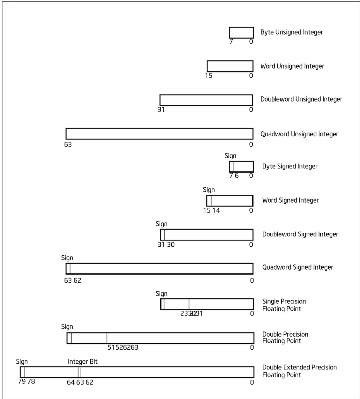
Figure 4-3. Numeric Data Types
4.2.1 Integers
The Intel 64 and IA-32 architectures define two types of integers: unsigned and signed. Unsigned integers are ordinary binary values ranging from 0 to the maximum positive number that can be encoded in the selected operand size. Signed integers
are two's complement binary values that can be used to represent both positive and negative integer values.
Some integer instructions (such as the ADD, SUB, PADDB, and PSUBB instructions) operate on either unsigned or signed integer operands. Other integer instructions (such as IMUL, MUL, IDIV, DIV, FIADD, and FISUB) operate on only one integer type.
The following sections describe the encodings and ranges of the two types of integers.
4.2.1.1 Unsigned Integers
Unsigned integers are unsigned binary numbers contained in a byte, word, double-word, and quadword. Their values range from 0 to 255 for an unsigned byte integer, from 0 to 65,535 for an unsigned word integer, from 0 to 232 - 1 for an unsigned doubleword integer, and from 0 to 264 - 1 for an unsigned quadword integer. Unsigned integers are sometimes referred to as ordinals.
4.2.1.2 Signed Integers
Signed integers are signed binary numbers held in a byte, word, doubleword, or quadword. All operations on signed integers assume a two's complement representation. The sign bit is located in bit 7 in a byte integer, bit 15 in a word integer, bit 31 in a doubleword integer, and bit 63 in a quadword integer (see the signed integer encodings in Table 4-1).
Table 4-1. Signed Integer Encodings
| Class Two's Complement Encoding | |||
| Positive Largest 0 | 11..11Smallest 0 00..01 | ||
| Zero 0 00..00 | |||
| Negative Smallest | 1 11..11Largest | .1 00..00 | |
| Integer indefinite | 1 00..00 | ||
| Signed Byte Integer:Signed Word Integer:Signed Doubleword Integer:Signed Quadword Integer: | ← 7 bits →← 15 bits →← 31 bits →← 63 bits → | ||
The sign bit is set for negative integers and cleared for positive integers and zero. Integer values range from -128 to +127 for a byte integer, from -32,768 to +32,767 for a word integer, from -231 to +231-1 for a doubleword integer, and from -263 to +263-1 for a quadword integer.
When storing integer values in memory, word integers are stored in 2 consecutive bytes; doubleword integers are stored in 4 consecutive bytes; and quadword integers are stored in 8 consecutive bytes.
The integer indefinite is a special value that is sometimes returned by the x87 FPU when operating on integer values. For more information, see Section 8.2.1, "Indefinites."
4.2.2 Floating-Point Data Types
The IA-32 architecture defines and operates on three floating-point data types: single-precision floating-point, double-precision floating-point, and double-extended precision floating-point (see Figure 4-3). The data formats for these data types correspond directly to formats specified in the IEEE Standard 754 for Binary Floating-Point Arithmetic.
Table 4-2 gives the length, precision, and approximate normalized range that can be represented by each of these data types. Denormal values are also supported in each of these types.
Table 4-2. Length, Precision, and Range of Floating-Point Data Types
| Data Type Length | Length Precision | Bits) | Approximate Normalized Range | |
| Binary Decimal | ||||
| Single Precision 32 | 24 2 | -126 to 2127 | 1.18 × 10-38 to 3.40 × 1038 | |
| Double Precision 64 | 53 2 | -1022 to 21023 | 2.23 × 10-308 to 1.79 × 10308 | |
| Double Extended Precision | 80 64 | 2 | -16382 to 216383 | 3.37 × 10-4932 to 1.18 × 104932 |
NOTE
Section 4.8, "Real Numbers and Floating-Point Formats," gives an overview of the IEEE Standard 754 floating-point formats and defines the terms integer bit, QNaN, SNaN, and denormal value.
Table 4-3 shows the floating-point encodings for zeros, denormalized finite numbers, normalized finite numbers, infinites, and NaNs for each of the three floating-point data types. It also gives the format for the QNaN floating-point indefinite value. (See Section 4.8.3.7, "QNaN Floating-Point Indefinite," for a discussion of the use of the QNaN floating-point indefinite value.)
For the single-precision and double-precision formats, only the fraction part of the significand is encoded. The integer is assumed to be 1 for all numbers except 0 and denormalized finite numbers. For the double extended-precision format, the integer is contained in bit 63, and the most-significant fraction bit is bit 62. Here, the integer is explicitly set to 1 for normalized numbers, infinities, and NaNs, and to 0 for zero and denormalized numbers.
Table 4-3. Floating-Point Number and NaN Encodings
| Class Sign Biased | Exponent Significand | ||||
| Integer1 | Fraction | ||||
| Positive +∞ | 0 11..11 1 00..00 | ||||
| +Normals 0 | 11..10 | 1 | 11..11 | ||
| . | . | . | . | ||
| . | . | . | . | ||
| 0 | 00..01 | 1 | 00..00 | ||
| +Denormals 0 | 00..00 | 0 | 11..11 | ||
| . | . | . | . | ||
| . | . | . | . | ||
| 0 | 00..00 | 0 | 00..01 | ||
| +Zero 0 00..00 | 0 00..00 | ||||
| Negative | -Zero 1 00..00 | 0 00..00 | |||
| -Denormals 1 | 00..00 | 0 | 00..01 | ||
| . | . | . | . | ||
| . | . | . | . | ||
| 1 | 00..00 | 0 | 11..11 | ||
| -Normals 1 | 00..01 | 1 | 00..00 | ||
| . | . | . | . | ||
| . | . | . | . | ||
| 1 | 11..10 | 1 | 11..11 | ||
| -∞ | 1 11..11 | 1 00..00 | |||
| NaNs | SNaN | X 11..11 | 1 0X..XX | 2 | |
| QNaN X 11..11 | 1 1X..XX | ||||
| QNaN Floating-Point Indefinite | 1 11..11 | 1 10..00 | |||
| Single-Precision:Double-Precision:Double Extended-Precision: | ← 8 Bits →← 11 Bits →← 15 Bits → | ← 23 Bits →← 52 Bits →← 63 Bits → | |||
NOTES:
- Integer bit is implied and not stored for single-precision and double-precision formats.
- The fraction for SNaN encodings must be non-zero with the most-significant bit 0.
The exponent of each floating-point data type is encoded in biased format; see Section 4.8.2.2, "Biased Exponent." The biasing constant is 127 for the single-precision format, 1023 for the double-precision format, and 16,383 for the double extended-precision format.
When storing floating-point values in memory, single-precision values are stored in 4 consecutive bytes in memory; double-precision values are stored in 8 consecutive bytes; and double extended-precision values are stored in 10 consecutive bytes.
The single-precision and double-precision floating-point data types are operated on by x87 FPU, and SSE/SSE2/SSE3 instructions. The double-extended-precision floating-point format is only operated on by the x87 FPU. See Section 11.6.8, "Compatibility of SIMD and x87 FPU Floating-Point Data Types," for a discussion of the compatibility of single-precision and double-precision floating-point data types between the x87 FPU and SSE/SSE2/SSE3 extensions.
4.3 POINTER DATA TYPES
Pointers are addresses of locations in memory.
In non-64-bit modes, the architecture defines two types of pointers: a near pointer and a far pointer. A near pointer is a 32-bit (or 16-bit) offset (also called an effective address) within a segment. Near pointers are used for all memory references in a flat memory model or for references in a segmented model where the identity of the segment being accessed is implied.
A far pointer is a logical address, consisting of a 16-bit segment selector and a 32-bit (or 16-bit) offset. Far pointers are used for memory references in a segmented memory model where the identity of a segment being accessed must be specified explicitly. Near and far pointers with 32-bit offsets are shown in Figure 4-4.

Figure 4-4. Pointer Data Types
4.3.1 Pointer Data Types in 64-Bit Mode
In 64-bit mode (a sub-mode of IA-32e mode), a near pointer is 64 bits. This equates to an effective address. Far pointers in 64-bit mode can be one of three forms:
- 16-bit segment selector, 16-bit offset if the operand size is 32 bits
• 16-bit segment selector, 32-bit offset if the operand size is 32 bits - 16-bit segment selector, 64-bit offset if the operand size is 64 bits
See Figure 4-5.

Figure 4-5. Pointers in 64-Bit Mode
4.4 BIT FIELD DATA TYPE
A bit field (see Figure 4-6) is a contiguous sequence of bits. It can begin at any bit position of any byte in memory and can contain up to 32 bits.

Figure 4-6. Bit Field Data Type
4.5 STRING DATA TYPES
Strings are continuous sequences of bits, bytes, words, or doublewords. A bit string can begin at any bit position of any byte and can contain up to 232-1 bits. A byte string can contain bytes, words, or doublewords and can range from zero to 232-1 bytes (4 GBytes).
4.6 PACKED SIMD DATA TYPES
Intel 64 and IA-32 architectures define and operate on a set of 64-bit and 128-bit packed data type for use in SIMD operations. These data types consist of fundamental data types (packed bytes, words, doublewords, and quadwords) and numeric interpretations of fundamental types for use in packed integer and packed floating-point operations.
4.6.1 64-Bit SIMD Packed Data Types
The 64-bit packed SIMD data types were introduced into the IA-32 architecture in the Intel MMX technology. They are operated on in MMX registers. The fundamental 64-bit packed data types are packed bytes, packed words, and packed doublewords (see Figure 4-7). When performing numeric SIMD operations on these data types, these data types are interpreted as containing byte, word, or doubleword integer values.
Fundamental 64-Bit Packed SIMD Data Types

Packed Bytes

Packed Words

Packed Doublewords
64-Bit Packed Integer Data Types

Packed Byte Integers

Packed Word Integers

Packed Doubleword Integers
Figure 4-7. 64-Bit Packed SIMD Data Types
4.6.2 128-Bit Packed SIMD Data Types
The 128-bit packed SIMD data types were introduced into the IA-32 architecture in the SSE extensions and used with SSE2, SSE3 and SSSE3 extensions. They are operated on primarily in the 128-bit XMM registers and memory. The fundamental 128-bit packed data types are packed bytes, packed words, packed doublewords, and packed quadwords (see Figure 4-8). When performing SIMD operations on these fundamental data types in XMM registers, these data types are interpreted as containing packed or scalar single-precision floating-point or double-precision floating-point values, or as containing packed byte, word, doubleword, or quadword integer values.

Figure 4-8. 128-Bit Packed SIMD Data Types
4.7 BCD AND PACKED BCD INTEGERS
Binary-coded decimal integers (BCD integers) are unsigned 4-bit integers with valid values ranging from 0 to 9. IA-32 architecture defines operations on BCD integers located in one or more general-purpose registers or in one or more x87 FPU registers (see Figure 4-9).

Figure 4-9. BCD Data Types
When operating on BCD integers in general-purpose registers, the BCD values can be unpacked (one BCD digit per byte) or packed (two BCD digits per byte). The value of an unpacked BCD integer is the binary value of the low half-byte (bits 0 through 3). The high half-byte (bits 4 through 7) can be any value during addition and subtraction, but must be zero during multiplication and division. Packed BCD integers allow two BCD digits to be contained in one byte. Here, the digit in the high half-byte is more significant than the digit in the low half-byte.
When operating on BCD integers in x87 FPU data registers, BCD values are packed in an 80-bit format and referred to as decimal integers. In this format, the first 9 bytes hold 18 BCD digits, 2 digits per byte. The least-significant digit is contained in the lower half-byte of byte 0 and the most-significant digit is contained in the upper half-byte of byte 9. The most significant bit of byte 10 contains the sign bit (0 = positive and 1 = negative; bits 0 through 6 of byte 10 are don't care bits). Negative decimal integers are not stored in two's complement form; they are distinguished from positive decimal integers only by the sign bit. The range of decimal integers that can be encoded in this format is -1018 + 1 to 1018 - 1 .
The decimal integer format exists in memory only. When a decimal integer is loaded in an x87 FPU data register, it is automatically converted to the double-extended-precision floating-point format. All decimal integers are exactly representable in double extended-precision format.
Table 4-4 gives the possible encodings of value in the decimal integer data type.
Table 4-4. Packed Decimal Integer Encodings
| Class Sign digit | digit digit digit | Magnitude | ||||||
| digit ... digit | ||||||||
| Positive Largest | 0 00 | 00000 1001 | 1001 1001 1001 ... | 1001 | ||||
| . | . | . | ||||||
| . | . | . | ||||||
| Smallest Zero | 0 00 | 00000 0000 | 0000 0000 0000 ... | 0001 | ||||
| 0 00 | 00000 0000 | 0000 0000 0000 ... | 0000 | |||||
| Negative Zero Smallest | 1 00 | 00000 0000 | 0000 0000 0000 ... | 0000 | ||||
| 1 00 | 00000 0000 | 0000 0000 0000 ... | 0001 | |||||
| . | . | . | ||||||
| . | . | . | ||||||
| Largest | 1 00 | 00000 1001 | 1001 1001 1001 ... | 1001 | ||||
| Packed BCD Integer Indefinite | 1 11 | 11111 1111 | 1111 1100 0000 ... | 0000 | ||||
| ← 1 byte → | ← 9 bytes → | |||||||
The packed BCD integer indefinite encoding (FFFFC000000000000000H) is stored by the FBSTP instruction in response to a masked floating-point invalid-operation exception. Attempting to load this value with the FBLD instruction produces an undefined result.
4.8 REAL NUMBERS AND FLOATING-POINT FORMATS
This section describes how real numbers are represented in floating-point format in x87 FPU and SSE/SSE2/SSE3 floating-point instructions. It also introduces terms such as normalized numbers, denormalized numbers, biased exponents, signed zeros, and NaNs. Readers who are already familiar with floating-point processing techniques and the IEEE Standard 754 for Binary Floating-Point Arithmetic may wish to skip this section.
4.8.1 Real Number System
As shown in Figure 4-10, the real-number system comprises the continuum of real numbers from minus infinity ( -∞ ) to plus infinity ( +∞ ).
Because the size and number of registers that any computer can have is limited, only a subset of the real-number continuum can be used in real-number (floating-point) calculations. As shown at the bottom of Figure 4-10, the subset of real numbers that the IA-32 architecture supports represents an approximation of the real number system. The range and precision of this real-number subset is determined by the IEEE Standard 754 floating-point formats.
4.8.2 Floating-Point Format
To increase the speed and efficiency of real-number computations, computers and microprocessors typically represent real numbers in a binary floating-point format. In this format, a real number has three parts: a sign, a significand, and an exponent (see Figure 4-11).
The sign is a binary value that indicates whether the number is positive (0) or negative (1). The significand has two parts: a 1-bit binary integer (also referred to as the J-bit) and a binary fraction. The integer-bit is often not represented, but instead is an implied value. The exponent is a binary integer that represents the base-2 power by which the significand is multiplied.
Table 4-5 shows how the real number 178.125 (in ordinary decimal format) is stored in IEEE Standard 754 floating-point format. The table lists a progression of real number notations that leads to the single-precision, 32-bit floating-point format. In this format, the significand is normalized (see Section 4.8.2.1, "Normalized Numbers") and the exponent is biased (see Section 4.8.2.2, "Biased Exponent"). For the single-precision floating-point format, the biasing constant is +127.

Figure 4-10. Binary Real Number System
![graph TD A["Sign"] --> B["Exponent Significand"] B --> C["Fraction"] C --> D["Integer or J-Bit"]](/content/2026/08/1567553/images/56a5b064911bc780b7cfe2fdf95ac996df04e750d35f64e9b7104a72b8d9e385.jpg)
Figure 4-11. Binary Floating-Point Format
Table 4-5. Real and Floating-Point Number Notation
| Notation Value | |||
| Ordinary Decimal 178.125 | |||
| Scientific Decimal 1 | .78125E10 2 | ||
| Scientific Binary 1 | .0110010001E2 111 | ||
| Scientific Binary (Biased Exponent) | 1.0110010001E2 10000110 | ||
| IEEE Single-Precision Format Sign | Sign Biased Exponent Normalized Significand | ||
| 0 10000110 | 011001000100000 | 000000001. (Implied) | |
4.8.2.1 Normalized Numbers
In most cases, floating-point numbers are encoded in normalized form. This means that except for zero, the significand is always made up of an integer of 1 and the following fraction:
1.fff...ff
For values less than 1, leading zeros are eliminated. (For each leading zero eliminated, the exponent is decremented by one.)
Representing numbers in normalized form maximizes the number of significant digits that can be accommodated in a significand of a given width. To summarize, a normalized real number consists of a normalized significand that represents a real number between 1 and 2 and an exponent that specifies the number's binary point.
4.8.2.2 Biased Exponent
In the IA-32 architecture, the exponents of floating-point numbers are encoded in a biased form. This means that a constant is added to the actual exponent so that the biased exponent is always a positive number. The value of the biasing constant depends on the number of bits available for representing exponents in the floating-point format being used. The biasing constant is chosen so that the smallest normalized number can be reciprocated without overflow.
See Section 4.2.2, "Floating-Point Data Types," for a list of the biasing constants that the IA-32 architecture uses for the various sizes of floating-point data-types.
4.8.3 Real Number and Non-number Encodings
A variety of real numbers and special values can be encoded in the IEEE Standard 754 floating-point format. These numbers and values are generally divided into the following classes:
- Signed zeros
• Denormalized finite numbers
• Normalized finite numbers - Signed infinities
- NaNs
- Indefinite numbers
(The term NaN stands for "Not a Number.")
Figure 4-12 shows how the encodings for these numbers and non-numbers fit into the real number continuum. The encodings shown here are for the IEEE single-precision floating-point format. The term "S" indicates the sign bit, "E" the biased exponent, and "Sig" the significand. The exponent values are given in decimal. The integer bit is shown for the significands, even though the integer bit is implied in single-precision floating-point format.

Real Number and NaN Encodings For 32-Bit Floating-Point Format
| S | E | Sig1 | S | E | Sig1 | ||
| 1 | 0 | 0.000... | - 0 | + 0 | 0 | 0.000... | |
| 1 | 0 | 0.XXX...2 | - Denormalized Finite | +Denormalized Finite | 0 | 0.XXX...2 | |
| 1 | 1...254 | 1.XXX... | - Normalized Finite | +Normalized Finite | 0 | 1...254 | 1.XXX... |
| 1 | 255 | 1.000... | -∞ | +∞ | 0 | 255 | 1.000... |
| X3 | 255 | 1.0XX...2 | SNaN | SNaN | X3 | 255 | 1.0XX...2 |
| X3 | 255 | 1.1XX... | QNaN | QNaN | X3 | 255 | 1.1XX... |
NOTES:
- Integer bit of fraction implied for single-precision floating-point format.
- Fraction must be non-zero.
- Sign bit ignored.
Figure 4-12. Real Numbers and NaNs
An IA-32 processor can operate on and/or return any of these values, depending on the type of computation being performed. The following sections describe these number and non-number classes.
4.8.3.1 Signed Zeros
Zero can be represented as a +0 or a -0 depending on the sign bit. Both encodings are equal in value. The sign of a zero result depends on the operation being performed and the rounding mode being used. Signed zeros have been provided to aid in implementing interval arithmetic. The sign of a zero may indicate the direction from which underflow occurred, or it may indicate the sign of an ∞ that has been reciprocated.
4.8.3.2 Normalized and Denormalized Finite Numbers
Non-zero, finite numbers are divided into two classes: normalized and denormalized. The normalized finite numbers comprise all the non-zero finite values that can be encoded in a normalized real number format between zero and ∞ . In the single-precision floating-point format shown in Figure 4-12, this group of numbers includes all the numbers with biased exponents ranging from 1 to 25410 (unbiased, the exponent range is from -12610 to +12710 ).
When floating-point numbers become very close to zero, the normalized-number format can no longer be used to represent the numbers. This is because the range of the exponent is not large enough to compensate for shifting the binary point to the right to eliminate leading zeros.
When the biased exponent is zero, smaller numbers can only be represented by making the integer bit (and perhaps other leading bits) of the significand zero. The numbers in this range are called denormalized (or tiny) numbers. The use of leading zeros with denormalized numbers allows smaller numbers to be represented. However, this denormalization causes a loss of precision (the number of significant bits in the fraction is reduced by the leading zeros).
When performing normalized floating-point computations, an IA-32 processor normally operates on normalized numbers and produces normalized numbers as results. Denormalized numbers represent an underflow condition. The exact conditions are specified in Section 4.9.1.5, "Numeric Underflow Exception (#U)."
A denormalized number is computed through a technique called gradual underflow. Table 4-6 gives an example of gradual underflow in the denormalization process. Here the single-precision format is being used, so the minimum exponent (unbiased) is -12610 . The true result in this example requires an exponent of -12910 in order to have a normalized number. Since -12910 is beyond the allowable exponent range, the result is denormalized by inserting leading zeros until the minimum exponent of -12610 is reached.
Table 4-6. Denormalization Process
| Operation Sign Exponent* | Significand | ||
| True Result | 0 | -129 | 1.01011100000...00 |
| Denormalize | 0 | -128 | 0.10101110000...00 |
| Denormalize | 0 | -127 | 0.01010111000...00 |
| Denormalize | 0 | -126 | 0.00101011100...00 |
| Denormal Result | 0 | -126 | 0.00101011100...00 |
* Expressed as an unbiased, decimal number.
In the extreme case, all the significant bits are shifted out to the right by leading zeros, creating a zero result.
The Intel 64 and IA-32 architectures deal with denormal values in the following ways:
- It avoids creating denormals by normalizing numbers whenever possible.
- It provides the floating-point underflow exception to permit programmers to detect cases when denormals are created.
- It provides the floating-point denormal-operand exception to permit procedures or programs to detect when denormals are being used as source operands for computations.
4.8.3.3 Signed Infinities
The two infinities, +∞ and -∞ , represent the maximum positive and negative real numbers, respectively, that can be represented in the floating-point format. Infinity is always represented by a significand of 1.00...00 (the integer bit may be implied) and the maximum biased exponent allowed in the specified format (for example, 25510 for the single-precision format).
The signs of infinities are observed, and comparisons are possible. Infinities are always interpreted in the affine sense; that is, -∞ is less than any finite number and +∞ is greater than any finite number. Arithmetic on infinities is always exact. Exceptions are generated only when the use of an infinity as a source operand constitutes an invalid operation.
Whereas denormalized numbers may represent an underflow condition, the two ∞ numbers may represent the result of an overflow condition. Here, the normalized result of a computation has a biased exponent greater than the largest allowable exponent for the selected result format.
4.8.3.4 NaNs
Since NaNs are non-numbers, they are not part of the real number line. In Figure 4-12, the encoding space for NaNs in the floating-point formats is shown
above the ends of the real number line. This space includes any value with the maximum allowable biased exponent and a non-zero fraction (the sign bit is ignored for NaNs).
The IA-32 architecture defines two classes of NaNs: quiet NaNs (QNaNs) and signaling NaNs (SNaNs). A QNaN is a NaN with the most significant fraction bit set; an SNaN is a NaN with the most significant fraction bit clear. QNaNs are allowed to propagate through most arithmetic operations without signaling an exception. SNaNs generally signal a floating-point invalid-operation exception whenever they appear as operands in arithmetic operations.
SNaNs are typically used to trap or invoke an exception handler. They must be inserted by software; that is, the processor never generates an SNaN as a result of a floating-point operation.
4.8.3.5 Operating on SNaNs and QNaNs
When a floating-point operation is performed on an SNaN and/or a QNaN, the result of the operation is either a QNaN delivered to the destination operand or the generation of a floating-point invalid operating exception, depending on the following rules:
- If one of the source operands is an SNaN and the floating-point invalid-operating exception is not masked (see Section 4.9.1.1, "Invalid Operation Exception (#I)"), the a floating-point invalid-operation exception is signaled and no result is stored in the destination operand.
- If either or both of the source operands are NaNs and floating-point invalid-operation exception is masked, the result is as shown in Table 4-7. When an SNaN is converted to a QNaN, the conversion is handled by setting the most-significant fraction bit of the SNaN to 1. Also, when one of the source operands is an SNaN, the floating-point invalid-operation exception flag it set. Note that for some combinations of source operands, the result is different for x87 FPU operations and for SSE/SSE2/SSE3 operations.
- When neither of the source operands is a NaN, but the operation generates a floating-point invalid-operation exception (see Tables 8-10 and 11-1), the result is commonly an SNaN source operand converted to a QNaN or the QNaN floating-point indefinite value.
Any exceptions to the behavior described in Table 4-7 are described in Section 8.5.1.2, "Invalid Arithmetic Operand Exception (#IA)," and Section 11.5.2.1, "Invalid Operation Exception (#I)."
Table 4-7. Rules for Handling NaNs
| Source Operands Result | 1 |
| SNaN and QNaN x87 FPU — QNaN source operand. | SSE/SSE2/SSE3 — First operand (if this operand is an SNaN, it is converted to a QNaN) |
| Two SNaNs x87 FPU—SNaN source operand with the larger significand, converted into a QNaN | SSE/SSE2/SSE3 — First operand converted to a QNaN |
| Two QNaNs x87 FPU — QNaN source operand with the larger significand | SSE/SSE2/SSE3 — First operand |
| SNaN and a floating-point value SNaN source operand, converted into a QNaN | operand, converted into a QNaN |
| QNaN and a floating-point value QNaN source operand | |
| SNaN (for instructions that take only one operand) | SNaN source operand, converted into a QNaN |
| QNaN (for instructions that take only one operand) | QNaN source operand |
NOTE:
- For SSE/SSE2/SSE3 instructions, the first operand is generally a source operand that becomes the destination operand. Within the Result column, the x87 FPU notation also applies to the FISTTP instruction in SSE3; the SSE3 notation applies to the SIMD floating-point instructions.
4.8.3.6 Using SNaNs and QNaNs in Applications
Except for the rules given at the beginning of Section 4.8.3.4, "NaNs," for encoding SNaNs and QNaNs, software is free to use the bits in the significand of a NaN for any purpose. Both SNaNs and QNaNs can be encoded to carry and store data, such as diagnostic information.
By unmasking the invalid operation exception, the programmer can use signaling NaNs to trap to the exception handler. The generality of this approach and the large number of NaN values that are available provide the sophisticated programmer with a tool that can be applied to a variety of special situations.
For example, a compiler can use signaling NaNs as references to uninitialized (real) array elements. The compiler can preinitialize each array element with a signaling NaN whose significand contained the index (relative position) of the element. Then, if an application program attempts to access an element that it had not initialized, it can use the NaN placed there by the compiler. If the invalid operation exception is unmasked, an interrupt will occur, and the exception handler will be invoked. The exception handler can determine which element has been accessed, since the
operand address field of the exception pointer will point to the NaN, and the NaN will contain the index number of the array element.
Quiet NaNs are often used to speed up debugging. In its early testing phase, a program often contains multiple errors. An exception handler can be written to save diagnostic information in memory whenever it was invoked. After storing the diagnostic data, it can supply a quiet NaN as the result of the erroneous instruction, and that NaN can point to its associated diagnostic area in memory. The program will then continue, creating a different NaN for each error. When the program ends, the NaN results can be used to access the diagnostic data saved at the time the errors occurred. Many errors can thus be diagnosed and corrected in one test run.
In embedded applications that use computed results in further computations, an undetected QNaN can invalidate all subsequent results. Such applications should therefore periodically check for QNaNs and provide a recovery mechanism to be used if a QNaN result is detected.
4.8.3.7 QNaN Floating-Point Indefinite
For the floating-point data type encodings (single-precision, double-precision, and double-extended-precision), one unique encoding (a QNaN) is reserved for representing the special value QNaN floating-point indefinite. The x87 FPU and the SSE/SSE2/SSE3 extensions return these indefinite values as responses to some masked floating-point exceptions. Table 4-3 shows the encoding used for the QNaN floating-point indefinite.
4.8.4 Rounding
When performing floating-point operations, the processor produces an infinitely precise floating-point result in the destination format (single-precision, double-precision, or double extended-precision floating-point) whenever possible. However, because only a subset of the numbers in the real number continuum can be represented in IEEE Standard 754 floating-point formats, it is often the case that an infinitely precise result cannot be encoded exactly in the format of the destination operand.
For example, the following value (a) has a 24-bit fraction. The least-significant bit of this fraction (the underlined bit) cannot be encoded exactly in the single-precision format (which has only a 23-bit fraction):
(a) 1.0001 0000 1000 0011 1001 0111E2 101
To round this result (a) , the processor first selects two representable fractions b and c that most closely bracket a in value (b < a < c) .
(b) 1.0001 0000 1000 0011 1001 011E 2 101
(c) 1.0001 0000 1000 0011 1001 100E2 101
The processor then sets the result to b or to c according to the selected rounding mode. Rounding introduces an error in a result that is less than one unit in the last place (the least significant bit position of the floating-point value) to which the result is rounded.
The IEEE Standard 754 defines four rounding modes (see Table 4-8): round to nearest, round up, round down, and round toward zero. The default rounding mode (for the Intel 64 and IA-32 architectures) is round to nearest. This mode provides the most accurate and statistically unbiased estimate of the true result and is suitable for most applications.
Table 4-8. Rounding Modes and Encoding of Rounding Control (RC) Field
| Rounding Mode | RC Field Setting | Description |
| Round to nearest (even) | 00B Rounded | result is the closest to the infinitely precise result. If two values are equally close, the result is the even value (that is, the one with the least-significant bit of zero). Default |
| Round down (toward -∞) | 01B | Rounded result is closest to but no greater than the infinitely precise result. |
| Round up (toward +∞) | 10B | Rounded result is closest to but no less than the infinitely precise result. |
| Round toward zero (Truncate) | 11B | Rounded result is closest to but no greater in absolute value than the infinitely precise result. |
The round up and round down modes are termed directed rounding and can be used to implement interval arithmetic. Interval arithmetic is used to determine upper and lower bounds for the true result of a multistep computation, when the intermediate results of the computation are subject to rounding.
The round toward zero mode (sometimes called the "chop" mode) is commonly used when performing integer arithmetic with the x87 FPU.
The rounded result is called the inexact result. When the processor produces an inexact result, the floating-point precision (inexact) flag (PE) is set (see Section 4.9.1.6, "Inexact-Result (Precision) Exception (#P)").
The rounding modes have no effect on comparison operations, operations that produce exact results, or operations that produce NaN results.
4.8.4.1 Rounding Control (RC) Fields
In the Intel 64 and IA-32 architectures, the rounding mode is controlled by a 2-bit rounding-control (RC) field (Table 4-8 shows the encoding of this field). The RC field is implemented in two different locations:
• x87 FPU control register (bits 10 and 11)
• The MXCSR register (bits 13 and 14)
Although these two RC fields perform the same function, they control rounding for different execution environments within the processor. The RC field in the x87 FPU control register controls rounding for computations performed with the x87 FPU instructions; the RC field in the MXCSR register controls rounding for SIMD floating-point computations performed with the SSE/SSE2 instructions.
4.8.4.2 Truncation with SSE and SSE2 Conversion Instructions
The following SSE/SSE2 instructions automatically truncate the results of conversions from floating-point values to integers when the result it inexact: CVTTPD2DQ, CVTTPS2DQ, CVTTPD2PI, CVTTPS2PI, CVTTSD2SI, CVTTSS2SI. Here, truncation means the round toward zero mode described in Table 4-8.
4.9 OVERVIEW OF FLOATING-POINT EXCEPTIONS
The following section provides an overview of floating-point exceptions and their handling in the IA-32 architecture. For information specific to the x87 FPU and to the SSE/SSE2/SSE3 extensions, refer to the following sections:
- Section 8.4, "x87 FPU Floating-Point Exception Handling"
• Section 11.5, "SSE, SSE2, and SSE3 Exceptions"
When operating on floating-point operands, the IA-32 architecture recognizes and detects six classes of exception conditions:
- Invalid operation (#I)
- Divide-by-zero (#Z)
• Denormalized operand (#D) - Numeric overflow (#O)
- Numeric underflow (#U)
• Inexact result (precision) (#P)
The nomenclature of “#” symbol followed by one or two letters (for example, #P) is used in this manual to indicate exception conditions. It is merely a short-hand form and is not related to assembler mnemonics.
NOTE
All of the exceptions listed above except the denormal-operand exception (#D) are defined in IEEE Standard 754.
The invalid-operation, divide-by-zero and denormal-operand exceptions are pre-computation exceptions (that is, they are detected before any arithmetic operation
occurs). The numeric-underflow, numeric-overflow and precision exceptions are post-computation exceptions.
Each of the six exception classes has a corresponding flag bit (IE, ZE, OE, UE, DE, or PE) and mask bit (IM, ZM, OM, UM, DM, or PM). When one or more floating-point exception conditions are detected, the processor sets the appropriate flag bits, then takes one of two possible courses of action, depending on the settings of the corresponding mask bits:
- Mask bit set. Handles the exception automatically, producing a predefined (and often times usable) result, while allowing program execution to continue undisturbed.
- Mask bit clear. Invokes a software exception handler to handle the exception.
The masked (default) responses to exceptions have been chosen to deliver a reasonable result for each exception condition and are generally satisfactory for most floating-point applications. By masking or unmasking specific floating-point exceptions, programmers can delegate responsibility for most exceptions to the processor and reserve the most severe exception conditions for software exception handlers.
Because the exception flags are "sticky," they provide a cumulative record of the exceptions that have occurred since they were last cleared. A programmer can thus mask all exceptions, run a calculation, and then inspect the exception flags to see if any exceptions were detected during the calculation.
In the IA-32 architecture, floating-point exception flag and mask bits are implemented in two different locations:
- x87 FPU status word and control word. The flag bits are located at bits 0 through 5 of the x87 FPU status word and the mask bits are located at bits 0 through 5 of the x87 FPU control word (see Figures 8-4 and 8-6).
- MXCSR register. The flag bits are located at bits 0 through 5 of the MXCSR register and the mask bits are located at bits 7 through 12 of the register (see Figure 10-3).
Although these two sets of flag and mask bits perform the same function, they report on and control exceptions for different execution environments within the processor. The flag and mask bits in the x87 FPU status and control words control exception reporting and masking for computations performed with the x87 FPU instructions; the companion bits in the MXCSR register control exception reporting and masking for SIMD floating-point computations performed with the SSE/SSE2/SSE3 instructions.
Note that when exceptions are masked, the processor may detect multiple exceptions in a single instruction, because it continues executing the instruction after performing its masked response. For example, the processor can detect a denormalized operand, perform its masked response to this exception, and then detect numeric underflow.
See Section 4.9.2, "Floating-Point Exception Priority," for a description of the rules for exception precedence when more than one floating-point exception condition is detected for an instruction.
4.9.1 Floating-Point Exception Conditions
The following sections describe the various conditions that cause a floating-point exception to be generated and the masked response of the processor when these conditions are detected. The Intel® 64 and IA-32 Architectures Software Developer's Manual, Volumes 3A & 3B, list the floating-point exceptions that can be signaled for each floating-point instruction.
4.9.1.1 Invalid Operation Exception (#I)
The processor reports an invalid operation exception in response to one or more invalid arithmetic operands. If the invalid operation exception is masked, the processor sets the IE flag and returns an indefinite value or a QNaN. This value overwrites the destination register specified by the instruction. If the invalid operation exception is not masked, the IE flag is set, a software exception handler is invoked, and the operands remain unaltered.
See Section 4.8.3.6, "Using SNaNs and QNaNs in Applications," for information about the result returned when an exception is caused by an SNaN.
The processor can detect a variety of invalid arithmetic operations that can be coded in a program. These operations generally indicate a programming error, such as dividing ∞ by ∞ . See the following sections for information regarding the invalid-operation exception when detected while executing x87 FPU or SSE/SSE2/SSE3 instructions:
- x87 FPU; Section 8.5.1, "Invalid Operation Exception"
- SIMD floating-point exceptions; Section 11.5.2.1, "Invalid Operation Exception (#I)"
4.9.1.2 Denormal Operand Exception (#D)
The processor reports the denormal-operand exception if an arithmetic instruction attempts to operate on a denormal operand (see Section 4.8.3.2, "Normalized and Denormalized Finite Numbers"). When the exception is masked, the processor sets the DE flag and proceeds with the instruction. Operating on denormal numbers will produce results at least as good as, and often better than, what can be obtained when denormal numbers are flushed to zero. Programmers can mask this exception so that a computation may proceed, then analyze any loss of accuracy when the final result is delivered.
When a denormal-operand exception is not masked, the DE flag is set, a software exception handler is invoked, and the operands remain unaltered. When denormal operands have reduced significance due to loss of low-order bits, it may be advisable to not operate on them. Precluding denormal operands from computations can be accomplished by an exception handler that responds to unmasked denormal-operand exceptions.
See the following sections for information regarding the denormal-operand exception when detected while executing x87 FPU or SSE/SSE2/SSE3 instructions:
- x87 FPU; Section 8.5.2, "Denormal Operand Exception (#D)"
- SIMD floating-point exceptions; Section 11.5.2.2, "Denormal-Operand Exception (#D)"
4.9.1.3 Divide-By-Zero Exception (#Z)
The processor reports the floating-point divide-by-zero exception whenever an instruction attempts to divide a finite non-zero operand by 0. The masked response for the divide-by-zero exception is to set the ZE flag and return an infinity signed with the exclusive OR of the sign of the operands. If the divide-by-zero exception is not masked, the ZE flag is set, a software exception handler is invoked, and the operands remain unaltered.
See the following sections for information regarding the divide-by-zero exception when detected while executing x87 FPU or SSE/SSE2 instructions:
• x87 FPU; Section 8.5.3, "Divide-By-Zero Exception (#Z)"
- SIMD floating-point exceptions; Section 11.5.2.3, "Divide-By-Zero Exception (#Z)"
4.9.1.4 Numeric Overflow Exception (#0)
The processor reports a floating-point numeric overflow exception whenever the rounded result of an instruction exceeds the largest allowable finite value that will fit into the destination operand. Table 4-9 shows the threshold range for numeric overflow for each of the floating-point formats; overflow occurs when a rounded result falls at or outside this threshold range.
Table 4-9. Numeric Overflow Thresholds
| Floating-Point Format Overflow Thresholds | |
| Single Precision | |x| ≥ 1.0 * 2128 |
| Double Precision | |x| ≥ 1.0 * 21024 |
| Double Extended Precision | |x| ≥ 1.0 * 216384 |
When a numeric-overflow exception occurs and the exception is masked, the processor sets the OE flag and returns one of the values shown in Table 4-10, according to the current rounding mode. See Section 4.8.4, "Rounding."
When numeric overflow occurs and the numeric-overflow exception is not masked, the OE flag is set, a software exception handler is invoked, and the source and destination operands either remain unchanged or a biased result is stored in the destination operand (depending whether the overflow exception was generated during an SSE/SSE2/SSE3 floating-point operation or an x87 FPU operation).
Table 4-10. Masked Responses to Numeric Overflow
| Rounding Mode Sign of True Result | ||
| To nearest + +∞ | - | -∞ |
| Toward -∞ | + | Largest finite positive number |
| - | -∞ | |
| Toward +∞ | + | +∞ |
| - Largest finite negative number | ||
| Toward zero | + | Largest finite positive number |
| - Largest finite negative number | ||
See the following sections for information regarding the numeric overflow exception when detected while executing x87 FPU instructions or while executing SSE/SSE2/SSE3 instructions:
- x87 FPU; Section 8.5.4, "Numeric Overflow Exception (#O)"
- SIMD floating-point exceptions; Section 11.5.2.4, "Numeric Overflow Exception (#O)"
4.9.1.5 Numeric Underflow Exception (#U)
The processor detects a floating-point numeric underflow condition whenever the result of rounding with unbounded exponent (taking into account precision control for x87) is tiny; that is, less than the smallest possible normalized, finite value that will fit into the destination operand. Table 4-11 shows the threshold range for
numeric underflow for each of the floating-point formats (assuming normalized results); underflow occurs when a rounded result falls strictly within the threshold range. The ability to detect and handle underflow is provided to prevent a very small result from propagating through a computation and causing another exception (such as overflow during division) to be generated at a later time.
Table 4-11. Numeric Underflow (Normalized) Thresholds
| Floating-Point Format Underflow Thresholds* | |
| Single Precision | |x| < 1.0 * 2-126 |
| Double Precision | |x| < 1.0 * 2-1022 |
| Double Extended Precision | |x| < 1.0 * 2-16382 |
* Where 'x' is the result rounded to destination precision with an unbounded exponent range.
How the processor handles an underflow condition, depends on two related conditions:
- creation of a tiny result
- creation of an inexact result; that is, a result that cannot be represented exactly in the destination format
Which of these events causes an underflow exception to be reported and how the processor responds to the exception condition depends on whether the underflow exception is masked:
- Underflow exception masked — The underflow exception is reported (the UE flag is set) only when the result is both tiny and inexact. The processor returns a denormalized result to the destination operand, regardless of inexactness.
- Underflow exception not masked — The underflow exception is reported when the result is tiny, regardless of inexactness. The processor leaves the source and destination operands unaltered or stores a biased result in the designating operand (depending whether the underflow exception was generated during an SSE/SSE2/SSE3 floating-point operation or an x87 FPU operation) and invokes a software exception handler.
See the following sections for information regarding the numeric underflow exception when detected while executing x87 FPU instructions or while executing SSE/SSE2/SSE3 instructions:
- x87 FPU; Section 8.5.5, "Numeric Underflow Exception (#U)"
- SIMD floating-point exceptions; Section 11.5.2.5, "Numeric Underflow Exception (#U)"
4.9.1.6 Inexact-Result (Precision) Exception (#P)
The inexact-result exception (also called the precision exception) occurs if the result of an operation is not exactly representable in the destination format. For example, the fraction 1/3 cannot be precisely represented in binary floating-point form. This
exception occurs frequently and indicates that some (normally acceptable) accuracy will be lost due to rounding. The exception is supported for applications that need to perform exact arithmetic only. Because the rounded result is generally satisfactory for most applications, this exception is commonly masked.
If the inexact-result exception is masked when an inexact-result condition occurs and a numeric overflow or underflow condition has not occurred, the processor sets the PE flag and stores the rounded result in the destination operand. The current rounding mode determines the method used to round the result. See Section 4.8.4, "Rounding."
If the inexact-result exception is not masked when an inexact result occurs and numeric overflow or underflow has not occurred, the PE flag is set, the rounded result is stored in the destination operand, and a software exception handler is invoked.
If an inexact result occurs in conjunction with numeric overflow or underflow, one of the following operations is carried out:
- If an inexact result occurs along with masked overflow or underflow, the OE flag or UE flag and the PE flag are set and the result is stored as described for the overflow or underflow exceptions; see Section 4.9.1.4, "Numeric Overflow Exception (#O)," or Section 4.9.1.5, "Numeric Underflow Exception (#U)." If the inexact result exception is unmasked, the processor also invokes a software exception handler.
- If an inexact result occurs along with unmasked overflow or underflow and the destination operand is a register, the OE or UE flag and the PE flag are set, the result is stored as described for the overflow or underflow exceptions, and a software exception handler is invoked.
If an unmasked numeric overflow or underflow exception occurs and the destination operand is a memory location (which can happen only for a floating-point store), the inexact-result condition is not reported and the C1 flag is cleared.
See the following sections for information regarding the inexact-result exception when detected while executing x87 FPU or SSE/SSE2/SSE3 instructions:
- x87 FPU; Section 8.5.6, "Inexact-Result (Precision) Exception (#P)"
- SIMD floating-point exceptions; Section 11.5.2.3, "Divide-By-Zero Exception (#Z)"
4.9.2 Floating-Point Exception Priority
The processor handles exceptions according to a predetermined precedence. When an instruction generates two or more exception conditions, the exception precedence sometimes results in the higher-priority exception being handled and the lower-priority exceptions being ignored. For example, dividing an SNaN by zero can potentially signal an invalid-operation exception (due to the SNaN operand) and a divide-by-zero exception. Here, if both exceptions are masked, the processor handles the higher-priority exception only (the invalid-operation exception), returning a QNaN to the destination. Alternately, a denormal-operand or inexact-result exception can
accompany a numeric underflow or overflow exception with both exceptions being handled.
The precedence for floating-point exceptions is as follows:
- Invalid-operation exception, subdivided as follows:
a. stack underflow (occurs with x87 FPU only)
b. stack overflow (occurs with x87 FPU only)
c. operand of unsupported format (occurs with x87 FPU only when using the double extended-precision floating-point format)
d. SNaN operand
- QNaN operand. Though this is not an exception, the handling of a QNaN operand has precedence over lower-priority exceptions. For example, a QNaN divided by zero results in a QNaN, not a zero-divide exception.
- Any other invalid-operation exception not mentioned above or a divide-by-zero exception.
- Denormal-operand exception. If masked, then instruction execution continues and a lower-priority exception can occur as well.
- Numeric overflow and underflow exceptions; possibly in conjunction with the inexact-result exception.
- Inexact-result exception.
Invalid operation, zero divide, and denormal operand exceptions are detected before a floating-point operation begins. Overflow, underflow, and precision exceptions are not detected until a true result has been computed. When an unmasked pre-operation exception is detected, the destination operand has not yet been updated, and appears as if the offending instruction has not been executed. When an unmasked post-operation exception is detected, the destination operand may be updated with a result, depending on the nature of the exception (except for SSE/SSE2/SSE3 instructions, which do not update their destination operands in such cases).
4.9.3 Typical Actions of a Floating-Point Exception Handler
After the floating-point exception handler is invoked, the processor handles the exception in the same manner that it handles non-floating-point exceptions. The floating-point exception handler is normally part of the operating system or executive software, and it usually invokes a user-registered floating-point exception handle.
A typical action of the exception handler is to store state information in memory. Other typical exception handler actions include:
- Examining the stored state information to determine the nature of the error
• Taking actions to correct the condition that caused the error
DATA TYPES
- Clearing the exception flags
- Returning to the interrupted program and resuming normal execution In lieu of writing recovery procedures, the exception handler can do the following:
- Increment in software an exception counter for later display or printing
- Print or display diagnostic information (such as the state information)
• Halt further program execution
This chapter provides an abridged overview of Intel 64 and IA-32 instructions. Instructions are divided into the following groups:
- General purpose
• x87 FPU
• x87 FPU and SIMD state management - Intel MMX technology
- SSE extensions
- SSE2 extensions
- SSE3 extensions
- SSSE3 extensions
- SSE4 extensions
- System instructions
• IA-32e mode: 64-bit mode instructions - VMX instructions
- SMX instructions
Table 5-1 lists the groups and IA-32 processors that support each group. Within these groups, most instructions are collected into functional subgroups.
Table 5-1. Instruction Groups and IA-32 Processors
| Instruction SetArchitecture Intel 64 and IA-32 Processor Support | |
| General Purpose All Intel 64 and IA-32 processors | |
| x87 FPU Intel486, Pentium | Pentium with MMX Technology, Celeron, PentiumPro, Pentium II, Pentium II Xeon, Pentium III, Pentium III Xeon,Pentium 4, Intel Xeon processors, Pentium M, Intel Core Solo, Intel Core Duo, Intel Core 2 Duo processors, Intel Atom processors |
| x87 FPU and SIMD State Management | Pentium II, Pentium II Xeon, Pentium III, Pentium III Xeon, Pentium 4,Intel Xeon processors, Pentium M, Intel Core Solo, Intel Core Duo, IntelCore 2 Duo processors, Intel Atom processors |
| MMX Technology | Pentium with MMX Technology, Celeron, Pentium II, Pentium II Xeon,Pentium III, Pentium III Xeon, Pentium 4, Intel Xeon processors,Pentium M, Intel Core Solo, Intel Core Duo, Intel Core 2 Duo processors,Intel Atom processors |
Table 5-1. Instruction Groups and IA-32 Processors (Contd.)
| Instruction SetArchitecture Intel 64 and IA-32 Processor Support | |
| SSE Extensions Pentium III, Pentium III Xeon, Pentium 4, Intel Xeon processors,Pentium M, Intel Core Solo, Intel Core Duo, Intel Core 2 Duo processors,Intel Atom processors | |
| SSE2 Extensions Pentium | 4, Intel Xeon processors, Pentium M, Intel Core Solo, Intel CoreDuo, Intel Core 2 Duo processors, Intel Atom processors |
| SSE3 Extensions Pentium | 4 supporting HT Technology (built on 90nm processtechnology), Intel Core Solo, Intel Core Duo, Intel Core 2 Duo processors,Intel Xeon processor 3xxxx, 5xxx, 7xxx Series, Intel Atom processors |
| SSSE3 Extensions Intel Xeon processor 3000, 3200, 5100, 5300, 7300 series, Intel Core2 Extreme processors QX6000 series, Intel Core 2 Duo, Intel Core 2Quad processors, Intel Pentium Dual-Core processors, Intel Atomprocessors | |
| SSE4.1 Extensions Intel Xeon processor 3100, 3300, 5200, 5400, 7400 series, Intel Core2 Extreme processors QX9000 series, Intel Core 2 Quad processorQ9000 series, Intel Core 2 Duo processors 8000 series, T9000 series. | |
| SSE4.2 Extensions Intel Core i7 processor. | |
| IA-32e mode: 64-bitmode instructions | Intel 64 processors |
| System Instructions Intel | 64 and IA-32 processors |
| VMX Instructions Intel 64 | and IA-32 processors supporting Intel VirtualizationTechnology |
| SMX Instructions Intel Core | 2 Duo processor E6x50, E8xxx; Intel Core 2 Quad processorQ9xxx |
The following sections list instructions in each major group and subgroup. Given for each instruction is its mnemonic and descriptive names. When two or more mnemonics are given (for example, CMOVA/CMOVNBE), they represent different mnemonics for the same instruction opcode. Assemblers support redundant mnemonics for some instructions to make it easier to read code listings. For instance, CMOVA (Conditional move if above) and CMOVNBE (Conditional move if not below or equal) represent the same condition. For detailed information about specific instructions, see the Intel® 64 and IA-32 Architectures Software Developer's Manual, Volumes 3A & 3B.
5.1 GENERAL-PURPOSE INSTRUCTIONS
The general-purpose instructions preform basic data movement, arithmetic, logic, program flow, and string operations that programmers commonly use to write application and system software to run on Intel 64 and IA-32 processors. They operate on data contained in memory, in the general-purpose registers (EAX, EBX, ECX, EDX, EDI, ESI, EBP, and ESP) and in the EFLAGS register. They also operate on address information contained in memory, the general-purpose registers, and the segment registers (CS, DS, SS, ES, FS, and GS).
This group of instructions includes the data transfer, binary integer arithmetic, decimal arithmetic, logic operations, shift and rotate, bit and byte operations, program control, string, flag control, segment register operations, and miscellaneous subgroups. The sections that following introduce each subgroup.
For more detailed information on general purpose-instructions, see Chapter 7, "Programming With General-Purpose Instructions."
5.1.1 Data Transfer Instructions
The data transfer instructions move data between memory and the general-purpose and segment registers. They also perform specific operations such as conditional moves, stack access, and data conversion.
MOV Move data between general-purpose registers; move data between memory and general-purpose or segment registers; move immediates to general-purpose registers
CMOVE/CMOVZ Conditional move if equal/Conditional move if zero
CMOVNE/CMOVNZ Conditional move if not equal/Conditional move if not zero
CMOVA/CMOVNBE Conditional move if above/Conditional move if not below or equal
CMOVAE/CMOVNB Conditional move if above or equal/Conditional move if not below
CMOVB/CMOVNAE Conditional move if below/Conditional move if not above or equal
CMOVBE/CMOVNA Conditional move if below or equal/Conditional move if not above
CMOVG/CMOVNLE Conditional move if greater/Conditional move if not less or equal
CMOVGE/CMOVNL Conditional move if greater or equal/Conditional move if not less
CMOVL/CMOVNGE Conditional move if less/Conditional move if not greater or equal
CMOVLE/CMOVNG Conditional move if less or equal/Conditional move if not greater
CMOVC Conditional move if carry
CMOVNC Conditional move if not carry
CMOVO Conditional move if overflow
CMOVNO Conditional move if not overflow
CMOVS Conditional move if sign (negative)
CMOVNS Conditional move if not sign (non-negative)
CMOVP/CMOVPE Conditional move if parity/Conditional move if parity even
CMOVNP/CMOVPO Conditional move if not parity/Conditional move if parity odd
XCHG Exchange
BSWAP Byte swap
XADD Exchange and add
CMPXCHG Compare and exchange
CMPXCHG8B Compare and exchange 8 bytes
PUSH Push onto stack
POP Pop off of stack
PUSHA/PUSHAD Push general-purpose registers onto stack
POPA/POPAD Pop general-purpose registers from stack
CWD/CDQ Convert word to doubleword/Convert doubleword to quadword
CBW/CWDE Convert byte to word/Convert word to doubleword in EAX register
MOVSX Move and sign extend
MOVZX Move and zero extend
5.1.2 Binary Arithmetic Instructions
The binary arithmetic instructions perform basic binary integer computations on byte, word, and doubleword integers located in memory and/or the general purpose registers.
ADD Integer add
ADC Add with carry
SUB Subtract
SBB Subtract with borrow
IMUL Signed multiply
MUL Unsigned multiply
IDIV Signed divide
DIV Unsigned divide
INC Increment
DEC Decrement
NEG Negate
CMP Compare
5.1.3 Decimal Arithmetic Instructions
The decimal arithmetic instructions perform decimal arithmetic on binary coded decimal (BCD) data.
DAA Decimal adjust after addition
DAS Decimal adjust after subtraction
AAA ASCII adjust after addition
AAS ASCII adjust after subtraction
AAM ASCII adjust after multiplication
AAD ASCII adjust before division
5.1.4 Logical Instructions
The logical instructions perform basic AND, OR, XOR, and NOT logical operations on byte, word, and doubleword values.
AND Perform bitwise logical AND
OR Perform bitwise logical OR
XOR Perform bitwise logical exclusive OR
NOT Perform bitwise logical NOT
5.1.5 Shift and Rotate Instructions
The shift and rotate instructions shift and rotate the bits in word and doubleword operands.
SAR Shift arithmetic right
SHR Shift logical right
SAL/SHL Shift arithmetic left/Shift logical left
SHRD Shift right double
SHLD Shift left double
ROR Rotate right
ROL Rotate left
RCR Rotate through carry right
RCL Rotate through carry left
5.1.6 Bit and Byte Instructions
Bit instructions test and modify individual bits in word and doubleword operands. Byte instructions set the value of a byte operand to indicate the status of flags in the EFLAGS register.
INSTRUCTION SET SUMMARY
BT Bit test
BTS Bit test and set
BTR Bit test and reset
BTC Bit test and complement
BSF Bit scan forward
BSR Bit scan reverse
SETE/SETZ Set byte if equal/Set byte if zero
SETNE/SETNZ Set byte if not equal/Set byte if not zero
SETA/SETNBE Set byte if above/Set byte if not below or equal
SETAE/SETNB/SETNC Set byte if above or equal/Set byte if not below/Set byte if not carry
SETB/SETNAE/SETC Set byte if below/Set byte if not above or equal/Set byte if carry
SETBE/SETNA Set byte if below or equal/Set byte if not above
SETG/SETNLE Set byte if greater/Set byte if not less or equal
SETGE/SETNL Set byte if greater or equal/Set byte if not less
SETL/SETNGE Set byte if less/Set byte if not greater or equal
SETLE/SETNG Set byte if less or equal/Set byte if not greater
SETS Set byte if sign (negative)
SETNS Set byte if not sign (non-negative)
SETO Set byte if overflow
SETNO Set byte if not overflow
SETPE/SETP Set byte if parity even/Set byte if parity
SETPO/SETNP Set byte if parity odd/Set byte if not parity
TEST Logical compare
5.1.7 Control Transfer Instructions
The control transfer instructions provide jump, conditional jump, loop, and call and return operations to control program flow.
JMP Jump
JE/JZ Jump if equal/Jump if zero
JNE/JNZ Jump if not equal/Jump if not zero
JA/JNBE Jump if above/Jump if not below or equal
JAE/JNB Jump if above or equal/Jump if not below
JB/JNAE Jump if below/Jump if not above or equal
JBE/JNA Jump if below or equal/Jump if not above
JG/JNLE Jump if greater/Jump if not less or equal
JGE/JNL Jump if greater or equal/Jump if not less
JL/JNGE Jump if less/Jump if not greater or equal
JLE/JNG Jump if less or equal/Jump if not greater
JC Jump if carry
JNC Jump if not carry
JO Jump if overflow
JNO Jump if not overflow
JS Jump if sign (negative)
JNS Jump if not sign (non-negative)
JPO/JNP Jump if parity odd/Jump if not parity
JPE/JP Jump if parity even/Jump if parity
JCXZ/JECXZ Jump register CX zero/Jump register ECX zero
LOOP Loop with ECX counter
LOOPZ/LOOPE Loop with ECX and zero/Loop with ECX and equal
LOOPNZ/LOOPNE Loop with ECX and not zero/Loop with ECX and not equal
CALL Call procedure
RET Return
IRET Return from interrupt
INT Software interrupt
INTO Interrupt on overflow
BOUND Detect value out of range
ENTER High-level procedure entry
LEAVE High-level procedure exit
5.1.8 String Instructions
The string instructions operate on strings of bytes, allowing them to be moved to and from memory.
MOVS/MOVSB Move string/Move byte string
MOVS/MOVSW Move string/Move word string
MOVS/MOVSD Move string/Move doubleword string
CMPS/CMPSB Compare string/Compare byte string
CMPS/CMPSW Compare string/Compare word string
CMPS/CMPSD Compare string/Compare doubleword string
SCAS/SCASB Scan string/Scan byte string
SCAS/SCASW Scan string/Scan word string
SCAS/SCASD Scan string/Scan doubleword string
LODS/LODSB Load string/Load byte string
LODS/LODSW Load string/Load word string
LODS/LODSD Load string/Load doubleword string
STOS/STOSB Store string/Store byte string
STOS/STOSW Store string/Store word string
STOS/STOSD Store string/Store doubleword string
REP Repeat while ECX not zero
REPE/REPZ Repeat while equal/Repeat while zero
REPNE/REPNZ Repeat while not equal/Repeat while not zero
5.1.9 I/O Instructions
These instructions move data between the processor's I/O ports and a register or memory.
IN Read from a port
OUT Write to a port
INS/INSB Input string from port/Input byte string from port
INS/INSW Input string from port/Input word string from port
INS/INSD Input string from port/Input doubleword string from port
OUTS/OUTSB Output string to port/Output byte string to port
OUTS/OUTSW Output string to port/Output word string to port
OUTS/OUTSD Output string to port/Output doubleword string to port
5.1.10 Enter and Leave Instructions
These instructions provide machine-language support for procedure calls in block-structured languages.
ENTER High-level procedure entry
LEAVE High-level procedure exit
5.1.11 Flag Control (EFLAG) Instructions
The flag control instructions operate on the flags in the EFLAGS register.
STC Set carry flag
CLC Clear the carry flag
CMC Complement the carry flag
CLD Clear the direction flag
STD Set direction flag
LAHF Load flags into AH register
SAHF Store AH register into flags
PUSHF/PUSHFD Push EFLAGS onto stack
POPF/POPFD Pop EFLAGS from stack
STI Set interrupt flag
CLI Clear the interrupt flag
5.1.12 Segment Register Instructions
The segment register instructions allow far pointers (segment addresses) to be loaded into the segment registers.
LDS Load far pointer using DS
LES Load far pointer using ES
LFS Load far pointer using FS
LGS Load far pointer using GS
LSS Load far pointer using SS
5.1.13 Miscellaneous Instructions
The miscellaneous instructions provide such functions as loading an effective address, executing a "no-operation," and retrieving processor identification information.
LEA Load effective address
NOP No operation
UD2 Undefined instruction
XLAT/XLATB Table lookup translation
CPUID Processor identification
MOVBE Move data after swapping data bytes
5.2 X87 FPU INSTRUCTIONS
The x87 FPU instructions are executed by the processor's x87 FPU. These instructions operate on floating-point, integer, and binary-coded decimal (BCD) operands. For more detail on x87 FPU instructions, see Chapter 8, "Programming with the x87 FPU."
These instructions are divided into the following subgroups: data transfer, load constants, and FPU control instructions. The sections that follow introduce each subgroup.
5.2.1 x87 FPU Data Transfer Instructions
The data transfer instructions move floating-point, integer, and BCD values between memory and the x87 FPU registers. They also perform conditional move operations on floating-point operands.
FLD Load floating-point value
FST Store floating-point value
FSTP Store floating-point value and pop
FILD Load integer
FIST Store integer
FISTP 1 Store integer and pop
FBLD Load BCD
FBSTP Store BCD and pop
FXCH Exchange registers
FCMOVE Floating-point conditional move if equal
FCMOVNE Floating-point conditional move if not equal
FCMOVB Floating-point conditional move if below
FCMOVBE Floating-point conditional move if below or equal
FCMOVNB Floating-point conditional move if not below
FCMOVNBE Floating-point conditional move if not below or equal
FCMOVU Floating-point conditional move if unordered
FCMOVNU Floating-point conditional move if not unordered
5.2.2 x87 FPU Basic Arithmetic Instructions
The basic arithmetic instructions perform basic arithmetic operations on floating-point and integer operands.
FADD Add floating-point
FADDP Add floating-point and pop
FIADD Add integer
FSUB Subtract floating-point
FSUBP Subtract floating-point and pop
FISUB Subtract integer
FSUBR Subtract floating-point reverse
FSUBRP Subtract floating-point reverse and pop
FISUBR Subtract integer reverse
FMUL Multiply floating-point
- SSE3 provides an instruction FISTTP for integer conversion.
FMULP Multiply floating-point and pop
FIMUL Multiply integer
FDIV Divide floating-point
FDIVP Divide floating-point and pop
FIDIV Divide integer
FDIVR Divide floating-point reverse
FDIVRP Divide floating-point reverse and pop
FIDIVR Divide integer reverse
FPREM Partial remainder
FPREM1 IEEE Partial remainder
FABS Absolute value
FCHS Change sign
FRNDINT Round to integer
FSCALE Scale by power of two
FSQRT Square root
FXTRACT Extract exponent and significand
5.2.3 x87 FPU Comparison Instructions
The compare instructions examine or compare floating-point or integer operands.
FCOM Compare floating-point
FCOMP Compare floating-point and pop
FCOMPP Compare floating-point and pop twice
FUCOM Unordered compare floating-point
FUCOMP Unordered compare floating-point and pop
FUCOMPP Unordered compare floating-point and pop twice
FICOM Compare integer
FICOMP Compare integer and pop
FCOMI Compare floating-point and set EFLAGS
FUCOMI Unordered compare floating-point and set EFLAGS
FCOMIP Compare floating-point, set EFLAGS, and pop
FUCOMIP Unordered compare floating-point, set EFLAGS, and pop
FTST Test floating-point (compare with 0.0)
FXAM Examine floating-point
5.2.4 x87 FPU Transcendental Instructions
The transcendental instructions perform basic trigonometric and logarithmic operations on floating-point operands.
FSIN Sine
FCOS Cosine
FSINCOS Sine and cosine
FPTAN Partial tangent
FPATAN Partial arctangent
F2XM1 2 x -1
FYL2X y*log 2 X
FYL2XP1 y*log 2(x+1)
5.2.5 x87 FPU Load Constants Instructions
The load constants instructions load common constants, such as π , into the x87 floating-point registers.
FLD1 Load +1.0
FLDZ Load +0.0
FLDPI Load π
FLDL2E Load log 2e
FLDLN2 Load log e2
FLDL2T Load 210
FLDLG2 Load log 102
5.2.6 x87 FPU Control Instructions
The x87 FPU control instructions operate on the x87 FPU register stack and save and restore the x87 FPU state.
FINCSTP Increment FPU register stack pointer
FDECSTP Decrement FPU register stack pointer
FFREE Free floating-point register
FINIT Initialize FPU after checking error conditions
FNINIT Initialize FPU without checking error conditions
FCLEX Clear floating-point exception flags after checking for error conditions
FNCLEX Clear floating-point exception flags without checking for error conditions
FSTCW Store FPU control word after checking error conditions
FNSTCW Store FPU control word without checking error conditions
FLDCW Load FPU control word
FSTENV Store FPU environment after checking error conditions
FNSTENV Store FPU environment without checking error conditions
FLDENV Load FPU environment
FSAVE Save FPU state after checking error conditions
FNSAVE Save FPU state without checking error conditions
FSTSW Store FPU status word after checking error conditions
FNSTSW Store FPU status word without checking error conditions
WAIT/FWAIT Wait for FPU
FNOP FPU no operation
5.3 X87 FPU AND SIMD STATE MANAGEMENT INSTRUCTIONS
Two state management instructions were introduced into the IA-32 architecture with the Pentium II processor family:
FXSAVE Save x87 FPU and SIMD state
FXRSTOR Restore x87 FPU and SIMD state
Initially, these instructions operated only on the x87 FPU (and MMX) registers to perform a fast save and restore, respectively, of the x87 FPU and MMX state. With the introduction of SSE extensions in the Pentium III processor family, these instructions were expanded to also save and restore the state of the XMM and MXCSR registers. Intel 64 architecture also supports these instructions.
See Section 10.5, "FXSAVE and FXRSTOR Instructions," for more detail.
5.4 MMX™ INSTRUCTIONS
Four extensions have been introduced into the IA-32 architecture to permit IA-32 processors to perform single-instruction multiple-data (SIMD) operations. These extensions include the MMX technology, SSE extensions, SSE2 extensions, and SSE3 extensions. For a discussion that puts SIMD instructions in their historical context, see Section 2.2.6, "SIMD Instructions."
MMX instructions operate on packed byte, word, doubleword, or quadword integer operands contained in memory, in MMX registers, and/or in general-purpose registers. For more detail on these instructions, see Chapter 9, "Programming with Intel® MMX™ Technology."
MMX instructions can only be executed on Intel 64 and IA-32 processors that support the MMX technology. Support for these instructions can be detected with the CPUID instruction. See the description of the CPUID instruction in Chapter 3, "Instruction
Set Reference, A-M," of the Intel® 64 and IA-32 Architectures Software Developer's Manual, Volume 2A.
MMX instructions are divided into the following subgroups: data transfer, conversion, packed arithmetic, comparison, logical, shift and rotate, and state management instructions. The sections that follow introduce each subgroup.
5.4.1 MMX Data Transfer Instructions
The data transfer instructions move doubleword and quadword operands between MMX registers and between MMX registers and memory.
MOVD Move doubleword
MOVQ Move quadword
5.4.2 MMX Conversion Instructions
The conversion instructions pack and unpack bytes, words, and doublewords PACKSSWB Pack words into bytes with signed saturation
PACKSSDW Pack doublewords into words with signed saturation
PACKUSWB Pack words into bytes with unsigned saturation.
PUNPCKHBW Unpack high-order bytes
PUNPCKHWD Unpack high-order words
PUNPCKHDQ Unpack high-order doublewords
PUNPCKLBW Unpack low-order bytes
PUNPCKLWD Unpack low-order words
PUNPCKLDQ Unpack low-order doublewords
5.4.3 MMX Packed Arithmetic Instructions
The packed arithmetic instructions perform packed integer arithmetic on packed byte, word, and doubleword integers.
PADDB Add packed byte integers
PADDW Add packed word integers
PADD Add packed doubleword integers
PADDSB Add packed signed byte integers with signed saturation
PADDSW Add packed signed word integers with signed saturation
PADDUSB Add packed unsigned byte integers with unsigned saturation
PADDUSW Add packed unsigned word integers with unsigned saturation
PSUBB Subtract packed byte integers
PSUBW Subtract packed word integers
PSUBD Subtract packed doubleword integers
PSUBSB Subtract packed signed byte integers with signed saturation
PSUBSW Subtract packed signed word integers with signed saturation
PSUBUSB Subtract packed unsigned byte integers with unsigned saturation
PSUBUSW Subtract packed unsigned word integers with unsigned saturation
PMULHW Multiply packed signed word integers and store high result
PMULLW Multiply packed signed word integers and store low result
PMADDWD Multiply and add packed word integers
5.4.4 MMX Comparison Instructions
The compare instructions compare packed bytes, words, or doublewords.
PCMPEQB Compare packed bytes for equal
PCMPEQW Compare packed words for equal
PCMPEQD Compare packed doublewords for equal
PCMPGTB Compare packed signed byte integers for greater than
PCMPGTW Compare packed signed word integers for greater than
PCMPGTD Compare packed signed doubleword integers for greater than
5.4.5 MMX Logical Instructions
The logical instructions perform AND, AND NOT, OR, and XOR operations on quad-word operands.
PAND Bitwise logical AND
PANDN Bitwise logical AND NOT
POR Bitwise logical OR
PXOR Bitwise logical exclusive OR
5.4.6 MMX Shift and Rotate Instructions
The shift and rotate instructions shift and rotate packed bytes, words, or double-words, or quadwords in 64-bit operands.
PSLLW Shift packed words left logical
PSLLD Shift packed doublewords left logical
PSLLQ Shift packed quadword left logical
PSRLW Shift packed words right logical
PSRLD Shift packed doublewords right logical
PSRLQ Shift packed quadword right logical
PSRAW Shift packed words right arithmetic
PSRAD Shift packed doublewords right arithmetic
5.4.7 MMX State Management Instructions
The EMMS instruction clears the MMX state from the MMX registers.
EMMS Empty MMX state
5.5 SSE INSTRUCTIONS
SSE instructions represent an extension of the SIMD execution model introduced with the MMX technology. For more detail on these instructions, see Chapter 10, "Programming with Streaming SIMD Extensions (SSE)."
SSE instructions can only be executed on Intel 64 and IA-32 processors that support SSE extensions. Support for these instructions can be detected with the CPUID instruction. See the description of the CPUID instruction in Chapter 3, "Instruction Set Reference, A-M," of the Intel® 64 and IA-32 Architectures Software Developer's Manual, Volume 2A.
SSE instructions are divided into four subgroups (note that the first subgroup has subordinate subgroups of its own):
- SIMD single-precision floating-point instructions that operate on the XMM registers
• MXSCR state management instructions - 64-bit SIMD integer instructions that operate on the MMX registers
- Cacheability control, prefetch, and instruction ordering instructions
The following sections provide an overview of these groups.
5.5.1 SSE SIMD Single-Precision Floating-Point Instructions
These instructions operate on packed and scalar single-precision floating-point values located in XMM registers and/or memory. This subgroup is further divided into the following subordinate subgroups: data transfer, packed arithmetic, comparison, logical, shuffle and unpack, and conversion instructions.
5.5.1.1 SSE Data Transfer Instructions
SSE data transfer instructions move packed and scalar single-precision floating-point operands between XMM registers and between XMM registers and memory.
| MOVAPS | Move four aligned packed single-precision floating-point values between XMM registers or between and XMM register and memory |
| MOVUPS | Move four unaligned packed single-precision floating-point values between XMM registers or between and XMM register and memory |
| MOVHPS | Move two packed single-precision floating-point values to an from the high quadword of an XMM register and memory |
| MOVHLPS | Move two packed single-precision floating-point values from the high quadword of an XMM register to the low quadword of another XMM register |
| MOVLPS | Move two packed single-precision floating-point values to an from the low quadword of an XMM register and memory |
| MOVLHPS | Move two packed single-precision floating-point values from the low quadword of an XMM register to the high quadword of another XMM register |
| MOVMSKPS | Extract sign mask from four packed single-precision floating-point values |
| MOVSS | Move scalar single-precision floating-point value between XMM registers or between an XMM register and memory |
5.5.1.2 SSE Packed Arithmetic Instructions
SSE packed arithmetic instructions perform packed and scalar arithmetic operations on packed and scalar single-precision floating-point operands.
ADDPS Add packed single-precision floating-point values
ADDSS Add scalar single-precision floating-point values
SUBPS Subtract packed single-precision floating-point values
SUBSS Subtract scalar single-precision floating-point values
MULPS Multiply packed single-precision floating-point values
MULSS Multiply scalar single-precision floating-point values
DIVPS Divide packed single-precision floating-point values
DIVSS Divide scalar single-precision floating-point values
RCPPS Compute reciprocals of packed single-precision floating-point values
RCPSS Compute reciprocal of scalar single-precision floating-point values
SQRTPS Compute square roots of packed single-precision floating-point values
SQRTSS Compute square root of scalar single-precision floating-point values
RSQRTPS Compute reciprocals of square roots of packed single-precision floating-point values
RSQRTSS Compute reciprocal of square root of scalar single-precision floating-point values
MAXPS Return maximum packed single-precision floating-point values
MAXSS Return maximum scalar single-precision floating-point values
MINPS Return minimum packed single-precision floating-point values
MINSS Return minimum scalar single-precision floating-point values
5.5.1.3 SSE Comparison Instructions
SSE compare instructions compare packed and scalar single-precision floating-point operands.
CMPPS Compare packed single-precision floating-point values
CMPSS Compare scalar single-precision floating-point values
COMISS Perform ordered comparison of scalar single-precision floating-point values and set flags in EFLAGS register
UCOMISS Perform unordered comparison of scalar single-precision floating-point values and set flags in EFLAGS register
5.5.1.4 SSE Logical Instructions
SSE logical instructions perform bitwise AND, AND NOT, OR, and XOR operations on packed single-precision floating-point operands.
ANDPS Perform bitwise logical AND of packed single-precision floating-point values
ANDNPS Perform bitwise logical AND NOT of packed single-precision floating-point values
ORPS Perform bitwise logical OR of packed single-precision floating-point values
XORPS Perform bitwise logical XOR of packed single-precision floating-point values
5.5.1.5 SSE Shuffle and Unpack Instructions
SSE shuffle and unpack instructions shuffle or interleave single-precision floating-point values in packed single-precision floating-point operands.
SHUFPS Shuffles values in packed single-precision floating-point operands
UNPCKHPS Unpacks and interleaves the two high-order values from two single-precision floating-point operands
UNPCKLPS Unpacks and interleaves the two low-order values from two single-precision floating-point operands
5.5.1.6 SSE Conversion Instructions
SSE conversion instructions convert packed and individual doubleword integers into packed and scalar single-precision floating-point values and vice versa.
CVTPI2PS Convert packed doubleword integers to packed single-precision floating-point values
CVTSI2SS Convert doubleword integer to scalar single-precision floating-point value
CVTPS2PI Convert packed single-precision floating-point values to packed doubleword integers
CVTTPS2PI Convert with truncation packed single-precision floating-point values to packed doubleword integers
CVTSS2SI Convert a scalar single-precision floating-point value to a doubleword integer
CVTTSS2SI Convert with truncation a scalar single-precision floating-point value to a scalar doubleword integer
5.5.2 SSE MXCSR State Management Instructions
MXCSR state management instructions allow saving and restoring the state of the MXCSR control and status register.
LDMXCSR
Load
MXCSR
register
STMXCSR Save MXCSR register state
5.5.3 SSE 64-Bit SIMD Integer Instructions
These SSE 64-bit SIMD integer instructions perform additional operations on packed bytes, words, or doublewords contained in MMX registers. They represent enhancements to the MMX instruction set described in Section 5.4, "MMX™ Instructions."
PAVGB Compute a
verage of packed unsigned byte integers
PAVGW
Compute verage of packed unsigned word integers
PEXTRW
Extract word
PINSRW
Insert word
PMAXUB
Maximum of packed unsigned byte integers
PMAXSW
Maximum of packed signed word integers
PMINUB
Minimum of packed unsigned byte integers
PMINSW
Minimum of packed signed word integers
PMOVMSKB Move byte mask
PMULHUW Multiply packed unsigned integers and store high result
PSADBW Compute sum of absolute differences
PSHUFW Shuffle packed integer word in MMX register
5.5.4 SSE Cacheability Control, Prefetch, and Instruction Ordering Instructions
The cacheability control instructions provide control over the caching of non-temporal data when storing data from the MMX and XMM registers to memory. The PREFETCH allows data to be prefetched to a selected cache level. The SFENCE instruction controls instruction ordering on store operations.
MASKMOVQ Non-temporal store of selected bytes from an MMX register into memory
MOVNTQ Non-temporal store of quadword from an MMX register into memory
MOVNTPS Non-temporal store of four packed single-precision floating-point values from an XMM register into memory
PREFETCHh Load 32 or more of bytes from memory to a selected level of the processor's cache hierarchy
SFENCE Serializes store operations
5.6 SSE2 INSTRUCTIONS
SSE2 extensions represent an extension of the SIMD execution model introduced with MMX technology and the SSE extensions. SSE2 instructions operate on packed double-precision floating-point operands and on packed byte, word, doubleword, and quadword operands located in the XMM registers. For more detail on these instructions, see Chapter 11, "Programming with Streaming SIMD Extensions 2 (SSE2)."
SSE2 instructions can only be executed on Intel 64 and IA-32 processors that support the SSE2 extensions. Support for these instructions can be detected with the CPUID instruction. See the description of the CPUID instruction in Chapter 3, "Instruction Set Reference, A-M," of the Intel® 64 and IA-32 Architectures Software Developer's Manual, Volume 2A.
These instructions are divided into four subgroups (note that the first subgroup is further divided into subordinate subgroups):
- Packed and scalar double-precision floating-point instructions
- Packed single-precision floating-point conversion instructions
• 128-bit SIMD integer instructions - Cacheability-control and instruction ordering instructions
The following sections give an overview of each subgroup.
5.6.1 SSE2 Packed and Scalar Double-Precision Floating-Point Instructions
SSE2 packed and scalar double-precision floating-point instructions are divided into the following subordinate subgroups: data movement, arithmetic, comparison, conversion, logical, and shuffle operations on double-precision floating-point operands. These are introduced in the sections that follow.
5.6.1.1 SSE2 Data Movement Instructions
SSE2 data movement instructions move double-precision floating-point data between XMM registers and between XMM registers and memory.
MOVAPD Move two aligned packed double-precision floating-point values between XMM registers or between and XMM register and memory
MOVUPD Move two unaligned packed double-precision floating-point values between XMM registers or between and XMM register and memory
MOVHPD Move high packed double-precision floating-point value to an from the high quadword of an XMM register and memory
MOVLPD Move low packed single-precision floating-point value to an from the low quadword of an XMM register and memory
MOVMSKPD Extract sign mask from two packed double-precision floating-point values
MOVSD Move scalar double-precision floating-point value between XMM registers or between an XMM register and memory
5.6.1.2 SSE2 Packed Arithmetic Instructions
The arithmetic instructions perform addition, subtraction, multiply, divide, square root, and maximum/minimum operations on packed and scalar double-precision floating-point operands.
ADDPD Add packed double-precision floating-point values
ADDSD Add scalar double precision floating-point values
SUBPD Subtract scalar double-precision floating-point values
SUBSD Subtract scalar double-precision floating-point values
MULPD Multiply packed double-precision floating-point values
MULSD Multiply scalar double-precision floating-point values
DIVPD Divide packed double-precision floating-point values
DIVSD Divide scalar double-precision floating-point values
SQRTPD Compute packed square roots of packed double-precision floating-point values
SQRTSD Compute scalar square root of scalar double-precision floating-point values
MAXPD Return maximum packed double-precision floating-point values
MAXSD Return maximum scalar double-precision floating-point values
MINPD Return minimum packed double-precision floating-point values
MINSD Return minimum scalar double-precision floating-point values
5.6.1.3 SSE2 Logical Instructions
SSE2 logical instructions preform AND, AND NOT, OR, and XOR operations on packed double-precision floating-point values.
ANDPD Perform bitwise logical AND of packed double-precision floating-point values
ANDNPD Perform bitwise logical AND NOT of packed double-precision floating-point values
ORPD Perform bitwise logical OR of packed double-precision floating-point values
XORPD Perform bitwise logical XOR of packed double-precision floating-point values
5.6.1.4 SSE2 Compare Instructions
SSE2 compare instructions compare packed and scalar double-precision floating-point values and return the results of the comparison either to the destination operand or to the EFLAGS register.
CMPPD Compare packed double-precision floating-point values
CMPSD Compare scalar double-precision floating-point values
COMISD Perform ordered comparison of scalar double-precision floating-point values and set flags in EFLAGS register
UCOMISD Perform unordered comparison of scalar double-precision floating-point values and set flags in EFLAGS register.
5.6.1.5 SSE2 Shuffle and Unpack Instructions
SSE2 shuffle and unpack instructions shuffle or interleave double-precision floating-point values in packed double-precision floating-point operands.
SHUFPD Shuffles values in packed double-precision floating-point operands
UNPCKHPD Unpacks and interleaves the high values from two packed double-precision floating-point operands
UNPCKLPD
Unpacks and interleaves double-precision floating-point operands
the low values from two
5.6.1.6 SSE2 Conversion Instructions
SSE2 conversion instructions convert packed and individual doubleword integers into packed and scalar double-precision floating-point values and vice versa. They also convert between packed and scalar single-precision and double-precision floating-point values.
CVTPD2PI Convert packed double-precision floating-point values to packed doubleword integers.
CVTTPD2PI Convert with truncation packed double-precision floating-point values to packed doubleword integers
CVTPI2PD Convert packed doubleword integers to packed double-precision floating-point values
CVTPD2DQ Convert packed double-precision floating-point values to packed doubleword integers
CVTTPD2DQ Convert with truncation packed double-precision floating-point values to packed doubleword integers
CVTDQ2PD Convert packed doubleword integers to packed double-precision floating-point values
CVTPS2PD Convert packed single-precision floating-point values to packed double-precision floating-point values
CVTPD2PS Convert packed double-precision floating-point values to packed single-precision floating-point values
CVTSS2SD Convert scalar single-precision floating-point values to scalar double-precision floating-point values
CVTSD2SS Convert scalar double-precision floating-point values to scalar single-precision floating-point values
CVTSD2SI Convert scalar double-precision floating-point values to a doubleword integer
CVTTSD2SI Convert with truncation scalar double-precision floating-point values to scalar doubleword integers
CVTSI2SD Convert doubleword integer to scalar double-precision floating-point value
5.6.2 SSE2 Packed Single-Precision Floating-Point Instructions
SSE2 packed single-precision floating-point instructions perform conversion operations on single-precision floating-point and integer operands. These instructions represent enhancements to the SSE single-precision floating-point instructions.
CVTDQ2PS Convert packed doubleword integers to packed single-precision floating-point values
CVTPS2DQ Convert packed single-precision floating-point values to packed doubleword integers
CVTTPS2DQ Convert with truncation packed single-precision floating-point values to packed doubleword integers
5.6.3 SSE2 128-Bit SIMD Integer Instructions
SSE2 SIMD integer instructions perform additional operations on packed words, doublewords, and quadwords contained in XMM and MMX registers.
MOVDQA Move aligned double quadword.
MOVDQU Move unaligned double quadword
MOVQ2DQ Move quadword integer from MMX to XMM registers
MOVDQ2Q Move quadword integer from XMM to MMX registers
PMULUDQ Multiply packed unsigned doubleword integers
PADDQ Add packed quadword integers
PSUBQ Subtract packed quadword integers
PSHUFLW Shuffle packed low words
PSHUFHW Shuffle packed high words
PSHUFD Shuffle packed doublewords
PSLLDQ Shift double quadword left logical
PSRLDQ Shift double quadword right logical
PUNPCKHQDQ Unpack high quadwords
PUNPCKLQDQ Unpack low quadwords
5.6.4 SSE2 Cacheability Control and Ordering Instructions
SSE2 cacheability control instructions provide additional operations for caching of non-temporal data when storing data from XMM registers to memory. LFENCE and MFENCE provide additional control of instruction ordering on store operations.
CLFLUSH Flushes and invalidates a memory operand and its associated cache line from all levels of the processor's cache hierarchy
LFENCE Serializes load operations
MFENCE Serializes load and store operations
PAUSE Improves the performance of "spin-wait loops"
MASKMOVDQU Non-temporal store of selected bytes from an XMM register into memory
MOVNTPD Non-temporal store of two packed double-precision floating-point values from an XMM register into memory
MOVNTDQ Non-temporal store of double quadword from an XMM register into memory
MOVNTI Non-temporal store of a doubleword from a general-purpose register into memory
5.7 SSE3 INSTRUCTIONS
The SSE3 extensions offers 13 instructions that accelerate performance of Streaming SIMD Extensions technology, Streaming SIMD Extensions 2 technology, and x87-FP math capabilities. These instructions can be grouped into the following categories:
- One x87FPU instruction used in integer conversion
- One SIMD integer instruction that addresses unaligned data loads
- Two SIMD floating-point packed ADD/SUB instructions
- Four SIMD floating-point horizontal ADD/SUB instructions
• Three SIMD floating-point LOAD/MOVE/DUPLICATE instructions - Two thread synchronization instructions
SSE3 instructions can only be executed on Intel 64 and IA-32 processors that support SSE3 extensions. Support for these instructions can be detected with the CPUID instruction. See the description of the CPUID instruction in Chapter 3, "Instruction Set Reference, A-M," of the Intel® 64 and IA-32 Architectures Software Developer's Manual, Volume 2A.
The sections that follow describe each subgroup.
5.7.1 SSE3 x87-FP Integer Conversion Instruction
FISTTP Behaves like the FISTP instruction but uses truncation, irrespective of the rounding mode specified in the floating-point control word (FCW)
5.7.2 SSE3 Specialized 128-bit Unaligned Data Load Instruction
LDDQU Special 128-bit unaligned load designed to avoid cache line splits
5.7.3 SSE3 SIMD Floating-Point Packed ADD/SUB Instructions
ADDSUBPS
Performs single-precision addition on the second and fourth pairs of 32-bit data elements within the operands; single-precision subtraction on the first and third pairs
ADDSUBPD Performs double-precision addition on the second pair of quad-words, and double-precision subtraction on the first pair
5.7.4 SSE3 SIMD Floating-Point Horizontal ADD/SUB Instructions
HADDPS Performs a single-precision addition on contiguous elements. The first data element of the result is obtained by adding the first and second elements of the first operand; the second element by adding the third and fourth elements of the first operand; the third by adding the first and second elements of the second operand; and the fourth by adding the third and fourth elements of the second operand.
HSUBPS Performs a single-precision subtraction on contiguous data elements. The first data element of the result is obtained by subtracting the second element of the first operand from the first element of the first operand; the second element by subtracting the fourth element of the first operand from the third element of the first operand; the third by subtracting the second element of the second operand from the first element of the second operand; and the fourth by subtracting the fourth element of the second operand from the third element of the second operand.
HADDPD Performs a double-precision addition on contiguous data elements. The first data element of the result is obtained by adding the first and second elements of the first operand; the second element by adding the first and second elements of the second operand.
HSUBPD Performs a double-precision subtraction on contiguous data elements. The first data element of the result is obtained by subtracting the second element of the first operand from the first element of the first operand; the second element by subtracting the second element of the second operand from the first element of the second operand.
5.7.5 SSE3 SIMD Floating-Point LOAD/MOVE/DUPLICATE Instructions
MOVSHDUP Loads/moves 128 bits; duplicating the second and fourth 32-bit data elements
MOVSLDUP Loads/moves 128 bits; duplicating the first and third 32-bit data elements
MOVDDUP Loads/moves 64 bits (bits[63:0] if the source is a register) and returns the same 64 bits in both the lower and upper halves of
the 128-bit result register; duplicates the 64 bits from the source
5.7.6 SSE3 Agent Synchronization Instructions
MONITOR Sets up an address range used to monitor write-back stores
MWAIT Enables a logical processor to enter into an optimized state while
waiting for a write-back store to the address range set up by the MONITOR instruction
5.8 SUPPLEMENTAL STREAMING SIMD EXTENSIONS 3 (SSSE3) INSTRUCTIONS
SSSE3 provide 32 instructions (represented by 14 mnemonics) to accelerate computations on packed integers. These include:
- Twelve instructions that perform horizontal addition or subtraction operations.
- Six instructions that evaluate absolute values.
- Two instructions that perform multiply and add operations and speed up the evaluation of dot products.
- Two instructions that accelerate packed-integer multiply operations and produce integer values with scaling.
- Two instructions that perform a byte-wise, in-place shuffle according to the second shuffle control operand.
- Six instructions that negate packed integers in the destination operand if the signs of the corresponding element in the source operand is less than zero.
- Two instructions that align data from the composite of two operands.
SSSE3 instructions can only be executed on Intel 64 and IA-32 processors that support SSSE3 extensions. Support for these instructions can be detected with the CPUID instruction. See the description of the CPUID instruction in Chapter 3, "Instruction Set Reference, A-M," of the Intel® 64 and IA-32 Architectures Software Developer's Manual, Volume 2A.
The sections that follow describe each subgroup.
5.8.1 Horizontal Addition/Subtraction
PHADDW Adds two adjacent, signed 16-bit integers horizontally from the source and destination operands and packs the signed 16-bit results to the destination operand.
PHADDSW Adds two adjacent, signed 16-bit integers horizontally from the source and destination operands and packs the signed, saturated 16-bit results to the destination operand.
PHADDD Adds two adjacent, signed 32-bit integers horizontally from the source and destination operands and packs the signed 32-bit results to the destination operand.
PHSUBW Performs horizontal subtraction on each adjacent pair of 16-bit signed integers by subtracting the most significant word from the least significant word of each pair in the source and destination operands. The signed 16-bit results are packed and written to the destination operand.
PHSUBSW Performs horizontal subtraction on each adjacent pair of 16-bit signed integers by subtracting the most significant word from the least significant word of each pair in the source and destination operands. The signed, saturated 16-bit results are packed and written to the destination operand.
PHSUBD Performs horizontal subtraction on each adjacent pair of 32-bit signed integers by subtracting the most significant doubleword from the least significant double word of each pair in the source and destination operands. The signed 32-bit results are packed and written to the destination operand.
5.8.2 Packed Absolute Values
PABSB Computes the absolute value of each signed byte data element.
PABSW Computes the absolute value of each signed 16-bit data element.
PABSD Computes the absolute value of each signed 32-bit data element.
5.8.3 Multiply and Add Packed Signed and Unsigned Bytes
PMADDUBSW Multiplies each unsigned byte value with the corresponding signed byte value to produce an intermediate, 16-bit signed integer. Each adjacent pair of 16-bit signed values are added horizontally. The signed, saturated 16-bit results are packed to the destination operand.
5.8.4 Packed Multiply High with Round and Scale
PMULHRSW Multiplies vertically each signed 16-bit integer from the destination operand with the corresponding signed 16-bit integer of the source operand, producing intermediate, signed 32-bit integers. Each intermediate 32-bit integer is truncated to the 18 most
significant bits. Rounding is always performed by adding 1 to the least significant bit of the 18-bit intermediate result. The final result is obtained by selecting the 16 bits immediately to the right of the most significant bit of each 18-bit intermediate result and packed to the destination operand.
5.8.5 Packed Shuffle Bytes
PSHUFB Permutes each byte in place, according to a shuffle control mask. The least significant three or four bits of each shuffle control byte of the control mask form the shuffle index. The shuffle mask is unaffected. If the most significant bit (bit 7) of a shuffle control byte is set, the constant zero is written in the result byte.
5.8.6 Packed Sign
PSIGNB/W/D Negates each signed integer element of the destination operand if the sign of the corresponding data element in the source operand is less than zero.
5.8.7 Packed Align Right
PALIGNR Source operand is appended after the destination operand forming an intermediate value of twice the width of an operand. The result is extracted from the intermediate value into the destination operand by selecting the 128 bit or 64 bit value that are right-aligned to the byte offset specified by the immediate value.
5.9 SSE4 INSTRUCTIONS
Intel® Streaming SIMD Extensions 4 (SSE4) introduces 54 new instructions. 47 of the SSE4 instructions are referred to as SSE4.1 in this document, 7 new SSE4 instructions are referred to as SSE4.2.
SSE4.1 is targeted to improve the performance of media, imaging, and 3D workloads. SSE4.1 adds instructions that improve compiler vectorization and significantly increase support for packed dword computation. The technology also provides a hint that can improve memory throughput when reading from uncacheable WC memory type.
The 47 SSE4.1 instructions include:
- Two instructions perform packed dword multiplies.
INSTRUCTION SET SUMMARY
- Two instructions perform floating-point dot products with input/output selects.
- One instruction performs a load with a streaming hint.
- Six instructions simplify packed blending.
• Eight instructions expand support for packed integer MIN/MAX. - Four instructions support floating-point round with selectable rounding mode and precision exception override.
- Seven instructions improve data insertion and extractions from XMM registers
- Twelve instructions improve packed integer format conversions (sign and zero extensions).
- One instruction improves SAD (sum absolute difference) generation for small block sizes.
- One instruction aids horizontal searching operations.
- One instruction improves masked comparisons.
- One instruction adds qword packed equality comparisons.
- One instruction adds dword packing with unsigned saturation.
The seven SSE4.2 instructions include:
- String and text processing that can take advantage of single-instruction multiple-data programming techniques.
- Application-targeted accelerator (ATA) instructions.
- A SIMD integer instruction that enhances the capability of the 128-bit integer SIMD capability in SSE4.1.
5.10 SSE4.1 INSTRUCTIONS
SSE4.1 instructions can use an XMM register as a source or destination. Programming SSE4.1 is similar to programming 128-bit Integer SIMD and floating-point SIMD instructions in SSE/SSE2/SSE3/SSSE3. SSE4.1 does not provide any 64-bit integer SIMD instructions operating on MMX registers. The sections that follow describe each subgroup.
5.10.1 Dword Multiply Instructions
PMULLD Returns four lower 32-bits of the 64-bit results of signed 32-bit integer multiplies.
PMULDQ Returns two 64-bit signed result of signed 32-bit integer multi-plies.
5.10.2 Floating-Point Dot Product Instructions
DPPD Perform double-precision dot product for up to 2 elements and broadcast.
DPPS Perform single-precision dot products for up to 4 elements and broadcast
5.10.3 Streaming Load Hint Instruction
MOVNTDQA Provides a non-temporal hint that can cause adjacent 16-byte items within an aligned 64-byte region (a streaming line) to be fetched and held in a small set of temporary buffers (“streaming load buffers”). Subsequent streaming loads to other aligned 16-byte items in the same streaming line may be supplied from the streaming load buffer and can improve throughput.
5.10.4 Packed Blending Instructions
BLENDPD Conditionally copies specified double-precision floating-point data elements in the source operand to the corresponding data elements in the destination, using an immediate byte control.
BLENDPS Conditionally copies specified single-precision floating-point data elements in the source operand to the corresponding data elements in the destination, using an immediate byte control.
BLENDVPD Conditionally copies specified double-precision floating-point data elements in the source operand to the corresponding data elements in the destination, using an implied mask.
BLENDVPS Conditionally copies specified single-precision floating-point data elements in the source operand to the corresponding data elements in the destination, using an implied mask.
PBLENDVB Conditionally copies specified byte elements in the source operand to the corresponding elements in the destination, using an implied mask.
PBLENDW Conditionally copies specified word elements in the source operand to the corresponding elements in the destination, using an immediate byte control.
5.10.5 Packed Integer MIN/MAX Instructions
PMINUW Compare packed unsigned word integers.
PMINUD Compare packed unsigned dword integers.
PMINSB Compare packed signed byte integers.
PMINSD Compare packed signed dword integers.
PMAXUW Compare packed unsigned word integers.
PMAXUD Compare packed unsigned dword integers.
PMAXSB Compare packed signed byte integers.
PMAXSD Compare packed signed dword integers.
5.10.6 Floating-Point Round Instructions with Selectable Rounding Mode
ROUNDPS Round packed single precision floating-point values into integer values and return rounded floating-point values.
ROUNDPD Round packed double precision floating-point values into integer values and return rounded floating-point values.
ROUNDSS Round the low packed single precision floating-point value into an integer value and return a rounded floating-point value.
ROUNDSD Round the low packed double precision floating-point value into an integer value and return a rounded floating-point value.
5.10.7 Insertion and Extractions from XMM Registers
EXTRACTPS Extracts a single-precision floating-point value from a specified offset in an XMM register and stores the result to memory or a general-purpose register
INSERTPS Inserts a single-precision floating-point value from either a 32-bit memory location or selected from a specified offset in an XMM register to a specified offset in the destination XMM register. In addition, INSERTPS allows zeroing out selected data elements in the destination, using a mask.
PINSRB Insert a byte value from a register or memory into an XMM register
PINSRD Insert a dword value from 32-bit register or memory into an XMM register
PINSRQ Insert a qword value from 64-bit register or memory into an XMM register
PEXTRB Extract a byte from an XMM register and insert the value into a general-purpose register or memory
PEXTRW Extract a word from an XMM register and insert the value into a general-purpose register or memory
PEXTRD Extract a dword from an XMM register and insert the value into a general-purpose register or memory
PEXTRQ Extract a qword from an XMM register and insert the value into a general-purpose register or memory
5.10.8 Packed Integer Format Conversions
PMOVSXBW Sign extend the lower 8-bit integer of each packed word element into packed signed word integers.
PMOVZXBW Zero extend the lower 8-bit integer of each packed word element into packed signed word integers.
PMOVSXBD Sign extend the lower 8-bit integer of each packed dword element into packed signed dword integers.
PMOVZXBD Zero extend the lower 8-bit integer of each packed dword element into packed signed dword integers.
PMOVSXWD Sign extend the lower 16-bit integer of each packed dword element into packed signed dword integers.
PMOVZXWD Zero extend the lower 16-bit integer of each packed dword element into packed signed dword integers..
PMOVSXBQ Sign extend the lower 8-bit integer of each packed qword element into packed signed qword integers.
PMOVZXBQ Zero extend the lower 8-bit integer of each packed qword element into packed signed qword integers.
PMOVSXWQ Sign extend the lower 16-bit integer of each packed qword element into packed signed qword integers.
PMOVZXWQ Zero extend the lower 16-bit integer of each packed qword element into packed signed qword integers.
PMOVSXDQ Sign extend the lower 32-bit integer of each packed qword element into packed signed qword integers.
PMOVZXDQ Zero extend the lower 32-bit integer of each packed qword element into packed signed qword integers.
5.10.9 Improved Sums of Absolute Differences (SAD) for 4-Byte Blocks
MPSADBW Performs eight 4-byte wide Sum of Absolute Differences operations to produce eight word integers.
5.10.10 Horizontal Search
PHMINPOSUW Finds the value and location of the minimum unsigned word from one of 8 horizontally packed unsigned words. The resulting value and location (offset within the source) are packed into the low dword of the destination XMM register.
5.10.11 Packed Test
PTEST Performs a logical AND between the destination with this mask and sets the ZF flag if the result is zero. The CF flag (zero for TEST) is set if the inverted mask AND'd with the destination is all zero
5.10.12 Packed Qword Equality Comparisons
PCMPEQQ 128-bit packed qword equality test
5.10.13 Dword Packing With Unsigned Saturation
PACKUSDW PACKUSDW packs dword to word with unsigned saturation
5.11 SSE4.2 INSTRUCTION SET
Five of the seven SSE4.2 instructions can use an XMM register as a source or destination. These include four text/string processing instructions and one packed quad-word compare SIMD instruction. Programming these five SSE4.2 instructions is similar to programming 128-bit Integer SIMD in SSE2/SSSE3. SSE4.2 does not provide any 64-bit integer SIMD instructions.
The remaining two SSE4.2 instructions uses general-purpose registers to perform accelerated processing functions in specific application areas.
The sections that follow describe each subgroup.
5.11.1 String and Text Processing Instructions
PCMPESTRI Packed compare explicit-length strings, return index in ECX/RCX PCMPESTRM Packed compare explicit-length strings, return mask in XMM0 PCMPISTRI Packed compare implicit-length strings, return index in ECX/RCX PCMPISTRM Packed compare implicit-length strings, return mask in XMM0
5.11.2 Packed Comparison SIMD integer Instruction
PCMPGTQ Performs logical compare of greater-than on packed integer quadwords.
5.11.3 Application-Targeted Accelerator Instructions
CRC32 Provides hardware acceleration to calculate cyclic redundancy checks for fast and efficient implementation of data integrity protocols.
POPCNT This instruction calculates of number of bits set to 1 in the second operand (source) and returns the count in the first operand (a destination register)
5.12 SYSTEM INSTRUCTIONS
The following system instructions are used to control those functions of the processor that are provided to support for operating systems and executives.
LGDT Load global descriptor table (GDT) register
SGDT Store global descriptor table (GDT) register
LLDT Load local descriptor table (LDT) register
SLDT Store local descriptor table (LDT) register
LTR Load task register
STR Store task register
LIDT Load interrupt descriptor table (IDT) register
SIDT Store interrupt descriptor table (IDT) register
MOV Load and store control registers
LMSW Load machine status word
SMSW Store machine status word
CLTS Clear the task-switched flag
ARPL Adjust requested privilege level
LAR Load access rights
LSL Load segment limit
VERR Verify segment for reading
VERW Verify segment for writing
MOV Load and store debug registers
INVD Invalidate cache, no writeback
WBINVD Invalidate cache, with writeback
INVLPG Invalidate TLB Entry
LOCK (prefix) Lock Bus
HLT Halt processor
RSM Return from system management mode (SMM)
RDMSR Read model-specific register
WRMSR Write model-specific register
RDPMC Read performance monitoring counters
RDTSC Read time stamp counter
RDTSCP Read time stamp counter and processor ID
SYSENTER Fast System Call, transfers to a flat protected mode kernel at
CPL = 0
SYSEXIT Fast System Call, transfers to a flat protected mode kernel at
CPL = 3
XSAVE Save processor extended states to memory
XRSTOR Restore processor extended states from memory
XGETBV Reads the state of an extended control register
XSETBV Writes the state of an extended control register
5.13 64-BIT MODE INSTRUCTIONS
The following instructions are introduced in 64-bit mode. This mode is a sub-mode of IA-32e mode.
CDQE Convert doubleword to quadword
CMPSQ Compare string operands
CMPXCHG16B Compare RDX:RAX with m128
LODSQ Load qword at address (R)SI into RAX
MOVSQ Move qword from address (R)SI to (R)DI
MOVZX (64-bits) Move doubleword to quadword, zero-extension
STOSQ Store RAX at address RDI
SWAPGS Exchanges current GS base register value with value in MSR address C0000102H
SYSCALL Fast call to privilege level 0 system procedures
SYSRET Return from fast system call
5.14 VIRTUAL-MACHINE EXTENSIONS
The behavior of the VMCS-maintenance instructions is summarized below:
VMPTRLD Takes a single 64-bit source operand in memory. It makes the referenced VMCS active and current.
VMPTRST Takes a single 64-bit destination operand that is in memory. Current-VMCS pointer is stored into the destination operand.
VMCLEAR Takes a single 64-bit operand in memory. The instruction sets the launch state of the VMCS referenced by the operand to "clear", renders that VMCS inactive, and ensures that data for
the VMCS have been written to the VMCS-data area in the referenced VMCS region.
VMREAD Reads a component from the VMCS (the encoding of that field is given in a register operand) and stores it into a destination operand.
VMWRITE Writes a component to the VMCS (the encoding of that field is given in a register operand) from a source operand.
The behavior of the VMX management instructions is summarized below:
VMCALL Allows a guest in VMX non-root operation to call the VMM for service. A VM exit occurs, transferring control to the VMM.
VMLAUNCH Launches a virtual machine managed by the VMCS. A VM entry occurs, transferring control to the VM.
VMRESUME Resumes a virtual machine managed by the VMCS. A VM entry occurs, transferring control to the VM.
VMXOFF Causes the processor to leave VMX operation.
VMXON Takes a single 64-bit source operand in memory. It causes a logical processor to enter VMX root operation and to use the memory referenced by the operand to support VMX operation.
INVEPT Invalidate cached Extended Page Table (EPT) mappings in the processor to synchronize address translation in virtual machines with memory-resident EPT pages.
INVVPID Invalidate cached mappings of address translation based on the Virtual Processor ID (VPID).
5.15 SAFER MODE EXTENSIONS
The behavior of the GETSEC instruction leaves of the Safer Mode Extensions (SMX) are summarized below:
GETSEC[CAPABILITIES]Returns the available leaf functions of the GETSEC instruction.
GETSEC[ENTERACCS] Loads an authenticated code chipset module and enters authenticated code execution mode.
GETSEC[EXITAC] Exits authenticated code execution mode.
GETSEC[SENTER] Establishes a Measured Launched Environment (MLE) which has its dynamic root of trust anchored to a chipset supporting Intel Trusted Execution Technology.
GETSEC[SEXIT] Exits the MLE.
GETSEC[PARAMETERS]Returns SMX related parameter information.
GETSEC[SMCRTL] SMX mode control.
GETSEC[WAKEUP] Wakes up sleeping logical processors inside an MLE.
INSTRUCTION SET SUMMARY
This chapter describes the facilities in the Intel 64 and IA-32 architectures for executing calls to procedures or subroutines. It also describes how interrupts and exceptions are handled from the perspective of an application programmer.
6.1 PROCEDURE CALL TYPES
The processor supports procedure calls in the following two different ways:
- CALL and RET instructions.
- ENTER and LEAVE instructions, in conjunction with the CALL and RET instructions.
Both of these procedure call mechanisms use the procedure stack, commonly referred to simply as "the stack," to save the state of the calling procedure, pass parameters to the called procedure, and store local variables for the currently executing procedure.
The processor's facilities for handling interrupts and exceptions are similar to those used by the CALL and RET instructions.
6.2 STACKS
The stack (see Figure 6-1) is a contiguous array of memory locations. It is contained in a segment and identified by the segment selector in the SS register. When using the flat memory model, the stack can be located anywhere in the linear address space for the program. A stack can be up to 4 GBytes long, the maximum size of a segment.
Items are placed on the stack using the PUSH instruction and removed from the stack using the POP instruction. When an item is pushed onto the stack, the processor decrements the ESP register, then writes the item at the new top of stack. When an item is popped off the stack, the processor reads the item from the top of stack, then increments the ESP register. In this manner, the stack grows down in memory (towards lesser addresses) when items are pushed on the stack and shrinks up (towards greater addresses) when the items are popped from the stack.
A program or operating system/executive can set up many stacks. For example, in multitasking systems, each task can be given its own stack. The number of stacks in a system is limited by the maximum number of segments and the available physical memory.
When a system sets up many stacks, only one stack—the current stack—is available at a time. The current stack is the one contained in the segment referenced by the SS register.
![graph TD A["Stack Segment"] --> B["Bottom of Stack (Initial ESP Value)"] B --> C["The Stack Can Be 16 or 32 Bits Wide"] C --> D["The EBP register is typically set to point to the return instruction pointer."] D --> E["Return Instruction Pointer"] E --> F["EBP Register"] E --> G["ESP Register"] H["Lo…](/content/2026/08/1567553/images/7f522a8ec61ca048223c7d059441f239b17985a4ed0991f0c1ce3a6202db71a7.jpg)
Figure 6-1. Stack Structure
The processor references the SS register automatically for all stack operations. For example, when the ESP register is used as a memory address, it automatically points to an address in the current stack. Also, the CALL, RET, PUSH, POP, ENTER, and LEAVE instructions all perform operations on the current stack.
6.2.1 Setting Up a Stack
To set a stack and establish it as the current stack, the program or operating system/executive must do the following:
- Establish a stack segment.
-
Load the segment selector for the stack segment into the SS register using a MOV, POP, or LSS instruction.
-
Load the stack pointer for the stack into the ESP register using a MOV, POP, or LSS instruction. The LSS instruction can be used to load the SS and ESP registers in one operation.
See "Segment Descriptors" in of the Intel® 64 and IA-32 Architectures Software Developer's Manual, Volume 3A, for information on how to set up a segment descriptor and segment limits for a stack segment.
6.2.2 Stack Alignment
The stack pointer for a stack segment should be aligned on 16-bit (word) or 32-bit (double-word) boundaries, depending on the width of the stack segment. The D flag in the segment descriptor for the current code segment sets the stack-segment width (see "Segment Descriptors" in Chapter 3, "Protected-Mode Memory Management," of the Intel® 64 and IA-32 Architectures Software Developer's Manual, Volume 3A). The PUSH and POP instructions use the D flag to determine how much to decrement or increment the stack pointer on a push or pop operation, respectively. When the stack width is 16 bits, the stack pointer is incremented or decremented in 16-bit increments; when the width is 32 bits, the stack pointer is incremented or decremented in 32-bit increments. Pushing a 16-bit value onto a 32-bit wide stack can result in stack misaligned (that is, the stack pointer is not aligned on a doubleword boundary). One exception to this rule is when the contents of a segment register (a 16-bit segment selector) are pushed onto a 32-bit wide stack. Here, the processor automatically aligns the stack pointer to the next 32-bit boundary.
The processor does not check stack pointer alignment. It is the responsibility of the programs, tasks, and system procedures running on the processor to maintain proper alignment of stack pointers. Misaligning a stack pointer can cause serious performance degradation and in some instances program failures.
6.2.3 Address-Size Attributes for Stack Accesses
Instructions that use the stack implicitly (such as the PUSH and POP instructions) have two address-size attributes each of either 16 or 32 bits. This is because they always have the implicit address of the top of the stack, and they may also have an explicit memory address (for example, PUSH Array1[EBX]). The attribute of the explicit address is determined by the D flag of the current code segment and the presence or absence of the 67H address-size prefix.
The address-size attribute of the top of the stack determines whether SP or ESP is used for the stack access. Stack operations with an address-size attribute of 16 use the 16-bit SP stack pointer register and can use a maximum stack address of FFFFH; stack operations with an address-size attribute of 32 bits use the 32-bit ESP register and can use a maximum address of FFFFFFFH. The default address-size attribute for data segments used as stacks is controlled by the B flag of the segment's descriptor. When this flag is clear, the default address-size attribute is 16; when the flag is set, the address-size attribute is 32.
6.2.4 Procedure Linking Information
The processor provides two pointers for linking of procedures: the stack-frame base pointer and the return instruction pointer. When used in conjunction with a standard software procedure-call technique, these pointers permit reliable and coherent linking of procedures.
6.2.4.1 Stack-Frame Base Pointer
The stack is typically divided into frames. Each stack frame can then contain local variables, parameters to be passed to another procedure, and procedure linking information. The stack-frame base pointer (contained in the EBP register) identifies a fixed reference point within the stack frame for the called procedure. To use the stack-frame base pointer, the called procedure typically copies the contents of the ESP register into the EBP register prior to pushing any local variables on the stack. The stack-frame base pointer then permits easy access to data structures passed on the stack, to the return instruction pointer, and to local variables added to the stack by the called procedure.
Like the ESP register, the EBP register automatically points to an address in the current stack segment (that is, the segment specified by the current contents of the SS register).
6.2.4.2 Return Instruction Pointer
Prior to branching to the first instruction of the called procedure, the CALL instruction pushes the address in the EIP register onto the current stack. This address is then called the return-instruction pointer and it points to the instruction where execution of the calling procedure should resume following a return from the called procedure. Upon returning from a called procedure, the RET instruction pops the return-instruction pointer from the stack back into the EIP register. Execution of the calling procedure then resumes.
The processor does not keep track of the location of the return-instruction pointer. It is thus up to the programmer to insure that stack pointer is pointing to the return-instruction pointer on the stack, prior to issuing a RET instruction. A common way to reset the stack pointer to the point to the return-instruction pointer is to move the contents of the EBP register into the ESP register. If the EBP register is loaded with the stack pointer immediately following a procedure call, it should point to the return instruction pointer on the stack.
The processor does not require that the return instruction pointer point back to the calling procedure. Prior to executing the RET instruction, the return instruction pointer can be manipulated in software to point to any address in the current code segment (near return) or another code segment (far return). Performing such an operation, however, should be undertaken very cautiously, using only well defined code entry points.
6.2.5 Stack Behavior in 64-Bit Mode
In 64-bit mode, address calculations that reference SS segments are treated as if the segment base is zero. Fields (base, limit, and attribute) in segment descriptor registers are ignored. SS DPL is modified such that it is always equal to CPL. This will be true even if it is the only field in the SS descriptor that is modified.
Registers E(SP), E(IP) and E(BP) are promoted to 64-bits and are re-named RSP, RIP, and RBP respectively. Some forms of segment load instructions are invalid (for example, LDS, POP ES).
PUSH/POP instructions increment/decrement the stack using a 64-bit width. When the contents of a segment register is pushed onto 64-bit stack, the pointer is automatically aligned to 64 bits (as with a stack that has a 32-bit width).
6.3 CALLING PROCEDURES USING CALL AND RET
The CALL instruction allows control transfers to procedures within the current code segment (near call) and in a different code segment (far call). Near calls usually provide access to local procedures within the currently running program or task. Far calls are usually used to access operating system procedures or procedures in a different task. See "CALL—Call Procedure" in Chapter 3, "Instruction Set Reference, A-M," of the Intel® 64 and IA-32 Architectures Software Developer's Manual, Volume 2A, for a detailed description of the CALL instruction.
The RET instruction also allows near and far returns to match the near and far versions of the CALL instruction. In addition, the RET instruction allows a program to increment the stack pointer on a return to release parameters from the stack. The number of bytes released from the stack is determined by an optional argument (n) to the RET instruction. See "RET—Return from Procedure" in Chapter 4, "Instruction Set Reference, N-Z," of the Intel® 64 and IA-32 Architectures Software Developer's Manual, Volume 2B, for a detailed description of the RET instruction.
6.3.1 Near CALL and RET Operation
When executing a near call, the processor does the following (see Figure 6-2):
- Pushes the current value of the EIP register on the stack.
- Loads the offset of the called procedure in the EIP register.
- Begins execution of the called procedure.
When executing a near return, the processor performs these actions:
- Pops the top-of-stack value (the return instruction pointer) into the EIP register.
- If the RET instruction has an optional n argument, increments the stack pointer by the number of bytes specified with the n operand to release parameters from the stack.
- Resumes execution of the calling procedure.
6.3.2 Far CALL and RET Operation
When executing a far call, the processor performs these actions (see Figure 6-2):
- Pushes the current value of the CS register on the stack.
- Pushes the current value of the EIP register on the stack.
- Loads the segment selector of the segment that contains the called procedure in the CS register.
- Loads the offset of the called procedure in the EIP register.
- Begins execution of the called procedure.
When executing a far return, the processor does the following:
- Pops the top-of-stack value (the return instruction pointer) into the EIP register.
- Pops the top-of-stack value (the segment selector for the code segment being returned to) into the CS register.
- If the RET instruction has an optional n argument, increments the stack pointer by the number of bytes specified with the n operand to release parameters from the stack.
- Resumes execution of the calling procedure.
![graph TD subgraph_Stack_During_Near_Call["Stack During Near Call"] A1["Stack Frame Before Call"] --> A2["Param 1"] A2 --> A3["Param 2"] A3 --> A4["Param 3"] A4 --> A5["Calling EIP"] end subgraph_Stack_During_Far_Call["Stack During Far Call"] B1["Stack Frame Before Call"] --> B2["Param 1"] B2 --> B3[…](/content/2026/08/1567553/images/d8d1f997ef6f9ded97f685782cd77d1ac91d57c4c173d510e84017ed49fc4761.jpg)
![graph LR A["Stack During Near Return"] --> B["Call"] B --> C["Stack During Far Return"] C --> D["Call"] D --> E["Calling CS"] E --> F["Calling EIP"] F --> G["Calling CS"] G --> H["Calling CS"] H --> I["Calling CS"] I --> J["Calling CS"] J --> K["Calling CS"] K --> L["Calling CS"] L --> M["Calling CS…](/content/2026/08/1567553/images/d843660767f17db9586b21e8431fc987bcf281b4e271904e18cc414df6c7f20d.jpg)
Note: On a near or far return, parameters are released from the stack based on the optional n operand in the RET n instruction.
Figure 6-2. Stack on Near and Far Calls
6.3.3 Parameter Passing
Parameters can be passed between procedures in any of three ways: through general-purpose registers, in an argument list, or on the stack.
6.3.3.1 Passing Parameters Through the General-Purpose Registers
The processor does not save the state of the general-purpose registers on procedure calls. A calling procedure can thus pass up to six parameters to the called procedure by copying the parameters into any of these registers (except the ESP and EBP registers) prior to executing the CALL instruction. The called procedure can likewise pass parameters back to the calling procedure through general-purpose registers.
6.3.3.2 Passing Parameters on the Stack
To pass a large number of parameters to the called procedure, the parameters can be placed on the stack, in the stack frame for the calling procedure. Here, it is useful to
use the stack-frame base pointer (in the EBP register) to make a frame boundary for easy access to the parameters.
The stack can also be used to pass parameters back from the called procedure to the calling procedure.
6.3.3.3 Passing Parameters in an Argument List
An alternate method of passing a larger number of parameters (or a data structure) to the called procedure is to place the parameters in an argument list in one of the data segments in memory. A pointer to the argument list can then be passed to the called procedure through a general-purpose register or the stack. Parameters can also be passed back to the calling procedure in this same manner.
6.3.4 Saving Procedure State Information
The processor does not save the contents of the general-purpose registers, segment registers, or the EFLAGS register on a procedure call. A calling procedure should explicitly save the values in any of the general-purpose registers that it will need when it resumes execution after a return. These values can be saved on the stack or in memory in one of the data segments.
The PUSHA and POPA instructions facilitate saving and restoring the contents of the general-purpose registers. PUSHA pushes the values in all the general-purpose registers on the stack in the following order: EAX, ECX, EDX, EBX, ESP (the value prior to executing the PUSHA instruction), EBP, ESI, and EDI. The POPA instruction pops all the register values saved with a PUSHA instruction (except the ESP value) from the stack to their respective registers.
If a called procedure changes the state of any of the segment registers explicitly, it should restore them to their former values before executing a return to the calling procedure.
If a calling procedure needs to maintain the state of the EFLAGS register, it can save and restore all or part of the register using the PUSHF/PUSHFD and POPF/POPFD instructions. The PUSHF instruction pushes the lower word of the EFLAGS register on the stack, while the PUSHFD instruction pushes the entire register. The POPF instruction pops a word from the stack into the lower word of the EFLAGS register, while the POPFD instruction pops a double word from the stack into the register.
6.3.5 Calls to Other Privilege Levels
The IA-32 architecture's protection mechanism recognizes four privilege levels, numbered from 0 to 3, where a greater number mean less privilege. The reason to use privilege levels is to improve the reliability of operating systems. For example, Figure 6-3 shows how privilege levels can be interpreted as rings of protection.
![graph TD A["Protection Rings"] --> B["Level 0"] B --> C["Level 1"] C --> D["Level 2"] D --> E["Level 3"] F["Applications"] --> G["Operating System Services (Device Drivers, Etc.)"] H["Operating System Kernel"] --> I["Highest: 0"] H --> J["1: 1"] H --> K["2: 2"] H --> L["3: 3"] style A fill:#f9f,stro…](/content/2026/08/1567553/images/8b8097926f42abe709f88452141f31a2478b8c11cda028a890fdb69d97219e5f.jpg)
Figure 6-3. Protection Rings
In this example, the highest privilege level 0 (at the center of the diagram) is used for segments that contain the most critical code modules in the system, usually the kernel of an operating system. The outer rings (with progressively lower privileges) are used for segments that contain code modules for less critical software.
Code modules in lower privilege segments can only access modules operating at higher privilege segments by means of a tightly controlled and protected interface called a gate. Attempts to access higher privilege segments without going through a protection gate and without having sufficient access rights causes a general-protection exception (#GP) to be generated.
If an operating system or executive uses this multilevel protection mechanism, a call to a procedure that is in a more privileged protection level than the calling procedure is handled in a similar manner as a far call (see Section 6.3.2, "Far CALL and RET Operation"). The differences are as follows:
- The segment selector provided in the CALL instruction references a special data structure called a call gate descriptor. Among other things, the call gate descriptor provides the following:
— access rights information
— the segment selector for the code segment of the called procedure
— an offset into the code segment (that is, the instruction pointer for the called procedure)
- The processor switches to a new stack to execute the called procedure. Each privilege level has its own stack. The segment selector and stack pointer for the privilege level 3 stack are stored in the SS and ESP registers, respectively, and are automatically saved when a call to a more privileged level occurs. The segment selectors and stack pointers for the privilege level 2, 1, and 0 stacks are stored in a system segment called the task state segment (TSS).
The use of a call gate and the TSS during a stack switch are transparent to the calling procedure, except when a general-protection exception is raised.
6.3.6 CALL and RET Operation Between Privilege Levels
When making a call to a more privileged protection level, the processor does the following (see Figure 6-4):
- Performs an access rights check (privilege check).
- Temporarily saves (internally) the current contents of the SS, ESP, CS, and EIP registers.
![graph TD subgraph Stack Frame Before Call A["Param 1"] --> B["Param 2"] B --> C["Param 3"] D["..."] --> E["..."] end subgraph Stack Frame After Call F["Calling SS"] --> G["Calling ESP"] H["..."] --> I["..."] J["..."] --> K["..."] L["..."] --> M["..."] N["..."] --> O["..."] P["..."] --> Q["..."] R[".…](/content/2026/08/1567553/images/a8c09bbb89ceea23ec5406ebe09f235a8450f2528db6abfc42b9446fb1ac21e9.jpg)
Note: On a return, parameters are released on both stacks based on the optional n operand in the RET n instruction.
Figure 6-4. Stack Switch on a Call to a Different Privilege Level
- Loads the segment selector and stack pointer for the new stack (that is, the stack for the privilege level being called) from the TSS into the SS and ESP registers and switches to the new stack.
- Pushes the temporarily saved SS and ESP values for the calling procedure's stack onto the new stack.
- Copies the parameters from the calling procedure's stack to the new stack. A value in the call gate descriptor determines how many parameters to copy to the new stack.
- Pushes the temporarily saved CS and EIP values for the calling procedure to the new stack.
- Loads the segment selector for the new code segment and the new instruction pointer from the call gate into the CS and EIP registers, respectively.
- Begins execution of the called procedure at the new privilege level.
When executing a return from the privileged procedure, the processor performs these actions:
- Performs a privilege check.
- Restores the CS and EIP registers to their values prior to the call.
- If the RET instruction has an optional n argument, increments the stack pointer by the number of bytes specified with the n operand to release parameters from the stack. If the call gate descriptor specifies that one or more parameters be copied from one stack to the other, a RET n instruction must be used to release the parameters from both stacks. Here, the n operand specifies the number of bytes occupied on each stack by the parameters. On a return, the processor increments ESP by n for each stack to step over (effectively remove) these parameters from the stacks.
- Restores the SS and ESP registers to their values prior to the call, which causes a switch back to the stack of the calling procedure.
- If the RET instruction has an optional n argument, increments the stack pointer by the number of bytes specified with the n operand to release parameters from the stack (see explanation in step 3).
- Resumes execution of the calling procedure.
See Chapter 5, "Protection," in the Intel® 64 and IA-32 Architectures Software Developer's Manual, Volume 3A, for detailed information on calls to privileged levels and the call gate descriptor.
6.3.7 Branch Functions in 64-Bit Mode
The 64-bit extensions expand branching mechanisms to accommodate branches in 64-bit linear-address space. These are:
- Near-branch semantics are redefined in 64-bit mode
- In 64-bit mode and compatibility mode, 64-bit call-gate descriptors for far calls are available
In 64-bit mode, the operand size for all near branches (CALL, RET, JCC, JCXZ, JMP, and LOOP) is forced to 64 bits. These instructions update the 64-bit RIP without the need for a REX operand-size prefix.
The following aspects of near branches are controlled by the effective operand size:
- Truncation of the size of the instruction pointer
- Size of a stack pop or push, due to a CALL or RET
- Size of a stack-pointer increment or decrement, due to a CALL or RET
- Indirect-branch operand size
In 64-bit mode, all of the above actions are forced to 64 bits regardless of operand size prefixes (operand size prefixes are silently ignored). However, the displacement field for relative branches is still limited to 32 bits and the address size for near branches is not forced in 64-bit mode.
Address sizes affect the size of RCX used for JCXZ and LOOP; they also impact the address calculation for memory indirect branches. Such addresses are 64 bits by default; but they can be overridden to 32 bits by an address size prefix.
Software typically uses far branches to change privilege levels. The legacy IA-32 architecture provides the call-gate mechanism to allow software to branch from one privilege level to another, although call gates can also be used for branches that do not change privilege levels. When call gates are used, the selector portion of the direct or indirect pointer references a gate descriptor (the offset in the instruction is ignored). The offset to the destination's code segment is taken from the call-gate descriptor.
64-bit mode redefines the type value of a 32-bit call-gate descriptor type to a 64-bit call gate descriptor and expands the size of the 64-bit descriptor to hold a 64-bit offset. The 64-bit mode call-gate descriptor allows far branches that reference any location in the supported linear-address space. These call gates also hold the target code selector (CS), allowing changes to privilege level and default size as a result of the gate transition.
Because immediates are generally specified up to 32 bits, the only way to specify a full 64-bit absolute RIP in 64-bit mode is with an indirect branch. For this reason, direct far branches are eliminated from the instruction set in 64-bit mode.
64-bit mode also expands the semantics of the SYSENTER and SYSEXIT instructions so that the instructions operate within a 64-bit memory space. The mode also introduces two new instructions: SYSCALL and SYSRET (which are valid only in 64-bit mode). For details, see "SYSENTER—Fast System Call" and "SYSEXIT—Fast Return from Fast System Call" in Chapter 4, "Instruction Set Reference, N-Z," of the Intel® 64 and IA-32 Architectures Software Developer's Manual, Volume 2B.
6.4 INTERRUPTS AND EXCEPTIONS
The processor provides two mechanisms for interrupting program execution, interrupts and exceptions:
- An interrupt is an asynchronous event that is typically triggered by an I/O device.
- An exception is a synchronous event that is generated when the processor detects one or more predefined conditions while executing an instruction. The IA-32 architecture specifies three classes of exceptions: faults, traps, and aborts.
The processor responds to interrupts and exceptions in essentially the same way. When an interrupt or exception is signaled, the processor halts execution of the current program or task and switches to a handler procedure that has been written specifically to handle the interrupt or exception condition. The processor accesses the handler procedure through an entry in the interrupt descriptor table (IDT). When the handler has completed handling the interrupt or exception, program control is returned to the interrupted program or task.
The operating system, executive, and/or device drivers normally handle interrupts and exceptions independently from application programs or tasks. Application programs can, however, access the interrupt and exception handlers incorporated in an operating system or executive through assembly-language calls. The remainder of this section gives a brief overview of the processor's interrupt and exception handling mechanism. See Chapter 6, "Interrupt and Exception Handling," in the Intel® 64 and IA-32 Architectures Software Developer's Manual, Volume 3B, for a description of this mechanism.
The IA-32 Architecture defines 18 predefined interrupts and exceptions and 224 user defined interrupts, which are associated with entries in the IDT. Each interrupt and exception in the IDT is identified with a number, called a vector. Table 6-1 lists the interrupts and exceptions with entries in the IDT and their respective vector numbers. Vectors 0 through 8, 10 through 14, and 16 through 19 are the predefined interrupts and exceptions, and vectors 32 through 255 are the user-defined interrupts, called maskable interrupts.
Note that the processor defines several additional interrupts that do not point to entries in the IDT; the most notable of these interrupts is the SMI interrupt. See Chapter 6, "Interrupt and Exception Handling," in the Intel® 64 and IA-32 Architectures Software Developer's Manual, Volume 3B, for more information about the interrupts and exceptions.
When the processor detects an interrupt or exception, it does one of the following things:
- Executes an implicit call to a handler procedure.
- Executes an implicit call to a handler task.
6.4.1 Call and Return Operation for Interrupt or Exception Handling Procedures
A call to an interrupt or exception handler procedure is similar to a procedure call to another protection level (see Section 6.3.6, "CALL and RET Operation Between Privilege Levels"). Here, the interrupt vector references one of two kinds of gates: an interrupt gate or a trap gate. Interrupt and trap gates are similar to call gates in that they provide the following information:
- Access rights information
- The segment selector for the code segment that contains the handler procedure
- An offset into the code segment to the first instruction of the handler procedure
The difference between an interrupt gate and a trap gate is as follows. If an interrupt or exception handler is called through an interrupt gate, the processor clears the interrupt enable (IF) flag in the EFLAGS register to prevent subsequent interrupts from interfering with the execution of the handler. When a handler is called through a trap gate, the state of the IF flag is not changed.
Table 6-1. Exceptions and Interrupts
| Vector No. | Mnemonic Description Source | ||
| 0 #DE | Divide Error DIV and IDIV instructions. | ||
| 1 #DB | Debug Any code or data reference. | ||
| 2 NMI | Interrupt | Non-maskable external interrupt. | |
| 3 | #BP | Breakpoint | INT 3 instruction. |
| 4 #OF | Overflow | INTO instruction. | |
| 5 #BR | BOUND Range | Exceeded BOUND instruction. | |
| 6 #UD | Invalid Opcode (UnDefined Opcode) | UD2 instruction or reserved opcode. 1 | |
| 7 #NM | Device Not Available (No Math Coprocessor) | Floating-point or WAIT/FWAIT instruction. | |
| 8 #DF | Double Fault | Any instruction | that can generate an exception, an NMI, or an INTR. |
| 9 #MF | CoProcessor Segment Overrun (reserved) | Floating-point instruction. 2 | |
| 10 #TS | Invalid TSS | Task switch or TSS access. | |
| 11 #NP | Segment Not Present Loading segment registers or accessing system segments. | ||
| 12 #SS | Stack Segment Fault | Stack operations and SS register loads. | |
| 13 #GP | General Protection | Any memory | reference and other protection checks. |
Table 6-1. Exceptions and Interrupts (Contd.)
| Vector No. | Mnemonic | Description | Source |
| 14 #PF | Page Fault Any memory reference. | ||
| 15 Reserved | |||
| 16 #MF | Floating-Point Error (Math Fault) | Floating-point or WAIT/FWAIT instruction. | |
| 17 #AC | Alignment Check Any data reference in memory. | 3 | |
| 18 #MC | Machine Check Error codes (if any) and source are model dependent.4 | ||
| 19 | #XM | SIMD Floating-Point Exception | SIMD Floating-Point Instruction5 |
| 20-31 | Reserved | ||
| 32-255 | Maskable Interrupts | External interrupt from INTR pin or INT n instruction. |
NOTES:
- The UD2 instruction was introduced in the Pentium Pro processor.
- IA-32 processors after the Intel386 processor do not generate this exception.
- This exception was introduced in the Intel486 processor.
- This exception was introduced in the Pentium processor and enhanced in the P6 family processors.
- This exception was introduced in the Pentium III processor.
If the code segment for the handler procedure has the same privilege level as the currently executing program or task, the handler procedure uses the current stack; if the handler executes at a more privileged level, the processor switches to the stack for the handler's privilege level.
If no stack switch occurs, the processor does the following when calling an interrupt or exception handler (see Figure 6-5):
- Pushes the current contents of the EFLAGS, CS, and EIP registers (in that order) on the stack.
- Pushes an error code (if appropriate) on the stack.
- Loads the segment selector for the new code segment and the new instruction pointer (from the interrupt gate or trap gate) into the CS and EIP registers, respectively.
- If the call is through an interrupt gate, clears the IF flag in the EFLAGS register.
- Begins execution of the handler procedure.
![graph TD A["Interrupted Procedure's and Handler's Stack"] --> B["Stack Usage with No Privilege-Level Change"] B --> C["Interrupted Procedure's Stack"] C --> D["Handler's Stack"] subgraph Stack Usage with No Privilege-Level Change E1["ESP Before Transfer to Handler"] --> F1["EFLAGS"] F1 --> G1["CS"]…](/content/2026/08/1567553/images/0c458860db688b668df871a814dbce780329e12d386727fea6630ae1df0cfbf5.jpg)
Figure 6-5. Stack Usage on Transfers to Interrupt and Exception Handling Routines
If a stack switch does occur, the processor does the following:
- Temporarily saves (internally) the current contents of the SS, ESP, EFLAGS, CS, and EIP registers.
- Loads the segment selector and stack pointer for the new stack (that is, the stack for the privilege level being called) from the TSS into the SS and ESP registers and switches to the new stack.
- Pushes the temporarily saved SS, ESP, EFLAGS, CS, and EIP values for the interrupted procedure's stack onto the new stack.
- Pushes an error code on the new stack (if appropriate).
- Loads the segment selector for the new code segment and the new instruction pointer (from the interrupt gate or trap gate) into the CS and EIP registers, respectively.
- If the call is through an interrupt gate, clears the IF flag in the EFLAGS register.
- Begins execution of the handler procedure at the new privilege level.
A return from an interrupt or exception handler is initiated with the IRET instruction. The IRET instruction is similar to the far RET instruction, except that it also restores the contents of the EFLAGS register for the interrupted procedure. When executing a return from an interrupt or exception handler from the same privilege level as the interrupted procedure, the processor performs these actions:
- Restores the CS and EIP registers to their values prior to the interrupt or exception.
- Restores the EFLAGS register.
- Increments the stack pointer appropriately.
- Resumes execution of the interrupted procedure.
When executing a return from an interrupt or exception handler from a different privilege level than the interrupted procedure, the processor performs these actions:
- Performs a privilege check.
- Restores the CS and EIP registers to their values prior to the interrupt or exception.
- Restores the EFLAGS register.
- Restores the SS and ESP registers to their values prior to the interrupt or exception, resulting in a stack switch back to the stack of the interrupted procedure.
- Resumes execution of the interrupted procedure.
6.4.2 Calls to Interrupt or Exception Handler Tasks
Interrupt and exception handler routines can also be executed in a separate task. Here, an interrupt or exception causes a task switch to a handler task. The handler task is given its own address space and (optionally) can execute at a higher protection level than application programs or tasks.
The switch to the handler task is accomplished with an implicit task call that references a task gate descriptor. The task gate provides access to the address space for the handler task. As part of the task switch, the processor saves complete state information for the interrupted program or task. Upon returning from the handler task, the state of the interrupted program or task is restored and execution continues. See Chapter 6, "Interrupt and Exception Handling," in the Intel® 64 and IA-32 Architectures Software Developer's Manual, Volume 3A, for more information on handling interrupts and exceptions through handler tasks.
6.4.3 Interrupt and Exception Handling in Real-Address Mode
When operating in real-address mode, the processor responds to an interrupt or exception with an implicit far call to an interrupt or exception handler. The processor uses the interrupt or exception vector number as an index into an interrupt table. The
interrupt table contains instruction pointers to the interrupt and exception handler procedures.
The processor saves the state of the EFLAGS register, the EIP register, the CS register, and an optional error code on the stack before switching to the handler procedure.
A return from the interrupt or exception handler is carried out with the IRET instruction.
See Chapter 17, "8086 Emulation," in the Intel® 64 and IA-32 Architectures Software Developer's Manual, Volume 3A, for more information on handling interrupts and exceptions in real-address mode.
6.4.4 INT n, INTO, INT 3, and BOUND Instructions
The INT n, INTO, INT 3, and BOUND instructions allow a program or task to explicitly call an interrupt or exception handler. The INT n instruction uses an interrupt vector as an argument, which allows a program to call any interrupt handler.
The INTO instruction explicitly calls the overflow exception (#OF) handler if the overflow flag (OF) in the EFLAGS register is set. The OF flag indicates overflow on arithmetic instructions, but it does not automatically raise an overflow exception. An overflow exception can only be raised explicitly in either of the following ways:
- Execute the INTO instruction.
- Test the OF flag and execute the INT n instruction with an argument of 4 (the vector number of the overflow exception) if the flag is set.
Both the methods of dealing with overflow conditions allow a program to test for overflow at specific places in the instruction stream.
The INT 3 instruction explicitly calls the breakpoint exception (#BP) handler.
The BOUND instruction explicitly calls the BOUND-range exceeded exception (#BR) handler if an operand is found to be not within predefined boundaries in memory. This instruction is provided for checking references to arrays and other data structures. Like the overflow exception, the BOUND-range exceeded exception can only be raised explicitly with the BOUND instruction or the INT n instruction with an argument of 5 (the vector number of the bounds-check exception). The processor does not implicitly perform bounds checks and raise the BOUND-range exceeded exception.
6.4.5 Handling Floating-Point Exceptions
When operating on individual or packed floating-point values, the IA-32 architecture supports a set of six floating-point exceptions. These exceptions can be generated during operations performed by the x87 FPU instructions or by SSE/SSE2/SSE3 instructions. When an x87 FPU instruction (including the FISTTP instruction in SSE3) generates one or more of these exceptions, it in turn generates floating-point error
exception (#MF); when an SSE/SSE2/SSE3 instruction generates a floating-point exception, it in turn generates SIMD floating-point exception (#XM).
See the following sections for further descriptions of the floating-point exceptions, how they are generated, and how they are handled:
- Section 4.9.1, "Floating-Point Exception Conditions," and Section 4.9.3, "Typical Actions of a Floating-Point Exception Handler"
- Section 8.4, "x87 FPU Floating-Point Exception Handling," and Section 8.5, "x87 FPU Floating-Point Exception Conditions"
• Section 11.5.1, "SIMD Floating-Point Exceptions" - Interrupt Behavior
6.4.6 Interrupt and Exception Behavior in 64-Bit Mode
64-bit extensions expand the legacy IA-32 interrupt-processing and exception-processing mechanism to allow support for 64-bit operating systems and applications. Changes include:
- All interrupt handlers pointed to by the IDT are 64-bit code (does not apply to the SMI handler).
- The size of interrupt-stack pushes is fixed at 64 bits. The processor uses 8-byte, zero extended stores.
- The stack pointer (SS:RSP) is pushed unconditionally on interrupts. In legacy environments, this push is conditional and based on a change in current privilege level (CPL).
- The new SS is set to NULL if there is a change in CPL.
- IRET behavior changes.
- There is a new interrupt stack-switch mechanism.
- The alignment of interrupt stack frame is different.
6.5 PROCEDURE CALLS FOR BLOCK-STRUCTURED LANGUAGES
The IA-32 architecture supports an alternate method of performing procedure calls with the ENTER (enter procedure) and LEAVE (leave procedure) instructions. These instructions automatically create and release, respectively, stack frames for called procedures. The stack frames have predefined spaces for local variables and the necessary pointers to allow coherent returns from called procedures. They also allow scope rules to be implemented so that procedures can access their own local variables and some number of other variables located in other stack frames.
ENTER and LEAVE offer two benefits:
- They provide machine-language support for implementing block-structured languages, such as C and Pascal.
- They simplify procedure entry and exit in compiler-generated code.
6.5.1 ENTER Instruction
The ENTER instruction creates a stack frame compatible with the scope rules typically used in block-structured languages. In block-structured languages, the scope of a procedure is the set of variables to which it has access. The rules for scope vary among languages. They may be based on the nesting of procedures, the division of the program into separately compiled files, or some other modularization scheme.
ENTER has two operands. The first specifies the number of bytes to be reserved on the stack for dynamic storage for the procedure being called. Dynamic storage is the memory allocated for variables created when the procedure is called, also known as automatic variables. The second parameter is the lexical nesting level (from 0 to 31) of the procedure. The nesting level is the depth of a procedure in a hierarchy of procedure calls. The lexical level is unrelated to either the protection privilege level or to the I/O privilege level of the currently running program or task.
ENTER, in the following example, allocates 2 Kbytes of dynamic storage on the stack and sets up pointers to two previous stack frames in the stack frame for this procedure:
ENTER 2048,3
The lexical nesting level determines the number of stack frame pointers to copy into the new stack frame from the preceding frame. A stack frame pointer is a doubleword used to access the variables of a procedure. The set of stack frame pointers used by a procedure to access the variables of other procedures is called the display. The first doubleword in the display is a pointer to the previous stack frame. This pointer is used by a LEAVE instruction to undo the effect of an ENTER instruction by discarding the current stack frame.
After the ENTER instruction creates the display for a procedure, it allocates the dynamic local variables for the procedure by decrementing the contents of the ESP register by the number of bytes specified in the first parameter. This new value in the ESP register serves as the initial top-of-stack for all PUSH and POP operations within the procedure.
To allow a procedure to address its display, the ENTER instruction leaves the EBP register pointing to the first doubleword in the display. Because stacks grow down, this is actually the doubleword with the highest address in the display. Data manipulation instructions that specify the EBP register as a base register automatically address locations within the stack segment instead of the data segment.
The ENTER instruction can be used in two ways: nested and non-nested. If the lexical level is 0, the non-nested form is used. The non-nested form pushes the contents of
the EBP register on the stack, copies the contents of the ESP register into the EBP register, and subtracts the first operand from the contents of the ESP register to allocate dynamic storage. The non-nested form differs from the nested form in that no stack frame pointers are copied. The nested form of the ENTER instruction occurs when the second parameter (lexical level) is not zero.
The following pseudo code shows the formal definition of the ENTER instruction. STORAGE is the number of bytes of dynamic storage to allocate for local variables, and LEVEL is the lexical nesting level.
PUSH EBP;
FRAME_PTR ← ESP;
IF LEVEL > 0
    THEN
    DO (LEVEL - 1) times
    EBP ← EBP - 4;
    PUSH Pointer(EBP); (* doubleword pointed to by EBP *)
    OD;
    PUSH FRAME_PTR;
FI;
EBP ← FRAME_PTR;
ESP ← ESP - STORAGE;
The main procedure (in which all other procedures are nested) operates at the highest lexical level, level 1. The first procedure it calls operates at the next deeper lexical level, level 2. A level 2 procedure can access the variables of the main program, which are at fixed locations specified by the compiler. In the case of level 1, the ENTER instruction allocates only the requested dynamic storage on the stack because there is no previous display to copy.
A procedure that calls another procedure at a lower lexical level gives the called procedure access to the variables of the caller. The ENTER instruction provides this access by placing a pointer to the calling procedure's stack frame in the display.
A procedure that calls another procedure at the same lexical level should not give access to its variables. In this case, the ENTER instruction copies only that part of the display from the calling procedure which refers to previously nested procedures operating at higher lexical levels. The new stack frame does not include the pointer for addressing the calling procedure's stack frame.
The ENTER instruction treats a re-entrant procedure as a call to a procedure at the same lexical level. In this case, each succeeding iteration of the re-entrant procedure can address only its own variables and the variables of the procedures within which it is nested. A re-entrant procedure always can address its own variables; it does not require pointers to the stack frames of previous iterations.
By copying only the stack frame pointers of procedures at higher lexical levels, the ENTER instruction makes certain that procedures access only those variables of higher lexical levels, not those at parallel lexical levels (see Figure 6-6).
![graph TD A["Main (Lexical Level 1)"] --> B["Procedure A (Lexical Level 2)"] A --> C["Procedure B (Lexical Level 3)"] A --> D["Procedure C (Lexical Level 3)"] A --> E["Procedure D (Lexical Level 4)"]](/content/2026/08/1567553/images/5a6e961940c3df24399c6e64473bc77e0a8279270819f5dfc5d0bdee02a86dd1.jpg)
Figure 6-6. Nested Procedures
Block-structured languages can use the lexical levels defined by ENTER to control access to the variables of nested procedures. In Figure 6-6, for example, if procedure A calls procedure B which, in turn, calls procedure C, then procedure C will have access to the variables of the MAIN procedure and procedure A, but not those of procedure B because they are at the same lexical level. The following definition describes the access to variables for the nested procedures in Figure 6-6.
- MAIN has variables at fixed locations.
- Procedure A can access only the variables of MAIN.
- Procedure B can access only the variables of procedure A and MAIN. Procedure B cannot access the variables of procedure C or procedure D.
- Procedure C can access only the variables of procedure A and MAIN. Procedure C cannot access the variables of procedure B or procedure D.
- Procedure D can access the variables of procedure C, procedure A, and MAIN. Procedure D cannot access the variables of procedure B.
In Figure 6-7, an ENTER instruction at the beginning of the MAIN procedure creates three doublewords of dynamic storage for MAIN, but copies no pointers from other stack frames. The first doubleword in the display holds a copy of the last value in the EBP register before the ENTER instruction was executed. The second doubleword holds a copy of the contents of the EBP register following the ENTER instruction. After the instruction is executed, the EBP register points to the first doubleword pushed on the stack, and the ESP register points to the last doubleword in the stack frame.
When MAIN calls procedure A, the ENTER instruction creates a new display (see Figure 6-8). The first doubleword is the last value held in MAIN's EBP register. The second doubleword is a pointer to MAIN's stack frame which is copied from the second doubleword in MAIN's display. This happens to be another copy of the last value held in MAIN's EBP register. Procedure A can access variables in MAIN because MAIN is at level 1.
Therefore the base address for the dynamic storage used in MAIN is the current address in the EBP register, plus four bytes to account for the saved contents of MAIN's EBP register. All dynamic variables for MAIN are at fixed, positive offsets from this value.
![graph TD A["Display"] --> B["Old EBP"] A --> C["Main's EBP"] D["Dynamic Storage"] --> E["..."] D --> F["..."] D --> G["..."] H["..."] --> I["EBP"] J["..."] --> K["ESP"]](/content/2026/08/1567553/images/5eb1ccf42e7047465a7dc85e8fa1a47b09f193ecdd62a1c176aef827dea0ff06.jpg)
Figure 6-7. Stack Frame After Entering the MAIN Procedure
![graph TD A["Display"] --> B["Old EBP"] A --> C["Main's EBP"] D["Dynamic Storage"] --> E["Procedure A's EBP"] B --> F["EBP"] C --> G["Main's EBP"] E --> H["EBP"] I["ESP"] --> J["End"]](/content/2026/08/1567553/images/f32c53769fa15c159e650d3fa216b430cc9a1a163537a2208edaffc207774156.jpg)
Figure 6-8. Stack Frame After Entering Procedure A
When procedure A calls procedure B, the ENTER instruction creates a new display (see Figure 6-9). The first doubleword holds a copy of the last value in procedure A's EBP register. The second and third doublewords are copies of the two stack frame pointers in procedure A's display. Procedure B can access variables in procedure A and MAIN by using the stack frame pointers in its display.
When procedure B calls procedure C, the ENTER instruction creates a new display for procedure C (see Figure 6-10). The first doubleword holds a copy of the last value in procedure B's EBP register. This is used by the LEAVE instruction to restore procedure B's stack frame. The second and third doublewords are copies of the two stack frame pointers in procedure A's display. If procedure C were at the next deeper lexical level from procedure B, a fourth doubleword would be copied, which would be the stack frame pointer to procedure B's local variables.
Note that procedure B and procedure C are at the same level, so procedure C is not intended to access procedure B's variables. This does not mean that procedure C is completely isolated from procedure B; procedure C is called by procedure B, so the pointer to the returning stack frame is a pointer to procedure B's stack frame. In addition, procedure B can pass parameters to procedure C either on the stack or through variables global to both procedures (that is, variables in the scope of both procedures).
![graph TD A["Display"] --> B["Dynamic Storage"] B --> C["Procedure A's EBP"] B --> D["Procedure B's EBP"] C --> E["Main's EBP"] D --> F["Main's EBP"] E --> G["Procedure A's EBP"] F --> H["Procedure B's EBP"] G --> I["Main's EBP"] H --> J["Main's EBP"] I --> K["Procedures A's EBP"] J --> L["Procedures…](/content/2026/08/1567553/images/4946438422e6a07da10976ad2b66c18fd97a718d29d3190e8c376e929c12f830.jpg)
Figure 6-9. Stack Frame After Entering Procedure B
![graph TD A[" "] --> B["Old EBP"] A --> C["Main's EBP"] D[" "] --> E["Main's EBP"] D --> F["Main's EBP"] G["Procedure A's EBP"] --> H["Procedure A's EBP"] I["Procedure A's EBP"] --> J["Main's EBP"] K["Procedure A's EBP"] --> L["Procedure B's EBP"] M["Procedure B's EBP"] --> N["Procedure B's EBP"] O["…](/content/2026/08/1567553/images/14fe31223379e33ac6bffe5439edab1100e73eac3249728ccdaaecde50ddf098.jpg)
Figure 6-10. Stack Frame After Entering Procedure C
6.5.2 LEAVE Instruction
The LEAVE instruction, which does not have any operands, reverses the action of the previous ENTER instruction. The LEAVE instruction copies the contents of the EBP register into the ESP register to release all stack space allocated to the procedure. Then it restores the old value of the EBP register from the stack. This simultaneously restores the ESP register to its original value. A subsequent RET instruction then can remove any arguments and the return address pushed on the stack by the calling program for use by the procedure.
PROCEDURE CALLS, INTERRUPTS, AND EXCEPTIONS
General-purpose (GP) instructions are a subset of the IA-32 instructions that represent the fundamental instruction set for the Intel IA-32 processors. These instructions were introduced into the IA-32 architecture with the first IA-32 processors (the Intel 8086 and 8088). Additional instructions were added to the general-purpose instruction set in subsequent families of IA-32 processors (the Intel 286, Intel386, Intel486, Pentium, Pentium Pro, and Pentium II processors).
Intel 64 architecture further extends the capability of most general-purpose instructions so that they are able to handle 64-bit data in 64-bit mode. A small number of general-purpose instructions (still supported in non-64-bit modes) are not supported in 64-bit mode.
General-purpose instructions perform basic data movement, memory addressing, arithmetic and logical, program flow control, input/output, and string operations on a set of integer, pointer, and BCD data types. This chapter provides an overview of the general-purpose instructions. See Intel® 64 and IA-32 Architectures Software Developer's Manual, Volumes 3A & 3B, for detailed descriptions of individual instructions.
7.1 PROGRAMMING ENVIRONMENT FOR GP INSTRUCTIONS
The programming environment for the general-purpose instructions consists of the set of registers and address space. The environment includes the following items:
- General-purpose registers — Eight 32-bit general-purpose registers (see Section 3.4.1, "General-Purpose Registers") are used in non-64-bit modes to address operands in memory. These registers are referenced by the names EAX, EBX, ECX, EDX, EBP, ESI EDI, and ESP.
- Segment registers — The six 16-bit segment registers contain segment pointers for use in accessing memory (see Section 3.4.2, "Segment Registers"). These registers are referenced by the names CS, DS, SS, ES, FS, and GS.
- EFLAGS register — This 32-bit register (see Section 3.4.3, "EFLAGS Register") is used to provide status and control for basic arithmetic, compare, and system operations.
- EIP register — This 32-bit register contains the current instruction pointer (see Section 3.4.3, "EFLAGS Register").
General-purpose instructions operate on the following data types. The width of valid data types is dependent on processor mode (see Chapter 4):
- Bytes, words, doublewords
• Signed and unsigned byte, word, doubleword integers
• Near and far pointers - Bit fields
- BCD integers
7.2 PROGRAMMING ENVIRONMENT FOR GP INSTRUCTIONS IN 64-BIT MODE
The programming environment for the general-purpose instructions in 64-bit mode is similar to that described in Section 7.1.
- General-purpose registers — In 64-bit mode, sixteen general-purpose registers available. These include the eight GPRs described in Section 7.1 and eight new GPRs (R8D-R15D). R8D-R15D are available by using a REX prefix. All sixteen GPRs can be promoted to 64 bits. The 64-bit registers are referenced as RAX, RBX, RCX, RDX, RBP, RSI, RDI, RSP and R8-R15 (see Section 3.4.1.1, "General-Purpose Registers in 64-Bit Mode"). Promotion to 64-bit operand requires REX prefix encodings.
- Segment registers — In 64-bit mode, segmentation is available but it is set up uniquely (see Section 3.4.2.1, "Segment Registers in 64-Bit Mode").
- Flags and Status register — When the processor is running in 64-bit mode, EFLAGS becomes the 64-bit RFLAGS register (see Section 3.4.3, "EFLAGS Register").
- Instruction Pointer register — In 64-bit mode, the EIP register becomes the 64-bit RIP register (see Section 3.5.1, "Instruction Pointer in 64-Bit Mode").
General-purpose instructions operate on the following data types in 64-bit mode. The width of valid data types is dependent on default operand size, address size, or a prefix that overrides the default size:
- Bytes, words, doublewords, quadwords
- Signed and unsigned byte, word, doubleword, quadword integers
- Near and far pointers
- Bit fields
See also:
- Chapter 3, "Basic Execution Environment," for more information about IA-32e modes.
- Chapter 2, "Instruction Format," in the Intel® 64 and IA-32 Architectures Software Developer's Manual, Volume 2A, for more detailed information about REX prefixes.
- Intel® 64 and IA-32 Architectures Software Developer's Manual, Volumes 2A & 2B for a complete listing of all instructions. This information documents the behavior of individual instructions in the 64-bit mode context.
7.3 SUMMARY OF GP INSTRUCTIONS
General purpose instructions are divided into the following subgroups:
- Data transfer
- Binary arithmetic
- Decimal arithmetic
- Logical
- Shift and rotate
- Bit and byte
- Control transfer
- String
• I/O - Enter and Leave
- Flag control
- Segment register
- Miscellaneous
Each sub-group of general-purpose instructions is discussed in the context of non-64-bit mode operation first. Changes in 64-bit mode beyond those affected by the use of the REX prefixes are discussed in separate sub-sections within each subgroup. For a simple list of general-purpose instructions by subgroup, see Chapter 5.
7.3.1 Data Transfer Instructions
The data transfer instructions move bytes, words, doublewords, or quadwords both between memory and the processor's registers and between registers. For the purpose of this discussion, these instructions are divided into subordinate subgroups that provide for:
- General data movement
- Exchange
- Stack manipulation
- Type conversion
7.3.1.1 General Data Movement Instructions
Move instructions — The MOV (move) and CMOVcc (conditional move) instructions transfer data between memory and registers or between registers.
The MOV instruction performs basic load data and store data operations between memory and the processor's registers and data movement operations between registers. It handles data transfers along the paths listed in Table 7-1. (See "MOV—Move to/from Control Registers" and "MOV—Move to/from Debug Registers" in Chapter 3, "Instruction Set Reference, A-M," of the Intel® 64 and IA-32 Architectures Software Developer's Manual, Volume 2A, for information on moving data to and from the control and debug registers.)
The MOV instruction cannot move data from one memory location to another or from one segment register to another segment register. Memory-to-memory moves are performed with the MOVS (string move) instruction (see Section 7.3.9, "String Operations").
Conditional move instructions — The CMOVcc instructions are a group of instructions that check the state of the status flags in the EFLAGS register and perform a move operation if the flags are in a specified state. These instructions can be used to move a 16-bit or 32-bit value from memory to a general-purpose register or from one general-purpose register to another. The flag state being tested is specified with a condition code (cc) associated with the instruction. If the condition is not satisfied, a move is not performed and execution continues with the instruction following the CMOVcc instruction.
Table 7-1. Move Instruction Operations
| Type of Data Movement Source → Destination | |
| From memory to a register | Memory location → General-purpose registerMemory location → Segment register |
| From a register to memory | General-purpose register → Memory locationSegment register → Memory location |
| Between registers | General-purpose register → General-purpose registerGeneral-purpose register → Segment registerSegment register → General-purpose registerGeneral-purpose register → Control registerControl register → General-purpose registerGeneral-purpose register → Debug registerDebug register → General-purpose register |
| Immediate data to a register | Immediate → General-purpose register |
| Immediate data to memory Immediate | → Memory location |
Table 7-2 shows mnemonics for CMOVcc instructions and the conditions being tested for each instruction. The condition code mnemonics are appended to the letters "CMOV" to form the mnemonics for CMOVcc instructions. The instructions listed in Table 7-2 as pairs (for example, CMOVA/CMOVNBE) are alternate names for the same instruction. The assembler provides these alternate names to make it easier to read program listings.
CMOVcc instructions are useful for optimizing small IF constructions. They also help eliminate branching overhead for IF statements and the possibility of branch mispredictions by the processor.
These conditional move instructions are supported in the P6 family, Pentium 4, and Intel Xeon processors. Software can check if CMOVcc instructions are supported by checking the processor's feature information with the CPUID instruction.
7.3.1.2 Exchange Instructions
The exchange instructions swap the contents of one or more operands and, in some cases, perform additional operations such as asserting the LOCK signal or modifying flags in the EFLAGS register.
The XCHG (exchange) instruction swaps the contents of two operands. This instruction takes the place of three MOV instructions and does not require a temporary location to save the contents of one operand location while the other is being loaded. When a memory operand is used with the XCHG instruction, the processor's LOCK signal is automatically asserted. This instruction is thus useful for implementing semaphores or similar data structures for process synchronization. See "Bus Locking" in Chapter 8, "Multiple-Processor Management," of the Intel® 64 and IA-32 Architectures Software Developer's Manual, Volume 3A, for more information on bus locking.
The BSWAP (byte swap) instruction reverses the byte order in a 32-bit register operand. Bit positions 0 through 7 are exchanged with 24 through 31, and bit positions 8 through 15 are exchanged with 16 through 23. Executing this instruction twice in a row leaves the register with the same value as before. The BSWAP instruction is useful for converting between "big-endian" and "little-endian" data formats. This instruction also speeds execution of decimal arithmetic. (The XCHG instruction can be used to swap the bytes in a word.)
Table 7-2. Conditional Move Instructions
| Instruction Mnemonic Status Flag | States Condition Description | |
| Unsigned Conditional Moves | ||
| CMOVA/CMOVNBE | (CF or ZF) = 0 | Above/not below or equal |
| CMOVAE/CMOVNB CF = 0 Above or CMOVNC CF = 0 Not carry | equal/not below | |
| CMOVB/CMOVNAE CF = 1 Below/not above or equal | ||
| CMOVC CF = 1 Carry | ||
| CMOVBE/CMOVNA (CF or ZF) = 1 Below or equal/not above | ||
| CMOVE/CMOVZ | ZF = 1 | Equal/zero |
| CMOVNE/CMOVNZ ZF = 0 | Not equal/not zero | |
| CMOVP/CMOVPE | PF = 1 | Parity/parity even |
| CMOVNP/CMOVPO | PF = 0 | Not parity/parity odd |
| Signed Conditional Moves | ||
| CMOVGE/CMOVNL | (SF xor OF) = 0 | Greater or equal/not less |
| CMOVL/CMOVNGE | (SF xor OF) = 1 | Less/not greater or equal |
| CMOVLE/CMOVNG | ((SF xor OF) or ZF) = 1 | Less or equal/not greater |
| CMOVO | OF = 1 | Overflow |
| CMOVNO | OF = 0 | Not overflow |
| CMOVS SF = 1 Sign (negative) | ||
| CMOVNS SF = 0 Not sign (non-negative) | ||
The XADD (exchange and add) instruction swaps two operands and then stores the sum of the two operands in the destination operand. The status flags in the EFLAGS register indicate the result of the addition. This instruction can be combined with the LOCK prefix (see "LOCK—Assert LOCK# Signal Prefix" in Chapter 3, "Instruction Set Reference, A-M," of the Intel® 64 and IA-32 Architectures Software Developer's Manual, Volume 2A) in a multiprocessing system to allow multiple processors to execute one DO loop.
The CMPXCHG (compare and exchange) and CMPXCHG8B (compare and exchange 8 bytes) instructions are used to synchronize operations in systems that use multiple processors. The CMPXCHG instruction requires three operands: a source operand in a register, another source operand in the EAX register, and a destination operand. If the values contained in the destination operand and the EAX register are equal, the destination operand is replaced with the value of the other source operand (the value not in the EAX register). Otherwise, the original value of the destination operand is loaded in the EAX register. The status flags in the EFLAGS
register reflect the result that would have been obtained by subtracting the destination operand from the value in the EAX register.
The CMPXCHG instruction is commonly used for testing and modifying semaphores. It checks to see if a semaphore is free. If the semaphore is free, it is marked allocated; otherwise it gets the ID of the current owner. This is all done in one uninterruptible operation. In a single-processor system, the CMPXCHG instruction eliminates the need to switch to protection level 0 (to disable interrupts) before executing multiple instructions to test and modify a semaphore.
For multiple processor systems, CMPXCHG can be combined with the LOCK prefix to perform the compare and exchange operation atomically. (See "Locked Atomic Operations" in Chapter 8, "Multiple-Processor Management," of the Intel® 64 and IA-32 Architectures Software Developer's Manual, Volume 3A, for more information on atomic operations.)
The CMPXCHG8B instruction also requires three operands: a 64-bit value in EDX:EAX, a 64-bit value in ECX:EBX, and a destination operand in memory. The instruction compares the 64-bit value in the EDX:EAX registers with the destination operand. If they are equal, the 64-bit value in the ECX:EBX register is stored in the destination operand. If the EDX:EAX register and the destination are not equal, the destination is loaded in the EDX:EAX register. The CMPXCHG8B instruction can be combined with the LOCK prefix to perform the operation atomically.
7.3.1.3 Exchange Instructions in 64-Bit Mode
The CMPXCHG16B instruction is available in 64-bit mode only. It is an extension of the functionality provided by CMPXCHG8B that operates on 128-bits of data.
7.3.1.4 Stack Manipulation Instructions
The PUSH, POP, PUSHA (push all registers), and POPA (pop all registers) instructions move data to and from the stack. The PUSH instruction decrements the stack pointer (contained in the ESP register), then copies the source operand to the top of stack (see Figure 7-1). It operates on memory operands, immediate operands, and register operands (including segment registers). The PUSH instruction is commonly used to place parameters on the stack before calling a procedure. It can also be used to reserve space on the stack for temporary variables.

Figure 7-1. Operation of the PUSH Instruction
The PUSHA instruction saves the contents of the eight general-purpose registers on the stack (see Figure 7-2). This instruction simplifies procedure calls by reducing the number of instructions required to save the contents of the general-purpose registers. The registers are pushed on the stack in the following order: EAX, ECX, EDX, EBX, the initial value of ESP before EAX was pushed, EBP, ESI, and EDI.
![graph TD A["Stack Growth"] --> B["Before Pushing Registers"] B --> C["31 0"] B --> D["n - 4"] B --> E["n - 8"] B --> F["n - 12"] B --> G["n - 16"] B --> H["n - 20"] B --> I["n - 24"] B --> J["n - 28"] B --> K["n - 32"] B --> L["n - 36"] M["After Pushing Registers"] --> N["31 0"] N --> O["EAX"] N -->…](/content/2026/08/1567553/images/65e1e9dafb8760eaed51e0bbbcf4bb6deb33d82d948b22feb6d367fbfb014d62.jpg)
Figure 7-2. Operation of the PUSHA Instruction
The POP instruction copies the word or doubleword at the current top of stack (indicated by the ESP register) to the location specified with the destination operand. It then increments the ESP register to point to the new top of stack (see Figure 7-3). The destination operand may specify a general-purpose register, a segment register, or a memory location.
![graph TD A["Stack Growth"] --> B["Before Popping Doubleword"] B --> C["031"] D["n"] --> E["Doubleword Value"] F["n - 4"] --> E G["n - 8"] --> E H["ESP"] --> I["After Popping Doubleword"] I --> J["031"] K["ESP"] --> L["After Popping Doubleword"]](/content/2026/08/1567553/images/d2bd04497e7c61dc0a80c55b4ef42f0056b2c76e84aa125a0924c728a2631033.jpg)
Figure 7-3. Operation of the POP Instruction
The POPA instruction reverses the effect of the PUSHA instruction. It pops the top eight words or doublewords from the top of the stack into the general-purpose registers, except for the ESP register (see Figure 7-4). If the operand-size attribute is 32, the doublewords on the stack are transferred to the registers in the following order: EDI, ESI, EBP, ignore doubleword, EBX, EDX, ECX, and EAX. The ESP register is restored by the action of popping the stack. If the operand-size attribute is 16, the words on the stack are transferred to the registers in the following order: DI, SI, BP, ignore word, BX, DX, CX, and AX.
![graph TD A["Stack Growth"] --> B["n"] B --> C["n - 4"] C --> D["n - 8"] D --> E["EAX"] E --> F["n - 12"] F --> G["ECX"] G --> H["n - 16"] H --> I["EDX"] I --> J["n - 20"] J --> K["EBX"] K --> L["n - 24"] L --> M["Ignored"] M --> N["n - 28"] N --> O["EBP"] O --> P["n - 32"] P --> Q["ESI"] Q --> R["n…](/content/2026/08/1567553/images/410a0b734656feced29d01ccf5e6e69121266e5db681cf4f3405a6d133fe94b9.jpg)
Figure 7-4. Operation of the POPA Instruction
7.3.1.5 Stack Manipulation Instructions in 64-Bit Mode
In 64-bit mode, the stack pointer size is 64 bits and cannot be overridden by an instruction prefix. In implicit stack references, address-size overrides are ignored. Pushes and pops of 32-bit values on the stack are not possible in 64-bit mode. 16-bit
pushes and pops are supported by using the 66H operand-size prefix. PUSHA, PUSHAD, POPA, and POPAD are not supported.
7.3.1.6 Type Conversion Instructions
The type conversion instructions convert bytes into words, words into doublewords, and doublewords into quadwords. These instructions are especially useful for converting integers to larger integer formats, because they perform sign extension (see Figure 7-5).
Two kinds of type conversion instructions are provided: simple conversion and move and convert.

Figure 7-5. Sign Extension
Simple conversion — The CBW (convert byte to word), CWDE (convert word to doubleword extended), CWD (convert word to doubleword), and CDQ (convert doubleword to quadword) instructions perform sign extension to double the size of the source operand.
The CBW instruction copies the sign (bit 7) of the byte in the AL register into every bit position of the upper byte of the AX register. The CWDE instruction copies the sign (bit 15) of the word in the AX register into every bit position of the high word of the EAX register.
The CWD instruction copies the sign (bit 15) of the word in the AX register into every bit position in the DX register. The CDQ instruction copies the sign (bit 31) of the doubleword in the EAX register into every bit position in the EDX register. The CWD instruction can be used to produce a doubleword dividend from a word before a word division, and the CDQ instruction can be used to produce a quadword dividend from a doubleword before doubleword division.
Move with sign or zero extension — The MOVSX (move with sign extension) and MOVZX (move with zero extension) instructions move the source operand into a register then perform the sign extension.
The MOVSX instruction extends an 8-bit value to a 16-bit value or an 8-bit or 16-bit value to a 32-bit value by sign extending the source operand, as shown in Figure 7-5. The MOVZX instruction extends an 8-bit value to a 16-bit value or an 8-bit or 16-bit value to a 32-bit value by zero extending the source operand.
7.3.1.7 Type Conversion Instructions in 64-Bit Mode
The MOVSXD instruction operates on 64-bit data. It sign-extends a 32-bit value to 64 bits. This instruction is not encodable in non-64-bit modes.
7.3.2 Binary Arithmetic Instructions
Binary arithmetic instructions operate on 8-, 16-, and 32-bit numeric data encoded as signed or unsigned binary integers. The binary arithmetic instructions may also be used in algorithms that operate on decimal (BCD) values.
For the purpose of this discussion, these instructions are divided subordinate subgroups of instructions that:
- Add and subtract
- Increment and decrement
• Compare and change signs - Multiply and divide
7.3.2.1 Addition and Subtraction Instructions
The ADD (add integers), ADC (add integers with carry), SUB (subtract integers), and SBB (subtract integers with borrow) instructions perform addition and subtraction operations on signed or unsigned integer operands.
The ADD instruction computes the sum of two integer operands.
The ADC instruction computes the sum of two integer operands, plus 1 if the CF flag is set. This instruction is used to propagate a carry when adding numbers in stages.
The SUB instruction computes the difference of two integer operands.
The SBB instruction computes the difference of two integer operands, minus 1 if the CF flag is set. This instruction is used to propagate a borrow when subtracting numbers in stages.
7.3.2.2 Increment and Decrement Instructions
The INC (increment) and DEC (decrement) instructions add 1 to or subtract 1 from an unsigned integer operand, respectively. A primary use of these instructions is for implementing counters.
7.3.2.3 Increment and Decrement Instructions in 64-Bit Mode
The INC and DEC instructions are supported in 64-bit mode. However, some forms of INC and DEC (the register operand being encoded using register extension field in the MOD R/M byte) are not encodable in 64-bit mode because the opcodes are treated as REX prefixes.
7.3.2.4 Comparison and Sign Change Instruction
The CMP (compare) instruction computes the difference between two integer operands and updates the OF, SF, ZF, AF, PF, and CF flags according to the result. The
source operands are not modified, nor is the result saved. The CMP instruction is commonly used in conjunction with a Jcc (jump) or SETcc (byte set on condition) instruction, with the latter instructions performing an action based on the result of a CMP instruction.
The NEG (negate) instruction subtracts a signed integer operand from zero. The effect of the NEG instruction is to change the sign of a two's complement operand while keeping its magnitude.
7.3.2.5 Multiplication and Divide Instructions
The processor provides two multiply instructions, MUL (unsigned multiply) and IMUL signed multiply), and two divide instructions, DIV (unsigned divide) and IDIV (signed divide).
The MUL instruction multiplies two unsigned integer operands. The result is computed to twice the size of the source operands (for example, if word operands are being multiplied, the result is a doubleword).
The IMUL instruction multiplies two signed integer operands. The result is computed to twice the size of the source operands; however, in some cases the result is truncated to the size of the source operands (see "IMUL—Signed Multiply" in Chapter 3, "Instruction Set Reference, A-M," of the Intel® 64 and IA-32 Architectures Software Developer's Manual, Volume 2A).
The DIV instruction divides one unsigned operand by another unsigned operand and returns a quotient and a remainder.
The IDIV instruction is identical to the DIV instruction, except that IDIV performs a signed division.
7.3.3 Decimal Arithmetic Instructions
Decimal arithmetic can be performed by combining the binary arithmetic instructions ADD, SUB, MUL, and DIV (discussed in Section 7.3.2, "Binary Arithmetic Instructions") with the decimal arithmetic instructions. The decimal arithmetic instructions are provided to carry out the following operations:
- To adjust the results of a previous binary arithmetic operation to produce a valid BCD result.
- To adjust the operands of a subsequent binary arithmetic operation so that the operation will produce a valid BCD result.
These instructions operate on both packed and unpacked BCD values. For the purpose of this discussion, the decimal arithmetic instructions are divided subordinate subgroups of instructions that provide:
- Packed BCD adjustments
- Unpacked BCD adjustments
7.3.3.1 Packed BCD Adjustment Instructions
The DAA (decimal adjust after addition) and DAS (decimal adjust after subtraction) instructions adjust the results of operations performed on packed BCD integers (see Section 4.7, "BCD and Packed BCD Integers"). Adding two packed BCD values requires two instructions: an ADD instruction followed by a DAA instruction. The ADD instruction adds (binary addition) the two values and stores the result in the AL register. The DAA instruction then adjusts the value in the AL register to obtain a valid, 2-digit, packed BCD value and sets the CF flag if a decimal carry occurred as the result of the addition.
Likewise, subtracting one packed BCD value from another requires a SUB instruction followed by a DAS instruction. The SUB instruction subtracts (binary subtraction) one BCD value from another and stores the result in the AL register. The DAS instruction then adjusts the value in the AL register to obtain a valid, 2-digit, packed BCD value and sets the CF flag if a decimal borrow occurred as the result of the subtraction.
7.3.3.2 Unpacked BCD Adjustment Instructions
The AAA (ASCII adjust after addition), AAS (ASCII adjust after subtraction), AAM (ASCII adjust after multiplication), and AAD (ASCII adjust before division) instructions adjust the results of arithmetic operations performed in unpacked BCD values (see Section 4.7, "BCD and Packed BCD Integers"). All these instructions assume that the value to be adjusted is stored in the AL register or, in one instance, the AL and AH registers.
The AAA instruction adjusts the contents of the AL register following the addition of two unpacked BCD values. It converts the binary value in the AL register into a decimal value and stores the result in the AL register in unpacked BCD format (the decimal number is stored in the lower 4 bits of the register and the upper 4 bits are cleared). If a decimal carry occurred as a result of the addition, the CF flag is set and the contents of the AH register are incremented by 1.
The AAS instruction adjusts the contents of the AL register following the subtraction of two unpacked BCD values. Here again, a binary value is converted into an unpacked BCD value. If a borrow was required to complete the decimal subtract, the CF flag is set and the contents of the AH register are decremented by 1.
The AAM instruction adjusts the contents of the AL register following a multiplication of two unpacked BCD values. It converts the binary value in the AL register into a decimal value and stores the least significant digit of the result in the AL register (in unpacked BCD format) and the most significant digit, if there is one, in the AH register (also in unpacked BCD format).
The AAD instruction adjusts a two-digit BCD value so that when the value is divided with the DIV instruction, a valid unpacked BCD result is obtained. The instruction converts the BCD value in registers AH (most significant digit) and AL (least significant digit) into a binary value and stores the result in register AL. When the value in AL is divided by an unpacked BCD value, the quotient and remainder will be automatically encoded in unpacked BCD format.
7.3.4 Decimal Arithmetic Instructions in 64-Bit Mode
Decimal arithmetic instructions are not supported in 64-bit mode, They are either invalid or not encodable.
7.3.5 Logical Instructions
The logical instructions AND, OR, XOR (exclusive or), and NOT perform the standard Boolean operations for which they are named. The AND, OR, and XOR instructions require two operands; the NOT instruction operates on a single operand.
7.3.6 Shift and Rotate Instructions
The shift and rotate instructions rearrange the bits within an operand. For the purpose of this discussion, these instructions are further divided subordinate subgroups of instructions that:
- Shift bits
- Double-shift bits (move them between operands)
- Rotate bits
7.3.6.1 Shift Instructions
The SAL (shift arithmetic left), SHL (shift logical left), SAR (shift arithmetic right), SHR (shift logical right) instructions perform an arithmetic or logical shift of the bits in a byte, word, or doubleword.
The SAL and SHL instructions perform the same operation (see Figure 7-6). They shift the source operand left by from 1 to 31 bit positions. Empty bit positions are cleared. The CF flag is loaded with the last bit shifted out of the operand.
Initial State
CF

Operand

After 1-bit SHL/SAL Instruction

After 10-bit SHL/SAL Instruction

Figure 7-6. SHL/SAL Instruction Operation
The SHR instruction shifts the source operand right by from 1 to 31 bit positions (see Figure 7-7). As with the SHL/SAL instruction, the empty bit positions are cleared and the CF flag is loaded with the last bit shifted out of the operand.
Initial State
Operand

After 1-bit SHR Instruction
![graph LR A["0"] --> B["0 1 0 0 0 1 0 0 0 1 0 0 0 1 0 0 0 1 0 0 0 1 0 0 0 1 0 0 0 1 1 1"] B --> C["1"]](/content/2026/08/1567553/images/22e90f79e9527a743d8bbfcdb255c552266ee4011b977ac7cc2e31cd8350bce8.jpg)
After 10-bit SHR Instruction
![graph LR A["0"] --> B["0 0 0 0 0 0 0 0 0 1 0 0 0 1 0 0 0 1 0 0 0 1 0 0 0 1 0 0 0 1 0"] B --> C["0"]](/content/2026/08/1567553/images/e95f09a5b2d5db57f944f92fca0cafe9c256abe17349e7623dc83536ee47d3da.jpg)
Figure 7-7. SHR Instruction Operation
The SAR instruction shifts the source operand right by from 1 to 31 bit positions (see Figure 7-8). This instruction differs from the SHR instruction in that it preserves the sign of the source operand by clearing empty bit positions if the operand is positive or setting the empty bits if the operand is negative. Again, the CF flag is loaded with the last bit shifted out of the operand.
The SAR and SHR instructions can also be used to perform division by powers of 2 (see "SAL/SAR/SHL/SHR—Shift Instructions" in Chapter 4, "Instruction Set Reference, N-Z," of the Intel® 64 and IA-32 Architectures Software Developer's Manual, Volume 2B).
![graph TD A["Initial State (Positive Operand)"] --> B["0 1 0 0 0 1 0 0 0 1 0 0 0 1 0 0 0 1 0 0 0 1 0 0 0 1 0 0 0 1 1 1"] C["After 1-bit SAR Instruction"] --> D["0 0 1 0 0 0 1 0 0 0 1 0 0 0 1 0 0 0 1 0 0 0 1 0 0 0 1 0 0 0 1 1"] E["Initial State (Negative Operand)"] --> F["1 1 0 0 0 1 0 0 0 1 0 0 0 1 0…](/content/2026/08/1567553/images/5533d8058a8d437ab12c992b35221e65701c9c94849fb63d5ad1a8d48b3bc1e4.jpg)
Figure 7-8. SAR Instruction Operation
7.3.6.2 Double-Shift Instructions
The SHLD (shift left double) and SHRD (shift right double) instructions shift a specified number of bits from one operand to another (see Figure 7-9). They are provided to facilitate operations on unaligned bit strings. They can also be used to implement a variety of bit string move operations.
![graph TD A["SHLD Instruction"] --> B["Destination (Memory or Register)CF"] B --> C["Source (Register)"] C --> D["Destination (Memory or Register)"] D --> E["CF"] F["SHRD Instruction"] --> G["Source (Register)"] G --> H["Destination (Memory or Register)"] H --> I["CF"] J["SHLD Instruction"] --> K["De…](/content/2026/08/1567553/images/885353ea37cb7bc1992e9de13c53e24591ae8f4b707f1c624ea7cdda719558f2.jpg)
Figure 7-9. SHLD and SHRD Instruction Operations
The SHLD instruction shifts the bits in the destination operand to the left and fills the empty bit positions (in the destination operand) with bits shifted out of the source operand. The destination and source operands must be the same length (either words or doublewords). The shift count can range from 0 to 31 bits. The result of this shift operation is stored in the destination operand, and the source operand is not modified. The CF flag is loaded with the last bit shifted out of the destination operand.
The SHRD instruction operates the same as the SHLD instruction except bits are shifted to the right in the destination operand, with the empty bit positions filled with bits shifted out of the source operand.
7.3.6.3 Rotate Instructions
The ROL (rotate left), ROR (rotate right), RCL (rotate through carry left) and RCR (rotate through carry right) instructions rotate the bits in the destination operand out of one end and back through the other end (see Figure 7-10). Unlike a shift, no bits are lost during a rotation. The rotate count can range from 0 to 31.
![graph TD A["Input"] --> B["ROL Instruction"] B --> C["Destination (Memory or Register)CF"] C --> D["Output"] E["ROR Instruction"] --> F["Destination (Memory or Register) CF"] F --> G["Output"] H["RCL Instruction"] --> I["Destination (Memory or Register)CF"] I --> J["Output"] K["RCR Instruction"] -->…](/content/2026/08/1567553/images/2a11a91a9058cea5543547c483921f756222ba1263028265eea4343552c6b0c2.jpg)
Figure 7-10. ROL, ROR, RCL, and RCR Instruction Operations
The ROL instruction rotates the bits in the operand to the left (toward more significant bit locations). The ROR instruction rotates the operand right (toward less significant bit locations).
The RCL instruction rotates the bits in the operand to the left, through the CF flag. This instruction treats the CF flag as a one-bit extension on the upper end of the operand. Each bit that exits from the most significant bit location of the operand moves into the CF flag. At the same time, the bit in the CF flag enters the least significant bit location of the operand.
The RCR instruction rotates the bits in the operand to the right through the CF flag.
For all the rotate instructions, the CF flag always contains the value of the last bit rotated out of the operand, even if the instruction does not use the CF flag as an extension of the operand. The value of this flag can then be tested by a conditional jump instruction (JC or JNC).
7.3.7 Bit and Byte Instructions
These instructions operate on bit or byte strings. For the purpose of this discussion, they are further divided subordinate subgroups that:
• Test and modify a single bit
- Scan a bit string
- Set a byte given conditions
• Test operands and report results
7.3.7.1 Bit Test and Modify Instructions
The bit test and modify instructions (see Table 7-3) operate on a single bit, which can be in an operand. The location of the bit is specified as an offset from the least significant bit of the operand. When the processor identifies the bit to be tested and modified, it first loads the CF flag with the current value of the bit. Then it assigns a new value to the selected bit, as determined by the modify operation for the instruction.
Table 7-3. Bit Test and Modify Instructions
| Instruction Effect on CF Flag Effect on Selected Bit | ||
| BT (Bit Test) CF flag ← Selected | Bit No effect | |
| BTS (Bit Test and Set) | CF flag ← Selected Bit | Selected Bit ← 1 |
| BTR (Bit Test and Reset) | CF flag ← Selected Bit | Selected Bit ← 0 |
| BTC (Bit Test and Complement) | CF flag ← Selected Bit | Selected Bit ← NOT (Selected Bit) |
7.3.7.2 Bit Scan Instructions
The BSF (bit scan forward) and BSR (bit scan reverse) instructions scan a bit string in a source operand for a set bit and store the bit index of the first set bit found in a destination register. The bit index is the offset from the least significant bit (bit 0) in the bit string to the first set bit. The BSF instruction scans the source operand low-to-high (from bit 0 of the source operand toward the most significant bit); the BSR instruction scans high-to-low (from the most significant bit toward the least significant bit).
7.3.7.3 Byte Set on Condition Instructions
The SETcc (set byte on condition) instructions set a destination-operand byte to 0 or 1, depending on the state of selected status flags (CF, OF, SF, ZF, and PF) in the EFLAGS register. The suffix (cc) added to the SET mnemonic determines the condition being tested for.
For example, the SETO instruction tests for overflow. If the OF flag is set, the destination byte is set to 1; if OF is clear, the destination byte is cleared to 0. Appendix B,
"EFLAGS Condition Codes," lists the conditions it is possible to test for with this instruction.
7.3.7.4 Test Instruction
The TEST instruction performs a logical AND of two operands and sets the SF, ZF, and PF flags according to the results. The flags can then be tested by the conditional jump or loop instructions or the SETcc instructions. The TEST instruction differs from the AND instruction in that it does not alter either of the operands.
7.3.8 Control Transfer Instructions
The processor provides both conditional and unconditional control transfer instructions to direct the flow of program execution. Conditional transfers are taken only for specified states of the status flags in the EFLAGS register. Unconditional control transfers are always executed.
For the purpose of this discussion, these instructions are further divided subordinate subgroups that process:
• Unconditional transfers
• Conditional transfers
- Software interrupts
7.3.8.1 Unconditional Transfer Instructions
The JMP, CALL, RET, INT, and IRET instructions transfer program control to another location (destination address) in the instruction stream. The destination can be within the same code segment (near transfer) or in a different code segment (far transfer).
Jump instruction — The JMP (jump) instruction unconditionally transfers program control to a destination instruction. The transfer is one-way; that is, a return address is not saved. A destination operand specifies the address (the instruction pointer) of the destination instruction. The address can be a relative address or an absolute address.
A relative address is a displacement (offset) with respect to the address in the EIP register. The destination address (a near pointer) is formed by adding the displacement to the address in the EIP register. The displacement is specified with a signed integer, allowing jumps either forward or backward in the instruction stream.
An absolute address is a offset from address 0 of a segment. It can be specified in either of the following ways:
- An address in a general-purpose register — This address is treated as a near pointer, which is copied into the EIP register. Program execution then continues at the new address within the current code segment.
- An address specified using the standard addressing modes of the processor — Here, the address can be a near pointer or a far pointer. If the address is for a near pointer, the address is translated into an offset and copied into the EIP register. If the address is for a far pointer, the address is translated into a segment selector (which is copied into the CS register) and an offset (which is copied into the EIP register).
In protected mode, the JMP instruction also allows jumps to a call gate, a task gate, and a task-state segment.
Call and return instructions — The CALL (call procedure) and RET (return from procedure) instructions allow a jump from one procedure (or subroutine) to another and a subsequent jump back (return) to the calling procedure.
The CALL instruction transfers program control from the current (or calling procedure) to another procedure (the called procedure). To allow a subsequent return to the calling procedure, the CALL instruction saves the current contents of the EIP register on the stack before jumping to the called procedure. The EIP register (prior to transferring program control) contains the address of the instruction following the CALL instruction. When this address is pushed on the stack, it is referred to as the return instruction pointer or return address.
The address of the called procedure (the address of the first instruction in the procedure being jumped to) is specified in a CALL instruction the same way as it is in a JMP instruction (see "Jump instruction" on page 7-21). The address can be specified as a relative address or an absolute address. If an absolute address is specified, it can be either a near or a far pointer.
The RET instruction transfers program control from the procedure currently being executed (the called procedure) back to the procedure that called it (the calling procedure). Transfer of control is accomplished by copying the return instruction pointer from the stack into the EIP register. Program execution then continues with the instruction pointed to by the EIP register.
The RET instruction has an optional operand, the value of which is added to the contents of the ESP register as part of the return operation. This operand allows the stack pointer to be incremented to remove parameters from the stack that were pushed on the stack by the calling procedure.
See Section 6.3, "Calling Procedures Using CALL and RET," for more information on the mechanics of making procedure calls with the CALL and RET instructions.
Return from interrupt instruction — When the processor services an interrupt, it performs an implicit call to an interrupt-handling procedure. The IRET (return from interrupt) instruction returns program control from an interrupt handler to the interrupted procedure (that is, the procedure that was executing when the interrupt occurred). The IRET instruction performs a similar operation to the RET instruction (see "Call and return instructions" on page 7-22) except that it also restores the EFLAGS register from the stack. The contents of the EFLAGS register are automatically stored on the stack along with the return instruction pointer when the processor services an interrupt.
7.3.8.2 Conditional Transfer Instructions
The conditional transfer instructions execute jumps or loops that transfer program control to another instruction in the instruction stream if specified conditions are met. The conditions for control transfer are specified with a set of condition codes that define various states of the status flags (CF, ZF, OF, PF, and SF) in the EFLAGS register.
Conditional jump instructions — The Jcc (conditional) jump instructions transfer program control to a destination instruction if the conditions specified with the condition code (cc) associated with the instruction are satisfied (see Table 7-4). If the condition is not satisfied, execution continues with the instruction following the Jcc instruction. As with the JMP instruction, the transfer is one-way; that is, a return address is not saved.
Table 7-4. Conditional Jump Instructions
| Instruction Mnemonic Condition (Flag States) Description | ||
| Unsigned Conditional Jumps | ||
| JA/JNBE (CF or ZF) = 0 Above/not below or equal | ||
| JAE/JNB CF = 0 Above or equal/not below | ||
| JB/JNAE CF = 1 Below/not above or equal | ||
| JBE/JNA (CF or ZF) = 1 Below or equal/not above | ||
| JC CF = 1 Carry | ||
| JE/JZ ZF = 1 Equal/zero | ||
| JNC CF = 0 Not carry | ||
| JNE/JNZ ZF = 0 Not equal/not zero | ||
| JNP/JPO PF = 0 Not parity/parity odd | ||
| JP/JPE | PF = 1 Parity/parity even | |
| JCXZ CX = 0 | Register CX is zero | |
| JECXZ | ECX = 0 | Register ECX is zero |
| Signed Conditional Jumps | ||
| JG/JNLE | ((SF xor OF) or ZF) = 0 | Greater/not less or equal |
| JGE/JNL | (SF xor OF) = 0 | Greater or equal/not less |
| JL/JNGE | (SF xor OF) = 1 | Less/not greater or equal |
| JLE/JNG | ((SF xor OF) or ZF) = 1 | Less or equal/not greater |
| JNO | OF = 0 | Not overflow |
| JNS SF = 0 Not sign (non-negative) | ||
| JO | OF = 1 | Overflow |
| JS SF = 1 Sign (negative) | ||
The destination operand specifies a relative address (a signed offset with respect to the address in the EIP register) that points to an instruction in the current code segment. The Jcc instructions do not support far transfers; however, far transfers can be accomplished with a combination of a Jcc and a JMP instruction (see "Jcc—Jump if Condition Is Met" in Chapter 3, "Instruction Set Reference, A-M," of the Intel® 64 and IA-32 Architectures Software Developer's Manual, Volume 2A).
Table 7-4 shows the mnemonics for the Jcc instructions and the conditions being tested for each instruction. The condition code mnemonics are appended to the letter "J" to form the mnemonic for a Jcc instruction. The instructions are divided into two groups: unsigned and signed conditional jumps. These groups correspond to the results of operations performed on unsigned and signed integers respectively. Those instructions listed as pairs (for example, JA/JNBE) are alternate names for the same instruction. Assemblers provide alternate names to make it easier to read program listings.
The JCXZ and JECXZ instructions test the CX and ECX registers, respectively, instead of one or more status flags. See "Jump if zero instructions" on page 7-25 for more information about these instructions.
Loop instructions — The LOOP, LOOPE (loop while equal), LOOPZ (loop while zero), LOOPNE (loop while not equal), and LOOPNZ (loop while not zero) instructions are conditional jump instructions that use the value of the ECX register as a count for the number of times to execute a loop. All the loop instructions decrement the count in the ECX register each time they are executed and terminate a loop when zero is reached. The LOOPE, LOOPZ, LOOPNE, and LOOPNZ instructions also accept the ZF flag as a condition for terminating the loop before the count reaches zero.
The LOOP instruction decrements the contents of the ECX register (or the CX register, if the address-size attribute is 16), then tests the register for the loop-termination condition. If the count in the ECX register is non-zero, program control is transferred to the instruction address specified by the destination operand. The destination operand is a relative address (that is, an offset relative to the contents of the EIP register), and it generally points to the first instruction in the block of code that is to be executed in the loop. When the count in the ECX register reaches zero, program control is transferred to the instruction immediately following the LOOP instruction, which terminates the loop. If the count in the ECX register is zero when the LOOP instruction is first executed, the register is pre-decremented to FFFFFFFH, causing the loop to be executed 232 times.
The LOOPE and LOOPZ instructions perform the same operation (they are mnemonics for the same instruction). These instructions operate the same as the LOOP instruction, except that they also test the ZF flag.
If the count in the ECX register is not zero and the ZF flag is set, program control is transferred to the destination operand. When the count reaches zero or the ZF flag is clear, the loop is terminated by transferring program control to the instruction immediately following the LOOPE/LOOPZ instruction.
The LOOPNE and LOOPNZ instructions (mnemonics for the same instruction) operate the same as the LOOPE/LOOPPZ instructions, except that they terminate the loop if the ZF flag is set.
Jump if zero instructions — The JECXZ (jump if ECX zero) instruction jumps to the location specified in the destination operand if the ECX register contains the value zero. This instruction can be used in combination with a loop instruction (LOOP, LOOPE, LOOPZ, LOOPNE, or LOOPNZ) to test the ECX register prior to beginning a loop. As described in "Loop instructions on page 7-24, the loop instructions decrement the contents of the ECX register before testing for zero. If the value in the ECX register is zero initially, it will be decremented to FFFFFFFH on the first loop instruction, causing the loop to be executed 232 times. To prevent this problem, a JECXZ instruction can be inserted at the beginning of the code block for the loop, causing a jump out the loop if the EAX register count is initially zero. When used with repeated string scan and compare instructions, the JECXZ instruction can determine whether the loop terminated because the count reached zero or because the scan or compare conditions were satisfied.
The JCXZ (jump if CX is zero) instruction operates the same as the JECXZ instruction when the 16-bit address-size attribute is used. Here, the CX register is tested for zero.
7.3.8.3 Control Transfer Instructions in 64-Bit Mode
In 64-bit mode, the operand size for all near branches (CALL, RET, JCC, JCXZ, JMP, and LOOP) is forced to 64 bits. The listed instructions update the 64-bit RIP without need for a REX operand-size prefix.
Near branches in the following operations are forced to 64-bits (regardless of operand size prefixes):
- Truncation of the size of the instruction pointer
- Size of a stack pop or push, due to CALL or RET
- Size of a stack-pointer increment or decrement, due to CALL or RET
- Indirect-branch operand size
Note that the displacement field for relative branches is still limited to 32 bits and the address size for near branches is not forced.
Address size determines the register size (CX/ECX/RCX) used for JCXZ and LOOP. It also impacts the address calculation for memory indirect branches. Addresses size is 64 bits by default, although it can be over-ridden to 32 bits (using a prefix).
7.3.8.4 Software Interrupt Instructions
The INT n (software interrupt), INTO (interrupt on overflow), and BOUND (detect value out of range) instructions allow a program to explicitly raise a specified interrupt or exception, which in turn causes the handler routine for the interrupt or exception to be called.
The INT n instruction can raise any of the processor's interrupts or exceptions by encoding the vector number or the interrupt or exception in the instruction. This instruction can be used to support software generated interrupts or to test the operation of interrupt and exception handlers.
The IRET (return from interrupt) instruction returns program control from an interrupt handler to the interrupted procedure. The IRET instruction performs a similar operation to the RET instruction.
The CALL (call procedure) and RET (return from procedure) instructions allow a jump from one procedure to another and a subsequent return to the calling procedure. EFLAGS register contents are automatically stored on the stack along with the return instruction pointer when the processor services an interrupt.
The INTO instruction raises the overflow exception if the OF flag is set. If the flag is clear, execution continues without raising the exception. This instruction allows software to access the overflow exception handler explicitly to check for overflow conditions.
The BOUND instruction compares a signed value against upper and lower bounds, and raises the "BOUND range exceeded" exception if the value is less than the lower bound or greater than the upper bound. This instruction is useful for operations such as checking an array index to make sure it falls within the range defined for the array.
7.3.8.5 Software Interrupt Instructions in 64-bit Mode and Compatibility Mode
In 64-bit mode, the stack size is 8 bytes wide. IRET must pop 8-byte items off the stack. SS:RSP pops unconditionally. BOUND is not supported.
In compatibility mode, SS:RSP is popped only if the CPL changes.
7.3.9 String Operations
The MOVS (Move String), CMPS (Compare string), SCAS (Scan string), LODS (Load string), and STOS (Store string) instructions permit large data structures, such as alphanumeric character strings, to be moved and examined in memory. These instructions operate on individual elements in a string, which can be a byte, word, or doubleword. The string elements to be operated on are identified with the ESI (source string element) and EDI (destination string element) registers. Both of these registers contain absolute addresses (offsets into a segment) that point to a string element.
By default, the ESI register addresses the segment identified with the DS segment register. A segment-override prefix allows the ESI register to be associated with the CS, SS, ES, FS, or GS segment register. The EDI register addresses the segment identified with the ES segment register; no segment override is allowed for the EDI register. The use of two different segment registers in the string instructions permits operations to be performed on strings located in different segments. Or by associating the ESI register with the ES segment register, both the source and destination
strings can be located in the same segment. (This latter condition can also be achieved by loading the DS and ES segment registers with the same segment selector and allowing the ESI register to default to the DS register.)
The MOVS instruction moves the string element addressed by the ESI register to the location addressed by the EDI register. The assembler recognizes three "short forms" of this instruction, which specify the size of the string to be moved: MOVSB (move byte string), MOVSW (move word string), and MOVSD (move doubleword string).
The CMPS instruction subtracts the destination string element from the source string element and updates the status flags (CF, ZF, OF, SF, PF, and AF) in the EFLAGS register according to the results. Neither string element is written back to memory. The assembler recognizes three "short forms" of the CMPS instruction: CMPSB (compare byte strings), CMPSW (compare word strings), and CMPSD (compare doubleword strings).
The SCAS instruction subtracts the destination string element from the contents of the EAX, AX, or AL register (depending on operand length) and updates the status flags according to the results. The string element and register contents are not modified. The following "short forms" of the SCAS instruction specify the operand length: SCASB (scan byte string), SCASW (scan word string), and SCASD (scan doubleword string).
The LODS instruction loads the source string element identified by the ESI register into the EAX register (for a doubleword string), the AX register (for a word string), or the AL register (for a byte string). The "short forms" for this instruction are LODSB (load byte string), LODSW (load word string), and LODSD (load doubleword string). This instruction is usually used in a loop, where other instructions process each element of the string after they are loaded into the target register.
The STOS instruction stores the source string element from the EAX (doubleword string), AX (word string), or AL (byte string) register into the memory location identified with the EDI register. The "short forms" for this instruction are STOSB (store byte string), STOSW (store word string), and STOSD (store doubleword string). This instruction is also normally used in a loop. Here a string is commonly loaded into the register with a LODS instruction, operated on by other instructions, and then stored again in memory with a STOS instruction.
The I/O instructions (see Section 7.3.11, "I/O Instructions") also perform operations on strings in memory.
7.3.9.1 Repeating String Operations
The string instructions described in Section 7.3.9, "String Operations", perform one iteration of a string operation. To operate strings longer than a doubleword, the string instructions can be combined with a repeat prefix (REP) to create a repeating instruction or be placed in a loop.
When used in string instructions, the ESI and EDI registers are automatically incremented or decremented after each iteration of an instruction to point to the next element (byte, word, or doubleword) in the string. String operations can thus begin
at higher addresses and work toward lower ones, or they can begin at lower addresses and work toward higher ones. The DF flag in the EFLAGS register controls whether the registers are incremented (DF = 0) or decremented (DF = 1). The STD and CLD instructions set and clear this flag, respectively.
The following repeat prefixes can be used in conjunction with a count in the ECX register to cause a string instruction to repeat:
- REP — Repeat while the ECX register not zero.
- REPE/REPZ — Repeat while the ECX register not zero and the ZF flag is set.
- REPNE/REPNZ — Repeat while the ECX register not zero and the ZF flag is clear.
When a string instruction has a repeat prefix, the operation executes until one of the termination conditions specified by the prefix is satisfied. The REPE/REPZ and REPNE/REPNZ prefixes are used only with the CMPS and SCAS instructions. Also, note that a REP STOS instruction is the fastest way to initialize a large block of memory.
7.3.10 String Operations in 64-Bit Mode
The behavior of MOVS (Move String), CMPS (Compare string), SCAS (Scan string), LODS (Load string), and STOS (Store string) instructions in 64-bit mode is similar to their behavior in non-64-bit modes, with the following differences:
- The source operand is specified by RSI or DS:ESI, depending on the address size attribute of the operation.
- The destination operand is specified by RDI or DS:EDI, depending on the address size attribute of the operation.
- Operation on 64-bit data is supported by using the REX.W prefix.
7.3.10.1 Repeating String Operations in 64-bit Mode
When using REP prefixes for string operations in 64-bit mode, the repeat count is specified by RCX or ECX (depending on the address size attribute of the operation). The default address size is 64 bits.
7.3.11 I/O Instructions
The IN (input from port to register), INS (input from port to string), OUT (output from register to port), and OUTS (output string to port) instructions move data between the processor's I/O ports and either a register or memory.
The register I/O instructions (IN and OUT) move data between an I/O port and the EAX register (32-bit I/O), the AX register (16-bit I/O), or the AL (8-bit I/O) register. The I/O port being read or written to is specified with an immediate operand or an address in the DX register.
The block I/O instructions (INS and OUTS) instructions move blocks of data (strings) between an I/O port and memory. These instructions operate similar to the string instructions (see Section 7.3.9, "String Operations"). The ESI and EDI registers are used to specify string elements in memory and the repeat prefixes (REP) are used to repeat the instructions to implement block moves. The assembler recognizes the following alternate mnemonics for these instructions: INSB (input byte), INSW (input word), and INSD (input doubleword), and OUTB (output byte), OUTW (output word), and OUTD (output doubleword).
The INS and OUTS instructions use an address in the DX register to specify the I/O port to be read or written to.
7.3.12 I/O Instructions in 64-Bit Mode
For I/O instructions to and from memory, the differences in 64-bit mode are:
- The source operand is specified by RSI or DS:ESI, depending on the address size attribute of the operation.
- The destination operand is specified by RDI or DS:EDI, depending on the address size attribute of the operation.
- Operation on 64-bit data is not encodable and REX prefixes are silently ignored.
7.3.13 Enter and Leave Instructions
The ENTER and LEAVE instructions provide machine-language support for procedure calls in block-structured languages, such as C and Pascal. These instructions and the call and return mechanism that they support are described in detail in Section 6.5, "Procedure Calls for Block-Structured Languages".
7.3.14 Flag Control (EFLAG) Instructions
The Flag Control (EFLAG) instructions allow the state of selected flags in the EFLAGS register to be read or modified. For the purpose of this discussion, these instructions are further divided subordinate subgroups of instructions that manipulate:
- Carry and direction flags
• The EFLAGS register - Interrupt flags
7.3.14.1 Carry and Direction Flag Instructions
The STC (set carry flag), CLC (clear carry flag), and CMC (complement carry flag) instructions allow the CF flags in the EFLAGS register to be modified directly. They are typically used to initialize the CF flag to a known state before an instruction that
uses the flag in an operation is executed. They are also used in conjunction with the rotate-with-carry instructions (RCL and RCR).
The STD (set direction flag) and CLD (clear direction flag) instructions allow the DF flag in the EFLAGS register to be modified directly. The DF flag determines the direction in which index registers ESI and EDI are stepped when executing string processing instructions. If the DF flag is clear, the index registers are incremented after each iteration of a string instruction; if the DF flag is set, the registers are decremented.
7.3.14.2 EFLAGS Transfer Instructions
The EFLAGS transfer instructions allow groups of flags in the EFLAGS register to be copied to a register or memory or be loaded from a register or memory.
The LAHF (load AH from flags) and SAHF (store AH into flags) instructions operate on five of the EFLAGS status flags (SF, ZF, AF, PF, and CF). The LAHF instruction copies the status flags to bits 7, 6, 4, 2, and 0 of the AH register, respectively. The contents of the remaining bits in the register (bits 5, 3, and 1) are unaffected, and the contents of the EFLAGS register remain unchanged. The SAHF instruction copies bits 7, 6, 4, 2, and 0 from the AH register into the SF, ZF, AF, PF, and CF flags, respectively in the EFLAGS register.
The PUSHF (push flags), PUSHFD (push flags double), POPF (pop flags), and POPFD (pop flags double) instructions copy the flags in the EFLAGS register to and from the stack. The PUSHF instruction pushes the lower word of the EFLAGS register onto the stack (see Figure 7-11). The PUSHFD instruction pushes the entire EFLAGS register onto the stack (with the RF and VM flags read as clear).

Figure 7-11. Flags Affected by the PUSHF, POPF, PUSHFD, and POPFD Instructions
The POPF instruction pops a word from the stack into the EFLAGS register. Only bits 11, 10, 8, 7, 6, 4, 2, and 0 of the EFLAGS register are affected with all uses of this instruction. If the current privilege level (CPL) of the current code segment is 0 (most privileged), the IOPL bits (bits 13 and 12) also are affected. If the I/O privilege level (IOPL) is greater than or equal to the CPL, numerically, the IF flag (bit 9) also is affected.
The POPFD instruction pops a doubleword into the EFLAGS register. This instruction can change the state of the AC bit (bit 18) and the ID bit (bit 21), as well as the bits affected by a POPF instruction. The restrictions for changing the IOPL bits and the IF flag that were given for the POPF instruction also apply to the POPFD instruction.
7.3.14.3 Interrupt Flag Instructions
The STI (set interrupt flag) and CTI (clear interrupt flag) instructions allow the interrupt IF flag in the EFLAGS register to be modified directly. The IF flag controls the servicing of hardware-generated interrupts (those received at the processor's INTR pin). If the IF flag is set, the processor services hardware interrupts; if the IF flag is clear, hardware interrupts are masked.
The ability to execute these instructions depends on the operating mode of the processor and the current privilege level (CPL) of the program or task attempting to execute these instructions.
7.3.15 Flag Control (RFLAG) Instructions in 64-Bit Mode
In 64-bit mode, the LAHF and SAHF instructions are supported if CPUID.80000001H:ECX.LAHF-SAHF[bit 0] = 1.
PUSHF and POPF behave the same in 64-bit mode as in non-64-bit mode. PUSHFD always pushes 64-bit RFLAGS onto the stack (with the RF and VM flags read as clear). POPFD always pops a 64-bit value from the top of the stack and loads the lower 32 bits into RFLAGS. It then zero extends the upper bits of RFLAGS.
7.3.16 Segment Register Instructions
The processor provides a variety of instructions that address the segment registers of the processor directly. These instructions are only used when an operating system or executive is using the segmented or the real-address mode memory model.
For the purpose of this discussion, these instructions are divided subordinate subgroups of instructions that allow:
• Segment-register load and store
• Far control transfers
- Software interrupt calls
- Handling of far pointers
7.3.16.1 Segment-Register Load and Store Instructions
The MOV instruction (introduced in Section 7.3.1.1, "General Data Movement Instructions") and the PUSH and POP instructions (introduced in Section 7.3.1.4, "Stack Manipulation Instructions") can transfer 16-bit segment selectors to and from
segment registers (DS, ES, FS, GS, and SS). The transfers are always made to or from a segment register and a general-purpose register or memory. Transfers between segment registers are not supported.
The POP and MOV instructions cannot place a value in the CS register. Only the far control-transfer versions of the JMP, CALL, and RET instructions (see Section 7.3.16.2, "Far Control Transfer Instructions") affect the CS register directly.
7.3.16.2 Far Control Transfer Instructions
The JMP and CALL instructions (see Section 7.3.8, "Control Transfer Instructions") both accept a far pointer as a source operand to transfer program control to a segment other than the segment currently being pointed to by the CS register. When a far call is made with the CALL instruction, the current values of the EIP and CS registers are both pushed on the stack.
The RET instruction (see "Call and return instructions" on page 7-22) can be used to execute a far return. Here, program control is transferred from a code segment that contains a called procedure back to the code segment that contained the calling procedure. The RET instruction restores the values of the CS and EIP registers for the calling procedure from the stack.
7.3.16.3 Software Interrupt Instructions
The software interrupt instructions INT, INTO, BOUND, and IRET (see Section 7.3.8.4, "Software Interrupt Instructions") can also call and return from interrupt and exception handler procedures that are located in a code segment other than the current code segment. With these instructions, however, the switching of code segments is handled transparently from the application program.
7.3.16.4 Load Far Pointer Instructions
The load far pointer instructions LDS (load far pointer using DS), LES (load far pointer using ES), LFS (load far pointer using FS), LGS (load far pointer using GS), and LSS (load far pointer using SS) load a far pointer from memory into a segment register and a general-purpose general register. The segment selector part of the far pointer is loaded into the selected segment register and the offset is loaded into the selected general-purpose register.
7.3.17 Miscellaneous Instructions
The following instructions perform operations that are of interest to applications programmers. For the purpose of this discussion, these instructions are further divided into subordinate subgroups of instructions that provide for:
- Address computations
- Table lookup
- Processor identification
- NOP and undefined instruction entry
7.3.17.1 Address Computation Instruction
The LEA (load effective address) instruction computes the effective address in memory (offset within a segment) of a source operand and places it in a general-purpose register. This instruction can interpret any of the processor's addressing modes and can perform any indexing or scaling that may be needed. It is especially useful for initializing the ESI or EDI registers before the execution of string instructions or for initializing the EBX register before an XLAT instruction.
7.3.17.2 Table Lookup Instructions
The XLAT and XLATB (table lookup) instructions replace the contents of the AL register with a byte read from a translation table in memory. The initial value in the AL register is interpreted as an unsigned index into the translation table. This index is added to the contents of the EBX register (which contains the base address of the table) to calculate the address of the table entry. These instructions are used for applications such as converting character codes from one alphabet into another (for example, an ASCII code could be used to look up its EBCDIC equivalent in a table).
7.3.17.3 Processor Identification Instruction
The CPUID (processor identification) instruction returns information about the processor on which the instruction is executed.
7.3.17.4 No-Operation and Undefined Instructions
The NOP (no operation) instruction increments the EIP register to point at the next instruction, but affects nothing else.
The UD2 (undefined) instruction generates an invalid opcode exception. Intel reserves the opcode for this instruction for this function. The instruction is provided to allow software to test an invalid opcode exception handler.
PROGRAMMING WITH GENERAL-PURPOSE INSTRUCTIONS
The x87 Floating-Point Unit (FPU) provides high-performance floating-point processing capabilities for use in graphics processing, scientific, engineering, and business applications. It supports the floating-point, integer, and packed BCD integer data types and the floating-point processing algorithms and exception handling architecture defined in the IEEE Standard 754 for Binary Floating-Point Arithmetic.
This chapter describes the x87 FPU's execution environment and instruction set. It also provides exception handling information that is specific to the x87 FPU. Refer to the following chapters or sections of chapters for additional information about x87 FPU instructions and floating-point operations:
- Intel® 64 and IA-32 Architectures Software Developer's Manual, Volumes 2A & 2B, provide detailed descriptions of x87 FPU instructions.
- Section 4.2.2, "Floating-Point Data Types," Section 4.2.1.2, "Signed Integers," and Section 4.7, "BCD and Packed BCD Integers," describe the floating-point, integer, and BCD data types.
- Section 4.9, "Overview of Floating-Point Exceptions," Section 4.9.1, "Floating-Point Exception Conditions," and Section 4.9.2, "Floating-Point Exception Priority," give an overview of the floating-point exceptions that the x87 FPU can detect and report.
8.1 X87 FPU EXECUTION ENVIRONMENT
The x87 FPU represents a separate execution environment within the IA-32 architecture (see Figure 8-1). This execution environment consists of eight data registers (called the x87 FPU data registers) and the following special-purpose registers:
- Status register
- Control register
- Tag word register
- Last instruction pointer register
- Last data (operand) pointer register
- Opcode register
These registers are described in the following sections.
The x87 FPU executes instructions from the processor's normal instruction stream. The state of the x87 FPU is independent from the state of the basic execution environment and from the state of SSE/SSE2/SSE3 extensions.
However, the x87 FPU and Intel MMX technology share state because the MMX registers are aliased to the x87 FPU data registers. Therefore, when writing code that uses
x87 FPU and MMX instructions, the programmer must explicitly manage the x87 FPU and MMX state (see Section 9.5, "Compatibility with x87 FPU Architecture").
8.1.1 x87 FPU in 64-Bit Mode and Compatibility Mode
In compatibility mode and 64-bit mode, x87 FPU instructions function like they do in protected mode. Memory operands are specified using the ModR/M, SIB encoding that is described in Section 3.7.5, "Specifying an Offset."
8.1.2 x87 FPU Data Registers
The x87 FPU data registers (shown in Figure 8-1) consist of eight 80-bit registers. Values are stored in these registers in the double extended-precision floating-point format shown in Figure 4-3. When floating-point, integer, or packed BCD integer values are loaded from memory into any of the x87 FPU data registers, the values are automatically converted into double extended-precision floating-point format (if they are not already in that format). When computation results are subsequently transferred back into memory from any of the x87 FPU registers, the results can be left in the double extended-precision floating-point format or converted back into a shorter floating-point format, an integer format, or the packed BCD integer format. (See Section 8.2, "x87 FPU Data Types," for a description of the data types operated on by the x87 FPU.)

Figure 8-1. x87 FPU Execution Environment
The x87 FPU instructions treat the eight x87 FPU data registers as a register stack (see Figure 8-2). All addressing of the data registers is relative to the register on the top of the stack. The register number of the current top-of-stack register is stored in the TOP (stack TOP) field in the x87 FPU status word. Load operations decrement TOP by one and load a value into the new top-of-stack register, and store operations store the value from the current TOP register in memory and then increment TOP by one. (For the x87 FPU, a load operation is equivalent to a push and a store operation is equivalent to a pop.) Note that load and store operations are also available that do not push and pop the stack.
![graph TD A["7"] --> B["6"] B --> C["5"] C --> D["4"] D --> E["3"] E --> F["2"] F --> G["1"] G --> H["0"] I["ST(2)"] --> J["ST(1)"] K["ST(0)"] --> L["011B"] M["Growth Stack"] --> N["↓"]](/content/2026/08/1567553/images/98874cc5596067f52530bf33320a0a5823e725a339c309341b6643d853a0d69c.jpg)
Figure 8-2. x87 FPU Data Register Stack
If a load operation is performed when TOP is at 0, register wraparound occurs and the new value of TOP is set to 7. The floating-point stack-overflow exception indicates when wraparound might cause an unsaved value to be overwritten (see Section 8.5.1.1, "Stack Overflow or Underflow Exception (#IS)").
Many floating-point instructions have several addressing modes that permit the programmer to implicitly operate on the top of the stack, or to explicitly operate on specific registers relative to the TOP. Assemblers support these register addressing modes, using the expression ST(0), or simply ST, to represent the current stack top and ST(i) to specify the ith register from TOP in the stack ( 0 ≤ i ≤ 7 ). For example, if TOP contains 011B (register 3 is the top of the stack), the following instruction would add the contents of two registers in the stack (registers 3 and 5):
FADD ST, ST(2);
Figure 8-3 shows an example of how the stack structure of the x87 FPU registers and instructions are typically used to perform a series of computations. Here, a two-dimensional dot product is computed, as follows:
- The first instruction (FLD value1) decrements the stack register pointer (TOP) and loads the value 5.6 from memory into ST(0). The result of this operation is shown in snap-shot (a).
- The second instruction multiplies the value in ST(0) by the value 2.4 from memory and stores the result in ST(0), shown in snap-shot (b).
- The third instruction decrements TOP and loads the value 3.8 in ST(0).
- The fourth instruction multiplies the value in ST(0) by the value 10.3 from memory and stores the result in ST(0), shown in snap-shot (c).
- The fifth instruction adds the value and the value in ST(1) and stores the result in ST(0), shown in snap-shot (d).
Computation
Dot Product = (5.6 x 2.4) + (3.8 x 10.3)
Code:
FLD value1 ; (a) value1 = 5.6
FMUL value2 ; (b) value2 = 2.4
FLD value3 ; value3 = 3.8
FMUL value4 ; (c) value4 = 10.3
FADD ST(1) ; (d)
(a)

ST(0)5.
(b)

ST(0)
(c)

(d)

Figure 8-3. Example x87 FPU Dot Product Computation
The style of programming demonstrated in this example is supported by the floating-point instruction set. In cases where the stack structure causes computation bottlenecks, the FXCH (exchange x87 FPU register contents) instruction can be used to streamline a computation.
8.1.2.1 Parameter Passing With the x87 FPU Register Stack
Like the general-purpose registers, the contents of the x87 FPU data registers are unaffected by procedure calls, or in other words, the values are maintained across procedure boundaries. A calling procedure can thus use the x87 FPU data registers (as well as the procedure stack) for passing parameter between procedures. The called procedure can reference parameters passed through the register stack using the current stack register pointer (TOP) and the ST(0) and ST(i) nomenclature. It is also common practice for a called procedure to leave a return value or result in register ST(0) when returning execution to the calling procedure or program.
When mixing MMX and x87 FPU instructions in the procedures or code sequences, the programmer is responsible for maintaining the integrity of parameters being passed in the x87 FPU data registers. If an MMX instruction is executed before the parameters in the x87 FPU data registers have been passed to another procedure, the parameters may be lost (see Section 9.5, "Compatibility with x87 FPU Architecture").
8.1.3 x87 FPU Status Register
The 16-bit x87 FPU status register (see Figure 8-4) indicates the current state of the x87 FPU. The flags in the x87 FPU status register include the FPU busy flag, top-of-stack (TOP) pointer, condition code flags, error summary status flag, stack fault flag, and exception flags. The x87 FPU sets the flags in this register to show the results of operations.

Figure 8-4. x87 FPU Status Word
The contents of the x87 FPU status register (referred to as the x87 FPU status word) can be stored in memory using the FSTSW/FNSTSW, FSTENV/FNSTENV, FSAVE/FNSAVE, and FXSAVE instructions. It can also be stored in the AX register of the integer unit, using the FSTSW/FNSTSW instructions.
8.1.3.1 Top of Stack (TOP) Pointer
A pointer to the x87 FPU data register that is currently at the top of the x87 FPU register stack is contained in bits 11 through 13 of the x87 FPU status word. This pointer, which is commonly referred to as TOP (for top-of-stack), is a binary value from 0 to 7. See Section 8.1.2, "x87 FPU Data Registers," for more information about the TOP pointer.
8.1.3.2 Condition Code Flags
The four condition code flags (C0 through C3) indicate the results of floating-point comparison and arithmetic operations. Table 8-1 summarizes the manner in which the floating-point instructions set the condition code flags. These condition code bits
are used principally for conditional branching and for storage of information used in exception handling (see Section 8.1.4, "Branching and Conditional Moves on Condition Codes").
As shown in Table 8-1, the C1 condition code flag is used for a variety of functions. When both the IE and SF flags in the x87 FPU status word are set, indicating a stack overflow or underflow exception (#IS), the C1 flag distinguishes between overflow (C1 = 1) and underflow (C1 = 0). When the PE flag in the status word is set, indicating an inexact (rounded) result, the C1 flag is set to 1 if the last rounding by the instruction was upward. The FXAM instruction sets C1 to the sign of the value being examined.
The C2 condition code flag is used by the FPREM and FPREM1 instructions to indicate an incomplete reduction (or partial remainder). When a successful reduction has been completed, the C0, C3, and C1 condition code flags are set to the three least-significant bits of the quotient (Q2, Q1, and Q0, respectively). See "FPREM1—Partial Remainder" in Chapter 3, "Instruction Set Reference, A-M," of the Intel® 64 and IA-32 Architectures Software Developer's Manual, Volume 2A, for more information on how these instructions use the condition code flags.
The FPTAN, FSIN, FCOS, and FSINCOS instructions set the C2 flag to 1 to indicate that the source operand is beyond the allowable range of ±263 and clear the C2 flag if the source operand is within the allowable range.
Where the state of the condition code flags are listed as undefined in Table 8-1, do not rely on any specific value in these flags.
8.1.3.3 x87 FPU Floating-Point Exception Flags
The six x87 FPU floating-point exception flags (bits 0 through 5) of the x87 FPU status word indicate that one or more floating-point exceptions have been detected since the bits were last cleared. The individual exception flags (IE, DE, ZE, OE, UE, and PE) are described in detail in Section 8.4, "x87 FPU Floating-Point Exception Handling." Each of the exception flags can be masked by an exception mask bit in the x87 FPU control word (see Section 8.1.5, "x87 FPU Control Word"). The exception summary status flag (ES, bit 7) is set when any of the unmasked exception flags are set. When the ES flag is set, the x87 FPU exception handler is invoked, using one of the techniques described in Section 8.7, "Handling x87 FPU Exceptions in Software." (Note that if an exception flag is masked, the x87 FPU will still set the appropriate flag if the associated exception occurs, but it will not set the ES flag.)
The exception flags are "sticky" bits (once set, they remain set until explicitly cleared). They can be cleared by executing the FCLEX/FNCLEX (clear exceptions) instructions, by reinitializing the x87 FPU with the FINIT/FNINIT or FSAVE/FNSAVE instructions, or by overwriting the flags with an FRSTOR or FLDENV instruction.
The B-bit (bit 15) is included for 8087 compatibility only. It reflects the contents of the ES flag.
Table 8-1. Condition Code Interpretation
| Instruction C0 C3 C2 C1 | ||||
| FCOM, FCOMP, FCOMPP,FICOM, FICOMP, FTST,FUCOM, FUCOMP, FUCOMPP | Result of Comparison Operandsare notComparable | 0 or #IS | ||
| FCOMI, FCOMIP, FUCOMI,FUCOMIP | Undefined. (These instructions set thestatus flags in the EFLAGS register.) | #IS | ||
| FXAM Operand class Sign | ||||
| FPREM, FPREM1 Q2 Q1 0 = reduction | complete1 = reductionincomplete | Q0 or #IS | ||
| F2XM1, FADD, FADDP,FBSTP, FCMOVcc, FIADD,FDIV, FDIVP, FDIVR, FDIVRP,FIDIV, FIDIVR, FIMUL, FIST,FISTP, FISUB, FISUBR,FMUL,FMULP, FPATAN, FRNDINT,FSCALE, FST, FSTP, FSUB,FSUBP, FSUBR,FSUBRP,FSQRT, FYL2X,FYL2XP1 | Undefined Roundup or #IS | |||
| FCOS, FSIN, FSINCOS,FPTAN | Undefined | 0 = sourceoperandwithin range1 = sourceoperand outof range | Roundup or #IS(Undefined ifC2 = 1) | |
| FABS, FBLD, FCHS,FDECSTP, FILD, FINCSTP,FLD, Load Constants, FSTP(ext. prec.), FXCH, FXTRACT | Undefined | 0 or #IS | ||
| FLDENV, FRSTOR | Each bit loaded from memory | |||
| FFREE, FLDCW,FCLEX/FNCLEX, FNOP,FSTCW/FNSTCW,FSTENV/FNSTENV,FSTSW/FNSTSW, | Undefined | |||
| FINIT/FNINIT,FSAVE/FNSAVE | 0 | 0 | 0 | 0 |
8.1.3.4 Stack Fault Flag
The stack fault flag (bit 6 of the x87 FPU status word) indicates that stack overflow or stack underflow has occurred with data in the x87 FPU data register stack. The x87 FPU explicitly sets the SF flag when it detects a stack overflow or underflow condition, but it does not explicitly clear the flag when it detects an invalid-arithmetic-operand condition.
When this flag is set, the condition code flag C1 indicates the nature of the fault: overflow (C1 = 1) and underflow (C1 = 0). The SF flag is a "sticky" flag, meaning that after it is set, the processor does not clear it until it is explicitly instructed to do so (for example, by an FINIT/FNINIT, FCLEX/FNCLEX, or FSAVE/FNSAVE instruction).
See Section 8.1.7, "x87 FPU Tag Word," for more information on x87 FPU stack faults.
8.1.4 Branching and Conditional Moves on Condition Codes
The x87 FPU (beginning with the P6 family processors) supports two mechanisms for branching and performing conditional moves according to comparisons of two floating-point values. These mechanism are referred to here as the "old mechanism" and the "new mechanism."
The old mechanism is available in x87 FPU's prior to the P6 family processors and in P6 family processors. This mechanism uses the floating-point compare instructions (FCOM, FCOMP, FCOMPP, FTST, FUCOMPP, FICOM, and FICOMP) to compare two floating-point values and set the condition code flags (C0 through C3) according to the results. The contents of the condition code flags are then copied into the status flags of the EFLAGS register using a two step process (see Figure 8-5):
- The FSTSW AX instruction moves the x87 FPU status word into the AX register.
- The SAHF instruction copies the upper 8 bits of the AX register, which includes the condition code flags, into the lower 8 bits of the EFLAGS register.
When the condition code flags have been loaded into the EFLAGS register, conditional jumps or conditional moves can be performed based on the new settings of the status flags in the EFLAGS register.
![graph TD A["Condition Code"] --> B["Status Flag"] B --> C["C0"] B --> D["C1"] B --> E["(none)"] B --> F["C2"] B --> G["PF"] B --> H["ZF"] I["x87 FPU Status Word"] --> J["FSTSW AX Instruction"] J --> K["AX Register"] K --> L["SAHF Instruction"] L --> M["EFLAGS Register"] M --> N["731"] N --> O["0"]](/content/2026/08/1567553/images/0d8df7c8f3138a14fb9783e50510e5a5333450b322cad151a8c549640b9b002c.jpg)
Figure 8-5. Moving the Condition Codes to the EFLAGS Register
The new mechanism is available beginning with the P6 family processors. Using this mechanism, the new floating-point compare and set EFLAGS instructions (FCOMI, FCOMIP, FUCOMI, and FUCOMIP) compare two floating-point values and set the ZF, PF, and CF flags in the EFLAGS register directly. A single instruction thus replaces the three instructions required by the old mechanism.
Note also that the FCMOVcc instructions (also new in the P6 family processors) allow conditional moves of floating-point values (values in the x87 FPU data registers) based on the setting of the status flags (ZF, PF, and CF) in the EFLAGS register. These instructions eliminate the need for an IF statement to perform conditional moves of floating-point values.
8.1.5 x87 FPU Control Word
The 16-bit x87 FPU control word (see Figure 8-6) controls the precision of the x87 FPU and rounding method used. It also contains the x87 FPU floating-point exception mask bits. The control word is cached in the x87 FPU control register. The contents of this register can be loaded with the FLDCW instruction and stored in memory with the FSTCW/FNSTCW instructions.

Figure 8-6. x87 FPU Control Word
When the x87 FPU is initialized with either an FINIT/FNINIT or FSAVE/FNSAVE instruction, the x87 FPU control word is set to 037FH, which masks all floating-point exceptions, sets rounding to nearest, and sets the x87 FPU precision to 64 bits.
8.1.5.1 x87 FPU Floating-Point Exception Mask Bits
The exception-flag mask bits (bits 0 through 5 of the x87 FPU control word) mask the 6 floating-point exception flags in the x87 FPU status word. When one of these mask bits is set, its corresponding x87 FPU floating-point exception is blocked from being generated.
8.1.5.2 Precision Control Field
The precision-control (PC) field (bits 8 and 9 of the x87 FPU control word) determines the precision (64, 53, or 24 bits) of floating-point calculations made by the x87 FPU (see Table 8-2). The default precision is double extended precision, which uses the full 64-bit significand available with the double extended-precision floating-point format of the x87 FPU data registers. This setting is best suited for most applications, because it allows applications to take full advantage of the maximum precision available with the x87 FPU data registers.
Table 8-2. Precision Control Field (PC)
| Precision PC Field | |
| Single Precision (24 bits) 00B | |
| Reserved 01B | |
| Double Precision (53 bits) 10B | |
| Double Extended Precision (64 bits) 11B |
The double precision and single precision settings reduce the size of the significand to 53 bits and 24 bits, respectively. These settings are provided to support IEEE Standard 754 and to provide compatibility with the specifications of certain existing programming languages. Using these settings nullifies the advantages of the double extended-precision floating-point format's 64-bit significand length. When reduced precision is specified, the rounding of the significand value clears the unused bits on the right to zeros.
The precision-control bits only affect the results of the following floating-point instructions: FADD, FADDP, FIADD, FSUB, FSUBP, FISUB, FSUBR, FSUBRP, FISUBR, FMUL, FMULP, FIMUL, FDIV, FDIVP, FIDIV, FDIVR, FDIVRP, FIDIVR, and FSQRT.
8.1.5.3 Rounding Control Field
The rounding-control (RC) field of the x87 FPU control register (bits 10 and 11) controls how the results of x87 FPU floating-point instructions are rounded. See Section 4.8.4, "Rounding," for a discussion of rounding of floating-point values; See Section 4.8.4.1, "Rounding Control (RC) Fields", for the encodings of the RC field.
8.1.6 Infinity Control Flag
The infinity control flag (bit 12 of the x87 FPU control word) is provided for compatibility with the Intel 287 Math Coprocessor; it is not meaningful for later version x87 FPU coprocessors or IA-32 processors. See Section 4.8.3.3, "Signed Infinities," for information on how the x87 FPUs handle infinity values.
8.1.7 x87 FPU Tag Word
The 16-bit tag word (see Figure 8-7) indicates the contents of each the 8 registers in the x87 FPU data-register stack (one 2-bit tag per register). The tag codes indicate whether a register contains a valid number, zero, or a special floating-point number (NaN, infinity, denormal, or unsupported format), or whether it is empty. The x87 FPU tag word is cached in the x87 FPU in the x87 FPU tag word register. When the x87 FPU is initialized with either an FINIT/FNINIT or FSAVE/FNSAVE instruction, the x87 FPU tag word is set to FFFFH, which marks all the x87 FPU data registers as empty.
10 — Special: invalid (NaN, unsupported), infinity, or denormal
11 — Empty
Figure 8-7. x87 FPU Tag Word
Each tag in the x87 FPU tag word corresponds to a physical register (numbers 0 through 7). The current top-of-stack (TOP) pointer stored in the x87 FPU status word can be used to associate tags with registers relative to ST(0).
The x87 FPU uses the tag values to detect stack overflow and underflow conditions (see Section 8.5.1.1, "Stack Overflow or Underflow Exception (#IS)").
Application programs and exception handlers can use this tag information to check the contents of an x87 FPU data register without performing complex decoding of the actual data in the register. To read the tag register, it must be stored in memory using either the FSTENV/FNSTENV or FSAVE/FNSAVE instructions. The location of the tag word in memory after being saved with one of these instructions is shown in Figures 8-9 through 8-12.
Software cannot directly load or modify the tags in the tag register. The FLDENV and FRSTOR instructions load an image of the tag register into the x87 FPU; however, the x87 FPU uses those tag values only to determine if the data registers are empty (11B) or non-empty (00B, 01B, or 10B).
If the tag register image indicates that a data register is empty, the tag in the tag register for that data register is marked empty (11B); if the tag register image indicates that the data register is non-empty, the x87 FPU reads the actual value in the data register and sets the tag for the register accordingly. This action prevents a program from setting the values in the tag register to incorrectly represent the actual contents of non-empty data registers.
8.1.8 x87 FPU Instruction and Data (Operand) Pointers
The x87 FPU stores pointers to the instruction and data (operand) for the last non-control instruction executed. These pointers are stored in two 48-bit registers: the x87 FPU instruction pointer and x87 FPU operand (data) pointer registers (see Figure 8-1). (These pointers are saved to provide state information for exception handlers.)
Note that the value in the x87 FPU data pointer register is always a pointer to a memory operand, If the last non-control instruction that was executed did not have a memory operand, the value in the data pointer register is undefined (reserved).
The contents of the x87 FPU instruction and data pointer registers remain unchanged when any of the control instructions (FINIT/FNINIT, FCLEX/FNCLEX, FLDCW, FSTCW/FNSTCW, FSTSW/FNSTSW, FSTENV/FNSTENV, FLDENV, FSAVE/FNSAVE, FRSTOR, and WAIT/FWAIT) are executed.
The pointers stored in the x87 FPU instruction and data pointer registers consist of an offset (stored in bits 0 through 31) and a segment selector (stored in bits 32 through 47).
These registers can be accessed by the FSTENV/FNSTENV, FLDENV, FINIT/FNINIT, FSAVE/FNSAVE, FRSTOR, FXSAVE, and FXRSTOR instructions. The FINIT/FNINIT and FSAVE/FNSAVE instructions clear these registers.
For all the x87 FPUs and NPXs except the 8087, the x87 FPU instruction pointer points to any prefixes that preceded the instruction. For the 8087, the x87 FPU instruction pointer points only to the actual opcode.
8.1.9 Last Instruction Opcode
The x87 FPU stores the opcode of the last non-control instruction executed in an 11-bit x87 FPU opcode register. (This information provides state information for exception handlers.) Only the first and second opcode bytes (after all prefixes) are stored in the x87 FPU opcode register. Figure 8-8 shows the encoding of these two bytes. Since the upper 5 bits of the first opcode byte are the same for all floating-point opcodes (11011B), only the lower 3 bits of this byte are stored in the opcode register.
8.1.9.1 Fopcode Compatibility Sub-mode
Beginning with the Pentium 4 and Intel Xeon processors, the IA-32 architecture provides program control over the storing of the last instruction opcode (sometimes referred to as the fopcode). Here, bit 2 of the IA32_MISC_ENABLE MSR enables (set) or disables (clear) the fopcode compatibility mode.
If FOP code compatibility mode is enabled, the FOP is defined as it has always been in previous IA32 implementations (always defined as the FOP of the last non-transparent FP instruction executed before a FSAVE/FSTENV/FXSAVE). If FOP code compatibility mode is disabled (default), FOP is only valid if the last non-transparent FP instruction executed before a FSAVE/FSTENV/FXSAVE had an unmasked exception.

Figure 8-8. Contents of x87 FPU Opcode Registers
The fopcode compatibility mode should be enabled only when x87 FPU floating-point exception handlers are designed to use the fopcode to analyze program performance or restart a program after an exception has been handled.
8.1.10 Saving the x87 FPU's State with FSTENV/FNSTENV and FSAVE/FNSAVE
The FSTENV/FNSTENV and FSAVE/FNSAVE instructions store x87 FPU state information in memory for use by exception handlers and other system and application software. The FSTENV/FNSTENV instruction saves the contents of the status, control, tag, x87 FPU instruction pointer, x87 FPU operand pointer, and opcode registers. The FSAVE/FNSAVE instruction stores that information plus the contents of the x87 FPU data registers. Note that the FSAVE/FNSAVE instruction also initializes the x87 FPU to default values (just as the FINIT/FNINIT instruction does) after it has saved the original state of the x87 FPU.
The manner in which this information is stored in memory depends on the operating mode of the processor (protected mode or real-address mode) and on the operand-size attribute in effect (32-bit or 16-bit). See Figures 8-9 through 8-12. In virtual-8086 mode or SMM, the real-address mode formats shown in Figure 8-12 is used. See Chapter 26, "System Management," of the Intel® 64 and IA-32 Architectures Software Developer's Manual, Volume 3B, for information on using the x87 FPU while in SMM.
The FLDENV and FRSTOR instructions allow x87 FPU state information to be loaded from memory into the x87 FPU. Here, the FLDENV instruction loads only the status, control, tag, x87 FPU instruction pointer, x87 FPU operand pointer, and opcode registers, and the FRSTOR instruction loads all the x87 FPU registers, including the x87 FPU stack registers.
32-Bit Protected Mode Format
| Control Word | 0 | ||
| Status Word | 4 | ||
| Tag Word | 8 | ||
| FPU Instruction Pointer Offset | 12 | ||
| 0 0 0 0 0 | Opcode 10...00 | FPU Instruction Pointer Selector | 16 |
| FPU Operand Pointer Offset | 20 | ||
| FPU Operand Pointer Selector | 24 | ||
For instructions that also store x87 FPU data registers, the eight 80-bit registers (R0-R7) follow the above structure in sequence.
Figure 8-9. Protected Mode x87 FPU State Image in Memory, 32-Bit Format
32-Bit Real-Address Mode Format
| Control Word | ||||
| Status Word | ||||
| Tag Word | ||||
| FPU Instruction Pointer 15...00 | ||||
| 0 0 0 0 | FPU Instruction Pointer 31...16 | 0 | Opcode 10...00 | |
| FPU Operand Pointer 15...00 | ||||
| 0 0 0 0 | FPU Operand Pointer 31...16 | 0 0 0 0 0 0 0 0 0 0 0 0 | ||
For instructions that also store x87 FPU data registers, the eight 80-bit registers (R0-R7) follow the above structure in sequence.
Figure 8-10. Real Mode x87 FPU State Image in Memory, 32-Bit Format
16-Bit Protected Mode Format
| 15 | 0 |
| Control Word | 0 |
| Status Word | 2 |
| Tag Word | 4 |
| FPU Instruction Pointer Offset | 6 |
| FPU Instruction Pointer Selector | 8 |
| FPU Operand Pointer Offset | 10 |
| FPU Operand Pointer Selector | 12 |
Figure 8-11. Protected Mode x87 FPU State Image in Memory, 16-Bit Format
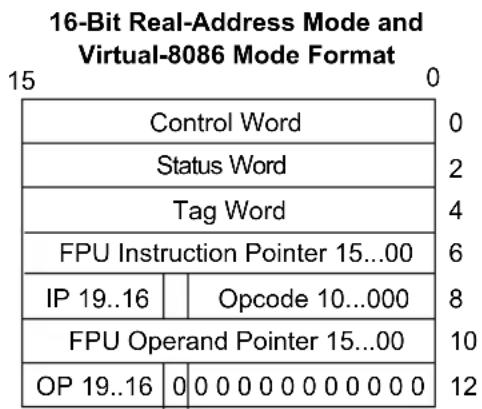
Figure 8-12. Real Mode x87 FPU State Image in Memory, 16-Bit Format
8.1.11 Saving the x87 FPU's State with FXSAVE
The FXSAVE and FXRSTOR instructions save and restore, respectively, the x87 FPU state along with the state of the XMM registers and the MXCSR register. Using the FXSAVE instruction to save the x87 FPU state has two benefits: (1) FXSAVE executes faster than FSAVE, and (2) FXSAVE saves the entire x87 FPU, MMX, and XMM state in one operation. See Section 10.5, "FXSAVE and FXRSTOR Instructions," for additional information about these instructions.
8.2 X87 FPU DATA TYPES
The x87 FPU recognizes and operates on the following seven data types (see Figures 8-13): single-precision floating point, double-precision floating point, double
extended-precision floating point, signed word integer, signed doubleword integer, signed quadword integer, and packed BCD decimal integers.
For detailed information about these data types, see Section 4.2.2, "Floating-Point Data Types," Section 4.2.1.2, "Signed Integers," and Section 4.7, "BCD and Packed BCD Integers."
With the exception of the 80-bit double extended-precision floating-point format, all of these data types exist in memory only. When they are loaded into x87 FPU data registers, they are converted into double extended-precision floating-point format and operated on in that format.
Denormal values are also supported in each of the floating-point types, as required by IEEE Standard 754. When a denormal number in single-precision or double-precision floating-point format is used as a source operand and the denormal exception is masked, the x87 FPU automatically normalizes the number when it is converted to double extended-precision format.
When stored in memory, the least significant byte of an x87 FPU data-type value is stored at the initial address specified for the value. Successive bytes from the value are then stored in successively higher addresses in memory. The floating-point instructions load and store memory operands using only the initial address of the operand.

Figure 8-13. x87 FPU Data Type Formats
As a general rule, values should be stored in memory in double-precision format. This format provides sufficient range and precision to return correct results with a minimum of programmer attention. The single-precision format is useful for debugging algorithms, because rounding problems will manifest themselves more quickly in this format. The double extended-precision format is normally reserved for holding intermediate results in the x87 FPU registers and constants. Its extra length is designed to shield final results from the effects of rounding and overflow/underflow in intermediate calculations. However, when an application requires the maximum range and precision of the x87 FPU (for data storage, computations, and results), values can be stored in memory in double extended-precision format.
8.2.1 Indefinites
For each x87 FPU data type, one unique encoding is reserved for representing the special value indefinite. The x87 FPU produces indefinite values as responses to some masked floating-point invalid-operation exceptions. See Tables 4-1, 4-3, and
4-4 for the encoding of the integer indefinite, QNaN floating-point indefinite, and packed BCD integer indefinite, respectively.
The binary integer encoding 100..00B represents either of two things, depending on the circumstances of its use:
- The largest negative number supported by the format (-215, -231 , or -263)
• The integer indefinite value
If this encoding is used as a source operand (as in an integer load or integer arithmetic instruction), the x87 FPU interprets it as the largest negative number representable in the format being used. If the x87 FPU detects an invalid operation when storing an integer value in memory with an FIST/FISTP instruction and the invalid-operation exception is masked, the x87 FPU stores the integer indefinite encoding in the destination operand as a masked response to the exception. In situations where the origin of a value with this encoding may be ambiguous, the invalid-operation exception flag can be examined to see if the value was produced as a response to an exception.
8.2.2 Unsupported Double Extended-Precision Floating-Point Encodings and Pseudo-Denormals
The double extended-precision floating-point format permits many encodings that do not fall into any of the categories shown in Table 4-3. Table 8-3 shows these unsupported encodings. Some of these encodings were supported by the Intel 287 math coprocessor; however, most of them are not supported by the Intel 387 math coprocessor and later IA-32 processors. These encodings are no longer supported due to changes made in the final version of IEEE Standard 754 that eliminated these encodings.
Specifically, the categories of encodings formerly known as pseudo-NaNs, pseudo-infinities, and un-normal numbers are not supported and should not be used as operand values. The Intel 387 math coprocessor and later IA-32 processors generate an invalid-operation exception when these encodings are encountered as operands.
Beginning with the Intel 387 math coprocessor, the encodings formerly known as pseudo-denormal numbers are not generated by IA-32 processors. When encountered as operands, however, they are handled correctly; that is, they are treated as denormals and a denormal exception is generated. Pseudo-denormal numbers should not be used as operand values. They are supported by current IA-32 processors (as described here) to support legacy code.
Table 8-3. Unsupported Double Extended-Precision Floating-Point Encodings and Pseudo-Denormals
| Class Sign Biased Exponent | Significand | ||||
| Integer | Fraction | ||||
| Positive Pseudo-NaNs | Quiet | 0 | 11..11 | 0 | 1 |
| . | . | . | |||
| 0 | 11..11 | 10..00 | |||
| Signaling | 0 | 11..11 | 0 | 01..11 | |
| . | . | . | |||
| 0 | 11..11 | 00..01 | |||
| Positive Floating Point | Pseudo-infinity 0 11..11 0 00..00 | ||||
| Unnormals | 0 | 11..10 | 0 | 1 | |
| . | . | . | |||
| 0 | 00..01 | 00..00 | |||
| Pseudo-denormals 0 | 00..00 | 1 | 1 | ||
| . | . | . | |||
| 0 | 00..00 | 00..00 | |||
| Negative Floating Point | Pseudo-denormals 1 | 00..00 | 1 | 1 | |
| . | . | . | |||
| 1 | 00..00 | 00..00 | |||
| Unnormals | 1 | 11..10 | 0 | 1 | |
| . | . | . | |||
| 1 | 00..01 | 00..00 | |||
| Pseudo-infinity 1 11..11 0 00..00 | |||||
| Negative Pseudo-NaNs | Signaling | 1 | 11..11 | 0 | 0 |
| . | . | . | |||
| 1 | 11..11 | 00..01 | |||
| Quiet | 1 | 11..11 | 0 | 1 | |
| . | . | . | |||
| 1 | 11..11 | 10..00 | |||
| ← 15 bits → | ← 63 bits → | ||||
8.3 X86 FPU INSTRUCTION SET
The floating-point instructions that the x87 FPU supports can be grouped into six functional categories:
• Data transfer instructions
• Basic arithmetic instructions
• Comparison instructions
• Transcendental instructions
- Load constant instructions
• x87 FPU control instructions
See Section 5.2, "x87 FPU Instructions," for a list of the floating-point instructions by category.
The following section briefly describes the instructions in each category. Detailed descriptions of the floating-point instructions are given in the Intel® 64 and IA-32 Architectures Software Developer's Manual, Volumes 3A & 3B.
8.3.1 Escape (ESC) Instructions
All of the instructions in the x87 FPU instruction set fall into a class of instructions known as escape (ESC) instructions. All of these instructions have a common opcode format, where the first byte of the opcode is one of the numbers from D8H through DFH.
8.3.2 x87 FPU Instruction Operands
Most floating-point instructions require one or two operands, located on the x87 FPU data-register stack or in memory. (None of the floating-point instructions accept immediate operands.)
When an operand is located in a data register, it is referenced relative to the ST(0) register (the register at the top of the register stack), rather than by a physical register number. Often the ST(0) register is an implied operand.
Operands in memory can be referenced using the same operand addressing methods described in Section 3.7, "Operand Addressing."
8.3.3 Data Transfer Instructions
The data transfer instructions (see Table 8-4) perform the following operations:
- Load a floating-point, integer, or packed BCD operand from memory into the ST(0) register.
- Store the value in an ST(0) register to memory in floating-point, integer, or packed BCD format.
- Move values between registers in the x87 FPU register stack.
The FLD (load floating point) instruction pushes a floating-point operand from memory onto the top of the x87 FPU data-register stack. If the operand is in single-precision or double-precision floating-point format, it is automatically converted to double extended-precision floating-point format. This instruction can also be used to push the value in a selected x87 FPU data register onto the top of the register stack.
The FILD (load integer) instruction converts an integer operand in memory into double extended-precision floating-point format and pushes the value onto the top of the register stack. The FBLD (load packed decimal) instruction performs the same load operation for a packed BCD operand in memory.
Table 8-4. Data Transfer Instructions
| Floating Point Integer Packed Decimal | |||||
| FLD Load Floating Point | FILD Load Point | Integer FBLD Load | Packed | Decimal | |
| FST Store Floating Point | FIST Store | Integer | |||
| FSTP Store Floating Point and Pop | FISTP Store | Integer and Pop | FBSTP Store | Packed Decimal and Pop | |
| FXCH Exchange Contents | Register | ||||
| FCMOVcc Conditional Move | |||||
The FST (store floating point) and FIST (store integer) instructions store the value in register ST(0) in memory in the destination format (floating point or integer, respectively). Again, the format conversion is carried out automatically.
The FSTP (store floating point and pop), FISTP (store integer and pop), and FBSTP (store packed decimal and pop) instructions store the value in the ST(0) registers into memory in the destination format (floating point, integer, or packed BCD), then performs a pop operation on the register stack. A pop operation causes the ST(0) register to be marked empty and the stack pointer (TOP) in the x87 FPU control work to be incremented by 1. The FSTP instruction can also be used to copy the value in the ST(0) register to another x87 FPU register [ST(i)].
The FXCH (exchange register contents) instruction exchanges the value in a selected register in the stack [ST(i)] with the value in ST(0).
The FCMOVcc (conditional move) instructions move the value in a selected register in the stack [ST(i)] to register ST(0) if a condition specified with a condition code (cc) is satisfied (see Table 8-5). The condition being tested for is represented by the status flags in the EFLAGS register. The condition code mnemonics are appended to the letters "FCMOV" to form the mnemonic for a FCMOVcc instruction.
Table 8-5. Floating-Point Conditional Move Instructions
| Instruction Mnemonic Status Flag States | Condition | Description |
| FCMOVB | CF=1 | Below |
| FCMOVNB | CF=0 | Not below |
| FCMOVE | ZF=1 | Equal |
| FCMOVNE | ZF=0 | Not equal |
Table 8-5. Floating-Point Conditional Move Instructions (Contd.)
| Instruction Mnemonic Status Flag States Condition Description | ||
| FCMOVBE | CF=1 or ZF=1 | Below or equal |
| FCMOVNBE | CF=0 or ZF=0 | Not below nor equal |
| FCMOVU | PF=1 | Unordered |
| FCMOVNU | PF=0 | Not unordered |
Like the CMOVcc instructions, the FCMOVcc instructions are useful for optimizing small IF constructions. They also help eliminate branching overhead for IF operations and the possibility of branch mispredictions by the processor.
Software can check if the FCMOVcc instructions are supported by checking the processor's feature information with the CPUID instruction.
8.3.4 Load Constant Instructions
The following instructions push commonly used constants onto the top [ST(0)] of the x87 FPU register stack:
FLDZ Load +0.0
FLD1 Load +1.0
FLDPI Load π
FLDL2T Load log 2 10
FLDL2E Load log 2e
FLDLG2 Load log 102
FLDLN2 Load log e2
The constant values have full double extended-precision floating-point precision (64 bits) and are accurate to approximately 19 decimal digits. They are stored internally in a format more precise than double extended-precision floating point. When loading the constant, the x87 FPU rounds the more precise internal constant according to the RC (rounding control) field of the x87 FPU control word. The inexact-result exception (#P) is not generated as a result of this rounding, nor is the C1 flag set in the x87 FPU status word if the value is rounded up. See Section 8.3.8, "Pi," for information on the π constant.
8.3.5 Basic Arithmetic Instructions
The following floating-point instructions perform basic arithmetic operations on floating-point numbers. Where applicable, these instructions match IEEE Standard 754:
FADD/FADDP Add floating point
| FIADD Add integer to floating point | |
| FSUB/FSUBP Subtract floating point | |
| FISUB Subtract integer from floating point | |
| FSUBR/FSUBRP Reverse subtract floating point | |
| FISUBR Reverse subtract floating point from integer | |
| FMUL/FMULP Multiply floating point | |
| FIMUL Multiply integer by floating point | |
| FDIV/FDIVP Divide floating point | |
| FIDIV Divide floating point by integer | |
| FDIVR/FDIVRP Reverse divide | |
| FIDIVR Reverse divide integer by floating point | |
| FABS Absolute value | |
| FCHS Change sign | |
| FSQRT | Square root |
| FPREM | Partial remainder |
| FPREM1 | IEEE partial remainder |
| FRNDINT | Round to integral value |
| FXTRACT | Extract exponent and significand |
The add, subtract, multiply and divide instructions operate on the following types of operands:
• Two x87 FPU data registers
• An x87 FPU data register and a floating-point or integer value in memory
See Section 8.1.2, "x87 FPU Data Registers," for a description of how operands are referenced on the data register stack.
Operands in memory can be in single-precision floating-point, double-precision floating-point, word-integer, or doubleword-integer format. They are converted to double extended-precision floating-point format automatically.
Reverse versions of the subtract (FSUBR) and divide (FDIVR) instructions enable efficient coding. For example, the following options are available with the FSUB and FSUBR instructions for operating on values in a specified x87 FPU data register ST(i) and the ST(0) register:
FSUB:
ST (0) ← ST (0) - ST (i) ST (i) ← ST (i) - ST (0)
FSUBR:
ST (0) ← ST (i) - ST (0) ST (i) ← ST (0) - ST (i)
These instructions eliminate the need to exchange values between the ST(0) register and another x87 FPU register to perform a subtraction or division.
The pop versions of the add, subtract, multiply, and divide instructions offer the option of popping the x87 FPU register stack following the arithmetic operation. These instructions operate on values in the ST(i) and ST(0) registers, store the result in the ST(i) register, and pop the ST(0) register.
The FPREM instruction computes the remainder from the division of two operands in the manner used by the Intel 8087 and Intel 287 math coprocessors; the FPREM1 instruction computes the remainder in the manner specified in IEEE Standard 754.
The FSQRT instruction computes the square root of the source operand.
The FRNDINT instruction returns a floating-point value that is the integral value closest to the source value in the direction of the rounding mode specified in the RC field of the x87 FPU control word.
The FABS, FCHS, and FXTRACT instructions perform convenient arithmetic operations. The FABS instruction produces the absolute value of the source operand. The FCHS instruction changes the sign of the source operand. The FXTRACT instruction separates the source operand into its exponent and fraction and stores each value in a register in floating-point format.
8.3.6 Comparison and Classification Instructions
The following instructions compare or classify floating-point values:
FCOM/FCOMP/FCOMPPCompare floating point and set x87 FPU condition code flags.
FUCOM/FUCOMP/FUCOMPPUnordered compare floating point and set x87 FPU condition code flags.
FICOM/FICOMPCompare integer and set x87 FPU condition code flags.
FCOMI/FCOMIPCompare floating point and set EFLAGS status flags.
FUCOMI/FUCOMIPUnordered compare floating point and set EFLAGS status flags.
FTST Test (compare floating point with 0.0). FXAMExamine.
Comparison of floating-point values differ from comparison of integers because floating-point values have four (rather than three) mutually exclusive relationships: less than, equal, greater than, and unordered.
The unordered relationship is true when at least one of the two values being compared is a NaN or in an unsupported format. This additional relationship is required because, by definition, NaNs are not numbers, so they cannot have less than, equal, or greater than relationships with other floating-point values.
The FCOM, FCOMP, and FCOMPP instructions compare the value in register ST(0) with a floating-point source operand and set the condition code flags (C0, C2, and C3) in the x87 FPU status word according to the results (see Table 8-6).
If an unordered condition is detected (one or both of the values are NaNs or in an undefined format), a floating-point invalid-operation exception is generated.
The pop versions of the instruction pop the x87 FPU register stack once or twice after the comparison operation is complete.
The FUCOM, FUCOMP, and FUCOMPP instructions operate the same as the FCOM, FCOMP, and FCOMPP instructions. The only difference is that with the FUCOM, FUCOMP, and FUCOMPP instructions, if an unordered condition is detected because one or both of the operands are QNaNs, the floating-point invalid-operation exception is not generated.
Table 8-6. Setting of x87 FPU Condition Code Flags for Floating-Point Number Comparisons
| Condition C3 C2 CO | |||
| ST(0) > Source Operand 0 0 0 | |||
| ST(0) < Source Operand 0 0 1 | |||
| ST(0) = Source Operand 1 0 0 | |||
| Unordered 1 1 1 |
The FICOM and FICOMP instructions also operate the same as the FCOM and FCOMP instructions, except that the source operand is an integer value in memory. The integer value is automatically converted into an double extended-precision floating-point value prior to making the comparison. The FICOMP instruction pops the x87 FPU register stack following the comparison operation.
The FTST instruction performs the same operation as the FCOM instruction, except that the value in register ST(0) is always compared with the value 0.0.
The FCOMI and FCOMIP instructions were introduced into the IA-32 architecture in the P6 family processors. They perform the same comparison as the FCOM and FCOMP instructions, except that they set the status flags (ZF, PF, and CF) in the EFLAGS register to indicate the results of the comparison (see Table 8-7) instead of the x87 FPU condition code flags. The FCOMI and FCOMIP instructions allow condition branch instructions (Jcc) to be executed directly from the results of their comparison.
Table 8-7. Setting of EFLAGS Status Flags for Floating-Point Number Comparisons
| Comparison Results ZF PF CF | |||
| STO > ST(i) | 0 | 0 | 0 |
| STO < ST(i) | 0 | 0 | 1 |
| STO = ST(i) | 1 | 0 | 0 |
| Unordered 1 1 1 | |||
Software can check if the FCOMI and FCOMIP instructions are supported by checking the processor's feature information with the CPUID instruction.
The FUCOMI and FUCOMIP instructions operate the same as the FCOMI and FCOMIP instructions, except that they do not generate a floating-point invalid-operation exception if the unordered condition is the result of one or both of the operands being a QNaN. The FCOMIP and FUCOMIP instructions pop the x87 FPU register stack following the comparison operation.
The FXAM instruction determines the classification of the floating-point value in the ST(0) register (that is, whether the value is zero, a denormal number, a normal finite number, ∞ , a NaN, or an unsupported format) or that the register is empty. It sets the x87 FPU condition code flags to indicate the classification (see "FXAM—Examine" in Chapter 3, "Instruction Set Reference, A-M," of the Intel® 64 and IA-32 Architectures Software Developer's Manual, Volume 2A). It also sets the C1 flag to indicate the sign of the value.
8.3.6.1 Branching on the x87 FPU Condition Codes
The processor does not offer any control-flow instructions that branch on the setting of the condition code flags (C0, C2, and C3) in the x87 FPU status word. To branch on the state of these flags, the x87 FPU status word must first be moved to the AX register in the integer unit. The FSTSW AX (store status word) instruction can be used for this purpose. When these flags are in the AX register, the TEST instruction can be used to control conditional branching as follows:
- Check for an unordered result. Use the TEST instruction to compare the contents of the AX register with the constant 0400H (see Table 8-8). This operation will clear the ZF flag in the EFLAGS register if the condition code flags indicate an unordered result; otherwise, the ZF flag will be set. The JNZ instruction can then be used to transfer control (if necessary) to a procedure for handling unordered operands.
Table 8-8. TEST Instruction Constants for Conditional Branching
| Order Constant Branch | ||
| ST(0) > Source Operand 4500H JZ | ||
| ST(0) < Source Operand 0100H | JNZ | |
| ST(0) = Source Operand 4000H | JNZ | |
| Unordered | 0400H | JNZ |
- Check ordered comparison result. Use the constants given in Table 8-8 in the TEST instruction to test for a less than, equal to, or greater than result, then use the corresponding conditional branch instruction to transfer program control to the appropriate procedure or section of code.
If a program or procedure has been thoroughly tested and it incorporates periodic checks for QNaN results, then it is not necessary to check for the unordered result every time a comparison is made.
See Section 8.1.4, "Branching and Conditional Moves on Condition Codes," for another technique for branching on x87 FPU condition codes.
Some non-comparison x87 FPU instructions update the condition code flags in the x87 FPU status word. To ensure that the status word is not altered inadvertently, store it immediately following a comparison operation.
8.3.7 Trigonometric Instructions
The following instructions perform four common trigonometric functions:
FSIN Sine
FCOS Cosine
FSINCOS Sine and cosine
FPTAN Tangent
FPATAN Arctangent
These instructions operate on the top one or two registers of the x87 FPU register stack and they return their results to the stack. The source operands for the FSIN, FCOS, FSINCOS, and FPTAN instructions must be given in radians; the source operand for the FPATAN instruction is given in rectangular coordinate units.
The FSINCOS instruction returns both the sine and the cosine of a source operand value. It operates faster than executing the FSIN and FCOS instructions in succession.
The FPATAN instruction computes the arctangent of ST(1) divided by ST(0), returning a result in radians. It is useful for converting rectangular coordinates to polar coordinates.
8.3.8 Pi
When the argument (source operand) of a trigonometric function is within the range of the function, the argument is automatically reduced by the appropriate multiple of 2π through the same reduction mechanism used by the FPREM and FPREM1 instructions. The internal value of π that the x87 FPU uses for argument reduction and other computations is as follows:
π = 0. f * 2 ^ 2
where:
f = C 9 0 FDAA 2 2 1 6 8 C 2 3 4 C
(The spaces in the fraction above indicate 32-bit boundaries.)
This internal π value has a 66-bit mantissa, which is 2 bits more than is allowed in the significand of an double extended-precision floating-point value. (Since 66 bits is not an even number of hexadecimal digits, two additional zeros have been added to the value so that it can be represented in hexadecimal format. The least-significant hexadecimal digit (C) is thus 1100B, where the two least-significant bits represent bits 67 and 68 of the mantissa.)
This value of π has been chosen to guarantee no loss of significance in a source operand, provided the operand is within the specified range for the instruction.
If the results of computations that explicitly use π are to be used in the FSIN, FCOS, FSINCOS, or FPTAN instructions, the full 66-bit fraction of π should be used. This insures that the results are consistent with the argument-reduction algorithms that these instructions use. Using a rounded version of π can cause inaccuracies in result values, which if propagated through several calculations, might result in meaningless results.
A common method of representing the full 66-bit fraction of π is to separate the value into two numbers (high π and low π ) that when added together give the value for π shown earlier in this section with the full 66-bit fraction:
π = high π + low π
For example, the following two values (given in scientific notation with the fraction in hexadecimal and the exponent in decimal) represent the 33 most-significant and the 33 least-significant bits of the fraction:
high _ π ( unnormalized ) = 0. C 9 0 FDAA 2 0 * 2 ^ + 2 low π ( unnormalized ) = 0. 4 2 D 1 8 4 6 9 8 * 2 ^ - 3 1
These values encoded in the IEEE double-precision floating-point format are as follows:
high π = 4 0 0 9 2 1 FB 5 4 4 0 0 0 0 0
low π = 3 DE0B461 1 A600000
(Note that in the IEEE double-precision floating-point format, the exponents are biased (by 1023) and the fractions are normalized.)
Similar versions of π can also be written in double extended-precision floating-point format.
When using this two-part π value in an algorithm, parallel computations should be performed on each part, with the results kept separate. When all the computations are complete, the two results can be added together to form the final result.
The complications of maintaining a consistent value of π for argument reduction can be avoided, either by applying the trigonometric functions only to arguments within the range of the automatic reduction mechanism, or by performing all argument reductions (down to a magnitude less than π/4 ) explicitly in software.
8.3.9 Logarithmic, Exponential, and Scale
The following instructions provide two different logarithmic functions, an exponential function and a scale function:
FYL2X Logarithm
FYL2XP1 Logarithm epsilon
F2XM1 Exponential
FSCALE Scale
The FYL2X and FYL2XP1 instructions perform two different base 2 logarithmic operations. The FYL2X instruction computes (y * log₂x). This operation permits the calculation of the log of any base using the following equation:
_ b x = (1 / _ 2 b) * _ 2 x
The FYL2XP1 instruction computes (y * 2(x + 1)) . This operation provides optimum accuracy for values of x that are close to 0.
The F2XM1 instruction computes (2x-1) . This instruction only operates on source values in the range -1.0 to +1.0.
The FSCALE instruction multiplies the source operand by a power of 2.
8.3.10 Transcendental Instruction Accuracy
New transcendental instruction algorithms were incorporated into the IA-32 architecture beginning with the Pentium processors. These new algorithms (used in transcendental instructions FSIN, FCOS, FSINCOS, FPTAN, FPATAN, F2XM1, FYL2X, and FYL2XP1) allow a higher level of accuracy than was possible in earlier IA-32 processors and x87 math coprocessors. The accuracy of these instructions is measured in terms of units in the last place (ulp). For a given argument x, let f(x) and F(x) be the correct and computed (approximate) function values, respectively. The error in ulps is defined to be:
error = | f (x) - F (x)2 ^ k 6 3 | -
where k is an integer such that:
1 ≤ 2 ^ - k f (x) lt; 2.
With the Pentium processor and later IA-32 processors, the worst case error on transcendental functions is less than 1 ulp when rounding to the nearest (even) and less than 1.5 ulps when rounding in other modes. The functions are guaranteed to be monotonic, with respect to the input operands, throughout the domain supported by the instruction.
The instructions FYL2X and FYL2XP1 are two operand instructions and are guaranteed to be within 1 ulp only when y equals 1. When y is not equal to 1, the maximum ulp error is always within 1.35 ulps in round to nearest mode. (For the two operand functions, monotonicity was proved by holding one of the operands constant.)
8.3.11 x87 FPU Control Instructions
The following instructions control the state and modes of operation of the x87 FPU. They also allow the status of the x87 FPU to be examined:
FINIT/FNINIT Initialize x87 FPU
FLDCW Load x87 FPU control word
FSTCW/FNSTCWStore x87 FPU control word
FSTSW/FNSTSWStore x87 FPU status word
FCLEX/FNCLEXClear x87 FPU exception flags
FLDENV Load x87 FPU environment
FSTENV/FNSTENVStore x87 FPU environment
FRSTOR Restore x87 FPU state
FSAVE/FNSAVESave x87 FPU state
FINCSTP Increment x87 FPU register stack pointer
FDECSTP Decrement x87 FPU register stack pointer
FFREE Free x87 FPU register
FNOP No operation
WAIT/FWAIT Check for and handle pending unmasked x87 FPU exceptions
The FINIT/FNINIT instructions initialize the x87 FPU and its internal registers to default values.
The FLDCW instructions loads the x87 FPU control word register with a value from memory. The FSTCW/FNSTCW and FSTSW/FNSTSW instructions store the x87 FPU
control and status words, respectively, in memory (or for an FSTSW/FNSTSW instruction in a general-purpose register).
The FSTENV/FNSTENV and FSAVE/FNSAVE instructions save the x87 FPU environment and state, respectively, in memory. The x87 FPU environment includes all the x87 FPU's control and status registers; the x87 FPU state includes the x87 FPU environment and the data registers in the x87 FPU register stack. (The FSAVE/FNSAVE instruction also initializes the x87 FPU to default values, like the FINIT/FNINIT instruction, after it saves the original state of the x87 FPU.)
The FLDENV and FRSTOR instructions load the x87 FPU environment and state, respectively, from memory into the x87 FPU. These instructions are commonly used when switching tasks or contexts.
The WAIT/FWAIT instructions are synchronization instructions. (They are actually mnemonics for the same opcode.) These instructions check the x87 FPU status word for pending unmasked x87 FPU exceptions. If any pending unmasked x87 FPU exceptions are found, they are handled before the processor resumes execution of the instructions (integer, floating-point, or system instruction) in the instruction stream. The WAIT/FWAIT instructions are provided to allow synchronization of instruction execution between the x87 FPU and the processor's integer unit. See Section 8.6, "x87 FPU Exception Synchronization," for more information on the use of the WAIT/FWAIT instructions.
8.3.12 Waiting vs. Non-waiting Instructions
All of the x87 FPU instructions except a few special control instructions perform a wait operation (similar to the WAIT/FWAIT instructions), to check for and handle pending unmasked x87 FPU floating-point exceptions, before they perform their primary operation (such as adding two floating-point numbers). These instructions are called waiting instructions. Some of the x87 FPU control instructions, such as FSTSW/FNSTSW, have both a waiting and a non-waiting version. The waiting version (with the "F" prefix) executes a wait operation before it performs its primary operation; whereas, the non-waiting version (with the "FN" prefix) ignores pending unmasked exceptions.
Non-waiting instructions allow software to save the current x87 FPU state without first handling pending exceptions or to reset or reinitialize the x87 FPU without regard for pending exceptions.
NOTES
When operating a Pentium or Intel486 processor in MS-DOS compatibility mode, it is possible (under unusual circumstances) for a non-waiting instruction to be interrupted prior to being executed to handle a pending x87 FPU exception. The circumstances where this can happen and the resulting action of the processor are described in
Section D.2.1.3, "No-Wait x87 FPU Instructions Can Get x87 FPU Interrupt in Window."
When operating a P6 family, Pentium 4, or Intel Xeon processor in MS-DOS compatibility mode, non-waiting instructions can not be interrupted in this way (see Section D.2.2, "MS-DOS* Compatibility Sub-mode in the P6 Family and Pentium® 4 Processors").
8.3.13 Unsupported x87 FPU Instructions
The Intel 8087 instructions FENI and FDISI and the Intel 287 math coprocessor instruction FSETPM perform no function in the Intel 387 math coprocessor and later IA-32 processors. If these opcodes are detected in the instruction stream, the x87 FPU performs no specific operation and no internal x87 FPU states are affected.
8.4 X87 FPU FLOATING-POINT EXCEPTION HANDLING
The x87 FPU detects the six classes of exception conditions described in Section 4.9, "Overview of Floating-Point Exceptions":
- Invalid operation (#I), with two subclasses:
— Stack overflow or underflow (#IS)
— Invalid arithmetic operation (#IA)
• Denormalized operand (#D)
- Divide-by-zero (#Z)
- Numeric overflow (#O)
- Numeric underflow (#U)
- Inexact result (precision) (#P)
Each of the six exception classes has a corresponding flag bit in the x87 FPU status word and a mask bit in the x87 FPU control word (see Section 8.1.3, "x87 FPU Status Register," and Section 8.1.5, "x87 FPU Control Word," respectively). In addition, the exception summary (ES) flag in the status word indicates when one or more unmasked exceptions has been detected. The stack fault (SF) flag (also in the status word) distinguishes between the two types of invalid-operation exceptions.
The mask bits can be set with FLDCW, FRSTOR, or FXRSTOR; they can be read with either FSTCW/FNSTCW, FSAVE/FNSAVE, or FXSAVE. The flag bits can be read with the FSTSW/FNSTSW, FSAVE/FNSAVE, or FXSAVE instruction.
NOTE
Section 4.9.1, "Floating-Point Exception Conditions," provides a general overview of how the IA-32 processor detects and handles the
various classes of floating-point exceptions. This information pertains to x87 FPU as well as SSE/SSE2/SSE3 extensions.
The following sections give specific information about how the x87 FPU handles floating-point exceptions that are unique to the x87 FPU.
8.4.1 Arithmetic vs. Non-arithmetic Instructions
When dealing with floating-point exceptions, it is useful to distinguish between arithmetic instructions and non-arithmetic instructions. Non-arithmetic instructions have no operands or do not make substantial changes to their operands. Arithmetic instructions do make significant changes to their operands; in particular, they make changes that could result in floating-point exceptions being signaled. Table 8-9 lists the non-arithmetic and arithmetic instructions. It should be noted that some non-arithmetic instructions can signal a floating-point stack (fault) exception, but this exception is not the result of an operation on an operand.
Table 8-9. Arithmetic and Non-arithmetic Instructions
| Non-arithmetic Instructions Arithmetic Instructions | |
| FABS F2XM1 | |
| FCHS FADD/FADDP | |
| FCLEX FBLD | |
| FDECSTP FBSTP | |
| FFREE FCOM/FCOMP/FCOMPP | |
| FINCSTP FCOS | |
| FINIT/FNINIT FDIV/FDIVP/FDIVR/FDIVRP | |
| FLD (register-to-register) FIADD | |
| FLD (extended format from memory) | FICOM/FICOMP |
| FLD constant | FIDIV/FIDIVR |
| FLDCW | FILD |
| FLDENV | FIMUL |
| FNOP | FIST/FISTP1 |
| FRSTOR | FISUB/FISUBR |
| FSAVE/FNSAVE | FLD (single and double) |
| FST/FSTP (register-to-register) | FMUL/FMULP |
| FSTP (extended format to memory) | FPATAN |
| FSTCW/FNSTCW | FPREM/FPREM1 |
| FSTENV/FNSTENV | FPTAN |
Table 8-9. Arithmetic and Non-arithmetic Instructions (Contd.)
| Non-arithmetic Instructions Arithmetic Instructions | |
| FSTSW/FNSTSW FRNDINTWAIT/FWAIT FSCALEFXAM FSINFXCH FSINCOS | FSQRTFST/FSTP (single and double)FSUB/FSUBP/FSUBR/FSUBRPFTSTFUCOM/FUCOMP/FUCOMPPFXTRACTFYL2X/FYL2XP1 |
NOTE:
1. The FISTTP instruction in SSE3 is an arithmetic x87 FPU instruction.
8.5 X87 FPU FLOATING-POINT EXCEPTION CONDITIONS
The following sections describe the various conditions that cause a floating-point exception to be generated by the x87 FPU and the masked response of the x87 FPU when these conditions are detected. Intel® 64 and IA-32 Architectures Software Developer's Manual, Volumes 2A & 2B, list the floating-point exceptions that can be signaled for each floating-point instruction.
See Section 4.9.2, "Floating-Point Exception Priority," for a description of the rules for exception precedence when more than one floating-point exception condition is detected for an instruction.
8.5.1 Invalid Operation Exception
The floating-point invalid-operation exception occurs in response to two sub-classes of operations:
- Stack overflow or underflow (#IS)
- Invalid arithmetic operand (#IA)
The flag for this exception (IE) is bit 0 of the x87 FPU status word, and the mask bit (IM) is bit 0 of the x87 FPU control word. The stack fault flag (SF) of the x87 FPU status word indicates the type of operation that caused the exception. When the SF flag is set to 1, a stack operation has resulted in stack overflow or underflow; when
the flag is cleared to 0, an arithmetic instruction has encountered an invalid operand. Note that the x87 FPU explicitly sets the SF flag when it detects a stack overflow or underflow condition, but it does not explicitly clear the flag when it detects an invalid-arithmetic-operand condition. As a result, the state of the SF flag can be 1 following an invalid-arithmetic-operation exception, if it was not cleared from the last time a stack overflow or underflow condition occurred. See Section 8.1.3.4, "Stack Fault Flag," for more information about the SF flag.
8.5.1.1 Stack Overflow or Underflow Exception (#IS)
The x87 FPU tag word keeps track of the contents of the registers in the x87 FPU register stack (see Section 8.1.7, "x87 FPU Tag Word"). It then uses this information to detect two different types of stack faults:
- Stack overflow — An instruction attempts to load a non-empty x87 FPU register from memory. A non-empty register is defined as a register containing a zero (tag value of 01), a valid value (tag value of 00), or a special value (tag value of 10).
- Stack underflow — An instruction references an empty x87 FPU register as a source operand, including attempting to write the contents of an empty register to memory. An empty register has a tag value of 11.
NOTES
The term stack overflow originates from the situation where the program has loaded (pushed) eight values from memory onto the x87 FPU register stack and the next value pushed on the stack causes a stack wraparound to a register that already contains a value.
The term stack underflow originates from the opposite situation. Here, a program has stored (popped) eight values from the x87 FPU register stack to memory and the next value popped from the stack causes stack wraparound to an empty register.
When the x87 FPU detects stack overflow or underflow, it sets the IE flag (bit 0) and the SF flag (bit 6) in the x87 FPU status word to 1. It then sets condition-code flag C1 (bit 9) in the x87 FPU status word to 1 if stack overflow occurred or to 0 if stack underflow occurred.
If the invalid-operation exception is masked, the x87 FPU returns the floating point, integer, or packed decimal integer indefinite value to the destination operand, depending on the instruction being executed. This value overwrites the destination register or memory location specified by the instruction.
If the invalid-operation exception is not masked, a software exception handler is invoked (see Section 8.7, "Handling x87 FPU Exceptions in Software") and the top-of-stack pointer (TOP) and source operands remain unchanged.
8.5.1.2 Invalid Arithmetic Operand Exception (#IA)
The x87 FPU is able to detect a variety of invalid arithmetic operations that can be coded in a program. These operations are listed in Table 8-10. (This list includes the invalid operations defined in IEEE Standard 754.)
When the x87 FPU detects an invalid arithmetic operand, it sets the IE flag (bit 0) in the x87 FPU status word to 1. If the invalid-operation exception is masked, the x87 FPU then returns an indefinite value or QNaN to the destination operand and/or sets the floating-point condition codes as shown in Table 8-10. If the invalid-operation exception is not masked, a software exception handler is invoked (see Section 8.7, "Handling x87 FPU Exceptions in Software") and the top-of-stack pointer (TOP) and source operands remain unchanged.
Table 8-10. Invalid Arithmetic Operations and the Masked Responses to Them
| Condition Masked Response | |
| Any arithmetic operation on an operand that is in an unsupported format. | Return the QNaN floating-point indefinite value to the destination operand. |
| Any arithmetic operation on a SNaN. Return a QNaN to the destination operand (see Table 4-7). | |
| Ordered compare and test operations: one or both operands are NaNs. | Set the condition code flags (C0, C2, and C3) in the x87 FPU status word or the CF, PF, and ZF flags in the EFLAGS register to 111B (not comparable). |
| Addition: operands are opposite-signed infinities. Subtraction: operands are like-signed infinities. | Return the QNaN floating-point indefinite value to the destination operand. |
| Multiplication: ∞ by 0; 0 by ∞. | Return the QNaN floating-point indefinite value to the destination operand. |
| Division: ∞ by ∞; 0 by 0. | Return the QNaN floating-point indefinite value to the destination operand. |
| Remainder instructions FPREM, FPREM1: modulus (divisor) is 0 or dividend is ∞. | Return the QNaN floating-point indefinite; clear condition code flag C2 to 0. |
| Trigonometric instructions FCOS, FPTAN, FSIN, FSINCOS: source operand is ∞. | Return the QNaN floating-point indefinite; clear condition code flag C2 to 0. |
| FSQRT: negative operand (except FSQRT (-0) = -0); FYL2X: negative operand (except FYL2X (-0) = -∞); FYL2XP1: operand more negative than -1. | Return the QNaN floating-point indefinite value to the destination operand. |
| FBSTP: Converted value cannot be represented in 18 decimal digits, or source value is an SNaN, QNaN, ±∞, or in an unsupported format. | Store packed BCD integer indefinite value in the destination operand. |
Table 8-10. Invalid Arithmetic Operations and the Masked Responses to Them (Contd.)
| FIST/FISTP: Converted value exceeds representable integer range of the destination operand, or source value is an SNaN, QNaN, ±∞, or in an unsupported format. | Store integer indefinite value in the destination operand. |
| FXCH: one or both registers are tagged empty. Load | empty registers with the QNaN floating-point indefinite value, then perform the exchange. |
Normally, when one or both of the source operands is a QNaN (and neither is an SNaN or in an unsupported format), an invalid-operand exception is not generated. An exception to this rule is most of the compare instructions (such as the FCOM and FCOMI instructions) and the floating-point to integer conversion instructions (FIST/FISTP and FBSTP). With these instructions, a QNaN source operand will generate an invalid-operand exception.
8.5.2 Denormal Operand Exception (#D)
The x87 FPU signals the denormal-operand exception under the following conditions:
- If an arithmetic instruction attempts to operate on a denormal operand (see Section 4.8.3.2, "Normalized and Denormalized Finite Numbers").
- If an attempt is made to load a denormal single-precision or double-precision floating-point value into an x87 FPU register. (If the denormal value being loaded is a double extended-precision floating-point value, the denormal-operand exception is not reported.)
The flag (DE) for this exception is bit 1 of the x87 FPU status word, and the mask bit (DM) is bit 1 of the x87 FPU control word.
When a denormal-operand exception occurs and the exception is masked, the x87 FPU sets the DE flag, then proceeds with the instruction. The denormal operand in single- or double-precision floating-point format is automatically normalized when converted to the double extended-precision floating-point format. Subsequent operations will benefit from the additional precision of the internal double extended-precision floating-point format.
When a denormal-operand exception occurs and the exception is not masked, the DE flag is set and a software exception handler is invoked (see Section 8.7, "Handling x87 FPU Exceptions in Software"). The top-of-stack pointer (TOP) and source operands remain unchanged.
For additional information about the denormal-operation exception, see Section 4.9.1.2, "Denormal Operand Exception (#D)."
8.5.3 Divide-By-Zero Exception (#Z)
The x87 FPU reports a floating-point divide-by-zero exception whenever an instruction attempts to divide a finite non-zero operand by 0. The flag (ZE) for this exception is bit 2 of the x87 FPU status word, and the mask bit (ZM) is bit 2 of the x87 FPU control word. The FDIV, FDIVP, FDIVR, FDIVRP, FIDIV, and FIDIVR instructions and the other instructions that perform division internally (FYL2X and FXTRACT) can report the divide-by-zero exception.
When a divide-by-zero exception occurs and the exception is masked, the x87 FPU sets the ZE flag and returns the values shown in Table 8-10. If the divide-by-zero exception is not masked, the ZE flag is set, a software exception handler is invoked (see Section 8.7, "Handling x87 FPU Exceptions in Software"), and the top-of-stack pointer (TOP) and source operands remain unchanged.
Table 8-11. Divide-By-Zero Conditions and the Masked Responses to Them
| Condition Masked Response | |
| Divide or reverse divide operation with a 0 divisor. | Returns an ∞ signed with the exclusive OR of the sign of the two operands to the destination operand. |
| FYL2X instruction. | Returns an ∞ signed with the opposite sign of the non-zero operand to the destination operand. |
| FXTRACT instruction. | ST(1) is set to -∞ ; ST(0) is set to 0 with the same sign as the source operand. |
8.5.4 Numeric Overflow Exception (#0)
The x87 FPU reports a floating-point numeric overflow exception (#O) whenever the rounded result of an arithmetic instruction exceeds the largest allowable finite value that will fit into the floating-point format of the destination operand. (See Section 4.9.1.4, "Numeric Overflow Exception (#O)," for additional information about the numeric overflow exception.)
When using the x87 FPU, numeric overflow can occur on arithmetic operations where the result is stored in an x87 FPU data register. It can also occur on store floating-point operations (using the FST and FSTP instructions), where a within-range value in a data register is stored in memory in a single-precision or double-precision floating-point format. The numeric overflow exception cannot occur when storing values in an integer or BCD integer format. Instead, the invalid-arithmetic-operand exception is signaled.
The flag (OE) for the numeric-overflow exception is bit 3 of the x87 FPU status word, and the mask bit (OM) is bit 3 of the x87 FPU control word.
When a numeric-overflow exception occurs and the exception is masked, the x87 FPU sets the OE flag and returns one of the values shown in Table 4-10. The value returned depends on the current rounding mode of the x87 FPU (see Section 8.1.5.3, "Rounding Control Field").
The action that the x87 FPU takes when numeric overflow occurs and the numeric-overflow exception is not masked, depends on whether the instruction is supposed to store the result in memory or on the register stack.
- Destination is a memory location — The OE flag is set and a software exception handler is invoked (see Section 8.7, "Handling x87 FPU Exceptions in Software"). The top-of-stack pointer (TOP) and source and destination operands remain unchanged. Because the data in the stack is in double extended-precision format, the exception handler has the option either of re-executing the store instruction after proper adjustment of the operand or of rounding the significand on the stack to the destination's precision as the standard requires. The exception handler should ultimately store a value into the destination location in memory if the program is to continue.
- Destination is the register stack — The significand of the result is rounded according to current settings of the precision and rounding control bits in the x87 FPU control word and the exponent of the result is adjusted by dividing it by 224576 . (For instructions not affected by the precision field, the significand is rounded to double-extended precision.) The resulting value is stored in the destination operand. Condition code bit C1 in the x87 FPU status word (called in this situation the "round-up bit") is set if the significand was rounded upward and cleared if the result was rounded toward 0. After the result is stored, the OE flag is set and a software exception handler is invoked. The scaling bias value 24,576 is equal to 3 * 213 . Biasing the exponent by 24,576 normally translates the number as nearly as possible to the middle of the double extended-precision floating-point exponent range so that, if desired, it can be used in subsequent scaled operations with less risk of causing further exceptions.
When using the FSCALE instruction, massive overflow can occur, where the result is too large to be represented, even with a bias-adjusted exponent. Here, if overflow occurs again, after the result has been biased, a properly signed ∞ is stored in the destination operand.
8.5.5 Numeric Underflow Exception (#U)
The x87 FPU detects a floating-point numeric underflow condition whenever the rounded result of an arithmetic instruction is tiny; that is, less than the smallest possible normalized, finite value that will fit into the floating-point format of the destination operand. (See Section 4.9.1.5, "Numeric Underflow Exception (#U)," for additional information about the numeric underflow exception.)
Like numeric overflow, numeric underflow can occur on arithmetic operations where the result is stored in an x87 FPU data register. It can also occur on store floating-point operations (with the FST and FSTP instructions), where a within-range value in a data register is stored in memory in the smaller single-precision or double-precision floating-point formats. A numeric underflow exception cannot occur when storing values in an integer or BCD integer format, because a tiny value is always rounded to an integral value of 0 or 1, depending on the rounding mode in effect.
The flag (UE) for the numeric-underflow exception is bit 4 of the x87 FPU status word, and the mask bit (UM) is bit 4 of the x87 FPU control word.
When a numeric-underflow condition occurs and the exception is masked, the x87 FPU performs the operation described in Section 4.9.1.5, "Numeric Underflow Exception (#U)."
When the exception is not masked, the action of the x87 FPU depends on whether the instruction is supposed to store the result in a memory location or on the x87 FPU resistor stack.
- Destination is a memory location — (Can occur only with a store instruction.) The UE flag is set and a software exception handler is invoked (see Section 8.7, "Handling x87 FPU Exceptions in Software"). The top-of-stack pointer (TOP) and source and destination operands remain unchanged, and no result is stored in memory.
Because the data in the stack is in double extended-precision format, the exception handler has the option either of re-exchanges the store instruction after proper adjustment of the operand or of rounding the significand on the stack to the destination's precision as the standard requires. The exception handler should ultimately store a value into the destination location in memory if the program is to continue.
- Destination is the register stack — The significand of the result is rounded according to current settings of the precision and rounding control bits in the x87 FPU control word and the exponent of the result is adjusted by multiplying it by 224576 . (For instructions not affected by the precision field, the significand is rounded to double extended precision.) The resulting value is stored in the destination operand. Condition code bit C1 in the x87 FPU status register (acting here as a “round-up bit”) is set if the significand was rounded upward and cleared if the result was rounded toward 0. After the result is stored, the UE flag is set and a software exception handler is invoked. The scaling bias value 24,576 is the same as is used for the overflow exception and has the same effect, which is to translate the result as nearly as possible to the middle of the double extended-precision floating-point exponent range.
When using the FSCALE instruction, massive underflow can occur, where the result is too tiny to be represented, even with a bias-adjusted exponent. Here, if underflow occurs again after the result has been biased, a properly signed 0 is stored in the destination operand.
8.5.6 Inexact-Result (Precision) Exception (#P)
The inexact-result exception (also called the precision exception) occurs if the result of an operation is not exactly representable in the destination format. (See Section 4.9.1.6, "Inexact-Result (Precision) Exception (#P)," for additional information about the numeric overflow exception.) Note that the transcendental instructions (FSIN, FCOS, FSINCOS, FPTAN, FPATAN, F2XM1, FYL2X, and FYL2XP1) by nature produce inexact results.
The inexact-result exception flag (PE) is bit 5 of the x87 FPU status word, and the mask bit (PM) is bit 5 of the x87 FPU control word.
If the inexact-result exception is masked when an inexact-result condition occurs and a numeric overflow or underflow condition has not occurred, the x87 FPU handles the exception as describe in Section 4.9.1.6, "Inexact-Result (Precision) Exception (#P)," with one additional action. The C1 (round-up) bit in the x87 FPU status word is set to indicate whether the inexact result was rounded up (C1 is set) or "not rounded up" (C1 is cleared). In the "not rounded up" case, the least-significant bits of the inexact result are truncated so that the result fits in the destination format.
If the inexact-result exception is not masked when an inexact result occurs and numeric overflow or underflow has not occurred, the x87 FPU handles the exception as described in the previous paragraph and, in addition, invokes a software exception handler.
If an inexact result occurs in conjunction with numeric overflow or underflow, the x87 FPU carries out one of the following operations:
- If an inexact result occurs in conjunction with masked overflow or underflow, the OE or UE flag and the PE flag are set and the result is stored as described for the overflow or underflow exceptions (see Section 8.5.4, "Numeric Overflow Exception (#O)," or Section 8.5.5, "Numeric Underflow Exception (#U)"). If the inexact result exception is unmasked, the x87 FPU also invokes a software exception handler.
- If an inexact result occurs in conjunction with unmasked overflow or underflow and the destination operand is a register, the OE or UE flag and the PE flag are set, the result is stored as described for the overflow or underflow exceptions (see Section 8.5.4, "Numeric Overflow Exception (#O)," or Section 8.5.5, "Numeric Underflow Exception (#U)") and a software exception handler is invoked.
If an unmasked numeric overflow or underflow exception occurs and the destination operand is a memory location (which can happen only for a floating-point store), the inexact-result condition is not reported and the C1 flag is cleared.
8.6 X87 FPU EXCEPTION SYNCHRONIZATION
Because the integer unit and x87 FPU are separate execution units, it is possible for the processor to execute floating-point, integer, and system instructions concurrently. No special programming techniques are required to gain the advantages of concurrent execution. (Floating-point instructions are placed in the instruction stream along with the integer and system instructions.) However, concurrent execution can cause problems for floating-point exception handlers.
This problem is related to the way the x87 FPU signals the existence of unmasked floating-point exceptions. (Special exception synchronization is not required for masked floating-point exceptions, because the x87 FPU always returns a masked result to the destination operand.)
When a floating-point exception is unmasked and the exception condition occurs, the x87 FPU stops further execution of the floating-point instruction and signals the exception event. On the next occurrence of a floating-point instruction or a WAIT/FWAIT instruction in the instruction stream, the processor checks the ES flag in the x87 FPU status word for pending floating-point exceptions. If floating-point exceptions are pending, the x87 FPU makes an implicit call (traps) to the floating-point software exception handler. The exception handler can then execute recovery procedures for selected or all floating-point exceptions.
Synchronization problems occur in the time between the moment when the exception is signaled and when it is actually handled. Because of concurrent execution, integer or system instructions can be executed during this time. It is thus possible for the source or destination operands for a floating-point instruction that faulted to be overwritten in memory, making it impossible for the exception handler to analyze or recover from the exception.
To solve this problem, an exception synchronizing instruction (either a floating-point instruction or a WAIT/FWAIT instruction) can be placed immediately after any floating-point instruction that might present a situation where state information pertaining to a floating-point exception might be lost or corrupted. Floating-point instructions that store data in memory are prime candidates for synchronization. For example, the following three lines of code have the potential for exception synchronization problems:
FILD COUNT ;Floating-point instruction
INC COUNT ;Integer instruction
FSQRT ;Subsequent floating-point instruction
In this example, the INC instruction modifies the source operand of the floating-point instruction, FILD. If an exception is signaled during the execution of the FILD instruction, the INC instruction would be allowed to overwrite the value stored in the COUNT memory location before the floating-point exception handler is called. With the COUNT variable modified, the floating-point exception handler would not be able to recover from the error.
Rearranging the instructions, as follows, so that the FSQRT instruction follows the FILD instruction, synchronizes floating-point exception handling and eliminates the possibility of the COUNT variable being overwritten before the floating-point exception handler is invoked.
FILD COUNT ;Floating-point instruction
FSQRT ;Subsequent floating-point instruction synchronizes
;any exceptions generated by the FILD instruction.
INC COUNT ;Integer instruction
The FSQRT instruction does not require any synchronization, because the results of this instruction are stored in the x87 FPU data registers and will remain there, undisturbed, until the next floating-point or WAIT/FWAIT instruction is executed. To absolutely insure that any exceptions emanating from the FSQRT instruction are handled (for example, prior to a procedure call), a WAIT instruction can be placed directly after the FSQRT instruction.
Note that some floating-point instructions (non-waiting instructions) do not check for pending unmasked exceptions (see Section 8.3.11, "x87 FPU Control Instructions"). They include the FNINIT, FNSTENV, FNSAVE, FNSTSW, FNSTCW, and FNCLEX instructions. When an FNINIT, FNSTENV, FNSAVE, or FNCLEX instruction is executed, all pending exceptions are essentially lost (either the x87 FPU status register is cleared or all exceptions are masked). The FNSTSW and FNSTCW instructions do not check for pending interrupts, but they do not modify the x87 FPU status and control registers. A subsequent "waiting" floating-point instruction can then handle any pending exceptions.
8.7 HANDLING X87 FPU EXCEPTIONS IN SOFTWARE
The x87 FPU in Pentium and later IA-32 processors provides two different modes of operation for invoking a software exception handler for floating-point exceptions: native mode and MS-DOS compatibility mode. The mode of operation is selected by CR0.NE[bit 5]. (See Chapter 2, "System Architecture Overview," in the Intel® 64 and IA-32 Architectures Software Developer's Manual, Volume 3A, for more information about the NE flag.)
8.7.1 Native Mode
The native mode for handling floating-point exceptions is selected by setting CR0.NE[bit 5] to 1. In this mode, if the x87 FPU detects an exception condition while executing a floating-point instruction and the exception is unmasked (the mask bit for the exception is cleared), the x87 FPU sets the flag for the exception and the ES flag in the x87 FPU status word. It then invokes the software exception handler through the floating-point-error exception (#MF, vector 16), immediately before execution of any of the following instructions in the processor's instruction stream:
- The next floating-point instruction, unless it is one of the non-waiting instructions (FNINIT, FNCLEX, FNSTSW, FNSTCW, FNSTENV, and FNSAVE).
- The next WAIT/FWAIT instruction.
• The next MMX instruction.
If the next floating-point instruction in the instruction stream is a non-waiting instruction, the x87 FPU executes the instruction without invoking the software exception handler.
8.7.2 MS-DOS* Compatibility Sub-mode
If CR0.NE[bit 5] is 0, the MS-DOS compatibility mode for handling floating-point exceptions is selected. In this mode, the software exception handler for floating-point exceptions is invoked externally using the processor's FERR#, INTR, and IGNNE# pins. This method of reporting floating-point errors and invoking an excep-
tion handler is provided to support the floating-point exception handling mechanism used in PC systems that are running the MS-DOS or Windows* 95 operating system.
Using FERR# and IGNNE# to handle floating-point exception is deprecated by modern operating systems, this approach also limits newer processors to operate with one logical processor active.
The MS-DOS compatibility mode is typically used as follows to invoke the floating-point exception handler:
- If the x87 FPU detects an unmasked floating-point exception, it sets the flag for the exception and the ES flag in the x87 FPU status word.
- If the IGNNE# pin is deasserted, the x87 FPU then asserts the FERR# pin either immediately, or else delayed (deferred) until just before the execution of the next waiting floating-point instruction or MMX instruction. Whether the FERR# pin is asserted immediately or delayed depends on the type of processor, the instruction, and the type of exception.
- If a preceding floating-point instruction has set the exception flag for an unmasked x87 FPU exception, the processor freezes just before executing the next WAIT instruction, waiting floating-point instruction, or MMX instruction. Whether the FERR# pin was asserted at the preceding floating-point instruction or is just now being asserted, the freezing of the processor assures that the x87 FPU exception handler will be invoked before the new floating-point (or MMX) instruction gets executed.
- The FERR# pin is connected through external hardware to IRQ13 of a cascaded, programmable interrupt controller (PIC). When the FERR# pin is asserted, the PIC is programmed to generate an interrupt 75H.
- The PIC asserts the INTR pin on the processor to signal the interrupt 75H.
- The BIOS for the PC system handles the interrupt 75H by branching to the interrupt 02H (NMI) interrupt handler.
- The interrupt 02H handler determines if the interrupt is the result of an NMI interrupt or a floating-point exception.
- If a floating-point exception is detected, the interrupt 02H handler branches to the floating-point exception handler.
If the IGNNE# pin is asserted, the processor ignores floating-point error conditions. This pin is provided to inhibit floating-point exceptions from being generated while the floating-point exception handler is servicing a previously signaled floating-point exception.
Appendix D, "Guidelines for Writing x87 FPU Exception Handlers," describes the MS-DOS compatibility mode in much greater detail. This mode is somewhat more complicated in the Intel486 and Pentium processor implementations, as described in Appendix D.
8.7.3 Handling x87 FPU Exceptions in Software
Section 4.9.3, "Typical Actions of a Floating-Point Exception Handler," shows actions that may be carried out by a floating-point exception handler. The state of the x87 FPU can be saved with the FSTENV/FNSTENV or FSAVE/FNSAVE instructions (see Section 8.1.10, "Saving the x87 FPU's State with FSTENV/FNSTENV and FSAVE/FNSAVE").
If the faulting floating-point instruction is followed by one or more non-floating-point instructions, it may not be useful to re-execute the faulting instruction. See Section 8.6, "x87 FPU Exception Synchronization," for more information on synchronizing floating-point exceptions.
In cases where the handler needs to restart program execution with the faulting instruction, the IRET instruction cannot be used directly. The reason for this is that because the exception is not generated until the next floating-point or WAIT/FWAIT instruction following the faulting floating-point instruction, the return instruction pointer on the stack may not point to the faulting instruction. To restart program execution at the faulting instruction, the exception handler must obtain a pointer to the instruction from the saved x87 FPU state information, load it into the return instruction pointer location on the stack, and then execute the IRET instruction.
See Section D.3.4, "x87 FPU Exception Handling Examples," for general examples of floating-point exception handlers and for specific examples of how to write a floating-point exception handler when using the MS-DOS compatibility mode.
PROGRAMMING WITH THE X87 FPU
The Intel MMX technology was introduced into the IA-32 architecture in the Pentium II processor family and Pentium processor with MMX technology. The extensions introduced in MMX technology support a single-instruction, multiple-data (SIMD) execution model that is designed to accelerate the performance of advanced media and communications applications.
This chapter describes MMX technology.
9.1 OVERVIEW OF MMX TECHNOLOGY
MMX technology defines a simple and flexible SIMD execution model to handle 64-bit packed integer data. This model adds the following features to the IA-32 architecture, while maintaining backwards compatibility with all IA-32 applications and operating-system code:
• Eight new 64-bit data registers, called MMX registers
- Three new packed data types:
— 64-bit packed byte integers (signed and unsigned)
— 64-bit packed word integers (signed and unsigned)
— 64-bit packed doubleword integers (signed and unsigned)
- Instructions that support the new data types and to handle MMX state management
- Extensions to the CPUID instruction
MMX technology is accessible from all the IA32-architecture execution modes (protected mode, real address mode, and virtual 8086 mode). It does not add any new modes to the architecture.
The following sections of this chapter describe MMX technology's programming environment, including MMX register set, data types, and instruction set. Additional instructions that operate on MMX registers have been added to the IA-32 architecture by the SSE/SSE2 extensions.
For more information, see:
- Section 10.4.4, "SSE 64-Bit SIMD Integer Instructions," describes MMX instructions added to the IA-32 architecture with the SSE extensions.
- Section 11.4.2, "SSE2 64-Bit and 128-Bit SIMD Integer Instructions," describes MMX instructions added to the IA-32 architecture with SSE2 extensions.
- Intel® 64 and IA-32 Architectures Software Developer's Manual, Volumes 2A & 2B, give detailed descriptions of MMX instructions.
- Chapter 12, "Intel® MMX™ Technology System Programming," in the Intel® 64 and IA-32 Architectures Software Developer's Manual, Volume 3B, describes the manner in which MMX technology is integrated into the IA-32 system programming model.
9.2 THE MMX TECHNOLOGY PROGRAMMING ENVIRONMENT
Figure 9-1 shows the execution environment for MMX technology. All MMX instructions operate on MMX registers, the general-purpose registers, and/or memory as follows:
- MMX registers — These eight registers (see Figure 9-1) are used to perform operations on 64-bit packed integer data. They are named MM0 through MM7.

Figure 9-1. MMX Technology Execution Environment
- General-purpose registers — The eight general-purpose registers (see Figure 3-5) are used with existing IA-32 addressing modes to address operands in memory. (MMX registers cannot be used to address memory). General-purpose registers are also used to hold operands for some MMX technology operations. They are EAX, EBX, ECX, EDX, EBP, ESI, EDI, and ESP.
9.2.1 MMX Technology in 64-Bit Mode and Compatibility Mode
In compatibility mode and 64-bit mode, MMX instructions function like they do in protected mode. Memory operands are specified using the ModR/M, SIB encoding described in Section 3.7.5.
9.2.2 MMX Registers
The MMX register set consists of eight 64-bit registers (see Figure 9-2), that are used to perform calculations on the MMX packed integer data types. Values in MMX registers have the same format as a 64-bit quantity in memory.
The MMX registers have two data access modes: 64-bit access mode and 32-bit access mode. The 64-bit access mode is used for:
- 64-bit memory accesses
- 64-bit transfers between MMX registers
- All pack, logical, and arithmetic instructions
- Some unpack instructions
The 32-bit access mode is used for:
• 32-bit memory accesses
• 32-bit transfer between general-purpose registers and MMX registers
- Some unpack instructions

Figure 9-2. MMX Register Set
Although MMX registers are defined in the IA-32 architecture as separate registers, they are aliased to the registers in the FPU data register stack (R0 through R7).
See also Section 9.5, "Compatibility with x87 FPU Architecture."
9.2.3 MMX Data Types
MMX technology introduced the following 64-bit data types to the IA-32 architecture (see Figure 9-3):
- 64-bit packed byte integers — eight packed bytes
- 64-bit packed word integers — four packed words
- 64-bit packed doubleword integers — two packed doublewords
MMX instructions move 64-bit packed data types (packed bytes, packed words, or packed doublewords) and the quadword data type between MMX registers and memory or between MMX registers in 64-bit blocks. However, when performing arithmetic or logical operations on the packed data types, MMX instructions operate in parallel on the individual bytes, words, or doublewords contained in MMX registers (see Section 9.2.5, "Single Instruction, Multiple Data (SIMD) Execution Model").

Figure 9-3. Data Types Introduced with the MMX Technology
9.2.4 Memory Data Formats
When stored in memory: bytes, words and doublewords in the packed data types are stored in consecutive addresses. The least significant byte, word, or doubleword is stored at the lowest address and the most significant byte, word, or doubleword is stored at the high address. The ordering of bytes, words, or doublewords in memory is always little endian. That is, the bytes with the low addresses are less significant than the bytes with high addresses.
9.2.5 Single Instruction, Multiple Data (SIMD) Execution Model
MMX technology uses the single instruction, multiple data (SIMD) technique for performing arithmetic and logical operations on bytes, words, or doublewords packed into MMX registers (see Figure 9-4). For example, the PADDSW instruction adds 4 signed word integers from one source operand to 4 signed word integers in a second source operand and stores 4 word integer results in a destination operand. This SIMD technique speeds up software performance by allowing the same operation to be carried out on multiple data elements in parallel. MMX technology supports parallel operations on byte, word, and doubleword data elements when contained in MMX registers.
The SIMD execution model supported in the MMX technology directly addresses the needs of modern media, communications, and graphics applications, which often use sophisticated algorithms that perform the same operations on a large number of small data types (bytes, words, and doublewords). For example, most audio data is represented in 16-bit (word) quantities. The MMX instructions can operate on 4 words simultaneously with one instruction. Video and graphics information is commonly represented as palletized 8-bit (byte) quantities. In Figure 9-4, one MMX instruction operates on 8 bytes simultaneously.
![graph TD A["Source 1"] --> B["X3"] A --> C["X2 X1 X0"] A --> D["Source 2"] B --> E["Y3"] C --> F["Y2 Y1 Y0"] D --> G["Destination"] E --> H["OP"] F --> I["OP"] G --> J["OP"] H --> K["X3 OP Y3 X2"] I --> L["OP Y2 X1 OP Y1 X0 OP Y0"] J --> M["Destination"] K --> N["OP"] L --> O["OP"] M --> P["OP"]](/content/2026/08/1567553/images/cf9c18246ffbea979a127accf31de9fbdb48a8d2e4b46b626f82073ad8b75297.jpg)
Figure 9-4. SIMD Execution Model
9.3 SATURATION AND WRAPAROUND MODES
When performing integer arithmetic, an operation may result in an out-of-range condition, where the true result cannot be represented in the destination format. For example, when performing arithmetic on signed word integers, positive overflow can occur when the true signed result is larger than 16 bits.
The MMX technology provides three ways of handling out-of-range conditions:
- Wraparound arithmetic — With wraparound arithmetic, a true out-of-range result is truncated (that is, the carry or overflow bit is ignored and only the least significant bits of the result are returned to the destination). Wraparound arithmetic is suitable for applications that control the range of operands to prevent out-of-range results. If the range of operands is not controlled, however, wraparound arithmetic can lead to large errors. For example, adding two large signed numbers can cause positive overflow and produce a negative result.
- Signed saturation arithmetic — With signed saturation arithmetic, out-of-range results are limited to the representable range of signed integers for the integer size being operated on (see Table 9-1). For example, if positive overflow occurs when operating on signed word integers, the result is "saturated" to 7FFFH, which is the largest positive integer that can be represented in 16 bits; if negative overflow occurs, the result is saturated to 8000H.
- Unsigned saturation arithmetic — With unsigned saturation arithmetic, out-of-range results are limited to the representable range of unsigned integers for the integer size. So, positive overflow when operating on unsigned byte integers results in FFH being returned and negative overflow results in 00H being returned.
Table 9-1. Data Range Limits for Saturation
| Data Type Lower Limit | Limit Upper Limit | ||||
| Hexadecimal Decimal Decimal Decimal | |||||
| Signed Byte 80H -128 | 7FH 127 | ||||
| Signed Word | 8000H | -32,768 | 7FFFH | 32,767 | |
| Unsigned Byte | 00H | 0 | FFH | 255 | |
| Unsigned Word | 0000H | 0 | FFFFH | 65,535 | |
Saturation arithmetic provides an answer for many overflow situations. For example, in color calculations, saturation causes a color to remain pure black or pure white without allowing inversion. It also prevents wraparound artifacts from entering into computations when range checking of source operands it not used.
MMX instructions do not indicate overflow or underflow occurrence by generating exceptions or setting flags in the EFLAGS register.
9.4 MMX INSTRUCTIONS
The MMX instruction set consists of 47 instructions, grouped into the following categories:
- Data transfer
- Arithmetic
- Comparison
- Conversion
- Unpacking
- Logical
- Shift
• Empty MMX state instruction (EMMS)
Table 9-2 gives a summary of the instructions in the MMX instruction set. The following sections give a brief overview of the instructions within each group.
NOTES
The MMX instructions described in this chapter are those instructions that are available in an IA-32 processor when
CPUID.01H:EDX.MMX[bit 23] = 1.
Section 10.4.4, "SSE 64-Bit SIMD Integer Instructions," and Section 11.4.2, "SSE2 64-Bit and 128-Bit SIMD Integer Instructions," list additional instructions included with SSE/SSE2 extensions that operate on the MMX registers but are not considered part of the MMX instruction set.
Table 9-2. MMX Instruction Set Summary
| Category Wraparound | Signed | Saturation | Unsigned Saturation |
| Arithmetic AdditionSubtractionMultiplicationMultiply and Add | PADDB, PADDW, PADDDPSUBB, PSUBW, PSUBDPMULL, PMULHPMADD | PADDSB, PADDSWPSUBSB, PSUBSW | PADDUSB, PADDUSWPSUBUSB, PSUBUSW |
| Comparison Compare for EqualCompare for Greater Than | PCMPEQB, PCMPEQW, PCMPEQDPCMPGTPB, PCMPGTPW, PCMPGTPD | ||
| Conversion Pack PACKSSWB, | PACKSSDW | PACKUSWB | |
| Unpack Unpack HighUnpack Low | PUNPCKHBW, PUNPCKHWD, PUNPCKHDQPUNPCKLBW, PUNPCKLWD, PUNPCKLDQ | ||
| Logical AndAnd NotOrExclusive OR | Packed Full Quadword | ||
| PANDPANDNPORPXOR | |||
Table 9-2. MMX Instruction Set Summary (Contd.)
| Category Wraparound | Signed | Saturation | Unsigned Saturation | |
| Shift Shift Left LogicalShift Right LogicalShift Right Arithmetic | PSLLW, PSLLDPSRLW, PSRLDPSRAW, PSRAD | PSLLQPSRLQ | ||
| Data Transfer | Register to RegisterLoad from MemoryStore to Memory | Doubleword Transfers Quadword Transfers | ||
| MOVDMOVDMOVD | MOVQMOVQMOVQ | |||
| Empty MMX State | EMMS | |||
9.4.1 Data Transfer Instructions
The MOVD (Move 32 Bits) instruction transfers 32 bits of packed data from memory to an MMX register and vice versa; or from a general-purpose register to an MMX register and vice versa.
The MOVQ (Move 64 Bits) instruction transfers 64 bits of packed data from memory to an MMX register and vice versa; or transfers data between MMX registers.
9.4.2 Arithmetic Instructions
The arithmetic instructions perform addition, subtraction, multiplication, and multiply/add operations on packed data types.
The PADDB/PADDW/PADDD (add packed integers) instructions and the PSUBB/PSUBW/PSUBD (subtract packed integers) instructions add or subtract the corresponding signed or unsigned data elements of the source and destination operands in wraparound mode. These instructions operate on packed byte, word, and doubleword data types.
The PADDSB/PADDSW (add packed signed integers with signed saturation) instructions and the PSUBSB/PSUBSW (subtract packed signed integers with signed saturation) instructions add or subtract the corresponding signed data elements of the source and destination operands and saturate the result to the limits of the signed data-type range. These instructions operate on packed byte and word data types.
The PADDUSB/PADDUSW (add packed unsigned integers with unsigned saturation) instructions and the PSUBUSB/PSUBUSW (subtract packed unsigned integers with
unsigned saturation) instructions add or subtract the corresponding unsigned data elements of the source and destination operands and saturate the result to the limits of the unsigned data-type range. These instructions operate on packed byte and word data types.
The PMULHW (multiply packed signed integers and store high result) and PMULLW (multiply packed signed integers and store low result) instructions perform a signed multiply of the corresponding words of the source and destination operands and write the high-order or low-order 16 bits of each of the results, respectively, to the destination operand.
The PMADDWD (multiply and add packed integers) instruction computes the products of the corresponding signed words of the source and destination operands. The four intermediate 32-bit doubleword products are summed in pairs (high-order pair and low-order pair) to produce two 32-bit doubleword results.
9.4.3 Comparison Instructions
The PCMPEQB/PCMPEQW/PCMPEQD (compare packed data for equal) instructions and the PCMPGTB/PCMPGTW/PCMPGTD (compare packed signed integers for greater than) instructions compare the corresponding signed data elements (bytes, words, or doublewords) in the source and destination operands for equal to or greater than, respectively.
These instructions generate a mask of ones or zeros which are written to the destination operand. Logical operations can use the mask to select packed elements. This can be used to implement a packed conditional move operation without a branch or a set of branch instructions. No flags in the EFLAGS register are affected.
9.4.4 Conversion Instructions
The PACKSSWB (pack words into bytes with signed saturation) and PACKSSDW (pack doublewords into words with signed saturation) instructions convert signed words into signed bytes and signed doublewords into signed words, respectively, using signed saturation.
PACKUSWB (pack words into bytes with unsigned saturation) converts signed words into unsigned bytes, using unsigned saturation.
9.4.5 Unpack Instructions
The PUNPCKHBW/PUNPCKHWD/PUNPCKHDQ (unpack high-order data elements) instructions and the PUNPCKLBW/PUNPCKLWD/PUNPCKLDQ (unpack low-order data elements) instructions unpack bytes, words, or doublewords from the high- or low-order data elements of the source and destination operands and interleave them in the destination operand. By placing all 0s in the source operand, these instructions
can be used to convert byte integers to word integers, word integers to doubleword integers, or doubleword integers to quadword integers.
9.4.6 Logical Instructions
PAND (bitwise logical AND), PANDN (bitwise logical AND NOT), POR (bitwise logical OR), and PXOR (bitwise logical exclusive OR) perform bitwise logical operations on the quadword source and destination operands.
9.4.7 Shift Instructions
The logical shift left, logical shift right and arithmetic shift right instructions shift each element by a specified number of bit positions.
The PSLLW/PSLLD/PSLLQ (shift packed data left logical) instructions and the PSRLW/PSRLD/PSRLQ (shift packed data right logical) instructions perform a logical left or right shift of the data elements and fill the empty high or low order bit positions with zeros. These instructions operate on packed words, doublewords, and quadwords.
The PSRAW/PSRAD (shift packed data right arithmetic) instructions perform an arithmetic right shift, copying the sign bit for each data element into empty bit positions on the upper end of each data element. This instruction operates on packed words and doublewords.
9.4.8 EMMS Instruction
The EMMS instruction empties the MMX state by setting the tags in x87 FPU tag word to 11B, indicating empty registers. This instruction must be executed at the end of an MMX routine before calling other routines that can execute floating-point instructions. See Section 9.6.3, "Using the EMMS Instruction," for more information on the use of this instruction.
9.5 COMPATIBILITY WITH X87 FPU ARCHITECTURE
The MMX state is aliased to the x87 FPU state. No new states or modes have been added to IA-32 architecture to support the MMX technology. The same floating-point instructions that save and restore the x87 FPU state also handle the MMX state (for example, during context switching).
MMX technology uses the same interface techniques between the x87 FPU and the operating system (primarily for task switching purposes). For more details, see Chapter 12, "Intel® MMX™ Technology System Programming," in the Intel® 64 and IA-32 Architectures Software Developer's Manual, Volume 3A.
9.5.1 MMX Instructions and the x87 FPU Tag Word
After each MMX instruction, the entire x87 FPU tag word is set to valid (00B). The EMMS instruction (empty MMX state) sets the entire x87 FPU tag word to empty (11B).
Chapter 12, "Intel® MMX™ Technology System Programming," in the Intel® 64 and IA-32 Architectures Software Developer's Manual, Volume 3A, provides additional information about the effects of x87 FPU and MMX instructions on the x87 FPU tag word. For a description of the tag word, see Section 8.1.7, "x87 FPU Tag Word."
9.6 WRITING APPLICATIONS WITH MMX CODE
The following sections give guidelines for writing application code that uses MMX technology.
9.6.1 Checking for MMX Technology Support
Before an application attempts to use the MMX technology, it should check that it is present on the processor. Check by following these steps:
- Check that the processor supports the CPUID instruction by attempting to execute the CPUID instruction. If the processor does not support the CPUID instruction, this will generate an invalid-opcode exception (#UD).
- Check that the processor supports the MMX technology (if CPUID.01H:EDX.MMX[bit 23] = 1).
- Check that emulation of the x87 FPU is disabled (if CR0.EM[bit 2] = 0).
If the processor attempts to execute an unsupported MMX instruction or attempts to execute an MMX instruction with CR0.EM[bit 2] set, this generates an invalid-opcode exception (#UD).
Example 9-1 illustrates how to use the CPUID instruction to detect the MMX technology. This example does not represent the entire CPUID sequence, but shows the portion used for detection of MMX technology.
Example 9-1. Partial Routine for Detecting MMX Technology with the CPUID Instruction
... ; identify existence of CPUID instruction
... ; identify Intel processor
mov EAX, 1 ; request for feature flags
CPUID ; 0FH, 0A2H CPUID instruction
test EDX, 00800000H ; Is IA MMX technology bit (Bit 23 of EDX) set?
jnz ; MMX_Technology_Found
9.6.2 Transitions Between x87 FPU and MMX Code
Applications can contain both x87 FPU floating-point and MMX instructions. However, because the MMX registers are aliased to the x87 FPU register stack, care must be taken when making transitions between x87 FPU instructions and MMX instructions to prevent incoherent or unexpected results.
When an MMX instruction (other than the EMMS instruction) is executed, the processor changes the x87 FPU state as follows:
- The TOS (top of stack) value of the x87 FPU status word is set to 0.
• The entire x87 FPU tag word is set to the valid state (00B in all tag fields). - When an MMX instruction writes to an MMX register, it writes ones (11B) to the exponent part of the corresponding floating-point register (bits 64 through 79).
The net result of these actions is that any x87 FPU state prior to the execution of the MMX instruction is essentially lost.
When an x87 FPU instruction is executed, the processor assumes that the current state of the x87 FPU register stack and control registers is valid and executes the instruction without any preparatory modifications to the x87 FPU state.
If the application contains both x87 FPU floating-point and MMX instructions, the following guidelines are recommended:
- When transitioning between x87 FPU and MMX code, save the state of any x87 FPU data or control registers that need to be preserved for future use. The FSAVE and FXSAVE instructions save the entire x87 FPU state.
- When transitioning between MMX and x87 FPU code, do the following:
— Save any data in the MMX registers that needs to be preserved for future use. FSAVE and FXSAVE also save the state of MMX registers.
— Execute the EMMS instruction to clear the MMX state from the x87 data and control registers.
The following sections describe the use of the EMMS instruction and give additional guidelines for mixing x87 FPU and MMX code.
9.6.3 Using the EMMS Instruction
As described in Section 9.6.2, "Transitions Between x87 FPU and MMX Code," when an MMX instruction executes, the x87 FPU tag word is marked valid (00B). In this state, the execution of subsequent x87 FPU instructions may produce unexpected x87 FPU floating-point exceptions and/or incorrect results because the x87 FPU register stack appears to contain valid data. The EMMS instruction is provided to prevent this problem by marking the x87 FPU tag word as empty.
The EMMS instruction should be used in each of the following cases:
- When an application using the x87 FPU instructions calls an MMX technology library/DLL (use the EMMS instruction at the end of the MMX code).
- When an application using MMX instructions calls a x87 FPU floating-point library/DLL (use the EMMS instruction before calling the x87 FPU code).
- When a switch is made between MMX code in a task or thread and other tasks or threads in cooperative operating systems, unless it is certain that more MMX instructions will be executed before any x87 FPU code.
EMMS is not required when mixing MMX technology instructions with SSE/SSE2/SSE3 instructions (see Section 11.6.7, "Interaction of SSE/SSE2 Instructions with x87 FPU and MMX Instructions").
9.6.4 Mixing MMX and x87 FPU Instructions
An application can contain both x87 FPU floating-point and MMX instructions.
However, frequent transitions between MMX and x87 FPU instructions are not recommended, because they can degrade performance in some processor implementations. When mixing MMX code with x87 FPU code, follow these guidelines:
- Keep the code in separate modules, procedures, or routines.
- Do not rely on register contents across transitions between x87 FPU and MMX code modules.
- When transitioning between MMX code and x87 FPU code, save the MMX register state (if it will be needed in the future) and execute an EMMS instruction to empty the MMX state.
- When transitioning between x87 FPU code and MMX code, save the x87 FPU state if it will be needed in the future.
9.6.5 Interfacing with MMX Code
MMX technology enables direct access to all the MMX registers. This means that all existing interface conventions that apply to the use of the processor's general-purpose registers (EAX, EBX, etc.) also apply to the use of MMX registers.
An efficient interface to MMX routines might pass parameters and return values through the MMX registers or through a combination of memory locations (via the stack) and MMX registers. Do not use the EMMS instruction or mix MMX and x87 FPU code when using to the MMX registers to pass parameters.
If a high-level language that does not support the MMX data types directly is used, the MMX data types can be defined as a 64-bit structure containing packed data types.
When implementing MMX instructions in high-level languages, other approaches can be taken, such as:
- Passing parameters to an MMX routine by passing a pointer to a structure via the stack.
- Returning a value from a function by returning a pointer to a structure.
9.6.6 Using MMX Code in a Multitasking Operating System Environment
An application needs to identify the nature of the multitasking operating system on which it runs. Each task retains its own state which must be saved when a task switch occurs. The processor state (context) consists of the general-purpose registers and the floating-point and MMX registers.
Operating systems can be classified into two types:
• Cooperative multitasking operating system
• Preemptive multitasking operating system
Cooperative multitasking operating systems do not save the FPU or MMX state when performing a context switch. Therefore, the application needs to save the relevant state before relinquishing direct or indirect control to the operating system.
Preemptive multitasking operating systems are responsible for saving and restoring the FPU and MMX state when performing a context switch. Therefore, the application does not have to save or restore the FPU and MMX state.
9.6.7 Exception Handling in MMX Code
MMX instructions generate the same type of memory-access exceptions as other IA-32 instructions (page fault, segment not present, and limit violations). Existing exception handlers do not have to be modified to handle these types of exceptions for MMX code.
Unless there is a pending floating-point exception, MMX instructions do not generate numeric exceptions. Therefore, there is no need to modify existing exception handlers or add new ones to handle numeric exceptions.
If a floating-point exception is pending, the subsequent MMX instruction generates a numeric error exception (interrupt 16 and/or assertion of the FERR# pin). The MMX instruction resumes execution upon return from the exception handler.
9.6.8 Register Mapping
MMX registers and their tags are mapped to physical locations of the floating-point registers and their tags. Register aliasing and mapping is described in more detail in Chapter 12, "Intel® MMX™ Technology System Programming," in the Intel® 64 and IA-32 Architectures Software Developer's Manual, Volume 3A.
9.6.9 Effect of Instruction Prefixes on MMX Instructions
Table 9-3 describes the effect of instruction prefixes on MMX instructions. Unpredictable behavior can range from being treated as a reserved operation on one genera-
tion of IA-32 processors to generating an invalid opcode exception on another generation of processors.
Table 9-3. Effect of Prefixes on MMX Instructions
| Prefix Type Effect on MMX Instructions | |
| Address Size Prefix (67H) Affects instructions with a memory operand. | |
| Reserved for instructions without a memory operand and may result in unpredictable behavior. | |
| Operand Size (66H) Reserved and may result in unpredictable behavior. | |
| Segment Override (2EH, 36H, 3EH, 26H, 64H, 65H) | Affects instructions with a memory operand. |
| Reserved for instructions without a memory operand and may result in unpredictable behavior. | |
| Repeat Prefix (F3H) Reserved and may result in unpredictable behavior. | |
| Repeat NE Prefix(F2H) Reserved and may result in unpredictable behavior. | |
| Lock Prefix (FOH) Reserved; generates invalid opcode exception (#UD). | |
| Branch Hint Prefixes (2EH and 3EH) | Reserved and may result in unpredictable behavior. |
See "Instruction Prefixes" in Chapter 2, "Instruction Format," of the Intel® 64 and IA-32 Architectures Software Developer's Manual, Volume 2A, for a description of the instruction prefixes.
PROGRAMMING WITH INTEL® MMX™ TECHNOLOGY
The streaming SIMD extensions (SSE) were introduced into the IA-32 architecture in the Pentium III processor family. These extensions enhance the performance of IA-32 processors for advanced 2-D and 3-D graphics, motion video, image processing, speech recognition, audio synthesis, telephony, and video conferencing.
This chapter describes SSE. Chapter 11, "Programming with Streaming SIMD Extensions 2 (SSE2)," provides information to assist in writing application programs that use SSE2 extensions. Chapter 12, "Programming with SSE3, SSSE3, SSE4 and AESNI," provides this information for SSE3 extensions.
10.1 OVERVIEW OF SSE EXTENSIONS
Intel MMX technology introduced single-instruction multiple-data (SIMD) capability into the IA-32 architecture, with the 64-bit MMX registers, 64-bit packed integer data types, and instructions that allowed SIMD operations to be performed on packed integers. SSE extensions expand the SIMD execution model by adding facilities for handling packed and scalar single-precision floating-point values contained in 128-bit registers.
If CPUID.01H:EDX.SSE[bit 25] = 1, SSE extensions are present.
SSE extensions add the following features to the IA-32 architecture, while maintaining backward compatibility with all existing IA-32 processors, applications and operating systems.
- Eight 128-bit data registers (called XMM registers) in non-64-bit modes; sixteen XMM registers are available in 64-bit mode.
- The 32-bit MXCSR register, which provides control and status bits for operations performed on XMM registers.
- The 128-bit packed single-precision floating-point data type (four IEEE single-precision floating-point values packed into a double quadword).
- Instructions that perform SIMD operations on single-precision floating-point values and that extend SIMD operations that can be performed on integers:
— 128-bit Packed and scalar single-precision floating-point instructions that operate on data located in MMX registers
— 64-bit SIMD integer instructions that support additional operations on packed integer operands located in MMX registers
- Instructions that save and restore the state of the MXCSR register.
- Instructions that support explicit prefetching of data, control of the cacheability of data, and control the ordering of store operations.
- Extensions to the CPUID instruction.
These features extend the IA-32 architecture's SIMD programming model in four important ways:
- The ability to perform SIMD operations on four packed single-precision floating-point values enhances the performance of IA-32 processors for advanced media and communications applications that use computation-intensive algorithms to perform repetitive operations on large arrays of simple, native data elements.
- The ability to perform SIMD single-precision floating-point operations in XMM registers and SIMD integer operations in MMX registers provides greater flexibility and throughput for executing applications that operate on large arrays of floating-point and integer data.
- Cache control instructions provide the ability to stream data in and out of XMM registers without polluting the caches and the ability to prefetch data to selected cache levels before it is actually used. Applications that require regular access to large amounts of data benefit from these prefetching and streaming store capabilities.
- The SFENCE (store fence) instruction provides greater control over the ordering of store operations when using weakly-ordered memory types.
SSE extensions are fully compatible with all software written for IA-32 processors. All existing software continues to run correctly, without modification, on processors that incorporate SSE extensions. Enhancements to CPUID permit detection of SSE extensions. SSE extensions are accessible from all IA-32 execution modes: protected mode, real address mode, and virtual-8086 mode.
The following sections of this chapter describe the programming environment for SSE extensions, including: XMM registers, the packed single-precision floating-point data type, and SSE instructions. For additional information, see:
- Section 11.6, "Writing Applications with SSE/SSE2 Extensions".
- Section 11.5, "SSE, SSE2, and SSE3 Exceptions," describes the exceptions that can be generated with SSE/SSE2/SSE3 instructions.
- Intel® 64 and IA-32 Architectures Software Developer's Manual, Volumes 2A & 2B, provide a detailed description of these instructions.
- Chapter 13, "System Programming for Instruction Set Extensions and Processor Extended States," in the Intel® 64 and IA-32 Architectures Software Developer's Manual, Volume 3A, gives guidelines for integrating these extensions into an operating-system environment.
10.2 SSE PROGRAMMING ENVIRONMENT
Figure 10-1 shows the execution environment for the SSE extensions. All SSE instructions operate on the XMM registers, MMX registers, and/or memory as follows:
- XMM registers — These eight registers (see Figure 10-2 and Section 10.2.2, "XMM Registers") are used to operate on packed or scalar single-precision floating-point data. Scalar operations are operations performed on individual (unpacked) single-precision floating-point values stored in the low doubleword of an XMM register. XMM registers are referenced by the names XMM0 through XMM7.

Figure 10-1. SSE Execution Environment
- MXCSR register — This 32-bit register (see Figure 10-3 and Section 10.2.3, "MXCSR Control and Status Register") provides status and control bits used in SIMD floating-point operations.
- MMX registers — These eight registers (see Figure 9-2) are used to perform operations on 6 4 -bit packed integer data. They are also used to hold operands for some operations performed between the MMX and XMM registers. MMX registers are referenced by the names MM0 through MM7.
- General-purpose registers — The eight general-purpose registers (see Figure 3-5) are used along with the existing IA-32 addressing modes to address operands in memory. (MMX and XMM registers cannot be used to address memory). The general-purpose registers are also used to hold operands for some
SSE instructions and are referenced as EAX, EBX, ECX, EDX, EBP, ESI, EDI, and ESP.
- EFLAGS register — This 32-bit register (see Figure 3-8) is used to record result of some compare operations.
10.2.1 SSE in 64-Bit Mode and Compatibility Mode
In compatibility mode, SSE extensions function like they do in protected mode. In 64-bit mode, eight additional XMM registers are accessible. Registers XMM8-XMM15 are accessed by using REX prefixes. Memory operands are specified using the ModR/M, SIB encoding described in Section 3.7.5.
Some SSE instructions may be used to operate on general-purpose registers. Use the REX.W prefix to access 64-bit general-purpose registers. Note that if a REX prefix is used when it has no meaning, the prefix is ignored.
10.2.2 XMM Registers
Eight 128-bit XMM data registers were introduced into the IA-32 architecture with SSE extensions (see Figure 10-2). These registers can be accessed directly using the names XMM0 to XMM7; and they can be accessed independently from the x87 FPU and MMX registers and the general-purpose registers (that is, they are not aliased to any other of the processor's registers).
| 127 0 |
| XMM7 |
| XMM6 |
| XMM5 |
| XMM4 |
| XMM3 |
| XMM2 |
| XMM1 |
| XMM0 |
Figure 10-2. XMM Registers
SSE instructions use the XMM registers only to operate on packed single-precision floating-point operands. SSE2 extensions expand the functions of the XMM registers to operand on packed or scalar double-precision floating-point operands and packed
integer operands (see Section 11.2, "SSE2 Programming Environment," and Section 12.1, "Programming Environment and Data types").
XMM registers can only be used to perform calculations on data; they cannot be used to address memory. Addressing memory is accomplished by using the general-purpose registers.
Data can be loaded into XMM registers or written from the registers to memory in 32-bit, 64-bit, and 128-bit increments. When storing the entire contents of an XMM register in memory (128-bit store), the data is stored in 16 consecutive bytes, with the low-order byte of the register being stored in the first byte in memory.
10.2.3 MXCSR Control and Status Register
The 32-bit MXCSR register (see Figure 10-3) contains control and status information for SSE, SSE2, and SSE3 SIMD floating-point operations. This register contains:
- flag and mask bits for SIMD floating-point exceptions
• rounding control field for SIMD floating-point operations - flush-to-zero flag that provides a means of controlling underflow conditions on SIMD floating-point operations
- denormals-are-zeros flag that controls how SIMD floating-point instructions handle denormal source operands
The contents of this register can be loaded from memory with the LDMXCSR and FXRSTOR instructions and stored in memory with STMXCSR and FXSAVE.
Bits 16 through 31 of the MXCSR register are reserved and are cleared on a power-up or reset of the processor; attempting to write a non-zero value to these bits, using either the FXRSTOR or LDMXCSR instructions, will result in a general-protection exception (#GP) being generated.

Figure 10-3. MXCSR Control/Status Register
10.2.3.1 SIMD Floating-Point Mask and Flag Bits
Bits 0 through 5 of the MXCSR register indicate whether a SIMD floating-point exception has been detected. They are "sticky" flags. That is, after a flag is set, it remains set until explicitly cleared. To clear these flags, use the LDMXCSR or the FXRSTOR instruction to write zeroes to them.
Bits 7 through 12 provide individual mask bits for the SIMD floating-point exceptions. An exception type is masked if the corresponding mask bit is set, and it is unmasked if the bit is clear. These mask bits are set upon a power-up or reset. This causes all SIMD floating-point exceptions to be initially masked.
If LDMXCSR or FXRSTOR clears a mask bit and sets the corresponding exception flag bit, a SIMD floating-point exception will not be generated as a result of this change. The unmasked exception will be generated only upon the execution of the next SSE/SSE2/SSE3 instruction that detects the unmasked exception condition.
For more information about the use of the SIMD floating-point exception mask and flag bits, see Section 11.5, "SSE, SSE2, and SSE3 Exceptions," and Section 12.8, "SSE3/SSSE3 and SSE4 Exceptions."
10.2.3.2 SIMD Floating-Point Rounding Control Field
Bits 13 and 14 of the MXCSR register (the rounding control [RC] field) control how the results of SIMD floating-point instructions are rounded. See Section 4.8.4, "Rounding," for a description of the function and encoding of the rounding control bits.
10.2.3.3 Flush-To-Zero
Bit 15 (FZ) of the MXCSR register enables the flush-to-zero mode, which controls the masked response to a SIMD floating-point underflow condition. When the underflow exception is masked and the flush-to-zero mode is enabled, the processor performs the following operations when it detects a floating-point underflow condition:
- Returns a zero result with the sign of the true result
- Sets the precision and underflow exception flags
If the underflow exception is not masked, the flush-to-zero bit is ignored.
The flush-to-zero mode is not compatible with IEEE Standard 754. The IEEE-mandated masked response to underflow is to deliver the denormalized result (see Section 4.8.3.2, "Normalized and Denormalized Finite Numbers"). The flush-to-zero mode is provided primarily for performance reasons. At the cost of a slight precision loss, faster execution can be achieved for applications where underflows are common and rounding the underflow result to zero can be tolerated.
The flush-to-zero bit is cleared upon a power-up or reset of the processor, disabling the flush-to-zero mode.
10.2.3.4 Denormals-Are-Zeros
Bit 6 (DAZ) of the MXCSR register enables the denormals-are-zeros mode, which controls the processor's response to a SIMD floating-point denormal operand condition. When the denormals-are-zeros flag is set, the processor converts all denormal source operands to a zero with the sign of the original operand before performing any computations on them. The processor does not set the denormal-operand exception flag (DE), regardless of the setting of the denormal-operand exception mask bit (DM); and it does not generate a denormal-operand exception if the exception is unmasked.
The denormals-are-zeros mode is not compatible with IEEE Standard 754 (see Section 4.8.3.2, "Normalized and Denormalized Finite Numbers"). The denormals-are-zeros mode is provided to improve processor performance for applications such as streaming media processing, where rounding a denormal operand to zero does not appreciably affect the quality of the processed data.
The denormals-are-zeros flag is cleared upon a power-up or reset of the processor, disabling the denormals-are-zeros mode.
The denormals-are-zeros mode was introduced in the Pentium 4 and Intel Xeon processor with the SSE2 extensions; however, it is fully compatible with the SSE
SIMD floating-point instructions (that is, the denormals-are-zeros flag affects the operation of the SSE SIMD floating-point instructions). In earlier IA-32 processors and in some models of the Pentium 4 processor, this flag (bit 6) is reserved. See Section 11.6.3, "Checking for the DAZ Flag in the MXCSR Register," for instructions for detecting the availability of this feature.
Attempting to set bit 6 of the MXCSR register on processors that do not support the DAZ flag will cause a general-protection exception (#GP). See Section 11.6.6, "Guidelines for Writing to the MXCSR Register," for instructions for preventing such general-protection exceptions by using the MXCSR_MASK value returned by the FXSAVE instruction.
10.2.4 Compatibility of SSE Extensions with SSE2/SSE3/MMX and the x87 FPU
The state (XMM registers and MXCSR register) introduced into the IA-32 execution environment with the SSE extensions is shared with SSE2 and SSE3 extensions. SSE/SSE2/SSE3 instructions are fully compatible; they can be executed together in the same instruction stream with no need to save state when switching between instruction sets.
XMM registers are independent of the x87 FPU and MMX registers, so SSE/SSE2/SSE3 operations performed on the XMM registers can be performed in parallel with operations on the x87 FPU and MMX registers (see Section 11.6.7, "Interaction of SSE/SSE2 Instructions with x87 FPU and MMX Instructions").
The FXSAVE and FXRSTOR instructions save and restore the SSE/SSE2/SSE3 states along with the x87 FPU and MMX state.
10.3 SSE DATA TYPES
SSE extensions introduced one data type, the 128-bit packed single-precision floating-point data type, to the IA-32 architecture (see Figure 10-4). This data type consists of four IEEE 32-bit single-precision floating-point values packed into a double quadword. (See Figure 4-3 for the layout of a single-precision floating-point value; refer to Section 4.2.2, "Floating-Point Data Types," for a detailed description of the single-precision floating-point format.)

Figure 10-4. 128-Bit Packed Single-Precision Floating-Point Data Type
This 128-bit packed single-precision floating-point data type is operated on in the XMM registers or in memory. Conversion instructions are provided to convert two packed single-precision floating-point values into two packed doubleword integers or a scalar single-precision floating-point value into a doubleword integer (see Figure 11-8).
SSE extensions provide conversion instructions between XMM registers and MMX registers, and between XMM registers and general-purpose bit registers. See Figure 11-8.
The address of a 128-bit packed memory operand must be aligned on a 16-byte boundary, except in the following cases:
- The MOVUPS instruction supports unaligned accesses.
- Scalar instructions that use a 4-byte memory operand that is not subject to alignment requirements.
Figure 4-2 shows the byte order of 128-bit (double quadword) data types in memory.
10.4 SSE INSTRUCTION SET
SSE instructions are divided into four functional groups
- Packed and scalar single-precision floating-point instructions
- 64-bit SIMD integer instructions
• State management instructions - Cacheability control, prefetch, and memory ordering instructions
The following sections give an overview of each of the instructions in these groups.
10.4.1 SSE Packed and Scalar Floating-Point Instructions
The packed and scalar single-precision floating-point instructions are divided into the following subgroups:
• Data movement instructions
• Arithmetic instructions
- Logical instructions
• Comparison instructions
- Shuffle instructions
- Conversion instructions
The packed single-precision floating-point instructions perform SIMD operations on packed single-precision floating-point operands (see Figure 10-5). Each source operand contains four single-precision floating-point values, and the destination
operand contains the results of the operation (OP) performed in parallel on the corresponding values (X0 and Y0, X1 and Y1, X2 and Y2, and X3 and Y3) in each operand.
![graph TD A["X3"] --> B["Y3"] C["X2 X1 X0"] --> D["Y2 Y1 Y0"] E["X3 OP Y3 X2"] --> F["OP"] G["X2 X1 OP Y1 X0"] --> H["OP"] I["X3 OP Y3 X2 OP Y2 X1 OP Y1 X0 OP Y0"] --> J["OP"] B --> K["OP"] D --> L["OP"] H --> M["OP"] J --> N["OP"]](/content/2026/08/1567553/images/064923c2331a288ac4b08e2c3b78c2f941fc171fe1d0ea051a2496e11ace1584.jpg)
Figure 10-5. Packed Single-Precision Floating-Point Operation
The scalar single-precision floating-point instructions operate on the low (least significant) doublewords of the two source operands (X0 and Y0); see Figure 10-6. The three most significant doublewords (X1, X2, and X3) of the first source operand are passed through to the destination. The scalar operations are similar to the floating-point operations performed in the x87 FPU data registers with the precision control field in the x87 FPU control word set for single precision (24-bit significand), except that x87 stack operations use a 15-bit exponent range for the result, while SSE operations use an 8-bit exponent range.
![graph TD A["X3"] --> B["Y3"] C["X2 X1 X0"] --> D["Y2 Y1 Y0"] E[" "] --> F["OP"] G["X3 X2 X1"] --> H["X0 OP Y0"] I[" "] --> H H --> J[" "] J --> K[" "]](/content/2026/08/1567553/images/93986a01d5f15a865dff0107bed75cdc3a4da5e737962c86487dcc36c1701d82.jpg)
Figure 10-6. Scalar Single-Precision Floating-Point Operation
10.4.1.1 SSE Data Movement Instructions
SSE data movement instructions move single-precision floating-point data between XMM registers and between an XMM register and memory.
The MOVAPS (move aligned packed single-precision floating-point values) instruction transfers a double quadword operand containing four packed single-precision floating-point values from memory to an XMM register and vice versa, or between XMM registers. The memory address must be aligned to a 16-byte boundary; otherwise, a general-protection exception (#GP) is generated.
The MOVUPS (move unaligned packed single-precision, floating-point) instruction performs the same operations as the MOVAPS instruction, except that 16-byte alignment of a memory address is not required.
The MOVSS (move scalar single-precision floating-point) instruction transfers a 32-bit single-precision floating-point operand from memory to the low doubleword of an XMM register and vice versa, or between XMM registers.
The MOVLPS (move low packed single-precision floating-point) instruction moves two packed single-precision floating-point values from memory to the low quadword of an XMM register and vice versa. The high quadword of the register is left unchanged.
The MOVHPS (move high packed single-precision floating-point) instruction moves two packed single-precision floating-point values from memory to the high quadword of an XMM register and vice versa. The low quadword of the register is left unchanged.
The MOVLHPS (move packed single-precision floating-point low to high) instruction moves two packed single-precision floating-point values from the low quadword of the source XMM register into the high quadword of the destination XMM register. The low quadword of the destination register is left unchanged.
The MOVHLPS (move packed single-precision floating-point high to low) instruction moves two packed single-precision floating-point values from the high quadword of the source XMM register into the low quadword of the destination XMM register. The high quadword of the destination register is left unchanged.
The MOVMSKPS (move packed single-precision floating-point mask) instruction transfers the most significant bit of each of the four packed single-precision floating-point numbers in an XMM register to a general-purpose register. This 4-bit value can then be used as a condition to perform branching.
10.4.1.2 SSE Arithmetic Instructions
SSE arithmetic instructions perform addition, subtraction, multiply, divide, reciprocal, square root, reciprocal of square root, and maximum/minimum operations on packed and scalar single-precision floating-point values.
The ADDPS (add packed single-precision floating-point values) and SUBPS (subtract packed single-precision floating-point values) instructions add and subtract, respectively, two packed single-precision floating-point operands.
The ADDSS (add scalar single-precision floating-point values) and SUBSS (subtract scalar single-precision floating-point values) instructions add and subtract, respectively, the low single-precision floating-point values of two operands and store the result in the low doubleword of the destination operand.
The MULPS (multiply packed single-precision floating-point values) instruction multiplies two packed single-precision floating-point operands.
The MULSS (multiply scalar single-precision floating-point values) instruction multiplies the low single-precision floating-point values of two operands and stores the result in the low doubleword of the destination operand.
The DIVPS (divide packed, single-precision floating-point values) instruction divides two packed single-precision floating-point operands.
The DIVSS (divide scalar single-precision floating-point values) instruction divides the low single-precision floating-point values of two operands and stores the result in the low doubleword of the destination operand.
The RCPPS (compute reciprocals of packed single-precision floating-point values) instruction computes the approximate reciprocals of values in a packed single-precision floating-point operand.
The RCPSS (compute reciprocal of scalar single-precision floating-point values) instruction computes the approximate reciprocal of the low single-precision floating-point value in the source operand and stores the result in the low doubleword of the destination operand.
The SQRTPS (compute square roots of packed single-precision floating-point values) instruction computes the square roots of the values in a packed single-precision floating-point operand.
The SQRTSS (compute square root of scalar single-precision floating-point values) instruction computes the square root of the low single-precision floating-point value in the source operand and stores the result in the low doubleword of the destination operand.
The RSQRTPS (compute reciprocals of square roots of packed single-precision floating-point values) instruction computes the approximate reciprocals of the square roots of the values in a packed single-precision floating-point operand.
The RSQRTSS (reciprocal of square root of scalar single-precision floating-point value) instruction computes the approximate reciprocal of the square root of the low single-precision floating-point value in the source operand and stores the result in the low doubleword of the destination operand.
The MAXPS (return maximum of packed single-precision floating-point values) instruction compares the corresponding values from two packed single-precision floating-point operands and returns the numerically greater value from each comparison to the destination operand.
The MAXSS (return maximum of scalar single-precision floating-point values) instruction compares the low values from two packed single-precision floating-point operands and returns the numerically greater value from the comparison to the low doubleword of the destination operand.
The MINPS (return minimum of packed single-precision floating-point values) instruction compares the corresponding values from two packed single-precision floating-point operands and returns the numerically lesser value from each comparison to the destination operand.
The MINSS (return minimum of scalar single-precision floating-point values) instruction compares the low values from two packed single-precision floating-point operands and returns the numerically lesser value from the comparison to the low doubleword of the destination operand.
10.4.2 SSE Logical Instructions
SSE logical instructions perform AND, AND NOT, OR, and XOR operations on packed single-precision floating-point values.
The ANDPS (bitwise logical AND of packed single-precision floating-point values) instruction returns the logical AND of two packed single-precision floating-point operands.
The ANDNPS (bitwise logical AND NOT of packed single-precision, floating-point values) instruction returns the logical AND NOT of two packed single-precision floating-point operands.
The ORPS (bitwise logical OR of packed single-precision, floating-point values) instruction returns the logical OR of two packed single-precision floating-point operands.
The XORPS (bitwise logical XOR of packed single-precision, floating-point values) instruction returns the logical XOR of two packed single-precision floating-point operands.
10.4.2.1 SSE Comparison Instructions
The compare instructions compare packed and scalar single-precision floating-point values and return the results of the comparison either to the destination operand or to the EFLAGS register.
The CMPPS (compare packed single-precision floating-point values) instruction compares the corresponding values from two packed single-precision floating-point operands, using an immediate operand as a predicate, and returns a 32-bit mask result of all 1s or all 0s for each comparison to the destination operand. The value of the immediate operand allows the selection of any of 8 compare conditions: equal, less than, less than equal, unordered, not equal, not less than, not less than or equal, or ordered.
The CMPSS (compare scalar single-precision, floating-point values) instruction compares the low values from two packed single-precision floating-point operands, using an immediate operand as a predicate, and returns a 32-bit mask result of all 1s or all 0s for the comparison to the low doubleword of the destination operand. The immediate operand selects the compare conditions as with the CMPPS instruction.
The COMISS (compare scalar single-precision floating-point values and set EFLAGS) and UCOMISS (unordered compare scalar single-precision floating-point values and set EFLAGS) instructions compare the low values of two packed single-precision floating-point operands and set the ZF, PF, and CF flags in the EFLAGS register to show the result (greater than, less than, equal, or unordered). These two instructions differ as follows: the COMISS instruction signals a floating-point invalid-operation (#I) exception when a source operand is either a QNaN or an SNaN; the UCOMISS instruction only signals an invalid-operation exception when a source operand is an SNaN.
10.4.2.2 SSE Shuffle and Unpack Instructions
SSE shuffle and unpack instructions shuffle or interleave the contents of two packed single-precision floating-point values and store the results in the destination operand.
The SHUFPS (shuffle packed single-precision floating-point values) instruction places any two of the four packed single-precision floating-point values from the destination operand into the two low-order doublewords of the destination operand, and places any two of the four packed single-precision floating-point values from the source operand in the two high-order doublewords of the destination operand (see Figure 10-7). By using the same register for the source and destination operands, the SHUFPS instruction can shuffle four single-precision floating-point values into any order.
![graph TD A["DEST"] --> B["X3 X2 X1 X0"] A --> C["Y3 Y2 Y1 Y0"] D["SRC"] --> E["Y3 ... Y0 Y3 ... Y0 X3 ... X0 X3 ... X0"] D --> F["Y3 ... Y0 Y3 ... Y0 X3 ... X0 X3 ... X0"] G["DEST"] --> H["..."] G --> I["..."] G --> J["..."] G --> K["..."]](/content/2026/08/1567553/images/221feb0c74053d2024b5022411af8add51bc0bdd07dab30f132ec3f90b6dc515.jpg)
Figure 10-7. SHUFPS Instruction, Packed Shuffle Operation
The UNPCKHPS (unpack and interleave high packed single-precision floating-point values) instruction performs an interleaved unpack of the high-order single-precision floating-point values from the source and destination operands and stores the result in the destination operand (see Figure 10-8).
![graph TD A["DEST"] --> B["X3 X2 X1 X0"] B --> C["Y3 Y2 Y1 Y0"] C --> D["Y3 X3 Y2 X2"] D --> E["DEST"] F["SRC"] --> C F --> D G[" "] --> C G --> D](/content/2026/08/1567553/images/a95b175409aa0a0ebd9e03622790a49cdfb6f448414d4c72af732ac2f1c8ad8b.jpg)
Figure 10-8. UNPCKHPS Instruction, High Unpack and Interleave Operation
The UNPCKLPS (unpack and interleave low packed single-precision floating-point values) instruction performs an interleaved unpack of the low-order single-precision floating-point values from the source and destination operands and stores the result in the destination operand (see Figure 10-9).
![graph TD A["DEST"] --> B["X3 X2 X1 X0"] B --> C["SUB"] D["SRC"] --> E["Y3 Y2 Y1 Y0"] E --> F["SUB"] G["DEST"] --> H["Y1 X1 Y0 X0"] H --> I["SUB"] J["SUB"] --> K["SUB"] K --> L["SUB"]](/content/2026/08/1567553/images/afe8da0f0311c74dfadf4f4b8c2279edcc3386796f2415729052386033559492.jpg)
Figure 10-9. UNPCKLPS Instruction, Low Unpack and Interleave Operation
10.4.3 SSE Conversion Instructions
SSE conversion instructions (see Figure 11-8) support packed and scalar conversions between single-precision floating-point and doubleword integer formats.
The CVTPI2PS (convert packed doubleword integers to packed single-precision floating-point values) instruction converts two packed signed doubleword integers into two packed single-precision floating-point values. When the conversion is inexact, the result is rounded according to the rounding mode selected in the MXCSR register.
The CVTSI2SS (convert doubleword integer to scalar single-precision floating-point value) instruction converts a signed doubleword integer into a single-precision floating-point value. When the conversion is inexact, the result is rounded according to the rounding mode selected in the MXCSR register.
The CVTPS2PI (convert packed single-precision floating-point values to packed doubleword integers) instruction converts two packed single-precision floating-point values into two packed signed doubleword integers. When the conversion is inexact, the result is rounded according to the rounding mode selected in the MXCSR register. The CVTTPS2PI (convert with truncation packed single-precision floating-point values to packed doubleword integers) instruction is similar to the CVTPS2PI instruction, except that truncation is used to round a source value to an integer value (see Section 4.8.4.2, "Truncation with SSE and SSE2 Conversion Instructions").
The CVTSS2SI (convert scalar single-precision floating-point value to doubleword integer) instruction converts a single-precision floating-point value into a signed doubleword integer. When the conversion is inexact, the result is rounded according to the rounding mode selected in the MXCSR register. The CVTTSS2SI (convert with truncation scalar single-precision floating-point value to doubleword integer) instruction is similar to the CVTSS2SI instruction, except that truncation is used to round the source value to an integer value (see Section 4.8.4.2, "Truncation with SSE and SSE2 Conversion Instructions").
10.4.4 SSE 64-Bit SIMD Integer Instructions
SSE extensions add the following 64-bit packed integer instructions to the IA-32 architecture. These instructions operate on data in MMX registers and 64-bit memory locations.
NOTE
When SSE2 extensions are present in an IA-32 processor, these instructions are extended to operate on 128-bit operands in XMM registers and 128-bit memory locations.
The PAVGB (compute average of packed unsigned byte integers) and PAVGW (compute average of packed unsigned word integers) instructions compute a SIMD average of two packed unsigned byte or word integer operands, respectively. For each corresponding pair of data elements in the packed source operands, the elements are added together, a 1 is added to the temporary sum, and that result is shifted right one bit position.
The PEXTRW (extract word) instruction copies a selected word from an MMX register into a general-purpose register.
The PINSRW (insert word) instruction copies a word from a general-purpose register or from memory into a selected word location in an MMX register.
The PMAXUB (maximum of packed unsigned byte integers) instruction compares the corresponding unsigned byte integers in two packed operands and returns the greater of each comparison to the destination operand.
The PMINUB (minimum of packed unsigned byte integers) instruction compares the corresponding unsigned byte integers in two packed operands and returns the lesser of each comparison to the destination operand.
The PMAXSW (maximum of packed signed word integers) instruction compares the corresponding signed word integers in two packed operands and returns the greater of each comparison to the destination operand.
The PMINSW (minimum of packed signed word integers) instruction compares the corresponding signed word integers in two packed operands and returns the lesser of each comparison to the destination operand.
The PMOVMSKB (move byte mask) instruction creates an 8-bit mask from the packed byte integers in an MMX register and stores the result in the low byte of a general-purpose register. The mask contains the most significant bit of each byte in the MMX register. (When operating on 128-bit operands, a 16-bit mask is created.)
The PMULHUW (multiply packed unsigned word integers and store high result) instruction performs a SIMD unsigned multiply of the words in the two source operands and returns the high word of each result to an MMX register.
The PSADBW (compute sum of absolute differences) instruction computes the SIMD absolute differences of the corresponding unsigned byte integers in two source operands, sums the differences, and stores the sum in the low word of the destination operand.
The PSHUFW (shuffle packed word integers) instruction shuffles the words in the source operand according to the order specified by an 8-bit immediate operand and returns the result to the destination operand.
10.4.5 MXCSR State Management Instructions
The MXCSR state management instructions (LDMXCSR and STMXCSR) load and save the state of the MXCSR register, respectively. The LDMXCSR instruction loads the MXCSR register from memory, while the STMXCSR instruction stores the contents of the register to memory.
10.4.6 Cacheability Control, Prefetch, and Memory Ordering Instructions
SSE extensions introduce several new instructions to give programs more control over the caching of data. They also introduces the PREFETCHh instructions, which provide the ability to prefetch data to a specified cache level, and the SFENCE instruction, which enforces program ordering on stores. These instructions are described in the following sections.
10.4.6.1 Cacheability Control Instructions
The following three instructions enable data from the MMX and XMM registers to be stored to memory using a non-temporal hint. The non-temporal hint directs the processor to when possible store the data to memory without writing the data into the cache hierarchy. See Section 10.4.6.2, "Caching of Temporal vs. Non-Temporal Data," for information about non-temporal stores and hints.
The MOVNTQ (store quadword using non-temporal hint) instruction stores packed integer data from an MMX register to memory, using a non-temporal hint.
The MOVNTPS (store packed single-precision floating-point values using non-temporal hint) instruction stores packed floating-point data from an XMM register to memory, using a non-temporal hint.
The MASKMOVQ (store selected bytes of quadword) instruction stores selected byte integers from an MMX register to memory, using a byte mask to selectively write the individual bytes. This instruction also uses a non-temporal hint.
10.4.6.2 Caching of Temporal vs. Non-Temporal Data
Data referenced by a program can be temporal (data will be used again) or non-temporal (data will be referenced once and not reused in the immediate future). For example, program code is generally temporal, whereas, multimedia data, such as the display list in a 3-D graphics application, is often non-temporal. To make efficient use of the processor's caches, it is generally desirable to cache temporal data and not cache non-temporal data. Overloading the processor's caches with non-temporal data is sometimes referred to as "polluting the caches." The SSE and SSE2 cacheability control instructions enable a program to write non-temporal data to memory in a manner that minimizes pollution of caches.
These SSE and SSE2 non-temporal store instructions minimize cache pollutions by treating the memory being accessed as the write combining (WC) type. If a program specifies a non-temporal store with one of these instructions and the destination region is mapped as cacheable memory (write back [WB], write through [WT] or WC memory type), the processor will do the following:
- If the memory location being written to is present in the cache hierarchy, the data in the caches is evicted.
- The non-temporal data is written to memory with WC semantics.
See also: Chapter 11, "Memory Cache Control," in the Intel® 64 and IA-32 Architectures Software Developer's Manual, Volume 3A.
Using the WC semantics, the store transaction will be weakly ordered, meaning that the data may not be written to memory in program order, and the store will not write allocate (that is, the processor will not fetch the corresponding cache line into the cache hierarchy, prior to performing the store). Also, different processor implementations may choose to collapse and combine these stores.
The memory type of the region being written to can override the non-temporal hint, if the memory address specified for the non-temporal store is in uncacheable memory. Uncacheable as referred to here means that the region being written to has been mapped with either an uncacheable (UC) or write protected (WP) memory type.
In general, WC semantics require software to ensure coherence, with respect to other processors and other system agents (such as graphics cards). Appropriate use of synchronization and fencing must be performed for producer-consumer usage models. Fencing ensures that all system agents have global visibility of the stored data; for instance, failure to fence may result in a written cache line staying within a processor and not being visible to other agents.
For processors that implement non-temporal stores by updating data in-place that already resides in the cache hierarchy, the destination region should also be mapped as WC. If mapped as WB or WT, there is the potential for speculative processor reads to bring the data into the caches; in this case, non-temporal stores would then update in place, and data would not be flushed from the processor by a subsequent fencing operation.
The memory type visible on the bus in the presence of memory type aliasing is implementation specific. As one possible example, the memory type written to the bus may reflect the memory type for the first store to this line, as seen in program order; other alternatives are possible. This behavior should be considered reserved, and dependence on the behavior of any particular implementation risks future incompatibility.
10.4.6.3 PREFETCHh Instructions
The PREFETCHh instructions permit programs to load data into the processor at a suggested cache level, so that the data is closer to the processor's load and store unit when it is needed. These instructions fetch 32 aligned bytes (or more, depending on the implementation) containing the addressed byte to a location in the cache hierarchy specified by the temporal locality hint (see Table 10-1). In this table, the first-level cache is closest to the processor and second-level cache is farther away from the processor than the first-level cache. The hints specify a prefetch of either temporal or non-temporal data (see Section 10.4.6.2, "Caching of Temporal vs. Non-Temporal Data"). Subsequent accesses to temporal data are treated like normal accesses, while those to non-temporal data will continue to minimize cache pollution. If the data is already present at a level of the cache hierarchy that is closer to the processor, the PREFETCHh instruction will not result in any data movement. The PREFETCHh instructions do not affect functional behavior of the program.
See Section 11.6.13, "Cacheability Hint Instructions," for additional information about the PREFETCH instructions.
Table 10-1. PREFETCHh Instructions Caching Hints
| PREFETCHhInstruction Mnemonic Actions | |
| PREFETCHTO Temporal | data—fetch data into all levels of cache hierarchy:▪ Pentium III processor—1st-level cache or 2nd-level cache▪ Pentium 4 and Intel Xeon processor—2nd-level cache |
| PREFETCHT1 Temporal | data—fetch data into level 2 cache and higher▪ Pentium III processor—2nd-level cache▪ Pentium 4 and Intel Xeon processor—2nd-level cache |
| PREFETCHT2 Temporal | data—fetch data into level 2 cache and higher▪ Pentium III processor—2nd-level cache▪ Pentium 4 and Intel Xeon processor—2nd-level cache |
| PREFETCHNTA Non-temporal | data—fetch data into location close to the processor, minimizing cache pollution▪ Pentium III processor—1st-level cache▪ Pentium 4 and Intel Xeon processor—2nd-level cache |
10.4.6.4 SFENCE Instruction
The SFENCE (Store Fence) instruction controls write ordering by creating a fence for memory store operations. This instruction guarantees that the result of every store instruction that precedes the store fence in program order is globally visible before any store instruction that follows the fence. The SFENCE instruction provides an efficient way of ensuring ordering between procedures that produce weakly-ordered data and procedures that consume that data.
10.5 FXSAVE AND FXRSTOR INSTRUCTIONS
The FXSAVE and FXRSTOR instructions were introduced into the IA-32 architecture in the Pentium II processor family (prior to the introduction of the SSE extensions). The original versions of these instructions performed a fast save and restore, respectively, of the x87 FPU register state. (By saving the state of the x87 FPU data registers, the FXSAVE and FXRSTOR instructions implicitly save and restore the state of the MMX registers.)
The SSE extensions expanded the scope of these instructions to save and restore the states of the XMM registers and the MXCSR register, along with the x87 FPU and MMX state.
The FXSAVE and FXRSTOR instructions can be used in place of the FSAVE/FNSAVE and FRSTOR instructions; however, the operation of the FXSAVE and FXRSTOR instructions are not identical to the operation of FSAVE/FNSAVE and FRSTOR.
NOTE
The FXSAVE and FXRSTOR instructions are not considered part of the SSE instruction group. They have a separate CPUID feature bit to indicate whether they are present (if CPUID.01H:EDX.FXSR[bit 24] = 1).
The CPUID feature bit for SSE extensions does not indicate the presence of FXSAVE and FXRSTOR.
10.6 HANDLING SSE INSTRUCTION EXCEPTIONS
See Section 11.5, "SSE, SSE2, and SSE3 Exceptions," for a detailed discussion of the general and SIMD floating-point exceptions that can be generated with the SSE instructions and for guidelines for handling these exceptions when they occur.
10.7 WRITING APPLICATIONS WITH THE SSE EXTENSIONS
See Section 11.6, "Writing Applications with SSE/SSE2 Extensions," for additional information about writing applications and operating-system code using the SSE extensions.
PROGRAMMING WITH STREAMING SIMD EXTENSIONS (SSE)
The streaming SIMD extensions 2 (SSE2) were introduced into the IA-32 architecture in the Pentium 4 and Intel Xeon processors. These extensions enhance the performance of IA-32 processors for advanced 3-D graphics, video decoding/encoding, speech recognition, E-commerce, Internet, scientific, and engineering applications.
This chapter describes the SSE2 extensions and provides information to assist in writing application programs that use these and the SSE extensions.
11.1 OVERVIEW OF SSE2 EXTENSIONS
SSE2 extensions use the single instruction multiple data (SIMD) execution model that is used with MMX technology and SSE extensions. They extend this model with support for packed double-precision floating-point values and for 128-bit packed integers.
If CPUID.01H:EDX.SSE2[bit 26] = 1, SSE2 extensions are present.
SSE2 extensions add the following features to the IA-32 architecture, while maintaining backward compatibility with all existing IA-32 processors, applications and operating systems.
- Six data types:
— 128-bit packed double-precision floating-point (two IEEE Standard 754 double-precision floating-point values packed into a double quadword)
— 128-bit packed byte integers
— 128-bit packed word integers
— 128-bit packed doubleword integers
— 128-bit packed quadword integers
- Instructions to support the additional data types and extend existing SIMD integer operations:
— Packed and scalar double-precision floating-point instructions
— Additional 64-bit and 128-bit SIMD integer instructions
— 128-bit versions of SIMD integer instructions introduced with the MMX technology and the SSE extensions
— Additional cacheability-control and instruction-ordering instructions
- Modifications to existing IA-32 instructions to support SSE2 features:
— Extensions and modifications to the CPUID instruction
— Modifications to the RDPMC instruction
These new features extend the IA-32 architecture's SIMD programming model in three important ways:
- They provide the ability to perform SIMD operations on pairs of packed double-precision floating-point values. This permits higher precision computations to be carried out in XMM registers, which enhances processor performance in scientific and engineering applications and in applications that use advanced 3-D geometry techniques (such as ray tracing). Additional flexibility is provided with instructions that operate on single (scalar) double-precision floating-point values located in the low quadword of an XMM register.
- They provide the ability to operate on 128-bit packed integers (bytes, words, doublewords, and quadwords) in XMM registers. This provides greater flexibility and greater throughput when performing SIMD operations on packed integers. The capability is particularly useful for applications such as RSA authentication and RC5 encryption. Using the full set of SIMD registers, data types, and instructions provided with the MMX technology and SSE/SSE2 extensions, programmers can develop algorithms that finely mix packed single- and double-precision floating-point data and 64- and 128-bit packed integer data.
- SSE2 extensions enhance the support introduced with SSE extensions for controlling the cacheability of SIMD data. SSE2 cache control instructions provide the ability to stream data in and out of the XMM registers without polluting the caches and the ability to prefetch data before it is actually used.
SSE2 extensions are fully compatible with all software written for IA-32 processors. All existing software continues to run correctly, without modification, on processors that incorporate SSE2 extensions, as well as in the presence of applications that incorporate these extensions. Enhancements to the CPUID instruction permit detection of the SSE2 extensions. Also, because the SSE2 extensions use the same registers as the SSE extensions, no new operating-system support is required for saving and restoring program state during a context switch beyond that provided for the SSE extensions.
SSE2 extensions are accessible from all IA-32 execution modes: protected mode, real address mode, virtual 8086 mode.
The following sections in this chapter describe the programming environment for SSE2 extensions including: the 128-bit XMM floating-point register set, data types, and SSE2 instructions. It also describes exceptions that can be generated with the SSE and SSE2 instructions and gives guidelines for writing applications with SSE and SSE2 extensions.
For additional information about SSE2 extensions, see:
- Intel® 64 and IA-32 Architectures Software Developer's Manual, Volumes 2A & 2B, provide a detailed description of individual SSE3 instructions.
- Chapter 13, "System Programming for Instruction Set Extensions and Processor Extended States," in the Intel® 64 and IA-32 Architectures Software Developer's Manual, Volume 3A, gives guidelines for integrating the SSE and SSE2 extensions into an operating-system environment.
11.2 SSE2 PROGRAMMING ENVIRONMENT
Figure 11-1 shows the programming environment for SSE2 extensions. No new registers or other instruction execution state are defined with SSE2 extensions. SSE2 instructions use the XMM registers, the MMX registers, and/or IA-32 general-purpose registers, as follows:
- XMM registers — These eight registers (see Figure 10-2) are used to operate on packed or scalar double-precision floating-point data. Scalar operations are operations performed on individual (unpacked) double-precision floating-point values stored in the low quadword of an XMM register. XMM registers are also used to perform operations on 128-bit packed integer data. They are referenced by the names XMM0 through XMM7.

Figure 11-1. Steaming SIMD Extensions 2 Execution Environment
- MXCSR register — This 32-bit register (see Figure 10-3) provides status and control bits used in floating-point operations. The denormals-are-zeros and flush-to-zero flags in this register provide a higher performance alternative for the handling of denormal source operands and denormal (underflow) results. For more information on the functions of these flags see Section 10.2.3.4, "Denormals-Are-Zeros," and Section 10.2.3.3, "Flush-To-Zero."
-
MMX registers — These eight registers (see Figure 9-2) are used to perform operations on 6 4 -bit packed integer data. They are also used to hold operands for some operations performed between MMX and XMM registers. MMX registers are referenced by the names MM0 through MM7.
-
General-purpose registers — The eight general-purpose registers (see Figure 3-5) are used along with the existing IA-32 addressing modes to address operands in memory. MMX and XMM registers cannot be used to address memory. The general-purpose registers are also used to hold operands for some SSE2 instructions. These registers are referenced by the names EAX, EBX, ECX, EDX, EBP, ESI, EDI, and ESP.
- EFLAGS register — This 32-bit register (see Figure 3-8) is used to record the results of some compare operations.
11.2.1 SSE2 in 64-Bit Mode and Compatibility Mode
In compatibility mode, SSE2 extensions function like they do in protected mode. In 64-bit mode, eight additional XMM registers are accessible. Registers XMM8-XMM15 are accessed by using REX prefixes.
Memory operands are specified using the ModR/M, SIB encoding described in Section 3.7.5.
Some SSE2 instructions may be used to operate on general-purpose registers. Use the REX.W prefix to access 64-bit general-purpose registers. Note that if a REX prefix is used when it has no meaning, the prefix is ignored.
11.2.2 Compatibility of SSE2 Extensions with SSE, MMX Technology and x87 FPU Programming Environment
SSE2 extensions do not introduce any new state to the IA-32 execution environment beyond that of SSE. SSE2 extensions represent an enhancement of SSE extensions; they are fully compatible and share the same state information. SSE and SSE2 instructions can be executed together in the same instruction stream without the need to save state when switching between instruction sets.
XMM registers are independent of the x87 FPU and MMX registers; so SSE and SSE2 operations performed on XMM registers can be performed in parallel with x87 FPU or MMX technology operations (see Section 11.6.7, "Interaction of SSE/SSE2 Instructions with x87 FPU and MMX Instructions").
The FXSAVE and FXRSTOR instructions save and restore the SSE and SSE2 states along with the x87 FPU and MMX states.
11.2.3 Denormals-Are-Zeros Flag
The denormals-are-zeros flag (bit 6 in the MXCSR register) was introduced into the IA-32 architecture with the SSE2 extensions. See Section 10.2.3.4, "Denormals-Are-Zeros," for a description of this flag.
11.3 SSE2 DATA TYPES
SSE2 extensions introduced one 128-bit packed floating-point data type and four 128-bit SIMD integer data types to the IA-32 architecture (see Figure 11-2).
- Packed double-precision floating-point — This 128-bit data type consists of two IEEE 64-bit double-precision floating-point values packed into a double quadword. (See Figure 4-3 for the layout of a 64-bit double-precision floating-point value; refer to Section 4.2.2, "Floating-Point Data Types," for a detailed description of double-precision floating-point values.)
- 128-bit packed integers — The four 128-bit packed integer data types can contain 16 byte integers, 8 word integers, 4 doubleword integers, or 2 quadword integers. (Refer to Section 4.6.2, "128-Bit Packed SIMD Data Types," for a detailed description of the 128-bit packed integers.)

Figure 11-2. Data Types Introduced with the SSE2 Extensions
All of these data types are operated on in XMM registers or memory. Instructions are provided to convert between these 128-bit data types and the 64-bit and 32-bit data types.
The address of a 128-bit packed memory operand must be aligned on a 16-byte boundary, except in the following cases:
- a MOVUPD instruction which supports unaligned accesses
- scalar instructions that use an 8-byte memory operand that is not subject to alignment requirements
Figure 4-2 shows the byte order of 128-bit (double quadword) and 64-bit (quadword) data types in memory.
11.4 SSE2 INSTRUCTIONS
The SSE2 instructions are divided into four functional groups:
- Packed and scalar double-precision floating-point instructions
- 64-bit and 128-bit SIMD integer instructions
- 128-bit extensions of SIMD integer instructions introduced with the MMX technology and the SSE extensions
- Cacheability-control and instruction-ordering instructions
The following sections provide more information about each group.
11.4.1 Packed and Scalar Double-Precision Floating-Point Instructions
The packed and scalar double-precision floating-point instructions are divided into the following sub-groups:
• Data movement instructions
• Arithmetic instructions
• Comparison instructions
- Conversion instructions
- Logical instructions
- Shuffle instructions
The packed double-precision floating-point instructions perform SIMD operations similarly to the packed single-precision floating-point instructions (see Figure 11-3). Each source operand contains two double-precision floating-point values, and the destination operand contains the results of the operation (OP) performed in parallel on the corresponding values (X0 and Y0, and X1 and Y1) in each operand.
![graph TD A["X1 X0"] --> B["Y1 Y0"] B --> C["OP"] B --> D["OP"] C --> E["X1 OP Y1 X0 OP Y0"] D --> E](/content/2026/08/1567553/images/8658e83724cce7e51ab64b57357cbd6585a7700dbdd66780c6f260e8eb8dcf90.jpg)
Figure 11-3. Packed Double-Precision Floating-Point Operations
The scalar double-precision floating-point instructions operate on the low (least significant) quadwords of two source operands (X0 and Y0), as shown in Figure 11-4. The high quadword (X1) of the first source operand is passed through to the destination. The scalar operations are similar to the floating-point operations performed in x87 FPU data registers with the precision control field in the x87 FPU control word set for double precision (53-bit significand), except that x87 stack operations use a 15-bit exponent range for the result while SSE2 operations use an 11-bit exponent range.
See Section 11.6.8, "Compatibility of SIMD and x87 FPU Floating-Point Data Types," for more information about obtaining compatible results when performing both scalar double-precision floating-point operations in XMM registers and in x87 FPU data registers.
![graph TD A["X1 X0"] --> B["Y1 Y0"] B --> C["X1 X0 OP Y0"] D["OP"] --> C E[" "] --> D](/content/2026/08/1567553/images/6e8ddd015f9ddd869ae8d903c114ce6f40add6b1aa13a4c198cbc158e845a811.jpg)
Figure 11-4. Scalar Double-Precision Floating-Point Operations
11.4.1.1 Data Movement Instructions
Data movement instructions move double-precision floating-point data between XMM registers and between XMM registers and memory.
The MOVAPD (move aligned packed double-precision floating-point) instruction transfers a 128-bit packed double-precision floating-point operand from memory to an XMM register or vice versa, or between XMM registers. The memory address must be aligned to a 16-byte boundary; if not, a general-protection exception (GP#) is generated.
The MOVUPD (move unaligned packed double-precision floating-point) instruction transfers a 128-bit packed double-precision floating-point operand from memory to an XMM register or vice versa, or between XMM registers. Alignment of the memory address is not required.
The MOVSD (move scalar double-precision floating-point) instruction transfers a 64-bit double-precision floating-point operand from memory to the low quadword of
an XMM register or vice versa, or between XMM registers. Alignment of the memory address is not required, unless alignment checking is enabled.
The MOVHPD (move high packed double-precision floating-point) instruction transfers a 64-bit double-precision floating-point operand from memory to the high quadword of an XMM register or vice versa. The low quadword of the register is left unchanged. Alignment of the memory address is not required, unless alignment checking is enabled.
The MOVLPD (move low packed double-precision floating-point) instruction transfers a 64-bit double-precision floating-point operand from memory to the low quadword of an XMM register or vice versa. The high quadword of the register is left unchanged. Alignment of the memory address is not required, unless alignment checking is enabled.
The MOVMSKPD (move packed double-precision floating-point mask) instruction extracts the sign bit of each of the two packed double-precision floating-point numbers in an XMM register and saves them in a general-purpose register. This 2-bit value can then be used as a condition to perform branching.
11.4.1.2 SSE2 Arithmetic Instructions
SSE2 arithmetic instructions perform addition, subtraction, multiply, divide, square root, and maximum/minimum operations on packed and scalar double-precision floating-point values.
The ADDPD (add packed double-precision floating-point values) and SUBPD (subtract packed double-precision floating-point values) instructions add and subtract, respectively, two packed double-precision floating-point operands.
The ADDSD (add scalar double-precision floating-point values) and SUBSD (subtract scalar double-precision floating-point values) instructions add and subtract, respectively, the low double-precision floating-point values of two operands and stores the result in the low quadword of the destination operand.
The MULPD (multiply packed double-precision floating-point values) instruction multiplies two packed double-precision floating-point operands.
The MULSD (multiply scalar double-precision floating-point values) instruction multiplies the low double-precision floating-point values of two operands and stores the result in the low quadword of the destination operand.
The DIVPD (divide packed double-precision floating-point values) instruction divides two packed double-precision floating-point operands.
The DIVSD (divide scalar double-precision floating-point values) instruction divides the low double-precision floating-point values of two operands and stores the result in the low quadword of the destination operand.
The SQRTPD (compute square roots of packed double-precision floating-point values) instruction computes the square roots of the values in a packed double-precision floating-point operand.
The SQRTSD (compute square root of scalar double-precision floating-point values) instruction computes the square root of the low double-precision floating-point value in the source operand and stores the result in the low quadword of the destination operand.
The MAXPD (return maximum of packed double-precision floating-point values) instruction compares the corresponding values in two packed double-precision floating-point operands and returns the numerically greater value from each comparison to the destination operand.
The MAXSD (return maximum of scalar double-precision floating-point values) instruction compares the low double-precision floating-point values from two packed double-precision floating-point operands and returns the numerically higher value from the comparison to the low quadword of the destination operand.
The MINPD (return minimum of packed double-precision floating-point values) instruction compares the corresponding values from two packed double-precision floating-point operands and returns the numerically lesser value from each comparison to the destination operand.
The MINSD (return minimum of scalar double-precision floating-point values) instruction compares the low values from two packed double-precision floating-point operands and returns the numerically lesser value from the comparison to the low quadword of the destination operand.
11.4.1.3 SSE2 Logical Instructions
SSE2 logical instructions perform AND, AND NOT, OR, and XOR operations on packed double-precision floating-point values.
The ANDPD (bitwise logical AND of packed double-precision floating-point values) instruction returns the logical AND of two packed double-precision floating-point operands.
The ANDNPD (bitwise logical AND NOT of packed double-precision floating-point values) instruction returns the logical AND NOT of two packed double-precision floating-point operands.
The ORPD (bitwise logical OR of packed double-precision floating-point values) instruction returns the logical OR of two packed double-precision floating-point operands.
The XORPD (bitwise logical XOR of packed double-precision floating-point values) instruction returns the logical XOR of two packed double-precision floating-point operands.
11.4.1.4 SSE2 Comparison Instructions
SSE2 compare instructions compare packed and scalar double-precision floating-point values and return the results of the comparison either to the destination operand or to the EFLAGS register.
The CMPPD (compare packed double-precision floating-point values) instruction compares the corresponding values from two packed double-precision floating-point operands, using an immediate operand as a predicate, and returns a 64-bit mask result of all 1s or all 0s for each comparison to the destination operand. The value of the immediate operand allows the selection of any of eight compare conditions: equal, less than, less than equal, unordered, not equal, not less than, not less than or equal, or ordered.
The CMPSD (compare scalar double-precision floating-point values) instruction compares the low values from two packed double-precision floating-point operands, using an immediate operand as a predicate, and returns a 64-bit mask result of all 1s or all 0s for the comparison to the low quadword of the destination operand. The immediate operand selects the compare condition as with the CMPPD instruction.
The COMISD (compare scalar double-precision floating-point values and set EFLAGS) and UCOMISD (unordered compare scalar double-precision floating-point values and set EFLAGS) instructions compare the low values of two packed double-precision floating-point operands and set the ZF, PF, and CF flags in the EFLAGS register to show the result (greater than, less than, equal, or unordered). These two instructions differ as follows: the COMISD instruction signals a floating-point invalid-operation (#I) exception when a source operand is either a QNaN or an SNaN; the UCOMISD instruction only signals an invalid-operation exception when a source operand is an SNaN.
11.4.1.5 SSE2 Shuffle and Unpack Instructions
SSE2 shuffle instructions shuffle the contents of two packed double-precision floating-point values and store the results in the destination operand.
The SHUFPD (shuffle packed double-precision floating-point values) instruction places either of the two packed double-precision floating-point values from the destination operand in the low quadword of the destination operand, and places either of the two packed double-precision floating-point values from source operand in the high quadword of the destination operand (see Figure 11-5). By using the same register for the source and destination operands, the SHUFPD instruction can swap two packed double-precision floating-point values.
![graph TD A["DEST"] --> B["X1 X0"] C["SRC"] --> D["Y1 Y0"] E["DEST"] --> F["Y1 or Y0"] G["X1 or X0"] --> H["Output"] B --> I["Output"] D --> J["Output"] F --> K["Output"] H --> L["Output"]](/content/2026/08/1567553/images/590bcbe3f44daf2ab1aa21407abac601d6980b17f1a9f38062193998026c7ec6.jpg)
Figure 11-5. SHUFPD Instruction, Packed Shuffle Operation
The UNPCKHPD (unpack and interleave high packed double-precision floating-point values) instruction performs an interleaved unpack of the high values from the source and destination operands and stores the result in the destination operand (see Figure 11-6).
The UNPCKLPD (unpack and interleave low packed double-precision floating-point values) instruction performs an interleaved unpack of the low values from the source and destination operands and stores the result in the destination operand (see Figure 11-7).
![graph TD A["DEST"] -->|X1| B["X0"] C["SRC"] -->|Y1 Y0| D["Y1"] E["DEST"] --> F["Y1"] G["X1"] --> H["X1"]](/content/2026/08/1567553/images/9d9b78e712ba24b7db97b111f5dd0317d3370d321678d06f8279724ee4573b80.jpg)
Figure 11-6. UNPCKHPD Instruction, High Unpack and Interleave Operation
![graph TD A["DEST"] --> B["X1"] A --> C["X0"] D["SRC"] --> E["Y1 Y0"] D --> F["..."] G["DEST"] --> H["Y0"] G --> I["X0"] B --> J["..."] C --> K["..."] E --> L["..."] H --> M["..."] I --> N["..."]](/content/2026/08/1567553/images/15658db7c9cadfd581f6b5a6d4f09efac0fc4f20e57c2618d462d9bb419ab077.jpg)
Figure 11-7. UNPCKLPD Instruction, Low Unpack and Interleave Operation
11.4.1.6 SSE2 Conversion Instructions
SSE2 conversion instructions (see Figure 11-8) support packed and scalar conversions between:
- Double-precision and single-precision floating-point formats
- Double-precision floating-point and doubleword integer formats
- Single-precision floating-point and doubleword integer formats
Conversion between double-precision and single-precision floating-points values — The following instructions convert operands between double-precision and single-precision floating-point formats. The operands being operated on are contained in XMM registers or memory (at most, one operand can reside in memory; the destination is always an MMX register).
The CVTPS2PD (convert packed single-precision floating-point values to packed double-precision floating-point values) instruction converts two packed single-precision floating-point values to two double-precision floating-point values.
The CVTPD2PS (convert packed double-precision floating-point values to packed single-precision floating-point values) instruction converts two packed double-precision floating-point values to two single-precision floating-point values. When a conversion is inexact, the result is rounded according to the rounding mode selected in the MXCSR register.
The CVTSS2SD (convert scalar single-precision floating-point value to scalar double-precision floating-point value) instruction converts a single-precision floating-point value to a double-precision floating-point value.
The CVTSD2SS (convert scalar double-precision floating-point value to scalar single-precision floating-point value) instruction converts a double-precision floating-point value to a single-precision floating-point value. When the conversion is inexact, the result is rounded according to the rounding mode selected in the MXCSR register.
![graph TD A["Single-Precision Floating Point (XMM/mem)"] -->|CVTSS2SI CVTTSS2SI| B["Doubleword Integer (r32/mem)"] A -->|CVTS2SS| C["Doubleword Integer (r32/mem)"] A -->|CVTPS2PI CVTPS2PI| D["Double-precision Floating Point (XMM/mem)"] A -->|CVTDQ2PS| E["4 Doubleword Integer (XMM/mem)"] A -->|CVTSD2S…](/content/2026/08/1567553/images/c84fb96ac650aaa499b57b2d646ff268fe940e594abc698c5b27ae449b7176d3.jpg)
Figure 11-8. SSE and SSE2 Conversion Instructions
Conversion between double-precision floating-point values and doubleword integers — The following instructions convert operands between double-precision floating-point and doubleword integer formats. Operands are housed in XMM registers, MMX registers, general registers or memory (at most one operand can reside in memory; the destination is always an XMM, MMX, or general register).
The CVTPD2PI (convert packed double-precision floating-point values to packed doubleword integers) instruction converts two packed double-precision floating-point numbers to two packed signed doubleword integers, with the result stored in an MMX register. When rounding to an integer value, the source value is rounded according to the rounding mode in the MXCSR register. The CVTTPD2PI (convert with truncation packed double-precision floating-point values to packed doubleword integers) instruction is similar to the CVTPD2PI instruction except that truncation is used to round a source value to an integer value (see Section 4.8.4.2, "Truncation with SSE and SSE2 Conversion Instructions").
The CVTPI2PD (convert packed doubleword integers to packed double-precision floating-point values) instruction converts two packed signed doubleword integers to two double-precision floating-point values.
The CVTPD2DQ (convert packed double-precision floating-point values to packed doubleword integers) instruction converts two packed double-precision floating-point numbers to two packed signed doubleword integers, with the result stored in the low quadword of an XMM register. When rounding an integer value, the source value is rounded according to the rounding mode selected in the MXCSR register. The CVTTPD2DQ (convert with truncation packed double-precision floating-point values to packed doubleword integers) instruction is similar to the CVTPD2DQ instruction except that truncation is used to round a source value to an integer value (see Section 4.8.4.2, "Truncation with SSE and SSE2 Conversion Instructions").
The CVTDQ2PD (convert packed doubleword integers to packed double-precision floating-point values) instruction converts two packed signed doubleword integers located in the low-order doublewords of an XMM register to two double-precision floating-point values.
The CVTSD2SI (convert scalar double-precision floating-point value to doubleword integer) instruction converts a double-precision floating-point value to a doubleword integer, and stores the result in a general-purpose register. When rounding an integer value, the source value is rounded according to the rounding mode selected in the MXCSR register. The CVTTSD2SI (convert with truncation scalar double-precision floating-point value to doubleword integer) instruction is similar to the CVTSD2SI instruction except that truncation is used to round the source value to an integer value (see Section 4.8.4.2, "Truncation with SSE and SSE2 Conversion Instructions").
The CVTSI2SD (convert doubleword integer to scalar double-precision floating-point value) instruction converts a signed doubleword integer in a general-purpose register to a double-precision floating-point number, and stores the result in an XMM register.
Conversion between single-precision floating-point and doubleword integer formats — These instructions convert between packed single-precision floating-point and packed doubleword integer formats. Operands are housed in XMM registers, MMX registers, general registers, or memory (the latter for at most one source operand). The destination is always an XMM, MMX, or general register. These SSE2 instructions supplement conversion instructions (CVTPI2PS, CVTPS2PI, CVTTPS2PI, CVTSI2SS, CVTSS2SI, and CVTTSS2SI) introduced with SSE extensions.
The CVTPS2DQ (convert packed single-precision floating-point values to packed doubleword integers) instruction converts four packed single-precision floating-point values to four packed signed doubleword integers, with the source and destination operands in XMM registers or memory (the latter for at most one source operand). When the conversion is inexact, the rounded value according to the rounding mode selected in the MXCSR register is returned. The CVTTPS2DQ (convert with truncation packed single-precision floating-point values to packed doubleword integers) instruction is similar to the CVTPS2DQ instruction except that truncation is used to round a source value to an integer value (see Section 4.8.4.2, "Truncation with SSE and SSE2 Conversion Instructions").
The CVTDQ2PS (convert packed doubleword integers to packed single-precision floating-point values) instruction converts four packed signed doubleword integers to four packed single-precision floating-point numbers, with the source and destination
operands in XMM registers or memory (the latter for at most one source operand). When the conversion is inexact, the rounded value according to the rounding mode selected in the MXCSR register is returned.
11.4.2 SSE2 64-Bit and 128-Bit SIMD Integer Instructions
SSE2 extensions add several 128-bit packed integer instructions to the IA-32 architecture. Where appropriate, a 64-bit version of each of these instructions is also provided. The 128-bit versions of instructions operate on data in XMM registers; 64-bit versions operate on data in MMX registers. The instructions follow.
The MOVDQA (move aligned double quadword) instruction transfers a double quadword operand from memory to an XMM register or vice versa; or between XMM registers. The memory address must be aligned to a 16-byte boundary; otherwise, a general-protection exception (#GP) is generated.
The MOVDQU (move unaligned double quadword) instruction performs the same operations as the MOVDQA instruction, except that 16-byte alignment of a memory address is not required.
The PADDQ (packed quadword add) instruction adds two packed quadword integer operands or two single quadword integer operands, and stores the results in an XMM or MMX register, respectively. This instruction can operate on either unsigned or signed (two's complement notation) integer operands.
The PSUBQ (packed quadword subtract) instruction subtracts two packed quadword integer operands or two single quadword integer operands, and stores the results in an XMM or MMX register, respectively. Like the PADDQ instruction, PSUBQ can operate on either unsigned or signed (two's complement notation) integer operands.
The PMULUDQ (multiply packed unsigned doubleword integers) instruction performs an unsigned multiply of unsigned doubleword integers and returns a quadword result. Both 64-bit and 128-bit versions of this instruction are available. The 64-bit version operates on two doubleword integers stored in the low doubleword of each source operand, and the quadword result is returned to an MMX register. The 128-bit version performs a packed multiply of two pairs of doubleword integers. Here, the doublewords are packed in the first and third doublewords of the source operands, and the quadword results are stored in the low and high quadwords of an XMM register.
The PSHUFLW (shuffle packed low words) instruction shuffles the word integers packed into the low quadword of the source operand and stores the shuffled result in the low quadword of the destination operand. An 8-bit immediate operand specifies the shuffle order.
The PSHUFHW (shuffle packed high words) instruction shuffles the word integers packed into the high quadword of the source operand and stores the shuffled result in the high quadword of the destination operand. An 8-bit immediate operand specifies the shuffle order.
The PSHUFD (shuffle packed doubleword integers) instruction shuffles the double-word integers packed into the source operand and stores the shuffled result in the destination operand. An 8-bit immediate operand specifies the shuffle order.
The PSLLDQ (shift double quadword left logical) instruction shifts the contents of the source operand to the left by the amount of bytes specified by an immediate operand. The empty low-order bytes are cleared (set to 0).
The PSRLDQ (shift double quadword right logical) instruction shifts the contents of the source operand to the right by the amount of bytes specified by an immediate operand. The empty high-order bytes are cleared (set to 0).
The PUNPCKHQDQ (Unpack high quadwords) instruction interleaves the high quadword of the source operand and the high quadword of the destination operand and writes them to the destination register.
The PUNPCKLQDQ (Unpack low quadwords) instruction interleaves the low quad-words of the source operand and the low quadwords of the destination operand and writes them to the destination register.
Two additional SSE instructions enable data movement from the MMX registers to the XMM registers.
The MOVQ2DQ (move quadword integer from MMX to XMM registers) instruction moves the quadword integer from an MMX source register to an XMM destination register.
The MOVDQ2Q (move quadword integer from XMM to MMX registers) instruction moves the low quadword integer from an XMM source register to an MMX destination register.
11.4.3 128-Bit SIMD Integer Instruction Extensions
All of 64-bit SIMD integer instructions introduced with MMX technology and SSE extensions (with the exception of the PSHUFW instruction) have been extended by SSE2 extensions to operate on 128-bit packed integer operands located in XMM registers. The 128-bit versions of these instructions follow the same SIMD conventions regarding packed operands as the 64-bit versions. For example, where the 64-bit version of the PADDB instruction operates on 8 packed bytes, the 128-bit version operates on 16 packed bytes.
11.4.4 Cacheability Control and Memory Ordering Instructions
SSE2 extensions that give programs more control over the caching, loading, and storing of data. are described below.
11.4.4.1 FLUSH Cache Line
The CLFLUSH (flush cache line) instruction writes and invalidates the cache line associated with a specified linear address. The invalidation is for all levels of the processor's cache hierarchy, and it is broadcast throughout the cache coherency domain.
NOTE
CLFLUSH was introduced with the SSE2 extensions. However, the instruction can be implemented in IA-32 processors that do not implement the SSE2 extensions. Detect CLFLUSH using the feature bit (if CPUID.01H:EDX.CLFSH[bit 19] = 1).
11.4.4.2 Cacheability Control Instructions
The following four instructions enable data from XMM and general-purpose registers to be stored to memory using a non-temporal hint. The non-temporal hint directs the processor to store data to memory without writing the data into the cache hierarchy whenever this is possible. See Section 10.4.6.2, "Caching of Temporal vs. Non-Temporal Data," for more information about non-temporal stores and hints.
The MOVNTDQ (store double quadword using non-temporal hint) instruction stores packed integer data from an XMM register to memory, using a non-temporal hint.
The MOVNTPD (store packed double-precision floating-point values using non-temporal hint) instruction stores packed double-precision floating-point data from an XMM register to memory, using a non-temporal hint.
The MOVNTI (store doubleword using non-temporal hint) instruction stores integer data from a general-purpose register to memory, using a non-temporal hint.
The MASKMOVDQU (store selected bytes of double quadword) instruction stores selected byte integers from an XMM register to memory, using a byte mask to selectively write the individual bytes. The memory location does not need to be aligned on a natural boundary. This instruction also uses a non-temporal hint.
11.4.4.3 Memory Ordering Instructions
SSE2 extensions introduce two new fence instructions (LFENCE and MFENCE) as companions to the SFENCE instruction introduced with SSE extensions.
The LFENCE instruction establishes a memory fence for loads. It guarantees ordering between two loads and prevents speculative loads from passing the load fence (that is, no speculative loads are allowed until all loads specified before the load fence have been carried out).
The MFENCE instruction combines the functions of LFENCE and SFENCE by establishing a memory fence for both loads and stores. It guarantees that all loads and stores specified before the fence are globally observable prior to any loads or stores being carried out after the fence.
11.4.4.4 Pause
The PAUSE instruction is provided to improve the performance of "spin-wait loops" executed on a Pentium 4 or Intel Xeon processor. On a Pentium 4 processor, it also provides the added benefit of reducing processor power consumption while executing a spin-wait loop. It is recommended that a PAUSE instruction always be included in the code sequence for a spin-wait loop.
11.4.5 Branch Hints
SSE2 extensions designate two instruction prefixes (2EH and 3EH) to provide branch hints to the processor (see "Instruction Prefixes" in Chapter 2 of the Intel® 64 and IA-32 Architectures Software Developer's Manual, Volume 2A). These prefixes can only be used with the Jcc instruction and only at the machine code level (that is, there are no mnemonics for the branch hints).
11.5 SSE, SSE2, AND SSE3 EXCEPTIONS
SSE/SSE2/SSE3 extensions generate two general types of exceptions:
• Non-numeric exceptions
• SIMD floating-point exceptions 1
SSE/SSE2/SSE3 instructions can generate the same type of memory-access and non-numeric exceptions as other IA-32 architecture instructions. Existing exception handlers can generally handle these exceptions without any code modification. See "Providing Non-Numeric Exception Handlers for Exceptions Generated by the SSE, SSE2 and SSE3 Instructions" in Chapter 13 of the Intel® 64 and IA-32 Architectures Software Developer's Manual, Volume 3A, for a list of the non-numeric exceptions that can be generated by SSE/SSE2/SSE3 instructions and for guidelines for handling these exceptions.
SSE/SSE2/SSE3 instructions do not generate numeric exceptions on packed integer operations; however, they can generate numeric (SIMD floating-point) exceptions on packed single-precision and double-precision floating-point operations. These SIMD floating-point exceptions are defined in the IEEE Standard 754 for Binary Floating-Point Arithmetic and are the same exceptions that are generated for x87 FPU instructions. See Section 11.5.1, "SIMD Floating-Point Exceptions," for a description of these exceptions.
11.5.1 SIMD Floating-Point Exceptions
SIMD floating-point exceptions are those exceptions that can be generated by SSE/SSE2/SSE3 instructions that operate on packed or scalar floating-point operands.
Six classes of SIMD floating-point exceptions can be generated:
- Invalid operation (#I)
- Divide-by-zero (#Z)
- Denormal operand (#D)
- Numeric overflow (#O)
- Numeric underflow (#U)
- Inexact result (Precision) (#P)
All of these exceptions (except the denormal operand exception) are defined in IEEE Standard 754, and they are the same exceptions that are generated with the x87 floating-point instructions. Section 4.9, "Overview of Floating-Point Exceptions," gives a detailed description of these exceptions and of how and when they are generated. The following sections discuss the implementation of these exceptions in SSE/SSE2/SSE3 extensions.
All SIMD floating-point exceptions are precise and occur as soon as the instruction completes execution.
Each of the six exception conditions has a corresponding flag (IE, DE, ZE, OE, UE, and PE) and mask bit (IM, DM, ZM, OM, UM, and PM) in the MXCSR register (see Figure 10-3). The mask bits can be set with the LDMXCSR or FXRSTOR instruction; the mask and flag bits can be read with the STMXCSR or FXSAVE instruction.
The OSXMMEXCEPT flag (bit 10) of control register CR4 provides additional control over generation of SIMD floating-point exceptions by allowing the operating system to indicate whether or not it supports software exception handlers for SIMD floating-point exceptions. If an unmasked SIMD floating-point exception is generated and the OSXMMEXCEPT flag is set, the processor invokes a software exception handler by generating a SIMD floating-point exception (#XM). If the OSXMMEXCEPT bit is clear, the processor generates an invalid-opcode exception (#UD) on the first SSE or SSE2 instruction that detects a SIMD floating-point exception condition. See Section 11.6.2, "Checking for SSE/SSE2 Support."
11.5.2 SIMD Floating-Point Exception Conditions
The following sections describe the conditions that cause a SIMD floating-point exception to be generated and the masked response of the processor when these conditions are detected.
See Section 4.9.2, "Floating-Point Exception Priority," for a description of the rules for exception precedence when more than one floating-point exception condition is detected for an instruction.
11.5.2.1 Invalid Operation Exception (#I)
The floating-point invalid-operation exception (#I) occurs in response to an invalid arithmetic operand. The flag (IE) and mask (IM) bits for the invalid operation exception are bits 0 and 7, respectively, in the MXCSR register.
If the invalid-operation exception is masked, the processor returns a QNaN, QNaN floating-point indefinite, integer indefinite, one of the source operands to the destination operand, or it sets the EFLAGS, depending on the operation being performed. When a value is returned to the destination operand, it overwrites the destination register specified by the instruction. Table 11-1 lists the invalid-arithmetic operations that the processor detects for instructions and the masked responses to these operations.
Table 11-1. Masked Responses of SSE/SSE2/SSE3 Instructions to Invalid Arithmetic Operations
| Condition Masked Response | |
| ADDPS, ADDSS, ADDPD, ADDSD, SUBPS, SUBSS, SUBPD, SUBSD, MULPS, MULSS, MULPD, MULSD, DIVPS, DIVSS, DIVPD, DIVSD, ADDSUBPD, ADDSUBPD, HADDPD, HADDP, HSUBPD or HSUBPS instruction with an SNaN operand | Return the SNaN converted to a QNaN; Refer to Table 4-7 for more details |
| SQRTPS, SQRTSS, SQRTPD, or SQRTSD with SNaN operands | Return the SNaN converted to a QNaN |
| SQRTPS, SQRTSS, SQRTPD, or SQRTSD with negative operands (except zero) | Return the QNaN floating-point Indefinite |
| MAXPS, MAXSS, MAXPD, MAXSD, MINPS, MINSS, MINPD, or MINSD instruction with QNaN or SNaN operands | Return the source 2 operand value |
| CMPPS, CMPSS, CMPPD or CMPSD instruction with QNaN or SNaN operands | Return a mask of all 0s (except for the predicates “not-equal,” “unordered,” “not-less-than,” or “not-less-than-or-equal,” which returns a mask of all 1s) |
| CVTPD2PS, CVTSD2SS, CVTPS2PD, CVTSS2SD with SNaN operands | Return the SNaN converted to a QNaN |
| COMISS or COMISD with QNaN or SNaN operand(s) | Set EFLAGS values to “not comparable” |
| Addition of opposite signed infinities or subtraction of like-signed infinities | Return the QNaN floating-point Indefinite |
| Multiplication of infinity by zero Return the QNaN | floating-point Indefinite |
| Divide of (0/0) or (∞ / ∞) Return the QNaN | floating-point Indefinite |
Table 11-1. Masked Responses of SSE/SSE2/SSE3 Instructions to Invalid Arithmetic Operations (Contd.)
| Condition Masked Response | |
| Conversion to integer when the value in the source register is a NaN, ∞ , or exceeds the representable range for CVTPS2PI, CVTTPS2PI, CVTSS2SI, CVTTSS2SI, CVTPD2PI, CVTSD2SI, CVTPD2DQ, CVTTPD2PI, CVTTSD2SI, CVTTPD2DQ, CVTPS2DQ, or CVTTPS2DQ | Return the integer Indefinite |
If the invalid operation exception is not masked, a software exception handler is invoked and the operands remain unchanged. See Section 11.5.4, "Handling SIMD Floating-Point Exceptions in Software."
Normally, when one or more of the source operands are QNaNs (and neither is an SNaN or in an unsupported format), an invalid-operation exception is not generated. The following instructions are exceptions to this rule: the COMISS and COMISD instructions; and the CMPPS, CMPSS, CMPPD, and CMPSD instructions (when the predicate is less than, less-than or equal, not less-than, or not less-than or equal). With these instructions, a QNaN source operand will generate an invalid-operation exception.
The invalid-operation exception is not affected by the flush-to-zero mode or by the denormals-are-zeros mode.
11.5.2.2 Denormal-Operand Exception (#D)
The processor signals the denormal-operand exception if an arithmetic instruction attempts to operate on a denormal operand. The flag (DE) and mask (DM) bits for the denormal-operand exception are bits 1 and 8, respectively, in the MXCSR register.
The CVTPI2PD, CVTPD2PI, CVTTPD2PI, CVTDQ2PD, CVTPD2DQ, CVTTPD2DQ, CVTSI2SD, CVTSD2SI, CVTTSD2SI, CVTPI2PS, CVTPS2PI, CVTTPS2PI, CVTSS2SI, CVTTSS2SI, CVTSI2SS, CVTDQ2PS, CVTPS2DQ, and CVTTPS2DQ conversion instructions do not signal denormal exceptions. The RCPSS, RCPPS, RSQRTSS, and RSQRTPS instructions do not signal any kind of floating-point exception.
The denormals-are-zero flag (bit 6) of the MXCSR register provides an additional option for handling denormal-operand exceptions. When this flag is set, denormal source operands are automatically converted to zeros with the sign of the source operand (see Section 10.2.3.4, "Denormals-Are-Zeros"). The denormal operand exception is not affected by the flush-to-zero mode.
See Section 4.9.1.2, "Denormal Operand Exception (#D)," for more information about the denormal exception. See Section 11.5.4, "Handling SIMD Floating-Point Exceptions in Software," for information on handling unmasked exceptions.
11.5.2.3 Divide-By-Zero Exception (#Z)
The processor reports a divide-by-zero exception when a DIVPS, DIVSS, DIVPD or DIVSD instruction attempts to divide a finite non-zero operand by 0. The flag (ZE) and mask (ZM) bits for the divide-by-zero exception are bits 2 and 9, respectively, in the MXCSR register.
See Section 4.9.1.3, "Divide-By-Zero Exception (#Z)," for more information about the divide-by-zero exception. See Section 11.5.4, "Handling SIMD Floating-Point Exceptions in Software," for information on handling unmasked exceptions.
The divide-by-zero exception is not affected by the flush-to-zero mode or by the denormals-are-zeros mode.
11.5.2.4 Numeric Overflow Exception (#0)
The processor reports a numeric overflow exception whenever the rounded result of an arithmetic instruction exceeds the largest allowable finite value that fits in the destination operand. This exception can be generated with the ADDPS, ADDSS, ADDPD, ADDSD, SUBPS, SUBSS, SUBPD, SUBSD, MULPS, MULSS, MULPD, MULSD, DIVPS, DIVSS, DIVPD, DIVSD, CVTPD2PS, CVTSD2SS, ADDSUBPD, ADDSUBPS, HADDPD, HADDPs, HSUBPD and HSUBPS instructions. The flag (OE) and mask (OM) bits for the numeric overflow exception are bits 3 and 10, respectively, in the MXCSR register.
See Section 4.9.1.4, "Numeric Overflow Exception (#O)," for more information about the numeric-overflow exception. See Section 11.5.4, "Handling SIMD Floating-Point Exceptions in Software," for information on handling unmasked exceptions.
The numeric overflow exception is not affected by the flush-to-zero mode or by the denormals-are-zeros mode.
11.5.2.5 Numeric Underflow Exception (#U)
The processor reports a numeric underflow exception whenever the rounded result of an arithmetic instruction is less than the smallest possible normalized, finite value that will fit in the destination operand and the numeric-underflow exception is not masked. If the numeric underflow exception is masked, both underflow and the inexact-result condition must be detected before numeric underflow is reported. This exception can be generated with the ADDPS, ADDSS, ADDPD, ADDSD, SUBPS, SUBSS, SUBPD, SUBSD, MULPS, MULSS, MULPD, MULSD, DIVPS, DIVSS, DIVPD, DIVSD, CVTPD2PS, CVTSD2SS, ADDSUBPD, ADDSUBPS, HADDPD, HADDPS, HSUBPD, and HSUBPS instructions. The flag (UE) and mask (UM) bits for the numeric underflow exception are bits 4 and 11, respectively, in the MXCSR register.
The flush-to-zero flag (bit 15) of the MXCSR register provides an additional option for handling numeric underflow exceptions. When this flag is set and the numeric underflow exception is masked, tiny results (results that trigger the underflow exception) are returned as a zero with the sign of the true result (see Section 10.2.3.3, "Flush-
To-Zero"). The numeric underflow exception is not affected by the denormals-are-zero mode.
See Section 4.9.1.5, "Numeric Underflow Exception (#U)," for more information about the numeric underflow exception. See Section 11.5.4, "Handling SIMD Floating-Point Exceptions in Software," for information on handling unmasked exceptions.
11.5.2.6 Inexact-Result (Precision) Exception (#P)
The inexact-result exception (also called the precision exception) occurs if the result of an operation is not exactly representable in the destination format. For example, the fraction 1/3 cannot be precisely represented in binary form. This exception occurs frequently and indicates that some (normally acceptable) accuracy has been lost. The exception is supported for applications that need to perform exact arithmetic only. Because the rounded result is generally satisfactory for most applications, this exception is commonly masked.
The flag (PE) and mask (PM) bits for the inexact-result exception are bits 2 and 12, respectively, in the MXCSR register.
See Section 4.9.1.6, "Inexact-Result (Precision) Exception (#P)," for more information about the inexact-result exception. See Section 11.5.4, "Handling SIMD Floating-Point Exceptions in Software," for information on handling unmasked exceptions.
In flush-to-zero mode, the inexact result exception is reported. The inexact result exception is not affected by the denormals-are-zero mode.
11.5.3 Generating SIMD Floating-Point Exceptions
When the processor executes a packed or scalar floating-point instruction, it looks for and reports on SIMD floating-point exception conditions using two sequential steps:
- Looks for, reports on, and handles pre-computation exception conditions (invalid-operand, divide-by-zero, and denormal operand)
- Looks for, reports on, and handles post-computation exception conditions (numeric overflow, numeric underflow, and inexact result)
If both pre- and post-computational exceptions are unmasked, it is possible for the processor to generate a SIMD floating-point exception (#XM) twice during the execution of an SSE, SSE2 or SSE3 instruction: once when it detects and handles a pre-computational exception and when it detects a post-computational exception.
11.5.3.1 Handling Masked Exceptions
If all exceptions are masked, the processor handles the exceptions it detects by placing the masked result (or results for packed operands) in a destination operand
and continuing program execution. The masked result may be a rounded normalized value, signed infinity, a denormal finite number, zero, a QNaN floating-point indefinite, or a QNaN depending on the exception condition detected. In most cases, the corresponding exception flag bit in MXCSR is also set. The one situation where an exception flag is not set is when an underflow condition is detected and it is not accompanied by an inexact result.
When operating on packed floating-point operands, the processor returns a masked result for each of the sub-operand computations and sets a separate set of internal exception flags for each computation. It then performs a logical-OR on the internal exception flag settings and sets the exception flags in the MXCSR register according to the results of OR operations.
For example, Figure 11-9 shows the results of an MULPS instruction. In the example, all SIMD floating-point exceptions are masked. Assume that a denormal exception condition is detected prior to the multiplication of sub-operands X0 and Y0, no exception condition is detected for the multiplication of X1 and Y1, a numeric overflow exception condition is detected for the multiplication of X2 and Y2, and another denormal exception is detected prior to the multiplication of sub-operands X3 and Y3. Because denormal exceptions are masked, the processor uses the denormal source values in the multiplications of (X0 and Y0) and of (X3 and Y3) passing the results of the multiplications through to the destination operand. With the denormal operand, the result of the X0 and Y0 computation is a normalized finite value, with no exceptions detected. However, the X3 and Y3 computation produces a tiny and inexact result. This causes the corresponding internal numeric underflow and inexact-result exception flags to be set.
![graph TD A["X3"] --> B["Y3 (Denormal)"] C["X2 X1 X0 (Denormal)"] --> D["Y2"] E["Y1"] --> F["MULPS"] G["Y0"] --> H["MULPS"] B --> I["Tiny, Inexact, Finite"] D --> J["Normalized Finite"] F --> K["MULPS"] H --> L["Normalized Finite"] I --> M["Normalized Finite"] J --> N["Normalized Finite"] K --> O["No…](/content/2026/08/1567553/images/9b8fa4e715c405d1463c2da9b8f97067007b82dc1f0bf6c95f4df33184591e8d.jpg)
Figure 11-9. Example Masked Response for Packed Operations
For the multiplication of X2 and Y2, the processor stores the floating-point ∞ in the destination operand, and sets the corresponding internal sub-operand numeric overflow flag. The result of the X1 and Y1 multiplication is passed through to the destination operand, with no internal sub-operand exception flags being set. Following the
computations, the individual sub-operand exceptions flags for denormal operand, numeric underflow, inexact result, and numeric overflow are OR'd and the corresponding flags are set in the MXCSR register.
The net result of this computation is that:
• Multiplication of X0 and Y0 produces a normalized finite result
• Multiplication of X1 and Y1 produces a normalized finite result
• Multiplication of X2 and Y2 produces a floating-point ∞ result
- Multiplication of X3 and Y3 produces a tiny, inexact, finite result
- Denormal operand, numeric underflow, numeric underflow, and inexact result flags are set in the MXCSR register
11.5.3.2 Handling Unmasked Exceptions
If all exceptions are unmasked, the processor:
- First detects any pre-computation exceptions: it ORs those exceptions, sets the appropriate exception flags, leaves the source and destination operands unaltered, and goes to step 2. If it does not detect any pre-computation exceptions, it goes to step 5.
- Checks CR4.OSXMMEXCPT[bit 10]. If this flag is set, the processor goes to step 3; if the flag is clear, it generates an invalid-opcode exception (#UD) and makes an implicit call to the invalid-opcode exception handler.
- Generates a SIMD floating-point exception (#XM) and makes an implicit call to the SIMD floating-point exception handler.
- If the exception handler is able to fix the source operands that generated the pre-computation exceptions or mask the condition in such a way as to allow the processor to continue executing the instruction, the processor resumes instruction execution as described in step 5.
- Upon returning from the exception handler (or if no pre-computation exceptions were detected), the processor checks for post-computation exceptions. If the processor detects any post-computation exceptions: it ORs those exceptions, sets the appropriate exception flags, leaves the source and destination operands unaltered, and repeats steps 2, 3, and 4.
- Upon returning from the exceptions handler in step 4 (or if no post-computation exceptions were detected), the processor completes the execution of the instruction.
The implication of this procedure is that for unmasked exceptions, the processor can generate a SIMD floating-point exception (#XM) twice: once if it detects pre-computation exception conditions and a second time if it detects post-computation exception conditions. For example, if SIMD floating-point exceptions are unmasked for the computation shown in Figure 11-9, the processor would generate one SIMD floating-point exception for denormal operand conditions and a second SIMD floating-point
exception for overflow and underflow (no inexact result exception would be generated because the multiplications of X0 and Y0 and of X1 and Y1 are exact).
11.5.3.3 Handling Combinations of Masked and Unmasked Exceptions
In situations where both masked and unmasked exceptions are detected, the processor will set exception flags for the masked and the unmasked exceptions. However, it will not return masked results until after the processor has detected and handled unmasked post-computation exceptions and returned from the exception handler (as in step 6 above) to finish executing the instruction.
11.5.4 Handling SIMD Floating-Point Exceptions in Software
Section 4.9.3, "Typical Actions of a Floating-Point Exception Handler," shows actions that may be carried out by a SIMD floating-point exception handler. The SSE/SSE2/SSE3 state is saved with the FXSAVE instruction (see Section 11.6.5, "Saving and Restoring the SSE/SSE2 State").
11.5.5 Interaction of SIMD and x87 FPU Floating-Point Exceptions
SIMD floating-point exceptions are generated independently from x87 FPU floating-point exceptions. SIMD floating-point exceptions do not cause assertion of the FERR# pin (independent of the value of CR0.NE[bit 5]). They ignore the assertion and deassertion of the IGNNE# pin.
If applications use SSE/SSE2/SSE3 instructions along with x87 FPU instructions (in the same task or program), consider the following:
- SIMD floating-point exceptions are reported independently from the x87 FPU floating-point exceptions. SIMD and x87 FPU floating-point exceptions can be unmasked independently. Separate x87 FPU and SIMD floating-point exception handlers must be provided if the same exception is unmasked for x87 FPU and for SSE/SSE2/SSE3 operations.
- The rounding mode specified in the MXCSR register does not affect x87 FPU instructions. Likewise, the rounding mode specified in the x87 FPU control word does not affect the SSE/SSE2/SSE3 instructions. To use the same rounding mode, the rounding control bits in the MXCSR register and in the x87 FPU control word must be set explicitly to the same value.
- The flush-to-zero mode set in the MXCSR register for SSE/SSE2/SSE3 instructions has no counterpart in the x87 FPU. For compatibility with the x87 FPU, set the flush-to-zero bit to 0.
- The denormals-are-zeros mode set in the MXCSR register for SSE/SSE2/SSE3 instructions has no counterpart in the x87 FPU. For compatibility with the x87 FPU, set the denormals-are-zeros bit to 0.
- An application that expects to detect x87 FPU exceptions that occur during the execution of x87 FPU instructions will not be notified if exceptions occurs during the execution of corresponding SSE/SSE2/SSE3 1 instructions, unless the exception masks that are enabled in the x87 FPU control word have also been enabled in the MXCSR register and the application is capable of handling SIMD floating-point exceptions (#XM).
— Masked exceptions that occur during an SSE/SSE2/SSE3 library call cannot be detected by unmasking the exceptions after the call (in an attempt to generate the fault based on the fact that an exception flag is set). A SIMD floating-point exception flag that is set when the corresponding exception is unmasked will not generate a fault; only the next occurrence of that unmasked exception will generate a fault.
— An application which checks the x87 FPU status word to determine if any masked exception flags were set during an x87 FPU library call will also need to check the MXCSR register to detect a similar occurrence of a masked exception flag being set during an SSE/SSE2/SSE3 library call.
11.6 WRITING APPLICATIONS WITH SSE/SSE2 EXTENSIONS
The following sections give some guidelines for writing application programs and operating-system code that uses the SSE and SSE2 extensions. Because SSE and SSE2 extensions share the same state and perform companion operations, these guidelines apply to both sets of extensions.
Chapter 13 in the Intel® 64 and IA-32 Architectures Software Developer's Manual, Volume 3A, discusses the interface to the processor for context switching as well as other operating system considerations when writing code that uses SSE/SSE2/SSE3 extensions.
11.6.1 General Guidelines for Using SSE/SSE2 Extensions
The following guidelines describe how to take full advantage of the performance gains available with the SSE and SSE2 extensions:
- Ensure that the processor supports the SSE and SSE2 extensions.
-
Ensure that your operating system supports the SSE and SSE2 extensions. (Operating system support for the SSE extensions implies support for SSE2 extension and vice versa.)
-
Use stack and data alignment techniques to keep data properly aligned for efficient memory use.
- Use the non-temporal store instructions offered with the SSE and SSE2 extensions.
- Employ the optimization and scheduling techniques described in the Intel Pentium 4 Optimization Reference Manual (see Section 1.4, "Related Literature," for the order number for this manual).
11.6.2 Checking for SSE/SSE2 Support
Before an application attempts to use the SSE and/or SSE2 extensions, it should check that they are present on the processor:
- Check that the processor supports the CPUID instruction. Bit 21 of the EFLAGS register can be used to check processor's support the CPUID instruction.
- Check that the processor supports the SSE and/or SSE2 extensions (true if CPUID.01H:EDX.SSE[bit 25] = 1 and/or CPUID.01H:EDX.SSE2[bit 26] = 1).
Operating system must provide system level support for handling SSE state, exceptions before an application can use the SSE and/or SSE2 extensions (see Chapter 13 in the Intel® 64 and IA-32 Architectures Software Developer's Manual, Volume 3A).
If the processor attempts to execute an unsupported SSE or SSE2 instruction, the processor will generate an invalid-opcode exception (#UD). If an operating system did not provide adequate system level support for SSE, executing an SSE or SSE2 instructions can also generate #UD.
11.6.3 Checking for the DAZ Flag in the MXCSR Register
The denormals-are-zero flag in the MXCSR register is available in most of the Pentium 4 processors and in the Intel Xeon processor, with the exception of some early steppings. To check for the presence of the DAZ flag in the MXCSR register, do the following:
- Establish a 512-byte FXSAVE area in memory.
- Clear the FXSAVE area to all 0s.
- Execute the FXSAVE instruction, using the address of the first byte of the cleared FXSAVE area as a source operand. See "FXSAVE—Save x87 FPU, MMX, SSE, and SSE2 State" in Chapter 3 of the Intel® 64 and IA-32 Architectures Software Developer's Manual, Volume 2A, for a description of the FXSAVE instruction and the layout of the FXSAVE image.
- Check the value in the MXCSR_MASK field in the FXSAVE image (bytes 28 through 31).
— If the value of the MXCSR_MASK field is 00000000H, the DAZ flag and denormals-are-zero mode are not supported.
— If the value of the MXCSR_MASK field is non-zero and bit 6 is set, the DAZ flag and denormals-are-zero mode are supported.
If the DAZ flag is not supported, then it is a reserved bit and attempting to write a 1 to it will cause a general-protection exception (#GP). See Section 11.6.6, "Guidelines for Writing to the MXCSR Register," for general guidelines for preventing general-protection exceptions when writing to the MXCSR register.
11.6.4 Initialization of SSE/SSE2 Extensions
The SSE and SSE2 state is contained in the XMM and MXCSR registers. Upon a hardware reset of the processor, this state is initialized as follows (see Table 11-2):
- All SIMD floating-point exceptions are masked (bits 7 through 12 of the MXCSR register is set to 1).
- All SIMD floating-point exception flags are cleared (bits 0 through 5 of the MXCSR register is set to 0).
- The rounding control is set to round-nearest (bits 13 and 14 of the MXCSR register are set to 00B).
- The flush-to-zero mode is disabled (bit 15 of the MXCSR register is set to 0).
- The denormals-are-zeros mode is disabled (bit 6 of the MXCSR register is set to 0). If the denormals-are-zeros mode is not supported, this bit is reserved and will be set to 0 on initialization.
• Each of the XMM registers is cleared (set to all zeros).
Table 11-2. SSE and SSE2 State Following a Power-up/Reset or INIT
| Registers Power-Up or | Reset | INIT |
| XMM0 through XMM7 +0.0 Unchanged | ||
| MXCSR 1F80H Unchanged |
If the processor is reset by asserting the INIT# pin, the SSE and SSE2 state is not changed.
11.6.5 Saving and Restoring the SSE/SSE2 State
The FXSAVE instruction saves the x87 FPU, MMX, SSE and SSE2 states (which includes the contents of eight XMM registers and the MXCSR registers) in a 512-byte block of memory. The FXRSTOR instruction restores the saved SSE and SSE2 state from memory. See the FXSAVE instruction in Chapter 3 of the Intel® 64 and IA-32 Architectures Software Developer's Manual, Volume 2A, for the layout of the 512-byte state block.
In addition to saving and restoring the SSE and SSE2 state, FXSAVE and FXRSTOR also save and restore the x87 FPU state (because MMX registers are aliased to the x87 FPU data registers this includes saving and restoring the MMX state). For greater code efficiency, it is suggested that FXSAVE and FXRSTOR be substituted for the FSAVE, FNSAVE and FRSTOR instructions in the following situations:
- When a context switch is being made in a multitasking environment
- During calls and returns from interrupt and exception handlers
In situations where the code is switching between x87 FPU and MMX technology computations (without a context switch or a call to an interrupt or exception), the FSAVE/FNSAVE and FRSTOR instructions are more efficient than the FXSAVE and FXRSTOR instructions.
11.6.6 Guidelines for Writing to the MXCSR Register
The MXCSR has several reserved bits, and attempting to write a 1 to any of these bits will cause a general-protection exception (#GP) to be generated. To allow software to identify these reserved bits, the MXCSR_MASK value is provided. Software can determine this mask value as follows:
- Establish a 512-byte FXSAVE area in memory.
- Clear the FXSAVE area to all 0s.
- Execute the FXSAVE instruction, using the address of the first byte of the cleared FXSAVE area as a source operand. See "FXSAVE—Save x87 FPU, MMX, SSE, and SSE2 State" in Chapter 3 of the Intel® 64 and IA-32 Architectures Software
Developer's Manual, Volume 2A, for a description of FX SAVE and the layout of the FXSAVE image.
- Check the value in the MXCSR_MASK field in the FXSAVE image (bytes 28 through 31).
— If the value of the MXCSR_MASK field is 00000000H, then the MXCSR_MASK value is the default value of 0000FFBFH. Note that this value indicates that bit 6 of the MXCSR register is reserved; this setting indicates that the denormals-are-zero mode is not supported on the processor.
— If the value of the MXCSR_MASK field is non-zero, the MXCSR_MASK value should be used as the MXCSR_MASK.
All bits set to 0 in the MXCSR_MASK value indicate reserved bits in the MXCSR register. Thus, if the MXCSR_MASK value is AND'd with a value to be written into the MXCSR register, the resulting value will be assured of having all its reserved bits set to 0, preventing the possibility of a general-protection exception being generated when the value is written to the MXCSR register.
For example, the default MXCSR_MASK value when 00000000H is returned in the FXSAVE image is 0000FFBFH. If software AND's a value to be written to MXCSR register with 0000FFBFH, bit 6 of the result (the DAZ flag) will be ensured of being set to 0, which is the required setting to prevent general-protection exceptions on processors that do not support the denormals-are-zero mode.
To prevent general-protection exceptions, the MXCSR_MASK value should be AND'd with the value to be written into the MXCSR register in the following situations:
- Operating system routines that receive a parameter from an application program and then write that value to the MXCSR register (either with an FXRSTOR or LDMXCSR instruction)
- Any application program that writes to the MXCSR register and that needs to run robustly on several different IA-32 processors
Note that all bits in the MXCSR_MASK value that are set to 1 indicate features that are supported by the MXCSR register; they can be treated as feature flags for identifying processor capabilities.
11.6.7 Interaction of SSE/SSE2 Instructions with x87 FPU and MMX Instructions
The XMM registers and the x87 FPU and MMX registers represent separate execution environments, which has certain ramifications when executing SSE, SSE2, MMX, and x87 FPU instructions in the same code module or when mixing code modules that contain these instructions:
- Those SSE and SSE2 instructions that operate only on XMM registers (such as the packed and scalar floating-point instructions and the 128-bit SIMD integer instructions) in the same instruction stream with 64-bit SIMD integer or x87 FPU instructions without any restrictions. For example, an application can perform the
majority of its floating-point computations in the XMM registers, using the packed and scalar floating-point instructions, and at the same time use the x87 FPU to perform trigonometric and other transcendental computations. Likewise, an application can perform packed 64-bit and 128-bit SIMD integer operations together without restrictions.
- Those SSE and SSE2 instructions that operate on MMX registers (such as the CVTPS2PI, CVTTPS2PI, CVTPI2PS, CVTPD2PI, CVTTPD2PI, CVTPI2PD, MOVDQ2Q, MOVQ2DQ, PADDQ, and PSUBQ instructions) can also be executed in the same instruction stream as 64-bit SIMD integer or x87 FPU instructions, however, here they are subject to the restrictions on the simultaneous use of MMX technology and x87 FPU instructions, which include:
— Transition from x87 FPU to MMX technology instructions or to SSE or SSE2 instructions that operate on MMX registers should be preceded by saving the state of the x87 FPU.
— Transition from MMX technology instructions or from SSE or SSE2 instructions that operate on MMX registers to x87 FPU instructions should be preceded by execution of the EMMS instruction.
11.6.8 Compatibility of SIMD and x87 FPU Floating-Point Data Types
SSE and SSE2 extensions operate on the same single-precision and double-precision floating-point data types that the x87 FPU operates on. However, when operating on these data types, the SSE and SSE2 extensions operate on them in their native format (single-precision or double-precision), in contrast to the x87 FPU which extends them to double extended-precision floating-point format to perform computations and then rounds the result back to a single-precision or double-precision format before writing results to memory. Because the x87 FPU operates on a higher precision format and then rounds the result to a lower precision format, it may return a slightly different result when performing the same operation on the same single-precision or double-precision floating-point values than is returned by the SSE and SSE2 extensions. The difference occurs only in the least-significant bits of the significand.
11.6.9 Mixing Packed and Scalar Floating-Point and 128-Bit SIMD Integer Instructions and Data
SSE and SSE2 extensions define typed operations on packed and scalar floating-point data types and on 128-bit SIMD integer data types, but IA-32 processors do not enforce this typing at the architectural level. They only enforce it at the microarchitectural level. Therefore, when a Pentium 4 or Intel Xeon processor loads a packed or scalar floating-point operand or a 128-bit packed integer operand from memory into an XMM register, it does not check that the actual data being loaded matches the data type specified in the instruction. Likewise, when the processor performs an
arithmetic operation on the data in an XMM register, it does not check that the data being operated on matches the data type specified in the instruction.
As a general rule, because data typing of SIMD floating-point and integer data types is not enforced at the architectural level, it is the responsibility of the programmer, assembler, or compiler to insure that code enforces data typing. Failure to enforce correct data typing can lead to computations that return unexpected results.
For example, in the following code sample, two packed single-precision floating-point operands are moved from memory into XMM registers (using MOVAPS instructions); then a double-precision packed add operation (using the ADDPD instruction) is performed on the operands:
movaps xmm0, [eax] ; EAX register contains pointer to packed
; single-precision floating-point operand
movaps xmm1, [ebx]
addpd xmm0, xmm1
Pentium 4 and Intel Xeon processors execute these instructions without generating an invalid-operand exception (#UD) and will produce the expected results in register XMM0 (that is, the high and low 64-bits of each register will be treated as a double-precision floating-point value and the processor will operate on them accordingly). Because the data types operated on and the data type expected by the ADDPD instruction were inconsistent, the instruction may result in a SIMD floating-point exception (such as numeric overflow [#O] or invalid operation [#I]) being generated, but the actual source of the problem (inconsistent data types) is not detected.
The ability to operate on an operand that contains a data type that is inconsistent with the typing of the instruction being executed, permits some valid operations to be performed. For example, the following instructions load a packed double-precision floating-point operand from memory to register XMM0, and a mask to register XMM1; then they use XORPD to toggle the sign bits of the two packed values in register XMM0.
movapd xmm0, [eax] ; EAX register contains pointer to packed
; double-precision floating-point operand
movaps xmm1, [ebx]; EBX register contains pointer to packed
; double-precision floating-point mask
xorpd xmm0, xmm1 ; XOR operation toggles sign bits using
; the mask in xmm1
In this example: XORPS or PXOR can be used in place of XORPD and yield the same correct result. However, because of the type mismatch between the operand data type and the instruction data type, a latency penalty will be incurred due to implementations of the instructions at the microarchitecture level.
Latency penalties can also be incurred by using move instructions of the wrong type. For example, MOVAPS and MOVAPD can both be used to move a packed single-preci-
sion operand from memory to an XMM register. However, if MOVAPD is used, a latency penalty will be incurred when a correctly typed instruction attempts to use the data in the register.
Note that these latency penalties are not incurred when moving data from XMM registers to memory.
11.6.10 Interfacing with SSE/SSE2 Procedures and Functions
SSE and SSE2 extensions allow direct access to XMM registers. This means that all existing interface conventions between procedures and functions that apply to the use of the general-purpose registers (EAX, EBX, etc.) also apply to XMM register usage.
11.6.10.1 Passing Parameters in XMM Registers
The state of XMM registers is preserved across procedure (or function) boundaries. Parameters can be passed from one procedure to another using XMM registers.
11.6.10.2 Saving XMM Register State on a Procedure or Function Call
The state of XMM registers can be saved in two ways: using an FXSAVE instruction or a move instruction. FXSAVE saves the state of all XMM registers (along with the state of MXCSR and the x87 FPU registers). This instruction is typically used for major changes in the context of the execution environment, such as a task switch. FXRSTOR restores the XMM, MXCSR, and x87 FPU registers stored with FXSAVE.
In cases where only XMM registers must be saved, or where selected XMM registers need to be saved, move instructions (MOVAPS, MOVUPS, MOVSS, MOVAPD, MOVUPD, MOVSD, MOVDQA, and MOVDQU) can be used. These instructions can also be used to restore the contents of XMM registers. To avoid performance degradation when saving XMM registers to memory or when loading XMM registers from memory, be sure to use the appropriately typed move instructions.
The move instructions can also be used to save the contents of XMM registers on the stack. Here, the stack pointer (in the ESP register) can be used as the memory address to the next available byte in the stack. Note that the stack pointer is not automatically incremented when using a move instruction (as it is with PUSH).
A move-instruction procedure that saves the contents of an XMM register to the stack is responsible for decrementing the value in the ESP register by 16. Likewise, a move-instruction procedure that loads an XMM register from the stack needs also to increment the ESP register by 16. To avoid performance degradation when moving the contents of XMM registers, use the appropriately typed move instructions.
Use the LDMXCSR and STMXCSR instructions to save and restore, respectively, the contents of the MXCSR register on a procedure call and return.
11.6.10.3 Caller-Save Requirement for Procedure and Function Calls
When making procedure (or function) calls from SSE or SSE2 code, a caller-save convention is recommended for saving the state of the calling procedure. Using this convention, any register whose content must survive intact across a procedure call must be stored in memory by the calling procedure prior to executing the call.
The primary reason for using the caller-save convention is to prevent performance degradation. XMM registers can contain packed or scalar double-precision floating-point, packed single-precision floating-point, and 128-bit packed integer data types. The called procedure has no way of knowing the data types in XMM registers following a call; so it is unlikely to use the correctly typed move instruction to store the contents of XMM registers in memory or to restore the contents of XMM registers from memory.
As described in Section 11.6.9, "Mixing Packed and Scalar Floating-Point and 128-Bit SIMD Integer Instructions and Data," executing a move instruction that does not match the type for the data being moved to/from XMM registers will be carried out correctly, but can lead to a greater instruction latency.
11.6.11 Updating Existing MMX Technology Routines Using 128-Bit SIMD Integer Instructions
SSE2 extensions extend all 64-bit MMX SIMD integer instructions to operate on 128-bit SIMD integers using XMM registers. The extended 128-bit SIMD integer instructions operate like the 64-bit SIMD integer instructions; this simplifies the porting of MMX technology applications. However, there are considerations:
- To take advantage of wider 128-bit SIMD integer instructions, MMX technology code must be recompiled to reference the XMM registers instead of MMX registers.
- Computation instructions that reference memory operands that are not aligned on 16-byte boundaries should be replaced with an unaligned 128-bit load (MOVUDQ instruction) followed by a version of the same computation operation that uses register instead of memory operands. Use of 128-bit packed integer computation instructions with memory operands that are not 16-byte aligned results in a general protection exception (#GP).
- Extension of the PSHUFW instruction (shuffle word across 64-bit integer operand) across a full 128-bit operand is emulated by a combination of the following instructions: PSHUFHW, PSHUFLW, and PSHUFD.
- Use of the 64-bit shift by bit instructions (PSRLQ, PSLLQ) can be extended to 128 bits in either of two ways:
— Use of PSRLQ and PSLLQ, along with masking logic operations.
— Rewriting the code sequence to use PSRLDQ and PSLLDQ (shift double quadword operand by bytes)
- Loop counters need to be updated, since each 128-bit SIMD integer instruction operates on twice the amount of data as its 64-bit SIMD integer counterpart.
11.6.12 Branching on Arithmetic Operations
There are no condition codes in SSE or SSE2 states. A packed-data comparison instruction generates a mask which can then be transferred to an integer register. The following code sequence provides an example of how to perform a conditional branch, based on the result of an SSE2 arithmetic operation.
cmppd XMM0, XMM1 ; generates a mask in XMM0 movmskpd EAX, XMM0 ; moves a 2 bit mask to eax test EAX, 0 ; compare with desired result jne BRANCH TARGET
The COMISD and UCOMISD instructions update the EFLAGS as the result of a scalar comparison. A conditional branch can then be scheduled immediately following COMISD/UCOMISD.
11.6.13 Cacheability Hint Instructions
SSE and SSE2 cacheability control instructions enable the programmer to control prefetching, caching, loading and storing of data. When correctly used, these instructions improve application performance.
To make efficient use of the processor's super-scalar microarchitecture, a program needs to provide a steady stream of data to the executing program to avoid stalling the processor. PREFETCHh instructions minimize the latency of data accesses in performance-critical sections of application code by allowing data to be fetched into the processor cache hierarchy in advance of actual usage.
PREFETCHh instructions do not change the user-visible semantics of a program, although they may affect performance. The operation of these instructions is implementation-dependent. Programmers may need to tune code for each IA-32 processor implementation. Excessive usage of PREFETCHh instructions may waste memory bandwidth and reduce performance. For more detailed information on the use of prefetch hints, refer to Chapter 7, "Optimizing Cache Usage," in the Intel® 64 and IA-32 Architectures Optimization Reference Manual.
The non-temporal store instructions (MOVNTI, MOVNTPD, MOVNTPS, MOVNTDQ, MOVNTQ, MASKMOVQ, and MASKMOVDQU) minimize cache pollution when writing non-temporal data to memory (see Section 10.4.6.2, "Caching of Temporal vs. Non-Temporal Data," and Section 10.4.6.1, "Cacheability Control Instructions"). They prevent non-temporal data from being written into processor caches on a store operation. These instructions are implementation specific. Programmers may have to tune their applications for each IA-32 processor implementation to take advantage of these instructions.
Besides reducing cache pollution, the use of weakly-ordered memory types can be important under certain data sharing relationships, such as a producer-consumer relationship. The use of weakly ordered memory can make the assembling of data more efficient; but care must be taken to ensure that the consumer obtains the data that the producer intended. Some common usage models that may be affected in this way by weakly-ordered stores are:
• Library functions that use weakly ordered memory to write results
- Compiler-generated code that writes weakly-ordered results
- Hand-crafted code
The degree to which a consumer of data knows that the data is weakly ordered can vary for these cases. As a result, the SFENCE or MFENCE instruction should be used to ensure ordering between routines that produce weakly-ordered data and routines that consume the data. SFENCE and MFENCE provide a performance-efficient way to ensure ordering by guaranteeing that every store instruction that precedes SFENCE/MFENCE in program order is globally visible before a store instruction that follows the fence.
11.6.14 Effect of Instruction Prefixes on the SSE/SSE2 Instructions
Table 11-3 describes the effects of instruction prefixes on SSE and SSE2 instructions. (Table 11-3 also applies to SIMD integer and SIMD floating-point instructions in SSE3.) Unpredictable behavior can range from prefixes being treated as a reserved operation on one generation of IA-32 processors to generating an invalid opcode exception on another generation of processors.
See also "Instruction Prefixes" in Chapter 2 of the Intel® 64 and IA-32 Architectures Software Developer's Manual, Volume 2A, for complete description of instruction prefixes.
NOTE
Some SSE/SSE2/SSE3 instructions have two-byte opcodes that are either 2 bytes or 3 bytes in length. Two-byte opcodes that are 3 bytes in length consist of: a mandatory prefix (F2H, F3H, or 66H), 0FH, and an opcode byte. See Table 11-3.
Table 11-3. Effect of Prefixes on SSE, SSE2, and SSE3 Instructions
| Prefix Type Effect on SSE, SSE2 and SSE3 Instructions | |
| Address Size Prefix (67H) Affects instructions with a memory operand. | |
| Operand Size (66H) Reserved and may result in unpredictable behavior. |
Table 11-3. Effect of Prefixes on SSE, SSE2, and SSE3 Instructions
| Prefix Type Effect on SSE, SSE2 and SSE3 Instructions | |
| Segment Override(2EH,36H,3EH,26H,64H,65H) | Affects instructions with a memory operand. |
| Reserved for instructions without a memory operand and may result in unpredictable behavior. | |
| Repeat Prefixes (F2H and F3H) Reserved and may result in unpredictable behavior. | |
| Lock Prefix (FOH) Reserved; generates invalid opcode exception (#UD). | |
| Branch Hint Prefixes(E2H and E3H) | Reserved and may result in unpredictable behavior. |
The Pentium 4 processor supporting Hyper-Threading Technology (HT Technology) introduces Streaming SIMD Extensions 3 (SSE3). The Intel Xeon processor 5100 series, Intel Core 2 processor families introduced Supplemental Streaming SIMD Extensions 3 (SSSE3). SSE4 are introduced in Intel processor generations built from 45nm process technology. This chapter describes SSE3, SSSE3, SSE4, and provides information to assist in writing application programs that use these extensions.
AESNI and PCLMLQDQ are instruction extensions targeted to accelerate high-speed block encryption and cryptographic processing. Section 12.13 covers these instructions and their relationship to the Advanced Encryption Standard (AES).
12.1 PROGRAMMING ENVIRONMENT AND DATA TYPES
The programming environment for using SSE3, SSSE3, and SSE4 is unchanged from those shown in Figure 3-1 and Figure 3-2. SSE3, SSSE3, and SSE4 do not introduce new data types. XMM registers are used to operate on packed integer data, single-precision floating-point data, or double-precision floating-point data.
One SSE3 instruction uses the x87 FPU for x87-style programming. There are two SSE3 instructions that use the general registers for thread synchronization. The MXCSR register governs SIMD floating-point operations. Note, however, that the x87FPU control word does not affect the SSE3 instruction that is executed by the x87 FPU (FISTTP), other than by unmasking an invalid operand or inexact result exception.
SSE4 instructions do not use MMX registers. Two of the SSE4.2 instructions operate on general-purpose registers; the rest of SSE4.2 instruction and SSE4.1 instructions operate on XMM registers.
12.1.1 SSE3, SSSE3, SSE4 in 64-Bit Mode and Compatibility Mode
In compatibility mode, SSE3, SSSE3, and SSE4 function like they do in protected mode. In 64-bit mode, eight additional XMM registers are accessible. Registers XMM8-XMM15 are accessed by using REX prefixes.
Memory operands are specified using the ModR/M, SIB encoding described in Section 3.7.5.
Some SSE3, SSSE3, and SSE4 instructions may be used to operate on general-purpose registers. Use the REX.W prefix to access 64-bit general-purpose registers. Note that if a REX prefix is used when it has no meaning, the prefix is ignored.
12.1.2 Compatibility of SSE3/SSSE3 with MMX Technology, the x87 FPU Environment, and SSE/SSE2 Extensions
SSE3, SSSE3, and SSE4 do not introduce any new state to the Intel 64 and IA-32 execution environments.
For SIMD and x87 programming, the FXSAVE and FXRSTOR instructions save and restore the architectural states of XMM, MXCSR, x87 FPU, and MMX registers. The MONITOR and MWAIT instructions use general purpose registers on input, they do not modify the content of those registers.
12.1.3 Horizontal and Asymmetric Processing
Many SSE/SSE2/SSE3/SSSE3 instructions accelerate SIMD data processing using a model referred to as vertical computation. Using this model, data flow is vertical between the data elements of the inputs and the output.
Figure 12-1 illustrates the asymmetric processing of the SSE3 instruction ADDSUBPD. Figure 12-2 illustrates the horizontal data movement of the SSE3 instruction HADDPD.
![graph TD A["X1 X0"] --> B["Y1 Y0"] B --> C["ADD"] B --> D["SUB"] C --> E["X1 + Y1 X0 -Y0"] D --> E](/content/2026/08/1567553/images/0089bf5bdf29b319202a4e2b1de04ca976d9c1ebacc3a2a61165b0d49ca98741.jpg)
Figure 12-1. Asymmetric Processing in ADDSUBPD
![graph TD A["X1 X0"] --> B["Y1 Y0"] B --> C["ADD"] B --> D["ADD"] C --> E["Y0 + Y1 X0 + X1"] D --> F["End"]](/content/2026/08/1567553/images/5cf5746e7b5783932421d73ebb2290ba59ef36a96e1bd75cb4e89fc13e21cf18.jpg)
Figure 12-2. Horizontal Data Movement in HADDPD
12.2 OVERVIEW OF SSE3 INSTRUCTIONS
SSE3 extensions include 13 instructions. See:
- Section 12.3, "SSE3 Instructions," provides an introduction to individual SSE3 instructions.
- Intel® 64 and IA-32 Architectures Software Developer's Manual, Volumes 2A & 2B, provide detailed information on individual instructions.
- Chapter 13, "System Programming for Instruction Set Extensions and Processor Extended States," in the Intel® 64 and IA-32 Architectures Software Developer's Manual, Volume 3A, gives guidelines for integrating SSE/SSE2/SSE3 extensions into an operating-system environment.
12.3 SSE3 INSTRUCTIONS
SSE3 instructions are grouped as follows:
• x87 FPU instruction
— One instruction that improves x87 FPU floating-point to integer conversion
• SIMD integer instruction
— One instruction that provides a specialized 128-bit unaligned data load
• SIMD floating-point instructions
— Three instructions that enhance LOAD/MOVE/DUPLICATE performance
— Two instructions that provide packed addition/subtraction
— Four instructions that provide horizontal addition/subtraction
- Thread synchronization instructions
— Two instructions that improve synchronization between multi-threaded agents
The instructions are discussed in more detail in the following paragraphs.
12.3.1 x87 FPU Instruction for Integer Conversion
The FISTTP instruction (x87 FPU Store Integer and Pop with Truncation) behaves like FISTP, but uses truncation regardless of what rounding mode is specified in the x87 FPU control word. The instruction converts the top of stack (ST0) to integer with rounding to and pops the stack.
The FISTTP instruction is available in three precisions: short integer (word or 16-bit), integer (double word or 32-bit), and long integer (64-bit). With FISTTP, applications no longer need to change the FCW when truncation is required.
12.3.2 SIMD Integer Instruction for Specialized 128-bit Unaligned Data Load
The LDDQU instruction is a special 128-bit unaligned load designed to avoid cache line splits. If the address of a 16-byte load is on a 16-byte boundary, LDQQU loads the bytes requested. If the address of the load is not aligned on a 16-byte boundary, LDDQU loads a 32-byte block starting at the 16-byte aligned address immediately below the load request. It then extracts the requested 16 bytes.
The instruction provides significant performance improvement on 128-bit unaligned memory accesses at the cost of some usage model restrictions.
12.3.3 SIMD Floating-Point Instructions That Enhance LOAD/MOVE/DUPLICATE Performance
The MOVSHDUP instruction loads/moves 128-bits, duplicating the second and fourth 32-bit data elements.
• MOVSHDUP OperandA, OperandB
— OperandA (128 bits, four data elements): 3 a, 2a, 1a, 0a
— OperandB (128 bits, four data elements): 3 b, 2b, 1b, 0b
— Result (stored in OperandA): 3 b , 3 b , 1 b , 1 b
The MOVSLDUP instruction loads/moves 128-bits, duplicating the first and third 32-bit data elements.
• MOVSLDUP OperandA, OperandB
— OperandA (128 bits, four data elements): 3 a, 2a, 1a, 0a
— OperandB (128 bits, four data elements): 3 b, 2b, 1b, 0b
— Result (stored in OperandA): 2 b , 2 b , 0 b , 0 b
The MOVDDUP instruction loads/moves 64-bits; duplicating the 64 bits from the source.
• MOVDDUP OperandA, OperandB
— OperandA (128 bits, two data elements): 1a , 0a
— OperandB (64 bits, one data element): 0 b
— Result (stored in OperandA): 0 b , 0 b
12.3.4 SIMD Floating-Point Instructions Provide Packed Addition/Subtraction
The ADDSUBPS instruction has two 128-bit operands. The instruction performs single-precision addition on the second and fourth pairs of 32-bit data elements within the operands; and single-precision subtraction on the first and third pairs.
- ADDSUBPS OperandA, OperandB
— OperandA (128 bits, four data elements): 3 a , 2 a , 1 a , 0 a
— OperandB (128 bits, four data elements): 3 b, 2b, 1b, 0b
— Result (stored in OperandA): 3a+3b, 2a-2b, 1a+1b, 0a-0b
The ADDSUBPD instruction has two 128-bit operands. The instruction performs double-precision addition on the second pair of quadwords, and double-precision subtraction on the first pair.
- ADDSUBPD OperandA, OperandB
— OperandA (128 bits, two data elements): 1 a, 0a
— OperandB (128 bits, two data elements): 1 b , 0 b
— Result (stored in OperandA): 1a+1b, 0a-0b
12.3.5 SIMD Floating-Point Instructions Provide Horizontal Addition/Subtraction
Most SIMD instructions operate vertically. This means that the result in position i is a function of the elements in position i of both operands. Horizontal addition/subtraction operates horizontally. This means that contiguous data elements in the same source operand are used to produce a result.
The HADDPS instruction performs a single-precision addition on contiguous data elements. The first data element of the result is obtained by adding the first and second elements of the first operand; the second element by adding the third and fourth elements of the first operand; the third by adding the first and second
elements of the second operand; and the fourth by adding the third and fourth elements of the second operand.
• HADDPS OperandA, OperandB
— OperandA (128 bits, four data elements): 3 a, 2a, 1a, 0a
— OperandB (128 bits, four data elements): 3 b, 2b, 1b, 0b
— Result (Stored in OperandA): 3b + 2b, 1b + 0b, 3a + 2a, 1a + 0a
The HSUBPS instruction performs a single-precision subtraction on contiguous data elements. The first data element of the result is obtained by subtracting the second element of the first operand from the first element of the first operand; the second element by subtracting the fourth element of the first operand from the third element of the first operand; the third by subtracting the second element of the second operand from the first element of the second operand; and the fourth by subtracting the fourth element of the second operand from the third element of the second operand.
• HSUBPS OperandA, OperandB
— OperandA (128 bits, four data elements): 3 a, 2a, 1a, 0a
— OperandB (128 bits, four data elements): 3 b, 2b, 1b, 0b
— Result (Stored in OperandA): 2b-3b , 0b-1b , 2a-3a , 0a-1a
The HADDPD instruction performs a double-precision addition on contiguous data elements. The first data element of the result is obtained by adding the first and second elements of the first operand; the second element by adding the first and second elements of the second operand.
• HADDPD OperandA, OperandB
— OperandA (128 bits, two data elements): 1 a, 0a
— OperandB (128 bits, two data elements): 1 b , 0 b
— Result (Stored in OperandA): 1b + 0b, 1a + 0a
The HSUBPD instruction performs a double-precision subtraction on contiguous data elements. The first data element of the result is obtained by subtracting the second element of the first operand from the first element of the first operand; the second element by subtracting the second element of the second operand from the first element of the second operand.
• HSUBPD OperandA OperandB
— OperandA (128 bits, two data elements): 1 a, 0a
— OperandB (128 bits, two data elements): 1b, 0b
— Result (Stored in OperandA): 0 b-1b, 0a-1a
12.3.6 Two Thread Synchronization Instructions
The MONITOR instruction sets up an address range that is used to monitor write-back-stores.
MWAIT enables a logical processor to enter into an optimized state while waiting for a write-back-store to the address range set up by MONITOR. MONITOR and MWAIT require the use of general purpose registers for its input. The registers used by MONITOR and MWAIT must be initialized properly; register content is not modified by these instructions.
12.4 WRITING APPLICATIONS WITH SSE3 EXTENSIONS
The following sections give guidelines for writing application programs and operating-system code that use SSE3 instructions.
12.4.1 Guidelines for Using SSE3 Extensions
The following guidelines describe how to maximize the benefits of using SSE3 extensions:
- Check that the processor supports SSE3 extensions.
— Application may need to ensure that the target operating system supports SSE3. (Operating system support for the SSE extensions implies sufficient support for SSE2 extensions and SSE3 extensions.)
- Ensure your operating system supports MONITOR and MWAIT.
- Employ the optimization and scheduling techniques described in the Intel® 64 and IA-32 Architectures Optimization Reference Manual (see Section 1.4, "Related Literature").
12.4.2 Checking for SSE3 Support
Before an application attempts to use the SIMD subset of SSE3 extensions, the application should follow the steps illustrated in Section 11.6.2, "Checking for SSE/SSE2 Support." Next, use the additional step provided below:
- Check that the processor supports the SIMD and x87 SSE3 extensions (if CPUID.01H:ECX.SSE3[bit 0] = 1).
An operating systems that provides application support for SSE, SSE2 also provides sufficient application support for SSE3. To use FISTTP, software only needs to check support for SSE3.
In the initial implementation of MONITOR and MWAIT, these two instructions are available to ring 0 and conditionally available at ring level greater than 0. Before an
application attempts to use the MONITOR and MWAIT instructions, the application should use the following steps:
- Check that the processor supports MONITOR and MWAIT. If CPUID.01H:ECX.MONITOR[bit 3] = 1, MONITOR and MWAIT are available at ring 0.
- Query the smallest and largest line size that MONITOR uses. Use CPUID.05H:EAX.smallest[bits 15:0];EBX.largest[bits15:0]. Values are returned in bytes in EAX and EBX.
- Ensure the memory address range(s) that will be supplied to MONITOR meets memory type requirements.
MONITOR and MWAIT are targeted for system software that supports efficient thread synchronization, See Chapter 13 in the Intel® 64 and IA-32 Architectures Software Developer's Manual, Volume 3A for details.
12.4.3 Enable FTZ and DAZ for SIMD Floating-Point Computation
Enabling the FTZ and DAZ flags in the MXCSR register is likely to accelerate SIMD floating-point computation where strict compliance to the IEEE standard 754-1985 is not required. The FTZ flag is available to Intel 64 and IA-32 processors that support the SSE; DAZ is available to Intel 64 processors and to most IA-32 processors that support SSE/SSE2/SSE3.
Software can detect the presence of DAZ, modify the MXCSR register, and save and restore state information by following the techniques discussed in Section 11.6.3 through Section 11.6.6.
12.4.4 Programming SSE3 with SSE/SSE2 Extensions
SIMD instructions in SSE3 extensions are intended to complement the use of SSE/SSE2 in programming SIMD applications. Application software that intends to use SSE3 instructions should also check for the availability of SSE/SSE2 instructions.
The FISTTP instruction in SSE3 is intended to accelerate x87 style programming where performance is limited by frequent floating-point conversion to integers; this happens when the x87 FPU control word is modified frequently. Use of FISTTP can eliminate the need to access the x87 FPU control word.
12.5 OVERVIEW OF SSSE3 INSTRUCTIONS
SSSE3 provides 32 instructions to accelerate a variety of multimedia and signal processing applications employing SIMD integer data. See:
- Section 12.6, "SSSE3 Instructions," provides an introduction to individual SSE3 instructions.
- Intel® 64 and IA-32 Architectures Software Developer's Manual, Volumes 2A & 2B, provide detailed information on individual instructions.
- Chapter 13, "System Programming for Instruction Set Extensions and Processor Extended States," in the Intel® 64 and IA-32 Architectures Software Developer's Manual, Volume 3A, gives guidelines for integrating SSE/SSE2/SSE3/SSSE3 extensions into an operating-system environment.
12.6 SSSE3 INSTRUCTIONS
SSSE3 instructions include:
- Twelve instructions that perform horizontal addition or subtraction operations.
- Six instructions that evaluate the absolute values.
- Two instructions that perform multiply and add operations and speed up the evaluation of dot products.
- Two instructions that accelerate packed-integer multiply operations and produce integer values with scaling.
- Two instructions that perform a byte-wise, in-place shuffle according to the second shuffle control operand.
- Six instructions that negate packed integers in the destination operand if the signs of the corresponding element in the source operand is less than zero.
- Two instructions that align data from the composite of two operands.
The operands of these instructions are packed integers of byte, word, or double word sizes. The operands are stored as 64 or 128 bit data in MMX registers, XMM registers, or memory.
The instructions are discussed in more detail in the following paragraphs.
12.6.1 Horizontal Addition/Subtraction
In analogy to the packed, floating-point horizontal add and subtract instructions in SSE3, SSSE3 offers similar capabilities on packed integer data. Data elements of signed words, doublewords are supported. Saturated version for horizontal add and subtract on signed words are also supported. The horizontal data movement of PHADD is shown in Figure 12-3.
![graph TD X0["X0"] --> Y0["Y0"] X1["X1"] --> Y1["Y1"] X2["X2"] --> Y2["Y2"] X3["X3"] --> Y3["Y3"] Y0 --> ADD1["ADD"] Y1 --> ADD2["ADD"] Y2 --> ADD3["ADD"] Y3 --> ADD4["ADD"] ADD1 --> X0 ADD2 --> X1 ADD3 --> X2 ADD4 --> X3 X0 --> X0_+X1_X2 + X3_Y0_+ Y0 --> X0_+X1_X2 + X3_Y0_+ ADD1 --> X0_+X1_X2 + X3_Y…](/content/2026/08/1567553/images/5fd67cdd10b1c6d2dc3c853bb0cdbc002fa903e5e63c57a0cadaf94c3758d645.jpg)
Figure 12-3. Horizontal Data Movement in PHADDD
There are six horizontal add instructions (represented by three mnemonics); three operate on 128-bit operands and three operate on 64-bit operands. The width of each data element is either 16 bits or 32 bits. The mnemonics are listed below.
- PHADDW adds two adjacent, signed 16-bit integers horizontally from the source and destination operands and packs the signed 16-bit results to the destination operand.
- PHADDSW adds two adjacent, signed 16-bit integers horizontally from the source and destination operands and packs the signed, saturated 16-bit results to the destination operand.
- PHADDD adds two adjacent, signed 32-bit integers horizontally from the source and destination operands and packs the signed 32-bit results to the destination operand.
There are six horizontal subtract instructions (represented by three mnemonics); three operate on 128-bit operands and three operate on 64-bit operands. The width of each data element is either 16 bits or 32 bits. These are listed below.
- PHSUBW performs horizontal subtraction on each adjacent pair of 16-bit signed integers by subtracting the most significant word from the least significant word of each pair in the source and destination operands. The signed 16-bit results are packed and written to the destination operand.
- PHSUBSW performs horizontal subtraction on each adjacent pair of 16-bit signed integers by subtracting the most significant word from the least significant word of each pair in the source and destination operands. The signed, saturated 16-bit results are packed and written to the destination operand.
- PHSUBD performs horizontal subtraction on each adjacent pair of 32-bit signed integers by subtracting the most significant doubleword from the least significant
double word of each pair in the source and destination operands. The signed 32-bit results are packed and written to the destination operand.
12.6.2 Packed Absolute Values
There are six packed-absolute-value instructions (represented by three mnemonics). Three operate on 128-bit operands and three operate on 64-bit operands. The widths of data elements are 8 bits, 16 bits or 32 bits. The absolute value of each data element of the source operand is stored as an UNSIGNED result in the destination operand.
• PABSB computes the absolute value of each signed byte data element.
- PABSW computes the absolute value of each signed 16-bit data element.
- PABSD computes the absolute value of each signed 32-bit data element.
12.6.3 Multiply and Add Packed Signed and Unsigned Bytes
There are two multiply-and-add-packed-signed-unsigned-byte instructions (represented by one mnemonic). One operates on 128-bit operands and the other operates on 64-bit operands. Multiplications are performed on each vertical pair of data elements. The data elements in the source operand are signed byte values, the input data elements of the destination operand are unsigned byte values.
- PMADDUBSW multiplies each unsigned byte value with the corresponding signed byte value to produce an intermediate, 16-bit signed integer. Each adjacent pair of 16-bit signed values are added horizontally. The signed, saturated 16-bit results are packed to the destination operand.
12.6.4 Packed Multiply High with Round and Scale
There are two packed-multiply-high-with-round-and-scale instructions (represented by one mnemonic). One operates on 128-bit operands and the other operates on 64-bit operands.
- PMULHRSW multiplies vertically each signed 16-bit integer from the destination operand with the corresponding signed 16-bit integer of the source operand, producing intermediate, signed 32-bit integers. Each intermediate 32-bit integer is truncated to the 18 most significant bits. Rounding is always performed by adding 1 to the least significant bit of the 18-bit intermediate result. The final result is obtained by selecting the 16 bits immediately to the right of the most significant bit of each 18-bit intermediate result and packed to the destination operand.
12.6.5 Packed Shuffle Bytes
There are two packed-shuffle-bytes instructions (represented by one mnemonic). One operates on 128-bit operands and the other operates on 64-bit operands. The shuffle operations are performed bytewise on the destination operand using the source operand as a control mask.
- PSHUFB permutes each byte in place, according to a shuffle control mask. The least significant three or four bits of each shuffle control byte of the control mask form the shuffle index. The shuffle mask is unaffected. If the most significant bit (bit 7) of a shuffle control byte is set, the constant zero is written in the result byte.
12.6.6 Packed Sign
There are six packed-sign instructions (represented by three mnemonics). Three operate on 128-bit operands and three operate on 64-bit operands. The widths of each data element for these instructions are 8 bit, 16 bit or 32 bit signed integers.
- PSIGNB/W/D negates each signed integer element of the destination operand if the sign of the corresponding data element in the source operand is less than zero.
12.6.7 Packed Align Right
There are two packed-align-right instructions (represented by one mnemonic). One operates on 128-bit operands and the other operates on 64-bit operands. These instructions concatenate the destination and source operand into a composite, and extract the result from the composite according to an immediate constant.
- PALIGNR's source operand is appended after the destination operand forming an intermediate value of twice the width of an operand. The result is extracted from the intermediate value into the destination operand by selecting the 128-bit or 64-bit value that are right-aligned to the byte offset specified by the immediate value.
12.7 WRITING APPLICATIONS WITH SSSE3 EXTENSIONS
The following sections give guidelines for writing application programs and operating-system code that use SSSE3 instructions.
12.7.1 Guidelines for Using SSSE3 Extensions
The following guidelines describe how to maximize the benefits of using SSSE3 extensions:
- Check that the processor supports SSSE3 extensions.
- Ensure that your operating system supports SSE/SSE2/SSE3/SSSE3 extensions. (Operating system support for the SSE extensions implies sufficient support for SSE2, SSE3, and SSSE3.)
- Employ the optimization and scheduling techniques described in the Intel® 64 and IA-32 Architectures Optimization Reference Manual (see Section 1.4, "Related Literature").
12.7.2 Checking for SSSE3 Support
Before an application attempts to use the SSSE3 extensions, the application should follow the steps illustrated in Section 11.6.2, "Checking for SSE/SSE2 Support." Next, use the additional step provided below:
- Check that the processor supports SSSE3 (if CPUID.01H:ECX.SSSE3[bit 9] = 1).
12.8 SSE3/SSSE3 AND SSE4 EXCEPTIONS
SSE3, SSSE3, and SSE4 instructions can generate the same type of memory-access and non-numeric exceptions as other Intel 64 or IA-32 instructions. Existing exception handlers generally handle these exceptions without code modification.
FISTTP can generate floating-point exceptions. Some SSE3 instructions can also generate SIMD floating-point exceptions.
SSE3 additions and changes are noted in the following sections. See also: Section 11.5, "SSE, SSE2, and SSE3 Exceptions".
12.8.1 Device Not Available (DNA) Exceptions
SSE3, SSSE3, and SSE4 will cause a DNA Exception (#NM) if the processor attempts to execute an SSE3 instruction while CR0.TS[bit 3] = 1. If
CPUID.01H:ECX.SSE3[bit 0] = 0, execution of an SSE3 extension will cause an invalid opcode fault regardless of the state of CR0.TS[bit 3].
Similarly, an attempt to execute an SSSE3 instruction on a processor that reports CPUID.01H:ECX.SSSE3[bit 9] = 0 will cause an invalid opcode fault regardless of the state of CR0.TS[bit 3]. An attempt to execute an SSE4.1 instruction on a processor that reports CPUID.01H:ECX.SSE4_1[bit 19] = 0 will cause an invalid opcode fault regardless of the state of CR0.TS[bit 3].
An attempt to execute PCMPGTQ or any one of the four string processing instructions in SSE4.2 on a processor that reports CPUID.01H:ECX.SSSE3[bit 20] = 0 will cause an invalid opcode fault regardless of the state of CR0.TS[bit 3]. CRC32 and POPCNT do not cause #NM.
12.8.2 Numeric Error flag and IGNNE#
Most SSE3 instructions ignore CR0.NE[bit 5] (treats it as if it were always set) and the IGNNE# pin. With one exception, all use the vector 19 software exception for error reporting. The exception is FISTTP; it behaves like other x87-FP instructions.
SSSE3 instructions ignore CR0.NE[bit 5] (treats it as if it were always set) and the IGNNE# pin.
SSSE3 instructions do not cause floating-point errors. Floating-point numeric errors for SSE4.1 are described in Section 12.8.4. SSE4.2 instructions do not cause floating-point errors.
12.8.3 Emulation
CR0.EM is used by some software to emulate x87 floating-point instructions, CR0.EM[bit 2] cannot be used for emulation of SSE, SSE2, SSE3, SSSE3, and SSE4. If an SSE3, SSSE3, and SSE4 instruction executes with CR0.EM[bit 2] set, an invalid opcode exception (INT 6) is generated instead of a device not available exception (INT 7).
12.8.4 IEEE 754 Compliance of SSE4.1 Floating-Point Instructions
The six SSE4.1 instructions that perform floating-point arithmetic are:
• DPPS
• DPPD
- ROUNDPS
- ROUNDPD
- ROUNDSS
- ROUNDSD
Dot Product operations are not specified in IEEE-754. When neither FTZ nor DAZ are enabled, the dot product instructions resemble sequences of IEEE-754 multiplies and adds (with rounding at each stage), except that the treatment of input NaN's is implementation specific (there will be at least one NaN in the output). The input select fields (bits imm8[4:7]) force input elements to +0.0f prior to the first multiply and will suppress input exceptions that would otherwise have been generated.
As a convenience to the exception handler, any exceptions signaled from DPPS or DPPD leave the destination unmodified.
Round operations signal invalid and precision only.
Table 12-1. SIMD numeric exceptions signaled by SSE4.1
| DPPS DPPD ROUNDPS | ROUNDSS | ROUNDPD ROUNDSD | ||||
| Overflow X X | ||||||
| Underflow X X | ||||||
| I n | v | a | (1) | I | X (1) | i |
| I n | e | x | (2) | a | X (2) | c |
| Denormal X X | ||||||
NOTE:
- Invalid is signaled only if Src = SNaN.
- Precision is ignored (regardless of the MXCSR precision mask) if if imm8[3] = '1'.
The other SSE4.1 instructions with floating-point arguments (BLENDPS, BLENDPD, BLENDVPS, BLENDVPD, INSERTPS, EXTRACTPS) do not signal any SIMD numeric exceptions.
12.9 SSE4 OVERVIEW
SSE4 comprises of two sets of extensions: SSE4.1 and SSE4.2. SSE4.1 is targeted to improve the performance of media, imaging, and 3D workloads. SSE4.1 adds instructions that improve compiler vectorization and significantly increase support for packed dword computation. The technology also provides a hint that can improve memory throughput when reading from uncacheable WC memory type.
The 47 SSE4.1 instructions include:
- Two instructions perform packed dword multiplies.
- Two instructions perform floating-point dot products with input/output selects.
- One instruction performs a load with a streaming hint.
- Six instructions simplify packed blending.
- Eight instructions expand support for packed integer MIN/MAX.
- Four instructions support floating-point round with selectable rounding mode and precision exception override.
- Seven instructions improve data insertion and extractions from XMM registers
- Twelve instructions improve packed integer format conversions (sign and zero extensions).
- One instruction improves SAD (sum absolute difference) generation for small block sizes.
-
One instruction aids horizontal searching operations.
-
One instruction improves masked comparisons.
- One instruction adds qword packed equality comparisons.
- One instruction adds dword packing with unsigned saturation.
The seven SSE4.2 instructions improve performance in the following areas:
- String and text processing that can take advantage of single-instruction multiple-data programming techniques.
- Application-targeted accelerator (ATA) instructions.
- A SIMD integer instruction that enhances the capability of the 128-bit integer SIMD capability in SSE4.1.
12.10 SSE4.1 INSTRUCTION SET
12.10.1 Dword Multiply Instructions
SSE4.1 adds two dword multiply instructions that aid vectorization. They allow four simultaneous 32 bit by 32 bit multiplies. PMULLD returns a low 32-bits of the result and PMULDQ returns a 64-bit signed result. These represent the most common integer multiply operation. See Table 12-2.
Table 12-2. Enhanced 32-bit SIMD Multiply Supported by SSE4.1
| 32 bit Integer Operation | |||
| unsigned x unsigned signed x signed | |||
| Result | Low 32-bit (not available) PMULLD | ||
| High 32-bit (not available) (not available) | |||
| 64-bit PMULUDQ* PMULDQ | |||
NOTE:
* Available prior to SSE4.1.
12.10.2 Floating-Point Dot Product Instructions
SSE4.1 adds two instructions for double-precision (for up to 2 elements; DPPD) and single-precision dot products (for up to 4 elements; DPPS).
These dot-product instructions include source select and destination broadcast which generally improves the flexibility. For example, a single DPPS instruction can be used for a 2, 3, or 4 element dot product.
12.10.3 Streaming Load Hint Instruction
Historically, CPU read accesses of WC memory type regions have significantly lower throughput than accesses to cacheable memory.
The streaming load instruction in SSE4.1, MOVNTDQA, provides a non-temporal hint that can cause adjacent 16-byte items within an aligned 64-byte region of WC memory type (a streaming line) to be fetched and held in a small set of temporary buffers ("streaming load buffers"). Subsequent streaming loads to other aligned 16-byte items in the same streaming line may be satisfied from the streaming load buffer and can improve throughput.
Programmers are advised to use the following practices to improve the efficiency of MOVNTDQA streaming loads from WC memory:
- Streaming loads must be 16-byte aligned.
- Temporally group streaming loads of the same streaming cache line for effective use of the small number of streaming load buffers. If loads to the same streaming line are excessively spaced apart, it may cause the streaming line to be re-fetched from memory.
- Temporally group streaming loads from at most a few streaming lines together. The number of streaming load buffers is small; grouping a modest number of streams will avoid running out of streaming load buffers and the resultant re-fetching of streaming lines from memory.
- Avoid writing to a streaming line until all 16-byte-aligned reads from the streaming line have occurred. Reading a 16-byte item from a streaming line that has been written, may cause the streaming line to be re-fetched.
- Avoid reading a given 16-byte item within a streaming line more than once; repeated loads of a particular 16-byte item are likely to cause the streaming line to be re-fetched.
- The streaming load buffers, reflecting the WC memory type characteristics, are not required to be snooped by operations from other agents. Software should not rely upon such coherency actions to provide any data coherency with respect to other logical processors or bus agents. Rather, software must insure the consistency of WC memory accesses between producers and consumers.
- Streaming loads may be weakly ordered and may appear to software to execute out of order with respect to other memory operations. Software must explicitly use fences (e.g. MFENCE) if it needs to preserve order among streaming loads or between streaming loads and other memory operations.
- Streaming loads must not be used to reference memory addresses that are mapped to I/O devices having side effects or when reads to these devices are destructive. This is because MOVNTDQA is speculative in nature.
Example 12-1 and Example 12-2 give two sketches of the basic assembly sequences that illustrate the principles of using MOVNTDQA in a situation of a pair of producer-consumer accessing a WC memory region.
Example 12-1. Sketch of MOVNTDQA Usage of a Consumer and a PCI Producer
// PO: producer is a PCI device writing into the WC space
<h1 id="the-pci-device-updates-status-through-a-uc-flag-u_dev_status">the PCI device updates status through a UC flag, "u_dev_status" .</h1>
<h1 id="the-protocol-for-u_dev_status-0-produce-1-consume-2-all-done">the protocol for "u_dev_status": 0: produce; 1: consume; 2: all done</h1>

mov eax, $0
mov [u_dev_status], eax

producerStart:
mov eax, [u_dev_status] # poll status flag to see if consumer is requestion data
cmp eax, $0 #
jne done # I no longer need to produce
commence PCI writes to WC region...

mov eax, $1 # producer ready to notify the consumer via status flag
mov [u_dev_status], eax

<h1 id="now-wait-for-consumer-to-signal-its-status">now wait for consumer to signal its status</h1>

spinloop:
cmp [u_dev_status], $1 # did I get a signal from the consumer ?
jne producerStart # yes I did
jmp spinloop # check again

done:

// producer is finished at this point
Example 12-1. Sketch of MOVNTDQA Usage of a Consumer and a PCI Producer (Contd.)
// P1: consumer check PCI status flag to consume WC data
mov eax, $0 # request to the producer
mov [u_dev_status], eax

consumerStart:
mov; eax, [u_dev_status] # reads the value of the PCI status
cmp eax, $1 # has producer written
jne consumerStart # tight loop; make it more efficient with pause, etc.
mfence # producer finished device writes to WC, ensure WC region is coherent
ntread:
movntdqa xmm0, [addr]
movntdqa xmm1, [addr + 16]
movntdqa xmm2, [addr + 32]
movntdqa xmm3, [addr + 48]
... # do any more NT reads as needed
mfence # ensure PCI device reads the correct value of [u_dev_status]
<h1 id="now-decide-whether-we-are-done-or-we-need-the-producer-to-produce-more-data">now decide whether we are done or we need the producer to produce more data</h1>
<h1 id="if-we-are-done-write-a-2-into-the-variable-otherwise-write-a-0-into-the-variable">if we are done write a 2 into the variable, otherwise write a 0 into the variable</h1>
mov eax, 0/2 # end or continue producing
mov [u_dev_status], eax

<h1 id="if-i-want-to-consume-again-i-will-jump-back-to-consumerstart-after-storing-a-0-into-eax">if I want to consume again I will jump back to consumerStart after storing a 0 into eax</h1>
<h1 id="otherwise-i-am-done">otherwise I am done</h1>
Example 12-2. Sketch of MOVNTDQA Usage of Producer-Consumer Threads
// PO: producer writes into the WC space
xchg is an implicitly locked operation.
producerStart:
We use a locked operation to prevent any races between the producer and the consumer
updating this variable. Assume initial value is 0
mov eax, $0 xchg eax, [signalVariable] # signalVariable is used for communicating cmp eax, $0 # am I supposed to be writing for the consumer jne done # I no longer need to produce movntdq [addr1], xmm0 # producer writes the data movntdq [addr2], xmm1 # ..
We will again use a locked instruction. Serves 2 purposes. Updated value signals to the consumer and
the serialization of the lock flushes all the WC stores to memory
mov eax, $1 xchg [signalVariable], eax # signal to the consumer
For simplicity, we show a spin loop, more efficient spin loop can be done using PAUSE
spinloop: cmp [signalVariable], $1 # did I get a signal from the consumer ? jne producerStart # yes I did jmp spinloop # check again done: // producer is finished at this point
Example 12-2. Sketch of MOVNTDQA Usage of Producer-Consumer Threads (Contd.)
// P1: consumer reads from write combining space
mov eax, $0
consumerStart: lock; xadd [signalVariable], eax # reads the value of the signal variable in cmp eax, $1 # has producer written to signal its state? jne consumerStart # simple loop; replace with PAUSE to make it more efficient.
read the data from the WC memory space with MOVNTDQA to achieve higher throughput
ntread: # keep reads from the same cache line as close together as possible movntdqa xmm0, [addr] movntdqa xmm1, [addr + 16] movntdqa xmm2, [addr + 32] movntdqa xmm3, [addr + 48]
since a lock prevents younger MOVNTDQA from passing it, the
above non temporal loads will happen only after the producer has signaled
... # do any more NT reads as needed
now decide whether we are done or we need the producer to produce more data
if we are done write a 2 into the variable, otherwise write a 0 into the variable
mov eax, 0/2 # end or continue producing xchg [signalVariable], eax
if I want to consume again I will jump back to consumerStart after storing a 0 into eax
otherwise I am done
12.10.4 Packed Blending Instructions
SSE4.1 adds 6 instructions used for blending (BLENDPS, BLENDPD, BLENDVPS, BLENDVPD, PBLENDVB, PBLENDW).
Blending conditionally copies a data element in a source operand to the same element in the destination. SSE4.1 instructions improve blending operations for most field sizes. A single new SSE4.1 instruction can generally replace a sequence of 2 to 4 operations using previous architectures.
The variable blend instructions (BLENDVPS, PBLENDVPD, PBLENDW) introduce the use of control bits stored in an implicit XMM register (XMM0). The most significant bit in each field (the sign bit, for 2's compliment integer or floating-point) is used as a selector. See Table 12-3.
Table 12-3. Blend Field Size and Control Modes Supported by SSE4.1
| Instructions | Packed Double FP | Packed Single FP | Packed QWord | Packed DWord | Packed Word | Packed Byte | Blend Control |
| BLENDPS X Imm8 | |||||||
| BLENDPD X Imm8 | |||||||
| BLENDVPS X X | (1) | XMMO | |||||
| BLENDVPD X X | (1) | XMMO | |||||
| PBLENDVB | (2) | (2) | (2) | X | XMMO | ||
| PBLENDW | X | X | X | Imm8 |
NOTE:
- Use of floating-point SIMD instructions on integer data types may incur performance penalties.
- Byte variable blend can be used for larger sized fields by reformatting (or shuffling) the blend control.
12.10.5 Packed Integer MIN/MAX Instructions
SSE4.1 adds 8 packed integer MIN and MAX instructions (PMINUW, PMINUD, PMINSB, PMINSD; PMAXUW, PMAXUD, PMAXSB, PMAXSD).
Four 32-bit integer packed MIN and MAX instructions operate on unsigned and signed dwords. Two instructions operate on signed bytes. Two instructions operate on unsigned words. See Table 12-4.
Table 12-4. Enhanced SIMD Integer MIN/MAX Instructions Supported by SSE4.1
| Integer Width | ||||
| Byte | Word | DWord | ||
| Integer Format | Unsigned | PMINUB* | PMINUW | PMINUD |
| PMAXUB* | PMAXUW | PMAXUD | ||
| Signed | PMINSB | PMINSW* | PMINSD | |
| PMAXSB | PMAXSW* | PMAXSD | ||
NOTE:
* Available prior to SSE4.1.
12.10.6 Floating-Point Round Instructions with Selectable Rounding Mode
High level languages and libraries often expose rounding operations having a variety of numeric rounding and exception behaviors. Using SSE/SSE2/SSE3 instructions to mitigate the rounding-mode-related problem is sometimes not straight forward.
SSE4.1 introduces four rounding instructions (ROUNDPS, ROUNDPD, ROUNDSS, ROUNDSD) that cover scalar and packed single- and double-precision floating-point operands. The rounding mode can be selected using an immediate from one of the IEEE-754 modes (Nearest, -Inf, +Inf, and Truncate) without changing the current rounding mode; or the instruction can be forced to use the current rounding mode. Another bit in the immediate is used to suppress inexact precision exceptions.
Rounding instructions in SSE4.1 generally permit single-instruction solutions to C99 functions ceil(), floor(), trunc(), rint(), nearbyint(). These instructions simplify the implementations of half-way-away-from-zero rounding modes as used by C99 round() and F90's nint().
12.10.7 Insertion and Extractions from XMM Registers
SSE4.1 adds 7 instructions (corresponding to 9 assembly instruction mnemonics) that simplify data insertion and extraction between general-purpose register (GPR) and XMM registers (EXTRACTPS, INSERTPS, PINSRB, PINSRD, PINSRQ, PEXTRB, PEXTRW, PEXTRD, and PEXTRQ). When accessing memory, no alignment is required for any of these instructions (unless alignment checking is enabled).
EXTRACTPS extracts a single-precision floating-point value from any dword offset in an XMM register and stores the result to memory or a general-purpose register. INSERTPS inserts a single floating-point value from either a 32-bit memory location or from specified element in an XMM register to a selected element in the destination XMM register. In addition, INSERTPS allows the insertion of +0.0f into any destination elements using a mask.
PINSRB, PINSRD, and PINSRQ insert byte, dword, or qword integer values from a register or memory into an XMM register. Insertion of integer word values were already supported by SSE2 (PINSRW).
PEXTRB, PEXTRW, PEXTRD, and PEXTRQ extract byte, word, dword, and qword from an XMM register and insert the values into a general-purpose register or memory.
12.10.8 Packed Integer Format Conversions
A common type of operation on packed integers is the conversion by zero- or sign-extension of packed integers into wider data types. SSE4.1 adds 12 instructions that convert from a smaller packed integer type to a larger integer type (PMOVSXBW, PMOVZXBW, PMOVSXBD, PMOVZXBD, PMOVSXWD, PMOVZXWD, PMOVSXBQ, PMOVZXBQ, PMOVSXWQ, PMOVZXWQ, PMOVSXDQ, PMOVZXDQ).
The source operand is from either an XMM register or memory; the destination is an XMM register. See Table 12-5.
When accessing memory, no alignment is required for any of the instructions unless alignment checking is enabled. In which case, all conversions must be aligned to the width of the memory reference. The number of elements converted (and width of memory reference) is illustrated in Table 12-6. The alignment requirement is shown in parenthesis.
Table 12-5. New SIMD Integer conversions supported by SSE4.1
| Source Type | ||||
| Byte Word Dword | ||||
| Destination Type | Signed Word | PMOVSXBW | ||
| Unsigned Word | PMOVZXBW | |||
| Signed Dword | PMOVSXBD | PMOVSXWD | ||
| Unsigned Dword | PMOVZXBD | PMOVZXWD | ||
| Signed Qword | PMOVSXBQ | PMOVSXWQ | PMOVSXDQ | |
| Unsigned Qword | PMOVZXBQ | PMOVZXWQ | PMOVZXDQ | |
Table 12-6. New SIMD Integer Conversions Supported by SSE4.1
| Source Type | ||||
| Byte Word Dword | ||||
| Destination Type | Word 8 (64 bits) | |||
| Dword 4 (32 bits) 4 (64 bits) | ||||
| Qword 2 (16 bits) 2 (32 bits) 2 (64 bits) | ||||
12.10.9 Improved Sums of Absolute Differences (SAD) for 4-Byte Blocks
SSE4.1 adds an instruction (MPSADBW) that performs eight 4-byte wide SAD operations per instruction to produce eight results. Compared to PSADBW, MPSADBW operates on smaller chunks (4-byte instead of 8-byte chunks); this makes the instruction better suited to video coding standards such as VC.1 and H.264. MPSADBW performs four times the number of absolute difference operations than that of PSADBW (per instruction). This can improve performance for dense motion searches.
MPSADBW uses a 4-byte wide field from a source operand; the offset of the 4-byte field within the 128-bit source operand is specified by two immediate control bits. MPSADBW produces eight 16-bit SAD results. Each 16-bit SAD result is formed from
overlapping pairs of 4 bytes in the destination with the 4-byte field from the source operand. MPSADBW uses eleven consecutive bytes in the destination operand, its offset is specified by a control bit in the immediate byte (i.e. the offset can be from byte 0 or from byte 4). Figure 12-4 illustrates the operation of MPSADBW. MPSADBW can simplify coding of dense motion estimation by providing source and destination offset control, higher throughput of SAD operations, and the smaller chunk size.
![graph TD A["Source"] --> B["Destination"] B --> C["Imm[1:0"]*32] B --> D["Imm[2"]*32] B --> E["Sum"] B --> F["Abs. Diff."] F --> G["127"] F --> H["96"] F --> I["64"] F --> J["0"] B --> K["127"] B --> L["16"] B --> M["0"]](/content/2026/08/1567553/images/7b455c145dc17472ce9e58bd6b9050f7eb06d8370f75911e0fc8d6bf45ddedf7.jpg)
Figure 12-4. MPSADBW Operation
12.10.10 Horizontal Search
SSE4.1 adds a search instruction (PHMINPOSUW) that finds the value and location of the minimum unsigned word from one of 8 horizontally packed unsigned words. The resulting value and location (offset within the source) are packed into the low dword of the destination XMM register.
Rapid search is often a significant component of motion estimation. MPSADBW and PHMINPOSUW can be used together to improve video encode.
12.10.11 Packed Test
The packed test instruction PTEST is similar to a 128-bit equivalent to the legacy instruction TEST. With PTEST, the source argument is typically used like a bit mask.
PTEST performs a logical AND between the destination with this mask and sets the ZF flag if the result is zero. The CF flag (zero for TEST) is set if the inverted mask AND'd with the destination is all zero. Because the destination is not modified, PTEST simplifies branching operations (such as branching on signs of packed floating-point numbers, or branching on zero fields).
12.10.12 Packed Qword Equality Comparisons
SSE4.1 adds a 128-bit packed qword equality test. The new instruction (PCMPEQQ) is identical to PCMPEQD, but has qword granularity.
12.10.13 Dword Packing With Unsigned Saturation
SSE4.1 adds a new instruction PACKUSDW to complete the set of small integer pack instructions in the family of SIMD instruction extensions. PACKUSDW packs dword to word with unsigned saturation. See Table 12-7 for the complete set of packing instructions for small integers.
Table 12-7. Enhanced SIMD Pack support by SSE4.1
| Pack Type | |||
| DWord -> word Word -> Byte | |||
| Saturation Type | Unsigned PACKUSDW (new!) PACKUSWB | ||
| Signed PACKSSDW PACKSSWB | |||
12.11 SSE4.2 INSTRUCTION SET
Five of the seven SSE4.2 instructions can use an XMM register as a source or destination. These include four text/string processing instructions and one packed quad-word compare SIMD instruction. Programming these five SSE4.2 instructions is similar to programming 128-bit Integer SIMD in SSE2/SSSE3. SSE4.2 does not provide any 64-bit integer SIMD instructions.
The remaining two SSE4.2 instructions uses general-purpose registers to perform accelerated processing functions in specific application areas.
12.11.1 String and Text Processing Instructions
String and text processing instructions in SSE4.2 allocates 4 opcodes to provide a rich set of string and text processing capabilities that traditionally required many more opcodes. These 4 instructions use XMM registers to process string or text elements of up to 128-bits (16 bytes or 8 words). Each instruction uses an immediate byte to support a rich set of programmable controls. A string-processing SSE4.2 instruction returns the result of processing each pair of string elements using either an index or a mask.
The capabilities of the string/text processing instructions include:
- Handling string/text fragments consisting of bytes or words, either signed or unsigned
- Support for partial string or fragments less than 16 bytes in length, using either explicit length or implicit null-termination
- Four types of string compare operations on word/byte elements
- Up to 256 compare operations performed in a single instruction on all string/text element pairs
• Built-in aggregation of intermediate results from comparisons
• Programmable control of processing on intermediate results - Programmable control of output formats in terms of an index or mask
- Bi-directional support for the index format
- Support for two mask formats: bit or natural element width
- Not requiring 16-byte alignment for memory operand
The four SSE4.2 instructions that process text/string fragments are:
• PCMPESTRI — Packed compare explicit-length strings, return index in ECX/RCX
• PCMPESTRM — Packed compare explicit-length strings, return mask in XMM0
• PCMPISTRI — Packed compare implicit-length strings, return index in ECX/RCX
• PCMPISTRM — Packed compare implicit-length strings, return mask in XMM0
All four require the use of an immediate byte to control operation. The two source operands can be XMM registers or a combination of XMM register and memory address. The immediate byte provides programmable control with the following attributes:
- Input data format
- Compare operation mode
• Intermediate result processing - Output selection
Depending on the output format associated with the instruction, the text/string processing instructions implicitly uses either a general-purpose register (ECX/RCX) or an XMM register (XMM0) to return the final result.
Two of the four text-string processing instructions specify string length explicitly. They use two general-purpose registers (EDX, EAX) to specify the number of valid data elements (either word or byte) in the source operands. The other two instructions specify valid string elements using null termination. A data element is considered valid only if it has a lower index than the least significant null data element.
12.11.1.1 Memory Operand Alignment
The text and string processing instructions in SSE4.2 do not perform alignment checking on memory operands. This is different from most other 128-bit SIMD
instructions accessing the XMM registers. The absence of an alignment check for these four instructions does not imply any modification to the existing definitions of other instructions.
12.11.2 Packed Comparison SIMD Integer Instruction
SSE4.2 also provides a 128-bit integer SIMD instruction PCMPGTQ that performs logical compare of greater-than on packed integer quadwords.
12.11.3 Application-Targeted Accelerator Instructions
There are two application-targeted accelerator instructions in SSE4.2:
- CRC32 — Provides hardware acceleration to calculate cyclic redundancy checks for fast and efficient implementation of data integrity protocols.
- POPCNT — Accelerates software performance in the searching of bit patterns.
12.12 WRITING APPLICATIONS WITH SSE4 EXTENSIONS
12.12.1 Guidelines for Using SSE4 Extensions
The following guidelines describe how to maximize the benefits of using SSE4 extensions:
- Check that the processor supports SSE4 extensions.
- Ensure that your operating system supports SSE/SSE2/SSE3/SSSE3 extensions. (Operating system support for the SSE extensions implies sufficient support for SSE2, SSE3, SSSE3, and SSE4.)
- Employ the optimization and scheduling techniques described in the Intel® 64 and IA-32 Architectures Optimization Reference Manual (see Section 1.4, "Related Literature").
12.12.2 Checking for SSE4.1 Support
Before an application attempts to use SSE4.1 instructions, the application should follow the steps illustrated in Section 11.6.2, "Checking for SSE/SSE2 Support."
Next, use the additional step provided below:
Check that the processor supports SSE4.1 (if CPUID.01H:ECX.SSE4_1[bit 19] = 1), SSE3 (if CPUID.01H:ECX.SSE3[bit 0] = 1), and SSSE3 (if CPUID.01H:ECX.SSSE3[bit 9] = 1).
12.12.3 Checking for SSE4.2 Support
Before an application attempts to use the following SSE4.2 instructions:
PCMPESTRI/PCMPESTRM/PCMPISTRI/PCMPISTRM, PCMPGTQ; the application should follow the steps illustrated in Section 11.6.2, "Checking for SSE/SSE2 Support."
Next, use the additional step provided below:
Check that the processor supports SSE4.2 (if CPUID.01H:ECX.SSE4_2[bit 20] = 1), SSE4.1 (if CPUID.01H:ECX.SSE4_1[bit 19] = 1), and SSSE3 (if
CPUID.01H:ECX.SSSE3[bit 9] = 1).
Before an application attempts to use the CRC32 instruction, it must check that the processor supports SSE4.2 (if CPUID.01H:ECX.SSE4_2[bit 20] = 1).
Before an application attempts to use the POPCNT instruction, it must check that the processor supports SSE4.2 (if CPUID.01H:ECX.SSE4_2[bit 20] = 1) and POPCNT (if CPUID.01H:ECX.POPCNT[bit 23] = 1).
12.13 AESNI OVERVIEW
The AESNI extension provides six instructions to accelerate symmetric block encryption/decryption of 128-bit data blocks using the Advanced Encryption Standard (AES) specified by the NIST publication FIPS 197. Specifically, two instructions (AESENC, AESENCLAST) target the AES encryption rounds, two instructions (AESDEC, AESDECLAST) target AES decryption rounds using the Equivalent Inverse Cipher. One instruction (AESIMC) targets the Inverse MixColumn transformation primitive and one instruction (AESKEYGEN) targets generation of round keys from the cipher key for the AES encryption/decryption rounds.
AES supports encryption/decryption using cipher key lengths of 128, 192, and 256 bits by processing the data block in 10, 12, 14 rounds of predefined transformations. Figure 12-5 depicts the cryptographic processing of a block of 128-bit plain text into cipher text.
![graph LR A["Plain text"] --> B["RK(0)"] B --> C["XOR"] C --> D["AES State"] D --> E["Round 1"] E --> F["AES State AES State"] F --> G["Rounds 2.. n-2"] G --> H["Cipher text"] I["AES-128: n = 10"] --> J K["AES-192: n = 12"] --> L M["AES-256: n = 14"] --> N O["RK(n-1)"] --> P Q["RK(n-1)"] --> R S["Las…](/content/2026/08/1567553/images/4bf0a7cb4a221c48964ac4e709d3d40294e7f1b0cbe5513046f075ffa198e325.jpg)
Figure 12-5. AES State Flow
The predefined AES transformation primitives are described in the next few sections, they are also referenced in the operation flow of instruction reference page of these instructions.
12.13.1 Little-Endian Architecture and Big-Endian Specification (FIPS 197)
FIPS 197 document defines the Advanced Encryption Standard (AES) and includes a set of test vectors for testing all of the steps in the algorithm, and can be used for testing and debugging.
The following observation is important for using the AES instructions offered in Intel 64 Architecture: FIPS 197 text convention is to write hex strings with the low-memory byte on the left and the high-memory byte on the right. Intel's convention is the reverse. It is similar to the difference between Big Endian and Little Endian notations.
In other words, a 128 bits vector in the FIPS document, when read from left to right, is encoded as [7:0, 15:8, 23:16, 31:24, ...127:120]. Note that inside the byte, the encoding is [7:0], so the first bit from the left is the most significant bit. In practice, the test vectors are written in hexadecimal notation, where pairs of hexadecimal digits define the different bytes. To translate the FIPS 197 notation to an Intel 64 architecture compatible ("Little Endian") format, each test vector needs to be byte-reflected to [127:120,... 31:24, 23:16, 15:8, 7:0].
Example A:
FIPS Test vector: 0x000102030405060708090a0b0c0d0e0f
Intel AES Hardware: 0x0f0e0d0c0b0a09080706050403020100
It should be pointed out that the only thing at issue is a textual convention, and programmers do not need to perform byte-reversal in their code, when using the AES instructions.
12.13.1.1 AES Data Structure in Intel 64 Architecture
The AES instructions that are defined in this document operate on one or on two 128 bits source operands: State and Round Key. From the architectural point of view, the state is input in an xmm register and the Round key is input either in an xmm register or a 128-bit memory location.
In AES algorithm, the state (128 bits) can be viewed as 4 32-bit doublewords ("Word"s in AES terminology): X3, X2, X1, X0.
The state may also be viewed as a set of 16 bytes. The 16 bytes can also be viewed as a 4x4 matrix of bytes where S(i, j) with i, j = 0, 1, 2, 3 compose the 32-bit "word"s as follows:
X 0 = S (3, 0) S (2, 0) S (1, 0) S (0, 0)
X 1 = S (3, 1) S (2, 1) S (1, 1) S (0, 1)
X 2 = S (3, 2) S (2, 2) S (1, 2) S (0, 2)
X 3 = S (3, 3) S (2, 3) S (1, 3) S (0, 3)
The following tables, Table 12-8 through Table 12-11, illustrate various representations of a 128-bit state.
Table 12-8. Byte and 32-bit Word Representation of a 128-bit State
| B y | t | e | # | 1 | 5 | 1 | 4 | 1 | 3 | 1 | 2 | 1 | 1 | 1 | 0 | 9 | 8 |
| Bit Position | 127-120 | 119-112 | 111-103 | 103-96 | 95-88 | 87-80 | 79-72 | 71-64 | 63-56 | 55-48 | 47-40 | 39-32 | 31-24 | 23-16 | 15-8 | 7-0 | |
| 127 - 96 95 - 64 | 64 - 32 31 - 0 | ||||||||||||||||
| State Word | X3 X2 X1 X0 | ||||||||||||||||
| State Byte | P | O | N | M | L | K | J | I | H | G | F | E | D | C | B | A | |
7 6
Table 12-9. Matrix Representation of a 128-bit State
| A | E | I | M | S(0, 0) | S(0, 1) | S(0, 2) | S(0, 3) |
| B | F | J | N | S(1, 0) | S(1, 1) | S(1, 2) | S(1, 3) |
| C | G | K | O | S(2, 0) | S(2, 1) | S(2, 2) | S(2, 3) |
| D | H | L | P | S(3, 0) | S(3, 1) | S(3, 2) | S(3, 3) |
Example:
FIPS vector: d4 bf 5d 30 e0 b4 52 ae b8 41 11 f1 1e 27 98 e5
This vector has the "least significant" byte d4 and the significant byte e5 (written in Big Endian format in the FIPS document). When it is translated to IA notations, the encoding is:
Table 12-10. Little Endian Representation of a 128-bit State
| B y | t | e | # | 1 | 5 | 1 | 4 | 1 | 3 | 1 | 2 | 1 | 1 | 1 | 0 | 9 |
| State Byte | P | O | N | M | L | K | J | I | H | G | F | E | D | C | B | A |
| State Value | e5 | 98 | 27 | 1e | f1 | 11 | 41 | b8 | ae | 52 | b4 | e0 | 30 | 5d | bf | d4 |
8 7 6
Table 12-11. Little Endian Representation of a 4x4 Byte Matrix
| A | E | I | M | d4 | e0 | b8 | 1e | |
| B | F | J | N | bf | b4 | 41 | 27 |
Table 12-11. Little Endian Representation of a 4x4 Byte Matrix
12.13.2 AES Transformations and Functions
The following functions and transformations are used in the algorithmic descriptions of AES instruction extensions AESDEC, AESDECLAST, AESENC, AESENCLAST, AESIMC, AESKEYGENASSIST.
Note that these transformations are expressed here in a Little Endian format (and not as in the FIPS 197 document).
- MixColumns(): A byte-oriented 4x4 matrix transformation on the matrix representation of a 128-bit AES state. A FIPS-197 defined 4x4 matrix is multiplied to each 4x1 column vector of the AES state. The columns are considered polynomials with coefficients in the Finite Field that is used in the definition of FIPS 197, the operations ("multiplication" and "addition") are in that Finite Field, and the polynomials are reduced modulo x4 + 1 .
The MixColumns() transformation defines the relationship between each byte of the result state, represented as S'(i, j) of a 4x4 matrix (see Section 12.13.1), as a function of input state bytes, S(i, j), as follows
S'(0, j) ← FFMUL(02H, S(0, j)) XOR FFMUL(03H, S(1, j)) XOR S(2, j) XOR S(3, j)
S'(1, j) ← S(0, j) XOR FFMUL( 02H, S(1, j) ) XOR FFMUL( 03H, S(2, j) ) XOR S(3, j)
S'(2, j) ← S(0, j) XOR S(1, j) XOR FFMUL( 02H, S(2, j) ) XOR FFMUL(03H, S(3, j) )
S'(3, j) ← FFMUL(03H, S(0, j)) XOR S(1, j) XOR S(2, j) XOR FFMUL(02H, S(3, j))
where j = 0, 1, 2, 3. FF_MUL(Byte1, Byte2) denotes the result of multiplying two elements (represented by Byte1 and byte2) in the Finite Field representation that defines AES. The result of produced bye FF_MUL(Byte1, Byte2) is an element in the Finite Field (represented as a byte). A Finite Field is a field with a finite number of elements, and when this number can be represented as a power of 2 (2n), its elements can be represented as the set of 2n binary strings of length n. AES uses a finite field with n=8 (having 256 elements). With this representation, "addition" of two elements in that field is a bit-wise XOR of their binary-string representation, producing another element in the field. Multiplication of two elements in that field is defined using an irreducible polynomial (for AES, this polynomial is m(x) = x8 + x4 + x3 + x + 1 ). In this Finite Field representation, the bit value of bit position k of a byte represents the coefficient of a polynomial of order k, e.g., 1010_1101B (ADH) is represented by the polynomial ( x7 + x5 + x3 + x2 + 1 ). The byte value result of multiplication of two elements is obtained by a carry-less multiplication of the two corresponding
polynomials, followed by reduction modulo the polynomial, where the remainder is calculated using operations defined in the field. For example, FF_MUL(57H, 83H) = C1H, because the carry-less polynomial multiplication of the polynomials represented by 57H and 83H produces (x13 + x11 + x9 + x8 + x6 + x5 + x4 + x3 + 1) , and the remainder modulo m(x) is (x7 + x6 + 1) .
- RotWord(): performs a byte-wise cyclic permutation (rotate right in little-endian byte order) on a 32-bit AES word.
The output word X'[j] of RotWord(X[j]) where X[j] represent the four bytes of column j, S(i, j), in descending order X[j] = (S(3, j), S(2, j), S(1, j), S(0, j)); X'[j] = (S'(3, j), S'(2, j), S'(1, j), S'(0, j)) ← (S(0, j), S(3, j), S(2, j), S(1, j))
- ShiftRows(): A byte-oriented matrix transformation that processes the matrix representation of a 16-byte AES state by cyclically shifting the last three rows of the state by different offset to the left, see Table 12-12.
Table 12-12. The ShiftRows Transformation
| Matrix Representation of Input State Output of ShiftRows | |||||||
| A | E | I | M | A | E | ||
| B | F | J | N | F | J | ||
| C | G | K | O | K | O | ||
| D | H | L | P | P | D | H | |
I
N
L
- SubBytes(): A byte-oriented transformation that processes the 128-bit AES state by applying a non-linear substitution table (S-BOX) on each byte of the state.
The SubBytes() function defines the relationship between each byte of the result state S'(i, j) as a function of input state byte S(i, j), by
S ^ (i, j) ← S - Box (S (i, j) [7: 4], S (i, j) [3: 0])
where S-BOX( S[7:4], S[3:0]) represents a look-up operation on a 16x16 table to return a byte value, see Table 12-13.
Table 12-13. Look-up Table Associated with S-Box Transformation
| S[3:0] | |||||||||||||||||
| 0 | 1 | 2 | 3 | 4 | 5 | 6 | 7 | 8 | 9 | a | b | c | d | e | |||
| S[7:4] | 0 63 | 7c 77 | 7b f2 | 6b 6f | c5 30 | 01 | 67 2b | fe d7 | ab 76 | ||||||||
| 1 ca | 82 c9 | 7d fa | 59 47 | f0 ad | d4 | a2 af | 9c a4 | 72 c0 | |||||||||
| 2 b7 | fd 93 | 26 36 | 3f f7 | cc 34 | a5 e5 | f1 71 | d8 31 | 15 | |||||||||
| 3 04 | c7 23 | c3 18 | 96 05 | 9a 07 | 12 | 80 e2 | eb 27 | b2 75 | |||||||||
| 4 09 | 83 2c | 1a 1b | 6e 5a | a0 52 | 3b | d6 b3 | 29 e3 | 2f 84 | |||||||||
| 5 53 | d1 00 | ed 20 | fc b1 | 5b 6a | cb | be 39 | 4a 4c | 58 cf | |||||||||
| 6 d0 | ef aa | fb 43 | 4d 33 | 85 45 | f9 02 | 7f 50 | 3c 9f | a8 | |||||||||
| 7 51 | a3 40 | 8f 92 | 9d 38 | f5 bc | b6 da | 21 10 | ff f3 | d2 | |||||||||
| 8 cd | 0c 13 | ec 5f | 97 44 | 17 c4 | a7 7e | 3d 64 | 5d 19 | 73 | |||||||||
| 9 60 | 81 4f | dc 22 | 2a 90 | 88 46 | ee b8 | 14 de | 5e 0b | db | |||||||||
| a e0 | 32 3a | 0a 49 | 06 24 | 5c c2 | d3 ac | 62 91 | 95 e4 | 79 | |||||||||
| b e7 | c8 37 | 6d 8d | d5 4e | a9 6c | 56 f4 | ea 65 | 7a ae | 08 | |||||||||
| c ba | 78 25 | 2e 1c | a6 b4 | c6 e8 | dd 74 | 1f 4b | bd 8b | 8a | |||||||||
| d 70 | 3e b5 | 66 48 | 03 f6 | 0e 61 | 35 57 | b9 86 | c1 1d | 9e | |||||||||
| e e1 | f8 98 | 11 69 | d9 8e | 94 9b | 1e 87 | e9 ce | 55 28 | df | |||||||||
| f | 8c | a1 | 89 | 0d | bf | e6 | 42 | 68 | 41 | 99 | 2d | 0f | b0 | 54 | bb | 16 | |
- SubWord(): produces an output AES word (four bytes) from the four bytes of an input word using a non-linear substitution table (S-BOX).
X ^ [j] = (S ^ (3, j), S ^ (2, j), S ^ (1, j), S ^ (0, j)) ← (S - Box (S (3, j)), S - Box (S (2, j)), S - Box (S (1, j)), S - Box (S (0, j)))
- InvMixColumns(): The inverse transformation of MixColumns().
The InvMixColumns() transformation defines the relationship between each byte of the result state S'(i, j) as a function of input state bytes, S(i, j), by
S ^ (0, j) ← FF _ MUL (0 eH, S (0, j)) XORFF _ MUL (0 bH, S (1, j)) XORFF _ MUL (0 dH, S (2, j)) XORFF _ MUL (0 9 H, S (3, j))
S ^ (1, j) ← FF _ MUL (0 9 H, S (0, j)) XORFF _ MUL (0 eH, S (1, j)) XORFF _ MUL (0 bH, S (2, j)) XORFF _ MUL (0 dH, S (3, j))
S ^ (2, j) ← FF _ MUL (0 dH, S (0, j)) XORFF _ MUL (0 9 H, S (1, j)) XORFF _ MUL (0 eH, S (2, j)) XORFF _ MUL (0 bH, S (3, j))
S'(3, j) ← FF_MUL(0bH, S(0, j)) XOR FF_MUL(0dH, S(1, j)) XOR FF_MUL(09H, S(2, j)) XOR FF_MUL(0eH, S(3, j)), where j = 0, 1, 2, 3.
- InvShiftRows(): The inverse transformation of InvShiftRows(). The InvShiftRows() transforms the matrix representation of a 16-byte AES state by cyclically shifting the last three rows of the state by different offset to the right, see Table 12-14.
Table 12-14. The InvShiftRows Transformation
| Matrix Representation of Input State Output of ShiftRows | |||||||
| A | E | I | M | A | E | ||
| B | F | J | N | N | B | ||
| C | G | K | O | K | O | ||
| D | H | L | P | H | L | P | |
I
F
C
D
- InvSubBytes(): The inverse transformation of SubBytes().
The InvSubBytes() transformation defines the relationship between each byte of the result state S'(i, j) as a function of input state byte S(i, j), by
S ^ (i, j) ← InvS - Box (S (i, j) [7: 4], S (i, j) [3: 0])
where InvS-BOX( S[7:4], S[3:0]) represents a look-up operation on a 16x16 table to return a byte value, see Table 12-15.
Table 12-15. Look-up Table Associated with InvS-Box Transformation
| S[3:0] | |||||||||||||||||
| 0 | 1 | 2 | 3 | 4 | 5 | 6 | 7 | 8 | 9 | a | b | c | d | e | |||
| S[7:4] | 0 52 | 09 6a | d5 30 | 36 a5 | 38 bf | 40 a3 | 9e | 81 f3 | d7 fb | ||||||||
| 1 7c | e3 39 | 82 9b | 2f ff | 87 34 | 8e | 43 44 | c4 de | e9 cb | |||||||||
| 2 54 | 7b 94 | 32 a6 | c2 23 | 3d ce | 4c | 95 0b | 42 fa | c3 4e | |||||||||
| 3 08 | 2e a1 | 66 28 | d9 24 | b2 76 | 5b a2 | 49 6d | 8b d1 | 25 | |||||||||
| 4 72 | f8 f6 | 64 86 | 68 98 | 16 d4 | a4 5c | cc 5d | 65 b6 | 92 | |||||||||
| 5 6c | 70 48 | 50 fd | ed b9 | da 5e | 15 46 | 57 a7 | 8d | 9d 84 | |||||||||
| 6 90 | d8 ab | 00 8c | bc d3 | 0a f7 | e4 58 | 05 b8 | b3 | 45 06 | |||||||||
| 7 d0 | 2c 1e | 8f ca | 3f 0f | 02 c1 | af bd | 03 01 | 13 | 8a 6b | |||||||||
| 8 3a | 91 11 | 41 4f | 67 dc | ca 97 | f2 cf | ce f0 | b4 | c6 73 | |||||||||
| 9 96 | ac 74 | 22 e7 | ad 35 | 85 e2 | f9 37 | e8 1c | 75 df | 6e | |||||||||
| a 47 | f1 1a | 71 1d | 29 c5 | 89 6f | b7 62 | 0e aa | 18 be | 1b | |||||||||
| b fc | 56 3e | 4b c6 | d2 79 | 20 9a | db c0 | fe 78 | cd 5a | f4 | |||||||||
| c 1f | dd a8 | 33 88 | 07 c7 | 31 b1 | 12 10 | 59 27 | 80 cc | 5f | |||||||||
| d 60 | 51 7f | a9 19 | b5 4a | 0d 2d | e5 7a | 9f | 93 c9 | 9c ef | |||||||||
| e a0 | e0 3b | 4d ae | 2a f5 | b0 c8 | eb bb | 3c 83 | 53 99 | 61 | |||||||||
| f | 17 2b | 04 7e | ba 77 | d6 26 | e1 69 | 14 63 | 55 21 | 0c 7d | |||||||||
12.13.3 PCLMULQDQ
The PCLMULQDQ instruction performs carry-less multiplication of two 64-bit data into a 128-bit result. Carry-less multiplication of two 128-bit data into a 256-bit result can use PCLMULQDQ as building blocks.
Carry-less multiplication is a component of many cryptographic systems. It is an important piece of implementing Galois Counter Mode (GCM) operation of block ciphers. GCM operation can be used in conjunction with AES algorithms to add authentication capability. GCM usage models also include IPsec, storage standard, and security protocols over fiber channel. Additionally, PCLMULQDQ can be used in calculations of hash functions and CRC using arbitrary polynomials.
12.13.4 Checking for AESNI Support
Before an application attempts to use AESNI instructions or PCLMULQDQ, the application should follow the steps illustrated in Section 11.6.2, "Checking for SSE/SSE2 Support." Next, use the additional step provided below:
Check that the processor supports AESNI (if CPUID.01H:ECX.AESNI[bit 25] = 1); Check that the processor supports PCLMULQDQ (if CPUID.01H:ECX.PCLMULQDQ[bit 1] = 1)
PROGRAMMING WITH SSE3, SSSE3, SSE4 AND AESNI
In addition to transferring data to and from external memory, IA-32 processors can also transfer data to and from input/output ports (I/O ports). I/O ports are created in system hardware by circuitry that decodes the control, data, and address pins on the processor. These I/O ports are then configured to communicate with peripheral devices. An I/O port can be an input port, an output port, or a bidirectional port. Some I/O ports are used for transmitting data, such as to and from the transmit and receive registers, respectively, of a serial interface device. Other I/O ports are used to control peripheral devices, such as the control registers of a disk controller.
This chapter describes the processor's I/O architecture. The topics discussed include:
- I/O port addressing
- I/O instructions
• I/O protection mechanism
13.1 I/O PORT ADDRESSING
The processor permits applications to access I/O ports in either of two ways:
- Through a separate I/O address space
• Through memory-mapped I/O
Accessing I/O ports through the I/O address space is handled through a set of I/O instructions and a special I/O protection mechanism. Accessing I/O ports through memory-mapped I/O is handled with the processors general-purpose move and string instructions, with protection provided through segmentation or paging. I/O ports can be mapped so that they appear in the I/O address space or the physical-memory address space (memory mapped I/O) or both.
One benefit of using the I/O address space is that writes to I/O ports are guaranteed to be completed before the next instruction in the instruction stream is executed. Thus, I/O writes to control system hardware cause the hardware to be set to its new state before any other instructions are executed. See Section 13.6, "Ordering I/O," for more information on serializing of I/O operations.
13.2 I/O PORT HARDWARE
From a hardware point of view, I/O addressing is handled through the processor's address lines. For the P6 family, Pentium 4, and Intel Xeon processors, the request command lines signal whether the address lines are being driven with a memory address or an I/O address; for Pentium processors and earlier IA-32 processors, the
M/IO# pin indicates a memory address (1) or an I/O address (0). When the separate I/O address space is selected, it is the responsibility of the hardware to decode the memory-I/O bus transaction to select I/O ports rather than memory. Data is transmitted between the processor and an I/O device through the data lines.
13.3 I/O ADDRESS SPACE
The processor's I/O address space is separate and distinct from the physical-memory address space. The I/O address space consists of 216 (64K) individually addressable 8-bit I/O ports, numbered 0 through FFFFH. I/O port addresses 0F8H through 0FFH are reserved. Do not assign I/O ports to these addresses. The result of an attempt to address beyond the I/O address space limit of FFFFH is implementation-specific; see the Developer's Manuals for specific processors for more details.
Any two consecutive 8-bit ports can be treated as a 16-bit port, and any four consecutive ports can be a 32-bit port. In this manner, the processor can transfer 8, 16, or 32 bits to or from a device in the I/O address space. Like words in memory, 16-bit ports should be aligned to even addresses (0, 2, 4, ...) so that all 16 bits can be transferred in a single bus cycle. Likewise, 32-bit ports should be aligned to addresses that are multiples of four (0, 4, 8, ...). The processor supports data transfers to unaligned ports, but there is a performance penalty because one or more extra bus cycle must be used.
The exact order of bus cycles used to access unaligned ports is undefined and is not guaranteed to remain the same in future IA-32 processors. If hardware or software requires that I/O ports be written to in a particular order, that order must be specified explicitly. For example, to load a word-length I/O port at address 2H and then another word port at 4H, two word-length writes must be used, rather than a single doubleword write at 2H.
Note that the processor does not mask parity errors for bus cycles to the I/O address space. Accessing I/O ports through the I/O address space is thus a possible source of parity errors.
I/O devices that respond like memory components can be accessed through the processor's physical-memory address space (see Figure 13-1). When using memory-mapped I/O, any of the processor's instructions that reference memory can be used to access an I/O port located at a physical-memory address. For example, the MOV instruction can transfer data between any register and a memory-mapped I/O port. The AND, OR, and TEST instructions may be used to manipulate bits in the control and status registers of a memory-mapped peripheral devices.
When using memory-mapped I/O, caching of the address space mapped for I/O operations must be prevented. With the Pentium 4, Intel Xeon, and P6 family processors, caching of I/O accesses can be prevented by using memory type range regis-
ters (MTRRs) to map the address space used for the memory-mapped I/O as uncacheable (UC). See Chapter 11, "Memory Cache Control" in the Intel® 64 and IA-32 Architectures Software Developer's Manual, Volume 3A, for a complete discussion of the MTRRs.
The Pentium and Intel486 processors do not support MTRRs. Instead, they provide the KEN# pin, which when held inactive (high) prevents caching of all addresses sent out on the system bus. To use this pin, external address decoding logic is required to block caching in specific address spaces.

Figure 13-1. Memory-Mapped I/O
All the IA-32 processors that have on-chip caches also provide the PCD (page-level cache disable) flag in page table and page directory entries. This flag allows caching to be disabled on a page-by-page basis. See "Page-Directory and Page-Table Entries" in Chapter 4 of in the Intel® 64 and IA-32 Architectures Software Developer's Manual, Volume 3A.
13.4 I/O INSTRUCTIONS
The processor's I/O instructions provide access to I/O ports through the I/O address space. (These instructions cannot be used to access memory-mapped I/O ports.) There are two groups of I/O instructions:
- Those that transfer a single item (byte, word, or doubleword) between an I/O port and a general-purpose register
- Those that transfer strings of items (strings of bytes, words, or doublewords) between an I/O port and memory
The register I/O instructions IN (input from I/O port) and OUT (output to I/O port) move data between I/O ports and the EAX register (32-bit I/O), the AX register (16-bit I/O), or the AL (8-bit I/O) register. The address of the I/O port can be given with an immediate value or a value in the DX register.
The string I/O instructions INS (input string from I/O port) and OUTS (output string to I/O port) move data between an I/O port and a memory location. The address of the I/O port being accessed is given in the DX register; the source or destination memory address is given in the DS:ESI or ES:EDI register, respectively.
When used with one of the repeat prefixes (such as REP), the INS and OUTS instructions perform string (or block) input or output operations. The repeat prefix REP modifies the INS and OUTS instructions to transfer blocks of data between an I/O port and memory. Here, the ESI or EDI register is incremented or decremented (according to the setting of the DF flag in the EFLAGS register) after each byte, word, or doubleword is transferred between the selected I/O port and memory.
See the references for IN, INS, OUT, and OUTS in Chapter 3 and Chapter 4 of the Intel® 64 and IA-32 Architectures Software Developer's Manual, Volumes 2A & 2B, for more information on these instructions.
13.5 PROTECTED-MODE I/O
When the processor is running in protected mode, the following protection mechanisms regulate access to I/O ports:
- When accessing I/O ports through the I/O address space, two protection devices control access:
— The I/O privilege level (IOPL) field in the EFLAGS register
— The I/O permission bit map of a task state segment (TSS)
- When accessing memory-mapped I/O ports, the normal segmentation and paging protection and the MTRRs (in processors that support them) also affect access to I/O ports. See Chapter 5, "Protection" and Chapter 11, "Memory Cache Control" in the Intel® 64 and IA-32 Architectures Software Developer's Manual, Volume 3A, for a complete discussion of memory protection.
The following sections describe the protection mechanisms available when accessing I/O ports in the I/O address space with the I/O instructions.
13.5.1 I/O Privilege Level
In systems where I/O protection is used, the IOPL field in the EFLAGS register controls access to the I/O address space by restricting use of selected instructions. This protection mechanism permits the operating system or executive to set the priv-
ilege level needed to perform I/O. In a typical protection ring model, access to the I/O address space is restricted to privilege levels 0 and 1. Here, kernel and the device drivers are allowed to perform I/O, while less privileged device drivers and application programs are denied access to the I/O address space. Application programs must then make calls to the operating system to perform I/O.
The following instructions can be executed only if the current privilege level (CPL) of the program or task currently executing is less than or equal to the IOPL: IN, INS, OUT, OUTS, CLI (clear interrupt-enable flag), and STI (set interrupt-enable flag).
These instructions are called I/O sensitive instructions, because they are sensitive to the IOPL field. Any attempt by a less privileged program or task to use an I/O sensitive instruction results in a general-protection exception (#GP) being signaled. Because each task has its own copy of the EFLAGS register, each task can have a different IOPL.
The I/O permission bit map in the TSS can be used to modify the effect of the IOPL on I/O sensitive instructions, allowing access to some I/O ports by less privileged programs or tasks (see Section 13.5.2, "I/O Permission Bit Map").
A program or task can change its IOPL only with the POPF and IRET instructions; however, such changes are privileged. No procedure may change the current IOPL unless it is running at privilege level 0. An attempt by a less privileged procedure to change the IOPL does not result in an exception; the IOPL simply remains unchanged.
The POPF instruction also may be used to change the state of the IF flag (as can the CLI and STI instructions); however, the POPF instruction in this case is also I/O sensitive. A procedure may use the POPF instruction to change the setting of the IF flag only if the CPL is less than or equal to the current IOPL. An attempt by a less privileged procedure to change the IF flag does not result in an exception; the IF flag simply remains unchanged.
13.5.2 I/O Permission Bit Map
The I/O permission bit map is a device for permitting limited access to I/O ports by less privileged programs or tasks and for tasks operating in virtual-8086 mode. The I/O permission bit map is located in the TSS (see Figure 13-2) for the currently running task or program. The address of the first byte of the I/O permission bit map is given in the I/O map base address field of the TSS. The size of the I/O permission bit map and its location in the TSS are variable.

Figure 13-2. I/O Permission Bit Map
Because each task has its own TSS, each task has its own I/O permission bit map. Access to individual I/O ports can thus be granted to individual tasks.
If in protected mode and the CPL is less than or equal to the current IOPL, the processor allows all I/O operations to proceed. If the CPL is greater than the IOPL or if the processor is operating in virtual-8086 mode, the processor checks the I/O permission bit map to determine if access to a particular I/O port is allowed. Each bit in the map corresponds to an I/O port byte address. For example, the control bit for I/O port address 29H in the I/O address space is found at bit position 1 of the sixth byte in the bit map. Before granting I/O access, the processor tests all the bits corresponding to the I/O port being addressed. For a doubleword access, for example, the processors tests the four bits corresponding to the four adjacent 8-bit port addresses. If any tested bit is set, a general-protection exception (#GP) is signaled. If all tested bits are clear, the I/O operation is allowed to proceed.
Because I/O port addresses are not necessarily aligned to word and doubleword boundaries, the processor reads two bytes from the I/O permission bit map for every access to an I/O port. To prevent exceptions from being generated when the ports with the highest addresses are accessed, an extra byte needs to included in the TSS immediately after the table. This byte must have all of its bits set, and it must be within the segment limit.
It is not necessary for the I/O permission bit map to represent all the I/O addresses. I/O addresses not spanned by the map are treated as if they had set bits in the map. For example, if the TSS segment limit is 10 bytes past the bit-map base address, the map has 11 bytes and the first 80 I/O ports are mapped. Higher addresses in the I/O address space generate exceptions.
If the I/O bit map base address is greater than or equal to the TSS segment limit, there is no I/O permission map, and all I/O instructions generate exceptions when the CPL is greater than the current IOPL.
13.6 ORDERING I/O
When controlling I/O devices it is often important that memory and I/O operations be carried out in precisely the order programmed. For example, a program may write a command to an I/O port, then read the status of the I/O device from another I/O port. It is important that the status returned be the status of the device after it receives the command, not before.
When using memory-mapped I/O, caution should be taken to avoid situations in which the programmed order is not preserved by the processor. To optimize performance, the processor allows cacheable memory reads to be reordered ahead of buffered writes in most situations. Internally, processor reads (cache hits) can be reordered around buffered writes. When using memory-mapped I/O, therefore, is possible that an I/O read might be performed before the memory write of a previous instruction. The recommended method of enforcing program ordering of memory-mapped I/O accesses with the Pentium 4, Intel Xeon, and P6 family processors is to use the MTRRs to make the memory mapped I/O address space uncacheable; for the Pentium and Intel486 processors, either the #KEN pin or the PCD flags can be used for this purpose (see Section 13.3.1, "Memory-Mapped I/O").
When the target of a read or write is in an uncacheable region of memory, memory reordering does not occur externally at the processor's pins (that is, reads and writes appear in-order). Designating a memory mapped I/O region of the address space as uncacheable insures that reads and writes of I/O devices are carried out in program order. See Chapter 11, "Memory Cache Control" in the Intel® 64 and IA-32 Architectures Software Developer's Manual, Volume 3A, for more information on using MTRRs.
Another method of enforcing program order is to insert one of the serializing instructions, such as the CPUID instruction, between operations. See Chapter 8, "Multiple-Processor Management" in the Intel® 64 and IA-32 Architectures Software Developer's Manual, Volume 3A, for more information on serialization of instructions.
It should be noted that the chip set being used to support the processor (bus controller, memory controller, and/or I/O controller) may post writes to uncacheable memory which can lead to out-of-order execution of memory accesses. In situations where out-of-order processing of memory accesses by the chip set can potentially cause faulty memory-mapped I/O processing, code must be written to force synchronization and ordering of I/O operations. Serializing instructions can often be used for this purpose.
When the I/O address space is used instead of memory-mapped I/O, the situation is different in two respects:
INPUT/OUTPUT
- The processor never buffers I/O writes. Therefore, strict ordering of I/O operations is enforced by the processor. (As with memory-mapped I/O, it is possible for a chip set to post writes in certain I/O ranges.)
- The processor synchronizes I/O instruction execution with external bus activity (see Table 13-1).
Table 13-1. I/O Instruction Serialization
| Instruction Being Executed | Processor Delays Execution of ... | Until Completion of ... | ||
| Current Instruction? | Next Instruction? Pending | Stores? Current | Store? | |
| IN Yes Yes | ||||
| INS Yes Yes | ||||
| REP INS Yes Yes | ||||
| OUT Yes Yes Yes | ||||
| OUTS | Yes | Yes | Yes | |
| REP OUTS | Yes | Yes | Yes | |
When writing software intended to run on IA-32 processors, it is necessary to identify the type of processor present in a system and the processor features that are available to an application.
14.1 USING THE CPUID INSTRUCTION
Use the CPUID instruction for processor identification in the Pentium M processor family, Pentium 4 processor family, Intel Xeon processor family, P6 family, Pentium processor, and later Intel486 processors. This instruction returns the family, model and (for some processors) a brand string for the processor that executes the instruction. It also indicates the features that are present in the processor and give information about the processors caches and TLB.
The ID flag (bit 21) in the EFLAGS register indicates support for the CPUID instruction. If a software procedure can set and clear this flag, the processor executing the procedure supports the CPUID instruction. The CPUID instruction will cause the invalid opcode exception (#UD) if executed on a processor that does not support it.
To obtain processor identification information, a source operand value is placed in the EAX register to select the type of information to be returned. When the CPUID instruction is executed, selected information is returned in the EAX, EBX, ECX, and EDX registers. For a complete description of the CPUID instruction, tables indicating values returned, and example code, see "CPUID—CPUID Identification" in Chapter 3 of the Intel® 64 and IA-32 Architectures Software Developer's Manual, Volume 2A.
14.1.1 Notes on Where to Start
For detailed application notes on the instruction, see AP-485, Intel Processor Identification and the CPUID Instruction (Order Number 241618). This publication provides additional information and example source code for use in identifying IA-32 processors. It also contains guidelines for using the CPUID instruction to help maintain the widest range of software compatibility. The following guidelines are among the most important, and should always be followed when using the CPUID instruction to determine available features:
- Always begin by testing for the "GenuineIntel," message in the EBX, EDX, and ECX registers when the CPUID instruction is executed with EAX equal to 0. If the processor is not genuine Intel, the feature identification flags may have different meanings than are described in Intel documentation.
- Test feature identification flags individually and do not make assumptions about undefined bits.
14.1.2 Identification of Earlier IA-32 Processors
The CPUID instruction is not available in earlier IA-32 processors up through the earlier Intel486 processors. For these processors, several other architectural features can be exploited to identify the processor.
The settings of bits 12 and 13 (IOPL), 14 (NT), and 15 (reserved) in the EFLAGS register are different for Intel's 32-bit processors than for the Intel 8086 and Intel 286 processors. By examining the settings of these bits (with the PUSHF/PUSHFD and POP/POPFD instructions), an application program can determine whether the processor is an 8086, Intel 286, or one of the Intel 32-bit processors:
- 8086 processor — Bits 12 through 15 of the EFLAGS register are always set.
- Intel 286 processor — Bits 12 through 15 are always clear in real-address mode.
- 32-bit processors — In real-address mode, bit 15 is always clear and bits 12 through 14 have the last value loaded into them. In protected mode, bit 15 is always clear, bit 14 has the last value loaded into it, and the IOPL bits depends on the current privilege level (CPL). The IOPL field can be changed only if the CPL is 0.
Other EFLAG register bits that can be used to differentiate between the 32-bit processors:
- Bit 18 (AC) — Implemented only on the Pentium 4, Intel Xeon, P6 family, Pentium, and Intel486 processors. The inability to set or clear this bit distinguishes an Intel386 processor from the later IA-32 processors.
- Bit 21 (ID) — Determines if the processor is able to execute the CPUID instruction. The ability to set and clear this bit indicates that it is a Pentium 4, Intel Xeon, P6 family, Pentium, or later-version Intel486 processor.
To determine whether an x87 FPU or NPX is present in a system, applications can write to the x87 FPU status and control registers using the FNINIT instruction and then verify that the correct values are read back using the FNSTENV instruction.
After determining that an x87 FPU or NPX is present, its type can then be determined. In most cases, the processor type will determine the type of FPU or NPX; however, an Intel386 processor is compatible with either an Intel 287 or Intel 387 math coprocessor.
The method the coprocessor uses to represent ∞ (after the execution of the FINIT, FNINIT, or RESET instruction) indicates which coprocessor is present. The Intel 287 math coprocessor uses the same bit representation for +∞ and -∞ ; whereas, the Intel 387 math coprocessor uses different representations for +∞ and -∞ .
A.1 EFLAGS AND INSTRUCTIONS
Table A-2 summarizes how the instructions affect the flags in the EFLAGS register. The following codes describe how the flags are affected.
Table A-1. Codes Describing Flags
| T Instruction tests flag. | |
| M | Instruction modifies flag (either sets or resets depending on operands). |
| 0 | Instruction resets flag. |
| 1 | Instruction sets flag. |
| — | Instruction's effect on flag is undefined. |
| R | Instruction restores prior value of flag. |
| Blank | Instruction does not affect flag. |
Table A-2. EFLAGS Cross-Reference
| I n s t r u c t i o n | O | F | S | F | Z | F | A | F | ||||||
| A A A - | - | - | T | M | - | M | ||||||||
| AAD | - | M | M | - | M | - | ||||||||
| AAM | - | M | M | - | M | - | ||||||||
| A A S | - | - | - | T | M | - | M | |||||||
| ADC | M | M | M | M | M | TM | ||||||||
| ADD M M | M | M | M | M | ||||||||||
| AND | 0 | M | M | - | M | 0 | ||||||||
| ARPL | M | |||||||||||||
| BOUND | ||||||||||||||
| BSF/BSR | - | - | M | - | - | - | ||||||||
| BSWAP | ||||||||||||||
| BT/BTS/BTR/BTC | - | - | - | - | M | |||||||||
| CALL | ||||||||||||||
Table A-2. EFLAGS Cross-Reference (Contd.)
| Instruction | OF | SF | ZF | AF | PF | CF | TF | IF | DF | NT | RF |
| CBW | |||||||||||
| CLC 0 | |||||||||||
| CLD 0 | |||||||||||
| CLI 0 | |||||||||||
| CLTS | |||||||||||
| CMC M | |||||||||||
| CMOVcc T T T | T | T | |||||||||
| C M P M M M M M M | |||||||||||
| C M P S M M M M M M M | T | ||||||||||
| C M P X C H G M M M M M M M | |||||||||||
| CMPXCHG8B M | |||||||||||
| COMSID | O | O | M | O | M | M | |||||
| COMISS | O | O | M | O | M | M | |||||
| CPUID | |||||||||||
| CWD | |||||||||||
| DAA | — | M | M | TM | M | TM | |||||
| DAS | — | M | M | TM | M | TM | |||||
| D E C | M M M M M M | ||||||||||
| DIV | — | — | — | — | — | — | |||||
| ENTER | |||||||||||
| ESC | |||||||||||
| FCMOVcc | T | T | T | ||||||||
| FCOMI, FCOMIP, FUCOMI, FUCOMIP | M | M | M | ||||||||
| HLT | |||||||||||
| IDIV | — | — | — | — | — | — | |||||
| IMUL | M | — | — | — | — | M | |||||
| IN | |||||||||||
| I N C | M M M M M | ||||||||||
| INS | T | ||||||||||
| INT | 0 0 | ||||||||||
Table A-2. EFLAGS Cross-Reference (Contd.)
| Instruction | OF | SF | ZF | AF | PF | CF | TF | IF | DF | NT | RF |
| INTO T 0 0 | |||||||||||
| INVD | |||||||||||
| INVLPG | |||||||||||
| U C O M | S | I D | 0 | 0 | M | 0 | M | M | |||
| U C O M | I | S S | 0 | 0 | M | 0 | M | M | |||
| I R E T | R | R | R | R | R | R | R | R | R | T | |
| Jcc T T T | T | T | |||||||||
| JCXZ | |||||||||||
| JMP | |||||||||||
| LAHF | |||||||||||
| LAR M | |||||||||||
| LDS/LES/LSS/LFS/LGS | |||||||||||
| LEA | |||||||||||
| LEAVE | |||||||||||
| LGDT/LIDT/LLDT/LMSW | |||||||||||
| LOCK | |||||||||||
| LODS | T | ||||||||||
| LOOP | |||||||||||
| LOOPE/LOOPNE | T | ||||||||||
| LSL | M | ||||||||||
| LTR | |||||||||||
| MONITOR | |||||||||||
| MWAIT | |||||||||||
| MOV | |||||||||||
| MOV control, debug, test | — | — | — | — | — | — | |||||
| MOVS | T | ||||||||||
| MOVSX/MOVZX | |||||||||||
| MUL | M | — | — | — | — | M | |||||
| NEG | M | M | M | M | M | M | |||||
| NOP | |||||||||||
| NOT |
Table A-2. EFLAGS Cross-Reference (Contd.)
| Instruction | OF | SF | ZF | AF | PF | CF | TF | IF | DF | NT | RF |
| OR 0 M M — M 0 | |||||||||||
| OUT | |||||||||||
| OUTS T | |||||||||||
| POP/POPA | |||||||||||
| P O P F | R | R | R | R | R | R | R | R | R | R | |
| PUSH/PUSHA/PUSHF | |||||||||||
| RCL/RCR 1 M TM | |||||||||||
| RCL/RCR count — TM | |||||||||||
| RDMSR | |||||||||||
| RDPMC | |||||||||||
| RDTSC | |||||||||||
| REP/REPE/REPNE | |||||||||||
| RET | |||||||||||
| ROL/ROR 1 M M | |||||||||||
| ROL/ROR count — M | |||||||||||
| RSM | M | M | M | M | M | M | M | M | M | M | M |
| S A H F | R | R | R | R | R | ||||||
| SAL/SAR/SHL/SHR 1 | M M | M — M | M | ||||||||
| SAL/SAR/SHL/SHR count | — | M | M | — | M | M | |||||
| SBB | M | M | M | M | M | TM | |||||
| SCAS | M | M | M | M | M | M | T | ||||
| SETcc | T | T | T | T | T | ||||||
| SGDT/SIDT/SLDT/SMSW | |||||||||||
| SHLD/SHRD | — M | M — M | M | ||||||||
| STC | 1 | ||||||||||
| STD | 1 | ||||||||||
| STI | 1 | ||||||||||
| STOS | T | ||||||||||
| STR | |||||||||||
| SUB | M | M | M | M | M | M |
Table A-2. EFLAGS Cross-Reference (Contd.)
| I n s t r u c t i o n | O | F | S | F | Z | F | A | F | |
| TEST 0 M M—M O | |||||||||
| UD2 | |||||||||
| VERR/VERRW M | |||||||||
| WAIT | |||||||||
| WBINVD | |||||||||
| WRMSR | |||||||||
| X A D D | M M M M M M | ||||||||
| XCHG | |||||||||
| XLAT | |||||||||
| XOR 0 M M—M O |
EFLAGS CROSS-REFERENCE
B.1 CONDITION CODES
Table B-1 lists condition codes that can be queried using CMOVcc, FCMOVcc, Jcc, and SETcc. Condition codes refer to the setting of one or more status flags (CF, OF, SF, ZF, and PF) in the EFLAGS register. In the table below:
- The "Mnemonic" column provides the suffix (cc) added to the instruction to specify a test condition.
- "Condition Tested For" describes the targeted condition.
- "Instruction Subcode" provides the opcode suffix added to the main opcode to specify the test condition.
- "Status Flags Setting" describes the flag setting.
Table B-1. EFLAGS Condition Codes
| Mnemonic (cc) Condition Tested For | Instruction Subcode Status | Flags Setting | |
| O Overflow 0000 | OF = 1 | ||
| NO No overflow 0001 OF = 0 | |||
| BNAE | BelowNeither above nor equal | 0010 CF = 1 | |
| NBAE | Not belowAbove or equal | 0011 CF = 0 | |
| EZ | EqualZero | 0100 ZF = 1 | |
| NENZ | Not equalNot zero | 0101 ZF = 0 | |
| BENA | Below or equalNot above | 0110 (CF OR ZF) = 1 | |
| NBEA | Neither below nor equalAbove | 0111 (CF OR ZF) = 0 | |
| S Sign | 1000 SF = 1 | ||
| NS | No sign | 1001 SF = 0 | |
| PPE | ParityParity even | 1010 PF = 1 | |
Table B-1. EFLAGS Condition Codes (Contd.)
| Mnemonic (cc) Condition Tested For | Instruction Subcode Status | Flags Setting | |
| NPPO | No parityParity odd | 1011 PF = 0 | |
| LNGE | LessNeither greater nor equal | 1100 (SF XOR OF) = 1 | |
| NLGE | Not lessGreater or equal | 1101 (SF XOR OF) = 0 | |
| LENG | Less or equalNot greater | 1110 ((SF XOR OF) OR ZF) = 1 | |
| NLEG | Neither less nor equalGreater | 1111 ((SF XOR OF) OR ZF) = 0 | |
Many of the test conditions are described in two different ways. For example, LE (less or equal) and NG (not greater) describe the same test condition. Alternate mnemonics are provided to make code more intelligible.
The terms “above” and “below” are associated with the CF flag and refer to the relation between two unsigned integer values. The terms “greater” and “less” are associated with the SF and OF flags and refer to the relation between two signed integer values.
C.1 OVERVIEW
This appendix shows which of the floating-point exceptions can be generated for:
• x87 FPU instructions — see Table C-2
- SSE instructions — see Table C-3
- SSE2 instructions — see Table C-4
- SSE3 instructions — see Table C-5
- SSE4 instructions — see Table C-6
Table C-1 lists types of floating-point exceptions that potentially can be generated by the x87 FPU and by SSE/SSE2/SSE3 instructions.
Table C-1. x87 FPU and SIMD Floating-Point Exceptions
| Floating-pointException Description | |
| #IS Invalid-operation exception for stack underflow or stack overflow (can only be generated for x87 FPU instructions)* | |
| #IA or #I Invalid-operation exception for invalid arithmetic operands and unsupported formats* | |
| #D Denormal-operand exception | |
| #Z Divide-by-zero exception | |
| #o Numeric-overflow exception | |
| #U Numeric-underflow exception | |
| #P Inexact-result (precision) exception | |
NOTE:
* The x87 FPU instruction set generates two types of invalid-operation exceptions: #IS (stack underflow or stack overflow) and #IA (invalid arithmetic operation due to invalid arithmetic operands or unsupported formats). SSE/SSE2/SSE3 instructions potentially generate #I (invalid operation exceptions due to invalid arithmetic operands or unsupported formats).
The floating point exceptions shown in Table C-1 (except for #D and #IS) are defined in IEEE Standard 754-1985 for Binary Floating-Point Arithmetic. See Section 4.9.1, "Floating-Point Exception Conditions," for a detailed discussion of floating-point exceptions.
C.2 X87 FPU INSTRUCTIONS
Table C-2 lists the x87 FPU instructions in alphabetical order. For each instruction, it summarizes the floating-point exceptions that the instruction can generate.
Table C-2. Exceptions Generated with x87 FPU Floating-Point Instructions
| Mnemonic Instruction | on #IS #IA #D #Z #O #U #P | |||||||
| F2XM1 Exponential Y Y Y Y | Y | |||||||
| FABS | Absolute value | Y | ||||||
| FADD(P) | Add floating-point | Y | Y | Y | Y | Y | Y | |
| FBLD | BCD load | Y | ||||||
| FBSTP | BCD store and pop | Y Y | Y | |||||
| FCHS | Change sign | Y | ||||||
| FCLEX | Clear exceptions | |||||||
| FCMOVcc | Floating-point conditional move | Y | ||||||
| FCOM, FCOMP, FCOMPP | Compare floating-point | Y Y Y | ||||||
| FCOMI, FCOMIP, FUCOMI, FUCOMIP | Compare floating-point and set EFLAGS | Y | Y | Y | ||||
| FCOS | Cosine | Y Y Y Y | ||||||
| FDECSTP | Decrement stack pointer | |||||||
| FDIV(R)(P) | Divide floating-point | Y | Y | Y | Y | Y | Y | Y |
| FFREE | Free register | |||||||
| FIADD | Integer add | Y Y Y | Y Y Y | |||||
| FICOM(P) | Integer compare | Y | Y | Y | ||||
| FIDIV | Integer divide | Y Y Y Y | Y Y | |||||
| FIDIVR | Integer divide reversed | Y | Y | Y | Y | Y | Y | Y |
| FILD | Integer load | Y | ||||||
| FIMUL | Integer multiply | Y Y Y | Y Y Y | |||||
| FINCSTP | Increment stack pointer | |||||||
| FINIT | Initialize processor | |||||||
| FIST(P) | Integer store | Y Y | Y | |||||
| FISTTP | Truncate to integer (SSE3 instruction) | Y | Y | Y | ||||
| FISUB(R) | Integer subtract | Y | Y | Y | Y | Y | Y |
Table C-2. Exceptions Generated with x87 FPU Floating-Point Instructions (Contd.)
| Mnemonic | Instruction | #IS | #IA | #D | #Z | #O | #U | #P |
| FLD extended or stack Load | floating-point Y | |||||||
| FLD single or double Load float | floating-point Y Y Y | |||||||
| FLD1 Load + 1.0 Y | ||||||||
| F L D C W | L o a d C o n t r o l w o | |||||||
| F L D E N | V L o a d e n v i r o n m | |||||||
| FLDL2E | Load 2e | Y | ||||||
| FLDL2T | Load 210 | Y | ||||||
| FLDLG2 | Load 102 | Y | ||||||
| FLDLN2 | Load e2 | Y | ||||||
| FLDPI | Load π | Y | ||||||
| FLDZ Load + 0.0 Y | ||||||||
| FMUL(P) | Multiply floating-point | Y | Y | Y | Y | Y | Y | |
| FNOP | No operation | |||||||
| FPATAN | Partial arctangent | Y | Y | Y | Y | Y | ||
| FPREM | Partial remainder | Y Y | Y | Y | ||||
| FPREM1 | IEEE partial remainder | Y Y | Y | Y | ||||
| FPTAN | Partial tangent | Y | Y | Y | Y | Y | ||
| FRNDINT | Round to integer | Y Y | Y | Y | ||||
| F R S T O | R R e s t o r e s t o | r e s t a t e | ||||||
| FSAVE | Save state | |||||||
| F S C A L | E S c a l e | |||||||
| FSIN | Sine | Y | Y | Y | Y | Y | ||
| FSINCOS | Sine and cosine | Y | Y | Y | Y | Y | ||
| FSQRT | Square root | Y Y | Y | Y | ||||
| FST(P) stack or extended | Store floating-point | Y | ||||||
| FST(P) single or double | Store floating-point | Y | Y | Y | Y | Y | ||
| FSTCW | Store control word | |||||||
| FSTENV | Store environment | |||||||
| FSTSW (AX) | Store status word | |||||||
| FSUB(R)(P) | Subtract floating-point | Y | Y | Y | Y | Y | Y | |
| FTST Test | Y Y Y | |||||||
Table C-2. Exceptions Generated with x87 FPU Floating-Point Instructions (Contd.)
| Mnemonic | Instruction | #IS | #IA | #D | #Z | #O | #U | #P |
| FUCOM(P)(P) Unordered compare floating-point | Y | Y | Y | |||||
| FWAIT CPU Wait | ||||||||
| FXAM Examine | ||||||||
| FXCH Exchange registers Y | ||||||||
| F X T R A | C T E x | t | r a c t | Y | Y | |||
| FYL2X | Logarithm | Y | Y | Y | Y | Y | Y | Y |
| FYL2XP1 | Logarithm epsilon | Y | Y | Y | Y | Y | Y | |
C.3 SSE INSTRUCTIONS
Table C-3 lists SSE instructions with at least one of the following characteristics:
• have floating-point operands
- generate floating-point results
- read or write floating-point status and control information
The table also summarizes the floating-point exceptions that each instruction can generate.
Table C-3. Exceptions Generated with SSE Instructions
| Mnemonic | Instruction | #I | #D | #Z | #O | #U | #P |
| ADDPS | Packed add. | Y | Y | Y | Y | Y | |
| ADDSS | Scalar add. | Y | Y | Y | Y | Y | |
| ANDNPS Packed logical INVERT and AND. | |||||||
| ANDPS | Packed logical AND. | ||||||
| CMPPS | Packed compare. | Y | Y | ||||
| CMPSS | Scalar compare. | Y | Y | ||||
| COMISS | Scalar ordered compare lower SP FP numbers and set the status flags. | Y | Y | ||||
| CVTPI2PS | Convert two 32-bit signed integers from MM2/Mem to two SP FP. | Y | |||||
Table C-3. Exceptions Generated with SSE Instructions (Contd.)
| Mnemonic | Instruction | #I | #D | #Z | #O | #U | #P |
| CVTPS2PI Convert lower two | o SP FP from XMM/Mem to two 32-bit signed integers in MM using rounding specified by MXCSR. | Y | Y | ||||
| CVTSI2SS Convert one 32-bit signed integer from Integer Reg/Mem to one SP FP. | Y | ||||||
| CVTSS2SI Convert one SP FP | from XMM/Mem to one 32-bit signed integer using rounding mode specified by MXCSR, and move the result to an integer register. | Y | Y | ||||
| CVTTPS2PI Convert two SP | FP from XMM2/Mem to two 32-bit signed integers in MM1 using truncate. | Y | Y | ||||
| CVTTSS2SI Convert lowest | SP FP from XMM/Mem to one 32-bit signed integer using truncate, and move the result to an integer register. | Y | Y | ||||
| D I V P S | P a c k e | d | d | i | v | i | d |
| D I V S S | S c a l a | r | d | i | v | i | d |
| LDMXCSR Load control/status word. | |||||||
| MAXPS Packed maximum. Y | Y | ||||||
| MAXSS Scalar maximum. Y | Y | ||||||
| MINPS | Packed minimum. Y Y | ||||||
| MINSS | Scalar minimum. | Y Y | |||||
| MOVAPS | Move four packed SP values. | ||||||
| MOVHLPS | Move packed SP high to low. | ||||||
| MOVHPS | Move two packed SP values between memory and the high half of an XMM register. | ||||||
| MOVLHPS | Move packed SP low to high. | ||||||
Table C-3. Exceptions Generated with SSE Instructions (Contd.)
| Mnemonic | Instruction | #I | #D | #Z | #O | #U | #P |
| MOVLPS Move two packed SP | SP values between memory and the low half of an XMM register. | ||||||
| MOVMSKPS Move sign mask | to r32. | ||||||
| MOVSS Move scalar SP number | between an XMM register and memory or a second XMM register. | ||||||
| MOVUPS Move unaligned packed data. | |||||||
| MULPS Packed multiply. Y Y | Y Y Y | ||||||
| MULSS Scalar multiply. Y Y | Y Y Y | ||||||
| ORPS Packed OR. | |||||||
| RCPPS Packed reciprocal. | |||||||
| RCPSS Scalar reciprocal. | |||||||
| RSQRTPS | Packed reciprocal square root. | ||||||
| RSQRTSS | Scalar reciprocal square root. | ||||||
| SHUFPS | Shuffle. | ||||||
| SQRTPS | Square Root of the packed SP FP numbers. | Y | Y | Y | |||
| SQRTSS | Scalar square roo. | Y Y | Y | ||||
| STMXCSR | Store control/status word. | ||||||
| SUBPS | Packed subtract. | Y | Y | Y | Y | Y | |
| SUBSS Scalar subtract. | Y Y Y Y Y | ||||||
| UCOMISS | Unordered compare lower SP FP numbers and set the status flags. | Y | Y | ||||
| UNPCKHPS | Interleave SP FP numbers. | ||||||
| UNPCKLPS | Interleave SP FP numbers. | ||||||
| XORPS | Packed XOR. | ||||||
C.4 SSE2 INSTRUCTIONS
Table C-4 lists SSE2 instructions with at least one of the following characteristics:
- floating-point operands
- floating point results
For each instruction, the table summarizes the floating-point exceptions that the instruction can generate.
Table C-4. Exceptions Generated with SSE2 Instructions
| Instruction Description | #I #D #Z #O #U #P | ||||||
| ADDPD Add two packed DP | FP numbers from XMM2/Mem to XMM1. | Y | Y | Y | Y | Y | |
| ADDSD Add the lower DP | FP number from XMM2/Mem to XMM1. | Y | Y | Y | Y | Y | |
| ANDNPD | Invert the 128 bits in XMM1 and then AND the result with 128 bits from XMM2/Mem. | ||||||
| ANDPD | Logical And of 128 bits from XMM2/Mem to XMM1 register. | ||||||
| CMPPD Compare packed DP | FP numbers from XMM2/Mem to packed DP FP numbers in XMM1 register using imm8 as predicate. | Y | Y | ||||
| CMPSD Compare lowest DP | FP number from XMM2/Mem to lowest DP FP number in XMM1 register using imm8 as predicate. | Y | Y | ||||
| COMISD | Compare lower DP FP number in XMM1 register with lower DP FP number in XMM2/Mem and set the status flags accordingly | Y | Y | ||||
| CVTDQ2PS | Convert four 32-bit signed integers from XMM/Mem to four SP FP. | Y | |||||
| CVTPS2DQ | Convert four SP FP from XMM/Mem to four 32-bit signed integers in XMM using rounding specified by MXCSR. | Y | Y |
Table C-4. Exceptions Generated with SSE2 Instructions (Contd.)
| Instruction | Description | #I | #D | #Z | #O | #U | #P |
| CVTTPS2DQ Convert four | SP FP from XMM/Mem to four 32-bit signed integers in XMM using truncate. | Y | Y | ||||
| CVTDQ2PD Convert two 3 | 2-bit signed integers in XMM2/Mem to 2 DP FP in xmm1 using rounding specified by MXCSR. | ||||||
| CVTPD2DQ Convert two DP | FP from XMM2/Mem to two 32-bit signed integers in xmm1 using rounding specified by MXCSR. | Y | Y | ||||
| CVTPD2PI Convert lower t | two DP FP from XMM/Mem to two 32-bit signed integers in MM using rounding specified by MXCSR. | Y | Y | ||||
| CVTPD2PS Convert two DP | FP to two SP FP. | Y | Y | Y | Y | Y | |
| CVTPI2PD Convert two 32 | bit signed integers from MM2/Mem to two DP FP. | ||||||
| CVTPS2PD Convert two SP | FP to two DP FP. | Y | Y | ||||
| CVTSD2SI Convert one DP | FP from XMM/Mem to one 32 bit signed integer using rounding mode specified by MXCSR, and move the result to an integer register. | Y | Y | ||||
| CVTSD2SS Convert scalar | DP FP to scalar SP FP. | Y | Y | Y | Y | Y | |
| CVTSI2SD Convert one 32 | bit signed integer from Integer Reg/Mem to one DP FP. | ||||||
| CVTSS2SD Convert scalar | SP FP to scalar DP FP. | Y | Y |
Table C-4. Exceptions Generated with SSE2 Instructions (Contd.)
| Instruction | Description | #I | #D | #Z | #O | #U | #P |
| CVTTPD2DQ Convert two | DP FP from XMM2/Mem to two 32-bit signed integers in XMM1 using truncate. | Y | Y | ||||
| CVTTPD2PI Convert two | DP FP from XMM2/Mem to two 32-bit signed integers in MM1 using truncate. | Y | Y | ||||
| CVTTSD2SI Convert lowest | DP FP from XMM/Mem to one 32 bit signed integer using truncate, and move the result to an integer register. | Y | Y | ||||
| DIVPD Divide packed DP FP numbers in XMM1 by XMM2/Mem | Y | Y | Y | Y | Y | Y | |
| DIVSD Divide lower DP FP numbers in XMM1 by XMM2/Mem | Y | Y | Y | Y | Y | Y | |
| MAXPD Return the maximum | DP FP numbers between XMM2/Mem and XMM1. | Y | Y | ||||
| MAXSD Return the maximum | DP FP number between the lower DP FP numbers from XMM2/Mem and XMM1. | Y | Y | ||||
| MINPD Return the minimum | DP numbers between XMM2/Mem and XMM1. | Y | Y | ||||
| MINSD Return the minimum | DP FP number between the lowest DP FP numbers from XMM2/Mem and XMM1. | Y | Y | ||||
| MOVAPD Move 128 bits representing 2 packed DP data from XMM2/Mem to XMM1 register. Or Move 128 bits representing 2 packed DP from XMM1 register to XMM2/Mem. | |||||||
Table C-4. Exceptions Generated with SSE2 Instructions (Contd.)
| Instruction | Description | #I | #D | #Z | #O | #U | #P |
| MOVHPD Move 64 bits representing one DP operand from Mem to upper field of XMM register. Or move 64 bits representing one DP operand from upper field of XMM register to Mem. | |||||||
| MOVLPD Move 64 bits representing one DP operand from Mem to lower field of XMM register. Or move 64 bits representing one DP operand from lower field of XMM register to Mem. | |||||||
| MOVMSKPD Move the sign mask to r32. | |||||||
| MOVSD Move 64 bits representing one scalar DP operand from XMM2/Mem to XMM1 register. Or move 64 bits representing one scalar DP operand from XMM1 register to XMM2/Mem. | |||||||
| MOVUPD Move 128 bits representing 2 DP data from XMM2/Mem to XMM1 register. Or move 128 bits representing 2 DP data from XMM1 register to XMM2/Mem. | |||||||
| MULPD Multiply packed DP FP numbers in XMM2/Mem to XMM1. | Y | Y | Y | Y | Y | ||
| MULSD Multiply the lowest DP FP number in XMM2/Mem to XMM1. | Y | Y | Y | Y | Y | ||
| ORPD OR 128 bits from XMM2/Mem to XMM1 register. | |||||||
| SHUFPD Shuffle Double. | |||||||
| SQRTPD Square Root Packed Double-Precision | Y | Y | Y | ||||
| SQRTSD Square Root Scaler Double-Precision | Y | Y | Y |
Table C-4. Exceptions Generated with SSE2 Instructions (Contd.)
| Instruction | Description | #I | #D | #Z | #O | #U | #P |
| SUBPD Subtract Packed Double-Precision. | Y | Y | Y | Y | Y | ||
| SUBSD Subtract Scaler Double-Precision. | Y | Y | Y | Y | Y | ||
| UCOMISD Compare lower DP FP number in XMM1 register with lower DP FP number in XMM2/Mem and set the status flags accordingly. | Y | Y | |||||
| UNPCKHPD Interleaves DP FP numbers from the high halves of XMM1 and XMM2/Mem into XMM1 register. | |||||||
| UNPCKLPD Interleaves DP FP numbers from the low halves of XMM1 and XMM2/Mem into XMM1 register. | |||||||
| XORPD XOR 128 bits from XMM2/Mem to XMM1 register. | |||||||
C.5 SSE3 INSTRUCTIONS
Table C-5 lists the SSE3 instructions that have at least one of the following characteristics:
• have floating-point operands
- generate floating-point results
For each instruction, the table summarizes the floating-point exceptions that the instruction can generate.
Table C-5. Exceptions Generated with SSE3 Instructions
| Instruction | Description | #I | #D | #Z | #O | #U | #P |
| ADDSUBPD | Add /Sub packed DP FP numbers from XMM2/Mem to XMM1. | Y | Y | Y | Y | Y | |
| ADDSUBPS | Add /Sub packed SP FP numbers from XMM2/Mem to XMM1. | Y | Y | Y | Y | Y |
Table C-5. Exceptions Generated with SSE3 Instructions (Contd.)
| Instruction | Description | #I | #D | #Z | #O | #U | #P |
| FISTTP See Table C-2. Y Y | |||||||
| HADDPD Add horizontally packed DFPF numbers XMM2/Mem to XMM1. | Y | Y | Y | Y | Y | ||
| HADDPS Add horizontally packed SFPF numbers XMM2/Mem to XMM1 | Y | Y | Y | Y | Y | ||
| HSUBPD Sub horizontally packed DFPF numbers XMM2/Mem to XMM1 | Y | Y | Y | Y | Y | ||
| HSUBPS Sub horizontally packed SFPF numbers XMM2/Mem to XMM1 | Y | Y | Y | Y | Y | ||
| LDDQU Load unaligned integer 128-bit. | |||||||
| MOVDDUP Move 64 bits representing one DP data from XMM2/Mem to XMM1 and duplicate. | |||||||
| MOVSHDUP Move 128 bits representing 4SP data from XMM2/Mem to XMM1 and duplicate high. | |||||||
| MOVSLDUP Move 128 bits representing 4SP data from XMM2/Mem to XMM1 and duplicate low. | |||||||
C.6 SSSE3 INSTRUCTIONS
SSSE3 instructions operate on integer data elements. They do not generate floating-point exceptions.
C.7 SSE4 INSTRUCTIONS
Table C-6 lists the SSE4.1 instructions that generate floating-point results.
For each instruction, the table summarizes the floating-point exceptions that the instruction can generate.
Table C-6. Exceptions Generated with SSE4 Instructions
| Instruction Description #I | #D #Z #O #U #P | |||||||||||||
| D | P | P | D | D | P | F | P | d | o | t | p | r | o | d |
| D | P | P | S | S | P | F | P | d | o | t | p | r | o | d |
| ROUNDPD | Round packed DP FP values to integer FP values. | Y | Y1 | |||||||||||
| ROUNDPS | Round packed SP FP values to integer FP values. | Y | Y1 | |||||||||||
| ROUNDSD | Round scalar DP FP value to integer FP value. | Y | Y1 | |||||||||||
| ROUNDSS | Round scalar SP FP value to integer FP value. | Y | Y1 | |||||||||||
NOTES:
- If bit 3 of immediate operand is 0
Other SSE4.1 instructions and SSE4.2 instructions do not generate floating-point exceptions.
FLOATING-POINT EXCEPTIONS SUMMARY
As described in Chapter 8, "Programming with the x87 FPU," the IA-32 Architecture supports two mechanisms for accessing exception handlers to handle unmasked x87 FPU exceptions: native mode and MS-DOS compatibility mode. The primary purpose of this appendix is to provide detailed information to help software engineers design and write x87 FPU exception-handling facilities to run on PC systems that use the MS-DOS compatibility mode 1 for handling x87 FPU exceptions. Some of the information in this appendix will also be of interest to engineers who are writing native-mode x87 FPU exception handlers. The information provided is as follows:
- Discussion of the origin of the MS-DOS x87 FPU exception handling mechanism and its relationship to the x87 FPU's native exception handling mechanism.
- Description of the IA-32 flags and processor pins that control the MS-DOS x87 FPU exception handling mechanism.
- Description of the external hardware typically required to support MS-DOS exception handling mechanism.
- Description of the x87 FPU's exception handling mechanism and the typical protocol for x87 FPU exception handlers.
• Code examples that demonstrate various levels of x87 FPU exception handlers. - Discussion of x87 FPU considerations in multitasking environments.
- Discussion of native mode x87 FPU exception handling.
The information given is oriented toward the most recent generations of IA-32 processors, starting with the Intel486. It is intended to augment the reference information given in Chapter 8, "Programming with the x87 FPU."
A more extensive version of this appendix is available in the application note AP-578, Software and Hardware Considerations for x87 FPU Exception Handlers for Intel Architecture Processors (Order Number 243291), which is available from Intel.
D.1 MS-DOS COMPATIBILITY SUB-MODE FOR HANDLING X87 FPU EXCEPTIONS
The first generations of IA-32 processors (starting with the Intel 8086 and 8088 processors and going through the Intel 286 and Intel386 processors) did not have an
on-chip floating-point unit. Instead, floating-point capability was provided on a separate numeric coprocessor chip. The first of these numeric coprocessors was the Intel 8087, which was followed by the Intel 287 and Intel 387 numeric coprocessors.
To allow the 8087 to signal floating-point exceptions to its companion 8086 or 8088, the 8087 has an output pin, INT, which it asserts when an unmasked floating-point exception occurs. The designers of the 8087 recommended that the output from this pin be routed through a programmable interrupt controller (PIC) such as the Intel 8259A to the INTR pin of the 8086 or 8088. The accompanying interrupt vector number could then be used to access the floating-point exception handler.
However, the original IBM* PC design and MS-DOS operating system used a different mechanism for handling the INT output from the 8087. It connected the INT pin directly to the NMI input pin of the 8086 or 8088. The NMI interrupt handler then had to determine if the interrupt was caused by a floating-point exception or another NMI event. This mechanism is the origin of what is now called the "MS-DOS compatibility mode." The decision to use this latter floating-point exception handling mechanism came about because when the IBM PC was first designed, the 8087 was not available. When the 8087 did become available, other functions had already been assigned to the eight inputs to the PIC. One of these functions was a BIOS video interrupt, which was assigned to interrupt number 16 for the 8086 and 8088.
The Intel 286 processor created the "native mode" for handling floating-point exceptions by providing a dedicated input pin (ERROR#) for receiving floating-point exception signals and a dedicated interrupt number, 16. Interrupt 16 was used to signal floating-point errors (also called math faults). It was intended that the ERROR# pin on the Intel 286 be connected to a corresponding ERROR# pin on the Intel 287 numeric coprocessor. When the Intel 287 signals a floating-point exception using this mechanism, the Intel 286 generates an interrupt 16, to invoke the floating-point exception handler.
To maintain compatibility with existing PC software, the native floating-point exception handling mode of the Intel 286 and 287 was not used in the IBM PC AT system design. Instead, the ERROR# pin on the Intel 286 was tied permanently high, and the ERROR# pin from the Intel 287 was routed to a second (cascaded) PIC. The resulting output of this PIC was routed through an exception handler and eventually caused an interrupt 2 (NMI interrupt). Here the NMI interrupt was shared with IBM PC AT's new parity checking feature. Interrupt 16 remained assigned to the BIOS video interrupt handler. The external hardware for the MS-DOS compatibility mode must prevent the Intel 286 processor from executing past the next x87 FPU instruction when an unmasked exception has been generated. To do this, it asserts the BUSY# signal into the Intel 286 when the ERROR# signal is asserted by the Intel 287.
The Intel386 processor and its companion Intel 387 numeric coprocessor provided the same hardware mechanism for signaling and handling floating-point exceptions as the Intel 286 and 287 processors. And again, to maintain compatibility with existing MS-DOS software, basically the same MS-DOS compatibility floating-point exception handling mechanism that was used in the IBM PC AT was used in PCs based on the Intel386 processor.
D.2 IMPLEMENTATION OF THE MS-DOS* COMPATIBILITY SUB-MODE IN THE INTEL486™, PENTIUM®, AND P6 PROCESSOR FAMILY, AND PENTIUM® 4 PROCESSORS
Beginning with the Intel486 ™ processor, the IA-32 architecture provided a dedicated mechanism for enabling the MS-DOS compatibility mode for x87 FPU exceptions and for generating external x87 FPU-exception signals while operating in this mode. The following sections describe the implementation of the MS-DOS compatibility mode in the Intel486 and Pentium processors and in the P6 family and Pentium 4 processors. Also described is the recommended external hardware to support this mode of operation.
D.2.1 MS-DOS* Compatibility Sub-mode in the Intel486™ and Pentium® Processors
In the Intel486 processor, several things were done to enhance and speed up the numeric coprocessor, now called the floating-point unit (x87 FPU). The most important enhancement was that the x87 FPU was included in the same chip as the processor, for increased speed in x87 FPU computations and reduced latency for x87 FPU exception handling. Also, for the first time, the MS-DOS compatibility mode was built into the chip design, with the addition of the NE bit in control register CR0 and the addition of the FERR# (Floating-point ERRor) and IGNNE# (IGNore Numeric Error) pins.
The NE bit selects the native x87 FPU exception handling mode (NE = 1) or the MS-DOS compatibility mode (NE = 0). When native mode is selected, all signaling of floating-point exceptions is handled internally in the Intel486 chip, resulting in the generation of an interrupt 16.
When MS-DOS compatibility mode is selected, the FERRR# and IGNNE# pins are used to signal floating-point exceptions. The FERR# output pin, which replaces the ERROR# pin from the previous generations of IA-32 numeric coprocessors, is connected to a PIC. A new input signal, IGNNE#, is provided to allow the x87 FPU exception handler to execute x87 FPU instructions, if desired, without first clearing the error condition and without triggering the interrupt a second time. This IGNNE# feature is needed to replicate the capability that was provided on MS-DOS compatible Intel 286 and Intel 287 and Intel386 and Intel 387 systems by turning off the BUSY# signal, when inside the x87 FPU exception handler, before clearing the error condition.
Note that Intel, in order to provide Intel486 processors for market segments that had no need for an x87 FPU, created the "SX" versions. These Intel486 SX processors did not contain the floating-point unit. Intel also produced Intel 487 SX processors for end users who later decided to upgrade to a system with an x87 FPU. These Intel 487 SX processors are similar to standard Intel486 processors with a working x87 FPU on board.
Thus, the external circuitry necessary to support the MS-DOS compatibility mode for Intel 487 SX processors is the same as for standard Intel486 DX processors.
The Pentium, P6 family, and Pentium 4 processors offer the same mechanism (the NE bit and the FERR# and IGNNE# pins) as the Intel486 processors for generating x87 FPU exceptions in MS-DOS compatibility mode. The actions of these mechanisms are slightly different and more straightforward for the P6 family and Pentium 4 processors, as described in Section D.2.2, "MS-DOS* Compatibility Sub-mode in the P6 Family and Pentium® 4 Processors."
For Pentium, P6 family, and Pentium 4 processors, it is important to note that the special DP (Dual Processing) mode for Pentium processors and also the more general Intel MultiProcessor Specification for systems with multiple Pentium, P6 family, or Pentium 4 processors support x87 FPU exception handling only in the native mode. Intel does not recommend using the MS-DOS compatibility x87 FPU mode for systems using more than one processor.
D.2.1.1 Basic Rules: When FERR# Is Generated
When MS-DOS compatibility mode is enabled for the Intel486 or Pentium processors (NE bit is set to 0) and the IGNNE# input pin is de-asserted, the FERR# signal is generated as follows:
- When an x87 FPU instruction causes an unmasked x87 FPU exception, the processor (in most cases) uses a "deferred" method of reporting the error. This means that the processor does not respond immediately, but rather freezes just before executing the next WAIT or x87 FPU instruction (except for "no-wait" instructions, which the x87 FPU executes regardless of an error condition).
- When the processor freezes, it also asserts the FERR# output.
- The frozen processor waits for an external interrupt, which must be supplied by external hardware in response to the FERR# assertion.
- In MS-DOS compatibility systems, FERR# is fed to the IRQ13 input in the cascaded PIC. The PIC generates interrupt 75H, which then branches to interrupt 2, as described earlier in this appendix for systems using the Intel 286 and Intel 287 or Intel386 and Intel 387 processors.
The deferred method of error reporting is used for all exceptions caused by the basic arithmetic instructions (including FADD, FSUB, FMUL, FDIV, FSQRT, FCOM and FUCOM), for precision exceptions caused by all types of x87 FPU instructions, and for numeric underflow and overflow exceptions caused by all types of x87 FPU instructions except stores to memory.
Some x87 FPU instructions with some x87 FPU exceptions use an "immediate" method of reporting errors. Here, the FERR# is asserted immediately, at the time that the exception occurs. The immediate method of error reporting is used for x87 FPU stack fault, invalid operation and denormal exceptions caused by all transcendental instructions, FSCALE, FXTRACT, FPREM and others, and all exceptions (except precision) when caused by x87 FPU store instructions. Like deferred error reporting,
immediate error reporting will cause the processor to freeze just before executing the next WAIT or x87 FPU instruction if the error condition has not been cleared by that time.
Note that in general, whether deferred or immediate error reporting is used for an x87 FPU exception depends both on which exception occurred and which instruction caused that exception. A complete specification of these cases, which applies to both the Pentium and the Intel486 processors, is given in Section 5.1.21 in the Pentium Processor Family Developer's Manual: Volume 1.
If NE = 0 but the IGNNE# input is active while an unmasked x87 FPU exception is in effect, the processor disregards the exception, does not assert FERR#, and continues. If IGNNE# is then de-asserted and the x87 FPU exception has not been cleared, the processor will respond as described above. (That is, an immediate exception case will assert FERR# immediately. A deferred exception case will assert FERR# and freeze just before the next x87 FPU or WAIT instruction.) The assertion of IGNNE# is intended for use only inside the x87 FPU exception handler, where it is needed if one wants to execute non-control x87 FPU instructions for diagnosis, before clearing the exception condition. When IGNNE# is asserted inside the exception handler, a preceding x87 FPU exception has already caused FERR# to be asserted, and the external interrupt hardware has responded, but IGNNE# assertion still prevents the freeze at x87 FPU instructions. Note that if IGNNE# is left active outside of the x87 FPU exception handler, additional x87 FPU instructions may be executed after a given instruction has caused an x87 FPU exception. In this case, if the x87 FPU exception handler ever did get invoked, it could not determine which instruction caused the exception.
To properly manage the interface between the processor's FERR# output, its IGNNE# input, and the IRQ13 input of the PIC, additional external hardware is needed. A recommended configuration is described in the following section.
D.2.1.2 Recommended External Hardware to Support the MS-DOS* Compatibility Sub-mode
Figure D-1 provides an external circuit that will assure proper handling of FERR# and IGNNE# when an x87 FPU exception occurs. In particular, it assures that IGNNE# will be active only inside the x87 FPU exception handler without depending on the order of actions by the exception handler. Some hardware implementations have been less robust because they have depended on the exception handler to clear the x87 FPU exception interrupt request to the PIC (FP_IRQ signal) before the handler causes FERR# to be de-asserted by clearing the exception from the x87 FPU itself.
Figure D-2 shows the details of how IGNNE# will behave when the circuit in Figure D-1 is implemented. The temporal regions within the x87 FPU exception handler activity are described as follows:
-
The FERR# signal is activated by an x87 FPU exception and sends an interrupt request through the PIC to the processor's INTR pin.
-
During the x87 FPU interrupt service routine (exception handler) the processor will need to clear the interrupt request latch (Flip Flop #1). It may also want to execute non-control x87 FPU instructions before the exception is cleared from the x87 FPU. For this purpose the IGNNE# must be driven low. Typically in the PC environment an I/O access to Port 0F0H clears the external x87 FPU exception interrupt request (FP_IRQ). In the recommended circuit, this access also is used to activate IGNNE#. With IGNNE# active, the x87 FPU exception handler may execute any x87 FPU instruction without being blocked by an active x87 FPU exception.
-
Clearing the exception within the x87 FPU will cause the FERR# signal to be deactivated and then there is no further need for IGNNE# to be active. In the recommended circuit, the deactivation of FERR# is used to deactivate IGNNE#. If another circuit is used, the software and circuit together must assure that IGNNE# is deactivated no later than the exit from the x87 FPU exception handler.
![graph TD A["I/O Port F0H Address Decode"] --> B["FERR#"] B --> C["FF #1"] C --> D["+5V"] D --> E["CLR"] E --> F["FF #2"] F --> G["+5V"] G --> H["Interrupt Controller"] H --> I["FP_IRQ"] I --> J["RESET"] J --> K["Inverter"] K --> L["IGNNE#"] L --> M["INTR"] M --> N["FP_IRQ"] style A fill:#f9f,stroke:…](/content/2026/08/1567553/images/d9a055e88ed0411f057b984b82ab5c1c1b47dd7b2e7796fd6790393f37bc7194.jpg)
Figure D-1. Recommended Circuit for MS-DOS Compatibility x87 FPU Exception Handling
In the circuit in Figure D-1, when the x87 FPU exception handler accesses I/O port 0F0H it clears the IRQ13 interrupt request output from Flip Flop #1 and also clocks out the IGNNE# signal (active) from Flip Flop #2. So the handler can activate IGNNE#, if needed, by doing this 0F0H access before clearing the x87 FPU exception condition (which de-asserts FERR#).
However, the circuit does not depend on the order of actions by the x87 FPU exception handler to guarantee the correct hardware state upon exit from the handler. Flip Flop #2, which drives IGNNE# to the processor, has its CLEAR input attached to the inverted FERR#. This ensures that IGNNE# can never be active when FERR# is inac-
tive. So if the handler clears the x87 FPU exception condition before the 0F0H access, IGNNE# does not get activated and left on after exit from the handler.

Figure D-2. Behavior of Signals During x87 FPU Exception Handling
D.2.1.3 No-Wait x87 FPU Instructions Can Get x87 FPU Interrupt in Window
The Pentium and Intel486 processors implement the "no-wait" floating-point instructions (FNINIT, FNCLEX, FNSTENV, FNSAVE, FNSTSW, FNSTCW, FNENI, FNDISI or FNSETPM) in the MS-DOS compatibility mode in the following manner. (See Section 8.3.11, "x87 FPU Control Instructions," and Section 8.3.12, "Waiting vs. Non-waiting Instructions," for a discussion of the no-wait instructions.)
If an unmasked numeric exception is pending from a preceding x87 FPU instruction, a member of the no-wait class of instructions will, at the beginning of its execution, assert the FERR# pin in response to that exception just like other x87 FPU instructions, but then, unlike the other x87 FPU instructions, FERR# will be de-asserted. This de-assertion was implemented to allow the no-wait class of instructions to proceed without an interrupt due to any pending numeric exception. However, the brief assertion of FERR# is sufficient to latch the x87 FPU exception request into most hardware interface implementations (including Intel's recommended circuit).
All the x87 FPU instructions are implemented such that during their execution, there is a window in which the processor will sample and accept external interrupts. If there is a pending interrupt, the processor services the interrupt first before resuming the execution of the instruction. Consequently, it is possible that the no-wait floating-point instruction may accept the external interrupt caused by it's own assertion of the FERR# pin in the event of a pending unmasked numeric exception,
which is not an explicitly documented behavior of a no-wait instruction. This process is illustrated in Figure D-3.
![graph TD A["Exception Generating Floating-Point Instruction"] --> B["Start of the "No-Wait" Floating-Point Instruction"] B --> C["External Interrupt Sampling Window"] C --> D["Window Closed"] E["System Dependent Delay"] -->|Assertion of FERR# by the Processor| B E -->|Assertion of INTR Pin…](/content/2026/08/1567553/images/03f43f4e19641314823099ebc51b3e9940dfb494364ce07f2b6bb3e7651a7e8e.jpg)
Figure D-3. Timing of Receipt of External Interrupt
Figure D-3 assumes that a floating-point instruction that generates a "deferred" error (as defined in the Section D.2.1.1, "Basic Rules: When FERR# Is Generated"), which asserts the FERR# pin only on encountering the next floating-point instruction, causes an unmasked numeric exception. Assume that the next floating-point instruction following this instruction is one of the no-wait floating-point instructions. The FERR# pin is asserted by the processor to indicate the pending exception on encountering the no-wait floating-point instruction. After the assertion of the FERR# pin the no-wait floating-point instruction opens a window where the pending external interrupts are sampled.
Then there are two cases possible depending on the timing of the receipt of the interrupt via the INTR pin (asserted by the system in response to the FERR# pin) by the processor.
Case 1 If the system responds to the assertion of FERR# pin by the no-wait floating-point instruction via the INTR pin during this window then the interrupt is serviced first, before resuming the execution of the no-wait floating-point instruction.
Case 2 If the system responds via the INTR pin after the window has closed then the interrupt is recognized only at the next instruction boundary.
There are two other ways, in addition to Case 1 above, in which a no-wait floating-point instruction can service a numeric exception inside its interrupt window. First, the first floating-point error condition could be of the "immediate" category (as defined in Section D.2.1.1, "Basic Rules: When FERR# Is Generated") that asserts FERR# immediately. If the system delay before asserting INTR is long enough, relative to the time elapsed before the no-wait floating-point instruction, INTR can be asserted inside the interrupt window for the latter. Second, consider two no-wait x87 FPU instructions in close sequence, and assume that a previous x87 FPU instruction has caused an unmasked numeric exception. Then if the INTR timing is too long for an FERR# signal triggered by the first no-wait instruction to hit the first instruction's interrupt window, it could catch the interrupt window of the second.
The possible malfunction of a no-wait x87 FPU instruction explained above cannot happen if the instruction is being used in the manner for which Intel originally designed it. The no-wait instructions were intended to be used inside the x87 FPU exception handler, to allow manipulation of the x87 FPU before the error condition is cleared, without hanging the processor because of the x87 FPU error condition, and without the need to assert IGNNE#. They will perform this function correctly, since before the error condition is cleared, the assertion of FERR# that caused the x87 FPU error handler to be invoked is still active. Thus the logic that would assert FERR# briefly at a no-wait instruction causes no change since FERR# is already asserted. The no-wait instructions may also be used without problem in the handler after the error condition is cleared, since now they will not cause FERR# to be asserted at all.
If a no-wait instruction is used outside of the x87 FPU exception handler, it may malfunction as explained above, depending on the details of the hardware interface implementation and which particular processor is involved. The actual interrupt inside the window in the no-wait instruction may be blocked by surrounding it with the instructions: PUSHFD, CLI, no-wait, then POPFD. (CLI blocks interrupts, and the push and pop of flags preserves and restores the original value of the interrupt flag.) However, if FERR# was triggered by the no-wait, its latched value and the PIC response will still be in effect. Further code can be used to check for and correct such a condition, if needed. Section D.3.6, "Considerations When x87 FPU Shared Between Tasks," discusses an important example of this type of problem and gives a solution.
D.2.2 MS-DOS* Compatibility Sub-mode in the P6 Family and Pentium® 4 Processors
When bit NE = 0 in CR0, the MS-DOS compatibility mode of the P6 family and Pentium 4 processors provides FERR# and IGNNE# functionality that is almost identical to the Intel486 and Pentium processors. The same external hardware described in Section D.2.1.2, "Recommended External Hardware to Support the MS-DOS* Compatibility Sub-mode," is recommended for the P6 family and Pentium 4 processors as well as the two previous generations. The only change to MS-DOS compatibility x87 FPU exception handling with the P6 family and Pentium 4 processors is that all exceptions for all x87 FPU instructions cause immediate error reporting. That is,
FERR# is asserted as soon as the x87 FPU detects an unmasked exception; there are no cases in which error reporting is deferred to the next x87 FPU or WAIT instruction.
(As is discussed in Section D.2.1.1, "Basic Rules: When FERR# Is Generated," most exception cases in the Intel486 and Pentium processors are of the deferred type.)
Although FERR# is asserted immediately upon detection of an unmasked x87 FPU error, this certainly does not mean that the requested interrupt will always be serviced before the next instruction in the code sequence is executed. To begin with, the P6 family and Pentium 4 processors execute several instructions simultaneously. There also will be a delay, which depends on the external hardware implementation, between the FERR# assertion from the processor and the responding INTR assertion to the processor. Further, the interrupt request to the PICs (IRQ13) may be temporarily blocked by the operating system, or delayed by higher priority interrupts, and processor response to INTR itself is blocked if the operating system has cleared the IF bit in EFLAGS. Note that Streaming SIMD Extensions numeric exceptions will not cause assertion of FERR# (independent of the value of CR0.NE). In addition, they ignore the assertion/deassertion of IGNNE#.
However, just as with the Intel486 and Pentium processors, if the IGNNE# input is inactive, a floating-point exception which occurred in the previous x87 FPU instruction and is unmasked causes the processor to freeze immediately when encountering the next WAIT or x87 FPU instruction (except for no-wait instructions). This means that if the x87 FPU exception handler has not already been invoked due to the earlier exception (and therefore, the handler not has cleared that exception state from the x87 FPU), the processor is forced to wait for the handler to be invoked and handle the exception, before the processor can execute another WAIT or x87 FPU instruction.
As explained in Section D.2.1.3, "No-Wait x87 FPU Instructions Can Get x87 FPU Interrupt in Window," if a no-wait instruction is used outside of the x87 FPU exception handler, in the Intel486 and Pentium processors, it may accept an unmasked exception from a previous x87 FPU instruction which happens to fall within the external interrupt sampling window that is opened near the beginning of execution of all x87 FPU instructions. This will not happen in the P6 family and Pentium 4 processors, because this sampling window has been removed from the no-wait group of x87 FPU instructions.
D.3 RECOMMENDED PROTOCOL FOR MS-DOS* COMPATIBILITY HANDLERS
The activities of numeric programs can be split into two major areas: program control and arithmetic. The program control part performs activities such as deciding what functions to perform, calculating addresses of numeric operands, and loop control. The arithmetic part simply adds, subtracts, multiplies, and performs other operations on the numeric operands. The processor is designed to handle these two parts separately and efficiently. An x87 FPU exception handler, if a system chooses to implement one, is often one of the most complicated parts of the program control code.
D.3.1 Floating-Point Exceptions and Their Defaults
The x87 FPU can recognize six classes of floating-point exception conditions while executing floating-point instructions:
-
I — Invalid operation
IS — Stack fault
IA — IEEE standard invalid operation
-
Z — Divide-by-zero
-
D — Denormalized operand
-
O — Numeric overflow
-
U — Numeric underflow
-
P — Inexact result (precision)
For complete details on these exceptions and their defaults, see Section 8.4, "x87 FPU Floating-Point Exception Handling," and Section 8.5, "x87 FPU Floating-Point Exception Conditions."
D.3.2 Two Options for Handling Numeric Exceptions
Depending on options determined by the software system designer, the processor takes one of two possible courses of action when a numeric exception occurs:
-
The x87 FPU can handle selected exceptions itself, producing a default fix-up that is reasonable in most situations. This allows the numeric program execution to continue undisturbed. Programs can mask individual exception types to indicate that the x87 FPU should generate this safe, reasonable result whenever the exception occurs. The default exception fix-up activity is treated by the x87 FPU as part of the instruction causing the exception; no external indication of the exception is given (except that the instruction takes longer to execute when it handles a masked exception.) When masked exceptions are detected, a flag is set in the numeric status register, but no information is preserved regarding where or when it was set.
-
A software exception handler can be invoked to handle the exception. When a numeric exception is unmasked and the exception occurs, the x87 FPU stops further execution of the numeric instruction and causes a branch to a software exception handler. The exception handler can then implement any sort of recovery procedures desired for any numeric exception detectable by the x87 FPU.
D.3.2.1 Automatic Exception Handling: Using Masked Exceptions
Each of the six exception conditions described above has a corresponding flag bit in the x87 FPU status word and a mask bit in the x87 FPU control word. If an exception
is masked (the corresponding mask bit in the control word = 1), the processor takes an appropriate default action and continues with the computation.
The processor has a default fix-up activity for every possible exception condition it may encounter. These masked-exception responses are designed to be safe and are generally acceptable for most numeric applications.
For example, if the Inexact result (Precision) exception is masked, the system can specify whether the x87 FPU should handle a result that cannot be represented exactly by one of four modes of rounding: rounding it normally, chopping it toward zero, always rounding it up, or always down. If the Underflow exception is masked, the x87 FPU will store a number that is too small to be represented in normalized form as a denormal (or zero if it's smaller than the smallest denormal). Note that when exceptions are masked, the x87 FPU may detect multiple exceptions in a single instruction, because it continues executing the instruction after performing its masked response. For example, the x87 FPU could detect a denormalized operand, perform its masked response to this exception, and then detect an underflow.
As an example of how even severe exceptions can be handled safely and automatically using the default exception responses, consider a calculation of the parallel resistance of several values using only the standard formula (see Figure D-4). If R1 becomes zero, the circuit resistance becomes zero. With the divide-by-zero and precision exceptions masked, the processor will produce the correct result. FDIV of R1 into 1 gives infinity, and then FDIV of (infinity +R2 +R3) into 1 gives zero.
Equivalent Resistance = 1 1R _ 1 + 1R _ 2 + 1R _ 3
Figure D-4. Arithmetic Example Using Infinity
By masking or unmasking specific numeric exceptions in the x87 FPU control word, programmers can delegate responsibility for most exceptions to the processor, reserving the most severe exceptions for programmed exception handlers. Exception-handling software is often difficult to write, and the masked responses have been tailored to deliver the most reasonable result for each condition. For the majority of applications, masking all exceptions yields satisfactory results with the
least programming effort. Certain exceptions can usefully be left unmasked during the debugging phase of software development, and then masked when the clean software is actually run. An invalid-operation exception for example, typically indicates a program error that must be corrected.
The exception flags in the x87 FPU status word provide a cumulative record of exceptions that have occurred since these flags were last cleared. Once set, these flags can be cleared only by executing the FCLEX/FNCLEX (clear exceptions) instruction, by reinitializing the x87 FPU with FINIT/FNINIT or FSAVE/FNSAVE, or by overwriting the flags with an FRSTOR or FLDENV instruction. This allows a programmer to mask all exceptions, run a calculation, and then inspect the status word to see if any exceptions were detected at any point in the calculation.
D.3.2.2 Software Exception Handling
If the x87 FPU in or with an IA-32 processor (Intel 286 and onwards) encounters an unmasked exception condition, with the system operated in the MS-DOS compatibility mode and with IGNNE# not asserted, a software exception handler is invoked through a PIC and the processor's INTR pin. The FERR# (or ERROR#) output from the x87 FPU that begins the process of invoking the exception handler may occur when the error condition is first detected, or when the processor encounters the next WAIT or x87 FPU instruction. Which of these two cases occurs depends on the processor generation and also on which exception and which x87 FPU instruction triggered it, as discussed earlier in Section D.1, "MS-DOS Compatibility Sub-mode for Handling x87 FPU Exceptions," and Section D.2, "Implementation of the MS-DOS* Compatibility Sub-mode in the Intel486™, Pentium®, and P6 Processor Family, and Pentium® 4 Processors." The elapsed time between the initial error signal and the invocation of the x87 FPU exception handler depends on course on the external hardware interface, and also on whether the external interrupt for x87 FPU errors is enabled. But the architecture ensures that the handler will be invoked before execution of the next WAIT or floating-point instruction since an unmasked floating-point exception causes the processor to freeze just before executing such an instruction (unless the IGNNE# input is active, or it is a no-wait x87 FPU instruction).
The frozen processor waits for an external interrupt, which must be supplied by external hardware in response to the FERR# (or ERROR#) output of the processor (or coprocessor), usually through IRQ13 on the "slave" PIC, and then through INTR. Then the external interrupt invokes the exception handling routine. Note that if the external interrupt for x87 FPU errors is disabled when the processor executes an x87 FPU instruction, the processor will freeze until some other (enabled) interrupt occurs if an unmasked x87 FPU exception condition is in effect. If NE = 0 but the IGNNE# input is active, the processor disregards the exception and continues. Error reporting via an external interrupt is supported for MS-DOS compatibility. Chapter 19, "IA-32 Architecture Compatibility," of the Intel® 64 and IA-32 Architectures Software Developer's Manual, Volume 3A, contains further discussion of compatibility issues.
The references above to the ERROR# output from the x87 FPU apply to the Intel 387 and Intel 287 math coprocessors (NPX chips). If one of these coprocessors encounters an unmasked exception condition, it signals the exception to the Intel 286 or
Intel386 processor using the ERROR# status line between the processor and the coprocessor. See Section D.1, "MS-DOS Compatibility Sub-mode for Handling x87 FPU Exceptions," in this appendix, and Chapter 19, "IA-32 Architecture Compatibility," in the Intel® 64 and IA-32 Architectures Software Developer's Manual, Volume 3A, for differences in x87 FPU exception handling.
The exception-handling routine is normally a part of the systems software. The routine must clear (or disable) the active exception flags in the x87 FPU status word before executing any floating-point instructions that cannot complete execution when there is a pending floating-point exception. Otherwise, the floating-point instruction will trigger the x87 FPU interrupt again, and the system will be caught in an endless loop of nested floating-point exceptions, and hang. In any event, the routine must clear (or disable) the active exception flags in the x87 FPU status word after handling them, and before IRET(D). Typical exception responses may include:
- Incrementing an exception counter for later display or printing.
- Printing or displaying diagnostic information (e.g., the x87 FPU environment and registers).
- Aborting further execution, or using the exception pointers to build an instruction that will run without exception and executing it.
Applications programmers should consult their operating system's reference manuals for the appropriate system response to numerical exceptions. For systems programmers, some details on writing software exception handlers are provided in Chapter 6, "Interrupt and Exception Handling," in the Intel® 64 and IA-32 Architectures Software Developer's Manual, Volume 3A, as well as in Section D.3.4, "x87 FPU Exception Handling Examples," in this appendix.
As discussed in Section D.2.1.2, "Recommended External Hardware to Support the MS-DOS* Compatibility Sub-mode," some early FERR# to INTR hardware interface implementations are less robust than the recommended circuit. This is because they depended on the exception handler to clear the x87 FPU exception interrupt request to the PIC (by accessing port 0F0H) before the handler causes FERR# to be de-asserted by clearing the exception from the x87 FPU itself. To eliminate the chance of a problem with this early hardware, Intel recommends that x87 FPU exception handlers always access port 0F0H before clearing the error condition from the x87 FPU.
D.3.3 Synchronization Required for Use of x87 FPU Exception Handlers
Concurrency or synchronization management requires a check for exceptions before letting the processor change a value just used by the x87 FPU. It is important to remember that almost any numeric instruction can, under the wrong circumstances, produce a numeric exception.
D.3.3.1 Exception Synchronization: What, Why, and When
Exception synchronization means that the exception handler inspects and deals with the exception in the context in which it occurred. If concurrent execution is allowed, the state of the processor when it recognizes the exception is often not in the context in which it occurred. The processor may have changed many of its internal registers and be executing a totally different program by the time the exception occurs. If the exception handler cannot recapture the original context, it cannot reliably determine the cause of the exception or recover successfully from the exception. To handle this situation, the x87 FPU has special registers updated at the start of each numeric instruction to describe the state of the numeric program when the failed instruction was attempted.
This provides tools to help the exception handler recapture the original context, but the application code must also be written with synchronization in mind. Overall, exception synchronization must ensure that the x87 FPU and other relevant parts of the context are in a well defined state when the handler is invoked after an unmasked numeric exception occurs.
When the x87 FPU signals an unmasked exception condition, it is requesting help. The fact that the exception was unmasked indicates that further numeric program execution under the arithmetic and programming rules of the x87 FPU will probably yield invalid results. Thus the exception must be handled, and with proper synchronization, or the program will not operate reliably.
For programmers using higher-level languages, all required synchronization is automatically provided by the appropriate compiler. However, for assembly language programmers exception synchronization remains the responsibility of the programmer. It is not uncommon for a programmer to expect that their numeric program will not cause numeric exceptions after it has been tested and debugged, but in a different system or numeric environment, exceptions may occur regularly nonetheless. An obvious example would be use of the program with some numbers beyond the range for which it was designed and tested. Example D-1 and Example D-2 in Section D.3.3.2, "Exception Synchronization Examples," show a subtle way in which unexpected exceptions can occur.
As described in Section D.3.1, "Floating-Point Exceptions and Their Defaults," depending on options determined by the software system designer, the processor can perform one of two possible courses of action when a numeric exception occurs.
- The x87 FPU can provide a default fix-up for selected numeric exceptions. If the x87 FPU performs its default action for all exceptions, then the need for exception synchronization is not manifest. However, code is often ported to contexts and operating systems for which it was not originally designed. Example D-1 and Example D-2, below, illustrate that it is safest to always consider exception synchronization when designing code that uses the x87 FPU.
- Alternatively, a software exception handler can be invoked to handle the exception. When a numeric exception is unmasked and the exception occurs, the x87 FPU stops further execution of the numeric instruction and causes a branch to a software exception handler. When an x87 FPU exception handler will be invoked, synchronization must always be considered to assure reliable performance.
Example D-1 and Example D-2, below, illustrate the need to always consider exception synchronization when writing numeric code, even when the code is initially intended for execution with exceptions masked.
D.3.3.2 Exception Synchronization Examples
In the following examples, three instructions are shown to load an integer, calculate its square root, then increment the integer. The synchronous execution of the x87 FPU will allow both of these programs to execute correctly, with INC COUNT being executed in parallel in the processor, as long as no exceptions occur on the FILD instruction. However, if the code is later moved to an environment where exceptions are unmasked, the code in Example D-1 will not work correctly:
Example D-1. Incorrect Error Synchronization
FILD COUNT ;x87 FPU instruction
INC COUNT ;integer instruction alters operand
FSQRT ;subsequent x87 FPU instruction -- error
;from previous x87 FPU instruction detected here
Example D-2. Proper Error Synchronization
FILD COUNT ;x87 FPU instruction
FSQRT ;subsequent x87 FPU instruction -- error from
;previous x87 FPU instruction detected here
INC COUNT ;integer instruction alters operand
In some operating systems supporting the x87 FPU, the numeric register stack is extended to memory. To extend the x87 FPU stack to memory, the invalid exception is unmasked. A push to a full register or pop from an empty register sets SF (Stack Fault flag) and causes an invalid operation exception. The recovery routine for the exception must recognize this situation, fix up the stack, then perform the original operation. The recovery routine will not work correctly in Example D-1. The problem is that the value of COUNT increments before the exception handler is invoked, so that the recovery routine will load an incorrect value of COUNT, causing the program to fail or behave unreliably.
D.3.3.3 Proper Exception Synchronization
As explained in Section D.2.1.2, "Recommended External Hardware to Support the MS-DOS* Compatibility Sub-mode," if the x87 FPU encounters an unmasked exception condition a software exception handler is invoked before execution of the next WAIT or floating-point instruction. This is because an unmasked floating-point exception causes the processor to freeze immediately before executing such an instruction (unless the IGNNE# input is active, or it is a no-wait x87 FPU instruction). Exactly when the exception handler will be invoked (in the interval between when the exception is detected and the next WAIT or x87 FPU instruction) is dependent on the processor generation, the system, and which x87 FPU instruction and exception is involved.
To be safe in exception synchronization, one should assume the handler will be invoked at the end of the interval. Thus the program should not change any value that might be needed by the handler (such as COUNT in Example D-1 and Example D-2) until after the next x87 FPU instruction following an x87 FPU instruction that could cause an error. If the program needs to modify such a value before the next x87 FPU instruction (or if the next x87 FPU instruction could also cause an error), then a WAIT instruction should be inserted before the value is modified. This will force the handling of any exception before the value is modified. A WAIT instruction should also be placed after the last floating-point instruction in an application so that any unmasked exceptions will be serviced before the task completes.
D.3.4 x87 FPU Exception Handling Examples
There are many approaches to writing exception handlers. One useful technique is to consider the exception handler procedure as consisting of "prologue," "body," and "epilogue" sections of code.
In the transfer of control to the exception handler due to an INTR, NMI, or SMI, external interrupts have been disabled by hardware. The prologue performs all functions that must be protected from possible interruption by higher-priority sources. Typically, this involves saving registers and transferring diagnostic information from the x87 FPU to memory. When the critical processing has been completed, the prologue may re-enable interrupts to allow higher-priority interrupt handlers to preempt the exception handler. The standard "prologue" not only saves the registers and transfers diagnostic information from the x87 FPU to memory but also clears the floating-point exception flags in the status word. Alternatively, when it is not necessary for the handler to be re-entrant, another technique may also be used. In this technique, the exception flags are not cleared in the "prologue" and the body of the handler must not contain any floating-point instructions that cannot complete execution when there is a pending floating-point exception. (The no-wait instructions are discussed in Section 8.3.12, "Waiting vs. Non-waiting Instructions.") Note that the handler must still clear the exception flag(s) before executing the IRET. If the exception handler uses neither of these techniques, the system will be caught in an endless loop of nested floating-point exceptions, and hang.
The body of the exception handler examines the diagnostic information and makes a response that is necessarily application-dependent. This response may range from halting execution, to displaying a message, to attempting to repair the problem and proceed with normal execution. The epilogue essentially reverses the actions of the prologue, restoring the processor so that normal execution can be resumed. The epilogue must not load an unmasked exception flag into the x87 FPU or another exception will be requested immediately.
The following code examples show the ASM386/486 coding of three skeleton exception handlers, with the save spaces given as correct for 32-bit protected mode. They show how prologues and epilogues can be written for various situations, but the application-dependent exception handling body is just indicated by comments showing where it should be placed.
The first two are very similar; their only substantial difference is their choice of instructions to save and restore the x87 FPU. The trade-off here is between the increased diagnostic information provided by FNSAVE and the faster execution of FNSTENV. (Also, after saving the original contents, FNSAVE re-initializes the x87 FPU, while FNSTENV only masks all x87 FPU exceptions.) For applications that are sensitive to interrupt latency or that do not need to examine register contents, FNSTENV reduces the duration of the "critical region," during which the processor does not recognize another interrupt request. (See the Section 8.1.10, "Saving the x87 FPU's State with FSTENV/FNSTENV and FSAVE/FNSAVE," for a complete description of the x87 FPU save image.) If the processor supports Streaming SIMD Extensions and the operating system supports it, the FXSAVE instruction should be used instead of FNSAVE. If the FXSAVE instruction is used, the save area should be increased to 512 bytes and aligned to 16 bytes to save the entire state. These steps will ensure that the complete context is saved.
After the exception handler body, the epilogues prepare the processor to resume execution from the point of interruption (for example, the instruction following the one that generated the unmasked exception). Notice that the exception flags in the memory image that is loaded into the x87 FPU are cleared to zero prior to reloading (in fact, in these examples, the entire status word image is cleared).
Example D-3 and Example D-4 assume that the exception handler itself will not cause an unmasked exception. Where this is a possibility, the general approach shown in Example D-5 can be employed. The basic technique is to save the full x87 FPU state and then to load a new control word in the prologue. Note that considerable care should be taken when designing an exception handler of this type to prevent the handler from being reentered endlessly.
Example D-3. Full-State Exception Handler
SAVE_ALL PROC
;SAVE REGISTERS, ALLOCATE STACK SPACE FOR x87 FPU STATE IMAGE PUSH EBP
MOV EBP, ESP
SUB ESP, 108; ALLOCATES 108 BYTES (32-bit PROTECTED MODE SIZE)
;SAVE FULL x87 FPU STATE, RESTORE INTERRUPT ENABLE FLAG (IF)
FNSAVE [EBP-108]
PUSH [EBP + OFFSET_TO_EFLAGS]; COPY OLD EFLAGS TO STACK TOP
POPFD ;RESTORE IF TO VALUE BEFORE x87 FPU EXCEPTION
;
;APPLICATION-DEPENDENT EXCEPTION HANDLING CODE GOES HERE
;
;CLEAR EXCEPTION FLAGS IN STATUS WORD (WHICH IS IN MEMORY)
;RESTORE MODIFIED STATE IMAGE
MOV BYTE PTR [EBP-104], OH
FRSTOR [EBP-108]
;DE-ALLOCATE STACK SPACE, RESTORE REGISTERS
MOV ESP, EBP
.
.
POP EBP
;
;RETURN TO INTERRUPTED CALCULATION
IRETD
SAVE_ALL ENDP
Example D-4. Reduced-Latency Exception Handler
SAVE_ENVIRONMENTPROC
;
;SAVE REGISTERS, ALLOCATE STACK SPACE FOR x87 FPU ENVIRONMENT PUSH EBP
.
.
MOV EBP, ESP
SUB ESP, 28 ;ALLOCATES 28 BYTES (32-bit PROTECTED MODE SIZE)
;SAVE ENVIRONMENT, RESTORE INTERRUPT ENABLE FLAG (IF)
FNSTENV [EBP - 28]
PUSH [EBP + OFFSET_TO_EFLAGS] ; COPY OLD EFLAGS TO STACK TOP POPFD ;RESTORE IF TO VALUE BEFORE x87 FPU EXCEPTION
;
;APPLICATION-DEPENDENT EXCEPTION HANDLING CODE GOES HERE
;
;CLEAR EXCEPTION FLAGS IN STATUS WORD (WHICH IS IN MEMORY)
;RESTORE MODIFIED ENVIRONMENT IMAGE
MOV BYTE PTR [EBP-24], OH
FLDENV [EBP-28]
;DE-ALLOCATE STACK SPACE, RESTORE REGISTERS
MOV ESP, EBP
.
.
POP EBP
;
;RETURN TO INTERRUPTED CALCULATION
IRETD
SAVE_ENVIRONMENT ENDP
Example D-5. Reentrant Exception Handler
LOCAL_CONTROL DW ?; ASSUME INITIALIZED
REENTRANTPROC
;
;SAVE REGISTERS, ALLOCATE STACK SPACE FOR x87 FPU STATE IMAGE
PUSH EBP
.
MOV EBP, ESP
SUB ESP, 108 ;ALLOCATES 108 BYTES (32-bit PROTECTED MODE SIZE)
;SAVE STATE, LOAD NEW CONTROL WORD, RESTORE INTERRUPT ENABLE FLAG (IF)
FNSAVE [EBP-108]
FLDCW LOCAL_CONTROL
PUSH [EBP + OFFSET_TO_EFLAGS] ;COPY OLD EFLAGS TO STACK TOP
POPFD ;RESTORE IF TO VALUE BEFORE x87 FPU EXCEPTION

;
;APPLICATION-DEPENDENT EXCEPTION HANDLING CODE
;GOES HERE - AN UNMASKED EXCEPTION
;GENERATED HERE WILL CAUSE THE EXCEPTION HANDLER TO BE REENTERED
;IF LOCAL STORAGE IS NEEDED, IT MUST BE ALLOCATED ON THE STACK

;
;CLEAR EXCEPTION FLAGS IN STATUS WORD (WHICH IS IN MEMORY)
;RESTORE MODIFIED STATE IMAGE
MOV BYTE PTR [EBP-104], OH
FRSTOR [EBP-108]
;DE-ALLOCATE STACK SPACE, RESTORE REGISTERS
MOV ESP, EBP
.
.
POP EBP
;
;RETURN TO POINT OF INTERRUPTION
IRETD
REENTRANT ENDP
D.3.5 Need for Storing State of IGNNE# Circuit If Using x87 FPU and SMM
The recommended circuit (see Figure D-1) for MS-DOS compatibility x87 FPU exception handling for Intel486 processors and beyond contains two flip flops. When the x87 FPU exception handler accesses I/O port 0F0H it clears the IRQ13 interrupt request output from Flip Flop #1 and also clocks out the IGNNE# signal (active) from Flip Flop #2.
The assertion of IGNNE# may be used by the handler if needed to execute any x87 FPU instruction while ignoring the pending x87 FPU errors. The problem here is that the state of Flip Flop #2 is effectively an additional (but hidden) status bit that can affect processor behavior, and so ideally should be saved upon entering SMM, and restored before resuming to normal operation. If this is not done, and also the SMM code saves the x87 FPU state, AND an x87 FPU error handler is being used which relies on IGNNE# assertion, then (very rarely) the x87 FPU handler will nest inside itself and malfunction. The following example shows how this can happen.
Suppose that the x87 FPU exception handler includes the following sequence:
FNSTSW save_sw ; save the x87 FPU status word
; using a no-wait x87 FPU instruction
OUTOF0H, AL ; clears IRQ13 & activates IGNNE#
FLDCW new_cw ; loads new CW ignoring x87 FPU errors,
; since IGNNE# is assumed active; or any
; other x87 FPU instruction that is not a no-wait
; type will cause the same problem
... FCLEX ; clear the x87 FPU error conditions & thus
; turn off FERR# & reset the IGNNE# FF
The problem will only occur if the processor enters SMM between the OUT and the FLDCW instructions. But if that happens, AND the SMM code saves the x87 FPU state using FNSAVE, then the IGNNE# Flip Flop will be cleared (because FNSAVE clears the x87 FPU errors and thus de-asserts FERR#). When the processor returns from SMM it will restore the x87 FPU state with FRSTOR, which will re-assert FERR#, but the IGNNE# Flip Flop will not get set. Then when the x87 FPU error handler executes the FLDCW instruction, the active error condition will cause the processor to re-enter the x87 FPU error handler from the beginning. This may cause the handler to malfunction.
To avoid this problem, Intel recommends two measures:
- Do not use the x87 FPU for calculations inside SMM code. (The normal power management, and sometimes security, functions provided by SMM have no need for x87 FPU calculations; if they are needed for some special case, use scaling or emulation instead.) This eliminates the need to do FNSAVE/FRSTOR inside SMM code, except when going into a 0 V suspend state (in which, in order to save power, the CPU is turned off completely, requiring its complete state to be saved).
- The system should not call upon SMM code to put the processor into 0 V suspend while the processor is running x87 FPU calculations, or just after an interrupt has occurred. Normal power management protocol avoids this by going into power down states only after timed intervals in which no system activity occurs.
D.3.6 Considerations When x87 FPU Shared Between Tasks
The IA-32 architecture allows speculative deferral of floating-point state swaps on task switches. This feature allows postponing an x87 FPU state swap until an x87 FPU instruction is actually encountered in another task. Since kernel tasks rarely use floating-point, and some applications do not use floating-point or use it infrequently, the amount of time saved by avoiding unnecessary stores of the floating-point state is significant. Speculative deferral of x87 FPU saves does, however, place an extra burden on the kernel in three key ways:
- The kernel must keep track of which thread owns the x87 FPU, which may be different from the currently executing thread.
- The kernel must associate any floating-point exceptions with the generating task. This requires special handling since floating-point exceptions are delivered asynchronous with other system activity.
- There are conditions under which spurious floating-point exception interrupts are generated, which the kernel must recognize and discard.
D.3.6.1 Speculatively Deferring x87 FPU Saves, General Overview
In order to support multitasking, each thread in the system needs a save area for the general-purpose registers, and each task that is allowed to use floating-point needs an x87 FPU save area large enough to hold the entire x87 FPU stack and associated x87 FPU state such as the control word and status word. (See Section 8.1.10,
"Saving the x87 FPU's State with FSTENV/FNSTENV and FSAVE/FNSAVE," for a complete description of the x87 FPU save image.) If the processor and the operating system support Streaming SIMD Extensions, the save area should be large enough and aligned correctly to hold x87 FPU and Streaming SIMD Extensions state.
On a task switch, the general-purpose registers are swapped out to their save area for the suspending thread, and the registers of the resuming thread are loaded. The x87 FPU state does not need to be saved at this point. If the resuming thread does not use the x87 FPU before it is itself suspended, then both a save and a load of the x87 FPU state has been avoided. It is often the case that several threads may be executed without any usage of the x87 FPU.
The processor supports speculative deferral of x87 FPU saves via interrupt 7 "Device Not Available" (DNA), used in conjunction with CR0 bit 3, the "Task Switched" bit (TS). (See "Control Registers" in Chapter 2 of the Intel® 64 and IA-32 Architectures Software Developer's Manual, Volume 3A.) Every task switch via the hardware supported task switching mechanism (see "Task Switching" in Chapter 7 of the Intel® 64 and IA-32 Architectures Software Developer's Manual, Volume 3A) sets TS. Multi-threaded kernels that use software task switching 1 can set the TS bit by reading CR0, ORing a "1" into 2 bit 3, and writing back CR0. Any subsequent floating-point instructions (now being executed in a new thread context) will fault via interrupt 7 before execution.
This allows a DNA handler to save the old floating-point context and reload the x87 FPU state for the current thread. The handler should clear the TS bit before exit using the CLTS instruction. On return from the handler the faulting thread will proceed with its floating-point computation.
Some operating systems save the x87 FPU context on every task switch, typically because they also change the linear address space between tasks. The problem and solution discussed in the following sections apply to these operating systems also.
D.3.6.2 Tracking x87 FPU Ownership
Since the contents of the x87 FPU may not belong to the currently executing thread, the thread identifier for the last x87 FPU user needs to be tracked separately. This is not complicated; the kernel should simply provide a variable to store the thread identifier of the x87 FPU owner, separate from the variable that stores the identifier for the currently executing thread. This variable is updated in the DNA exception
handler, and is used by the DNA exception handler to find the x87 FPU save areas of the old and new threads. A simplified flow for a DNA exception handler is then:
- Use the "x87 FPU Owner" variable to find the x87 FPU save area of the last thread to use the x87 FPU.
- Save the x87 FPU contents to the old thread's save area, typically using an FNSAVE or FXSAVE instruction.
- Set the x87 FPU Owner variable to the identify the currently executing thread.
- Reload the x87 FPU contents from the new thread's save area, typically using an FRSTOR or FXSTOR instruction.
- Clear TS using the CLTS instruction and exit the DNA exception handler.
While this flow covers the basic requirements for speculatively deferred x87 FPU state swaps, there are some additional subtleties that need to be handled in a robust implementation.
D.3.6.3 Interaction of x87 FPU State Saves and Floating-Point Exception Association
Recall these key points from earlier in this document: When considering floating-point exceptions across all implementations of the IA-32 architecture, and across all floating-point instructions, a floating-point exception can be initiated from any time during the excepting floating-point instruction, up to just before the next floating-point instruction. The "next" floating-point instruction may be the FNSAVE used to save the x87 FPU state for a task switch. In the case of "no-wait:" instructions such as FNSAVE, the interrupt from a previously excepting instruction (NE = 0 case) may arrive just before the no-wait instruction, during, or shortly thereafter with a system dependent delay.
Note that this implies that an floating-point exception might be registered during the state swap process itself, and the kernel and floating-point exception interrupt handler must be prepared for this case.
A simple way to handle the case of exceptions arriving during x87 FPU state swaps is to allow the kernel to be one of the x87 FPU owning threads. A reserved thread identifier is used to indicate kernel ownership of the x87 FPU. During an floating-point state swap, the "x87 FPU owner" variable should be set to indicate the kernel as the current owner. At the completion of the state swap, the variable should be set to indicate the new owning thread. The numeric exception handler needs to check the x87 FPU owner and discard any numeric exceptions that occur while the kernel is the x87 FPU owner. A more general flow for a DNA exception handler that handles this case is shown in Figure D-5.
Numeric exceptions received while the kernel owns the x87 FPU for a state swap must be discarded in the kernel without being dispatched to a handler. A flow for a numeric exception dispatch routine is shown in Figure D-6.
It may at first glance seem that there is a possibility of floating-point exceptions being lost because of exceptions that are discarded during state swaps. This is not the case, as the exception will be re-issued when the floating-point state is reloaded. Walking through state swaps both with and without pending numeric exceptions will clarify the operation of these two handlers.
![graph TD A["DNA Handler Entry"] --> B["other handler set up code"] B --> C{Current Thread same as FPU Owner?} C -->|No| D["FPU Owner := Kernel"] D --> E["FNSAVE to Old Thread's FP Save Area (may cause numeric exception)"] E --> F["FRSTOR from Current Thread's FP Save Area"] F --> G["other handler co…](/content/2026/08/1567553/images/0b1fc7033317f48ba49151814d981293be475b9a91e2b5ade48e946c2de7d1c4.jpg)
Figure D-5. General Program Flow for DNA Exception Handler
![graph TD A["Numeric Exception Entry"] --> B{Is Kernel FPU Owner?} B -->|No| C["Normal Dispatch to Numeric Exception Handler"] B -->|Yes| D["Exit"]](/content/2026/08/1567553/images/adf1cee4bd045b151206b1b3b47f2f692f39a60a63d9b3dcdca641dc38e7ad2b.jpg)
Figure D-6. Program Flow for a Numeric Exception Dispatch Routine
Case #1: x87 FPU State Swap Without Numeric Exception
Assume two threads A and B, both using the floating-point unit. Let A be the thread to have most recently executed a floating-point instruction, with no pending numeric exceptions. Let B be the currently executing thread. CR0.TS was set when thread A was suspended.
When B starts to execute a floating-point instruction the instruction will fault with the DNA exception because TS is set.
At this point the handler is entered, and eventually it finds that the current x87 FPU Owner is not the currently executing thread. To guard the x87 FPU state swap from extraneous numeric exceptions, the x87 FPU Owner is set to be the kernel. The old owner's x87 FPU state is saved with FNSAVE, and the current thread's x87 FPU state is restored with FRSTOR. Before exiting, the x87 FPU owner is set to thread B, and the TS bit is cleared.
On exit, thread B resumes execution of the faulting floating-point instruction and continues.
Case #2: x87 FPU State Swap with Discarded Numeric Exception
Again, assume two threads A and B, both using the floating-point unit. Let A be the thread to have most recently executed a floating-point instruction, but this time let there be a pending numeric exception. Let B be the currently executing thread. When B starts to execute a floating-point instruction the instruction will fault with the DNA exception and enter the DNA handler. (If both numeric and DNA exceptions are pending, the DNA exception takes precedence, in order to support handling the numeric exception in its own context.)
When the FNSAVE starts, it will trigger an interrupt via FERR# because of the pending numeric exception. After some system dependent delay, the numeric exception handler is entered. It may be entered before the FNSAVE starts to execute, or it may be entered shortly after execution of the FNSAVE. Since the x87 FPU Owner is the kernel, the numeric exception handler simply exits, discarding the exception. The
DNA handler resumes execution, completing the FNSAVE of the old floating-point context of thread A and the FRSTOR of the floating-point context for thread B.
Thread A eventually gets an opportunity to handle the exception that was discarded during the task switch. After some time, thread B is suspended, and thread A resumes execution. When thread A starts to execute an floating-point instruction, once again the DNA exception handler is entered. B's x87 FPU state is saved with FNSAVE, and A's x87 FPU state is restored with FRSTOR. Note that in restoring the x87 FPU state from A's save area, the pending numeric exception flags are reloaded into the floating-point status word. Now when the DNA exception handler returns, thread A resumes execution of the faulting floating-point instruction just long enough to immediately generate a numeric exception, which now gets handled in the normal way. The net result is that the task switch and resulting x87 FPU state swap via the DNA exception handler causes an extra numeric exception which can be safely discarded.
D.3.6.4 Interrupt Routing From the Kernel
In MS-DOS, an application that wishes to handle numeric exceptions hooks interrupt 16 by placing its handler address in the interrupt vector table, and exiting via a jump to the previous interrupt 16 handler. Protected mode systems that run MS-DOS programs under a subsystem can emulate this exception delivery mechanism. For example, assume a protected mode OS. that runs with CR0.NE[bit 5] = 1, and that runs MS-DOS programs in a virtual machine subsystem. The MS-DOS program is set up in a virtual machine that provides a virtualized interrupt table. The MS-DOS application hooks interrupt 16 in the virtual machine in the normal way. A numeric exception will trap to the kernel via the real INT 16 residing in the kernel at ring 0.
The INT 16 handler in the kernel then locates the correct MS-DOS virtual machine, and reflects the interrupt to the virtual machine monitor. The virtual machine monitor then emulates an interrupt by jumping through the address in the virtualized interrupt table, eventually reaching the application's numeric exception handler.
D.3.6.5 Special Considerations for Operating Systems that Support Streaming SIMD Extensions
Operating systems that support Streaming SIMD Extensions instructions introduced with the Pentium III processor should use the FXSAVE and FXRSTOR instructions to save and restore the new SIMD floating-point instruction register state as well as the floating-point state. Such operating systems must consider the following issues:
-
Enlarged state save area — FNSAVE/FRSTOR instructions operate on a 94-byte or 108-byte memory region, depending on whether they are executed in 16-bit or 32-bit mode. The FXSAVE/FXRSTOR instructions operate on a 512-byte memory region.
-
Alignment requirements — FXSAVE/FXRSTOR instructions require the memory region on which they operate to be 16-byte aligned (refer to the individual instruction instructions descriptions in Chapter 3 of the Intel® 64 and
IA-32 Architectures Software Developer's Manual, Volume 2A, for information about exceptions generated if the memory region is not aligned).
-
Maintaining compatibility with legacy applications/libraries — The operating system changes to support Streaming SIMD Extensions must be invisible to legacy applications or libraries that deal only with floating-point instructions. The layout of the memory region operated on by the FXSAVE/FXRSTOR instructions is different from the layout for the FNSAVE/FRSTOR instructions. Specifically, the format of the x87 FPU tag word and the length of the various fields in the memory region is different. Care must be taken to return the x87 FPU state to a legacy application (e.g., when reporting FP exceptions) in the format it expects.
-
Instruction semantic differences — There are some semantic differences between the way the FXSAVE and FSAVE/FNSAVE instructions operate. The FSAVE/FNSAVE instructions clear the x87 FPU after they save the state while the FXSAVE instruction saves the x87 FPU/Streaming SIMD Extensions state but does not clear it. Operating systems that use FXSAVE to save the x87 FPU state before making it available for another thread (e.g., during thread switch time) should take precautions not to pass a "dirty" x87 FPU to another application.
D.4 DIFFERENCES FOR HANDLERS USING NATIVE MODE
The 8087 has an INT pin which it asserts when an unmasked exception occurs. But there is no interrupt input pin in the 8086 or 8088 dedicated to its attachment, nor an interrupt vector number in the 8086 or 8088 specific for an x87 FPU error assertion. Beginning with the Intel 286 and Intel 287 hardware, a connection was dedicated to support the x87 FPU exception and interrupt vector 16 was assigned to it.
D.4.1 Origin with the Intel 286 and Intel 287, and Intel386 and Intel 387 Processors
The Intel 286 and Intel 287, and Intel386 and Intel 387 processor/coprocessor pairs are each provided with ERROR# pins that are recommended to be connected between the processor and x87 FPU. If this is done, when an unmasked x87 FPU exception occurs, the x87 FPU records the exception, and asserts its ERROR# pin. The processor recognizes this active condition of the ERROR# status line immediately before execution of the next WAIT or x87 FPU instruction (except for the no-wait type) in its instruction stream, and branches to the routine at interrupt vector 16. Thus an x87 FPU exception will be handled before any other x87 FPU instruction (after the one causing the error) is executed (except for no-wait instructions, which will be executed without triggering the x87 FPU exception interrupt, but it will remain pending).
Using the dedicated INT 16 for x87 FPU exception handling is referred to as the native mode. It is the simplest approach, and the one recommended most highly by Intel.
D.4.2 Changes with Intel486, Pentium and Pentium Pro Processors with CRO.NE[bit 5] = 1
With these three generations of the IA-32 architecture, more enhancements and speedup features have been added to the corresponding x87 FPU. Also, the x87 FPU is now built into the same chip as the processor, which allows further increases in the speed at which the x87 FPU can operate as part of the integrated system. This also means that the native mode of x87 FPU exception handling, selected by setting bit NE of register CR0 to 1, is now entirely internal.
If an unmasked exception occurs during an x87 FPU instruction, the x87 FPU records the exception internally, and triggers the exception handler through interrupt 16 immediately before execution of the next WAIT or x87 FPU instruction (except for no-wait instructions, which will be executed as described in Section D.4.1, "Origin with the Intel 286 and Intel 287, and Intel386 and Intel 387 Processors").
An unmasked numerical exception causes the FERR# output to be activated even with NE = 1, and at exactly the same point in the program flow as it would have been asserted if NE were zero. However, the system would not connect FERR# to a PIC to generate INTR when operating in the native, internal mode. (If the hardware of a system has FERR# connected to trigger IRQ13 in order to support MS-DOS, but an operating system using the native mode is actually running the system, it is the operating system's responsibility to make sure that IRQ13 is not enabled in the slave PIC.) With this configuration a system is immune to the problem discussed in Section D.2.1.3, "No-Wait x87 FPU Instructions Can Get x87 FPU Interrupt in Window," where for Intel486 and Pentium processors a no-wait x87 FPU instruction can get an x87 FPU exception.
D.4.3 Considerations When x87 FPU Shared Between Tasks Using Native Mode
The protocols recommended in Section D.3.6, "Considerations When x87 FPU Shared Between Tasks," for MS-DOS compatibility x87 FPU exception handlers that are shared between tasks may be used without change with the native mode. However, the protocols for a handler written specifically for native mode can be simplified, because the problem of a spurious floating-point exception interrupt occurring while the kernel is executing cannot happen in native mode.
The problem as actually found in practical code in a MS-DOS compatibility system happens when the DNA handler uses FNSAVE to switch x87 FPU contexts. If an x87 FPU exception is active, then FNSAVE triggers FERR# briefly, which usually will cause the x87 FPU exception handler to be invoked inside the DNA handler. In native mode, neither FNSAVE nor any other no-wait instructions can trigger interrupt 16. (As
discussed above, FERR# gets asserted independent of the value of the NE bit, but when NE = 1, the operating system should not enable its path through the PIC.) Another possible (very rare) way a floating-point exception interrupt could occur while the kernel is executing is by an x87 FPU immediate exception case having its interrupt delayed by the external hardware until execution has switched to the kernel. This also cannot happen in native mode because there is no delay through external hardware.
Thus the native mode x87 FPU exception handler can omit the test to see if the kernel is the x87 FPU owner, and the DNA handler for a native mode system can omit the step of setting the kernel as the x87 FPU owner at the handler's beginning. Since however these simplifications are minor and save little code, it would be a reasonable and conservative habit (as long as the MS-DOS compatibility mode is widely used) to include these steps in all systems.
Note that the special DP (Dual Processing) mode for Pentium processors, and also the more general Intel MultiProcessor Specification for systems with multiple Pentium, P6 family, or Pentium 4 processors, support x87 FPU exception handling only in the native mode. Intel does not recommend using the MS-DOS compatibility mode for systems using more than one processor.
GUIDELINES FOR WRITING X87 FPU EXCEPTION HANDLERS
See Section 11.5, "SSE, SSE2, and SSE3 Exceptions," for a detailed discussion of SIMD floating-point exceptions.
This appendix considers only SSE/SSE2/SSE3 instructions that can generate numeric (SIMD floating-point) exceptions, and gives an overview of the necessary support for handling such exceptions. This appendix does not address instructions that do not generate floating-point exceptions (such as RSQRTSS, RSQRTPS, RCPSS, or RCPPS), any x87 instructions, or any unlisted instruction.
For detailed information on which instructions generate numeric exceptions, and a listing of those exceptions, refer to Appendix C, "Floating-Point Exceptions Summary." Non-numeric exceptions are handled in a way similar to that for the standard IA-32 instructions.
E.1 TWO OPTIONS FOR HANDLING FLOATING-POINT EXCEPTIONS
Just as for x87 FPU floating-point exceptions, the processor takes one of two possible courses of action when an SSE/SSE2/SSE3 instruction raises a floating-point exception:
- If the exception being raised is masked (by setting the corresponding mask bit in the MXCSR to 1), then a default result is produced which is acceptable in most situations. No external indication of the exception is given, but the corresponding exception flags in the MXCSR are set and may be examined later. Note though that for packed operations, an exception flag that is set in the MXCSR will not tell which of the sub-operands caused the event to occur.
- If the exception being raised is not masked (by setting the corresponding mask bit in the MXCSR to 0), a software exception handler previously registered by the user with operating system support will be invoked through the SIMD floating-point exception (#XM, vector 19). This case is discussed below in Section E.2, "Software Exception Handling."
E.2 SOFTWARE EXCEPTION HANDLING
The exception handling routine reached via interrupt vector 19 is usually part of the system software (the operating system kernel). Note that an interrupt descriptor table (IDT) entry must have been previously set up for this vector (refer to Chapter
6, "Interrupt and Exception Handling," in the Intel® 64 and IA-32 Architectures Software Developer's Manual, Volume 3A). Some compilers use specific run-time libraries to assist in floating-point exception handling. If any x87 FPU floating-point operations are going to be performed that might raise floating-point exceptions, then the exception handling routine must either disable all floating-point exceptions (for example, loading a local control word with FLDCW), or it must be implemented as re-entrant (for the case of x87 FPU exceptions, refer to Example D-1 in Appendix D, "Guidelines for Writing x87 FPU Exception Handlers"). If this is not the case, the routine has to clear the status flags for x87 FPU exceptions or to mask all x87 FPU floating-point exceptions. For SIMD floating-point exceptions though, the exception flags in MXCSR do not have to be cleared, even if they remain unmasked (but they may still be cleared). Exceptions are in this case precise and occur immediately, and a SIMD floating-point exception status flag that is set when the corresponding exception is unmasked will not generate an exception.
Typical actions performed by this low-level exception handling routine are:
- Incrementing an exception counter for later display or printing
- Printing or displaying diagnostic information (e.g. the MXCSR and XMM registers)
- Aborting further execution, or using the exception pointers to build an instruction that will run without exception and executing it
- Storing information about the exception in a data structure that will be passed to a higher level user exception handler
In most cases (and this applies also to SSE/SSE2/SSE3 instructions), there will be three main components of a low-level floating-point exception handler: a prologue, a body, and an epilogue.
The prologue performs functions that must be protected from possible interruption by higher-priority sources - typically saving registers and transferring diagnostic information from the processor to memory. When the critical processing has been completed, the prologue may re-enable interrupts to allow higher-priority interrupt handlers to preempt the exception handler (assuming that the interrupt handler was called through an interrupt gate, meaning that the processor cleared the interrupt enable (IF) flag in the EFLAGS register - refer to Section 6.4.1, "Call and Return Operation for Interrupt or Exception Handling Procedures").
The body of the exception handler examines the diagnostic information and makes a response that is application-dependent. It may range from halting execution, to displaying a message, to attempting to fix the problem and then proceeding with normal execution, to setting up a data structure, calling a higher-level user exception handler and continuing execution upon return from it. This latter case will be assumed in Section E.4, "SIMD Floating-Point Exceptions and the IEEE Standard 754" below.
Finally, the epilogue essentially reverses the actions of the prologue, restoring the processor state so that normal execution can be resumed.
The following example represents a typical exception handler. To link it with Example E-2 that will follow in Section E.4.3, "Example SIMD Floating-Point Emulation Imple-
mentation," assume that the body of the handler (not shown here in detail) passes the saved state to a routine that will examine in turn all the sub-operands of the excepting instruction, invoking a user floating-point exception handler if a particular set of sub-operands raises an unmasked (enabled) exception, or emulating the instruction otherwise.
Example E-1. SIMD Floating-Point Exception Handler
SIMD_FP_EXC_HANDLER PROC
;PROLOGUE
;SAVE REGISTERS THAT MIGHT BE USED BY THE EXCEPTION HANDLER
PUSH EBP ;SAVE EBP
PUSH EAX ;SAVE EAX
...
MOV EBP, ESP ;SAVE ESP in EBP
SUB ESP, 512 ;ALLOCATE 512 BYTES
AND ESP, 0ffffffOh ;MAKE THE ADDRESS 16-BYTE ALIGNED
FXSAVE [ESP] ; SAVE FP, MMX, AND SIMD FP STATE
PUSH [EBP+EFLAGS_OFFSET]; COPY OLD EFLAGS TO STACK TOP
POPFD ;RESTORE THE INTERRUPT ENABLE FLAG IF
;TO VALUE BEFORE SIMD FP EXCEPTION
;BODY
;APPLICATION-DEPENDENT EXCEPTION HANDLING CODE GOES HERE
IRET ;RETURN TO INTERRUPTED CALCULATION
SIMD_FP_EXC_HANDLER ENDP
E.3 EXCEPTION SYNCHRONIZATION
An SSE/SSE2/SSE3 instruction can execute in parallel with other similar instructions, with integer instructions, and with floating-point or MMX instructions. Unlike for x87 instructions, special precaution for exception synchronization is not necessary in this case. This is because floating-point exceptions for SSE/SSE2/SSE3 instructions
occur immediately and are not delayed until a subsequent floating-point instruction is executed. However, floating-point emulation may be necessary when unmasked floating-point exceptions are generated.
E.4 SIMD FLOATING-POINT EXCEPTIONS AND THE IEEE STANDARD 754
SSE/SSE2/SSE3 extensions are 100% compatible with the IEEE Standard 754 for Binary Floating-Point Arithmetic, satisfying all of its mandatory requirements (when the flush-to-zero or denormals-are-zeros modes are not enabled). But a programming environment that includes SSE/SSE2/SSE3 instructions will comply with both the obligatory and the strongly recommended requirements of the IEEE Standard 754 regarding floating-point exception handling, only as a combination of hardware and software (which is acceptable). The standard states that a user should be able to request a trap on any of the five floating-point exceptions (note that the denormal exception is an IA-32 addition), and it also specifies the values (operands or result) to be delivered to the exception handler.
The main issue is that for SSE/SSE2/SSE3 instructions that raise post-computation exceptions (traps: overflow, underflow, or inexact), unlike for x87 FPU instructions, the processor does not provide the result recommended by IEEE Standard 754 to the user handler. If a user program needs the result of an instruction that generated a post-computation exception, it is the responsibility of the software to produce this result by emulating the faulting SSE/SSE2/SSE3 instruction. Another issue is that the standard does not specify explicitly how to handle multiple floating-point exceptions that occur simultaneously. For packed operations, a logical OR of the flags that would be set by each sub-operation is used to set the exception flags in the MXCSR. The following subsections present one possible way to solve these problems.
E.4.1 Floating-Point Emulation
Every operating system must provide a kernel level floating-point exception handler (a template was presented in Section E.2, "Software Exception Handling" above). In the following discussion, assume that a user mode floating-point exception filter is supplied for SIMD floating-point exceptions (for example as part of a library of C functions), that a user program can invoke in order to handle unmasked exceptions. The user mode floating-point exception filter (not shown here) has to be able to emulate the subset of SSE/SSE2/SSE3 instructions that can generate numeric exceptions, and has to be able to invoke a user provided floating-point exception handler for floating-point exceptions. When a floating-point exception that is not masked is raised by an SSE/SSE2/SSE3 instruction, the low-level floating-point exception handler will be called. This low-level handler may in turn call the user mode floating-point exception filter. The filter function receives the original operands of the excepting instruction as no results are provided by the hardware, whether a pre-computation or a post-computation exception has occurred. The filter will unpack the
operands into up to four sets of sub-operands, and will submit them one set at a time to an emulation function (See Example E-2 in Section E.4.3, "Example SIMD Floating-Point Emulation Implementation"). The emulation function will examine the sub-operands, and will possibly redo the necessary calculation.
Two cases are possible:
- If an unmasked (enabled) exception would occur in this process, the emulation function will return to its caller (the filter function) with the appropriate information. The filter will invoke a (previously registered) user floating-point exception handler for this set of sub-operands, and will record the result upon return from the user handler (provided the user handler allows continuation of the execution).
- If no unmasked (enabled) exception would occur, the emulation function will determine and will return to its caller the result of the operation for the current set of sub-operands (it has to be IEEE Standard 754 compliant). The filter function will record the result (plus any new flag settings).
The user level filter function will then call the emulation function for the next set of sub-operands (if any). When done with all the operand sets, the partial results will be packed (if the excepting instruction has a packed floating-point result, which is true for most SSE/SSE2/SSE3 numeric instructions) and the filter will return to the low-level exception handler, which in turn will return from the interruption, allowing execution to continue. Note that the instruction pointer (EIP) has to be altered to point to the instruction following the excepting instruction, in order to continue execution correctly.
If a user mode floating-point exception filter is not provided, then all the work for decoding the excepting instruction, reading its operands, emulating the instruction for the components of the result that do not correspond to unmasked floating-point exceptions, and providing the compounded result will have to be performed by the user-provided floating-point exception handler.
Actual emulation might have to take place for one operand or pair of operands for scalar operations, and for all sub-operands or pairs of sub-operands for packed operations. The steps to perform are the following:
- The excepting instruction has to be decoded and the operands have to be read from the saved context.
- The instruction has to be emulated for each (pair of) sub-operand(s); if no floating-point exception occurs, the partial result has to be saved; if a masked floating-point exception occurs, the masked result has to be produced through emulation and saved, and the appropriate status flags have to be set; if an unmasked floating-point exception occurs, the result has to be generated by the user provided floating-point exception handler, and the appropriate status flags have to be set.
- The partial results have to be combined and written to the context that will be restored upon application program resumption.
A diagram of the control flow in handling an unmasked floating-point exception is presented below.
![graph TD A["User Application"] --> B["Low-Level Floating-Point Exception Handler"] B --> C["User Level Floating-Point Exception Filter"] C --> D["User Floating-Point Exception Handler"]](/content/2026/08/1567553/images/a37bf9fb4eb2f59cfbef6d8f2c16c2bba8600f73cb9378d3e7ec6cd086ce9d11.jpg)
Figure E-1. Control Flow for Handling Unmasked Floating-Point Exceptions
From the user-level floating-point filter, Example E-2 in Section E.4.3, "Example SIMD Floating-Point Emulation Implementation," will present only the floating-point emulation part. In order to understand the actions involved, the expected response to exceptions has to be known for all SSE/SSE2/SSE3 numeric instructions in two situations: with exceptions enabled (unmasked result), and with exceptions disabled (masked result). The latter can be found in Section 6.4, "Interrupts and Exceptions." The response to NaN operands that do not raise an exception is specified in Section 4.8.3.4, "NaNs." Operations on NaNs are explained in the same source. This response is also discussed in more detail in the next subsection, along with the unmasked and masked responses to floating-point exceptions.
E.4.2 SSE/SSE2/SSE3 Response To Floating-Point Exceptions
This subsection specifies the unmasked response expected from the SSE/SSE2/SSE3 instructions that raise floating-point exceptions. The masked response is given in parallel, as it is necessary in the emulation process of the instructions that raise unmasked floating-point exceptions. The response to NaN operands is also included in more detail than in Section 4.8.3.4, "NaNs." For floating-point exception priority, refer to "Priority Among Simultaneous Exceptions and Interrupts" in Chapter 6,
"Interrupt and Exception Handling," of Intel® 64 and IA-32 Architectures Software Developer's Manual, Volume 3A.
E.4.2.1 Numeric Exceptions
There are six classes of numeric (floating-point) exception conditions that can occur: Invalid operation (#I), Divide-by-Zero (#Z), Denormal Operand (#D), Numeric Overflow (#O), Numeric Underflow (#U), and Inexact Result (precision) (#P). #I, #Z, #D are pre-computation exceptions (floating-point faults), detected before the arithmetic operation. #O, #U, #P are post-computation exceptions (floating-point traps).
Users can control how the SSE/SSE2/SSE3 floating-point exceptions are handled by setting the mask/unmask bits in MXCSR. Masked exceptions are handled by the processor, or by software if they are combined with unmasked exceptions occurring in the same instruction. Unmasked exceptions are usually handled by the low-level exception handler, in conjunction with user-level software.
E.4.2.2 Results of Operations with NaN Operands or a NaN Result for SSE/SSE2/SSE3 Numeric Instructions
The tables below (E-1 through E-10) specify the response of SSE/SSE2/SSE3 instructions to NaN inputs, or to other inputs that lead to NaN results.
These results will be referenced by subsequent tables (e.g., E-10). Most operations do not raise an invalid exception for quiet NaN operands, but even so, they will have higher precedence over raising floating-point exceptions other than invalid operation.
Note that the single precision QNaN Indefinite value is 0xffc00000, the double precision QNaN Indefinite value is 0xfff8000000000000, and the Integer Indefinite value is 0x80000000 (not a floating-point number, but it can be the result of a conversion instruction from floating-point to integer).
For an unmasked exception, no result will be provided by the hardware to the user handler. If a user registered floating-point exception handler is invoked, it may provide a result for the excepting instruction, that will be used if execution of the application code is continued after returning from the interruption.
In Tables E-1 through Table E-12, the specified operands cause an invalid exception, unless the unmasked result is marked with "not an exception". In this latter case, the unmasked and masked results are the same.
Table E-1. ADDPS, ADDSS, SUBPS, SUBSS, MULPS, MULSS, DIVPS, DIVSS, ADDPD, ADDSD, SUBPD, SUBSD, MULPD, MULSD, DIVPD, DIVSD, ADDSUBPS, ADDSUBPD, HADDPS, HADDPD, HSUBPS, HSUBPD
| Source Operands Masked Result | Unmasked Result | |
| SNaN1 op1 SNaN2 SNaN1 | 0040 | 00000H or SNaN1 | 00080000000000000H2 | None |
| SNaN1 op QNaN2 SNaN1 | 0040 | 0000H or SNaN1 | 00080000000000000H2 | None |
| QNaN1 op SNaN2 QNaN1 None | ||
| QNaN1 op QNaN2 QNaN1 QNaN1 | (not an exception) | |
| SNaN op real value SNaN | 0040 | 0000H or SNaN1 | 00080000000000000H2 | None |
| Real value op SNaN SNaN | 0040 | 0000H or SNaN1 | 00080000000000000H2 | None |
| QNaN op real value QNaN QNaN | (not an exception) | |
| Real value op QNaN QNaN QNaN | (not an exception) | |
| Neither source operand is SNaN, but #I is signaled (e.g. for Inf - Inf, Inf * 0, Inf / Inf, 0/0 ) | Single precision or double precision QNaN Indefinite | None |
NOTES:
- For Tables E-1 to E-12: op denotes the operation to be performed.
- SNaN | 0x00400000 is a quiet NaN in single precision format (if SNaN is in single precision) and SNaN | 0008000000000000H is a quiet NaN in double precision format (if SNaN is in double precision), obtained from the signaling NaN given as input.
- Operations involving only quiet NaNs do not raise floating-point exceptions.
Table E-2. CMPPS.EQ, CMPSS.EQ, CMPPS.ORD, CMPSS.ORD, CMPPD.EQ, CMPSD.EQ, CMPPD.ORD, CMPSD.ORD
| Source Operands Masked Result | Unmasked Result | |
| NaN op Opd2 (any Opd2) 00000 | 000H or000000000000000H1 | 00000000H or000000000000000H1(not an exception) |
| Opd1 op NaN (any Opd1) 00000 | 000H or000000000000000H1 | 00000000H or000000000000000H1(not an exception) |
NOTE:
- 32-bit results are for single, and 64-bit results for double precision operations.
Table E-3. CMPPS.NEQ, CMPSS.NEQ, CMPPS.UNORD, CMPSS.UNORD, CMPPD.NEQ, CMPSD.NEQ, CMPPD.UNORD, CMPSD.UNORD
| Source Operands Masked Result | Unmasked Result | |
| NaN op Opd2 (any Opd2) FFFFFFFF | FFFH orFFFFFFFFFFFFFFFFH 1 | FFFFFFFFH orFFFFFFFFFFFFFFFFH 1 (not an exception) |
| Opd1 op NaN (any Opd1) FFFFFFFF | FFFH orFFFFFFFFFFFFFFFFH 1 | FFFFFFFFH orFFFFFFFFFFFFFFFFH 1 (not an exception) |
NOTE:
- 32-bit results are for single, and 64-bit results for double precision operations.
Table E-4. CMPPS.LT, CMPSS.LT, CMPPS.LE, CMPSS.LE, CMPPD.LT, CMPSD.LT, CMPPD.LE, CMPSD.LE
| Source Operands Masked Result | Unmasked Result | |
| NaN op Opd2 (any Opd2) 00000 | 000H or0000000000000000H 1 | None |
| Opd1 op NaN (any Opd1) 00000 | 000H or0000000000000000H 1 | None |
NOTE:
- 32-bit results are for single, and 64-bit results for double precision operations.
Table E-5. CMPPS.NLT, CMPSS.NLT, CMPPS.NLE, CMPSS.NLE, CMPPD.NLT, CMPSD.NLT, CMPPD.NLE, CMPSD.NLE
| Source Operands Masked Result | Unmasked Result | |
| NaN op Opd2 (any Opd2) FFFFFFFF | FFFH orFFFFFFFFFFFFFFFFH 1 | None |
| Opd1 op NaN (any Opd1) FFFFFFFF | FFFH orFFFFFFFFFFFFFFFFH 1 | None |
NOTE:
- 32-bit results are for single, and 64-bit results for double precision operations.
Table E-6. COMISS, COMISD
| Source Operands Masked Result | Unmasked Result | |
| SNaN op Opd2 (any Opd2) OF, SF | AF = 000 ZF, PF, CF = 111 | None |
| Opd1 op SNaN (any Opd1) OF, SF | AF = 000 ZF, PF, CF = 111 | None |
| QNaN op Opd2 (any Opd2) OF, SF | AF = 000 ZF, PF, CF = 111 | None |
| Opd1 op QNaN (any Opd1) OF, SF | AF = 000 ZF, PF, CF = 111 | None |
Table E-7. UCOMISS, UCOMISD
| Source Operands Masked Result | Unmasked Result | |
| SNaN op Opd2 (any Opd2) OF, SF | AF = 000 ZF, PF, CF = 111 | None |
| Opd1 op SNaN (any Opd1) OF, SF | AF = 000 ZF, PF, CF = 111 | None |
| QNaN op Opd2 (any Opd2 ≠ SNaN) | OF, SF, AF = 000 ZF, PF, CF = 111 | OF, SF, AF = 000 ZF, PF, CF = 111 (not an exception) |
| Opd1 op QNaN (any Opd1 ≠ SNaN) | OF, SF, AF = 000 ZF, PF, CF = 111 | OF, SF, AF = 000 ZF, PF, CF = 111 (not an exception) |
Table E-8. CVTPS2PI, CVTSS2SI, CVTTPS2PI, CVTTSS2SI, CVTPD2PI, CVTSD2SI, CVTTPD2PI, CVTTSD2SI, CVTPS2DQ, CVTTPS2DQ, CVTPD2DQ, CVTTPD2DQ
| Source Operand Masked Result | Unmasked Result | |
| SNaN | 80000000H8000000000000001(Integer Indefinite) | None or |
| QNaN 80000000H or | 80000000000000001(Integer Indefinite) | None |
NOTE:
- 32-bit results are for single, and 64-bit results for double precision operations.
Table E-9. MAXPS, MAXSS, MINPS, MINSS, MAXPD, MAXSD, MINPD, MINSD
| Source Operands Masked Result | Unmasked Result | |
| Opd1 op NaN2 (any Opd1) NaN2 | None | |
| NaN1 op Opd2 (any Opd2) Opd2 | None |
NOTE:
- SNaN and QNaN operands raise an Invalid Operation fault.
Table E-10. SQRTPS, SQRTSS, SQRTPD, SQRTSD
| Source Operand Masked Result | Unmasked Result | |
| QNaN QNaN QNaN (not an exception) | ||
| SNaN SNaN | 00400000H or | SNaN 00080000000000000H1 | None |
| Source operand is not SNaN; but #I is signaled (e.g. for sqrt (-1.0)) | Single precision or double precision QNaN Indefinite | None |
NOTE:
- SNaN | 00400000H is a quiet NaN in single precision format (if SNaN is in single precision) and SNaN | 0008000000000000H is a quiet NaN in double precision format (if SNaN is in double precision), obtained from the signaling NaN given as input.
Table E-11. CVTPS2PD, CVTSS2SD
| Source Operands Masked Result | Unmasked Result | |
| QNaN QNaN1 | 1 | QNaN11 (not an exception) |
| SNaN QNaN1 | 2 | None |
NOTES:
- The double precision output QNaN1 is created from the single precision input QNaN as follows: the sign bit is preserved, the 8-bit exponent FFH is replaced by the 11-bit exponent 7FFH, and the 24-bit significand is extended to a 53-bit significand by appending 29 bits equal to 0.
- The double precision output QNaN1 is created from the single precision input SNaN as follows: the sign bit is preserved, the 8-bit exponent FFH is replaced by the 11-bit exponent 7FFH, and the 24-bit significand is extended to a 53-bit significand by pending 29 bits equal to 0. The second most significant bit of the significand is changed from 0 to 1 to convert the signaling NaN into a quiet NaN.
Table E-12. CVTPD2PS, CVTSD2SS
| Source Operands Masked Result | Unmasked Result | |
| QNaN QNaN1 | 1 | QNaN11 (not an exception) |
| SNaN QNaN1 | 2 | None |
NOTES:
- The single precision output QNaN1 is created from the double precision input QNaN as follows: the sign bit is preserved, the 11-bit exponent 7FFH is replaced by the 8-bit exponent FFH, and the 53-bit significand is truncated to a 24-bit significand by removing its 29 least significant bits.
- The single precision output QNaN1 is created from the double precision input SNaN as follows: the sign bit is preserved, the 11-bit exponent 7FFH is replaced by the 8-bit exponent FFH, and the 53-bit significand is truncated to a 24-bit significand by removing its 29 least significant bits. The second most significant bit of the significand is changed from 0 to 1 to convert the signaling NaN into a quiet NaN.
E.4.2.3 Condition Codes, Exception Flags, and Response for Masked and Unmasked Numeric Exceptions
In the following, the masked response is what the processor provides when a masked exception is raised by an SSE/SSE2/SSE3 numeric instruction. The same response is provided by the floating-point emulator for SSE/SSE2/SSE3 numeric instructions, when certain components of the quadruple input operands generate exceptions that are masked (the emulator also generates the correct answer, as specified by IEEE Standard 754 wherever applicable, in the case when no floating-point exception occurs). The unmasked response is what the emulator provides to the user handler for those components of the packed operands of SSE/SSE2/SSE3 instructions that raise unmasked exceptions. Note that for pre-computation exceptions (floating-point
faults), no result is provided to the user handler. For post-computation exceptions (floating-point traps), a result is provided to the user handler, as specified below.
In the following tables, the result is denoted by 'res', with the understanding that for the actual instruction, the destination coincides with the first source operand (except for COMISS, UCOMISS, COMISD, and UCOMISD, whose destination is the EFLAGS register).
Table E-13. #I - Invalid Operations
| Instruction Condition | Masked Response | Unmasked Response and Exception Code | |
| ADDPSADDPADDSSADDSDHADDPSHADDPADDSUBPS (the addition component)ADDSUBPD (the addition component) | src1 or src2 1 = SNaN Refer to Table E-1 for NaN operands, #IA = 1 | src1, src2unchanged; #IA = 1 | |
| src1 = +Inf, src2 = -Inf or src1 = -Inf, src2 = +Inf | res 1 = QNaN Indefinite, #IA = 1 | ||
| SUBPSSUBPDSUBSSSUBSDHSUBPSHSUBPDADDSUBPS (the subtraction component)ADDSUBPD (the subtraction component) | src1 or src2 = SNaN Refer to Table E-1 for NaN operands, #IA = 1 | src1, src2unchanged; #IA = 1 | |
| src1 = +Inf, src2 = +Inf or src1 = -Inf, src2 = -Inf | res = QNaN Indefinite, #IA = 1 | ||
| MULPSMULPDMULSSMULSD | src1 or src2 = SNaN Refer to Table E-1 for NaN operands, #IA = 1 | src1, src2unchanged; #IA = 1 | |
| src1 = ±Inf, src2 = ±0 or src1 = ±0, src2 = ±Inf | res = QNaN Indefinite, #IA = 1 | ||
| DIVPSDIVPDDIVSSDIVSD | src1 or src2 = SNaN Refer to Table E-1 for NaN operands, #IA = 1 | src1, src2unchanged; #IA = 1 | |
| src1 = ±Inf, src2 = ±Inf or src1 = ±0, src2 = ±0 | res = QNaN Indefinite, #IA = 1 | ||
Table E-13. #I - Invalid Operations (Contd.)
| Instruction Condition | Masked Response | Unmasked Response and Exception Code | |
| SQRTPSSQRTPDSQRTSSSQRTSD | src = SNaN Refer to Table E-10 | for NaN operands, #IA = 1 | src unchanged, #IA = 1 |
| src < 0 (note that -0 < 0 is false) | res = QNaN Indefinite, #IA = 1 | ||
| MAXPSMAXSSMAXPDMAXSD | src1 = NaN or src2 = NaN res = | src2, #IA = 1 src1, src2 | unchanged; #IA = 1 |
| MINPSMINSSMINPDMINSD | src1 = NaN or src2 = NaN res = | src2, #IA = 1 src1, src2 | unchanged; #IA = 1 |
Table E-13. #I - Invalid Operations (Contd.)
| Instruction Condition Masked Response | Unmasked Response and Exception Code | ||
| CMPPS.LT | src1 = NaN or src2 = NaN Refer to Table E-4 and Table E-5 for NaN operands; #IA = 1 | src1, src2 unchanged; #IA = 1 | |
| CMPPS.LE | |||
| CMPPS.NLT | |||
| CMPPS.NLE | |||
| CMPSS.LT | |||
| CMPSS.LE | |||
| CMPSS.NLT | |||
| CMPSS.NLE | |||
| CMPPD.LT | |||
| CMPPD.LE | |||
| CMPPD.NLT | |||
| CMPPD.NLE | |||
| CMPSD.LT | |||
| CMPSD.LE | |||
| CMPSD.NLT | |||
| CMPSD.NLE | |||
| COMISS | src1 = NaN or src2 = NaN Refer to Table E-6 for NaN operands | src1, src2, EFLAGS unchanged; #IA = 1 | |
| COMISD | |||
| UCOMISS | src1 = SNaN or src2 = SNaN Refer to Table E-7 for NaN operands | src1, src2, EFLAGS unchanged; #IA = 1 | |
| UCOMISD | |||
| CVTPS2PI | src = NaN, ±Inf, or |(src)rnd| > 7FFFFFFH and (src)rnd ≠ 80000000H | res = Integer Indefinite, #IA = 1 | src unchanged, #IA = 1 |
| CVTSS2SI | |||
| CVTPD2PI | |||
| CVTSD2SI | |||
| CVTPS2DQ | See Note2 for information on rnd. | ||
| CVTPD2DQ | |||
| CVTTPS2PI | src = NaN, ±Inf, or |(src)rz| > 7FFFFFFH and (src)rz ≠ 80000000H | res = Integer Indefinite, #IA = 1 | src unchanged, #IA = 1 |
| CVTTSS2SI | |||
| CVTTPD2PI | |||
| CVTTSD2SI | |||
| CVTTPS2DQ | See Note2 for information on rz. | ||
| CVTTPD2DQ | |||
| CVTPS2PD | src = NAN Refer to Table E-11 for NaN operands | src unchanged, #IA = 1 | |
| CVTSS2SD | |||
| CVTPD2P | src = NAN Refer to Table E-12 for NaN operands | src unchanged, #IA = 1 | |
| CVTSD2SS | |||
Table E-13. #I - Invalid Operations (Contd.)
| Instruction Condition | Masked Response | Unmasked Response and Exception Code |
NOTES:
-
For Tables E-13 to E-18:
-
src denotes the single source operand of a unary operation.
- src1, src2 denote the first and second source operand of a binary operation.
-
res denotes the numerical result of an operation.
-
rnd signifies the user rounding mode from MXCSR, and rz signifies the rounding mode toward zero. (truncate), when rounding a floating-point value to an integer. For more information, refer to Table 4-8.
-
For NAN encodings, see Table 4-3.
Table E-14. #Z - Divide-by-Zero
| Instruction Condition | Masked Response | Unmasked Response and Exception Code | |
| DIVPS | src1 = finite non-zero (normal, or denormal) | res = ±Inf, #ZE = 1 | src1, src2 unchanged; #ZE = 1 |
| DIVSS | |||
| DIVPD | src2 = ±0 | ||
| DIVPS |
Table E-15. #D - Denormal Operand
| Instruction Condition | Masked Response | Unmasked Response and Exception Code | |
| ADDPSADDPADDDSUBPSADDSUBPDHADDPSHADDPDSUBPSSUBPDHSUBPSHSUBPDMULPSMULPDDIVPSDIVPDSQRTPSSQRTPDMAXPSMAXPDMINPSMINPDCMPPSCMPPDADDSSADDSDSUBSSSUBSDMULSSMULSDDIVSSDIVSDSQRTSSSQRTSDMAXSSMAXSDMINSSMINSDCMPSSCMPSDCOMISSCOMISDCUOMISSUCOMISDCVTPS2PD | src1 = denormal 1 or src2 = denormal (and the DAZ bit in MXCSR is 0) | res = Result rounded to the destination precision and using the bounded exponent, but only if no unmasked post-computation exception occurs. | src1, src2 unchanged; #DE = 1Note that SQRT, CVTPS2PD, CVTSS2SD, CVTPD2PS, CVTSD2SS have only 1 src. |
Table E-15. #D - Denormal Operand (Contd.)
| Instruction Condition | Masked Response | Unmasked Response and Exception Code | |
| CVTSS2SD | |||
| CVTPD2PS | |||
| CVTSD2SS |
NOTE:
- For denormal encodings, see Section 4.8.3.2, "Normalized and Denormalized Finite Numbers."
Table E-16. #0 - Numeric Overflow
| Instruction Condition Masked | Response | Unmasked Response and Exception Code | |||
| ADDPSADDSUBPSHADDPSSUBPSHSUBPSMULPSDIVPSADDSSSUBSSMULSSDIVSSCVTPD2PSCVTSD2SS | Rounded result > largest single precision finite normal value | Rounding | Sign Result & Status Flags | res = (result calculated with unbounded exponent and rounded to the destination precision) / 2192 #OE = 1#PE = 1 if the result is inexact | |
| To nearest + | - | #OE = 1, #PE = 1 res = ∞ res = ∞ | |||
| Toward∞ | + - | #OE = 1, #PE = 1 res = 1.11...1 * 2127 res = ∞ | |||
| Toward∞ | + - | #OE = 1, #PE = 1 res = ∞ res = -1.11...1 * 2127 | |||
| Toward0 | + - | #OE = 1, #PE = 1 res = 1.11...1 * 2127 res = -1.11...1 * 2127 | |||
Table E-16. #0 - Numeric Overflow (Contd.)
| Instruction Condition Masked | Response | Unmasked Response and Exception Code | |||
| ADDPD ADDSUBPD HADDPD SUBPD HSUBPD MULPD DIVPD ADDSD SUBSD MULSD DIVSD | Rounded result > largest double precision finite normal value | Rounding | Sign Result & Status Flags | res = (result calculated with unbounded exponent and rounded to the destination precision) / 21536 ▪ # O E = 1▪ #PE = 1 if the result is inexact | |
| To nearest + | - | #OE = 1, #PE = 1res = ∞res = ∞ | |||
| Toward∞ | +- | #OE = 1, #PE = 1res = 1.11...1 * 21023 res = ∞ | |||
| Toward∞ | +- | #OE = 1, #PE = 1res = ∞res = -1.11...1 * 21023 | |||
| Toward0 | +- | #OE = 1, #PE = 1res = 1.11...1 * 21023 res = -1.11...1 * 21023 | |||
Table E-17. #U - Numeric Underflow
| Instruction Condition | Masked Response | Unmasked Response and Exception Code | |
| ADDPSADDSUBPSHADDPSSUBPSHSUBPSMULPSDIVPSADDSSSUBSSMULSSDIVSSCVTPD2PSCVTSD2SS | Result calculated with unbounded exponent and rounded to the destination precision < smallest single precision finite normal value. | res = ±0, denormal, or normal#UE = 1 and #PE = 1, but only if the result is inexact | res = (result calculated with unbounded exponent and rounded to the destination precision)* 2192 ▪ # U E = 1▪ #PE = 1 if the result is inexact |
| ADDPADDSUBPDHADDPDSUBPDHSUBPDMULPDDIVPDADDSDSUBSDMULSDDIVSD | Result calculated with unbounded exponent and rounded to the destination precision < smallest double precision finite normal value. | res = ±0, denormal or normal#UE = 1 and #PE = 1, but only if the result is inexact | res = (result calculated with unbounded exponent and rounded to the destination precision)* 21536 ▪ # U E = 1▪ #PE = 1 if the result is inexact |
Table E-18. #P - Inexact Result (Precision)
| Instruction Condition Masked Response | Unmasked Response and Exception Code | ||
| ADDPSADDPADDSUBPSADDSUBPDHADDPSHADDPSUBPSSUBPDHSUBPSHSUBPDMULPSMULPDDIVPSDIVPDSQRTPSSQRTPDCCVTDQ2PSCVTPI2PSCVTPS2PICVTPS2DQCVTPD2PICVTPD2DQCVTPD2PSCVTTPS2PICVTTPD2PICVTTPD2DQCVTTPS2DQADDSSADDSDSUBSSSUBSDMULSSMULSDDIVSSDIVSDSQRTSSSQRTSDCVTSI2SSCVTSS2SICVTSD2SICVTSD2SSCVTTSS2SICVTTSD2SI | The result is not exactly representable in the destination format. | res = Result rounded to the destination precision and using the bounded exponent, but only if no unmasked underflow or overflow conditions occur (this exception can occur in the presence of a masked underflow or overflow); #PE = 1. | Only if no underflow/overflow condition occurred, or if the corresponding exceptions are masked:▪ Set #OE if masked overflow and set result as described above for masked overflow.▪ Set #UE if masked underflow and set result as described above for masked underflow.If neither underflow nor overflow, res equals the result rounded to the destination precision and using the bounded exponent set #PE = 1. |
E.4.3 Example SIMD Floating-Point Emulation Implementation
The sample code listed below may be considered as being part of a user-level floating-point exception filter for the SSE/SSE2/SSE3 numeric instructions. It is assumed that the filter function is invoked by a low-level exception handler (reached via interrupt vector 19 when an unmasked floating-point exception occurs), and that it operates as explained in Section E.4.1, "Floating-Point Emulation." The sample code does the emulation only for the SSE instructions for addition, subtraction, multiplication, and division. For this, it uses C code and x87 FPU operations. Operations corresponding to other SSE/SSE2/SSE3 numeric instructions can be emulated similarly. The example assumes that the emulation function receives a pointer to a data structure specifying a number of input parameters: the operation that caused the exception, a set of sub-operands (unpacked, of type float), the rounding mode (the precision is always single), exception masks (having the same relative bit positions as in the MXCSR but starting from bit 0 in an unsigned integer), and flush-to-zero and denormals-are-zeros indicators.
The output parameters are a floating-point result (of type float), the cause of the exception (identified by constants not explicitly defined below), and the exception status flags. The corresponding C definition is:
typedef struct {
    unsigned int operation; //SSE or SSE2 operation: ADDPS, ADDSS, ...
    unsigned int operand1_uint32; //first operand value
    unsigned int operand2_uint32; //second operand value (if any)
    float result_fval; // result value (if any)
    unsigned int rounding_mode; //rounding mode
    unsigned int exc_masks; //exception masks, in the order P,U,O,Z,D,I
    unsigned int exception_cause; //exception cause
    unsigned int status_flag_inexact; //inexact status flag
    unsigned int status_flag_underflow; //underflow status flag
    unsigned int status_flag_overflow; //overflow status flag
    unsigned int status_flag_divide_by_zero;
    //divide by zero status flag
    unsigned int status_flag_denormal_operand;
    //denormal operand status flag
    unsigned int status_flag_invalid_operation;
    //invalid operation status flag
    unsigned int ftz; // flush-to-zero flag
    unsigned int daz; // denormals-are-zeros flag
} EXC_ENV;
The arithmetic operations exemplified are emulated as follows:
- If the denormals-are-zeros mode is enabled (the DAZ bit in MXCSR is set to 1), replace all the denormal inputs with zeroes of the same sign (the denormal flag is not affected by this change).
- Perform the operation using x87 FPU instructions, with exceptions disabled, the original user rounding mode, and single precision. This reveals invalid, denormal, or divide-by-zero exceptions (if there are any) and stores the result in memory as a double precision value (whose exponent range is large enough to look like "unbounded" to the result of the single precision computation).
- If no unmasked exceptions were detected, determine if the result is less than the smallest normal number (tiny) that can be represented in single precision format, or greater than the largest normal number that can be represented in single precision format (huge). If an unmasked overflow or underflow occurs, calculate the scaled result that will be handed to the user exception handler, as specified by IEEE Standard 754.
- If no exception was raised, calculate the result with a "bounded" exponent. If the result is tiny, it requires denormalization (shifting the significand right while incrementing the exponent to bring it into the admissible range of [-126, +127] for single precision floating-point numbers).
The result obtained in step 2 cannot be used because it might incur a double rounding error (it was rounded to 24 bits in step 2, and might have to be rounded again in the denormalization process). To overcome this is, calculate the result as a double precision value, and store it to memory in single precision format.
Rounding first to 53 bits in the significand, and then to 24 never causes a double rounding error (exact properties exist that state when double-rounding error occurs, but for the elementary arithmetic operations, the rule of thumb is that if an infinitely precise result is rounded to 2p+1 bits and then again to p bits, the result is the same as when rounding directly to p bits, which means that no double-rounding error occurs).
-
If the result is inexact and the inexact exceptions are unmasked, the calculated result will be delivered to the user floating-point exception handler.
-
The flush-to-zero case is dealt with if the result is tiny.
-
The emulation function returns RAISE_EXCEPTION to the filter function if an exception has to be raised (the exception_cause field indicates the cause). Otherwise, the emulation function returns DO_NOT_ RAISE_EXCEPTION. In the first case, the result is provided by the user exception handler called by the filter function. In the second case, it is provided by the emulation function. The filter function has to collect all the partial results, and to assemble the scalar or packed result that is used if execution is to continue.
Example E-2. SIMD Floating-Point Emulation
// masks for individual status word bits
#define PRECISION_MASK 0x20
#define UNDERFLOW_MASK 0x10
#define OVERFLOW_MASK 0x08
#define ZERODIVIDE_MASK 0x04
#define DENORMAL_MASK 0x02
#define INVALID_MASK 0x01

// 32-bit constants
static unsigned ZEROF_ARRAY[] = {0x00000000};
#define ZEROF * (float *) ZEROF_ARRAY
    // +0.0
static unsigned NZEROF_ARRAY[] = {0x80000000};
#define NZEROF * (float *) NZEROF_ARRAY
    // -0.0
static unsigned POSINFF_ARRAY[] = {0x7f800000};
#define POSINFF * (float *) POSINFF_ARRAY
    // +Inf
static unsigned NEGINFF_ARRAY[] = {0xff800000};
#define NEGINFF * (float *) NEGINFF_ARRAY
    // -Inf

// 64-bit constants
static unsigned MIN_SINGLE_NORMAL_ARRAY[] = {0x00000000, 0x38100000};
#define MIN_SINGLE_NORMAL * (double *) MIN_SINGLE_NORMAL_ARRAY
    // +1.0 * 2^-126
static unsigned MAX_SINGLE_NORMAL_ARRAY[] = {0x70000000, 0x47efffff};
#define MAX_SINGLE_NORMAL * (double *) MAX_SINGLE_NORMAL_ARRAY
    // +1.1...1*2^127
static unsigned TWO_TO_192_ARRAY[] = {0x00000000, 0x4bf00000};
#define TWO_TO_192 * (double *) TWO_TO_192_ARRAY
    // +1.0 * 2^192
static unsigned TWO_TO_M192_ARRAY[] = {0x00000000, 0x33f00000};
#define TWO_TO_M192 * (double *) TWO_TO_M192_ARRAY
    // +1.0 * 2^-192

// auxiliary functions
static int isnanf (unsigned int); // returns 1 if f is a NaN, and 0 otherwise
static float quietf (unsigned int); // converts a signaling NaN to a quiet
    // NaN, and leaves a quiet NaN unchanged
static unsigned int check_for_daz (unsigned int); // converts denormals
    // to zeros of the same sign;
    // does not affect any status flags

// emulation of SSE and SSE2 instructions using
// C code and x87 FPU instructions

unsigned int
simd_fp_emulate (EXC_ENV *exc_env)
{
int uiopd1; // first operand of the add, subtract, multiply, or divide
int uiopd2; // second operand of the add, subtract, multiply, or divide
float res; // result of the add, subtract, multiply, or divide
double dbl_res24; // result with 24-bit significand, but "unbounded" exponent
    // (needed to check tininess, to provide a scaled result to
    // an underflow/overflow trap handler, and in flush-to-zero mode)
double dbl_res; // result in double precision format (needed to avoid a
    // double rounding error when denormalizing)
unsigned int result_tiny;
unsigned int result_huge;
unsigned short int sw; // 16 bits
unsigned short int cw; // 16 bits
// have to check first for faults (V, D, Z), and then for traps (O, U, I)
// initialize x87 FPU (floating-point exceptions are masked)
_asm {
    fninit;
}
result_tiny = 0;
result_huge = 0;
switch (exc_env->operation) {
case ADDPS:
case ADDSS:
case SUBPS:
case SUBSS:
case MULPS:
case MULSS:
case DIVPS:
case DIVSS:

uiopd1 = exc_env->operand1_uint32; // copy as unsigned int
    // do not copy as float to avoid conversion
    // of SNaN to QNaN by compiled code
uiopd2 = exc_env->operand2_uint32;
    // do not copy as float to avoid conversion of SNaN
    // to QNaN by compiled code
uiopd1 = check_for_daz (uiopd1); // operand1 = +0.0 * operand1 if it is
    // denormal and DAZ=1
uiopd2 = check_for_daz (uiopd2); // operand2 = +0.0 * operand2 if it is
    // denormal and DAZ=1

// execute the operation and check whether the invalid, denormal, or
// divide by zero flags are set and the respective exceptions enabled

// set control word with rounding mode set to exc_env->rounding_mode,
// single precision, and all exceptions disabled
switch (exc_env->rounding_mode) {
    case ROUND_TO_NEAREST:
    cw = 0x003f; // round to nearest, single precision, exceptions masked
    break;
    case ROUND_DOWN:
    cw = 0x043f; // round down, single precision, exceptions masked
    break;
    case ROUND_UP:
    cw = 0x083f; // round up, single precision, exceptions masked
    break;
    case ROUND_TO_ZERO:
    cw = 0x0c3f; // round to zero, single precision, exceptions masked
    break;
    default:
    ;
}
_asm {
    fldcw WORD PTR cw;
}

// compute result and round to the destination precision, with
// "unbounded" exponent (first IEEE rounding)
switch (exc_env->operation) {

    case ADDPS:
    case ADDSS:
    // perform the addition
    __asm {
    fnclex;
    // load input operands
    fld DWORD PTR uiopd1; // may set denormal or invalid status flags
    fld DWORD PTR uiopd2; // may set denormal or invalid status flags
    faddp st(1), st(0); // may set inexact or invalid status flags
    // store result
    fstp QWORD PTR dbl_res24; // exact
    }
    break;

    case SUBPS:
    case SUBSS:
    // perform the subtraction
    __asm {
    fnclex;
    // load input operands
    fld DWORD PTR uiopd1; // may set denormal or invalid status flags
    fld DWORD PTR uiopd2; // may set denormal or invalid status flags
    fsubp st(1), st(0); // may set the inexact or invalid status flags

    // store result
    fstp QWORD PTR dbl_res24; // exact
    }
    break;
case MULPS:
    case MULSS:
    // perform the multiplication
    __asm {
    fnclex;
    // load input operands
    fld DWORD PTR uiopd1; // may set denormal or invalid status flags
    fld DWORD PTR uiopd2; // may set denormal or invalid status flags
    fmulp st(1), st(0); // may set inexact or invalid status flags

    // store result
    fstp QWORD PTR dbl_res24; // exact
    }
    break;

    case DIVPS:
    case DIVSS:
    // perform the division
    __asm {
    fnclex;
    // load input operands
    fld DWORD PTR uiopd1; // may set denormal or invalid status flags
    fld DWORD PTR uiopd2; // may set denormal or invalid status flags
    fdivp st(1), st(0); // may set the inexact, divide by zero, or
    // invalid status flags
    // store result
    fstp QWORD PTR dbl_res24; // exact
    }
    break;

    default:
    ; // will never occur
    }

    // read status word
    __asm {
    fstsw WORD PTR sw;
}

if (sw & ZERODIVIDE_MASK)
sw = sw & ~DENORMAL_MASK; // clear D flag for (denormal / 0)

// if invalid flag is set, and invalid exceptions are enabled, take trap
if (!(exc_env->exc_masks & INVALID_MASK) && (sw & INVALID_MASK)) {
    exc_env->status_flag_invalid_operation = 1;
    exc_env->exception_cause = INVALID_OPERATION;
    return (RAISE_EXCEPTION);
}

// checking for NaN operands has priority over denormal exceptions;
// also fix for the SSE and SSE2
// differences in treating two NaN inputs between the
// instructions and other IA-32 instructions
if (isnanf (uiopd1) || isnanf (uiopd2)) {
    if (isnanf (uiopd1) && isnanf (uiopd2))
    exc_env->result_fval = quietf (uiopd1);
    else
    exc_env->result_fval = (float)dbl_res24; // exact

    if (sw & INVALID_MASK) exc_env->status_flag_invalid_operation = 1;
    return (DO_NOT_RAISE_EXCEPTION);
}

// if denormal flag set, and denormal exceptions are enabled, take trap
if (!(exc_env->exc_masks & DENORMAL_MASK) && (sw & DENORMAL_MASK)) {
    exc_env->status_flag_denormal_operand = 1;
    exc_env->exception_cause = DENORMAL_OPERAND;
    return (RAISE_EXCEPTION);
}

// if divide by zero flag set, and divide by zero exceptions are
// enabled, take trap (for divide only)
if (!(exc_env->exc_masks & ZERODIVIDE_MASK) && (sw & ZERODIVIDE_MASK)) {
    exc_env->status_flag_divide_by_zero = 1;
    exc_env->exception_cause = DIVIDE_BY_ZERO;
    return (RAISE_EXCEPTION);
}

// done if the result is a NaN (QNaN Indefinite)
res = (float)dbl_res24;
if (isnanf (*(unsigned int *)&res)) {
    exc_env->result_fval = res; // exact
    exc_env->status_flag_invalid_operation = 1;
    return (DO_NOT_RAISE_EXCEPTION);
}

// dbl_res24 is not a NaN at this point
if (sw & DENORMAL_MASK) exc_env->status_flag_denormal_operand = 1;

// Note: (dbl_res24 = 0.0 && sw & PRECISION_MASK) cannot occur
if (-MIN_SINGLE_NORMAL < dbl_res24 && dbl_res24 < 0.0 ||
    0.0 < dbl_res24 && dbl_res24 < MIN_SINGLE_NORMAL) {
    result_tiny = 1;
}

// check if the result is huge
if (BEGINFF < dbl_res24 && dbl_res24 < -MAX_SINGLE_NORMAL ||
    MAX_SINGLE_NORMAL < dbl_res24 && dbl_res24 < POSINFF) {
    result_huge = 1;
}
// at this point, there are no enabled I,D, or Z exceptions
// to take; the instr.
// might lead to an enabled underflow, enabled underflow and inexact,
// enabled overflow, enabled overflow and inexact, enabled inexact, or
// none of these; if there are no U or 0 enabled exceptions, re-execute
// the instruction using IA-32 double precision format, and the
// user's rounding mode; exceptions must have
// been disabled before calling
// this function; an inexact exception may be reported on the 53-bit
// fsubp, fmulp, or on both the 53-bit and 24-bit conversions, while an
// overflow or underflow (with traps disabled) may be reported on the
// conversion from dbl_res to res

// check whether there is an underflow, overflow,
// or inexact trap to be taken
// if the underflow traps are enabled and the result is
// tiny, take underflow trap

if (!(exc_env->exc_masks & UNDERFLOW_MASK) && result_tiny) {
    dbl_res24 = TWO_TO_192 * dbl_res24; // exact
    exc_env->status_flag_underflow = 1;
    exc_env->exception_cause = UNDERFLOW;
    exc_env->result_fval = (float)dbl_res24; // exact
    if (sw & PRECISION_MASK) exc_env->status_flag_inexact = 1;
    return (RAISE_EXCEPTION);
}

// if overflow traps are enabled and the result is huge, take
// overflow trap
if (!(exc_env->exc_masks & OVERFLOW_MASK) && result_huge) {
    dbl_res24 = TWO_TO_M192 * dbl_res24; // exact
    exc_env->status_flag_overflow = 1;
    exc_env->exception_cause = OVERFLOW;
    exc_env->result_fval = (float)dbl_res24; // exact
    if (sw & PRECISION_MASK) exc_env->status_flag_inexact = 1;
    return (RAISE_EXCEPTION);
}

// set control word with rounding mode set to exc_env->rounding_mode,
// double precision, and all exceptions disabled
cw = cw | 0x0200; // set precision to double
__asm {
    fldcw WORD PTR cw;
}

switch (exc_env->operation) {

    case ADDPS:
    case ADDSS:
    // perform the addition
    __asm {
// load input operands
fld DWORD PTR uiopd1; // may set the denormal status flag
fld DWORD PTR uiopd2; // may set the denormal status flag
faddp st(1), st(0); // rounded to 53 bits, may set the inexact
// status flag

// store result
fstp QWORD PTR dbl_res; // exact, will not set any flag
}

break;

case SUBPS:
case SUBSS:
    // perform the subtraction
    _asm {
    // load input operands
    fld DWORD PTR uiopd1; // may set the denormal status flag
    fld DWORD PTR uiopd2; // may set the denormal status flag
    fsubp st(1), st(0); // rounded to 53 bits, may set the inexact
    // status flag

    // store result
    fstp QWORD PTR dbl_res; // exact, will not set any flag
}

break;

case MULPS:
case MULSS:
    // perform the multiplication
    _asm {
    // load input operands
    fld DWORD PTR uiopd1; // may set the denormal status flag
    fld DWORD PTR uiopd2; // may set the denormal status flag
    fmulp st(1), st(0); // rounded to 53 bits, exact
    // store result
    fstp QWORD PTR dbl_res; // exact, will not set any flag
}

break;

case DIVPS:
case DIVSS:
    // perform the division
    _asm {
    // load input operands
    fld DWORD PTR uiopd1; // may set the denormal status flag
    fld DWORD PTR uiopd2; // may set the denormal status flag
    fdivp st(1), st(0); // rounded to 53 bits, may set the inexact
    // status flag

    // store result
    fstp QWORD PTR dbl_res; // exact, will not set any flag
}

break;

default:
; // will never occur
}

// calculate result for the case an inexact trap has to be taken, or
// when no trap occurs (second IEEE rounding)
res = (float)dbl_res;
    // may set P, U or O; may also involve denormalizing the result

// read status word
_asm {
    fstsw WORD PTR sw;
}

// if inexact traps are enabled and result is inexact, take inexact trap
if (!(exc_env->exc_masks & PRECISION_MASK) &&
    ((sw & PRECISION_MASK) || (exc_env->ftz && result_tiny)) {
    exc_env->status_flag_inexact = 1;
    exc_env->exception_cause = INEXACT;
    if (result_tiny) {
    exc_env->status_flag_underflow = 1;

    // if ftz = 1 and result is tiny, result = 0.0
    // (no need to check for underflow traps disabled: result tiny and
    // underflow traps enabled would have caused taking an underflow
    // trap above)
    if (exc_env->ftz) {
    if (res > 0.0)
    res = ZEROF;
    else if (res < 0.0)
    res = NZEROF;
    // else leave res unchanged
    }
    }
    if (result_huge) exc_env->status_flag_overflow = 1;
    exc_env->result_fval = res;
    return (RAISE_EXCEPTION);
}

// if it got here, then there is no trap to be taken; the following must
// hold: ((the MXCSR U exceptions are disabled or
//
// the MXCSR underflow exceptions are enabled and the underflow flag is
// clear and (the inexact flag is set or the inexact flag is clear and
// the 24-bit result with unbounded exponent is not tiny)))
// and (the MXCSR overflow traps are disabled or the overflow flag is
// clear) and (the MXCSR inexact traps are disabled or the inexact flag
// is clear)
//
// in this case, the result has to be delivered (the status flags are
// sticky, so they are all set correctly already)
GUIDELINES FOR WRITING SIMD FLOATING-POINT EXCEPTION HANDLERS
// read status word to see if result is inexact
    __asm {
    fstsw WORD PTR sw;
    }

    if (sw & UNDERFLOW_MASK) exc_env->status_flag_underflow = 1;
    if (sw & OVERFLOW_MASK) exc_env->status_flag_overflow = 1;
    if (sw & PRECISION_MASK) exc_env->status_flag_inexact = 1;

    // if ftz = 1, and result is tiny (underflow traps must be disabled),
    // result = 0.0
    if (exc_env->ftz && result_tiny) {
    if (res > 0.0)
    res = ZEROF;
    else if (res < 0.0)
    res = NZEROF;
    // else leave res unchanged

    exc_env->status_flag_inexact = 1;
    exc_env->status_flag_underflow = 1;
    }

    exc_env->result_fval = res;
    if (sw & ZERODIVIDE_MASK) exc_env->status_flag_divide_by_zero = 1;
    if (sw & DENORMAL_MASK) exc_env->status_flag_denormal = 1;
    if (sw & INVALID_MASK) exc_env->status_flag_invalid_operation = 1;
    return (DO_NOT_RAISE_EXCEPTION);

    break;

case CMPPS:
case CMPSS:

    ...
    break;

case COMISS:
case UCOMISS:

    ...
    break;

case CVTPI2PS:
case CVTSI2SS:

    ...
    break;

case CVTPS2PI:
case CVTSS2SI:
case CVTTPS2PI:
case CVTTSS2SI:

    break;

    case MAXPS:
    case MAXSS:
    case MINPS:
    case MINSS:

    break;

    case SQRTPS:
    case SQRTSS:

    break;

    break;

case UNSPEC:
    break;
    default:
    }
}
GUIDELINES FOR WRITING SIMD FLOATING-POINT EXCEPTION HANDLERS
INDEX
Numerics
128-bit
packed byte integers data type, 4-13, 11-5
packed double-precision floating-point data type, 4-13, 11-5
packed doubleword integers data type, 4-13
packed quadword integers data type, 4-13
packed SIMD data types, 4-12
packed single-precision floating-point data type, 4-13, 10-8
packed word integers data type, 4-13, 11-5
16-bit
address size, 3-11
operand size, 3-11
286 processor, 2-1
32-bit
address size, 3-11
operand size, 3-11
64-bit
packed byte integers data type, 4-12, 9-3
packed doubleword integers data type, 4-12
packed doubleword integers data types, 9-4
packed word integers data type, 4-12, 9-4
64-bit mode
sub-mode of IA-32e, 3-2
address calculation, 3-12
address size, 3-25
address space, 3-6
BOUND instruction, 7-26
branch behavior, 6-11
byte register limitation, 3-17
CALL instruction, 6-12, 7-25
canonical address, 3-13
CMPS instruction, 7-28
CMPXCHG16B instruction, 7-7
data types, 7-2
DEC instruction, 7-12
decimal arithmetic instructions, 7-15
default operand and address sizes, 3-2
exceptions, 6-19
far pointer, 4-9
feature list, 2-27
GDTR register, 3-6
IDTR register, 3-6
INC instruction, 7-12
instruction pointer, 3-12, 3-24
instructions introduced, 5-36
interrupts, 6-19
introduction, 2-27, 3-2, 7-2
IRET instruction, 7-26
I/O instructions, 7-29
JCC instruction, 6-12, 7-25
JCXZ instruction, 6-12, 7-25
JMP instruction, 6-12, 7-25
LODS instruction, 7-28
LOOP instruction, 6-12, 7-25
memory models, 3-11
memory operands, 3-29
MMX technology, 9-2
MOVS instruction, 7-28
MOVSXD instruction, 7-11
near pointer, 4-9
operand addressing, 3-32
operand size, 3-25
operands, 3-28, 3-29
POPF instruction, 7-31
promoted instructions, 3-2
PUSHA, PUSHAD, POPA, POPAD, 7-10
PUSHF instruction, 7-31
PUSHFD instruction, 7-31
real address mode, 3-11
register operands, 3-28
REP prefix, 7-28
RET instruction, 6-12, 7-25
REX prefix, 3-2, 3-16, 3-25
RFLAGS register, 7-31
RIP register, 3-12
RIP-relative addressing, 3-24, 3-32
SAHF instruction, 7-31
SCAS instruction, 7-28
segment registers, 3-20
segmentation, 3-11, 3-30
SSE extensions, 10-4
SSE2 extensions, 11-4
SSE3 extensions, 12-1
SSSE3 extensions, 12-1
stack behavior, 6-5
STOS instruction, 7-28
TR register, 3-6
x87 FPU, 8-2
See also: IA-32e mode, compatibility mode
8086 processor, 2-1
8088 processor, 2-1
A
AAA instruction, 7-14
AAD instruction, 7-14
AAM instruction, 7-14
AAS instruction, 7-14
AC (alignment check) flag, EFLAGS register, 3-23
Access rights, segment descriptor, 6-9, 6-14
ADC instruction, 7-12
ADD instruction, 7-12
INDEX
ADDPD instruction, 11-8
ADDPS instruction, 10-12
Address size attribute
code segment, 3-24
description of, 3-24
of stack, 6-3
Address sizes, 3-11
Address space
64-bit mode, 3-2, 3-6
compatibility mode, 3-2
overview of, 3-3
physical, 3-8
Addressing modes
assembler, 3-32
base, 3-30, 3-31, 3-32
base plus displacement, 3-31
base plus index plus displacement, 3-32
base plus index time scale plus displacement, 3-32
canonical address, 3-13
displacement, 3-30, 3-31, 3-32
effective address, 3-30
immediate operands, 3-27
index, 3-30, 3-32
index times scale plus displacement, 3-32
memory operands, 3-28, 3-29
register operands, 3-27, 3-28
RIP-relative addressing, 3-24, 3-32
scale factor, 3-30, 3-32
specifying a segment selector, 3-29
specifying an offset, 3-30
specifying offsets in 64-bit mode, 3-32
ADDSD instruction, 11-8
ADDSS instruction, 10-12
ADDSUBPD instruction, 5-26, 12-5
ADDSUBPS instruction, 5-25, 12-5
Advanced media boost, 2-15
advanced smart cache, 2-15
AF (adjust) flag, EFLAGS register, 3-21, A-1
AH register, 3-16
AL register, 3-16
Alignment
words, doublewords, quadwords, 4-2
AND instruction, 7-15
ANDNPD instruction, 11-9
ANDNPS instruction, 10-13
ANDPD instruction, 11-9
ANDPS instruction, 10-13
Arctangent, x87 FPU operation, 8-29
Arithmetic instructions, x87 FPU, 8-35
Assembler, addressing modes, 3-32
Asymmetric processing model, 12-2
AX register, 3-16
B
B (default size) flag, segment descriptor, 3-24
Base (operand addressing), 3-30, 3-31, 3-32
Basic execution environment, 3-2
Basic programming environment, 7-1, 7-2
B-bit, x87 FPU status word, 8-7
BCD integers
packed, 4-14
relationship to status flags, 3-22
unpacked, 4-13, 7-14
x87 FPU encoding, 4-14, 4-15
BH register, 3-16
Bias value
numeric overflow, 8-41
numeric underflow, 8-42
Biased exponent, 4-18
Biasing constant, for floating-point numbers, 4-8
Binary numbers, 1-7
Binary-coded decimal (see BCD)
Bit field, 4-10
Bit order, 1-5
BL register, 3-16
BOUND instruction, 6-18, 7-26, 7-32
BOUND range exceeded exception (#BR), 6-18
BP register, 3-16
Branch
control transfer instructions, 7-21
hints, 11-18
on EFLAGS register status flags, 7-23, 8-9
on x87 FPU condition codes, 8-9, 8-28
prediction, 2-10
BSF instruction, 7-20
BSR instruction, 7-20
BSWAP instruction, 7-5
BT instruction, 3-20, 3-22, 7-20
BTC instruction, 3-20, 3-22, 7-20
BTR instruction, 3-20, 3-22, 7-20
BTS instruction, 3-20, 3-22, 7-20
BX register, 3-16
Byte, 4-1
Byte order, 1-5
C
C1 flag, x87 FPU status word, 8-7, 8-37, 8-41, 8-43
C2 flag, x87 FPU status word, 8-7
cache, smart, 2-6
Call gate, 6-9
CALL instruction, 3-24, 6-4, 6-5, 6-9, 7-22, 7-32
Calls (see Procedure calls)
Canonical address, 3-13
CBW instruction, 7-11
CDQ instruction, 7-11
Celeron processor
description of, 2-3
CF (carry) flag, EFLAGS register, 3-21, A-1
CH register, 3-16
CL register, 3-16
CLC instruction, 3-22, 7-29
CLD instruction, 3-22, 7-30
CLFLUSH instruction, 11-17
CLI instruction, 13-5
CMC instruction, 3-22, 7-29
CMOVcc instructions, 7-4, 7-6
CMP instruction, 7-12
CMPPD instruction, 11-10
CMPPS instruction, 10-13
CMPS instruction, 3-22, 7-27
CMPSD instruction, 11-10
CMPSS instruction, 10-14
CMPXCHG instruction, 7-6
CMPXCHG16B instruction, 7-7
CMPXCHG8B instruction, 7-6
Code segment, 3-19
COMISD instruction, 11-10
COMISS instruction, 10-14
Compare
compare and exchange, 7-6
integers, 7-12
real numbers, x87 FPU, 8-27
strings, 7-27
Compatibility mode
address space, 3-2
branch functions, 6-12
call gate descriptors, 6-12
introduction, 2-27, 3-2
memory models, 3-11
MMX technology, 9-2
segmentation, 3-30
SSE extensions, 10-4
SSE2 extensions, 11-4
SSE3 extensions, 12-1
SSSE3 extensions, 12-1
x87 FPU, 8-2
See also: IA-32e mode, 64-bit mode
Compatibility, software, 1-5
compilers
documentation, 1-9
Condition code flags, x87 FPU status word
branching on, 8-9
conditional moves on, 8-9
description of, 8-6
interpretation of, 8-8
use of, 8-27
Conditional moves, x87 FPU condition codes, 8-9
Constants (floating point), 8-24
Control registers
64-bit mode, 3-6
overview of, 3-5
Core microarchitecture, 2-14, 2-17, 2-18
core microarchitecture, 2-14, 2-17, 2-18
Core Solo and Core Duo, 2-5
Cosine, x87 FPU operation, 8-29
CPUID instruction
AP-485, 1-9
CLFLUSH flag, 11-17
CMOVcc feature flag, 7-5
determine support for, 3-23
earlier processors, 14-2
FXSAVE-FXRSTOR flag, 10-21
MMX feature flag, 9-11
processor identification, 14-1
serializing use, 13-7
SSE feature flag, 10-1, 10-9
SSE2 feature flag, 11-1, 12-7, 12-8
SSE3 feature flag, 12-8
SSSE2 feature flag, 12-13, 12-28, 12-29, 12-37
summary of, 7-33
CS register, 3-17, 3-19
CTI instruction, 7-31
Current privilege level (see CPL)
Current stack, 6-2, 6-4
CVTDQ2PD instruction, 11-14
CVTDQ2PS instruction, 11-14
CVTPD2DQ instruction, 11-14
CVTPD2PI instruction, 11-13
CVTPD2PS instruction, 11-12
CVTPI2PD instruction, 11-13
CVTPI2PS instruction, 10-16
CVTPS2DQ instruction, 11-14
CVTPS2PD instruction, 11-12
CVTPS2PI instruction, 10-16
CVTSD2SI instruction, 11-14
CVTSD2SS instruction, 11-12
CVTSI2SD instruction, 11-14
CVTSI2SS instruction, 10-16
CVTSS2SD instruction, 11-12
CVTSS2SI instruction, 10-16
CVTTPD2DQ instruction, 11-14
CVTTPD2PI instruction, 11-13
CVTTPS2DQ instruction, 11-14
CVTTPS2PI instruction, 10-16
CVTTSD2SI instruction, 11-14
CVTTSS2SI instruction, 10-16
CWD instruction, 7-11
CWDE instruction, 7-11
CX register, 3-16
D
D (default size) flag, segment descriptor, 6-3
DAA instruction, 7-14
DAS instruction, 7-14
Data movement instructions, 7-3
Data pointer, x87 FPU, 8-13
Data registers, x87 FPU, 8-2
Data segment, 3-19
Data types
128-bit packed SIMD, 4-12
64-bit mode, 7-2
64-bit packed SIMD, 4-11
alignment, 4-2
BCD integers, 4-13, 7-14
bit field, 4-10
byte, 4-1
doubleword, 4-1
floating-point, 4-6
fundamental, 4-1
INDEX
integers, 4-4
numeric, 4-3
operated on by GP instructions, 7-1, 7-2
operated on by MMX technology, 9-3
operated on by SSE extensions, 10-8
operated on by SSE2 extensions, 11-5
operated on by x87 FPU, 8-17
operated on in 64-bit mode, 4-9
packed bytes, 9-3
packed doublewords, 9-3
packed SIMD, 4-11
packed words, 9-3
pointers, 4-9
quadword, 4-1, 9-3
signed integers, 4-5
strings, 4-11
unsigned integers, 4-5
word, 4-1
DAZ (denormals-are-zeros) flag
MXCSR register, 10-7
DE (denormal operand exception) flag
MXCSR register, 11-21
x87 FPU status word, 8-7, 8-39
Debug registers
64-bit mode, 3-6
legacy modes, 3-5
DEC instruction, 7-12
Decimal integers, x87 FPU, 4-15
Deeper sleep, 2-6
Denormal number (see Denormalized finite number)
Denormal operand exception (#D)
overview of, 4-28
SSE and SSE2 extensions, 11-21
x87 FPU, 8-38
Denormalization process, 4-21
Denormalized finite number, 4-7, 4-20
Denormals-are-zero
DAZ flag, MXCSR register, 10-7, 11-3, 11-4, 11-28
mode, 10-7, 11-28
DF (direction) flag, EFLAGS register, 3-22, A-1
DH register, 3-16
DI register, 3-16
Digital media boost, 2-6
Displacement (operand addressing), 3-30, 3-31, 3-32
DIV instruction, 7-13
Divide, 4-29
Divide by zero exception (#Z)
SSE and SSE2 extensions, 11-22
x87 FPU, 8-40
DIVPD instruction, 11-8
DIVPS instruction, 10-12
DIVSD instruction, 11-8
DIVSS instruction, 10-12
DL register, 3-16
DM (denormal operand exception) mask bit
MXCSR register, 11-21
x87 FPU, 8-39
x87 FPU control word, 8-11
Double-extended-precision FP format, 4-6
Double-precision floating-point format, 4-6
Doubleword, 4-1
DS register, 3-17, 3-19
Dual-core technology
introduction, 2-23
DX register, 3-16
Dynamic data flow analysis, 2-10
Dynamic execution, 2-10, 2-15, 2-17, 2-18
E
EAX register, 3-14, 3-16
EBP register, 3-14, 3-16, 6-4, 6-8
EBX register, 3-14, 3-16
ECX register, 3-14, 3-16
EDI register, 3-14, 3-16
EDX register, 3-14, 3-16
Effective address, 3-30
EFLAGS register
64-bit mode, 7-2
condition codes, B-1
cross-reference with instructions, A-1
description of, 3-20
instructions that operate on, 7-29
overview, 3-14
part of basic programming environment, 7-1
restoring from stack, 6-8
saving on a procedure call, 6-8
status flags, 8-9, 8-10, 8-28
use with CMOVcc instructions, 7-4
EIP register
description of, 3-24
overview, 3-14
part of basic programming environment, 7-1
relationship to CS register, 3-19
EMMS instruction, 9-10, 9-12
Enhanced Intel Deeper Sleep, 2-6
ENTER instruction, 6-19, 6-20, 7-29
GETSEC, 5-37
ES register, 3-17, 3-19
ES (exception summary) flag
x87 FPU status word, 8-44
ESC instructions, x87 FPU, 8-22
ESI register, 3-14, 3-16
ESP register, 3-16
ESP register (stack pointer), 3-14, 6-3, 6-4
Exception flags, x87 FPU status word, 8-7
Exception handlers
overview of, 6-13
SIMD floating-point exceptions, E-1
SSE and SSE2 extensions, 11-25, 11-26
typical actions of a FP exception handler, 4-33
x87 FPU, 8-45
Exception priority, floating-point exceptions, 4-32
Exception-flag masks, x87 FPU control word, 8-11
Exceptions
64-bit mode, 6-19
description of, 6-13
handler, 6-13
implicit call to handler, 6-1
in real-address mode, 6-17
notation, 1-8
vector, 6-13
Exponent, floating-point number, 4-16
F
F2XM1 instruction, 8-31
FABS instruction, 8-25
FADD instruction, 8-24
FADDP instruction, 8-24
Far call
description of, 6-5
operation, 6-6
Far pointer
16-bit addressing, 3-11
32-bit addressing, 3-11
64-bit mode, 4-9
description of, 3-8, 4-9
legacy modes, 4-9
Far return operation, 6-6
FBLD instruction, 8-23
FBSTP instruction, 8-23
FCHS instruction, 8-25
FCLEX/FNCLEX instructions, 8-7
FCMOVcc instructions, 8-10, 8-23
FCOM instruction, 8-9, 8-26
FCOMI instruction, 8-10, 8-26
FCOMIP instruction, 8-10, 8-26
FCOMP instruction, 8-9, 8-26
FCOMPP instruction, 8-9, 8-26
FCOS instruction, 8-7, 8-29
FDIV instruction, 8-25
FDIVP instruction, 8-25
FDIVR instruction, 8-25
FDIVRP instruction, 8-25
Feature determination, of processor, 14-1
FIADD instruction, 8-25
FICOM instruction, 8-9, 8-26
FICOMP instruction, 8-9, 8-26
FIDIV instruction, 8-25
FIDIVR instruction, 8-25
FILD instruction, 8-23
FIMUL instruction, 8-25
FINIT/FNINIT instructions, 8-7, 8-11, 8-12, 8-32
FIST instruction, 8-23
FISTP instruction, 8-23
FISTTP instruction, 5-25, 12-4
FISUB instruction, 8-25
FISUBR instruction, 8-25
Flags
cross-reference with instructions, A-1
Flat memory model, 3-8, 3-18
FLD instruction, 8-22
FLD1 instruction, 8-24
FLDCW instruction, 8-10, 8-32
FLDENV instruction, 8-7, 8-13, 8-15, 8-33
FLDL2E instruction, 8-24
FLDL2T instruction, 8-24
FLDLG2 instruction, 8-24
FLDLN2 instruction, 8-24
FLDPI instruction, 8-24
FLDSW instruction, 8-32
FLDZ instruction, 8-24
Floating-point data types
biasing constant, 4-8
denormalized finite number, 4-7
description of, 4-6
double extended precision format, 4-6, 4-7
double precision format, 4-6, 4-7
infinites, 4-7
normalized finite number, 4-7
single precision format, 4-6, 4-7
SSE extensions, 10-8
SSE2 extensions, 11-5
storing in memory, 4-9
x87 FPU, 8-17
zeros, 4-7
Floating-point exception handlers
SSE and SSE2 extensions, 11-25, 11-26
typical actions, 4-33
x87 FPU, 8-45
Floating-point exceptions
denormal operand exception (#D), 4-28, 8-39, 11-21, C-1
divide by zero exception (#Z), 4-29, 8-40, 11-22, C-1
exception conditions, 4-28
exception priority, 4-32
inexact result (precision) exception (#P), 4-31, 8-42, 11-22, C-1
invalid operation exception (#1), 4-28, 8-36, 11-20
invalid-operation exception (#IA), C-1
invalid-operation exception (#IS), C-1
invalid-operation exception (#I), C-1
numeric overflow exception (#0), 4-29, 8-40, 11-22, C-1
numeric underflow exception (#U), 4-30, 8-41, 11-22, C-1
summary of, 4-26, C-1
typical handler actions, 4-33
Floating-point format
biased exponent, 4-18
description of, 8-17
exponent, 4-16
fraction, 4-16
indefinite, 4-8
QNaN floating-point indefinite, 4-24
real number system, 4-15
sign, 4-16
significand, 4-16
Floating-point numbers
INDEX
defined, 4-16
encoding, 4-8
Flush-to-zero
FZ flag, MXCSR register, 10-7, 11-3
mode, 10-7
FMUL instruction, 8-25
FMULP instruction, 8-25
FNOP instruction, 8-32
Fopcode compatibility mode, 8-14
FPATAN instruction, 8-29
FPREM instruction, 8-7, 8-25, 8-30
FPREM1 instruction, 8-7, 8-25, 8-30
FPTAN instruction, 8-7
Fraction, floating-point number, 4-16
FRNDINT instruction, 8-25
FRSTOR instruction, 8-7, 8-13, 8-15, 8-33
FS register, 3-17, 3-19
FSAVE/FNSAVE instructions, 8-6, 8-7, 8-13, 8-15, 8-33
FSCALE instruction, 8-31
FSIN instruction, 8-7, 8-29
FSINCOS instruction, 8-7, 8-29
FSQRT instruction, 8-25
FST instruction, 8-23
FSTCW/FNSTCW instructions, 8-10, 8-32
FSTENV/FNSTENV instructions, 8-6, 8-13, 8-15, 8-33
FSTP instruction, 8-23
FSTSW/FNSTSW instructions, 8-6, 8-32
FSUB instruction, 8-25
FSUBP instruction, 8-25
FSUBR instruction, 8-25
FSUBRP instruction, 8-25
FTST instruction, 8-9, 8-26
FUCOM instruction, 8-26
FUCOMI instruction, 8-10, 8-26
FUCOMIP instruction, 8-10, 8-26
FUCOMP instruction, 8-26
FUCOMPP instruction, 8-9, 8-26
FXAM instruction, 8-7, 8-26
FXCH instruction, 8-23
FXRSTOR instruction, 5-13, 8-17, 10-20, 11-34
FXSAVE instruction, 5-13, 8-17, 10-20, 11-34
FXTRACT instruction, 8-25
FYL2X instruction, 8-31
FYL2XP1 instruction, 8-31
G
GDTR register, 3-5, 3-6
General purpose registers
64-bit mode, 3-6, 3-17
description of, 3-13, 3-14
overview of, 3-3, 3-6
parameter passing, 6-7
part of basic programming environment, 7-1, 7-2
using REX prefix, 3-17
General-purpose instructions
64-bit mode, 7-2
basic programming environment, 7-1
data types operated on, 7-1, 7-2
description of, 7-1
origin of, 7-1
programming with, 7-1
summary of, 5-3, 7-3
GS register, 3-17, 3-19
H
HADDPD instruction, 5-26, 12-6
HADDPS instruction, 5-26, 12-5
Hexadecimal numbers, 1-7
Horizontal processing model, 12-2
HSUBPD instruction, 5-26, 12-6
HSUBPS instruction, 5-26, 12-6
HT Technology
first processor, 2-4
implementing, 2-23
introduction, 2-22
I
IA-32 architecture
history of, 2-1
introduction to, 2-1
IA-32e mode
introduction, 2-27
segmentation, 3-30
See also: 64-bit mode, compatibility mode
IA32_MISC_ENABLE MSR, 8-14
ID (identification) flag, EFLAGS register, 3-23
IDIV instruction, 7-13
IDTR register, 3-5, 3-6
IE (invalid operation exception) flag
MXCSR register, 11-20
x87 FPU status word, 8-7, 8-37, 8-38
IEEE Standard 754, 4-6, 4-15, 8-1
IF (interrupt enable) flag
EFLAGS register, 3-23, 6-14, 13-5, A-1
IM (invalid operation exception) mask bit
MXCSR register, 11-20
x87 FPU control word, 8-11
Immediate operands, 3-27
IMUL instruction, 7-13
IN instruction, 5-8, 7-28, 13-4
INC instruction, 7-12
Indefinite
description of, 4-24
floating-point format, 4-8, 4-19
integer, 4-6, 8-20
packed BCD integer, 4-15
QNaN floating-point, 4-22, 4-24
Index (operand addressing), 3-30, 3-32
Inexact result (precision)
exception (#P), overview, 4-31
exception (#P), SSE-SSE2 extensions, 11-23
exception (#P), x87 FPU, 8-42
on floating-point operations, 4-25
Infinity control flag, x87 FPU control word, 8-12
Infinity, floating-point format, 4-7, 4-21
INIT pin, 3-20
Input/output (see I/O)
INS instruction, 5-8, 7-28, 13-4
Instruction operands, 1-6
Instruction pointer
64-bit mode, 7-2
EIP register, 3-14, 3-24
RIP register, 3-24
RIP, EIP, IP compared, 3-12
x87 FPU, 8-13
Instruction prefixes
effect on SSE and SSE2 instructions, 11-37
REX prefix, 3-2, 3-16
Instruction set
binary arithmetic instructions, 7-12
bit scan instructions, 7-20
bit test and modify instructions, 7-20
byte-set-on-condition instructions, 7-20
cacheability control instructions, 5-20, 5-24
comparison and sign change instruction, 7-12
control transfer instructions, 7-21
data movement instructions, 7-3
decimal arithmetic instructions, 7-13
EFLAGS cross-reference, A-1
EFLAGS instructions, 7-29
exchange instructions, 7-5
FXSAVE and FXRSTOR instructions, 5-13
general-purpose instructions, 5-3
grouped by processor, 5-1
increment and decrement instructions, 7-12
instruction ordering instructions, 5-20, 5-24
I/O instructions, 5-8, 7-28
logical instructions, 7-15
MMX instructions, 5-13, 9-6
multiply and divide instructions, 7-13
processor identification instruction, 7-33
repeating string operations, 7-27
rotate instructions, 7-18
segment register instructions, 7-31
shift instructions, 7-15
SIMD instructions, introduction to, 2-19
software interrupt instructions, 7-25
SSE instructions, 5-16
SSE2 instructions, 5-20
stack manipulation instructions, 7-7
string operation instructions, 7-26
summary, 5-1
system instructions, 5-35
test instruction, 7-21
type conversion instructions, 7-10
x87 FPU and SIMD state management instructions, 5-13
x87 FPU instructions, 5-9
INT instruction, 6-18, 7-32
Integers
description of, 4-4
indefinite, 4-6, 8-20
signed integer encodings, 4-6
signed, description of, 4-5
unsigned integer encodings, 4-5
unsigned, description of, 4-5
Intel 64 architecture
64-bit mode, 3-2
64-bit mode instructions, 5-36
address space, 3-8
compatibility mode, 3-2
data types, 4-1
definition of, 1-3
executing calls, 6-1
general purpose instructions, 7-1
generations, 2-28
history of, 2-1
IA32e mode, 3-2
introduction, 2-27
memory organization, 3-8, 3-10
relation to IA-32, 1-3
See also: IA-32e mode
Intel Advanced Digital Media Boost, 2-6, 2-15
Intel Advanced Smart Cache, 2-15
Intel Advanced Thermal Manager, 2-6
Intel Core 2 Extreme processor family, 2-6, 2-25
Intel Core Duo processor, 2-5, 2-24
Intel Core microarchitecture, 2-6, 2-14, 2-17, 2-18, 2-25
Intel Core Solo processor, 2-5
Intel developer link, 1-10
Intel Dynamic Power Coordination, 2-6
Intel NetBurst microarchitecture, 1-2
description of, 2-11
introduction, 2-11
Intel Pentium D processor, 2-24
Intel Pentium processor Extreme Edition, 2-23
Intel Smart Cache, 2-6
Intel Smart Memory Access, 2-6, 2-15
Intel software network link, 1-10
Intel VTune Performance Analyzer
related information, 1-9
Intel Wide Dynamic Execution, 2-6, 2-15, 2-17, 2-18
Intel Xeon processor, 1-1
description of, 2-4
Intel Xeon processor 5100 series, 2-6, 2-25
Intel386 processor, 2-2
Intel486 processor
history of, 2-2
Inter-privilege level call
description of, 6-8
operation, 6-10
Inter-privilege level return
description of, 6-8
operation, 6-10
Interrupt gate, 6-14
Interrupt handler, 6-13
Interrupt vector, 6-13
INDEX
Interrupts
64-bit mode. 6-19
description of, 6-13
handler, 6-13
implicit call to an interrupt handler procedure, 6-14
implicit call to an interrupt handler task, 6-17
implicit call to interrupt handler procedure, 6-14
implicit call to interrupt handler task, 6-17
in real-address mode, 6-17
maskable, 6-13
user-defined, 6-13
vector, 6-13
INTn instruction, 7-26
INTO instruction, 6-18, 7-26, 7-32
Invalid arithmetic operand exception (#IA)
description of, 8-38
masked response to, 8-38
Invalid operation exception (#1)
overview, 4-28
SSE and SSE2 extensions, 11-20
x87 FPU, 8-36
IOPL (I/O privilege level) field
EFLAGS register, 3-23, 13-4
IRET instruction, 3-24, 6-17, 6-18, 7-22, 7-32, 13-5
I/O
address space, 13-2
instruction serialization, 13-7
instructions, 5-8, 7-28, 13-3
I/O privilege level (see IOPL)
map base, 13-5
permission bit map, 13-5
ports, 3-5, 13-1, 13-2, 13-4, 13-7
sensitive instructions, 13-4
J
J-bit, 4-16
Jcc instructions, 3-22, 3-24, 7-23
JMP instruction, 3-24, 7-21, 7-32
L
L1 (level 1) cache, 2-10, 2-13
L2 (level 2) cache, 2-10, 2-13
Last instruction opcode, x87 FPU, 8-14
LDDQU instruction, 5-25, 12-4
LDMXCSR instruction, 10-17, 11-34
LDS instruction, 7-32
LDTR register, 3-5, 3-6
LEA instruction, 7-33
LEAVE instruction, 6-19, 6-25, 7-29
LES instruction, 7-32
LFENCE instruction, 11-17
LGS instruction, 7-32
Linear address, 3-8
Linear address space
defined, 3-8
maximum size, 3-8
LOCK signal, 7-5
LODS instruction, 3-22, 7-27
Log epsilon, x87 FPU operation, 8-31
Logical address, 3-8
LOOP instructions, 7-24
LOOPcc instructions, 3-22, 7-24
LSS instruction, 7-32
M
Machine check registers, 3-5
Machine specific registers (see MSRs)
Maskable interrupts, 6-13
Masked responses
denormal operand exception (#D), 4-28, 8-39
divide by zero exception (#Z), 4-29, 8-40
inexact result (precision) exception (#P), 4-32, 8-43
invalid arithmetic operation (#IA), 8-38
invalid operation exception (#1), 4-28
numeric overflow exception (#0), 4-30, 8-40
numeric underflow exception (#U), 4-31, 8-42
stack overflow or underflow
exception (#IS), 8-37
MASKMOVDQU instruction, 11-17, 11-36
MASKMOVQ instruction, 10-18, 11-36
Masks, exception-flags
MXCSR register, 10-6
x87 FPU control word, 8-11
MAXPD instruction, 11-9
MAXPS instruction, 10-12
MAXSD instruction, 11-9
MAXSS instruction, 10-13
Memory
flat memory model, 3-8
management registers, 3-5
memory type range registers (MTRRs), 3-5
modes of operation, 3-10
organization, 3-8
physical, 3-8
real address mode memory model, 3-9, 3-10
segmented memory model, 3-8
virtual-8086 mode memory model, 3-9, 3-10
Memory operands
64-bit mode, 3-29
legacy modes, 3-28
Memory-mapped I/O, 13-2
MFENCE instruction, 11-17, 11-37
Microarchitecture
(see Intel NetBurst microarchitecture)
(see P6 family microarchitecture)
MINPD instruction, 11-9
MINPS instruction, 10-13
MINSD instruction, 11-9
MINSS instruction, 10-13
MMX instruction set
arithmetic instructions, 9-8
comparison instructions, 9-9
conversion instructions, 9-9
data transfer instructions, 9-8
EMMS instruction, 9-10
logical instructions, 9-10
overview, 9-6
shift instructions, 9-10
MMX registers
description of, 9-3
overview of, 3-3
MMX technology
64-bit mode, 9-2
64-bit packed SIMD data types, 4-11
compatibility mode, 9-2
compatibility with FPU architecture, 9-10
data types, 9-3
detecting MMX technology with CPUID instruction, 9-11
effect of instruction prefixes on MMX instructions, 9-14
exception handling in MMX code, 9-14
IA-32e mode, 9-2
instruction set, 5-13, 9-6
interfacing with MMX code, 9-13
introduction to, 9-1
memory data formats, 9-4
mixing MMX and floating-point instructions, 9-13
MMX registers, 9-3
programming environment (overview), 9-2
register mapping, 9-14
saturation arithmetic, 9-5
SIMD execution environment, 9-4
transitions between x87 FPU - MMX code, 9-12
updating MMX technology routines using 128-bit SIMD integer instructions, 11-35
using MMX code in a multitasking operating system environment, 9-14
using the EMMS instruction, 9-12
wraparound mode, 9-5
Modes of operation
64-bit mode, 3-2
compatibility mode, 3-2
memory models used with, 3-10
overview, 3-1, 3-6
protected mode, 3-1
real address mode, 3-1
system management mode (SMM), 3-1
MONITOR instruction, 5-27, 12-7
Moore's law, 2-28
MOV instruction, 7-4, 7-31
MOVAPD instruction, 11-7, 11-34
MOVAPS instruction, 10-11, 11-34
MOVD instruction, 9-8
MOVDDUP instruction, 5-26, 12-5
MOVDQ2Q instruction, 11-16
MOVDQA instruction, 11-15, 11-34
MOVDQU instruction, 11-15, 11-34
MOVHLPS instruction, 10-11
MOVHPD instruction, 11-8
MOVHPS instruction, 10-11
MOVLHPS instruction, 10-11
MOVLPD instruction, 11-8
MOVLPS instruction, 10-11
MOVMSKPD instruction, 11-8
MOVMSKPS instruction, 10-11
MOVNTDQ instruction, 11-17, 11-36
MOVNTI instruction, 11-17, 11-36
MOVNTPD instruction, 11-17, 11-36
MOVNTPS instruction, 10-18, 11-36
MOVNTQ instruction, 10-18, 11-36
MOVQ instruction, 9-8
MOVQ2DQ instruction, 11-16
MOVS instruction, 3-22, 7-27
MOVSD instruction, 11-7, 11-34
MOVSHDUP instruction, 5-26, 12-4
MOVSLDUP instruction, 5-26, 12-4
MOVSS instruction, 10-11, 11-34
MOVSX instruction, 7-11
MOVSXD instruction, 7-11
MOVUPD instruction, 11-7, 11-34
MOVUPS instruction, 10-9, 10-11, 11-34
MOVZX instruction, 7-11
MS-DOS compatibility mode, 8-45, D-1
MSRs, 3-5
MTRRs, 3-5
MUL instruction, 7-13
MULPD instruction, 11-8
MULPS instruction, 10-12
MULSD instruction, 11-8
MULSS instruction, 10-12
Multi-core technology, 2-23
Multi-threading capability, 2-23
MWAIT instruction, 5-27, 12-7
MXCSR register, 11-23
denormals-are-zero (DAZ) flag, 10-7, 11-3, 11-4
description, 10-5
flush-to-zero flag (FZ), 10-7
FXSAVE and FXRSTOR instructions, 11-34
LDMXCSR instruction, 11-34
load and store instructions, 10-17
RC field, 4-25
saving on a procedure or function call, 11-34
SIMD floating-point mask and flag bits, 10-6
SIMD floating-point rounding control field, 10-7
state management instructions, 5-19, 10-17
STMXCSR instruction, 11-34
writing to while preventing general-protection exceptions (#GP), 11-30
N
NaNs
description of, 4-19, 4-21
encoding of, 4-7, 4-8, 4-19
SNaNs vs. QNaNs, 4-21
INDEX
Near call
description of, 6-5
operation, 6-5
Near pointer
64-bit mode, 4-9
legacy modes, 4-9
Near return operation, 6-5
NEG instruction, 7-12
NetBurst microarchitecture (see Intel NetBurst microarchitecture)
Non-arithmetic instructions, x87 FPU, 8-35
Non-number encodings, floating-point format, 4-19
Non-temporal data
caching of, 10-18
description, 10-18
temporal vs. non-temporal data, 10-18
Non-waiting instructions, x87 FPU, 8-33, 8-45
NOP instruction, 7-33
Normalized finite number, 4-7, 4-18, 4-20
NOT instruction, 7-15
Notation
bit and byte order, 1-5
exceptions, 1-8
hexadecimal and binary numbers, 1-7
instruction operands, 1-6
notational conventions, 1-5
reserved bits, 1-5
segmented addressing, 1-7
NT (nested task) flag, EFLAGS register, 3-23, A-1
Numeric overflow exception (#0)
overview, 4-29
SSE and SSE2 extensions, 11-22
x87 FPU, 8-7, 8-40
Numeric underflow exception (#U)
overview, 4-30
SSE and SSE2 extensions, 11-22
x87 FPU, 8-7, 8-41
O
OE (numeric overflow exception) flag
MXCSR register, 11-22
x87 FPU status word, 8-7, 8-40
OF (overflow) flag
EFLAGS register, 3-21, 6-18
OF (overflow) flag, EFLAGS register, A-1
Offset (operand addressing), 3-30
Offset (operand addressing, 64-bit mode), 3-32
OM (numeric overflow exception) mask bit MXCSR register, 11-22
x87 FPU control word, 8-11, 8-40
Operand
addressing, modes, 3-26
instruction, 1-6
size attribute, 3-24
sizes, 3-11, 3-25
x87 FPU instructions, 8-22
OR instruction, 7-15
Ordering I/O, 13-7
ORPD instruction, 11-9
ORPS instruction, 10-13
OSXMMEXCPT flag
control register CR4, 11-25
OUT instruction, 5-8, 7-28, 13-4
OUTS instruction, 5-8, 7-28, 13-4
Overflow exception (#OF), 6-18
Overflow, x87 FPU stack, 8-36, 8-37
P
P6 family microarchitecture
description of, 2-9
history of, 2-3
P6 family processors
description of, 1-1
history of, 2-3
P6 family microarchitecture, 2-9
PABSB instruction, 5-28, 12-11
PABSD instruction, 12-11
PABSW instruction, 5-28, 12-11
Packed
BCD integer indefinite, 4-15
BCD integers, 4-14
bytes, 9-3
doublewords, 9-3
SIMD data types, 4-11
SIMD floating-point values, 4-12
SIMD integers, 4-11, 4-12
words, 9-3
PACKSSWB instruction, 9-9
PACKUSWB instruction, 9-9
PADDB instruction, 9-8
PADDD instruction, 9-8
PADDQ instruction, 11-15
PADDSB instruction, 9-8
PADDSW instruction, 9-8
PADDUSB instruction, 9-8
PADDUSW instruction, 9-8
PADDW instruction, 9-8
PALIGNR instruction, 5-29, 12-12
PAND instruction, 9-10
PANDN instruction, 9-10
Parameter passing
argument list, 6-8
on stack, 6-7
on the stack, 6-7
through general-purpose registers, 6-7
x87 FPU register stack, 8-5
XMM registers, 11-34
PAUSE instruction, 11-18
PAVGB instruction, 10-16
PC (precision) field, x87 FPU control word, 8-11
PCMPEQB instruction, 9-9
PCMPEQD instruction, 9-9
PCMPEQW instruction, 9-9
PCMPGTB instruction, 9-9
PCMPGTD instruction, 9-9
PCMPGTW instruction, 9-9
PE (inexact result exception) flag, 11-23
MXCSR register, 4-25
x87 FPU status word, 4-25, 8-7, 8-43
Pentium 4 processor, 1-1
description of, 2-4, 2-5
Pentium 4 processor supporting Hyper-Threading Technology
description of, 2-4, 2-5
Pentium II processor, 1-2
description of, 2-3
P6 family microarchitecture, 2-9
Pentium II Xeon processor
description of, 2-3
Pentium III processor, 1-2
description of, 2-4
P6 family microarchitecture, 2-9
Pentium III Xeon processor
description of, 2-4
Pentium M processor
description of, 2-5
instructions supported, 2-5
Pentium Pro processor, 1-2
description of, 2-3
P6 family microarchitecture, 2-9
Pentium processor, 1-1
history of, 2-2
Pentium processor Extreme Edition
introduction, 2-5
Pentium processor with MMX technology, 2-3
Performance monitoring counters, 3-5
PEXTRW instruction, 10-17
PF (parity) flag, EFLAGS register, 3-21, A-1
PHADDD instruction, 5-28, 12-10
PHADDSW instruction, 5-28, 12-10
PHADDW instruction, 5-27, 12-10
PHSUBD instruction, 5-28, 12-10
PHSUBSW instruction, 5-28, 12-10
PHSUBW instruction, 5-28, 12-10
Physical
address space, 3-8
memory, 3-8
PINSRW instruction, 10-17
Pi, x87 FPU constant, 8-30
PM (inexact result exception) mask bit
MXCSR register, 11-23
x87 FPU control word, 8-11, 8-43
PMADDUBSW instruction, 5-28, 12-11
PMADDWD instruction, 9-9
PMAXSW instruction, 10-17
PMAXUB instruction, 10-17
PMINSW instruction, 10-17
PMINUB instruction, 10-17
PMOVMSKB instruction, 10-17
PMULHRSW instruction, 5-28, 12-11
PMULHUW instruction, 10-17
PMULUDQ instruction, 11-15
Pointer data types, 4-9
Pointers
64-bit mode, 4-9
far pointer, 4-9
near pointer, 4-9
POP instruction, 6-1, 6-3, 7-8, 7-31
POPA instruction, 6-8, 7-9
POPF instruction, 3-20, 6-8, 7-30, 13-5
POPFD instruction, 3-20, 6-8, 7-30
POR instruction, 9-10
Power coordination, 2-6
PREFETCHh instructions, 10-19, 11-36
Privilege levels
description of, 6-9
inter-privilege level calls, 6-8
protection rings, 6-9
stack switching, 6-15
Procedure calls
description of, 6-5
far call, 6-5
for block-structured languages, 6-19
inter-privilege level call, 6-10
linking, 6-4
near call, 6-5
overview, 6-1
return instruction pointer (ElP register), 6-4
saving procedure state information, 6-8
stack, 6-1
stack switching, 6-10
to exception handler procedure, 6-14
to exception task, 6-17
to interrupt handler procedure, 6-14
to interrupt task, 6-17
to other privilege levels, 6-8
types of, 6-1
Processor identification
earlier Intel architecture processors, 14-2
early processors, 14-2
notes on where to start, 14-1
using CPUID, 14-1
using CPUID instruction, 14-1
Processor state information, saving, 6-8
Protected mode
I/O, 13-4
memory models used, 3-10
overview, 3-1
Protection rings, 6-9
PSADBW instruction, 10-17
PSHUFB instruction, 5-29, 12-12
PSHUFD instruction, 11-16
PSHUFHW instruction, 11-15
PSHUFLW instruction, 11-15
PSHUFW instruction, 10-17, 11-16
PSIGNB/W/D instruction, 5-29, 12-12
PSLLD instruction, 9-10
PSLLDQ instruction, 11-16
PSLLQ instruction, 9-10
PSLLW instruction, 9-10
INDEX
PSRLDQ instruction, 11-16
PSUBB instruction, 9-8
PSUBD instruction, 9-8
PSUBQ instruction, 11-15
PSUBSB instruction, 9-8
PSUBSW instruction, 9-8
PSUBUSB instruction, 9-8
PSUBUSW instruction, 9-8
PSUBW instruction, 9-8
PUNPCKHBW instruction, 9-9
PUNPCKHDQ instruction, 9-9
PUNPCKHQDQ instruction, 11-16
PUNPCKHWD instruction, 9-9
PUNPCKLBW instruction, 9-9
PUNPCKLDQ instruction, 9-9
PUNPCKLQDQ instruction, 11-16
PUNPCKLWD instruction, 9-9
PUSH instruction, 6-1, 6-3, 7-7, 7-31
PUSHA instruction, 6-8, 7-8
PUSHF instruction, 3-20, 6-8, 7-30
PUSHFD instruction, 3-20, 6-8, 7-30
PXOR instruction, 9-10
Q
QNaN floating-point indefinite, 4-7, 4-22, 4-24, 8-20
QNaNs
description of, 4-22
effect on COMISD and UCOMISD, 11-10
encodings, 4-7
operating on, 4-22
rules for generating, 4-23
using in applications, 4-23
Quadword, 4-1, 9-3
Quiet NaN (see QNaN)
R
R8D-R15D registers, 3-16
R8-R15 registers, 3-16
RAX register, 3-16
RBP register, 3-16, 6-5
RBX register, 3-16
RC (rounding control) field
MXCSR register, 4-25, 10-7
x87 FPU control word, 4-25, 8-12
RCL instruction, 7-19
RCPPS instruction, 10-12
RCPSS instruction, 10-12
RCR instruction, 7-19
RCX register, 3-16
RDI register, 3-16
RDX register, 3-16
Real address mode
handling exceptions in, 6-17
handling interrupts in, 6-17
memory model, 3-9, 3-10
memory model used, 3-11
not in 64-bit mode, 3-11
overview, 3-1
Real numbers
continuum, 4-16
encoding, 4-19
notation, 4-18
system, 4-15
Register operands
64-bit mode, 3-28
legacy modes, 3-27
Register stack, x87 FPU, 8-2
Registers
64-bit mode, 3-16, 3-20
control registers, 3-5
CR in 64-bit mode, 3-6
debug registers, 3-5
EFLAGS register, 3-14, 3-20
ElP register, 3-14, 3-24
general purpose registers, 3-13, 3-14
instruction pointer, 3-14
machine check registers, 3-5
memory management registers, 3-5
MMX registers, 3-3, 9-3
MSRs, 3-5
MTRRs, 3-5
MXCSR register, 10-6
performance monitoring counters, 3-5
REX prefix, 3-16
segment registers, 3-13, 3-17
x87 FPU registers, 8-1
XMM registers, 3-3, 10-4
Related literature, 1-9
REP/REPE/REPZ/REPNE/REPNZ
prefixes, 7-27, 13-4
Reserved bits, 1-5
RESET pin, 3-20
RET instruction, 3-24, 6-4, 6-5, 7-22, 7-32
Return instruction pointer, 6-4
Returns, from procedure calls
exception handler, return from, 6-14
far return, 6-6
inter-privilege level return, 6-10
interrupt handler, return from, 6-14
near return, 6-5
REX prefixes, 3-2, 3-16, 3-25
RF (resume) flag, EFLAGS register, 3-23, A-1
RFLAGS, 3-24
RFLAGS register, 7-31
See EFLAGS register
RIP register, 6-5
64-bit mode, 7-2
description of, 3-24
relation to EIP, 7-2
ROL instruction, 7-19
ROR instruction, 7-19
Rounding
modes, floating-point operations, 4-25
modes, x87 FPU, 8-12
toward zero (truncation), 4-26
Rounding control (RC) field
MXCSR register, 4-25, 10-7
x87 FPU control word, 4-25, 8-12
RSI register, 3-16
RSP register, 3-16, 6-5
RSQRTPS instruction, 10-12
RSQRTSS instruction, 10-12
S
SAHF instruction, 3-20, 7-30
SAL instruction, 7-15
SAR instruction, 7-17
Saturation arithmetic (MMX instructions), 9-5
SBB instruction, 7-12
Scalar operations
defined, 10-10, 11-7
scalar double-precision FP operands, 11-7
scalar single-precision FP operands, 10-10
Scale (operand addressing), 3-30, 3-32
Scale, x87 FPU operation, 8-31
Scaling bias value, 8-41, 8-42
SCAS instruction, 3-22, 7-27
Segment
defined, 3-8
maximum number, 3-8
Segment override prefixes, 3-29
Segment registers
64-bit mode, 3-20, 3-30, 7-2
default usage rules, 3-29
description of, 3-13, 3-17
part of basic programming environment, 7-1
Segment selector
description of, 3-8, 3-17
segment override prefixes, 3-29
specifying, 3-29
Segmented memory model, 1-7, 3-8, 3-18
Serialization of I/O instructions, 13-7
Serializing instructions, 13-7
SETcc instructions, 3-22, 7-20
SF (sign) flag, EFLAGS register, 3-21, A-1
SF (stack fault) flag, x87 FPU status word, 8-9, 8-37
SFENCE instruction, 10-20, 11-17, 11-37
SHL instruction, 7-15
SHLD instruction, 7-18
SHR instruction, 7-16
SHRD instruction, 7-18
Shuffle instructions
SSE extensions, 10-14
SSE2 extensions, 11-10
SHUFPD instruction, 11-10
SI register, 3-16
Signaling NaN (see SNaN)
Signed
infinity, 4-21
integers, description of, 4-5
integers, encodings, 4-6
zero, 4-20
Significand, of floating-point number, 4-16
Sign, floating-point number, 4-16
SIMD floating-point exception (#XM), 11-25
SIMD floating-point exceptions
denormal operand exception (#D), 11-21
divide-by-zero (#Z), 11-22
exception conditions, 11-19
exception handlers, E-1
inexact result exception (#P), 11-23
invalid operation exception (#I), 11-20
list of, 11-19
numeric overflow exception (#0), 11-22
numeric underflow exception (#U), 11-22
precision exception (#P), 11-23
software handling, 11-26
summary of, C-1
writing exception handlers for, E-1
SIMD floating-point flag bits, 10-6
SIMD floating-point mask bits, 10-6
SIMD floating-point rounding control field, 10-7
SIMD (single-instruction, multiple-data)
execution model, 2-3, 2-4, 9-4
instructions, 2-19, 5-20, 10-10
MMX instructions, 5-13
operations, on packed double-precision
floating-point operands, 11-6
operations, on packed single-precision
floating-point operands, 10-9
packed data types, 4-11
SSE instructions, 5-16
SSE2 instructions, 11-6, 12-3, 12-9
Sine, x87 FPU operation, 8-29
Single-precision floating-point format, 4-6
Sleep, 2-6
Smart cache, 2-6
Smart memory access, 2-15
smart memory access, 2-6
SMM
memory model used, 3-11
overview, 3-1
SNaNs
description of, 4-22
effect on COMISD and UCOMISD, 11-10
encodings, 4-7
operating on, 4-22
typical uses of, 4-22
using in applications, 4-23
Software compatibility, 1-5
SP register, 3-16
Speculative execution, 2-10, 2-13
Spin-wait loops
programming with PAUSE instruction, 11-18
SQRTPD instruction, 11-8
SQRTPS instruction, 10-12
SQRTSD instruction, 11-9
SQRTSS instruction, 10-12
SS register, 3-17, 3-19, 6-1
INDEX
SSE extensions
128-bit packed single-precision data type, 10-8
64-bit mode, 10-4
64-bit SIMD integer instructions, 10-16
branching on arithmetic operations, 11-36
cacheability control instructions, 10-18
cacheability hint instructions, 11-36
caller-save requirement for procedure and function calls, 11-35
checking for SSE and SSE2 support, 11-28
comparison instructions, 10-13
compatibility mode, 10-4
compatibility of SIMD and x87 FPU floating-point data types, 11-32
conversion instructions, 10-15
data movement instructions, 10-11
data types, 10-8, 12-1
denormal operand exception (#D), 11-21
denormals-are-zeros mode, 10-7
divide by zero exception (#Z), 11-22
exceptions, 11-18
floating-point format, 4-15, 4-16
flush-to-zero mode, 10-7
generating SIMD FP exceptions, 11-23
guidelines for using, 11-27
handling combinations of masked and unmasked exceptions, 11-26
handling masked exceptions, 11-23
handling SIMD floating-point exceptions in software, 11-26
handling unmasked exceptions, 11-25, 11-26
inexact result exception (#P), 11-23
instruction prefixes, effect on SSE and SSE2 instructions, 11-37
instruction set, 5-16, 10-9
interaction of SIMD and x87 FPU floating-point exceptions, 11-26
interaction of SSE and SSE2 instructions with x87 FPU and MMX instructions, 11-31
interfacing with SSE and SSE2 procedures and functions, 11-34
intermixing packed and scalar floating-point and 128-bit SIMD integer instructions and data, 11-32
introduction, 2-4
invalid operation exception (#1), 11-20
logical instructions, 10-13
masked responses to invalid arithmetic operations, 11-20
memory ordering instruction, 10-20
MMX technology compatibility, 10-8
MXCSR register, 10-5
MXCSR state management instructions, 10-17
non-temporal data, operating on, 10-18
numeric overflow exception (#0), 11-22
numeric underflow exception (#U), 11-22
overview, 10-1
packed 128-Bit SIMD data types, 4-12
packed and scalar floating-point instructions, 10-9
programming environment, 10-3
QNaN floating-point indefinite, 4-24
restoring SSE and SSE2 state, 11-30
REX prefixes, 10-4
saving SSE and SSE2 state, 11-30
saving XMM register state on a procedure or function call, 11-34
shuffle instructions, 10-14
SIMD floating-point exception conditions, 11-19
SIMD floating-point exception cross reference, C-4
SIMD floating-point exception (#XM), 11-25, 11-26
SIMD floating-point exceptions, 11-19
SIMD floating-point mask and flag bits, 10-6
SIMD floating-point rounding control field, 10-7
SSE and SSE2 conversion instruction chart, 11-13
SSE feature flag, CPUID instruction, 11-28
SSE2 compatibility, 10-8
unpack instructions, 10-14
updating MMX technology routines using128-bit SIMD integer instructions, 11-35
x87 FPU compatibility, 10-8
XMM registers, 10-4
SSE feature flag, CPUID instruction, 11-28, 12-7
SSE instructions
descriptions of, 10-9
SIMD floating-point exception cross-reference, C-4
summary of, 5-16
SSE2 extensions
128-bit packed single-precision data type, 11-4
128-bit packed single-precision data type, 12-2
128-bit SIMD integer instruction extensions, 11-16
64-bit and 128-bit SIMD integer instructions, 11-15
64-bit mode, 11-4
arithmetic instructions, 11-8
branch hints, 11-18
branching on arithmetic operations, 11-36
cacheability control instructions, 11-17
cacheability hint instructions, 11-36
caller-save requirement for procedure and function calls, 11-35
checking for SSE and SSE2 support, 11-28
comparison instructions, 11-9
compatibility mode, 11-4
compatibility of SIMD and x87 FPU floating-point data types, 11-32
conversion instructions, 11-12
data movement instructions, 11-7
data types, 11-4, 11-5, 12-2
denormal operand exception (#D), 11-21
denormals-are-zero mode, 11-4
divide by zero exception (#Z), 11-22
exceptions, 11-18
floating-point format, 4-15, 4-16
generating SIMD floating-point exceptions, 11-23
guidelines for using, 11-27
handling combinations of masked and unmasked exceptions, 11-26
handling masked exceptions, 11-23
handling SIMD floating-point exceptions in software, 11-26
handling unmasked exceptions, 11-25, 11-26
inexact result exception (#P), 11-23
initialization of, 11-29
instruction prefixes, effect on SSE and SSE2 instructions, 11-37
instruction set, 5-20
instructions, 11-6, 12-3, 12-9
interaction of SIMD and x87 FPU floating-point exceptions, 11-26
interaction of SSE and SSE2 instructions with x87 FPU and MMX instructions, 11-31
interfacing with SSE and SSE2 procedures and functions, 11-34
intermixing packed and scalar floating-point and 128-bit SIMD integer instructions and data, 11-32
invalid operation exception (#1), 11-20
logical instructions, 11-9
masked responses to invalid arithmetic operations . 11-20
memory ordering instructions, 11-17
MMX technology compatibility, 11-4
numeric overflow exception (#0), 11-22
numeric underflow exception (#U), 11-22
overview of, 11-1
packed 128-Bit SIMD data types, 4-12
packed and scalar floating-point instructions, 11-6
programming environment, 11-3
QNaN floating-point indefinite, 4-24
restoring SSE and SSE2 state, 11-30
REX prefixes, 11-4
saving SSE and SSE2 state, 11-30
saving XMM register state on a procedure or function call, 11-34
shuffle instructions, 11-10
SIMD floating-point exception conditions, 11-19
SIMD floating-point exception cross reference, C-7
SIMD floating-point exception (#XM), 11-25, 11-26
SIMD floating-point exceptions, 11-19
SSE and SSE2 conversion instruction chart, 11-13
SSE compatibility, 11-4
SSE2 feature flag, CPUID instruction, 11-28
unpack instructions, 11-10
updating MMX technology routines using 128-bit SIMD integer instructions, 11-35
writing applications with, 11-27
x87 FPU compatibility, 11-4
SSE2 feature flag, CPUID instruction, 11-28, 12-7
SSE2 instructions
descriptions of, 11-6, 12-3, 12-9
SIMD floating-point exception cross-reference, C-7
summary of, 5-20
SSE3 extensions
64-bit mode, 12-1
asymmetric processing, 12-2
compatibility mode, 12-1
DNA exceptions, 12-13
emulation, 12-14
enabling support in a system executive, 12-7, 12-28
exceptions, 12-13
guideline for packed addition/subtraction instructions, 12-8
horizontal addition/subtraction instructions, 12-5
horizontal processing, 12-2
instruction that addresses cache line splits, 5-25
instruction that improves X87-FP integer conversion, 5-25
instructions for horizontal addition/subtraction, 5-26
instructions for packed addition/subtraction, 5-26
instructions that enhance LOAD/MOVE/DUPLICATE, 5-26
instructions that improve synchronization between agents, 5-27
LOAD/MOVE/DUPLICATE enhancement instructions, 12-4
MMX technology compatibility, 12-2
numeric error flag and IGNNE#, 12-14
packed addition/subtraction instructions, 12-5
programming environment, 12-1
REX prefixes, 12-1
SIMD floating-point exception cross reference, C-11, C-13
specialized 120-bit load instruction, 12-4
SSE compatibility, 12-2
SSE2 compatibility, 12-2
x87 FPU compatibility, 12-2
SSE3 instructions
descriptions of, 12-3
SIMD floating-point exception cross-reference, C-11, C-13
summary of, 5-25
SSSE3 extensions
64-bit mode, 12-1
asymmetric processing, 12-2
checking for support, 12-13
compatibility, 12-2
compatibility mode, 12-1
data types, 12-1
DNA exceptions, 12-13
emulation, 12-14
enabling support in a system executive, 12-12
exceptions, 12-13
INDEX
horizontal add/subtract instructions, 12-9
horizontal processing, 12-2
MMX technology compatibility, 12-2
multiply and add packed instructions, 12-11
numeric error flag and IGNNE#, 12-14
packed absolute value instructions, 12-11
packed align instruction, 12-12
packed multiply high instructions, 12-11
packed shuffle instruction, 12-12
programming environment, 12-1
SSSE2 compatibility, 12-2
x87 FPU compatibility, 12-2
SSSE3 instructions
descriptions of, 12-8
summary of, 5-27
Stack
64-bit mode, 3-6, 6-5
64-bit mode behavior, 6-19
address-size attribute, 6-3
alignment, 6-3
alignment of stack pointer, 6-3
current stack, 6-2, 6-4
description of, 6-1
EIP register (return instruction pointer), 6-4
maximum size, 6-1
number allowed, 6-1
overview of, 3-5
passing parameters on, 6-7
popping values from, 6-1
procedure linking information, 6-4
pushing values on, 6-1
return instruction pointer, 6-4
SS register, 6-1
stack segment, 3-19, 6-1
stack-frame base pointer, EBP register, 6-4
switching
on calls to interrupt and exception handlers, 6-15
on inter-privilege level calls, 6-11, 6-16
privilege levels, 6-10
width, 6-3
Stack, x87 FPU
stack fault, 8-9
stack overflow and underflow exception (#IS), 8-7, 8-36, 8-37
Status flags
EFLAGS register, 3-21, 8-9, 8-10, 8-28
STC instruction, 3-22, 7-29
STD instruction, 3-22, 7-30
STI instruction, 7-31, 13-5
Sticky bits, 8-7
STMXCSR instruction, 10-17, 11-34
STOS instruction, 3-22, 7-27
Streaming SIMD extensions 2 (see SSE2 extensions)
Streaming SIMD extensions (see SSE extensions)
String data type, 4-11
ST(0), top-of-stack register, 8-4
SUB instruction, 7-12
Superscalar microarchitecture
P6 family microarchitecture, 2-3
P6 family processors, 2-9
Pentium 4 processor, 2-12
Pentium Pro processor, 2-3
Pentium processor, 2-2
System management mode (see SMM)
T
Tangent, x87 FPU operation, 8-29
Task gate, 6-17
Task register, 3-5
Task state segment (see TSS)
Tasks
exception handler, 6-17
interrupt handler, 6-17
Temporal data, 10-18
TEST instruction, 7-21
TF (trap) flag, EFLAGS register, 3-23, A-1
Thermal Monitor, 2-6
Tiny number, 4-20
TOP (stack TOP) field
x87 FPU status word, 8-3, 9-12
TR register, 3-6
Trace cache, 2-13
Transcendental instruction accuracy, 8-31
Trap gate, 6-14
Truncation
description of, 4-26
with SSE-SSE2 conversion instructions, 4-26
TSS
I/O map base, 13-5
I/O permission bit map, 13-5
saving state of EFLAGS register, 3-20
U
UCOMISD instruction, 11-10
UCOMISS instruction, 10-14
UD2 instruction, 7-33
UE (numeric underflow exception) flag
MXCSR register, 11-22
x87 FPU status word, 8-7, 8-42
UM (numeric underflow exception) mask bit
MXCSR register, 11-22
x87 FPU control word, 8-11, 8-42
Underflow
FPU exception
(see Numeric underflow exception)
numeric, floating-point, 4-20
x87 FPU stack, 8-36, 8-37
Underflow, x87 FPU stack, 8-37
Unpack instructions
SSE extensions, 10-14
SSE2 extensions, 11-10
UNPCKHPD instruction, 11-11
UNPCKHPS instruction, 10-15
UNPCKLPD instruction, 11-11
UNPCKLPS instruction, 10-15
Unsigned integers
description of, 4-5
range of, 4-5
types, 4-5
Unsupported, 8-20
floating-point formats, x87 FPU, 8-20
x87 FPU instructions, 8-34
V
Vector (see Interrupt vector)
VIF (virtual interrupt) flag, EFLAGS register, 3-23
VIP (virtual interrupt pending) flag
EFLAGS register, 3-23
Virtual 8086 mode
description of, 3-23
memory model, 3-9, 3-10
VM (virtual 8086 mode) flag, EFLAGS register, 3-23
VMCALL instruction, 5-37
VMCLEAR instruction, 5-36, 5-37
VMLAUNCH instruction, 5-37
VMPTRLD instruction, 5-36, 5-37
VMPTRST instruction, 5-36, 5-37
VMREAD instruction, 5-37
VMRESUME instruction, 5-37
VMWRITE instruction, 5-37
VMX
instruction set, 5-36, 5-37
introduction, 2-28
Virtual machine monitor (VMM), 2-28
virtualization, 2-28
VMXOFF instruction, 5-37
VMXON instruction, 5-37
W
Waiting instructions, x87 FPU, 8-33
WAIT/FWAIT instructions, 8-33, 8-44
WC memory type, 10-18
wide dynamic execution, 2-6
Word, 4-1
Wraparound mode (MMX instructions), 9-5
X
x87 FPU
64-bit mode, 8-2
compatibility mode, 8-2
control word, 8-10
data pointer, 8-13
data registers, 8-2
execution environment, 8-1
floating-point data types, 8-17
floating-point format, 4-15, 4-16
fopcode compatibility mode, 8-14
FXSAVE and FXRSTOR instructions, 11-34
IEEE Standard 754, 8-1
instruction pointer, 8-13
instruction set, 8-21
last instruction opcode, 8-14
overview of registers, 3-3
programming, 8-1
QNaN floating-point indefinite, 4-24
register stack, 8-2
register stack, parameter passing, 8-5
registers, 8-1
save and restore state instructions, 5-13
saving registers, 11-34
state, 8-15
state, image, 8-16, 8-17
state, saving, 8-15, 8-17
status register, 8-6
tag word, 8-12
transcendental instruction accuracy, 8-31
x87 FPU control word
description of, 8-10
exception-flag mask bits, 8-11
infinity control flag, 8-12
precision control (PC) field, 8-11
rounding control (RC) field, 4-25, 8-12
x87 FPU exception handling
description of, 8-45
floating-point exception summary, C-2
MS-DOS compatibility mode, 8-45
native mode, 8-45
x87 FPU floating-point exceptions
denormal operand exception, 8-39
division-by-zero, 8-40
exception conditions, 8-36
exception summary, C-2
guidelines for writing exception handlers, D-1
inexact-result (precision), 8-42
interaction of SIMD and x87 FPU floating-point exceptions, 11-26
invalid arithmetic operand, 8-36, 8-38
MS-DOS compatibility mode, D-1
numeric overflow, 8-40
numeric underflow, 8-41
software handling, 8-45
stack overflow, 8-7, 8-37
stack underflow, 8-7, 8-36, 8-37
summary of, 8-34
synchronization, 8-43
x87 FPU instructions
arithmetic vs. non-arithmetic instructions, 8-35
basic arithmetic, 8-24
comparison and classification, 8-26
control, 8-32
data transfer, 8-22
exponential, 8-31
instruction set, 8-21
load constant, 8-24
logarithmic, 8-31
operands, 8-22
overview, 8-21
INDEX
save and restore state, 8-32
scale, 8-31
transcendental, 8-31
transitions between x87 FPU and MMX code, 9-12
trigonometric, 8-29
unsupported, 8-34
x87 FPU status word
condition code flags, 8-6
DE flag, 8-39
description of, 8-6
exception flags, 8-7
OE flag, 8-40
PE flag, 8-7
stack fault flag, 8-9
TOP field, 8-3
top of stack (TOP) pointer, 8-6
x87 FPU tag word, 8-12, 9-12
XADD instruction, 7-6
XCHG instruction, 7-5
XLAT/XLATB instruction, 7-33
XMM registers
64-bit mode, 3-6
description, 10-4
FXSAVE and FXRSTOR instructions, 11-34
overview of, 3-3
parameters passing in, 11-34
saving on a procedure or function call, 11-34
XOR instruction, 7-15
XORPD instruction, 11-9
XORPS instruction, 10-13
Z
ZE (divide by zero exception) flag
x87 FPU status word, 8-7, 8-40
ZE (divide by zero exception) flag bit
MXCSR register, 11-22
Zero, floating-point format, 4-7, 4-20
ZF (zero) flag, EFLAGS register, 3-21, A-1
ZM (divide by zero exception) mask bit
MXCSR register, 11-22
x87 FPU control word, 8-11, 8-40


- INTEL® 64 AND IA-32 ARCHITECTURES SOFTWARE DEVELOPER'S MANUAL
- CONTENTS
- CHAPTER
- ABOUT THIS MANUAL
- INTEL® 64 AND IA-32 ARCHITECTURES
- PAGE
- BASIC EXECUTION ENVIRONMENT
- DATA TYPES
- INSTRUCTION SET SUMMARY
- PROCEDURE CALLS, INTERRUPTS, AND EXCEPTIONS
- PROGRAMMING WITH
- GENERAL-PURPOSE INSTRUCTIONS
- PROGRAMMING WITH THE X87 FPU
- PROGRAMMING WITH INTEL® MMX™ TECHNOLOGY
- STREAMING SIMD EXTENSIONS (SSE)
- STREAMING SIMD EXTENSIONS 2 (SSE2)
- PROGRAMMING WITH SSE3, SSSE3, SSE4 AND AESNI
- INPUT/OUTPUT
- PROCESSOR IDENTIFICATION AND FEATURE DETERMINATION
- APPENDIX A
- EFLAGS CROSS-REFERENCE
- APPENDIX B
- EFLAGS CONDITION CODES
- APPENDIX C
- FLOATING-POINT EXCEPTIONS SUMMARY
- APPENDIX D
- GUIDELINES FOR WRITING X87 FPU
- EXCEPTION HANDLERS
- APPENDIX E
- GUIDELINES FOR WRITING SIMD FLOATING-POINT EXCEPTION HANDLERS
- FIGURES
- TABLES
- INTEL® 64 AND IA-32 PROCESSORS COVERED IN THIS MANUAL
- OVERVIEW OF VOLUME 1: BASIC ARCHITECTURE
- NOTATIONAL CONVENTIONS
- BIT AND BYTE ORDER
- RESERVED BITS AND SOFTWARE COMPATIBILITY
- NOTE
- INSTRUCTION OPERANDS
- HEXADECIMAL AND BINARY NUMBERS
- SEGMENTED ADDRESSING
- A NEW SYNTAX FOR CPUID, CR, AND MSR VALUES
- EXCEPTIONS
- PF(FAULT CODE)
- GP(0)
- RELATED LITERATURE
- SEE ALSO
- BRIEF HISTORY OF INTEL ® 64 AND IA-32 ARCHITECTURE
- BIT PROCESSORS AND SEGMENTATION (1978)
- THE IN286 PROCESSOR (1982)
- THE INTEL TM 8 PROCESSOR (1985)
- THE INTEL TM 86OCESSOR (1989)
- THE INFENTIUM® PROCESSOR (1993)
- THE P6 FAMILY OF PROCESSORS (1995-1999)
- THE INPENTIUM® 4 PROCESSOR FAMILY (2000-2006)
- THE INTELON® PROCESSOR (2001- 2007)
- THE INPENTIUM® M PROCESSOR (2003-CURRENT)
- THE INTEPENTIUM® PROCESSOR EXTREME EDITION (2005-2007)
- THE INTEL ® CORE TM DUO AND INTEL ® CORE TM SOLO PROCESSORS (2006-2007)
- THE INTEXEON® PROCESSOR 5100, 5300 SERIES AND INTEL® CORE™ 2 PROCESSOR FAMILY (2006-CURRENT)
- THE INTEL® PROCESSOR 5200, 5400, 7400 SERIES AND INTEL® CORE™ 2 PROCESSOR FAMILY (2007-CURRENT)
- THE INTEATOM™ PROCESSOR FAMILY (2008-CURRENT)
- THE INTELORE™ I7 PROCESSOR FAMILY (2008-CURRENT)
- THE INTEXEON® PROCESSOR 7500 SERIES (2010)
- INTEL CORE™ PROCESSOR FAMILY (2010)
- THE INTEXEON® PROCESSOR 5600 SERIES (2010)
- MORE ON SPECIFIC ADVANCES
- P6 FAMILY MICROARCHITECTURE
- INTEL NETBUMICROARCHITECTURE
- THE FRONT END PIPELINE
- OUT-OF-ORDER EXECUTION CORE
- RETIREMENT UNIT
- INTEL® CORE™ MICROARCHITECTURE
- THE FRONT END
- EXECUTION CORE
- INTEL® ATOM™ MICROARCHITECTURE
- ADVANCED MICRO-OPS EXECUTION
- INTEL SMART CACHE
- EFFICIENT MEMORY ACCESS
- INTEL ® DIGITAL MEDIA BOOST
- INTEL® MICROARCHITECTURE CODENAME NEHALEM
- ENHANCED PROCESSOR CORE
- SMART MEMORY ACCESS
- HYPERTHREADING TECHNOLOGY
- DEDICATED POWER MANAGEMENT INNOVATIONS
- SIMD INSTRUCTIONS
- INTEL® HYPER-THREADING TECHNOLOGY
- SOME IMPLEMENTATION NOTES
- MULTI-CORE TECHNOLOGY
- INTEL CORE 2 EXTREME QUAD-CORE PROCESSOR
- INTEL CORE 2 QUAD PROCESSOR
- INTEL XEON PROCESSOR 3200 SERIES
- INTEL XEON PROCESSOR 5300 SERIES
- INTEL® 64 ARCHITECTURE
- INTEL® VIRTUALIZATION TECHNOLOGY (INTEL® VT)
- INTEL® 64 AND IA-32 PROCESSOR GENERATIONS
- NOTES
- OVERVIEW OF THE BASIC EXECUTION ENVIRONMENT
- BIT MODE EXECUTION ENVIRONMENT
- MEMORY ORGANIZATION
- IA-32 MEMORY MODELS
- PAGING AND VIRTUAL MEMORY
- MEMORY ORGANIZATION IN 64-BIT MODE
- MODES OF OPERATION VS. MEMORY MODEL
- BIT AND 16-BIT ADDRESS AND OPERAND SIZES
- EXTENDED PHYSICAL ADDRESSING IN PROTECTED MODE
- ADDRESS CALCULATIONS IN 64-BIT MODE
- CANONICAL ADDRESSING
- BASIC PROGRAM EXECUTION REGISTERS
- GENERAL-PURPOSE REGISTERS
- GENERAL-PURPOSE REGISTERS IN 64-BIT MODE
- SEGMENT REGISTERS IN 64-BIT MODE
- EFLAGS REGISTER
- STATUS FLAGS
- DF FLAG
- SYSTEM FLAGS AND IOPL FIELD
- IOPL (BITS 12 AND 13)
- RFLAGS REGISTER IN 64-BIT MODE
- INSTRUCTION POINTER
- INSTRUCTION POINTER IN 64-BIT MODE
- OPERAND-SIZE AND ADDRESS-SIZE ATTRIBUTES
- OPERAND SIZE AND ADDRESS SIZE IN 64-BIT MODE
- OPERAND ADDRESSING
- IMMEDIATE OPERANDS
- REGISTER OPERANDS
- REGISTER OPERANDS IN 64-BIT MODE
- MEMORY OPERANDS
- MEMORY OPERANDS IN 64-BIT MODE
- SPECIFYING A SEGMENT SELECTOR
- SEGMENTATION IN 64-BIT MODE
- SPECIFYING AN OFFSET
- SPECIFYING AN OFFSET IN 64-BIT MODE
- ASSEMBLER AND COMPILER ADDRESSING MODES
- I/O PORT ADDRESSING
- FUNDAMENTAL DATA TYPES
- ALIGNMENT OF WORDS, DOUBLEWORDS, QUADWORDS, AND DOUBLE QUADWORDS
- NUMERIC DATA TYPES
- INTEGERS
- UNSIGNED INTEGERS
- SIGNED INTEGERS
- FLOATING-POINT DATA TYPES
- POINTER DATA TYPES
- POINTER DATA TYPES IN 64-BIT MODE
- BIT FIELD DATA TYPE
- STRING DATA TYPES
- PACKED SIMD DATA TYPES
- BIT SIMD PACKED DATA TYPES
- BIT PACKED SIMD DATA TYPES
- BCD AND PACKED BCD INTEGERS
- REAL NUMBERS AND FLOATING-POINT FORMATS
- REAL NUMBER SYSTEM
- FLOATING-POINT FORMAT
- NORMALIZED NUMBERS
- BIASED EXPONENT
- REAL NUMBER AND NON-NUMBER ENCODINGS
- SIGNED ZEROS
- NORMALIZED AND DENORMALIZED FINITE NUMBERS
- SIGNED INFINITIES
- NANS
- OPERATING ON SNANS AND QNANS
- USING SNANS AND QNANS IN APPLICATIONS
- QNAN FLOATING-POINT INDEFINITE
- ROUNDING
- ROUNDING CONTROL (RC) FIELDS
- TRUNCATION WITH SSE AND SSE2 CONVERSION INSTRUCTIONS
- OVERVIEW OF FLOATING-POINT EXCEPTIONS
- FLOATING-POINT EXCEPTION CONDITIONS
- INVALID OPERATION EXCEPTION (#I)
- DENORMAL OPERAND EXCEPTION (#D)
- DIVIDE-BY-ZERO EXCEPTION (#Z)
- NUMERIC OVERFLOW EXCEPTION (#0)
- NUMERIC UNDERFLOW EXCEPTION (#U)
- INEXACT-RESULT (PRECISION) EXCEPTION (#P)
- FLOATING-POINT EXCEPTION PRIORITY
- TYPICAL ACTIONS OF A FLOATING-POINT EXCEPTION HANDLER
- DATA TRANSFER INSTRUCTIONS
- BINARY ARITHMETIC INSTRUCTIONS
- DECIMAL ARITHMETIC INSTRUCTIONS
- LOGICAL INSTRUCTIONS
- SHIFT AND ROTATE INSTRUCTIONS
- BIT AND BYTE INSTRUCTIONS
- CONTROL TRANSFER INSTRUCTIONS
- STRING INSTRUCTIONS
- I/O INSTRUCTIONS
- ENTER AND LEAVE INSTRUCTIONS
- FLAG CONTROL (EFLAG) INSTRUCTIONS
- SEGMENT REGISTER INSTRUCTIONS
- MISCELLANEOUS INSTRUCTIONS
- X87 FPU INSTRUCTIONS
- X87 FPU DATA TRANSFER INSTRUCTIONS
- X87 FPU BASIC ARITHMETIC INSTRUCTIONS
- X87 FPU COMPARISON INSTRUCTIONS
- X87 FPU TRANSCENDENTAL INSTRUCTIONS
- X87 FPU LOAD CONSTANTS INSTRUCTIONS
- X87 FPU CONTROL INSTRUCTIONS
- X87 FPU AND SIMD STATE MANAGEMENT INSTRUCTIONS
- MMX™ INSTRUCTIONS
- MMX DATA TRANSFER INSTRUCTIONS
- MMX CONVERSION INSTRUCTIONS
- MMX PACKED ARITHMETIC INSTRUCTIONS
- MMX COMPARISON INSTRUCTIONS
- MMX LOGICAL INSTRUCTIONS
- MMX SHIFT AND ROTATE INSTRUCTIONS
- MMX STATE MANAGEMENT INSTRUCTIONS
- SSE INSTRUCTIONS
- SSE SIMD SINGLE-PRECISION FLOATING-POINT INSTRUCTIONS
- SSE DATA TRANSFER INSTRUCTIONS
- SSE PACKED ARITHMETIC INSTRUCTIONS
- SSE COMPARISON INSTRUCTIONS
- SSE LOGICAL INSTRUCTIONS
- SSE SHUFFLE AND UNPACK INSTRUCTIONS
- SSE CONVERSION INSTRUCTIONS
- SSE MXCSR STATE MANAGEMENT INSTRUCTIONS
- SSE 64-BIT SIMD INTEGER INSTRUCTIONS
- SSE CACHEABILITY CONTROL, PREFETCH, AND INSTRUCTION ORDERING INSTRUCTIONS
- SSE2 INSTRUCTIONS
- SSE2 PACKED AND SCALAR DOUBLE-PRECISION FLOATING-POINT INSTRUCTIONS
- SSE2 DATA MOVEMENT INSTRUCTIONS
- SSE2 PACKED ARITHMETIC INSTRUCTIONS
- SSE2 LOGICAL INSTRUCTIONS
- SSE2 COMPARE INSTRUCTIONS
- SSE2 SHUFFLE AND UNPACK INSTRUCTIONS
- SSE2 CONVERSION INSTRUCTIONS
- SSE2 PACKED SINGLE-PRECISION FLOATING-POINT INSTRUCTIONS
- SSE2 128-BIT SIMD INTEGER INSTRUCTIONS
- SSE2 CACHEABILITY CONTROL AND ORDERING INSTRUCTIONS
- SSE3 INSTRUCTIONS
- SSE3 X87-FP INTEGER CONVERSION INSTRUCTION
- SSE3 SPECIALIZED 128-BIT UNALIGNED DATA LOAD INSTRUCTION
- SSE3 SIMD FLOATING-POINT PACKED ADD/SUB INSTRUCTIONS
- SSE3 SIMD FLOATING-POINT HORIZONTAL ADD/SUB INSTRUCTIONS
- SSE3 SIMD FLOATING-POINT LOAD/MOVE/DUPLICATE INSTRUCTIONS
- SSE3 AGENT SYNCHRONIZATION INSTRUCTIONS
- SUPPLEMENTAL STREAMING SIMD EXTENSIONS 3 (SSSE3) INSTRUCTIONS
- HORIZONTAL ADDITION/SUBTRACTION
- PACKED ABSOLUTE VALUES
- MULTIPLY AND ADD PACKED SIGNED AND UNSIGNED BYTES
- PACKED MULTIPLY HIGH WITH ROUND AND SCALE
- PACKED SHUFFLE BYTES
- PACKED SIGN
- PACKED ALIGN RIGHT
- SSE4 INSTRUCTIONS
- SSE4.1 INSTRUCTIONS
- DWORD MULTIPLY INSTRUCTIONS
- FLOATING-POINT DOT PRODUCT INSTRUCTIONS
- STREAMING LOAD HINT INSTRUCTION
- PACKED BLENDING INSTRUCTIONS
- PACKED INTEGER MIN/MAX INSTRUCTIONS
- FLOATING-POINT ROUND INSTRUCTIONS WITH SELECTABLE ROUNDING MODE
- INSERTION AND EXTRACTIONS FROM XMM REGISTERS
- PACKED INTEGER FORMAT CONVERSIONS
- IMPROVED SUMS OF ABSOLUTE DIFFERENCES (SAD) FOR 4-BYTE BLOCKS
- HORIZONTAL SEARCH
- PACKED TEST
- PACKED QWORD EQUALITY COMPARISONS
- DWORD PACKING WITH UNSIGNED SATURATION
- SSE4.2 INSTRUCTION SET
- STRING AND TEXT PROCESSING INSTRUCTIONS
- PACKED COMPARISON SIMD INTEGER INSTRUCTION
- APPLICATION-TARGETED ACCELERATOR INSTRUCTIONS
- SYSTEM INSTRUCTIONS
- BIT MODE INSTRUCTIONS
- VIRTUAL-MACHINE EXTENSIONS
- SAFER MODE EXTENSIONS
- PROCEDURE CALL TYPES
- STACKS
- SETTING UP A STACK
- STACK ALIGNMENT
- ADDRESS-SIZE ATTRIBUTES FOR STACK ACCESSES
- PROCEDURE LINKING INFORMATION
- STACK-FRAME BASE POINTER
- RETURN INSTRUCTION POINTER
- STACK BEHAVIOR IN 64-BIT MODE
- CALLING PROCEDURES USING CALL AND RET
- NEAR CALL AND RET OPERATION
- FAR CALL AND RET OPERATION
- PARAMETER PASSING
- PASSING PARAMETERS THROUGH THE GENERAL-PURPOSE REGISTERS
- PASSING PARAMETERS ON THE STACK
- PASSING PARAMETERS IN AN ARGUMENT LIST
- SAVING PROCEDURE STATE INFORMATION
- CALLS TO OTHER PRIVILEGE LEVELS
- CALL AND RET OPERATION BETWEEN PRIVILEGE LEVELS
- BRANCH FUNCTIONS IN 64-BIT MODE
- INTERRUPTS AND EXCEPTIONS
- CALL AND RETURN OPERATION FOR INTERRUPT OR EXCEPTION HANDLING PROCEDURES
- CALLS TO INTERRUPT OR EXCEPTION HANDLER TASKS
- INTERRUPT AND EXCEPTION HANDLING IN REAL-ADDRESS MODE
- INT N, INTO, INT 3, AND BOUND INSTRUCTIONS
- HANDLING FLOATING-POINT EXCEPTIONS
- INTERRUPT AND EXCEPTION BEHAVIOR IN 64-BIT MODE
- PROCEDURE CALLS FOR BLOCK-STRUCTURED LANGUAGES
- ENTER INSTRUCTION
- ENTER
- LEAVE INSTRUCTION
- PROGRAMMING ENVIRONMENT FOR GP INSTRUCTIONS
- PROGRAMMING ENVIRONMENT FOR GP INSTRUCTIONS IN 64-BIT MODE
- SUMMARY OF GP INSTRUCTIONS
- GENERAL DATA MOVEMENT INSTRUCTIONS
- EXCHANGE INSTRUCTIONS
- EXCHANGE INSTRUCTIONS IN 64-BIT MODE
- STACK MANIPULATION INSTRUCTIONS
- STACK MANIPULATION INSTRUCTIONS IN 64-BIT MODE
- TYPE CONVERSION INSTRUCTIONS
- TYPE CONVERSION INSTRUCTIONS IN 64-BIT MODE
- ADDITION AND SUBTRACTION INSTRUCTIONS
- INCREMENT AND DECREMENT INSTRUCTIONS
- INCREMENT AND DECREMENT INSTRUCTIONS IN 64-BIT MODE
- COMPARISON AND SIGN CHANGE INSTRUCTION
- MULTIPLICATION AND DIVIDE INSTRUCTIONS
- PACKED BCD ADJUSTMENT INSTRUCTIONS
- UNPACKED BCD ADJUSTMENT INSTRUCTIONS
- DECIMAL ARITHMETIC INSTRUCTIONS IN 64-BIT MODE
- SHIFT INSTRUCTIONS
- DOUBLE-SHIFT INSTRUCTIONS
- ROTATE INSTRUCTIONS
- BIT TEST AND MODIFY INSTRUCTIONS
- BIT SCAN INSTRUCTIONS
- BYTE SET ON CONDITION INSTRUCTIONS
- TEST INSTRUCTION
- UNCONDITIONAL TRANSFER INSTRUCTIONS
- CONDITIONAL TRANSFER INSTRUCTIONS
- CONTROL TRANSFER INSTRUCTIONS IN 64-BIT MODE
- SOFTWARE INTERRUPT INSTRUCTIONS
- SOFTWARE INTERRUPT INSTRUCTIONS IN 64-BIT MODE AND COMPATIBILITY MODE
- STRING OPERATIONS
- REPEATING STRING OPERATIONS
- STRING OPERATIONS IN 64-BIT MODE
- REPEATING STRING OPERATIONS IN 64-BIT MODE
- I/O INSTRUCTIONS IN 64-BIT MODE
- CARRY AND DIRECTION FLAG INSTRUCTIONS
- EFLAGS TRANSFER INSTRUCTIONS
- INTERRUPT FLAG INSTRUCTIONS
- FLAG CONTROL (RFLAG) INSTRUCTIONS IN 64-BIT MODE
- SEGMENT-REGISTER LOAD AND STORE INSTRUCTIONS
- FAR CONTROL TRANSFER INSTRUCTIONS
- LOAD FAR POINTER INSTRUCTIONS
- ADDRESS COMPUTATION INSTRUCTION
- TABLE LOOKUP INSTRUCTIONS
- PROCESSOR IDENTIFICATION INSTRUCTION
- NO-OPERATION AND UNDEFINED INSTRUCTIONS
- X87 FPU EXECUTION ENVIRONMENT
- X87 FPU IN 64-BIT MODE AND COMPATIBILITY MODE
- X87 FPU DATA REGISTERS
- COMPUTATION
- CODE
- PARAMETER PASSING WITH THE X87 FPU REGISTER STACK
- X87 FPU STATUS REGISTER
- TOP OF STACK (TOP) POINTER
- CONDITION CODE FLAGS
- X87 FPU FLOATING-POINT EXCEPTION FLAGS
- STACK FAULT FLAG
- BRANCHING AND CONDITIONAL MOVES ON CONDITION CODES
- X87 FPU CONTROL WORD
- X87 FPU FLOATING-POINT EXCEPTION MASK BITS
- PRECISION CONTROL FIELD
- ROUNDING CONTROL FIELD
- INFINITY CONTROL FLAG
- X87 FPU TAG WORD
- X87 FPU INSTRUCTION AND DATA (OPERAND) POINTERS
- LAST INSTRUCTION OPCODE
- FOPCODE COMPATIBILITY SUB-MODE
- SAVING THE X87 FPU'S STATE WITH FSTENV/FNSTENV AND FSAVE/FNSAVE
- SAVING THE X87 FPU'S STATE WITH FXSAVE
- X87 FPU DATA TYPES
- INDEFINITES
- UNSUPPORTED DOUBLE EXTENDED-PRECISION FLOATING-POINT ENCODINGS AND PSEUDO-DENORMALS
- X86 FPU INSTRUCTION SET
- ESCAPE (ESC) INSTRUCTIONS
- X87 FPU INSTRUCTION OPERANDS
- LOAD CONSTANT INSTRUCTIONS
- BASIC ARITHMETIC INSTRUCTIONS
- COMPARISON AND CLASSIFICATION INSTRUCTIONS
- BRANCHING ON THE X87 FPU CONDITION CODES
- TRIGONOMETRIC INSTRUCTIONS
- PI
- LOGARITHMIC, EXPONENTIAL, AND SCALE
- TRANSCENDENTAL INSTRUCTION ACCURACY
- WAITING VS. NON-WAITING INSTRUCTIONS
- UNSUPPORTED X87 FPU INSTRUCTIONS
- X87 FPU FLOATING-POINT EXCEPTION HANDLING
- ARITHMETIC VS. NON-ARITHMETIC INSTRUCTIONS
- X87 FPU FLOATING-POINT EXCEPTION CONDITIONS
- INVALID OPERATION EXCEPTION
- STACK OVERFLOW OR UNDERFLOW EXCEPTION (#IS)
- INVALID ARITHMETIC OPERAND EXCEPTION (#IA)
- X87 FPU EXCEPTION SYNCHRONIZATION
- HANDLING X87 FPU EXCEPTIONS IN SOFTWARE
- NATIVE MODE
- MS-DOS* COMPATIBILITY SUB-MODE
- OVERVIEW OF MMX TECHNOLOGY
- THE MMX TECHNOLOGY PROGRAMMING ENVIRONMENT
- MMX TECHNOLOGY IN 64-BIT MODE AND COMPATIBILITY MODE
- MMX REGISTERS
- MMX DATA TYPES
- MEMORY DATA FORMATS
- SINGLE INSTRUCTION, MULTIPLE DATA (SIMD) EXECUTION MODEL
- SATURATION AND WRAPAROUND MODES
- MMX INSTRUCTIONS
- ARITHMETIC INSTRUCTIONS
- COMPARISON INSTRUCTIONS
- CONVERSION INSTRUCTIONS
- UNPACK INSTRUCTIONS
- EMMS INSTRUCTION
- COMPATIBILITY WITH X87 FPU ARCHITECTURE
- MMX INSTRUCTIONS AND THE X87 FPU TAG WORD
- WRITING APPLICATIONS WITH MMX CODE
- CHECKING FOR MMX TECHNOLOGY SUPPORT
- EXAMPLE 9-1. PARTIAL ROUTINE FOR DETECTING MMX TECHNOLOGY WITH THE CPUID INSTRUCTION
- TRANSITIONS BETWEEN X87 FPU AND MMX CODE
- USING THE EMMS INSTRUCTION
- MIXING MMX AND X87 FPU INSTRUCTIONS
- INTERFACING WITH MMX CODE
- USING MMX CODE IN A MULTITASKING OPERATING SYSTEM ENVIRONMENT
- EXCEPTION HANDLING IN MMX CODE
- REGISTER MAPPING
- EFFECT OF INSTRUCTION PREFIXES ON MMX INSTRUCTIONS
- OVERVIEW OF SSE EXTENSIONS
- SSE PROGRAMMING ENVIRONMENT
- SSE IN 64-BIT MODE AND COMPATIBILITY MODE
- XMM REGISTERS
- MXCSR CONTROL AND STATUS REGISTER
- SIMD FLOATING-POINT MASK AND FLAG BITS
- SIMD FLOATING-POINT ROUNDING CONTROL FIELD
- FLUSH-TO-ZERO
- DENORMALS-ARE-ZEROS
- COMPATIBILITY OF SSE EXTENSIONS WITH SSE2/SSE3/MMX AND THE X87 FPU
- SSE DATA TYPES
- SSE INSTRUCTION SET
- SSE PACKED AND SCALAR FLOATING-POINT INSTRUCTIONS
- SSE DATA MOVEMENT INSTRUCTIONS
- SSE ARITHMETIC INSTRUCTIONS
- MXCSR STATE MANAGEMENT INSTRUCTIONS
- CACHEABILITY CONTROL, PREFETCH, AND MEMORY ORDERING INSTRUCTIONS
- CACHEABILITY CONTROL INSTRUCTIONS
- CACHING OF TEMPORAL VS. NON-TEMPORAL DATA
- PREFETCHH INSTRUCTIONS
- SFENCE INSTRUCTION
- FXSAVE AND FXRSTOR INSTRUCTIONS
- HANDLING SSE INSTRUCTION EXCEPTIONS
- WRITING APPLICATIONS WITH THE SSE EXTENSIONS
- OVERVIEW OF SSE2 EXTENSIONS
- SSE2 PROGRAMMING ENVIRONMENT
- SSE2 IN 64-BIT MODE AND COMPATIBILITY MODE
- COMPATIBILITY OF SSE2 EXTENSIONS WITH SSE, MMX TECHNOLOGY AND X87 FPU PROGRAMMING ENVIRONMENT
- DENORMALS-ARE-ZEROS FLAG
- SSE2 DATA TYPES
- PACKED AND SCALAR DOUBLE-PRECISION FLOATING-POINT INSTRUCTIONS
- DATA MOVEMENT INSTRUCTIONS
- SSE2 ARITHMETIC INSTRUCTIONS
- SSE2 COMPARISON INSTRUCTIONS
- SSE2 64-BIT AND 128-BIT SIMD INTEGER INSTRUCTIONS
- BIT SIMD INTEGER INSTRUCTION EXTENSIONS
- CACHEABILITY CONTROL AND MEMORY ORDERING INSTRUCTIONS
- FLUSH CACHE LINE
- MEMORY ORDERING INSTRUCTIONS
- PAUSE
- BRANCH HINTS
- SSE, SSE2, AND SSE3 EXCEPTIONS
- SIMD FLOATING-POINT EXCEPTIONS
- SIMD FLOATING-POINT EXCEPTION CONDITIONS
- DENORMAL-OPERAND EXCEPTION (#D)
- GENERATING SIMD FLOATING-POINT EXCEPTIONS
- HANDLING MASKED EXCEPTIONS
- HANDLING UNMASKED EXCEPTIONS
- HANDLING COMBINATIONS OF MASKED AND UNMASKED EXCEPTIONS
- HANDLING SIMD FLOATING-POINT EXCEPTIONS IN SOFTWARE
- INTERACTION OF SIMD AND X87 FPU FLOATING-POINT EXCEPTIONS
- WRITING APPLICATIONS WITH SSE/SSE2 EXTENSIONS
- GENERAL GUIDELINES FOR USING SSE/SSE2 EXTENSIONS
- CHECKING FOR SSE/SSE2 SUPPORT
- CHECKING FOR THE DAZ FLAG IN THE MXCSR REGISTER
- INITIALIZATION OF SSE/SSE2 EXTENSIONS
- SAVING AND RESTORING THE SSE/SSE2 STATE
- GUIDELINES FOR WRITING TO THE MXCSR REGISTER
- INTERACTION OF SSE/SSE2 INSTRUCTIONS WITH X87 FPU AND MMX INSTRUCTIONS
- COMPATIBILITY OF SIMD AND X87 FPU FLOATING-POINT DATA TYPES
- MIXING PACKED AND SCALAR FLOATING-POINT AND 128-BIT SIMD INTEGER INSTRUCTIONS AND DATA
- INTERFACING WITH SSE/SSE2 PROCEDURES AND FUNCTIONS
- PASSING PARAMETERS IN XMM REGISTERS
- SAVING XMM REGISTER STATE ON A PROCEDURE OR FUNCTION CALL
- CALLER-SAVE REQUIREMENT FOR PROCEDURE AND FUNCTION CALLS
- UPDATING EXISTING MMX TECHNOLOGY ROUTINES USING 128-BIT SIMD INTEGER INSTRUCTIONS
- BRANCHING ON ARITHMETIC OPERATIONS
- CACHEABILITY HINT INSTRUCTIONS
- EFFECT OF INSTRUCTION PREFIXES ON THE SSE/SSE2 INSTRUCTIONS
- PROGRAMMING ENVIRONMENT AND DATA TYPES
- SSE3, SSSE3, SSE4 IN 64-BIT MODE AND COMPATIBILITY MODE
- COMPATIBILITY OF SSE3/SSSE3 WITH MMX TECHNOLOGY, THE X87 FPU ENVIRONMENT, AND SSE/SSE2 EXTENSIONS
- HORIZONTAL AND ASYMMETRIC PROCESSING
- OVERVIEW OF SSE3 INSTRUCTIONS
- X87 FPU INSTRUCTION FOR INTEGER CONVERSION
- SIMD INTEGER INSTRUCTION FOR SPECIALIZED 128-BIT UNALIGNED DATA LOAD
- SIMD FLOATING-POINT INSTRUCTIONS THAT ENHANCE LOAD/MOVE/DUPLICATE PERFORMANCE
- SIMD FLOATING-POINT INSTRUCTIONS PROVIDE PACKED ADDITION/SUBTRACTION
- SIMD FLOATING-POINT INSTRUCTIONS PROVIDE HORIZONTAL ADDITION/SUBTRACTION
- TWO THREAD SYNCHRONIZATION INSTRUCTIONS
- WRITING APPLICATIONS WITH SSE3 EXTENSIONS
- GUIDELINES FOR USING SSE3 EXTENSIONS
- CHECKING FOR SSE3 SUPPORT
- ENABLE FTZ AND DAZ FOR SIMD FLOATING-POINT COMPUTATION
- PROGRAMMING SSE3 WITH SSE/SSE2 EXTENSIONS
- OVERVIEW OF SSSE3 INSTRUCTIONS
- SSSE3 INSTRUCTIONS
- WRITING APPLICATIONS WITH SSSE3 EXTENSIONS
- GUIDELINES FOR USING SSSE3 EXTENSIONS
- CHECKING FOR SSSE3 SUPPORT
- SSE3/SSSE3 AND SSE4 EXCEPTIONS
- DEVICE NOT AVAILABLE (DNA) EXCEPTIONS
- NUMERIC ERROR FLAG AND IGNNE
- EMULATION
- IEEE 754 COMPLIANCE OF SSE4.1 FLOATING-POINT INSTRUCTIONS
- SSE4 OVERVIEW
- SSE4.1 INSTRUCTION SET
- XCHG IS AN IMPLICITLY LOCKED OPERATION
- WE USE A LOCKED OPERATION TO PREVENT ANY RACES BETWEEN THE PRODUCER AND THE CONSUMER
- UPDATING THIS VARIABLE. ASSUME INITIAL VALUE IS
- WE WILL AGAIN USE A LOCKED INSTRUCTION. SERVES 2 PURPOSES. UPDATED VALUE SIGNALS TO THE CONSUMER AND
- THE SERIALIZATION OF THE LOCK FLUSHES ALL THE WC STORES TO MEMORY
- FOR SIMPLICITY, WE SHOW A SPIN LOOP, MORE EFFICIENT SPIN LOOP CAN BE DONE USING PAUSE
- READ THE DATA FROM THE WC MEMORY SPACE WITH MOVNTDQA TO ACHIEVE HIGHER THROUGHPUT
- SINCE A LOCK PREVENTS YOUNGER MOVNTDQA FROM PASSING IT, THE
- ABOVE NON TEMPORAL LOADS WILL HAPPEN ONLY AFTER THE PRODUCER HAS SIGNALED
- NOW DECIDE WHETHER WE ARE DONE OR WE NEED THE PRODUCER TO PRODUCE MORE DATA
- IF WE ARE DONE WRITE A 2 INTO THE VARIABLE, OTHERWISE WRITE A 0 INTO THE VARIABLE
- IF I WANT TO CONSUME AGAIN I WILL JUMP BACK TO CONSUMERSTART AFTER STORING A 0 INTO EAX
- OTHERWISE I AM DONE
- MEMORY OPERAND ALIGNMENT
- WRITING APPLICATIONS WITH SSE4 EXTENSIONS
- GUIDELINES FOR USING SSE4 EXTENSIONS
- CHECKING FOR SSE4.1 SUPPORT
- CHECKING FOR SSE4.2 SUPPORT
- AESNI OVERVIEW
- LITTLE-ENDIAN ARCHITECTURE AND BIG-ENDIAN SPECIFICATION (FIPS 197)
- AES DATA STRUCTURE IN INTEL 64 ARCHITECTURE
- AES TRANSFORMATIONS AND FUNCTIONS
- PCLMULQDQ
- CHECKING FOR AESNI SUPPORT
- I/O PORT HARDWARE
- I/O ADDRESS SPACE
- PROTECTED-MODE I/O
- I/O PRIVILEGE LEVEL
- I/O PERMISSION BIT MAP
- ORDERING I/O
- USING THE CPUID INSTRUCTION
- NOTES ON WHERE TO START
- IDENTIFICATION OF EARLIER IA-32 PROCESSORS
- A.1 EFLAGS AND INSTRUCTIONS
- B.1 CONDITION CODES
- C.1 OVERVIEW
- C.2 X87 FPU INSTRUCTIONS
- C.3 SSE INSTRUCTIONS
- C.4 SSE2 INSTRUCTIONS
- C.5 SSE3 INSTRUCTIONS
- C.6 SSSE3 INSTRUCTIONS
- C.7 SSE4 INSTRUCTIONS
- D.1 MS-DOS COMPATIBILITY SUB-MODE FOR HANDLING X87 FPU EXCEPTIONS
- D.2 IMPLEMENTATION OF THE MS-DOS* COMPATIBILITY SUB-MODE IN THE INTEL486™, PENTIUM®, AND P6 PROCESSOR FAMILY, AND PENTIUM® 4 PROCESSORS
- D.2.1 MS-DOS* COMPATIBILITY SUB-MODE IN THE INTEL486™ AND PENTIUM® PROCESSORS
- D.2.1.1 BASIC RULES: WHEN FERR# IS GENERATED
- D.2.1.2 RECOMMENDED EXTERNAL HARDWARE TO SUPPORT THE MS-DOS* COMPATIBILITY SUB-MODE
- D.2.1.3 NO-WAIT X87 FPU INSTRUCTIONS CAN GET X87 FPU INTERRUPT IN WINDOW
- D.2.2 MS-DOS* COMPATIBILITY SUB-MODE IN THE P6 FAMILY AND PENTIUM® 4 PROCESSORS
- D.3 RECOMMENDED PROTOCOL FOR MS-DOS* COMPATIBILITY HANDLERS
- D.3.1 FLOATING-POINT EXCEPTIONS AND THEIR DEFAULTS
- I — INVALID OPERATION
- IS — STACK FAULT
- IA — IEEE STANDARD INVALID OPERATION
- Z — DIVIDE-BY-ZERO
- D — DENORMALIZED OPERAND
- O — NUMERIC OVERFLOW
- U — NUMERIC UNDERFLOW
- P — INEXACT RESULT (PRECISION)
- D.3.2 TWO OPTIONS FOR HANDLING NUMERIC EXCEPTIONS
- D.3.2.1 AUTOMATIC EXCEPTION HANDLING: USING MASKED EXCEPTIONS
- D.3.2.2 SOFTWARE EXCEPTION HANDLING
- D.3.3 SYNCHRONIZATION REQUIRED FOR USE OF X87 FPU EXCEPTION HANDLERS
- D.3.3.1 EXCEPTION SYNCHRONIZATION: WHAT, WHY, AND WHEN
- D.3.3.2 EXCEPTION SYNCHRONIZATION EXAMPLES
- EXAMPLE D-1. INCORRECT ERROR SYNCHRONIZATION
- EXAMPLE D-2. PROPER ERROR SYNCHRONIZATION
- D.3.3.3 PROPER EXCEPTION SYNCHRONIZATION
- D.3.4 X87 FPU EXCEPTION HANDLING EXAMPLES
- EXAMPLE D-3. FULL-STATE EXCEPTION HANDLER
- D.3.5 NEED FOR STORING STATE OF IGNNE# CIRCUIT IF USING X87 FPU AND SMM
- D.3.6 CONSIDERATIONS WHEN X87 FPU SHARED BETWEEN TASKS
- D.3.6.1 SPECULATIVELY DEFERRING X87 FPU SAVES, GENERAL OVERVIEW
- D.3.6.2 TRACKING X87 FPU OWNERSHIP
- D.3.6.3 INTERACTION OF X87 FPU STATE SAVES AND FLOATING-POINT EXCEPTION ASSOCIATION
- CASE #1: X87 FPU STATE SWAP WITHOUT NUMERIC EXCEPTION
- CASE #2: X87 FPU STATE SWAP WITH DISCARDED NUMERIC EXCEPTION
- D.3.6.4 INTERRUPT ROUTING FROM THE KERNEL
- D.3.6.5 SPECIAL CONSIDERATIONS FOR OPERATING SYSTEMS THAT SUPPORT STREAMING SIMD EXTENSIONS
- D.4 DIFFERENCES FOR HANDLERS USING NATIVE MODE
- D.4.1 ORIGIN WITH THE INTEL 286 AND INTEL 287, AND INTEL386 AND INTEL 387 PROCESSORS
- D.4.2 CHANGES WITH INTEL486, PENTIUM AND PENTIUM PRO PROCESSORS WITH CRO.NE[BIT 5]
- D.4.3 CONSIDERATIONS WHEN X87 FPU SHARED BETWEEN TASKS USING NATIVE MODE
- E.1 TWO OPTIONS FOR HANDLING FLOATING-POINT EXCEPTIONS
- E.2 SOFTWARE EXCEPTION HANDLING
- EXAMPLE E-1. SIMD FLOATING-POINT EXCEPTION HANDLER
- E.3 EXCEPTION SYNCHRONIZATION
- E.4 SIMD FLOATING-POINT EXCEPTIONS AND THE IEEE STANDARD
- E.4.1 FLOATING-POINT EMULATION
- E.4.2 SSE/SSE2/SSE3 RESPONSE TO FLOATING-POINT EXCEPTIONS
- E.4.2.1 NUMERIC EXCEPTIONS
- E.4.2.2 RESULTS OF OPERATIONS WITH NAN OPERANDS OR A NAN RESULT FOR SSE/SSE2/SSE3 NUMERIC INSTRUCTIONS
- E.4.2.3 CONDITION CODES, EXCEPTION FLAGS, AND RESPONSE FOR MASKED AND UNMASKED NUMERIC EXCEPTIONS
- E.4.3 EXAMPLE SIMD FLOATING-POINT EMULATION IMPLEMENTATION
- INDEX
- NUMERICS
- A
- B
- C
- D
- E
- F
- G
- H
- I
- J
- L
- M
- N
- O
- P
- Q
- R
- S
- T
- U
- V
- W
- X
- Z
Brand : INTEL
Model : E5506
Category : Processor