SA-AK48 - Hi-Fi System PANASONIC - Free user manual and instructions
Find the device manual for free SA-AK48 PANASONIC in PDF.

User questions about SA-AK48 PANASONIC
0 question about this device. Answer the ones you know or ask your own.
Ask a new question about this device
Download the instructions for your Hi-Fi System in PDF format for free! Find your manual SA-AK48 - PANASONIC and take your electronic device back in hand. On this page are published all the documents necessary for the use of your device. SA-AK48 by PANASONIC.
USER MANUAL SA-AK48 PANASONIC
natural_image
Three electronic devices with speaker modules and a remote control unit, shown from different angles (no visible text or symbols)Remote
SB-AK48
SA-AK48
SB-AK48
Control
Transmitter
SA-AK48
Colour
(S) ...... Silver Type
Areas
(GC) ...... Asia, Latin America,
Middle
East
and
TAPE SECTION : AR2 MECHANISM SERIES
CD SECTION : RAE0152Z-M TRAVERSE DECK SERIES
SYSTEM : SC-AK48
Specifications
- AMPLIFIER SECTION
PMPO 3000W
RMS power output
THD 10%, both channels driven
(HIGH) 40W per channel (6Ω)
(MID) 40W per channel (6Ω)
(LOW) 120W per channel (6Ω)
(TOTAL) 200W per channel (6Ω)
Input sensitivity
AUX 250mA
MIC 0.7mV
Input impedance
AUX 13.9kΩ
MIC 680Ω
•FM TUNER SECTION
Frequency range 87.50 - 108.00MHz
(50kHz steps)
Sensitivity 2.5μV (IHF)
S/N 26dB 2.2μV
Antenna terminal (s) 75Ω (unbalanced)
•AM TUNER SECTION
Frequency range 552-1629kHz (9kHz steps)
Sensitivity 520-1630kHz (10kHz steps)
S/N 20dB (at 999kHz) 560μV/m
•CASSETTE DECK SECTION
Track system 4 track, 2 channel
Heads
Record/playback Soild permalloy head
Erasure Double gap ferrite head
Motor DC servo motor
Recording system AC bias 100kHz
Erasing system AC erase 100kHz
Tape speed 4.8cm/s
Frequency response (+3, -6dB) at DECK OUT
NORMAL (TYPE I) 35Hz - 14kHz
HIGH (TYPE II) 35Hz - 14kHz
S/N 50dB (A weighted)
Wow and flutter 0.18% (WRMS)
Fast forward and rewind time Approx. 120 seconds with
C-60 cassette tape
- CD SECTION
Sampling frequency 44.1kHz
Decoding 16 bit linear
Beam source/wave length Semiconductor laser/
780nm
Number of channels Stereo
Frequency response 20Hz - 20kHz (+1dB, -2dB)
Wow and flutter Below measurable limit
Digital filter 8fs
D/A converter
MASH (1bit DAC)
Weight
9.0kg
GENERAL
Power supply :
AC110V/127V/220V/
230-240V, 50/50Hz
Power consumption
220W
Power consumption in standby
mode
Eco mode on
0.8W
Eco mode off
14W
Dimensions (WxHxD)
270x331x338mm
Notes:
- Specifications are subject to change without notice. Weight and dimensions are approximate.
- Total harmonic distortion is measured by the digital spectrum analyzer.
•SYSTEM
SC-AK48 :
Main unit: SA-AK48
Speakers : SB-AK48

WARNING
This service information is designed for experienced repair technicians only and is not designed for use by the general public. It does not contain warnings or cautions to advise non-technical individuals of potential dangers in attempting to service a product. Products powered by electricity should be serviced or repaired only by experienced professional technicians. Any attempt to service or repair the product or products dealt with in this service information by anyone else could result in serious injury or death.
CONTENTS
Page
1 Accessories 3
2 Before Repair 3
3 Protection Circuitry 3
4 Handling Precautions for Traverse Deck----4
4.1. Handling the traverse deck (optical---pickup)---4
4.2. Grounding for electrostatic breakdown prevention
4.3. Caution when Replacing the Traverse…Deck…4
5 Precaution of Laser Diode 5
6 Location of Controls 6
7 Location of Controls for Remote Control Transmitter-7
8 Operation Checks and Component Replacement Procedures
8.1. Checking for the main-P.G.B. 8
8.2. Disassembly for the CD changer-assy-9
8.3. Checking for the unit operational --condition---11
8.4. Replacement for the traverse deck----13
8.5. Replacement for the disc-tray 16
8.6. Disassembly and reassembly for mechanism base unit 18
8.7. Replacement for the motor-assiy 24
8.8. Replacement for the pinch roller ass'y and-25head
8.9. Replacement for the CD motor ass'y, capstan capstan belt B and winding-belt 27
8.10. Replacement for the components parts on the mechanism P.C.B. 29
8.11. Replacement for the cassette lid ass'y 29
8.12. Measure for tape trouble 30
9 Checking Procedure for Self-operation of Cassette
Mechanism Ass'y 31
9.1. Operation Check Providing with Cassette---Tapel
9.2. Operation Check Not Provided with Cassette-31Tape
10 Self-Diagnostic Display Function 32
11 Description of Error Code 33
11.1. Error Detection for Cassette Mechanism block----33
11.2. Error Detection for CD/Changer block 33
11.3. Error Detection for Cassette Mechanism block----33
12 CD Test Mode Function 34
13 Measurement and Adjustments 35
13.1. Tuner Section 35
13.2. Cassette Deck Section 36
14 Illustration of ICs, Transistors and Diodes 38
15 Schematic Diagram 39
15.1. Schematic Diagram Notes 39
15.2. Schematic Diagram 40
16 Printed Circuit Board Diagram 58
17 Block Diagram 69
18 Troubleshooting Guide 77
dWiring Connection Diagram 79
20 Terminal Function of ICs 81
20.1. IC600 (M38199MF227): System Control and FL Drive81
c80.2. IC701 (AN8839NSBE2):Servo Amp 81
A20.3. IC702 (MN662790RSC):Servo Processor/Digital Signal Processor/Digital Filter/D/A converter----81
20.4. IC703 (AN8739SBE2): Focus Coil/Tracking Coil/Traverse Motor/SpindleMotor Drive----82
21 Replacement Parts List 83
22 Cabinet Parts Location 95
23 Mechanism Parts Location 97
24 CD Mechanism Parts Location 99
25 Packaging 100
1 Accessories
· AC power supply cord [for other areas] (RJA0019-2K) 1
- AM loop antenna (RSA0029) 1
- Remote control transmitter (RAK-SC957WK) 1

• Power plag adaptor (SJP5213-2) 1

· FM indoor antenna (RSA0008-J) 1
- Batteries for remote control transmitter (R6/LR6, AA, UM-3) ....2 Note : These are available on sales route.

2 Before Repair
- Turn off the power supply. Using a 10Ω, 10W resistor, connect both ends of power supply capacitors (C571 - 574, 558) in order to discharge the voltage.
- Before turning the power supply on, after completion of repair, slowly apply the primary voltage by using a power supply voltage controller to make sure that the consumed
3 Protection Circuitry
The protection circuitry may have operated if either of the following conditions are noticed:
- No sound is heard when the power is switched ON.
• Sound stops during a performance.
The function of this circuitry is to prevent circuitry damage if, for example, the positive and negative speaker connection wires are "shorted", or if speaker systems with an impedance less than the indicated rated impedance of the amplifier are used. If this occurs, follow the procedure outlines below:
- Switch OFF the power.
- Determine the cause of the problem and correct it.
- Switch ON the power once again.
Note:
When the protection circuitry functions, the unit will not operate unless the power is first switched OFF and ON again.
current at 50Hz in NO SIGNAL mode should be shown below with respect to supply voltage 230/230-240V.
| Power supply voltage | AC230V, 50Hz AC230 - 240V, 50Hz |
| Consumed current Less than 250mA | Less than 250mA |
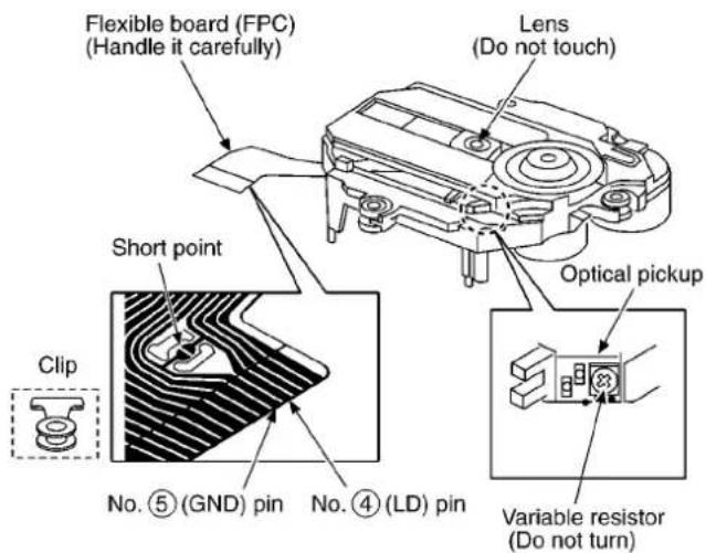
4 Handling Precautions for Traverse Deck
The laser diodes in the traverse deck (optical pickup) may break down due to potential difference caused by static electricity of clothes or human body.
So, be careful of electrostatic breakdown during repair of the traverse deck (optical pickup).
4.1. Handling the traverse deck (optical pickup)
- The traverse deck (optical pickup) is an extremely high-precision construction and must not be subjected to impact, excessive vibration, or other types of rough handling.
- In order to prevent static electricity damage to the laser diode, use a short pin or similar tool to short the optical pickup's flexible circuit boards after they have been disconnected from the main circuit board.
- Handle the flexible circuit boards with care; excessive force could cause them to be broken.
- Do not turn the pre-set variable resistor (for adjustment of the laser power); it has been adjusted at the factory. (as shown in Fig.1)
text_image
Flexible board (FPC) (Handle it carefully) Short point Clip No. ⑤ (GND) pin No. ④ (LD) pin Lens (Do not touch) Optical pickup Variable resistor (Do not turn)Fig.1
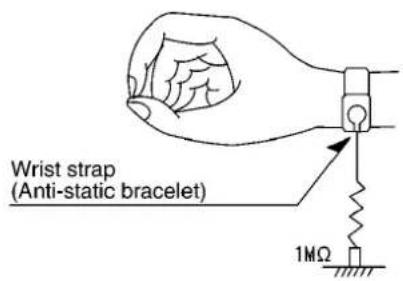
4.2. Grounding for electrostatic breakdown prevention
- Human body grounding
Use the anti-atatic wrist strap to discharge the static electricity from your body. - Work table grounding
Put a conductive material (sheet) or steel sheet on the area where the optical pickup is placed, and ground the sheet. (sa shown in Fig.2)
text_image
Wrist strap (Anti-static bracelet) 1MΩ
text_image
Iron plate or some metals to conduct electricityFig.2
Caution:
The static electricity of your clothes will not be grounded through the wrist strap. So, take care not to let your clothes touch the traverse deck (optical pickup)
4.3. Caution when Replacing the Traverse Deck
The traverse deck has a short point shorted with sol the laser diode against electrostatic breakdown. Be sure remove the solder from the short point before making connections.
CAUTION:
THIS PRODUCT UNTILIZES A LASER. USE OF CONTROLS OR ADJUSTMENTS OR PERFORMANCE PROCEDURES OTHER THAN THOSE SPECIFIED HEREIN MAY RESULT IN HAZARDOUS RADIATION EXPOSURE.
5 Precaution of Laser Diode
CAUTION: This product utilizes a laser diode with the unit turned "on", invisible laser radiation is emitted from the pick up lens.
Wave length: 780 nm
Maximum output radiation power from pick up: 100 μW/VDE
Laser radiation from the pick up unit is safety level, but be sure the followings:
- Do not disassemble the pick up unit, since radiation from exposed laser diode is dangerous.
- Do not adjust the variable resistor on the pick up unit. It was already adjusted.
- Do not lock at the focus lens using optical instruments.
- Recommend not to lock at pick up lens for a long time.
text_image
CLASS 1 LASER PRODUCT| DANGER | INVISIBLE LASER RADIATION WHEN OPEN.AVOID DIRECT EXPOSURE TO BEAM. |
| ADVARSEL | USYNLIG LASERSTRÅLING VED ÅBNING, NÄR SIKKERHEDSAFBRYDEREER UDE AF FUNKTION. UNDGÅ UDSÄTTELSE FOR STRÅLING. |
| VARO! | AVATTAESSA JA SUOJALLUKITUS OHITETTAESSA OLET ALTTIINANÄKYMÄTÖNTA LASERSÄTEILYLE. ÄLA KATSO SÄTEESEN. |
| VARNING | OSYNLIG LASERSTRÅLNING NÄR DENNA DEL ÄR ÖPPNAD OCHSPÄRREN AR URKOPPLAD. BETRAKTA EJ STARÅLEN. |
| ADVARSEL | USYNLIG LASERSTRÅLING NÄR DEKSEL ÄPNES OG SIKKERHEDSLÄSBRYTES. UNNGÅ EKSPONERING FOR STRÅLEN. |
| VORSICHT | UNSICHTBARE LASERSTRAHLLING, WENN ABDECKUNG GEÖFFNET.NICHT DEM STRAHL AUSSETZEN. |
(Inside of product)
(Indersiden at apparatet)
(Tuotteen sisällä)
(Apparatens insida)
(Produktets innside)
6 Location of Controls
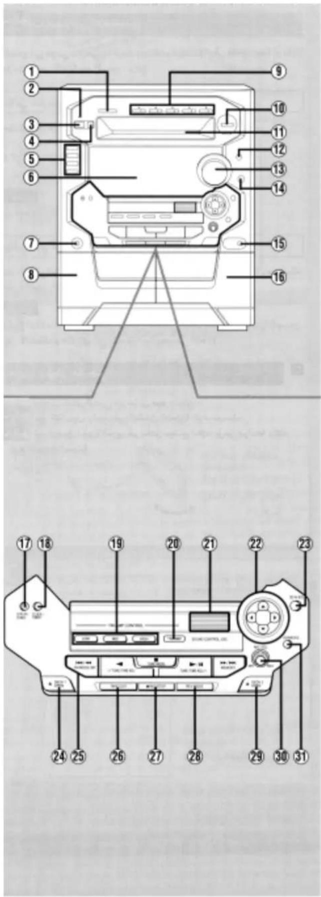
text_image
Technical diagram of a CD-ROM device with numbered component labels for identification and assembly reference.Main unit
No.
Name
① CD manager button (CD MANAGER)
② AC supply indicator (AC IN)
This indicator lights when the unit is connected to the AC mains supply.
③ Standby/on switch (○/I, POWER)
Press to switch the unit from on to standby mode or vice versa. In standby mode, the unit is still consuming a small amount of power.
④ Eco button (MODE)
⑤ Input select buttons and indicators (CD, TUNER BAND, TAPE DECK 1/2, AUX)
⑥ Display
⑦ Headphone jack (PHONES)
⑧ Deck 1 cassette holder
⑨ Disc direct play, open/close buttons and indicators (CD 1 \~ CD 5, △)
⑩ Random play button (RANDOM)
⑪ Disc tray
⑫ Display select/demonstration button (-DISPLAY/-DEMO)
⑬ Volume control (VOLUME)
⑭ Super woofer on/off button and indicator (S.WOOFER)
⑮ Microphone jack (MIC)
⑯ Deck 2 cassette holder
Center console
No.
Name
⑰ Play timer/record timer button and indicator ( play/ REC)
⑯ Clock/timer button (CLOCK/TIMER)
⑲ TRI-AMP control buttons (LOW, MID, HIGH)
20 TRI-AMP indicator (TRI-AMP)
②1 Jog control (SOUND CONTROL JOG)
⑳ Joy stick
②3D AI EQ button (3D AI EQ)
24 Deck 1 open button (△ DECK 1 OPEN)
25 Basic operating buttons
Functions change according to the source.
⑳ Tape edit button (TAPE EDIT)
Recording start/stop button (● REC/STOP)
28 Reverse mode select button (REV MODE)
29 Deck 2 open button (△ DECK 2 OPEN)
⑳ Microphone volume control (MIC VOL)
⑲ Karaoke button (KARAOKE)
7 Location of Controls for Remote Control Transmitter
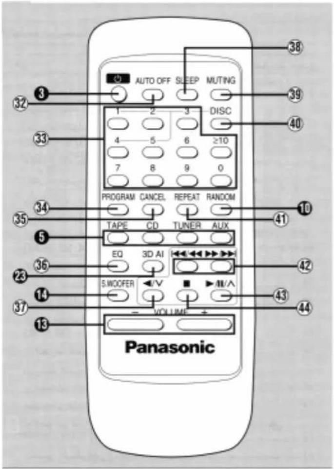
text_image
32 33 34 35 36 37 38 39 40 1 2 3 DISC 4 5 6 ≥10 7 8 9 0 PROGRAM CANCEL REPEAT RANDOM TAPE CD TUNER AUX EQ 3D AI 5.WOCFER V ▶/II/A VOLUME PanasonicRemote control
Buttons 3, 5, 10, 13, 14 and 26 have the same functions as the corresponding buttons on the main unit.
No.
Name
③2 Auto off button (AUTO OFF)
33 Numeric buttons (≥10, 1-0)
34 Program button (PROGRAM)
35 Cancel button (CANCEL)
36 EQ select button (EQ)
⑲ Reverse side playback/preset channel select button (◀/∨).
36 Sleep button (SLEEP)
39 Muting button (MUTING)
④0 Disc button (DISC)
41 Repeat button (REPEAT)
④2 Skip/search buttons (1◄◄/◄◄, ►►/►►)
④3 Play/pause/preset channel select button (▶/II/∧)
④ Stop button (■)
8 Operation Checks and Component Replacement Procedures
- This section describes procedures for checking the operation of the major printed circuit boards and replacing the main components.
- For reassembly after operation checks or replacement, reverse the respective procedures. Special reassembly procedures are described only when required.
Gear for servicing (as jig) information
- This unit has a gear which used for checking items (Open/close of disc tray, up/down operation of traverse unit by manually) when servicing. (For gear information, that is described on the items for disassembly procedures.)
- For preparation of gear (for servicing), perform the procedures as follows.
-
In case of re-servicing the same set, the "gear for servicing" may be took off because it had been used. So, the "gear for servicing" must be stored.
-
Remove the gear provided with mechanism cover as shown below.
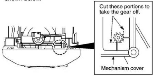
text_image
Cut these portions to take the gear off. Mechanism cover- Insert the hexagonal wrench (2mm) into the gear, and then project the tip of wrench for 1\~2mm length.
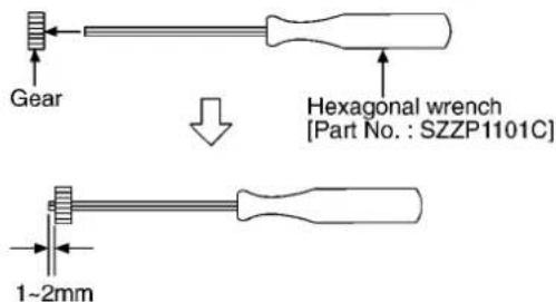
text_image
Gear Hexagonal wrench [Part No. : SZZP1101C] 1-2mm(Preparation of gear as jig is completed.)
8.1. Checking for the main P.C.B

text_image
a b a × 6 (Step 1) (b) × 5 (a) (Step 2)
text_image
Hook (A) Hook (B) Cabinet(Step 3)
Lift up the both sides of cabinet ass'y to release the hooks (A). Then, pull the cabinet ass'y toward the rear and release the hook (B) to remove the cabinet ass'y.
NOTE:
When installing the cabinet ass'y, take care not to damage the front cabinet ass'y from hook (B).
- Check the main P.C.B. as shown below.

text_image
Main P.C.B.8.2. Disassembly for the CD changer ass'y
(The CD changer unit can be removed until the tray ornament would removed.)
8.2.1. Disassembly for the disc tray ornament
- Follow the (Step 1) - (Step 3) of item 8.1.
When opening the disc tray automatically
(Step 3)
Push the open / close button 1, so the disc tray will be open automatically.
(If the other buttons would be pushed, disc tray would be open.)
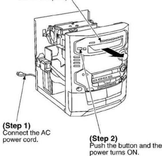
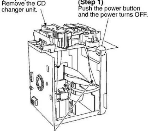
text_image
(Step 1) Connect the AC power cord. (Step 2) Push the button and the power turns ON.
text_image
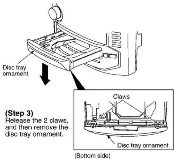
(Step 4) Disconnect the AC power cord. (Bottom side) Disc tray Disc tray ornament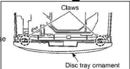
text_image
Claws Disc tray ornament(Step 5)
Release the 2 claws, and then remove the disc tray ornament.
(Step 8)
Push the open / close button 1, so the disc tray will be close.

text_image
(Step 6) Connect the AC power cord. (Step 7) Push the button and the power turns ON.When opening the disc tray manually
(Step 1)
Upset the unit.
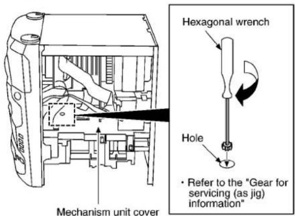
text_image
Hexagonal wrench Hole • Refer to the "Gear for servicing (as jig) information"(Step 2)
Insert the gear for servicing into the bottom hole of mechanism unit cover, and then rotate the hexagonal wrench in the direction of arrow. So, the disc tray will be open.
text_image
Disc tray ornament (Step 3) Release the 2 claws, and then remove the disc tray ornament. Claws Disc tray ornament (Bottom side)
text_image
(Step 4) Push the disc tray.8.2.2. Disassembly for the CD changer unit
- Follow the (Step 1) - (Step 3) of item 8.1.
- Follow the disassembly instruction for the disc tray ornament of item 8.2.1.
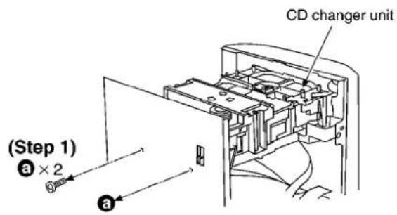
text_image
(Step 1) a × 2 CD changer unit a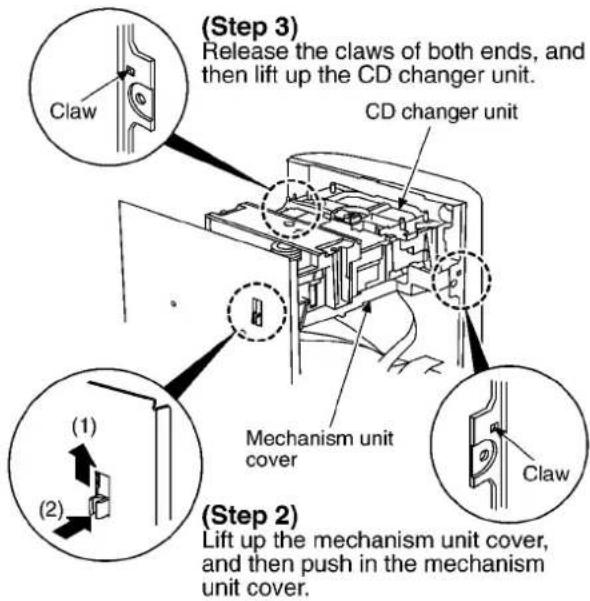
text_image
(Step 3) Release the claws of both ends, and then lift up the CD changer unit. CD changer unit Mechanism unit cover Step 2) Lift up the mechanism unit cover, and then push in the mechanism unit cover.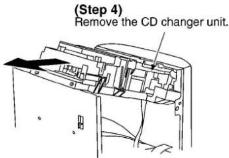
text_image
(Step 4) Remove the CD changer unit.
text_image
(Step 5) Place the CD changer unit on the unit. NOTE: Cover the front panel ass'y with cloth to prevent from damage. The preparation of checking procedures in operational condition is completed.8.3. Checking for the unit operational condition
(Place the unit horizontally when loading the CD
8.3.1. Initial setting of CD unit
- Follow the (Step 1) - (Step 3) of item 8.1.
- Follow the disassembly instruction for the disc tray ornament of item 8.2.1.
- Follow the disassembly instruction for the CD changer unit of item 8.2.2.
(Step 2)

text_image
Push power button and the power turns ON. (Step 1) Connect the AC power cord.(Step 3)
Select the input select button to "CD".

text_image
(Step 5) Put the CD into the disc tray. Disc tray(Step 4)
Push the open/close button 1, and then open the disc tray.
Push the open/close button 1, and then close the disc tray. (Then, the CD will load.) changer Unit.)
(Step 6)

natural_image
Technical line drawing of an electronic device casing with internal components (no text or symbols)(The initial setting of CD unit is completed.)
8.3.2. Checking for the CD servo
- The initial setting of CD unit must be completed.
(Refer to the initial setting of CD unit in item 8.3.1.)
(Step 3)

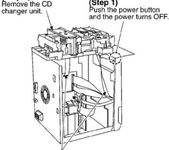
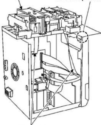
text_image
Remove the CD changer unit. (Step 1) Push the power button and the power turns OFF.(Step 2)
Remove the FFC boards.
text_image
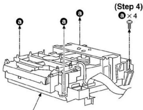
(Step 4) a × 4(Step 5)
Remove the mechanism unit cover.
- Check the CD servo P.C.B. as shown below.

text_image
(Step 7) Connect the FFC board (19 pin) from CD servo P.C.B.. (Step 6) Lay the unit.8R.C.B. Checking for the FL P.C.B. and cassette mechanism control P.C.B.
- The initial setting of CD unit must be completed. (Refer to the initial setting of CD unit in item 8.3.1.)
(Step 3)
text_image
Remove the CD changer unit. (Step 1) Push the power button and the power turns OFF.(Step 2)
Remove the FFC boards.
text_image
(Step 5) Release the 2 claws, and then draw the front panel ass'y. Claw Claw a(Step 4) a × 2
- Check the FL P.C.B. and cassette mechanism control P.C.B. as shown below.
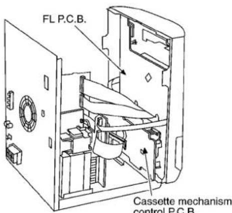
text_image
FL P.C.B. Cassette mechanism control P.C.B.8.3.4. Checking for the power supply P.C.B.
- The initial setting of CD unit must be completed. (Refer to the initial setting of CD unit in item 8.3.1.)
(Step 3)
text_image
Remove the CD changer unit. (Step 1) Push the power button and the power turns OFF.(Step 2)
Remove the FFC boards.

text_image
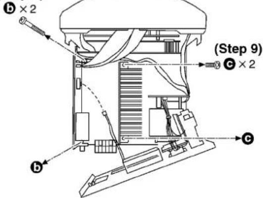
(Step 6) Release the 3 claws, and then remove the rear cover. Rear cover Claw (Step 5) a × 6 a a a Claw a Claw (Step 4) Remove the connector (CP303).(Step 7)

text_image
Step 7) lease the 2 claws, and then move the cord clamper. Cord clamper Claws(Step 8)
text_image
b ×2 (Step 9) C ×2 b c- Check the power supply P.C.B. as shown below.

text_image
Power supply P.C.B.8.4. Replacement for the traverse deck ass'y
- Follow the (Step 1) - (Step 3) of item 8.1.
- Follow the disassembly instruction for the disc tray ornament of item 8.2.1.
- Follow the disassembly instruction for the CD changer unit of item 8.2.2.
(Step 3)
Remove the CD changer unit.
(Step 1)
Push the power button and the power turns OFF.
natural_image
Technical line drawing of an internal device housing with visible components and structural details (no text or symbols)(Step 2)
Remove the FFC boards.
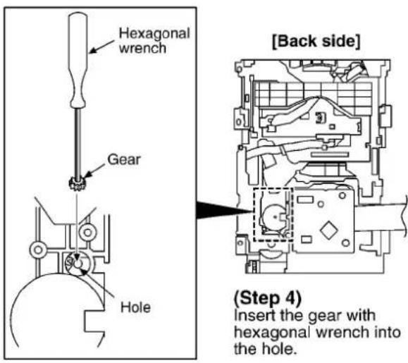
text_image
Hexagonal wrench Gear Hole [Back side] (Step 4) Insert the gear with hexagonal wrench into the hole.
text_image
Hexagonal wrench Disc tray(Step 5) Rotate the hexagonal wrench in the direction of arrow (clockwise), and then open the disc tray fully.
text_image
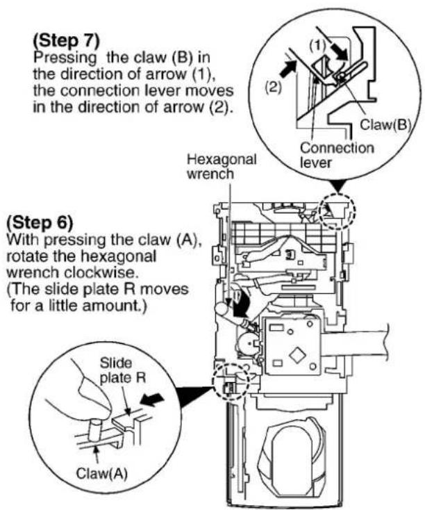
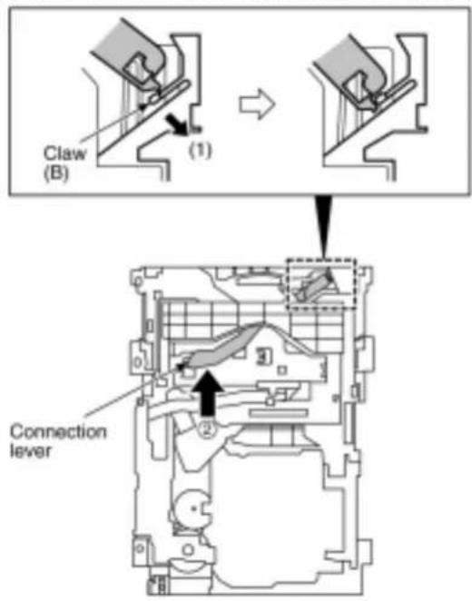
(Step 7) Pressing the claw (B) in the direction of arrow (1), the connection lever moves in the direction of arrow (2). (Step 6) With pressing the claw (A), rotate the hexagonal wrench clockwise. (The slide plate R moves for a little amount.) Hexagonal wrench Slide plate R Claw(A)
text_image
(Step 8) Lift up the traverse deck ass'y.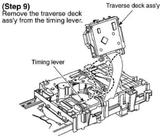
text_image
(Step 9) Remove the traverse deck ass'y from the timing lever. Traverse deck ass'y Timing lever
text_image
(Step 10) a × 3 Solder Solder(Step 11) Unsolder the motor terminals (4 points).
(Step 12)
Remove the FFC board from the connector, and then remove the CD servo P.C.B..
text_image
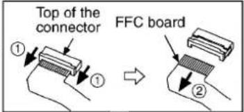
Top of the connector FFC board
text_image
CD servo P.C.B.Caution:
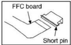
Insert a short pin into the traverse unit FFC board.
(Refer to "Handling Precautions for Traverse Deck".)
(Step 13)
Remove the pin.
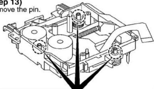
text_image
ep 13) move the pin.- Widen the boss using a regular screwdriver.
2. Pull out the pin in the direction of arrow.

text_image
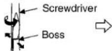
(Step 14) Release the claw, and then remove the traverse deck ass'y. Floating spring (1) Floating spring (1) Claw Floating spring (2)NOTE:
Be careful not to lose the 3 floating springs because those will also be removed on removal of the traverse deck ass'y.
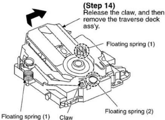
Installation of the CD servo P.C.B. after replacement
text_image
(Step 3) a × 3 (a) (a) (Step 2) Install the CD servo P.C.B. in the traverse deck ass'y. Rest detect switch S701 (Step 1) Connect the FFC board. FFC board (Step 4) Solder.Note for installation of the CD servo P.C.B.
Before installing the CD servo P.C.B., move the optical pickup toward the outer edge from the mark “◀”. [Otherwise, the rest detect switch (S701) mounted on the CD servo P.C.B. may be damaged.]
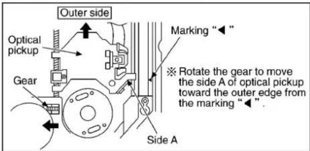
text_image
Outer side Optical pickup Gear Marking "◀" ※ Rotate the gear to move the side A of optical pickup toward the outer edge from the marking "◀". Side AInstallation for traverse deck ass'y
(Step 2)
Align the boss of traverse deck ass'y with the slot of traverse cam gear.
Install the traverse deck ass'y to the timing lever.
(Step 1)

text_image
in the boss of traverse ck ass'y with the slot of verse cam gear. Boss Install the deck ass' timing lev Slot of traverse cam gear Timing lever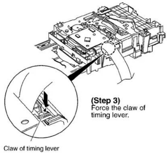
text_image
(Step 3) Force the claw of timing lever. Claw of timing lever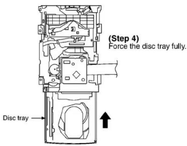
text_image
(Step 4) Force the disc tray fully. Disc tray
text_image
Claw(B) (1) Connection lever (2)(Step 5) With pressing the claw (B) in the direction of arrow (1), force the connection lever in the direction of arrow (2).
8.5. Replacement for the disc tra
- Follow the (Step 1) - (Step 3) of item 8.1.
- Follow the disassembly instruction for the disc tray ornament of item 8.2.1.
- Follow the disassembly instruction for the CD changer unit of item 8.2.2.
(Step 3)
Remove the CD changer unit.
(Step 1)
Push the power button and the power turns OFF.
natural_image
Technical line drawing of an internal mechanical device with no visible text or symbols(Step 2)
Remove the FFC boards.
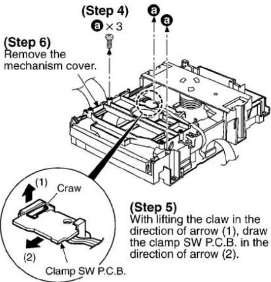
text_image
(Step 6) Remove the mechanism cover. (Step 4) a × 3 a a (1) Craw (2) Clamp SW P.C.B. (Step 5) With lifting the claw in the direction of arrow (1), draw the clamp SW P.C.B. in the direction of arrow (2).
text_image
Hexagonal wrench Gear Hole (Step 7) Insert the gear with hexagonal wrench into the hole.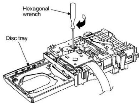
text_image
Hexagonal wrench Disc tray(Step 8)
Rotate the hexagonal wrench in the direction of arrow (clockwise), and then open the disc tray fully.
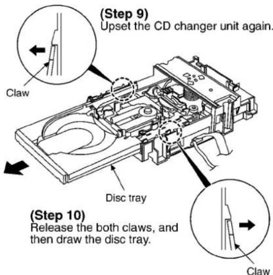
text_image
(Step 9) Upset the CD changer unit again. Claw Disc tray (Step 10) Release the both claws, and then draw the disc tray. Claw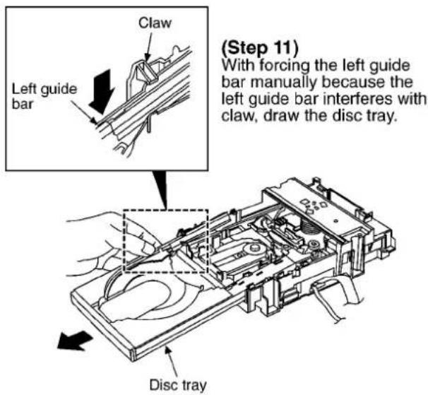
text_image
(Step 11) With forcing the left guide bar manually because the left guide bar interferes with claw, draw the disc tray. Left guide bar Disc trayInstallation of the disc tray after replacement
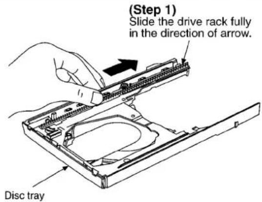
text_image
(Step 1) Slide the drive rack fully in the direction of arrow. Disc tray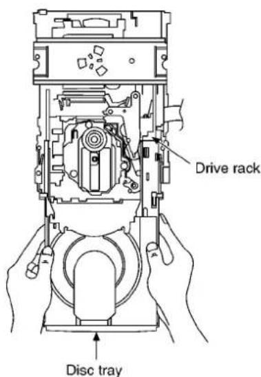
text_image
Drive rack Disc tray(Step 2)
Holding the drive rack not to move, install the disc tray.

text_image
Drive rack Drive gear (Step 3) Align the drive rack with the drive gear. Right guide bar NOTE:NOTE: Force the right guide bar of tray base manually not to move upwards.

text_image
(Step 4) Holding the drive rack manually, push the disc tray in the direction of arrow. Disc tray
text_image
(Step 3) b × 3 b b Claw (Step 4) Release the claw, and then remove the gear holder.
text_image
(Step 5) Remove the belt and change gear spring. Belt Change gear spring NOTE: Take care not to lose the change gear spring.8.6. Disassembly and reassembly for mechanism base drive
Disassembly for mechanism base drive unit
- Follow the (Step 1) - (Step 11) of item 8.1.
- Follow the disassembly instruction for the disc tray ornament of item 8.2.1.
- Follow the disassembly instruction for the CD changer unit of item 8.2.2.
- Follow the (Step 1) - (Step 9) of item 8.4.
- Follow the (Step 1) - (Step 11) of item 8.5.

text_image
(Step 1) a × 2 (Step 2) Remove the upper plate. a(Step 6)
Remove the pulley gear, change gear and UP/DOWN gear.

text_image
Pulley gear Change gear UP/DOWN gear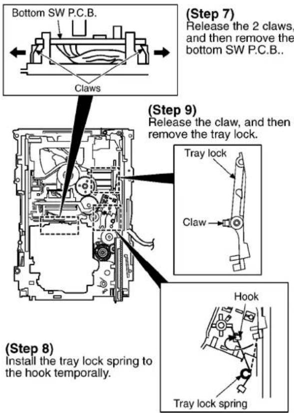
text_image
(Step 7) Release the 2 claws, and then remove the bottom SW P.C.B.. Claws (Step 9) Release the claw, and then remove the tray lock. Tray lock Claw (Step 8) Install the tray lock spring to the hook temporally. Hook Tray lock spring(Step 10)
Release the claw, and then remove the rear lock.
NOTE: Take care not take the rear lock spring off.
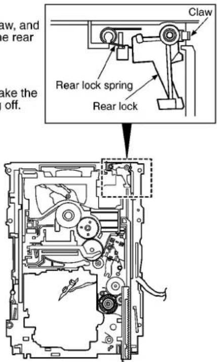
text_image
Claw Rear lock spring Rear lock raw, and the rear take the off.(Step 11)
Pressing the claw (B) in the direction of arrow (1), force the connection lever in the direction of arrow (2).
text_image
Claw (B) (1) Connection lever(Step 12)
Move the slide plate 1 to the end of stock side.
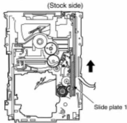
text_image
(Stock side) Slide plate 1(Step 13) Lift up the left end of spindle base unit in the direction of arrow (1), and then remove the unit in the direction of arrow (2).

text_image
(1) (2) Spindle base unit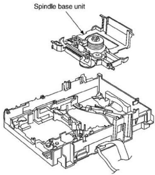
text_image
Spindle base unit(Step 14)
Remove the slide plate 1 and slide plate 2.

text_image
Slide plate 1 Slide plate 2(Step 15)
Remove the traverse relay gear, traverse cam gear and drive gear.

text_image
Traverse cam gear Traverse relay gear Drive gearDiassembly/reassembly for the spindle base unit

text_image
Disc spacer (Step 1) Draw the 5 disc spacers.(Step 2)
Pushing the claw, slide the support plate in the direction of arrow, and then remove it.
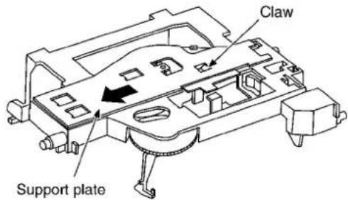
text_image
Claw Support plate(Installation for disc lever spring)
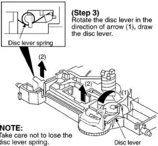
text_image
(Step 3) Rotate the disc lever in the direction of arrow (1), draw the disc lever. Disc lever spring (2) NOTE: Take care not to lose the disc lever spring. (1) Disc lever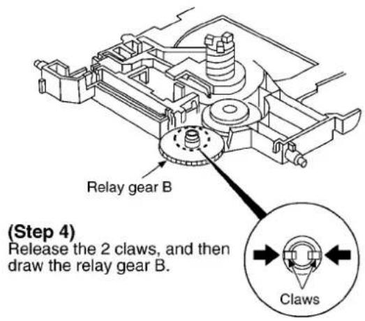
text_image
(Step 4) Release the 2 claws, and then draw the relay gear B. Relay gear B Claws
text_image
(Step 5) Claws Release the 2 claws.NOTE:
Hold the loading stopper ass'y manually because it is flipped by spring.
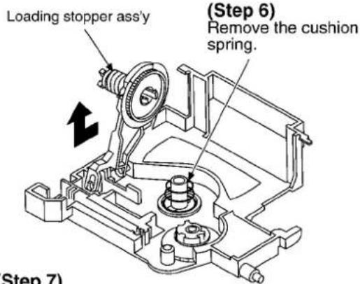
text_image
Loading stopper ass'y (Step 6) Remove the cushion spring. Step 7)(Step 7)
Remove the loading stopper ass'y in the direction of arrow.
text_image
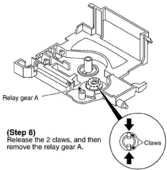
Relay gear A (Step 8) Release the 2 claws, and then remove the relay gear A. Claws(Step 9)
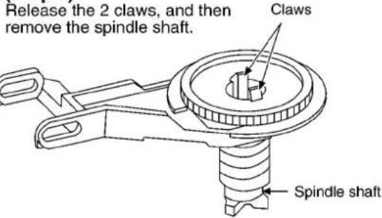
text_image
Release the 2 claws, and then remove the spindle shaft. Claws Spindle shaft(Step 10)
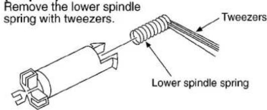
text_image
Remove the lower spindle spring with tweezers. Lower spindle spring Tweezers
text_image
(Step 11) Force the lower hook with thin tip of minus screwdriver. Spindle shaft Minus screwdriver Lower hook (Step 12) Squeeze the shaft of lower hook, and then draw it. Lower hook(Step 14)
Insert the thin tip of minus screwdriver between the lower spindle and UP/DOWN base, and then slacken the lower spindle to release the stopper.
Then, rotate the lower spindle and remove it.
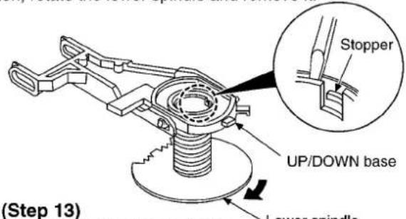
text_image
(Step 13) Stopper UP/DOWN base Lower spindleRotate the lower spindle in the direction of arrow until the lower spindle interferes with stopper.

text_image
Loading stopper UP/DOWN base Hold bars(Step 15)
Rotate the UP/DOWN base at a 90 degree angle. Then, spread the hold bars of loading stopper and remove the UP/DOWN base.
Installation for loading stopper ass'y
(Step 1)
Align the claw of loading stopper ass'y with the slot of spindle base. (Caution should be exercised when alignment of claw due to the size of claws.)
Loading stopper ass'y

text_image
Claw(Large) Slot(Large) Claw(Small) Slot(Small)(Step 2)
Lower the loading stopper ass'y, and then align the lower spindle with the trapezoid tooth of relay gear A.
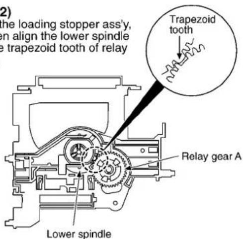
text_image
(2) the loading stopper ass'y, on align the lower spindle the trapezoid tooth of relay Trapezoid tooth Relay gear A Lower spindle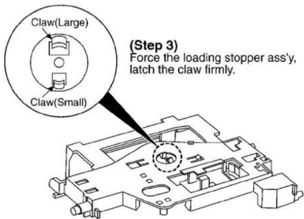
text_image
Claw(Large) Claw(Small) (Step 3) Force the loading stopper ass'y, latch the claw firmly.Reassembling for mechanism base drive unit

text_image
Traverse cam gear (Step 1) Install the traverse cam gear.(Step 2)
Rotate the traverse cam gear to the direction of arrow.

text_image
Traverse cam gear(Step 3)
Install the drive gear and traverse relay gear.

text_image
Traverse relay gear Drive gear※ When installing the traverse relay gear, align the trapezoid tooth of gear with tooth of drive gear.
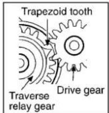
text_image
Trapezoid tooth Traverse relay gear Drive gearSA-AK48
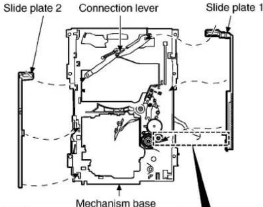
text_image
Slide plate 2 Connection lever Slide plate 1 Mechanism base(Step 4)
Install the slide plate 2 to the mechanism base, and then match to the connection lever.
Install the slide plate 1 to the mechanism base, and then match to the connection lever and align the trapezoid tooth of traverse relay gear with the slide plate 1.
(Step 5)
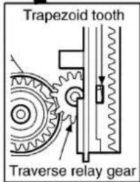
text_image
Trapezoid tooth Traverse relay gear
text_image
(1) (2) (S Ins ba (F plSpindle base unit
Install the spindle base unit. (First, install slide plate 1.)
(Step 6)

text_image
(Step 8) Install the rear lock. (The claw should be latched.) Claw Rear lock spring Rear lock (Step 7) Move the slide plate 1 to forward fully.(Front side)

text_image
Bottom SW P.C.B. Claw (Step 9) Install the bottom SW P.C.B.. (The claw should be latched.) (Step 10) Install the tray lock. (The claw should be latched.) Tray lock Claw (Step 11) Remove the tray lock spring from hook, and then latch to the tray lock. Hook Tray lock spring(Step 12)
Install the UP/DOWN gear, change gear, change gear spring, pulley gear and belt in the order of ①-⑤.
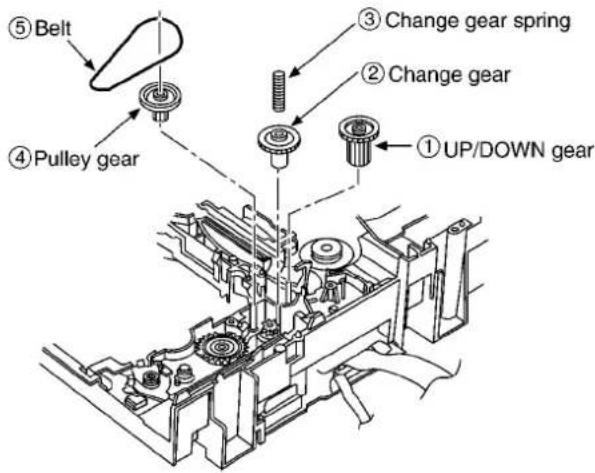
text_image
⑤Belt ④Pulley gear ③Change gear spring ②Change gear ①UP/DOWN gear(Step 14)
Install the upper plate ass'y, and then tighten the screw (b).

text_image
Upper plate ass'y Gear holder (a) × 3 (b) × 2 (Step 13) Install the gear holder, and then tighten the screw (a).(Step 15)
install the tray base, traverse deck ass'y and mechanism cover. (Refer to the items 5.4. and 5.5.)
[Operation check after servicing]
Check the proper operation of following items with gear and hexagonal screwdriver.
1) Open/close of tray base.
2) Moving the tray base to the stock side.
3) UP/DOWN operation of spindle base unit.
4) UP/DOWN operation of traverse unit.
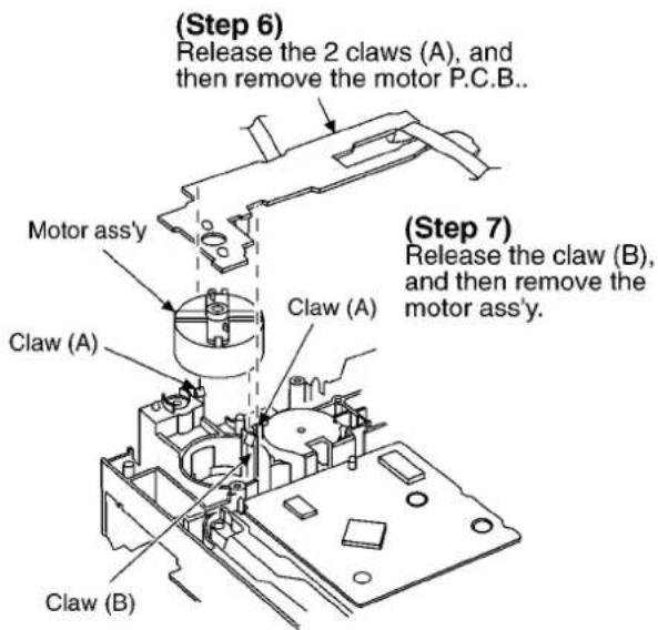
8.7. Replacement for the motor ass'y
- Follow the (Step 1) - (Step 3) of item 8.1.
- Follow the disassembly instruction for the disc tray ornament of item 8.2.1.
- Follow the disassembly instruction for the CD changer unit of item 8.2.2.
- Follow the (Step 1) - (Step 10) of item 8.5.

text_image
(Step 1) Install the belt temporarily. NOTE: Take care not apply the grease to the belt.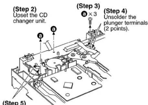
text_image
(Step 2) Upset the CD changer unit. (a) (a) (a) × 3 (Step 3) (Step 4) Unsolder the plunger terminals (2 points). (Step 5)(Step 5)
Unsolder the motor terminals (2 points).
text_image
(Step 6) Release the 2 claws (A), and then remove the motor P.C.B.. Motor ass'y Claw (A) Claw (A) Claw (B) (Step 7) Release the claw (B), and then remove the motor ass'y.Notice for motor ass'y installation
-
Locate the name plate of motor to the traverse deck.
-
Align the hole of motor with the ribs.
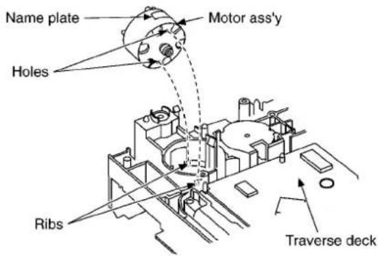
text_image
Name plate Motor ass'y Holes Ribs Traverse deck8.8. Replacement for the pinch roller ass'y and head block
- Follow the (Step 1) - (Step 3) of item 8.1.
- Follow the disassembly instruction for the disc tray ornament of item 8.2.1.
- Follow the disassembly instruction for the CD changer unit of item 8.2.2.
- Follow the (Step 1) - (Step 3) of item 8.3.3.
(Step 1)
Remove the connector (CN502).
(Step 3)
Release the 2 claws, and then draw the front panel ass'y.

text_image
Claw Claw a(Step 2) a × 2
(Step 4)
Pull out the FFC board.

natural_image
Technical line drawing of a mechanical device with internal components and a tool (no text or symbols)(Step 5)
Remove the flat cable from the connector (CN304).
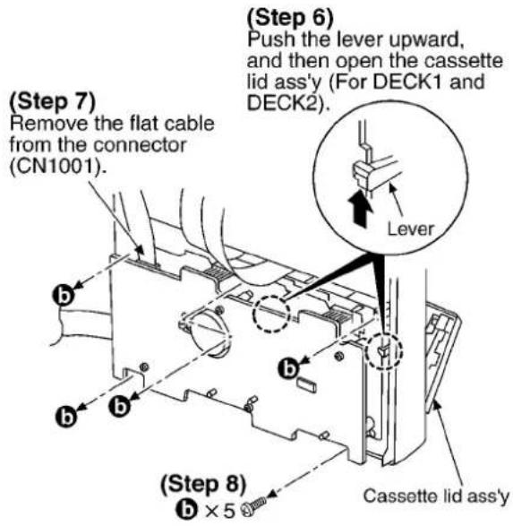
text_image
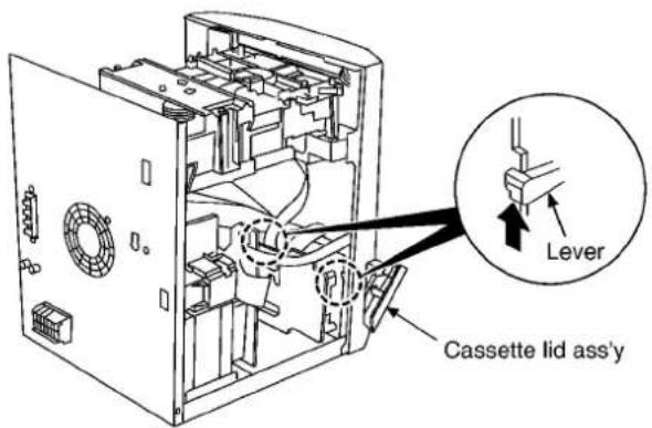
(Step 7) Remove the flat cable from the connector (CN1001). (Step 6) Push the lever upward, and then open the cassette lid ass'y (For DECK1 and DECK2). Lever (Step 8) b × 5 g Cassette lid ass'y(Step 9)
Tilt the cassette mechanism in the direction of arrow (1), and then remove it in the direction of arrow (2).
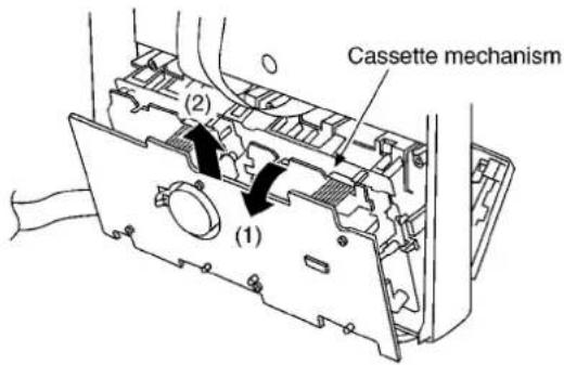
text_image
Cassette mechanism (1) (2)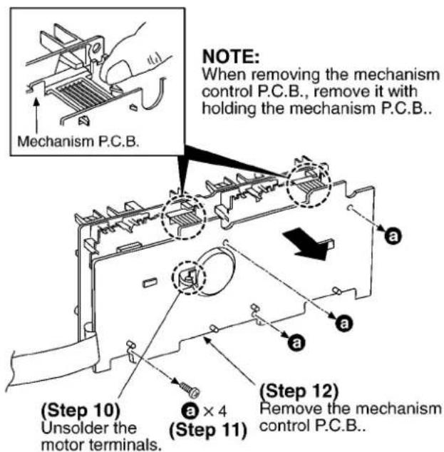
text_image
NOTE: When removing the mechanism control P.C.B., remove it with holding the mechanism P.C.B.. Mechanism P.C.B. (a) (a) (a) (Step 10) Unsolder the motor terminals. (a) × 4 (Step 11) (Step 12) Remove the mechanism control P.C.B.. a × 4※ The mechanism as shown below is for DECK2.
For the one of DECK1, perform the same procedures.
Release the 2 claws, and then remove the pinch roller (R), (F).
(Step 13)

text_image
Pinch roller ass'y (R) [RXL0125] Pinch roller ass'y (F) [RXL0124] Claw Claw Claw Head connector (Step 14)(Step 14)
Release the 2 claws, and then remove the head connector.
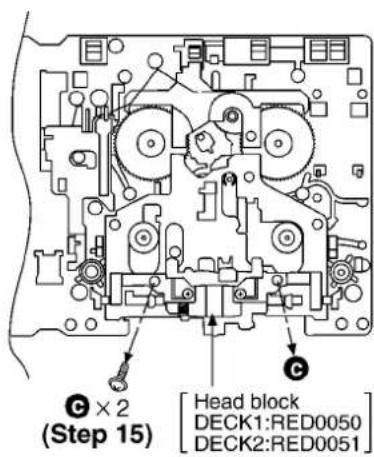
text_image
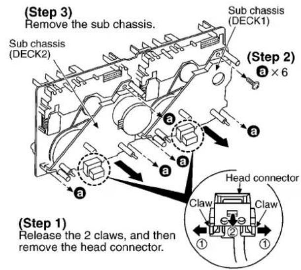
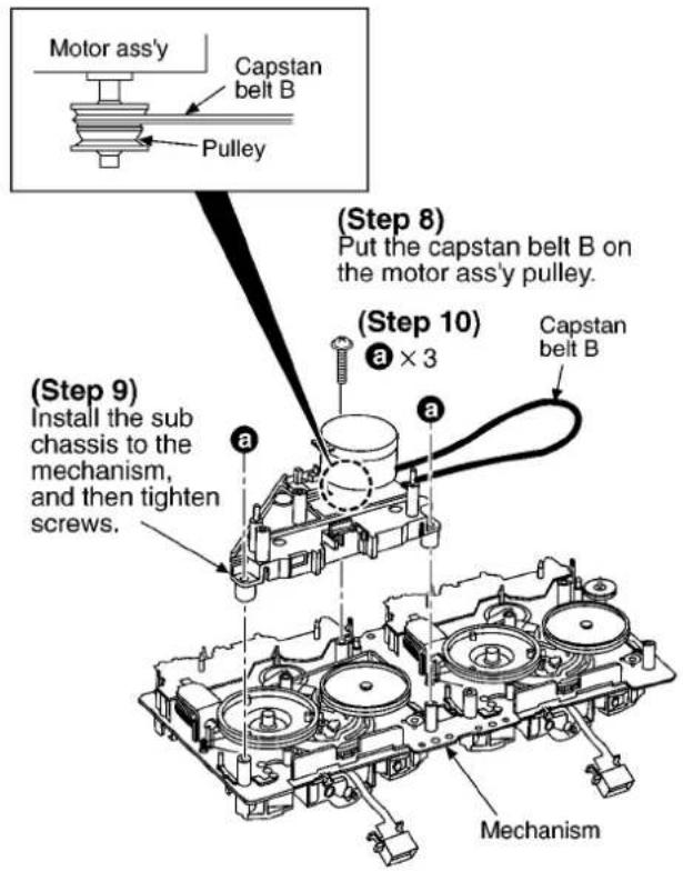
C × 2 (Step 15) Head block DECK1:RED0050 DECK2:RED00518.9. Replacement for the CD motor ass'y, capstan belt A, capstan belt B and winding belt
- Follow the (Step 1) - (Step 3) of item 8.1.
- Follow the disassembly instruction for the disc tray ornament of item 8.2.1.
- Follow the disassembly instruction for the CD changer unit of item 8.2.2.
- Follow the (Step 1) - (Step 3) of item 8.3.3.
- Follow the (Step 1) - (Step 11) of item 8.8.
text_image
(Step 3) Remove the sub chassis. Sub chassis (DECK2) Sub chassis (DECK1) (Step 2) a × 6 a a a (a) (a) Head connector Claw Claw (Step 1) Release the 2 claws, and then remove the head connector.
text_image
Capstan belt B [RDV0057] (Step 4) b × 2 Capstan belt A [RDV0034-1] b DC motor ass'y [REM0088]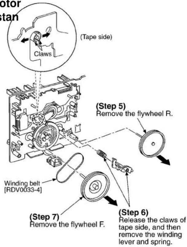
text_image
Motor tan (Tape side) Claws (Step 5) Remove the flywheel R. Winding belt [RDV0033-4] (Step 7) Remove the flywheel F. (Step 6) Release the claws of tape side, and then remove the winding lever and spring.
text_image
Installation of the belt (Boss) Marking (Step 1) The boss and marking should be positioned horizontally. Boss (Boss) (Step 2) Put the winding belt on the pulley temporarily. Boss (Boss) (Step 3) Install the flywheel F.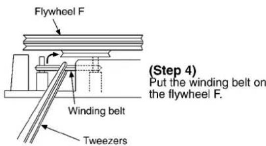
text_image
Flywheel F Winding belt Tweezers (Step 4) Put the winding belt on the flywheel F.
text_image
Winding arm (Step 6) Install the flywheel R.(Step 5)
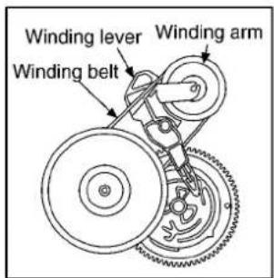
Install the winding lever and spring while pressing the winding arm in the direction of arrow.
(The winding lever must be inserted completely and latched with claws.)
NOTE:
The winding lever should be positioned as shown below.
text_image
Winding lever Winding belt Winding arm(Step 7)
Put the capstan belt A temporarily as shown below.

text_image
Boss Capstan belt A Boss Capstan belt A Boss(Side view)
text_image
Motor ass'y Capstan belt B Pulley (Step 8) Put the capstan belt B on the motor ass'y pulley. (Step 10) a × 3 Capstan belt B (Step 9) Install the sub chassis to the mechanism, and then tighten screws. Mechanism(Step 11)

text_image
Put the capstan belt B as shown below. Capstan belt B Capstan belt A(Step 12)
Put the capstan belt A on the motor ass'y pulley.
8.10. Replacement for the components parts on the mechanism P.C.B.
- Follow the (Step 1) - (Step 3) of item 8.1.
- Follow the disassembly instruction for the disc tray ornament of item 8.2.1.
- Follow the disassembly instruction for the CD changer unit of item 8.2.2.
- Follow the (Step 1) - (Step 5) of item 8.3.3.
- Follow the (Step 1) - (Step 6) of item 8.8.
text_image
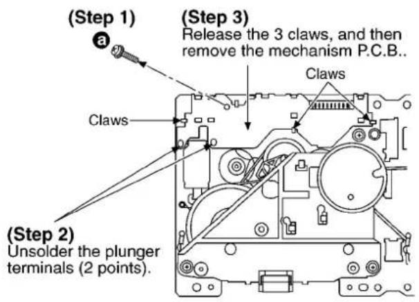
(Step 1) (Step 3) Release the 3 claws, and then remove the mechanism P.C.B.. Claws Claws (Step 2) Unsolder the plunger terminals (2 points).8.11. Replacement for the cassette lid ass'y
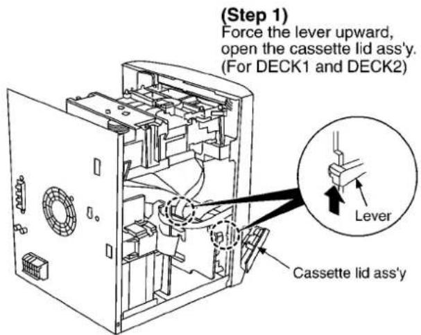
- Follow the (Step 1) - (Step 3) of item 8.1.
text_image
(Step 1) Force the lever upward, open the cassette lid ass'y. (For DECK1 and DECK2) Lever Cassette lid ass'y(Step 2)
Lift up the cassette lid ass'y in the direction of arrow.
(For DECK1 and DECK2)
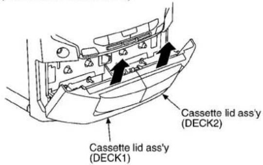
text_image
Cassette lid ass'y (DECK1) Cassette lid ass'y (DECK2)(Step 3)
Remove the cassette lid ass'y.
(For DECK1 and DECK2)
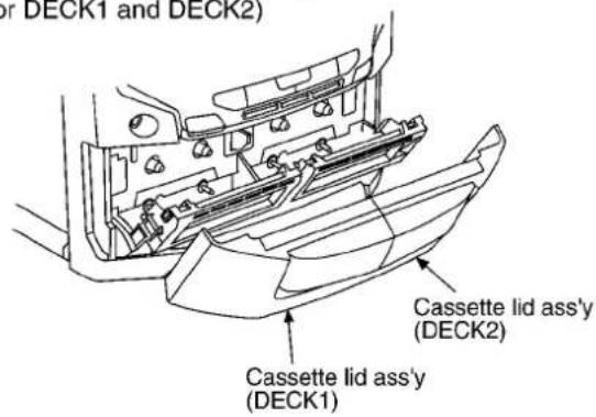
text_image
Cassette lid ass'y (DECK1) Cassette lid ass'y (DECK2)8.12. Measure for tape trouble
- Follow the (Step 1) - (Step 3) of item 8.1.
(Step 1)
If a cassette tape cannot be removed from the deck since the tape is caught by the capstan or pinch roller during playback or recording, rotate the flywheel F in the direction of the arrow to remove the tape.
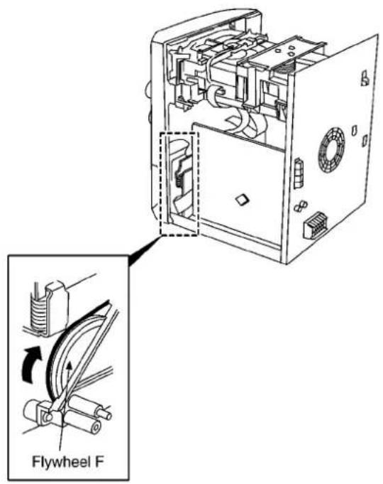
text_image
Flywheel F(Step 2)
Force the lever upward and open the cassette lid ass'y. Take the cassette tape off.
text_image
Cassette lid ass'y Lever9 Checking Procedure for Self-operation of Cassette Mechanism Ass'y
- This procedure describes simple methods independent of mechanism controller or governor circuit.
9.1. Operation Check Providing with Cassette Tape
- Push up the EJECT lever with rubber band.(Refer to Fig. 2)
- Apply DC 5V to the MOTOR. (MOTOR will be rotated) (Refer to Fig. 1)
- Provide the cassette tape with mechanism ass'y.
- Apply DC 9V to the plunger, and then operate it by switching power ON/OFF. (Power: +PL, -PL) (Refer to Fig. 1)
a. FWD PLAY :Supply power to the plunger momentary. (Duration: approx. 50msec.)
b. FWD FF At FWD PLAY mode, supply power to the plunger momentary. (Duration: approx. 50msec.)
c. STOP : At FWD FF mode, supply power to the plunger momentary. (Duration: approx. 50msec.)
d. REV PLAY : At STOP mode, supply power to the plunger for ordinary duration. (Duration: approx. 200msec.)
e. REV REW : At REV PLAY mode, supply power to the plunger momentary. (Duration: approx. 50msec.)
f. STOP At REV REW mode, supply power to the plunger momentary. (Duration: approx. 50msec.) Repeat the above operation to FWD PLAY mode.
Note: Incorrect duration for power supply may be operated to other mode.
9.1.1. Connection Diagram Between the Mechanism Ass'y and Power Supply (MOTOR and Plunger)
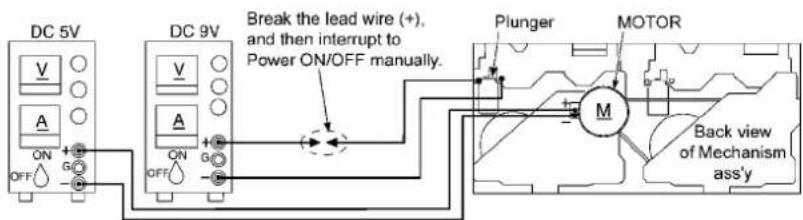
text_image
DC 5V A ON OFF DC 9V Break the lead wire (+), and then interrupt to Power ON/OFF manually. Plunger MOTOR Back view of Mechanism ass'yFig. 1
9.1.2. Detail View of EJECT Lever (EJECT lever fixed by rubber band, Plunger rib operation)
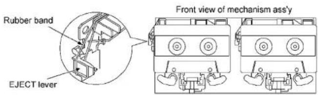
text_image
Rubber band EJECT lever Front view of mechanism ass'yFig. 2
9.2. Operation Check Not Provided with Cassette Tape
- Push up the EJECT lever with rubber band. (Refer to Fig. 2)
- Apply DC 5V to the MOTOR. (MOTOR will be rotated)
- Lift up the plunger rib of mechanism ass'y with the tip of minus screwdriver, and then operate it same as power supply duration. (Refer to Fig. 3)
Note: Operation order is same as the "Operation Check Providing with Cassette Tape" item 4. above.
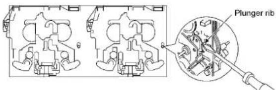
text_image
Plunger ribFig. 3
10 Self-Diagnostic Display Function
●Self-Diagnostic display
This unit is equipped with a self-diagnostic display function which, if a problem occurs, will display an error code corresponding to the problem. Use this function when performing maintenance on the unit.
●How to set the Self-Diagnostic Function
text_image
Display T φ/1 TUNE MODE MEMORY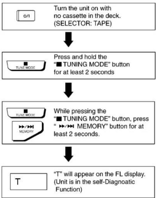
flowchart
graph TD
A["Turn the unit on with no cassette in the deck.<br>(SELECTOR: TAPE)"] --> B["Press and hold the "TUNING MODE" button for at least 2 seconds"]
B --> C["While pressing the "TUNING MODE" button, press "▶▶▶▶ MEMORY" button for at least 2 seconds."]
C --> D[""T" will appear on the FL display.<br>(Unit is in the self-Diagnostic Function)"]
•Cassette Mechanism Test
(For error code H01, H02, H03, F01, F02)
- Press "TAPE, DECK 1/2" to select Deck 2.
- Load a cassette tape with the erasure prevention tab removed from the left side only and close the cassette holder.
-
Press "MEMORY" button. (FAST FORWARD shall be executed for 2 seconds, afterwhich it will STOP)
-
Load a cassette tape with the erasure prevention tab removed from the right side only and close the cassette holder.
-
Press "FM MODE/BP" button. (REWIND shall be executed for 2 seconds, afterwhich it will STOP)
-
Load a pre-recorded tape with both recording tabs intact and close the cassette holder.
-
Press "TUNE/TIME ADSJ ^" button.
-
Press "● REC/STOP" button. (Tape will not move)
-
Press ■ TUNE MODE" button to indicate Error Code. (Error Code is displayed for DECK1 when DECK selector is switched to DECK1 and display for DECK2 when it is switched to DECK2)
-
Press "TAPE, DECK1/2" button to select DECK1.
-
Repeat step 2 to 9 to test DECK1. (Tape Deck1 will not check H02 because of no recording function)
•CD Mechanism Test
(F15, F16, F17, F26, F27, F28, F29, H15)
- Press "CD" button.
- Press "CD Manager" button.
- Press "■/TUNE MODE" button to indicate Error Code.
•To clear all Error Code
- Press "TUNE MODE" button
- FL will display "CLEAR" for 1 second and changer to "T".
●How to cancel Self-Diagnostic Function
- Press "⏻" button OFF.
●Power Amplifier Failure (F61)
- When power amplifier fail, F61 will be displayed automatically.
11 Description of Error Code
11.1. Error Detection for Cassette Mechanism block
No. Error Error Display Problem Condition
| 1 | MODE SW detection error | H01 | Faulty operation of cassette mechanism.Faulty contact or short-circuit of mechanism mode switch (S951, S971) |
| 2 | REC INH SW detection error | H02 | Recording not possible.Faulty contact or short-circuit of REC INH switch (S974, S975) |
| 3 | HALF SW detection error | H03 | Playback can not perform.Faulty contact or short-circuit of HALF switch (S952, S972) |
| 4 | Reel Pulse detection error | F01 | The tape advances slightly and then stops.Faulty reel pulse, faulty hole detect IC (IC951, IC971) |
| 5 | TPS abnormal | F02 | Cassette deck will not perform TPS function.Faulty playback EQ/recording amplifier IC (IC1101) |
11.2. Error Detection for CD/Changer block
No. Error Error Display Problem Condition
| 1 | REST SW detection error | F15 | CD dose not function.This error occurs when the Optical Pick Up REST SW (S701) is not detected within the specified time (about 8 seconds) |
| 2 | CD tray opens automatically | F16 | CLAMP switch (S4) NG (Check & Replace) |
| 3 | Does not startup when “TUNE/TIME ADJ^” button is pressed | F17 | BOTTOM switch (S5) NG (Check & Replace) |
| 4 | Transmission error between CD servo LSI and micon | F26 | CD does not function.This error occurs when the POWER is ON for the CD block and an error is detected after the transmission has started. |
| 5 | Startup fails even when you insert CD or the selected disc tray does not open | F27 | Tray 1 detect switch or Tray 2 detect switch NG (Check & Replace) |
| 6 | Cannot insert CD | F28 | Tray 1 detect switch NG (Check & Replace) |
| 7 | Cannot eject CD | F29 | Check if Disc is stuck. Tray 2 detect switch NG (Confirm & Replace) |
| 8 | CD Tray closes | H15 | CD disc tray detect switch NG (S3) (Check & Replace) |
11.3. Error Detection for Cassette Mechanism block
No. Error Error Display Problem Condition
| 1 POWER AMP output abnormal | F61 | When POWER is switch on, power become off automatically. During normal operation, if DC DET become L, PCNT shall become L and the error display on the left shall be displayed (IC500) |
12 CD Test Mode Function
This CD test mode is provided to check CD unit without connecting to changer loading mechanism. This mode shall operate CD PLAY with CD unit being connected only and CD Automatic Alignment result is shown on FL display.
●How to set CD test mode

text_image
Display CD TEST φ/1 CD TUNE MODE MEMORY
flowchart
graph TD
    A["Prepare and set up the CD unit\nCheck condition (Refer to " checking for\nthe CD servo P.C.B.")"] --> B["Press CD button"]
    B --> C["Press and hold the\n" TUNE MODE" button\nfor at least 2 seconds"]
    C --> D["While pressing the\n" TUNE MODE" button, press\n" >>> MEMORY" button for at\nleast 2 seconds."]
    D --> E["Display\n"CD TEST will appear\non the FL display.\n(Unit is in the Self-Diagnostic Function)"]
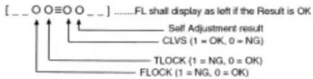
- CD Automatic Alignment result indication
Under CD test mode, pressing the numeric key '0' on the remote controller will display the auto adjustment result. FLOCK, TLOCK and CLVS status shall be shown as bellow.
text_image
[__ O O≡O O __] ....FL shall display as left if the Result is OK Self Adjustment result CLVS (1 = OK, 0 = NG) TLOCK (1 = NG, 0 = OK) FLOCK (1 = NG, 0 = OK)13 Measurement and Adjustments
13.1. Tuner Section
13.1.1. Measuring Instruments and Special Tools
• AM signal generator (AM-SG)
• EVM-AC (AC Electronic voltmeter)
• EVM-DC (DC Electronic voltmeter)
- Oscilloscope
- Choke coil (100μH)
- AM loop antenna
Note:
- Trimmer will be instability that once you tighten, please adjust with tighten slowly from loosened condition.
- Adjust OSC coil and IFT with nonmetal driver.
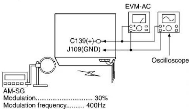
13.1.2. AM IF Adjustment
- Connect the instrument as shown in Fig.1.
- Set the unit to AM mode.
- Apply signal sa shown in Fig.1 from AM-SG.
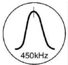
- AdjustZ102 so that the output frequency is maximized in Fig.2.
text_image
EVM-AC C139(+) J109(GND) Oscilloscope AM-SG Modulation...... 30% Modulation frequency...... 400HzFig.1
text_image
450kHzFig.2
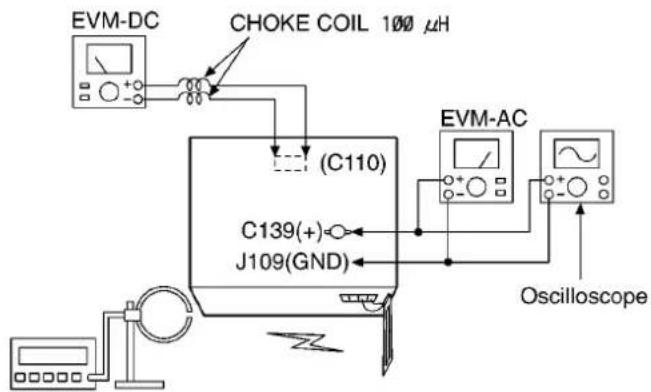
13.1.3. AM RF Adjustment
- Connect the instrument as shown in Fig.3.
- Set the unit to AM mode.
- Set AM-SG to 522kHz.
- Receive 522kHz in the unit.
- AdjustZ101 (OSC) so that the EVM-AC is maximized.
- Set AM-SG to 603kHz.
- Receive 603kHz in the unit.
- AdjustZ101 (ANT) so that the EVM-AC is maximized.
- Set AM-SG to 522kHz.
-
Receive 522kHz in the unit.
-
Adjust Z101 (OSC) so that the EVM-DC value is within 0.5 ± 1.4V .
text_image
EVM-DC CHOKE COIL 1000 µH (C110) C139(+) J109(GND) EVM-AC OscilloscopeAM-SG
Modulation.... 30%
Modulation frequency..... 400Hz
Fig.3
13.1.4. Adjustment point
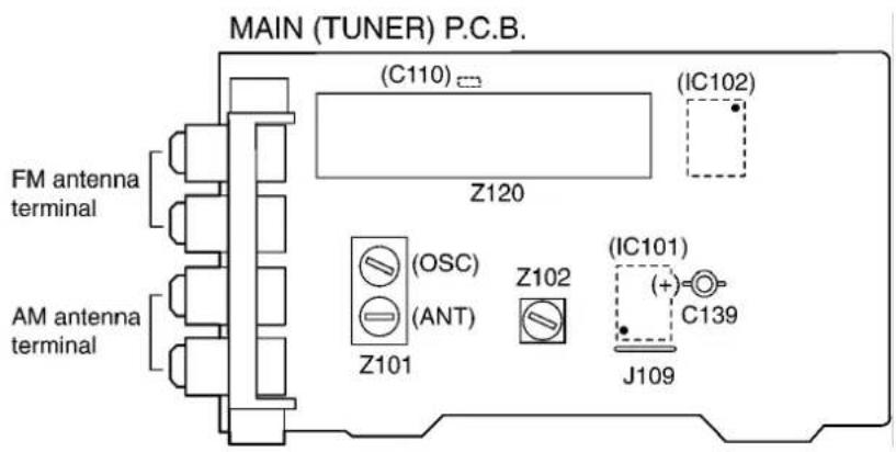
text_image
MAIN (TUNER) P.C.B. (C110) (IC102) Z120 FM antenna terminal (OSC) Z102 (ANC) (ANT) IC101 (+) C139 AM antenna terminal Z101 J10913.2. Cassette Deck Section
13.2.1. Measuring Instruments and Special Tools
• Digital frequency counter
• EVM-AC (AC Electronic voltmeter)
- Test tape
QZZCFM : Head azimuth adjustment
QZZCWAT : Tape speed adjustment
QZZCRA : Normal reference blank tape
QZZCRX : CrO2 tape
13.2.2. Head Azimuth Adjustment (Deck 1/2)
Caution:
- Please replace both azimuth adjustment screws (RHE5152ZB) and springs (RMB0331) simultaneously when readjusting the head azimuth. (Shown in Fig.5). Even if you wish to readjust the head azimuth without replacing the screws and springs, a fine adjustment cannot be done because of the screw-locking bond adhered to the azimuth screw and spring.
- Please remove the screw-locking bond left on the head base when replacing the azimuth screw.
-
If you wish to readjust the head azimuth, be sure to adjust with adhering the cassette tape closely to the mechanism by pushing the center of cassette tape with your finger. (shown in Fig.6)
-
Connect the measuring instrument as shown in Fig.7.
-
Playback the azimuth adjustment portion (8kHz, -20dB) of test tape (QZZCFM). Adjust the azimuth adjusting screw until the outputs of the L/R-ch are maximized. (Refer to Fig.8)
Make sure that the difference in the peak level between left and right channels does not exceed 0.5dB. -
Perform the same adjustment in reverse playback mode. Checking of the level difference forward and reverse directions
-
Playback the playback gain adjustment portion (315Hz, 0dB) of test tape (QZZCFM). Check if level difference between forward and reverse direction is within 1.5dB.
-
After the adjustment, apply screwlock to the azimuth adjusting screw.

(RHE5152ZB)

(RMB0331)
Fig.5
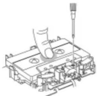
natural_image
Technical line drawing of a mechanical assembly with a screwdriver inserted (no text or symbols)Fig.6

flowchart
graph TD
    A["UNIT"] --> B["(Lch)"]
    B --> C["TP9"]
    B --> D["or (Rch)"]
    B --> E["TP10"]
    B --> F["GND"]
    C --> G["EVM"]
    D --> G
    E --> G
    F --> G
Fig.7
text_image
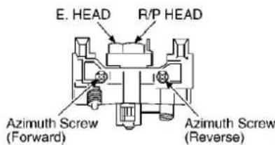
E. HEAD R/P HEAD Azimuth Screw (Forward) Azimuth Screw (Reverse)Fig.8
13.2.3. Tape Speed Adjustment (Deck 1/2)
- Insert the test tape (QZZCWAT) to Deck 2 and playback the (FWD side) the middle portion of it.
- Adjust motor VR (Deck 2) for the output value shown below. Adjustment target : 2940 - 3060Hz (NORMAL speed)
- After alignment, assure that the output frequency of the DECK2 REV and DECK1 FWD are within ±45Hz and ±60Hz respectively of the value of the output frequency of DECK2 FWD.
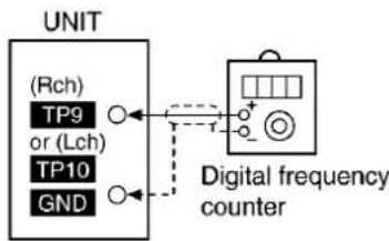
text_image
UNIT (Rch) TP9 or (Lch) TP10 GND Digital frequency counterFig.9
Fig.10
13.2.4. Bias OSC Frequency Adjustment (Deck 2)
- Set the unit to "AUX" position.
- Insert the Normal blank tape (QZZCRA) into DECK2 and set the unit to "REC" mode (use REC/STOP key).
- Adjust L1201 so that the output frequency is within the standard value.
Standard value : 97±8kHz
text_image
TP11 Erase head R1182 1 Ω TP12 Digital frequency counterFig.11
13.2.5. Bias Voltage Check
- Set the unit to "AUX" position.
- Insert the Normal blank tape (QZZCRA) into DECK2 and set the unit to "REC" mode (use REC/STOP key).
- Measure and make sure that the output is within the standard value.
- Insert the CrO2 tape (QZZCRX).
- Repeat step 2 and 3.
Standard value (Normal) : 14±4mV
Standard value (CrO2) : 15mV
text_image
TP5 1MΩ 1kΩ + - TP4 EVMFig.12
13.2.6. Erase Voltage Check
- Set the unit to "AUX" position.
- Insert the Normal blank tape (QZZCRA) into DECK2 and set the unit to "REC" mode (use REC/STOP" key).
- Measure and make sure that the output is within the standard value.
- Insert the CrO2 tape (QZZCRX).
- Repeat step 2 and 3.
Standard value (Normal) : more than 80mV Standard value (CrO2) : more than 80mV
text_image
Erase head TP11 R1182 1 Ω TP12 EVMFig.13
13.2.7. Adjustment Point
text_image
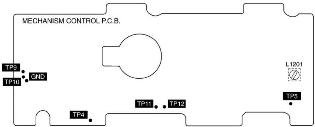
MECHANISM CONTROL P.C.B. TP9 TP10 GND L1201 TP4 TP11 TP12 TP5Fig.14
14 Illustration of ICs, Transistors and Diodes
 | AN8839NSBE2 | 28PIN | MN662790RSC | M5218AP | BA7755A | |
| BU2090AF-E2 | 16PIN | |||||
| LA1833NMNTLM | 24PIN | |||||
| LC72131MDTRM | 20PIN | |||||
| M51167AFP-TB | 36PIN | |||||
| M62456FPE1 | 24PIN | |||||
| M62457FPE1 | 16PIN | |||||
M62433AFP | AN8739SBE2 | M38199MF227 | 0N2180RLC1 | TA7291P | STK470-040 | |
RSN311W64A-P |  | 2SB621ARSTA2SB621RTA2SD1302STA2SD965RTAKTA12710YTA |  | 2SA933SSTA2SC1740SSTA2SC2058SPTA2SD2144STAKRA102MTA | KRC102MTAKRC103MTAKRC110MTAKTC3199GRTARVTDTC143EST | |
2SJ498CDTA |  | 2SB1436R2SC2002KTA2SC2786MTA2SC2787FL1TA |  | 2SA1037AKSTX2SC2412KT96R2SD2114K1VDTA114EKA146DTA143XKA146DTC114TKA146 | DTC144TKA146KRA102STAKRC102STAKRC111STAKTC3875GRTAKTD1304TA | |
2SC3940AQSTA | 2SK544F-AC | 1D3ERL1N4003S-P |  | MTZJ10BTAMTZJ12BTAMTZJ15CTAMTZJ16BTAMTZJ30BTAMTZJ4R7BTAMTZJ7R5ATA | MA165TARVD1SS133TA | |
1SS291TAMA700ATA | MA4020LTAA8A4] | GP1S94 |  | SLI325DCT31SLI325URCT31SLR325MCT31W | SVC211SPA-AL | |
UDZSTE175R1B | MA111TX1SS355TE17ide | MA8036HTXMA8047MTX | KBP152G4R5 | DAP202KT146 | MA723TA | |
RK306LFU1 | LNJ301MPUJAD | |||||
15 Schematic Diagram
15.1. Schematic Diagram Notes
- This schematic diagram may be modified at any time with the development of new technology.
Notes:
• S1 : Tray position 1 detect switch in OFF position
• S2 : Tray position 2 detect switch in OFF position
• S3 : Tray open detect switch in OFF position
• S4 : Clump switch in OFF position
• S5 : Bottom switch on OFF position
• S501 : Voltage select switch (VOLT ADJ)
• S600 : Sound control jog switch (SOUND CONTROL JOG)
• S601 : TRI-AMP control switch (LOW)
• S602 : Auxiliary input switch (AUX)
• S603 : Deck1 open switch ( DECK1 OPEN)
• S604 : CD management switch (CD MANAGER)
• S605 : Tuner/band select switch (TUNER/BAND)
• S606 : Tape edit switch (TAPE EDIT)
• S607 : Disc5 direct open/close switch () ▲
• S608 : CD switch (CD)
• S609 : Recording start/stop switch (RDC/STOP)
• S610 : Disc direct play switch (CD5)
• S611 : Tape/deck select switch (TAPE/DECK1/2)
• S612 : Reverse mode select switch (REV MODE)
• S613 : Disc4 direct open/close switch () ▲
• S614 : EQ down switch ( ) ▼
• S615 : Super woofer switch (S. WOOFER)
• S616 : Disc2 open switch ( DECK2 OPEN)
• S617 : Disc direct play switch (CD4)
• S618 : EQ left switch ()
- S619 : Display select/demonstration mode switch (-DISPLAY/—DEMO)
• S620 : Playback, tuning, time adjust switch (◀, TUNE/TIME ADJ)
• S621 : Play timer/record timer switch (PLAY/REC)
• S622 : EQ up switch () ▲
• S623 : Disc3 direct open/close switch () ▲
• S624 : Karaoke switch (KARAOKE)
• S625 : Clock/timer select switch (CLOCK/TIMER)
• S626 : EQ right switch ( ) ▶
• S627 : Disc direct play switch (CD3)
• S628 : Eco switch (MODE)
• S629 : Stop/tune mode switch (/T) NE MODE)
• S630 : Disc2 direct open/close switch ( ) ▲
• S631 : Random play switch (RANDOM)
• S632 : FF/skip, memory switch ( , MEMORM)
• S633 : Disc2 direct play switch (CD2)
- S634 : Playback/pause, tuning, time adjust switch ( ▶/■, TUNE/TIME ADJ ) ∧
• S635 : Disc1 direct open/close switch () ▲
• S636 : Disc direct play switch (CD1)
• S637 : REW/R.skip, FM mode/beat proof switch (◀◀/◀◀, FM MODE/BP)
• S638 : Standby/on switch ( ⏻ /l)
• S639 : 3D AI EQ switch (3D AI EQ)
• S640 : TRI-AMP control switch (MID)
• S641 : TRI-AMP control switch (HIGH)
• S701 : Rest switch (REST)
• S951 : Deck1 mode detect switch (MODE)
• S952 : Deck1 half detect switch (HALF)
• S953 : Deck1 CrO2 tape detect switch (ATS/CrO2)
• S971 : Deck2 mode select switch (MODE)
• S972 : Deck2 half detect switch (HALF)
• S973 : Deck2 CrO2 tape detect switch (ATS/CrO2)
• S974 : Deck2 reverse side record prevention tab detect switch (R. REC. INH)
• S975 : Deck2 forward side record prevention tab detect switch (F. REC. INH)
• VR600 : Volume control (VOLUME)
• VR601 : Microphone volume control (MIC VOL)
- Indicated voltage values are the standard values for the unit measured by the DC electronic circuit tester (high-impedance) with the chassis taken as standard.
Therefore, there may exist some error in the voltage values, depending on the internal impedance of the DC circuit tester.
No mark ...... CD STOP
( )...... CD playback (1kHz, L+R, 0dB)
< > ...... FM
「」……AM
(( )) ...... DECK2 playback
《 》...... DECK2 record
- Important safety notice:
Components identified by ⚠ mark have special characteristics important for safety.
Furthermore, special parts which have purposes of fire-retardent (resistors), high-quality sound (capacitors), low-noise (resistors), etc. are used.
When replacing any of components, be sure to use only manufacturers specified parts shown in the parts list.
- Caution!
IC and LSI are sensitive to static electricity.
Secondary trouble can be prevented by taking care during repair.
Ground the soldering iron.
Put a conductive mat on the work table.
Do not touch the legs of IC or LSI with the fingers directly.
- *L10-L12 are printed coils formed on the P.C.B. and thus not found in the Replacement Parts list.
• Voltage and signal line
→ : Positive voltage line
→ : Negative voltage line
→ : CD signal line
: FM signal line
: FM OSC signal line
→ : AM signal line
: AM OSC signal line
: Tape playback signal line
Tape recording signal line
→ : Front low SP drive signal line
→ : Front mid/high SP drive signal line
: Mic signal line
15.2. Schematic Diagram
SCHEMATIC DIAGRAM-1
NOTE:
The number which noted at the connectors on the schematic diagram as
"SCHEMATIC DIAGRAM-1" or "SCHEMATIC DIAGRAM-2"
indicates the schematic diagram serial number located on the left corner in the schematic diagram.
text_image
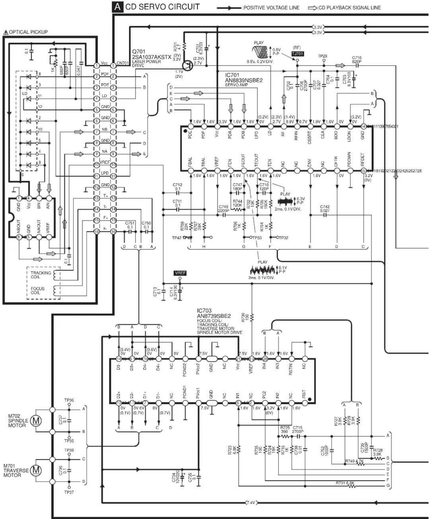
A CD SERVO CIRCUIT :POSITIVE VOLTAGE LINE :CD PLAYBACK SIGNAL LINE OPTICAL PICKUP Q701 2SA1037AKSTX LASER POWER DRIVE CN701 Vcc 1K 680P 880P 0.047 LD 11 12 10 5 4 9 6 1 4 GND Vcc B GND NN GND NA VREF LPD 11 12 T+ 13 14 15 16 17 18 19 20 21 22 23 24 25 26 27 28 30 31 32 33 34 35 36 37 38 39 40 41 42 43 44 45 46 47 48 49 50 51 52 53 54 55 56 57 58 59 60 61 62 63 64 65 66 67 68 69 70 71 72 73 74 75 76 77 78 79 80 81 82 83 84 85 86 87 88 89 90 91 92 93 94 95 96 97 98 99 100 101 102 103 104 105 106 107 108 109 110 111 112 113 114 115 116 117 118 119 120 121 122 123 124 125 126 127 128 129 130 131 132 133 134 135 136 137 138 139 140 141 142 143 144 145 146 147 148 149 150 151 152 153 154 155 156 157 158 159 160 161 162 163 164 165 166 167 168 169 170 171 172 173 174 175 176 177 178 179 180 181 182SCHEMATIC DIAGRAM-2

text_image
POSITIVE VOLTAGE LINE CD PLAYBACK SIGNAL LINE TP20T 18 C731 6.3V220 C730 0.1 C754 470P R721 1K PLAY 2.2V P-P C725 100P C726 100P C728 50V1 TP21 B TP217 1K R718 1K C731 6.3V220 C730 0.1 C754 470P R717 1K PLAY 2.2V P-P C725 100P C726 100P C728 50V1 TP23 A TP23 TP21 C732 6.3V220 C735 0.1 C722 10P X701 (16.9344MHz) Y714 R714 D. C721 10P R711 82K R714 R712 220 R741 47K R742 220K R709 88K C717 0.1 C744 820IP R742 1.5V R742 1.6V AVsc2 AVcc2 VCOF PLLF DSLF DRF IREF ARF WVEL DSLFF2 PLLFF2 LDON BDO RFDET TRCRS OPT VDET RFENV TE FE TE FBAL VREF FOD TRO KICK ECS ECM PC YVD 1VRV 21 3.3V 3.3V 3.3V 3.3V 3.3V 3.3V 3.3V 3.3V 3.3V 3.3V 3.3V 3.3V 3.3V 3.3V 3.3V 3.3V 3.3V 3.3V 3.3V 3.3V 3.3SCHEMATIC DIAGRAM-3
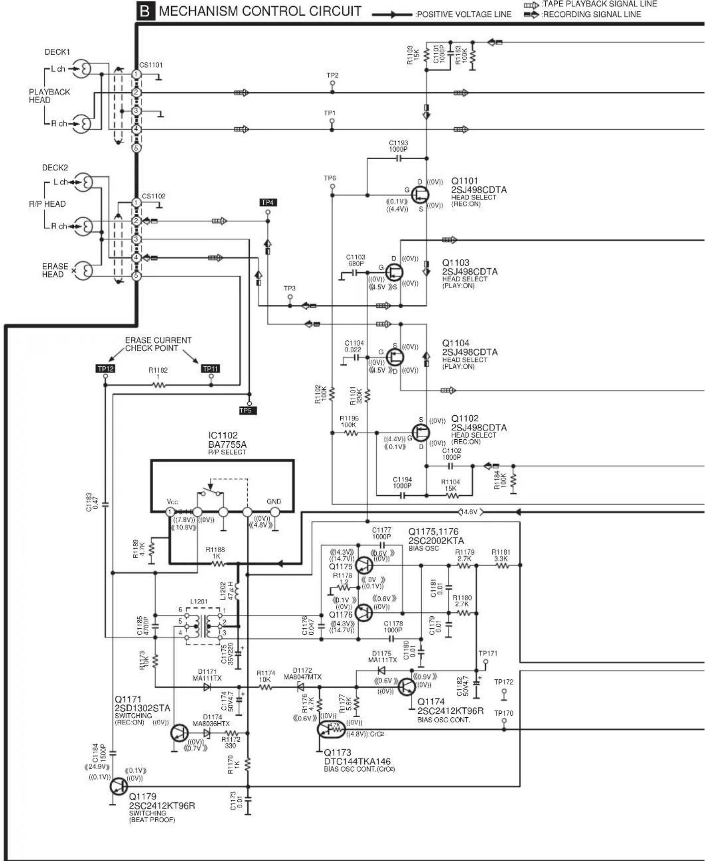
text_image
B MECHANISM CONTROL CIRCUIT → :POSITIVE VOLTAGE LINE :TAPE PLAYBACK SIGNAL LINE :RECORDING SIGNAL LINE DECK1 L ch PLAYBACK HEAD R ch DECK2 L ch R/P HEAD R ch ERASE HEAD TP12 R1182 TP31 TP5 TP2 TP1 TP6 G (0.1V) (4.4V) Q1101 2SJ498CDTA HEAD SELECT (REC.ON) Q1103 2SJ498CDTA HEAD SELECT (PLAY:ON) Q1104 2SJ498CDTA HEAD SELECT (PLAY:ON) IC1102 BA7755A R/P SELECT C1183 0.47 Vcc (7.8V) (0V) (10.8V) GND (0V) (4.8V) R1189 1.7K R1188 1K C1176 0.47 C1177 1000P (4.3V) (14.7V) Q1175,1176 2SC2002KTA BIAS OSC R1179 2.7K R1181 3.3K R1180 2.7K C1191 0.01 C1179 0.01 D1175 MA111TX Q1174 2SC2412KT96R BIAS OSC CONT. TP171 Q1173 DTC144TKA146 BIAS OSC CONT.(CrOc) Q1174 2SC2412KT96R BIAS OSC CONT.(CrOc) Q1173 DTC144TKA146 BIAS OSC CONT.(CrOc) Q1174 2SC2412KT96R BIAS OSC CONT.(CrOc) Q1173 DTC144TKA146 BIAS OSC CONT.(CrOc) Q1174 2SC2412KT96R BIAS OSC CONT. TP172 Q1173 DTC144TKA146 BIAS OSC CONT.(CrOc) Q1173 DTC144TKA146 BIAS OSC CONT.(CrOc) Q1173 DTC144TKA146 BIAS OSC CONT.(CrOc) Q1173 DTC144TKA146 BIAS OSC CONT.(CrOc) Q1173 DTC144TKA146 BIAS OSC CONT. (CrOc)SCHEMATIC DIAGRAM-4
text_image
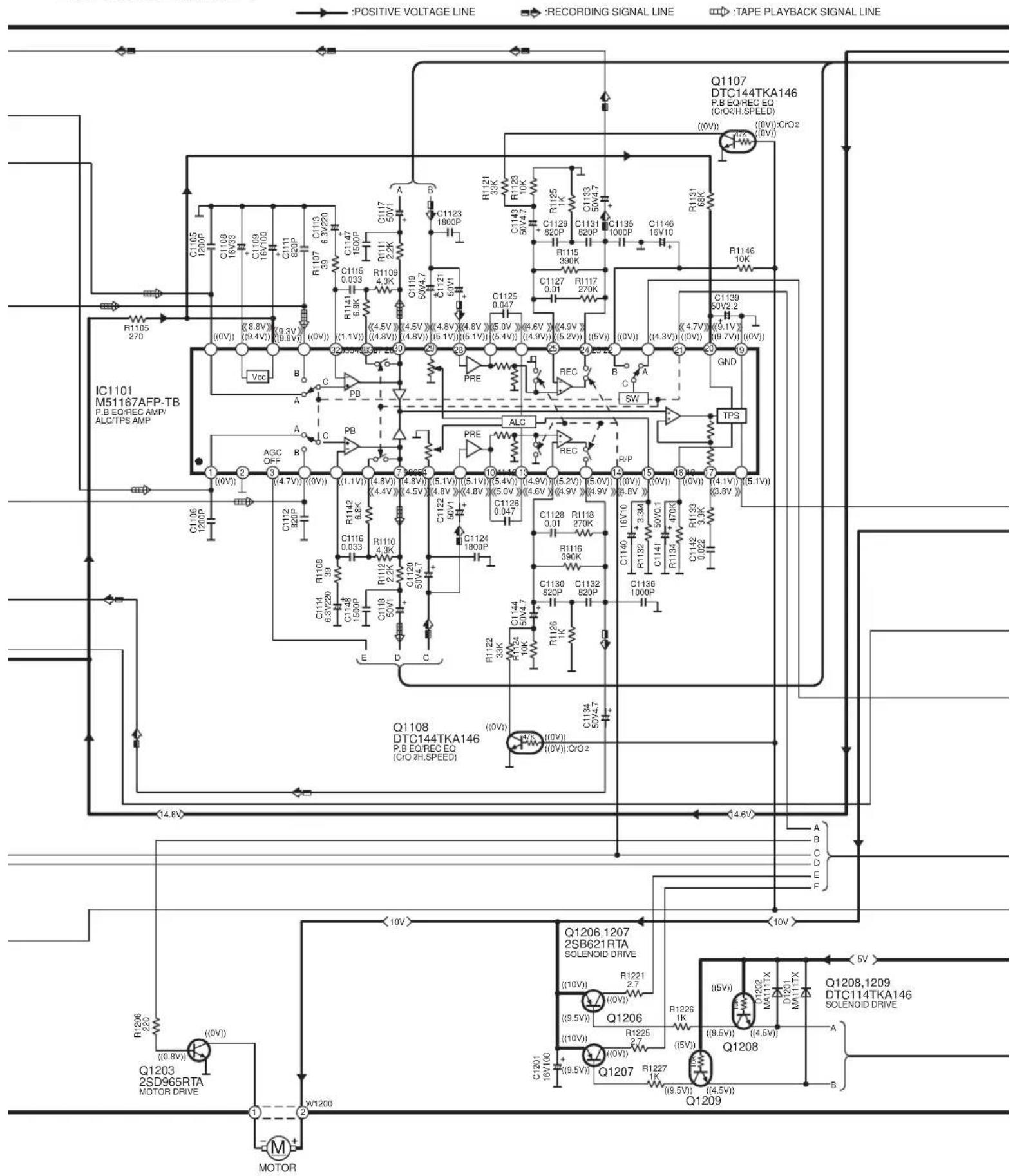
·POSITIVE VOLTAGE LINE ·RECORDING SIGNAL LINE ·TAPE PLAYBACK SIGNAL LINE Q1107 DTC144TKA146 P.B EQ/REC EQ (CIO/H.SPEED) (0V) (0V)CrO2 (0V) (0V) R1105 270 IC1101 M51167AFP-TB P.B EQ/REC AMP/ ALC/TPS AMP R1105 1200P C1105 16V3 C1108 16V100 C1111 820P R1107 39 C1115 0.033 R1141 6.8K C1147 1500P R1141 4.3K C115 4.5V (4.8V) (5.1V) (5.4V) (4.9V) (5.2V) (5V) (4.3V) (0V) C1123 1800P C1125 0.047 C1125 0.01 C1139 20V2.2 C1139 20V2.2 C1135 1000P C1146 16V10 R1146 10K C1138 30V2.2 C1138 30V2.2 C1138 30V2.2 C1138 30V2.2 C1138 30V2.2 C1138 30V2.2 C1138 30V2.2 C1138 30V2.2 C1138 35V2.2 C1138 35V2.2 C1138 35V2.2 C1138 35V2.2 C1138 35V2.2 C1138 35V2.2 C1138 35V2.2 C1138 35V2.2 C1146 5V2.2 C1146 5V2.2 C1146 5V2.2 C1146 5V2.2 C1146 5V2.2 C1146 5V2.2 C1146 5V2.2 C1146 5V2.2 C1146 5V2. Q1108 DTC144TKA146 P.B EQ/REC EQ (CIO/H.SPEED) (0V) (0V) (0V) (0V) (0V) (0V) (0V) (0V) (0V) (0V) (0V) (0V) (0V) (0V) (0V) (0V) (0V) (0V) (0V) (0V) (0V) (0V) (0V) (0V) (0V) (0W) (4.6W) Q1206, 1207 2SB621 RTA SOLENOID DRIVE R1221 2.7 (0V) Q1206 Q1207 R1226 (9.5V) Q1207 R1225 (9.5V) Q1207 R1227 (9.5V) Q1209 DTC144TKA146 SOLENOID DRIVE Q1208, 1209SCHEMATIC DIAGRAM-5


text_image
Q1151,1152 DTC144TKA146 SWITCHING (PLAY:ON) Q1151 (0V) C1153 (0.2V) R1152 1M Q1154 (1.2V) R1158 220 C1165 16V10 Q1153 (0.5V) R1159 200 C1162 16V10 Q1154 (0.5V) C1166 16V10 Q1153,1154 2SC2412KT96R BUFFER AMP C1152 16V10 Q1154 (0.5V) C1158 220 C1167 16V10 Q1153,1154 2SC2412KT96R BUFFER AMP C1154 0.0V R1159 10K D173 M4TITX R1233 4.8V 0.6V R1223 4.7V Q1145 10K R1233 4.7V Q1146 + 4.8V 0.6V 0V F E Q1120 (0.5V) (0.6V) Q1121 (0.5V) R1233 - 0.6V R1233 - 0.6V Q1128,121 2SC2412KT96R INTERFACE Q118-121 (0V) R1390 56K R1390 - 0.6V R1390 - 0.6V Q118-121 (0V) R1390 - 0.6V Q1188,720 (0V) R1390 - 0.6V Q1189,720 (0V) R1390 - 0.6V Q1189,720 (0V) R1390 - 0.6V Q1189,720 (0V) R1390 - 0.6V Q1189,720 (0V) R1390 - 0. CP1102 CP1103 CP1104 CP1105 CP1106 CP1107 CP1108 CP1109 CP110A CP110B CP110C CP110D CP110E CP110F CP110G CP110H CP110I CP110J CP110K CP110L CP110M CP110N CP110O CP110P CP110Q CP110R CP110S CP110T CP110U CP110V CP110W CP110X CP110Y CP110Z CP110A CP110B CP110C CP110D CP110E CP110F CP110G CP110H CP110I CP110J CP110K CP110L CP110M CP110N CP110O CP110P CP1288,723,724,725,726,727,728,729,730,732,733,734,735,736,737,738,739,740,742,743,744,745,746,747,748,749,750,752,753,754,755,756,757,758,759,760,762,763,764,765,766,767,768,769,770,772,773,774,775,776,777,778,779,780,782,783,784,785,786,787,788,789,790,792,793,794,795,796,797,798,799,800,802,803,804,805,806,807,808,809,852, IC973 (ATS/C/O) S973 (F.REC/INH) S973 (MODE) S974 (R.REC/INH) S972 (HALF) S973 (F.REC/INH) S974 (MODE) S974 (R.REC/INH) S972 (HALF) S973 (F.REC/INH) S974 (MODE) S974 (R.REC/INH) S972 (HALF) S973 (F.REC/INH) S974 (MODE) S974 (R.REC/INH) S972 (HALFY) S973 (F.REC/INH) S974 (MODE) S974 (R.REC/INH) S972 (HALFY) S973 (F.REC/INH) S974 (MODE) S974 (R.REC/INH) S972 (HALFY) S973 (F.REC/INH) S974 (MODE) S.5V 5.5V 5.5V 5.5V 5.5V 5.5V 5.5V 5.5V 5.5V 5.5V 5.5V 5.5V 5.5V 5.5V 5.5V 5.5V 5.5V 5.5V 5.5V 5.5V 5.5V 6.5V 6.5V 6.5V 6.5V 6.5V 6.5V 6.5V 6.5V 6.5V 6.5V 6.5V 6.5V 6.5V 6.5V 6.5V 6.5V 6.5V 6.5V 6.5V 6.5V 8.5V 8.5V 8.5V 8.5V 8.5V 8.5V 8.5V 8.5V 8.5V 8.5V 8.5V 8.5V 8.5V 8.5V 8.5V 8.5V 8.5V 8.5V 8.5V 8.5V 9.5V 9.5V 9.5V 9.5V 9.5V 9.5V 9.5V 9.5V 9.5V 9.5V 9.5V 9.5V 9.5V 9.5V 9.5V 9.5V 9.5V 9.5V 9.5V 9.5V 3K C MECHANISM (DECK2) CIRCUIT D MECHANISM (DECKI) CIRCUITSCHEMATIC DIAGRAM-6
text_image
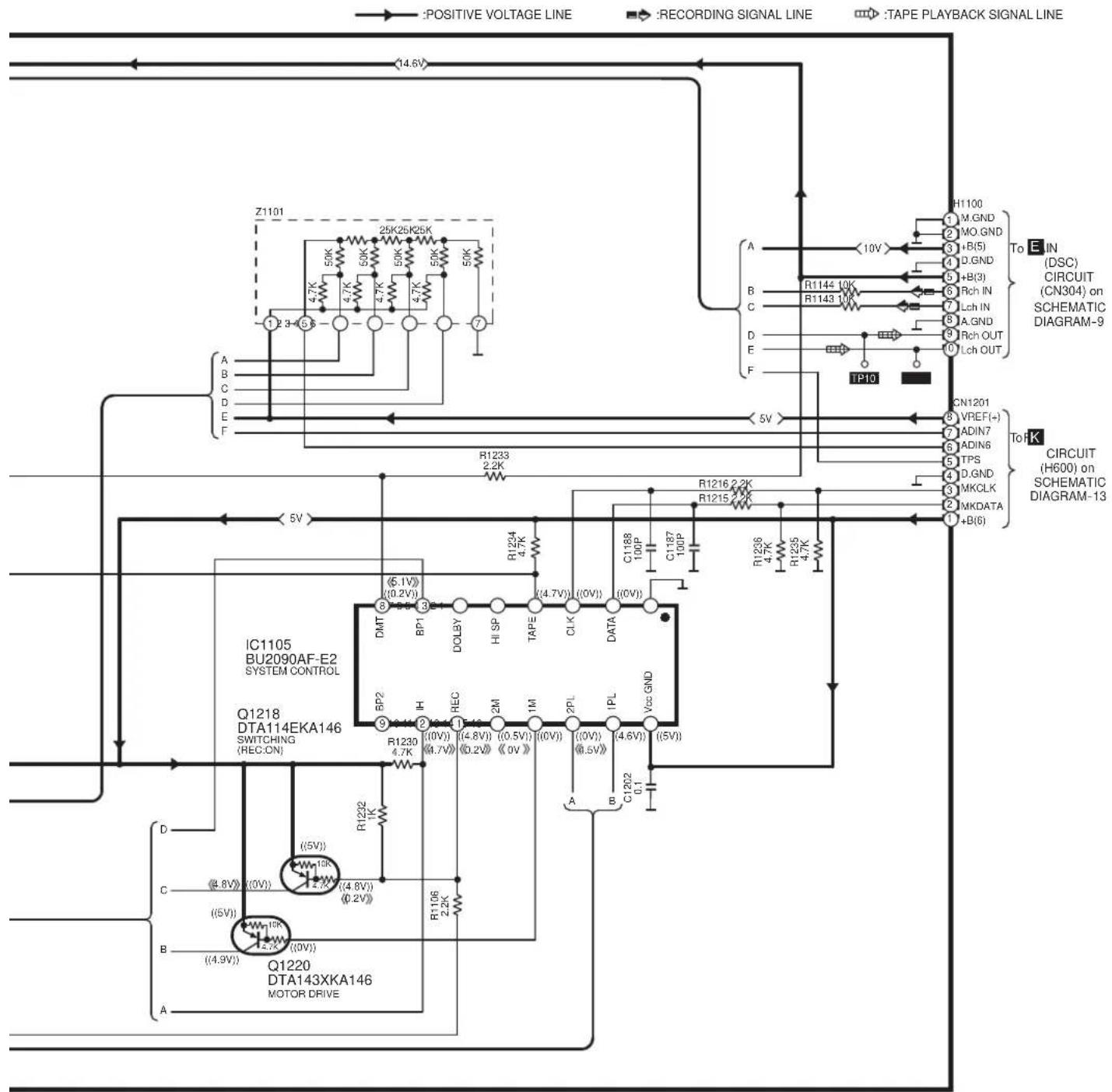
Positive voltage line Recording signal line TAPE PLAYBACK SIGNAL LINE 14.6V Z1101 25K25K25K 50K 50K 50K 50K 50K 1 2 3 4 5 6 A B C D E F 5V R1233 2.2K R1216 2.2K R1215 R1234 4.7K C1188 100P C1187 100P R1236 4.7K R1235 4.7K TP10 To E IN (DSC) CIRCUIT (CN304) on SCHEMAIC DIAGRAM-9 CN1201 VREF(+) ADIN7 ADIN6 TPS D.GND MKCLK MKDATA +B(6) To K CIRCUIT (H600) on SCHEMAIC DIAGRAM-13 IC1105 BU2090AF-E2 SYSTEM CONTROL Q1218 DTA114EKA146 SWITCHING (REC:ON) IC1105 BU2090AF-E2 SYSTEM CONTROL Q1218 DTA114EKA146 SWITCHING (REC:ON) D C (4.8V) (0V) (5V) (4.8V) (0.2V) (4.9V) (0V) Q1220 DTA143XKA146 MOTOR DRIVESCHEMATIC DIAGRAM-7
text_image
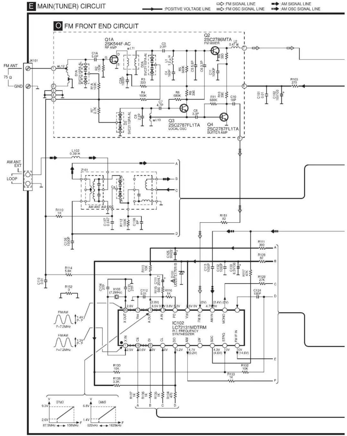
E MAIN(TUNER) CIRCUIT → :POSITIVE VOLTAGE LINE FM ANT 75 Ω GND Q1A 2SK544F-AC RF AMP C1A 5.6P DIA SVC211SPA/AL R1A 100K C2A 100k G S D2A SVC211SPA/AL R23 100k C3 2.2P L1 1.2k H D4 100P R5 500K C5 5.6P C6 3.3P C11 100P R8 680K R9 390 C7 4.73 R10 390 C8 3.3P R11 680K C10 18P Q2 2SC2786MTA FM MIXER L2 0.47 μ 7 C101 0.01 C102 1.6V/100 R103 270 Q3 2SC2787FL1TA LOCAL OSC Q4 2SC2787FL1TA BUFFER AMP 6 AM ANT EXT L LOOP L102 0.39 H Z101 A B Ca C AM ANT AM OSC R110 1K C137 0.047 R112 100K C136 9BP D R151 82 C125 16V22+ C134 27P X103 (7.2MHz) C133 27P C112 0.01 R115 C111 560 26V4.7+ UO25TE75R1B DIO1 + - (2.8V) 6.5V 0.8V 0.8V 3.2V 3.5V 0V 4.7V 0V 4.7V 0V 4.7V 0V 4.7V 0V 4.7V 0V 4.7V 0V 4.7V 0V 4.7V 0V 4.7V 0V 4.7V 0V 4.7V 0V 4.7V 0V 4.7V 0S IC102 LC72131MDTRM PLI FREQUENCY SYNTHESIZER IC102 LC72131MDTRM PLI FREQUENCY SYNTHESIZER FM/AM F=7.2MHz FM/AM F=7.2MHz P-P FM/AM F=7.2MHz P-P ICL Frequency Synthesiser X:IN CE DI CL DO MM UW SDC STRQ FM/F IN 4.3V (4.6V) 10V (14.6V) R130 10K R138 3.3K R137 1K R136 1K R135 1K R134 470 K R133 1K R132 10K F V [FM] 9.3V V [AM] 2.6V 87.5MHz → 108MHz → 522kHz → 1629kHzSCHEMATIC DIAGRAM-8
text_image
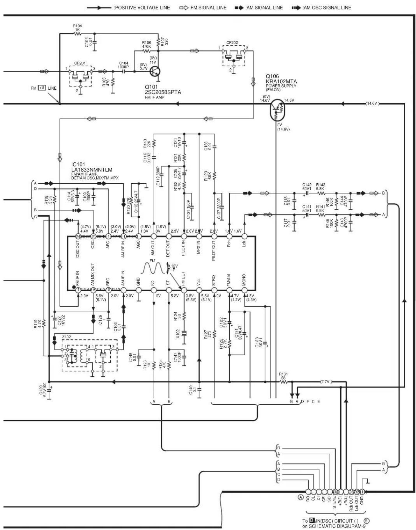
R104 1K C103 0.01 CF201 1 2 R105 470 C104 1000P (0V) (0V) 0.7V Q101 2SC2058SPTA FM IF AMP CF202 3 2 Q106 KRA102MTA POWER SUPPLY (FM:ON) (0V) 14.6V (14.6V) FM +B LINE IC101 LA1833NMNTLM FM:AM IF AMP DET:AM OSC,MIX/FM MPX A D C B C D R118 3.3K C114 50V/3.5 C109 100W R120 47K C115 V4.7 C119 88P C120 22K 16V/10 C138 0.01 R123 68K C137 320P C118 0.01 C142 50V/1 R142 6.8K C141 50V/1 R144 6.8K R146 100K C144 470P C143 470P A B FM IF IN OSC OUT (4.7V) (6.1V) (2.0V) (2.0V) (2.0V) (1.5V) (1.9V) (2.3V) (2.0V) (2.0V) (2.0V) (1.9V) (2.3V) (2.0V) (2.0V) (2.0V) (2.0V) (2.0V) (2.0V) (2.0V) (2.0V) (2.0V) (2.0V) (2.0V) (2.0V) (2.0V) (2.0V) (2.0V) (2.0V) (2.0V) (1.9V) (2.3V) (2.0V) (2.0V) (2.0V) (2.0V) (2.0V) (2.0V) (2.0V) (2.0V) (2.0V) (2.0V) (2.0V) (1.9V) (2.3V) (2.0V) (2.0V) (2.0V) (1.9V) (2.3V) (2.0V) (2.0V) (2.0V) (2.0V) (2.0V) (2.0V) (2.0V) (2.0V) (2.0V) (1.9V) (2.3V) (2.0V) (2.0V) (2.0V) (2.0V) (2.0V) (1.9V) (2.3V) (2.0V) (2.0V) (2.0V) (2.0V) (2.0V) (1.9V) (2.3V) (2.0V) (2.0V) (1.9V) (2.3V) (2.0V) (1.9V) (2.3V) (2.0V) (1.9V) (2.3V) (2.0V) (1.9V) (2.3V) (2.0V) (1.9V) (2.3V) (2.0V) (1.9V) (2.3V) (2.0V) (2.3V) C177 16V/22 C177 58V/6.1V C177 58V/6.1V C177 58V/6.1V C177 58V/6.1V C177 58V/6.1V C177 58V/6.1V C177 58V/6.1V C177 58V/6.1V R199 4.7K C177 58V/6.1V C177 58V/6.1V C177 58V/6.1V C177 58V/6.1V C177 58V/6.1V C177 58V/6.1V C177 58V/6.1V Z102 4 3 3 3 3 3 3 3 3 3 3 3 3 3 3 3 3 3 3 3 3 3 3 3 3 3 3 3 3 3 3 3 3 3 3 3 3 3 3 3 3 3 3 3 3 3 3 3 3 3 3 4 4 4 4 4 4 4 4 4 4 4 4 4 4 4 4 4 4 4 4 4 4 4 4 4 4 4 4 4 4 4 4 4 4 4 4 4 4 4 4 4 4 4 4 4 4 4 4 4 4 5 5 5 5 5 5 5 5 5 5 5 5 5 5 5 5 5 5 5 5 5 5 5 5 5 5 5 5 5 5 5 5 5 5 5 5 5 5,6,6,6,6,6,6,6,6,6,6,6,6,6,6,6,6,6,6,6,6,6,6,6,6,6,6,6,6,6,6,6,6,6,6,6,6,6,6,6,6,6,6,6,6,6,6,6,6,6,6,8+/-/-/-/-/-/-/-/-/-/-/-/-/-/-/-/-/-/-/-/-/-/-/-/-/-/-/-/-/-/-/-/-/-/-/-/-/-/-/-/-/-/-/-/-/-/-/-/-/-/-/-/-/-/-/-/-/-/-/-/-/-/-/-/-/-/-/-/-/-/-/-/-/-/-/-/-/-/-/-/-/-/-/-/-/-/-/-/-/-/-/-/-/-/-/-/-/-/-/-/- / (The circuit is an analog circuit) and is a schematic diagram of the circuit.SCHEMATIC DIAGRAM-9

text_image
E MAIN(DSC) CIRCUIT RECORDING SIGNAL LINE CD PLAYBACK SIGNAL LINE FM SIGNAL LINE AM SIGNAL LINE CN303 R411 2.2K CN303 A GND CD Rch D+BI(2) TX B+I1 P GND R+I4 MIC MGND CHG AD1 SD CHG AD2 SER5 SER6 CD MUTEA P CONT VL1 7.5V 3.3V R S To B MECHANISM CONTROL CIRCUIT(H1100) on SCHEMAIC DIAGRAM-6 M.GND 1 MO.GND 2 +B(5) D.GND 3 +B(3) REC Rch 4 REC Lch 5 A.GND 6 PB Rch 7 PB Lch 8 R207 5.9K R407 6K R213 27K R413 27K F C204 220P C404 220P H C300 0.01 10V 4.6V 7.7V To E MAIN(TUNER) CIRCUIT (A) on SCHEMAIC DIAGRAM-8 DO 1 CL 2 DI 3 CE 4 SD 5 ST EYE 6 +B(3) +B(4) Rch IN 7 Lch IN 8 GND 9 R210 1K R410 1K R209 PCK R409 PCK M N H MOTOR CIRCUIT IC1 TA7291P MOTOR DRIVE IC1 TA7291P MOTOR DRIVE Q350 2SB621ARSTA PLUNGER DRIVE D316 FLIN400S/P Q351 KRC102STA PLUNGER DRIVE S4 (CLAMP) W2 3 D MTZ4HR/BTA 4.5V 0V Q1 RVTDC143EST MOTOR DRIVE CN1 1 2 3 4 5 6 7 8 9 10 11 12 13 14 15 16 17 18 19 20 21 22 23 24 25 26 27 28 29 30 31 32 33 34 35 36 37 38 39 40 41 42 43 44 45 46 47 48 49 50 51 52 53 54 55 56 57 58 59 60 61 62 63 64 65 66 67 68 69 70 71 72 73 74 75 76 77 78 79 80 81 82 83 84 85 86 87 88 89 90 91 92 93 94 95 96 97 98 99 100 S2 (TRAY POSITION2 DET.) S1 (TRAY POSITION1 DET.) S3 (OPEN DET.) R354 I2X R355 I2Y R356 I2Z R357 I2X R358 I2Y R359 I2X R360 I2Y R361 I2X R362 I2Y R363 I2X R364 I2Y R365 I2X R366 I2Y R367 I2X R368 I2Y R369 I2X R370 I2Y R371 I2X R372 I2Y R373 I2X R374 I2Y R375 I2X R376 I2Y R377 I2X R378 I2Y R379 I2X R380 I2Y R381 I2X R382 I2Y R383 I2X R384 I2Y R385 I2X R386 I2Y R387 I2X R388 I2Y R389 I2XSCHEMATIC DIAGRAM-10


text_image
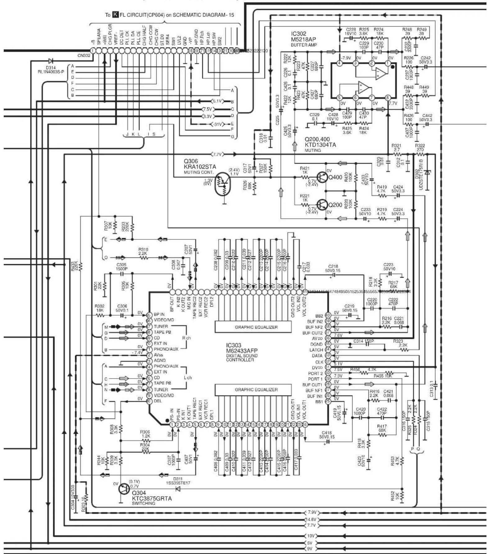
To K FL CIRCUIT(CP604) on SCHEMAIC DIAGRAM- 15 CN302 D314 RL1N4003S-P A E D F C B R-SFEMA -BU CHG PLOR VREF- DC DEI PLL CK PLL DA PLL CE CHG HALF CHG CW ST D0 SPM1 LVL2 GND -VP HP GND IP Pch HP Lh HP SW SW2 D311 1SS355TE17 Q304 KTC3875GRTA SWITCHING C22 222120 Q306 KRA102STA MUTING CONT. (2.4V) 1.1V C17 50V1 R27 150K R29 1.3V R30 0.01 R31 2.2K R32 1.8K R33 2.2K R34 1.2K R35 2.2K R36 1.8K R37 2.2K R38 1.8K R39 2.2K R40 1.8K R41 2.2K R42 1.8K R43 2.2K R44 1.8K R45 2.2K R46 1.8K R47 2.2K R48 1.8K R49 2.2K R50 3.3V 50V/3.3V C225 C405 50V/3.3V C425 50V/3.3V C435 50V/3.3V C445 50V/3.3V C455 50V/3.3V C465 50V/3.3V C475 50V/3.3V C485 50V/3.3V C495 50V/3.3V C505 50V/3.3V C515 50V/3.3V C525 50V/3.3V C535 50V/3.3V C545 50V/3.3V C555 50V/3.3V C565 50V/3.3V C575 50V/3.3V C585 50V/3.3V C595 50V/3.3V C605 50V/3.3V C615 50V/3.3V C625 50V/3.3V C635 50V/3.3V C645 50V/3.3V C655 50V/3.3V C665 50V/3.3V C675 50V/3.3V C685 50V/3.3V C695 50V/3.3V C705 50V/3.3V C715 50V/3.3V C725 50V/3.3V C735 50V/3.3V C745 50V/3.3V C755 50V/3.3V C765 50V/3.3V C775 50V/3.3V C785 50V/3.3V C795 50V/3.3V C805 50V/3.3V C815 50V/3.3V C825 50V/3.3V C835 50V/3.3V C845 50V/3.3V C855 50V/3.3V C865 50V/3.3V C875 50V/3.3V C885 50V/3.3V C895 50V/3.3V C905 50V/3.3V C915 50V/3.3V C925 50V/3.3V C935 50V/3.3V C945 50V/3.3V C955 50V/3.3V C965 50V/3.3V C975 50V/3.3V C985 50V/3.3V C995 50V/3.3V C1005 16W, VOUT, VOUT, VOUT, VOUT, VOUT, VOUT, VOUT, VOUT, VOUT, VOUT, VOUT, VOUT, VOUT, VOUT, VOUT, VOUT, VOUT, VOUT, VOUT, VOUT, VOUT, VOUT, VOUT, VOUT, VOUT, VOUT, VOUT, VOUT, VOUT, VOUT, VOUT, VOUT, VOUT, VOUT, Q200,400 KTD1304TA MUTING Q2121 2.7 VOUT, VOUT, VOUT, VOUT, VOUT, VOUT, VOUT, VOUT, VOUT, VOUT, VOUT, VOUT, VOUT, VOUT, VOUT, VOUT, VOUT, VOUT, VOUT, VOUT, VOUT, VOUT, VOUT, VOUT, VOUT, VOUT, VOUT, VOUT, VOUT, VOUT, VOUT, VOUT, VOUT, UDTSTE17R1B D9J2 UDTSTE17R1B D9J2 UDTSTE17R1B D9J2 UDTSTE17R1B D9J2 UDTSTE17R1B D9J2 UDTSTE17R1B D9J2 UDTSTE17R1B D9J2 UDTSTE17R1B D9J2 UDTSTE17R1B D9J2 UDTSTESCHEMATIC DIAGRAM-11

- :NEGATIVE VOLTAGE LINE
- :POSITIVE VOLTAGE LINE

:CD SIGNAL LINE

FRONT LOW SP DRIVE SIGNAL LINE
FRONT MID/HIGHT SP DRIVE SIGNAL LINE
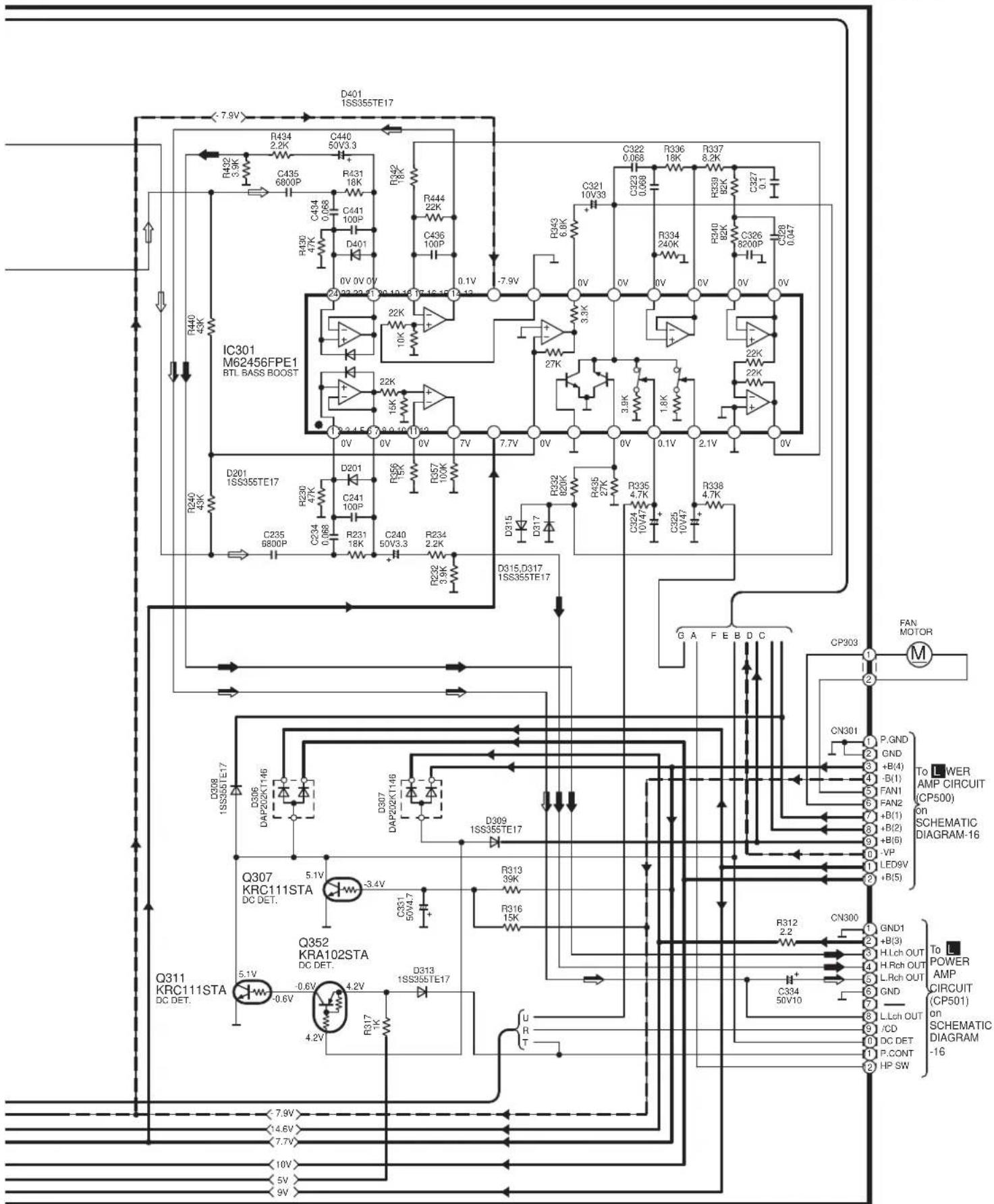
text_image
D401 ISS355TE17 R434 2.2K C440 50V3.3 R432 3.9K C435 6800P R431 18K R431 47K C434 0.068 C441 100P R444 22K C436 100P R437 47K D401 0V 0V 0V 20 10 15 15 15 15 15 15 15 15 15 15 15 15 15 15 15 15 15 15 15 15 15 15 15 15 15 15 15 15 15 15 15 15 15 15 R232 22K C222 0.068 C233 0.068 C234 0.068 C235 0.068 C236 0.068 C237 0.068 C238 0.068 C239 0.068 C240 0.068 C241 0.068 C242 0.068 C243 0.068 C244 0.068 C245 0.068 C246 0.068 C247 0.068 C248 0.068 C249 0.068 C250 0.068 C251 0.068 C252 0.068 C253 0.068 C254 0.068 C255 0.068 C256 0.068 C257 0.068 C258 0.068 C259 0.068 C260 0.068 C261 0.068 C262 0.068 C263 0.068 C264 0.068 C265 0.068 C266 0.068 C267 0.068 C268 0.068 C269 0.068 C270 0.068 C271 0.068 C272 0.068 C273 0.068 C274 0.068 C275 0.068 C276 0.068 C277 0.068 C278 0.068 C279 0.068 C280 0.068 C281 D337-1SS355TE17-D337-1SS355TE17-D337-1SS355TE17-D337-1SS355TE17-D337-1SS355TE17-D337-1SS355TE17-D337-1SS355TE17-D337-1SS355TE17-D337-1SS35S-TE17-D337-1SS35S-TE17-D337-1SS35S-TE17-D337-1SS35S-TE17-D337-1SS35S-TE17-D337-1SS35S-TE17-D337-1SS35S-TE17-D337-1SS35S-TESCHEMATIC DIAGRAM-12
text_image
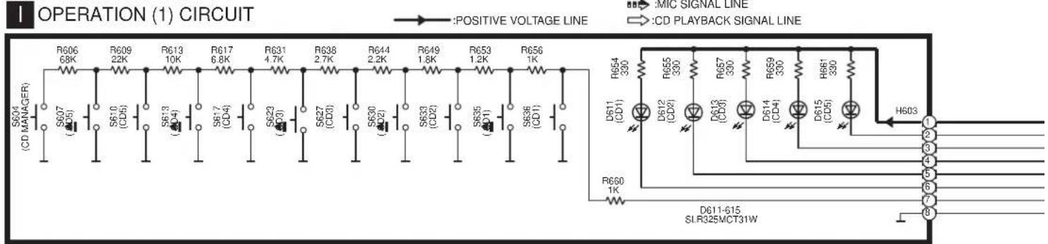
OPERATION (1) CIRCUIT :POSITIVE VOLTAGE LINE :MIC SIGNAL LINE :CD PLAYBACK SIGNAL LINE S604 (CD MANAGER) R606 68K R609 22K R613 10K R617 6.8K R631 4.7K R638 2.7K R644 2.2K R649 1.8K R653 1.2K R656 1K S607 (D5) S610 (CD5) S613 (D4) S617 (CD4) S623 (D3) S627 (CD3) S630 (A2) S633 (CD2) S635 (D1) S636 (CD1) R654 330 R655 330 R657 330 R659 330 R661 330 H603 D611-615 SLR32SMCT31WJ OPERATION (2) CIRCUIT

text_image
R605 10K R608 6.8K R611 4.7K R616 2.7K R624 2.2K R639 1.8K R640 1.2K R648 1K R652 1K S800 (SOUND CONTROL JOG) 1 2 3 C632 100P C633 100P R935 12K R910 22K R606 (TAPE EDIT) SB09 (PEC/STOP) SB12 (REY MODE) SB16 (ECK2 OPEN) SB20 (TUNE DOWN) SB37 (FM MODE BP) SB29 (TUNE MODE) SB32 (MEMORY) SB34 (TIME UP) R602 6.8K R645 4.7K R677 2.7K R647 2.2K D607 SLR325MCT31W (TRI-AMP) R646 330 CP600
text_image
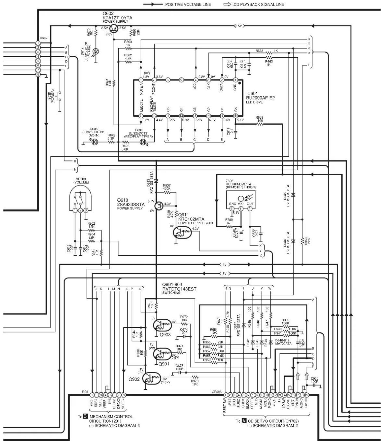
K FL CIRCUIT CN600 R996 10K F G H JK601 MIC L606 10μH C666 0.022 L607 10μH S624 (KARAOKE) R641 1.8K R603 1.2K R607 1K R610 1K S002 (AUX/MD) S005 (TUNER) S008 (CD) S611 (TAPE) X Y R636 68K R615 22K R618 10K R630 6.8K R635 4.7K R623 2.7K R600 2.2K R604 1.8K R629 1.2K R634 1K R639 1K S639 (3D ALEQ) S614 (FO) S618 (EO) S622 (EQ) S626 (EO) S615 (S.WOOFER/VBASS) S619 (DISPLAY/DEMO) S631 (RANDOM) S625 (CLOCK/TIMER) S621 (PLAY/REC) S628 (ECD MODE) 8.5V IC602 BU2090AF-E2 LED DRIVE R681 1K R687 1K D603 LN501MPLIAD (S.WOOFER) D600 SLR325MCT31W (TAPE) D601 SLR325MCT31W (CD) D602 SLR325MCT31W (TUNER) D605 SLR325MCT31W (AUX) D606 SLR325MCT31W (AUX) A C E D B TR1 AMP 0.6V 7 6 5 4 3 2 1 0V 0V DATA GND SW AUX TAPE TUNER CD LVL2 LVL1 Vcc 9 6.8V 10 0V 6.8V 5.9V 6.9V 7.2V 7.5V 7.8V 8.0V 8.5V 8.8V 9.0V 9.5V 9.8V 10.0V 10.5V 11.0V 11.5V 12.0V 12.5V 13.0V 13.5V 14.0V 14.5V 15.0V 15.5V 16.0V 16.5V 17.0V 17.5V 18.0V 18.5V 19.0V 19.5V 20.0V 20.5V 21.0V 21.5V 22.0V 22.5V 23.0V 23.5V 24.0V 24.5V 25.0V 25.5V 26.0V 26.5V 27.0V 27.5V 28.0V 28.5V 29.0V 29.5V 30.0V 30.5V 31.0V 31.5V 32.0V 32.5V 33.0V 33.5V 34.0V 34.5V 35.0V 35.5V 36.0V 36.5V 37.0V 37.5V 38.0V 38.5V 39.0V 39.5V 40.0V 40.5V 41.0V 41.5V 42.0V 42.5V 43.0V 43.5V 44.0V 44.5V 45.0V 45.5V 46.0V 46.5V 47.0V 47.5V 48.0V 48.5V 49.0V 49.5V 50.0V 50.5V 51.0V 51.5V 52.0V 52.5V 53.0V 53.5V 54.0V 54.5V 55.0V 55.5V 56.0V 56.5V 57.0V 57.5V 58.0V 58.5V 59.0V 59.5V 60.0V 60.5V 61.0V 61.5V 62.0V 62.5v C672 0.1 L601 -10μH L604 C686 C687 C784 C788 C792 C794 C798 C799 C804 C808 C812 C814 C818SCHEMATIC DIAGRAM-13
text_image
Q602 KTA12710YTA POWER SUPPLY R673 8.5V 7.8V R695 22K R693 1K R682 4.7K R684 1.3V 0V 1.3V 3.6V 5 6 5 4 0.2V 3 0V 2 0V 1 IC601 BU2090AF-E2 LED DRIVE D615 TLMUT-AC MUTE-A REC/PLAY TIMER C5 C4 C3 C2 G1 G0 0.2V 4.4V 6.9V 6.9V 6.9V 6.9V 0.6V 5.1V C511 0.1 R658 100 R663 1K a b c d e f R651 0.1 R652 1K R653 6BP R654 1K VR600 (VOLUME) Q610 2SA933SSTA POWER SUPPLY D649 RVDTSS137A R937 4.70K R938 4.7K Q611 KRC102MTA POWER SUPPLY CONT Q902 Q901-903 RVTDTC143EST SWITCHING Q903 Q901-903 RVTDTC143EST SWITCHING R972 10K R971 10K R970 10K R960 1K R954 10K R948 4.7K D647 RVDTSS137A R945 100 R946 100 D642 100 D640-542 MA700ATA R939 100K R940 100K R941 100K C674 100P R955 22K R956 22K R957 5.6K R958 5.6K R959 10K R972 10K R971 10K (2V) Q901 (2V) Q902 (2V) Q903 (2V) Q904 (2V) Q905 (2V) Q906 (2V) Q907 (2V) Q908 (2V) Q909 (2V) Q910 (2V) Q911 (2V) Q912 (2V) Q913 (2V) Q914 (2V) Q915 (2V) Q916 (2V) Q917 (2V) Q918 (2V) Q919 (2V) Q920 (2V) Q921 (2V) Q922 (2V) Q923 (2V) Q924 (2V) Q925 (2V) Q926 (2V) Q927 (2V) Q928 (2V) Q929 (2V) Q930 (2V) Q931 (2V) Q932 (2V) Q933 (2V) Q934 (2V) Q935 (2V) Q936 (2V) Q937 (2V) Q938 (2V) Q939 (2V) Q940 (2V) Q941 (2V) Q942 (2V) Q943 (2V) Q944 (2V) Q945 (2V) Q946 (2V) Q947 (2V) Q948 (2V) Q949 (2V) Q950 (2V) Q951 (2V) Q952 (2V) Q953 (2V) Q954 (2V) Q955 (2V) Q956 (2V) Q957 (2V) Q958 (2V) Q959 (2V) Q960 (2V) Q961 (2V) Q962 (2V) Q963 (2V) Q964 (2V) Q965 (2V) Q966 (2V) Q967 (2V) Q968 (2V) Q969 (2V) Q970 (2V) CP606 H600 +8U1 -SEH-SEH-SEH-SEH-SEH-SEH-SEH-SEH-SEH-SEH-SEH-SEH-SEH-SEH-SEH-SEH-SEH-SEH-SEH-SEH-SEH-SEH-SEH-SEH-SEH-SEH-SEH-SEH-SEH-SEH-SEH-SEH-SEH-SEH-SCHEMATIC DIAGRAM-6 TO B MECHANISM CONTROL CIRCUIT(CN1201) on SCHEMAIC DIAGRAM-6 CPST SW STAT SUBO SIOCK BLOK KWD MDD DATA MCLK PON DLD LD SW DLD RD RIN A GND LSH IN CD SERVO CIRCUIT(CN702) on SCHEMAIC DIAGRAM-2 TO A CD SERVO CIRCUIT(CN702) on SCHEMAIC DIAGRAM-2
text_image
L603 3.3uH C626 1000P D630 MA723TA R678 680 C625 6.3V/1000 C623 1000P C624 6.3V/100 C623 1000P C624 6.3V/100 C623 1000P C624 6.3V/100 C623 1000P C624 6.3V/100 C623 1000P C624 6.3V/ 100 C623 1000P C624 6.3V/100 C623 1000P C624 6.3V/100 C623 1000P C624 6.3V/100 C623 1000P C624 6.3V / 100 C623 1000P C624 6.3V / 100 C623 1000P C624 6.3V / 100 C623 1000P C624 6.3V / 100 C623 1000P C624 6 3V / 100 C623 1000P C624 6.3V / 100 C623 1000P C624 6.3V / 100 C623 1000P C624 6.3V / 100 C623 1000P C679 5V C678 5V C677 5V C676 5V C675 5V C674 5V C673 5V C672 5V C671 5V C670 5V C669 5V C668 5V C667 5V C666 5V C665 5V C664 5V C663 5V C662 5V C661 5V C659 5V C658 5V C657 5V C656 5V C655 5V C654 5V C653 5V C652 5V C651 5V C649 5V C648 5V C647 5V C646 5V C645 5V C644 5V C643 5V C642 5V C641 5V C640 5V C639 5V C638 5V C637 5V C636 5V C635 5V C634 5V C633 5V C632 5V C631 5VSCHEMATIC DIAGRAM-15
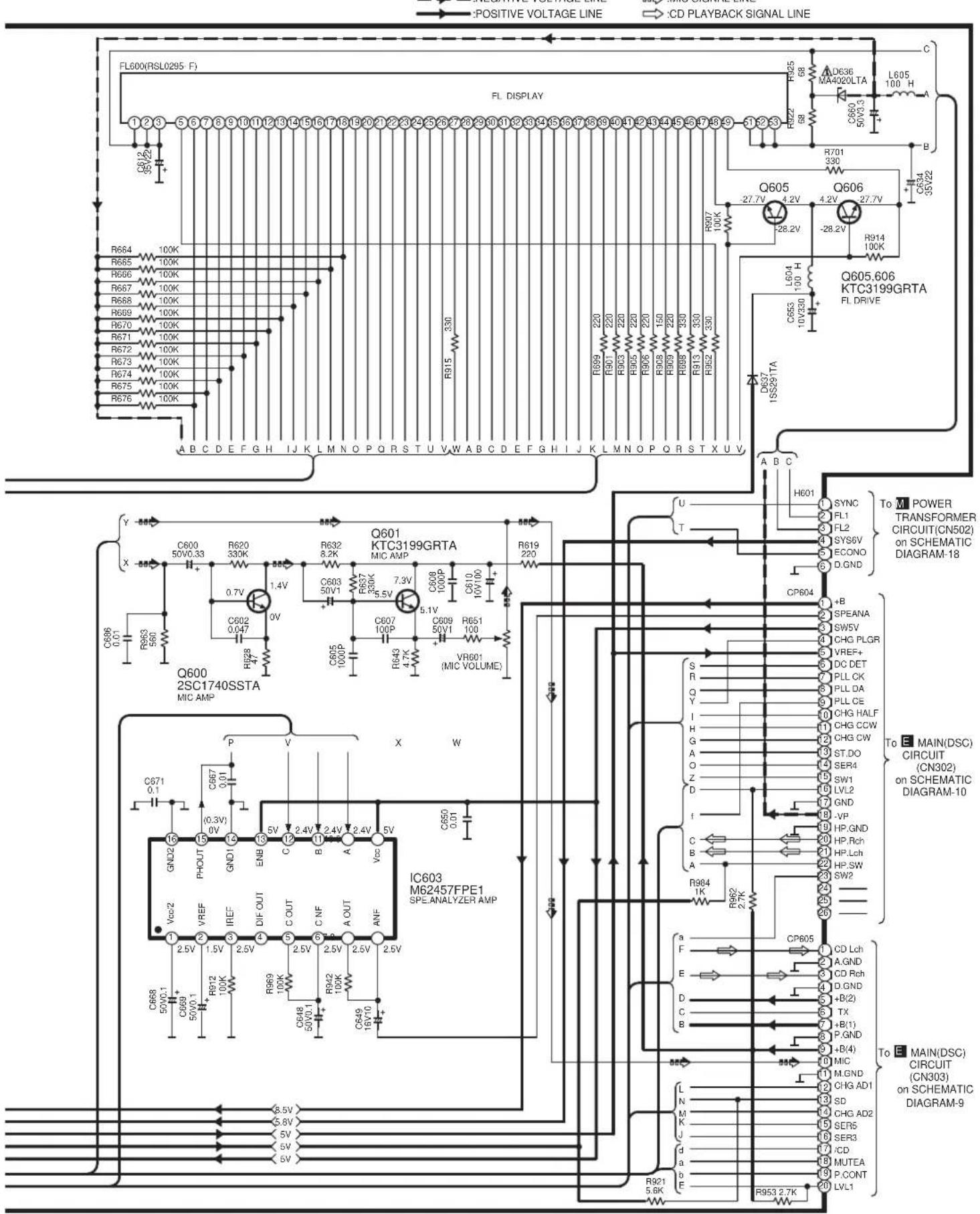
text_image
FL600(RSL0295 F) FL DISPLAY R664 100K R665 100K R667 100K R668 100K R669 100K R670 100K R671 100K R672 100K R673 100K R674 100K R675 100K R676 100K Q605.606 KTC3199GRTA FL DRIVE Q601 KTC3199GRTA MIC AMP C600 50V0.33 C602 330K C603 50V1 C607 100P C609 50V1 C610 100P C619 220 C620 8.2K C621 8.2K C622 8.2K C623 8.2K C624 8.2K C625 8.2K C626 8.2K C627 8.2K C628 8.2K C629 8.2K C630 8.2K C631 8.2K C632 8.2K C633 8.2K C634 8.2K C635 8.2K C636 8.2K C637 8.2K C638 8.2K C639 8.2K C640 8.2K C641 8.2K C642 8.2K C643 8.2K C644 8.2K C645 8.2K C646 8.2K C647 8.2K C648 8.2K C649 8.2K C650 8.2K C651 8.2K C652 8.2K C653 8.2K C654 8.2K C655 8.2K C656 8.2K C657 8.2K C658 8.2K C659 8.2K C660 8.2K C661 8.2K C662 8.2K C663 8.2K C664 8.2K C665 8.2K C666 8.2K C667 8.2K C668 8.2K C669 8.2K C670 8.2K C671 8.2K C672 8.2K C673 8.2K C674 8.2K C675 8.2K C676 8.2K Q600 2SC1740SSTA MIC AMP Q601 KTC3199GRTA MIC AMP Q602 KTC3199GRTA MIC AMP Q603 KTC3199GRTA MIC AMP Q604 KTC3199GRTA MIC AMP Q605 KTC3199GRTA MIC AMP Q606 KTC3199GRTA MIC AMP Q607 KTC3199GRTA MIC AMP Q608 KTC3199GRTA MIC AMP Q609 KTC3199GRTA MIC AMP Q610 KTC3199GRTA MIC AMP Q611 KTC3199GRTA MIC AMP Q612 KTC3199GRTA MIC AMP Q613 KTC3199GRTA MIC AMP Q614 KTC3199GRTA MIC AMP Q615 KTC3199GRTA MIC AMP Q616 KTC3199GRTA MIC AMP Q617 KTC3199GRTA MIC AMP Q618 KTC3199GRTA MIC AMP Q619 KTC3199GRTA MIC AMP Q620 KTC3199GRTA MIC AMP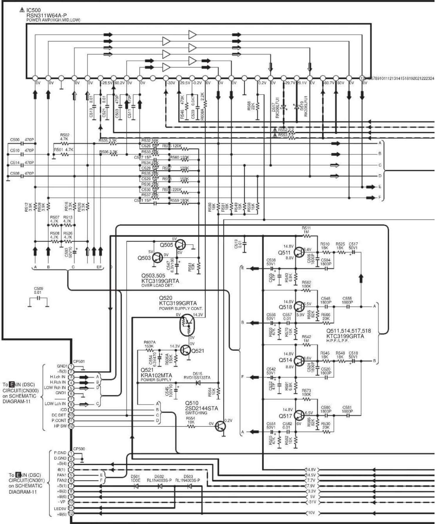
text_image
IC500 RSN311W64A-P POWER AMP(HIGH,MID,LOW) 0V 0V 0V 0V 28.5V 60.2V 0V 0V -3.0V 29.5V -0.2V 6V 0V 0V 0.2V 0V -29.7V 99.1V 0V -60.7V 60V 0V 0V C500 470P C510 470P C514 470P C508 470P R502 4.7K R501 4.7K R506 3.3K R532 2.5K C526 R533 120K C527 1.5P R560 120K C534 R537 120K C538 R539 150K C539 R539 220K C537 R539 180K C537 R559 180K R580 18K R581 18K R582 18K R583 18K R584 18K R585 18K R586 2.2K D517 RK36FLU1 D519 RK36FLU1 R562 2.7 R563 A B C D E F Q503,505 KTC3199GRTA OVER LOAD DET. Q503,505 Q503,505 KTC3199GRTA POWER SUPPLY CONT. Q520 KTC3199GRTA POWER SUPPLY CONT. Q521 KRA102MTA POWER SUPPLY D515 RVD1SS133TA Q510 2SD2144STA SWITCHING R607A 150K 14.3V Q521 R606A 6.3V/100 V DV DV DV DV DV DV DV DV DV DV DV DV DV DV DV DV DV DV DV DV DV DV DV DV DV DV DV DV DV DV DV DV DV DV DV DV DV DV DV DV DV DV DV DV DV DV DV DV DV DV DV DV DV DV DV DV DV DV DV DV DV DV DV DV DV DV DV DV DV DV DV DV DV DV DV DV DV DV DV DV DV DV DV DV DV DV DV DV DV DV DV DV DV DV DV DV DV DV DV DVDV Q511,514,517,518 KTC3199GRTA H.P.F./L.P.F. Q518,518,518 KTC3199GRTA H.P.F./L.P.F. Q514,518,518 KTC3199GRTA H.P.F./L.P.F. Q517,518,518 KTC3199GRTA H.P.F./L.P.F. Q514,518,518 KTC3199GRTA H.P.F./L.P.F. Q517,518,518 KTC3199GRTA H.P.F./L.P.F. Q514,518,518 KTC31:99GRTA H.P.F./L.P.F. Q517,518,518 KTC3199GRTA H.P.F./L.P.F. Q514,518,518 KTC3199GRTA H.P.F./L.P.F. Q517,518,518 KTC3199GRTA H.P.F./L.P.F . Q514,518,518 KTC3199GRTA H.P.F./L.P.F . Q517,518,518 KTC3199GRTA H.P.F./L.P.F . Q514,518,518 KTC3199GRTA H.P.F./L.P.F . Q517,518,518 KTC3199GRTA H.P.F./L.P.F . Q514,518,518,518 KTC3199GRTA H.P.F./L.P.F . Q517,518,518 KTC3199GRTA H.P.F./L.P.F . Q514,518,518 KTC3199GRTA H.P.F./L.P.F . Q517,518,518 KTC31:99GRTA H.P.F./L.P.F . Q514,518,518 KTC3199GRTA H.P.F./L.P.F . Q517,518,518 KTC31:99GRTA H.P.F./L.P.F . Q514,518,518 KTC31:99GRTA H.P.F./L.P.F . Q517,518,518 KTC3:99GRTA H.P.F./L.P.F . Q514,518,518 KTC3:99GRTA H.P.F./L.P.F . Q517,518,518 KTC3:99GRTA H.P.F./L.P.F . Q514,518,518 KTC3:99GRTA H.P.F./L.P.F . Q517,518,518 KTC3:99GRTA H.P.F./L.P.C To EIN (DSC) CIRCUIT(CN300) on SCHEMAIC DIAGRAM-1I GNDI ① +B(3) ② A H.Lch IN ③ B H.Rch IN ④ D LOW Rch IN ⑤ D GNDI ⑥ C D LOW Lch IN ⑦ C /CD ⑨ DC DET ⑩ P.CONT ⑪ HP SW ⑫ CP500 P.GND ⑬D.GND ⑭B(4) ⑮ E F GNDI ⑯ D.GND ⑰B(4) ⑱ FANI ⑲ FAN2 ⑳ FANJ ⑴ FANJ ⑵ FANJ ⑶ FANJ ⑷ FANJ ⑧ FANJ ⑨ FANJ ⑩ FANJ ⑪ FANJ ⑫ FANJ ⑬ FANJ ⑭ FANJ ⑮ FANJ ⑯ FANJ ⑰ FANJ ⑱ FANJ ⑲ FANJ ⑳ FANJ ㉑ FANJ ㉒ FANJ ㉓ FANJ ㉔ FANJ ㉕ FANJ ㉖ FANJ ㉗ FANJ ㉘ FANJ ㉙ FANJ ㉚ FANJ ㉛ FANJ ㉜ FANJ ㉝ FANJ ㉞ FANJ ㉟ FANJ ㉟ FANJ ㉟ FANJ ㉟ FANJ ㉟ FANJ ㉟ FANJ ㉟ FANJ ㉟ FANJ ㉟ FANJ ㉟ FANJ ㉟ FANJ ㉟ FANJ ㉟ FANJ ㉟ FANJ ㉟ FANJ ㉟ FANJ ㉟ FANJSCHEMATIC DIAGRAM-17

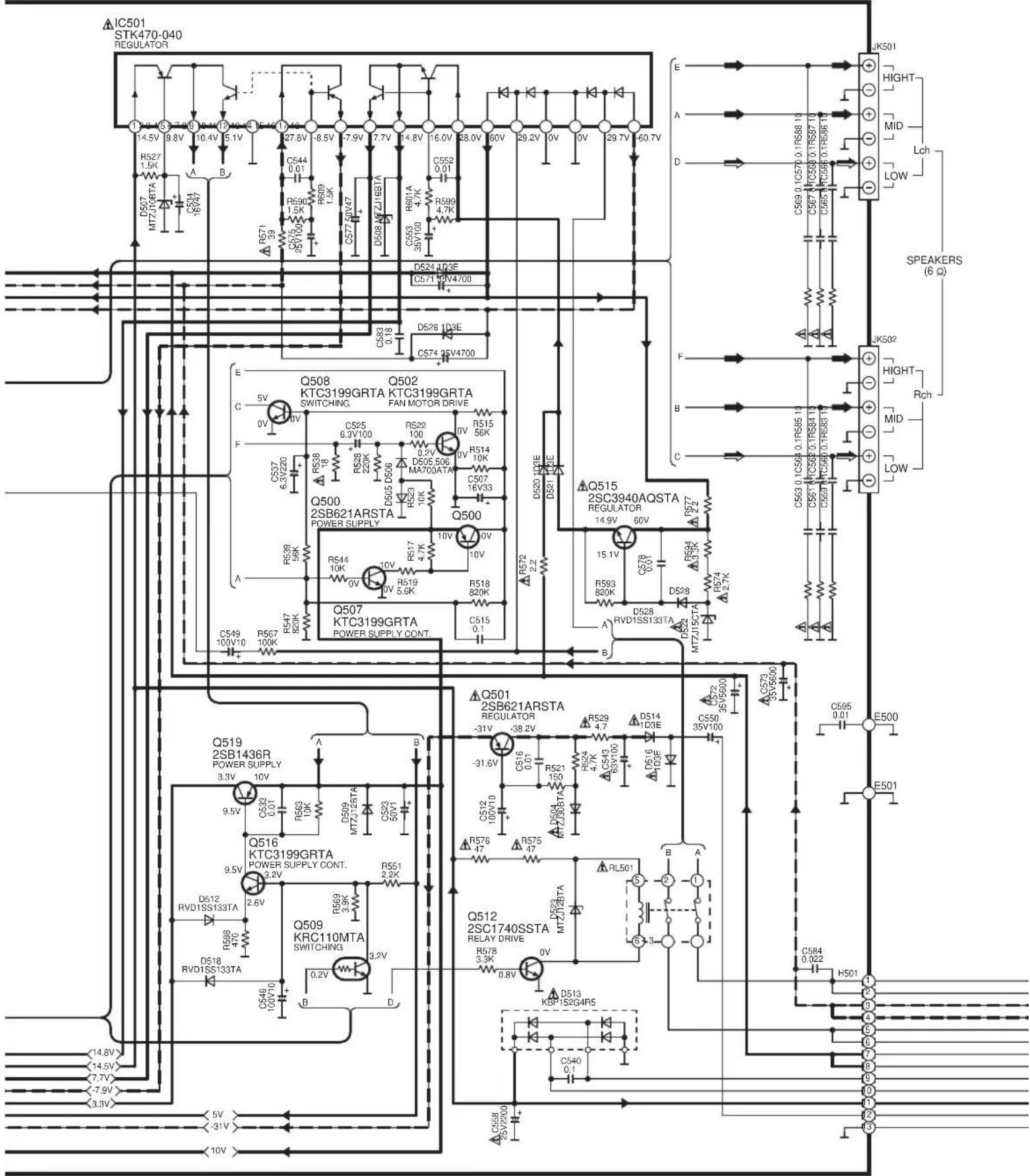
text_image
IC501 STK470-040 REGULATOR 14.5V 9.8V 10.4V 5.1V R527 1.5K A B C544 0.01 R590 1.5K C577 2V/100 R599 1.5K C563 2GB/100 D524 AQ3E C571 5V/4/00 D526 D3E C574 35V/4700 Q508 KTC3199GRTA KTC3199GRTA SWITCHING FAN MOTOR DRIVE Q502 Q502 Q500 2SB621ARSTA POWER SUPPLY Q500 2SC3940AQSTA REGULATOR 14.9V 60V C549 R567 100K C547 820K C546 100V/10 Q519 2SB1436R POWER SUPPLY 3.3V 10V Q516 KTC3199GRTA POWER SUPPLY CONT. Q509 KRC110MTA SWITCHING Q512 2SC1740SSTA RELAY DRIVE RL501 D528 RD1SS133TA D528 RD1SS133TA D528 RD1SS133TA D528 RD1SS133TA D528 RD1SS133TA D528 RD1SS133TA D528 RD1SS133TA D528 RD1SS133TA D528 RD1SS133TA D536 0.1 C540 0.1 C546 100V/10 C547 820K C548 100V/10 C549 100V/10 C557 6.5V/20 C558 6.5V/20 C563 6.3V/100 C563 6.3V/100 C563 6.3V/100 C563 6.3V/100 C563 6.3V/100 C563 6.3V/100 C563 6.3V/100 C563 6.3V/100SCHEMATIC DIAGRAM-18
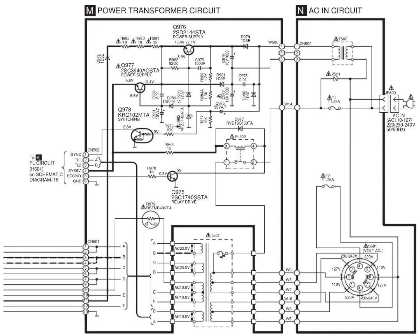
text_image
M POWER TRANSFORMER CIRCUIT Q976 2SD2144STA POWER SUPPLY 10.4V 27.1V R985 R980 R981 18 18 22 D878 1D3E Q977 2SC3940AQSTA POWER SUPPLY 5.8V 10.4V C980 0.01 D984 1SS291TA D983 1D3E C976 16V1000 R983 1.2K R984A 1.5K C977 16V1000 D981 1D3E C975 35V4.7 D990 1D3E Q978 KRC102MTA SWITCHING 2.8V R976 10K D982 MTZJ7/R5ATA R977 10K D977 RVD1SS133TA RL502 W500 ①②③④⑤⑥⑦⑧⑨⑪⑫⑬⑭⑮⑯⑰⑱⑲⑳⑺⑳⑴⑵⑶⑷⑧⑨⑸⑰⑱⑲⑳⑺⑺④⑤⑥⑦⑧⑨⑩⑪⑫⑬⑭⑮⑯⑰⑱⑲⑳⑺④③②①②③④⑤⑥⑦⑧⑨⑩⑪⑫⑬⑮⑯⑯⑰⑱⑲⑳⑮⑯⑰⑱⑲⑳⑮⑯⑰⑱⑲⑳⑮⑯㉑㉒㉓㉔㉕㉖㉗㉘㉙㉚㉛㉜㉚㉟㉳㉟㉟㉳㉟㉟㉳㉟㉟㉟㉟㉟㉟㉟㉟㉟㉟㉟㉟㉟㉟㉟㉟㉟㉟㉟㉟㉟㉟㉟㉟㉟㉟㉟㉟㉟㉟㉟㉟㉟㉟㉟㉟㉟㉟㉟㉟㉟㉟㉟㉟㉟㉟㉟㉟㉟㉟㉞16 Printed Circuit Board Diagram
| A | B | C | D | E | F |
Notes: • This printed circuit board diagram may be modified at any time with the development of new technology.
- *L10\~12 are printed coils formed on the P.C.B. and thus not found in the replacement parts list.
A CD SERVO P.C.B.

text_image
IC701 RJ701 RJ702 RJ703 RJ704 RJ705 RJ706 RJ707 RJ708 RJ709 RJ710 RJ711 RJ712 RJ713 RJ714 RJ715 RJ716 RJ717 RJ718 RJ719 RJ720 RJ721 RJ722 RJ723 RJ724 RJ725 RJ726 RJ727 RJ728 RJ729 RJ730 RJ731 RJ732 RJ733 RJ734 RJ735 RJ736 RJ737 RJ738 RJ739 RJ740 RJ741 RJ742 RJ743 RJ744 RJ745 RJ746 RJ747 RJ748 RJ749 RJ750 RJ751 RJ752 RJ753 RJ754 RJ755 RJ756 RJ757 RJ758 RJ759 RJ760 RJ761 RJ762 RJ763 RJ764 RJ765 RJ766 RJ767 RJ768 RJ769 RJ770 RJ771 RJ772 RJ773 RJ774 RJ775 RJ776 RJ777 RJ778 RJ779 RJ780 RJ781 RJ782 RJ783 RJ784 RJ785 RJ786 RJ787 RJ788 RJ789 RJ790 RJ791 RJ792 RJ793 RJ794 RJ795 RJ796 RJ797 RJ798 RJ799 RJ800 IC701(SPINDLE MOTOR) IC702(REST SW) IC703(TRAVESER MOTOR) VREFtext_image
Circuit board layout diagram with component labels and pin numbers, including ICs, resistors, capacitors, and connectors.| Ref. No. | Lo. No. | Ref. No. | Lo. No. | Ref. No. | Lo. No. | Ref. No. | Lo. No. | Ref. No. | Lo. No. | Ref. No. | Lo. No. | Ref. No. | Lo. No. | Ref. No. | Lo. No. |
| MECHANISM P.C.B. (DECK 1) | |||||||||||||||
| IC951D951 | 3B3A | S951 | 3B | S952 | 3B | S953 | 3A | CS951 | 3C | R952 | 3C | R953 | 3A | ||
| MECHANISM P.C.B. (DECK 2) | |||||||||||||||
| IC971D971 | 3E3D | Z971S971 | 3E3E | S972S973 | 3E3D | S974 S975 | 3D | 3F | CS971 | 3F | R972 | 3F | R973 | 3D | |
D MECHANSIM P.C.B. (DECK1)

text_image
S953 D951 R953 SOLENOID (REPX0108) S952 4 1 IC951 R952 S951 1 2 3 4 5 6 7 8 9 CS951Note for IC951 replacement
- Two different types (old or new) parts are mounted on P.C.B. as for IC951.
- When servicing, care to replace the parts due to those shape.
- Replacement procedures
| Parts No. | Direction | Remarks | |
| Old | 0N2180RLC | Mount the parts on given position.(Printed pattern on P.C.B.) | Refer tothe figurebelow. |
| New | 0N2180RLC1 ≈ | Mount the parts so the cutcorner is located upper right. |
C MECHANSIM P.C.B. (DECK2)
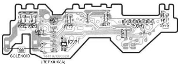
text_image
S974 S973 D971 R972 SOLENOID Z971 7 5 4 3 2 1 IC971 1441A/X0082A (REPX0108A) S972 S971 H972 CS971 S975Note for IC971 replacement
- Two different types (old or new) parts are mounted on P.C.B. as for IC971.
- When servicing, care to replace the parts due to those shape.
- Replacement procedures
| Parts No. | Direction | Remarks | |
| Old | 0N2180RLC | Mount the parts on given position.(Printed pattern on P.C.B.) | Refer tothe figurebelow. |
| New | 0N2180RLC1 ≈ | Mount the parts so the cutcorner is located upper right. |
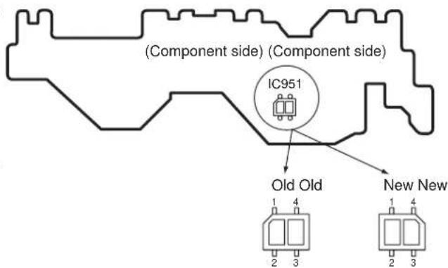
text_image
(Component side) (Component side) IC951 Old Old New New 1 4 2 3 1 4 2 3Old
| 0N2180RLC1432314 | 0N2180RI C 1  |
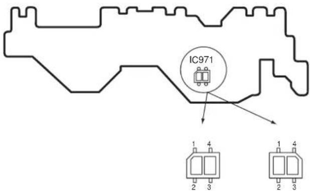
text_image
IC971 1 4 2 3 1 4 2 3Old
0N2180RLC1 YX58 YX58 |
New
text_image
Circuit board layout diagram with labeled components and part numbers, including resistors, capacitors, and connectors| Ref. No. | Lo. No. | Ref. No. | Lo. No. | Ref. | No. Lo. No. | Ref. No. | Lo. No. | |
| HMOTOR P.C.B. | ||||||||
| IC1 | 3C | S2 | 4B | W2 | 4C | C2 | 2B | |
| Q1 | 4C | S3 | 3C | RM1 | 2B | |||
| D2 | 4C | CN1 | 4C | R1 | 3C | |||
| S1 | 3B | W1 | 5C | C1 | 2C | |||
| NAC IN P.C.B. | ||||||||
| T502 | 2D | F1 | 2F | W5 | 5F | W9 | 4F | |
| S501 | 4E | F2 | 3F | W6 | 5E | W10 | 4F | |
| Z501 | 2E | CN500 | 2E | W7 | 5F | JK500 | 4D | |
| PL1 | 3F | W1A | 2F | W8 | 4F | |||
M POWER TRANSFORMER P.C.B.

text_image
Q977 B C E D976 CN502 6 5 4 3 2 1 CN501 R980 R981 D981 C976 C977 C978 R984 R983 D979 R976 R977 C975 W500 Q975 B C E D980 D977 4 3 2 1 RL502 W6 W1A W5 W8 W9 W10 T501[POWER TRANSFORMER] J X0192CA-1(REPX0202C)
flowchart
graph TD
    subgraph_PLC1["PLC"]
        A["DECK1"] --> B["PLAYBACK HEAD (L ch)"]
        C["DECK2"] --> D["R/P HEAD (L ch)"]
        E["ERASE HEAD"] --> F["SWITCHING (BEAT PROOF)"]
        G["INTERFACE"] --> H["INTERFACE INTERFACE"]
        I["SOLENOID DRIVE [DECK2"]] --> J["MOTOR DRIVE"]
    end

    subgraph_PLC2["PLC"]
        K["BU2090AF-E2 SYSTEM CONTROL"] --> L["SOLENOID DRIVE [DECK1"]]
        M["SOLENOID DRIVE [DECK2"]] --> N["SOLENOID DRIVE"]
    end

    subgraph_PLC3["PLC"]
        O["TP3( T.P41) "] --> P["HEAD SELECT (PLAY:ON)"]
        Q["TP5"] --> R["SWITCHING (REC:ON)"]
        S["TP11"] --> T["SWITCHING (REC:ON)"]
        U["TP12"] --> V["L1201 +B3"]
        W["TP179"] --> X["BIAS OSC CONTROL"]
        Y["Q1171"] --> Z["BIAS OSC CONTROL"]
    end

    subgraph_PLC4["PLC"]
        AA["TP9( TP10) "] --> AB["BUFFER AMP"]
        AC["TP153( Q1154) "] --> AD["TPS"]
        AE["Q1151( Q1152) "] --> AF["SWITCHING (PLAY:ON)"]
        AG["S972 (HALF)"] --> AH["INTERFACE"]
        AI["S971 (MODE)"] --> AJ["Z971"]
        AK["S974 (R.REC INH.)"] --> AL["S975 (F.REC INH.)"]
        AM["S972 (HALF)"] --> AN["S971 (MODE)"]
        AO["S974 (R.REC INH.)"] --> AP["S975 (F.REC INH.)"]
        AQ["S972 (HALF)"] --> AR["S971 (MODE)"]
        AS["S974 (R.REC INH.)"] --> AT["S975 (F.REC INH.)"]
        AU["S972 (HALF)"] --> AV["S971 (MODE)"]
        AW["S974 (R.REC INH.)"] --> AX["S975 (F.REC INH.)"]
        AY["S972 (HALF)"] --> AZ["S971 (MODE)"]
        BA["S974 (R.REC INH.)"] --> BB["S975 (F.REC INH.)"]
    end

    subgraph_PLC5["PLC"]
        BC["Q1103( Q1104) "] --> BD["HEAD SELECT (PLAY:ON)"]
        BE["Q1101( Q1102) "] --> BF["HEAD SELECT (REC:ON)"]
        BG["Q1218"] --> BH["SWITCHING (REC:ON)"]
        BI["Q26(11)"] --> BJ["ALC"]
        BK["Q28(9)"] --> BL["AGC.OFF"]
    end

    subgraph_PLC6["PLC"]
        BM["Q1107( Q1108) "] --> BN["REC EQ (CrO2/H.SPEED)"]
        BO["Q1108"] --> BP["Bias OSC CONTROL"]
    end

    subgraph_PLC7["PLC"]
        BQ["S951 (MODE)"] --> BR["VREF+ VREF"]
    end

    subgraph_PLC8["PLC"]
        BS["S952 (HALF)"] --> BT["Z1101 INTERFACE"]
    end

    subgraph_PLC9["PLC"]
        BU["SOLVIDE DRIVE"] --> BV["MOTOR DRIVE"]
    end

    subgraph_PLC10["PLC"]
        BW["SOLVIDE DRIVE"] --> BX["MOTOR"]
    end

    subgraph_PLC11["PLC"]
        BY["SOLVIDE DRIVE"] --> BZ["MOTOR"]
    end

    subgraph_PLC12["PLC"]
        CA["SOLVIDE DRIVE"] --> CB["MOTOR"]
    end

    subgraph_PLC13["PLC"]
        CC["SOLVIDE DRIVE"] --> CD["MOTOR"]
    end

    subgraph_PLC14["PLC"]
        CE["SOLVIDE DRIVE"] --> CF["MOTOR"]
    end

    subgraph_PLC15["PLC"]
        CG["SOLVIDE DRIVE"] --> CH["MOTOR"]
    end

    subgraph_PLC16["PLC"]
        CI["SOLVIDE DRIVE"] --> CJ["MOTOR"]
    end

    subgraph_PLC17["PLC"]
        CK["SOLVIDE DRIVE"] --> CL["MOTOR"]
    end

    subgraph_PLC18["PLC"]
        CM["SOLVIDE DRIVE"] --> CN["MOTOR"]
    end

    subgraph_PLC19["PLC"]
        CO["SOLVIDE DRIVE"] --> CP["MOTOR"]
    end

    subgraph_PLC20["PLC"]
        CR["SOLVIDE DRIVE"] --> CS["MOTOR"]
    end

    subgraph_PLC21["PLC"]
        DD["SOLVIDE DRIVE"] --> DE["MOTOR"]
    end

    subgraph_PLC22["PLC"]
        DF["SOLVIDE DRIVE"] --> DG["MOTOR"]
    end

    subgraph_PLC23["PLC"]
        DH["SOLVIDE DRIVE"] --> DI["MOTOR"]
    end

    subgraph_PLC24["PLC"]
        DJ["SOLVIDE DRIVE"] --> DK["MOTOR"]
    end

    subgraph_PLC25["PLC"]
        DL["SOLVIDE DRIVE"] --> DV["MOTOR"]
    end

    subgraph_PLC26["PLC"]
        DV["MOTOR"] --> DW["MOTOR Drive"]

    subgraph_PLC27["PLC"]
        DX["SOLVIDE DRIVE"] --> DXM["MOTOR Drive"]

    subgraph_PLC28["PLC"]
        DXM["MOTOR Drive"]

    subgraph_PLC29["PLC"]
        DXM["MOTOR Drive"]

    subgraph_PLC30["PLC"]
        DXM["MOTOR Drive"]

    subgraph_PLC31["PLC"]
        DXM["MOTOR Drive"]

    subgraph_PLC32["PLC"]
        DXM["MOTOR Drive"]

    subgraph_PLC33["PLC"]
        DXM["MOTOR Drive"]

    subgraph_PLC34["PLC"]
        DXM["MOTOR Drive"]

    subgraph_PLC35["PLC"]
        DXM["MOTOR Drive"]

    subgraph_PLC36["PLC"]
        DXM["MOTOR Drive"]

    subgraph_PLC37["PLC"]
        DXM["MOTOR Drive"]

    subgraph_PLC38["PLC"]
        DXM["MOTOR Drive"]

    subgraph_PLC39["PLC"]
        DXM["MOTOR Drive"]

    subgraph_PLC40["PLC"]
        DXM["MOTOR Drive"]

    subgraph_PLC41["PLC"]
        DXM["MOTOR Drive"]

    subgraph_PLC42["PLC"]
        DXM["MOTOR Drive"]

    subgraph_PLC43["PLC"]
        DXM["MOTOR Drive"]

    subgraph_PLC44["PLC"]
        DXM["MOTOR Drive"]

    subgraph_PLC45["PLC"]
        DXM["MOTOR Drive"]

    subgraph_PLC46["PLC"]
        DXM["MOTOR Drive"]

    subgraph_PLC47["PLC"]
        DXM["MOTOR Drive"]

    subgraph_PLC48["PLC"]
        DXM["MOTOR Drive"]

    subgraph_PLC49["PLC"]
        DXM["MOTOR Drive"]

    subgraph_PLC50["PLC"]
        DXM["MOTOR Drive"]

    subgraph_PLC51["PLC"]
        DXM["MOTOR Drive"]

    subgraph_PLC52["PLC"]
        DXM["MOTOR Drive"]

    subgraph_PLC53["PLC"]
        DXM["MOTOR Drive"]

    subgraph_PLC54["PLC"]
        DXM["MOTOR Drive"]

    subgraph_PLC55["PLC"]
        DXM["MOTOR Drive"]

    subgraph_PLC56["PLC"]
        DXM["MOTOR Drive"]

    subgraph_PLC57["PLC"]
        DXM["MOTOR Drive"]

    subgraph_PLC58["PLC"]
        DXM["MOTOR Drive"]

    subgraph_PLC59["PLC"]
        DXM["MOTOR Drive"]

    subgraph_PLC60["PLC"]
        DXM["MOTOR Drive"]

    subgraph_PLC61["PLC"]
        DXM["MOTOR Drive"]

    subgraph_PLC62["PLC"]
        DXM["MOTOR Drive"]

    subgraph_PLC63["PLC"]
        DXM["MOTOR Drive"]

    subgraph_PLC64["PLC"]
        DXM["MOTOR Drive"]

    subgraph_PLC65["PLC"]
        DXM["MOTOR Drive"]

    subgraph_PLC66["PLC"]
        DXM["MOTOR Drive"]

    subgraph_PLC67["PLC"]
        DXM["MOTOR Drive"]

    subgraph_PLC68["PLC"]
        DXM["MOTOR Drive"]

    subgraph_PLC69["PLC"]
        DXM["MOTOR Drive"]

    subgraph_PLC70["PLC"]
        DXM["MOTOR Drive"]

    subgraph_PLC71["PLC"]
        DXM["MOTOR Drive"]

    subgraph_PLC72["PLC"]
        DXM["MOTOR Drive"]

    subgraph_PLC73["PLC"]
        DXM["MOTOR Drive"]

    subgraph_PLC74["PLC"]
        DXM["MOTOR Drive"]

    subgraph_PLC75["PLC"]
        DXM["MOTOR Drive"]

    subgraph_PLC76["PLC"]
        DXM["MOTOR Drive"]

    subgraph_PLC77["PLC"]
        DXM["MOTOR Drive"]

    subgraph_PLC78["PLC"]
        DXM["MOTOR Drive"]

    subgraph_PLC79["PLC"]
        DXM["MOTOR Drive"]

    subgraph_PLC80["PLC"]
        DXM["MOTOR Drive"]

    subgraph_PLC81["PLC"]
        DXM["MOTOR Drive"]

    subgraph_PLC82["PLC"]
        DXM["MOTOR Drive"]

    subgraph_PLC83["PLC"]
        DXM["MOTOR Drive"]

    subgraph_PLC84["PLC"]
        DXM["MOTOR Drive"]

    subgraph_PLC85["PLC"]
        DXM["MOTOR Drive"]

    subgraph_PLC86["PLC"]
        DXM["MOTOR Drive"]

    subgraph_PLC87["PLC"]
        DXM["MOTOR Drive"]

    subgraph_PLC88["PLC"]
        DXM["MOTOR Drive"]

    subgraph_PLC89["PLC"]
        DXM["MOTOR Drive"]

    subgraph_PLC90["PLC"]
        DXM["MOTOR Drive"]

    subgraph_PLC91["PLC"]
        DXM["MOTOR Drive"]

    subgraph_PLC92["PLC"]
        DXM["MOTOR Drive"]

    subgraph_PLC93["PLC"]
        DXM["MOTOR Drive"]

    subgraph_PLC94["PLC"]
        DXM["MOTOR Drive"]

    subgraph_PLC95["PLC"]
        DXM["MOTOR Drive"]

    subgraph_PLC96["PLC"]
        DXM["MOTOR Drive"]

    subgraph_PLC97["PLC"]
        DXM["MOTOR Drive"]

    subgraph_PLC98["PLC"]
        DXM["MOTOR Drive"]

    subgraph_PLC99["PLC"]
        DXM["MOTOR Drive"]

    subgraph_PLC100["PLC"]
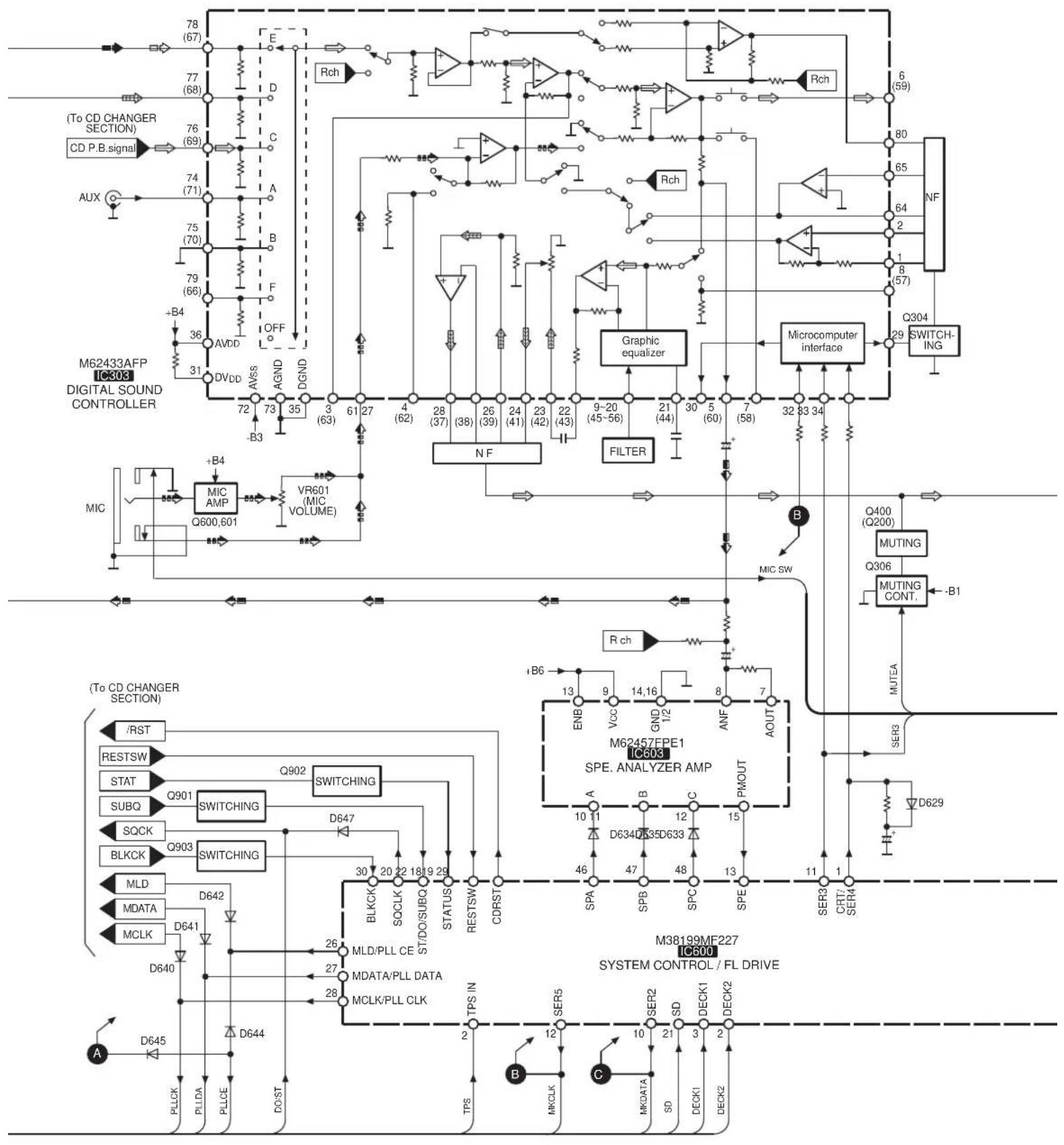
text_image
(To CD CHANGER SECTION) CD P.B.signal AUX 78 (67) 77 (68) 76 (69) 74 (71) 75 (70) 79 (66) +B4 36 DVDD AVDD OFF M62433AFP IC308 DIGITAL SOUND CONTROLLER MIC +B4 MIC AMP Q600,601 VR601 (MIC VOLUME) -63 35 61 27 4 (62) 28 (37) (38) 26 (39) 24 (41) 23 (42) 22 (43) 9-20 (45-56) 21 (44) 30 (60) 7 (58) 32 83 34 CQ304 SWITCHING Microcomputer interface N F FILTER Graphic equalizer Rch Rch Rch MIC SW B Q400 (Q200) MUTING Q306 MUTING CONT. -B1 -MUTEA SER3 D629 (M62457EPE1 IC603 SPE. ANALYZER AMP A B C PMOUT 10 11 D634D535D633 13 9 14,16 GND 1/2 ANF AOUT 10 11 D634D535D633 15 13 SPE 11 SER3 CRT/ SER4 +B6 Rch ENB VCC GND 1/2 ANF AOUT BLKCK SQCLK ST.DO/SUBQ STATUS RESTSW CDRST SPA SPB SPC SPE 30 20 22 18 19 29 30 27 28 26 MLD/PLL CE DATA/PLL Data MCLK/PLL CLK TPS IN SER5 SER2 SD DECK1 DECK2 A D645 PLCK PLDA PLCE DOST TPS MKCLK MKDATA SD DECK1 DECK2
flowchart
graph TD
    subgraph_ICs["IC301 BTL BASS BOOST"]
        M5218AP["IC302"] --> BUFFER["AMP"]
        BUFFER --> +B4_B1
        R_ch --> 2
        2 --> 6
        6 --> 2
        2 --> 3
        3 --> 4
        4 --> 5
        5 --> -B1
        5 --> -B4
        5 --> 10911
    end

    subgraph_ICs["IC601 LED DRIVE"]
        D604_611-615["REC/PLAY TIMER, CD1-5"] --> +B10
        +B10 --> REC/PLAY_TIMER_G1-5
        REC/PLAY_TIMER_G1-5 --> Vcc
        Vcc --> 16
        16 --> +B11
        +B11 --> D605_AC_IN
        D605_AC_IN --> +B10
        +B10 --> D607["(TRI-AMP)"]
        D607 --> 9-13
        9-13 --> SW_AUX_TAPE_TUNER_CD
        SW_AUX_TAPE_TUNER_CD --> 8
        8 --> TPIL_AMP
        TPIL_AMP --> 15
        15 --> LV1_LVL2
        LV1_LVL2 --> 14
        14 --> VREF+
    end

    subgraph_ICs["IC602 LED DRIVE"]
        BU2090AF_E2["IC601"] --> DATA
        BU2090AF_E2 --> CLK
        BU2090AF_E2 --> A
        BU2090AF_E2 --> PCONT
        BU2090AF_E2 --> MUTE_A
        BU2090AF_E2 --> GND
        BU2090AF_E2 --> LED_CTL
        BU2090AF_E2 --> Q602
        BU2090AF_E2 --> POWER_SUPPLY
        POWER_SUPPLY --> +B10-B9
        POWER_SUPPLY --> D617
        POWER_SUPPLY --> D617_(FL_LED)
    end

    subgraph_ICs["IC600 SYSTEM CONTROL / FL DRIVE"]
        Z602["REMOTE SENSOR"] --> VREF+
        RESET --> Q607
        RESET --> VR600(VOLUME) --> S600(SOUND CONTROL JOG) --> KEYSwitch
        S600 --> 5-8
        KEYSwitch --> HP_SW
    end

    subgraph_ICs["IC601 FL DISPLAY"]
        GRD1-13 --> FL600
        SEG1-32 --> FL600
        D618_620_625 --> REGION_IN
        MBP1 --> SWITCH_ING
        XOUT --> SWITCH_ING
        XIN --> SWITCH_ING
        XMBP2 --> SWITCH_ING
        XOUT --> SWITCH_ING
        XIN --> SWITCH_ING
        XCANX --> SWITCH_ING
    end
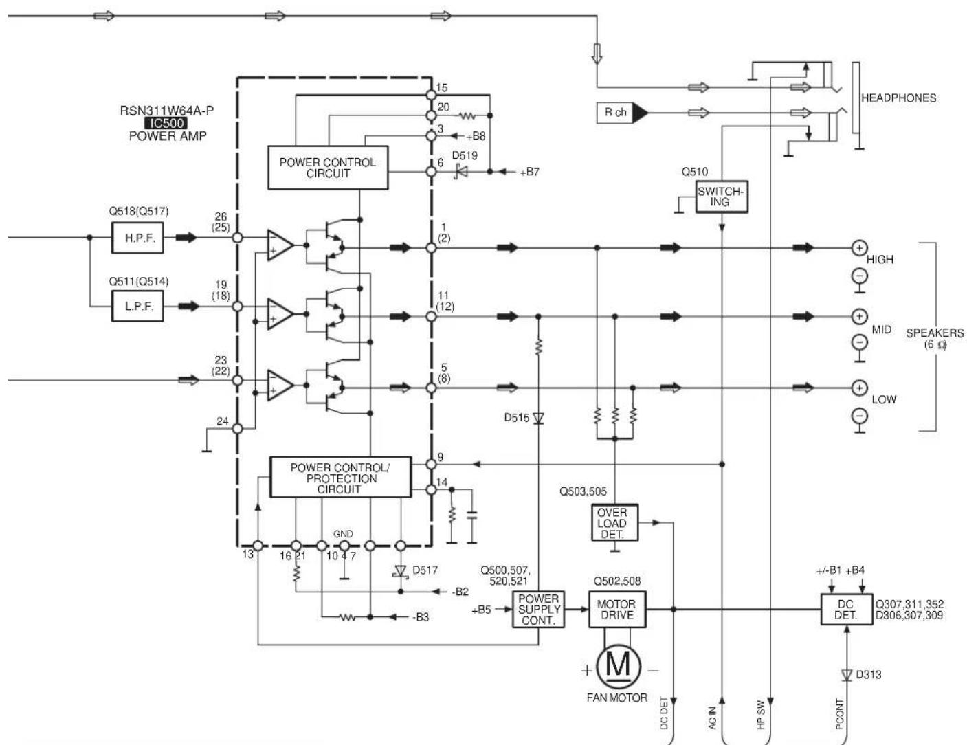
flowchart
graph TD
    A["RSN311W64A-P IC500 POWER AMP"] --> B["POWER CONTROL CIRCUIT"]
    B --> C["POWER CONTROL/ PROTECTION CIRCUIT"]
    C --> D["POWER SUPPLY CONT."]
    D --> E["MOTOR DRIVE"]
    E --> F["DC DET."]
    F --> G["+/-B1 +B4 DC DET"]
    G --> H["PCONT"]
    I["Q518(Q517) H.P.F."] --> J["26 (25)"]
    K["Q511(Q514) L.P.F."] --> L["19 (18)"]
    M["23 (22)"] --> N["24"]
    O["13"] --> P["16 21"]
    Q["10 4 7"] --> R["GND"]
    S["D517"] --> T["-B2"]
    U["D519"] --> V["B7"]
    W["D515"] --> X["Switching"]
    Y["Q503,505 OVER LOAD DET."] --> Z["Motor Drive"]
    AA["+/-B5 FAN MOTOR"] --> AB["MOTOR Drive"]
    AC["AC IN"] --> AD["DC DET"]
    AE["HP SW"] --> AF["PCONT"]
    AG["HADPHONES"] --> AH["R ch"]
    AI["SPEAKERS (6 Ω)"] --> AJ["+ HIGH"]
    AK["MID"] --> AL["+ MID"]
    AM["LOW"] --> AN["+ LOW"]
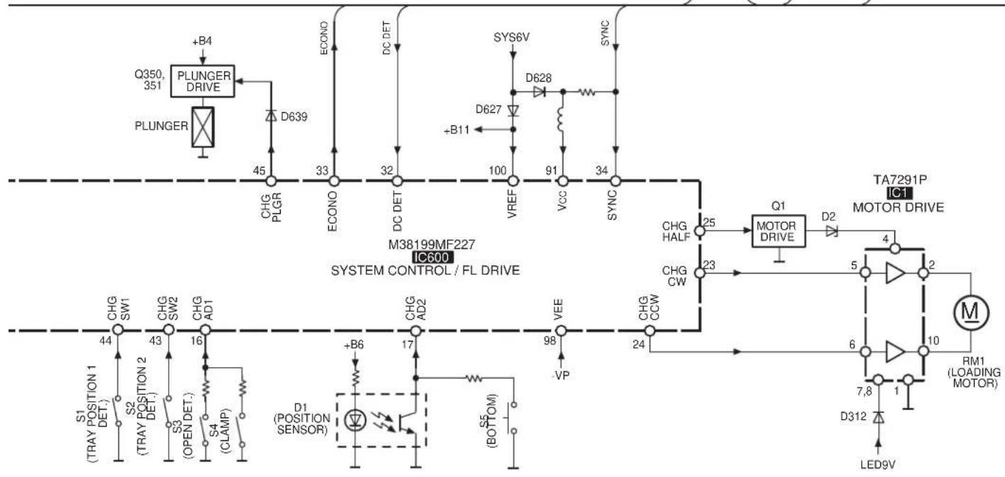
flowchart
graph TD
    A["PLUNGER DRIVE"] -->|+B4| B["Q350, 351"]
    B --> C["PLUNGER"]
    C --> D["CHG PLGR"]
    D --> E["33"]
    E --> F["ECONO"]
    F --> G["32"]
    G --> H["DC DET"]
    H --> I["SYS6V"]
    I --> J["D628"]
    J --> K["SYNC"]
    K --> L["VREF"]
    L --> M["91"]
    M --> N["VCC"]
    N --> O["34"]
    O --> P["SYNC"]
    P --> Q["TA7291P MOTOR DRIVE"]
    Q --> R["Q1 MOTOR DRIVE"]
    R --> S["D2"]
    S --> T["4"]
    T --> U["5"]
    U --> V["2"]
    V --> W["M (LOADING MOTOR)"]
    W --> X["6"]
    X --> Y["10"]
    Y --> Z["7,8 LED9V"]
    W --> AA["1"]
    AA --> AB["D312"]
    AB --> AC["S5 (BOTTOM)"]
    AC --> AD["CHG AD2"]
    AD --> AE["98 VP"]
    AE --> AF["VEE"]
    AF --> AG["CHG CCW"]
    AG --> AH["24"]
    AH --> AI["CHG SW1"]
    AI --> AJ["44"]
    AJ --> AK["S1 (TRAY POSITION 1 DET.)"]
    AK --> AL["S2 (TRAY POSITION 2 DET.)"]
    AL --> AM["S3 (OPEN DET.)"]
    AM --> AN["S4 (CLAMP)"]
    AN --> AO["D1 (POSITION SENSOR)"]
    AO --> AP["+B6"]
    AP --> AQ["17"]
    AQ --> AR["CHG SW2"]
    AR --> AS["43"]
    AS --> AT["CHG AD1"]
    AT --> AU["16"]
    AU --> AV["S2 (TRAY POSITION 2 DET.)"]
    AV --> AW["S3 (OPEN DET.)"]
    AW --> AX["S4 (CLAMP)"]
    AX --> AY["D1 (POSITION SENSOR)"]
    AY --> AZ["98 VP"]
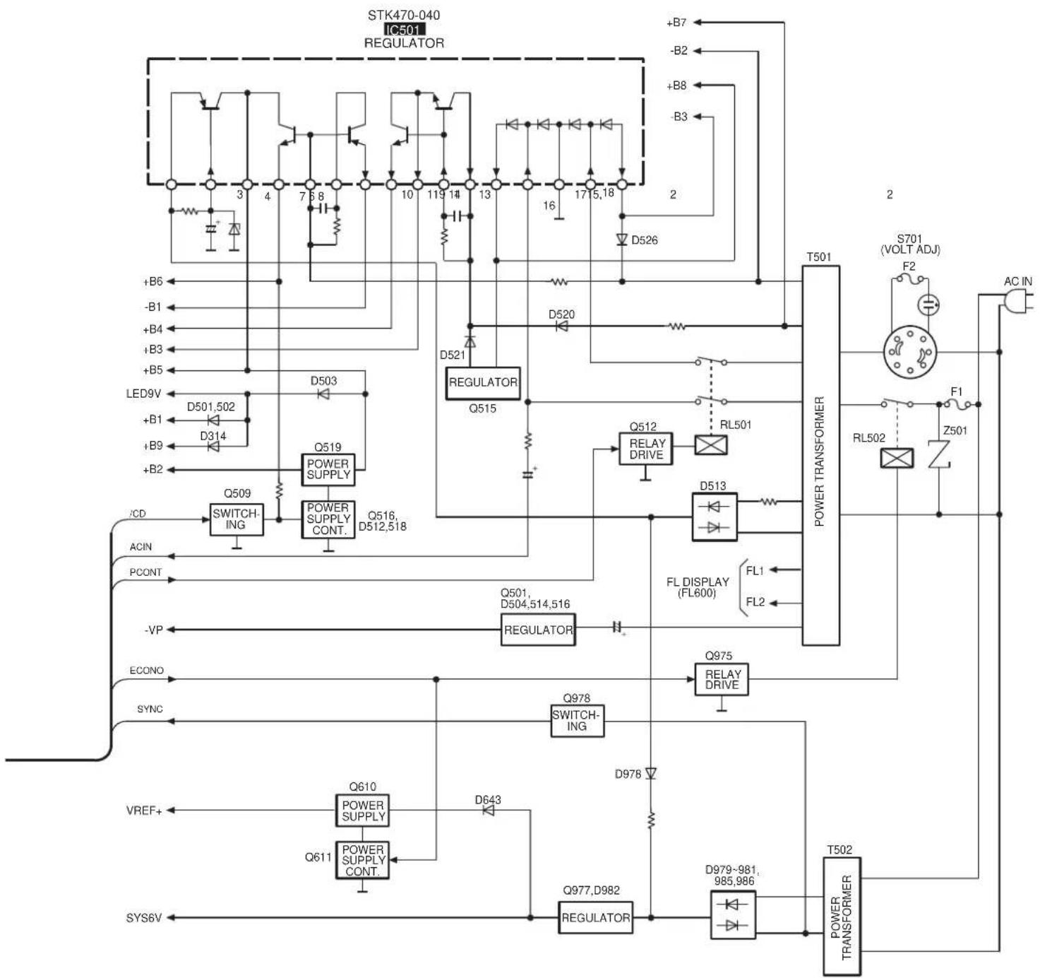
flowchart
graph TD
    A["STK470-040 IC501 REGULATOR"] --> B["3"]
    A --> C["4"]
    A --> D["7"]
    A --> E["8"]
    A --> F["10"]
    A --> G["119"]
    A --> H["14"]
    A --> I["13"]
    A --> J["16"]
    A --> K["17"]
    A --> L["15,18"]
    A --> M["2"]
    A --> N["D526"]
    A --> O["D521"]
    P["+B6"] --> Q["D501,502"]
    R["-B1"] --> S["D314"]
    T["+B4"] --> U["D503"]
    V["+B3"] --> W["D503"]
    X["+B5"] --> Y["D503"]
    Z["LED9V"] --> AA["+B1"]
    AB["+B9"] --> AC["+B2"]
    AD["/CD"] --> AE["Q509 SWITCHING"]
    AF["ACIN"] --> AG["PCONT"]
    AH["VREF+"] --> AI["Q610 POWER SUPPLY"]
    AJ["VREF+"] --> AK["Q611 POWER SUPPLY CONT."]
    AL["SYS6V"] --> AM["Q519 POWER SUPPLY CONT."]
    AN["POWER SUPPLY"] --> AO["Q516, D512,518"]
    AP["RELAY DRIVE"] --> AQ["RL501"]
    AR["FL DISPLAY (FL600)"] --> AS["FL1 FL2"]
    AT["T501"] --> AU["POWER TRANSFORMER"]
    AV["T502"] --> AW["POWER TRANSFORMER"]
    AX["S701 (VOLT ADJ)"] --> AY["F2"]
    AZ["RL502"] --> BA["Z501"]
    BB["AC IN"] --> BC["AC IN"]
Notes
1) CD PLAYBACK SIGNAL LINE
: FM SIGNAL LINE
00: FM OSC SIGNAL LINE
: AM SIGNAL LINE
AM OSC SIGNAL LINE
TAPE PLAYBACK SIGNAL LINE
TAPE RECORDING SIGNAL LINE
→: FRONT LOW SP DRIVE SIGNAL LINE
→: FRONT MID/HIGH SP DRIVE SIGNAL LINE
MIC SIGNAL LINE
2) ( ) indicates pin No. of Right channel.
18 Troubleshooting Guide
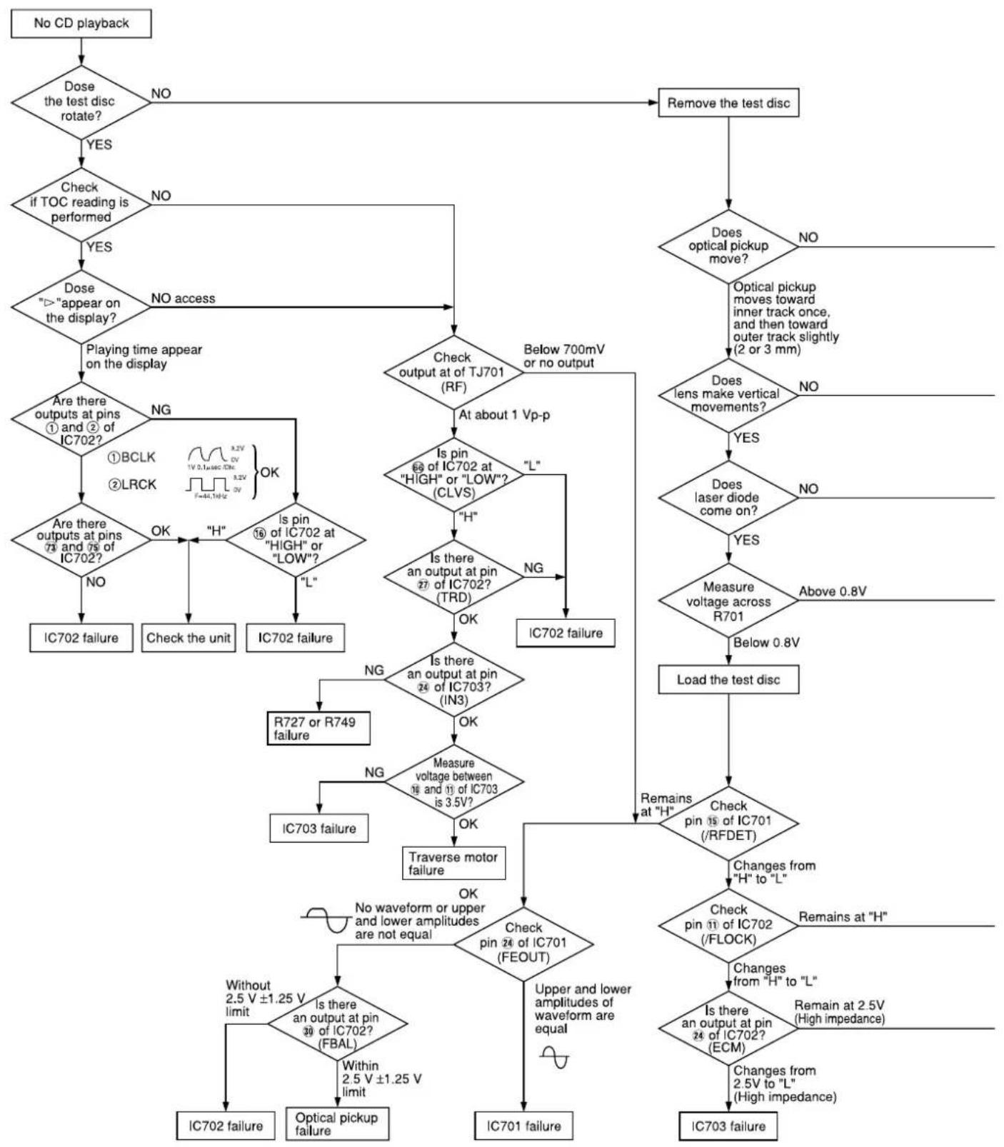
flowchart
graph TD
    A["No CD playback"] --> B{Dose the test disc rotate?}
    B -->|NO| C["Remove the test disc"]
    B -->|YES| D{Check if TOC reading is performed}
    D -->|NO| E{Dose "->" appear on the display?}
    D -->|YES| F["Playing time appear on the display"]
    E -->|NO access| G{Check output at of TJ701 (RF)}
    E -->|NG| H{Are there outputs at pins ① and ② of IC702?}
    H -->|NO| I["IC702 failure"]
    H -->|NG| J{Are there outputs at pins ③ and ④ of IC702?}
    J -->|NO| K["Check the unit"]
    J -->|OK| L{Is pin ⑥ of IC702 at "HIGH" or "LOW"?}
    L -->|NO| M["IC702 failure"]
    L -->|OK| N{Is the output at pin ⑦ of IC703? (IN3)}
    N -->|NG| O["R727 or R749 failure"]
    N -->|OK| P{Measure voltage between ⑧ and ⑬ of IC703 is 3.5V?}
    P -->|NG| Q["IC703 failure"]
    P -->|OK| R{Check pin ⑲ of IC701 (FEOUT)}
    R -->|NO| S["IC702 failure"]
    R -->|Yes| T{Does optical pickup move?}
    T -->|NO| U["Optical pickup moves toward inner track once, and then toward outer track slightly (2 or 3 mm)"]
    T -->|YES| V{Does lens make vertical movements?}
    V -->|NO| W{Does laser diode come on?}
    V -->|YES| X{Measure voltage across R701}
    X -->|Below 0.8V| Y["Load the test disc"]
    X -->|Remains at "H"| Z{Check pin ⑯ of IC701 (/RFDET)}
    Z -->|Changes from "H" to "L"| AA{Check pin ⑪ of IC702 (/FLOCK)}
    AA -->|Remains at "H"| AB{Is there an output at pin ⑫ of IC702? (ECM)}
    AB -->|Changes from "H" to "L"| AC{Is there an output at pin ⑬ of IC702? (ECM)}
    AC -->|Remains at 2.5V (High impedance)| AD["IC703 failure"]
    AC -->|Changes from 2.5V to "L" (High impedance)| AE["IC703 failure"]
    E -->|NO access| F
    F --> G
    G --> H
    H --> I
    I --> J
    J --> J
    J --> K
    K --> L
    L --> M
    M --> N
    N --> O
    O --> P
    P --> Q
    Q --> R
    R --> S
    R --> S
    S --> T
    T --> U
    U --> V
    V --> X
    X --> Y
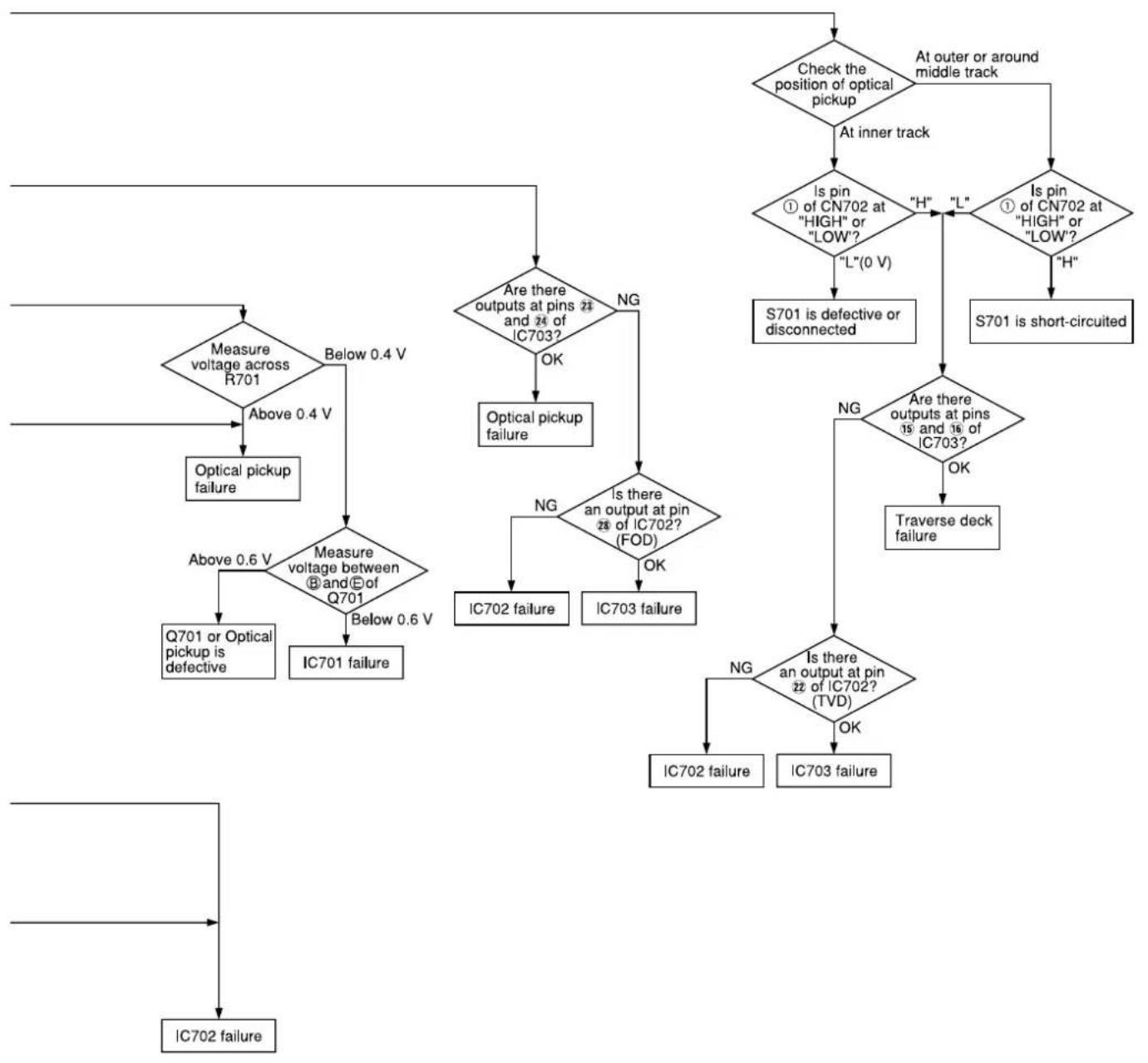
flowchart
graph TD
    A["IC702 failure"] --> B["Q701 or Optical pickup is defective"]
    B --> C{Measure voltage between ⑧ and ⑫ of Q701}
    C -->|Above 0.4 V| D["Above 0.4 V"]
    D --> E{Measure voltage across R701}
    E --> F{Are there outputs at pins 24 and 24 of IC703?}
    F -->|NG| G{Is there an output at pin 28 of IC702? (FOD)}
    G -->|NG| H["IC702 failure"]
    G -->|OK| I["IC703 failure"]
    F -->|OK| J["Optical pickup failure"]
    K["Check the position of optical pickup"] --> L{Is pin ① of CN702 at "HIGH" or "LOW"?}
    L -->|“L”(0 V) to “H” to “L” to “L”| M["S701 is defective or disconnected"]
    L --> N{Is pin ① of CN702 at "HIGH" or "LOW"?}
    N -->|“H” to S701 is short-circuited
    N -->|NG| O["Traverse deck failure"]
    O --> P{Is there an output at pin 22 of IC702? (TVD)}
    P -->|NG| Q["IC702 failure"]
    P -->|OK| R["IC703 failure"]
    P --> S["At outer or around middle track"]
    S --> T["At inner track"]
    T --> L
19 Wiring Connection Diagram
SA-AK48
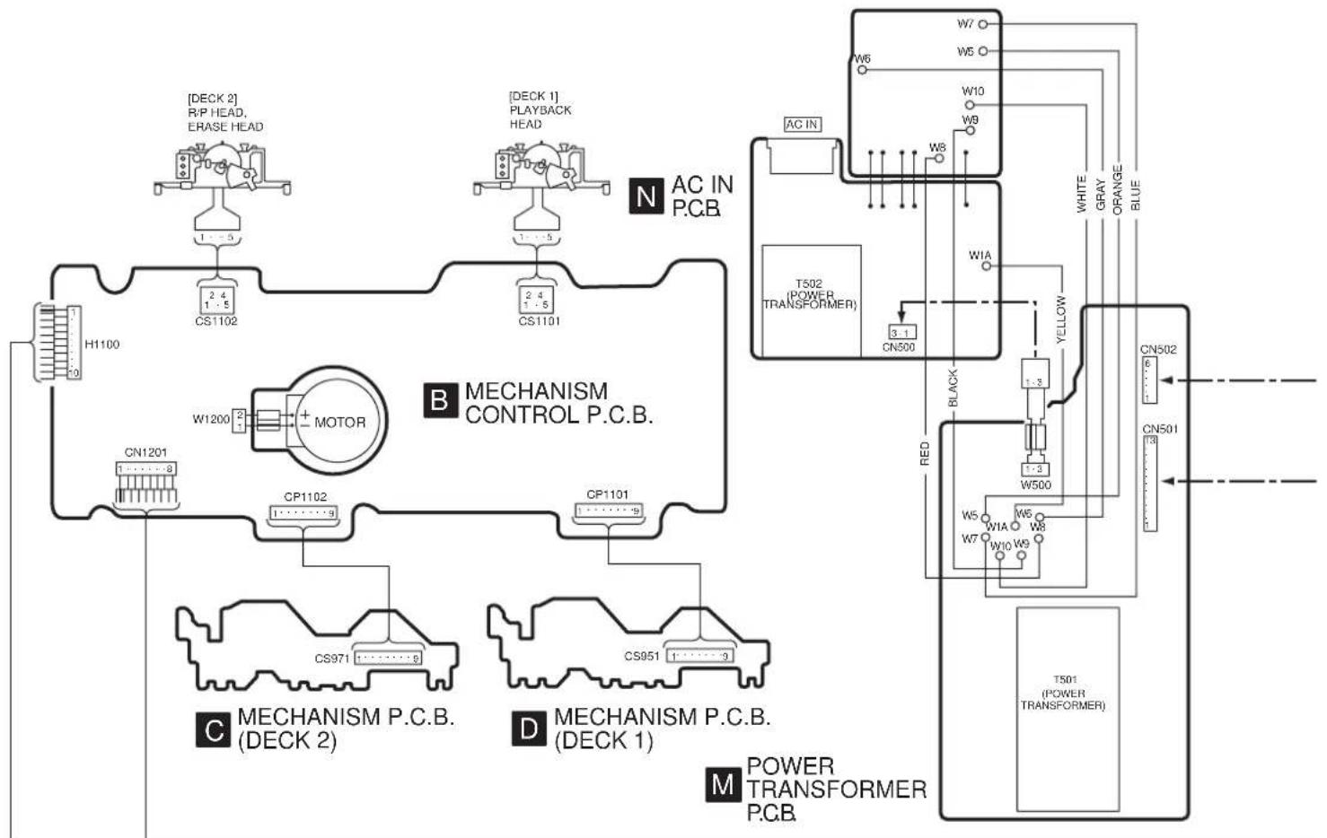
flowchart
graph TD
    subgraph_Motor_B["MECHANISM CONTROL P.C.B."]
        A1["CS971"] --> B1["CP1102"]
        A2["CS951"] --> B2["CP1101"]
        B1 --> C1["AC IN"]
        B2 --> C2["AC IN"]
    end

    subgraph_Power_Trauma["POWER TRANSFORMER P.C.B."]
        D1["CS1102"] --> E1["AC IN"]
        D2["CS1101"] --> E2["AC IN"]
        E1 --> F1["W1200 2"]
        E2 --> F2["W1200 2"]
        F1 --> G1["H1100 1"]
        F2 --> G2["H1100 1"]
    end

    subgraph_Control_B["Control Panel B"]
        H["MOTOR"] --> I["MOTOR"]
    end

    subgraph_Power_Trauma_M["Power Transformer P.C.B."]
        J1["CS971"] --> K1["CP1102"]
        J2["CS951"] --> K2["CP1101"]
        K1 --> L1["W1200 2"]
        K2 --> L2["W1200 2"]
    end

    subgraph_Control_B_B["Control Panel B"]
        M["T502 (POWER TRANSFORMER)"] --> N["T502 (POWER TRANSFORMER)"]
    end

    subgraph_Power_Trauma_N["Power Transformer N"]
        O["T501 (POWER TRANSFORMER)"] --> P["T501 (POWER TRANSFORMER)"]
    end

    style Motor_B fill:#f9f,stroke:#333
    style Control_B fill:#ccf,stroke:#333
    style Power_Trauma_M fill:#cfc,stroke:#333
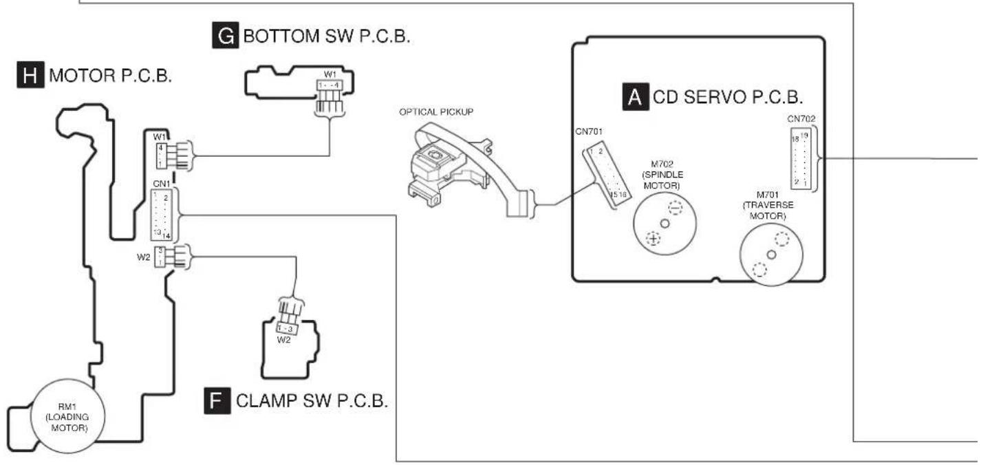
text_image
G BOTTOM SW P.C.B. H MOTOR P.C.B. W1 1-4 W1 CN1 2 3 14 W2 3 W2 F CLAMP SW P.C.B. RM1 (LOADING MOTOR) OPTICAL PICKUP A CD SERVO P.C.B. CN701 1 2 15 18 M702 (SPINDLE MOTOR) CN702 18 19 2 1 M701 (TRAVERSE MOTOR)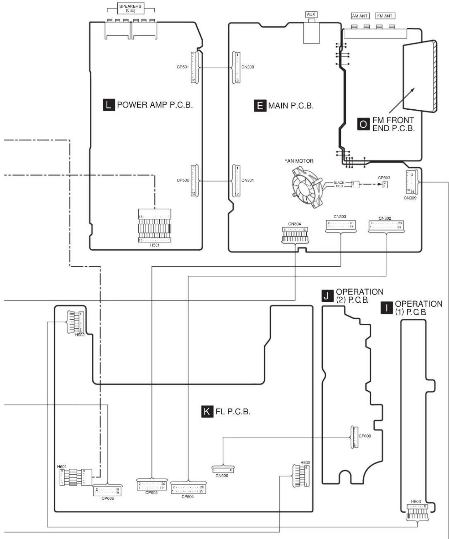
text_image
SPEAKERS (B.B.) L POWER AMP P.C.B. CP501 CN300 E MAIN P.C.B. CN301 FN MOTOR AM ANT FM ANT FM FRONT END P.C.B. CN304 CN303 CN302 J OPERATION (2) P.C.B. I OPERATION (1) P.C.B. H601 CP605 CP605 CP604 K FL P.C.B. CN600 H600 H603 1 2 3 4 5 6 7 8 9 10 11 12 13 14 15 16 17 18 19 20 21 22 23 24 25 26 27 28 29 30 31 32 33 34 35 36 37 38 39 40 41 42 43 44 45 46 47 48 49 50 51 52 53 54 55 56 57 58 59 60 61 62 63 64 65 66 67 68 69 70 71 72 73 74 75 76 77 78 79 8020 Terminal Function of ICs
20.1. IC600 (M38199MF227):
System Control and FL Driver
| Pin No. | Terminal Name | I/O | Function |
| 1 | CRT/SER4 I | CRT timer | |
| 2 | TPS I TPS signal input | ||
| 3 | DECK1 I Deck1 mechanism condition input | ||
| 4 | DECK2 I Deck2 mechanism condition input | ||
| 5-8 | KEY4-KEY1 | I Operation switch signal input | |
| 9 | SER1 O Serial clock output for IC601 and IC602 | ||
| 10 | SER2 O Serial data/cock output for IC601 and IC1105 | ||
| 11 | SER3 O Serial data output for IC602 | ||
| 12 | SER5 O Serial data/cock output for IC303 or IC1105 | ||
| 13 | SPE I Spectrum analyzer signal input | ||
| 14 | V JOGA/B | I Volume control signal input | |
| 15 | J JOG A/B | I | Sound control signal input |
| 16 | CHG AD1 | I | Open detect switch (S3) and clump detect switch (S4) signal input |
| 17 | CHG AD2 | I | Position sensor (D1) and bottom detect switch (S5) signal input |
| 18 | CDRST | O | Reset signal output for CD circuit |
| 19 | STATUS | I | Status signal input from CD circuit |
| 20 | SQCLK | O | CD subcode clock output |
| 21 | SD | I | Station detector signal input for tuner circuit |
| 22 | ST/DO/SUBQ | I CD | subcode data input |
| 23 | CHG CW | O | CD mechanism motor control signal output (forward direction) |
| 24 | CHG CCW | O | CD mechanism motor control signal output (reverse direction) |
| 25 | CHG HALF | O | CD mechanism motor speed control signal output |
| 26 | MLD/PLLCE | O | CD command load signal output and tuner chip enable output |
| 27 | MDATA/PLLDA | O CD | command data output and tuner PLL data output |
| 28 | MCLK/PLLCLK | O CD | command data output and tuner PLL clock output |
| 29 | REST SW | I | Rest switch (S701) signal input |
| 30 | BLKCK | I | CD subcode block clock input |
| 31 | RMT | I | Remote control signal input |
| 32 | DCDET | I | DC ditect terminal |
| 33 | ECONO | O | Eco signal output |
| 34 | SYNC | I | AC power source detect signal input |
| 35 | /RESET | I | System reset signal input |
| 36 | XCIN | I | Oscillator connection (Sub clock : 32.768kHz) |
| 37 | XCOUT | O | Oscillator connection (Sub clock : 32.768kHz) |
| 38 | XIN | I | Oscillator connection (Main clock : 8.0kHz) |
| 39 | XOUT | O | Oscillator connection (Main clock : 8.0kHz) |
| 40 | VSS | GND | |
| 41 | MBP1 | O | Beat proof control signal output |
| 42 | MBP2 | O | Beat proof control signal output |
| 43 | CHG SW2 | I | Disc tray position 2 detect signal input |
| 44 | CHG SW1 | I | Disc tray position 1 detect signal input |
| 45 | CHG PLGR | O | CD mechanism solenoid control signal output |
| 46 | SPA | O | Spectrum analyzer band control signal output |
| 47 | SPB | ||
| 48 | SPC |
| Pin No. | Terminal Name | I/O Function | |
| 49|61 | GRD1|GRD13 | O FL | grid signal output |
| 62|90 | SEG32|SEG4 | O | FL segment signal output |
| 91 | VCC | I | Power supply (+5V) |
| 92|94 | SEG3|SEG1 | O | FL segment signal output |
| 95 | REG IN | I | Region select signal input |
| 96 | EEDATA | - | Not used, open |
| 97 | EECLK | - | Not used, open |
| 98 | VEE | Power supply (-30V) | |
| 99 | AVSS | -GND | |
| 100 | VREF | I | Reference voltage input |
20.2. IC701 (AN8839NSBE2):
Servo Amp
| Pin No. | Terminal Name | I/O | Function |
| 1 | PDE | I | Tracking signal input terminal 1 (E ch) |
| 2 | I | Tracking signal input terminal 2 (F ch) | |
| 3 | V_cc | I Power supply terminal | |
| 4 | PDA | I | Focus signal input terminal 1 (A ch) |
| 5 | PDB | I | Focus signal input terminal 2 (B ch) |
| 6 | LPD I Laser PD signal | ||
| 7 | LD O Laser power auto control output | ||
| 8 | RF | O | RF amp terminal |
| 9 | RFIN | I | AGC input terminal |
| 10 | CSBRT | I | OFTR capacitor connection terminal |
| 11 | CEA | I | HPF-AMP capacitor connection terminal |
| 12 | BDO | O | Dropout detection control |
| 13 | LDON | I | LD APC ON/OFF (H: ON) |
| 14 | GND | - | GND terminal |
| 15 | /RFDET | O | RF detect signal output (L: detect) |
| 16 | PDOWN | - | Power down terminal |
| 17 | OFTR | O | Off track detection (H: detect) |
| 18 | NC | - | Not used, open |
| 19 | ENV | O | Envelope signal output |
| 20 | NC | - | Not used, open |
| 21 | |||
| 22 | TEN | Tracking error signal input | |
| 23 | TEOUT | O | Tracking error signal output |
| 24 | FEOUT | O | Focus error signal output |
| 25 | FEN | I | Focus error signal input |
| 26 | VREF O Reference voltage output | ||
| 27 | TBAL | I | Tracking balance adj. input |
| 28 | FBAL | I | Focus balance adj. input |
20.3. IC702 (MN662790RSC):
Servo Processor/Digital Signal Processor/Digital Filter/ D/A converter
| Pin No. | Terminal Name | I/O | Function |
| 1 | BCLK | - | Serial bit clock output (Not used, open) |
| 2 | LRCK | - | L/R discriminating signal output(Not used, open) |
| 3 | SRDATA | - | Serial data signal output (Not used, open) |
| 4 | DV_DD1 | I Power supply terminal | |
| Pin No. | Terminal Name | I/O Function | |
| 5 | DV_ss1 - GND terminal | ||
| 6 TX O Digital audio interface signal output | |||
| 7 MCLK I Command clock signal input | |||
| 8 MDATA I Command data signal input | |||
| 9 MLD I Command load signal input | |||
| 10 ENSE - Sense signal (Not used, open) | |||
| 11 | /FLOCK | - Optical servo condition (focus)(Not used, open) | |
| 12 | /TLOCK | - Optical servo condition (tracking)(Not used, open) | |
| 13 | BLKCK | O Sub-code block clock signal output(f=75 Hz) | |
| 14 | SQCK | I Sub-code Q resistor clock signal input | |
| 15 | SUBQ | O Sub-code Q data signal output | |
| 16 | DMUTE | - Muting input (Not used, connected to GND) | |
| 17 | STAT | O Status signal output | |
| 18 | /RST | I Reset signal input (L: reset) | |
| 19MCK - System clock (f=4.2336 MHz)(Not used, open) | |||
| 20 | CSEL | I Frequency control terminal of crystal oscillator (Connected to V_DD ) | |
| 21 | TRV | - Traverse servo control signal output(Not used, open) | |
| 22 | TVD | O Traverse drive signal output | |
| 23 | PC | O Turntable motor drive signal output (L: ON) | |
| 24 | ECM | O Turntable motor drive signal output(Forced mode) | |
| 25 | ECS | O Turntable motor drive signal output(Servo error signal) | |
| 26 | KICK | - Kick pulse output (Not used, open) | |
| 27 | TRD | O Tracking drive signal output | |
| 28 | FOD | O Focus drive signal output | |
| 29 | VREF | I D/A drive output normal voltage input | |
| 30 | FBAL | O Focus balance adj. output | |
| 31 | TBAL | O Tracking balance adj. output | |
| 32 | FE | I Focus error signal input | |
| 33 | TE | I Tracking error signal input | |
| 34 | RFENV | I RF envelope signal input | |
| 35 | VDET | I Oscillator detect signal input (H: detect) | |
| 36 | OFT | I Off track signal input (H: Off track) | |
| 37 TRCRS I Track cross signal input | |||
| 38 | /RFDET | I RF detect signal input (L: detect) | |
| 39 | BDO | I Dropout detection signal input (H: dropout) | |
| 40 | LDON | O Laser power control signal output (H: ON) | |
| 41 | PLLF2 | - PLL loop filter terminal (Not used, open) | |
| 42 | DSLF2 | I/O DSL loop filter terminal | |
| 43 | WVEL | - Double velocity status signal output(Not used, open) | |
| 44 | ARF | I RF signal input | |
| 45 | IREF | I Reference current input | |
| 46 | DRF | I DSL bias terminal | |
| 47 | DSLF | I/O DSL loop filter terminal | |
| 48 PLLF I/O PLL loop filter terminal | |||
| 49 | VCOF | - VCO loop filter terminal(Not used, connected to GND) | |
| 50 AV DD2 I Power supply terminal | |||
| 51 AV SS2 - GND terminal | |||
| 52 | EFM | - EFM signal (Not used, open) | |
| 53 | PCK - PLL extract clock (Not used, open) | ||
| 54 VCOF2 - VCO loop filter terminal(Not used, connected to GND) | |||
| 55 | SUBC | - Sub-code serial output clock(Not used, open) | |
| 56 | SBCK | - Sub-code serial input data(Not used, connected to GND) | |
| 57 | V_ss | - GND terminal | |
| 58 | X1 IN | I Crystal oscillator terminal (f=16.9344 MHz) | |
| 59 X2 OUT | O | ||
| Pin No. | Terminal Name | I/O Function | |
| 60 | V_DD | I Power supply terminal | |
| 61 | BYTCK | - | Byte clock signal (Not used, open) |
| 62 | /CLDCK | - | Sub-code frame clock signal(Not used, open) |
| 63 | FCLK | - | Crystal frame clock (Not used, open) |
| 64 | IPFLAG | - | Interpolation flag terminal (Not used, open) |
| 65 | FLAG | - | Flag terminal (Not used, open) |
| 66 | CLVS | - | Turntable servo phase synchro signal(Not used, open) |
| 67 | CRC | - | Sub-code CRC check terminal(Not used, open) |
| 68 | DEMPH | - | De-emphasis ON signal (Not used, open) |
| 69 | RESY | - | Re-synchronizing signal of frame sync.(Not used, open) |
| 70 | IOSEL | I | I/O select signal input (Connected to V_DD ) |
| 71 | /TEST | I | Test terminal(Not used, connected to power supply) |
| 72 | AV_DD1 I Power supply terminal | ||
| 73 | OUTL | O | L ch audio signal output |
| 74 | AVSS1 - GND terminal | ||
| 75 | OUTR | O | R ch audio signal output |
| 76 | RSEL | I | Polarity direction control terminal of RF signal (Not used, connected to power supply) |
| 77 | IOVDD | I Power supply terminal | |
| 78 | PSEL | I | Test terminal (Connected to GND) |
| 79 | MSEL | - | Output frequency select signal input(Not used, connected to GND) |
| 80 | SSEL | I | SUBQ output mode select signal input(Not used, connected to V_DD ) |
20.4. IC703 (AN8739SBE2): Focus Coil/Tracking Coil/Traverse Motor/Spindle Motor Drive
| Pin No. | Terminal Name | I/O | Function |
| 1 | /RST | - | Not used, open |
| 2 NC | - | Not used | |
| 3 | IN2 | I | Motor driver 2 input |
| 4 | PC2 | I | Turntable motor drive signal input (L: ON) |
| 5 NC | - | Not used | |
| 6 | IN1 | I | Motor driver 1 input |
| 7 | PV_CC 1 I D | river power supply terminal 1 | |
| 8 | PGND1 | - | Driver GND terminal 1 |
| 9 | NC | - | Not used, connected to GND |
| 10 | D1- | O | Motor driver 1 output terminal (-) |
| 11 | D1+ | O | Motor driver 1 output terminal (+) |
| 12 | D2- | O | Motor driver 2 output terminal (-) |
| 13 | D2+ | O | Motor driver 2 output terminal (+) |
| 14 | D3- | O | Motor driver 3 output terminal (-) |
| 15 | D3+ | O | Motor driver 3 output terminal (+) |
| 16 | D4- | O | Motor driver 4 output terminal (-) |
| 17 | D4+ | O | Motor driver 4 output terminal (+) |
| 18 | NC | - | Not used |
| 19 | PGND2 | - | Driver GND terminal 2 |
| 20 PV CC2 I D | river power supply terminal 2 | ||
| 21 | V_CC | I Power supply terminal | |
| 22 | VREF | I | Reference voltage input terminal |
| 23 | IN4 | I | Motor driver 4 input |
| 24 | IN3 | I | Motor driver 3 input |
| 25 RSTIN | I Reset terminal(Not used, connected to GND) | ||
| 26 | NC | - | Not used, connected to GND |
21 Replacement Parts List
Notes:
- Important safety notice :
Component identified △ mark have special characteristics important safety. Furthermore, special parts which have purposes retardant (resistors), hight-quality sound (capacitors low-noise (resistors), etc. are used. When replacing any of components, be sure manufactures specified parts shown in the part
- The
- The marking (RTL) indicates that Retention Time is Limited for this item. After the discontinuation of this assembly in production, the item will continue to be available for a specific period of item. The retention period of availability is dependent on the type of assembly, and in accordance with the laws governing part and product retention. After the end of this period, the assembly will on longer be available.
• [M] indicates in the remarks columns indicates parts supplied by MESA.
| Ref. No. | Part No. | Part Name & Description | Psc. | Remarks |
| CABINET AND CHASSIS | ||||
| 1 | REEX0065-1 | 20P FFC | 1 | [M] |
| 2 | REEX0081 | 19P FFC WIRE | 1 | [M] |
| 3 | REEX0083 | 14P FFC WIRE | 1 | [M] |
| 4 | REEX0090 | 26P FFC | 1 | [M] |
| 5 | PFAK48 | FRONT PANEL | 1 | [M] |
| 6 | RGU1847-H | RANDOM BUTTON | 1 | [M] |
| 7 | RGU1855-H | DEMO BUTTON | 1 | [M] |
| 8 | RGU1849-Q | S. WOOFER BUTTOM | 1 | [M] |
| 9 | RGU1854B-H | A1 BUTTON | 1 | [M] |
| 10 | RGU1851-H | CONTROL BUTTON | 1 | [M] |
| 11 | RGL0487-Q | LIGHTING CHIP | 1 | [M] |
| 12 | RGU1845-H | POWER BUTTON | 1 | [M] |
| 13 | RGK1234-K | EQ SHEET | 1 | [M] |
| 14 | RGL0489-Q | CLOCK LIGHT | 1 | [M] |
| 15 | RGU1853-H | CLOCK BUTTON | 1 | [M] |
| 16 | RGU1852-H | DECK BUTTON | 1 | [M] |
| 17 | RKF0585-K2J | CASS. HOLDER (L) | 1 | [M] |
| 18 | RKF0586-K2J | CASS. HOLDER (R) | 1 | [M] |
| 19 | RKF0604-H | CASSETTE LID (L) | 1 | [M] |
| 20 | RKF0605-H | CASSETTE LID (R) | 1 | [M] |
| 21 | RKW0601-Q | CASSETTE WINODW (L) | 1 | [M] |
| 22 | RKW0602-Q | CASSETTE WINDOW (R) | 1 | [M] |
| 23 | RXG0049 | DAMPER GEAR UNIT | 2 | [M] |
| 24 | RMB0474-1 | CASS. OPEN SPRING | 2 | [M] |
| 25 | RKW0603-V1 | FL WINDOW | 1 | [M] |
| 26 | RUS757ZAA | CASSETTE HALF SPRING | 4 | [M] |
| 27 | RGK1233-Q | JOG ORNAMENT 1 | 1 | [M] |
| 28 | RGK1240-Q | JOG ORNAMENT 2 | 1 | [M] |
| 29 | RGK1238A-S | JOG SHEET | 1 | [M] |
| 30 | RGU1848A-Q | FUNCTION BUTTON | 1 | [M] |
| 31 | RMKX0036 | BOTTOM CHASSIS | 1 | [M] |
| 32 | RYQ0289-S1 | JOY UNIT | 1 | [M] |
| 33 | RMKX0038A | CD HCASSIS | 1 | [M] |
| 34 | SHE187-4 | SPACER (TRANS) | 2 | [M] |
| 35 | REM0072-3 | FAN | 1 | [M] |
| 36 | RGRX2B0016-2 | REAR PANEL | 1 | [M] |
| 37 | RMNX0029-4 | SUB-TRANS HOLDER | 1 | [M] |
| 38 | RKMX2B0045-DBL | TOP CABINET (BENT) | 1 | [M] |
| 39 | RGK1232-S | CD LID | 1 | [M] |
| 40 | RGW0330A-S | MAIN VOL KNOB | 1 | [M] |
| 41 | RGU1850A-Q | DPL BUTTON | 1 | [M] |
| Ref.No. | Part No. | Part Name & Description | Psc. | Remarks |
| 42 | RYQ0290-S | JOG CYLINDER UNIT | 1 | [M] |
| 43 | RGL0486-Q | DISC LIGHTING CHIP | 1 | [M] |
| 44 | RGB0113-N | PANA BADGE (HOOK TYP | 1 | [M] |
| 45 of f | RHD30002-H | SCREW | 6 | [M] |
| 46 | RGU1846-H | DISC BUTTON | 1 | [M] |
| 47 | RXXX0017-2 | HEAT SINK UNIT | 1 | [M] |
| 48 | RMN0577 | JOY CYLINDER BASE | 2 | [M] |
| 49 US | RGLX0017-Q | TRI-AMP LIGHT CHIP | 1 | [M] |
| list. | RKA0059-K | LEG RUBBER | 1 | [M] |
| 51 | RMNX0030 | FL HOLDER | 1 | [M] |
| 52 | RMRX0030 | HEAT SINK SUPPORT | 1 | [M] |
| 53 | RMNX0019 | PCB SPACER | 1 | [M] |
| 54 | RGW0341-S | MIC KNOB | 1 | [M] |
| 55 | XTW3+15T | SCREW | 4 | [M] |
| 56 | XTB3+10JFZ | SCREW | 5 | [M] |
| 57 | XTBS3+8JFZ1 | SCREW | 26 | [M] |
| 58 | XTBS26+10J | SCREW | 20 | [M] |
| 59 | XTB3+20J | SCREW | 2 | [M] |
| 60 | XTW3+12T | SCREW | 4 | [M] |
| 61 | XTB3+10J | SCREW | 2 | [M] |
| 62 | RSC0027-2 | TUNER PACK | 1 | [M] |
| CASSETTE DECK | ||||
| 101 | RED0050 | R/P HEAD BLOCK UNIT | 1 | [M] |
| 101-1 | RHE5152ZB | SCREW | 2 | [M] |
| 102 | RED0051 | P/B HEAD BLOCK UNIT | 1 | [M] |
| 102-1 | RHE5152ZB | SCREW | 2 | [M] |
| 103 | RDG0300 | REEL BASE GEAR | 4 | [M] |
| 104 | RDG0301 | WINDING RELAY GEAR | 2 | [M] |
| 105 | RDK0026 | MAIN GEAR | 2 | [M] |
| 106 | RDR0029 | RELAY PULLEY | 1 | [M] |
| 107 | RDV0033-4 | WINDING BELT | 2 | [M] |
| 108 | RDV0034-1 | CAPSTAN BELT 'A' | 1 | [M] |
| 109 | RDV0057 | MAIN BELT B | 1 | [M] |
| 110 | RMB0312 | TRIGGER LEVER SPRING | 2 | [M] |
| 111 | RMB0400 | REEL SPRING | 4 | [M] |
| 112 | RMB0403 | HEAB PANEL SPRING | 2 | [M] |
| 113 | RMB0404 | BRAKE ROD SPRING | 2 | [M] |
| 114 | RMB0406 | FR LEVER SP | 2 | [M] |
| 115 | RMB0408 | THRUST SPRING | 2 | [M] |
| 116 | RML0370 | TRIGGER LEVER | 2 | [M] |
| 117 | RML0371 | FR LEVER | 2 | [M] |
| 118 | RML0372 | WINDING LEVER | 2 | [M] |
| 119 | RML0374 | EJECT LEVER | 2 | [M] |
| 120 | RMM0131 | BRAKE ROD | 2 | [M] |
| 121 | RMM0133-1 | EJECT ROD | 2 | [M] |
| 122 | RMQ0519 | REEL HUB | 4 | [M] |
| 123 | RMS0398-1 | MOVING CORE | 2 | [M] |
| 124 | RSJ0003 | PLUNGER | 2 | [M] |
| 125 | RMC0061 | PACK SPRING | 2 | [M] |
| 126 | RXF0061 | FLYWHEEL 'F' ASS'Y | 2 | [M] |
| 127 | RXF0062 | FLYWHEEL 'R' ASS'Y | 2 | [M] |
| 128 | RXG0040 | FF RELAY GEAR ASS'Y | 2 | [M] |
| 129 | RMK0283A-J | SUB CHASSIS | 2 | [M] |
| 130 | RXL0124 | PINCH ROLLER 'F' ASS | 2 | [M] |
| 130-1 | RMB0401 | PINCH ARM SPRING 'F' | 2 | [M] |
| 131 | RXL0125 | PINCH ROLLER 'R' ASS | 2 | [M] |
| 131-1 | RMB0402 | PINCH ARM SPRING 'R' | 2 | [M] |
| 132 | RXL0126 | WINDING ARM ASS'Y | 2 | [M] |
| 133 | RXQ0412 | HEAD PANEL ASS'Y | 2 | [M] |
| 133-1 | RMB0405 | FR ROD SPRING | 2 | [M] |
| 133-2 | RMM0132 | FR ROD | 2 | [M] |
| 134 | REM0088 | CAP MOTOR ASS'Y | 1 | [M] |
| 135 | RHD26022 | MOTOR SCREW | 2 | [M] |
| 136 | XTW2+5L | HEAD BLOCK UNIT SCRE | 4 | [M] |
| 137 | XTW26+10S | SUB-CHASSIS SCREW | 6 | [M] |
| 138 | XYC2+JF17 | PCB EARTH SCREW | 2 | [M] |
| 139 | RFKJXED70-K | CHASSIS ASS'Y | 1 | [M] |
| TRAVERSE DECK | ||||
| 301 RML0 | 517 TIMING LEVER 1 [M] | |||
| 302 RML0 | 516 PLUNGER LEVER 1 [M] | |||
| 303 RMB0 | 551 UPPER SPINDLE SPRING 1 [M] | |||
| 304 RMQ0 | 744 LOWER HOOK 1 [M] | |||
| 305 RDV0 | 056 BELT 1 [M] | |||
| 306 RML0 | 525 FRONT LOCK LEVER 1 [M] | |||
| 307 RML0 | 526 DISC LEVER 1 [M] | |||
| 308 RDG0 | 424 DRIVE GEAR 1 [M] | |||
| 309 RDG0 | 425 CHANGE GEAR 1 [M] | |||
| 310 RDG0 | 427 TRAVERSE CAM GEAR 1 [M] | |||
| 311 RDG0 | 428 TRAVERSE RELAY GEAR 1 [M] | |||
| 312 RDG0 | 426 UP/DOWN GEAR 1 [M] | |||
| 313 RDG0 | 429 PULLEY GEAR 1 [M] | |||
| 314 | RMB0549-1 | CHANGE GEAR SPRING | 1 | [M] |
| 315 RMQ0 | 748 PITCH PLATE 1 [M] | |||
| 316 RMB0 | 553 PUSH SPRING 1 [M] | |||
| 317 RML0 | 530 ASSIST LEVER 1 [M] | |||
| 318 RML0 | 518 CONNECTION LEVER 1 [M] | |||
| 319 RMM0 | 201 SLIDE PLATE 1 1 [M] | |||
| 320 RME0 | 258 REAR LOCK SPRING 1 [M] | |||
| 321 RML0 | 521 REAR LOCK | 1 [M] | ||
| 322 | RME0257 | TRAY LOCK LEVER SPRI | 1 | [M] |
| 323 RML0 | 520 TRAY LOCK | 1 [M] | ||
| 324 RMM0 | 202 SLIDE PLATE 2 1 [M] | |||
| 325 XTB3 | +10J SCREW | 1 [M] | ||
| 326 RMR0 | 334 FIXED PLATE 1 [M] | |||
| 327 RMR0 | 624-W2 CLAMPER | 1 [M] | ||
| 328 RMB0 | 561 ASSIST LEVER SPRING 1 [M] | |||
| 329 RMR1 | 121-K MECHA COVER 1 [M] | |||
| 330 RMA1 | 110-2 TRAY ANGLE 1 [M] | |||
| 331 | RMR1122-H1 | TRAY BASE | 1 | [M] |
| 332 RMM0 | 204 CARRIER | 1 [M] | ||
| 333 RMM0 | 203 DRIVE RACK 1 [M] | |||
| 334 RDG0 | 432 SPEED UP GEAR 1 [M] | |||
| 335 RML0 | 524 SLIDE LOCK 1 [M] | |||
| 336 RML0 | 523 CARRIER LOCK 1 [M] | |||
| 337 RME0 | 260-1 SLIDE LOCK SPRING 1 [M] | |||
| 338 RMR1 | 123-H TRAY 1 [M] | |||
| 339 | RXQ0595 | MOTOR SUB ASS'Y | 1 | [M] |
| 341 RSJ0 | 003 SOLENOLD ASS'Y | 1 [M] | ||
| 343 RMA1 | 106 UPPER PLATE 1 [M] | |||
| 344 RML0 | 519 8CD LEVER | 1 [M] | ||
| 345 | RFKNAAK27GCS | MECHA BASE ASS'Y | 1 | [M] |
| 346 RML0 | 522 TURNING STOPPER | 1 [M] | ||
| 347 RMQ0 | 745 LOWER SPINDLE 1 [M] | |||
| 348 RMQ0 | 746 UP/DOWN BASE 1 [M] | |||
| 349 RMB0 | 550 LOWER SPINDLE SPRING 1 [M] | |||
| 350 RMQ0 | 747 UPPER HOOK 1 [M] | |||
| 351 RME0 | 263 CLICK SPRING 1 [M] | |||
| 352 RMQ0 | 743 SPINDLE SHAFT 1 [M] | |||
| 353 RMB0 | 552 CUSHION SPRING | 1 [M] | ||
| 354 | RDG0430 | RELAY GEAR 'A' | 1 | [M] |
| 355 | RDG0431 | RELAY GEAR 'B' | 1 | [M] |
| 356 | RME0262 | DISK LEVER SP. | 1 | [M] |
| 357 RMA1 | 105 SUPPORT PLATE 1 [M] | |||
| 358 RAE0 | 152Z-3 TRAVERSE | 1 [M] | ||
| 358-1 | SHGD113-1 FLOATING CUSHION 3 [M] | |||
| 358-2 | SNSD38 | TRV MOTOR ASS'Y SCRE | 2 | [M] |
| 359 RME0 | 142 FLOATING SPRING A 1 [M] | |||
| 360 RME0 | 109 FLOATING SPRING B 2 [M] | |||
| 361 RMR1 | 124-K1 TRAVERSE CHASSIS 1 [M] | |||
| 362 RMS0 | 632 TRAVERSE PIN 3 [M] | |||
| 363 XTN2 | +6G SCREW | 3 [M] | ||
| 364 | RXQ0304-1 | NUT PLATE ASS'Y | 1 | [M] |
| 365 RXQ0 | 339 TRAVERSE MOTOR ASS'Y 1 [M] | |||
| 366 | XQN17+CG5 | NUT PLATE ASS'Y SCRE | 1 | [M] |
| 369 RMX0 | 141 PUSH SPACER 1 [M] | |||
| 370 RMQ0 | 749 UPPER SPINDLE 1 [M] | |||
| 371 RHMO | 001 MAGNET | 5 [M] | ||
| 372 RMX0 | 140 DISC SPACER 1 [M] | |||
| 373 RME0 | 261 FRONT LOCK SPRING 1 [M] |
| Ref.No. | Part No. | Part Name & Description | Psc. | Remarks |
| 374 RMQ0 | 742 SPINDLE BA | SE 1 [M] | ||
| INTEGRATED CIRCUITS | ||||
| IC1 TA72 | 91P IC DRIVE | 1 [M] | ||
| IC101 | LA1833NMNTLM | IC IF & MPX | 1 | [M] |
| IC102 | LC72131MDTRM | IC PLL | 1 | [M] |
| IC301 | M62456FPE1 | IC BTL | 1 | [M] |
| IC302 | M5218AP | IC BUFFER AMP | 1 | [M] |
| IC303 | M62433AFP | IC AUDIO | 1 | [M] |
| IC500 | RSN311W64A-P | IC HIC | 1 | [M] △ |
| IC501 | STK470-040 | IC HIC | 1 | [M] △ |
| IC600 | M38199MF227 | IC MICRO PROCESSOR | 1 | [M] |
| IC601 | BU2090AF-E2 | IC I/O EXPANDER | 1 | [M] |
| IC602 | BU2090AF-E2 | IC I/O EXPANDER | 1 | [M] |
| IC603 | M62457FPE1 | IC SPEANA | 1 | [M] |
| IC701 | AN8839NSBE2 | IC RF HEAD AMP | 1 | [M] |
| IC702 | MN662790RSC | IC LSI | 1 | [M] |
| IC703 | AN8739SBE2 | IC 4CH DRIVER | 1 | [M] |
| IC951 | ON2180RLC1 | IC PHOTO INTERUPTOR | 1 | [M] |
| IC971 | ON2180RLC1 | IC PHOTO INTERUPTOR | 1 | [M] |
| IC1101 | M51167AFP-TB | IC R/P | 1 | [M] |
| IC1102 | BA7755A | IC SW | 1 | [M] |
| IC1105 | BU2090AF-E2 | IC I/O EXPANDER | 1 | [M] |
| TRANSISTORS | ||||
| Q1 | 2SK544F-AC | TRANSISTOR 1 [M] | ||
| Q1 | RVTDTC143EST | TRANSISTOR 1 [M] | ||
| Q2 | 2SC2786MTA | TRANSISTOR 1 [M] | ||
| Q3 | 2SC2787FL1TA | TRANSISTOR 1 [M] | ||
| Q4 | 2SC2787FL1TA | TRANSISTOR 1 [M] | ||
| Q101 | 2SC2058SPTA | TRANSISTOR 1 [M] | ||
| Q106 | KRA102MTA TRANSISTOR 1 [M] | |||
| Q200 | KTD1304TA TRANSISTOR 1 [M] | |||
| Q304 | KTC3875GRTA | TRANSISTOR 1 [M] | ||
| Q306 | KRA102STA TRANSISTOR 1 [M] | |||
| Q307 | KRC111STA TRANSISTOR 1 [M] | |||
| Q311 | KRC111STA TRANSISTOR 1 [M] | |||
| Q350 | 2SB621ARSTA | TRANSISTOR 1 [M] | ||
| Q351 | KRC102STA TRANSISTOR 1 [M] | |||
| Q352 | KRA102STA TRANSISTOR 1 [M] | |||
| Q400 | KTD1304TA TRANSISTOR 1 [M] | |||
| Q500 | 2SB621ARSTA | TRANSISTOR 1 [M] | ||
| Q501 | 2SB621ARSTA | TRANSISTOR 1 [M] | △ | |
| Q502 | KTC3199GRTA | TRANSISTOR 1 [M] | ||
| Q503 | KTC3199GRTA | TRANSISTOR 1 [M] | ||
| Q505 | KTC3199GRTA | TRANSISTOR 1 [M] | ||
| Q507 | KTC3199GRTA | TRANSISTOR 1 [M] | ||
| Q508 | KTC3199GRTA | TRANSISTOR 1 [M] | ||
| Q509 | KRC110MTA TRANSISTOR 1 [M] | |||
| Q510 | 2SD2144STA | TRANSISTOR 1 [M] | ||
| Q511 | KTC3199GRTA | TRANSISTOR 1 [M] | ||
| Q512 | 2SC1740SSTA | TRANSISTOR 1 [M] | ||
| Q514 | KTC3199GRTA | TRANSISTOR 1 [M] | ||
| Q515 | 2SC3940AQSTA | TRANSISTOR 1 [M] | △ | |
| Q516 | KTC3199GRTA | TRANSISTOR 1 [M] | ||
| Q517 | KTC3199GRTA | TRANSISTOR 1 [M] | ||
| Q518 | KTC3199GRTA | TRANSISTOR 1 [M] | ||
| Q519 | 2SB1436R | TRANSISTOR 1 [M] | ||
| Q520 | KTC3199GRTA | TRANSISTOR 1 [M] | ||
| Q521 | KRA102MTA TRANSISTOR 1 [M] | |||
| Q600 | 2SC1740SSTA | TRANSISTOR 1 [M] | ||
| Q601 | KTC3199GRTA | TRANSISTOR 1 [M] | ||
| Q602 | KTA12710YTA | TRANSISTOR 1 [M] | ||
| Q605 | KTC3199GRTA | TRANSISTOR 1 [M] | ||
| Q606 | KTC3199GRTA | TRANSISTOR 1 [M] | ||
| Q607 | KRC103MTA TRANSISTOR 1 [M] | |||
| Q608 | KTC3199GRTA | TRANSISTOR 1 [M] | ||
| Q609 | KTC3199GRTA | TRANSISTOR 1 [M] | ||
| Q610 | 2SA933SSTA | TRANSISTOR 1 [M] | ||
| Q611 | KRC102MTA TRANSISTOR 1 [M] | |||
| Q701 | 2SA1037AKSTX | TRANSISTOR 1 [M] | ||
| Q901 RVT | DTC143EST TRANSISTOR 1 [M] | |||
| Q902 RVT | DTC143EST TRANSISTOR 1 [M] | |||
| Q903 RVT | DTC143EST TRANSISTOR 1 [M] | |||
| Q975 2SC | 1740SSTA TRANSISTOR 1 [M] | |||
| Q976 2SD | 2144STA TRANSISTOR 1 [M] | |||
| Q977 2SC | 3940AQSTA TRANSISTOR 1 [M] | |||
| Q978 KRC | 102MTA TRANSISTOR 1 [M] | |||
| Q1101 2S | J498CDTA TRANSISTOR 1 [M] | |||
| Q1102 2S | J498CDTA TRANSISTOR 1 [M] | |||
| Q1103 2S | J498CDTA TRANSISTOR 1 [M] | |||
| Q1104 2S | J498CDTA TRANSISTOR 1 [M] | |||
| Q1107 DTC | 144TKA146 TRANSISTOR 1 [M] | |||
| Q1108 DTC | 144TKA146 TRANSISTOR 1 [M] | |||
| Q1115 2SD | 2114K1V TRANSISTOR 1 [M] | |||
| Q1116 2SD | 2114K1V TRANSISTOR 1 [M] | |||
| Q1118 2SC | 2412KT96R TRANSISTOR 1 [M] | |||
| Q1119 2SC | 2412KT96R TRANSISTOR 1 [M] | |||
| Q1120 2SC | 2412KT96R TRANSISTOR 1 [M] | |||
| Q1121 2SC | 2412KT96R TRANSISTOR 1 [M] | |||
| Q1151 DTC | 144TKA146 TRANSISTOR 1 [M] | |||
| Q1152 DTC | 144TKA146 TRANSISTOR 1 [M] | |||
| Q1153 2SC | 2412KT96R TRANSISTOR 1 [M] | |||
| Q1154 2SC | 2412KT96R TRANSISTOR 1 [M] | |||
| Q1171 2SD | 1302STA TRANSISTOR 1 [M] | |||
| Q1173 DTC | 144TKA146 TRANSISTOR 1 [M] | |||
| Q1174 2SC | 2412KT96R TRANSISTOR 1 [M] | |||
| Q1175 2SC | 2002KTA TRANSISTOR 1 [M] | |||
| Q1176 2SC | 2002KTA TRANSISTOR 1 [M] | |||
| Q1179 2SC | 2412KT96R TRANSISTOR 1 [M] | |||
| Q1203 2SD | 965RTA TRANSISTOR 1 [M] | |||
| Q1206 2SB | 621RTA TRANSISTOR 1 [M] | |||
| Q1207 2SB | 621RTA TRANSISTOR 1 [M] | |||
| Q1208 DTC | 114TKA146 TRANSISTOR 1 [M] | |||
| Q1209 DTC | 114TKA146 TRANSISTOR 1 [M] | |||
| Q1218 DTA | 114EKA146 TRANSISTOR 1 [M] | |||
| Q1220 DTA | 143XKA146 TRANSISTOR 1 [M] | |||
| DIODES | ||||
| D1 GP1S9 | 4 DIODE 1 [M] | |||
| D1A SVC2 | 11SPA-AL DIODE 1 [M] | |||
| D2 MTZJ4 | R7BTA DIODE 1 [M] | |||
| D2A SVC2 | 11SPA-AL DIODE 1 [M] | |||
| D3 SVC21 | 1SPA-AL DIODE 1 [M] | |||
| D101 UDZ | STE175R1B DIODE 1 [M] | |||
| D201 1SS | 355TE17 DIODE 1 [M] | |||
| D302 UDZ | STE175R1B DIODE 1 [M] | |||
| D306 DAP | 202KT146 DIODE 1 [M] | |||
| D307 DAP | 202KT146 DIODE 1 [M] | |||
| D308 1SS | 355TE17 DIODE 1 [M] | |||
| D309 1SS | 355TE17 DIODE 1 [M] | |||
| D311 1SS | 355TE17 DIODE 1 [M] | |||
| D312 RL1 | N4003S-P DIODE 1 [M] | |||
| D313 1SS | 355TE17 DIODE 1 [M] | |||
| D314 RL1 | N4003S-P DIODE 1 [M] | |||
| D315 1SS | 355TE17 DIODE 1 [M] | |||
| D316 RL1 | N4003S-P DIODE 1 [M] | |||
| D317 1SS | 355TE17 DIODE 1 [M] | |||
| D401 1SS | 355TE17 DIODE 1 [M] | |||
| D501 1D3E | DIODE 1 [M] | |||
| D502 RL1 | N4003S-P DIODE 1 [M] | |||
| D503 RL1 | N4003S-P DIODE 1 [M] | |||
| D504 MTZ | J30BTA DIODE 1 [M] | |||
| D505 MA | 700ATA DIODE 1 [M] | |||
| D506 MA | 700ATA DIODE 1 [M] | |||
| D507 MTZ | J10BTA DIODE 1 [M] | |||
| D508 MTZ | J16BTA DIODE 1 [M] | |||
| D509 MTZ | J12BTA DIODE 1 [M] | |||
| D512 RVD | 1SS133TA DIODE 1 [M] | |||
| D513 KBF | 152G4R5 DIODE 1 [M] | |||
| D514 1D3E | DIODE 1 [M] | |||
| D515 RVD | 1SS133TA DIODE 1 [M] | |||
| D516 1D3E | DIODE 1 [M] |
| Ref.No. | Part No. | Part Name & Description | Psc. | Remarks |
| D517 RK3 | 06LFU1 DIODE 1 | [M] | ||
| D518 RVD | 1SS133TA DIODE | 1 [M] | ||
| D519 RK3 | 06LFU1 DIODE 1 | [M] | ||
| D520 1D3 | E DIODE 1 [M] | |||
| D521 1D3 | E DIODE 1 [M] | |||
| D522 MTZ | J15CTA DIODE 1 | [M] | ||
| D523 MTZ | J12BTA DIODE 1 | [M] | ||
| D524 1D3 | E DIODE 1 [M] | |||
| D526 1D3 | E DIODE 1 [M] | |||
| D528 RVD | 1SS133TA DIODE | 1 [M] | ||
| D600 SLR | 325MCT31W DIODE | 1 [M] | ||
| D601 SLR | 325MCT31W DIODE | 1 [M] | ||
| D602 SLR | 325MCT31W DIODE | 1 [M] | ||
| D603 LNJ | 301MPUJAD DIODE | 1 [M] | ||
| D604 SLI | 325DCT31 DIODE | 1 [M] | ||
| D605 SLI | 325URCT31 DIODE | 1 [M] | ||
| D606 SLR | 325MCT31W DIODE | 1 [M] | ||
| D607 SLR | 325MCT31W DIODE | 1 [M] | ||
| D611 SLR | 325MCT31W DIODE | 1 [M] | ||
| D612 SLR | 325MCT31W DIODE | 1 [M] | ||
| D613 SLR | 325MCT31W DIODE | 1 [M] | ||
| D614 SLR | 325MCT31W DIODE | 1 [M] | ||
| D615 SLR | 325MCT31W DIODE | 1 [M] | ||
| D617 SLI | 325DCT31 DIODE | 1 [M] | ||
| D620 RVD | 1SS133TA DIODE | 1 [M] | ||
| D622 RVD | 1SS133TA DIODE | 1 [M] | ||
| D624 RVD | 1SS133TA DIODE | 1 [M] | ||
| D627 1SS | 291TA DIODE | 1 [M] | ||
| D628 1SS | 291TA DIODE | 1 [M] | ||
| D629 RVD | 1SS133TA DIODE | 1 [M] | ||
| D630 MA7 | 23TA DIODE | 1 [M] | ||
| D633 RVD | 1SS133TA DIODE | 1 [M] | ||
| D634 RVD | 1SS133TA DIODE | 1 [M] | ||
| D635 RVD | 1SS133TA DIODE | 1 [M] | ||
| D636 MA4 | 020LTA DIODE | 1 [M] | ||
| D637 1SS | 291TA DIODE | 1 [M] | ||
| D638 RVD | 1SS133TA DIODE | 1 [M] | ||
| D639 RVD | 1SS133TA DIODE | 1 [M] | ||
| D640 MA7 | 00ATA DIODE | 1 [M] | ||
| D641 MA7 | 00ATA DIODE | 1 [M] | ||
| D642 MA7 | 00ATA DIODE | 1 [M] | ||
| D643 RVD | 1SS133TA DIODE | 1 [M] | ||
| D644 RVD | 1SS133TA DIODE | 1 [M] | ||
| D645 RVD | 1SS133TA DIODE | 1 [M] | ||
| D646 RVD | 1SS133TA DIODE | 1 [M] | ||
| D647 RVD | 1SS133TA DIODE | 1 [M] | ||
| D951 MA1 | 65TA DIODE | 1 [M] | ||
| D971 MA1 | 65TA DIODE | 1 [M] | ||
| D977 RVD | 1SS133TA DIODE | 1 [M] | ||
| D978 1D3 | E DIODE | 1 [M] | ||
| D979 1D3 | E DIODE | 1 [M] | ||
| D980 1D3 | E DIODE | 1 [M] | ||
| D981 1D3 | E DIODE | 1 [M] | ||
| D982 MTZ | J7R5ATA DIODE | 1 [M] | ||
| D983 1D3 | E DIODE | 1 [M] | ||
| D984 1SS | 291TA DIODE | 1 [M] | ||
| D1171 MA | 111TX DIODE | 1 [M] | ||
| D1172 MA | 8047MTX DIODE | 1 [M] | ||
| D1173 MA | 111TX DIODE | 1 [M] | ||
| D1174 MA | 8036HTX DIODE | 1 [M] | ||
| D1175 MA | 111TX DIODE | 1 [M] | ||
| D1201 MA | 111TX DIODE | 1 [M] | ||
| D1202 MA | 111TX DIODE | 1 [M] | ||
| VARIABLE RESISTORS | ||||
| VR600 EV | EKE2F3024B VARIABLE RESISTOR | 1 [M] | ||
| VR601 EV | UF2AF30B14 VARIABLE RESISTOR | 1 [M] | ||
| SWITCHES | ||||
| S501 | RSR4B007S-Q | SW VOLTAGE ADJUST | 1 [M] | |
| S601 | EVQ21405R | SW TRI-AMP LOW | 1 [M] | |
| S602 EVQ | 21405R SW AUX | 1 [M] | ||
| S603 | EVQ21405R | SW DECK 1 OPEN | 1 | [M] |
| S604 EVQ | 21405R SW CD | MANAGER 1 [M] | ||
| S605 EVQ | 21405R SW TUNER 1 [M] | |||
| S606 EVQ | 21405R SW TAPE | EDIT 1 [M] | ||
| S607 EVQ | 11G05R SW EJECT | 5 1 [M] | ||
| S608 EVQ | 21405R SW CD 1 | [M] | ||
| S609 EVQ | 21405R SW REC/ | STOP 1 [M] | ||
| S610 EVQ | 11G05R SW DISC | 5 1 [M] | ||
| S611 EVQ | 21405R SW TAPE 1 [M] | |||
| S612 EVQ | 21405R SW REV | MODE 1 [M] | ||
| S613 EVQ | 11G05R SW EJECT | 4 1 [M] | ||
| S614 EVQ | 11G07K SW EQ | DOWN 1 [M] | ||
| S615 EVQ | 21405R SW S. | WOOFER 1 [M] | ||
| S616 | EVQ21405R | SW DECK 2 OPEN | 1 | [M] |
| S617 EVQ | 11G05R SW DISC | 4 1 [M] | ||
| S618 EVQ | 11G07K SW EQ | LEFT 1 [M] | ||
| S619 EVQ | 21405R SW DISPLAY/DEMO | 1 [M] | ||
| S620 EVQ | 21405R SW TUNE | DOWN 1 [M] | ||
| S621 EVQ | 21405R SW PLAY/REC 1 [M] | |||
| S622 EVQ | 11G07K SW EQ | UP 1 [M] | ||
| S623 EVQ | 11G05R SW EJECT | 3 1 [M] | ||
| S624 EVQ | 21405R SW KARAOKE 1 [M] | |||
| S625 EVQ | 21405R SW CLOCK/TIMER 1 [M] | |||
| S626 EVQ | 11G07K SW EQ | RIGHT 1 [M] | ||
| S627 EVQ | 11G05R SW DISC | 3 1 [M] | ||
| S628 EVQ | 21405R SW ECO | 1 [M] | ||
| S629 | EVQ21405R | SW TUNE MODE/STOP | 1 | [M] |
| S630 EVQ | 11G05R SW EJECT | 2 1 [M] | ||
| S631 EVQ | 21405R SW RANDOM 1 [M] | |||
| S632 EVQ | 21405R SW MEMORY 1 [M] | |||
| S633 EVQ | 11G05R SW DISC | 2 1 [M] | ||
| S634 EVQ | 21405R SW TUNER UP 1 [M] | |||
| S635 EVQ | 11G05R SW EJECT | 1 1 [M] | ||
| S636 EVQ | 11G05R SW DISC | 1 1 [M] | ||
| S637 EVQ | 21405R SW FM | MODE/BP 1 [M] | ||
| S638 EVQ | 21405R SW POWER 1 [M] | |||
| S639 | EVQ21405R | SW 3D AI EQ | 1 | [M] |
| S640 EVQ | 21405R SW TRI- | AMP MID 1 [M] | ||
| S641 | EVQ21405R | SW TRI-AMP HIGH | 1 | [M] |
| S701 RSH | 1A043-U SW | REST 1 [M] | ||
| S951 RSH | 1A018-3U LEAF | SWITCH 1 [M] | ||
| S952 RSH | 1A019-2U SW | LEAF 1 [M] | ||
| S953 RSH | 1A019-2U SW | LEAF 1 [M] | ||
| S971 RSH | 1A018-3U LEAF | SWITCH 1 [M] | ||
| S972 RSH | 1A019-2U SW | LEAF 1 [M] | ||
| S973 RSH | 1A019-2U SW | LEAF 1 [M] | ||
| S974 RSH | 1A019-2U SW | LEAF 1 [M] | ||
| S975 RSH | 1A019-2U SW | LEAF 1 [M] | ||
| SWITCHES | ||||
| S1 | RSH1A032-U | SW PUSH | 1 | [M] |
| S2 | RSH1A032-U | SW PUSH | 1 | [M] |
| S3 | RSH1A005-1U | SW | 1 | [M] |
| S4 | RSH1A91ZA-A | SW CD | 1 | [M] |
| S5 | RSP1A017-A | SW LOCK | 1 | [M] |
| S600 | EVQVXD00112B | SW A1 JOG VOLUME | 1 | [M] |
| CONNECTORS | ||||
| CN1 | RJS1A9414 FF | CONNECTOR 1 [M] | ||
| CN300 | RJU057G12 | 12P P2 MQ CONNECTOR | 1 | [M] |
| CN301 | RJU057G12 | 12P P2 MQ CONNECTOR | 1 | [M] |
| CN302 | RJS1A9426-1 | 26P FFC CONNECTOR | 1 | [M] |
| CN303 | RJS1A9420 | 20P FFC CONNECTOR | 1 | [M] |
| CN304 | RJS1A5210 | 10P WIRE HOLDER | 1 | [M] |
| CN309 | RJS1A9414-1 | 14P CONNECTOR | 1 | [M] |
| CN500 | RJT029W03V-1 | CONNECTOR 1 [M] | ||
| CN501 | RJT119W13V | 13P CONNECTOR | 1 | [M] |
| CN502 | RJP6G18ZA SOCKET | ET 1 [M] | ||
| CN600 | RJT066H08F | CONNECTOR 1 [M] | ||
| CN701 | RJS2A6016 | 16P FFC CONNECTOR | 1 | [M] |
| Ref.No. | Part No. | Part Name & Description | Psc. | Remarks |
| CN702 | RJS1A6719-1Q | 19P FFC CONNECTOR | 1 | [M] |
| CN1201 | RJS8T7ZA | 8P MOLEX CONNECTOR | 1 | [M] |
| CP303 | RJP2G4YA | CONNECTOR 1 [M] | ||
| CP500 | RJT057G12 | 12P P2 MQ CONNECTOR | 1 | [M] |
| CP501 | RJT057G12 | 12P P2 MQ CONNECTOR | 1 | [M] |
| CP600 | RJU066H08 | 8P B-B SOCKET | 1 | [M] |
| CP604 | RJS1A9426-1 | 26P FFC CONNECTOR | 1 | [M] |
| CP605 | RJS1A9420 | 20P FFC CONNECTOR | 1 | [M] |
| CP606 | RJS1A6219-1 | 19P FFC CONNECTOR | 1 | [M] |
| CP1101 | RJT071K09A | 9P B/B CONNECTOR | 1 | [M] |
| CP1102 | RJT071K09A | 9P B/B CONNECTOR | 1 | [M] |
| CS951 | RJU071H09M1 | CONNECTOR 1 [M] | ||
| CS971 | RJU071H09M1 | CONNECTOR 1 [M] | ||
| CS1101 | RJS1A6805-J | 5P CONNECTOR SOCKET | 1 | [M] |
| CS1102 | RJS1A6805-J | 5P CONNECTOR SOCKET | 1 | [M] |
| COILS & TRANSFORMERS | ||||
| L1 | RLQZP1R2KT-Y | COIL | 1 | [M] |
| L2 | RLQZPR47KT-Y | COIL | 1 | [M] |
| L102 RLQ | B1R0KTD-D INDUCTOR 1 [M] | |||
| L600 RLQ | ZP101KT-Y AXIAL COIL 1 [M] | |||
| L601 RLQ | ZP100KT-Y AXIAL COIL 1 [M] | |||
| L602 RLQ | ZP101KT-Y AXIAL COIL 1 [M] | |||
| L603 RLQ | ZP3R3KT-Y AXIAL COIL 1 [M] | |||
| L604 RLQ | ZP101KT-Y AXIAL COIL 1 [M] | |||
| L605 RLQ | ZP101KT-Y AXIAL COIL 1 [M] | |||
| L606 RLQ | B100JTD-D INDUCTOR 1 [M] | |||
| L607 RLQ | ZP100KT-Y AXIAL COIL 1 [M] | |||
| L1201 | RL08C002M-T | BIAS OSC COIL | 1 | [M] |
| L1202 | RLQZB470KT-D | RF CHOKE COIL | 1 | [M] |
| T501 | RTP1P3E004-T | POWER TRANSFORMER | 1 | [M] △ |
| T502 | RTP1H3E001 | BACKUP TRANSFORMER | 1 | [M] △ |
| COMPONENT COMBINATIO | ||||
| Z101 RLA | 2Z007-T COIL | 1 [M] | ||
| Z102 | RLI2Z021M-T | AM IF BLOCK | 1 | [M] |
| Z501 ERZ | V10V511CS ZENER DIODE 1 [M] | △ | ||
| Z602 RCD | RPM6937H4 R/C | SENSOR 1 [M] | ||
| Z971 EXBF | F7L355SYV RADA RESISTOR 1 [M] | |||
| Z1101 | EXBF7L355SYV | RADA RESISTOR | 1 | [M] |
| CERAMIC FILTERS | ||||
| CF201 | RLFFETWND01M | FM CF | 1 | [M] |
| CF202 | RLFFETWND01M | FM CF | 1 | [M] |
| RELAY | ||||
| RL501 | RSY0037M-C | RELAY 1 [M] | ||
| RL502 | RSY0056M-C | PRIMAY RELAY | 1 | [M] △ |
| OSCILLATORS | ||||
| X102 RLF | DFT22DD DISCRIMINATOR 1 [M] | |||
| X103 | RSXC7M20S05T | CRYSTAL OSCILLATOR | 1 | [M] |
| X600 | RSXZ8M00D01T | CERAMIC RESONATOR | 1 | [M] |
| X601 | RSXD32K7S02 | CRYSTAL OSCILLATOR | 1 | [M] |
| X701 | RSXZ16M9M01T | CERAMIC OSCILLATOR | 1 | [M] |
| DISPLAY TUBE | ||||
| FL600 | RSL0295-F FL DISPLAY 1 [M] | |||
| FUSES | ||||
| F1 | XBA2C40TB0 | FUSE | 1 | [M] △ |
| F2 | XBA2C20TB0 | FUSE | 1 | [M] △ |
| FUSE HOLDERS | ||||
| FC1 | EYF52BC | FUSE HOLDER | 1 | [M] |
| FC2 | EYF52BC | FUSE HOLDER | 1 | [M] |
| FC3 | EYF52BC | FUSE HOLDER | 1 | [M] |
| FC4 | EYF52BC | FUSE HOLDER | 1 | [M] |
| HOLDERS | ||||
| H501 | RJS1A5513 | 13P WIRE HOLDER | 1 | [M] |
| H600 | RMR0317 | 8P CABLE HOLDER | 1 | [M] |
| H601 | RMR0315 | 6P CABLE HOLDER | 1 | [M] |
| H602 | RMR0317 | 8P CABLE HOLDER | 1 | [M] |
| H603 | RMR0317 | 8P CABLE HOLDER | 1 | [M] |
| H1100 | RMR0319 | 10P CABLE HOLDER | 1 | [M] |
| JACKS | ||||
| JK101 | RJH5414 | JK ANTENNA | 1 | [M] |
| JK305 | RJH2206 | JK RCA | 1 | [M] |
| JK500 | SJS9236-1 | JK SOCKET | 1 | [M] △ |
| JK501 | RJH5603 | JK SPEAKER TERMINAL | 1 | [M] |
| JK502 | RJH5603 | JK SPEAKER TERMINAL | 1 | [M] |
| JK600 | RJJ37TK07-X | JK HP/MIC | 1 | [M] |
| JK601 | RJJ37TK07-X | JK HP/MIC | 1 | [M] |
| EARTH TERMINAL | ||||
| E500 | SNE1004-2 | EARTH TERMINAL | 1 | [M] |
| WIRES | ||||
| W1A | REE0854 | PRI WIRE YELLOW | 1 | [M] |
| W1 | REZ1023-1 | 4P WIRE | 1 | [M] |
| W2A | REZ1024 | 3P WIRE | 1 | [M] |
| W5 | REEX0057 | WIRE (ORANGE) | 1 | [M] |
| W6 | REE0955 | WIRE (GREY) | 1 | [M] |
| W7 | REEX0059 | WIRE (BLUE) | 1 | [M] |
| W8 | REEX0086 | WIRE (RED) | 1 | [M] |
| W9 | REEX0061 | WIRE (BLACK) | 1 | [M] |
| W10 | REEX0062 | WIRE (WHITE) | 1 | [M] |
| W500 | REXX0206 | STANDBY BY WIRE | 1 | [M] |
| W501 | REXX0224 | 13P WIRE | 1 | [M] |
| W600 | RWJ0208155RX | 8P WIRE | 1 | [M] |
| W601 | REXX0223 | 6P WIRE | 1 | [M] |
| W602 | RWJ1108080RR | 8P WIRE | 1 | [M] |
| W1100 | RWJ8010160RX | 10P WIRE | 1 | [M] |
| W1200 | RWJ0102065CK | WIRE | 1 | [M] |
| JUMPER PLATE | ||||
| PL1 | RJR0199 | JUMPER PLATE | 1 | [M] |
| PACKING MATERIALS | ||||
| P1 | RPGX0645 | PACKING CASE | 1 | [M] |
| P2 | RPN1267 | POLYFOAM | 1 | [M] |
| P3 | RPFX0007 | MIRAMAT BAG | 1 | [M] |
| ACCESSORIES | ||||
| A1 | RAK2B1248-MONT | REMOTE CONTROL NACIONAL | 1 | [M] |
| A1 | RAK21248 | REMOTE CONTROL IMPORT. | 1 | [M] |
| A1-1 | RKK-SC957WK | R/C BATTERY COVER | 1 | [M] |
| A2 | VJA2B004 | AC CORD | 1 | [M] △ |
| A3 | RQT5322-G | O/I BOOK | 1 | [M] |
| A3 | RQT5323-R | O/I BOOK | 1 | [M] |
| A4 | RSA0006-J | FM ANT | 1 | [M] |
| A5 | RSA0029 | AM LOOP ANT | 1 | [M] |
| A6 | SJP5213-2 | AC CORD ADAPTOR | 1 | [M] △ |
| RESISTORS | ||||
| R1 | ERDS2TJ102T | 1K 1/4W | 1 | [M] |
| Ref. No. | Part No. | Part Name & Description | Psc. | Remarks |
| R1A | ERDS2TJ104T | 100K 1/4W | 1 | [M] |
| R2 | ERDS2TJ104T | 100K 1/4W | 1 | [M] |
| R3 | ERDS2TJ221T | 220 1/4W | 1 | [M] |
| R4 | ERDS2TJ104T | 100K 1/4W | 1 | [M] |
| R5 | ERDS2TJ564T | 560K 1/4W | 1 | [M] |
| R6 | ERDS2TJ391T | 390 1/4W | 1 | [M] |
| R7 | ERDS2TJ272T | 2.7K 1/4W | 1 | [M] |
| R8 | ERDS2TJ684T | 680K 1/4W | 1 | [M] |
| R9 | ERDS2TJ391T | 390 1/4W | 1 | [M] |
| R10 | ERDS2TJ391T | 390 1/4W | 1 | [M] |
| R11 | ERDS2TJ684T | 680K 1/4W | 1 | [M] |
| R102 | ERJ6GEYJ472V | 4.7K 1/10W | 1 | [M] |
| R103 | ERJ6GEYJ271V | 270 1/10W | 1 | [M] |
| R104 | ERJ6GEYJ102V | 1K 1/10W | 1 | [M] |
| R105 | ERJ6GEYJ471V | 470 1/10W | 1 | [M] |
| R106 | ERJ6GEYJ474V | 470K 1/10W | 1 | [M] |
| R107 | ERJ6GEYJ331V | 330 1/10W | 1 | [M] |
| R110 | ERJ6GEYJ102V | 1K 1/10W | 1 | [M] |
| R111 | ERJ6GEYJ391V | 390 1/10W | 1 | [M] |
| R112 | ERJ6GEYJ104V | 100K 1/10W | 1 | [M] |
| R113 | ERJ6GEYJ103V | 10K 1/10W | 1 | [M] |
| R114 | ERJ6GEYJ562V | 5.6K 1/10W | 1 | [M] |
| R115 | ERJ6GEYJ561V | 560 1/10W | 1 | [M] |
| R116 | ERJ6GEYJ102V | 1K 1/10W | 1 | [M] |
| R117 | ERJ6GEYJ473V | 47K 1/10W | 1 | [M] |
| R118 | ERJ6GEYJ332V | 3.3K 1/10W | 1 | [M] |
| R119 | ERJ6GEYJ472V | 4.7K 1/10W | 1 | [M] |
| R120 | ERJ6GEYJ473V | 47K 1/10W | 1 | [M] |
| R121 | ERJ6GEYJ223V | 22K 1/10W | 1 | [M] |
| R122 | ERJ6GEYJ272V | 2.7K 1/10W | 1 | [M] |
| R123 | ERJ6GEYJ683V | 68K 1/10W | 1 | [M] |
| R124 | ERJ6GEYJ330V | 33 1/10W | 1 | [M] |
| R125 | ERJ6GEYJ471V | 470 1/10W | 1 | [M] |
| R126 | ERJ6GEYJ102V | 1K 1/10W | 1 | [M] |
| R127 | ERJ6GEYJ471V | 470 1/10W | 1 | [M] |
| R128 | ERJ6GEYJ820V | 82 1/10W | 1 | [M] |
| R129 | ERJ6GEYJ273V | 27K 1/10W | 1 | [M] |
| R130 | ERJ6GEYJ103V | 10K 1/10W | 1 | [M] |
| R131 | ERJ8GEYJ680V | 68 1/8W | 1 | [M] |
| R132 | ERJ6GEYJ103V | 10K 1/10W | 1 | [M] |
| R133 | ERJ6GEYJ102V | 1K 1/10W | 1 | [M] |
| R134 | ERJ6GEYJ471V | 470 1/10W | 1 | [M] |
| R135 | ERJ6GEYJ102V | 1K 1/10W | 1 | [M] |
| R136 | ERJ6GEYJ102V | 1K 1/10W | 1 | [M] |
| R137 | ERJ6GEYJ102V | 1K 1/10W | 1 | [M] |
| R138 | ERJ6GEYJ332V | 3.3K 1/10W | 1 | [M] |
| R141 | ERJ6GEYJ682V | 6.8K 1/10W | 1 | [M] |
| R142 | ERJ6GEYJ682V | 6.8K 1/10W | 1 | [M] |
| R143 | ERJ6GEYJ223V | 22K 1/10W | 1 | [M] |
| R145 | ERJ6GEYJ104V | 100K 1/10W | 1 | [M] |
| R146 | ERJ6GEYJ104V | 100K 1/10W | 1 | [M] |
| R151 | ERJ6GEYJ820V | 82 1/10W | 1 | [M] |
| R152 | ERJ6GEYOR00V | 0 1/10W | 1 | [M] |
| R201 | ERJ6GEYJ103V | 10K 1/10W | 1 | [M] |
| R202 | ERJ6GEYJ392V | 3.9K 1/10W | 1 | [M] |
| R207 | ERJ6GEYJ682V | 6.8K 1/10W | 1 | [M] |
| R208 | ERJ6GEYJ103V | 10K 1/10W | 1 | [M] |
| R209 | ERJ6GEYJ473V | 47K 1/10W | 1 | [M] |
| R210 | ERJ6GEYJ102V | 1K 1/10W | 1 | [M] |
| R211 | ERJ6GEYJ222V | 2.2K 1/10W | 1 | [M] |
| R212 | ERJ6GEYJ472V | 4.7K 1/10W | 1 | [M] |
| R213 | ERJ6GEYJ273V | 27K 1/10W | 1 | [M] |
| R215 | ERJ6GEYJ102V | 1K 1/10W | 1 | [M] |
| R216 | ERJ6GEYJ222V | 2.2K 1/10W | 1 | [M] |
| R217 | ERJ6GEYJ683V | 68K 1/10W | 1 | [M] |
| R218 | ERJ6GEYJ332V | 3.3K 1/10W | 1 | [M] |
| R219 | ERJ6GEYJ472V | 4.7K 1/10W | 1 | [M] |
| R220 | ERJ6GEYJ104V | 100K 1/10W | 1 | [M] |
| R221 | ERJ6GEYJ102V | 1K 1/10W | 1 | [M] |
| R222 | ERJ6GEYJ123V | 12K 1/10W | 1 | [M] |
| R223 | ERJ6GEYJ473V | 47K 1/10W | 1 | [M] |
| R224 | ERJ6GEYJ183V | 18K 1/10W | 1 | [M] |
| R225 | ERJ6GEYJ362V | 3.6K 1/10W | 1 | [M] |
| R226 ERJ | 6GEYJ101V 100 | 1/10W 1 [M] | ||
| R230 ERJ | 6GEYJ473V 47K | 1/10W 1 [M] | ||
| R231 ERJ | 6GEYJ183V 18K | 1/10W 1 [M] | ||
| R232 ERJ | 6GEYJ392V 3.9K | 1/10W 1 [M] | ||
| R233 ERJ | 6GEYJ224V 220K | 1/10W 1 [M] | ||
| R234 ERJ | 6GEYJ222V 2.2K | 1/10W 1 [M] | ||
| R240 ERJ | 6GEYJ433V 43K | 1/10W 1 [M] | ||
| R248 ERJ | 6GEYJ390V 39 | 1/10W 1 [M] | ||
| R249 ERJ | 6GEYJ390V 39 | 1/10W 1 [M] | ||
| R300 ERJ | 6GEYJ472V 4.7K | 1/10W 1 [M] | ||
| R301 ERJ | 6GEYJ223V 22K | 1/10W 1 [M] | ||
| R302 ERJ | 6GEYJ183V 18K | 1/10W 1 [M] | ||
| R303 ERJ | 6GEYJ100V 10 | 1/10W 1 [M] | ||
| R304 ERJ | 6GEYJ223V 22K | 1/10W 1 [M] | ||
| R305 ERJ | 6GEYJ103V 10K | 1/10W 1 [M] | ||
| R306 ERJ | 6GEYJ122V 1.2K | 1/10W 1 [M] | ||
| R307 ERJ | 6GEYJ103V 10K | 1/10W 1 [M] | ||
| R308 ERJ | 6GEYJ332V 3.3K | 1/10W 1 [M] | ||
| R309 ERJ | 6GEYJ332V 3.3K | 1/10W 1 [M] | ||
| R310 ERJ | 6GEYJ222V 2.2K | 1/10W 1 [M] | ||
| R312 ERJ | 6GEYJ2R2V 2.2 | 1/10W 1 [M] | ||
| R313 ERJ | 6GEYJ393V 39K | 1/10W 1 [M] | ||
| R316 ERJ | 6GEYJ153V 15K | 1/10W 1 [M] | ||
| R317 ERJ | 6GEYJ102V 1K | 1/10W 1 [M] | ||
| R321 ERJ | 6GEYJ2R7V 2.7 | 1/10W 1 [M] | ||
| R322 ERJ | 6GEYJ271V 270 | 1/10W 1 [M] | ||
| R323 ERJ | 6GEYJ222V 2.2K | 1/10W 1 [M] | ||
| R324 ERJ | 6GEYJ222V 2.2K | 1/10W 1 [M] | ||
| R325 ERJ | 6GEYJ222V 2.2K | 1/10W 1 [M] | ||
| R326 ERJ | 6GEYJ683V 68K | 1/10W 1 [M] | ||
| R327 ERJ | 6GEYJ154V 150K | 1/10W 1 [M] | ||
| R332 ERJ | 6GEYJ824V 820K | 1/10W 1 [M] | ||
| R334 ERJ | 6GEYJ244V 240K | 1/10W 1 [M] | ||
| R335 ERJ | 6GEYJ472V 4.7K | 1/10W 1 [M] | ||
| R336 ERJ | 6GEYJ183V 18K | 1/10W 1 [M] | ||
| R337 ERJ | 6GEYJ822V 8.2K | 1/10W 1 [M] | ||
| R338 ERJ | 6GEYJ472V 4.7K | 1/10W 1 [M] | ||
| R339 ERJ | 6GEYJ823V 82K | 1/10W 1 [M] | ||
| R340 ERJ | 6GEYJ823V 82K | 1/10W 1 [M] | ||
| R342 ERJ | 6GEYJ183V 18K | 1/10W 1 [M] | ||
| R343 ERJ | 6GEYJ682V 6.8K | 1/10W 1 [M] | ||
| R344 ERJ | 6GEYJ103V 10K | 1/10W 1 [M] | ||
| R345 ERJ | 6GEYJ221V 220 | 1/10W 1 [M] | ||
| R346 ERJ | 6GEYJ223V 22K | 1/10W 1 [M] | ||
| R347 ERJ | 6GEYJ123V 12K | 1/10W 1 [M] | ||
| R349 ERJ | 6GEYJ103V 10K | 1/10W 1 [M] | ||
| R350 ERJ | 6GEYJ102V 1K | 1/10W 1 [M] | ||
| R351 ERJ | 6GEYJ103V 10K | 1/10W 1 [M] | ||
| R353 ERJ | 6GEYJ103V 10K | 1/10W 1 [M] | ||
| R354 ERJ | 6GEYJ123V 12K | 1/10W 1 [M] | ||
| R355 ERJ | 6GEYJ223V 22K | 1/10W 1 [M] | ||
| R356 ERJ | 6GEYJ153V 15K | 1/10W 1 [M] | ||
| R357 ERJ | 6GEYJ104V 100K | 1/10W 1 [M] | ||
| R358 ERJ | 6GEYJ473V 47K | 1/10W 1 [M] | ||
| R359 ERJ | 6GEYJ473V 47K | 1/10W 1 [M] | ||
| R401 ERJ | 6GEYJ103V 10K | 1/10W 1 [M] | ||
| R402 ERJ | 6GEYJ392V 3.9K | 1/10W 1 [M] | ||
| R407 ERJ | 6GEYJ682V 6.8K | 1/10W 1 [M] | ||
| R408 ERJ | 6GEYJ103V 10K | 1/10W 1 [M] | ||
| R409 ERJ | 6GEYJ473V 47K | 1/10W 1 [M] | ||
| R410 ERJ | 6GEYJ102V 1K | 1/10W 1 [M] | ||
| R411 ERJ | 6GEYJ222V 2.2K | 1/10W 1 [M] | ||
| R412 ERJ | 6GEYJ472V 4.7K | 1/10W 1 [M] | ||
| R413 ERJ | 6GEYJ273V 27K | 1/10W 1 [M] | ||
| R415 ERJ | 6GEYJ102V 1K | 1/10W 1 [M] | ||
| R416 ERJ | 6GEYJ222V 2.2K | 1/10W 1 [M] | ||
| R417 ERJ | 6GEYJ683V 68K | 1/10W 1 [M] | ||
| R418 ERJ | 6GEYJ332V 3.3K | 1/10W 1 [M] | ||
| R419 ERJ | 6GEYJ472V 4.7K | 1/10W 1 [M] | ||
| R420 ERJ | 6GEYJ104V 100K | 1/10W 1 [M] | ||
| R421 ERJ | 6GEYJ102V 1K | 1/10W 1 [M] | ||
| R422 ERJ | 6GEYJ123V 12K | 1/10W 1 [M] | ||
| R423 ERJ | 6GEYJ473V 47K | 1/10W 1 [M] |
| Ref.No. | Part No. | Part Name & Description | Psc. | Remarks |
| R424 ERJ | 6GEYJ183V 18K | 1/10W 1 [M] | ||
| R425 ERJ | 6GEYJ362V 3.6K | 1/10W 1 [M] | ||
| R426 ERJ | 6GEYJ101V 100 | 1/10W 1 [M] | ||
| R430 ERJ | 6GEYJ473V 47K | 1/10W 1 [M] | ||
| R431 ERJ | 6GEYJ183V 18K | 1/10W 1 [M] | ||
| R432 ERJ | 6GEYJ392V 3.9K | 1/10W 1 [M] | ||
| R433 ERJ | 6GEYJ224V 220K | 1/10W 1 [M] | ||
| R434 ERJ | 6GEYJ222V 2.2K | 1/10W 1 [M] | ||
| R435 ERJ | 6GEYJ273V 27K | 1/10W 1 [M] | ||
| R440 ERJ | 6GEYJ433V 43K | 1/10W 1 [M] | ||
| R444 ERJ | 6GEYJ223V 22K | 1/10W 1 [M] | ||
| R448 ERJ | 6GEYJ390V 39 | 1/10W 1 [M] | ||
| R449 ERJ | 6GEYJ390V 39 | 1/10W 1 [M] | ||
| R452 ERJ | 6GEYJ103V 10K | 1/10W 1 [M] | ||
| R453 ERJ | 6GEYJ472V 4.7K | 1/10W 1 [M] | ||
| R454 ERJ | 6GEYJ103V 10K | 1/10W 1 [M] | ||
| R455 ERJ | 6GEYJ103V 10K | 1/10W 1 [M] | ||
| R456 ERJ | 6GEYJ472V 4.7K | 1/10W 1 [M] | ||
| R500 ERDS | S2TJ473T 47K | 1/4W 1 [M] | ||
| R501 ERDS | S2TJ472T 4.7K | 1/4W 1 [M] | ||
| R502 ERDS | S2TJ472T 4.7K | 1/4W 1 [M] | ||
| R505 ERDS | S2TJ332T 3.3K | 1/4W 1 [M] | ||
| R506 ERDS | S2TJ332T 3.3K | 1/4W 1 [M] | ||
| R507 ERDS | S2TJ472T 4.7K | 1/4W 1 [M] | ||
| R508 ERDS | S2TJ472T 4.7K | 1/4W 1 [M] | ||
| R509 ERDS | S2TJ392T 3.9K | 1/4W 1 [M] | ||
| R510 ERDS | S2TJ183T 18K | 1/4W 1 [M] | ||
| R511 ERDS | S2TJ105T 1M 1 | 4W 1 [M] | ||
| R512 ERDS | S2TJ392T 3.9K | 1/4W 1 [M] | ||
| R513 ERDS | S2TJ472T 4.7K | 1/4W 1 [M] | ||
| R514 ERDS | S2TJ103T 10K | 1/4W 1 [M] | ||
| R515 ERDS | S2TJ563T 56K | 1/4W 1 [M] | ||
| R516 ERDS | S2TJ332T 3.3K | 1/4W 1 [M] | ||
| R517 ERDS | S2TJ472T 4.7K | 1/4W 1 [M] | ||
| R518 ERDS | S2TJ824T 820K | 1/4W 1 [M] | ||
| R519 ERDS | S2TJ562T 5.6K | 1/4W 1 [M] | ||
| R520 ERDS | S2TJ332T 3.3K | 1/4W 1 [M] | ||
| R521 ERDS | S2TJ151T 150 | 1/4W 1 [M] | ||
| R522 ERDS | S2TJ101T 100 | 1/4W 1 [M] | ||
| R523 ERDS | S2TJ103T 10K | 1/4W 1 [M] | ||
| R524 ERDS | S2TJ472T 4.7K | 1/4W 1 [M] | ||
| R525 ERDS | S2TJ183T 18K | 1/4W 1 [M] | ||
| R526 ERDS | S2TJ472T 4.7K | 1/4W 1 [M] | ||
| R527 ERDS | S2TJ152T 1.5K | 1/4W 1 [M] | ||
| R528 ERDS | S2TJ224T 220K | 1/4W 1 [M] | ||
| R529 ERDS | 2FCVJ4R7T 4.7 | 1/4W 1 [M] | Δ | |
| R530 ERDS | S2TJ203T 20K | 1/4W 1 [M] | ||
| R532 ERDS | S2TJ563T 56K | 1/4W 1 [M] | ||
| R533 ERDS | S2TJ563T 56K | 1/4W 1 [M] | ||
| R534 ERDS | S2TJ563T 56K | 1/4W 1 [M] | ||
| R535 ERDS | S2TJ563T 56K | 1/4W 1 [M] | ||
| R536 ERDS | S2TJ563T 56K | 1/4W 1 [M] | ||
| R537 ERDS | S2TJ563T 56K | 1/4W 1 [M] | ||
| R538 ERDS | S1FVJ180T 18 | 1/2W 1 [M] | Δ | |
| R539 ERDS | S2TJ563T 56K | 1/4W 1 [M] | ||
| R540 ERDS | S2TJ682T 6.8K | 1/4W 1 [M] | ||
| R542 ERDS | S2TJ105T 1M 1 | 4W 1 [M] | ||
| R544 ERDS | S2TJ103T 10K | 1/4W 1 [M] | ||
| R545 ERDS | S2TJ183T 18K | 1/4W 1 [M] | ||
| R546 ERDS | S2TJ474T 470K | 1/4W 1 [M] | ||
| R547 ERDS | S2TJ824T 820K | 1/4W 1 [M] | ||
| R548 ERDS | S2TJ183T 18K | 1/4W 1 [M] | ||
| R549 ERDS | S2TJ153T 15K | 1/4W 1 [M] | ||
| R550 ERDS | S2TJ153T 15K | 1/4W 1 [M] | ||
| R551 ERDS | S2TJ222T 2.2K | 1/4W 1 [M] | ||
| R552 ERDS | S1FVJ2R2T 2.2 | 1/2W 1 [M] | Δ | |
| R553 ERDS | S1FVJ2R2T 2.2 | 1/2W 1 [M] | Δ | |
| R554 ERDS | S2TJ103T 10K | 1/4W 1 [M] | ||
| R555 ERDS | S2TJ124T 120K | 1/4W 1 [M] | ||
| R556 ERDS | S2TJ224T 220K | 1/4W 1 [M] | ||
| R557 ERDS | S2TJ124T 120K | 1/4W 1 [M] | ||
| R558 ERDS | S2TJ154T 150K | 1/4W 1 [M] | ||
| R559 ERDS | S2TJ184T 180K | 1/4W 1 [M] | ||
| R560 ERD | S2TJ124T 120K | 1/4W 1 [M] | ||
| R561 ERD | S2TJ103T 10K | 1/4W 1 [M] | ||
| R562 ERD | S2TJ104T 100K | 1/4W 1 [M] | ||
| R563 ERD | S2TJ103T 10K | 1/4W 1 [M] | ||
| R564 ERD | S2TJ103T 10K | 1/4W 1 [M] | ||
| R565 ERD | S2TJ823T 82K | 1/4W 1 [M] | ||
| R566 ERD | S2TJ203T 20K | 1/4W 1 [M] | ||
| R567 ERD | S2TJ104T 100K | 1/4W 1 [M] | ||
| R568 ERD | S2TJ223T 22K | 1/4W 1 [M] | ||
| R569 ERD | S2TJ392T 3.9K | 1/4W 1 [M] | ||
| R570 ERD | S2TJ103T 10K | 1/4W 1 [M] | ||
| R571 ERD | 2FCVG390T 39 | 1/4W 1 [M] | ||
| R572 ERD | S1FVJ2R2T 2.2 | 1/2W 1 [M] | ||
| R573 ERD | S2TJ104T 100K | 1/4W 1 [M] | ||
| R574 ERD | S1FVJ272T 2.7K | 1/2W 1 [M] | ||
| R575 ERD | S1FVJ470T 47 | 1/2W 1 [M] | ||
| R576 ERD | S1FVJ470T 47 | 1/2W 1 [M] | ||
| R577 ERD | S1FVJ2R2T 2.2 | 1/2W 1 [M] | ||
| R578 ERD | S2TJ332T 3.3K | 1/4W 1 [M] | ||
| R580 ERD | S2TJ183T 18K | 1/4W 1 [M] | ||
| R581 ERD | S2TJ183T 18K | 1/4W 1 [M] | ||
| R583 ERD | S1FVJ100T 10 | 1/2W 1 [M] | ||
| R584 ERD | S1FVJ100T 10 | 1/2W 1 [M] | ||
| R585 ERD | S1FVJ100T 10 | 1/2W 1 [M] | ||
| R586 ERD | S1FVJ100T 10 | 1/2W 1 [M] | ||
| R587 ERD | S1FVJ100T 10 | 1/2W 1 [M] | ||
| R588 ERD | S1FVJ100T 10 | 1/2W 1 [M] | ||
| R590 ERD | S2TJ152T 1.5K | 1/4W 1 [M] | ||
| R591 ERD | S2TJ682T 6.8K | 1/4W 1 [M] | ||
| R592 ERD | S2TJ103T 10K | 1/4W 1 [M] | ||
| R593 ERD | S2TJ824T 820K | 1/4W 1 [M] | ||
| R594 ERD | S1FVJ332T 3.3K | 1/2W 1 [M] | ||
| R595 ERD | S2TJ823T 82K | 1/4W 1 [M] | ||
| R598 ERD | S2TJ471T 470 | 1/4W 1 [M] | ||
| R599 ERD | S2TJ472T 4.7K | 1/4W 1 [M] | ||
| R600 ERD | S2TJ222T 2.2K | 1/4W 1 [M] | ||
| R600 ERD | S2TJ473T 47K | 1/4W 1 [M] | ||
| R601 ERD | S2TJ331T 330 | 1/4W 1 [M] | ||
| R601A ERD | S2TJ472T 4.7K | 1/4W 1 [M] | ||
| R602A ERD | S2TJ682T 6.8K | 1/4W 1 [M] | ||
| R603 ERD | S2TJ122T 1.2K | 1/4W 1 [M] | ||
| R604 ERD | S2TJ182T 1.8K | 1/4W 1 [M] | ||
| R605 ERD | S2TJ103T 10K | 1/4W 1 [M] | ||
| R606A ERD | S2TJ154T 150K | 1/4W 1 [M] | ||
| R606 ERD | S2TJ683T 68K | 1/4W 1 [M] | ||
| R607 ERD | S2TJ102T 1K | 1/4W 1 [M] | ||
| R607A ERD | S2TJ154T 150K | 1/4W 1 [M] | ||
| R608A ERD | S2TJ222T 2.2K | 1/4W 1 [M] | ||
| R608 ERD | S2TJ682T 6.8K | 1/4W 1 [M] | ||
| R609 ERD | S2TJ152T 1.5K | 1/4W 1 [M] | ||
| R609 ERD | S2TJ223T 22K | 1/4W 1 [M] | ||
| R610 ERD | S2TJ102T 1K | 1/4W 1 [M] | ||
| R611 ERD | S2TJ472T 4.7K | 1/4W 1 [M] | ||
| R613 ERD | S2TJ103T 10K | 1/4W 1 [M] | ||
| R615 ERD | S2TJ223T 22K | 1/4W 1 [M] | ||
| R616 ERD | S2TJ272T 2.7K | 1/4W 1 [M] | ||
| R617 ERD | S2TJ682T 6.8K | 1/4W 1 [M] | ||
| R618 ERD | S2TJ103T 10K | 1/4W 1 [M] | ||
| R619 ERD | S2TJ221T 220 | 1/4W 1 [M] | ||
| R620 ERD | S2TJ334T 330K | 1/4W 1 [M] | ||
| R621 ERD | S2TJ221T 220 | 1/4W 1 [M] | ||
| R622 ERD | S2TJ562T 5.6K | 1/4W 1 [M] | ||
| R623 ERD | S2TJ272T 2.7K | 1/4W 1 [M] | ||
| R624 ERD | S2TJ222T 2.2K | 1/4W 1 [M] | ||
| R625 ERD | S2TJ331T 330 | 1/4W 1 [M] | ||
| R626 ERD | S2TJ331T 330 | 1/4W 1 [M] | ||
| R627 ERD | S2TJ331T 330 | 1/4W 1 [M] | ||
| R628 ERD | S2TJ470T 47 | 1/4W 1 [M] | ||
| R629 ERD | S2TJ122T 1.2K | 1/4W 1 [M] | ||
| R630 ERD | S2TJ682T 6.8K | 1/4W 1 [M] | ||
| R631 ERD | S2TJ472T 4.7K | 1/4W 1 [M] | ||
| R632 ERD | S2TJ822T 8.2K | 1/4W 1 [M] | ||
| R633 ERD | S2TJ182T 1.8K | 1/4W 1 [M] |
| Ref. No. | Part No. | Part Name & Description | Psc. | Remarks |
| R634 ERD | S2TJ102T 1K 1/4W 1 [M] | |||
| R635 ERD | S2TJ472T 4.7K 1/4W 1 [M] | |||
| R636 ERD | S2TJ683T 68K 1/4W 1 [M] | |||
| R637 ERD | S2TJ334T 330K 1/4W 1 [M] | |||
| R638 ERD | S2TJ272T 2.7K 1/4W 1 [M] | |||
| R639 ERD | S2TJ102T 1K 1/4W 1 [M] | |||
| R640 ERD | S2TJ122T 1.2K 1/4W 1 [M] | |||
| R641 ERD | S2TJ182T 1.8K 1/4W 1 [M] | |||
| R642 ERD | S2TJ332T 3.3K 1/4W 1 [M] | |||
| R643 ERD | S2TJ472T 4.7K 1/4W 1 [M] | |||
| R644 ERD | S2TJ222T 2.2K 1/4W 1 [M] | |||
| R645 ERD | S2TJ472T 4.7K 1/4W 1 [M] | |||
| R646 ERD | S2TJ331T 330 1/4W 1 [M] | |||
| R647 ERD | S2TJ222T 2.2K 1/4W 1 [M] | |||
| R648 ERD | S2TJ102T 1K 1/4W 1 [M] | |||
| R649 ERD | S2TJ182T 1.8K 1/4W 1 [M] | |||
| R651 ERD | S2TJ101T 100 1/4W 1 [M] | |||
| R652 ERD | S2TJ102T 1K 1/4W 1 [M] | |||
| R653 ERD | S2TJ122T 1.2K 1/4W 1 [M] | |||
| R654 ERD | S2TJ331T 330 1/4W 1 [M] | |||
| R655 ERD | S2TJ331T 330 1/4W 1 [M] | |||
| R656 ERD | S2TJ102T 1K 1/4W 1 [M] | |||
| R657 ERD | S2TJ331T 330 1/4W 1 [M] | |||
| R658 ERD | S2TJ101T 100 1/4W 1 [M] | |||
| R659 ERD | S2TJ331T 330 1/4W 1 [M] | |||
| R660 ERD | S2TJ102T 1K 1/4W 1 [M] | |||
| R661 ERD | S2TJ331T 330 1/4W 1 [M] | |||
| R662 ERD | S2TJ102T 1K 1/4W 1 [M] | |||
| R663 ERD | S2TJ102T 1K 1/4W 1 [M] | |||
| R664 ERD | S2TJ104T 100K 1/4W 1 [M] | |||
| R665 ERD | S2TJ104T 100K 1/4W 1 [M] | |||
| R666 ERD | S2TJ104T 100K 1/4W 1 [M] | |||
| R667 ERD | S2TJ104T 100K 1/4W 1 [M] | |||
| R668 ERD | S2TJ104T 100K 1/4W 1 [M] | |||
| R669 ERD | S2TJ104T 100K 1/4W 1 [M] | |||
| R670 ERD | S2TJ104T 100K 1/4W 1 [M] | |||
| R671 ERD | S2TJ104T 100K 1/4W 1 [M] | |||
| R672 ERD | S2TJ104T 100K 1/4W 1 [M] | |||
| R673 ERD | S2TJ104T 100K 1/4W 1 [M] | |||
| R674 ERD | S2TJ104T 100K 1/4W 1 [M] | |||
| R675 ERD | S2TJ104T 100K 1/4W 1 [M] | |||
| R676 ERD | S2TJ104T 100K 1/4W 1 [M] | |||
| R677 ERD | S2TJ272T 2.7K 1/4W 1 [M] | |||
| R678 ERD | S2TJ681T 680 1/4W 1 [M] | |||
| R679 ERD | S2TJ821T 820 1/4W 1 [M] | |||
| R680 ERD | S2TJ101T 100 1/4W 1 [M] | |||
| R681 ERD | S2TJ102T 1K 1/4W 1 [M] | |||
| R682 ERD | S2TJ472T 4.7K 1/4W 1 [M] | |||
| R683 ERD | S2TJ103T 10K 1/4W 1 [M] | |||
| R684 ERD | S2TJ103T 10K 1/4W 1 [M] | |||
| R685 ERD | S2TJ103T 10K 1/4W 1 [M] | |||
| R686 ERD | S2TJ223T 22K 1/4W 1 [M] | |||
| R687 ERD | S2TJ102T 1K 1/4W 1 [M] | |||
| R688 ERD | S2TJ103T 10K 1/4W 1 [M] | |||
| R689 ERD | S2TJ101T 100 1/4W 1 [M] | |||
| R690 ERD | S2TJ101T 100 1/4W 1 [M] | |||
| R691 ERD | S2TJ101T 100 1/4W 1 [M] | |||
| R692 ERD | S2TJ101T 100 1/4W 1 [M] | |||
| R693 ERD | S2TJ102T 1K 1/4W 1 [M] | |||
| R694 ERD | S2TJ152T 1.5K 1/4W 1 [M] | |||
| R695 ERD | S2TJ223T 22K 1/4W 1 [M] | |||
| R696 ERD | S2TJ103T 10K 1/4W 1 [M] | |||
| R697 ERD | S2TJ224T 220K 1/4W 1 [M] | |||
| R698 ERD | S2TJ331T 330 1/4W 1 [M] | |||
| R699 ERD | S2TJ221T 220 1/4W 1 [M] | |||
| R700 ERD | S2TJ470T 47 1/4W 1 [M] | |||
| R701 ERD | S2TJ331T 330 1/4W 1 [M] | |||
| R701 ERJ | 6GEYJ4R7A 4.7 1/10W 1 [M] | |||
| R702 ERJ | 6GEYJ103A 10K 1/10W 1 [M] | |||
| R704 ERJ | 6GEYJ102A 1K 1/10W 1 [M] | |||
| R705 ERJ | 6GEYJ154A 150K 1/10W 1 [M] | |||
| R706 ERJ | 6GEYJ102A 1K 1/10W 1 [M] | |||
| R707 ERJ | 6GEYJ393V 39K 1/10W 1 [M] | |||
| R708 ERJ | 6GEYJ223A 22K | 1/10W 1 [M] | ||
| R709 ERJ | 6GEYJ683A 68K | 1/10W 1 [M] | ||
| R710 ERJ | 6GEYJ102V 1K | 1/10W 1 [M] | ||
| R711 ERJ | 6GEYJ823A 82K | 1/10W 1 [M] | ||
| R712 ERJ | 8GEYJ221A 220 | 1/8W 1 [M] | ||
| R714 ERJ | 6GEYOR00A 0 1 | 1/10W 1 [M] | ||
| R715 ERJ | 6GEYJ102A 1K | 1/10W 1 [M] | ||
| R717 ERJ | 6GEYJ102A 1K | 1/10W 1 [M] | ||
| R718 ERJ | 6GEYJ102A 1K | 1/10W 1 [M] | ||
| R721 ERJ | 6GEYJ101A 100 | 1/10W 1 [M] | ||
| R723 ERJ | 6GEYJ682A 6.8K | 1/10W 1 [M] | ||
| R724 ERJ | 6GEYJ183A 18K | 1/10W 1 [M] | ||
| R725 ERJ | 6GEYJ391A 390 | 1/10W 1 [M] | ||
| R727 ERJ | 6GEYJ392A 3.9K | 1/10W 1 [M] | ||
| R728 ERJ | 6GEYJ392A 3.9K | 1/10W 1 [M] | ||
| R729 ERJ | 6GEYJ392A 3.9K | 1/10W 1 [M] | ||
| R731 ERJ | 6GEYJ682A 6.8K | 1/10W 1 [M] | ||
| R735 ERJ | 6GEYJ101A 100 | 1/10W 1 [M] | ||
| R736 ERJ | 6GEYJ101A 100 | 1/10W 1 [M] | ||
| R741 ERJ | 6GEYJ473A 47K | 1/10W 1 [M] | ||
| R742 ERJ | 6GEYJ224A 220K | 1/10W 1 [M] | ||
| R744 ERJ | 6GEYJ124A 120K | 1/10W 1 [M] | ||
| R749 ERJ | 6GEYJ472A 4.7K | 1/10W 1 [M] | ||
| R750 ERJ | 8GEYJ5R6V 5.6 | 1/8W 1 [M] | ||
| R753 ERJ | 6GEYJ100V 10 | 1/10W 1 [M] | ||
| R900 ERDS2TJ103T 10K | 1/4W 1 [M] | |||
| R901 ERDS2TJ221T 220 | 1/4W 1 [M] | |||
| R902 ERDS2TJ123T 12K | 1/4W 1 [M] | |||
| R903 ERDS2TJ221T 220 | 1/4W 1 [M] | |||
| R904 ERDS2TJ223T 22K | 1/4W 1 [M] | |||
| R905 ERDS2TJ221T 220 | 1/4W 1 [M] | |||
| R906 ERDS2TJ221T 220 | 1/4W 1 [M] | |||
| R907 ERDS2TJ104T 100K | 1/4W 1 [M] | |||
| R908 ERDS2TJ151T 150 | 1/4W 1 [M] | |||
| R909 ERDS2TJ221T 220 | 1/4W 1 [M] | |||
| R910 ERDS2TJ223T 22K | 1/4W 1 [M] | |||
| R911 ERDS2TJ473T 47K | 1/4W 1 [M] | |||
| R912 ERDS2TJ104T 100K | 1/4W 1 [M] | |||
| R913 ERDS2TJ331T 330 | 1/4W 1 [M] | |||
| R914 ERDS2TJ104T 100K | 1/4W 1 [M] | |||
| R915 ERDS2TJ331T 330 | 1/4W 1 [M] | |||
| R916 ERDS2TJ101T 100 | 1/4W 1 [M] | |||
| R917 ERDS2TJ681T 680 | 1/4W 1 [M] | |||
| R918 ERDS2TJ106T 10M | 1/4W 1 [M] | |||
| R919 ERDS2TJ101T 100 | 1/4W 1 [M] | |||
| R920 ERDS2TJ334T 330K | 1/4W 1 [M] | |||
| R921 ERDS2TJ562T 5.6K | 1/4W 1 [M] | |||
| R922 ERDS2TJ680T 68 1 | 4W 1 [M] | |||
| R925 ERDS2TJ680T 68 1 | 4W 1 [M] | |||
| R926 ERDS2TJ102T 1K 1 | 4W 1 [M] | |||
| R927 ERDS2TJ103T 10K | 1/4W 1 [M] | |||
| R928 ERDS2TJ103T 10K | 1/4W 1 [M] | |||
| R929 ERDS2TJ103T 10K | 1/4W 1 [M] | |||
| R930 ERDS2TJ103T 10K | 1/4W 1 [M] | |||
| R931 ERDS2TJ472T 4.7K | 1/4W 1 [M] | |||
| R932 ERDS2TJ223T 22K | 1/4W 1 [M] | |||
| R933 ERDS2TJ471T 470 | 1/4W 1 [M] | |||
| R934 ERDS2TJ472T 4.7K | 1/4W 1 [M] | |||
| R935 ERDS2TJ123T 12K | 1/4W 1 [M] | |||
| R936 ERDS2TJ103T 10K | 1/4W 1 [M] | |||
| R937 ERDS2TJ474T 470K | 1/4W 1 [M] | |||
| R938 ERDS2TJ472T 4.7K | 1/4W 1 [M] | |||
| R939 ERDS2TJ104T 100K | 1/4W 1 [M] | |||
| R940 ERDS2TJ104T 100K | 1/4W 1 [M] | |||
| R941 ERDS2TJ104T 100K | 1/4W 1 [M] | |||
| R942 ERDS2TJ104T 100K | 1/4W 1 [M] | |||
| R943 ERDS2TJ103T 10K | 1/4W 1 [M] | |||
| R944 ERDS2TJ103T 10K | 1/4W 1 [M] | |||
| R945 ERDS2TJ101T 100 | 1/4W 1 [M] | |||
| R946 ERDS2TJ101T 100 | 1/4W 1 [M] | |||
| R947 ERDS2TJ101T 100 | 1/4W 1 [M] | |||
| R948 ERDS2TJ472T 4.7K | 1/4W 1 [M] | |||
| R949 ERDS2TJ223T 22K | 1/4W 1 [M] |
| Ref.No. | Part No. | Part Name & Description | Psc. | Remarks |
| R950 ERDS2TJ223T 22K1/4W 1 [M] | ||||
| R951 ERDS2TJ103T 10K1/4W 1 [M] | ||||
| R952 ERDS2TJ331T 3301/4W 1 [M] | ||||
| R952 ERDS2TJ821T 8201/4W 1 [M] | ||||
| R953 ERDS2TJ272T 2.7K1/4W 1 [M] | ||||
| R953 ERDS2TJ393T 39K1/4W 1 [M] | ||||
| R954 ERDS2TJ103T 10K1/4W 1 [M] | ||||
| R955 ERDS2TJ223T 22K1/4W 1 [M] | ||||
| R956 ERDS2TJ223T 22K1/4W 1 [M] | ||||
| R957 ERDS2TJ562T 5.6K1/4W 1 [M] | ||||
| R958 ERDS2TJ562T 5.6K1/4W 1 [M] | ||||
| R959 ERDS2TJ103T 10K1/4W 1 [M] | ||||
| R960 ERDS2TJ102T 1K 1/4W 1 [M] | ||||
| R961 ERDS2TJ103T 10K1/4W 1 [M] | ||||
| R962 ERDS2TJ272T 2.7K1/4W 1 [M] | ||||
| R963 ERDS2TJ561T 5601/4W 1 [M] | ||||
| R964 ERDS2TJ103T 10K1/4W 1 [M] | ||||
| R966 ERDS2TJ101T 1001/4W 1 [M] | ||||
| R967 ERDS2TJ101T 1001/4W 1 [M] | ||||
| R969 ERDS2TJ104T 100K1/4W 1 [M] | ||||
| R970 ERDS2TJ103T 10K1/4W 1 [M] | ||||
| R971 ERDS2TJ103T 10K1/4W 1 [M] | ||||
| R972 ERDS2TJ103T 10K1/4W 1 [M] | ||||
| R972 ERDS2TJ821T 8201/4W 1 [M] | ||||
| R973 ERDS2TJ101T 1001/4W 1 [M] | ||||
| R973 ERDS2TJ393T 39K1/4W 1 [M] | ||||
| R976 ERDS2TJ103T 10K1/4W 1 [M] | ||||
| R977 ERDS2TJ103T 10K1/4W 1 [M] | ||||
| R978 ERDS2TJ102T 1K 1/4W 1 [M] | ||||
| R979 RSFMB40KT-L FUSEPROTECTOR 1 [M] | Δ | |||
| R980 ERDS1FVJ180T 181/2W 1 [M] | Δ | |||
| R981 ERDS1FVJ220T 221/2W 1 [M] | Δ | |||
| R982 ERDS2TJ824T 820K1/4W 1 [M] | ||||
| R983 ERDS2TJ122T 1.2K1/4W 1 [M] | ||||
| R984 ERDS2TJ102T 1K 1/4W 1 [M] | ||||
| R984A ERDS2TJ152T 1.5K1/4W 1 [M] | ||||
| R985 ERDS1FVJ180T 181/2W 1 [M] | Δ | |||
| R986 ERDS2TJ150T 15 1/4W 1 [M] | ||||
| R1101 ERJ6GEYJ334A 330K 1/10W 1 [M] | ||||
| R1102 ERJ6GEYJ104A 100K 1/10W 1 [M] | ||||
| R1103 ERJ6GEYJ153A 15K1/10W 1 [M] | ||||
| R1104 ERJ6GEYJ153A 15K1/10W 1 [M] | ||||
| R1105 ERJ6GEYJ271A 2701/10W 1 [M] | ||||
| R1106 ERJ6GEYJ222A 2.2K 1/10W 1 [M] | ||||
| R1107 ERJ6GEYJ390A 391/10W 1 [M] | ||||
| R1108 ERJ6GEYJ390A 391/10W 1 [M] | ||||
| R1109 ERJ6GEYJ432A 4.3K 1/10W 1 [M] | ||||
| R1110 ERJ6GEYJ432A 4.3K 1/10W 1 [M] | ||||
| R1111 ERJ6GEYJ222A 2.2K 1/10W 1 [M] | ||||
| R1112 ERJ6GEYJ222A 2.2K 1/10W 1 [M] | ||||
| R1115 ERJ6GEYJ394A 390K 1/10W 1 [M] | ||||
| R1116 ERJ6GEYJ394A 390K 1/10W 1 [M] | ||||
| R1117 ERJ6GEYJ274A 270K 1/10W 1 [M] | ||||
| R1118 ERJ6GEYJ274A 270K 1/10W 1 [M] | ||||
| R1121 ERJ6GEYJ333A 33K 1/10W 1 [M] | ||||
| R1122 ERJ6GEYJ333A 33K 1/10W 1 [M] | ||||
| R1123 ERJ6GEYJ103A 10K1/10W 1 [M] | ||||
| R1124 ERJ6GEYJ103A 10K1/10W 1 [M] | ||||
| R1125 ERJ6GEYJ102A 1K1/10W 1 [M] | ||||
| R1126 ERJ6GEYJ102A 1K1/10W 1 [M] | ||||
| R1131 ERJ6GEYJ683A 68K1/10W 1 [M] | ||||
| R1132 ERJ6GEYJ335A 3.3M 1/10W 1 [M] | ||||
| R1133 ERJ6GEYJ332A 3.3K 1/10W 1 [M] | ||||
| R1134 ERJ6GEYJ474A 470K 1/10W 1 [M] | ||||
| R1139 ERJ6GEYJ103A 10K1/10W 1 [M] | ||||
| R1141 ERJ6GEYJ682A 6.8K 1/10W 1 [M] | ||||
| R1142 ERJ6GEYJ682A 6.8K 1/10W 1 [M] | ||||
| R1143 ERJ6GEYJ103A 10K1/10W 1 [M] | ||||
| R1144 ERJ6GEYJ103A 10K1/10W 1 [M] | ||||
| R1145 ERJ6GEYJ103A 10K1/10W 1 [M] | ||||
| R1146 ERJ6GEYJ103A 10K1/10W 1 [M] | ||||
| R1151 ERJ6GEYJ105A 1M1/10W 1 [M] | ||||
| R1152 ERJ6GEYJ105A 1M1/10W 1 [M] | ||||
| R1153 ER | J6GEYJ122A 1.2K 1/10W 1 [M] | |||
| R1154 ER | J6GEYJ122A 1.2K 1/10W 1 [M] | |||
| R1155 ER | J6GEYJ221A 220 1/10W 1 [M] | |||
| R1156 ER | J6GEYJ221A 220 1/10W 1 [M] | |||
| R1158 ER | J6GEYJ221A 220 1/10W 1 [M] | |||
| R1161 ER | J8GEYJ472A 4.7K 1/8W 1 [M] | |||
| R1162 ER | J6GEYJ472A 4.7K 1/10W 1 [M] | |||
| R1165 ER | J6GEYJ563A 56K 1/10W 1 [M] | |||
| R1166 ER | J6GEYJ104A 100K 1/10W 1 [M] | |||
| R1167 ER | J6GEYJ470A 47 1/10W 1 [M] | |||
| R1170 ER | J6GEYJ102A 1K 1/10W 1 [M] | |||
| R1172 ER | J6GEYJ331A 330 1/10W 1 [M] | |||
| R1173 ER | J6GEYJ103A 10K 1/10W 1 [M] | |||
| R1174 ER | J6GEYJ103A 10K 1/10W 1 [M] | |||
| R1176 ER | J6GEYJ472A 4.7K 1/10W 1 [M] | |||
| R1177 ER | J6GEYJ562A 5.6K 1/10W 1 [M] | |||
| R1178 ER | J6GEYJ1R2A 1.2 1/10W 1 [M] | |||
| R1179 ER | J6GEYJ272A 2.7K 1/10W 1 [M] | |||
| R1180 ER | J6GEYJ272A 2.7K 1/10W 1 [M] | |||
| R1181 ER | J6GEYJ332A 3.3K 1/10W 1 [M] | |||
| R1182 ER | J6GEYJ1R0A 1 1/10W 1 [M] | |||
| R1183 ER | J6GEYJ104A 100K 1/10W 1 [M] | |||
| R1184 ER | J6GEYJ104A 100K 1/10W 1 [M] | |||
| R1186 ER | J6GEYJ102A 1K 1/10W 1 [M] | |||
| R1188 ER | J6GEYJ102A 1K 1/10W 1 [M] | |||
| R1189 ER | J6GEYJ472A 4.7K 1/10W 1 [M] | |||
| R1190 ER | J6GEYJ104A 100K 1/10W 1 [M] | |||
| R1191 ER | J6GEYJ563A 56K 1/10W 1 [M] | |||
| R1192 ER | J6GEYJ470A 47 1/10W 1 [M] | |||
| R1195 ER | J6GEYJ104A 100K 1/10W 1 [M] | |||
| R1196 ER | J6GEYJ473A 47K 1/10W 1 [M] | |||
| R1197 ER | J6GEYJ473A 47K 1/10W 1 [M] | |||
| R1206 ER | J6GEYJ221A 220 1/10W 1 [M] | |||
| R1213 ER | J6GEYJ152A 1.5K 1/10W 1 [M] | |||
| R1215 ER | J6GEYJ222A 2.2K 1/10W 1 [M] | |||
| R1216 ER | J6GEYJ222A 2.2K 1/10W 1 [M] | |||
| R1220 ER | J8GEYJ472A 4.7K 1/8W 1 [M] | |||
| R1221 ER | J6GEYJ2R7A 2.7 1/10W 1 [M] | |||
| R1225 ER | J6GEYJ2R7A 2.7 1/10W 1 [M] | |||
| R1226 ER | J6GEYJ102A 1K 1/10W 1 [M] | |||
| R1227 ER | J6GEYJ102A 1K 1/10W 1 [M] | |||
| R1230 ER | J6GEYJ472A 4.7K 1/10W 1 [M] | |||
| R1232 ER | J6GEYJ102A 1K 1/10W 1 [M] | |||
| R1233 ER | J6GEYJ222A 2.2K 1/10W 1 [M] | |||
| R1234 ER | J6GEYJ472A 4.7K 1/10W 1 [M] | |||
| R1235 ER | J6GEYJ472A 4.7K 1/10W 1 [M] | |||
| R1236 ER | J6GEYJ472A 4.7K 1/10W 1 [M] | |||
| CAPACITORS | ||||
| C1A ECBT | 1H5R6KC5 5.6P 50V 1 [M] | |||
| C1 ECEA1 | CKA101B 100 16V 1 [M] | |||
| C2 ECBT1 | E103ZF5 0.01 25V 1 [M] | |||
| C2A RCBS | 1H102KBY 1000P 50V 1 [M] | |||
| C3 ECBT1 | H2R2KC5 2.2P 50V 1 [M] | |||
| C4 ECBT1 | H181KB5 180P 50V 1 [M] | |||
| C5 ECBT1 | H5R6KC5 5.6P 50V 1 [M] | |||
| C6 ECBT1 | H3R3KC5 3.3P 50V 1 [M] | |||
| C7 ECBT1 | H4R7KC5 4.7P 50V 1 [M] | |||
| C8 ECBT1 | H3R3KC5 3.3P 50V 1 [M] | |||
| C9 ECBT1 | H2R2KC5 2.2P 50V 1 [M] | |||
| C10 ECBT | 1H180JC5 18P 50V 1 [M] | |||
| C11 RCBS | 1H102KBY 1000P 50V 1 [M] | |||
| C101 ECUV1H103KBN 0.01 50V 1 [M] | ||||
| C102 ECEA1 | CKA100B 10 16V 1 [M] | |||
| C103 ECUV1H103KBN 0.01 50V 1 [M] | ||||
| C104 ECUV1H102KBN 1000P 50V 1 [M] | ||||
| C106 ECUV1H103KBN 0.01 50V 1 [M] | ||||
| C107 ECUV1E473ZFN 0.047 25V 1 [M] | ||||
| C108 ECUV1H080DCN 8P 50V 1 [M] | ||||
| C109 ECUV1H102KBN 1000P 50V 1 [M] | ||||
| C110 ECUV1H103KBN 0.01 50V 1 [M] | ||||
| C111 ECEA1 | EKA4R7B 4.7 25V 1 [M] |
| Ref. No. | Part No. | Part Name & Description | Psc. | Remarks |
| C112 | ECU V1H103KBN 0.01 | 50V 1 [M] | ||
| C113 | ECU V1H102KBN 1000P | 50V 1 [M] | ||
| C114 | ECEA1HKA3R3B 3.3 | 50V 1 [M] | ||
| C115 | ECEA1EKA4R7B 4.7 | 25V 1 [M] | ||
| C116 | ECUVNE333KBN 0.033 | 25V 1 [M] | ||
| C117 | ECUV1H103KBN 0.01 | 50V 1 [M] | ||
| C118 | ECUV1H103KBN 0.01 | 50V 1 [M] | ||
| C119 | ECQP2A681JZT 680P | 100V 1 [M] | ||
| C120 | ECEA1CKA100B 10 | 16V 1 [M] | ||
| C121 | ECEA1HKAR47B 0.47 | 50V 1 [M] | ||
| C122 | ECEA1HKA010B 1 | 50V 1 [M] | ||
| C123 | ECEA1HKA010B 1 | 50V 1 [M] | ||
| C124 | ECUV1H101KCN 100P | 50V 1 [M] | ||
| C125 | ECEA1CKA220B 22 | 16V 1 [M] | ||
| C126 | ECUVNC105ZFN 1 | 16V 1 [M] | ||
| C127 | ECEA1CKA220B 22 | 16V 1 [M] | ||
| C129 | ECEA0JKA101B 100 | 6.3V 1 [M] | ||
| C130 | ECEA0JKA101B 100 | 6.3V 1 [M] | ||
| C131 | ECUV1H151KCN 150P | 50V 1 [M] | ||
| C132 | ECUV1H102KBN 1000P | 50V 1 [M] | ||
| C133 | ECUV1H270JCN 27P | 50V 1 [M] | ||
| C134 | ECUV1H270JCN 27P | 50V 1 [M] | ||
| C136 | ECUV1H102KBN 1000P | 50V 1 [M] | ||
| C137 | ECUV1H332KBN 3300P | 50V 1 [M] | ||
| C138 | ECUV1H103KBN 0.01 | 50V 1 [M] | ||
| C139 | ECEA1EKA4R7B 4.7 | 25V 1 [M] | ||
| C141 | ECEA1HKA010B 1 | 50V 1 [M] | ||
| C142 | ECEA1HKA010B 1 | 50V 1 [M] | ||
| C143 | ECUV1H472KBN 4700P | 50V 1 [M] | ||
| C144 | ECUV1H472KBN 4700P | 50V 1 [M] | ||
| C147 | ECUV1H102KBN 1000P | 50V 1 [M] | ||
| C148 | ECUV1H103KBN 0.01 | 50V 1 [M] | ||
| C149 | ECUV1E104ZFN 0.1 | 25V 1 [M] | ||
| C202 | ECUZ1H101JCN 100P | 50V 1 [M] | ||
| C204 | ECUV1H221KBN 220P | 50V 1 [M] | ||
| C207 | ECEA1HKA010B 1 | 50V 1 [M] | ||
| C208 | ECUVNC823KBV 0.082 | 16V 1 [M] | ||
| C209 | ECQV1H334JZ3 0.33 | 50V 1 [M] | ||
| C210 | ECUZ1E223KBN 0.022 | 25V 1 [M] | ||
| C211 | ECUZNC393KBN 0.039 | 16V 1 [M] | ||
| C212 | ECUZ1E273KBN 0.027 | 25V 1 [M] | ||
| C213 | ECUZ1H222KBN 2200P | 50V 1 [M] | ||
| C214 | ECUZ1H222KBN 2200P | 50V 1 [M] | ||
| C215 | ECUZ1H272KBN 2700P | 50V 1 [M] | ||
| C216 | ECUZ1H222KBN 2200P | 50V 1 [M] | ||
| C217 | ECUZ1C333KBN 0.033 | 16V 1 [M] | ||
| C218 | ECEA1HKAR15B 0.15 | 50V 1 [M] | ||
| C219 | ECEA1HKAR15B 0.15 | 50V 1 [M] | ||
| C220 | ECUZ1H102KBN 1000P | 50V 1 [M] | ||
| C221 | ECUZNC683KBN 0.068 | 16V 1 [M] | ||
| C222 | ECUZ1H471KBN 470P | 50V 1 [M] | ||
| C223 | ECEA1HKA100B 10 | 50V 1 [M] | ||
| C224 | ECEA1HKA3R3B 3.3 | 50V 1 [M] | ||
| C225 | ECEA1HKA3R3B 3.3 | 50V 1 [M] | ||
| C226 | ECUZ1E104MBN 0.1 | 25V 1 [M] | ||
| C227 | ECUV1H681KBN 680P | 50V 1 [M] | ||
| C228 | ECEA1CKA100B 10 | 16V 1 [M] | ||
| C229 | ECUZ1H101JCN 100P | 50V 1 [M] | ||
| C230 | ECUZ1H470JCN 47P | 50V 1 [M] | ||
| C232 | ECUV1H332KBN 3300P | 50V 1 [M] | ||
| C233 | ECEA1HKA100B 10 | 50V 1 [M] | ||
| C234 | ECUZNC683KBN 0.068 | 16V 1 [M] | ||
| C235 | ECUV1H682KBN 6800P | 50V 1 [M] | ||
| C236 | ECUZ1C474ZFN 0.47 | 16V 1 [M] | ||
| C237 | ECUZ1H102KBN 1000P | 50V 1 [M] | ||
| C240 | ECEA1HKA3R3B 3.3 | 50V 1 [M] | ||
| C241 | ECUZ1H101JCN 100P | 50V 1 [M] | ||
| C242 | ECEA1HKA3R3B 3.3 | 50V 1 [M] | ||
| C300 | ECUZ1C103KBN 0.01 | 16V 1 [M] | ||
| C301 | ECUZ1H102KBN 1000P | 50V 1 [M] | ||
| C303 | ECUV1H682KBN 6800P | 50V 1 [M] | ||
| C304 | ECEA1AM331B 330 | 10V 1 [M] | ||
| C305 | ECUZ1H152KBN 1500P | 50V 1 [M] | ||
| C306 | ECEA1HKA0R1B 0.1 | 50V 1 [M] | ||
| C307 | ECUZ1H102KBN 1000P | 50V 1 [M] | ||
| C308 | ECUZ1E473ZFN 0.047 | 25V 1 [M] | ||
| C312 | ECUZ1E104ZFN 0.1 | 25V 1 [M] | ||
| C313 | ECUZ1E104ZFN 0.1 | 25V 1 [M] | ||
| C314 | ECUV1H151KCN 150P | 50V 1 [M] | ||
| C315 | ECUV1H151KCN 150P | 50V 1 [M] | ||
| C316 | ECUV1H151KCN 150P | 50V 1 [M] | ||
| C317 | ECEA1HKA010B 1 | 50V 1 [M] | ||
| C318 | ECUZ1C103KBN 0.01 | 16V 1 [M] | ||
| C320 | ECUZ1C103KBN 0.01 | 16V 1 [M] | ||
| C321 | ECEA1AKA330B 33 | 10V 1 [M] | ||
| C322 | ECUZNC683KBN 0.068 | 16V 1 [M] | ||
| C323 | ECUZNC683KBN 0.068 | 16V 1 [M] | ||
| C324 | ECEA1AKA470B 47 | 10V 1 [M] | ||
| C325 | ECEA1AKA470B 47 | 10V 1 [M] | ||
| C326 | ECUV1H822KBN 8200P | 50V 1 [M] | ||
| C327 | ECUVNC104KBV 0.1 | 16V 1 [M] | ||
| C328 | ECUZ1C473KBN 0.047 | 16V 1 [M] | ||
| C329 | ECUZ1E104ZFN 0.1 | 25V 1 [M] | ||
| C331 | ECEA1HKA4R7B 4.7 | 50V 1 [M] | ||
| C334 | ECEA1HKA100B 10 | 50V 1 [M] | ||
| C402 | ECUZ1H101JCN 100P | 50V 1 [M] | ||
| C404 | ECUV1H221KBN 220P | 50V 1 [M] | ||
| C407 | ECEA1HKA010B 1 | 50V 1 [M] | ||
| C408 | ECUVNC823KBV 0.082 | 16V 1 [M] | ||
| C409 | ECQV1H334JZ3 0.33 | 50V 1 [M] | ||
| C410 | ECUZ1E223KBN 0.022 | 25V 1 [M] | ||
| C411 | ECUZNC393KBN 0.039 | 16V 1 [M] | ||
| C412 | ECUZ1E273KBN 0.027 | 25V 1 [M] | ||
| C413 | ECUV1H222KBN 2200P | 50V 1 [M] | ||
| C414 | ECUZ1H222KBN 2200P | 50V 1 [M] | ||
| C415 | ECUZ1H272KBN 2700P | 50V 1 [M] | ||
| C416 | ECUZ1H222KBN 2200P | 50V 1 [M] | ||
| C417 | ECUZ1C333KBN 0.033 | 16V 1 [M] | ||
| C418 | ECEA1HKAR15B 0.15 | 50V 1 [M] | ||
| C419 | ECEA1HKAR15B 0.15 | 50V 1 [M] | ||
| C420 | ECUZ1H102KBN 1000P | 50V 1 [M] | ||
| C421 | ECUZNC683KBN 0.068 | 16V 1 [M] | ||
| C422 | ECUZ1H471KBN 470P | 50V 1 [M] | ||
| C423 | ECEA1HKA100B 10 | 50V 1 [M] | ||
| C424 | ECEA1HKA3R3B 3.3 | 50V 1 [M] | ||
| C425 | ECEA1HKA3R3B 3.3 | 50V 1 [M] | ||
| C426 | ECUZ1E104MBN 0.1 | 25V 1 [M] | ||
| C427 | ECUV1H681KBN 680P | 50V 1 [M] | ||
| C428 | ECEA1CKA100B 10 | 16V 1 [M] | ||
| C429 | ECUZ1H101JCN 100P | 50V 1 [M] | ||
| C430 | ECUZ1H470JCN 47P | 50V 1 [M] | ||
| C432 | ECUV1H332KBN 3300P | 50V 1 [M] | ||
| C433 | ECEA1HKA100B 10 | 50V 1 [M] | ||
| C434 | ECUZNC683KBN 0.068 | 16V 1 [M] | ||
| C435 | ECUV1H682KBN 6800P | 50V 1 [M] | ||
| C436 | ECUZ1H101JCN 100P | 50V 1 [M] | ||
| C437 | ECUZ1H102KBN 1000P | 50V 1 [M] | ||
| C440 | ECEA1HKA3R3B 3.3 | 50V 1 [M] | ||
| C441 | ECUZ1H101JCN 100P | 50V 1 [M] | ||
| C442 | ECEA1HKA3R3B 3.3 | 50V 1 [M] | ||
| C500 | ECBT1H471KB5 | 470P | 50V 1 [M] | |
| C503 | ECBT1H471KB5 | 470P | 50V 1 [M] | |
| C504 | ECBT1C182KR5 | 1800P | 16V 1 [M] | |
| C505 | ECBT1H470J5 | 47P | 50V 1 [M] | |
| C506 | ECBT1C182KR5 | 1800P | 16V 1 [M] | |
| C507 | ECEA1CKA330B | 33 | 16V 1 [M] | |
| C508 | ECBT1H471KB5 | 470P | 50V 1 [M] | |
| C510 | ECBT1H471KB5 | 470P | 50V 1 [M] | |
| C511 | ECBT1H471KB5 | 470P | 50V 1 [M] | |
| C512 | ECEA2AM100B 10 | 100V 1 [M] | ||
| C513 | ECKR1H103ZF5 | 0.01 | 50V 1 [M] | |
| C514 | ECBT1H471KB5 | 470P | 50V 1 [M] | |
| C515 | ECBT1H104ZF5 | 0.1 | 50V 1 [M] | |
| C516 | ECKR1H103ZF5 | 0.01 | 50V 1 [M] | |
| C517 | ECEA1HKA010B 1 | 50V 1 [M] | ||
| C518 | ECEA1HKA010B 1 | 50V 1 [M] |
| Ref.No. | Part No. | Part Name & Description | Psc. | Remarks |
| C520 | ECBT1C182KR5 1800 | P 16V 1 [M] | ||
| C521 | ECKR1H103ZF5 0.01 | 50V 1 [M] | ||
| C523 | ECEA1HKA010B 1 50 | V 1 [M] | ||
| C524 | ECBT1C182KR5 1800 | P 16V 1 [M] | ||
| C525 | ECEA0JKA101B 100 | 6.3V 1 [M] | ||
| C526 | ECBT1H150JC5 15P | 50V 1 [M] | ||
| C527 | ECBT1H150JC5 15P | 50V 1 [M] | ||
| C528 | ECBT1H150JC5 15P | 50V 1 [M] | ||
| C529 | ECBT1H150JC5 15P | 50V 1 [M] | ||
| C530 | ECBT1H150JC5 15P | 50V 1 [M] | ||
| C531 | ECBT1H150JC5 15P | 50V 1 [M] | ||
| C532 | ECBT1H470J5 47P | 50V 1 [M] | ||
| C533 | ECKR1H103ZF5 0.01 | 50V 1 [M] | ||
| C534 | ECEA1CKA470B 47 | 6V 1 [M] | ||
| C537 | ECEA0JKA221B 220 | 6.3V 1 [M] | ||
| C538 | ECEA1HKA010B 1 50 | V 1 [M] | ||
| C539 | ECBT1H473ZF5 0.04 | 7 50V 1 [M] | ||
| C540 | ECQV1H104JZ3 0.1 | 50V 1 [M] | ||
| C542 | ECEA1HKA010B 1 50 | V 1 [M] | ||
| C543 | ECEA1JM101B 100 | 63V 1 [M] | △ | |
| C544 | ECBT1H103KB5 0.01 | 50V 1 [M] | ||
| C545 | ECEA2AU100B 10 10 | 0V 1 [M] | ||
| C546 | ECEA2AU100B 10 10 | 0V 1 [M] | ||
| C547 | ECEA0JKA101B 100 | 6.3V 1 [M] | ||
| C548 | ECBT1C182KR5 1800 | P 16V 1 [M] | ||
| C549 | ECEA2AU100B 10 10 | 0V 1 [M] | ||
| C550 | ECEA1VM101B 100 | 35V 1 [M] | ||
| C551 | ECEA1HKA010B 1 50 | V 1 [M] | ||
| C552 | ECKR1H103ZF5 0.01 | 50V 1 [M] | ||
| C553 | ECEA1VM101B 100 | 35V 1 [M] | ||
| C554 | ECA0JM471B 470 | 6.3V 1 [M] | ||
| C555 | ECBT1C182KR5 1800 | P 16V 1 [M] | ||
| C556 | ECEA1HKA010B 1 50 | V 1 [M] | ||
| C557 | ECBT1H103KB5 0.01 | 50V 1 [M] | ||
| C558 | RCEA1E222B-S 2200 | P 25V 1 [M] | △ | |
| C559 | ECBT1H104ZF5 0.1 | 50V 1 [M] | ||
| C560 | ECBT1H104ZF5 0.1 | 50V 1 [M] | ||
| C561 | ECBT1H104ZF5 0.1 | 50V 1 [M] | ||
| C562 | ECBT1H104ZF5 0.1 | 50V 1 [M] | ||
| C563 | ECBT1H104ZF5 0.1 | 50V 1 [M] | ||
| C564 | ECBT1H104ZF5 0.1 | 50V 1 [M] | ||
| C565 | ECBT1H104ZF5 0.1 | 50V 1 [M] | ||
| C566 | ECBT1H104ZF5 0.1 | 50V 1 [M] | ||
| C567 | ECBT1H104ZF5 0.1 | 50V 1 [M] | ||
| C568 | ECBT1H104ZF5 0.1 | 50V 1 [M] | ||
| C569 | ECBT1H104ZF5 0.1 | 50V 1 [M] | ||
| C570 | ECBT1H104ZF5 0.1 | 50V 1 [M] | ||
| C571 | RCE1VFW472BJ 4700 | 35V 1 [M] | ||
| C572 | RCE1VFW562BJ 5600 | 35V 1 [M] | △ | |
| C573 | RCE1VFW562BJ 5600 | 35V 1 [M] | △ | |
| C574 | RCE1VFW472BJ 4700 | 35V 1 [M] | ||
| C575 | ECEA1EM101B 100 | 25V 1 [M] | ||
| C577 | ECEA1HM470B 47 50 | V 1 [M] | ||
| C578 | ECBT1H103KB5 0.01 | 50V 1 [M] | ||
| C580 | ECBT1C182KR5 1800 | P 16V 1 [M] | ||
| C581 | ECBT1C182KR5 1800 | P 16V 1 [M] | ||
| C582 | ECBT1H103KB5 0.01 | 50V 1 [M] | ||
| C583 | ECQV1H184JZ3 0.18 | 50V 1 [M] | ||
| C584 | ECQP1223JZT 0.022 | 100V 1 [M] | ||
| C593 | ECEA1HKA100B 10 50 | V 1 [M] | ||
| C595 | ECBT1H103KB5 0.01 | 50V 1 [M] | ||
| C600 | ECEA1HKAR33B 0.33 | 50V 1 [M] | ||
| C602 | ECBT1H473ZF5 0.047 | 50V 1 [M] | ||
| C603 | ECEA1HKA010B 1 50 | V 1 [M] | ||
| C604 | ECBT1E223ZF5 0.022 | 25V 1 [M] | ||
| C605 | ECBT1H102KB5 1000 | P 50V 1 [M] | ||
| C606 | ECBT1E223ZF5 0.022 | 25V 1 [M] | ||
| C607 | ECBT1H101KB5 100P | 50V 1 [M] | ||
| C608 | ECBT1H102KB5 1000 | P 50V 1 [M] | ||
| C609 | ECEA1HKA010B 1 50 | V 1 [M] | ||
| C610 | ECEA1AKA101B 100 | 10V 1 [M] | ||
| C611 | ECBT1H104ZF5 0.1 | 50V 1 [M] | ||
| C612 | ECEA1VKA220B 22 35V 1 [M] | |||
| C613 ECB | T1H681KB5 680P | 50V 1 [M] | ||
| C614 ECB | T1H681KB5 680P | 50V 1 [M] | ||
| C615 ECB | T1H101KB5 100P | 50V 1 [M] | ||
| C616 ECB | T1H101KB5 100P | 50V 1 [M] | ||
| C617 ECB | T1H101KB5 100P | 50V 1 [M] | ||
| C618 ECB | T1H101KB5 100P | 50V 1 [M] | ||
| C619 ECB | T1E104ZF5 0.1 | 25V 1 [M] | ||
| C622 ECB | T1E103ZF5 0.01 | 25V 1 [M] | ||
| C623 ECB | T1H102KB5 1000P | 50V 1 [M] | ||
| C624 ECEA0JKA101B | 100 | 6.3V 1 [M] | ||
| C625 RCEA0J102B-S | 1000P | 6.3V 1 [M] | ||
| C626 ECB | T1H102KB5 1000P | 50V 1 [M] | ||
| C627 ECB | T1E103ZF5 0.01 | 25V 1 [M] | ||
| C628 ECEA1AKA220B | 22 | 10V 1 [M] | ||
| C629 ECB | T1H331KB5 330P | 50V 1 [M] | ||
| C630 ECB | T1H561KB5 560P | 50V 1 [M] | ||
| C631 ECB | T1H561KB5 560P | 50V 1 [M] | ||
| C632 ECB | T1H101KB5 100P | 50V 1 [M] | ||
| C633 ECB | T1H101KB5 100P | 50V 1 [M] | ||
| C635 ECB | T1H561KB5 560P | 50V 1 [M] | ||
| C636 ECB | T1H561KB5 560P | 50V 1 [M] | ||
| C637 ECB | T1H561KB5 560P | 50V 1 [M] | ||
| C638 ECB | T1H561KB5 560P | 50V 1 [M] | ||
| C639 ECB | T1H101KB5 100P | 50V 1 [M] | ||
| C640 ECEA1HKA4R7B | 4.7 | 50V 1 [M] | ||
| C642 ECEA1CKA100B | 10 | 16V 1 [M] | ||
| C643 ECB | T1H561KB5 560P | 50V 1 [M] | ||
| C644 ECB | T1H561KB5 560P | 50V 1 [M] | ||
| C645 ECB | T1H561KB5 560P | 50V 1 [M] | ||
| C646 ECB | T1H561KB5 560P | 50V 1 [M] | ||
| C647 ECB | T1E103ZF5 0.01 | 25V 1 [M] | ||
| C648 ECEA1HKA0R1B | 0.1 | 50V 1 [M] | ||
| C649 ECEA1CKA100B | 10 | 16V 1 [M] | ||
| C650 ECB | T1E103ZF5 0.01 | 25V 1 [M] | ||
| C651 ECB | T1H150JC5 15P | 50V 1 [M] | ||
| C652 ECB | T1H101KB5 100P | 50V 1 [M] | ||
| C653 ECEA1AM331B | 330 | 10V 1 [M] | ||
| C655 ECB | T1H101KB5 100P | 50V 1 [M] | ||
| C656 ECB | T1H680J5 68P | 50V 1 [M] | ||
| C657 ECB | T1H680J5 68P | 50V 1 [M] | ||
| C658 ECEA1HKA010B | 1 | 50V 1 [M] | ||
| C659 ECB | T1H560J5 56P | 50V 1 [M] | ||
| C660 ECEA1HKA3R3B | 3.3 | 50V 1 [M] | ||
| C661 ECB | T1H560J5 56P | 50V 1 [M] | ||
| C662 ECEA1HKA2R2B | 2.2 | 50V 1 [M] | ||
| C663 ECB | T1H102KB5 1000P | 50V 1 [M] | ||
| C664 ECB | T1H102KB5 1000P | 50V 1 [M] | ||
| C665 ECB | T1H561KB5 560P | 50V 1 [M] | ||
| C666 ECB | T1E223ZF5 0.022 | 25V 1 [M] | ||
| C667 ECB | T1E103ZF5 0.01 | 25V 1 [M] | ||
| C668 ECEA1HKA0R1B | 0.1 | 50V 1 [M] | ||
| C669 ECEA1HKA0R1B | 0.1 | 50V 1 [M] | ||
| C670 ECB | T1H561KB5 560P | 50V 1 [M] | ||
| C671 ECB | T1H104ZF5 0.1 | 50V 1 [M] | ||
| C672 ECB | T1H104ZF5 0.1 | 50V 1 [M] | ||
| C674 ECB | T1H101KB5 100P | 50V 1 [M] | ||
| C675 ECB | T1H101KB5 100P | 50V 1 [M] | ||
| C686 ECB | T1C103MS5 0.01 | 16V 1 [M] | ||
| C701 ECEA0JKA330I | 33 | 6.3V 1 [M] | ||
| C702 ECUZ1E104MBN | 0.1 | 25V 1 [M] | ||
| C703 ECEA0JKA101I | 100 | 6.3V 1 [M] | ||
| C704 ECUZ1E104MBN | 0.1 | 25V 1 [M] | ||
| C706 ECUZ1H272KBN | 2700P | 50V 1 [M] | ||
| C707 ECUZ1E273KBN | 0.027 | 25V 1 [M] | ||
| C710 ECUZ1H121KCN | 120P | 50V 1 [M] | ||
| C711 ECUZ1E104ZFN | 0.1 | 25V 1 [M] | ||
| C712 ECUZ1E104ZFN | 0.1 | 25V 1 [M] | ||
| C713 ECUZ1E104MBN | 0.1 | 25V 1 [M] | ||
| C714 ECEA0JKA101I | 100 | 6.3V 1 [M] | ||
| C715 ECUZ1H272KBN | 2700P | 50V 1 [M] | ||
| C716 ECUZ1H821KBN | 820P | 50V 1 [M] | ||
| C717 ECUZ1E104ZFN | 0.1 | 25V 1 [M] | ||
| C718 ECUZ1C224KBN | 0.22 | 16V 1 [M] |
| Ref.No. | Part No. | Part Name & Description | Psc. | Remarks |
| C721 ECU | Z1H100DCN 10P | 50V 1 [M] | ||
| C722 ECU | Z1H100DCN 10P | 50V 1 [M] | ||
| C723 ECE | A1AKA221I 220 | 10V 1 [M] | ||
| C724 ECU | Z1E104MBN 0.1 | 25V 1 [M] | ||
| C725 ECU | Z1H102KBN 1000P | 50V 1 [M] | ||
| C726 ECU | Z1H102KBN 1000P | 50V 1 [M] | ||
| C727 ECA | 1HAK010XI 1 50V 1 [M] | |||
| C728 ECA | 1HAK010XI 1 50V 1 [M] | |||
| C730 ECU | Z1E104ZFN 0.1 | 25V 1 [M] | ||
| C731 ECE | A0JKA221I 220 | 6.3V 1 [M] | ||
| C732 ECE | A0JKA221I 220 | 6.3V 1 [M] | ||
| C733 ECU | Z1E104MBN 0.1 | 25V 1 [M] | ||
| C734 ECE | A1AKA221I 220 | 10V 1 [M] | ||
| C735 ECU | Z1E104ZFN 0.1 | 25V 1 [M] | ||
| C736 ECU | Z1E104ZFN 0.1 | 25V 1 [M] | ||
| C737 ECU | Z1E104ZFN 0.1 | 25V 1 [M] | ||
| C738 ECU | Z1H103KBN 0.01 | 50V 1 [M] | ||
| C739 ECU | Z1H152KBN 1500P | 50V 1 [M] | ||
| C742 ECU | Z1E273KBN 0.027 | 25V 1 [M] | ||
| C743 ECU | Z1E104ZFN 0.1 | 25V 1 [M] | ||
| C744 ECU | Z1E822KBN 8200P | 25V 1 [M] | ||
| C745 ECU | Z1H102KBN 1000P | 50V 1 [M] | ||
| C747 ECU | Z1H181KCN 180P | 50V 1 [M] | ||
| C749 ECU | Z1H222KBN 2200P | 50V 1 [M] | ||
| C750 ECU | Z1E104MBN 0.1 | 25V 1 [M] | ||
| C751 ECU | Z1E104MBN 0.1 | 25V 1 [M] | ||
| C752 ECU | Z1H102KBN 1000P | 50V 1 [M] | ||
| C753 ECU | Z1H471KBM 470P | 50V 1 [M] | ||
| C754 ECU | Z1H471KBN 470P | 50V 1 [M] | ||
| C900 ECE | T1H101KB5 100P | 50V 1 [M] | ||
| C901 ECE | T1H101KB5 100P | 50V 1 [M] | ||
| C902 ECE | T1H104ZF5 0.1 | 50V 1 [M] | ||
| C975 ECE | A1VKA4R7B 4.7 | 35V 1 [M] | ||
| C976 RCE | A1C102B-S 1000P | 16V 1 [M] | ||
| C977 RCE | A1C102B-S 1000P | 16V 1 [M] | ||
| C978 ECKR1H103ZF5 0.01 | 50V 1 [M] | |||
| C979 ECKR1H102ZF5 1000P | 50V 1 [M] | |||
| C980 ECKR1H103ZF5 0.01 | 50V 1 [M] | |||
| C981 ECE | A1AKA470B 47 10V 1 [M] | |||
| C1101 ECUZ1H102KBN 1000P | 50V 1 [M] | |||
| C1102 ECUZ1H102KBN 1000P | 50V 1 [M] | |||
| C1103 ECUZ1H681KBN 680P | 50V 1 [M] | |||
| C1104 ECFR1C223KR 0.022 | 16V 1 [M] | |||
| C1105 ECUZ1H122KBN 1200P | 50V 1 [M] | |||
| C1106 ECUZ1H122KBN 1200P | 50V 1 [M] | |||
| C1108 ECEA1CKA330B 33 | 16V 1 [M] | |||
| C1109 ECEA1CKA101B 100 | 16V 1 [M] | |||
| C1111 ECUZ1H821KBN 820P | 50V 1 [M] | |||
| C1112 ECUZ1H821KBN 820P | 50V 1 [M] | |||
| C1113 ECEA0JKA221B 220 | 6.3V 1 [M] | |||
| C1114 ECEA0JKA221B 220 | 6.3V 1 [M] | |||
| C1115 ECFR1C333JR 0.033 | 16V 1 [M] | |||
| C1116 ECFR1C333JR 0.033 | 16V 1 [M] | |||
| C1117 ECEA1HKM010B 1 50V 1 [M] | ||||
| C1118 ECEA1HKM010B 1 50V 1 [M] | ||||
| C1119 ECEA1HKA4R7B 4.7 | 50V 1 [M] | |||
| C1120 ECEA1HKA4R7B 4.7 | 50V 1 [M] | |||
| C1121 ECEA1HKA010B 1 50V 1 [M] | ||||
| C1122 ECEA1HKA010B 1 50V 1 [M] | ||||
| C1123 ECUZ1H182KBN 1800P | 50V 1 [M] | |||
| C1124 ECUZ1H182KBN 1800P | 50V 1 [M] | |||
| C1125 ECFR1C473MR 0.047 | 16V 1 [M] | |||
| C1126 ECFR1C473MR 0.047 | 16V 1 [M] | |||
| C1127 ECUZ1H103KBN 0.01 | 50V 1 [M] | |||
| C1128 ECUZ1H103KBN 0.01 | 50V 1 [M] | |||
| C1129 ECUZ1H821KBN 820P | 50V 1 [M] | |||
| C1130 ECUZ1H821KBN 820P | 50V 1 [M] | |||
| C1131 ECUZ1H821KBN 820P | 50V 1 [M] | |||
| C1132 ECUZ1H821KBN 820P | 50V 1 [M] | |||
| C1133 ECEA1HKA4R7B 4.7 | 50V 1 [M] | |||
| C1134 ECEA1HKA4R7B 4.7 | 50V 1 [M] | |||
| C1135 ECUZ1H102KBN 1000P | 50V 1 [M] | |||
| C1136 ECUZ1H102KBN 1000P | 50V 1 [M] |
SA-AK48
| Ref. No. | Part No. | Part Name & Description | Psc. | Remarks |
| C1139 | ECEA1HKA2R2B | 2.2 50V | 1 | [M] |
| C1140 | ECEA1CKA100B | 10 16V | 1 | [M] |
| C1141 | ECEA1HKA0R1B | 0.1 50V | 1 | [M] |
| C1142 | ECFR1C223KR | 0.022 16V | 1 | [M] |
| C1143 | ECEA1HKA4R7B | 4.7 50V | 1 | [M] |
| C1144 | ECEA1HKA4R7B | 4.7 50V | 1 | [M] |
| C1145 | ECEA1CKA100B | 10 16V | 1 | [M] |
| C1146 | ECEA1CKA100B | 10 16V | 1 | [M] |
| C1147 | ECUZ1H152KBN | 1500P 50V | 1 | [M] |
| C1148 | ECUZ1H152KBN | 1500P 50V | 1 | [M] |
| C1150 | ECEA1AKA470B | 47 10V | 1 | [M] |
| C1151 | ECEA1CKA100B | 10 16V | 1 | [M] |
| C1152 | ECEA1CKA100B | 10 16V | 1 | [M] |
| C1153 | ECUZ1H102KBN | 1000P 50V | 1 | [M] |
| C1154 | ECUZ1H102KBN | 1000P 50V | 1 | [M] |
| C1162 | ECEA1CKA101B | 100 16V | 1 | [M] |
| C1165 | ECEA1CKA100B | 10 16V | 1 | [M] |
| C1166 | ECEA1CKA100B | 10 16V | 1 | [M] |
| C1173 | ECUZ1H103KBN | 0.01 50V | 1 | [M] |
| C1174 | ECEA1HKA4R7B | 4.7 50V | 1 | [M] |
| C1175 | ECEA1VU221B | 220 35V | 1 | [M] |
| C1176 | ECQV1H473JZ3 | 0.047 50V | 1 | [M] |
| C1177 | ECUZ1H102KBN | 1000P 50V | 1 | [M] |
| C1178 | ECUZ1H102KBN | 1000P 50V | 1 | [M] |
| C1179 | ECUZ1H103KBN | 0.01 50V | 1 | [M] |
| C1180 | ECUZ1H103KBN | 0.01 50V | 1 | [M] |
| C1181 | ECUZ1H103KBN | 0.01 50V | 1 | [M] |
| C1182 | ECEA1HKA4R7B | 4.7 50V | 1 | [M] |
| C1183 | ECQV1H474JZ3 | 0.47 50V | 1 | [M] |
| C1184 | ECQP1152JZT | 1500P 100V | 1 | [M] |
| C1185 | ECQP2A472JZT | 4700P 100V | 1 | [M] |
| C1186 | ECEA1AKA470B | 47 10V | 1 | [M] |
| C1187 | ECUZ1H101KBN | 100P 50V | 1 | [M] |
| C1188 | ECUZ1H101KBN | 100P 50V | 1 | [M] |
| C1193 | ECUZ1H102KBN | 1000P 50V | 1 | [M] |
| C1194 | ECUZ1H102KBN | 1000P 50V | 1 | [M] |
| C1201 | ECEA1CKA101B | 100 16V | 1 | [M] |
| C1202 | ECUZ1E104ZFN | 0.1 25V | 1 | [M] |
| CHIP JUMPER | ||||
| RJ701 | ERJ6GEY0R00A | 0 1/10W | 1 | [M] |
| RJ702 | ERJ8GEY0R00A | 0 1/8W | 1 | [M] |
| RJ704 | ERJ8GEY0R00A | 0 1/8W | 1 | [M] |
| RJ707 | ERJ8GEY0R00A | 0 1/8W | 1 | [M] |
| RJ708 | ERJ8GEY0R00A | 0 1/8W | 1 | [M] |
| RJ709 | ERJ8GEY0R00A | 0 1/8W | 1 | [M] |
| RJ710 | ERJ8GEY0R00A | 0 1/8W | 1 | [M] |
| RJ712 | ERJ8GEY0R00A | 0 1/8W | 1 | [M] |
| RJ715 | ERJ6GEY0R00A | 0 1/10W | 1 | [M] |
| RJ716 | ERJ6GEY0R00A | 0 1/10W | 1 | [M] |
| RJ721 | ERJ6GEY0R00A | 0 1/10W | 1 | [M] |
| RJ722 | ERJ6GEY0R00A | 0 1/10W | 1 | [M] |
| RJ724 | ERJ6GEY0R00A | 0 1/10W | 1 | [M] |
| RJ727 | ERJ6GEY0R00A | 0 1/10W | 1 | [M] |
| RJ728 | ERJ6GEY0R00A | 0 1/10W | 1 | [M] |
| RJ731 | ERJ6GEY0R00A | 0 1/10W | 1 | [M] |
| RJ732 | ERJ6GEY0R00A | 0 1/10W | 1 | [M] |
| RJ734 | ERJ6GEY0R00A | 0 1/10W | 1 | [M] |
| RJ750 | ERJ6GEY0R00A | 0 1/10W | 1 | [M] |
| TEST JUMPER | ||||
| TJ701 | EYF8CU | TEST JUMPER | 1 | [M] |
| PLACAS MONTADAS | |
| CÓDIGO | DESCRIÇÃO |
| AK48-PCI-POWER-MONT | PLACA POWER |
| AK48-PCI-TRAFO-MONT | PLACA DO TRAFO |
| AK48-MAIN-MONT | PLACA MAIN |
| AK48-PCI-PAINEL-MONT | PLACA DO PAINEL |
| PCI-DECK78-MONT | PLACA DO DECK |
22 Cabinet Parts Location
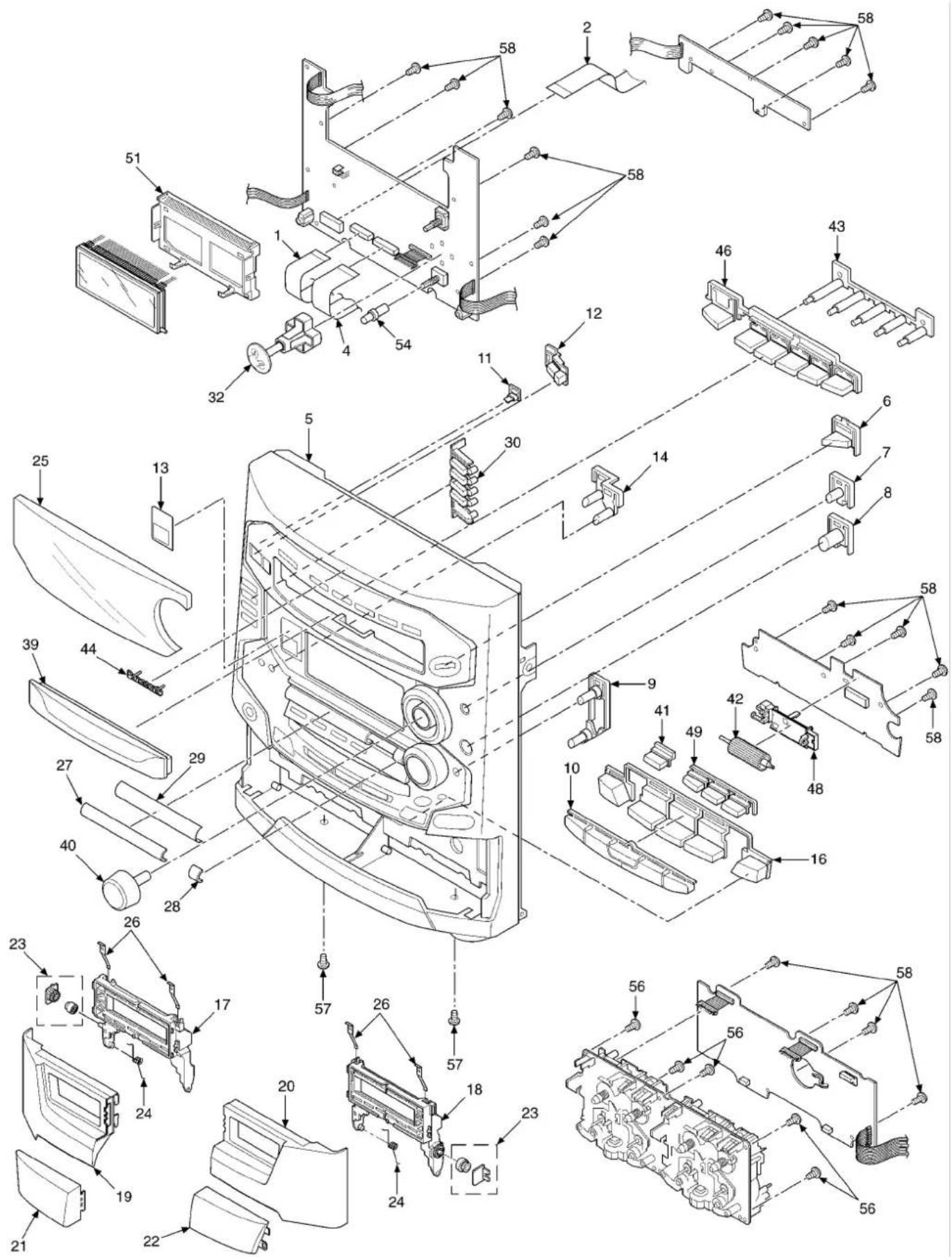
text_image
Exploded view diagram of a refrigerator internal components with numbered parts for identification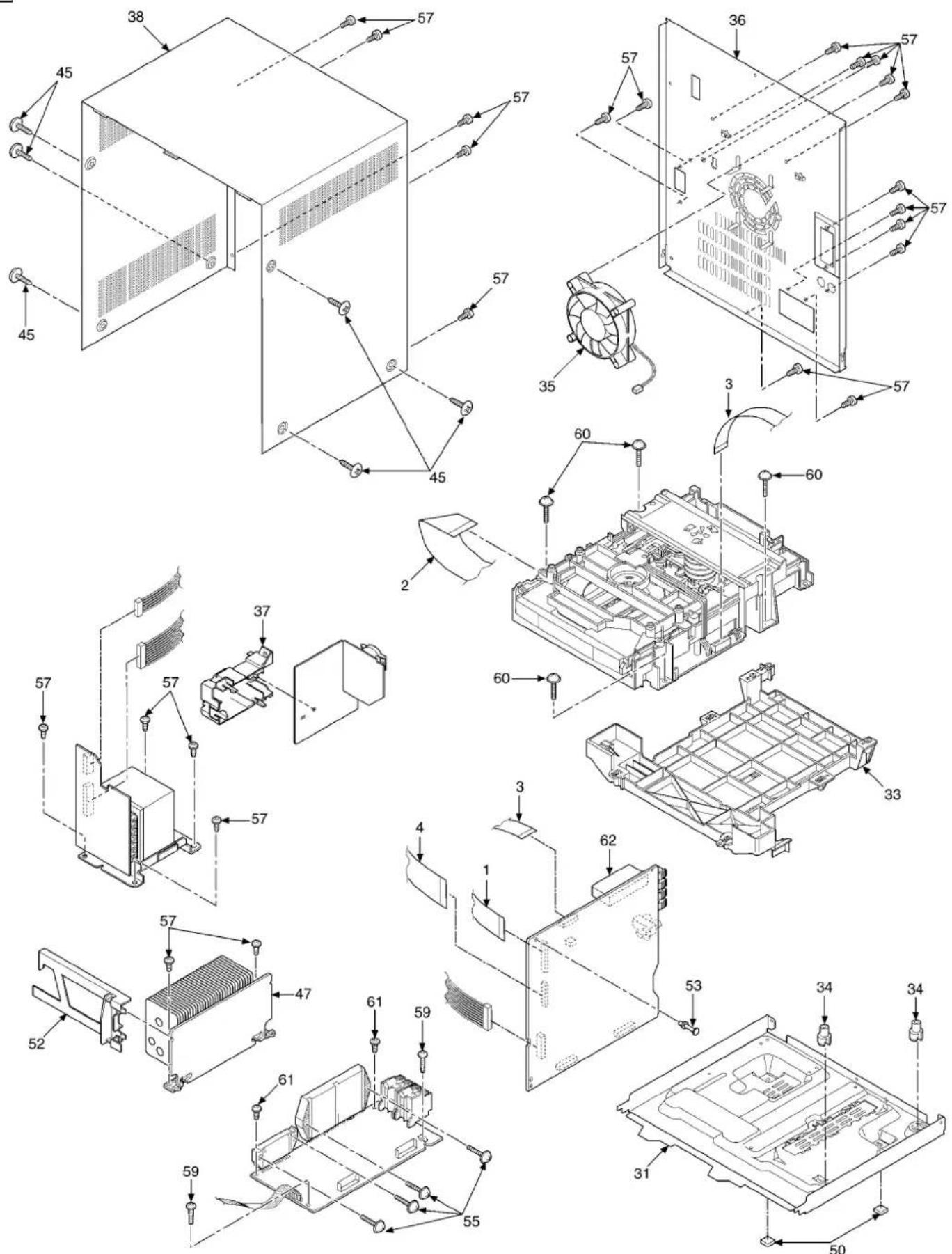
text_image
Exploded technical diagram of a computer system with numbered components and labeled parts23 Mechanism Parts Location
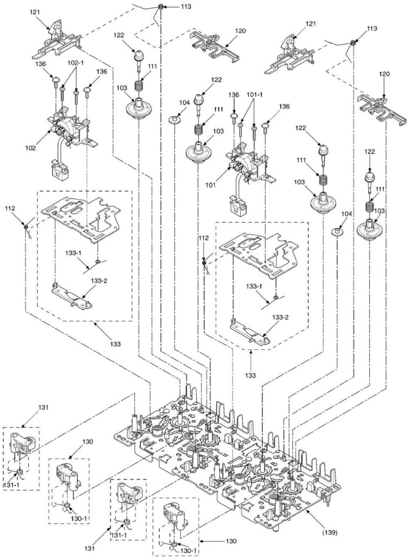
text_image
Technical diagram of a mechanical assembly with numbered components and exploded views, likely for assembly or manufacturing purposes.SPECIFICATIONS
| Playback torque | 20 - 60g · cm |
| Fast forward torque | 60 - 160g · cm |
| Rewind torque | 60 - 160g · cm |

text_image
ayback torque 20 - 60g - cm st forward torque 60 - 160g - cm wind torque 60 - 160g - cm MECHANISM P.C.B) (MECHANISM P.C.B) CS971 CS953 CS951 S952 S951 138 138 137 137 137 137 137 137 137 137 137 137 137 137 137 137 137 137 137 137 137 137 137 137 137 137 137 138 138 138 138 138 138 138 138 138 138 138 138 138 138 138 138 138 138 138 138 138 138 138 138 138 13924 CD Mechanism Parts Location
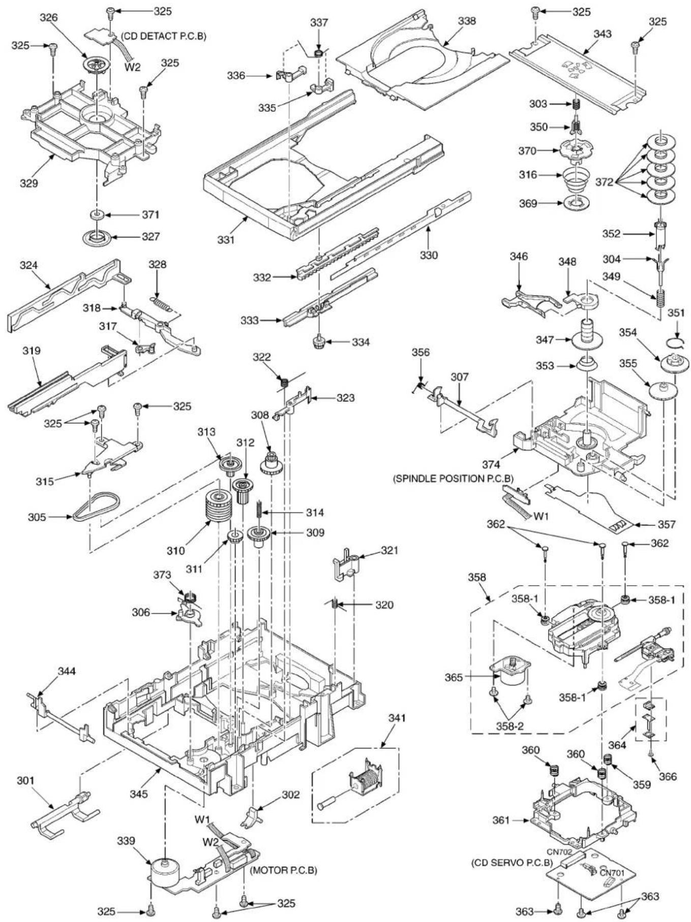
text_image
Exploded view diagram of a mechanical assembly with numbered components and labeled parts such as CD DETACT P.C.B, MOTOR P.C.B, and SPINDLE POSITION P.C.B.25 Packaging

flowchart
graph TD
    A["P1(RPGX0645)"] --> B["P2"]
    B --> C["Speaker Unit"]
    C --> D["Accessory Case"]
    D --> E["A2"]
    E --> F["A3"]
    F --> G["A4"]
    G --> H["A6(SJP5213-2)"]
    H --> I["BATTERY"]
    I --> J["A1,A1-1"]
    J --> K["A5"]
    K --> L["Fan Bag"]
    L --> M["Speaker Unit"]
    M --> N["Accresory Case"]
Service Manual
Speaker System

text_image
Remote Control Transmitter SB-AK48 SA-AK48 SB-AK48SB-AK48
Colour
(S)... Silver Type
Area
(GC)... Asia, Latin America, Africa and
Middle Near East
Specification
Type 4 way speaker system
Speaker(s)
Super Woofer 17cm cone type
Woofer 12cm cone type
Tweeter 6cm ring shaped dome type
Super Tweeter Piezo type
Impedance
HIGH 6Ω
MID 6Ω
LOW 6Ω
Input power
HIGH 60W (Music)
MID 60W (Music)
LOW 200W (Music)
Output sound pressure level 87 dB/W (1.0m)
Cross over frequency 150 Hz, 3.5 kHz
Frequency range 40 Hz - 50 kHz (-16 dB)
50 Hz - 36 kHz (-10 dB)
Dimensions (W x H x D) 250 x 348 x 292 mm
Weight 5.1 kg
Notes :
Specifications are subject to change without notice. Weight and dimensions are approximate.
■System : SC-AK48 (GC) Music Center : SA-AK48 (GC)
Speaker : SB-AK48 (GC)
WARNING
This service information is designed for experienced repair technicians only and is not designed for use by the general public. It does not contain warnings or cautions to advise non-technical individuals of potential dangers in attempting to service a product. Products powered by electricity should be serviced or repaired only by experienced professional technicians. Any attempt to service or repair the product or products dealt with in this service information by anyone else could result in serious injury or death.
1 Connection of the Speaker Cables
- Be sure to connect speaker cables before connecting the AC power supply cord.
- The load impedance of any speaker used with this unit must be 6 .
-
Be sure to connect the cable from the right speaker to the roght terminal and the cable from the left speaker to the left terminal.
-
Strip off the outer covering, and twist the center conductor. Make sure the bare ends of the wires are not unravelled. Notes : they are, twist them toght again.)
-
Insert the wire to the rear panel of the unit and close the lever.
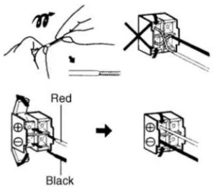
text_image
Red Black- To prevent damage to circuitry, never short-circuit positive (+) and negative (-) speaker wires.
- Be sure to connect only positive (red) wires to positive (+) terminals and negative (black) wires to negative (-) terminals.
2 Schematic Diagram
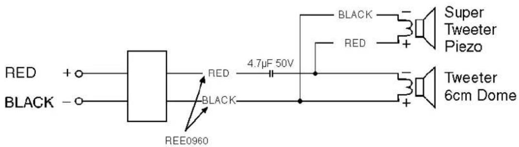
text_image
RED + BLACK - RED BLACK 4.7µF 50V BLACK RED Super Tweeter Piezo Tweeter 6cm Dome REE0960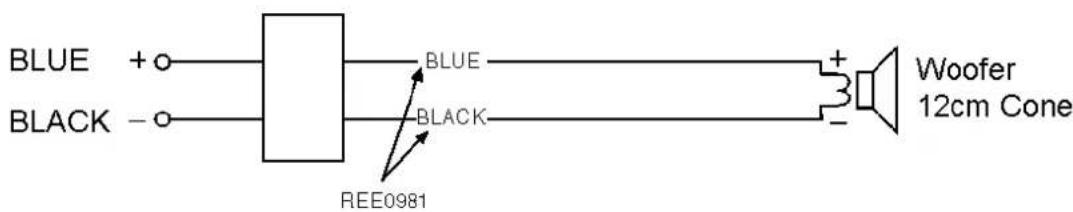
text_image
BLUE + - BLACK - - BLUE BLACK REE0981 Woofer 12cm Cone
text_image
RED +o BLACK -o Super Woofer 17cm Cone3 Cabinet PartsLocation

text_image
Exploded view diagram of a mechanical assembly with numbered components and directional arrows indicating assembly paths.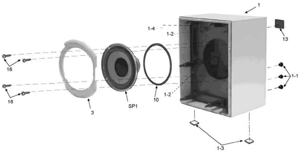
text_image
Exploded view diagram of an electronic device showing internal components and labeled parts4 ReplacementPartsList
Notes:
• Importantsafetynotice:
Components identified by ⚠ mark have special characteristics important for safety.
Furthermore, special parts which have purposes of fireretardant (resistors), high-quality sound (capacitors), low noise (resistors), etc are used.
When replacing any of these components, be sure to use only manufacturer's specified parts shown in the parts list.
• [M] indicates in the Remarks columns indicates parts supplied by MESA.
| Ref. No. | Part No. | Part Name & Description | Remarks |
| CABINET AND CHASSIS | |||
| 1 BKM0146 | SP CABINET AS | S'Y(L) [M] | |
| 1 BKM0145 | SP CABINET AS | S'Y(R) [M] |
| Ref. No. | Part No. | Part Name & Description | Remarks |
| 1-1 RGQ0230 | O-K CORD CLIPPER [M] | ||
| 1-2 RMQ0941 | BUSH TERMINAL [M] | ||
| 1-3 RKA007 | 2-KJ LEG [M] | ||
| 1-4 RMQ093 | PORT PACKING [M] | ||
| 2 | RYQ0296-S | FRONT PANEL (L) | [M] |
| 2 | RYQ0296A-S | FRONT PANEL (R) | [M] |
| 3 RMR1278-W | WOOFER RING [M] | ||
| 4 RMR1277-K | BACK CAVITY [M] | ||
| 5 | RMQ0936S | EVA PACKING (B/C) | [M] |
| 6 REE0960 | CORD ASS'Y | [M] | |
| 7 | RMR1281A-H | EXTEND PORT R | [M] |
| 7 | RMR1281-H | EXTEND PORT L | [M] |
| 8 RMG0513-K | CATCHER | [M] | |
| 10 | RMQ0705 | EVA PACKING (S/W) | [M] |
| 11 | RMG0490-K | CHER [M] | |
| 12 | RYB0234 NET F | FRAME ASS'Y [M] | |
| 13 | RGN1849-K | BACK LEBAL | [M] |
| 14 | XTB4+10G SCREW (B/C) [M] | ||
| 15 | XTB4+14G SCREW (F/P) [M] | ||
| 16 | XTB4+20AFN | SCREW (SUPER WOOFER) | [M] |
| 17 | RHD40009-S | SCREW (FRONT PANEL) | [M] |
| 18 | XTB4+8GFZ SCREW (TWEETER) [M] |
SB-AK48
| Ref. No. | Part No. | Part Name & Description | Remarks |
| 19 XTB3+10G | SCREW (EXTE | ND PORT) [M] | |
| 20 RGK0985 | B-H ORNAMENT | CAP [M] | |
| 21 RKA0072 | -KJ LEG [M] | ||
| 22 RGQ0260 | -S PANEL SPACER | [M] | |
| 23 RYQ0297 | -H ORNAMENT | ASS'Y (L) [M] | |
| 23 RYQ0297 | A-H ORNAMENT | ASS'Y (R) [M] | |
| 24 RGK0500 | -K DUST CAP [M] | ||
| 25 RMR1208 | -K TWEETER SPACER [M] | ||
| 26 REE0981 | WIRE [M] | ||
| 27 RMQ0931 | C CAB PACKING | [M] | |
| 28 RMQ0931 | LK CABINET PACKING | [M] | |
| CAPACITORS | |||
| C1 ECEA1HAY | 4R7S 4.7uF 50V | [M] | |
| PACKING MATERIALS | |||
| P1 RPH0187 | MIRAMAT | [M] | |
| P2 RPN1250 | POLYFOAM [M] | ||
| SPEAKER | |||
| SP1 | EAST17PL11B6 | SUPER WOOFER [M] | |
| SP2 | EAST12P25A6 | WOOFER | [M] |
| SP3 | EAST6PH06A6 | TWEETER | [M] |
| SP4 | EFBS55C41A6 | SUPER TWEETER | [M] |